fsdm0565r fairchild power switch (fps)
TRANSCRIPT
©2003 Fairchild Semiconductor Corporation
www.fairchildsemi.com
Rev.1.0.0
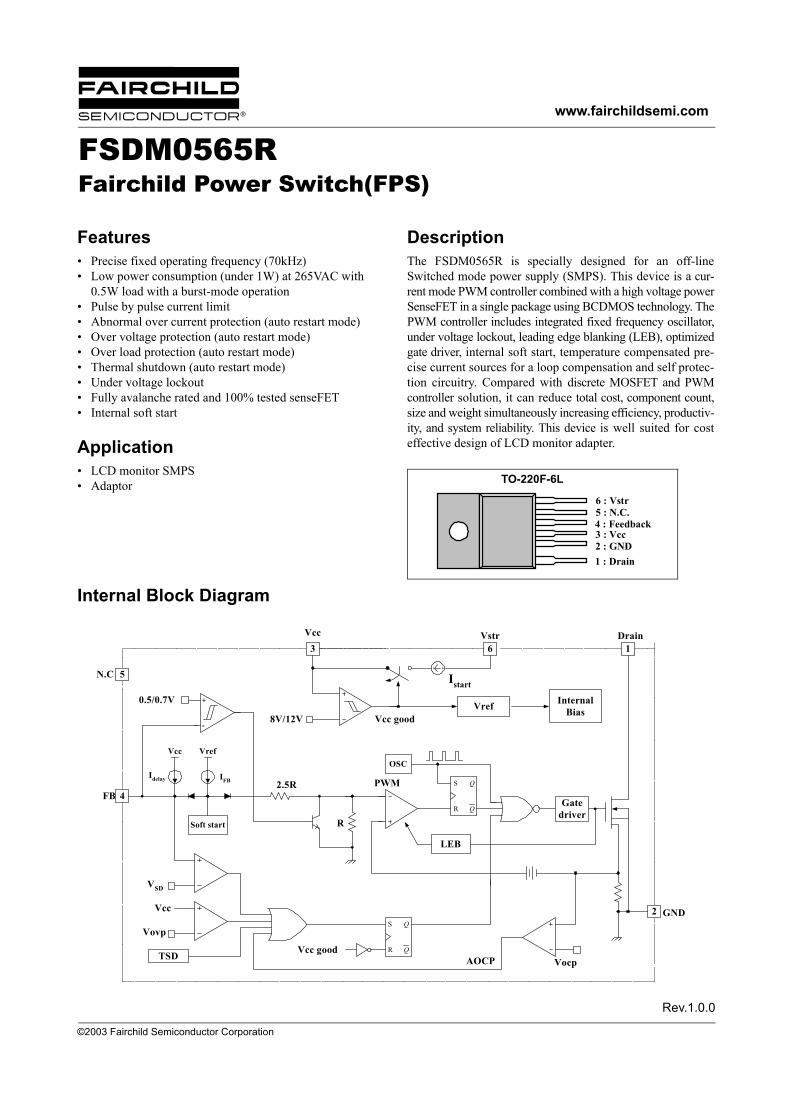
Features• Precise fixed operating frequency (70kHz)• Low power consumption (under 1W) at 265VAC with
0.5W load with a burst-mode operation• Pulse by pulse current limit• Abnormal over current protection (auto restart mode)• Over voltage protection (auto restart mode)• Over load protection (auto restart mode)• Thermal shutdown (auto restart mode)• Under voltage lockout• Fully avalanche rated and 100% tested senseFET• Internal soft start
Application• LCD monitor SMPS• Adaptor
DescriptionThe FSDM0565R is specially designed for an off-lineSwitched mode power supply (SMPS). This device is a cur-rent mode PWM controller combined with a high voltage powerSenseFET in a single package using BCDMOS technology. ThePWM controller includes integrated fixed frequency oscillator,under voltage lockout, leading edge blanking (LEB), optimizedgate driver, internal soft start, temperature compensated pre-cise current sources for a loop compensation and self protec-tion circuitry. Compared with discrete MOSFET and PWMcontroller solution, it can reduce total cost, component count,size and weight simultaneously increasing efficiency, productiv-ity, and system reliability. This device is well suited for costeffective design of LCD monitor adapter.
TO-220F-6L
1 : Drain2 : GND3 : Vcc4 : Feedback5 : N.C.6 : Vstr
Internal Block Diagram
8V/12V
3 1
2
4
5
Vref InternalBias
S
Q
Q
R
OSCVcc Vref
Idelay IFB
VSD
TSD
Vovp
Vcc
Vocp
S
Q
Q
R
R
2.5R
Vcc good
Vcc Drain
N.C
FB
GND
AOCP
Gatedriver
6Vstr
Istart
Vcc good
0.5/0.7V
LEB
PWM
Soft start
+
-
FSDM0565RFairchild Power Switch(FPS)

FSDM0565R
2
Pin Definitions
Pin Number Pin Name Pin Function Description
1 Drain This pin is the high voltage power SenseFET drain. It is designed to drive the transformer directly.
2 GND This pin is the control ground and the SenseFET source.
3 Vcc
This pin is the positive supply voltage input. During start up, the power is supplied by an internal high voltage current source that is connected to the Vstr pin. When Vcc reaches 12V, the internal high voltage current source is disabled and the power is supplied from auxiliary transformer winding.
4 Feedback
This pin is internally connected to the inverting input of the PWM comparator. The collector of an optocoupler is typically tied to this pin. For stable operation, a capacitor should be placed between this pin and GND. If the voltage of this pin reaches 6.0V, the over load protection is activated resulting in shutdown of the FPS.
5 N.C -
6 Vstr
This pin is connected directly to the high voltage DC link. At startup, the internal high voltage current source supplies internal bias and charges the external capacitor that is conneted to the Vcc pin. Once Vcc reaches 12V, the internal current source is disabled.
FSDM0565R
3
Absolute Maximum Ratings(Ta=25°C, unless otherwise specified)
Notes:1. Tj=25°C to 150°C2. Repetitive rating: Pulse width limited by maximum junction temperature3. L= mH, starting Tj=25°C4. L=13uH, starting Tj=25°C
Parameter Symbol Value UnitDrain-gate voltage (RGS=1MΩ) VDGR 650 VGate-source (GND) voltage VGS ±30 VDrain current pulsed (2) IDM 20 ADCSingle pulsed avalanche energy (3) EAS 570 mJSingle pulsed avalanche current (4) IAS - ASupply voltage VCC 19 VInput voltage range VFB -0.3 to VCC V
Total power dissipationPD(Watt H/S) 62 W
Derating 0.498 W/°COperating junction temperature Tj +150 °COperating ambient temperature TA -25 to +85 °CStorage temperature range TSTG -55 to +150 °C
FSDM0565R
4
Electrical Characteristics (SenseFET part)(Ta=25°C unless otherwise specified)
Note:1. Pulse test : Pulse width ≤ 300µS, duty ≤ 2%
Parameter Symbol Condition Min. Typ. Max. UnitDrain source breakdown voltage BVDSS VGS = 0V, ID = 250µA 650 - - V
Zero gate voltage drain current IDSSVDS = 650V, VGS = 0V - - 50 µAVDS= 520VVGS = 0V, TC = 125°C - - 200 µA
Static drain source on resistance (1) RDS(ON) VGS = 10V, ID = 2.5A - 1.76 2.2 Ω
Forward transconductance gfs VDS = 50V, ID = 2.5A 2.5 - - mhoInput capacitance Ciss
VGS = 0V, VDS = 25V,f = 1MHz
- 1457 -pFOutput capacitance Coss - 130 -
Reverse transfer capacitance Crss - 38.8 -Turn on delay time td(on) VDD= 325V, ID= 6.5A
(MOSFET switchingtime is essentiallyindependent of operating temperature)
- 22 -
nsRise time tr - 70 -Turn off delay time td(off) - 105 -Fall time tf - 65 -Total gate charge(gate-source+gate-drain) Qg VGS = 10V, ID = 5.0A,
VDS = 520V (MOSFET switching time is essentially independent of operating temperature)
- - 56
nCGate-source charge Qgs - 10.3 -Gate-drain (miller) charge Qgd - 22.3 -
FSDM0565R
5
Electrical Characteristics (Continued) (Ta=25°C unless otherwise specified)
Note:1. These parameters, although guaranteed at the design, are not tested in mass production..2. These parameters, although guaranteed, are tested in EDS(wafer test) process.
Parameter Symbol Condition Min. Typ. Max. UnitUVLO SECTIONStart threshold voltage VSTART VFB=GND 11 12 13 VStop threshold voltage VSTOP VFB=GND 7 8 9 VOSCILLATOR SECTIONInitial frequency FOSC Vfb = 3V 60 66 72 kHzVoltage stability FSTABLE 13V ≤ Vcc ≤ 18V 0 1 3 %Temperature stability (note4) ∆FOSC -25°C ≤ Ta ≤ 85°C 0 ±5 ±10 %Maximum duty cycle DMAX - 75 80 85 %Minimum duty cycle DMIN - - - 0 %FEEDBACK SECTIONFeedback source current IFB VFB=GND 0.7 0.9 1.1 mAShutdown feedback voltage VSD Vfb ≥ 5.5V 5.5 6.0 6.5 VShutdown delay current Idelay VFB=5V 2.8 3.5 4.2 µAPROTECTION SECTIONOver voltage protection VOVP - 18 19 20 VAbnormal Over current protection voltage (Note2)
VOCP - 1.44 1.6 1.76 V
Thermal shutdown temp.(Note4) TSD Hysteresis 130 145 160 °CSOFTSTART SECTIONSoftstart time Ts Vfb=3 - 10 15 msecBURST MODE SECTIONBurst mode enable feedback voltage (Note4) VBEN Vcc=14V - 0.5 - VBurst mode disable feedback voltage (Note4) VBDV Vcc=14V - 0.7 - VCURRENT LIMIT(SELF-PROTECTION)SECTIONPeak current limit (Note3) IOVER Vfb=5V, VCC=14V 2.0 2.3 2.6 ATOTAL DEVICE SECTION
Operating supply current (Note1)IOP Vfb=GND, VCC=14V
- 3 5 mAIOP(MIN) Vfb=GND, VCC=10VIOP(MAX) Vfb=GND, VCC=18V
FSDM0565R
6
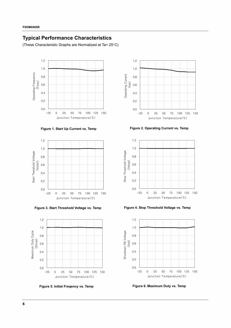
Typical Performance Characteristics(These Characteristic Graphs are Normalized at Ta= 25°C)
0.0
0.2
0.4
0.6
0.8
1.0
1.2
-25 0 25 50 75 100 125 150
Junction Temperature()
Opera
ting F
requency
(Fosc)
0.0
0.2
0.4
0.6
0.8
1.0
1.2
-25 0 25 50 75 100 125 150
Junction Temperature()
Opera
ting C
urrent
(Iop)
0.0
0.2
0.4
0.6
0.8
1.0
1.2
-25 0 25 50 75 100 125 150
Junction Temperature()
Sta
rt T
hers
hold
Voltage
(Vsta
rt)
0.0
0.2
0.4
0.6
0.8
1.0
1.2
-25 0 25 50 75 100 125 150
Junction Temperature()
Sto
p T
hre
shold
Voltage
(Vsto
p)
0.0
0.2
0.4
0.6
0.8
1.0
1.2
-25 0 25 50 75 100 125 150
Junction Temperature()
Maxi
mum
Duty
Cyc
le
(Dm
ax)
0.0
0.2
0.4
0.6
0.8
1.0
1.2
-25 0 25 50 75 100 125 150
Junction Temperatu re()
Shutd
ow
n F
B V
oltage
(Vsd)
Figure 1. Start Up Current vs. Temp Figure 2. Operating Current vs. Temp
Figure 3. Start Threshold Voltage vs. Temp Figure 4. Stop Threshold Voltage vs. Temp
Figure 5. Initial Freqency vs. Temp Figure 6. Maximum Duty vs. Temp
FSDM0565R
7
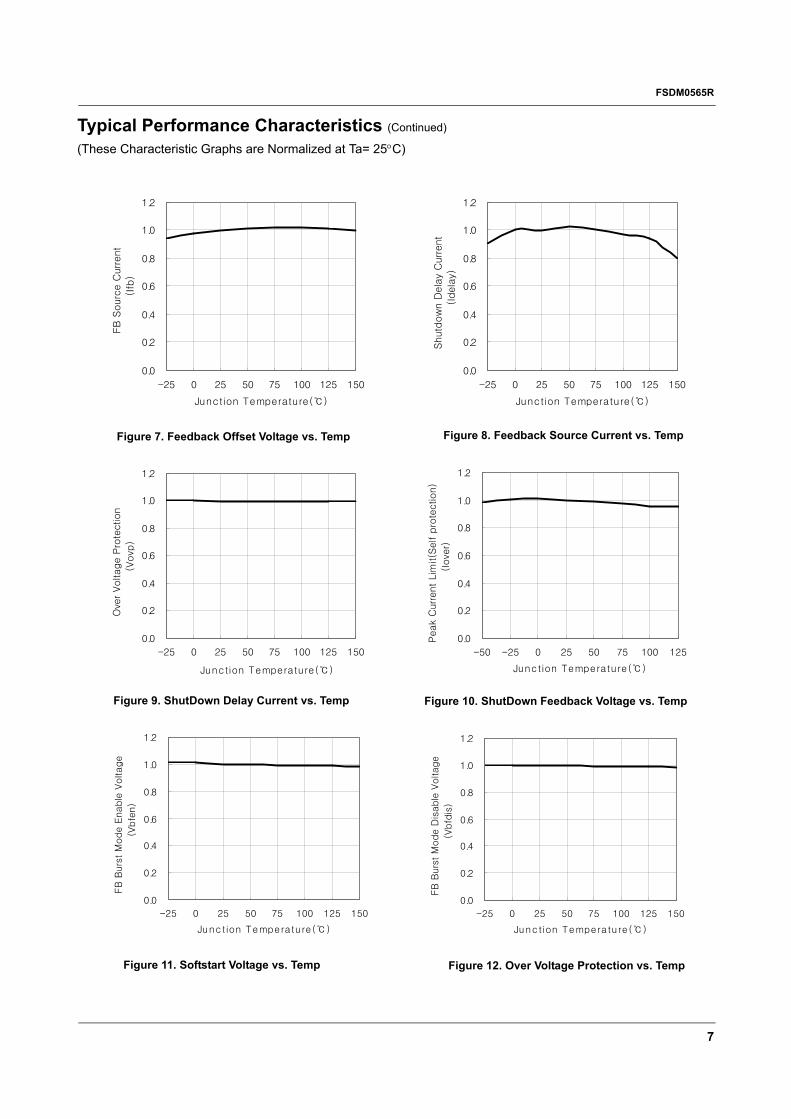
Typical Performance Characteristics (Continued)
(These Characteristic Graphs are Normalized at Ta= 25°C)
0.0
0.2
0.4
0.6
0.8
1.0
1.2
-25 0 25 50 75 100 125 150
Junction Temperature()
FB
Sourc
e C
urrent
(Ifb
)
0.0
0.2
0.4
0.6
0.8
1.0
1.2
-25 0 25 50 75 100 125 150
Junction Temperature()
Shutd
ow
n D
ela
y C
urrent
(Idela
y)
0.0
0.2
0.4
0.6
0.8
1.0
1.2
-25 0 25 50 75 100 125 150
Junction Temperature()
Ove
r Voltage P
rote
ction
(Vovp
)
0.0
0.2
0.4
0.6
0.8
1.0
1.2
-50 -25 0 25 50 75 100 125
Junction Temperature()
Peak C
urrent Lim
it(S
elf p
rote
ction)
(Iove
r)
0.0
0.2
0.4
0.6
0.8
1.0
1.2
-25 0 25 50 75 100 125 150
Junction Temperatu re()
FB
Burs
t M
ode E
nable
Voltage
(Vbfe
n)
0.0
0.2
0.4
0.6
0.8
1.0
1.2
-25 0 25 50 75 100 125 150
Junction Temperatu re ()
FB
Burs
t M
ode D
isable
Voltage
(Vbfd
is)
Figure 7. Feedback Offset Voltage vs. Temp Figure 8. Feedback Source Current vs. Temp
Figure 9. ShutDown Delay Current vs. Temp Figure 10. ShutDown Feedback Voltage vs. Temp
Figure 11. Softstart Voltage vs. Temp Figure 12. Over Voltage Protection vs. Temp
FSDM0565R
8
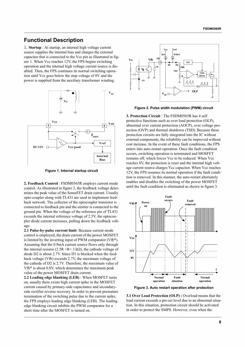
Functional Description1. Startup : At startup, an internal high voltage current source supplies the internal bias and charges the external capacitor that is connected to the Vcc pin as illustrated in fig-ure 1. When Vcc reaches 12V, the FPS begins switching operation and the internal high voltage current source is dis-abled. Then, the FPS continues its normal switching opera-tion until Vcc goes below the stop voltage of 8V and the power is supplied from the auxiliary transformer winding.
Figure 1. Internal startup circuit
2. Feedback Control : FSDM0565R employs current mode control. As illustrated in figure 2, the feedback voltage deter-mines the peak value of the SenseFET drain current. Usually opto-coupler along with TL431 are used to implement feed-back network. The collector of the optocoupler transistor is connected to feedback pin and the emitter is connected to the ground pin. When the voltage of the reference pin of TL431 exceeds the internal reference voltage of 2.5V, the optocou-pler diode current increases, pulling down the feedback volt-age.2.1 Pulse-by-pulse current limit: Because current mode control is employed, the drain current of the power MOSFET is limited by the inverting input of PWM comparator (Vfb*). Assuming that the 0.9mA current source flows only through the internal resistor (2.5R +R= 3 kΩ), the cathode voltage of diode D2 is about 2.7V. Since D1 is blocked when the feed-back voltage (Vfb) exceeds 2.7V, the maximum voltage of the cathode of D2 is 2.7V. Therefore, the maximum value of Vfb* is about 0.8V, which determines the maximum peak value of the power MOSFET drain current. 2.2 Leading edge blanking (LEB) : When MOSFET turns on, usually there exists high current spike in the MOSFET current caused by primary-side capacitance and secondary-side rectifier reverse recovery. In order to prevent premature termination of the switching pulse due to the current spike, the FPS employs leading edge blanking (LEB). The leading edge blanking circuit inhibits the PWM comparator for a short time after the MOSFET is turned on.
Figure 2. Pulse width modulation (PWM) circuit
3. Protection Circuit : The FSDM0565R has 4 self protective functions such as over load protection (OLP), abnormal over current protection (AOCP), over voltage pro-tection (OVP) and thermal shutdown (TSD). Because these protection circuits are fully integrated into the IC without external components, the reliability can be improved without cost increase. In the event of these fault conditions, the FPS enters into auto-restart operation. Once the fault condition occurs, switching operation is terminated and MOSFET remains off, which forces Vcc to be reduced. When Vcc reaches 8V, the protection is reset and the internal high volt-age current source charges Vcc capacitor. When Vcc reaches 12V, the FPS resumes its normal operation if the fault condi-tion is removed. In this manner, the auto-restart alternately enables and disables the switching of the power MOSFET until the fault condition is eliminated as shown in figure 3.
Figure 3. Auto restart operation after protection
3.1 Over Load Protection (OLP) : Overload means that the load current exceeds a pre-set level due to an abnormal situa-tion. In this situation, protection circuit should be activated in order to protect the SMPS. However, even when the
8V/12V
3
Vref
InternalBias
Vcc6 Vstr
Istart
Vcc good
VDC
Vc
4 OSC
Vcc Vref
2uA 0.9mA
VSD
R
28R
FB
Gatedriver
OLP
D1 D2
Vfb*
Vfb
431
Cfb
Vo
Faultsituation
8V
12V
Vcc
Vds
t
Faultoccurs Fault
removed
Normaloperation
Normaloperation
Poweron
FSDM0565R
9
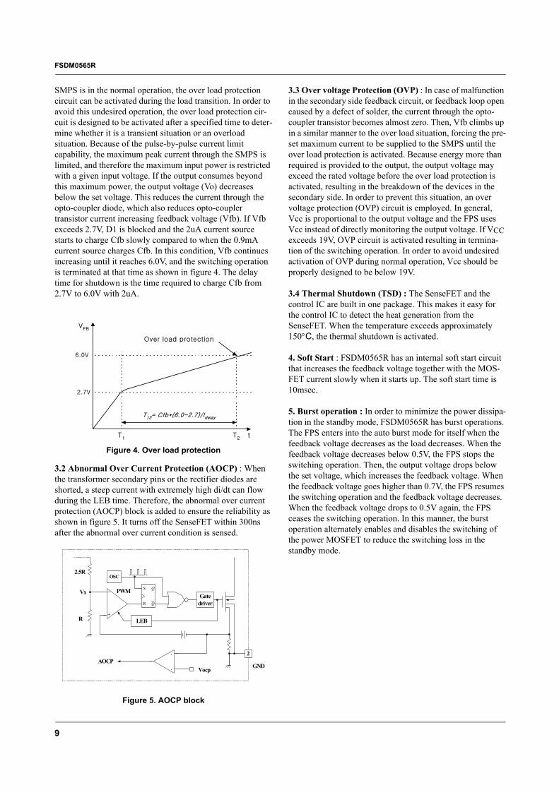
SMPS is in the normal operation, the over load protection circuit can be activated during the load transition. In order to avoid this undesired operation, the over load protection cir-cuit is designed to be activated after a specified time to deter-mine whether it is a transient situation or an overload situation. Because of the pulse-by-pulse current limit capability, the maximum peak current through the SMPS is limited, and therefore the maximum input power is restricted with a given input voltage. If the output consumes beyond this maximum power, the output voltage (Vo) decreases below the set voltage. This reduces the current through the opto-coupler diode, which also reduces opto-coupler transistor current increasing feedback voltage (Vfb). If Vfb exceeds 2.7V, D1 is blocked and the 2uA current source starts to charge Cfb slowly compared to when the 0.9mA current source charges Cfb. In this condition, Vfb continues increasing until it reaches 6.0V, and the switching operation is terminated at that time as shown in figure 4. The delay time for shutdown is the time required to charge Cfb from 2.7V to 6.0V with 2uA.
Figure 4. Over load protection
3.2 Abnormal Over Current Protection (AOCP) : When the transformer secondary pins or the rectifier diodes are shorted, a steep current with extremely high di/dt can flow during the LEB time. Therefore, the abnormal over current protection (AOCP) block is added to ensure the reliability as shown in figure 5. It turns off the SenseFET within 300ns after the abnormal over current condition is sensed.
Figure 5. AOCP block
3.3 Over voltage Protection (OVP) : In case of malfunction in the secondary side feedback circuit, or feedback loop open caused by a defect of solder, the current through the opto-coupler transistor becomes almost zero. Then, Vfb climbs up in a similar manner to the over load situation, forcing the pre-set maximum current to be supplied to the SMPS until the over load protection is activated. Because energy more than required is provided to the output, the output voltage may exceed the rated voltage before the over load protection is activated, resulting in the breakdown of the devices in the secondary side. In order to prevent this situation, an over voltage protection (OVP) circuit is employed. In general, Vcc is proportional to the output voltage and the FPS uses Vcc instead of directly monitoring the output voltage. If VCC exceeds 19V, OVP circuit is activated resulting in termina-tion of the switching operation. In order to avoid undesired activation of OVP during normal operation, Vcc should be properly designed to be below 19V.
3.4 Thermal Shutdown (TSD) : The SenseFET and the control IC are built in one package. This makes it easy for the control IC to detect the heat generation from the SenseFET. When the temperature exceeds approximately 150°C, the thermal shutdown is activated.
4. Soft Start : FSDM0565R has an internal soft start circuit that increases the feedback voltage together with the MOS-FET current slowly when it starts up. The soft start time is 10msec.
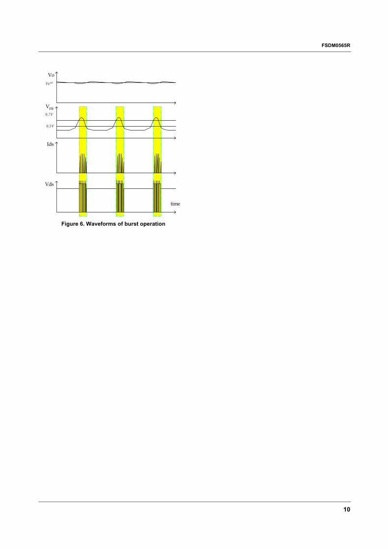
5. Burst operation : In order to minimize the power dissipa-tion in the standby mode, FSDM0565R has burst operations. The FPS enters into the auto burst mode for itself when the feedback voltage decreases as the load decreases. When the feedback voltage decreases below 0.5V, the FPS stops the switching operation. Then, the output voltage drops below the set voltage, which increases the feedback voltage. When the feedback voltage goes higher than 0.7V, the FPS resumes the switching operation and the feedback voltage decreases. When the feedback voltage drops to 0.5V again, the FPS ceases the switching operation. In this manner, the burst operation alternately enables and disables the switching of the power MOSFET to reduce the switching loss in the standby mode.
VFB
t
2.7V
6.0V
Over load protection
T12= Cfb*(6.0-2.7)/Idelay
T1
T2
2
S
Q
Q
R
OSC
R
2.5R
GND
Gatedriver
LEB
PWMVx
+
- VocpAOCP
FSDM0565R
10
Figure 6. Waveforms of burst operation
VFB
Vds
0.5V
0.7V
Ids
VoVoset
time
FSDM0565R
11
Typical application circuit
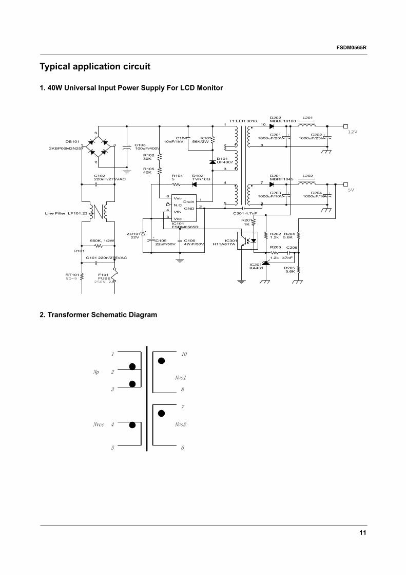
1. 40W Universal Input Power Supply For LCD Monitor
2. Transformer Schematic Diagram
5V
L201
RT101
-+
2KBP06M3N257
DB1011
2
3
4
D202MBRF10100
+C2021000uF/25V
Line Filter: LF101:23mH
ZD10122V
5D-9
IC101FSDM0565R
4
3
2
15
6
Vfb
Vcc
GND
DrainN.C
Vstr
R10540K
D101UF4007
R10230K
D201MBRF1045
D102TVR10G
F101FUSE
R2045.6K+
C10522uF/50V
IC201KA431
T1:EER 3016
7
8
10
3
22
1
4
5 6
R2021.2k
C10410nF/1kV
12V+C201
1000uF/25V
250V 2A
+C2031000uF/10V
C101 220n/275VAC
R2011K
R10356K/2W
R203
1.2k
R2055.6K
L202
+C2041000uF/10V
C301 4.7nF
+ C103100uF/400V
R1045
C102220nF/275VAC
C10647nF/50V
IC301H11A817A
R101
560K, 1/2W
C205
47nF
1
2
3
4
5
10
6
Np
Nvcc
Nvo1
7
Nvo2
8
FSDM0565R
12
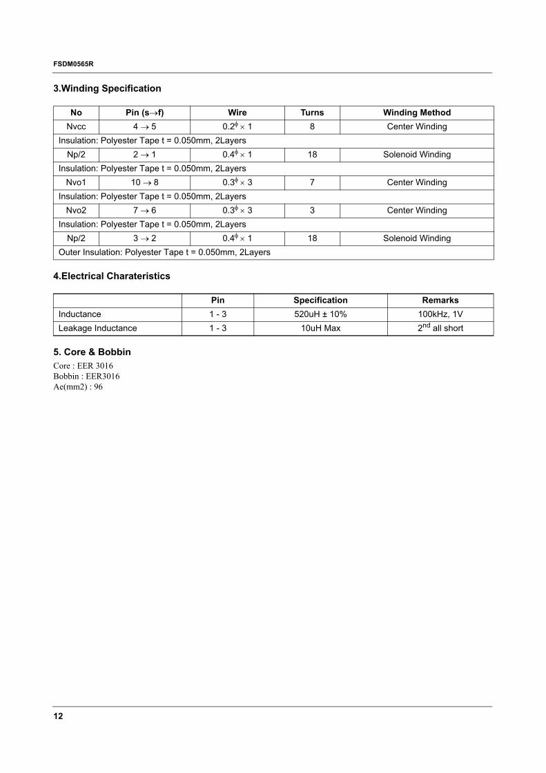
3.Winding Specification
4.Electrical Charateristics
5. Core & BobbinCore : EER 3016Bobbin : EER3016Ae(mm2) : 96
No Pin (s→f) Wire Turns Winding MethodNvcc 4 → 5 0.2φ × 1 8 Center Winding
Insulation: Polyester Tape t = 0.050mm, 2LayersNp/2 2 → 1 0.4φ × 1 18 Solenoid Winding
Insulation: Polyester Tape t = 0.050mm, 2LayersNvo1 10 → 8 0.3φ × 3 7 Center Winding
Insulation: Polyester Tape t = 0.050mm, 2LayersNvo2 7 → 6 0.3φ × 3 3 Center Winding
Insulation: Polyester Tape t = 0.050mm, 2LayersNp/2 3 → 2 0.4φ × 1 18 Solenoid Winding
Outer Insulation: Polyester Tape t = 0.050mm, 2Layers
Pin Specification RemarksInductance 1 - 3 520uH ± 10% 100kHz, 1VLeakage Inductance 1 - 3 10uH Max 2nd all short
FSDM0565R
13
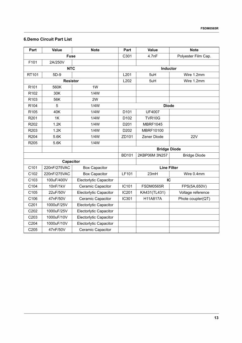
6.Demo Circuit Part List
Part Value Note Part Value NoteFuse C301 4.7nF Polyester Film Cap.
F101 2A/250VNTC Inductor
RT101 5D-9 L201 5uH Wire 1.2mmResistor L202 5uH Wire 1.2mm
R101 560K 1WR102 30K 1/4WR103 56K 2WR104 5 1/4W DiodeR105 40K 1/4W D101 UF4007R201 1K 1/4W D102 TVR10GR202 1.2K 1/4W D201 MBRF1045R203 1.2K 1/4W D202 MBRF10100R204 5.6K 1/4W ZD101 Zener Diode 22VR205 5.6K 1/4W
Bridge DiodeBD101 2KBP06M 3N257 Bridge Diode
CapacitorC101 220nF/275VAC Box Capacitor Line FilterC102 220nF/275VAC Box Capacitor LF101 23mH Wire 0.4mmC103 100uF/400V Electorlytic Capacitor ICC104 10nF/1kV Ceramic Capacitor IC101 FSDM0565R FPS(5A,650V)C105 22uF/50V Electorlytic Capacitor IC201 KA431(TL431) Voltage referenceC106 47nF/50V Ceramic Capacitor IC301 H11A817A Phote coupler(QT)C201 1000uF/25V Electorlytic CapacitorC202 1000uF/25V Electorlytic CapacitorC203 1000uF/10V Electorlytic CapacitorC204 1000uF/10V Electorlytic CapacitorC205 47nF/50V Ceramic Capacitor
FSDM0565R
14
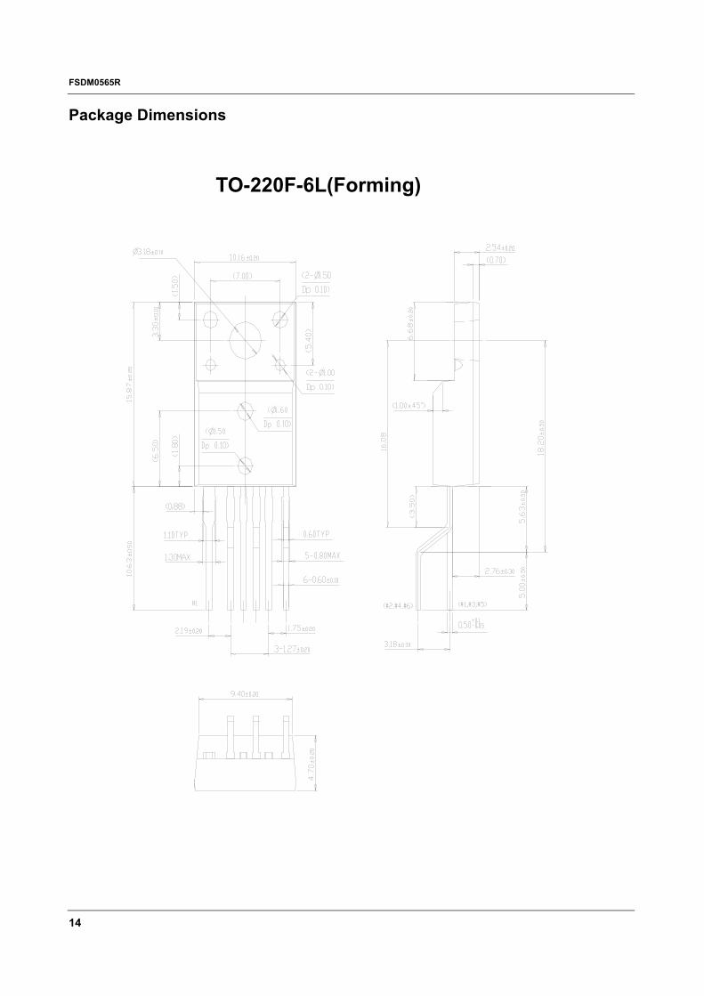
Package Dimensions
TO-220F-6L(Forming)

FSDM0565R
15
Ordering Information
YDTU : Forming Type
Product Number Package Marking Code BVdss Rds(on)Max.FSDM0565RYDTU TO-220F-6L(Forming) DM0565R 650V 2.2
FSDM0565R
8/28/03 0.0m 001Stock#DSxxxxxxxx
2003 Fairchild Semiconductor Corporation
LIFE SUPPORT POLICY FAIRCHILD’S PRODUCTS ARE NOT AUTHORIZED FOR USE AS CRITICAL COMPONENTS IN LIFE SUPPORT DEVICES OR SYSTEMS WITHOUT THE EXPRESS WRITTEN APPROVAL OF THE PRESIDENT OF FAIRCHILD SEMICONDUCTOR CORPORATION. As used herein:
1. Life support devices or systems are devices or systems which, (a) are intended for surgical implant into the body, or (b) support or sustain life, and (c) whose failure to perform when properly used in accordance with instructions for use provided in the labeling, can be reasonably expected to result in a significant injury of the user.
2. A critical component in any component of a life support device or system whose failure to perform can be reasonably expected to cause the failure of the life support device or system, or to affect its safety or effectiveness.
www.fairchildsemi.com
DISCLAIMER FAIRCHILD SEMICONDUCTOR RESERVES THE RIGHT TO MAKE CHANGES WITHOUT FURTHER NOTICE TO ANY PRODUCTS HEREIN TO IMPROVE RELIABILITY, FUNCTION OR DESIGN. FAIRCHILD DOES NOT ASSUME ANY LIABILITY ARISING OUT OF THE APPLICATION OR USE OF ANY PRODUCT OR CIRCUIT DESCRIBED HEREIN; NEITHER DOES IT CONVEY ANY LICENSE UNDER ITS PATENT RIGHTS, NOR THE RIGHTS OF OTHERS.