fr60 mb91460t series - fujitsu
TRANSCRIPT
FME-MB91460T rev 2.0FUJITSU MICROELECTRONICS LIMITEDDATA SHEET
32-bit MicrocontrollerCMOS
FR60 MB91460T Series
MB91F467TA, MB91F469TA
DESCRIPTIONMB91460T series is a line of general-purpose 32-bit RISC microcontrollers designed for embedded controlapplications which require high-speed real-time processing, such as consumer devices and on-board vehiclesystems. This series uses the FR60 CPU, which is compatible with the FR family* of CPUs.
This series contains the LIN-USART and CAN controllers.
*: FR, the abbreviation of FUJITSU RISC controller, is a line of products of Fujitsu Microelectronics Limited.
FEATURES1. FR60 CPU core
• 32-bit RISC, load/store architecture, five-stage pipeline• 16-bit fixed-length instructions (basic instructions)• Instruction execution speed: 1 instruction per cycle• Instructions including memory-to-memory transfer, bit manipulation, and barrel shift instructions: Instructions
suitable for embedded applications• Function entry/exit instructions and register data multi-load store instructions: Instructions supporting C
language• Register interlock function: Facilitating assembly-language coding• Built-in multiplier with instruction-level support
Signed 32-bit multiplication: 5 cyclesSigned 16-bit multiplication: 3 cycles
• Interrupts (save PC/PS) : 6 cycles (16 priority levels)(Continued)
RELIMIN
ARY
Copyright©2008 FUJITSU MICROELECTRONICS LIMITED All rights reserved
“Check Sheet” is seen at the following support pageURL: http://www.fujitsu.com/global/services/microelectronics/product/micom/support/index.html
“Check Sheet” lists the minimal requirement items to be checked to prevent problems beforehand in system development.
Be sure to refer to the “Check Sheet” for the latest cautions on development.P
MB91460T Series
2
(Continued)• Harvard architecture enabling program access and data access to be performed simultaneously• Instructions compatible with the FR family
2. Internal peripheral resources• General-purpose ports: Maximum 109 ports• DMAC (DMA Controller)
Maximum of 5 channels able to operate simultaneously2 transfer sources (internal peripheral/software)Activation source can be selected using softwareAddressing mode specifies full 32-bit addresses (increment/decrement/fixed)Transfer mode (demand transfer/burst transfer/step transfer/block transfer)Transfer data size selectable from 8/16/32-bitMulti-byte transfer enabled (by software)DMAC descriptor in I/O areas (200H to 240H, 1000H to 1024H)
• A/D converter (successive approximation type)10-bit resolution: 32 channels **Conversion time: minimum 1 μs
• External interrupt inputs: 12 channels **8 channels shared with A/D converter AN8-15
• Bit search module (for REALOS)Function to search from the MSB (most significant bit) for the position of the first “0”, “1”, or changed bit in a word
• LIN-USART (full duplex double buffer): 11 channels **Clock synchronous/asynchronous selectableSync-break detectionInternal dedicated baud rate generator
• I2C* bus interface (supports 400 kbps): 4 channels **Master/slave transmission and receptionArbitration function, clock synchronization function
• CAN controller (C-CAN): Maximum of 2 channelsMaximum transfer speed: 1 Mbps32 transmission/reception message buffers
• Sound generator: 1 channelTone frequency: PWM frequency divide-by-two (reload value + 1)
• Monitor external voltageGenerate an interrupt in case of voltage lower/higher than the defined thresholds (reference voltage)
• 16-bit PPG timer: 14 channels **• 16-bit PFM timer: 1 channel **• 16-bit reload timer: 8 channels• 16-bit free-run timer: 8 channels (1 channel each for ICU and OCU) **• Input capture: 8 channels (operates in conjunction with the free-run timer)• Output compare: 8 channels (operates in conjunction with the free-run timer)• Up/Down counter: 2 channels (4*8-bit or 2*16-bit) **• Watchdog timer
Note: ** The maximum channel count is given; the real number depends on port multiplexing.(Continued)
PRELIMIN
ARY
MB91460T Series
(Continued)• Real-time clock• Low-power consumption modes: Sleep/stop mode function• Low voltage detection circuit• Clock supervisor
Monitors the sub-clock (32 kHz) and the main clock (4 MHz) , and switches to a recovery clock (CR oscillator,etc.) when the oscillations stop.
• Clock modulator• Clock monitor• Sub-clock calibration
Corrects the real-time clock timer when operating with the 32 kHz or CR oscillator• Main oscillator stabilization timer
Generates an interrupt in sub-clock mode after the stabilization wait time has elapsed on the 23-bit stabilizationwait time counter
• Sub-oscillator stabilization timerGenerates an interrupt in main clock mode after the stabilization wait time has elapsed on the 15-bit stabilizationwait time counter
3. Package and technology• Package: QFP-144• CMOS 0.18 μm technology• Power supply range 3 V to 5 V (1.8 V internal logic provided by a step-down voltage converter)• Operating temperature range: between − 40°C and + 105°C
Note: *Purchase of Fujitsu I2C components conveys a license under the Philips I2C Patent Rights to use these components in an I2C system provided that the system conforms to the I2C Standard Specification as defined by Philips.
PRELIMIN
ARY
3
MB91460T Series
4
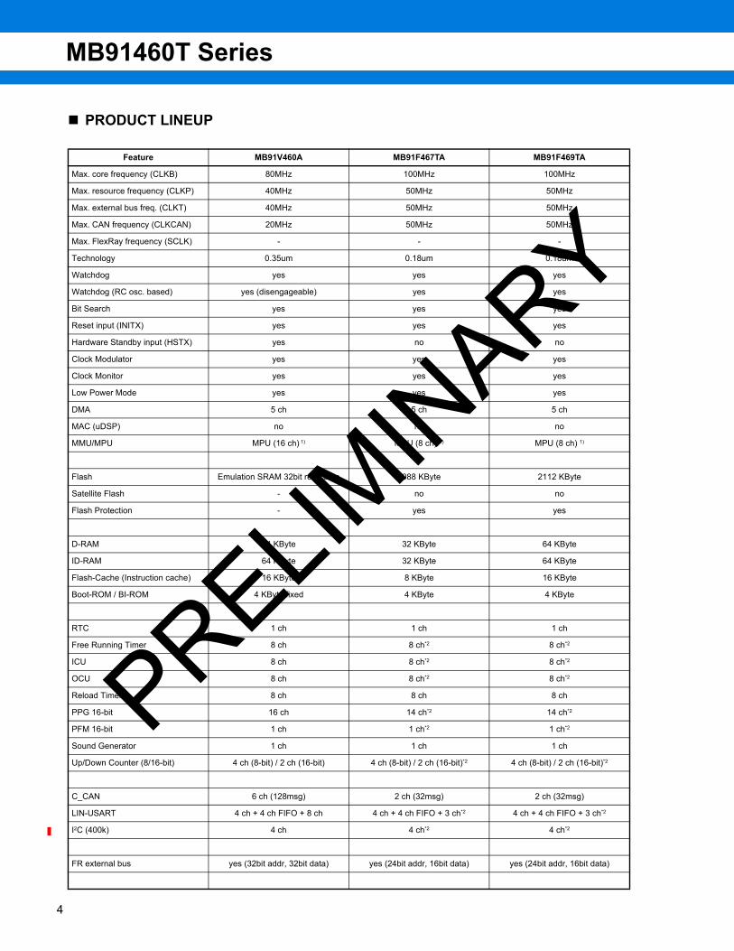
PRODUCT LINEUP
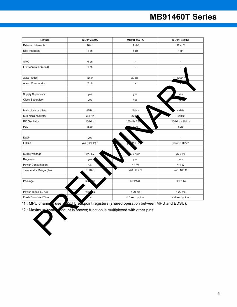
Feature MB91V460A MB91F467TA MB91F469TA
Max. core frequency (CLKB) 80MHz 100MHz 100MHz
Max. resource frequency (CLKP) 40MHz 50MHz 50MHz
Max. external bus freq. (CLKT) 40MHz 50MHz 50MHz
Max. CAN frequency (CLKCAN) 20MHz 50MHz 50MHz
Max. FlexRay frequency (SCLK) - - -
Technology 0.35um 0.18um 0.18um
Watchdog yes yes yes
Watchdog (RC osc. based) yes (disengageable) yes yes
Bit Search yes yes yes
Reset input (INITX) yes yes yes
Hardware Standby input (HSTX) yes no no
Clock Modulator yes yes yes
Clock Monitor yes yes yes
Low Power Mode yes yes yes
DMA 5 ch 5 ch 5 ch
MAC (uDSP) no no no
MMU/MPU MPU (16 ch) 1) MPU (8 ch) 1) MPU (8 ch) 1)
Flash Emulation SRAM 32bit read data 1088 KByte 2112 KByte
Satellite Flash - no no
Flash Protection - yes yes
D-RAM 64 KByte 32 KByte 64 KByte
ID-RAM 64 KByte 32 KByte 64 KByte
Flash-Cache (Instruction cache) 16 KByte 8 KByte 16 KByte
Boot-ROM / BI-ROM 4 KByte fixed 4 KByte 4 KByte
RTC 1 ch 1 ch 1 ch
Free Running Timer 8 ch 8 ch*2 8 ch*2
ICU 8 ch 8 ch*2 8 ch*2
OCU 8 ch 8 ch*2 8 ch*2
Reload Timer 8 ch 8 ch 8 ch
PPG 16-bit 16 ch 14 ch*2 14 ch*2
PFM 16-bit 1 ch 1 ch*2 1 ch*2
Sound Generator 1 ch 1 ch 1 ch
Up/Down Counter (8/16-bit) 4 ch (8-bit) / 2 ch (16-bit) 4 ch (8-bit) / 2 ch (16-bit)*2 4 ch (8-bit) / 2 ch (16-bit)*2
C_CAN 6 ch (128msg) 2 ch (32msg) 2 ch (32msg)
LIN-USART 4 ch + 4 ch FIFO + 8 ch 4 ch + 4 ch FIFO + 3 ch*2 4 ch + 4 ch FIFO + 3 ch*2
I2C (400k) 4 ch 4 ch*2 4 ch*2
FR external bus yes (32bit addr, 32bit data) yes (24bit addr, 16bit data) yes (24bit addr, 16bit data)
PRELIMIN
ARY
MB91460T Series
*1 : MPU channels use EDSU breakpoint registers (shared operation between MPU and EDSU).
*2 : Maximum channel count is shown; function is multiplexed with other pins
External Interrupts 16 ch 12 ch*2 12 ch*2
NMI Interrupts 1 ch 1 ch 1 ch
SMC 6 ch - -
LCD controller (40x4) 1 ch - -
ADC (10 bit) 32 ch 32 ch*2 32 ch*2
Alarm Comparator 2 ch - -
Supply Supervisor yes yes yes
Clock Supervisor yes yes yes
Main clock oscillator 4MHz 4MHz 4MHz
Sub clock oscillator 32kHz 32kHz 32kHz
RC Oscillator 100kHz 100kHz / 2MHz 100kHz / 2MHz
PLL x 20 x 25 x 25
DSU4 yes - -
EDSU yes (32 BP) *1 yes (16 BP) *1 yes (16 BP) *1
Supply Voltage 3V / 5V 3V / 5V 3V / 5V
Regulator yes yes yes
Power Consumption n.a. < 1 W < 1 W
Temperatur Range (Ta) 0..70 C -40..105 C -40..105 C
Package BGA660 QFP144 QFP144
Power on to PLL run < 20 ms < 20 ms < 20 ms
Flash Download Time n.a. < 5 sec. typical < 6 sec typical
Feature MB91V460A MB91F467TA MB91F469TA
PRELIMIN
ARY
5
MB91460T Series
6
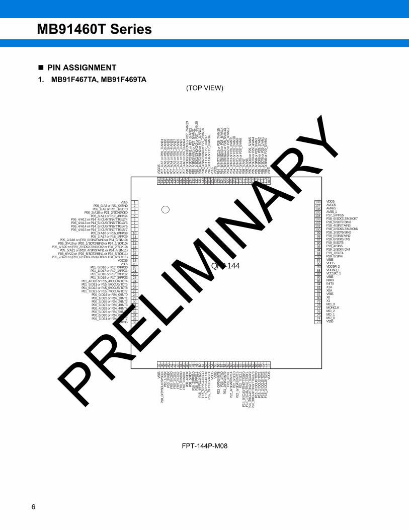
123456789101112131415161718192021222324252627282930313233343536
108107106105104103102101100999897969594939291908988878685848382818079787776757473
VDD5AVCC5AVRH5AVSS_1P17_5/PPG5P18_6/SCK7/ZIN3/CK7P18_5/SOT7/BIN3P18_4/SIN7/AIN3P18_2/SCK6/ZIN2/CK6P18_1/SOT6/BIN2P18_0/SIN6/AIN2P19_6/SCK5/CK5P19_5/SOT5P19_4/SIN5P19_2/SCK4/CK4P19_1/SOT4P19_0/SIN4VSS5VDD5VDD5R_2VDD5R_1VCC18C_1VSS5NMIXINITXX1AX0AVSS5X0X1MD_3MONCLKMD_2MD_1MD_0VSS5
VSS5P06_0/A8 or P21_0/SIN0P06_1/A9 or P21_1/SOT0
P06_2/A10 or P21_2/SCK0/CK0P06_3/A11 or P17_4/PPG4
P06_4/A12 or P14_4/ICU4/TIN4/TTG12/4P06_4/A13 or P14_5/ICU5/TIN5/TTG13/5P06_4/A14 or P14_6/ICU6/TIN6/TTG14/6P06_4/A15 or P14_7/ICU7/TIN7/TTG15/7
P05_0/A16 or P16_0/PPG8P05_1/A17 or P16_1/PPG9
P05_2/A18 or (P20_0/SIN2/AIN0 or P34_0/SIN10)P05_3/A19 or (P20_1/SOT2/BIN0 or P34_1/SOT10)
P05_4/A20 or (P20_2/SCK2/ZIN0/CK2 or P34_2/SCK10)P05_5/A21 or (P20_4/SIN3/AIN1 or P34_4/SIN11)
P05_6/A22 or (P20_5/SOT3/BIN1 or P34_5/SOT11)P05_7/A23 or (P20_6/SCK3/ZIN1/CK3 or P34_6/SCK11)
VDD35VSS5
P01_0/D16 or P17_0/PPG0P01_1/D17 or P17_1/PPG1P01_2/D18 or P17_2/PPG2P01_3/D19 or P17_3/PPG3
P01_4/D20 or P15_4/OCU4/TOT4P01_5/D21 or P15_5/OCU5/TOT5P01_6/D22 or P15_6/OCU6/TOT6P01_7/D23 or P15_7/OCU7/TOT7
P00_0/D24 or P24_0/INT0P00_1/D25 or P24_1/INT1P00_2/D26 or P24_2/INT2P00_3/D27 or P24_4/INT3P00_4/D28 or P24_4/INT4P00_5/D29 or P24_5/INT5P00_6/D30 or P24_6/INT6P00_7/D31 or P24_7/INT7
VDD35
37 38 39 40 41 42 43 44 45 46 47 48 49 50 51 52 53 54 55 56 57 58 59 60 61 62 63 64 65 66 67 68 69 70 71 72
144
143
142
141
140
139
138
137
136
135
134
133
132
131
130
129
128
127
126
125
124
123
122
121
120
119
118
117
116
115
114
113
112
111
110
109
VDD
35P0
7_7/
A7
or P
26_7
/AN
31P0
7_6/
A6
or P
26_6
/AN
30P0
7_5/
A5
or P
26_5
/AN
29P0
7_4/
A4
or P
26_4
/AN
28P0
7_3/
A3
or P
26_3
/AN
27P0
7_2/
A2
or P
26_2
/AN
26P0
7_1/
A1
or P
26_1
/AN
25P0
7_0/
A0
or P
26_0
/AN
24P2
0_6/
SCK3
/ZIN
1/C
K3 o
r P27
_7/A
N23
P20_
5/SO
T3/B
IN1
or P
27_6
/AN
22P2
0_4/
SIN
3/A
IN1
or P
27_5
/AN
21P2
0_2/
SCK2
/ZIN
0/C
K2 o
r P27
_4/A
N2 0
P20_
1/SO
T2/B
IN0
or P
27_3
/AN
19P2
0_0/
SIN
2/A
IN0
or P
27_2
/AN
18P1
6_1/
PPG
9 or
P27
_1/A
N17
P16_
0/PP
G8
or P
27_0
/AN
16VS
S5VD
D5
P24_
7/IN
T7/S
CL3
or P
28_7
/AN
15P2
4_6/
INT6
/SD
A3
or P
28_6
/AN
14P2
4_5/
INT5
/SC
L2 o
r P28
_5/A
N13
P24_
4/IN
T4/S
DA
2 or
P28
_4/A
N12
P24_
3/IN
T3 o
r P28
_3/A
N11
P24_
2/IN
T2 o
r P28
_2/A
N10
P24_
1/IN
T1 o
r P28
_1/A
N9
P24_
0/IN
T0 o
r P28
_0/A
N8
P29_
7/A
N7
P29_
6/A
N6
P35_
6/SC
K9 o
r P29
_5/A
N5
P35_
5/SO
T9 o
r P29
_4/A
N4
P35_
4/SI
N9
or P
29_3
/AN
3P3
5_2/
SCK8
or P
29_2
/AN
2P3
5_1/
SOT8
or P
29_1
/AN
1P3
5_0/
SIN
8 or
P29
_0/A
N0
VSS5
VSS5
P10_
0/SY
SCLK
/SYS
CLK
P10_
1/A
SXP1
0_3/
WEX
P09_
0/C
SX0
P09_
1/C
SX1
P09_
2/C
SX2
P08_
0/W
RX0
P08_
1/W
RX1
P08_
4/RD
XP0
8_5/
RDY
P16_
2/PP
G10
P16_
3/PP
G11
P16_
4/PP
G12
/SG
AP1
6_5/
PPG
13/S
GO
P16_
6/PP
G14
/PFM
P16_
7/PP
G15
/AG
TXVD
D5
VSS5
P23_
0/RX
0/IN
T8P2
3_1/
TX0
P23_
2/RX
1/IN
T9P2
3_3/
TX1
P22_
4/SD
A0/
INT1
4P2
2_5/
SCL0
P22_
6/SD
A1/
INT1
5P2
2_7/
SCL1
P14_
0/IC
U0/
TIN
0/TT
G8/
0P1
4_1/
ICU
1/TI
N1/
TTG
9/1
P14_
2/IC
U2/
TIN
2/TT
G10
/2P1
4_3/
ICU
3/TI
N3/
TTG
11/3
P15_
0/O
CU
0/TO
T0P1
5_1/
OC
U1/
TOT1
P15_
2/O
CU
2/TO
T2P1
5_3/
OC
U3/
TOT3
VDD
5QFP-144
PIN ASSIGNMENT1. MB91F467TA, MB91F469TA
(TOP VIEW)
FPT-144P-M08
PRELIMIN
ARY
MB91460T Series
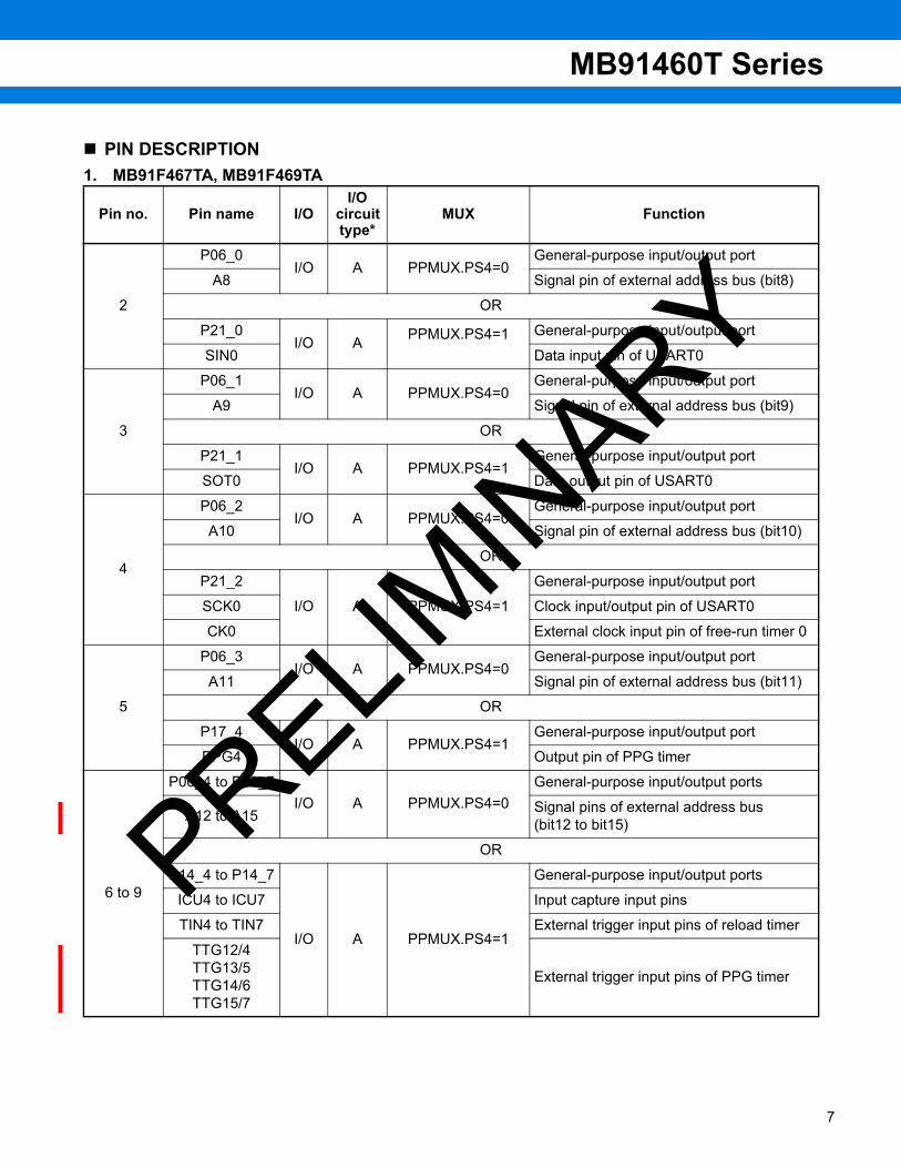
PIN DESCRIPTION1. MB91F467TA, MB91F469TA
Pin no. Pin name I/OI/O
circuit type*
MUX Function
2
P06_0I/O A PPMUX.PS4=0
General-purpose input/output port
A8 Signal pin of external address bus (bit8)
OR
P21_0I/O A PPMUX.PS4=1 General-purpose input/output port
SIN0 Data input pin of USART0
3
P06_1I/O A PPMUX.PS4=0
General-purpose input/output port
A9 Signal pin of external address bus (bit9)
OR
P21_1I/O A PPMUX.PS4=1
General-purpose input/output port
SOT0 Data output pin of USART0
4
P06_2I/O A PPMUX.PS4=0
General-purpose input/output port
A10 Signal pin of external address bus (bit10)
OR
P21_2
I/O A PPMUX.PS4=1
General-purpose input/output port
SCK0 Clock input/output pin of USART0
CK0 External clock input pin of free-run timer 0
5
P06_3I/O A PPMUX.PS4=0
General-purpose input/output port
A11 Signal pin of external address bus (bit11)
OR
P17_4I/O A PPMUX.PS4=1
General-purpose input/output port
PPG4 Output pin of PPG timer
6 to 9
P06_4 to P06_7I/O A PPMUX.PS4=0
General-purpose input/output ports
A12 to A15 Signal pins of external address bus(bit12 to bit15)
OR
P14_4 to P14_7
I/O A PPMUX.PS4=1
General-purpose input/output ports
ICU4 to ICU7 Input capture input pins
TIN4 to TIN7 External trigger input pins of reload timer
TTG12/4TTG13/5TTG14/6TTG15/7
External trigger input pins of PPG timer
PRELIMIN
ARY
7

MB91460T Series
8
10
P05_0I/O A PPMUX.PR10=0
General-purpose input/output ports
A16, A17 Signal pins of external address bus(bit16, bit17)
OR
P16_0I/O A PPMUX.PR10=1
General-purpose input/output ports
PPG8, PPG9 Output pins of PPG timer
11
P05_1I/O A PPMUX.PR11=0
General-purpose input/output ports
A16, A17 Signal pins of external address bus(bit16, bit17)
OR
P16_1 I/OA PPMUX.PR11=1
General-purpose input/output ports
PPG8, PPG9 Output pins of PPG timer
12
P05_2I/O A PPMUX.PR12=0
General-purpose input/output port
A18 Signal pin of external address bus (bit18)
OR
P20_0
I/O APPMUX.PR12=1
andPPMUX.PRPS0=1
General-purpose input/output port
SIN2 Data input pin of USART2
AIN0 Up/down counter input pin
OR
P34_0I/O A
PPMUX.PR12=1and
PPMUX.PRPS0=0
General-purpose input/output port
SIN10 Data input pin of USART10
13
P05_3I/O A PPMUX.PR13=0
General-purpose input/output port
A19 Signal pin of external address bus (bit19)
OR
P20_1
I/O APPMUX.PR13=1
andPPMUX.PRPS0=1
General-purpose input/output port
SOT2 Data output pin of USART2
BIN0 Up/down counter input pin
OR
P34_1I/O A
PPMUX.PR13=1and
PPMUX.PRPS0=0
General-purpose input/output port
SOT10 Data output pin of USART10
Pin no. Pin name I/OI/O
circuit type*
MUX Function
PRELIMIN
ARY
MB91460T Series
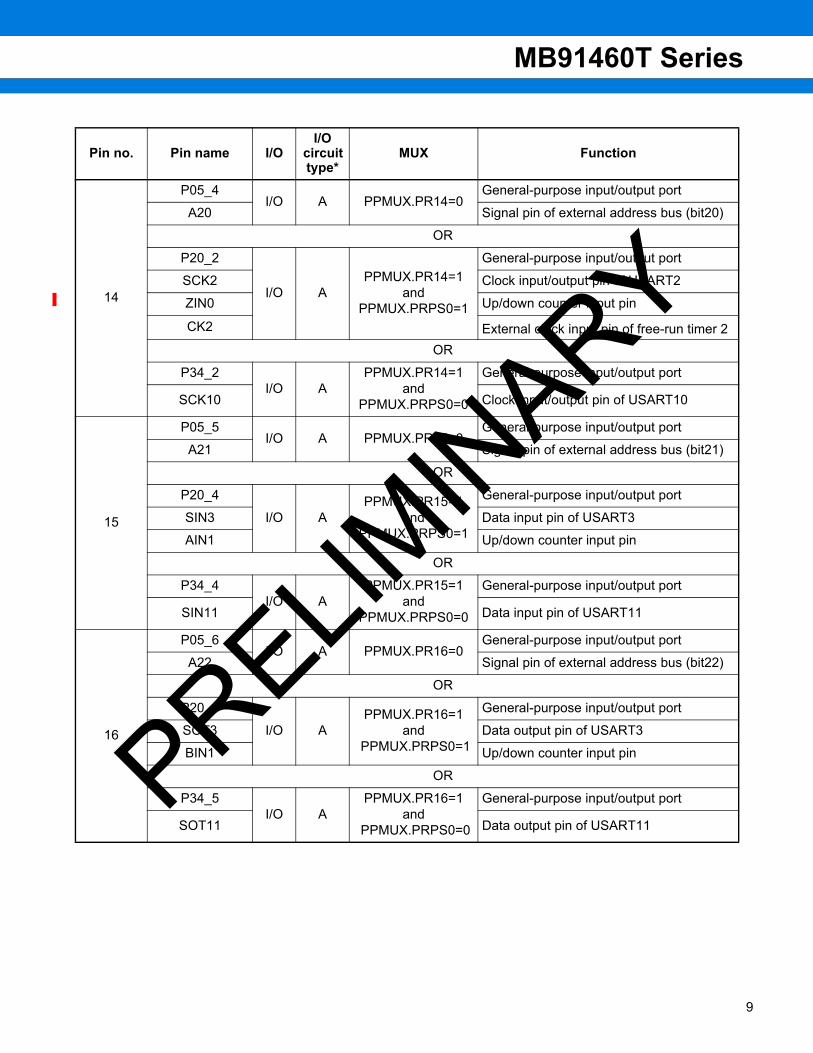
14
P05_4I/O A PPMUX.PR14=0
General-purpose input/output port
A20 Signal pin of external address bus (bit20)
OR
P20_2
I/O APPMUX.PR14=1
andPPMUX.PRPS0=1
General-purpose input/output port
SCK2 Clock input/output pin of USART2
ZIN0 Up/down counter input pin
CK2 External clock input pin of free-run timer 2OR
P34_2I/O A
PPMUX.PR14=1and
PPMUX.PRPS0=0
General-purpose input/output port
SCK10 Clock input/output pin of USART10
15
P05_5I/O A PPMUX.PR15=0
General-purpose input/output port
A21 Signal pin of external address bus (bit21)
OR
P20_4
I/O APPMUX.PR15=1
andPPMUX.PRPS0=1
General-purpose input/output port
SIN3 Data input pin of USART3
AIN1 Up/down counter input pin
OR
P34_4I/O A
PPMUX.PR15=1and
PPMUX.PRPS0=0
General-purpose input/output port
SIN11 Data input pin of USART11
16
P05_6I/O A PPMUX.PR16=0
General-purpose input/output port
A22 Signal pin of external address bus (bit22)
OR
P20_5
I/O APPMUX.PR16=1
and PPMUX.PRPS0=1
General-purpose input/output port
SOT3 Data output pin of USART3
BIN1 Up/down counter input pin
OR
P34_5I/O A
PPMUX.PR16=1and
PPMUX.PRPS0=0
General-purpose input/output port
SOT11 Data output pin of USART11
Pin no. Pin name I/OI/O
circuit type*
MUX Function
PRELIMIN
ARY
9

MB91460T Series
10
17
P05_7I/O A PPMUX.PR17=0
General-purpose input/output port
A23 Signal pin of external address bus (bit23)
OR
P20_6
I/O APPMUX.PR17=1
andPPMUX.PRPS0=1
General-purpose input/output port
SCK3 Clock input/output pin of USART3
ZIN1 Up/down counter input pin
CK3 External clock input pin of free-run timer 3OR
P34_6I/O A
PPMUX.PR17=1and
PPMUX.PRPS0=0
General-purpose input/output port
SCK11 Clock input/output pin of USART11
20 to 23
P01_0 to P01_3I/O A PPMUX.PS3=0
General-purpose input/output ports
D16 to D19 Signal pins of external data bus(bit16 to bit19)
OR
P17_0 to P17_3I/O A PPMUX.PS3=1
General-purpose input/output ports
PPG0 to PPG3 Output pins of PPG timer
24 to 27
P01_4 to P01_7I/O A PPMUX.PS3=0
General-purpose input/output ports
D20 to D23 Signal pins of external data bus(bit20 to bit23)
OR
P15_4 to P15_7
I/O A PPMUX.PS3=1
General-purpose input/output ports
OCU4 to OCU7 Output compare output pins
TOT4 to TOT7 Reload timer output pins
28 to 35
P00_0 to P00_7I/O A PPMUX.PR0=0
General-purpose input/output ports
D24 to D31 Signal pins of external data bus(bit24 to bit31)
OR
P24_0 to P24_7I/O A PPMUX.PR0=1
General-purpose input/output ports
INT0 to INT7 External interrupt input pins
38P10_0
I/O A --General-purpose input/output port
SYSCLK External bus clock output pin
39P10_1
I/O A -General-purpose input/output port
ASX Address strobe output pin
40P10_2
I/O A -General-purpose input/output port
WEX Write enable output pin
Pin no. Pin name I/OI/O
circuit type*
MUX Function
PRELIMIN
ARY

MB91460T Series
41 to 43 P09_0 to P09_2I/O A -
General-purpose input/output ports
CSX0 to CSX2 Chip select output pins
44, 45P08_0, P08_1
I/O A -General-purpose input/output ports
WRX0, WRX1 External write strobe output pins
46P08_4
I/O A -General-purpose input/output port
RDX External read strobe output pin
47P08_7
I/O A -General-purpose input/output port
RDY External ready input pin
48, 49P16_2, P16_3
I/O A -General-purpose input/output ports
PPG10, PPG11 Output pins of PPG timer
50
P16_4
I/O A -
General-purpose input/output port
PPG12 Output pin of PPG timer
SGA SGA output pin of sound generator
51
P16_5
I/O A -
General-purpose input/output port
PPG13 Output pin of PPG timer
SGO SG0 output pin of sound generator
52
P16_6
I/O A -
General-purpose input/output port
PPG14 Output pin of PPG timer
PFM Pulse frequency modulator output pin
53
P16_7
I/O A -
General-purpose input/output port
PPG15 Output pin of PPG timer
ATGX A/D converter external trigger input pin
56
P23_0
I/O A -
General-purpose input/output port
RX0 RX input/output pin of CAN0
INT8 External interrupt input pin
57P23_1
I/O A -General-purpose input/output port
TX0 TX output pin of CAN0
58
P23_2
I/O A -
General-purpose input/output port
RX1 RX input/output pin of CAN1
INT9 External interrupt input pin
59P23_3
I/O A -General-purpose input/output port
TX1 TX output pin of CAN1
60
P22_4
I/O C -
General-purpose input/output port
SDA0 I2C bus DATA input/output pin (open drain)INT14 External interrupt input pin
Pin no. Pin name I/OI/O
circuit type*
MUX Function
PRELIMIN
ARY
11
MB91460T Series
12
61P22_5
I/O C -General-purpose input/output port
SCL0 I2C bus clock input/output pin (open drain)
62
P22_6
I/O C -
General-purpose input/output port
SDA1 I2C bus DATA input/output pin (open drain)INT15 External interrupt input pin
63P22_7
I/O C -General-purpose input/output port
SCL1 I2C bus clock input/output pin (open drain)
64 to 67
P14_0 to P14_3
I/O A -
General-purpose input/output ports
ICU0 to ICU3 Input capture input pins
TIN0 to TIN3 External trigger input pins of reload timer
TTG8/0 to TTG11/3 External trigger input pins of PPG timer
68 to 71P15_0 to P15_3
I/OA -
General-purpose input/output ports
OCU0 to OCU3 Output compare output pins
TOT0 to TOT3 Reload timer output pins
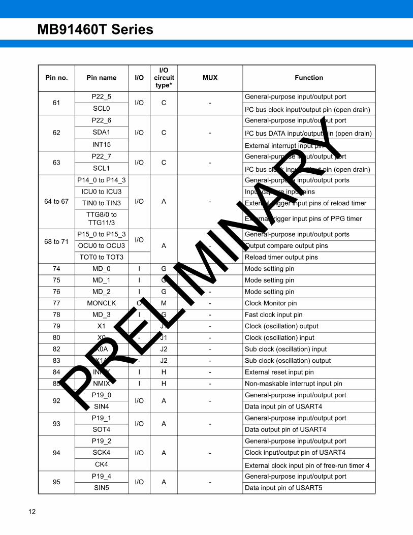
74 MD_0 I G - Mode setting pin
75 MD_1 I G - Mode setting pin
76 MD_2 I G - Mode setting pin
77 MONCLK O M - Clock Monitor pin
78 MD_3 I G - Fast clock input pin
79 X1 - J1 - Clock (oscillation) output
80 X0 - J1 - Clock (oscillation) input
82 X0A - J2 - Sub clock (oscillation) input
83 X1A - J2 - Sub clock (oscillation) output
84 INITX I H - External reset input pin
85 NMIX I H - Non-maskable interrupt input pin
92P19_0
I/O A -General-purpose input/output port
SIN4 Data input pin of USART4
93P19_1
I/O A -General-purpose input/output port
SOT4 Data output pin of USART4
94
P19_2
I/O A -
General-purpose input/output port
SCK4 Clock input/output pin of USART4
CK4 External clock input pin of free-run timer 4
95P19_4
I/O A -General-purpose input/output port
SIN5 Data input pin of USART5
Pin no. Pin name I/OI/O
circuit type*
MUX Function
PRELIMIN
ARY

MB91460T Series
96P19_5
I/O A -General-purpose input/output port
SOT5 Data output pin of USART5
97
P19_6
I/O A -
General-purpose input/output port
SCK5 Clock input/output pin of USART5
CK5 External clock input pin of free-run timer 5
98
P18_0
I/O A -
General-purpose input/output port
SIN6 Data input pin of USART6
AIN2 Up/down counter input pin
99
P18_1
I/O A -
General-purpose input/output port
SOT6 Data output pin of USART6
BIN2 Up/down counter input pin
100
P18_2
I/O A -
General-purpose input/output port
SCK6 Clock input/output pin of USART6
ZIN2 Up/down counter input pin
CK6 External clock input pin of free-run timer 6
101
P18_4
I/O A -
General-purpose input/output port
SIN7 Data input pin of USART7
AIN3 Up/down counter input pin
102
P18_5
I/O A -
General-purpose input/output port
SOT7 Data output pin of USART7
BIN3 Up/down counter input pin
103
P18_6
I/O A -
General-purpose input/output port
SCK7 Clock input/output pin of USART7
ZIN3 Up/down counter input pin
CK7 External clock input pin of free-run timer 7
104P17_5
I/O A -General-purpose input/output port
PPG5 Output pin of PPG timer
110
P35_0 I/O B PPMUX.PS5=0
General-purpose input/output port
SIN8 Data input pin of USART8
OR
P29_0I/O B PPMUX.PS5=1
General-purpose input/output port
AN0 Analog input pin of A/D converter
Pin no. Pin name I/OI/O
circuit type*
MUX Function
PRELIMIN
ARY
13

MB91460T Series
14
111
P35_1I/O B PPMUX.PS5=0
General-purpose input/output port
SOT8 Data output pin of USART8
OR
P29_1I/O B PPMUX.PS5=1
General-purpose input/output port
AN1 Analog input pin of A/D converter
112
P35_2I/O B PPMUX.PS5=0
General-purpose input/output port
SCK8 Clock input/output pin of USART8
OR
P29_2I/O B PPMUX.PS5=1
General-purpose input/output port
AN2 Analog input pin of A/D converter
113
P35_4I/O B PPMUX.PS5=0
General-purpose input/output port
SIN9 Data input pin of USART9
OR
P29_3I/O B PPMUX.PS5=1
General-purpose input/output port
AN3 Analog input pin of A/D converter
114
P35_5I/O B PPMUX.PS5=0
General-purpose input/output port
SOT9 Data output pin of USART9
OR
P29_4I/O B PPMUX.PS5=1
General-purpose input/output port
AN4 Analog input pin of A/D converter
115
P35_6I/O B PPMUX.PS5=0
General-purpose input/output port
SCK9 Clock input/output pin of USART9
OR
P29_5I/O B PPMUX.PS5=1
General-purpose input/output port
AN5 Analog input pin of A/D converter
116, 117P29_6, P29_7
I/O B -General-purpose input/output ports
AN6, AN7 Analog input pins of A/D converter
118 to 121
P24_0 to P24_3I/O B
PPMUX.PS2=0and
PPMUX.PR0=0
General-purpose input/output ports
INT0 to INT3 External interrupt input pins
OR
P28_0 to P28_3I/O B
PPMUX.PS2=1or
PPMUX.PR0=1
General-purpose input/output ports
AN8 to AN11 Analog input pins of A/D converter
Pin no. Pin name I/OI/O
circuit type*
MUX Function
PRELIMIN
ARY

MB91460T Series
122
P24_4
I/O DPPMUX.PS2=0
andPPMUX.PR0=0
General-purpose input/output port
INT4 External interrupt input pin
SDA2 I2C bus DATA input/output pin (open drain)
OR
P28_4I/O D
PPMUX.PS2=1or
PPMUX.PR0=1
General-purpose input/output port
AN12 Analog input pin of A/D converter
123
P24_5
I/O DPPMUX.PS2=0
andPPMUX.PR0=0
General-purpose input/output port
INT5 External interrupt input pin
SCL2 I2C bus clock input/output pin (open drain)
OR
P28_5I/O D
PPMUX.PS2=1or
PPMUX.PR0=1
General-purpose input/output port
AN13 Analog input pin of A/D converter
124
P24_6
I/O DPPMUX.PS2=0
andPPMUX.PR0=0
General-purpose input/output port
INT6 External interrupt input pin
SDA3 I2C bus DATA input/output pin (open drain)
OR
P28_6I/O D
PPMUX.PS2=1or
PPMUX.PR0=1
General-purpose input/output port
AN14 Analog input pin of A/D converter
125
P24_7
I/O CPPMUX.PS2=0
andPPMUX.PR0=0
General-purpose input/output port
INT7 External interrupt input pin
SCL3 I2C bus clock input/output pin (open drain)
OR
P28_7I/O B
PPMUX.PS2=1or
PPMUX.PR0=1
General-purpose input/output port
AN15 Analog input pin of A/D converter
128, 129
P16_0, P16_1
I/O A
PPMUX.PS1=0and_not
(PPMUX.PR11=1and
PPMUX.PRPS0=1)
General-purpose input/output ports
PPG8, PPG9 Output pins of PPG timer
OR
P27_0, P27_1
I/O A
PPMUX.PS1=1or
(PPMUX.PR11=1and
PPMUX.PRPS0=1)
General-purpose input/output ports
AN16, AN17 Analog input pins of A/D converter
Pin no. Pin name I/OI/O
circuit type*
MUX Function
PRELIMIN
ARY
15

MB91460T Series
16
130
P20_0
I/O A
PPMUX.PS1=0and_not
(PPMUX.PR12=1and
PPMUX.PRPS0=1)
General-purpose input/output port
SIN2 Data input pin of USART2
AIN0 Up/down counter input pin
OR
P27_2
I/O A
PPMUX.PS1=1or
(PPMUX.PR12=1and
PPMUX.PRPS0=1)
General-purpose input/output port
AN18 Analog input pin of A/D converter
131
P20_1
I/O A
PPMUX.PS1=0and_not
(PPMUX.PR13=1and
PPMUX.PRPS0=1)
General-purpose input/output port
SOT2 Data output pin of USART2
BIN0 Up/down counter input pin
OR
P27_3
I/O A
PPMUX.PS1=1or
(PPMUX.PR13=1and
PPMUX.PRPS0=1)
General-purpose input/output port
AN19 Analog input pin of A/D converter
132
P20_2
I/O A
PPMUX.PS1=0and_not
(PPMUX.PR14=1and
PPMUX.PRPS0=1)
General-purpose input/output port
SCK2 Clock input/output pin of USART2
ZIN0 Up/down counter input pin
CK2 External clock input pin of free-run timer 2OR
P27_4
I/O A
PPMUX.PS1=1or
(PPMUX.PR14=1and
PPMUX.PRPS0=1)
General-purpose input/output port
AN20 Analog input pin of A/D converter
133
P20_4
I/O A
PPMUX.PS1=0and_not
(PPMUX.PR15=1and
PPMUX.PRPS0=1)
General-purpose input/output port
SIN3 Data input pin of USART3
AIN1 Up/down counter input pin
OR
P27_5
I/O A
PPMUX.PS1=1or
(PPMUX.PR15=1and
PPMUX.PRPS0=1)
General-purpose input/output port
AN21 Analog input pin of A/D converter
Pin no. Pin name I/OI/O
circuit type*
MUX Function
PRELIMIN
ARY

MB91460T Series
*: For information about the I/O circuit type, refer to “ I/O CIRCUIT TYPES”.
134
P20_5
I/O A
PPMUX.PS1=0and_not
(PPMUX.PR16=1and
PPMUX.PRPS0=1)
General-purpose input/output port
SOT3 Data output pin of USART3
BIN1 Up/down counter input pin
OR
P27_6
I/O A
PPMUX.PS1=1or
(PPMUX.PR16=1and
PPMUX.PRPS0=1)
General-purpose input/output port
AN22 Analog input pin of A/D converter
135
P20_6
I/O A
PPMUX.PS1=0and_not
(PPMUX.PR17=1and
PPMUX.PRPS0=1)
General-purpose input/output port
SCK3 Clock input/output pin of USART3
ZIN1 Up/down counter input pin
CK3 External clock input pin of free-run timer 3
OR
P27_7
I/O A
PPMUX.PS1=1or
(PPMUX.PR17=1and
PPMUX.PRPS0=1)
General-purpose input/output port
AN23 Analog input pin of A/D converter
136 to 143
P07_0 to P07_7I/O A PPMUX.PS0=0
General-purpose input/output ports
A0 to A7 Signal pins of external address bus (bit0 to bit7)
OR
P26_0 to P26_7I/O A PPMUX.PS0=1
General-purpose input/output ports
AN24 to AN31 Analog input pins of A/D converter
Pin no. Pin name I/OI/O
circuit type*
MUX Function
PRELIMIN
ARY
17

MB91460T Series
18
[Power supply/Ground pins]Pin no. Pin name I/O Function
1, 19, 37, 55, 73, 81, 86, 91, 109, 127 VSS5
Supply
Ground pins
18, 36, 144 VDD35 Power supply pins for external data bus
54, 72, 90, 108, 126 VDD5 Power supply pins
88, 89 VDD5R Power supply pins for internal regulator
105 AVSS5 Analog ground pin for A/D converter
107 AVCC5 Power supply pin for A/D converter
106 AVRH5 Reference power supply pin for A/D converter
87 VCC18C Capacitor connection pin for internal regulator
PRELIMIN
ARY

MB91460T Series
I/O CIRCUIT TYPES
Type Circuit Remarks
A CMOS level output (programmable IOL = 5mA, IOH = -5mA and IOL = 2mA, IOH = -2mA)2 different CMOS hysteresis inputs with input shutdown functionAutomotive input with input shutdown functionTTL input with input shutdown functionProgrammable pull-up resistor: 50kΩ approx.
B CMOS level output (programmable IOL = 5mA, IOH = -5mA and IOL = 2mA, IOH = -2mA)2 different CMOS hysteresis inputs with input shutdown functionAutomotive input with input shutdown function)TTL input with input shutdown functionProgrammable pull-up resistor: 50kΩ approx.Analog input
pull-up control
R
CMOS hysteresis type1
Automotive inputs
TTL input
CMOS hysteresis type2
pull- down control
driver strength control
data line
standby control forinput shutdown
R
analog input
pull-up control
pull- down control
driver strength control
data line
CMOS hysteresis type1
Automotive inputs
TTL input
CMOS hysteresis type2
standby control forinput shutdown
PRELIMIN
ARY
19
MB91460T Series
20
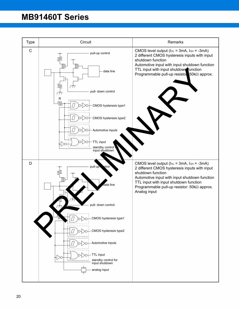
C CMOS level output (IOL = 3mA, IOH = -3mA)2 different CMOS hysteresis inputs with input shutdown functionAutomotive input with input shutdown functionTTL input with input shutdown functionProgrammable pull-up resistor: 50kΩ approx.
D CMOS level output (IOL = 3mA, IOH = -3mA)2 different CMOS hysteresis inputs with input shutdown functionAutomotive input with input shutdown functionTTL input with input shutdown functionProgrammable pull-up resistor: 50kΩ approx.Analog input
Type Circuit Remarks
pull-up control
R
CMOS hysteresis type1
Automotive inputs
TTL input
CMOS hysteresis type2
pull- down control
data line
standby control forinput shutdown
R
analog input
pull-up control
pull- down control
data line
CMOS hysteresis type1
Automotive inputs
TTL input
CMOS hysteresis type2
standby control forinput shutdown
PRELIMIN
ARY

MB91460T Series
E CMOS level output (programmable IOL = 5mA, IOH = -5mA and IOL = 2mA, IOH = -2mA, and IOL = 30mA, IOH = -30mA)2 different CMOS hysteresis inputs with input shutdown functionAutomotive input with input shutdown functionTTL input with input shutdown functionProgrammable pull-up resistor: 50kΩ approx.
F CMOS level output (programmable IOL = 5mA, IOH = -5mA and IOL = 2mA, IOH = -2mA, and IOL = 30mA, IOH = -30mA)2 different CMOS hysteresis inputs with input shutdown functionAutomotive input with input shutdown functionTTL input with input shutdown functionProgrammable pull-up resistor: 50kΩ approx.Analog input
Type Circuit Remarks
pull-up control
R
CMOS hysteresis type1
Automotive inputs
TTL input
CMOS hysteresis type2
pull- down control
driver strength control
data line
standby control forinput shutdown
R
analog input
pull-up control
pull- down control
driver strength control
data line
CMOS hysteresis type1
Automotive inputs
TTL input
CMOS hysteresis type2
standby control forinput shutdown
PRELIMIN
ARY
21
MB91460T Series
22
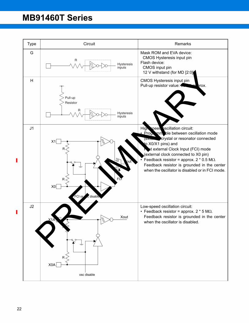
G Mask ROM and EVA device: CMOS Hysteresis input pinFlash device: CMOS input pin 12 V withstand (for MD [2:0])
H CMOS Hysteresis input pinPull-up resistor value: 50 kΩ approx.
J1 High-speed oscillation circuit:• Programmable between oscillation mode
(external crystal or resonator connected to X0/X1 pins) and Fast external Clock Input (FCI) mode (external clock connected to X0 pin)
• Feedback resistor = approx. 2 * 0.5 MΩ. Feedback resistor is grounded in the centerwhen the oscillator is disabled or in FCI mode.
J2 Low-speed oscillation circuit:• Feedback resistor = approx. 2 * 5 MΩ.
Feedback resistor is grounded in the centerwhen the oscillator is disabled.
Type Circuit Remarks
RHysteresisinputs
R
Pull-up
Resistor
Hysteresisinputs
X1
X0
R
R
Xout
FCI
0
1
FCI or osc disable
X1A
X0A
R
R
Xout
osc disable
PRELIMIN
ARY

MB91460T Series
K CMOS level output (programmable IOL = 5mA, IOH = -5mA and IOL = 2mA, IOH = -2mA)2 different CMOS hysteresis inputs with input shutdown functionAutomotive input with input shutdown functionTTL input with input shutdown functionProgrammable pull-up resistor: 50kΩ approx.LCD SEG/COM output
L CMOS level output (programmable IOL = 5mA, IOH = -5mA and IOL = 2mA, IOH = -2mA)2 different CMOS hysteresis inputs with input shutdown functionAutomotive input with input shutdown function)TTL input with input shutdown functionProgrammable pull-up resistor: 50kΩ approx.Analog inputLCD Voltage input
Type Circuit Remarks
pull-up control
R
CMOS hysteresis type1
Automotive inputs
TTL input
CMOS hysteresis type2
pull- down control
driver strength control
data line
standby control forinput shutdown
LCD SEG/COM
R
pull-up control
pull- down control
driver strength control
data line
CMOS hysteresis type1
Automotive inputs
TTL input
CMOS hysteresis type2
standby control forinput shutdownVLCD
PRELIMIN
ARY
23

MB91460T Series
24
M CMOS level tri-state output(IOL = 5mA, IOH = -5mA)
NAnalog input pin with protection
Type Circuit Remarks
tri-state control
data line
analog input line
PRELIMIN
ARY
MB91460T Series
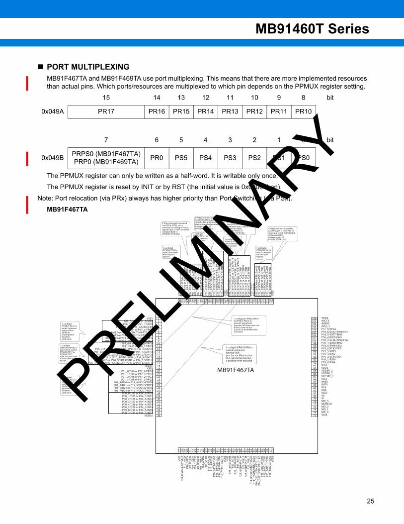
PORT MULTIPLEXINGMB91F467TA and MB91F469TA use port multiplexing. This means that there are more implemented resourcesthan actual pins. Which ports/resources are multiplexed to which pin depends on the PPMUX register setting.
The PPMUX register can only be written as a half-word. It is writable only once.
The PPMUX register is reset by INIT or by RST (the initial value is 0x0000 then).
Note: Port relocation (via PRx) always has higher priority than Port Switching (via PSx).
MB91F467TA
15 14 13 12 11 10 9 8 bit
0x049A PR17 PR16 PR15 PR14 PR13 PR12 PR11 PR10
7 6 5 4 3 2 1 0 bit
0x049B PRPS0 (MB91F467TA)PRP0 (MB91F469TA) PR0 PS5 PS4 PS3 PS2 PS1 PS0
123456789
101112131415161718192021222324252627282930313233343536
108107106105104103102101100
999897969594939291908988878685848382818079787776757473
VDD5AVCC5AVRH5AVSS_1P17_5/PPG5P18_6/SCK7/ZIN3/CK7P18_5/SOT7/BIN3P18_4/SIN7/AIN3P18_2/SCK6/ZIN2/CK6P18_1/SOT6/BIN2P18_0/SIN6/AIN2P19_6/SCK5/CK5P19_5/SOT5P19_4/SIN5P19_2/SCK4/CK4P19_1/SOT4P19_0/SIN4VSS5VDD5VDD5R_2VDD5R_1VCC18C_1VSS5NMIXINITXX1AX0AVSS5X0X1MD_3MONCLKMD_2MD_1MD_0VSS5
VSS5P06_0/A8 or P21_0/SIN0
P06_1/A9 or P21_1/SOT0P06_2/A10 or P21_2/SCK0/CK0
P06_3/A11 or P17_4/PPG4P06_4/A12 or P14_4/ICU4/TIN4/TTG12/4P06_4/A13 or P14_5/ICU5/TIN5/TTG13/5P06_4/A14 or P14_6/ICU6/TIN6/TTG14/6P06_4/A15 or P14_7/ICU7/TIN7/TTG15/7
P05_0/A16 or P16_0/PPG8P05_1/A17 or P16_1/PPG9
P05_2/A18 or (P20_0/SIN2/AIN0 or P34_0/SIN10)P05_3/A19 or (P20_1/SOT2/BIN0 or P34_1/SOT10)
P05_4/A20 or (P20_2/SCK2/ZIN0/CK2 or P34_2/SCK10)P05_5/A21 or (P20_4/SIN3/AIN1 or P34_4/SIN11)
P05_6/A22 or (P20_5/SOT3/BIN1 or P34_5/SOT11)P05_7/A23 or (P20_6/SCK3/ZIN1/CK3 or P34_6/SCK11)
VDD35VSS5
P01_0/D16 or P17_0/PPG0P01_1/D17 or P17_1/PPG1P01_2/D18 or P17_2/PPG2P01_3/D19 or P17_3/PPG3
P01_4/D20 or P15_4/OCU4/TOT4P01_5/D21 or P15_5/OCU5/TOT5P01_6/D22 or P15_6/OCU6/TOT6P01_7/D23 or P15_7/OCU7/TOT7
P00_0/D24 or P24_0/INT0P00_1/D25 or P24_1/INT1P00_2/D26 or P24_2/INT2P00_3/D27 or P24_4/INT3P00_4/D28 or P24_4/INT4P00_5/D29 or P24_5/INT5P00_6/D30 or P24_6/INT6P00_7/D31 or P24_7/INT7
VDD35
37 38 39 40 41 42 43 44 45 46 47 48 49 50 51 52 53 54 55 56 57 58 59 60 61 62 63 64 65 66 67 68 69 70 71 72
144
143
142
141
140
139
138
137
136
135
134
133
132
131
130
129
128
127
126
125
124
123
122
121
120
119
118
117
116
115
114
113
112
111
110
109
VDD
35P0
7_7/
A7
or P
26_7
/AN
31P0
7_6/
A6
or P
26_6
/AN
30P0
7_5/
A5
or P
26_5
/AN
29P0
7_4/
A4
or P
26_4
/AN
28P0
7_3/
A3
or P
26_3
/AN
27P0
7_2/
A2
or P
26_2
/AN
26P0
7_1/
A1
or P
26_1
/AN
25P0
7_0/
A0
or P
26_0
/AN
24P2
0_6/
SCK3
/ZIN
1/CK
3 or
P27
_7/A
N23
P20_
5/SO
T3/B
IN1
or P
27_6
/AN
22P2
0_4/
SIN
3/A
IN1
or P
27_5
/AN
21P2
0_2/
SCK2
/ZIN
0/CK
2 or
P27
_4/A
N20
P20_
1/SO
T2/B
IN0
or P
27_3
/AN
19P2
0_0/
SIN
2/A
IN0
or P
27_2
/AN
18P1
6_1/
PPG
9 or
P27
_1/A
N17
P16_
0/PP
G8
or P
27_0
/AN
16VS
S5VD
D5
P24_
7/IN
T7/S
CL3
or P
28_7
/AN
15P2
4_6/
INT6
/SD
A3
or P
28_6
/AN
14P2
4_5/
INT5
/SCL
2 or
P28
_5/A
N13
P24_
4/IN
T4/S
DA
2 or
P28
_4/A
N12
P24_
3/IN
T3 o
r P28
_3/A
N11
P24_
2/IN
T2 o
r P28
_2/A
N10
P24_
1/IN
T1 o
r P28
_1/A
N9
P24_
0/IN
T0 o
r P28
_0/A
N8
P29_
7/A
N7
P29_
6/A
N6
P35_
6/SC
K9 o
r P29
_5/A
N5
P35_
5/SO
T9 o
r P29
_4/A
N4
P35_
4/SI
N9
or P
29_3
/AN
3P3
5_2/
SCK8
or P
29_2
/AN
2P3
5_1/
SOT8
or P
29_1
/AN
1P3
5_0/
SIN
8 or
P29
_0/A
N0
VSS5
VSS5
P10_
0/SY
SCLK
/SYS
CLK
P10_
1/A
SXP1
0_3/
WEX
P09_
0/CS
X0P0
9_1/
CSX1
P09_
2/CS
X2P0
8_0/
WRX
0P0
8_1/
WRX
1P0
8_4/
RDX
P08_
5/RD
YP1
6_2/
PPG
10P1
6_3/
PPG
11P1
6_4/
PPG
12/S
GA
P16_
5/PP
G13
/SG
OP1
6_6/
PPG
14/P
FMP1
6_7/
PPG
15/A
GTX
VDD
5VS
S5P2
3_0/
RX0/
INT8
P23_
1/TX
0P2
3_2/
RX1/
INT9
P23_
3/TX
1P2
2_4/
SDA
0/IN
T14
P22_
5/SC
L0P2
2_6/
SDA
1/IN
T15
P22_
7/SC
L1P1
4_0/
ICU
0/TI
N0/
TTG
8/0
P14_
1/IC
U1/
TIN
1/TT
G9/
1P1
4_2/
ICU
2/TI
N2/
TTG
10/2
P14_
3/IC
U3/
TIN
3/TT
G11
/3P1
5_0/
OCU
0/TO
T0P1
5_1/
OCU
1/TO
T1P1
5_2/
OCU
2/TO
T2P1
5_3/
OCU
3/TO
T3VD
D5
MB91F467TA
1 configbyte (PPMUX.PR17 to PPMUX.PR10) to relocate peripheral function (all 8 pins, but not ANxx), external bus functon is disabled when relocated
1 configbit (PPMUX.PR0) torelocate peripheral function (all 8pins, but not ANxx and not I2C), external bus functon is disabled when relocated
if ANxx channel is enabled(via PFR & EPFR), pin isswitched to analogue input,digital input is then disabled(independant ofPPMUX.PS/PR bits)
if ANxx channel is enabled(via PFR) pin is switched toanalogue input, digital inputis then disabled(independant ofPPMUX.PS/PR bits)
if ANxx channel is enabled(via PFR), pin is switched toanalogue input, digital inputis then disabled(independant ofPPMUX.PS/PR bits)1 configbit
(PPMUX.PS2) toswitch betweenthe two portlayouts 1 configbit
(PPMUX.PS5) toswitch between the two port layouts
1 configbit(PPMUX.PS0) toswitch betweenthe two portlayouts
if ANxx channel is enabled(via PFR & EPFR), pin isswitched to analogue input,digital input is then disabled(independant ofPPMUX.PS/PR bits)
1 configbit(PPMUX.PS1) toswitch betweenthe two portlayouts
1 configbit(PPMUX.PS4) toswitch betweenexternal bus (default)or peripheral function(all 8 pins)
1 configbit(PPMUX.PS3) toswitch betweenexternal bus(default) orperipheral function(all 8 pins)
1 configbit(PPMUX.PRPS0) todetermine wetherPPMUX.PR17 toPPMUX.PR12relocate pins fromP20 or switch Pinsto P34
PRELIMIN
ARY
25

MB91460T Series
26
MB91F469TA
123456789
101112131415161718192021222324252627282930313233343536
108107106105104103102101100
999897969594939291908988878685848382818079787776757473
VDD5AVCC5AVRH5AVSS_1P17_5/PPG5P18_6/SCK7/ZIN3/CK7P18_5/SOT7/BIN3P18_4/SIN7/AIN3P18_2/SCK6/ZIN2/CK6P18_1/SOT6/BIN2P18_0/SIN6/AIN2P19_6/SCK5/CK5P19_5/SOT5P19_4/SIN5P19_2/SCK4/CK4P19_1/SOT4P19_0/SIN4VSS5VDD5VDD5R_2VDD5R_1VCC18C_1VSS5NMIXINITXX1AX0AVSS5X0X1MD_3MONCLKMD_2MD_1MD_0VSS5
VSS5P06_0/A8 or P21_0/SIN0
P06_1/A9 or P21_1/SOT0P06_2/A10 or P21_2/SCK0/CK0
P06_3/A11 or P17_4/PPG4P06_4/A12 or P14_4/ICU4/TIN4/TTG12/4P06_4/A13 or P14_5/ICU5/TIN5/TTG13/5P06_4/A14 or P14_6/ICU6/TIN6/TTG14/6P06_4/A15 or P14_7/ICU7/TIN7/TTG15/7
P05_0/A16 or P16_0/PPG8P05_1/A17 or P16_1/PPG9
P05_2/A18 or (P20_0/SIN2/AIN0 or P34_0/SIN10)P05_3/A19 or (P20_1/SOT2/BIN0 or P34_1/SOT10)
P05_4/A20 or (P20_2/SCK2/ZIN0/CK2 or P34_2/SCK10)P05_5/A21 or (P20_4/SIN3/AIN1 or P34_4/SIN11)
P05_6/A22 or (P20_5/SOT3/BIN1 or P34_5/SOT11)P05_7/A23 or (P20_6/SCK3/ZIN1/CK3 or P34_6/SCK11)
VDD35VSS5
P01_0/D16 or P17_0/PPG0P01_1/D17 or P17_1/PPG1P01_2/D18 or P17_2/PPG2P01_3/D19 or P17_3/PPG3
P01_4/D20 or P15_4/OCU4/TOT4P01_5/D21 or P15_5/OCU5/TOT5P01_6/D22 or P15_6/OCU6/TOT6P01_7/D23 or P15_7/OCU7/TOT7
P00_0/D24 or P24_0/INT0P00_1/D25 or P24_1/INT1P00_2/D26 or P24_2/INT2P00_3/D27 or P24_4/INT3P00_4/D28 or P24_4/INT4P00_5/D29 or P24_5/INT5P00_6/D30 or P24_6/INT6P00_7/D31 or P24_7/INT7
VDD35
37 38 39 40 41 42 43 44 45 46 47 48 49 50 51 52 53 54 55 56 57 58 59 60 61 62 63 64 65 66 67 68 69 70 71 72
144
143
142
141
140
139
138
137
136
135
134
133
132
131
130
129
128
127
126
125
124
123
122
121
120
119
118
117
116
115
114
113
112
111
110
109
VDD
35P0
7_7/
A7
or P
26_7
/AN
31P0
7_6/
A6
or P
26_6
/AN
30P0
7_5/
A5
or P
26_5
/AN
29P0
7_4/
A4
or P
26_4
/AN
28P0
7_3/
A3
or P
26_3
/AN
27P0
7_2/
A2
or P
26_2
/AN
26P0
7_1/
A1
or P
26_1
/AN
25P0
7_0/
A0
or P
26_0
/AN
24P2
0_6/
SCK3
/ZIN
1/CK
3 or
P27
_7/A
N23
P20_
5/SO
T3/B
IN1
or P
27_6
/AN
22P2
0_4/
SIN
3/A
IN1
or P
27_5
/AN
21P2
0_2/
SCK2
/ZIN
0/CK
2 or
P27
_4/A
N20
P20_
1/SO
T2/B
IN0
or P
27_3
/AN
19P2
0_0/
SIN
2/A
IN0
or P
27_2
/AN
18P1
6_1/
PPG
9 or
P27
_1/A
N17
P16_
0/PP
G8
or P
27_0
/AN
16VS
S5VD
D5
P24_
7/IN
T7/S
CL3
or P
28_7
/AN
15P2
4_6/
INT6
/SD
A3
or P
28_6
/AN
14P2
4_5/
INT5
/SCL
2 or
P28
_5/A
N13
P24_
4/IN
T4/S
DA
2 or
P28
_4/A
N12
P24_
3/IN
T3 o
r P28
_3/A
N11
P24_
2/IN
T2 o
r P28
_2/A
N10
P24_
1/IN
T1 o
r P28
_1/A
N9
P24_
0/IN
T0 o
r P28
_0/A
N8
P29_
7/A
N7
P29_
6/A
N6
P35_
6/SC
K9 o
r P29
_5/A
N5
P35_
5/SO
T9 o
r P29
_4/A
N4
P35_
4/SI
N9
or P
29_3
/AN
3P3
5_2/
SCK8
or P
29_2
/AN
2P3
5_1/
SOT8
or P
29_1
/AN
1P3
5_0/
SIN
8 or
P29
_0/A
N0
VSS5
VSS5
P10_
0/SY
SCLK
/SYS
CLK
P10_
1/A
SXP1
0_3/
WEX
P09_
0/CS
X0P0
9_1/
CSX1
P09_
2/CS
X2P0
8_0/
WRX
0P0
8_1/
WRX
1P0
8_4/
RDX
P08_
5/RD
YP1
6_2/
PPG
10P1
6_3/
PPG
11P1
6_4/
PPG
12/S
GA
P16_
5/PP
G13
/SG
OP1
6_6/
PPG
14/P
FMP1
6_7/
PPG
15/A
GTX
VDD
5VS
S5P2
3_0/
RX0/
INT8
P23_
1/TX
0P2
3_2/
RX1/
INT9
P23_
3/TX
1P2
2_4/
SDA
0/IN
T14
P22_
5/SC
L0P2
2_6/
SDA
1/IN
T15
P22_
7/SC
L1P1
4_0/
ICU
0/TI
N0/
TTG
8/0
P14_
1/IC
U1/
TIN
1/TT
G9/
1P1
4_2/
ICU
2/TI
N2/
TTG
10/2
P14_
3/IC
U3/
TIN
3/TT
G11
/3P1
5_0/
OCU
0/TO
T0P1
5_1/
OCU
1/TO
T1P1
5_2/
OCU
2/TO
T2P1
5_3/
OCU
3/TO
T3VD
D5
MB91F469TA
1 configbyte (PPMUX.PR17 to PPMUX.PR10) to relocate peripheral function (all 8 pins, but not ANxx), external bus functon is disabled when relocated
1 configbit (PPMUX.PR0) torelocate peripheral function (all 8pins, but not ANxx and not I2C), external bus functon is disabled when relocated
1 configbit(PPMUX.PS4) toswitch betweenexternal bus (default)or peripheral function(all 8 pins)
1 configbit(PPMUX.PS3) toswitch betweenexternal bus(default) orperipheral function(all 8 pins)
1 configbit(PPMUX.PRPS0) todetermine wetherPPMUX.PR17 toPPMUX.PR12relocate pins fromP20 or switch Pinsto P34
PRELIMIN
ARY

MB91460T Series
HANDLING DEVICES1. Preventing Latch-up
Latch-up may occur in a CMOS IC if a voltage higher than (VDD5, VDD35) or less than (VSS5) is applied to aninput or output pin or if a voltage exceeding the rating is applied between the power supply pins and groundpins. If latch-up occurs, the power supply current increases rapidly, sometimes resulting in thermal breakdownof the device. Therefore, be very careful not to apply voltages in excess of the absolute maximum ratings.
2. Handling of unused input pinsIf unused input pins are left open, abnormal operation may result. Any unused input pins should be connectedto pull-up or pull-down resistor (2KΩ to 10KΩ) or enable internal pullup or pulldown resisters (PPER/PPCR)before the input enable (PORTEN) is activated by software. The mode pins MD_x can be connected to VSS5 orVDD5 directly. Unused ALARM input pins can be connected to AVSS5 directly.
3. Power supply pinsIn MB91460T series, devices including multiple power supply pins and ground pins are designed as follows;pins necessary to be at the same potential are interconnected internally to prevent malfunctions such as latch-up. All of the power supply pins and ground pins must be externally connected to the power supply and groundrespectively in order to reduce unnecessary radiation, to prevent strobe signal malfunctions due to the groundlevel rising and to follow the total output current ratings. Furthermore, the power supply pins and ground pins ofthe MB91460T series must be connected to the current supply source via a low impedance.It is also recommended to connect a ceramic capacitor of approximately 0.1 μF as a bypass capacitor betweenpower supply pin and ground pin near this device.This series has a built-in step-down regulator. Connect a bypass capacitor of 4.7 μF (use a X7R ceramiccapacitator) to VCC18C pin for the regulator.
4. Crystal oscillator circuitNoise in proximity to the X0 (X0A) and X1 (X1A) pins can cause the device to operate abnormally. Printed circuitboards should be designed so that the X0 (X0A) and X1 (X1A) pins, and crystal oscillator, as well as bypasscapacitors connected to ground, are located near the device and ground.It is recommended that the printed circuit board layout be designed such that the X0 and X1 pins or X0A andX1A pins are surrounded by ground plane for the stable operation.Please request the oscillator manufacturer to evaluate the oscillational characteristics of the crystal and thisdevice.
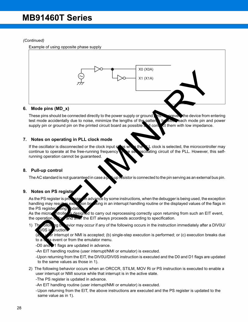
5. Notes on using external clockWhen using the external clock, it is necessary to simultaneously supply the X0 (X0A) and the X1 (X1A) pins. Inthe described combination, X1 (X1A) should be supplied with a clock signal which has the opposite phase tothe X0 (X0A) pins. At X0 and X1, a frequency up to 16 MHz is possible.
(Continued)
PRELIMIN
ARY
27
MB91460T Series
28
(Continued)Example of using opposite phase supply
6. Mode pins (MD_x)These pins should be connected directly to the power supply or ground pins. To prevent the device from enteringtest mode accidentally due to noise, minimize the lengths of the patterns between each mode pin and powersupply pin or ground pin on the printed circuit board as possible and connect them with low impedance.
7. Notes on operating in PLL clock modeIf the oscillator is disconnected or the clock input stops when the PLL clock is selected, the microcontroller maycontinue to operate at the free-running frequency of the self-oscillating circuit of the PLL. However, this self-running operation cannot be guaranteed.
8. Pull-up controlThe AC standard is not guaranteed in case a pull-up resistor is connected to the pin serving as an external bus pin.
9. Notes on PS registerAs the PS register is processed in advance by some instructions, when the debugger is being used, the exceptionhandling may result in execution breaking in an interrupt handling routine or the displayed values of the flags inthe PS register being updated.As the microcontroller is designed to carry out reprocessing correctly upon returning from such an EIT event,the operation before and after the EIT always proceeds according to specification.
1) The following behavior may occur if any of the following occurs in the instruction immediately after a DIV0U/DIV0S instruction:(a) a user interrupt or NMI is accepted; (b) single-step execution is performed; or (c) execution breaks dueto a data event or from the emulator menu.-D0 and D1 flags are updated in advance.-An EIT handling routine (user interrupt/NMI or emulator) is executed.-Upon returning from the EIT, the DIV0U/DIV0S instruction is executed and the D0 and D1 flags are updatedto the same values as those in 1).
2) The following behavior occurs when an ORCCR, STILM, MOV Ri or PS instruction is executed to enable a user interrupt or NMI source while that interrupt is in the active state.-The PS register is updated in advance.-An EIT handling routine (user interrupt/NMI or emulator) is executed.-Upon returning from the EIT, the above instructions are executed and the PS register is updated to the same value as in 1).
X0 (X0A)
X1 (X1A)
PRELIMIN
ARY

MB91460T Series
NOTES ON DEBUGGER1. Execution of the RETI Command
If single-step execution is used in an environment where an interrupt occurs frequently, the correspondinginterrupt handling routine will be executed repeatedly to the exclusion of other processing. This will prevent themain routine and the handlers for low priority level interrupts from being executed (For example, if the time-basetimer interrupt is enabled, stepping over the RETI instruction will always break on the first line of the time-basetimer interrupt handler).
Disable the corresponding interrupts when the corresponding interrupt handling routine no longer needs debug-ging.
2. Break functionIf the range of addresses that cause a hardware break (including event breaks) is set to the address of thecurrent system stack pointer or to an area that contains the stack pointer, execution will break after eachinstruction regardless of whether the user program actually contains data access instructions.
To prevent this, do not set (word) access to the area containing the address of the system stack pointer as thetarget of the hardware break (including an event breaks).
3. Operand breakIt may cause malfunctions if a stack pointer exists in the area which is set as the DSU operand break. Do notset the access to the areas containing the address of system stack pointer as a target of data event break.
PRELIMIN
ARY
29

MB91460T Series
30
BLOCK DIAGRAM1. MB91F467TA, MB91F469TA
AIN0 to AIN3BIN0 to BIN3ZIN0 to ZIN3
TTG0/8 to TTG7/15PPG0 to PPG5, PPG8 to PPG15
TIN0 to TIN7TOT0 to TOT7
CK0, CK2 to CK7
ICU0 to ICU7
OCU0 to OCU3
PFM
SDA0 to SDA3SCL0 to SCL3
AN0 to AN31
ATGX
SGASG0
SIN0,SIN2 to SIN7SOT0,SOT2 to SOT7SCK0,SCK2 to SCK7
ASXRDXWRX0 to WRX1
CSX0 to CSX2
A0 to A23
D16 to D31
RX0 to RX1TX0 to TX1
R-bus16
I-bus32
D-bus32
Flash-Cache8 Kbytes (MB91F467TA)
16 Kbytes (MB91F469TA)
Flash memory1088 Kbytes (MB91F467TA)2112 Kbytes (MB91F469TA)
ID-RAM32 Kbytes (MB91F467TA)64 Kbytes (MB91F469TA)
Bus converter
D-RAM32 Kbytes (MB91F467TA)64 Kbytes (MB91F469TA)
Bit search
CAN2 channels
32 <-> 16 bus adapter
Externalbus
interface
WEX
Clock modulator
Clock monitor
GPIO
MONCLK
Interrupt controller
INT0 to INT7,INT8, INT9, INT14, INT15
External interrupt12 channels
Clock supervisor
Clock control
PPG timer14 channels
Reload timer8 channels
Free-run timer8 channels
Input capture8 channels
Output compare8 channels
Up/down counter4 channels
PFM timer1 channel
LIN-USART11 channels
4 channelsI C2
Real time clock
A/D converter32 channels
Sound generator1 channel
NMI1 channel
FR60 CPUcore
WATCHDOG
PRELIMIN
ARY

MB91460T Series
CPU AND CONTROL UNITThe FR family CPU is a high performance core that is designed based on the RISC architecture with advancedinstructions for embedded applications.
1. Features• Adoption of RISC architecture
Basic instruction: 1 instruction per cycle• General-purpose registers: 32-bit × 16 registers• 4 Gbytes linear memory space• Multiplier installed
32-bit × 32-bit multiplication: 5 cycles16-bit × 16-bit multiplication: 3 cycles
• Enhanced interrupt processing functionQuick response speed (6 cycles)Multiple-interrupt supportLevel mask function (16 levels)
• Enhanced instructions for I/O operationMemory-to-memory transfer instructionBit processing instructionBasic instruction word length: 16 bits
• Low-power consumptionSleep mode/stop mode
2. Internal architecture• The FR family CPU uses the Harvard architecture in which the instruction bus and data bus are independent
of each other.• A 32-bit ↔ 16-bit buffer is connected to the 32-bit bus (D-bus) to provide an interface between the CPU and
peripheral resources.• A Harvard ↔ Princeton bus converter is connected to both the I-bus and D-bus to provide an interface between
the CPU and the bus controller.
PRELIMIN
ARY
31
MB91460T Series
32
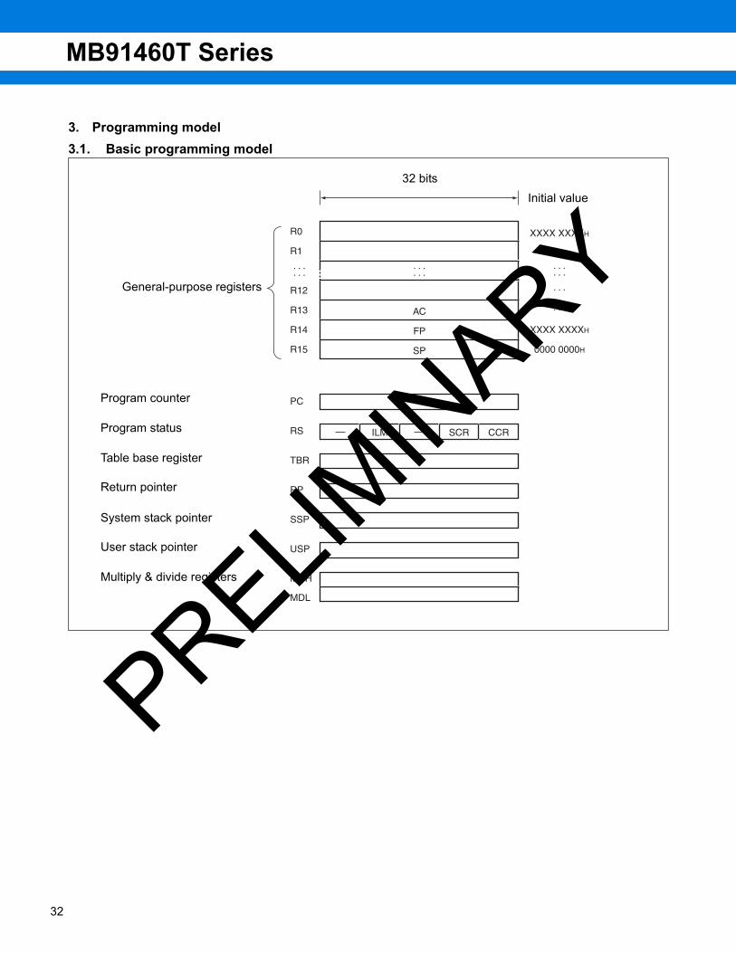
3. Programming model3.1. Basic programming model
ILM SCR CCR
FP
SP
AC
. . .
. . .
. . .
. . .
XXXX XXXXH
0000 0000H
XXXX XXXXH
. . .
. . .
. . .
R0
R1
R12
R13
R14
R15
PC
RS
RP
TBR
SSP
USP
MDL
MDH
. . .
. . .
32 bitsInitial value
General-purpose registers
Program counter
Program status
Table base register
Return pointer
System stack pointer
User stack pointer
Multiply & divide registers
PRELIMIN
ARY
MB91460T Series
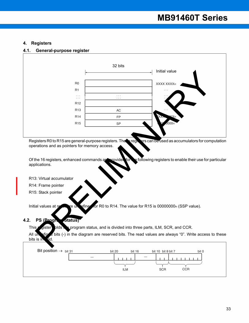
4. Registers4.1. General-purpose register
Registers R0 to R15 are general-purpose registers. These registers can be used as accumulators for computationoperations and as pointers for memory access.
Of the 16 registers, enhanced commands are provided for the following registers to enable their use for particularapplications.
R13: Virtual accumulator
R14: Frame pointer
R15: Stack pointer
Initial values at reset are undefined for R0 to R14. The value for R15 is 00000000H (SSP value).
4.2. PS (Program Status) This register holds the program status, and is divided into three parts, ILM, SCR, and CCR.
All undefined bits (-) in the diagram are reserved bits. The read values are always “0”. Write access to thesebits is invalid.
FP
SP
AC
. . .
. . .
. . .
. . .
XXXX XXXXH
0000 0000H
XXXX XXXXH
. . .
. . .
. . .
R0
R1
R12
R13
R14
R15
. . .
. . .
32 bitsInitial value
Bit position → bit 20 bit 0bit 7bit 8bit 10bit 16
ILM SCR CCR
bit 31PRELIM
INARY
33
MB91460T Series
34
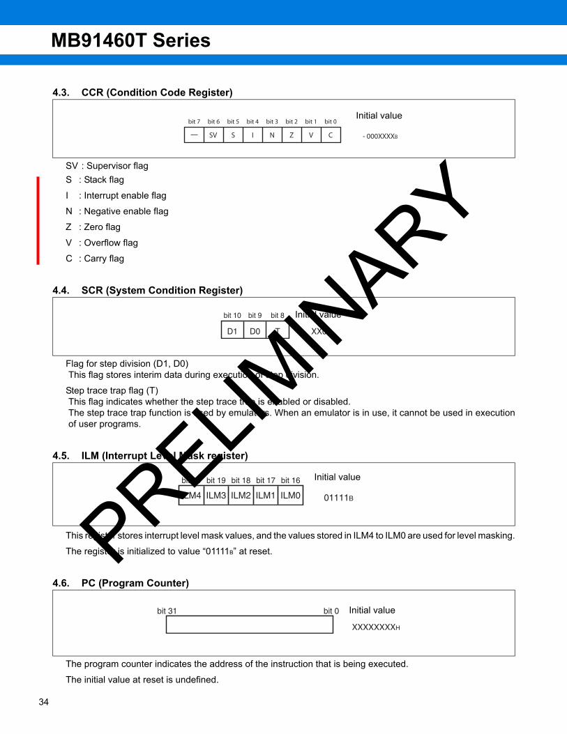
4.3. CCR (Condition Code Register)
SV : Supervisor flag S : Stack flag
I : Interrupt enable flag
N : Negative enable flag
Z : Zero flag
V : Overflow flag
C : Carry flag
4.4. SCR (System Condition Register)
Flag for step division (D1, D0) This flag stores interim data during execution of step division.
Step trace trap flag (T) This flag indicates whether the step trace trap is enabled or disabled.The step trace trap function is used by emulators. When an emulator is in use, it cannot be used in executionof user programs.
4.5. ILM (Interrupt Level Mask register)
This register stores interrupt level mask values, and the values stored in ILM4 to ILM0 are used for level masking.
The register is initialized to value “01111B” at reset.
4.6. PC (Program Counter)
The program counter indicates the address of the instruction that is being executed.
The initial value at reset is undefined.
- 000XXXXB
bit 0bit 1bit 2bit 3bit 4bit 5bit 6bit 7
CVZNISSV
Initial value
bit 10 bit 8bit 9
D1 D0 T XX0B
Initial value
bit 18 bit 16bit 17
ILM2 ILM1 ILM0 01111BILM3ILM4
bit 20 bit 19 Initial value
bit 0bit 31
XXXXXXXXH
Initial value
PRELIMIN
ARY
MB91460T Series
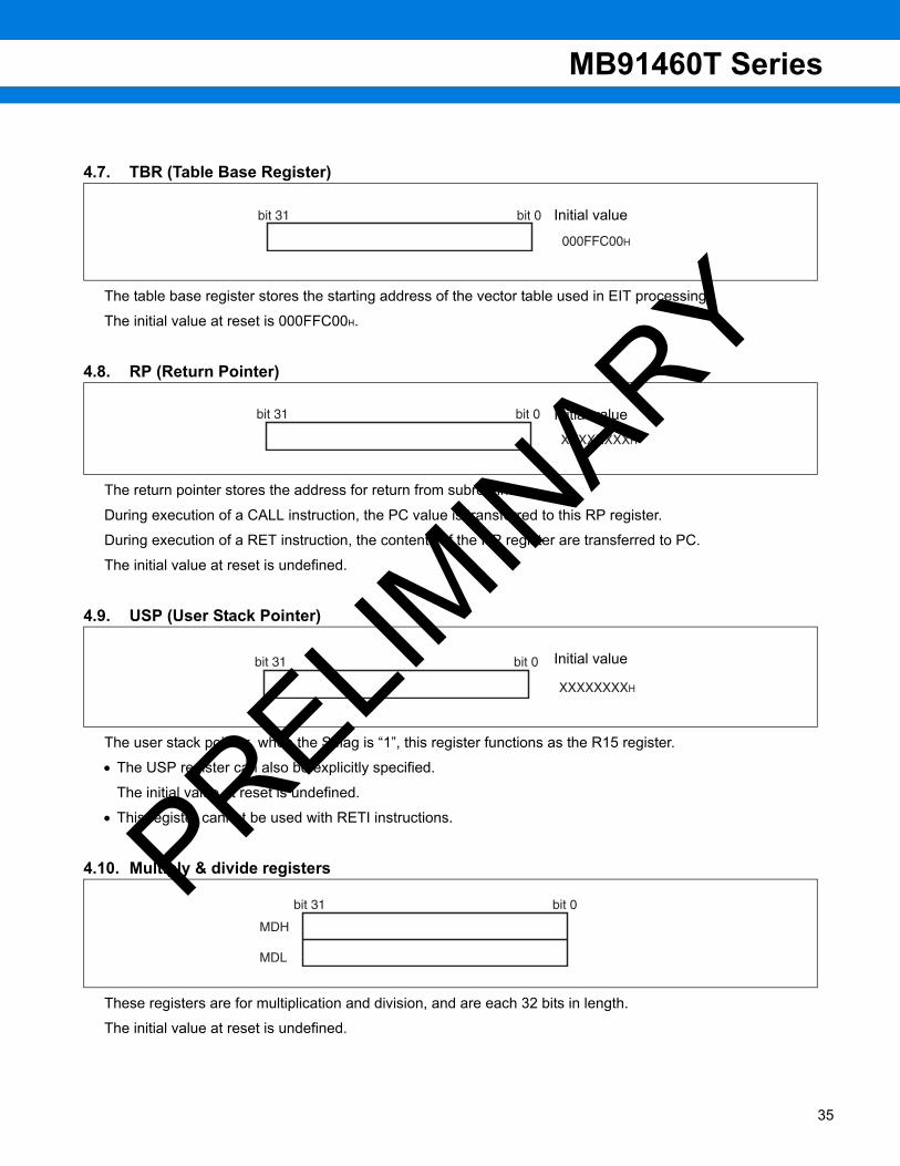
4.7. TBR (Table Base Register)
The table base register stores the starting address of the vector table used in EIT processing.
The initial value at reset is 000FFC00H.
4.8. RP (Return Pointer)
The return pointer stores the address for return from subroutines.
During execution of a CALL instruction, the PC value is transferred to this RP register.
During execution of a RET instruction, the contents of the RP register are transferred to PC.
The initial value at reset is undefined.
4.9. USP (User Stack Pointer)
The user stack pointer, when the S flag is “1”, this register functions as the R15 register.
• The USP register can also be explicitly specified.
The initial value at reset is undefined.
• This register cannot be used with RETI instructions.
4.10. Multiply & divide registers
These registers are for multiplication and division, and are each 32 bits in length.
The initial value at reset is undefined.
bit 0bit 31
000FFC00H
Initial value
bit 0bit 31
XXXXXXXXH
Initial value
bit 0bit 31
XXXXXXXXH
Initial value
bit 0
MDL
bit 31
MDH
PRELIMIN
ARY
35

MB91460T Series
36
EMBEDDED PROGRAM/DATA MEMORY (FLASH)
1. Flash features• MB91F467TA: 1088 Kbytes (16 × 64 Kbytes + 8 × 8 Kbytes = 8.5 Mbits)• MB91F469TA: 2112 Kbytes (32 × 64 Kbytes + 8 × 8 Kbytes = 16.5 Mbits)• Programmable wait state for read/write access• Flash and Boot security with security vector at 0x0014:8000 - 0x0014:800F• Boot security • Basic specification: Same as MBM29LV400TC (except size and part of sector configuration)
2. Operation modes(1) 64-bit CPU mode:
• CPU reads and executes programs in word (32-bit) length units.• Flash writing is not possible.• Actual Flash Memory access is performed in d-word (64-bit) length units.
(2) 32-bit CPU mode: • CPU reads, writes and executes programs in word (32-bit) length units.• Actual Flash Memory access is performed in word (32-bit) length units.
(3) 16-bit CPU mode: • CPU reads and writes in half-word (16-bit) length units.• Program execution from the Flash is not possible.• Actual Flash Memory access is performed in half-word (16-bit) length units.
(4) Flash memory mode (external access to Flash memory enabled)
PRELIMIN
ARY
MB91460T Series
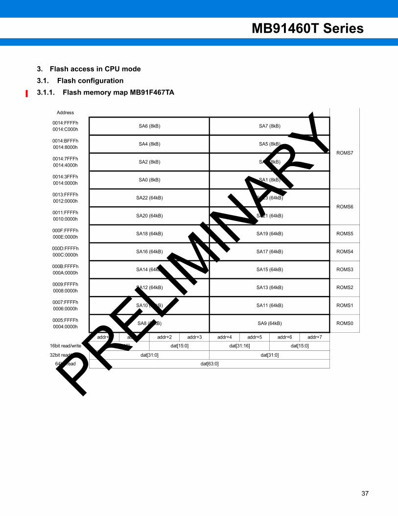
3. Flash access in CPU mode3.1. Flash configuration3.1.1. Flash memory map MB91F467TA
ROMS1
ROMS0
addr+6
ROMS5
ROMS4
ROMS6
ROMS7
ROMS3
ROMS2
dat[31:16] dat[15:0]
dat[31:0] dat[31:0]
dat[31:16] dat[15:0]16bit read/write
32bit read/write
dat[63:0]64bit read
addr+7addr+2
SA0 (8kB)
SA16 (64kB)
SA10 (64kB)
SA21 (64kB)
SA19 (64kB)
Address
0014:FFFFh
0014:C000h
0014:BFFFh
0014:8000h
SA7 (8kB)
SA5 (8kB)
SA3 (8kB)
SA1 (8kB)
SA23 (64kB)
SA6 (8kB)
SA4 (8kB)
SA2 (8kB)
SA22 (64kB)
SA20 (64kB)
0013:FFFFh
0012:0000h
0011:FFFFh
0010:0000h
SA18 (64kB)
0014:7FFFh
0014:4000h
0014:3FFFh
0014:0000h
000F:FFFFh
000E:0000h
SA15 (64kB)
000D:FFFFh
000C:0000h
000B:FFFFh
000A:0000h
addr+5
SA11 (64kB)
SA8 (64kB) SA9 (64kB)
addr+0 addr+1 addr+3 addr+4
0009:FFFFh
0008:0000h
0007:FFFFh
0006:0000h
0005:FFFFh
0004:0000h
SA17 (64kB)
SA14 (64kB)
SA12 (64kB) SA13 (64kB)
PRELIMIN
ARY
37

MB91460T Series
38
3.1.2. Flash memory map MB91F469TA
dat[31:0]32bit read/write mode dat[31:0]
dat[15:0]
addr+2 addr+3 addr+4
16bit read/write mode dat[31:16] dat[15:0] dat[31:16]
addr+5addr+0 addr+1
SA11 (64kB)
addr+6 addr+7
ROMS1
0005:FFFFh
0004:0000hSA8 (64kB) SA9 (64kB) ROMS0
0007:FFFFh
0006:0000hSA10 (64kB)
SA15 (64kB) ROMS3
0009:FFFFh
0008:0000hSA12 (64kB) SA13 (64kB) ROMS2
000B:FFFFh
000A:0000hSA14 (64kB)
SA19 (64kB) ROMS5
000D:FFFFh
000C:0000hSA16 (64kB) SA17 (64kB) ROMS4
000F:FFFFh
000E:0000hSA18 (64kB)
SA23 (64kB)
ROMS6
0011:FFFFh
0010:0000hSA20 (64kB) SA21 (64kB)
0013:FFFFh
0012:0000hSA22 (64kB)
SA27 (64kB)
ROMS7
0015:FFFFh
0014:0000hSA24 (64kB) SA25 (64kB)
0017:FFFFh
0016:0000hSA26 (64kB)
SA31 (64kB)
ROMS8
0019:FFFFh
0018:0000hSA28 (64kB) SA29 (64kB)
001B:FFFFh
001A:0000hSA30 (64kB)
ROMS9
001D:FFFFh
001C:0000hSA32 (64kB) SA33 (64kB)
SA37 (64kB)
001F:FFFFh
001E:0000hSA34 (64kB) SA35 (64kB)
0021:FFFFh
0020:0000hSA36 (64kB)
SA3 (8kB)
SA1 (8kB)
0023:FFFFh
0022:0000hSA38 (64kB) SA39 (64kB)
0024:3FFFh
0024:0000hSA0 (8kB)
Address
ROMS10
0024:FFFFh
0024:C000hSA6 (8kB) SA7 (8kB)
0024:BFFFh
0024:8000hSA4 (8kB) SA5 (8kB)
0024:7FFFh
0024:4000hSA2 (8kB)
64bit read mode dat[63:0]
PRELIMIN
ARY
MB91460T Series
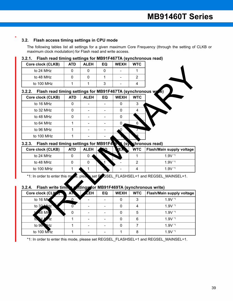
3.2. Flash access timing settings in CPU modeThe following tables list all settings for a given maximum Core Frequency (through the setting of CLKB ormaximum clock modulation) for Flash read and write access.
3.2.1. Flash read timing settings for MB91F467TA (synchronous read)
3.2.2. Flash read timing settings for MB91F467TA (synchronous write)
3.2.3. Flash read timing settings for MB91F469TA (synchronous read)
*1: In order to enter this mode, please set REGSEL_FLASHSEL=1 and REGSEL_MAINSEL=1.
3.2.4. Flash write timing settings for MB91F469TA (synchronous write)
*1: In order to enter this mode, please set REGSEL_FLASHSEL=1 and REGSEL_MAINSEL=1.
Core clock (CLKB) ATD ALEH EQ WEXH WTCto 24 MHz 0 0 0 - 1
to 48 MHz 0 0 1 - 2
to 100 MHz 1 1 3 - 4
Core clock (CLKB) ATD ALEH EQ WEXH WTCto 16 MHz 0 - - 0 3
to 32 MHz 0 - - 0 4
to 48 MHz 0 - - 0 5
to 64 MHz 1 - - 0 6
to 96 MHz 1 - - 0 7
to 100 MHz 1 - - 1 8
Core clock (CLKB) ATD ALEH EQ WEXH WTC Flash/Main supply voltageto 24 MHz 0 0 0 - 1 1.9V *1
to 48 MHz 0 0 1 - 2 1.9V *1
to 100 MHz 1 1 3 - 4 1.9V *1
Core clock (CLKB) ATD ALEH EQ WEXH WTC Flash/Main supply voltageto 16 MHz 0 - - 0 3 1.9V *1
to 32 MHz 0 - - 0 4 1.9V *1
to 48 MHz 0 - - 0 5 1.9V *1
to 64 MHz 1 - - 0 6 1.9V *1
to 96 MHz 1 - - 0 7 1.9V *1
to 100 MHz 1 - - 1 8 1.9V *1PRELIMIN
ARY
39

MB91460T Series
40
3.3. Address mapping from CPU to parallel programming modeThe following tables show the calculation from CPU addresses to flash macro addresses which are used inparallel programming.
3.3.1. Address mapping MB91F467TA
Note: FA result is without 20:0000h offset for parallel Flash programming.Set offset by keeping FA[21] = 1 as described in section “Parallel Flash programming mode”.
3.3.2. Address mapping MB91F469TA
Note: FA result is without 40:0000h offset for parallel Flash programming . Set offset by keeping FA[22] = 1 as described in section “Parallel Flash programming mode”.
CPU Address(addr) Condition Flash
sectors FA (flash address) Calculation
14:0000hto
14:FFFFhaddr[2]==0 SA0, SA2, SA4, SA6
(8 Kbyte)FA := addr - addr%00:4000h + (addr%00:4000h)/2
- (addr/2)%4 + addr%4 - 05:0000h
14:0000hto
14:FFFFhaddr[2]==1 SA1, SA3, SA5, SA7
(8 Kbyte)FA := addr - addr%00:4000h + (addr%00:4000h)/2 +
00:2000h - (addr/2)%4 + addr%4 - 05:0000h
04:0000hto
13:FFFFhaddr[2]==0
SA8, SA10, SA12, SA14, SA16, SA18, SA20, SA22
(64 Kbyte)
FA := addr - addr%02:0000 + (addr%02:0000h)/2 - (addr/2)%4 + addr%4 + 0C:0000h
04:0000hto
13:FFFFhaddr[2]==1
SA9, SA11, SA13, SA15, SA17, SA19, SA21, SA23
(64 Kbyte)
FA := addr - addr%02:0000h + (addr%02:0000h)/2 + 01:0000h - (addr/2)%4 + addr%4 + 0C:0000h
CPU Address(addr) Condition Flash
sectors FA (flash address) Calculation
24:0000hto
24:FFFFhaddr[2]==0 SA0, SA2, SA4, SA6
(8 Kbyte)FA := addr - addr%00:4000h + (addr%00:4000h)/2
- (addr/2)%4 + addr%4 - 05:0000h
24:0000hto
24:FFFFhaddr[2]==1 SA1, SA3, SA5, SA7
(8 Kbyte)
FA := addr - addr%00:4000h + (addr%00:4000h)/2- (addr/2)%4 + addr%4 - 05:0000h
+ 00:2000h
04:0000hto
23:FFFFhaddr[2]==0
SA8, SA10, SA12, SA14, SA16, SA18, SA20, SA22, SA24, SA26, SA28, SA30, SA32, SA34, SA36, SA38
(64 Kbyte)
FA := addr - addr%02:0000 + (addr%02:0000h)/2- (addr/2)%4 + addr%4 + 1C:0000h
04:0000hto
23:FFFFhaddr[2]==1
SA9, SA11, SA13, SA15, SA17, SA19, SA21, SA23, SA25, SA27, SA29, SA31, SA33, SA35, SA37, SA39
(64 Kbyte)
FA := addr - addr%02:0000h + (addr%02:0000h)/2- (addr/2)%4 + addr%4 + 1C:0000h
+ 01:0000hPRELIMIN
ARY

MB91460T Series
4. Parallel Flash programming mode4.1. Flash configuration in parallel Flash programming mode
Parallel Flash programming mode (MD[2:0] = 111):
MB91F467TA
16bit write mode DQ[15:0] DQ[15:0]
SA20 (64kB)
SA19 (64kB)
SA18 (64kB)
FA[21:0]
003E:FFFFh
003E:0000h
003D:FFFFh
003D:0000h
003F:FFFFh
003F:0000hSA23 (64kB)
SA22 (64kB)
SA21 (64kB)
003C:FFFFh
003C:0000h
003B:FFFFh
003B:0000h
003A:FFFFh
003A:0000h
0039:FFFFh
0039:0000hSA17 (64kB)
0038:FFFFh
0038:0000h
0037:FFFFh
0037:0000h
SA16 (64kB)
SA15 (64kB)
0036:FFFFh
0036:0000h
0035:FFFFh
0035:0000h
SA14 (64kB)
SA13 (64kB)
0034:FFFFh
0034:0000h
0033:FFFFh
0033:0000h
SA12 (64kB)
SA11 (64kB)
0032:FFFFh
0032:0000h
0031:FFFFh
0031:0000h
SA10 (64kB)
SA9 (64kB)
0030:FFFFh
0030:0000h
002F:FFFFh
002F:E000h
SA8 (64kB)
SA7 (8kB)
002F:7FFFh
002F:6000h
SA4 (8kB)
SA3 (8kB)
002F:DFFFh
002F:C000h
002F:BFFFh
002F:A000h
SA6 (8kB)
SA5 (8kB)
002F:1FFFh
002F:0000hSA0 (8kB)
FA[1:0]=00 FA[1:0]=10
002F:5FFFh
002F:4000h
002F:3FFFh
002F:2000h
SA2 (8kB)
SA1 (8kB)
002F:9FFFh
002F:8000h PRELIMIN
ARY
41
MB91460T Series
42
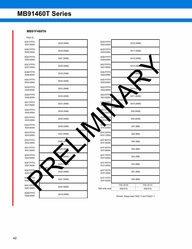
MB91F469TA
003D:FFFFh
003D:0000hSA37 (64kB)
FA[21:0]
003F:FFFFh
003F:0000hSA39 (64kB)
003E:FFFFh
003E:0000hSA38 (64kB)
003B:FFFFh
003B:0000hSA35 (64kB)
003C:FFFFh
003C:0000hSA36 (64kB)
0039:FFFFh
0039:0000hSA33 (64kB)
003A:FFFFh
003A:0000hSA34 (64kB)
0037:FFFFh
0037:0000hSA31 (64kB)
0038:FFFFh
0038:0000hSA32 (64kB)
0035:FFFFh
0035:0000hSA29 (64kB)
0036:FFFFh
0036:0000hSA30 (64kB)
0033:FFFFh
0033:0000hSA27 (64kB)
0034:FFFFh
0034:0000hSA28 (64kB)
0031:FFFFh
0031:0000hSA25 (64kB)
0032:FFFFh
0032:0000hSA26 (64kB)
002F:FFFFh
002F:0000hSA23 (64kB)
0030:FFFFh
0030:0000hSA24 (64kB)
002A:FFFFh
002A:0000hSA18 (64kB)
002B:FFFFh
002B:0000hSA19 (64kB)
002C:FFFFh
002C:0000hSA20 (64kB)
002D:FFFFh
002D:0000hSA21 (64kB)
002E:FFFFh
002E:0000hSA22 (64kB)
0029:FFFFh
0029:0000hSA17 (64kB)
0028:FFFFh
0028:0000hSA16 (64kB)
0027:FFFFh
0027:0000hSA15 (64kB)
0026:FFFFh
0026:0000hSA14 (64kB)
0025:FFFFh
0025:0000hSA13 (64kB)
0024:FFFFh
0024:0000hSA12 (64kB)
0023:FFFFh
0023:0000hSA11 (64kB)
0022:FFFFh
0022:0000hSA10 (64kB)
0021:FFFFh
0021:0000hSA9 (64kB)
0020:FFFFh
0020:0000hSA8 (64kB)
001F:BFFFh
001F:A000hSA5 (8kB)
001F:9FFFh
001F:8000hSA4 (8kB)
001F:FFFFh
001F:E000hSA7 (8kB)
001F:DFFFh
001F:C000hSA6 (8kB)
SA3 (8kB)
001F:5FFFh
001F:4000hSA2 (8kB)
001F:3FFFh
001F:2000hSA1 (8kB)
001F:7FFFh
001F:6000h
001F:1FFFh
001F:0000hSA0 (8kB)
FA[1:0]=00 FA[1:0]=10
16bit write mode DQ[15:0] DQ[15:0]
Remark: Always keep FA[0] = 0 and FA[22] = 1
PRELIMIN
ARY
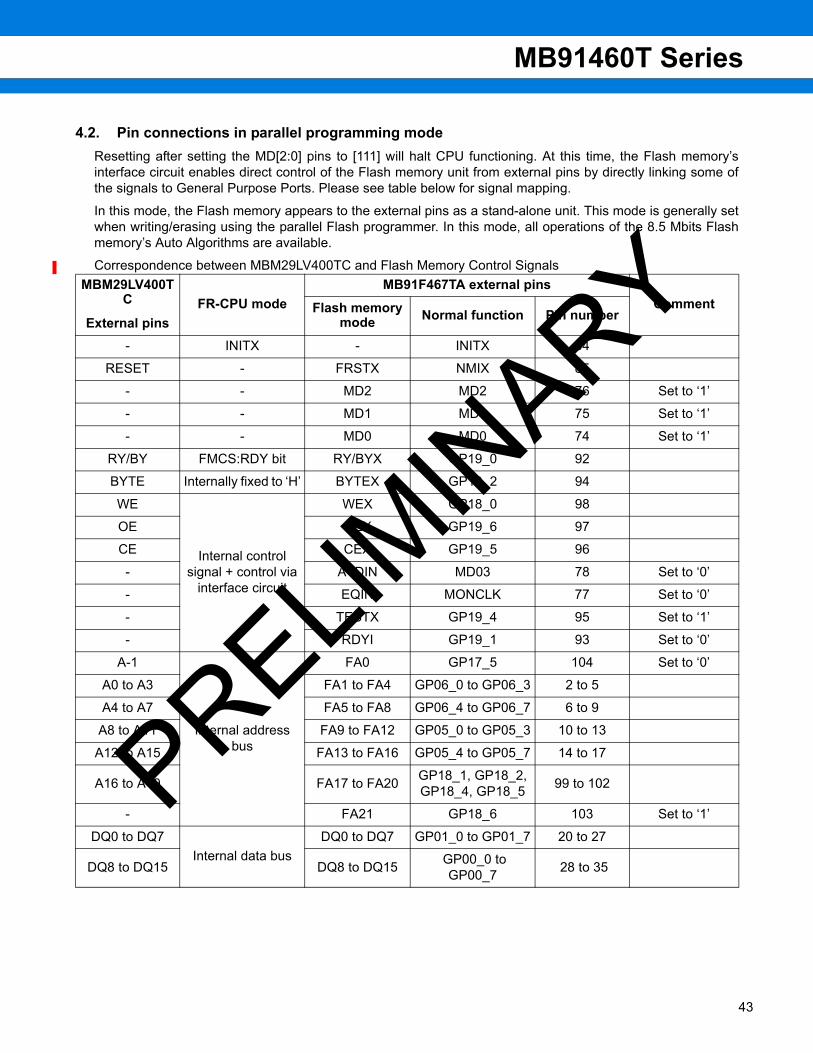
MB91460T Series
4.2. Pin connections in parallel programming modeResetting after setting the MD[2:0] pins to [111] will halt CPU functioning. At this time, the Flash memory’sinterface circuit enables direct control of the Flash memory unit from external pins by directly linking some ofthe signals to General Purpose Ports. Please see table below for signal mapping.
In this mode, the Flash memory appears to the external pins as a stand-alone unit. This mode is generally setwhen writing/erasing using the parallel Flash programmer. In this mode, all operations of the 8.5 Mbits Flashmemory’s Auto Algorithms are available.
Correspondence between MBM29LV400TC and Flash Memory Control SignalsMBM29LV400T
C
External pinsFR-CPU mode
MB91F467TA external pinsCommentFlash memory
mode Normal function Pin number
- INITX - INITX 84
RESET - FRSTX NMIX 85
- - MD2 MD2 76 Set to ‘1’
- - MD1 MD1 75 Set to ‘1’
- - MD0 MD0 74 Set to ‘1’
RY/BY FMCS:RDY bit RY/BYX GP19_0 92
BYTE Internally fixed to ‘H’ BYTEX GP19_2 94
WE
Internal control signal + control via
interface circuit
WEX GP18_0 98
OE OEX GP19_6 97
CE CEX GP19_5 96
- ATDIN MD03 78 Set to ‘0’
- EQIN MONCLK 77 Set to ‘0’
- TESTX GP19_4 95 Set to ‘1’
- RDYI GP19_1 93 Set to ‘0’
A-1
Internal address bus
FA0 GP17_5 104 Set to ‘0’
A0 to A3 FA1 to FA4 GP06_0 to GP06_3 2 to 5
A4 to A7 FA5 to FA8 GP06_4 to GP06_7 6 to 9
A8 to A11 FA9 to FA12 GP05_0 to GP05_3 10 to 13
A12 to A15 FA13 to FA16 GP05_4 to GP05_7 14 to 17
A16 to A19 FA17 to FA20 GP18_1, GP18_2, GP18_4, GP18_5 99 to 102
- FA21 GP18_6 103 Set to ‘1’
DQ0 to DQ7Internal data bus
DQ0 to DQ7 GP01_0 to GP01_7 20 to 27
DQ8 to DQ15 DQ8 to DQ15 GP00_0 to GP00_7 28 to 35
PRELIMIN
ARY
43
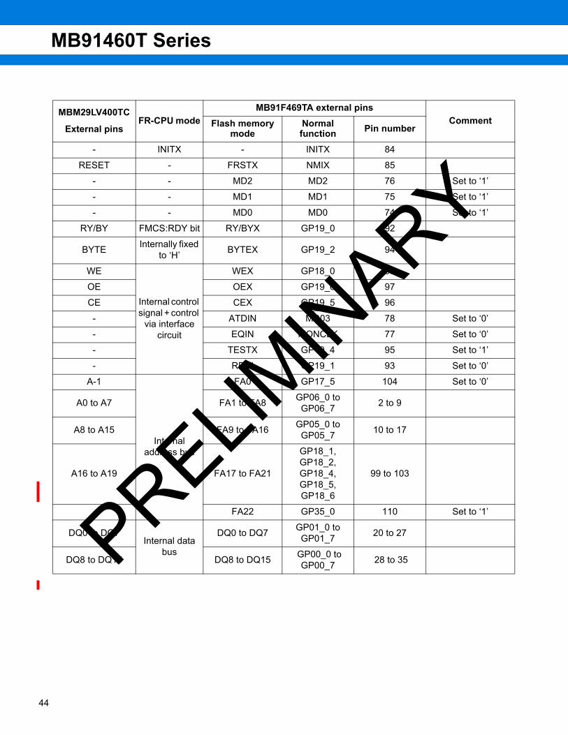
MB91460T Series
44
MBM29LV400TC
External pinsFR-CPU mode
MB91F469TA external pinsCommentFlash memory
modeNormal function Pin number
- INITX - INITX 84
RESET - FRSTX NMIX 85
- - MD2 MD2 76 Set to ‘1’
- - MD1 MD1 75 Set to ‘1’
- - MD0 MD0 74 Set to ‘1’
RY/BY FMCS:RDY bit RY/BYX GP19_0 92
BYTE Internally fixed to ‘H’ BYTEX GP19_2 94
WE
Internal control signal + control
via interface circuit
WEX GP18_0 98
OE OEX GP19_6 97
CE CEX GP19_5 96
- ATDIN MD03 78 Set to ‘0’
- EQIN MONCLK 77 Set to ‘0’
- TESTX GP19_4 95 Set to ‘1’
- RDYI GP19_1 93 Set to ‘0’
A-1
Internal address bus
FA0 GP17_5 104 Set to ‘0’
A0 to A7 FA1 to FA8 GP06_0 to GP06_7 2 to 9
A8 to A15 FA9 to FA16 GP05_0 to GP05_7 10 to 17
A16 to A19 FA17 to FA21
GP18_1, GP18_2, GP18_4, GP18_5,GP18_6
99 to 103
- FA22 GP35_0 110 Set to ‘1’
DQ0 to DQ7Internal data
bus
DQ0 to DQ7 GP01_0 to GP01_7 20 to 27
DQ8 to DQ15 DQ8 to DQ15 GP00_0 to GP00_7 28 to 35PRELIMIN
ARY
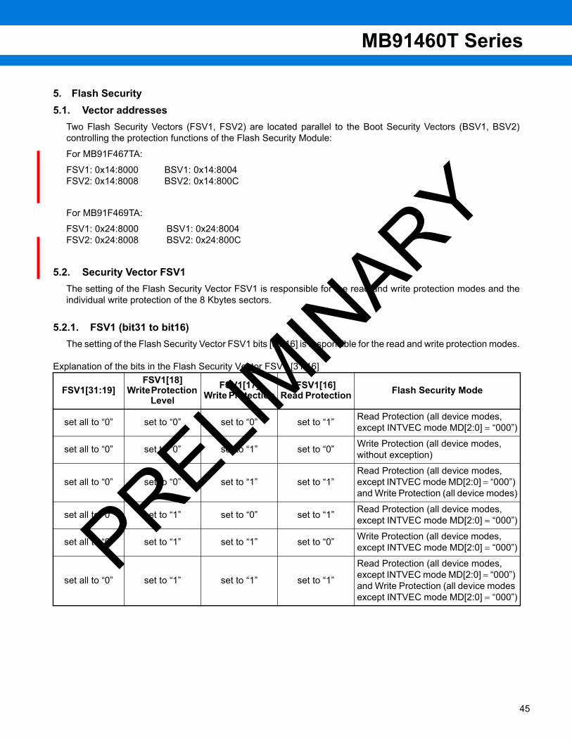
MB91460T Series
5. Flash Security5.1. Vector addresses
Two Flash Security Vectors (FSV1, FSV2) are located parallel to the Boot Security Vectors (BSV1, BSV2)controlling the protection functions of the Flash Security Module:
For MB91F467TA:
FSV1: 0x14:8000 BSV1: 0x14:8004FSV2: 0x14:8008 BSV2: 0x14:800C
For MB91F469TA:
FSV1: 0x24:8000 BSV1: 0x24:8004FSV2: 0x24:8008 BSV2: 0x24:800C
5.2. Security Vector FSV1The setting of the Flash Security Vector FSV1 is responsible for the read and write protection modes and theindividual write protection of the 8 Kbytes sectors.
5.2.1. FSV1 (bit31 to bit16)The setting of the Flash Security Vector FSV1 bits [31:16] is responsible for the read and write protection modes.
Explanation of the bits in the Flash Security Vector FSV1 [31:16]
FSV1[31:19]FSV1[18]
Write Protection Level
FSV1[17]Write Protection
FSV1[16]Read Protection Flash Security Mode
set all to “0” set to “0” set to “0” set to “1” Read Protection (all device modes, except INTVEC mode MD[2:0] = “000”)
set all to “0” set to “0” set to “1” set to “0” Write Protection (all device modes, without exception)
set all to “0” set to “0” set to “1” set to “1”Read Protection (all device modes, except INTVEC mode MD[2:0] = “000”) and Write Protection (all device modes)
set all to “0” set to “1” set to “0” set to “1” Read Protection (all device modes, except INTVEC mode MD[2:0] = “000”)
set all to “0” set to “1” set to “1” set to “0” Write Protection (all device modes, except INTVEC mode MD[2:0] = “000”)
set all to “0” set to “1” set to “1” set to “1”
Read Protection (all device modes, except INTVEC mode MD[2:0] = “000”) and Write Protection (all device modes except INTVEC mode MD[2:0] = “000”)
PRELIMIN
ARY
45
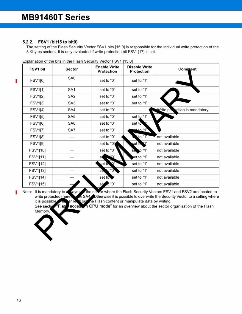
MB91460T Series
46
5.2.2. FSV1 (bit15 to bit0)The setting of the Flash Security Vector FSV1 bits [15:0] is responsible for the individual write protection of the 8 Kbytes sectors. It is only evaluated if write protection bit FSV1[17] is set.
Explanation of the bits in the Flash Security Vector FSV1 [15:0]
Note: It is mandatory to always set the sector where the Flash Security Vectors FSV1 and FSV2 are located to write protected (here sector SA4). Otherwise it is possible to overwrite the Security Vector to a setting where it is possible to either read out the Flash content or manipulate data by writing.See section “Flash access in CPU mode” for an overview about the sector organisation of the Flash Memory.
FSV1 bit Sector Enable Write Protection
Disable Write Protection Comment
FSV1[0] SA0 set to “0” set to “1”
FSV1[1] SA1 set to “0” set to “1”
FSV1[2] SA2 set to “0” set to “1”
FSV1[3] SA3 set to “0” set to “1”
FSV1[4] SA4 set to “0” ⎯ Write protection is mandatory!
FSV1[5] SA5 set to “0” set to “1”
FSV1[6] SA6 set to “0” set to “1”
FSV1[7] SA7 set to “0” set to “1”
FSV1[8] ⎯ set to “0” set to “1” not available
FSV1[9] ⎯ set to “0” set to “1” not available
FSV1[10] ⎯ set to “0” set to “1” not available
FSV1[11] ⎯ set to “0” set to “1” not available
FSV1[12] ⎯ set to “0” set to “1” not available
FSV1[13] ⎯ set to “0” set to “1” not available
FSV1[14] ⎯ set to “0” set to “1” not available
FSV1[15] ⎯ set to “0” set to “1” not available
PRELIMIN
ARY
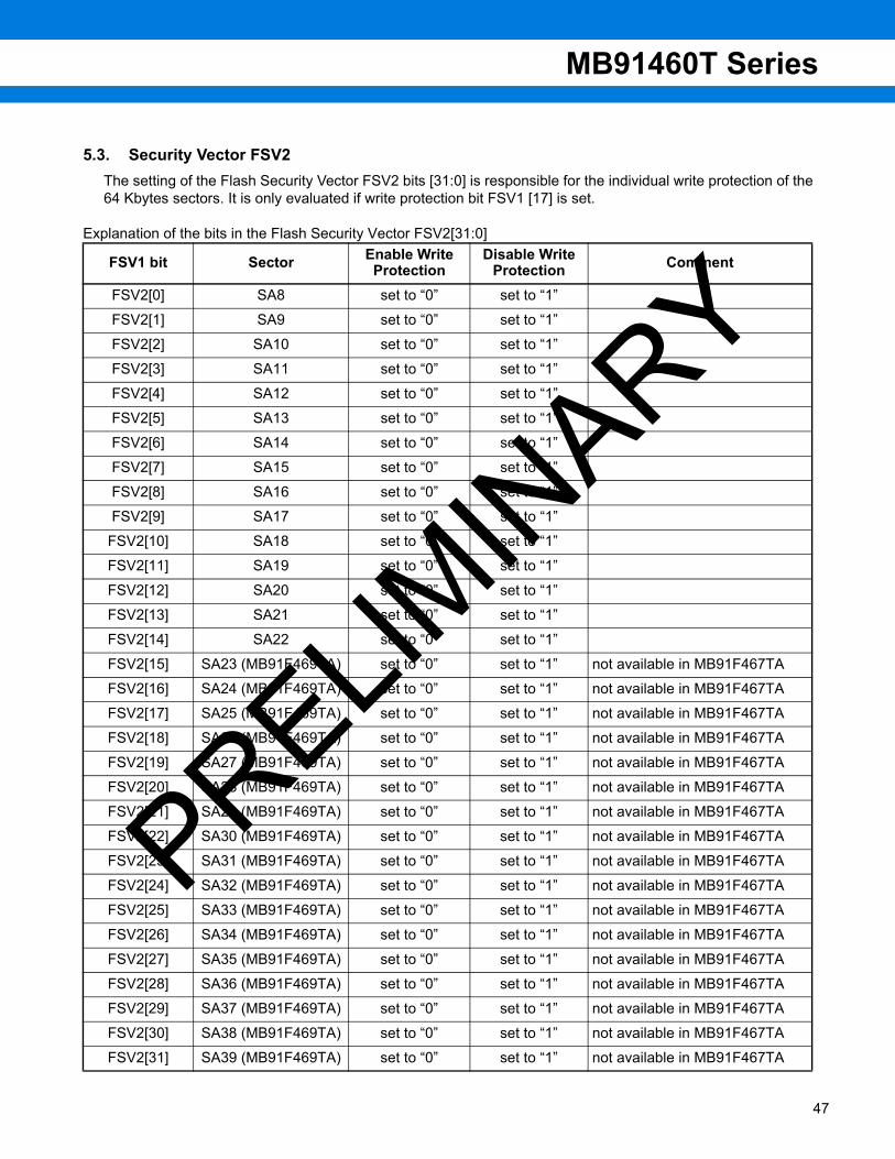
MB91460T Series
5.3. Security Vector FSV2The setting of the Flash Security Vector FSV2 bits [31:0] is responsible for the individual write protection of the64 Kbytes sectors. It is only evaluated if write protection bit FSV1 [17] is set.
Explanation of the bits in the Flash Security Vector FSV2[31:0]
FSV1 bit Sector Enable Write Protection
Disable Write Protection Comment
FSV2[0] SA8 set to “0” set to “1”
FSV2[1] SA9 set to “0” set to “1”
FSV2[2] SA10 set to “0” set to “1”
FSV2[3] SA11 set to “0” set to “1”
FSV2[4] SA12 set to “0” set to “1”
FSV2[5] SA13 set to “0” set to “1”
FSV2[6] SA14 set to “0” set to “1”
FSV2[7] SA15 set to “0” set to “1”
FSV2[8] SA16 set to “0” set to “1”
FSV2[9] SA17 set to “0” set to “1”
FSV2[10] SA18 set to “0” set to “1”
FSV2[11] SA19 set to “0” set to “1”
FSV2[12] SA20 set to “0” set to “1”
FSV2[13] SA21 set to “0” set to “1”
FSV2[14] SA22 set to “0” set to “1”
FSV2[15] SA23 (MB91F469TA) set to “0” set to “1” not available in MB91F467TA
FSV2[16] SA24 (MB91F469TA) set to “0” set to “1” not available in MB91F467TA
FSV2[17] SA25 (MB91F469TA) set to “0” set to “1” not available in MB91F467TA
FSV2[18] SA26 (MB91F469TA) set to “0” set to “1” not available in MB91F467TA
FSV2[19] SA27 (MB91F469TA) set to “0” set to “1” not available in MB91F467TA
FSV2[20] SA28 (MB91F469TA) set to “0” set to “1” not available in MB91F467TA
FSV2[21] SA29 (MB91F469TA) set to “0” set to “1” not available in MB91F467TA
FSV2[22] SA30 (MB91F469TA) set to “0” set to “1” not available in MB91F467TA
FSV2[23] SA31 (MB91F469TA) set to “0” set to “1” not available in MB91F467TA
FSV2[24] SA32 (MB91F469TA) set to “0” set to “1” not available in MB91F467TA
FSV2[25] SA33 (MB91F469TA) set to “0” set to “1” not available in MB91F467TA
FSV2[26] SA34 (MB91F469TA) set to “0” set to “1” not available in MB91F467TA
FSV2[27] SA35 (MB91F469TA) set to “0” set to “1” not available in MB91F467TA
FSV2[28] SA36 (MB91F469TA) set to “0” set to “1” not available in MB91F467TA
FSV2[29] SA37 (MB91F469TA) set to “0” set to “1” not available in MB91F467TA
FSV2[30] SA38 (MB91F469TA) set to “0” set to “1” not available in MB91F467TA
FSV2[31] SA39 (MB91F469TA) set to “0” set to “1” not available in MB91F467TA
PRELIMIN
ARY
47

MB91460T Series
48
Note: See section “Flash access in CPU mode” for an overview about the sector organisation of the Flash Memory
MEMORY SPACEThe FR family has 4 Gbytes of logical address space (232 addresses) available to the CPU by linear access.• Direct addressing area
The following address space area is used for I/O.
This area is called direct addressing area, and the address of an operand can be specified directly in aninstruction.
The size of directly addressable area depends on the length of the data being accessed as shown below.
Byte data access : 000H to 0FFH
Half word access : 000H to 1FFH
Word data access: 000H to 3FFH
PRELIMIN
ARY

MB91460T Series
MEMORY MAPS1. MB91F467TA, MB91F469TA
MB91F467TA MB91F469TA00000000H
00000400H
I/O (direct addressing area)
I/O
00002000H
00004000H
Flash-Cache (8 KBytes)
00001000H
DMA
00006000H
00007000H
Flash memory control
00008000H
0000B000H
Boot ROM (4 Kbytes)
0000C000H
CAN
0000D000H
00028000H
D-RAM (0 wait, 32 Kbytes)
00030000H
ID-RAM (32 Kbytes)
00038000H
00040000H
Flash memory (1088 Kbytes)
00150000H
00180000H
External bus area
00500000H
External data bus
FFFFFFFFH
Note: Access prohibited areas
00000000H
I/O (direct addressing area)
I/O
00001000H
00002000H
Flash-Cache (16 KBytes)
00000400H
DMA
00006000H
00007000H
Flash memory control
00008000H
0000B000H
Boot ROM (4 Kbytes)
0000C000H
CAN
0000D000H
00020000H
D-RAM (0 wait, 64 Kbytes)
00030000H
ID-RAM (64 Kbytes)
00040000H
Flash memory (2112 Kbytes)
00250000H
00280000H
External bus area
00500000H
External data bus
FFFFFFFFH
Note: Access prohibited areas
PRELIMIN
ARY
49

MB91460T Series
50
I/O MAP1. MB91F467TA, MB91F469TA
Note: Initial values of register bits are represented as follows:“ 1 ” : Initial value “ 1 ”“ 0 ” : Initial value “ 0 ”“ X ” : Initial value “ undefined ”“ - ” : No physical register at this locationAccess is barred with an undefined data access attribute.
AddressRegister
Block + 0 + 1 + 2 + 3
000000HPDR0 [R/W]XXXXXXXX
PDR1 [R/W]XXXXXXXX
PDR2 [R/W]XXXXXXXX
PDR3 [R/W]XXXXXXXX
T-unit port data register
Read/write attribute
Register initial value after reset
Register name (column 1 register at address 4n, column 2 register at address 4n + 2)
Leftmost register address (for word access, the register in column 1 becomes the MSB side of the data.)
PRELIMIN
ARY
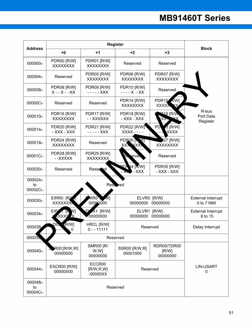
MB91460T Series
AddressRegister
Block+0 +1 +2 +3
000000HPDR00 [R/W]XXXXXXXX
PDR01 [R/W]XXXXXXXX Reserved Reserved
R-busPort DataRegister
000004H Reserved PDR05 [R/W]XXXXXXXX
PDR06 [R/W]XXXXXXXX
PDR07 [R/W]XXXXXXXX
000008HPDR08 [R/W]X - - X - -XX
PDR09 [R/W]- - - - - XXX
PDR10 [R/W]- - - - X - XX Reserved
00000CH Reserved Reserved PDR14 [R/W]XXXXXXXX
PDR15 [R/W]XXXXXXXX
000010HPDR16 [R/W]XXXXXXXX
PDR17 [R/W]- - XXXXXX
PDR18 [R/W]- XXX - XXX
PDR19 [R/W]- XXX - XXX
000014HPDR20 [R/W]- XXX - XXX
PDR21 [R/W]- - - - - XXX
PDR22 [R/W]XXXX - - - -
PDR23 [R/W]- - - - XXXX
000018HPDR24 [R/W]XXXXXXXX Reserved PDR26 [R/W]
XXXXXXXXPDR27 [R/W]XXXXXXXX
00001CHPDR28 [R/W]
- -XXXXXPDR29 [R/W]XXXXXXXX Reserved Reserved
000020H Reserved Reserved PDR34 [R/W]- XXX - XXX
PDR35 [R/W]- XXX - XXX
000024H
to00002CH
Reserved
000030HEIRR0 [R/W]XXXXXXXX
ENIR0 [R/W]00000000
ELVR0 [R/W]00000000 00000000
External Interrupt 0 to 7 NMI
000034HEIRR1 [R/W]XXXXXXXX
ENIR1 [R/W]00000000
ELVR1 [R/W]00000000 00000000
External Interrupt 8 to 15
000038HDICR [R/W]- - - - - - - 0
HRCL [R/W]0 - - 11111 Reserved Delay Interrupt
00003CH Reserved
000040HSCR00 [R/W,W]
00000000
SMR00 [R/W,W]
00000000
SSR00 [R/W,R]00001000
RDR00/TDR00 [R/W]
00000000
LIN-USART0000044H
ESCR00 [R/W]00000X00
ECCR00 [R/W,R,W]-00000XX
Reserved
000048H
to00004CH
Reserved
PRELIMIN
ARY
51

MB91460T Series
52
000050HSCR02 [R/W,W]
00000000
SMR02 [R/W,W]
00000000
SSR02 [R/W,R]00001000
RDR02/TDR02 [R/W]
00000000 LIN-USART2
000054HESCR02 [R/W]
00000X00
ECCR02 [R/W,R,W]-00000XX
Reserved
000058HSCR03[R/W,W]
00000000
SMR03 [R/W,W]
00000000
SSR03 [R/W,R]00001000
RDR03/TDR02 [R/W]
00000000 LIN-USART3
00005CHESCR03 [R/W]
00000X00
ECCR03 [R/W,R,W]-00000XX
Reserved
000060HSCR04 [R/W,W]
00000000
SMR04 [R/W,W]
00000000
SSR04 [R/W,R]00001000
RDR04/TDR04 [R/W]
00000000 LIN-USART4
with FIFO000064H
ESCR04 [R/W]00000X00
ECCR04 [R/W,R,W]-00000XX
FSR04 [R]- - - 00000
FCR04 [R/W]0001 - 000
000068HSCR05 [R/W,W]
00000000
SMR05 [R/W,W]
00000000
SSR05 [R/W,R]00001000
RDR05/TDR05 [R/W]
00000000 LIN-USART5
with FIFO00006CH
ESCR05 [R/W]00000X00
ECCR05 [R/W,R,W]-00000XX
FSR05 [R]- - - 00000
FCR05 [R/W]0001 - 000
000070HSCR06 [R/W,W]
00000000
SMR06 [R/W,W]
00000000
SSR06 [R/W,R]00001000
RDR06/TDR06 [R/W]
00000000 LIN-USART6
with FIFO000074H
ESCR06 [R/W]00000X00
ECCR06 [R/W,R,W]-00000XX
FSR06 [R]- - - 00000
FCR06 [R/W]0001 - 000
000078HSCR07 [R/W,W]
00000000
SMR07 [R/W,W]
00000000
SSR07 [R/W,R]00001000
RDR07/TDR07 [R/W]
00000000 LIN-USART7
with FIFO00007CH
ESCR07 [R/W]00000X00
ECCR07 [R/W,R,W]-00000XX
FSR07 [R]- - - 00000
FCR07 [R/W]0001 - 000
000080H Reserved
PRELIMIN
ARY

MB91460T Series
000080HBGR100 [R/W]
00000000BGR000 [R/W]
00000000 Reserved Reserved
BaudrateGenerator
LIN-USART0 to 7
000084HBGR102 [R/W]
00000000BGR002 [R/W]
00000000BGR103 [R/W]
00000000BGR003 [R/W]
00000000
000088HBGR104 [R/W]
00000000BGR004 [R/W]
00000000BGR105 [R/W]
00000000BGR005 [R/W]
00000000
00008CHBGR106 [R/W]
00000000BGR006 [R/W]
00000000BGR107 [R/W]
00000000BGR007 [R/W]
00000000
0000CCH Reserved
0000D0HIBCR0 [R/W]
00000000IBSR0 [R]00000000
ITBAH0 [R/W]- - - - - - 00
ITBAL0 [R/W]00000000
I2C 00000D4HITMKH0 [R/W]
00 - - - - 11ITMKL0 [R/W]
11111111ISMK0 [R/W]
01111111ISBA0 [R/W]
- 0000000
0000D8H Reserved IDAR0 [R/W]00000000
ICCR0 [R/W]- 0011111 Reserved
0000DCHIBCR1 [R/W]
00000000IBSR1 [R]00000000
ITBAH1 [R/W]- - - - - - 00
ITBAL1 [R/W]00000000
I2C 10000E0HITMKH1 [R/W]
00 - - - - 11ITMKL1 [R/W]
11111111ISMK1 [R/W]
01111111ISBA1 [R/W]
- 0000000
0000E4H Reserved IDAR1 [R/W]00000000
ICCR1 [R/W]- 0011111 Reserved
0000E8H
to0000FCH
Reserved
000100HGCN10 [R/W]
00110010 00010000 Reserved GCN20 [R/W]- - - - 0000
PPG Control0 to 3
000104HGCN11 [R/W]
00110010 00010000 Reserved GCN21 [R/W]- - - - 0000
PPG Control4-7
000108HGCN12 [R/W]
00110010 00010000 Reserved GCN22 [R/W]- - - - 0000
PPG Control8 to 11
000110HPTMR00 [R]
11111111 11111111PCSR00 [W]
XXXXXXXX XXXXXXXXPPG 0
000114HPDUT00 [W]
XXXXXXXX XXXXXXXXPCNH00 [R/W]
0000000 -PCNL00 [R/W]
000000 - 0
000118HPTMR01 [R]
11111111 11111111PCSR01 [W]
XXXXXXXX XXXXXXXXPPG 1
00011CHPDUT01 [W]
XXXXXXXX XXXXXXXXPCNH01 [R/W]
0000000 -PCNL01 [R/W]
000000 - 0
PRELIMIN
ARY
53
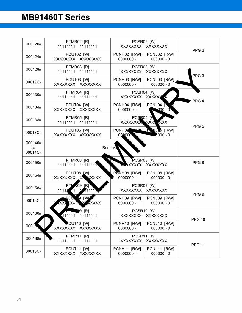
MB91460T Series
54
000120HPTMR02 [R]
11111111 11111111PCSR02 [W]
XXXXXXXX XXXXXXXXPPG 2
000124HPDUT02 [W]
XXXXXXXX XXXXXXXXPCNH02 [R/W]
0000000 -PCNL02 [R/W]
000000 - 0
000128HPTMR03 [R]
11111111 11111111PCSR03 [W]
XXXXXXXX XXXXXXXXPPG 3
00012CHPDUT03 [W]
XXXXXXXX XXXXXXXXPCNH03 [R/W]
0000000 -PCNL03 [R/W]
000000 - 0
000130HPTMR04 [R]
11111111 11111111PCSR04 [W]
XXXXXXXX XXXXXXXXPPG 4
000134HPDUT04 [W]
XXXXXXXX XXXXXXXXPCNH04 [R/W]
0000000 -PCNL04 [R/W]
000000 - 0
000138HPTMR05 [R]
11111111 11111111PCSR05 [W]
XXXXXXXX XXXXXXXXPPG 5
00013CHPDUT05 [W]
XXXXXXXX XXXXXXXXPCNH05 [R/W]
0000000 -PCNL05 [R/W]
000000 - 0
000140H
to00014CH
Reserved
000150HPTMR08 [R]
11111111 11111111PCSR08 [W]
XXXXXXXX XXXXXXXX PPG 8
000154HPDUT08 [W]
XXXXXXXX XXXXXXXXPCNH08 [R/W]
0000000 -PCNL08 [R/W]
000000 - 0
000158HPTMR09 [R]
11111111 11111111PCSR09 [W]
XXXXXXXX XXXXXXXXPPG 9
00015CHPDUT09 [W]
XXXXXXXX XXXXXXXXPCNH09 [R/W]
0000000 -PCNL09 [R/W]
000000 - 0
000160HPTMR10 [R]
11111111 11111111PCSR10 [W]
XXXXXXXX XXXXXXXXPPG 10
000164HPDUT10 [W]
XXXXXXXX XXXXXXXXPCNH10 [R/W]
0000000 -PCNL10 [R/W]
000000 - 0
000168HPTMR11 [R]
11111111 11111111PCSR11 [W]
XXXXXXXX XXXXXXXXPPG 11
00016CHPDUT11 [W]
XXXXXXXX XXXXXXXXPCNH11 [R/W]
0000000 -PCNL11 [R/W]
000000 - 0
PRELIMIN
ARY

MB91460T Series
000170H
P0TMCSRH[R/W]
- 0000000
P0TMCSRL[R/W]
01000000
P1TMCSRH[R/W]
- 0000000
P1TMCSRL[R/W]
01000000Pulse
Frequency Modulator000174H
P0TMRLR [W]XXXXXXXX XXXXXXXX
P0TMR [R]XXXXXXXX XXXXXXXX
000178HP1TMRLR [W]
XXXXXXXX XXXXXXXXP1TMR [R]
XXXXXXXX XXXXXXXX
00017CH Reserved
000180H Reserved ICS01 [R/W]00000000 Reserved ICS23 [R/W]
00000000Input
Capture0 to 3
000184HIPCP0 [R]
XXXXXXXX XXXXXXXXIPCP1 [R]
XXXXXXXX XXXXXXXX
000188HIPCP2 [R]
XXXXXXXX XXXXXXXXIPCP3 [R]
XXXXXXXX XXXXXXXX
00018CHOCS01 [R/W]
- - - 0 - - 00 0000 - - 00 OCS23 [R/W]
- - - 0 - - 00 0000 - - 00 Output
Compare0 to 3
000190HOCCP0 [R/W]
XXXXXXXX XXXXXXXXOCCP1 [R/W]
XXXXXXXX XXXXXXXX
000194HOCCP2 [R/W]
XXXXXXXX XXXXXXXXOCCP3 [R/W]
XXXXXXXX XXXXXXXX
000198HSGCRH [R/W]
0000 - - 00SGCRL [R/W]
- - 0 - - 000SGFR [R/W, R]
XXXXXXXX XXXXXXXX SoundGenerator
00019CHSGAR [R/W]
00000000 Reserved SGTR [R/W]XXXXXXXX
SGDR [R/W]XXXXXXXX
0001A0HADERH [R/W]
00000000 00000000ADERL [R/W]
00000000 00000000
A/DConverter0001A4 ADCS1 [R/W]
00000000ADCS0 [R/W]
00000000ADCR1 [R]000000XX
ADCR0 [R]XXXXXXXX
0001A8HADCT1 [R/W]
00010000ADCT0 [R/W]
00101100ADSCH [R/W]
- - - 00000ADECH [R/W]
- - - 00000
0001B0HTMRLRC0 [W]
XXXXXXXX XXXXXXXXTMRC0 [R]
XXXXXXXX XXXXXXXX Reload Timer 0
(PPG 0 to 1)0001B4H ReservedTMCSRCH0
[R/W]- - - 00000
TMCSRCL0[R/W]
0 - 000000
0001B8HTMRLRC1 [W]
XXXXXXXX XXXXXXXXTMRC1 [R]
XXXXXXXX XXXXXXXX Reload Timer 1
(PPG 2 to 3)0001BCH ReservedTMCSRCH1
[R/W]- - - 00000
TMCSRCL1[R/W]
0 - 000000
PRELIMIN
ARY
55

MB91460T Series
56
0001C0HTMRLRC2 [W]
XXXXXXXX XXXXXXXXTMRC2 [R]
XXXXXXXX XXXXXXXX Reload Timer 2
(PPG 4 to 5)0001C4H ReservedTMCSRCH2
[R/W]- - - 00000
TMCSRCL2[R/W]
0 - 000000
0001C8H
to0001CCH
Reserved
0001D0HTMRLRC4 [W]
XXXXXXXX XXXXXXXXTMRC4 [R]
XXXXXXXX XXXXXXXX Reload Timer 4
(PPG 8 to 9)0001D4H ReservedTMCSRCH4
[R/W]- - - 00000
TMCSRL4[R/W]
0 - 000000
0001D8HTMRLRC5 [W]
XXXXXXXX XXXXXXXXTMRC5 [R]
XXXXXXXX XXXXXXXX Reload Timer 5
(PPG10 to 11)0001DCH ReservedTMCSRCH5
[R/W]- - - 00000
TMCSRL5[R/W]
0 - 000000
0001E0HTMRLRC6 [W]
XXXXXXXX XXXXXXXXTMRC6 [R]
XXXXXXXX XXXXXXXX Reload Timer 6
(PPG 12 to 13)0001E4H ReservedTMCSRCH6
[R/W]- - - 00000
TMCSRL6[R/W]
0 - 000000
0001E8HTMRLR7 [W]
XXXXXXXX XXXXXXXXTMRC7 [R]
XXXXXXXX XXXXXXXX Reload Timer 7
(PPG 14 to 15)0001ECH ReservedTMCSRCH7
[R/W]- - - 00000
TMCSRCL7[R/W]
0 - 000000
0001F0HTCDT0 [R/W]
XXXXXXXX XXXXXXXX Reserved TCCS0 [R/W]00000000
Free RunningTimer 0
(ICU 0 to 1)
0001F4HTCDT1 [R/W]
XXXXXXXX XXXXXXXX Reserved TCCS1 [R/W]00000000
Free RunningTimer 1
(ICU 2 to 3)
0001F8HTCDT2 [R/W]
XXXXXXXX XXXXXXXX Reserved TCCS2 [R/W]00000000
Free RunningTimer 2
(OCU 0 to 1)
0001FCHTCDT3 [R/W]
XXXXXXXX XXXXXXXX Reserved TCCS3 [R/W]00000000
Free RunningTimer 3
(OCU 2 to 3)
PRELIMIN
ARY
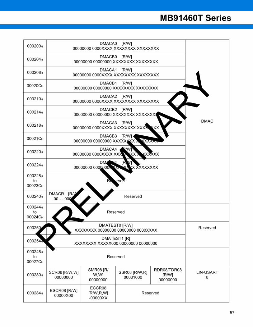
MB91460T Series
000200HDMACA0 [R/W]
00000000 0000XXXX XXXXXXXX XXXXXXXX
DMAC
000204HDMACB0 [R/W]
00000000 00000000 XXXXXXXX XXXXXXXX
000208HDMACA1 [R/W]
00000000 0000XXXX XXXXXXXX XXXXXXXX
00020CHDMACB1 [R/W]
00000000 00000000 XXXXXXXX XXXXXXXX
000210HDMACA2 [R/W]
00000000 0000XXXX XXXXXXXX XXXXXXXX
000214HDMACB2 [R/W]
00000000 00000000 XXXXXXXX XXXXXXXX
000218HDMACA3 [R/W]
00000000 0000XXXX XXXXXXXX XXXXXXXX
00021CHDMACB3 [R/W]
00000000 00000000 XXXXXXXX XXXXXXXX
000220HDMACA4 [R/W]
00000000 0000XXXX XXXXXXXX XXXXXXXX
000224HDMACB4 [R/W]
00000000 00000000 XXXXXXXX XXXXXXXX
000228H
to00023CH
Reserved
000240HDMACR [R/W]
00 - - 0000 Reserved
000244H
to00024CH
Reserved
000250HDMATEST0 [R/W]
XXXXXXXX 00000000 00000000 0000XXXX Reserved
000254HDMATEST1 [R]
XXXXXXXX XXXXX000 00000000 00000000
000248H to
00027CH
Reserved
000280HSCR08 [R/W,W]
00000000
SMR08 [R/W,W]
00000000
SSR08 [R/W,R]00001000
RDR08/TDR08 [R/W]
00000000
LIN-USART8
000284HESCR08 [R/W]
00000X00
ECCR08 [R/W,R,W]-00000XX
Reserved
PRELIMIN
ARY
57
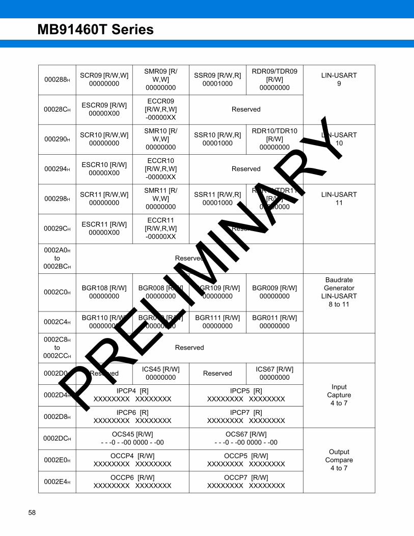
MB91460T Series
58
000288HSCR09 [R/W,W]
00000000
SMR09 [R/W,W]
00000000
SSR09 [R/W,R]00001000
RDR09/TDR09 [R/W]
00000000
LIN-USART9
00028CHESCR09 [R/W]
00000X00
ECCR09 [R/W,R,W]-00000XX
Reserved
000290HSCR10 [R/W,W]
00000000
SMR10 [R/W,W]
00000000
SSR10 [R/W,R]00001000
RDR10/TDR10 [R/W]
00000000
LIN-USART10
000294HESCR10 [R/W]
00000X00
ECCR10 [R/W,R,W]-00000XX
Reserved
000298HSCR11 [R/W,W]
00000000
SMR11 [R/W,W]
00000000
SSR11 [R/W,R]00001000
RDR11/TDR11 [R/W]
00000000
LIN-USART11
00029CHESCR11 [R/W]
00000X00
ECCR11 [R/W,R,W]-00000XX
Reserved
0002A0H
to0002BCH
Reserved
0002C0HBGR108 [R/W]
00000000BGR008 [R/W]
00000000BGR109 [R/W]
00000000BGR009 [R/W]
00000000
BaudrateGenerator
LIN-USART8 to 11
0002C4HBGR110 [R/W]
00000000BGR010 [R/W]
00000000BGR111 [R/W]
00000000BGR011 [R/W]
00000000
0002C8H to
0002CCH
Reserved
0002D0H Reserved ICS45 [R/W]00000000 Reserved ICS67 [R/W]
00000000Input
Capture4 to 7
0002D4HIPCP4 [R]
XXXXXXXX XXXXXXXXIPCP5 [R]
XXXXXXXX XXXXXXXX
0002D8HIPCP6 [R]
XXXXXXXX XXXXXXXXIPCP7 [R]
XXXXXXXX XXXXXXXX
0002DCHOCS45 [R/W]
- - -0 - -00 0000 - -00OCS67 [R/W]
- - -0 - -00 0000 - -00Output
Compare4 to 7
0002E0HOCCP4 [R/W]
XXXXXXXX XXXXXXXXOCCP5 [R/W]
XXXXXXXX XXXXXXXX
0002E4HOCCP6 [R/W]
XXXXXXXX XXXXXXXXOCCP7 [R/W]
XXXXXXXX XXXXXXXX
PRELIMIN
ARY
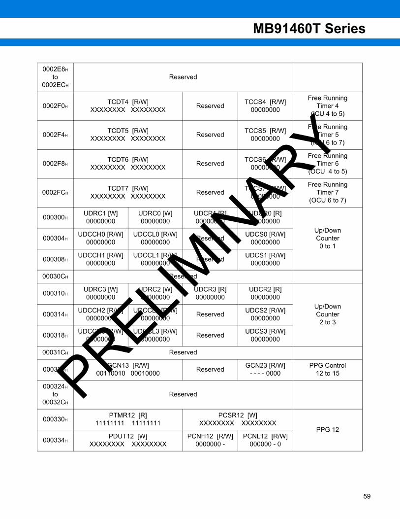
MB91460T Series
0002E8H
to0002ECH
Reserved
0002F0HTCDT4 [R/W]
XXXXXXXX XXXXXXXX Reserved TCCS4 [R/W]00000000
Free RunningTimer 4
(ICU 4 to 5)
0002F4HTCDT5 [R/W]
XXXXXXXX XXXXXXXX Reserved TCCS5 [R/W]00000000
Free RunningTimer 5
(ICU 6 to 7)
0002F8HTCDT6 [R/W]
XXXXXXXX XXXXXXXX Reserved TCCS6 [R/W]00000000
Free RunningTimer 6
(OCU 4 to 5)
0002FCHTCDT7 [R/W]
XXXXXXXX XXXXXXXX Reserved TCCS7 [R/W]00000000
Free RunningTimer 7
(OCU 6 to 7)
000300HUDRC1 [W]00000000
UDRC0 [W]00000000
UDCR1 [R]00000000
UDCR0 [R]00000000
Up/DownCounter0 to 1
000304HUDCCH0 [R/W]
00000000UDCCL0 [R/W]
00000000 Reserved UDCS0 [R/W]00000000
000308HUDCCH1 [R/W]
00000000UDCCL1 [R/W]
00000000 Reserved UDCS1 [R/W]00000000
00030CH Reserved
000310HUDRC3 [W]00000000
UDRC2 [W]00000000
UDCR3 [R]00000000
UDCR2 [R]00000000
Up/DownCounter2 to 3
000314HUDCCH2 [R/W]
00000000UDCCL2 [R/W]
00000000 Reserved UDCS2 [R/W]00000000
000318HUDCCH3 [R/W]
00000000UDCCL3 [R/W]
00000000 Reserved UDCS3 [R/W]00000000
00031CH Reserved
000320HGCN13 [R/W]
00110010 00010000 Reserved GCN23 [R/W]- - - - 0000
PPG Control12 to 15
000324H
to00032CH
Reserved
000330HPTMR12 [R]
11111111 11111111PCSR12 [W]
XXXXXXXX XXXXXXXXPPG 12
000334HPDUT12 [W]
XXXXXXXX XXXXXXXXPCNH12 [R/W]
0000000 -PCNL12 [R/W]
000000 - 0
PRELIMIN
ARY
59

MB91460T Series
60
000338HPTMR13 [R]
11111111 11111111PCSR13 [W]
XXXXXXXX XXXXXXXXPPG 13
00033CHPDUT13 [W]
XXXXXXXX XXXXXXXXPCNH13 [R/W]
0000000 -PCNL13 [R/W]
000000 - 0
000340HPTMR14 [R]
11111111 11111111PCSR14 [W]
XXXXXXXX XXXXXXXXPPG 14
000344HPDUT14 [W]
XXXXXXXX XXXXXXXXPCNH14 [R/W]
0000000 -PCNL14 [R/W]
000000 - 0
000348HPTMR15 [R]
11111111 11111111PCSR15 [W]
XXXXXXXX XXXXXXXXPPG 15
00034CHPDUT15 [W]
XXXXXXXX XXXXXXXXPCNH15 [R/W]
0000000 -PCNL15 [R/W]
000000 - 0
000368HIBCR2 [R/W]
00000000IBSR2 [R]00000000
ITBAH2 [R/W]- - - - - - 00
ITBAL2 [R/W]00000000
I2C 200036CHITMKH2 [R/W]
00 - - - - 11ITMKL2 [R/W]
11111111ISMK2 [R/W]
01111111ISBA2 [R/W]
- 0000000
000370H Reserved IDAR2 [R/W]00000000
ICCR2 [R/W]- 0011111 Reserved
000374HIBCR3 [R/W]
00000000IBSR3 [R]00000000
ITBAH3 [R/W]- - - - - - 00
ITBAL3 [R/W]00000000
I2C 3000378HITMKH3 [R/W]
00 - - - - 11ITMKL3 [R/W]
11111111ISMK3 [R/W]
01111111ISBA3 [R/W]
- 0000000
00037CH Reserved IDAR3 [R/W]00000000
ICCR3 [R/W]- 0011111 Reserved
000380H
to00038CH
Reserved
000390H
ROMS [R]11111111 00000000
(MB91F467TA)11111000 00000000
(MB91F469TA)
Reserved ROM Select Register
000394H
to0003ECH
ReservedPRELIMIN
ARY

MB91460T Series
0003F0HBSD0 [W]
XXXXXXXX XXXXXXXX XXXXXXXX XXXXXXXX
Bit Search Module0003F4H
BSD1 [R/W]XXXXXXXX XXXXXXXX XXXXXXXX XXXXXXXX
0003F8HBSDC [W]
XXXXXXXX XXXXXXXX XXXXXXXX XXXXXXXX
0003FCHBSRR [R]
XXXXXXXX XXXXXXXX XXXXXXXX XXXXXXXX
000400H
to00043CH
Reserved
000440HICR00 [R/W]
---11111ICR01 [R/W]
---11111ICR02 [R/W]
---11111ICR03 [R/W]
---11111
InterruptControl
Unit
000444HICR04 [R/W]
---11111ICR05 [R/W]
---11111ICR06 [R/W]
---11111ICR07 [R/W]
---11111
000448HICR08 [R/W]
---11111ICR09 [R/W]
---11111ICR10 [R/W]
---11111ICR11 [R/W]
---11111
00044CHICR12 [R/W]
---11111ICR13 [R/W]
---11111ICR14 [R/W]
---11111ICR15 [R/W]
---11111
000450HICR16 [R/W]
---11111ICR17 [R/W]
---11111ICR18 [R/W]
---11111ICR19 [R/W]
---11111
000454HICR20 [R/W]
---11111ICR21 [R/W]
---11111ICR22 [R/W]
---11111ICR23 [R/W]
---11111
000458HICR24 [R/W]
---11111ICR25 [R/W]
---11111ICR26 [R/W]
---11111ICR27 [R/W]
---11111
00045CHICR28 [R/W]
---11111ICR29 [R/W]
---11111ICR30 [R/W]
---11111ICR31 [R/W]
---11111
000460HICR32 [R/W]
---11111ICR33 [R/W]
---11111ICR34 [R/W]
---11111ICR35 [R/W]
---11111
000464HICR36 [R/W]
---11111ICR37 [R/W]
---11111ICR38 [R/W]
---11111ICR39 [R/W]
---11111
000468HICR40 [R/W]
---11111ICR41 [R/W]
---11111ICR42 [R/W]
---11111ICR43 [R/W]
---11111
00046CHICR44 [R/W]
---11111ICR45 [R/W]
---11111ICR46 [R/W]
---11111ICR47 [R/W]
---11111
000470HICR48 [R/W]
---11111ICR49 [R/W]
---11111ICR50 [R/W]
---11111ICR51 [R/W]
---11111
000474HICR52 [R/W]
---11111ICR53 [R/W]
---11111ICR54 [R/W]
---11111ICR55 [R/W]
---11111
000478HICR56 [R/W]
---11111ICR57 [R/W]
---11111ICR58 [R/W]
---11111ICR59 [R/W]
---11111
PRELIMIN
ARY
61

MB91460T Series
62
00047CHICR60 [R/W]
---11111ICR61 [R/W]
---11111ICR62 [R/W]
---11111ICR63 [R/W]
---11111 Interrupt Control Unit
000480HRSRR [R/W]
10000000STCR [R/W]
00110011TBCR [R/W]00XXX – 00
CTBR [W]XXXXXXXX Clock
Control Unit000484H
CLKR [R/W]---- 0000
WPR [W]XXXXXXXX
DIVR0 [R/W]00000011
DIVR1 [R/W]00000000
000488HCTEST [R/W]XXXX00XX Reserved Reserved Reserved Reserved
00048CH
PLLDIVM [R/W]
- - - 00000
PLLDIVN [R/W]- - - 00000
PLLDIVG [R/W]- - - 00000
PLLDIVG [W]00000000
PLL ClockGear Unit
000490H
PLLCTRL [R/W]
- - - - 0000Reserved Reserved Reserved
000494HOSCC1 [R/W]
- - - - - 010OSCS1 [R/W]
00001111OSCC2 [R/W]
- - - - - 010OSCS2 [R/W]
00001111
Main/SubOscillatorControl
000498HPORTEN [R/W]
- - - - - - 00 Reserved PPMUX [R/W] *1
00000000 00000000
Port InputEnable Control /PortMux Control
00049CH Reserved
0004A0H Reserved WTCER [R/W]- - - - - - 00
WTCR [R/W]00000000 000 – 00 – 0
Real Time Clock(Watch Timer)0004A4H Reserved WTBR [R/W]
- - - XXXXX XXXXXXXX XXXXXXXX
0004A8HWTHR [R/W]
- - - 00000WTMR [R/W]
- - 000000WTSR [R/W]
- - 000000 Reserved
0004ACHCSVTR [R/W]
- - - 00010CSVCR [R/W]
00011100CSCFG [R/W]
0X000000CMCFG [R/W]
00000000
Clock-Supervisor /
Selector /Monitor
0004B0HCUCR [R/W]
- - - - - - - - - - - 0 - - 00CUTD [R/W]
10000000 00000000 Calibration Unit of Sub Oscillation
0004B4HCUTR1 [R]
- - - - - - - - 00000000CUTR2 [R]
00000000 00000000
0004B8HCMPR [R/W]
- - 000010 11111101 Reserved CMCR [R/W]- 001 - - 00 Clock
Modulation0004BCH
CMT1 [R/W]00000000 1 - - - 0000
CMT2 [R/W]- - 000000 - - 000000
0004C0HCANPRE [R/W]
0 - - - 0000CANCKD [R/W]
- - - - - 000 *2 Reserved Reserved CAN Clock Control
PRELIMIN
ARY
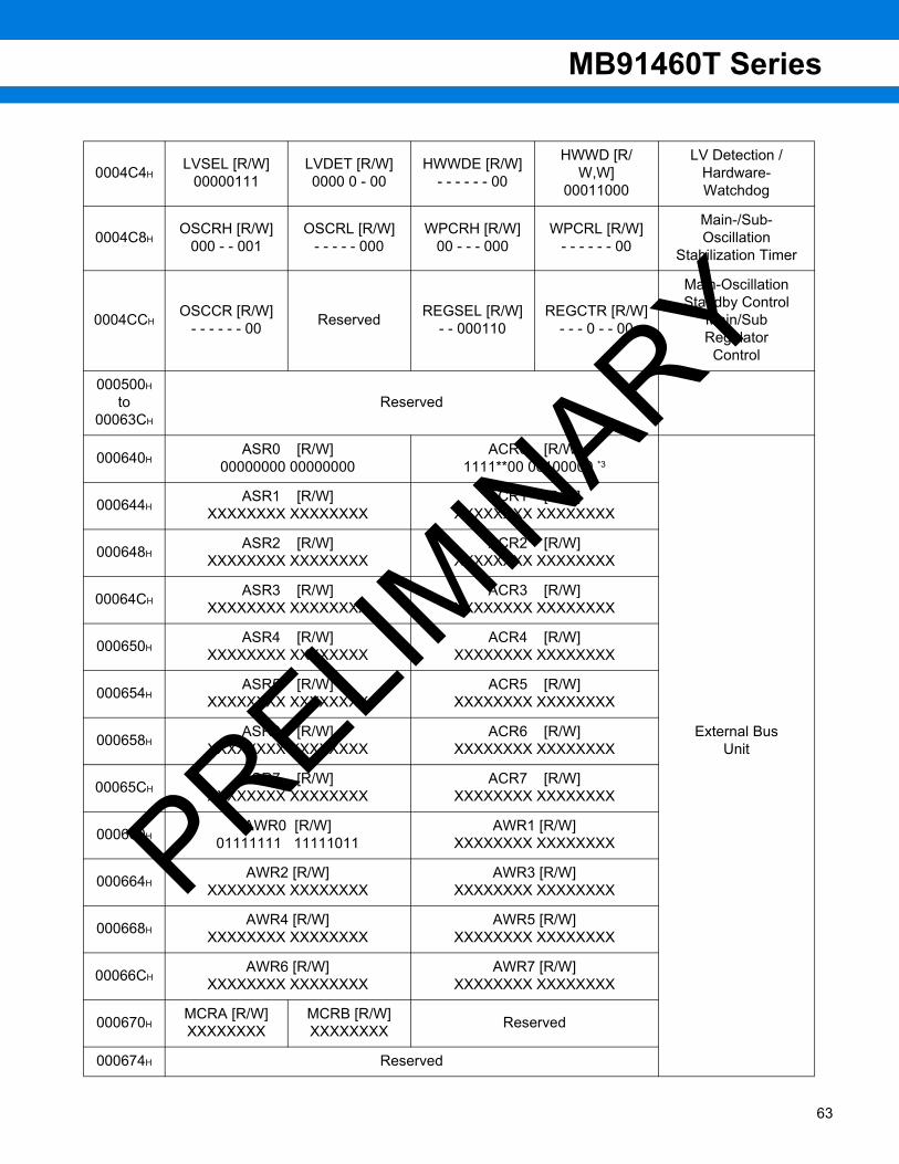
MB91460T Series
0004C4HLVSEL [R/W]
00000111LVDET [R/W]0000 0 - 00
HWWDE [R/W]- - - - - - 00
HWWD [R/W,W]
00011000
LV Detection /Hardware-Watchdog
0004C8HOSCRH [R/W]
000 - - 001OSCRL [R/W]
- - - - - 000WPCRH [R/W]
00 - - - 000WPCRL [R/W]
- - - - - - 00
Main-/Sub-Oscillation
Stabilization Timer
0004CCHOSCCR [R/W]
- - - - - - 00 Reserved REGSEL [R/W]- - 000110
REGCTR [R/W]- - - 0 - - 00
Main-Oscillation Standby Control
Main/Sub Regulator
Control
000500H
to00063CH
Reserved
000640HASR0 [R/W]
00000000 00000000ACR0 [R/W]
1111**00 00100000 *3
External BusUnit
000644HASR1 [R/W]
XXXXXXXX XXXXXXXXACR1 [R/W]
XXXXXXXX XXXXXXXX
000648HASR2 [R/W]
XXXXXXXX XXXXXXXXACR2 [R/W]
XXXXXXXX XXXXXXXX
00064CHASR3 [R/W]
XXXXXXXX XXXXXXXXACR3 [R/W]
XXXXXXXX XXXXXXXX
000650HASR4 [R/W]
XXXXXXXX XXXXXXXXACR4 [R/W]
XXXXXXXX XXXXXXXX
000654HASR5 [R/W]
XXXXXXXX XXXXXXXXACR5 [R/W]
XXXXXXXX XXXXXXXX
000658HASR6 [R/W]
XXXXXXXX XXXXXXXXACR6 [R/W]
XXXXXXXX XXXXXXXX
00065CHASR7 [R/W]
XXXXXXXX XXXXXXXXACR7 [R/W]
XXXXXXXX XXXXXXXX
000660HAWR0 [R/W]
01111111 11111011AWR1 [R/W]
XXXXXXXX XXXXXXXX
000664HAWR2 [R/W]
XXXXXXXX XXXXXXXXAWR3 [R/W]
XXXXXXXX XXXXXXXX
000668HAWR4 [R/W]
XXXXXXXX XXXXXXXXAWR5 [R/W]
XXXXXXXX XXXXXXXX
00066CHAWR6 [R/W]
XXXXXXXX XXXXXXXXAWR7 [R/W]
XXXXXXXX XXXXXXXX
000670HMCRA [R/W]XXXXXXXX
MCRB [R/W]XXXXXXXX Reserved
000674H Reserved
PRELIMIN
ARY
63
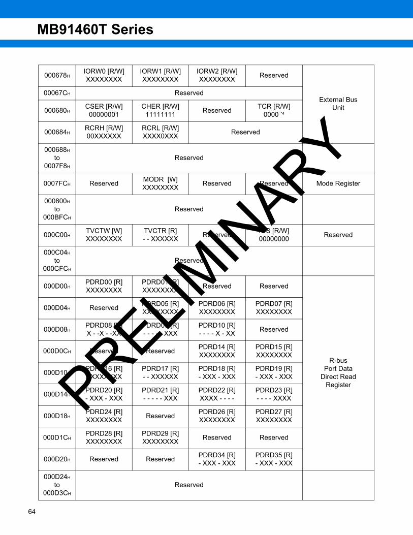
MB91460T Series
64
000678HIORW0 [R/W]XXXXXXXX
IORW1 [R/W]XXXXXXXX
IORW2 [R/W]XXXXXXXX Reserved
External BusUnit
00067CH Reserved
000680HCSER [R/W]00000001
CHER [R/W]11111111 Reserved TCR [R/W]
0000 *4
000684HRCRH [R/W]00XXXXXX
RCRL [R/W]XXXX0XXX Reserved
000688H
to0007F8H
Reserved
0007FCH Reserved MODR [W]XXXXXXXX Reserved Reserved Mode Register
000800H
to000BFCH
Reserved
000C00HTVCTW [W]XXXXXXXX
TVCTR [R]- - XXXXXX Reserved IOS [R/W]
00000000 Reserved
000C04H
to000CFCH
Reserved
000D00HPDRD00 [R]XXXXXXXX
PDRD01 [R]XXXXXXXX Reserved Reserved
R-busPort Data
Direct ReadRegister
000D04H Reserved PDRD05 [R]XXXXXXXX
PDRD06 [R]XXXXXXXX
PDRD07 [R]XXXXXXXX
000D08HPDRD08 [R]X - -X - -XX
PDRD09 [R]- - - - - XXX
PDRD10 [R]- - - - X - XX Reserved
000D0CH Reserved Reserved PDRD14 [R]XXXXXXXX
PDRD15 [R]XXXXXXXX
000D10HPDRD16 [R]XXXXXXXX
PDRD17 [R]- - XXXXXX
PDRD18 [R]- XXX - XXX
PDRD19 [R]- XXX - XXX
000D14HPDRD20 [R]- XXX - XXX
PDRD21 [R]- - - - - XXX
PDRD22 [R]XXXX - - - -
PDRD23 [R]- - - - XXXX
000D18HPDRD24 [R]XXXXXXXX Reserved PDRD26 [R]
XXXXXXXXPDRD27 [R]XXXXXXXX
000D1CHPDRD28 [R]XXXXXXXX
PDRD29 [R]XXXXXXXX Reserved Reserved
000D20H Reserved Reserved PDRD34 [R]- XXX - XXX
PDRD35 [R]- XXX - XXX
000D24H
to000D3CH
Reserved
PRELIMIN
ARY
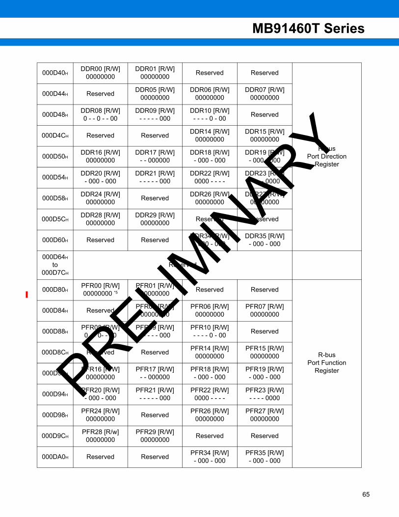
MB91460T Series
000D40HDDR00 [R/W]
00000000DDR01 [R/W]
00000000 Reserved Reserved
R-busPort Direction
Register
000D44H Reserved DDR05 [R/W]00000000
DDR06 [R/W]00000000
DDR07 [R/W]00000000
000D48HDDR08 [R/W]0 - - 0 - - 00
DDR09 [R/W]- - - - - 000
DDR10 [R/W]- - - - 0 - 00 Reserved
000D4CH Reserved Reserved DDR14 [R/W]00000000
DDR15 [R/W]00000000
000D50HDDR16 [R/W]
00000000DDR17 [R/W]
- - 000000DDR18 [R/W]
- 000 - 000DDR19 [R/W]
- 000 - 000
000D54HDDR20 [R/W]
- 000 - 000DDR21 [R/W]
- - - - - 000DDR22 [R/W]
0000 - - - -DDR23 [R/W]
- - - - 0000
000D58HDDR24 [R/W]
00000000 Reserved DDR26 [R/W]00000000
DDR27 [R/W]00000000
000D5CHDDR28 [R/W]
00000000DDR29 [R/W]
00000000 Reserved Reserved
000D60H Reserved Reserved DDR34 [R/W]- 000 - 000
DDR35 [R/W]- 000 - 000
000D64H
to000D7CH
Reserved
000D80HPFR00 [R/W]00000000 *5
PFR01 [R/W]00000000 Reserved Reserved
R-busPort Function
Register
000D84H Reserved PFR05 [R/W]00000000
PFR06 [R/W]00000000
PFR07 [R/W]00000000
000D88HPFR08 [R/W]0 - - 0- - 00
PFR09 [R/W]- - - - - 000
PFR10 [R/W]- - - - 0 - 00 Reserved
000D8CH Reserved Reserved PFR14 [R/W]00000000
PFR15 [R/W]00000000
000D90HPFR16 [R/W]
00000000PFR17 [R/W]
- - 000000PFR18 [R/W]- 000 - 000
PFR19 [R/W]- 000 - 000
000D94HPFR20 [R/W]- 000 - 000
PFR21 [R/W]- - - - - 000
PFR22 [R/W]0000 - - - -
PFR23 [R/W]- - - - 0000
000D98HPFR24 [R/W]
00000000 Reserved PFR26 [R/W]00000000
PFR27 [R/W]00000000
000D9CHPFR28 [R/w]
00000000PFR29 [R/W]
00000000 Reserved Reserved
000DA0H Reserved Reserved PFR34 [R/W]- 000 - 000
PFR35 [R/W]- 000 - 000
PRELIMIN
ARY
65

MB91460T Series
66
000DA4H
to000DBCH
Reserved
000DC0H Reserved Reserved Reserved Reserved
R-bus PortExtra Function
Register
000DC4H Reserved Reserved Reserved Reserved
000DC8H Reserved Reserved EPFR10 [R/W]- - - - - - - 0 Reserved
000DCCH Reserved Reserved EPFR14 [R/W]00000000
EPFR15 [R/W]00000000
000DD0HEPFR16 [R/W]
0000 - - - - Reserved EPFR18 [R/W]- 000 - 000
EPFR19 [R/W]- 0 - - - 0 - -
000DD4HEPFR20 [R/W]
- 000 - 000EPFR21 [R/W]
- - - - - 0 - - Reserved Reserved
000DD8H Reserved Reserved EPFR26 [R/W]00000000
EPFR27 [R/W]00000000
000DDCH Reserved Reserved Reserved Reserved
000DE0H Reserved Reserved EPFR34 [R/W]- 000 - 000
EPFR35 [R/W]- 000 - 000
000DE4H
to000DFCH
Reserved
000E00HPODR00 [R/W]
00000000PODR01 [R/W]
00000000 Reserved Reserved
R-bus PortOutput Drive
SelectRegister
000E04H Reserved PODR05 [R/W]00000000
PODR06 [R/W]00000000
PODR07 [R/W]00000000
000E08HPODR08 [R/W]
0 - -0 - - 00PODR09 [R/W]
- - - - - 000PODR10 [R/W]
- - - - 0 - 00 Reserved
000E0CH Reserved Reserved PODR14 [R/W]00000000
PODR15 [R/W]00000000
000E10HPODR16 [R/W]
00000000PODR17 [R/W]
- - 000000PODR18 [R/W]
- 000 - 000PODR19 [R/W]
- 000 - 000
000E14HPODR20 [R/W]
- 000 - 000PODR21 [R/W]
- - - - - 000 Reserved PODR23 [R/W]- - - - 0000
000E18HPODR24 [R/W]
- - - - 0000 Reserved PODR26 [R/W]00000000
PODR27 [R/W]00000000
000E1CHPODR28 [R/W]
0000000PODR29 [R/W]
00000000 Reserved Reserved
000E20H Reserved Reserved PODR34 [R/W]- 000 - 000
PODR35 [R/W]- 000 - 000
PRELIMIN
ARY

MB91460T Series
000E24H
to000E3CH
Reserved
000E40HPILR00 [R/W]
00000000PILR01 [R/W]
00000000 Reserved Reserved
R-bus PortInput Level Select
Register
000E44H Reserved PILR05 [R/W]00000000
PILR06 [R/W]00000000
PILR07 [R/W]00000000
000E48HPILR08 [R/W]0 - - 0 - - 00
PILR09 [R/W]- - - - - 000
PILR10 [R/W]- - - -0- - 00 Reserved
000E4CH Reserved Reserved PILR14 [R/W]00000000
PILR15 [R/W]00000000
000E50HPILR16 [R/W]
00000000PILR17 [R/W]
- - 000000PILR18 [R/W]
- 000 - 000 PILR19 [R/W]
- 000 - 000
000E54H
PILR20 [R/W]- 000 - 000
PILR21 [R/W]- - - - - 000
PILR22 [R/W]0000 - - - -
PILR23 [R/W]- - - - 0000
000E58HPILR24 [R/W]
00000000 Reserved PILR26 [R/W]00000000
PILR27 [R/W]00000000
000E5CHPILR28 [R/W]
00000000PILR29 [R/W]
00000000 Reserved Reserved
000E60H Reserved Reserved PILR34 [R/W]- 000 - 000
PILR35 [R/W]- 000 - 000
000E64H
to000E7CH
Reserved
PRELIMIN
ARY
67

MB91460T Series
68
000E80HEPILR00[R/W]
00000000EPILR01 [R/W]
00000000 Reserved Reserved
R-bus PortExtra Input Level
SelectRegister
000E84H Reserved EPILR05 [R/W]00000000
EPILR06 [R/W]00000000
EPILR07 [R/W]00000000
000E88HEPILR08 [R/W]
0 - - 0 - - 00EPILR09 [R/W]
- - - - - 000EPILR10 [R/W]
- - - - 0 - 00 Reserved
000E8CH Reserved Reserved EPILR14 [R/W]00000000
EPILR15 [R/W]00000000
000E90HEPILR16 [R/W]
00000000EPILR17 [R/W]
- - 000000EPILR18 [R/W]
- 000 - 000EPILR19 [R/W]
- 000 - 000
000E94HEPILR20 [R/W]
- 000 - 000EPILR21 [R/W]
- - - - - 000EPILR22 [R/W]
0000 - - - -EPILR23 [R/W]
- - - - 0000
000E98HEPILR24 [R/W]
00000000 Reserved EPILR26 [R/W]00000000
EPILR27 [R/W]00000000
000E9CHEPILR28 [R/W]
0000000EPILR29 [R/W]
00000000 Reserved Reserved
000EA0H Reserved Reserved EPILR34 [R/W]- 000 - 000
EPILR35 [R/W]- 000 - 000
000EA4H
to000EBCH
Reserved
000EC0HPPER00 [R/W]
00000000PPER01 [R/W]
00000000 Reserved Reserved
R-bus PortPull-Up/Down
EnableRegister
000EC4H Reserved PPER05 [R/W]00000000
PPER06 [R/W]00000000
PPER07 [R/W]00000000
000EC8HPPER08 [R/W]
0 - - 0 - - 00PPER09 [R/W]
- - - - - 000PPER10 [R/W]
- - - - 0 - 00 Reserved
000ECCH Reserved Reserved PPER14 [R/W]00000000
PPER15 [R/W]00000000
000ED0HPPER16 [R/W]
00000000PPER17 [R/W]
- - 000000PPER18 [R/W]
- 000 - 000PPER19 [R/W]
- 000 - 000
000ED4HPPER20 [R/W]
- 000 - 000PPER21 [R/W]
- - - - - 000 Reserved PPER23 [R/W]- - - - 0000
000ED8HPPER24 [R/W]
- - - - 0000 Reserved PPER26 [R/W]00000000
PPER27 [R/W]00000000
000EDCHPPER28 [R/W]
0000000PPER29 [R/W]
00000000 Reserved Reserved
000EE0H Reserved Reserved PPER34 [R/W]- 000 - 000
PPER35 [R/W]- 000 - 000
PRELIMIN
ARY

MB91460T Series
000EE4H
to000EFCH
Reserved
000F00HPPCR00 [R/W]
11111111PPCR01 [R/W]
11111111 Reserved Reserved
R-bus PortPull-Up/Down
ControlRegister
000F04H Reserved PPCR05 [R/W]11111111
PPCR06 [R/W]11111111
PPCR07 [R/W]11111111
000F08HPPCR08 [R/W]
1 - - 1 - - 11PPCR09 [R/W]
- - - - - 111PPCR10 [R/W]
- - - - 1 - 11 Reserved
000F0CH Reserved Reserved PPCR14 [R/W]11111111
PPCR15 [R/W]11111111
000F10HPPCR16 [R/W]
11111111PPCR17 [R/W]
- - 111111PPCR18 [R/W]
- 111 - 111PPCR19 [R/W]
- 111 - 111
000F14HPPCR20 [R/W]
- 111 - 111PPCR21 [R/W]
- - - - - 111 Reserved PPCR23 [R/W]- - - - 1111
000F18HPPCR24 [R/W]
- - - - 1111 Reserved PPCR26 [R/W]11111111
PPCR27 [R/W]11111111
000F1CHPPCR28 [R/W]
- - 11111PPCR29 [R/W]
11111111 Reserved Reserved
000F20H Reserved Reserved PPCR34 [R/W]- 000 - 000
PPCR35 [R/W]- 000 - 000
000F24H
to000FFCH
Reserved
PRELIMIN
ARY
69

MB91460T Series
70
001000HDMASA0 [R/W]
XXXXXXXX XXXXXXXX XXXXXXXX XXXXXXXX
DMAC
001004HDMADA0 [R/W]
XXXXXXXX XXXXXXXX XXXXXXXX XXXXXXXX
001008HDMASA1 [R/W]
XXXXXXXX XXXXXXXX XXXXXXXX XXXXXXXX
00100CHDMADA1 [R/W]
XXXXXXXX XXXXXXXX XXXXXXXX XXXXXXXX
001010HDMASA2 [R/W]
XXXXXXXX XXXXXXXX XXXXXXXX XXXXXXXX
001014HDMADA2 [R/W]
XXXXXXXX XXXXXXXX XXXXXXXX XXXXXXXX
001018HDMASA3 [R/W]
XXXXXXXX XXXXXXXX XXXXXXXX XXXXXXXX
00101CHDMADA3 [R/W]
XXXXXXXX XXXXXXXX XXXXXXXX XXXXXXXX
001020HDMASA4 [R/W]
XXXXXXXX XXXXXXXX XXXXXXXX XXXXXXXX
001024HDMADA4 [R/W]
XXXXXXXX XXXXXXXX XXXXXXXX XXXXXXXX
001028H
to01FFCH
Reserved
002000H
to006FFCH
MB91F467TA Flash-cache size is 8 KB: 004000H to 005FFCH
MB91F469TA Flash-cache size is 16 KB: 004000H to 005FFCH
Flash-cache /I-RAM area
007000HFMCS [R/W]
01101000FMCR [R]- - - 00000
FCHCR [R/W]- - - - - - 00 10000011
Flash Memory/- CacheControlRegister
007004HFMWT [R/W]
11111111 11111111FMWT2 [R]- 001 - - - -
FMPS [R/W]- - - - - 000
007008HFMAC [R]
00000000 00000000 00000000 00000000
00700CHFCHA0 [R/W]
- - - - - - - - - - - 00000 00000000 00000000I-Cache
Non-cacheable area setting
Register007010HFCHA1 [R/W]
- - - - - - - - - - - 00000 00000000 00000000
007014H
to007FFCH
Reserved
PRELIMIN
ARY
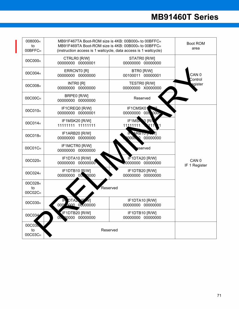
MB91460T Series
008000H
to00BFFCH
MB91F467TA Boot-ROM size is 4KB: 00B000H to 00BFFCH
MB91F469TA Boot-ROM size is 4KB: 00B000H to 00BFFCH
(instruction access is 1 waitcycle, data access is 1 waitcycle)
Boot ROMarea
00C000HCTRLR0 [R/W]
00000000 00000001STATR0 [R/W]
00000000 00000000
CAN 0ControlRegister
00C004HERRCNT0 [R]
00000000 00000000BTR0 [R/W]
00100011 00000001
00C008HINTR0 [R]
00000000 00000000TESTR0 [R/W]
00000000 X0000000
00C00CHBRPE0 [R/W]
00000000 00000000 Reserved
00C010HIF1CREQ0 [R/W]
00000000 00000001IF1CMSK0 [R/W]
00000000 00000000
CAN 0IF 1 Register
00C014HIF1MSK20 [R/W]
11111111 11111111IF1MSK10 [R/W]
11111111 11111111
00C018HIF1ARB20 [R/W]
00000000 00000000IF1ARB10 [R/W]
00000000 00000000
00C01CHIF1MCTR0 [R/W]
00000000 00000000 Reserved
00C020HIF1DTA10 [R/W]
00000000 00000000IF1DTA20 [R/W]
00000000 00000000
00C024HIF1DTB10 [R/W]
00000000 00000000IF1DTB20 [R/W]
00000000 00000000
00C028H
to00C02CH
Reserved
00C030HIF1DTA20 [R/W]
00000000 00000000IF1DTA10 [R/W]
00000000 00000000
00C034HIF1DTB20 [R/W]
00000000 00000000IF1DTB10 [R/W]
00000000 00000000
00C038H
to00C03CH
ReservedPRELIMIN
ARY
71
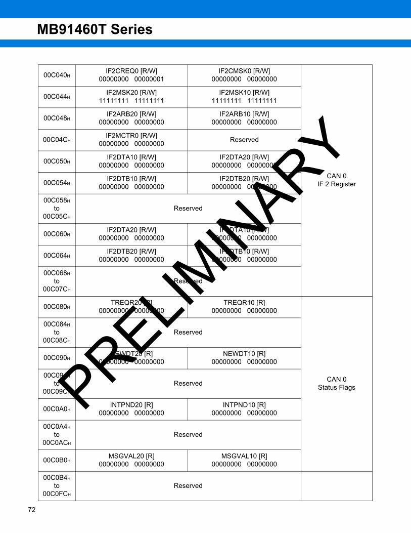
MB91460T Series
72
00C040HIF2CREQ0 [R/W]
00000000 00000001IF2CMSK0 [R/W]
00000000 00000000
CAN 0IF 2 Register
00C044HIF2MSK20 [R/W]
11111111 11111111IF2MSK10 [R/W]
11111111 11111111
00C048HIF2ARB20 [R/W]
00000000 00000000IF2ARB10 [R/W]
00000000 00000000
00C04CHIF2MCTR0 [R/W]
00000000 00000000 Reserved
00C050HIF2DTA10 [R/W]
00000000 00000000IF2DTA20 [R/W]
00000000 00000000
00C054HIF2DTB10 [R/W]
00000000 00000000IF2DTB20 [R/W]
00000000 00000000
00C058H
to00C05CH
Reserved
00C060HIF2DTA20 [R/W]
00000000 00000000IF2DTA10 [R/W]
00000000 00000000
00C064HIF2DTB20 [R/W]
00000000 00000000IF2DTB10 [R/W]
00000000 00000000
00C068H
to00C07CH
Reserved
00C080HTREQR20 [R]
00000000 00000000TREQR10 [R]
00000000 00000000
CAN 0Status Flags
00C084H
to00C08CH
Reserved
00C090HNEWDT20 [R]
00000000 00000000NEWDT10 [R]
00000000 00000000
00C094H
to00C09CH
Reserved
00C0A0HINTPND20 [R]
00000000 00000000INTPND10 [R]
00000000 00000000
00C0A4H
to00C0ACH
Reserved
00C0B0HMSGVAL20 [R]
00000000 00000000MSGVAL10 [R]
00000000 00000000
00C0B4H
to00C0FCH
Reserved
PRELIMIN
ARY

MB91460T Series
00C100HCTRLR1 [R/W]
00000000 00000001STATR1 [R/W]
00000000 00000000
CAN 1ControlRegister
00C104HERRCNT1 [R]
00000000 00000000BTR1 [R/W]
00100011 00000001
00C108HINTR1 [R]
00000000 00000000TESTR1 [R/W]
00000000 X0000000
00C10CHBRPE1 [R/W]
00000000 00000000 Reserved
00C110HIF1CREQ1 [R/W]
00000000 00000001IF1CMSK1 [R/W]
00000000 00000000
CAN 1IF 1 Register
00C114HIF1MSK21 [R/W]
11111111 11111111IF1MSK11 [R/W]
11111111 11111111
00C118HIF1ARB21 [R/W]
00000000 00000000IF1ARB11 [R/W]
00000000 00000000
00C11CHIF1MCTR1 [R/W]
00000000 00000000 Reserved
00C120HIF1DTA11 [R/W]
00000000 00000000IF1DTA21 [R/W]
00000000 00000000
00C124HIF1DTB11 [R/W]
00000000 00000000IF1DTB21 [R/W]
00000000 00000000
00C128H
to00C12CH
Reserved
00C130HIF1DTA21 [R/W]
00000000 00000000IF1DTA11 [R/W]
00000000 00000000
00C134HIF1DTB21 [R/W]
00000000 00000000IF1DTB11 [R/W]
00000000 00000000
00C138H
to00C13CH
Reserved
00C140HIF2CREQ1 [R/W]
00000000 00000001IF2CMSK1 [R/W]
00000000 00000000
CAN 1IF 2 Register
00C144HIF2MSK21 [R/W]
11111111 11111111IF2MSK11 [R/W]
11111111 11111111
00C148HIF2ARB21 [R/W]
00000000 00000000IF2ARB11 [R/W]
00000000 00000000
00C14CHIF2MCTR1 [R/W]
00000000 00000000 Reserved
00C150HIF2DTA11 [R/W]
00000000 00000000IF2DTA21 [R/W]
00000000 00000000
PRELIMIN
ARY
73

MB91460T Series
74
00C154HIF2DTB11 [R/W]
00000000 00000000IF2DTB21 [R/W]
00000000 00000000
CAN 1IF 2 Register
00C158H
to00C15CH
Reserved
00C160HIF2DTA21 [R/W]
00000000 00000000IF2DTA11 [R/W]
00000000 00000000
00C164HIF2DTB21 [R/W]
00000000 00000000IF2DTB11 [R/W]
00000000 00000000
00C168H
to00C17CH
Reserved
00C180HTREQR21 [R]
00000000 00000000TREQR11 [R]
00000000 00000000
CAN 1Status Flags
00C184H
to00C18CH
Reserved
00C190HNEWDT21 [R]
00000000 00000000NEWDT11 [R]
00000000 00000000
00C194H
to00C19CH
Reserved
00C1A0HINTPND21 [R]
00000000 00000000INTPND11 [R]
00000000 00000000
00C1A4H
to00C1ACH
Reserved
00C1B0HMSGVAL21 [R]
00000000 00000000MSGVAL11 [R]
00000000 00000000
00C1B4H
to00EFF H
Reserved
00F000HBCTRL [R/W]
- - - - - - - - - - - - - - - - 11111100 00000000
EDSU / MPU
00F004HBSTAT [R/W]
- - - - - - - - - - - - - 000 00000000 10 - - 0000
00F008HBIAC [R]
- - - - - - - - - - - - - - - - 00000000 00000000
00F00CHBOAC [R]
- - - - - - - - - - - - - - - - 00000000 00000000
00F010HBIRQ [R/W]
- - - - - - - - - - - - - - - - 00000000 00000000
PRELIMIN
ARY

MB91460T Series
00F014H
to00F01CH
Reserved
EDSU / MPU
00F020HBCR0 [R/W]
- - - - - - - - 00000000 00000000 00000000
00F024HBCR1 [R/W]
- - - - - - - - 00000000 00000000 00000000
00F028HBCR2 [R/W]
- - - - - - - - 00000000 00000000 00000000
00F02CHBCR3 [R/W]
- - - - - - - - 00000000 00000000 00000000
00F030H
to00F07CH
Reserved
00F080HBAD0 [R/W]
XXXXXXXX XXXXXXXX XXXXXXXX XXXXXXXX
EDSU / MPU
00F084HBAD1 [R/W]
XXXXXXXX XXXXXXXX XXXXXXXX XXXXXXXX
00F088HBAD2 [R/W]
XXXXXXXX XXXXXXXX XXXXXXXX XXXXXXXX
00F08CHBAD3 [R/W]
XXXXXXXX XXXXXXXX XXXXXXXX XXXXXXXX
00F090HBAD4 [R/W]
XXXXXXXX XXXXXXXX XXXXXXXX XXXXXXXX
00F094HBAD5 [R/W]
XXXXXXXX XXXXXXXX XXXXXXXX XXXXXXXX
00F098HBAD6 [R/W]
XXXXXXXX XXXXXXXX XXXXXXXX XXXXXXXX
00F09CHBAD7 [R/W]
XXXXXXXX XXXXXXXX XXXXXXXX XXXXXXXX
00F0A0HBAD8 [R/W]
XXXXXXXX XXXXXXXX XXXXXXXX XXXXXXXX
00F0A4HBAD9 [R/W]
XXXXXXXX XXXXXXXX XXXXXXXX XXXXXXXX
00F0A8HBAD10 [R/W]
XXXXXXXX XXXXXXXX XXXXXXXX XXXXXXXX
00F0ACHBAD11 [R/W]
XXXXXXXX XXXXXXXX XXXXXXXX XXXXXXXX
00F0B0HBAD12 [R/W]
XXXXXXXX XXXXXXXX XXXXXXXX XXXXXXXX
PRELIMIN
ARY
75

MB91460T Series
76
*1: Writable only once as half-word. PPMUX is reset by INIT and RST
*2: depends on the number of available CAN channels
*3: ACR0 [11: 10] depends on bus width setting in Mode vector fetch information
*4: TCR [3: 0] INIT value = 0000, keeps value after RST
*5: PFR initial values for ports 00..10 depend on the selected mode at the mode pins MD_0..MD_2:internal usermode (000): PFR00..PFR10 initialized to all 0external usermode (001): PFR00..PFR10 initialized to all 1
00F0B4HBAD13 [R/W]
XXXXXXXX XXXXXXXX XXXXXXXX XXXXXXXX
EDSU / MPU00F0B8H
BAD14 [R/W]XXXXXXXX XXXXXXXX XXXXXXXX XXXXXXXX
00F0BCHBAD15 [R/W]
XXXXXXXX XXXXXXXX XXXXXXXX XXXXXXXX
00F0C0H
to027FFCH
Reserved
020000H
to02FFFCH
MB91F467TA D-RAM size is 32KB: 028000H to 02FFFCH
MB91F469TA D-RAM size is 64KB: 020000H to 02FFFCH
(data access is 0 waitcycles)
D-RAMarea
030000H
to03FFFCH
MB91F467TA ID-RAM size is 32KB: 030000H to 037FFCH
MB91F469TA ID-RAM size is 64KB: 030000H to 03FFFCH (instruction access is 0 waitcycles, data access is 1 waitcycle)
ID-RAMarea
PRELIMIN
ARY

MB91460T Series
2. Flash memory and external bus areaMB91F467TA
32bit read/write dat[31:0] dat[31:0]16bit read/write dat[31:16] dat[15:0] dat[31:16] dat[15:0]
AddressRegister
Block + 0 + 1 + 2 + 3 + 4 + 5 + 6 + 7
040000H
to 05FFF8H
SA8 (64kB, MB91F467TA) SA9 (64kB, MB91F467TA) ROMS0
060000H
to 07FFF8H
SA10 (64kB, MB91F467TA) SA11 (64kB, MB91F467TA) ROMS1
080000H
to 09FFF8H
SA12 (64kB) SA13 (64kB) ROMS2
0A0000H
to 0BFFF8H
SA14 (64kB) SA15 (64kB) ROMS3
0C0000H
to 0DFFF8H
SA16 (64kB) SA17 (64kB) ROMS4
0E0000H
to 0FFFF0H
SA18 (64kB)
FMV [R]06 00 00 00H
SA19 (64kB)
FRV [R]00 00 BF F8H
ROMS5
0FFFF8H
100000H
to 11FFF8H
SA20 (64kB, MB91F467TA) SA21 (64kB, MB91F467TA)
ROMS6120000H
to 13FFF8H
SA22 (64kB, MB91F467TA) SA23 (64kB, MB91F467TA)
140000H
to 143FF8H
SA0 (8kB, MB91F467TA) SA1 (8kB, MB91F467TA)
ROMS7
144000H
to 17FF8H
SA2 (8kB, MB91F467TA) SA3 (8kB, MB91F467TA)
148000H
to 14BFF8H
SA4 (8kB, MB91F467TA) SA5 (8kB, MB91F467TA)
14C000H
to 14FFF8H
SA6 (8kB, MB91F467TA) SA7 (8kB, MB91F467TA)
PRELIMIN
ARY
77

MB91460T Series
78
Note: Write operations to address 0FFFF8H and 0FFFFCH are not possible. When reading these addresses, the values shown above will be read.
32bit read/write dat[31:0] dat[31:0]16bit read/write dat[31:16] dat[15:0] dat[31:16] dat[15:0]
AddressRegister
Block + 0 + 1 + 2 + 3 + 4 + 5 + 6 + 7
150000H
to17FFF8H
Reserved ROMS7
180000H
to1BFFF8H
Reserved
ROMS8
1C0000H
to1FFFF8H
ROMS9
200000H
to27FFF8H
ROMS10
280000H
to2FFFF8H
ROMS11
300000H
to37FFF8H
ROMS12
380000H
to3FFFF8H
ROMS13
400000H
to47FFF8H
ROMS14
480000H
to4FFFF8H
ROMS15
PRELIMIN
ARY

MB91460T Series
MB91F469TA32bit read/write dat[31:0] dat[31:0]16bit read/write dat[31:16] dat[15:0] dat[31:16] dat[15:0]
AddressRegister
Block + 0 + 1 + 2 + 3 + 4 + 5 + 6 + 7
040000H
to05FFFFH
SA8 (64kB, MB91F469TA) SA9 (64kB, MB91F469TA) ROMS0
060000H
to07FFFFH
SA10 (64kB, MB91F469TA) SA11 (64kB, MB91F469TA) ROMS1
080000H
to09FFFFH
SA12 (64kB) SA13 (64kB) ROMS2
0A0000H
to0BFFFFH
SA14 (64kB) SA15(64kB) ROMS3
0C0000H
to0DFFFFH
SA16 (64kB) SA17 (64kB) ROMS4
0E0000H
to0FFFF4H
SA18 (64kB) SA19 (64kB)ROMS5
0FFFF8HFMV [R]
06 00 00 00HFRV [R]
00 00 BF F8H
100000H
to11FFFFH
SA20 (64kB, MB91F469TA) SA21 (64kB, MB91F469TA)
ROMS6120000H
to13FFFFH
SA22 (64kB, MB91F469TA) SA23 (64kB, MB91F469TA)
140000H
to15FFFFH
SA24 (64kB) SA25 (64kB)
ROMS7160000H
to17FFFFH
SA26 (64kB) SA27 (64kB)
180000H
to19FFFFH
SA28 (64kB) SA29 (64kB)
ROMS81A0000H
to1BFFFFH
SA30 (64kB) SA31 (64kB)
PRELIMIN
ARY
79

MB91460T Series
80
32bit read/write dat[31:0] dat[31:0]16bit read/write dat[31:16] dat[15:0] dat[31:16] dat[15:0]
AddressRegister
Block + 0 + 1 + 2 + 3 + 4 + 5 + 6 + 7
1C0000H
to1DFFFFH
SA32 (64kB) SA33 (64kB)
ROMS91E0000H
to1FFFFFH
SA34 (64kB) SA35 (64kB)
200000H
to21FFFFH
SA36 (64kB) SA37 (64kB)
ROMS10
220000H
to23FFFFH
SA38 (64kB) SA39 (64kB)
240000H
to243FFFH
SA0 (8kB, MB91F469TA) SA1 (8kB, MB91F469TA)
244000H
to247FFFH
SA2 (8kB, MB91F469TA) SA3 (8kB, MB91F469TA)
248000H
to24BFFFH
SA4 (8kB, MB91F469TA) SA5 (8kB, MB91F469TA)
24C000H
to24FFFFH
SA6 (8kB, MB91F469TA) SA7 (8kB, MB91F469TA)
250000H
to27FFFFH
reserved
PRELIMIN
ARY
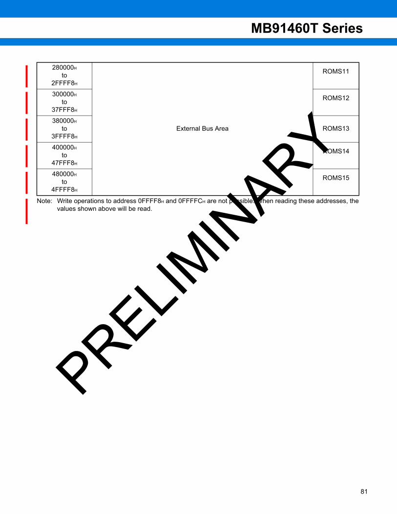
MB91460T Series
Note: Write operations to address 0FFFF8H and 0FFFFCH are not possible. When reading these addresses, the values shown above will be read.
280000H
to2FFFF8H
External Bus Area
ROMS11
300000H
to37FFF8H
ROMS12
380000H
to3FFFF8H
ROMS13
400000H
to47FFF8H
ROMS14
480000H
to4FFFF8H
ROMS15
PRELIMIN
ARY
81
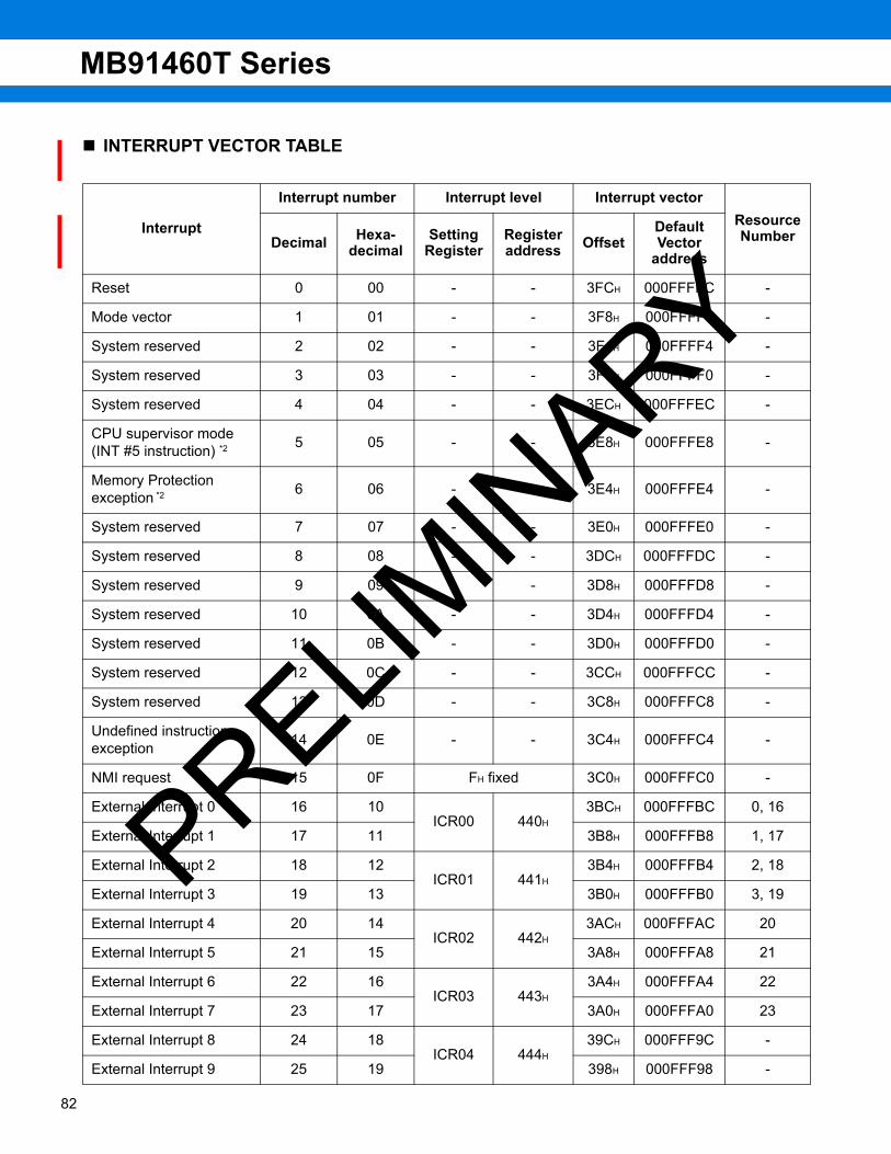
MB91460T Series
82
INTERRUPT VECTOR TABLE
Interrupt
Interrupt number Interrupt level Interrupt vectorResourceNumberDecimal Hexa-
decimalSetting
RegisterRegisteraddress Offset
DefaultVector
address
Reset 0 00 - - 3FCH 000FFFFC -
Mode vector 1 01 - - 3F8H 000FFFF8 -
System reserved 2 02 - - 3F4H 000FFFF4 -
System reserved 3 03 - - 3F0H 000FFFF0 -
System reserved 4 04 - - 3ECH 000FFFEC -
CPU supervisor mode(INT #5 instruction) *2 5 05 - - 3E8H 000FFFE8 -
Memory Protection exception *2 6 06 - - 3E4H 000FFFE4 -
System reserved 7 07 - - 3E0H 000FFFE0 -
System reserved 8 08 - - 3DCH 000FFFDC -
System reserved 9 09 - - 3D8H 000FFFD8 -
System reserved 10 0A - - 3D4H 000FFFD4 -
System reserved 11 0B - - 3D0H 000FFFD0 -
System reserved 12 0C - - 3CCH 000FFFCC -
System reserved 13 0D - - 3C8H 000FFFC8 -
Undefined instructionexception 14 0E - - 3C4H 000FFFC4 -
NMI request 15 0F FH fixed 3C0H 000FFFC0 -
External Interrupt 0 16 10ICR00 440H
3BCH 000FFFBC 0, 16
External Interrupt 1 17 11 3B8H 000FFFB8 1, 17
External Interrupt 2 18 12ICR01 441H
3B4H 000FFFB4 2, 18
External Interrupt 3 19 13 3B0H 000FFFB0 3, 19
External Interrupt 4 20 14ICR02 442H
3ACH 000FFFAC 20
External Interrupt 5 21 15 3A8H 000FFFA8 21
External Interrupt 6 22 16ICR03 443H
3A4H 000FFFA4 22
External Interrupt 7 23 17 3A0H 000FFFA0 23
External Interrupt 8 24 18ICR04 444H
39CH 000FFF9C -
External Interrupt 9 25 19 398H 000FFF98 -
PRELIMIN
ARY
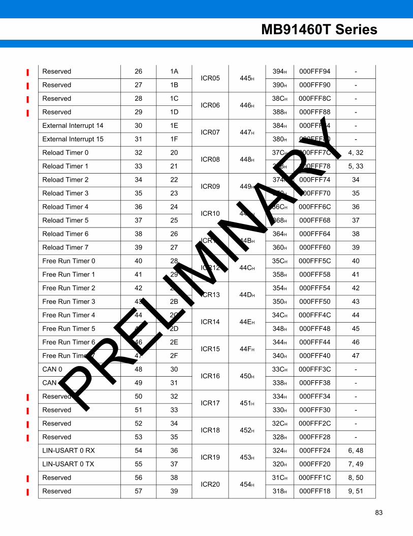
MB91460T Series
Reserved 26 1AICR05 445H
394H 000FFF94 -
Reserved 27 1B 390H 000FFF90 -
Reserved 28 1CICR06 446H
38CH 000FFF8C -
Reserved 29 1D 388H 000FFF88 -
External Interrupt 14 30 1EICR07 447H
384H 000FFF84 -
External Interrupt 15 31 1F 380H 000FFF80 -
Reload Timer 0 32 20ICR08 448H
37CH 000FFF7C 4, 32
Reload Timer 1 33 21 378H 000FFF78 5, 33
Reload Timer 2 34 22ICR09 449H
374H 000FFF74 34
Reload Timer 3 35 23 370H 000FFF70 35
Reload Timer 4 36 24ICR10 44AH
36CH 000FFF6C 36
Reload Timer 5 37 25 368H 000FFF68 37
Reload Timer 6 38 26ICR11 44BH
364H 000FFF64 38
Reload Timer 7 39 27 360H 000FFF60 39
Free Run Timer 0 40 28ICR12 44CH
35CH 000FFF5C 40
Free Run Timer 1 41 29 358H 000FFF58 41
Free Run Timer 2 42 2AICR13 44DH
354H 000FFF54 42
Free Run Timer 3 43 2B 350H 000FFF50 43
Free Run Timer 4 44 2CICR14 44EH
34CH 000FFF4C 44
Free Run Timer 5 45 2D 348H 000FFF48 45
Free Run Timer 6 46 2EICR15 44FH
344H 000FFF44 46
Free Run Timer 7 47 2F 340H 000FFF40 47
CAN 0 48 30ICR16 450H
33CH 000FFF3C -
CAN 1 49 31 338H 000FFF38 -
Reserved 50 32ICR17 451H
334H 000FFF34 -
Reserved 51 33 330H 000FFF30 -
Reserved 52 34ICR18 452H
32CH 000FFF2C -
Reserved 53 35 328H 000FFF28 -
LIN-USART 0 RX 54 36ICR19 453H
324H 000FFF24 6, 48
LIN-USART 0 TX 55 37 320H 000FFF20 7, 49
Reserved 56 38ICR20 454H
31CH 000FFF1C 8, 50
Reserved 57 39 318H 000FFF18 9, 51
PRELIMIN
ARY
83

MB91460T Series
84
LIN-USART 2 RX 58 3AICR21 455H
314H 000FFF14 52
LIN-USART 2 TX 59 3B 310H 000FFF10 53
LIN-USART 3 RX 60 3CICR22 456H
30CH 000FFF0C 54
LIN-USART 3 TX 61 3D 308H 000FFF08 55
System reserved 62 3EICR23 *3 457H
304H 000FFF04 -
Delayed Interrupt 63 3F 300H 000FFF00 -
System reserved *4 64 40(ICR24) (458H)
2FCH 000FFEFC -
System reserved *4 65 41 2F8H 000FFEF8 -
LIN-USART (FIFO) 4 RX 66 42ICR25 459H
2F4H 000FFEF4 10, 56
LIN-USART (FIFO) 4 TX 67 43 2F0H 000FFEF0 11, 57
LIN-USART (FIFO) 5 RX 68 44ICR26 45AH
2ECH 000FFEEC 12, 58
LIN-USART (FIFO) 5 TX 69 45 2E8H 000FFEE8 13, 59
LIN-USART (FIFO) 6 RX 70 46ICR27 45BH
2E4H 000FFEE4 60
LIN-USART (FIFO) 6 TX 71 47 2E0H 000FFEE0 61
LIN-USART (FIFO) 7 RX 72 48ICR28 45CH
2DCH 000FFEDC 62
LIN-USART (FIFO) 7 TX 73 49 2D8H 000FFED8 63
I2C 0 / I2C 2 74 4AICR29 45DH
2D4H 000FFED4 -
I2C 1 / I2C 3 75 4B 2D0H 000FFED0 -
LIN-USART 8 RX 76 4CICR30 45EH
2CCH 000FFECC 64
LIN-USART 8 TX 77 4D 2C8H 000FFEC8 65
LIN-USART 9 RX 78 4EICR31 45FH
2C4H 000FFEC4 66
LIN-USART 9 TX 79 4F 2C0H 000FFEC0 67
LIN-USART 10 RX 80 50ICR32 460H
2BCH 000FFEBC 68
LIN-USART 10 TX 81 51 2B8H 000FFEB8 69
LIN-USART 11 RX 82 52ICR33 461H
2B4H 000FFEB4 70
LIN-USART 11 TX 83 53 2B0H 000FFEB0 71
Reserved 84 54ICR34 462H
2ACH 000FFEAC 72
Reserved 85 55 2A8H 000FFEA8 73
Reserved 86 56ICR35 463H
2A4H 000FFEA4 74
Reserved 87 57 2A0H 000FFEA0 75
Reserved 88 58ICR36 464H
29CH 000FFE9C 76
Reserved 89 59 298H 000FFE98 77
PRELIMIN
ARY

MB91460T Series
Reserved 90 5AICR37 465H
294H 000FFE94 78
Reserved 91 5B 290H 000FFE90 79
Input Capture 0 92 5CICR38 466H
28CH 000FFE8C 80
Input Capture 1 93 5D 288H 000FFE88 81
Input Capture 2 94 5EICR39 467H
284H 000FFE84 82
Input Capture 3 95 5F 280H 000FFE80 83
Input Capture 4 96 60ICR40 468H
27CH 000FFE7C 84
Input Capture 5 97 61 278H 000FFE78 85
Input Capture 6 98 62ICR41 469H
274H 000FFE74 86
Input Capture 7 99 63 270H 000FFE70 87
Output Compare 0 100 64ICR42 46AH
26CH 000FFE6C 88
Output Compare 1 101 65 268H 000FFE68 89
Output Compare 2 102 66ICR43 46BH
264H 000FFE64 90
Output Compare 3 103 67 260H 000FFE60 91
Output Compare 4 104 68ICR44 46CH
25CH 000FFE5C 92
Output Compare 5 105 69 258H 000FFE58 93
Output Compare 6 106 6AICR45 46DH
254H 000FFE54 94
Output Compare 7 107 6B 250H 000FFE50 95
Sound Generator 108 6CICR46 46EH
24CH 000FFE4C -
Phase Frequency Modulator 109 6D 248H 000FFE48 -
System reserved 110 6EICR47 *4 46FH
244H 000FFE44 -
System reserved 111 6F 240H 000FFE40 -
PPG 0 112 70ICR48 470H
23CH 000FFE3C 15, 96
PPG 1 113 71 238H 000FFE38 97
PPG 2 114 72ICR49 471H
234H 000FFE34 98
PPG 3 115 73 230H 000FFE30 99
PPG 4 116 74ICR50 472H
22CH 000FFE2C 100
PPG 5 117 75 228H 000FFE28 101
Reserved 118 76ICR51 473H
224H 000FFE24 102
Reserved 119 77 220H 000FFE20 103
PPG 8 120 78ICR52 474H
21CH 000FFE1C 104
PPG 9 121 79 218H 000FFE18 105
PRELIMIN
ARY
85

MB91460T Series
86
PPG 10 122 7AICR53 475H
214H 000FFE14 106
PPG 11 123 7B 210H 000FFE10 107
PPG 12 124 7CICR54 476H
20CH 000FFE0C 108
PPG 13 125 7D 208H 000FFE08 109
PPG 14 126 7EICR55 477H
204H 000FFE04 110
PPG 15 127 7F 200H 000FFE00 111
Up/Down Counter 0 128 80ICR56 478H
1FCH 000FFDFC -
Up/Down Counter 1 129 81 1F8H 000FFDF8 -
Up/Down Counter 2 130 82ICR57 479H
1F4H 000FFDF4 -
Up/Down Counter 3 131 83 1F0H 000FFDF0 -
Real Time Clock 132 84ICR58 47AH
1ECH 000FFDEC -
Calibration Unit 133 85 1E8H 000FFDE8 -
A/D Converter 0 134 86ICR59 47BH
1E4H 000FFDE4 14, 112
- 135 87 1E0H 000FFDE0 -
Reserved 136 88ICR60 47CH
1DCH000FFDD
C -
Reserved 137 89 1D8H 000FFDD8 -
Low Voltage Detection 138 8AICR61 47DH
1D4H 000FFDD4 -
Reserved 139 8B 1D0H 000FFDD0 -
Timebase Overflow 140 8CICR62 47EH
1CCH000FFDC
C -
PLL Clock Gear 141 8D 1C8H 000FFDC8 -
DMA Controller 142 8EICR63 47FH
1C4H 000FFDC4 -
Main/Sub OSC stability wait 143 8F 1C0H 000FFDC0 -
Security vector 144 90 - - 1BCH 000FFDBC -
Used by the INTinstruction
145to
255
91toFF
- -1B8H
to000H
000FFDB8to
000FFC00-PRELIM
INARY

MB91460T Series
*1: The ICRs are located in the interrupt controller and set the interrupt level for each interrupt request. An ICR is provided for each interrupt request.
*2: The vector address for each EIT (exception, interrupt or trap) is calculated by adding the listed offset to the table base register value (TBR) . The TBR specifies the top of the EIT vector table. The addresses listed in the table are for the default TBR value (000FFC00H) . The TBR is initialized to this value by a reset. The TBR is set to 000FFC00H after the internal boot ROM is executed.
*3: ICR23 and ICR47 can be exchanged by setting the REALOS compatibility bit (addr 0C03H: IOS[0]).
*4: Used by REALOS.
PRELIMIN
ARY
87

MB91460T Series
88
RECOMMENDED SETTINGS1. PLL and Clockgear settings
Please note that for MB91F467TA the core base clock frequencies are valid in the 1.8V operation mode of theMain regulator and Flash *1.
Please note that for MB91F469TA the core base clock frequencies are valid in the 1.9V operation mode of theMain regulator and Flash *2.
Recommended PLL divider and clockgear settings
*1 : Keep REGSEL_FLASHSEL=0 and REGSEL_MAINSEL=0 at their initial value*2 : Set REGSEL_FLASHSEL=1 and REGSEL_MAINSEL=1
PLL Input (CLK)
[MHz]
Frequency Parameter Clockgear ParameterPLL
Output (X)[MHz]
Core Base Clock[MHz] Remarks
DIVM DIVN DIVG MULG MULG4 2 25 16 24 200 100
4 2 24 16 24 192 96
4 2 23 16 24 184 92
4 2 22 16 24 176 88
4 2 21 16 20 168 84
4 2 20 16 20 160 80
4 2 19 16 20 152 76
4 2 18 16 20 144 72
4 2 17 16 16 136 68
4 2 16 16 16 128 64
4 2 15 16 16 120 60
4 2 14 16 16 112 56
4 2 13 16 12 104 52
4 2 12 16 12 96 48
4 2 11 16 12 88 44
4 4 10 16 24 160 40
4 4 9 16 24 144 36
4 4 8 16 24 128 32
4 4 7 16 24 112 28
4 6 6 16 24 144 24
4 8 5 16 28 160 20
4 10 4 16 32 160 16
4 12 3 16 32 144 12
PRELIMIN
ARY

MB91460T Series
2. Clock Modulator settingsThe following table shows all possible settings for the Clock Modulator in a base clock frequency range from32MHz up to 88MHz.
The Flash access time settings need to be adjusted according to Fmax while the PLL and clockgear settingsshould be set according to base clock frequency.
Clock Modulator settings, frequency range and supported supply voltageModulation Degree
(k)Random No
(N)CMPR[hex]
Baseclk[MHz]
Fmin[MHz]
Fmax[MHz]
1 3 026F 88 79.5 98.5
1 3 026F 84 76.1 93.8
1 3 026F 80 72.6 89.1
1 5 02AE 80 68.7 95.8
2 3 046E 80 68.7 95.8
1 3 026F 76 69.1 84.5
1 5 02AE 76 65.3 90.8
1 7 02ED 76 62 98.1
2 3 046E 76 65.3 90.8
3 3 066D 76 62 98.1
1 3 026F 72 65.5 79.9
1 5 02AE 72 62 85.8
1 7 02ED 72 58.8 92.7
2 3 046E 72 62 85.8
3 3 066D 72 58.8 92.7
1 3 026F 68 62 75.3
1 5 02AE 68 58.7 80.9
1 7 02ED 68 55.7 87.3
1 9 032C 68 53 95
2 3 046E 68 58.7 80.9
2 5 04AC 68 53 95
3 3 066D 68 55.7 87.3
4 3 086C 68 53 95
1 3 026F 64 58.5 70.7
1 5 02AE 64 55.3 75.9
1 7 02ED 64 52.5 82
1 9 032C 64 49.9 89.1
1 11 036B 64 47.6 97.6
2 3 046E 64 55.3 75.9
2 5 04AC 64 49.9 89.1
3 3 066D 64 52.5 82
PRELIMIN
ARY
89

MB91460T Series
90
4 3 086C 64 49.9 89.1
5 3 0A6B 64 47.6 97.6
1 3 026F 60 54.9 66.1
1 5 02AE 60 51.9 71
1 7 02ED 60 49.3 76.7
1 9 032C 60 46.9 83.3
1 11 036B 60 44.7 91.3
2 3 046E 60 51.9 71
2 5 04AC 60 46.9 83.3
3 3 066D 60 49.3 76.7
4 3 086C 60 46.9 83.3
5 3 0A6B 60 44.7 91.3
1 3 026F 56 51.4 61.6
1 5 02AE 56 48.6 66.1
1 7 02ED 56 46.1 71.4
1 9 032C 56 43.8 77.6
1 11 036B 56 41.8 84.9
1 13 03AA 56 39.9 93.8
2 3 046E 56 48.6 66.1
2 5 04AC 56 43.8 77.6
2 7 04EA 56 39.9 93.8
3 3 066D 56 46.1 71.4
3 5 06AA 56 39.9 93.8
4 3 086C 56 43.8 77.6
5 3 0A6B 56 41.8 84.9
6 3 0C6A 56 39.9 93.8
1 3 026F 52 47.8 57
1 5 02AE 52 45.2 61.2
1 7 02ED 52 42.9 66.1
1 9 032C 52 40.8 71.8
1 11 036B 52 38.8 78.6
1 13 03AA 52 37.1 86.8
1 15 03E9 52 35.5 96.9
2 3 046E 52 45.2 61.2
2 5 04AC 52 40.8 71.8
2 7 04EA 52 37.1 86.8
3 3 066D 52 42.9 66.1
Modulation Degree(k)
Random No(N)
CMPR[hex]
Baseclk[MHz]
Fmin[MHz]
Fmax[MHz]
PRELIMIN
ARY

MB91460T Series
3 5 06AA 52 37.1 86.8
4 3 086C 52 40.8 71.8
5 3 0A6B 52 38.8 78.6
6 3 0C6A 52 37.1 86.8
7 3 0E69 52 35.5 96.9
1 3 026F 48 44.2 52.5
1 5 02AE 48 41.8 56.4
1 7 02ED 48 39.6 60.9
1 9 032C 48 37.7 66.1
1 11 036B 48 35.9 72.3
1 13 03AA 48 34.3 79.9
1 15 03E9 48 32.8 89.1
2 3 046E 48 41.8 56.4
2 5 04AC 48 37.7 66.1
2 7 04EA 48 34.3 79.9
3 3 066D 48 39.6 60.9
3 5 06AA 48 34.3 79.9
4 3 086C 48 37.7 66.1
5 3 0A6B 48 35.9 72.3
6 3 0C6A 48 34.3 79.9
7 3 0E69 48 32.8 89.1
1 3 026F 44 40.6 48.1
1 5 02AE 44 38.4 51.6
1 7 02ED 44 36.4 55.7
1 9 032C 44 34.6 60.4
1 11 036B 44 33 66.1
1 13 03AA 44 31.5 73
1 15 03E9 44 30.1 81.4
2 3 046E 44 38.4 51.6
2 5 04AC 44 34.6 60.4
2 7 04EA 44 31.5 73
2 9 0528 44 28.9 92.1
3 3 066D 44 36.4 55.7
3 5 06AA 44 31.5 73
4 3 086C 44 34.6 60.4
4 5 08A8 44 28.9 92.1
5 3 0A6B 44 33 66.1
Modulation Degree(k)
Random No(N)
CMPR[hex]
Baseclk[MHz]
Fmin[MHz]
Fmax[MHz]
PRELIMIN
ARY
91

MB91460T Series
92
6 3 0C6A 44 31.5 73
7 3 0E69 44 30.1 81.4
8 3 1068 44 28.9 92.1
1 3 026F 40 37 43.6
1 5 02AE 40 34.9 46.8
1 7 02ED 40 33.1 50.5
1 9 032C 40 31.5 54.8
1 11 036B 40 30 59.9
1 13 03AA 40 28.7 66.1
1 15 03E9 40 27.4 73.7
2 3 046E 40 34.9 46.8
2 5 04AC 40 31.5 54.8
2 7 04EA 40 28.7 66.1
2 9 0528 40 26.3 83.3
3 3 066D 40 33.1 50.5
3 5 06AA 40 28.7 66.1
3 7 06E7 40 25.3 95.8
4 3 086C 40 31.5 54.8
4 5 08A8 40 26.3 83.3
5 3 0A6B 40 30 59.9
6 3 0C6A 40 28.7 66.1
7 3 0E69 40 27.4 73.7
8 3 1068 40 26.3 83.3
9 3 1267 40 25.3 95.8
1 3 026F 36 33.3 39.2
1 5 02AE 36 31.5 42
1 7 02ED 36 29.9 45.3
1 9 032C 36 28.4 49.2
1 11 036B 36 27.1 53.8
1 13 03AA 36 25.8 59.3
1 15 03E9 36 24.7 66.1
2 3 046E 36 31.5 42
2 5 04AC 36 28.4 49.2
2 7 04EA 36 25.8 59.3
2 9 0528 36 23.7 74.7
3 3 066D 36 29.9 45.3
3 5 06AA 36 25.8 59.3
Modulation Degree(k)
Random No(N)
CMPR[hex]
Baseclk[MHz]
Fmin[MHz]
Fmax[MHz]
PRELIMIN
ARY
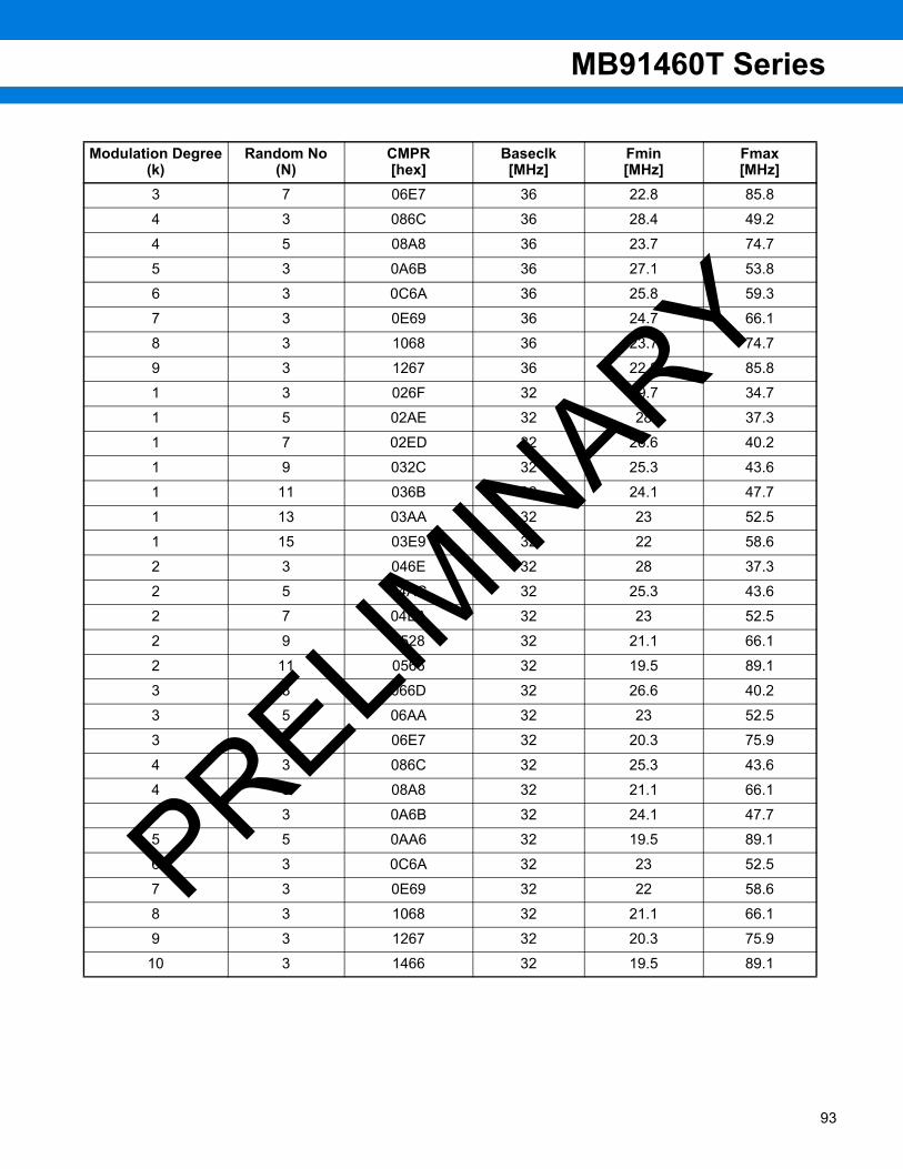
MB91460T Series
3 7 06E7 36 22.8 85.8
4 3 086C 36 28.4 49.2
4 5 08A8 36 23.7 74.7
5 3 0A6B 36 27.1 53.8
6 3 0C6A 36 25.8 59.3
7 3 0E69 36 24.7 66.1
8 3 1068 36 23.7 74.7
9 3 1267 36 22.8 85.8
1 3 026F 32 29.7 34.7
1 5 02AE 32 28 37.3
1 7 02ED 32 26.6 40.2
1 9 032C 32 25.3 43.6
1 11 036B 32 24.1 47.7
1 13 03AA 32 23 52.5
1 15 03E9 32 22 58.6
2 3 046E 32 28 37.3
2 5 04AC 32 25.3 43.6
2 7 04EA 32 23 52.5
2 9 0528 32 21.1 66.1
2 11 0566 32 19.5 89.1
3 3 066D 32 26.6 40.2
3 5 06AA 32 23 52.5
3 7 06E7 32 20.3 75.9
4 3 086C 32 25.3 43.6
4 5 08A8 32 21.1 66.1
5 3 0A6B 32 24.1 47.7
5 5 0AA6 32 19.5 89.1
6 3 0C6A 32 23 52.5
7 3 0E69 32 22 58.6
8 3 1068 32 21.1 66.1
9 3 1267 32 20.3 75.9
10 3 1466 32 19.5 89.1
Modulation Degree(k)
Random No(N)
CMPR[hex]
Baseclk[MHz]
Fmin[MHz]
Fmax[MHz]
PRELIMIN
ARY
93

MB91460T Series
94
ELECTRICAL CHARACTERISTICS1. Absolute maximum ratings
*1: The parameter is based on VSS5 = 0.0 V.
*2: AVCC5 and AVRH5 must not exceed VDD5 + 0.3 V.
*3: • Use within recommended operating conditions.• Use with DC voltage (current).• +B signals are input signals that exceed the VDD5 voltage. +B signals should always be applied by
connecting a limiting resistor between the +B signal and the microcontroller.• The value of the limiting resistor should be set so that the current input to the microcontroller pin does not
exceed the rated value at any time , either instantaneously or for an extended period, when the +B signal is input.
• Note that when the microcontroller drive current is low, such as in the low power consumption modes, the +B input potential can increase the potential at the power supply pin via a protective diode, possibly affecting other devices.
• Note that if the +B signal is input when the microcontroller is off (not fixed at 0 V), power is supplied through the +B input pin; therefore, the microcontroller may partially operate.
• Note that if the +B signal is input at power-on, since the power is supplied through the pin, the power-on reset may not function in the power supply voltage.
Parameter SymbolRating
Unit RemarksMin Max
Power supply voltage 1*1 VDD5R − 0.3 + 6.0 VPower supply voltage 2*1 VDD5 − 0.3 + 6.0 VPower supply voltage 4*1 VDD35 − 0.3 + 6.0 V
Relationship of the supply voltages AVCC5
VDD5-0.3 VDD5+0.3 V
At least one pin of the Ports 110 to 143 (AN*) is used as digital input or output.
VSS5-0.3 VDD5+0.3 VAll pins of the Ports 110 to 143 (AN*) follow the condition of VIA
Analog power supply voltage*1 AVCC5 − 0.3 + 6.0 V *2
Analog referencepower supply voltage*1 AVRH − 0.3 + 6.0 V *2
Input voltage 1*1 VI1 Vss5 − 0.3 VDD5 + 0.3 VInput voltage 2*1 VI2 Vss5 − 0.3 VDD35 + 0.3 V External busAnalog pin input voltage*1 VIA AVss5 − 0.3 AVcc5 + 0.3 VOutput voltage 1*1 VO1 Vss5 − 0.3 VDD5 + 0.3 VOutput voltage 2*1 VO2 Vss5 − 0.3 VDD35 + 0.3 V External busMaximum clamp current ICLAMP − 4.0 + 4.0 mA *3
Total maximum clamp current Σ |ICLAMP| ⎯ 20 mA *3
Power consumption PD ⎯ 1000 mWOperating temperature TA − 40 + 105 °CStorage temperature Tstg − 55 + 150 °C
PRELIMIN
ARY
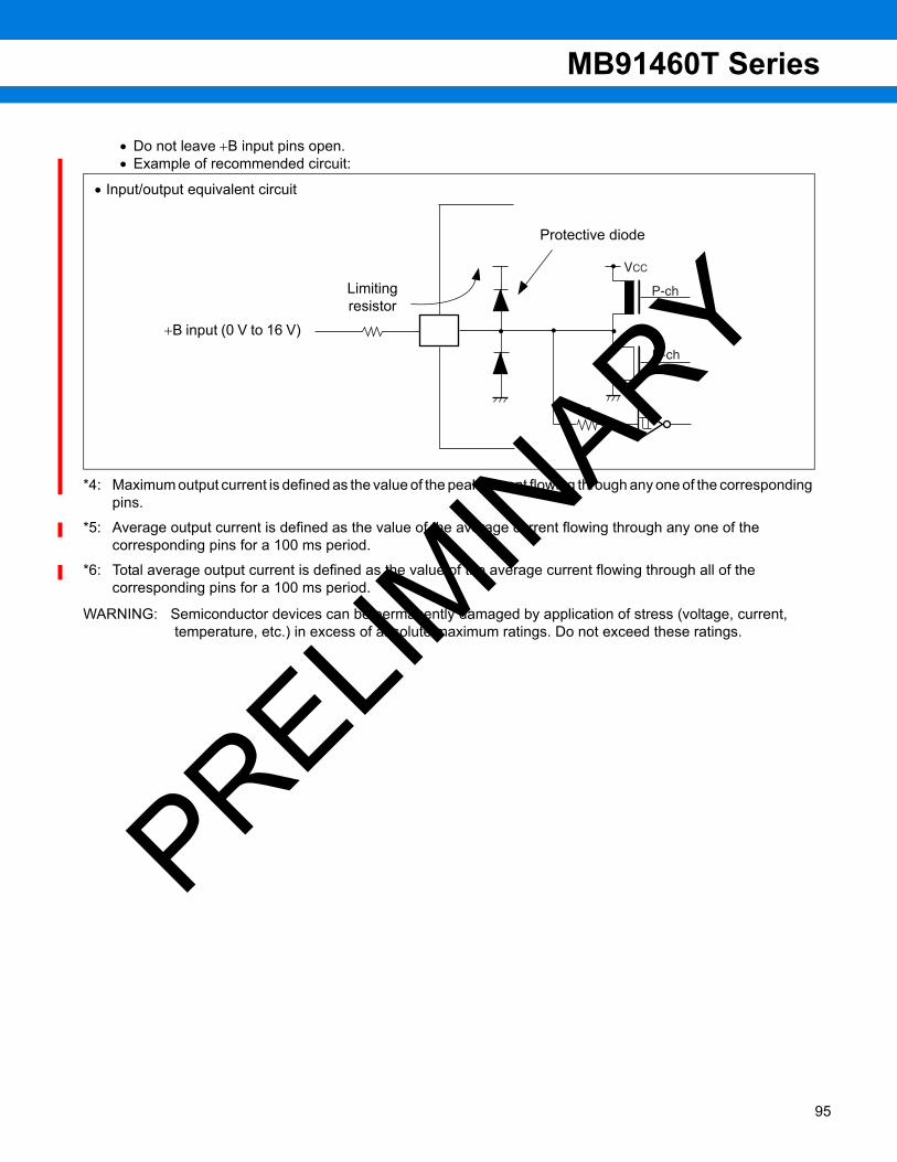
MB91460T Series
• Do not leave +B input pins open.• Example of recommended circuit:
*4: Maximum output current is defined as the value of the peak current flowing through any one of the corresponding pins.
*5: Average output current is defined as the value of the average current flowing through any one of the corresponding pins for a 100 ms period.
*6: Total average output current is defined as the value of the average current flowing through all of the corresponding pins for a 100 ms period.
WARNING: Semiconductor devices can be permanently damaged by application of stress (voltage, current, temperature, etc.) in excess of absolute maximum ratings. Do not exceed these ratings.
P-ch
N-ch
VCC
R
• Input/output equivalent circuit
+B input (0 V to 16 V)
Limitingresistor
Protective diode
PRELIMIN
ARY
95
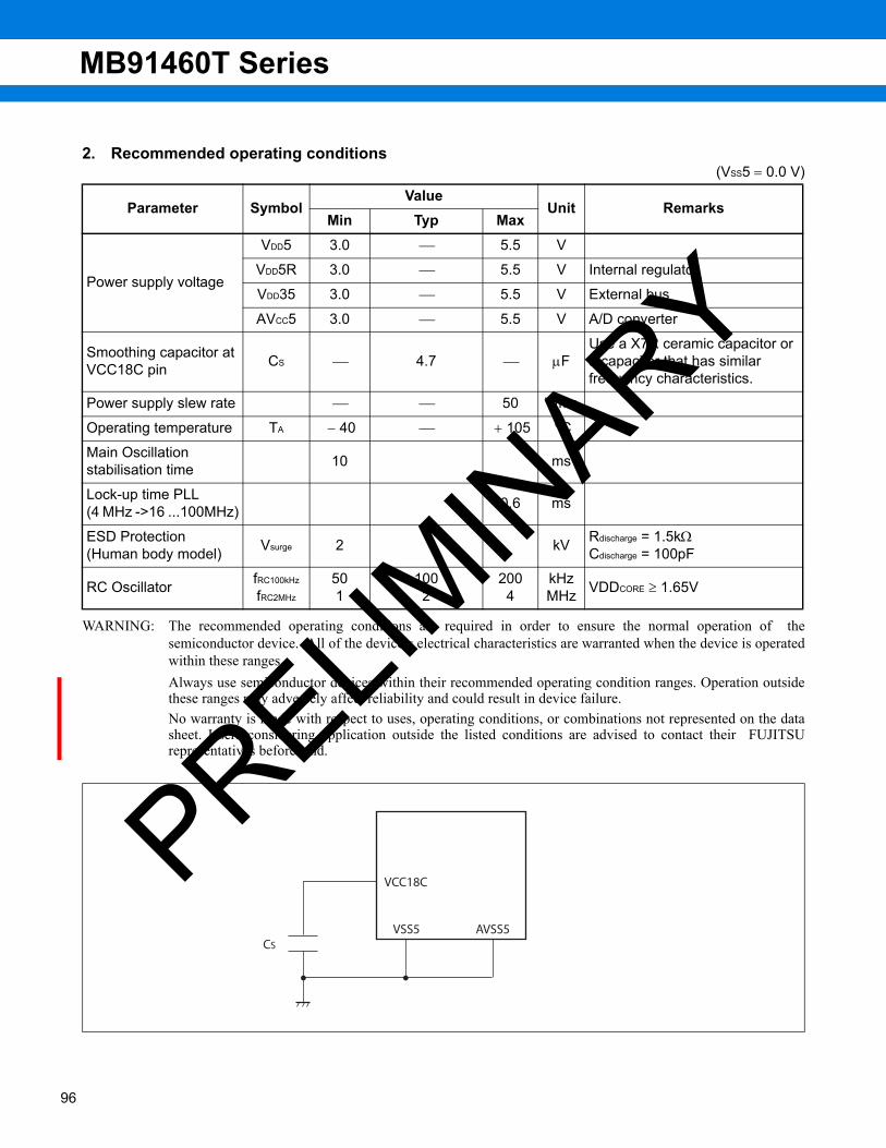
MB91460T Series
96
2. Recommended operating conditions (VSS5 = 0.0 V)
WARNING: The recommended operating conditions are required in order to ensure the normal operation of thesemiconductor device. All of the device’s electrical characteristics are warranted when the device is operatedwithin these ranges.Always use semiconductor devices within their recommended operating condition ranges. Operation outsidethese ranges may adversely affect reliability and could result in device failure.No warranty is made with respect to uses, operating conditions, or combinations not represented on the datasheet. Users considering application outside the listed conditions are advised to contact their FUJITSUrepresentatives beforehand.
Parameter SymbolValue
Unit RemarksMin Typ Max
Power supply voltage
VDD5 3.0 ⎯ 5.5 V
VDD5R 3.0 ⎯ 5.5 V Internal regulator
VDD35 3.0 ⎯ 5.5 V External bus
AVCC5 3.0 ⎯ 5.5 V A/D converter
Smoothing capacitor at VCC18C pin CS ⎯ 4.7 ⎯ μF
Use a X7R ceramic capacitor or a capacitor that has similar frequency characteristics.
Power supply slew rate ⎯ ⎯ 50 V/ms
Operating temperature TA − 40 ⎯ + 105 °C
Main Oscillationstabilisation time 10 ms
Lock-up time PLL(4 MHz ->16 ...100MHz) 0.6 ms
ESD Protection(Human body model) Vsurge 2 kV Rdischarge = 1.5kΩ
Cdischarge = 100pF
RC Oscillator fRC100kHz
fRC2MHz
501
1002
2004
kHzMHz VDDCORE ≥ 1.65V
CS
AVSS5VSS5
VCC18CPRELIMIN
ARY
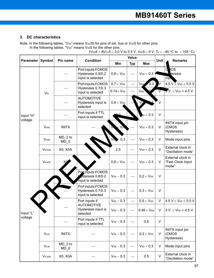
MB91460T Series
3. DC characteristicsNote: In the following tables, “VDD” means VDD35 for pins of ext. bus or VDD5 for other pins. In the following tables, “VSS” means VSS5 for the other pins.
(VDD5 = AVCC5 = 3.0 V to 5.5 V, VSS5 = 0 V, TA = −40 °C to + 105 °C)
Parameter Symbol Pin name ConditionValue
Unit RemarksMin Typ Max
Input “H” voltage
VIH
⎯Port inputs if CMOS Hysteresis 0.8/0.2 input is selected
0.8 × VDD ⎯ VDD + 0.3 VCMOS hysteresis input
⎯Port inputs if CMOS Hysteresis 0.7/0.3 input is selected
0.7 × VDD ⎯ VDD + 0.3 V 4.5 V ≤ VDD ≤ 5.5 V
0.74 × VDD ⎯ VDD + 0.3 V 3 V ≤ VDD < 4.5 V
⎯AUTOMOTIVE Hysteresis input is selected
0.8 × VDD ⎯ VDD + 0.3 V
⎯ Port inputs if TTL input is selected 2.0 ⎯ VDD + 0.3 V
VIHR INITX ⎯ 0.8 × VDD ⎯ VDD + 0.3 VINITX input pin (CMOS Hysteresis)
VIHMMD_2 to MD_0 ⎯ VDD − 0.3 ⎯ VDD + 0.3 V Mode input pins
VIHX0S X0, X0A ⎯ 2.5 ⎯ VDD + 0.3 V External clock in “Oscillation mode”
VIHX0F X0 ⎯ 0.8 × VDD ⎯ VDD + 0.3 VExternal clock in “Fast Clock Input mode”
Input “L” voltage
VIL
⎯Port inputs if CMOS Hysteresis 0.8/0.2 input is selected
VSS − 0.3 ⎯ 0.2 × VDD V
⎯Port inputs if CMOS Hysteresis 0.7/0.3 input is selected
VSS − 0.3 ⎯ 0.3 × VDD V
⎯
Port inputs if AUTOMOTIVE Hysteresis input is selected
VSS − 0.3 ⎯ 0.5 × VDD V 4.5 V ≤ VDD ≤ 5.5 V
VSS − 0.3 ⎯ 0.46 × VDD V 3 V ≤ VDD < 4.5 V
⎯ Port inputs if TTL input is selected VSS − 0.3 ⎯ 0.8 V
VILR INITX ⎯ VSS − 0.3 ⎯ 0.2 × VDD VINITX input pin (CMOS Hysteresis)
VILMMD_2 to MD_0 ⎯ VSS − 0.3 ⎯ VSS + 0.3 V Mode input pins
VILXDS X0, X0A ⎯ VSS − 0.3 ⎯ 0.5 V External clock in “Oscillation mode”
PRELIMIN
ARY
97

MB91460T Series
98
(VDD5 = AVCC5 = 3.0 V to 5.5 V, VSS5 = 0 V, TA = −40 °C to + 105 °C)
Parameter Symbol Pin name Condition
ValueUnit Remarks
Min Typ Max
Input “L” voltage VILXDF X0 ⎯ VSS − 0.3 ⎯ 0.2 × VDD V
External clock in “Fast Clock Input mode”
Output “H” voltage
VOH2Normal outputs
4.5V VDD 5.5V,IOH = − 2mA
VDD − 0.5 ⎯ ⎯ V Driving strength set to 2 mA3.0V VDD 4.5V,
IOH = − 1.6mA
VOH5Normal outputs
4.5V VDD 5.5V, IOH = − 5mA
VDD − 0.5 ⎯ ⎯ V Driving strength set to 5 mA3.0V VDD 4.5V,
IOH = − 3mA
VOH3I2C
outputs3.0V VDD 5.5V, IOH = − 3mA VDD − 0.5 ⎯ ⎯ V
Output “L“ voltage
VOL2Normal outputs
4.5V VDD 5.5V, IOH = + 2mA
⎯ ⎯ 0.4 V Driving strength set to 2 mA3.0V VDD 4.5V,
IOH = + 1.6mA
VOL5Normal outputs
4.5V VDD 5.5V, IOH = + 5mA
⎯ ⎯ 0.4 V Driving strength set to 5 mA3.0V VDD 4.5V,
IOH = + 3mA
VOL3I2C
outputs3.0V VDD 5.5V, IOH = + 3mA ⎯ ⎯ 0.4 V
Input leakage current IIL Pnn_m
*1
3.0V VDD 5.5VVSS5 < VI < VDD
TA=25 °C − 1 ⎯ + 1
μA3.0V VDD 5.5VVSS5 < VI < VDD
TA=105 °C − 3 ⎯ + 3
Pull-up resistance RUP
Pnn_m, INITX*1 ⎯ 25 50 100 kΩ
Pull-down resistance RDOWN Pnn_m ⎯ 25 50 100 kΩ
Inputcapacitance CIN
All except VDD5,
VDD5R, VSS5,
AVCC5, AVSS,
AVRH5
f = 1 MHz - 5 15 pF
≤ ≤
≤ ≤
≤ ≤
≤ ≤
≤ ≤
≤ ≤
≤ ≤
≤ ≤
≤ ≤
≤ ≤
≤ ≤
≤ ≤
PRELIMIN
ARY

MB91460T Series
*1 Pnn_m includes all pins unless the pins, which include analog inputs.
*2 Main regulator OFF, sub regulator set to 1.2V, Low voltage detection disabled.
Power supply current MB91F467TA
ICC VDD5R
MB91F467TA:CLKB: 100 MHzCLKP: 50 MHzCLKT: 50 MHzCLKCAN: 50 MHz
⎯ 110 140 mA Code fetch from Flash
ICCH VDD5R
TA = + 25 °C ⎯ 30 150 μAAt stop mode *2
TA = + 105 °C ⎯ 300 2000 μA
TA = + 25 °C ⎯ 100 500 μA RTC: 4 MHz mode *2TA = + 105 °C ⎯ 500 2400 μA
TA = + 25 °C ⎯ 50 250 μA RTC: 100 kHz mode *2TA = + 105 °C ⎯ 400 2200 μA
ILVE VDD5 ⎯ ⎯ 70 150 μA External low voltage detection
ILVI VDD5R ⎯ ⎯ 50 100 μA Internal low voltage detection
IOSC VDD5⎯ ⎯ 250 500 μA Main clock
(4 MHz)
⎯ ⎯ 20 40 μA Sub clock (32 kHz)
Power supply current MB91F469TA
ICC VDD5R
MB91F469TA:CLKB: 100 MHzCLKP: 50 MHzCLKT: 50 MHzCLKCAN: 50 MHz
⎯ 180 220 mA Code fetch from Flash
ICCH VDD5R
TA = + 25 °C ⎯ 50 200 μAAt stop mode*2
TA = + 105 °C ⎯ 580 2500 μA
TA = + 25 °C ⎯ 150 720 μA RTC: 4 MHz mode*2TA = + 105 °C ⎯ 720 3500 μA
TA = + 25 °C ⎯ 80 360 μA RTC: 100 kHz mode*2TA = + 105 °C ⎯ 650 3200 μA
ILVE VDD5 ⎯ ⎯ 70 150 μA External low voltage detection
ILVI VDD5R ⎯ ⎯ 50 100 μA Internal low voltage detection
IOSC VDD5⎯ ⎯ 250 500 μA Main clock
(4 MHz)
⎯ ⎯ 20 40 μA Sub clock (32 kHz)
Parameter Symbol Pin name Condition
ValueUnit Remarks
Min Typ Max
PRELIMIN
ARY
99
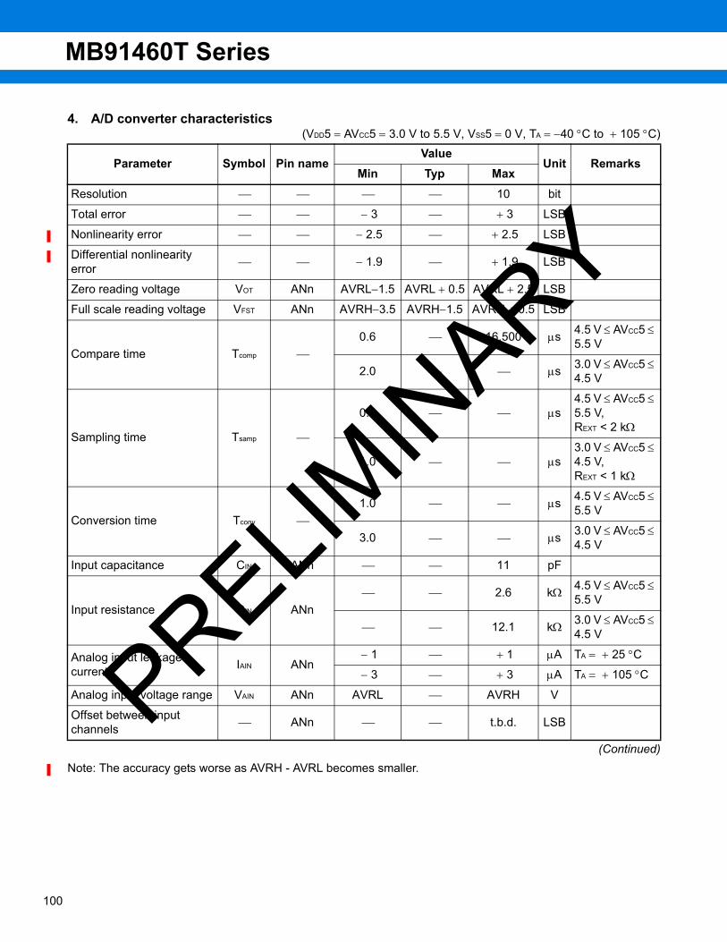
MB91460T Series
100
4. A/D converter characteristics (VDD5 = AVCC5 = 3.0 V to 5.5 V, VSS5 = 0 V, TA = −40 °C to + 105 °C)
(Continued)Note: The accuracy gets worse as AVRH - AVRL becomes smaller.
Parameter Symbol Pin nameValue
Unit RemarksMin Typ Max
Resolution ⎯ ⎯ ⎯ ⎯ 10 bit
Total error ⎯ ⎯ − 3 ⎯ + 3 LSB
Nonlinearity error ⎯ ⎯ − 2.5 ⎯ + 2.5 LSB
Differential nonlinearity error ⎯ ⎯ − 1.9 ⎯ + 1.9 LSB
Zero reading voltage VOT ANn AVRL−1.5 AVRL + 0.5 AVRL + 2.5 LSB
Full scale reading voltage VFST ANn AVRH−3.5 AVRH−1.5 AVRH + 0.5 LSB
Compare time Tcomp ⎯0.6 ⎯ 16,500 μs 4.5 V ≤ AVCC5 ≤
5.5 V
2.0 ⎯ ⎯ μs 3.0 V ≤ AVCC5 ≤ 4.5 V
Sampling time Tsamp ⎯
0.4 ⎯ ⎯ μs4.5 V ≤ AVCC5 ≤ 5.5 V,REXT < 2 kΩ
1.0 ⎯ ⎯ μs3.0 V ≤ AVCC5 ≤ 4.5 V,REXT < 1 kΩ
Conversion time Tconv ⎯1.0 ⎯ ⎯ μs 4.5 V ≤ AVCC5 ≤
5.5 V
3.0 ⎯ ⎯ μs 3.0 V ≤ AVCC5 ≤ 4.5 V
Input capacitance CIN ANn ⎯ ⎯ 11 pF
Input resistance RIN ANn⎯ ⎯ 2.6 kΩ 4.5 V ≤ AVCC5 ≤
5.5 V
⎯ ⎯ 12.1 kΩ 3.0 V ≤ AVCC5 ≤ 4.5 V
Analog input leakagecurrent IAIN ANn
− 1 ⎯ + 1 μA TA = + 25 °C
− 3 ⎯ + 3 μA TA = + 105 °C
Analog input voltage range VAIN ANn AVRL ⎯ AVRH V
Offset between input channels ⎯ ANn ⎯ ⎯ t.b.d. LSBPRELIM
INARY

MB91460T Series
(Continued)
*1: Supply current at AVCC5, if A/D converter and ALARM comparator are not operating, (VDD5 = AVCC5 = AVRH = 5.0 V)
*2: Input current at AVRH5, if A/D converter is not operating, (VDD5 = AVCC5 = AVRH = 5.0 V)
Sampling Time CalculationTsamp = ( 2.6 kOhm + REXT) × 11pF × 7; for 4.5V ≤ AVCC5 ≤ 5.5VTsamp = (12.1 kOhm + REXT) × 11pF × 7; for 3.0V ≤ AVCC5 ≤ 4.5V
Conversion Time CalculationTconv = Tsamp + Tcomp
Definition of A/D converter terms• Resolution
Analog variation that is recognizable by the A/D converter.• Linearity error
Deviation between actual conversion characteristics and a straight line connecting the zero transition point (00 0000 0000B ↔ 00 0000 0001B) and the full scale transition point (11 1111 1110B ↔ 11 1111 1111B).
• Differential linearity errorDeviation of the input voltage from the ideal value that is required to change the output code by 1 LSB.
• Total errorThis error indicates the difference between actual and theoretical values, including the zero transition error,full scale transition error, and linearity error.
Parameter Symbol Pin nameValue
Unit RemarksMin Typ Max
Reference voltage range AVRH AVRH5 0.75 × AVCC5 ⎯ AVCC5 V
Power supply currentIA AVCC5 ⎯ 2.5 5 mA A/D Converter
active
IAH AVCC5 ⎯ ⎯ 5 μA A/D Converter not operated *1
Reference voltage currentIR AVRH5 ⎯ 0.7 1 mA A/D Converter
active
IRH AVRH5 ⎯ ⎯ 5 μA A/D Converter not operated *2
PRELIMIN
ARY
101

MB91460T Series
102
(Continued)
3FFH
3FEH
3FDH
004H
003H
002H
001H
AVSS5 AVRH
0.5 LSB'
{1 LSB’ (N - 1) + 0.5 LSB’}
1.5 LSB’
Analog input
Total error
Dig
ital o
utpu
t
Actual conversion characteristics
VNT
(measurement value)
Ideal characteristics
Actual conversion characteristics
Total error of digital output N = 1 LSB'
VNT − {1 LSB' × (N − 1) + 0.5 LSB'}
N : A/D converter digital output valueVOT' (ideal value) = AVSS5 + 0.5 LSB' [V]VFST' (ideal value) = AVRH − 1.5 LSB' [V]VNT: Voltage at which the digital output changes from (N + 1) H to NH
1LSB' (ideal value) = 1024
AVRH − AVSS5 [V]
PRELIMIN
ARY

MB91460T Series
(Continued)
(N+1)H
NH
(N-1)H
(N-2)H
AVSS5 AVRH
3FFH
3FEH
3FDH
004H
003H
002H
001H
AVSS5 AVRH
{1 LSB (N - 1) + VOT}
Analog inputAnalog input
Differential linearity errorLinearity error
Dig
ital o
utpu
t
Dig
ital o
utpu
t
Actual conversion characteristics
VFST(measure-ment value)
VNT(measure-ment value)
Actual conversion characteristics
Ideal characteristics
VTO (measurement value)
Actual conversion characteristics
VNT(measure-ment value)
VFST (measure-ment value)
Linearity error of digital output N = 1LSB
VNT − {1LSB × (N − 1) + VOT} [LSB]
Differential linearity error of digital output N = 1LSB
V (N + 1) T − VNT − 1 [LSB]
1LSB = 1022
VFST − VOT [V]
N : A/D converter digital output valueVOT : Voltage at which the digital output changes from 000H to 001H.VFST : Voltage at which the digital output changes from 3FEH to 3FFH.
Actual conversion characteristics
Idealcharacteristics
PRELIMIN
ARY
103

MB91460T Series
104
5. FLASH memory program/erase characteristics5.1. MB91F467TA, MB91F469TA
(TA = 25oC, Vcc = 5.0V)
*1: This value was converted from the results of evaluating the reliability of the technology(using Arrhenius equation to convert high temperature measurements into normalized value at 85oC)
ParameterValue
Unit RemarksMin Typ Max
Sector erase time - 0.5 2.0 s Erasure programming time not included
Chip erase time - n*0.5 n*2.0 s n is the number of Flash sector of the device
Word programming time - 6 100 μs System overhead time not included
Programme/Erase cycle 10 000 cycle
Flash data retention time 20 year *1
PRELIMIN
ARY

MB91460T Series
6. AC characteristics6.1. Clock timing
(VDD5 = 3.0 V to 5.5 V, Vss5 = 0 V, TA = −40 °C to + 105 °C)
• Clock timing condition
Parameter Symbol Pin nameValue
Unit ConditionMin Typ Max
Clock frequency fC
X0X1 3.5 4 16 MHz Opposite phase external
supply or crystal
X0AX1A 32 32.768 100 kHz
0.8 VCC
0.2 VCC
PWH PWL
tC
X0,X1,X0A,X1A
PRELIMIN
ARY
105

MB91460T Series
106
6.2. Reset input ratings (VDD5 = 3.0 V to 5.5 V, VSS5 = 0 V, TA = −40 °C to + 105 °C)
Parameter Symbol Pin name ConditionValue
UnitMin Max
INITX input time(at power-on)
tINTL INITX ⎯8 ⎯ ms
INITX input time(other than the above) 20 ⎯ μs
0.2 VCC
tINTL
INITX
PRELIMIN
ARY

MB91460T Series
6.3. LIN-USART Timings at VDD5 = 3.0 to 5.5 V• Conditions during AC measurements• All AC tests were measured under the following conditions:• - IOdrive = 5 mA• - VDD5 = 3.0 V to 5.5 V, Iload = 3 mA• - VSS5 = 0 V• - Ta = -40 °C to +105× °C• - Cl = 50 pF (load capacity value of pins when testing)• - VOL = 0.2 x VDD5,• - VOH = 0.8 x VDD5• - EPILR = 0, PILR = 1 (Automotive Level = worst case)
(VDD5 = 3.0 V to 5.5 V, VSS5 = 0 V, TA = −40 °C to + 105 °C)
*: Parameter m depends on tSCYCI and can be calculated as: • if tSCYCI = 2*k*tCLKP, then m = k, where k is an integer > 2• if tSCYCI = (2*k + 1)*tCLKP, then m = k + 1, where k is an integer > 1
Notes: • The above values are AC characteristics for CLK synchronous mode.• tCLKP is the cycle time of the peripheral clock.
Parameter Symbol Pin name ConditionVDD5 = 3.0 V to 4.5 V VDD5 = 4.5 V to 5.5 V
UnitMin Max Min Max
Serial clock cycle time tSCYCI SCKn
Internal clock
operation (master mode)
4 tCLKP ⎯ 4 tCLKP ⎯ ns
SCK ↓ → SOT delay time tSLOVI
SCKnSOTn − 30 30 − 20 20 ns
SOT → SCK ↓ delay time tOVSHI
SCKnSOTn
m × tCLKP − 30* ⎯ m ×
tCLKP − 20* ⎯ ns
Valid SIN → SCK ↑ setup time tIVSHI
SCKnSINn tCLKP + 55 ⎯ tCLKP + 45 ⎯ ns
SCK ↑ → valid SIN hold time tSHIXI
SCKnSINn 0 ⎯ 0 ⎯ ns
Serial clock “H” pulse width tSHSLE SCKn
External clock
operation (slave mode)
tCLKP + 10 ⎯ tCLKP + 10 ⎯ ns
Serial clock“L” pulse width tSLSHE SCKn tCLKP + 10 ⎯ tCLKP + 10 ⎯ ns
SCK ↓ → SOT delay time tSLOVE
SCKnSOTn ⎯ 2 tCLKP + 55 ⎯ 2 tCLKP + 45 ns
Valid SIN → SCK ↑ setup time tIVSHE
SCKnSINn 10 ⎯ 10 ⎯ ns
SCK ↑ → valid SIN hold time tSHIXE
SCKnSINn tCLKP + 10 ⎯ tCLKP + 10 ⎯ ns
SCK rising time tFE SCKn ⎯ 20 ⎯ 20 ns
SCK falling time tRE SCKn ⎯ 20 ⎯ 20 nsPRELIM
INARY
107

MB91460T Series
108
• Internal clock mode (master mode)
• External clock mode (slave mode)
tIVSHI
VOH
tSHIXI
tSLOVI
tSCYCI
VOLSOTn
SCKnfor ESCR.SCES = 0
SCKnfor ESCR.SCES = 1
tOVSHI
VOL
VOL
VOL
VOL
VOL
VOH
VOH
VOH
VOH VOH
SINn
tIVSHE
VOH
tSHIXE
tSLOVE
tSLSHE
VOLSOTn
SCKnfor ESCR.SCES = 0
SCKnfor ESCR.SCES = 1
VOL
VOL
VOL
VOL
VOH
VOH
VOH
VOLVOHVOHVOH
SINn
tSHSLE
VOL
tRE
VOH
tFE
VOL
PRELIMIN
ARY
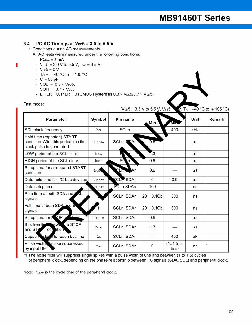
MB91460T Series
6.4. I2C AC Timings at VDD5 = 3.0 to 5.5 V• Conditions during AC measurements
All AC tests were measured under the following conditions:- IOdrive = 3 mA- VDD5 = 3.0 V to 5.5 V, Iload = 3 mA- VSS5 = 0 V- Ta = − 40 °C to + 105 °C- Cl = 50 pF- VOL = 0.3 × VDD5,
VOH = 0.7 × VDD5- EPILR = 0, PILR = 0 (CMOS Hysteresis 0.3 × VDD5/0.7 × VDD5)
Fast mode: (VDD5 = 3.5 V to 5.5 V, VSS5 = 0 V, TA = −40 °C to + 105 °C)
*1 The noise filter will suppress single spikes with a pulse width of 0ns and between (1 to 1.5) cycles of peripheral clock, depending on the phase relationship between I2C signals (SDA, SCL) and peripheral clock.
Note: tCLKP is the cycle time of the peripheral clock.
Parameter Symbol Pin nameValue
Unit RemarkMin Max
SCL clock frequency fSCL SCLn 0 400 kHz
Hold time (repeated) START condition. After this period, the first clock pulse is generated
tHD;STA SCLn, SDAn 0.6 ⎯ μs
LOW period of the SCL clock tLOW SCLn 1.3 ⎯ μs
HIGH period of the SCL clock tHIGH SCLn 0.6 ⎯ μs
Setup time for a repeated START condition tSU;STA SCLn, SDAn 0.6 ⎯ μs
Data hold time for I2C-bus devices tHD;DAT SCLn, SDAn 0 0.9 μs
Data setup time tSU;DAT SCLn SDAn 100 ⎯ ns
Rise time of both SDA and SCL signals tr SCLn, SDAn 20 + 0.1Cb 300 ns
Fall time of both SDA and SCL signals tf SCLn, SDAn 20 + 0.1Cb 300 ns
Setup time for STOP condition tSU;STO SCLn, SDAn 0.6 ⎯ μs
Bus free time between a STOP and START condition tBUF SCLn, SDAn 1.3 ⎯ μs
Capacitive load for each bus line Cb SCLn, SDAn ⎯ 400 pF
Pulse width of spike suppressed by input filter tSP SCLn, SDAn 0 (1..1.5) ×
tCLKPns *1PRELIM
INARY
109

MB91460T Series
110
A
SSr
PS
CL
tHD
;STA
tr
tr
tSP
tSU
;ST0
tSU
;STA
tSU
;DAT
tHD
;DAT
tHD
;STA
tLO
WtH
IGH
tBU
F
tf
tf
PRELIMIN
ARY

MB91460T Series
6.5. Free-run timer clock (VDD5 = 3.0 V to 5.5 V, VSS5 = 0 V, TA = −40 °C to + 105 °C)
Note: tCLKP is the cycle time of the peripheral clock.
6.6. Trigger input timing (VDD5 = 3.0 V to 5.5 V, VSS5 = 0 V, TA = −40 °C to + 105 °C)
Note: tCLKP is the cycle time of the peripheral clock.
Parameter Symbol Pin name ConditionValue
UnitMin Max
Input pulse width tTIWH
tTIWLCKn ⎯ 4tCLKP ⎯ ns
Parameter Symbol Pin name ConditionValue
UnitMin Max
Input capture input trigger tINP ICUn ⎯ 5tCLKP ⎯ ns
A/D converter trigger tATGX ATGX ⎯ 5tCLKP ⎯ ns
tTIWH tTIWL
CKn
ICUn, ATGX
tATGX, tINP
PRELIMIN
ARY
111

MB91460T Series
112
6.7. External Bus AC Timings at VDD35 = 4.5 to 5.5 V• Conditions during AC measurements
All AC tests were measured under the following conditions:- IOdrive = 5 mA- VDD35 = 4.5 V to 5.5 V, Iload = 5 mA- VSS5 = 0 V- Ta = − 40 °C to + 105 °C- Cl = 50 pF- VOL = 0.2 × VDD35,
VOH = 0.8 × VDD35- EPILR = 0, PILR = 1 (Automotive Level = worst case)
6.7.1. Basic Timing (VDD35 = 4.5 V to 5.5 V, Vss5 = 0 V, TA = −40 °C to + 105 °C)
Note: tCLKT is the cycle time of the external bus clock.
Parameter Symbol Pin nameValue
UnitMin Max
SYSCLKtCLCH
SYSCLK1/2 x tCLKT − 7 1/2 × tCLKT + 7 ns
tCHCL 1/2 × tCLKT − 7 1/2 × tCLKT + 7 ns
SYSCLK ↓ to CSXn delay timetCLCSL
SYSCLKCSXn
⎯ 9 ns
tCLCSH ⎯ 8 ns
SYSCLK ↑ to CSXn delay time (Addr → CS delay) tCHCSL − 5 + 2 ns
SYSCLK ↓ to ASX delay timetCLASL SYSCLK
ASX⎯ 8 ns
tCLASH ⎯ 8 ns
SYSCLK ↓ to Address valid delay time tCLAVSYSCLKA23 to A0 ⎯ 11 ns
PRELIMIN
ARY
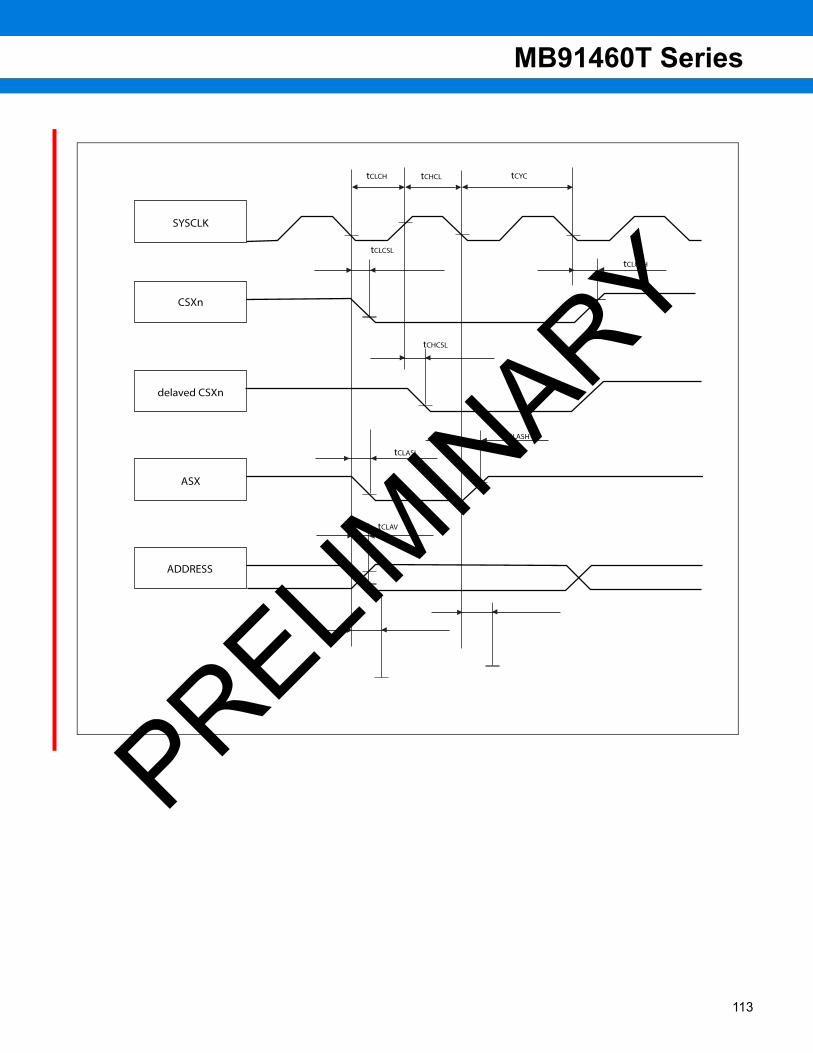
MB91460T Series
SYSCLK
CSXn
delaved CSXn
ASX
ADDRESS
tCHCSL
tCLASL
tCLAV
tCLASH
tCLCSL
tCLCH tCHCL tCYC
tCLCSH
PRELIMIN
ARY
113
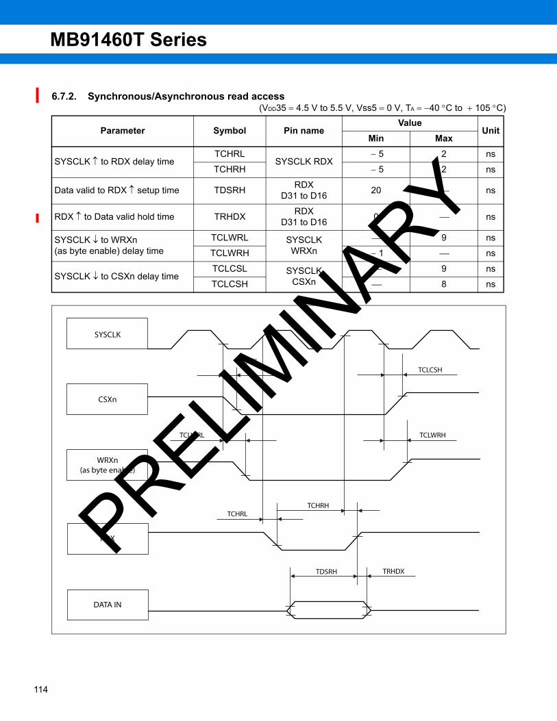
MB91460T Series
114
6.7.2. Synchronous/Asynchronous read access (VDD35 = 4.5 V to 5.5 V, Vss5 = 0 V, TA = −40 °C to + 105 °C)
Parameter Symbol Pin nameValue
UnitMin Max
SYSCLK ↑ to RDX delay timeTCHRL
SYSCLK RDX − 5 2 ns
TCHRH − 5 2 ns
Data valid to RDX ↑ setup time TDSRH RDXD31 to D16 20 ⎯ ns
RDX ↑ to Data valid hold time TRHDX RDXD31 to D16 0 ⎯ ns
SYSCLK ↓ to WRXn (as byte enable) delay time
TCLWRL SYSCLKWRXn
⎯ 9 ns
TCLWRH − 1 ⎯ ns
SYSCLK ↓ to CSXn delay timeTCLCSL SYSCLK
CSXn⎯ 9 ns
TCLCSH ⎯ 8 ns
SYSCLK
CSXn
WRXn(as byte enable)
RDX
DATA IN
TDSRH TRHDX
TCHRHTCHRL
TCLWRL TCLWRH
TCLCSHTCLCSL
PRELIMIN
ARY
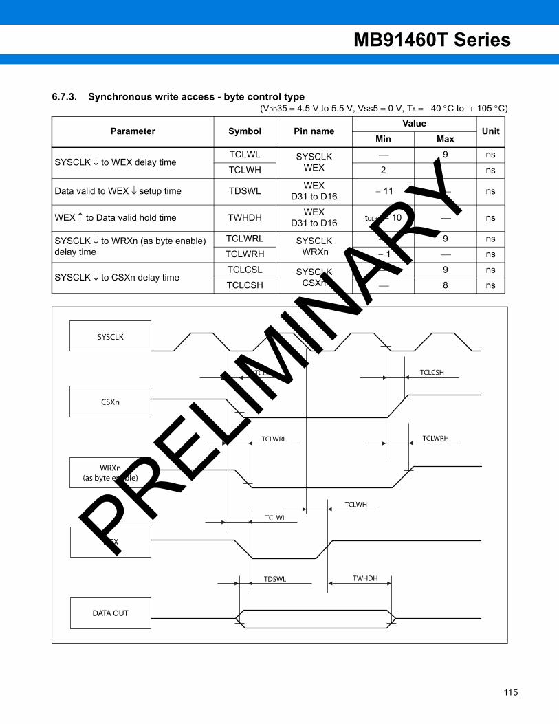
MB91460T Series
6.7.3. Synchronous write access - byte control type (VDD35 = 4.5 V to 5.5 V, Vss5 = 0 V, TA = −40 °C to + 105 °C)
Parameter Symbol Pin nameValue
UnitMin Max
SYSCLK ↓ to WEX delay timeTCLWL SYSCLK
WEX⎯ 9 ns
TCLWH 2 ⎯ ns
Data valid to WEX ↓ setup time TDSWL WEXD31 to D16 − 11 ⎯ ns
WEX ↑ to Data valid hold time TWHDH WEXD31 to D16 tCLKT − 10 ⎯ ns
SYSCLK ↓ to WRXn (as byte enable) delay time
TCLWRL SYSCLK WRXn
⎯ 9 ns
TCLWRH − 1 ⎯ ns
SYSCLK ↓ to CSXn delay timeTCLCSL SYSCLK
CSXn⎯ 9 ns
TCLCSH ⎯ 8 ns
SYSCLK
CSXn
WRXn(as byte enable)
WEX
DATA OUT
TCLWH
TCLWL
TCLWRL
TDSWL TWHDH
TCLWRH
TCLCSHTCLCSL
PRELIMIN
ARY
115

MB91460T Series
116
6.7.4. Synchronous write access - no byte control type (VDD35 = 4.5 V to 5.5 V, Vss5 = 0 V, TA = −40 °C to + 105 °C)
Parameter Symbol Pin nameValue
UnitMin Max
SYSCLK ↓ to WRXn delay timeTCLWRL SYSCLK
WRXn⎯ 9 ns
TCLWRH − 1 ⎯ ns
Data valid to WRXn ↓ setup time TDSWRL WRXnD31 to D16 − 12 ⎯ ns
WRXn ↑ to Data valid hold time TWRHDH WRXnD31 to D16 tCLKT − 8 ⎯ ns
SYSCLK ↓ to CSXn delay timeTCLCSL SYSCLK
CSXn⎯ 9 ns
TCLCSH ⎯ 8 ns
SYSCLK
CSXn
WRXn
DATA OUT
TCLWRH
TCLWRL
TDSWRL TWRHDH
TCLCSHTCLCSL
PRELIMIN
ARY

MB91460T Series
6.7.5. Asynchronous write access - byte control type (VDD35 = 4.5 V to 5.5 V, Vss5 = 0 V, TA = −40 °C to + 105 °C)
Parameter Symbol Pin nameValue
UnitMin Max
WEX ↓ to WEX ↑ pulse width TWLWH WEX tCLKT − 2 ⎯ ns
Data valid to WEX ↓ setup time TDSWL WEXD31 to D16 1/2 × tCLKT − 13 ⎯ ns
WEX ↑ to Data valid hold time TWHDH WEXD31 to D16 1/2 × tCLKT − 10 ⎯ ns
WEX to WRXn delay timeTWRLWL WEX
WRXn⎯ 1/2 × tCLKT + 2 ns
TWHWRH 1/2 × tCLKT − 4 ⎯ ns
WEX to CSXn delay timeTCLWL WEX
CSXn⎯ 1/2 × tCLKT ns
TWHCH 1/2 × tCLKT − 5 ⎯ ns
CSXn
WRXn(as byte enable)
WEX
DATA OUT
TWHDH
TWHWRH
TWHCH
TWRLWL
TWLWH
TCLWL
TDSWL
PRELIMIN
ARY
117
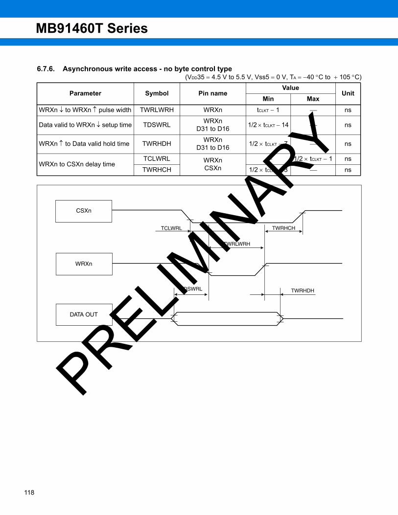
MB91460T Series
118
6.7.6. Asynchronous write access - no byte control type (VDD35 = 4.5 V to 5.5 V, Vss5 = 0 V, TA = −40 °C to + 105 °C)
Parameter Symbol Pin nameValue
UnitMin Max
WRXn ↓ to WRXn ↑ pulse width TWRLWRH WRXn tCLKT − 1 ⎯ ns
Data valid to WRXn ↓ setup time TDSWRL WRXnD31 to D16 1/2 × tCLKT − 14 ⎯ ns
WRXn ↑ to Data valid hold time TWRHDH WRXnD31 to D16 1/2 × tCLKT − 7 ⎯ ns
WRXn to CSXn delay timeTCLWRL WRXn
CSXn⎯ 1/2 × tCLKT − 1 ns
TWRHCH 1/2 × tCLKT − 3 ⎯ ns
CSXn
WRXn
DATA OUT
TWRHDH
TWRHCHTCLWRL
TWRLWRH
TDSWRL
PRELIMIN
ARY

MB91460T Series
6.7.7. RDY waitcycle insertion (VDD35 = 4.5 V to 5.5 V, Vss5 = 0 V, TA = −40 °C to + 105 °C)
Parameter Symbol Pin nameValue
UnitMin Max
RDY setup time TRDYS SYSCLKRDY 21 ⎯ ns
RDY hold time TRDYH SYSCLKRDY 0 ⎯ ns
SYSCLK
RDY
TRDYS TRDYH
PRELIMIN
ARY
119

MB91460T Series
120
6.8. External Bus AC Timings at VDD35 = 3.0 to 4.5 V• Conditions during AC measurements
All AC tests were measured under the following conditions:- IOdrive = 5 mA- VDD35 = 3.0 V to 4.5 V, Iload = 3 mA- VSS5 = 0 V- Ta = − 40 °C to + 105 °C- Cl = 50 pF- VOL = 0.2 × VDD35,
VOH = 0.8 × VDD35- EPILR = 0, PILR = 1 (Automotive Level = worst case)
6.8.1. Basic Timing (VDD35 = 3.0 V to 4.5 V, Vss5 = 0 V, TA = −40 °C to + 105 °C)
Parameter Symbol Pin nameValue
UnitMin Max
SYSCLKTCLCH
SYSCLK1/2 × tCLKT − 13 1/2 × tCLKT + 13 ns
TCHCL 1/2 × tCLKT − 13 1/2 × tCLKT + 13 ns
SYSCLK ↓ to CSXn delay timeTCLCSL
SYSCLKCSXn
⎯ 6 ns
TCLCSH ⎯ 7 ns
SYSCLK ↑ to CSXn delay time(Addr → CS delay) TCHCSL − 11 0 ns
SYSCLK ↓ to ASX delay timeTCLASL SYSCLK
ASX⎯ 6 ns
TCLASH ⎯ 9 ns
SYSCLK ↓ to Address valid delay time TCLAV SYSCLK
A23 to A0 ⎯ 13 ns
PRELIMIN
ARY
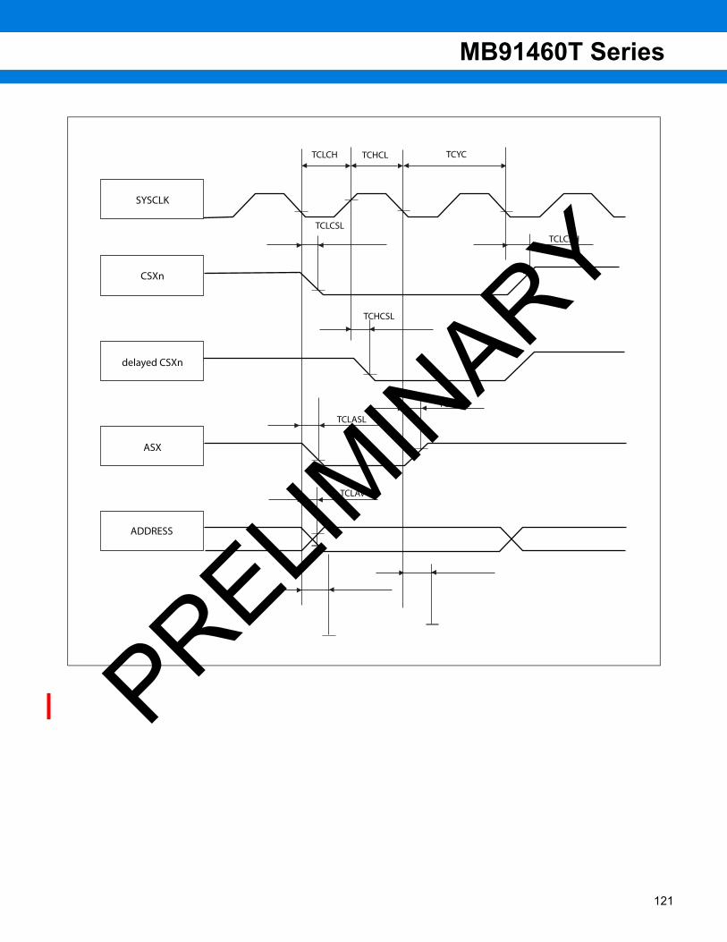
MB91460T Series
SYSCLK
CSXn
delayed CSXn
ASX
ADDRESS
TCHCSL
TCLASL
TCLAV
TCLASH
TCLCSL
TCLCH TCHCL TCYC
TCLCSH
PRELIMIN
ARY
121

MB91460T Series
122
6.8.2. Synchronous/Asynchronous read access (VDD35 = 3.0 V to 4.5 V, Vss5 = 0 V, TA = −40 °C to + 105 °C)
Parameter Symbol Pin nameValue
UnitMin Max
SYSCLK ↑ to RDX delay timeTCHRL
SYSCLK RDX − 12 0 ns
TCHRH − 9 1 ns
Data valid to RDX ↑ setup time TDSRH RDXD31 to D16 29 ⎯ ns
RDX ↑ to Data valid hold time (internal SYSCLK → MCLKI / /MCLKI feedback)
TRHDX RDXD31 to D16 0 ⎯ ns
SYSCLK ↓ to WRXn (as byte enable) delay time
TCLWRL SYSCLKWRXn
⎯ 6 ns
TCLWRH 0 ⎯ ns
SYSCLK ↓ to CSXn delay timeTCLCSL SYSCLK
CSXn⎯ 6 ns
TCLCSH ⎯ 7 ns
SYSCLK
CSXn
WRXn(as byte enable)
RDX
DATA IN
TDSRH TRHDX
TCHRHTCHRL
TCLWRL TCLWRH
TCLCSHTCLCSL
PRELIMIN
ARY

MB91460T Series
6.8.3. Synchronous write access - byte control type (VDD35 = 3.0 V to 4.5 V, Vss5 = 0 V, TA = −40 °C to + 105 °C)
Parameter Symbol Pin nameValue
UnitMin Max
SYSCLK ↓ to WEX delay timeTCLWL SYSCLK
WEX⎯ 7 ns
TCLWH 1 ⎯ ns
Data valid to WEX ↓ setup time TDSWL WEXD31 to D16 − 20 ⎯ ns
WEX ↑ to Data valid hold time TWHDH WEXD31 to D16 tCLKT − 19 ⎯ ns
SYSCLK ↓ to WRXn (as byte enable) delay time
TCLWRL SYSCLKWRXn
⎯ 6 ns
TCLWRH 0 ⎯ ns
SYSCLK ↓ to CSXn delay timeTCLCSL SYSCLK
CSXn⎯ 6 ns
TCLCSH ⎯ 7 ns
SYSCLK
CSXn
WRXn(as byte enable)
WEX
DATA OUT
TCLWH
TCLWL
TCLWRL
TDSWL TWHDH
TCLWRH
TCLCSHTCLCSL
PRELIMIN
ARY
123

MB91460T Series
6.8.4. Synchronous write access - no byte control type (VDD35 = 3.0 V to 4.5 V, Vss5 = 0 V, TA = −40 °C to + 105 °C)
Parameter Symbol Pin nameValue
UnitMin Max
SYSCLK ↓ to WRXn delay timeTCLWRL SYSCLK
WRXn⎯ 6 ns
TCLWRH 0 ⎯ ns
Data valid to WRXn ↓ setup time TDSWRL WRXnD31 to D16 − 20 ⎯ ns
WRXn ↑ to Data valid hold time TWRHDH WRXnD31 to D16 tCLKT − 14 ⎯ ns
SYSCLK ↓ to CSXn delay timeTCLCSL SYSCLK
CSXn⎯ 6 ns
TCLCSH ⎯ 7 ns
SYSCLK
CSXn
WRXn
DATA OUT
TCLWRH
TCLWRL
TDSWRL TWRHDH
TCLCSHTCLCSL
PRELIMIN
ARY

MB91460T Series
6.8.5. Asynchronous write access - byte control type (VDD35 = 3.0 V to 4.5 V, Vss5 = 0 V, TA = −40 °C to + 105 °C)
Parameter Symbol Pin nameValue
UnitMin Max
WEX ↓ to WEX ↑ pulse width TWLWH WEX tCLKT − 2 ⎯ ns
Data valid to WEX ↓ setup time TDSWL WEXD31 to D16 1/2 × tCLKT − 20 ⎯ ns
WEX ↑ to Data valid hold time TWHDH WEXD31 to D16 1/2 × tCLKT − 20 ⎯ ns
WEX to WRXn delay timeTWRLWL WEX
WRXn⎯ 1/2 × tCLKT + 3 ns
TWHWRH 1/2 × tCLKT − 7 ⎯ ns
WEX to CSXn delay timeTCLWL WEX
CSXn⎯ 1/2 × tCLKT − 1 ns
TWHCH 1/2 × tCLKT − 4 ⎯ ns
CSXn
WRXn(as byte enable)
WEX
DATA OUT
TWHDH
TWHWRH
TWHCH
TWRLWL
TWLWH
TCLWL
TDSWL
PRELIMIN
ARY
125

MB91460T Series
126
6.8.6. Asynchronous write access - no byte control type (VDD35 = 3.0 V to 4.5 V, Vss5 = 0 V, TA = −40 °C to + 105 °C)
Parameter Symbol Pin nameValue
UnitMin Max
WRXn ↓ to WRXn ↑ pulse width TWRLWRH WRXn tCLKT − 2 ⎯ ns
Data valid to WRXn ↓ setup time TDSWRL WRXnD31 to D16 1/2 × tCLKT − 21 ⎯ ns
WRXn ↑ to Data valid hold time TWRHDH WRXnD31 to D16 1/2 × tCLKT − 18 ⎯ ns
WRXn to CSXn delay timeTCLWRL WRXn
CSXn⎯ 1/2 × tCLKT − 1 ns
TWRHCH 1/2 × tCLKT − 4 ⎯ ns
CSXn
WRXn
DATA OUT
TWRHDH
TWRHCHTCLWRL
TWRLWRH
TDSWRL
PRELIMIN
ARY

MB91460T Series
6.8.7. RDY waitcycle insertion (VDD35 = 3.0 V to 4.5 V, Vss5 = 0 V, TA = −40 °C to + 105 °C)
Parameter Symbol Pin nameValue
UnitMin Max
RDY setup time TRDYS SYSCLKRDY 37 ⎯ ns
RDY hold time TRDYH SYSCLKRDY 0 ⎯ ns
SYSCLK
RDY
TRDYS TRDYH
PRELIMIN
ARY
127

MB91460T Series
128
ORDERING INFORMATION
Part number Package RemarksMB91F467TAPMC-GSE2MB91F469TAPMC-GSE2
144-pin plastic QFP (FPT-144P-M08) Lead-free package
PRELIMIN
ARY

MB91460T Series
PACKAGE DIMENSION
Please confirm the latest Package dimension by following URL.http://edevice.fujitsu.com/fj/DATASHEET/ef-ovpklv.html
mm 05.0hctip daeLPFQL citsalp nip-441
Package width ×package length
20.0 × 20.0 mm
Lead shape Gullwing
Sealing method Plastic mold
Mounting height 1.70 mm MAX
Weight 1.20g
Code
(Reference)P-LFQFP144-20×20-0.50
144-pin plastic LQFP
(FPT-144P-M08)
(FPT-144P-M08)
C 2003 FUJITSU LIMITED F144019S-c-4-6
Details of "A" part
0.25(.010)
(Stand off)(.004±.004)
0.10±0.10
(.024±.006)
0.60±0.15
(.020±.008)
0.50±0.20
1.50+0.20–0.10
+.008–.004.059
0˚~8˚
0.50(.020)
"A"
0.08(.003)
0.145±0.055
(.006±.002)
LEAD No. 1 36
INDEX
37
72
73108
109
144
0.22±0.05
(.009±.002)M0.08(.003)
20.00±0.10(.787±.004)SQ
22.00±0.20(.866±.008)SQ
(Mounting height)
*
Dimensions in mm (inches).Note: The values in parentheses are reference values.
Note 1) *:Values do not include resin protrusion.
Resin protrusion is +0.25(.010)Max(each side).
Note 2) Pins width and pins thickness include plating thickness.
Note 3) Pins width do not include tie bar cutting remainder.
PRELIMIN
ARY
129

MB91460T Series
130
REVISION HISTORY
Version Date Remark
2.0 2008-09-02 Initial version
PRELIMIN
ARY