f2mc-8fx mb95130/m series hardware manual - fujitsu
TRANSCRIPT
FUJITSU SEMICONDUCTORCONTROLLER MANUAL
F2MC-8FX8-BIT MICROCONTROLLER
MB95130/M SeriesHARDWARE MANUAL
CM26-10113-1E

F2MC-8FX8-BIT MICROCONTROLLER
MB95130/M SeriesHARDWARE MANUAL
“Check Sheet” is seen at the following support page
URL : http://www.fujitsu.com/global/services/microelectronics/product/micom/support/index.html
“Check Sheet” lists the minimal requirement items to be checked to prevent problems beforehand in system development.
Be sure to refer to the “Check Sheet” for the latest cautions on development.
FUJITSU LIMITED

PREFACE
The Purpose and Intended Readership of This ManualThank you very much for your continued special support for Fujitsu semiconductor products.
The MB95130/M series is a line of products developed as general-purpose products in the F2MC-8FX
series of proprietary 8-bit single-chip microcontrollers applicable as application-specific integrated
circuits (ASICs). The MB95130/M series can be used for a wide range of applications from consumer
products including portable devices to industrial equipment.
Intended for engineers who actually develop products using the MB95130/M series of microcontrollers,
this manual describes its functions, features, and operations. You should read through the manual.
For details on individual instructions, refer to the "F2MC-8FX Programming Manual".
Note: F2MC is the abbreviation of FUJITSU Flexible Microcontroller.
TrademarkThe company names and brand names in this document are the trademarks or registered trademarks of
their respective owners.
Sample Programs
Fujitsu provides sample programs free of charge to operate the peripheral resources of the F2MC-8FX
family of microcontrollers. Feel free to use such sample programs to check the operational specifications
and usages of Fujitsu microcontrollers.
Microcontroller support information:
http://www.fujitsu.com/global/services/microelectronics/product/micom/support/
Note that sample programs are subject to change without notice. As these pieces of software are offered
to show standard operations and usages, evaluate them sufficiently before use with your system. Fujitsu
assumes no liability for any damages whatsoever arising out of the use of sample programs.
i
Copyright ©2006 FUJITSU LIMITED All rights reserved.
• The contents of this document are subject to change without notice. Customers are advised to consult with FUJITSU salesrepresentatives before ordering.
• The information, such as descriptions of function and application circuit examples, in this document are presented solelyfor the purpose of reference to show examples of operations and uses of Fujitsu semiconductor device; Fujitsu does notwarrant proper operation of the device with respect to use based on such information. When you develop equipmentincorporating the device based on such information, you must assume any responsibility arising out of such use of theinformation. Fujitsu assumes no liability for any damages whatsoever arising out of the use of the information.
• Any information in this document, including descriptions of function and schematic diagrams, shall not be construed aslicense of the use or exercise of any intellectual property right, such as patent right or copyright, or any other right ofFujitsu or any third party or does Fujitsu warrant non-infringement of any third-party's intellectual property right or otherright by using such information. Fujitsu assumes no liability for any infringement of the intellectual property rights or otherrights of third parties which would result from the use of information contained herein.
• The products described in this document are designed, developed and manufactured as contemplated for general use,including without limitation, ordinary industrial use, general office use, personal use, and household use, but are notdesigned, developed and manufactured as contemplated (1) for use accompanying fatal risks or dangers that, unlessextremely high safety is secured, could have a serious effect to the public, and could lead directly to death, personal injury,severe physical damage or other loss (i.e., nuclear reaction control in nuclear facility, aircraft flight control, air trafficcontrol, mass transport control, medical life support system, missile launch control in weapon system), or (2) for userequiring extremely high reliability (i.e., submersible repeater and artificial satellite). Please note that Fujitsu will not beliable against you and/or any third party for any claims or damages arising in connection with above-mentioned uses of theproducts.
• Any semiconductor devices have an inherent chance of failure. You must protect against injury, damage or loss from suchfailures by incorporating safety design measures into your facility and equipment such as redundancy, fire protection, andprevention of over-current levels and other abnormal operating conditions.
• If any products described in this document represent goods or technologies subject to certain restrictions on export underthe Foreign Exchange and Foreign Trade Law of Japan, the prior authorization by Japanese government will be required forexport of those products from Japan.
ii
CONTENTS
CHAPTER 1 DESCRIPTION ............................................................................................. 11.1 Feature of MB95130/M Series ............................................................................................................ 21.2 Product Lineup of MB95130/M Series ................................................................................................ 41.3 Difference Points among Products and Notes on Selecting a Product ............................................... 61.4 Block Diagram of MB95130/M Series ................................................................................................. 81.5 Pin Assignment ................................................................................................................................... 91.6 Package Dimension .......................................................................................................................... 101.7 Pin Description .................................................................................................................................. 111.8 I/O Circuit Type ................................................................................................................................. 13
CHAPTER 2 HANDLING DEVICES ................................................................................ 152.1 Device Handling Precautions ............................................................................................................ 16
CHAPTER 3 MEMORY SPACE ...................................................................................... 213.1 Memory Space .................................................................................................................................. 22
3.1.1 Areas for Specific Applications .................................................................................................... 243.2 Memory Map ..................................................................................................................................... 25
CHAPTER 4 MEMORY ACCESS MODE ........................................................................ 274.1 Memory Access Mode ...................................................................................................................... 28
CHAPTER 5 CPU ............................................................................................................ 295.1 Dedicated Registers ......................................................................................................................... 30
5.1.1 Register Bank Pointer (RP) ......................................................................................................... 325.1.2 Direct Bank Pointer (DP) ............................................................................................................. 335.1.3 Condition Code Register (CCR) .................................................................................................. 35
5.2 General-purpose Registers ............................................................................................................... 375.3 Placement of 16-bit Data in Memory ................................................................................................ 39
CHAPTER 6 CLOCK CONTROLLER ............................................................................. 416.1 Overview of Clock Controller ............................................................................................................ 426.2 Oscillation Stabilization Wait Time .................................................................................................... 486.3 System Clock Control Register (SYCC) ........................................................................................... 506.4 PLL Control Register (PLLC) ............................................................................................................ 526.5 Oscillation Stabilization Wait Time Setting Register (WATR) ........................................................... 556.6 Standby Control Register (STBC) ..................................................................................................... 586.7 Clock Modes ..................................................................................................................................... 616.8 Operations in Low-power Consumption Modes (Standby Modes) ................................................... 66
6.8.1 Notes on Using Standby Mode .................................................................................................... 676.8.2 Sleep Mode ................................................................................................................................. 716.8.3 Stop Mode ................................................................................................................................... 726.8.4 Timebase Timer Mode ................................................................................................................. 73
iii
6.8.5 Watch Mode ................................................................................................................................ 746.9 Clock Oscillator Circuits .................................................................................................................... 756.10 Overview of Prescaler ....................................................................................................................... 776.11 Configuration of Prescaler ................................................................................................................ 786.12 Operating Explanation of Prescaler .................................................................................................. 796.13 Notes on Use of Prescaler ................................................................................................................ 80
CHAPTER 7 RESET ........................................................................................................ 817.1 Reset Operation ................................................................................................................................ 827.2 Reset Source Register (RSRR) ........................................................................................................ 86
CHAPTER 8 INTERRUPTS ............................................................................................. 898.1 Interrupts ........................................................................................................................................... 90
8.1.1 Interrupt Level Setting Registers (ILR0 to ILR5) .......................................................................... 928.1.2 Interrupt Processing .................................................................................................................... 938.1.3 Nested Interrupts ......................................................................................................................... 958.1.4 Interrupt Processing Time ........................................................................................................... 968.1.5 Stack Operations During Interrupt Processing ............................................................................ 978.1.6 Interrupt Processing Stack Area .................................................................................................. 98
CHAPTER 9 I/O PORT .................................................................................................... 999.1 Overview of I/O Ports ...................................................................................................................... 1009.2 Port 0 .............................................................................................................................................. 101
9.2.1 Port 0 Registers ......................................................................................................................... 1049.2.2 Operations of Port 0 .................................................................................................................. 105
9.3 Port 1 .............................................................................................................................................. 1079.3.1 Port 1 Registers ......................................................................................................................... 1099.3.2 Operations of Port 1 .................................................................................................................. 110
9.4 Port F .............................................................................................................................................. 1129.4.1 Port F Registers ......................................................................................................................... 1149.4.2 Operations of Port F .................................................................................................................. 115
9.5 Port G ............................................................................................................................................. 1179.5.1 Port G Registers ........................................................................................................................ 1199.5.2 Operations of Port G .................................................................................................................. 120
CHAPTER 10 TIMEBASE TIMER ................................................................................... 12310.1 Overview of Timebase Timer .......................................................................................................... 12410.2 Configuration of Timebase Timer ................................................................................................... 12510.3 Registers of the Timebase Timer .................................................................................................... 127
10.3.1 Timebase Timer Control Register (TBTC) ................................................................................. 12810.4 Interrupts of Timebase Timer .......................................................................................................... 13010.5 Explanation of Timebase Timer Operations and Setup Procedure Example ................................. 13210.6 Precautions when Using Timebase Timer ...................................................................................... 135
CHAPTER 11 WATCHDOG TIMER ................................................................................ 13711.1 Overview of Watchdog Timer ......................................................................................................... 13811.2 Configuration of Watchdog Timer ................................................................................................... 139
iv
11.3 Registers of the Watchdog Timer ................................................................................................... 14111.3.1 Watchdog Timer Control Register (WDTC) ............................................................................... 142
11.4 Explanation of Watchdog Timer Operations and Setup Procedure Example ................................. 14411.5 Precautions when Using Watchdog Timer ...................................................................................... 146
CHAPTER 12 WATCH PRESCALER ............................................................................. 14712.1 Overview of Watch Prescaler ......................................................................................................... 14812.2 Configuration of Watch Prescaler ................................................................................................... 14912.3 Registers of the Watch Prescaler ................................................................................................... 151
12.3.1 Watch Prescaler Control Register (WPCR) ............................................................................... 15212.4 Interrupts of Watch Prescaler ......................................................................................................... 15412.5 Explanation of Watch Prescaler Operations and Setup Procedure Example ................................. 15612.6 Precautions when Using Watch Prescaler ...................................................................................... 15812.7 Sample Programs for Watch Prescaler .......................................................................................... 159
CHAPTER 13 WATCH COUNTER .................................................................................. 16113.1 Overview of Watch Counter ............................................................................................................ 16213.2 Configuration of Watch Counter ..................................................................................................... 16313.3 Registers of Watch Counter ............................................................................................................ 165
13.3.1 Watch Counter Data Register (WCDR) ..................................................................................... 16613.3.2 Watch Counter Control Register (WCSR) ................................................................................. 167
13.4 Interrupts of Watch Counter ............................................................................................................ 16913.5 Explanation of Watch Counter Operations and Setup Procedure Example ................................... 17013.6 Precautions when Using Watch Counter ........................................................................................ 17213.7 Sample Programs for Watch Counter ............................................................................................. 173
CHAPTER 14 WILD REGISTER ..................................................................................... 17514.1 Overview of Wild Register .............................................................................................................. 17614.2 Configuration of Wild Register ........................................................................................................ 17714.3 Registers of Wild Register .............................................................................................................. 179
14.3.1 Wild Register Data Setup Registers (WRDR0 to WRDR2) ....................................................... 18114.3.2 Wild Register Address Setup Registers (WRAR0 to WRAR2) .................................................. 18214.3.3 Wild Register Address Compare Enable Register (WREN) ...................................................... 18314.3.4 Wild Register Data Test Setup Register (WROR) ..................................................................... 184
14.4 Operating Description of Wild Register ........................................................................................... 18514.5 Typical Hardware Connection Example .......................................................................................... 186
CHAPTER 15 8/16-BIT COMPOUND TIMER ................................................................. 18715.1 Overview of 8/16-bit Compound Timer ........................................................................................... 18815.2 Configuration of 8/16-bit Compound Timer ..................................................................................... 19015.3 Channels of 8/16-bit Compound Timer ........................................................................................... 19315.4 Pins of 8/16-bit Compound Timer ................................................................................................... 19415.5 Registers of 8/16-bit Compound Timer ........................................................................................... 196
15.5.1 8/16-bit Compound Timer 00/01 Control Status Register 0 (T00CR0/T01CR0) ........................ 19715.5.2 8/16-bit Compound Timer 00/01 Control Status Register 1 (T00CR1/T01CR1) ........................ 20015.5.3 8/16-bit Compound Timer 00/01 Timer Mode Control Register ch.0 (TMCR0) ......................... 20315.5.4 8/16-bit Compound Timer 00/01 Data Register ch.0 (T00DR/T01DR) ...................................... 206
v
15.6 Interrupts of 8/16-bit Compound Timer ........................................................................................... 20915.7 Operating Description of Interval Timer Function (One-shot Mode) ............................................... 21115.8 Operating Description of Interval Timer Function (Continuous Mode) ............................................ 21315.9 Operating Description of Interval Timer Function (Free-run Mode) ................................................ 21515.10 Operating Description of PWM Timer Function (Fixed-cycle mode) ............................................... 21715.11 Operating Description of PWM Timer Function (Variable-cycle Mode) .......................................... 21915.12 Operating Description of PWC Timer Function ............................................................................... 22115.13 Operating Description of Input Capture Function ........................................................................... 22315.14 Operating Description of Noise Filter .............................................................................................. 22515.15 States in Each Mode during Operation ........................................................................................... 22615.16 Precautions when Using 8/16-bit Compound Timer ....................................................................... 228
CHAPTER 16 8/16-BIT PPG ........................................................................................... 22916.1 Overview of 8/16-bit PPG ............................................................................................................... 23016.2 Configuration of 8/16-bit PPG ......................................................................................................... 23116.3 Channels of 8/16-bit PPG ............................................................................................................... 23316.4 Pins of 8/16-bit PPG ....................................................................................................................... 23416.5 Registers of 8/16-bit PPG ............................................................................................................... 236
16.5.1 8/16-bit PPG Timer 01 Control Register ch.0 (PC01) ................................................................ 23716.5.2 8/16-bit PPG Timer 00 Control Register ch.0 (PC00) ................................................................ 23916.5.3 8/16-bit PPG Timer 00/01 Cycle Setup Buffer Register (PPS01/PPS00) .................................. 24116.5.4 8/16-bit PPG Timer 00/01 Duty Setup Buffer Register (PDS01/PDS00) ................................... 24216.5.5 8/16-bit PPG Start Register (PPGS) .......................................................................................... 24316.5.6 8/16-bit PPG Output Inversion Register (REVC) ....................................................................... 244
16.6 Interrupts of 8/16-bit PPG ............................................................................................................... 24516.7 Operating Description of 8/16-bit PPG ........................................................................................... 246
16.7.1 8-bit PPG Independent Mode .................................................................................................... 24716.7.2 8-bit Prescaler + 8-bit PPG Mode .............................................................................................. 24916.7.3 16-bit PPG Mode ....................................................................................................................... 251
16.8 Precautions when Using 8/16-bit PPG ........................................................................................... 25316.9 Sample Programs for 8/16-bit PPG Timer ...................................................................................... 254
CHAPTER 17 16-BIT PPG TIMER .................................................................................. 25717.1 Overview of 16-bit PPG Timer ........................................................................................................ 25817.2 Configuration of 16-bit PPG Timer .................................................................................................. 25917.3 Channels of 16-bit PPG Timer ........................................................................................................ 26117.4 Pins of 16-bit PPG Timer ................................................................................................................ 26217.5 Registers of 16-bit PPG Timer ........................................................................................................ 263
17.5.1 16- bit PPG Down Counter Registers (PDCRH0, PDCRL0) ...................................................... 26417.5.2 16-bit PPG Cycle Setting Buffer Registers (PCSRH0, PCSRL0) .............................................. 26517.5.3 16-bit PPG Duty Setting Buffer Registers (PDUTH0, PDUTL0) ................................................ 26617.5.4 16-bit PPG Status Control Register (PCNTH0, PCNTL0) ......................................................... 267
17.6 Interrupts of 16-bit PPG Timer ........................................................................................................ 27117.7 Explanation of 16-bit PPG Timer Operations and Setup Procedure Example ................................ 27217.8 Precautions when Using 16-bit PPG Timer .................................................................................... 27617.9 Sample Programs for 16-bit PPG Timer ......................................................................................... 277
vi
CHAPTER 18 EXTERNAL INTERRUPT CIRCUIT ......................................................... 28118.1 Overview of External Interrupt Circuit ............................................................................................. 28218.2 Configuration of External Interrupt Circuit ....................................................................................... 28318.3 Channels of External Interrupt Circuit ............................................................................................. 28418.4 Pins of External Interrupt Circuit ..................................................................................................... 28518.5 Registers of External Interrupt Circuit ............................................................................................. 286
18.5.1 External Interrupt Control Register (EIC00) ............................................................................... 28718.6 Interrupts of External Interrupt Circuit ............................................................................................. 28918.7 Explanation of External Interrupt Circuit Operations and Setup Procedure Example ..................... 29018.8 Precautions when Using External Interrupt Circuit ......................................................................... 29218.9 Sample Programs for External Interrupt Circuit .............................................................................. 293
CHAPTER 19 INTERRUPT PIN SELECTION CIRCUIT ................................................. 29519.1 Overview of Interrupt Pin Selection Circuit ..................................................................................... 29619.2 Configuration of Interrupt Pin Selection Circuit ............................................................................... 29719.3 Pins of Interrupt Pin Selection Circuit ............................................................................................. 29819.4 Registers of Interrupt Pin Selection Circuit ..................................................................................... 299
19.4.1 Interrupt Pin Selection Circuit Control Register (WICR) ............................................................ 30019.5 Operating Description of Interrupt Pin Selection Circuit ................................................................. 30319.6 Precautions when Using Interrupt Pin Selection Circuit ................................................................. 304
CHAPTER 20 UART/SIO ................................................................................................. 30520.1 Overview of UART/SIO ................................................................................................................... 30620.2 Configuration of UART/SIO ............................................................................................................ 30720.3 Channels of UART/SIO ................................................................................................................... 30920.4 Pins of UART/SIO ........................................................................................................................... 31020.5 Registers of UART/SIO ................................................................................................................... 312
20.5.1 UART/SIO Serial Mode Control Register 1 (SMC10) ................................................................ 31320.5.2 UART/SIO Serial Mode Control Register 2 (SMC20) ................................................................ 31520.5.3 UART/SIO Serial Status and Data Register (SSR0) ................................................................. 31720.5.4 UART/SIO Serial Input Data Register (RDR0) .......................................................................... 31920.5.5 UART/SIO Serial Output Data Register (TDR0) ........................................................................ 320
20.6 Interrupts of UART/SIO ................................................................................................................... 32120.7 Explanation of UART/SIO Operations and Setup Procedure Example .......................................... 322
20.7.1 Operating Description of Operation Mode 0 .............................................................................. 32320.7.2 Operating Description of Operation Mode 1 .............................................................................. 330
20.8 Sample Programs for UART/SIO .................................................................................................... 336
CHAPTER 21 UART/SIO DEDICATED BAUD RATE GENERATOR ............................. 34121.1 Overview of UART/SIO Dedicated Baud Rate Generator .............................................................. 34221.2 Channels of UART/SIO Dedicated Baud Rate Generator .............................................................. 34321.3 Registers of UART/SIO Dedicated Baud Rate Generator .............................................................. 344
21.3.1 UART/SIO Dedicated Baud Rate Generator Prescaler Selection Register (PSSR) .................. 34521.3.2 UART/SIO Dedicated Baud Rate Generator Baud Rate Setting Register (BRSR) ................... 346
21.4 Operating Description of UART/SIO Dedicated Baud Rate Generator ........................................... 347
vii
CHAPTER 22 LIN-UART ................................................................................................. 34922.1 Overview of LIN-UART ................................................................................................................... 35022.2 Configuration of LIN-UART ............................................................................................................. 35222.3 LIN-UART Pins ............................................................................................................................... 35722.4 Registers of LIN-UART ................................................................................................................... 358
22.4.1 LIN-UART Serial Control Register (SCR) .................................................................................. 35922.4.2 LIN-UART Serial Mode Register (SMR) .................................................................................... 36122.4.3 LIN-UART Serial Status Register (SSR) ................................................................................... 36322.4.4 LIN-UART Reception Data Register/LIN-UART Transmit Data Register (RDR/TDR) ............... 36522.4.5 LIN-UART Extended Status Control Register (ESCR) .............................................................. 36722.4.6 LIN-UART Extended Communication Control Register (ECCR) ............................................... 36922.4.7 LIN-UART Baud Rate Generator Register 0, 1 (BGR 0/1) ........................................................ 371
22.5 LIN-UART Interrupt ......................................................................................................................... 37222.5.1 Timing of Reception Interrupt Generation and Flag Set ............................................................ 37622.5.2 Timing of transmit interrupt generation and flag set .................................................................. 378
22.6 LIN-UART Baud Rate ..................................................................................................................... 38022.6.1 Baud Rate Setting ..................................................................................................................... 38222.6.2 Reload Counter ......................................................................................................................... 386
22.7 Operations and Setting Procedure Example of LIN-UART ............................................................. 38822.7.1 Operation of Asynchronous Mode (Operation Mode 0, 1) ......................................................... 39022.7.2 Operation of Synchronous Mode (Operation Mode 2) ............................................................... 39422.7.3 Operation of LIN function (Operation Mode 3) .......................................................................... 39822.7.4 Serial Pin Direct Access ............................................................................................................ 40122.7.5 Bidirectional Communication Function (Normal Mode) ............................................................. 40222.7.6 Master/Slave Mode Communication Function (Multiprocessor Mode) ...................................... 40422.7.7 LIN Communication Function .................................................................................................... 40722.7.8 Example of LIN-UART LIN Communication Flowchart (Operation Mode 3) .............................. 408
22.8 Notes on Using LIN-UART .............................................................................................................. 41022.9 Sample Programs of LIN-UART ..................................................................................................... 412
CHAPTER 23 8/10-BIT A/D CONVERTER ..................................................................... 41723.1 Overview of 8/10-bit A/D Converter ................................................................................................ 41823.2 Configuration of 8/10-bit A/D Converter .......................................................................................... 41923.3 Pins of 8/10-bit A/D Converter ........................................................................................................ 42123.4 Registers of 8/10-bit A/D Converter ................................................................................................ 423
23.4.1 8/10-bit A/D Converter Control Register 1 (ADC1) .................................................................... 42423.4.2 8/10-bit A/D Converter Control Register 2 (ADC2) .................................................................... 42623.4.3 8/10-bit A/D Converter Data Registers Upper/Lower (ADDH, ADDL) ....................................... 428
23.5 Interrupts of 8/10-bit A/D Converter ................................................................................................ 42923.6 Operations of 8/10-bit A/D Converter and Its Setup Procedure Examples ..................................... 43023.7 Notes on Use of 8/10-bit A/D Converter ......................................................................................... 43323.8 Sample Programs for 8/10-bit A/D Converter ................................................................................. 434
viii
CHAPTER 24 LOW-VOLTAGE DETECTION RESET CIRCUIT ..................................... 43724.1 Overview of Low-voltage Detection Reset Circuit ........................................................................... 43824.2 Configuration of Low-voltage Detection Reset Circuit .................................................................... 43924.3 Pins of Low-voltage Detection Reset Circuit ................................................................................... 44024.4 Operations of Low-voltage Detection Reset Circuit ........................................................................ 441
CHAPTER 25 256-KBIT FLASH MEMORY .................................................................... 44325.1 Overview of 256-Kbit Flash Memory ............................................................................................... 44425.2 Sector Configuration of Flash Memory ........................................................................................... 44525.3 Register of Flash Memory ............................................................................................................... 446
25.3.1 Flash Memory Status Register (FSR) ........................................................................................ 44725.4 Starting the Flash Memory Automatic Algorithm ............................................................................ 44925.5 Checking the Automatic Algorithm Execution Status ...................................................................... 451
25.5.1 Data Polling Flag (DQ7) ............................................................................................................ 45325.5.2 Toggle Bit Flag (DQ6) ................................................................................................................ 45425.5.3 Execution Time-out Flag (DQ5) ................................................................................................. 45525.5.4 Toggle Bit 2 Flag (DQ2) ............................................................................................................. 456
25.6 Details of Programming/Erasing Flash Memory ............................................................................. 45725.6.1 Placing Flash Memory in the Read/Reset State ........................................................................ 45825.6.2 Programming Data into Flash Memory ...................................................................................... 45925.6.3 Erasing All Data from Flash Memory (Chip Erase) .................................................................... 461
25.7 Features of Flash Security .............................................................................................................. 462
CHAPTER 26 EXAMPLE OF SERIAL PROGRAMMING CONNECTION ...................... 46326.1 Basic Configuration of MB95F136MS, NS/MW, NW Serial Programming Connection .................. 46426.2 Example of Serial Programming Connection .................................................................................. 46726.3 Example of Minimum Connection to Flash Microcomputer Programmer ....................................... 469
APPENDIX ......................................................................................................................... 471APPENDIX A I/O Map ................................................................................................................................ 472APPENDIX B Table of Interrupt Causes .................................................................................................... 476APPENDIX C Memory Map ........................................................................................................................ 477APPENDIX D Pin Status of MB95130/M series .......................................................................................... 479APPENDIX E Instruction Overview ............................................................................................................ 481APPENDIX F Mask Option ........................................................................................................................ 497APPENDIX G Writing to Flash Microcontroller Using Parallel Writer .......................................................... 499
Index .................................................................................................................................... 501
Register Index..................................................................................................................... 525
Pin Function Index ............................................................................................................. 527
Interrupt Vector Index ........................................................................................................ 528
ix

x

Main changes in this edition
Page Changes (For details, refer to main body.)
- First edition
xi

xii
CHAPTER 1DESCRIPTION
This chapter explains a feature and a basic specification of the MB95130/M series.
1.1 Feature of MB95130/M Series
1.2 Product Lineup of MB95130/M Series
1.3 Difference Points among Products and Notes on Selecting a Product
1.4 Block Diagram of MB95130/M Series
1.5 Pin Assignment
1.6 Package Dimension
1.7 Pin Description
1.8 I/O Circuit Type
1
CHAPTER 1 DESCRIPTION
1.1 Feature of MB95130/M Series
In addition to a compact instruction set, the MB95130/M series is a general-purpose single-chip microcontroller built-in abundant peripheral functions.
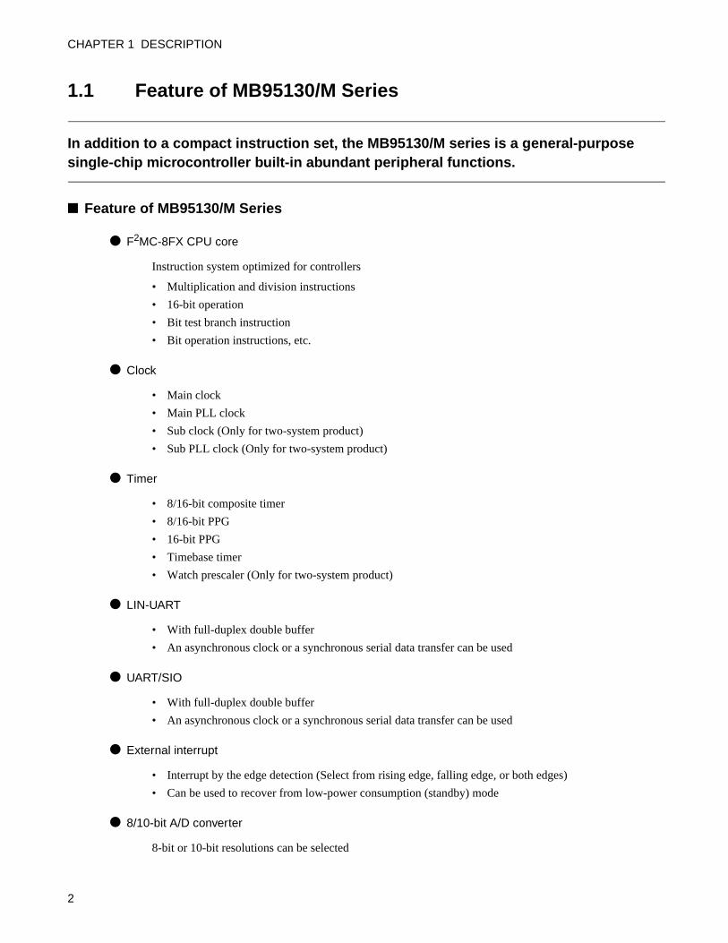
Feature of MB95130/M Series
F2MC-8FX CPU core
Instruction system optimized for controllers
• Multiplication and division instructions
• 16-bit operation
• Bit test branch instruction
• Bit operation instructions, etc.
Clock
• Main clock
• Main PLL clock
• Sub clock (Only for two-system product)
• Sub PLL clock (Only for two-system product)
Timer
• 8/16-bit composite timer
• 8/16-bit PPG
• 16-bit PPG
• Timebase timer
• Watch prescaler (Only for two-system product)
LIN-UART
• With full-duplex double buffer
• An asynchronous clock or a synchronous serial data transfer can be used
UART/SIO
• With full-duplex double buffer
• An asynchronous clock or a synchronous serial data transfer can be used
External interrupt
• Interrupt by the edge detection (Select from rising edge, falling edge, or both edges)
• Can be used to recover from low-power consumption (standby) mode
8/10-bit A/D converter
8-bit or 10-bit resolutions can be selected
2
CHAPTER 1 DESCRIPTION
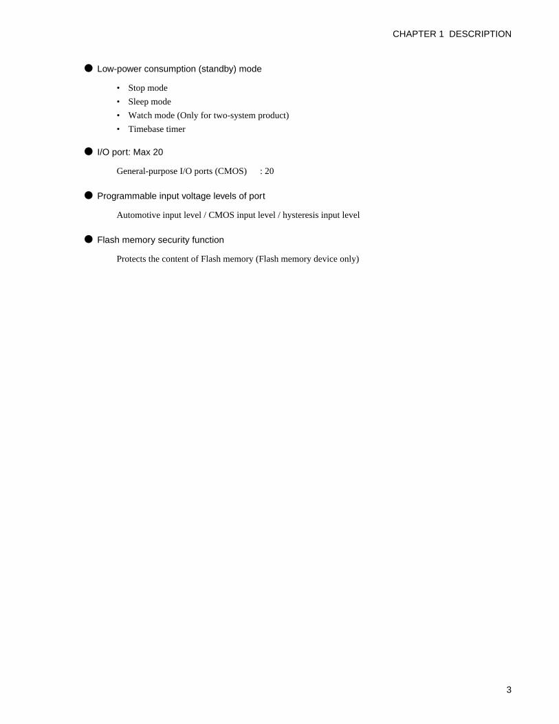
Low-power consumption (standby) mode
• Stop mode
• Sleep mode
• Watch mode (Only for two-system product)
• Timebase timer
I/O port: Max 20
General-purpose I/O ports (CMOS) : 20
Programmable input voltage levels of port
Automotive input level / CMOS input level / hysteresis input level
Flash memory security function
Protects the content of Flash memory (Flash memory device only)
3
CHAPTER 1 DESCRIPTION
1.2 Product Lineup of MB95130/M Series
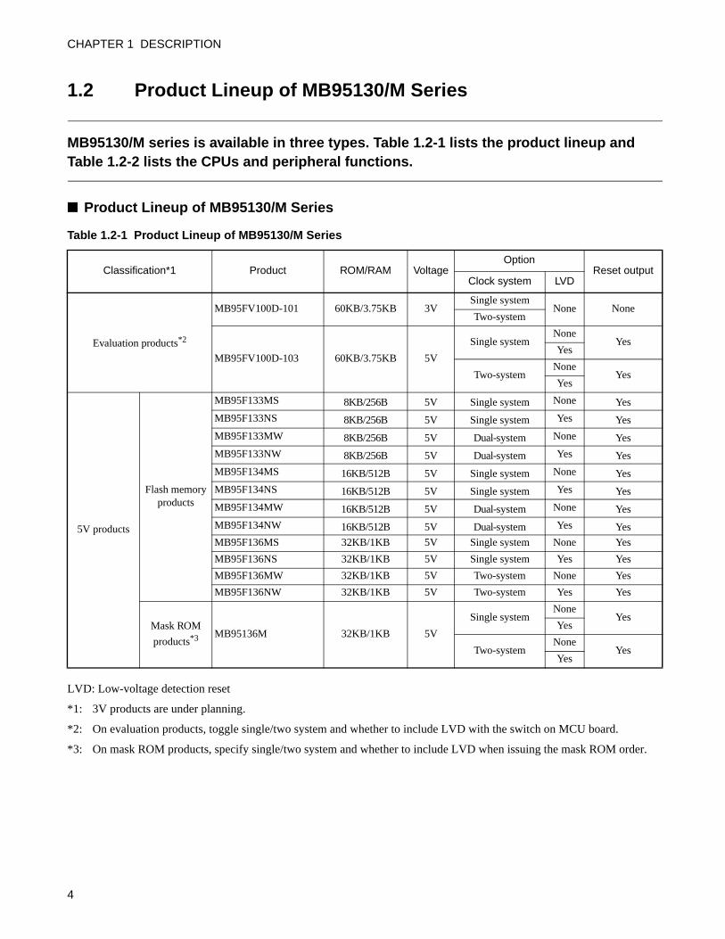
MB95130/M series is available in three types. Table 1.2-1 lists the product lineup and Table 1.2-2 lists the CPUs and peripheral functions.
Product Lineup of MB95130/M Series
LVD: Low-voltage detection reset
*1: 3V products are under planning.
*2: On evaluation products, toggle single/two system and whether to include LVD with the switch on MCU board.
*3: On mask ROM products, specify single/two system and whether to include LVD when issuing the mask ROM order.
Table 1.2-1 Product Lineup of MB95130/M Series
Classification*1 Product ROM/RAM VoltageOption
Reset outputClock system LVD
Evaluation products*2
MB95FV100D-101 60KB/3.75KB 3VSingle system
None NoneTwo-system
MB95FV100D-103 60KB/3.75KB 5V
Single systemNone
YesYes
Two-systemNone
YesYes
5V products
Flash memory products
MB95F133MS 8KB/256B 5V Single system None Yes
MB95F133NS 8KB/256B 5V Single system Yes Yes
MB95F133MW 8KB/256B 5V Dual-system None Yes
MB95F133NW 8KB/256B 5V Dual-system Yes Yes
MB95F134MS 16KB/512B 5V Single system None Yes
MB95F134NS 16KB/512B 5V Single system Yes Yes
MB95F134MW 16KB/512B 5V Dual-system None Yes
MB95F134NW 16KB/512B 5V Dual-system Yes Yes
MB95F136MS 32KB/1KB 5V Single system None Yes
MB95F136NS 32KB/1KB 5V Single system Yes Yes
MB95F136MW 32KB/1KB 5V Two-system None Yes
MB95F136NW 32KB/1KB 5V Two-system Yes Yes
Mask ROM
products*3 MB95136M 32KB/1KB 5V
Single systemNone
YesYes
Two-systemNone
YesYes
4
CHAPTER 1 DESCRIPTION
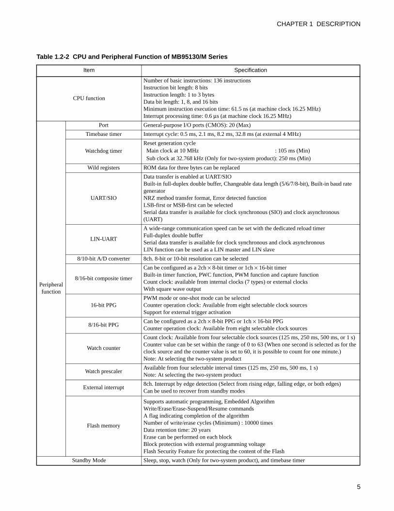
Table 1.2-2 CPU and Peripheral Function of MB95130/M Series
Item Specification
CPU function
Number of basic instructions: 136 instructionsInstruction bit length: 8 bitsInstruction length: 1 to 3 bytesData bit length: 1, 8, and 16 bitsMinimum instruction execution time: 61.5 ns (at machine clock 16.25 MHz)Interrupt processing time: 0.6 µs (at machine clock 16.25 MHz)
Peripheral function
Port General-purpose I/O ports (CMOS): 20 (Max)
Timebase timer Interrupt cycle: 0.5 ms, 2.1 ms, 8.2 ms, 32.8 ms (at external 4 MHz)
Watchdog timerReset generation cycle Main clock at 10 MHz : 105 ms (Min) Sub clock at 32.768 kHz (Only for two-system product): 250 ms (Min)
Wild registers ROM data for three bytes can be replaced
UART/SIO
Data transfer is enabled at UART/SIOBuilt-in full-duplex double buffer, Changeable data length (5/6/7/8-bit), Built-in baud rate generatorNRZ method transfer format, Error detected functionLSB-first or MSB-first can be selectedSerial data transfer is available for clock synchronous (SIO) and clock asynchronous (UART)
LIN-UART
A wide-range communication speed can be set with the dedicated reload timerFull-duplex double bufferSerial data transfer is available for clock synchronous and clock asynchronousLIN function can be used as a LIN master and LIN slave
8/10-bit A/D converter 8ch. 8-bit or 10-bit resolution can be selected
8/16-bit composite timer
Can be configured as a 2ch × 8-bit timer or 1ch × 16-bit timerBuilt-in timer function, PWC function, PWM function and capture functionCount clock: available from internal clocks (7 types) or external clocksWith square wave output
16-bit PPGPWM mode or one-shot mode can be selectedCounter operation clock: Available from eight selectable clock sourcesSupport for external trigger activation
8/16-bit PPGCan be configured as a 2ch × 8-bit PPG or 1ch × 16-bit PPGCounter operation clock: Available from eight selectable clock sources
Watch counter
Count clock: Available from four selectable clock sources (125 ms, 250 ms, 500 ms, or 1 s)Counter value can be set within the range of 0 to 63 (When one second is selected as for the clock source and the counter value is set to 60, it is possible to count for one minute.)Note: At selecting the two-system product
Watch prescalerAvailable from four selectable interval times (125 ms, 250 ms, 500 ms, 1 s)Note: At selecting the two-system product
External interrupt8ch. Interrupt by edge detection (Select from rising edge, falling edge, or both edges)Can be used to recover from standby modes
Flash memory
Supports automatic programming, Embedded AlgorithmWrite/Erase/Erase-Suspend/Resume commandsA flag indicating completion of the algorithmNumber of write/erase cycles (Minimum) : 10000 timesData retention time: 20 yearsErase can be performed on each blockBlock protection with external programming voltageFlash Security Feature for protecting the content of the Flash
Standby Mode Sleep, stop, watch (Only for two-system product), and timebase timer
5
CHAPTER 1 DESCRIPTION
1.3 Difference Points among Products and Notes on Selecting a Product
The following describes differences among MB95130/M series products and notes when selecting the product.
Difference Points among Products and Notes on Selecting a Product
Notes on using evaluation products
The evaluation products are intended to support software development for a number of different F2MC-8FX
family series and products, and it therefore includes additional functions that may not be included in
MB95130/M series. Accordingly, access to I/O address of peripheral functions that are not used in
MB95130/M series is prohibited.
Reading or writing to these prohibited addresses may cause these unused peripheral functions to operate
and lead to unexpected hardware or software problems.
Take particular care not to use word access to read or write odd numbered bytes in the prohibited areas (It
causes unexpected read/write operation).
Also, as the read values of prohibited addresses on the evaluation product are different to the values on the
flash memory and mask ROM products, do not use these values in the program.
The functions corresponding to certain bits in single-byte registers may not be supported on some mask
ROM and flash memory products. However, reading or writing to these bits will not cause malfunction of
the hardware. Also, as the evaluation, flash memory, and mask ROM products are designed to have
identical software operation, no particular precautions are required.
Difference of memory space
If the memory size on the evaluation product is different to the flash memory or mask ROM product, please
ensure you understand these differences when developing software.
Current consumption
The current consumption of flash memory products is greater than for mask ROM products.
For the details of current consumption, refer to "ELECTRICAL CHARACTERISTICS" in data sheet.
Package
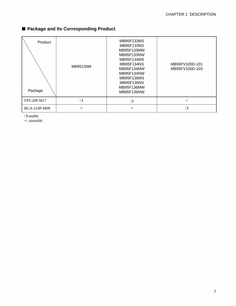
For detailed information on each package, see "Package and Its Corresponding Product" and "1.6
Package Dimension".
Operating voltage
The operating voltage may be different depending on the products. For the details, see "ELECTRICAL
CHARACTERISTICS" in "data sheet".
Difference of MOD pin
For mask ROM products, a pull-down resistor is provided for the MOD pin.
6
CHAPTER 1 DESCRIPTION
Package and Its Corresponding Product
MB95136M
MB95F133MSMB95F133NSMB95F133MWMB95F133NWMB95F134MSMB95F134NSMB95F134MWMB95F134NWMB95F136MSMB95F136NSMB95F136MWMB95F136NW
MB95FV100D-101MB95FV100D-103
FPT-28P-M17 ×
BGA-224P-M08 × ×
:usable×: unusable
Product
Package
7
CHAPTER 1 DESCRIPTION
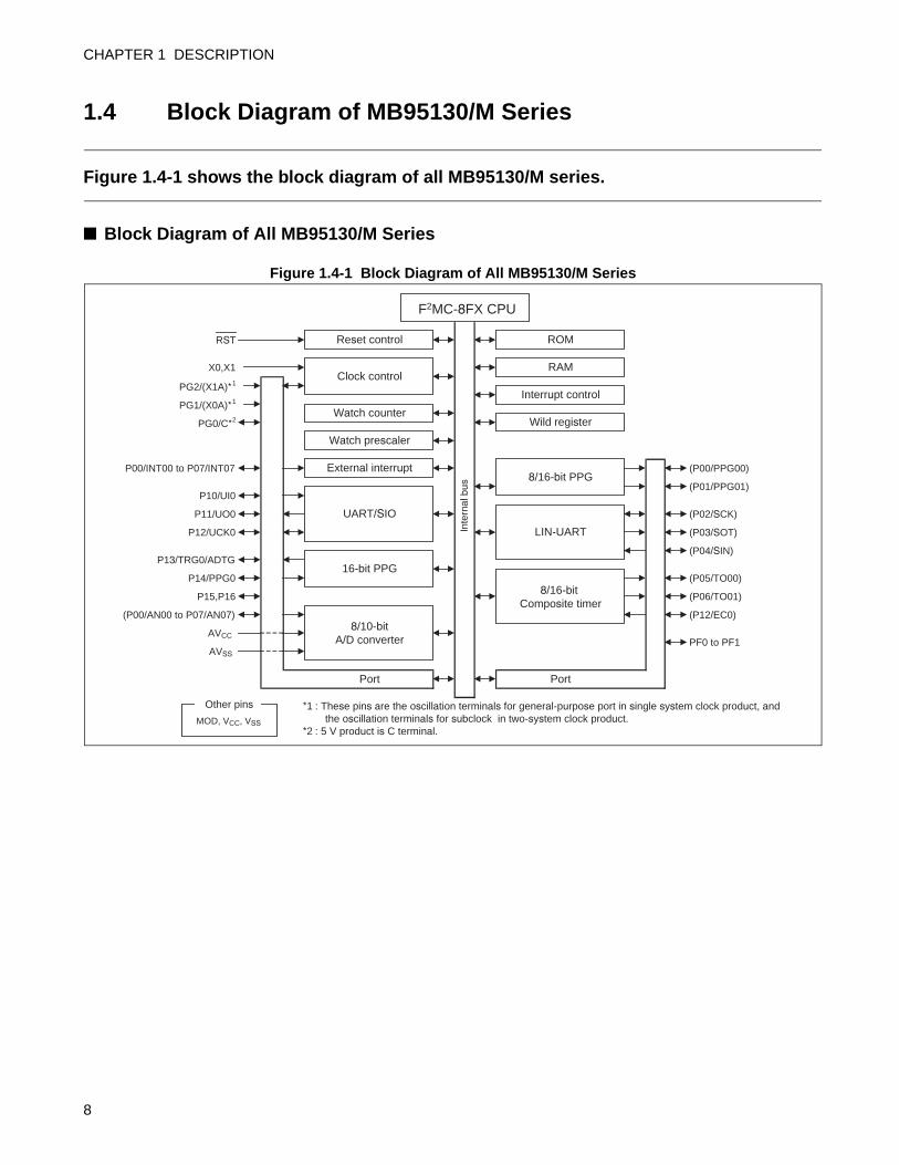
1.4 Block Diagram of MB95130/M Series
Figure 1.4-1 shows the block diagram of all MB95130/M series.
Block Diagram of All MB95130/M Series
Figure 1.4-1 Block Diagram of All MB95130/M Series
AVCC
AVSS
(P06/TO01)
(P12/EC0)
PF0 to PF1
Port
Inte
rnal
bus
Port
(P05/TO00)
(P04/SIN)
(P02/SCK)
(P00/AN00 to P07/AN07)
P15,P16
P11/UO0
P12/UCK0
P13/TRG0/ADTG
P14/PPG0
(P01/PPG01)
(P00/PPG00)
(P03/SOT)
P00/INT00 to P07/INT07
P10/UI0
RST
X0,X1
PG0/C*2
PG2/(X1A)*1
PG1/(X0A)*1
External interrupt
UART/SIO
16-bit PPG
8/10-bitA/D converter
LIN-UART
8/16-bit PPG
F2MC-8FX CPU
8/16-bit Composite timer
ROM
RAM
Interrupt control
Wild register
Reset control
Watch counter
Clock control
Watch prescaler
*1 : These pins are the oscillation terminals for general-purpose port in single system clock product, and the oscillation terminals for subclock in two-system clock product.
*2 : 5 V product is C terminal.
Other pins
MOD, VCC, VSS
8
CHAPTER 1 DESCRIPTION
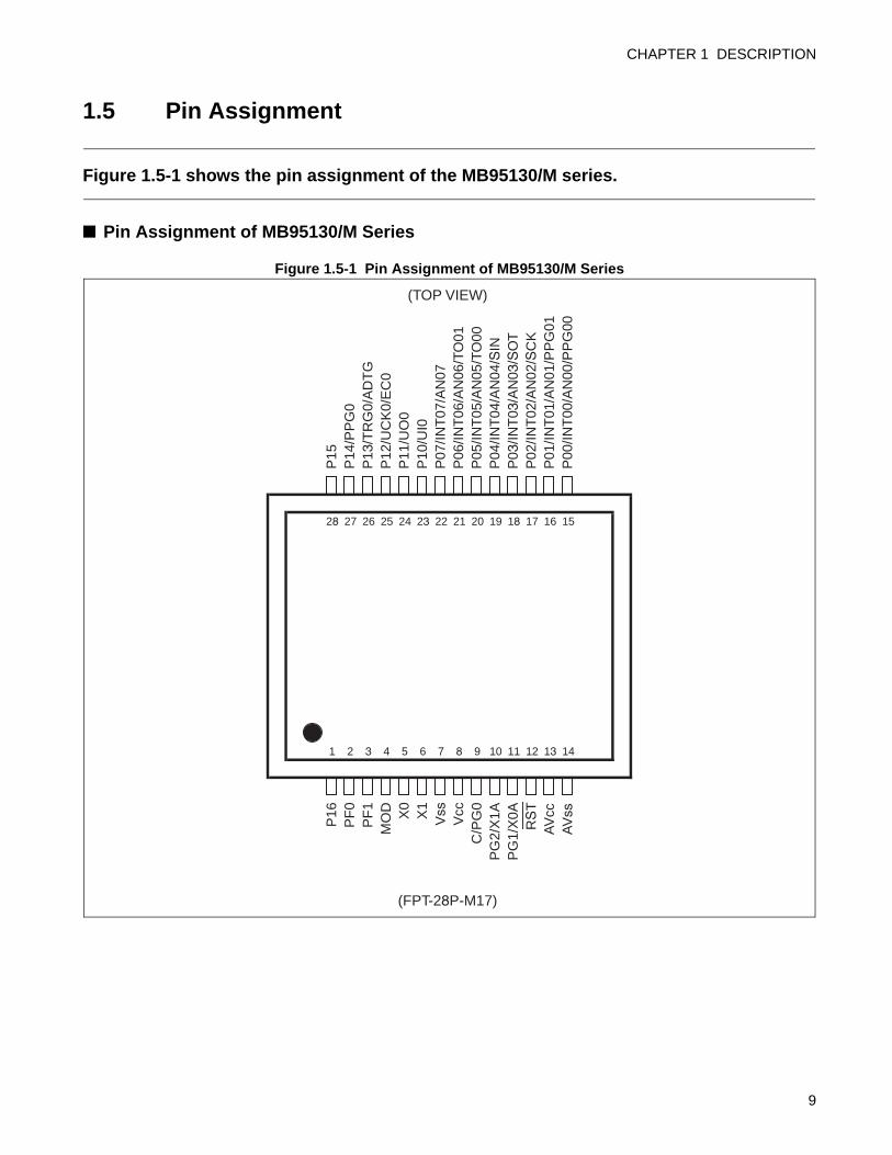
1.5 Pin Assignment
Figure 1.5-1 shows the pin assignment of the MB95130/M series.
Pin Assignment of MB95130/M Series
Figure 1.5-1 Pin Assignment of MB95130/M Series
P15
P14
/PP
G0
P13
/TR
G0/
AD
TG
P12
/UC
K0/
EC
0P
11/U
O0
P10
/UI0
P07
/INT
07/A
N07
P06
/INT
06/A
N06
/TO
01P
05/IN
T05
/AN
05/T
O00
P04
/INT
04/A
N04
/SIN
P03
/INT
03/A
N03
/SO
TP
02/IN
T02
/AN
02/S
CK
P01
/INT
01/A
N01
/PP
G01
P00
/INT
00/A
N00
/PP
G00
28 27 26 25 24 23 22 21 20 19 18 17 16 15
1 2 3 4 5 6 7 8 9 10 11 12 13 14
P16
PF
0P
F1
MO
D X0
X1
Vss
Vcc
C/P
G0
PG
2/X
1AP
G1/
X0A
AV
ccA
Vss
RS
T
(TOP VIEW)
(FPT-28P-M17)
9
CHAPTER 1 DESCRIPTION
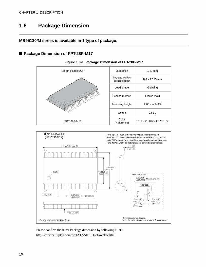
1.6 Package Dimension
MB95130/M series is available in 1 type of package.
Package Dimension of FPT-28P-M17
Figure 1.6-1 Package Dimension of FPT-28P-M17
Please confirm the latest Package dimension by following URL.
http://edevice.fujitsu.com/fj/DATASHEET/ef-ovpklv.html
28-pin plastic SOP Lead pitch 1.27 mm
Package width ×package length
8.6 × 17.75 mm
Lead shape Gullwing
Sealing method Plastic mold
Mounting height 2.80 mm MAX
Weight 0.82 g
Code(Reference)
P-SOP28-8.6 × 17.75-1.27
28-pin plastic SOP(FPT-28P-M17)
(FPT-28P-M17)
C 2002 FUJITSU LIMITED F28048S-c-3-4
.699 –.008+.010
–0.20+0.25
17.75
1
1.27(.050)
8.60±0.20(.339±.008)
11.80±0.30(.465±.012)
M0.13(.005)
14
1528
0.10(.004)
0.47±0.08(.019±.003)
INDEX
"A"
–0.04+0.03
0.17
.007+.001–.002
0~8˚
0.25(.010)
Details of "A" part
(Mounting height)2.65±0.15
(.104±.006)
0.20±0.15(.008±.006)(Stand off)
0.80±0.20(.031±.008)0.88±0.15
(.035±.006)
*1
*2
Dimensions in mm (inches).Note: The values in parentheses are reference values.
Note 1) *1 : These dimensions include resin protrusion.Note 2) *2 : These dimensions do not include resin protrusion.Note 3) Pins width and pins thickness include plating thickness.Note 4) Pins width do not include tie bar cutting remainder.
10
CHAPTER 1 DESCRIPTION
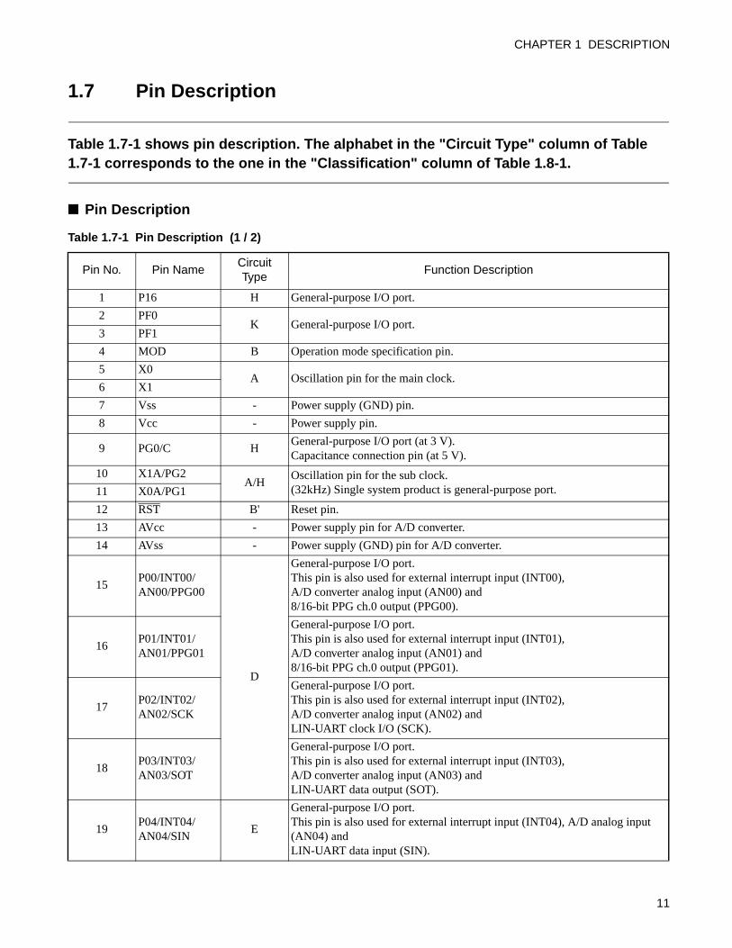
1.7 Pin Description
Table 1.7-1 shows pin description. The alphabet in the "Circuit Type" column of Table 1.7-1 corresponds to the one in the "Classification" column of Table 1.8-1.
Pin Description
Table 1.7-1 Pin Description (1 / 2)
Pin No. Pin NameCircuit Type
Function Description
1 P16 H General-purpose I/O port.
2 PF0K General-purpose I/O port.
3 PF1
4 MOD B Operation mode specification pin.
5 X0A Oscillation pin for the main clock.
6 X1
7 Vss - Power supply (GND) pin.
8 Vcc - Power supply pin.
9 PG0/C HGeneral-purpose I/O port (at 3 V).Capacitance connection pin (at 5 V).
10 X1A/PG2A/H
Oscillation pin for the sub clock.(32kHz) Single system product is general-purpose port.11 X0A/PG1
12 RST B' Reset pin.
13 AVcc - Power supply pin for A/D converter.
14 AVss - Power supply (GND) pin for A/D converter.
15P00/INT00/AN00/PPG00
D
General-purpose I/O port.This pin is also used for external interrupt input (INT00),A/D converter analog input (AN00) and 8/16-bit PPG ch.0 output (PPG00).
16P01/INT01/AN01/PPG01
General-purpose I/O port.This pin is also used for external interrupt input (INT01),A/D converter analog input (AN01) and 8/16-bit PPG ch.0 output (PPG01).
17P02/INT02/AN02/SCK
General-purpose I/O port.This pin is also used for external interrupt input (INT02),A/D converter analog input (AN02) and LIN-UART clock I/O (SCK).
18P03/INT03/AN03/SOT
General-purpose I/O port.This pin is also used for external interrupt input (INT03),A/D converter analog input (AN03) and LIN-UART data output (SOT).
19P04/INT04/AN04/SIN
E
General-purpose I/O port.This pin is also used for external interrupt input (INT04), A/D analog input (AN04) and LIN-UART data input (SIN).
11
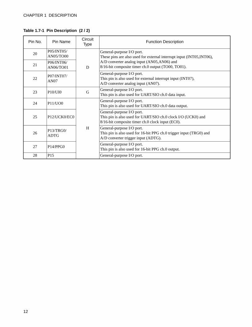
CHAPTER 1 DESCRIPTION
20P05/INT05/AN05/TO00
D
General-purpose I/O port.These pins are also used for external interrupt input (INT05,INT06),A/D converter analog input (AN05,AN06) and 8/16-bit composite timer ch.0 output (TO00, TO01).21
P06/INT06/AN06/TO01
22P07/INT07/AN07
General-purpose I/O port.This pin is also used for external interrupt input (INT07),A/D converter analog input (AN07).
23 P10/UI0 GGeneral-purpose I/O port.This pin is also used for UART/SIO ch.0 data input.
24 P11/UO0
H
General-purpose I/O port.This pin is also used for UART/SIO ch.0 data output.
25 P12/UCK0/EC0General-purpose I/O port.This pin is also used for UART/SIO ch.0 clock I/O (UCK0) and8/16-bit composite timer ch.0 clock input (EC0).
26P13/TRG0/ADTG
General-purpose I/O port.This pin is also used for 16-bit PPG ch.0 trigger input (TRG0) andA/D converter trigger input (ADTG).
27 P14/PPG0General-purpose I/O port.This pin is also used for 16-bit PPG ch.0 output.
28 P15 General-purpose I/O port.
Table 1.7-1 Pin Description (2 / 2)
Pin No. Pin NameCircuit Type
Function Description
12
CHAPTER 1 DESCRIPTION
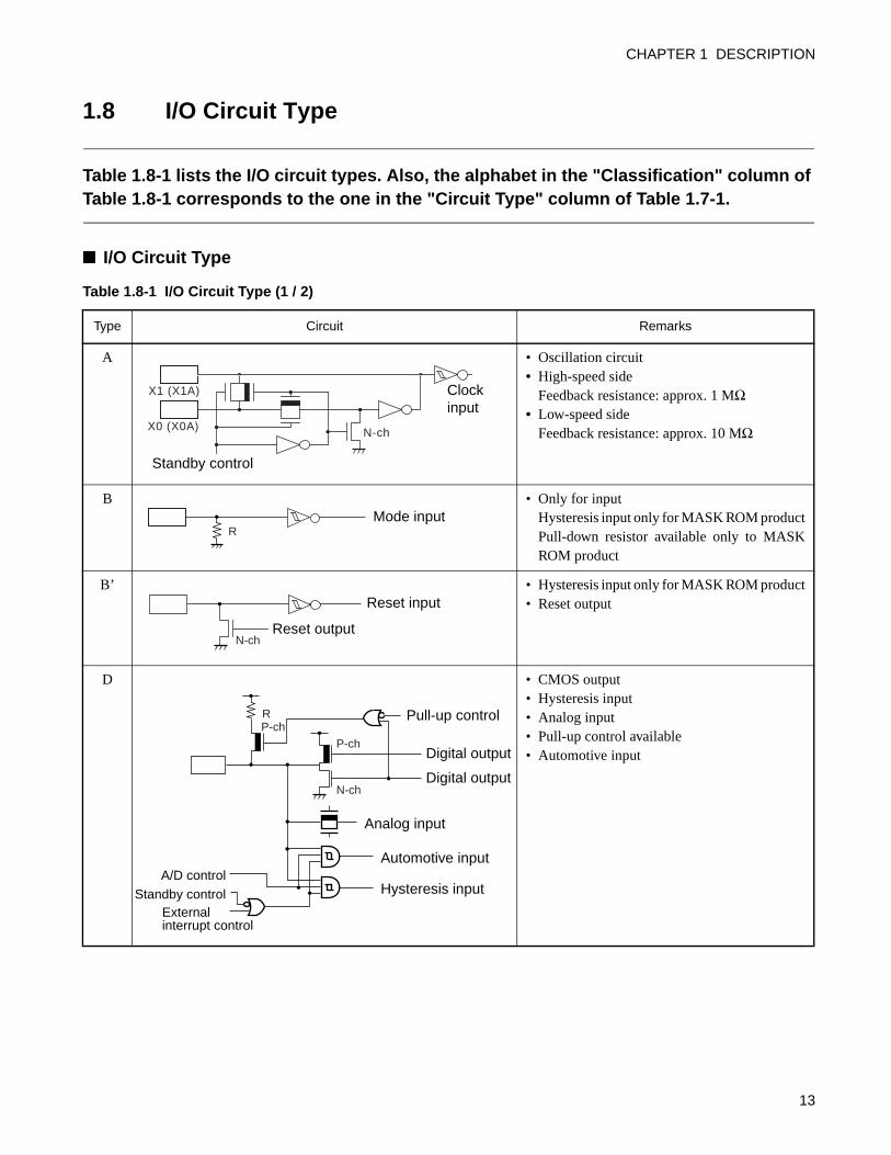
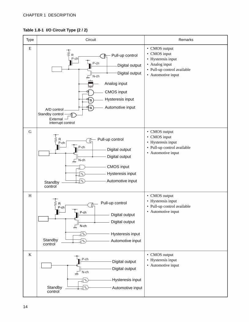
1.8 I/O Circuit Type
Table 1.8-1 lists the I/O circuit types. Also, the alphabet in the "Classification" column of Table 1.8-1 corresponds to the one in the "Circuit Type" column of Table 1.7-1.
I/O Circuit Type
Table 1.8-1 I/O Circuit Type (1 / 2)
Type Circuit Remarks
A • Oscillation circuit• High-speed side
Feedback resistance: approx. 1 MΩ• Low-speed side
Feedback resistance: approx. 10 MΩ
B • Only for inputHysteresis input only for MASK ROM productPull-down resistor available only to MASKROM product
B’ • Hysteresis input only for MASK ROM product• Reset output
D • CMOS output• Hysteresis input• Analog input• Pull-up control available• Automotive input
X0 (X0A)
X1 (X1A)
N-ch
Standby control
Clock input
RMode input
N-ch
Reset input
Reset output
R
N-ch
P-chP-ch
Pull-up control
A/D control
Digital output
Digital output
Analog input
Automotive input
Hysteresis inputStandby controlExternal interrupt control
13
CHAPTER 1 DESCRIPTION
E • CMOS output• CMOS input• Hysteresis input• Analog input• Pull-up control available• Automotive input
G • CMOS output• CMOS input• Hysteresis input• Pull-up control available• Automotive input
H • CMOS output• Hysteresis input• Pull-up control available• Automotive input
K • CMOS output• Hysteresis input• Automotive input
Table 1.8-1 I/O Circuit Type (2 / 2)
Type Circuit Remarks
R
N-ch
P-chP-ch
Pull-up control
Digital output
Digital output
Hysteresis input
Automotive input
CMOS input
A/D controlStandby control
External interrupt control
Analog input
R
P-ch
N-ch
P-chPull-up control
Standby control
Digital output
Digital output
Hysteresis input
CMOS input
Automotive input
P-ch
P-ch
N-ch
R Pull-up control
Standby control
Digital output
Digital output
Hysteresis input
Automotive input
P-ch
N-ch
Standbycontrol
Digital output
Digital output
Hysteresis input
Automotive input
14
CHAPTER 2HANDLING DEVICES
This chapter gives notes on using.
2.1 Device Handling Precautions
15
CHAPTER 2 HANDLING DEVICES
2.1 Device Handling Precautions
This section summarizes the precautions on the device's power supply voltage and pin treatment.
Device Handling Precautions
Preventing Latch-up
Care must be taken to ensure that maximum voltage ratings are not exceeded when they are used.
Latch-up may occur on CMOS ICs if voltage higher than VCC or lower than VSS is applied to input and
output pins other than medium- and high-withstand voltage pins or if higher than the rating voltage is
applied between VCC pin and VSS pin.
When latch-up occurs, power supply current increases rapidly and might thermally damage elements.
Also, take care to prevent the analog power supply voltage (AVCC) and analog input voltage from
exceeding the digital power supply voltage (VCC) when the analog system power supply is turned on or off.
Stable Supply Voltage
Supply voltage should be stabilized.
A sudden change in power-supply voltage may cause a malfunction even within the guaranteed operating
range of the Vcc power-supply voltage.
For stabilization, in principle, keep the variation in Vcc ripple (p-p value) in a commercial frequency range
(50 Hz/60 Hz) not to exceed 10% of the standard Vcc value and suppress the voltage variation so that the
transient variation rate does not exceed 0.1 V/ms during a momentary change such as when the power
supply is switched.
Precautions for Use of External Clock
Even when an external clock is used, oscillation stabilization wait time is required for power-on reset,
wake-up from sub clock mode or stop mode.
Precautions for DebugWhen using an evaluation device (mounted on an MCU board) for software development, there may be
some differences between the operation of the evaluation device and the device you will actually use. The
following lists some points to note during development.
SYCC Register Settings
During debugging, the values of the DIV1 and DIV0 bits in the SYCC register may differ from the user
settings. This is because, when a break occurs, the CPU adjusts the communications speed between the
evaluation device and the BGM adapter to use the optimum speed.
To prevent this from occurring, you need to set response speed optimization to disabled.
This point is explained in "Section 2.3.1 of the Function Description for the SOFTUNE WORKBENCH
development environment". Please refer to this document also.
16
CHAPTER 2 HANDLING DEVICES
Flash Memory Types and Sizes
Each evaluation device can be used for debugging of a number of different production models (series).
When developing your program, please take note of the actual ROM and RAM sizes on the device you
intend to use.
Further, evaluation devices use dual-operation flash memory. However, some production models have flash
memory containing only one sector. Please take note of any differences between the flash memory
configurations of the production and evaluation devices, particularly if writing a program that performs
self-updating of flash memory.
Differences in Flash Memory Content
The debugger for the F2MC-8FX family uses the software break instruction to implement break points.
When continuous or step execution is performed after setting a break point, the software break instruction
is written to the break address in the flash memory on the evaluation device.
Accordingly, the contents of flash memory after a software break has been inserted by the debugger will be
different to the program data image generated by the compiler. Before performing a checksum, you must
remember to clear all break points and "synchronize flash memory".
Restrictions Relating to the Flash Memory on the Evaluation Device
The following restrictions apply to the evaluation device for the F2MC-8FX family.
(1) Writing or erasing the lower bank (addresses 1000H-3FFFH) is not possible.
When debugging, please do this on the production flash memory model.
(2) Do not use the chip erase command for the flash memory on the evaluation device. When debugging,
please do this on the production flash memory model.
Operation of Peripheral Functions During a Break
When a CPU break occurs, the debugger for the F2MC-8FX family halts CPU operation (instruction code
fetch, decoding, instruction execution, updating the PC, etc.) but the peripheral functions (PPG timer,
UART, A/D converter, etc.) continue to operate.
The following are some example implications:
(1) If the overflow flag for a timer/counter is set during a CPU break and the interrupt is enabled, the
interrupt routine will run immediately when execution restarts after the break.
(2) Clearing the overflow flag for a timer/counter via the memory window or similar during a CPU break
will not appear to work as the flag will quickly be reset again.
Prohibited Access to Undefined I/O Addresses
The debugger for the F2MC-8FX family uses the same evaluation device for debugging all models. This
evaluation device includes all peripheral functions that may be used during debugging. Accessing a register
that does not exist on your target production device may invoke a peripheral function that should not exist
and may result in abnormal operation. Accordingly, please do not access undefined address areas.
17
CHAPTER 2 HANDLING DEVICES
Pin Connection
Treatment of Unused Pin
Leaving unused input pins unconnected can cause abnormal operation or latch-up, leaving to permanent
damage. Unused input pins should always be pulled up or down through resistance of at least 2 kΩ. Any
unused input/output pins may be set to output mode and left open, or set to input mode and treated the same
as unused input pins. If there is unused output pin, make it open.
Treatment of Power Supply Pins on A/D Converter
Connect to be AVCC = VCC and AVSS = VSS even if the A/D converter is not in use.
Noise riding on the AVCC pin may cause accuracy degradation. So, connect approx. 0.1 µF ceramic
capacitor as a bypass capacitor between AVCC and AVSS pins in the vicinity of this device.
Power Supply Pins
In products with multiple VCC or VSS pins, the pins of the same potential are internally connected in the
device to avoid abnormal operations including latch-up. However, you must connect the pins to external
power supply and a ground line to lower the electro-magnetic emission level, to prevent abnormal
operation of strobe signals caused by the rise in the ground level, and to conform to the total output current
rating.
Moreover, connect the current supply source with the VCC and VSS pins of this device at the low
impedance.
It is also advisable to connect a ceramic bypass capacitor of approximately 0.1 µF between VCC and VSS
pins near this device.
Mode Pin (MOD)
Connect the mode pin directly to VCC or VSS.
To prevent the device unintentionally entering test mode due to noise, lay out the printed circuit board so as
to minimize the distance from the mode pins to VCC or VSS and to provide a low-impedance connection.
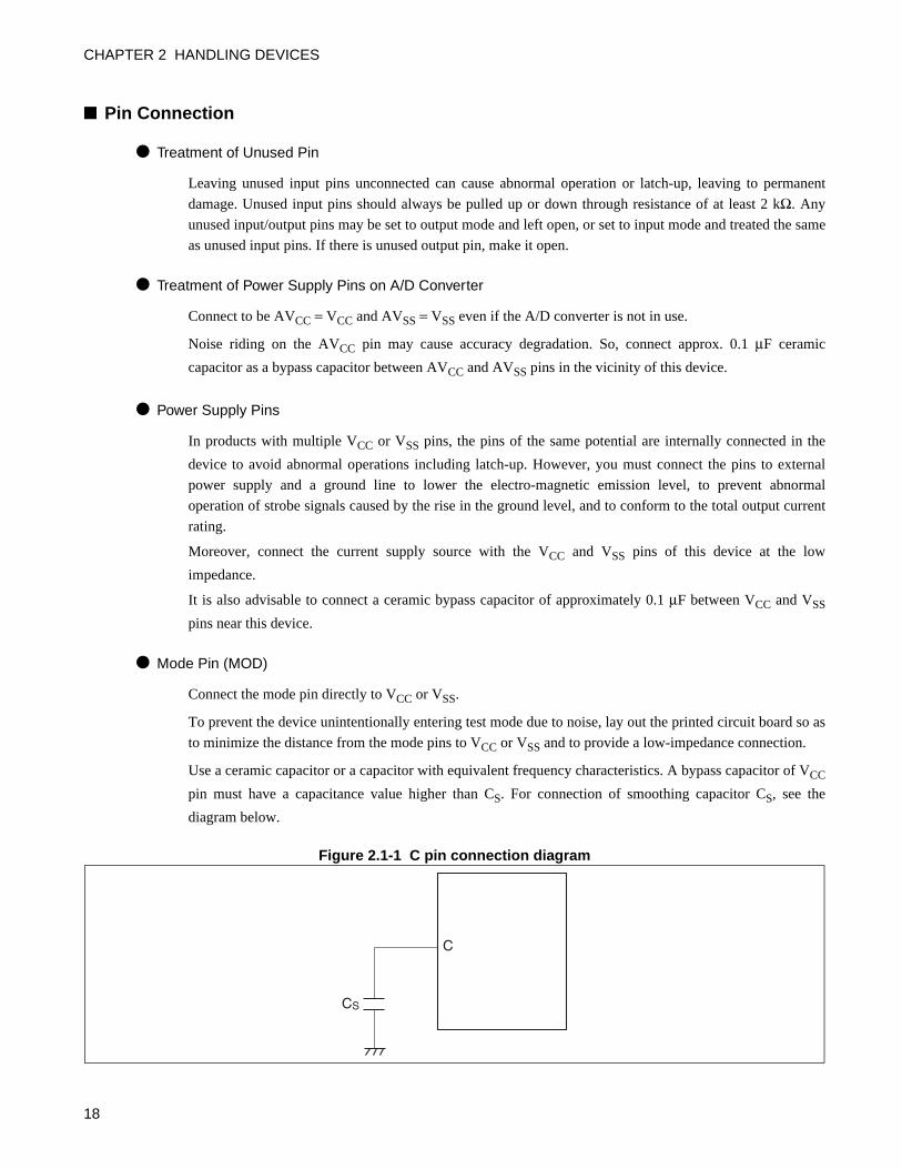
Use a ceramic capacitor or a capacitor with equivalent frequency characteristics. A bypass capacitor of VCC
pin must have a capacitance value higher than CS. For connection of smoothing capacitor CS, see the
diagram below.
Figure 2.1-1 C pin connection diagram
CS
C
18

CHAPTER 2 HANDLING DEVICES
NC Pins
Any pins marked "NC" (not connected) must be left open.
Analog Power Supply
Always set the same potential to AVCC and VCC. When VCC > AVCC, the current may flow through the
AN00 to AN07 pins.
19

CHAPTER 2 HANDLING DEVICES
20
CHAPTER 3MEMORY SPACE
This chapter describes memory space.
3.1 Memory Space
3.2 Memory Map
21
CHAPTER 3 MEMORY SPACE
3.1 Memory Space
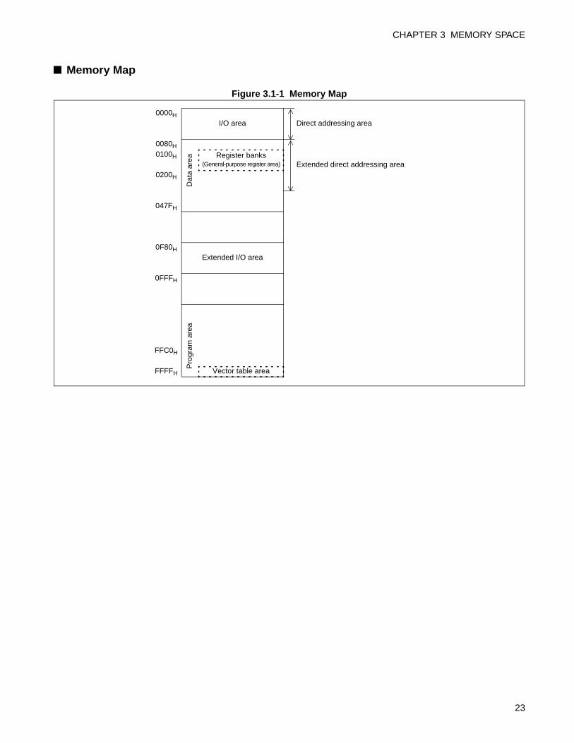
The memory space on the F2MC-8FX family is 64 K bytes, divided into I/O, extended I/O, data, and program areas. The memory space includes special-purpose areas such as the general-purpose registers and vector table.
Configuration of Memory Space
I/O area (addresses: 0000H to 007FH)
• This area contains the control registers and data registers for on-chip peripheral resources.
• As the I/O area is allocated as part of memory space, it can be accessed in the same way as for memory.It can also be accessed at higher speed by using direct addressing instructions.
Extended I/O area (addresses: 0F80H to 0FFFH)
• This area contains the control registers and data registers for on-chip peripheral resources.
• As the extended I/O area is allocated as part of memory space, it can be accessed in the same way as formemory.
Data area
• Static RAM is incorporated as the internal data area.
• The internal RAM capacity is different depending on the product.
• The RAM area from 80H to FFH can be accessed at higher speed by using direct addressing instructions.
• The area from 100H to 47FH is an extended direct addressing area. It can be accessed at higher speed bydirect addressing instructions with the direct bank pointer set.
• Addresses 100H to 1FFH can be used as a general-purpose register area.
Program area
• ROM is incorporated as the internal program area.
• The internal ROM capacity is different depending on the model.
• Addresses FFC0H to FFFFH are used as the vector table.
22
CHAPTER 3 MEMORY SPACE
Memory Map
Figure 3.1-1 Memory Map
0000HI/O area Direct addressing area
0080H0100H
Dat
a ar
ea
Register banks(General-purpose register area) Extended direct addressing area
0200H
047FH
0F80HExtended I/O area
0FFFH
Pro
gram
are
a
FFC0H
FFFFH Vector table area
23
CHAPTER 3 MEMORY SPACE
3.1.1 Areas for Specific Applications
The general-purpose register area and vector table area are used for the specific applications.
General-purpose Register Area (Addresses: 0100H to 01FFH)
• This area contains the auxiliary registers used for 8-bit arithmetic or transfer operations.
• As the area is allocated as part of the RAM area, it can also be used as ordinary RAM.
• When the area is used as general-purpose registers, general-purpose register addressing enables higher-speed access using short instructions.
For details, see Section "5.1.1 Register Bank Pointer (RP)" and Section "5.2 General-purpose Registers".
Vector Table Area (Addresses: FFC0H to FFFFH)
• This area is used as the vector table for vector call instructions (CALLV), interrupts, and resets.
• The vector table area is allocated at the top of the ROM area. At the individual addresses in the vectortable, the start addresses of their respective service routines are set as data.
Table 8.1-1 lists the vector table addresses to be referenced for vector call instructions, interrupts, and for
resets.
For details, see CHAPTER 8 INTERRUPTS, CHAPTER 7 RESET, and " CALLV #vct" in Appendix
E.2 "Special Instructions".
24
CHAPTER 3 MEMORY SPACE
3.2 Memory Map
This section gives a memory map of the MB95130/M series.
Memory Map
Figure 3.2-1 Memory Map
Flash : Flash memoryROM : Mask ROM
MB95FV100D-101MB95FV100D-103
MB95136M
MB95F133MS/F133NSMB95F134MS/F134NSMB95F136MS/F136NS
MB95F133MW/F133NWMB95F134MW/F134NWMB95F136MW/F136NW
0000H
I/O
0000H
I/O
0000H
I/O
0080H 0080H 0080H
RAM 3.75K bytes RAM 1K bytes RAM
0100H Registers0100H Registers
0100H Registers
0200H 0200H 0200H
0480HAccess prohibited
Address #1Access prohibited
0F80H
Extended I/O
0F80H
Extended I/O
0F80H
Extended I/O
1000H 1000H
Access prohibited
1000H
Access prohibited
Flash 60K bytes 8000H Address #2
ROM 32K bytes Flash memory
FFFFH FFFFH FFFFH
25
CHAPTER 3 MEMORY SPACE
Flash memory RAM Address #1 Address #2
MB95F133MS/F133NS8 Kbytes 256 bytes 0180H E000H
MB95F133MW/F133NW
MB95F134MS/F134NS16 Kbytes 512 bytes 0280H C000H
MB95F134MW/F134NW
MB95F136MS/F136NS32 Kbytes 1 Kbytes 0480H 8000H
MB95F136MW/F136NW
26
CHAPTER 4MEMORY ACCESS MODE
This chapter describes the memory access mode.
4.1 Memory Access Mode
27
CHAPTER 4 MEMORY ACCESS MODE
4.1 Memory Access Mode
The memory access mode supported by the MB95130/M series is only single-chip mode.
Single-chip ModeSingle-chip mode uses only internal RAM and ROM without using an external bus access.
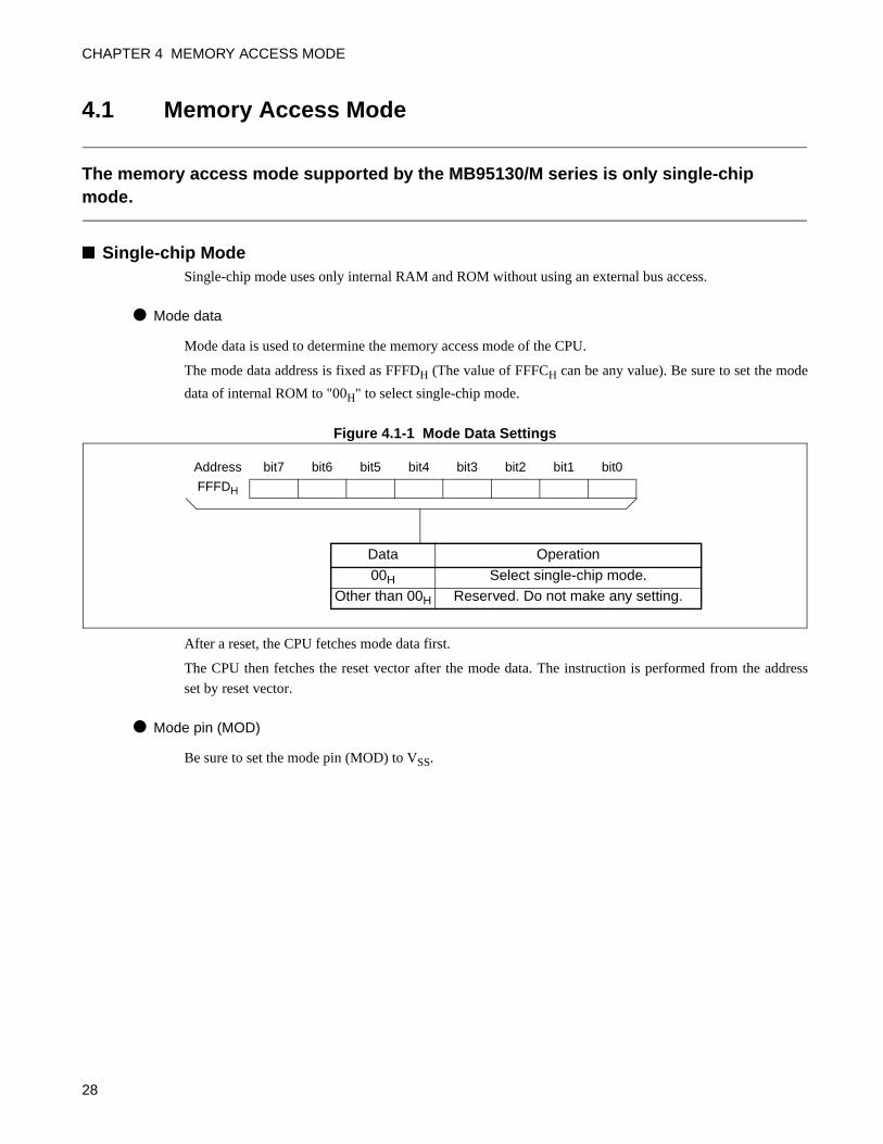
Mode data
Mode data is used to determine the memory access mode of the CPU.
The mode data address is fixed as FFFDH (The value of FFFCH can be any value). Be sure to set the mode
data of internal ROM to "00H" to select single-chip mode.
Figure 4.1-1 Mode Data Settings
After a reset, the CPU fetches mode data first.
The CPU then fetches the reset vector after the mode data. The instruction is performed from the address
set by reset vector.
Mode pin (MOD)
Be sure to set the mode pin (MOD) to VSS.
Address bit7 bit6 bit5 bit4 bit3 bit2 bit1 bit0
FFFDH
Data Operation
00H Select single-chip mode.Other than 00H Reserved. Do not make any setting.
28
CHAPTER 5CPU
This chapter describes functions and operations of the CPU.
5.1 Dedicated Registers
5.2 General-purpose Registers
5.3 Placement of 16-bit Data in Memory
29
CHAPTER 5 CPU
5.1 Dedicated Registers
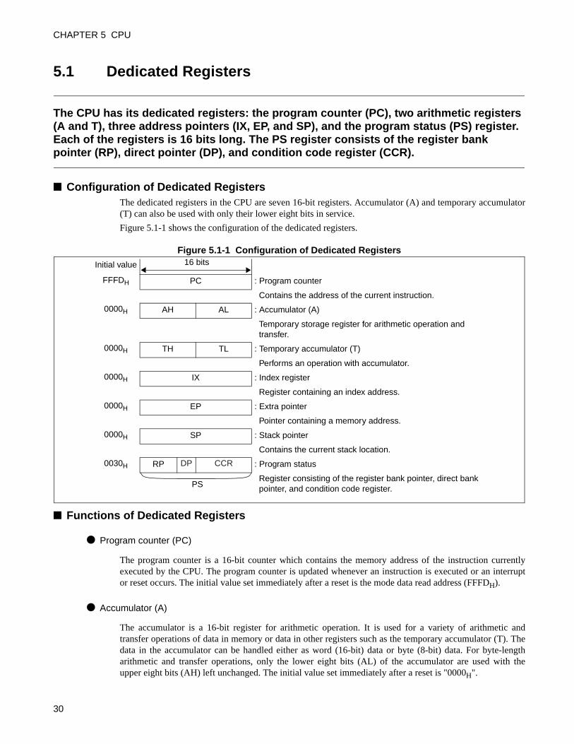
The CPU has its dedicated registers: the program counter (PC), two arithmetic registers (A and T), three address pointers (IX, EP, and SP), and the program status (PS) register. Each of the registers is 16 bits long. The PS register consists of the register bank pointer (RP), direct pointer (DP), and condition code register (CCR).
Configuration of Dedicated RegistersThe dedicated registers in the CPU are seven 16-bit registers. Accumulator (A) and temporary accumulator(T) can also be used with only their lower eight bits in service.
Figure 5.1-1 shows the configuration of the dedicated registers.
Figure 5.1-1 Configuration of Dedicated Registers
Functions of Dedicated Registers
Program counter (PC)
The program counter is a 16-bit counter which contains the memory address of the instruction currentlyexecuted by the CPU. The program counter is updated whenever an instruction is executed or an interruptor reset occurs. The initial value set immediately after a reset is the mode data read address (FFFDH).
Accumulator (A)
The accumulator is a 16-bit register for arithmetic operation. It is used for a variety of arithmetic andtransfer operations of data in memory or data in other registers such as the temporary accumulator (T). Thedata in the accumulator can be handled either as word (16-bit) data or byte (8-bit) data. For byte-lengtharithmetic and transfer operations, only the lower eight bits (AL) of the accumulator are used with theupper eight bits (AH) left unchanged. The initial value set immediately after a reset is "0000H".
Initial value
FFFDH PC : Program counter
Contains the address of the current instruction.
0000H AH AL : Accumulator (A)
Temporary storage register for arithmetic operation and transfer.
0000H TH TL : Temporary accumulator (T)
Performs an operation with accumulator.
0000H IX : Index register
Register containing an index address.
0000H EP : Extra pointer
Pointer containing a memory address.
0000H SP : Stack pointer
Contains the current stack location.
0030H RP DP CCR : Program status
Register consisting of the register bank pointer, direct bank pointer, and condition code register.
16 bits
PS
30
CHAPTER 5 CPU
Temporary accumulator (T)
The temporary accumulator is an auxiliary 16-bit register for arithmetic operation. It is used to perform
arithmetic operations with the data in the accumulator (A). The data in the temporary accumulator is
handled as word data for word-length (16-bit) operations with the accumulator (A) and as byte data for
byte-length (8-bit) operations. For byte-length operations, only the lower eight bits (TL) of the temporary
accumulator are used and the upper eight bits (TH) are not used.
When a MOV instruction is used to transfer data to the accumulator (A), the previous contents of the
accumulator are automatically transferred to the temporary accumulator. When transferring byte-length
data, the upper eight bits (TH) of the temporary accumulator remain unchanged. The initial value after a
reset is "0000H".
Index register (IX)
The index register is a 16-bit register used to hold the index address. The index register is used with a
single-byte offset (-128 to +127). The offset value is added to the index address to generate the memory
address for data access. The initial value after a reset is "0000H".
Extra pointer (EP)
The extra pointer is a 16-bit register which contains the value indicating the memory address for data
access. The initial value after a reset is "0000H".
Stack pointer (SP)
The stack pointer is a 16-bit register which holds the address referenced when an interrupt or subroutine
call occurs and by the stack push and pop instructions. During program execution, the value of the stack
pointer indicates the address of the most recent data pushed onto the stack. The initial value after a reset is
"0000H".
Program status (PS)
The program status is a 16-bit control register. The upper eight bits make up the register bank pointer (RP)
and direct bank pointer (DP); the lower eight bits make up the condition code register (CCR).
In the upper eight bits, the upper five bits make up the register bank pointer used to contain the address of
the general-purpose register bank. The lower three bits make up the direct bank pointer which locates the
area to be accessed at high speed by direct addressing.
The lower eight bits make up the condition code register (CCR) which consists of flags that represent the
state of the CPU.
The instructions that can access the program status are MOVW A,PS or MOVW PS,A. The register bank
pointer (RP) and direct bank pointer (DP) in the program status register can also be read from or written to
by accessing the mirror address (0078H).
Note that the condition code register (CCR) is part of the program status register and cannot be accessed
independently.
Refer to the "F2MC-8FX Programming Manual" for details on using the dedicated registers.
31
CHAPTER 5 CPU
5.1.1 Register Bank Pointer (RP)
The register bank pointer (RP) in bits 15 to 11 of the program status (PS) register contains the address of the general-purpose register bank that is currently in use and is translated into a real address when general-purpose register addressing is used.
Configuration of Register Bank Pointer (RP)Figure 5.1-2 shows the configuration of the register bank pointer.
Figure 5.1-2 Configuration of Register Bank Pointer
The register bank pointer contains the address of the register bank currently being used. The content of the
register bank pointer is translated into a real address according to the rule shown in Figure 5.1-3.
Figure 5.1-3 Rule for Translation into Real Addresses in General-purpose Register Area
The register bank pointer specifies the register bank used as general-purpose registers in the RAM area.
There are a total of 32 register banks. The current register bank is specified by setting a value between 0
and 31 in the upper five bits of the register bank pointer. Each register bank has eight 8-bit general-purpose
registers which are selected by the lower three bits of the op-code.
The register bank pointer allows the space from "0100H" to up to "01FFH (Max.)" to be used as a general-
purpose register area. Note, however, that the available area is limited depending on the product. The initial
value after a reset is "0000H".
Mirror Address for Register Bank and Direct Bank PointersThe register bank pointer (RP) and direct bank pointer (DP) can be written to and read from by accessing
the program status (PS) register using the "MOVW A,PS" and "MOVW PS,A" instructions, respectively.
They can also be written to and read from directly by accessing mirror address "0078H" of the register bank
pointer.
RP DP CCR
bit15 bit14 bit13 bit12 bit11 bit10 bit9 bit8 bit7 bit6 bit5 bit4 bit3 bit2 bit1 bit0
PS R4 R3 R2 R1 R0 DP2 DP1 DP0 H I IL1 IL0 N Z V C 00000B
RP Initial value
Fixed value RP: Upper Op-code: Lower
"0" "0" "0" "0" "0" "0" "0" "1" R4 R3 R2 R1 R0 b2 b1 b0
↓ ↓ ↓ ↓ ↓ ↓ ↓ ↓ ↓ ↓ ↓ ↓ ↓ ↓ ↓ ↓
A15 A14 A13 A12 A11 A10 A9 A8 A7 A6 A5 A4 A3 A2 A1 A0Generated address
32
CHAPTER 5 CPU
5.1.2 Direct Bank Pointer (DP)
The direct bank pointer (DP) in bits 10 to 8 of the program status (PS) register specifies the area to be accessed by direct addressing.
Configuration of Direct Bank Pointer (DP)Figure 5.1-4 shows the configuration of the direct bank pointer.
Figure 5.1-4 Configuration of Direct Bank Pointer
The areas from 0000H to 007FH and 0080H to 047FH can be accessed by direct addressing. Access to
0000H to 007FH is specified with an operand regardless of the value in the direct bank pointer. Access to
0080H to 047FH is specified with the value in the value of the direct bank pointer and the operand.
Table 5.1-1 shows the relationship between direct bank pointer (DP) and access area; Table 5.1-2 lists the
direct addressing instructions.
RP DP CCR
bit15 bit14 bit13 bit12 bit11 bit10 bit9 bit8 bit7 bit6 bit5 bit4 bit3 bit2 bit1 bit0
PS R4 R3 R2 R1 R0 DP2 DP1 DP0 H I IL1 IL0 N Z V C 000B
DP Initial value
Table 5.1-1 Direct Access Pointer and Access Area
Direct bank pointer (DP) [2:0] Operand-specified dir Access area
XXXB (It does not affect the mapping. ) 0000H to 007FH 0000H to 007FH
000B (Initial value)
0080H to 00FFH
0080H to 00FFH
001B 0100H to 017FH
010B 0180H to 01FFH
011B 0200H to 027FH
100B 0280H to 02FFH
101B 0300H to 037FH
110B 0380H to 03FFH
111B 0400H to 047FH
33
CHAPTER 5 CPU
Table 5.1-2 Direct Address Instruction List
Applicable Instruction
CLRB dir:bit
SETB dir:bit
BBC dir:bit,rel
BBS dir:bit,rel
MOV A,dir
CMP A,dir
ADDC A,dir
SUBC A,dir
MOV dir,A
XOR A,dir
AND A,dir
OR A,dir
MOV dir,#imm
CMP dir,#imm
MOVW A,dir
MOVW dir,A
34
CHAPTER 5 CPU
5.1.3 Condition Code Register (CCR)
The condition code register (CCR) in the lower eight bits of the program status (PS) register consists of the bits (H, N, Z, V, and C) containing information about the arithmetic result or transfer data and the bits (I, IL1, and IL0) used to control the acceptance of interrupt requests.
Configuration of Condition Code Register (CCR)
Figure 5.1-5 Configuration of Condition Code Register
The condition code register is a part of the program status (PS) register and therefore cannot be accessed
independently.
Bits Result Information Bits
Half carry flag (H)
This flag is set to "1" when a carry from bit 3 to bit 4 or a borrow from bit 4 to bit 3 occurs as the result of
an operation. Otherwise, the flag is set to "0". Do not use this flag for any operation other than addition and
subtraction as the flag is intended for decimal-adjusted instructions.
Negative flag (N)
This flag is set to "1" when the value of the most significant bit is "1" as the result of an operation and set to
"0" if the value is "0".
Zero flag (Z)
This flag is set to "1" when the result of an operation is "0" and set to "0" otherwise.
Overflow flag (V)
This flag indicates whether an operation has resulted in an overflow, assuming the operand used for the
operation as an integer represented by a two's complement. The flag is set to "1" when an overflow occurs
and set to "0" otherwise.
RP DP CCR
bit15 bit14 bit13 bit12 bit11 bit10 bit9 bit8 bit7 bit6 bit5 bit4 bit3 bit2 bit1 bit0
PS R4 R3 R2 R1 R0 DP2 DP1 DP0 H I IL1 IL0 N Z V C 00110000B
Half carry flagInterrupt enable flagInterrupt level bitsNegative flagZero flagOverflow flagCarry flag
CCR Initial value
35
CHAPTER 5 CPU
Carry flag (C)
This flag is set to "1" when a carry from bit 7 or a borrow to bit 7 occurs as the result of an operation.
Otherwise, the flag is set to "0". When a shift instruction is executed, the flag is set to the shift-out value.
Figure 5.1-6 shows how the carry flag is updated by a shift instruction.
Figure 5.1-6 Carry Flag Updated by Shift Instruction
Interrupt Acceptance Control Bits
Interrupt enable flag (I)
When this flag is set to "1", interrupts are enabled and accepted by the CPU. When this flag is set to "0",
interrupts are disabled and rejected by the CPU.
The initial value after a reset is "0".
The SETI and CLRI instructions set and clear the flag to "1" and "0", respectively.
Interrupt level bits (IL1, IL0)
These bits indicate the level of the interrupt currently accepted by the CPU.
The interrupt level is compared with the value of the interrupt level setting register (ILR0 to ILR5) that
corresponds to the interrupt request (IRQ0 to IRQ23) of each peripheral resource.
The CPU services an interrupt request only when its interrupt level is smaller than the value of these bits
with the interrupt enable flag set (CCR: I = 1). Table 5.1-3 lists interrupt level priorities. The initial value
after a reset is "11B".
The interrupt level bits (IL1, IL0) are usually "11B" with the CPU not servicing an interrupt (with the main
program running).
For details on interrupts, see "8.1 Interrupts".
• Left-shift (ROLC) • Right-shift (RORC)
bit7 bit0 bit7 bit0
C C
Table 5.1-3 Interrupt Levels
IL1 IL0 Interrupt Level Priority
0 0 0 High
0 1 1
1 0 2
1 1 3 Low (No interrupt)
36
CHAPTER 5 CPU
5.2 General-purpose Registers
The general-purpose registers are memory blocks consisting of eight 8-bit registers per bank. A total of up to 32 register banks can be used. The register bank pointer (RP) is used to specify the register bank.Register banks are useful for interrupt handling, vector call processing, and subroutine calls.
Configuration of General-purpose Registers• The general-purpose registers are 8-bit registers and are located in register banks in the general-purpose
register area (in RAM).
• Up to 32 banks can be used, where each bank consists of eight registers (R0 to R7).
• The register bank pointer (RP) specifies the register bank currently being used and the lower three bitsof the op-code specify general-purpose register 0 (R0) to 7 (R7).
Figure 5.2-1 shows the configuration of the register banks.
Figure 5.2-1 Configuration of Register Banks
For information on the general-purpose register area available on each model, see "3.1.1 Areas for Specific
Applications".
R0
R1
R2
R3
R4
R5
R6
R7
R0
= 0100H + 8 × (RP)
R1
R2
R3
R4
R5
R6
R7
R0
R1
R2
R3
R4
R5
R6
R7
This address
32 banks
Memory area
1F8H
Address 100H
107H
1FFH
8bits
The number of banks available is restricted by the RAM capacity available.
Bank 31
Bank 0
37
CHAPTER 5 CPU
Features of General-purpose RegistersThere are the following features in the general-purpose registers:
• High-speed access to RAM using short instructions (general-purpose register addressing).
• Blocks of register banks facilitating data backup and division by function unit.
General-purpose register banks can be allocated exclusively for specific interrupt service routines or vector
call (CALLV #0 to #7) processing routines. An example is always using the fourth register bank for the
second interrupt.
Only specifying a dedicated register bank at the beginning of an interrupt service routine automatically
saves the general-purpose registers before the interrupt. This eliminates the need for pushing general-
purpose register data onto the stack, allowing the CPU to accept interrupts at high speed.
Notes:
• When coding an interrupt service routine, be careful not to change the value of the interrupt levelbits (CCR: IL1, IL0) in the condition code register when specifying the register bank by updatingthe register bank pointer (RP) in that routine. Perform the programming by using either of them.
• Read the interrupt level bits and save their value before writing to the RP.
• Directly write to the RP mirror address "0078H" to update the RP.
38
CHAPTER 5 CPU
5.3 Placement of 16-bit Data in Memory
This section describes how 16-bit data is stored in memory.
Placement of 16-bit Data in Memory
State of 16-bit data stored in RAM
When you write 16-bit data to memory, the upper byte of the data is stored at a smaller address and the
lower byte is stored at the next address. When you read 16-bit data, it is handled in the same way.
Figure 5.3-1 shows how 16-bit data is placed in memory.
Figure 5.3-1 Placing 16-bit Data in Memory
State of operand-specified 16-bit data
In the same way, even when the operands in an instruction specifies 16-bit data, the upper byte is stored at
the address closer to the op-code (instruction) and the lower byte is stored at the next address.
That is true whether the operands are either memory addresses or 16-bit immediate data.
Figure 5.3-2 shows how 16-bit data in an instruction is placed.
Figure 5.3-2 Storing 16-bit Data in Instruction
State of 16-bit data in the stack
When 16-bit register data is pushed onto the stack upon an interrupt, the upper byte is stored at a lower
address in the same way.
Before execution
AfterexecutionMemory Memory
A 1 2 3 4 H 1 2 3 4 HA
MOVW 0081H, A0080H
0081H
0082H
0083H
0080H
0081H
0082H
0083H
12 H34 H
Extended address16-bit immediate data
Assemble
Extended address16-bit immediate data
[Example]
39

CHAPTER 5 CPU
40
CHAPTER 6CLOCK CONTROLLER
This chapter describes the functions and operations of the clock controller.
6.1 Overview of Clock Controller
6.2 Oscillation Stabilization Wait Time
6.3 System Clock Control Register (SYCC)
6.4 PLL Control Register (PLLC)
6.5 Oscillation Stabilization Wait Time Setting Register (WATR)
6.6 Standby Control Register (STBC)
6.7 Clock Modes
6.8 Operations in Low-power Consumption Modes (Standby Modes)
6.9 Clock Oscillator Circuits
6.10 Overview of Prescaler
6.11 Configuration of Prescaler
6.12 Operating Explanation of Prescaler
6.13 Notes on Use of Prescaler
41
CHAPTER 6 CLOCK CONTROLLER
6.1 Overview of Clock Controller
The F2MC-8FX family has a built-in clock controller that optimizes its power consumption. It includes two- system clock product supporting both of the main clock and sub clock and single system clock product supporting only the main clock.The clock controller enables/disables clock oscillation, enables/disables the supply of clock signals to the internal circuitry, selects the clock source, and controls the PLL and frequency divider circuits.
Overview of Clock ControllerThe clock controller enables/disables clock oscillation, enables/disables clock supply to the internal
circuitry, selects the clock source, and controls the PLL and frequency divider circuits.
The clock controller controls the internal clock according to the clock mode, standby mode settings and the
reset operation. The current clock mode selects the internal operating clock and the standby mode selects
whether to enable or disable clock oscillation and signal supply.
The clock controller selects the optimum power consumption and features depending on the combination of
clock mode and standby mode.
Two- system clock product have four different source clocks: a main clock, which is the main oscillation
clock divided by two, a sub clock, which is the sub oscillation clock divided by two, a main PLL clock,
which is the main oscillation clock multiplied by the PLL multiplier and a sub PLL clock, which is the sub
oscillation clock multiplied by the PLL multiplier.
Single system clock product have two different source clocks: a main clock, which is the main oscillationclock divided by two; and a main PLL clock, which is the main oscillation clock multiplied by the PLLmultiplier.
42
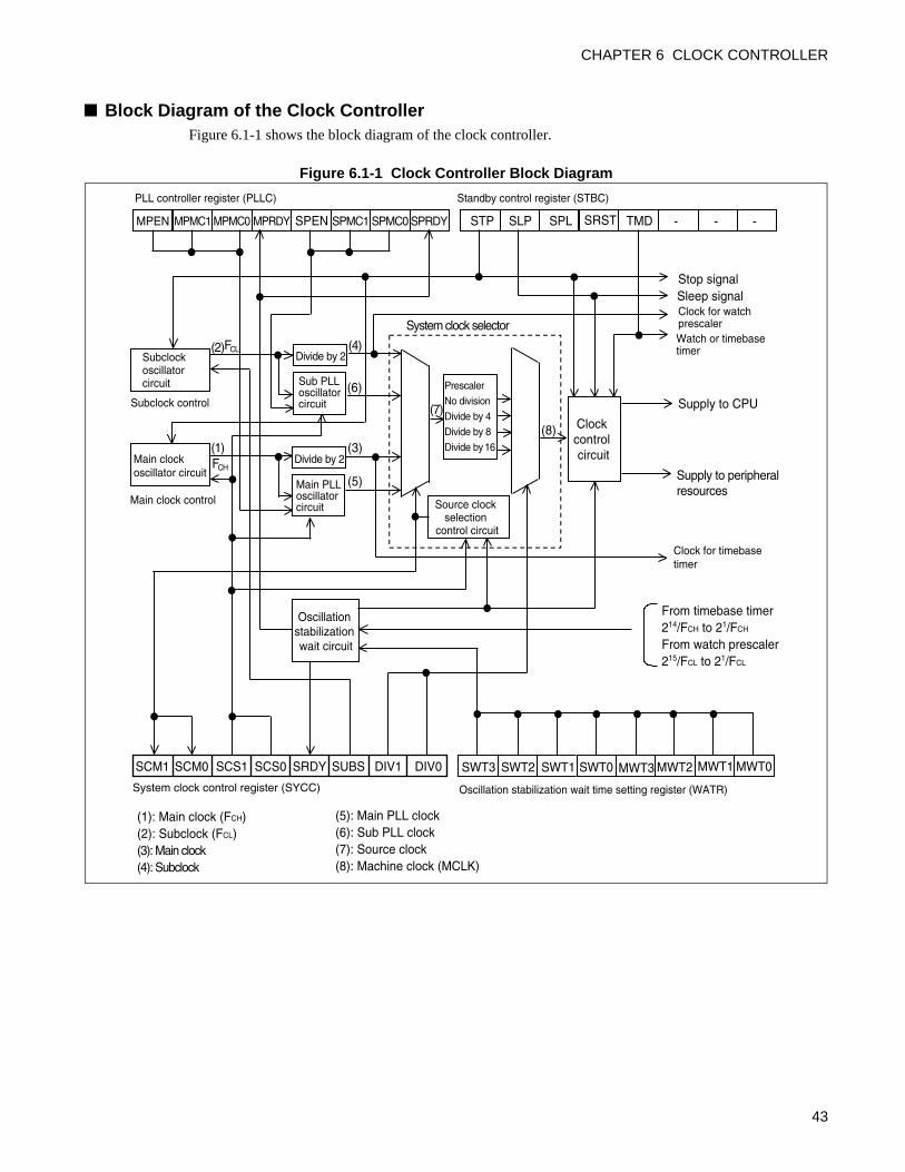
CHAPTER 6 CLOCK CONTROLLER
Block Diagram of the Clock Controller Figure 6.1-1 shows the block diagram of the clock controller.
Figure 6.1-1 Clock Controller Block Diagram
- - -
Standby control register (STBC)
Subclock oscillator circuit
System clock selector
Prescaler
No division
Divide by 4
Divide by 8
Divide by 16
Main clock oscillator circuit
Divide by 2
Main PLL oscillator circuit
Divide by 2
Sub PLL oscillator circuit
Clock control circuit
Subclock control
System clock control register (SYCC)
Oscillation stabilization wait circuit
Supply to CPU
Supply to peripheral resources
Sleep signalStop signal
Watch or timebase timer
Clock for timebase timer
Main clock control
Oscillation stabilization wait time setting register (WATR)
Source clock selection
control circuit
MPMC1
PLL controller register (PLLC)
(1)
(2) (4)
(3)
(5)
(6)
(7)
(8)
(1): Main clock (FCH)(2): Subclock (FCL) (3): Main clock (4): Subclock
(5): Main PLL clock(6): Sub PLL clock(7): Source clock(8): Machine clock (MCLK)
From timebase timer214/FCH to 21/FCH From watch prescaler215/FCL to 21/FCL
FCH
FCL
MPMC0 MPRDY SPEN SPMC1 SPMC0 SPRDY STP SLP SPL SRST TMDMPEN
SCM1 SCM0 SCS1 SCS0 SRDY SUBS DIV1 DIV0 SWT3 SWT2 SWT1 SWT0 MWT3 MWT2 MWT1 MWT0
Clock for watch prescaler
43
CHAPTER 6 CLOCK CONTROLLER
The clock controller consists of the following blocks:
Main clock oscillator circuit
This block is the oscillator circuit for the main clock.
Sub clock oscillator circuit (Two-system clock product)
This block is the oscillator circuit for the sub clock.
Main PLL oscillator circuit
This block is the oscillator circuit for the main PLL.
Sub PLL oscillator circuit (Two-system clock product)
This block is the oscillator circuit for the sub PLL clock.
System clock selector
This block selects one of the four different source clocks for main clock, sub clock, main PLL clock, and
sub PLL clock depending on the clock mode. The prescaler frequency-divides the selected source clock
into the machine clock. It is supplied to the clock control circuit.
Clock control circuit
This block controls the supply of the machine clock to the CPU and each peripheral resource according to
the standby mode or oscillation stabilization wait time.
Oscillation stabilization wait circuit
This block outputs the oscillation stabilization wait time signal for each clock from 14 types of main clock
oscillation stabilization signals created by the timebase timer and 15 types of sub clock oscillation
stabilization signals created by the watch prescaler.
System clock control register (SYCC)
This register is used to control current clock mode display, clock mode selection, machine clock divide
ratio selection, and sub clock oscillation in main clock mode and main PLL clock mode.
Standby control register (STBC)
This register is used to control the transition from RUN state to standby mode, the setting of pin states in
stop mode, timebase timer mode, or watch mode, and the generation of software resets.
PLL control register (PLLC)
This register is used to enable/disable the oscillation of the main PLL and sub PLL clocks, set the
multiplier, and to indicate the stability of PLL oscillation.
Oscillation stabilization wait time setting register (WATR)
This register is used to set the oscillation stabilization wait time for the main clock and sub clock.
44
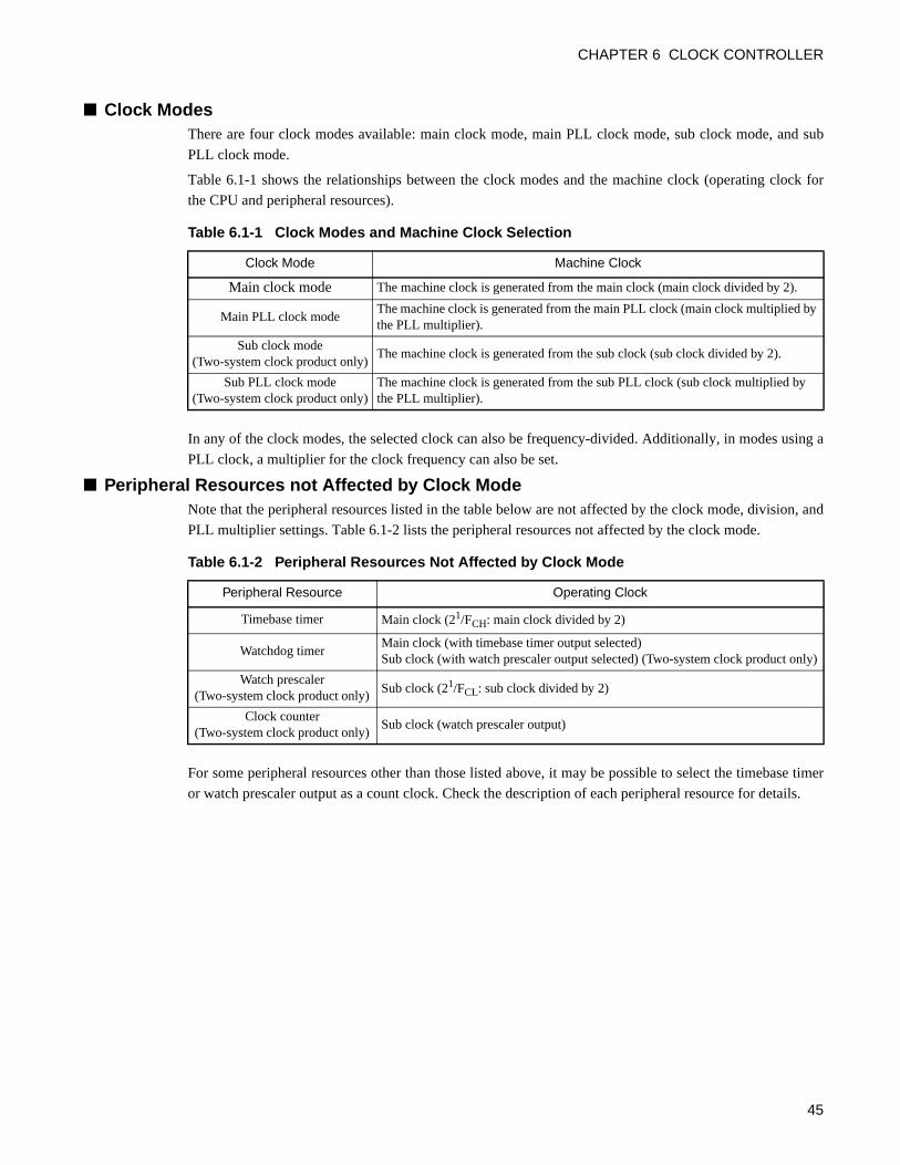
CHAPTER 6 CLOCK CONTROLLER
Clock ModesThere are four clock modes available: main clock mode, main PLL clock mode, sub clock mode, and sub
PLL clock mode.
Table 6.1-1 shows the relationships between the clock modes and the machine clock (operating clock for
the CPU and peripheral resources).
In any of the clock modes, the selected clock can also be frequency-divided. Additionally, in modes using a
PLL clock, a multiplier for the clock frequency can also be set.
Peripheral Resources not Affected by Clock ModeNote that the peripheral resources listed in the table below are not affected by the clock mode, division, and
PLL multiplier settings. Table 6.1-2 lists the peripheral resources not affected by the clock mode.
For some peripheral resources other than those listed above, it may be possible to select the timebase timer
or watch prescaler output as a count clock. Check the description of each peripheral resource for details.
Table 6.1-1 Clock Modes and Machine Clock Selection
Clock Mode Machine Clock
Main clock mode The machine clock is generated from the main clock (main clock divided by 2).
Main PLL clock modeThe machine clock is generated from the main PLL clock (main clock multiplied by the PLL multiplier).
Sub clock mode(Two-system clock product only)
The machine clock is generated from the sub clock (sub clock divided by 2).
Sub PLL clock mode(Two-system clock product only)
The machine clock is generated from the sub PLL clock (sub clock multiplied by the PLL multiplier).
Table 6.1-2 Peripheral Resources Not Affected by Clock Mode
Peripheral Resource Operating Clock
Timebase timer Main clock (21/FCH: main clock divided by 2)
Watchdog timerMain clock (with timebase timer output selected)Sub clock (with watch prescaler output selected) (Two-system clock product only)
Watch prescaler(Two-system clock product only)
Sub clock (21/FCL: sub clock divided by 2)
Clock counter(Two-system clock product only)
Sub clock (watch prescaler output)
45
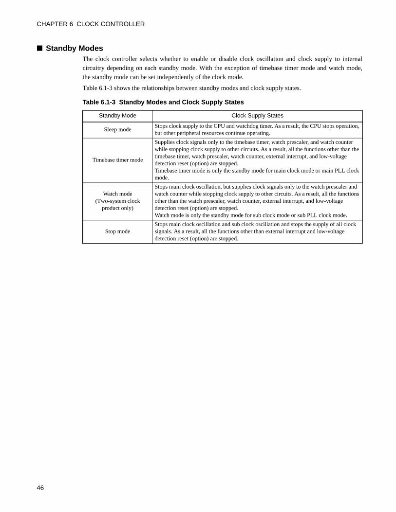
CHAPTER 6 CLOCK CONTROLLER
Standby ModesThe clock controller selects whether to enable or disable clock oscillation and clock supply to internal
circuitry depending on each standby mode. With the exception of timebase timer mode and watch mode,
the standby mode can be set independently of the clock mode.
Table 6.1-3 shows the relationships between standby modes and clock supply states.
Table 6.1-3 Standby Modes and Clock Supply States
Standby Mode Clock Supply States
Sleep modeStops clock supply to the CPU and watchdog timer. As a result, the CPU stops operation, but other peripheral resources continue operating.
Timebase timer mode
Supplies clock signals only to the timebase timer, watch prescaler, and watch counter while stopping clock supply to other circuits. As a result, all the functions other than the timebase timer, watch prescaler, watch counter, external interrupt, and low-voltage detection reset (option) are stopped.Timebase timer mode is only the standby mode for main clock mode or main PLL clock mode.
Watch mode (Two-system clock
product only)
Stops main clock oscillation, but supplies clock signals only to the watch prescaler and watch counter while stopping clock supply to other circuits. As a result, all the functions other than the watch prescaler, watch counter, external interrupt, and low-voltage detection reset (option) are stopped.Watch mode is only the standby mode for sub clock mode or sub PLL clock mode.
Stop modeStops main clock oscillation and sub clock oscillation and stops the supply of all clock signals. As a result, all the functions other than external interrupt and low-voltage detection reset (option) are stopped.
46
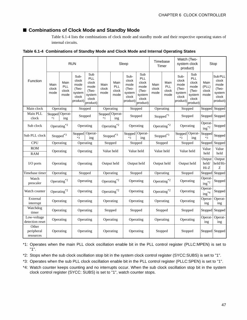
CHAPTER 6 CLOCK CONTROLLER
Combinations of Clock Mode and Standby ModeTable 6.1-4 lists the combinations of clock mode and standby mode and their respective operating states of
internal circuits.
*1: Operates when the main PLL clock oscillation enable bit in the PLL control register (PLLC:MPEN) is set to"1".
*2: Stops when the sub clock oscillation stop bit in the system clock control register (SYCC:SUBS) is set to "1".
*3: Operates when the sub PLL clock oscillation enable bit in the PLL control register (PLLC:SPEN) is set to "1".
*4: Watch counter keeps counting and no interrupts occur. When the sub clock oscillation stop bit in the systemclock control register (SYCC: SUBS) is set to "1", watch counter stops.
Table 6.1-4 Combinations of Standby Mode and Clock Mode and Internal Operating States
Function
RUN SleepTimebase
Timer
Watch (Two-system clock
product)Stop
Main clock mode
Main PLL clock mode
Sub-clock mode (Two-
system clock
product)
Sub PLL clock mode (Two-
system clock
product)
Main clock mode
Main PLL clock mode
Sub-clock mode (Two-
system clock
product)
Sub PLL clock mode (Two-
system clock
product)
Main clock mode
Main PLL clock mode
Sub-clock mode (Two-
system clock
product)
Sub PLL clock mode (Two-
system clock
product)
Main (PLL)clock mode
Sub PLL clock mode (Two-
system clock
product)
Main clock Operating Stopped Operating Stopped Operating Stopped Stopped Stopped
Main PLL clock
Stopped*1
Operat-ing
Stopped Stopped*1
Operat-ing
Stopped Stopped*1 Stopped Stopped Stopped
Sub clock Operating*2 Operating Operating*2 Operating Operating*2 OperatingOperat-
ing*2 Stopped
Sub PLL clock Stopped*3 Stopped*3
Operat-ing Stopped*3 Stopped
*3
Operat-ing Stopped*3 Stopped
*3
Operat-ing
Stopped*3
Stopped
CPU Operating Operating Stopped Stopped Stopped Stopped Stopped Stopped
ROMOperating Operating Value held Value held Value held Value held
Value held
Value heldRAM
I/O ports Operating Operating Output held Output held Output held Output heldOutput held/Hi-Z
Output held/Hi-
Z
Timebase timer Operating Stopped Operating Stopped Operating Stopped Stopped Stopped
Watch prescaler Operating*2 Operating Operating*2 Operating Operating*2 Operating
Operat-
ing*2 Stopped
Watch counter Operating*2 Operating Operating*2 Operating Operating*2 OperatingOperat-
ing*4 Stopped
External interrupt
Operating Operating Operating Operating Operating OperatingOperat-
ingOperat-
ingWatchdog
timerOperating Operating Stopped Stopped Stopped Stopped Stopped Stopped
Low-voltage detection reset
Operating Operating Operating Operating Operating OperatingOperat-
ingOperat-
ingOther
peripheral resources
Operating Operating Operating Operating Stopped Stopped Stopped Stopped
47
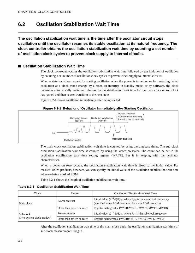
CHAPTER 6 CLOCK CONTROLLER
6.2 Oscillation Stabilization Wait Time
The oscillation stabilization wait time is the time after the oscillator circuit stops oscillation until the oscillator resumes its stable oscillation at its natural frequency. The clock controller obtains the oscillation stabilization wait time by counting a set number of oscillation clock cycles to prevent clock supply to internal circuits.
Oscillation Stabilization Wait TimeThe clock controller obtains the oscillation stabilization wait time followed by the initiation of oscillation
by counting a set number of oscillation clock cycles to prevent clock supply to internal circuits.
When a state transition request for starting oscillation when the power is turned on or for restarting halted
oscillation at a clock mode change by a reset, an interrupt in standby mode, or by software, the clock
controller automatically waits until the oscillation stabilization wait time for the main clock or sub clock
has passed and then causes transition to the next state.
Figure 6.2-1 shows oscillation immediately after being started.
Figure 6.2-1 Behavior of Oscillator Immediately after Starting Oscillation
The main clock oscillation stabilization wait time is counted by using the timebase timer. The sub clock
oscillation stabilization wait time is counted by using the watch prescaler. The count can be set in the
oscillation stabilization wait time setting register (WATR). Set it in keeping with the oscillator
characteristics.
When a power-on reset occurs, the oscillation stabilization wait time is fixed to the initial value. For
masked ROM products, however, you can specify the initial value of the oscillation stabilization wait time
when ordering masked ROM.
Table 6.2-1 shows the length of oscillation stabilization wait time.
After the oscillation stabilization wait time of the main clock ends, the oscillation stabilization wait time of
sub clock measurement is begun.
( )Oscillation stabilization wait time
Normal operationOperation after returning from stop mode or a reset
Oscillation started
X1
Oscillation time of oscillator
Oscillation stabilized
Table 6.2-1 Oscillation Stabilization Wait Time
Clock Factor Oscillation Stabilization Wait Time
Main clockPower-on reset
Initial value: (214-2)/FCH, where FCH is the main clock frequency
(specified when ROM is ordered for mask ROM products)
Other than power-on reset Register setting value (WATR:MWT3, MWT2, MWT1, MWT0)
Sub clock (Two-system clock product)
Power-on reset Initial value: (215-2)/FCL, where FCL is the sub clock frequency.
Other than power-on reset Register setting value (WATR:SWT3, SWT2, SWT1, SWT0)
48
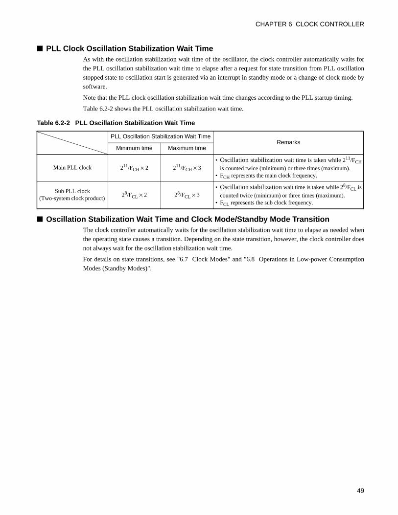
CHAPTER 6 CLOCK CONTROLLER
PLL Clock Oscillation Stabilization Wait TimeAs with the oscillation stabilization wait time of the oscillator, the clock controller automatically waits for
the PLL oscillation stabilization wait time to elapse after a request for state transition from PLL oscillation
stopped state to oscillation start is generated via an interrupt in standby mode or a change of clock mode by
software.
Note that the PLL clock oscillation stabilization wait time changes according to the PLL startup timing.
Table 6.2-2 shows the PLL oscillation stabilization wait time.
Oscillation Stabilization Wait Time and Clock Mode/Standby Mode TransitionThe clock controller automatically waits for the oscillation stabilization wait time to elapse as needed when
the operating state causes a transition. Depending on the state transition, however, the clock controller does
not always wait for the oscillation stabilization wait time.
For details on state transitions, see "6.7 Clock Modes" and "6.8 Operations in Low-power Consumption
Modes (Standby Modes)".
Table 6.2-2 PLL Oscillation Stabilization Wait Time
PLL Oscillation Stabilization Wait TimeRemarks
Minimum time Maximum time
Main PLL clock 211/FCH × 2 211/FCH × 3• Oscillation stabilization wait time is taken while 211/FCH
is counted twice (minimum) or three times (maximum).• FCH represents the main clock frequency.
Sub PLL clock (Two-system clock product)
28/FCL × 2 28/FCL × 3• Oscillation stabilization wait time is taken while 28/FCL is
counted twice (minimum) or three times (maximum).• FCL represents the sub clock frequency.
49
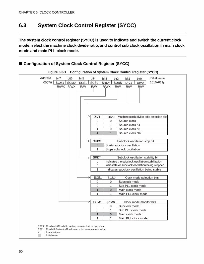
CHAPTER 6 CLOCK CONTROLLER
6.3 System Clock Control Register (SYCC)
The system clock control register (SYCC) is used to indicate and switch the current clock mode, select the machine clock divide ratio, and control sub clock oscillation in main clock mode and main PLL clock mode.
Configuration of System Clock Control Register (SYCC)
Figure 6.3-1 Configuration of System Clock Control Register (SYCC)
DIV1 Machine clock divide ratio selection bits 0 0 Source clock 0 1 Source clock / 41 0 Source clock / 81 1 Source clock /16
SUBS Subclock oscillation stop bit 0 Starts subclock oscillation 1 Stops subclock oscillation
SRDY Subclock oscillation stability bit
0 Indicates the subclock oscillation stabilization wait state or subclock oscillation being stopped
1 Indicates subclock oscillation being stable
Cock mode selection bits 0 0 Subclock mode 0 1 Sub PLL clock mode1 0 Main clock mode 1 1 Main PLL clock mode
Clock mode monitor bits0 0 Subclock mode 0 1 Sub PLL clock mode1 0 Main clock mode 1 1 Main PLL clock mode
SCS1 DIV0DIV1 SUBSSRDYSCS0SCM0SCM10007H
Address bit0 Initial value1010x011B
R/WR/WR/WR/WR/W R/WXR/WXR/WX
bit1bit2bit3 bit4 bit5 bit6 bit7
R/WX : Read only (Readable, writing has no effect on operation)R/W : Readable/writable (Read value is the same as write value) X : Indeterminate : Initial value
DIV0
SCS1 SCS0
SCM0SCM1
50
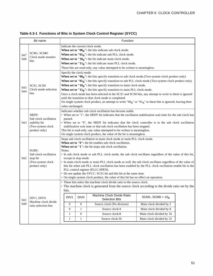
CHAPTER 6 CLOCK CONTROLLER
Table 6.3-1 Functions of Bits in System Clock Control Register (SYCC)
Bit name Function
bit7bit6
SCM1, SCM0:Clock mode monitor bits
Indicate the current clock mode.When set to "00B": the bits indicate sub clock mode.
When set to "01B": the bit indicate sub PLL clock mode.
When set to "10B": the bit indicate main clock mode.
When set to "11B": the bit indicate main PLL clock mode.
These bits are read-only; any value attempted to be written is meaningless.
bit5bit4
SCS1, SCS0:Clock mode selection bits
Specify the clock mode.When set to "00B": the bits specify transition to sub clock mode.(Two-system clock product only)
When set to "01B": the bits specify transition to sub PLL clock mode.(Two-system clock product only)
When set to "10B": the bits specify transition to main clock mode.
When set to "11B": the bits specify transition to main PLL clock mode.
Once a clock mode has been selected in the SCS1 and SCS0 bits, any attempt to write to them is ignored until the transition to that clock mode is completed.On single system clock product, an attempt to write "00B" or "01B" to these bits is ignored, leaving their
value unchanged.
bit3
SRDY:Sub clock oscillation stability bit(Two-system clock product only)
Indicates whether sub clock oscillation has become stable.• When set to "1", the SRDY bit indicates that the oscillation stabilization wait time for the sub clock has
passed.• When set to "0", the SRDY bit indicates that the clock controller is in the sub clock oscillation
stabilization wait state or that sub clock oscillation has been stopped.This bit is read-only; any value attempted to be written is meaningless.On single system clock product, the value of the bit is meaningless.
bit2
SUBS:Sub clock oscillation stop bit(Two-system clock product only)
Stops sub clock oscillation in main clock mode or main PLL clock mode.When set to "0": the bit enables sub clock oscillation.When set to "1": the bit stops sub clock oscillation.Notes: • In sub clock mode or sub PLL clock mode, the sub clock oscillates regardless of the value of this bit,
except in stop mode.• In main clock mode or main PLL clock mode as well, the sub clock oscillates regardless of the value of
this bit when sub PLL clock oscillation has been enabled by the PLL clock oscillation enable bit in thePLL control register (PLLC:SPEN).
• Do not update the SYCC: SCS1 bit and this bit at the same time.• On single system clock product, the value of this bit has no effect on operation.
bit1bit0
DIV1, DIV0:Machine clock divide ratio selection bits
• These bits select the machine clock divide ratio to the source clock.• The machine clock is generated from the source clock according to the divide ratio set by the
bits.
DIV1 DIV0Machine Clock Divide Ratio
Selection BitsSCM1, SCM0 = 10B
0 0 Source clock (No division) Main clock divided by 2
0 1 Source clock/4 Main clock divided by 8
1 0 Source clock/8 Main clock divided by 16
1 1 Source clock/16 Main clock divided by 32
51
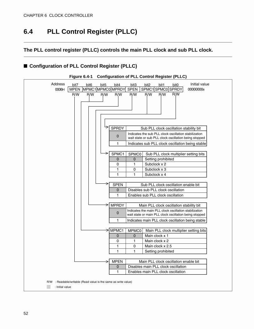
CHAPTER 6 CLOCK CONTROLLER
6.4 PLL Control Register (PLLC)
The PLL control register (PLLC) controls the main PLL clock and sub PLL clock.
Configuration of PLL Control Register (PLLC)
Figure 6.4-1 Configuration of PLL Control Register (PLLC)
SPRDY Sub PLL clock oscillation stability bit
0 Indicates the sub PLL clock oscillation stabilization wait state or sub PLL clock oscillation being stopped
1 Indicates sub PLL clock oscillation being stable
SPMC1 SPMC0 Sub PLL clock multiplier setting bits0 0 Setting prohibited 0 1 Subclock x 21 0 Subclock x 31 1 Subclock x 4
SPEN Sub PLL clock oscillation enable bit
0 Disables sub PLL clock oscillation1 Enables sub PLL clock oscillation
MPRDY Main PLL clock oscillation stability bit
0 Indicates the main PLL clock oscillation stabilization wait state or main PLL clock oscillation being stopped
1 Indicates main PLL clock oscillation being stable
MPMC1 Main PLL clock multiplier setting bits0 0 Main clock x 10 1 Main clock x 21 0 Main clock x 2.51 1 Setting prohibited
MPEN Main PLL clock oscillation enable bit
0 Disables main PLL clock oscillation1 Enables main PLL clock oscillation
bit7Address
0006H MPMC1
Initial value 00000000BMPEN MPMC0 SPEN SPMC0 SPRDY
R/W R/WR/WR/WR/W R/W R/WR/W
R/W : Readable/writable (Read value is the same as write value) : Initial value
MPRDY SPMC1bit6 bit5 bit4 bit3 bit2 bit1 bit0
MPMC0
52
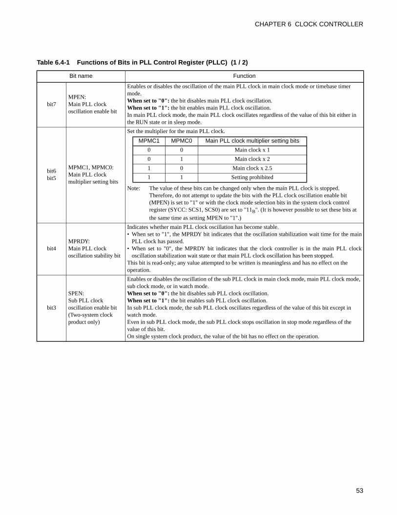
CHAPTER 6 CLOCK CONTROLLER
Table 6.4-1 Functions of Bits in PLL Control Register (PLLC) (1 / 2)
Bit name Function
bit7MPEN:Main PLL clock oscillation enable bit
Enables or disables the oscillation of the main PLL clock in main clock mode or timebase timer mode.When set to "0": the bit disables main PLL clock oscillation.When set to "1": the bit enables main PLL clock oscillation.In main PLL clock mode, the main PLL clock oscillates regardless of the value of this bit either in the RUN state or in sleep mode.
bit6bit5
MPMC1, MPMC0:Main PLL clock multiplier setting bits
Set the multiplier for the main PLL clock.
Note: The value of these bits can be changed only when the main PLL clock is stopped. Therefore, do not attempt to update the bits with the PLL clock oscillation enable bit (MPEN) is set to "1" or with the clock mode selection bits in the system clock control register (SYCC: SCS1, SCS0) are set to "11B". (It is however possible to set these bits at
the same time as setting MPEN to "1".)
bit4MPRDY:Main PLL clock oscillation stability bit
Indicates whether main PLL clock oscillation has become stable.• When set to "1", the MPRDY bit indicates that the oscillation stabilization wait time for the main
PLL clock has passed.• When set to "0", the MPRDY bit indicates that the clock controller is in the main PLL clock
oscillation stabilization wait state or that main PLL clock oscillation has been stopped.This bit is read-only; any value attempted to be written is meaningless and has no effect on the operation.
bit3
SPEN:Sub PLL clock oscillation enable bit(Two-system clock product only)
Enables or disables the oscillation of the sub PLL clock in main clock mode, main PLL clock mode, sub clock mode, or in watch mode.When set to "0": the bit disables sub PLL clock oscillation.When set to "1": the bit enables sub PLL clock oscillation.In sub PLL clock mode, the sub PLL clock oscillates regardless of the value of this bit except in watch mode.Even in sub PLL clock mode, the sub PLL clock stops oscillation in stop mode regardless of the value of this bit.On single system clock product, the value of the bit has no effect on the operation.
MPMC1 MPMC0 Main PLL clock multiplier setting bits
0 0 Main clock x 1
0 1 Main clock x 2
1 0 Main clock x 2.5
1 1 Setting prohibited
53
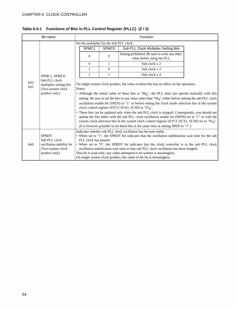
CHAPTER 6 CLOCK CONTROLLER
bit2bit1
SPMC1, SPMC0:Sub PLL clock multiplier setting bits(Two-system clock product only)
Set the multiplier for the Sub PLL clock.
On single system clock product, the value of these bits has no effect on the operation.Notes: • Although the initial value of these bits is "00B", the PLL does not operate normally with this
setting. Be sure to set the bits to any value other than "00B" either before setting the sub PLL clock
oscillation enable bit (SPEN) to "1" or before setting the clock mode selection bits in the systemclock control register (SYCC:SCS1, SCS0) to "01B".
• These bits can be updated only when the sub PLL clock is stopped. Consequently, you should notupdate the bits either with the sub PLL clock oscillation enable bit (SPEN) set to "1" or with thesystem clock selection bits in the system clock control register (SYCC:SCS1, SCS0) set to "01B".
(It is however possible to set these bits at the same time as setting SPEN to "1".)
bit0
SPRDY:Sub PLL clock oscillation stability bit(Two-system clock product only)
Indicates whether sub PLL clock oscillation has become stable.• When set to "1", the SPRDY bit indicates that the oscillation stabilization wait time for the sub
PLL clock has passed.• When set to "0", the SPRDY bit indicates that the clock controller is in the sub PLL clock
oscillation stabilization wait state or that sub PLL clock oscillation has been stopped.This bit is read-only; any value attempted to be written is meaningless.On single system clock product, the value of the bit is meaningless.
Table 6.4-1 Functions of Bits in PLL Control Register (PLLC) (2 / 2)
Bit name Function
SPMC1 SPMC0 Sub PLL Clock Multiplier Setting Bits
0 0Setting prohibited. Be sure to write any other
value before using the PLL.
0 1 Sub clock x 2
1 0 Sub clock x 3
1 1 Sub clock x 4
54
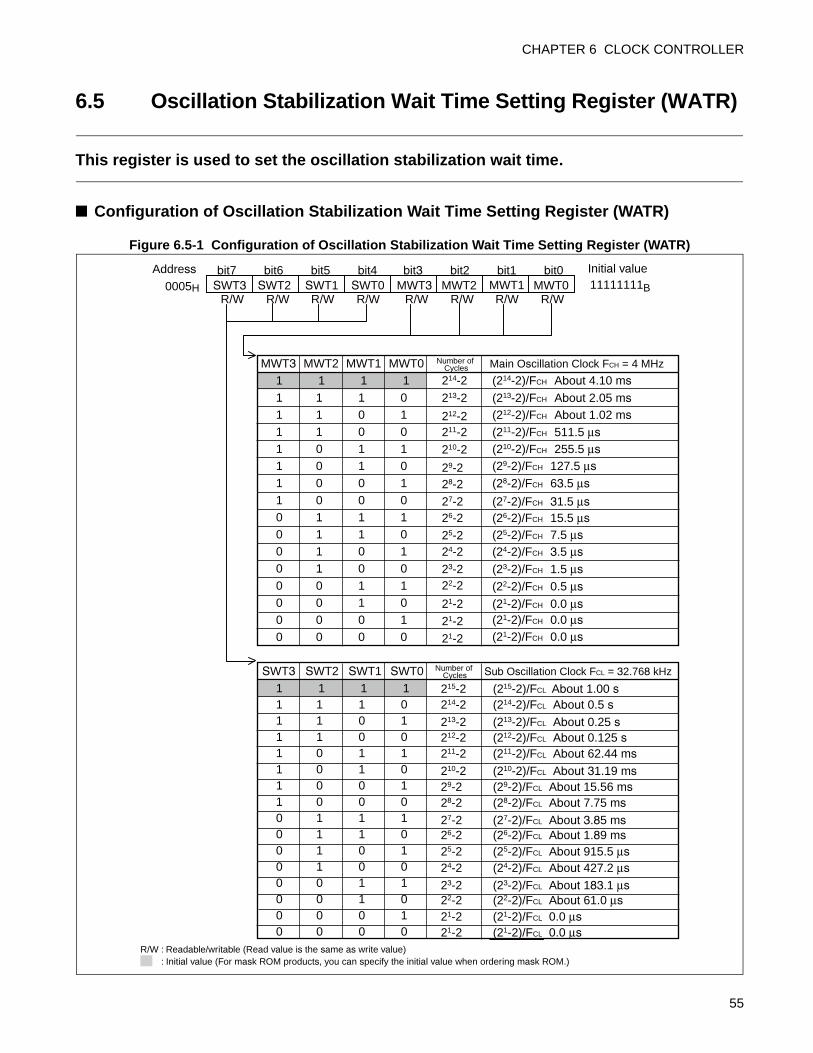
CHAPTER 6 CLOCK CONTROLLER
6.5 Oscillation Stabilization Wait Time Setting Register (WATR)
This register is used to set the oscillation stabilization wait time.
Configuration of Oscillation Stabilization Wait Time Setting Register (WATR)
Figure 6.5-1 Configuration of Oscillation Stabilization Wait Time Setting Register (WATR)
MWT3 MWT2 MWT1 MWT0 Number of Cycles
Number of Cycles
Main Oscillation Clock FCH = 4 MHz
1 1 1 1 214-2
213-2
212-2211-2
210-2
29-228-2
27-226-2
25-224-2
23-222-2
21-2
21-2
21-2
214-2215-2
213-2212-2211-2
210-229-228-2
27-226-225-224-2
23-222-221-221-2
(214-2)/FCH About 4.10 ms
(213-2)/FCH About 2.05 ms(212-2)/FCH About 1.02 ms(211-2)/FCH 511.5 µs(210-2)/FCH 255.5 µs(29-2)/FCH 127.5 µs
(28-2)/FCH 63.5 µs
(27-2)/FCH 31.5 µs(26-2)/FCH 15.5 µs(25-2)/FCH 7.5 µs(24-2)/FCH 3.5 µs
(23-2)/FCH 1.5 µs
(22-2)/FCH 0.5 µs
(21-2)/FCH 0.0 µs(21-2)/FCH 0.0 µs(21-2)/FCH 0.0 µs
1 1 1 01 1 0 11 1 0 01 0 1 11 0 1 01 0 0 11 0 0 00 1 1 10 1 1 00 1 0 10 1 0 00 0 1 10 0 1 00 0 0 10 0 0 0
SWT3 SWT2 SWT1 SWT0 Sub Oscillation Clock FCL = 32.768 kHz
1 1 1 1 1 1 1 01 1 0 11 1 0 01 0 1 11 0 1 01 0 0 11 0 0 00 1 1 10 1 1 00 1 0 10 1 0 00 0 1 10 0 1 00 0 0 10 0 0 0
(214-2)/FCL About 0.5 s (215-2)/FCL About 1.00 s
(213-2)/FCL About 0.25 s (212-2)/FCL About 0.125 s (211-2)/FCL About 62.44 ms
(210-2)/FCL About 31.19 ms (29-2)/FCL About 15.56 ms (28-2)/FCL About 7.75 ms
(27-2)/FCL About 3.85 ms (26-2)/FCL About 1.89 ms (25-2)/FCL About 915.5 µs (24-2)/FCL About 427.2 µs
(23-2)/FCL About 183.1 µs (22-2)/FCL About 61.0 µs(21-2)/FCL 0.0 µs (21-2)/FCL 0.0 µs
bit7 bit6 bit5 bit4 bit3 bit2 bit1 bit0Address
0005H SWT2 Initial value 11111111B SWT3 SWT1 SWT0 MWT3 MWT2 MWT1 MWT0
R/WR/WR/WR/WR/WR/WR/WR/W
R/W : Readable/writable (Read value is the same as write value) : Initial value (For mask ROM products, you can specify the initial value when ordering mask ROM.)
55
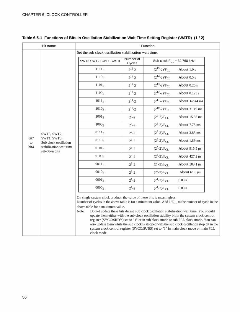
CHAPTER 6 CLOCK CONTROLLER
Table 6.5-1 Functions of Bits in Oscillation Stabilization Wait Time Setting Register (WATR) (1 / 2)
Bit name Function
bit7 to
bit4
SWT3, SWT2,SWT1, SWT0:Sub clock oscillation stabilization wait time selection bits
Set the sub clock oscillation stabilization wait time.
On single system clock product, the value of these bits is meaningless.Number of cycles in the above table is for a minimum value. Add 1/FCL to the number of cycle in the
above table for a maximum value.Note: Do not update these bits during sub clock oscillation stabilization wait time. You should
update them either with the sub clock oscillation stability bit in the system clock control register (SYCC:SRDY) set to "1" or in sub clock mode or sub PLL clock mode. You can also update them while the sub clock is stopped with the sub clock oscillation stop bit in the system clock control register (SYCC:SUBS) set to "1" in main clock mode or main PLL clock mode.
SWT3 SWT2 SWT1 SWT0Number of
CyclesSub clock FCL = 32.768 kHz
1111B 215-2 (215-2)/FCL About 1.0 s
1110B 214-2 (214-2)/FCL About 0.5 s
1101B 213-2 (213-2)/FCL About 0.25 s
1100B 212-2 (212-2)/FCL About 0.125 s
1011B 211-2 (211-2)/FCL About 62.44 ms
1010B 210-2 (210-2)/FCL About 31.19 ms
1001B 29-2 (29-2)/FCL About 15.56 ms
1000B 28-2 (28-2)/FCL About 7.75 ms
0111B 27-2 (27-2)/FCL About 3.85 ms
0110B 26-2 (26-2)/FCL About 1.89 ms
0101B 25-2 (25-2)/FCL About 915.5 µs
0100B 24-2 (24-2)/FCL About 427.2 µs
0011B 23-2 (23-2)/FCL About 183.1 µs
0010B 22-2 (22-2)/FCL About 61.0 µs
0001B 21-2 (21-2)/FCL 0.0 µs
0000B 21-2 (21-2)/FCL 0.0 µs
56
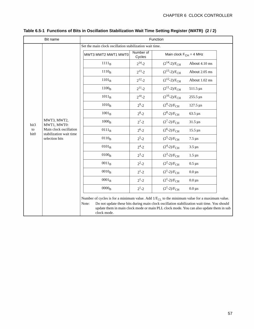
CHAPTER 6 CLOCK CONTROLLER
bit3to
bit0
MWT3, MWT2,MWT1, MWT0:Main clock oscillation stabilization wait time selection bits
Set the main clock oscillation stabilization wait time.
Number of cycles is for a minimum value. Add 1/FCL to the minimum value for a maximum value.
Note: Do not update these bits during main clock oscillation stabilization wait time. You should update them in main clock mode or main PLL clock mode. You can also update them in sub clock mode.
Table 6.5-1 Functions of Bits in Oscillation Stabilization Wait Time Setting Register (WATR) (2 / 2)
Bit name Function
MWT3 MWT2 MWT1 MWT0Number of
CyclesMain clock FCH = 4 MHz
1111B 214-2 (214-2)/FCH About 4.10 ms
1110B 213-2 (213-2)/FCH About 2.05 ms
1101B 212-2 (212-2)/FCH About 1.02 ms
1100B 211-2 (211-2)/FCH 511.5 µs
1011B 210-2 (210-2)/FCH 255.5 µs
1010B 29-2 (29-2)/FCH 127.5 µs
1001B 28-2 (28-2)/FCH 63.5 µs
1000B 27-2 (27-2)/FCH 31.5 µs
0111B 26-2 (26-2)/FCH 15.5 µs
0110B 25-2 (25-2)/FCH 7.5 µs
0101B 24-2 (24-2)/FCH 3.5 µs
0100B 23-2 (23-2)/FCH 1.5 µs
0011B 22-2 (22-2)/FCH 0.5 µs
0010B 21-2 (21-2)/FCH 0.0 µs
0001B 21-2 (21-2)/FCH 0.0 µs
0000B 21-2 (21-2)/FCH 0.0 µs
57
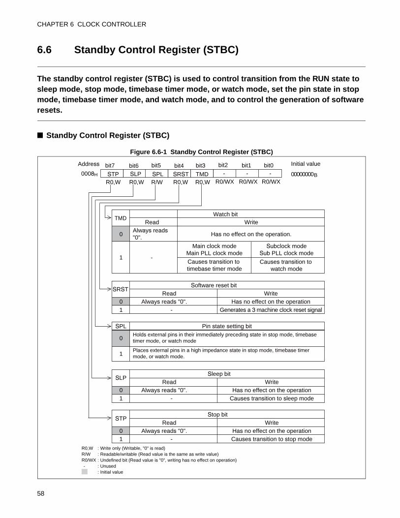
CHAPTER 6 CLOCK CONTROLLER
6.6 Standby Control Register (STBC)
The standby control register (STBC) is used to control transition from the RUN state to sleep mode, stop mode, timebase timer mode, or watch mode, set the pin state in stop mode, timebase timer mode, and watch mode, and to control the generation of software resets.
Standby Control Register (STBC)
Figure 6.6-1 Standby Control Register (STBC)
Watch bitTMD
Read Write
0 Always reads "0". Has no effect on the operation.
Main clock modeMain PLL clock mode
Subclock modeSub PLL clock mode
1 - Causes transition to timebase timer mode
Causes transition to watch mode
Software reset bit
SRST Read Write
0 Always reads "0". Has no effect on the operation 1 - Generates a 3 machine clock reset signal
SPL Pin state setting bit
0 Holds external pins in their immediately preceding state in stop mode, timebase timer mode, or watch mode
1 Places external pins in a high impedance state in stop mode, timebase timer mode, or watch mode.
Sleep bit
SLPRead Write
0 Always reads "0". Has no effect on the operation 1 - Causes transition to sleep mode
Stop bit STP
Read Write 0 Always reads "0". Has no effect on the operation 1 - Causes transition to stop mode
Address
0008H
bit7 bit6 bit3 Initial value
00000000BSTP SLP R/W SPL
R0,WR0,WR0,WR0,W R0/WX R0/WX R0/WX SRST TMD - - -
R0,W : Write only (Writable, "0" is read)R/W : Readable/writable (Read value is the same as write value)R0/WX : Undefined bit (Read value is "0", writing has no effect on operation)- : Unused
: Initial value
bit2 bit1 bit0bit5 bit4
58
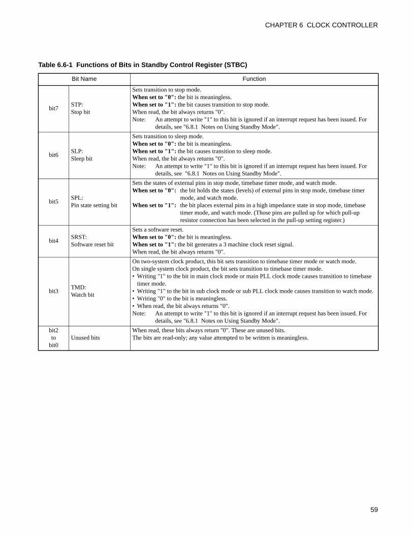
CHAPTER 6 CLOCK CONTROLLER
Table 6.6-1 Functions of Bits in Standby Control Register (STBC)
Bit Name Function
bit7STP:Stop bit
Sets transition to stop mode.When set to "0": the bit is meaningless.When set to "1": the bit causes transition to stop mode.When read, the bit always returns "0".Note: An attempt to write "1" to this bit is ignored if an interrupt request has been issued. For
details, see "6.8.1 Notes on Using Standby Mode".
bit6SLP:Sleep bit
Sets transition to sleep mode.When set to "0": the bit is meaningless.When set to "1": the bit causes transition to sleep mode.When read, the bit always returns "0".Note: An attempt to write "1" to this bit is ignored if an interrupt request has been issued. For
details, see "6.8.1 Notes on Using Standby Mode".
bit5SPL:Pin state setting bit
Sets the states of external pins in stop mode, timebase timer mode, and watch mode.When set to "0": the bit holds the states (levels) of external pins in stop mode, timebase timer
mode, and watch mode.When set to "1": the bit places external pins in a high impedance state in stop mode, timebase
timer mode, and watch mode. (Those pins are pulled up for which pull-up resistor connection has been selected in the pull-up setting register.)
bit4SRST:Software reset bit
Sets a software reset.When set to "0": the bit is meaningless.When set to "1": the bit generates a 3 machine clock reset signal.When read, the bit always returns "0".
bit3TMD:Watch bit
On two-system clock product, this bit sets transition to timebase timer mode or watch mode.On single system clock product, the bit sets transition to timebase timer mode.• Writing "1" to the bit in main clock mode or main PLL clock mode causes transition to timebase
timer mode.• Writing "1" to the bit in sub clock mode or sub PLL clock mode causes transition to watch mode.• Writing "0" to the bit is meaningless.• When read, the bit always returns "0".Note: An attempt to write "1" to this bit is ignored if an interrupt request has been issued. For
details, see "6.8.1 Notes on Using Standby Mode".
bit2to
bit0Unused bits
When read, these bits always return "0". These are unused bits.The bits are read-only; any value attempted to be written is meaningless.
59
CHAPTER 6 CLOCK CONTROLLER
Notes:
• Set the standby mode after making sure that the transition to clock mode has been completed bycomparing the values of the clock mode monitor bits (SYCC:SCM1,SCM0) and clock modesetting bits (SYCC:SCS1,SCS0) in the system clock control register.
• If you write "1" simultaneously to two or more of the stop bit (STP), sleep bit (SLP), software resetbit (SRST), and watch bit (TMD), priority is given to them in the following order:
(1) Software reset bit (SRST)
(2) Stop bit (STP)
(3) Watch bit (TMD)
(4) Sleep bit (SLP)
When released from the standby mode, the device returns to the normal operating status.
60
CHAPTER 6 CLOCK CONTROLLER
6.7 Clock Modes
The clock modes available are: main clock mode, sub clock mode, main PLL clock mode, and sub PLL clock mode. Mode switching takes place according to the settings in the system clock control register (SYCC).Sub clock mode and sub PLL clock mode are not supported by single system clock product.
Operations in Main Clock ModeMain clock mode uses the main clock as the machine clock for the CPU and peripheral resources.
The timebase timer operates with the main clock.
The watch prescaler and watch counter operate with the sub clock (on two-system clock product).
If you set standby mode during operation in main clock mode, the device can enter sleep mode, stop mode,
or timebase timer mode.
After a reset, main clock mode is always set regardless of the clock mode used before the reset.
Operations in Sub Clock Mode (on Two-system Clock Product) Sub clock mode uses the sub clock as the machine clock for the CPU and peripheral resources with main
clock oscillation stopped. In this mode, the timebase timer remains stopped as it requires the main clock for
operation.
If you set standby mode during operation in sub clock mode, the device can enter sleep mode, stop mode,
or watch mode.
Operations in Main PLL Clock ModeMain PLL clock mode uses the main PLL clock as the machine clock for the CPU and peripheral resources.
The timebase timer and watchdog timer operate with the main clock.
The watch prescaler and watch counter operate with the sub clock (on two-system clock product).
If you set standby mode during operation in main PLL clock mode, the device can enter sleep mode, stop
mode, or timebase timer mode.
Operations in Sub PLL Clock Mode (on Two-system Clock Product)Sub PLL clock mode uses the sub PLL clock as the machine clock for the CPU and peripheral resources
with main clock oscillation stopped. In this mode, the timebase timer remains stopped as it requires the
main clock for operation. The watch prescaler and watch counter operate with the sub clock.
If you set standby mode during operation in sub PLL clock mode, the device can enter sleep mode, stop
mode, or watch mode.
61
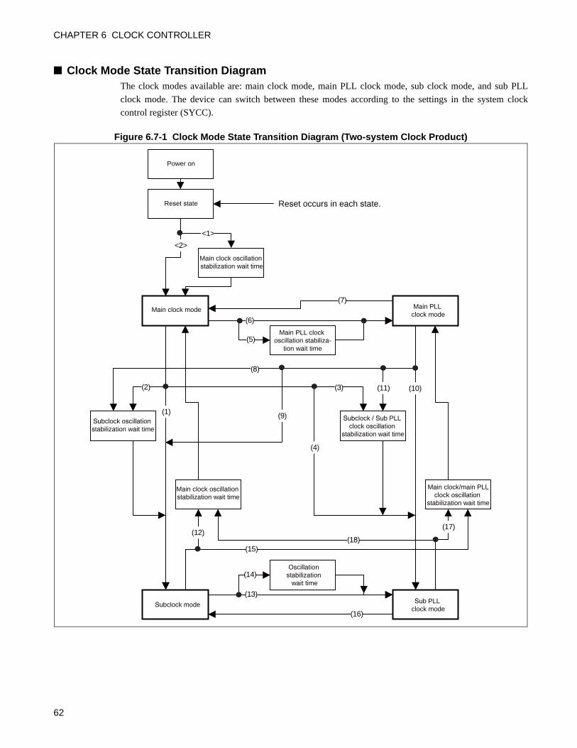
CHAPTER 6 CLOCK CONTROLLER
Clock Mode State Transition DiagramThe clock modes available are: main clock mode, main PLL clock mode, sub clock mode, and sub PLL
clock mode. The device can switch between these modes according to the settings in the system clock
control register (SYCC).
Figure 6.7-1 Clock Mode State Transition Diagram (Two-system Clock Product)
Power on
Reset state
Main clock oscillation stabilization wait time
Main PLL clock oscillation stabiliza-
tion wait time
Main clock oscillation stabilization wait time
Subclock oscillation stabilization wait time
Oscillation stabilization
wait time
Subclock mode
Main clock mode
Subclock / Sub PLL clock oscillation
stabilization wait time
Main clock/main PLLclock oscillation
stabilization wait time
(1)
(2) (3)
(5)
(7)
(6)
(8)
(10) (11)
(12)
(13)
(14)
(15)
(16)
(17)
(18)
(4)
(9)
Reset occurs in each state.
<1> <2>
Main PLL clock mode
Sub PLL clock mode
62
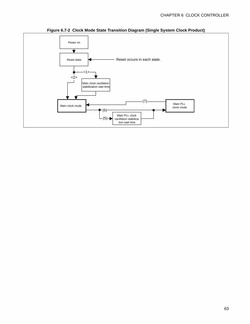
CHAPTER 6 CLOCK CONTROLLER
Figure 6.7-2 Clock Mode State Transition Diagram (Single System Clock Product)
Power on
Reset state
Main PLL clock oscillation stabiliza-
tion wait time
Main PLL clock mode
Main clock mode
(7)
Reset occurs in each state.
<1> <2>
(5)
(6)
Main clock oscillation stabilization wait time
63
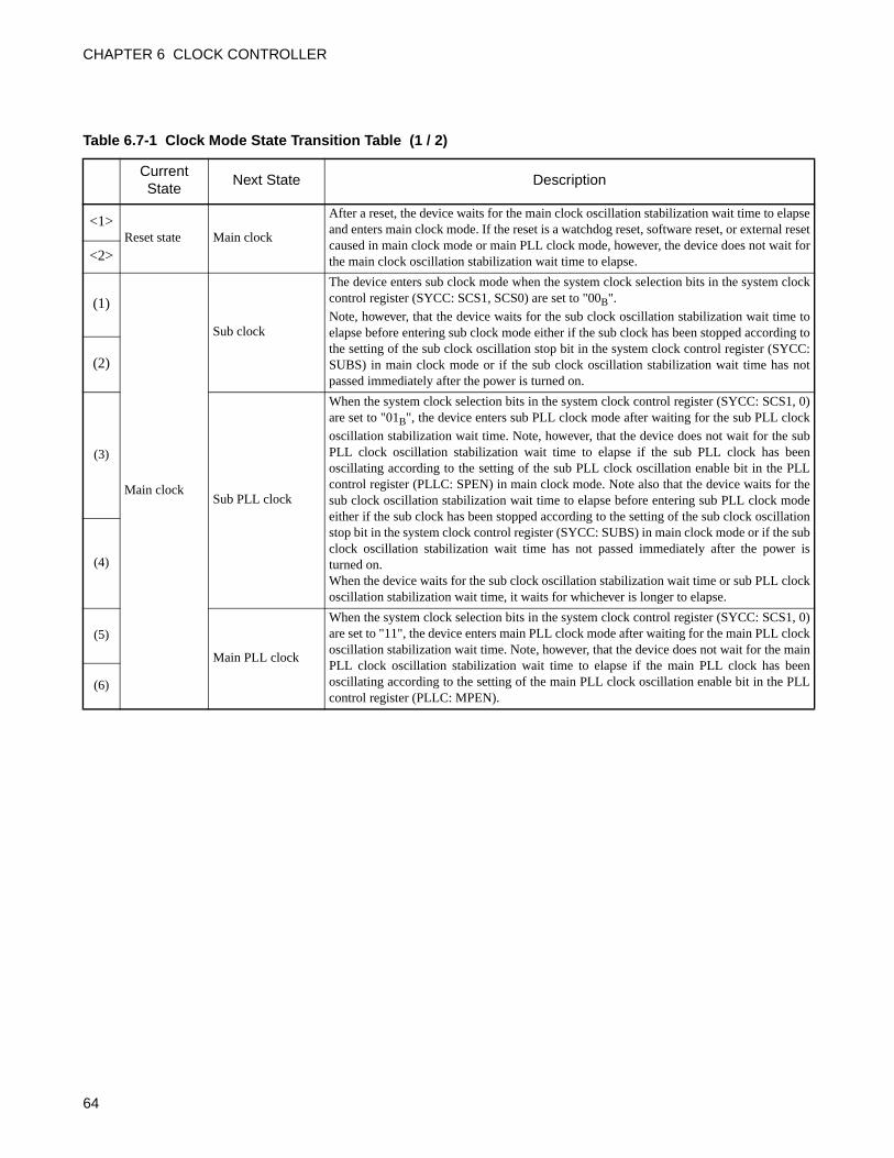
CHAPTER 6 CLOCK CONTROLLER
Table 6.7-1 Clock Mode State Transition Table (1 / 2)
Current State
Next State Description
<1>Reset state Main clock
After a reset, the device waits for the main clock oscillation stabilization wait time to elapseand enters main clock mode. If the reset is a watchdog reset, software reset, or external resetcaused in main clock mode or main PLL clock mode, however, the device does not wait forthe main clock oscillation stabilization wait time to elapse.<2>
(1)
Main clock
Sub clock
The device enters sub clock mode when the system clock selection bits in the system clockcontrol register (SYCC: SCS1, SCS0) are set to "00B".
Note, however, that the device waits for the sub clock oscillation stabilization wait time toelapse before entering sub clock mode either if the sub clock has been stopped according tothe setting of the sub clock oscillation stop bit in the system clock control register (SYCC:SUBS) in main clock mode or if the sub clock oscillation stabilization wait time has notpassed immediately after the power is turned on.
(2)
(3)
Sub PLL clock
When the system clock selection bits in the system clock control register (SYCC: SCS1, 0)are set to "01B", the device enters sub PLL clock mode after waiting for the sub PLL clock
oscillation stabilization wait time. Note, however, that the device does not wait for the subPLL clock oscillation stabilization wait time to elapse if the sub PLL clock has beenoscillating according to the setting of the sub PLL clock oscillation enable bit in the PLLcontrol register (PLLC: SPEN) in main clock mode. Note also that the device waits for thesub clock oscillation stabilization wait time to elapse before entering sub PLL clock modeeither if the sub clock has been stopped according to the setting of the sub clock oscillationstop bit in the system clock control register (SYCC: SUBS) in main clock mode or if the subclock oscillation stabilization wait time has not passed immediately after the power isturned on.When the device waits for the sub clock oscillation stabilization wait time or sub PLL clockoscillation stabilization wait time, it waits for whichever is longer to elapse.
(4)
(5)
Main PLL clock
When the system clock selection bits in the system clock control register (SYCC: SCS1, 0)are set to "11", the device enters main PLL clock mode after waiting for the main PLL clockoscillation stabilization wait time. Note, however, that the device does not wait for the mainPLL clock oscillation stabilization wait time to elapse if the main PLL clock has beenoscillating according to the setting of the main PLL clock oscillation enable bit in the PLLcontrol register (PLLC: MPEN).
(6)
64
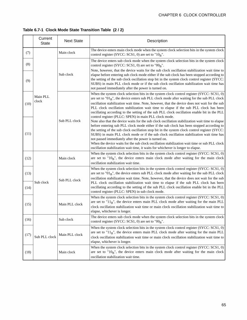
CHAPTER 6 CLOCK CONTROLLER
(7)
Main PLL clock
Main clockThe device enters main clock mode when the system clock selection bits in the system clockcontrol register (SYCC: SCS1, 0) are set to "10B".
(8)
Sub clock
The device enters sub clock mode when the system clock selection bits in the system clockcontrol register (SYCC: SCS1, 0) are set to "00B".
Note, however, that the device waits for the sub clock oscillation stabilization wait time toelapse before entering sub clock mode either if the sub clock has been stopped according tothe setting of the sub clock oscillation stop bit in the system clock control register (SYCC:SUBS) in main PLL clock mode or if the sub clock oscillation stabilization wait time hasnot passed immediately after the power is turned on.
(9)
(10)
Sub PLL clock
When the system clock selection bits in the system clock control register (SYCC: SCS1, 0)are set to "01B", the device enters sub PLL clock mode after waiting for the sub PLL clock
oscillation stabilization wait time. Note, however, that the device does not wait for the subPLL clock oscillation stabilization wait time to elapse if the sub PLL clock has beenoscillating according to the setting of the sub PLL clock oscillation enable bit in the PLLcontrol register (PLLC: SPEN) in main PLL clock mode.Note also that the device waits for the sub clock oscillation stabilization wait time to elapsebefore entering sub PLL clock mode either if the sub clock has been stopped according tothe setting of the sub clock oscillation stop bit in the system clock control register (SYCC:SUBS) in main PLL clock mode or if the sub clock oscillation stabilization wait time hasnot passed immediately after the power is turned on.When the device waits for the sub clock oscillation stabilization wait time or sub PLL clockoscillation stabilization wait time, it waits for whichever is longer to elapse.
(11)
(12)
Sub clock
Main clockWhen the system clock selection bits in the system clock control register (SYCC: SCS1, 0)are set to "10B", the device enters main clock mode after waiting for the main clock
oscillation stabilization wait time.
(13)
Sub PLL clock
When the system clock selection bits in the system clock control register (SYCC: SCS1, 0)are set to "01B", the device enters sub PLL clock mode after waiting for the sub PLL clock
oscillation stabilization wait time. Note, however, that the device does not wait for the subPLL clock oscillation stabilization wait time to elapse if the sub PLL clock has beenoscillating according to the setting of the sub PLL clock oscillation enable bit in the PLLcontrol register (PLLC: SPEN) in sub clock mode.
(14)
(15) Main PLL clock
When the system clock selection bits in the system clock control register (SYCC: SCS1, 0)are set to "11B", the device enters main PLL clock mode after waiting for the main PLL
clock oscillation stabilization wait time or main clock oscillation stabilization wait time toelapse, whichever is longer.
(16)
Sub PLL clock
Sub clockThe device enters sub clock mode when the system clock selection bits in the system clockcontrol register (SYCC: SCS1, 0) are set to "00B".
(17) Main PLL clock
When the system clock selection bits in the system clock control register (SYCC: SCS1, 0)are set to "11B", the device enters main PLL clock mode after waiting for the main PLL
clock oscillation stabilization wait time or main clock oscillation stabilization wait time toelapse, whichever is longer.
(18) Main clockWhen the system clock selection bits in the system clock control register (SYCC: SCS1, 0)are set to "10B", the device enters main clock mode after waiting for the main clock
oscillation stabilization wait time.
Table 6.7-1 Clock Mode State Transition Table (2 / 2)
Current State
Next State Description
65
CHAPTER 6 CLOCK CONTROLLER
6.8 Operations in Low-power Consumption Modes (Standby Modes)
The standby modes available are: sleep mode, stop mode, timebase timer mode, and watch mode.
Overview of Transitions to and from Standby ModeThe standby modes available are: sleep mode, stop mode, timebase timer mode, and watch mode. The
device enters standby mode according to the settings in the standby control register (STBC).
The device is released from standby mode in response to an interrupt or reset. Before transition to normal
operation, the device waits for the oscillation stabilization wait time to elapse as required.
When released from standby mode by a reset, the device returns to main clock mode. When released from
standby mode by an interrupt, the device enters the clock mode in which the device was before entering the
standby mode.
Pin States in Standby ModeThe pin state setting bit (STBC:SPL) of the standby control register can be used to set the I/O port/
peripheral resource pins in the stop mode, timebase timer mode, or watch mode to hold their immediately
preceding state or to be placed in a high impedance state.
See "APPENDIX D Pin Status of MB95130/M series" for the states of all pins in standby modes.
66
CHAPTER 6 CLOCK CONTROLLER
6.8.1 Notes on Using Standby Mode
Even if the standby control register (STBC) sets standby mode, transition to the standby mode does not take place when an interrupt request has been issued from a peripheral resource. When the device returns from standby mode to the normal operating state in response to an interrupt, the operation that follows varies depending on whether the interrupt request is accepted or not.
Place at Least Three NOP Instructions Immediately Following a Standby Mode Setting Instruction.
The device requires four machine clock cycles before entering standby mode after it is set in the standby
control register. During that period, the CPU executes the program. To avoid program execution during this
transition to standby mode, enter at least three NOP instructions.
The device operates normally if you place instructions other than NOP instructions. In that case, however,
note that the device may execute the instructions to be executed after being released from standby mode
before entering the standby mode and that the device may enter the standby mode during instruction
execution, which is resumed after the device is released from the standby mode (increasing the number of
instruction execution cycles).
Check That Clock-mode Transition has been Completed before Setting Standby Mode.Before setting standby mode, make sure that clock-mode transition has been completed by comparing the
values of the clock mode monitor bit (SYCC: SCM1, 0) and clock mode setting bit (SYCC: SCS1, 0) in the
system clock control register.
An Interrupt Request may Suppress Transition to Standby Mode.If an attempt is made to set a standby mode while an interrupt request with an interrupt level higher than
"11B" has been issued, the device ignores the attempt to write to the standby control register and continues
instruction execution without entering the standby mode. The device does not enter the standby mode even
after having serviced the interrupt.
This behavior is the same as when interrupts are disabled by the interrupt enable flag (CCR:I) and interrupt
level bits in the condition code register (CCR:IL 1,0) of the CPU.
Standby Mode is Also Canceled when the CPU Rejects Interrupts.When an interrupt request with an interrupt level higher than "11B" is issued in standby mode, the device is
released from the standby mode regardless of the settings of the interrupt enable flag (CCR: I) and interrupt
level bits (CCR:IL1,0) of the condition code register of the CPU.
After being released from standby mode, the device services the interrupt when the CPU's condition code
register has been set to accept interrupts. If the register has been set to reject interrupts, the device resumes
processing from the instruction that follows the last instruction executed before entering the standby mode.
67
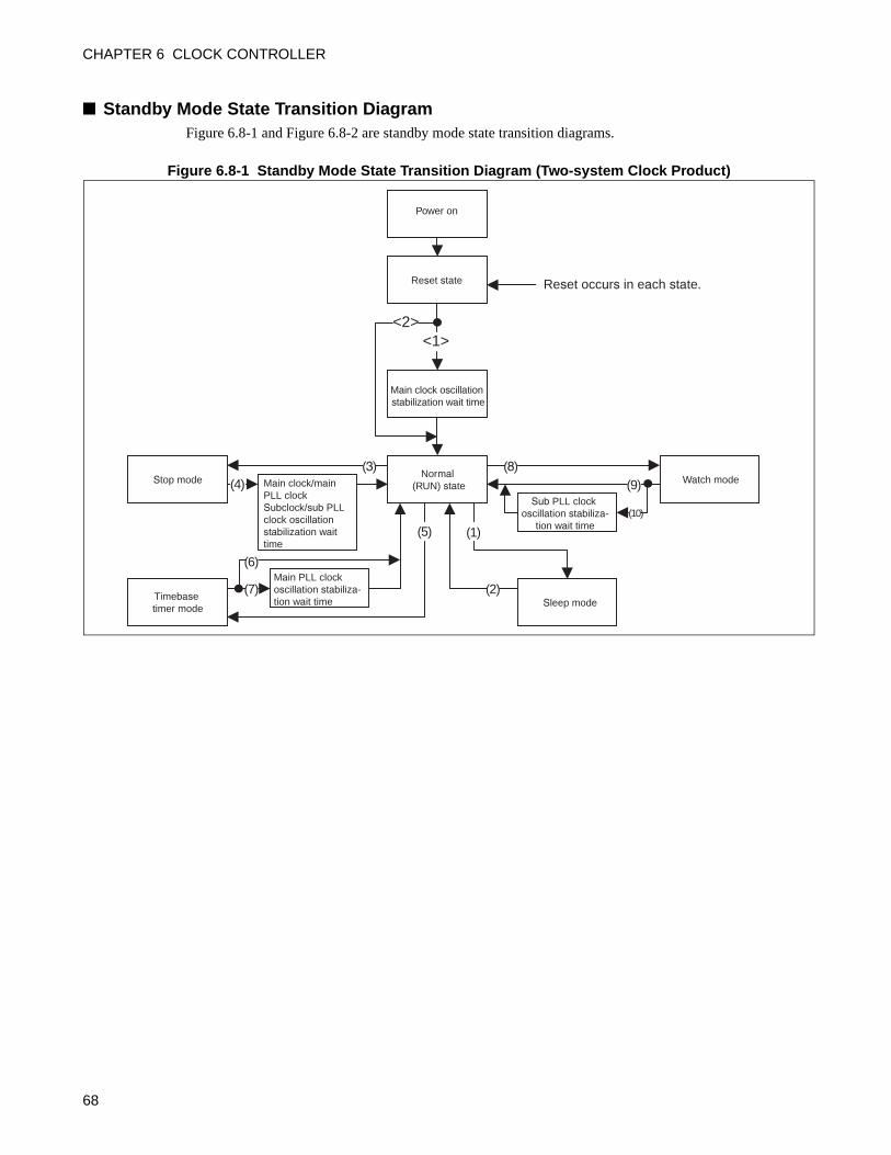
CHAPTER 6 CLOCK CONTROLLER
Standby Mode State Transition DiagramFigure 6.8-1 and Figure 6.8-2 are standby mode state transition diagrams.
Figure 6.8-1 Standby Mode State Transition Diagram (Two-system Clock Product)
Power on
Reset state
Main clock oscillation stabilization wait time
Normal (RUN) state
Watch mode
<2> <1>
Main clock/main PLL clockSubclock/sub PLL clock oscillation stabilization wait time
Main PLL clock oscillation stabiliza-tion wait timeTimebase
timer mode
Stop mode
Sleep mode
Sub PLL clock oscillation stabiliza-
tion wait time(1)
(2)
(3)(4)
(5)
(6)
(7)
(8)(9)
(10)
Reset occurs in each state.
68
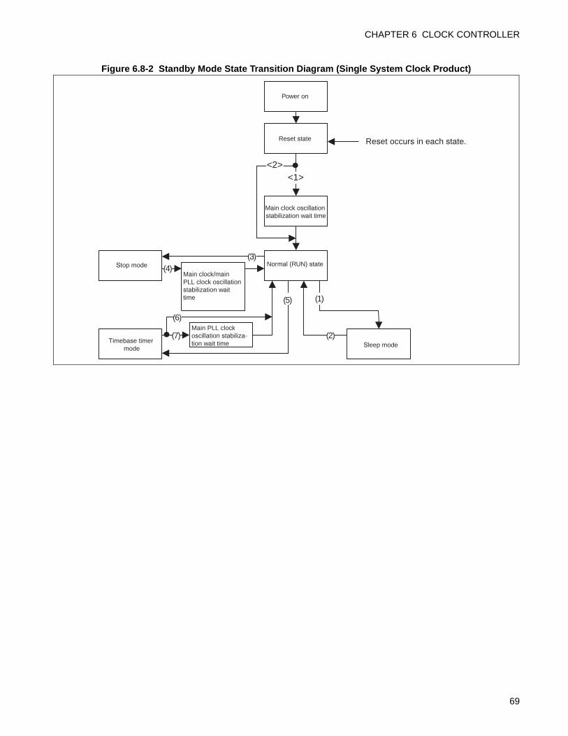
CHAPTER 6 CLOCK CONTROLLER
Figure 6.8-2 Standby Mode State Transition Diagram (Single System Clock Product)
Power on
Reset state Reset occurs in each state.
Main clock/main PLL clock oscillation stabilization wait time
Main PLL clock oscillation stabiliza-tion wait timeTimebase timer
mode
Stop mode
Sleep mode
(1)
(2)
(3)(4)
(5)
(6)
(7)
Main clock oscillation stabilization wait time
Normal (RUN) state
<1><2>
69
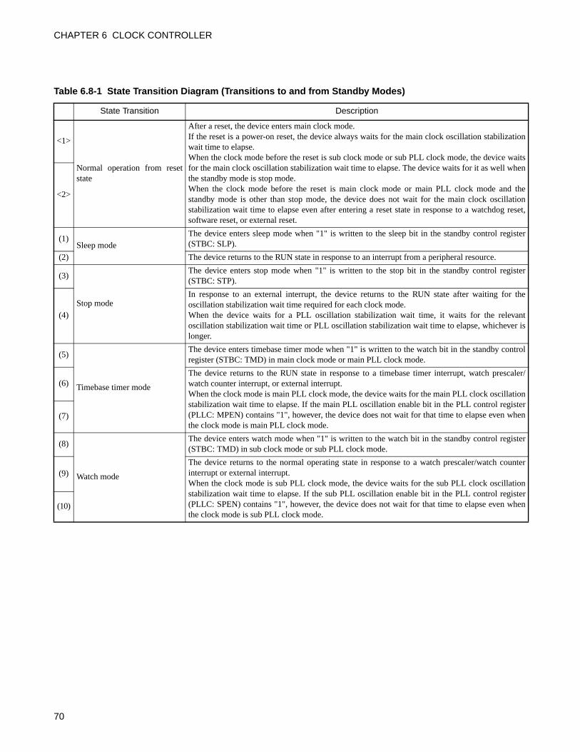
CHAPTER 6 CLOCK CONTROLLER
Table 6.8-1 State Transition Diagram (Transitions to and from Standby Modes)
State Transition Description
<1>
Normal operation from resetstate
After a reset, the device enters main clock mode.If the reset is a power-on reset, the device always waits for the main clock oscillation stabilizationwait time to elapse.When the clock mode before the reset is sub clock mode or sub PLL clock mode, the device waitsfor the main clock oscillation stabilization wait time to elapse. The device waits for it as well whenthe standby mode is stop mode.When the clock mode before the reset is main clock mode or main PLL clock mode and thestandby mode is other than stop mode, the device does not wait for the main clock oscillationstabilization wait time to elapse even after entering a reset state in response to a watchdog reset,software reset, or external reset.
<2>
(1)Sleep mode
The device enters sleep mode when "1" is written to the sleep bit in the standby control register(STBC: SLP).
(2) The device returns to the RUN state in response to an interrupt from a peripheral resource.
(3)
Stop mode
The device enters stop mode when "1" is written to the stop bit in the standby control register(STBC: STP).
(4)
In response to an external interrupt, the device returns to the RUN state after waiting for theoscillation stabilization wait time required for each clock mode.When the device waits for a PLL oscillation stabilization wait time, it waits for the relevantoscillation stabilization wait time or PLL oscillation stabilization wait time to elapse, whichever islonger.
(5)
Timebase timer mode
The device enters timebase timer mode when "1" is written to the watch bit in the standby controlregister (STBC: TMD) in main clock mode or main PLL clock mode.
(6)The device returns to the RUN state in response to a timebase timer interrupt, watch prescaler/watch counter interrupt, or external interrupt.When the clock mode is main PLL clock mode, the device waits for the main PLL clock oscillationstabilization wait time to elapse. If the main PLL oscillation enable bit in the PLL control register(PLLC: MPEN) contains "1", however, the device does not wait for that time to elapse even whenthe clock mode is main PLL clock mode.
(7)
(8)
Watch mode
The device enters watch mode when "1" is written to the watch bit in the standby control register(STBC: TMD) in sub clock mode or sub PLL clock mode.
(9)The device returns to the normal operating state in response to a watch prescaler/watch counterinterrupt or external interrupt.When the clock mode is sub PLL clock mode, the device waits for the sub PLL clock oscillationstabilization wait time to elapse. If the sub PLL oscillation enable bit in the PLL control register(PLLC: SPEN) contains "1", however, the device does not wait for that time to elapse even whenthe clock mode is sub PLL clock mode.
(10)
70
CHAPTER 6 CLOCK CONTROLLER
6.8.2 Sleep Mode
Sleep mode stops the operations of the CPU and watchdog timer.
Operations in Sleep ModeSleep mode stops the operating clock for the CPU and watchdog timer. In this mode, the CPU stops while
retaining the contents of registers and RAM that exist immediately before the transition to sleep mode, but
the peripheral resources except the watchdog timer continue operating.
Transition to sleep mode
Writing "1" to the sleep bit in the standby control register (STBC:SLP) causes the device to enter sleep
mode.
Cancellation of sleep mode
A reset or an interrupt from a peripheral resource releases the device from sleep mode.
71
CHAPTER 6 CLOCK CONTROLLER
6.8.3 Stop Mode
Stop mode stops the main clock.
Operations in Stop ModeStop mode stops the main clock. In this mode, the device stops all the functions except external interrupt
and low-voltage detection reset while retaining the contents of registers and RAM that exist immediately
before the transition to stop mode.
In main clock mode or main PLL clock mode, however, you can start or stop sub clock oscillation by
setting the sub clock oscillation stop bit in the system clock control register (SYCC: SUBS). When the sub
clock is oscillating, the watch prescaler and watch counter operate.
Transition to stop mode
Writing "1" to the stop bit in the standby control register (STBC:STP) causes the device to enter stop mode.
At this time, the states of external pins are retained when the pin state setting bit in the standby control
register (STBC:SPL) is "0", and the states of external pins become high impedance when that bit is "1"
(those pins are pulled up for which pull-up resistor connection has been selected in the pull-up setting
register).
In main clock mode or main PLL clock mode, a timebase timer interrupt request may be generated while
the device is waiting for main clock oscillation to stabilize after being released from stop mode by an
interrupt. If the interrupt interval time of the timebase timer is shorter than the main clock oscillation
stabilization wait time, you should disable interrupt requests output from the timebase timer before entering
stop mode, thereby preventing unexpected interrupts from occurring.
You should also disable interrupt requests output from the watch prescaler before entering stop mode in sub
clock mode or sub PLL clock mode.
Cancellation of stop mode
The device is released from stop mode in response to a reset or an external interrupt.
In main clock mode or main PLL clock mode, you can start or stop sub clock oscillation by setting the sub
clock oscillation stop bit in the system clock control register (SYCC: SUBS). When the sub clock is
oscillating, you can also release the device from stop mode using an interrupt by the watch prescaler or
watch counter.
Note:
When stop mode is canceled via an interrupt, peripheral resources placed into stop mode during anaction resume that action. Therefore, the initial interval time of the interval timer and other similarsettings are rendered indeterminate. After recovery from stop mode, initialize each peripheralresource as necessary.
72
CHAPTER 6 CLOCK CONTROLLER
6.8.4 Timebase Timer Mode
Timebase timer mode allows only the main clock oscillation, sub clock oscillation, timebase timer, and watch prescaler to work. The operating clock for the CPU and peripheral resources is stopped in this mode.
Operations in Timebase Timer ModeIn timebase timer mode, main clock supply is stopped except for the timebase timer. The device stops all
the functions except timebase timer, external interrupt and low-voltage detection reset while retaining the
contents of registers and RAM that exist immediately before the transition to timebase timer mode.
You can however start or stop sub clock oscillation by setting the sub clock oscillation stop bit in the
system clock control register (SYCC: SUBS). When the sub clock is oscillating, the watch prescaler and
watch counter operate.
Transition to timebase timer mode
Writing "1" to the watch bit in the standby control register (STBC:TMD) causes the device to enter
timebase timer mode if the system clock monitor bits in the system clock control register (SYCC: SCM1,
SCM0) are "10B" or "11B".
The device can enter timebase timer mode only when the clock mode is main clock mode or main PLL
clock mode.
Upon transition to timebase timer mode, the states of external pins are retained when the pin state setting
bit in the standby control register (STBC:SPL) is "0", and the states of external pins become high
impedance when that bit is "1" (those pins are pulled up for which pull-up resistor connection has been
selected in the pull-up setting register).
Cancellation of timebase timer mode
The device is released from timebase timer mode in response to a reset, timebase timer interrupt, or
external interrupt.
You can start or stop sub clock oscillation by setting the sub clock oscillation stop bit in the system clock
control register (SYCC: SUBS). When the sub clock is oscillating, you can also release the device from
timebase timer mode using an interrupt by the watch prescaler or watch counter.
Note:
When timebase timer mode is canceled via an interrupt, peripheral resources placed into timebasetimer mode during an action resume that action. Therefore, the initial interval time of the intervaltimer and other similar settings are rendered indeterminate. After recovery from timebase timermode, initialize each peripheral resource as necessary.
73
CHAPTER 6 CLOCK CONTROLLER
6.8.5 Watch Mode
Watch mode allows only the sub clock and watch prescaler to work. The operating clock for the CPU and peripheral resources is stopped in this mode.
Operations in Watch ModeIn watch mode, the operating clock for the CPU and peripheral resources is stopped. The device stops all
the functions except the watch prescaler, watch counter, external interrupt, and low-voltage detection reset
while retaining the contents of registers and RAM that exist immediately before the transition to watch
mode.
Transition to watch mode
Writing "1" to the watch bit in the standby control register (STBC:TMD) causes the device to enter watch
mode if the system clock monitor bits in the system clock control register (SYCC: SCM1, SCM0) are
"00B" or "01B".
The device can enter watch mode only when the clock mode is sub clock mode or sub PLL clock mode.
Upon transition to watch mode, the states of external pins are retained when the pin state setting bit in the
standby control register (STBC:SPL) is "0", and the states of external pins become high impedance when
that bit is "1" (those pins are pulled up for which pull-up resistor connection has been selected in the pull-
up setting register).
Cancellation of watch mode
The device is released from watch mode in response to a reset, watch interrupt, or external interrupt.
Note:
When watch mode is canceled via an interrupt, peripheral resources placed into watch mode duringan action resume that action. Therefore, the initial interval time of the interval timer and other similarsettings are rendered indeterminate. After recovery from watch mode, initialize each peripheralresource as necessary.
74
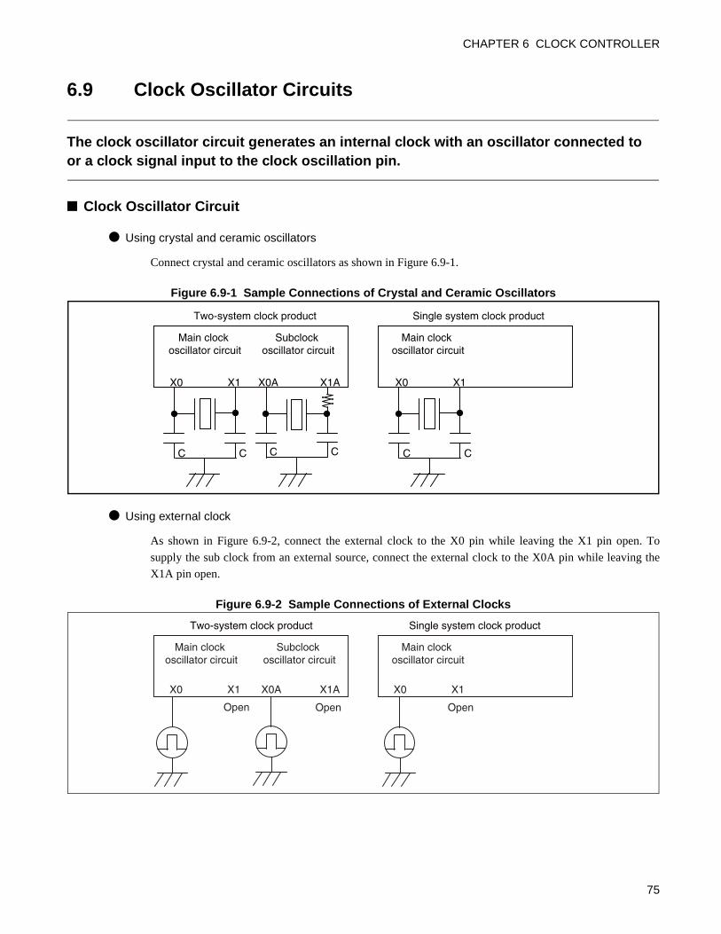
CHAPTER 6 CLOCK CONTROLLER
6.9 Clock Oscillator Circuits
The clock oscillator circuit generates an internal clock with an oscillator connected to or a clock signal input to the clock oscillation pin.
Clock Oscillator Circuit
Using crystal and ceramic oscillators
Connect crystal and ceramic oscillators as shown in Figure 6.9-1.
Figure 6.9-1 Sample Connections of Crystal and Ceramic Oscillators
Using external clock
As shown in Figure 6.9-2, connect the external clock to the X0 pin while leaving the X1 pin open. To
supply the sub clock from an external source, connect the external clock to the X0A pin while leaving the
X1A pin open.
Figure 6.9-2 Sample Connections of External Clocks
X0 X1 X0A X1A 63/ I NT13/ X0A P64/ X1
Main clock oscillator circuit
Subclock oscillator circuit
Main clock oscillator circuit
Two-system clock product Single system clock product
C C C C C C
X0 X1
Main clock oscillator circuit
Subclock oscillator circuit
Main clock oscillator circuit
Open Open Open
X0 X1 X0 X1X0A X1A
Two-system clock product Single system clock product
75

CHAPTER 6 CLOCK CONTROLLER
Note:
If you use only the main clock without using sub clock oscillation on a two-system clock product andit enters sub clock mode for some reason, there is no solution to recovering its operation as there isno clock supply available. If you use the main clock alone, therefore, be sure to select a singlesystem clock product.
76
CHAPTER 6 CLOCK CONTROLLER
6.10 Overview of Prescaler
The prescaler generates the count clock source for various peripheral resources from the machine clock (MCLK) and the count clock output from the time-base timer.
PrescalerThe prescaler generates the count clock source for various peripheral resources from the machine clock
(MCLK) that drives the CPU and the count clock (27/FCH or 28/FCH) output from of the time-base timer.
The count clock source is a clock frequency-divided by the prescaler or a buffered clock, used by the
peripheral resources listed below.
Note that the prescaler has no control register and operates continuously driven by the machine clock
(MCLK) and the count clock (27/FCH or 28/FCH) of the timebase timer.
• 8/16-bit compound timer 0
• 8/16-bit PPG timer 0, 1
• 16-bit PPG timer 0
• UART/SIO baud rate generator 0
• 8/10-bit A/D converter
77
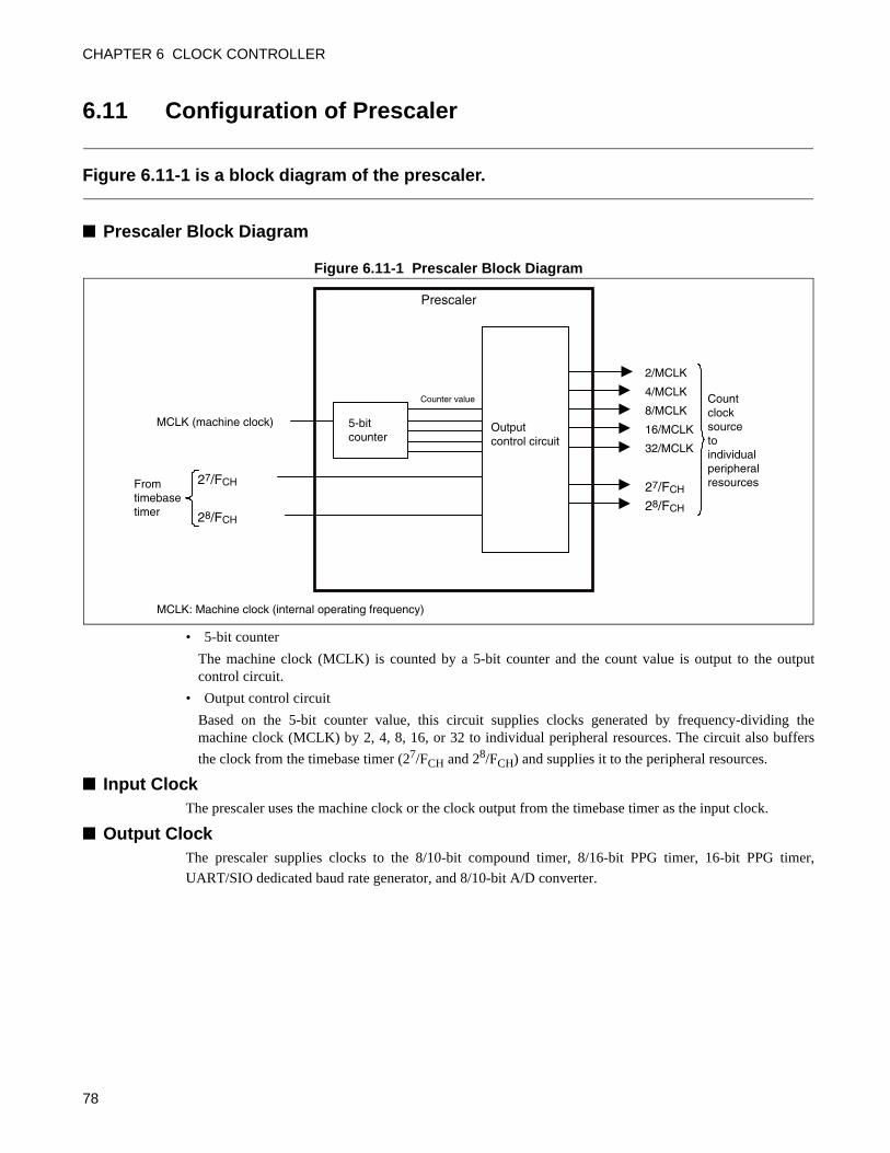
CHAPTER 6 CLOCK CONTROLLER
6.11 Configuration of Prescaler
Figure 6.11-1 is a block diagram of the prescaler.
Prescaler Block Diagram
Figure 6.11-1 Prescaler Block Diagram
• 5-bit counter
The machine clock (MCLK) is counted by a 5-bit counter and the count value is output to the outputcontrol circuit.
• Output control circuit
Based on the 5-bit counter value, this circuit supplies clocks generated by frequency-dividing themachine clock (MCLK) by 2, 4, 8, 16, or 32 to individual peripheral resources. The circuit also buffers
the clock from the timebase timer (27/FCH and 28/FCH) and supplies it to the peripheral resources.
Input ClockThe prescaler uses the machine clock or the clock output from the timebase timer as the input clock.
Output ClockThe prescaler supplies clocks to the 8/10-bit compound timer, 8/16-bit PPG timer, 16-bit PPG timer,
UART/SIO dedicated baud rate generator, and 8/10-bit A/D converter.
MCLK: Machine clock (internal operating frequency)
Prescaler
27/FCH
Output control circuit
28/FCH
MCLK (machine clock)
From timebase timer
Count clock sourceto individual peripheral resources
5-bit counter
27/FCH
2/MCLK
28/FCH
4/MCLK
8/MCLK
16/MCLK
32/MCLK
Counter value
78
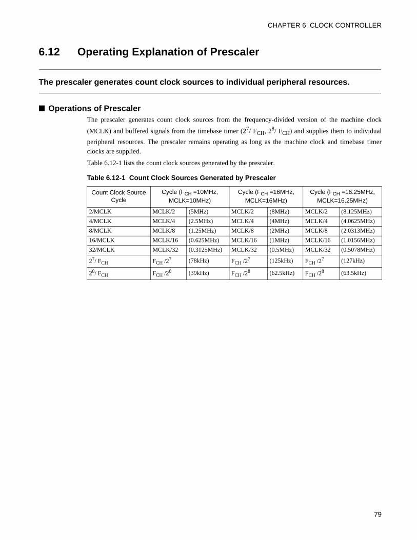
CHAPTER 6 CLOCK CONTROLLER
6.12 Operating Explanation of Prescaler
The prescaler generates count clock sources to individual peripheral resources.
Operations of PrescalerThe prescaler generates count clock sources from the frequency-divided version of the machine clock
(MCLK) and buffered signals from the timebase timer (27/ FCH, 28/ FCH) and supplies them to individual
peripheral resources. The prescaler remains operating as long as the machine clock and timebase timer
clocks are supplied.
Table 6.12-1 lists the count clock sources generated by the prescaler.
Table 6.12-1 Count Clock Sources Generated by Prescaler
Count Clock Source Cycle
Cycle (FCH =10MHz, MCLK=10MHz)
Cycle (FCH =16MHz, MCLK=16MHz)
Cycle (FCH =16.25MHz, MCLK=16.25MHz)
2/MCLK MCLK/2 (5MHz) MCLK/2 (8MHz) MCLK/2 (8.125MHz)
4/MCLK MCLK/4 (2.5MHz) MCLK/4 (4MHz) MCLK/4 (4.0625MHz)
8/MCLK MCLK/8 (1.25MHz) MCLK/8 (2MHz) MCLK/8 (2.0313MHz)
16/MCLK MCLK/16 (0.625MHz) MCLK/16 (1MHz) MCLK/16 (1.0156MHz)
32/MCLK MCLK/32 (0.3125MHz) MCLK/32 (0.5MHz) MCLK/32 (0.5078MHz)
27/ FCH FCH /27 (78kHz) FCH /27 (125kHz) FCH /27 (127kHz)
28/ FCH FCH /28 (39kHz) FCH /28 (62.5kHz) FCH /28 (63.5kHz)
79
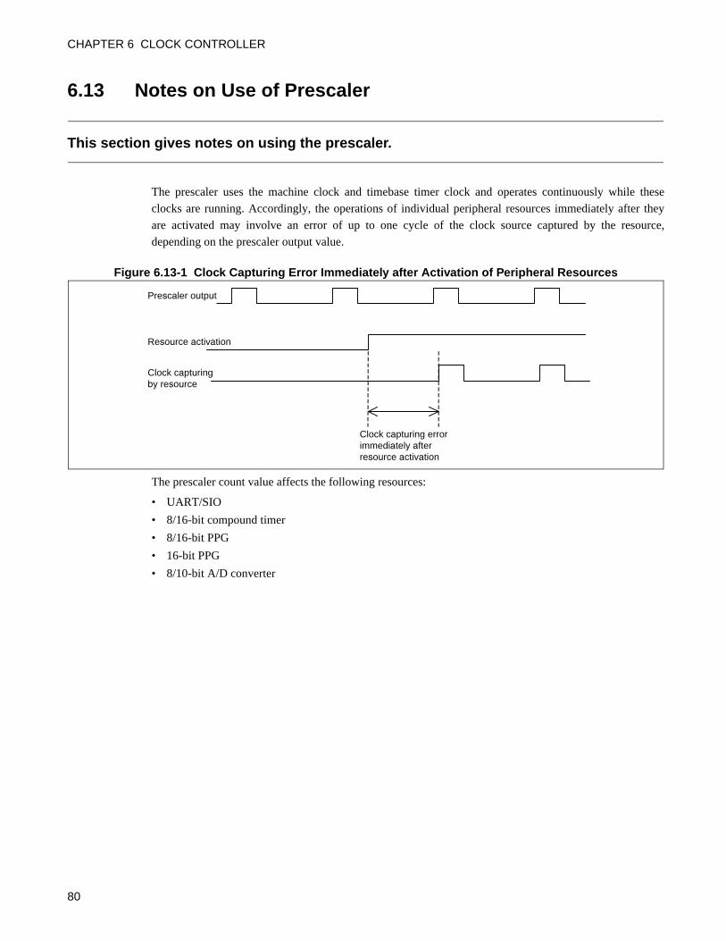
CHAPTER 6 CLOCK CONTROLLER
6.13 Notes on Use of Prescaler
This section gives notes on using the prescaler.
The prescaler uses the machine clock and timebase timer clock and operates continuously while these
clocks are running. Accordingly, the operations of individual peripheral resources immediately after they
are activated may involve an error of up to one cycle of the clock source captured by the resource,
depending on the prescaler output value.
Figure 6.13-1 Clock Capturing Error Immediately after Activation of Peripheral Resources
The prescaler count value affects the following resources:
• UART/SIO
• 8/16-bit compound timer
• 8/16-bit PPG
• 16-bit PPG
• 8/10-bit A/D converter
Prescaler output
Resource activation
Clock capturing by resource
Clock capturing error immediately after resource activation
80
CHAPTER 7RESET
This section describes the reset operation.
7.1 Reset Operation
7.2 Reset Source Register (RSRR)
81
CHAPTER 7 RESET
7.1 Reset Operation
When a reset factor occurs, the CPU stops the current execution immediately and enters the reset release wait state. When the device is released from the reset, the CPU reads mode data and the reset vector from internal ROM (mode fetch). When the power is turned on or when the device is released from a reset in sub clock mode, sub-PLL clock mode, or stop mode, the CPU performs mode fetch after the oscillation stabilization wait time has passed.
Reset FactorsResets are classified into four reset factors.
External reset
An external reset is generated upon "L" level input to the external reset pin (RST).
An externally input reset signal is accepted asynchronously via the internal noise filter and generates an
internal reset signal in synchronization with the machine clock to initialize the internal circuit.
Consequently, a clock is necessary for internal circuit initialization. Clock input is therefore necessary for
operation with an external clock. Note, however, that external pins (including I/O ports and peripheral
resources) are reset asynchronously. Additionally, there are standard pulse-width values for external reset
input. If the value is below the standard, the reset may not be accepted.
The standard value is listed on the data sheet. Please design your external reset circuit so that this standard
is met.
Software reset
Writing "1" to the software reset bit of the standby control register (STBC:SRST) generates a software
reset.
Watchdog reset
After the watchdog timer starts, a watchdog reset is generated if the watchdog timer is not cleared within a
preset amount of time.
Table 7.1-1 Reset Factors
Reset Factor Reset Condition
External reset "L" level input to the external reset pin
Software reset"1" is written to the software reset bit (STBC: SRST) in the standby control register.
Watchdog reset The watchdog timer causes an overflow.
Power-on reset/low-voltage detection reset
The power is turned on or the supply voltage falls below the detected voltage. (Option)
82
CHAPTER 7 RESET
Power-on reset/low-voltage detection reset (Option)
A power-on reset is generated when the power is turned on.
Some 5V products have a low-voltage detection reset circuit (option) integrated.
The low-voltage detection reset circuit generates a reset if the power supply voltage falls below a
predetermined level.
The logical function of the low-voltage detection reset is completely equivalent to the power-on reset. All
the text in this manual concerning power-on resets applies to low-voltage detection resets as well.
For details about low-voltage detection resets, see "CHAPTER 24 LOW-VOLTAGE DETECTION
RESET CIRCUIT".
Reset TimeIn the case of a software reset or watchdog reset, the reset time consists of a total of three machine clock
cycles: one machine clock cycle at the machine clock frequency selected before the reset, and two machine
clock cycles at the machine clock frequency initially set after the reset (1/32 of the main clock frequency).
However, the reset time may be extended in machine clock cycles of the frequency selected before the
reset, via the RAM access protection function which suppresses resets during RAM access. In addition,
when in main clock oscillation stabilization standby mode, the reset time is further extended for the
oscillation stabilization wait time.
External resets and resets are also affected by the RAM access protection function and main clock
oscillation stabilization wait time.
In the case of a power-on reset or low-voltage detection reset, the reset continues during the oscillation
stabilization wait time.
Reset OutputThe reset pin of 5V products with the reset (For details, see Table 1.2-1.) outputs "L" level during reset
time. However, a reset pin does not output "L" level in the case of an external reset.
The reset pin of 3V products and 5V products without the reset outputs do not have an output function.
83
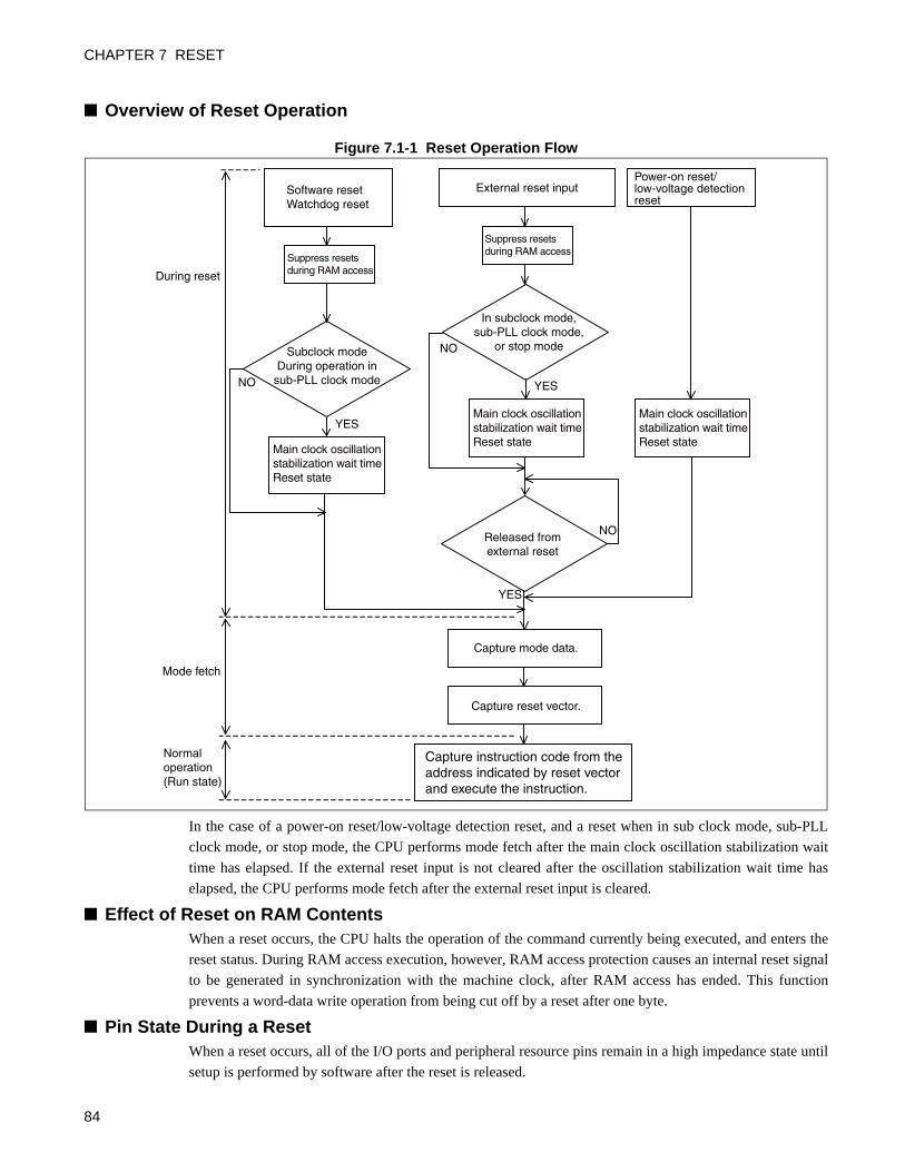
CHAPTER 7 RESET
Overview of Reset Operation
Figure 7.1-1 Reset Operation Flow
In the case of a power-on reset/low-voltage detection reset, and a reset when in sub clock mode, sub-PLL
clock mode, or stop mode, the CPU performs mode fetch after the main clock oscillation stabilization wait
time has elapsed. If the external reset input is not cleared after the oscillation stabilization wait time has
elapsed, the CPU performs mode fetch after the external reset input is cleared.
Effect of Reset on RAM ContentsWhen a reset occurs, the CPU halts the operation of the command currently being executed, and enters the
reset status. During RAM access execution, however, RAM access protection causes an internal reset signal
to be generated in synchronization with the machine clock, after RAM access has ended. This function
prevents a word-data write operation from being cut off by a reset after one byte.
Pin State During a ResetWhen a reset occurs, all of the I/O ports and peripheral resource pins remain in a high impedance state until
setup is performed by software after the reset is released.
Software resetWatchdog reset
External reset input
Power-on reset/low-voltage detectionreset
Released fromexternal reset
Main clock oscillationstabilization wait timeReset state
Main clock oscillationstabilization wait timeReset state
Main clock oscillationstabilization wait timeReset state
Capture mode data.
Capture reset vector.
Capture instruction code from the address indicated by reset vector and execute the instruction.
During reset
Mode fetch
Normaloperation(Run state)
YES
YES
NO
YES
NO
NO
Suppress resetsduring RAM access
Suppress resetsduring RAM access
Subclock modeDuring operation in
sub-PLL clock mode
In subclock mode,sub-PLL clock mode,
or stop mode
84
CHAPTER 7 RESET
Note:
Connect a pull-up resistor to those pins which remain at high impedance during a reset to preventthe devices the pins from malfunctioning.
See "APPENDIX D Pin Status of MB95130/M series" for details about the states of all pins during a
reset.
85
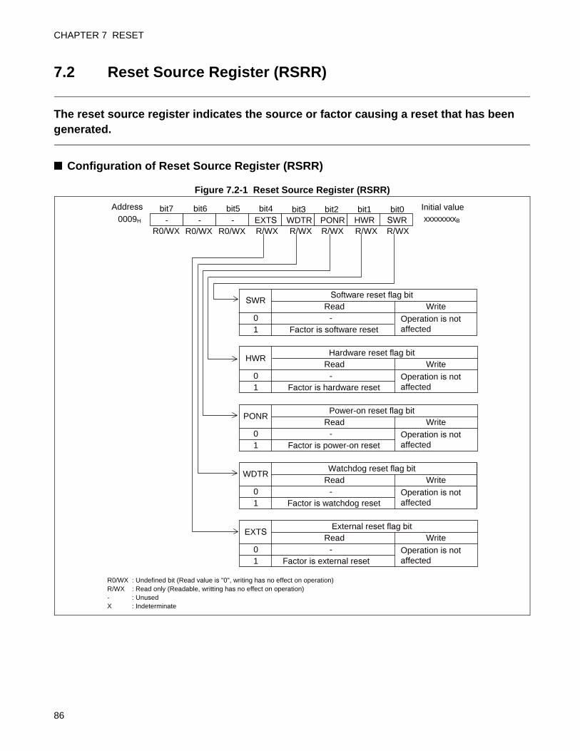
CHAPTER 7 RESET
7.2 Reset Source Register (RSRR)
The reset source register indicates the source or factor causing a reset that has been generated.
Configuration of Reset Source Register (RSRR)
Figure 7.2-1 Reset Source Register (RSRR)
Software reset flag bit SWR
Read Write0 -1 Factor is software reset
Operation is not affected
Hardware reset flag bitHWR
Read Write0 -1 Factor is hardware reset
Operation is not affected
Power-on reset flag bitPONR
Read Write0 -1 Factor is power-on reset
Operation is not affected
Watchdog reset flag bit WDTR
Read Write 0 - 1 Factor is watchdog reset
Operation is not affected
External reset flag bit
EXTSRead Write
0 - 1 Factor is external reset
Operation is not affected
SWR HWRPONR WDTR EXTS - - 0009H
Address bit0 Initial value xxxxxxxxB
R0/WX-
R0/WXR0/WX R/WXR/WXR/WXR/WXR/WX
bit1 bit2 bit3 bit4 bit5bit6 bit7
R0/WX : Undefined bit (Read value is "0", writing has no effect on operation)R/WX : Read only (Readable, writting has no effect on operation)- : Unused X : Indeterminate
86
CHAPTER 7 RESET
Note: Reading the reset source register clears its contents. To use the reset source register for calculation,therefore, you should move the contents of the register to RAM in advance.
Table 7.2-1 Functions of Bits in Reset Source Register (RSRR)
Bit Name Function
bit7bit6bit5
Unused bitsThe value read is always 0.These bits are read-only. Any value written is meaningless.
bit4EXTS:External reset flag bit
This bit is set to "1" to indicate that an external reset has occurred.Otherwise, the bit retains the value existing before the reset occurred.• Read access to this bit sets it to "0".• The bit is read-only. Any value written is meaningless.
bit3WDTR:Watchdog reset flag bit
This bit is set to "1" to indicate that a watchdog reset has occurred.Otherwise, the bit retains the value existing before the reset occurred.• Read access to this bit sets it to "0".• The bit is read-only. Any value written is meaningless.
bit2PONR:Power-on reset flag bit
This bit is set to "1" to indicate that a power-on reset or low-voltage detection reset (option) has occurred.Otherwise, the bit retains the value existing before the reset occurred.• The low-voltage detection reset function is provided for specific models.• Read access to this bit sets it to "0".• The bit is read-only. Any value written is meaningless.
bit1HWR:Hardware reset flag bit
This bit is set to "1" to indicate that a reset other than software resets has occurred. When any of bits 2 to 5 is set to "1", therefore, this bit is set to "1" as well.Otherwise, the bit retains the value existing before the reset occurred.• Read access to this bit sets it to "0".• The bit is read-only. Any value written is meaningless.
bit0SWR:Software reset flag bit
This bit is set to "1" to indicate that a software reset has occurred.Otherwise, the bit retains the value existing before the reset occurred.• Read access to this bit or a power-on reset sets it to "0".• The bit is read-only. Any value written is meaningless.
87

CHAPTER 7 RESET
88
CHAPTER 8INTERRUPTS
This chapter explains the interrupts.
8.1 Interrupts
89
CHAPTER 8 INTERRUPTS
8.1 Interrupts
This section explains the interrupts.
Overview of Interrupts
The F2MC-8FX family has 24 interrupt request input lines corresponding to peripheral resources, for each
of which an interrupt level can be set independently.
When a peripheral resource generates an interrupt request, the interrupt request is output to the interrupt
controller. The interrupt controller checks the interrupt level of that interrupt request and then passes the
occurrence of the interrupt to the CPU. The CPU services the interrupt according to the interrupt
acceptance status. Interrupt requests also release the device from standby mode to resume instruction
execution.
Interrupt Requests from Peripheral ResourcesFigure 8.1-1 lists the interrupt requests corresponding to peripheral resources. When an interrupt is
accepted, a branch to the interrupt service routine takes place with the content of the interrupt vector table
address corresponding to the interrupt request as the address of the branch destination.
The priority for each interrupt request can be set to one of four levels using the interrupt level setting
registers (ILR0 to ILR5).
If another interrupt request with the same or lower level occurs during execution of the interrupt service
routine, the interrupt is processed after the current interrupt handler routine completes. If interrupt requests
of the same level occur at the same time, IRQ0 is assigned the highest priority.
90
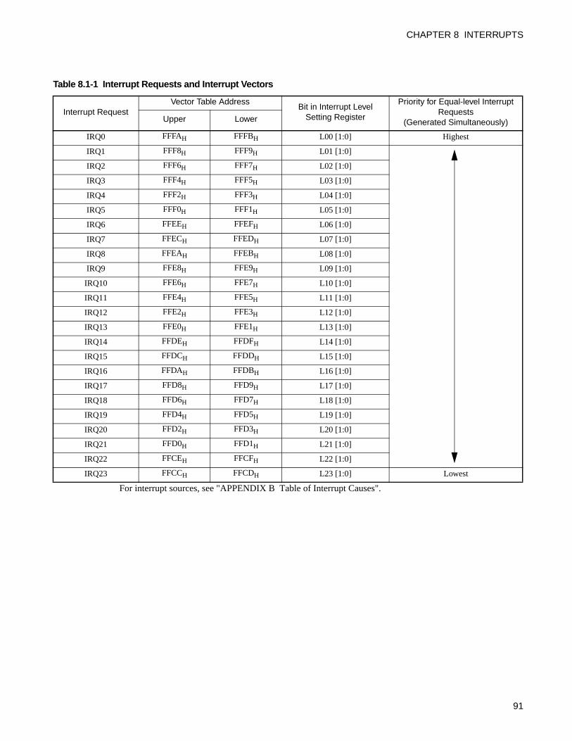
CHAPTER 8 INTERRUPTS
For interrupt sources, see "APPENDIX B Table of Interrupt Causes".
Table 8.1-1 Interrupt Requests and Interrupt Vectors
Interrupt RequestVector Table Address
Bit in Interrupt Level Setting Register
Priority for Equal-level Interrupt Requests
(Generated Simultaneously)Upper Lower
IRQ0 FFFAH FFFBH L00 [1:0] Highest
IRQ1 FFF8H FFF9H L01 [1:0]
IRQ2 FFF6H FFF7H L02 [1:0]
IRQ3 FFF4H FFF5H L03 [1:0]
IRQ4 FFF2H FFF3H L04 [1:0]
IRQ5 FFF0H FFF1H L05 [1:0]
IRQ6 FFEEH FFEFH L06 [1:0]
IRQ7 FFECH FFEDH L07 [1:0]
IRQ8 FFEAH FFEBH L08 [1:0]
IRQ9 FFE8H FFE9H L09 [1:0]
IRQ10 FFE6H FFE7H L10 [1:0]
IRQ11 FFE4H FFE5H L11 [1:0]
IRQ12 FFE2H FFE3H L12 [1:0]
IRQ13 FFE0H FFE1H L13 [1:0]
IRQ14 FFDEH FFDFH L14 [1:0]
IRQ15 FFDCH FFDDH L15 [1:0]
IRQ16 FFDAH FFDBH L16 [1:0]
IRQ17 FFD8H FFD9H L17 [1:0]
IRQ18 FFD6H FFD7H L18 [1:0]
IRQ19 FFD4H FFD5H L19 [1:0]
IRQ20 FFD2H FFD3H L20 [1:0]
IRQ21 FFD0H FFD1H L21 [1:0]
IRQ22 FFCEH FFCFH L22 [1:0]
IRQ23 FFCCH FFCDH L23 [1:0] Lowest
91
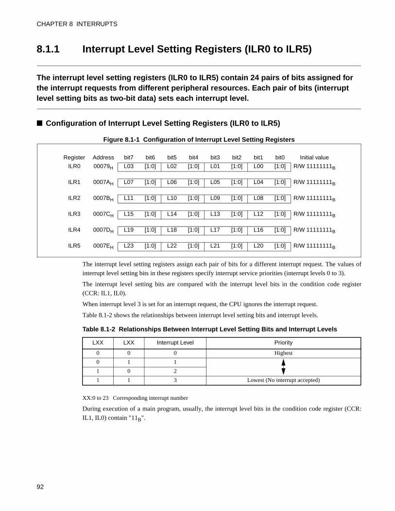
CHAPTER 8 INTERRUPTS
8.1.1 Interrupt Level Setting Registers (ILR0 to ILR5)
The interrupt level setting registers (ILR0 to ILR5) contain 24 pairs of bits assigned for the interrupt requests from different peripheral resources. Each pair of bits (interrupt level setting bits as two-bit data) sets each interrupt level.
Configuration of Interrupt Level Setting Registers (ILR0 to ILR5)
Figure 8.1-1 Configuration of Interrupt Level Setting Registers
The interrupt level setting registers assign each pair of bits for a different interrupt request. The values of
interrupt level setting bits in these registers specify interrupt service priorities (interrupt levels 0 to 3).
The interrupt level setting bits are compared with the interrupt level bits in the condition code register
(CCR: IL1, IL0).
When interrupt level 3 is set for an interrupt request, the CPU ignores the interrupt request.
Table 8.1-2 shows the relationships between interrupt level setting bits and interrupt levels.
XX:0 to 23 Corresponding interrupt number
During execution of a main program, usually, the interrupt level bits in the condition code register (CCR:
IL1, IL0) contain "11B".
Register Address bit7 bit6 bit5 bit4 bit3 bit2 bit1 bit0 Initial value
ILR0 00079H L03 [1:0] L02 [1:0] L01 [1:0] L00 [1:0] R/W 11111111B
ILR1 0007AH L07 [1:0] L06 [1:0] L05 [1:0] L04 [1:0] R/W 11111111B
ILR2 0007BH L11 [1:0] L10 [1:0] L09 [1:0] L08 [1:0] R/W 11111111B
ILR3 0007CH L15 [1:0] L14 [1:0] L13 [1:0] L12 [1:0] R/W 11111111B
ILR4 0007DH L19 [1:0] L18 [1:0] L17 [1:0] L16 [1:0] R/W 11111111B
ILR5 0007EH L23 [1:0] L22 [1:0] L21 [1:0] L20 [1:0] R/W 11111111B
Table 8.1-2 Relationships Between Interrupt Level Setting Bits and Interrupt Levels
LXX LXX Interrupt Level Priority
0 0 0 Highest
0 1 1
1 0 2
1 1 3 Lowest (No interrupt accepted)
92
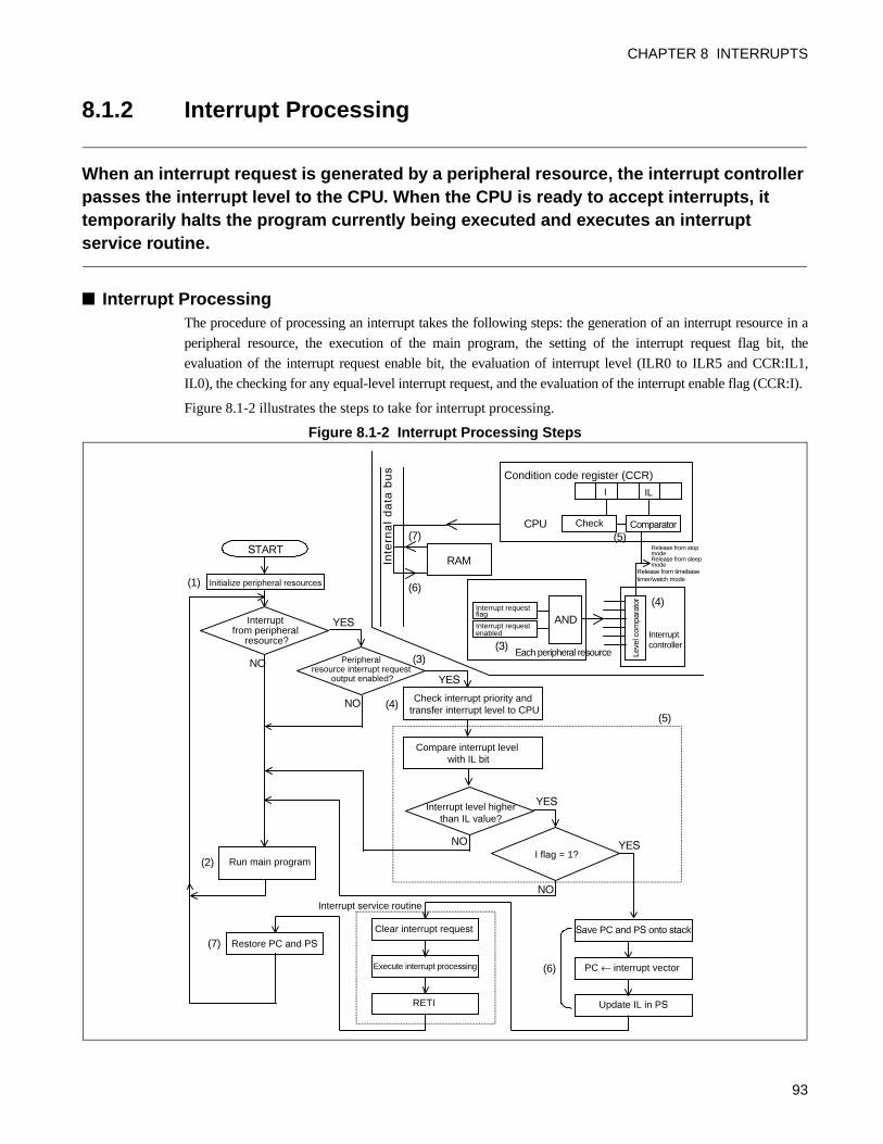
CHAPTER 8 INTERRUPTS
8.1.2 Interrupt Processing
When an interrupt request is generated by a peripheral resource, the interrupt controller passes the interrupt level to the CPU. When the CPU is ready to accept interrupts, it temporarily halts the program currently being executed and executes an interrupt service routine.
Interrupt ProcessingThe procedure of processing an interrupt takes the following steps: the generation of an interrupt resource in a
peripheral resource, the execution of the main program, the setting of the interrupt request flag bit, the
evaluation of the interrupt request enable bit, the evaluation of interrupt level (ILR0 to ILR5 and CCR:IL1,
IL0), the checking for any equal-level interrupt request, and the evaluation of the interrupt enable flag (CCR:I).
Figure 8.1-2 illustrates the steps to take for interrupt processing.
Figure 8.1-2 Interrupt Processing Steps
Interrupt
from peripheral resource?
Peripheral resource interrupt request
output enabled?
Check interrupt priority and transfer interrupt level to CPU
Compare interrupt level with IL bit
START
Run main program
Restore PC and PS
Initialize peripheral resources
Interrupt level higher than IL value?
I flag = 1?
Clear interrupt request
Execute interrupt processing
RETI Update IL in PS
PC ← interrupt vector
Save PC and PS onto stack
Leve
l com
para
tor
Interrupt controller
AND Interrupt request flag
Interrupt request enabled
Each peripheral resource
Condition code register (CCR)
Comparator CheckCPU
RAM Inte
rna
l d
ata
bu
s
I IL
Release from stop modeRelease from sleep mode
Release from timebase timer/watch mode(1)
(2)
(3)
(4) (5)
(6)
(7)
(3)
(4)
(5)
(6)
(7)
NO
NO
NO
NO YES
YES
YES
YES
Interrupt service routine
93
CHAPTER 8 INTERRUPTS
(1) Any interrupt request is disabled immediately after a reset. In the peripheral resource initialization
program, initialize those peripheral resources which generate interrupts and set their interrupt levels in
their respective interrupt level setting registers (ILR0 to ILR5) before starting operating the peripheral
resources. The interrupt level can be set to 0, 1, 2, or 3. Level 0 is given the highest priority, and level 1
the second highest. Setting level 3 for a peripheral resource disables interrupts from that resource.
(2) Execute the main program (or the interrupt service routine for nested interrupts).
(3) When an interrupt is triggered in a peripheral resource, the interrupt request flag bit of the peripheral
resource is set to "1". If the interrupt request enable bit of the peripheral resource has been set to enable
interrupts, the interrupt request is then output to the interrupt controller.
(4) The interrupt controller always monitors interrupt requests from individual peripheral resources and
transfers the highest-priority interrupt level, to the CPU, among the interrupt levels of the currently
generated interrupt requests. The relative priority to be assigned if another request with the same
interrupt level occurs simultaneously is also determined at this time.
(5) If the received interrupt level or priority is lower than the level set in the interrupt level bits in the
condition code register (CCR: IL1, IL0), the CPU checks the content of the interrupt enable flag
(CCR:I) and, if interrupts are enabled (CCR:I = 1), accepts the interrupt.
(6) The CPU pushes the contents of the program counter (PC) and program status (PS) register onto the
stack, fetches the start address of the interrupt service routine from the corresponding interrupt vector
table, changes the value of the interrupt level bits in the condition code register (CCR: IL1, IL0) to the
value of the received interrupt level, then starts the execution of the interrupt service routine.
(7) Finally, the CPU uses the RETI instruction to restore the program counter (PC) and program status (PS)
values from the stack and resumes execution from the instruction that follows the instruction executed
prior to the interrupt.
Note:
The interrupt request flag bits of peripheral resources are not automatically cleared to "0" after aninterrupt request is accepted. The bits must therefore be cleared to "0" by a program (by writing "0"to the interrupt request flag bit) in the interrupt service routine.
An interrupt causes the device to recover from standby mode (low power consumption mode). For details,
see "6.8 Operations in Low-power Consumption Modes (Standby Modes)".
94
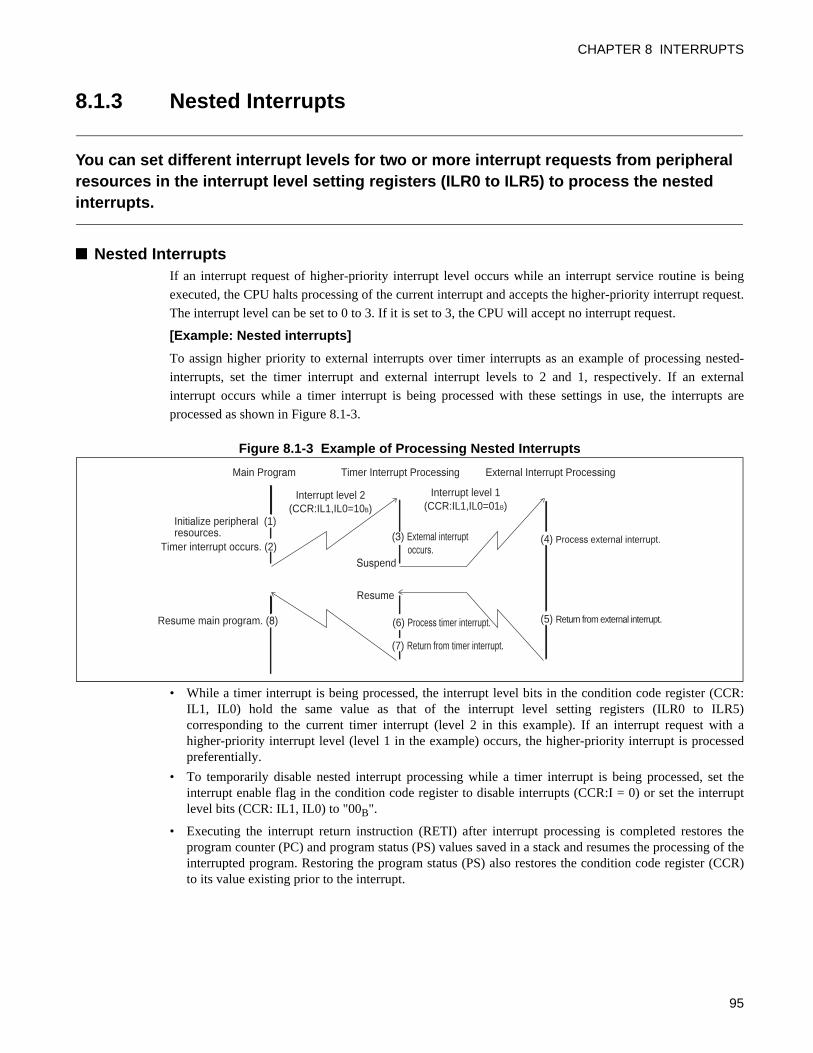
CHAPTER 8 INTERRUPTS
8.1.3 Nested Interrupts
You can set different interrupt levels for two or more interrupt requests from peripheral resources in the interrupt level setting registers (ILR0 to ILR5) to process the nested interrupts.
Nested InterruptsIf an interrupt request of higher-priority interrupt level occurs while an interrupt service routine is being
executed, the CPU halts processing of the current interrupt and accepts the higher-priority interrupt request.
The interrupt level can be set to 0 to 3. If it is set to 3, the CPU will accept no interrupt request.
[Example: Nested interrupts]
To assign higher priority to external interrupts over timer interrupts as an example of processing nested-
interrupts, set the timer interrupt and external interrupt levels to 2 and 1, respectively. If an external
interrupt occurs while a timer interrupt is being processed with these settings in use, the interrupts are
processed as shown in Figure 8.1-3.
Figure 8.1-3 Example of Processing Nested Interrupts
• While a timer interrupt is being processed, the interrupt level bits in the condition code register (CCR:IL1, IL0) hold the same value as that of the interrupt level setting registers (ILR0 to ILR5)corresponding to the current timer interrupt (level 2 in this example). If an interrupt request with ahigher-priority interrupt level (level 1 in the example) occurs, the higher-priority interrupt is processedpreferentially.
• To temporarily disable nested interrupt processing while a timer interrupt is being processed, set theinterrupt enable flag in the condition code register to disable interrupts (CCR:I = 0) or set the interruptlevel bits (CCR: IL1, IL0) to "00B".
• Executing the interrupt return instruction (RETI) after interrupt processing is completed restores theprogram counter (PC) and program status (PS) values saved in a stack and resumes the processing of theinterrupted program. Restoring the program status (PS) also restores the condition code register (CCR)to its value existing prior to the interrupt.
(6) Process timer interrupt.
(7) Return from timer interrupt.
(3) External interrupt occurs.
(4) Process external interrupt.
(5) Return from external interrupt.
Timer Interrupt ProcessingMain Program External Interrupt Processing
Interrupt level 2(CCR:IL1,IL0=10B)
Initialize peripheral (1)resources.
Timer interrupt occurs. (2)
Resume main program. (8)
Resume
Interrupt level 1(CCR:IL1,IL0=01B)
Suspend
95
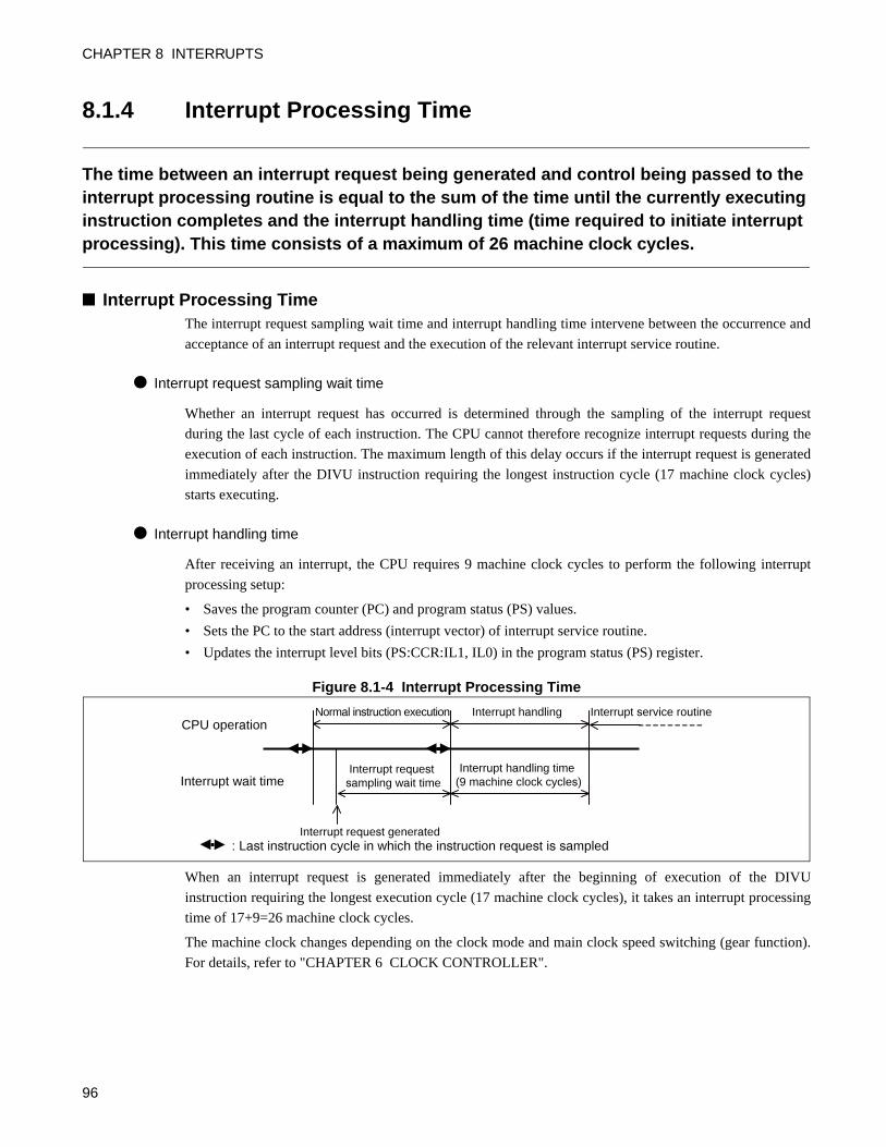
CHAPTER 8 INTERRUPTS
8.1.4 Interrupt Processing Time
The time between an interrupt request being generated and control being passed to the interrupt processing routine is equal to the sum of the time until the currently executing instruction completes and the interrupt handling time (time required to initiate interrupt processing). This time consists of a maximum of 26 machine clock cycles.
Interrupt Processing TimeThe interrupt request sampling wait time and interrupt handling time intervene between the occurrence and
acceptance of an interrupt request and the execution of the relevant interrupt service routine.
Interrupt request sampling wait time
Whether an interrupt request has occurred is determined through the sampling of the interrupt request
during the last cycle of each instruction. The CPU cannot therefore recognize interrupt requests during the
execution of each instruction. The maximum length of this delay occurs if the interrupt request is generated
immediately after the DIVU instruction requiring the longest instruction cycle (17 machine clock cycles)
starts executing.
Interrupt handling time
After receiving an interrupt, the CPU requires 9 machine clock cycles to perform the following interrupt
processing setup:
• Saves the program counter (PC) and program status (PS) values.
• Sets the PC to the start address (interrupt vector) of interrupt service routine.
• Updates the interrupt level bits (PS:CCR:IL1, IL0) in the program status (PS) register.
Figure 8.1-4 Interrupt Processing Time
When an interrupt request is generated immediately after the beginning of execution of the DIVU
instruction requiring the longest execution cycle (17 machine clock cycles), it takes an interrupt processing
time of 17+9=26 machine clock cycles.
The machine clock changes depending on the clock mode and main clock speed switching (gear function).
For details, refer to "CHAPTER 6 CLOCK CONTROLLER".
CPU operation
Interrupt wait time Interrupt request
sampling wait time
Normal instruction execution
Interrupt handling time (9 machine clock cycles)
Interrupt handling Interrupt service routine
Interrupt request generated : Last instruction cycle in which the instruction request is sampled
96
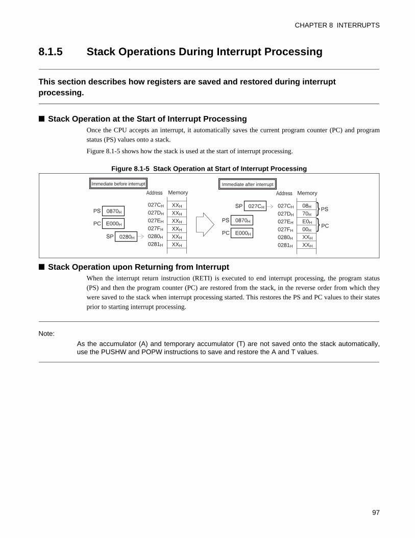
CHAPTER 8 INTERRUPTS
8.1.5 Stack Operations During Interrupt Processing
This section describes how registers are saved and restored during interrupt processing.
Stack Operation at the Start of Interrupt ProcessingOnce the CPU accepts an interrupt, it automatically saves the current program counter (PC) and program
status (PS) values onto a stack.
Figure 8.1-5 shows how the stack is used at the start of interrupt processing.
Figure 8.1-5 Stack Operation at Start of Interrupt Processing
Stack Operation upon Returning from InterruptWhen the interrupt return instruction (RETI) is executed to end interrupt processing, the program status
(PS) and then the program counter (PC) are restored from the stack, in the reverse order from which they
were saved to the stack when interrupt processing started. This restores the PS and PC values to their states
prior to starting interrupt processing.
Note:
As the accumulator (A) and temporary accumulator (T) are not saved onto the stack automatically,use the PUSHW and POPW instructions to save and restore the A and T values.
Immediate before interrupt
SP
Memory
XXH
Address
PC
PS
Immediate after interrupt
MemoryAddress
PC
PSXXH
XXH
XXH
XXH
XXH
08H
70H
E0H
00H
XXH
XXH
0870H
E000H
0280H
SP
PC
PS
027CH
0870H
E000H
027CH
0281H
027DH
027EH
027FH
0280H
027CH
0281H
027DH
027EH
027FH
0280H
97
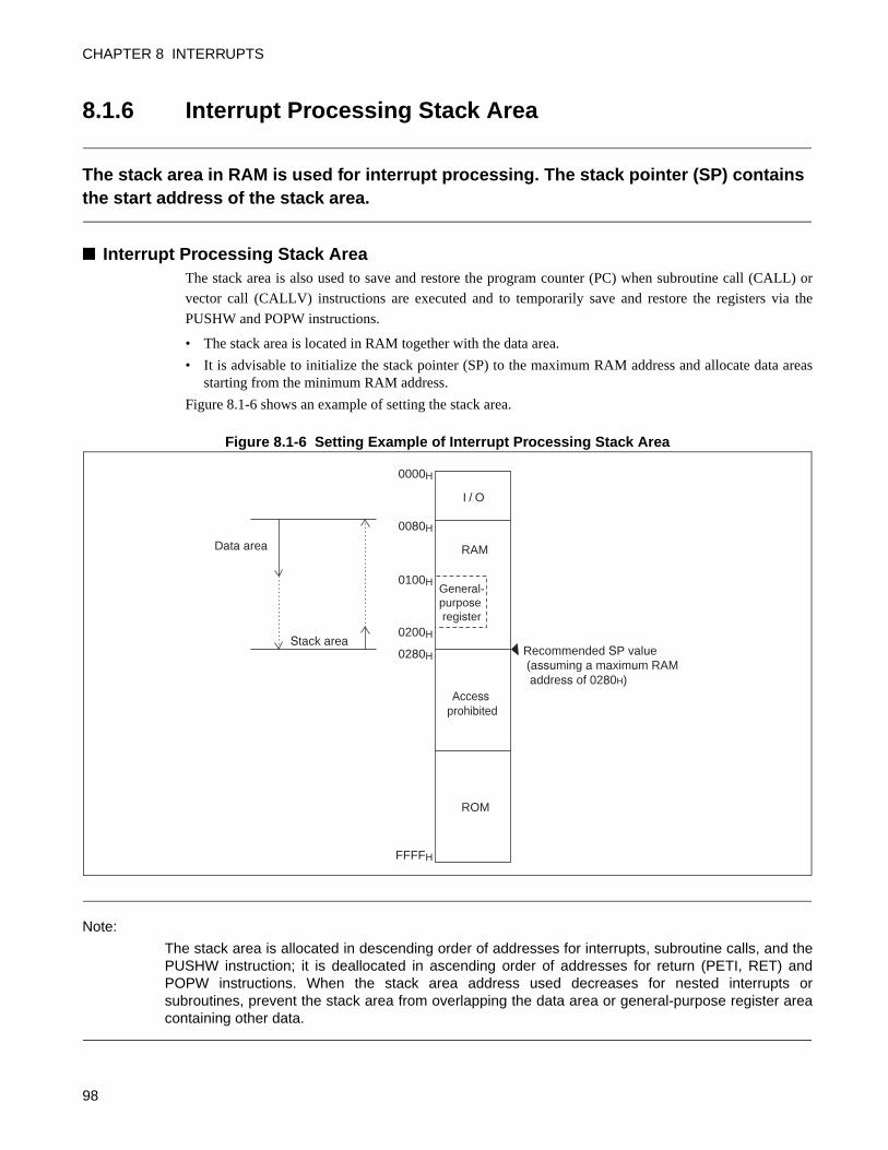
CHAPTER 8 INTERRUPTS
8.1.6 Interrupt Processing Stack Area
The stack area in RAM is used for interrupt processing. The stack pointer (SP) contains the start address of the stack area.
Interrupt Processing Stack AreaThe stack area is also used to save and restore the program counter (PC) when subroutine call (CALL) or
vector call (CALLV) instructions are executed and to temporarily save and restore the registers via the
PUSHW and POPW instructions.
• The stack area is located in RAM together with the data area.
• It is advisable to initialize the stack pointer (SP) to the maximum RAM address and allocate data areasstarting from the minimum RAM address.
Figure 8.1-6 shows an example of setting the stack area.
Figure 8.1-6 Setting Example of Interrupt Processing Stack Area
Note:
The stack area is allocated in descending order of addresses for interrupts, subroutine calls, and thePUSHW instruction; it is deallocated in ascending order of addresses for return (PETI, RET) andPOPW instructions. When the stack area address used decreases for nested interrupts orsubroutines, prevent the stack area from overlapping the data area or general-purpose register areacontaining other data.
0000H
I / O
RAM
General-purpose register
ROM
Stack areaRecommended SP value (assuming a maximum RAM address of 0280H)
Data area
Access prohibited
0080H
0100H
0200H
0280H
FFFFH
98
CHAPTER 9I/O PORT
This chapter describes the functions and operations of the I/O ports.
9.1 Overview of I/O Ports
9.2 Port 0
9.3 Port 1
9.4 Port F
9.5 Port G
99
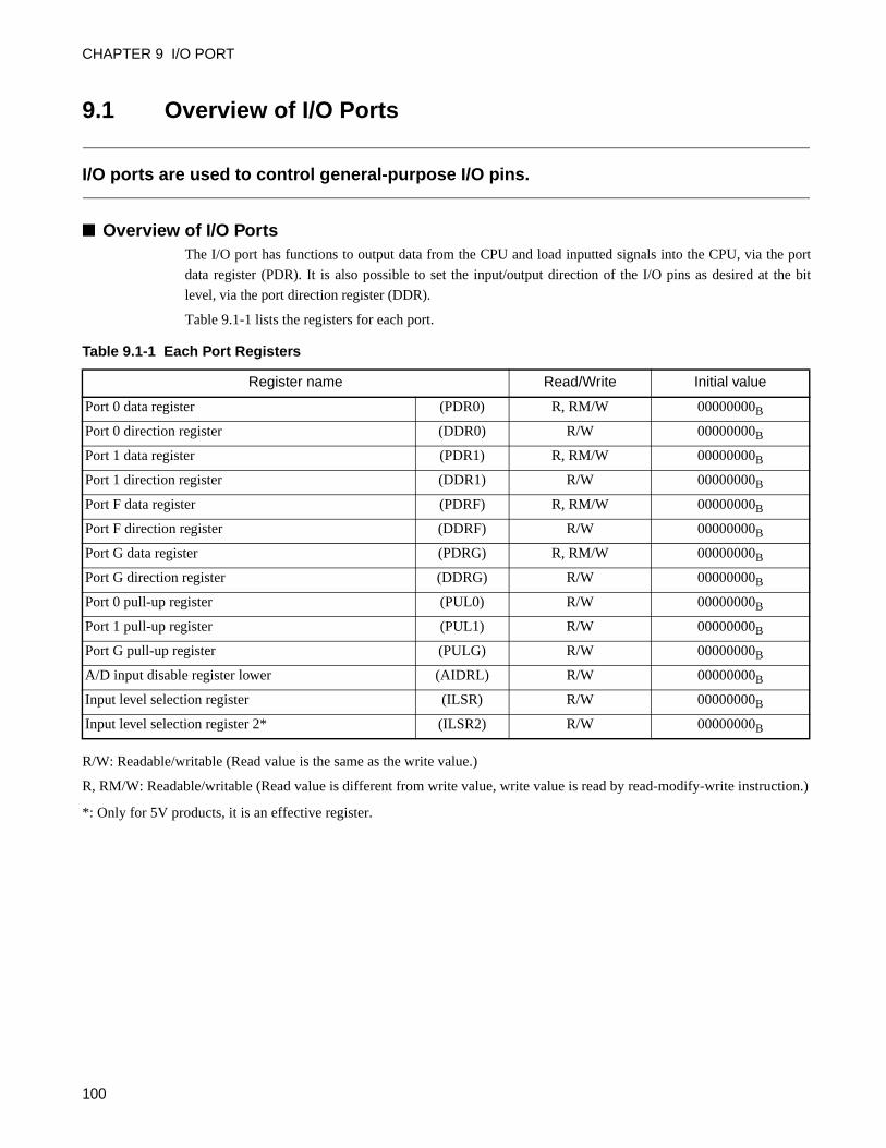
CHAPTER 9 I/O PORT
9.1 Overview of I/O Ports
I/O ports are used to control general-purpose I/O pins.
Overview of I/O PortsThe I/O port has functions to output data from the CPU and load inputted signals into the CPU, via the port
data register (PDR). It is also possible to set the input/output direction of the I/O pins as desired at the bit
level, via the port direction register (DDR).
Table 9.1-1 lists the registers for each port.
R/W: Readable/writable (Read value is the same as the write value.)
R, RM/W: Readable/writable (Read value is different from write value, write value is read by read-modify-write instruction.)
*: Only for 5V products, it is an effective register.
Table 9.1-1 Each Port Registers
Register name Read/Write Initial value
Port 0 data register (PDR0) R, RM/W 00000000B
Port 0 direction register (DDR0) R/W 00000000B
Port 1 data register (PDR1) R, RM/W 00000000B
Port 1 direction register (DDR1) R/W 00000000B
Port F data register (PDRF) R, RM/W 00000000B
Port F direction register (DDRF) R/W 00000000B
Port G data register (PDRG) R, RM/W 00000000B
Port G direction register (DDRG) R/W 00000000B
Port 0 pull-up register (PUL0) R/W 00000000B
Port 1 pull-up register (PUL1) R/W 00000000B
Port G pull-up register (PULG) R/W 00000000B
A/D input disable register lower (AIDRL) R/W 00000000B
Input level selection register (ILSR) R/W 00000000B
Input level selection register 2* (ILSR2) R/W 00000000B
100
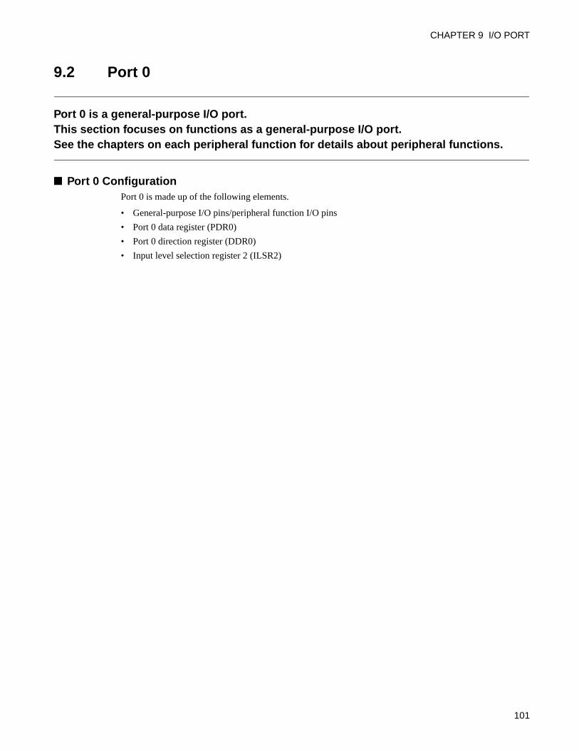
CHAPTER 9 I/O PORT
9.2 Port 0
Port 0 is a general-purpose I/O port.This section focuses on functions as a general-purpose I/O port.See the chapters on each peripheral function for details about peripheral functions.
Port 0 ConfigurationPort 0 is made up of the following elements.
• General-purpose I/O pins/peripheral function I/O pins
• Port 0 data register (PDR0)
• Port 0 direction register (DDR0)
• Input level selection register 2 (ILSR2)
101
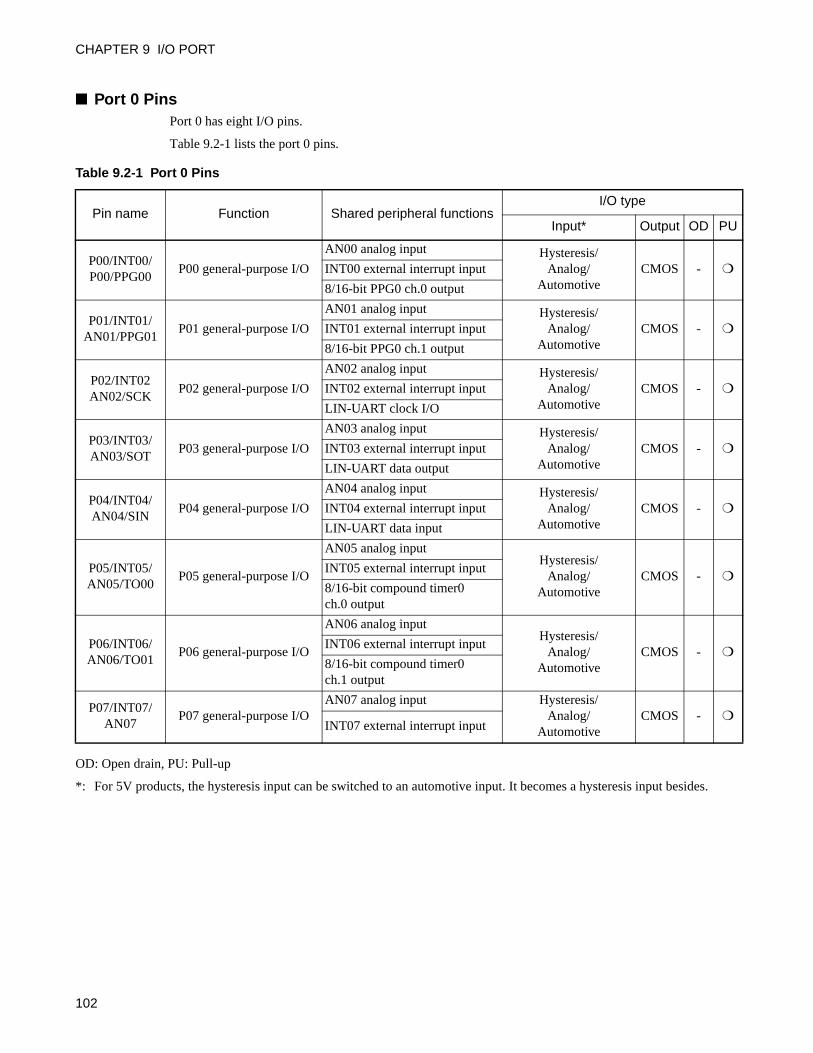
CHAPTER 9 I/O PORT
Port 0 PinsPort 0 has eight I/O pins.
Table 9.2-1 lists the port 0 pins.
OD: Open drain, PU: Pull-up
*: For 5V products, the hysteresis input can be switched to an automotive input. It becomes a hysteresis input besides.
Table 9.2-1 Port 0 Pins
Pin name Function Shared peripheral functionsI/O type
Input* Output OD PU
P00/INT00/P00/PPG00
P00 general-purpose I/O
AN00 analog input Hysteresis/Analog/
AutomotiveCMOS - INT00 external interrupt input
8/16-bit PPG0 ch.0 output
P01/INT01/AN01/PPG01
P01 general-purpose I/O
AN01 analog input Hysteresis/Analog/
AutomotiveCMOS - INT01 external interrupt input
8/16-bit PPG0 ch.1 output
P02/INT02AN02/SCK
P02 general-purpose I/O
AN02 analog input Hysteresis/Analog/
AutomotiveCMOS - INT02 external interrupt input
LIN-UART clock I/O
P03/INT03/AN03/SOT
P03 general-purpose I/O
AN03 analog input Hysteresis/Analog/
AutomotiveCMOS - INT03 external interrupt input
LIN-UART data output
P04/INT04/AN04/SIN
P04 general-purpose I/O
AN04 analog input Hysteresis/Analog/
AutomotiveCMOS - INT04 external interrupt input
LIN-UART data input
P05/INT05/AN05/TO00
P05 general-purpose I/O
AN05 analog inputHysteresis/
Analog/Automotive
CMOS - INT05 external interrupt input
8/16-bit compound timer0 ch.0 output
P06/INT06/AN06/TO01
P06 general-purpose I/O
AN06 analog inputHysteresis/
Analog/Automotive
CMOS - INT06 external interrupt input
8/16-bit compound timer0 ch.1 output
P07/INT07/AN07
P07 general-purpose I/OAN07 analog input Hysteresis/
Analog/Automotive
CMOS - INT07 external interrupt input
102
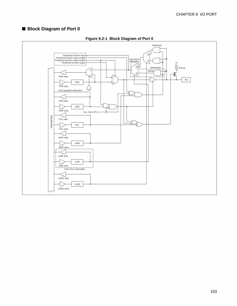
CHAPTER 9 I/O PORT
Block Diagram of Port 0
Figure 9.2-1 Block Diagram of Port 0
PDR read
PDR write
PDR
DDR read
DDR write
DDR
PUL read
PUL write
PUL
AIDR read
AIDR write
AIDR
0
11
0
Peripheral function outputPeripheral function output enable
Peripheral function input enablePeripheral function input
Pin
Stop, Watch (SPL=1)
Inte
rnal
bus
In bit operation instruction
Automotive Pull-up
ILSR read
ILSR write
ILSR
Hysteresis
CMOS
Only P04 is selectable.
Only P04 is selectable.
0
1
0
1
ILSR2 read
ILSR2 write
ILSR2
103
CHAPTER 9 I/O PORT
9.2.1 Port 0 Registers
This section describes the port 0 registers.
Port 0 Register FunctionTable 9.2-2 lists the port 0 register functions.
*: Only for 5V products, it is an effective register.
Table 9.2-3 lists the correspondence between port 0 pins and each register bit.
*: Only for 5V products, it is an effective register.
Table 9.2-2 Port 0 Register Function
Register name Data Read Read read-modify-write Write
PDR00 Pin state is "L" level. PDR register value is "0". As output port, outputs "L" level.
1 Pin state is "H" level. PDR register value is "1". As output port, outputs "H" level.
DDR00 Port input enabled
1 Port output enabled
PUL00 Pull-up disabled
1 Pull-up enabled
AIDRL0 Analog input enabled
1 Port input enabled
ILSR0 Hysteresis input level selection
1 CMOS input level selection
ILSR2*0 Hysteresis input level selection
1 Automotive input level selection
Table 9.2-3 Correspondence between Registers and Pins for Port 0
Correspondence between related register bits and pins
Pin name P07 P06 P05 P04 P03 P02 P01 P00
PDR0
bit7 bit6 bit5 bit4 bit3 bit2 bit1 bit0DDR0
PUL0
AIDRL
ILSR - - - bit2 - - - -
ILSR2* bit0
104
CHAPTER 9 I/O PORT
9.2.2 Operations of Port 0
This section describes the operations of port 0.
Operations of Port 0
Operation as an output port
• Setting the corresponding DDR register bit to "1" sets a pin as an output port.
• When a pin is set as an output port, it outputs the value of the PDR register to pins.
• If data is written to the PDR register, the value is stored in the output latch and output to the pin as it is.
• Reading the PDR register returns the PDR register value.
Operation as an input port
• Setting the corresponding DDR register bit to "0" sets a pin as an input port.
• When using the analog input shared pin as an input port, set the corresponding bits in the A/D inputdisable register low (AIDRL) to "1".
• If data is written to the PDR register, the value is stored in the output latch but not output to the pin.
• Reading the PDR register returns the pin value. However, the read-modify-write command returns thePDR register value.
Operation as a peripheral function output
• Setting the output enable bit of a peripheral function sets the corresponding pin as a peripheral functionoutput.
• The pin value can be read from the PDR register even if the peripheral function output is enabled.Therefore, the output value of a peripheral function can be read by the read operation on PDR register.However, the read-modify-write command returns the PDR register value.
Operation as a peripheral function input
• Set the DDR register bit, which is corresponding to the peripheral function input pin, to "0" to set a pinas an input port.
• As with an input port, when using the analog input shared pin as another peripheral function input,configure it as an input port.
• Reading the PDR register returns the pin value, regardless of whether the peripheral function uses aninput pin. However, the read-modify-write command returns the PDR register value.
Operation at reset
• Resetting the CPU initializes the DDR register values to "0", and sets the port input enabled. Note thatthe pin sharing for the analog input is set its port input disabled since A/D input disable register low(AIDRL) is initialized to "0".
105
CHAPTER 9 I/O PORT
Operation in stop mode and watch mode
• If the pin state specification bit in the standby control register (STBC:SPL) is set to "1" when the deviceswitches to stop or watch mode, the pin is set forcibly to the high-impedance state regardless of theDDR register value. Note that the input is locked to "L" and blocked in order to prevent leaks due tofreed input. However, if the interrupt input is enabled for the external interrupt control register (EIC) ofthe external interrupt circuit and the interrupt pin selection circuit control register (WICR) of theexternal interrupt selection circuit, the input is enabled and not blocked.
• If the pin state specification bit is "0", the state remains in port I/O or peripheral function I/O and theoutput is maintained.
Operation as an analog input
• Set the DDR register bit, which is corresponding to the analog input pin, to "0", and set the AIDRLregister bit to "0".
• Set the corresponding PUL register bit to "0".
Operation of the external interrupt input pin
• Set the DDR register bit, which is corresponding to the external interrupt input pin, to "0".
• Pin values are continuously input to the external interrupt circuit. When using the pin for a functionother than an interrupt, you must disable the corresponding external interrupt.
Operation of the pull-up control register
• Writing "1" to the PUL register internally connects the pull-up resistor to the pin. When the output is"L" level, the pull-up resistor is disconnected regardless of the PUL register value.
Operation of the input level selection register 2
• The ILSR2 register is a valid register only for 5V models.
• Setting bit 0 of the ILSR2 register to "1" changes the port 0 input level from the hysteresis input level tothe automotive input level. The hysteresis input level is used when bit 0 of the ILSR2 register is "0".
• Only modify the port 0 input level setting when the peripheral functions input are halted.
Table 9.2-4 shows the pin states of the port.
SPL: Pin state specification bit in standby control register (STBC:SPL)
Hi-Z: High impedance
*: "Input disabled" means the state that the operation of the input gate close to the pin is disabled.
Table 9.2-4 Pin State of Port 0
Operating state
Normal operationSleep
Stop (SPL=0)Watch (SPL=0)
Stop (SPL=1)Watch (SPL=1)
At reset
Pin stateI/O port/
peripheral function I/O
Hi-Z(the pull-up setting is enabled)
Input cutoff(If external interrupts are enabled, the external interrupt can be input.)
Hi-ZInput disabled*
106
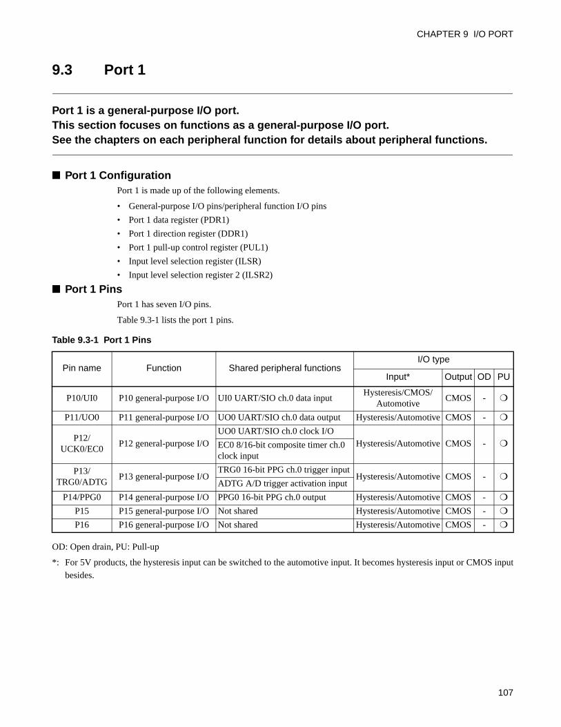
CHAPTER 9 I/O PORT
9.3 Port 1
Port 1 is a general-purpose I/O port.This section focuses on functions as a general-purpose I/O port.See the chapters on each peripheral function for details about peripheral functions.
Port 1 ConfigurationPort 1 is made up of the following elements.
• General-purpose I/O pins/peripheral function I/O pins
• Port 1 data register (PDR1)
• Port 1 direction register (DDR1)
• Port 1 pull-up control register (PUL1)
• Input level selection register (ILSR)
• Input level selection register 2 (ILSR2)
Port 1 PinsPort 1 has seven I/O pins.
Table 9.3-1 lists the port 1 pins.
OD: Open drain, PU: Pull-up
*: For 5V products, the hysteresis input can be switched to the automotive input. It becomes hysteresis input or CMOS input
besides.
Table 9.3-1 Port 1 Pins
Pin name Function Shared peripheral functionsI/O type
Input* Output OD PU
P10/UI0 P10 general-purpose I/O UI0 UART/SIO ch.0 data inputHysteresis/CMOS/
AutomotiveCMOS -
P11/UO0 P11 general-purpose I/O UO0 UART/SIO ch.0 data output Hysteresis/Automotive CMOS -
P12/UCK0/EC0
P12 general-purpose I/OUO0 UART/SIO ch.0 clock I/O
Hysteresis/Automotive CMOS - EC0 8/16-bit composite timer ch.0 clock input
P13/TRG0/ADTG
P13 general-purpose I/OTRG0 16-bit PPG ch.0 trigger input
Hysteresis/Automotive CMOS - ADTG A/D trigger activation input
P14/PPG0 P14 general-purpose I/O PPG0 16-bit PPG ch.0 output Hysteresis/Automotive CMOS -
P15 P15 general-purpose I/O Not shared Hysteresis/Automotive CMOS -
P16 P16 general-purpose I/O Not shared Hysteresis/Automotive CMOS -
107
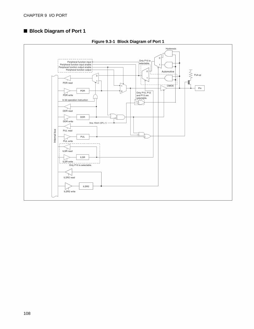
CHAPTER 9 I/O PORT
Block Diagram of Port 1
Figure 9.3-1 Block Diagram of Port 1
PDR read
PDR write
PDR
DDR read
DDR write
DDR
PUL read
PUL write
PUL
1
0
Peripheral function outputPeripheral function output enable
Peripheral function input enablePeripheral function input
Pin
Stop, Watch (SPL=1)
Inte
rnal
bus
In bit operation instruction
Pull-up
ILSR read
ILSR write
ILSR
Hysteresis
CMOS
Only P10 is selectable.
Only P10 is selectable.
Only P10, P12 and P13 are selectable.
Automotive
0
1
ILSR2 read
ILSR2 write
ILSR2
0
1
0
1
108
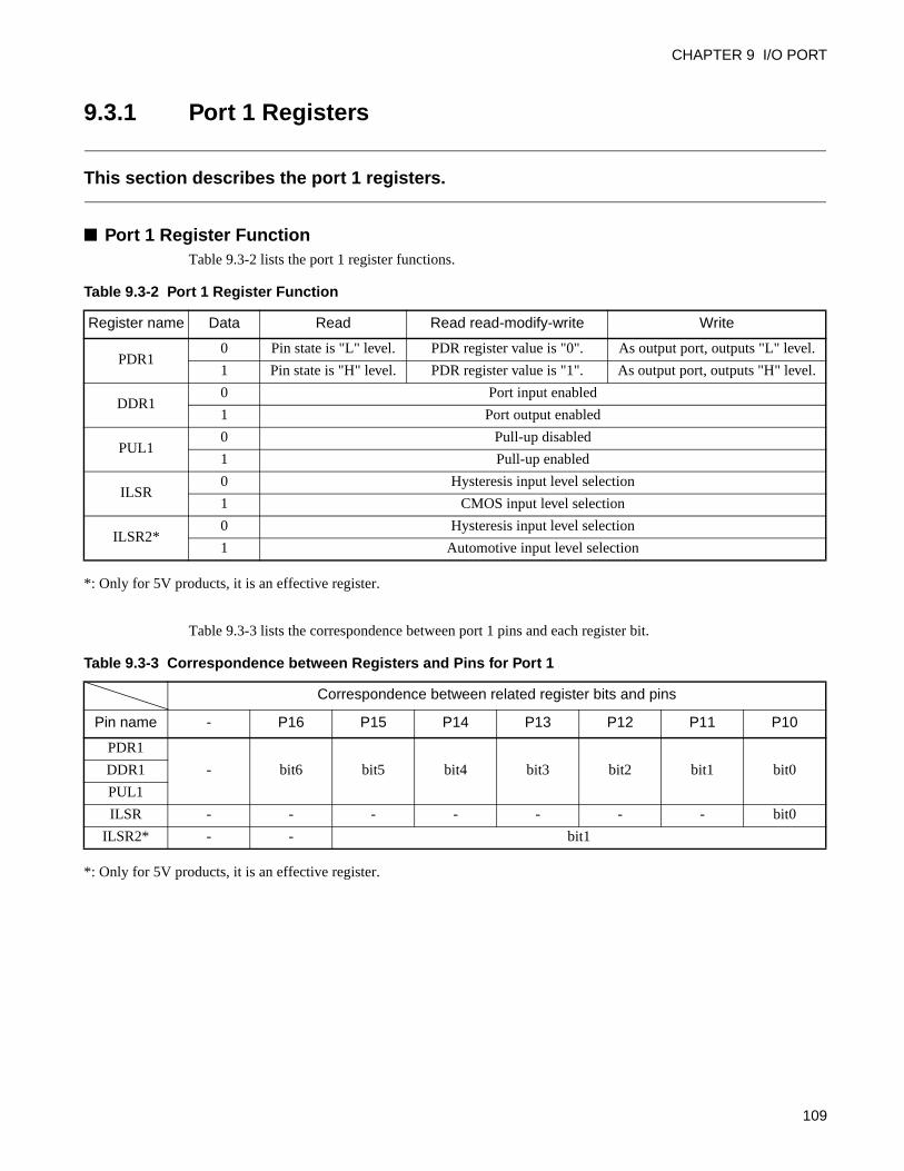
CHAPTER 9 I/O PORT
9.3.1 Port 1 Registers
This section describes the port 1 registers.
Port 1 Register FunctionTable 9.3-2 lists the port 1 register functions.
*: Only for 5V products, it is an effective register.
Table 9.3-3 lists the correspondence between port 1 pins and each register bit.
*: Only for 5V products, it is an effective register.
Table 9.3-2 Port 1 Register Function
Register name Data Read Read read-modify-write Write
PDR10 Pin state is "L" level. PDR register value is "0". As output port, outputs "L" level.
1 Pin state is "H" level. PDR register value is "1". As output port, outputs "H" level.
DDR10 Port input enabled
1 Port output enabled
PUL10 Pull-up disabled
1 Pull-up enabled
ILSR0 Hysteresis input level selection
1 CMOS input level selection
ILSR2*0 Hysteresis input level selection
1 Automotive input level selection
Table 9.3-3 Correspondence between Registers and Pins for Port 1
Correspondence between related register bits and pins
Pin name - P16 P15 P14 P13 P12 P11 P10
PDR1
- bit6 bit5 bit4 bit3 bit2 bit1 bit0DDR1
PUL1
ILSR - - - - - - - bit0
ILSR2* - - bit1
109
CHAPTER 9 I/O PORT
9.3.2 Operations of Port 1
This section describes the operations of port 1.
Operations of Port 1
Operation as an output port
• Setting the corresponding DDR register bit to "1" sets a pin as an output port.
• For a peripheral function sharing pins, disable its output.
• When a pin is set as an output port, it outputs the value of the PDR register to pins.
• If data is written to the PDR register, the value is stored in the output latch and output to the pin as it is.
• Reading the PDR register returns the PDR register value.
Operation as an input port
• Setting the corresponding DDR register bit to "0" sets a pin as an input port.
• For a peripheral function sharing pins, disable its output.
• If data is written to the PDR register, the value is stored in the output latch but not output to the pin.
• Reading the PDR register returns the pin value. However, the read-modify-write command returns thePDR register value.
Operation as a peripheral function output
• Setting the output enable bit of a peripheral function sets the corresponding pin as a peripheral functionoutput.
• The pin value can be read from the PDR register even if the peripheral function output is enabled.Therefore, the output value of a peripheral function can be read by the read operation on PDR register.However, the read-modify-write command returns the PDR register value.
Operation as a peripheral function input
• Set the DDR register bit, which is corresponding to the peripheral function input pin, to "0" to set a pinas an input port.
• Reading the PDR register returns the pin value, regardless of whether the peripheral function uses aninput pin. However, the read-modify-write command returns the PDR register value.
Operation at reset
• Resetting the CPU initializes the DDR register values to "0", and sets the port input enabled.
110
CHAPTER 9 I/O PORT
Operation in stop mode and watch mode
• If the pin state specification bit in the standby control register (STBC:SPL) is set to "1" when the deviceswitches to stop or watch mode, the pin is set forcibly to the high-impedance state regardless of theDDR register value. Note that the input is locked to "L" and blocked in order to prevent leaks due tofreed input. However, if the interrupt input of P10/U10, P12/U0K0, P13/TRG0/ADTG port is enabledfor the external interrupt control register (EIC) of the external interrupt circuit and the interrupt pinselection circuit control register (WICR) of the external interrupt selection circuit, the input is enabledand not blocked.
• If the pin state specification bit is "0", the state remains in port I/O or peripheral function I/O and theoutput is maintained.
Operation of the pull-up control register
• Writing "1" to the PUL register internally connects the pull-up resistor to the pin. When the output is"L" level, the pull-up resistor is disconnected regardless of the PUL register value.
Operation of the input level selection register
• Setting "1" to the bit0 of ILSR register changes only P10 from the hysteresis input level to the CMOSinput level. When the bit0 of ILSR register is "0", it should be the hysteresis input level.
• For pins other than P10, the CMOS input level cannot be selected; however, only the hysteresis inputlevel or the automotive input level can.
• Make sure that the input level for P10 is changed during the peripheral function (UART/SIO) stopped.
Operation of the input level selection register 2
• The ILSR2 register is a valid register only for 5V models.
• Setting bit 1 of the ILSR2 register to "1" changes the port 1 input level from the hysteresis input level tothe automotive input level. The hysteresis input level is used when bit 1 of the ILSR2 register is "0".
• P10 only uses the automotive input level when bit 0 of the ILSR register is "0". In the case of P10 only,setting "1" to bit 0 of the ILSR register has priority over ILSR2.
• Only modify the port 1 input level setting when the peripheral functions (ART/SIO) are halted.
Table 9.3-4 shows the pin states of the port.
SPL: Pin state specification bit in standby control register (STBC:SPL)
Hi-Z: High impedance
*: "Input enabled" means that the input function is enabled; it requires the pull-up or pull-down operation, or preventing
leaks by external inputs. Same as other ports when used as an output port.
Table 9.3-4 Pin State of Port 1
Operating state
Normal operationSleep
Stop (SPL=0)Watch (SPL=0)
Stop (SPL=1)Watch (SPL=1)
At reset
Pin stateI/O port/
peripheral function I/O
Hi-Z(the pull-up setting is enabled)
Input cutoff
Hi-ZInput enabled*
(Not functional)
111
CHAPTER 9 I/O PORT
9.4 Port F
Port F is a general-purpose I/O port.This section focuses on functions as a general-purpose I/O port.See the chapters on each peripheral function for details about peripheral functions.
Port F ConfigurationPort F is made up of the following elements.
• General-purpose I/O pins/peripheral function I/O pins
• Port F data register (PDRF)
• Port F direction register (DDRF)
• Input level selection register 2 (ILSR2)
Port F PinsPort F has two I/O pins.
Table 9.4-1 lists the port F pins.
OD: Open drain, PU: Pull-up
*: For 5V products, the hysteresis input can be switched to the automotive input. It becomes hysteresis input besides.
Table 9.4-1 Port F Pins
Pin name Function Shared peripheral functionsI/O type
Input* Output OD PU
PF0 PF0 general-purpose I/O Not shared Hysteresis/Automotive CMOS - -
PF1 PF1 general-purpose I/O Not shared Hysteresis/Automotive CMOS - -
112
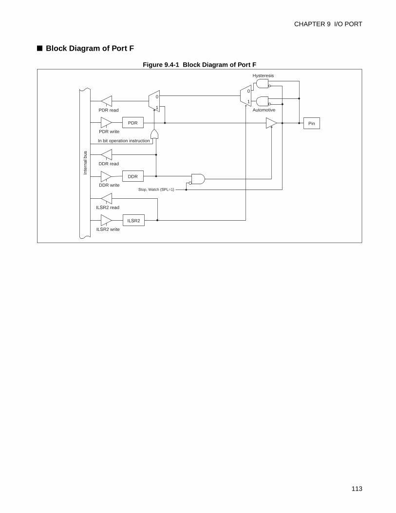
CHAPTER 9 I/O PORT
Block Diagram of Port F
Figure 9.4-1 Block Diagram of Port F
PDR read
PDR write
PDR
DDR read
DDR write
DDR
0
1
Pin
Stop, Watch (SPL=1)
Inte
rnal
bus
In bit operation instruction
Hysteresis
Automotive
ILSR2 read
ILSR2 write
ILSR2
0
1
113
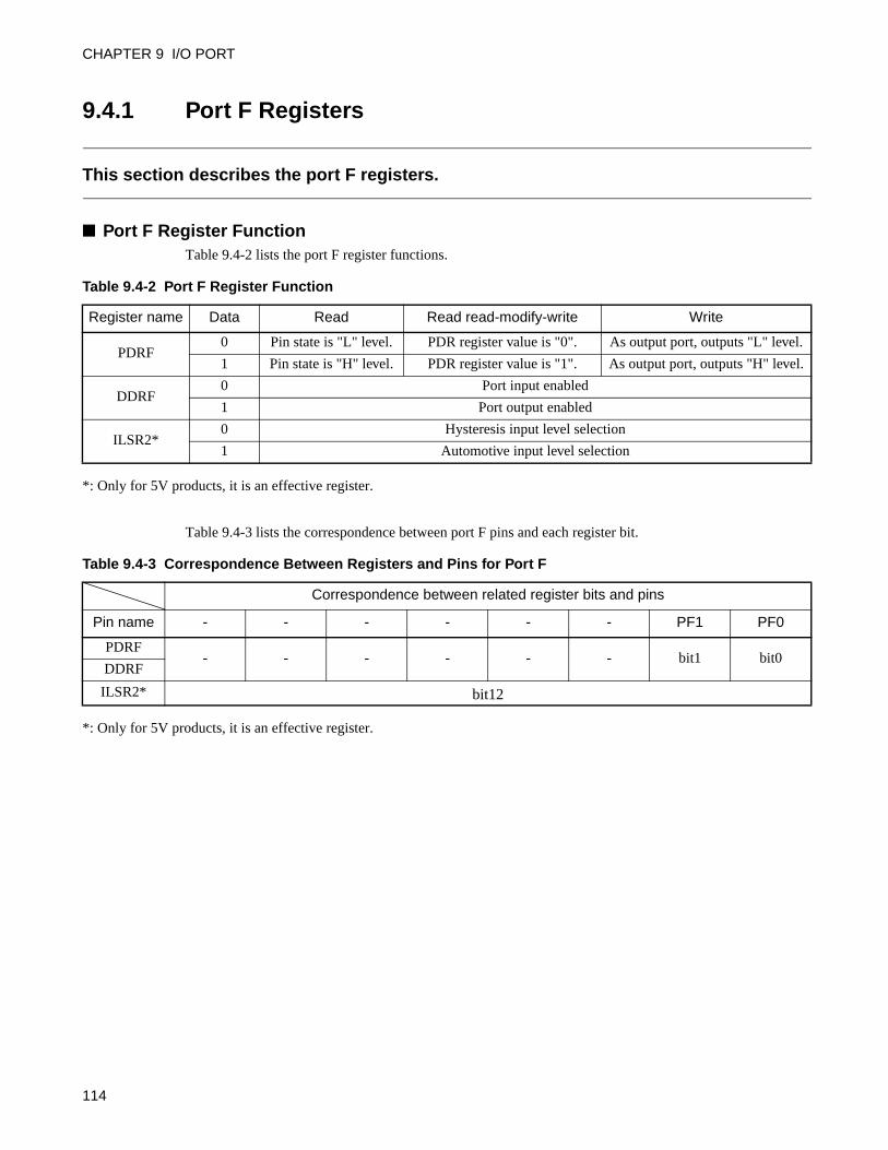
CHAPTER 9 I/O PORT
9.4.1 Port F Registers
This section describes the port F registers.
Port F Register FunctionTable 9.4-2 lists the port F register functions.
*: Only for 5V products, it is an effective register.
Table 9.4-3 lists the correspondence between port F pins and each register bit.
*: Only for 5V products, it is an effective register.
Table 9.4-2 Port F Register Function
Register name Data Read Read read-modify-write Write
PDRF0 Pin state is "L" level. PDR register value is "0". As output port, outputs "L" level.
1 Pin state is "H" level. PDR register value is "1". As output port, outputs "H" level.
DDRF0 Port input enabled
1 Port output enabled
ILSR2*0 Hysteresis input level selection
1 Automotive input level selection
Table 9.4-3 Correspondence Between Registers and Pins for Port F
Correspondence between related register bits and pins
Pin name - - - - - - PF1 PF0
PDRF- - - - - - bit1 bit0
DDRF
ILSR2* bit12
114
CHAPTER 9 I/O PORT
9.4.2 Operations of Port F
This section describes the operations of port F.
Operations of Port F
Operation as an output port
• Setting the corresponding DDR register bit to "1" sets a pin as an output port.
• For a peripheral function sharing pins, disable its output.
• When a pin is set as an output port, it outputs the value of the PDR register to pins.
• If data is written to the PDR register, the value is stored in the output latch and output to the pin as it is.
• Reading the PDR register returns the PDR register value.
Operation as an input port
• Setting the corresponding DDR register bit to "0" sets a pin as an input port.
• If data is written to the PDR register, the value is stored in the output latch but not output to the pin.
• Reading the PDR register returns the pin value. However, the read-modify-write command returns thePDR register value.
Operation at reset
• Resetting the CPU initializes the DDR register values to "0", and sets the port input enabled.
Operation in stop mode and watch mode
• If the pin state specification bit in the standby control register (STBC:SPL) is set to "1" when the deviceswitches to stop or watch mode, the pin is set forcibly to the high-impedance state regardless of theDDR register value. Note that the input is locked to "L" and blocked in order to prevent leaks due tofreed input.
• If the pin state specification bit is "0", the state remains in port I/O and the output is maintained.
Operation of the input level selection register 2
• The ILSR2 register is a valid register only for 5V models.
• Setting bit 2 of the ILSR2 register to "1" changes the port F input level from the hysteresis input level tothe automotive input level. The hysteresis input level is used when bit 2 of the ILSR2 register is "0".
115
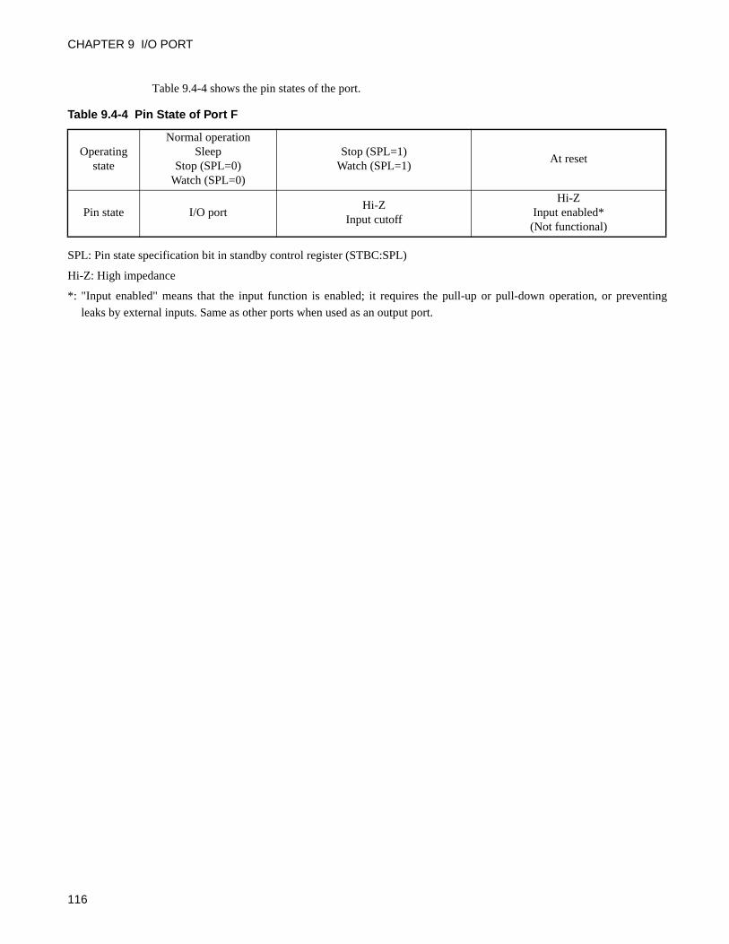
CHAPTER 9 I/O PORT
Table 9.4-4 shows the pin states of the port.
SPL: Pin state specification bit in standby control register (STBC:SPL)
Hi-Z: High impedance
*: "Input enabled" means that the input function is enabled; it requires the pull-up or pull-down operation, or preventing
leaks by external inputs. Same as other ports when used as an output port.
Table 9.4-4 Pin State of Port F
Operating state
Normal operationSleep
Stop (SPL=0)Watch (SPL=0)
Stop (SPL=1)Watch (SPL=1)
At reset
Pin state I/O portHi-Z
Input cutoff
Hi-ZInput enabled*
(Not functional)
116
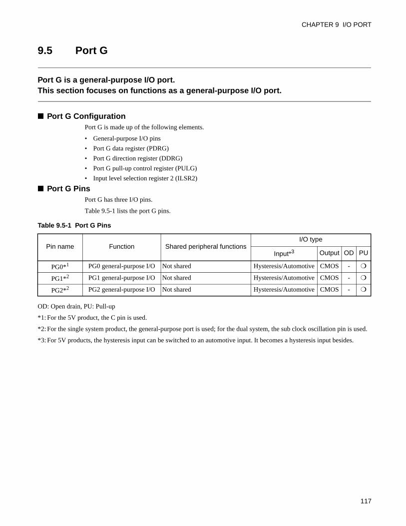
CHAPTER 9 I/O PORT
9.5 Port G
Port G is a general-purpose I/O port.This section focuses on functions as a general-purpose I/O port.
Port G ConfigurationPort G is made up of the following elements.
• General-purpose I/O pins
• Port G data register (PDRG)
• Port G direction register (DDRG)
• Port G pull-up control register (PULG)
• Input level selection register 2 (ILSR2)
Port G PinsPort G has three I/O pins.
Table 9.5-1 lists the port G pins.
OD: Open drain, PU: Pull-up
*1: For the 5V product, the C pin is used.
*2: For the single system product, the general-purpose port is used; for the dual system, the sub clock oscillation pin is used.
*3: For 5V products, the hysteresis input can be switched to an automotive input. It becomes a hysteresis input besides.
Table 9.5-1 Port G Pins
Pin name Function Shared peripheral functionsI/O type
Input*3 Output OD PU
PG0*1 PG0 general-purpose I/O Not shared Hysteresis/Automotive CMOS -
PG1*2 PG1 general-purpose I/O Not shared Hysteresis/Automotive CMOS -
PG2*2 PG2 general-purpose I/O Not shared Hysteresis/Automotive CMOS -
117
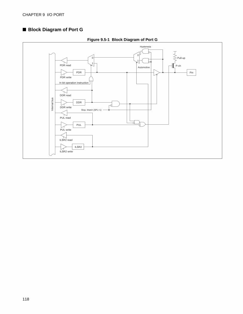
CHAPTER 9 I/O PORT
Block Diagram of Port G
Figure 9.5-1 Block Diagram of Port G
ILSR2 read
ILSR2 write
ILSR2
Hysteresis
Automotive
0
1
PDR read
PDR write
PDR
DDR read
DDR write
DDR
PUL read
PUL write
PUL
0
1
Pin
Stop, Watch (SPL=1)Inte
rnal
bus
In bit operation instruction
Pull-up
P-ch
118
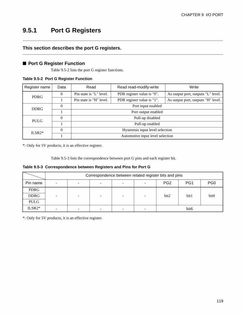
CHAPTER 9 I/O PORT
9.5.1 Port G Registers
This section describes the port G registers.
Port G Register FunctionTable 9.5-2 lists the port G register functions.
*: Only for 5V products, it is an effective register.
Table 9.5-3 lists the correspondence between port G pins and each register bit.
*: Only for 5V products, it is an effective register.
Table 9.5-2 Port G Register Function
Register name Data Read Read read-modify-write Write
PDRG0 Pin state is "L" level. PDR register value is "0". As output port, outputs "L" level.
1 Pin state is "H" level. PDR register value is "1". As output port, outputs "H" level.
DDRG0 Port input enabled
1 Port output enabled
PULG0 Pull-up disabled
1 Pull-up enabled
ILSR2*0 Hysteresis input level selection
1 Automotive input level selection
Table 9.5-3 Correspondence between Registers and Pins for Port G
Correspondence between related register bits and pins
Pin name - - - - - PG2 PG1 PG0
PDRG
- - - - - bit2 bit1 bit0DDRG
PULG
ILSR2* - - - - - bit6
119
CHAPTER 9 I/O PORT
9.5.2 Operations of Port G
This section describes the operations of port G.
Operations of Port G
Operation as an output port
• Setting the corresponding DDR register bit to "1" sets a pin as an output port.
• When a pin is set as an output port, it outputs the value of the PDR register to pins.
• If data is written to the PDR register, the value is stored in the output latch and output to the pin as it is.
• Reading the PDR register returns the PDR register value.
Operation as an input port
• Setting the corresponding DDR register bit to "0" sets a pin as an input port.
• If data is written to the PDR register, the value is stored in the output latch but not output to the pin.
• Reading the PDR register returns the pin value. However, the read-modify-write command returns thePDR register value.
Operation at reset
• Resetting the CPU initializes the DDR register values to "0", and sets the port input enabled.
Operation in stop mode and watch mode
• If the pin state specification bit in the standby control register (STBC:SPL) is set to "1" when the deviceswitches to stop or watch mode, the pin is set forcibly to the high-impedance state regardless of theDDR register value. Note that the input is locked to "L" and blocked in order to prevent leaks due tofreed input.
• If the pin state specification bit is "0", the state remains in port I/O and the output is maintained.
Operation of the pull-up control register
• Writing "1" to the PUL register internally connects the pull-up resistor to the pin. When the output is"L" level, the pull-up resistor is disconnected regardless of the PUL register value.
Operation of the input level selection register 2
• The ILSR2 register is a valid register only for 5V models.
• Setting bit 6 of the ILSR2 register to "1" changes the port G input level from the hysteresis input level tothe automotive input level. The hysteresis input level is used when bit 6 of the ILSR2 register is "0".
120
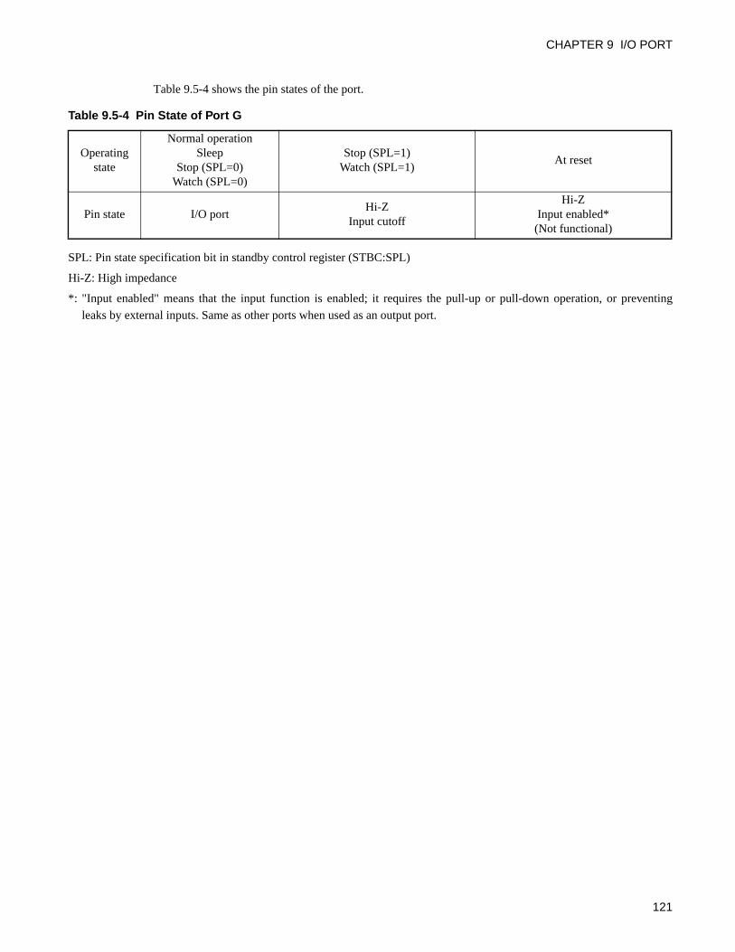
CHAPTER 9 I/O PORT
Table 9.5-4 shows the pin states of the port.
SPL: Pin state specification bit in standby control register (STBC:SPL)
Hi-Z: High impedance
*: "Input enabled" means that the input function is enabled; it requires the pull-up or pull-down operation, or preventing
leaks by external inputs. Same as other ports when used as an output port.
Table 9.5-4 Pin State of Port G
Operating state
Normal operationSleep
Stop (SPL=0)Watch (SPL=0)
Stop (SPL=1)Watch (SPL=1)
At reset
Pin state I/O portHi-Z
Input cutoff
Hi-ZInput enabled*
(Not functional)
121

CHAPTER 9 I/O PORT
122
CHAPTER 10TIMEBASE TIMER
This chapter describes the functions and operations of the timebase timer.
10.1 Overview of Timebase Timer
10.2 Configuration of Timebase Timer
10.3 Registers of the Timebase Timer
10.4 Interrupts of Timebase Timer
10.5 Explanation of Timebase Timer Operations and Setup Procedure Example
10.6 Precautions when Using Timebase Timer
123
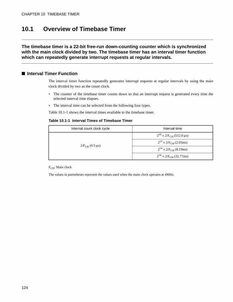
CHAPTER 10 TIMEBASE TIMER
10.1 Overview of Timebase Timer
The timebase timer is a 22-bit free-run down-counting counter which is synchronized with the main clock divided by two. The timebase timer has an interval timer function which can repeatedly generate interrupt requests at regular intervals.
Interval Timer Function
The interval timer function repeatedly generates interrupt requests at regular intervals by using the main
clock divided by two as the count clock.
• The counter of the timebase timer counts down so that an interrupt request is generated every time theselected interval time elapses.
• The interval time can be selected from the following four types.
Table 10.1-1 shows the interval times available to the timebase timer.
FCH: Main clock
The values in parentheses represent the values used when the main clock operates at 4MHz.
Table 10.1-1 Interval Times of Timebase Timer
Internal count clock cycle Interval time
2/FCH (0.5 µs)
210 × 2/FCH (512.0 µs)
212 × 2/FCH (2.05ms)
214 × 2/FCH (8.19ms)
216 × 2/FCH (32.77ms)
124
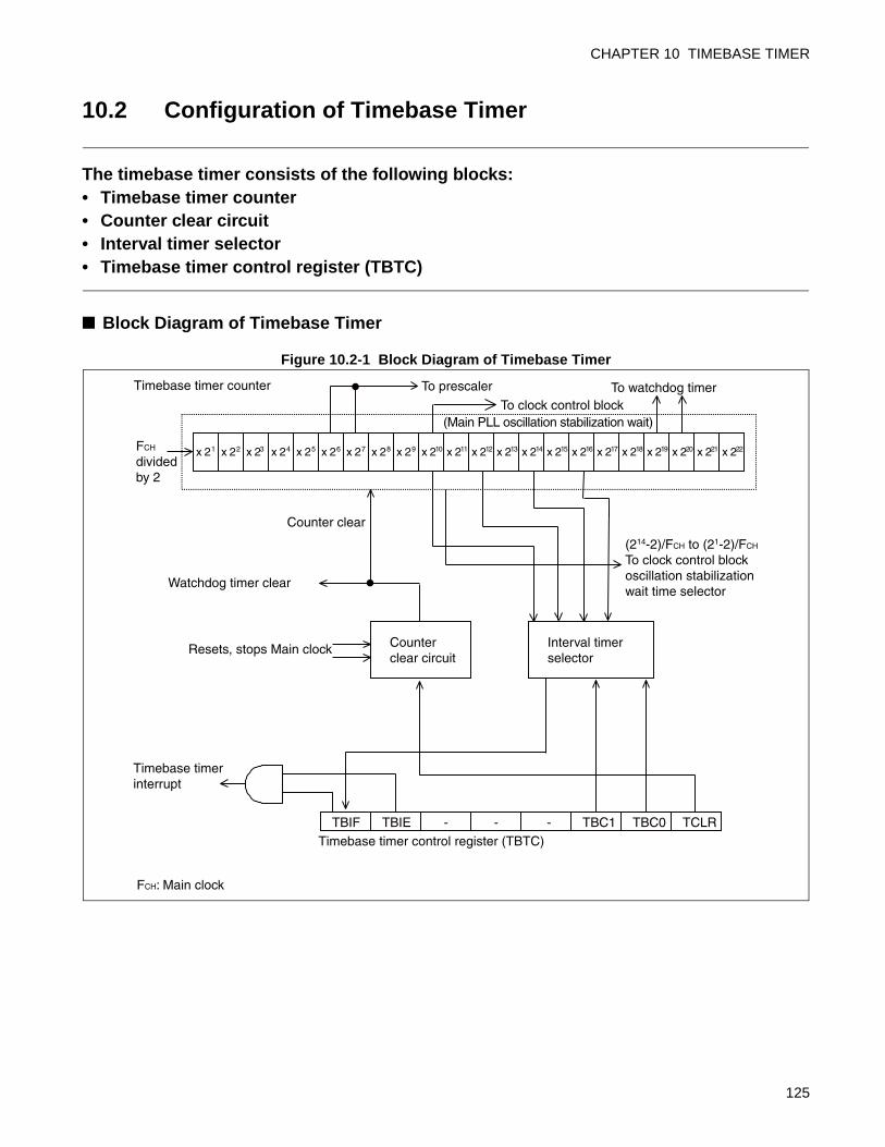
CHAPTER 10 TIMEBASE TIMER
10.2 Configuration of Timebase Timer
The timebase timer consists of the following blocks:• Timebase timer counter• Counter clear circuit• Interval timer selector• Timebase timer control register (TBTC)
Block Diagram of Timebase Timer
Figure 10.2-1 Block Diagram of Timebase Timer
x 21 x 22 x 23 x 24 x 25 x 26 x 27 x 28 x 29 x 210 x 211 x 212 x 213 x 214 x 215 x 216 x 217 x 218
Timebase timer counter
FCH divided by 2
Counter clear
To prescaler To watchdog timer
Counter clear circuit
Interval timer selector
TCLR TBC1 TBIF TBIE - - - TBC0 Timebase timer control register (TBTC)
Resets, stops Main clock
Watchdog timer clear
Timebase timer interrupt
(214-2)/FCH to (21-2)/FCH
To clock control block oscillation stabilization wait time selector
FCH: Main clock
x 219 x 221 x 220 x 222
To clock control block (Main PLL oscillation stabilization wait)
125
CHAPTER 10 TIMEBASE TIMER
Timebase timer counter
22-bit down-counter that uses the main clock divided by two as the count clock
Counter clear circuit
This circuit controls clearing of the timebase counter.
Interval timer selector
This circuit selects the one bit from four bits in the 22 bits that make up the timebase timer counter to use
the interval timer.
Timebase timer control register (TBTC)
This register selects the interval time, clears the counter, controls interrupts and checks the status.
Input ClockThe timebase timer uses the main clock divided by two as its input clock (count clock).
Output ClockThe timebase timer supplies clocks to the main clock oscillation stabilization wait time timer, the watchdog
timer and the prescaler.
126
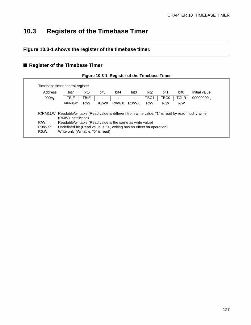
CHAPTER 10 TIMEBASE TIMER
10.3 Registers of the Timebase Timer
Figure 10.3-1 shows the register of the timebase timer.
Register of the Timebase Timer
Figure 10.3-1 Register of the Timebase Timer
Timebase timer control register
Address bit7 bit6 bit5 bit4 bit3 bit2 bit1 bit0 Initial value
000AH TBIF TBIE - - - TBC1 TBC0 TCLR 00000000BR(RM1),W R/W R0/WX R0/WX R0/WX R/W R/W R/W
R(RM1),W: Readable/writable (Read value is different from write value, "1" is read by read-modify-write (RMW) instruction)
R/W: Readable/writable (Read value is the same as write value)R0/WX: Undefined bit (Read value is "0", writing has no effect on operation)R0,W: Write only (Writable, "0" is read)
127
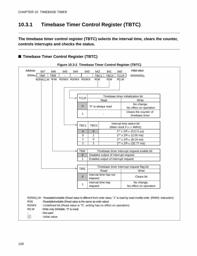
CHAPTER 10 TIMEBASE TIMER
10.3.1 Timebase Timer Control Register (TBTC)
The timebase timer control register (TBTC) selects the interval time, clears the counter, controls interrupts and checks the status.
Timebase Timer Control Register (TBTC)
Figure 10.3-2 Timebase Timer Control Register (TBTC)
Timebase timer initialization bit TCLR
Read Write
0 "0" is always read No change,
No effect on operation
1 - Clears the counter of
timebase timer
TBC1 TBC0 Interval time select bit
(Main clock FCH = 4MHz)
0 0 210 x 2/FCH (512.0 µs) 011
1 212 x 2/FCH (2.05 ms)
214 x 2/FCH (8.19 ms) 216 x 2/FCH (32.77 ms)
01
TBIE Timebase timer interrupt request enable bit0 Disables output of interrupt request 1 Enables output of interrupt request
Timebase timer interrupt request flag bit
TBIERead Write
0 Interval time has not elapsed
Clears bit
1 Interval time has elapsed
No change, No effect on operation
Address
000AH TBIF TBIE - - TCLRTBC0TBC1-bit0bit1bit2bit3bit4bit5bit6bit7 Initial value
00000000B R(RM1),W R/W R0/WX R0/WX R0/WX R/W R/W R0,W
R(RM1),W : Readable/writable (Read value is different from write value, "1" is read by read-modify-write (RMW) instruction)R/W : Readable/writable (Read value is the same as write value)R0/WX : Undefined bit (Read value is "0", writing has no effect on operation)R0,W : Write only (Writable, "0" is read)- : Not used : Initial value
128
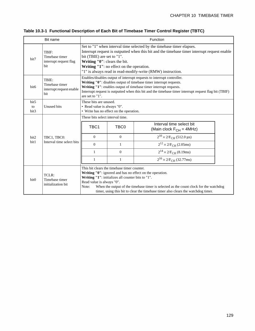
CHAPTER 10 TIMEBASE TIMER
Table 10.3-1 Functional Description of Each Bit of Timebase Timer Control Register (TBTC)
Bit name Function
bit7
TBIF:Timebase timer interrupt request flag bit
Set to "1" when interval time selected by the timebase timer elapses.Interrupt request is outputted when this bit and the timebase timer interrupt request enable bit (TBIE) are set to "1".Writing "0": clears the bit.Writing "1": no effect on the operation."1" is always read in read-modify-write (RMW) instruction.
bit6
TBIE:Timebase timer interrupt request enable bit
Enables/disables output of interrupt requests to interrupt controller.Writing "0": disables output of timebase timer interrupt requests.Writing "1": enables output of timebase timer interrupt requests.Interrupt request is outputted when this bit and the timebase timer interrupt request flag bit (TBIF) are set to "1".
bit5 to
bit3Unused bits
These bits are unused.• Read value is always "0".• Write has no effect on the operation.
bit2bit1
TBC1, TBC0:Interval time select bits
These bits select interval time.
bit0TCLR:Timebase timer initialization bit
This bit clears the timebase timer counter.Writing "0": ignored and has no effect on the operation.Writing "1": initializes all counter bits to "1".Read value is always "0".Note: When the output of the timebase timer is selected as the count clock for the watchdog
timer, using this bit to clear the timebase timer also clears the watchdog timer.
TBC1 TBC0Interval time select bit
(Main clock FCH = 4MHz)
0 0 210 × 2/FCH (512.0 µs)
0 1 212 × 2/FCH (2.05ms)
1 0 214 × 2/FCH (8.19ms)
1 1 216 × 2/FCH (32.77ms)
129
CHAPTER 10 TIMEBASE TIMER
10.4 Interrupts of Timebase Timer
An interrupt request is triggered when the interval time selected by the timebase timer elapses (interval timer function).
Interrupt when Interval Function is in OperationWhen the timebase timer counter counts down using the internal count clock and the selected timebase
timer counter underflows, the timebase timer interrupt request flag bit (TBTC:TBIF) is set to "1". If the
timebase timer interrupt request enable bit is enabled (TBTC:TBIE = 1), an interrupt request (IRQE) will
be generated to interrupt controller.
• Regardless of the value of TBIE bit, TBIF bit is set to "1", when the selected bit underflows.
• When TBIF bit is set to "1" and TBIE bit is changed from the disable state to the enable state (0 → 1),an interrupt request is generated immediately.
• TBIF bit is not set when the counter is cleared (TBTC:TCLR = 1) and the timebase timer counterunderflows at the same time.
• Write "1" to TBIF bit to clear an interrupt request in an interrupt processing routine.
Note:
When enabling the output of interrupt requests after canceling a reset (TBTC:TBIE = 1), always clearTBIF bit at the same time (TBTC:TBIF = 0).
Table 10.4-1 Interrupts of Timebase Timer
Item Description
Interrupt condition Interval time set by "TBTC:TBC1" and "TBC0" has elapsed
Interrupt flag TBTC:TBIF
Interrupt enable TBTC:TBIE
130
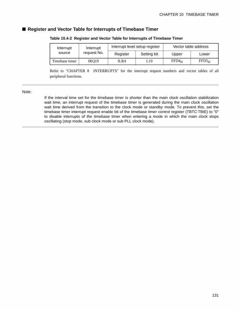
CHAPTER 10 TIMEBASE TIMER
Register and Vector Table for Interrupts of Timebase Timer
Refer to "CHAPTER 8 INTERRUPTS" for the interrupt request numbers and vector tables of all
peripheral functions.
Note:
If the interval time set for the timebase timer is shorter than the main clock oscillation stabilizationwait time, an interrupt request of the timebase timer is generated during the main clock oscillationwait time derived from the transition to the clock mode or standby mode. To prevent this, set thetimebase timer interrupt request enable bit of the timebase timer control register (TBTC:TBIE) to "0"to disable interrupts of the timebase timer when entering a mode in which the main clock stopsoscillating (stop mode, sub clock mode or sub PLL clock mode).
Table 10.4-2 Register and Vector Table for Interrupts of Timebase Timer
Interrupt source
Interrupt request No.
Interrupt level setup register Vector table address
Register Setting bit Upper Lower
Timebase timer IRQ19 ILR4 L19 FFD4H FFD5H
131
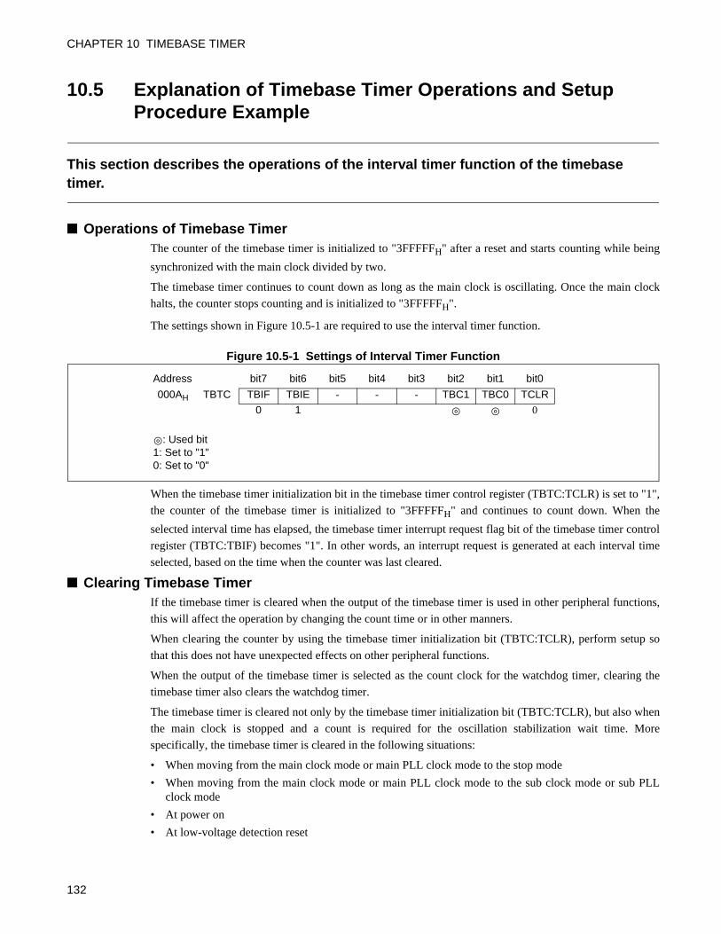
CHAPTER 10 TIMEBASE TIMER
10.5 Explanation of Timebase Timer Operations and Setup Procedure Example
This section describes the operations of the interval timer function of the timebase timer.
Operations of Timebase TimerThe counter of the timebase timer is initialized to "3FFFFFH" after a reset and starts counting while being
synchronized with the main clock divided by two.
The timebase timer continues to count down as long as the main clock is oscillating. Once the main clock
halts, the counter stops counting and is initialized to "3FFFFFH".
The settings shown in Figure 10.5-1 are required to use the interval timer function.
Figure 10.5-1 Settings of Interval Timer Function
When the timebase timer initialization bit in the timebase timer control register (TBTC:TCLR) is set to "1",
the counter of the timebase timer is initialized to "3FFFFFH" and continues to count down. When the
selected interval time has elapsed, the timebase timer interrupt request flag bit of the timebase timer control
register (TBTC:TBIF) becomes "1". In other words, an interrupt request is generated at each interval time
selected, based on the time when the counter was last cleared.
Clearing Timebase TimerIf the timebase timer is cleared when the output of the timebase timer is used in other peripheral functions,
this will affect the operation by changing the count time or in other manners.
When clearing the counter by using the timebase timer initialization bit (TBTC:TCLR), perform setup so
that this does not have unexpected effects on other peripheral functions.
When the output of the timebase timer is selected as the count clock for the watchdog timer, clearing the
timebase timer also clears the watchdog timer.
The timebase timer is cleared not only by the timebase timer initialization bit (TBTC:TCLR), but also when
the main clock is stopped and a count is required for the oscillation stabilization wait time. More
specifically, the timebase timer is cleared in the following situations:
• When moving from the main clock mode or main PLL clock mode to the stop mode
• When moving from the main clock mode or main PLL clock mode to the sub clock mode or sub PLLclock mode
• At power on
• At low-voltage detection reset
Address bit7 bit6 bit5 bit4 bit3 bit2 bit1 bit0
000AH TBTC TBIF TBIE - - - TBC1 TBC0 TCLR
0 1 0
: Used bit1: Set to "1"0: Set to "0"
132
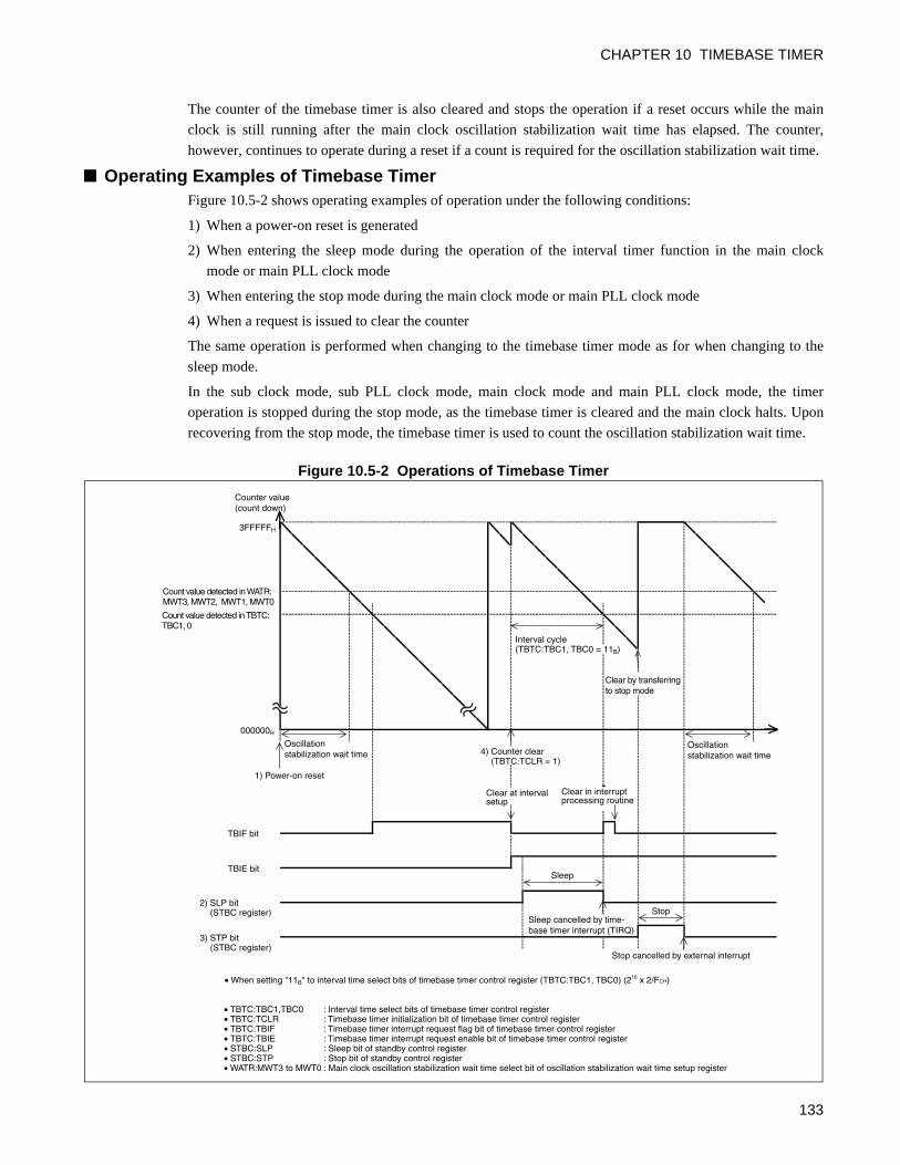
CHAPTER 10 TIMEBASE TIMER
The counter of the timebase timer is also cleared and stops the operation if a reset occurs while the main
clock is still running after the main clock oscillation stabilization wait time has elapsed. The counter,
however, continues to operate during a reset if a count is required for the oscillation stabilization wait time.
Operating Examples of Timebase TimerFigure 10.5-2 shows operating examples of operation under the following conditions:
1) When a power-on reset is generated
2) When entering the sleep mode during the operation of the interval timer function in the main clock
mode or main PLL clock mode
3) When entering the stop mode during the main clock mode or main PLL clock mode
4) When a request is issued to clear the counter
The same operation is performed when changing to the timebase timer mode as for when changing to the
sleep mode.
In the sub clock mode, sub PLL clock mode, main clock mode and main PLL clock mode, the timer
operation is stopped during the stop mode, as the timebase timer is cleared and the main clock halts. Upon
recovering from the stop mode, the timebase timer is used to count the oscillation stabilization wait time.
Figure 10.5-2 Operations of Timebase Timer
TBIF bit
TBIE bit
2) SLP bit (STBC register)
3) STP bit (STBC register)
Counter value(count down)
Clear by transferringto stop mode
000000H Oscillation stabilization wait time
1) Power-on reset
Interval cycle (TBTC:TBC1, TBC0 = 11B)
3FFFFFH
Clear in interruptprocessing routine
Sleep
Stop Sleep cancelled by time-base timer interrupt (TIRQ)
Stop cancelled by external interrupt
• When setting "11B" to interval time select bits of timebase timer control register (TBTC:TBC1, TBC0) (216 x 2/FCH)
• TBTC:TBC1,TBC0 : Interval time select bits of timebase timer control register• TBTC:TCLR : Timebase timer initialization bit of timebase timer control register• TBTC:TBIF : Timebase timer interrupt request flag bit of timebase timer control register• TBTC:TBIE : Timebase timer interrupt request enable bit of timebase timer control register• STBC:SLP : Sleep bit of standby control register • STBC:STP : Stop bit of standby control register• WATR:MWT3 to MWT0 : Main clock oscillation stabilization wait time select bit of oscillation stabilization wait time setup register
Oscillationstabilization wait time
Count value detected in TBTC:TBC1, 0
Count value detected in WATR:MWT3, MWT2, MWT1, MWT0
4) Counter clear (TBTC:TCLR = 1)
Clear at intervalsetup
133
CHAPTER 10 TIMEBASE TIMER
Setup Procedure Example
Initial Setting
The timebase timer is set up in the following procedure:
1) Disable interrupts. (TBTC:TBIE = 0)
2) Set the interval time. (TBTC:TBC1, 0)
3) Enable interrupts. (TBTC:TBIE = 1)
4) Clear the counter. (TBTC:TCLR = 1)
Processing interrupts
1) Clear the interrupt request flag. (TBTC:TBIF = 0)
2) Clear the counter. (TBTC:TCLR = 1)
134
CHAPTER 10 TIMEBASE TIMER
10.6 Precautions when Using Timebase Timer
Care must be taken for the following points when using the timebase timer.
Precautions when Using Timebase Timer
When setting the timer by program
The timer cannot be recovered from interrupt processing, when the timebase timer interrupt request flag bit
(TBTC:TBIF) is set to "1" and the interrupt request enable bit is enabled (TBTC:TBIE = 1). Always clear
TBIF bit in the interrupt processing routine.
Clearing Timebase Timer
The timebase timer is cleared not only by the timebase timer initialization bit (TBTC:TCLR = 1) but also
when the oscillation stabilization wait time is required for the main clock. When the timebase timer is
selected for the count clock of the watchdog timer (WDTC:CS1, CS0 = 00B or CS1, CS0, = 01B), clearing
the timebase timer also clears the watchdog timer.
Peripheral functions receiving clock from timebase timer
In the mode where the source oscillation of the main clock is stopped, the counter is cleared and the
timebase timer stops operation. In addition, if the timebase timer is cleared when the output of the timebase
timer is used in other peripheral functions, this will affect the operation such as cycle change.
The clock for the watchdog timer is also outputted from the initial state. However, as the watchdog timer
counter is cleared at the same time, the watchdog timer operates in the normal cycles.
135

CHAPTER 10 TIMEBASE TIMER
136
CHAPTER 11WATCHDOG TIMER
This chapter describes the functions and operations of the watchdog timer.
11.1 Overview of Watchdog Timer
11.2 Configuration of Watchdog Timer
11.3 Registers of the Watchdog Timer
11.4 Explanation of Watchdog Timer Operations and Setup Procedure Example
11.5 Precautions when Using Watchdog Timer
137
CHAPTER 11 WATCHDOG TIMER
11.1 Overview of Watchdog Timer
The watchdog timer serves as a counter used to prevent programs from running out of control.
Watchdog Timer FunctionThe watchdog timer functions as a counter used to prevent programs from running out of control. Once the
watchdog timer is activated, its counter needs to be cleared at specified intervals regularly. A watchdog
reset is generated if the timer is not cleared within a certain amount of time due to a problem such as the
program entering an infinite loop.
The output of either the timebase timer or watch prescaler can be selected as the count clock for the
watchdog timer.
The interval times of the watchdog timer are shown in Table 11.1-1. If the counter of the watchdog timer is
not cleared, a watchdog reset is generated between the minimum time and the maximum time. Clear the
counter of the watchdog timer within the minimum time.
*: WDTC:CS1, 0: Count clock switch bit of watchdog timer control register
For information about the minimum and maximum times of the watchdog timer interval,
refer to "11.4 Explanation of Watchdog Timer Operations and Setup Procedure Example".
Table 11.1-1 Interval Times of Watchdog Timer
Count clock typeCount clock switch bit
(WDTC:CS1, 0)*
Interval time
Minimum time Maximum time
Timebase timer output(main clock = 4MHz)
00B 524 ms 1.05 s
01B 262 ms 524 ms
Watch prescaler output(sub clock = 32.768kHz)
10B 500 ms 1.00 s
11B 250 ms 500 ms
138
CHAPTER 11 WATCHDOG TIMER
11.2 Configuration of Watchdog Timer
The watchdog timer consists of the following blocks:• Count clock selector• Watchdog timer counter• Reset control circuit• Watchdog timer clear selector• Counter clear control circuit• Watchdog timer control register (WDTC)
Block Diagram of Watchdog Timer
Figure 11.2-1 Block Diagram of Watchdog Timer
CS1 - CS0 - WTE3 WTE2 WTE0 WTE1
Count clock selector
Watchdog timer clear selector
Counter clear control circuit
Reset controlcircuit
Clear signal from timebase timer
Clear signal from watch prescaler
Sleep mode starts Stop mode starts Timebase timer/watch mode starts
FCH: Main clockFCL: Subclock
213 x 2/FCH, 212 x 2/FCH (Watch prescaler output)
220 x 2/FCH, 219 x 2/FCH (Timebase timer output)
Watchdog timer counter
RST
Overflow
Watchdog timer
Clearingactivated
Watchdog timer control register (WDTC)
139
CHAPTER 11 WATCHDOG TIMER
Count clock selector
This selector selects the count clock of the watchdog timer counter.
Watchdog timer counter
This is a 1-bit counter that uses the output of either the timebase timer or watch prescaler as the count
clock.
Reset control circuit
This circuit generates a reset signal when the watchdog timer counter overflows.
Watchdog timer clear selector
This selector selects the watchdog timer clear signal.
Counter clear control circuit
This circuit controls the clearing and stopping of the watchdog timer counter.
Watchdog timer control register (WDTC)
This register performs setup for activating/clearing the watchdog timer counter as well as for selecting the
count clock.
Input ClockThe watchdog timer uses the output clock from either the timebase timer or watch prescaler as the input
clock (count clock).
140
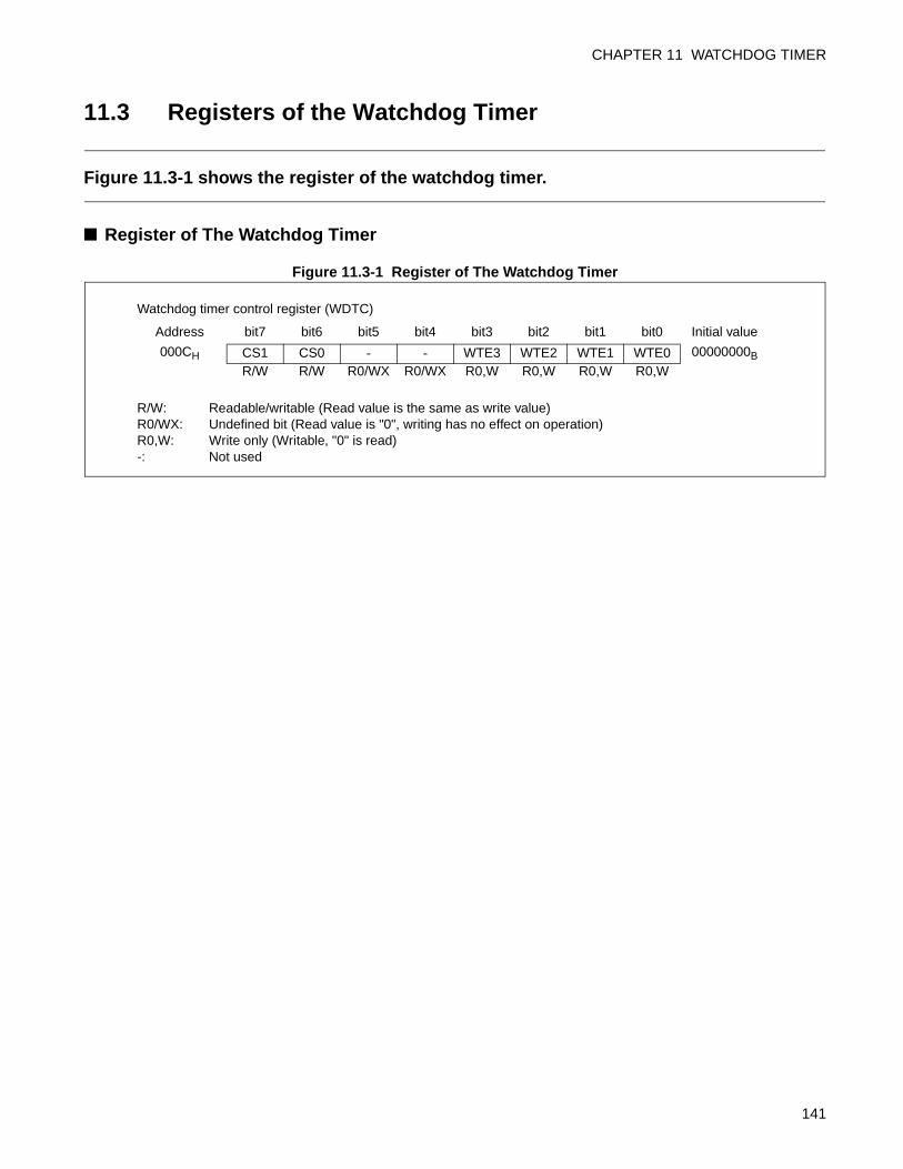
CHAPTER 11 WATCHDOG TIMER
11.3 Registers of the Watchdog Timer
Figure 11.3-1 shows the register of the watchdog timer.
Register of The Watchdog Timer
Figure 11.3-1 Register of The Watchdog Timer
Watchdog timer control register (WDTC)
Address bit7 bit6 bit5 bit4 bit3 bit2 bit1 bit0 Initial value
000CH CS1 CS0 - - WTE3 WTE2 WTE1 WTE0 00000000B
R/W R/W R0/WX R0/WX R0,W R0,W R0,W R0,W
R/W: Readable/writable (Read value is the same as write value)R0/WX: Undefined bit (Read value is "0", writing has no effect on operation)R0,W: Write only (Writable, "0" is read)-: Not used
141
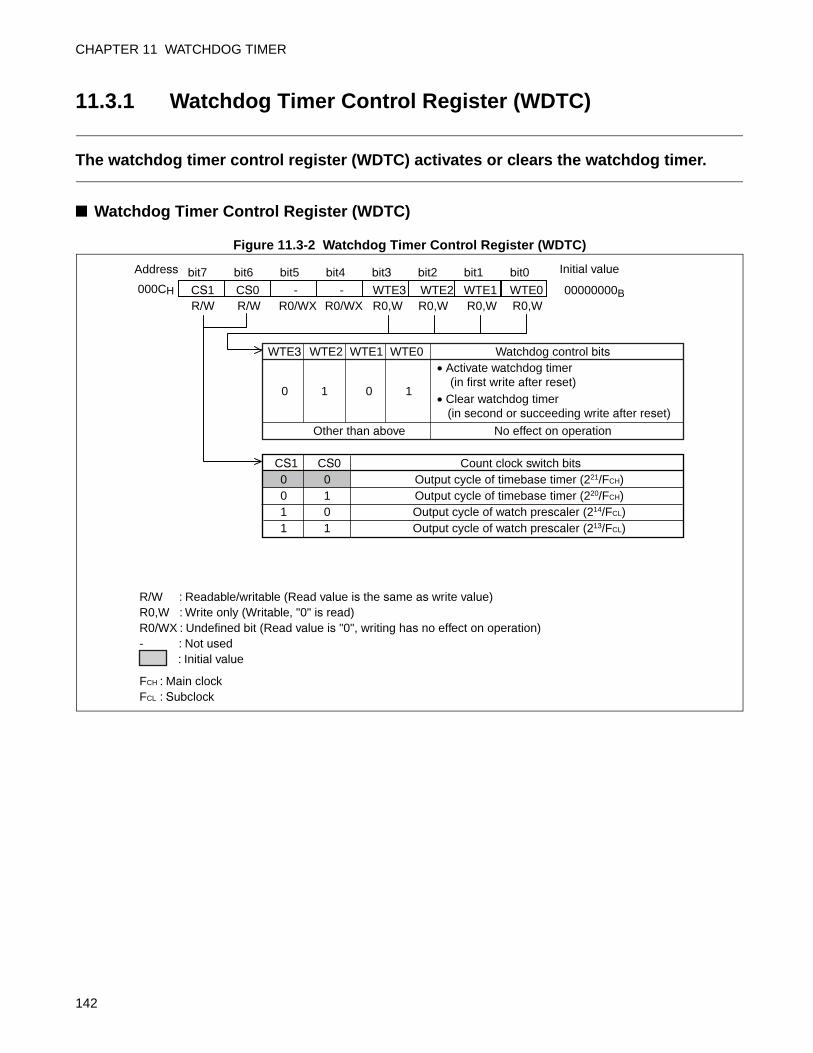
CHAPTER 11 WATCHDOG TIMER
11.3.1 Watchdog Timer Control Register (WDTC)
The watchdog timer control register (WDTC) activates or clears the watchdog timer.
Watchdog Timer Control Register (WDTC)
Figure 11.3-2 Watchdog Timer Control Register (WDTC)
WTE3 WTE2 WTE1 WTE0 Watchdog control bits
10 10
• Activate watchdog timer (in first write after reset)
• Clear watchdog timer (in second or succeeding write after reset)
Other than above No effect on operation
CS1 CS0 Count clock switch bits 0 0 Output cycle of timebase timer (221/FCH) 0 Output cycle of timebase timer (220/FCH) 1 Output cycle of watch prescaler (214/FCL) 1
101 Output cycle of watch prescaler (213/FCL)
Address
000CH
bit5
-
bit6
CS0 R/W
bit7
CS1 R/W
bit4
- R0/WXR0/WX
bit3
WTE3
bit2
WTE2
bit1
WTE1
bit0
WTE0 R0,W R0,W R0,W R0,W
Initial value
00000000B
FCH : Main clock FCL : Subclock
R/W : Readable/writable (Read value is the same as write value) R0,W : Write only (Writable, "0" is read) R0/WX : Undefined bit (Read value is "0", writing has no effect on operation)- : Not used : Initial value
142
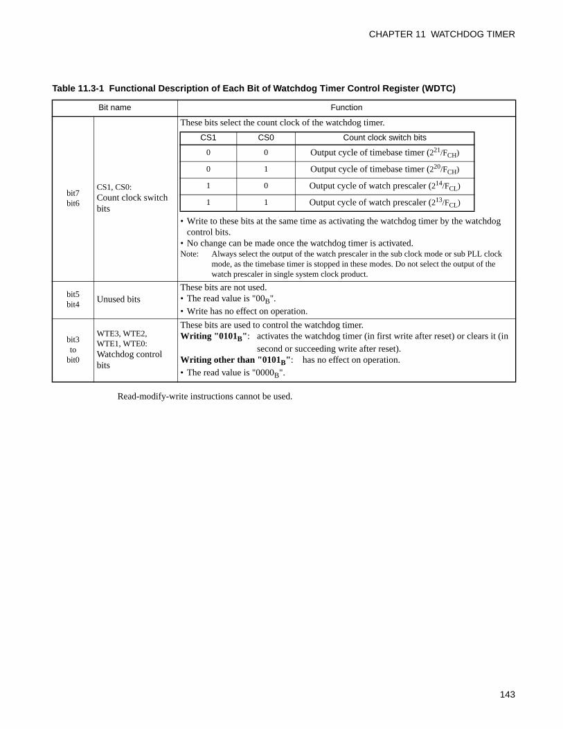
CHAPTER 11 WATCHDOG TIMER
Read-modify-write instructions cannot be used.
Table 11.3-1 Functional Description of Each Bit of Watchdog Timer Control Register (WDTC)
Bit name Function
bit7bit6
CS1, CS0:Count clock switch bits
These bits select the count clock of the watchdog timer.
• Write to these bits at the same time as activating the watchdog timer by the watchdog control bits.
• No change can be made once the watchdog timer is activated.Note: Always select the output of the watch prescaler in the sub clock mode or sub PLL clock
mode, as the timebase timer is stopped in these modes. Do not select the output of the watch prescaler in single system clock product.
bit5bit4
Unused bitsThese bits are not used.• The read value is "00B".• Write has no effect on operation.
bit3to
bit0
WTE3, WTE2,WTE1, WTE0:Watchdog control bits
These bits are used to control the watchdog timer.Writing "0101B": activates the watchdog timer (in first write after reset) or clears it (in
second or succeeding write after reset).Writing other than "0101B": has no effect on operation.• The read value is "0000B".
CS1 CS0 Count clock switch bits
0 0 Output cycle of timebase timer (221/FCH)
0 1 Output cycle of timebase timer (220/FCH)
1 0 Output cycle of watch prescaler (214/FCL)
1 1 Output cycle of watch prescaler (213/FCL)
143
CHAPTER 11 WATCHDOG TIMER
11.4 Explanation of Watchdog Timer Operations and Setup Procedure Example
The watchdog timer generates a watchdog reset when the watchdog timer counter overflows.
Operations of Watchdog Timer
How to activate the watchdog timer
• The timer of the watchdog timer is activated when "0101B" is written to the watchdog control bits of thewatchdog timer control register (WDTC:WTE3 to WTE0) for the first time after a reset. The countclock switch bits of the watchdog timer control register (WDTC:CS1,CS0) should also be set at thesame time.
• Once the watchdog timer is activated, a reset is the only way to stop its operation.
Clearing the watchdog timer
• When the counter of the watchdog timer is not cleared within the interval time, it overflows, allowingthe watchdog timer to generate a watchdog reset.
• The counter of the watchdog timer is cleared when "0101B" is written to the watchdog control bits of thewatchdog timer control register (WDTC:WTE3 to WTE0) for the second or any succeeding time.
• The watchdog timer is cleared at the same time as the timer selected as the count clock (timebase timeror watch prescaler) is cleared.
Operation in standby mode
Regardless of the clock mode selected, the watchdog timer clears its counter and stops the operation when
entering a standby mode (sleep/stop/timebase timer/watch).
Once released from the standby mode, the timer restarts the operation.
Note:
The watchdog timer is also cleared when the timer selected as the count clock (timebase timer orwatch prescaler) is cleared.For this reason, the watchdog timer cannot function as such, if the software is set to clear theselected timer repeatedly during the interval time of the watchdog timer.
144
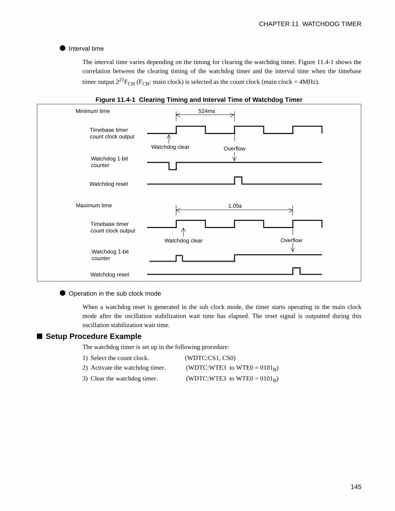
CHAPTER 11 WATCHDOG TIMER
Interval time
The interval time varies depending on the timing for clearing the watchdog timer. Figure 11.4-1 shows the
correlation between the clearing timing of the watchdog timer and the interval time when the timebase
timer output 221FCH (FCH: main clock) is selected as the count clock (main clock = 4MHz).
Figure 11.4-1 Clearing Timing and Interval Time of Watchdog Timer
Operation in the sub clock mode
When a watchdog reset is generated in the sub clock mode, the timer starts operating in the main clock
mode after the oscillation stabilization wait time has elapsed. The reset signal is outputted during this
oscillation stabilization wait time.
Setup Procedure ExampleThe watchdog timer is set up in the following procedure:
1) Select the count clock. (WDTC:CS1, CS0)
2) Activate the watchdog timer. (WDTC:WTE3 to WTE0 = 0101B)
3) Clear the watchdog timer. (WDTC:WTE3 to WTE0 = 0101B)
Timebase timer count clock output
Watchdog 1-bit counter
Watchdog reset
Minimum time
Maximum time
Timebase timer count clock output
Watchdog 1-bit counter
Watchdog reset
Watchdog clear
Watchdog clear
Overflow
Overflow
524ms
1.05s
145
CHAPTER 11 WATCHDOG TIMER
11.5 Precautions when Using Watchdog Timer
Care must be taken for the following points when using the watchdog timer.
Precautions when Using Watchdog Timer
Stopping the watchdog timer
Once activated, the watchdog timer cannot be stopped until a reset is generated.
Selecting the count clock
The count clock switch bits (WDTC:CS1,0) can be rewritten only when the watchdog control bits
(WDTC:WTE3 to WTE0) are set to "0101B" upon the activation of the watchdog timer. The count clock
switch bits cannot be written by a bit operation instruction. Moreover, the bit settings should not be
changed once the timer is activated.
In the sub clock mode, the timebase timer does not operate because the main clock stops oscillating.
In order to operate the watchdog timer in the sub clock mode, it is necessary to select the watch prescaler as
the count clock beforehand and set "WDTC:CS1,0" to "10B" or "11B".
Clearing the watchdog timer
Clearing the counter used for the count clock of the watchdog timer (timebase timer or watch prescaler)
also clears the counter of the watchdog timer.
The counter of the watchdog timer is cleared when entering the sleep mode, stop mode or watch mode.
Programming precaution
When creating a program in which the watchdog timer is cleared repeatedly in the main loop, set the
processing time of the main loop including the interrupt processing time to the minimum watchdog timer
interval time or shorter.
146
CHAPTER 12WATCH PRESCALER
This chapter describes the functions and operations of the watch prescaler.
12.1 Overview of Watch Prescaler
12.2 Configuration of Watch Prescaler
12.3 Registers of the Watch Prescaler
12.4 Interrupts of Watch Prescaler
12.5 Explanation of Watch Prescaler Operations and Setup Procedure Example
12.6 Precautions when Using Watch Prescaler
12.7 Sample Programs for Watch Prescaler
147
CHAPTER 12 WATCH PRESCALER
12.1 Overview of Watch Prescaler
The watch prescaler is a 15-bit down-counting, free-run counter, which is synchronized with the sub clock divided by two. It has an interval timer function that continuously generates interrupt requests at regular intervals.
Interval Timer FunctionThe interval timer function continuously generates interrupt requests at regular intervals, using the sub
clock divided by two as its count clock.
• The counter of the watch prescaler counts down and an interrupt request is generated every time theselected interval time has elapsed.
• The interval time can be selected from the following four types:
Table 12.1-1 shows the interval times of the watch prescaler.
FCL: Sub clock
The values in parentheses represent the values achieved when the sub clock operates at 32.768kHz.
Note:
The watch prescaler cannot be used in single system clock product.
Table 12.1-1 Interval Times of Watch Prescaler
Internal count clock cycle Interval time
2/FCL (61.0 µs)
211 × 2/FCL (125ms)
212 × 2/FCL (250ms)
213 × 2/FCL (500ms)
214 × 2/FCL (1.00s)
148
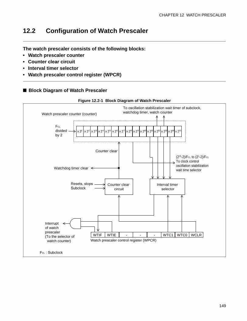
CHAPTER 12 WATCH PRESCALER
12.2 Configuration of Watch Prescaler
The watch prescaler consists of the following blocks:• Watch prescaler counter• Counter clear circuit• Interval timer selector• Watch prescaler control register (WPCR)
Block Diagram of Watch Prescaler
Figure 12.2-1 Block Diagram of Watch Prescaler
x 21 x 22 x 23 x 24 x 25 x 26 x 27 x 28 x 29 x 210 x 211 x 212 x 213 x 214 x 215
Counter clear circuit
Interval timer selector
WTIF WTIE - - - WTC1 WTC0 WCLR
Watch prescaler counter (counter)
To oscillation stabilization wait timer of subclock,watchdog timer, watch counter
Watch prescaler control register (WPCR)
(215-2)/FCL to (21-2)/FCL
To clock control oscillation stabilizationwait time selector
Resets, stopsSubclock
Interrupt of watch prescaler(To the selector of watch counter)
Watchdog timer clear
FCL divided by 2
FCL : Subclock
Counter clear
149
CHAPTER 12 WATCH PRESCALER
Watch prescaler counter (counter)
This is a 15-bit down-counter that uses the sub clock divided by two as its count clock.
Counter clear circuit
This circuit controls the clearing of the watch prescaler.
Interval timer selector
This circuit selects one out of the four bits used for the interval timer among 15 bits available in the watch
prescaler counter.
Watch prescaler control register (WPCR)
This register selects the interval time, clears the counter, controls interrupts and checks the status.
Input ClockThe watch prescaler uses the sub clock divided by two as its input clock (count clock).
Output ClockThe watch prescaler supplies its clock to the timer for the oscillation stabilization wait time of the sub
clock, the watchdog timer and the watch counter.
150
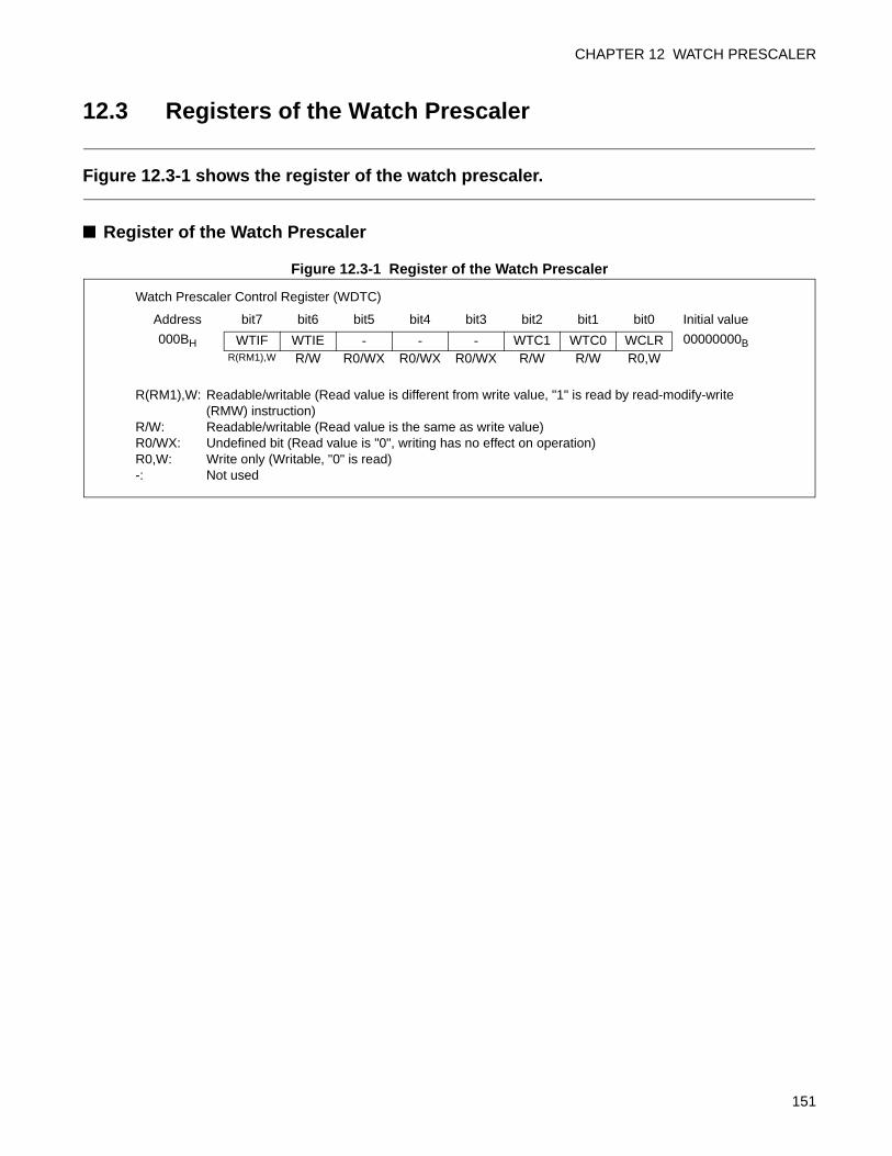
CHAPTER 12 WATCH PRESCALER
12.3 Registers of the Watch Prescaler
Figure 12.3-1 shows the register of the watch prescaler.
Register of the Watch Prescaler
Figure 12.3-1 Register of the Watch Prescaler
Watch Prescaler Control Register (WDTC)
Address bit7 bit6 bit5 bit4 bit3 bit2 bit1 bit0 Initial value
000BH WTIF WTIE - - - WTC1 WTC0 WCLR 00000000BR(RM1),W R/W R0/WX R0/WX R0/WX R/W R/W R0,W
R(RM1),W: Readable/writable (Read value is different from write value, "1" is read by read-modify-write (RMW) instruction)
R/W: Readable/writable (Read value is the same as write value)R0/WX: Undefined bit (Read value is "0", writing has no effect on operation)R0,W: Write only (Writable, "0" is read)-: Not used
151
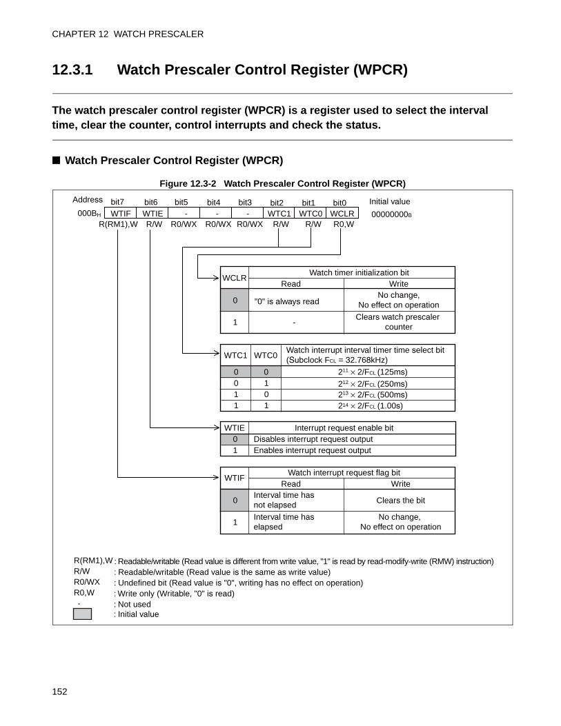
CHAPTER 12 WATCH PRESCALER
12.3.1 Watch Prescaler Control Register (WPCR)
The watch prescaler control register (WPCR) is a register used to select the interval time, clear the counter, control interrupts and check the status.
Watch Prescaler Control Register (WPCR)
Figure 12.3-2 Watch Prescaler Control Register (WPCR)
Watch timer initialization bit WCLR
Read Write
0 "0" is always readNo change,
No effect on operation
1 -Clears watch prescaler
counter
WTC1 WTC0Watch interrupt interval timer time select bit(Subclock FCL = 32.768kHz)
0 0 211 × 2/FCL (125ms)
212 × 2/FCL (250ms) 213 × 2/FCL (500ms) 214 × 2/FCL (1.00s)
011
101
WTIE Interrupt request enable bit
0 Disables interrupt request output 1 Enables interrupt request output
Watch interrupt request flag bitWTIF
Read Write
0 Interval time has not elapsed
Clears the bit
1 Interval time has elapsed
No change, No effect on operation
Address
000BH
bit7
R(RM1),W WTIF
bit6 WTIE
bit5 -
bit4 -
bit3 -R0/WX R0/WX R0/WX
bit2 WTC1
bit1
R/W R/W R/W WTC0
bit0 WCLR R0,W
Initial value
00000000B
R(RM1),W : Readable/writable (Read value is different from write value, "1" is read by read-modify-write (RMW) instruction)R/W : Readable/writable (Read value is the same as write value)R0/WX : Undefined bit (Read value is "0", writing has no effect on operation)R0,W : Write only (Writable, "0" is read)- : Not used : Initial value
152
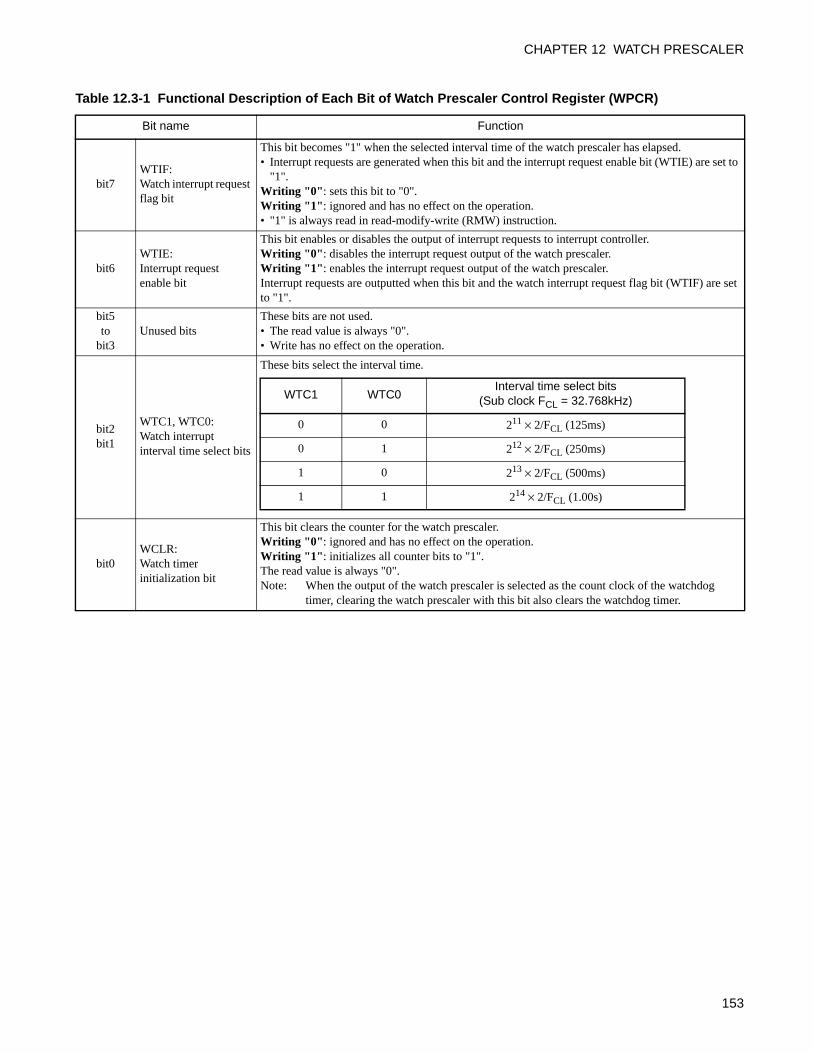
CHAPTER 12 WATCH PRESCALER
Table 12.3-1 Functional Description of Each Bit of Watch Prescaler Control Register (WPCR)
Bit name Function
bit7WTIF: Watch interrupt request flag bit
This bit becomes "1" when the selected interval time of the watch prescaler has elapsed.• Interrupt requests are generated when this bit and the interrupt request enable bit (WTIE) are set to
"1".Writing "0": sets this bit to "0".Writing "1": ignored and has no effect on the operation.• "1" is always read in read-modify-write (RMW) instruction.
bit6WTIE: Interrupt request enable bit
This bit enables or disables the output of interrupt requests to interrupt controller.Writing "0": disables the interrupt request output of the watch prescaler.Writing "1": enables the interrupt request output of the watch prescaler.Interrupt requests are outputted when this bit and the watch interrupt request flag bit (WTIF) are set to "1".
bit5to
bit3Unused bits
These bits are not used.• The read value is always "0".• Write has no effect on the operation.
bit2bit1
WTC1, WTC0: Watch interrupt interval time select bits
These bits select the interval time.
bit0WCLR: Watch timer initialization bit
This bit clears the counter for the watch prescaler.Writing "0": ignored and has no effect on the operation.Writing "1": initializes all counter bits to "1".The read value is always "0".Note: When the output of the watch prescaler is selected as the count clock of the watchdog
timer, clearing the watch prescaler with this bit also clears the watchdog timer.
WTC1 WTC0Interval time select bits
(Sub clock FCL = 32.768kHz)
0 0 211 × 2/FCL (125ms)
0 1 212 × 2/FCL (250ms)
1 0 213 × 2/FCL (500ms)
1 1 214 × 2/FCL (1.00s)
153
CHAPTER 12 WATCH PRESCALER
12.4 Interrupts of Watch Prescaler
An interrupt request is generated when the selected interval time of the watch prescaler has elapsed (interval timer function).
Interrupts in Operation of Interval Timer Function (Watch Interrupts)In any mode other than the main stop mode, the watch interrupt request flag bit is set to "1" (WPCR:WTIF
= 1), when the watch prescaler counter counts up by using the source oscillation of the sub clock and the
time of the interval timer has elapsed. If the interrupt request enable bit is also enabled (WPCR:WTIE = 1)
and watch counter start interrupt request enable bit of the watch counter is disabled (WCSR: ISEL0), an
interrupt request (IRQ20) occurs from watch prescaler to an interrupt controller.
• Regardless of the value in the WTIE bit, the WTIF bit is set to "1" when the time set by the watchinterrupt interval time select bits has been reached.
• When the WTIF bit is set to "1", changing the WTIE bit from the disable state to the enable state(WPCR:WTIE = 0 → 1) immediately generates an interrupt request.
• The WTIF bit cannot be set when the counter is cleared (WPCR:WCLR = 1) at the same time as theselected bit overflows.
• Write "0" to the WTIF bit in the interrupt processing routine to clear an interrupt request to "0".
Note:
When enabling the output of interrupt requests (WPCR:WTIE = 1) after canceling a reset, alwaysclear the WTIF bit at the same time (WPCR:WTIF = 0).
Interrupts of Watch Prescaler
Register and Vector Table Related to Interrupts of Watch Prescaler
*: The watch prescaler shares the same interrupt request number and vector table as the watch counter.
Refer to "CHAPTER 8 INTERRUPTS" for the interrupt request numbers and vector tables of all peripheral
functions.
Table 12.4-1 Interrupts of Watch Prescaler
Item Description
Interrupt condition Interval time set by "WPCR:WTC1" and "WTC0" has elapsed.
Interrupt flag WPCR:WTIF
Interrupt enable WPCR:WTIE
Table 12.4-2 Register and Vector Table Related to Interrupts of Watch Prescaler
Interrupt source
Interrupt request No.
Interrupt level setup register Vector table address
Register Setting bit Upper Lower
Watch
prescaler* IRQ20 ILR5 L20 FFD2H FFD3H
154
CHAPTER 12 WATCH PRESCALER
Note:
If the interval time set for the watch prescaler is shorter than the oscillation stabilization wait time ofthe sub clock, an interrupt request of the watch prescaler is generated during the oscillationstabilization wait time of the sub clock required for recovery by an external interrupt upon thetransition from the sub clock mode or the sub PLL clock mode to the stop mode. To prevent this, setthe interrupt request enable bit (WPCR:WTIE) in the watch prescaler control register to "0" to disableinterrupts of the watch prescaler when entering the stop mode during the sub clock mode or the subPLL clock mode.
155
CHAPTER 12 WATCH PRESCALER
12.5 Explanation of Watch Prescaler Operations and Setup Procedure Example
The watch prescaler operates as an interval timer.
Operations of Interval Timer Function (Watch Prescaler)The counter of the watch prescaler continues to count down using the sub clock divided by two as its count
clock as long as the sub clock oscillates.
When cleared (WPCR:WCLR = 1), the counter starts to count down from "7FFFH". Once "0000H" is
reached, the counter returns to "7FFFH" to continue the count. When the time set by the interrupt interval
time select bits is reached during down-counting, the watch interrupt request flag bit (WPCR:WTIF) is set
to "1" in any mode other than the main stop mode. In other words, a watch interrupt request is generated at
each selected interval time, based on the time when the counter was last cleared.
Clearing Watch PrescalerIf the watch prescaler is cleared when the output of the watch prescaler is used in other peripheral
functions, this will affect the operation by changing the count time or in other manners.
When clearing the counter by using the watch prescaler initialization bit (WTCR:WCLR), perform setup so
that this does not have unexpected effects on other peripheral functions.
When the output of the watch prescaler is selected as the count clock, clearing the watch prescaler also
clears the watchdog timer.
The watch prescaler is cleared not only by the watch prescaler initialization bit (WTCR:WCLR) but also
when the sub clock is stopped and a count is required for the oscillation stabilization wait time.
• When moving from the sub clock mode or sub PLL clock mode to the stop mode
• When the sub clock oscillation stop bit in the system clock control register (SYCC:SUBS) is set to "1"in the main clock mode or main PLL clock mode
In addition, the counter of the watch prescaler is cleared and stops operation when a reset is generated.
Operating Examples of Watch PrescalerFigure 12.5-1 shows operating examples under the following conditions:
1) When a power-on reset is generated
2) When entering the sleep mode during the operation of the interval timer function in the sub clock mode
or sub PLL clock mode
3) When entering the stop mode during the operation of the interval timer function in the sub clock mode
or sub PLL clock mode
4) When a request is issued to clear the counter
The same operation is performed when changing to the watch mode as for when changing to the sleep
mode.
156
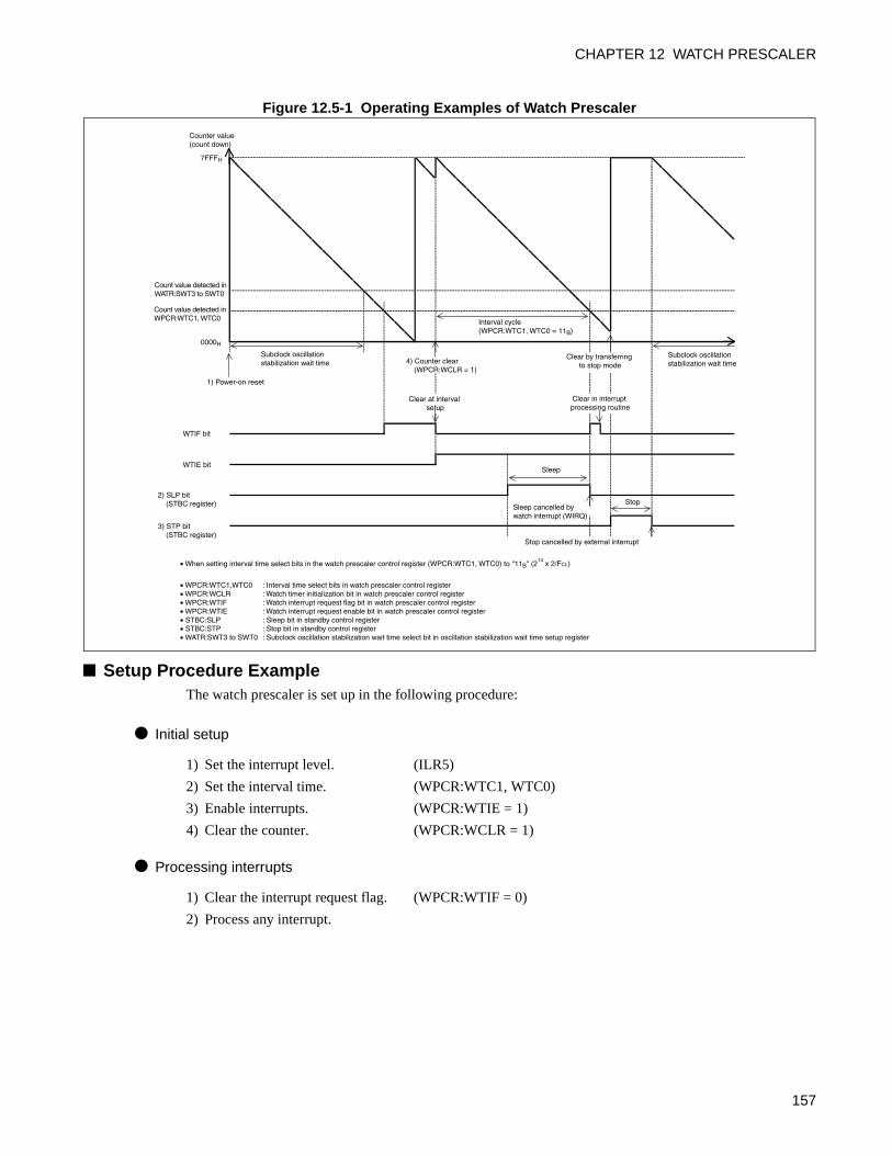
CHAPTER 12 WATCH PRESCALER
Figure 12.5-1 Operating Examples of Watch Prescaler
Setup Procedure ExampleThe watch prescaler is set up in the following procedure:
Initial setup
1) Set the interrupt level. (ILR5)
2) Set the interval time. (WPCR:WTC1, WTC0)
3) Enable interrupts. (WPCR:WTIE = 1)
4) Clear the counter. (WPCR:WCLR = 1)
Processing interrupts
1) Clear the interrupt request flag. (WPCR:WTIF = 0)
2) Process any interrupt.
WTIF bit
WTIE bit
2) SLP bit (STBC register)
3) STP bit (STBC register)
Counter value(count down)
Clear by transferring to stop mode
0000H
Subclock oscillation stabilization wait time
1) Power-on reset
Interval cycle (WPCR:WTC1, WTC0 = 11B)
7FFFH
Clear at interval setup
Sleep
Stop Sleep cancelled by watch interrupt (WIRQ)
Stop cancelled by external interrupt
• When setting interval time select bits in the watch prescaler control register (WPCR:WTC1, WTC0) to "11B" (214
x 2/FCL)
Count value detected in WPCR:WTC1, WTC0
Count value detected in WATR:SWT3 to SWT0
4) Counter clear (WPCR:WCLR = 1)
Subclock oscillation stabilization wait time
Clear in interrupt processing routine
• WPCR:WTC1,WTC0 : Interval time select bits in watch prescaler control register • WPCR:WCLR : Watch timer initialization bit in watch prescaler control register• WPCR:WTIF : Watch interrupt request flag bit in watch prescaler control register • WPCR:WTIE : Watch interrupt request enable bit in watch prescaler control register • STBC:SLP : Sleep bit in standby control register • STBC:STP : Stop bit in standby control register • WATR:SWT3 to SWT0 : Subclock oscillation stabilization wait time select bit in oscillation stabilization wait time setup register
157
CHAPTER 12 WATCH PRESCALER
12.6 Precautions when Using Watch Prescaler
Shown below are the precautions that must be followed when using the watch prescaler.The watch prescaler cannot be used in single system clock option product.
Precautions when Using Watch Prescaler
When setting the prescaler by program
The prescaler cannot be recovered from interrupt processing when the watch interrupt request flag bit
(WPCR:WTIF) is set to "1" and the interrupt request enable bit is enabled (WPCR:WTIE = 1). Always
clear the WTIF bit within the interrupt routine.
Clearing the watch prescaler
When the watch prescaler is selected as the count clock of the watchdog timer (WDTC:CS1, CS0 = 10B or
CS1, CS0 = 11B), clearing the watch prescaler also clears the watchdog timer.
Watch interrupts
In the main stop mode, the watch prescaler performs counting but does not generate the watch prescaler
interrupts (IRQ20).
Peripheral functions receiving clock from the watch prescaler
If the watch prescaler is cleared when the output of the watch prescaler is used in other peripheral
functions, this will affect the operation by changing the count time or in other manners.
The clock for the watchdog timer is also outputted from the initial state. However, as the watchdog timer
counter is cleared at the same time as the prescaler counter, the watchdog timer operates in the normal
cycles.
158
CHAPTER 12 WATCH PRESCALER
12.7 Sample Programs for Watch Prescaler
We provide sample programs that can be used to operate the watch prescaler.
Sample Programs for Watch PrescalerFor information about sample programs for the watch prescaler, refer to " Sample programs" in Preface.
Setup Methods without Sample Program
How to initialize the watch prescaler
The watch timer initialization bit (WPCR:WCLR) is used.
How to select the interval time
The watch interrupt interval time select bits (WPCR:WTC1/WTC0) are used to select the interval time.
Interrupt-related register
The interrupt level register shown in the following table is used to select the interrupt level.
How to enable/disable/clear interrupts
Interrupt request enable flag, Interrupt request flag
The interrupt request enable bit (WPCR:WTIE) is used to enable interrupts.
The watch interrupt request flag (WPCR:WTIF) is used to clear interrupt requests.
What to be controlled Watch timer initialization bit (WCLR)
When initializing watch prescaler Set the bit to "1"
Interrupt source Interrupt level setup register Interrupt vector
Watch prescalerInterrupt level register (ILR5)
Address: 0007EH
#20Address: 0FFD2H
What to be controlled Interrupt request enable bit (WTIE)
When disabling interrupt requests Set the bit to "0"
When enabling interrupt requests Set the bit to "1"
What to be controlled Watch interrupt request flag (WTIF)
When clearing interrupt requests Write "0"
159

CHAPTER 12 WATCH PRESCALER
160
CHAPTER 13WATCH COUNTER
This chapter describes the functions and operations of the watch counter.
13.1 Overview of Watch Counter
13.2 Configuration of Watch Counter
13.3 Registers of Watch Counter
13.4 Interrupts of Watch Counter
13.5 Explanation of Watch Counter Operations and Setup Procedure Example
13.6 Precautions when Using Watch Counter
13.7 Sample Programs for Watch Counter
161
CHAPTER 13 WATCH COUNTER
13.1 Overview of Watch Counter
The watch counter can generate interrupt requests ranging from min. 125ms to max. 63s intervals.
Watch CounterThe watch counter performs counting for the number of times specified in the register by using the selected
count clock and generates an interrupt request. The count clock can be selected from the four types shown
in Table 13.1-1. The count value can be set to any number from 0 to 63. When "0" is selected, no interrupt
is generated.
When the count clock is set to 1s and the count value is set to "60", an interrupt is generated every one
minute.
FCL: Sub clock
Table 13.1-1 Count Clock Types
Count clock Count cycle when FCL operates at 32.768kHz
212/FCL125ms
213/FCL250ms
214/FCL500ms
215/FCL1s
162
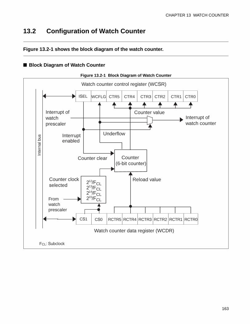
CHAPTER 13 WATCH COUNTER
13.2 Configuration of Watch Counter
Figure 13.2-1 shows the block diagram of the watch counter.
Block Diagram of Watch Counter
Figure 13.2-1 Block Diagram of Watch Counter
Inte
rnal
bus
ISEL WCFLG CTR5 CTR4 CTR3 CTR2 CTR1 CTR0
CS1 CS0 RCTR5 RCTR4 RCTR3 RCTR2 RCTR1 RCTR0
Counter (6-bit counter)
Counter clear
Watch counter control register (WCSR)
Watch counter data register (WCDR)
Underflow
Reload value
Counter value
Counter clock selected
From watch prescaler
2 /FCL2 /FCL2 /FCL2 /FCL
12
13
14
15
Interrupt enabled
FCL: Subclock
Interrupt of watch prescaler
Interrupt of watch counter
163
CHAPTER 13 WATCH COUNTER
Counter
This is a 6-bit down-counter that uses the output clock of the watch prescaler as its count clock.
Watch counter control register (WCSR)
This register controls interrupts and checks the status.
Watch counter data register (WCDR)
This register sets the interval time and selects the count clock.
Input ClockThe watch counter uses the output clock of the watch prescaler as its input clock (count clock).
164
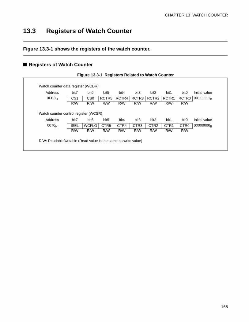
CHAPTER 13 WATCH COUNTER
13.3 Registers of Watch Counter
Figure 13.3-1 shows the registers of the watch counter.
Registers of Watch Counter
Figure 13.3-1 Registers Related to Watch Counter
Watch counter data register (WCDR)
Address bit7 bit6 bit5 bit4 bit3 bit2 bit1 bit0 Initial value
0FE3H CS1 CS0 RCTR5 RCTR4 RCTR3 RCTR2 RCTR1 RCTR0 00111111B
R/W R/W R/W R/W R/W R/W R/W R/W
Watch counter control register (WCSR)
Address bit7 bit6 bit5 bit4 bit3 bit2 bit1 bit0 Initial value
0070H ISEL WCFLG CTR5 CTR4 CTR3 CTR2 CTR1 CTR0 00000000B
R/W R/W R/W R/W R/W R/W R/W R/W
R/W: Readable/writable (Read value is the same as write value)
165
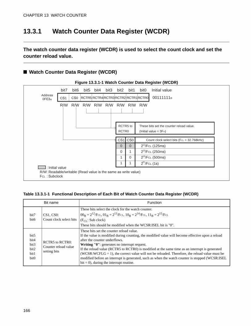
CHAPTER 13 WATCH COUNTER
13.3.1 Watch Counter Data Register (WCDR)
The watch counter data register (WCDR) is used to select the count clock and set the counter reload value.
Watch Counter Data Register (WCDR)
Figure 13.3.1-1 Watch Counter Data Register (WCDR)
R/W
bit7 bit6 bit5 bit4 bit3 bit2 bit1 bit0
00111111B
Initial value
CS1 CS0 RCTR4 RCTR2 RCTR1RCTR0RCTR5
R/W
RCTR3
: Initial valueR/W: Readable/writable (Read value is the same as write value)FCL : Subclock
CS1
0
0
1
1
CS0
0
1
0
1
RCTR5 to
RCTR0
These bits set the counter reload value.
(Initial value = 3FH)
Count clock select bits (FCL = 32.768kHz)
2 /FCL (125ms)
2 /FCL (250ms)
2 /FCL (500ms)
2 /FCL (1s)
12
13
14
15
Address0FE3H
R/W R/W R/W R/W R/W R/W
Table 13.3.1-1 Functional Description of Each Bit of Watch Counter Data Register (WCDR)
Bit name Function
bit7bit6
CS1, CS0:Count clock select bits
These bits select the clock for the watch counter.
00B = 212/FCL, 01B = 213/FCL, 10B = 214/FCL, 11B = 215/FCL
(FCL: Sub clock)
These bits should be modified when the WCSR:ISEL bit is "0".
bit5bit4bit3bit2bit1bit0
RCTR5 to RCTR0:Counter reload value setting bits
These bits set the counter reload value.If the value is modified during counting, the modified value will become effective upon a reload after the counter underflows.Writing "0": generates no interrupt request.If the reload value (RCTR5 to RCTR0) is modified at the same time as an interrupt is generated (WCSR:WCFLG = 1), the correct value will not be reloaded. Therefore, the reload value must be modified before an interrupt is generated, such as when the watch counter is stopped (WCSR:ISEL bit = 0), during the interrupt routine.
166
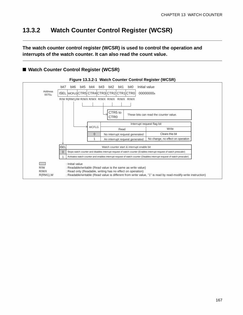
CHAPTER 13 WATCH COUNTER
13.3.2 Watch Counter Control Register (WCSR)
The watch counter control register (WCSR) is used to control the operation and interrupts of the watch counter. It can also read the count value.
Watch Counter Control Register (WCSR)
Figure 13.3.2-1 Watch Counter Control Register (WCSR)
R/WX
bit7 bit6 bit5 bit4 bit3 bit2 bit1 bit0
00000000B
Initial value
ISEL WCFLG CTR4 CTR2 CTR1 CTR0CTR5
R/WX
CTR3
: Initial valueR/W : Readable/writable (Read value is the same as write value)R/WX : Read only (Readable, writing has no effect on operation)R(RM1),W : Readable/writable (Read value is different from write value, "1" is read by read-modify-write instruction)
0
1
R/W R(RM1)/W R/WX R/WX R/WX R/WX
CTR5 toCTR0
These bits can read the counter value.
Read
No interrupt request generated
An interrupt request generated
ISEL
0
1
Watch counter start & interrupt enable bit
Stops watch counter and disables interrupt request of watch counter (Enables interrupt request of watch prescaler)
Activates watch counter and enables interrupt request of watch counter (Disables interrupt request of watch prescaler)
WCFLGInterrupt request flag bit
Write
Clears this bit
No change, no effect on operation
Address0070H
167
CHAPTER 13 WATCH COUNTER
Table 13.3.2-1 Functional Description of Each Bit of Watch Counter Status Register (WCSR)
Bit name Function
bit7
ISEL:Watch counter start & interrupt request enable bit
• This bit activates the watch counter and selects whether to enable interrupts of the watch counter or those of the watch prescaler.
When set to "0":The watch counter is cleared and stopped. Moreover, interrupt requests of the watch counter are disabled, while interrupt requests of the watch prescaler are enabled.
When set to "1":The interrupt request output of the watch counter is enabled and the counter starts operation. On the other hand, interrupt requests of the watch prescaler are disabled.
• Always disable interrupts of the watch prescaler before setting this bit to "1" to select interrupts of the watch counter.
• The watch counter performs counting, using an asynchronous clock from the watch prescaler. For this reason, an error of up to one count clock may occur at the beginning of a count cycle, depending on the timing for setting ISEL bit to "1".
bit6WCFLG:Interrupt request flag bit
• This bit is set to "1" when the counter underflows.• When this bit and the ISEL bit are both set to "1", a watch counter interrupt is generated.• Writing "0" clears the bit.• Writing "1" has no effect on the operation.• "1" is always read in read-modify-write (RMW) instruction.
bit5bit4bit3bit2bit1bit0
CTR5 to CTR0:Counter read bits
• These bits can read the counter value during counting. It should be noted that the correct counter value may not be read if a read is attempted while the counter value is being changed. Therefore, read the counter value twice to check if the same value is read on both occasions before using it.
• Write has no effect on the operation.
168
CHAPTER 13 WATCH COUNTER
13.4 Interrupts of Watch Counter
The watch counter outputs interrupt requests when the counter underflows (counter value = 000001B).
Interrupts of Watch CounterWhen the counter of the watch counter underflows, the interrupt request flag bit (WCFLG) of the watch
counter control register (WCSR) is set to "1". If the interrupt request enable bit (ISEL) of the watch counter
is set to "1", an interrupt request of the watch counter is outputted to the interrupt controller.
Table 13.4-1 shows the interrupt control bits and interrupt sources of the watch counter.
Register and Vector Table Related to Interrupts of Watch Counter
Refer to "CHAPTER 8 INTERRUPTS" for the interrupt request numbers and vector tables of all
peripheral functions.
*: The watch counter shares the same interrupt request number and vector table as the watch prescaler.
Table 13.4-1 Interrupt Control Bits and Interrupt Sources of Watch Timer
Item Description
Interrupt request flag bit WCFLG bit of the WCSR register
Interrupt request enable bit ISEL bit of the WCSR register
Interrupt source Counter underflow
Table 13.4-2 Register and Vector Table Related to Interrupts of Watch Counter
Interrupt source
Interrupt request No.
Interrupt level setup register Vector table address
Register Setting bit Upper Lower
Watch counter* IRQ20 ILR5 L20 FFD2H FFD3H
169
CHAPTER 13 WATCH COUNTER
13.5 Explanation of Watch Counter Operations and Setup Procedure Example
The watch counter counts down for the number of times specified in the count value by RCTR5 to RCTR0 bits, using the count clock selected by CS1 and CS0 bits, when the ISEL bit is set to "1". Once the counter underflows, WCFLG bit of the WCSR register is set to "1", generating an interrupt.
Setup Procedure of Watch CounterThe setup procedure of the watch counter is described below.
(1) Select the count clock (CS1 and CS0 bits) and set the counter reload value (RCTR5 to RCTR0 bits).
(2) Set the ISEL bit of the WCSR register to "1" to start a down count and enable interrupts. Also disable
interrupts of the watch prescaler.
The watch counter performs counting by using a divided clock (asynchronous) from the watch
prescaler. An error of up to one count clock may occur at the beginning of a count cycle, depending on
the timing for setting the ISEL bit to "1".
(3) When the counter underflows, the WCFLG bit of the WCSR register is set to "1", generating an
interrupt.
(4) Write "0" to the WCFLG bit to clear it.
(5) If RCTR5 to RCTR0 bits are modified during counting, the reload value will be updated during a
reload after the counter is set to "1".
(6) When writing "0" to the ISEL bit, the counter becomes "0" and stops operation.
Figure 13.5-1 Descriptive Diagram of Watch Counter Operation
RCTR5 to RCTR0
WCFLG
ISEL
7 9
CS1,CS0 "1,1"(1)
(2)
(3) (4)
(6)
CTR5 to CTR0 70 6 5 4 3 2 1 9 8 7 6 5 4 0
(5)
Count clock
170
CHAPTER 13 WATCH COUNTER
Note:
When the operation is reactivated by WCSR:ISEL=0 after counter stop, please reactivate afterconfirming reading WCSR:CTR[5:0] twice, and clearing to CTR[5:0]=000000B.
Operation in Sub Stop ModeWhen the device enters the sub stop mode, the watch counter stops the count operation and the watch
prescaler is also cleared. Therefore, the watch counter cannot count the correct value after the sub stop mode
is cancelled. After the sub stop mode is cancelled, the ISEL bit must always be set to "0" to clear the counter
before use. In any standby mode other than the sub stop mode, the watch counter continues to operate.
Operation at the Main Stop ModeThe interrupt is not generated though the clock counter continues the count operation when entering the
main stop mode. Moreover, the clock counter stops, too, when sub clock oscillation stop bit (SYCC:
SUBS) of the system clock control register is set to "1".
Setup Procedure ExampleThe watch counter is set up in the following procedure:
Initial setup
1) Set the interrupt level. (ILR5)
2) Select the count clock. (WCDR:CS1, CS0)
3) Set the counter reload value. (WCDR:RCTR5 to RCTR0)
4) Activate the watch counter and enable interrupts. (WCDR:ISEL = 1)
Interrupt processing
1) Clear the interrupt request flag. (WCSR:WCFLG = 0)
2) Process any interrupt.
171
CHAPTER 13 WATCH COUNTER
13.6 Precautions when Using Watch Counter
Shown below are the precautions that must be followed when using the watch counter.
• If the watch prescaler is cleared during the operation of the watch counter, the watch counter may not beable to perform normal operation. When clearing the watch prescaler, set the ISEL bit of the WCSRregister to "0" to stop the watch counter in advance.
• When the operation is reactivated by WCSR:ISEL=0 after counter stop, please reactivate afterconfirming reading WCSR:CTR[5:0] twice, and clearing to CTR[5:0]=000000B.
172
CHAPTER 13 WATCH COUNTER
13.7 Sample Programs for Watch Counter
We provide sample programs that can be used to operate the watch counter.
Sample Programs for Watch CounterFor information about sample programs for the watch counter, refer to " Sample Programs" in Preface.
Setup Methods without Programs
How to enable/stop the watch counter
Use the interrupt request enable bit (WCSR:ISEL).
How to select the count clock
The count clock select bits (WCDR:CS1/CS0) are used to select the clock.
Interrupt-related register
The interrupt level is set in the interrupt level register shown in the following table.
How to enable/disable/clear interrupts
Interrupt request enable flag, Interrupt request flag
The interrupt request enable bit (WCSR:ISEL) is used to enable interrupts.
The interrupt request flag (WCSR:WCFLG) is used to clear interrupt requests.
What to be controlled Watch timer initialization bit (ISEL)
When enabling watch counter Set the bit to "1"
When stopping watch counter Set the bit to "0"
Interrupt source Interrupt level setup register Interrupt vector
Watch counterInterrupt level register (ILR5)
Address: 0007EH
#20Address: 0FFD2H
What to be controlled Interrupt request enable bit (ISEL)
When disabling interrupt request Set the bit to "0"
When enabling interrupt request Set the bit to "1"
What to be controlled Interrupt request flag (WCFLG)
When clearing interrupt request Write "0"
173

CHAPTER 13 WATCH COUNTER
174
CHAPTER 14WILD REGISTER
This chapter describes the functions and operations of the wild register.
14.1 Overview of Wild Register
14.2 Configuration of Wild Register
14.3 Registers of Wild Register
14.4 Operating Description of Wild Register
14.5 Typical Hardware Connection Example
175
CHAPTER 14 WILD REGISTER
14.1 Overview of Wild Register
The wild register can be used to patch bugs in the program by using the addresses set in the built-in register and amendment data.The following section describes the wild register function.
Wild Register FunctionThe wild register consists of 3 data setup registers, 3 upper-address setup registers, 3 lower-address setup
registers, a 1-byte address compare enable register and a 1-byte data test setup register. When certain
addresses and modified data are specified in these registers, the ROM data can be replaced with the
modified data specified in the registers. Data of up to three different addresses can be modified.
The wild register function can be used to debug the program after creating the mask and patch bugs in the
program.
176
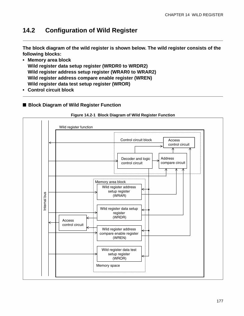
CHAPTER 14 WILD REGISTER
14.2 Configuration of Wild Register
The block diagram of the wild register is shown below. The wild register consists of the following blocks:• Memory area block
Wild register data setup register (WRDR0 to WRDR2)Wild register address setup register (WRAR0 to WRAR2) Wild register address compare enable register (WREN)Wild register data test setup register (WROR)
• Control circuit block
Block Diagram of Wild Register Function
Figure 14.2-1 Block Diagram of Wild Register Function
Access control circuit
Address compare circuit
Decoder and logic control circuit
Wild register address compare enable register
(WREN)
Wild register data test setup register
(WROR)
Wild register data setup register (WRDR)
Wild register address setup register
(WRAR)
Access control circuit
Inte
rnal
bus
Memory space
Control circuit block
Wild register function
Memory area block
177
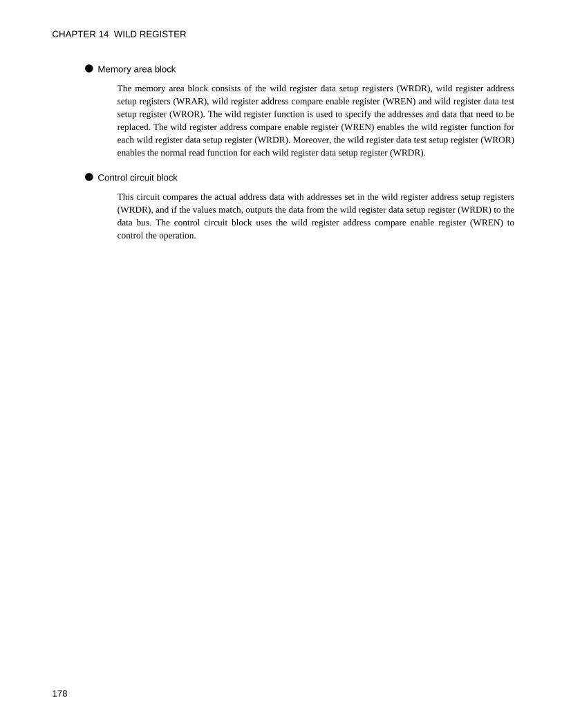
CHAPTER 14 WILD REGISTER
Memory area block
The memory area block consists of the wild register data setup registers (WRDR), wild register address
setup registers (WRAR), wild register address compare enable register (WREN) and wild register data test
setup register (WROR). The wild register function is used to specify the addresses and data that need to be
replaced. The wild register address compare enable register (WREN) enables the wild register function for
each wild register data setup register (WRDR). Moreover, the wild register data test setup register (WROR)
enables the normal read function for each wild register data setup register (WRDR).
Control circuit block
This circuit compares the actual address data with addresses set in the wild register address setup registers
(WRDR), and if the values match, outputs the data from the wild register data setup register (WRDR) to the
data bus. The control circuit block uses the wild register address compare enable register (WREN) to
control the operation.
178
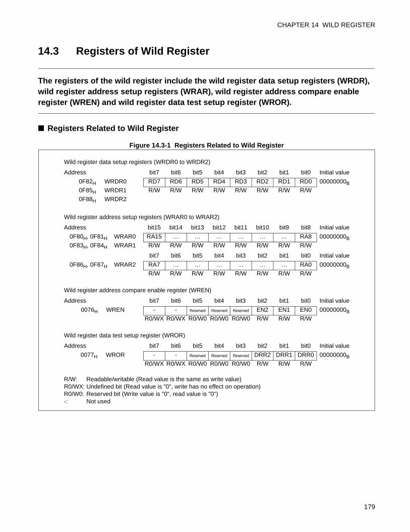
CHAPTER 14 WILD REGISTER
14.3 Registers of Wild Register
The registers of the wild register include the wild register data setup registers (WRDR), wild register address setup registers (WRAR), wild register address compare enable register (WREN) and wild register data test setup register (WROR).
Registers Related to Wild Register
Figure 14.3-1 Registers Related to Wild Register
Wild register data setup registers (WRDR0 to WRDR2)
Address bit7 bit6 bit5 bit4 bit3 bit2 bit1 bit0 Initial value
0F82H WRDR0 RD7 RD6 RD5 RD4 RD3 RD2 RD1 RD0 00000000B
0F85H WRDR1 R/W R/W R/W R/W R/W R/W R/W R/W
0F88H WRDR2
Wild register address setup registers (WRAR0 to WRAR2)
Address bit15 bit14 bit13 bit12 bit11 bit10 bit9 bit8 Initial value
0F80H, 0F81H WRAR0 RA15 … … … … … … RA8 00000000B
0F83H, 0F84H WRAR1 R/W R/W R/W R/W R/W R/W R/W R/W
bit7 bit6 bit5 bit4 bit3 bit2 bit1 bit0 Initial value
0F86H, 0F87H WRAR2 RA7 … … … … … … RA0 00000000B
R/W R/W R/W R/W R/W R/W R/W R/W
Wild register address compare enable register (WREN)
Address bit7 bit6 bit5 bit4 bit3 bit2 bit1 bit0 Initial value
0076H WREN - - Reserved Reserved Reserved EN2 EN1 EN0 00000000B
R0/WX R0/WX R0/W0 R0/W0 R0/W0 R/W R/W R/W
Wild register data test setup register (WROR)
Address bit7 bit6 bit5 bit4 bit3 bit2 bit1 bit0 Initial value
0077H WROR - - Reserved Reserved Reserved DRR2 DRR1 DRR0 00000000B
R0/WX R0/WX R0/W0 R0/W0 R0/W0 R/W R/W R/W
R/W: Readable/writable (Read value is the same as write value)R0/WX: Undefined bit (Read value is "0", write has no effect on operation)R0/W0: Reserved bit (Write value is "0", read value is "0")-: Not used
179
CHAPTER 14 WILD REGISTER
Wild Register NumberEach wild register address setup register (WRAR) and wild register data setup register (WRDR) has its
corresponding wild register number.
Table 14.3-1 Wild Register Numbers Corresponding to Wild Register Address Setup Registers and Wild Register Data Setup Registers
Wild register number Wild register address setup register (WRAR) Wild register data setup register (WRDR)
0 WRAR0 WRDR0
1 WRAR1 WRDR1
2 WRAR2 WRDR2
180
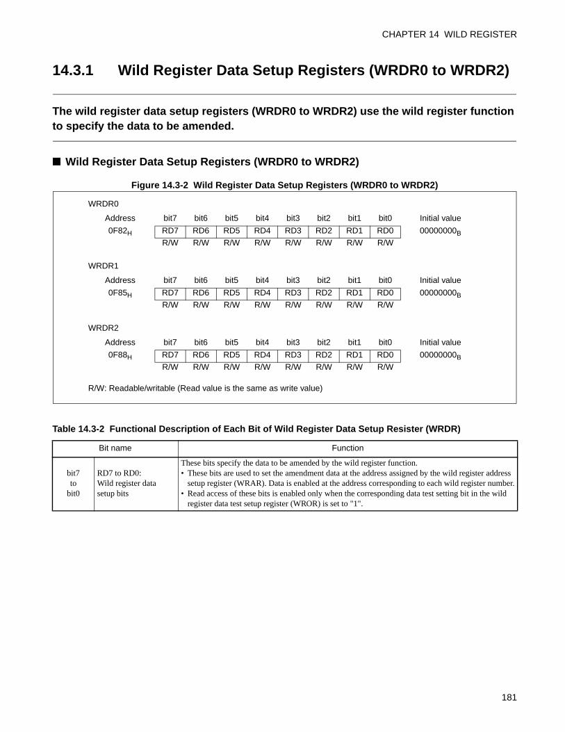
CHAPTER 14 WILD REGISTER
14.3.1 Wild Register Data Setup Registers (WRDR0 to WRDR2)
The wild register data setup registers (WRDR0 to WRDR2) use the wild register function to specify the data to be amended.
Wild Register Data Setup Registers (WRDR0 to WRDR2)
Figure 14.3-2 Wild Register Data Setup Registers (WRDR0 to WRDR2)
WRDR0
Address bit7 bit6 bit5 bit4 bit3 bit2 bit1 bit0 Initial value
0F82H RD7 RD6 RD5 RD4 RD3 RD2 RD1 RD0 00000000B
R/W R/W R/W R/W R/W R/W R/W R/W
WRDR1
Address bit7 bit6 bit5 bit4 bit3 bit2 bit1 bit0 Initial value
0F85H RD7 RD6 RD5 RD4 RD3 RD2 RD1 RD0 00000000B
R/W R/W R/W R/W R/W R/W R/W R/W
WRDR2
Address bit7 bit6 bit5 bit4 bit3 bit2 bit1 bit0 Initial value
0F88H RD7 RD6 RD5 RD4 RD3 RD2 RD1 RD0 00000000B
R/W R/W R/W R/W R/W R/W R/W R/W
R/W: Readable/writable (Read value is the same as write value)
Table 14.3-2 Functional Description of Each Bit of Wild Register Data Setup Resister (WRDR)
Bit name Function
bit7to
bit0
RD7 to RD0:Wild register data setup bits
These bits specify the data to be amended by the wild register function.• These bits are used to set the amendment data at the address assigned by the wild register address
setup register (WRAR). Data is enabled at the address corresponding to each wild register number.• Read access of these bits is enabled only when the corresponding data test setting bit in the wild
register data test setup register (WROR) is set to "1".
181
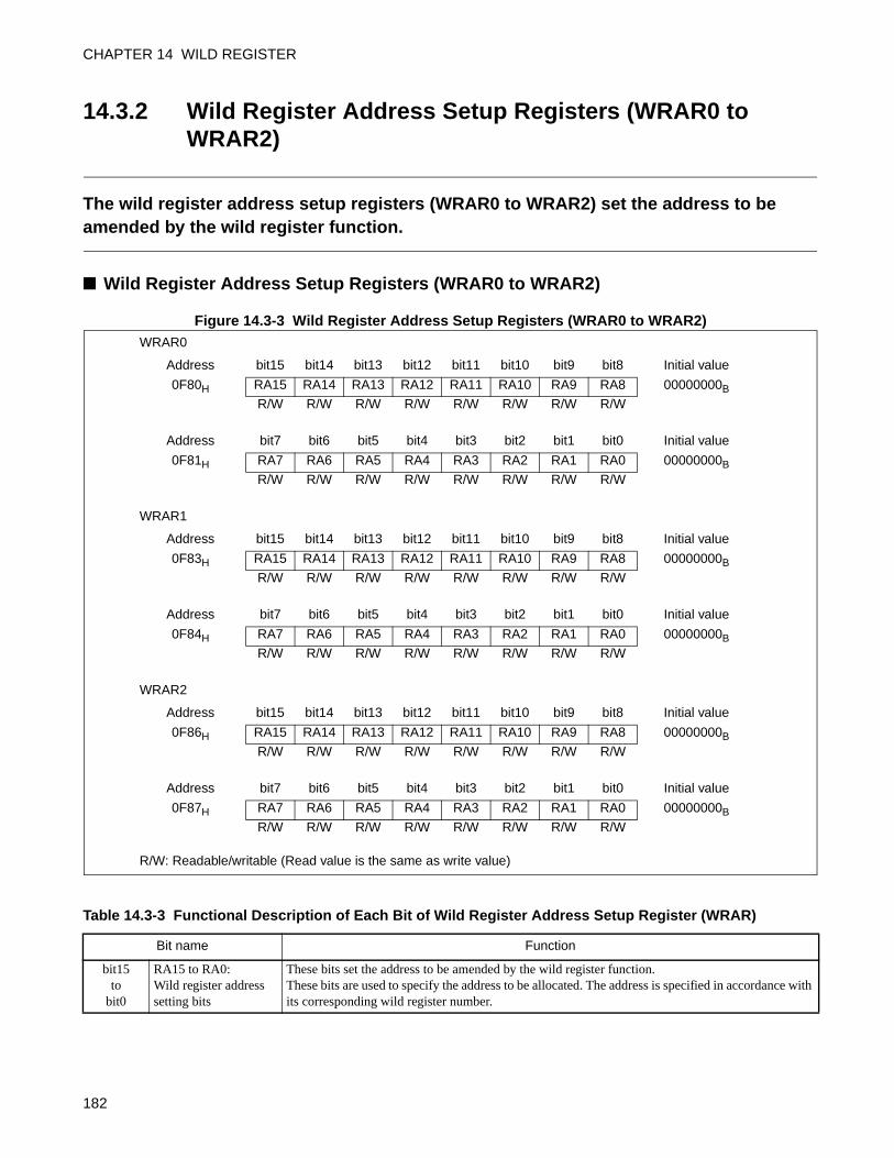
CHAPTER 14 WILD REGISTER
14.3.2 Wild Register Address Setup Registers (WRAR0 to WRAR2)
The wild register address setup registers (WRAR0 to WRAR2) set the address to be amended by the wild register function.
Wild Register Address Setup Registers (WRAR0 to WRAR2)
Figure 14.3-3 Wild Register Address Setup Registers (WRAR0 to WRAR2)WRAR0
Address bit15 bit14 bit13 bit12 bit11 bit10 bit9 bit8 Initial value
0F80H RA15 RA14 RA13 RA12 RA11 RA10 RA9 RA8 00000000B
R/W R/W R/W R/W R/W R/W R/W R/W
Address bit7 bit6 bit5 bit4 bit3 bit2 bit1 bit0 Initial value
0F81H RA7 RA6 RA5 RA4 RA3 RA2 RA1 RA0 00000000B
R/W R/W R/W R/W R/W R/W R/W R/W
WRAR1
Address bit15 bit14 bit13 bit12 bit11 bit10 bit9 bit8 Initial value
0F83H RA15 RA14 RA13 RA12 RA11 RA10 RA9 RA8 00000000B
R/W R/W R/W R/W R/W R/W R/W R/W
Address bit7 bit6 bit5 bit4 bit3 bit2 bit1 bit0 Initial value
0F84H RA7 RA6 RA5 RA4 RA3 RA2 RA1 RA0 00000000B
R/W R/W R/W R/W R/W R/W R/W R/W
WRAR2
Address bit15 bit14 bit13 bit12 bit11 bit10 bit9 bit8 Initial value
0F86H RA15 RA14 RA13 RA12 RA11 RA10 RA9 RA8 00000000B
R/W R/W R/W R/W R/W R/W R/W R/W
Address bit7 bit6 bit5 bit4 bit3 bit2 bit1 bit0 Initial value
0F87H RA7 RA6 RA5 RA4 RA3 RA2 RA1 RA0 00000000B
R/W R/W R/W R/W R/W R/W R/W R/W
R/W: Readable/writable (Read value is the same as write value)
Table 14.3-3 Functional Description of Each Bit of Wild Register Address Setup Register (WRAR)
Bit name Function
bit15to
bit0
RA15 to RA0:Wild register address setting bits
These bits set the address to be amended by the wild register function.These bits are used to specify the address to be allocated. The address is specified in accordance with its corresponding wild register number.
182
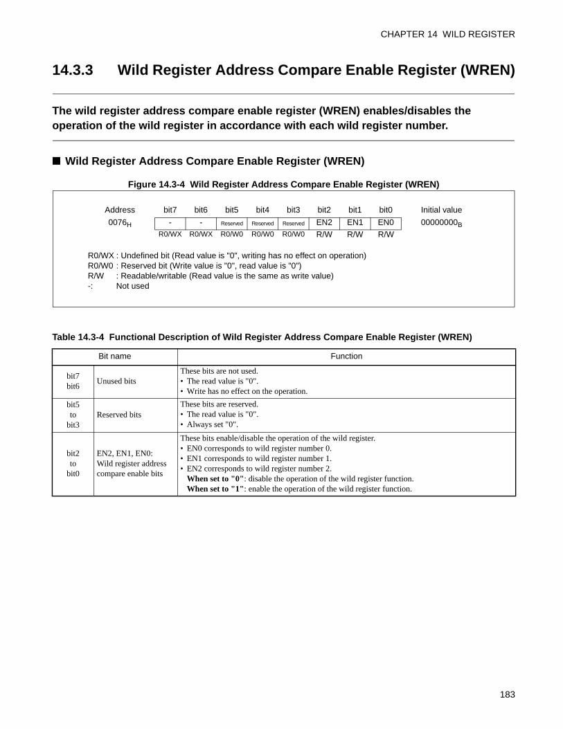
CHAPTER 14 WILD REGISTER
14.3.3 Wild Register Address Compare Enable Register (WREN)
The wild register address compare enable register (WREN) enables/disables the operation of the wild register in accordance with each wild register number.
Wild Register Address Compare Enable Register (WREN)
Figure 14.3-4 Wild Register Address Compare Enable Register (WREN)
Address bit7 bit6 bit5 bit4 bit3 bit2 bit1 bit0 Initial value
0076H - - Reserved Reserved Reserved EN2 EN1 EN0 00000000BR0/WX R0/WX R0/W0 R0/W0 R0/W0 R/W R/W R/W
R0/WX : Undefined bit (Read value is "0", writing has no effect on operation)R0/W0 : Reserved bit (Write value is "0", read value is "0")R/W : Readable/writable (Read value is the same as write value)-: Not used
Table 14.3-4 Functional Description of Wild Register Address Compare Enable Register (WREN)
Bit name Function
bit7bit6
Unused bitsThese bits are not used.• The read value is "0".• Write has no effect on the operation.
bit5to
bit3Reserved bits
These bits are reserved.• The read value is "0".• Always set "0".
bit2to
bit0
EN2, EN1, EN0:Wild register address compare enable bits
These bits enable/disable the operation of the wild register.• EN0 corresponds to wild register number 0.• EN1 corresponds to wild register number 1.• EN2 corresponds to wild register number 2.
When set to "0": disable the operation of the wild register function.When set to "1": enable the operation of the wild register function.
183
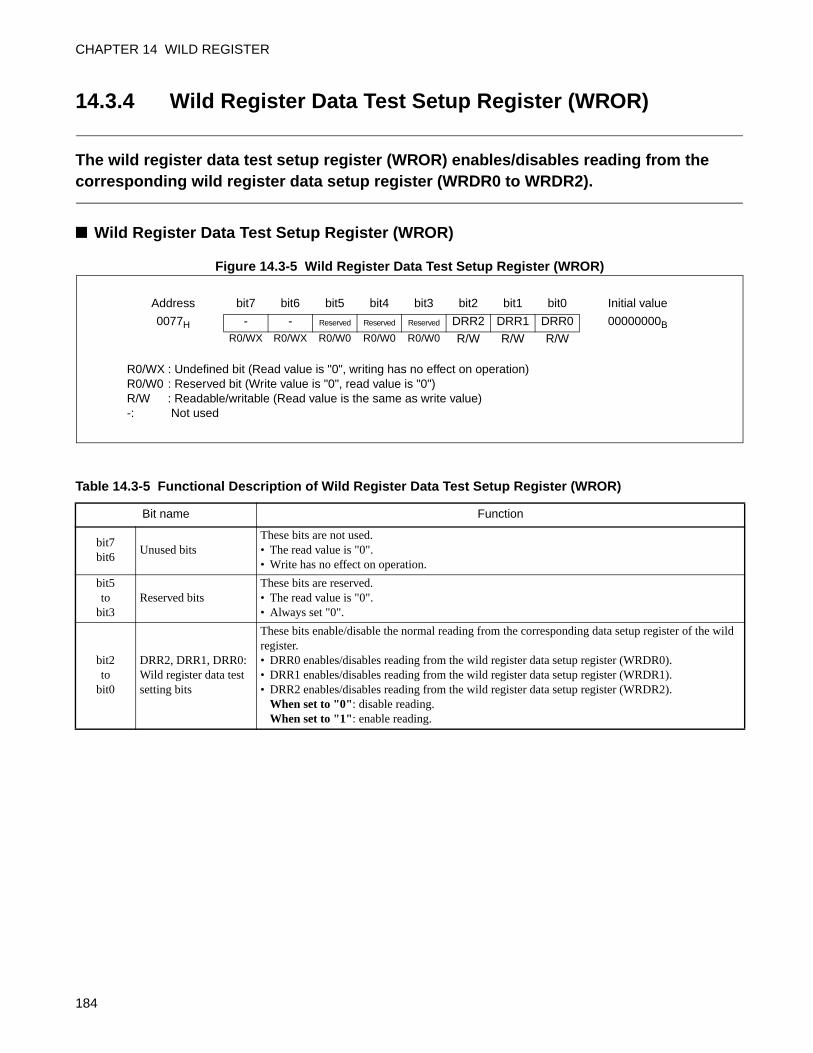
CHAPTER 14 WILD REGISTER
14.3.4 Wild Register Data Test Setup Register (WROR)
The wild register data test setup register (WROR) enables/disables reading from the corresponding wild register data setup register (WRDR0 to WRDR2).
Wild Register Data Test Setup Register (WROR)
Figure 14.3-5 Wild Register Data Test Setup Register (WROR)
Address bit7 bit6 bit5 bit4 bit3 bit2 bit1 bit0 Initial value
0077H - - Reserved Reserved Reserved DRR2 DRR1 DRR0 00000000BR0/WX R0/WX R0/W0 R0/W0 R0/W0 R/W R/W R/W
R0/WX : Undefined bit (Read value is "0", writing has no effect on operation)R0/W0 : Reserved bit (Write value is "0", read value is "0")R/W : Readable/writable (Read value is the same as write value)-: Not used
Table 14.3-5 Functional Description of Wild Register Data Test Setup Register (WROR)
Bit name Function
bit7bit6
Unused bitsThese bits are not used.• The read value is "0".• Write has no effect on operation.
bit5to
bit3Reserved bits
These bits are reserved.• The read value is "0".• Always set "0".
bit2to
bit0
DRR2, DRR1, DRR0:Wild register data test setting bits
These bits enable/disable the normal reading from the corresponding data setup register of the wild register.• DRR0 enables/disables reading from the wild register data setup register (WRDR0).• DRR1 enables/disables reading from the wild register data setup register (WRDR1).• DRR2 enables/disables reading from the wild register data setup register (WRDR2).
When set to "0": disable reading.When set to "1": enable reading.
184
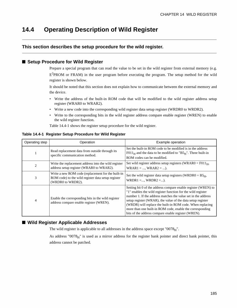
CHAPTER 14 WILD REGISTER
14.4 Operating Description of Wild Register
This section describes the setup procedure for the wild register.
Setup Procedure for Wild RegisterPrepare a special program that can read the value to be set in the wild register from external memory (e.g.
E2PROM or FRAM) in the user program before executing the program. The setup method for the wild
register is shown below.
It should be noted that this section does not explain how to communicate between the external memory and
the device.
• Write the address of the built-in ROM code that will be modified to the wild register address setupregister (WRAR0 to WRAR2).
• Write a new code into the corresponding wild register data setup register (WRDR0 to WRDR2).
• Write to the corresponding bits in the wild register address compare enable register (WREN) to enablethe wild register function.
Table 14.4-1 shows the register setup procedure for the wild register.
Wild Register Applicable AddressesThe wild register is applicable to all addresses in the address space except "0078H".
As address "0078H" is used as a mirror address for the register bank pointer and direct bank pointer, this
address cannot be patched.
Table 14.4-1 Register Setup Procedure for Wild Register
Operating step Operation Example operation
1Read replacement data from outside through its specific communication method.
Set the built-in ROM code to be modified is in the address F011H and the data to be modified to "B5H". Three built-in
ROM codes can be modified.
2Write the replacement address into the wild register address setup register (WRAR0 to WRAR2).
Set wild register address setup registers (WRAR0 = F011H,
WRAR1 = ..., WRAR2 = ...).
3Write a new ROM code (replacement for the built-in ROM code) to the wild register data setup register (WRDR0 to WRDR2).
Set the wild register data setup registers (WRDR0 = B5H,
WRDR1 =..., WRDR2 =...).
4Enable the corresponding bits in the wild register address compare enable register (WREN).
Setting bit 0 of the address compare enable register (WREN) to "1" enables the wild register function for the wild register number 1. If the address matches the value set in the address setup register (WRAR), the value of the data setup register (WRDR) will replace the built-in ROM code. When replacing more than one built-in ROM code, enable the corresponding bits of the address compare enable register (WREN).
185
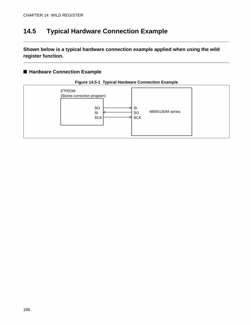
CHAPTER 14 WILD REGISTER
14.5 Typical Hardware Connection Example
Shown below is a typical hardware connection example applied when using the wild register function.
Hardware Connection Example
Figure 14.5-1 Typical Hardware Connection Example
E2PROM (Stores correction program)
SO SI SCK
SI SO SCK
MB95130/M series
186
CHAPTER 158/16-BIT COMPOUND TIMER
This chapter describes the functions and operations of the 8/16-bit compound timer.
15.1 Overview of 8/16-bit Compound Timer
15.2 Configuration of 8/16-bit Compound Timer
15.3 Channels of 8/16-bit Compound Timer
15.4 Pins of 8/16-bit Compound Timer
15.5 Registers of 8/16-bit Compound Timer
15.6 Interrupts of 8/16-bit Compound Timer
15.7 Operating Description of Interval Timer Function (One-shot Mode)
15.8 Operating Description of Interval Timer Function (Continuous Mode)
15.9 Operating Description of Interval Timer Function (Free-run Mode)
15.10 Operating Description of PWM Timer Function (Fixed-cycle mode)
15.11 Operating Description of PWM Timer Function (Variable-cycle Mode)
15.12 Operating Description of PWC Timer Function
15.13 Operating Description of Input Capture Function
15.14 Operating Description of Noise Filter
15.15 States in Each Mode during Operation
15.16 Precautions when Using 8/16-bit Compound Timer
187
CHAPTER 15 8/16-BIT COMPOUND TIMER
15.1 Overview of 8/16-bit Compound Timer
The 8/16-bit compound timer consists of two 8-bit counters and can be used as two 8-bit timers, or one 16-bit timer if they are connected in cascade.The 8/16-bit compound timer has the following functions:• Interval timer function• PWM timer function• PWC timer function (pulse width measurement)• Input capture function
Interval Timer Function (One-shot Mode)When the interval timer function (one-shot mode) is selected, the counter starts counting from "00H" as the
timer is started. When the counter value matches the register setting value, the timer output is inverted, the
interrupt request occurs, and the count operation is stopped.
Interval Timer Function (Continuous Mode)When the interval timer function (continuous mode) is selected, the counter starts counting from "00H" as
the timer is started. When the counter value matches the register setting value, the timer output is inverted,
the interrupt request occurs, and the count operation is continued from "00H" again. The timer output a
square wave as a result of this repeated operation.
Interval Timer Function (Free-run Mode)When the interval timer function (free-run mode) is selected, the counter starts counting from "00H". When
the counter value matches the register setting value, the timer output is inverted and the interrupt request
occurs. When the counter continues to count until reaching "FFH", it restarts counting from "00H" to
continue the counting operation. The timer outputs a square wave as a result of this repeated operation.
PWM Timer Function (Fixed-cycle Mode)When the PWM timer function (fixed-cycle mode) is selected, a PWM signal with a variable "H" pulse
width is generated in fixed cycles. The cycle is fixed to "FFH" during 8-bit operation or "FFFFH" during
16-bit operation. The time is determined by the count clock selected. The "H" pulse width is specified by
setting a register.
PWM Timer Function (Variable-cycle Mode)When the PWM timer function (variable-cycle mode) is selected, two 8-bit counters are used to generate an
8-bit PWM signal in any cycles and duty depending on the cycle and "L" pulse width specified by registers.
In this operation mode, the compound timer cannot serve as a 16-bit counter, as two 8-bit counters are used.
188
CHAPTER 15 8/16-BIT COMPOUND TIMER
PWC Timer FunctionWhen the PWC timer function is selected, the width and cycle of an external input pulse can be measured.
In this operation mode, the counter starts counting from "00H" upon detection of a count start edge of an
external input signal and transfers the count value to a register to generate an interrupt upon detection of a
count end edge.
Input Capture FunctionWhen the input capture function is selected, the counter value is stored in a register upon detection of an
edge for an external input signal.
This function is available in either free-run mode or clear mode for count operation.
In the clear mode, the counter starts counting from "00H" and transfers its value to a register to generate an
interrupt upon detection of an edge. In this case, the counter continues to count from "00H".
In the free-run mode, the counter transfers its value to a register to generate an interrupt upon detection of
an edge. In this case, however, the counter continues to count without being cleared.
189
CHAPTER 15 8/16-BIT COMPOUND TIMER
15.2 Configuration of 8/16-bit Compound Timer
The 8/16-bit compound timer consists of the following blocks:• 8-bit counter × 2 channels• 8-bit comparator (including a temporary latch) × 2 channels• 8/16-bit compound timer 00/01 data register × 2 channels (T00DR/T01DR) • 8/16-bit compound timer 00/01 control status register 0 × 2 channels (T00CR0/
T01CR0) • 8/16-bit compound timer 00/01 control status register 1 × 2 channels (T00CR1/
T01CR1) • 8/16-bit compound timer 00/01 timer mode control register (TMCR0)• Output controller × 2 channels• Control logic × 2 channels• Count clock selector × 2 channels• Edge detector × 2 channels• Noise filter × 2 channels
190
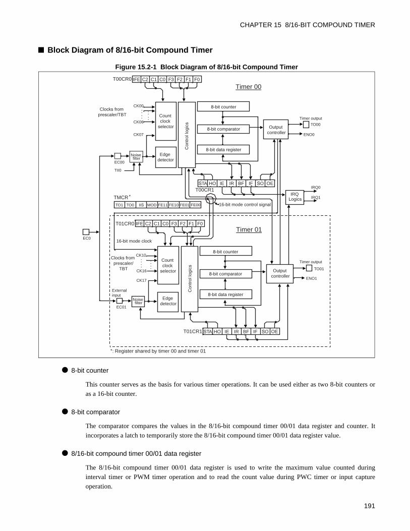
CHAPTER 15 8/16-BIT COMPOUND TIMER
Block Diagram of 8/16-bit Compound Timer
Figure 15.2-1 Block Diagram of 8/16-bit Compound Timer
8-bit counter
This counter serves as the basis for various timer operations. It can be used either as two 8-bit counters or
as a 16-bit counter.
8-bit comparator
The comparator compares the values in the 8/16-bit compound timer 00/01 data register and counter. It
incorporates a latch to temporarily store the 8/16-bit compound timer 00/01 data register value.
8/16-bit compound timer 00/01 data register
The 8/16-bit compound timer 00/01 data register is used to write the maximum value counted during
interval timer or PWM timer operation and to read the count value during PWC timer or input capture
operation.
8-bit counter
8-bit comparator
8-bit data register
Count clock
selector
Count clock
selector
Edge detector
Output controller
8-bit counter
8-bit comparator
8-bit data register
Output controller
Con
trol
logi
csC
ontr
ol lo
gics
Timer 00
Timer 01
IRQLogics
IRQ0
Timer output
Timer output
16-bit mode clock
T00CR0
T00CR1
T01CR1
T01CR0
TO00
EC00
TO01
ENO0
ENO1
IRQ1
16-bit mode control signal
::
Noise filter
Edge detector
Noise filter
CK00
CK06
::
Clocks from prescaler/TBT
Clocks from prescaler/
TBT::
CK10
CK16
::
EC01
External input
CK07
CK17
TMCR*
*: Register shared by timer 00 and timer 01
TII0
EC0
IFE C2 F3C1 C0 F2 F1 F0
STA HO BFIE IR IF SO OE
TO1 TO0 FE11IIS MOD FE10 FE01 FE00
IFE C2 F3C1 C0 F2 F1 F0
STA HO BFIE IR IF SO OE
191
CHAPTER 15 8/16-BIT COMPOUND TIMER
8/16-bit compound timer 00/01 control status registers 0 (T00CR0/T01CR0)
These registers are used to select the timer operation mode, select the count clock, and to enable or disable
IF flag interrupts.
8/16-bit compound timer 00/01 control status registers 1 (T00CR1/T01CR1)
These registers are used to control interrupt flags, timer output, and timer operation.
8/16-bit compound timer 00/01 timer mode control register (TMCR0)
This register is used to select the noise filter function, 8-bit or16-bit operation mode, and signal input to
timer 00 and to indicate the timer output value.
Output controller
The output controller controls timer output. The timer output is supplied to the external pin when the pin
output has been enabled.
Control logic
The control logic controls timer operation.
Count clock selector
The selector selects the counter operation clock signal from among prescaler outputs (machine clock
divided signal and timebase timer output).
Edge detector
The edge detector selects the edge of an external input signal to be used as an event for PWC timer
operation or input capture operation.
Noise filter
This filter serves as a noise filter for external input signals. "H" pulse noise, "L" pulse noise, or "H"/"L"-
pulse noise elimination can be selected as the filter function.
TII0 internal pin (internally connected to the LIN-UART, available only in channel 0)
The TII0 pin serves as the signal input pin for timer 00; it is connected to the LIN-UART inside the chip.
For information about how to use the pin, refer to "CHAPTER 22 LIN-UART". Note that the TII0 pin in
channel 1 is internally fixed to "0".
Input ClockThe 8/16-bit compound timer uses the output clock from the prescaler as its input clock (count clock).
192
CHAPTER 15 8/16-BIT COMPOUND TIMER
15.3 Channels of 8/16-bit Compound Timer
This section describes the channels of 8/16-bit compound timer.
Channels of 8/16-bit Compound TimerMB95130/M series contains one channel of 8/16-bit compound timer.
In one channel, there are two 8-bit counters. Each counter can be used as two 8-bit timers or one 16-bit
timer. The following table lists the external pins and registers corresponding to each channel.
The 2-digit number in the pin names and register names corresponds to channel and timer. The upper
number corresponds to channel and the lower number corresponds to timer.
Table 15.3-1 8/16-bit Compound Timer Channels and Corresponding External Pins
Channel Pin name Pin function
0
TO00 Timer 00 output
TO01 Timer 01 output
EC0 Timer 00 input and timer 01 input
Table 15.3-2 8/16-bit Compound Timer Channels and Corresponding Registers
Channel Register name Registers
0
T00CR0 Timer 00 control status register 0
T01CR0 Timer 01 control status register 0
T00CR1 Timer 00 control status register 1
T01CR1 Timer 01 control status register 1
T00DR Timer 00 data register
T01DR Timer 01 data register
TMCR0 Timer 00/01 timer mode control register
193
CHAPTER 15 8/16-BIT COMPOUND TIMER
15.4 Pins of 8/16-bit Compound Timer
This section describes the pins related to the 8/16-bit compound timer.
Pins Related to 8/16-bit Compound TimerThe external pins related to the 8/16-bit compound timer are TO00, TO01, and EC0. TII0 is for internalchip connection.
TO00 pins
TO00:
This pin serves as the timer output pin for timer 00 during 8-bit operation or for timers 00 and 01 during16-bit operation. When the output is enabled (T00CR1:OE = 1) in interval timer, PWM timer, or PWCtimer function, the pin is set for output automatically regardless of the port direction register (DDR2:bit2)to serve as the timer output TO00 pin.
The output remains indeterminate when the input capture function has been selected enabling output.
TO01 pins
TO01:
This pin serves as the timer output pin for timer 01 during 8-bit operation. When the output is enabled(T00CR1:OE = 1) in interval timer, PWM timer (fixed cycle mode), or PWC timer function, the pin is setfor output automatically regardless of the port direction register (DDR2:bit3) to serve as the timer outputTO01 pin.
The output remains indeterminate during 16-bit operation when the PWM timer function (variable-cyclemode) or input capture function has been selected enabling output.
EC0 pins
The EC0 pin is connected to the EC00 and EC01 internal pins.
EC00 internal pin:
This pin serves as the external count clock input pin for timer 00 when the interval timer or PWM timerfunction has been selected, or as the signal input pin for timer 00 when the PWC timer or input capturefunction has been selected. The pin cannot be set as the external count clock input pin when the PWCtimer or input capture function has been selected.
To use this input feature, set the port direction register (DDR2:bit4) to "0" to set the pin as an input port.
EC01 internal pin:
This pin serves as the external count clock input pin for timer 01 when the interval timer or PWM timerfunction has been selected or the signal input pin for timer 01 when the PWC timer or input capturefunction has been selected. The pin cannot be set as the external count clock input pin when the PWCtimer or input capture function has been selected.
This input is not used during 16-bit operation. The input can be used as well when the PWM timerfunction has been selected (variable-cycle mode).
To use this input feature, set the port direction register (DDR2:bit4) to set the pin as an input port.
194
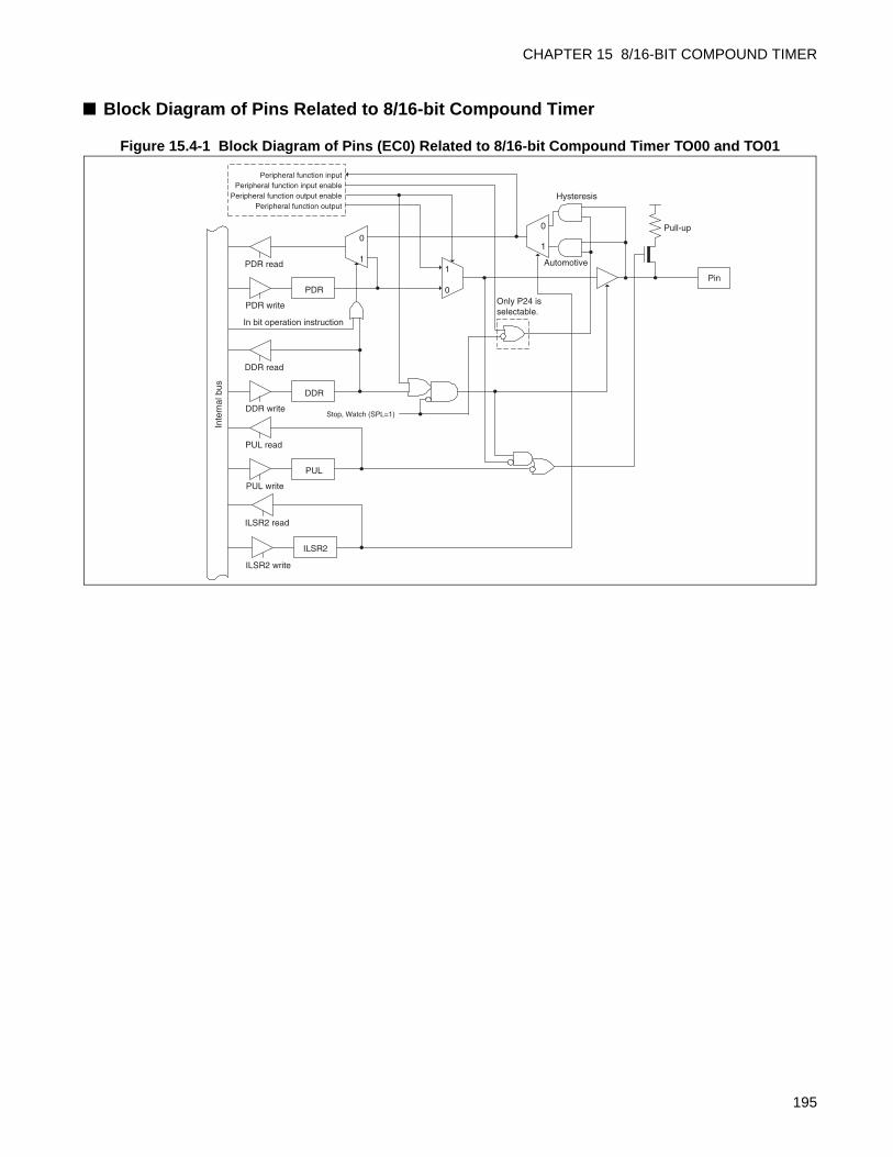
CHAPTER 15 8/16-BIT COMPOUND TIMER
Block Diagram of Pins Related to 8/16-bit Compound Timer
Figure 15.4-1 Block Diagram of Pins (EC0) Related to 8/16-bit Compound Timer TO00 and TO01
ILSR2 read
ILSR2 write
ILSR2
0
1
PDR read
PDR write
PDR
DDR read
DDR write
DDR
PUL read
PUL write
PUL
0
11
0
Peripheral function outputPeripheral function output enable
Peripheral function input enablePeripheral function input
Pin
Stop, Watch (SPL=1)
Inte
rnal
bus
In bit operation instruction
Pull-up
Only P24 is selectable.
Hysteresis
Automotive
195
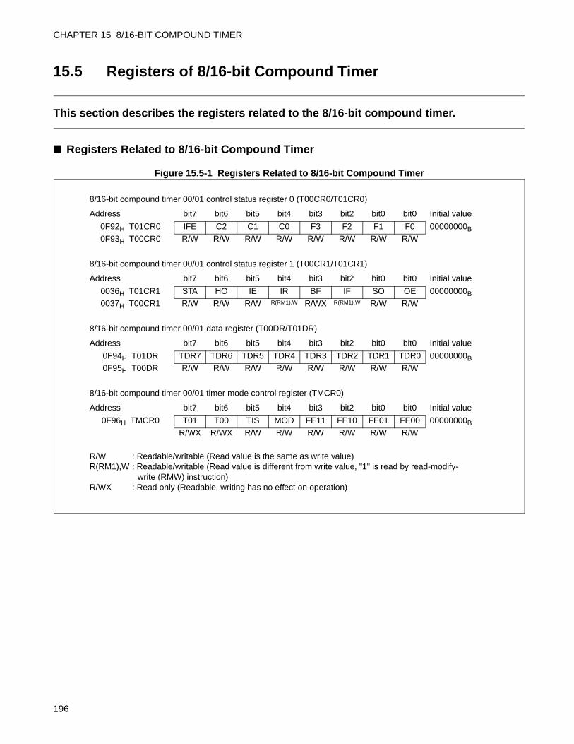
CHAPTER 15 8/16-BIT COMPOUND TIMER
15.5 Registers of 8/16-bit Compound Timer
This section describes the registers related to the 8/16-bit compound timer.
Registers Related to 8/16-bit Compound Timer
Figure 15.5-1 Registers Related to 8/16-bit Compound Timer
8/16-bit compound timer 00/01 control status register 0 (T00CR0/T01CR0)
Address bit7 bit6 bit5 bit4 bit3 bit2 bit0 bit0 Initial value
0F92H T01CR0 IFE C2 C1 C0 F3 F2 F1 F0 00000000B
0F93H T00CR0 R/W R/W R/W R/W R/W R/W R/W R/W
8/16-bit compound timer 00/01 control status register 1 (T00CR1/T01CR1)
Address bit7 bit6 bit5 bit4 bit3 bit2 bit0 bit0 Initial value
0036H T01CR1 STA HO IE IR BF IF SO OE 00000000B
0037H T00CR1 R/W R/W R/W R(RM1),W R/WX R(RM1),W R/W R/W
8/16-bit compound timer 00/01 data register (T00DR/T01DR)
Address bit7 bit6 bit5 bit4 bit3 bit2 bit0 bit0 Initial value
0F94H T01DR TDR7 TDR6 TDR5 TDR4 TDR3 TDR2 TDR1 TDR0 00000000B
0F95H T00DR R/W R/W R/W R/W R/W R/W R/W R/W
8/16-bit compound timer 00/01 timer mode control register (TMCR0)
Address bit7 bit6 bit5 bit4 bit3 bit2 bit0 bit0 Initial value
0F96H TMCR0 T01 T00 TIS MOD FE11 FE10 FE01 FE00 00000000B
R/WX R/WX R/W R/W R/W R/W R/W R/W
R/W : Readable/writable (Read value is the same as write value)R(RM1),W : Readable/writable (Read value is different from write value, "1" is read by read-modify-
write (RMW) instruction)R/WX : Read only (Readable, writing has no effect on operation)
196
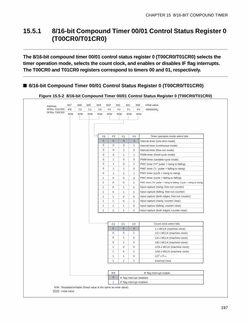
CHAPTER 15 8/16-BIT COMPOUND TIMER
15.5.1 8/16-bit Compound Timer 00/01 Control Status Register 0 (T00CR0/T01CR0)
The 8/16-bit compound timer 00/01 control status register 0 (T00CR0/T01CR0) selects the timer operation mode, selects the count clock, and enables or disables IF flag interrupts. The T00CR0 and T01CR0 registers correspond to timers 00 and 01, respectively.
8/16-bit Compound Timer 00/01 Control Status Register 0 (T00CR0/T01CR0)
Figure 15.5-2 8/16-bit Compound Timer 00/01 Control Status Register 0 (T00CR0/T01CR0)
F2 F1 F0 Timer operation mode select bits
0 0 0
0 0 1
0 1 0
0 1 1
1 0 0
1 0 1
1 1 0
1 1 1
IFE IF flag interrupt enable
0 IF flag interrupt disabled
1 IF flag interrupt enabled
bit7 bit6 bit5 bit4 bit3 bit2 bit1 bit0 Initial value
IFE C2 C1 C0 F3 F2 F1 F0 00000000B
R/W R/W R/W R/W R/W R/W R/W R/W
R/W : Readable/writable (Read value is the same as write value)
: Initial value
F3
0
0
0
0
0
0
0
0
0 0 0
0 0 1
0 1 0
0 1 1
1 0 0
1 0 1
1 1 0
1 1 1
1
1
1
1
1
1
1
1
C2 C1 C0 Count clock select bits
0 0 0
0 0 1
0 1 0
0 1 1
1 0 0
1 0 1
1 1 0
1 1 1 External clock
Interval timer (one-shot mode)
Interval timer (continuous mode)
Interval timer (free-run mode)
PWM timer (fixed-cycle mode)
PWM timer (variable-cycle mode)
PWC timer ("H" pulse = rising to falling)
PWC timer ("L" pulse = falling to rising)
PWC timer (cycle = rising to rising)
PWC timer (cycle = falling to falling)
PWC timer ("H" pulse = rising to falling; Cycle = rising to rising)
Input capture (rising, free-run counter)
Input capture (falling, free-run counter)
Input capture (both edges, free-run counter)
Input capture (rising, counter clear)
Input capture (falling, counter clear)
Input capture (both edges, counter clear)
1/27 x FCH
1/32 x MCLK (machine clock)
1/16 x MCLK (machine clock)
1/8 x MCLK (machine clock)
1/4 x MCLK (machine clock)
1/2 x MCLK (machine clock)
1 x MCLK (machine clock)
Address0F92H T01CR00F93H T00CR0
197
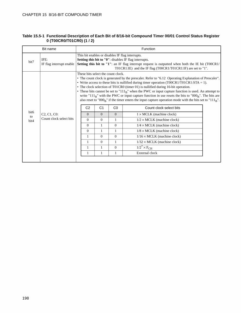
CHAPTER 15 8/16-BIT COMPOUND TIMER
Table 15.5-1 Functional Description of Each Bit of 8/16-bit Compound Timer 00/01 Control Status Register 0 (T00CR0/T01CR0) (1 / 2)
Bit name Function
bit7IFE:IF flag interrupt enable
This bit enables or disables IF flag interrupts.Setting this bit to "0": disables IF flag interrupts.Setting this bit to "1": an IF flag interrupt request is outputted when both the IE bit (T00CR1/
T01CR1:IE) and the IF flag (T00CR1/T01CR1:IF) are set to "1".
bit6to
bit4
C2, C1, C0:Count clock select bits
These bits select the count clock.• The count clock is generated by the prescaler. Refer to "6.12 Operating Explanation of Prescaler".• Write access to these bits is nullified during timer operation (T00CR1/T01CR1:STA = 1).• The clock selection of T01CR0 (timer 01) is nullified during 16-bit operation.• These bits cannot be set to "111B" when the PWC or input capture function is used. An attempt to
write "111B" with the PWC or input capture function in use resets the bits to "000B". The bits arealso reset to "000B" if the timer enters the input capture operation mode with the bits set to "111B".
C2 C1 C0 Count clock select bits
0 0 0 1 × MCLK (machine clock)
0 0 1 1/2 × MCLK (machine clock)
0 1 0 1/4 × MCLK (machine clock)
0 1 1 1/8 × MCLK (machine clock)
1 0 0 1/16 × MCLK (machine clock)
1 0 1 1/32 × MCLK (machine clock)
1 1 0 1/27 × FCH
1 1 1 External clock
198
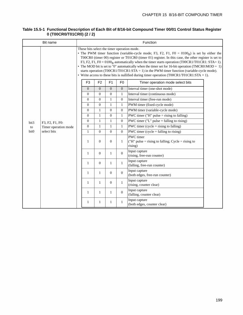
CHAPTER 15 8/16-BIT COMPOUND TIMER
bit3to
bit0
F3, F2, F1, F0:Timer operation mode select bits
These bits select the timer operation mode.• The PWM timer function (variable-cycle mode; F3, F2, F1, F0 = 0100B) is set by either the
T00CR0 (timer 00) register or T01CR0 (timer 01) register. In this case, the other register is set toF3, F2, F1, F0 = 0100B automatically when the timer starts operation (T00CR1/T01CR1: STA= 1).
• The MOD bit is set to "0" automatically when the timer set for 16-bit operation (TMCR0:MOD = 1)starts operation (T00CR1/T01CR1:STA = 1) in the PWM timer function (variable-cycle mode).
• Write access to these bits is nullified during timer operation (T00CR1/T01CR1:STA = 1).
Table 15.5-1 Functional Description of Each Bit of 8/16-bit Compound Timer 00/01 Control Status Register 0 (T00CR0/T01CR0) (2 / 2)
Bit name Function
F3 F2 F1 F0 Timer operation mode select bits
0 0 0 0 Interval timer (one-shot mode)
0 0 0 1 Interval timer (continuous mode)
0 0 1 0 Interval timer (free-run mode)
0 0 1 1 PWM timer (fixed-cycle mode)
0 1 0 0 PWM timer (variable-cycle mode)
0 1 0 1 PWC timer ("H" pulse = rising to falling)
0 1 1 0 PWC timer ("L" pulse = falling to rising)
0 1 1 1 PWC timer (cycle = rising to falling)
1 0 0 0 PWC timer (cycle = falling to rising)
1 0 0 1PWC timer("H" pulse = rising to falling; Cycle = rising to rising)
1 0 1 0Input capture(rising, free-run counter)
1 0 1 1Input capture(falling, free-run counter)
1 1 0 0Input capture(both edges, free-run counter)
1 1 0 1Input capture(rising, counter clear)
1 1 1 0Input capture(falling, counter clear)
1 1 1 1Input capture(both edges, counter clear)
199
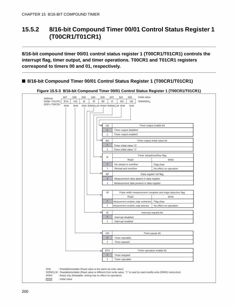
CHAPTER 15 8/16-BIT COMPOUND TIMER
15.5.2 8/16-bit Compound Timer 00/01 Control Status Register 1 (T00CR1/T01CR1)
8/16-bit compound timer 00/01 control status register 1 (T00CR1/T01CR1) controls the interrupt flag, timer output, and timer operations. T00CR1 and T01CR1 registers correspond to timers 00 and 01, respectively.
8/16-bit Compound Timer 00/01 Control Status Register 1 (T00CR1/T01CR1)
Figure 15.5-3 8/16-bit Compound Timer 00/01 Control Status Register 1 (T00CR1/T01CR1)
IR Pulse width measurement complete and edge detection flag
0 Measurement complete, edge undetected
1 Measurement complete, edge detected
bit7 bit6 bit5 bit4 bit3 bit2 bit1 bit0 Initial value
STA HO IE IR BF IF SO OE 00000000B
R/W R/W R/W R(RM1),W R/WX R(RM1),W R/W R/W
: Initial value
IE Interrupt request bit
0 Interrupt disabled
1 Interrupt enabled
HO Timer pause bit
0 Timer operable
1 Timer paused
STA Timer operation enable bit
0 Timer stopped
1 Timer operable
Read Write
Flag clear
No effect on operation
R/W : Readable/writable (Read value is the same as write value)R(RM1),W : Readable/writable (Read value is different from write value, "1" is read by read-modify-write (RMW) instruction)R/WX : Read only (Readable, writing has no effect on operation)
OE Timer output enable bit
0 Timer output disabled
1 Timer output enabled
SO Timer output initial value bit
0 Timer initial value "0"
1 Timer initial value "1"
IFTimer reload/overflow flag
0 No reload or overflow
1 Reload and overflow
Read Write
Flag clear
No effect on operation
BF Data register full flag
0 Measurement data absent in data register
1 Measurement data present in data register
Address0036H T01CR10037H T00CR1
200
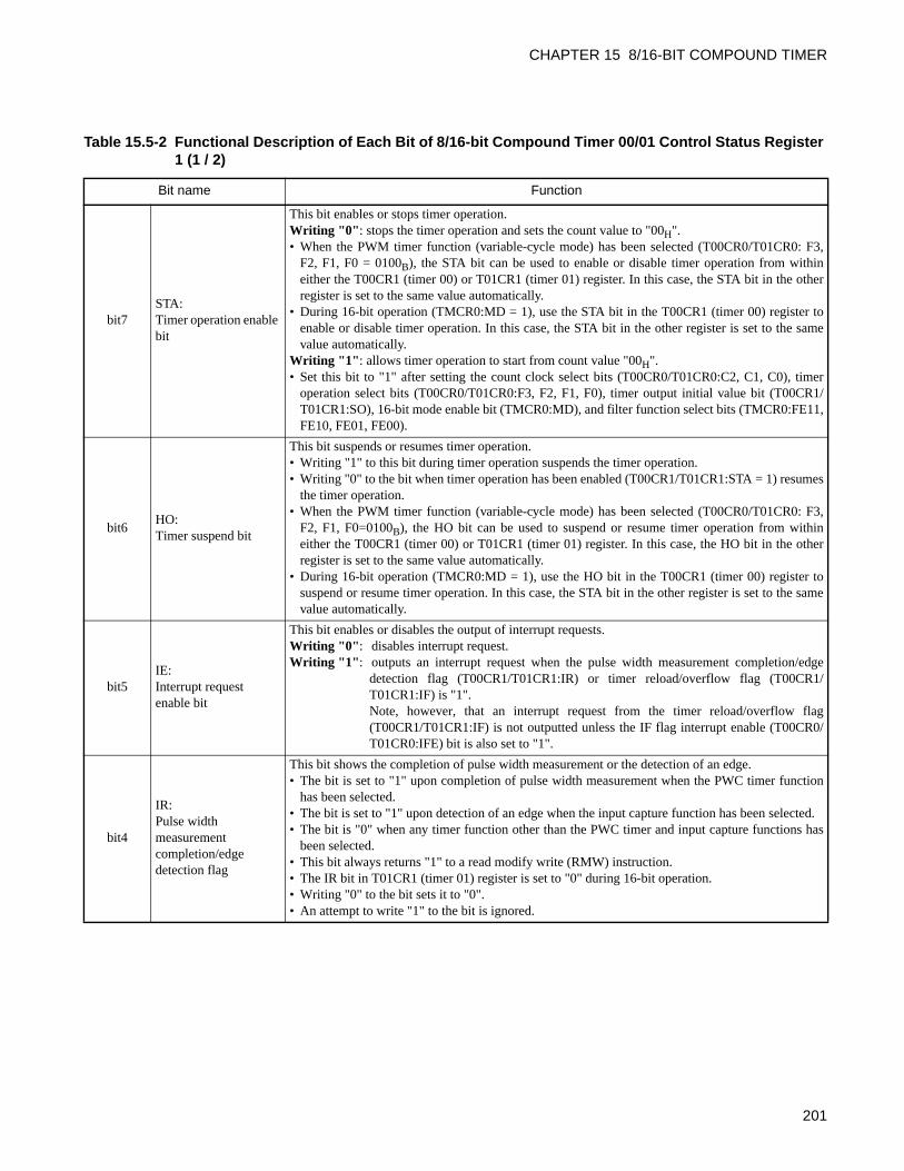
CHAPTER 15 8/16-BIT COMPOUND TIMER
Table 15.5-2 Functional Description of Each Bit of 8/16-bit Compound Timer 00/01 Control Status Register 1 (1 / 2)
Bit name Function
bit7STA:Timer operation enable bit
This bit enables or stops timer operation.Writing "0": stops the timer operation and sets the count value to "00H".• When the PWM timer function (variable-cycle mode) has been selected (T00CR0/T01CR0: F3,
F2, F1, F0 = 0100B), the STA bit can be used to enable or disable timer operation from withineither the T00CR1 (timer 00) or T01CR1 (timer 01) register. In this case, the STA bit in the otherregister is set to the same value automatically.
• During 16-bit operation (TMCR0:MD = 1), use the STA bit in the T00CR1 (timer 00) register toenable or disable timer operation. In this case, the STA bit in the other register is set to the samevalue automatically.
Writing "1": allows timer operation to start from count value "00H".• Set this bit to "1" after setting the count clock select bits (T00CR0/T01CR0:C2, C1, C0), timer
operation select bits (T00CR0/T01CR0:F3, F2, F1, F0), timer output initial value bit (T00CR1/T01CR1:SO), 16-bit mode enable bit (TMCR0:MD), and filter function select bits (TMCR0:FE11,FE10, FE01, FE00).
bit6HO:Timer suspend bit
This bit suspends or resumes timer operation.• Writing "1" to this bit during timer operation suspends the timer operation.• Writing "0" to the bit when timer operation has been enabled (T00CR1/T01CR1:STA = 1) resumes
the timer operation.• When the PWM timer function (variable-cycle mode) has been selected (T00CR0/T01CR0: F3,
F2, F1, F0=0100B), the HO bit can be used to suspend or resume timer operation from withineither the T00CR1 (timer 00) or T01CR1 (timer 01) register. In this case, the HO bit in the otherregister is set to the same value automatically.
• During 16-bit operation (TMCR0:MD = 1), use the HO bit in the T00CR1 (timer 00) register tosuspend or resume timer operation. In this case, the STA bit in the other register is set to the samevalue automatically.
bit5IE:Interrupt request enable bit
This bit enables or disables the output of interrupt requests.Writing "0": disables interrupt request.Writing "1": outputs an interrupt request when the pulse width measurement completion/edge
detection flag (T00CR1/T01CR1:IR) or timer reload/overflow flag (T00CR1/T01CR1:IF) is "1".Note, however, that an interrupt request from the timer reload/overflow flag(T00CR1/T01CR1:IF) is not outputted unless the IF flag interrupt enable (T00CR0/T01CR0:IFE) bit is also set to "1".
bit4
IR:Pulse width measurement completion/edge detection flag
This bit shows the completion of pulse width measurement or the detection of an edge.• The bit is set to "1" upon completion of pulse width measurement when the PWC timer function
has been selected.• The bit is set to "1" upon detection of an edge when the input capture function has been selected.• The bit is "0" when any timer function other than the PWC timer and input capture functions has
been selected.• This bit always returns "1" to a read modify write (RMW) instruction.• The IR bit in T01CR1 (timer 01) register is set to "0" during 16-bit operation.• Writing "0" to the bit sets it to "0".• An attempt to write "1" to the bit is ignored.
201
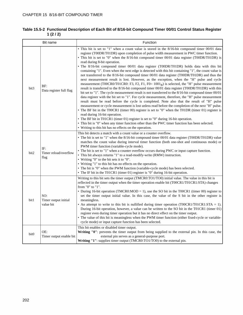
CHAPTER 15 8/16-BIT COMPOUND TIMER
bit3BF:Data register full flag
• This bit is set to "1" when a count value is stored in the 8/16-bit compound timer 00/01 dataregister (T00DR/T01DR) upon completion of pulse width measurement in PWC timer function.
• This bit is set to "0" when the 8/16-bit compound timer 00/01 data register (T00DR/T01DR) isread during 8-bit operation.
• The 8/16-bit compound timer 00/01 data register (T00DR/T01DR) holds data with this bitcontaining "1". Even when the next edge is detected with this bit containing "1", the count value isnot transferred to the 8/16-bit compound timer 00/01 data register (T00DR/T01DR) and thus thenext measurement result is lost. However, as the exception, when the "H" pulse and cyclemeasurement (T00CR0/T01CR0: F3, F2, F1, F0= 1001B) is selected, the "H" pulse measurementresult is transferred to the 8/16-bit compound timer 00/01 data register (T00DR/T01DR) with thisbit set to "1". The cycle measurement result is not transferred to the 8/16-bit compound timer 00/01data register with the bit set to "1". For cycle measurement, therefore, the "H" pulse measurementresult must be read before the cycle is completed. Note also that the result of "H" pulsemeasurement or cycle measurement is lost unless read before the completion of the next "H" pulse.
• The BF bit in the T00CR1 (timer 00) register is set to "0" when the T01DR (timer 01) register isread during 16-bit operation.
• The BF bit in T01CR1 (timer 01) register is set to "0" during 16-bit operation.• This bit is "0" when any timer function other than the PWC timer function has been selected.• Writing to this bit has no effects on the operation.
bit2IF:Timer reload/overflow flag
This bit detects a match with a count value or a counter overflow.• The bit is set to "1" when the 8/16-bit compound timer 00/01 data register (T00DR/T01DR) value
matches the count value during interval timer function (both one-shot and continuous mode) orPWM timer function (variable-cycle mode).
• The bit is set to "1" when a counter overflow occurs during PWC or input capture function.• This bit always returns "1" to a read-modify-write (RMW) instruction.• Writing "0" to the bit sets it to "0".• Writing "1" to this bit has no effects on the operation.• The bit is "0" when the PWM function (variable-cycle mode) has been selected.• The IF bit in the T01CR1 (timer 01) register is "0" during 16-bit operation.
bit1SO:Timer output initial value bit
Writing to this bit sets the timer output (TMCR0:TO1/TO0) initial value. The value in this bit is reflected in the timer output when the timer operation enable bit (T00CR1/T01CR1:STA) changes from "0" to "1".• During 16-bit operation (TMCR0:MOD = 1), use the SO bit in the T00CR1 (timer 00) register to
set the timer output initial value. In this case, the value of the S bit in the other register ismeaningless.
• An attempt to write to this bit is nullified during timer operation (T00CR1/T01CR1:STA = 1).During 16-bit operation, however, a value can be written to the SO bit in the T01CR1 (timer 01)register even during timer operation but it has no direct effect on the timer output.
• The value of this bit is meaningless when the PWM timer function (either fixed-cycle or variable-cycle mode) or input capture function has been selected.
bit0OE:Timer output enable bit
This bit enables or disabled timer output.Writing "0": prevents the timer output from being supplied to the external pin. In this case, the
external pin serves as a general-purpose port.Writing "1": supplies timer output (TMCR0:TO1/TO0) to the external pin.
Table 15.5-2 Functional Description of Each Bit of 8/16-bit Compound Timer 00/01 Control Status Register 1 (2 / 2)
Bit name Function
202
CHAPTER 15 8/16-BIT COMPOUND TIMER
15.5.3 8/16-bit Compound Timer 00/01 Timer Mode Control Register ch.0 (TMCR0)
The 8/16-bit compound timer 00/01 timer mode control register ch.0 (TMCR0) selects the filter function, 8-bit or 16-bit operation mode, and signal input to timer 00 and to indicate the timer output value. This register serves for both of timers 00 and 01.
8/16-bit Compound Timer 00/01 Timer Mode Control Register ch.0 (TMCR0)
Figure 15.5-4 8/16-bit Compound Timer 00/01 Timer Mode Control Register ch.0 (TMCR0)
MOD 8-bit/16-bit operation mode select bit
0 8-bit operation
1 16-bit operation
TO0 Timer 00 output bit
0Output value of timer 00
1
TO1
0
Timer 01 output bit
1
bit7 bit6 bit5 bit4 bit3 bit2 bit1 bit0 Initial value
TO1 TO0 IIS MOD FE11 FE10 FE01 FE00 00000000B
R/WX R/WX R/W R/W R/W R/W R/W R/W
: Initial value
R/W : Readable/writable (Read value is the same as write value)R(RM1),W : Readable/writable (Read value is different from write value, "1" is read by read-modify-write (RMW) instruction)R/WX : Read only (Readable, writing has no effect on operation)
FE01 FE00 Timer 00 filter function select bits
0 0 No filtering
0 1
1 0
1 1
Removing "H" pulse noise
Removing "L" pulse noise
Removing "H"/"L" pulse noise
FE11 FE10 Timer 01 filter function select bits
0 0 No filtering
0 1
1 0
1 1
Removing "H" pulse noise
Removing "L" pulse noise
Removing "H"/"L" pulse noise
IIS Timer 00 internal signal select bit
0 Selecting external signal (EC00) as timer 00 input
1 Selecting internal signal (TII0) as timer 00 input
Output value of timer 01
Address0F96H
TMCR0
203
CHAPTER 15 8/16-BIT COMPOUND TIMER
Table 15.5-3 Functional Description of Each Bit of 8/16-bit Compound Timer 00/01 Timer Mode Control Register ch.0 (TMCR0) (1 / 2)
Bit name Function
bit7TO1:Timer 01 output bit
This bit indicates the output value of timer 01. When the timer starts operation (T00CR1/T01CR1:STA = 1), the value in the bit changes depending on the selected timer function.• Writing to this bit has no effect on the operation.• The value in the bit remains indeterminate during 16-bit operation when the PWM timer function
(variable-cycle mode) or input capture function has been selected.• When the timer stops operation (T00CR1/T01CR1:STA = 0) in interval timer or PWC timer
function, this bit holds the last value.• When the timer stops operation in PWM timer function (fixed-cycle mode), this bit holds the last
value.• When the timer operation mode select bit (T00CR0/T01CR0: F3, F2, F1, F0) is changed with the
timer being stopped, the bit indicates the last value of timer operation if the same timer operationhas ever been performed or otherwise contains "0".
bit6TO0:Timer 00 output bit
This bit indicates the output value of timer 00. When the timer starts operation (T00CR1/T01CR1:STA = 1), the value in the bit changes depending on the selected timer function.• Writing to this bit has no effect on the operation.• The value in the bit remains indeterminate when the input capture function has been selected.• When the timer stops operation (T00CR1/T01CR1:STA = 0) in interval timer, PWM timer
(variable-cycle mode), or PWC timer function, this bit holds the last value.• When the timer stops operation in PWM timer function (fixed-cycle mode), this bit holds the last
value.• When the timer operation mode select bit (T00CR0/T01CR0: F3, F2, F1, F0) is changed with the
timer being stopped, the bit indicates the last value of timer operation if the same timer operationhas ever been performed or otherwise contains "0".
bit5IIS:Timer 00 internal signal select bit
This bit selects the signal input to timer 00 when the PWC timer or input capture function has beenselected.Writing "0": selects the external signal (EC00) as the signal input for timer 00.Writing "1": selects the internal signal (TII0) as the signal input for timer 00.
bit4MOD:16-bit mode enable bit
This bit selects 8-bit or 16-bit operation mode.Writing "0": allows timers 00 and 01 to operate as separate 8-bit timers.Writing "1": allows timers 00 and 01 to operate as a 16-bit timer.• This bit is set to "0" automatically when the timer starts operation (T00CR1/T01CR1:STA=1) in
PWM timer mode (variable-cycle mode).• Write access to this bit is nullified during timer operation (T00CR1:STA = 1 or T01CR1:STA = 1).
bit3bit2
FE11, FE10:Timer 01 filter function select bits
These bits select the filter function for the external signal (EC01) to timer 01 when the PWC timeror input capture function has been selected.
• Write access to these bits is nullified during timer operation (T01CR1:STA = 1).• The settings of the bits have no effect on operation when the interval timer or PWM timer function
has been selected (filter function does not operate.).
FE11 FE10 Timer 01 filter function select bits
0 0 No filtering
0 1 Removing "H" pulse noise
1 0 Removing "L" pulse noise
1 1 Removing "H"/"L" pulse noise
204
CHAPTER 15 8/16-BIT COMPOUND TIMER
bit1bit0
FE01, FE00:Timer 00 filter function select bits
These bits select the filter function for the external signal (EC00) to timer 00 when the PWC timeror input capture function has been selected.
• An attempt to write to these bits is nullified during timer operation (T00CR1:STA = 1).• The settings of these bits have no effect on operation when the interval timer or PWM timer
function has been selected (filter function does not operate.).
Table 15.5-3 Functional Description of Each Bit of 8/16-bit Compound Timer 00/01 Timer Mode Control Register ch.0 (TMCR0) (2 / 2)
Bit name Function
FE01 FE00 Timer 00 filter function select bits
0 0 No filtering
0 1 Removing "H" pulse noise
1 0 Removing "L" pulse noise
1 1 Removing "H"/"L" pulse noise
205
CHAPTER 15 8/16-BIT COMPOUND TIMER
15.5.4 8/16-bit Compound Timer 00/01 Data Register ch.0 (T00DR/T01DR)
The 8/16-bit compound timer 00/01 data register (T00DR/T01DR) is used to write the maximum value counted during interval timer or PWM timer operation and to read the count value during PWC timer or input capture operation. The T00DR and T01DR registers correspond to timers 00 and 01, respectively.
8/16-bit Compound Timer 00/01 Data Register (T00DR/T01DR)
Figure 15.5-5 8/16-bit Compound Timer 00/01 Data Register (T00DR/T01DR)
Interval timer function
The 8/16-bit compound timer 00/01 data register (T00DR/T01DR) is used to set the interval time. When
the timer starts operation (T00CR1/T01CR1:STA = 1), the value of this register is transferred to the latch in
the 8-bit comparator and the counter starts counting. When the count value matches the value held in the
latch in the 8-bit comparator, the value of this register is transferred again to the latch and the count value is
reset to "00H" to continue to count.
The current count value can be read from this register.
An attempt to write "00H" to this register is disabled in interval timer function.
In 16-bit operation, set the upper data to T01DR and lower data to T00DR. And, write and read T01DR and
T00DR in this order.
PWM timer functions (fixed-cycle)
The 8/16-bit compound timer 00/01 data register (T00DR/T01DR) is used to set "H" pulse width time.
When the timer starts operation (T00CR1/T01CR1:STA=1), the value of this register is transferred to the
latch in the 8-bit comparator and the counter starts counting from timer output "H". When the count value
matches the value held in the latch, the timer output becomes "L" and the counter continues to count until
the count value reaches "FFH". When an overflow occurs, the value of this register is transferred again to
the latch in the 8-bit comparator and the counter performs the next cycle of counting.
The current value can be read from this register. In 16-bit operation, set the upper data to T01DR and lower
data to T00DR. And, write and read T01DR and T00DR in this order.
Address bit7 bit6 bit5 bit4 bit3 bit2 bit1 bit0 Initial value
0F94H T01DR TDR7 TDR6 TDR5 TDR4 TDR3 TDR2 TDR1 TDR0 00000000B
0F95H T00DR R/W R/W R/W R/W R/W R/W R/W R/W
R/W: Readable/writable (Read value is the same as write value)
206
CHAPTER 15 8/16-BIT COMPOUND TIMER
PWM timer functions (variable-cycle)
The 8/16-bit compound timer 00 data register (T00DR) and 8/16-bit compound timer 01 data register
(T01DR) are used to set "L" pulse width timer and cycle, respectively. When the timer starts operation
(T00CR1/T01CR1:STA = 1), the value of each register is transferred to the latch in the 8-bit comparator
and two counters start counting from timer output "L". When the T00DR value held in the latch matches
the timer 00 counter value, the timer output becomes "H" and the counting continues until the T01DR value
held in the latch matches the timer 01 counter value. When the T01DR value held in the latch of the 8-bit
comparator matches the timer 01 counter value, the values of these registers are transferred again to the
latch and the next PWM cycle of counting is performed continuously.
The current count value can be read from this register.
In 16-bit operation, set the upper data and lower data to T01DR and T00DR, respectively. And, write and
read T01DR and T00DR in this order.
PWC timer function
The 8/16-bit compound timer 00/01 data register (T00DR/T01DR) is used to read PWC measurement
results. When PWC measurement is completed, the counter value is transferred to this register and the BF
bit is set to "1".
When the 8/16-bit compound timer 00/01 data register is read, the BF bit is set to "0". Transfer to the 8/16-
bit compound timer 00/01 data register is not performed with the BF bit containing "1".
As the exception, when the "H" pulse and cycle measurement (T00CR0/T01CR0:F3, F2, F1, F0 = 1001B)
is selected, the "H" pulse measurement result is transferred to the 8/16-bit compound timer 00/01 data
register with the BF bit set to "1", but the cycle measurement result is not transferred to the 8/16-bit
compound timer 00/01 data register with the BF bit set to "1". For cycle measurement, therefore, the "H"
pulse measurement result must be read before the cycle is completed. Note also that the result of "H" pulse
measurement or cycle measurement is lost unless read before the completion of the next "H" pulse.
When reading the 8/16-bit compound timer 00/01 data register, be careful not to clear the BF bit
unintentionally.
Writing to the 8/16-bit compound timer 00/01 data register updates the stored measurement data with the
write value. Therefore, do not perform a write operation. In 16-bit operation, the upper data and lower data
are transferred to T01DR and T00DR, respectively. Read T01DR and T00DR in this order.
Input capture function
The 8/16-bit compound timer 00/01 data register (T00DR/T01DR) is used to read input capture results.
When a specified edge is detected, the counter value is transferred to the 8/16-bit compound timer 00/01
data register.
Writing a value to the data register updates the measurement data stored there with that value. Therefore,
do not write to the 8/16-bit compound timer 00/01 data register. In 16-bit operation, the upper data and
lower data are transferred to T01DR and T00DR, respectively. Read T01DR and T00DR in this order.
207
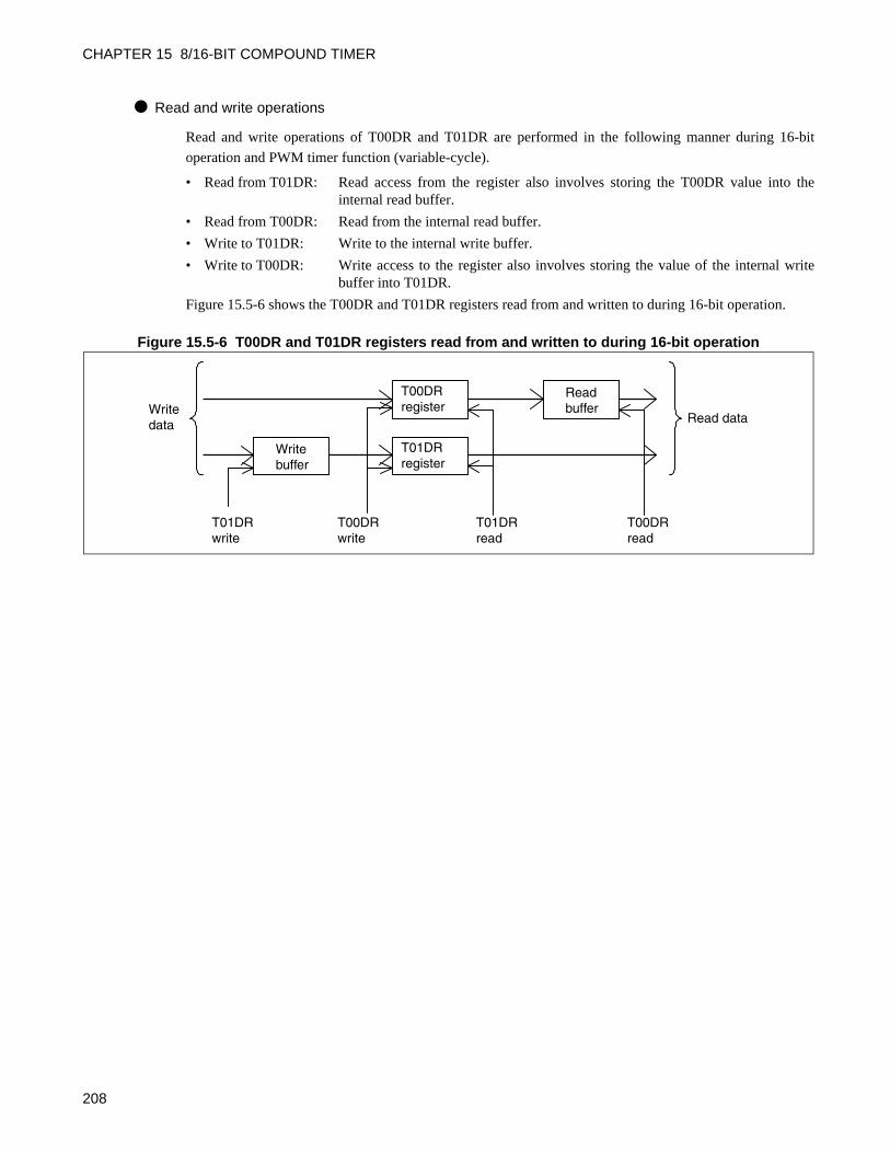
CHAPTER 15 8/16-BIT COMPOUND TIMER
Read and write operations
Read and write operations of T00DR and T01DR are performed in the following manner during 16-bit
operation and PWM timer function (variable-cycle).
• Read from T01DR: Read access from the register also involves storing the T00DR value into theinternal read buffer.
• Read from T00DR: Read from the internal read buffer.
• Write to T01DR: Write to the internal write buffer.
• Write to T00DR: Write access to the register also involves storing the value of the internal writebuffer into T01DR.
Figure 15.5-6 shows the T00DR and T01DR registers read from and written to during 16-bit operation.
Figure 15.5-6 T00DR and T01DR registers read from and written to during 16-bit operation
T00DR register
T01DR register
Read buffer
Write buffer
T01DR write
T00DR write
T01DR read
T00DR read
Read dataWrite data
208
CHAPTER 15 8/16-BIT COMPOUND TIMER
15.6 Interrupts of 8/16-bit Compound Timer
The 8/16-bit compound timer generates the following types of interrupts to each of which an interrupt number and interrupt vector are assigned.• Timer 00 interrupt• Timer 01 interrupt
Timer 00 InterruptTable 15.6-1 explains the timer 00 interrupt and its source.
Timer 01 InterruptTable 15.6-2 explains the timer 01 interrupt and its cause.
Table 15.6-1 Timer 00 Interrupt
Item Description
Interrupt generating condition
Comparison match in interval timer function or PWM timer function (variable-cycle mode) has been selected
Overflow in PWC timer function or input capture function
Completion of measurement in PWC timer function or edge detection in input capture function
Interrupt flag T00CR1:IF T00CR1:IF T00CR1:IR
Interrupt enable T00CR1:IE and T00CR0:IFE T00CR1:IE and T00CR0:IFE T00CR1:IE
Table 15.6-2 Timer 01 Interrupt
Item Description
Interrupt generating condition
Comparison match in interval timer function or PWM timer function (variable-cycle mode) has been selectedExcluded during 16-bit operation
Overflow in PWC timer function or input capture functionExcluded during 16-bit operation
Completion of measurement in PWC timer function or edge detection in input capture functionExcluded during 16-bit operation
Interrupt flag T01CR1:IF T01CR1:IF T01CR1:IR
Interrupt enable T01CR1:IE and T00CR0:IFE T01CR1:IE and T00CR0:IFE T01CR1:IE
209
CHAPTER 15 8/16-BIT COMPOUND TIMER
Registers and Vector Tables Related to Interrupts of 8/16-bit Compound Timer
The request numbers and vector tables of all peripheral functions are listed in Appendix B "Interrupt
Source Tables".
Table 15.6-3 Registers and Vector Tables Related to Interrupts of 8/16-bit Compound Timer
Interrupt source
Interrupt request No.
Interrupt level setup register Vector table address
Register Setting bit Upper Lower
Timer 00 IRQ5 ILR1 L05 FFF0H FFF1H
Timer 01 IRQ6 ILR1 L06 FFEEH FFEFH
210
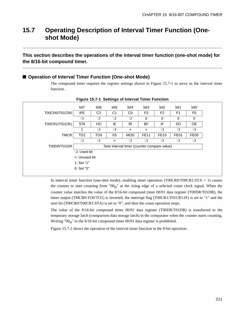
CHAPTER 15 8/16-BIT COMPOUND TIMER
15.7 Operating Description of Interval Timer Function (One-shot Mode)
This section describes the operations of the interval timer function (one-shot mode) for the 8/16-bit compound timer.
Operation of Interval Timer Function (One-shot Mode)The compound timer requires the register settings shown in Figure 15.7-1 to serve as the interval timer
function.
Figure 15.7-1 Settings of Interval Timer Function
In interval timer function (one-shot mode), enabling timer operation (T00CR0/T00CR1:STA = 1) causes
the counter to start counting from "00H" at the rising edge of a selected count clock signal. When the
counter value matches the value of the 8/16-bit compound timer 00/01 data register (T00DR/T01DR), the
timer output (TMCR0:TO0/TO1) is inverted, the interrupt flag (T00CR1/T01CR1:IF) is set to "1" and the
start bit (T00CR0/T00CR1:STA) is set to "0", and then the count operation stops.
The value of the 8/16-bit compound timer 00/01 data register (T00DR/T01DR) is transferred to the
temporary storage latch (comparison data storage latch) in the comparator when the counter starts counting.
Writing "00H" to the 8/16-bit compound timer 00/01 data register is prohibited.
Figure 15.7-2 shows the operation of the interval timer function in the 8-bit operation.
bit7 bit6 bit5 bit4 bit3 bit2 bit1 bit0
T00CR0/T01CR0 IFE C2 C1 C0 F3 F2 F1 F0
0 0 0 0
T00CR1/T01CR1 STA HO IE IR BF IF SO OE
1 × ×
TMCR TO1 TO0 IIS MOD FE11 FE10 FE01 FE00
×
T00DR/T01DR Sets interval timer (counter compare value)
: Used bit
×: Unused bit
1: Set "1"
0: Set "0"
211
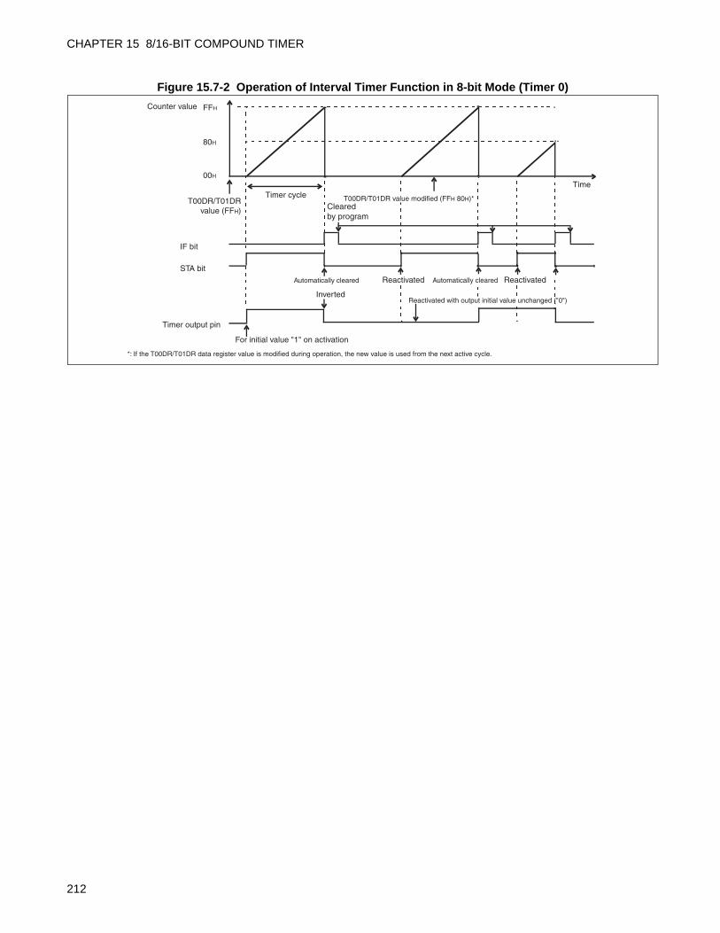
CHAPTER 15 8/16-BIT COMPOUND TIMER
Figure 15.7-2 Operation of Interval Timer Function in 8-bit Mode (Timer 0)
Counter value FFH
80H
00H
Timer cycle
Cleared by program
Time
IF bit
STA bit
T00DR/T01DRvalue (FFH)
Timer output pin
Automatically cleared Reactivated
Inverted
For initial value "1" on activation
*: If the T00DR/T01DR data register value is modified during operation, the new value is used from the next active cycle.
Automatically cleared Reactivated
Reactivated with output initial value unchanged ("0")
T00DR/T01DR value modified (FFH 80H)*
212
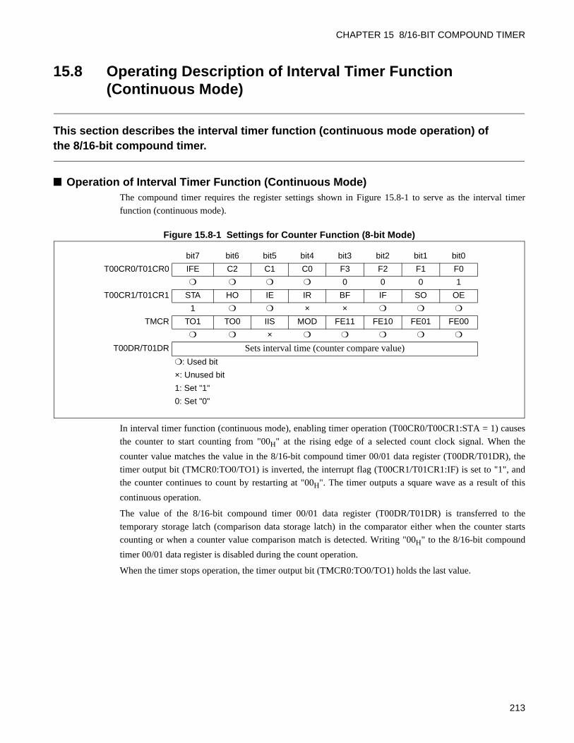
CHAPTER 15 8/16-BIT COMPOUND TIMER
15.8 Operating Description of Interval Timer Function (Continuous Mode)
This section describes the interval timer function (continuous mode operation) of the 8/16-bit compound timer.
Operation of Interval Timer Function (Continuous Mode)The compound timer requires the register settings shown in Figure 15.8-1 to serve as the interval timer
function (continuous mode).
Figure 15.8-1 Settings for Counter Function (8-bit Mode)
In interval timer function (continuous mode), enabling timer operation (T00CR0/T00CR1:STA = 1) causes
the counter to start counting from "00H" at the rising edge of a selected count clock signal. When the
counter value matches the value in the 8/16-bit compound timer 00/01 data register (T00DR/T01DR), the
timer output bit (TMCR0:TO0/TO1) is inverted, the interrupt flag (T00CR1/T01CR1:IF) is set to "1", and
the counter continues to count by restarting at "00H". The timer outputs a square wave as a result of this
continuous operation.
The value of the 8/16-bit compound timer 00/01 data register (T00DR/T01DR) is transferred to the
temporary storage latch (comparison data storage latch) in the comparator either when the counter starts
counting or when a counter value comparison match is detected. Writing "00H" to the 8/16-bit compound
timer 00/01 data register is disabled during the count operation.
When the timer stops operation, the timer output bit (TMCR0:TO0/TO1) holds the last value.
bit7 bit6 bit5 bit4 bit3 bit2 bit1 bit0
T00CR0/T01CR0 IFE C2 C1 C0 F3 F2 F1 F0
0 0 0 1
T00CR1/T01CR1 STA HO IE IR BF IF SO OE
1 × ×
TMCR TO1 TO0 IIS MOD FE11 FE10 FE01 FE00
×
T00DR/T01DR Sets interval time (counter compare value)
: Used bit
×: Unused bit
1: Set "1"
0: Set "0"
213
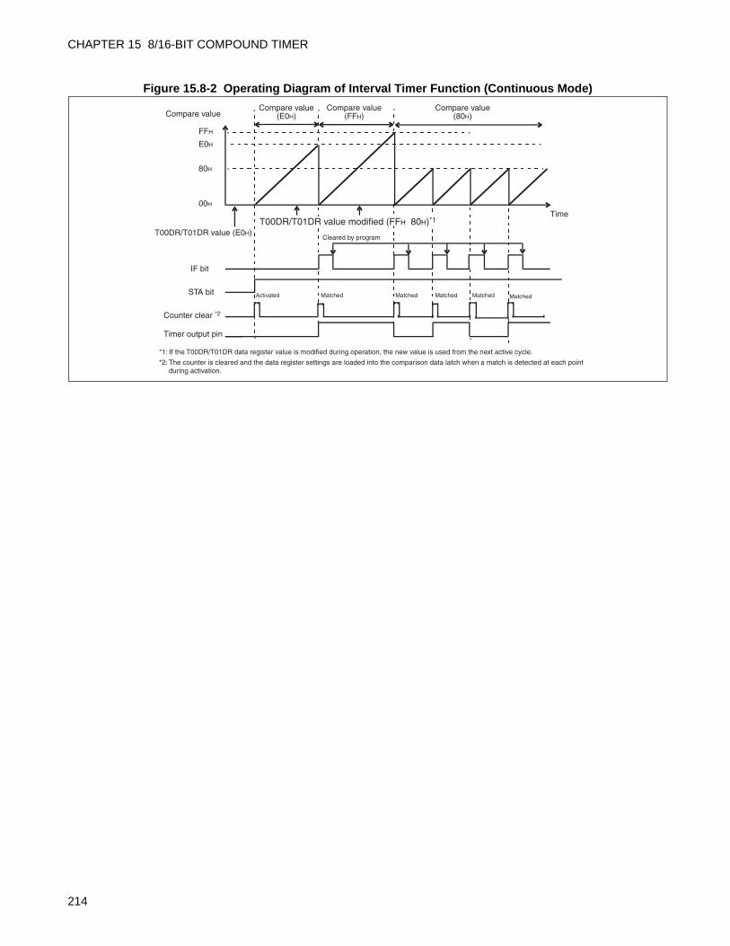
CHAPTER 15 8/16-BIT COMPOUND TIMER
Figure 15.8-2 Operating Diagram of Interval Timer Function (Continuous Mode)
Compare valueCompare value
(FFH)Compare value
(80H)
FFH
80H
00H
T00DR/T01DR value (E0H)Cleared by program
Time
IF bit
STA bit
Counter clear *2
Timer output pin
*1: If the T00DR/T01DR data register value is modified during operation, the new value is used from the next active cycle.
E0H
Compare value(E0H)
Activated Matched Matched Matched Matched Matched
*2: The counter is cleared and the data register settings are loaded into the comparison data latch when a match is detected at each point during activation.
T00DR/T01DR value modified (FFH 80H)*1
214
CHAPTER 15 8/16-BIT COMPOUND TIMER
15.9 Operating Description of Interval Timer Function (Free-run Mode)
This section describes the operation of the interval timer function (free-run mode) for the 8/16-bit compound timer.
Operation of Interval Timer Function (Free-run Mode)The compound timer requires the settings shown in Figure 15.9-1 to serve as the interval timer function
(free-run mode).
Figure 15.9-1 Settings for Interval Timer Function (Free-run Mode)
In interval timer function (free-run mode), enabling timer operation (T00CR0/T00CR1:STA = 1) causes the
counter to start counting from "00H" at the rising edge of a selected count clock signal. When the counter
value matches the value in the 8/16-bit compound timer 00/01 data register (T00DR/T01DR), the timer
output bit (TMCR0:TO0/TO1) is inverted and the interrupt flag (T00CR1/T01CR1:IF) is set to "1". The
counter continues to count, and when the count value reaches "FFH", it restarts counting at "00H" to
continue. The timer outputs a square wave as a result of this continuous operation.
The value of the 8/16-bit compound timer 00/01 data register (T00DR/T01DR) is transferred to the
temporary storage latch (comparison data storage latch) in the comparator either when the counter starts
counting or when a counter value comparison match is detected. Writing "00H" to the 8/16-bit compound
timer 00/01 data register is prohibited.
When the timer stops operation, the timer output bit (TMCR0:TO0/TO1) holds the last value.
bit7 bit6 bit5 bit4 bit3 bit2 bit1 bit0
T00CR0/T01CR0 IFE C2 C1 C0 F3 F2 F1 F0
0 0 1 0
T00CR1/T01CR1 STA HO IE IR BF IF SO OE
1 × ×
TMCR TO1 TO0 IIS MOD FE11 FE10 FE01 FE00
×
T00DR/T01DR Sets interval time (counter compare value)
: Used bit
×: Unused bit
1: Set "1"
0: Set "0"
215
CHAPTER 15 8/16-BIT COMPOUND TIMER
Figure 15.9-2 Operating Diagram of Interval Timer Function (Free-run Mode)
Counter value
FFH
80H
00H
T00DR/T01DR value (E0H)Cleared by program
Time
IF bit
STA bit
Counter value match *
Timer output pin
E0H
(E0H)
Activated Matched Matched Matched
*: The counter is not cleared and the data register settings are not reloaded into the comparison data latch when a match is detected at each point during activation.
Matched
Although the T00DR/T01DR value is modified, it is not updated into the comparison latch.
216
CHAPTER 15 8/16-BIT COMPOUND TIMER
15.10 Operating Description of PWM Timer Function (Fixed-cycle mode)
This section describes the operation of the PWM timer function (fixed-cycle mode) for the 8/16-bit compound timer.
Operation of PWM Timer Function (Fixed-cycle Mode)The compound timer requires the settings shown in Figure 15.10-1 to serve as the PWM timer function
(fixed-cycle mode).
Figure 15.10-1 Settings for PWM Timer Function (Fixed-cycle Mode)
In PWM timer function (fixed-cycle mode), a fixed cycle PWM signal in a variable "H" pulse width is
outputted from the timer output pin (TO00/TO01). The cycle is fixed to "FFH" in 8-bit operation or
"FFFFH" in 16-bit operation. The time is determined by the count clock selected. The "H" pulse width is
specified by the value in the 8/16-bit compound timer 00/01 data register (T00DR/T01DR).
This function has no effect on the interrupt flag (T00CR1/T01CR1:IF). As each cycle always starts with
"H" pulse output, the timer output initial value setting bit (T00CR1/T01CR1:SO) is meaningless.
The value of the 8/16-bit compound timer 00/01 data register (T00DR/T01DR) is transferred to the
temporary storage latch (comparison data storage latch) in the comparator either when the counter starts
counting or when a counter value comparison match is detected.
When the timer stops operation, the timer output bit (TMCR0:TO0/TO1) holds the last value.
The "H" pulse is one count clock shorter than the setting value in the output waveform immediately after
activation of the timer (write "1" to the STA bit).
bit7 bit6 bit5 bit4 bit3 bit2 bit1 bit0
T00CR0/T01CR0 IFE C2 C1 C0 F3 F2 F1 F0
0 0 1 1
T00CR1/T01CR1 STA HO IE IR BF IF SO OE
1 × × × × × ×
TMCR TO1 TO0 IIS MOD FE11 FE10 FE01 FE00
×
T00DR/T01DR Sets "H" pulse width (compare value)
: Used bit
×: Unused bit
1: Set "1"
0: Set "0"
217
CHAPTER 15 8/16-BIT COMPOUND TIMER
Figure 15.10-2 Operating Diagram of PWM Timer Function (Fixed-cycle Mode)
T00DR/T01DR register value: "00H" (duty ratio = 0%)
Counter value
"H"
"L"
"H"
"L"
"H"
"L"
00H
Counter value
Counter value
PWM waveform
PWM waveform
PWM waveform
T00DR/T01DR register value: "80H" (duty ratio = 50%)
T00DR/T01DR register value: "FFH" (duty ratio = 99.6%)
FFH00H
FFH00H
80H
One count width
Note: When the PWM function has been selected, the timer output pin holds the level used when the counter stops (T00CR0/T01CR0:STA = 0).
FFH00H
00H
00H
218
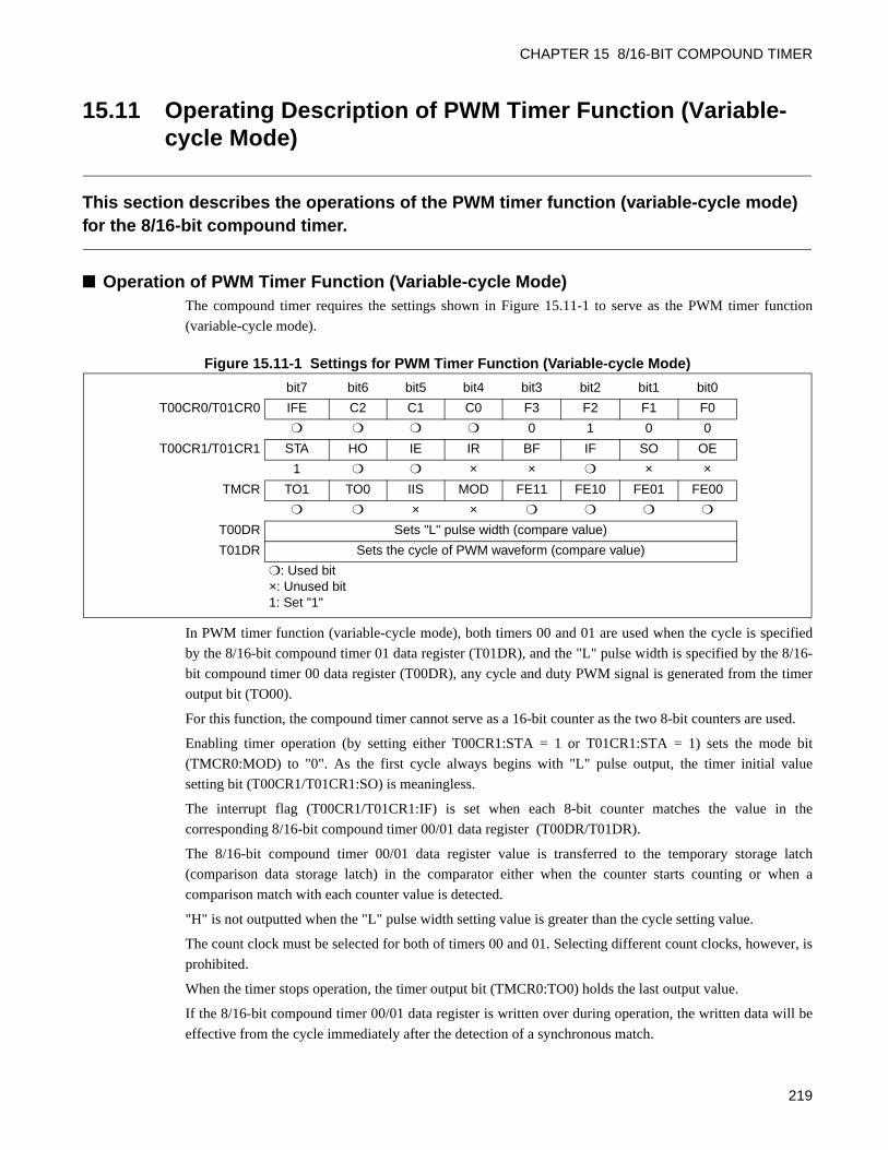
CHAPTER 15 8/16-BIT COMPOUND TIMER
15.11 Operating Description of PWM Timer Function (Variable-cycle Mode)
This section describes the operations of the PWM timer function (variable-cycle mode) for the 8/16-bit compound timer.
Operation of PWM Timer Function (Variable-cycle Mode)The compound timer requires the settings shown in Figure 15.11-1 to serve as the PWM timer function
(variable-cycle mode).
Figure 15.11-1 Settings for PWM Timer Function (Variable-cycle Mode)
In PWM timer function (variable-cycle mode), both timers 00 and 01 are used when the cycle is specified
by the 8/16-bit compound timer 01 data register (T01DR), and the "L" pulse width is specified by the 8/16-
bit compound timer 00 data register (T00DR), any cycle and duty PWM signal is generated from the timer
output bit (TO00).
For this function, the compound timer cannot serve as a 16-bit counter as the two 8-bit counters are used.
Enabling timer operation (by setting either T00CR1:STA = 1 or T01CR1:STA = 1) sets the mode bit
(TMCR0:MOD) to "0". As the first cycle always begins with "L" pulse output, the timer initial value
setting bit (T00CR1/T01CR1:SO) is meaningless.
The interrupt flag (T00CR1/T01CR1:IF) is set when each 8-bit counter matches the value in the
corresponding 8/16-bit compound timer 00/01 data register (T00DR/T01DR).
The 8/16-bit compound timer 00/01 data register value is transferred to the temporary storage latch
(comparison data storage latch) in the comparator either when the counter starts counting or when a
comparison match with each counter value is detected.
"H" is not outputted when the "L" pulse width setting value is greater than the cycle setting value.
The count clock must be selected for both of timers 00 and 01. Selecting different count clocks, however, is
prohibited.
When the timer stops operation, the timer output bit (TMCR0:TO0) holds the last output value.
If the 8/16-bit compound timer 00/01 data register is written over during operation, the written data will be
effective from the cycle immediately after the detection of a synchronous match.
bit7 bit6 bit5 bit4 bit3 bit2 bit1 bit0
T00CR0/T01CR0 IFE C2 C1 C0 F3 F2 F1 F0
0 1 0 0
T00CR1/T01CR1 STA HO IE IR BF IF SO OE
1 × × × ×
TMCR TO1 TO0 IIS MOD FE11 FE10 FE01 FE00
× ×
T00DR Sets "L" pulse width (compare value)
T01DR Sets the cycle of PWM waveform (compare value)
: Used bit×: Unused bit1: Set "1"
219
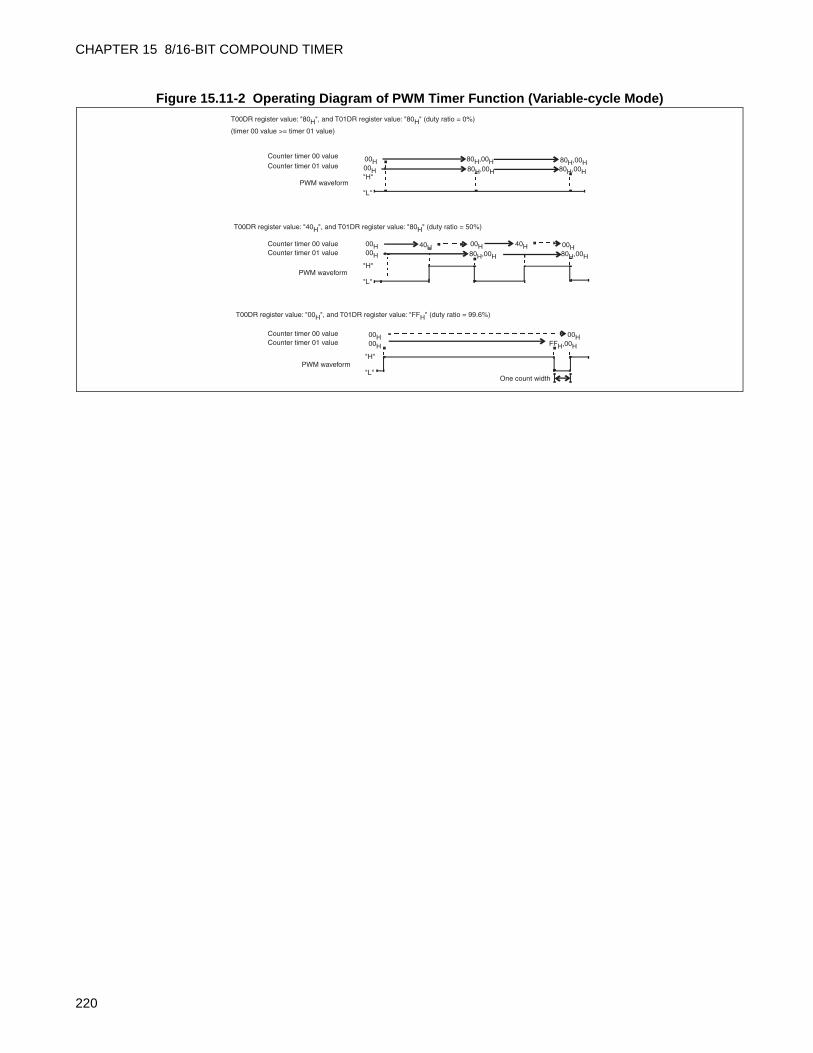
CHAPTER 15 8/16-BIT COMPOUND TIMER
Figure 15.11-2 Operating Diagram of PWM Timer Function (Variable-cycle Mode)
Counter timer 00 value
"H"
"L"
"H"
"L"
"H"
"L"
00H
PWM waveform
PWM waveform
PWM waveform
T00DR register value: "80H", and T01DR register value: "80H" (duty ratio = 0%)
FFH,00H
80H,00H00H 80H,00H80H,00H00H 80H,00H
Counter timer 01 value
Counter timer 00 valueCounter timer 01 value
00H00H 00H80H,00H00H 80H,00H
40H 40H
Counter timer 00 valueCounter timer 01 value
00H 00H
One count width
(timer 00 value >= timer 01 value)
T00DR register value: "40H", and T01DR register value: "80H" (duty ratio = 50%)
T00DR register value: "00H", and T01DR register value: "FFH" (duty ratio = 99.6%)
220
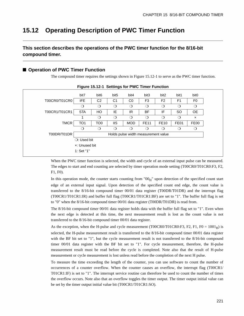
CHAPTER 15 8/16-BIT COMPOUND TIMER
15.12 Operating Description of PWC Timer Function
This section describes the operations of the PWC timer function for the 8/16-bit compound timer.
Operation of PWC Timer FunctionThe compound timer requires the settings shown in Figure 15.12-1 to serve as the PWC timer function.
Figure 15.12-1 Settings for PWC Timer Function
When the PWC timer function is selected, the width and cycle of an external input pulse can be measured.
The edges to start and end counting are selected by timer operation mode setting (T00CR0/T01CR0:F3, F2,
F1, F0).
In this operation mode, the counter starts counting from "00H" upon detection of the specified count start
edge of an external input signal. Upon detection of the specified count end edge, the count value is
transferred to the 8/16-bit compound timer 00/01 data register (T00DR/T01DR) and the interrupt flag
(T00CR1/T01CR1:IR) and buffer full flag (T00CR1/T01CR1:BF) are set to "1". The buffer full flag is set
to "0" when the 8/16-bit compound timer 00/01 data register (T00DR/T01DR) is read from.
The 8/16-bit compound timer 00/01 data register holds data with the buffer full flag set to "1". Even when
the next edge is detected at this time, the next measurement result is lost as the count value is not
transferred to the 8/16-bit compound timer 00/01 data register.
As the exception, when the H-pulse and cycle measurement (T00CR0/T01CR0:F3, F2, F1, F0 = 1001B) is
selected, the H-pulse measurement result is transferred to the 8/16-bit compound timer 00/01 data register
with the BF bit set to "1", but the cycle measurement result is not transferred to the 8/16-bit compound
timer 00/01 data register with the BF bit set to "1". For cycle measurement, therefore, the H-pulse
measurement result must be read before the cycle is completed. Note also that the result of H-pulse
measurement or cycle measurement is lost unless read before the completion of the next H pulse.
To measure the time exceeding the length of the counter, you can use software to count the number of
occurrences of a counter overflow. When the counter causes an overflow, the interrupt flag (T00CR1/
T01CR1:IF) is set to "1". The interrupt service routine can therefore be used to count the number of times
the overflow occurs. Note also that an overflow toggles the timer output. The timer output initial value can
be set by the timer output initial value bit (T00CR1/T01CR1:SO).
bit7 bit6 bit5 bit4 bit3 bit2 bit1 bit0
T00CR0/T01CR0 IFE C2 C1 C0 F3 F2 F1 F0
T00CR1/T01CR1 STA HO IE IR BF IF SO OE
1 ×
TMCR TO1 TO0 IIS MOD FE11 FE10 FE01 FE00
T00DR/T01DR Holds pulse width measurement value
: Used bit
×: Unused bit
1: Set "1"
221
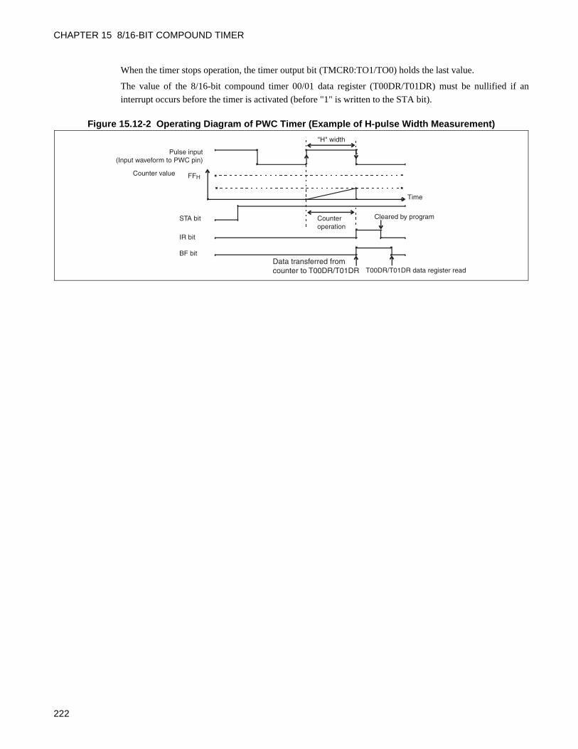
CHAPTER 15 8/16-BIT COMPOUND TIMER
When the timer stops operation, the timer output bit (TMCR0:TO1/TO0) holds the last value.
The value of the 8/16-bit compound timer 00/01 data register (T00DR/T01DR) must be nullified if an
interrupt occurs before the timer is activated (before "1" is written to the STA bit).
Figure 15.12-2 Operating Diagram of PWC Timer (Example of H-pulse Width Measurement)
Pulse input(Input waveform to PWC pin)
Counter value FFH
STA bit
IR bit
BF bit
"H" width
Counter operation
Time
Cleared by program
Data transferred from counter to T00DR/T01DR T00DR/T01DR data register read
222
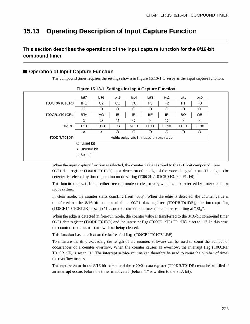
CHAPTER 15 8/16-BIT COMPOUND TIMER
15.13 Operating Description of Input Capture Function
This section describes the operations of the input capture function for the 8/16-bit compound timer.
Operation of Input Capture FunctionThe compound timer requires the settings shown in Figure 15.13-1 to serve as the input capture function.
Figure 15.13-1 Settings for Input Capture Function
When the input capture function is selected, the counter value is stored to the 8/16-bit compound timer
00/01 data register (T00DR/T01DR) upon detection of an edge of the external signal input. The edge to be
detected is selected by timer operation mode setting (T00CR0/T01CR0:F3, F2, F1, F0).
This function is available in either free-run mode or clear mode, which can be selected by timer operation
mode setting.
In clear mode, the counter starts counting from "00H". When the edge is detected, the counter value is
transferred to the 8/16-bit compound timer 00/01 data register (T00DR/T01DR), the interrupt flag
(T00CR1/T01CR1:IR) is set to "1", and the counter continues to count by restarting at "00H".
When the edge is detected in free-run mode, the counter value is transferred to the 8/16-bit compound timer
00/01 data register (T00DR/T01DR) and the interrupt flag (T00CR1/T01CR1:IR) is set to "1". In this case,
the counter continues to count without being cleared.
This function has no effect on the buffer full flag (T00CR1/T01CR1:BF).
To measure the time exceeding the length of the counter, software can be used to count the number of
occurrences of a counter overflow. When the counter causes an overflow, the interrupt flag (T00CR1/
T01CR1:IF) is set to "1". The interrupt service routine can therefore be used to count the number of times
the overflow occurs.
The capture value in the 8/16-bit compound timer 00/01 data register (T00DR/T01DR) must be nullified if
an interrupt occurs before the timer is activated (before "1" is written to the STA bit).
bit7 bit6 bit5 bit4 bit3 bit2 bit1 bit0
T00CR0/T01CR0 IFE C2 C1 C0 F3 F2 F1 F0
T00CR1/T01CR1 STA HO IE IR BF IF SO OE
1 × × ×
TMCR TO1 TO0 IIS MOD FE11 FE10 FE01 FE00
× ×
T00DR/T01DR Holds pulse width measurement value
: Used bit
×: Unused bit
1: Set "1"
223
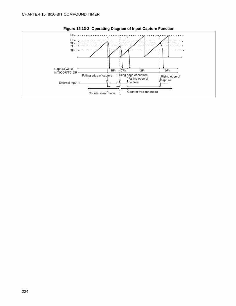
CHAPTER 15 8/16-BIT COMPOUND TIMER
Figure 15.13-2 Operating Diagram of Input Capture Function
FFH
BFH
7FH9FH
3FH
3FH 9FH
Counter free-run modeCounter clear mode
BFH 7FHCapture value in T00DR/T01DR
Falling edge of capture
Rising edge of capture
External input
Falling edge of capture Rising edge of capture
224
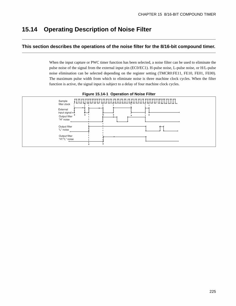
CHAPTER 15 8/16-BIT COMPOUND TIMER
15.14 Operating Description of Noise Filter
This section describes the operations of the noise filter for the 8/16-bit compound timer.
When the input capture or PWC timer function has been selected, a noise filter can be used to eliminate the
pulse noise of the signal from the external input pin (EC0/EC1). H-pulse noise, L-pulse noise, or H/L-pulse
noise elimination can be selected depending on the register setting (TMCR0:FE11, FE10, FE01, FE00).
The maximum pulse width from which to eliminate noise is three machine clock cycles. When the filter
function is active, the signal input is subject to a delay of four machine clock cycles.
Figure 15.14-1 Operation of Noise Filter
Sample filter clock
External input signal
Output filter "H" noise
Output filter "L" noise
Output filter "H"/"L" noise
225
CHAPTER 15 8/16-BIT COMPOUND TIMER
15.15 States in Each Mode during Operation
This section describes how the 8/16-bit compound timer behaves when the microcontroller enters watch mode or stop mode or when a suspend (T00CR1/T01CR1:HO = 1) request is issued during operation.
When Interval Timer, Input Capture, or PWC Function Has Been SelectedFigure 15.15-1 shows how the counter value changes when transition to watch mode or stop mode or a
suspend request occurs during operation of the 8/16-bit compound timer.
The counter stops operation while holding the value when transition to stop mode or watch mode occurs.
When the stop mode or watch mode is canceled by an interrupt, the counter resumes operation with the last
value held. So the first interval time and external clock count are incorrect. After releasing from stop mode
or watch mode, be sure to initialize the counter value.
Figure 15.15-1 Operations of Counter in Standby Mode or in Pause (Not Serving as PWM Timer)
Counter valueFFH
80H
00H
T00DR/T01DR data register value (FFH)
Timer cycle Time
IF bit
Cleared by program Operation halts Operation halts
STA bit
IE bit
SLP bit (STBC register)
STP bit (STBC register)
Wake-up from stop mode by external interrupt
HO bit
HO requestHO request ends
Request ends
Delay of oscillation stabilization wait time
Interval time after wake-up from stop mode (indeterminate)
Operation history
Sleep mode
Wake-up from sleep mode by interrupt
Stop mode
Operation reactivated
226
CHAPTER 15 8/16-BIT COMPOUND TIMER
Figure 15.15-2 Operations of Counter in Standby Mode or in Pause (Serving as PWM Timer)
Counter valueFFH
00H
T00DR/T01DR value (FFH)Time
STA bit
PWM timer output pin
(FFH)
SLP bit(STBC register)
STP bit(STBC register)
Sleep mode
*
*: The PWM timer output maintains the value held before it enters the stop mode.
HO bit
Wake-up from sleep mode by interrupt
Delay of oscillation stabilization wait time
Maintains the level prior to stop
Wake-up from stop mode by external interrupt
Maintains the level prior to hold
227
CHAPTER 15 8/16-BIT COMPOUND TIMER
15.16 Precautions when Using 8/16-bit Compound Timer
This section explains the precautions to be taken when using the 8/16-bit compound timer.
Precautions when Using 8/16-bit Compound TimerWhen changing the timer function by using the timer operation mode select bits (T00CR0/T01CR0:F3, F2,
F1, F0), the timer operation must be stopped (T00CR1/T01CR1:STA = 0) before clearing the interrupt flag
(T00CR1/T01CR1:IF, IR), interrupt enable bits (T00CR1/T01CR1:IE, T00CR0/T01CR0:IFE) and buffer
full flag (T00CR1/T01CR1:BF).
When the PWC or input capture function has been selected, an interrupt may occur even before the timer is
activated (STA = 0). Therefore, nullify the value of the 8/16-bit compound timer 00/01 data register
(T00DR/T01DR) obtained before the activation.
228
CHAPTER 168/16-BIT PPG
This chapter describes the functions and operations of the 8/16-bit PPG.
16.1 Overview of 8/16-bit PPG
16.2 Configuration of 8/16-bit PPG
16.3 Channels of 8/16-bit PPG
16.4 Pins of 8/16-bit PPG
16.5 Registers of 8/16-bit PPG
16.6 Interrupts of 8/16-bit PPG
16.7 Operating Description of 8/16-bit PPG
16.8 Precautions when Using 8/16-bit PPG
16.9 Sample Programs for 8/16-bit PPG Timer
229
CHAPTER 16 8/16-BIT PPG
16.1 Overview of 8/16-bit PPG
The 8/16-bit PPG is an 8-bit reload timer module that uses pulse output control based on timer operation to perform PPG output. The 8/16-bit PPG also operates in cascade (8 bits + 8 bits) as 16-bit PPG.
Overview of 8/16-bit PPGThe following section summarizes the 8/16-bit PPG functions.
8-bit PPG output independent operation mode
In this mode, the unit can operate as 2 8-bit PPG (PPG timer 00 and PPG timer 01).
8-bit prescaler + 8-bit PPG output operation mode
The rising and falling edge detection pulses from the PPG timer 01 output can be inputted to the down-
counter of the PPG timer 00 to enable variable-cycle 8-bit PPG output.
16-bit PPG output operation mode
The unit can also operate in cascade (PPG timer 01 (upper 8 bits) + PPG timer 00 (lower 8 bits)) as 16-bit
PPG output.
PPG output operation
In this operation, a variable-cycle pulse waveform is outputted in any duty ratio.
The unit can also be used as a D/A converter in conjunction with an external circuit.
Output inversion mode
This mode can invert the PPG output value.
230
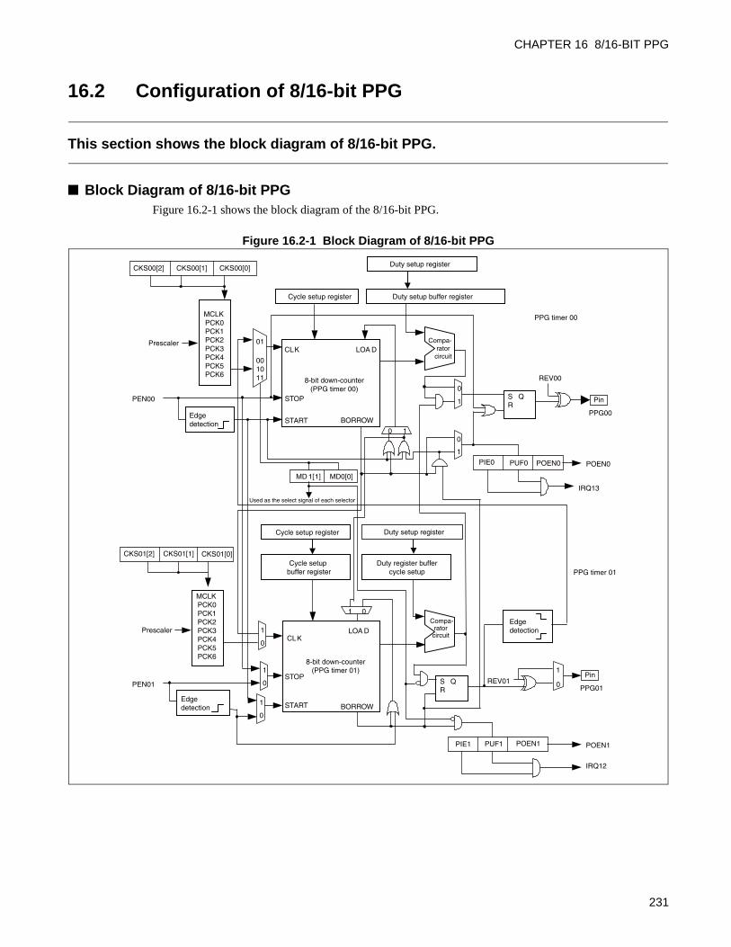
CHAPTER 16 8/16-BIT PPG
16.2 Configuration of 8/16-bit PPG
This section shows the block diagram of 8/16-bit PPG.
Block Diagram of 8/16-bit PPGFigure 16.2-1 shows the block diagram of the 8/16-bit PPG.
Figure 16.2-1 Block Diagram of 8/16-bit PPG
Cycle setup register Duty setup buffer register
MCLK PCK0 PCK1 PCK2 PCK3 PCK4 PCK5 PCK6
8-bit down-counter(PPG timer 00)
CLK
START
STOP
BORROW
LOA D
CKS00[2] CKS00[1] CKS00[0]
Cycle setup register Duty setup register
MCLK PCK0 PCK1 PCK2 PCK3 PCK4 PCK5 PCK6
8-bit down-counter(PPG timer 01)
CLK
START
STOP
BORROW
LOA D
CKS01[2] CKS01[1] CKS01[0]
PEN00
Prescaler
Edge detection
PEN01
Edge detection
MD 1[1] MD0[0]
1
0
01
S Q R
REV00
PPG timer 00
PPG timer 01
S Q R
REV01
1
0 PPG01
Pin
1
0
1
010
PIE1
PPG00
Pin
PUF1 POEN1
IRQ12
POEN1
PIE0 PUF0 POEN0
IRQ13
POEN0
Edge detectionPrescaler
01
1
0
001011
1
0
Used as the select signal of each selector
Duty setup register
Cycle setup buffer register
Duty register buffercycle setup
Compa-rator
circuit
Compa-rator
circuit
231
CHAPTER 16 8/16-BIT PPG
Counter clock selector
The clock for the countdown of 8-bit down counter is selected from eight types of internal count clocks.
8-bit down-counter
It counts down with the count clock selected with the count clock selector.
Comparator circuit
The output is kept "H" until the value of 8-bit down counter is corresponding to the value of 8/16-bit PPG
duty setup buffer register from the value of 8/16-bit set buffer register of PPG cycle.
Afterwards, after keep "L" the output until the counter value is corresponding to "1", it keeps counting 8-bit
down counter from the value of 8/16-bit PPG cycle setup buffer register.
8/16-bit PPG timer 01 control register (PC01)
The operation condition on the PPG timer 01 side of 8/16-bit PPG timer is set.
8/16-bit PPG timer 00 control register (PC00)
The operation mode of 8/16-bit PPG timer and the operation condition on the PPG timer 00 side are set.
8/16-bit PPG timer 01/00 cycle setup buffer register ch.0 (PPS01), 0(PPS00)
The compare value for the cycle of 8/16-bit PPG timer is set.
8/16-bit PPG timer 01/00 duty setup buffer register ch.0 (PDS01), 0(PDS00)
The compare value for "H" width of 8/16-bit PPG timer is set.
8/16-bit PPG start register
The start or the stop of 8/16-bit PPG timer is set.
8/16-bit PPG output inversion register
An initial level also includes the output of 8/16-bit PPG timer and it is reversed.
Input ClockThe 8/16-bit PPG uses the output clock from the prescaler as its input clock (count clock).
232
CHAPTER 16 8/16-BIT PPG
16.3 Channels of 8/16-bit PPG
This section describes the channels of the 8/16-bit PPG.
Channels of 8/16-bit PPGMB95130/M series has two channels of the 8/16-bit PPG. There are 8-bit PPG timer 00 and 8-bit PPG
timer 01 in 1 channel. They can be used respectively as two 8-bit PPGs. Also, they can be used as a 16-bit
PPG.
Table 16.3-1 and Table 16.3-2 show the channels and their corresponding pins and registers.
The following sections describe only the 8/16-bit PPG in ch.0 side.
Table 16.3-1 Pins of 8/16-bit PPG
Channel Pin name Pin function
0PPG00 PPG timer 00 (8-bit PPG (00), 16-bit PPG)
PPG01 PPG timer 01 (8-bit PPG (01), 8-bit prescaler)
1PPG10 PPG timer 00 (8-bit PPG (10), 16-bit PPG)
PPG11 PPG timer 01 (8-bit PPG (11), 8-bit prescaler)
Table 16.3-2 Registers of 8/16-bit PPG
Channel Register name Corresponding register (as written in this manual)
0
PC01 8/16-bit PPG timer 01 control register
PC00 8/16-bit PPG timer 00 control register
PPS01 8/16-bit PPG timer 01 cycle setup buffer register
PPS00 8/16-bit PPG timer 00 cycle setup buffer register
PDS01 8/16-bit PPG timer 01 duty setup buffer register
PDS00 8/16-bit PPG timer 00 duty setup buffer register
1
PC11 8/16-bit PPG timer 01 control register
PC10 8/16-bit PPG timer 00 control register
PPS11 8/16-bit PPG timer 01 cycle setup buffer register
PPS10 8/16-bit PPG timer 00 cycle setup buffer register
PDS11 8/16-bit PPG timer 01 duty setup buffer register
PDS10 8/16-bit PPG timer 00 duty setup buffer register
Both channelsPPGS 8/16-bit PPG start register
REVC 8/16-bit PPG output inversion register
233
CHAPTER 16 8/16-BIT PPG
16.4 Pins of 8/16-bit PPG
This section describes the pins of the 8/16-bit PPG.
Pins of 8/16-bit PPG
PPG00 pin and PPG01 pin
These pins function both as general-purpose I/O ports and 8/16-bit PPG outputs.
PPG00, PPG01: A PPG waveform is outputted to these pins. The PPG waveform can be outputted by
enabling the output by the 8/16-bit PPG timer 01/00 control registers (PC0: POEN0 = 1,
PC1: POEN1 = 1).
234
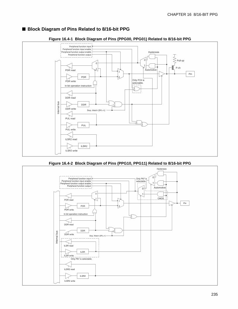
CHAPTER 16 8/16-BIT PPG
Block Diagram of Pins Related to 8/16-bit PPG
Figure 16.4-1 Block Diagram of Pins (PPG00, PPG01) Related to 8/16-bit PPG
Figure 16.4-2 Block Diagram of Pins (PPG10, PPG11) Related to 8/16-bit PPG
ILSR2 read
ILSR2 write
ILSR2
0
1
PDR read
PDR write
PDR
DDR read
DDR write
DDR
PUL read
PUL write
PUL
0
11
0
Peripheral function outputPeripheral function output enable
Peripheral function input enablePeripheral function input
Pin
Stop, Watch (SPL=1)
Inte
rnal
bus
In bit operation instruction
Pull-up
Only P24 is selectable.
Hysteresis
AutomotiveP-ch
ILSR2 read
ILSR2 write
ILSR2
0
1
0
1
Automotive
PDR read
PDR write
PDR
DDR read
DDR write
DDR
0
11
0
Peripheral function outputPeripheral function output enable
Peripheral function input enablePeripheral function input
Pin
Stop, Watch (SPL=1)
Inte
rnal
bus
In bit operation instruction
ILSR read
ILSR write
ILSR
Hysteresis
CMOS
Only P67 is selectable.
Only P67 is selectable.
235
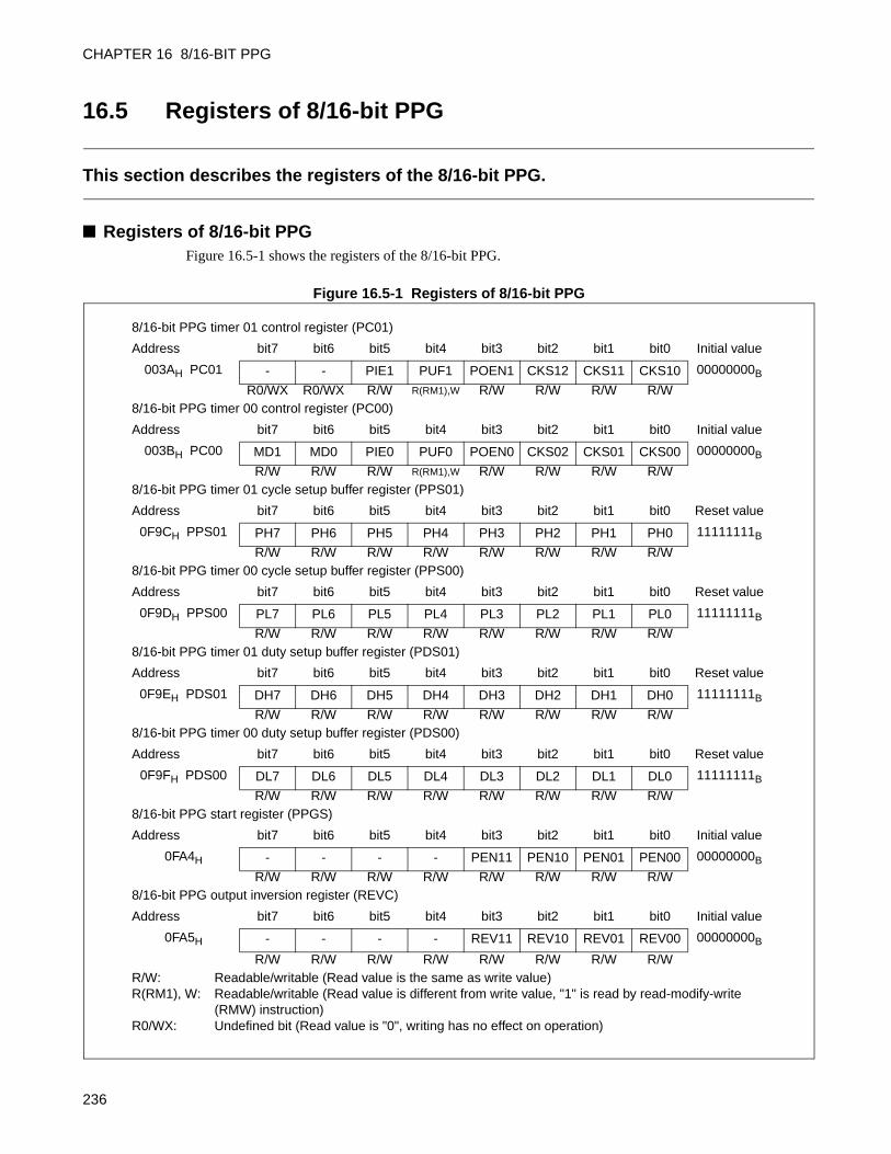
CHAPTER 16 8/16-BIT PPG
16.5 Registers of 8/16-bit PPG
This section describes the registers of the 8/16-bit PPG.
Registers of 8/16-bit PPGFigure 16.5-1 shows the registers of the 8/16-bit PPG.
Figure 16.5-1 Registers of 8/16-bit PPG
8/16-bit PPG timer 01 control register (PC01)
Address bit7 bit6 bit5 bit4 bit3 bit2 bit1 bit0 Initial value
003AH PC01 - - PIE1 PUF1 POEN1 CKS12 CKS11 CKS10 00000000B
R0/WX R0/WX R/W R(RM1),W R/W R/W R/W R/W8/16-bit PPG timer 00 control register (PC00)
Address bit7 bit6 bit5 bit4 bit3 bit2 bit1 bit0 Initial value
003BH PC00 MD1 MD0 PIE0 PUF0 POEN0 CKS02 CKS01 CKS00 00000000B
R/W R/W R/W R(RM1),W R/W R/W R/W R/W8/16-bit PPG timer 01 cycle setup buffer register (PPS01)
Address bit7 bit6 bit5 bit4 bit3 bit2 bit1 bit0 Reset value
0F9CH PPS01 PH7 PH6 PH5 PH4 PH3 PH2 PH1 PH0 11111111B
R/W R/W R/W R/W R/W R/W R/W R/W8/16-bit PPG timer 00 cycle setup buffer register (PPS00)
Address bit7 bit6 bit5 bit4 bit3 bit2 bit1 bit0 Reset value
0F9DH PPS00 PL7 PL6 PL5 PL4 PL3 PL2 PL1 PL0 11111111B
R/W R/W R/W R/W R/W R/W R/W R/W8/16-bit PPG timer 01 duty setup buffer register (PDS01)
Address bit7 bit6 bit5 bit4 bit3 bit2 bit1 bit0 Reset value
0F9EH PDS01 DH7 DH6 DH5 DH4 DH3 DH2 DH1 DH0 11111111B
R/W R/W R/W R/W R/W R/W R/W R/W8/16-bit PPG timer 00 duty setup buffer register (PDS00)
Address bit7 bit6 bit5 bit4 bit3 bit2 bit1 bit0 Reset value
0F9FH PDS00 DL7 DL6 DL5 DL4 DL3 DL2 DL1 DL0 11111111B
R/W R/W R/W R/W R/W R/W R/W R/W8/16-bit PPG start register (PPGS)
Address bit7 bit6 bit5 bit4 bit3 bit2 bit1 bit0 Initial value
0FA4H - - - - PEN11 PEN10 PEN01 PEN00 00000000B
R/W R/W R/W R/W R/W R/W R/W R/W8/16-bit PPG output inversion register (REVC)
Address bit7 bit6 bit5 bit4 bit3 bit2 bit1 bit0 Initial value
0FA5H - - - - REV11 REV10 REV01 REV00 00000000B
R/W R/W R/W R/W R/W R/W R/W R/WR/W: Readable/writable (Read value is the same as write value)R(RM1), W: Readable/writable (Read value is different from write value, "1" is read by read-modify-write
(RMW) instruction)R0/WX: Undefined bit (Read value is "0", writing has no effect on operation)
236
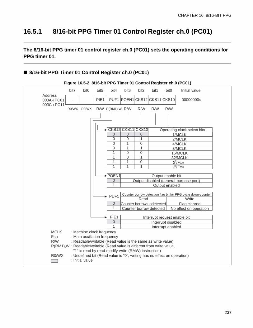
CHAPTER 16 8/16-BIT PPG
16.5.1 8/16-bit PPG Timer 01 Control Register ch.0 (PC01)
The 8/16-bit PPG timer 01 control register ch.0 (PC01) sets the operating conditions for PPG timer 01.
8/16-bit PPG Timer 01 Control Register ch.0 (PC01)
Figure 16.5-2 8/16-bit PPG Timer 01 Control Register ch.0 (PC01)
0 1/MCLK
- - PIE1 PUF1 POEN1 CKS12 CKS11 CKS10 00000000B
bit7Address003AH PC01003CH PC11
bit6 bit5 bit4 bit3 bit2 bit1 bit0 Initial value
R0/WX R0/WX R/W R(RM1),W R/W R/W R/W R/W
Operating clock select bitsCKS10CKS11CKS1200
2/MCLK1004/MCLK0108/MCLK11016/MCLK00132/MCLK10127/FCH01128/FCH111
Output enable bitOutput disabled (general-purpose port)
POEN10
Output enabled1
Counter borrow detection flag bit for PPG cycle down-counterRead Write
Counter borrow undetected
PUF1
Flag cleared0No effect on operation1 Counter borrow detected
Interrupt request enable bitInterrupt disabled
PIE10
Interrupt enabled1MCLK FCH R/W R(RM1),W
R0/WX
: Machine clock frequency: Main oscillation frequency: Readable/writable (Read value is the same as write value): Readable/writable (Read value is different from write value, "1" is read by read-modify-write (RMW) instruction)
: Undefined bit (Read value is "0", writing has no effect on operation): Initial value
237
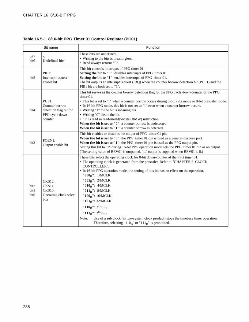
CHAPTER 16 8/16-BIT PPG
Table 16.5-1 8/16-bit PPG Timer 01 Control Register (PC01)
Bit name Function
bit7bit6
-:Undefined bits
These bits are undefined.• Writing to the bits is meaningless.• Read always returns "0".
bit5PIE1:Interrupt request enable bit
This bit controls interrupts of PPG timer 01.Setting the bit to "0": disables interrupts of PPG timer 01.Setting the bit to "1": enables interrupts of PPG timer 01.The bit outputs an interrupt request (IRQ) when the counter borrow detection bit (PUF1) and the PIE1 bit are both set to "1".
bit4
PUF1:Counter borrow detection flag bit for PPG cycle down-counter
This bit serves as the counter borrow detection flag for the PPG cycle down-counter of the PPG timer 01.• This bit is set to "1" when a counter borrow occurs during 8-bit PPG mode or 8-bit prescaler mode.• In 16-bit PPG mode, this bit is not set to "1" even when a counter borrow occurs.• Writing "1" to the bit is meaningless.• Writing "0" clears the bit.• "1" is read in read-modify-write (RMW) instruction.When the bit is set to "0": a counter borrow is undetected.When the bit is set to "1": a counter borrow is detected.
bit3POEN1:Output enable bit
This bit enables or disables the output of PPG timer 01 pin.When the bit is set to "0": the PPG timer 01 pin is used as a general-purpose port.When the bit is set to "1": the PPG timer 01 pin is used as the PPG output pin.Setting this bit to "1" during 16-bit PPG operation mode sets the PPG timer 01 pin as an output. (The setting value of REV01 is outputted. "L" output is supplied when REV01 is 0.)
bit2bit1bit0
CKS12,CKS11,CKS10:Operating clock select bits
These bits select the operating clock for 8-bit down-counter of the PPG timer 01.• The operating clock is generated from the prescaler. Refer to "CHAPTER 6 CLOCK
CONTROLLER".• In 16-bit PPG operation mode, the setting of this bit has no effect on the operation.
"000B": 1/MCLK
"001B": 2/MCLK
"010B": 4/MCLK
"011B": 8/MCLK
"100B": 16/MCLK
"101B": 32/MCLK
"110B": 27/FCH
"111B": 28/FCH
Note: Use of a sub clock (in two-system clock product) stops the timebase timer operation. Therefore, selecting "110B" or "111B" is prohibited.
238
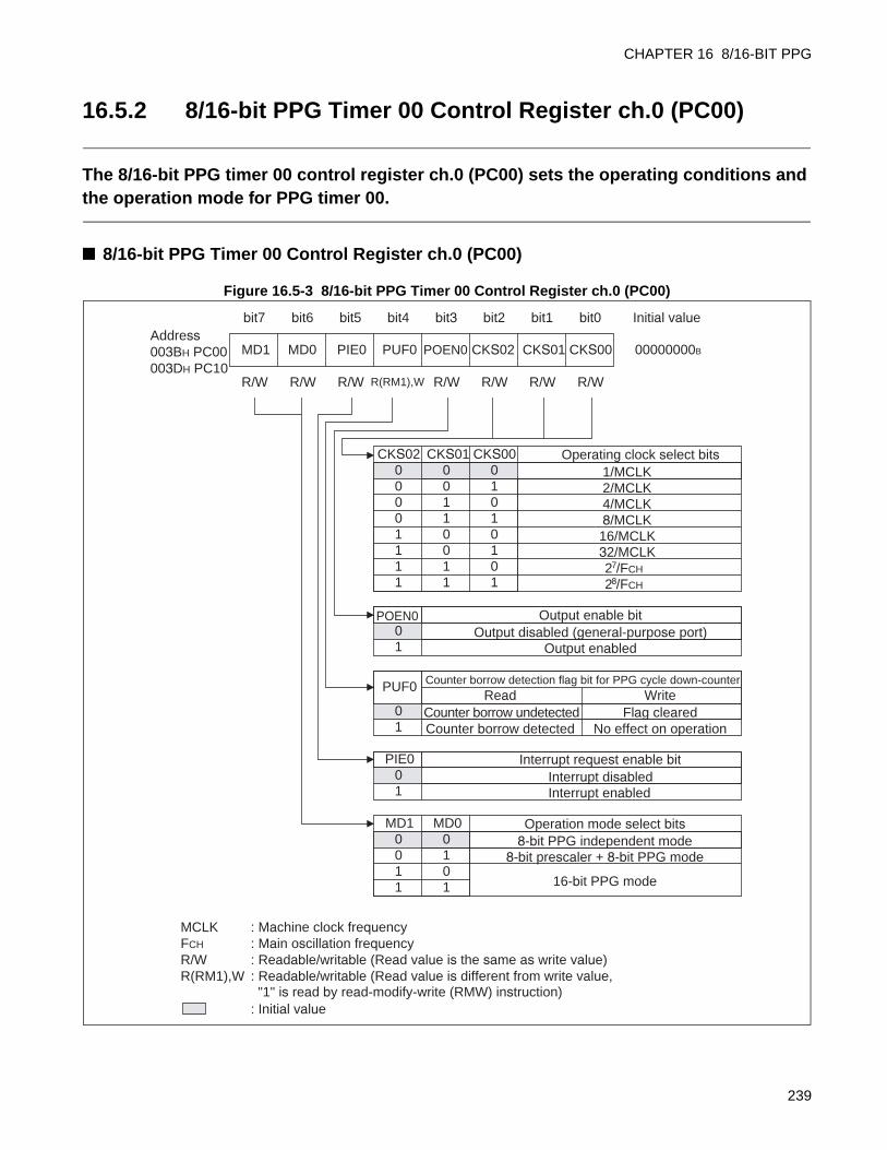
CHAPTER 16 8/16-BIT PPG
16.5.2 8/16-bit PPG Timer 00 Control Register ch.0 (PC00)
The 8/16-bit PPG timer 00 control register ch.0 (PC00) sets the operating conditions and the operation mode for PPG timer 00.
8/16-bit PPG Timer 00 Control Register ch.0 (PC00)
Figure 16.5-3 8/16-bit PPG Timer 00 Control Register ch.0 (PC00)
0
0 1/MCLK
MD1 MD0 PIE0 PUF0 POEN0 CKS02 CKS01 CKS00 00000000B
bit7 bit6 bit5 bit4 bit3 bit2 bit1 bit0 Initial value
R/W R/W R/W R(RM1),W R/W R/W R/W R/W
Operating clock select bitsCKS00CKS01CKS0200
2/MCLK1004/MCLK0108/MCLK11016/MCLK00132/MCLK10127/FCH01128/FCH111
Output enable bitOutput disabled (general-purpose port)
POEN00
Output enabled1
Counter borrow detection flag bit for PPG cycle down-counterRead Write
Counter borrow undetected
PUF0
Flag cleared0No effect on operation1 Counter borrow detected
Interrupt request enable bitInterrupt disabled
PIE00
Interrupt enabled1
8-bit PPG independent modeOperation mode select bitsMD0MD1
08-bit prescaler + 8-bit PPG mode10
16-bit PPG mode0111
MCLK FCH R/W R(RM1),W
: Machine clock frequency: Main oscillation frequency: Readable/writable (Read value is the same as write value): Readable/writable (Read value is different from write value, "1" is read by read-modify-write (RMW) instruction)
: Initial value
Address003BH PC00003DH PC10
239
CHAPTER 16 8/16-BIT PPG
Table 16.5-2 8/16-bit PPG0 Control Register (PC0)
Bit name Function
bit7bit6
MD1,MD0:Operation mode select bits
These bits select the PPG operation mode.Do not modify the bit settings during counting.
When set to "00B": 8-bit PPG independent mode
When set to "01B": 8-bit prescaler + 8-bit PPG mode
When set to "1xB": 16-bit PPG mode
bit5PIE0:Interrupt request enable bit
This bit controls interrupts of PPG timer 00.• Set this bit in 16-bit PPG operation mode.
Setting the bit to "0": disables interrupts of PPG timer 00.Setting the bit to "1": enables interrupts of PPG timer 00.
• An interrupt request (IRQ) is outputted when the counter borrow detection bit (PUF0) and PIE0 bit are both set to "1".
bit4
PUF0:Counter borrow detection flag bit for PPG cycle down-counter
This is the counter borrow detection flag for the PPG cycle down-counter of PPG timer 00.• Only this bit is effective in 16-bit PPG operation mode (PC1:PUF1 is not operable).
Note: Always effective in 8-bit mode• Writing "1" to this bit is meaningless.• Writing "0" clears the bit.• "1" is read in read-modify-write (RMW) instruction.
When set to "0": Counter borrow of PPG timer 00 undetectedWhen set to "1": Counter borrow of PPG timer 00 detected
bit3POEN0:Output enable bit
This bit enables or disables the output of PPG timer 00 pin.When set to "0": PPG timer 00 pin is used as a general-purpose port.When set to "1": PPG timer 00 pin is used as the PPG output pin.
As the output is supplied from the PPG timer 00 pin in 16-bit PPG operation mode, this bit is used to control the operation.
bit2bit1bit0
CKS02,CKS01,CKS00:Operating clock select bits
These bits select the operating clock for PPG down-counter PPG timer 00.• The operating clock is generated from the prescaler. Refer to "CHAPTER 6 CLOCK
CONTROLLER".• The rising and falling edge detection pulses from the PPG timer 01 output are used as the count
clock for PPG timer 00 when the 8-bit prescaler + 8-bit PPG mode has been selected. Therefore, the setting of this bit has no effect on the operation.
• Set this bit in 16-bit PPG operation mode."000B": 1/MCLK
"001B": 2/MCLK
"010B": 4/MCLK
"011B": 8/MCLK
"100B": 16/MCLK
"101B": 32/MCLK
"110B": 27/FCH
"111B": 28/FCH
Note: Use of a sub clock (in two-system clock product) stops the timebase timer operation. Therefore, selecting "110B" or "111B" is prohibited.
240
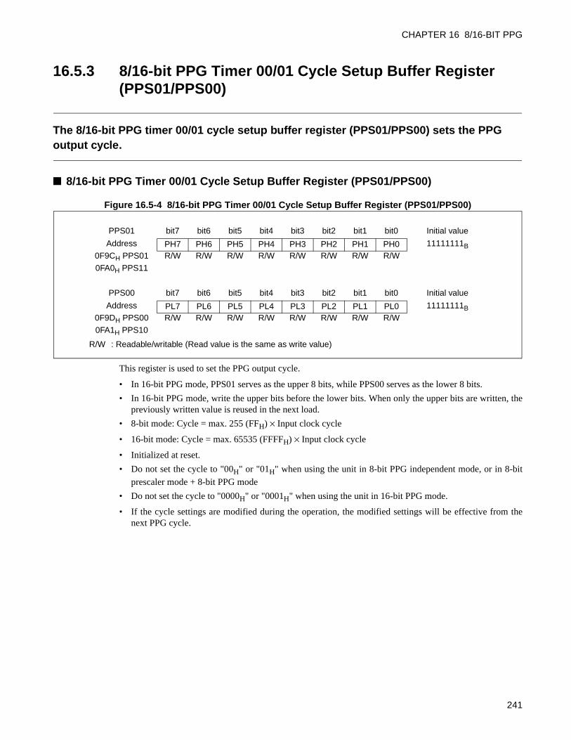
CHAPTER 16 8/16-BIT PPG
16.5.3 8/16-bit PPG Timer 00/01 Cycle Setup Buffer Register (PPS01/PPS00)
The 8/16-bit PPG timer 00/01 cycle setup buffer register (PPS01/PPS00) sets the PPG output cycle.
8/16-bit PPG Timer 00/01 Cycle Setup Buffer Register (PPS01/PPS00)
Figure 16.5-4 8/16-bit PPG Timer 00/01 Cycle Setup Buffer Register (PPS01/PPS00)
This register is used to set the PPG output cycle.
• In 16-bit PPG mode, PPS01 serves as the upper 8 bits, while PPS00 serves as the lower 8 bits.
• In 16-bit PPG mode, write the upper bits before the lower bits. When only the upper bits are written, thepreviously written value is reused in the next load.
• 8-bit mode: Cycle = max. 255 (FFH) × Input clock cycle
• 16-bit mode: Cycle = max. 65535 (FFFFH) × Input clock cycle
• Initialized at reset.
• Do not set the cycle to "00H" or "01H" when using the unit in 8-bit PPG independent mode, or in 8-bitprescaler mode + 8-bit PPG mode
• Do not set the cycle to "0000H" or "0001H" when using the unit in 16-bit PPG mode.
• If the cycle settings are modified during the operation, the modified settings will be effective from thenext PPG cycle.
PPS01 bit7 bit6 bit5 bit4 bit3 bit2 bit1 bit0 Initial value
Address PH7 PH6 PH5 PH4 PH3 PH2 PH1 PH0 11111111B
0F9CH PPS01 R/W R/W R/W R/W R/W R/W R/W R/W
0FA0H PPS11
PPS00 bit7 bit6 bit5 bit4 bit3 bit2 bit1 bit0 Initial value
Address PL7 PL6 PL5 PL4 PL3 PL2 PL1 PL0 11111111B
0F9DH PPS00 R/W R/W R/W R/W R/W R/W R/W R/W
0FA1H PPS10
R/W : Readable/writable (Read value is the same as write value)
241
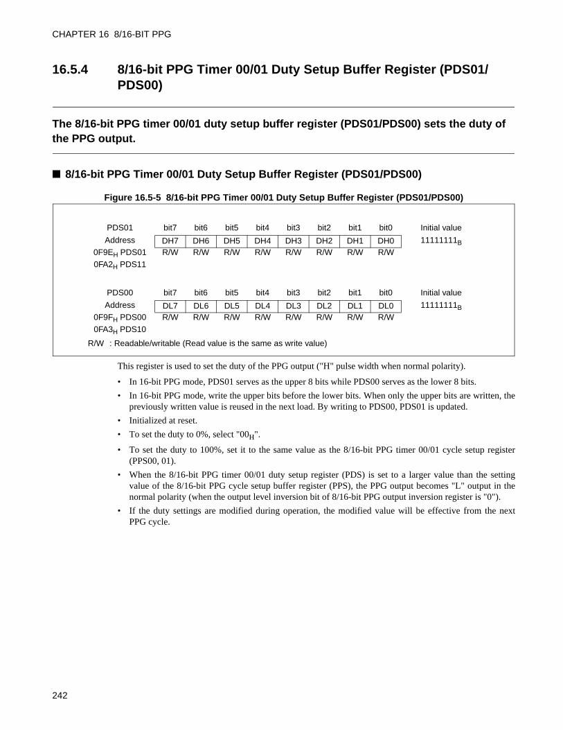
CHAPTER 16 8/16-BIT PPG
16.5.4 8/16-bit PPG Timer 00/01 Duty Setup Buffer Register (PDS01/PDS00)
The 8/16-bit PPG timer 00/01 duty setup buffer register (PDS01/PDS00) sets the duty of the PPG output.
8/16-bit PPG Timer 00/01 Duty Setup Buffer Register (PDS01/PDS00)
Figure 16.5-5 8/16-bit PPG Timer 00/01 Duty Setup Buffer Register (PDS01/PDS00)
This register is used to set the duty of the PPG output ("H" pulse width when normal polarity).
• In 16-bit PPG mode, PDS01 serves as the upper 8 bits while PDS00 serves as the lower 8 bits.
• In 16-bit PPG mode, write the upper bits before the lower bits. When only the upper bits are written, thepreviously written value is reused in the next load. By writing to PDS00, PDS01 is updated.
• Initialized at reset.
• To set the duty to 0%, select "00H".
• To set the duty to 100%, set it to the same value as the 8/16-bit PPG timer 00/01 cycle setup register(PPS00, 01).
• When the 8/16-bit PPG timer 00/01 duty setup register (PDS) is set to a larger value than the settingvalue of the 8/16-bit PPG cycle setup buffer register (PPS), the PPG output becomes "L" output in thenormal polarity (when the output level inversion bit of 8/16-bit PPG output inversion register is "0").
• If the duty settings are modified during operation, the modified value will be effective from the nextPPG cycle.
PDS01 bit7 bit6 bit5 bit4 bit3 bit2 bit1 bit0 Initial value
Address DH7 DH6 DH5 DH4 DH3 DH2 DH1 DH0 11111111B
0F9EH PDS01 R/W R/W R/W R/W R/W R/W R/W R/W
0FA2H PDS11
PDS00 bit7 bit6 bit5 bit4 bit3 bit2 bit1 bit0 Initial value
Address DL7 DL6 DL5 DL4 DL3 DL2 DL1 DL0 11111111B
0F9FH PDS00 R/W R/W R/W R/W R/W R/W R/W R/W
0FA3H PDS10
R/W : Readable/writable (Read value is the same as write value)
242
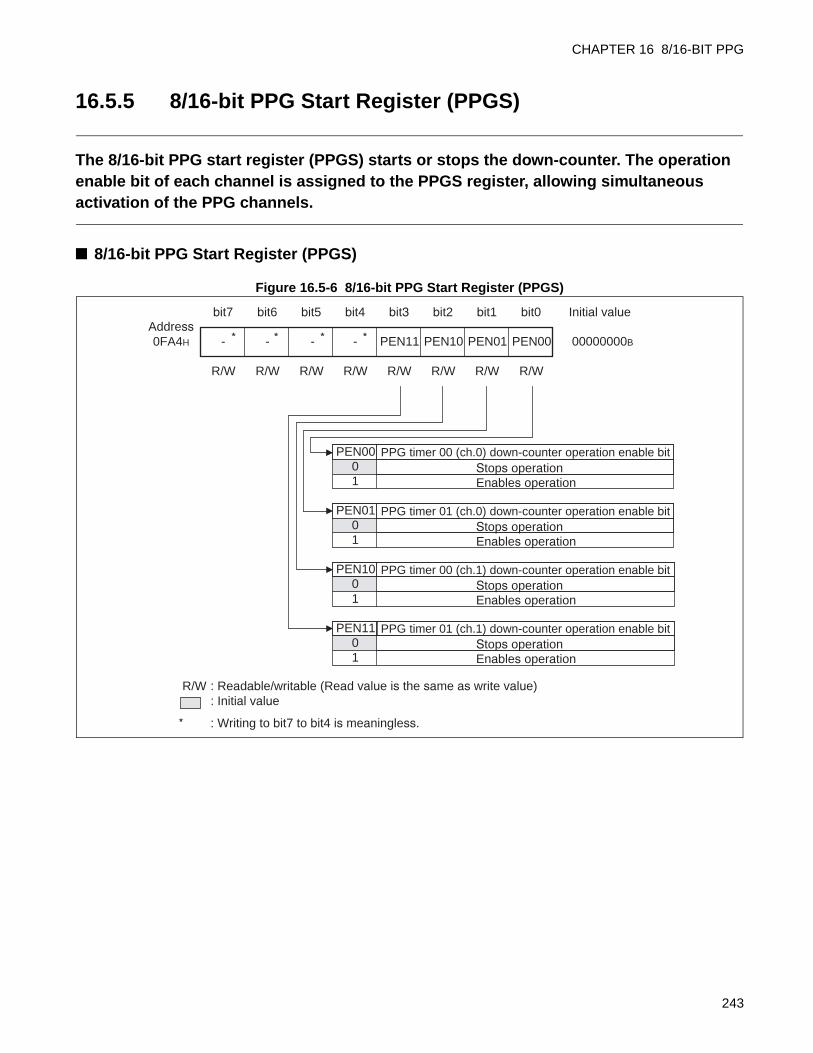
CHAPTER 16 8/16-BIT PPG
16.5.5 8/16-bit PPG Start Register (PPGS)
The 8/16-bit PPG start register (PPGS) starts or stops the down-counter. The operation enable bit of each channel is assigned to the PPGS register, allowing simultaneous activation of the PPG channels.
8/16-bit PPG Start Register (PPGS)
Figure 16.5-6 8/16-bit PPG Start Register (PPGS)
- - - - PEN11 PEN10 PEN01 PEN00 00000000B
bit7Address0FA4H
bit6 bit5 bit4 bit3 bit2 bit1 bit0 Initial value
R/W R/W R/W R/W R/W R/W R/W R/W
PPG timer 00 (ch.0) down-counter operation enable bitStops operation
PEN000
Enables operation1
PPG timer 01 (ch.0) down-counter operation enable bitStops operation
PEN010
Enables operation1
PPG timer 00 (ch.1) down-counter operation enable bitStops operation
PEN100
Enables operation1
PPG timer 01 (ch.1) down-counter operation enable bitStops operation
PEN110
Enables operation1
R/W : Readable/writable (Read value is the same as write value): Initial value
: Writing to bit7 to bit4 is meaningless.*
* * * *
243
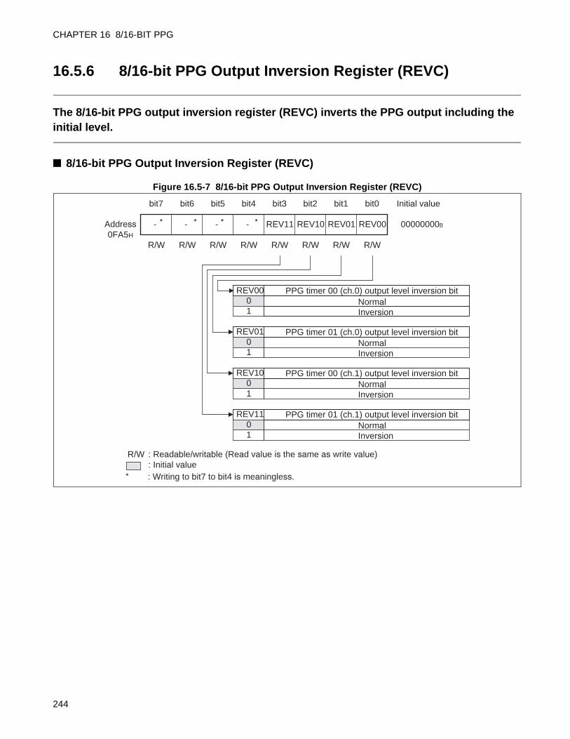
CHAPTER 16 8/16-BIT PPG
16.5.6 8/16-bit PPG Output Inversion Register (REVC)
The 8/16-bit PPG output inversion register (REVC) inverts the PPG output including the initial level.
8/16-bit PPG Output Inversion Register (REVC)
Figure 16.5-7 8/16-bit PPG Output Inversion Register (REVC)
- - - - REV11 REV10 REV01 REV00 00000000B
bit7 bit6 bit5 bit4 bit3 bit2 bit1 bit0 Initial value
R/W R/W R/W R/W R/W R/W R/W R/W
PPG timer 00 (ch.0) output level inversion bitNormal
REV000
Inversion1
PPG timer 01 (ch.0) output level inversion bitREV0101
PPG timer 00 (ch.1) output level inversion bitREV1001
PPG timer 01 (ch.1) output level inversion bitREV1101
NormalInversion
NormalInversion
NormalInversion
R/W : Readable/writable (Read value is the same as write value): Initial value
Address0FA5H
: Writing to bit7 to bit4 is meaningless.*
* * * *
244
CHAPTER 16 8/16-BIT PPG
16.6 Interrupts of 8/16-bit PPG
The 8/16-bit PPG outputs an interrupt request when a counter borrow is detected.
Interrupts of 8/16-bit PPGTable 16.6-1 shows the interrupt control bits and interrupt sources of the 8/16-bit PPG.
When a counter borrow occurs on the down-counter, the 8/16-bit PPG sets the counter borrow detection
flag bit (PUF) in the 8/16-bit PPG timer 00/01 control register (PC) to "1". When the interrupt request
enable bit is enabled (PIE = 1), an interrupt request is outputted to the interrupt controller.
In 16-bit PPG mode, the 8/16-bit PPG timer 00 control register (PC00) is available.
Registers and Vector Table Related to Interrupts of 8/16-bit PPG
ch. : channel
Refer to "APPENDIX B Table of Interrupt Causes" for the interrupt request numbers and vector tables of
all peripheral functions.
Table 16.6-1 Interrupt Control Bits and Interrupt Sources of 8/16-bit PPG
Item
Description
PPG timer 01(8-bit PPG, 8-bit prescaler)
PPG timer 00(8-bit PPG, 16-bit PPG)
Interrupt request flag bit PUF1 bit in PC1 PUF0 bit in PC0
Interrupt request enable bit PIE1 bit in PC1 PIE0 bit in PC0
Interrupt source Counter borrow of PPG cycle down-counter
Table 16.6-2 Registers and Vector Table Related to Interrupts of 8/16-bit PPG
Interrupt source
Interrupt request No.
Interrupt level setup register Vector table address
Register Setting bit Upper Lower
ch.0 (upper) IRQ12 ILR3 L12 FFE2H FFE3H
ch.0 (lower) IRQ13 ILR3 L13 FFE0H FFE1H
245
CHAPTER 16 8/16-BIT PPG
16.7 Operating Description of 8/16-bit PPG
This section describes the operations of the 8/16-bit PPG.
Setup Procedure ExampleThe setup procedure of the 8/16-bit PPG is described below.
Initial setup
1) Set the port output (DDR2, DDR6)
2) Set the interrupt revel (ILR2, ILR3)
3) Select the operating clock, enable the output and interrupt (PC01)
4) Select the operating clock, enable the output and interrupt, select the operation mode (PC00)
5) Set the cycle (PPS)
6) Set the duty (PDS)
7) Set the output inversion (REVC)
8) Start PPG (PPGs)
Interrupt processing
1) Process any interrupt
2) Clear the interrupt request flag (PC01: PUF1, PC00: PUF0)
3) Start PPG (PPGS)
246
CHAPTER 16 8/16-BIT PPG
16.7.1 8-bit PPG Independent Mode
In this mode, the unit operates as two channels (PPG timer 00 and PPG timer 01) of the 8-bit PPG.
Setting 8-bit Independent ModeThe unit requires the register settings shown in Figure 16.7-1 to operate in 8-bit independent mode.
Figure 16.7-1 8-bit Independent Mode
Operation of 8-bit PPG Independent Mode• This mode is selected when the operation mode select bits (MD1, 0) in the 8/16-bit PPG timer 00
control register (PC00) are set to "00B".
• When the corresponding bit (PEN) in the 8/16-bit PPG start register (PPGS) is set to "1", the value inthe 8/16-bit PPG cycle setup buffer register (PPS) is loaded to start down-count operation. When thecount value reaches "1", the value in the cycle setup register is reloaded to repeat the counting.
• "H" is output to the PPG output synchronizing with the count clock. When the down-counter valuematches the value in the 8/16-bit PPG timer 00/01 duty setup buffer register (PDS). After "H" which isthe value of duty setting is output, "L" is output to the PPG output.
If, however, the PPG output inversion bit is set to "1", the PPG output is set and reset inversely from the
above process.
Figure 16.7-2 shows the operation of the 8-bit PPG independent mode.
bit7 bit6 bit5 bit4 bit3 bit2 bit1 bit0
PC01 - - PIE1 PUF1 POEN1 CKS12 CKS11 CKS10
PC00 MD1 MD0 PIE0 PUF0 POEN0 CKS02 CKS01 CKS000 0
PPS01 PH7 PH6 PH5 PH4 PH3 PH2 PH1 PH0
PPS00 PL7 PL6 PL5 PL4 PL3 PL2 PL1 PL0
PDS01 DH7 DH6 DH5 DH4 DH3 DH2 DH1 DH0
PDS00 DH7 DH6 DH5 DH4 DH3 DH2 DH1 DH0
PPGS - - - - PEN11 PEN10 PEN01 PEN00* * * * * *
REVC - - - - REV11 REV10 REV01 REV00* * * * * *
: Used bit0 : Set "0"* : The bit status depends on the number of channels provided.
Set PPG output cycle for PPG timer 01
Set PPG output cycle for PPG timer 00
Set PPG output duty for PPG timer 01
Set PPG output duty for PPG timer 00
247
CHAPTER 16 8/16-BIT PPG
Figure 16.7-2 Operation of 8-bit PPG Independent Mode
Example for setting the duty to 50%
When PDS is set to "02H" with PPS set to "04H", the PPG output is set at a duty ratio of 50% (PPSsetting value /2 set to PDS).
5 4 3 2 1 5 4 3 2 1 5 4 3 2
Synchronizing with machine clock
(1)
(2) α
Down-counter value matches matches duty setting value
(Normal polarity)
PPG00 Pin
(Inversion polarity)
Counter borrow
PPG output source
m=5
n=4
Stop
(1) = n x T
(2) = m x T
T: Count clock cyclem: PPS register valuen: PDS register valueα: The value changes depending on the count clock selected and the start timing.
Count clock (Cycle T)
PEN(Counter start)
PPG timer 00 counter value
Duty setting
(PDS)
Cycle setting
(PPS)
Stop
248
CHAPTER 16 8/16-BIT PPG
16.7.2 8-bit Prescaler + 8-bit PPG Mode
In this mode, the rising and falling edge detection pulses from the PPG timer 01 output can be used as the count clock of the PPG timer 00 down-counter to allow variable-cycle 8-bit PPG output from PPG timer 00.
Setting 8-bit Prescaler + 8-bit PPG ModeThe unit requires the register settings shown in Figure 16.7-3 to operate in 8-bit prescaler + 8-bit PPG
mode.
Figure 16.7-3 Setting 8-bit Prescaler + 8-bit PPG Mode
Operation of 8-bit Prescaler + 8-bit PPG Mode• This mode is selected by setting the operation mode select bits (MD1, 0) of the 8/16-bit PPG timer 00
control register (PC00) to "01B". This allows PPG timer 01 to be used as an 8-bit prescaler and PPGtimer 00 to be used as an 8-bit PPG.
• When the PPG timer 00 (ch.1) down counter operation enable bit (PEN01) is set to "1", the 8-bitprescaler (PPG timer 01) loads the value in the 8/16-bit PPG timer 01 cycle setup buffer register(PPS01) and starts down-count operation. When the value of the down-counter matches the value in the8/16-bit PPG timer 01 duty setup buffer register (PDS01), the PPG01 output is set to "H" synchronizingwith the count clock. After "H" which is the value of duty setting is output, the PPG01 output is set to"L". If the output inversion signal (REV01) is "0", the polarity will remain the same. If it is "1", the
bit7 bit6 bit5 bit4 bit3 bit2 bit1 bit0
PC01 - - PIE1 PUF1 POEN1 CKS12 CKS11 CKS10
PC00 MD1 MD0 PIE0 PUF0 POEN0 CKS02 CKS01 CKS000 1 × × ×
PPS01 PH7 PH6 PH5 PH4 PH3 PH2 PH1 PH0
PPS00 PL7 PL6 PL5 PL4 PL3 PL2 PL1 PL0
PDS01 DH7 DH6 DH5 DH4 DH3 DH2 DH1 DH0
PDS00 DH7 DH6 DH5 DH4 DH3 DH2 DH1 DH0
PPGS - - - - PEN11 PEN10 PEN01 PEN00* * * * * *
REVC - - - - REV11 REV10 REV01 REV00* * * * * *
: Used bit0 : Set "0"1 : Set "1"× : Setting nullified* : The bit status varies depending of the number of channels implemented
Set PPG output cycle for PPG timer 01
Set PPG output cycle for PPG timer 00
Set PPG output duty for PPG timer 01
Set PPG output duty for PPG timer 00
249
CHAPTER 16 8/16-BIT PPG
polarity will be inverted and the signal will be outputted to the PPG pin.
• When the PPG operation enable bit (PEN00) is set to "1", the 8-bit PPG (PPG timer 00) loads the valuein the 8/16-bit PPG timer 00 cycle setup buffer register (PPS00) and starts down-count operation (countclock = rising and falling edge detection pulses of PPG01 output after PPG timer 01 operation isenabled). When the count value reaches "1", the value in the 8/16-bit PPG timer 00 cycle setup bufferregister is reloaded to repeat the counting. When the value of the down-counter matches the value in the8/16-bit PPG timer 00 duty setup buffer register (PDS00), the PPG00 output is set to "H" synchronizingwith the count clock. After "H" which is the value of duty setting is output, the PPG00 output is reset to"L". If the output inversion signal (REV00) is "0", the polarity will remain the same. If it is "1", thepolarity will be inverted and the signal will be outputted to the PPG00 pin.
• Set that the duty of the 8-bit prescaler (PPG timer 01) output to 50%.
• When PPG timer 00 is started with the 8-bit prescaler (PPG timer 01) being stopped, PPG timer 00 doesnot count.
• When the duty of the 8-bit prescaler (PPG timer 01) is set to 0% or 100%, PPG timer 00 does notperform counting as the 8-bit prescaler (PPG timer 01) output does not toggle.
Figure 16.7-4 shows the operation of 8-bit prescaler + 8-bit PPG mode.
Figure 16.7-4 Operation of 8-bit Prescaler + 8-bit PPG Mode
m1=4
n1=2
4 3 2 1 4 3 2 1 4 3 2 1 4 3 2
(1) = n1 x T (2) = m1 x T
Synchronizing with machine clock
Synchronizing with machine clock
(1)
(2) α
Count clock(Cycle T)
PEN01
PPG timer 01 counter value
Down-counter value matches matches duty setting value
Duty setting(PDS01)
Cycle setting(PPS01)
(Normal polarity)PPG01
PEN00
3 PPG timer 00 counter value
m0=3
n0=2 Duty setting
(PDS00)
Cycle setting(PPS00)
2 1 3 2 1
(Normal polarity)PPG00
(Inversion polarity)
(Inversion polarity)
3
1 4
2
(3)
β (4)
(3) = (1) x n0 (4) = (1) x m0
Down-counter value matches matches duty setting value
Counter borrow
PPG output source
Counter borrow
PPG output source
T: Count clock cyclem0: PPS00 register valuen0: PDS00 register valuem1: PPS01 register valuen1: PDS01 register value
α: The value changes depending on the count clock selected and the PEN01 start timing.β: The value changes depending on the PPG01 output (ch.1) waveform and the PEN00 start timing.
250
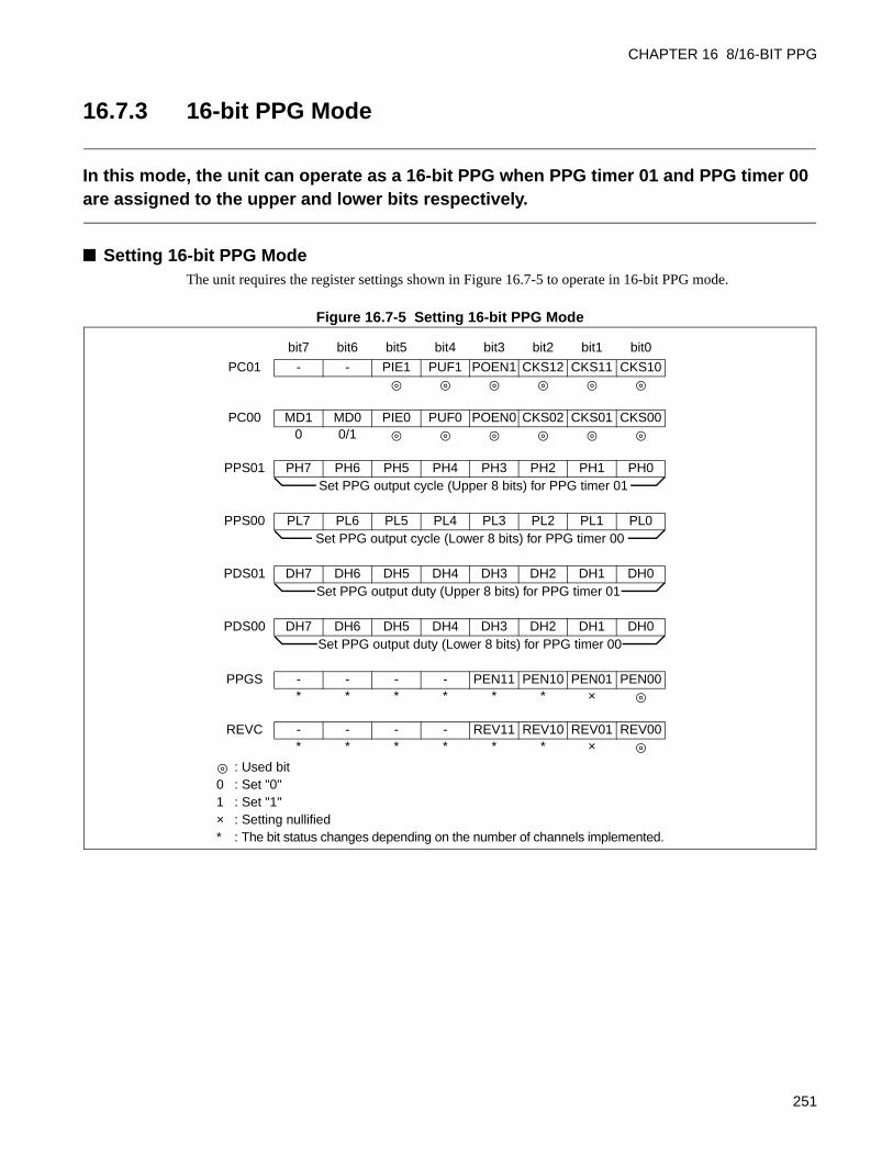
CHAPTER 16 8/16-BIT PPG
16.7.3 16-bit PPG Mode
In this mode, the unit can operate as a 16-bit PPG when PPG timer 01 and PPG timer 00 are assigned to the upper and lower bits respectively.
Setting 16-bit PPG ModeThe unit requires the register settings shown in Figure 16.7-5 to operate in 16-bit PPG mode.
Figure 16.7-5 Setting 16-bit PPG Mode
bit7 bit6 bit5 bit4 bit3 bit2 bit1 bit0
PC01 - - PIE1 PUF1 POEN1 CKS12 CKS11 CKS10
PC00 MD1 MD0 PIE0 PUF0 POEN0 CKS02 CKS01 CKS000 0/1
PPS01 PH7 PH6 PH5 PH4 PH3 PH2 PH1 PH0
PPS00 PL7 PL6 PL5 PL4 PL3 PL2 PL1 PL0
PDS01 DH7 DH6 DH5 DH4 DH3 DH2 DH1 DH0
PDS00 DH7 DH6 DH5 DH4 DH3 DH2 DH1 DH0
PPGS - - - - PEN11 PEN10 PEN01 PEN00* * * * * * ×
REVC - - - - REV11 REV10 REV01 REV00* * * * * * ×
: Used bit0 : Set "0"1 : Set "1"× : Setting nullified* : The bit status changes depending on the number of channels implemented.
Set PPG output cycle (Upper 8 bits) for PPG timer 01
Set PPG output cycle (Lower 8 bits) for PPG timer 00
Set PPG output duty (Upper 8 bits) for PPG timer 01
Set PPG output duty (Lower 8 bits) for PPG timer 00
251
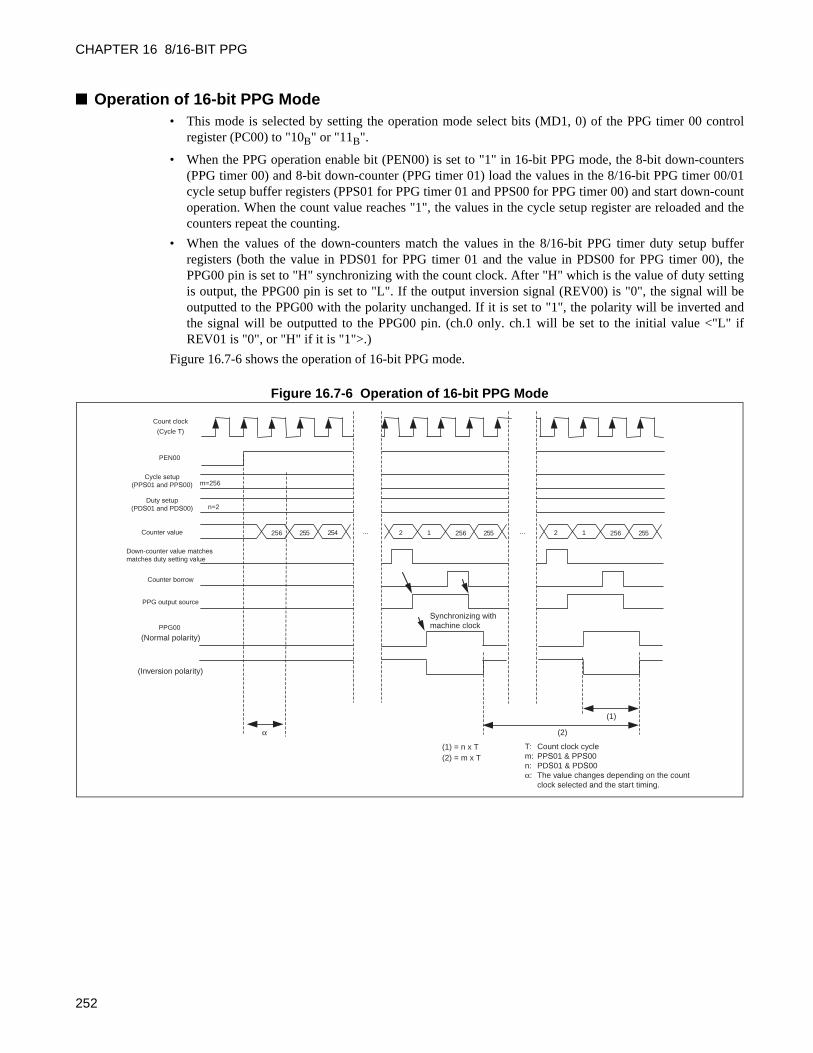
CHAPTER 16 8/16-BIT PPG
Operation of 16-bit PPG Mode• This mode is selected by setting the operation mode select bits (MD1, 0) of the PPG timer 00 control
register (PC00) to "10B" or "11B".
• When the PPG operation enable bit (PEN00) is set to "1" in 16-bit PPG mode, the 8-bit down-counters(PPG timer 00) and 8-bit down-counter (PPG timer 01) load the values in the 8/16-bit PPG timer 00/01cycle setup buffer registers (PPS01 for PPG timer 01 and PPS00 for PPG timer 00) and start down-countoperation. When the count value reaches "1", the values in the cycle setup register are reloaded and thecounters repeat the counting.
• When the values of the down-counters match the values in the 8/16-bit PPG timer duty setup bufferregisters (both the value in PDS01 for PPG timer 01 and the value in PDS00 for PPG timer 00), thePPG00 pin is set to "H" synchronizing with the count clock. After "H" which is the value of duty settingis output, the PPG00 pin is set to "L". If the output inversion signal (REV00) is "0", the signal will beoutputted to the PPG00 with the polarity unchanged. If it is set to "1", the polarity will be inverted andthe signal will be outputted to the PPG00 pin. (ch.0 only. ch.1 will be set to the initial value <"L" ifREV01 is "0", or "H" if it is "1">.)
Figure 16.7-6 shows the operation of 16-bit PPG mode.
Figure 16.7-6 Operation of 16-bit PPG Mode
Count clock
(Cycle T)
256 255 254 ... 2 1
PEN00
Cycle setup(PPS01 and PPS00)
Duty setup(PDS01 and PDS00)
Counter value 256 255
m=256
n=2
... 2 1 256 255
(Normal polarity)PPG00
(Inversion polarity)
(1)
(2) = m x T (1) = n x T
α (2)
Synchronizing with machine clock
Down-counter value matches matches duty setting value
Counter borrow
PPG output source
T: Count clock cyclem: PPS01 & PPS00n: PDS01 & PDS00α: The value changes depending on the count clock selected and the start timing.
252
CHAPTER 16 8/16-BIT PPG
16.8 Precautions when Using 8/16-bit PPG
The following precautions must be followed when using the 8/16-bit PPG.
Precautions when Using 8/16-bit PPG
Operational precaution
Depending on the timing between the activation of PPG and count clock, an error may occur in the first
cycle of the PPG output immediately after the activation. The error varies depending on the count clock
selected. The output, however, is performed properly in the succeeding cycles.
Precaution regarding interrupts
A PPG interrupt is generated when the interrupt enable bit (PIE1/PIE0) is set to "1" and the interrupt
request flag bit (PUF1/PUF0) in the 8/16-bit PPG timer 01/00 control register (PC01/PC00) is also set to
"1". Always clear the interrupt request flag bit (PUF1/PUF0) to "0" in the interrupt routine.
253
CHAPTER 16 8/16-BIT PPG
16.9 Sample Programs for 8/16-bit PPG Timer
We provide sample programs that can be used to operate the 8/16-bit PPG timer.
Sample Programs for 8/16-bit PPG TimerFor information about the sample programs for the 8/16-bit PPG timer, refer to " Sample Programs" in
Preface.
Setup Methods without Sample Program
How to enable/stop PPG operation
The PPG operation enable bit (PPGS:PEN00 or PEN01) is used for PPG00.
PPG operation must be enabled before the PPG is activated.
The PPG operation enable bit (PPGS:PEN00 or PEN01) is used for PPG01.
PPG operation must be enabled before the PPG is activated.
How to set the PPG operation mode
The operation mode select bits (PC0:MD[1:0]) are used.
How to select the operating clock
ch.1 is selected by the operating clock select bits (PC1:CKS12/CKS11/CKS10).
ch.0 is selected by the operating clock select bits (PC0:CKS02/CKS01/CKS00).
How to enable/disable the PPG output pin
The output enable bit (PC0 or PC1:POEN0 or POEN1) is used.
Control PPG operation enable bit (PEN00 or PEN01)
When stopping PPG operation Set the bit to "0"
When enabling PPG operation Set the bit to "1"
Control PPG operation enable bit (PEN00 or PEN01)
When stopping PPG operation Set the bit to "0"
When enabling PPG operation Set the bit to "1"
Control Output enable bit (POEN0 or POEN1)
When enabling PPG output Set the bit to "1"
When disabling PPG output Set the bit to "0"
254
CHAPTER 16 8/16-BIT PPG
How to invert the PPG output
The output level inversion bit (REVC:REV00 or REV10) is used for PPG00.
The output level inversion bit (REVC:REV01 or REV11) is used for PPG01.
Interrupt-related register
The interrupt level is set by the interrupt setup register shown in the following table.
How to enable/disable/clear interrupts
Interrupt request enable flag, Interrupt request flag
The interrupt request enable bit (PC00:PIE0 or PC01:PIE1) is used to enable or disable interrupts.
The interrupt request flag (PC00:PUF0 or PC01:PUF1) is used to clear interrupt requests.
Control Output level inversion bit (REV00 or REV10)
When inverting PPG output Set the bit to "1"
Control Output level inversion bit (REV01 or REV11)
When inverting PPG output Set the bit to "1"
Interrupt source Interrupt level setup register Interrupt vector
ch.1 (lower)Interrupt level register (ILR2)
Address:0007BH
#09Address:0FFE8H
ch.1 (upper)Interrupt level register (ILR2)
Address:0007BH
#10Address:0FFE6H
ch.0 (lower)Interrupt level register (ILR3)
Address:0007CH
#12Address:0FFE2H
ch.0 (upper)Interrupt level register (ILR3)
Address:0007CH
#13Address:0FFE0H
What to be controlled Interrupt request enable bit (PIE0 or PIE1)
When disabling interrupt requests Set the bit to "0"
When enabling interrupt requests Set the bit to "1"
What to be controlled Interrupt request flag (PUF0 or PUF1)
When clearing interrupt requests Write "0"
255

CHAPTER 16 8/16-BIT PPG
256
CHAPTER 1716-BIT PPG TIMER
This chapter describes the functions and operations of the 16-bit PPG timer.
17.1 Overview of 16-bit PPG Timer
17.2 Configuration of 16-bit PPG Timer
17.3 Channels of 16-bit PPG Timer
17.4 Pins of 16-bit PPG Timer
17.5 Registers of 16-bit PPG Timer
17.6 Interrupts of 16-bit PPG Timer
17.7 Explanation of 16-bit PPG Timer Operations and Setup Procedure Example
17.8 Precautions when Using 16-bit PPG Timer
17.9 Sample Programs for 16-bit PPG Timer
257
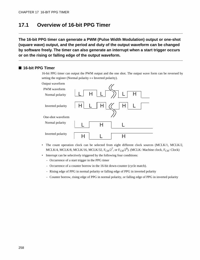
CHAPTER 17 16-BIT PPG TIMER
17.1 Overview of 16-bit PPG Timer
The 16-bit PPG timer can generate a PWM (Pulse Width Modulation) output or one-shot (square wave) output, and the period and duty of the output waveform can be changed by software freely. The timer can also generate an interrupt when a start trigger occurs or on the rising or falling edge of the output waveform.
16-bit PPG Timer16-bit PPG timer can output the PWM output and the one shot. The output wave form can be reversed by
setting the register (Normal polarity ↔ Inverted polarity).
Output waveform
PWM waveform
Normal polarity
Inverted polarity
One-shot waveform
Normal polarity
Inverted polarity
• The count operation clock can be selected from eight different clock sources (MCLK/1, MCLK/2,
MCLK/4, MCLK/8, MCLK/16, MCLK/32, FCH/27, or FCH/28). (MCLK: Machine clock, FCH: Clock)
• Interrupt can be selectively triggered by the following four conditions:
- Occurrence of a start trigger in the PPG timer
- Occurrence of a counter borrow in the 16-bit down-counter (cycle match).
- Rising edge of PPG in normal polarity or falling edge of PPG in inverted polarity
- Counter borrow, rising edge of PPG in normal polarity, or falling edge of PPG in inverted polarity
L
L LH HL
H HL LH
LH
H HL
258
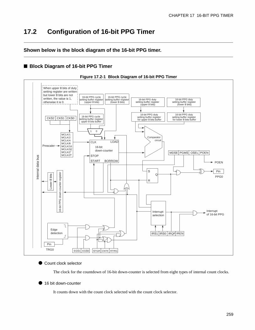
CHAPTER 17 16-BIT PPG TIMER
17.2 Configuration of 16-bit PPG Timer
Shown below is the block diagram of the 16-bit PPG timer.
Block Diagram of 16-bit PPG Timer
Figure 17.2-1 Block Diagram of 16-bit PPG Timer
Count clock selector
The clock for the countdown of 16-bit down-counter is selected from eight types of internal count clocks.
16 bit down-counter
It counts down with the count clock selected with the count clock selector.
MCLK/1MCLK/2MCLK/4MCLK/8MCLK/16MCLK/32MCLK/2
CLK LOAD
START BORROW
16-bit down-counter
SQ
R
Interrupt selection
Prescaler
MDSE PGMS OSEL POEN
Pin
Interrupt of 16-bit PPG
IRS1 IRS0 IRQF IREN
16-b
it P
PG
dow
n-co
unte
r re
gist
er
CKS2 CKS1 CKS0
Inte
rnal
dat
a bu
s MCLK/2 STOP
Edge detection
STGR CNTE RTRG
POEN
7
8
1 0
16-bit PPG cycle setting buffer register
(upper 8 bits)
16-bit PPG cycle setting buffer register
(lower 8 bits)
16-bit PPG cycle setting buffer register
upper 8 bits buffer
16-bit PPG duty setting buffer register
(lower 8 bits)
16-bit PPG duty setting buffer register
(upper 8 bits)
16-bit PPG duty setting buffer register for lower 8 bits buffer
16-bit PPG duty setting buffer register for upper 8 bits buffer
PPG0
When upper 8 bits of duty setting register are written but lower 8 bits are not written, the value is 1, otherwise it is 0.
EGS1 EGS0
Low
er 8
bits
Comparator circuit
Pin
TRG0
259
CHAPTER 17 16-BIT PPG TIMER
Comparator circuit
The output is kept "H" until the value of 16-bit down-counter is corresponding to the value of 8/16-bit PPG
duty setting buffer register from the value of 16-bit PPG cycle setting buffer register.
Afterwards, after keep "L" the output until the counter value is corresponding to "1", it keeps counting 8-bit
down counter from the value of 16-bit PPG cycle setting buffer register.
16-bit PPG down-counter register (PDCRH, PDCRL)
The value of 16-bit down-counter of 16-bit PPG timer is read.
16-bit PPG cycle setting buffer register (PCSRH, PCSRL)
The compare value for the cycle of 16-bit PPG timer is set.
16-bit PPG duty setting buffer register (PDUTH, PDUTL)
The compare value for "H" width of 16-bit PPG timer is set.
16-bit PPG status control register (PCNTH, PCNTL)
The operation mode and the operation condition of 16-bit PPG timer are set.
Input ClockThe 16-bit PPG timer uses the output clock from the prescaler as its input clock (count clock).
260
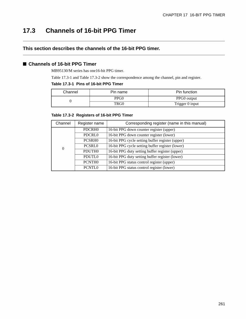
CHAPTER 17 16-BIT PPG TIMER
17.3 Channels of 16-bit PPG Timer
This section describes the channels of the 16-bit PPG timer.
Channels of 16-bit PPG TimerMB95130/M series has one16-bit PPG timer.
Table 17.3-1 and Table 17.3-2 show the correspondence among the channel, pin and register.
Table 17.3-1 Pins of 16-bit PPG Timer
Channel Pin name Pin function
0PPG0 PPG0 outputTRG0 Trigger 0 input
Table 17.3-2 Registers of 16-bit PPG Timer
Channel Register name Corresponding register (name in this manual)
0
PDCRH0 16-bit PPG down counter register (upper)PDCRL0 16-bit PPG down counter register (lower)PCSRH0 16-bit PPG cycle setting buffer register (upper)PCSRL0 16-bit PPG cycle setting buffer register (lower)PDUTH0 16-bit PPG duty setting buffer register (upper)PDUTL0 16-bit PPG duty setting buffer register (lower)PCNTH0 16-bit PPG status control register (upper)PCNTL0 16-bit PPG status control register (lower)
261
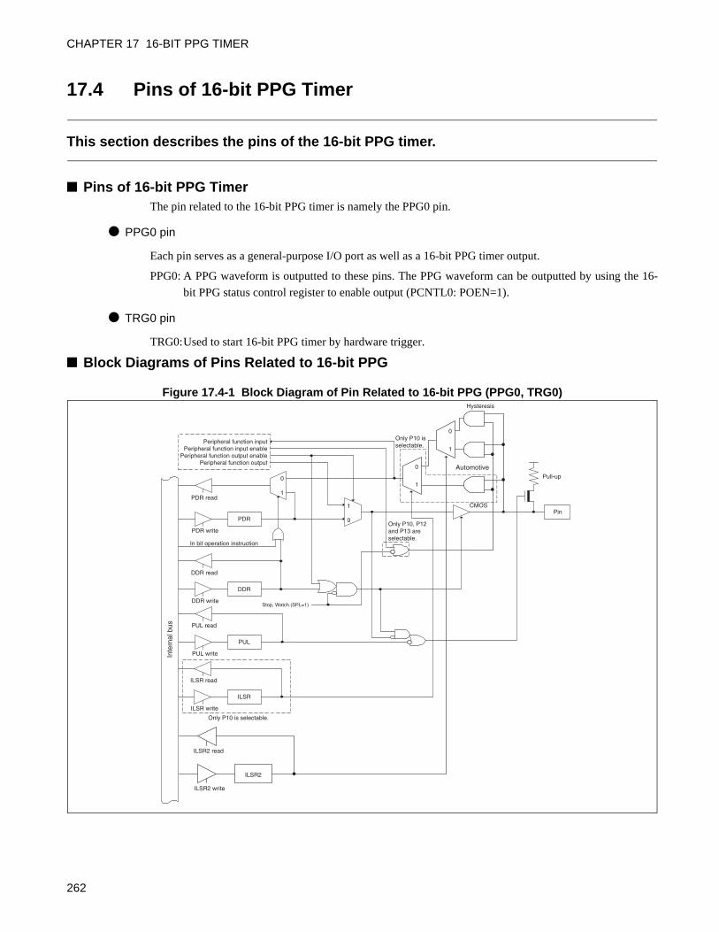
CHAPTER 17 16-BIT PPG TIMER
17.4 Pins of 16-bit PPG Timer
This section describes the pins of the 16-bit PPG timer.
Pins of 16-bit PPG TimerThe pin related to the 16-bit PPG timer is namely the PPG0 pin.
PPG0 pin
Each pin serves as a general-purpose I/O port as well as a 16-bit PPG timer output.
PPG0: A PPG waveform is outputted to these pins. The PPG waveform can be outputted by using the 16-
bit PPG status control register to enable output (PCNTL0: POEN=1).
TRG0 pin
TRG0:Used to start 16-bit PPG timer by hardware trigger.
Block Diagrams of Pins Related to 16-bit PPG
Figure 17.4-1 Block Diagram of Pin Related to 16-bit PPG (PPG0, TRG0)
PDR read
PDR write
PDR
DDR read
DDR write
DDR
PUL read
PUL write
PUL
1
0
Peripheral function outputPeripheral function output enable
Peripheral function input enablePeripheral function input
Pin
Stop, Watch (SPL=1)
Inte
rnal
bus
In bit operation instruction
Pull-up
ILSR read
ILSR write
ILSR
Hysteresis
CMOS
Only P10 is selectable.
Only P10 is selectable.
Only P10, P12 and P13 are selectable.
Automotive
0
1
ILSR2 read
ILSR2 write
ILSR2
0
1
0
1
262
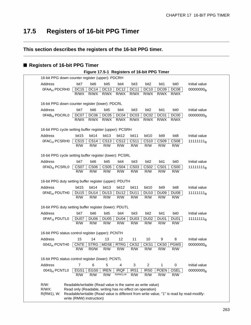
CHAPTER 17 16-BIT PPG TIMER
17.5 Registers of 16-bit PPG Timer
This section describes the registers of the 16-bit PPG timer.
Registers of 16-bit PPG TimerFigure 17.5-1 Registers of 16-bit PPG Timer
16-bit PPG down counter register (upper): PDCRH
Address bit7 bit6 bit5 bit4 bit3 bit2 bit1 bit0 Initial value
0FAAH PDCRH0 DC15 DC14 DC13 DC12 DC11 DC10 DC09 DC08 00000000BR/WX R/WX R/WX R/WX R/WX R/WX R/WX R/WX
16-bit PPG down counter register (lower): PDCRL
Address bit7 bit6 bit5 bit4 bit3 bit2 bit1 bit0 Initial value
0FABH PDCRL0 DC07 DC06 DC05 DC04 DC03 DC02 DC01 DC00 00000000BR/WX R/WX R/WX R/WX R/WX R/WX R/WX R/WX
16-bit PPG cycle setting buffer register (upper): PCSRH
Address bit15 bit14 bit13 bit12 bit11 bit10 bit9 bit8 Initial value
0FACH PCSRH0 CS15 CS14 CS13 CS12 CS11 CS10 CS09 CS08 11111111BR/W R/W R/W R/W R/W R/W R/W R/W
16-bit PPG cycle setting buffer register (lower): PCSRL
Address bit7 bit6 bit5 bit4 bit3 bit2 bit1 bit0 Initial value
0FADH PCSRL0 CS07 CS06 CS05 CS04 CS03 CS02 CS01 CS00 11111111BR/W R/W R/W R/W R/W R/W R/W R/W
16-bit PPG duty setting buffer register (upper): PDUTH
Address bit15 bit14 bit13 bit12 bit11 bit10 bit9 bit8 Initial value
0FAEH PDUTH0 DU15 DU14 DU13 DU12 DU11 DU10 DU09 DU08 11111111BR/W R/W R/W R/W R/W R/W R/W R/W
16-bit PPG duty setting buffer register (lower): PDUTL
Address bit7 bit6 bit5 bit4 bit3 bit2 bit1 bit0 Initial value
0FAFH PDUTL0 DU07 DU06 DU05 DU04 DU03 DU02 DU01 DU01 11111111BR/W R/W R/W R/W R/W R/W R/W R/W
16-bit PPG status control register (upper): PCNTH
Address 15 14 13 12 11 10 9 8 Initial value
0042H PCNTH0 CNTE STRG MDSE RTRG CKS2 CKS1 CKS0 PGMS 00000000BR/W R0/W R/W R/W R/W R/W R/W R/W
16-bit PPG status control register (lower): PCNTL
Address 7 6 5 4 3 2 1 0 Initial value
0043H PCNTL0 EGS1 EGS0 IREN IRQF IRS1 IRS0 POEN OSEL 00000000BR/W R/W R/W R(RM1),W R/W R/W R/W R/W
R/W: Readable/writable (Read value is the same as write value)R/WX: Read only (Readable, writing has no effect on operation)R(RM1), W: Readable/writable (Read value is different from write value, "1" is read by read-modify-
write (RMW) instruction)
263
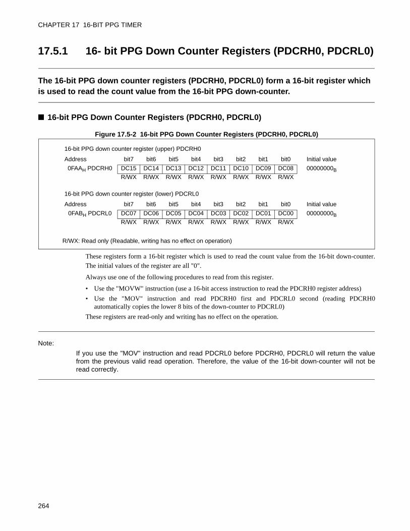
CHAPTER 17 16-BIT PPG TIMER
17.5.1 16- bit PPG Down Counter Registers (PDCRH0, PDCRL0)
The 16-bit PPG down counter registers (PDCRH0, PDCRL0) form a 16-bit register which is used to read the count value from the 16-bit PPG down-counter.
16-bit PPG Down Counter Registers (PDCRH0, PDCRL0)
Figure 17.5-2 16-bit PPG Down Counter Registers (PDCRH0, PDCRL0)
These registers form a 16-bit register which is used to read the count value from the 16-bit down-counter.
The initial values of the register are all "0".
Always use one of the following procedures to read from this register.
• Use the "MOVW" instruction (use a 16-bit access instruction to read the PDCRH0 register address)
• Use the "MOV" instruction and read PDCRH0 first and PDCRL0 second (reading PDCRH0automatically copies the lower 8 bits of the down-counter to PDCRL0)
These registers are read-only and writing has no effect on the operation.
Note:
If you use the "MOV" instruction and read PDCRL0 before PDCRH0, PDCRL0 will return the valuefrom the previous valid read operation. Therefore, the value of the 16-bit down-counter will not beread correctly.
R/WX: Read only (Readable, writing has no effect on operation)
16-bit PPG down counter register (upper) PDCRH0
Address bit7 bit6 bit5 bit4 bit3 bit2 bit1 bit0 Initial value
0FAAH PDCRH0 DC15 DC14 DC13 DC12 DC11 DC10 DC09 DC08 00000000B
R/WX R/WX R/WX R/WX R/WX R/WX R/WX R/WX
16-bit PPG down counter register (lower) PDCRL0
Address bit7 bit6 bit5 bit4 bit3 bit2 bit1 bit0 Initial value
0FABH PDCRL0 DC07 DC06 DC05 DC04 DC03 DC02 DC01 DC00 00000000B
R/WX R/WX R/WX R/WX R/WX R/WX R/WX R/WX
264
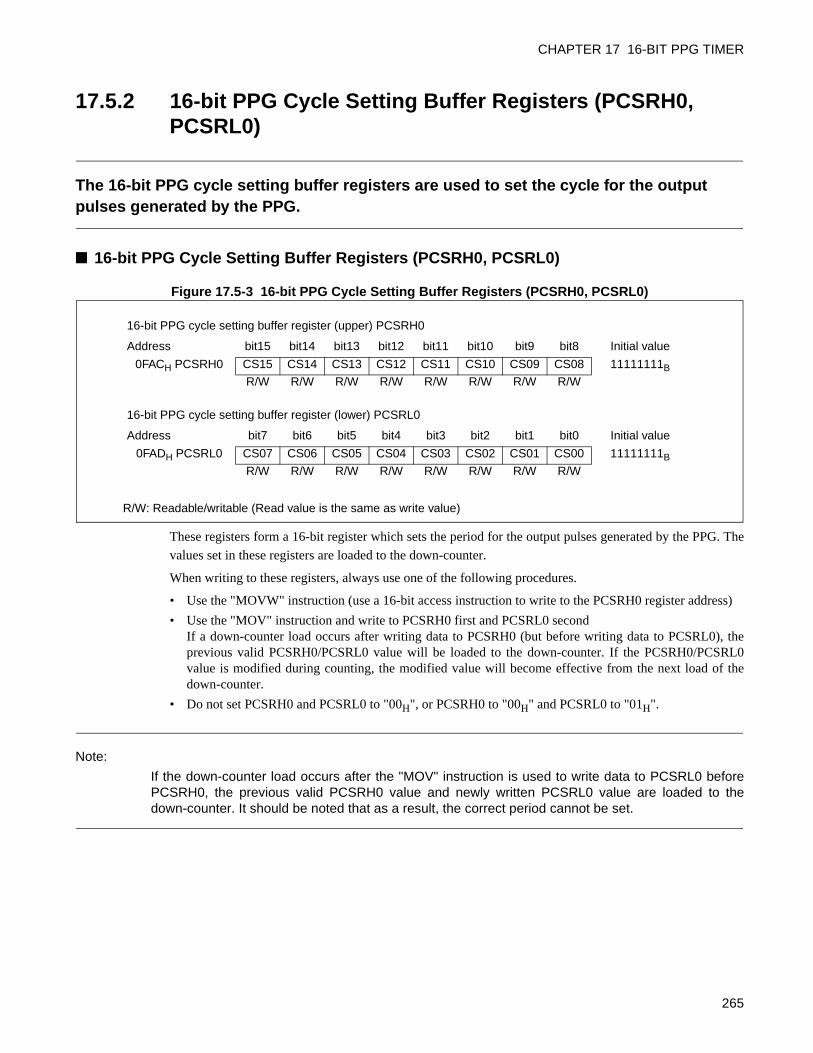
CHAPTER 17 16-BIT PPG TIMER
17.5.2 16-bit PPG Cycle Setting Buffer Registers (PCSRH0, PCSRL0)
The 16-bit PPG cycle setting buffer registers are used to set the cycle for the output pulses generated by the PPG.
16-bit PPG Cycle Setting Buffer Registers (PCSRH0, PCSRL0)
Figure 17.5-3 16-bit PPG Cycle Setting Buffer Registers (PCSRH0, PCSRL0)
These registers form a 16-bit register which sets the period for the output pulses generated by the PPG. The
values set in these registers are loaded to the down-counter.
When writing to these registers, always use one of the following procedures.
• Use the "MOVW" instruction (use a 16-bit access instruction to write to the PCSRH0 register address)
• Use the "MOV" instruction and write to PCSRH0 first and PCSRL0 secondIf a down-counter load occurs after writing data to PCSRH0 (but before writing data to PCSRL0), theprevious valid PCSRH0/PCSRL0 value will be loaded to the down-counter. If the PCSRH0/PCSRL0value is modified during counting, the modified value will become effective from the next load of thedown-counter.
• Do not set PCSRH0 and PCSRL0 to "00H", or PCSRH0 to "00H" and PCSRL0 to "01H".
Note:
If the down-counter load occurs after the "MOV" instruction is used to write data to PCSRL0 beforePCSRH0, the previous valid PCSRH0 value and newly written PCSRL0 value are loaded to thedown-counter. It should be noted that as a result, the correct period cannot be set.
R/W: Readable/writable (Read value is the same as write value)
16-bit PPG cycle setting buffer register (upper) PCSRH0
Address bit15 bit14 bit13 bit12 bit11 bit10 bit9 bit8 Initial value
0FACH PCSRH0 CS15 CS14 CS13 CS12 CS11 CS10 CS09 CS08 11111111B
R/W R/W R/W R/W R/W R/W R/W R/W
16-bit PPG cycle setting buffer register (lower) PCSRL0
Address bit7 bit6 bit5 bit4 bit3 bit2 bit1 bit0 Initial value
0FADH PCSRL0 CS07 CS06 CS05 CS04 CS03 CS02 CS01 CS00 11111111B
R/W R/W R/W R/W R/W R/W R/W R/W
265
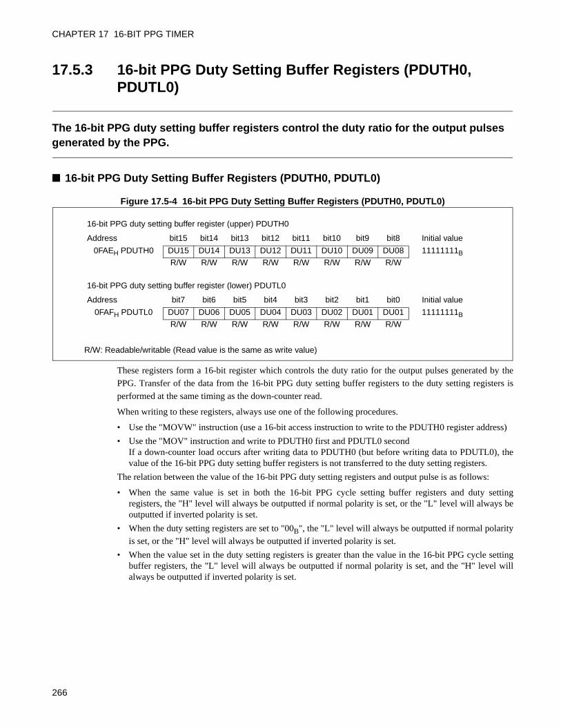
CHAPTER 17 16-BIT PPG TIMER
17.5.3 16-bit PPG Duty Setting Buffer Registers (PDUTH0, PDUTL0)
The 16-bit PPG duty setting buffer registers control the duty ratio for the output pulses generated by the PPG.
16-bit PPG Duty Setting Buffer Registers (PDUTH0, PDUTL0)
Figure 17.5-4 16-bit PPG Duty Setting Buffer Registers (PDUTH0, PDUTL0)
These registers form a 16-bit register which controls the duty ratio for the output pulses generated by the
PPG. Transfer of the data from the 16-bit PPG duty setting buffer registers to the duty setting registers is
performed at the same timing as the down-counter read.
When writing to these registers, always use one of the following procedures.
• Use the "MOVW" instruction (use a 16-bit access instruction to write to the PDUTH0 register address)
• Use the "MOV" instruction and write to PDUTH0 first and PDUTL0 secondIf a down-counter load occurs after writing data to PDUTH0 (but before writing data to PDUTL0), thevalue of the 16-bit PPG duty setting buffer registers is not transferred to the duty setting registers.
The relation between the value of the 16-bit PPG duty setting registers and output pulse is as follows:
• When the same value is set in both the 16-bit PPG cycle setting buffer registers and duty settingregisters, the "H" level will always be outputted if normal polarity is set, or the "L" level will always beoutputted if inverted polarity is set.
• When the duty setting registers are set to "00B", the "L" level will always be outputted if normal polarityis set, or the "H" level will always be outputted if inverted polarity is set.
• When the value set in the duty setting registers is greater than the value in the 16-bit PPG cycle settingbuffer registers, the "L" level will always be outputted if normal polarity is set, and the "H" level willalways be outputted if inverted polarity is set.
R/W: Readable/writable (Read value is the same as write value)
16-bit PPG duty setting buffer register (upper) PDUTH0
Address bit15 bit14 bit13 bit12 bit11 bit10 bit9 bit8 Initial value
0FAEH PDUTH0 DU15 DU14 DU13 DU12 DU11 DU10 DU09 DU08 11111111B
R/W R/W R/W R/W R/W R/W R/W R/W
16-bit PPG duty setting buffer register (lower) PDUTL0
Address bit7 bit6 bit5 bit4 bit3 bit2 bit1 bit0 Initial value
0FAFH PDUTL0 DU07 DU06 DU05 DU04 DU03 DU02 DU01 DU01 11111111B
R/W R/W R/W R/W R/W R/W R/W R/W
266
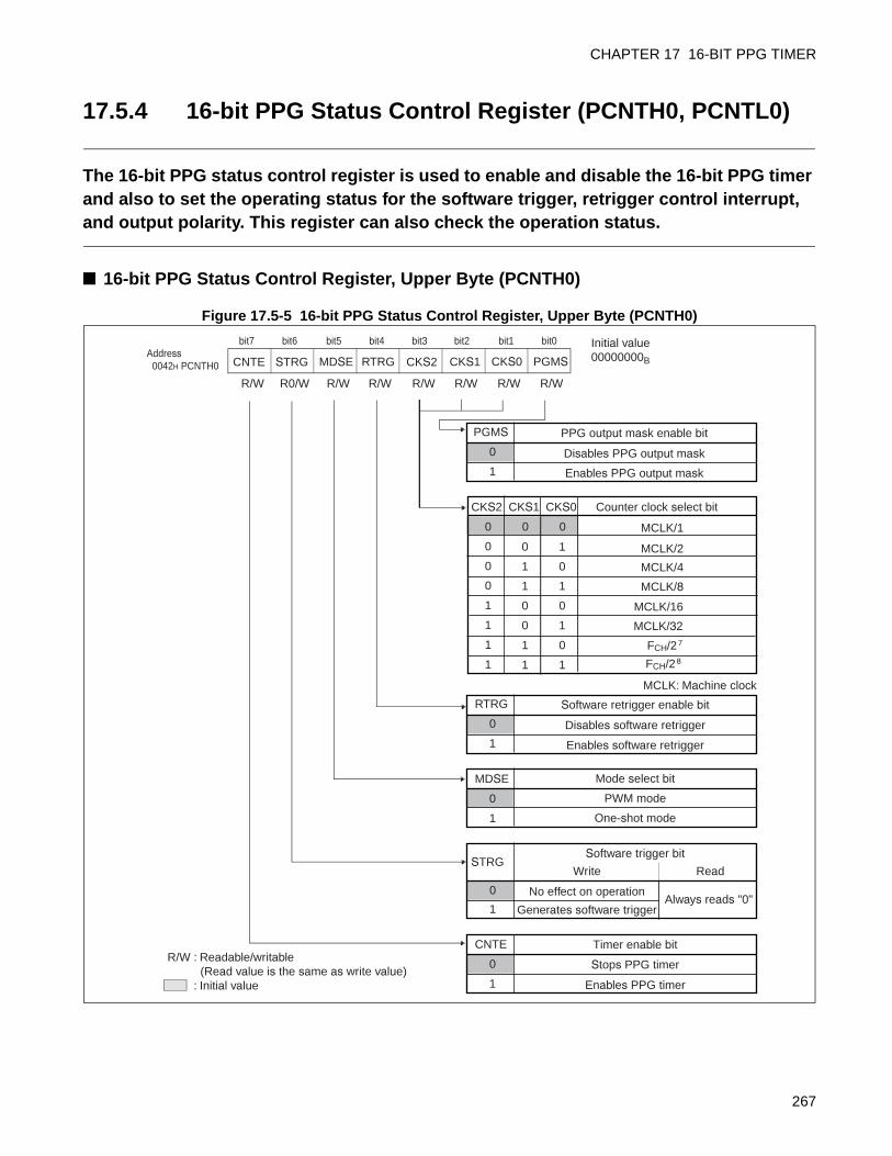
CHAPTER 17 16-BIT PPG TIMER
17.5.4 16-bit PPG Status Control Register (PCNTH0, PCNTL0)
The 16-bit PPG status control register is used to enable and disable the 16-bit PPG timer and also to set the operating status for the software trigger, retrigger control interrupt, and output polarity. This register can also check the operation status.
16-bit PPG Status Control Register, Upper Byte (PCNTH0)
Figure 17.5-5 16-bit PPG Status Control Register, Upper Byte (PCNTH0)
PGMS PPG output mask enable bit
Disables PPG output mask
Enables PPG output mask
0
1
CKS2 CKS1 CKS0
0 0 0 MCLK/1
MCLK/2
MCLK/4
MCLK/8
MCLK/16
MCLK/32
FCH/27
0 0 1
0 1 0
0 1 1
1 0 0
1 0 1
1 1 0
1 1 1
RTRG
0
1
MDSE
0 PWM mode
Mode select bit
1
STRGSoftware trigger bit
No effect on operation
Generates software trigger
Write Read
0Always reads "0"
1
CNTE
0
1
R/W : Readable/writable (Read value is the same as write value) : Initial value
Counter clock select bit
MCLK: Machine clock
Software retrigger enable bit
Disables software retrigger
Enables software retrigger
One-shot mode
Timer enable bit
Stops PPG timer
Enables PPG timer
bit7Address
0042H PCNTH0
bit6 bit5 bit4 bit3 bit2 bit1 bit0
R/W R0/W R/W R/W R/W R/W R/WR/W
CNTE STRG MDSE RTRG CKS1 CKS0 PGMS
Initial value00000000BCKS2
FCH/28
267
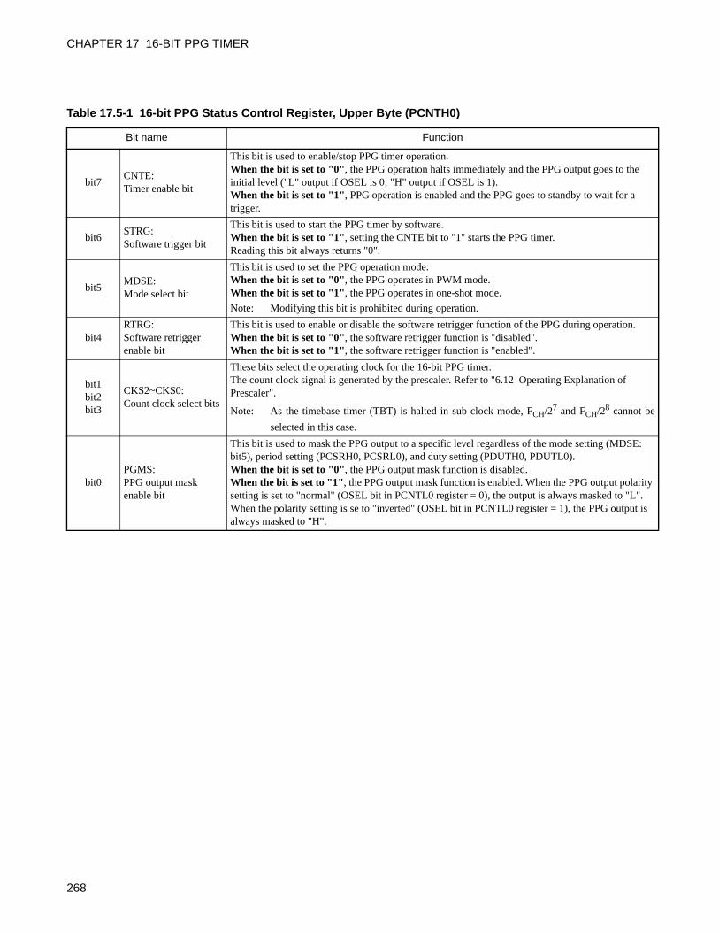
CHAPTER 17 16-BIT PPG TIMER
Table 17.5-1 16-bit PPG Status Control Register, Upper Byte (PCNTH0)
Bit name Function
bit7CNTE:Timer enable bit
This bit is used to enable/stop PPG timer operation.When the bit is set to "0", the PPG operation halts immediately and the PPG output goes to the initial level ("L" output if OSEL is 0; "H" output if OSEL is 1).When the bit is set to "1", PPG operation is enabled and the PPG goes to standby to wait for a trigger.
bit6STRG:Software trigger bit
This bit is used to start the PPG timer by software.When the bit is set to "1", setting the CNTE bit to "1" starts the PPG timer.Reading this bit always returns "0".
bit5MDSE:Mode select bit
This bit is used to set the PPG operation mode.When the bit is set to "0", the PPG operates in PWM mode.When the bit is set to "1", the PPG operates in one-shot mode.
Note: Modifying this bit is prohibited during operation.
bit4RTRG:Software retrigger enable bit
This bit is used to enable or disable the software retrigger function of the PPG during operation.When the bit is set to "0", the software retrigger function is "disabled".When the bit is set to "1", the software retrigger function is "enabled".
bit1bit2bit3
CKS2~CKS0:Count clock select bits
These bits select the operating clock for the 16-bit PPG timer.The count clock signal is generated by the prescaler. Refer to "6.12 Operating Explanation of Prescaler".
Note: As the timebase timer (TBT) is halted in sub clock mode, FCH/27 and FCH/28 cannot be
selected in this case.
bit0PGMS:PPG output mask enable bit
This bit is used to mask the PPG output to a specific level regardless of the mode setting (MDSE: bit5), period setting (PCSRH0, PCSRL0), and duty setting (PDUTH0, PDUTL0).When the bit is set to "0", the PPG output mask function is disabled.When the bit is set to "1", the PPG output mask function is enabled. When the PPG output polarity setting is set to "normal" (OSEL bit in PCNTL0 register = 0), the output is always masked to "L".When the polarity setting is se to "inverted" (OSEL bit in PCNTL0 register = 1), the PPG output is always masked to "H".
268
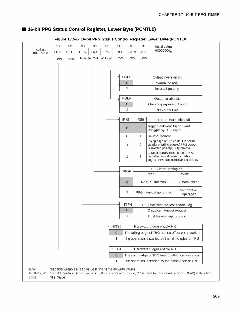
CHAPTER 17 16-BIT PPG TIMER
16-bit PPG Status Control Register, Lower Byte (PCNTL0)
Figure 17.5-6 16-bit PPG Status Control Register, Lower Byte (PCNTL0)
OSEL Output inversion bit
Normal polarity
Inverted polarity
0
1
POEN
0
1
IRS1 IRS0
0
0
Rising edge of PPG output in normal polarity or falling edge of PPG output in inverted polarity (Duty match)
1
1
1
0
1
0
IRQFPPG interrupt flag bit
PPG interrupt request enable flag
No PPG interrupt
PPG interrupt generated
Read Write
0
1
IREN
0
1
R/W: Readable/writable (Read value is the same as write value)R(RM1), W: Readable/writable (Read value is different from write value, "1" is read by read-modify-write (RMW) instruction) : Initial value
Output enable bit
General-purpose I/O port
PPG output pin
Interrupt type select bit
Trigger, software trigger, and retrigger by TRG input
Disables interrupt request
Enables interrupt request
R/W R(RM1),W R/W R/W R/WR/W
IREN IRQF IRS0 POEN OSEL
Initial value00000000BIRS1
Counter borrow
Counter borrow, rising edge of PPG output in normal polarity, or falling edge of PPG output in inverted polarity
Clears this bit
No effect on operation
EGS0EGS1
R/WR/W
bit7 bit6 bit5 bit4 bit3 bit2 bit1 bit0Address
0043H PCNTL0
EGS0
1
0
Hardware trigger enable bit0
The falling edge of TRG has no effect on operation
The operation is started by the falling edge of TRG
EGS1
1
0
Hardware trigger enable bit1
The rising edge of TRG has no effect on operation
The operation is started by the rising edge of TRG
269
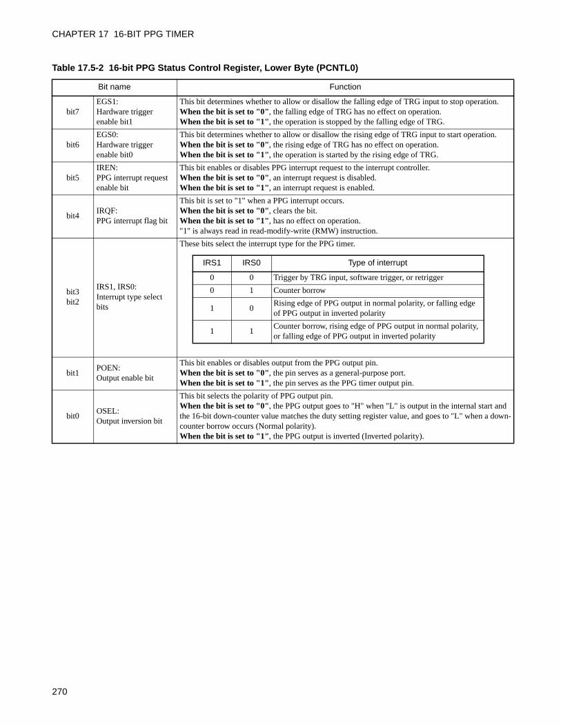
CHAPTER 17 16-BIT PPG TIMER
Table 17.5-2 16-bit PPG Status Control Register, Lower Byte (PCNTL0)
Bit name Function
bit7EGS1:Hardware trigger enable bit1
This bit determines whether to allow or disallow the falling edge of TRG input to stop operation.When the bit is set to "0", the falling edge of TRG has no effect on operation.When the bit is set to "1", the operation is stopped by the falling edge of TRG.
bit6EGS0:Hardware trigger enable bit0
This bit determines whether to allow or disallow the rising edge of TRG input to start operation.When the bit is set to "0", the rising edge of TRG has no effect on operation.When the bit is set to "1", the operation is started by the rising edge of TRG.
bit5IREN:PPG interrupt request enable bit
This bit enables or disables PPG interrupt request to the interrupt controller.When the bit is set to "0", an interrupt request is disabled.When the bit is set to "1", an interrupt request is enabled.
bit4IRQF:PPG interrupt flag bit
This bit is set to "1" when a PPG interrupt occurs.When the bit is set to "0", clears the bit.When the bit is set to "1", has no effect on operation."1" is always read in read-modify-write (RMW) instruction.
bit3bit2
IRS1, IRS0:Interrupt type select bits
These bits select the interrupt type for the PPG timer.
bit1POEN:Output enable bit
This bit enables or disables output from the PPG output pin.When the bit is set to "0", the pin serves as a general-purpose port.When the bit is set to "1", the pin serves as the PPG timer output pin.
bit0OSEL:Output inversion bit
This bit selects the polarity of PPG output pin.When the bit is set to "0", the PPG output goes to "H" when "L" is output in the internal start and the 16-bit down-counter value matches the duty setting register value, and goes to "L" when a down-counter borrow occurs (Normal polarity).When the bit is set to "1", the PPG output is inverted (Inverted polarity).
IRS1 IRS0 Type of interrupt
0 0 Trigger by TRG input, software trigger, or retrigger
0 1 Counter borrow
1 0 Rising edge of PPG output in normal polarity, or falling edge of PPG output in inverted polarity
1 1 Counter borrow, rising edge of PPG output in normal polarity, or falling edge of PPG output in inverted polarity
270
CHAPTER 17 16-BIT PPG TIMER
17.6 Interrupts of 16-bit PPG Timer
The 16-bit PPG timer can generate interrupt requests in the following cases:• When a trigger or counter borrow occurs• When a rising edge of PPG is generated in normal polarity• When a falling edge of PPG is generated in inverted polarityThe interrupt operation is controlled by IRS1 (bit 3) and IRS0 (bit2) in the PCNTL register.
Interrupts of 16-bit PPG TimerTable 17.6-1 shows interrupt control bits and interrupt sources of the 16-bit PPG timer.
When IRQF (bit 4) in the 16-bit PPG status control register (PCNTL0) is set to "1" and interrupt requests
are enabled (PCNTL0:IREN: bit 5 = 1) in the 16-bit PPG timer, an interrupt request is generated and
outputted to the controller.
Registers and Vector Table Related to Interrupts of 16-bit PPG Timer
ch.: Channel
Refer to "APPENDIX B Table of Interrupt Causes" for the interrupt request numbers and vector tables of
all peripheral functions.
Table 17.6-1 Interrupt Control Bits and Interrupt Sources of 16-bit PPG Timer
Item Description
Interrupt flag bit PCNTL0:IRQF
Interrupt request enable bit PCNTL0:IREN
Interrupt type select bits PCNTL0:IRS1, 0
Interrupt sources
PCNTL0:IRS1, 0=00Hardware trigger by TRG Pin input of 16-bit down-counter, software trigger and retrigger
PCNTL0:IRS1, 0=01Counter borrow of 16-bit down-counter
PCNTL0:IRS1, 0=10Rising edge of PPG0 output in normal polarity, or falling edge of PPG0 output in inverted polarity
PCNTL0:IRS1, 0=11Counter borrow of 16-bit down-counter, rising edge of PPG0 output in normal polarity, or falling edge of PPG0 output in inverted polarity
Table 17.6-2 Registers and Vector Table Related to Interrupts of 16-bit PPG Timer
Interrupt source
Interrupt request No.
Interrupt level setting register Vector table address
Register Setting bit Upper Lower
ch.0 IRQ15 ILR3 L15 FFDCH FFDDH
271
CHAPTER 17 16-BIT PPG TIMER
17.7 Explanation of 16-bit PPG Timer Operations and Setup Procedure Example
The 16-bit PPG timer can operate in PWM mode or one-shot mode. In addition, a retrigger function can be used in the 16-bit PPG timer.
PWM Mode (MDSE of PCNTH Register: bit 5 = 0)In PWM operation mode, the 16-bit PPG cycle setting buffer register (PCSRH0, PCSRL0) values are
loaded and the 16-bit down-counter starts down-count operation when a software trigger is inputted or a
hardware trigger by TRG pin input is inputted. When the count value reaches "1", the 16-bit PPG cycle
setting buffer register (PCSRH0, PCSRL0) values are reloaded to repeat the down-count operation.
The initial state of the PPG output is "L". When the 16-bit down-counter value matches the value set in the
duty setting registers, the output changes to "H" synchronizing with count clock. The output changes back
to "L" when the "H" was output until the value of duty setting. (The output levels will be reversed if OSEL
is set to "1".)
When the retrigger function is disabled (RTRG = 0), software triggers (STRG = 1) are ignored during the
operation of the down-counter.
When the down-counter is not running, the maximum time between a valid trigger input occurring and the
down-counter starting is as follows.
Software trigger: 1count clock cycle + 2 machine clock cycles
Hardware trigger by TRG Pin input: 1 count clock cycle + 3 machine clock cycles
The minimum time is as follows.
Software trigger: 2 machine clock cycles
Hardware trigger by TRG Pin input: 3 machine clock cycles
When the down-counter is running, the maximum time between a valid retrigger input occurring and the
down-counter restarting is as follows.
Software trigger: 1 count clock cycle + 2 machine clock cycles
Hardware trigger by TRG Pin input: 1 count clock cycle + 3 machine clock cycles
The minimum time is as follows.
Software trigger: 2 machine clock cycles
Hardware trigger by TRG Pin input: 3 machine clock cycles
272
CHAPTER 17 16-BIT PPG TIMER
Invalidating the retrigger (RTRG of PCNTH0 register: bit 4 = 0)
Figure 17.7-1 When Retrigger Is Invalid in PWM Mode
Validating the retrigger (RTRG of PCNTH0 register: bit 4 = 1)
Figure 17.7-2 When Retrigger Is Valid in PWM Mode
m
n
0
(1)=n × T ns(2)=m × T ns
PPG
(1)
(2)
(Normal polarity)
(Inverted polarity)
Time
16-bit down counter value
Software trigger
n : PDUTH0 & PDUTL0 register valuem: PCSRH0 & PCSRL0 register valueT : Count clock cycle
Rising edge detectedTrigger ignored
m
n
0
(1)=n × T ns(2)=m × T ns
PPG
PPG
(1)(2)
(Normal polarity)
(Inverted polarity)
Time
Counter value
Software trigger
Rising edge detected
Restarted by trigger
n : PDUTH0 & PDUTL0 register valuem: PCSRH0 & PCSRL0 register valueT : Count clock cycle
273
CHAPTER 17 16-BIT PPG TIMER
One-shot Mode (MDSE of PCNTH0 Register: bit 5 = 1)One-shot operation mode can be used to output a single pulse with a specified width when a valid trigger
input occurs. When retriggering is enabled and a valid trigger is detected during the counter operation, the
down counter value is reloaded.
The initial state of the PPG output is "L". When the 16-bit down-counter value matches the value set in the
duty setting registers, the output changes to "H". The output changes back to "L" when the counter reaches
"1". (The output levels will be reversed if OSEL is set to 1.)
Invalidating the retrigger (RTRG of PCNTH0 register: bit 4 = 0)
Figure 17.7-3 When Retrigger Is Invalid in One-shot Mode
Validating the retrigger (RTRG of PCNTH0 register: bit 4 = 1)
Figure 17.7-4 When Retrigger Is Valid in One-shot Mode
m
n
0
Trigger ignored
(1)=n × T ns(2)=m × T ns
PPG
PPG
(1)
(2)
(Normal polarity)
(Inverted polarity)
Time
Counter value
Software trigger
Rising edge detected
n : PDUTH0 & PDUTL0 register valuem: PCSRH0 & PCSRL0 register valueT : Count clock cycle
m
n
0
(1)=n × T ns(2)=m × T ns
PPG
PPG
(1)
(2)
(Normal polarity)
(Inverted polarity)
Time
Counter value
Software triggerTrigger restarted
Rising edge detected
n : PDUTH0 & PDUTL0 register valuem: PCSRH0 & PCSRL0 register valueT : Count clock cycle
274
CHAPTER 17 16-BIT PPG TIMER
Hardware Trigger"Hardware trigger" refers to PPG activation by signal input to the TRG input pin. When EGS1 and EGS0
are set to "11B" and the hardware trigger is used with TRG input, PPG starts operation on a rising edge and
halts the operation upon the detection of a falling edge.
Moreover, the PPG timer begins operation of the following rising edge from the beginning.
The operation can be retriggered by a valid TRG input hardware trigger regardless of the retrigger setting
of the RTRG bit when the TRG input hardware trigger has been selected.
Figure 17.7-5 Hardware Trigger in PWM Mode
Setup Procedure ExampleThe 16-bit PPG timer is set up in the following procedure:
Initial setup
1) Set the interrupt level (ILR3, ILR4)
2) Enable the hardware trigger and interrupts, select the interrupt type, and enable output (PCNTL)
3) Select the count clock and the mode, and enable timer operation (PCNTH)
4) Set the cycle (PCSR)
5) Set the duty (PDUT)
6) Start the PPG by the software trigger (PCNTH:STGR = 1)
Interrupt processing
1) Process any interrupt
2) Clear the interrupt request flag (PCNTL:IRQF)
m
n
0
(1)=n × T ns(2)=m × T ns
PPG
(1)
(2)
(Normal polarity)
(Inverted polarity)
Time
Counter value
Hardware trigger
Falling edge detectedRising edge detected
n : PDUTH0 & PDUTL0 register valuem: PCSRH0 & PCSRL0 register valueT : Count clock cycle
275
CHAPTER 17 16-BIT PPG TIMER
17.8 Precautions when Using 16-bit PPG Timer
Shown below are the precautions that must be followed when using the 16-bit PPG timer.
Precautions when Using 16-bit PPG Timer
Precautions when setting the program
Do not use the retrigger if the same values are set for the cycle and duty. If used, the PPG output will go to
the "L" level for one count clock cycle after the retrigger, and then go back to the "H" level when normal
polarity has been selected.
If the microcontroller enters a standby mode, the TRG pin setting may change and cause the device to
malfunction. Therefore, disable the timer enable bit (PCNTH0:CNTE = 0) or disable the hardware trigger
enable bit (PCNTL0:EGS1, EGS0 = 00B).
When the cycle and duty are set to the same value, an interrupt is generated only once by duty match.
Moreover, if the duty is set to a value greater than the value of the period, no interrupt will be generated by
duty match.
Do not disable the timer enable bit (PCNTH0: CNTE = 0) and software trigger (PCNTH0: STRG =1) at the
same time when retrigger by the software is enabled (PCNTH0: RTRG =1) and the retrigger is selected as
an interrupt type (PCNTL0: IRS1, IRS0 = 00B) during count operation. If it occurs, interrupt flag bit may
set by retrigger although timer stops.
276
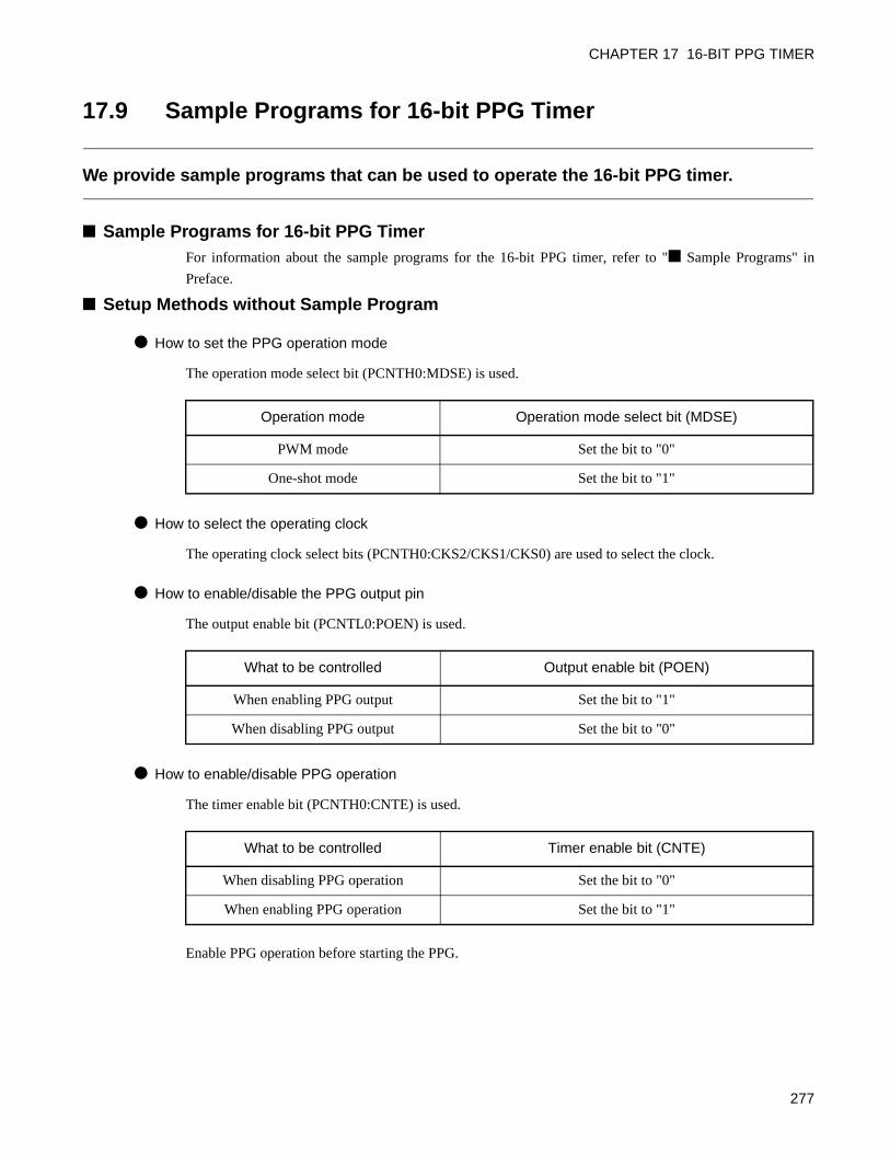
CHAPTER 17 16-BIT PPG TIMER
17.9 Sample Programs for 16-bit PPG Timer
We provide sample programs that can be used to operate the 16-bit PPG timer.
Sample Programs for 16-bit PPG TimerFor information about the sample programs for the 16-bit PPG timer, refer to " Sample Programs" in
Preface.
Setup Methods without Sample Program
How to set the PPG operation mode
The operation mode select bit (PCNTH0:MDSE) is used.
How to select the operating clock
The operating clock select bits (PCNTH0:CKS2/CKS1/CKS0) are used to select the clock.
How to enable/disable the PPG output pin
The output enable bit (PCNTL0:POEN) is used.
How to enable/disable PPG operation
The timer enable bit (PCNTH0:CNTE) is used.
Enable PPG operation before starting the PPG.
Operation mode Operation mode select bit (MDSE)
PWM mode Set the bit to "0"
One-shot mode Set the bit to "1"
What to be controlled Output enable bit (POEN)
When enabling PPG output Set the bit to "1"
When disabling PPG output Set the bit to "0"
What to be controlled Timer enable bit (CNTE)
When disabling PPG operation Set the bit to "0"
When enabling PPG operation Set the bit to "1"
277
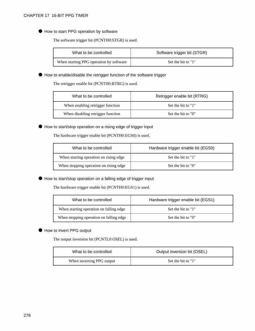
CHAPTER 17 16-BIT PPG TIMER
How to start PPG operation by software
The software trigger bit (PCNTH0:STGR) is used.
How to enable/disable the retrigger function of the software trigger
The retrigger enable bit (PCNTH0:RTRG) is used.
How to start/stop operation on a rising edge of trigger input
The hardware trigger enable bit (PCNTH0:EGS0) is used.
How to start/stop operation on a falling edge of trigger input
The hardware trigger enable bit (PCNTH0:EGS1) is used.
How to invert PPG output
The output inversion bit (PCNTL0:OSEL) is used.
What to be controlled Software trigger bit (STGR)
When starting PPG operation by software Set the bit to "1"
What to be controlled Retrigger enable bit (RTRG)
When enabling retrigger function Set the bit to "1"
When disabling retrigger function Set the bit to "0"
What to be controlled Hardware trigger enable bit (EGS0)
When starting operation on rising edge Set the bit to "1"
When stopping operation on rising edge Set the bit to "0"
What to be controlled Hardware trigger enable bit (EGS1)
When starting operation on falling edge Set the bit to "1"
When stopping operation on falling edge Set the bit to "0"
What to be controlled Output inversion bit (OSEL)
When inverting PPG output Set the bit to "1"
278
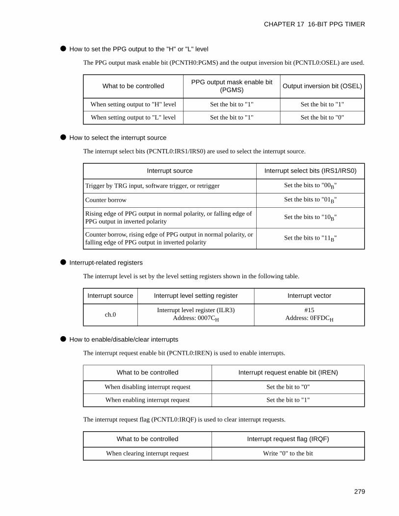
CHAPTER 17 16-BIT PPG TIMER
How to set the PPG output to the "H" or "L" level
The PPG output mask enable bit (PCNTH0:PGMS) and the output inversion bit (PCNTL0:OSEL) are used.
How to select the interrupt source
The interrupt select bits (PCNTL0:IRS1/IRS0) are used to select the interrupt source.
Interrupt-related registers
The interrupt level is set by the level setting registers shown in the following table.
How to enable/disable/clear interrupts
The interrupt request enable bit (PCNTL0:IREN) is used to enable interrupts.
The interrupt request flag (PCNTL0:IRQF) is used to clear interrupt requests.
What to be controlledPPG output mask enable bit
(PGMS)Output inversion bit (OSEL)
When setting output to "H" level Set the bit to "1" Set the bit to "1"
When setting output to "L" level Set the bit to "1" Set the bit to "0"
Interrupt source Interrupt select bits (IRS1/IRS0)
Trigger by TRG input, software trigger, or retrigger Set the bits to "00B"
Counter borrow Set the bits to "01B"
Rising edge of PPG output in normal polarity, or falling edge of PPG output in inverted polarity
Set the bits to "10B"
Counter borrow, rising edge of PPG output in normal polarity, or falling edge of PPG output in inverted polarity
Set the bits to "11B"
Interrupt source Interrupt level setting register Interrupt vector
ch.0Interrupt level register (ILR3)
Address: 0007CH
#15Address: 0FFDCH
What to be controlled Interrupt request enable bit (IREN)
When disabling interrupt request Set the bit to "0"
When enabling interrupt request Set the bit to "1"
What to be controlled Interrupt request flag (IRQF)
When clearing interrupt request Write "0" to the bit
279

CHAPTER 17 16-BIT PPG TIMER
280
CHAPTER 18EXTERNAL INTERRUPT
CIRCUIT
This chapter describes the functions and operations of the external interrupt circuit.
18.1 Overview of External Interrupt Circuit
18.2 Configuration of External Interrupt Circuit
18.3 Channels of External Interrupt Circuit
18.4 Pins of External Interrupt Circuit
18.5 Registers of External Interrupt Circuit
18.6 Interrupts of External Interrupt Circuit
18.7 Explanation of External Interrupt Circuit Operations and Setup Procedure Example
18.8 Precautions when Using External Interrupt Circuit
18.9 Sample Programs for External Interrupt Circuit
281
CHAPTER 18 EXTERNAL INTERRUPT CIRCUIT
18.1 Overview of External Interrupt Circuit
The external interrupt circuit detects edges on the signal that is inputted to the external interrupt pin and generates interrupt requests to the CPU.
Functions of External Interrupt CircuitThe external interrupt circuit has the functions to detect any edge of a signal that is inputted to an external
interrupt pin and generate an interrupt request to the CPU. This interrupt allows the unit to recover from a
standby mode and return to its normal operation.
282
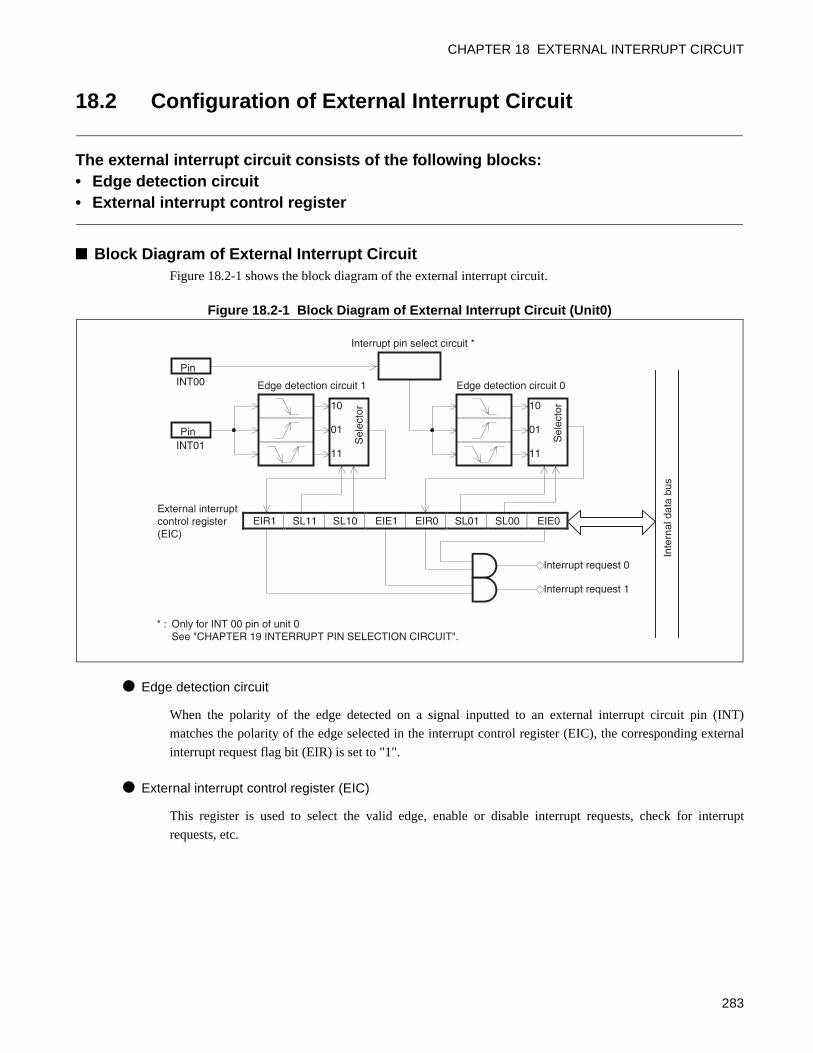
CHAPTER 18 EXTERNAL INTERRUPT CIRCUIT
18.2 Configuration of External Interrupt Circuit
The external interrupt circuit consists of the following blocks:• Edge detection circuit• External interrupt control register
Block Diagram of External Interrupt CircuitFigure 18.2-1 shows the block diagram of the external interrupt circuit.
Figure 18.2-1 Block Diagram of External Interrupt Circuit (Unit0)
Edge detection circuit
When the polarity of the edge detected on a signal inputted to an external interrupt circuit pin (INT)
matches the polarity of the edge selected in the interrupt control register (EIC), the corresponding external
interrupt request flag bit (EIR) is set to "1".
External interrupt control register (EIC)
This register is used to select the valid edge, enable or disable interrupt requests, check for interrupt
requests, etc.
EIR1 SL11 SL10 EIE1 EIR0 SL01 SL00 EIE0 External interrupt control register (EIC)
* : Only for INT 00 pin of unit 0See "CHAPTER 19 INTERRUPT PIN SELECTION CIRCUIT".
INT00 Pin
INT01 Pin
10 01 11
Sel
ecto
r
10 01 11
Sel
ecto
r
Interrupt request 0
Interrupt request 1
Inte
rnal
dat
a bu
s
Edge detection circuit 0Edge detection circuit 1
Interrupt pin select circuit *
283
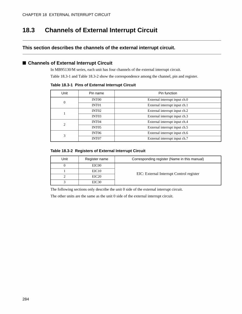
CHAPTER 18 EXTERNAL INTERRUPT CIRCUIT
18.3 Channels of External Interrupt Circuit
This section describes the channels of the external interrupt circuit.
Channels of External Interrupt CircuitIn MB95130/M series, each unit has four channels of the external interrupt circuit.
Table 18.3-1 and Table 18.3-2 show the correspondence among the channel, pin and register.
The following sections only describe the unit 0 side of the external interrupt circuit.
The other units are the same as the unit 0 side of the external interrupt circuit.
Table 18.3-1 Pins of External Interrupt Circuit
Unit Pin name Pin function
0INT00 External interrupt input ch.0
INT01 External interrupt input ch.1
1INT02 External interrupt input ch.2
INT03 External interrupt input ch.3
2INT04 External interrupt input ch.4
INT05 External interrupt input ch.5
3INT06 External interrupt input ch.6
INT07 External interrupt input ch.7
Table 18.3-2 Registers of External Interrupt Circuit
Unit Register name Corresponding register (Name in this manual)
0 EIC00
EIC: External Interrupt Control register1 EIC10
2 EIC20
3 EIC30
284
CHAPTER 18 EXTERNAL INTERRUPT CIRCUIT
18.4 Pins of External Interrupt Circuit
This section shows the pins related to the external interrupt circuit and the block diagram of such pins.
Pins Related to External Interrupt CircuitThe pins related to the external interrupt circuit are the INT00 to INT07 pins.
INT00 to INT07 pins
These pins serve both as external interrupt inputs and as general-purpose I/O ports.
INT00 to INT07: When the corresponding pin of the INT00 to INT07 pins is set as an input port by the
port direction register (DDR) and the corresponding external interrupt input is enabled
by the external interrupt control register (EIC), that pin functions as an external
interrupt input pin (INT00 = INT07).
The state of pins can be read from the port data register (PDR) whenever input port is
set as a pin function. However, the value of PDR is read when read-modify-write
(RMW) instruction is used.
Block Diagram of Pins Related to External Interrupt Circuit
Figure 18.4-1 Block Diagram of Pins (INT00 to INT07) Related to External Interrupt Circuit
ILSR2 read
ILSR2 write
ILSR2
Hysteresis
Automotive
0
1
PDR read
PDR write
PDR
DDR read
DDR write
DDR
0
1
Peripheral function input enablePeripheral function input
Pin
Stop, Watch (SPL=1)
Inte
rnal
bus
In bit operation instruction
285
CHAPTER 18 EXTERNAL INTERRUPT CIRCUIT
18.5 Registers of External Interrupt Circuit
This section describes the registers of the external interrupt circuit.
List of Registers of External Interrupt CircuitFigure 18.5-1 shows the registers of the external interrupt circuit.
Figure 18.5-1 Registers of External Interrupt Circuit
R/W: Readable/writable (Read value is the same as write value)R(RM1), W: Readable/writable (Read value is different from write value, "1" is read by read-modify-write
(RMW) instruction)
External interrupt control register (EIC)
Address bit7 bit6 bit5 bit4 bit3 bit2 bit1 bit0 Initial value
0048H EIC00 EIR1 SL11 SL10 EIE1 EIR0 SL01 SL00 EIE0 00000000B
R(RM1),W R/W R/W R/W R(RM1),W R/W R/W R/W
Address bit7 bit6 bit5 bit4 bit3 bit2 bit1 bit0 Initial value
0049H EIC10 EIR1 SL11 SL10 EIE1 EIR0 SL01 SL00 EIE0 00000000B
R(RM1),W R/W R/W R/W R(RM1),W R/W R/W R/W
Address bit7 bit6 bit5 bit4 bit3 bit2 bit1 bit0 Initial value
004AH EIC20 EIR1 SL11 SL10 EIE1 EIR0 SL01 SL00 EIE0 00000000B
R(RM1),W R/W R/W R/W R(RM1),W R/W R/W R/W
Address bit7 bit6 bit5 bit4 bit3 bit2 bit1 bit0 Initial value
004BH EIC30 EIR1 SL11 SL10 EIE1 EIR0 SL01 SL00 EIE0 00000000B
R(RM1),W R/W R/W R/W R(RM1),W R/W R/W R/W
286
CHAPTER 18 EXTERNAL INTERRUPT CIRCUIT
18.5.1 External Interrupt Control Register (EIC00)
The external interrupt control register (EIC00) is used to select the edge polarity for the external interrupt input and control interrupts.
External Interrupt Control Register (EIC00)
Figure 18.5-2 External Interrupt Control Register (EIC00)
0
0
EIR1 SL11 SL10 EIE1 EIR0 SL01 SL00 EIE0 00000000B
bit7Address bit6 bit5 bit4 bit3 bit2 bit1 bit0 Initial value
R(RM1),W R/W R/W R/W R/W R/W R/W
Interrupt request enable bit 0Disables output of interrupt requestEnables output of interrupt request
EIE001
Edge polarity select bits 0No edge detection
SL010
Rising edge0
Both edges
External interrupt request flag bit 0Read Write
Specified edge not inputted
EIR0
Clears this bit0Specified edge inputted1 No change, no effect on others
Falling edge1011
1
SL00
Interrupt request enable bit 1Disables output of interrupt requestEnables output of interrupt request
EIE101
Edge polarity select bits 1No edge detection
SL110
Rising edge0
Both edges
External interrupt request flag bit 1Read Write
Specified edge not inputted
EIR1
Clears this bit0Specified edge inputted1 No change, no effect on others
Falling edge1011
1
SL10
R(RM1),W
R/WR(RM1),W
: Readable/writable (Read value is the same as write value): Readable/writable (Read value is different from write value, "1" is read by read-modify-write (RMW) instruction): Initial value
0048H EIC000049H EIC10004AH EIC20004BH EIC30
287
CHAPTER 18 EXTERNAL INTERRUPT CIRCUIT
Table 18.5-1 Functional Description of Each Bit of External Interrupt Control Register (EIC00)
Bit name Function
bit7EIR1:External interrupt request flag bit 1
This flag is set to "1" when the edge selected by the edge polarity select bits (SL11, SL10) is inputted to the external interrupt pin INT1.• When this bit and the interrupt request enable bit 1 (EIE1) are set to "1", an interrupt request is
outputted.• Writing "0" clears the bit. Writing "1" has no effect.• "1" is read in read-modify-write (RMW) instructions.
bit6bit5
SL11, SL10:Edge polarity select bits 1
These bits select the polarity of the interrupt source edge of the pulse inputted to the external interrupt pin INT1.• Edge detection is not performed and no interrupt is generated when these bits are set to "00B".
• Rising edges are detected when these bits are "01B", falling edges when "10B", and both edges
when "11B".
bit4EIE1:Interrupt request enable bit 1
This bit is used to enable and disable output of interrupt requests to the interrupt controller. When this bit and the external interrupt request flag bit 1 (EIR1) are "1", an interrupt request is outputted.• When using an external interrupt pin, write "0" to the corresponding bit in the port direction
register (DDR) to set the pin as an input.• The status of the external interrupt pin can be read directly from the port data register, regardless of
the status of the interrupt request enable bit.
bit3EIR0:External interrupt request flag bit 0
This flag is set to "1" when the edge selected by the edge polarity select bits (SL01, SL00) is inputted to the external interrupt pin INT0.• When this bit and the interrupt request enable bit 0 (EIE0) are set to "1", an interrupt request is
outputted.• Writing "0" clears the bit. Writing "1" has no effect.• "1" is read in read-modify-write (RMW) instructions.
bit2bit1
SL01, SL00:Edge polarity select bits 0
These bits are used to select the polarity of the interrupt source edge of the pulse inputted to the external interrupt pin INT0.• Edge detection is not performed and no interrupt request is generated when these bits are "00B".
• Rising edges are detected when the bits are "01B", falling edges when "10B", and both edges when
"11B".
bit0EIE0:Interrupt request enable bit 0
This bit enables or disables the output of interrupt requests to the interrupt controller. An interrupt request is outputted when this bit and the external interrupt request flag bit 0 (EIR0) are "1".• When using an external interrupt pin, write "0" to the corresponding bit in the port direction
register (DDR) to set the pin as an input.• The status of the external interrupt pin can be read directly from the port data register (PFR),
regardless of the status of the interrupt request enable bit.
288
CHAPTER 18 EXTERNAL INTERRUPT CIRCUIT
18.6 Interrupts of External Interrupt Circuit
The interrupt sources for the external interrupt circuit include detection of the specified edge of the signal inputted to an external interrupt pin.
Interrupt During Operation of External Interrupt CircuitWhen the specified edge of external interrupt input is detected, the corresponding external interrupt request
flag bit (EIC: EIR0, EIR1) is set to "1". In this case, an interrupt request will be generated to the interrupt
controller, if the corresponding interrupt request enable bit is enabled (EIC: EIE0, EIE1=1). Write "0" to
the corresponding external interrupt request flag big to clear the interrupt request in the interrupt process
routine.
Registers and Vector Table Related to Interrupts of External Interrupt Circuit
ch.: Channel
Refer to "APPENDIX B Table of Interrupt Causes" for the interrupt request numbers and vector tables of
all peripheral functions.
Table 18.6-1 Registers and Vector Table Related to Interrupts of External Interrupt Circuit
Interrupt source
Interrupt request No.
Interrupt level setting register Vector table address
Register Setting bit Upper Lower
ch.0IRQ0 ILR0 L00 FFFAH FFFBH
ch.4
ch.1IRQ1 ILR0 L01 FFF8H FFF9H
ch.5
ch.2IRQ2 ILR0 L02 FFF6H FFF7H
ch.6
ch.3IRQ3 ILR0 L03 FFF4H FFF5H
ch.7
289
CHAPTER 18 EXTERNAL INTERRUPT CIRCUIT
18.7 Explanation of External Interrupt Circuit Operations and Setup Procedure Example
This section describes the operation of the external interrupt circuit.
Operation of External Interrupt CircuitWhen the polarity of an edge of a signal inputted from one of the external interrupt pins (INT0, 1) matches
the polarity of the edge selected by the external interrupt control register (EIC: SL00 to SL11), the
corresponding external interrupt request flag bit (EIC: EIR0, EIR1) is set to "1" and the interrupt request is
generated.
Always set the interrupt enable bit to "0" when not using an external interrupt to recover from a standby
mode.
When setting the edge polarity select bit (SL), set the interrupt request enable bit (EIE) to "0" to prevent the
interrupt request from being generated accidentally. Also clear the interrupt request flag bit (EIR) to "0"
after changing the edge polarity.
Figure 18.7-1 shows the operation for setting the INT0 pin as an external interrupt input.
Figure 18.7-1 Operation of External Interrupt
Input waveform to INT0 pin
EIR0 bit
EIE0 bit
SL01 bit
SL00 bit
IRQ
Cleared by program
Interrupt request flag bit cleared by program
No edge detection
Rising edge Falling edge Both edges
290
CHAPTER 18 EXTERNAL INTERRUPT CIRCUIT
Setup Procedure ExampleThe external interrupt circuit is set up in the following procedure:
Initial setup
1) Set the interrupt level. (ILR0)
2) Select the edge polarity. (EIC:SL01, SL00)
3) Enable interrupt requests. (EIC:EIE0 = 1)
Interrupt processing
1) Clear the interrupt request flag. (EIC:EIR0 = 0)
2) Process any interrupt.
Note:
The external interrupt input is also used as an I/O port. Therefore, when it is used as the externalinterrupt input, the corresponding bit in the port direction register (DDR) must be set to "0" (input).
291
CHAPTER 18 EXTERNAL INTERRUPT CIRCUIT
18.8 Precautions when Using External Interrupt Circuit
This section describes the precautions that must be followed when using the external interrupt circuit.
Precautions when Using External Interrupt Circuit• Set the interrupt request enable bit (EIE) to "0" (disabling interrupt requests) when setting the edge
polarity select bit (SL). Also clear the external interrupt request flag bit (EIR) to "0" after setting theedge polarity.
• The operation cannot recover from the interrupt processing routine if the external interrupt request flagbit is "1" and the interrupt request enable bit is enabled. Always clear the external interrupt request flagbit in the interrupt processing routine.
292
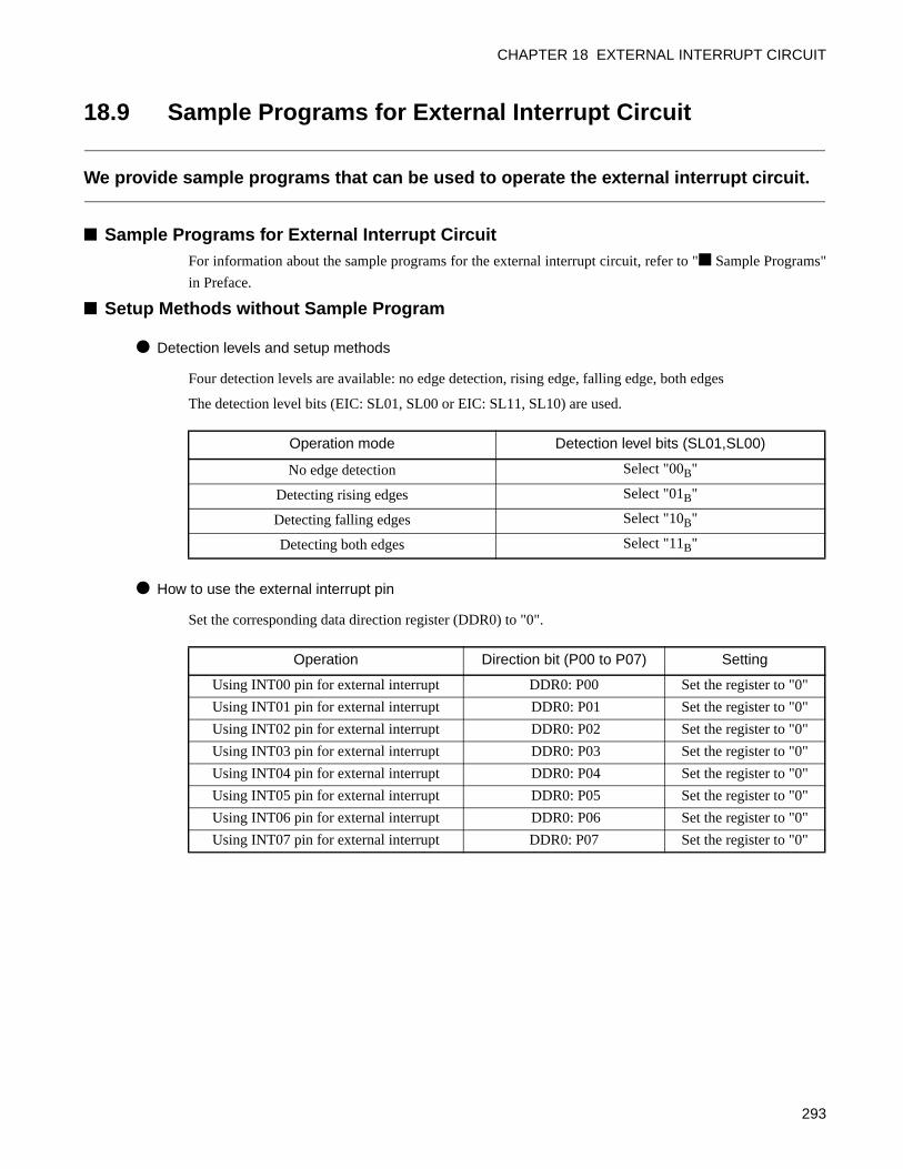
CHAPTER 18 EXTERNAL INTERRUPT CIRCUIT
18.9 Sample Programs for External Interrupt Circuit
We provide sample programs that can be used to operate the external interrupt circuit.
Sample Programs for External Interrupt CircuitFor information about the sample programs for the external interrupt circuit, refer to " Sample Programs"
in Preface.
Setup Methods without Sample Program
Detection levels and setup methods
Four detection levels are available: no edge detection, rising edge, falling edge, both edges
The detection level bits (EIC: SL01, SL00 or EIC: SL11, SL10) are used.
How to use the external interrupt pin
Set the corresponding data direction register (DDR0) to "0".
Operation mode Detection level bits (SL01,SL00)
No edge detection Select "00B"
Detecting rising edges Select "01B"
Detecting falling edges Select "10B"
Detecting both edges Select "11B"
Operation Direction bit (P00 to P07) Setting
Using INT00 pin for external interrupt DDR0: P00 Set the register to "0"
Using INT01 pin for external interrupt DDR0: P01 Set the register to "0"
Using INT02 pin for external interrupt DDR0: P02 Set the register to "0"
Using INT03 pin for external interrupt DDR0: P03 Set the register to "0"
Using INT04 pin for external interrupt DDR0: P04 Set the register to "0"
Using INT05 pin for external interrupt DDR0: P05 Set the register to "0"
Using INT06 pin for external interrupt DDR0: P06 Set the register to "0"
Using INT07 pin for external interrupt DDR0: P07 Set the register to "0"
293
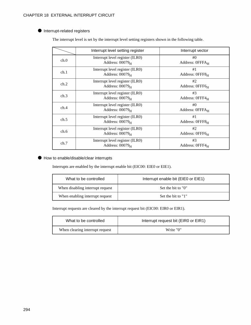
CHAPTER 18 EXTERNAL INTERRUPT CIRCUIT
Interrupt-related registers
The interrupt level is set by the interrupt level setting registers shown in the following table.
How to enable/disable/clear interrupts
Interrupts are enabled by the interrupt enable bit (EIC00: EIE0 or EIE1).
Interrupt requests are cleared by the interrupt request bit (EIC00: EIR0 or EIR1).
Interrupt level setting register Interrupt vector
ch.0Interrupt level register (ILR0)
Address: 00079H
#0Address: 0FFFAH
ch.1Interrupt level register (ILR0)
Address: 00079H
#1Address: 0FFF8H
ch.2Interrupt level register (ILR0)
Address: 00079H
#2Address: 0FFF6H
ch.3Interrupt level register (ILR0)
Address: 00079H
#3Address: 0FFF4H
ch.4Interrupt level register (ILR0)
Address: 00079H
#0Address: 0FFFAH
ch.5Interrupt level register (ILR0)
Address: 00079H
#1Address: 0FFF8H
ch.6Interrupt level register (ILR0)
Address: 00079H
#2Address: 0FFF6H
ch.7Interrupt level register (ILR0)
Address: 00079H
#3Address: 0FFF4H
What to be controlled Interrupt enable bit (EIE0 or EIE1)
When disabling interrupt request Set the bit to "0"
When enabling interrupt request Set the bit to "1"
What to be controlled Interrupt request bit (EIR0 or EIR1)
When clearing interrupt request Write "0"
294
CHAPTER 19INTERRUPT PIN SELECTION
CIRCUIT
This chapter describes the functions and operations of the interrupt pin selection circuit.
19.1 Overview of Interrupt Pin Selection Circuit
19.2 Configuration of Interrupt Pin Selection Circuit
19.3 Pins of Interrupt Pin Selection Circuit
19.4 Registers of Interrupt Pin Selection Circuit
19.5 Operating Description of Interrupt Pin Selection Circuit
19.6 Precautions when Using Interrupt Pin Selection Circuit
295
CHAPTER 19 INTERRUPT PIN SELECTION CIRCUIT
19.1 Overview of Interrupt Pin Selection Circuit
The interrupt pin selection circuit selects pins to be used as interrupt input pins from among various peripheral input pins.
Interrupt Pin Selection CircuitThe interrupt pin selection circuit is used to select interrupt input pins from amongst various peripheral
inputs (TRG0/ADTG, UCK0, UI0, EC0, SCK, SI, INT00). The input signal from each peripheral function
pin is selected by this circuit and the signal is used as the INT00 (channel 0) input of external interrupt.
This enables the input signals to the peripheral function pins to also serve as external interrupt pins.
296
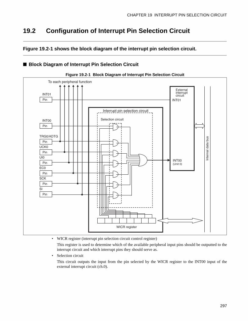
CHAPTER 19 INTERRUPT PIN SELECTION CIRCUIT
19.2 Configuration of Interrupt Pin Selection Circuit
Figure 19.2-1 shows the block diagram of the interrupt pin selection circuit.
Block Diagram of Interrupt Pin Selection Circuit
Figure 19.2-1 Block Diagram of Interrupt Pin Selection Circuit
• WICR register (interrupt pin selection circuit control register)
This register is used to determine which of the available peripheral input pins should be outputted to theinterrupt circuit and which interrupt pins they should serve as.
• Selection circuit
This circuit outputs the input from the pin selected by the WICR register to the INT00 input of theexternal interrupt circuit (ch.0).
Pin
INT01External interrupt circuit
INT01
INT00(Unit 0)
Interrupt pin selection circuit
To each peripheral function
Selection circuit
Pin
Pin
Pin
INT00
Pin
Pin
Pin
Pin
SI
UCK0
UI0
EC0
SCK
TRG0/ADTG
WICR register
Inte
rnal
dat
a bu
s
297
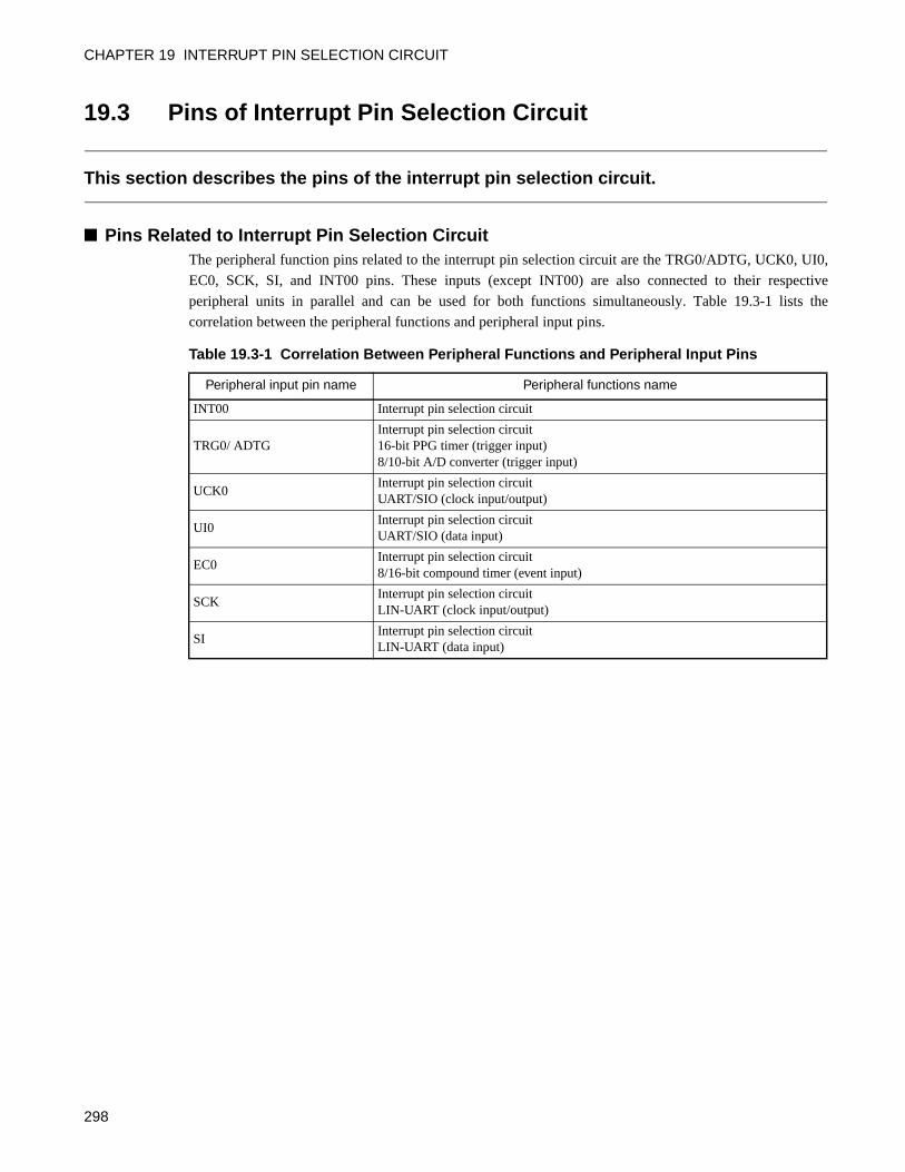
CHAPTER 19 INTERRUPT PIN SELECTION CIRCUIT
19.3 Pins of Interrupt Pin Selection Circuit
This section describes the pins of the interrupt pin selection circuit.
Pins Related to Interrupt Pin Selection CircuitThe peripheral function pins related to the interrupt pin selection circuit are the TRG0/ADTG, UCK0, UI0,
EC0, SCK, SI, and INT00 pins. These inputs (except INT00) are also connected to their respective
peripheral units in parallel and can be used for both functions simultaneously. Table 19.3-1 lists the
correlation between the peripheral functions and peripheral input pins.
Table 19.3-1 Correlation Between Peripheral Functions and Peripheral Input Pins
Peripheral input pin name Peripheral functions name
INT00 Interrupt pin selection circuit
TRG0/ ADTGInterrupt pin selection circuit16-bit PPG timer (trigger input)8/10-bit A/D converter (trigger input)
UCK0Interrupt pin selection circuitUART/SIO (clock input/output)
UI0Interrupt pin selection circuitUART/SIO (data input)
EC0Interrupt pin selection circuit8/16-bit compound timer (event input)
SCKInterrupt pin selection circuitLIN-UART (clock input/output)
SIInterrupt pin selection circuitLIN-UART (data input)
298
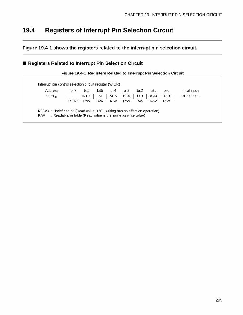
CHAPTER 19 INTERRUPT PIN SELECTION CIRCUIT
19.4 Registers of Interrupt Pin Selection Circuit
Figure 19.4-1 shows the registers related to the interrupt pin selection circuit.
Registers Related to Interrupt Pin Selection Circuit
Figure 19.4-1 Registers Related to Interrupt Pin Selection Circuit
Interrupt pin control selection circuit register (WICR)
Address bit7 bit6 bit5 bit4 bit3 bit2 bit1 bit0 Initial value
0FEFH - INT00 SI SCK EC0 UI0 UCK0 TRG0 01000000BR0/WX R/W R/W R/W R/W R/W R/W R/W
R0/WX : Undefined bit (Read value is "0", writing has no effect on operation)R/W : Readable/writable (Read value is the same as write value)
299
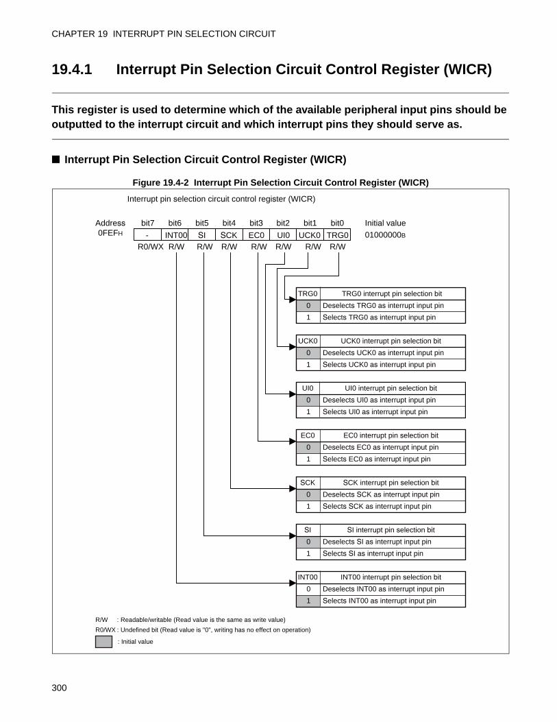
CHAPTER 19 INTERRUPT PIN SELECTION CIRCUIT
19.4.1 Interrupt Pin Selection Circuit Control Register (WICR)
This register is used to determine which of the available peripheral input pins should be outputted to the interrupt circuit and which interrupt pins they should serve as.
Interrupt Pin Selection Circuit Control Register (WICR)
Figure 19.4-2 Interrupt Pin Selection Circuit Control Register (WICR)
Interrupt pin selection circuit control register (WICR)
Address0FEFH - INT00 SI SCK EC0 UI0 UCK0
bit7 bit6 bit5 bit4 bit3 bit2 bit1 bit0
TRG0
Initial value 01000000B
R0/WX R/WR/WR/WR/WR/WR/WR/W
TRG0
1
TRG0 interrupt pin selection bit
Deselects TRG0 as interrupt input pin
Selects TRG0 as interrupt input pin 0
UCK0
1
UCK0 interrupt pin selection bit
Deselects UCK0 as interrupt input pin
Selects UCK0 as interrupt input pin 0
UI0
1
UI0 interrupt pin selection bit
Deselects UI0 as interrupt input pin
Selects UI0 as interrupt input pin 0
EC0
1
EC0 interrupt pin selection bit
Deselects EC0 as interrupt input pin
Selects EC0 as interrupt input pin 0
SCK
1
SCK interrupt pin selection bit
Deselects SCK as interrupt input pin
Selects SCK as interrupt input pin 0
SI
1
SI interrupt pin selection bit
Deselects SI as interrupt input pin
Selects SI as interrupt input pin 0
INT00
1
INT00 interrupt pin selection bit
Deselects INT00 as interrupt input pin
Selects INT00 as interrupt input pin 0
R/W : Readable/writable (Read value is the same as write value)
R0/WX : Undefined bit (Read value is "0", writing has no effect on operation)
: Initial value
300
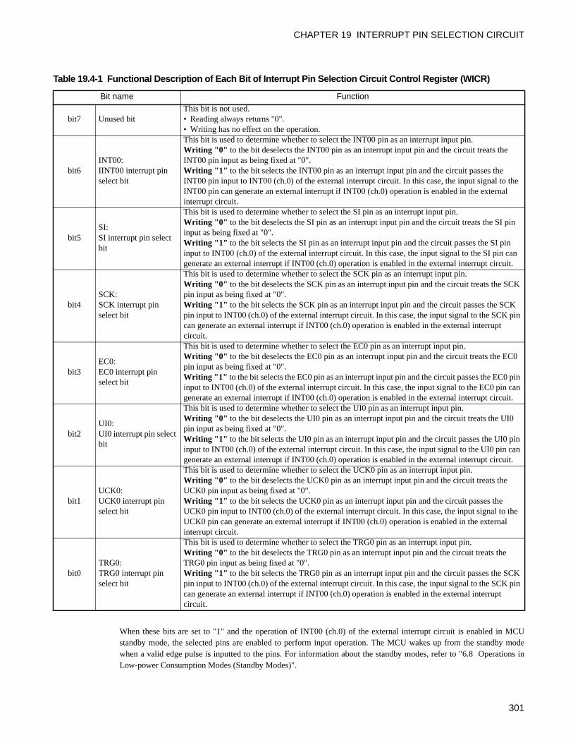
CHAPTER 19 INTERRUPT PIN SELECTION CIRCUIT
When these bits are set to "1" and the operation of INT00 (ch.0) of the external interrupt circuit is enabled in MCUstandby mode, the selected pins are enabled to perform input operation. The MCU wakes up from the standby modewhen a valid edge pulse is inputted to the pins. For information about the standby modes, refer to "6.8 Operations inLow-power Consumption Modes (Standby Modes)".
Table 19.4-1 Functional Description of Each Bit of Interrupt Pin Selection Circuit Control Register (WICR)
Bit name Function
bit7 Unused bitThis bit is not used.• Reading always returns "0".• Writing has no effect on the operation.
bit6INT00:IINT00 interrupt pin select bit
This bit is used to determine whether to select the INT00 pin as an interrupt input pin.Writing "0" to the bit deselects the INT00 pin as an interrupt input pin and the circuit treats the INT00 pin input as being fixed at "0".Writing "1" to the bit selects the INT00 pin as an interrupt input pin and the circuit passes the INT00 pin input to INT00 (ch.0) of the external interrupt circuit. In this case, the input signal to the INT00 pin can generate an external interrupt if INT00 (ch.0) operation is enabled in the external interrupt circuit.
bit5SI:SI interrupt pin select bit
This bit is used to determine whether to select the SI pin as an interrupt input pin.Writing "0" to the bit deselects the SI pin as an interrupt input pin and the circuit treats the SI pin input as being fixed at "0".Writing "1" to the bit selects the SI pin as an interrupt input pin and the circuit passes the SI pin input to INT00 (ch.0) of the external interrupt circuit. In this case, the input signal to the SI pin can generate an external interrupt if INT00 (ch.0) operation is enabled in the external interrupt circuit.
bit4SCK:SCK interrupt pin select bit
This bit is used to determine whether to select the SCK pin as an interrupt input pin.Writing "0" to the bit deselects the SCK pin as an interrupt input pin and the circuit treats the SCK pin input as being fixed at "0".Writing "1" to the bit selects the SCK pin as an interrupt input pin and the circuit passes the SCK pin input to INT00 (ch.0) of the external interrupt circuit. In this case, the input signal to the SCK pin can generate an external interrupt if INT00 (ch.0) operation is enabled in the external interrupt circuit.
bit3EC0:EC0 interrupt pin select bit
This bit is used to determine whether to select the EC0 pin as an interrupt input pin.Writing "0" to the bit deselects the EC0 pin as an interrupt input pin and the circuit treats the EC0 pin input as being fixed at "0".Writing "1" to the bit selects the EC0 pin as an interrupt input pin and the circuit passes the EC0 pin input to INT00 (ch.0) of the external interrupt circuit. In this case, the input signal to the EC0 pin can generate an external interrupt if INT00 (ch.0) operation is enabled in the external interrupt circuit.
bit2UI0:UI0 interrupt pin select bit
This bit is used to determine whether to select the UI0 pin as an interrupt input pin.Writing "0" to the bit deselects the UI0 pin as an interrupt input pin and the circuit treats the UI0 pin input as being fixed at "0".Writing "1" to the bit selects the UI0 pin as an interrupt input pin and the circuit passes the UI0 pin input to INT00 (ch.0) of the external interrupt circuit. In this case, the input signal to the UI0 pin can generate an external interrupt if INT00 (ch.0) operation is enabled in the external interrupt circuit.
bit1UCK0:UCK0 interrupt pin select bit
This bit is used to determine whether to select the UCK0 pin as an interrupt input pin.Writing "0" to the bit deselects the UCK0 pin as an interrupt input pin and the circuit treats the UCK0 pin input as being fixed at "0".Writing "1" to the bit selects the UCK0 pin as an interrupt input pin and the circuit passes the UCK0 pin input to INT00 (ch.0) of the external interrupt circuit. In this case, the input signal to the UCK0 pin can generate an external interrupt if INT00 (ch.0) operation is enabled in the external interrupt circuit.
bit0TRG0:TRG0 interrupt pin select bit
This bit is used to determine whether to select the TRG0 pin as an interrupt input pin.Writing "0" to the bit deselects the TRG0 pin as an interrupt input pin and the circuit treats the TRG0 pin input as being fixed at "0".Writing "1" to the bit selects the TRG0 pin as an interrupt input pin and the circuit passes the SCK pin input to INT00 (ch.0) of the external interrupt circuit. In this case, the input signal to the SCK pin can generate an external interrupt if INT00 (ch.0) operation is enabled in the external interrupt circuit.
301
CHAPTER 19 INTERRUPT PIN SELECTION CIRCUIT
Note:
The input signals to the peripheral pins do not generate an external interrupt even when "1" is writtento these bits if the INT00 (ch.0) of the external interrupt circuit is disabled.
Do not modify the values of these bits while the INT00 (ch.0) of the external interrupt circuit isenabled. If modified, the external interrupt circuit may detect a valid edge, depending on the pin inputlevel. If more than one interrupt pin are selected in WICR (interrupt pin selection circuit control register)simultaneously and the operation of INT00 (ch.0) of the external interrupt circuit is enabled (thevalues other than "00B" are set to SL01, SL00 bits in EIC00 register of external interrupt circuit.), theselected pins will remain enabled to perform input so as to accept interrupts even in a standby mode.
302
CHAPTER 19 INTERRUPT PIN SELECTION CIRCUIT
19.5 Operating Description of Interrupt Pin Selection Circuit
The interrupt pins are selected by setting WICR (interrupt pin selection circuit control register).
Operation of Interrupt Pin Selection CircuitThe WICR (interrupt pin selection circuit control register) setting is used to select the input pins to be
inputted to INT00 of the external interrupt circuit (ch.0). Shown below is the setup procedure for the
interrupt pin selection circuit and external interrupt circuit (ch.0), which must be followed when selecting
the TRG0 pin as an interrupt pin.
1) Write "0" to the corresponding bit in the port direction register (DDR) to set the pin as an input.
2) Select the TRG0 pin as an interrupt input pin in WICR (interrupt pin selection circuit control register)
(Write "01H" to the WICR register. At this point, after writing "0" in the EIE0 bit of the EIC00 register
of the external interrupt circuit, the operation of the external interrupt circuit is disabled).
3) Enable the operation of INT00 of the external interrupt circuit (ch.0).
(Set the SL01 and SL00 bits of the EIC00 register to any value other than "00B" in the external interrupt
circuit to select the valid edge. Also write "1" to the EIE0 bit to enable interrupts).
4) The subsequent interrupt operation is the same as for the external interrupt circuit.
• When a reset is released, WICR (interrupt pin selection circuit control register) is initialized to "40H"and the INT00 bit is selected as the only available interrupt pin. Update the value of this register beforeenabling the operation of the external interrupt circuit, when using any pins other than the INT00 pin asexternal interrupt pins.
Note:
If more than one interrupt pin are selected in WICR (interrupt pin selection circuit control register)simultaneously, an input to INT00 (ch.0) of the external interrupt circuit is treated as "H" if any of theselected input signals is "H". (It becomes "OR" of the signals inputted to the selected pins.)
303
CHAPTER 19 INTERRUPT PIN SELECTION CIRCUIT
19.6 Precautions when Using Interrupt Pin Selection Circuit
This section explains the precautions to be taken when using the interrupt pin selection circuit.
• If more than one interrupt pin are selected in WICR (interrupt pin selection circuit control register)simultaneously and the operation of INT00 (ch.0) of the external interrupt circuit is enabled (Set theSL01 and SL00 bits of the EIC00 register to any value other than "00B" in the external interrupt circuitto select the valid edge. Also write "1" to the EIE0 bit to enable interrupts), the selected pins will remainenabled to perform input so as to accept interrupts even in a standby mode.
• If more than one interrupt pin are selected in WICR (interrupt pin selection circuit control register)simultaneously, an input to INT00 (ch.0) of the external interrupt circuit is treated as "H" if any of theselected input signals is "H" (It becomes "OR" of the signals inputted to the selected pins).
304
CHAPTER 20UART/SIO
This chapter describes the functions and operations of UART/SIO.
20.1 Overview of UART/SIO
20.2 Configuration of UART/SIO
20.3 Channels of UART/SIO
20.4 Pins of UART/SIO
20.5 Registers of UART/SIO
20.6 Interrupts of UART/SIO
20.7 Explanation of UART/SIO Operations and Setup Procedure Example
20.8 Sample Programs for UART/SIO
305
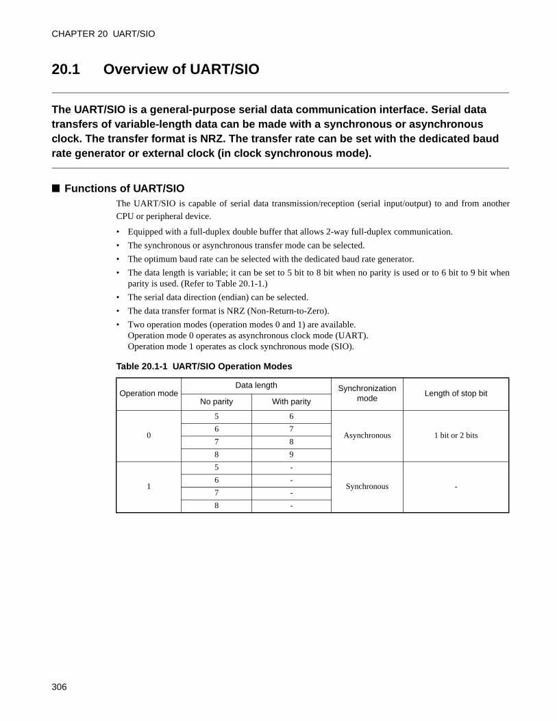
CHAPTER 20 UART/SIO
20.1 Overview of UART/SIO
The UART/SIO is a general-purpose serial data communication interface. Serial data transfers of variable-length data can be made with a synchronous or asynchronous clock. The transfer format is NRZ. The transfer rate can be set with the dedicated baud rate generator or external clock (in clock synchronous mode).
Functions of UART/SIOThe UART/SIO is capable of serial data transmission/reception (serial input/output) to and from another
CPU or peripheral device.
• Equipped with a full-duplex double buffer that allows 2-way full-duplex communication.
• The synchronous or asynchronous transfer mode can be selected.
• The optimum baud rate can be selected with the dedicated baud rate generator.
• The data length is variable; it can be set to 5 bit to 8 bit when no parity is used or to 6 bit to 9 bit whenparity is used. (Refer to Table 20.1-1.)
• The serial data direction (endian) can be selected.
• The data transfer format is NRZ (Non-Return-to-Zero).
• Two operation modes (operation modes 0 and 1) are available.Operation mode 0 operates as asynchronous clock mode (UART).Operation mode 1 operates as clock synchronous mode (SIO).
Table 20.1-1 UART/SIO Operation Modes
Operation modeData length Synchronization
modeLength of stop bit
No parity With parity
0
5 6
Asynchronous 1 bit or 2 bits6 7
7 8
8 9
1
5 -
Synchronous -6 -
7 -
8 -
306
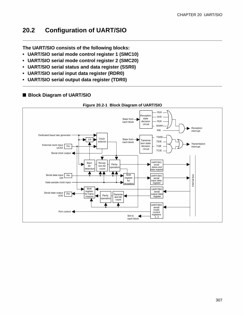
CHAPTER 20 UART/SIO
20.2 Configuration of UART/SIO
The UART/SIO consists of the following blocks:• UART/SIO serial mode control register 1 (SMC10)• UART/SIO serial mode control register 2 (SMC20)• UART/SIO serial status and data register (SSR0)• UART/SIO serial input data register (RDR0)• UART/SIO serial output data register (TDR0)
Block Diagram of UART/SIO
Figure 20.2-1 Block Diagram of UART/SIO
Dedicated baud rate generator
1/4
Pin
Pin
Pin
Clock selector
External clock inputUCK0
Serial data inputUI0
Start bit
detection
Recep-tion bit count
Parity operation
Shift register
for reception
UART/SIO serial
input data register
UART/SIO serial
status anddata register
UART/SIO serial mode control
registers 1, 2
UART/SIO serial
output data register
Shift register for trans-mission
Transmis-sion bit count
Parity operation
Serial data outputUO0
Serial clock output
Port control
Set to each block
Inte
rnal
bus
Reception
state decision
circuit
PER
OVE
FER
RDRF
Transmis-sion state decision
circuit
TDRE
RIE
TEIE
Reception interrupt
Transmission interrupt
State from each block
State from each block
TCPL
TCIE
Data sample clock input
307
CHAPTER 20 UART/SIO
UART/SIO serial mode control register 1 (SMC10)
This register controls UART/SIO operation mode. It is used to set the serial data direction (endian), parity
and its polarity, stop bit length, operation mode (synchronous/asynchronous), data length, and serial clock.
UART/SIO serial mode control register 2 (SMC20)
This register controls UART/SIO operation mode. It is used to enable/disable serial clock output, serial data
output, transmission/reception, and interrupts and to clear the reception error flag.
UART/SIO serial status and data register (SSR0)
This register indicates the transmission/reception status and error status of UART/SIO.
UART/SIO serial input data register (RDR0)
This register holds the receive data. The serial input is converted and then stored in this register.
UART/SIO serial output data register (TDR0)
This register sets the transmit data. Data written to this register is serial-converted and then outputted.
Input ClockThe UART/SIO uses the output clock (internal clock) from the dedicated baud rate generator or the input
signal (external clock) from the UCK pin as its input clock (serial clock).
308
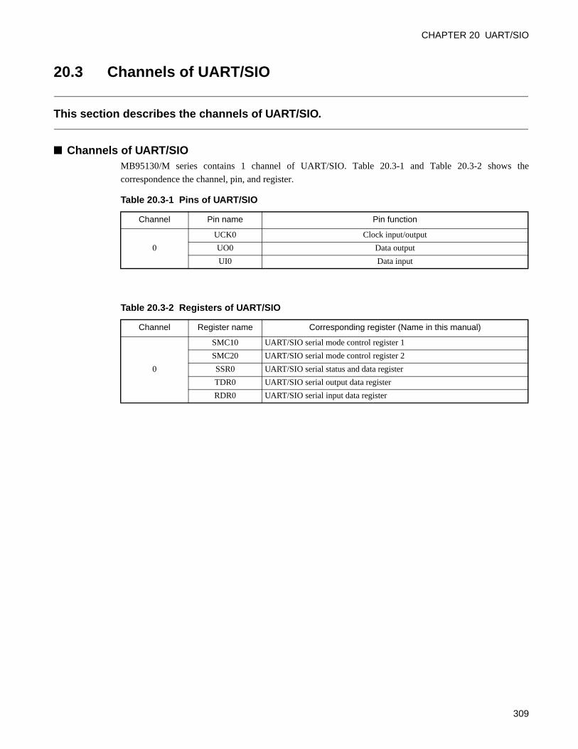
CHAPTER 20 UART/SIO
20.3 Channels of UART/SIO
This section describes the channels of UART/SIO.
Channels of UART/SIOMB95130/M series contains 1 channel of UART/SIO. Table 20.3-1 and Table 20.3-2 shows the
correspondence the channel, pin, and register.
Table 20.3-1 Pins of UART/SIO
Channel Pin name Pin function
0
UCK0 Clock input/output
UO0 Data output
UI0 Data input
Table 20.3-2 Registers of UART/SIO
Channel Register name Corresponding register (Name in this manual)
0
SMC10 UART/SIO serial mode control register 1
SMC20 UART/SIO serial mode control register 2
SSR0 UART/SIO serial status and data register
TDR0 UART/SIO serial output data register
RDR0 UART/SIO serial input data register
309
CHAPTER 20 UART/SIO
20.4 Pins of UART/SIO
This section describes the pins related to the UART/SIO.
Pins Related to UART/SIOThe pins associated with UART/SIO are the clock input and output pin (UCK0), serial data output pin
(UO0) and serial data input pin (UI).
UCK0:
Clock input/output pin for UART/SIO.
When the clock output is enabled (SMC20:SCKE=1), it serves as a UART/SIO clock output pin (UCK0)regardless of the value of the corresponding port direction register. At this time, do not select the externalclock (set SMC10:CKS = 0).
When it is to be used as a UART/SIO clock input pin, disable the clock output (SMC20:SCKE = 0) andmake sure that it is set as input port by the corresponding port direction register. At this time, be sure toselect the external clock (set SMC10:CKS = 0).
UO0:
Serial data output pin for UART/SIO. When the serial data output is enabled (SMC20:TXOE = 1), itserves as a UART/SIO serial data output pin (UO0) regardless of the value of the corresponding portdirection register.
UI0:
Serial data input pin for UART/SIO. When it is to be used as a UART/SIO serial data input pin, makesure that it is set as input port by the corresponding port direction register.
310
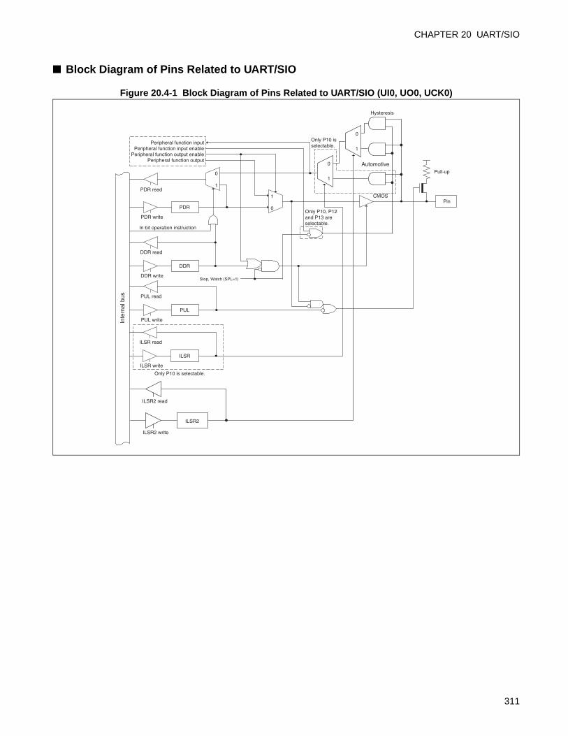
CHAPTER 20 UART/SIO
Block Diagram of Pins Related to UART/SIO
Figure 20.4-1 Block Diagram of Pins Related to UART/SIO (UI0, UO0, UCK0)
PDR read
PDR write
PDR
DDR read
DDR write
DDR
PUL read
PUL write
PUL
1
0
Peripheral function outputPeripheral function output enable
Peripheral function input enablePeripheral function input
Pin
Stop, Watch (SPL=1)
Inte
rnal
bus
In bit operation instruction
Pull-up
ILSR read
ILSR write
ILSR
Hysteresis
CMOS
Only P10 is selectable.
Only P10 is selectable.
Only P10, P12 and P13 are selectable.
Automotive
0
1
ILSR2 read
ILSR2 write
ILSR2
0
1
0
1
311
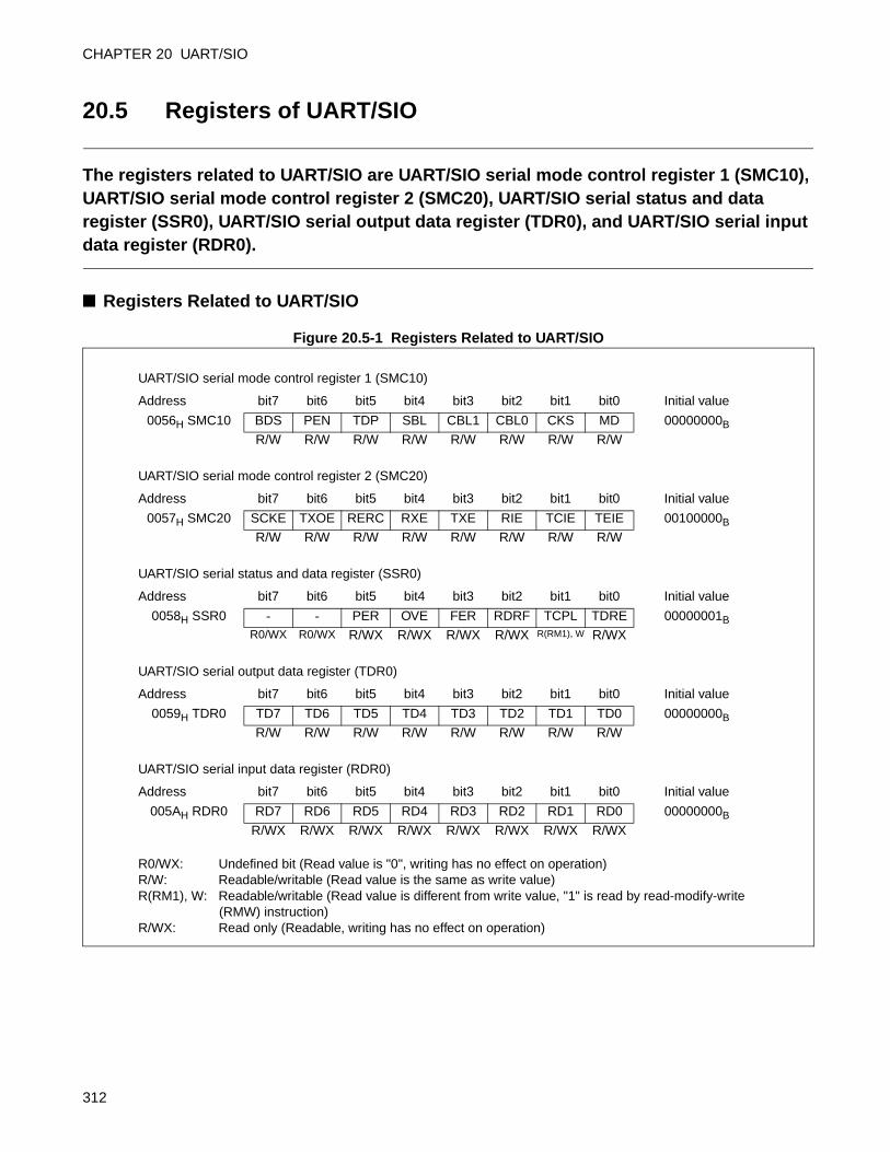
CHAPTER 20 UART/SIO
20.5 Registers of UART/SIO
The registers related to UART/SIO are UART/SIO serial mode control register 1 (SMC10), UART/SIO serial mode control register 2 (SMC20), UART/SIO serial status and data register (SSR0), UART/SIO serial output data register (TDR0), and UART/SIO serial input data register (RDR0).
Registers Related to UART/SIO
Figure 20.5-1 Registers Related to UART/SIO
UART/SIO serial mode control register 1 (SMC10)
Address bit7 bit6 bit5 bit4 bit3 bit2 bit1 bit0 Initial value
0056H SMC10 BDS PEN TDP SBL CBL1 CBL0 CKS MD 00000000B
R/W R/W R/W R/W R/W R/W R/W R/W
UART/SIO serial mode control register 2 (SMC20)
Address bit7 bit6 bit5 bit4 bit3 bit2 bit1 bit0 Initial value
0057H SMC20 SCKE TXOE RERC RXE TXE RIE TCIE TEIE 00100000B
R/W R/W R/W R/W R/W R/W R/W R/W
UART/SIO serial status and data register (SSR0)
Address bit7 bit6 bit5 bit4 bit3 bit2 bit1 bit0 Initial value
0058H SSR0 - - PER OVE FER RDRF TCPL TDRE 00000001BR0/WX R0/WX R/WX R/WX R/WX R/WX R(RM1), W R/WX
UART/SIO serial output data register (TDR0)
Address bit7 bit6 bit5 bit4 bit3 bit2 bit1 bit0 Initial value
0059H TDR0 TD7 TD6 TD5 TD4 TD3 TD2 TD1 TD0 00000000B
R/W R/W R/W R/W R/W R/W R/W R/W
UART/SIO serial input data register (RDR0)
Address bit7 bit6 bit5 bit4 bit3 bit2 bit1 bit0 Initial value
005AH RDR0 RD7 RD6 RD5 RD4 RD3 RD2 RD1 RD0 00000000B
R/WX R/WX R/WX R/WX R/WX R/WX R/WX R/WX
R0/WX: Undefined bit (Read value is "0", writing has no effect on operation)R/W: Readable/writable (Read value is the same as write value)R(RM1), W: Readable/writable (Read value is different from write value, "1" is read by read-modify-write
(RMW) instruction)R/WX: Read only (Readable, writing has no effect on operation)
312
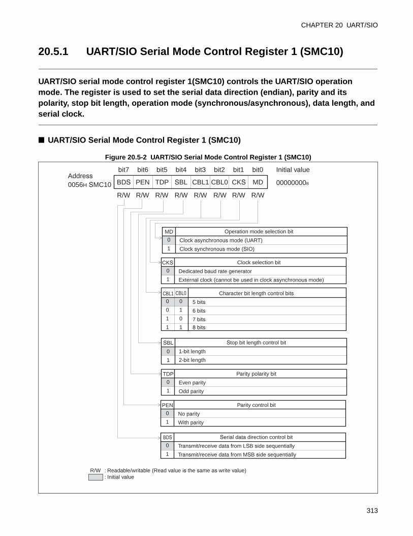
CHAPTER 20 UART/SIO
20.5.1 UART/SIO Serial Mode Control Register 1 (SMC10)
UART/SIO serial mode control register 1(SMC10) controls the UART/SIO operation mode. The register is used to set the serial data direction (endian), parity and its polarity, stop bit length, operation mode (synchronous/asynchronous), data length, and serial clock.
UART/SIO Serial Mode Control Register 1 (SMC10)
Figure 20.5-2 UART/SIO Serial Mode Control Register 1 (SMC10)
5 bits
6 bits
7 bits
8 bits
BDS
0
1
Transmit/receive data from LSB side sequentially
Transmit/receive data from MSB side sequentially
Serial data direction control bit
SBL
0
1
1-bit length
2-bit length
Stop bit length control bit
PEN
0
1
No parity
With parity
Parity control bit
R/W : Readable/writable (Read value is the same as write value) : Initial value
BDS TDP SBL
bit7Address0056H SMC10
bit6 bit5 bit4 bit3 bit2 bit1 bit0
00000000B
Initial value
R/W
PEN CBL1 CKS MDCBL0
R/W R/W R/W R/W R/WR/WR/W
CBL10
0
1
1
Character bit length control bitsCBL0
0
1
0
1
TDP
0
1
Even parity
Odd parity
Parity polarity bit
CKS
0
1
Dedicated baud rate generator
External clock (cannot be used in clock asynchronous mode)
Clock selection bit
MD
0
1
Clock asynchronous mode (UART)
Clock synchronous mode (SIO)
Operation mode selection bit
313
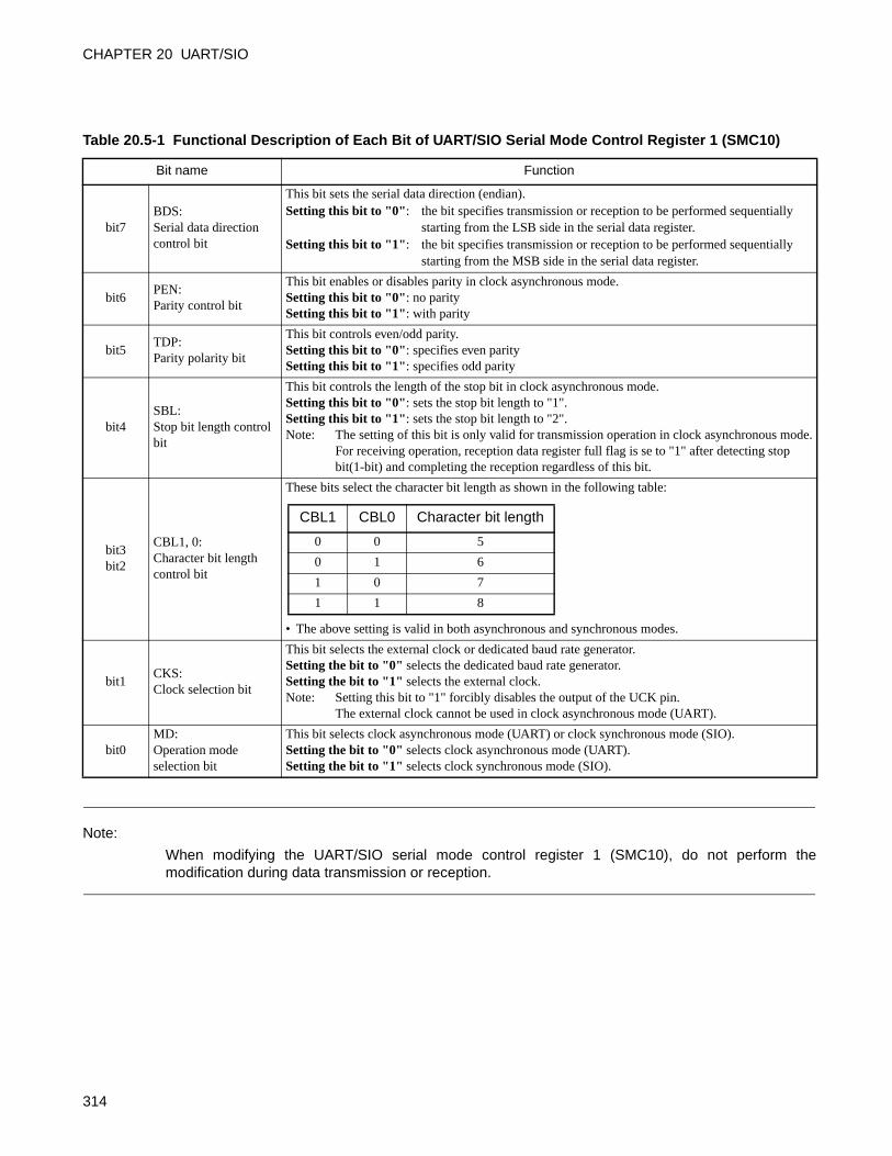
CHAPTER 20 UART/SIO
Note:
When modifying the UART/SIO serial mode control register 1 (SMC10), do not perform themodification during data transmission or reception.
Table 20.5-1 Functional Description of Each Bit of UART/SIO Serial Mode Control Register 1 (SMC10)
Bit name Function
bit7BDS:Serial data direction control bit
This bit sets the serial data direction (endian).Setting this bit to "0": the bit specifies transmission or reception to be performed sequentially
starting from the LSB side in the serial data register.Setting this bit to "1": the bit specifies transmission or reception to be performed sequentially
starting from the MSB side in the serial data register.
bit6PEN:Parity control bit
This bit enables or disables parity in clock asynchronous mode.Setting this bit to "0": no paritySetting this bit to "1": with parity
bit5TDP:Parity polarity bit
This bit controls even/odd parity.Setting this bit to "0": specifies even paritySetting this bit to "1": specifies odd parity
bit4SBL:Stop bit length control bit
This bit controls the length of the stop bit in clock asynchronous mode.Setting this bit to "0": sets the stop bit length to "1".Setting this bit to "1": sets the stop bit length to "2".Note: The setting of this bit is only valid for transmission operation in clock asynchronous mode.
For receiving operation, reception data register full flag is se to "1" after detecting stop bit(1-bit) and completing the reception regardless of this bit.
bit3bit2
CBL1, 0:Character bit length control bit
These bits select the character bit length as shown in the following table:
• The above setting is valid in both asynchronous and synchronous modes.
bit1CKS:Clock selection bit
This bit selects the external clock or dedicated baud rate generator.Setting the bit to "0" selects the dedicated baud rate generator.Setting the bit to "1" selects the external clock.Note: Setting this bit to "1" forcibly disables the output of the UCK pin.
The external clock cannot be used in clock asynchronous mode (UART).
bit0MD:Operation mode selection bit
This bit selects clock asynchronous mode (UART) or clock synchronous mode (SIO).Setting the bit to "0" selects clock asynchronous mode (UART).Setting the bit to "1" selects clock synchronous mode (SIO).
CBL1 CBL0 Character bit length
0 0 5
0 1 6
1 0 7
1 1 8
314
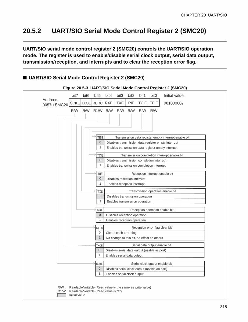
CHAPTER 20 UART/SIO
20.5.2 UART/SIO Serial Mode Control Register 2 (SMC20)
UART/SIO serial mode control register 2 (SMC20) controls the UART/SIO operation mode. The register is used to enable/disable serial clock output, serial data output, transmission/reception, and interrupts and to clear the reception error flag.
UART/SIO Serial Mode Control Register 2 (SMC20)
Figure 20.5-3 UART/SIO Serial Mode Control Register 2 (SMC20)
0
1
Disables serial data output (usable as port)
Enables serial data output
Serial data output enable bit
R/W : Readable/writable (Read value is the same as write value)R1/W : Readable/writable (Read value is "1") : Initial value
RIE
0
1
Disables reception interrupt
Enables reception interrupt
Reception interrupt enable bit
0
1
Clears each error flag
No change to this bit, no effect on others
Reception error flag clear bit
RXE
bit7Address0057H SMC20
bit6 bit5 bit4 bit3 bit2 bit1 bit0
00100000B
Initial value
TXE TCIE TEIERIE
R/WR/W
SCKE TXOE RERC
R/WR/WR/WR1/WR/WR/W
TEIE
SCKE
TXOE
RERC
RXE
TXE
0
1
Disables transmission data register empty interrupt
Enables transmission data register empty interrupt
Transmission data register empty interrupt enable bit
TCIE
0
1
Disables transmission completion interrupt
Enables transmission completion interrupt
Transmission completion interrupt enable bit
0
1
Disables transmission operation
Enables transmission operation
Transmission operation enable bit
0
1
Disables reception operation
Enables reception operation
Reception operation enable bit
0
1
Disables serial clock output (usable as port)
Enables serial clock output
Serial clock output enable bit
315
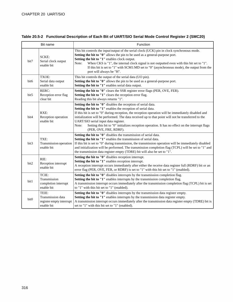
CHAPTER 20 UART/SIO
Table 20.5-2 Functional Description of Each Bit of UART/SIO Serial Mode Control Register 2 (SMC20)
Bit name Function
bit7SCKE:Serial clock output enable bit
This bit controls the input/output of the serial clock (UCK) pin in clock synchronous mode.Setting the bit to "0" allows the pin to be used as a general-purpose port.Setting the bit to "1" enables clock output.Note: When CKS is "1", the internal clock signal is not outputted even with this bit set to "1".
If this bit is set to "1" with SCM1:MD set to "0" (asynchronous mode), the output from the port will always be "H".
bit6TXOE:Serial data output enable bit
This bit controls the output of the serial data (UO pin).Setting the bit to "0" allows the pin to be used as a general-purpose port.Setting the bit to "1" enables serial data output.
bit5RERC:Reception error flag clear bit
Setting the bit to "0" clears the SSR register error flags (PER, OVE, FER).Setting the bit to "1" clears the reception error flag.Reading this bit always returns "1".
bit4RXE:Reception operation enable bit
Setting the bit to "0" disables the reception of serial data.Setting the bit to "1" enables the reception of serial data.If this bit is set to "0" during reception, the reception operation will be immediately disabled and initialization will be performed. The data received up to that point will not be transferred to the UART/SIO serial input data register. Note: Setting this bit to "0" initializes reception operation. It has no effect on the interrupt flags
(PER, OVE, FRE, RDRF).
bit3TXE:Transmission operation enable bit
Setting the bit to "0" disables the transmission of serial data.Setting the bit to "1" enables the transmission of serial data.If this bit is set to "0" during transmission, the transmission operation will be immediately disabled and initialization will be performed. The transmission completion flag (TCPL) will be set to "1" and the transmission data register empty (TDRE) bit will also be set to "1".
bit2RIE:Reception interrupt enable bit
Setting the bit to "0" disables reception interrupt.Setting the bit to "1" enables reception interrupt.A reception interrupt occurs immediately after either the receive data register full (RDRF) bit or an error flag (PER, OVE, FER, or RDRF) is set to "1" with this bit set to "1" (enabled).
bit1
TCIE:Transmission completion interrupt enable bit
Setting the bit to "0" disables interrupts by the transmission completion flag.Setting the bit to "1" enables interrupts by the transmission completion flag.A transmission interrupt occurs immediately after the transmission completion flag (TCPL) bit is set to "1" with this bit set to "1" (enabled).
bit0
TEIE:Transmission data register empty interrupt enable bit
Setting the bit to "0" disables interrupts by the transmission data register empty.Setting the bit to "1" enables interrupts by the transmission data register empty.A transmission interrupt occurs immediately after the transmission data register empty (TDRE) bit is set to "1" with this bit set to "1" (enabled).
316
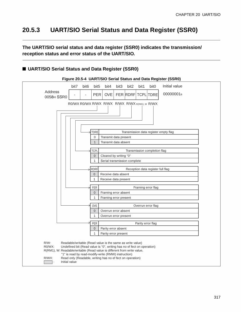
CHAPTER 20 UART/SIO
20.5.3 UART/SIO Serial Status and Data Register (SSR0)
The UART/SIO serial status and data register (SSR0) indicates the transmission/reception status and error status of the UART/SIO.
UART/SIO Serial Status and Data Register (SSR0)
Figure 20.5-4 UART/SIO Serial Status and Data Register (SSR0)
R/W: Readable/writable (Read value is the same as write value)R0/WX: Undefined bit (Read value is "0", writing has no ef fect on operation)R(RM1), W: Readable/writable (Read value is different from write value, "1" is read by read-modify-write (RMW) instruction)R/WX: Read only (Readable, writing has no ef fect on operation) : Initial value
- - PER OVE FER RDRF TCPL
R/WXR/WX
bit7Address0058H SSR0
bit6 bit5 bit4 bit3 bit2 bit1 bit0
00000001B
Initial value
R/WXR/WX R(RM1), W
OVE
0
1
Overrun error absent
Overrun error present
Overrun error flag
FER
0
1
Framing error absent
Framing error present
Framing error flag
TCPL
0
1
Cleared by writing "0"
Serial transmission complete
Transmission completion flag
PER
0
1
Parity error absent
Parity error present
Parity error flag
RDRF
0
1
Receive data absent
Receive data present
Reception data register full flag
TDRE
0
1
Transmit data present
Transmit data absent
Transmission data register empty flag
R/WX
TDRE
R0/WXR0/WX
317
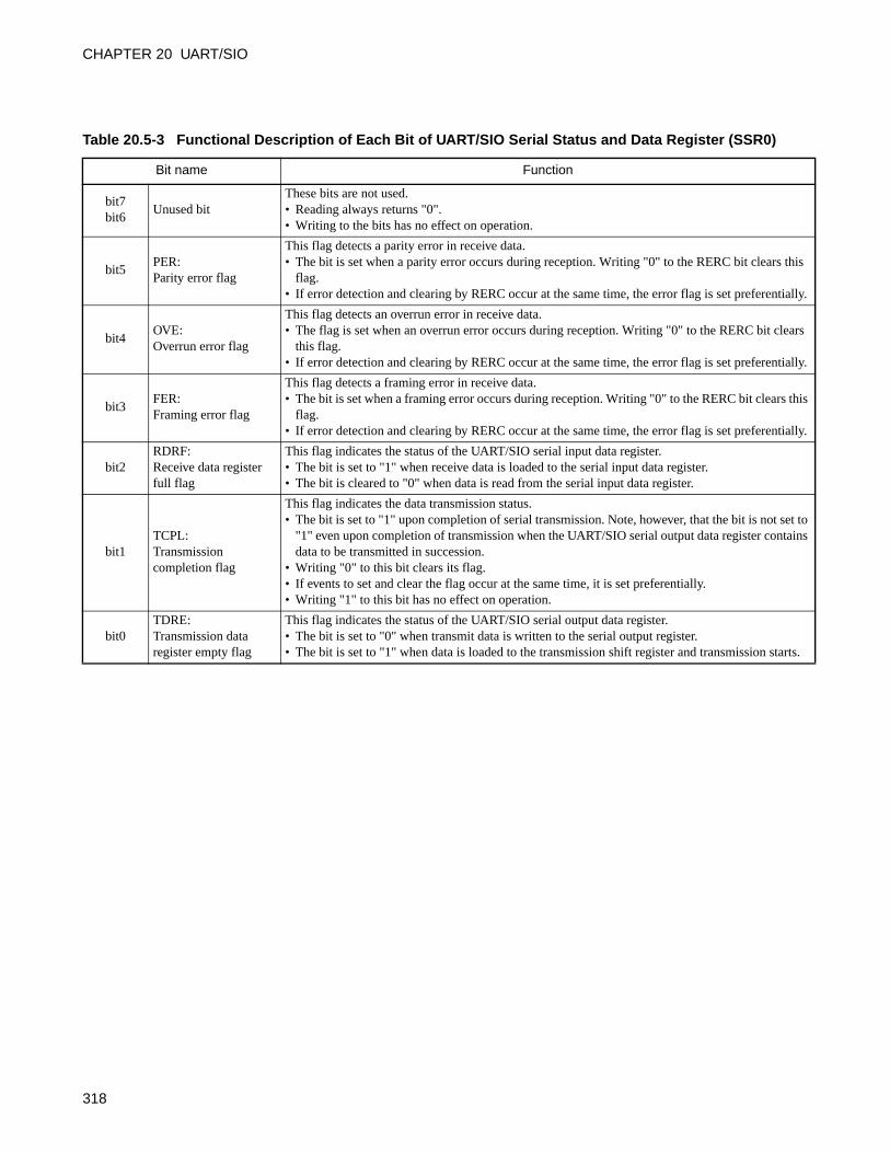
CHAPTER 20 UART/SIO
Table 20.5-3 Functional Description of Each Bit of UART/SIO Serial Status and Data Register (SSR0)
Bit name Function
bit7bit6
Unused bitThese bits are not used.• Reading always returns "0".• Writing to the bits has no effect on operation.
bit5PER:Parity error flag
This flag detects a parity error in receive data.• The bit is set when a parity error occurs during reception. Writing "0" to the RERC bit clears this
flag.• If error detection and clearing by RERC occur at the same time, the error flag is set preferentially.
bit4OVE:Overrun error flag
This flag detects an overrun error in receive data.• The flag is set when an overrun error occurs during reception. Writing "0" to the RERC bit clears
this flag.• If error detection and clearing by RERC occur at the same time, the error flag is set preferentially.
bit3FER:Framing error flag
This flag detects a framing error in receive data.• The bit is set when a framing error occurs during reception. Writing "0" to the RERC bit clears this
flag.• If error detection and clearing by RERC occur at the same time, the error flag is set preferentially.
bit2RDRF:Receive data register full flag
This flag indicates the status of the UART/SIO serial input data register.• The bit is set to "1" when receive data is loaded to the serial input data register.• The bit is cleared to "0" when data is read from the serial input data register.
bit1TCPL:Transmission completion flag
This flag indicates the data transmission status.• The bit is set to "1" upon completion of serial transmission. Note, however, that the bit is not set to
"1" even upon completion of transmission when the UART/SIO serial output data register contains data to be transmitted in succession.
• Writing "0" to this bit clears its flag.• If events to set and clear the flag occur at the same time, it is set preferentially.• Writing "1" to this bit has no effect on operation.
bit0TDRE:Transmission data register empty flag
This flag indicates the status of the UART/SIO serial output data register.• The bit is set to "0" when transmit data is written to the serial output register.• The bit is set to "1" when data is loaded to the transmission shift register and transmission starts.
318
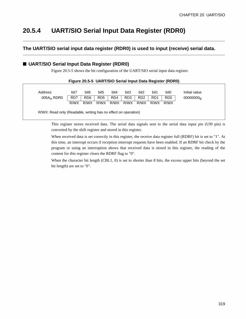
CHAPTER 20 UART/SIO
20.5.4 UART/SIO Serial Input Data Register (RDR0)
The UART/SIO serial input data register (RDR0) is used to input (receive) serial data.
UART/SIO Serial Input Data Register (RDR0)Figure 20.5-5 shows the bit configuration of the UART/SIO serial input data register.
Figure 20.5-5 UART/SIO Serial Input Data Register (RDR0)
This register stores received data. The serial data signals sent to the serial data input pin (UI0 pin) is
converted by the shift register and stored in this register.
When received data is set correctly in this register, the receive data register full (RDRF) bit is set to "1". At
this time, an interrupt occurs if reception interrupt requests have been enabled. If an RDRF bit check by the
program or using an interruption shows that received data is stored in this register, the reading of the
content for this register clears the RDRF flag to "0".
When the character bit length (CBL1, 0) is set to shorter than 8 bits, the excess upper bits (beyond the set
bit length) are set to "0".
Address bit7 bit6 bit5 bit4 bit3 bit2 bit1 bit0 Initial value
005AH RDR0 RD7 RD6 RD5 RD4 RD3 RD2 RD1 RD0 00000000B
R/WX R/WX R/WX R/WX R/WX R/WX R/WX R/WX
R/WX: Read only (Readable, writing has no effect on operation)
319
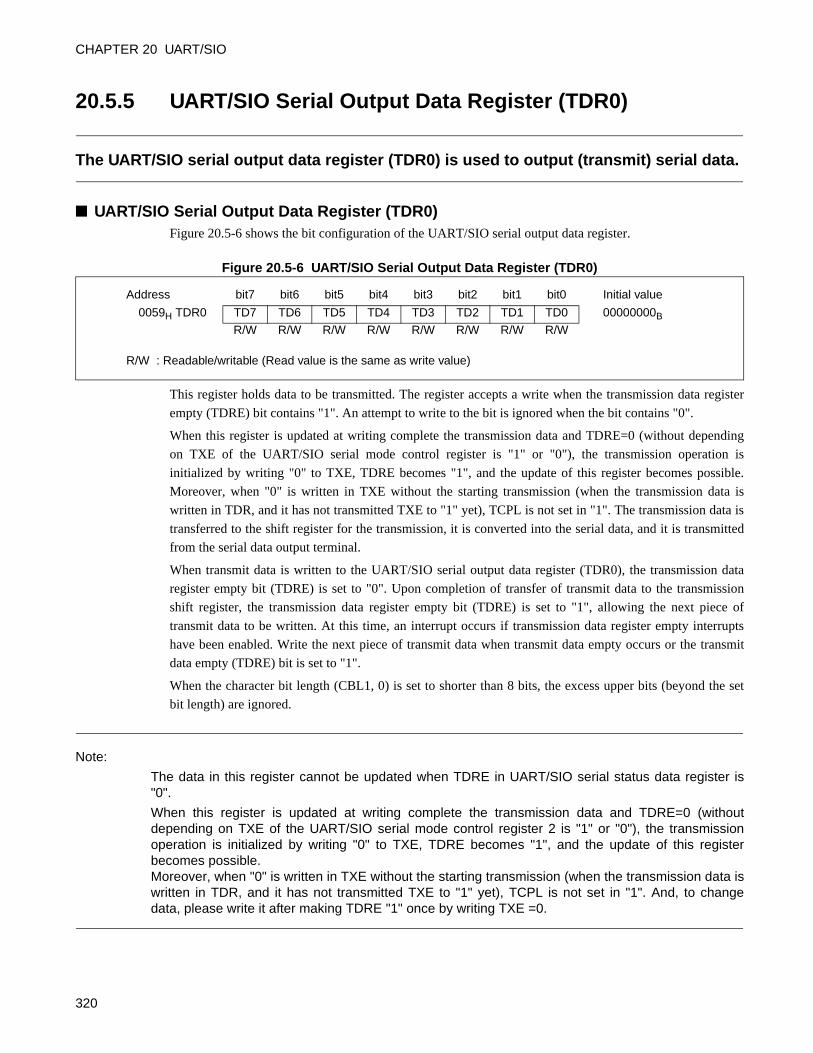
CHAPTER 20 UART/SIO
20.5.5 UART/SIO Serial Output Data Register (TDR0)
The UART/SIO serial output data register (TDR0) is used to output (transmit) serial data.
UART/SIO Serial Output Data Register (TDR0)Figure 20.5-6 shows the bit configuration of the UART/SIO serial output data register.
Figure 20.5-6 UART/SIO Serial Output Data Register (TDR0)
This register holds data to be transmitted. The register accepts a write when the transmission data register
empty (TDRE) bit contains "1". An attempt to write to the bit is ignored when the bit contains "0".
When this register is updated at writing complete the transmission data and TDRE=0 (without depending
on TXE of the UART/SIO serial mode control register is "1" or "0"), the transmission operation is
initialized by writing "0" to TXE, TDRE becomes "1", and the update of this register becomes possible.
Moreover, when "0" is written in TXE without the starting transmission (when the transmission data is
written in TDR, and it has not transmitted TXE to "1" yet), TCPL is not set in "1". The transmission data is
transferred to the shift register for the transmission, it is converted into the serial data, and it is transmitted
from the serial data output terminal.
When transmit data is written to the UART/SIO serial output data register (TDR0), the transmission data
register empty bit (TDRE) is set to "0". Upon completion of transfer of transmit data to the transmission
shift register, the transmission data register empty bit (TDRE) is set to "1", allowing the next piece of
transmit data to be written. At this time, an interrupt occurs if transmission data register empty interrupts
have been enabled. Write the next piece of transmit data when transmit data empty occurs or the transmit
data empty (TDRE) bit is set to "1".
When the character bit length (CBL1, 0) is set to shorter than 8 bits, the excess upper bits (beyond the set
bit length) are ignored.
Note:
The data in this register cannot be updated when TDRE in UART/SIO serial status data register is"0".
When this register is updated at writing complete the transmission data and TDRE=0 (withoutdepending on TXE of the UART/SIO serial mode control register 2 is "1" or "0"), the transmissionoperation is initialized by writing "0" to TXE, TDRE becomes "1", and the update of this registerbecomes possible. Moreover, when "0" is written in TXE without the starting transmission (when the transmission data iswritten in TDR, and it has not transmitted TXE to "1" yet), TCPL is not set in "1". And, to changedata, please write it after making TDRE "1" once by writing TXE =0.
Address bit7 bit6 bit5 bit4 bit3 bit2 bit1 bit0 Initial value
0059H TDR0 TD7 TD6 TD5 TD4 TD3 TD2 TD1 TD0 00000000B
R/W R/W R/W R/W R/W R/W R/W R/W
R/W : Readable/writable (Read value is the same as write value)
320
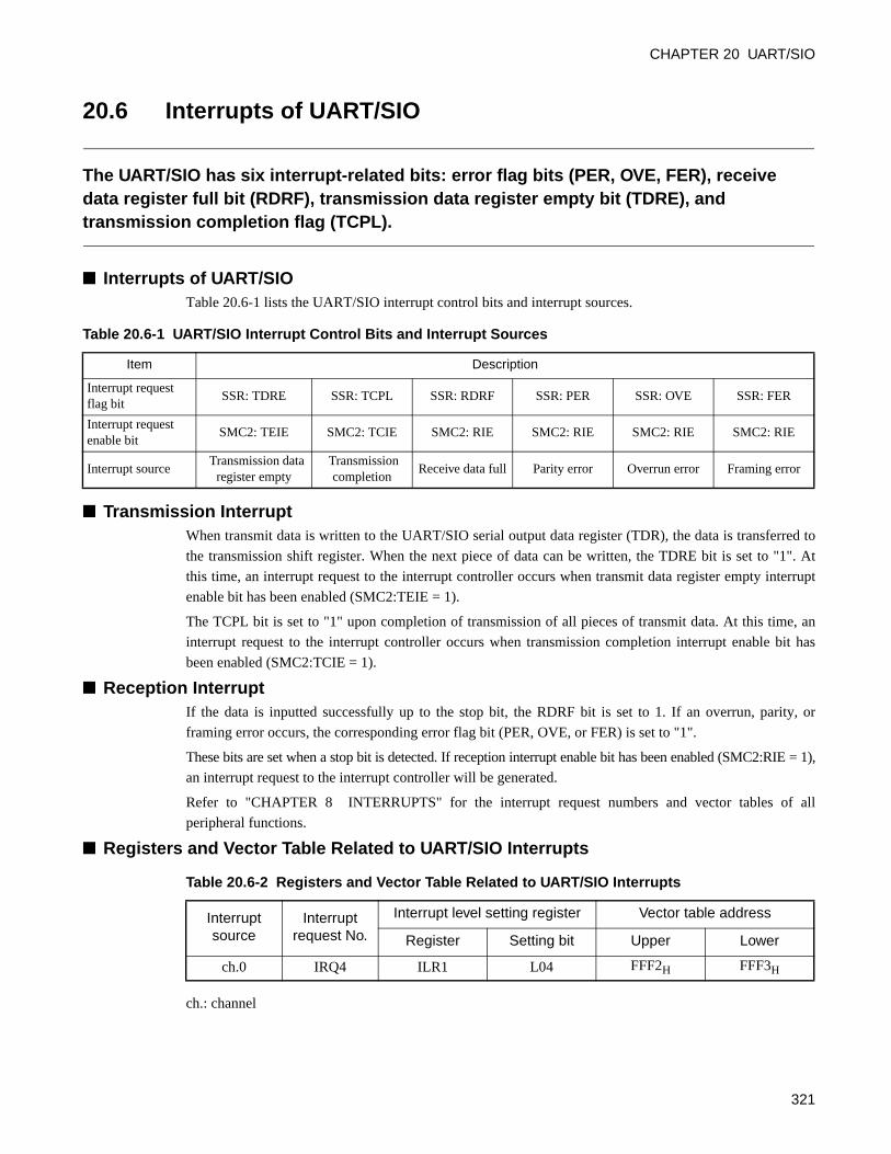
CHAPTER 20 UART/SIO
20.6 Interrupts of UART/SIO
The UART/SIO has six interrupt-related bits: error flag bits (PER, OVE, FER), receive data register full bit (RDRF), transmission data register empty bit (TDRE), and transmission completion flag (TCPL).
Interrupts of UART/SIOTable 20.6-1 lists the UART/SIO interrupt control bits and interrupt sources.
Transmission InterruptWhen transmit data is written to the UART/SIO serial output data register (TDR), the data is transferred to
the transmission shift register. When the next piece of data can be written, the TDRE bit is set to "1". At
this time, an interrupt request to the interrupt controller occurs when transmit data register empty interrupt
enable bit has been enabled (SMC2:TEIE = 1).
The TCPL bit is set to "1" upon completion of transmission of all pieces of transmit data. At this time, an
interrupt request to the interrupt controller occurs when transmission completion interrupt enable bit has
been enabled (SMC2:TCIE = 1).
Reception InterruptIf the data is inputted successfully up to the stop bit, the RDRF bit is set to 1. If an overrun, parity, or
framing error occurs, the corresponding error flag bit (PER, OVE, or FER) is set to "1".
These bits are set when a stop bit is detected. If reception interrupt enable bit has been enabled (SMC2:RIE = 1),
an interrupt request to the interrupt controller will be generated.
Refer to "CHAPTER 8 INTERRUPTS" for the interrupt request numbers and vector tables of all
peripheral functions.
Registers and Vector Table Related to UART/SIO Interrupts
ch.: channel
Table 20.6-1 UART/SIO Interrupt Control Bits and Interrupt Sources
Item Description
Interrupt request flag bit
SSR: TDRE SSR: TCPL SSR: RDRF SSR: PER SSR: OVE SSR: FER
Interrupt request enable bit
SMC2: TEIE SMC2: TCIE SMC2: RIE SMC2: RIE SMC2: RIE SMC2: RIE
Interrupt source Transmission data
register empty Transmission
completionReceive data full Parity error Overrun error Framing error
Table 20.6-2 Registers and Vector Table Related to UART/SIO Interrupts
Interrupt source
Interrupt request No.
Interrupt level setting register Vector table address
Register Setting bit Upper Lower
ch.0 IRQ4 ILR1 L04 FFF2H FFF3H
321
CHAPTER 20 UART/SIO
20.7 Explanation of UART/SIO Operations and Setup Procedure Example
The UART/SIO has a serial communication function (operation mode 0, 1).
Operation of UART/SIO
Operation mode
Two operation modes are available in the UART/SIO. Clock synchronous mode (SIO) or clock
asynchronous mode (SUAR) can be selected (see Table 20.7-1).
Setup Procedure ExampleThe UART/SIO is set up in the following procedure.
Initial setup
1) Set the port input. (DDR1)
2) Set the interrupt level. (ILR1)
3) Set the prescaler. (PSSR)
4) Set the baud rate. (BRSR)
5) Select the clock. (SMC10:CKS)
6) Set the operation mode. (SMC10:MD)
7) Enable/disable the serial clock output. (SMC20:SCKE)
8) Enable reception. (SMC20:RXE = 1)
9) Enable interrupts. (SMC20:RIE = 1)
Interrupt processing
Read receive data. (RDR0)
Table 20.7-1 Operation Modes of UART/SIO
Operation modeData length Synchronization
modeLength of stop bit
No parity With parity
0
5 6
Asynchronous 1 bit or 2 bits6 7
7 8
8 9
1
5 -
Synchronous -6 -
7 -
8 -
322
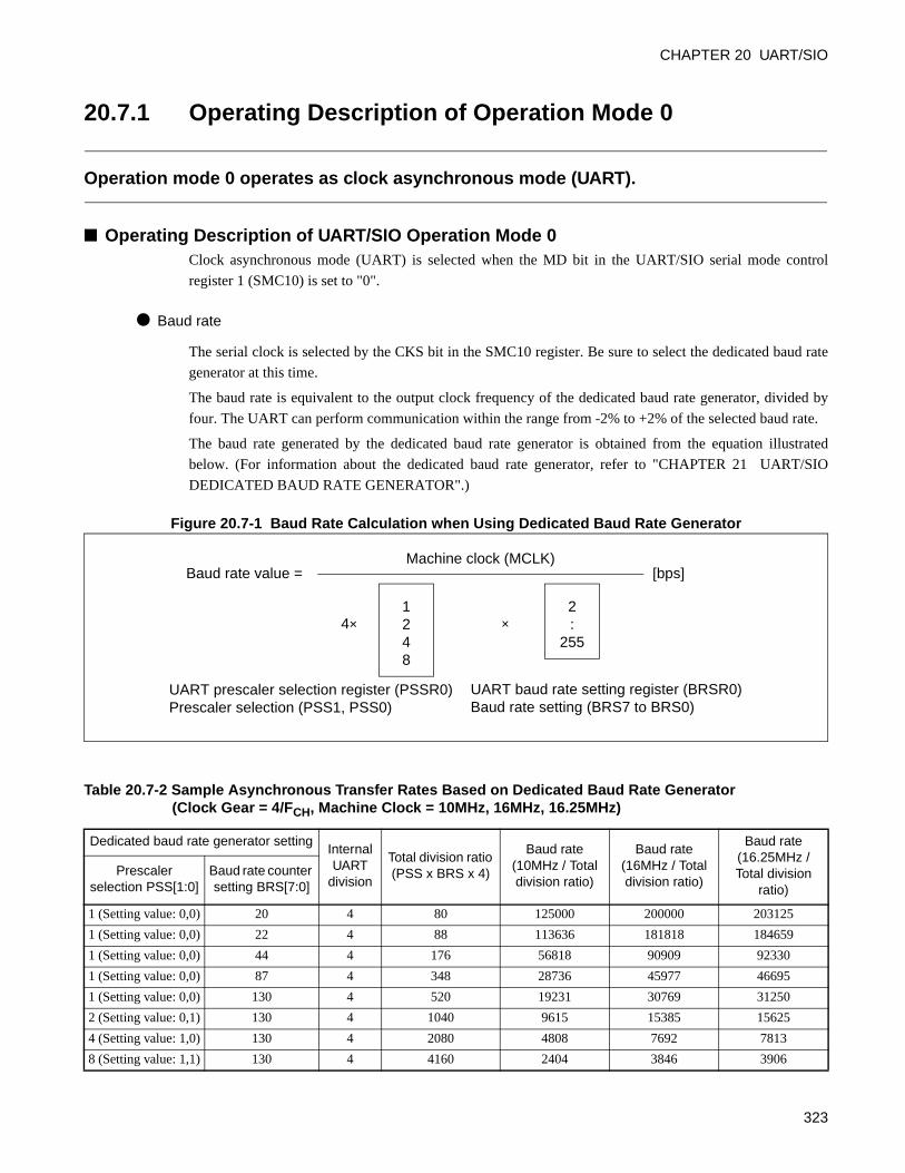
CHAPTER 20 UART/SIO
20.7.1 Operating Description of Operation Mode 0
Operation mode 0 operates as clock asynchronous mode (UART).
Operating Description of UART/SIO Operation Mode 0Clock asynchronous mode (UART) is selected when the MD bit in the UART/SIO serial mode control
register 1 (SMC10) is set to "0".
Baud rate
The serial clock is selected by the CKS bit in the SMC10 register. Be sure to select the dedicated baud rate
generator at this time.
The baud rate is equivalent to the output clock frequency of the dedicated baud rate generator, divided by
four. The UART can perform communication within the range from -2% to +2% of the selected baud rate.
The baud rate generated by the dedicated baud rate generator is obtained from the equation illustrated
below. (For information about the dedicated baud rate generator, refer to "CHAPTER 21 UART/SIO
DEDICATED BAUD RATE GENERATOR".)
Figure 20.7-1 Baud Rate Calculation when Using Dedicated Baud Rate Generator
Baud rate value =Machine clock (MCLK)
[bps]
4× ×1248
2:
255
UART baud rate setting register (BRSR0)Baud rate setting (BRS7 to BRS0)
UART prescaler selection register (PSSR0)Prescaler selection (PSS1, PSS0)
Table 20.7-2 Sample Asynchronous Transfer Rates Based on Dedicated Baud Rate Generator(Clock Gear = 4/FCH, Machine Clock = 10MHz, 16MHz, 16.25MHz)
Dedicated baud rate generator settingInternal UART
division
Total division ratio (PSS x BRS x 4)
Baud rate (10MHz / Total division ratio)
Baud rate (16MHz / Total division ratio)
Baud rate (16.25MHz / Total division
ratio)
Prescaler selection PSS[1:0]
Baud rate counter setting BRS[7:0]
1 (Setting value: 0,0) 20 4 80 125000 200000 203125
1 (Setting value: 0,0) 22 4 88 113636 181818 184659
1 (Setting value: 0,0) 44 4 176 56818 90909 92330
1 (Setting value: 0,0) 87 4 348 28736 45977 46695
1 (Setting value: 0,0) 130 4 520 19231 30769 31250
2 (Setting value: 0,1) 130 4 1040 9615 15385 15625
4 (Setting value: 1,0) 130 4 2080 4808 7692 7813
8 (Setting value: 1,1) 130 4 4160 2404 3846 3906
323
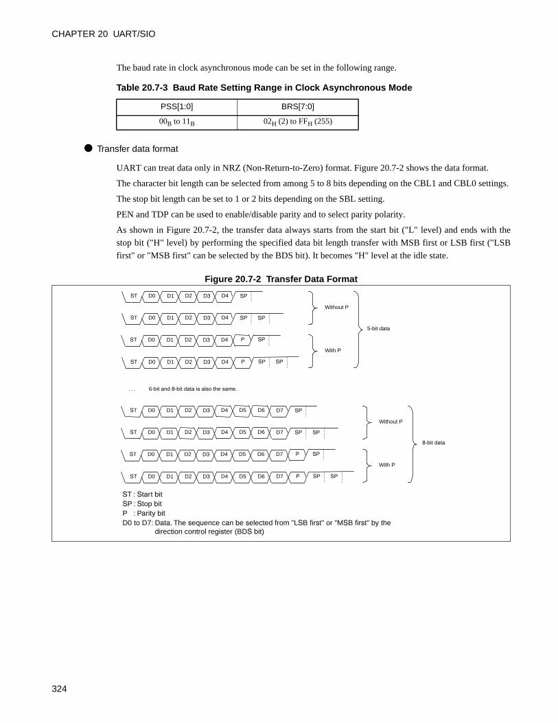
CHAPTER 20 UART/SIO
The baud rate in clock asynchronous mode can be set in the following range.
Transfer data format
UART can treat data only in NRZ (Non-Return-to-Zero) format. Figure 20.7-2 shows the data format.
The character bit length can be selected from among 5 to 8 bits depending on the CBL1 and CBL0 settings.
The stop bit length can be set to 1 or 2 bits depending on the SBL setting.
PEN and TDP can be used to enable/disable parity and to select parity polarity.
As shown in Figure 20.7-2, the transfer data always starts from the start bit ("L" level) and ends with the
stop bit ("H" level) by performing the specified data bit length transfer with MSB first or LSB first ("LSB
first" or "MSB first" can be selected by the BDS bit). It becomes "H" level at the idle state.
Figure 20.7-2 Transfer Data Format
Table 20.7-3 Baud Rate Setting Range in Clock Asynchronous Mode
PSS[1:0] BRS[7:0]
00B to 11B 02H (2) to FFH (255)
ST D0 D1 D2 D3 D4 SP
ST D0 D1 D2 D3 D4 P SP
ST D0 D1 D2 D3 D4 SP SP
ST D0 D1 D2 D3 D4 P SP SP
ST D0 D1 D2 D3 D4 D5 D6 D7 SP
ST D0 D1 D2 D3 D4 D5 D6 P SPD7
ST D0 D1 D2 D3 D4 D5 D6 D7 SP SP
ST D0 D1 D2 D3 D4 D5 D6 P SPD7 SP
Without P
With P
Without P
With P
5-bit data
8-bit data
ST : Start bit SP : Stop bitP : Parity bitD0 to D7: Data. The sequence can be selected from "LSB first" or "MSB first" by the
direction control register (BDS bit)
. . . 6-bit and 8-bit data is also the same.
324
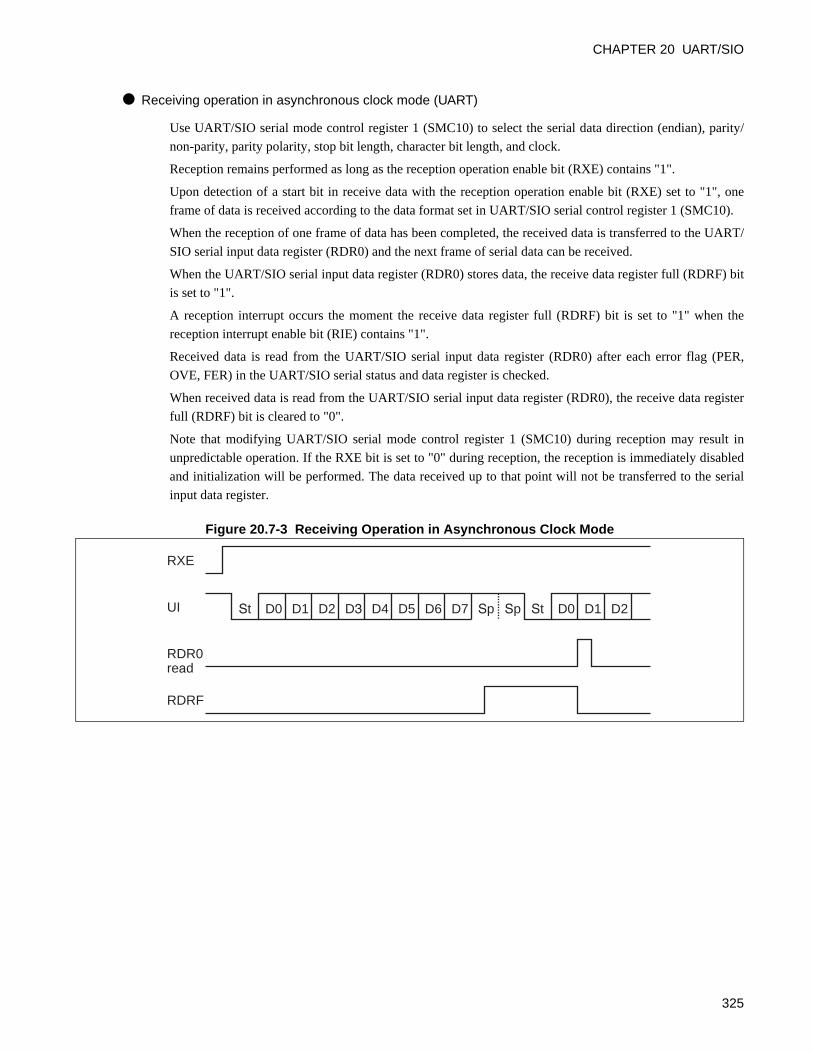
CHAPTER 20 UART/SIO
Receiving operation in asynchronous clock mode (UART)
Use UART/SIO serial mode control register 1 (SMC10) to select the serial data direction (endian), parity/
non-parity, parity polarity, stop bit length, character bit length, and clock.
Reception remains performed as long as the reception operation enable bit (RXE) contains "1".
Upon detection of a start bit in receive data with the reception operation enable bit (RXE) set to "1", one
frame of data is received according to the data format set in UART/SIO serial control register 1 (SMC10).
When the reception of one frame of data has been completed, the received data is transferred to the UART/
SIO serial input data register (RDR0) and the next frame of serial data can be received.
When the UART/SIO serial input data register (RDR0) stores data, the receive data register full (RDRF) bit
is set to "1".
A reception interrupt occurs the moment the receive data register full (RDRF) bit is set to "1" when the
reception interrupt enable bit (RIE) contains "1".
Received data is read from the UART/SIO serial input data register (RDR0) after each error flag (PER,
OVE, FER) in the UART/SIO serial status and data register is checked.
When received data is read from the UART/SIO serial input data register (RDR0), the receive data register
full (RDRF) bit is cleared to "0".
Note that modifying UART/SIO serial mode control register 1 (SMC10) during reception may result in
unpredictable operation. If the RXE bit is set to "0" during reception, the reception is immediately disabled
and initialization will be performed. The data received up to that point will not be transferred to the serial
input data register.
Figure 20.7-3 Receiving Operation in Asynchronous Clock Mode
UI St D0 D1 D2 D3 D4 D5 D6 Sp SpD7 St D0 D1 D2
RXE
RDR0 read
RDRF
325
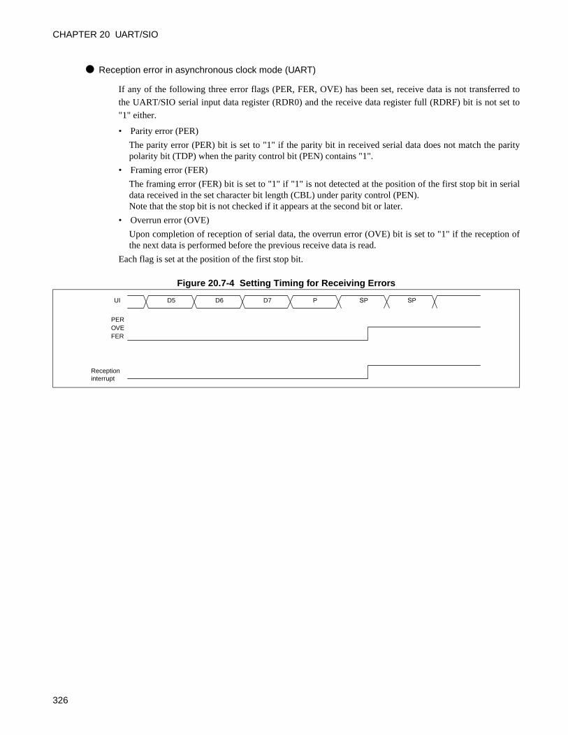
CHAPTER 20 UART/SIO
Reception error in asynchronous clock mode (UART)
If any of the following three error flags (PER, FER, OVE) has been set, receive data is not transferred to
the UART/SIO serial input data register (RDR0) and the receive data register full (RDRF) bit is not set to
"1" either.
• Parity error (PER)
The parity error (PER) bit is set to "1" if the parity bit in received serial data does not match the paritypolarity bit (TDP) when the parity control bit (PEN) contains "1".
• Framing error (FER)
The framing error (FER) bit is set to "1" if "1" is not detected at the position of the first stop bit in serialdata received in the set character bit length (CBL) under parity control (PEN). Note that the stop bit is not checked if it appears at the second bit or later.
• Overrun error (OVE)
Upon completion of reception of serial data, the overrun error (OVE) bit is set to "1" if the reception ofthe next data is performed before the previous receive data is read.
Each flag is set at the position of the first stop bit.
Figure 20.7-4 Setting Timing for Receiving Errors
UI D5 D6 D7 P SP SP
PEROVEFER
Reception interrupt
326
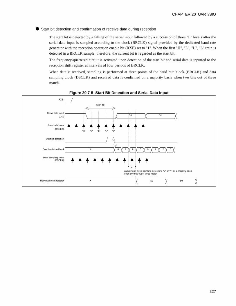
CHAPTER 20 UART/SIO
Start bit detection and confirmation of receive data during reception
The start bit is detected by a falling of the serial input followed by a succession of three "L" levels after the
serial data input is sampled according to the clock (BRCLK) signal provided by the dedicated baud rate
generator with the reception operation enable bit (RXE) set to "1". When the first "H", "L", "L", "L" train is
detected in a BRCLK sample, therefore, the current bit is regarded as the start bit.
The frequency-quartered circuit is activated upon detection of the start bit and serial data is inputted to the
reception shift register at intervals of four periods of BRCLK.
When data is received, sampling is performed at three points of the baud rate clock (BRCLK) and data
sampling clock (DSCLK) and received data is confirmed on a majority basis when two bits out of three
match.
Figure 20.7-5 Start Bit Detection and Serial Data Input
Baud rate clock
(BRCLK)
RXE
Counter divided by 4 0
"H"
D0
X
Reception shift register
"L" "L "L" "L" "
D1
1 2 3
Data sampling clock(DSCLK)
Serial data input
(UI0)
Start bit detection
0 1 2 3
D0 D1 X
Start bit
Sampling at three points to determine "0" or "1" on a majority basis when two bits out of three match
327
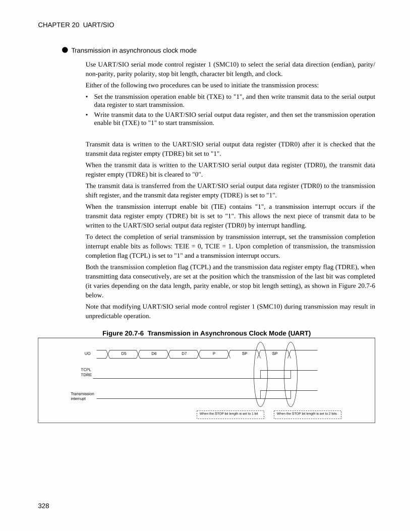
CHAPTER 20 UART/SIO
Transmission in asynchronous clock mode
Use UART/SIO serial mode control register 1 (SMC10) to select the serial data direction (endian), parity/
non-parity, parity polarity, stop bit length, character bit length, and clock.
Either of the following two procedures can be used to initiate the transmission process:
• Set the transmission operation enable bit (TXE) to "1", and then write transmit data to the serial outputdata register to start transmission.
• Write transmit data to the UART/SIO serial output data register, and then set the transmission operationenable bit (TXE) to "1" to start transmission.
Transmit data is written to the UART/SIO serial output data register (TDR0) after it is checked that the
transmit data register empty (TDRE) bit set to "1".
When the transmit data is written to the UART/SIO serial output data register (TDR0), the transmit data
register empty (TDRE) bit is cleared to "0".
The transmit data is transferred from the UART/SIO serial output data register (TDR0) to the transmission
shift register, and the transmit data register empty (TDRE) is set to "1".
When the transmission interrupt enable bit (TIE) contains "1", a transmission interrupt occurs if the
transmit data register empty (TDRE) bit is set to "1". This allows the next piece of transmit data to be
written to the UART/SIO serial output data register (TDR0) by interrupt handling.
To detect the completion of serial transmission by transmission interrupt, set the transmission completion
interrupt enable bits as follows: TEIE = 0, TCIE = 1. Upon completion of transmission, the transmission
completion flag (TCPL) is set to "1" and a transmission interrupt occurs.
Both the transmission completion flag (TCPL) and the transmission data register empty flag (TDRE), when
transmitting data consecutively, are set at the position which the transmission of the last bit was completed
(it varies depending on the data length, parity enable, or stop bit length setting), as shown in Figure 20.7-6
below.
Note that modifying UART/SIO serial mode control register 1 (SMC10) during transmission may result in
unpredictable operation.
Figure 20.7-6 Transmission in Asynchronous Clock Mode (UART)
UO D5 D6 D7 P SP SP
TCPLTDRE
Transmission interrupt
When the STOP bit length is set to 2 bitsWhen the STOP bit length is set to 1 bit
328
CHAPTER 20 UART/SIO
The TDRE flag is set at the point indicated in the following figure if the preceding piece of transmit data
does not exist in the transmission shift register.
Figure 20.7-7 Setting Timing 1 for Transmit Data Register Empty Flag (TDRE) (When TXE is "1")
Figure 20.7-8 Setting Timing 2 for Transmit Data Register Empty Flag (TDRE) (When TXE Is Switched from "0" to "1")
Concurrent transmission and reception
In asynchronous clock mode (UART), transmission and reception can be performed independently.
Therefore, transmission and reception can be performed at the same time or even with transmitting and
receiving frames overlapping each other in shifted phases.
UO D0 D1
TDRE
Transmission interrupt
TXE"1"
Writing of transmit data
D2 D3
Data transfer from UART/SIO serial output data register (TDR) to transmission shift register is performed in one machine clock (MCLK) cycle.
UO D0 D1
TDRE
TXE
D2 D3
Transmission interrupt
Writing of transmit data
329
CHAPTER 20 UART/SIO
20.7.2 Operating Description of Operation Mode 1
Operation mode 1 operates in synchronous clock mode.
Operating Description of UART/SIO Operation Mode 1Setting the MD bit in UART/SIO serial mode control register 1 (SMC10) to "1" selects synchronous clock
mode (SIO).
The character bit length in synchronous clock mode (SIO) is variable between 5 bits and 8 bits.
Note, however, that parity is disabled and no stop bit is used.
The serial clock is selected by the CKS bit in the SMC10 register. Select the dedicated baud rate generator
or external clock. The SIO performs shift operation using the selected serial clock as a shift clock.
To input the external clock signal, set the SCKE bit to "0".
To output the dedicated baud rate generator output as a shift clock signal, set the SCKE bit to "1". The
serial clock signal is obtained by dividing clock by two, which is supplied by the dedicated baud rate
generator. The baud rate in the SIO mode can be set in the following range. (For more information about
the dedicated baud rate generator, also refer to "CHAPTER 21 UART/SIO DEDICATED BAUD RATE
GENERATOR")
The baud rate applied when the external clock or dedicated baud rate generator is used is obtained from the
corresponding equation illustrated below.
Figure 20.7-9 Calculating Baud Rate Based on External Clock
Table 20.7-4 Baud Rate Setting Range in SIO Mode
PSS[1:0] BRS[7:0]
00B to 11B01H(1) to FFH(255), 00H(256)
(The highest and lowest baud rate settings are 01H and 00H, respectively.)
Baud rate value =1
[bps]External clock*
*: External clock
More than 4 machine clock
More than 4 machine clock
330
CHAPTER 20 UART/SIO
Figure 20.7-10 Baud Rate Calculation Formula for Using Dedicated Baud Rate Generator
Serial clock
The serial clock signal is outputted under control of the output for transmit data. When only reception is
performed, therefore, set transmission control (TXE = 1) to write dummy transmit data to the UART/SIO
serial output register. Refer to the data sheet for the UCK clock value.
Reception in UART/SIO operation mode 1
For reception in operation mode 1, each register is used as follows.
Baud rate value =
Machine clock (MCLK)[bps]
2× ×1248
1:
256
UART baud rate setting register (BRSR0)Baud rate setting (BRS7 to BRS0)
UART prescaler selection register (PSSR0)Prescaler selection (PSS1, PSS0)
331
CHAPTER 20 UART/SIO
Figure 20.7-11 Registers Used for Reception in Operation Mode 1
The reception depends on whether the serial clock has been set to external or internal clock.
<When external clock is enabled>
When the reception operation enable bit (RXE) contains "1", serial data is received always at the risingedge of the external clock signal.
<When internal clock is enabled>
The serial clock signal is outputted in accordance with transmission. Therefore, transmission must beperformed even when only performing reception. The following two procedures can be used.
• Set the transmission operation enable bit (TXE) to "1", then write transmit data to the UART/SIO serialoutput data register to generate the serial clock signal and start reception.
SMC10 (UART/SIO serial mode control register 1)
bit7 bit6 bit5 bit4 bit3 bit2 bit1 bit0
BDS PEN TDP SBL CBL1 CBL0 CKS MD SMC10× × × 1
SMC20 (UART/SIO serial mode control register 2)
bit7 bit6 bit5 bit4 bit3 bit2 bit1 bit0
SCKE TXOE RERC RXE TXE RIE TCIE TEIE SMC200 × ×
SSR0 (UART/SIO serial status and data register)
bit7 bit6 bit5 bit4 bit3 bit2 bit1 bit0
- - PER OVE FER RDRF TCPL TDRE SSR0× × × × × ×
TDR0 (UART/SIO serial output data register)
bit7 bit6 bit5 bit4 bit3 bit2 bit1 bit0
TD7 TD6 TD5 TD4 TD3 TD2 TD1 TD0 TDR0× × × × × × × ×
RDR0 (UART/SIO serial input data register)
bit7 bit6 bit5 bit4 bit3 bit2 bit1 bit0
RD7 RD6 RD5 RD4 RD3 RD2 RD1 RD0 RDR0
: Used bitx : Unused bit1 : Set "1"0 : Set "0"
332
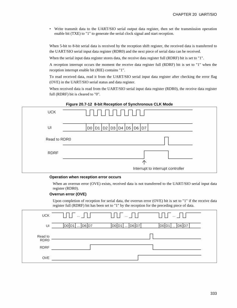
CHAPTER 20 UART/SIO
• Write transmit data to the UART/SIO serial output data register, then set the transmission operationenable bit (TXE) to "1" to generate the serial clock signal and start reception.
When 5-bit to 8-bit serial data is received by the reception shift register, the received data is transferred to
the UART/SIO serial input data register (RDR0) and the next piece of serial data can be received.
When the serial input data register stores data, the receive data register full (RDRF) bit is set to "1".
A reception interrupt occurs the moment the receive data register full (RDRF) bit is set to "1" when the
reception interrupt enable bit (RIE) contains "1".
To read received data, read it from the UART/SIO serial input data register after checking the error flag
(OVE) in the UART/SIO serial status and data register.
When received data is read from the UART/SIO serial input data register (RDR0), the receive data register
full (RDRF) bit is cleared to "0".
Figure 20.7-12 8-bit Reception of Synchronous CLK Mode
Operation when reception error occurs
When an overrun error (OVE) exists, received data is not transferred to the UART/SIO serial input dataregister (RDR0).
Overrun error (OVE)
Upon completion of reception for serial data, the overrun error (OVE) bit is set to "1" if the receive dataregister full (RDRF) bit has been set to "1" by the reception for the preceding piece of data.
UI D0 D1 D2 D3 D4 D5 D6 D7
UCK
Read to RDR0
RDRF
Interrupt to interrupt controller
UCK
UI D0 D1 ... D6 D7 D0 D1 ... D6 D7 D0 D1 ...
... ... ...
D6 D7
Read to RDR0
RDRF
OVE
333
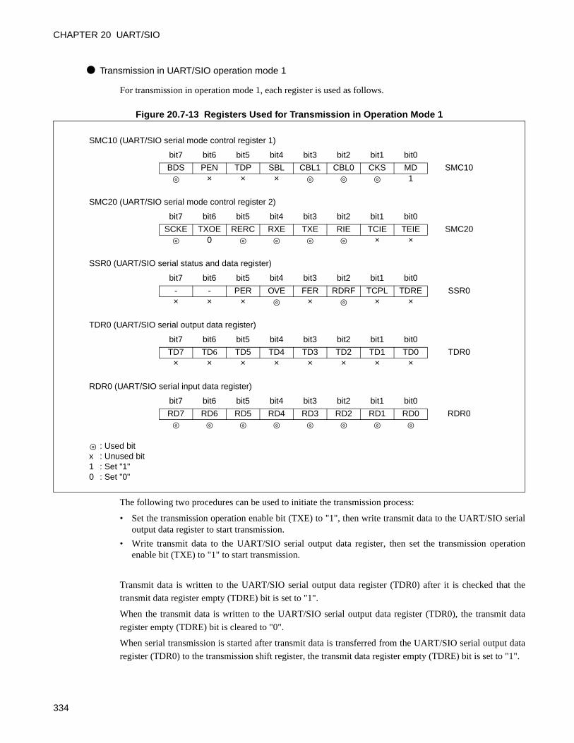
CHAPTER 20 UART/SIO
Transmission in UART/SIO operation mode 1
For transmission in operation mode 1, each register is used as follows.
Figure 20.7-13 Registers Used for Transmission in Operation Mode 1
The following two procedures can be used to initiate the transmission process:
• Set the transmission operation enable bit (TXE) to "1", then write transmit data to the UART/SIO serialoutput data register to start transmission.
• Write transmit data to the UART/SIO serial output data register, then set the transmission operationenable bit (TXE) to "1" to start transmission.
Transmit data is written to the UART/SIO serial output data register (TDR0) after it is checked that the
transmit data register empty (TDRE) bit is set to "1".
When the transmit data is written to the UART/SIO serial output data register (TDR0), the transmit data
register empty (TDRE) bit is cleared to "0".
When serial transmission is started after transmit data is transferred from the UART/SIO serial output data
register (TDR0) to the transmission shift register, the transmit data register empty (TDRE) bit is set to "1".
SMC10 (UART/SIO serial mode control register 1)
bit7 bit6 bit5 bit4 bit3 bit2 bit1 bit0
BDS PEN TDP SBL CBL1 CBL0 CKS MD SMC10× × × 1
SMC20 (UART/SIO serial mode control register 2)
bit7 bit6 bit5 bit4 bit3 bit2 bit1 bit0
SCKE TXOE RERC RXE TXE RIE TCIE TEIE SMC200 × ×
SSR0 (UART/SIO serial status and data register)
bit7 bit6 bit5 bit4 bit3 bit2 bit1 bit0
- - PER OVE FER RDRF TCPL TDRE SSR0× × × × × ×
TDR0 (UART/SIO serial output data register)
bit7 bit6 bit5 bit4 bit3 bit2 bit1 bit0
TD7 TD6 TD5 TD4 TD3 TD2 TD1 TD0 TDR0× × × × × × × ×
RDR0 (UART/SIO serial input data register)
bit7 bit6 bit5 bit4 bit3 bit2 bit1 bit0
RD7 RD6 RD5 RD4 RD3 RD2 RD1 RD0 RDR0
: Used bitx : Unused bit1 : Set "1"0 : Set "0"
334
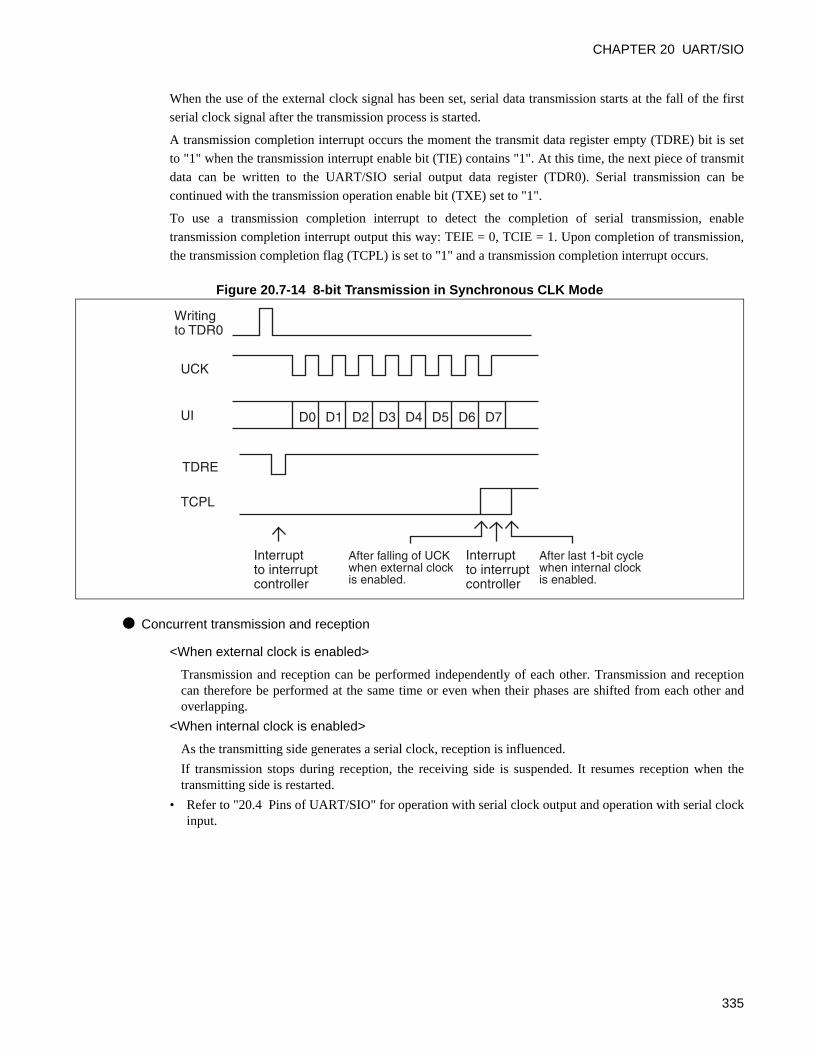
CHAPTER 20 UART/SIO
When the use of the external clock signal has been set, serial data transmission starts at the fall of the first
serial clock signal after the transmission process is started.
A transmission completion interrupt occurs the moment the transmit data register empty (TDRE) bit is set
to "1" when the transmission interrupt enable bit (TIE) contains "1". At this time, the next piece of transmit
data can be written to the UART/SIO serial output data register (TDR0). Serial transmission can be
continued with the transmission operation enable bit (TXE) set to "1".
To use a transmission completion interrupt to detect the completion of serial transmission, enable
transmission completion interrupt output this way: TEIE = 0, TCIE = 1. Upon completion of transmission,
the transmission completion flag (TCPL) is set to "1" and a transmission completion interrupt occurs.
Figure 20.7-14 8-bit Transmission in Synchronous CLK Mode
Concurrent transmission and reception
<When external clock is enabled>
Transmission and reception can be performed independently of each other. Transmission and receptioncan therefore be performed at the same time or even when their phases are shifted from each other andoverlapping.
<When internal clock is enabled>
As the transmitting side generates a serial clock, reception is influenced.
If transmission stops during reception, the receiving side is suspended. It resumes reception when thetransmitting side is restarted.
• Refer to "20.4 Pins of UART/SIO" for operation with serial clock output and operation with serial clockinput.
UI D0 D1 D2 D3 D4 D5 D6 D7
UCK
TCPL
Writing to TDR0
Interrupt to interrupt controller
TDRE
Interrupt to interrupt controller
After falling of UCKwhen external clock is enabled.
After last 1-bit cyclewhen internal clockis enabled.
335
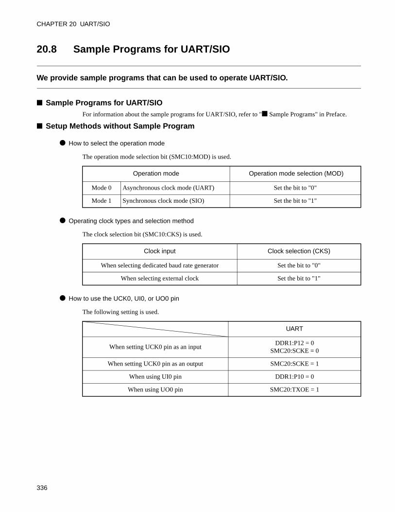
CHAPTER 20 UART/SIO
20.8 Sample Programs for UART/SIO
We provide sample programs that can be used to operate UART/SIO.
Sample Programs for UART/SIOFor information about the sample programs for UART/SIO, refer to " Sample Programs" in Preface.
Setup Methods without Sample Program
How to select the operation mode
The operation mode selection bit (SMC10:MOD) is used.
Operating clock types and selection method
The clock selection bit (SMC10:CKS) is used.
How to use the UCK0, UI0, or UO0 pin
The following setting is used.
Operation mode Operation mode selection (MOD)
Mode 0 Asynchronous clock mode (UART) Set the bit to "0"
Mode 1 Synchronous clock mode (SIO) Set the bit to "1"
Clock input Clock selection (CKS)
When selecting dedicated baud rate generator Set the bit to "0"
When selecting external clock Set the bit to "1"
UART
When setting UCK0 pin as an inputDDR1:P12 = 0
SMC20:SCKE = 0
When setting UCK0 pin as an output SMC20:SCKE = 1
When using UI0 pin DDR1:P10 = 0
When using UO0 pin SMC20:TXOE = 1
336
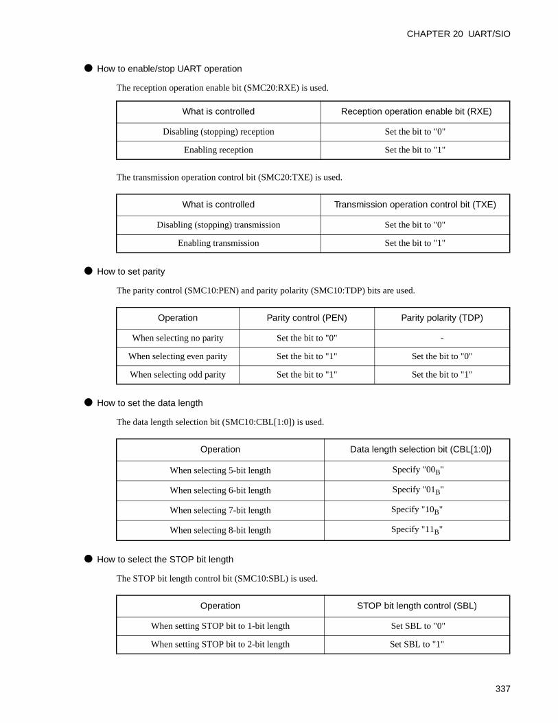
CHAPTER 20 UART/SIO
How to enable/stop UART operation
The reception operation enable bit (SMC20:RXE) is used.
The transmission operation control bit (SMC20:TXE) is used.
How to set parity
The parity control (SMC10:PEN) and parity polarity (SMC10:TDP) bits are used.
How to set the data length
The data length selection bit (SMC10:CBL[1:0]) is used.
How to select the STOP bit length
The STOP bit length control bit (SMC10:SBL) is used.
What is controlled Reception operation enable bit (RXE)
Disabling (stopping) reception Set the bit to "0"
Enabling reception Set the bit to "1"
What is controlled Transmission operation control bit (TXE)
Disabling (stopping) transmission Set the bit to "0"
Enabling transmission Set the bit to "1"
Operation Parity control (PEN) Parity polarity (TDP)
When selecting no parity Set the bit to "0" -
When selecting even parity Set the bit to "1" Set the bit to "0"
When selecting odd parity Set the bit to "1" Set the bit to "1"
Operation Data length selection bit (CBL[1:0])
When selecting 5-bit length Specify "00B"
When selecting 6-bit length Specify "01B"
When selecting 7-bit length Specify "10B"
When selecting 8-bit length Specify "11B"
Operation STOP bit length control (SBL)
When setting STOP bit to 1-bit length Set SBL to "0"
When setting STOP bit to 2-bit length Set SBL to "1"
337
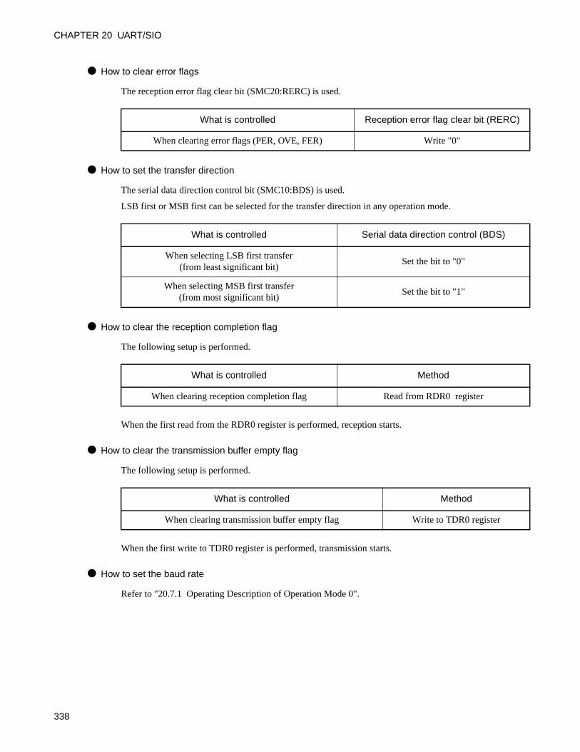
CHAPTER 20 UART/SIO
How to clear error flags
The reception error flag clear bit (SMC20:RERC) is used.
How to set the transfer direction
The serial data direction control bit (SMC10:BDS) is used.
LSB first or MSB first can be selected for the transfer direction in any operation mode.
How to clear the reception completion flag
The following setup is performed.
When the first read from the RDR0 register is performed, reception starts.
How to clear the transmission buffer empty flag
The following setup is performed.
When the first write to TDR0 register is performed, transmission starts.
How to set the baud rate
Refer to "20.7.1 Operating Description of Operation Mode 0".
What is controlled Reception error flag clear bit (RERC)
When clearing error flags (PER, OVE, FER) Write "0"
What is controlled Serial data direction control (BDS)
When selecting LSB first transfer (from least significant bit)
Set the bit to "0"
When selecting MSB first transfer (from most significant bit)
Set the bit to "1"
What is controlled Method
When clearing reception completion flag Read from RDR0 register
What is controlled Method
When clearing transmission buffer empty flag Write to TDR0 register
338
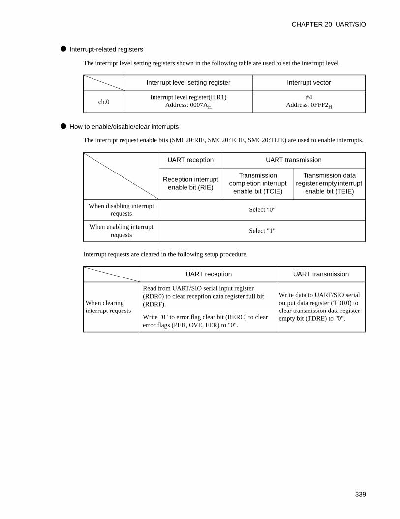
CHAPTER 20 UART/SIO
Interrupt-related registers
The interrupt level setting registers shown in the following table are used to set the interrupt level.
How to enable/disable/clear interrupts
The interrupt request enable bits (SMC20:RIE, SMC20:TCIE, SMC20:TEIE) are used to enable interrupts.
Interrupt requests are cleared in the following setup procedure.
Interrupt level setting register Interrupt vector
ch.0Interrupt level register(ILR1)
Address: 0007AH
#4Address: 0FFF2H
UART reception UART transmission
Reception interrupt enable bit (RIE)
Transmission completion interrupt
enable bit (TCIE)
Transmission data register empty interrupt
enable bit (TEIE)
When disabling interrupt requests
Select "0"
When enabling interrupt requests
Select "1"
UART reception UART transmission
When clearing interrupt requests
Read from UART/SIO serial input register (RDR0) to clear reception data register full bit (RDRF).
Write data to UART/SIO serial output data register (TDR0) to clear transmission data register empty bit (TDRE) to "0".Write "0" to error flag clear bit (RERC) to clear
error flags (PER, OVE, FER) to "0".
339

CHAPTER 20 UART/SIO
340
CHAPTER 21UART/SIO
DEDICATED BAUDRATE GENERATOR
This chapter describes the functions and operations of the dedicated baud rate generator of UART/SIO.
21.1 Overview of UART/SIO Dedicated Baud Rate Generator
21.2 Channels of UART/SIO Dedicated Baud Rate Generator
21.3 Registers of UART/SIO Dedicated Baud Rate Generator
21.4 Operating Description of UART/SIO Dedicated Baud Rate Generator
341
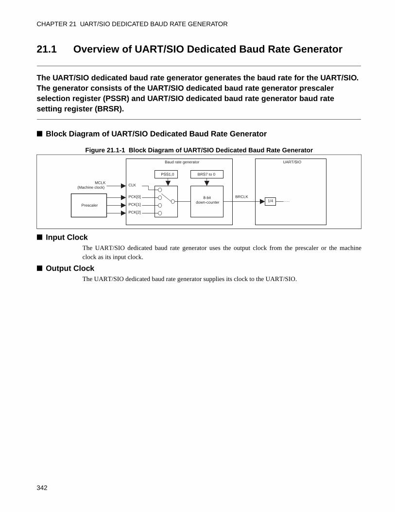
CHAPTER 21 UART/SIO DEDICATED BAUD RATE GENERATOR
21.1 Overview of UART/SIO Dedicated Baud Rate Generator
The UART/SIO dedicated baud rate generator generates the baud rate for the UART/SIO.The generator consists of the UART/SIO dedicated baud rate generator prescaler selection register (PSSR) and UART/SIO dedicated baud rate generator baud rate setting register (BRSR).
Block Diagram of UART/SIO Dedicated Baud Rate Generator
Figure 21.1-1 Block Diagram of UART/SIO Dedicated Baud Rate Generator
Input ClockThe UART/SIO dedicated baud rate generator uses the output clock from the prescaler or the machine
clock as its input clock.
Output ClockThe UART/SIO dedicated baud rate generator supplies its clock to the UART/SIO.
Baud rate generator
CLK
PCK[0]
PCK[1]
PCK[2]
8-bit down-counter
UART/SIO
1/4
PSS1,0 BRS7 to 0
BRCLK
MCLK(Machine clock)
Prescaler
342
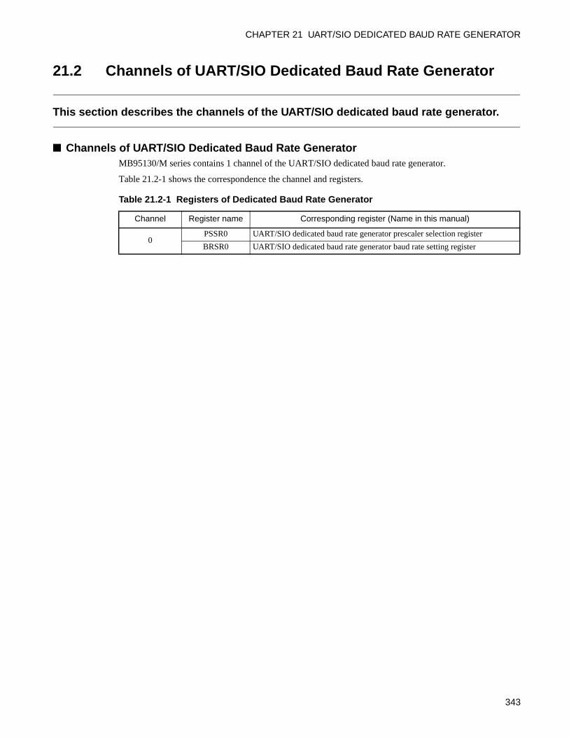
CHAPTER 21 UART/SIO DEDICATED BAUD RATE GENERATOR
21.2 Channels of UART/SIO Dedicated Baud Rate Generator
This section describes the channels of the UART/SIO dedicated baud rate generator.
Channels of UART/SIO Dedicated Baud Rate GeneratorMB95130/M series contains 1 channel of the UART/SIO dedicated baud rate generator.
Table 21.2-1 shows the correspondence the channel and registers.
Table 21.2-1 Registers of Dedicated Baud Rate Generator
Channel Register name Corresponding register (Name in this manual)
0PSSR0 UART/SIO dedicated baud rate generator prescaler selection register
BRSR0 UART/SIO dedicated baud rate generator baud rate setting register
343
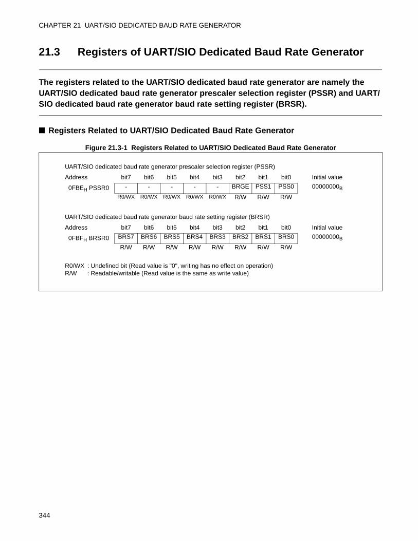
CHAPTER 21 UART/SIO DEDICATED BAUD RATE GENERATOR
21.3 Registers of UART/SIO Dedicated Baud Rate Generator
The registers related to the UART/SIO dedicated baud rate generator are namely the UART/SIO dedicated baud rate generator prescaler selection register (PSSR) and UART/SIO dedicated baud rate generator baud rate setting register (BRSR).
Registers Related to UART/SIO Dedicated Baud Rate Generator
Figure 21.3-1 Registers Related to UART/SIO Dedicated Baud Rate Generator
UART/SIO dedicated baud rate generator prescaler selection register (PSSR)
Address bit7 bit6 bit5 bit4 bit3 bit2 bit1 bit0 Initial value
0FBEH PSSR0 - - - - - BRGE PSS1 PSS0 00000000B
R0/WX R0/WX R0/WX R0/WX R0/WX R/W R/W R/W
UART/SIO dedicated baud rate generator baud rate setting register (BRSR)
Address bit7 bit6 bit5 bit4 bit3 bit2 bit1 bit0 Initial value
0FBFH BRSR0 BRS7 BRS6 BRS5 BRS4 BRS3 BRS2 BRS1 BRS0 00000000B
R/W R/W R/W R/W R/W R/W R/W R/W
R0/WX : Undefined bit (Read value is "0", writing has no effect on operation)R/W : Readable/writable (Read value is the same as write value)
344
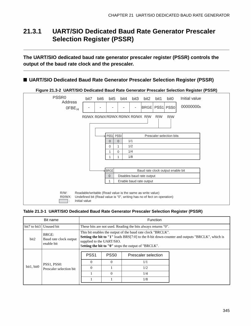
CHAPTER 21 UART/SIO DEDICATED BAUD RATE GENERATOR
21.3.1 UART/SIO Dedicated Baud Rate Generator Prescaler Selection Register (PSSR)
The UART/SIO dedicated baud rate generator prescaler register (PSSR) controls the output of the baud rate clock and the prescaler.
UART/SIO Dedicated Baud Rate Generator Prescaler Selection Register (PSSR)
Figure 21.3-2 UART/SIO Dedicated Baud Rate Generator Prescaler Selection Register (PSSR)
Table 21.3-1 UART/SIO Dedicated Baud Rate Generator Prescaler Selection Register (PSSR)
Bit name Function
bit7 to bit3 Unused bit These bits are not used. Reading the bits always returns "0".
bit2BRGE:Baud rate clock output enable bit
This bit enables the output of the baud rate clock "BRCLK".Setting the bit to "1" loads BRS[7:0] to the 8-bit down-counter and outputs "BRCLK", which is supplied to the UART/SIO.Setting the bit to "0" stops the output of "BRCLK".
bit1, bit0PSS1, PSS0:Prescaler selection bit
R/W: Readable/writable (Read value is the same as write value) R0/WX: Undefined bit (Read value is "0", writing has no ef fect on operation) : Initial value
- - - - - BRGE PSS1
R0/WXR0/WX
bit7 bit6 bit5 bit4 bit3 bit2 bit1 bit0
00000000B
Initial valueAddress
0FBEH
PSSR0
R/WR0/WX R/W
BRGE
0
1
Disables baud rate output
Enable baud rate output
Baud rate clock output enable bit
PSS1 PSS0
0
0
1
1
0
1
0
1
1/1
1/2
1/4
1/8
Prescaler selection bits
R/W
PSS0
R0/WXR0/WX
PSS1 PSS0 Prescaler selection
0 0 1/1
0 1 1/2
1 0 1/4
1 1 1/8
345
CHAPTER 21 UART/SIO DEDICATED BAUD RATE GENERATOR
21.3.2 UART/SIO Dedicated Baud Rate Generator Baud Rate Setting Register (BRSR)
The UART/SIO dedicated baud rate generator dedicated baud rate generator baud rate setting register (BRSR) controls the baud rate settings.
UART/SIO Dedicated Baud Rate Generator Baud Rate Setting Register (BRSR)
Figure 21.3-3 UART/SIO Dedicated Baud Rate Generator Baud Rate Setting Register (BRSR)
This register sets the cycle of the 8-bit down-counter and can be used to set any baud rate clock. Write to
the register when the UART is stopped.
Do not set BRS[7:0] to "00H" or "01H" in clock asynchronous mode.
Address bit7 bit6 bit5 bit4 bit3 bit2 bit1 bit0 Initial value
0FBFH BRSR0 BRS7 BRS6 BRS5 BRS4 BRS3 BRS2 BRS1 BRS0 00000000B
R/W R/W R/W R/W R/W R/W R/W R/W
R/W: Readable/writable (Read value is the same as write value)
346
CHAPTER 21 UART/SIO DEDICATED BAUD RATE GENERATOR
21.4 Operating Description of UART/SIO Dedicated Baud Rate Generator
The UART/SIO dedicated baud rate generator serves as the baud rate generator for asynchronous clock mode.
Baud Rate SettingThe SMC10 register (CKS bit) of the UART/SIO is used to select the serial clock. This selects the UART/
SIO dedicated baud rate generator.
In asynchronous CLK mode, the shift clock that is selected by the CKS bit and divided by four is used and
transfers can be performed within the range from -2% to +2%. The baud rate calculation formula for the
UART/SIO dedicated baud rate generator is shown below.
Figure 21.4-1 Baud Rate Calculation Formula when UART/SIO Dedicated Baud Rate Generator Is Used
The baud rate can be set in UART mode within the following range.
Table 21.4-1Sample Asynchronous Transfer Rates by Baud Rate Generator (Machine Clock = 10MHz, 16MHz, 16.25MHz)
UART/SIO Dedicated baud rate generator setting UART
internal division
Total division ratio
(PSS x BRS x4)
Baud rate (10MHz/Total division ratio)
Baud rate (16MHz /
Total division ratio)
Baud rate (16.25MHz / Total division
ratio)Prescaler selection
PSS[1:0]Baud rate counter setting BRS [7:0]
1 (Setting value: 0, 0) 20 4 80 125000 200000 203125
1 (Setting value: 0, 0) 22 4 88 113636 181818 184659
1 (Setting value: 0, 0) 44 4 176 56818 90909 92330
1 (Setting value: 0, 0) 87 4 348 28736 45977 46695
1 (Setting value: 0, 0) 130 4 520 19231 30769 31250
2 (Setting value: 0, 1) 130 4 1040 9615 15385 15625
4 (Setting value: 1, 0) 130 4 2080 4808 7692 7813
8 (Setting value: 1, 1) 130 4 4160 2404 3846 3906
Baud rate = Machine clock (MCLK)
[bps]
4× ×1248
2:
255
UART dedicated baud rate generator baud rate setting register (BRSR0)Baud rate setting (BRS7 to BRS0)
UART dedicated baud rate generator prescaler selection register (PSSR0)Prescaler selection (PSS1, PSS0)
Table 21.4-2 Permissible Baud Rate Range in UART Mode
PSS[1:0] BRS[7:0]
00B to 11B 02H (2) to FFH (255)
347

CHAPTER 21 UART/SIO DEDICATED BAUD RATE GENERATOR
348

CHAPTER 22LIN-UART
This chapter describes the function and operation of the LIN-UART
22.1 Overview of LIN-UART
22.2 Configuration of LIN-UART
22.3 LIN-UART Pins
22.4 Registers of LIN-UART
22.5 LIN-UART Interrupt
22.6 LIN-UART Baud Rate
22.7 Operations and Setting Procedure Example of LIN-UART
22.8 Notes on Using LIN-UART
22.9 Sample Programs of LIN-UART
349
CHAPTER 22 LIN-UART
22.1 Overview of LIN-UART
The LIN (Local Interconnect Network)-UART is a general-purpose serial data communication interface for synchronous or asynchronous (start-stop synchronization) communication with external devices. In addition to a bi-directional communication function (normal mode) and master/slave communication function (multiprocessor mode: supports both master and slave operation), the LIN-UART also supports the special functions used by the LIN bus.
Functions of LIN-UARTThe LIN-UART is a general-purpose serial data communication interface for exchanging serial data with
other CPUs and peripheral devices. Table 22.1-1 lists the functions of the LIN-UART.
Table 22.1-1 Functions of LIN-UART
Function
Data buffer Full-duplex double-buffer
Serial inputThe LIN-UART oversamples received data for five times to determine the received value by majority (only asynchronous mode).
Transfer mode• Clock synchronization (Select start/stop synchronization, or start/stop bit)• Clock asynchronous (Start/stop bits available)
Baud rate• Dedicated baud rate generator provided (made of a 15-bit reload counter)• The external clock can be inputted. The reload counter can also be used to adjust the external
clock.
Data length• 7 bits (not in synchronous or LIN mode)• 8 bits
Signal type NRZ (Non Return to Zero)
Start bit timing Synchronization with the start bit falling edge in asynchronous mode.
Reception error detection• Framing error• Overrun error• Parity error (Not supported in operation mode 1)
Interrupt request• Reception interrupts (reception completed, reception error detected, LIN synch break detected)• Transmit interrupts (send data empty)• Interrupt requests to TII0 (LIN synch field detected: LSYN)
Master/slave mode communication function (Multiprocessor mode)
Capable of 1 (master) to n (slaves) communication (support both the master and slave system)
Synchronous mode Send side/receive side of serial clock
Pin access Serial I/O pin states can be read directly.
LIN bus option
• Master device operation• Slave device operation• LIN synch break detection• LIN synch break generation• Detection of LIN synch field start/stop edges connected to the 8/16-bit multifunction timer
Synchronous serial clockContinuous output to the SCK pin is possible for synchronous communication using the start/stop bits
Clock delay option Special synchronous clock mode for delaying the clock (used for SPI)
350
CHAPTER 22 LIN-UART
The LIN-UART operates in four different modes. The operation mode is selected by the MD0 and MD1 bits
in the LIN-UART serial mode register (SMR). Mode 0 and mode 2 are used for bi-directional serial
communication; mode 1 for master/slave communication; and mode 3 for LIN master/slave communication.
The MD0 and MD1 bits in the LIN-UART serial mode register (SMR) are used to select the following
LIN-UART operation modes.
• Mode 1 supports both master and slave operation for the multiprocessor mode.
• Mode 3 is fixed to communication format 8-bit data, no parity, stop bit 1, LSB-first.
Table 22.1-2 LIN-UART Operation Modes
Operation modeData length Synchronous
methodStop bit length Data bit format
No parity With parity
0 Normal mode 7 bits or 8 bits Asynchronous1 bit or 2 bits LSB first
MSB first1 Multiprocessor mode 7 bits or 8 bits +1* - Asynchronous
2 Normal mode 8 bits Synchronous None, 1 bit, 2 bits
3 LIN mode 8 bits - Asynchronous 1 bit LSB first
- : Unavailable* : "+1" is the address/data selection bit (A/D) used for communication control in multiprocessor mode.
Table 22.1-3 LIN-UART Operation Modes
MD1 MD0 Mode Type
0 0 0 Asynchronous (Normal mode)
0 1 1 Asynchronous (Multiprocessor mode)
1 0 2 Synchronous (Normal mode)
1 1 3 Asynchronous (LIN mode)
351
CHAPTER 22 LIN-UART
22.2 Configuration of LIN-UART
LIN-UART is made up of the following blocks.• Reload counter• Reception control circuit• Reception shift register• LIN-UART Reception data register (RDR)• Transmit control circuit• Transmit shift register• LIN-UART Transmit data register (TDR)• Error detection circuit• Oversampling circuit• Interrupt generation circuit• LIN synch break/Synch Field detection circuit• Bus idle detection circuit• LIN-UART serial control register (SCR)• LIN-UART serial mode register (SMR)• LIN-UART Serial status register (SSR)• LIN-UART Extended status control register (ESCR)• LIN-UART Extended communication control register (ECCR)
352
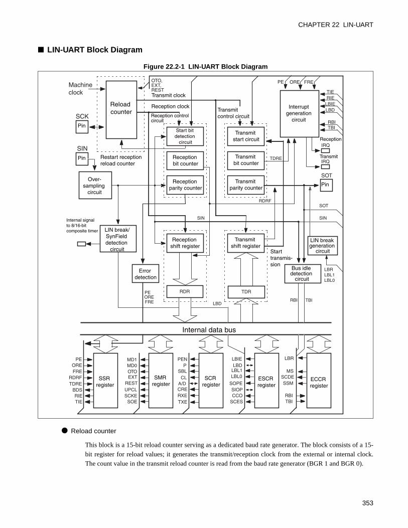
CHAPTER 22 LIN-UART
LIN-UART Block Diagram
Figure 22.2-1 LIN-UART Block Diagram
Reload counter
This block is a 15-bit reload counter serving as a dedicated baud rate generator. The block consists of a 15-
bit register for reload values; it generates the transmit/reception clock from the external or internal clock.
The count value in the transmit reload counter is read from the baud rate generator (BGR 1 and BGR 0).
RDR TDR
PENP
SBLCL
A/DCRERXETXE
MD1MD0OTOEXT
REST
SCKESOE
PEOREFRE
RDRFTDRE
BDSRIETIE
LBIELBD
SOPESIOPCCO
SCES
LBIELBD
RBI
RIETIE
IRQ
IRQ
LBD
SIN
PE ORE FREMachineclock
SIN
SOT
MS
SSM SCDE
TDRE
RDRF
RBITBI
UPCL
OTO,EXT,REST
PEOREFRE
TBI
RBI TBI
SIN
SCK
SOT
LBR
LBRLBL1LBL0
LBL1LBL0
Pin
Pin
Pin
Reload counter
Restart reception reload counter
Over-sampling
circuit
Internal signal to 8/16-bit composite timer LIN break/
SynField detection
circuit
Error detection
Internal data bus
SSR register
SMR register
SCR register
ESCR register
ECCR register
Bus idle detection
circuit
LIN break generation
circuit
Transmit shift register
Start transmis-sion
Reception shift register
Transmit parity counter
Reception parity counter
Reception bit counter
Transmit bit counter
Transmit start circuit
Start bit detection
circuit
Interrupt generation
circuit
Transmit control circuitReception control
circuit
Transmit clock
Reception clock
Reception
Transmit
353
CHAPTER 22 LIN-UART
Reception control circuit
This block consists of a reception bit counter, a start bit detection circuit, and a reception parity counter.
The reception bit counter counts the reception data bits and sets a flag in the LIN-UART reception data
register when one data reception is completed according to the specified data length. If the reception
interrupt is enabled at this time, a reception interrupt request is generated. The start bit detection circuit
detects a start bit in a serial input signal. When a start bit is detected, the circuit sends a signal to the reload
counter in synchronization with the start bit falling edge. The reception parity counter calculates the parity
of the received data.
Reception shift register
The circuit inputs received data from the SIN pin while bit-shifting and transfers it to the RDR register
upon completion of reception.
LIN-UART reception data register (RDR)
This register retains the received data. Serial input data is converted and stored in the LIN-UART reception
data register.
Transmit control circuit
This block consists of a transmit bit counter, a transmission start circuit, and a transmit parity counter. The
transmit bit counter counts the transmit data bits and sets a flag in the transmit data register when one data
transmission is completed according to the specified data length. If the transmit interrupt is enabled at this
time, a transmit interrupt request is generated. The transmit start circuit starts transmission when data is
written to the TDR. The transmit parity counter generates a parity bit for data to be transmitted if the data is
parity-checked.
Transmit shift register
The data written to the LIN-UART transmit data register (TDR) is transferred to the transmit shift register,
and output to the SOT pin while bit-shifting.
LIN-UART transmit data register (TDR)
This register sets the transmit data. The written data is converted to serial data and output.
Error detection circuit
This circuit detects an error upon completion of reception, if any. If an error occurs, the corresponding error
flag is set.
Oversampling circuit
In asynchronous mode, the LIN-UART oversamples received data for five times to determine the received
value by majority. The LIN-UART stops during operation in synchronous mode.
Interrupt generation circuit
This circuit controls all interrupt factors. An interrupt is generated immediately if the corresponding
interrupt enable bit has been set.
354
CHAPTER 22 LIN-UART
LIN synch break/Synch Field detection circuit
This circuit detects a LIN synch break when the LIN master node transmits a message header. The LBD
flag is set when the LIN synch break is detected. An internal signal is output to 8/16-bit compound timer in
order to detect the first and fifth falling edges of the LIN synch Field and to measure the actual serial clock
synchronization transmitted by the master node.
LIN synch break generation circuit
This circuit generates a LIN synch break with the specified length.
Bus idle detection circuit
This circuit detects that no transmission or reception is in progress, and generates the TBI and RBI flag
bits.
LIN-UART serial control register (SCR)
Operating functions are as follows:
• Sets parity bit existence
• Parity bit selection
• Sets stop bit length
• Sets data length
• Selects the frame data format in mode 1
• Clears error flag
• Enable/disable transmission
• Enables/disables reception
LIN-UART serial mode register (SMR)
Operating functions are as follows:
• Selects the LIN-UART operation mode
• Selects a clock input source
• Selects between one-to-one connection or reload counter connection for the external clock
• Resets a dedicated reload timer
• LIN-UART software reset (maintains register settings)
• Enables/disables output to the serial data pin
• Enables/disables output to the clock pin
LIN-UART serial status register (SSR)
Operating functions are as follows:
• Check transmission/reception or error status
• Selects the transfer direction (LSB-first or MSB-first)
• Enables/disables reception interrupts
• Enables/disables transmit interrupts
355
CHAPTER 22 LIN-UART
Extended status control register (ESCR)
• Enables/disables LIN synch break interrupts
• LIN synch break detection
• Selects LIN synch break length
• Direct access to SIN pin and SOT pin
• Sets continuous clock output in LIN-UART synchronous clock mode
• Sampling clock edge selection
LIN-UART extended communication control register (ECCR)
• Bus idle detection
• Synchronous clock setting
• LIN synch break generation
Input ClockLIN-UART uses a machine clock or an input signal from the SCK pin as an input clock.
Input clock is used as clock source of transmission/reception of LIN-UART.
356
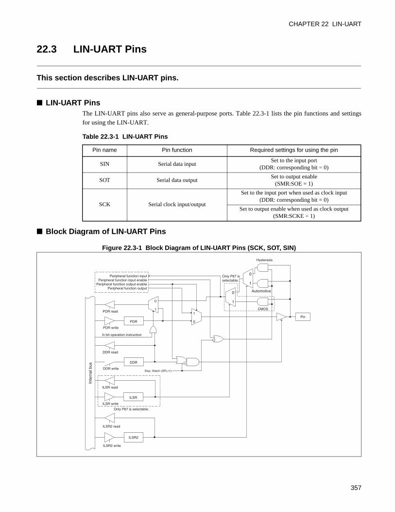
CHAPTER 22 LIN-UART
22.3 LIN-UART Pins
This section describes LIN-UART pins.
LIN-UART PinsThe LIN-UART pins also serve as general-purpose ports. Table 22.3-1 lists the pin functions and settings
for using the LIN-UART.
Block Diagram of LIN-UART Pins
Figure 22.3-1 Block Diagram of LIN-UART Pins (SCK, SOT, SIN)
Table 22.3-1 LIN-UART Pins
Pin name Pin function Required settings for using the pin
SIN Serial data inputSet to the input port
(DDR: corresponding bit = 0)
SOT Serial data outputSet to output enable
(SMR:SOE = 1)
SCK Serial clock input/output
Set to the input port when used as clock input(DDR: corresponding bit = 0)
Set to output enable when used as clock output(SMR:SCKE = 1)
ILSR2 read
ILSR2 write
ILSR2
0
1
0
1
Automotive
PDR read
PDR write
PDR
DDR read
DDR write
DDR
0
11
0
Peripheral function outputPeripheral function output enable
Peripheral function input enablePeripheral function input
Pin
Stop, Watch (SPL=1)
Inte
rnal
bus
In bit operation instruction
ILSR read
ILSR write
ILSR
Hysteresis
CMOS
Only P67 is selectable.
Only P67 is selectable.
357
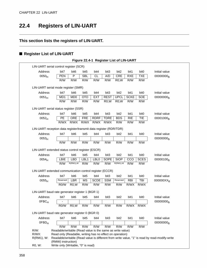
CHAPTER 22 LIN-UART
22.4 Registers of LIN-UART
This section lists the registers of LIN-UART.
Register List of LIN-UART
Figure 22.4-1 Register List of LIN-UART
LIN-UART serial control register (SCR)
Address bit7 bit6 bit5 bit4 bit3 bit2 bit1 bit0 Initial value
0050H PEN P SBL CL A/D CRE RXE TXE 00000000BR/W R/W R/W R/W R/W R0,W R/W R/W
LIN-UART serial mode register (SMR)
Address bit7 bit6 bit5 bit4 bit3 bit2 bit1 bit0 Initial value
0051H MD1 MD0 OTO EXT REST UPCL SCKE SOE 00000000BR/W R/W R/W R/W R0,W R0,W R/W R/W
LIN-UART serial status register (SSR)
Address bit7 bit6 bit5 bit4 bit3 bit2 bit1 bit0 Initial value0052H PE ORE FRE RDRF TDRE BDS RIE TIE 00001000B
R/WX R/WX R/WX R/WX R/WX R/W R/W R/W
LIN-UART reception data register/transmit data register (RDR/TDR)
Address bit7 bit6 bit5 bit4 bit3 bit2 bit1 bit0 Initial value
0053H 00000000B
R/W R/W R/W R/W R/W R/W R/W R/W
LIN-UART extended status control register (ESCR)
Address bit7 bit6 bit5 bit4 bit3 bit2 bit1 bit0 Initial value
0054H LBIE LBD LBL1 LBL0 SOPE SIOP CCO SCES 00000100B
R/W R(RM1),W R/W R/W R/W R(RM1),W R/W R/W
LIN-UART extended communication control register (ECCR)
Address bit7 bit6 bit5 bit4 bit3 bit2 bit1 bit0 Initial value
0055H Reserved LBR MS SCDE SSM Reserved RBI TBI 000000XXB
R0/W R0,W R/W R/W R/W R/W R/WX R/WX
LIN-UART baud rate generator register 1 (BGR 1)
Address bit7 bit6 bit5 bit4 bit3 bit2 bit1 bit0 Initial value
0FBCH - 00000000BR0/W R0,W R/W R/W R/W R/W R/WX R/WX
LIN-UART baud rate generator register 0 (BGR 0)
Address bit7 bit6 bit5 bit4 bit3 bit2 bit1 bit0 Initial value
0FBDH 00000000BR/W R/W R/W R/W R/W R/W R/W R/W
R/W: Readable/writable (Read value is the same as write value)R/WX: Read only (Readable, writing has no effect on operation)R(RM1), W: Readable/writable (Read value is different from write value, "1" is read by read-modify-write
(RMW) instruction)R0, W: Write only (Writable, "0" is read)
358
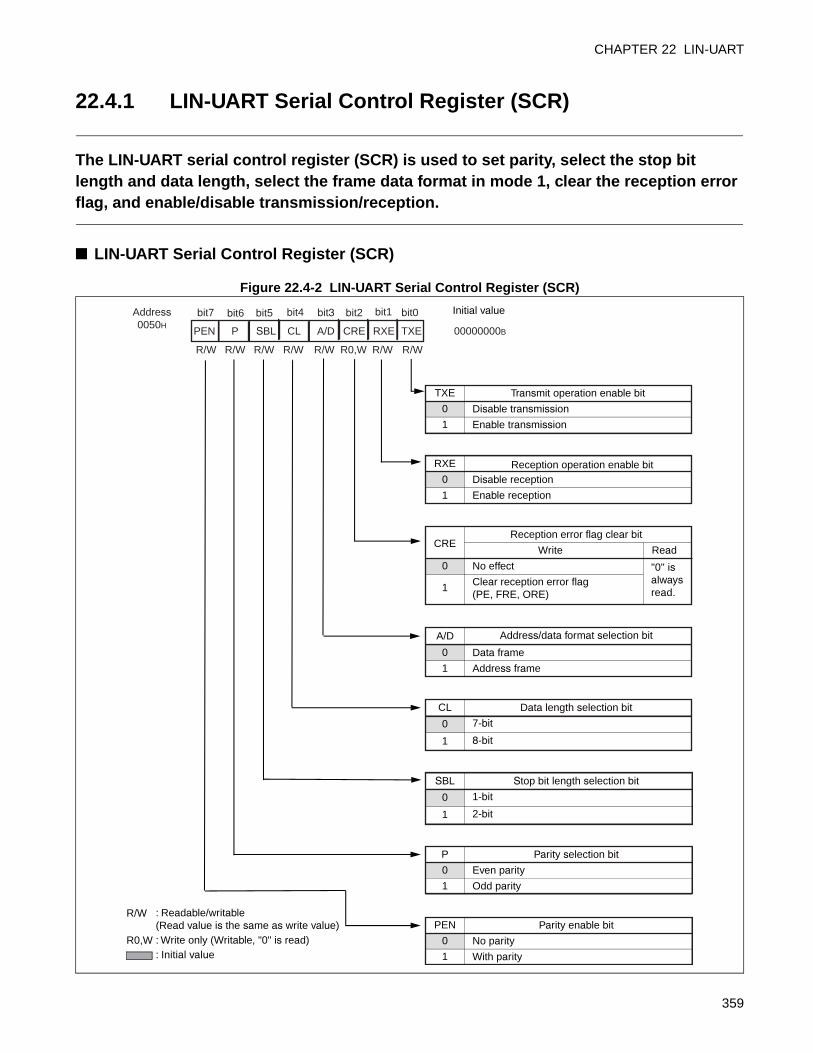
CHAPTER 22 LIN-UART
22.4.1 LIN-UART Serial Control Register (SCR)
The LIN-UART serial control register (SCR) is used to set parity, select the stop bit length and data length, select the frame data format in mode 1, clear the reception error flag, and enable/disable transmission/reception.
LIN-UART Serial Control Register (SCR)
Figure 22.4-2 LIN-UART Serial Control Register (SCR)
PEN P SBL CL A/D CRE RXE TXE
bit7Address0050H
R/W
00000000B
bit6 bit5 bit4 bit3 bit0bit1bit2
R/WR/WR/WR/W R/WR0,WR/W
TXE Transmit operation enable bit
0 Disable transmission
1 Enable transmission
RXE Reception operation enable bit0 Disable reception
1 Enable reception
CREReception error flag clear bit
Write Read
0 No effect "0" is always read.1 Clear reception error flag
(PE, FRE, ORE)
A/D Address/data format selection bit
0 Data frame
1 Address frame
CL Data length selection bit
0 7-bit
1 8-bit
SBL Stop bit length selection bit
0 1-bit
1 2-bit
P Parity selection bit
0 Even parity
1 Odd parity
PEN Parity enable bit
0 No parity
1 With parity
R/W
R0,W
: Readable/writable (Read value is the same as write value): Write only (Writable, "0" is read): Initial value
Initial value
359
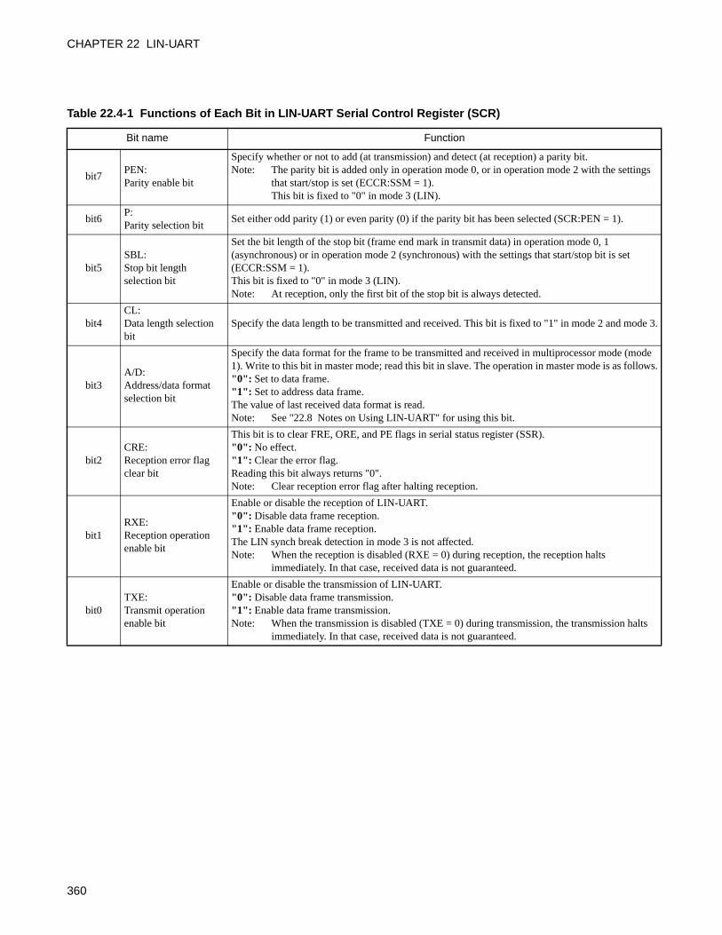
CHAPTER 22 LIN-UART
Table 22.4-1 Functions of Each Bit in LIN-UART Serial Control Register (SCR)
Bit name Function
bit7PEN:Parity enable bit
Specify whether or not to add (at transmission) and detect (at reception) a parity bit. Note: The parity bit is added only in operation mode 0, or in operation mode 2 with the settings
that start/stop is set (ECCR:SSM = 1).This bit is fixed to "0" in mode 3 (LIN).
bit6P:Parity selection bit
Set either odd parity (1) or even parity (0) if the parity bit has been selected (SCR:PEN = 1).
bit5SBL:Stop bit length selection bit
Set the bit length of the stop bit (frame end mark in transmit data) in operation mode 0, 1 (asynchronous) or in operation mode 2 (synchronous) with the settings that start/stop bit is set (ECCR:SSM = 1).This bit is fixed to "0" in mode 3 (LIN).Note: At reception, only the first bit of the stop bit is always detected.
bit4CL:Data length selection bit
Specify the data length to be transmitted and received. This bit is fixed to "1" in mode 2 and mode 3.
bit3A/D:Address/data format selection bit
Specify the data format for the frame to be transmitted and received in multiprocessor mode (mode 1). Write to this bit in master mode; read this bit in slave. The operation in master mode is as follows."0": Set to data frame."1": Set to address data frame.The value of last received data format is read.Note: See "22.8 Notes on Using LIN-UART" for using this bit.
bit2CRE:Reception error flag clear bit
This bit is to clear FRE, ORE, and PE flags in serial status register (SSR)."0": No effect."1": Clear the error flag.Reading this bit always returns "0".Note: Clear reception error flag after halting reception.
bit1RXE:Reception operation enable bit
Enable or disable the reception of LIN-UART."0": Disable data frame reception."1": Enable data frame reception.The LIN synch break detection in mode 3 is not affected.Note: When the reception is disabled (RXE = 0) during reception, the reception halts
immediately. In that case, received data is not guaranteed.
bit0TXE:Transmit operation enable bit
Enable or disable the transmission of LIN-UART."0": Disable data frame transmission."1": Enable data frame transmission. Note: When the transmission is disabled (TXE = 0) during transmission, the transmission halts
immediately. In that case, received data is not guaranteed.
360
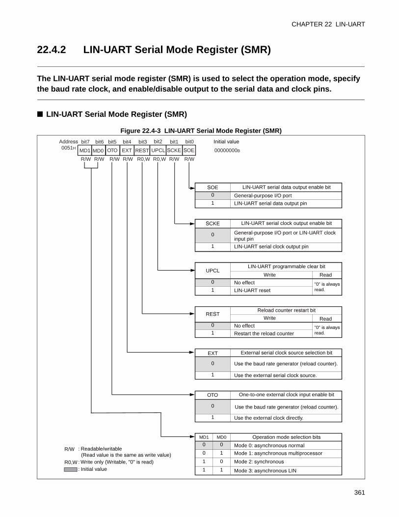
CHAPTER 22 LIN-UART
22.4.2 LIN-UART Serial Mode Register (SMR)
The LIN-UART serial mode register (SMR) is used to select the operation mode, specify the baud rate clock, and enable/disable output to the serial data and clock pins.
LIN-UART Serial Mode Register (SMR)
Figure 22.4-3 LIN-UART Serial Mode Register (SMR)
MD1 MD0 OTO EXT REST UPCL SCKE SOE
bit7
R/W R/W R/W R/W R/W R/WR0,WR0,W
00000000B
bit0bit1bit2bit3bit4bit6 bit5
SOE LIN-UART serial data output enable bit
0 General-purpose I/O port1 LIN-UART serial data output pin
SCKE LIN-UART serial clock output enable bit
0 General-purpose I/O port or LIN-UART clock input pin
1 LIN-UART serial clock output pin
UPCLLIN-UART programmable clear bit
Write Read0 No effect "0" is always
read.1 LIN-UART reset
RESTReload counter restart bit
Write0 No effect1 Restart the reload counter
EXT External serial clock source selection bit
0 Use the baud rate generator (reload counter).
1 Use the external serial clock source.
OTO One-to-one external clock input enable bit
0
1 Use the external clock directly.
MD1 MD0 Operation mode selection bits0 0 Mode 0: asynchronous normal0 1
1 0
1 1
Initial value
R/W
R0,W
: Readable/writable (Read value is the same as write value): Write only (Writable, "0" is read): Initial value
Read
"0" is always read.
Use the baud rate generator (reload counter).
Mode 1: asynchronous multiprocessor
Mode 2: synchronous
Mode 3: asynchronous LIN
Address0051H
361
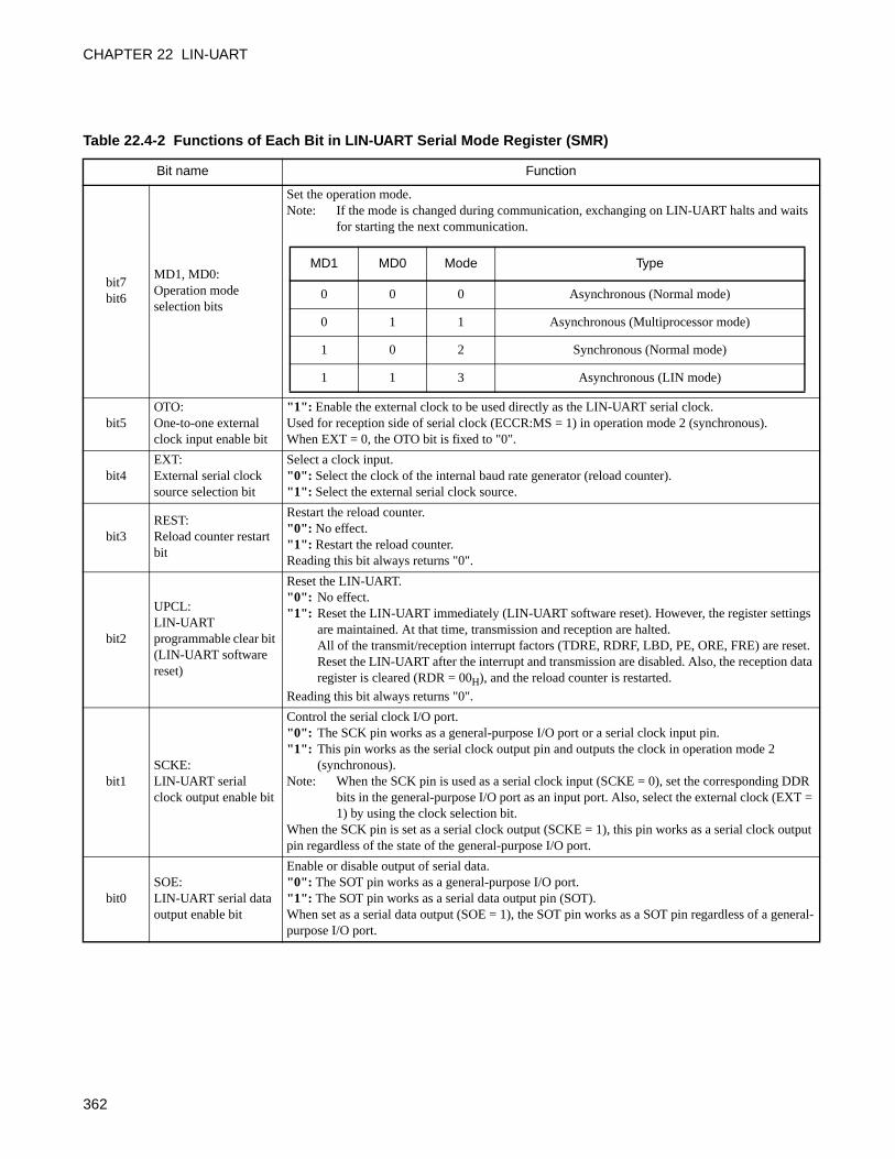
CHAPTER 22 LIN-UART
Table 22.4-2 Functions of Each Bit in LIN-UART Serial Mode Register (SMR)
Bit name Function
bit7bit6
MD1, MD0:Operation mode selection bits
Set the operation mode.Note: If the mode is changed during communication, exchanging on LIN-UART halts and waits
for starting the next communication.
bit5OTO:One-to-one external clock input enable bit
"1": Enable the external clock to be used directly as the LIN-UART serial clock.Used for reception side of serial clock (ECCR:MS = 1) in operation mode 2 (synchronous).When EXT = 0, the OTO bit is fixed to "0".
bit4EXT:External serial clock source selection bit
Select a clock input."0": Select the clock of the internal baud rate generator (reload counter)."1": Select the external serial clock source.
bit3REST:Reload counter restart bit
Restart the reload counter."0": No effect."1": Restart the reload counter.Reading this bit always returns "0".
bit2
UPCL:LIN-UART programmable clear bit (LIN-UART software reset)
Reset the LIN-UART."0": No effect."1": Reset the LIN-UART immediately (LIN-UART software reset). However, the register settings
are maintained. At that time, transmission and reception are halted.All of the transmit/reception interrupt factors (TDRE, RDRF, LBD, PE, ORE, FRE) are reset. Reset the LIN-UART after the interrupt and transmission are disabled. Also, the reception data register is cleared (RDR = 00H), and the reload counter is restarted.
Reading this bit always returns "0".
bit1SCKE:LIN-UART serial clock output enable bit
Control the serial clock I/O port."0": The SCK pin works as a general-purpose I/O port or a serial clock input pin. "1": This pin works as the serial clock output pin and outputs the clock in operation mode 2
(synchronous).Note: When the SCK pin is used as a serial clock input (SCKE = 0), set the corresponding DDR
bits in the general-purpose I/O port as an input port. Also, select the external clock (EXT = 1) by using the clock selection bit.
When the SCK pin is set as a serial clock output (SCKE = 1), this pin works as a serial clock output pin regardless of the state of the general-purpose I/O port.
bit0SOE:LIN-UART serial data output enable bit
Enable or disable output of serial data."0": The SOT pin works as a general-purpose I/O port."1": The SOT pin works as a serial data output pin (SOT).When set as a serial data output (SOE = 1), the SOT pin works as a SOT pin regardless of a general-purpose I/O port.
MD1 MD0 Mode Type
0 0 0 Asynchronous (Normal mode)
0 1 1 Asynchronous (Multiprocessor mode)
1 0 2 Synchronous (Normal mode)
1 1 3 Asynchronous (LIN mode)
362
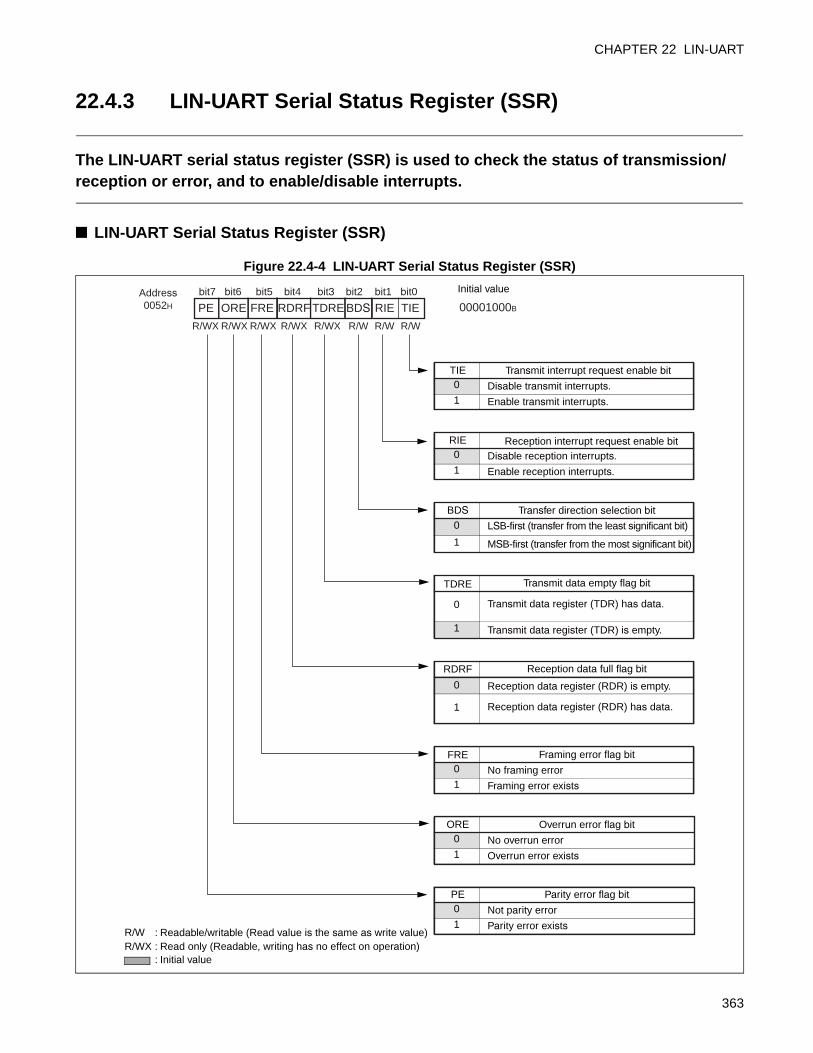
CHAPTER 22 LIN-UART
22.4.3 LIN-UART Serial Status Register (SSR)
The LIN-UART serial status register (SSR) is used to check the status of transmission/reception or error, and to enable/disable interrupts.
LIN-UART Serial Status Register (SSR)
Figure 22.4-4 LIN-UART Serial Status Register (SSR)
PE ORE FRE RDRF TDRE BDS RIE TIEbit7 bit6 bit1 bit0bit5 bit4 bit3 bit2
00001000B
R/W : Readable/writable (Read value is the same as write value)R/WX : Read only (Readable, writing has no effect on operation)
: Initial value
TIE Transmit interrupt request enable bit0 Disable transmit interrupts.1 Enable transmit interrupts.
RIE Reception interrupt request enable bit0 Disable reception interrupts.1 Enable reception interrupts.
BDS Transfer direction selection bit0 LSB-first (transfer from the least significant bit)
1
TDRE Transmit data empty flag bit
0 Transmit data register (TDR) has data.
1 Transmit data register (TDR) is empty.
RDRF Reception data full flag bit
0
1
FRE Framing error flag bit0 No framing error1 Framing error exists
ORE Overrun error flag bit0 No overrun error1 Overrun error exists
PE Parity error flag bit0 Not parity error1 Parity error exists
Initial value
MSB-first (transfer from the most significant bit)
Reception data register (RDR) is empty.
Reception data register (RDR) has data.
R/WX R/WX R/WX R/WX R/WX R/W R/W R/W
Address0052H
363
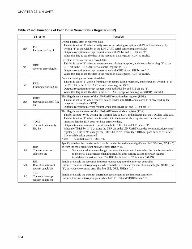
CHAPTER 22 LIN-UART
Table 22.4-3 Functions of Each Bit in Serial Status Register (SSR)
Bit name Function
bit7PE:Parity error flag bit
Detect a parity error in received data.• This bit is set to "1" when a parity error occurs during reception with PE = 1, and cleared by
writing "1" to the CRE bit in the LIN-UART serial control register (SCR).• Output a reception interrupt request when both PE bit and RIE bit are "1".• When this flag is set, the data in the reception data register (RDR) is invalid.
bit6ORE:Overrun error flag bit
Detect an overrun error in received data.• This bit is set to "1" when an overrun occurs during reception, and cleared by writing "1" to the
CRE bit in the LIN-UART serial control register (SCR).• Output a reception interrupt request when both ORE bit and RIE bit are "1".• When this flag is set, the data in the reception data register (RDR) is invalid.
bit5FRE:Framing error flag bit
Detect a framing error in received data.• This bit is set to "1" when a framing error occurs during reception, and cleared by writing "1" to
the CRE bit in the LIN-UART serial control register (SCR).• Output a reception interrupt request when both FRE bit and RIE bit are "1".• When this flag is set, the data in the LIN-UART reception data register (RDR) is invalid.
bit4RDRF:Reception data full flag bit
This flag shows the status of the LIN-UART reception data register (RDR).• This bit is set to "1" when received data is loaded into RDR, and cleared to "0" by reading the
reception data register (RDR).• Output a reception interrupt request when both RDRF bit and RIE bit are "1".
bit3TDRE:Transmit data empty flag bit
This flag shows the status of the LIN-UART transmit data register (TDR).• This bit is set to "0" by writing the transmit data to TDR, and indicates that the TDR has valid data.
This bit is set to "1" when data is loaded into the transmit shift register and transferred, and indicates that the TDR does not have effective data.
• Output a transmit interrupt request when both TDRE bit and TIE bit are "1".• When the TDRE bit is "1", setting the LBR bit in the LIN-UART extended communication control
register (ECCR) to "1" changes the TDRE bit to "0". Then, the TDRE bit goes back to "1" after LIN synch break is generated.
Note: The initial state is TDRE =1.
bit2BDS:Transfer direction selection bit
Specify whether the transfer serial data is transfer from the least significant bit (LSB-first, BDS = 0) or from the most significant bit (MSB-first, BDS = 1).Note: Since data values are exchanged between the upper and lower when the data is read/written
to the serial data register, changing BDS bit after writing data to the RDR register invalidates the written data. The BDS bit is fixed to "0" in mode 3 (LIN).
bit1RIE:Reception interrupt request enable bit
Enable or disable the reception interrupt request output to the interrupt controller.Output a reception interrupt request when both the RIE bit and the reception data flag bit (RDRF) are "1", or when one or more error flag bits (PE, ORE, FRE) is "1".
bit0TIE:Transmit interrupt request enable bit
Enable or disable the transmit interrupt request output to the interrupt controller.Output a transmit interrupt request when both TIE bit and TDRE bit are "1".
364
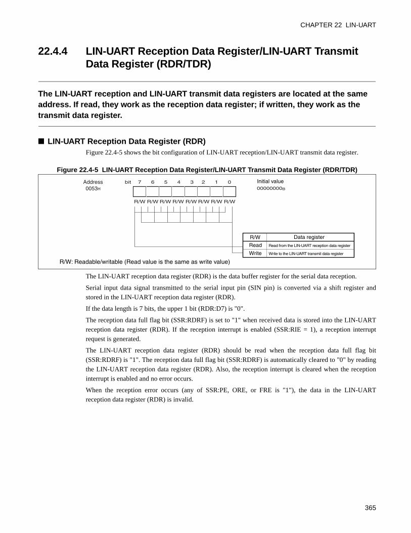
CHAPTER 22 LIN-UART
22.4.4 LIN-UART Reception Data Register/LIN-UART Transmit Data Register (RDR/TDR)
The LIN-UART reception and LIN-UART transmit data registers are located at the same address. If read, they work as the reception data register; if written, they work as the transmit data register.
LIN-UART Reception Data Register (RDR)Figure 22.4-5 shows the bit configuration of LIN-UART reception/LIN-UART transmit data register.
Figure 22.4-5 LIN-UART Reception Data Register/LIN-UART Transmit Data Register (RDR/TDR)
The LIN-UART reception data register (RDR) is the data buffer register for the serial data reception.
Serial input data signal transmitted to the serial input pin (SIN pin) is converted via a shift register and
stored in the LIN-UART reception data register (RDR).
If the data length is 7 bits, the upper 1 bit (RDR:D7) is "0".
The reception data full flag bit (SSR:RDRF) is set to "1" when received data is stored into the LIN-UART
reception data register (RDR). If the reception interrupt is enabled (SSR:RIE = 1), a reception interrupt
request is generated.
The LIN-UART reception data register (RDR) should be read when the reception data full flag bit
(SSR:RDRF) is "1". The reception data full flag bit (SSR:RDRF) is automatically cleared to "0" by reading
the LIN-UART reception data register (RDR). Also, the reception interrupt is cleared when the reception
interrupt is enabled and no error occurs.
When the reception error occurs (any of SSR:PE, ORE, or FRE is "1"), the data in the LIN-UART
reception data register (RDR) is invalid.
00000000 Bbit 7 6 5 4 3 2 1 0
R/W R/W R/W R/W R/W R/W R/W R/W
Initial value
R/W Data register
Read Read from the LIN-UART reception data register
Write Write to the LIN-UART transmit data register
R/W: Readable/writable (Read value is the same as write value)
Address0053H
365
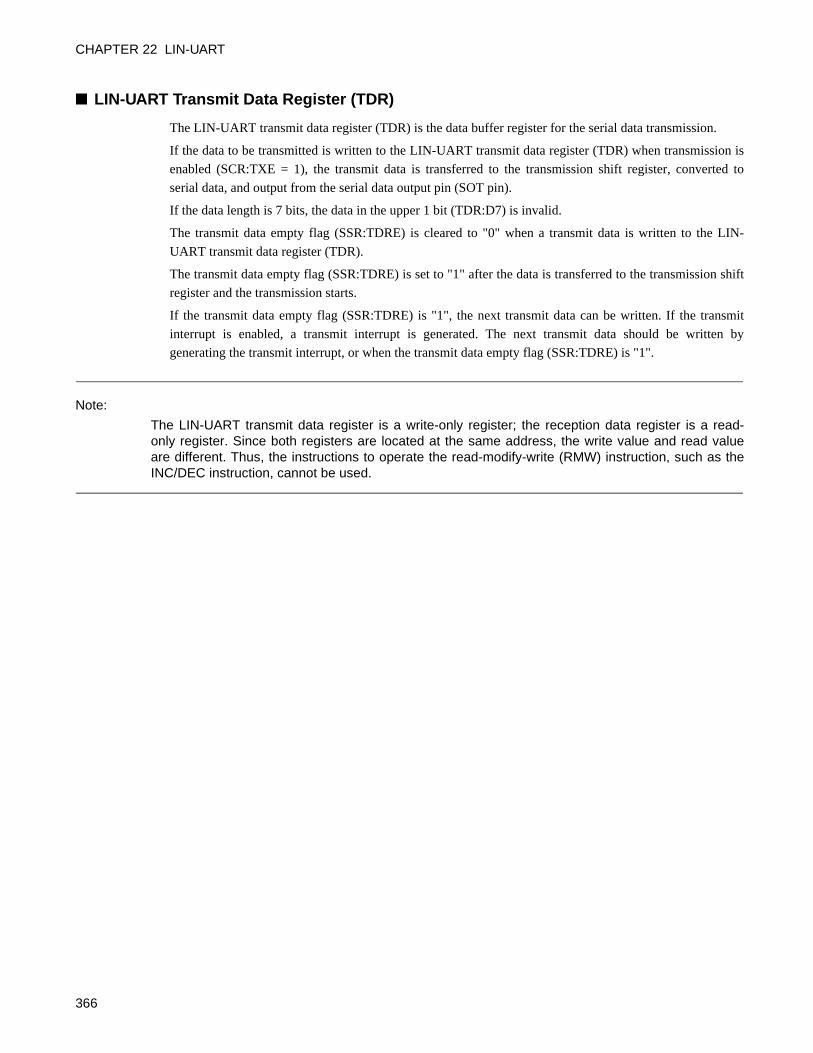
CHAPTER 22 LIN-UART
LIN-UART Transmit Data Register (TDR)
The LIN-UART transmit data register (TDR) is the data buffer register for the serial data transmission.
If the data to be transmitted is written to the LIN-UART transmit data register (TDR) when transmission is
enabled (SCR:TXE = 1), the transmit data is transferred to the transmission shift register, converted to
serial data, and output from the serial data output pin (SOT pin).
If the data length is 7 bits, the data in the upper 1 bit (TDR:D7) is invalid.
The transmit data empty flag (SSR:TDRE) is cleared to "0" when a transmit data is written to the LIN-
UART transmit data register (TDR).
The transmit data empty flag (SSR:TDRE) is set to "1" after the data is transferred to the transmission shift
register and the transmission starts.
If the transmit data empty flag (SSR:TDRE) is "1", the next transmit data can be written. If the transmit
interrupt is enabled, a transmit interrupt is generated. The next transmit data should be written by
generating the transmit interrupt, or when the transmit data empty flag (SSR:TDRE) is "1".
Note:
The LIN-UART transmit data register is a write-only register; the reception data register is a read-only register. Since both registers are located at the same address, the write value and read valueare different. Thus, the instructions to operate the read-modify-write (RMW) instruction, such as theINC/DEC instruction, cannot be used.
366
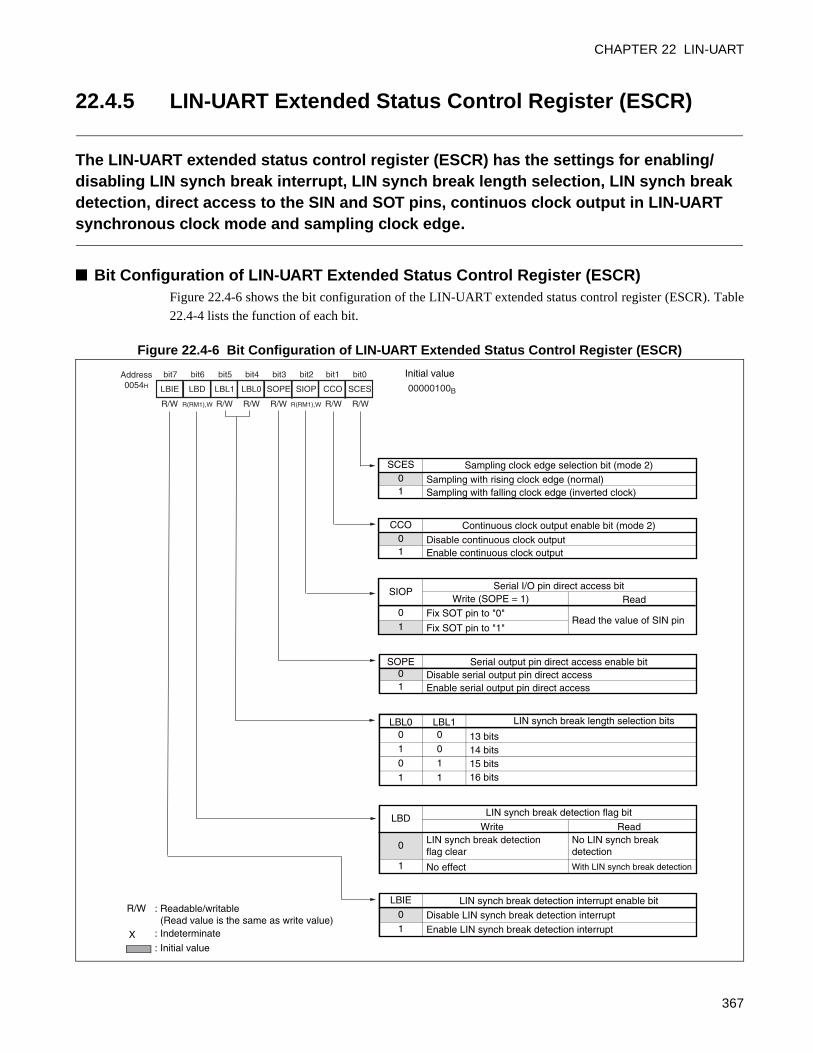
CHAPTER 22 LIN-UART
22.4.5 LIN-UART Extended Status Control Register (ESCR)
The LIN-UART extended status control register (ESCR) has the settings for enabling/disabling LIN synch break interrupt, LIN synch break length selection, LIN synch break detection, direct access to the SIN and SOT pins, continuos clock output in LIN-UART synchronous clock mode and sampling clock edge.
Bit Configuration of LIN-UART Extended Status Control Register (ESCR)Figure 22.4-6 shows the bit configuration of the LIN-UART extended status control register (ESCR). Table
22.4-4 lists the function of each bit.
Figure 22.4-6 Bit Configuration of LIN-UART Extended Status Control Register (ESCR)
LBIE LBD LBL1 LBL0 SIOP CCO SCES 00000100BSOPE
bit7 bit6 bit5 bit4 bit3 bit2 bit1 bit0
R/W R(RM1),W R(RM1),WR/W R/W R/W R/W R/W
Initial value
SCES Sampling clock edge selection bit (mode 2)0 Sampling with rising clock edge (normal)1 Sampling with falling clock edge (inverted clock)
CCO Continuous clock output enable bit (mode 2)0 Disable continuous clock output1 Enable continuous clock output
SIOPSerial I/O pin direct access bit
Write (SOPE = 1) Read0 Fix SOT pin to "0"
Read the value of SIN pin1
SOPE Serial output pin direct access enable bit0 Disable serial output pin direct access1 Enable serial output pin direct access
LBL0 LBL1 LIN synch break length selection bits0
10
1
0
01
1
LBDLIN synch break detection flag bit
Write Read
0 LIN synch break detection flag clear
No LIN synch break detection
1 No effect With LIN synch break detection
LBIE LIN synch break detection interrupt enable bit0 Disable LIN synch break detection interrupt1 Enable LIN synch break detection interrupt
R/W : Readable/writable (Read value is the same as write value)
X : Indeterminate
: Initial value
Fix SOT pin to "1"
13 bits14 bits15 bits16 bits
Address0054H
367
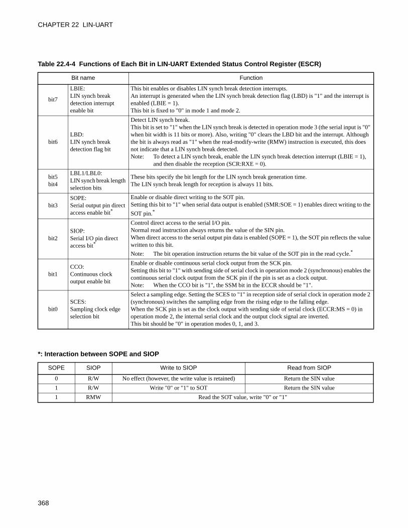
CHAPTER 22 LIN-UART
Table 22.4-4 Functions of Each Bit in LIN-UART Extended Status Control Register (ESCR)
Bit name Function
bit7
LBIE:LIN synch break detection interrupt enable bit
This bit enables or disables LIN synch break detection interrupts.An interrupt is generated when the LIN synch break detection flag (LBD) is "1" and the interrupt is enabled (LBIE = 1).This bit is fixed to "0" in mode 1 and mode 2.
bit6LBD:LIN synch break detection flag bit
Detect LIN synch break.This bit is set to "1" when the LIN synch break is detected in operation mode 3 (the serial input is "0" when bit width is 11 bits or more). Also, writing "0" clears the LBD bit and the interrupt. Although the bit is always read as "1" when the read-modify-write (RMW) instruction is executed, this does not indicate that a LIN synch break detected.Note: To detect a LIN synch break, enable the LIN synch break detection interrupt (LBIE = 1),
and then disable the reception (SCR:RXE = 0).
bit5bit4
LBL1/LBL0:LIN synch break length selection bits
These bits specify the bit length for the LIN synch break generation time.The LIN synch break length for reception is always 11 bits.
bit3SOPE:Serial output pin direct access enable bit*
Enable or disable direct writing to the SOT pin.Setting this bit to "1" when serial data output is enabled (SMR:SOE = 1) enables direct writing to the
SOT pin.*
bit2SIOP:Serial I/O pin direct access bit*
Control direct access to the serial I/O pin.Normal read instruction always returns the value of the SIN pin.When direct access to the serial output pin data is enabled (SOPE = 1), the SOT pin reflects the value written to this bit.
Note: The bit operation instruction returns the bit value of the SOT pin in the read cycle.*
bit1CCO:Continuous clock output enable bit
Enable or disable continuous serial clock output from the SCK pin.Setting this bit to "1" with sending side of serial clock in operation mode 2 (synchronous) enables the continuous serial clock output from the SCK pin if the pin is set as a clock output.Note: When the CCO bit is "1", the SSM bit in the ECCR should be "1".
bit0SCES:Sampling clock edge selection bit
Select a sampling edge. Setting the SCES to "1" in reception side of serial clock in operation mode 2 (synchronous) switches the sampling edge from the rising edge to the falling edge.When the SCK pin is set as the clock output with sending side of serial clock (ECCR:MS = 0) in operation mode 2, the internal serial clock and the output clock signal are inverted.This bit should be "0" in operation modes 0, 1, and 3.
*: Interaction between SOPE and SIOP
SOPE SIOP Write to SIOP Read from SIOP
0 R/W No effect (however, the write value is retained) Return the SIN value
1 R/W Write "0" or "1" to SOT Return the SIN value
1 RMW Read the SOT value, write "0" or "1"
368
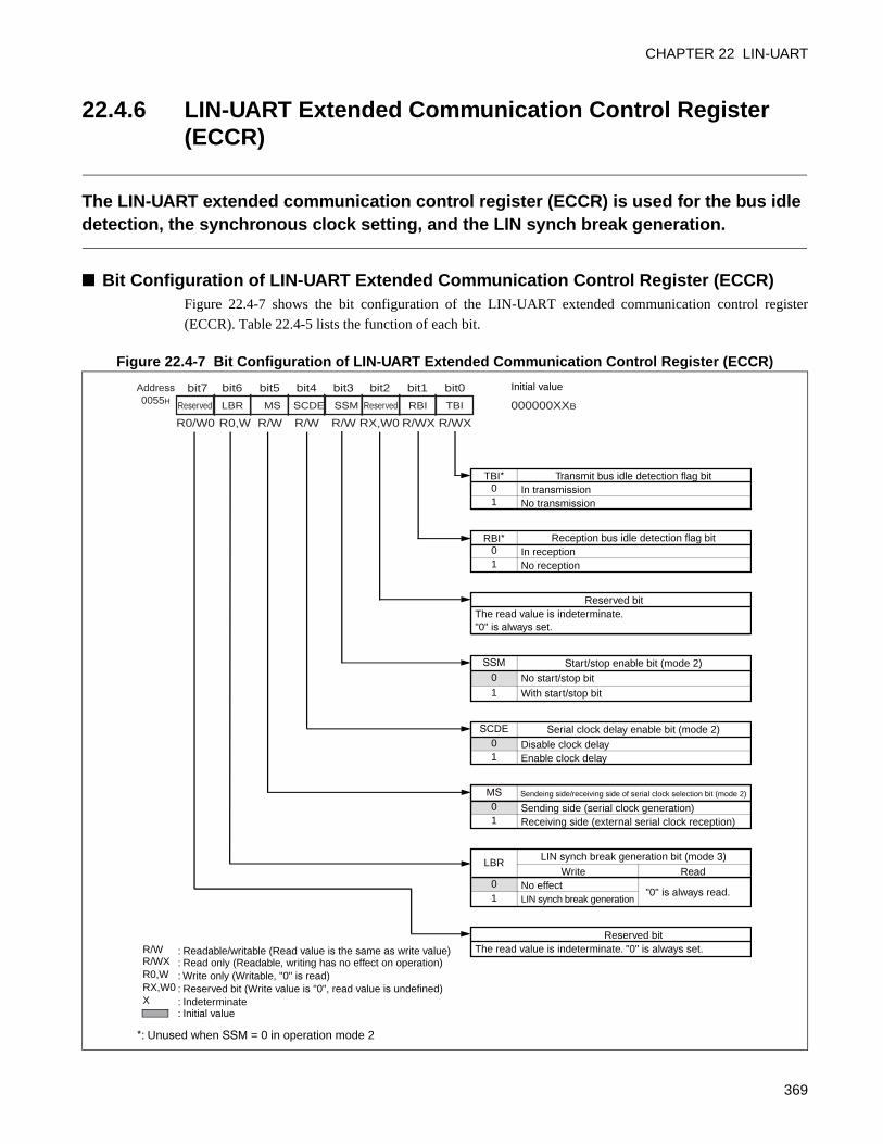
CHAPTER 22 LIN-UART
22.4.6 LIN-UART Extended Communication Control Register (ECCR)
The LIN-UART extended communication control register (ECCR) is used for the bus idle detection, the synchronous clock setting, and the LIN synch break generation.
Bit Configuration of LIN-UART Extended Communication Control Register (ECCR)Figure 22.4-7 shows the bit configuration of the LIN-UART extended communication control register
(ECCR). Table 22.4-5 lists the function of each bit.
Figure 22.4-7 Bit Configuration of LIN-UART Extended Communication Control Register (ECCR)
MS SCDE SSM ReservedReserved RBI TBI 000000XXBLBR
bit7 bit6 bit5 bit4 bit3 bit2 bit1 bit0
R0,W R/W R/W R/W R/WX R/WXR0/W0 RX,W0
Initial value
TBI* Transmit bus idle detection flag bit0 In transmission1 No transmission
RBI* Reception bus idle detection flag bit0 In reception1 No reception
Reserved bitThe read value is indeterminate."0" is always set.
SSM Start/stop enable bit (mode 2)0 No start/stop bit1 With start/stop bit
SCDE Serial clock delay enable bit (mode 2)0 Disable clock delay1 Enable clock delay
MS Sendeing side/receiving side of serial clock selection bit (mode 2)
0 Sending side (serial clock generation)1 Receiving side (external serial clock reception)
LBRLIN synch break generation bit (mode 3)
Write Read0 No effect
"0" is always read.1 LIN synch break generation
Reserved bitThe read value is indeterminate. "0" is always set.R/W : Readable/writable (Read value is the same as write value)
R/WX : Read only (Readable, writing has no effect on operation)R0,W : Write only (Writable, "0" is read)RX,W0 : Reserved bit (Write value is "0", read value is undefined)X : Indeterminate
: Initial value
*: Unused when SSM = 0 in operation mode 2
Address0055H
369
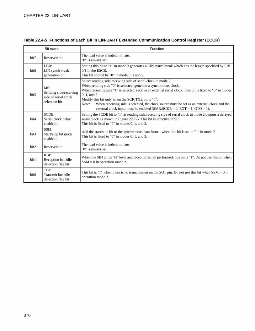
CHAPTER 22 LIN-UART
Table 22.4-5 Functions of Each Bit in LIN-UART Extended Communication Control Register (ECCR)
Bit name Function
bit7 Reserved bitThe read value is indeterminate."0" is always set.
bit6LBR:LIN synch break generation bit
Setting this bit to "1" in mode 3 generates a LIN synch break which has the length specified by LBL 0/1 in the ESCR.This bit should be "0" in mode 0, 1 and 2.
bit5
MS:Sending side/receiving side of serial clock selection bit
Select sending side/receiving side of serial clock in mode 2.When sending side "0" is selected, generate a synchronous clock.When receiving side "1" is selected, receive an external serial clock. This bit is fixed to "0" in modes 0, 1, and 3.Modify this bit only when the SCR:TXE bit is "0".Note: When receiving side is selected, the clock source must be set as an external clock and the
external clock input must be enabled (SMR:SCKE = 0, EXT = 1, OTO = 1).
bit4SCDE:Serial clock delay enable bit
Setting the SCDE bit to "1" at sending side/receiving side of serial clock in mode 2 outputs a delayed serial clock as shown in Figure 22.7-5. This bit is effective in SPI. This bit is fixed to "0" in modes 0, 1, and 3.
bit3SSM:Start/stop bit mode enable bit
Add the start/stop bit to the synchronous data format when this bit is set to "1" in mode 2.This bit is fixed to "0" in modes 0, 1, and 3.
bit2 Reserved bitThe read value is indeterminate."0" is always set.
bit1RBI:Reception bus idle detection flag bit
When the SIN pin is "H" level and reception is not performed, this bit is "1". Do not use this bit when SSM = 0 in operation mode 2.
bit0TBI:Transmit bus idle detection flag bit
This bit is "1" when there is no transmission on the SOT pin. Do not use this bit when SSM = 0 in operation mode 2.
370
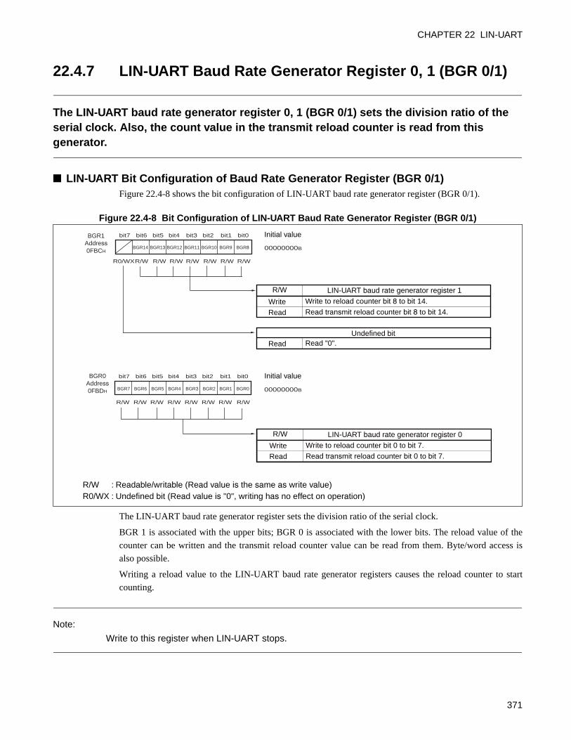
CHAPTER 22 LIN-UART
22.4.7 LIN-UART Baud Rate Generator Register 0, 1 (BGR 0/1)
The LIN-UART baud rate generator register 0, 1 (BGR 0/1) sets the division ratio of the serial clock. Also, the count value in the transmit reload counter is read from this generator.
LIN-UART Bit Configuration of Baud Rate Generator Register (BGR 0/1)Figure 22.4-8 shows the bit configuration of LIN-UART baud rate generator register (BGR 0/1).
Figure 22.4-8 Bit Configuration of LIN-UART Baud Rate Generator Register (BGR 0/1)
The LIN-UART baud rate generator register sets the division ratio of the serial clock.
BGR 1 is associated with the upper bits; BGR 0 is associated with the lower bits. The reload value of the
counter can be written and the transmit reload counter value can be read from them. Byte/word access is
also possible.
Writing a reload value to the LIN-UART baud rate generator registers causes the reload counter to start
counting.
Note:
Write to this register when LIN-UART stops.
00000000B
R0/WX
bit7 bit6 bit5 bit4 bit3 bit2 bit1 bit0
BGR14 BGR13 BGR12 BGR11 BGR10 BGR9 BGR8
00000000B
R/W R/W R/W R/W R/W R/W R/W
bit7 bit6 bit5 bit4 bit3 bit2 bit1 bit0
R/W R/W R/W R/W R/W R/W R/W R/W
BGR1Address0FBCH
Initial value
R/W LIN-UART baud rate generator register 1
Write Write to reload counter bit 8 to bit 14.
Read Read transmit reload counter bit 8 to bit 14.
Undefined bitRead Read "0".
R/W : Readable/writable (Read value is the same as write value)R0/WX : Undefined bit (Read value is "0", writing has no effect on operation)
R/W LIN-UART baud rate generator register 0
Write to reload counter bit 0 to bit 7.Read transmit reload counter bit 0 to bit 7.
Initial value
ReadWrite
BGR0Address0FBDH BGR6BGR7 BGR5 BGR4 BGR3 BGR2 BGR1 BGR0
371
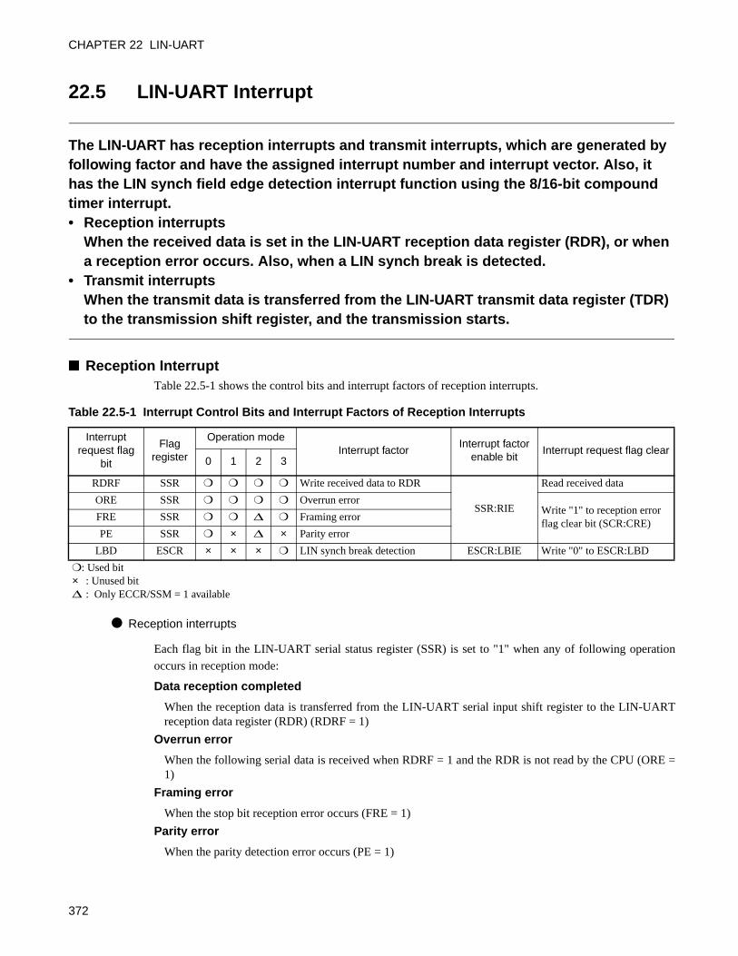
CHAPTER 22 LIN-UART
22.5 LIN-UART Interrupt
The LIN-UART has reception interrupts and transmit interrupts, which are generated by following factor and have the assigned interrupt number and interrupt vector. Also, it has the LIN synch field edge detection interrupt function using the 8/16-bit compound timer interrupt.• Reception interrupts
When the received data is set in the LIN-UART reception data register (RDR), or when a reception error occurs. Also, when a LIN synch break is detected.
• Transmit interruptsWhen the transmit data is transferred from the LIN-UART transmit data register (TDR) to the transmission shift register, and the transmission starts.
Reception InterruptTable 22.5-1 shows the control bits and interrupt factors of reception interrupts.
Reception interrupts
Each flag bit in the LIN-UART serial status register (SSR) is set to "1" when any of following operation
occurs in reception mode:
Data reception completed
When the reception data is transferred from the LIN-UART serial input shift register to the LIN-UARTreception data register (RDR) (RDRF = 1)
Overrun error
When the following serial data is received when RDRF = 1 and the RDR is not read by the CPU (ORE =1)
Framing error
When the stop bit reception error occurs (FRE = 1)
Parity error
When the parity detection error occurs (PE = 1)
Table 22.5-1 Interrupt Control Bits and Interrupt Factors of Reception Interrupts
Interrupt request flag
bit
Flag register
Operation modeInterrupt factor
Interrupt factor enable bit
Interrupt request flag clear0 1 2 3
RDRF SSR Write received data to RDR
SSR:RIE
Read received data
ORE SSR Overrun errorWrite "1" to reception error flag clear bit (SCR:CRE)
FRE SSR ∆ Framing error
PE SSR × ∆ × Parity error
LBD ESCR × × × LIN synch break detection ESCR:LBIE Write "0" to ESCR:LBD
: Used bit× : Unused bit∆ : Only ECCR/SSM = 1 available
372
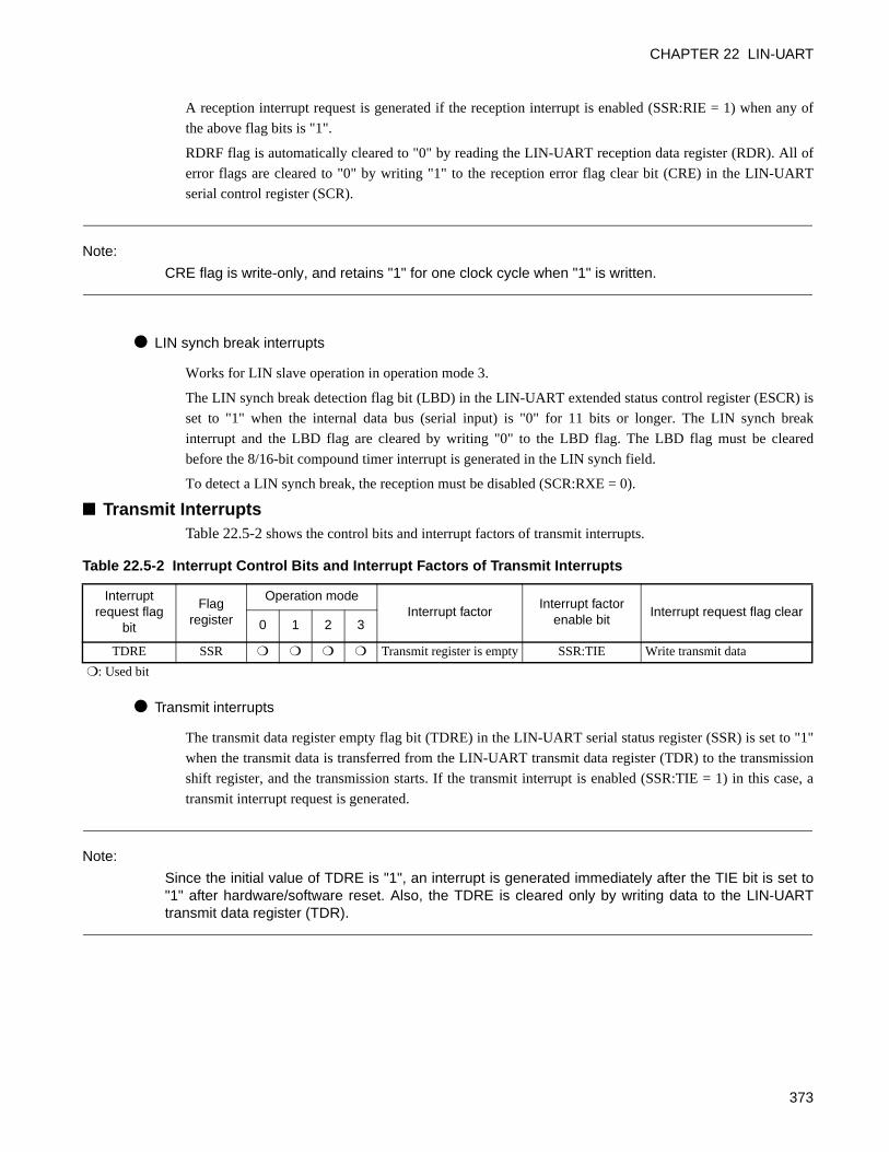
CHAPTER 22 LIN-UART
A reception interrupt request is generated if the reception interrupt is enabled (SSR:RIE = 1) when any of
the above flag bits is "1".
RDRF flag is automatically cleared to "0" by reading the LIN-UART reception data register (RDR). All of
error flags are cleared to "0" by writing "1" to the reception error flag clear bit (CRE) in the LIN-UART
serial control register (SCR).
Note:
CRE flag is write-only, and retains "1" for one clock cycle when "1" is written.
LIN synch break interrupts
Works for LIN slave operation in operation mode 3.
The LIN synch break detection flag bit (LBD) in the LIN-UART extended status control register (ESCR) is
set to "1" when the internal data bus (serial input) is "0" for 11 bits or longer. The LIN synch break
interrupt and the LBD flag are cleared by writing "0" to the LBD flag. The LBD flag must be cleared
before the 8/16-bit compound timer interrupt is generated in the LIN synch field.
To detect a LIN synch break, the reception must be disabled (SCR:RXE = 0).
Transmit InterruptsTable 22.5-2 shows the control bits and interrupt factors of transmit interrupts.
Transmit interrupts
The transmit data register empty flag bit (TDRE) in the LIN-UART serial status register (SSR) is set to "1"
when the transmit data is transferred from the LIN-UART transmit data register (TDR) to the transmission
shift register, and the transmission starts. If the transmit interrupt is enabled (SSR:TIE = 1) in this case, a
transmit interrupt request is generated.
Note:
Since the initial value of TDRE is "1", an interrupt is generated immediately after the TIE bit is set to"1" after hardware/software reset. Also, the TDRE is cleared only by writing data to the LIN-UARTtransmit data register (TDR).
Table 22.5-2 Interrupt Control Bits and Interrupt Factors of Transmit Interrupts
Interrupt request flag
bit
Flag register
Operation modeInterrupt factor
Interrupt factor enable bit
Interrupt request flag clear0 1 2 3
TDRE SSR Transmit register is empty SSR:TIE Write transmit data
: Used bit
373
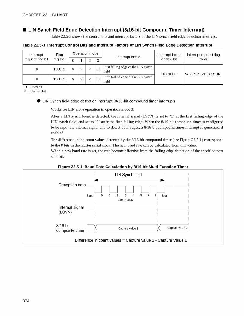
CHAPTER 22 LIN-UART
LIN Synch Field Edge Detection Interrupt (8/16-bit Compound Timer Interrupt)Table 22.5-3 shows the control bits and interrupt factors of the LIN synch field edge detection interrupt.
LIN Synch field edge detection interrupt (8/16-bit compound timer interrupt)
Works for LIN slave operation in operation mode 3.
After a LIN synch break is detected, the internal signal (LSYN) is set to "1" at the first falling edge of the
LIN synch field, and set to "0" after the fifth falling edge. When the 8/16-bit compound timer is configured
to be input the internal signal and to detect both edges, a 8/16-bit compound timer interrupt is generated if
enabled.
The difference in the count values detected by the 8/16-bit compound timer (see Figure 22.5-1) corresponds
to the 8 bits in the master serial clock. The new baud rate can be calculated from this value.
When a new baud rate is set, the rate become effective from the falling edge detection of the specified next
start bit.
Figure 22.5-1 Baud Rate Calculation by 8/16-bit Multi-Function Timer
Table 22.5-3 Interrupt Control Bits and Interrupt Factors of LIN Synch Field Edge Detection Interrupt
Interrupt request flag bit
Flag register
Operation modeInterrupt factor
Interrupt factor enable bit
Interrupt request flag clear0 1 2 3
IR T00CR1 × × × First falling edge of the LIN synch field
T00CR1:IE Write "0" to T00CR1:IRIR T00CR1 × × ×
Fifth falling edge of the LIN synch field
: Used bit× : Unused bit
LIN Synch field
Start Stop0 1 2 7
Reception data
Data = 0x55
Internal signal (LSYN)
8/16-bit composite timer
Capture value 1 Capture value 2
Difference in count values = Capture value 2 - Capture Value 1
3 4 5 6
374
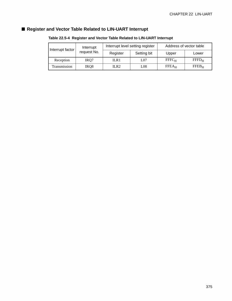
CHAPTER 22 LIN-UART
Register and Vector Table Related to LIN-UART Interrupt
Table 22.5-4 Register and Vector Table Related to LIN-UART Interrupt
Interrupt factorInterrupt
request No.
Interrupt level setting register Address of vector table
Register Setting bit Upper Lower
Reception IRQ7 ILR1 L07 FFFCH FFFDH
Transmission IRQ8 ILR2 L08 FFEAH FFEBH
375
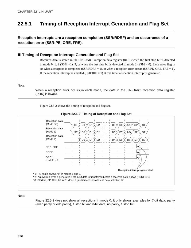
CHAPTER 22 LIN-UART
22.5.1 Timing of Reception Interrupt Generation and Flag Set
Reception interrupts are a reception completion (SSR:RDRF) and an occurrence of a reception error (SSR:PE, ORE, FRE).
Timing of Reception Interrupt Generation and Flag SetReceived data is stored in the LIN-UART reception data register (RDR) when the first stop bit is detected
in mode 0, 1, 2 (SSM =1), 3, or when the last data bit is detected in mode 2 (SSM = 0). Each error flag is
set when a reception is completed (SSR:RDRF = 1), or when a reception error occurs (SSR:PE, ORE, FRE = 1).
If the reception interrupt is enabled (SSR:RIE = 1) at this time, a reception interrupt is generated.
Note:
When a reception error occurs in each mode, the data in the LIN-UART reception data register(RDR) is invalid.
Figure 22.5-2 shows the timing of reception and flag set.
Figure 22.5-2 Timing of Reception and Flag Set
Note:
Figure 22.5-2 does not show all receptions in mode 0. It only shows examples for 7-bit data, parity(even parity or odd parity), 1 stop bit and 8-bit data, no parity, 1 stop bit.
RDRF
PE*1, FRE
ORE*2
(RDRF = 1)
ST D0 D1 D2 D5 D6 D7/P SP ST
ST D0 D1 D2 D6 D7 A/D SP ST
D0 D1 D2 D4 D5 D6 D7 D0
Reception data (Mode 0/3)
Reception data (Mode 1)
Reception data (Mode 2)
Reception interrupts generated
* 1: PE flag is always "0" in modes 1 and 3.* 2: An overrun error is generated if the next data is transferred before a received data is read (RDRF = 1).ST: Start bit, SP: Stop bit, A/D: Mode 1 (multiprocessor) address data selection bit
…
…
…
376
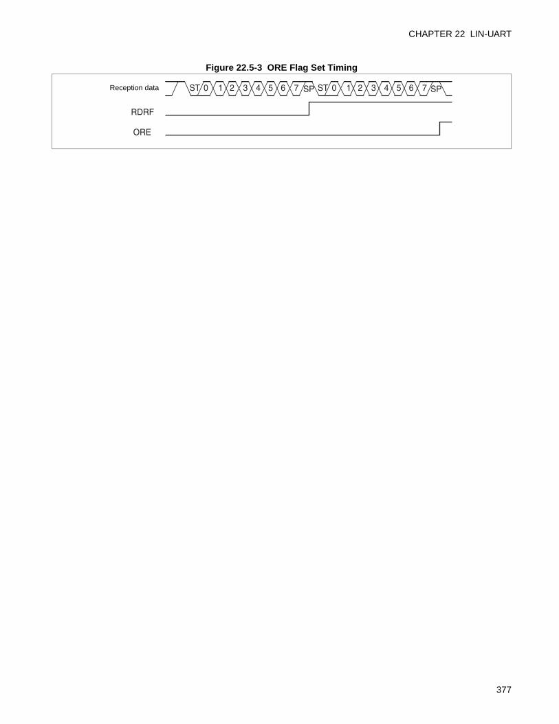
CHAPTER 22 LIN-UART
Figure 22.5-3 ORE Flag Set Timing
RDRF
ORE
ST 0 1 2 3 4 5 6 7 STSP 0 1 2 3 4 5 6 7 SPReception data
377
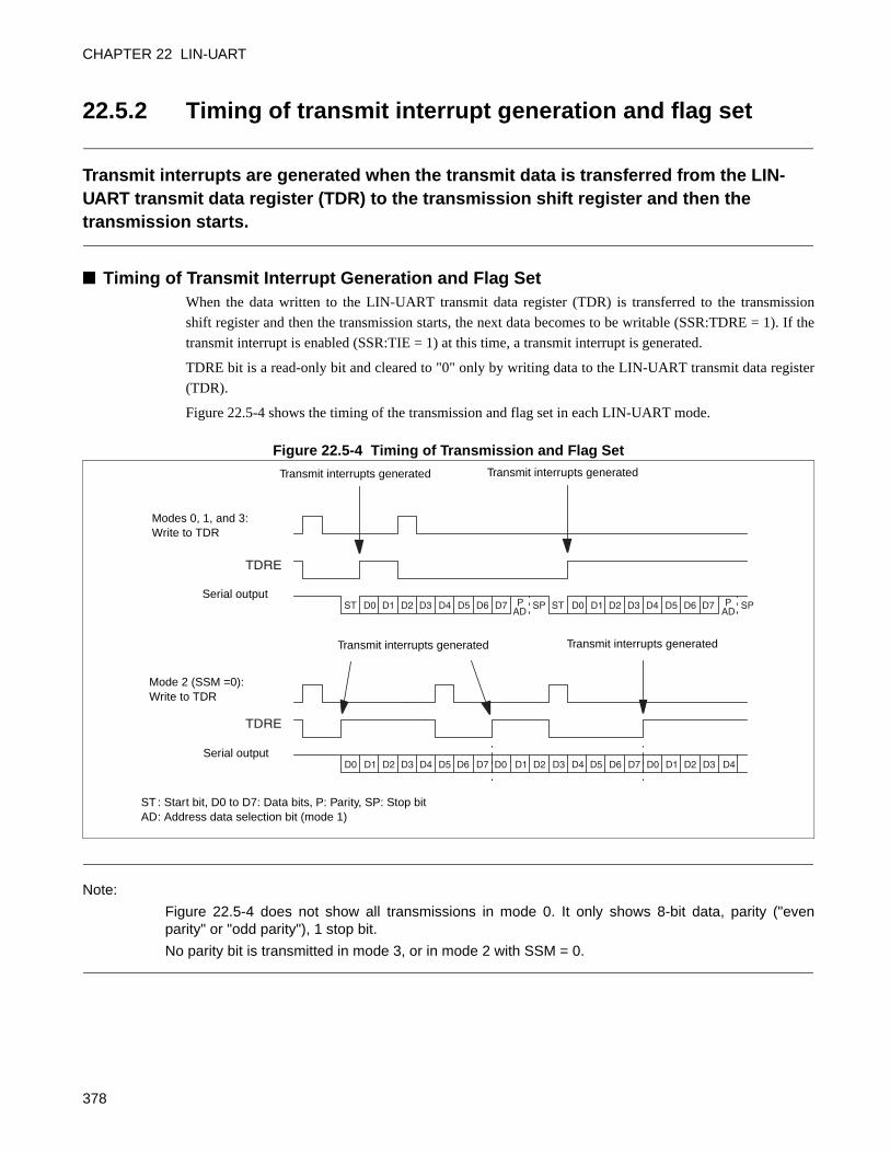
CHAPTER 22 LIN-UART
22.5.2 Timing of transmit interrupt generation and flag set
Transmit interrupts are generated when the transmit data is transferred from the LIN-UART transmit data register (TDR) to the transmission shift register and then the transmission starts.
Timing of Transmit Interrupt Generation and Flag SetWhen the data written to the LIN-UART transmit data register (TDR) is transferred to the transmission
shift register and then the transmission starts, the next data becomes to be writable (SSR:TDRE = 1). If the
transmit interrupt is enabled (SSR:TIE = 1) at this time, a transmit interrupt is generated.
TDRE bit is a read-only bit and cleared to "0" only by writing data to the LIN-UART transmit data register
(TDR).
Figure 22.5-4 shows the timing of the transmission and flag set in each LIN-UART mode.
Figure 22.5-4 Timing of Transmission and Flag Set
Note:
Figure 22.5-4 does not show all transmissions in mode 0. It only shows 8-bit data, parity ("evenparity" or "odd parity"), 1 stop bit.
No parity bit is transmitted in mode 3, or in mode 2 with SSM = 0.
TDRE
TDRE
ST D0 D1 D2 D3 D4 D5 D6 D7 PAD
SP ST D0 D1 D2 D3 D4 D5 D6 D7 PAD
SP
D0 D1 D2 D3 D4 D5 D6 D7 D0 D1 D2 D3 D4 D5 D6 D7 D0 D1 D2 D3 D4
Transmit interrupts generated Transmit interrupts generated
Transmit interrupts generated Transmit interrupts generated
Modes 0, 1, and 3: Write to TDR
Serial output
Mode 2 (SSM =0): Write to TDR
Serial output
ST : Start bit, D0 to D7: Data bits, P: Parity, SP: Stop bitAD: Address data selection bit (mode 1)
378
CHAPTER 22 LIN-UART
Transmit Interrupt Request Generation Timing
When TDRE flag is set to "1" if the transmit interrupt is enabled (SSR:TIE = 1), a transmit interrupt request
is generated.
Note:
Since the TDRE bit is initially set to "1", a transmit interrupt is generated immediately after thetransmit interrupt is enabled (SSR:TIE = 1). Be careful with the timing for enabling the transmitinterrupt since the TDRE bit can be cleared only by writing new data to the LIN-UART transmit dataregister (TDR).
Refer to "APPENDIX B Table of Interrupt Causes" for interrupt request number/vector table of each
peripheral function.
379
CHAPTER 22 LIN-UART
22.6 LIN-UART Baud Rate
One of the following can be selected for the LIN-UART input clock (send/receive clock source): • Input a machine clock into a baud rate generator (reload counter)• Input an external clock into a baud rate generator (reload counter)• Use the external clock (SCK pin input clock) directly.
LIN-UART Baud Rate SelectionYou can select one of the following three different baud rates. Figure 22.6-1 shows the baud rate selection
circuit.
Baud rate derived from the internal clock divided by the dedicated baud rate generator (reload counter)
Two internal reload counters are provided and assigned the transmit and reception serial clock respectively.
The baud rate is selected by setting a 15-bit reload value in the LIN-UART baud rate generator register 1, 0
(BGR1, BGR0).
The reload counter divides the internal clock by the specified value.
It is used in asynchronous mode and in synchronous mode (sending side of serial clock).
To set the clock source, select the use of the internal clock and baud rate generator (SMR:EXT = 0, OTO = 0).
Baud rate derived from the external clock divided by the dedicated baud rate generator (reload counter)
The external clock is used as the clock source for the reload counter.
The baud rate is selected by setting a 15-bit reload value in the LIN-UART baud rate generator register 1, 0
(BGR0, BGR1).
The reload counter divides the external clock by the specified value.
It is used in asynchronous mode.
To set the clock source, select the use of the external clock and baud rate generator (SMR:EXT = 1, OTO = 0).
Baud rate by the external clock (one-to-one mode)
The clock input from the clock input pin (SCK) of the LIN-UART is used as the baud rate (slave 2
operation (ECCR:MS =1) in synchronous mode).
It is used in synchronous mode (receiving side of serial clock).
To set the clock source, select the external clock and its direct use (SMR:EXT = 1, OTO = 1).
380

CHAPTER 22 LIN-UART
Figure 22.6-1 LIN-UART Baud Rate Selection Circuit
EXTREST
BGR7
BGR10BGR9BGR8
BGR6BGR5
BGR4BGR3BGR2BGR1BGR0
Txc = 0?
Txc = v/2?
OTO
1
01
0
BGR13BGR12BGR11
BGR14
F/F
Rxc = 0?
Rxc = v/2?
F/F
EXT
OTO
1
0
Reload value: v
Reception15-bit reload counter
Transmit15-bit reload counter
Reload value: v
Counter value: TXC
Reload
Reload
ResetStart bit falling edge detection
Reception clock
Transmit clock
SCK(External clock
input)
Reset
Reset
Set
Set
Internal data bus
SMRregister
BGR1register
BGR0register
MCLK (Machine clock)
381
CHAPTER 22 LIN-UART
22.6.1 Baud Rate Setting
This section shows baud rate settings and the calculation result of serial clock frequencies.
Baud Rate CalculationThe two 15-bit reload counters are set by the LIN-UART baud rate generator register 1, 0 (BGR 1, BGR 0).
The expressions for the baud rate are as follows.
Reload value:
v = (MCLK/b) - 1
v: Reload value, b: Baud rate, MCLK: Machine clock, or external clock frequency
Calculation example
Assuming that the machine clock is 10MHz, the internal clock is used, and the baud rate is set to 19200
bps:
Reload value:
Thus, the actual baud rate can be calculated as follows.
Note:
The reload counter halts if the reload value is set to "0". Therefore, the least reload value should be"1".
For transmission/reception in asynchronous mode, the reload value must be at least "4" in order todetermine the reception value by oversampling on five times.
v = (10 × 106
) -1 = 520.83 ... 52019200
b =MCLK
=10 × 106
= 19193.8579 (v + 1) 521
382
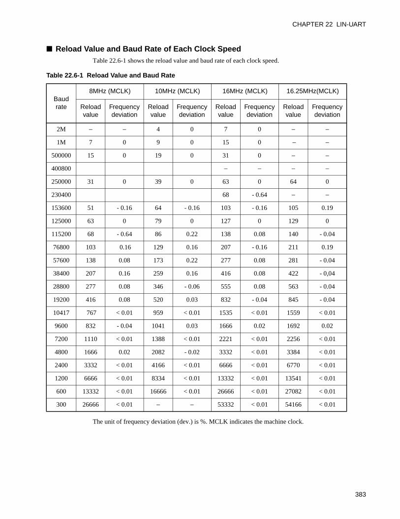
383
CHAPTER 22 LIN-UART
Reload Value and Baud Rate of Each Clock SpeedTable 22.6-1 shows the reload value and baud rate of each clock speed.
The unit of frequency deviation (dev.) is %. MCLK indicates the machine clock.
Table 22.6-1 Reload Value and Baud Rate
Baud rate
8MHz (MCLK) 10MHz (MCLK) 16MHz (MCLK) 16.25MHz(MCLK)
Reload value
Frequency deviation
Reload value
Frequency deviation
Reload value
Frequency deviation
Reload value
Frequency deviation
2M − − 4 0 7 0 − −
1M 7 0 9 0 15 0 − −
500000 15 0 19 0 31 0 − −
400800 − − − −
250000 31 0 39 0 63 0 64 0
230400 68 - 0.64 − −
153600 51 - 0.16 64 - 0.16 103 - 0.16 105 0.19
125000 63 0 79 0 127 0 129 0
115200 68 - 0.64 86 0.22 138 0.08 140 - 0.04
76800 103 0.16 129 0.16 207 - 0.16 211 0.19
57600 138 0.08 173 0.22 277 0.08 281 - 0.04
38400 207 0.16 259 0.16 416 0.08 422 - 0,04
28800 277 0.08 346 - 0.06 555 0.08 563 - 0.04
19200 416 0.08 520 0.03 832 - 0.04 845 - 0.04
10417 767 < 0.01 959 < 0.01 1535 < 0.01 1559 < 0.01
9600 832 - 0.04 1041 0.03 1666 0.02 1692 0.02
7200 1110 < 0.01 1388 < 0.01 2221 < 0.01 2256 < 0.01
4800 1666 0.02 2082 - 0.02 3332 < 0.01 3384 < 0.01
2400 3332 < 0.01 4166 < 0.01 6666 < 0.01 6770 < 0.01
1200 6666 < 0.01 8334 < 0.01 13332 < 0.01 13541 < 0.01
600 13332 < 0.01 16666 < 0.01 26666 < 0.01 27082 < 0.01
300 26666 < 0.01 − − 53332 < 0.01 54166 < 0.01
CHAPTER 22 LIN-UART
External ClockThe external clock is selected by writing "1" to the EXT bit in the LIN-UART serial mode register (SMR).
In the baud rate generator, the external clock can be used in the same way as the internal clock.
When slave operation is used in synchronous mode 2, select the one-to-one external clock input mode
(SMR:OTO = 1). In this mode, the external clock input to SCK is input directly to the LIN-UART serial
clock.
Note:
The external clock signal is synchronized with the internal clock (MCLK: machine clock) in the LIN-UART. Therefore, the signal is unstable because the external clock cannot be divided if its cycle isfaster than half cycle of the internal clock.For the value of the SCK clock, refer to the data sheet.
384
CHAPTER 22 LIN-UART
Operation of Dedicated Baud Rate Generator (Reload Counter)
Figure 22.6-2 shows the operation of two reload counters when the reload value is "832 as an example".
Figure 22.6-2 Operation of Dedicated Baud Rate Generator (Reload Counter)
Note:
The falling edge of the serial clock signal is generated after the reload value divided by 2 ((V+1)/2) iscounted.
Transmit/reception clock
Reload counter
Reload counter value
002 001 832 831 830 829 828 417 416 415 414 413 412 411
Falling at (V+1)/2
385
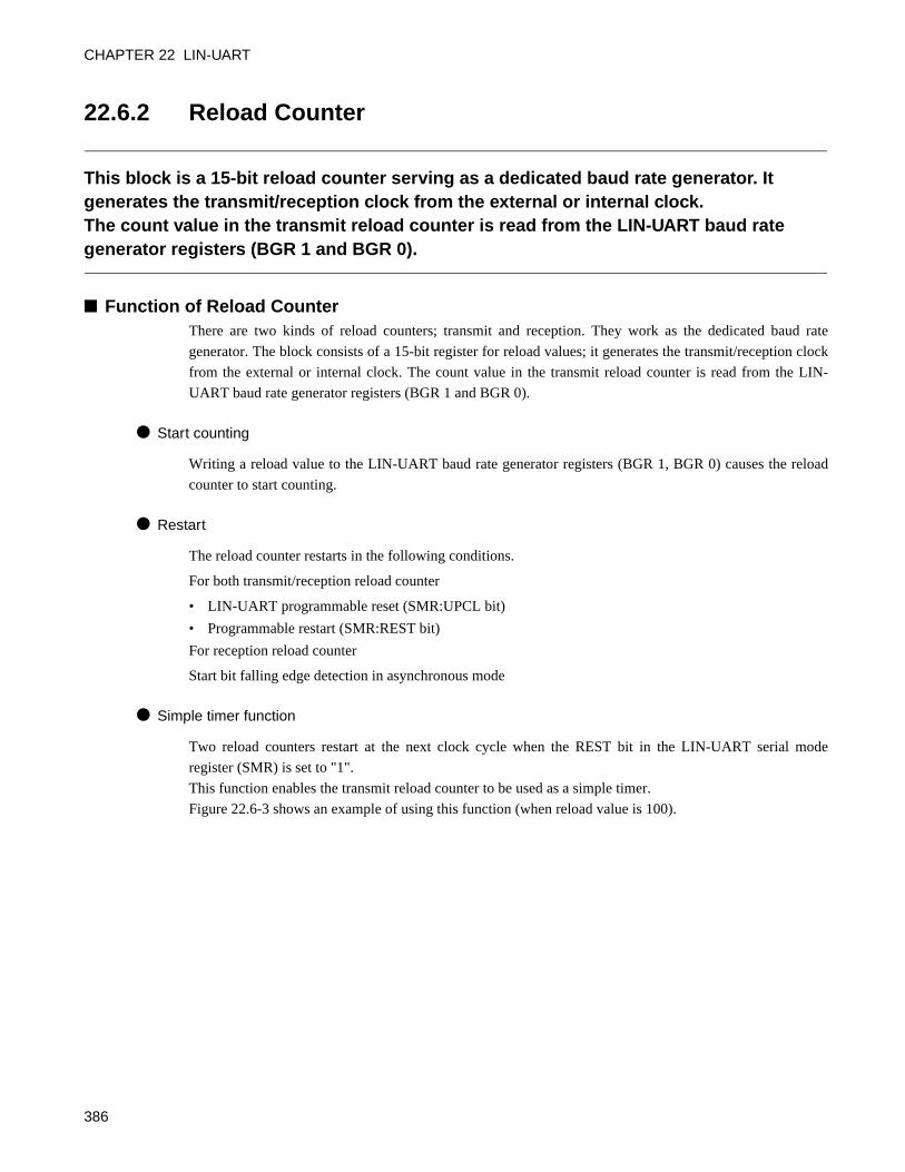
CHAPTER 22 LIN-UART
22.6.2 Reload Counter
This block is a 15-bit reload counter serving as a dedicated baud rate generator. It generates the transmit/reception clock from the external or internal clock.The count value in the transmit reload counter is read from the LIN-UART baud rate generator registers (BGR 1 and BGR 0).
Function of Reload CounterThere are two kinds of reload counters; transmit and reception. They work as the dedicated baud rate
generator. The block consists of a 15-bit register for reload values; it generates the transmit/reception clock
from the external or internal clock. The count value in the transmit reload counter is read from the LIN-
UART baud rate generator registers (BGR 1 and BGR 0).
Start counting
Writing a reload value to the LIN-UART baud rate generator registers (BGR 1, BGR 0) causes the reload
counter to start counting.
Restart
The reload counter restarts in the following conditions.
For both transmit/reception reload counter
• LIN-UART programmable reset (SMR:UPCL bit)
• Programmable restart (SMR:REST bit)
For reception reload counter
Start bit falling edge detection in asynchronous mode
Simple timer function
Two reload counters restart at the next clock cycle when the REST bit in the LIN-UART serial mode
register (SMR) is set to "1".
This function enables the transmit reload counter to be used as a simple timer.
Figure 22.6-3 shows an example of using this function (when reload value is 100).
386
CHAPTER 22 LIN-UART
Figure 22.6-3 Example of Using a Simple Timer by Restarting the Reload Timer
The number of machine cycles "cyc" after restart in this example is obtained by the following expression.
cyc = v - c + 1 = 100 - 90 + 1 = 11
v: Reload value, c: Reload counter value
Note:
The reload counters also restart when the LIN-UART is reset by writing "1" to the SMR:UPCL bit.
Automatic restart (reception reload counter only)
The reception reload counter is restarted when the start bit falling edge is detected in asynchronousmode. This is the function to synchronize the reception shift register with the reception data.
Clear counter
When a reset occurs, the reload values in the LIN-UART baud rate generator registers (BGR 1, BGR 0) and
the reload counter are cleared to "00H", and the reload counter halts.
Although the counter value is temporarily cleared to "00H" by the LIN-UART reset (writing "1" to
SMR:UPCL), the reload counter restarts since the reload value is retained.
The counter value is not cleared to "00H" by the reset setting (writing "1" to SMR:REST), and the reload
counter restarts.
MCLK
Write
(Machine clock)
SMR registerREST bit
write signal
Reload counter
Reload
BGR0/BGR1 register read signal
Register read value 90
: Don't care
37 36 35 100 99 98 97 96 95 94 93 92 91 90 89 88 87
387
CHAPTER 22 LIN-UART
22.7 Operations and Setting Procedure Example of LIN-UART
LIN-UART operates in mode 0, 2 for bi-directional serial communication, in mode 1 for master/slave communication, and in mode 3 for LIN master/slave communication.
Operation of LIN-UART
Operation mode
The LIN-UART has four operation modes (0 to 3), allowing the connections and the data transfer methods
between CPUs to be selected as listed in Table 22.7-1.
The MD0 and MD1 bits in the LIN-UART serial mode register (SMR) are used to select the following
LIN-UART operation modes.
Notes:
• Both master and slave operation are supported in a system with master/slave connection in mode1.
• In mode 3, the communication format is fixed to 8-bit data, no parity, stop bit1, LSB-first.
• If the mode is changed, all transmissions and receptions are canceled, and the LIN-UART waitsfor the next operation.
Table 22.7-1 LIN-UART Operation Modes
Operation modeData length
Synchronous method Stop bit length Data bit formatNo parity With parity
0 Normal mode 7 bits or 8 bits Asynchronous1 bit or 2 bits LSB first
MSB first1
Multiprocessor mode 7 bits or 8 bits +1* - Asynchronous
2 Normal mode 8 bits Synchronous None, 1 bit, 2 bits
3 LIN mode 8 bits - Asynchronous 1 bit LSB first
- : Unavailable* : "+1" is the address/data selection bit (A/D) used for communication control in multiprocessor mode.
Table 22.7-2 LIN-UART Operation Modes
MD1 MD0 Mode Type
0 0 0 Asynchronous (Normal mode)
0 1 1 Asynchronous (Multiprocessor mode)
1 0 2 Synchronous (Normal mode)
1 1 3 Asynchronous (LIN mode)
388
CHAPTER 22 LIN-UART
Inter-CPU Connection Method
You can select either external clock one-to-one connection (normal mode) or master/slave connection
(multiprocessor mode). In either methods, data length, parity setting, synchronization type must be the
same between all CPUs and thus the operation mode must be selected as follows.
• One-to-one connection: Two CPUs must use the same method in either operation mode 0 or 2. Selectthe operation mode 0 for asynchronous method or the operation mode 2 forsynchronous method. Also, for the operation mode 2, set one CPU as sendingside of serial clock and the other as the receiving side of serial clock.
• Master/slave connection: Select operation mode 1. Use the system as a master/slave system.
Synchronous MethodIn asynchronous method, the reception clock is synchronized with the reception start bit falling edge. In
synchronous method, the reception clock can be synchronized by the sending side of serial clock signal or
the clock signal at operating as sending side of serial clock.
SignalingNRZ (Non Return to Zero).
Enable Transmission/ReceptionThe LIN-UART uses the SCR:TXE bit and the SCR:RXE bit to control transmission and reception,
respectively. To disable transmission or reception, set as follows.
• If the reception is in progress, wait until the reception completed, read the LIN-UART reception dataregister (RDR), and then disable the reception.
• If the transmission is in progress, wait until the transmission completed, and then disable thetransmission.
Setting ProcedureLIN-UART is set in the following procedure:
Initial setting
1) Set the port input (DDR1).
2) Set the interrupt level (ILR1, ILR2).
3) Set the data format, enable transmission/reception (SCR).
4) The operation mode, baud rate selection, pin output enabled (SMR)
5) The baud rate generator (BGR1,BGR0)
389
CHAPTER 22 LIN-UART
22.7.1 Operation of Asynchronous Mode (Operation Mode 0, 1)
When LIN-UART is used in operation mode 0 (normal mode) or operation mode 1 (multiprocessor mode), the transfer method is asynchronous.
Asynchronous Mode Operation
Transmit/reception data format
Transmit/reception data always begins with a start bit ("L" level) followed by a specified data bits length
and ends up with at least one stop bit ("H" level).
The bit transfer direction (LSB-first or MSB-first) is determined by the BDS bit in the LIN-UART serial
status register (SSR). When a parity is used, the parity bit is always placed between the last data bit and the
first stop bit.
In operation mode 0, select 7-bit or 8-bit for the data length. You can select whether or not to use a parity.
Also, the stop bit length (1 or 2) can be selected.
In operation mode 1, a data length is 7-bit or 8-bit, the parity is not added, and the address/data bit is added.
The stop bit length (1 or 2) can be selected.
The bit length of transmit/reception frame is calculated as follows:
Length = 1 + d + p + s
(d = Number of data bits [7 or 8], p = parity [0 or 1],
s = Number of stop bits [1 or 2])
Figure 22.7-1 shows the data format in asynchronous mode.
390
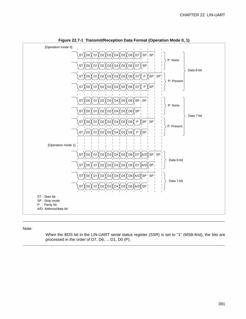
CHAPTER 22 LIN-UART
Figure 22.7-1 Transmit/Reception Data Format (Operation Mode 0, 1)
Note:
When the BDS bit in the LIN-UART serial status register (SSR) is set to "1" (MSB-first), the bits areprocessed in the order of D7, D6, ... D1, D0 (P).
ST D0 D1 D2 D3 D4 D5 D6 D7 SP SP
ST D0 D1 D2 D3 D4 D5 D6 D7 P SP
ST D0 D1 D2 D3 D4 D5 D6 D7 SP
SPST D0 D1 D2 D3 D4 D5 D6 D7 P SP
ST D0 D1 D2 D3 D4 D5 D6 SP SP
ST D0 D1 D2 D3 D4 D5 D6 P SP
ST D0 D1 D2 D3 D4 D5 D6 SP
SPST D0 D1 D2 D3 D4 D5 D6 P SP
ST D0 D1 D2 D3 D4 D5 D6 D7 A/D SP
ST D0 D1 D2 D3 D4 D5 D6 A/D SP
ST D0 D1 D2 D3 D4 D5 D6 D7 A/D
ST D0 D1 D2 D3 D4 D5 D6 A/D SP SP
SP
SP
[Operation mode 0]
[Operation mode 1]
ST : Start bitSP : Stop modeP : Parity bitA/D: Address/data bit
P: None
Data 8-bit
Data 7-bit
P: Present
P: None
P: Present
Data 8-bit
Data 7-bit
391
CHAPTER 22 LIN-UART
Transmission
If the transmit data register empty flag bit (TDRE) in the LIN-UART serial status register (SSR) is "1",
transmit data can be written into the LIN-UART transmit data register (TDR). Writing data sets the TDRE
flag to "0". If transmission is enabled (SCR:TXE = 1) at this time, the data is written to the transmit shift
register and the transmission is started sequentially from the start bit in the next serial clock cycle.
When TDRE flag is set to "1" if the transmit interrupt is enabled (TIE = 1), an interrupt is generated when
the TDRE flag is set to "1".
When the data length is set to 7-bit (CL = 0), the bit 7 in the TDR is an unused bit regardless of the transfer
direction select bit (BDS) setting (LSB-first or MSB-first).
Note:
Since the initial value of transmit data empty flag bit (SSR:TDRE) is "1", an interrupt is generatedimmediately when transmit interrupts are enabled (SSR:TIE =1).
Reception
The reception is performed when reception is enabled (SCR:RXE =1). When the start bit is detected, one
frame data is received according to the data format defined in the LIN-UART serial control register (SCR).
If an error occurs, the error flag (SSR:PE, ORE, FRE) is set. After the reception of the one frame data is
completed, the received data is transferred from the reception shift register to the LIN-UART reception
data register (RDR), and the reception data register full flag bit (SSR:RDRF) is set to "1". If the reception
interrupt request is enabled (SSR:RIE = 1) at this time, a reception interrupt request is output.
To read the received data, check the error flag status and read the received data from the LIN-UART
reception data register (RDR) if the reception is normal. If a reception error occurs, perform error
handlings.
When the received data is read, the reception data register full flag bit (SSR:RDRF) is cleared to "0".
When the data length is set to 7-bit (CL = 0), the MSB in the TDR is an unused bit regardless of the
transfer direction select bit (BDS) setting (LSB-first or MSB-first).
Note:
Data in the LIN-UART reception data register (RDR) becomes valid when the reception data registerfull flag bit (SSR:RDRF) is set to "1" and no error occurs (SSR:PE, ORE, FRE=0).
Input clock
Internal or external clock is used. For the baud rate, select the baud rate generator (SMR:EXT = 0 or 1,
OTO = 0).
392
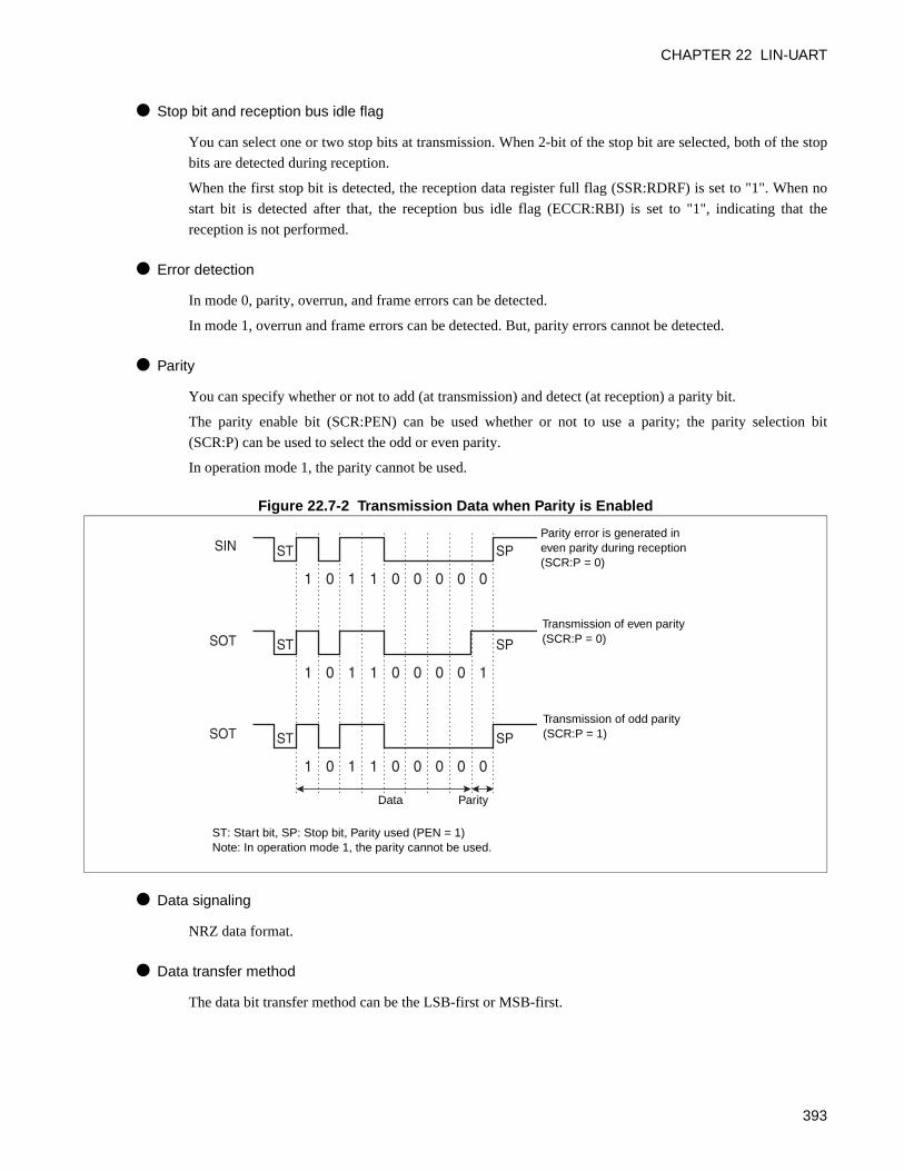
CHAPTER 22 LIN-UART
Stop bit and reception bus idle flag
You can select one or two stop bits at transmission. When 2-bit of the stop bit are selected, both of the stop
bits are detected during reception.
When the first stop bit is detected, the reception data register full flag (SSR:RDRF) is set to "1". When no
start bit is detected after that, the reception bus idle flag (ECCR:RBI) is set to "1", indicating that the
reception is not performed.
Error detection
In mode 0, parity, overrun, and frame errors can be detected.
In mode 1, overrun and frame errors can be detected. But, parity errors cannot be detected.
Parity
You can specify whether or not to add (at transmission) and detect (at reception) a parity bit.
The parity enable bit (SCR:PEN) can be used whether or not to use a parity; the parity selection bit
(SCR:P) can be used to select the odd or even parity.
In operation mode 1, the parity cannot be used.
Figure 22.7-2 Transmission Data when Parity is Enabled
Data signaling
NRZ data format.
Data transfer method
The data bit transfer method can be the LSB-first or MSB-first.
SIN
1 0 1 1 0 0 0
SOT
1 0 1 1 0 0 1
SOT
1 0 1 1 0 0 0
ST SP
ST SP
ST SP
0
0
0
0
0
0
Parity error is generated in even parity during reception (SCR:P = 0)
Transmission of even parity (SCR:P = 0)
Transmission of odd parity (SCR:P = 1)
ST: Start bit, SP: Stop bit, Parity used (PEN = 1) Note: In operation mode 1, the parity cannot be used.
ParityData
393
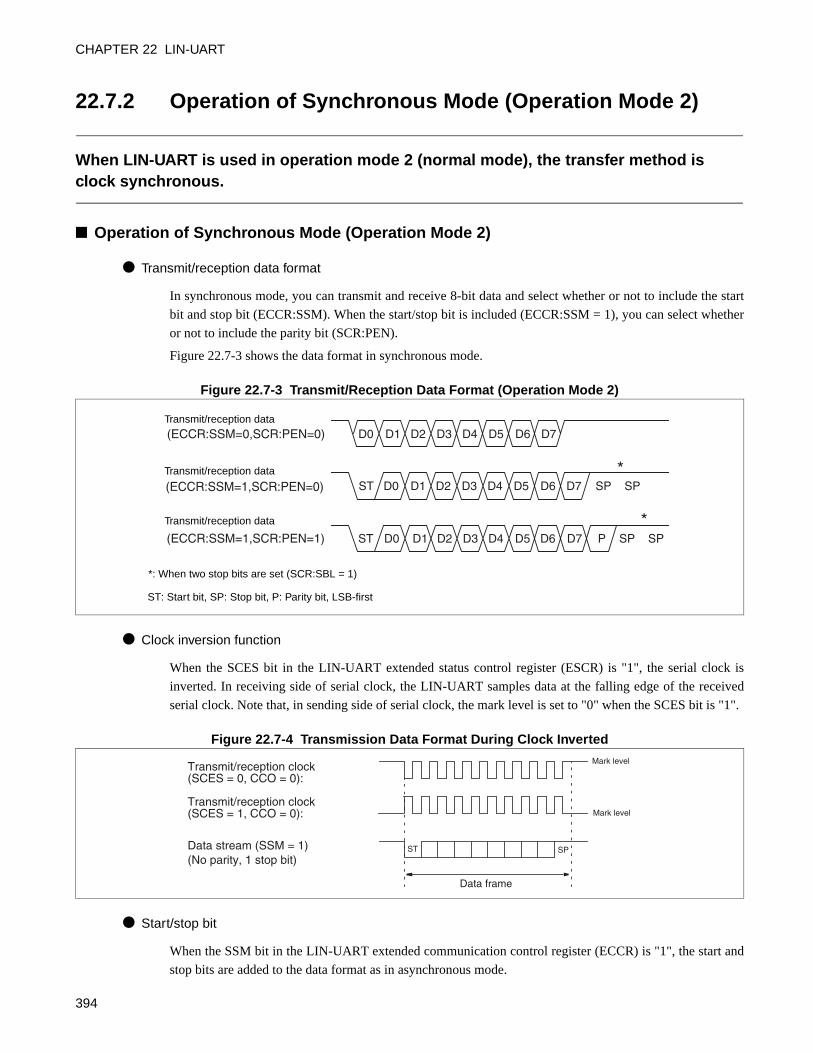
CHAPTER 22 LIN-UART
22.7.2 Operation of Synchronous Mode (Operation Mode 2)
When LIN-UART is used in operation mode 2 (normal mode), the transfer method is clock synchronous.
Operation of Synchronous Mode (Operation Mode 2)
Transmit/reception data format
In synchronous mode, you can transmit and receive 8-bit data and select whether or not to include the start
bit and stop bit (ECCR:SSM). When the start/stop bit is included (ECCR:SSM = 1), you can select whether
or not to include the parity bit (SCR:PEN).
Figure 22.7-3 shows the data format in synchronous mode.
Figure 22.7-3 Transmit/Reception Data Format (Operation Mode 2)
Clock inversion function
When the SCES bit in the LIN-UART extended status control register (ESCR) is "1", the serial clock is
inverted. In receiving side of serial clock, the LIN-UART samples data at the falling edge of the received
serial clock. Note that, in sending side of serial clock, the mark level is set to "0" when the SCES bit is "1".
Figure 22.7-4 Transmission Data Format During Clock Inverted
Start/stop bit
When the SSM bit in the LIN-UART extended communication control register (ECCR) is "1", the start and
stop bits are added to the data format as in asynchronous mode.
*
*
(ECCR:SSM=0,SCR:PEN=0)
(ECCR:SSM=1,SCR:PEN=0)
(ECCR:SSM=1,SCR:PEN=1)
D0 D1 D2 D3 D4 D5 D6 D7
ST D0 D1 D2 D3 D4 D5 D6 D7
ST D0 D1 D2 D3 D4 D5 D6 D7 P SP SP
SP SP
Transmit/reception data
Transmit/reception data
Transmit/reception data
*: When two stop bits are set (SCR:SBL = 1)
ST: Start bit, SP: Stop bit, P: Parity bit, LSB-first
Data frame
Transmit/reception clock
Data stream (SSM = 1) (No parity, 1 stop bit)
ST SP
(SCES = 0, CCO = 0):
Transmit/reception clock(SCES = 1, CCO = 0):
Mark level
Mark level
394
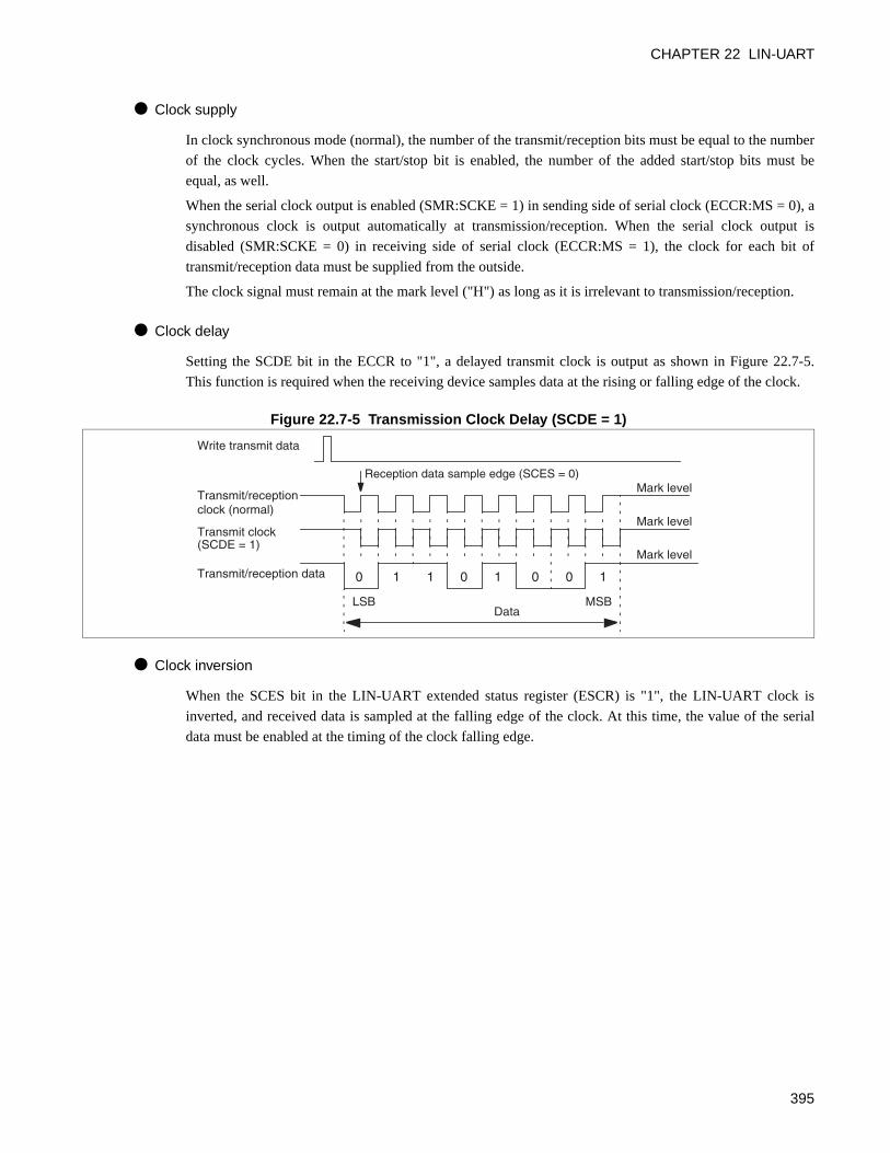
CHAPTER 22 LIN-UART
Clock supply
In clock synchronous mode (normal), the number of the transmit/reception bits must be equal to the number
of the clock cycles. When the start/stop bit is enabled, the number of the added start/stop bits must be
equal, as well.
When the serial clock output is enabled (SMR:SCKE = 1) in sending side of serial clock (ECCR:MS = 0), a
synchronous clock is output automatically at transmission/reception. When the serial clock output is
disabled (SMR:SCKE = 0) in receiving side of serial clock (ECCR:MS = 1), the clock for each bit of
transmit/reception data must be supplied from the outside.
The clock signal must remain at the mark level ("H") as long as it is irrelevant to transmission/reception.
Clock delay
Setting the SCDE bit in the ECCR to "1", a delayed transmit clock is output as shown in Figure 22.7-5.
This function is required when the receiving device samples data at the rising or falling edge of the clock.
Figure 22.7-5 Transmission Clock Delay (SCDE = 1)
Clock inversion
When the SCES bit in the LIN-UART extended status register (ESCR) is "1", the LIN-UART clock is
inverted, and received data is sampled at the falling edge of the clock. At this time, the value of the serial
data must be enabled at the timing of the clock falling edge.
Write transmit data
Transmit/reception clock (normal)
Transmit/reception data 1
DataLSB MSB
Mark level
Transmit clock(SCDE = 1)
Mark level
Mark level
Reception data sample edge (SCES = 0)
0 1 1 0 1 0 0
395
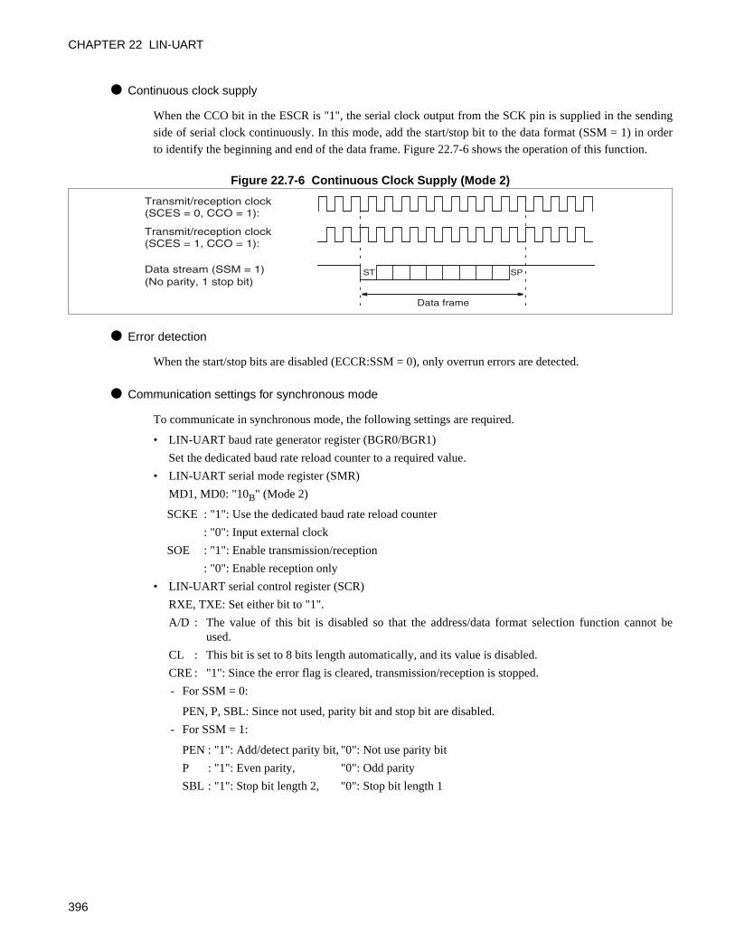
CHAPTER 22 LIN-UART
Continuous clock supply
When the CCO bit in the ESCR is "1", the serial clock output from the SCK pin is supplied in the sending
side of serial clock continuously. In this mode, add the start/stop bit to the data format (SSM = 1) in order
to identify the beginning and end of the data frame. Figure 22.7-6 shows the operation of this function.
Figure 22.7-6 Continuous Clock Supply (Mode 2)
Error detection
When the start/stop bits are disabled (ECCR:SSM = 0), only overrun errors are detected.
Communication settings for synchronous mode
To communicate in synchronous mode, the following settings are required.
• LIN-UART baud rate generator register (BGR0/BGR1)
Set the dedicated baud rate reload counter to a required value.
• LIN-UART serial mode register (SMR)
MD1, MD0: "10B" (Mode 2)
SCKE : "1": Use the dedicated baud rate reload counter
: "0": Input external clock
SOE : "1": Enable transmission/reception
: "0": Enable reception only
• LIN-UART serial control register (SCR)
RXE, TXE: Set either bit to "1".
A/D : The value of this bit is disabled so that the address/data format selection function cannot beused.
CL : This bit is set to 8 bits length automatically, and its value is disabled.
CRE : "1": Since the error flag is cleared, transmission/reception is stopped.
- For SSM = 0:
PEN, P, SBL: Since not used, parity bit and stop bit are disabled.
- For SSM = 1:
PEN : "1": Add/detect parity bit, "0": Not use parity bit
P : "1": Even parity, "0": Odd parity
SBL : "1": Stop bit length 2, "0": Stop bit length 1
Data frame
Transmit/reception clock
Data stream (SSM = 1) (No parity, 1 stop bit)
ST SP
(SCES = 0, CCO = 1):
Transmit/reception clock(SCES = 1, CCO = 1):
396
CHAPTER 22 LIN-UART
• LIN-UART serial status register (SSR)
BDS : "0": LSB-first, "1": MSB-first
RIE : "1": Enable reception interrupt, "0": Disable reception interrupt
TIE : "1": Enable transmit interrupt, "0": Disable transmit interrupt
• LIN-UART extended communication control register (ECCR)
SSM : "0": Not use start/stop bit (normal),
"1": Use start/stop bit (extended function),
MS : "0": Sending side of serial clock (serial clock output),
"1": Receiving side of serial clock (input serial clock from sending side of serial clock)
Note:
To start communication, write data into the LIN-UART transmit data register (TDR).
To receive data, disable the serial output (SMR:SOE = 0), and then write dummy data into the TDR.
Enabling continuous clock and start/stop bit allows bi-directional communication as in asynchronousmode.
397
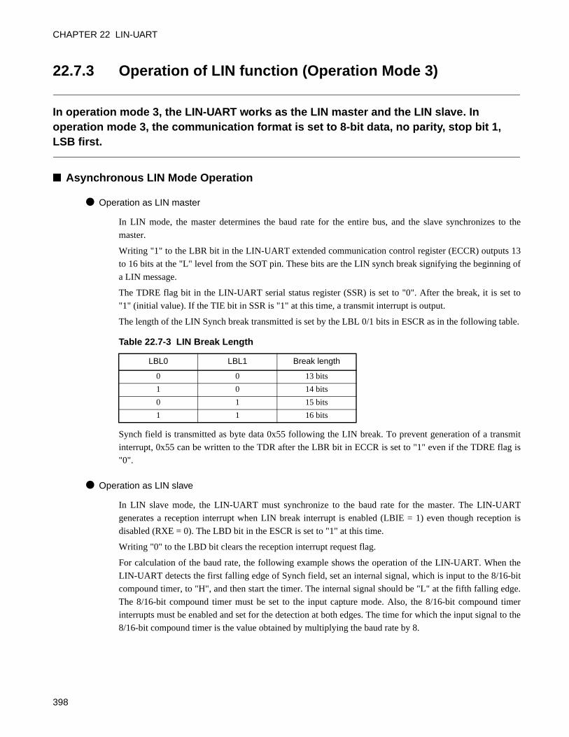
CHAPTER 22 LIN-UART
22.7.3 Operation of LIN function (Operation Mode 3)
In operation mode 3, the LIN-UART works as the LIN master and the LIN slave. In operation mode 3, the communication format is set to 8-bit data, no parity, stop bit 1, LSB first.
Asynchronous LIN Mode Operation
Operation as LIN master
In LIN mode, the master determines the baud rate for the entire bus, and the slave synchronizes to the
master.
Writing "1" to the LBR bit in the LIN-UART extended communication control register (ECCR) outputs 13
to 16 bits at the "L" level from the SOT pin. These bits are the LIN synch break signifying the beginning of
a LIN message.
The TDRE flag bit in the LIN-UART serial status register (SSR) is set to "0". After the break, it is set to
"1" (initial value). If the TIE bit in SSR is "1" at this time, a transmit interrupt is output.
The length of the LIN Synch break transmitted is set by the LBL 0/1 bits in ESCR as in the following table.
Synch field is transmitted as byte data 0x55 following the LIN break. To prevent generation of a transmit
interrupt, 0x55 can be written to the TDR after the LBR bit in ECCR is set to "1" even if the TDRE flag is
"0".
Operation as LIN slave
In LIN slave mode, the LIN-UART must synchronize to the baud rate for the master. The LIN-UART
generates a reception interrupt when LIN break interrupt is enabled (LBIE = 1) even though reception is
disabled (RXE = 0). The LBD bit in the ESCR is set to "1" at this time.
Writing "0" to the LBD bit clears the reception interrupt request flag.
For calculation of the baud rate, the following example shows the operation of the LIN-UART. When the
LIN-UART detects the first falling edge of Synch field, set an internal signal, which is input to the 8/16-bit
compound timer, to "H", and then start the timer. The internal signal should be "L" at the fifth falling edge.
The 8/16-bit compound timer must be set to the input capture mode. Also, the 8/16-bit compound timer
interrupts must be enabled and set for the detection at both edges. The time for which the input signal to the
8/16-bit compound timer is the value obtained by multiplying the baud rate by 8.
Table 22.7-3 LIN Break Length
LBL0 LBL1 Break length
0 0 13 bits
1 0 14 bits
0 1 15 bits
1 1 16 bits
398
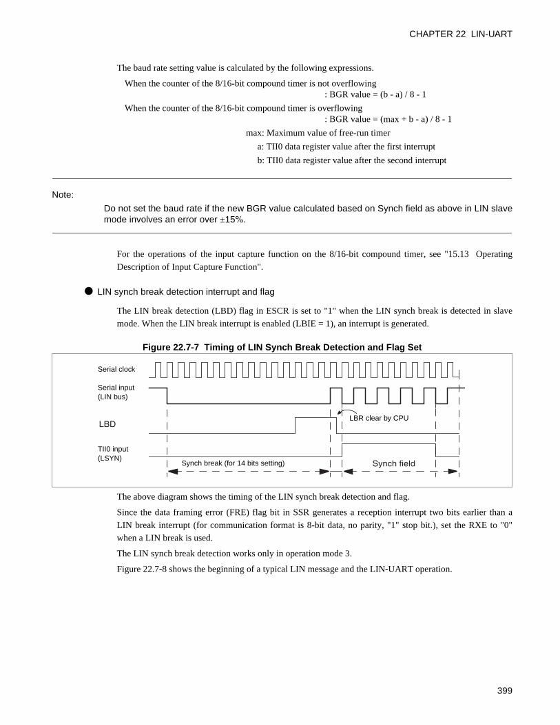
CHAPTER 22 LIN-UART
The baud rate setting value is calculated by the following expressions.
When the counter of the 8/16-bit compound timer is not overflowing: BGR value = (b - a) / 8 - 1
When the counter of the 8/16-bit compound timer is overflowing: BGR value = (max + b - a) / 8 - 1
max: Maximum value of free-run timer
a: TII0 data register value after the first interrupt
b: TII0 data register value after the second interrupt
Note:
Do not set the baud rate if the new BGR value calculated based on Synch field as above in LIN slavemode involves an error over ±15%.
For the operations of the input capture function on the 8/16-bit compound timer, see "15.13 Operating
Description of Input Capture Function".
LIN synch break detection interrupt and flag
The LIN break detection (LBD) flag in ESCR is set to "1" when the LIN synch break is detected in slave
mode. When the LIN break interrupt is enabled (LBIE = 1), an interrupt is generated.
Figure 22.7-7 Timing of LIN Synch Break Detection and Flag Set
The above diagram shows the timing of the LIN synch break detection and flag.
Since the data framing error (FRE) flag bit in SSR generates a reception interrupt two bits earlier than a
LIN break interrupt (for communication format is 8-bit data, no parity, "1" stop bit.), set the RXE to "0"
when a LIN break is used.
The LIN synch break detection works only in operation mode 3.
Figure 22.7-8 shows the beginning of a typical LIN message and the LIN-UART operation.
LBD
Synch field
Serial clock
Serial input (LIN bus)
TII0 input (LSYN)
LBR clear by CPU
Synch break (for 14 bits setting)
399
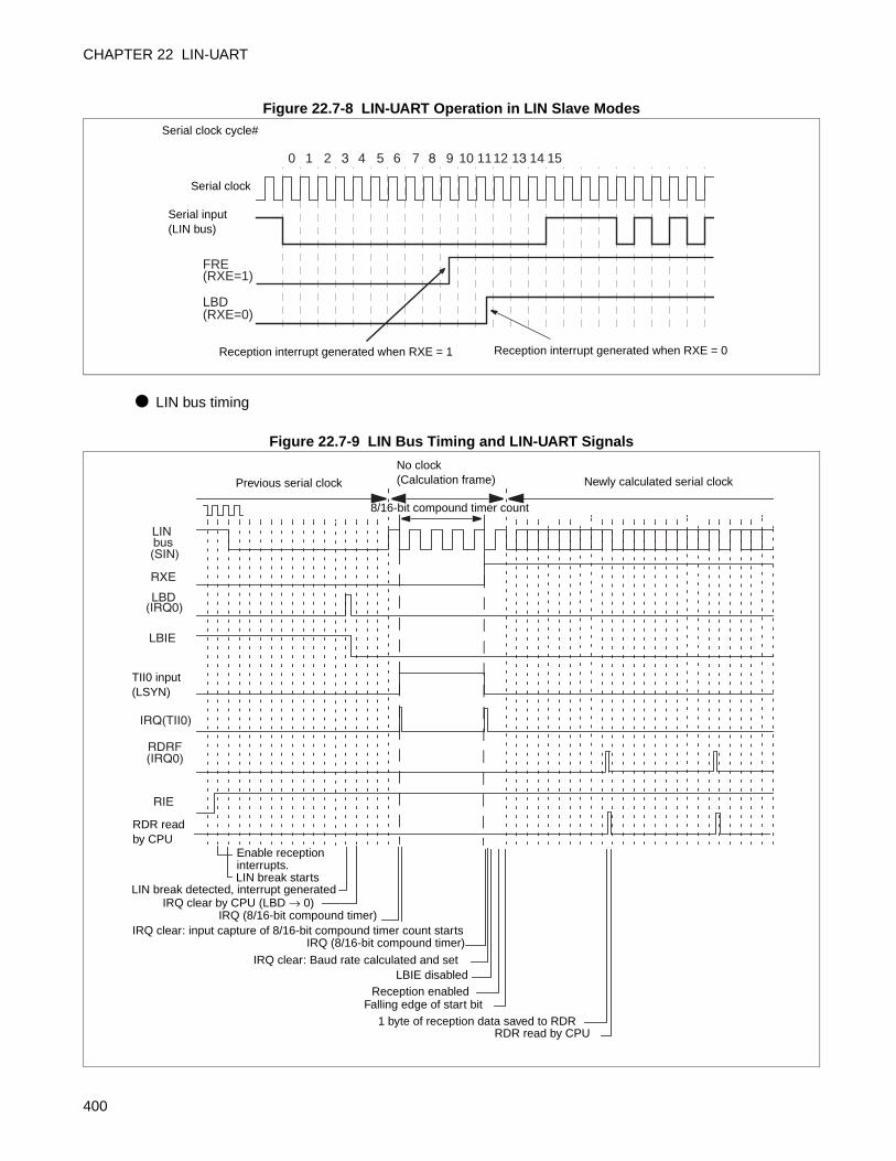
CHAPTER 22 LIN-UART
Figure 22.7-8 LIN-UART Operation in LIN Slave Modes
LIN bus timing
Figure 22.7-9 LIN Bus Timing and LIN-UART Signals
FRE(RXE=1)
LBD(RXE=0)
0 1 2 3 4 5 6 7 8 9 10 1112 13 14 15
Serial clock cycle#
Serial clock
Serial input (LIN bus)
Reception interrupt generated when RXE = 1 Reception interrupt generated when RXE = 0
bus
RXE
LBD(IRQ0)
RDRF
(SIN)
(IRQ0)
IRQ(TII0)
LIN
LBIE
RIE
No clock(Calculation frame)Previous serial clock Newly calculated serial clock
8/16-bit compound timer count
Enable reception interrupts.LIN break starts
LIN break detected, interrupt generatedIRQ clear by CPU (LBD → 0)
IRQ clear: input capture of 8/16-bit compound timer count starts
IRQ clear: Baud rate calculated and setLBIE disabled
Reception enabledFalling edge of start bit
1 byte of reception data saved to RDRRDR read by CPU
RDR read by CPU
TII0 input (LSYN)
IRQ (8/16-bit compound timer)
IRQ (8/16-bit compound timer)
400
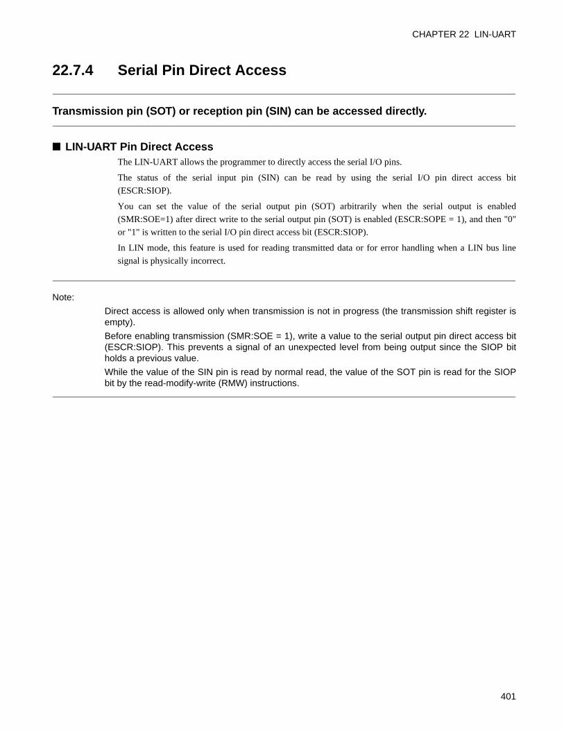
CHAPTER 22 LIN-UART
22.7.4 Serial Pin Direct Access
Transmission pin (SOT) or reception pin (SIN) can be accessed directly.
LIN-UART Pin Direct AccessThe LIN-UART allows the programmer to directly access the serial I/O pins.
The status of the serial input pin (SIN) can be read by using the serial I/O pin direct access bit
(ESCR:SIOP).
You can set the value of the serial output pin (SOT) arbitrarily when the serial output is enabled
(SMR:SOE=1) after direct write to the serial output pin (SOT) is enabled (ESCR:SOPE = 1), and then "0"
or "1" is written to the serial I/O pin direct access bit (ESCR:SIOP).
In LIN mode, this feature is used for reading transmitted data or for error handling when a LIN bus line
signal is physically incorrect.
Note:
Direct access is allowed only when transmission is not in progress (the transmission shift register isempty).
Before enabling transmission (SMR:SOE = 1), write a value to the serial output pin direct access bit(ESCR:SIOP). This prevents a signal of an unexpected level from being output since the SIOP bitholds a previous value.
While the value of the SIN pin is read by normal read, the value of the SOT pin is read for the SIOPbit by the read-modify-write (RMW) instructions.
401
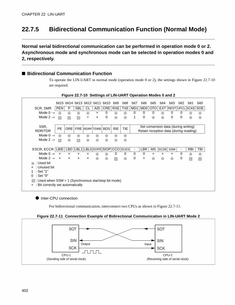
CHAPTER 22 LIN-UART
22.7.5 Bidirectional Communication Function (Normal Mode)
Normal serial bidirectional communication can be performed in operation mode 0 or 2. Asynchronous mode and synchronous mode can be selected in operation modes 0 and 2, respectively.
Bidirectional Communication FunctionTo operate the LIN-UART in normal mode (operation mode 0 or 2), the settings shown in Figure 22.7-10
are required.
Figure 22.7-10 Settings of LIN-UART Operation Modes 0 and 2
Inter-CPU connection
For bidirectional communication, interconnect two CPUs as shown in Figure 22.7-11.
Figure 22.7-11 Connection Example of Bidirectional Communication in LIN-UART Mode 2
bit15 bit14 bit13 bit12 bit11 bit10 bit9 bit8 bit7 bit6 bit5 bit4 bit3 bit2 bit1 bit0
SCR, SMR PEN P SBL CL A/D CRE RXE TXE MD1 MD0 OTO EXT REST UPCL SCKE SOEMode 0 → × 0 0 0 0 0 0Mode 2 → + × 0 1 0 0 0
SSR, RDR/TDR
PE ORE FRE RDRF TDRE BDS RIE TIESet conversion data (during writing)
Retain reception data (during reading)Mode 0 →Mode 2 →
ESCR, ECCR LBIE LBD LBL1 LBL0 SOPE SIOP CCO SCES - LBR MS SCDE SSM - RBI TBIMode 0 → × × × × 0 0 0 0 × × × 0Mode 2 → × × × × 0 × 0
: Used bit× : Unused bit1 : Set "1"0 : Set "0"
: Used when SSM = 1 (Synchronous star/stop bit mode)+ : Bit correctly set automatically
SOT
SIN
SCK
SOT
SIN
SCKOutput Input
CPU-1(Sending side of serial clock)
CPU-2(Receiving side of serial clock)
402
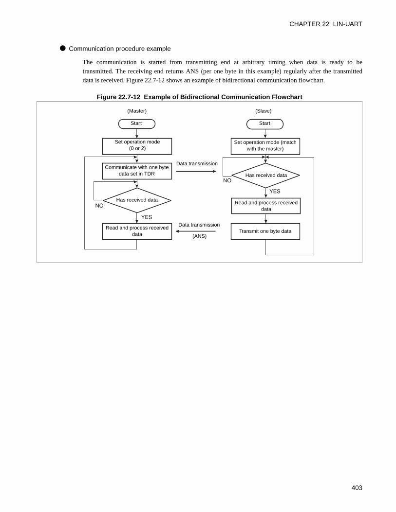
CHAPTER 22 LIN-UART
Communication procedure example
The communication is started from transmitting end at arbitrary timing when data is ready to be
transmitted. The receiving end returns ANS (per one byte in this example) regularly after the transmitted
data is received. Figure 22.7-12 shows an example of bidirectional communication flowchart.
Figure 22.7-12 Example of Bidirectional Communication Flowchart
NO
NO
YES
YES
Start Start
(Master) (Slave)
Set operation mode (0 or 2)
Communicate with one byte data set in TDR
Has received data
Read and process received data
Set operation mode (match with the master)
Read and process received data
Has received data
Transmit one byte dataData transmission
Data transmission
(ANS)
403
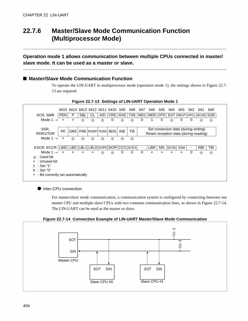
CHAPTER 22 LIN-UART
22.7.6 Master/Slave Mode Communication Function (Multiprocessor Mode)
Operation mode 1 allows communication between multiple CPUs connected in master/slave mode. It can be used as a master or slave.
Master/Slave Mode Communication FunctionTo operate the LIN-UART in multiprocessor mode (operation mode 1), the settings shown in Figure 22.7-
13 are required.
Figure 22.7-13 Settings of LIN-UART Operation Mode 1
Inter-CPU connection
For master/slave mode communication, a communication system is configured by connecting between one
master CPU and multiple slave CPUs with two common communication lines, as shown in Figure 22.7-14.
The LIN-UART can be used as the master or slave.
Figure 22.7-14 Connection Example of LIN-UART Master/Slave Mode Communication
bit15 bit14 bit13 bit12 bit11 bit10 bit9 bit8 bit7 bit6 bit5 bit4 bit3 bit2 bit1 bit0
SCR, SMR PEN P SBL CL A/D CRE RXE TXE MD1 MD0 OTO EXT REST UPCL SCKE SOEMode 1 → + × 0 0 1 0 0 0
SSR, RDR1/TDR
PE ORE FRE RDRF TDRE BDS RIE TIESet conversion data (during writing)
Retain reception data (during reading)Mode 1 → ×
ESCR, ECCR LBIE LBD LBL1 LBL0 SOPE SIOP CCO SCES - LBR MS SCDE SSM - RBI TBIMode 1 → × × × × 0 0 0 × × × × 0
: Used bit× : Unused bit1 : Set "1"0 : Set "0"+ : Bit correctly set automatically
SOT
SIN
SOT SIN SOT SIN
Master CPU
Slave CPU #0 Slave CPU #1
404
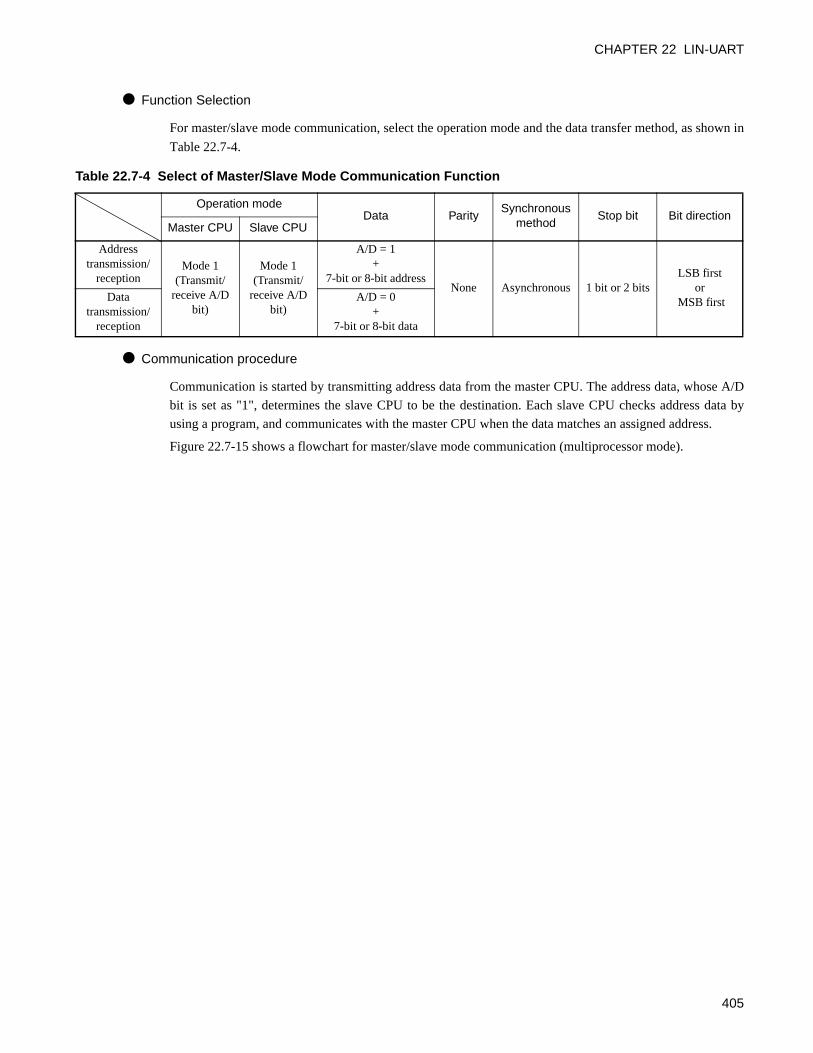
CHAPTER 22 LIN-UART
Function Selection
For master/slave mode communication, select the operation mode and the data transfer method, as shown in
Table 22.7-4.
Communication procedure
Communication is started by transmitting address data from the master CPU. The address data, whose A/D
bit is set as "1", determines the slave CPU to be the destination. Each slave CPU checks address data by
using a program, and communicates with the master CPU when the data matches an assigned address.
Figure 22.7-15 shows a flowchart for master/slave mode communication (multiprocessor mode).
Table 22.7-4 Select of Master/Slave Mode Communication Function
Operation modeData Parity
Synchronous method
Stop bit Bit directionMaster CPU Slave CPU
Address transmission/
receptionMode 1
(Transmit/receive A/D
bit)
Mode 1 (Transmit/
receive A/D bit)
A/D = 1 +
7-bit or 8-bit address None Asynchronous 1 bit or 2 bits
LSB first or
MSB firstData transmission/
reception
A/D = 0 +
7-bit or 8-bit data
405
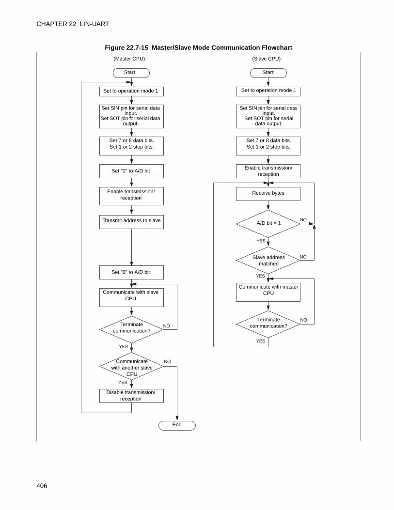
CHAPTER 22 LIN-UART
Figure 22.7-15 Master/Slave Mode Communication Flowchart
NO
YES
YES
NO
NO
NO
YES
YES
YES
NO
(Master CPU) (Slave CPU)
Start Start
Set to operation mode 1 Set to operation mode 1
Set SIN pin for serial data input.
Set SOT pin for serial data output.
Set SIN pin for serial data input.
Set SOT pin for serial data output.
Set 7 or 8 data bits. Set 1 or 2 stop bits.
Set 7 or 8 data bits. Set 1 or 2 stop bits.
Set "1" to A/D bitEnable transmission/
reception
Enable transmission/reception
Transmit address to slave
Receive bytes
A/D bit = 1
Set "0" to A/D bit
Communicate with slave CPU
Terminate communication?
Communicate with another slave
CPU
Disable transmission/reception
End
Slave address matched
Communicate with master CPU
Terminate communication?
406
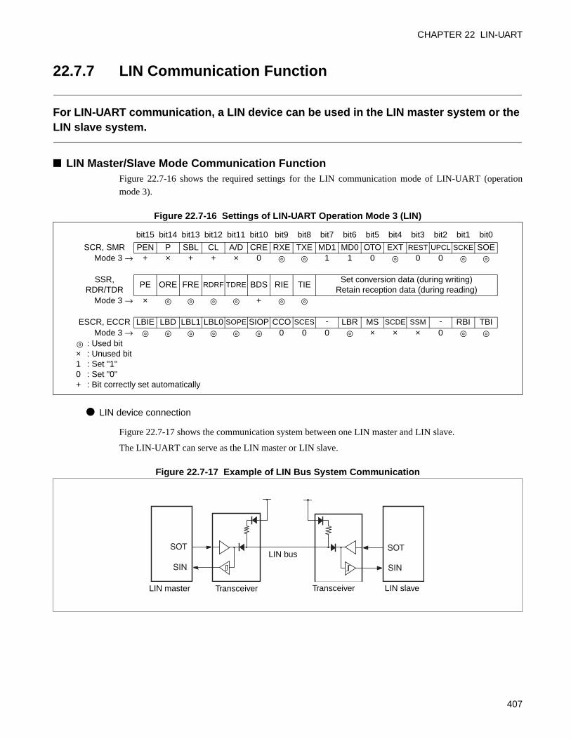
CHAPTER 22 LIN-UART
22.7.7 LIN Communication Function
For LIN-UART communication, a LIN device can be used in the LIN master system or the LIN slave system.
LIN Master/Slave Mode Communication FunctionFigure 22.7-16 shows the required settings for the LIN communication mode of LIN-UART (operation
mode 3).
Figure 22.7-16 Settings of LIN-UART Operation Mode 3 (LIN)
LIN device connection
Figure 22.7-17 shows the communication system between one LIN master and LIN slave.
The LIN-UART can serve as the LIN master or LIN slave.
Figure 22.7-17 Example of LIN Bus System Communication
bit15 bit14 bit13 bit12 bit11 bit10 bit9 bit8 bit7 bit6 bit5 bit4 bit3 bit2 bit1 bit0
SCR, SMR PEN P SBL CL A/D CRE RXE TXE MD1 MD0 OTO EXT REST UPCL SCKE SOEMode 3 → + × + + × 0 1 1 0 0 0
SSR, RDR/TDR
PE ORE FRE RDRF TDRE BDS RIE TIESet conversion data (during writing)
Retain reception data (during reading)Mode 3 → × +
ESCR, ECCR LBIE LBD LBL1 LBL0 SOPE SIOP CCO SCES - LBR MS SCDE SSM - RBI TBIMode 3 → 0 0 0 × × × 0
: Used bit× : Unused bit1 : Set "1"0 : Set "0"+ : Bit correctly set automatically
SOT
SIN
SOT
SIN
LIN master Transceiver Transceiver LIN slave
LIN bus
407
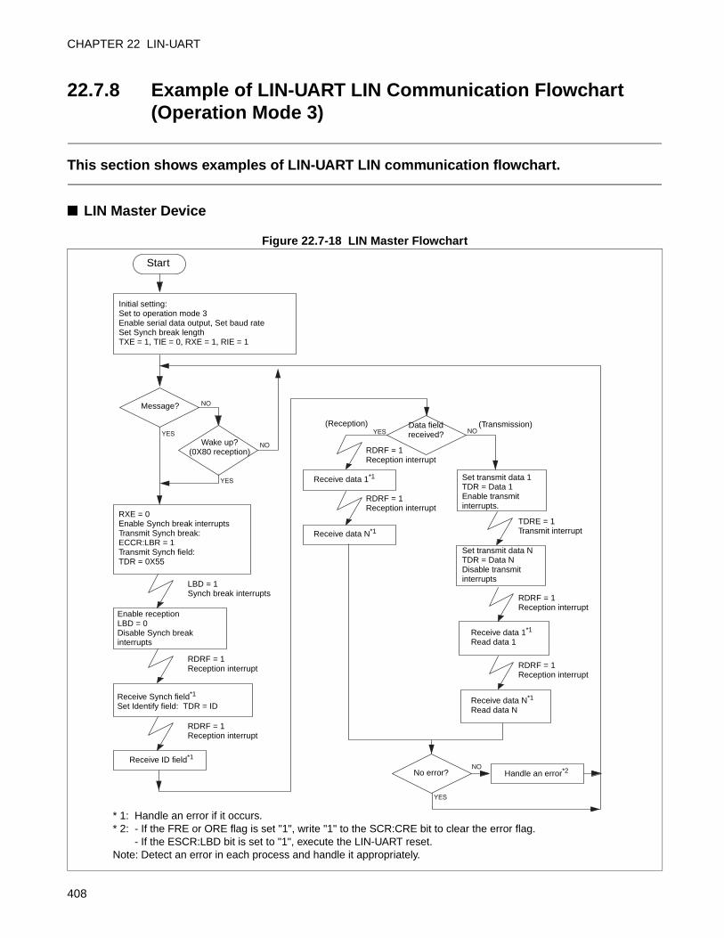
CHAPTER 22 LIN-UART
22.7.8 Example of LIN-UART LIN Communication Flowchart (Operation Mode 3)
This section shows examples of LIN-UART LIN communication flowchart.
LIN Master Device
Figure 22.7-18 LIN Master Flowchart
YES
NO
NO
YES
YES
NO
YES NO
Start
Initial setting:Set to operation mode 3Enable serial data output, Set baud rateSet Synch break lengthTXE = 1, TIE = 0, RXE = 1, RIE = 1
Message?
RXE = 0Enable Synch break interruptsTransmit Synch break: ECCR:LBR = 1Transmit Synch field: TDR = 0X55
LBD = 1Synch break interrupts
Receive ID field*1
Enable receptionLBD = 0Disable Synch break interrupts
No error? Handle an error*2
Data field received?
Set transmit data 1TDR = Data 1Enable transmit interrupts.
Wake up?(0X80 reception)
Receive Synch field*1 Set Identify field: TDR = ID
RDRF = 1Reception interrupt
RDRF = 1Reception interrupt
(Reception) (Transmission)
RDRF = 1 Reception interrupt
Receive data 1*1
Receive data N*1
RDRF = 1 Reception interrupt
Set transmit data NTDR = Data NDisable transmit interrupts
Receive data 1*1
Read data 1
Receive data N*1 Read data N
TDRE = 1Transmit interrupt
RDRF = 1Reception interrupt
RDRF = 1Reception interrupt
* 1: Handle an error if it occurs.* 2: - If the FRE or ORE flag is set "1", write "1" to the SCR:CRE bit to clear the error flag.
- If the ESCR:LBD bit is set to "1", execute the LIN-UART reset.Note: Detect an error in each process and handle it appropriately.
408
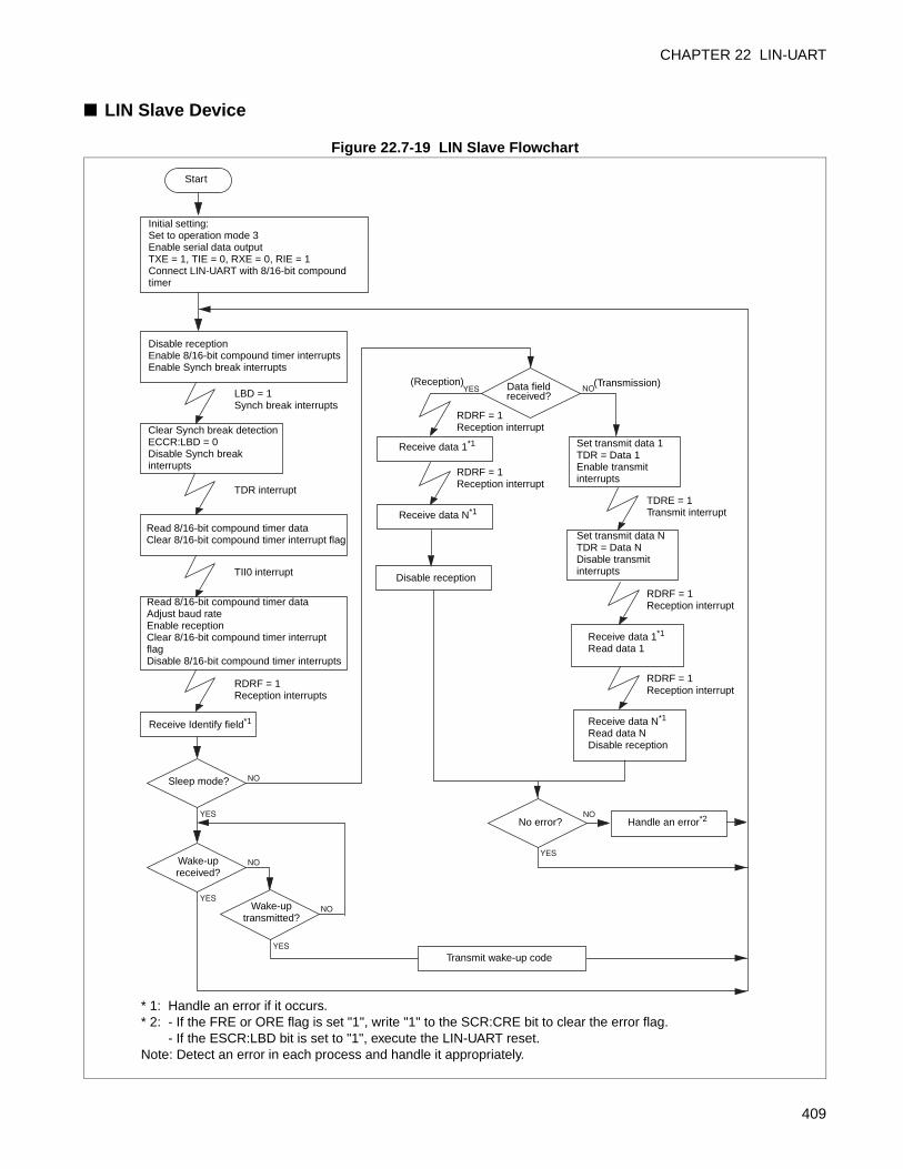
CHAPTER 22 LIN-UART
LIN Slave Device
Figure 22.7-19 LIN Slave Flowchart
YES
NO
NO
YES
YES
NO
YES NO
YES
NO
Start
Initial setting:Set to operation mode 3Enable serial data outputTXE = 1, TIE = 0, RXE = 0, RIE = 1Connect LIN-UART with 8/16-bit compound timer
Read 8/16-bit compound timer dataAdjust baud rateEnable receptionClear 8/16-bit compound timer interrupt flagDisable 8/16-bit compound timer interrupts
LBD = 1Synch break interrupts
Receive Identify field*1
Disable receptionEnable 8/16-bit compound timer interruptsEnable Synch break interrupts
No error? Handle an error*2
Data field received?
Set transmit data 1TDR = Data 1Enable transmit interrupts
Read 8/16-bit compound timer dataClear 8/16-bit compound timer interrupt flag
TDR interrupt
TII0 interrupt
(Reception) (Transmission)
RDRF = 1Reception interrupt
Receive data 1*1
Receive data N*1
RDRF = 1Reception interrupt
Set transmit data NTDR = Data NDisable transmit interrupts
Receive data 1*1
Read data 1
Receive data N*1
Read data NDisable reception
TDRE = 1 Transmit interrupt
RDRF = 1 Reception interrupt
* 1: Handle an error if it occurs.* 2: - If the FRE or ORE flag is set "1", write "1" to the SCR:CRE bit to clear the error flag.
- If the ESCR:LBD bit is set to "1", execute the LIN-UART reset.Note: Detect an error in each process and handle it appropriately.
Clear Synch break detectionECCR:LBD = 0Disable Synch break interrupts
RDRF = 1Reception interrupts
Sleep mode?
Wake-up received?
Wake-up transmitted?
Disable reception
Transmit wake-up code
RDRF = 1 Reception interrupt
409
CHAPTER 22 LIN-UART
22.8 Notes on Using LIN-UART
This section shows notes on using the LIN-UART.
Notes on Using LIN-UART
Enabling operation
The LIN-UART has the TXE (transmission) and RXE (reception) enable bit in the LIN-UART serial
control register (SCR) for transmission and reception, respectively. Since both transmission and reception
are disabled by default (internal value), these operations must be enabled before transfer. Also, you can
disable these operations to stop transfer as required.
Setting communication mode
The communication mode must be set while the LIN-UART is stopped. If the mode is set during
transmission/reception, the transmitted/received data is not guaranteed.
Timing of enabling transmit interrupts
Since the default (initial) value of the transmit data empty flag bit (SSR:TDRE) is "1" (no transmit data,
transmit data write enabled), a transmit interrupt request is generated immediately when transmit interrupt
request is enabled (SSR:TIE =1). To prevent this, be sure to set the transmit data before setting the TIE flag
to "1".
Changing operation setting
Reset the LIN-UART after changing its settings, such as adding the start/stop bit or changing the data
format.
The correct operation settings are not guaranteed even if you reset the LIN-UART (SMR:UPCL = 1)
concurrently with setting the LIN-UART serial mode register (SMR). Therefore, after setting the bit in
LIN-UART serial mode register (SMR), reset the LIN-UART (SMR:UPCL = 1) again.
Using LIN function
Although the LIN functions are available in the operation mode 3, the LIN format is automatically set in
the mode 3 (8-bit data, no parity, 1 stop bit, LSB-first).
While the length of LIN break transmit bit is variable, the detection bit length is fixed to 11 bits.
Setting LIN slave
When starting LIN slave mode, be sure to set the baud rate before receiving the LIN synch break in order to
make sure that the minimum 13 bits length of the LIN synch break is detected.
Bus idle function
The bus idle is not available in synchronous mode 2.
410
CHAPTER 22 LIN-UART
A/D bit (LIN-UART serial control register (SCR): Address/data format selection bit)
Be sure to note the followings when using the A/D bit.
The A/D bit is used to select the address/data for transmission when it is written, and to read the A/D bit
received last when it reads. Internally, the A/D bit values for transmission and reception are stored in
separate registers.
The transmit A/D bit value is read when read-modify-write (RMW) instructions are used. Therefore, an
incorrect value may be written to the A/D bit when another bit in the SCR is bit-accessed.
For the above reason, the A/D bit must be set at the last access to the SCR before transmission. Or, the
above problem can be prevented by byte-accessing whenever the SCR is written.
LIN-UART software reset
Execute the LIN-UART software reset (SMR:UPCL = 1) when the TXE bit in the LIN-UART serial
control register (SCR) is "0".
Synch break detection
In mode 3 (LIN mode), when serial input has 11 bits width or more and becomes "L", the LBD bit in the
extended status control register (ESCR) is set to "1" (Synch break detection) and the LIN-UART waits for
the Synch field. As a result, when serial input has more than 11 bits of "0", the LIN-UART recognizes that
the Synch break is input (LBD = 1), and then waits for the Synch field.
In this case, execute the LIN-UART reset (SMR: UPCL = 1).
411
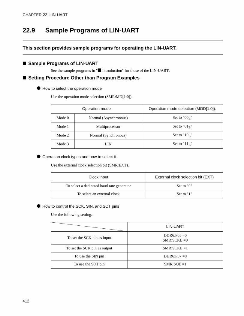
CHAPTER 22 LIN-UART
22.9 Sample Programs of LIN-UART
This section provides sample programs for operating the LIN-UART.
Sample Programs of LIN-UARTSee the sample programs in " Introduction" for those of the LIN-UART.
Setting Procedure Other than Program Examples
How to select the operation mode
Use the operation mode selection (SMR:MD[1:0]).
Operation clock types and how to select it
Use the external clock selection bit (SMR:EXT).
How to control the SCK, SIN, and SOT pins
Use the following setting.
Operation mode Operation mode selection (MOD[1:0]).
Mode 0 Normal (Asynchronous) Set to "00B"
Mode 1 Multiprocessor Set to "01B"
Mode 2 Normal (Synchronous) Set to "10B"
Mode 3 LIN Set to "11B"
Clock input External clock selection bit (EXT)
To select a dedicated baud rate generator Set to "0"
To select an external clock Set to "1"
LIN-UART
To set the SCK pin as inputDDR6:P05 =0
SMR:SCKE =0
To set the SCK pin as output SMR:SCKE =1
To use the SIN pin DDR6:P07 =0
To use the SOT pin SMR:SOE =1
412
CHAPTER 22 LIN-UART
How to enable/disable the LIN-UART operation
Use the reception enable bit (SCR:RXE).
Use the transmit control bit (SCR:TXE).
How to use an external clock as the LIN-UART serial clock
Use the one-to-one external clock enable bit (SMR:OTO).
How to restart the reload counter
Use the reload counter restart bit (SMR:REST).
How to reset the LIN-UART
Use the LIN-UART programmable clear bit (SMR:UPCL).
How to set the parity
Use the parity enable bit (SCR:PEN) and the parity selection bit (SCR:P).
Control details Reception enable bit (RXE)
Disable reception Set to "0"
Enable reception Set to "1"
Control details Transmit control bit (TXE)
Disable transmission Set to "0"
Enable transmission Set to "1"
Control details Reception enable bit (OTO)
Enable external clock Set to "1"
Control details Reload counter restart bit (REST)
Restart the reload counter Set to "1"
Control details LIN-UART programmable clear bit (UPCL)
Reset the LIN-UART software Set to "1"
Operation Parity control (PEN) Parity polarity (P)
To set to no parity Set to "0" -
To set to even parity Set to "1" Set to "0"
To set to odd parity Set to "1" Set to "1"
413
CHAPTER 22 LIN-UART
How to set the data length
Use the data length selection bit (SCR:CL).
How to select the STOP bit length
Use the STOP bit length control (SCR:SBL).
How to clear the error flag
Use the reception error flag clear bit (SCR:CRE).
How to set the transfer direction
Use the transfer direction selection bit (SSR:BDS).
LSB/MSB can be selected for transfer direction in any operation mode.
How to clear the reception completion flag
Uses the following setting.
The first RDR register read is the reception initiation.
Operation Data length selection bit (CL)
To set the bit length to 7 Set to "0"
To set the bit length to 8 Set to "1"
Operation STOP bit length control (SBL)
To set STOP bit length to 1 Set to "0"
To set STOP bit length to 2 Set to "1"
Control details Reception error flag clear bit (CRE)
To clear the error flag (PE, ORE, FRE) Write "0"
Control details Serial data direction control (BDS)
To select the LSB first (from the least significant bit)
Set to "0"
To select the MSB first (from the most significant bit)
Set to "1"
Control details Method
To clear the reception completion flag Read the RDR register
414
CHAPTER 22 LIN-UART
How to clear the transmit buffer empty flag
Uses the following setting.
The first TDR register write is the transmit initiation.
How to select the data format (Address/Data) (Only in mode 1)
Use the data length selection bit (SCR:A/D).
This is effective only at transmission. The A/D bit is ignored at reception.
How to set the baud rate
See "22.6 LIN-UART Baud Rate".
Interrupt related registers
Interrupt level is set by interrupt level setting registers as in the following table.
Control details Method
To clear the transmit buffer empty flag Write to TDR register
Operation Data format selection bit (A/D)
To select the data frame Set to "0"
To select the address frame Set to "1"
Interrupt level setting register Interrupt vector
ReceptionInterrupt level register (ILR1)
Address: 0007AH
#7Address: 0FFFCH
TransmissionInterrupt level register (ILR2)
Address: 0007BH
#8Address: 0FFEAH
415
CHAPTER 22 LIN-UART
How to enable/disable/clear interrupts
Interrupt request enable flag, interrupt request flag
Interrupt request enable bit (SSR:RIE), (SSR:TIE) is used to enable interrupts.
The following setting is used to clear interrupt requests.
UART reception UART transmission
Reception interrupt enable bit (RIE)
Reception interrupt enable bit (TIE)
To disable interrupt requests Set to "0"
To enable interrupt requests Set to "1"
UART reception UART transmission
To clear interrupt requests
The reception data register full (RDRF) is cleared by reading the LIN-UART serial input register (RDR).
The transmit data register empty (TDRE) is set to "0" by writing data to the LIN-UART serial output data register (TDR).The error flags (PE, ORE, FRE) are set to "0" by
writing "1" to the error flag clear bit (CRE).
416
CHAPTER 238/10-BIT A/D CONVERTER
This chapter describes the functions and operations of the 8/10-bit A/D converter.
23.1 Overview of 8/10-bit A/D Converter
23.2 Configuration of 8/10-bit A/D Converter
23.3 Pins of 8/10-bit A/D Converter
23.4 Registers of 8/10-bit A/D Converter
23.5 Interrupts of 8/10-bit A/D Converter
23.6 Operations of 8/10-bit A/D Converter and Its Setup Procedure Examples
23.7 Notes on Use of 8/10-bit A/D Converter
23.8 Sample Programs for 8/10-bit A/D Converter
417
CHAPTER 23 8/10-BIT A/D CONVERTER
23.1 Overview of 8/10-bit A/D Converter
The 8/10-bit A/D converter is a 10-bit successive approximation type of 8/10-bit A/D converter. It can be started via software, external trigger, and internal clock, with one input signal selected from among multiple analog input pins.
A/D Conversion FunctionsThe A/D converter converts analog voltages (input voltages) input to an analog input pin to 10-bit digital
values.
• One of multiple analog input pins can be selected.
• The conversion speed is programmable to be configured (selected according to the operating voltageand frequency).
• An interrupt is generated when A/D conversion completes.
• The completion of conversion can also be checked with the ADI bit in the ADC1 register.
To activate A/D conversion functions, follow one of the methods given below.
• Activation using the AD bit in the ADC1 register
• Continuous activation using the external pin (ADTG)
• Continuous activation using the 8/16-bit compound timer output TO00
418
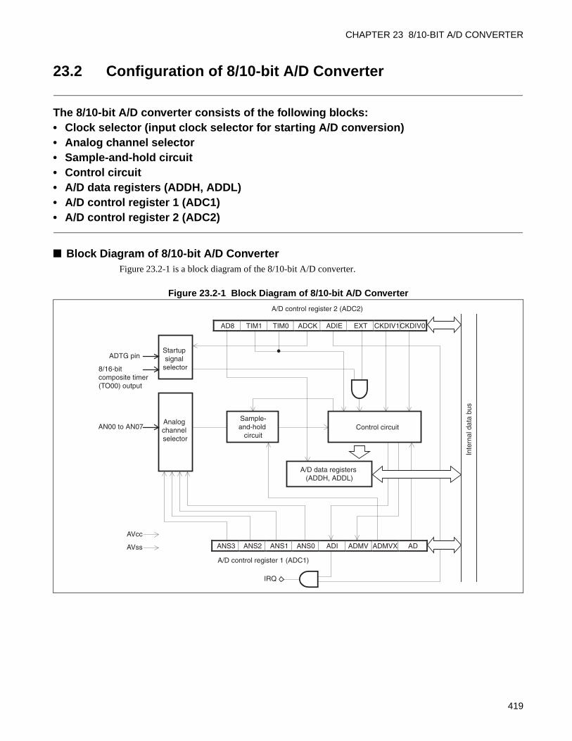
CHAPTER 23 8/10-BIT A/D CONVERTER
23.2 Configuration of 8/10-bit A/D Converter
The 8/10-bit A/D converter consists of the following blocks: • Clock selector (input clock selector for starting A/D conversion)• Analog channel selector• Sample-and-hold circuit• Control circuit• A/D data registers (ADDH, ADDL)• A/D control register 1 (ADC1) • A/D control register 2 (ADC2)
Block Diagram of 8/10-bit A/D ConverterFigure 23.2-1 is a block diagram of the 8/10-bit A/D converter.
Figure 23.2-1 Block Diagram of 8/10-bit A/D Converter
AD8 TIM1 TIM0 ADCK ADIE EXT CKDIV1 CKDIV0
ANS3 ANS2 ANS1 ANS0 ADI ADMV ADMVX AD
A/D control register 2 (ADC2)
Analog channel selector
A/D control register 1 (ADC1)
Sample-and-hold
circuit
Control circuit
A/D data registers (ADDH, ADDL)
AVcc
IRQ
Inte
rnal
dat
a bu
s
AN00 to AN07
8/16-bit composite timer (TO00) output
AVss
Startup signal
selector
ADTG pin
419
CHAPTER 23 8/10-BIT A/D CONVERTER
Clock selector
This block selects the A/D conversion clock with continuous activation enabled (ADC2:EXT = 1).
Analog channel selector
This circuit selects one of multiple analog input pins.
Sample-and-hold circuit
This circuit holds the input voltage selected by the analog channel selector. This enables A/D conversion to
be performed without being affected by variation in input voltage during conversion (comparison) by
sampling and holding the input voltage immediately after starting A/D conversion.
Control circuit
The A/D conversion function determines the values in the 10-bit A/D data register sequentially from MSB
to LSB based on the voltage compare signals from the comparator. When conversion is completed, the A/D
conversion function sets the interrupt request flag bit (ADC1: ADI).
A/D data registers (ADDH/ADDL)
The high-order two bits of 10-bit A/D data are stored in the ADDH register; the low-order eight bits are
stored in the ADDL register.
Setting the A/D conversion precision bit (ADC2:AD8) to "1" provides 8-bit precision, storing the upper
eight bits of the 10-bit A/D data in the ADDL register.
A/D control register 1 (ADC1)
This register is used to enable and disable functions, select an analog input pin, check statuses, and control
interrupts.
A/D control register 2 (ADC2)
This register is used to select an input clock, enable and disable interrupts, and select functions.
Input ClockThe 8/10-bit A/D converter uses the output clock from the prescaler as the input clock (operation clock).
420
CHAPTER 23 8/10-BIT A/D CONVERTER
23.3 Pins of 8/10-bit A/D Converter
This section describes the pins of the 8/10-bit A/D converter.
Pins of 8/10-bit A/D ConverterMB95130/M series has 8 channels of analog input pin.
Analog input pins also serve as general-purpose I/O ports.
AN07 to AN00 Pin
AN07 to AN00: When using the A/D conversion function, input the analog voltage you wish to convert
to one of these pins. Each of the pins serves as an analog input pin by selecting it using
the analog input channel select bits (ADC1: ANS0 to ANS3) with the corresponding bit
in the port direction register (DDR) set to 0. Even when the 8/10-bit A/D converter is
used, the pins not used for analog input can be used as general-purpose I/O ports.
Note that the number of analog input pins differs depending on the series.
ADTG Pin
ADTG: This is a pin used to activate A/D conversion function by external trigger.
AVCC pin
AVCC: This is a 8/10-bit A/D converter power supply pin. Use this at the same potential as VCC.
If A/D conversion precision is demanded, you should take measures to ensure that VCC
noise does not enter AVCC, or use a separate power source. You should connect this pin
to a power source even when the 8/10-bit A/D converter is not being used.
AVSS pin
AVSS: This is a ground pin of the 8/10-bit A/D converter. Use this at the same potential as VSS.
When A/D conversion precision is required, take measures to ensure that the VSS noise
does not interfere with AVSS. You should connect this pin to a ground (GND) even
when the 8/10-bit A/D converter is not being used.
421
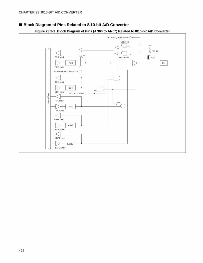
CHAPTER 23 8/10-BIT A/D CONVERTER
Block Diagram of Pins Related to 8/10-bit A/D Converter
Figure 23.3-1 Block Diagram of Pins (AN00 to AN07) Related to 8/10-bit A/D Converter
ILSR2 read
ILSR2 write
ILSR2
0
1
PDR read
PDR write
PDR
DDR read
DDR write
DDR
PUL read
PUL write
PUL
AIDR read
AIDR write
AIDR
0
1
Pin
Stop, Watch (SPL=1)
Inte
rnal
bus
In bit operation instruction
Pull-up
A/D analog input
Hysteresis
Automotive P-ch
422
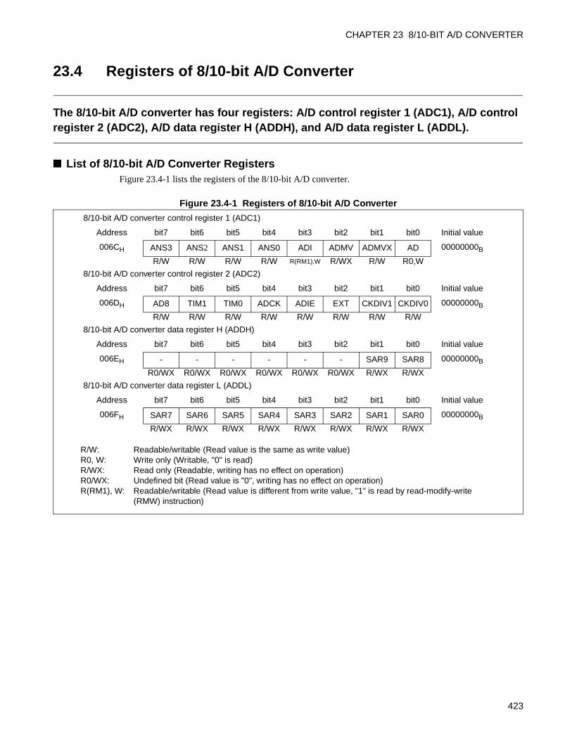
CHAPTER 23 8/10-BIT A/D CONVERTER
23.4 Registers of 8/10-bit A/D Converter
The 8/10-bit A/D converter has four registers: A/D control register 1 (ADC1), A/D control register 2 (ADC2), A/D data register H (ADDH), and A/D data register L (ADDL).
List of 8/10-bit A/D Converter RegistersFigure 23.4-1 lists the registers of the 8/10-bit A/D converter.
Figure 23.4-1 Registers of 8/10-bit A/D Converter
R/W: Readable/writable (Read value is the same as write value)R0, W: Write only (Writable, "0" is read)R/WX: Read only (Readable, writing has no effect on operation)R0/WX: Undefined bit (Read value is "0", writing has no effect on operation)R(RM1), W: Readable/writable (Read value is different from write value, "1" is read by read-modify-write
(RMW) instruction)
8/10-bit A/D converter control register 1 (ADC1)
Address bit7 bit6 bit5 bit4 bit3 bit2 bit1 bit0 Initial value
006CH ANS3 ANS2 ANS1 ANS0 ADI ADMV ADMVX AD 00000000B
R/W R/W R/W R/W R(RM1),W R/WX R/W R0,W
8/10-bit A/D converter control register 2 (ADC2)
Address bit7 bit6 bit5 bit4 bit3 bit2 bit1 bit0 Initial value
006DH AD8 TIM1 TIM0 ADCK ADIE EXT CKDIV1 CKDIV0 00000000B
R/W R/W R/W R/W R/W R/W R/W R/W
8/10-bit A/D converter data register H (ADDH)
Address bit7 bit6 bit5 bit4 bit3 bit2 bit1 bit0 Initial value
006EH - - - - - - SAR9 SAR8 00000000B
R0/WX R0/WX R0/WX R0/WX R0/WX R0/WX R/WX R/WX
8/10-bit A/D converter data register L (ADDL)
Address bit7 bit6 bit5 bit4 bit3 bit2 bit1 bit0 Initial value
006FH SAR7 SAR6 SAR5 SAR4 SAR3 SAR2 SAR1 SAR0 00000000B
R/WX R/WX R/WX R/WX R/WX R/WX R/WX R/WX
423
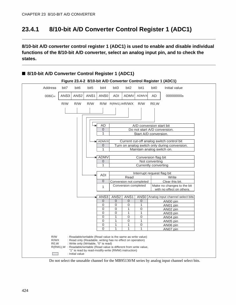
CHAPTER 23 8/10-BIT A/D CONVERTER
23.4.1 8/10-bit A/D Converter Control Register 1 (ADC1)
8/10-bit A/D converter control register 1 (ADC1) is used to enable and disable individual functions of the 8/10-bit A/D converter, select an analog input pin, and to check the states.
8/10-bit A/D Converter Control Register 1 (ADC1)
Figure 23.4-2 8/10-bit A/D Converter Control Register 1 (ADC1)
Do not select the unusable channel for the MB95130/M series by analog input channel select bits.
00
00000000B
bit7Address bit6 bit5 bit4 bit3 bit2 bit1 bit0 Initial value
R/W R/W R/W R/W R(RM1),WR/WX R/W R0,W
A/D conversion start bitDo not start A/D conversion.
Start A/D conversion.
AD01
Analog input channel select bits
AN00 pinANS3
0AN01 pin0
AN03 pin
Interrupt request flag bitRead Write
Conversion not completed
ADI
Clear this bit.0Conversion completed1 Make no changes to the bit
with no effect on others.
AN02 pin0000
0
ANS2
ANS3 ANS2 ANS1 ANS0 ADI ADMV ADMVX AD
Current cut-off analog switch control bitTurn on analog switch only during conversion.
Maintain analog switch on.
ADMVX
01
Conversion flag bitNot converting
Currently converting
ADMV01
00 1
011
1
110
0 010
0
110
0 011
1
ANS1 ANS0
AN04 pinAN05 pin
AN07 pinAN06 pin
R/WR/WXR0,WR(RM1),W
: Readable/writable (Read value is the same as write value): Read only (Readable, writing has no effect on operation): Write only (Writable, "0" is read): Readable/writable (Read value is different from write value, "1" is read by read-modify-write (RMW) instruction): Initial value
006CH
424
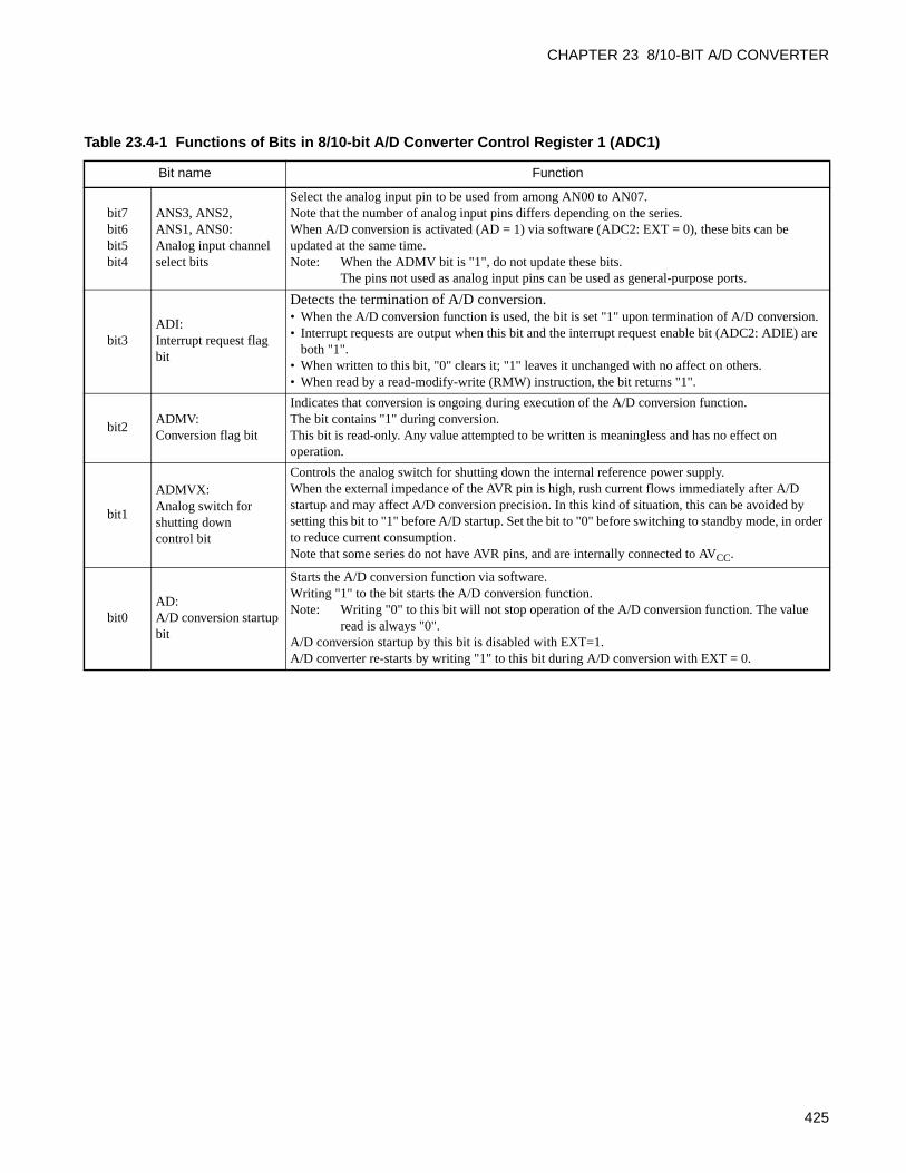
CHAPTER 23 8/10-BIT A/D CONVERTER
Table 23.4-1 Functions of Bits in 8/10-bit A/D Converter Control Register 1 (ADC1)
Bit name Function
bit7bit6bit5bit4
ANS3, ANS2,ANS1, ANS0:Analog input channel select bits
Select the analog input pin to be used from among AN00 to AN07.Note that the number of analog input pins differs depending on the series.When A/D conversion is activated (AD = 1) via software (ADC2: EXT = 0), these bits can be updated at the same time.Note: When the ADMV bit is "1", do not update these bits.
The pins not used as analog input pins can be used as general-purpose ports.
bit3ADI:Interrupt request flag bit
Detects the termination of A/D conversion.• When the A/D conversion function is used, the bit is set "1" upon termination of A/D conversion.• Interrupt requests are output when this bit and the interrupt request enable bit (ADC2: ADIE) are
both "1".• When written to this bit, "0" clears it; "1" leaves it unchanged with no affect on others.• When read by a read-modify-write (RMW) instruction, the bit returns "1".
bit2ADMV:Conversion flag bit
Indicates that conversion is ongoing during execution of the A/D conversion function.The bit contains "1" during conversion.This bit is read-only. Any value attempted to be written is meaningless and has no effect on operation.
bit1
ADMVX:Analog switch for shutting down control bit
Controls the analog switch for shutting down the internal reference power supply.When the external impedance of the AVR pin is high, rush current flows immediately after A/D startup and may affect A/D conversion precision. In this kind of situation, this can be avoided by setting this bit to "1" before A/D startup. Set the bit to "0" before switching to standby mode, in order to reduce current consumption.Note that some series do not have AVR pins, and are internally connected to AVCC.
bit0AD:A/D conversion startup bit
Starts the A/D conversion function via software.Writing "1" to the bit starts the A/D conversion function.Note: Writing "0" to this bit will not stop operation of the A/D conversion function. The value
read is always "0".A/D conversion startup by this bit is disabled with EXT=1.A/D converter re-starts by writing "1" to this bit during A/D conversion with EXT = 0.
425
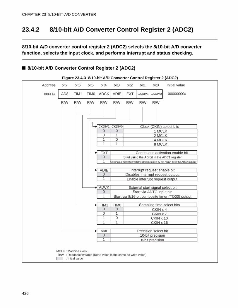
CHAPTER 23 8/10-BIT A/D CONVERTER
23.4.2 8/10-bit A/D Converter Control Register 2 (ADC2)
8/10-bit A/D converter control register 2 (ADC2) selects the 8/10-bit A/D converter function, selects the input clock, and performs interrupt and status checking.
8/10-bit A/D Converter Control Register 2 (ADC2)
Figure 23.4-3 8/10-bit A/D Converter Control Register 2 (ADC2)
0
00000000B
bit7Address bit6 bit5 bit4 bit3 bit2 bit1 bit0 Initial value
R/W R/W R/W R/W R/W R/W R/W R/W
Interrupt request enable bitDisables interrupt request output.Enable interrupt request output.
ADIE01
Clock (CKIN) select bits1 MCLK
CKDIV1
02 MCLK0
8 MCLK4 MCLK
1011
1
CKDIV0
Precision select bit10-bit precision8-bit precision
AD8
01
AD8 TIM1 TIM0 ADCK ADIE EXT CKDIV1 CKDIV0
Continuous activation enable bitStart using the AD bit in the ADC1 register
Continuous activation with the clock selected by the ADCK bit in the ADC2 register
EXT01
External start signal select bitStart via ADTG input pin
Start via 8/16-bit composite timer (TO00) output
ADCK01
0Sampling time select bits
CKIN x 4TIM1
0CKIN x 70
CKIN x 16CKIN x 10
1011
1
TIM0
MCLK R/W
: Machine clock: Readable/writable (Read value is the same as write value): Initial value
006DH
426
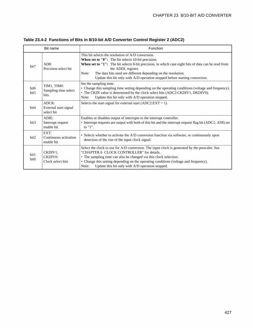
CHAPTER 23 8/10-BIT A/D CONVERTER
Table 23.4-2 Functions of Bits in 8/10-bit A/D Converter Control Register 2 (ADC2)
Bit name Function
bit7AD8:Precision select bit
This bit selects the resolution of A/D conversion.When set to "0": The bit selects 10-bit precision.When set to "1": The bit selects 8-bit precision, in which case eight bits of data can be read from
the ADDL register.Note: The data bits used are different depending on the resolution.
Update this bit only with A/D operation stopped before starting conversion.
bit6bit5
TIM1, TIM0:Sampling time select bits
Set the sampling time.• Change this sampling time setting depending on the operating conditions (voltage and frequency).• The CKIN value is determined by the clock select bits (ADC2:CKDIV1, DKDIV0).Note: Update this bit only with A/D operation stopped.
bit4ADCK:External start signal select bit
Selects the start signal for external start (ADC2:EXT = 1).
bit3ADIE:Interrupt request enable bit
Enables or disables output of interrupts to the interrupt controller.• Interrupt requests are output with both of this bit and the interrupt request flag bit (ADC1: ADI) set
to "1".
bit2EXT:Continuous activation enable bit
• Selects whether to activate the A/D conversion function via software, or continuously upon detection of the rise of the input clock signal.
bit1bit0
CKDIV1,CKDIV0:Clock select bits
Select the clock to use for A/D conversion. The input clock is generated by the prescaler. See "CHAPTER 6 CLOCK CONTROLLER" for details.• The sampling time can also be changed via this clock selection.• Change this setting depending on the operating conditions (voltage and frequency).Note: Update this bit only with A/D operation stopped.
427
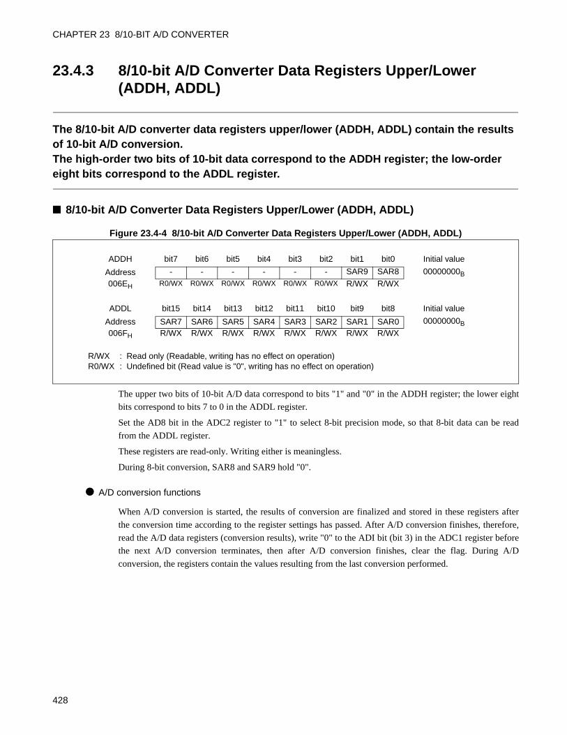
CHAPTER 23 8/10-BIT A/D CONVERTER
23.4.3 8/10-bit A/D Converter Data Registers Upper/Lower (ADDH, ADDL)
The 8/10-bit A/D converter data registers upper/lower (ADDH, ADDL) contain the results of 10-bit A/D conversion.The high-order two bits of 10-bit data correspond to the ADDH register; the low-order eight bits correspond to the ADDL register.
8/10-bit A/D Converter Data Registers Upper/Lower (ADDH, ADDL)
Figure 23.4-4 8/10-bit A/D Converter Data Registers Upper/Lower (ADDH, ADDL)
The upper two bits of 10-bit A/D data correspond to bits "1" and "0" in the ADDH register; the lower eight
bits correspond to bits 7 to 0 in the ADDL register.
Set the AD8 bit in the ADC2 register to "1" to select 8-bit precision mode, so that 8-bit data can be read
from the ADDL register.
These registers are read-only. Writing either is meaningless.
During 8-bit conversion, SAR8 and SAR9 hold "0".
A/D conversion functions
When A/D conversion is started, the results of conversion are finalized and stored in these registers after
the conversion time according to the register settings has passed. After A/D conversion finishes, therefore,
read the A/D data registers (conversion results), write "0" to the ADI bit (bit 3) in the ADC1 register before
the next A/D conversion terminates, then after A/D conversion finishes, clear the flag. During A/D
conversion, the registers contain the values resulting from the last conversion performed.
ADDH bit7 bit6 bit5 bit4 bit3 bit2 bit1 bit0 Initial value
Address - - - - - - SAR9 SAR8 00000000B
006EH R0/WX R0/WX R0/WX R0/WX R0/WX R0/WX R/WX R/WX
ADDL bit15 bit14 bit13 bit12 bit11 bit10 bit9 bit8 Initial value
Address SAR7 SAR6 SAR5 SAR4 SAR3 SAR2 SAR1 SAR0 00000000B
006FH R/WX R/WX R/WX R/WX R/WX R/WX R/WX R/WX
R/WX : Read only (Readable, writing has no effect on operation)R0/WX : Undefined bit (Read value is "0", writing has no effect on operation)
428
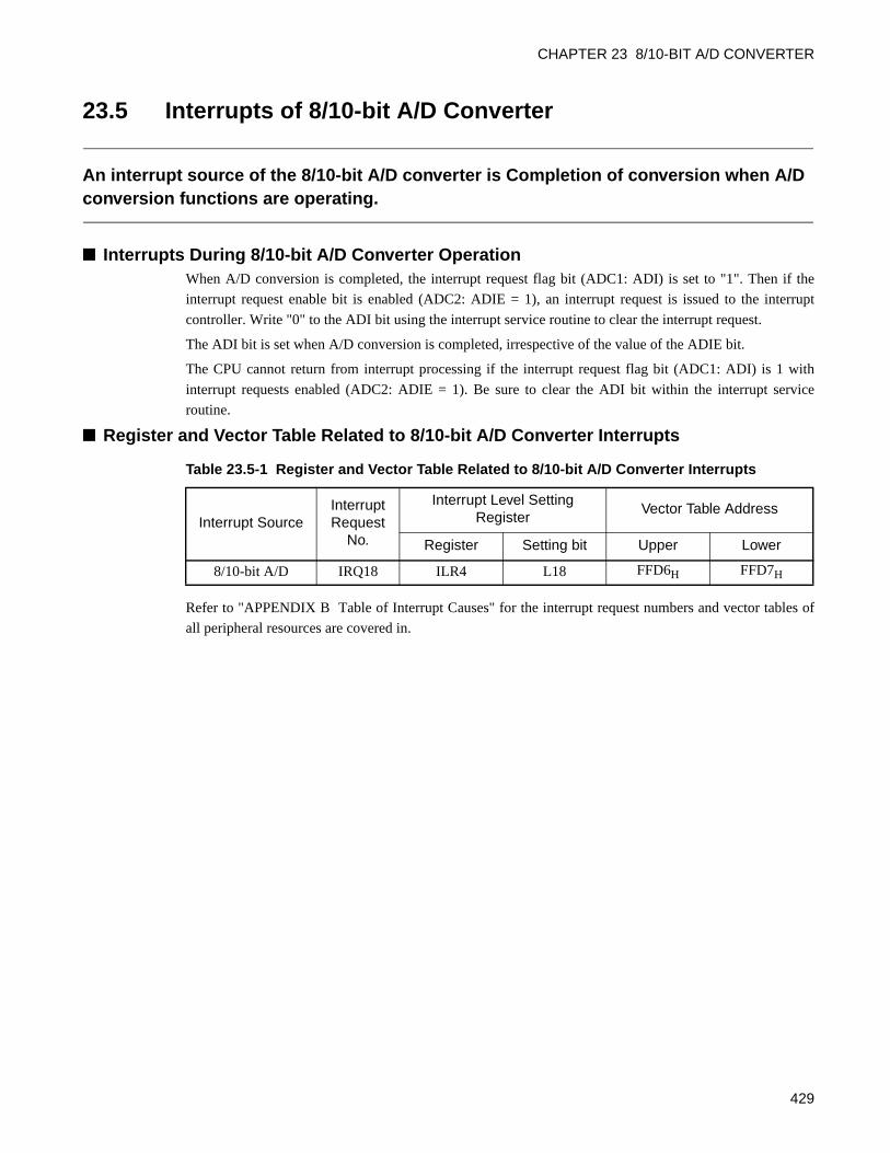
CHAPTER 23 8/10-BIT A/D CONVERTER
23.5 Interrupts of 8/10-bit A/D Converter
An interrupt source of the 8/10-bit A/D converter is Completion of conversion when A/D conversion functions are operating.
Interrupts During 8/10-bit A/D Converter OperationWhen A/D conversion is completed, the interrupt request flag bit (ADC1: ADI) is set to "1". Then if the
interrupt request enable bit is enabled (ADC2: ADIE = 1), an interrupt request is issued to the interrupt
controller. Write "0" to the ADI bit using the interrupt service routine to clear the interrupt request.
The ADI bit is set when A/D conversion is completed, irrespective of the value of the ADIE bit.
The CPU cannot return from interrupt processing if the interrupt request flag bit (ADC1: ADI) is 1 with
interrupt requests enabled (ADC2: ADIE = 1). Be sure to clear the ADI bit within the interrupt service
routine.
Register and Vector Table Related to 8/10-bit A/D Converter Interrupts
Refer to "APPENDIX B Table of Interrupt Causes" for the interrupt request numbers and vector tables of
all peripheral resources are covered in.
Table 23.5-1 Register and Vector Table Related to 8/10-bit A/D Converter Interrupts
Interrupt SourceInterrupt Request
No.
Interrupt Level Setting Register
Vector Table Address
Register Setting bit Upper Lower
8/10-bit A/D IRQ18 ILR4 L18 FFD6H FFD7H
429
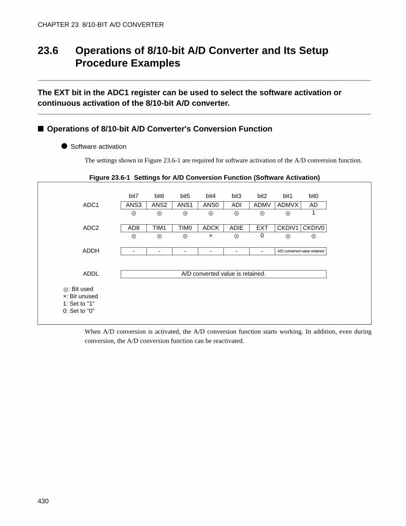
CHAPTER 23 8/10-BIT A/D CONVERTER
23.6 Operations of 8/10-bit A/D Converter and Its Setup Procedure Examples
The EXT bit in the ADC1 register can be used to select the software activation or continuous activation of the 8/10-bit A/D converter.
Operations of 8/10-bit A/D Converter's Conversion Function
Software activation
The settings shown in Figure 23.6-1 are required for software activation of the A/D conversion function.
Figure 23.6-1 Settings for A/D Conversion Function (Software Activation)
When A/D conversion is activated, the A/D conversion function starts working. In addition, even during
conversion, the A/D conversion function can be reactivated.
bit7 bit6 bit5 bit4 bit3 bit2 bit1 bit0
ADC1 ANS3 ANS2 ANS1 ANS0 ADI ADMV ADMVX AD1
ADC2 AD8 TIM1 TIM0 ADCK ADIE EXT CKDIV1 CKDIV0× 0
ADDH - - - - - - A/D converted value retained
ADDL A/D converted value is retained.
: Bit used×: Bit unused1: Set to "1"0: Set to "0"
430
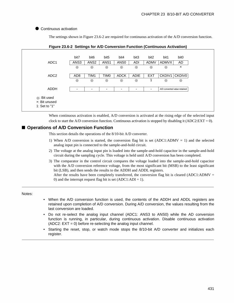
CHAPTER 23 8/10-BIT A/D CONVERTER
Continuous activation
The settings shown in Figure 23.6-2 are required for continuous activation of the A/D conversion function.
Figure 23.6-2 Settings for A/D Conversion Function (Continuous Activation)
When continuous activation is enabled, A/D conversion is activated at the rising edge of the selected input
clock to start the A/D conversion function. Continuous activation is stopped by disabling it (ADC2:EXT = 0).
Operations of A/D Conversion FunctionThis section details the operations of the 8/10-bit A/D converter.
1) When A/D conversion is started, the conversion flag bit is set (ADC1:ADMV = 1) and the selectedanalog input pin is connected to the sample-and-hold circuit.
2) The voltage at the analog input pin is loaded into the sample-and-hold capacitor in the sample-and-holdcircuit during the sampling cycle. This voltage is held until A/D conversion has been completed.
3) The comparator in the control circuit compares the voltage loaded into the sample-and-hold capacitorwith the A/D conversion reference voltage, from the most significant bit (MSB) to the least significantbit (LSB), and then sends the results to the ADDH and ADDL registers.After the results have been completely transferred, the conversion flag bit is cleared (ADC1:ADMV =0) and the interrupt request flag bit is set (ADC1:ADI = 1).
Notes:
• When the A/D conversion function is used, the contents of the ADDH and ADDL registers areretained upon completion of A/D conversion. During A/D conversion, the values resulting from thelast conversion are loaded.
• Do not re-select the analog input channel (ADC1: ANS3 to ANS0) while the AD conversionfunction is running, in particular, during continuous activation. Disable continuous activation(ADC2: EXT = 0) before re-selecting the analog input channel.
• Starting the reset, stop, or watch mode stops the 8/10-bit A/D converter and initializes eachregister.
bit7 bit6 bit5 bit4 bit3 bit2 bit1 bit0
ADC1 ANS3 ANS2 ANS1 ANS0 ADI ADMV ADMVX AD×
ADC2 AD8 TIM1 TIM0 ADCK ADIE EXT CKDIV1 CKDIV01
ADDH - - - - - - A/D converted value retained
: Bit used×: Bit unused1: Set to "1"
431
CHAPTER 23 8/10-BIT A/D CONVERTER
Setup Procedure ExampleFollow the procedure below to set up the 8/10-bit A/D converter:
Initialization
1) Set the port for input (DDR1).
2) Set the interrupt level (ILR4).
3) Enable A/D input (ADC1:ANS0 to ANS3).
4) Set the sampling time (ADC2:TIM1, TIM0).
5) Select the clock (ADC2:CKDIV1, CKDIV0).
6) Set A/D conversion properties (ADC2:AD8).
7) Select the operation mode (ADC2:EXT).
8) Select the startup trigger (ADC2:ADCK).
9) Enable interrupts (ADC2:ADIE=1).
10)Activate A/D (ADC1:AD=1).
Interrupt processing
1) Clear the interrupt request flag (ADC1:ADI=0).
2) Read converted values (ADDH, ADDL).
3) Activate A/D (ADC1:AD=1).
432
CHAPTER 23 8/10-BIT A/D CONVERTER
23.7 Notes on Use of 8/10-bit A/D Converter
This section summarizes notes on using the 8/10-bit A/D converter.
Notes on Use of 8/10-bit A/D Converter
Notes on programmed setup
• When the A/D conversion function is used, the contents of the ADDH and ADDL registers are retainedupon completion of A/D conversion. During A/D conversion, the values resulting from the lastconversion are loaded.
• Do not re-select the analog input channel (ADC1: ANS3 to ANS0) while the A/D conversion function isrunning, in particular, during continuous activation. Disable continuous activation (ADC2: EXT = 0)before re-selecting the analog input channel.
• Starting the reset, stop, or watch mode stops the 8/10-bit A/D converter and initializes each register.
• The CPU cannot return from interrupt processing if the interrupt request flag bit (ADC1: ADI) is 1 withinterrupt requests enabled (ADC2: ADIE = 1). Be sure to clear the ADI bit within the interrupt serviceroutine.
Note on interrupt requests
If A/D conversion is reactivated (ADC1: AD = 1) and terminated at the same time, the interrupt request
flag bit (ADC1: ADI) is set.
Error
As |AVR-AVSS| decreases, an error increases relatively.
8/10-bit A/D converter and analog input power-on/shut-down sequences
Turn on the 8/10-bit A/D converter power supply (AVCC, AVSS) and analog input (AN00 to AN07) at the
same as or after turning on the digital power supply (VCC,).
In addition, turn off the digital power supply (VCC) either at the same time as or after turning off the 8/10-
bit A/D converter power supply (AVCC, AVSS) and analog input (AN00 to AN07).
Be careful not to let the AVCC, AVSS, and analog input exceed the voltage of the digital power supply
when turning the 8/10-bit A/D converter on and off.
Conversion time
The conversion speed of the A/D conversion function is affected by the clock mode, main clock oscillation
frequency, and main clock speed switching (gear function).
Example: Sampling time = CKIN × (ADC2: TIM1/TIM0 setting)
Compare time = CKIN x 10 (fixed value) + MCLK
Conversion time = A/D start processing time + sampling time + compare time
• The error max. 1CKIN-1MCLK may occur depending on the timing of A/D startup.
• Program the software satisfied with "sampling time" and "compare time" in A/D conversion of datasheet.
433
CHAPTER 23 8/10-BIT A/D CONVERTER
23.8 Sample Programs for 8/10-bit A/D Converter
Fujitsu provides sample programs to operate the 8/10-bit A/D converter.
Sample Programs for 8/10-bit A/D ConverterFor sample programs for the 8/10-bit A/D converter, see " Sample Programs" in "Preface".
Setting Methods not Covered by Sample Programs
Selecting the operating clock for the 8/10-bit A/D converter
Use the clock select bits (ADC2:CKDIV1/CKDIV0) to select the operating clock.
Selecting the sampling time of the 8/10-bit A/D converter
Use the sampling time select bits (ADC2:TIM1/TIM0) to select the sampling time.
Controlling the analog switch for internal reference power shutdown of the 8/10-bit A/D converter
Use the analog switch control bit (ADC1:ADMVX) to control the internal reference power shutdown
analog switch.
Selecting the 8/10-bit A/D converter activation method
Use the continuous activation enable bit (ADC2:EXT) to select the startup trigger.
• Generating a software trigger
Use the A/D conversion start bit (ADC1:AD) to generate a software trigger.
Control item Analog switch control bit (ADMVX)
To turn off internal reference power supply Set the bit to "0".
To turn on internal reference power supply Set the bit to "1".
A/D startup factorContinuous activation enable bit
(EXT)
To select the software trigger Set the bit to "0".
To select the input clock rising signal Set the bit to "1".
Operation A/D conversion start bit (AD)
To generate a software trigger Set the bit to "1".
434
CHAPTER 23 8/10-BIT A/D CONVERTER
• Activation using the input clock
A startup trigger is generated at the rise of the input clock signal.
To select the input clock, use the external start signal select bit (ADC2:ADCK).
Selecting the A/D conversion precision
To select the precision of conversion results, use the precision select bit (ADC2:AD8).
Using analog input pins
To select an analog input pin, use the analog input channel select bits (ADC1:ANS3 to ANS0).
Input clock External start signal select bit (ADCK)
To select the ADTG input pin Set the bit to "0".
To select the 8/16-bit compound timer (TDO0) Set the bit to "1".
Operating mode Precision select bit (AD8)
To select 10-bit precision Set the bit to "0".
To select 8-bit precision Set the bit to "1".
Operation Analog input channel select bits (ANS3 to ANS0)
To use the AN0 pin Set the pins to "0000B".
To use the AN1 pin Set the pins to "0001B".
To use the AN2 pin Set the pins to "0010B".
To use the AN3 pin Set the pins to "0011B".
To use the AN4 pin Set the pins to "0100B".
To use the AN5 pin Set the pins to "0101B".
To use the AN6 pin Set the pins to "0110B".
To use the AN7 pin Set the pins to "01111B".
435
CHAPTER 23 8/10-BIT A/D CONVERTER
Checking the completion of conversion
The following two methods can be used to check whether conversion has been completed.
• Checking with the interrupt request flag bit (ADC1:ADI)
• Checking with the conversion flag bit (ADC1:ADMV)
Interrupted related register
Use the following interrupt level setting register to set the interrupt level.
Enabling, disabling, and clearing interrupts
To enable interrupts, use the interrupt request enable bit (ADC2:ADIE).
To clear interrupt requests, use the interrupt request bit (ADC1:ADI).
Interrupt request flag bit (ADI) Meaning
The value read is "0". A/D conversion completed with no interrupt request
The value read is "1". A/D conversion completed with interrupt request generated
Conversion flag bit (ADMV) Setting
The value read is "0". A/D conversion completed (suspended)
The value read is "1". A/D conversion in progress
Interrupt source Interrupt level setting register Interrupt vector
8/10-bit ADInterrupt level register (ILR4)
Address: 0007DH
#18Address: 0FFD6H
Control item Interrupt request enable bit (ADIE)
To disable interrupt requests Set the bit to "0".
To enable interrupt requests Set the bit to "1".
Control item Interrupt request bit (ADI)
To clear an interrupt request Set the bit to "1" or activate A/D.
436
CHAPTER 24LOW-VOLTAGE DETECTION
RESET CIRCUIT
This chapter describes the functions and operations of the low-voltage detection reset circuit.
24.1 Overview of Low-voltage Detection Reset Circuit
24.2 Configuration of Low-voltage Detection Reset Circuit
24.3 Pins of Low-voltage Detection Reset Circuit
24.4 Operations of Low-voltage Detection Reset Circuit
437
CHAPTER 24 LOW-VOLTAGE DETECTION RESET CIRCUIT
24.1 Overview of Low-voltage Detection Reset Circuit
The low-voltage detection reset circuit monitors the power supply voltage and generates a reset signal if the voltage drops below the detection voltage level (available as an option to 5-V products only).
Low-voltage Detection Reset CircuitThis circuit monitors the power supply voltage and generates a reset signal if the voltage drops below the
detection voltage level. The circuit can be selected as an option to 5-V products only. Refer to the data
sheet for details of the electrical characteristics.
438
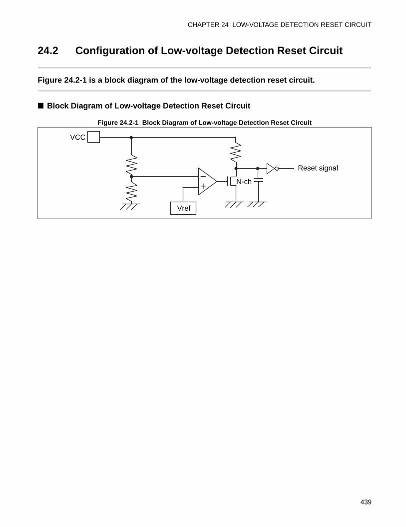
CHAPTER 24 LOW-VOLTAGE DETECTION RESET CIRCUIT
24.2 Configuration of Low-voltage Detection Reset Circuit
Figure 24.2-1 is a block diagram of the low-voltage detection reset circuit.
Block Diagram of Low-voltage Detection Reset Circuit
Figure 24.2-1 Block Diagram of Low-voltage Detection Reset Circuit
Reset signal
Vref
VCC
N-ch
439
CHAPTER 24 LOW-VOLTAGE DETECTION RESET CIRCUIT
24.3 Pins of Low-voltage Detection Reset Circuit
This section explains the pins of the low-voltage detection reset circuit.
Pins Related to Low-voltage Detection Reset Circuit
VCC pin
The low-voltage detection reset circuit monitors the voltage at this pin.
VSS pin
This pin is a GND pin serving as the reference for voltage detection.
RST pins
The low-voltage detection reset signal is output inside the microcontroller and to this pin.
440
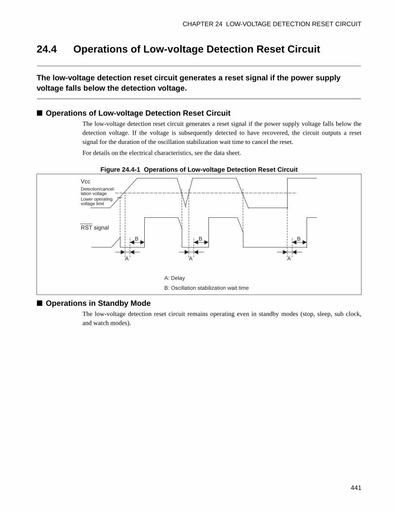
CHAPTER 24 LOW-VOLTAGE DETECTION RESET CIRCUIT
24.4 Operations of Low-voltage Detection Reset Circuit
The low-voltage detection reset circuit generates a reset signal if the power supply voltage falls below the detection voltage.
Operations of Low-voltage Detection Reset CircuitThe low-voltage detection reset circuit generates a reset signal if the power supply voltage falls below the
detection voltage. If the voltage is subsequently detected to have recovered, the circuit outputs a reset
signal for the duration of the oscillation stabilization wait time to cancel the reset.
For details on the electrical characteristics, see the data sheet.
Figure 24.4-1 Operations of Low-voltage Detection Reset Circuit
Operations in Standby ModeThe low-voltage detection reset circuit remains operating even in standby modes (stop, sleep, sub clock,
and watch modes).
Vcc
RST signal
A: Delay
B: Oscillation stabilization wait time
Lower operating voltage limit
Detection/cancel-lation voltage
A A A
B B B
441

CHAPTER 24 LOW-VOLTAGE DETECTION RESET CIRCUIT
442
CHAPTER 25256-KBIT FLASH
MEMORY
This chapter describes the functions and operations of 256-Kbit flash memory.
25.1 Overview of 256-Kbit Flash Memory
25.2 Sector Configuration of Flash Memory
25.3 Register of Flash Memory
25.4 Starting the Flash Memory Automatic Algorithm
25.5 Checking the Automatic Algorithm Execution Status
25.6 Details of Programming/Erasing Flash Memory
25.7 Features of Flash Security
443
CHAPTER 25 256-KBIT FLASH MEMORY
25.1 Overview of 256-Kbit Flash Memory
The following methods can be used to program (write) and erase data into/from flash memory:• Programming/erasing using a parallel programmer• Programming/erasing using a dedicated serial programmer• Programming/erasing by program executionThis section describes "programming/erasing by program execution".
Overview of 256-Kbit Flash Memory256-Kbit flash memory is located from 8000H to FFFFH on the CPU memory map. The function of the
flash memory interface circuit provides read access and program access from the CPU to flash memory.
As flash memory can be programmed and erased by the instructions from the CPU via the flash memory
interface circuit, you can efficiently reprogram (update) program code and data in flash memory with the
device mounted on a circuit board.
Features of 256-Kbit Flash Memory• Sector configuration: 32K bytes × 8 bits
• Automatic program algorithm (Embedded Algorithm)
• Detection of completion of programming/erasing using the data polling or toggle bit function
• Detection of completion of programming/erasing by CPU interrupts
• Compatible with JEDEC standard command
• Programming/erase count (minimum): 10,000 times
Programming and Erasing Flash Memory• It is not possible to write to and read from the flash memory at the same time.
• To program/erase data into/from a bank in flash memory, execute the one copied from the flash memoryto RAM, so that writing to the flash memory can be performed.
444
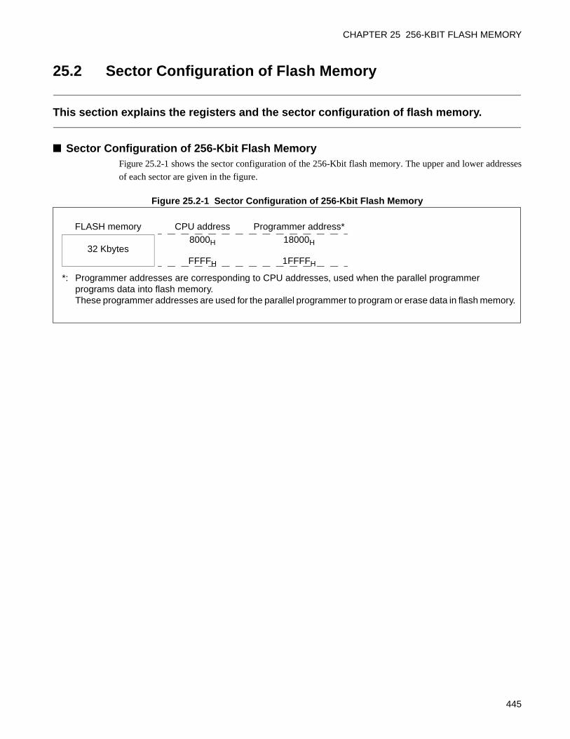
CHAPTER 25 256-KBIT FLASH MEMORY
25.2 Sector Configuration of Flash Memory
This section explains the registers and the sector configuration of flash memory.
Sector Configuration of 256-Kbit Flash MemoryFigure 25.2-1 shows the sector configuration of the 256-Kbit flash memory. The upper and lower addresses
of each sector are given in the figure.
Figure 25.2-1 Sector Configuration of 256-Kbit Flash Memory
*: Programmer addresses are corresponding to CPU addresses, used when the parallel programmer programs data into flash memory.These programmer addresses are used for the parallel programmer to program or erase data in flash memory.
FLASH memory CPU address Programmer address*
32 Kbytes8000H 18000H
FFFFH 1FFFFH
445
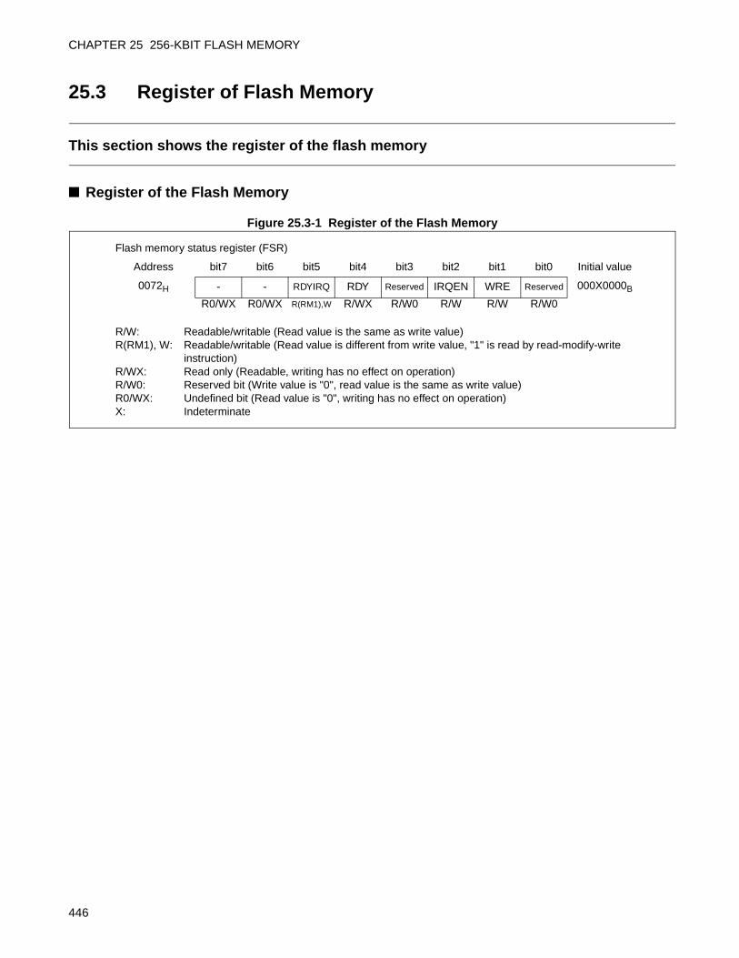
CHAPTER 25 256-KBIT FLASH MEMORY
25.3 Register of Flash Memory
This section shows the register of the flash memory
Register of the Flash Memory
Figure 25.3-1 Register of the Flash Memory
Flash memory status register (FSR)
Address bit7 bit6 bit5 bit4 bit3 bit2 bit1 bit0 Initial value
0072H - - RDYIRQ RDY Reserved IRQEN WRE Reserved 000X0000B
R0/WX R0/WX R(RM1),W R/WX R/W0 R/W R/W R/W0
R/W: Readable/writable (Read value is the same as write value)R(RM1), W: Readable/writable (Read value is different from write value, "1" is read by read-modify-write
instruction)R/WX: Read only (Readable, writing has no effect on operation)R/W0: Reserved bit (Write value is "0", read value is the same as write value)R0/WX: Undefined bit (Read value is "0", writing has no effect on operation)X: Indeterminate
446
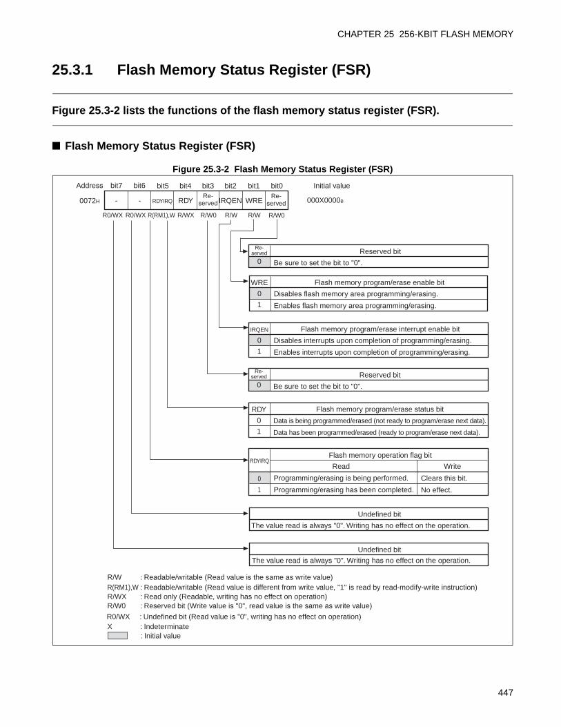
CHAPTER 25 256-KBIT FLASH MEMORY
25.3.1 Flash Memory Status Register (FSR)
Figure 25.3-2 lists the functions of the flash memory status register (FSR).
Flash Memory Status Register (FSR)
Figure 25.3-2 Flash Memory Status Register (FSR)
Initial value
000X0000B
bit4bit5 bit3 bit2 bit1 bit0bit7Address bit6
R0/WX R/W0R/WXR(RM1),W R/WR0/WX R/W
Undefined bit
Re-served
0Reserved bit
Be sure to set the bit to "0".
RDY
0
1
Flash memory program/erase status bit
Data is being programmed/erased (not ready to program/erase next data).
Data has been programmed/erased (ready to program/erase next data).
0
1
Flash memory operation flag bit
Programming/erasing is being performed.
Programming/erasing has been completed.
RDYIRQRead
Clears this bit.
No effect.
: IndeterminateX: Initial value
: Reserved bit (Write value is "0", read value is the same as write value)R/W0: Read only (Readable, writing has no effect on operation)R/WX
: Readable/writable (Read value is the same as write value)R/W
Undefined bit
The value read is always "0". Writing has no effect on the operation.
RDYIRQ IRQEN WRERDY- -Re-
served
WRE
0
1
Flash memory program/erase enable bit
Disables flash memory area programming/erasing.
Enables flash memory area programming/erasing.
IRQEN
0
1
Flash memory program/erase interrupt enable bit
Disables interrupts upon completion of programming/erasing.
Enables interrupts upon completion of programming/erasing.
: Readable/writable (Read value is different from write value, "1" is read by read-modify-write instruction)R(RM1),W
The value read is always "0". Writing has no effect on the operation.
: Undefined bit (Read value is "0", writing has no effect on operation)R0/WX
0072H
Write
R/W0
Re-served
Re-served
0Reserved bit
Be sure to set the bit to "0".
447
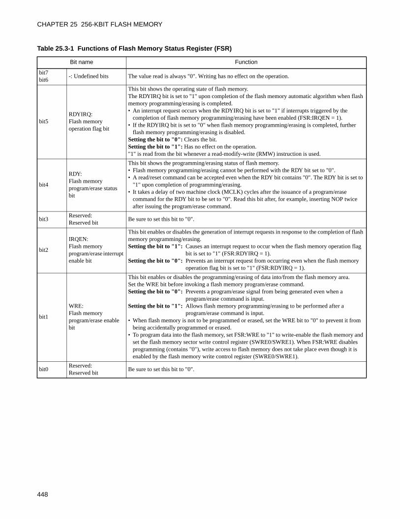
CHAPTER 25 256-KBIT FLASH MEMORY
Table 25.3-1 Functions of Flash Memory Status Register (FSR)
Bit name Function
bit7bit6
-: Undefined bits The value read is always "0". Writing has no effect on the operation.
bit5RDYIRQ:Flash memory operation flag bit
This bit shows the operating state of flash memory.The RDYIRQ bit is set to "1" upon completion of the flash memory automatic algorithm when flash memory programming/erasing is completed.• An interrupt request occurs when the RDYIRQ bit is set to "1" if interrupts triggered by the
completion of flash memory programming/erasing have been enabled (FSR:IRQEN = 1).• If the RDYIRQ bit is set to "0" when flash memory programming/erasing is completed, further
flash memory programming/erasing is disabled.Setting the bit to "0": Clears the bit.Setting the bit to "1": Has no effect on the operation."1" is read from the bit whenever a read-modify-write (RMW) instruction is used.
bit4
RDY: Flash memory program/erase status bit
This bit shows the programming/erasing status of flash memory.• Flash memory programming/erasing cannot be performed with the RDY bit set to "0".• A read/reset command can be accepted even when the RDY bit contains "0". The RDY bit is set to
"1" upon completion of programming/erasing.• It takes a delay of two machine clock (MCLK) cycles after the issuance of a program/erase
command for the RDY bit to be set to "0". Read this bit after, for example, inserting NOP twice after issuing the program/erase command.
bit3Reserved:Reserved bit
Be sure to set this bit to "0".
bit2
IRQEN: Flash memory program/erase interrupt enable bit
This bit enables or disables the generation of interrupt requests in response to the completion of flash memory programming/erasing.Setting the bit to "1": Causes an interrupt request to occur when the flash memory operation flag
bit is set to "1" (FSR:RDYIRQ = 1).Setting the bit to "0": Prevents an interrupt request from occurring even when the flash memory
operation flag bit is set to "1" (FSR:RDYIRQ = 1).
bit1
WRE: Flash memory program/erase enable bit
This bit enables or disables the programming/erasing of data into/from the flash memory area.Set the WRE bit before invoking a flash memory program/erase command.Setting the bit to "0": Prevents a program/erase signal from being generated even when a
program/erase command is input.Setting the bit to "1": Allows flash memory programming/erasing to be performed after a
program/erase command is input.• When flash memory is not to be programmed or erased, set the WRE bit to "0" to prevent it from
being accidentally programmed or erased.• To program data into the flash memory, set FSR:WRE to "1" to write-enable the flash memory and
set the flash memory sector write control register (SWRE0/SWRE1). When FSR:WRE disables programming (contains "0"), write access to flash memory does not take place even though it is enabled by the flash memory write control register (SWRE0/SWRE1).
bit0Reserved:Reserved bit
Be sure to set this bit to "0".
448
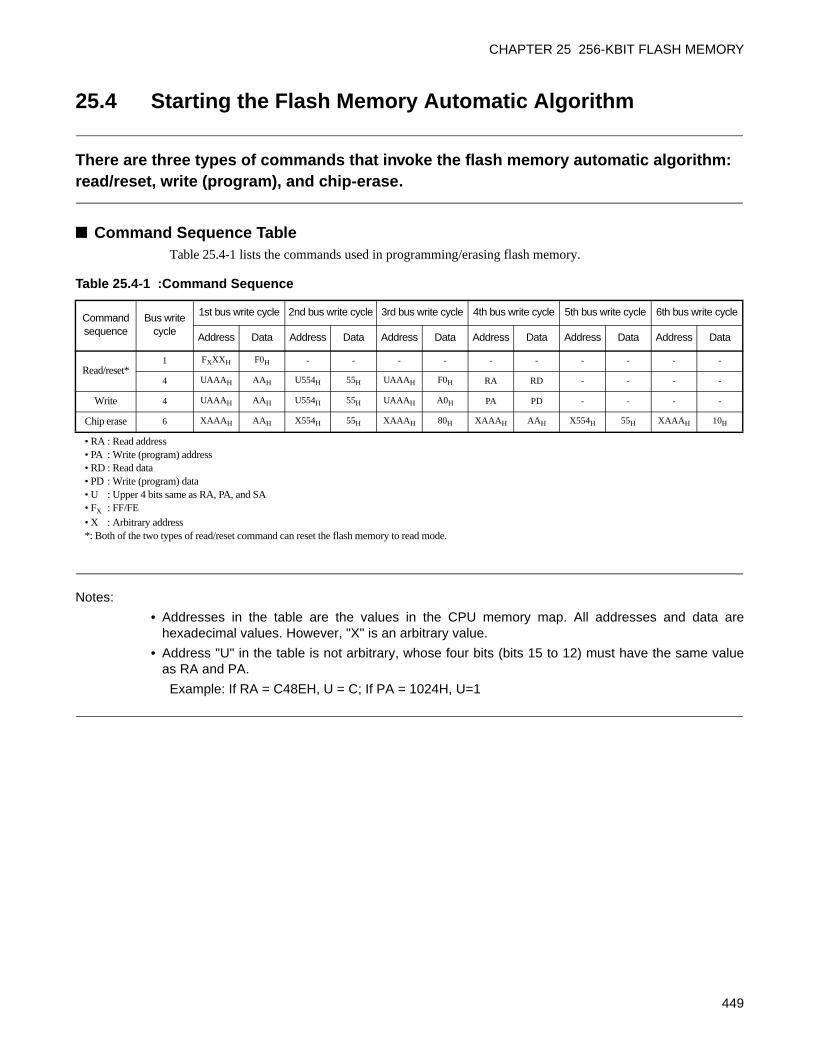
CHAPTER 25 256-KBIT FLASH MEMORY
25.4 Starting the Flash Memory Automatic Algorithm
There are three types of commands that invoke the flash memory automatic algorithm: read/reset, write (program), and chip-erase.
Command Sequence TableTable 25.4-1 lists the commands used in programming/erasing flash memory.
Notes:
• Addresses in the table are the values in the CPU memory map. All addresses and data arehexadecimal values. However, "X" is an arbitrary value.
• Address "U" in the table is not arbitrary, whose four bits (bits 15 to 12) must have the same valueas RA and PA.
Example: If RA = C48EH, U = C; If PA = 1024H, U=1
Table 25.4-1 :Command Sequence
Command sequence
Bus write cycle
1st bus write cycle 2nd bus write cycle 3rd bus write cycle 4th bus write cycle 5th bus write cycle 6th bus write cycle
Address Data Address Data Address Data Address Data Address Data Address Data
Read/reset*1 FXXXH F0H - - - - - - - - - -
4 UAAAH AAH U554H 55H UAAAH F0H RA RD - - - -
Write 4 UAAAH AAH U554H 55H UAAAH A0H PA PD - - - -
Chip erase 6 XAAAH AAH X554H 55H XAAAH 80H XAAAH AAH X554H 55H XAAAH 10H
• RA : Read address• PA : Write (program) address• RD : Read data• PD : Write (program) data• U : Upper 4 bits same as RA, PA, and SA• FX : FF/FE• X : Arbitrary address*: Both of the two types of read/reset command can reset the flash memory to read mode.
449
CHAPTER 25 256-KBIT FLASH MEMORY
Notes on Issuing CommandsPay attention to the following points when issuing commands in the command sequence table:
The upper address U bits (bits 15 to 12) used when commands are issued must have the same value as RA
and PA, from the first command on.
If the above measures are not followed, commands are not recognized normally. Execute a reset to
initialize the command sequencer in the flash memory.
450
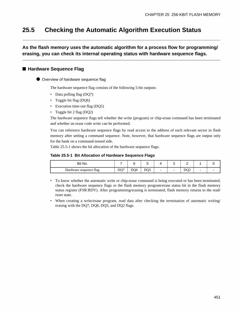
CHAPTER 25 256-KBIT FLASH MEMORY
25.5 Checking the Automatic Algorithm Execution Status
As the flash memory uses the automatic algorithm for a process flow for programming/erasing, you can check its internal operating status with hardware sequence flags.
Hardware Sequence Flag
Overview of hardware sequence flag
The hardware sequence flag consists of the following 5-bit outputs:
• Data polling flag (DQ7)
• Toggle bit flag (DQ6)
• Execution time-out flag (DQ5)
• Toggle bit 2 flag (DQ2)
The hardware sequence flags tell whether the write (program) or chip-erase command has been terminated
and whether an erase code write can be performed.
You can reference hardware sequence flags by read access to the address of each relevant sector in flash
memory after setting a command sequence. Note, however, that hardware sequence flags are output only
for the bank on a command-issued side.
Table 25.5-1 shows the bit allocation of the hardware sequence flags.
• To know whether the automatic write or chip-erase command is being executed or has been terminated,check the hardware sequence flags or the flash memory program/erase status bit in the flash memorystatus register (FSR:RDY). After programming/erasing is terminated, flash memory returns to the read/reset state.
• When creating a write/erase program, read data after checking the termination of automatic writing/erasing with the DQ7, DQ6, DQ5, and DQ2 flags.
Table 25.5-1 Bit Allocation of Hardware Sequence Flags
Bit No. 7 6 5 4 3 2 1 0
Hardware sequence flag DQ7 DQ6 DQ5 - - DQ2 - -
451
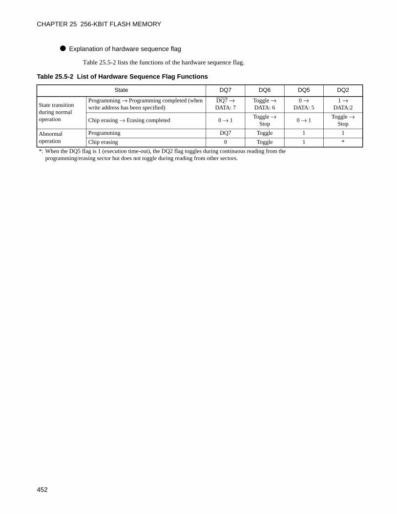
CHAPTER 25 256-KBIT FLASH MEMORY
Explanation of hardware sequence flag
Table 25.5-2 lists the functions of the hardware sequence flag.
Table 25.5-2 List of Hardware Sequence Flag Functions
State DQ7 DQ6 DQ5 DQ2
State transition during normal operation
Programming → Programming completed (when write address has been specified)
DQ7 →DATA: 7
Toggle →DATA: 6
0 →DATA: 5
1 →DATA:2
Chip erasing → Erasing completed 0 → 1Toggle →
Stop0 → 1
Toggle → Stop
Abnormal operation
Programming DQ7 Toggle 1 1
Chip erasing 0 Toggle 1 *
*: When the DQ5 flag is 1 (execution time-out), the DQ2 flag toggles during continuous reading from the programming/erasing sector but does not toggle during reading from other sectors.
452
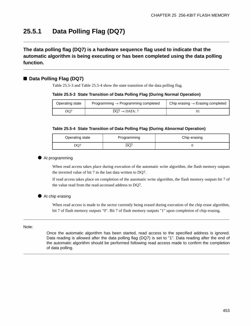
CHAPTER 25 256-KBIT FLASH MEMORY
25.5.1 Data Polling Flag (DQ7)
The data polling flag (DQ7) is a hardware sequence flag used to indicate that the automatic algorithm is being executing or has been completed using the data polling function.
Data Polling Flag (DQ7)Table 25.5-3 and Table 25.5-4 show the state transition of the data polling flag.
At programming
When read access takes place during execution of the automatic write algorithm, the flash memory outputs
the inverted value of bit 7 in the last data written to DQ7.
If read access takes place on completion of the automatic write algorithm, the flash memory outputs bit 7 of
the value read from the read-accessed address to DQ7.
At chip erasing
When read access is made to the sector currently being erased during execution of the chip erase algorithm,
bit 7 of flash memory outputs "0". Bit 7 of flash memory outputs "1" upon completion of chip erasing.
Note:
Once the automatic algorithm has been started, read access to the specified address is ignored.Data reading is allowed after the data polling flag (DQ7) is set to "1". Data reading after the end ofthe automatic algorithm should be performed following read access made to confirm the completionof data polling.
Table 25.5-3 State Transition of Data Polling Flag (During Normal Operation)
Operating state Programming → Programming completed Chip erasing → Erasing completed
DQ7 DQ7 → DATA: 7 01
Table 25.5-4 State Transition of Data Polling Flag (During Abnormal Operation)
Operating state Programming Chip erasing
DQ7 DQ7 0
453
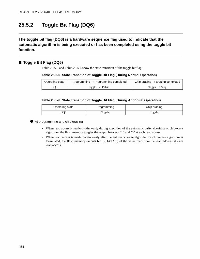
CHAPTER 25 256-KBIT FLASH MEMORY
25.5.2 Toggle Bit Flag (DQ6)
The toggle bit flag (DQ6) is a hardware sequence flag used to indicate that the automatic algorithm is being executed or has been completed using the toggle bit function.
Toggle Bit Flag (DQ6)Table 25.5-5 and Table 25.5-6 show the state transition of the toggle bit flag.
At programming and chip erasing
• When read access is made continuously during execution of the automatic write algorithm or chip-erasealgorithm, the flash memory toggles the output between "1" and "0" at each read access.
• When read access is made continuously after the automatic write algorithm or chip-erase algorithm isterminated, the flash memory outputs bit 6 (DATA:6) of the value read from the read address at eachread access.
Table 25.5-5 State Transition of Toggle Bit Flag (During Normal Operation)
Operating state Programming → Programming completed Chip erasing → Erasing completed
DQ6 Toggle → DATA: 6 Toggle → Stop
Table 25.5-6 State Transition of Toggle Bit Flag (During Abnormal Operation)
Operating state Programming Chip erasing
DQ6 Toggle Toggle
454
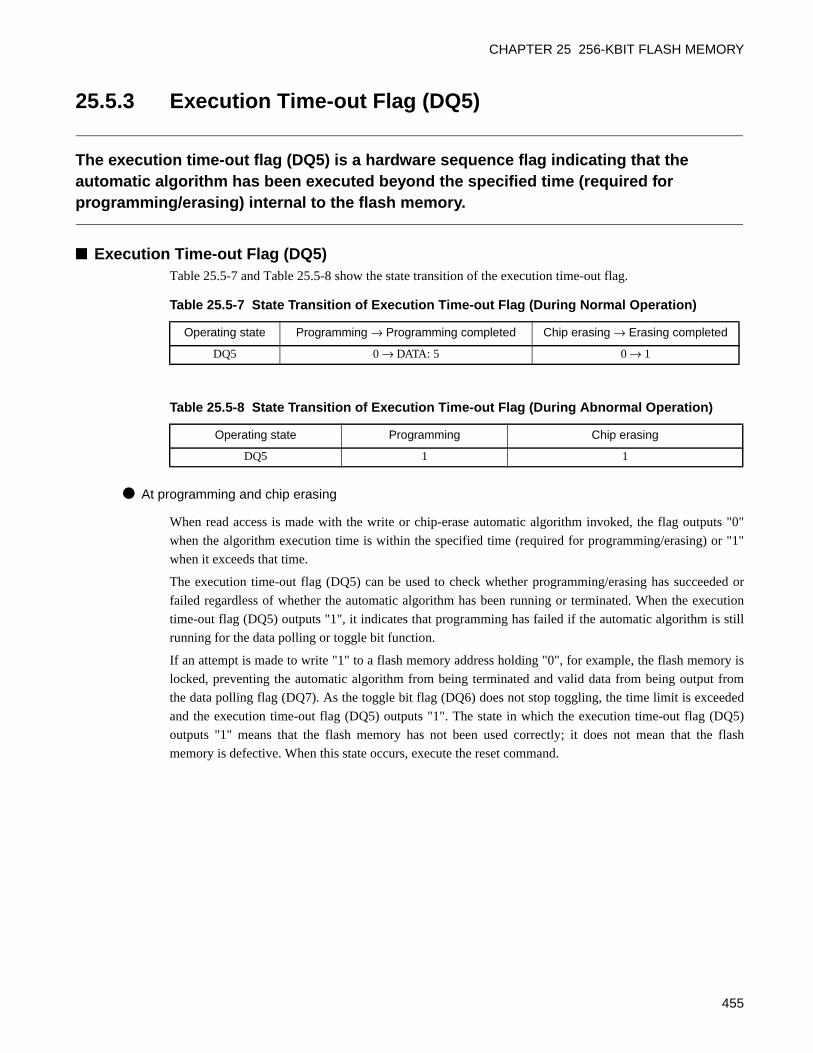
CHAPTER 25 256-KBIT FLASH MEMORY
25.5.3 Execution Time-out Flag (DQ5)
The execution time-out flag (DQ5) is a hardware sequence flag indicating that the automatic algorithm has been executed beyond the specified time (required for programming/erasing) internal to the flash memory.
Execution Time-out Flag (DQ5)Table 25.5-7 and Table 25.5-8 show the state transition of the execution time-out flag.
At programming and chip erasing
When read access is made with the write or chip-erase automatic algorithm invoked, the flag outputs "0"
when the algorithm execution time is within the specified time (required for programming/erasing) or "1"
when it exceeds that time.
The execution time-out flag (DQ5) can be used to check whether programming/erasing has succeeded or
failed regardless of whether the automatic algorithm has been running or terminated. When the execution
time-out flag (DQ5) outputs "1", it indicates that programming has failed if the automatic algorithm is still
running for the data polling or toggle bit function.
If an attempt is made to write "1" to a flash memory address holding "0", for example, the flash memory is
locked, preventing the automatic algorithm from being terminated and valid data from being output from
the data polling flag (DQ7). As the toggle bit flag (DQ6) does not stop toggling, the time limit is exceeded
and the execution time-out flag (DQ5) outputs "1". The state in which the execution time-out flag (DQ5)
outputs "1" means that the flash memory has not been used correctly; it does not mean that the flash
memory is defective. When this state occurs, execute the reset command.
Table 25.5-7 State Transition of Execution Time-out Flag (During Normal Operation)
Operating state Programming → Programming completed Chip erasing → Erasing completed
DQ5 0 → DATA: 5 0 → 1
Table 25.5-8 State Transition of Execution Time-out Flag (During Abnormal Operation)
Operating state Programming Chip erasing
DQ5 1 1
455
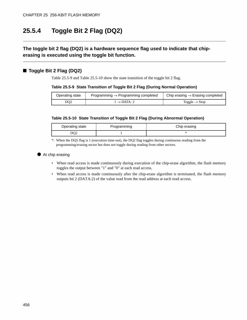
CHAPTER 25 256-KBIT FLASH MEMORY
25.5.4 Toggle Bit 2 Flag (DQ2)
The toggle bit 2 flag (DQ2) is a hardware sequence flag used to indicate that chip-erasing is executed using the toggle bit function.
Toggle Bit 2 Flag (DQ2)Table 25.5-9 and Table 25.5-10 show the state transition of the toggle bit 2 flag.
*: When the DQ5 flag is 1 (execution time-out), the DQ2 flag toggles during continuous reading from the programming/erasing sector but does not toggle during reading from other sectors.
At chip erasing
• When read access is made continuously during execution of the chip-erase algorithm, the flash memorytoggles the output between "1" and "0" at each read access.
• When read access is made continuously after the chip-erase algorithm is terminated, the flash memoryoutputs bit 2 (DATA:2) of the value read from the read address at each read access.
Table 25.5-9 State Transition of Toggle Bit 2 Flag (During Normal Operation)
Operating state Programming → Programming completed Chip erasing → Erasing completed
DQ2 1 → DATA: 2 Toggle → Stop
Table 25.5-10 State Transition of Toggle Bit 2 Flag (During Abnormal Operation)
Operating state Programming Chip erasing
DQ2 1 *
456
CHAPTER 25 256-KBIT FLASH MEMORY
25.6 Details of Programming/Erasing Flash Memory
This section describes the individual procedures for flash memory reading/resetting, programming, and chip-erasing by entering their respective commands to invoke the automatic algorithm.
Details of Programming/Erasing Flash MemoryThe automatic algorithm can be invoked by writing the read/reset, program, and chip-erase command
sequence to flash memory from the CPU. Writing command sequence to flash memory from the CPU must
always be performed continuously. The termination of the automatic algorithm can be checked by the data
polling function. After the automatic algorithm terminates normally, the flash memory returns to the read/
reset state.
The individual operations are explained in the following order:
• Enter read/reset state.
• Program data.
• Erase all data (chip-erase).
457
CHAPTER 25 256-KBIT FLASH MEMORY
25.6.1 Placing Flash Memory in the Read/Reset State
This section explains the procedure for entering the read/reset command to place flash memory in the read/reset state.
Placing Flash Memory in the Read/Reset State• To place flash memory in the read/reset state, send the read/reset command in the command sequence
table continuously from the CPU to flash memory.
• The read/reset command is available in two different command sequences: one involves a single busoperation and the other involves four bus operations, which are essentially the same.
• Since the read/reset state is the initial state of flash memory, the flash memory always enters this stateafter the power is turned on and at the normal termination of a command. The read/reset state is alsodescribed as the wait state for command input.
• In the read/reset state, read access to flash memory enables data to be read. As is the case with maskedROM, program access from the CPU can be made.
• Read access to flash memory does not require the read/reset command. If a command is not terminatednormally, use the read/reset command to initialize the automatic algorithm.
458
CHAPTER 25 256-KBIT FLASH MEMORY
25.6.2 Programming Data into Flash Memory
This section explains the procedure for entering the write (program) command to program data into flash memory.
Programming Data into Flash Memory• To start the automatic algorithm for programming data into flash memory, send the program command
in the command sequence table continuously from the CPU to flash memory.
• Upon completion of data programming to a target address in the fourth cycle, the automatic algorithmstarts automatic programming.
How to specify addresses
• Programming (writing) can be performed even in any order of addresses or across a sector boundary.Data written by a single program command is only one byte.
Notes on programming data
• Bit data cannot be returned from "0" to "1" by programming. When bit data "1" is programmed to bitdata "0", the data polling algorithm (DQ7) or toggle operation (DQ6) is not terminated, the flashmemory element is determined to be defective, and the execution time-out flag (DQ5) detects an error toindicate that the specified programming time has been exceeded.When data is read in the read/reset state, the bit data remains "0". To return the bit data from "0" to "1",erase flash memory.
• All commands are ignored during automatic programming.
• If a hardware reset occurs during programming, the data being programmed to the current address is notguaranteed. Retry from the chip-erase command.
Flash Memory Programming Procedure• Figure 25.6-1 gives an example of the procedure for programming data into flash memory. The
hardware sequence flags can be used to check the operating state of the automatic algorithm in flashmemory. The data polling flag (DQ7) is used for checking the completion of programming into flashmemory in this example.
• Flag check data should be read from the address where data was last written.
• Because the data polling flag (DQ7) and execution time-out flag (DQ5) are updated at the same time,the data polling flag (DQ7) must be checked even when the execution time-out flag (DQ5) is "1".
• Similarly, the toggle bit flag (DQ6) must be checked as it stops toggling at the same time as when theexecution time-out flag (DQ5) changes to "1".
459
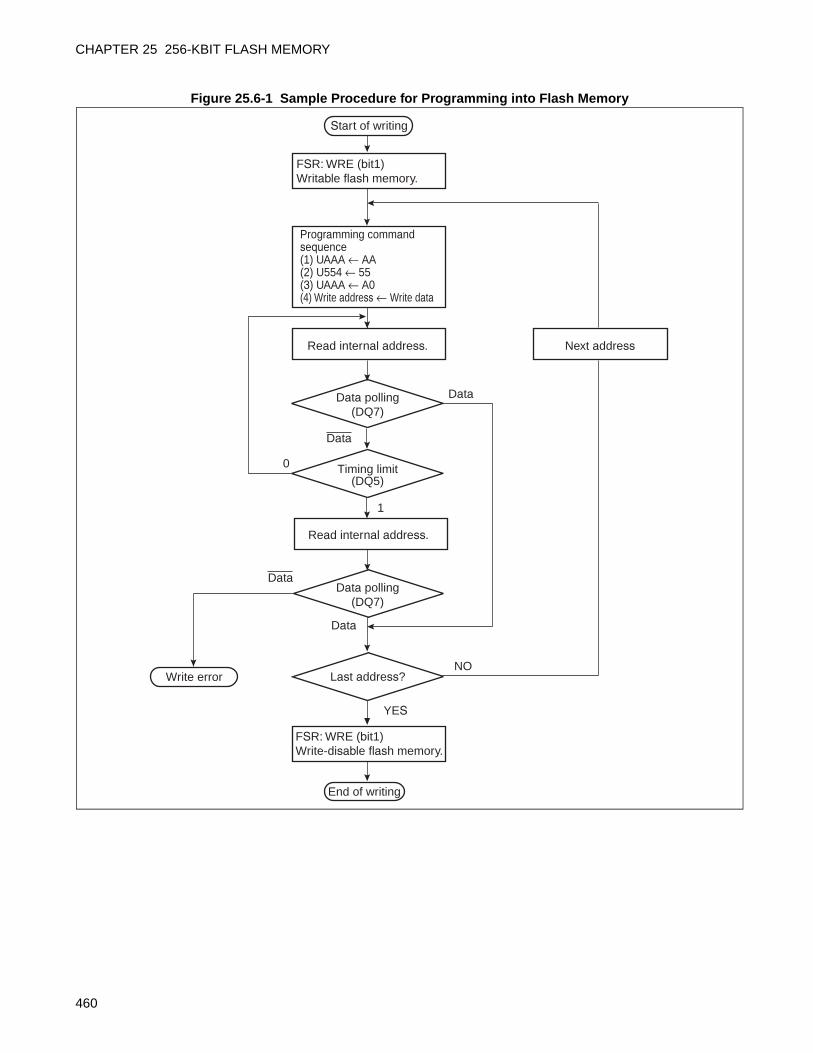
CHAPTER 25 256-KBIT FLASH MEMORY
Figure 25.6-1 Sample Procedure for Programming into Flash Memory
Start of writing
Read internal address.
Programming command sequence(1) UAAA ← AA(2) U554 ← 55(3) UAAA ← A0(4) Write address ← Write data
Next address
Read internal address.
FSR: WRE (bit1)Writable flash memory.
Data polling(DQ7)
Data polling(DQ7)
Data
Data
Timing limit(DQ5)
1
End of writing
0
Last address?
YES
NO
FSR: WRE (bit1)Write-disable flash memory.
Write error
Data
Data
460
CHAPTER 25 256-KBIT FLASH MEMORY
25.6.3 Erasing All Data from Flash Memory (Chip Erase)
This section describes the procedure for issuing the chip erase command to erase all data from flash memory.
Erasing Data from Flash Memory (Chip Erase)• To erase all data from flash memory, send the chip erase command in the command sequence table
continuously from the CPU to flash memory.
• The chip erase command is executed in six bus operations. Chip erasing is started upon completion ofthe sixth programming cycle.
• Before chip erasing, the user need not perform programming into flash memory. During execution of theautomatic erase algorithm, flash memory automatically programs "0" before erasing all cellsautomatically.
Notes on Chip ErasingIf a hardware reset occurs during erasure, the data being erased from flash memory is not guaranteed.
461
CHAPTER 25 256-KBIT FLASH MEMORY
25.7 Features of Flash Security
The flash security controller function prevents the contents of flash memory from being read through external pins.
Features of Flash SecurityWriting protection code "01H" to a flash memory address (8000H) restricts access to flash memory, barring
read/write access to flash memory from any external pin. Once flash memory has been protected, the
function cannot be unlocked until the chip erase command is executed.
Note that only addresses 5554H and 2AAAH can be read as exceptions.
It is advisable to code the protection code at the end of flash programming. This is to avoid unnecessary
protection during programming.
Once flash memory has been protected, the chip erase operation is required before it can be reprogrammed.
For details, ask your local representative of Fujitsu.
462
CHAPTER 26EXAMPLE OF SERIAL
PROGRAMMINGCONNECTION
This chapter describes the example of a serial programming connection.
26.1 Basic Configuration of the Flash Memory Products Serial Programming Connection
26.2 Example of Serial Programming Connection
26.3 Example of Minimum Connection to Flash Microcomputer Programmer
463
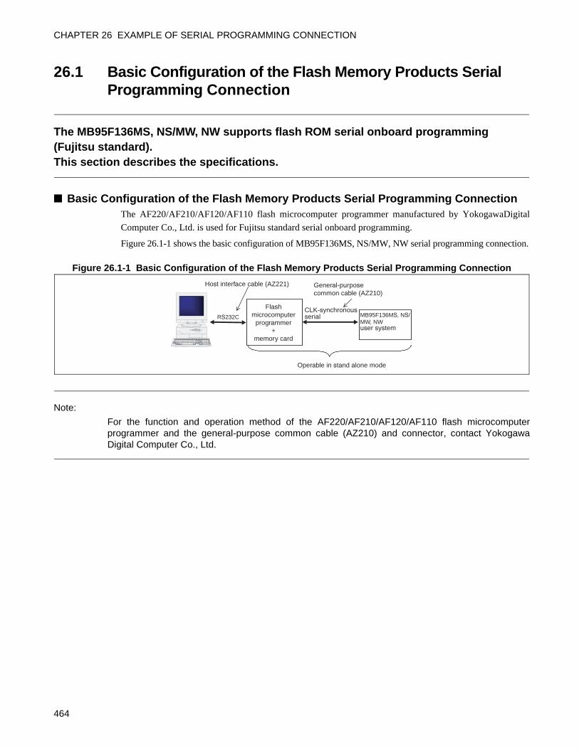
CHAPTER 26 EXAMPLE OF SERIAL PROGRAMMING CONNECTION
26.1 Basic Configuration of the Flash Memory Products Serial Programming Connection
The MB95F136MS, NS/MW, NW supports flash ROM serial onboard programming (Fujitsu standard).This section describes the specifications.
Basic Configuration of the Flash Memory Products Serial Programming ConnectionThe AF220/AF210/AF120/AF110 flash microcomputer programmer manufactured by YokogawaDigital
Computer Co., Ltd. is used for Fujitsu standard serial onboard programming.
Figure 26.1-1 shows the basic configuration of MB95F136MS, NS/MW, NW serial programming connection.
Figure 26.1-1 Basic Configuration of the Flash Memory Products Serial Programming Connection
Note:
For the function and operation method of the AF220/AF210/AF120/AF110 flash microcomputerprogrammer and the general-purpose common cable (AZ210) and connector, contact YokogawaDigital Computer Co., Ltd.
Flashmicrocomputer
programmer+
memory card
MB95F136MS, NS/MW, NWuser system
RS232CCLK-synchronous serial
Operable in stand alone mode
General-purposecommon cable (AZ210)
Host interface cable (AZ221)
464
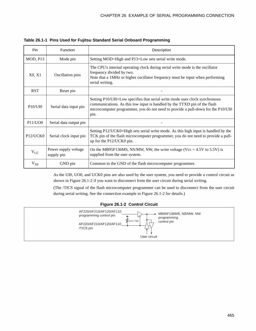
CHAPTER 26 EXAMPLE OF SERIAL PROGRAMMING CONNECTION
As the UI0, UO0, and UCK0 pins are also used by the user system, you need to provide a control circuit as
shown in Figure 26.1-2 if you want to disconnect from the user circuit during serial writing.
(The /TICS signal of the flash microcomputer programmer can be used to disconnect from the user circuit
during serial writing. See the connection example in Figure 26.1-2 for details.)
Figure 26.1-2 Control Circuit
Table 26.1-1 Pins Used for Fujitsu Standard Serial Onboard Programming
Pin Function Description
MOD, P13 Mode pin Setting MOD=High and P13=Low sets serial write mode.
X0, X1 Oscillation pins
The CPU's internal operating clock during serial write mode is the oscillator frequency divided by two.Note that a 1MHz or higher oscillator frequency must be input when performing serial writing.
RST Reset pin -
P10/UI0 Serial data input pin
Setting P10/UI0=Low specifies that serial write mode uses clock synchronous communications. As this low input is handled by the TTXD pin of the flash microcomputer programmer, you do not need to provide a pull-down for the P10/UI0 pin.
P11/UO0 Serial data output pin -
P12/UCK0 Serial clock input pinSetting P12/UCK0=High sets serial write mode. As this high input is handled by the TCK pin of the flash microcomputer programmer, you do not need to provide a pull-up for the P12/UCK0 pin.
VCCPower supply voltage supply pin
On the MB95F136MS, NS/MW, NW, the write voltage (Vcc = 4.5V to 5.5V) is supplied from the user system.
VSS GND pin Common to the GND of the flash microcomputer programmer.
User circuit
>=
MB95F136MS, NS/MW, NW programming control pin
AF220/AF210/AF120/AF110programming control pin
AF220/AF210/AF120/AF110/TICS pin
4.7 kΩ
465
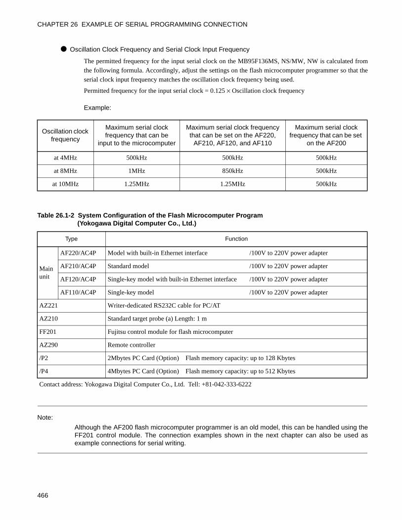
CHAPTER 26 EXAMPLE OF SERIAL PROGRAMMING CONNECTION
Oscillation Clock Frequency and Serial Clock Input Frequency
The permitted frequency for the input serial clock on the MB95F136MS, NS/MW, NW is calculated from
the following formula. Accordingly, adjust the settings on the flash microcomputer programmer so that the
serial clock input frequency matches the oscillation clock frequency being used.
Permitted frequency for the input serial clock = 0.125 × Oscillation clock frequency
Example:
Note:
Although the AF200 flash microcomputer programmer is an old model, this can be handled using theFF201 control module. The connection examples shown in the next chapter can also be used asexample connections for serial writing.
Oscillation clock frequency
Maximum serial clock frequency that can be
input to the microcomputer
Maximum serial clock frequency that can be set on the AF220,
AF210, AF120, and AF110
Maximum serial clock frequency that can be set
on the AF200
at 4MHz 500kHz 500kHz 500kHz
at 8MHz 1MHz 850kHz 500kHz
at 10MHz 1.25MHz 1.25MHz 500kHz
Table 26.1-2 System Configuration of the Flash Microcomputer Program (Yokogawa Digital Computer Co., Ltd.)
Type Function
Main unit
AF220/AC4P Model with built-in Ethernet interface /100V to 220V power adapter
AF210/AC4P Standard model /100V to 220V power adapter
AF120/AC4P Single-key model with built-in Ethernet interface /100V to 220V power adapter
AF110/AC4P Single-key model /100V to 220V power adapter
AZ221 Writer-dedicated RS232C cable for PC/AT
AZ210 Standard target probe (a) Length: 1 m
FF201 Fujitsu control module for flash microcomputer
AZ290 Remote controller
/P2 2Mbytes PC Card (Option) Flash memory capacity: up to 128 Kbytes
/P4 4Mbytes PC Card (Option) Flash memory capacity: up to 512 Kbytes
Contact address: Yokogawa Digital Computer Co., Ltd. Tell: +81-042-333-6222
466
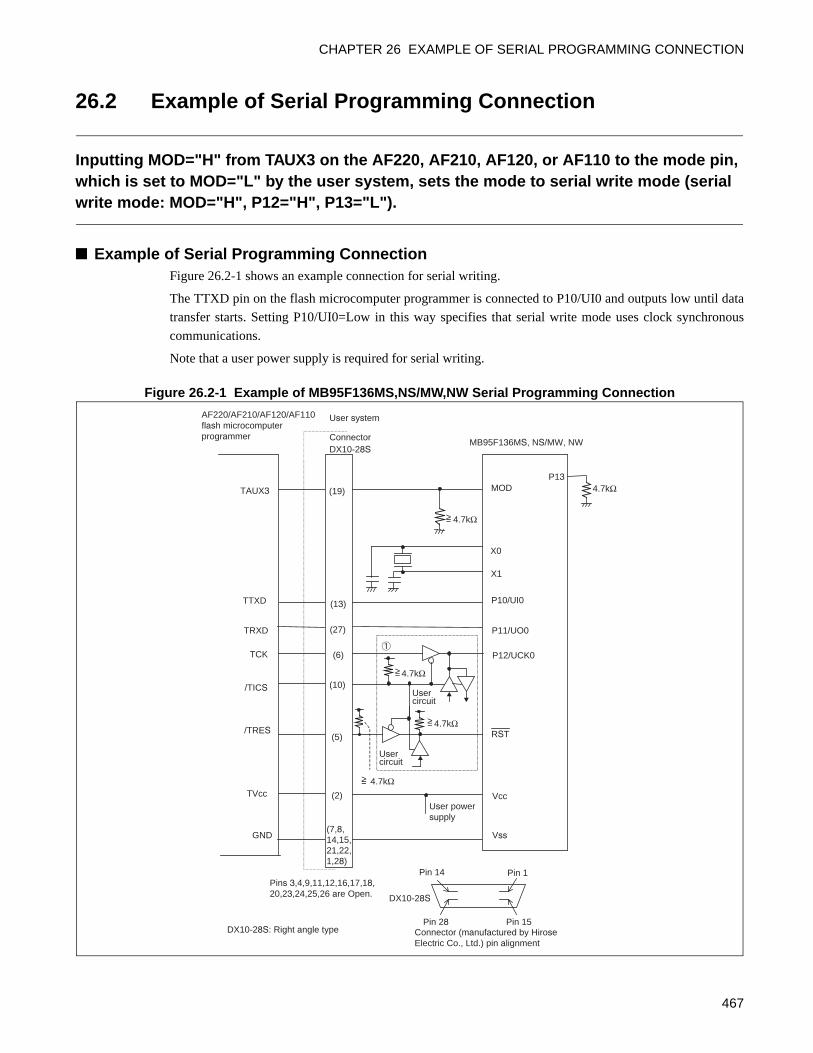
CHAPTER 26 EXAMPLE OF SERIAL PROGRAMMING CONNECTION
26.2 Example of Serial Programming Connection
Inputting MOD="H" from TAUX3 on the AF220, AF210, AF120, or AF110 to the mode pin, which is set to MOD="L" by the user system, sets the mode to serial write mode (serial write mode: MOD="H", P12="H", P13="L").
Example of Serial Programming ConnectionFigure 26.2-1 shows an example connection for serial writing.
The TTXD pin on the flash microcomputer programmer is connected to P10/UI0 and outputs low until data
transfer starts. Setting P10/UI0=Low in this way specifies that serial write mode uses clock synchronous
communications.
Note that a user power supply is required for serial writing.
Figure 26.2-1 Example of MB95F136MS,NS/MW,NW Serial Programming Connection
Vss
Vcc
GND
ConnectorDX10-28S
AF220/AF210/AF120/AF110 flash microcomputerprogrammer
MB95F136MS, NS/MW, NW
(7,8, 14,15, 21,22, 1,28)
User system
Pins 3,4,9,11,12,16,17,18, 20,23,24,25,26 are Open.
Pin 1
Pin 28 Pin 15
Pin 14
Connector (manufactured by HiroseElectric Co., Ltd.) pin alignment
DX10-28S
DX10-28S: Right angle type
(2) TVcc User powersupply
P11/UO0 TRXD (27)
X0
X1
/TICS Usercircuit
(10)
/TRES
Usercircuit
RST(5)
P10/UI0 TTXD (13)
P12/UCK0 TCK (6)
MOD TAUX3 (19)
P13
>=
>=
>=
>=
4.7kΩ
4.7kΩ
4.7kΩ
4.7kΩ
4.7kΩ
467
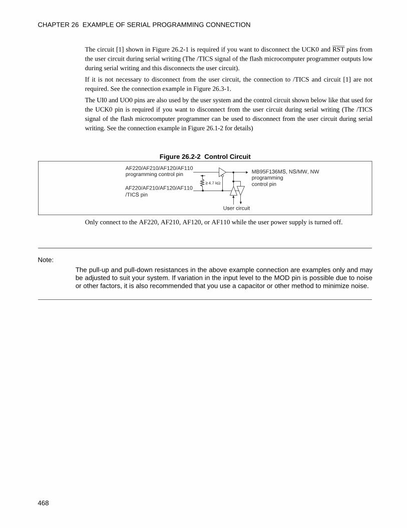
CHAPTER 26 EXAMPLE OF SERIAL PROGRAMMING CONNECTION
The circuit [1] shown in Figure 26.2-1 is required if you want to disconnect the UCK0 and RST pins from
the user circuit during serial writing (The /TICS signal of the flash microcomputer programmer outputs low
during serial writing and this disconnects the user circuit).
If it is not necessary to disconnect from the user circuit, the connection to /TICS and circuit [1] are not
required. See the connection example in Figure 26.3-1.
The UI0 and UO0 pins are also used by the user system and the control circuit shown below like that used for
the UCK0 pin is required if you want to disconnect from the user circuit during serial writing (The /TICS
signal of the flash microcomputer programmer can be used to disconnect from the user circuit during serial
writing. See the connection example in Figure 26.1-2 for details)
Figure 26.2-2 Control Circuit
Only connect to the AF220, AF210, AF120, or AF110 while the user power supply is turned off.
Note:
The pull-up and pull-down resistances in the above example connection are examples only and maybe adjusted to suit your system. If variation in the input level to the MOD pin is possible due to noiseor other factors, it is also recommended that you use a capacitor or other method to minimize noise.
User circuit
>=
MB95F136MS, NS/MW, NW programming control pin
AF220/AF210/AF120/AF110programming control pin
AF220/AF210/AF120/AF110/TICS pin
4.7 kΩ
468
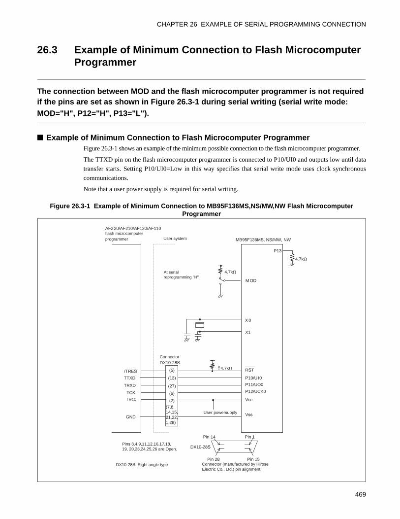
CHAPTER 26 EXAMPLE OF SERIAL PROGRAMMING CONNECTION
26.3 Example of Minimum Connection to Flash Microcomputer Programmer
The connection between MOD and the flash microcomputer programmer is not required if the pins are set as shown in Figure 26.3-1 during serial writing (serial write mode: MOD="H", P12="H", P13="L").
Example of Minimum Connection to Flash Microcomputer ProgrammerFigure 26.3-1 shows an example of the minimum possible connection to the flash microcomputer programmer.
The TTXD pin on the flash microcomputer programmer is connected to P10/UI0 and outputs low until data
transfer starts. Setting P10/UI0=Low in this way specifies that serial write mode uses clock synchronous
communications.
Note that a user power supply is required for serial writing.
Figure 26.3-1 Example of Minimum Connection to MB95F136MS,NS/MW,NW Flash Microcomputer Programmer
Vss GND
Connector DX10-28S
AF220/AF210/AF120/AF110 flash microcomputerprogrammer MB95F136MS, NS/MW, NW
(7,8, 14,15, 21,22, 1,28)
User system
Pin 1
Pin 28 Pin 15
Pin 14
Connector (manufactured by Hirose Electric Co., Ltd.) pin alignment
DX10-28S
DX10-28S: Right angle type
User powersupply
P10/UI0 TTXD (13)
P11/UO0 TRXD (27) P12/UCK0 TCK (6) Vcc (2) TVcc
M OD
/TRES RST (5)
X 0
X1
4.7
P13
At serialreprogramming "H"
Pins 3,4,9,11,12,16,17,18, 19, 20,23,24,25,26 are Open.
>=
469
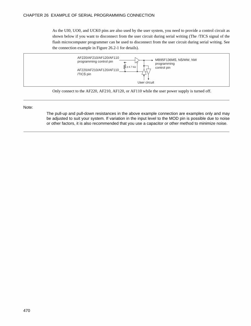
CHAPTER 26 EXAMPLE OF SERIAL PROGRAMMING CONNECTION
As the UI0, UO0, and UCK0 pins are also used by the user system, you need to provide a control circuit as
shown below if you want to disconnect from the user circuit during serial writing (The /TICS signal of the
flash microcomputer programmer can be used to disconnect from the user circuit during serial writing. See
the connection example in Figure 26.2-1 for details).
Only connect to the AF220, AF210, AF120, or AF110 while the user power supply is turned off.
Note:
The pull-up and pull-down resistances in the above example connection are examples only and maybe adjusted to suit your system. If variation in the input level to the MOD pin is possible due to noiseor other factors, it is also recommended that you use a capacitor or other method to minimize noise.
User circuit
>=
MB95F136MS, NS/MW, NW programming control pin
AF220/AF210/AF120/AF110programming control pin
AF220/AF210/AF120/AF110/TICS pin
4.7 kΩ
470
APPENDIX
This appendix explains I/O map, interrupt list, memory map, pin status, instruction overview, mask option and writing to Flash microcomputer using parallel writer.
APPENDIX A I/O Map
APPENDIX B Table of Interrupt Causes
APPENDIX C Memory Map
APPENDIX D Pin Status of MB95130/M series
APPENDIX E Instruction Overview
APPENDIX F Mask Option
APPENDIX G Writing to Flash Microcontroller Using Parallel Writer
471
APPENDIX A I/O Map
APPENDIX A I/O Map
This section explains I/O map that is used on MB95130/M series.
I/O Map
Table A-1 MB95130/M Series (1 / 4)
AddressRegister
abbreviationRegister name R/W
Initial value
0000H PDR0 Port 0 data register R/W 00000000B
0001H DDR0 Port 0 direction register R/W 00000000B
0002H PDR1 Port 1 data register R/W 00000000B
0003H DDR1 Port 1 direction register R/W 00000000B
0004H (Do Not Use)
0005H WATR Oscillation stabilization wait time setting register R/W 11111111B
0006H PLLC PLL control register R/W 00000000B
0007H SYCC System clock control register R/W 1010x011B
0008H STBC Standby control register R/W 00000000B
0009H RSRR Reset cause register R xxxxxxxxB
000AH TBTC Timebase timer control register R/W 00000000B
000BH WPCR Watch prescaler control register R/W 00000000B
000CH WDTC Watchdog timer control register R/W 00000000B
000DH
to0027H
(Do Not Use)
0028H PDRF Port F data register R/W 00000000B
0029H DDRF Port F direction register R/W 00000000B
002AH PDRG Port G data register R/W 00000000B
002BH DDRG Port G direction register R/W 00000000B
002CH PUL0 Port 0 pull-up register R/W 00000000B
002DH PUL1 Port 1 pull-up register R/W 00000000B
002EH
to0034H
(Do Not Use)
0035H PULG Port G pull-up register R/W 00000000B
0036H T01CR1 8/16-bit composite timer 01 control status register 1 ch.0 R/W 00000000B
0037H T00CR1 8/16-bit composite timer 00 control status register 1 ch.0 R/W 00000000B
0038H(Do Not Use)
0039H
003AH PC01 8/16-bit PPG1 control register ch.0 R/W 00000000B
003BH PC00 8/16-bit PPG0 control register ch.0 R/W 00000000B
472
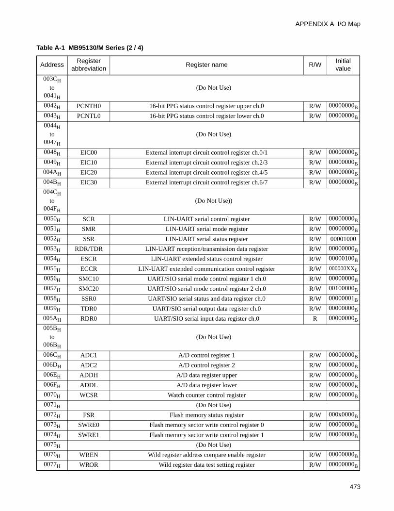
APPENDIX A I/O Map
003CH
to0041H
(Do Not Use)
0042H PCNTH0 16-bit PPG status control register upper ch.0 R/W 00000000B
0043H PCNTL0 16-bit PPG status control register lower ch.0 R/W 00000000B
0044H
to0047H
(Do Not Use)
0048H EIC00 External interrupt circuit control register ch.0/1 R/W 00000000B
0049H EIC10 External interrupt circuit control register ch.2/3 R/W 00000000B
004AH EIC20 External interrupt circuit control register ch.4/5 R/W 00000000B
004BH EIC30 External interrupt circuit control register ch.6/7 R/W 00000000B
004CH
to004FH
(Do Not Use))
0050H SCR LIN-UART serial control register R/W 00000000B
0051H SMR LIN-UART serial mode register R/W 00000000B
0052H SSR LIN-UART serial status register R/W 00001000
0053H RDR/TDR LIN-UART reception/transmission data register R/W 00000000B
0054H ESCR LIN-UART extended status control register R/W 00000100B
0055H ECCR LIN-UART extended communication control register R/W 000000XXB
0056H SMC10 UART/SIO serial mode control register 1 ch.0 R/W 00000000B
0057H SMC20 UART/SIO serial mode control register 2 ch.0 R/W 00100000B
0058H SSR0 UART/SIO serial status and data register ch.0 R/W 00000001B
0059H TDR0 UART/SIO serial output data register ch.0 R/W 00000000B
005AH RDR0 UART/SIO serial input data register ch.0 R 00000000B
005BH
to006BH
(Do Not Use)
006CH ADC1 A/D control register 1 R/W 00000000B
006DH ADC2 A/D control register 2 R/W 00000000B
006EH ADDH A/D data register upper R/W 00000000B
006FH ADDL A/D data register lower R/W 00000000B
0070H WCSR Watch counter control register R/W 00000000B
0071H (Do Not Use)
0072H FSR Flash memory status register R/W 000x0000B
0073H SWRE0 Flash memory sector write control register 0 R/W 00000000B
0074H SWRE1 Flash memory sector write control register 1 R/W 00000000B
0075H (Do Not Use)
0076H WREN Wild register address compare enable register R/W 00000000B
0077H WROR Wild register data test setting register R/W 00000000B
Table A-1 MB95130/M Series (2 / 4)
AddressRegister
abbreviationRegister name R/W
Initial value
473
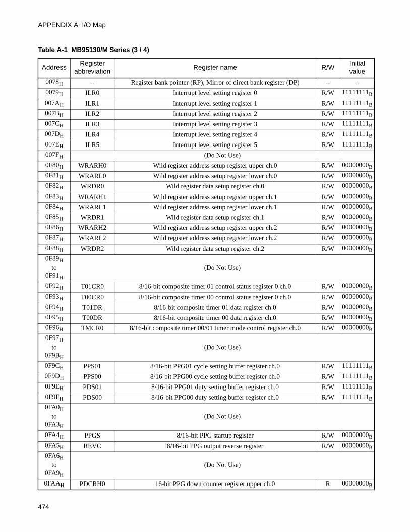
APPENDIX A I/O Map
0078H -- Register bank pointer (RP), Mirror of direct bank register (DP) -- --
0079H ILR0 Interrupt level setting register 0 R/W 11111111B
007AH ILR1 Interrupt level setting register 1 R/W 11111111B
007BH ILR2 Interrupt level setting register 2 R/W 11111111B
007CH ILR3 Interrupt level setting register 3 R/W 11111111B
007DH ILR4 Interrupt level setting register 4 R/W 11111111B
007EH ILR5 Interrupt level setting register 5 R/W 11111111B
007FH (Do Not Use)
0F80H WRARH0 Wild register address setup register upper ch.0 R/W 00000000B
0F81H WRARL0 Wild register address setup register lower ch.0 R/W 00000000B
0F82H WRDR0 Wild register data setup register ch.0 R/W 00000000B
0F83H WRARH1 Wild register address setup register upper ch.1 R/W 00000000B
0F84H WRARL1 Wild register address setup register lower ch.1 R/W 00000000B
0F85H WRDR1 Wild register data setup register ch.1 R/W 00000000B
0F86H WRARH2 Wild register address setup register upper ch.2 R/W 00000000B
0F87H WRARL2 Wild register address setup register lower ch.2 R/W 00000000B
0F88H WRDR2 Wild register data setup register ch.2 R/W 00000000B
0F89H
to0F91H
(Do Not Use)
0F92H T01CR0 8/16-bit composite timer 01 control status register 0 ch.0 R/W 00000000B
0F93H T00CR0 8/16-bit composite timer 00 control status register 0 ch.0 R/W 00000000B
0F94H T01DR 8/16-bit composite timer 01 data register ch.0 R/W 00000000B
0F95H T00DR 8/16-bit composite timer 00 data register ch.0 R/W 00000000B
0F96H TMCR0 8/16-bit composite timer 00/01 timer mode control register ch.0 R/W 00000000B
0F97H
to0F9BH
(Do Not Use)
0F9CH PPS01 8/16-bit PPG01 cycle setting buffer register ch.0 R/W 11111111B
0F9DH PPS00 8/16-bit PPG00 cycle setting buffer register ch.0 R/W 11111111B
0F9EH PDS01 8/16-bit PPG01 duty setting buffer register ch.0 R/W 11111111B
0F9FH PDS00 8/16-bit PPG00 duty setting buffer register ch.0 R/W 11111111B
0FA0H
to0FA3H
(Do Not Use)
0FA4H PPGS 8/16-bit PPG startup register R/W 00000000B
0FA5H REVC 8/16-bit PPG output reverse register R/W 00000000B
0FA6H
to0FA9H
(Do Not Use)
0FAAH PDCRH0 16-bit PPG down counter register upper ch.0 R 00000000B
Table A-1 MB95130/M Series (3 / 4)
AddressRegister
abbreviationRegister name R/W
Initial value
474
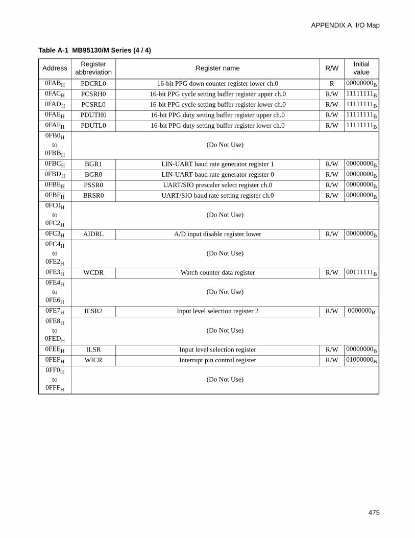
APPENDIX A I/O Map
0FABH PDCRL0 16-bit PPG down counter register lower ch.0 R 00000000B
0FACH PCSRH0 16-bit PPG cycle setting buffer register upper ch.0 R/W 11111111B
0FADH PCSRL0 16-bit PPG cycle setting buffer register lower ch.0 R/W 11111111B
0FAEH PDUTH0 16-bit PPG duty setting buffer register upper ch.0 R/W 11111111B
0FAFH PDUTL0 16-bit PPG duty setting buffer register lower ch.0 R/W 11111111B
0FB0H
to0FBBH
(Do Not Use)
0FBCH BGR1 LIN-UART baud rate generator register 1 R/W 00000000B
0FBDH BGR0 LIN-UART baud rate generator register 0 R/W 00000000B
0FBEH PSSR0 UART/SIO prescaler select register ch.0 R/W 00000000B
0FBFH BRSR0 UART/SIO baud rate setting register ch.0 R/W 00000000B
0FC0H
to0FC2H
(Do Not Use)
0FC3H AIDRL A/D input disable register lower R/W 00000000B
0FC4H
to0FE2H
(Do Not Use)
0FE3H WCDR Watch counter data register R/W 00111111B
0FE4H
to0FE6H
(Do Not Use)
0FE7H ILSR2 Input level selection register 2 R/W 0000000B
0FE8H
to0FEDH
(Do Not Use)
0FEEH ILSR Input level selection register R/W 00000000B
0FEFH WICR Interrupt pin control register R/W 01000000B
0FF0H
to0FFFH
(Do Not Use)
Table A-1 MB95130/M Series (4 / 4)
AddressRegister
abbreviationRegister name R/W
Initial value
475
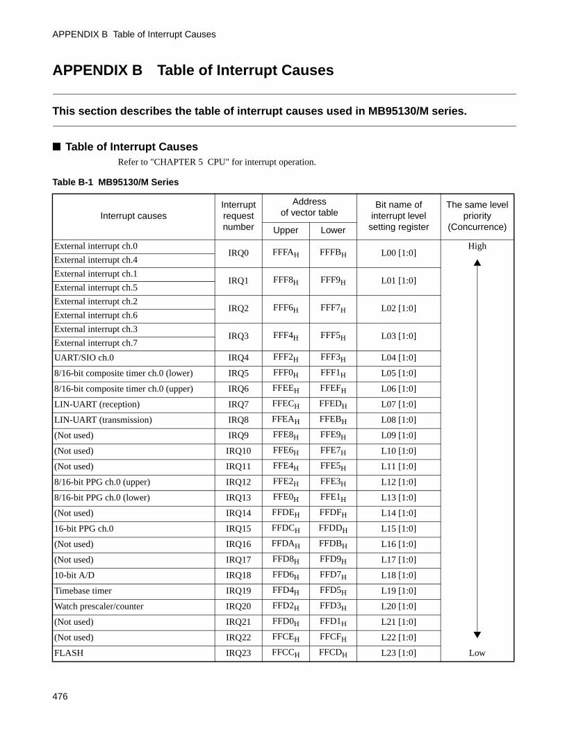
APPENDIX B Table of Interrupt Causes
APPENDIX B Table of Interrupt Causes
This section describes the table of interrupt causes used in MB95130/M series.
Table of Interrupt CausesRefer to "CHAPTER 5 CPU" for interrupt operation.
Table B-1 MB95130/M Series
Interrupt causesInterruptrequest number
Addressof vector table
Bit name of interrupt level
setting register
The same levelpriority
(Concurrence)Upper Lower
External interrupt ch.0IRQ0 FFFAH FFFBH L00 [1:0]
High
External interrupt ch.4
External interrupt ch.1IRQ1 FFF8H FFF9H L01 [1:0]
External interrupt ch.5
External interrupt ch.2IRQ2 FFF6H FFF7H L02 [1:0]
External interrupt ch.6
External interrupt ch.3IRQ3 FFF4H FFF5H L03 [1:0]
External interrupt ch.7
UART/SIO ch.0 IRQ4 FFF2H FFF3H L04 [1:0]
8/16-bit composite timer ch.0 (lower) IRQ5 FFF0H FFF1H L05 [1:0]
8/16-bit composite timer ch.0 (upper) IRQ6 FFEEH FFEFH L06 [1:0]
LIN-UART (reception) IRQ7 FFECH FFEDH L07 [1:0]
LIN-UART (transmission) IRQ8 FFEAH FFEBH L08 [1:0]
(Not used) IRQ9 FFE8H FFE9H L09 [1:0]
(Not used) IRQ10 FFE6H FFE7H L10 [1:0]
(Not used) IRQ11 FFE4H FFE5H L11 [1:0]
8/16-bit PPG ch.0 (upper) IRQ12 FFE2H FFE3H L12 [1:0]
8/16-bit PPG ch.0 (lower) IRQ13 FFE0H FFE1H L13 [1:0]
(Not used) IRQ14 FFDEH FFDFH L14 [1:0]
16-bit PPG ch.0 IRQ15 FFDCH FFDDH L15 [1:0]
(Not used) IRQ16 FFDAH FFDBH L16 [1:0]
(Not used) IRQ17 FFD8H FFD9H L17 [1:0]
10-bit A/D IRQ18 FFD6H FFD7H L18 [1:0]
Timebase timer IRQ19 FFD4H FFD5H L19 [1:0]
Watch prescaler/counter IRQ20 FFD2H FFD3H L20 [1:0]
(Not used) IRQ21 FFD0H FFD1H L21 [1:0]
(Not used) IRQ22 FFCEH FFCFH L22 [1:0]
FLASH IRQ23 FFCCH FFCDH L23 [1:0] Low
476
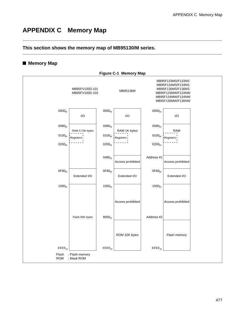
APPENDIX C Memory Map
APPENDIX C Memory Map
This section shows the memory map of MB95130/M series.
Memory Map
Figure C-1 Memory Map
Flash : Flash memoryROM : Mask ROM
MB95FV100D-101MB95FV100D-103
MB95136M
MB95F133MS/F133NSMB95F134MS/F134NSMB95F136MS/F136NS
MB95F133MW/F133NWMB95F134MW/F134NWMB95F136MW/F136NW
0000H
I/O
0000H
I/O
0000H
I/O
0080H 0080H 0080H
RAM 3.75K bytes RAM 1K bytes RAM
0100H Registers0100H Registers
0100H Registers
0200H 0200H 0200H
0480HAccess prohibited
Address #1Access prohibited
0F80H
Extended I/O
0F80H
Extended I/O
0F80H
Extended I/O
1000H 1000H
Access prohibited
1000H
Access prohibited
Flash 60K bytes 8000H Address #2
ROM 32K bytes Flash memory
FFFFH FFFFH FFFFH
477

APPENDIX C Memory Map
Flash memory RAM Address #1 Address #2
MB95F133MS/F133NS8 Kbytes 256 bytes 0180H E000H
MB95F133MW/F133NW
MB95F134MS/F134NS16 Kbytes 512 bytes 0280H C000H
MB95F134MW/F134NW
MB95F136MS/F136NS32 Kbytes 1 Kbytes 0480H 8000H
MB95F136MW/F136NW
478
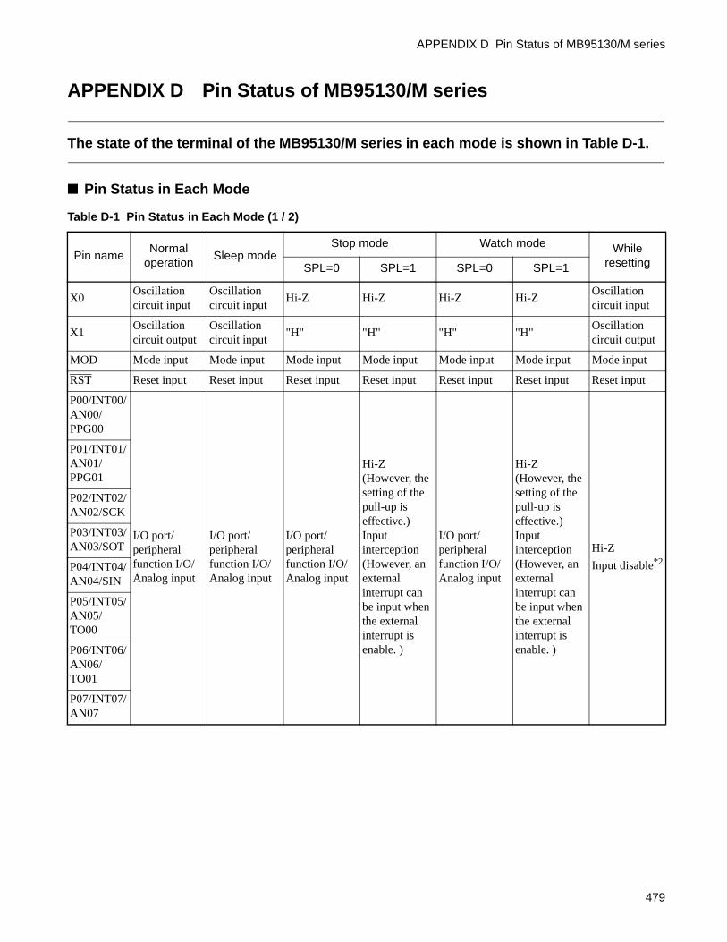
APPENDIX D Pin Status of MB95130/M series
APPENDIX D Pin Status of MB95130/M series
The state of the terminal of the MB95130/M series in each mode is shown in Table D-1.
Pin Status in Each Mode
Table D-1 Pin Status in Each Mode (1 / 2)
Pin nameNormal
operationSleep mode
Stop mode Watch mode While resettingSPL=0 SPL=1 SPL=0 SPL=1
X0Oscillation circuit input
Oscillation circuit input
Hi-Z Hi-Z Hi-Z Hi-ZOscillation circuit input
X1Oscillation circuit output
Oscillation circuit input
"H" "H" "H" "H"Oscillation circuit output
MOD Mode input Mode input Mode input Mode input Mode input Mode input Mode input
RST Reset input Reset input Reset input Reset input Reset input Reset input Reset input
P00/INT00/AN00/PPG00
I/O port/peripheral function I/O/Analog input
I/O port/peripheral function I/O/Analog input
I/O port/peripheral function I/O/Analog input
Hi-Z(However, the setting of the pull-up is effective.) Input interception (However, an external interrupt can be input when the external interrupt is enable. )
I/O port/peripheral function I/O/Analog input
Hi-Z(However, the setting of the pull-up is effective.) Input interception (However, an external interrupt can be input when the external interrupt is enable. )
Hi-Z
Input disable*2
P01/INT01/AN01/PPG01
P02/INT02/AN02/SCK
P03/INT03/AN03/SOT
P04/INT04/AN04/SIN
P05/INT05/AN05/TO00
P06/INT06/AN06/TO01
P07/INT07/AN07
479
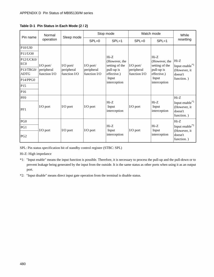
APPENDIX D Pin Status of MB95130/M series
SPL: Pin status specification bit of standby control register (STBC: SPL)
Hi-Z: High impedance
*1: "Input enable" means the input function is possible. Therefore, it is necessary to process the pull-up and the pull-down or to
prevent leakage being generated by the input from the outside. It is the same status as other ports when using it as an output
port.
*2: "Input disable" means direct input gate operation from the terminal is disable status.
P10/UI0
I/O port/peripheral function I/O
I/O port/peripheral function I/O
I/O port/peripheral function I/O
Hi-Z(However, the setting of the pull-up is effective.) Input interception
I/O port/peripheral function I/O
Hi-Z(However, the setting of the pull-up is effective.) Input interception
Hi-Z
Input enable*1
(However, it doesn't function. )
P11/UO0
P12/UCK0/EC0
P13/TRG0/ADTG
P14/PPG0
P15
P16
PF0
I/O port I/O port I/O portHi-Z Input interception
I/O portHi-Z Input interception
Hi-Z
Input enable*1
(However, it doesn't function. )
PF1
PG0
I/O port I/O port I/O portHi-Z Input interception
I/O portHi-Z Input interception
Hi-Z
Input enable*1
(However, it doesn't function. )
PG1
PG2
Table D-1 Pin Status in Each Mode (2 / 2)
Pin nameNormal
operationSleep mode
Stop mode Watch mode While resettingSPL=0 SPL=1 SPL=0 SPL=1
480
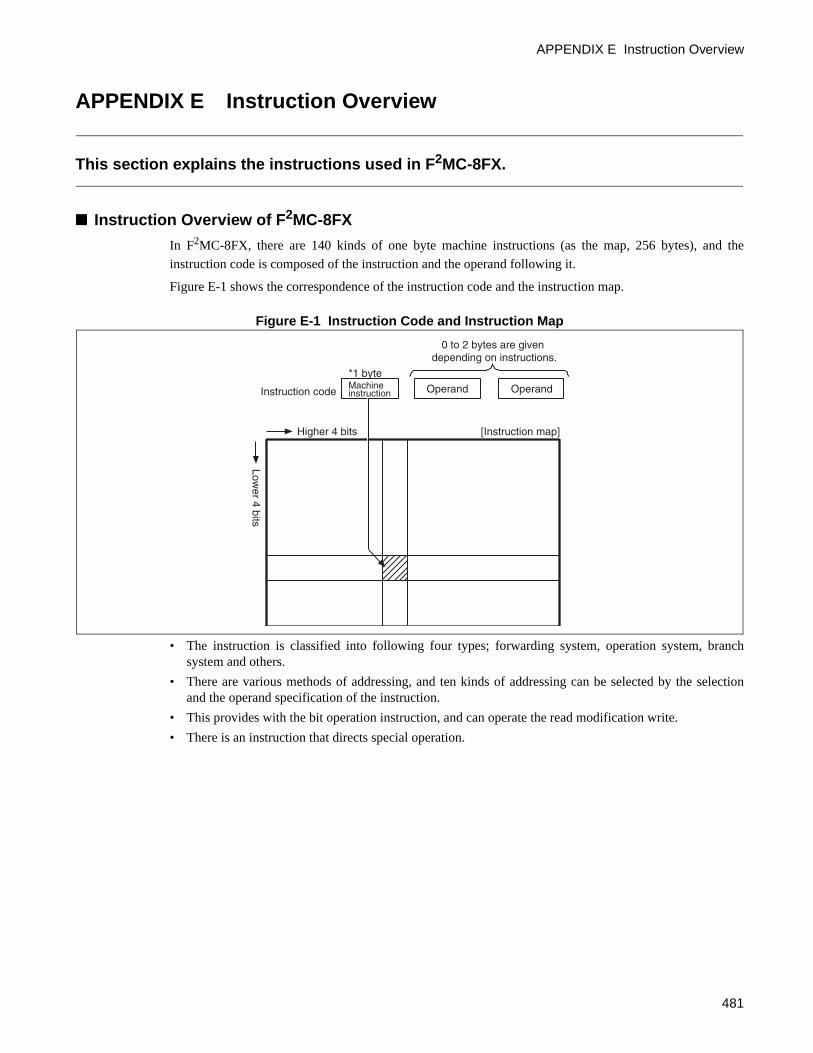
APPENDIX E Instruction Overview
APPENDIX E Instruction Overview
This section explains the instructions used in F2MC-8FX.
Instruction Overview of F2MC-8FX
In F2MC-8FX, there are 140 kinds of one byte machine instructions (as the map, 256 bytes), and the
instruction code is composed of the instruction and the operand following it.
Figure E-1 shows the correspondence of the instruction code and the instruction map.
Figure E-1 Instruction Code and Instruction Map
• The instruction is classified into following four types; forwarding system, operation system, branchsystem and others.
• There are various methods of addressing, and ten kinds of addressing can be selected by the selectionand the operand specification of the instruction.
• This provides with the bit operation instruction, and can operate the read modification write.
• There is an instruction that directs special operation.
Higher 4 bits
Lower 4 bits
*1 byte
[Instruction map]
Machine instructionInstruction code Operand Operand
0 to 2 bytes are given depending on instructions.
481
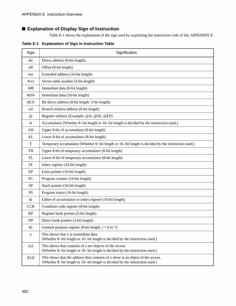
APPENDIX E Instruction Overview
Explanation of Display Sign of InstructionTable E-1 shows the explanation of the sign used by explaining the instruction code of this APPENDIX E.
Table E-1 Explanation of Sign in Instruction Table
Sign Signification
dir Direct address (8-bit length)
off Offset (8-bit length)
ext Extended address (16-bit length)
#vct Vector table number (3-bit length)
#d8 Immediate data (8-bit length)
#d16 Immediate data (16-bit length)
dir:b Bit direct address (8-bit length: 3-bit length)
rel Branch relative address (8-bit length)
@ Register indirect (Example: @A, @IX, @EP)
A Accumulator (Whether 8- bit length or 16- bit length is decided by the instruction used.)
AH Upper 8-bit of accumulator (8-bit length)
AL Lower 8-bit of accumulator (8-bit length)
T Temporary accumulator (Whether 8- bit length or 16- bit length is decided by the instruction used.)
TH Upper 8-bit of temporary accumulator (8-bit length)
TL Lower 8-bit of temporary accumulator (8-bit length)
IX Index register (16-bit length)
EP Extra pointer (16-bit length)
PC Program counter (16-bit length)
SP Stack pointer (16-bit length)
PS Program status (16-bit length)
dr Either of accumulator or index register (16-bit length)
CCR Condition code register (8-bit length)
RP Register bank pointer (5-bit length)
DP Direct bank pointer (3-bit length)
Ri General-purpose register (8-bit length, i = 0 to 7)
x This shows that x is immediate data.(Whether 8- bit length or 16- bit length is decided by the instruction used.)
(x) This shows that contents of x are objects of the access.(Whether 8- bit length or 16- bit length is decided by the instruction used.)
((x)) This shows that the address that contents of x show is an object of the access.(Whether 8- bit length or 16- bit length is decided by the instruction used.)
482
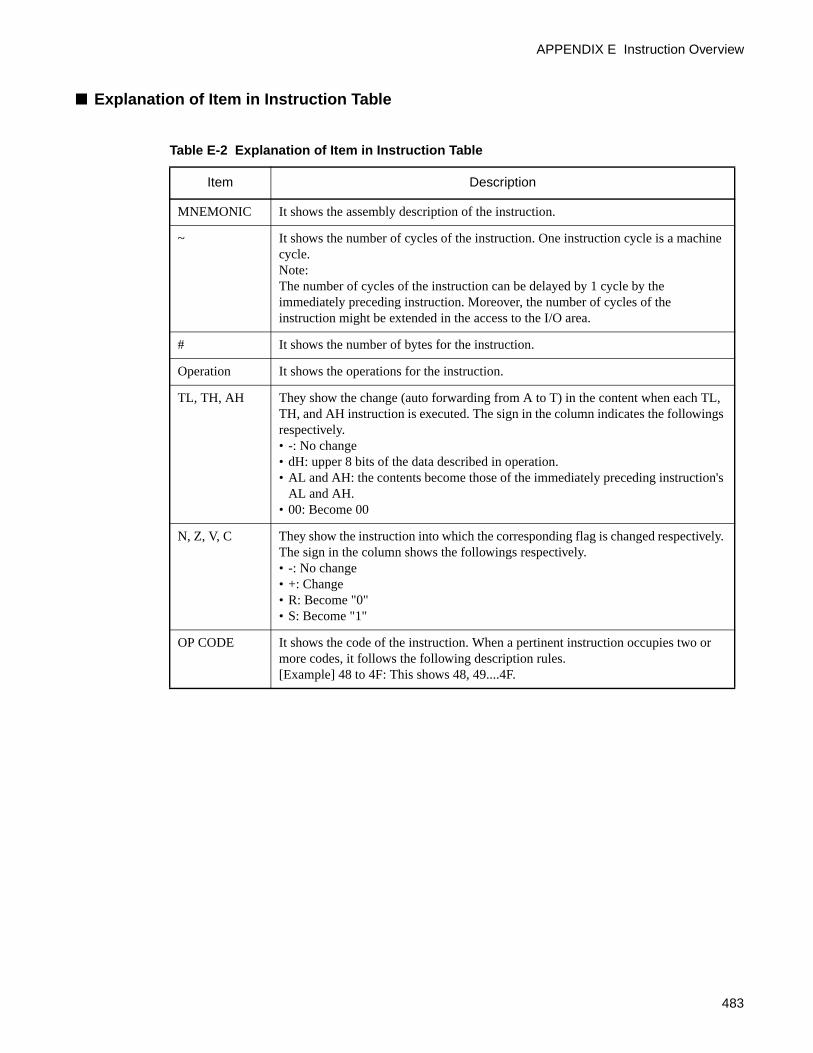
APPENDIX E Instruction Overview
Explanation of Item in Instruction Table
Table E-2 Explanation of Item in Instruction Table
Item Description
MNEMONIC It shows the assembly description of the instruction.
~ It shows the number of cycles of the instruction. One instruction cycle is a machine cycle.Note:The number of cycles of the instruction can be delayed by 1 cycle by the immediately preceding instruction. Moreover, the number of cycles of the instruction might be extended in the access to the I/O area.
# It shows the number of bytes for the instruction.
Operation It shows the operations for the instruction.
TL, TH, AH They show the change (auto forwarding from A to T) in the content when each TL, TH, and AH instruction is executed. The sign in the column indicates the followings respectively.• -: No change• dH: upper 8 bits of the data described in operation.• AL and AH: the contents become those of the immediately preceding instruction's
AL and AH.• 00: Become 00
N, Z, V, C They show the instruction into which the corresponding flag is changed respectively. The sign in the column shows the followings respectively.• -: No change• +: Change• R: Become "0"• S: Become "1"
OP CODE It shows the code of the instruction. When a pertinent instruction occupies two or more codes, it follows the following description rules.[Example] 48 to 4F: This shows 48, 49....4F.
483
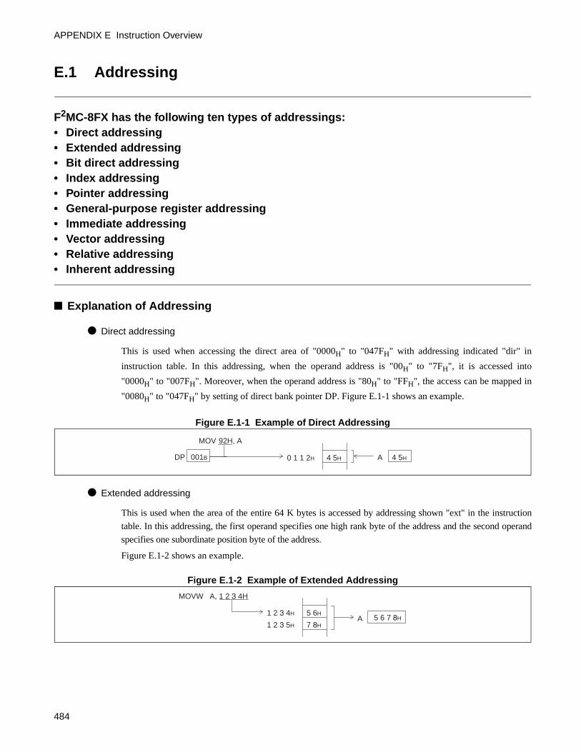
APPENDIX E Instruction Overview
E.1 Addressing
F2MC-8FX has the following ten types of addressings: • Direct addressing• Extended addressing• Bit direct addressing• Index addressing• Pointer addressing• General-purpose register addressing• Immediate addressing• Vector addressing• Relative addressing• Inherent addressing
Explanation of Addressing
Direct addressing
This is used when accessing the direct area of "0000H" to "047FH" with addressing indicated "dir" in
instruction table. In this addressing, when the operand address is "00H" to "7FH", it is accessed into
"0000H" to "007FH". Moreover, when the operand address is "80H" to "FFH", the access can be mapped in
"0080H" to "047FH" by setting of direct bank pointer DP. Figure E.1-1 shows an example.
Figure E.1-1 Example of Direct Addressing
Extended addressing
This is used when the area of the entire 64 K bytes is accessed by addressing shown "ext" in the instruction
table. In this addressing, the first operand specifies one high rank byte of the address and the second operand
specifies one subordinate position byte of the address.
Figure E.1-2 shows an example.
Figure E.1-2 Example of Extended Addressing
MOV 92H, A
4 5H 4 5HA0 1 1 2H001BDP
1 2 3 4H
MOVW A, 1 2 3 4H
5 6 7 8HA5 6H
7 8H1 2 3 5H
484
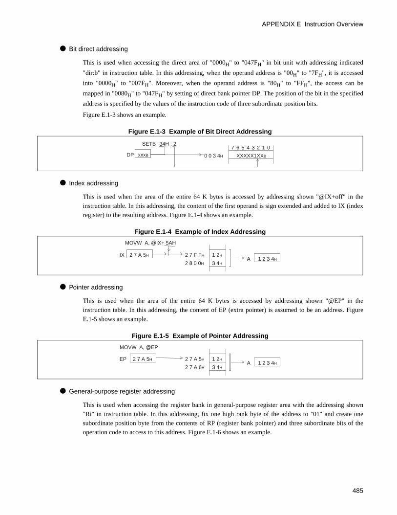
APPENDIX E Instruction Overview
Bit direct addressing
This is used when accessing the direct area of "0000H" to "047FH" in bit unit with addressing indicated
"dir:b" in instruction table. In this addressing, when the operand address is "00H" to "7FH", it is accessed
into "0000H" to "007FH". Moreover, when the operand address is "80H" to "FFH", the access can be
mapped in "0080H" to "047FH" by setting of direct bank pointer DP. The position of the bit in the specified
address is specified by the values of the instruction code of three subordinate position bits.
Figure E.1-3 shows an example.
Figure E.1-3 Example of Bit Direct Addressing
Index addressing
This is used when the area of the entire 64 K bytes is accessed by addressing shown "@IX+off" in the
instruction table. In this addressing, the content of the first operand is sign extended and added to IX (index
register) to the resulting address. Figure E.1-4 shows an example.
Figure E.1-4 Example of Index Addressing
Pointer addressing
This is used when the area of the entire 64 K bytes is accessed by addressing shown "@EP" in the
instruction table. In this addressing, the content of EP (extra pointer) is assumed to be an address. Figure
E.1-5 shows an example.
Figure E.1-5 Example of Pointer Addressing
General-purpose register addressing
This is used when accessing the register bank in general-purpose register area with the addressing shown
"Ri" in instruction table. In this addressing, fix one high rank byte of the address to "01" and create one
subordinate position byte from the contents of RP (register bank pointer) and three subordinate bits of the
operation code to access to this address. Figure E.1-6 shows an example.
SETB 34H : 2
XXXXX1XXB0 0 3 4H
7 6 5 4 3 2 1 0xxxBDP
2 7 F FH
MOVW A, @IX+ 5AH
1 2 3 4HA1 2H
3 4H2 8 0 0H
2 7 A 5HIX
2 7 A 5H
MOVW A, @EP
1 2 3 4HA1 2H
3 4H2 7 A 6H
2 7 A 5HEP
485
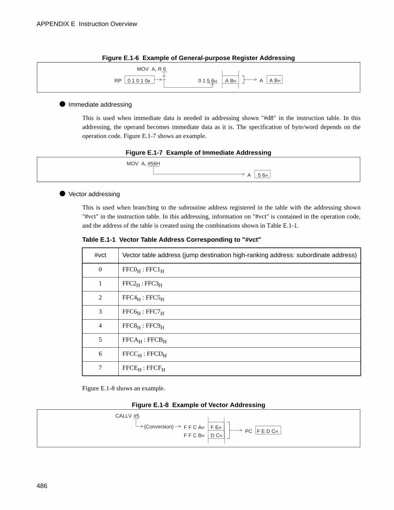
APPENDIX E Instruction Overview
Figure E.1-6 Example of General-purpose Register Addressing
Immediate addressing
This is used when immediate data is needed in addressing shown "#d8" in the instruction table. In this
addressing, the operand becomes immediate data as it is. The specification of byte/word depends on the
operation code. Figure E.1-7 shows an example.
Figure E.1-7 Example of Immediate Addressing
Vector addressing
This is used when branching to the subroutine address registered in the table with the addressing shown
"#vct" in the instruction table. In this addressing, information on "#vct" is contained in the operation code,
and the address of the table is created using the combinations shown in Table E.1-1.
Figure E.1-8 shows an example.
Figure E.1-8 Example of Vector Addressing
0 1 5 6H
MOV A, R 6
A BHAA BH0 1 0 1 0BRP
MOV A, #56H
5 6HA
Table E.1-1 Vector Table Address Corresponding to "#vct"
#vct Vector table address (jump destination high-ranking address: subordinate address)
0 FFC0H : FFC1H
1 FFC2H : FFC3H
2 FFC4H : FFC5H
3 FFC6H : FFC7H
4 FFC8H : FFC9H
5 FFCAH : FFCBH
6 FFCCH : FFCDH
7 FFCEH : FFCFH
F F C AH
CALLV #5
F E D CHPCF EH
D CHF F C BH
(Conversion)
486
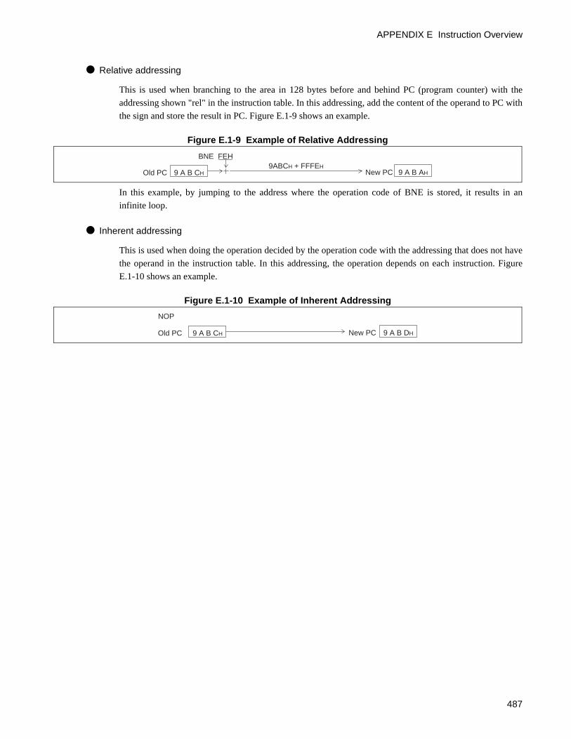
APPENDIX E Instruction Overview
Relative addressing
This is used when branching to the area in 128 bytes before and behind PC (program counter) with the
addressing shown "rel" in the instruction table. In this addressing, add the content of the operand to PC with
the sign and store the result in PC. Figure E.1-9 shows an example.
Figure E.1-9 Example of Relative Addressing
In this example, by jumping to the address where the operation code of BNE is stored, it results in an
infinite loop.
Inherent addressing
This is used when doing the operation decided by the operation code with the addressing that does not have
the operand in the instruction table. In this addressing, the operation depends on each instruction. Figure
E.1-10 shows an example.
Figure E.1-10 Example of Inherent Addressing
9 A B AH
BNE FEH
New PC9 A B CHOld PC9ABCH + FFFEH
9 A B DH
NOP
New PC9 A B CHOld PC
487
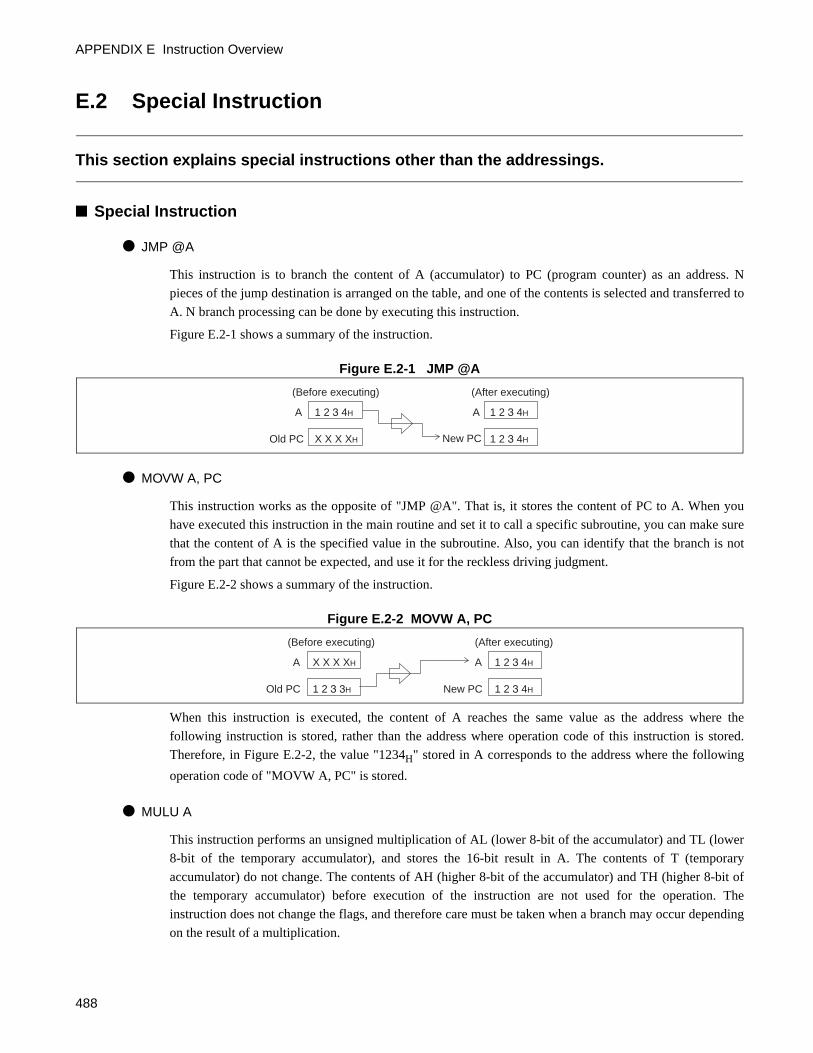
APPENDIX E Instruction Overview
E.2 Special Instruction
This section explains special instructions other than the addressings.
Special Instruction
JMP @A
This instruction is to branch the content of A (accumulator) to PC (program counter) as an address. N
pieces of the jump destination is arranged on the table, and one of the contents is selected and transferred to
A. N branch processing can be done by executing this instruction.
Figure E.2-1 shows a summary of the instruction.
Figure E.2-1 JMP @A
MOVW A, PC
This instruction works as the opposite of "JMP @A". That is, it stores the content of PC to A. When you
have executed this instruction in the main routine and set it to call a specific subroutine, you can make sure
that the content of A is the specified value in the subroutine. Also, you can identify that the branch is not
from the part that cannot be expected, and use it for the reckless driving judgment.
Figure E.2-2 shows a summary of the instruction.
Figure E.2-2 MOVW A, PC
When this instruction is executed, the content of A reaches the same value as the address where the
following instruction is stored, rather than the address where operation code of this instruction is stored.
Therefore, in Figure E.2-2, the value "1234H" stored in A corresponds to the address where the following
operation code of "MOVW A, PC" is stored.
MULU A
This instruction performs an unsigned multiplication of AL (lower 8-bit of the accumulator) and TL (lower
8-bit of the temporary accumulator), and stores the 16-bit result in A. The contents of T (temporary
accumulator) do not change. The contents of AH (higher 8-bit of the accumulator) and TH (higher 8-bit of
the temporary accumulator) before execution of the instruction are not used for the operation. The
instruction does not change the flags, and therefore care must be taken when a branch may occur depending
on the result of a multiplication.
1 2 3 4HA
X X X XHOld PC
1 2 3 4HA
New PC
(Before executing) (After executing)
1 2 3 4H
X X X XH
1 2 3 3H
A
Old PC
1 2 3 4HA
New PC
(Before executing) (After executing)
1 2 3 4H
488
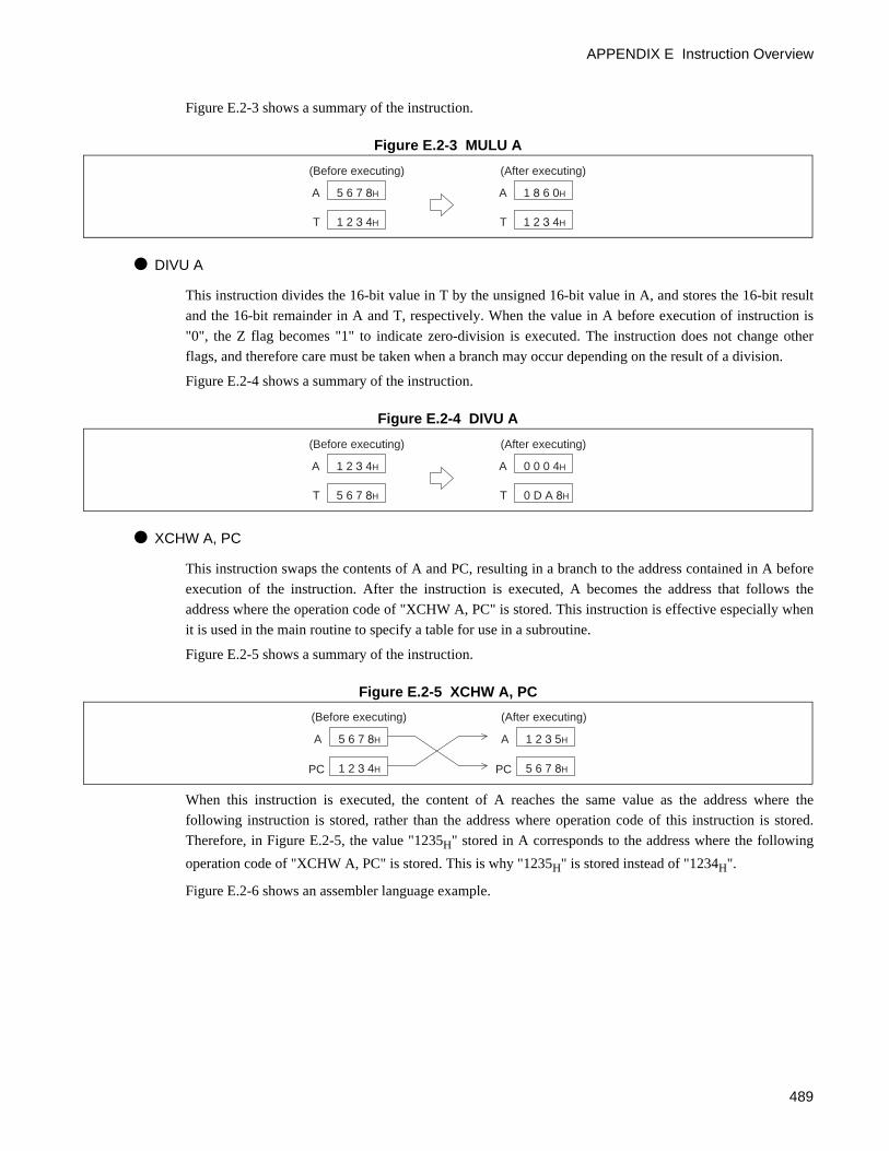
APPENDIX E Instruction Overview
Figure E.2-3 shows a summary of the instruction.
Figure E.2-3 MULU A
DIVU A
This instruction divides the 16-bit value in T by the unsigned 16-bit value in A, and stores the 16-bit result
and the 16-bit remainder in A and T, respectively. When the value in A before execution of instruction is
"0", the Z flag becomes "1" to indicate zero-division is executed. The instruction does not change other
flags, and therefore care must be taken when a branch may occur depending on the result of a division.
Figure E.2-4 shows a summary of the instruction.
Figure E.2-4 DIVU A
XCHW A, PC
This instruction swaps the contents of A and PC, resulting in a branch to the address contained in A before
execution of the instruction. After the instruction is executed, A becomes the address that follows the
address where the operation code of "XCHW A, PC" is stored. This instruction is effective especially when
it is used in the main routine to specify a table for use in a subroutine.
Figure E.2-5 shows a summary of the instruction.
Figure E.2-5 XCHW A, PC
When this instruction is executed, the content of A reaches the same value as the address where the
following instruction is stored, rather than the address where operation code of this instruction is stored.
Therefore, in Figure E.2-5, the value "1235H" stored in A corresponds to the address where the following
operation code of "XCHW A, PC" is stored. This is why "1235H" is stored instead of "1234H".
Figure E.2-6 shows an assembler language example.
1 2 3 4H
A
T
1 8 6 0HA
T
(Before executing) (After executing)
1 2 3 4H
5 6 7 8H
5 6 7 8H
A
T
0 0 0 4HA
T
(Before executing) (After executing)
0 D A 8H
1 2 3 4H
1 2 3 4H
A
PC
1 2 3 5HA
PC
(Before executing) (After executing)
5 6 7 8H
5 6 7 8H
489
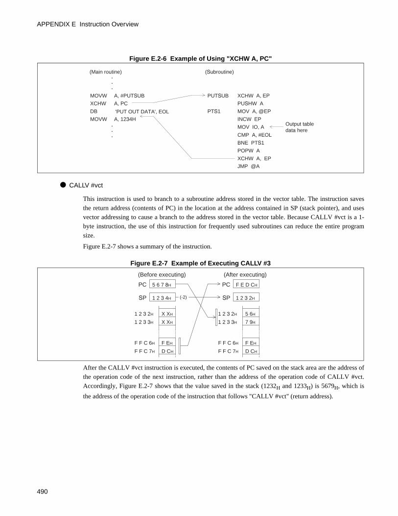
APPENDIX E Instruction Overview
Figure E.2-6 Example of Using "XCHW A, PC"
CALLV #vct
This instruction is used to branch to a subroutine address stored in the vector table. The instruction saves
the return address (contents of PC) in the location at the address contained in SP (stack pointer), and uses
vector addressing to cause a branch to the address stored in the vector table. Because CALLV #vct is a 1-
byte instruction, the use of this instruction for frequently used subroutines can reduce the entire program
size.
Figure E.2-7 shows a summary of the instruction.
Figure E.2-7 Example of Executing CALLV #3
After the CALLV #vct instruction is executed, the contents of PC saved on the stack area are the address of
the operation code of the next instruction, rather than the address of the operation code of CALLV #vct.
Accordingly, Figure E.2-7 shows that the value saved in the stack (1232H and 1233H) is 5679H, which is
the address of the operation code of the instruction that follows "CALLV #vct" (return address).
MOVW
XCHW
DB
MOVW
A, #PUTSUB
A, PC
'PUT OUT DATA', EOLA, 1234H
(Main routine)
XCHW A, EP
PUSHW A
MOV A, @EP
INCW EP
MOV IO, A
CMP A, #EOL
BNE PTS1
POPW A
XCHW A, EP
JMP @A
PUTSUB
PTS1
(Subroutine)
Output table data here
1 2 3 4H
PC
SP
F E D CHPC
SP
(Before executing) (After executing)
1 2 3 2H
5 6 7 8H
1 2 3 2H
1 2 3 3H
X XH
X XH
F EH
D CH
F F C 6H
F F C 7H
1 2 3 2H
1 2 3 3H
5 6H
7 9H
F EH
D CH
F F C 6H
F F C 7H
(-2)
490
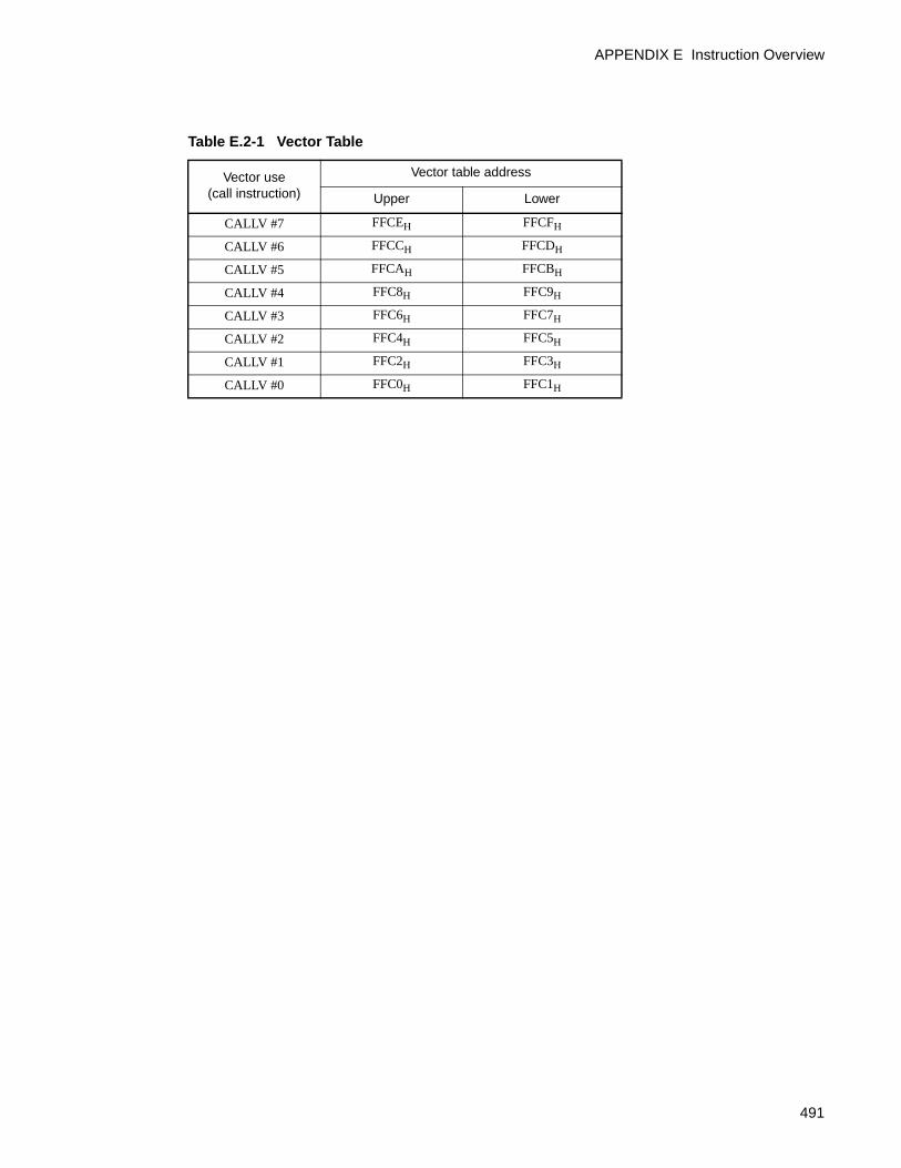
APPENDIX E Instruction Overview
Table E.2-1 Vector Table
Vector use(call instruction)
Vector table address
Upper Lower
CALLV #7 FFCEH FFCFH
CALLV #6 FFCCH FFCDH
CALLV #5 FFCAH FFCBH
CALLV #4 FFC8H FFC9H
CALLV #3 FFC6H FFC7H
CALLV #2 FFC4H FFC5H
CALLV #1 FFC2H FFC3H
CALLV #0 FFC0H FFC1H
491
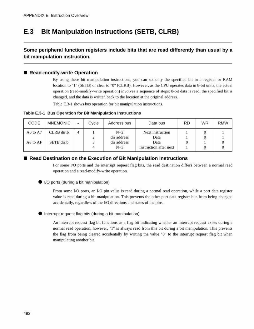
APPENDIX E Instruction Overview
E.3 Bit Manipulation Instructions (SETB, CLRB)
Some peripheral function registers include bits that are read differently than usual by abit manipulation instruction.
Read-modify-write OperationBy using these bit manipulation instructions, you can set only the specified bit in a register or RAM
location to "1" (SETB) or clear to "0" (CLRB). However, as the CPU operates data in 8-bit units, the actual
operation (read-modify-write operation) involves a sequence of steps: 8-bit data is read, the specified bit is
changed, and the data is written back to the location at the original address.
Table E.3-1 shows bus operation for bit manipulation instructions.
Read Destination on the Execution of Bit Manipulation InstructionsFor some I/O ports and the interrupt request flag bits, the read destination differs between a normal read
operation and a read-modify-write operation.
I/O ports (during a bit manipulation)
From some I/O ports, an I/O pin value is read during a normal read operation, while a port data register
value is read during a bit manipulation. This prevents the other port data register bits from being changed
accidentally, regardless of the I/O directions and states of the pins.
Interrupt request flag bits (during a bit manipulation)
An interrupt request flag bit functions as a flag bit indicating whether an interrupt request exists during a
normal read operation, however, "1" is always read from this bit during a bit manipulation. This prevents
the flag from being cleared accidentally by writing the value "0" to the interrupt request flag bit when
manipulating another bit.
Table E.3-1 Bus Operation for Bit Manipulation Instructions
CODE MNEMONIC ~ Cycle Address bus Data bus RD WR RMW
A0 to A7
A8 to AF
CLRB dir:b
SETB dir:b
4 1234
N+2dir addressdir address
N+3
Next instructionDataData
Instruction after next
1101
0010
1100
492
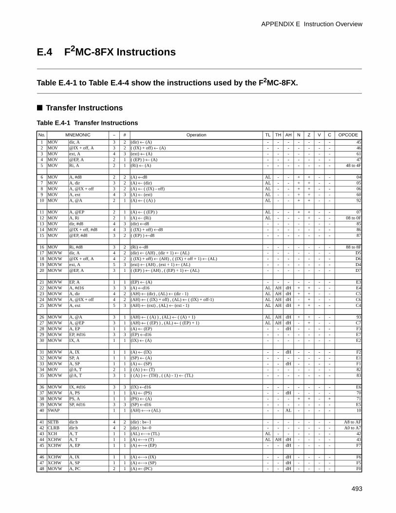
APPENDIX E Instruction Overview
E.4 F2MC-8FX Instructions
Table E.4-1 to Table E.4-4 show the instructions used by the F2MC-8FX.
Transfer Instructions
Table E.4-1 Transfer Instructions
No. MNEMONIC ~ # Operation TL TH AH N Z V C OPCODE
1 MOV dir, A 3 2 (dir) ← (A) - - - - - - - 452 MOV @IX + off, A 3 2 ( (IX) + off) ← (A) - - - - - - - 463 MOV ext, A 4 3 (ext) ← (A) - - - - - - - 614 MOV @EP, A 2 1 ( (EP) ) ← (A) - - - - - - - 475 MOV Ri, A 2 1 (Ri) ← (A) - - - - - - - 48 to 4F
6 MOV A, #d8 2 2 (A) ←d8 AL - - + + - - 047 MOV A, dir 3 2 (A) ← (dir) AL - - + + - - 058 MOV A, @IX + off 3 2 (A) ← ( (IX) - off) AL - - + + - - 069 MOV A, ext 4 3 (A) ← (ext) AL - - + + - - 6010 MOV A, @A 2 1 (A) ← ( (A) ) AL - - + + - - 92
11 MOV A, @EP 2 1 (A) ← ( (EP) ) AL - - + + - - 0712 MOV A, Ri 2 1 (A) ← (Ri) AL - - - + - - 08 to 0F13 MOV dir, #d8 4 3 (dir) ←d8 - - - - - - - 8514 MOV @IX + off, #d8 4 3 ( (IX) + off) ←d8 - - - - - - - 8615 MOV @EP, #d8 3 2 ( (EP) ) ←d8 - - - - - - - 87
16 MOV Ri, #d8 3 2 (Ri) ←d8 - - - - - - - 88 to 8F17 MOVW dir, A 4 2 (dir) ← (AH) , (dir + 1) ← (AL) - - - - - - - D518 MOVW @IX + off, A 4 2 ( (IX) + off) ← (AH) , ( (IX) + off + 1) ← (AL) - - - - - - - D619 MOVW ext, A 5 3 (ext) ← (AH) , (ext + 1) ← (AL) - - - - - - - D420 MOVW @EP, A 3 1 ( (EP) ) ← (AH) , ( (EP) + 1) ← (AL) - - - - - - - D7
21 MOVW EP, A 1 1 (EP) ← (A) - - - - - - - E322 MOVW A, #d16 3 3 (A) ←d16 AL AH dH + + - - E423 MOVW A, dir 4 2 (AH) ← (dir) , (AL) ← (dir - 1) AL AH dH + + - - C524 MOVW A, @IX + off 4 2 (AH) ← ( (IX) + off) , (AL) ← ( (IX) + off-1) AL AH dH - + - - C625 MOVW A, ext 5 3 (AH) ← (ext) , (AL) ← (ext - 1) AL AH dH + + - - C4
26 MOVW A, @A 3 1 (AH) ← ( (A) ) , (AL) ← ( (A) + 1) AL AH dH + + - - 9327 MOVW A, @EP 3 1 (AH) ← ( (EP) ) , (AL) ← ( (EP) + 1) AL AH dH - + - - C728 MOVW A, EP 1 1 (A) ← (EP) - - dH - - - - F329 MOVW EP, #d16 3 3 (EP) ←d16 - - - - - - - E730 MOVW IX, A 1 1 (IX) ← (A) - - - - - - - E2
31 MOVW A, IX 1 1 (A) ← (IX) - - dH - - - - F232 MOVW SP, A 1 1 (SP) ← (A) - - - - - - - E133 MOVW A, SP 1 1 (A) ← (SP) - - dH - - - - F134 MOV @A, T 2 1 ( (A) ) ← (T) - - - - - - - 8235 MOVW @A, T 3 1 ( (A) ) ← (TH) , ( (A) - 1) ← (TL) - - - - - - - 83
36 MOVW IX, #d16 3 3 (IX) ←d16 - - - - - - - E637 MOVW A, PS 1 1 (A) ← (PS) - - dH - - - - 7038 MOVW PS, A 1 1 (PS) ← (A) - - - + + - + 7139 MOVW SP, #d16 3 3 (SP) ←d16 - - - - - - - E540 SWAP 1 1 (AH) ←→ (AL) - - AL - - - - 10
41 SETB dir:b 4 2 (dir) : b←1 - - - - - - - A8 to AF42 CLRB dir:b 4 2 (dir) : b←0 - - - - - - - A0 to A743 XCH A, T 1 1 (AL) ←→ (TL) AL - - - - - - 4244 XCHW A, T 1 1 (A) ←→ (T) AL AH dH - - - - 4345 XCHW A, EP 1 1 (A) ←→ (EP) - - dH - - - - F7
46 XCHW A, IX 1 1 (A) ←→ (IX) - - dH - - - - F647 XCHW A, SP 1 1 (A) ←→ (SP) - - dH - - - - F548 MOVW A, PC 2 1 (A) ← (PC) - - dH - - - - F0
493
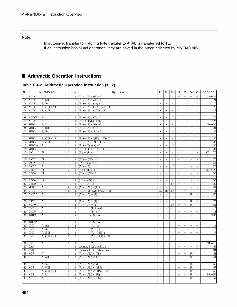
APPENDIX E Instruction Overview
Note:
In automatic transfer to T during byte transfer to A, AL is transferred to TL.If an instruction has plural operands, they are saved in the order indicated by MNEMONIC.
Arithmetic Operation Instructions
Table E.4-2 Arithmetic Operation Instruction (1 / 2)
No. MNEMONIC ~ # Operation TL TH AH N Z V C OPCODE
1 ADDC A, Ri 2 1 (A) ← (A) + (Ri) + C - - - + + + + 28 to 2F2 ADDC A, #d8 2 2 (A) ← (A) + d8 + C - - - + + + + 243 ADDC A, dir 3 2 (A) ← (A) + (dir) + C - - - + + + + 254 ADDC A, @IX + off 3 2 (A) ← (A) + ( (IX) + off) + C - - - + + + + 265 ADDC A, @EP 2 1 (A) ← (A) + ( (EP) ) + C - - - + + + + 27
6 ADDCW A 1 1 (A) ← (A) + (T) + C - - dH + + + + 237 ADDC A 1 1 (AL) ← (AL) + (TL) + C - - - + + + + 228 SUBC A, Ri 2 1 (A) ← (A) - (Ri) - C - - - + + + + 38 to 3F9 SUBC A, #d8 2 2 (A) ← (A) - d8 - C - - - + + + + 3410 SUBC A, dir 3 2 (A) ← (A) - (dir) - C - - - + + + + 35
11 SUBC A, @IX + off 3 2 (A) ← (A) - ( (IX) + off) - C - - - + + + + 3612 SUBC A, @EP 2 1 (A) ← (A) - ( (EP) ) - C - - - + + + + 3713 SUBCW A 1 1 (A) ← (T) - (A) - C - - dH + + + + 3314 SUBC A 1 1 (AL) ← (TL) - (AL) - C - - - + + + + 3215 INC Ri 3 1 (Ri) ← (Ri) + 1 - - - + + + - C8 to CF
16 INCW EP 1 1 (EP) ← (EP) + 1 - - - - - - - C317 INCW IX 1 1 (IX) ← (IX) + 1 - - - - - - - C218 INCW A 1 1 (A) ← (A) + 1 - - dH + + - - C019 DEC Ri 3 1 (Ri) ← (Ri) - 1 - - - + + + - D8 to DF20 DECW EP 1 1 (EP) ← (EP) - 1 - - - - - - - D3
21 DECW IX 1 1 (IX) ← (IX) - 1 - - - - - - - D222 DECW A 1 1 (A) ← (A) - 1 - - dH + + - - D023 MULU A 8 1 (A) ← (AL) × (TL) - - dH - - - - 0124 DIVU A 17 1 (A) ← (T) / (A) , MOD→ (T) dL dH dH - + - - 1125 ANDW A 1 1 (A) ← (A) (T) - - dH + + R - 63
26 ORW A 1 1 (A) ← (A) (T) - - dH + + R - 7327 XORW A 1 1 (A) ← (A) (T) - - dH + + R - 5328 CMP A 1 1 (TL) - (AL) - - - + + + + 1229 CMPW A 1 1 (T) - (A) - - - + + + + 1330 RORC A 1 1 - - - + + - + 0302
31 ROLCA 1 1 - - - + + - + 32 CMP A, #d8 2 2 (A) - d8 - - - + + + + 1433 CMP A, dir 3 2 (A) - (dir) - - - + + + + 1534 CMP A, @EP 2 1 (A) - ( (EP) ) - - - + + + + 1735 CMP A, @IX + off 3 2 (A) - ( (IX) + off) - - - + + + + 16
36 CMP A, Ri 2 1 (A) - (Ri) - - - + + + + 18 to 1F37 DAA 1 1 decimaladjustforaddition - - - + + + + 8438 DAS 1 1 decimaladjustforsubtraction - - - + + + + 9439 XOR A 1 1 (A) ← (AL) (TL) - - - + + R - 5240 XOR A, #d8 2 2 (A) ← (AL) d8 - - - + + R - 54
41 XOR A, dir 3 2 (A) ← (AL) (dir) - - - + + R - 5542 XOR A, @EP 2 1 (A) ← (AL) ( (EP) ) - - - + + R - 5743 XOR A, @IX + off 3 2 (A) ← (AL) ( (IX) + off) - - - + + R - 5644 XOR A, Ri 2 1 (A) ← (AL) (Ri) - - - + + R - 58 to 5F45 AND A 1 1 (A) ← (AL) (TL) - - - + + R - 62
C→A
C←A
494
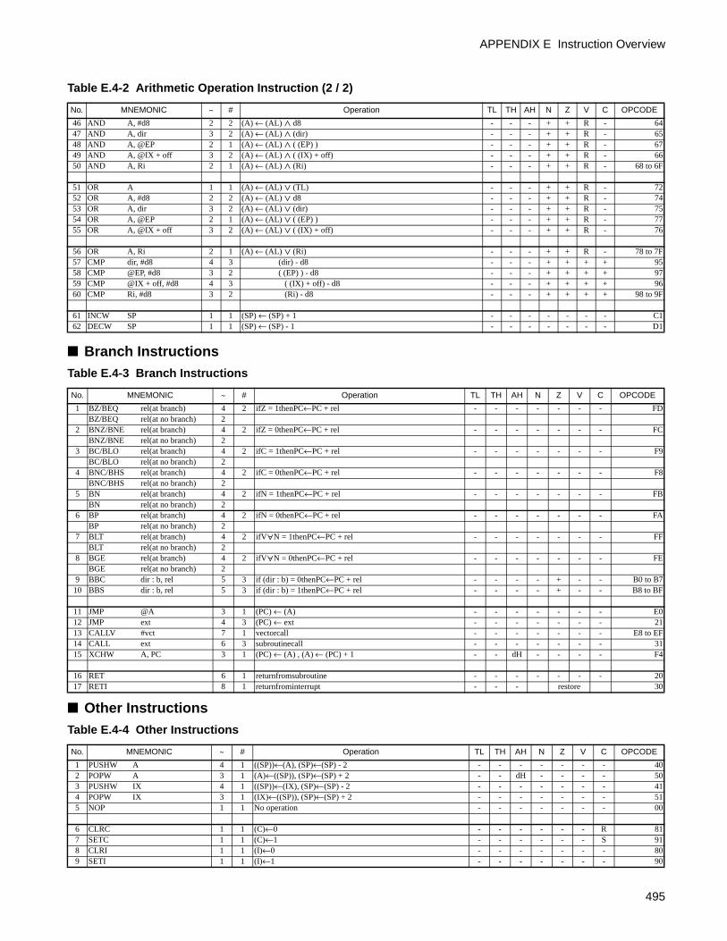
APPENDIX E Instruction Overview
Branch Instructions
Other Instructions
46 AND A, #d8 2 2 (A) ← (AL) d8 - - - + + R - 6447 AND A, dir 3 2 (A) ← (AL) (dir) - - - + + R - 6548 AND A, @EP 2 1 (A) ← (AL) ( (EP) ) - - - + + R - 6749 AND A, @IX + off 3 2 (A) ← (AL) ( (IX) + off) - - - + + R - 6650 AND A, Ri 2 1 (A) ← (AL) (Ri) - - - + + R - 68 to 6F
51 OR A 1 1 (A) ← (AL) (TL) - - - + + R - 7252 OR A, #d8 2 2 (A) ← (AL) d8 - - - + + R - 7453 OR A, dir 3 2 (A) ← (AL) (dir) - - - + + R - 7554 OR A, @EP 2 1 (A) ← (AL) ( (EP) ) - - - + + R - 7755 OR A, @IX + off 3 2 (A) ← (AL) ( (IX) + off) - - - + + R - 76
56 OR A, Ri 2 1 (A) ← (AL) (Ri) - - - + + R - 78 to 7F57 CMP dir, #d8 4 3 (dir) - d8 - - - + + + + 9558 CMP @EP, #d8 3 2 ( (EP) ) - d8 - - - + + + + 9759 CMP @IX + off, #d8 4 3 ( (IX) + off) - d8 - - - + + + + 9660 CMP Ri, #d8 3 2 (Ri) - d8 - - - + + + + 98 to 9F
61 INCW SP 1 1 (SP) ← (SP) + 1 - - - - - - - C162 DECW SP 1 1 (SP) ← (SP) - 1 - - - - - - - D1
Table E.4-3 Branch Instructions
No. MNEMONIC ~ # Operation TL TH AH N Z V C OPCODE
1 BZ/BEQ rel(at branch) 4 2 ifZ = 1thenPC←PC + rel - - - - - - - FDBZ/BEQ rel(at no branch) 2
2 BNZ/BNE rel(at branch) 4 2 ifZ = 0thenPC←PC + rel - - - - - - - FCBNZ/BNE rel(at no branch) 2
3 BC/BLO rel(at branch) 4 2 ifC = 1thenPC←PC + rel - - - - - - - F9BC/BLO rel(at no branch) 2
4 BNC/BHS rel(at branch) 4 2 ifC = 0thenPC←PC + rel - - - - - - - F8BNC/BHS rel(at no branch) 2
5 BN rel(at branch) 4 2 ifN = 1thenPC←PC + rel - - - - - - - FBBN rel(at no branch) 2
6 BP rel(at branch) 4 2 ifN = 0thenPC←PC + rel - - - - - - - FABP rel(at no branch) 2
7 BLT rel(at branch) 4 2 ifV N = 1thenPC←PC + rel - - - - - - - FFBLT rel(at no branch) 2
8 BGE rel(at branch) 4 2 ifV N = 0thenPC←PC + rel - - - - - - - FEBGE rel(at no branch) 2
9 BBC dir : b, rel 5 3 if (dir : b) = 0thenPC←PC + rel - - - - + - - B0 to B710 BBS dir : b, rel 5 3 if (dir : b) = 1thenPC←PC + rel - - - - + - - B8 to BF
11 JMP @A 3 1 (PC) ← (A) - - - - - - - E012 JMP ext 4 3 (PC) ← ext - - - - - - - 2113 CALLV #vct 7 1 vectorcall - - - - - - - E8 to EF14 CALL ext 6 3 subroutinecall - - - - - - - 3115 XCHW A, PC 3 1 (PC) ← (A) , (A) ← (PC) + 1 - - dH - - - - F4
16 RET 6 1 returnfromsubroutine - - - - - - - 2017 RETI 8 1 returnfrominterrupt - - - restore 30
Table E.4-4 Other Instructions
No. MNEMONIC ~ # Operation TL TH AH N Z V C OPCODE
1 PUSHW A 4 1 ((SP))←(A), (SP)←(SP) - 2 - - - - - - - 402 POPW A 3 1 (A)←((SP)), (SP)←(SP) + 2 - - dH - - - - 503 PUSHW IX 4 1 ((SP))←(IX), (SP)←(SP) - 2 - - - - - - - 414 POPW IX 3 1 (IX)←((SP)), (SP)←(SP) + 2 - - - - - - - 515 NOP 1 1 No operation - - - - - - - 00
6 CLRC 1 1 (C)←0 - - - - - - R 817 SETC 1 1 (C)←1 - - - - - - S 918 CLRI 1 1 (I)←0 - - - - - - - 809 SETI 1 1 (I)←1 - - - - - - - 90
Table E.4-2 Arithmetic Operation Instruction (2 / 2)
No. MNEMONIC ~ # Operation TL TH AH N Z V C OPCODE
495
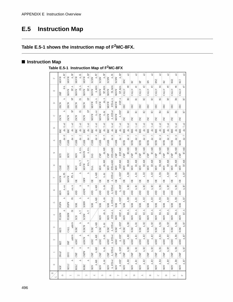
APPENDIX E Instruction Overview
E.5 Instruction Map
Table E.5-1 shows the instruction map of F2MC-8FX.
Instruction MapTable E.5-1 Instruction Map of F2MC-8FX
NO
P
MU
LU
A
ROLC
A
RORC
A
MO
V
A, #
d8
MO
V A, d
ir
MO
V
A, @
IX+d
MO
V
A, @
EP
MO
V
A
, R0
MO
V
A
, R1
MO
V
A
, R2
MO
V
A
, R3
MO
V
A
, R4
MO
V
A
, R5
MO
V
A
, R6
MO
V
A
, R7
SWA
P
DIV
U
A
CMP
A
CMPW
A
CMP
A, #
d8
CMP
A
, dir
CMP
A, @
IX+d
CMP
A, @
EP
CMP
A
, R0
CMP
A
, R1
CMP
A
, R2
CMP
A
, R3
CMP
A
, R4
CMP
A
, R5
CMP
A
, R6
CMP
A
, R7
RET
JMP
addr
16
AD
DC
A
AD
DCW
A
AD
DC
A, #
d8
AD
DC
A
, dir
AD
DC
A, @
IX+d
AD
DC
A, @
EP
AD
DC
A
, R0
AD
DC
A
, R1
AD
DC
A
, R2
AD
DC
A
, R3
AD
DC
A
, R4
AD
DC
A
, R5
AD
DC
A
, R6
AD
DC
A
, R7
RETI
CALL ad
dr16
SUBC
A
SUBC
W
A
SUBC
A, #
d8
SUBC
A
, dir
SUBC
A, @
IX+d
SUBC
A, @
EP
SUBC
A
, R0
SUBC
A
, R1
SUBC
A
, R2
SUBC
A
, R3
SUBC
A
, R4
SUBC
A
, R5
SUBC
A
, R6
SUBC
A
, R7
PUSH
W
A
PUSH
W
IX
XCH
A
, T
XCH
W
A
, T
MO
V
d
ir, A
MO
V
@IX
+d, A
MO
V
@EP
, A
MO
V
R
0, A
MO
V
R
1, A
MO
V
R
2, A
MO
V
R
3, A
MO
V
R
4, A
MO
V
R
5, A
MO
V
R
6, A
MO
V
R
7, A
POPW
A
POPW
IX
XO
R
A
XO
RW
A
XO
R
A, #
d8
XO
R
A
, dir
XO
R
A, @
IX+d
XO
R
A, @
EP
XO
R
A
, R0
XO
R
A
, R1
XO
R
A
, R2
XO
R
A
, R3
XO
R
A
, R4
XO
R
A
, R5
XO
R
A
, R6
XO
R
A
, R7
MO
V
A
, ext
MO
V
ex
t, A
AN
D
A
AN
DW
A
AN
D
A, #
d8
AN
D
A
, dir
AN
D
A, @
IX+d
AN
D
A, @
EP
AN
D
A
, R0
AN
D
A
, R1
AN
D
A
, R2
AN
D
A
, R3
AN
D
A
, R4
AN
D
A
, R5
AN
D
A
, R6
AN
D
A
, R7
MO
VW
A
, PS
MO
VW
PS
, A
OR
A
ORW
A
OR
A, #
d8
OR
A
, dir
OR
A, @
IX+d
OR
A, @
EP
OR
A
, R0
OR
A
, R1
OR
A
, R2
OR
A
, R3
OR
A
, R4
OR
A
, R5
OR
A
, R6
OR
A
, R7
CLRI
CLRC
MO
V
@A
, T
MO
VW
@A
, T
DA
A
MO
V
dir,
#d8
MO
V
@IX
+d,#
d8
MO
V
@
EP, #
d8
MO
V
R0,
#d8
MO
V
R1,
#d8
MO
V
R2,
#d8
MO
V
R3,
#d8
MO
V
R4,
#d8
MO
V
R5,
#d8
MO
V
R6,
#d8
MO
V
R7,
#d8
SETI
SETC
MO
V
A, @
A
MO
VW
A, @
A
DA
S
CMP
dir,
#d8
CMP
@IX
+d,#
d8
CMP
@
EP, #
d8
CMP
R0,
#d8
CMP
R1,
#d8
CMP
R2,
#d8
CMP
R3,
#d8
CMP
R4,
#d8
CMP
R5,
#d8
CMP
R6,
#d8
CMP
R7,
#d8
CLRB
d
ir : 0
CLRB
d
ir : 1
CLRB
d
ir : 2
CLRB
d
ir : 3
CLRB
d
ir : 4
CLRB
d
ir : 5
CLRB
d
ir : 6
CLRB
d
ir : 7
SETB
d
ir : 0
SETB
d
ir : 1
SETB
d
ir : 2
SETB
d
ir : 3
SETB
d
ir : 4
SETB
d
ir : 5
SETB
d
ir : 6
SETB
d
ir : 7
BBC
di
r : 0
, rel
BBC
di
r : 1
, rel
BBC
di
r : 2
, rel
BBC
di
r : 3
, rel
BBC
di
r : 4
, rel
BBC
di
r : 5
, rel
BBC
di
r : 6
, rel
BBC
di
r : 7
, rel
BBS
di
r : 0
, rel
BBS
di
r : 1
, rel
BBS
di
r : 2
, rel
BBS
di
r : 3
, rel
BBS
di
r : 4
, rel
BBS
di
r : 5
, rel
BBS
di
r : 6
, rel
BBS
di
r : 7
, rel
INCW
A
INCW
SP
INCW
IX
INCW
EP
MO
VW
A
, ext
MO
VW
A
, dir
MO
VW
A, @
IX+d
MO
VW
A, @
EP
INC
R0
INC
R1
INC
R2
INC
R3
INC
R4
INC
R5
INC
R6
INC
R7
DEC
W
A
DEC
W
SP
DEC
W
IX
DEC
W
EP
MO
VW
ex
t, A
MO
VW
d
ir, A
MO
VW
@IX
+d, A
MO
VW
@EP
, A
DEC
R0
DEC
R1
DEC
R2
DEC
R3
DEC
R4
DEC
R5
DEC
R6
DEC
R7
JMP
@A
MO
VW
SP
, A
MO
VW
IX
, A
MO
VW
EP
, A
MO
VW
A, #
d16
MO
VW
S
P, #
d16
MO
VW
I
X, #
d16
MO
VW
E
P, #
d16
CALL
V
#0
CALL
V
#1
CALL
V
#2
CALL
V
#3
CALL
V
#4
CALL
V
#5
CALL
V
#6
CALL
V
#7
MO
VW
A
, PC
MO
VW
A
, SP
MO
VW
A
, IX
MO
VW
A
, EP
XCH
W
A
, PC
XCH
W
A
, SP
XCH
W
A
, IX
XCH
W
A
, EP
BNC
rel
BC
rel
BP
rel
BN
rel
BNZ
rel
BZ
rel
BGE
rel
BLT
rel
496
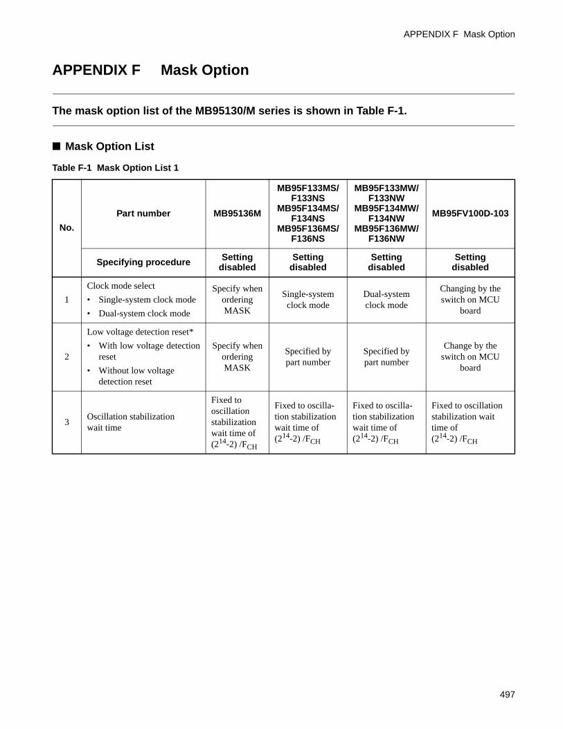
APPENDIX F Mask Option
APPENDIX F Mask Option
The mask option list of the MB95130/M series is shown in Table F-1.
Mask Option List
Table F-1 Mask Option List 1
No.
Part number MB95136M
MB95F133MS/F133NS
MB95F134MS/F134NS
MB95F136MS/F136NS
MB95F133MW/F133NW
MB95F134MW/F134NW
MB95F136MW/F136NW
MB95FV100D-103
Specifying procedure Setting disabled
Setting disabled
Setting disabled
Setting disabled
1
Clock mode select
• Single-system clock mode
• Dual-system clock mode
Specify whenordering MASK
Single-system clock mode
Dual-system clock mode
Changing by the switch on MCU
board
2
Low voltage detection reset*
• With low voltage detectionreset
• Without low voltagedetection reset
Specify whenordering MASK
Specified by part number
Specified by part number
Change by the switch on MCU
board
3Oscillation stabilizationwait time
Fixed tooscillationstabilization wait time of(214-2) /FCH
Fixed to oscilla-tion stabilization wait time of (214-2) /FCH
Fixed to oscilla-tion stabilization wait time of (214-2) /FCH
Fixed to oscillation stabilization wait time of (214-2) /FCH
497
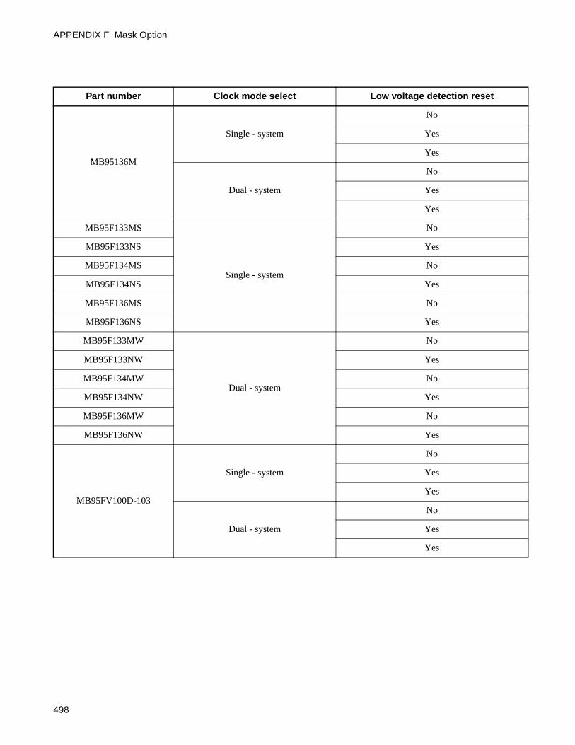
APPENDIX F Mask Option
Part number Clock mode select Low voltage detection reset
MB95136M
Single - system
No
Yes
Yes
Dual - system
No
Yes
Yes
MB95F133MS
Single - system
No
MB95F133NS Yes
MB95F134MS No
MB95F134NS Yes
MB95F136MS No
MB95F136NS Yes
MB95F133MW
Dual - system
No
MB95F133NW Yes
MB95F134MW No
MB95F134NW Yes
MB95F136MW No
MB95F136NW Yes
MB95FV100D-103
Single - system
No
Yes
Yes
Dual - system
No
Yes
Yes
498
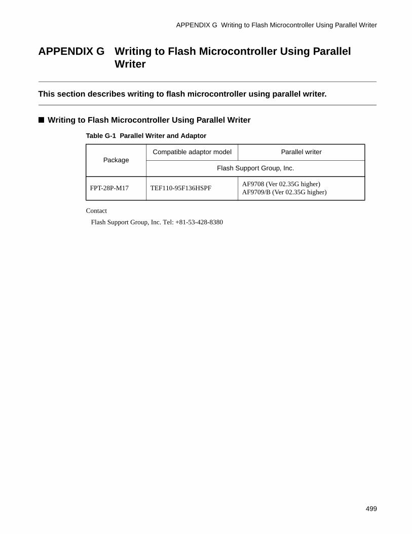
APPENDIX G Writing to Flash Microcontroller Using Parallel Writer
APPENDIX G Writing to Flash Microcontroller Using Parallel Writer
This section describes writing to flash microcontroller using parallel writer.
Writing to Flash Microcontroller Using Parallel Writer
Contact
Flash Support Group, Inc. Tel: +81-53-428-8380
Table G-1 Parallel Writer and Adaptor
PackageCompatible adaptor model Parallel writer
Flash Support Group, Inc.
FPT-28P-M17 TEF110-95F136HSPFAF9708 (Ver 02.35G higher)AF9709/B (Ver 02.35G higher)
499
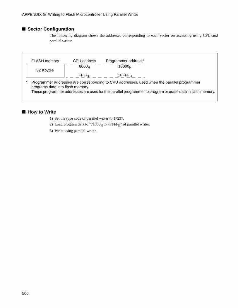
APPENDIX G Writing to Flash Microcontroller Using Parallel Writer
Sector ConfigurationThe following diagram shows the addresses corresponding to each sector on accessing using CPU and
parallel writer.
How to Write1) Set the type code of parallel writer to 17237.
2) Load program data to "71000H to 7FFFFH" of parallel writer.
3) Write using parallel writer.
*: Programmer addresses are corresponding to CPU addresses, used when the parallel programmer programs data into flash memory.These programmer addresses are used for the parallel programmer to program or erase data in flash memory.
FLASH memory CPU address Programmer address*
32 Kbytes8000H 18000H
FFFFH 1FFFFH
500
Index
Index
Numerics
16-bit16-bit PPG Cycle Setting Buffer Registers
(PCSRH0, PCSRL0) ........................... 26516-bit PPG Down Counter Registers
(PDCRH0, PDCRL0) .......................... 26416-bit PPG Duty Setting Buffer Registers
(PDUTH0, PDUTL0) .......................... 26616-bit PPG Status Control Register, Lower Byte
(PCNTL0) .......................................... 26916-bit PPG Status Control Register, Upper Byte
(PCNTH0).......................................... 26716-bit PPG Timer............................................. 258Block Diagram of 16-bit PPG Timer .................. 259Block Diagrams of Pins Related
to 16-bit PPG...................................... 262Channels of 16-bit PPG Timer........................... 261Interrupts of 16-bit PPG Timer .......................... 271Operation of 16-bit PPG Mode .......................... 252Pins of 16-bit PPG Timer.................................. 262Precautions when Using 16-bit PPG Timer ......... 276Registers and Vector Table Related to Interrupts
of 16-bit PPG Timer ............................ 271Registers of 16-bit PPG Timer........................... 263Sample Programs for 16-bit PPG Timer ............. 277Setting 16-bit PPG Mode .................................. 251
16-bit DataPlacement of 16-bit Data in Memory ................... 39
16-bit PPG Cycle Setting Buffer Registers16-bit PPG Cycle Setting Buffer Registers
(PCSRH0, PCSRL0) ........................... 26516-bit PPG Down Counter Registers
16-bit PPG Down Counter Registers (PDCRH0, PDCRL0) .......................... 264
16-bit PPG Duty Setting Buffer Registers16-bit PPG Duty Setting Buffer Registers
(PDUTH0, PDUTL0) .......................... 26616-bit PPG Status Control Register
16-bit PPG Status Control Register, Lower Byte (PCNTL0) .......................................... 269
16-bit PPG Status Control Register, Upper Byte (PCNTH0).......................................... 267
256-Kbit Flash MemoryFeatures of 256-Kbit Flash Memory................... 444Overview of 256-Kbit Flash Memory................. 444Sector Configuration of 256-Kbit Flash
Memory ............................................. 4458/10-bit
Block Diagram of 8/10-bit A/D Converter .......... 419
Block Diagram of Pins Related to 8/10-bit A/D Converter............................................422
Interrupts During 8/10-bit A/D Converter Operation ............................................429
List of 8/10-bit A/D Converter Registers.............423Notes on Use of 8/10-bit A/D Converter .............433Operations of 8/10-bit A/D Converter's Conversion
Function .............................................430Pins of 8/10-bit A/D Converter ..........................421Register and Vector Table Related to 8/10-bit A/D
Converter Interrupts .............................429Sample Programs for 8/10-bit A/D
Converter............................................4348/10-bit A/D Converter
Block Diagram of 8/10-bit A/D Converter...........419Block Diagram of Pins Related to 8/10-bit A/D
Converter............................................422Interrupts During 8/10-bit A/D Converter
Operation ............................................429List of 8/10-bit A/D Converter Registers.............423Notes on Use of 8/10-bit A/D Converter .............433Operations of 8/10-bit A/D Converter's Conversion
Function .............................................430Pins of 8/10-bit A/D Converter ..........................421Register and Vector Table Related to 8/10-bit A/D
Converter Interrupts .............................429Sample Programs for 8/10-bit A/D
Converter............................................4348/10-bit A/D Converter Control Register
8/10-bit A/D Converter Control Register 1 (ADC1) ..............................................424
8/10-bit A/D Converter Control Register 2 (ADC2) ..............................................426
8/10-bit A/D Converter Data Registers8/10-bit A/D Converter Data Registers Upper/Lower
(ADDH,ADDL)...................................4288/10-bit A/D Converter Registers
List of 8/10-bit A/D Converter Registers.............4238/16-bit
8/16-bit Compound Timer 00/01 Control Status Register 0 (T00CR0/T01CR0) ..............197
8/16-bit Compound Timer 00/01 Control Status Register 1 (T00CR1/T01CR1) ..............200
8/16-bit Compound Timer 00/01 Data Register (T00DR/T01DR) .................................206
8/16-bit Compound Timer 00/01 Timer Mode Control Register ch.0 (TMCR0) ........................203
8/16-bit PPG Output Inversion Register (REVC) ..............................................244
8/16-bit PPG Start Register (PPGS) ....................243
501
Index
8/16-bit PPG Timer 00 Control Register ch.0 (PC00) ...............................................239
8/16-bit PPG Timer 00/01 Cycle Setup Buffer Register (PPS01/PPS00) ...................................241
8/16-bit PPG Timer 00/01 Duty Setup Buffer Register (PDS01/PDS00) ..................................242
8/16-bit PPG Timer 01 Control Register ch.0 (PC01)...............................................237
Block Diagram of 8/16-bit Compound Timer .................................................191
Block Diagram of 8/16-bit PPG .........................231Block Diagram of Pins Related to 8/16-bit Compound
Timer .................................................195Block Diagram of Pins Related
to 8/16-bit PPG ...................................235Channels of 8/16-bit Compound Timer...............193Channels of 8/16-bit PPG..................................233Interrupts of 8/16-bit PPG .................................245LIN Synch Field Edge Detection Interrupt (8/16-bit
Compound Timer Interrupt) .................374Overview of 8/16-bit PPG .................................230Pins of 8/16-bit PPG .........................................234Pins Related to 8/16-bit Compound Timer ..........194Precautions when Using 8/16-bit Compound
Timer .................................................228Precautions when Using 8/16-bit PPG ................253Registers and Vector Table Related to Interrupts
of 8/16-bit PPG ...................................245Registers and Vector Tables Related to Interrupts
of 8/16-bit Compound Timer ................210Registers of 8/16-bit PPG..................................236Registers Related to 8/16-bit Compound
Timer .................................................196Sample Programs for 8/16-bit PPG Timer...........254
8/16-bit Compound Timer 00/01 Control Status Register
8/16-bit Compound Timer 00/01 Control Status Register 0 (T00CR0/T01CR0).............. 197
8/16-bit Compound Timer 00/01 Control Status Register 1 (T00CR1/T01CR1).............. 200
8/16-bit Compound Timer 00/01 Data Register8/16-bit Compound Timer 00/01 Data Register
(T00DR/T01DR) ................................ 2068/16-bit Compound Timer 00/01 Timer Mode Control
Register8/16-bit Compound Timer 00/01 Timer Mode Control
Register ch.0 (TMCR0) ....................... 2038/16-bit PPG Output Inversion Register
8/16-bit PPG Output Inversion Register (REVC) ............................................. 244
8/16-bit PPG Start Register8/16-bit PPG Start Register (PPGS) ................... 243
8/16-bit PPG Timer 00 Control Register8/16-bit PPG Timer 00 Control Register ch.0
(PC00) ............................................... 2398/16-bit PPG Timer 00/01 Cycle Setup Buffer
Register8/16-bit PPG Timer 00/01 Cycle Setup Buffer Register
(PPS01/PPS00) ................................... 2418/16-bit PPG Timer 00/01 Duty Setup Buffer Register
8/16-bit PPG Timer 00/01 Duty Setup Buffer Register (PDS01/PDS00).................................. 242
8/16-bit PPG Timer 01 Control Register8/16-bit PPG Timer 01 Control Register ch.0
(PC01) ............................................... 2378-bit
Operation of 8-bit PPG Independent Mode ......... 247Operation of 8-bit Prescaler + 8-bit PPG
Mode ................................................. 249Setting 8-bit Independent Mode......................... 247Setting 8-bit Prescaler + 8-bit PPG Mode ........... 249
502
Index
A
A/D8/10-bit A/D Converter Control Register 1
(ADC1).............................................. 4248/10-bit A/D Converter Control Register 2
(ADC2).............................................. 4268/10-bit A/D Converter Data Registers Upper/Lower
(ADDH,ADDL) .................................. 428A/D Conversion Functions................................ 418Block Diagram of 8/10-bit A/D Converter .......... 419Block Diagram of Pins Related to 8/10-bit A/D
Converter ........................................... 422Interrupts During 8/10-bit A/D Converter
Operation ........................................... 429List of 8/10-bit A/D Converter Registers ............ 423Notes on Use of 8/10-bit A/D Converter............. 433Operations of 8/10-bit A/D Converter's Conversion
Function............................................. 430Operations of A/D Conversion Function............. 431Pins of 8/10-bit A/D Converter.......................... 421Register and Vector Table Related to 8/10-bit A/D
Converter Interrupts ............................ 429Sample Programs for 8/10-bit A/D
Converter ........................................... 434A/D Conversion
A/D Conversion Functions................................ 418Operations of A/D Conversion Function............. 431
A/D ConverterBlock Diagram of 8/10-bit A/D Converter .......... 419Block Diagram of Pins Related to 8/10-bit A/D
Converter ........................................... 422Interrupts During 8/10-bit A/D Converter
Operation ........................................... 429List of 8/10-bit A/D Converter Registers ............ 423Notes on Use of 8/10-bit A/D Converter............. 433Operations of 8/10-bit A/D Converter's Conversion
Function............................................. 430Pins of 8/10-bit A/D Converter.......................... 421Register and Vector Table Related to 8/10-bit A/D
Converter Interrupts ............................ 429Sample Programs for 8/10-bit A/D
Converter ........................................... 434A/D Converter Registers
List of 8/10-bit A/D Converter Registers ............ 423ADC
8/10-bit A/D Converter Control Register 1 (ADC1).............................................. 424
8/10-bit A/D Converter Control Register 2 (ADC2).............................................. 426
ADDH,ADDL8/10-bit A/D Converter Data Registers Upper/Lower
(ADDH,ADDL) .................................. 428Addressing
Explanation of Addressing ................................ 484
Arithmetic OperationArithmetic Operation Instructions ......................494
Asynchronous LIN ModeAsynchronous LIN Mode Operation ...................398
Asynchronous ModeAsynchronous Mode Operation ..........................390
B
Baud RateBaud Rate Calculation.......................................382Baud Rate Setting .............................................347Block Diagram of UART/SIO Dedicated Baud Rate
Generator ............................................342Channels of UART/SIO Dedicated Baud Rate
Generator ............................................343LIN-UART Baud Rate Selection ........................380LIN-UART Bit Configuration of Baud Rate Generator
Register (BGR 0/1) ..............................371Operation of Dedicated Baud Rate Generator
(Reload Counter) .................................385Registers Related to UART/SIO Dedicated Baud Rate
Generator ............................................344Reload Value and Baud Rate
of Each Clock Speed ............................383UART/SIO Dedicated Baud Rate Generator Baud
Rate Setting Register (BRSR) ...............346UART/SIO Dedicated Baud Rate Generator Prescaler
Selection Register (PSSR) ....................345Baud Rate Generator Register
LIN-UART Bit Configuration of Baud Rate Generator Register (BGR 0/1) ..............................371
BGRLIN-UART Bit Configuration of Baud Rate Generator
Register (BGR 0/1) ..............................371Bidirectional Communication
Bidirectional Communication Function...............402Bit 5
One-shot Mode (MDSE of PCNTH0 Register: bit 5=1)...............................................274
PWM Mode (MDSE of PCNTH Register: bit 5=0)...............................................272
Bit ConfigurationBit Configuration of LIN-UART Extended
Communication Control Register (ECCR) ..............................................369
Bit Configuration of LIN-UART Extended Status Control Register (ESCR) ......................367
LIN-UART Bit Configuration of Baud Rate Generator Register (BGR 0/1) ..............................371
Bit Manipulation InstructionsRead Destination on the Execution of Bit
Manipulation Instructions .....................492Bits Result Information Bits
Bits Result Information Bits ................................35
503
Index
Block DiagramBlock Diagram of 16-bit PPG Timer ..................259Block Diagram of 8/10-bit A/D Converter ..........419Block Diagram of 8/16-bit Compound
Timer .................................................191Block Diagram of 8/16-bit PPG .........................231Block Diagram of All MB95130/M Series ..............8Block Diagram of External Interrupt
Circuit ................................................283Block Diagram of Interrupt Pin Selection
Circuit ................................................297Block Diagram of LIN-UART Pins ....................357Block Diagram of Low-voltage Detection Reset
Circuit ................................................439Block Diagram of Pins Related to 8/10-bit A/D
Converter ...........................................422Block Diagram of Pins Related to 8/16-bit Compound
Timer .................................................195Block Diagram of Pins Related
to 8/16-bit PPG ...................................235Block Diagram of Pins Related to External Interrupt
Circuit ................................................285Block Diagram of Pins Related
to UART/SIO......................................311Block Diagram of Port 0 ...................................103Block Diagram of Port 1 ...................................108Block Diagram of Port F ...................................113Block Diagram of Port G ..................................118Block Diagram of the Clock Controller ................43Block Diagram of Timebase Timer ....................125Block Diagram of UART/SIO ...........................307Block Diagram of UART/SIO Dedicated Baud Rate
Generator ...........................................342Block Diagram of Watch Counter ......................163Block Diagram of Watch Prescaler ....................149Block Diagram of Watchdog Timer ...................139Block Diagram of Wild Register Function ..........177Block Diagrams of Pins Related
to 16-bit PPG ......................................262LIN-UART Block Diagram ...............................353Prescaler Block Diagram.....................................78
BranchBranch Instructions...........................................495
BRSRUART/SIO Dedicated Baud Rate Generator Baud
Rate Setting Register (BRSR)...............346
C
CalculationBaud Rate Calculation ......................................382
CausesTable of Interrupt Causes ..................................476
CCRConfiguration of Condition Code Register
(CCR) ..................................................35
ChannelsChannels of 16-bit PPG Timer .......................... 261Channels of 8/16-bit Compound Timer .............. 193Channels of 8/16-bit PPG ................................. 233Channels of External Interrupt Circuit................ 284Channels of UART/SIO.................................... 309Channels of UART/SIO Dedicated Baud Rate
Generator ........................................... 343Check
Check That Clock-mode Transition has been Completed before Setting Standby Mode. .................................................. 67
Chip EraseErasing Data from Flash Memory
(Chip Erase) ....................................... 461Notes on Chip Erasing...................................... 461
ClearingClearing Timebase Timer ................................. 132Clearing Watch Prescaler.................................. 156
ClockBlock Diagram of the Clock Controller ................ 43Check That Clock-mode Transition
has been Completed before Setting Standby Mode. .................................................. 67
Clock Mode State Transition Diagram ................. 62Clock Oscillator Circuit ...................................... 75Combinations of Clock Mode and Standby
Mode ................................................... 47Configuration of System Clock Control Register
(SYCC)................................................ 50External Clock................................................. 384Input Clock .............. 78, 126, 140, 150, 164, 192,
232, 260, 308, 342, 356, 420Operations in Main Clock Mode.......................... 61Operations in Main PLL Clock Mode .................. 61Operations in Sub PLL Clock Mode
(on Two-system Clock Product) ............. 61Oscillation Stabilization Wait Time and Clock Mode/
Standby Mode Transition....................... 49Output Clock ............................. 78, 126, 150, 342Overview of Clock Controller ............................. 42Peripheral Resources not Affected
by Clock Mode ..................................... 45PLL Clock Oscillation Stabilization Wait
Time .................................................... 49Reload Value and Baud Rate
of Each Clock Speed ........................... 383Clock Controller
Block Diagram of the Clock Controller ................ 43Overview of Clock Controller ............................. 42
Clock ModeClock Mode State Transition Diagram ................. 62Clock Modes ..................................................... 45Combinations of Clock Mode and Standby
Mode ................................................... 47Operations in Main Clock Mode.......................... 61
504
Index
Operations in Main PLL Clock Mode .................. 61Operations in Sub PLL Clock Mode
(on Two-system Clock Product) ............. 61Oscillation Stabilization Wait Time and Clock Mode/
Standby Mode Transition....................... 49Peripheral Resources not Affected
by Clock Mode ..................................... 45Combinations
Combinations of Clock Mode and Standby Mode ................................................... 47
CommandCommand Sequence Table................................ 449Notes on Issuing Commands ............................. 450
Command Sequence TableCommand Sequence Table................................ 449
CommunicationBidirectional Communication Function .............. 402Bit Configuration of LIN-UART Extended
Communication Control Register (ECCR).............................................. 369
LIN Master/Slave Mode Communication Function............................................. 407
Master/Slave Mode Communication Function............................................. 404
CompareWild Register Address Compare Enable Register
(WREN)............................................. 183Compound Timer
8/16-bit Compound Timer 00/01 Control Status Register 0 (T00CR0/T01CR0) .............. 197
8/16-bit Compound Timer 00/01 Control Status Register 1 (T00CR1/T01CR1) .............. 200
8/16-bit Compound Timer 00/01 Data Register (T00DR/T01DR)................................. 206
8/16-bit Compound Timer 00/01 Timer Mode Control Register ch.0 (TMCR0) ....................... 203
Block Diagram of 8/16-bit Compound Timer...... 191Block Diagram of Pins Related to 8/16-bit Compound
Timer................................................. 195Channels of 8/16-bit Compound Timer .............. 193Pins Related to 8/16-bit Compound Timer .......... 194Precautions when Using 8/16-bit Compound
Timer................................................. 228Registers and Vector Tables Related to Interrupts
of 8/16-bit Compound Timer................ 210Registers Related to 8/16-bit Compound
Timer................................................. 196Compound Timer Interrupt
LIN Synch Field Edge Detection Interrupt (8/16-bit Compound Timer Interrupt) ................. 374
Condition Code RegisterConfiguration of Condition Code Register
(CCR) .................................................. 35
ConfigurationBit Configuration of LIN-UART Extended
Communication Control Register (ECCR) ..............................................369
Bit Configuration of LIN-UART Extended Status Control Register (ESCR) ......................367
Configuration of Condition Code Register (CCR)...................................................35
Configuration of Dedicated Registers ...................30Configuration of Direct Bank Pointer (DP)............33Configuration of General-purpose Registers ..........37Configuration of Interrupt Level Setting Registers
(ILR0 to ILR5) ......................................92Configuration of Memory Space ..........................22Configuration of Oscillation Stabilization Wait Time
Setting Register (WATR) .......................55Configuration of PLL Control Register
(PLLC) .................................................52Configuration of Register Bank Pointer (RP).........32Configuration of Reset Source Register
(RSRR).................................................86Configuration of System Clock Control Register
(SYCC) ................................................50LIN-UART Bit Configuration of Baud Rate Generator
Register (BGR 0/1) ..............................371Port 0 Configuration .........................................101Port 1 Configuration .........................................107Port F Configuration .........................................112Port G Configuration.........................................117Sector Configuration .........................................500Sector Configuration of 256-Kbit Flash
Memory..............................................445Connection Method
Inter-CPU Connection Method...........................389Continuous Mode
Interval Timer Function (Continuous Mode) ..............................188
Operation of Interval Timer Function (Continuous Mode) ..............................213
Control Register16-bit PPG Status Control Register, Lower Byte
(PCNTL0)...........................................26916-bit PPG Status Control Register, Upper Byte
(PCNTH0) ..........................................2678/16-bit PPG Timer 00 Control Register ch.0
(PC00) ................................................2398/16-bit PPG Timer 01 Control Register ch.0
(PC01) ................................................237Bit Configuration of LIN-UART Extended
Communication Control Register (ECCR) ..............................................369
ConversionA/D Conversion Functions ................................418Operations of 8/10-bit A/D Converter's Conversion
Function .............................................430Operations of A/D Conversion Function .............431
505
Index
Counter16-bit PPG Down Counter Registers
(PDCRH0, PDCRL0) ..........................264Block Diagram of Watch Counter ......................163Function of Reload Counter...............................386Interrupts of Watch Counter ..............................169Operation of Dedicated Baud Rate Generator
(Reload Counter).................................385Register and Vector Table Related to Interrupts of
Watch Counter ....................................169Registers of Watch Counter...............................165Sample Programs for Watch Counter .................173Setup Procedure of Watch Counter ....................170Watch Counter .................................................162Watch Counter Control Register (WCSR)...........167Watch Counter Data Register (WCDR) ..............166
CPUInter-CPU Connection Method ..........................389Standby Mode is Also Canceled when the CPU
Rejects Interrupts. .................................67
D
Data Polling FlagData Polling Flag (DQ7) ...................................453
Dedicated Baud Rate GeneratorBlock Diagram of UART/SIO Dedicated Baud Rate
Generator ...........................................342Channels of UART/SIO Dedicated Baud Rate
Generator ...........................................343Operation of Dedicated Baud Rate Generator
(Reload Counter).................................385Registers Related to UART/SIO Dedicated Baud Rate
Generator ...........................................344UART/SIO Dedicated Baud Rate Generator Baud
Rate Setting Register (BRSR)...............346UART/SIO Dedicated Baud Rate Generator Prescaler
Selection Register (PSSR) ....................345Dedicated Registers
Configuration of Dedicated Registers ...................30Functions of Dedicated Registers .........................30
DescriptionOperating Description of UART/SIO Operation
Mode 0...............................................323Operating Description of UART/SIO Operation
Mode 1...............................................330Pin Description ..................................................11
DetailsDetails of Programming/Erasing
Flash Memory.....................................457Device
Device Handling Precautions...............................16
Difference Points among ProductsDifference Points among Products and Notes on
Selecting a Product ................................. 6Direct Access
LIN-UART Pin Direct Access........................... 401Direct Bank
Configuration of Direct Bank Pointer (DP) ........... 33Mirror Address for Register Bank and Direct Bank
Pointers................................................ 32Display Sign
Explanation of Display Sign of Instruction ......... 482DQ
Data Polling Flag (DQ7)................................... 453Execution Time-out Flag (DQ5) ........................ 455Toggle Bit 2 Flag (DQ2)................................... 456Toggle Bit Flag (DQ6) ..................................... 454
E
ECCRBit Configuration of LIN-UART Extended
Communication Control Register (ECCR).............................................. 369
EffectEffect of Reset on RAM Contents........................ 84
EICExternal Interrupt Control Register (EIC00) ....... 287
Enable Transmission/ReceptionEnable Transmission/Reception......................... 389
ErasingDetails of Programming/Erasing
Flash Memory .................................... 457Erasing Data from Flash Memory
(Chip Erase) ....................................... 461Notes on Chip Erasing...................................... 461Programming and Erasing Flash Memory........... 444
ESCRBit Configuration of LIN-UART Extended Status
Control Register (ESCR) ..................... 367Example
Example of Minimum Connection to Flash Microcomputer Programmer ................ 469
Hardware Connection Example ......................... 186Operating Examples of Timebase Timer ............ 133Operating Examples of Watch Prescaler............. 156Setting Procedure Other than Program
Examples ........................................... 412Setup Procedure Example ........ 134, 145, 157, 171,
246, 275, 291, 322, 432Execution Time-out Flag
Execution Time-out Flag (DQ5) ........................ 455Explanation
Explanation of Addressing ................................ 484Explanation of Display Sign of Instruction ......... 482Explanation of Item in Instruction Table ............ 483
506
Index
Extended Communication Control RegisterBit Configuration of LIN-UART Extended
Communication Control Register (ECCR).............................................. 369
Extended Status Control RegisterBit Configuration of LIN-UART Extended Status
Control Register (ESCR) ..................... 367External Clock
External Clock ................................................. 384External Interrupt
Block Diagram of External Interrupt Circuit................................................ 283
Block Diagram of Pins Related to External Interrupt Circuit................................................ 285
Channels of External Interrupt Circuit................ 284External Interrupt Control Register (EIC00) ....... 287Functions of External Interrupt Circuit ............... 282Interrupt During Operation of External Interrupt
Circuit................................................ 289List of Registers of External Interrupt
Circuit................................................ 286Operation of External Interrupt Circuit............... 290Pins Related to External Interrupt Circuit ........... 285Precautions when Using External Interrupt
Circuit................................................ 292Registers and Vector Table Related to Interrupts
of External Interrupt Circuit ................. 289Sample Programs for External Interrupt
Circuit................................................ 293External Interrupt Circuit
Block Diagram of External Interrupt Circuit................................................ 283
Block Diagram of Pins Related to External Interrupt Circuit................................................ 285
Channels of External Interrupt Circuit................ 284Functions of External Interrupt Circuit ............... 282Interrupt During Operation of External Interrupt
Circuit................................................ 289List of Registers of External Interrupt
Circuit................................................ 286Operation of External Interrupt Circuit............... 290Pins Related to External Interrupt Circuit ........... 285Precautions when Using External Interrupt
Circuit................................................ 292Registers and Vector Table Related to Interrupts
of External Interrupt Circuit ................. 289Sample Programs for External Interrupt
Circuit................................................ 293External Interrupt Control Register
External Interrupt Control Register (EIC00) ....... 287
F
F2MC-8FXInstruction Overview of F2MC-8FX .................. 481
FeatureFeature of MB95130/M Series ...............................2Features of 256-Kbit Flash Memory ...................444Features of Flash Security .................................462Features of General-purpose Registers ..................38
Fixed-cycle ModeOperation of PWM Timer Function
(Fixed-cycle Mode)..............................217PWM Timer Function (Fixed-cycle Mode)..........188
FlagData Polling Flag (DQ7) ...................................453Execution Time-out Flag (DQ5).........................455Hardware Sequence Flag ...................................451Timing of Reception Interrupt Generation
and Flag Set ........................................376Timing of Transmit Interrupt Generation
and Flag Set ........................................378Toggle Bit 2 Flag (DQ2) ...................................456Toggle Bit Flag (DQ6) ......................................454
Flash MemoryDetails of Programming/Erasing
Flash Memory .....................................457Erasing Data from Flash Memory
(Chip Erase) ........................................461Features of 256-Kbit Flash Memory ...................444Flash Memory Programming Procedure ..............459Flash Memory Status Register (FSR)..................447Overview of 256-Kbit Flash Memory .................444Placing Flash Memory in the Read/Reset
State ...................................................458Programming and Erasing Flash Memory ...........444Programming Data into Flash Memory ...............459Register of the Flash Memory ............................446Sector Configuration of 256-Kbit Flash
Memory..............................................445Flash Memory Status Register
Flash Memory Status Register (FSR)..................447Flash Microcomputer Programmer
Example of Minimum Connection to Flash Microcomputer Programmer .................469
Flash MicrocontrollerWriting to Flash Microcontroller
Using Parallel Writer ...........................499Flash Security
Features of Flash Security .................................462FPT-28P-M17
Package Dimension of FPT-28P-M17...................10Free-run Mode
Interval Timer Function (Free-run Mode)............188Operation of Interval Timer Function
(Free-run Mode) ..................................215FSR
Flash Memory Status Register (FSR)..................447
507
Index
FunctionA/D Conversion Functions ................................418Bidirectional Communication Function ..............402Block Diagram of Wild Register Function ..........177Function of Reload Counter...............................386Functions of Dedicated Registers .........................30Functions of External Interrupt Circuit ...............282Functions of LIN-UART ...................................350Functions of UART/SIO ...................................306Input Capture Function .....................................189Interrupt when Interval Function is
in Operation........................................130Interrupts in Operation of Interval Timer Function
(Watch Interrupts) ...............................154Interval Timer Function ............................124, 148Interval Timer Function
(Continuous Mode)..............................188Interval Timer Function (Free-run Mode) ...........188Interval Timer Function (One-shot Mode) ..........188LIN Master/Slave Mode Communication
Function .............................................407Master/Slave Mode Communication
Function .............................................404Operation of Input Capture Function ..................223Operation of Interval Timer Function
(Continuous Mode)..............................213Operation of Interval Timer Function
(Free-run Mode)..................................215Operation of Interval Timer Function
(One-shot Mode) .................................211Operation of PWC Timer Function ....................221Operation of PWM Timer Function
(Fixed-cycle Mode) .............................217Operation of PWM Timer Function
(Variable-cycle Mode) .........................219Operations of 8/10-bit A/D Converter's Conversion
Function .............................................430Operations of A/D Conversion Function .............431Operations of Interval Timer Function
(Watch Prescaler) ................................156Port 0 Register Function....................................104Port 1 Register Function....................................109Port F Register Function ...................................114Port G Register Function...................................119PWC Timer Function........................................189PWM Timer Function (Fixed-cycle Mode) .........188PWM Timer Function
(Variable-cycle Mode) .........................188Watchdog Timer Function.................................138When Interval Timer, Input Capture, or PWC Function
Has Been Selected ...............................226Wild Register Function .....................................176
G
General-purpose RegisterConfiguration of General-purpose Registers..........37
Features of General-purpose Registers ................. 38General-purpose Register Area
(Addresses: 0100H to 01FFH) ................. 24
H
HandlingDevice Handling Precautions .............................. 16
Hardware Connection ExampleHardware Connection Example ......................... 186
Hardware Sequence FlagHardware Sequence Flag .................................. 451
Hardware TriggerHardware Trigger............................................. 275
How to WriteHow to Write................................................... 500
I
I/O CircuitI/O Circuit Type ................................................ 13
I/O MapI/O Map .......................................................... 472
I/O PortsOverview of I/O Ports ...................................... 100
ILRConfiguration of Interrupt Level Setting Registers
(ILR0 to ILR5) ..................................... 92Input
Input Capture Function ..................................... 189Input Clock .............. 78, 126, 140, 150, 164, 192,
232, 260, 308, 342, 356, 420Operation of Input Capture Function.................. 223UART/SIO Serial Input Data Register
(RDR0) .............................................. 319When Interval Timer, Input Capture, or PWC Function
Has Been Selected............................... 226Input Capture
Input Capture Function ..................................... 189Operation of Input Capture Function.................. 223When Interval Timer, Input Capture, or PWC Function
Has Been Selected............................... 226Instruction
Arithmetic Operation Instructions...................... 494Branch Instructions .......................................... 495Explanation of Display Sign of Instruction ......... 482Explanation of Item in Instruction Table ............ 483Instruction Map ............................................... 496Instruction Overview of F2MC-8FX .................. 481Other Instructions ............................................ 495Place at Least Three NOP Instructions Immediately
Following a Standby Mode Setting Instruction. ........................................... 67
Read Destination on the Execution of Bit Manipulation Instructions .................... 492
Special Instruction ........................................... 488
508
Index
Transfer Instructions ........................................ 493Instruction Map
Instruction Map ............................................... 496Inter-CPU Connection
Inter-CPU Connection Method .......................... 389Interrupt
An Interrupt Request may Suppress Transition to Standby Mode....................................... 67
Block Diagram of External Interrupt Circuit................................................ 283
Block Diagram of Interrupt Pin Selection Circuit................................................ 297
Block Diagram of Pins Related to External Interrupt Circuit................................................ 285
Channels of External Interrupt Circuit................ 284Configuration of Interrupt Level Setting Registers
(ILR0 to ILR5) ..................................... 92External Interrupt Control Register (EIC00) ....... 287Functions of External Interrupt Circuit ............... 282Interrupt Acceptance Control Bits........................ 36Interrupt During Operation of External Interrupt
Circuit................................................ 289Interrupt Pin Selection Circuit ........................... 296Interrupt Pin Selection Circuit Control Register
(WICR).............................................. 300Interrupt Processing ........................................... 93Interrupt Processing Stack Area........................... 98Interrupt Processing Time ................................... 96Interrupt Requests from Peripheral
Resources............................................. 90Interrupt when Interval Function is
in Operation ....................................... 130Interrupts During 8/10-bit A/D Converter
Operation ........................................... 429Interrupts in Operation of Interval Timer Function
(Watch Interrupts) ............................... 154Interrupts of 16-bit PPG Timer .......................... 271Interrupts of 8/16-bit PPG ................................. 245Interrupts of UART/SIO ................................... 321Interrupts of Watch Counter .............................. 169Interrupts of Watch Prescaler ............................ 154LIN Synch Field Edge Detection Interrupt (8/16-bit
Compound Timer Interrupt) ................. 374List of Registers of External Interrupt
Circuit................................................ 286Nested Interrupts................................................ 95Operation of External Interrupt Circuit............... 290Operation of Interrupt Pin Selection Circuit ........ 303Overview of Interrupts........................................ 90Pins Related to External Interrupt Circuit ........... 285Pins Related to Interrupt Pin Selection
Circuit................................................ 298Precautions when Using External Interrupt
Circuit................................................ 292Reception Interrupt .................................. 321, 372
Register and Vector Table for Interrupts of Timebase Timer .................................................131
Register and Vector Table Related to 8/10-bit A/D Converter Interrupts .............................429
Register and Vector Table Related to Interrupts of Watch Counter ....................................169
Register and Vector Table Related to Interrupts of Watch Prescaler...................................154
Register and Vector Table Related to LIN-UART Interrupt..............................................375
Registers and Vector Table Related to Interrupts of 16-bit PPG Timer.............................271
Registers and Vector Table Related to Interrupts of 8/16-bit PPG ...................................245
Registers and Vector Table Related to Interrupts of External Interrupt Circuit..................289
Registers and Vector Table Related to UART/SIO Interrupts ............................................321
Registers and Vector Tables Related to Interrupts of 8/16-bit Compound Timer ................210
Registers Related to Interrupt Pin Selection Circuit ................................................299
Sample Programs for External Interrupt Circuit ................................................293
Stack Operation at the Start of Interrupt Processing.............................................97
Stack Operation upon Returning from Interrupt........................................97
Standby Mode is Also Canceled when the CPU Rejects Interrupts. ..................................67
Table of Interrupt Causes ..................................476Timer 00 Interrupt ............................................209Timer 01 Interrupt ............................................209Timing of Reception Interrupt Generation
and Flag Set ........................................376Timing of Transmit Interrupt Generation
and Flag Set ........................................378Transmission Interrupt ......................................321Transmit Interrupt Request Generation
Timing................................................379Transmit Interrupts ...........................................373
Interrupt Acceptance Control BitsInterrupt Acceptance Control Bits ........................36
Interrupt Level Setting RegistersConfiguration of Interrupt Level Setting Registers
(ILR0 to ILR5) ......................................92Interrupt Pin Selection Circuit Control Register
Interrupt Pin Selection Circuit Control Register (WICR) ..............................................300
Interrupt RequestsInterrupt Requests from Peripheral
Resources .............................................90Interval Function
Interrupt when Interval Function is in Operation ........................................130
509
Index
Interval TimerInterrupts in Operation of Interval Timer Function
(Watch Interrupts) ...............................154Interval Timer Function ............................124, 148Interval Timer Function
(Continuous Mode)..............................188Interval Timer Function (Free-run Mode) ...........188Interval Timer Function (One-shot Mode) ..........188Operation of Interval Timer Function
(Continuous Mode)..............................213Operation of Interval Timer Function
(Free-run Mode)..................................215Operation of Interval Timer Function
(One-shot Mode) .................................211Operations of Interval Timer Function
(Watch Prescaler) ................................156When Interval Timer, Input Capture, or PWC Function
Has Been Selected ...............................226
L
LINAsynchronous LIN Mode Operation...................398Bit Configuration of LIN-UART Extended
Communication Control Register (ECCR) ..............................................369
Bit Configuration of LIN-UART Extended Status Control Register (ESCR)......................367
Block Diagram of LIN-UART Pins ....................357Functions of LIN-UART ...................................350LIN Master Device ...........................................408LIN Master/Slave Mode Communication
Function .............................................407LIN Slave Device .............................................409LIN Synch Field Edge Detection Interrupt (8/16-bit
Compound Timer Interrupt) .................374LIN-UART Baud Rate Selection........................380LIN-UART Bit Configuration of Baud Rate Generator
Register (BGR 0/1)..............................371LIN-UART Block Diagram ...............................353LIN-UART Pin Direct Access ...........................401LIN-UART Pins...............................................357LIN-UART Reception Data Register (RDR) .......365LIN-UART Serial Control Register (SCR)..........359LIN-UART Serial Mode Register (SMR) ...........361LIN-UART Serial Status Register (SSR) ............363LIN-UART Transmit Data Register (TDR) .........366Notes on Using LIN-UART...............................410Operation of LIN-UART...................................388Register and Vector Table Related to LIN-UART
Interrupt .............................................375Register List of LIN-UART...............................358Sample Programs of LIN-UART........................412
LIN-UARTBit Configuration of LIN-UART Extended
Communication Control Register (ECCR) ..............................................369
Bit Configuration of LIN-UART Extended Status Control Register (ESCR) ..................... 367
Block Diagram of LIN-UART Pins ................... 357Functions of LIN-UART .................................. 350LIN-UART Baud Rate Selection ....................... 380LIN-UART Bit Configuration of Baud Rate Generator
Register (BGR 0/1) ............................. 371LIN-UART Block Diagram .............................. 353LIN-UART Pin Direct Access........................... 401LIN-UART Pins .............................................. 357LIN-UART Reception Data Register (RDR)....... 365LIN-UART Serial Control Register (SCR) ......... 359LIN-UART Serial Mode Register (SMR) ........... 361LIN-UART Serial Status Register (SSR) ............ 363LIN-UART Transmit Data Register (TDR) ........ 366Notes on Using LIN-UART .............................. 410Operation of LIN-UART .................................. 388Register and Vector Table Related to LIN-UART
Interrupt ............................................. 375Register List of LIN-UART .............................. 358Sample Programs of LIN-UART ....................... 412
LIN-UART Extended CommunicationBit Configuration of LIN-UART Extended
Communication Control Register (ECCR).............................................. 369
LIN-UART Extended Status Control RegisterBit Configuration of LIN-UART Extended Status
Control Register (ESCR) ..................... 367LIN-UART Reception Data Register
LIN-UART Reception Data Register (RDR)....... 365LIN-UART Serial Control Register
LIN-UART Serial Control Register (SCR) ......... 359LIN-UART Serial Mode Register
LIN-UART Serial Mode Register (SMR) ........... 361LIN-UART Serial Status Register
LIN-UART Serial Status Register (SSR) ............ 363LIN-UART Transmit Data Register
LIN-UART Transmit Data Register (TDR) ........ 366List
List of 8/10-bit A/D Converter Registers ............ 423List of Registers of External Interrupt
Circuit ............................................... 286Register List of LIN-UART .............................. 358
Low-voltage Detection Reset CircuitBlock Diagram of Low-voltage Detection Reset
Circuit ............................................... 439Low-voltage Detection Reset Circuit ................. 438Operations of Low-voltage Detection Reset
Circuit ............................................... 441Pins Related to Low-voltage Detection Reset
Circuit ............................................... 440
M
Main Clock ModeOperations in Main Clock Mode.......................... 61
510
Index
Main Stop ModeOperation at the Main Stop Mode ...................... 171
ManipulationRead Destination on the Execution of Bit
Manipulation Instructions .................... 492Mask Option List
Mask Option List ............................................. 497Master
LIN Master Device........................................... 408LIN Master/Slave Mode Communication
Function............................................. 407Master/Slave Mode Communication
Function............................................. 404Master Device
LIN Master Device........................................... 408MB95130/M Series
Block Diagram of All MB95130/M Series.............. 8Feature of MB95130/M Series .............................. 2Pin Assignment of MB95130/M Series .................. 9Product Lineup of MB95130/M Series ................... 4
MDSEOne-shot Mode (MDSE of PCNTH0 Register:
bit 5=1) .............................................. 274PWM Mode (MDSE of PCNTH Register:
bit 5=0) .............................................. 272Memory
Configuration of Memory Space.......................... 22Details of Programming/Erasing
Flash Memory .................................... 457Erasing Data from Flash Memory
(Chip Erase) ....................................... 461Features of 256-Kbit Flash Memory................... 444Flash Memory Programming Procedure ............. 459Flash Memory Status Register (FSR) ................. 447Memory Map....................................... 23, 25, 477Overview of 256-Kbit Flash Memory................. 444Placement of 16-bit Data in Memory ................... 39Placing Flash Memory in the Read/Reset
State .................................................. 458Programming and Erasing Flash Memory........... 444Programming Data into Flash Memory............... 459Register of the Flash Memory ........................... 446Sector Configuration of 256-Kbit Flash
Memory ............................................. 445Memory Map
Memory Map....................................... 23, 25, 477Memory Space
Configuration of Memory Space.......................... 22Minimum Connection
Example of Minimum Connection to Flash Microcomputer Programmer ................ 469
Mirror AddressMirror Address for Register Bank and Direct Bank
Pointers................................................ 32
Mode8/16-bit Compound Timer 00/01 Timer Mode Control
Register ch.0 (TMCR0) ........................203An Interrupt Request may Suppress Transition to
Standby Mode. ......................................67Asynchronous LIN Mode Operation ...................398Asynchronous Mode Operation ..........................390Check That Clock-mode Transition
has been Completed before Setting Standby Mode. ...................................................67
Clock Mode State Transition Diagram ..................62Clock Modes ......................................................45Combinations of Clock Mode and Standby
Mode ....................................................47Interval Timer Function
(Continuous Mode) ..............................188Interval Timer Function (Free-run Mode)............188Interval Timer Function (One-shot Mode) ...........188LIN Master/Slave Mode Communication
Function .............................................407LIN-UART Serial Mode Register (SMR)............361Master/Slave Mode Communication
Function .............................................404One-shot Mode (MDSE of PCNTH0 Register:
bit 5=1)...............................................274Operating Description of UART/SIO Operation
Mode 0 ...............................................323Operating Description of UART/SIO Operation
Mode 1 ...............................................330Operation at the Main Stop Mode.......................171Operation in Sub Stop Mode ..............................171Operation of 16-bit PPG Mode...........................252Operation of 8-bit PPG Independent Mode..........247Operation of 8-bit Prescaler + 8-bit PPG
Mode ..................................................249Operation of Interval Timer Function
(Continuous Mode) ..............................213Operation of Interval Timer Function
(Free-run Mode) ..................................215Operation of Interval Timer Function
(One-shot Mode) .................................211Operation of PWM Timer Function
(Fixed-cycle Mode)..............................217Operation of PWM Timer Function
(Variable-cycle Mode) .........................219Operation of Synchronous Mode
(Operation Mode 2) .............................394Operations in Main Clock Mode ..........................61Operations in Main PLL Clock Mode ...................61Operations in Sleep Mode ...................................71Operations in Standby Mode..............................441Operations in Stop Mode .....................................72Operations in Sub PLL Clock Mode
(on Two-system Clock Product) ..............61Operations in Sub clock Mode
(on Two-system Clock Product) ..............61Operations in Timebase Timer Mode ....................73
511
Index
Operations in Watch Mode..................................74Oscillation Stabilization Wait Time and Clock Mode/
Standby Mode Transition .......................49Overview of Transitions to and from Standby
Mode ...................................................66Peripheral Resources not Affected
by Clock Mode .....................................45Pin States in Standby Mode .................................66Place at Least Three NOP Instructions Immediately
Following a Standby Mode Setting Instruction. ...........................................67
PWM Mode (MDSE of PCNTH Register: bit 5=0) ..............................................272
PWM Timer Function (Fixed-cycle Mode) .........188PWM Timer Function
(Variable-cycle Mode) .........................188Setting 16-bit PPG Mode ..................................251Setting 8-bit Independent Mode .........................247Setting 8-bit Prescaler + 8-bit PPG Mode ...........249Single-chip Mode ...............................................28Standby Mode is Also Canceled when the CPU
Rejects Interrupts. .................................67Standby Mode State Transition Diagram ..............68Standby Modes ..................................................46UART/SIO Serial Mode Control Register 1
(SMC10) ............................................313UART/SIO Serial Mode Control Register 2
(SMC20) ............................................315Mode Operation
Asynchronous LIN Mode Operation...................398Asynchronous Mode Operation .........................390
N
Nested InterruptsNested Interrupts ................................................95
NoteDifference Points among Products and Notes on
Selecting a Product ..................................6Notes on Chip Erasing ......................................461Notes on Issuing Commands .............................450Notes on Use of 8/10-bit A/D Converter .............433Notes on Using LIN-UART...............................410
O
One-shot ModeInterval Timer Function (One-shot Mode) ..........188One-shot Mode (MDSE of PCNTH0 Register:
bit 5=1) ..............................................274Operation of Interval Timer Function
(One-shot Mode) .................................211Operating
Operating Description of UART/SIO Operation Mode 0...............................................323
Operating Description of UART/SIO Operation Mode 1...............................................330
Operating Examples of Timebase Timer ............ 133Operating Examples of Watch Prescaler............. 156
OperationArithmetic Operation Instructions...................... 494Asynchronous LIN Mode Operation .................. 398Asynchronous Mode Operation ......................... 390Interrupt During Operation of External Interrupt
Circuit ............................................... 289Interrupt when Interval Function is
in Operation ....................................... 130Interrupts During 8/10-bit A/D Converter
Operation ........................................... 429Interrupts in Operation of Interval Timer Function
(Watch Interrupts) ............................... 154Operating Description of UART/SIO Operation
Mode 0 .............................................. 323Operating Description of UART/SIO Operation
Mode 1 .............................................. 330Operation at the Main Stop Mode ...................... 171Operation in Sub Stop Mode ............................. 171Operation of 16-bit PPG Mode .......................... 252Operation of 8-bit PPG Independent Mode ......... 247Operation of 8-bit Prescaler + 8-bit PPG
Mode ................................................. 249Operation of Dedicated Baud Rate Generator
(Reload Counter) ................................ 385Operation of External Interrupt Circuit............... 290Operation of Input Capture Function.................. 223Operation of Interrupt Pin Selection Circuit ........ 303Operation of Interval Timer Function
(Continuous Mode) ............................. 213Operation of Interval Timer Function
(Free-run Mode) ................................. 215Operation of Interval Timer Function
(One-shot Mode)................................. 211Operation of LIN-UART .................................. 388Operation of PWC Timer Function .................... 221Operation of PWM Timer Function
(Fixed-cycle Mode) ............................. 217Operation of PWM Timer Function
(Variable-cycle Mode)......................... 219Operation of Synchronous Mode
(Operation Mode 2)............................. 394Operation of UART/SIO................................... 322Operations in Main Clock Mode.......................... 61Operations in Main PLL Clock Mode .................. 61Operations in Sleep Mode................................... 71Operations in Standby Mode ............................. 441Operations in Stop Mode .................................... 72Operations in Sub PLL Clock Mode
(on Two-system Clock Product) ............. 61Operations in Sub clock Mode
(on Two-system Clock Product) ............. 61Operations in Timebase Timer Mode ................... 73Operations in Watch Mode ................................. 74Operations of 8/10-bit A/D Converter's Conversion
Function............................................. 430
512
Index
Operations of A/D Conversion Function............. 431Operations of Interval Timer Function
(Watch Prescaler)................................ 156Operations of Low-voltage Detection Reset
Circuit................................................ 441Operations of Port 0 ......................................... 105Operations of Port 1 ......................................... 110Operations of Port F ......................................... 115Operations of Port G ........................................ 120Operations of Prescaler....................................... 79Operations of Timebase Timer .......................... 132Operations of Watchdog Timer ......................... 144Overview of Reset Operation .............................. 84Read-modify-write Operation............................ 492Stack Operation at the Start of Interrupt
Processing ............................................ 97Stack Operation upon Returning
from Interrupt ....................................... 97Operation Mode
Operating Description of UART/SIO Operation Mode 0 .............................................. 323
Operating Description of UART/SIO Operation Mode 1 .............................................. 330
Operation of Synchronous Mode (Operation Mode 2) ............................. 394
Oscillation Stabilization Wait TimeConfiguration of Oscillation Stabilization Wait Time
Setting Register (WATR)....................... 55Oscillation Stabilization Wait Time ..................... 48Oscillation Stabilization Wait Time and Clock Mode/
Standby Mode Transition....................... 49PLL Clock Oscillation Stabilization Wait
Time .................................................... 49Oscillation Stabilization Wait Time Setting Register
Configuration of Oscillation Stabilization Wait Time Setting Register (WATR)....................... 55
Other InstructionsOther Instructions ............................................ 495
Output8/16-bit PPG Output Inversion Register
(REVC).............................................. 244Output Clock ............................. 78, 126, 150, 342Reset Output...................................................... 83UART/SIO Serial Output Data Register
(TDR0) .............................................. 320Overview
Instruction Overview of F2MC-8FX .................. 481Overview of 256-Kbit Flash Memory................. 444Overview of 8/16-bit PPG................................. 230Overview of Clock Controller ............................. 42Overview of I/O Ports ...................................... 100Overview of Interrupts........................................ 90Overview of Reset Operation .............................. 84Overview of Transitions to and from Standby
Mode ................................................... 66
P
Package and Its Corresponding ProductPackage and Its Corresponding Product ..................7
Package DimensionPackage Dimension of FPT-28P-M17...................10
Parallel WriterWriting to Flash Microcontroller
Using Parallel Writer ...........................499PC
8/16-bit PPG Timer 00 Control Register ch.0 (PC00) ................................................239
8/16-bit PPG Timer 01 Control Register ch.0 (PC01) ................................................237
PCNTH16-bit PPG Status Control Register, Upper Byte
(PCNTH0) ..........................................267One-shot Mode (MDSE of PCNTH0 Register:
bit 5=1)...............................................274PWM Mode (MDSE of PCNTH Register:
bit 5=0)...............................................272PCNTL
16-bit PPG Status Control Register, Lower Byte (PCNTL0)...........................................269
PCSRH0, PCSRL016-bit PPG Cycle Setting Buffer Registers
(PCSRH0, PCSRL0) ............................265PDCRH0, PDCRL0
16-bit PPG Down Counter Registers (PDCRH0, PDCRL0) ...........................264
PDS8/16-bit PPG Timer 00/01 Duty Setup Buffer Register
(PDS01/PDS00) ..................................242PDUTH0, PDUTL0
16-bit PPG Duty Setting Buffer Registers (PDUTH0, PDUTL0) ...........................266
Peripheral ResourcesInterrupt Requests from Peripheral
Resources .............................................90Peripheral Resources not Affected
by Clock Mode ......................................45Pin
Block Diagram of LIN-UART Pins ....................357Block Diagram of Pins Related to 8/10-bit A/D
Converter............................................422Block Diagram of Pins Related to 8/16-bit Compound
Timer .................................................195Block Diagram of Pins Related
to 8/16-bit PPG....................................235Block Diagram of Pins Related to External Interrupt
Circuit ................................................285Block Diagram of Pins Related
to UART/SIO ......................................311Block Diagrams of Pins Related
to 16-bit PPG ......................................262
513
Index
LIN-UART Pins...............................................357Operation of Interrupt Pin Selection Circuit ........303Pins of 16-bit PPG Timer ..................................262Pins of 8/10-bit A/D Converter ..........................421Pins of 8/16-bit PPG .........................................234Pins Related to 8/16-bit Compound Timer ..........194Pins Related to External Interrupt Circuit............285Pins Related to Interrupt Pin Selection
Circuit ................................................298Pins Related to Low-voltage Detection Reset
Circuit ................................................440Pins Related to UART/SIO................................310Port 0 Pins .......................................................102Port 1 Pins .......................................................107Port F Pins .......................................................112Port G Pins ......................................................117
Pin AssignmentPin Assignment of MB95130/M Series...................9
Pin ConnectionPin Connection...................................................18
Pin DescriptionPin Description ..................................................11
Pin StatePin State During a Reset .....................................84Pin States in Standby Mode .................................66
Pin StatusPin Status in Each Mode ...................................479
Place at Least Three NOP Instructions ImmediatelyPlace at Least Three NOP Instructions Immediately
Following a Standby Mode Setting Instruction. ...........................................67
PlacementPlacement of 16-bit Data in Memory....................39
Placing Flash MemoryPlacing Flash Memory in the Read/Reset
State...................................................458PLL
Configuration of PLL Control Register (PLLC).................................................52
Operations in Main PLL Clock Mode...................61Operations in Sub PLL Clock Mode
(on Two-system Clock Product)..............61PLL Clock Oscillation Stabilization Wait
Time ....................................................49PLL Clock
PLL Clock Oscillation Stabilization Wait Time ....................................................49
PLL Clock ModeOperations in Main PLL Clock Mode...................61Operations in Sub PLL Clock Mode
(on Two-system Clock Product)..............61PLL Control Register
Configuration of PLL Control Register (PLLC).................................................52
Port 0Block Diagram of Port 0 ................................... 103Operations of Port 0 ......................................... 105Port 0 Configuration......................................... 101Port 0 Pins....................................................... 102Port 0 Register Function ................................... 104
Port 1Block Diagram of Port 1 ................................... 108Operations of Port 1 ......................................... 110Port 1 Configuration......................................... 107Port 1 Pins....................................................... 107Port 1 Register Function ................................... 109
Port FBlock Diagram of Port F................................... 113Operations of Port F ......................................... 115Port F Configuration ........................................ 112Port F Pins ...................................................... 112Port F Register Function ................................... 114
Port GBlock Diagram of Port G .................................. 118Operations of Port G ........................................ 120Port G Configuration ........................................ 117Port G Pins ...................................................... 117Port G Register Function .................................. 119
PPG16-bit PPG Cycle Setting Buffer Registers
(PCSRH0, PCSRL0) ........................... 26516-bit PPG Down Counter Registers
(PDCRH0, PDCRL0) .......................... 26416-bit PPG Duty Setting Buffer Registers
(PDUTH0, PDUTL0) .......................... 26616-bit PPG Status Control Register, Lower Byte
(PCNTL0) .......................................... 26916-bit PPG Status Control Register, Upper Byte
(PCNTH0) ......................................... 26716-bit PPG Timer............................................. 2588/16-bit PPG Output Inversion Register
(REVC) ............................................. 2448/16-bit PPG Start Register (PPGS) ................... 2438/16-bit PPG Timer 00 Control Register ch.0
(PC00) ............................................... 2398/16-bit PPG Timer 00/01 Cycle Setup Buffer Register
(PPS01/PPS00) ................................... 2418/16-bit PPG Timer 00/01 Duty Setup Buffer Register
(PDS01/PDS00).................................. 2428/16-bit PPG Timer 01 Control Register ch.0
(PC01) ............................................... 237Block Diagram of 16-bit PPG Timer.................. 259Block Diagram of 8/16-bit PPG......................... 231Block Diagram of Pins Related
to 8/16-bit PPG ................................... 235Block Diagrams of Pins Related
to 16-bit PPG...................................... 262Channels of 16-bit PPG Timer .......................... 261Channels of 8/16-bit PPG ................................. 233Interrupts of 16-bit PPG Timer .......................... 271
514
Index
Interrupts of 8/16-bit PPG ................................. 245Operation of 16-bit PPG Mode .......................... 252Operation of 8-bit PPG Independent Mode ......... 247Operation of 8-bit Prescaler + 8-bit PPG
Mode ................................................. 249Overview of 8/16-bit PPG................................. 230Pins of 16-bit PPG Timer.................................. 262Pins of 8/16-bit PPG......................................... 234Precautions when Using 16-bit PPG Timer ......... 276Precautions when Using 8/16-bit PPG................ 253Registers and Vector Table Related to Interrupts
of 16-bit PPG Timer ............................ 271Registers and Vector Table Related to Interrupts
of 8/16-bit PPG................................... 245Registers of 16-bit PPG Timer........................... 263Registers of 8/16-bit PPG ................................. 236Sample Programs for 16-bit PPG Timer ............. 277Sample Programs for 8/16-bit PPG Timer .......... 254Setting 16-bit PPG Mode .................................. 251Setting 8-bit Prescaler + 8-bit PPG Mode ........... 249
PPG Timer16-bit PPG Timer............................................. 2588/16-bit PPG Timer 00 Control Register ch.0
(PC00) ............................................... 2398/16-bit PPG Timer 00/01 Cycle Setup Buffer Register
(PPS01/PPS00) ................................... 2418/16-bit PPG Timer 00/01 Duty Setup Buffer Register
(PDS01/PDS00).................................. 2428/16-bit PPG Timer 01 Control Register ch.0
(PC01) ............................................... 237Block Diagram of 16-bit PPG Timer .................. 259Channels of 16-bit PPG Timer........................... 261Interrupts of 16-bit PPG Timer .......................... 271Pins of 16-bit PPG Timer.................................. 262Precautions when Using 16-bit PPG Timer ......... 276Registers and Vector Table Related to Interrupts
of 16-bit PPG Timer ............................ 271Registers of 16-bit PPG Timer........................... 263Sample Programs for 16-bit PPG Timer ............. 277Sample Programs for 8/16-bit PPG Timer .......... 254
PPGS8/16-bit PPG Start Register (PPGS) ................... 243
PPS8/16-bit PPG Timer 00/01 Cycle Setup Buffer Register
(PPS01/PPS00) ................................... 241Precautions
Device Handling Precautions .............................. 16Precautions when Using 16-bit PPG Timer ......... 276Precautions when Using 8/16-bit Compound
Timer................................................. 228Precautions when Using 8/16-bit PPG................ 253Precautions when Using External Interrupt
Circuit................................................ 292Precautions when Using Timebase Timer ........... 135Precautions when Using Watch Prescaler ........... 158Precautions when Using Watchdog Timer .......... 146
PrescalerBlock Diagram of Watch Prescaler .....................149Clearing Watch Prescaler ..................................156Interrupts of Watch Prescaler .............................154Operating Examples of Watch Prescaler .............156Operation of 8-bit Prescaler + 8-bit PPG
Mode ..................................................249Operations of Interval Timer Function
(Watch Prescaler) ................................156Operations of Prescaler .......................................79Precautions when Using Watch Prescaler............158Prescaler ............................................................77Prescaler Block Diagram .....................................78Register and Vector Table Related to Interrupts of
Watch Prescaler...................................154Register of the Watch Prescaler..........................151Sample Programs for Watch Prescaler ................159Setting 8-bit Prescaler + 8-bit PPG Mode ............249UART/SIO Dedicated Baud Rate Generator Prescaler
Selection Register (PSSR) ....................345Watch Prescaler Control Register (WPCR) .........152
ProcedureFlash Memory Programming Procedure ..............459Setting Procedure .............................................389Setting Procedure Other than Program
Examples ............................................412Setup Procedure Example.........134, 145, 157, 171,
246, 275, 291, 322, 432Setup Procedure for Wild Register .....................185Setup Procedure of Watch Counter.....................170
ProcessingInterrupt Processing ............................................93Interrupt Processing Stack Area ...........................98Interrupt Processing Time....................................96Stack Operation at the Start of Interrupt
Processing.............................................97Product Lineup
Product Lineup of MB95130/M Series....................4Program
Sample Programs for 16-bit PPG Timer ..............277Sample Programs for 8/10-bit A/D
Converter............................................434Sample Programs for 8/16-bit PPG Timer ...........254Sample Programs for External Interrupt
Circuit ................................................293Sample Programs for UART/SIO .......................336Sample Programs for Watch Counter..................173Sample Programs for Watch Prescaler ................159Sample Programs of LIN-UART ........................412Setting Methods not Covered by Sample
Programs ............................................434Setting Procedure Other than Program
Examples ............................................412Setup Methods without Programs .......................173Setup Methods without Sample
Program ..............159, 254, 277, 293, 336
515
Index
ProgrammingDetails of Programming/Erasing
Flash Memory.....................................457Flash Memory Programming Procedure..............459Programming and Erasing Flash Memory ...........444Programming Data into Flash Memory ...............459
PSSRUART/SIO Dedicated Baud Rate Generator Prescaler
Selection Register (PSSR) ....................345PWC
Operation of PWC Timer Function ....................221PWC Timer Function........................................189When Interval Timer, Input Capture, or PWC Function
Has Been Selected ...............................226PWM
Operation of PWM Timer Function (Fixed-cycle Mode) .............................217
Operation of PWM Timer Function (Variable-cycle Mode) .........................219
PWM Mode (MDSE of PCNTH Register: bit 5=0) ..............................................272
PWM Timer Function (Fixed-cycle Mode) .........188PWM Timer Function
(Variable-cycle Mode) .........................188PWM Timer
Operation of PWM Timer Function (Fixed-cycle Mode) .............................217
Operation of PWM Timer Function (Variable-cycle Mode) .........................219
PWM Timer Function (Fixed-cycle Mode) .........188PWM Timer Function
(Variable-cycle Mode) .........................188
R
RAMEffect of Reset on RAM Contents ........................84
RDRLIN-UART Reception Data Register (RDR) .......365UART/SIO Serial Input Data Register
(RDR0) ..............................................319Read
Placing Flash Memory in the Read/Reset State...................................................458
Read Destination on the Execution of Bit Manipulation Instructions.....................492
Read-modify-writeRead-modify-write Operation ............................492
ReceptionEnable Transmission/Reception .........................389LIN-UART Reception Data Register (RDR) .......365Reception Interrupt...................................321, 372Timing of Reception Interrupt Generation
and Flag Set ........................................376Reception Data Register
LIN-UART Reception Data Register (RDR) .......365
Reception InterruptReception Interrupt .......................................... 321Timing of Reception Interrupt Generation
and Flag Set ....................................... 376Register
16-bit PPG Cycle Setting Buffer Registers (PCSRH0, PCSRL0) ........................... 265
16-bit PPG Down Counter Registers (PDCRH0, PDCRL0) .......................... 264
16-bit PPG Duty Setting Buffer Registers (PDUTH0, PDUTL0) .......................... 266
16-bit PPG Status Control Register, Lower Byte (PCNTL0) .......................................... 269
16-bit PPG Status Control Register, Upper Byte (PCNTH0) ......................................... 267
8/10-bit A/D Converter Control Register 1 (ADC1).............................................. 424
8/10-bit A/D Converter Control Register 2 (ADC2).............................................. 426
8/10-bit A/D Converter Data Registers Upper/Lower (ADDH,ADDL).................................. 428
8/16-bit Compound Timer 00/01 Control Status Register 0 (T00CR0/T01CR0).............. 197
8/16-bit Compound Timer 00/01 Control Status Register 1 (T00CR1/T01CR1).............. 200
8/16-bit Compound Timer 00/01 Data Register (T00DR/T01DR) ................................ 206
8/16-bit Compound Timer 00/01 Timer Mode Control Register ch.0 (TMCR0) ....................... 203
8/16-bit PPG Output Inversion Register (REVC) ............................................. 244
8/16-bit PPG Start Register (PPGS) ................... 2438/16-bit PPG Timer 00 Control Register ch.0
(PC00) ............................................... 2398/16-bit PPG Timer 00/01 Cycle Setup Buffer Register
(PPS01/PPS00) ................................... 2418/16-bit PPG Timer 00/01 Duty Setup Buffer Register
(PDS01/PDS00).................................. 2428/16-bit PPG Timer 01 Control Register ch.0
(PC01) ............................................... 237Bit Configuration of LIN-UART Extended
Communication Control Register (ECCR).............................................. 369
Bit Configuration of LIN-UART Extended Status Control Register (ESCR) ..................... 367
Block Diagram of Wild Register Function.......... 177Configuration of Condition Code Register
(CCR) .................................................. 35Configuration of Dedicated Registers................... 30Configuration of General-purpose Registers ......... 37Configuration of Interrupt Level Setting Registers
(ILR0 to ILR5) ..................................... 92Configuration of Oscillation Stabilization Wait Time
Setting Register (WATR)....................... 55Configuration of PLL Control Register
(PLLC) ................................................ 52Configuration of Register Bank Pointer (RP) ........ 32
516
Index
Configuration of Reset Source Register (RSRR) ................................................ 86
Configuration of System Clock Control Register (SYCC)................................................ 50
External Interrupt Control Register (EIC00) ....... 287Features of General-purpose Registers ................. 38Flash Memory Status Register (FSR) ................. 447Functions of Dedicated Registers......................... 30General-purpose Register Area
(Addresses: 0100H to 01FFH) ................. 24Interrupt Pin Selection Circuit Control Register
(WICR).............................................. 300LIN-UART Bit Configuration of Baud Rate Generator
Register (BGR 0/1) ............................. 371LIN-UART Reception Data Register (RDR) ....... 365LIN-UART Serial Control Register (SCR) ......... 359LIN-UART Serial Mode Register (SMR) ........... 361LIN-UART Serial Status Register (SSR) ............ 363LIN-UART Transmit Data Register (TDR)......... 366List of 8/10-bit A/D Converter Registers ............ 423List of Registers of External Interrupt
Circuit................................................ 286Mirror Address for Register Bank and Direct Bank
Pointers................................................ 32One-shot Mode (MDSE of PCNTH0 Register:
bit 5=1) .............................................. 274Port 0 Register Function ................................... 104Port 1 Register Function ................................... 109Port F Register Function ................................... 114Port G Register Function .................................. 119PWM Mode (MDSE of PCNTH Register:
bit 5=0) .............................................. 272Register and Vector Table for Interrupts of Timebase
Timer................................................. 131Register and Vector Table Related to 8/10-bit A/D
Converter Interrupts ............................ 429Register and Vector Table Related to Interrupts of
Watch Counter.................................... 169Register and Vector Table Related to Interrupts of
Watch Prescaler .................................. 154Register and Vector Table Related to LIN-UART
Interrupt ............................................. 375Register List of LIN-UART .............................. 358Register of the Flash Memory ........................... 446Register of the Timebase Timer......................... 127Register of the Watch Prescaler ......................... 151Register of The Watchdog Timer ....................... 141Registers and Vector Table Related to Interrupts
of 16-bit PPG Timer ............................ 271Registers and Vector Table Related to Interrupts
of 8/16-bit PPG................................... 245Registers and Vector Table Related to Interrupts
of External Interrupt Circuit ................. 289Registers and Vector Table Related to UART/SIO
Interrupts............................................ 321
Registers and Vector Tables Related to Interrupts of 8/16-bit Compound Timer ................210
Registers of 16-bit PPG Timer ...........................263Registers of 8/16-bit PPG ..................................236Registers of Watch Counter ...............................165Registers Related to 8/16-bit Compound
Timer .................................................196Registers Related to Interrupt Pin Selection
Circuit ................................................299Registers Related to UART/SIO.........................312Registers Related to UART/SIO Dedicated Baud Rate
Generator ............................................344Registers Related to Wild Register .....................179Setup Procedure for Wild Register .....................185Standby Control Register (STBC) ........................58Timebase Timer Control Register (TBTC) ..........128UART/SIO Dedicated Baud Rate Generator Baud
Rate Setting Register (BRSR) ...............346UART/SIO Dedicated Baud Rate Generator Prescaler
Selection Register (PSSR) ....................345UART/SIO Serial Input Data Register
(RDR0)...............................................319UART/SIO Serial Mode Control Register 1
(SMC10).............................................313UART/SIO Serial Mode Control Register 2
(SMC20).............................................315UART/SIO Serial Output Data Register
(TDR0) ...............................................320UART/SIO Serial Status and Data Register
(SSR0)................................................317Watch Counter Control Register (WCSR) ...........167Watch Counter Data Register (WCDR)...............166Watch Prescaler Control Register (WPCR) .........152Watchdog Timer Control Register (WDTC) ........142Wild Register Address Compare Enable Register
(WREN) .............................................183Wild Register Address Setup Registers
(WRAR0 to WRAR2) ..........................182Wild Register Applicable Addresses...................185Wild Register Data Setup Registers
(WRDR0 to WRDR2) ..........................181Wild Register Data Test Setup Register
(WROR) .............................................184Wild Register Function .....................................176Wild Register Number ......................................180
Register BankConfiguration of Register Bank Pointer (RP).........32Mirror Address for Register Bank and Direct Bank
Pointers ................................................32Reload Counter
Function of Reload Counter ...............................386Operation of Dedicated Baud Rate Generator
(Reload Counter) .................................385Reload Value
Reload Value and Baud Rate of Each Clock Speed ............................383
517
Index
ResetBlock Diagram of Low-voltage Detection Reset
Circuit ................................................439Configuration of Reset Source Register
(RSRR) ................................................86Effect of Reset on RAM Contents ........................84Low-voltage Detection Reset Circuit..................438Operations of Low-voltage Detection Reset
Circuit ................................................441Overview of Reset Operation...............................84Pin State During a Reset .....................................84Pins Related to Low-voltage Detection Reset
Circuit ................................................440Placing Flash Memory in the Read/Reset
State...................................................458Reset Factors .....................................................82Reset Output ......................................................83Reset Time ........................................................83
Reset OperationOverview of Reset Operation...............................84
Reset Source RegisterConfiguration of Reset Source Register
(RSRR) ................................................86Result
Bits Result Information Bits ................................35Returning
Stack Operation upon Returning from Interrupt .......................................97
REVC8/16-bit PPG Output Inversion Register
(REVC) ..............................................244RP
Configuration of Register Bank Pointer (RP) ........32RSRR
Configuration of Reset Source Register (RSRR) ................................................86
S
SampleSample Programs for 16-bit PPG Timer..............277Sample Programs for 8/10-bit A/D
Converter ...........................................434Sample Programs for 8/16-bit PPG Timer...........254Sample Programs for External Interrupt
Circuit ................................................293Sample Programs for UART/SIO.......................336Sample Programs for Watch Counter .................173Sample Programs for Watch Prescaler ................159Sample Programs of LIN-UART........................412Setting Methods not Covered by Sample
Programs ............................................434Setup Methods without Sample
Program .............159, 254, 277, 293, 336
Sample ProgramSetup Methods without Sample
Program ..................... 254, 277, 293, 336SCR
LIN-UART Serial Control Register (SCR) ......... 359Sector Configuration
Sector Configuration ........................................ 500Sector Configuration of 256-Kbit Flash
Memory ............................................. 445Selecting
Difference Points among Products and Notes on Selecting a Product ................................. 6
SelectionBlock Diagram of Interrupt Pin Selection
Circuit ............................................... 297Interrupt Pin Selection Circuit ........................... 296Interrupt Pin Selection Circuit Control Register
(WICR).............................................. 300LIN-UART Baud Rate Selection ....................... 380Operation of Interrupt Pin Selection Circuit ........ 303Pins Related to Interrupt Pin Selection
Circuit ............................................... 298Registers Related to Interrupt Pin Selection
Circuit ............................................... 299UART/SIO Dedicated Baud Rate Generator Prescaler
Selection Register (PSSR).................... 345Serial Control Register
LIN-UART Serial Control Register (SCR) ......... 359Serial Input Data Register
UART/SIO Serial Input Data Register (RDR0) .............................................. 319
Serial Mode Control RegisterUART/SIO Serial Mode Control Register 1
(SMC10) ............................................ 313UART/SIO Serial Mode Control Register 2
(SMC20) ............................................ 315Serial Mode Register
LIN-UART Serial Mode Register (SMR) ........... 361Serial Output Data Register
UART/SIO Serial Output Data Register (TDR0) .............................................. 320
Serial Status and Data RegisterUART/SIO Serial Status and Data Register
(SSR0) ............................................... 317Serial Status Register
LIN-UART Serial Status Register (SSR) ............ 363Setting
16-bit PPG Cycle Setting Buffer Registers (PCSRH0, PCSRL0) ........................... 265
16-bit PPG Duty Setting Buffer Registers (PDUTH0, PDUTL0) .......................... 266
Baud Rate Setting ............................................ 347Check That Clock-mode Transition
has been Completed before Setting Standby Mode. .................................................. 67
518
Index
Configuration of Interrupt Level Setting Registers (ILR0 to ILR5) ..................................... 92
Configuration of Oscillation Stabilization Wait Time Setting Register (WATR)....................... 55
Place at Least Three NOP Instructions Immediately Following a Standby Mode Setting Instruction. ........................................... 67
Setting 16-bit PPG Mode .................................. 251Setting 8-bit Independent Mode......................... 247Setting 8-bit Prescaler + 8-bit PPG Mode ........... 249Setting Methods not Covered by Sample
Programs............................................ 434Setting Procedure ............................................. 389Setting Procedure Other than Program
Examples ........................................... 412UART/SIO Dedicated Baud Rate Generator Baud
Rate Setting Register (BRSR) .............. 346Setting Procedure
Setting Procedure ............................................. 389Setting Procedure Other than Program
Examples ........................................... 412Setup
8/16-bit PPG Timer 00/01 Cycle Setup Buffer Register (PPS01/PPS00) ................................... 241
8/16-bit PPG Timer 00/01 Duty Setup Buffer Register (PDS01/PDS00).................................. 242
Setup Methods without Programs ...................... 173Setup Methods without Sample
Program ............. 159, 254, 277, 293, 336Setup Procedure Example ........ 134, 145, 157, 171,
246, 275, 291, 322, 432Setup Procedure for Wild Register..................... 185Setup Procedure of Watch Counter .................... 170Wild Register Address Setup Registers
(WRAR0 to WRAR2) ......................... 182Wild Register Data Setup Registers
(WRDR0 to WRDR2) ......................... 181Wild Register Data Test Setup Register
(WROR) ............................................ 184Signaling
Signaling......................................................... 389Single-chip Mode
Single-chip Mode............................................... 28SIO
Block Diagram of Pins Related to UART/SIO ..................................... 311
Block Diagram of UART/SIO ........................... 307Block Diagram of UART/SIO Dedicated Baud Rate
Generator ........................................... 342Channels of UART/SIO.................................... 309Channels of UART/SIO Dedicated Baud Rate
Generator ........................................... 343Functions of UART/SIO ................................... 306Interrupts of UART/SIO ................................... 321Operating Description of UART/SIO Operation
Mode 0 .............................................. 323
Operating Description of UART/SIO Operation Mode 1 ...............................................330
Operation of UART/SIO ...................................322Pins Related to UART/SIO ................................310Registers and Vector Table Related to UART/SIO
Interrupts ............................................321Registers Related to UART/SIO.........................312Registers Related to UART/SIO Dedicated Baud Rate
Generator ............................................344Sample Programs for UART/SIO .......................336UART/SIO Dedicated Baud Rate Generator Baud
Rate Setting Register (BRSR) ...............346UART/SIO Dedicated Baud Rate Generator Prescaler
Selection Register (PSSR) ....................345UART/SIO Serial Input Data Register
(RDR0)...............................................319UART/SIO Serial Mode Control Register 1
(SMC10).............................................313UART/SIO Serial Mode Control Register 2
(SMC20).............................................315UART/SIO Serial Output Data Register
(TDR0) ...............................................320UART/SIO Serial Status and Data Register
(SSR0)................................................317Slave
LIN Master/Slave Mode Communication Function .............................................407
LIN Slave Device .............................................409Master/Slave Mode Communication
Function .............................................404Slave Device
LIN Slave Device .............................................409Sleep
Operations in Sleep Mode ...................................71Sleep Mode
Operations in Sleep Mode ...................................71SMC
UART/SIO Serial Mode Control Register 1 (SMC10).............................................313
UART/SIO Serial Mode Control Register 2 (SMC20).............................................315
SMRLIN-UART Serial Mode Register (SMR)............361
SourceConfiguration of Reset Source Register
(RSRR).................................................86Special Instruction
Special Instruction ............................................488SSR
LIN-UART Serial Status Register (SSR).............363UART/SIO Serial Status and Data Register
(SSR0)................................................317Stack
Interrupt Processing Stack Area ...........................98
519
Index
Stack Operation at the Start of Interrupt Processing ............................................97
Stack Operation upon Returning from Interrupt .......................................97
Stack AreaInterrupt Processing Stack Area ...........................98
Stack OperationStack Operation at the Start of Interrupt
Processing ............................................97Stack Operation upon Returning
from Interrupt .......................................97Standby
An Interrupt Request may Suppress Transition to Standby Mode. ......................................67
Check That Clock-mode Transition has been Completed before Setting Standby Mode....................................................67
Combinations of Clock Mode and Standby Mode ...................................................47
Operations in Standby Mode .............................441Oscillation Stabilization Wait Time and Clock Mode/
Standby Mode Transition .......................49Overview of Transitions to and from Standby
Mode ...................................................66Pin States in Standby Mode .................................66Place at Least Three NOP Instructions Immediately
Following a Standby Mode Setting Instruction. ...........................................67
Standby Control Register (STBC) ........................58Standby Mode is Also Canceled when the CPU
Rejects Interrupts. .................................67Standby Mode State Transition Diagram ..............68Standby Modes ..................................................46
Standby Control RegisterStandby Control Register (STBC) ........................58
Standby ModeAn Interrupt Request may Suppress Transition to
Standby Mode. ......................................67Check That Clock-mode Transition
has been Completed before Setting Standby Mode....................................................67
Combinations of Clock Mode and Standby Mode ...................................................47
Operations in Standby Mode .............................441Oscillation Stabilization Wait Time and Clock Mode/
Standby Mode Transition .......................49Overview of Transitions to and from Standby
Mode ...................................................66Pin States in Standby Mode .................................66Place at Least Three NOP Instructions Immediately
Following a Standby Mode Setting Instruction. ...........................................67
Standby Mode is Also Canceled when the CPU Rejects Interrupts. .................................67
Standby Mode State Transition Diagram ..............68Standby Modes ..................................................46
Start8/16-bit PPG Start Register (PPGS) ................... 243Stack Operation at the Start of Interrupt
Processing ............................................ 97State
Clock Mode State Transition Diagram ................. 62Pin State During a Reset ..................................... 84Placing Flash Memory in the Read/Reset
State .................................................. 458Standby Mode State Transition Diagram .............. 68
Status16-bit PPG Status Control Register, Lower Byte
(PCNTL0) .......................................... 26916-bit PPG Status Control Register, Upper Byte
(PCNTH0) ......................................... 2678/16-bit Compound Timer 00/01 Control Status
Register 0 (T00CR0/T01CR0).............. 1978/16-bit Compound Timer 00/01 Control Status
Register 1 (T00CR1/T01CR1).............. 200Bit Configuration of LIN-UART Extended Status
Control Register (ESCR) ..................... 367Flash Memory Status Register (FSR) ................. 447LIN-UART Serial Status Register (SSR) ............ 363UART/SIO Serial Status and Data Register
(SSR0) ............................................... 317Status Register
8/16-bit Compound Timer 00/01 Control Status Register 1 (T00CR1/T01CR1).............. 200
STBCStandby Control Register (STBC)........................ 58
StopOperation at the Main Stop Mode ...................... 171Operation in Sub Stop Mode ............................. 171Operations in Stop Mode .................................... 72
Stop ModeOperation at the Main Stop Mode ...................... 171Operation in Sub Stop Mode ............................. 171Operations in Stop Mode .................................... 72
Sub Stop ModeOperation in Sub Stop Mode ............................. 171
Sub Clock ModeOperations in Sub Clock Mode
(on Two-system Clock Product) ............. 61SYCC
Configuration of System Clock Control Register (SYCC)................................................ 50
Synchronous MethodSynchronous Method........................................ 389
Synchronous ModeOperation of Synchronous Mode
(Operation Mode 2)............................. 394System
Configuration of System Clock Control Register (SYCC)................................................ 50
520
Index
System Clock Control RegisterConfiguration of System Clock Control Register
(SYCC)................................................ 50
T
T00CR0/T01CR08/16-bit Compound Timer 00/01 Control Status
Register 0 (T00CR0/T01CR0) .............. 197T00CR1/T01CR1
8/16-bit Compound Timer 00/01 Control Status Register 1 (T00CR1/T01CR1) .............. 200
T00DR/T01DR8/16-bit Compound Timer 00/01 Data Register
(T00DR/T01DR)................................. 206Table
Command Sequence Table................................ 449Explanation of Item in Instruction Table ............ 483Register and Vector Table for Interrupts of Timebase
Timer................................................. 131Register and Vector Table Related to 8/10-bit A/D
Converter Interrupts ............................ 429Register and Vector Table Related to Interrupts of
Watch Counter.................................... 169Register and Vector Table Related to Interrupts of
Watch Prescaler .................................. 154Register and Vector Table Related to LIN-UART
Interrupt ............................................. 375Registers and Vector Table Related to Interrupts
of 16-bit PPG Timer ............................ 271Registers and Vector Table Related to Interrupts
of 8/16-bit PPG................................... 245Registers and Vector Table Related to Interrupts
of External Interrupt Circuit ................. 289Registers and Vector Table Related to UART/SIO
Interrupts............................................ 321Table of Interrupt Causes .................................. 476Vector Table Area
(Addresses: FFC0H to FFFFH)................ 24TBTC
Timebase Timer Control Register (TBTC).......... 128TDR
LIN-UART Transmit Data Register (TDR)......... 366UART/SIO Serial Output Data Register
(TDR0) .............................................. 320Timebase Timer
Block Diagram of Timebase Timer .................... 125Clearing Timebase Timer.................................. 132Operating Examples of Timebase Timer............. 133Operations of Timebase Timer .......................... 132Precautions when Using Timebase Timer ........... 135Register and Vector Table for Interrupts of Timebase
Timer................................................. 131Register of the Timebase Timer......................... 127
Timebase Timer Control RegisterTimebase Timer Control Register (TBTC).......... 128
Timebase Timer ModeOperations in Timebase Timer Mode ....................73
Timer 00Timer 00 Interrupt ............................................209
Timer 01Timer 01 Interrupt ............................................209
TimingTiming of Reception Interrupt Generation
and Flag Set ........................................376Timing of Transmit Interrupt Generation
and Flag Set ........................................378Transmit Interrupt Request Generation
Timing................................................379TMCR
8/16-bit Compound Timer 00/01 Timer Mode Control Register ch.0 (TMCR0) ........................203
Toggle Bit 2 FlagToggle Bit 2 Flag (DQ2) ...................................456
Toggle Bit FlagToggle Bit Flag (DQ6) ......................................454
TransferTransfer Instructions .........................................493
Transfer InstructionsTransfer Instructions .........................................493
TransitionAn Interrupt Request may Suppress Transition to
Standby Mode. ......................................67Check That Clock-mode Transition
has been Completed before Setting Standby Mode. ...................................................67
Clock Mode State Transition Diagram ..................62Oscillation Stabilization Wait Time and Clock Mode/
Standby Mode Transition .......................49Overview of Transitions to and from Standby
Mode ....................................................66Standby Mode State Transition Diagram ...............68
TransmissionEnable Transmission/Reception .........................389Transmission Interrupt ......................................321
Transmission InterruptTransmission Interrupt ......................................321
TransmitTiming of Transmit Interrupt Generation
and Flag Set ........................................378Transmit Interrupt Request Generation
Timing................................................379Transmit Interrupts ...........................................373
Transmit Data RegisterLIN-UART Transmit Data Register (TDR) .........366
Two-system Clock ProductOperations in Sub PLL Clock Mode
(on Two-system Clock Product) ..............61Operations in Sub Clock Mode
(on Two-system Clock Product) ..............61
521
Index
U
UARTBit Configuration of LIN-UART Extended
Communication Control Register (ECCR) ..............................................369
Bit Configuration of LIN-UART Extended Status Control Register (ESCR)......................367
Block Diagram of LIN-UART Pins ....................357Block Diagram of Pins Related
to UART/SIO......................................311Block Diagram of UART/SIO ...........................307Block Diagram of UART/SIO Dedicated Baud Rate
Generator ...........................................342Channels of UART/SIO ....................................309Channels of UART/SIO Dedicated Baud Rate
Generator ...........................................343Functions of LIN-UART ...................................350Functions of UART/SIO ...................................306Interrupts of UART/SIO ...................................321LIN-UART Baud Rate Selection........................380LIN-UART Bit Configuration of Baud Rate Generator
Register (BGR 0/1)..............................371LIN-UART Block Diagram ...............................353LIN-UART Pin Direct Access ...........................401LIN-UART Pins...............................................357LIN-UART Reception Data Register (RDR) .......365LIN-UART Serial Control Register (SCR)..........359LIN-UART Serial Mode Register (SMR) ...........361LIN-UART Serial Status Register (SSR) ............363LIN-UART Transmit Data Register (TDR) .........366Notes on Using LIN-UART...............................410Operating Description of UART/SIO Operation
Mode 0...............................................323Operating Description of UART/SIO Operation
Mode 1...............................................330Operation of LIN-UART...................................388Operation of UART/SIO ...................................322Pins Related to UART/SIO................................310Register and Vector Table Related to LIN-UART
Interrupt .............................................375Register List of LIN-UART...............................358Registers and Vector Table Related to UART/SIO
Interrupts ............................................321Registers Related to UART/SIO ........................312Registers Related to UART/SIO Dedicated Baud Rate
Generator ...........................................344Sample Programs for UART/SIO.......................336Sample Programs of LIN-UART........................412UART/SIO Dedicated Baud Rate Generator Baud
Rate Setting Register (BRSR)...............346UART/SIO Dedicated Baud Rate Generator Prescaler
Selection Register (PSSR) ....................345UART/SIO Serial Input Data Register
(RDR0) ..............................................319
UART/SIO Serial Mode Control Register 1 (SMC10) ............................................ 313
UART/SIO Serial Mode Control Register 2 (SMC20) ............................................ 315
UART/SIO Serial Output Data Register (TDR0) .............................................. 320
UART/SIO Serial Status and Data Register (SSR0) ............................................... 317
UART/SIOBlock Diagram of Pins Related
to UART/SIO ..................................... 311Block Diagram of UART/SIO ........................... 307Block Diagram of UART/SIO Dedicated Baud Rate
Generator ........................................... 342Channels of UART/SIO.................................... 309Channels of UART/SIO Dedicated Baud Rate
Generator ........................................... 343Functions of UART/SIO ................................... 306Interrupts of UART/SIO ................................... 321Operating Description of UART/SIO Operation
Mode 0 .............................................. 323Operating Description of UART/SIO Operation
Mode 1 .............................................. 330Operation of UART/SIO................................... 322Pins Related to UART/SIO ............................... 310Registers and Vector Table Related to UART/SIO
Interrupts ........................................... 321Registers Related to UART/SIO ........................ 312Registers Related to UART/SIO Dedicated Baud Rate
Generator ........................................... 344Sample Programs for UART/SIO ...................... 336UART/SIO Dedicated Baud Rate Generator Baud
Rate Setting Register (BRSR) .............. 346UART/SIO Dedicated Baud Rate Generator Prescaler
Selection Register (PSSR).................... 345UART/SIO Serial Input Data Register
(RDR0) .............................................. 319UART/SIO Serial Mode Control Register 1
(SMC10) ............................................ 313UART/SIO Serial Mode Control Register 2
(SMC20) ............................................ 315UART/SIO Serial Output Data Register
(TDR0) .............................................. 320UART/SIO Serial Status and Data Register
(SSR0) ............................................... 317UART/SIO Dedicated Baud Rate Generator Baud
Rate Setting RegisterUART/SIO Dedicated Baud Rate Generator Baud
Rate Setting Register (BRSR) .............. 346UART/SIO Dedicated Baud Rate Generator
Prescaler Selection RegisterUART/SIO Dedicated Baud Rate Generator Prescaler
Selection Register (PSSR).................... 345UART/SIO Serial Input Data Register
UART/SIO Serial Input Data Register (RDR0) .............................................. 319
522
Index
UART/SIO Serial Mode Control RegisterUART/SIO Serial Mode Control Register 1
(SMC10) ............................................ 313UART/SIO Serial Mode Control Register 2
(SMC20) ............................................ 315UART/SIO Serial Output Data Register
UART/SIO Serial Output Data Register (TDR0) .............................................. 320
UART/SIO Serial Status and Data RegisterUART/SIO Serial Status and Data Register
(SSR0) ............................................... 317
V
Variable-cycle ModeOperation of PWM Timer Function
(Variable-cycle Mode)......................... 219PWM Timer Function
(Variable-cycle Mode)......................... 188Vector
Registers and Vector Table Related to UART/SIO Interrupts............................................ 321
Vector TableRegister and Vector Table for Interrupts of Timebase
Timer................................................. 131Register and Vector Table Related to 8/10-bit A/D
Converter Interrupts ............................ 429Register and Vector Table Related to Interrupts of
Watch Counter.................................... 169Register and Vector Table Related to Interrupts of
Watch Prescaler .................................. 154Register and Vector Table Related to LIN-UART
Interrupt ............................................. 375Registers and Vector Table Related to Interrupts
of 16-bit PPG Timer ............................ 271Registers and Vector Table Related to Interrupts
of 8/16-bit PPG................................... 245Registers and Vector Table Related to Interrupts
of External Interrupt Circuit ................. 289Registers and Vector Table Related to UART/SIO
Interrupts............................................ 321Registers and Vector Tables Related to Interrupts
of 8/16-bit Compound Timer................ 210Vector Table Area
(Addresses: FFC0H to FFFFH)................ 24
W
Watch CounterBlock Diagram of Watch Counter...................... 163Interrupts of Watch Counter .............................. 169Register and Vector Table Related to Interrupts of
Watch Counter.................................... 169Registers of Watch Counter .............................. 165Sample Programs for Watch Counter ................. 173Setup Procedure of Watch Counter .................... 170Watch Counter................................................. 162
Watch Counter Control Register (WCSR) ...........167Watch Counter Data Register (WCDR)...............166
Watch Counter Control RegisterWatch Counter Control Register (WCSR) ...........167
Watch Counter Data RegisterWatch Counter Data Register (WCDR)...............166
Watch InterruptsInterrupts in Operation of Interval Timer Function
(Watch Interrupts)................................154Watch Mode
Operations in Watch Mode ..................................74Watch Prescaler
Block Diagram of Watch Prescaler .....................149Clearing Watch Prescaler ..................................156Interrupts of Watch Prescaler .............................154Operating Examples of Watch Prescaler .............156Operations of Interval Timer Function
(Watch Prescaler) ................................156Precautions when Using Watch Prescaler............158Register and Vector Table Related to Interrupts of
Watch Prescaler...................................154Register of the Watch Prescaler..........................151Sample Programs for Watch Prescaler ................159Watch Prescaler Control Register (WPCR) .........152
Watch Prescaler Control RegisterWatch Prescaler Control Register (WPCR) .........152
Watchdog TimerBlock Diagram of Watchdog Timer....................139Operations of Watchdog Timer ..........................144Precautions when Using Watchdog Timer ...........146Register of The Watchdog Timer .......................141Watchdog Timer Control Register (WDTC) ........142Watchdog Timer Function .................................138
Watchdog Timer Control RegisterWatchdog Timer Control Register (WDTC) ........142
WCDRWatch Counter Data Register (WCDR)...............166
WCSRWatch Counter Control Register (WCSR) ...........167
WDTCWatchdog Timer Control Register (WDTC) ........142
WICRInterrupt Pin Selection Circuit Control Register
(WICR) ..............................................300Wild Register
Block Diagram of Wild Register Function ..........177Registers Related to Wild Register .....................179Setup Procedure for Wild Register .....................185Wild Register Address Compare Enable Register
(WREN) .............................................183Wild Register Address Setup Registers
(WRAR0 to WRAR2) ..........................182Wild Register Applicable Addresses...................185Wild Register Data Setup Registers
(WRDR0 to WRDR2) ..........................181
523
Index
Wild Register Data Test Setup Register (WROR).............................................184
Wild Register Function .....................................176Wild Register Number ......................................180
Wild Register Address Compare Enable RegisterWild Register Address Compare Enable Register
(WREN) .............................................183Wild Register Address Setup Registers
Wild Register Address Setup Registers (WRAR0 to WRAR2)..........................182
Wild Register Data Setup RegistersWild Register Data Setup Registers
(WRDR0 to WRDR2)..........................181Wild Register Data Test Setup Register
Wild Register Data Test Setup Register (WROR).............................................184
WPCRWatch Prescaler Control Register (WPCR) .........152
WRARWild Register Address Setup Registers
(WRAR0 to WRAR2) ......................... 182WRDR
Wild Register Data Setup Registers (WRDR0 to WRDR2) ......................... 181
WRENWild Register Address Compare Enable Register
(WREN) ............................................ 183Write
How to Write................................................... 500Writing
Writing to Flash Microcontroller Using Parallel Writer........................... 499
WRORWild Register Data Test Setup Register
(WROR) ............................................ 184
524
Register Index
Register Index
A
ADC1 A/D control register 1 ............................ 424ADC2 A/D control register 2 ............................ 426ADDH A/D data register upper......................... 428ADDL A/D data register lower ......................... 428AIDRL A/D input disable register lower ............ 100
B
BGR0 LIN-UART baud rate generator register 0.............................................................. 371
BGR1 LIN-UART baud rate generator register 1.............................................................. 371
BRSR0 UART/SIO dedicated baud rate generator baud rate setting register ch0 ............... 346
D
DDR0 Port 0 direction register......................... 100DDR1 Port 1 direction register......................... 100DDRF Port F direction register ........................ 100DDRG Port G direction register........................ 100
E
ECCR LIN-UART extended communication control register.................................................. 369
EIC00 External interrupt control register ch0/1.............................................................. 287
EIC10 External interrupt control register ch2/3.............................................................. 287
EIC20 External interrupt control register ch4/5.............................................................. 287
EIC30 External interrupt control register ch6/7.............................................................. 287
ESCR LIN-UART extended status control register.............................................................. 367
F
FSR Flash memory status register ............... 447
I
ILR0 Interrupt level setting register 0 .............. 92ILR1 Interrupt level setting register 1 .............. 92ILR2 Interrupt level setting register 2 .............. 92ILR3 Interrupt level setting register 3 .............. 92ILR4 Interrupt level setting register 4 .............. 92ILR5 Interrupt level setting register 5 .............. 92
ILSR Input level selection register..................100ILSR2 Input level selection register2................100
P
PC00 8/16-bit PPG timer 00 control register ch0..............................................................239
PC01 8/16-bit PPG timer 01 control register ch0..............................................................237
PC10 8/16-bit PPG timer 00 control register ch1..............................................................239
PC11 8/16-bit PPG timer 01 control register ch1..............................................................237
PCNTH0 16-bit PPG status control register upper ch0..............................................................267
PCNTL0 16-bit PPG status control register lower ch0..............................................................267
PCSRH0 16-bit PPG cycle setting buffer register upper ch0 ..............................................265
PCSRL0 16-bit PPG cycle setting buffer register lower ch0 ...............................................265
PDCRH0 16-bit PPG down counter register upper ch0..............................................................264
PDCRL0 16-bit PPG down counter register lower ch0..............................................................264
PDR0 Port 0 data register................................100PDR1 Port 1 data register................................100PDRF Port F data register................................100PDRG Port G data register ...............................100PDS00 8/16-bit PPG timer 00 duty setting buffer
register ch0............................................242PDS01 8/16-bit PPG timer 01 duty setting buffer
register ch0............................................242PDS10 8/16-bit PPG timer 00 duty setting buffer
register ch1............................................242PDS11 8/16-bit PPG timer 01 duty setting buffer
register ch1............................................242PDUTH0 16-bit PPG duty setting buffer register
upper ch0 ..............................................266PDUTL0 16-bit PPG duty setting buffer register lower
ch0.........................................................266PLLC PLL control register .................................52PPGS 8/16-bit PPG start register.....................243PPS00 8/16-bit PPG timer 00 cycle setup buffer
register ch0............................................241PPS01 8/16-bit PPG timer 01 cycle setup buffer
register ch0............................................241
525
Register Index
PPS10 8/16-bit PPG timer 00 cycle setup buffer register ch1 ...........................................241
PPS11 8/16-bit PPG timer 01 cycle setup buffer register ch1 ...........................................241
PSSR0 UART/SIO dedicated baud rate generator prescaler selection register ch0 ............345
PUL0 Port 0 pull-up register............................100PUL1 Port 1 pull-up register............................100PULG Port G pull-up register...........................100
R
RDR/TDRLIN-UART reception /transmit data register..............................................................365
RDR0 UART/SIO serial input data register ch0..............................................................319
REVC 8/16-bit PPG output inversion register..............................................................244
RSSR Reset source register..............................86
S
SCR LIN-UART serial control register ...........359SMC10 UART/SIO serial mode control register 1
ch0 ........................................................313SMC20 UART/SIO serial mode control register 2
ch0 ........................................................315SMR LIN-UART serial mode register.............361SSR LIN-UART serial status register ............363SSR0 UART/SIO serial status and data register
ch0 ........................................................317STBC Standby control register ..........................58SYCC System clock control register ..................50
T
T00CR0 8/16-bit composite timer 00 control status register 0 ch0 ........................................197
T00CR1 8/16-bit composite timer 00 control status register 1 ch0 ........................................200
T00DR 8/16-bit composite timer 00 data register ch0 ........................................................206
T01CR0 8/16-bit composite timer 01 control status register 0 ch0 ........................................197
T01CR1 8/16-bit composite timer 01 control status register 1 ch0........................................ 200
T01DR 8/16-bit composite timer 01 data register ch0........................................................ 206
TBTC Timebase timer control register ............ 128TDR0 UART/SIO serial output data register ch0
.............................................................. 320TMCR0 8/16-bit composite timer 00/01 timer mode
control register ch0 ............................... 203
W
WATR Oscillation stabilization wait time setting register.................................................... 55
WCDR Watch counter data register ................. 166WCSR Watch counter control register.............. 167WDTC Watchdog timer control register............ 142WICR Interrupt pin selection circuit control register
.............................................................. 300WPCR Watch prescaler control register........... 152WRARH0Wild register address setup register upper
ch0........................................................ 182WRARH1Wild register address setup register upper
ch1........................................................ 182WRARH2Wild register address setup register upper
ch2........................................................ 182WRARL0Wild register address setup register lower
ch0........................................................ 182WRARL1Wild register address setup register lower
ch1........................................................ 182WRARL2Wild register address setup register lower
ch2........................................................ 182WRDR0 Wild register data setup register ch0
.............................................................. 181WRDR1 Wild register data setup register ch1
.............................................................. 181WRDR2 Wild register data setup register ch2
.............................................................. 181WREN Wild register address compare enable
register.................................................. 183WROR Wild register data test setup register
.............................................................. 184
526
527
Pin Function Index
Pin Function Index
A
ADTG A/D converter trigger input pin .............. 421AN00 A/D converter analog input pin ch0....... 421AN01 A/D converter analog input pin ch1....... 421AN02 A/D converter analog input pin ch2....... 421AN03 A/D converter analog input pin ch3....... 421AN04 A/D converter analog input pin ch4....... 421AN05 A/D converter analog input pin ch5....... 421AN06 A/D converter analog input pin ch6....... 421AN07 A/D converter analog input pin ch7....... 421AVCC A/D converter power supply pin............ 421AVSS A/D converter ground pin...................... 421
E
EC0 8/16-bit composite timer 00/01 clock input pin ch0 .................................................. 194
I
INT00 External interrupt input pin ch0............. 285INT01 External interrupt input pin ch1............. 285INT02 External interrupt input pin ch2............. 285INT03 External interrupt input pin ch3............. 285INT04 External interrupt input pin ch4............. 285INT05 External interrupt input pin ch5............. 285INT06 External interrupt input pin ch6............. 285INT07 External interrupt input pin ch7............. 285
M
MOD Mode pin ................................................. 28
P
PPG0 16-bit PPG output pin ch0 .....................262PPG00 8/16-bit PPG timer 00 output pin ch0
..............................................................234PPG01 8/16-bit PPG timer 01 output pin ch0
..............................................................234PPG10 8/16-bit PPG timer 00 output pin ch1
..............................................................235PPG11 8/16-bit PPG timer 01 output pin ch1
..............................................................235
S
SCK LIN-UART clock input/output pin ...........357SIN LIN-UART serial data input pin..............357SOT LIN-UART serial data output pin ...........357
T
TO00 8/16-bit composite timer 00 output pin ch0..............................................................194
TO01 8/16-bit composite timer 01 output pin ch0..............................................................194
TRG0 16-bit PPG trigger input pin ch0 ............262
U
UCK0 UART/SIO clock input/output pin ch0..............................................................310
UI0 UART/SIO data input pin ch0 ................310UO0 UART/SIO data output pin ch0..............310
528
Interrupt Vector Index
Interrupt Vector Index
IRQ0 External interrupt ch0............................289IRQ0 External interrupt ch4............................289IRQ1 External interrupt ch1............................289IRQ1 External interrupt ch5............................289IRQ2 External interrupt ch2............................289IRQ2 External interrupt ch6............................289IRQ3 External interrupt ch3............................289IRQ3 External interrupt ch7............................289IRQ4 UART/SIO ch0 ......................................321IRQ5 8/16-bit composite timer ch0 lower .......210IRQ6 8/16-bit composite timer ch0 upper.......210IRQ7 LIN-UART (Receive) .............................375IRQ8 LIN-UART (Transmit) ............................375IRQ9 8/16-bit PPG ch1 lower .........................245IRQ10 8/16-bit PPG ch1 upper ........................245IRQ12 8/16-bit PPG ch0 upper ........................245IRQ13 8/16-bit PPG ch0 lower .........................245IRQ14 8/16-bit composite timer ch1 upper.......210IRQ15 16-bit PPG ch0......................................271IRQ18 8/10-bit A/D ...........................................429IRQ19 Timebase timer .....................................131IRQ20 Watch prescaler/counter ...............154, 169IRQ22 8/16-bit composite timer ch1 lower .......210
CM26-10113-1E
FUJITSU SEMICONDUCTOR • CONTROLLER MANUAL
F2MC-8FX
8-BIT MICROCONTROLLER
MB95130/M Series
HARDWARE MANUAL
November 2006 the first edition
Published FUJITSU LIMITED Electronic Devices
Edited Business Promotion Dept.
