flexible substrate antennas
TRANSCRIPT

Seediscussions,stats,andauthorprofilesforthispublicationat:https://www.researchgate.net/publication/233379748
FlexibleSubstrateAntennas
DATASETinINTERNATIONALJOURNALOFANTENNASANDPROPAGATION·NOVEMBER2012
ImpactFactor:0.66
CITATIONS
2
READS
567
4AUTHORS:
CarlesFernández-Prades
CTTCCatalanTelecommunicationsTechnol…
80PUBLICATIONS344CITATIONS
SEEPROFILE
HendrikRogier
GhentUniversity
228PUBLICATIONS1,895CITATIONS
SEEPROFILE
AnaCollado
CTTCCatalanTelecommunicationsTechnol…
102PUBLICATIONS596CITATIONS
SEEPROFILE
ManosTentzeris
GeorgiaInstituteofTechnology
699PUBLICATIONS6,725CITATIONS
SEEPROFILE
Availablefrom:CarlesFernández-Prades
Retrievedon:03February2016

Flexible Substrate Antennas
Guest Editors: Carles Fernández-Prades, Hendrik Rogier, Ana Collado, and Manos M. Tentzeris
International Journal of Antennas and Propagation

Flexible Substrate Antennas

International Journal of Antennas and Propagation
Flexible Substrate Antennas
Guest Editors: Carles Fernandez-Prades, Hendrik Rogier,Ana Collado, and Manos M. Tentzeris

Copyright © 2012 Hindawi Publishing Corporation. All rights reserved.
This is a special issue published in “International Journal of Antennas and Propagation.” All articles are open access articles distributedunder the Creative Commons Attribution License, which permits unrestricted use, distribution, and reproduction in any medium, pro-vided the original work is properly cited.

Editorial Board
M. Ali, USACharles Bunting, USAFelipe Catedra, SpainDau-Chyrh Chang, TaiwanDeb Chatterjee, USAZ. N. Chen, SingaporeMichael Yan Wah Chia, SingaporeChristos Christodoulou, USAShyh-Jong Chung, TaiwanLorenzo Crocco, ItalyTayeb A. Denidni, CanadaAntonije R. Djordjevic, SerbiaKaru P. Esselle, AustraliaFrancisco Falcone, SpainMiguel Ferrando, SpainVincenzo Galdi, ItalyWei Hong, ChinaHon Tat Hui, SingaporeTamer S. Ibrahim, USAShyh-Kang Jeng, Taiwan
Mandeep Jit Singh, MalaysiaNemai Karmakar, AustraliaSe-Yun Kim, Republic of KoreaAhmed A. Kishk, CanadaTribikram Kundu, USAByungje Lee, Republic of KoreaJu-Hong Lee, TaiwanL. Li, SingaporeYilong Lu, SingaporeAtsushi Mase, JapanAndrea Massa, ItalyGiuseppe Mazzarella, ItalyDerek McNamara, CanadaC. F. Mecklenbrauker, AustriaMichele Midrio, ItalyMark Mirotznik, USAAnanda S. Mohan, AustraliaP. Mohanan, IndiaPavel Nikitin, USAA. D. Panagopoulos, Greece
Matteo Pastorino, ItalySadasiva M. Rao, USASembiam R. Rengarajan, USAAhmad Safaai-Jazi, USASafieddin Safavi Naeini, CanadaMagdalena Salazar-Palma, SpainStefano Selleri, ItalyKrishnasamy T. Selvan, IndiaZhongxiang Q. Shen, SingaporeJohn J. Shynk, USASeong-Youp Suh, USAParveen Wahid, USAYuanxun Ethan Wang, USADaniel S. Weile, USAQuan Xue, Hong KongTat Soon Yeo, SingaporeJong Won Yu, Republic of KoreaWenhua Yu, USAAnping Zhao, ChinaLei Zhu, Singapore

Contents
Flexible Substrate Antennas, Carles Fernandez-Prades, Hendrik Rogier, Ana Collado,and Manos M. TentzerisVolume 2012, Article ID 746360, 2 pages
Novel Flexible Artificial Magnetic Conductor, M. E. de Cos and F. Las-HerasVolume 2012, Article ID 353821, 7 pages
Flexible Sierpinski Carpet Fractal Antenna on a Hilbert Slot Patterned Ground, Vasa Radonic,Keith Palmer, Goran Stojanovic, and Vesna Crnojevic-BenginVolume 2012, Article ID 980916, 7 pages
Performance of High-Permittivity Ceramic-Polymer Composite as a Substrate for UHF RFID TagAntennas, A. A. Babar, V. A. Bhagavati, L. Ukkonen, A. Z. Elsherbeni, P. Kallio, and L. SydanheimoVolume 2012, Article ID 905409, 8 pages
Efficiency of a Compact Elliptical Planar Ultra-Wideband Antenna Based on Conductive Polymers,Thomas Kaufmann, Akhilesh Verma, Van-Tan Truong, Bo Weng, Roderick Shepherd,and Christophe FumeauxVolume 2012, Article ID 972696, 11 pages
Development of Full-Scale Ultrathin Shell Reflector, Durmus, Turkmen, Omer Soykasap,and Sukru KarakayaVolume 2012, Article ID 829780, 9 pages
High-Gain Textile Antenna Array System for Off-Body Communication, Maria Lucia Scarpello,Luigi Vallozzi, Hendrik Rogier, and Dries Vande GinsteVolume 2012, Article ID 573438, 12 pages
Textile UWB Antenna Bending and Wet Performances, Mai A. R. Osman, M. K. A. Rahim, N. A. Samsuri,M. K. Elbasheer, and M. E. AliVolume 2012, Article ID 251682, 12 pages
New Flexible Medical Compact Antenna: Design and Analysis, Yann Mahe, Anne Chousseaud,Marc Brunet, and Bruno FroppierVolume 2012, Article ID 837230, 6 pages
Investigation of Flexible Textile Antennas and AMC Reflectors, M. Mantash, A.-C. Tarot, S. Collardey,and K. MahdjoubiVolume 2012, Article ID 236505, 10 pages
Cylindrical Bending of Deformable Textile Rectangular Patch Antennas, Freek Boeykens, Luigi Vallozzi,and Hendrik RogierVolume 2012, Article ID 170420, 11 pages
Flexible Hilbert-Curve Loop Antenna Having a Triple-Band and Omnidirectional Pattern forWLAN/WiMAX Applications, Dang-Oh Kim, Che-Young Kim, and Dae-Geun YangVolume 2012, Article ID 687256, 9 pages
Inkjet Printed Planar Coil Antenna Analysis for NFC Technology Applications, I. Ortego, N. Sanchez,J. Garcia, F. Casado, D. Valderas, and J. I. SanchoVolume 2012, Article ID 486565, 6 pages

Low-Interference Dual Resonant Antenna Configurations for Multistandard Multifunction Handsetsand Portable Computers, Mohamed Sanad and Noha HassanVolume 2012, Article ID 407973, 8 pages

Hindawi Publishing CorporationInternational Journal of Antennas and PropagationVolume 2012, Article ID 746360, 2 pagesdoi:10.1155/2012/746360
Editorial
Flexible Substrate Antennas
Carles Fernandez-Prades,1 Hendrik Rogier,2 Ana Collado,1 and Manos M. Tentzeris3
1 Centre Tecnologic de Telecomunicacions de Catalunya, Communications Subsystems Area, 08860 Castelldefels, Spain2 Department of Information Technology, Ghent University, 9000 Ghent, Belgium3 School of Electrical and Computer Engineering, Georgia Institute of Technology, Atlanta, GA 30332, USA
Correspondence should be addressed to Carles Fernandez-Prades, [email protected]
Received 27 June 2012; Accepted 27 June 2012
Copyright © 2012 Carles Fernandez-Prades et al. This is an open access article distributed under the Creative CommonsAttribution License, which permits unrestricted use, distribution, and reproduction in any medium, provided the original work isproperly cited.
Flexible electronics can currently be considered a well-established technology that has reached a certain degree ofmaturity in meeting the requirements of tightly assembledelectronic packages, providing reliable electrical connectionswhere the assembly is required to flex during its normal useor where board thickness, weight, or space constraints aredriving factors.
In this context, flexible substrate antennas (FSAs) playa key role in the integration and packaging of wire-less communication devices and sensor networks. Thoseantennas, which are designed such that the resonant peakfrequency remains unaffected after bending, stretching, ortwisting, are currently being embedded into materials suchas textile fabrics, bandages, stickers, and bendable displays.FSAs are rapidly emerging as a popular choice for radiofrequency identification (RFID) tags, multisystem wirelesscommunication gadgets, wearable computer systems, andsmart clothing and spurring new applications in wirelesssensing such as monitoring of civil construction, health caresupervision, or the integration in search and rescue satellitesystems.
The introduction of new design concepts, new materialsand new fabrication processes is adding momentum andinterest to the development of flexible antennas for consumerelectronics. Researchers are continuingly relying on flexibleantenna technology to solve the problems of efficiency,reliability, cost, weight, shape, and reproducibility. There isalso the need of using environmentally friendly and low-cost materials and production processes, in order to allowfor the easy disposal of a massive number of those devices.This special issue aims at reflecting current research trends
and new approaches in FSAs, collecting 13 peer-reviewedarticles (with an acceptance ratio of 52%) reporting originalresearch coming from 46 authors of 19 institutions of 14countries.
Authors of this special issue used a variety of materialssuch as silver nanoparticle ink printed on Kapton polyimidefilm, ceramic-polymer and carbon-epoxy composites, con-ductive polymers such as PEDOT or PPy, metamaterial-based artificial magnetic conductor structures, or a copper-plated nylon fabric that acts as a conductive electrotextilematerial. They addressed a number of technologies locatedin different frequency bands, including near field commu-nications (13,56 MHz), UHF RFID tag antennas (860 MHz),global navigation satellite systems (L2 band at 1.227 GHz andL1 band at 1.575 GHz), L-band DVB-H (1452–1492 MHz),GSM1800 (1710–1880 MHz), PCS1900 (1859–1990 MHz),UMTS (1900–2170 MHz), wireless local area networks suchas WiFi and WiMAX (2.4-, 3.6-, and 5-GHz), Bluetooth(2.4 GHz), ultra-wideband (3.1 to 10.6 GHz), and evenscientific applications at the Ku-band (12–18 GHz). Thisdiversity reflects the lively momentum that research of FSAsis experiencing, as corroborated by the number of scientificpublications on the topic shown in Figure 1.
Acknowledgments
We would like to thank many people whose efforts madethis special issue possible. We thank the authors for theirresponse to our initial call for papers, and we wouldlike to acknowledge the significant contributions of the

2 International Journal of Antennas and Propagation
180
160
140
120
100
80
60
40
20
0
2001
2002
2003
2004
2005
2006
2007
2008
2009
2010
2011
Year
Nu
mbe
r of
pap
ers
Figure 1: Number of papers that matches the search “flexibleantennas” at the Thomson Reuters’ Web of Science, using data fromthe Science Citation Index Expanded (SCI-EXPANDED) and Con-ference Proceedings Citation Index-Science (CPCI-S) databases.
reviewers who provided feedback on multiple versions of thepapers.
Carles Fernandez-PradesHendrik Rogier
Ana ColladoManos M. Tentzeris
Hindawi Publishing CorporationInternational Journal of Antennas and PropagationVolume 2012, Article ID 353821, 7 pagesdoi:10.1155/2012/353821
Research Article
Novel Flexible Artificial Magnetic Conductor
M. E. de Cos and F. Las-Heras
Area de Teorıa de la Senal y Comunicaciones, Departamento de Ingenierıa Electrica, Universidad de Oviedo, Edificio Polivalente,Modulo 8, Campus Universitario de Gijon, Asturias, 33203 Gijon, Spain
Correspondence should be addressed to M. E. de Cos, [email protected]
Received 15 February 2012; Revised 29 April 2012; Accepted 30 April 2012
Academic Editor: Carles Fernandez-Prades
Copyright © 2012 M. E. de Cos and F. Las-Heras. This is an open access article distributed under the Creative CommonsAttribution License, which permits unrestricted use, distribution, and reproduction in any medium, provided the original work isproperly cited.
A novel flexible uniplanar AMC design is presented. An AMC prototype is manufactured using laser micromachining and it ischaracterized under flat and bent conditions by measuring its reflection coefficient phase in an anechoic chamber. The designedprototype shows broad AMC operation bandwidth (6.96% and higher) and polarization angle independency. Its angular stabilitymargin, when operating under oblique incidence, is also tested obtaining ±8◦ as limit for a 14.4 cm× 14.4 cm prototype.
1. Introduction
Metamaterials have attracted a lot of attention in therecent years due to their unique properties in controllingthe propagation of electromagnetic waves, which makesthem able to solve some antennas and microwave circuits’problems. Between the metamaterial structures ArtificialMagnetic Conductor (AMC) structures [1–10] are especiallyinteresting in the design of highly efficient and low-profileantennas [11–17], due to their inherent in-phase reflectionproperties which in addition reduces the radiation to thebody [18] in wearable applications [19–23].
Perfect Magnetic Conductors (PMCs) do not exist innature. AMCs are synthesized PMCs and are dual to a PerfectElectric Conductor (PEC) from an electromagnetic point ofview. AMCs exhibit a reflection coefficient with a magnitudevalue of 1 and a phase value of 0◦ in the ideal losslesscase. It is considered [1–3] that AMCs behave as PMCsover a certain frequency band, the so-called bandwidth ofAMC performance or AMC operation bandwidth, which isgenerally defined in the range from +90◦ to −90◦, sincein this range, the phase values would not cause destructiveinterference between direct and reflected waves.
AMCs are often implemented using two-dimensionalperiodic metallic lattices patterned on a conductor-backeddielectric surface. The research efforts recently focus on the
development of low-cost AMCs that can be easily integratedin microwave and millimeter wave circuits. This requires theuse of geometries without via holes [2, 4–9] (in contrastto designs consisting in patches with via holes [1]) aswell as the use of a unilayer periodic Frequency SelectiveSurface (FSS) over a metallic ground plane (in contrastto multilayered FSSs [10]). In the unilayer case, the maindrawback is the very narrow AMC operation bandwidth.By optimizing the unit cell geometry design and usinga low relative dielectric permittivity substrate, which inaddition reduces the cost, this can be overcome to someextent.
The interest in flexible AMCs is growing since it wouldbe desirable to have AMC being object-shape-adapted formany applications as Radio Frequency Identification (RFID)tags over metallic objects [24], wearable antennas [19–23],and RCS reduction [25]. This would require the AMC to beflexible (especially in the case of objects with curved surfaces)but without losing its functionality.
In this paper, a novel compact uniplanar AMC designwithout via holes is presented and manufactured using abendable dielectric substrate, which adds the advantage offlexibility to the resulting AMC structure, preserving itsremarked features. In addition, the novel AMC exhibits otheradvantages as broad AMC operation bandwidth and highangular stability.
2 International Journal of Antennas and Propagation
Wa
b
c
d
f
e
i
g1
g2
W
(a)
Waveport
PBCs PBCs
Ground plane
h
Unit-cell
y
z
x
(b)
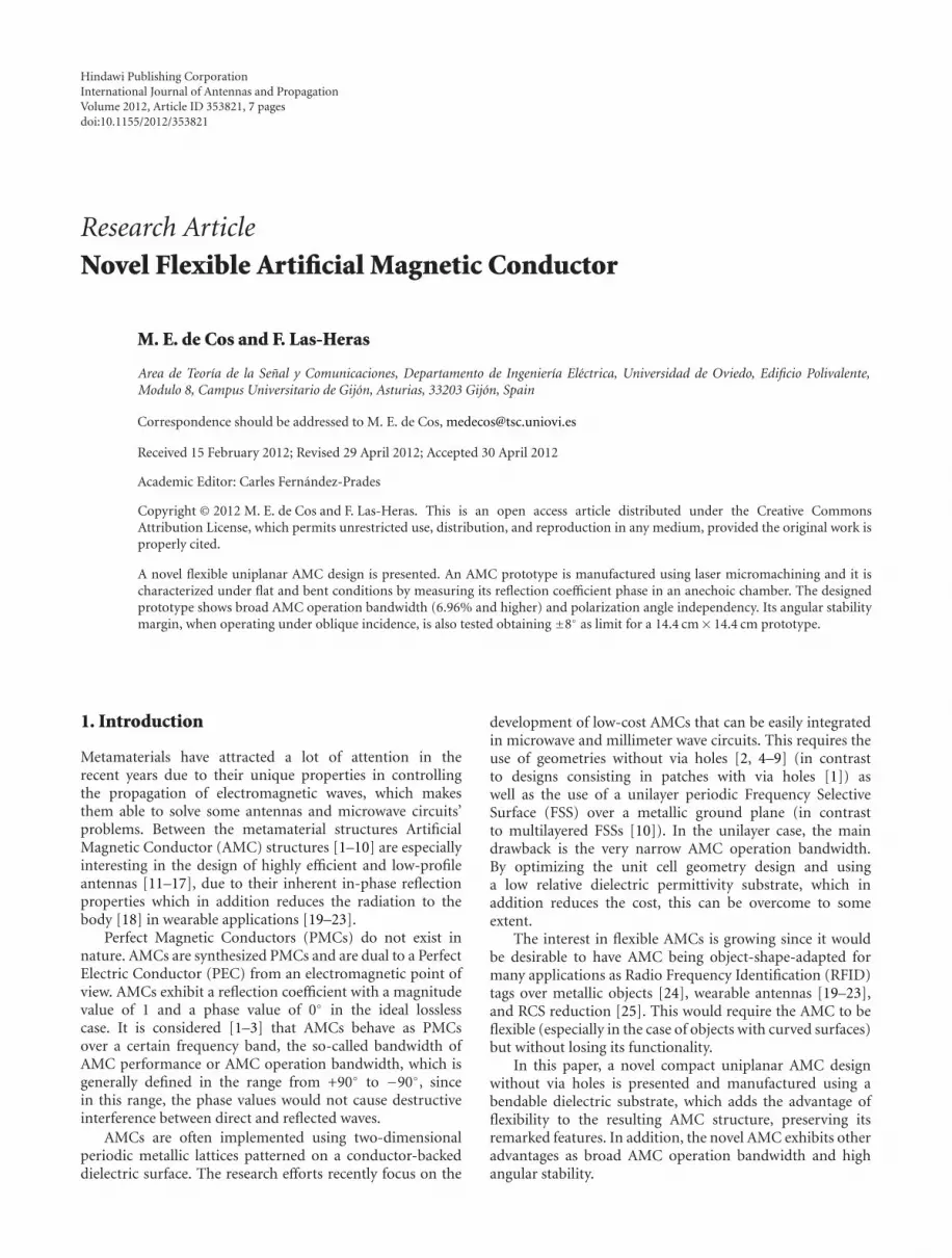
Figure 1: AMC unit-cell design: (a) unit-cell geometry top view and (b) simulation setup.
2. AMC Desing
In an AMC structure each unit cell implements a distributedparallel LC network having one or more resonant frequen-cies. The resonance frequency is where the high impedanceand AMC conditions occur and for a parallel LC circuit isequal to 1/(2π
√LC), while in-phase reflection bandwidth is
proportional to√L/C. In order to achieve an AMC structure
at a certain frequency and with the desired bandwidtha designer can modify the unit cell geometry togetherwith substrate’s relative dielectric permittivity and thickness.The thicker the dielectric substrate is, the wider the AMCbandwidth is. The higher the dielectric substrate relativepermittivity, the lower the resonance frequency but also, thelower the AMC bandwidth [6]. Finally, by changing the unitcell geometry the equivalent LC resonant circuit is modified.In order to obtain a wider AMC operation bandwidth, itis necessary to increase L and reduce C. L can be increasedusing a thicker dielectric substrate and also including in thegeometry narrow and long strips (lines). C can be reducedby reducing substrate’s relative dielectric permittivity εr andincreasing the gap between the metallization edge and theunit-cell edge (and so the gap between adjacent unit cells). Inorder to obtain both compact size and broad AMC operationbandwidth, a trade-off solution regarding εr and substratethickness has to be adopted.
Taking all these considerations into account, a novel uni-planar AMC at 6 GHz has been designed using ROGER3003substrate with a thickness h = 0.762 mm, relative dielectricpermittivity εr = 3.0, and loss tangent tgδ = 0.0013.
Finite Element Method (FEM) together with the Bloch-Floquet theory is used in simulation to search for thefrequency band in which the periodic structure behaves as anAMC. The AMC reflection coefficient for a uniform incidentplane wave is simulated using HFSS of Ansoft, modeling a
single cell of the structure with periodic boundary conditions(PBC) on its sides and resembling the modeling of an infinitestructure [1, 6, 7, 9]. The periodic structure is illuminated,launching normal plane waves using a waveport positioneda half-wavelength above it (see Figure 1(b)). The phasereference plane is taken on the periodic surface. The phaseof the reflection coefficient of the AMC plane is compared tothat of a PEC plane taken as reference and placed in identicalposition, in the same way as in [1].
The geometry of the AMC unit cell is shown inFigure 1(a). Its design has taken into account that the AMCwill be subsequently bent. When defining “h,” the thicknessof the substrate is taken into account that it is desired to beas thin as possible considering the thickness commerciallyavailable and to be bendable. Also the thinner the dielectricsubstrate, the higher the AMC’s angular stability underoblique incidence. Very narrow strips have been avoidedsince they may break when the AMC is bent, despite the longand narrow strips increasing the bandwidth of operation asAMC. Internal gaps in the geometry are used to modify theequivalent C and thus adjust the frequency and bandwidth,as desired (in addition to what has been explained earlier inthis section). The final optimized dimensions for operationat 6 GHz are detailed in Table 1. From the simulatedreflection coefficient phase of the designed AMC structure(see Figure 2), it can be concluded that the resonancefrequency is 6 GHz with an AMC operation bandwidth of500 MHz (8.33% with respect to the central frequency)which is a broad bandwidth for a low-profile AMC (λ0/65.6at 6 GHz).
The AMC performance under different polarization ofthe electrical incident field (under normal incidence) andunder oblique incidence is very important in some of theAMC intended applications as for example RFID tags, orwearable antennas. In the case of RFID tags when combining
International Journal of Antennas and Propagation 3
5 5.5 6 6.5 7 7.5
−180
−135
−90
−45
0
45
90
135
180
Frequency (GHz)
Refl
ecti
on p
has
e (d
eg)
0◦
15◦
30◦60◦
90◦
45◦
Figure 2: Simulated reflection phase of the AMC surface fordifferent incident field (Einc) polarization angles = 0◦, 15◦, 30◦, 45◦,60◦, and 90◦.
Table 1: Unit-cell dimensions.
Dimensions (mm)
W a b c d e f g1 g2 i
12.0 6.456 1.646 1.827 0.609 0.945 0.730 0.032 0.154 0.522
the AMC with the antenna, the angular stability of the AMCwill influence the antenna radiation performance, and thiswill have direct impact on the angular reading range of thefinal RFID tag depending on the position of the reader withrespect to the tagged object. Following this, an AMC designwith as higher angular stability as possible is desirable.
Aiming to study the angular stability margin [26] of thepresented structure, the reflection coefficient phase versusfrequency for different incident angles θinc between 0◦
and 60◦ has been simulated for transverse-electric- (TE-)polarized waves. The absolute and relative deviations of theresonant frequency which are, respectively, 50 MHz, 0.82%for θinc = 40◦ and 100 MHz, 1.6% for θinc = 60◦ can beobtained from Figure 3. The AMC operation bandwidth isslightly reduced from θinc = 40◦. From these obtained results,it can be concluded that the presented AMC design is highlystable as its angular margin ranges from 0◦ to 60◦ preservingan AMC operation bandwidth of 260 MHz in which theoperation frequency of 6 GHz is always included.
3. Flexible AMC’s Characterization
In order to validate the simulation results, a 12 × 12 cellsplanar AMC prototype has been manufactured using lasermicromachining to be measured.
There are many arbitrary ways of bending a flexibleAMC. Two typical different bending patterns have beenselected and tested (see Figure 4): a “creeping” pattern(henceforth referred to as creeping prototype) which can becaused in textile AMC integrated in the garment, for example
−180
−135
−90
−45
45
0
90
135
180
Refl
ecti
on p
has
e (d
eg)
5 5.5 6 6.5 7 7.5Frequency (GHz)
0◦
20◦40◦
60◦
Figure 3: Simulated reflection phase of the AMC surface for TEpolarizations for different incident angles θinc = 0◦, 15◦, 30◦, 45◦,and 60◦.
when the arm is bent at the elbow, and a “smooth” pattern(henceforth referred as smooth prototype) which can becaused in the torso or in the shoulder.
3.1. Measurement Setup in Anechoic Chamber. Two-hornantenna probes working in the band 5–7 GHz have beenchosen as Tx and Rx (see Figure 5) in the measurement setup(similar to the one used in [7, 9]), being 3 m the separationbetween each probe and the object under test. The measuredprototypes physical size is 14.4 cm× 14.4 cm (PEC and AMChave the same size). For the upper frequency ( f = 7 GHz),the far field distance (RFF = 2D2/λ) is RFF,7 GHz ∼ 0.97 m,whereas for the lower frequency ( f = 5 GHz) it decreasesuntil RFF,5 GHz ∼ 0.69 m. Thus, the prototypes have beenmeasured in far field conditions.
3.2. Reflection Phase Measurement for AMC Band Determina-tion. To calculate the reflection coefficient of the AMC struc-ture the same methodology as for the full-wave simulation,based on the utilization of a reference measurement (metallicplate) [1, 7], is followed.
Firstly the flat AMC has been characterized and then theprototype has been bent and measured.
The measured reflection phase of the flat and bentmanufactured prototypes for normal incidence conditions isshown in Figure 6. The flat prototype has the resonance at6.178 GHz which means a 2.9% deviation with respect to thesimulation (6.0 GHz), very probably due to under-etching inthe laser micromachining.
From Table 2 and Figure 6, it can be observed that almostthere is no frequency shift for the manufactured creepingbent prototype with respect to the flat prototype resonance,whereas the smooth bent prototype has its resonance at6.208 GHz, which means just a 1.69% deviation with respectto the flat prototype. The flat prototype shows a 430 MHz(6.96%) AMC operation bandwidth in good agreement withthe simulated value (8.33%) (see Figure 2), whereas the

4 International Journal of Antennas and Propagation
(b)(a) (c)
hs
hc1 hc2WsWc1 Wc2
Figure 4: (a) Flat manufactured prototype and bending patters: (b) smooth prototype with Ws = 125 mm and hs = 30 mm; (c) creepingprototype with Wc1 = 60 mm, Wc2 = 52 mm, hc1 = 18 mm, and hc2 = 15 mm.
Tx horn antenna
Rx horn antenna
Tx horn antenna
Rx horn antenna
Figure 5: Reflection coefficient measurement setup in anechoic chamber.
Table 2: Prototypes comparison.
PrototypeResonance
frequency (GHz)
Frequency deviationwith respect to flat
(%)
Measuredbandwidth
(%)
Flat 6.178 0 6.96
Smooth 6.073 1.69 8.02
Creeping 6.208 0.48 10.07
creeping bent prototype exhibits 625 MHz (10.07%) and thesmooth bent AMC shows 487 MHz (8.02%), even slightlywider than that of the flat prototype.
3.3. Reflection Phase Characterization for Different Field Polar-ization Angles. The reflection phase stability of the man-ufactured AMC prototypes with respect to the incident
field polarization angle (ϕ) has been also tested throughmeasurements.
It has been proved that under normal incidence (θinc =0◦) the flat prototype presents the same reflection phase forany polarization due to the unit cell symmetry (see Figure 7).In the case of the bent prototype, this invariance with respectto the polarization angle is also present.
3.4. Reflection Phase Characterization for Different IncidenceAngles. The angular stability under oblique incidence hasbeen analyzed for both the smooth and the creepingprototypes. The reflection coefficient phase versus frequency,for different incident angles θinc, has been measured. Forthe flat prototype, resonance conditions are met within anangular margin of θinc = ±10◦ (see Figure 8), whereasfor the smooth and creeping bent prototypes the obtainedangular margin is θinc = ±8◦ (see Figures 9 and 10). Thedifferences between simulation and measurements can be

International Journal of Antennas and Propagation 5
5.4 5.6 5.8 6 6.2 6.4 6.6
Frequency (GHz)
Flat
Smooth
Creeping
0
−180
−135
−90
−45
45
90
135
180
Refl
ecti
on p
has
e (◦
)
Figure 6: Measured reflection coefficient phase of the flat and bentprototypes versus frequency.
5.5 5.6 5.7 5.8 5.9 6 6.1 6.2 6.3 6.4 6.5Frequency (GHz)
−180
−135
−90
−45
0
45
90
135
180
Refl
ecti
on p
has
e (◦
)
0◦
15◦
30◦60◦
90◦
45◦
Figure 7: Reflection phase of the manufactured prototype fordifferent incident field (Einc) polarization angles (ϕ).
attributed to the small and finite size of the manufacturedprototype, which leads to some nulls in the scattered fieldamplitude, depending on the incident angle and the distancebetween the prototype and the antennas. This also happenswhen characterizing a finite-size PEC following the sameprocedure.
The presented results show that it is possible to obtaina flexible AMC without reducing the bandwidth of AMCperformance with respect to a rigid AMC that uses the sameunit-cell design and preserving its angular stability underoblique incidence.
5.8 5.9 6 6.1 6.2 6.3 6.4 6.5
Frequency (GHz)
Incident angle 0ºIncident angle 4ºIncident angle 10º
Incident angle −4ºIncident angle −10º
−180
−135
−90
−45
0
45
90
135
180
Refl
ecti
on p
has
e (◦
)
Figure 8: Reflection phase of the manufactured flat prototype fordifferent incident angles (θinc).
5.4 5.6 5.8 6 6.2 6.4
Frequency (GHz)
−180
−135
−90
−45
0
45
90
135
180
Refl
ecti
on p
has
e (◦
)
0◦
4◦
8◦
−4◦
−8◦
Figure 9: Reflection phase of the manufactured smooth prototypefor different incident angles (θinc).
4. Conclusions
A novel flexible uniplanar AMC design based on FEMsimulations has been presented. A prototype has beenmanufactured using a bendable dielectric substrate and it hasbeen characterized by means of reflection coefficient phasemeasurements in anechoic chamber under flat and bentconditions. Broad AMC operation bandwidth, polarizationangle independency under normal incidence, and highangular stability under oblique incidence have been found.
The presented uniplanar low-profile design without viaholes, together with the flexible characteristic, low cost,simple fabrication, and integration, makes it very attractive

6 International Journal of Antennas and Propagation
5.4 5.6 5.8 6 6.2 6.4 6.6
Frequency (GHz)
−180
−135
−90
−45
0
45
90
135
180
Refl
ecti
on p
has
e (◦
)
0◦
4◦
8◦
−4◦
−8◦
Figure 10: Reflection phase of the manufactured creeping proto-type for different incident angles (θinc).
for applications involving antennas in RFID tags, wearablesystems, and RCS reduction. Also it could be used as part ofMicrowave Integrated Circuits (MICs).
Acknowledgments
This work has been supported by the Ministerio de Cienciae Innovacion of Spain/FEDER under Projects TEC2011-24492 (iScat) and CONSOLIDER-INGENIO CSD2008-00068 (TERASENSE), by the Gobierno del Principado deAsturias (PCTI)/FEDER-FSE under Projects EQUIP08-06,FC09-COF09-12, EQUIP10-31, and PC10-06 (FLEXANT).
References
[1] D. Sievenpiper, L. Zhang, R. F. Jimenez Broas, N. G.Alexopolous, and E. Yablonovitch, “High-impedance electro-magnetic surfaces with a forbidden frequency band,” IEEETransactions on Microwave Theory and Techniques, vol. 47, no.11, pp. 2059–2074, 1999.
[2] F. R. Yang, K. P. Ma, M. Yongxi Qian, and T. Itoh, “Auniplanar compact photonic-bandgap (UC-PBG) structureand its applications for microwave circuits,” IEEE Transactionson Microwave Theory and Techniques, vol. 47, no. 8, pp. 1509–1514, 1999.
[3] F. Yang and Y. Rahmat-Samii, Electromagnetic Band-GapStructures in Antenna Engineering, The Cambridge RF andMicrowave Engineering Series, Cambridge University, 2008.
[4] J. McVay, N. Engheta, and A. Hoorfar, “High impedance met-amaterials surfaces using Hilbert-curve inclusions,” IEEEMicrowave and Wireless Components Letters, vol. 14, no. 3, pp.130–132, 2004.
[5] Y. Kim, F. Yang, and A. Z. Elsherbeni, “Compact artificialmagnetic conductor designs using planar square spiral geome-tries,” Progress in Electromagnetics Research, vol. 77, pp. 43–54,2007.
[6] M. E. De Cos, F. L. Heras, and M. Franco, “Design of planarartificial magnetic conductor ground plane using frequency-selective surfaces for frequencies below 1 GHz,” IEEE Antennasand Wireless Propagation Letters, vol. 8, pp. 951–954, 2009.
[7] M. E. De Cos, Y. Alvarez, and F. Las-Heras, “Planar artificialmagnetic conductor: design and characterization setup inthe RFID SHF band,” Journal of Electromagnetic Waves andApplications, vol. 23, no. 11-12, pp. 1467–1478, 2009.
[8] D. J. Kern, D. H. Werner, A. Monorchio, L. Lanuzza, and M. J.Wilhelm, “The design synthesis of multiband artificial mag-netic conductors using high impedance frequency selectivesurfaces,” IEEE Transactions on Antennas and Propagation, vol.53, no. 1 I, pp. 8–17, 2005.
[9] M. E. De Cos, Y. Alvarez, R. C. Hadarig, and F. Las-Heras,“Novel SHF-band uniplanar artificial magnetic conductor,”IEEE Antennas and Wireless Propagation Letters, vol. 9, pp. 44–47, 2010.
[10] A. Monorchio, G. Manara, and L. Lanuzza, “Synthesis ofartificial magnetic conductors by using multilayered frequencyselective surfaces,” IEEE Antennas and Wireless PropagationLetters, vol. 1, pp. 196–199, 2002.
[11] F. Yang and Y. Rahmat-Samii, “Reflection phase characteriza-tions of the EBG ground plane for low profile wire antennaapplications,” IEEE Transactions on Antennas and Propagation,vol. 51, no. 10 I, pp. 2691–2703, 2003.
[12] J. McVay, A. Hoorfar, and N. Engheta, “Small dipole antennanear peano high-impedance surfaces,” in Proceedings of theIEEE Antennas and Propagation Society Symposium, vol. 1, pp.305–308, June 2004.
[13] H. Mosallaei and K. Sarabandi, “Antenna miniaturizationand bandwidth enhancement using a reactive impedancesubstrate,” IEEE Transactions on Antennas and Propagation,vol. 52, no. 9, pp. 2403–2414, 2004.
[14] L. Akhoondzadeh-Asl, D. J. Kern, P. S. Hall, and D. H. Werner,“Wideband dipoles on electromagnetic bandgap groundplanes,” IEEE Transactions on Antennas and Propagation, vol.55, no. 9, pp. 2426–2434, 2007.
[15] J. Liang and H. Y. D. Yang, “Radiation characteristics of amicrostrip patch over an electromagnetic bandgap surface,”IEEE Transactions on Antennas and Propagation, vol. 55, no.6, pp. 1691–1697, 2007.
[16] A. P. Feresidis, G. Goussetis, S. Wang, and J. C. Vardaxoglou,“Artificial magnetic conductor surfaces and their applicationto low-profile high-gain planar antennas,” IEEE Transactionson Antennas and Propagation, vol. 53, no. 1 I, pp. 209–215,2005.
[17] J. R. Sohn, K. Y. Kim, H. S. Tae, and J. H. Lee, “Comparativestudy on various artificial magnetic conductors for low-profileantenna,” Progress in Electromagnetics Research, vol. 61, pp. 27–37, 2006.
[18] E. Rajo-Iglesias, L. Inclan-Sanchez, and Q. Quevedo-Teruel,“Back radiation reduction in patch antennas using planar softsurfaces,” Progress In Electromagnetics Research Letters, vol. 6,pp. 123–130, 2009.
[19] S. Zhu and R. Langley, “Dual-band wearable textile antennaon an EBG substrate,” IEEE Transactions on Antennas andPropagation, vol. 57, no. 4, pp. 926–935, 2009.
[20] M. Mantash, A-C. Tarot, S. Collardey, and K. Mabjoubi,“Dual-band antenna for W-LAN applications with EBG,” inProceedings of the 5th International Congress on Advanced Elec-tromagnetic Materials in Microwave and Optics (Metamaterials’11), pp. 456–458, Barcelona, Spain, October 2011.
[21] M. Mantash, A. C. Tarot, S. Collardey, and K. Mahdjoubi,“Dual-band CPW-fed G-antenna using an EBG structure,” in

International Journal of Antennas and Propagation 7
Proceedings of the 6th Loughborough Antennas and PropagationConference (LAPC ’10), pp. 453–456, November 2010.
[22] P. Salonen and Y. Rahmat-Samii, “Textile antennas: effectsof antenna bending on input matching and impedancebandwidth,” IEEE Aerospace and Electronic Systems Magazine,vol. 22, no. 3, pp. 10–14, 2007.
[23] P. Salonen, F. Yang, Y. Rahmat-Samii, and M. Kivikoski,“WEBGA—Wearable electromagnetic band-gap antenna,” inProceedings of the IEEE Antennas and Propagation SocietySymposium, vol. 1, pp. 451–454, Monterrey, Calif, USA, June2004.
[24] R. C. Hadarig, M. E. De Cos Gomez, Y. Alvarez, and F. Las-Heras, “Novel bow-tie—AMC combination for 5.8-GHz RFIDtags usable with metallic objects,” IEEE Antennas and WirelessPropagation Letters, vol. 9, pp. 1217–1220, 2010.
[25] M. E. de Cos, Y. Alvarez, and F. Las-Heras, “A novel approachfor RCS reduction using a combination of artificial magneticconductors,” Progress in Electromagnetics Research, vol. 107,pp. 147–159, 2010.
[26] C. R. Simovski, P. De Maagt, S. A. Tretyakov, M. Paquay, andA. A. Sochava, “Angular stabilisation of resonant frequency ofartificial magnetic conductors for TE-incidence,” ElectronicsLetters, vol. 40, no. 2, pp. 92–93, 2004.

Hindawi Publishing CorporationInternational Journal of Antennas and PropagationVolume 2012, Article ID 980916, 7 pagesdoi:10.1155/2012/980916
Research Article
Flexible Sierpinski Carpet Fractal Antenna on a Hilbert SlotPatterned Ground
Vasa Radonic,1 Keith Palmer,2 Goran Stojanovic,1 and Vesna Crnojevic-Bengin1
1 Faculty of Technical Sciences, University of Novi Sad, Trg Dositeja Obradovica 6, 21000 Novi Sad, Serbia2 Department of Electrical and Electronic Engineering, Stellenbosch University, Private Bag X1, Matieland,Stellenbosch 7602, South Africa
Correspondence should be addressed to Vasa Radonic, [email protected]
Received 15 December 2011; Accepted 5 April 2012
Academic Editor: Carles Fernandez-Prades
Copyright © 2012 Vasa Radonic et al. This is an open access article distributed under the Creative Commons Attribution License,which permits unrestricted use, distribution, and reproduction in any medium, provided the original work is properly cited.
This paper presents a novel design of fractal antenna on a flexible substrate that operates in UMTS band (universal mobiletelecommunication system, 1.92–2.17 GHz). The antenna consists of a Sierpinski carpet fractal radiator, which reduces the overallsize of the antenna, and it is realized on top of a Hilbert slot in the ground layer, to achieve required impedance matching. Theantenna is compact with the overall dimensions equal to 70 mm × 31 mm × 0.075 mm. Influence that folding has on the initialplanar topology is investigated in detail. The obtained results show that the proposed antenna is more tolerant to folding than theconventional patch and that it exhibits relatively stable radiation patterns even when folded in complex manners.
1. Introduction
Designing a small antenna with good bandwidth perfor-mance presents a challenge for modern communicationdevices, such as Bluetooth or WLAN devices. To minimizethe size of the antenna or to improve its characteristics,various solutions based on fractal geometry have recentlybeen proposed [1–8]. Different fractal geometries, such asPeano, Hilbert, or Sierpinski curves, have been used to bringforth the benefits of small size [2, 4, 6–8], wide bandwidth[5], or multiband operation [3, 5, 6]. This paper presents afractal topology that is tolerant to folding.
Fractal curves are unique for their self-similarity andspace-filling properties. Due to the self-similarity, a fractalantenna being made up of many differently scaled copiesof itself is likely to maintain similar radiation parametersin different bands proportional to the wavelengths. Onthe other hand, the space-filling property of fractals allowstheoretically the design of infinite-length lines on finitesubstrate areas, thus leading to compact antennas.
Flexible electronics are becoming more viable with therecent technological developments opening up possibilitiesto integrate wireless functions into clothing, moving objects,or into animals to monitor various parameters of interest.
Although flexible technology offers components that canbend together with the host medium (e.g., textile) withpractically no disturbance to the subject wearing it, bendingcan significantly deteriorate the performances of the wirelesscomponents, most notably the antenna. Significant researchefforts are currently focused on study and analyzing theviability of these flexible substrate materials. Several exper-imental studies have been carried out recently to investigatethe effects of antenna bending on its characteristics such asresonant frequency, return loss, impedance bandwidth, gain,and radiation patterns [8–13].
In this paper, we propose a novel flexible antenna basedon the Sierpinski carpet fractal curve of the third order,realized on a Hilbert slotted ground. The proposed antennawas simulated using CST Microwave Studio and comparedwith the conventional patch antenna. Impact of foldingon both antennas was analyzed in details. To validate thesimulation results, the proposed antenna was fabricated andmeasured.
2. Fractal Antenna
The proposed antenna consists of a Sierpinski carpet radiatorrealized on the top side of the flexible substrate with

2 International Journal of Antennas and Propagation
a
a
l
w
(a)
x
gHwH
lp
(b)
Figure 1: (a) Proposed fractal antenna on a Hilbert slot patterned ground (black: top metallic layer, dark gray: bottom metallic layer); (b)magnified detail of the patterned ground under the feed line (black: bottom metallic layer).
a Hilbert slot on the bottom side (Figure 1). The Sierpinskicarpet antenna is in essence a square metallic patch dividedinto 9 congruent subsquares in a 3-by-3 grid, in which themetallization of the middle square section is removed. Thesame procedure is then applied recursively to the remaining8 subsquares and again to the resulting elements. In thatmanner, the third-order fractal antenna is obtained with thedimensions of the radiator equal to 20 mm × 20 mm. Theantenna is fed by a 2.6 mm wide and 10 mm long microstripline.
In order to match the antenna to a 50Ω SMA connector,four serially connected slots in the shape of the Hilbertfractal curve of the second order were printed in the groundplane (Figure 1(b)). The position and line width and spacingof the Hilbert slot are the most important parametersfor the impedance matching as well as for obtaining agood radiation pattern and reflection coefficient of theantenna. The position x and the line width and spacing,denoted wH and gH , respectively, were optimized with thefollowing values obtained: x = 0.6 mm, wH = gH = 0.5 mm.The total length of the Hilbert slot is 6 mm. As can beseen from Figure 1(b), there is no ground plane underthe radiator. The existing ground plane is split into twosections by the Hilbert slot, generating some electromagneticcoupling. As a consequence, apart from the reduction ofthe ground plane area, a decrease of the antenna resonantfrequency is obtained, which additionally contributes toantenna miniaturization.
The antenna was designed using a 0.075 mm thickKapton substrate with relative permittivity εr = 3.2 anddissipation factor equal to 0.0019. All simulations wereperformed using CST Microwave Studio.
Various ways of bending the antenna were analyzed,shown in Figure 2. In Figure 2(a) the antenna is folded alongone-third of its length in the y-direction, and two-thirds inFigure 1(b). In the cases shown in Figures 1(c) and 1(d) moredemanding modifications are made: the antenna was foldedtwice, along the one and two third of its length, resultingin structures with a cross-section similar to letters C andZ, respectively. In that way, the dimensions of the antennawere significantly changed: its length was decreased while itsheight was increased.
Figure 3 compares the simulated return loss of theinitial planar fractal antenna with the return losses of itsfolded modifications. More detailed results are presentedin Table 1, where the proposed fractal antenna is alsocompared to the conventional patch antenna realized ona partial ground plane and tuned to the same frequency,as well as to the patch’s folded modifications obtained bybending the patch antenna in the same manner as shown inFigure 2. Final dimensions of the patch radiator are 24 mm×24 mm, while the length of the partial ground is 2.1 mm. Tofacilitate the comparison, frequency shifts and variations inthe bandwidth are also listed in Table 1, relative to the planarversions of the antenna in question.
As expected, it can be seen that any folding of theantenna directly impacts on its performances. However, thisimpact is significantly reduced in the case of the proposedfractal antenna: the frequency shift of the patch antennadue to bending ranges between 2.42 and 6.81%, whileit is equal to 3.4% for the worst-case fractal antenna.Fractional bandwidth of the fractal antenna changes upto 25.14%, while conventional one exhibits 34.49%. Theaverage frequency shift for the patch antenna is 4.09% while

International Journal of Antennas and Propagation 3
Table 1: Detailed comparison between performances of the proposed fractal and the conventional patch antenna, for both the planar andthe folded cases.
Antenna type Modification f r [GHz] Δf r [%] FBW [%] ΔFBW [%] S11 [dB]
Fractal
Planar 1.9850 — 5.37 — −25.71 2.0120 1.36 4.02 −25.14 −14.72 2.0120 1.36 5.13 −4.47 −20.83 2.0525 3.40 n/a n/a −9.4
4 2.0255 2.04 4.42 −17.69 −16.3
Patch
Planar 1.9445 — 9.8 — −34.41 1.9985 2.78 8.1 −17.35 −18.42 1.9915 2.42 8.35 −14.80 −22.53 2.0770 6.81 6.42 −34.49 −23.64 2.0295 4.37 7.83 −20.10 −33.5
(a) (b)
(c) (d)
Figure 2: Different ways of folding the antenna: (a) modification 1, (b) modification 2, (c) modification 3, and (d) modification 4.
it is only 2.04% for the proposed fractal antenna. The sameholds for the average variation of the fractional bandwidth:21.7% for the conventional antenna versus only 15.3% forthe fractal antenna. Inspecting the tabulated results, it canbe concluded that the deterioration of performance observedfor simple modifications of the patch antenna (modifications1 and 2) is similar to the case of complex modifications ofthe fractal antenna (modifications 3 and 4). This illustratesthe robustness to folding that the proposed fractal antennaexhibits over the conventional patch. In the same time, thefractal antenna occupies 30% smaller substrate area than thepatch, and it is less sensitive to mechanical strain.
In Figures 4 and 5 radiation patterns in E-plane and H-plane for the planar fractal and patch antennas and theirmodifications relative to the flat antennas are shown. Thepatterns are omnidirectional in H-plane. The average gain
reduction in the case of conventional antenna is 46%, whilethe fractal antenna exhibits 41%. It can be seen that thechange of the main lobe directivity is similar for bothantennas and equal to 40%.
3. Fabrication and Measurement
The proposed fractal antenna was fabricated using aDimatix [14] material deposition printer DMP-3000, whichis cartridge-based piezo inkjet printing system which enablesdirect deposition of fluids (functional materials). The res-olution of the inkjet process is mainly governed by thenozzle diameter (approximately the droplet diameter) andthe statistical variation of the droplet flight and spreadingon the substrate. Resolution can be modified by adjusting

4 International Journal of Antennas and Propagation
0
−5
−10
−15
−20
−25
−30
Flat antennaModification 1Modification 2
Modification 3Modification 4
11(d
B)
1.6 1.7 1.8 1.9 2 2.1 2.2 2.3 2.4
f
S
(GHz)
Figure 3: Simulated return loss for the proposed planar fractal antenna and its folded modifications.
0 60 120 180
0
Rel
ativ
e am
plit
ude
(dB
)
Angle (deg)
Flat antennaModification 1Modification 2
Modification 3Modification 4
−10
−20
−30
−40−180 −120 −60
(a)
0 60 120 180
0
Rel
ativ
e am
plit
ude
(dB
)
Angle (deg)
Flat antennaModification 1Modification 2
Modification 3Modification 4
−1
−2
−3
−5
−4
−180 −120 −60
(b)
Figure 4: Radiations patterns for the proposed fractal antenna: (a) radiation pattern in E-plane, (b) radiation pattern in H-plane.
the angle of the printhead during printing. In the case ofprinting with silver nanoparticle ink (Suntronic Jet SilverU6503, [15]), the minimum droplet diameter was around50 μm and drop spacing was 25 μm (center to center) whichhas obtained by changing the printhead angle. 16 nozzleprinthead with the capacity of 1.5 mL was used. Spacingbetween each nozzle is 254 microns; nozzle diameter isaround 25 μm with average drop sizes of 10 pl. The voltagewaveform amplitude used for piezoelement actuation was27 V, with a firing frequency of 4 kHz. The proposed antennawas printed on 75 μm thick Kapton film substrate with
dielectric constant of 3.2 and dissipation factor of 0.0019[16]. After printing the pattern, silver nanoparticles weresintered on at 200◦C for 45 minutes in order to get a uniformconductive structure of the fabricated antenna and the SMAconnector was mounted using silver paste. Photographs ofthe fabricated fractal antennas are shown in Figure 6, whileFigure 7 shows comparison of simulated and measuredreturn loss for the planar fractal antenna and its measuredgain.
Good agreement is observed, and the fundamental reso-nance occurs at 1.990 GHz as predicted, with reflection better

International Journal of Antennas and Propagation 5
0 60 120 180
0R
elat
ive
ampl
itu
de (
dB)
Angle (deg)
Flat antennaModification 1Modification 2
Modification 3Modification 4
−10
−20
−30
−40−180 −120 −60
(a)
0 60 120 180
0
Rel
ativ
e am
plit
ude
(dB
)
Angle (deg)
Flat antennaModification 1Modification 2
Modification 3Modification 4
−1
−2
−3
−5
−4
−180 −120 −60
(b)
Figure 5: Radiations patterns for the conventional patch antenna: (a) radiation pattern in E-plane, (b) radiation pattern in H-plane.
(a) (b)
Figure 6: Photographs of the fabricated fractal antenna: (a) top layer, (b) bottom layer.
1.5 1.6 1.7 1.8 1.9 2 2.1 2.2 2.3 2.4 2.5
Gai
n (
dBi)
0
−4
−8
−12
−16
−20
−24
−28
0
−5
−10
−15
−20
−25
Simulated S11
Measured S11
Measured gain
11(d
B)
f
S
(GHz)
Figure 7: Comparison of simulated and measured return losses for the planar fractal antenna and the measured gain.

6 International Journal of Antennas and Propagation
0 60 120 180
0
Rel
ativ
e am
plit
ude
(dB
)
Angle (deg)
MeasuredSimulated
−10
−20
−30
−40
−5
−15
−25
−35
−180 −120 −60 0 60 120 180
0
Rel
ativ
e am
plit
ude
(dB
)
Angle (deg)
MeasuredSimulated
−10
−20
−30
−40
−5
−15
−25
−35
−180 −120 −60
(a)
0 60 120 180
0
Rel
ativ
e am
plit
ude
(dB
)
Angle (deg)
−10
−20
−30
−40
−5
−15
−25
−35
−180 −120 −60
Measured modification 2Measured modification 3Simulated modification 2Simulated modification 3
0 60 120 180
0
Rel
ativ
e am
plit
ude
(dB
)
Angle (deg)
−10
−20
−30
−40
−5
−15
−25
−35
−180 −120 −60
Measured modification 2Measured modification 3Simulated modification 2Simulated modification 3
(b)
Figure 8: Comparison of simulated and measured radiations patterns in E-plane and H-plane for: (a) the planar fractal antenna and (b)modification 2 and modification 3 of the fractal antenna.
than −15 dB. The −10 dB bandwidth is contained between1.93 GHz and 2.043 GHz, yielding 113 MHz bandwidth, thatis, 5.7%.
Figure 8 shows the comparison of simulated and mea-sured radiation patterns for the planar fractal antenna and itstwo modifications: modification 2 and modification 3. Thepattern measurements were taken in an anechoic chamberusing a vector network analyzer, and the measured patternsagree well with the simulated ones bar for some ripple that isascribed to reflections in the chamber.
4. Conclusion
A flexible Sierpinski carpet fractal antenna has been pre-sented, more tolerant to folding than its conventionalpatch counterpart. The proposed antenna achieves improvedperformance such as the smaller influence of folding to theresonant frequency and the smaller variation of the gain,while the main lobe directivity changes similarly for both thefractal and the conventional antennas. The average frequencyshift induced by folding of the patch antenna is 4.09% whileit is only 2.04% for the proposed fractal antenna. The same

International Journal of Antennas and Propagation 7
holds for the average variation of the fractional bandwidth:21.7% for the conventional antenna versus only 15.3% forthe fractal antenna. Moreover, the proposed fractal antennaoccupies 30% smaller surface than the patch, and it is lesssensitive to mechanical strain.
Acknowledgments
This work has been partially supported by the EuropeanCommission through FP7 Project MultiWaveS, Grant no.PIRSES-GA-2009-247532. The authors thank the Depart-ment of Broadband Infocommunications and Electromag-netic Theory, Budapest University of Technology and Eco-nomics, Budapest, Hungary, for the anechoic chambermeasurements.
References
[1] M. F. Pantoja, F. G. Ruiz, A. R. Bretones, and R. G. Martın,“GA design of wire pre-fractal antennas and comparisonwith other euclidean geometries,” IEEE Antennas and WirelessPropagation Letters, vol. 2, pp. 238–241, 2003.
[2] I. K. Kim, J. G. Yook, and H. K. Park, “Fractal-shape small sizemicrostrip patch antenna,” Microwave and Optical TechnologyLetters, vol. 34, no. 1, pp. 15–17, 2002.
[3] C. Puente-Baliarda, J. Romeu, R. Pous, and A. Cardama, “Onthe behavior of the sierpinski multiband fractal antenna,” IEEETransactions on Antennas and Propagation, vol. 46, no. 4, pp.517–524, 1998.
[4] J. Anguera, C. Puente, C. Borja, and J. Soler, “Fractal-shapedantennas: a review,” in Wiley Encyclopedia of RF and MicrowaveEngineering, K. Chang, Ed., vol. 2, pp. 1620–1635, Wiley, NewYork, NY, USA, 2005.
[5] S. Wong and B. L. Ooi, “Analysus and bandwidth enchcementof Sierpinski carpet antenna,” Microwave and Optical Technol-ogy Letters, vol. 31, no. 1, 2001.
[6] R. Azaro, E. Zeni, T. Gazzini, R. Dallapiccola, and A. Massa,“Synthesis of a three-dimensional triband (L1-L2 GPS and Wi-Fi) prefractal tree antenna,” Microwave and Optical TechnologyLetters, vol. 49, no. 9, pp. 2114–2118, 2007.
[7] J. P. Gianvittorio and Y. Rahmat-Samii, “Fractal antennas: anovel antenna miniaturization technique, and applications,”IEEE Antennas and Propagation Magazine, vol. 44, no. 1, pp.20–36, 2002.
[8] S. R. Best, “On the resonant properties of the Koch fractal andother wire monopole antennas,” IEEE Antennas and WirelessPropagation Letters, vol. 1, pp. 74–76, 2002.
[9] E. C. Lee, P. J. Soh, N. B. M. Hashim et al., “Design andfabrication of a flexible Minkowski fractal antenna for VHFapplications,” in Proceedings of the 5th European Conference onAntennas and Propagation (EUCAP ’11), pp. 521–524, April2011.
[10] J. Jung, H. Lee, and Y. Lim, “Broadband flexible meander lineantenna with vertical lines,” Microwave and Optical TechnologyLetters, vol. 49, no. 8, pp. 1984–1987, 2007.
[11] S. Subramaniam and B. Gupta, “Design and developmentof flexible fabric antenna for body-worn applications and itsperformance study under flat and bent positions,” Microwaveand Optical Technology Letters, vol. 53, no. 9, pp. 2004–2011,2011.
[12] T. F. Kennedy, P. W. Fink, A. W. Chu, N. J. Champagne, G.Y. Lin, and M. A. Khayat, “Body-worn E-textile antennas: the
good, the low-mass, and the conformal,” IEEE Transactions onAntennas and Propagation, vol. 57, no. 4, pp. 910–918, 2009.
[13] C. Hertleer, H. Rogier, L. Vallozzi, and L. Van Langenhove,“A textile antenna for off-body communication integratedinto protective clothing for firefighters,” IEEE Transactions onAntennas and Propagation, vol. 57, no. 4, pp. 919–925, 2009.
[14] http://www.dimatix.com/.[15] http://www.sunchemical.com/.[16] http://www.gts-flexible.co.uk.

Hindawi Publishing CorporationInternational Journal of Antennas and PropagationVolume 2012, Article ID 905409, 8 pagesdoi:10.1155/2012/905409
Research Article
Performance of High-Permittivity Ceramic-Polymer Compositeas a Substrate for UHF RFID Tag Antennas
A. A. Babar,1 V. A. Bhagavati,2 L. Ukkonen,1 A. Z. Elsherbeni,3 P. Kallio,2 and L. Sydanheimo1
1 Rauma Research Unit, Department of Electronics, Tampere University of Technology, 26100 Rauma, Finland2 Micro and Nano Systems Research Group, Department of Automation Science and Engineering,Tampere University of Technology, 33720 Tampere, Finland
3 Electrical Engineering Department, The University of Mississippi, University, MS 38677, USA
Correspondence should be addressed to A. A. Babar, [email protected]
Received 12 December 2011; Accepted 4 April 2012
Academic Editor: Carles Fernandez-Prades
Copyright © 2012 A. A. Babar et al. This is an open access article distributed under the Creative Commons Attribution License,which permits unrestricted use, distribution, and reproduction in any medium, provided the original work is properly cited.
A high-permittivity ceramic-polymer composite substrate is fabricated and proposed for its potential use in UHF RFID tags.The substrate is developed using high-permittivity Barium Titanate (BaTiO3) ceramic powder mixed with polydimethylsiloxane(PDMS) polymer. The resulting composite achieves a soft, hydrophobic, heat resistant, low loss, and flexible material with highdielectric constant. The percentage of the ceramic powder in the composite helps in achieving variable permittivity values. Whenthis material is used as a substrate for a tag antenna, it will help the tag to be reduced in size, to conform to uneven or roughsurface, and to be less vulnerable to breakage or other environmental damages. A small passive UHF RFID tag antenna is designed,fabricated, and attached to this type of composite substrate, to demonstrate the performance of this composite material.
1. Introduction
There have been a growing demand and progress in thefield of wireless communication and identification in recentyears. The use of Radio frequency identification (RFID)technology as an effective and reliable way of tracking andsensing various objects is gaining much importance recently.An RFID system is composed of two main components, thereader and the tag. A commonly used passive RFID tag iscomposed of an IC chip and an antenna, which contains itsown unique identification code (ID) [1]. The identificationcode is sent back to the reader when the tag is interrogated orenergized through backscattered modulation of the incidentcontinuous wave [2]. The input impedance of a passiveUHF RFID tag antenna and reflectivity rely on the physicalproperties of the substrate or material it is attached to and onthe antenna’s geometry. The permittivity of the substrate hasa great impact on the size of the tag antenna. Using higher-permittivity substrate can be useful in reducing the size of thetag antenna.
Substrates play a vital role in the development and useof electronic devices. Flexible substrates have gained much
importance in recent years. Different techniques and types ofmaterials have been used to develop flexible electronic sub-strates [3–6]. One of the most commonly used flexible plasticsubstrates is polyester, PEEK (polyaryletheretherketone) andpolyimides [7, 8]. Several techniques are being studied andused to embed and integrate electronic components withthese flexible substrate materials [9, 10]. There has beena growing interest in the development of flexible antennasusing flexible substrates. This gives the advantage of havingconformal antennas being placed and attached to unevenshaped structures and surfaces. It is more desirable to useflexible substrate materials that are less vulnerable to heat,water, and other damaging effects.
The size of the RFID tag antenna is also one of the majorconcerns for RFID applications. Reducing the size of the tagantenna comes at the cost of its performance, such as gainand efficiency of the antenna. Therefore, achieving a smallRFID tag antenna, with improved efficiency is an importantand challenging task for antenna designers. Using high-permittivity substrates is considered for reducing the overallsize and for having compact antenna structures. Several com-mercially available substrates, with high permittivity values,

2 International Journal of Antennas and Propagation
have hard and rigid structures. They are more breakable, lessconformal, and not suitable for uneven surfaces.
In this paper, new high-permittivity substrates have beendeveloped and tested for RFID tag antenna designs. Thesubstrates are soft and flexible in nature, resistant to water,heat, breaking, and other damaging effects. The substrateshave been fabricated by mixing a ceramic powder knownas barium titanate (BaTiO3) with polydimethylsiloxane(PDMS) polymer. Barium titanate is a ferroelectric material,with high dielectric constant values. The dielectric propertiesof the substrates depend on the fabrication process, the ratioand the type of ceramic powder used in the composite.The permittivity value of the substrates can be changed bychanging the percentage of ceramic powder in PDMS. Thisprovides the flexibility to achieve desired high permittivityvalues of the substrates.
To demonstrate the performance of the composite sub-strate for an RFID tag, a small passive UHF RFID tag antennais designed and fabricated on a thin sheet of FR4. It is thenattached to the ceramic-polymer substrate. This was usefulto accurately fabricate the small tag antenna and analyzethe performance of the substrate. The antenna is designedusing miniaturization techniques to reduce the size of the tagantenna and make it more compact and suitable for variousobjects. The substrate of the antenna makes it possible toplace and attach the tag on irregular surfaces and roughterrains. This type of high permittivity composite substrateallows the possibility of achieving small flexible thin tags forfuture applications which may include the design of fullyflexible on-metal, thin, conformal, and embedded tags usinginkjet printing.
The rest of the paper is organized as follows. In Section 2,properties of the ceramic and polymer will be discussed.This will be followed by the fabrication process of thecomposite substrate in Section 3. Section 4 will focus on thedesign and development of the tag antenna. Simulations andmeasurements results are discussed and shown in Section 5,followed by the conclusions in Section 6.
2. Properties of Ceramic and Polymer
In this section, the properties and characteristics of both theceramic powder and the polymer used in this experimentwill be discussed. The ceramic powder used in the compositesubstrate is a ferroelectric material known as barium titanate(BaTiO3). Polydimethylsiloxane (PDMS) polymer is mixedwith the ceramic powder and fabricated, to make it a soft andflexible solid composite substrate.
2.1. Characteristics of PDMS. PDMS is most widely used typeof a silicon-based organic polymer, belonging to a group ofsiloxanes. It is available in fluid, elastomer, and resin form[11]. The chemical structure of PDMS is stated in [11].
PDMS materials have high thermal stability, low surfacetension, characteristic pressure and bulk viscosity. They aretransparent, hydrophobic in nature and durable at hightemperatures. Other PDMS properties include lubricity,
shear stability, high dielectric strength, antifriction, and goodresistance to UV radiations [11, 12].
In the elastomer form, PDMS is suitable for flexiblesubstrates. Elastomeric PDMS structures are typically fabri-cated using viscous liquid and a liquid cross-linking agent.Among other factors such as curing time and temperature,the bending stiffness depends on the amount of cross-linkingagent used. Larger amounts of PDMS result in more rigidstructures [12].
The most common applications of PDMS include rubbermolds, surfactants, water repellents, adhesives, personal careand cosmetics, dielectric encapsulation, hydraulic fluids,lubricants, fuser oil, and protectants. It can also be used invarious other applications such as contact lenses, medicaland microfluidic devices, and applications [11–14].
2.2. Characteristics of BaTiO3. Barium titanate (BaTiO3) is aferroelectric ceramic powder, with piezoelectric properties[15]. It is insoluble in water and alkalis, whereas soluble insome acids such as sulfuric, hydrofluoric, and hydrochloricacids. It usually has very high permittivity values. It canacquire four different shapes of crystals, cubic, tetragonal,orthorhombic, and rhombohedral. However, the permittiv-ity depends on many factors, such as the grain size, shape andsize of the crystals, impurities, and on processing techniques[16]. Ferroelectric ceramics can be used in several applica-tions, such as capacitors, thermostatic devices, light switches,current controllers and to generate ultrasonic energy [15].Similarly, barium titanate is used to manufacture manyelectronic components, such as multilayer capacitors [17],positive temperature coefficient (PTC) thermistors, trans-ducers, and tunable phase shifters [18, 19].
Due to recent advances in electronics, much attention hasbeen focused on small and miniaturized electronic devices.Growing interest is targeting the use of high permittivitymaterial in electronics industry to decrease the size of elec-tronic and wireless components and devices.
3. Fabrication Technique Usedfor Ceramic-Polymer CompositeSubstrate Material
In this section, design and fabrication technique of thecomposite substrate is discussed. A stepwise approach is usedto explain the fabrication process of PDMS-BaTiO3 (bariumtitanate) composite substrate. A similar approach has alsobeen used in [20]. The PDMS used is Sylgard-184, whichis supplied as a two component Kit containing a “base pre-polymer” (the viscous liquid) and a “curing agent” (the liq-uid cross-linking agent) manufactured by Dow Corning [21].
Following are the steps to make the ceramic-polymercomposite substrate.
(1) First, the base prepolymer is mixed with the curingagent in a mass ratio of 10 (pre-polymer): 1 (curingagent). The mixture is then mixed vigorously for 5–10minutes in a plastic container, which enables uniformcross-linking.

International Journal of Antennas and Propagation 3
Figure 1: Degassing chambers used to degas the samples.
(2) After mixing PDMS (the base pre-polymer with thecuring agent), it is left for degassing in a degassingchamber for 15–20 minutes. This helps in extractingpossible air bubbles formed during the process ofmixing. The degassing chambers used for degassingof the samples are shown in Figure 1. In this step, thesamples are placed in the bigger degassing chamber,to accommodate the plastic glass used for mixing.
(3) The degassed mixture of PDMS is mixed with BaTiO3
ceramic powder. The ceramic powder is providedfrom Sachtleben Pigments [22]. The percentage ofceramic powder mixed with PDMS is on a volume-based ratio, as defined in (1) [20]:
v% = Cm/Cρ
Cm/Cρ + Pm/Pρ× 100%. (1)
In the previous equation Cm and Cρ refer to the massand density of the ceramic (BaTiO3), respectively,whereas, Pm and Pρ are the mass and density of thepolymer (PDMS).
In this experiment, 15% and 25% of BaTiO3 ceramicpowder are mixed with PDMS. The BaTiO3 ceramic powderprovided by Sachtleben Pigments has a grain size equal to80 nm. The density of BaTiO3 is equal to 6.02 g/cm3, whereasthe density of PDMS is equal to 1.05 gm/cm3.
(4) After adding PDMS with the ceramic powder, vigor-ous stirring is done for about 15–20 min, as shownin Figure 2. The mixture is stirred until it transformsinto a smooth paste. A smooth white paste withoutany lumps is a good indicator of a good mixture.
(5) The mixture is then poured into a small Petri dishon a flat surface, to have an even distribution of thethick paste inside the container. This mixture can bepoured into different types of molds, depending onthe desired shape, as shown in Figure 3.
(6) After pouring the mixture into the Petri dish, it isagain left for degassing for a continuous time periodof 5-6 hours, to remove excessive air bubbles. Thefirst 5-6 hours are considered crucial, as they help inremoving the maximum amount of air bubbles. It hasbeen observed that, even after 5-6 hours of degassing,
Figure 2: Vigorous mixing of PDMS ceramic powder with PDMSmixture.
Figure 3: Pouring the well-mixed paste into a Petri dish.
few air bubbles are still popping out of the mixture.Therefore, to ensure that the mixture has no airbubbles left, it is kept under vacuum pressure for 30hours, as shown in Figure 4. Usually a solid structureis achieved within 24 hours of curing. This processcan be made faster, by heating the mixture afterdegassing. However, the heating of the composite canmake the substrate structure more rigid, dependingon the applied temperature.
(7) After curing, the composite substrate is carefullytaken out of the Petri dish.
As shown in Figure 5, the final composite substrate is soft andflexible with a smooth surface. The substrate can be softerand more flexible by changing the thickness of the substrate.

4 International Journal of Antennas and Propagation
(a) (b)
Figure 4: (a) Small degassing chamber, to degas the final composite mixture in room temperature. (b) Extraction of air bubbles from thesurface of the composite mixture during degassing.
(a) (b)
Figure 5: Final solid shape of the flexible composite substrate.
4. Antenna Design Technique
In this section, UHF RFID tag antenna design techniques arediscussed. The tag antenna is designed using Ansoft HFSSv.12 [23]. A multilayer substrate approach is used to designand fabricate the tag antenna. The tag antenna is first fabri-cated on a thin sheet of FR4 substrate layer of 0.16 mm thick-ness, using milling machine. Later the tag is attached to theceramic-polymer composite substrate, as stated in Section 3.
Alien Higgs 3 IC with −18 dBm sensitivity is used in thetag antenna [24]. The IC provided by the manufacture comeswith a strap attachment. In order to take the effect of thestrap into account, 0.2 pF of parasitic capacitance is addedin parallel to the nominal IC impedance. The tag is matchedat 860 MHz.
Figure 6 shows the tag antenna in a form of a round sym-metric dipole structure. The IC strap of the tag is attachedbetween the two feeding pads with dimensions representedby a and b. Line d connects the two feeding pads with thetwo symmetric halves of the dipole structure along the x-axis,as shown in Figure 6. The two halves of the dipole structureare shorted or T-matched along the x-axis using line “g”. Theedge “n” of the two sides of the dipole structure is kept at adistance of 1 mm from each side. Table 1 lists the dimensionsof the geometrical parameters of the tag, shown in Figure 6.
a
b cd
e fg
h
m
n
0
0
40◦
72.6◦X
Y
Z
o
k
Figure 6: Geometrical parameters of the designed tag antenna.
Miniaturization techniques are used to reduce the overallsize of the tag. T-matching technique is useful in reducingthe overall size of the tag, by increasing the inductance ofthe antenna. T-matching works as an impedance transformer[25]. The length and width of the shorted line are ofconsiderable importance in tuning the antenna. The tuning

International Journal of Antennas and Propagation 5
Table 1: Geometrical parameters of the tag.
Line Length (mm) Width (mm)
a 3.25 —
b 2.5 —
c 0.75 —
d 3.55 2
e 3.75 2
f 1 —
g 14.5 0.5
h 4.15 —
k 6.75 —
m 7.5 —
n 16.6 —
o 26.5 —
Antenna’s copper part(thickness = 0.035 mm)
FR4 substrate(thickness = 0.16 mm)
2.5 mm Ceramic-polymer composite layer
Figure 7: Side view of the tag antenna substrate.
and matching of the tag antenna to the desired frequency canalso be done by changing the distance “f ” of the shorted line“g” from the feeding pads.
A round-shaped tag with a feeding point aligned in thex-axis of the tag antenna provides a longer current path. Thishelps in reducing the overall size of the tag antenna and inachieving a compact shape of the tag. The tag antenna can betuned further by increasing or decreasing the gap betweenthe two “n” edges or by adjusting the separation distancebetween the two halves of the tag. Figure 7 shows the sideview of the tag, demonstrating a multilayer structure of thetag’s substrate.
Figure 7 illustrates two main layers of the substrate. Firstthe tag is fabricated on a thin sheet of FR4, with 35 μm coppercladding, using milling machine. This is attached to thecustom made composite substrate layer of 2.5 mm thickness.The two layers were attached using commercially availableadhesive glue. The effect of the glue is considered negligiblysmall to affect the tag antennas performance. The two layersare attached carefully, to avoid any air gap in between, asit can alter the effective permittivity of the substrate. Therelative permittivity value of the ceramic-polymer compositelayer in this experiment is approximately equal to 10.5 and8 for 25% and 15% of BaTiO3 mixtures, respectively. Thisis measured by agilent dielectric probe and verified by theexperimental results presented in [26, 27].
5. Simulation and Measurement Results
This section focuses on the simulation and measurementresults of the tag, on a multilayer substrate. Section 5.1
800 820 840 860 880 900 920 940 960 980 1000−18
−16
−14
−12
−10
−8
−6
−4
−2
0
Frequency (MHz)
Pow
er r
eflec
tion
coe
ffici
ent
(dB
)
25% of BaTiO3
15% of BaTiO3
Figure 8: Simulated power reflection coefficient of the RFIDtag antenna with 25% and 15% of BaTiO3 concentration in thecomposite substrate material.
demonstrates the simulated power reflection coefficient andconjugate impedance matching of the designed tag antenna.In Section 5.2, measured results of the tag are discussed.
5.1. Simulation Results of the Tag Antenna. The transfer ofpower between the complex load (IC) impedance and thecomplex source (tag antenna) impedance is analyzed using(2). The power reflection coefficient can be analyzed byconsidering the ratio of the incident power on the tag anten-na (Ptag) and the power reflected back (Prfl), as defined in[28, 29] such that
Prfl
Ptag=
∣∣∣∣ZIC − Z∗aZIC + Za
∣∣∣∣2
. (2)
In the previous equation Za = Ra + jXa is the impedance ofthe tag antenna, whereas ZIC = RIC+ jXIC is the impedance ofthe chip. The superscript (∗) denotes the complex conjugate.Lower value of the power reflection coefficient at the desiredoperating frequency indicates an optimal power transfer. Anoptimal power transfer enables the maximum achievablerealized gain and read range of the tag.
The simulated power reflection coefficient of the tag isshown in Figure 8. The tag is matched to 860 MHz with asubstrate having 25% of BaTiO3 and to 915 MHz with 15%of BaTiO3 composite substrate.
Figure 9 shows the input impedance of the tag antennaand the chip, on top of a 25% ceramic composite substrate,illustrating a good conjugate matching of the tag antennawith the chip, at 860 MHz. This is essential to minimizethe reflection loss at this junction and improve the powertransmission and maximize the read range.
5.2. Measurement Results of the Tag Antenna. The tag anten-na is measured using Tagformance RFID measurementsdevice in an anechoic chamber by Voyantic Ltd., [30]. Theanechoic chamber is designed to measure the UHF RFIDtag antennas. The chamber consists of a rotating table anda linearly polarized reader antenna. The linearly polarized

6 International Journal of Antennas and Propagation
800 820 840 860 880 900 920 940 960 980 1000−300
−200
−100
0
100
200
300
400
500
Frequency (MHz)
Impe
dan
ce (
ohm
)
Tag reactanceTag resistance
Chip resistanceChip reactance
Figure 9: Simulated chip and antenna impedance of the UHF RFIDtag on top of a 25% ceramic-polymer composite.
800 820 840 860 880 900 920 940 960 980 10000
1
2
3
4
5
6
7
Frequency (MHz)
Rea
d ra
nge
(m
)
25% of BaTiO3
15% of BaTiO3
Figure 10: Calculated read range [dtag] in +z direction of thetag antenna, with 15% and 25% of BaTiO3 concentration in thecomposite substrates, based on measured results and (3).
reader antenna is connected to the Tagformance measure-ment equipment.
Read range of the tag is calculated using the measuredresults from the Tagformance, using [31].
dtag = λ
4π
√1.64PERP
LfwdPth. (3)
In (3), “dtag” represents the read range of the tag antenna.“Lfwd” is the measured path loss from the generator’s outputport to the input port of a hypothetic isotropic antennaplaced at the tag’s location. The forward path loss is achievedfrom the measured calibration data obtained from Tagfor-mance measurement device. The European effective radiatedpower “PERP” is considered to be equal to 2 W (33 dBm), asstated in [32]. “Pth” represents the measured threshold powerin the forward direction, from the transmitter to the tagantenna. The threshold power is the minimum continuouswave power from the transmitter, required to turn on the ICand enable the tag to send a response to EPC Gen 2 protocol’squery command. The read range of the tag antenna with 15%
800 820 840 860 880 900 920 940 960 980 10005
10
15
20
25
Frequency (MHz)
Tran
smit
ted
pow
er (
dBm
)
25% of BaTiO3
15% of BaTiO3
Figure 11: Measured threshold transmitted power in +z directionof the tag antenna, with 15% and 25% of BaTiO3 concentration inthe composite substrates.
800 820 840 860 880 900 920 940 960 980 1000−25
−20
−15
−10
−5
0
Frequency (MHz)
Rea
lized
gai
n (
dBi)
Measured (15%)of BaTiO3
Measured (25%)of BaTiO3
Simulated (25%)of BaTiO3
Simulated (15%)of BaTiO3
Figure 12: Simulated and measured realized gain in “+z” directionof the tag antenna with 15% and 25% of BaTiO3 concentration inthe composite substrates.
and 25% of BaTiO3 composite substrates, calculated usingthe measured results from (3), is shown in Figure 10.
According to Figure 10, the maximum read range achiev-ed is between 5 and 6 meters at 860 MHz and 915 MHz.Figure 11 shows the threshold power of the tag required toturn on the IC, with 15% and 25% BaTiO3 composite sub-strates.
The measured realized gain of the tag antenna is analyzedusing the path loss measurement data from the Tagformancemeasuring equipment. This can be described as [31]
Gr = PIC
Lfwd · Pth. (4)
In the previous equation “PIC” refers to the sensitivity of theIC. “Lfwd” is the forward path loss from the transmitter tothe tag antenna, and “Pth” represents the threshold power,as defined in (3). The maximum simulated and measuredrealized gain of the tag antenna with 15% and 25% BaTiO3
composite substrate is shown in Figure 12.

International Journal of Antennas and Propagation 7
0◦
15◦
30◦
45◦
60◦75◦90◦
90◦
105◦
120◦
135◦
150◦
165◦
180◦
165◦
150◦
135◦
120◦
105◦ 75◦60◦
45◦
30◦
15◦
−12−8
−40
MeasuredSimulated
zdB
Figure 13: Measured and simulated E-plane (yz-plane) of the tagsradiation pattern, using normalized gain (dB) values, at 860 MHz.
In Figure 12, the measured and simulated realized gainsat 860 MHz and 915 MHz show a good agreement with eachother. The maximum realized gain achieved at 860 MHz and915 MHz frequency bands, shows a reasonable performanceof such a small tag antenna. Figures 13 and 14 show thesimulated and measured normalized gain radiation patternsof the tag at 860 MHz.
In Figures 13 and 14, E and H planes of the normalizedgain radiation pattern are shown. The measured and sim-ulated radiation patterns show dipole like omnidirectionalradiation pattern.
6. Conclusions
A ceramic-polymer composite substrate is fabricated andstudied for use in UHF RFID tag antennas application. Toachieve such a high dielectric substrate, ceramic (BaTiO3)powder is fabricated with a polymer known as polydimethyl-siloxane. The composite achieves a high permittivity and lowloss substrate material. The low-loss nature of the substrateenhances the realized gain and read range of the tag antenna.Various permittivity values can be achieved by changing thepercentage of the ceramic in the substrate. To demonstratethis phenomenon, two substrates with 15% and 25% ofBaTiO3 ceramic were fabricated with the polymer. The com-posite substrate materials are flexible, low loss, hydrophobicin nature, and heat resistant. This gives the advantage to thetag to conform to several uneven surfaces, without bearingthe risk of breaking and possible environmental damages.To demonstrate the performance of the two substrates, asmall UHF RFID tag antenna is designed and fabricated
0◦
15◦
30◦
45◦
60◦75◦90◦
90◦
105◦
120◦
135◦
150◦
165◦
180◦
165◦
150◦
135◦
120◦
105◦ 75◦60◦
45◦
30◦
15◦
−12−8
−40
MeasuredSimulated
zdB
Figure 14: Measured and simulated H-plane (xz-plane) of the tagsradiation pattern, using normalized gain (dB) values, at 860 MHz.
on top of a thin FR4 sheet and then glued to the custommade substrate. The measured and simulated results showthat the tag antenna has a good performance with respectto its size. This type of small tag antennas can be useful inseveral applications, due to its small size with respect to itsread range and omnidirectional radiation pattern properties.Possible future work may include fabricating thin high per-mittivity flexible substrates for embedded and on metal tags.To make the thin low-loss substrates fully flexible in nature,the tag antennas can also be printed directly on top of thecomposite substrate using inkjet printer.
Acknowledgments
The authors would like to thank Jani Kallioinen and Sach-tleben Ltd. for providing BaTiO3 powder samples. The au-thors would also like to thank Samu Hemmila from TampereUniversity of Technology for suggestions using PDMS.
References
[1] D. M. Dobkin, The RF in RFID: passive UHF RFID in Practice,Elsevier, Amsterdam, The Netherlands, 2007.
[2] G. Marrocco and F. Amato, “Self-sensing passive RFID: fromtheory to tag design and experimentation,” in Proceedings ofthe 39th European Microwave Conference: Science, Progress andQuality at Radiofrequencies (EuMC ’09), pp. 1–4, Rome, Italy,October 2009.
[3] A. Sazonov, D. Striakhilev, C. H. O. Lee, and A. Nathan, “Low-temperature materials and thin film transistors for flexible

8 International Journal of Antennas and Propagation
electronics,” Proceedings of the IEEE, vol. 93, no. 8, pp. 1420–1428, 2005.
[4] T. H. Sterns, Flexible Printed Circuitry, McGraw-Hill, NewYork, NY, USA, 1996.
[5] G. P. Crawford, Flexible Flat Panel Displays, John Wiley & Sons,Chichester, UK, 2005.
[6] K. J. Allen, “Reel to real: prospects for flexible displays,” Pro-ceedings of the IEEE, vol. 93, no. 8, pp. 1394–1399, 2005.
[7] S. R. Forrest, “The path to ubiquitous and low-cost organicelectronic appliances on plastic,” Nature, vol. 428, no. 6986,pp. 911–918, 2004.
[8] K. Jain, M. Klosner, M. Zemel, and S. Raghunandan, “Flexibleelectronics and displays: high-resolution, roll-to-roll, projec-tion lithography and photoablation processing technologiesfor high-throughput production,” Proceedings of the IEEE, vol.93, no. 8, pp. 1500–1510, 2005.
[9] K. W. Paik, S. Cho, and J. G. Hyun, “Novel epoxy/BaTiO3 com-posite embedded capacitor films embedded in organic sub-strates,” in Proceedings of the International IEEE Conference onAsian Green Electronics (AGEC ’04), pp. 68–73, January 2004.
[10] C. H. Wang and G. B. Lee, “Automatic bio-sampling chipsintegrated with micro-pumps and micro-valves for disease de-tection,” Biosensors and Bioelectronics, vol. 21, no. 3, pp. 419–425, 2005.
[11] J. E. Mark, Polymer Data Handbook, Oxford University Press,New York, NY, USA, 1999.
[12] J. Kuncova-Kallio and P. J. Kallio, “PDMS and its suitabilityfor analytical microfluidic devices,” in Proceedings of the 28thAnnual International Conference of the IEEE Engineering inMedicine and Biology Society (EMBS ’06), pp. 2486–2489,September 2006.
[13] H. S. El-Zaim and J. P. Heggers, “Silicones for pharmaceu-tical and biomedical applications,” in Polymeric Biomaterials,Revised and Expanded, pp. 79–88, Marcel Dekker, New York,NY, USA, 2001.
[14] A. Mata, A. J. Fleischman, and S. Roy, “Characterizationof polydimethylsiloxane (PDMS) properties for biomedicalmicro/nanosystems.,” Biomedical Microdevices, vol. 7, no. 4,pp. 281–293, 2005.
[15] A. J. Moulson and J. M. Herbert, Electroceramics: Materials,Properties, Applications, John Wiley & Sons, 2003.
[16] L. Guo, H. Luo, J. Gao, L. Guo, and J. Yang, “Microwavehydrothermal synthesis of barium titanate powders,” MaterialsLetters, vol. 60, no. 24, pp. 3011–3014, 2006.
[17] H. Saito, H. Chazono, H. Kishi, and N. Yamaoka, “X7Rmultilayer ceramic capacitors with nickel electrodes,” JapaneseJournal of Applied Physics, vol. 30, no. 9, pp. 2307–2310, 1991.
[18] S. Chatterjee and H. S. Maiti, “Novel method of doping PTCthermistor sensor elements during sintering through diffusionby vapour phase,” Materials Chemistry and Physics, vol. 67, no.1–3, pp. 294–297, 2001.
[19] B. Huybrechts, K. Ishizaki, and M. Takata, “The positive tem-perature coefficient of resistivity in barium titanate,” Journal ofMaterials Science, vol. 30, no. 10, pp. 2463–2474, 1995.
[20] S. Koulouridis, G. Kiziltas, Y. Zhou, D. J. Hansford, andJ. L. Volakis, “Polymer-ceramic composites for microwaveapplications: fabrication and performance assessment,” IEEETransactions on Microwave Theory and Techniques, vol. 54, no.12, pp. 4202–4208, 2006.
[21] Dow Corning Corporation, “Sylgard 184, material properties,”http://www.dowcorning.com/.
[22] Sachtleben Pigments, Pori, Finland, http://www.sachtleben.com/.
[23] Ansoft HFSS, http://www.ansoft.com/products/hf/hfss/.
[24] Alien Technology. Higgs 2 product overview, http://www.alientechnology.com/docs/products/DS H2.pdf.
[25] G. Marrocco, “The art of UHF RFID antenna design: impe-dance-matching and size-reduction techniques,” IEEE Anten-nas and Propagation Magazine, vol. 50, no. 1, pp. 66–79, 2008.
[26] Agilent Technologies, “85070E Dielectric Probe Kit,” http://www.agilent.com/.
[27] S. Sankaralingam and B. Gupta, “Determination of dielectricconstant of fabric materials and their use as substrates fordesign and development of antennas for wearable applica-tions,” IEEE Transactions on Instrumentation and Measure-ment, vol. 59, no. 12, pp. 3122–3130, 2010.
[28] K. Kurokawa, “Power waves and the scattering matrix,” IEEETransactions on Microwave Theory and Techniques, vol. 13, no.2, pp. 194–202, 1965.
[29] P. V. Nikitin, K. V. S. Rao, S. F. Lam, V. Pillai, R. Martinez, andH. Heinrich, “Power reflection coefficient analysis for compleximpedances in RFID tag design,” IEEE Transactions on Micro-wave Theory and Techniques, vol. 53, no. 9, pp. 2721–2725,2005.
[30] Voyantic, “RFID measurements solutions,” http://www.voyan-tic.com/.
[31] J. Virtanen, T. Bjorninen, L. Ukkonen, and L. Sydanheimo,“Passive UHF inkjet-printed narrow-line RFID tags,” IEEE An-tennas and Wireless Propagation Letters, vol. 9, pp. 440–443,2010.
[32] EPC frequency regulations UHF.

Hindawi Publishing CorporationInternational Journal of Antennas and PropagationVolume 2012, Article ID 972696, 11 pagesdoi:10.1155/2012/972696
Research Article
Efficiency of a Compact Elliptical Planar Ultra-WidebandAntenna Based on Conductive Polymers
Thomas Kaufmann,1 Akhilesh Verma,1 Van-Tan Truong,2
Bo Weng,3 Roderick Shepherd,4 and Christophe Fumeaux1
1 The University of Adelaide, Adelaide, SA 5005, Australia2 Defence Science and Technology Organisation (DSTO) Melbourne, Fischermans Bend, VIC 3207, Australia3 University of Wollongong, Wollongong, NSW 2522, Australia4 The University of Sydney, Sydney, NSW 2006, Australia
Correspondence should be addressed to Thomas Kaufmann, [email protected]
Received 14 December 2011; Revised 5 April 2012; Accepted 5 April 2012
Academic Editor: Carles Fernandez-Prades
Copyright © 2012 Thomas Kaufmann et al. This is an open access article distributed under the Creative Commons AttributionLicense, which permits unrestricted use, distribution, and reproduction in any medium, provided the original work is properlycited.
A planar antenna for ultra-wideband (UWB) applications covering the 3.1–10.6 GHz range has been designed as a test bed forefficiency measurements of antennas manufactured using polymer conductors. Two types of conductive polymers, PEDOT andPPy (polypyrrole), with very different thicknesses and conductivities have been selected as conductors for the radiating elements.A comparison between measured radiation patterns of the conductive polymers and a copper reference antenna allows to estimatethe conductor losses of the two types of conductive polymers. For a 158 μm thick PPy polymer, an efficiency of almost 80% can beobserved over the whole UWB spectrum. For a 7 μm thick PEDOT layer, an average efficiency of 26.6% demonstrates, consideringthe room for improvement, the potential of this type of versatile materials as flexible printable alternative to conductive metallicpaints. The paper demonstrates that, even though the PEDOT conductivity is an order of magnitude larger than that of PPy, thethicker PPy layer leads to much higher efficiency over the whole UWB frequency range. This result highlights that high efficiencycan be achieved not only through high conductivity, but also through a sufficiently thick layer of conductive polymers.
1. Introduction
Recent advances in material research have enabled the syn-thesis of a wide range of conductive polymers with char-acteristics that make them interesting for electromagneticapplications. Increasingly high electrical conductivity andmechanical elasticity, combined with the potential of low-cost mass production, make these types of materials highlyinteresting for the manufacture of antennas as integratedcomponents for emerging all-polymer electronic devices.Additionally, some electroactive conductive polymers havethe ability to change their properties through the applicationof a bias voltage, suggesting applicability for future designsof reconfigurable antennas. In this perspective, conductivepolymers appear as an increasingly relevant type of materialswith the potential to allow the creation of mechanically
flexible, electrically reconfigurable antennas at a low cost.Conductive polymer films can be manufactured and pat-terned with conventional inkjet printing or screening tech-nology. It is expected that through the progress in compositepolymers, a further increase in the present conductivities atroom temperature will be achieved.
Previous work on conductive polymers includes numer-ous implementations from UHF to mm-waves. Often theseantennas have been designed as proof of concept, whereasquantitative studies on the efficiency are less common. Thefollowing selection of publications on antennas constructedwith less conductive materials illustrates the status ofresearch, with some of the contributions providing efficiencyestimations. Regarding the electromagnetic properties ofconductive polymer for use in antenna design, previouslypublished work at microwave frequencies has considered

2 International Journal of Antennas and Propagation
Top view
Side view
Ultralam 2000
An
ten
na
Feed
OA
OB
h= 1.5 mm, r= 2.5, tan = 0.0022
Cu
/PE
DO
T/P
Py
Cu lf
OB/2
l subs
trat
e
wsubstrate
x
y
z
xy
z
wMS
Figure 1: Schematic of the antenna. In all manufactured antennas,the feeding section was produced in copper, and the radiatingelements have been manufactured alternatively in copper, PEDOT,or PPy.
narrowband microstrip patch antennas in [1–3]. In par-ticular, the latter two references estimated the efficiencydegradation due to the use of a top patch manufacturedfrom different conductive polymers. Using a very promisingtype of conductive polymers, a carbon-nanotube- (CNT-)based textile microstrip patch antenna has been presentedin [4], where the efficiency has been estimated at −2 dBcompared to an ideal patch antenna. The application of aCNT ground plane for microstrip antennas, rather than forthe resonant element, has been investigated in [5]. Anotherimplementation of conducting textiles as a building block ofantennas has been presented in [6] at the high VHF/low UHFrange with conductive polymer-coated fibres. In a real-wordapplication, the performance of a MIMO ad hoc networkwith transparent conductive polymer antennas [7] has beenestimated at 2.5 GHz with promising results. At a lowerfrequency range, conductive polymer-based RFID antennashave been introduced in [8, 9] with evaluation of radiationperformance. For these lower frequencies, the conductivityand thickness of the materials is often still quite low, leadingto rather small efficiencies. In the realm of flexible, printedantennas, an inkjet-printed ultra-wideband (UWB) antennabased on conductive (metallic) ink with a paper substratehas been introduced in [10]. Also, a new printing processfor metallic conductors has been introduced in [11] for2.4 GHz applications, implemented on printed microstrippatch antenna with a plastic substrate. In the millimeterrange, an extensive range of studies on the efficiency of CNTmonopole antennas have been performed [12].
The characterization of conductive polymer antennas forhigh-frequency applications is in its infancy, and this paperexplores the impact of losses in a practical antenna setup,
2 4 6 8 10 12
Frequency (GHz)
|S 11|(
dB)
0
−5
−10
−15
−20
−25
CuRS= 2.3Ω/sq
RS= 9Ω/sqRS= 20Ω/sq
−30
Figure 2: Simulated input reflections for different values of thesheet resistance of the conductive polymer antenna section. For PPy,the estimated sheet resistance is RS = 2.3Ω/sq, and, for PEDOT, itis calculated as RS = 9Ω/sq.
due to the use of nonideal conductors with thickness belowrequirement. Especially the relevant comparison between aconductor with low conductivity/large thickness (PPy) andhigh conductivity/small thickness (PEDOT) will shed somelight of the efficiency of these conductors in relation to theskin depth in the UWB spectrum.
Two types of these conductors, PEDOT and polypyrrole(PPy), have been selected for the manufacture of theantennas presented in this paper. The PEDOT exhibits thehighest conductivity and has the ability to directly be inkjet-printed on a carrier substrate, however with a feasiblethickness presently limited to a few micrometers. PPy on theother side has lower electrical conductivity but can be pro-duced in significantly thicker films. In the present form,PPy requires manual manufacture for small-scale prototypeproduction.
The goal of this paper is to estimate the efficiency ofantennas based on conductive polymers over a large fre-quency range. Therefore, a planar UWB antenna has beendesigned for operation from 3.1 to 10.6 GHz. This designacts as a test bed for the two different conductive polymers.By comparison with the same design built in copper forreference, the efficiency of the polymer conductors at variousfrequencies can be experimentally evaluated. The resultsshow different performance for the two conductive polymerapproaches explored here. With the knowledge of the presentlimitations in terms of conductivity and layer thickness, moreelaborate antennas based on conductive polymers can bedesigned in the future.
International Journal of Antennas and Propagation 3
(a) Copper, upper plane (b) PPy, upper plane (c) PEDOT, upper plane
(d) Copper, lower plane (e) PPy, lower plane (f) PEDOT, lower plane
Figure 3: Upper and lower planes of the three antennas.
2 4 6 8 10 12
Frequency (GHz)
|S 11|(
dB)
0
−5
−10
−15
−20
−25
−30
CuPEDOTPPy
Figure 4: Input reflections for the antennas. The nonshaded areadesignates the operation UWB spectrum from 3.1 to 10.6 GHz.
2 4 6 8 10 12
Frequency (GHz)
PEDOTPPy
0
0.2
0.4
0.6
0.8
1
Con
duct
or e
cien
cye c
Figure 5: Efficiency for averaged gains in the xz-plane for the PPyand PEDOT antennas. The nonshaded area designates the UWBspectrum.
2. Conductive Polymers
Polymers are large organic molecules that are omnipresentin nature, for example, in DNA and proteins. They are also

4 International Journal of Antennas and Propagation
0◦30◦
60◦
90◦
120◦
150◦180◦
240◦
270◦
300◦
330◦
−30
−20
−10
0210◦
(a) Copper, xy-plane
0◦30◦
60◦
90◦
120◦
150◦180◦
240◦
270◦
300◦
330◦
−30
−20
−10
0210◦
(b) Copper, yz-plane
0◦30◦
60◦
90◦
120◦
150◦180◦
240◦
270◦
300◦
330◦
−30
−20
−10
0210◦
(c) Copper, xz-plane
0◦30◦
60◦
90◦
120◦
150◦180◦
240◦
270◦
300◦
330◦
−30
−20
−10
0210◦
(d) PEDOT, xy-plane
0◦30◦
60◦
90◦
120◦
150◦180◦
240◦
270◦
300◦
330◦
−30
−20
−10
0210◦
(e) PEDOT, yz-plane
0◦30◦
60◦
90◦
120◦
150◦180◦
240◦
270◦
300◦
330◦
−30
−20
−10
0210◦
(f) PEDOT, xz-plane
0◦30◦
60◦
90◦
120◦
150◦180◦
240◦
270◦
300◦
330◦
−30
−20
−10
0210◦
(g) PPy, xy-plane
0◦30◦
60◦
90◦
120◦
150◦180◦
240◦
270◦
300◦
330◦
−30
−20
−10
0210◦
(h) PPy, yz-plane
0◦30◦
60◦
90◦
120◦
150◦180◦
240◦
270◦
300◦
330◦
−30
−20
−10
0210◦
(i) PPy, xz-plane
Figure 6: Radiation patterns for the antennas with the three different conductors at a frequency of 3.1 GHz. The solid line represents thecopolarization and the dotted line the cross-polarization.
very important synthetic materials, including the class ofplastic materials. Polymers are composed of large chainsof carbon-based molecules linked by covalent bonds. Sincethe original demonstration of electrical conductivity insynthesized polymer materials [13], research efforts haveresulted in a steady increase of the dc-conductivity ofconductive polymers through improvement in their intrinsicproperties or through the use of composite and dopedpolymers [14]. Long-term predictions arguably state thatdoped polymers or composites could approach metals interms of dc-conductivity at room temperature. But beyondthe promise in terms of electrical conductivity, conductivepolymers such as PEDOT or PPy are very attractive materials
because of the possibility to pattern them as thin filmsthrough low-cost printing (screen or inkjet) and because oftheir flexibility.
The rapid developments in conductive polymer scienceprovide a strong motivation for using these materials asalternatives to classical metallic conductors in the designand fabrication of electromagnetic devices as componentsin flexible electronics. Despite the fact that the conductivityof these polymers remains below that of metals, it hasbeen proven to be high enough to build antennas [11, 15].Clearly, antenna technology can strongly benefit from theexploitation of low-cost, flexible, light-weight plastic-likeelectrical conductors with suitable processing and patterning

International Journal of Antennas and Propagation 5
0◦30◦
60◦
90◦
120◦
150◦180◦
240◦
270◦
300◦
330◦
−30
−20
−10
0210◦
(a) Copper, xy-plane
0◦30◦
60◦
90◦
120◦
150◦180◦
240◦
270◦
300◦
330◦
−30
−20
−10
0210◦
(b) Copper, yz-plane
0◦30◦
60◦
90◦
120◦
150◦180◦
240◦
270◦
300◦
330◦
−30
−20
−10
0210◦
(c) Copper, xz-plane
0◦30◦
60◦
90◦
120◦
150◦180◦
240◦
270◦
300◦
330◦
−30
−20
−10
0210◦
(d) PEDOT, xy-plane
0◦30◦
60◦
90◦
120◦
150◦180◦
240◦
270◦
300◦
330◦
−30
−20
−10
0210◦
(e) PEDOT, yz-plane
0◦30◦
60◦
90◦
120◦
150◦180◦
240◦
270◦
300◦
330◦
−30
−20
−10
0210◦
(f) PEDOT, xz-plane
0◦30◦
60◦
90◦
120◦
150◦180◦
240◦
270◦
300◦
330◦
−30
−20
−10
0210◦
(g) PPy, xy-plane
0◦30◦
60◦
90◦
120◦
150◦180◦
240◦
270◦
300◦
330◦
−30
−20
−10
0210◦
(h) PPy, yz-plane
0◦30◦
60◦
90◦
120◦
150◦180◦
240◦
270◦
300◦
330◦
−30
−20
−10
0210◦
(i) PPy, xz-plane
Figure 7: Radiation patterns for the antennas with the three different conductors at a frequency of 5 GHz. The solid line represents thecopolarization and the dotted line the cross-polarization.
technology. But beyond these particular properties, there arealso the promises of three other unique characteristics thatare potentially realizable with conductive polymer materials.The first one is the optical transparency, which could allowthe integration of antennas onto windshields, solar panelsor displays. The second one is the biocompatibility andbiodegradability, which, when combined to the flexibility,opens the door to wearable and biodegradable implantabledevices [16]. The third one is the possibility of dynamicallycontrolling the electrical properties of polymers in electro-active cells, which suggests the possibility of low-cost flex-ible reconfigurability in antenna applications. Such deviceswould be able to adapt to multiple functional requirements,
that is, work at multiple frequencies and/or dynamicallyadapt to their environment through polarization or spacediversity.
The two different polymer materials employed in thepresent investigation are described in the following. Theyare representative of very different approaches, with differentstrengths and challenges.
2.1. PEDOT. PEDOT:PSS is a stable conductive polymeravailable as an aqueous dispersion for a variety of coating andprinting methods including inkjet, flexographic, gravure, slotdie, and screen. DC conductivities as high as 100, 000 S/m

6 International Journal of Antennas and Propagation
0◦30◦
60◦
90◦
120◦
150◦180◦
240◦
270◦
300◦
330◦
−30
−20
−10
0210◦
(a) Copper, xy-plane
0◦30◦
60◦
90◦
120◦
150◦180◦
240◦
270◦
300◦
330◦
−30
−20
−10
0210◦
(b) Copper, yz-plane
0◦30◦
60◦
90◦
120◦
150◦180◦
240◦
270◦
300◦
330◦
−30
−20
−10
0210◦
(c) Copper, xz-plane
0◦30◦
60◦
90◦
120◦
150◦180◦
240◦
270◦
300◦
330◦
−30
−20
−10
0210◦
(d) PEDOT, xy-plane
0◦30◦
60◦
90◦
120◦
150◦180◦
240◦
270◦
300◦
330◦
−30
−20
−10
0210◦
(e) PEDOT, yz-plane
0◦30◦
60◦
90◦
120◦
150◦180◦
240◦
270◦
300◦
330◦
−30
−20
−10
0210◦
(f) PEDOT, xz-plane
0◦30◦
60◦
90◦
120◦
150◦180◦
240◦
270◦
300◦
330◦
−30
−20
−10
0210◦
(g) PPy, xy-plane
0◦30◦
60◦
90◦
120◦
150◦180◦
240◦
270◦
300◦
330◦
−30
−20
−10
0210◦
(h) PPy, yz-plane
0◦30◦
60◦
90◦
120◦
150◦180◦
240◦
270◦
300◦
330◦
−30
−20
−10
0210◦
(i) PPy, xz-plane
Figure 8: Radiation patterns for the antennas with the three different conductors at a frequency of 7 GHz. The solid line represents thecopolarization and the dotted line the cross-polarization.
are achievable from commercial formulations, and, afterlow-temperature annealing, very stable films are produced.Film thicknesses are very much dependent on the processingmethod and typically range from 50 nm to 100 μm. In thiswork, we employ inkjet printing as this method providesgreatest design flexibility when optimizing device geometryand allows for printing complex patterns.
A Dimatix DMP2800 inkjet printer was used to processa commercial PEDOT ink Clevios P Jet HCv2 [17] andpattern a film of 7μm thickness on a 100μm polyethyleneterephthalate (PET) substrate. The printed PEDOT film hasa dc-conductivity of 16, 000 S/m. The inkjet system employed
is capable of printing very thin films (50 nm) of PEDOT.However, for antenna applications, film thicknesses of theorder of micrometers are required, and therefore multiplelayers were printed consecutively on top of each other. Afterheat annealing, the thickness of the final multilayer printedfilm was measured using a Dektak contact profiler. The inkjetsystem employed uses printheads with only 16 jets (0.6–0.8 mm print swathe width), and, as a result, the fabricationprocess is currently quite time consuming. Using widerformat printheads with increased print swathe width wouldsignificantly reduce fabrication time even with multilayerpatterning. Also, as PEDOT:PSS is available for a wide

International Journal of Antennas and Propagation 7
0◦30◦
60◦
90◦
120◦
150◦180◦
240◦
270◦
300◦
330◦
−30
−20
−10
0210◦
(a) Copper, xy-plane
0◦30◦
60◦
90◦
120◦
150◦180◦
240◦
270◦
300◦
330◦
−30
−20
−10
0210◦
(b) Copper, yz-plane
0◦30◦
60◦
90◦
120◦
150◦180◦
240◦
270◦
300◦
330◦
−30
−20
−10
0210◦
(c) Copper, xz-plane
0◦30◦
60◦
90◦
120◦
150◦180◦
240◦
270◦
300◦
330◦
−30
−20
−10
0210◦
(d) PEDOT, xy-plane
0◦30◦
60◦
90◦
120◦
150◦180◦
240◦
270◦
300◦
330◦
−30
−20
−10
0210◦
(e) PEDOT, yz-plane
0◦30◦
60◦
90◦
120◦
150◦180◦
240◦
270◦
300◦
330◦
−30
−20
−10
0210◦
(f) PEDOT, xz-plane
0◦30◦
60◦
90◦
120◦
150◦180◦
240◦
270◦
300◦
330◦
−30
−20
−10
0210◦
(g) PPy, xy-plane
0◦30◦
60◦
90◦
120◦
150◦180◦
240◦
270◦
300◦
330◦
−30
−20
−10
0210◦
(h) PPy, yz-plane
0◦30◦
60◦
90◦
120◦
150◦180◦
240◦
270◦
300◦
330◦
−30
−20
−10
0210◦
(i) PPy, xz-plane
Figure 9: Radiation patterns for the antennas with the three different conductors at a frequency of 9 GHz. The solid line represents thecopolarization and the dotted line the cross-polarization.
range of processing methods, once final antenna designsare chosen, other approaches can be employed to scale thefabrication process for industrial applications.
2.2. Polypyrrole (PPy) Conducting Polymers. PPy is one ofthe most popular conducting polymers used in applicationsowing to its thermal/environmental stability. Depending onthe method of polymerization, PPy can be synthesized asfree-standing films or powder. In the current form, free-standing film samples are used and must be patternedmanually. In this case, the simple shapes have been carvedout using a scalpel.
The PPy samples are obtained from the Defence Sci-ence and Technology Organization (DSTO) in Melbourne,Australia. The polymer was prepared in accordance withthe procedure indicated by Truong and Ternan [18]; thatis, through electrochemical polymerization in an aqueoussolution. Sodium p-toluene sulphonate (p-TS) was used asthe dopant. Electrodes of stainless steel were used for growingthe film in a nitrogen environment. The films obtained bythe above procedure are between 57 and 158 μm thick andhave been washed in acetonitrile/water (1 : 1 solution) toremove excess dopant. The films were then allowed to dry.In the present investigation, a free-standing sample with a

8 International Journal of Antennas and Propagation
Table 1: DC conductivity and skin depths of the applied conduct-ing materials at the lower and upper margins of the UWB spectrum.
Copper PEDOT PPy
σ 5.8 · 107 S/m 16, 000 S/m 2, 720 S/m
δ (3.1GHz) 1.2μm 71.5 μm 173.3 μm
δ (10.6 GHz) 0.6μm 38.6 μm 93.7 μm
thickness of 158μm is used. Using the four-probe technique,the dc-conductivity of the film sample could be measuredas 2, 720 S/m, that is, roughly one order of magnitude belowthe conductivity of the PEDOT sample. The thickness of thePPy film was accurately measured using a Scanning ElectronMicroscope (SEM) Philips XL 30.
3. UWB Antenna
The antenna design presented in this paper is an adaptationof a circular UWB dipole antenna [19]. The most importantcriteria for this layout is established by the availabilityof conductive polymer samples: due to the limited areasof free-standing PPy samples and the long printing timesfor patterned PEDOT films, the conductive area of thedesigned antenna has been minimized. Additionally, simpleshapes were favoured to facilitate the manual cutting ofPPy films. As low-loss substrate, Rogers Ultralam 2000with a thickness of 1.5 mm (60 mil) has been selected as itexhibits accurately specified permittivity (εr = 2.5 ± 0.1)and allows for milling of the copper reference antenna aswell as the contacting structure of the polymer antennas.A short feeding microstrip line section built in copper hasbeen included in the present design to allow soldering ofan SMA connector. The antenna starts after this launchingsection and is then manufactured using the two mentionedconductive polymers.
All numerical simulations for optimization of thepresent design have been performed using the finite-elementfrequency-domain solver of HFSS. The copper layers can besimulated using the traditional model with finite conductiv-ities. The polymer conductors however are in the range ofor much thinner than a skin depth (as shown in Table 1) inthe chosen frequency range; therefore, the finite conductivitymodel is not applicable. Instead, the conductive polymershave been modeled as a thin layer of finite impedance withthe sheet resistanceRS estimated through the dc-conductivityσ as [20]
RS = 1σd
, (1)
where d designates the thickness of the conductor film. Forthe printed PEDOT conductor, a thickness of d = 7μm andconductivity of σ = 16 kS/m lead to a sheet resistance ofRS = 9Ω/sq. For the PPy sample, the sheet resistance couldbe estimated as RS = 2.3Ω/sq (d = 158μm, σ = 2, 720 S/m).
3.1. Design. After consideration of several design options, amicrostrip line fed structure on two planes has been selectedas shown in Figure 1 with a shape adapted from [21, 22]. This
arrangement minimizes the impact of production tolerances,in comparison to a coplanar waveguide feed.
On the upper plane, the microstrip line is connected toan elliptically shaped conductor. On the lower plane, theground plane evolves into a half-ellipse (Figure 1). The widthof the ground plane has also been minimized to reducethe amount of conducting material required. The openingslot between the ellipsoidal shapes on the two planes actsas a broadband radiating structure with a predominantlyvertical linear polarization. The microstrip line is fed througha coaxial SMA connector, which is soldered onto a copperfeeding structure.
The dimensions of the antenna have been optimizedto give acceptable input reflections (|S11| < −10 dB) forall different conductivities of the radiating elements whileretaining a minimal size. For the antenna as shown inFigure 1, the ellipse with an axial ratio of AR = 0.5 has amajor axis of OA = 44 mm and a minor axis of OB = 22 mm.The feeding structure has a length of l f = 11 mm to allowthe feeding microstrip mode to establish after the transitionfrom the coaxial SMA connector. For a 50Ω impedance, thewidth of the microstrip line has been kept constant as wMS =4 mm to facilitate the manufacturing process. A short taper(2 mm) at the transition between the coaxial connector andthe microstrip line avoids coupling effects from the metallicconnector case. The size of the substrate has been chosensufficiently large to accommodate the antenna with a widthof wsubstrate = 60 mm and a length of lsubstrate = 52 mm.
The simulated input reflections for a variation of sheetresistances RS = [2.3, 9, 20]Ω/sq and the metallic copperconductor are shown in Figure 2. The following observationscan be made for increasing conductor losses. At first, theinput reflections decrease with increasing sheet resistance.This happens up to a point where the mismatch between thecopper and polymer microstrip line becomes too large (i.e.,towards RS = 20Ω/sq), which manifests in generally largerreflections. Additionally, a shift of the first resonance to lowerfrequencies can be observed.
3.2. Manufacture. Three separate antennas have been man-ufactured. First, an all-copper antenna has been built forverification of the design and to provide a reference forefficiency estimations. Using classical milling technology, theshapes were cut from an all-copper layer on the Ultralamsubstrate.
For the second antenna, the antenna part in Figure 1has been realized with a printed PEDOT layer. The initialtransition from the coaxial SMA connector to the feedsection remains in copper. Conductive epoxy has been usedto establish a permanent galvanic connection between thefeeding line/ground plane and the radiating elements. Thethin PET substrate is facing away from the substrate so thatthe conductor can be directly connected to the feeding line.Due to the low dielectric constant (εr < 3), low losses, andthin dimension, the effect of the PET layer can be neglected.
For the third antenna, the radiating part of the antennahas been manufactured in PPy. Using a prefabricated tem-plate, the shapes have been cut with a scalpel from the flexible

International Journal of Antennas and Propagation 9
free-standing PPy sample. The conductive polymer has thenbeen fixed onto the substrate with a few dots of regular epoxy,and an electrical connection to the copper microstrip feedingline has been established through a small area of conductiveepoxy at the feed/antenna transition. Due to the manualproduction process, deviation from the original design mustbe expected. Also, slight discrepancies in the alignment couldnot be avoided. Figure 3 shows the manufactured antennas.
4. Measurements
To characterize the antennas, the input reflections (S11
parameter) and radiation patterns of all three antennas havebeen measured. The absolute gain patterns provides thebasis for the estimation of the polymer antennas’ efficiencyby comparing their radiation performance with that of thereference copper device.
4.1. Input Reflections. The maximum acceptable input reflec-tions correspond to |S11| = −10 dB. As shown in Figure 4,this has been nearly fulfilled for all antennas. The copperantenna shows a good correspondence with the simulatedresults. For the polymer antennas, the results somewhatdeviate from the simulated values. This is attributed to tol-erances in the manufacture, misalignment of the conductorsand a nonideal transition using conductive glue from themicrostrip feeding line to the polymer layers. Nevertheless,a shift of the resonances towards lower frequencies canbe observed demonstrating consistency with the simulatedresults.
4.2. Patterns. The radiation patterns are shown in Figures 6,7, 8, and 9 at the end of this paper for the frequencies f =[3.1, 5, 7, 9] GHz in form of the total realized gain.
A dipole-like behavior is expected, which should trans-late as an omnidirectional pattern in the xy-plane (subfig-ures (a), (d), and (g)). This is indeed observed at lowerfrequencies, while the omnidirectional characteristics slightlydeteriorates towards the upper end of the UWB spectrum.As anticipated, the patterns in the xz- and yz-plane exhibit azero along the dipole axis, that is, towards 0◦ and 180◦. Again,the patterns deteriorate towards higher frequencies, wheredeviations in manufacturing quality have a larger impact.
It can generally be observed that all patterns exhibitsimilar characteristics. The xz-plane patterns offer the bestsimilarity between the different conductors, and the patternsin the yz-plane show largest discrepancies between allantennas at all frequencies.
4.3. Efficiency. The efficiency ecd of an antenna is included inthe definition of the gain G in terms of its directivity D as
G = ecdD, ecd = eced, (2)
where the efficiency ec is related to conductor losses and edto dielectric losses. In this paper, the goal is to estimate thelosses that occur because of the relatively low conductivity ofthe conductive polymer, that is, to characterize the efficiency
ec at microwave frequencies. A straightforward method is todirectly compare the radiation performance of the copperand polymer antennas. The dielectric substrate materialsare identical and therefore show identical dielectric lossesand associated dielectric efficiencies ed. The losses of thecopper can be assumed negligible, that is, ec ≈ 1. Therefore,the difference of the gains between the copper and thetwo polymer antennas is an indicator of the losses in therespective conductive polymer.
The efficiency is estimated here based on the perfor-mance in the xz-plane pattern where the patterns havethe same shape, that is, the same directivity. The averagedtotal received power over all azimuthal angles is used as ameasure of the average gain, and the efficiency can then beapproximated as
ec ≈∑
φ GPolymer(θ = 90◦,φ
)Δφ∑
φ GCu(θ = 90◦,φ
)Δφ
. (3)
This simplified approach avoids performing measurementswith a Wheeler Cap notoriously difficult through the UWBrange or carrying out involved measurements of the wholethree-dimensional pattern for a gain/directivity comparison[23, 24].
Figure 5 shows the resulting conductor efficiencies asa function of the frequency for the antennas based onPEDOT and PPy. The average efficiency over the whole UWBfrequency band is ec = 26.6% for the PEDOT and ec = 79.2%for the PPy antenna. This is in good agreement with theresults based on a microstrip patch antenna for the same twomaterials at 6 GHz in [3].
The same observation can be done with the patterns inthe xy- and yz-plane, but, due to a divergence of the patternstowards higher frequencies (especially for the yz-plane), thecurves are more noisy and the results are less reliable above7 GHz. Nevertheless, these results are highly encouraging ina demonstration of the general feasibility of using these typesof materials as conductor in microwave antenna structures.
5. Conclusion
Conductive polymers are promising materials for the man-ufacture of low-cost and mechanically flexible antennaswith potentially complex geometries. In this paper a planarantenna design realized with conducting polymer for ultra-wideband applications has been presented. The design hasbeen simplified to minimize the area of polymer samplesrequired and allow for manual manufacture. A taperedelliptical aperture acts as radiating element between the twoconductors.
Three antennas have been manufactured with a shortfeeding structure made out of copper for easy connection.The body of the radiating structure is built, respectively, incopper, PEDOT, or PPy conductive polymers. A reasonablyomnidirectional dipole-like radiation pattern over a largefrequency bandwidth with low-input reflections has beenobserved for all three antennas. The similarity of the patternsallowed to estimate the conductor losses by comparing thegain patterns.

10 International Journal of Antennas and Propagation
For the PPy antenna, a very satisfying efficiency ofec = 79.2% averaged over the whole UWB spectrumcould be measured. This good performance is due to thelarge thickness of the free-standing conductive polymerfilm. The disadvantage of this arrangement is howeverthe (currently) manual manufacture of the geometry. ThePEDOT technology allows for the direct printing of complexgeometries onto a carrier substrate. However, the processis still presently limited in terms of achievable thicknesses,and, therefore, despite a higher conductivity compared to thePPy, less satisfactory performances were achieved. For thisantenna, an efficiency of ec = 26.6% has been measured,which nevertheless encourages further investigation in thistype of material given its potential.
It has been demonstrated in the present study that eventhough the PPy conductor exhibits a conductivity lower byan order of magnitude compared to PEDOT, this drawbackcan be compensated by increasing substantially the filmconductor thickness to reach values close to the skin depth.This approach has resulted in an efficiency loss of onlyaround 1 dB for the PPy antenna compared to a copperantenna. As for the PEDOT antenna, the currently achievedthickness of 7μm in inkjet printing needs to be increased asit is well below skin depth.
The research on the material side currently mainly focuson increasing conductivity, for example, in composite formwith carbon nanotubes or graphene. The present resultsdemonstrate the need for further research on improvingthe processability for achieving thicker layer thicknesses, ascomplementary path.
The degradation of efficiency coming about through theuse of conducting polymers in the fabrication of antennashas to be put into the perspective of the attractive propertiesof the materials, such as plastic-like mechanical flexibil-ity, processability, and potential for low-cost patterning.Potential designs will also benefit from the biocompatibilityand biodegradability for medical applications and from theelectroactivity for reconfigurable designs. Finally, polymerantennas could be seamlessly integrated in low-cost all-polymer electronic devices.
Acknowledgments
The authors are grateful to Hansruedi Benedikter who per-formed the measurement at the Laboratory for MicrowaveElectronics and Electromagnetic Fields (IFH) at ETH Zurich,Switzerland. The authors acknowledge the support of theAustralian Research Council (ARC) under Discovery ProjectDP120100661.
References
[1] H. Rmili, J.-L. Miane, H. Zangar, and T. Olinga, “Design ofmicrostrip-fed proximity-coupled conducting-polymer patchantenna,” Microwave and Optical Technology Letters, vol. 48,no. 4, pp. 655–660, 2006.
[2] A. Verma, B. Weng, R. Shepherd et al., “6 GHz microstrippatch antennas with PEDOT and polypyrrole conducting pol-ymers,” in Proceedings of the 12th International Conference on
Electromagnetics in Advanced Applications (ICEAA ’10), pp.329–332, September 2010.
[3] A. Verma, C. Fumeaux, V. T. Truong, and B. D. Bates,“Effect of film thickness on the radiation efficiency of a4.5 GHz polypyrrole conducting polymer patch antenna,” inProceedings of the Asia-Pacific Microwave Conference (APMC’10), pp. 95–98, December 2010.
[4] Y. Bayram, Y. Zhou, B. S. Shim et al., “E-textile conductorsand polymer composites for conformal lightweight antennas,”IEEE Transactions on Antennas and Propagation, vol. 58, no. 8,pp. 2732–2736, 2010.
[5] A. Mehdipour, A. R. Sebak, C. W. Trueman, I. D. Rosca, andS. V. Hoa, “Performance of microstrip patch antenna on areinforced carbon fiber composite ground plane,” Microwaveand Optical Technology Letters, vol. 53, no. 6, pp. 1328–1331,2011.
[6] P. Pillai, E. Paster, L. Montemayor, C. Benson, and I. W.Hunter, “Development of soldier conformable antennae usingconducting polymers,” Tech. Rep., Massachusetts Institute ofTechnology, 2010.
[7] N. J. Kirsch, N. A. Vacirca, T. P. Kurzweg, A. K. Fontecchio,and K. R. Dandekar, “Performance of transparent conductivepolymer antennas in a MIMO ad-hoc network,” in Proceedingsof the 6th Annual IEEE International Conference on Wireless andMobile Computing, Networking and Communications (WiMob’10), pp. 9–14, October 2010.
[8] N. J. Kirsch, N. A. Vacirca, E. E. Plowman, T. P. Kurzweg,A. K. Fontecchio, and K. R. Dandekar, “Optically transparentconductive polymer RFID meandering dipole antenna,” inProceedings of the IEEE International Conference on RFID(RFID ’09), pp. 278–282, April 2009.
[9] S. Cichos, J. Haberland, and H. Reichl, “Performance analysisof polymer based antenna-coils for RFID,” in Proceedings of the2nd International IEEE Conference on Polymers and Adhesivesin Microelectronics and Photonics (POLYTRONIC ’02), pp.120–124, 2002.
[10] G. Shaker, S. Safavi-Naeini, N. Sangary, and M. M. Tentzeris,“Inkjet printing of ultrawideband (UWB) antennas on paper-based substrates,” IEEE Antennas and Wireless PropagationLetters, vol. 10, pp. 111–114, 2011.
[11] M. Mantysalo and P. Mansikkamaki, “An inkjet-depositedantenna for 2.4 ghz applications,” International Journal ofElectronics and Communications, vol. 63, no. 1, pp. 31–35,2009.
[12] A. Mehdipour, I. D. Rosca, and A. R. Sebak, “Carbonnanotube composites for wideband millimeter-wave antennaapplications,” IEEE Transactions on Antennas and Propagation,vol. 59, no. 10, pp. 3572–3578, 2011.
[13] C. K. Chiang, C. R. Fincher, Y. W. Park et al., “Electricalconductivity in doped polyacetylene,” Physical Review Letters,vol. 39, no. 17, pp. 1098–1101, 1977.
[14] A. Epstein, “Insulator-metal transition and metallic state inconducting polymers,” in Handbook of Conducting Polymers,pp. 15.1–15.75, 2007.
[15] E. Yilmaz, D. P. Kasilingam, and B. M. Notaros, “Perfor-mance analysis of wearable microstrip antennas with low-conductivity materials,” in Proceedings of the IEEE Interna-tional Symposium on Antennas and Propagation (AP-S 08), July2008.
[16] F. Migneco, Y. C. Huang, R. K. Birla, and S. J. Hollister,“Poly(glycerol-dodecanoate), a biodegradable polyester formedical devices and tissue engineering scaffolds,” Biomateri-als, vol. 30, no. 33, pp. 6479–6484, 2009.

International Journal of Antennas and Propagation 11
[17] Clevios, Heraeus Conductive Polymers Division, 2011, http://www.clevios.com/.
[18] V.-T. Truong and J. G. Ternan, “Complex conductivity ofa conducting polymer composite at microwave frequencies,”Polymer, vol. 36, no. 5, pp. 905–909, 1995.
[19] H. G. Schantz, “Planar elliptical dipoles,” in Proceedings ofthe IEEE Antennas and Propagation Society International Sym-posium, 2002.
[20] B. V. V. Zeghbroeck, Principles of Semiconductor Devices, Pren-tice Hall, 2009.
[21] K. C. L. Chan, Y. Huang, and X. Zhu, “A planar ellipticalmonopole antenna for UWB applications,” in Proceedings ofthe IEEE/ACES International Conference on Wireless Communi-cations and Applied Computational Electromagnetics, pp. 182–185, April 2005.
[22] J. Liang, C. C. Chiau, X. Chen, and C. G. Parini, “Study ofa printed circular disc monopole antenna for UWB systems,”IEEE Transactions on Antennas and Propagation, vol. 53, no.11, pp. 3500–3504, 2005.
[23] H. Choo, R. Rogers, and H. Ling, “On the wheeler cap meas-urement of the efficiency of microstrip antennas,” IEEE Trans-actions on Antennas and Propagation, vol. 53, no. 7, pp. 2328–2332, 2005.
[24] H. Schantz, The Art and Science of Ultrawideband Antennas,Artech House, 2005.

Hindawi Publishing CorporationInternational Journal of Antennas and PropagationVolume 2012, Article ID 829780, 9 pagesdoi:10.1155/2012/829780
Research Article
Development of Full-Scale Ultrathin Shell Reflector
Durmus Turkmen,1 Omer Soykasap,2 and Sukru Karakaya3
1 Department of Mechanical Engineering, Pamukkale University, 20070 Denizli, Turkey2 Department of Material Science and Engineering, Afyon Kocatepe University, 03200 Afyonkarahisar, Turkey3 Department of Mechanical Education, Afyon Kocatepe University, 03200 Afyonkarahisar, Turkey
Correspondence should be addressed to Omer Soykasap, [email protected]
Received 16 December 2011; Accepted 21 March 2012
Academic Editor: Carles Fernandez-Prades
Copyright © 2012 Durmus Turkmen et al. This is an open access article distributed under the Creative Commons AttributionLicense, which permits unrestricted use, distribution, and reproduction in any medium, provided the original work is properlycited.
It is aimed that a new ultrathin shell composite reflector is developed considering different design options to optimize thestiffness/mass ratio, cost, and manufacturing. The reflector is an offset parabolic reflector with a diameter of 6 m, a focal length of4.8 m, and an offset of 0.3 m and has the ability of folding and self-deploying. For Ku-band missions a full-scale offset parabolicreflector antenna is designed by considering different concepts of stiffening: (i) reflective surface and skirt, (ii) reflective surfaceand radial ribs, and (iii) reflective surface, skirt, and radial ribs. In a preliminary study, the options are modeled using ABAQUSfinite element program and compared with respect to their mass, fundamental frequency, and thermal surface errors. It is foundthat the option of reflective surface and skirt is more advantageous. The option is further analyzed to optimize the stiffness/massratio considering the design parameters of material thickness, width of the skirt, and ply angles. Using the TOPSIS method isdetermined the best reflector concept among thirty different designs. Accordingly, new design can be said to have some advantagesin terms of mass, natural frequency, number of parts, production, and assembly than both SSBR and AstroMesh reflectors.
1. Introduction
There have been extensive studies on spaceborne reflectorsto increase the performance with a reduced cost. There area number of reflector concepts; selection of the best conceptdepends on application and size of the reflectors. The mainrequirement for large reflectors is that they must be packagedin the limited volume of the launch vehicle, and they must bedeployed to required shape in orbit. In order to compactlypackage a large reflector, the structure is to be folded orbent; the smaller packaged volume is required to lower thelaunch cost [1, 2]. Folding and self-deploying shell reflectorhas a thin reflective surface and some reinforcements tostiffen the structure, which are designed to allow folding [3].Tan et al. studied the stiffened spring-back reflector (SSBR),showing the feasibility, folding, and self-deploying capabilityof a 0.8 scaled demonstrator. The full-size high-accuracyoffset reflector of 6 m diameter met the requirements for Ku-band application [4]. Datashvili et al. studied the technicalassessment of the high-accuracy large-spaceborne reflectorantenna concepts for Ku-band. Thin shell reflector antenna
(SSBR) was selected as one of the best options. The SSBRconcept has several advantages over the current state-of-the-art AstroMesh reflector, namely, simplicity, relatively lowermanufacturing costs, a lower surface error, and a simplerfolding. On the other hand, the main advantages of Astro-Mesh are its lower mass and its small packaged volume [1, 5].
In this study, it is aimed that a new ultrathin shellcomposite reflector is developed considering different designoptions to optimize the stiffness/mass ratio, cost, and manu-facturing. SSBR is taken as reference reflector with a diameterofD = 6 m, a focal length of F = 4.8 m, and an offset distanceof 0.3 m. The concepts of stiffening the reflector structureinclude (i) reflective surface and skirt, (ii) reflective surfaceand radial ribs, and (iii) reflective surface, skirt, and radialribs. In a preliminary study, the options are modeled usingthe ABAQUS finite element program [6] and compared interms of their mass and fundamental frequencies. It is foundthe concept of reflective surface and skirt is more advanta-geous over the other options. The concept is further analyzedto optimize the stiffness/mass ratio considering the designparameters of thickness of the skirt, width of the skirt, and

2 International Journal of Antennas and Propagation
Main paraboloid O set reflectorZ
Z
Y
Y
P
X
X
O
Z
F
Zo
P XA
Oφ
Xo XB
I
Skirt
Main paraboloid
O set reflector
I
X
Figure 1: Offset reflector.
ply angles. Using the TOPSIS method will be determined thebest reflector design among thirty different designs. Then,new design will be compared with SSBR and AstroMeshreflectors.
2. Preliminary Design
The full-scale reflector is an offset parabolic reflector with adiameter of D = 6 m, a focal length of F = 4.8 m, and an off-set of XA = 0.3 m. The reflector is modeled in the ABAQUSfinite element software; first, the main paraboloid is created;next the offset reflector surface is obtained by a cut using acylinder with its axis z being parallel to the axis Z of theparaboloid. Figure 1 shows the details of the modeling, whereoffset distance XA = 0.3 m and diameter of the reflector D =XB −XA = 6 m. There is also flat skirt with a width of 0.15 maround the rim of the reflector. The SSBR used a triaxialcarbon fiber/epoxy for the reflector, but there are thermaldistortion problems in the triaxial material; hence, a plainweave carbon/epoxy is chosen instead for the new reflector.The reflector is assumed to be made of plain weave carbonT300B/L160 epoxy, with an areal density of dry cloth of94 g/m2 and a ply thickness of 0.11 mm. Material propertiesof a single ply are obtained for a fiber volume fraction ofVf = 0.485 as E1 = E2 = 60.2 GPa, G12 = 2.94 GPa, v12 =0.031, and ρ = 1.440 kg/m3, which is based on the analyticalapproach developed for plain-woven composite materials[7].
The three concepts of stiffening the reflector structureinclude (i) reflective surface and skirt, (ii) reflective surfaceand radial ribs, and (iii) reflective surface, skirt, and radialribs. The reflector surface is modeled as a laminated compos-ite shell, using S4R quadratic elements, with a total numberof elements of 14250. The concepts are compared in terms ofmass and fundamental frequency.
2.1. The Concept of Reflective Surface and Skirt. It is envisagedthat a reflector with much simpler design and significantlylower mass and lower cost is possible by considering somedesign changes on SSBR. First, several stiffening elementsincluding radial, spiral, central, and rim reinforcements anda skirt were used in the original SSBR. All reinforcing
Y
XZ
Reflective surface Skirt
Figure 2: Reflective surface with flat skirt, case E.
elements except the skirt are removed in the new reflectorin order to simplify the structure and to reduce its mass.Second, there were circumferential slits on the skirt near therim that was introduced to reduce the stress and/or strain inthe structure during folding. All slits are removed in the newconcept. Hence, we consider only reflective surface with a flatskirt to investigate full advantage of stiffening.
The concept is modeled in ABAQUS as seen in Figure 2.It consists of two parts: reflective surface and skirt that areconnected to each other by tie constraints. The skirt is madeof three plies (0/45/0) and a width of 0.15 m, whereas thereflective surface is made of either three plies (0/45/0) or twoplies (0/45). The case of reflective surface and skirt is denotedas case E.
2.2. The Concept of Reflective Surface and Rib. Compositetape springs are commonly used for deployable structures forstiffening the structure. The tape springs exhibit high initialstiffness in deployed configuration and folds and deployselastically (can be seen in Figure 7).
Therefore, it can be a good choice to stiffen the reflectivesurface as a rib. Figures 3 and 4 show the modeled reflectorwith initially curved large tape springs. Two options areconsidered: (i) the tape springs are attached to the back ofthe reflective surface and subject to opposite sense bendingduring folding of the reflector denoted as case T and (ii)the tape springs are attached to the back of the reflectivesurface and subject to equal sense bending during folding of

International Journal of Antennas and Propagation 3
Table 1: Comparison of different design cases.
DesignsFrequency, (Hz)
mass (kg)Mode 1 Mode 2 Mode 3 Mode 4 Mode 5 Mode 6 Mode 7 Mode 8
case Ea 1.025 1.124 3.362 3.385 6.735 6.775 9.282 9.734 15.91
case Eb 1.110 1.212 3.632 3.654 6.920 6.942 7.712 7.725 11.08
case Ta 0.254 0.274 0.328 0.395 0.407 1.018 1.092 1.097 17.69
case Tb 0.232 0.277 0.295 0.351 0.356 0.796 0.905 1.065 12.86
case Da 1.515 1.536 2.262 2.475 2.605 3.251 3.612 3.674 17.69
case Db 1.448 1.461 2.078 2.290 2.328 2.681 2.865 2.914 12.86
case ETa 1.102 1.190 3.516 3.531 6.789 7.145 9.680 9.796 19.15
case ETb 1.178 1.260 3.712 3.722 6.925 7.353 8.288 8.479 14.32
case EDa 2.254 2.314 5.077 5.089 8.306 8.476 9.990 10.18 19.15
case EDb 2.293 2.342 5.160 5.182 7.972 8.136 8.426 8.635 14.32a: reflective surface with three plies, b: reflective surface with two plies.
Y
XZ
Reflective surface
rib
Figure 3: Reflective surface with tape springs, case T.
Y
XZ
Reflective surface
rib
Figure 4: Reflective surface with tape spring, case D.
the reflector denoted as case D. For case T, the tape springshave the same longitudinal curvature as the reflective surfaceand are connected to the reflective surface tangentially. Forcase D, the tape springs have the same longitudinal curvatureas the reflective surface, but are connected to the reflectivesurface through their edges. For both cases, eight tape springsare considered and connected to reflective surface by tieconstraints. The tape springs have a subtended angle of60 deg and transverse radius of 0.3 m and are made of threeply (0/45/0) composites of the same material. Again thereflective surface is assumed to be made of either three plies(0/45/0) or two plies (0/45).
2.3. Concept of Reflective Surface with Skirt and Ribs. In thisconcept the reflective surface is stiffened by both skirt andribs. Flat skirt is added to the models shown in Figures 3and 4 by tie constraints. The skirt and ribs are assumed tohave three plies (0/45/0). The cases of reflective surface withskirt and ribs are denoted as case ED and case ET.
2.4. Results of Preliminary Analysis. The modal analysis iscarried out for each reflector under free boundary condi-tions; the natural frequencies, mass, and the mode shapes areobtained. The results are given in Table 1. The cases of E, D,and ED with reflective surface of two plies are better whenhigh fundamental frequency with low mass is considered.The reflective surface with two plies is advantageous due toless thickness and material cost.
The reflective surface with skirt, case E, has the lowestmass, and it also satisfies the requirement of a minimumfundamental frequency of 1 Hz. It can be manufactured asa single piece. It allows folding and self-deploying. Hence, itis the best option compared to the other cases.
The reflective surface with rib, case D, has a slightlyhigher mass and a higher fundamental frequency. However,the other modes except mode two have less natural frequen-cies than that of case E. The reflective surface and the ribsmust be manufactured separately. Attachment of the ribs tothe reflective surface is another issue that must be furtherstudied. 3D folding behavior of the ribs or the reflectivesurface with ribs should be investigated.
The reflective surface with skirt and ribs, case ED, has thehighest fundamental frequency but with a higher mass. Thismakes manufacturing even more difficult, and it has still thesame drawbacks of case D.
The mode shapes of the options are given in Figure 5. Inall cases mode shapes have circumferential sine waves alongthe rim of the reflector. Two consecutive natural frequenciesare close to each other; corresponding modes are similar butwith a phase angle.
2.5. Thermal Analysis. Structural parts that work in spaceenvironment are subject to great temperature variance. So,the structural parts need to be made of materials with low

4 International Journal of Antennas and Propagation
Figure 5: First four modes of the cases E, T, D, ET, and ED with three-ply reflective surface, from top to down.
coefficient of thermal expansion (CTE). Thermal changesthat occur in orbit cause surface errors and reductions inperformance. Thermal analysis is carried out under thermalloads for the best three designs of case Eb, case Db, andcase EDb, and then the surface error is estimated, which canbe used to estimate the electrical performance. In order tomeasure the surface accuracy, root mean square error (RMS)is considered. The surface accuracy of reflective surface canbe obtained by considering the ideal design surface and thebest-fit paraboloid surface. The best-fit paraboloid is definedin XYZ coordinate system as Z = (X2 + Y 2)/(4F), and itis obtained by minimizing the RMS error using parametersof Euler rotation angles (θ, φ, ϕ) and the parameters oftranslations (x0, y0, z0) from the xyz coordinate system asfollows: ⎡⎢⎢⎢⎣
X
Y
Z
⎤⎥⎥⎥⎦ = BCD
⎡⎢⎢⎢⎣x
y
z
⎤⎥⎥⎥⎦ +
⎡⎢⎢⎢⎣x0
y0
z0
⎤⎥⎥⎥⎦,
B =
⎡⎢⎢⎢⎣cos
(ψ)
sin(ψ)
0
− sin(ψ)
cos(ψ)
0
0 0 1
⎤⎥⎥⎥⎦,
C =
⎡⎢⎢⎢⎣1 0 0
0 cos(θ) sin(θ)
0 − sin(θ) cos(θ)
⎤⎥⎥⎥⎦,
D =
⎡⎢⎢⎢⎣cos
(φ)
sin(φ)
0
− sin(φ)
cos(φ)
0
0 0 1
⎤⎥⎥⎥⎦.(1)
RMS error in Z direction is calculated for all the nodes asfollows:
δrms =
√√√√∑(Zi − Zi
)2
n, (2)
where Zi is the coordinate of a point of distorted surface andZi is the corresponding coordinate of the best-fit paraboloid.
The woven carbon/epoxy composite, which is used forthe reflective surface and the ribs, has a CTE of between 2 ×10⁻⁶/◦C and 6× 10⁻⁶/◦C. However, a lower CTE is obtainedwhen special resin for the space applications is used; hencea CTE of 0.5 × 10⁻⁶/◦C is taken for the analysis. Thermal

International Journal of Antennas and Propagation 5
Y
XZ
0.0670.0630.0590.0550.0510.0470.0430.0390.0340.030.0260.0220.018
U , magnitude
(a)
0.0710.067
0.0590.0550.050.0460.0420.0380.0340.0290.0250.021
0.063
Y
XZ
U , magnitude
(b)
0.0890.0820.0750.0680.0610.0540.0470.0390.0320.0250.0180.0110.004
Y
XZ
U , magnitude
(c)
Figure 6: Displacement magnitudes due to LC3 thermal loading (units in mm), case Eb (a), case Db, (b), and case EDb (c).
Table 2: RMS errors for thermal loads.
Thermal loadsEb Db EDb
RMS (mm) F (mm) RMS (mm) F (mm) RMS (mm) F (mm)
LC1 0.003 4800.25 0.06 4800.36 0.045 4800.16
LC2 0.050 4802.52 0.08 4800.75 0.055 4800.90
LC3 0.035 4800.40 0.04 4800.20 0.032 4800.25
loading conditions are as follows [1, 8]:
LC1: a gradient along the x-direction of 100◦C over thetotal length of the reflector,
LC2: uniform absolute temperature −150◦C,
LC3: uniform absolute temperature 170◦C.
The thermal loads are applied to the finite elementmodel of three concepts using initial temperature of 20◦C.The displacement contours are shown in Figure 6 for eachconcept. The focal length and RMS error for each conceptare given in Table 2. The worst loading is LC2 for both RMSand the focal length. All concepts yield similar results of

6 International Journal of Antennas and Propagation
α = subtend angleRT = transverse radius
Transverse sense tape spring
Equal sense tape spring
RT
RT
α
αY
XZ
Transverse sense tape spring RT
RT
αα
ααααααααααααααα
Figure 7
a low RMS error and small variation in the design focallength; hence they all are acceptable.
3. Optimization of the Reflector with Skirt
The preliminary study showed that the option of reflectivesurface with skirt suits better for low cost, low mass, andsufficient stiffness. Therefore, it is chosen as the best conceptfor the new thin shell reflector. In order to increase stiffnesswhile keeping low mass the structure is optimized consider-ing design changes. During the optimization the followingis considered for the design. First the reflective surface isto have a continuous surface; no discontinuity is allowed.Next the reflector mass should be less than 14 kg. Then thereflector has the minimum number of parts with manufac-turing ease and low cost. Last but not least the reflector mustbe foldable.
The design parameters are the thickness of the skirt,t2, width of the skirt, w, and composite ply angles of theskirt. Three different widths, 150 mm, 200 mm, and 250 mm,for the skirt and a maximum of six plies for the skirt areconsidered. The reflective surface has the plies 0/45 with athickness of 0.22 mm, which are taken to be constant. Themass and fundamental frequencies are given in Table 3.
Adding 45 deg plies to the skirt increases the frequency.Increasing the width of the skirt increases both the massand the frequency of the structure. The design with askirt of 0/45/45/0 and a width of 250 mm has the highestfrequency/mass ratio. However, the frequency is not critical;the design with a skirt of 0/45/0 and a width of 250 mm hasthe second highest frequency/mass ratio but has a lower massand frequency.
3.1. Determination of the Best Offset Reflector Model UsingTOPSIS Method. The TOPSIS method developed by Hwangand Yoon is one of the multicriteria decision-making tech-niques. The basis of the method is the decision points basedon the proximity of the ideal solution. With this method,the maximum and minimum values can be compared to
Table 3: Comparison of different designs of reflective surface withskirt.
Design no.Skirt with plies 0n, w = 150 mm
n t2 (mm) mass (kg) Freq. (Hz)
1 2 0.22 10.600 0.768
2 3 0.33 11.085 0.850
3 4 0.44 11.550 0.912
4 5 0.55 12.020 0.954
5 6 0.66 12.500 0.988
Skirt with plies 0n, w = 200 mm
n t2 (mm) mass (kg) Freq. (Hz)
6 2 0.22 10.930 1.025
7 3 0.33 11.560 1.127
8 4 0.44 12.200 1.199
9 5 0.55 12.840 1.245
10 6 0.66 13.475 1.278
Skirt with plies 0n, w = 250 mm
n t2 (mm) mass (kg) Freq. (Hz)
11 2 0.22 11.260 1.330
12 3 0.33 12.060 1.469
13 4 0.44 12.860 1.533
14 5 0.55 13.660 1.569
15 6 0.66 14.460 1.585
Skirt with plies 0/45n/0, w = 150 mm
n t2 (mm) mass (kg) Freq. (Hz)
16 0 0.22 10.600 1.070
17 1 0.33 11.085 1.195
18 2 0.44 11.550 1.350
19 3 0.55 12.020 1.388
20 4 0.66 12.500 1.399
Skirt with plies 0/45n/0, w = 200 mm
n t2 (mm) mass (kg) Freq. (Hz)
21 0 0.22 10.930 1.470
22 1 0.33 11.560 1.620
23 2 0.44 12.200 1.829
24 3 0.55 12.840 1.851
25 4 0.66 13.475 1.852
Skirt with plies 0/45n/0, w = 250 mm
n t2 (mm) mass (kg) Freq. (Hz)
26 0 0.22 11.260 1.702
27 1 0.33 12.060 1.990
28 2 0.44 12.860 2.145
29 3 0.55 13.660 2.135
30 4 0.66 14.460 2.105
the ideal state [9–13]. The TOPSIS method consists of sixsteps. The TOPSIS method steps are described below.

International Journal of Antennas and Propagation 7
Table 4: Reflector designs.
Weight coefficients w1 w2 w3 w4 Value of proximity to decision C∗iDesigns Mass, (kg) Fundamental frequency (Hz) Manufacturing cost Packing volume
1 10.60 0.768 1 5 0.405
2 11.08 0.850 2 4 0.355
3 11.55 0.912 3 3 0.286
4 12.02 0.954 4 2 0.223
5 12.50 0.988 5 1 0.214
6 10.93 1.025 1 5 0.458
7 11.56 1.127 2 4 0.430
8 12.20 1.199 3 3 0.388
9 12.84 1.245 4 2 0.351
10 13.47 1.278 5 1 0.340
11 11.26 1.330 1 5 0.549
12 12.06 1.469 2 4 0.564
13 12.86 1.533 3 3 0.539
14 13.66 1.569 4 2 0.498
15 14.46 1.585 5 1 0.464
16 10.60 1.070 1 5 0.465
17 11.08 1.195 2 4 0.444
18 11.55 1.350 3 3 0.435
19 12.02 1.388 4 2 0.391
20 12.50 1.399 5 1 0.361
21 10.93 1.470 1 5 0.587
22 11.56 1.620 2 4 0.612
23 12.20 1.829 3 3 0.636
24 12.84 1.851 4 2 0.578
25 13.47 1.852 5 1 0.525
26 11.26 1.702 1 5 0.672
27 12.06 1.990 2 4 0.750
28 12.86 2.145 3 3 0.725
29 13.66 2.135 4 2 0.654
30 14.46 2.105 5 1 0.588
Step 1 (creating the decision matrix). The decision matrixconsists of rows of decision point located in the lines. Factorsin the evaluation takes place in the columns. The decisionmatrix is shown as follows:
Ai j =
⎡⎢⎢⎢⎢⎢⎢⎢⎣
a11 a12 · · · a1n
a21 a22 · · · a2n
......
am1 am2 · · · amn
⎤⎥⎥⎥⎥⎥⎥⎥⎦, (3)
Ai j is the matrix, m the number of decision point, and n thenumber of assessment factor.
Step 2 (creating standard decision matrix (R)). Standarddecision matrix is calculated using the following formula:
ri j =ai j√∑mk=1 a
2k j
. (4)
Thus, the R matrix is obtained as follows:
Rij =
⎡⎢⎢⎢⎢⎢⎢⎢⎣
r11 r12 . . . r1n
r21 r22 . . . r2n
......
rm1 rm2 . . . rmn
⎤⎥⎥⎥⎥⎥⎥⎥⎦. (5)
Step 3 (constructing the weighted normalized decisionmatrix (V)). Weight values are determined according to

8 International Journal of Antennas and Propagation
Table 5: Comparison of new design, SSBR, and AstroMesh.
New Design SSBR [1–4] AstroMesh [15]
Aperture Diameter, m 6 6 6
F/D 0.8 0.8 0.64
Offset, m 0.3 0.3 0.75
Mass, kg 12.06 23.6 14.50
Fundamental frequency, Hz 1.99 1.87 2.00
Number of parts Monolithic Monolithic Many (nets, meshes, ring truss, etc.)
Manufacturing and assembly Easier Easy Difficult
purpose (ωi j : i : 1, 2, . . . N). Then each column of the Rmatrix elements multiplying with ωi j value and V matrix iscreated:
Vij =
⎡⎢⎢⎢⎢⎢⎢⎢⎣
w1r11 w2r12 . . . wnr1n
w1r21 w2r22 . . . wnr2n
......
w1rm1 w2rm2 . . . wnrmn
⎤⎥⎥⎥⎥⎥⎥⎥⎦. (6)
Step 4 (ideal (A∗) and negative ideal (A−) creating solutions).For creating the ideal solution set, the elders of column valuesof V matrix are selected. Finding the ideal solution set isshown in the following formula:
A∗ ={(
maxivi j | j ∈ J
),(
minivi j | j ∈ J ′
)}. (7)
Here, A∗ = {v∗1 , v∗2 , . . . , v∗n } and J is maximization andJ ′ minimization of the value negative ideal.
For creating the negative ideal solution set, the smaller ofcolumn values of V matrix are selected. Finding the negativeideal solution set is shown in the following formula:
A− ={(
minivi j | j ∈ J
),(
maxi
vi j | j ∈ J ′)}
. (8)
Here, A− = {v−1 , v−2 , . . . , v−n } is shown.
Step 5 (calculating the separation measure). For finding thedeviations of solution set the Euclidian distance approach isutilized. Here, the obtained deviation values are called ideal(S∗i ) and negative ideal separation (S−i ) measures. Ideal andnegative ideal separation are calculated using the followingformula:
S∗i =√√√√√ n∑j=1
(vi j − v∗j )2,
S−i =√√√√√ n∑j=1
(vi j − v−j )2.
(9)
Step 6 (calculating the relative closeness for the idealsolution). To calculate the ideal solution proximity (C∗i ),
the ideal and negative ideal separation measure is used.Calculation of the relative proximity to the ideal solution isshown in the following formula:
C∗i =S−i
S−i + S∗i. (10)
Here, C∗i value gets the range of 0 ≤ C∗i ≤ 1 [14].
3.2. Determining the Best Reflector Design. The natural fre-quency and mass constitute the first two-column decisionmatrix of values in Table 4. The other two columns are man-ufacturing costs and packaging volume. While skirt thicknessand skirt width increase, the manufacturing cost increases.The same situation is valid for packing volume. The packagevolume increases with the skirt thickness. This is due to thefact that the minimum bend radius increases with the thick-ness of material. For these reasons, these criteria are takeninto account using scores from 1 to 5. Weight coefficientsof decision matrix are determined as w1 = 0.4, w2 = 0.35,w3 = 0.05, and w4 = 0.20.
The decision-making process is evaluated with theTOPSIS method by taking into account four different criteriaand thirty different designs. Value of proximity to decisionis seen in Table 4. The ideal design is obtained when valueof proximity to decision is the highest. According to this,the best design is the twenty-seventh design. The optimizedresults are compared with SSBR and Astromesh reflectoras given in Table 5. The new design has some advantages interms of lower mass, number of parts, ease of manufacturingand assembly. The 1/3 scale predesign reflector is accom-plished and a part of ground tests such as folding, modal, anddeploying have been completed. Predesign reflector made ofthree-ply (0/45/0) plain weave carbon/epoxy can be seen inFigure 8.
4. Conclusions
A new ultrathin shell composite reflector is developedconsidering different design options to optimize the stiff-ness/mass ratio, cost, and manufacturing. The stiffenedspring-back reflector is taken as reference reflector. Prelim-inary design study shows that the reflective surface with onlya skirt has simpler design with high stiffness/mass ratio. Thisoption is further analyzed to optimize the stiffness/mass ratio

International Journal of Antennas and Propagation 9
1/3 scale reflector Folded reflector from one point
Figure 8
considering the design parameters of material thickness,width of the skirt, and ply angles. The optimized reflector hasa mass of 12.06 kg and a fundamental frequency of 1.99 Hz.The new design has some advantages compared with pre-vious design of both the stiffened spring-back reflector andAstroMesh reflector.
Acknowledgments
This research work is supported by the Scientific and Tech-nological Research Council of Turkey under Grant 109M421and the Pamukkale University Scientific Research Center.
References
[1] O. Soykasap and L. T. Tan, “High-precision offset stiffenedspringback composite reflectors,” AIAA Journal, vol. 49, no.10, p. 2144, 2011.
[2] O. Soykasap, A. Watt, S. Pellegrino, and P. Howard, “Novelconcept for all-composite deployable SAR reflectors,” in Pro-ceedings of the European Conference on Spacecraft Structures,Materials & Mechanical Testing (ESA/ESTEC ’05), Noordwijk,The Netherlands, 2005.
[3] O. Soykasap and S. Karakaya, “Design of folding and self-deploying thin shell reflector,” in Proceedings of the Interna-tional Scientific Conference on Advanced Lightweight Structuresand Reflector Antennas, Tbilisi, Ga, USA, October 2009.
[4] L. T. Tan, O. Soykasap, and S. Pellegrino, “Design & manufac-ture of stiffened spring-back reflector demonstrator,” in Pro-ceedings of the 46th AIAA/ASME/ASCE/AHS/ASC Structures,Structural Dynamics and Materials Conference, AIAA Paper2005–2048, pp. 3078–3088, Austin, Tex, USA, April 2005.
[5] L. Datashvili, M. Lang, C. Zauner et al., “Technical assess-ment of high accuracy large space borne reflector antenna(TAHARA),” Tech. Rep. number TR LLB-R-12/07/04-02D-02,Technical University of Munich, Munich, Germany, 2004.
[6] “ABAQUS/Standard User’s Manual,” Ver. 6.10, DassaultSystemes Simulia Corp., Pawtucket, RI, USA, 2010.
[7] O. Soykasap, “Analysis of plain-weave composites,” Mechanicsof Composite Materials, vol. 47, no. 2, pp. 161–176, 2011.
[8] Y. Gowayed, W. Zou, and S. Gross, “Analytical approach toevaluate the coefficients of thermal expansion of textile com-posite materials,” Polymer Composites, vol. 21, no. 5, pp. 814–820, 2000.
[9] P. Liu, “An extended TOPSIS method for multiple attributegroup decision making based on generalized interval-valuedtrapezoidal fuzzy numbers,” Informatica, vol. 35, no. 2, pp.185–196, 2011.
[10] G. R. Jahanshahloo, F. H. Lotfi, and M. Izadikhah, “Extensionof the TOPSIS method for decision-making problems withfuzzy data,” Applied Mathematics and Computation, vol. 181,no. 2, pp. 1544–1551, 2006.
[11] F. Ecer, “Bulanık Ortamlarda Grup Kararı Vermeye YardımcıBir Yontem Fuzzy TOPSIS Ve Bir Uygulama,” Dokuz EylulUniversitesi, Isletme Fakultesi Dergisi, vol. 7, no. 2, pp. 77–96,2006.
[12] J. Dodangeh, R. B. M. Yusuff, and J. Jassbi, “Using topsismethod with goal programming for best selection of strategicplans in BSC model,” Journal of American Science, vol. 6, no. 3,2010.
[13] O. Jadidi, F Firouzi, and E. Bagliery, “TOPSIS method forsupplier selection problem,” World Academy of Science, Engi-neering and Technology, vol. 71, 2010.
[14] http://www.deu.edu.tr/userweb/k.yaralioglu/dosyalar/TOPSIS Yontemi.doc.
[15] “AstroMesh Reflector,” Document No. DS-409, Astro Aero-space, Redondo Beach, Calif, USA, 2004.

Hindawi Publishing CorporationInternational Journal of Antennas and PropagationVolume 2012, Article ID 573438, 12 pagesdoi:10.1155/2012/573438
Research Article
High-Gain Textile Antenna Array System for Off-BodyCommunication
Maria Lucia Scarpello, Luigi Vallozzi, Hendrik Rogier, and Dries Vande Ginste
Electromagnetics Group, Department of Information Technology (INTEC), Ghent University, Sint-Pietersnieuwstraat 41, 9000 Gent,Belgium
Correspondence should be addressed to Maria Lucia Scarpello, [email protected]
Received 20 September 2011; Revised 8 March 2012; Accepted 8 March 2012
Academic Editor: Carles Fernandez-Prades
Copyright © 2012 Maria Lucia Scarpello et al. This is an open access article distributed under the Creative Commons AttributionLicense, which permits unrestricted use, distribution, and reproduction in any medium, provided the original work is properlycited.
A novel high-gain textile antenna array system, fully integrated into a rescue-worker’s vest and operating in the Industrial,Scientific, and Medical wireless band (2.4–2.4835 GHz), is presented. The system comprises an array consisting of four tip-truncated equilateral triangular microstrip patch antennas (ETMPAs), a power divider, line stretchers, and coaxial cables. The arrayis vertically positioned on the human torso to produce a narrow beam in elevation, as such reducing fading and allowing to steerthe maximum gain in a small angular sector centered around the broadside direction. To allow simple low-cost beam steering, wespecifically minimize mutual coupling by using a relative large distance between the patches and by selecting the ETMPA elementas the most suited topology from three potential patch geometries. Moreover, we investigate the stability of return loss and mutualcoupling characteristics under different relative humidity conditions, when bending the array, when placing the system on-body,and when covering it by different textile layers. Reflection coefficient and gain patterns are simulated and measured for the antennasystem in free space and placed on the human body.
1. Introduction
Garments present a large platform for deploying smart textilesystems combining textiles, electronics, and antennas. Beingflexible, light weight, and conformable to the wearer, acommunication system based on textile antennas can be fullyintegrated into clothing [1–5]. For example, one type ofapplication for wearable antenna systems involves monitor-ing the activity and life signs of rescue workers active in thefield, with the electronics being integrated into protectivegarments, setting up the off-body wireless communicationlink between the wearer and the closest base station [6]. Inthe literature, much research has been published about textileantennas based on a single radiating element, operatingin the 2.45 GHz Industrial, Scientific, and Medical (ISM)band (2.4–2.4835 GHz) [7–10], achieving good performancein terms of reflection coefficients and gain. The state ofthe art of research in wearable antenna arrays shows thata 3 × 3 fabric Electromagnetic Band Gap (EBG) antennaarray with an overall thickness of 4.48 mm and size of
120 × 120 mm2 can cover the 2.45 GHz ISM band, with amaximum measured gain of 6.4 dBi at 2.45 GHz in freespace [11]. In [12] a four-element microstrip array on a 3Dwoven composite, operating at 1.54 GHz, is presented, butits gain is really low, and even not indicated. In [13], a two-element microstrip parallel array on a 3D orthogonal wovencomposite is studied, operating at 1.5 GHz with a gain equalto 6.4 dBi.
In [11–13], the mutual coupling between the adjacentelements of the array is not studied, whereas in this paper,we present the design and characterization of a 4-port textileantenna array system, able to operate in a wireless body andpersonal area network, in the 2.45 GHz ISM band. For thefirst time in the literature, a complete study of the mutualcoupling between the adjacent elements of the wearablearray is performed when the array is in planar and bentstate. The presented textile array is able to provide morereliable wireless off-body links, thanks to its array gain andits steerable narrow main beam. This is realized by deployingthe array vertically on the human torso, allowing to steer

2 International Journal of Antennas and Propagation
the main beam in elevation within a narrow angular sectoraround the broadside direction, that is, away from the rescueworker and with the main beam pointing towards the closestbase station, as requested by its intended application. Thelarge aperture of the array leads to beam confinement, whichin turn results in a smaller number of propagation paths andthereby less fading.
To achieve simple low-cost beam steering, we adopt aUniform Linear Array (ULA) topology, composed of four-patch antennas. Three different patch topologies are inves-tigated in order to choose the one yielding the lowestmutual coupling between two adjacent elements. The sim-ulated topologies are tip-truncated Equilateral TriangularMicrostrip Patch Antenna (ETMPA), square ring patch an-tenna, and rhomboidal ring patch antenna. First, the distancebetween patches is chosen to be 3/4 λ, where λ is the free-space wavelength, to minimize mutual coupling between twoadjacent elements, while allowing beamsteering within anangle of 20◦ around broadside without grating lobes. Second,it is decided to adopt the ETMPA topology—for the firsttime in the literature chosen as radiating element for atextile antenna array system—since the ETMPA exhibitslower mutual coupling between adjacent elements than theother two patch topologies. Third, when deploying thesystem on-body, it is verified by real-life measurements thatmutual coupling levels remain low under different adverseconditions: bending, varying relative humidity conditions,coverage by different textile layers, and proximity effects dueto the body of the wearer.
Section 2 presents the design of the textile array. First, thechoice of the array topology is explained, then a comparisonbetween three different patch topologies is performed bymeans of full-wave simulations performed on the differentarray topologies. This comparison results in the optimaltopology to be adopted as antenna element for the array inthe remainder of the paper. Next, an accurate study of thetextile array with the chosen patch topology is performed.In this section, it is also shown that the design choices leadto reliable off-body communication links, thanks to reducedfading. In Section 3, we show the simulations and measure-ments performed on the complete system, being a ULAconnected by four coaxial cables to four line stretchers—providing the phase shifts necessary for beam steering—anda commercial four-way power divider. The influence of therelative humidity (rH) on the reflection coefficient of theantenna array is discussed based on reliable and reproduciblemeasurements in a controlled environment. Reflection coef-ficients and gain of the array are simulated by means of CSTMicrowave Studio and measured in free space and on thehuman body. Additional measurements of gain are carriedout when the array is operating in other reproducible, butpotentially adverse, conditions, demonstrating the array’sfunctionality while being placed inside a firefighter jacket.For the evaluation of performance and safety issues, the 10-g averaged Specific Absorption Rate (SAR) is calculated andcompared to the ICNIRP [14] and FCC guidelines [15].A comprehensive study of the mutual coupling betweeneach patch of the antenna and the other three elements iscarried out when the antenna is in planar and bent state, and
W
L
3/4 = 92 mm
Port 1
Port 2
Port 3
Port 4
y
xz
Figure 1: Top view of the textile antenna array and its position onthe human body. (Note that in this figure, for illustrative purposes,the array is shown exposed on top of the garment. In reality,however, it is integrated into the garment.).
under different rH conditions. In Section 4, conclusions aresummarized.
2. Design of the Textile Antenna Array
We now present a textile array providing a higher gain andoffering more reliable communication links in a multipathenvironment than a single textile patch antenna. Therefore,we carefully chose the array and antenna element topologywith the aim of maximizing the antenna aperture and min-imizing the mutual coupling between two adjacent elementsof the array.
2.1. Choice of Array Topology. We adopted a ULA topology,composed of four single patch antennas. The textile array ismeant to be worn by a person, and it is vertically positionedon the human torso, as shown in Figure 1, in between twolayers of garment, to avoid being directly in touch with theskin of the person. The array aperture was chosen in orderto fully exploit the large platform presented by the garment.Deploying a vertical array allows to confine the energy withina narrow beam, centered around the azimuth plane. Thevertical array offers limited steering capabilities of the beammaximum in a narrow angular sector, centered around thebroadside direction. The total size of the array is 480 ×180 mm2 and the distance between the four patches is 3/4λ,where λ is the free-space wavelength, being approximately122 mm, as shown in Figure 1. The choice of 92 mm betweentwo consecutive feeding points is a convenient choice as thecomplete array should be fit vertically on the human torso.Also the rather large spacing between two elements is chosento minimize mutual coupling, while still allowing limitedsteering, and to yield a low-cost array with a large aperture.

International Journal of Antennas and Propagation 3
a
b
c
dY
X
Z
(X f, Y f)
Figure 2: ETMPA.
a
b
c
d
Y
X
Z
(X f, Y f)
Figure 3: Square ring patch antenna.
2.2. Choice of Antenna Element Topology. In order to obtainthe optimal performance from the chosen antenna arraytopology, we carefully investigated three antenna elementtopologies: tip-truncated ETMPA, square ring patch, andrhomboidal ring patch. Each single radiating element isshown in Figures 2, 3, and 4, and their dimensions arelisted in Table 1. Four equal radiating elements are part ofone ULA. Both the patch and ground plane of the arrayare made of Flectron, a breathable and highly conductiveelectrotextile material, being a copper-plated nylon fabricwith a surface resistivity of less than 0.10Ω/sq. The threeULAs are simulated on a polyurethane protective foam,called “Azzurri”, manufactured by Brunet Lion [16], whosethickness is 3.55 mm and which is typically used in firefight-ers jackets. The dielectric characteristics of the substrate areεr = 1.19 and tan δ = 0.003.
a
b
c
d Y
X
Z
(X f, Y f)
Figure 4: Rhomboidal ring patch antenna.
Table 1: Patch dimensions of the three antenna element topologieson Azzurri foam, used in the simulation study.
ETMPA (mm) Square (mm) Rhombus (mm)
a 60.1 8.4 8.4
b 69 9.5 9.5
c 8 51.52 51.93
d 52.8 48.44 48.85
Xf 27.5 8.29 10.03
Yf 10 5.56 −2.24
The substrate and patch dimensions were chosen to sat-isfy the following design criteria within the entire 2.45 GHzISM band: ∣∣∣Si j∣∣∣ < −10 dB for i = j, (1)∣∣∣Si j∣∣∣ < −25 dB for i /= j, (2)
i, j = 1, 2, 3, 4, (3)
where i and j indicate the port numbers of the antenna array(Figure 1) and the Si j denote the pertinent S-parameters. InFigure 5, the simulated return loss of one patch of each oneof the three ULAs is indicated and, in correspondence to (1),the ISM band is completely covered for the three topologies.Figure 6 shows the mutual coupling level between the firstand the second antenna element obtained for each of thethree arrays and it is seen that (2) is satisfied. The lowestmutual coupling value, however, is obtained for the ULAwith the tip-truncated ETMPA elements. Using this topology,|S12| remains below−30 dB within the entire ISM band. Thismargin of 5 dB with respect to constraint (2) is necessary asFigure 6 is the result of a simulation, and it can be expected

4 International Journal of Antennas and Propagation
2 2.2 2.4 2.6 2.8 3
0ISM band
ETMPA
(dB
)
−5
−10
−15
−20
−25
−30
−35
−40
Frequency (GHz)
SquareRhombus
|S 11|
Figure 5: Simulated reflection coefficients of one port of the ULAarray: tip-truncated ETMPA (full line), square ring patch (dashedline), and rhomboidal ring patch (dotted and dashed line).
2 2.2 2.4 2.6 2.8 3
ISM band
(dB
)
−20
−30
−40
Frequency (GHz)
−50
−60
−70
−80
ETMPASquareRhombus
|S 12|
Figure 6: Simulated mutual coupling between the first and secondport of the ULA array: tip-truncated ETMPA (full line), square ringpatch (dashed line), and rhomboidal ring patch (dotted and dashedline).
that actual measured mutual coupling values of the man-ufactured array will be higher (see Section 3.4). Therefore,we proceed our study with ULAs consisting of tip-truncatedETMPA elements. The triangular patch, used as antennaelement, not only guarantees low mutual coupling betweenadjacent elements, it also provides radiation characteristicssimilar to a rectangular microstrip antenna while occupyinga smaller area. It is frequently used as a microstrip element,microstrip radiator or for array design on rigid substrates[17], but never before on a textile substrate. By cutting off
Table 2: Patch dimensions of the tip-truncated ETMPA on theAzzurri and cotton substrates, used as antenna elements in the arrayprototypes.
Azzurri (mm) Cotton (mm)
a 60.1 51.3
b 69 53
c 8 6.6
d 52.8 45.8
Xf 27.5 20.8
Yf 10 7.7
a triangle from one of the tips of the patch [18, 19], the sizeof the ETMPA was further reduced.
2.3. Antenna Array Design and Prototyping. The completearray was hand cut and glued. The four tip-truncatedETMPAs are fed by means of 50Ω coaxial SMA connectors,which are manually soldered. To be able to study the stabilityof the array characteristics in different relative humidityconditions (Section 3), the optimal array topology is imple-mented on two different nonconductive textile substrates,having very different Moisture Regains (MR), that is, theabove introduced polyurethane protective foam, “Azzurri,”and a cotton fabric. The characteristics of the Azzurri foamare of course the ones presented in Section 2.2. The cottonsubstrate, composed of four thin layers of cotton fabric toprovide a large enough bandwidth, has a total thickness of2.27 mm and its dielectric characteristics are εr = 1.94 andtan δ = 0.02. Geometrical parameters of the patches arelisted in Table 2 and indicated in Figure 2. Obviously, alsofor the implementation on cotton, the patch dimensionsand choice of substrate material and thickness are chosento satisfy (1) and (2). When deployed, both textile arrayimplementations—on cotton and on Azzurri—result to belight weight, conformal to the body, and easy to bend.
2.4. Benefit of the Array in a Multipath Environment. It isnow demonstrated that the above design choices indeedlead to more reliable off-body communication links. In aline-of-sight scenario in absence of multipath, the use ofa vertical array is expected to provide 6 dB of array gaincompared to a single textile patch, thanks to the confinementof the beam in elevation. In the receive case, an extra 6 dBof gain is obtained as the signal is received by the fourantenna elements of the array. When deploying the arrayin a multipath environment, the beam confinement alongthe elevation direction will reduce the number of pathscontributing to fading, and it is expected that fluctuationsdue to fading will be smaller compared to the single textileantenna case. This statement was validated by means of theray tracer Winprop V7.40 of AWE Communications. Weconsidered a wireless link in an office building of GhentUniversity, of which the floor plan is shown in Figure 7. A2.45 GHz ISM band access point is located at one end of thecorridor, being position C in Figure 7. A firefighter equippedwith a textile antenna system as shown in Figure 1 walks

International Journal of Antennas and Propagation 5
A
B
C
Figure 7: Plan of the indoor environment: the person wearing thefirefighter jacket walks for 21 m from the position A to B, while thetransmitting access point antenna is positioned in location C.
towards the access point from position A to position B, fora total distance of 21 m. Figure 8 displays the amplitudesof the signal received by a single textile patch and by thevertical textile array after beamforming, taking into accountthe antenna’s gain patterns shown in Figures 12 and 13. Thisclearly demonstrates the benefits of beam confinement inelevation by the textile array. First, for the receive case, weclearly observe an array gain thanks to beamforming (Notethat, for the transmit case, the full line will decrease by 6 dB,since the available power must be equally distributed over thefour antenna elements). Second, the large fading dips seenin the dotted curve for the single textile antenna are clearlyreduced by the narrow beam generated by the vertical array(full curve). Hence, both in outdoor and indoor scenarios,the proposed system will provide more reliable links than asingle textile patch.
3. Simulation and Measurements
To feed the array in the system, a commercially availableconventional four-way power divider is used, attached to thearray by means of four thin flexible coaxial cables containingfour line stretchers, as shown in Figure 9, to guarantee that(i) the same power is injected at each port of the array and(ii) beamsteering is implemented by manipulating the phases
24 21 18 15 12 9 6 3
0
10
20
30
40
|v rx|(
dBm
V)
Distance TX-RX (m)
−10
1× 11× 4-beamforming
Figure 8: Amplitude of the signal received by the array afterbeamforming (full line) versus the amplitude of the signal receivedby a single patch antenna (dotted line), as a function of distance tothe transmit antenna.
NetworkAnalyzer
4-way
power
divider
4 coaxial cables4 line stretchers
Figure 9: Entire antenna system, consisting of a four-way powerdivider, four cables, four line stretchers, and the textile antennaarray.
of the line stretchers. We now evaluate the performance ofthe complete textile array system by means of simulationsand measurements. The simulations are all performed usingthe 3D simulator CST Microwave Studio. First, the reflectioncoefficient of the array system is measured for varying rHconditions created in a controlled environment. Second, thearray is placed in the anechoic chamber for the measurementof gain in free space and when being deployed on the humantorso. Third, a comprehensive mutual coupling study iscarried out when the antenna is in planar and bent state andwhile varying the rH conditions.
3.1. Reflection Coefficient Measurement under Varying Rela-tive Humidity Conditions. Environmental changes, such ashumidity, can influence the performance of textile antennas.

6 International Journal of Antennas and Propagation
ISM band
2 2.2 2.4 2.6 2.8 3
Frequency (GHz)
0
(dB
)
−10
−20
−30
−40
−50
10% rH30% rH50% rH
70% rH90% rHSimulation
|S 11|
Figure 10: Array on Azzurri: reflection coefficients, simulation (fullline) versus measurements (dashed line).
For example, as fire fighters are subjected to heat and heavyphysical exertion, there is an increase of thermal sweating,substantially changing the rH. Therefore, in this paper, theinfluence of rH on the performance of the array systemis studied. The choice of Azzurri foam and cotton fabric,as nonconductive antenna substrates, is made as these aretextile materials characterized by a small and a large moistureregain (MR), respectively: MR of Azzurri is 1.7%, whereasthe MR of cotton is 6.9%. To obtain reproducible and reliablemeasurements, the two implementations of the array wereconditioned for 24 hours in a climate test cabinet (WK 350from Weiss Technik) at a temperature of 23◦C and the rHwas varied each day. At the end of each day, they weretaken out of the test cabinet, one by one, and immediatelymeasured with an Agilent RF Network Analyzer placed in thenonanechoic lab environment where the climate test cabinetis located to prevent any possible change in the conditionsof the antenna. Note that, to cover the complete ISM band,the required −10 dB impedance bandwidth of the antenna is83.5 MHz in the [2.4–2.4835] GHz ISM band. The reflectioncoefficient of the entire antenna system, consisting of thefour-way power divider, the four line stretchers, and the fourcoaxial cables (Figure 9), attached to the array implementedon either of the two substrates, were measured for an rHequal to 10%, 30%, 50%, 70%, and 90%. Figures 10 and11 show the measured reflection coefficient of the arrayon Azzurri and on cotton, respectively, in comparison withthe simulated reflection coefficient. The difference betweensimulated and measured results in Figures 10 and 11 stemsfrom the losses that are present in the complete system. Theinsertion loss (IL) of the power divider is approximately6 dB, the IL of each cable is 0.76 dB and the IL of each linestretcher is 0.2 dB. In the simulations, the IL of the cablesand line stretchers were not considered. On the one hand,the antenna on Azzurri exhibits a very stable performance,fully covering the ISM band. On the other hand, for the
ISM band0
(dB
)
−5
−10
−20
−252 2.2 2.4 2.6 2.8 3
Frequency (GHz)
10% rH30% rH50% rH
70% rH90% rHSimulation
−15|S 11|
Figure 11: Array on cotton: reflection coefficients, simulation (fullline) versus measurements (dashed line).
Gai
n (
dBi)
20
10
0
−10
−20
−30
−40−180−150 −100 −50 0 50 100 150 180
Array measured gainArray simulated gainOne port measured gainOne port simulated gain
Figure 12: Array on Azzurri: gain pattern at 2.45 GHz, in theazimuth plane (yz-plane), simulation versus measurement of theentire array and of one single patch.
antenna on cotton, the resonance frequency decreases withincreasing rH, and the ISM band is no longer coveredwhen the rH is 90%. This is related to the MR value ofthe two nonconductive substrates: in fact, when choosing atextile material as a substrate for a textile antenna suitablefor integration into garment, the MR value of the textilemust be taken into account, as indicated in [20]. Whenvarying the rH, the antenna efficiency of the array fabricatedon Azzurri substrate remains nearly constant, whereas forthe antenna elements of the array produced on the cottonsubstrate, the radiation efficiency decreases with increasingrH [21]. Predicting the change of the dielectric constantof substrates, due to changes in rH, and predicting the

International Journal of Antennas and Propagation 7G
ain
(dB
i)
20
10
0
−10
−20
−30
−40−180 −150 −100 −50 0 50 100 150 180
Array measured gainArray simulated gainOne port measured gainOne port simulated gain
Figure 13: Array on Azzurri: gain pattern at 2.45 GHz, in theelevation plane (xz-plane), simulation versus measurement of theentire array and of one single patch.
variation of the thickness of the substrates, due to swellingof, for example, the cotton fibers, would be possible byusing techniques described in [22]. However, in this paper,we opted to skip this step and to immediately implementtwo designs, validating directly the end results by means ofreliable measurements in a controlled environment. Giventhe lack of stability in the reflection coefficient of the arrayon the cotton substrate under varying humidity conditions,we decided to continue the study for the textile arrayimplemented on Azzurri foam only.
3.2. Free-Space Measurements. To check if the present arrayon Azzurri is a better solution in terms of gain with respectto the single patch antenna, we performed measurementsand simulations comparing the configuration where the fourports are equally fed by the four-way power divider to the onewhere only one of the four patches is excited, while the otherthree patches are connected to a 50Ω load. Figure 12 showsthe gain pattern of the array at 2.45 GHz, in the azimuthplane (yz-plane). The array’s simulated gain is 6 dB largerthan the simulated gain of the single patch antenna. Thisis a predictable result because the array is a four-port array,gaining 6 dB with respect to the single patch. In reality, thisvalue cannot be achieved. The entire system, as illustratedin Figure 9, encompasses different elements, such as linestretchers, cables, and a power divider, which generate lossesthat are hard to avoid. Consequently, the measured gain is4 dB larger than the gain of a single patch antenna. Thesimulated gain pattern has the beam steered along φm = 0◦,with φm indicating the angle φ in the yz-plane where the gainis maximum. The measured gain pattern exhibits a beamsteered along φm = −4◦. This deviation is due to the difficultyto position the entire antenna system (Figure 9) in theanechoic chamber for measurements. Nonetheless, this smallpositioning error does not result in major degradation of the
Woven aramid
Goretex andnonwoven aramid
Aramid and viscose
Textile array
Figure 14: Antenna between textile layers composing the firefightersuit.
PNA-X2 1
SGH
Figure 15: Entire antenna system placed on the human body: port2 of the Agilent N5242A PNA-X Network Analyzer is connected tothe Standard Gain Horn (SGH) and port 1 is connected to the 4-port power divider.
array performance, given the sufficiently large beamwidthof the array. Figure 13 shows the gain pattern of the arrayat 2.45 GHz in the elevation plane (xz-plane). The array’smeasured 3 dB beam width is equal to 18◦ and similarconclusions concerning the difference between measured andsimulated gain, as for Figure 12, can be drawn.
3.3. On-Body Measurements. In real-life applications, theantenna is positioned vertically on the torso of the humanbody, to steer the beam poviding the maximum gain in anarrow angular sector in the broadside direction, where thebase station is located. The array may be deployed in afirefighter jacket, whose composing textile layers are shownin Figure 14. The first layer on top of the array is acombined moisture and thermal barrier, made of Goretexand nonwoven aramid, and above it there is an outer shellfabric layer made out of woven aramid. Below the groundplane there is a third layer, composing the jacket liner,made out of aramid and viscose. The resulting effect on thegain was investigated by means of simulations, with the 3Dsimulator CST Microwave Studio, and by measurements.
During measurements, the layout shown in Figure 15 isadopted to place the entire antenna system on the humanbody: the array is integrated into the firefighter jacket, infront of the human torso, between the textile layers combinedthe suit. Four line stretchers are placed between the four SMA
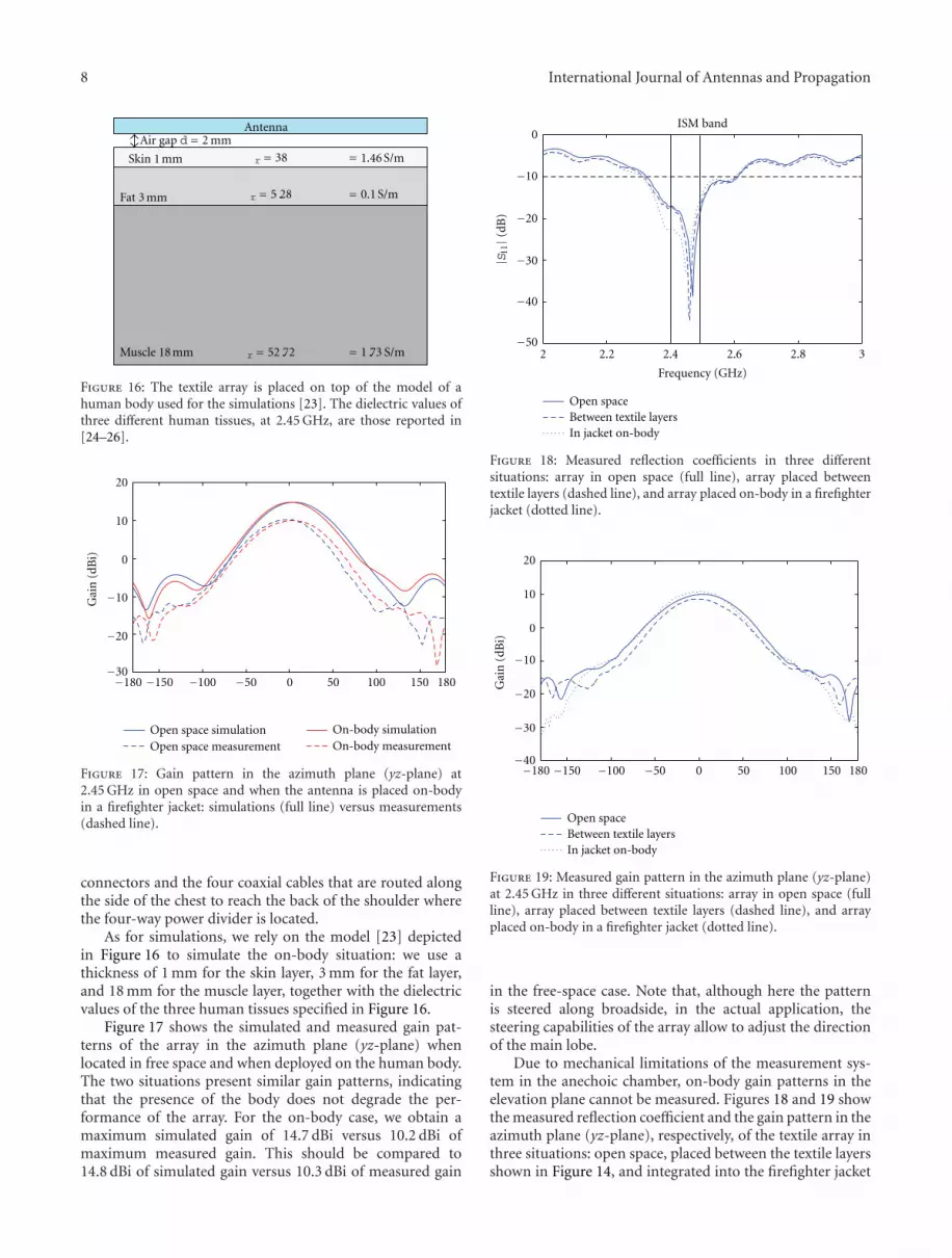
8 International Journal of Antennas and Propagation
AntennaAir gap d= 2 mm
Skin 1 mm
Fat 3 mm
Muscle 18 mm
r= 38
r= 5.28
r= 52.72
=
=
= 1.73 S/m
1.46 S/m
0.1 S/m
Figure 16: The textile array is placed on top of the model of ahuman body used for the simulations [23]. The dielectric values ofthree different human tissues, at 2.45 GHz, are those reported in[24–26].
Gai
n (
dBi)
20
10
0
−10
−20
−30−180 −150 −100 −50 0 50 100 150 180
Open space simulationOpen space measurement
On-body simulationOn-body measurement
Figure 17: Gain pattern in the azimuth plane (yz-plane) at2.45 GHz in open space and when the antenna is placed on-bodyin a firefighter jacket: simulations (full line) versus measurements(dashed line).
connectors and the four coaxial cables that are routed alongthe side of the chest to reach the back of the shoulder wherethe four-way power divider is located.
As for simulations, we rely on the model [23] depictedin Figure 16 to simulate the on-body situation: we use athickness of 1 mm for the skin layer, 3 mm for the fat layer,and 18 mm for the muscle layer, together with the dielectricvalues of the three human tissues specified in Figure 16.
Figure 17 shows the simulated and measured gain pat-terns of the array in the azimuth plane (yz-plane) whenlocated in free space and when deployed on the human body.The two situations present similar gain patterns, indicatingthat the presence of the body does not degrade the per-formance of the array. For the on-body case, we obtain amaximum simulated gain of 14.7 dBi versus 10.2 dBi ofmaximum measured gain. This should be compared to14.8 dBi of simulated gain versus 10.3 dBi of measured gain
0ISM band
(dB
)
−10
−20
−30
−40
−502 2.2 2.4 2.6 2.8 3
Frequency (GHz)
Open spaceBetween textile layersIn jacket on-body
|S 11|
Figure 18: Measured reflection coefficients in three differentsituations: array in open space (full line), array placed betweentextile layers (dashed line), and array placed on-body in a firefighterjacket (dotted line).
Gai
n (
dBi)
20
10
0
−10
−20
−30
−40−180 −150 −100 −50 0 50 100 150 180
Open spaceBetween textile layersIn jacket on-body
Figure 19: Measured gain pattern in the azimuth plane (yz-plane)at 2.45 GHz in three different situations: array in open space (fullline), array placed between textile layers (dashed line), and arrayplaced on-body in a firefighter jacket (dotted line).
in the free-space case. Note that, although here the patternis steered along broadside, in the actual application, thesteering capabilities of the array allow to adjust the directionof the main lobe.
Due to mechanical limitations of the measurement sys-tem in the anechoic chamber, on-body gain patterns in theelevation plane cannot be measured. Figures 18 and 19 showthe measured reflection coefficient and the gain pattern in theazimuth plane (yz-plane), respectively, of the textile array inthree situations: open space, placed between the textile layersshown in Figure 14, and integrated into the firefighter jacket

International Journal of Antennas and Propagation 9
(W/kg)
0.0124
0.0111
0.00998
0.00885
0.00771
0.00658
0.00545
0.00431
0.00318
0.00204
Type SAR (rms)
Monitor SAR (f= 2.45
0.012438 W/kg at 203.844/23.6057/−30.6286
Frequency 2.45
x
y z
0.000343
Maximum-3d
) [1[0.5, 0] + 2[0.5, 0] + 3[0.5, 0] + 4[0.5, 0]] (10 g)
Figure 20: SAR distribution.
worn by a person. In all the three cases, the ISM band is fullycovered and the gain patterns exhibit the same trend.
The human body has a very complex structure in termsof electrical parameters of each tissue, thus the energy of highfrequency electromagnetic waves is absorbed by the humanbody with various intensity, depending on the part of thebody and on the wave frequency. To analyze this problemand to guarantee that the antenna in this paper does notharm the person wearing it, the Specific Absorption Rate(SAR) is calculated, using the 3D simulator CST MicrowaveStudio, which computes the amount of energy absorbedby the human body. The human body model used for thesimulations is shown in Figure 16. Figure 20 presents theSAR distribution in the xy-plane of the array at z = 0 whenthe input power at each port is 0.5 W. The 10-g averaged SARpeak value is 0.0124 W/Kg. This value fulfills the ICNIRP[14] and FCC [15] guidelines for general public exposure.
3.4. Mutual Coupling Measurements . To assess the sensitivityof the mutual coupling in the array w.r.t. environmentalconditions, more specifically, w.r.t. to changes in the relativehumidity, two types of measurements are performed in a realnonanechoic lab environment after 24 h of conditioning inthe climate test cabinet and the results are verified againstthe conditions (1) and (2): first, the reflection coefficient ofeach individual array element is measured, while terminatingthe other three elements with a 50Ω load; second, the mutual
coupling between each pair of antenna elements is measured,while terminating the other two elements with a 50Ω load.Figure 21(a) shows the measured reflection coefficient atport 1 of the array, and Figures 21(b), 21(c), and 21(d) showthe mutual coupling between port 1 of the antenna arrayand the other three ports, setting rH to be 20%, 40%, 60%,and 80%. It is observed that the array is rather insensitivew.r.t. to environmental conditions, always satisfying (1). Forthe other antenna elements (ports 2–4) a similar behavior isobserved. Thanks to the careful design, the mutual couplingbetween the individual radiators remains low enough and (2)is always satisfied. Similar characteristics are obtained for theother combinations of port pairs, being 2 and 3; 2 and 4; 3and 4.
Next, the mutual coupling between each pair of ports ofthe array was measured when the array—in flat condition—is positioned in our anechoic chamber in three conditions,being in open space, between the textile layers composingthe firefighter suit shown in Figure 14, and when it is fullyintegrated inside the firefighter jacket. Results are shownin Figures 22(a), 22(c), and 22(e). We note that, given thefact that the measurements are now performed in anechoicconditions, the mutual coupling levels are lower than theones found in Figures 21(b), 21(c), 21(d) and that theyvary little for the different setups. To verify the effectsof bending on the mutual coupling between each pair ofantenna elements, the array is bent around a plastic cylinder

10 International Journal of Antennas and Propagation
2 2.2 2.4 2.6 2.8 3
0
(dB
)
−10
−20
−30
−40
−50
Frequency (GHz)
ISM band
|S 11|
(a) Reflection coefficients at port 1
−25
−30
−35
−40
−45
−50
−55
−60
(dB
)
2 2.2 2.4 2.6 2.8 3
Frequency (GHz)
|S 12|
(b) Mutual coupling between port 1 and 2
(dB
)
−30
−40
−50
−60
−70
−802 2.2 2.4 2.6 2.8 3
Frequency (GHz)
20% rH40% rH
60% rH80% rH
|S 13|
(c) Mutual coupling between port 1 and 3
(dB
)
−40
−50
−60
−70
−80
−902 2.2 2.4 2.6 2.8 3
Frequency (GHz)
20% rH40% rH
60% rH80% rH
|S 14|
(d) Mutual coupling between port 1 and 4
Figure 21: S-parameter measurements after acclimatization of the array, measured in a nonanechoic environment: reflection coefficients atport 1 of the array and mutual coupling between port 1 of the array and the other three ports.
with a diameter of 15 cm, oriented vertically, that is, alongthe y-axis, representing an extreme case where the array isbent around an arm. The mutual coupling was measuredwhen the array is in open space and between the textile layers,composing the firefighter suit, shown in Figure 14. It is foundthat mutual coupling is not significantly affected by bendingthe textile array. Finally, we observe that both in planar andbent state, (2) is always satisfied. Similar characteristics areobtained for the other combinations of port pairs, that is, 2and 3; 2 and 4; 3 and 4.
4. Conclusion
The design, manufacturing, and measurements were dis-cussed of a wearable system composed of a four-way powerdivider and line stretchers interconnecting a four-elementULA textile array consisting of tip-truncated ETMPAs imple-mented on two different nonconductive textile substrates,that is, cotton fabric and Azzurri foam, operating in the2.45 GHz ISM band. Thanks to the exclusive use of isolating
and conductive textiles, the array is breathable, flexible andmay be fully integrated into garments, worn by rescue work-ers or fire fighters, active in a disaster area. The array shouldbe placed vertically on the human torso, to steer the beamproviding the maximum gain in elevation angle within anarrow angular sector around the broadside direction, en-suring that the main beam points towards the base station.Thereto, a four-patch ULA was chosen with a relatively largespacing between the individual elements. This leads to a low-cost design with a large antenna aperture and low mutualcoupling between the patches, allowing easy steering. Thenarrow antenna beam also results in less fading and, hence,reliable communication. Under reproducible rH conditions,realized in the climate test cabinet, measurements of thereflection coefficient of the array system were performed:the implementation of the array on Azzurri foam exhibitsperfectly stable characteristics. For the implementation oncotton, however, the resonance frequency decreases withincreasing rH, and the ISM band is no longer covered whenthe rH is 90%. Hence, when choosing a textile material as

International Journal of Antennas and Propagation 11
−30
−40
−50
−60
−70
−80
(dB
)
2 2.2 2.4 2.6 2.8 3
Frequency (GHz)
|S 12|
(a) Planar: mutual coupling between port 1 and 2
−35
−40
−45
−50
−55
−60
−65
(dB
)
2 2.2 2.4 2.6 2.8 3
Frequency (GHz)
|S 12|
(b) Bent: mutual coupling between port 1 and 2
−50
−55
−60
−65
−70
−75
−80
(dB
)
2 2.2 2.4 2.6 2.8 3
Frequency (GHz)
|S 13|
(c) Planar: mutual coupling between port 1 and 3
−40
−50
−60
−70
−80
(dB
)
−902 2.2 2.4 2.6 2.8 3
Frequency (GHz)
|S 13|
(d) Bent: mutual coupling between port 1 and 3
−50
−60
−70
−80
(dB
)
−90
−1002 2.2 2.4 2.6 2.8 3
Frequency (GHz)
Open spaceBetween textile layersInto jacket
|S 14|
(e) Planar: mutual coupling between port 1 and 4
−50
−60
−70
−80
(dB
)
−902 2.2 2.4 2.6 2.8 3
Frequency (GHz)
Open spaceBetween textile layers
|S 14|
(f) Bent: mutual coupling between port 1 and 4
Figure 22: Mutual coupling between port 1 of the array and the other three ports, when the array is in planar and bent state.
a substrate for a textile antenna array to integrate into agarment, the MR value of the textile material must be takeninto account. Consequently, a comprehensive study of theperformance of the array system was carried out for thetextile implementation on the Azzurri foam substrate only.Measurements of the reflection coefficient in the 2.45 GHz
ISM band demonstrate a large bandwidth, providing fullcoverage of the ISM band, both when the array system isoperating in free space and when it is deployed on a humanbody. Simulations and measurements of the gain patternsin free space and on-body show very good correspondence,demonstrating that the human body does not degrade the

12 International Journal of Antennas and Propagation
performance of the textile antenna system. Injecting an inputpower of 0.5 W at each port of the array, the calculated SARvalues averaged in 10-g tissue show that the textile antennaarray respects the ICNIRP and FCC guidelines for generalpublic exposure. Next, the mutual coupling between the fourports of the array was measured for varying rH levels, tocheck the sensitivity of the array to environmental changes.Moreover, a careful study of the mutual coupling betweenthe four ports of the array was carried out with the arrayin planar and bent state, for different setups: in open space,between textile layers composing the firefighter suit, andinside the firefighter jacket. Thanks to the ETMPA topologyof the individual patches and the rather large spacing of 3/4 λbetween them, the mutual coupling is always low.
In summary, thanks to a careful design and a thoroughstudy of mutual coupling effects, we managed to presenta low-cost textile antenna array system functioning in the2.45 GHz ISM band, with low-cost steering capabilities,significantly higher gain than a single patch antenna, tolerantto being placed on the body and resistant to environmentalchanges, and resulting in reliable off-body communicationlinks thanks to reduced fading.
References
[1] M. Klemm, I. Locher, and G. Troster, “A novel circularly polar-ized textile antenna for wearable applications,” in Proceedingsof the 7th European Microwave Week, pp. 137–140, October2004.
[2] P. Salonen and H. Hurme, “A novel fabric WLAN antenna forwearable applications,” in Proceedings of the IEEE Antennasand Propagation Society International Symposium, pp. 700–703, June 2003.
[3] E. K. Kaivanto, M. Berg, E. Salonen, and P. de Maagt, “Weara-ble circularly polarized antenna for personal satellite commu-nication and navigation,” IEEE Transactions on Antennas andPropagation, vol. 59, no. 12, pp. 4490–4496, 2011.
[4] G.-Y. Lee, D. Psychoudakis, C.-C. Chen, and J. L. Volakis,“Omnidirectional vest-mounted body-worn antenna systemfor UHF operation,” IEEE Antennas and Wireless PropagationLetters, vol. 10, pp. 581–583, 2011.
[5] C. Hertleer, A. Tronquo, H. Rogier, and L. Van Langenhove,“The use of textile materials to design wearable microstrippatch antennas,” Textile Research Journal, vol. 78, no. 8, pp.651–658, 2008.
[6] C. Hertleer, H. Rogier, L. Vallozzi, and L. Van Langenhove,“A textile antenna for off-body communication integratedinto protective clothing for firefighters,” IEEE Transactions onAntennas and Propagation, vol. 57, no. 4, pp. 919–925, 2009.
[7] J. Vicente and A. A. Moreira, “Electro-textile printed slotantenna over finite EBG structure,” in International Workshopon Antenna Technology (iWAT ’10), pp. 1–4, March 2010.
[8] Q. Bai and R. Langley, “Wearable EBG antenna bending andcrumpling,” in Proceedings of the Loughborough Antennas andPropagation Conference (LAPC ’09), pp. 201–204, Loughbor-ough, UK, November 2009.
[9] L. Vallozzi, P. Van Torre, C. Hertleer, H. Rogier, M. Moeneclae-y, and J. Verhaevert, “Wireless communication for firefightersusing dual-polarized textile antennas integrated in their gar-ment,” IEEE Transactions on Antennas and Propagation, vol. 58,no. 4, pp. 1357–1368, 2010.
[10] L. Vallozzi and H. Rogier, “Radiation characteristics of a textileantenna designed for apparel application,” in Proceedings of theIEEE Symposium for Space Applications of Wireless and RFID(SWIRF ’07), May 2007.
[11] S. Zhu and R. Langley, “Dual-band wearable textile antennaon an EBG substrate,” IEEE Transactions on Antennas andPropagation, vol. 57, no. 4, pp. 926–935, 2009.
[12] C. Du, S. Zhong, L. Yao, and Y. Qiu, “Textile microstrip arrayantenna on three-dimensional orthogonal woven composite,”in Proceedings of the 4th European Conference on Antennas andPropagation (EuCAP ’10), pp. 1–2, April 2010.
[13] C. Du, S. Zhong, L. Yao, and Y. Qiu, “Textile microstrip two-element array antenna on 3D orthogonal woven composite,”in Proceedings of the International Symposium on Signals, Sys-tems and Electronics (ISSSE ’10), vol. 2, pp. 1–2, September2010.
[14] ICNIRP, “Guidelines for limiting exposure to time-varyingelectric, magnetic, and electromagnetic fields,” Health Physics,vol. 74, no. 4, pp. 494–522, 1998.
[15] FCC, “Evaluating Compliance with FCC Guidelines for Hu-man Exposure to Radiofrequency Electromagnetic Fields,”Supplement C to OET Bulletin 65, Washington, DC, USA,2001.
[16] http://www.lioninternational.fr/index.php.[17] Y. Siddiqui Jawad and G. Debatosh, “Applications of triangular
microstrip patch: circuit elements to modern wireless anten-nas,” Mikrotalasna Revija, vol. 13, no. 1, pp. 8–11, 2007.
[18] S. Sadat Karimabadi, Y. Mohsenzadeh, A. Reza Attari, andS. Mahdi, “Bandwidth enhancement of single-feed circularlypolarized equilateral triangular microstrip antenna,” in Pro-ceedings of the Progress in Electromagnetic Research Symposium,pp. 147–150, Hangzhou, China, March 2008.
[19] C. Tang, J. Lu, and K. Wong, “Circularly polarised equilateral-triangular microstrip antenna with truncated tip,” ElectronicsLetters, vol. 34, no. 13, pp. 1277–1278, 1998.
[20] C. Hertleer, A. Van Laere, H. Rogier, and L. Van Langenhove,“Influence of relative humidity on textile antenna perfor-mance,” Textile Research Journal, vol. 80, no. 2, pp. 177–183,2010.
[21] F. Declercq, Characterization and design strategies for activetextile antennas [Ph.D. thesis], Ghent University, 2011.
[22] F. Declercq, I. Couckuyt, H. Rogier, and T. Dhaene, “Complexpermittivity characterization of textile materials by means ofsurrogate modelling,” in Proceedings of the IEEE InternationalSymposium Antennas and Propagation and CNCUSNC/ URSIRadio Science Meeting, July 2010.
[23] M. Klemm, I. Z. Kovcs, G. F. Pedersen, and G. Troster, “Novelsmall-size directional antenna for UWB WBAN/WPAN appli-cations,” IEEE Transactions on Antennas and Propagation, vol.53, no. 12, pp. 3884–3896, 2005.
[24] C. Gabriel, S. Gabriel, and E. Corthout, “The dielectric prop-erties of biological tissues: I. Literature survey,” Physics in Med-icine and Biology, vol. 41, no. 11, pp. 2231–2249, 1996.
[25] S. Gabriel, R. W. Lau, and C. Gabriel, “The dielectric prop-erties of biological tissues: II. Measurements in the frequencyrange 10 Hz to 20 GHz,” Physics in Medicine and Biology, vol.41, no. 11, pp. 2251–2269, 1996.
[26] C. Gabriel, S. Gabriel, and E. Corthout, “The dielectric prop-erties of biological tissues: III. Parametric models for the di-electric spectrum of tissues,” Physics in Medicine and Biology,vol. 41, no. 11, pp. 2271–2293, 1996.

Hindawi Publishing CorporationInternational Journal of Antennas and PropagationVolume 2012, Article ID 251682, 12 pagesdoi:10.1155/2012/251682
Research Article
Textile UWB Antenna Bending and Wet Performances
Mai A. R. Osman,1 M. K. A. Rahim,1 N. A. Samsuri,1 M. K. Elbasheer,2 and M. E. Ali3
1 Radio Communication Engineering Department (RaCED), Faculty of Electrical Engineering, Universiti Teknologi Malaysia, 81310Johor, Malaysia
2 Mechanical Engineering Department, Faculty of Engineering, Sudan University of Science and Technology, Khartoum 407-111, Sudan3 Electronic and Electrical Engineering Department, School of Engineering and Built Environment, Edinburgh Napier University,Merchiston Campus, EH10 5DT Edinburgh, UK
Correspondence should be addressed to Mai A. R. Osman, [email protected]
Received 15 November 2011; Revised 11 February 2012; Accepted 7 March 2012
Academic Editor: Hendrik Rogier
Copyright © 2012 Mai A. R. Osman et al. This is an open access article distributed under the Creative Commons AttributionLicense, which permits unrestricted use, distribution, and reproduction in any medium, provided the original work is properlycited.
The vision and ideas of wearable computing systems describe future electronic systems as an integral part of our everydayclothing that provides the wearer with such intelligent personal assistants. Recently, there has been growing interest in the antennacommunity to merge between wearable systems technology, ultrawideband (UWB) technology and textile technology. This workaimed to make closer steps towards real wearability by investigating the possibilities of designing wearable UWB antenna wheretextile materials are used for the substrate as well as the conducting parts of the designed antenna. Two types of conductingmaterials have been used for conducting parts, while a nonconducting fabric has been used as antenna substrate material. A setof comparative results of the proposed design were presented and discussed. Moreover, effects on the return loss by means ofmeasurements for each fabricated antenna prototype under bent and fully wet conditions were discussed in more details.
1. Introduction
Portable electronic devices have become part of everydayhuman life acting as mobile phones that are quite oftencarried throughout the day and allow not just telephonecalls alone but also provide internet access, multimedia,and personal digital assistant. This form of “always on”and constantly connected status can be considered as a steptowards the pervasive computing paradigm. According tothat, extensive worldwide research has been carried out onnew wearable devices where wearable computers will becapable to perform as ancestors to smart clothes. In thatsense, smart clothes will ensure the ability of wearable devicesto escape from the confines of the rigid box and hencemerge with textile technology. This kind of incorporationof antennas into uniform will add the benefit of eliminatingclumsy devices that can be entangled to some extent [1–3].However, as technologies advances, new and a vast number
of potential applications emerged, such as: wireless trans-actions, general network connections, navigation support,location-based services, tourism, security, emergency, childprotection, intelligent transportation system, military appli-cations, smart suits, backpack radar, battlefield personnelcare, medical monitoring, smart diagnosis, aging care,biosensors, space applications, and astronaut monitoring.
On the other hand, the key considerations for wearableelectronics are to be lightweight, flexible, small size, inexpen-sive, able to withstand damage from obstacles (robust), andcomfortable to wear [4–6]. Since the Federal Communica-tions Commission (FCC) in 2002 approved the commercialuse of frequency bands from 3.1 to 10.6 GHz for Ultraw-ideband(UWB) systems, UWB antennas received more andmore attention with the advancement of communicationtechnology [7–9]. The attractive features of UWB antennas,such as low profile, low cost, and radiation properties, donot need to transmit a high-power signal to the receiver, can

2 International Journal of Antennas and Propagation
Sqr 10.4
D 30Sqr 6
2× 3.7
60
3.2
(a)
60
27
50
(b)
Figure 1: CST model along with the geometry and dimensions in millimetre of the current paper design; (a) front view and (b) back viewof the proposed antenna design.
(a) (b)
Figure 2: The fabricated wearable UWB antenna prototypes using flannel fabric with: (a) copper conducting sheet, (b) Shieldit conductingfabric.
have a longer battery life, and the compact size enhancedthe possibilities of reducing the wearable devices size andtherefore ease the fabrication process [9, 10].
Since 1997, wearable telecommunication systems havebecome popular topics in research institutions. Numerouspapers have been published about the design, fabrication andapplications of wearable antennas and systems. Some of thesedevelopments are highlighted below. Several researches havetaken quantum leaps in utilizing textile materials as antennasubstrate [10–12]. Wearable antennas have been developed inthe form of flexible metal patches on textile substrates [13–15]. A dual-band wearable antenna was discussed in detail[16, 17]. Furthermore, another investigation of using elec-trotextile materials for designing microstrip patch antenna aswell as UWB antenna were reported in [18, 19]. In addition,UWB sensors and their suitability for medical applicationswere also considered [20–22]. With all these mentionedfindings, markets opened up to a wide range of potential
requirements and investigations for these novel materialsconsidering UWB antenna designs and applications. Con-sistent with all these facts mentioned above, authors ofthe current paper aimed to make closer steps towards realwearability. Moreover, full success can be achieved onlywhen the antenna and all related components are entirelyconverted into 100% textile materials where the use ofembedded textile components guarantees washing of theelectronic suit and accordingly reuse of it. In this work, a fullytextile UWB antenna is presented with detailed discussionabout the concept, simulation, as well as manufacturingprocess. Two types of conducting materials have been usedfor conducting parts, while a nonconducting fabric hasbeen used as antenna substrate material. In the followingsections, materials that have been used to accomplish thewearable antenna design, successive design steps, and aset of comparative results of the proposed design shall bepresented. Moreover, effects on the return loss by means of

International Journal of Antennas and Propagation 3
(a) (b)
Figure 3: Snapshot of (|S11|) measurement environment of both antenna prototypes using (a) copper conducting tape and (b) Shielditconducting fabric.
Frequency (GHz)
Simulated copper tape Measured copper tapeMeasured Shieldit fabric
10
0
−10
−20
−30
−40
−50
−60
S 11
(dB
)
0 2 4 6 8 10 12 14 16
2D graph 1
Figure 4: Comparison between simulated and measured (|S11|)results of the proposed wearable textile UWB antenna design.
measurements for each fabricated antenna prototype underbent and fully wet conditions will be discussed in moredetails.
2. Material Selection
The most important properties of textile materials that aremobilized in wearable applications are flexibility to conformto the body, comfort to touch, and softness. Applications alsoneed to be cost-effective, widely available, allow easy inter-pretation, and provide consistent results. The terms textile
and fabric antenna are used interchangeably here. However,in most cases, textile antenna refers to an antenna, whereasthe term fabric relates to the substrate material. In thispaper, a fully textile UWB wearable antenna is designedand analyzed. The proposed antenna designs are made fromflannel fabric substrate material along with two types ofconducting materials that will be discussed in more detailsin the following sections.
2.1. Substrate Material. For flexible antennas, textile materi-als form interesting substrates because fabric antennas canbe easily integrated into clothes. Textile materials generallyhave a very low dielectric constant which reduces surfacewave losses and improves antenna’s impedance bandwidth[19, 20]. In this work, our study focuses on using flannelfabric as substrate material. Flannel fabric is a kind of 100%cotton material with smooth, firm, and fluffy surface thatmade the fabric suitable for wearable applications. Moreover,fabric substrate material features might aid in maintainingthe distance to remain constant between the radiating patchand the ground plane in order to control antenna’s electricalcharacteristics. In fact, the smooth and firm surface of fabricsubstrate material is required to allow conductive sheetsto be fastened evenly and stoutly on fabric surface. If thecopper sheet detaches merely from one corner and the spacebetween the metal layers varies, the resonant frequency ofthe proposed antenna changes. The thickness of this fabricis almost 1 mm, but in order to characterize the effect oftextile materials accurately, it is important to know its relativepermittivity. Thus, using the commercial dielectric probe(reflected method), the measured relative permittivity offlannel fabric covering the frequency range from 300 MHzup to 20 GHz is approximately 1.7 while the loss tangent isabout 0.025.

4 International Journal of Antennas and Propagation
1
1
1.3
1.3
1.6
1.6
2
2
2.7
2.7
4
4
6
6
10
10
−10
−6
−4
−2.7
−2
−1.6−1.3−1−0.75
−0.5
−0.3
−0.15
0.15
0.15
0.3
0.3
0.5
0.5
0.75
0.75
(a) (b)
(c)
Figure 5: Comparison between simulated and measured results of the input impedance locus using smith chart. (a) Simulated antennausing copper conducting sheet, (b) measured results of copper conducting sheet, and (c) measured results of Shieldit conducting fabric.
2.2. Conducting Materials. A systematic study was demon-strated using two types of conducting materials. Firstly,copper conducting sheet with a thickness of 0.03 mm isused in UWB antenna design and numerical analyses for thesake of preliminary design investigation. After that, anothertype of conducting material (Shieldit conducting fabric) witha thickness of 0.17 mm is proposed for investigation. Theproposed conducting material which is so called “electro-textile material” seems to be most suitable and convenientfor textile wearable antenna applications when comparedwith the unfeasible features of copper conducting sheet (notpossible to be washed, not attractive to the wearer, unable towithstand multiple deformation processes, etc.).
Shieldit conducting fabric is made from strong polyestersubstrate that is plated with nickel and copper, hence it canperform as high quality flame retardant fabric. The fabric iscoated on one side with nonconductive hot melt adhesivewhich make the attachment process easier by ironing theconducting fabric on to the surface of flannel fabric substratematerial. The proposed conducting fabric can be washed aswell as its ability to resist temperature up to 200◦C.
3. Design Consideration
In general, the design and construction of the UWB planermonopole antenna consist of a circular parch to be placed at

International Journal of Antennas and Propagation 5
Figure 6: Snapshot of measured radiation pattern environment ofthe UWB textile antenna using copper conducting sheet.
the top of flannel fabric substrate material—a microstrip feedline and a partial ground plane beneath the fabric substratematerial. At the starting point in designing UWB fabricantenna, the main patch is initially calculated using (1) belowin order to create circular patch at the centre frequency ofthe UWB spectrum at 7.85 GHz. Where a is the radius ofthe circular patch antenna in millimetre, fr is the resonancefrequency in GHz, and εr is the relative permittivity of thetextile substrate material:
a = 87.94fr√εr. (1)
The transmission line feeding technique is introduced inorder to connect the main radiating circular patch to the50Ω Sub Miniature Version (SMA) connector. Moreover,the partial ground plane was implemented for the proposedantenna design; hence such types of truncated groundplane play an important role in broadband and widebandcharacteristics of the designed antennas. In particular, theprocess of ground plane truncation acts as an impedancematching element that controls the impedance bandwidthof the circular patch. Thus, it creates a capacitive load thatneutralizes the inductive nature of the patch to producenearly pure resistive input impedance. According to that,ground plane truncation is achieved by slicing the topportion of the ground plane that covers the radiating patchelement to less than half and covers the transmission linesection only.
Using CST microwave office software simulation pack-age, the UWB fabric antenna design with copper conduct-ing sheet was initially proposed and numerically analyzedbased on the characterization information of flannel fabricsubstrate material mentioned before. On the contrary, nonumerical analysis has been performed for the UWB antennausing Shieldit fabric due to software limitation which allowsthe setting of copper conducting material only. For furtheroptimizations, one slit at the top of the circular patch andtwo slits at the bottom of both sides of the main radiatingpatch are introduced. In addition, a rotated square hole (slot)at the centre of the circular patch is also needed to fine tune
the impedance bandwidth at certain frequencies. Thus, withthe incorporation of these slits and even the centre slot,the impedance bandwidth throughout the spectrum of theUWB antenna frequencies is well-matched below the level of−10 dB. A 50 ohm microstrip feed line was provided for theantenna feed; hence the position was determined accordingto [23, 24].
Pursuing the simulation process, both UWB antennaprototypes are fabricated utilizing copper conducting sheetfor the first antenna prototype and Shieldit conductingfabric for the second antenna prototype. Figure 1 belowdemonstrates the CST model along with the geometry anddimensions in millimetre of the current paper design afteroptimization considering that the design of this antenna hasbeen conducted in air space. The size of the substrate is setto 60 mm × 60 mm while the patch radius is set to 15 mmfor both proposed and fabricated antenna prototypes andthe ground plane size is set to 50 mm × 27 mm. Yet, allthese dimensions are shown in Figure 1. Measured results ofboth fabricated prototypes are compared with the simulatedresults of copper conducting sheet antenna design.
4. Textile Antenna Fabrication
Fabrication process of the wearable textile UWB antenna hasbeen achieved using flannel fabric as substrate material. Thecopper conducting sheet and Shieldit conducting fabric areused as the conducting materials for the radiating element(front side). However, the ground metal (back side) of bothantenna prototypes is made from copper conducting sheetin order to study the effect of conducting materials in morecomparable and accurate manner. Moreover, direct metalsoldering is used to connect the feed line of the top radiatingpatch and the ground plane to the SMA coaxial connector inboth fabricated antenna prototypes as illustrated in Figure 2.On the other hand, the process of cutting both types ofconducting materials turns out to be very critical, hence onlya simple cutting tool (scalpel) is used. Thus, the processof making conducting materials edges precise and accuratewas essential. On the contrary, the attachment process ofboth types of conducting materials seemed to be easy,hence the copper conducting sheet which is backed by self-adhesive has been pressed easily and nicely over flannelfabric substrate material. Besides that, Shieldit conductingfabric that is coated on one side with a nonconductivehot melt adhesive has been attached to flannel fabric byironing and pressing it firmly and easily. Thus, both typesof conducting materials turned out to be good solutions asboth have been evenly placed and fastened over flannel fabricsubstrate material. Figures 2(a) and 2(b) demonstrate thefabricated antenna prototypes using copper conducting sheetand Shieldit conducting fabric, respectively.
5. Results and Discussions
In order to provide better investigation, this section shallfirstly present the simulated and measured reflection coef-ficient (|S11|) and bandwidth results of the UWB antenna

6 International Journal of Antennas and Propagation
(dB)
0
30
60
90
120
150
180
210
240
270
300
33010
0
−10
−20
−30
−40
−50
−60
10
0
−10
−20
−30
−40
−50100−10−20−30−40−5010 0 −10 −20 −30 −40 −50
−60−60
−60
Simulated copper sheet, f = 5 GHzSimulated copper sheet, f = 8 GHzSimulated copper sheet, f = 12 GHz
(a) E-Co polar horizontal plane of simulated copper sheet results.
(dB)
0
30
60
90
120
150
180
210
240
270
300
3300
−20
−40
0 −20 −40
0−20−40
0
−20
−40
−60 −60
−60
−60
Simulated copper sheet, f = 5 GHzSimulated copper sheet, f = 8 GHzSimulated copper sheet, f = 12 GHz
(b) E-Co polar vertical plane of simulated copper sheet results.
(dB)
0
30
60
90
120
150
180
210
240
270
300
3300
−20
−40
0 −20 −40
0−20−40
0
−20
−40
−60 −60
−60
−60
Measured copper sheet, f = 5 GHzMeasured copper sheet, f = 8 GHzMeasured copper sheet, f = 12 GHz
(c) E-Co polar horizontal plane of measured copper sheet results.
(dB)
0
30
60
90
120
150
180
210
240
270
300
3300
−20
−40
0 −20 −40
0−20−40
0
−20
−40
−60 −60
−60
−60
Measured copper sheet, f = 5 GHzMeasured copper sheet, f = 8 GHzMeasured copper sheet, f = 12 GHz
(d) E-Co polar vertical plane of measured copper sheet results.
Figure 7: The behaviour of simulated and measured 2D radiation pattern results of the wearable textile UWB antenna design using copperconducting sheet considering three different selected frequency samples that represent the overall achieved bandwidth.
design and then briefly discuss and compare betweenmeasured results obtained by both antenna prototypes. Afterthat, simulated and measured radiation patterns results willbe considered and briefly discussed. Moreover, effects on thereturn loss by means of measurements on each fabricatedantenna prototype under bent and fully wet conditions willbe addressed at the end of this section.
5.1. Simulated and Measured Return Loss Results. The wear-able textile UWB antenna simulated design produced goodimpedance matching with reflection coefficient being below−10 dB. The bandwidth expands from the lower frequencyof 2 GHz till the upper frequency of 15 GHz and thusresulted in BW of 7.5% over the intended UWB frequencyrange. According to that, a network analyzer was used to
International Journal of Antennas and Propagation 7
(a) H-convex (b) H-concave (c) H-convex (d) H-concave
Figure 8: Snapshots of measurement environment of UWB antenna prototype using copper conducting sheet.
Frequency (GHz)
0
−10
−20
−30
−40
−50
S 11
(dB
)
0 2 4 6 8 10 12 14 16
Bending: UWB flannel copper tape
Msrd planer Cp tapeMsrd bent H convex Cp tapeMsrd bent H concave Cp tapeMsrd bent V convex Cp tapeMsrd bent V concave Cp tape
Figure 9: Measured (|S11|) bending results of UWB antennaprototype using copper conducting sheet.
measure the return loss of both antenna prototypes asa function of frequency. Figure 3 demonstrates snapshotsof (|S11|) measurement environment of the current paperantenna prototypes, while Figure 4 made a clear verificationand comparison between simulated (|S11|) results of copperconducting sheet antenna design and measured (|S11|)results of both antenna prototypes considering each type ofconducting material.
The black solid line demonstrates the simulated (|S11|)and bandwidth results of the UWB antenna design usingcopper conducting sheet, while the blue long dashed lineshows the measured (|S11|) and bandwidth results of theantenna prototype with copper conducting sheet as well.Moreover, the red dash-dotted line shows the measuredreturn loss and bandwidth results of the UWB antennaprototype utilizing Shieldit conducting fabric.
Although the slight deviation between the presentedresults, Figure 4 exhibited that (|S11|) results were compa-rable; hence each of the proposed antenna design achievedmore than 12 GHz BW within the UWB intended frequencyrange. Moreover, All UWB antenna prototypes maintainedreturn loss results below the level of 10 dB with an acceptableand reasonable variation in resonance frequencies depths dueto fabrication and measurement tolerances as well as thevariation in conductivity related to each conducting materialinvolved in the current investigation. Results indicated thatthe measured values of flannel fabric dielectric propertieswere valid enough to provide design information, since thetargeted UWB range of frequency is reasonably well met andhence produced comparable measured results.
In addition, Figure 5 expresses the comparison betweensimulated and measured results of the input impedancelocus using smith chart. Figure 5(a) represents the simulatedresults of the antenna prototype using copper conductingsheet where several loops can be observed on the smithchart within the VSWR = 2 circles. Conveniently, theseloops correspond to locations on smith chart where theantenna’s impedance locus crosses the real axis and henceindicated that resonance frequencies are those at whichthe input impedance is purely real. Similar performanceshave been achieved for the input impedance measuredresults for the fabricated antennas utilizing copper con-ducting sheet, and Shieldit conducting fabric as shown

8 International Journal of Antennas and Propagation
in Figures 5(b) and 5(c), respectively. Although the slightdeviations between simulated and measured results arevisible to some extent, Figure 5 exhibited that all fabricatedantennas input impedance results were comparable.
5.2. Simulated and Measured Radiation Pattern Results.Although the limitation of measurement equipments used,the behaviour of 2D simulated and measured radiation pat-tern components of UWB antenna using copper conductingsheet only is presented, measured and discussed. A snapshotof measured, radiation pattern environment is depictedin Figure 6 where the antenna is located in an anechoicchamber. Furthermore, Figure 7 clarifies the 2D simulatedand measured copolar radiation pattern components in thehorizontal and vertical planes with three different frequencysamples at 5 GHz, 8 GHz, and 12 GHz achieved by copperconducting sheet UWB antenna design of the current paper,where measurement process has been conducted in air space.However, for the sake of better comparison, the measuredradiation pattern results were plotted in the range between−90◦ and +90◦. Moreover, the magnitude of the radiationpattern has been normalized to simplify the viewing ofmeasured results.
Figures 7(a) and 7(b) represent the simulated horizontaland vertical planes copolar radiation pattern componentsrespectively of UWB antenna design using copper conduct-ing sheet. On the other hand, the measured copolar radiationpattern components of the fabricated antenna prototypeusing copper conducting sheet representing the horizontaland vertical planes respectively are demonstrated in Figures7(c) and 7(d).
From Figures 7(a) and 7(b), it can be noticed that theantenna resembles omnidirectional radiation pattern com-ponents in the vertical plane whatever the frequency underanalysis, while two nulls are visible along the horizontalplane for each frequency under analysis. Moreover, fromFigures 7(c) and 7(d), one can observe the slight differencebetween simulated and measured radiation pattern results inthe horizontal and vertical planes. This slight difference canbe related to fabrication tolerance and misalignment duringmeasurement setup. However, both results correlate well toeach other hence the patterns are similar. Although the otherantenna prototype using Shieldit conducting fabric was notmeasured due to limitations in measurement equipments,the expectation of producing omni directional radiation pat-tern are high. Thus, these results claimed that future antennadesigners need to ensure that wearable telecommunicationdevices operate properly in the vicinity of human body. Inparticular, even though UWB antennas known by its low-power operation and extremely low radiated power, specialattention must be paid to the specific absorption rate (SAR)in order to avoid harm to human body.
5.3. Simulated Gain and Efficiency Results. The variationsof frequencies versus the gain of the wearable textile UWBantenna design are all demonstrated in Table 1. The maxi-mum gain achieved was about 4.8 dB at 10 GHz. In contrast,the highest percentage of efficiency reached 95% at 6 GHz
Table 1: Gain and efficiency simulated results of textile uwbantenna design.
Frequency(GHz)
Gain (dB)Efficiency
(%)
2 2.6 92
3 3.6 93
4 3.0 93
5 2.8 94
6 3.4 95
7 4.2 94
8 4.0 92
9 4.2 95
10 4.8 91
11 4.3 89
12 3.9 91
13 4.0 92
14 4.0 91
15 4.0 85
and 9 GHz. However, the lowest efficiency was about 85% at15 GHz. Consequently, results showed that this present paperdesign has low power consumption due to the achievementof gain results that was less than 5 dB in most range offrequencies between 3 GHz and 15 GHz. In addition, theefficiency of the antenna could be considered vast comparedto commercial antennas.
5.4. Effects of Antenna Bending on Measured Return Loss . Ina realistic on-body application, the antenna is supposed tobe integrated into a suit, and accordingly it will be subjectto bending and wetness. Therefore, the effects of bending bymeans of measurements on both proposed UWB antennaprototypes are investigated. Both antenna prototypes aretested on polystyrene cylinder with a diameter of 80 mmthat corresponds approximately to the typical size of humanadult arm. Moreover, each antenna is studied in conven-tional planer form (as discussed previously) and at fourbending positions: horizontal convex, horizontal concave,vertical convex, and vertical concave. Figure 8 demonstratessnapshots of measurement environment of UWB antennaprototype using copper conducting sheet, while Figure 9illustrates measured (|S11|) bending results of copper sheetantenna prototype.
The impedance performances of UWB antenna withcopper sheet considering all bent positions are nearly thesame with slight fluctuations in return loss when comparedwith measured planer position. According to that, resultsindicated that UWB antenna with copper conducting sheetfunctions satisfactorily under most bending conditions.However, further investigations need to be performed inorder to study the effect of severe bending angles as well ascrumbling effect on antenna performances.
On the other hand, similar investigations have beenperformed on the UWB antenna prototype using Shielditconducting fabric. Figure 10 demonstrates snapshots of

International Journal of Antennas and Propagation 9
(a) H-convex (b) H-concave (c) H-convex (d) H-concave
Figure 10: Snapshots of measurement environment of UWB antenna prototype using Shieldit conducting fabric.
Frequency (GHz)
20
10
0
−10
−20
−30
−40
−50
−60
S 11
(dB
)
0 2 4 6 8 10 12 14 16
Bending: UWB flannel Shieldit
Msrd planer: UWB ShielditMsrd bent H-convex: UWB ShielditMsrd bent H-concave: UWB ShielditMsrd bent V-convex: UWB ShielditMsrd bent V-concave: UWB Shieldit
Figure 11: Measured (|S11|) bending results of UWB antennaprototype using Shieldit conducting fabric.
measurement environment of UWB antenna prototype usingShieldit conducting fabric, while Figure 11 illustrates themeasured bending results of Shieldit conducting fabricantenna prototype. The impedance performances of UWBantenna with Shieldit conducting fabric considering all bentpositions are almost identical with slight fluctuations inreturn loss when compared with the measured flat position.According to that, results indicated that UWB antennawith Shieldit conducting fabric functions satisfactorily undermost bending conditions. However, further investigations
need to be performed in order to study the effect of severebending angles as well as crumbling effect on the proposedantenna performances.
5.5. Antenna Performance on Wet Conditions. Water has gota very high dielectric constant as compared to any fabricsubstrate material. Thus, when an antenna absorbs water, themoisture might change the antenna performance parameterssignificantly. The higher dielectric constant of water dom-inates the antenna performance by changing the resonantfrequency. According to that, wearable antennas need to bemeasured considering wetness aspects.
In the current paper, measured results of four differentstates considering wetness, dampness and even when fullydried again for the UWB antenna prototype using copperconducting sheet and Shieldit conducting fabric are depictedin Figures 12 and 13, respectively.
Moreover, Figures 14 and 15 illustrate, the measured(|S11|) results of UWB antenna prototypes using copperconducting sheet and Shieldit conducting fabric, respectively.Firstly, the textile antenna prototype was kept under waterfor more than three hours and measured inside water. Afterthat, antenna under test was taken out of the water andmeasured immediately. Then, the antenna has been dried upusing dry towel and measured; hence this state is recalled asapproximately dry condition. Finally, the performance of theintegrated antenna was tested when fully dried again.
From Figures 14 and 15, the blue solid line demonstratesthe planner antenna performance when it was dry (beforeputting the antenna inside water) and after completely dried,while the dotted line shows the antenna performance insidewater (completely wet). On the other hand, the short dashedline represents the immediately wet antenna state; hence theantenna was measured when it has been taken immediatelyout of water. Moreover, the dash-dotted line illustrates the

10 International Journal of Antennas and Propagation
(a) Inside water (b) Immediately wet (c) Approximately dried (d) Completely dry
Figure 12: Snapshots of measured results of UWB antenna prototype using copper conducting sheet considering different states of wetness,dampness, and fully dried.
(a) Inside water (b) Immediately wet (c) Approximately dried (d) Completely dry
Figure 13: Snapshots of measured results of UWB antenna prototype using Shieldit conducting fabric considering different states of wetness,dampness, and fully dried.
performance of the antenna after it has been dried (using drytowel) and measured.
In the case of copper sheet antenna prototype, the insidewater and immediately wet measurements indicated that theantenna was able to resonate with an expected degradation inresonance frequency while the frequency depth maintainedto be below −8 dB in all UWB frequency range. After dryingthe antenna with dry towel, measured results (approximatelydry) indicated that the antenna showed good impedancematching performances from 2 GHz up to 15 GHz withsome negligible effect of water and moisture on antennaperformance. Finally, results reported that the performancebefore and after wetness as the antenna has been fully driedremained unchanged.
However, Shieldit fabric antenna prototype is measuredinside water and hence results indicated that the antenna isable to resonate with an expected degradation in resonance
frequency while the frequency depth maintained to bebelow −8 dB in all UWB frequency range. Although theslight deviation, measured results of immediately wet state,approximately dry state, and fully dried condition showedthat the antenna performances remained unchanged whencompared with measured results of planer state beforewetness. Results indicated that the minor effect of waterand moisture on antenna performance makes the proposedantenna suitable for humid conditions as well.
6. Conclusion
Fully textile antennas and specially electrotextile materialsthemselves have strong potential to be used as antennasfor transmission purposes in garments. In the currentmanuscript, UWB wearable antenna using fully textile mate-rials are proposed and presented. The proposed antenna

International Journal of Antennas and Propagation 11
20
10
0
−10
−20
−30
−40
−50
S 11
(dB
)
2 4 6 8 10 12 14 16
Frequency (GHz)
Msrd planer: UWB copper tapeMsrd inside water: UWB copper tapeMsrd immed wet: UWB copper tapeMsrd approx dry: UWB copper tape
Wet performance: UWB copper tape
Figure 14: Measured (|S11|) results of UWB antenna prototypeusing copper conducting sheet considering several wet conditions.
20
10
0
−10
−20
−30
−40
−50
−60
S 11
(dB
)
0 2 4 6 8 10 12 14 16
Frequency (GHz)
Msrd planer and dry: UWB ShielditMsrd inside water: UWB ShielditMsrd immed wet: UWB ShielditMsrd approx dry: UWB Shieldit
Wet performance: UWB Shieldit
Figure 15: Measured (|S11|) results of UWB antenna prototypeusing Shieldit conducting fabric considering several wet conditions.
design provides more than 12 GHz bandwidth with suchcompact size and flexible materials and showed goodmeasured return loss (|S11|) characteristics, omnidirectionalpatterns, as well as adequate gain and efficiency results.Moreover, effects of bending and wetness by means of mea-surements on both proposed UWB antenna performancesare investigated. Results indicated that flannel fabric canact and perform as good candidate for textile wearableapplications and possible to replace rigid board substratematerials. Besides that, the fabricated antennas using textile
conducting materials complied wearable antennas require-ments by providing the wearer with compact antennaprototypes, flexible materials, ease of washing as well asensuring the attractiveness of wearable devices. However,washable packaging of the electronics and durable inter-connections remain major challenges to be tackled for allwearable electronics. Consequently, evaluation of long-termbehaviour, durability and system performance after repeatedwetness and laundering should invariably be considered inresearch tasks.
Acknowledgments
Authors wish to acknowledge the support of Ministry ofHigher Education (MOHE), Research Management Cen-tre (RMC), Radio Communication Engineering Depart-ment (RaCED), Faculty of Electrical Engineering, UniversitiTeknologi Malaysia for supporting this research work underGrant no. 4L008 and 74578. The authors also wish to thankSudan University of Science and Technology for supportingthis research paper.
References
[1] L. van Langenhove, Smart Textiles for Medicine and Healthcare,CRC Press, Cambridge, UK, 2007.
[2] A. R. Chandran and W. G. Scanlon, “Dual-band low profileantennas for body-centric communications,” in Proceedingsof the International Workshop on Antenna Technology: SmallAntennas, Innovative Structures and Materials (iWAT ’10), pp.1–4, Lisbon, Portugal, March 2010.
[3] H. Rogier, C. Hertleer, L. Vallozzi, P. van Torre, F. Declercq,and M. Moeneclaey, “Indoor off-body communication basedon a textile multi-antenna system integrated in clothing forrescue workers,” in Proceedings of the 2nd IET Seminar onAntennas and Propagation for Body-Centric Wireless Commu-nications, pp. 1–36, London, UK, April 2009.
[4] B. Sanz-Izquierdo, J. C. Batchelor, and M. I. Sobhy, “CompactUWB wearable antenna,” in Proceedings of th 3rd Loughbor-ough Antennas and Propagation Conference (LAPC ’07), pp.121–124, Loughborough, UK, April 2007.
[5] L. Januszkiewicz, S. Hausman, and T. Kacprzak, “Textile body-worn exponentially tapered vee antenna,” Electronic Letters,vol. 42, no. 3, 2007.
[6] N. Chahat, M. Zhadobov, R. Sauleau, and K. Mahdjoubi,“Improvement of the on-body performance of a dual-bandtextile antenna using an EBG structure,” in Proceedings ofthe 6th Loughborough Antennas and Propagation Conference(LAPC ’10), pp. 465–468, Loughborough, UK, November2010.
[7] S. Barbarino and F. Consoli, “UWB circular slot antennaprovided with an inverted-L notch filter for the 5 GHz WLANband,” Progress in Electromagnetics Research, vol. 104, pp. 1–13,2010.
[8] M. A. Matin, Ultra Wideband Communications: Novel Trendsin Antennas and Propagations, InTech, Rijeka, Croatia, 2011.
[9] I. Minin, Microwave and Millimeter Wave Technologies: Mod-ern UWB Antennas and Equipment, InTech, Uttarakhand,India, 2010.
[10] M. A. R. Osman, M. K. A. Rahim, M. Azfar, A. K. Kamardin,F. Zubir, and N. A. Samsuri, “Performance and evaluation of

12 International Journal of Antennas and Propagation
ultra-wideband wearable textile antenna,” in Proceedings ofthe IEEE European Conference on Antennas and Propagation(EuCAP ’11), Rome, Italy, April 2011.
[11] P. van Torre, L. Vallozzi, C. Hertleer, H. Rogier, M.Moeneclaey, and J. Verhaevert, “Indoor Off-Body wire-less MIMO communication with dual polarized textile anten-nas,” IEEE Transactions on Antennas and Propagation, vol. 59,no. 2, pp. 631–642, 2011.
[12] S. Sankaralingam and B. Gupta, “Determination of dielectricconstant of fabric materials and their use as substrates fordesign and development of antennas for wearable applica-tions,” IEEE Transactions on Instrumentation and Measure-ment, vol. 59, no. 12, pp. 3122–3130, 2010.
[13] P. J. Soh, G. A. E. Vandenbosch, V. Volski, and H. M. R.Nurul, “Characterization of a simple broadband textile planarinverted-F antenna (PIFA) for on body communications,” inProceedings of the 20th International Conference on AppliedElectromagnetics and Communications (ICECom ’10), pp. 1–4,Dubrovnik, Croatia, September 2010.
[14] S. Zhu and R. J. Langley, “Dual-band wearable antennas overEBG substrate,” IET Electronics Letters, vol. 43, no. 3, pp. 141–143, 2007.
[15] M. Tanaka and J. H. Jang, “Wearable microstrip antenna,” inProceedings of the IEEE International Symposium on Antennasand Propagation and URSI North American Radio ScienceMeeting, Columbus, Ohio, USA, June 2003.
[16] B. Sanz-Izquierdo, F. Huang, and J. C. Batchelor, “Covert dual-band wearable button antenna,” Electronics Letters, vol. 42, no.12, pp. 668–670, 2006.
[17] R. Langley and S. Zhu, “Dual band wearable antenna,” inProceedings of the Loughborough Antennas and PropagationConference (LAPC ’08), pp. 14–17, Loughborough, UK, March2008.
[18] M. A. R. Osman, M. K. A. Rahim, S. H. S. Ariffin, and S.K. S. Yuosf, “The investigation of flannel fabric layers,” inProceedings of the International Symposium on Antennas andPropagations, Macao, China, November 2010.
[19] M. Klemm and G. Troester, “Textile UWB antennas forwireless body area networks,” IEEE Transactions on Antennasand Propagation, vol. 54, no. 11, pp. 3192–3197, 2006.
[20] A. Lazaro, D. Girbau, and R. Villarino, “Weflighted centroidmethod for breast tumor localization using an UWB radar,”Progress in Electromagnetics Research B, no. 24, pp. 1–15, 2010.
[21] S. Gao, S. Xiao, D. Jin, and B. Z. Wang, “WideBand antennafor ultra-wideband (UWB) body-centric wireless communi-cations,” in Proceedings of the IEEE International Conferenceon Ultra-Wideband (ICUWB ’10), pp. 1–4, Nanjing, China,September 2010.
[22] P. Sungmee and S. Jayaraman, “Wearable biomedical systems:research to reality,” in Proceedings of the IEEE InternationalConference on Portable Information Devices (PORTABLE ’07),Orlando, Fla, USA, March 2007.
[23] C. A. Balanis, Antenna Theory Analysis and Design, John Wiley& Sons, New York, NY, USA, 2005.
[24] W. L. Stutzman and G. A. Thiele, Antenna Theory and Design,John Wiley & Sons, New York, NY, USA, 2nd edition, 1998.

Hindawi Publishing CorporationInternational Journal of Antennas and PropagationVolume 2012, Article ID 837230, 6 pagesdoi:10.1155/2012/837230
Application Article
New Flexible Medical Compact Antenna: Design and Analysis
Yann Mahe, Anne Chousseaud, Marc Brunet, and Bruno Froppier
Lunam Universite de Nantes, UMR 6164 Institut d’Electronique et de Telecommunications de Rennes, Site de Nantes,Polytech Nantes, rue Christian PAUC, BP 50609, 44306 Nantes Cedex 3, France
Correspondence should be addressed to Yann Mahe, [email protected]
Received 14 December 2011; Revised 16 February 2012; Accepted 19 February 2012
Academic Editor: Hendrik Rogier
Copyright © 2012 Yann Mahe et al. This is an open access article distributed under the Creative Commons Attribution License,which permits unrestricted use, distribution, and reproduction in any medium, provided the original work is properly cited.
Some results on embedded antennas for medical wireless communication systems are presented. Medical telemetry can advanta-geously assist medical diagnostics. For example, you can better locate a diseased area by monitoring temperature inside the humanbody. In order to establish efficient wireless links in such an environment, a special attention should be paid to the antenna design.It is required to be of a low profile, very small regardless of the working frequency—434 MHz in the ISM band, safe, and costeffective. Design of the as-considered antenna is proposed based on a simple model. The approach has been demonstrated for acompact flexible antenna with a factor of 10 with respect to the half-wave antenna, rolling up inside an ingestible pill. Measured andcalculated impedance behaviour and radiation characteristics of the modified patch are determined. Excellent agreement wasfound between experiment and theory.
1. Introduction
Medical applications benefited from recent research inthe field of miniaturized wireless communication systems.Depending on the working frequencies, one of the main chal-lenges is to design very small antennas; that would be to makethese communication systems implantable or ingestible inthe human body. Various types of compact antennas havebeen investigated [1–7]. Nevertheless, it is sometimes quitedifficult to design the same kind of proposed antennas whenthe working frequency or the available space is different.Indeed, no design rules have been given to help the engineers.
In the case of digestive monitoring system, an ingestiblecapsule with a small size is required. Therefore, all monitor-ing systems must be implemented inside the desired pill.
For example, we can retain a classical used pill as shownin Figure 1. The space allowed is very limited. This is espe-cially true when not only the antenna but also other activeparts (batteries, sensors, etc.) of the communication systemare embedded within a pill.
Moreover, these parts have to be shielded from a radi-ation that can interfere with the sensor and generate erro-neous data.
The dimensions of the selected pill are 7 mm diameterand 17 mm height. So, we propose to investigate a microstrip
patch antenna for which a particular effort in terms of mini-aturization must be done. Two main points support this deci-sion. Firstly, this kind of antenna presents a ground planeon its bottom face which can advantageously be used forshielding the electronic part of the module from radiation.Secondly, if this antenna is manufactured on a flexible sub-strate, it can easily be rolled up inside the pill.
The retained frequency for this specific application isfrom the ISM bandwidth (433.05; 434.79 MHz) in whichequivalent isotropic radiated power (EIRP) must be lowerthan 14 dBm. So the main challenge is to reduce the size ofthe antenna for about a factor of 90% compared with clas-sical half-wavelength patch antenna and to ensure the con-formability inside the pill.
Herewith, we will start by presenting the antenna geome-try and the design rules to obtain an initial structure close tothe optimal one. Our aim is to provide a very simple modelin order to limit the optimization effort.
This approach proves its efficiency because the length ofthe proposed antenna for first estimation and final solutionis slightly modified.
A first didactic example of low-cost antenna in freespace on FR4 dielectric (εr = 4.4 and height = 1.58 mm) isproposed.

2 International Journal of Antennas and Propagation
7 mm
17 m
m
Figure 1: Example of possible pill.
This structure has been optimised with CAD simulationtool like Ansoft HFSS. Scattering parameter (S11) shows agood agreement between simulation and measurement. Theinput impedance of the antenna can take any value between0 and a maximum value fixed by the geometry. To illustratethis concept, an example of 25Ω input impedance antennais proposed. This input impedance can be easily changed bychoosing an appropriate position of the feeding point alongthe structure. Finally, the dimensions of a medical foldingantenna is proposed and investigated. All are within an envi-ronment whose properties are close to those of the humanbody with concluding results.
The preliminary design method will be described indetail below.
2. Theoretical Considerations
2.1. Physical Analysis of Field Distributions. Patch antennas(Figure 2) are very common structures, but their size is oneof the main drawbacks (half guided wavelength size). As longas the patch antenna works on its TM01 mode, it is possibleto state that the electrical field has constant amplitude alongits width (W) and varies in cosine along its length (L). Acommon technique to reduce the overall size of a microstrippatch antenna is to use only half part of this antenna placingsome shorting points on the null electric field plane. The fielddistribution remains unchanged in both the cases. In thisconfiguration (Figure 2(b)), the antenna length correspondsapproximately to a quarter guided wavelength [8].
Introducing one or more impedance steps in the struc-ture (Stepped Impedance Resonator, SIR Concept, Figure 3)will lead to either one of the following: a nonperiodic fre-quency behaviour with nonharmonic values resonant fre-quencies [9, 10] or smaller structures without changing theirfundamental working frequency. One typical example forthis is the H-antenna [11, 12] obtained from a half-wavestructure. An example to reduce the overall size of such an-tenna would be to combine the two previous techniques asshown in Figure 4.
Finally, if the smallest line width is long enough in thislast structure, it is possible to further reduce the length of theantenna by meandering it. The concept of using these threeminiaturization techniques is very appealing in terms ofcompactness. However, it would be more interesting if one
can determine approximate dimension of such a structure ina simple way.
2.2. Design Method. It is well known that resonance condi-tions are achieved when the imaginary part of the equivalentinput impedance of a resonator is null. In case of short-endedSIR antenna, by neglecting the discontinuity effects, it is pos-sible to propose a simple model for this kind of structure. TheSIR antenna is now reduced to two transmission lines withdifferent characteristic impedances, ended with one part bya short circuit and the other part by an open circuit. Thismodel is presented in Figure 5.
The impedance Zinput at a distance L from a given im-pedance load through a lossless transmission line with anhomogeneous characteristic impedance Zc and a wave num-ber β is given below
Zinput = Zc · Zload + j · Zc · tan(β · L)
Zc + j · Zload · tan(β · L) . (1)
This equation can be applied to both sections of the proposeddesign. So, for the structure described in Figures 3 and 4, theequivalent impedance Zr1 presented at the end of the firstline section (W1, L1) loaded by an open circuit is given asfollows:
Zr1 = − j · Zc1tan
(β1 · L1
) . (2)
Through the second line (W2, L2), the equivalent impedancecan be calculated by substituting Zr2 equal to zero on theshort cut plane (short circuit) at the working frequency:
Zr2 = Zc2 · Zr1 + j · Zc2 · tan(β2 · L2
)Zc2 + j · Zr1 · tan
(β2 · L2
) = 0. (3)
We can get the condition of resonance (4) by solving (2) and(3) which will lead us to a two-equation system given by (5).
Zc2 · − j · Zc1 + j · Zc2 · tan(β2 · L2
) · tan(β1 · L1
)Zc2 · tan
(β1 · L1
)+ Zc1 · tan
(β2 · L2
) = 0,
(4)
− Zc1 + Zc2 · tan(β2 · L2
) · tan(β1 · L1
) = 0,
Zc2 · tan(β1 · L1
)+ Zc1 · tan
(β2 · L2
)/= 0.
(5)
Here, we have to find the optimal value of the quadruplet(Zc1, Zc2, L1, L2) which satisfies the conditions given by (5).Equation (5) represents an overdefined system. This leadsdesigners to choose which variable should be fixed first.
Since the problem is related to compactness, the widthand the length of the first part have to be first chosen.
An important effort of miniaturization is made by mean-dering the high impedance line. To improve this effect, thesecond line width has to be compatible with meandering, andit also should be fixed.
By setting the values of W1, W2, and L1, it is possible todetermine the length L2 for which the given operating fre-quency is achieved. For example, if we choose W1 = 18 mm,

International Journal of Antennas and Propagation 3
W
L= g/2
L= g/2Conducting planes
(a)
Shorting points
W
Shorting points
L= g/4
L= g/4
(b)
Figure 2: Example of elementary half (a) and quarter wave (with shorting points) (b) patch antennas. Electric field distributions along theantenna lengths.
W 2
W 1
L
Figure 3: H antenna example.
W 2
W 1
Figure 4: Short-circuited SIR antenna.
L1 = 3 mm, and W2 = 0.2 mm, then L2 can be calculated as67 mm for the resonant frequency of 434 MHz.
As the difference in width goes higher, more importancewill be placed on compactness.
To further increase the compactness, the second linesection can be meandered according to the width of the firstsection line (Figure 6). The gap between meandered lines hasto be adjusted to have a capacitive coupling between armsas low as possible. Thus, the chosen gap will be five timesgreater than its width. The feeding point along the antenna isdependent on the input impedance chosen for the antenna.Indeed, the antenna can be matched directly on any real im-pedance under a maximum value determined by the geome-try. An HFSS simulation is also required using L2 as the onlyoptimization parameter.
Open circuit
W 2
W 1
Zc1Zc2
Zr1 Zr2
L1 L2
Figure 5: Description of the structure.
H-plane
E-plane
H-pla
E-plane
Figure 6: Final antenna.
3. Results
3.1. First Realization on Rigid and Low-Cost Substrate. Accor-ding to the design rules previously presented, a free space an-tenna built on FR4 substrate is fabricated. A gap betweentwo meandered lines is chosen equal to 1 mm as mentionedbefore. This structure is simulated and optimized usingAnsoft HFSS. Optimal dimensions are 18 mm × 9 mm withthe first line section dimension of 3 × 18 mm2 and for thesecond one 0.2×75 mm2. The L2 length is shifted 8 mm fromformula compared with simulations and measurements re-sults. This could be explained by discontinuities effects alongthe antenna which are not taken into account in the simpleused model.

4 International Journal of Antennas and Propagation
−25
−20
−15
−10
−5
0
Simulated Measured
Frequency (GHz)
300 400 500 600 700
S 11
(dB
)
Figure 7: S11 coefficient (dotted lines: HFSS simulation, solid lines:measurement) for 25Ω access.
−150
−180
−120
−90
−60 −50
−40
−60
150
120
90
60
−30 30
0
= 0◦, freq.= 434 MHz
(a)
−150
−180
−120
−90
−60 −50
−40
−60
150
120
90
60
−30 300
= 90◦, freq.= 434 MHz
(b)
Figure 8: Radiation pattern Gϕ (dot dash) and Gθ (solid) at434 MHz and 25Ω access as simulated.
The design of the proposed antenna is given in Figure 6.The input impedance chosen for the antenna is, for example,25Ω, but it can vary from 0 up to 6 kΩ in this topology.
Measurements of scattering parameter S11 are in a goodagreement with simulations as shown in Figure 7.
Radiation pattern is given in Figure 8 in two characteris-tic planes. Maximum radiation gain is around −33 dBi, witha radiation pattern quite omnidirectional in the ϕ = 0 plane.The gain can be improved by increasing the length of the L1
section but at the expense of compactness.We have proposed an antenna design method with strong
constraint in terms of compactness. This method is basedon the prior knowledge of characteristic impedance and pro-pagation constant values of the two line sections. This infor-mation could be evaluated by the formula given by [13]. Thelength of L2 is then evaluated using (5) to fix the resonantfrequency. This method has been applied to design a con-formal antenna for medical application in an environmentwhose properties are close to those of the human body. Inthis type of application, a flexible substrate is suitable to rollin the antenna inside a pill.
3.2. Realization on Flexible Substrate. To ensure compactnessconstraints of ingestible pills, the design has been carriedout on a 50 μm thickness flexible substrate (AP8525 fromDuPont Pyralux) with a metal thickness of 18 μm and a rela-tive permittivity of 3.4.
Antenna dimensions are evaluated based on the previousdesign rules.
As stated before, the method is based on the prior knowl-edge of characteristic impedance and propagation constantvalues for each line sections. These values are thus computedby HFSS modelling each line cross-section. Fixing the widthand the length of the first line section (18 × 3 mm2) and thewidth of the second one (0.2 mm), the length L2 could becalculated according to (5). The computed length L2 is foundequal to 22.5 mm. As in the case of the first studied antenna,a shift of 6.5 mm from formula compared with simulationand measurement results is observed. The second line sectiondimensions are therefore 0.2 × 16 mm2. Dimensions of theantenna built on flex are 18 × 5.4 mm2 which is completelycompatible with the dimensions of the selected pill.
A prototype of the antenna has been fabricated andinvestigated according to the measurement setup describedin Figure 9. This consists of the antenna under test (1)immersed in a 20 cm diameter container (2) full of specifichuman tissue equivalent liquid material with a dielectricconstant of 49.6 and a conductivity of 0.51 S/m. The receiver(3), 80 cm aside from the container, consists of a half-wave vertical polarized patch antenna (5 dBi gain) associatedwith low noise amplifier (LNA) to be as close as possibleto the target application. The reflection and transmissioncoefficients were measured by a vector network analyzer(VNA) (4) operating over the range of 300 kHz–20 GHz with50Ω RF input impedance.
Measurement results show a good matching with simula-tion in terms of frequency setting and scattering parameters(Figure 10). The link budget (transmission coefficient) has

International Journal of Antennas and Propagation 5
Flat or rolled-inantenna (1)
Cable
Patch antenna
80 cm
Receiver (3)
VNA (4)
LNA
Container Ø= 20 cm (2)
Figure 9: Structure of the system.
0
0.3 0.4 0.5
Frequency (GHz)
−10
−20
−30
S11 (dB)
(a)
Frequency (GHz)
0.4 0.60.2
−40
−20
−60
S21 (dB)
(b)
Figure 10: Measured scattering parameter of the antenna deep intissue-equivalent liquid material.
been measured when the antenna is rolled in or not in thepill. No major change has been observed between the twoconfigurations. Moreover, the radiation of the proposed an-tenna is quite omnidirectional. Different configurations havebeen tested, and the budget link is slightly modified (less than3 dB over 360◦ range).
To improve the link budget, one can actually imagine areceiver placed on the human body interface. In this case,the received antenna should be designed properly taking intoconsideration the human body impact.
A first prototype of the final system is presented inFigure 11. The antenna is rolling up inside the capsule, andtherefore the active part is shielded by the ground plane ofthe antenna.
4. Conclusion
In this paper, we have demonstrated that a very compactantenna (λg/20) can be obtained using several miniaturiza-tion techniques. The dimensions of the design have been cal-culated from a simple theoretical model. The difference bet-ween first estimation and final solution is minimal whichproves the approach efficiency. To illustrate this concept, wehave designed an antenna working around 434 MHz fre-quency. An antenna of size 18 mm × 9 mm is designed com-pared with classical half guided wavelength patch antenna(20 cm on FR4 substrate). A size reduction of the overall an-tenna of about 90% is achieved. Any arbitrary real inputimpedance from 0 up to few kΩ can be chosen by findingappropriate position of the feeding point along the structure.Simulations and measurements match well whereas radia-tion pattern is quite omnidirectional in one plane. This an-tenna has also been designed on a flex substrate to be in termsembedded as a conformal antenna in different applicationslike ingestible medical wireless capsule. An example of this

6 International Journal of Antennas and Propagation
(a)
(b)
Figure 11: Structure of the system.
antenna has been achieved showing the interest of suchan approach. A good quality link from pill embedding con-formal antenna to a receiver shows the feasibility of this kindof antenna.
Acknowledgment
The authors would like to thank NXP Semiconductors fortheir financial support and for their efforts in manufacturingand test.
References
[1] Q. Wang, K. Wolf, and D. Plettermeier, “An UWB capsuleendoscope antenna design for biomedical communications,”in Proceedings of the 3rd International Symposium on AppliedSciences in Biomedical and Communication Technologies (ISA-BEL ’10), pp. 1–6, Rome, Italy, November 2010.
[2] D. Zhao, X. Hou, X. Wang, and C. Peng, “Miniaturizationdesign of the antenna for wireless capsule endoscope,” in Pro-ceedings of the4th International Conference on Bioinformaticsand Biomedical Engineering (ICBBE ’10), Chengdu, china, June2010.
[3] P. M. Izdebski, H. Rajagopalan, and Y. Rahmat-Samii, “Con-formal ingestible capsule antenna: a novel chandelier mean-dered design,” IEEE Transactions on Antennas and Propagation,vol. 57, no. 4, pp. 900–909, 2009.
[4] S. H. Lee and Y. J. Yoon, “A dual spiral antenna for ultra-wide-band capsule endoscope system,” in Proceedings of the IEEEInternational Workshop on Antenna Technology: Small Anten-nas and Novel Metamaterials (IWAT ’08), pp. 227–230, Chiba,Jaban, March 2008.
[5] S. H. Lee, J. Lee, Y. J. Yoon, S. Park, C. Cheon, and S. Nam,“A wideband spiral antenna for ingestible capsule endoscopesystems: experimental results in a human phantom and a pig,”IEEE Transactions on Biomedical Engineering, vol. 58, no. 6, pp.1734–1741, 2011.
[6] J. George, M. Deepukumar, C. K. Aanandan, P. Mohanan, andK. G. Nair, “New compact microstrip antenna,” Electronics Let-ters, vol. 32, no. 6, pp. 508–509, 1996.
[7] L. Desclos, Y. Mahe, S. Reed, G. Poilasne, and S. Toutain,“Patch antenna size reduction by combining inductive loadingand short-points technique,” Microwave and Optical Technol-ogy Letters, vol. 30, no. 6, pp. 385–386, 2001.
[8] P. Bhartia, I. Bahl, R. Garg, and A. Ittipiboon, Microstrip An-tenna Design Handbook, Artech House Antennas and Propa-gation Library, Norwood, Mass, USA, 2001.
[9] J. H. Lu and K. L. Wong, “Slot-loaded, meandered rectangularmicrostrip antenna with compact dual-frequency operation,”Electronics Letters, vol. 34, no. 11, pp. 1048–1050, 1998.
[10] Y. Mahe, L. Desclos, R. Moreau, and S. Toutain, “Miniaturizedpatch antenna for dual-frequency operation,” in Proceedings ofthe 31st European Microwave Conference (EuMC ’01), London,UK, September 2001.
[11] C. S. Lee and K. H. Tseng, “Size reduction of microstrip an-tennas,” Electronics Letters, vol. 37, no. 21, pp. 1274–1275,2001.
[12] A. H. Chaloupa, N. Klien, M. Peiniger, H. Piel, A. Pischke,and G. Splitt, “Miniaturized hightemperature supraconductorpatch antenna,” IEEE Transaction on Microwaves Theory andTechnique, vol. 39, no. 9, pp. 1513–1521, 1991.
[13] M. Kirschning and R. H. Jansen, “Accurate model for effectivedielectric constant of microstrip with validity up to millimeterwave frequencies,” Electronics Letters, vol. 18, no. 6, pp. 272–273, 1982.

Hindawi Publishing CorporationInternational Journal of Antennas and PropagationVolume 2012, Article ID 236505, 10 pagesdoi:10.1155/2012/236505
Research Article
Investigation of Flexible Textile Antennas and AMC Reflectors
M. Mantash, A.-C. Tarot, S. Collardey, and K. Mahdjoubi
(Institute of Electronics and Telecommunications of Rennes) IETR, University of Rennes 1, Campus de Beaulieu,bat. 11D, 35042 Rennes Cedex, France
Correspondence should be addressed to A.-C. Tarot, [email protected]
Received 15 December 2011; Revised 15 February 2012; Accepted 17 February 2012
Academic Editor: Hendrik Rogier
Copyright © 2012 M. Mantash et al. This is an open access article distributed under the Creative Commons Attribution License,which permits unrestricted use, distribution, and reproduction in any medium, provided the original work is properly cited.
In this paper, two different methods for fabric characterization are presented: a single frequency method and a broadbandmethod. Felt and denim fabrics are characterized, and patch antennas are designed using these substrates to test both methods.Prototypes of the antennas on felt and denim are manufactured using conductive textile (called electrotextile) aiming to obtainfully flexible antennas. The prototypes are characterized in anechoic chamber to be compared and obtain conclusions related to thecharacterization methods. A new dual-band hexagonal AMC reflector combinable with antennas is also proposed to improve theirperformance and reduce the backward radiation to the human body. A novel broadband CPW-fed monopole antenna is designedto be combined with the AMC. The resulted prototype is characterized and compared with the performance of the CPW-fedantenna alone.
1. Introduction
In recent years, flexible and textile antennas have taken a lotof attention due to their application in wearable systems.A review of wearable textile antennas is presented in [1],whereas, in [2], a GPS textile antenna is tested in real-work conditions. A Bluetooth textile antenna under bendingconditions is presented in [3] and has also been combinedwith artificial magnetic conductors (AMCs [4–7]) aiming toimprove their radiation properties [8], reduce the backwardscattered radiation to the body [9, 10], or cover dual-bandapplications [9].
Nowadays, research efforts focus on both the design ofnew antennas and the development of novel textiles to beused as antenna substrates. Wearable antennas need to beintegrated within everyday clothing, be low profile, and behidden as much as possible. There are also other challengingworks to maintain the critical antenna parameters at anacceptable level in all “normal” operation condition andenvironment. For example, stress (bending) can affect theaxial ratio, operating frequency, and efficiency; humiditycan affect the conductive textiles, by rusting them andchanging their conductivity, as well as the dielectric textilesby changing their relative dielectric permittivity [11].
Bearing in mind all these facts, the selection of a properconductive textile and a substrate for the antenna design
are key points. The electrical parameters of garments aregenerally not available in literature. Therefore, the first stepto accomplish is the characterization of the fabric in terms ofdielectric permittivity and loss tangent.
In this paper, two methods for fabric characterization arepresented. Two well-known fabrics, felt and denim, are char-acterized to test the methods, and prototypes of patch anten-nas on these fabrics are manufactured using electrotextilesas conductive parts. Then, these manufactured prototypesare characterized through return loss and radiation patternmeasurements in order to obtain some conclusions regardingthe characterization methods. In addition, the design of anovel hexagonal dual-band textile AMC to be combined withantennas in order to improve their performance and protectthe human body from radiation is presented. A broadbandCPW-fed broadband antenna on felt is proposed to becombined with the dual-band AMC. Finally, a prototypeof CPW-fed monopole antenna over AMC using felt ismanufactured and characterized. It shows the enhancementof the antenna performance when combined with AMC.
2. Methods of Fabric Characterization
In order to perform the electrical characterization (dielectricconstant εr and loss tangent tan δ) of the fabrics, two
2 International Journal of Antennas and Propagation
(a) (b)
(c) (d)
Figure 1: Fabric characterization setup: microstrip line ((a) and (c)) for calibration and open stub ((b) and (d)) for permittivitymeasurement using denim (up) and felt (down).
different methods were used: the method of stub resonator[12] which is valid for a single frequency and a broadbandmethod based on a stripline cell [13]. Both methods areapplied to denim and felt fabrics, and their results will becompared.
2.1. Single Frequency Method. The procedure used in themethod of stub resonator [12] to perform the electricalcharacterization (dielectric constant εr and loss tangenttan δ) of the fabric is as follows: first, the set-up calibration iscarried out by measuring the S21 parameter for a microstripline (see Figures 1(a) and 1(c)) on the fabric. Then, theS21 parameter for λ/4 stub (see Figures 1(b) and 1(d)) ismeasured. After this step, simulation of the S21 parameterfor the λ/4 stub is carried out using HFSS software [14]. Thedielectric constant εr is then adjusted in simulations in orderto match the simulated curve of the S21 parameter to themeasured one.
This method of characterization is applied to twocommonly used fabrics: denim and felt. Cupper tape is usedfor the metallic parts (ground plane and lines). The linewidth and stub length are, respectively, 3.6 mm and 25 mmfor denim, and 4 mm and 26.5 mm for felt. For denim, thebest match for the resonant frequency is obtained using εr =
1.6 (Figure 2). Concerning the loss tangent (tan δ), weobtained 0.05. The estimated values for felt are, respectively,εr = 1.22, and tan δ = 0.016. These estimated values will beused for antennas simulations.
Compared to other characterization methods [13], theadvantages of this one are simplicity, rapidity, no need forspecific equipment, and, finally, applicability to all types offabrics.
This method is well suited to textile whose characteristicsare not highly variable with frequency (i.e., the textilethat is not dispersive). If the textiles are dispersive, that ispermittivity varies versus frequency, a broadband method ispreferable [13]. However, it needs some specific setup andsoftware.
2.2. Broadband Method. Suitable for measuring the complexpermittivity and permeability of isotropic solid materials,this method is based on a stripline topology (see Figure 3).The samples come in the form of rectangular plates or thinfilms deposited on a dielectric support.
The electromagnetic analysis of the cell is based on aquasistatic approach. This approach represents the cross-section of the stripline containing the tested sample byan equivalent cross-section consisting of a homogeneous

International Journal of Antennas and Propagation 3
1.5 1.7 1.9 2.1 2.3 2.5 2.7 2.9 3
Frequency (GHz)
SimulationMeasurement
S 21
(dB
)
−25
−20
−15
−10
−5
0
(a)
1.5 1.7 1.9 2.1 2.3 2.5 2.7 2.9 3
Frequency (GHz)
SimulationMeasurement
−50
−40
−30
−20
−10
0
S 21
(dB
)
(b)
Figure 2: Simulation and measurement of S21 parameter for the open stub on denim (a) and on felt (b).
Connector Metallic tape
DUT position
Connector
Figure 3: Stripline used for measurements.
medium of effective permittivity and permeability εeff andμeff. The measurement parameters Si j are traced back to theactual parameters of the material. The frequency range istypically 300 kHz–8 GHz. The accuracy of the results is high,with a relative error less than 5% [15]. This method has beenused to characterize denim and felt samples to compare theobtained results with those of the single frequency method.
According to this method applied between 1 GHz and6 GHz, the measured values for relative dielectric constant εrvary from 1.215 to 1.225 for felt (Figure 4) and from 1.6 to1.65 for denim (Figure 5). Regarding the loss tangent tan δ,the values are 0.016 for felt and 0.05 for denim and relativemagnetic permeability μr = 1 for both felt and denim fabrics.
Comparing the obtained results using the two methods,it can be observed that both of them estimate the same valuesfor felt, but there are slight differences for denim.
3. Electrotextiles
The manufacturing of antennas integrable into clothing hasbecome possible through the use of electrotextile, which
1 2 3 4 5 61.2
1.21
1.22
1.23
Frequency (GHz)
r
Figure 4: Measured permittivity versus frequency for felt.
are conductive fabrics [16] obtained by interleaving normalfabrics with conductive metal/polymer threads. The selectionof an appropriate electrotextile is an important step in thedesign of a textile antenna. In order to ensure the optimumcharacteristics for a definite application, the electrotextilefor textile antennas should exhibit the following properties:low electrical resistance to minimize losses, flexible to beable to be deformed when worn, inelastic and tear resistantto preserve its electrical properties, and light weight to becomfortable.
Bearing in mind all these facts, two different electro-textiles have been selected in this paper: “Pure CopperTaffeta Fabric” and “Shieldit Super.” Properties of such

4 International Journal of Antennas and Propagation
1 2 3 4 5 61.5
1.55
1.6
1.65
1.7
Frequency (GHz)
r
Figure 5: Measured permittivity versus frequency for denim.
electrotextiles, provided by supplier are given in Table 1.Photographs taken through a microscope are presented inFigure 6. Moreover, the resistivity of both electrotextiles hasbeen measured in our laboratory IETR, using the “4-probesetup.”
“Pure Copper Taffeta Fabric” is made using pure copperand has the advantages of being smooth, flexible, lightweight, easy to be cut and sewn.
An additional adhesive layer is unfortunately needed tofix the electrotextile to the fabric, thus increasing the losses.
“Shieldit Super” is made of polyester substrate conduc-tive nickel and copper plated then backed with nonconduc-tive hot melt adhesive. It has the advantages of excellentshielding and low corrosion, it is also easy to be cut andsewn, and, additionally, its adhesiveness is activated at 130◦C= 266◦F. It can be ironed on to cotton or another fabric.The use of polyester substrate instead of nylon (as in anotherelectrotextile) makes it better for moisture management asit is more hydrophobic and (more difficult it to becomewet) which allow to better conserve its electromagneticproperties. For these reasons, Shieldit Super will be usedin next section. As a drawback, it can cause skin irritationbecause of containing nickel, but this is not a major concernin the design presented here as an additional fabric layer canbe used to isolate the electrotextile from the body.
4. Antennas on Textile
Two patch antennas at 2.45 GHz using denim and felt fabricsas substrate are designed and characterized. Both use ShielditSuper as electrotextile.
Figure 7 shows the manufactured prototypes. The patchdimensions as well as the return loss and realized gain aregiven in Figure 8 and Figure 9 for felt and denim fabrics.
Figure 10 shows the setup for measuring the radiationpattern of the prototypes using Satimo stargate SG 32.
There is a good agreement between the measurement andthe simulation results both for felt and denim substrates.A slight frequency shift between the simulation and exper-imental results is observed both for S11 and gain parameters.It can be attributed to the manufacturing tolerances.
Regarding the radiation patterns (see Figure 11), oneobserves a good agreement between the measured and simu-lated curves for the principal polarization and a satisfactoryone for the cross polarization.
5. Artificial Magnetic Conductor(AMC) on Textile
The textile antennas usable in wearable applications can becombined with artificial magnetic conductors (AMCs) withthe aim of improving the antenna’s radiation properties andreducing their backward radiation to the human body [4–7].These performances are achieved due to the AMC in-phasereflection property. Here, a dual-band AMC, resonating at2.4 GHz and 5.5 GHz, is designed to be combined with thedual-band CPW-fed antenna on felt.
The resonance frequency and the bandwidth of an AMCreflectors are determined by the unit-cell geometry, thedielectric permittivity, and the substrate thickness. Thus,for a given dielectric substrate, the unit-cell design plays animportant role to obtain dual-band behavior and to ensuresufficient bandwidth at each subband.
Figure 12 shows the geometry of the proposed AMCfor dual-band operation. The unit-cell consists of an innerhexagonal patch surrounded by a concentric hexagonal loop.The hexagonal shape offers a rotational symmetry for thewave propagation and the best filling factor which allows themaximum metallic size and consequently the best bandwidthresults. Dual-band behavior is due to the fact that the centralpatch and the surrounding ring have two different resonancefrequencies.
Shieldit electrotextile is used for the metallic elements(hexagon unit-cells and the ground plane under the dielectricsubstrate) and felt fabric with h = 4 mm (thickness), εr =1.22, and loss tangent tan δ ∼= 0.016.
To find the frequency band in which the periodic struc-ture exhibits AMC behavior, we have studied by simulationits reflection coefficient for a uniform plane wave, usingcommercial software HFSS V.13 of Ansoft [14].
A single cell of the structure has been investigatedwith periodic boundary conditions (PBCs) on its sides,modeling an infinite structure. Normal incidence planewaves are launched to illuminate the periodic structure usinga waveport placed a half-wavelength above it. Following [4],the reflection coefficient phase on the AMC is obtained. Thephase reference plane is taken on the periodic surface.
Simulation has shown that the inner hexagon mainlydetermines the higher resonant frequency. Increasing theelements size, Hex out and Hex in, lowers the resonantfrequency, while increasing the gap 2 dL between unit cellsraises the lower frequency. Hex cut can be used to control the

International Journal of Antennas and Propagation 5
0.232 mm
0.205 mm
(a)
0.354 mm
(b)
Figure 6: Microphotographs of (a) Pure Cooper Taffeta Fabric. (b) Schieldit Super.
(a) (b)
Figure 7: Patch antenna on denim (a) and felt (b) using Shieldit Super electrotextile.
130 mm
130
mm
xy Felt
52.5
mm
38.2
mm
58.1 mm
2.2 2.3 2.4 2.5 2.6 2.7
Frequency (GHz)
0
−10
−20
−30
−40
S 11
(dB
)
MeasurementSimulation
(a)
MeasurementSimulation
8
6
4
2
0
Rea
lized
gai
n (
dB)
2.35 2.4 2.45 2.5 2.55 2.6 2.65
Frequency (GHz)
(b)
Figure 8: Prototype geometry description and characterization results for patch antenna on felt: return loss (a) and realized gain (b).

6 International Journal of Antennas and Propagation
Table 1: Properties of electrotextiles.
Electrotextile Pure Copper Taffeta Fabric Shieldit Super
Measured resistance (IETR) 0.031 Ohm/sq 0.025 Ohm/sq
Surface resistance 0.05 Ohm/sq <0.1 Ohm/sq
Conductivity 2.5 × 10⁵ S/m 6.67 × 10⁵ S/m
Thread pitch 0.232 mm 0.146 mm
Conductive element Cu Ni and Cu
Adhesive backing No Yes
Thickness 0.08 mm 0.17 mm
Weight 80 g/m2 230 g/m2
110 mm
110
mm
xy Denim
45 m
m
43 mm
50 mm
2.2 2.3 2.4 2.5 2.6 2.7
Frequency (GHz)
0
−10
−20
−30
−40
S 11
(dB
)
MeasurementSimulation
(a)
MeasurementSimulation
Rea
lized
gai
n (
dB)
2.35 2.4 2.45 2.5 2.55 2.6 2.65
Frequency (GHz)
3
2.5
2
1.5
1
0.5
0
(b)
Figure 9: Prototype geometry description and characterization results for patch antenna on denim: return loss (a) and realized gain (b).
Figure 10: Antenna’s measurement setup in Satimo stargate SG 32anechoic chamber.
lower frequency and the upper band bandwidth. To achievedual-band operation at the intended frequencies, the unit-cell dimensions are optimized. The optimized values aregiven in Table 2.
According to simulation results shown in Figure 13 anddetailed on Table 3, the AMC behavior of the structure
Table 2: Unit-cell dimensions for dual hexagonal AMC.
Dimensions (mm)
Hex out Hex cut Hex in dL h
15.7 12 11.5 0.8 4.0
Table 3: Frequency bands and bandwidths for dual-band hexagonalAMC.
Frequencies (GHz) Bandwidth
fLow fr fUp Total (MHz) %
Lower band 2.40 2.55 2.70 300 11.76
Upper band 5.04 5.50 6.04 1000 18.18
takes place from 2.4 GHz to 2.7 GHz and from 5.04 GHz to6.04 GHz covering all the WiFi bands.
6. Design of a Novel Broadband Textile Antenna
To show the capabilities of the AMC reflector announced inthe previous section in terms of dual-band operation andbackward radiation reduction, a novel CPW-fed broadbandantenna is designed to be placed over it.

International Journal of Antennas and Propagation 7
0◦30◦
60◦
90◦
120◦
150◦±180◦
−150◦
−120◦
−90◦
−60◦
−30◦
−30−20−10
0
Felt
X
Y
= 0◦
= 90◦
Denim
E-plane: = 90◦
0◦30◦
60◦
90◦
120◦
150◦±180◦
−150◦
−120◦
−90◦
−60◦
−30◦
−30−20−10
0
0◦30◦
60◦
90◦
120◦
150◦±180◦
−150◦
−120◦
−90◦
−60◦
−30◦
−30−20−10
0
0◦30◦
60◦
90◦
120◦
150◦±180◦
−150◦
−120◦
−90◦
−60◦
−30◦
−30−20−10
0
E-plane: = 90◦
H -plane: = 0◦
H -plane: = 0◦
Figure 11: Radiation pattern of the patch antennas on felt (f = 2.450 GHz) and denim (f = 2.525 GHz) substrates. Solid curves presentthe principal polarization (PP) and the dotted ones the cross polarization (XP). Blue curves correspond to the simulation patterns and redcurves to the measured ones.
2 dL
Hex_cutHex_out
Hex_in
Figure 12: Dual-band textile hexagonal AMC-manufactured pro-totype: top view and unit-cell detail.
The geometry of the proposed CPW-fed broadbandantenna is shown in Figure 15. The antenna consists of arectangular radiating element with two slots and fed by aCPW line. Shieldit Super electrotextile is used to implementthese conductive parts which are adhered onto the same sideof a 2 mm thick felt substrate.
2 2.5 3 3.5 4 4.5 5 5.5 6 6.5 7
Frequency (GHz)
Refl
ecti
on p
has
e (d
eg)
−180
−135
−90
−45
0
45
90
135
180
Figure 13: Simulated reflection phase of the AMC surface.
The antenna geometry has been optimized to coverthe S11 bandwidth from 2 GHz to 6 GHz. The resultingoptimized dimensions are given in Figure 14.
In Figure 15 is presented the measured and simu-lated return loss of the manufactured CPW-fed broadbandantenna. The measurement results yielding a bandwidth

8 International Journal of Antennas and Propagation
32 mm
57 m
m
1 mm
0.2 mm
32 m
m
20 m
m3.8 mm14 mm
(a) (b)
Figure 14: CPW-fed broadband antenna geometry and prototype.
−5
−10
−15
−20
−25
−302 2.5 3 3.5 4 4.5 5 5.5 6
Frequency (GHz)
SimulationMeasurement
S 11
(deg
)
Figure 15: Simulated and measured return loss for the CPW-fedbroadband monopole antenna on felt.
77 mm87 mm
Figure 16: CPW-fed antenna on AMC prototype using felt andelectrotextile.
y
xxz
Antenna
Felt
Substrate
Hexagonal
h= 4 mmFelt
AMC substrate Ground plane
h= 2 mm
Space = 2 mm
Figure 17: Side view of CPW-fed antenna on AMC prototype.
−5
−10
−15
−20
−25
−302 2.5 3 3.5 4 4.5 5 5.5 6
Frequency (GHz)
Antenna aloneAntenna over AMC
S 11
(deg
)
Figure 18: Return loss measurement results for the CPW-fedantenna alone and for the CPW-fed antenna on AMC.

International Journal of Antennas and Propagation 9
−30−20
−10
E-plane : = 90◦
−30−20
−10
E-plane : = 90◦
−30−20
−10
H -plane : = 90◦
0◦
30◦
60◦90◦
120◦
150◦
±180◦
−150◦
−120◦
−90◦−60◦
−30◦
0◦
30◦
60◦90◦
120◦
150◦
±180◦
−150◦
−120◦
−90◦−60◦
−30◦
0◦
30◦
60◦90◦
120◦
150◦
±180◦
−150◦
−120◦
−90◦−60◦
−30◦
−30−20
−10
H -plane : = 90◦
f= 2700 MHz
f= 5300 MHz
x
z
y
0◦
30◦
60◦90◦
120◦
150◦
±180◦
−150◦
−120◦
−90◦−60◦
−30◦
Figure 19: Measured radiation patterns (PP in solid line and XP in dashed line) at f = 2.700 GHz and f = 5.300 GHz, CP, for the CPW-fedmonopole antenna without (blue) and with (red) AMC reflector, manufactured on felt substrate.
from 2.1 GHz to 5.7 GHz agree quite well with simulationones exhibiting proper matching from 2 GHz to 5.9 GHz.A slight shift in frequency mainly due to manufacturingtolerances can be observed.
E-plane and H-plane normalized radiation pattern aredepicted in Figure 19 at 2.7 GHz and 5.3 GHz. As it isexpected for a monopole antenna alone (in free space), theH-plane pattern is almost omnidirectional. The realized gainversus frequency is shown in Figure 20.
7. Antenna over AMC on Textile
Figure 16 shows the manufactured prototype of CPW-fedantenna on AMC using felt and electrotextile. Between theantenna and the AMC, there is a 2 mm foam layer (seeFigure 17). The prototype dimensions are 87 mm × 77 mm.
In Figure 18, the measured return loss for the CPW-fed antenna on AMC and for CPW-fed antenna alone ispresented for comparison. It can be observed that a dual-band performance is obtained for the combined structuredue to the AMC dual-band behavior. A slight frequencyshift to lower frequencies also appears due to capacitiveeffects when placing the antenna over the AMC. Finally,the radiation patterns for both prototypes are shown inFigure 19, whereas the gain has been depicted in Figure 20.As it could be expected, the backward radiation of the
8
7
6
5
4
3
2
1
0
Rea
lized
gai
n (
dB)
2 2.5 3 3.5 4 4.5 5 5.5 6
Frequency (GHz)
Antenna aloneAntenna over AMC
Figure 20: Measured realized gain for the CPW-fed monopoleantenna alone and for the CPW-fed monopole antenna over AMC.
antenna is reduced by the AMC reflector and the gain isconsiderably improved.
8. Conclusions
Two methods for fabric characterization are presented in thispaper: one working at a single frequency and the other on abroadband range. They allowed to retrieve the permittivity

10 International Journal of Antennas and Propagation
of felt and denim materials. Based on these data, two patchantennas are realized on these materials. We obtained a verygood agreement between the simulation and experimentalresults for return loss, as well as for the gain parameters,confirming the reliability of the retrieved data.
One of the major contributions of this paper is the designof a textile AMC of original shape. This reflector has beendesigned to be combined with the textile antennas in orderto protect the human body from radiation in one hand andto improve the antenna performance in the other hand. AMCstructure has a dual-band behavior and is intended to coverboth of the Wifi bands.
To examine the validity of the AMC properties, weintroduced a novel CPW-fed broadband antenna (workingon the whole frequency range from low Wifi band tohigh Wifi band), realized it on felt substrate, and placedit over the AMC. A remarkable enhancement is obtainedfor the backward radiation and the gain of the combinedstructure compared to those of the CPW-fed antenna alone,concluding to the necessity of AMC reflectors for the on-body applications.
Acknowledgments
This work has been supported by “Agence Nationale de laRecherche” (ANR), France, under Grants ANR-09-VERS-003 for the METAmateriaux pour VESTements intelligents(METAVEST) project and also by the “Images et Reseaux”cluster.
References
[1] B. Gupta, S. Sankaralingam, and S. Dhar, “Development ofwearable and implantable antennas in the last decade: areview,” in Proceedings of the 10th Mediterranean MicrowaveSymposium, (MMS ’10), pp. 251–252, August 2010.
[2] L. Vallozzi, W. Vandendriessche, H. Rogier, C. Hertleer, andM. L. Scarpello, “Wearable textile GPS antenna for integrationin protective garments,” in Proceedings of the 4th EuropeanConference on Antennas and Propagation, (EuCAP ’10), April2010.
[3] I. Locher, M. Klemm, T. Kirstein, and G. Troster, “Designand characterization of purely textile patch antennas,” IEEETransactions on Advanced Packaging, vol. 29, no. 4, pp. 777–788, 2006.
[4] D. Sievenpiper, L. Zhang, R. F. Jimenez Broas, N. G.Alexopolous, and E. Yablonovitch, “High-impedance electro-magnetic surfaces with a forbidden frequency band,” IEEETransactions on Microwave Theory and Techniques, vol. 47, no.11, pp. 2059–2074, 1999.
[5] F. R. Yang, K. P. Ma, M. Yongxi Qian, and T. Itoh, “Auniplanar compact photonic-bandgap (UC-PBG) structureand its applications for microwave circuits,” IEEE Transactionson Microwave Theory and Techniques, vol. 47, no. 8, pp. 1509–1514, 1999.
[6] M. E. De Cos, Y. Alvarez, R. C. Hadarig, and F. Las-Heras, “Flexible uniplanar artificial magnetic conductor,” inProceedings of the Electromagnetic Research (PIER ’10), vol.106, pp. 349–362, July 2010.
[7] M. E. De Cos, Y. Alvarez, and F. Las-Heras, “Planar artificialmagnetic conductor: design and characterization setup in
the RFID SHF band,” Journal of Electromagnetic Waves andApplications, vol. 23, no. 11-12, pp. 1467–1478, 2009.
[8] J. Liang and H. Y. D. Yang, “Radiation characteristics of amicrostrip patch over an electromagnetic bandgap surface,”IEEE Transactions on Antennas and Propagation, vol. 55, no.6, pp. 1691–1697, 2007.
[9] S. Zhu and R. Langley, “Dual-band wearable textile antennaon an EBG substrate,” IEEE Transactions on Antennas andPropagation, vol. 57, no. 4, pp. 926–935, 2009.
[10] M. Mantash, A-C Tarot, S. Collardey, and K. Mahdjoubi,“Dual-band CPW-fed G-antenna using an EBG structure,” inProceedings of the Antennas and Propagation Conference (LAPC’10), pp. 453–456, Loughborough, UK, 2010.
[11] C. Hertleer, A. van Laere, H. Rogier, and L. van Langenhove,“Influence of relative humidity on textile antenna perfor-mance,” Textile Research Journal, vol. 80, no. 2, pp. 177–183,2010.
[12] D. Liu, U. Pfeiffer, J. Grzyb, and B. Gaucher, AdvancedMillimeter-Wave Technologies: Antennas, Packaging and Cir-cuits, chapter 5, Wiley, 2009.
[13] E. Salahun, P. Queffelec, M. Le Floc’h, and P. Gelin, “A broad-band permeameter for “in situ” measurements of rectangularsamples,” IEEE Transactions on Magnetics, vol. 37, no. 4 I, pp.2743–2745, 2001.
[14] Ansoft HFSS, Four Station Square Suite 200, Pittsburgh, Pa,USA.
[15] http://www.univ-brest.fr/lest/caracterisation/pages/pagesfrancais/.
[16] A. Tronquo, H. Rogier, C. Hertleer, and L. van Langenhove,“Applying textile materials for the design of antennas forwireless body area networks,” in Proceedings of the EuropeanConference on Antennas and Propagation (EuCAP ’06), no. ESASP-626, pp. 1–5, Nice, France, November 2006.

Hindawi Publishing CorporationInternational Journal of Antennas and PropagationVolume 2012, Article ID 170420, 11 pagesdoi:10.1155/2012/170420
Research Article
Cylindrical Bending of Deformable Textile RectangularPatch Antennas
Freek Boeykens, Luigi Vallozzi, and Hendrik Rogier
Department of Information Technology, Ghent University, St. Pietersnieuwstraat 41, 9000 Ghent, Belgium
Correspondence should be addressed to Freek Boeykens, [email protected]
Received 22 November 2011; Accepted 24 January 2012
Academic Editor: Ana Collado
Copyright © 2012 Freek Boeykens et al. This is an open access article distributed under the Creative Commons AttributionLicense, which permits unrestricted use, distribution, and reproduction in any medium, provided the original work is properlycited.
Textile patch antennas are well known as basic components for wearable systems that allow communication between a human bodyand the external world. Due to their flexibility, textile antennas are subjected to bending when worn, causing a variation in reso-nance frequency and radiation pattern with respect to the flat state in which their nominal design is performed. Hence, it is impor-tant for textile antenna engineers to be able to predict these performance parameters as a function of the bending radius. Therefore,we propose a comprehensive analytical model that extends the cylindrical cavity model for conformal rigid patch antennas byincorporating the effects of patch stretching and substrate compression. It allows to predict the resonance frequency and theradiation pattern as a function of the bending radius. Its validity has been verified experimentally. Unlike previous contributions,which concerned only qualitative studies by means of measurements and numerical full-wave simulations, the proposed modeloffers advantages in terms of physical insight, accuracy, speed, and cost.
1. Introduction
Textile antennas emerged during the last decade as a newpromising class of antennas that are particularly suitable foruse in wearable applications [1–5]. These antennas can befully integrated into intelligent garments, known as wearableelectronic systems [6], enabling the transmission of data col-lected by wearable sensors or the reception of signals sent towearable actuators integrated into clothing. The applicationsof wearable systems and textile antennas are numerous, rang-ing from rescue workers interventions’ coordination to mon-itoring of dependent patients in hospital and sports appli-cations.
In order to allow an optimal integration into garmentswithout hindering the wearer’s movements and comfort, themost suitable topology for a textile antenna is the planarpatch. This flexible patch may be subjected to bending whenthe garment is worn, conforming its shape to the surface onwhich it is placed. As a result, stretching of the patch (resul-ting in an elongation of the resonant length) and substratecompression (leading to a variation of the dielectric permit-tivity as a function of the bending radius) can occur.
Since the beginning of textile antenna design, these ef-fects have been taken into account, however, they were notwell known and were compensated for by increasing theantenna bandwidth and validating the design afterwards byexperiments [4]. Hence, it is essential to model the behaviourof the antenna under bent conditions and to predict theinfluence of bending on the resonance frequency and theradiation pattern. Full-wave simulation approaches are apotential solution, but most available commercial softwaretools do not offer the possibility of building a conformalmesh for bent structures, which results in inaccuracies in theobtained results. Moreover, these simulations do not offerphysical insight into the bending mechanisms and may re-quire high computational effort and time. Therefore, we pro-pose analytical formulas that help the designer to assess apriori the effects of bending, stretching, and compression.The work described in this paper focuses on cylindricalbending in particular, since, for wearable applications, textileantennas are usually deployed on cylindrical surfaces such asa human arm, a leg, or a torso.
This study starts from past research efforts on rigidconformal antennas attached to cylindrical surfaces, of which

2 International Journal of Antennas and Propagation
several contributions can be found in literature. Krowne star-ted by extending the popular cavity model for the rectangularpatch antenna (introduced by Lo et al. in 1979 [7]) tothe cylindrical case [8]. Resonance frequencies for the TEz
and TMz modes were theoretically derived, though radia-tion patterns were not calculated in this model. A morecomprehensive study was performed by Dahele et al. [9] andLuk et al. [10]. Their cavity model is only valid for patchantennas with a very thin substrate, but resonance frequen-cies, far fields, input impedances, and Q-factors were derivedanalytically. Other analytical approaches were also intro-duced, which allow to calculate radiation patterns of anten-nas with patches of arbitrary shape [11–13]. However, theyare based on an electric surface current model and assumethe surface current distribution to be known on the patch.
Cylindrical bending of deformable textile antennas hasbeen an important subject in recent papers, but exclusivelyfrom an experimental point of view [4, 5, 14–16]. The generalconclusions drawn from these contributions are that bendingcauses an upward shift of the resonance frequency, abroadening of the radiation pattern, a decrease in gain alongbroadside, and an alteration of the polarisation (in case ofa circularly polarised antenna). Yet, these studies are ratherqualitative and do not provide physical insight into the com-plex mechanisms occurring due to antenna bending.
The present work tries to overcome all drawbacks of theprevious analysis methods by proposing a comprehensivestudy on cylindrical bending of rectangular textile patchantennas. An analytical model based on the cylindrical cavitymodel for conformal antennas, which allows to calculateboth the resonance frequency and the radiation pattern, isconstructed. This offers the advantage of requiring onlysmall computational effort for calculating the main antennaperformance parameters.
In order to model deformable textile patch antennas,some novel extensions to rigid conformal antenna models areproposed:
(1) Wearable textile antennas are usually realised withelectrotextiles as conductive patch materials, whichare subjected to stretching when the antenna is bent.This causes an elongation of the patch along onedirection and shifts the resonance frequency [17].This behaviour is integrated into the model by intro-ducing a factor that determines the location of theoriginal patch width.
(2) Textile antennas are subjected to compression whenbent, which causes a variation of its dielectric permit-tivity. This can be tackled by proposing an expressionfor the compressed permittivity εr,comp as a functionof the bending radius.
The model is validated by means of
(1) theoretical validation for large curvature radii usingDebye’s expansion for large-order Bessel functions;
(2) experimental validation by measuring five prototypesbased on different substrates with different thick-nesses, patch materials, and operation frequencies.
The organisation of the paper is as follows. First, the cav-ity model for cylindrical-rectangular antennas is described inSection 2. The expressions for the resonant fields inside thecavity are calculated, from which the resonance frequenciesand radiation patterns are derived. In Section 3, the cavitymodel is verified for large curvature radii by comparing theobtained dispersion relations with the expression for reso-nance frequencies in rectangular cavities. Section 4 presentsthe experimental results. The proposed model is verified bymeans of five textile antenna prototypes with different geo-metries and material characteristics. Both resonance fre-quencies and radiation patterns are compared. Finally, thegeneral conclusions are summarised in Section 5.
2. Theory
The geometry of the cylindrical cavity representing the textileantenna is shown in Figure 1. The length and width of thewearable antenna are denoted by L and W , and the flexibledielectric substrate has a height h and relative permittivity εr .The curvature radius is a, and the angle formed by the edgesof the patch is β.
In order to obtain a relationship between W , a, and β,one has to take into account whether the antenna patch isstretchable or not. According to [17], the following relationsexist for stretchable patches:
ΔW
W= h
2a + h, (1a)
β(a + h) =W + ΔW , (1b)
with W + ΔW the width of the bent patch. This is shown inFigure 2. Combining (1a) and (1b) leads to
β
(a +
h
2
)=W. (2)
This means that the original patch width is located at ρ =a+h/2 due to patch elongation. If the patch is nonstretchable,the patch length does not vary when bending the antennaand groundplane crumpling occurs. The original width W isthen still located at ρ = a + h.
Because textile antennas can be constructed using bothstretchable and nonstretchable patches, we introduce a factord (Figure 2) that determines the location of the originalwidth:
W = β(a + hd). (3)
This factor d can take values between 0.5 and 1. For perfectlystretchable patches we find that d = 0.5 and for perfectlynonstretchable patches d = 1.
2.1. The Cavity Model. We now proceed with the derivationof the cylindrical cavity model [8]. The cavity is bounded byelectric walls at ρ = a and ρ = a + h and magnetic walls atφ = ±β/2 and z = ±L/2.

International Journal of Antennas and Propagation 3
z
a
Lx
W
y
(a)
z
x
y
h
εr
(b)
Figure 1: Geometry of the cavity: top view (a) and side view (b).
W + ΔW
Wd.h
h
a
Figure 2: Patch elongation.
The electric and magnetic fields inside the cavity aregiven by
E = −∇× F− jωμA +1jωε
∇(∇ · A), (4a)
H = ∇× A− jωεF +1jωμ
∇(∇ · F), (4b)
where, given the translation invariance of the structure, thevector potentials are defined by
A = Azuz,
F = Fzuz.(5)
The scalar wave functions Az and Fz obey the scalarHelmholtz equation
∇2ψ + k2ψ = 0, (6)
with k2 = εrk20.
After separation of variables in cylindrical coordinates,the TEz solution is found by choosing A = 0. Applying theboundary conditions leads to
ψ = Rkφ
(kρρ
)sin
(mπ
βφ +
mπ
2
)cos
(nπ
zz +
nπ
2
), (7)
where
Rkφ
(kρρ
)= cTE
(Y ′kφ
(kρa
)Jkφ
(kρρ
)− J ′kφ
(kρa
)Ykφ
(kρρ
)),
kφ = mπ
β,
kz = nπ
L,
kρ =√k2 − k2
z .
(8)
The TMz solution can be found by choosing F = 0. Ap-plying the boundary conditions leads to
ψ = Rkφ
(kρρ
)cos
(mπ
βφ +
mπ
2
)sin
(nπ
zz +
nπ
2
), (9)
where
Rkφ
(kρρ
)= cTM
(Ykφ
(kρa
)Jkφ
(kρρ
)− Jkφ
(kρa
)Ykφ
(kρρ
)).
(10)

4 International Journal of Antennas and Propagation
The constants cTE and cTM are proportionality coeffi-cients for the TEz and the TMz modes, respectively. Furtherin this paper, the TEz and TMz modes will also be referred toas the TEmn and the TMmn modes.
2.2. Resonance Frequency. The dispersion relations are foundby imposing all boundary conditions. For the TEz modes, thedispersion relation becomes
J ′kφ(kρa
)Y ′kφ
(kρ(a + h)
)= J ′kφ
(kρ(a + h)
)Y ′kφ
(kρa
). (11)
For the TMz modes, one finds
Jkφ
(kρa
)Ykφ
(kρ(a + h)
)= Jkφ
(kρ(a + h)
)Ykφ
(kρa
). (12)
The resonance frequencies are found as zeros of theseequations.
2.3. Radiation Pattern. The radiation pattern can be calcu-lated from the equivalent magnetic currents M = Eρuρ × un
along the edges of the curved patch [10, 18].In general, Eρ can be written as
Eρ = λ(ρ)
cos
(mπ
βφ +
mπ
2
)cos
(nπ
Lz +
nπ
2
), (13)
where λ(ρ) is a mode-dependent factor. For the TEz modes,λ(ρ) is defined as
λTE(ρ) = −1
ρ
mπ
βRmπ/β
⎛⎝√k2 −
(nπ
L
)2
ρ
⎞⎠. (14)
For the TMz modes, λ(ρ) becomes
λTM(ρ) = − jω
εnπ
L
√k2 −
(nπ
L
)2
R′mπ/β
⎛⎝√k2 −
(nπ
L
)2
ρ
⎞⎠.(15)
After some calculations, the following far-field compo-nents are found:
Eθ = λ(a + h)2π2 sin θ
e− jk0r
rσ(n,−Lk0 cos θ)
·+∞∑
p=−∞
e jpφ j p+1I(m, p,β
)H
(2)p ((a + h)k0 sin θ)
,
(16a)
Eφ = jλ(a + h)
2π2
e− jk0r
r
·+∞∑
p=−∞
e jpφ j p+1
H(2)′p ((a + h)k0 sin θ)
×(σ(m, pβ
)I(n,−k0 cos θ,L)
− p cos θ σ(n,−Lk0 cos θ)I(m, p,β
)(a + h)k0sin2θ
)(16b)
with
σ(q, a
) = (−1)qe− ja/2 − e ja/2,
I(q, a, b
) = ∫ b/2
−b/2cos
(qπ
bx +
qπ
2
)e− jaxdx,
= jab2 σ
(q, ab
)a2b2 − q2π2
.
(17)
3. Validation of the Model forLarge Curvature Radii
Now, the analytical model will be verified for the limit casewhere the curvature radius a tends to∞. A rectangular cavityis then obtained, and the following relation should be found:
k2 =(mπ
W
)2
+(nπ
L
)2
+(lπ
h
)2
. (18)
By rewriting (11) and (12) using the substitutions
ν = mπ
β, (19a)
secα =√k2 −
(nπ
L
)2W − βhdmπ
, (19b)
sec γ =√k2 −
(nπ
L
)2W − βh(d − 1)mπ
, (19c)
we obtain
Jν(ν secα)Yν
(ν sec γ
) = Jν(ν sec γ
)Yν(ν secα), (20a)
J ′ν(ν secα)Y ′ν(ν sec γ
) = J ′ν(ν sec γ
)Y ′ν(ν secα). (20b)
When taking the limit for a to ∞, ν also goes to ∞, whileα and γ remain constant. Debye’s asymptotic expansion forlarge-order Bessel functions can then be utilised for ν → ∞[19]:
Jν(
ν sec χ)∼
√2
πν tan χ
⎛⎝cos ξ∞∑k=0
U2k
(jcotχ
)ν2k
− j sin ξ∞∑k=0
U2k+1
(jcotχ
)ν2k+1
⎞⎠,
(21a)

International Journal of Antennas and Propagation 5
Yν
(ν sec χ
)∼
√2
πν tan χ
⎛⎝sin ξ∞∑k=0
U2k
(jcotχ
)ν2k
+ j cos ξ∞∑k=0
U2k+1
(jcotχ
)ν2k+1
⎞⎠,
(21b)
J ′ν(
ν sec χ)∼
√sin 2χπν
⎛⎝− sin ξ∞∑k=0
V2k
(jcotχ
)ν2k
− j cos ξ∞∑k=0
V2k+1
(jcotχ
)ν2k+1
⎞⎠,
(21c)
Y ′ν(
ν sec χ)∼
√sin 2χπν
⎛⎝cos ξ∞∑k=0
V2k
(jcotχ
)ν2k
− j sin ξ∞∑k=0
V2k+1
(jcotχ
)ν2k+1
⎞⎠,
(21d)
with
ξ = ν(
tan χ − χ)− π
4, (22)
and Uk(p) andVk(p) polynomials in p of degree 3k, given byU0(p) = V0(p) = 1, and
Uk+1(p) = 1
2p2(1− p2)U ′
k
(p)
+18
∫ p
0
(1− 5t2
)Uk(t) dt,
Vk+1(p) = Uk+1
(p)− 1
2p(1− p2)Uk
(p)
− p2(1− p2)U ′k
(p).
(23)
Using the lowest-order Debye’s expression, one finds forboth the dispersion relations:
sin ξ cos ξ′ = sin ξ′ cos ξ (24)
with
ξ = ν(tanα− α)− π
4,
ξ′ = ν(tan γ − γ)− π
4.
(25)
This leads to
tan γ − γ = tanα− α +l
nβ. (26)
Assuming that h� λ, a first-order Taylor expansion canbe performed on tan γ(h)−γ(h) and tanα(h)−α(h) for h →0. Expression (26) then becomes
sinα(0) = lπ
h
1√k2 − (nπ/L)2
. (27)
Combining (19b) and (27) results in√√√√1− 1(k2 − (nπ/L)2
)(W/(mπ))2
= lπ
h
1√k2 − (nπ/L)2
,
(28)
which finally leads to (18) and verifies the transition to arectangular cavity.
4. Comparison of Experimental andTheoretical Results
Using this model, the resonance frequencies and radiationpatterns of flexible textile antennas can be calculated ana-lytically. However, when comparing the measured resonancefrequencies of a fabricated textile antenna with the frequen-cies obtained from our model for different bending radii,a discrepancy is noticed. This is due to the fact that textileantennas are subjected to compression when bent. Conse-quently, the substrate permittivity will change as a functionof the bending radius. This effect needs to be incorporatedin our model in order to provide a good prediction of theresonance frequency. In other words, an expression for thepermittivity εr,comp of a substrate subjected to compressionneeds to be found.
4.1. Experimental Setup. By measuring five prototypes withdifferent specifications and constructed on different flexiblematerials, the effect of several parameters on εr,comp is inves-tigated. Their geometry is displayed in Figure 3. All proto-types are fed by a probe feed structure, with the probe locatedon the perpendicular bisector of the Lp edge.
Prototypes 1 and 2 are both fabricated on aramid sub-strates and are designed for the 1.57 GHz GPS band. Thepatch material of prototype 1 is the stretchable electro-textileFlectron, whereas nonstretchable copper foil is used for pro-totype 2. Prototypes 3, 4, and 5 are fabricated on cottonsubstrates and have copper foil as patch material. Prototypes3 and 5 are designed for the 1.57 GHz GPS band, whereasprototype 4 operates in the 2.45 GHz ISM band. The differ-ence between prototype 3 and 5 is the thickness of the sub-strate. The parameters of the prototypes are shown inTable 1, where the substrate height h is determined based onthe ISO 5084 standard [20].
For these prototypes, the resonance frequencies in flatand bent state are measured by means of a PNA-X vector net-work analyser. The bent states are realised by attaching theantennas to plastic cylinders with different radii rangingfrom 31.5 mm to 90 mm. These radii resemble typical cur-vatures of human body parts.
When the antennas are bent in the Wp direction, themodel is used by setting L = Lp and W = Wp. According tothe model, the TE10 mode is then excited and (11) needs tobe solved in order to determine the resonance frequency.Similarly, when bending the antennas in the Lp direction, onehas to set L = Wp and W = Lp. According to the model,the TM01 mode is then excited, and the resonance frequencyfollows from (12).

6 International Journal of Antennas and Propagation
Table 1: Parameters of the prototypes.
Prototype 1 2 3 4 5
Lp [mm] 81.2 81.2 78.5 52.5 78.5
Wp [mm] 69.25 69.25 69.3 43.7 68.3
h [mm] 2 2 2.7 2.7 4.05
y f [mm] 16 16 17 11 16.8
εr 1.75 1.75 1.715 1.715 1.715
d 0.5 1 1 1 1
W p
h εr
Lp
yf
Figure 3: Geometry of a prototype.
4.2. Compression Effects on the Permittivity. After comparingthe measured resonance frequencies of the prototypes for thedifferent bending radii, the following observations are made:
(1) The εr,comp is inversely proportional to the bendingradius a, since compression becomes stronger as thecurvature radius decreases.
(2) The part of the substrate that undergoes the largestcompression has a height h(d − 0.5), and εr,comp isdirectly proportional to this.
(3) The compression is not frequency dependent.
Based on these observations, an empirical formula forεr,comp can be found:
εr,comp = εr,flat
(1 + η
h(d − 0.5)a
). (29)
The permittivity εr,flat is obtained by evaluating (18) aftermeasuring the antenna in flat state under well-defined envi-ronmental conditions. It therefore captures effects such ashumidity, temperature, and fringing effects, while the secondterm in (29) isolates the effect of bending. The parameter his the height of the flexible substrate in flat state, measured
Table 2: Proportionality factors η for the compression correctionterm.
Prototype 2 3 4 5
TE10 mode 1 589 1 497 1 472 1 485
TM01 mode 380 214 592 654
Table 3: Relative mean error between the modeled and measuredresonance frequencies of the bent prototypes for the TE10 mode.
Prototype 1 2 3 4 5
τ(0) [%] 0.09 1.56 1.97 1.94 2.91
τ(η) [%] 0.09 0.03 0.09 0.07 0.12
Table 4: Relative mean error between the modeled and measuredresonance frequencies of the bent prototypes for the TM01 mode.
Prototype 1 2 3 4 5
τ(0) [%] 0.04 0.37 0.23 0.76 1.28
τ(η) [%] 0.04 0.03 0.07 0.10 0.07
according to the ISO 5084 standard. This simplifies the workof the designer, since he does not need to measure the heightof the substrates for each bending radius.
Expression (29) also takes into account the followingremarks:
(1) When a tends to ∞, the antenna becomes planar andεr,flat is found.
(2) For perfectly stretchable antennas, εr,comp = εr,flat.Hence, the resonance frequency will not change whenthe antenna is bent.
The proportionality factor η can be found for each pro-totype with a nonstretchable patch by minimising an errorfunction τ(η), defined by
τ(η) = 1
N
N∑i=1
∣∣ f mod ,i(η)− fmeas,i
∣∣fmeas,i
. (30)
This function represents the relative mean error betweenthe modeled and measured resonance frequencies of a bentprototype, with N being the number of cylinders.
The calculation of η is carried out iteratively by combin-ing MATLAB’s minimisation function fminsearch with ouranalytical model in Maple. The obtained values for both theTE10 and the TM01 modes are shown in Table 2. The η-valuesfor the TE10 modes are quite similar, whereas the valuesfor the TM01 mode exhibit larger differences. Also, there isa significant difference between the values for the TE10 modeand the TM01 mode. This is due to the geometry and feedingstructure of the prototypes. The solid feed points are notlocated in the center of the patches and thus produce diffe-rent compression effects, depending on whether the proto-types are bent in the Wp direction or the Lp direction.
Tables 3 and 4 display the error values when using εr =εr,flat (shown as τ(0)) and εr = εr,comp (shown as τ(η)) forthe TE10 mode and the TM01 mode, respectively. A constant

International Journal of Antennas and Propagation 7
small error of ca. 0.1% can be found for all prototypes whenusing the ideal proportionality factor η, validating the use of(29).
4.3. Resonance Frequency. Figure 4 shows the modeled andmeasured resonance frequencies of prototypes 1 and 3 as afunction of the bending radius when the antennas are bentin the Wp direction. Prototype 1 has a stretchable patch, sopatch elongation occurs and the substrate will not be com-pressed (εr,comp = εr,flat). Consequently, the resonance fre-quency almost does not change when the antenna is bent.Prototype 3 has a nonstretchable patch, therefore the reso-nance frequency will change with varying curvature radii.The resonance frequencies obtained from the model withand without compression correction are displayed, wherethe model without compression correction can be seen as ifthe antenna would be conformally attached to the cylinders.Since the prototypes are flexible deformable antennas, themeasured curve follows the curve obtained from the modelwith compression correction. One also notices that the in-crease in resonance frequency for smaller bending radii is notas distinct as compared to the conformal case. This behaviouris also observed for the other prototypes.
In Figure 5, the modeled and measured resonance fre-quencies of prototypes 1 and 3 are displayed as a function ofthe bending radius when the antennas are bent in the Lp
direction. According to the model, the resonance frequencyof prototype 1 does not vary since no compression occursand the resonant length is not bent in TMz mode. For pro-totype 3, a decrease in resonance frequency now occurs forsmaller bending radii. This effect is purely due to compres-sion of the substrate, which can also be noticed by compa-rison with the curve obtained from the model without com-pression correction, where the resonance frequency does notchange. Again, this result is also observed for the other pro-totypes.
As a footnote, we like to point out the difference in reso-nance frequency for the flat state between Figures 4 and 5.The measurements for the TMz case were performed later intime than those for the TEz case. As a result, the resonancefrequencies of the prototypes have changed due to humidityeffects. This effect is larger for prototype 3 than for prototype1, since the cotton substrate suffers more from this effect thanthe aramid substrate [21]. However, the model still remainsaccurate, since it only takes into account bending effects. Inother words, using this formulation, the effect of bending onthe behaviour of deformable antennas can be isolated.
4.4. Radiation Pattern. Figure 6 shows the modeled andmeasured radiation patterns in the XY plane (as defined inFigure 1) of the stretchable prototype 1 for curvature radii of90 mm and 31.5 mm at a frequency of 1.567 GHz (the reso-nance frequency of the planar antenna) when the antenna isbent in the Wp direction. The radiation pattern calculated bythe model is normalised with respect to the measured gain inbroadside direction, since only its shape can be predicted. Fora curvature radius of 90 mm, the measured 3 dB beamwidthis 75◦, and the modeled 3 dB beamwidth is 80◦. For a bending
3 4 5 6 7 8 9 10
1.54
1.56
1.58
1.6
1.62
Curvature radius (cm)
Prot. 1: modelProt. 1: measurementProt. 3: model with εr, flat
Prot. 3: measurementFr
equ
ency
(GH
z)
Prot. 3: model with εr, comp
Figure 4: Resonance frequencies of prototypes 1 and 3 as a functionof the bending radius when the antennas are bent along the Wp
direction.
3 4 5 6 7 8 9 10
1.52
1.54
1.56
1.58
1.6
Curvature radius (cm)
Prot. 1: modelProt. 1: measurementProt. 3: model with εr, flat
Prot. 3: measurement
Freq
uen
cy(G
Hz)
Prot. 3: model with εr, comp
Figure 5: Resonance frequencies of prototypes 1 and 3 as a functionof the bending radius when the antennas are bent along the Lp
direction.
radius of 31.5 mm, the measured 3 dB beamwidth is 86◦, andthe modeled 3 dB beamwidth is 84◦.
On Figure 7, the modeled and measured radiation pat-terns in the XY plane of the nonstretchable prototype 2are displayed for curvature radii of 90 mm and 31.5 mmat a frequency of 1.573 GHz (the resonance frequency of

8 International Journal of Antennas and Propagation
ModelMeasurement
30
60
90
120
150
180
210
240
270
300
330
0
0
4.3 dBi
−10
−20
(a)
ModelMeasurement
30
60
90
120
150
180
210
240
270
300
330
0
0
−10
−20
2.73 dBi
(b)
Figure 6: Radiation pattern in XY plane of prototype 1 for 1.567 GHz when bent in the Wp direction. The bending radii are 90 mm (a) and31.5 mm (b).
30
60
90
120
150
180
210
240
270
300
330
0
0
ModelMeasurement
−10
−20
5.14 dBi
(a)
ModelMeasurement
30
60
90
120
150
180
210
240
270
300
330
0
0
−10
−20
3.41 dBi
(b)
Figure 7: Radiation pattern in XY plane of prototype 2 for 1.573 GHz when bent in the Wp direction. The bending radii are 90 mm (a) and31.5 mm (b).

International Journal of Antennas and Propagation 9
30
60
90
120
150
180
210
240
270
300
330
0
0
−10
−20
4.33 dBi
ModelMeasurement
(a)
ModelMeasurement
30
60
90
120
150
180
210
240
270
300
330
0
0
3.72 dBi
−10
−20
(b)
Figure 8: Radiation pattern in XY plane of prototype 2 for 1.573 GHz when bent in the Lp direction. The bending radii are 90 mm (a) and40 mm (b).
Prototype 1Prototype 2
Gai
n(d
Bi)
3
3.5
4
4.5
5
70
75
80
85
3 4 5 6 7 8 9 10
Curvature radius (cm)
3db
BW
(◦)
Figure 9: Measured gain and 3 dB beamwidth of prototypes 1 and2 when the antennas are bent in the Wp direction. The solid linesindicate the gain along broadside, and the dashed lines show the3 dB beamwidths.
the planar antenna) when the antenna is bent in the Wp
direction. For a curvature radius of 90 mm, the measured3 dB beamwidth is 70◦, and the modeled 3 dB beamwidthis 80◦. For a bending radius of 31.5 mm, the measured 3 dBbeamwidth is 88◦, and the modeled 3 dB beamwidth is 86◦.
There is no distinct difference between the shape of theradiation patterns of prototype 1 and 2. Hence, stretching hasalmost no influence on the radiation pattern of bent flexibleantennas. Also, from the model we conclude that the use ofthe corrected permittivity due to compression has almost noinfluence on the radiation pattern.
Figure 8 shows the modeled and measured radiation pat-terns in the XY plane of prototype 2 for curvature radii of90 mm and 40 mm at a frequency of 1.573 GHz when theantenna is bent in the Lp direction. For a curvature radiusof 90 mm, the measured 3 dB beamwidth is 85◦, and themodeled 3 dB beamwidth is 82◦. For a bending radius of40 mm, the measured 3 dB beamwidth is 94◦, and the mode-led 3 dB beamwidth is 94◦.
The influence of bending on the gain along broadsidedirection and the 3 dB beamwidth is shown in Figure 9. Themeasured gain and 3 dB beamwidth of prototype 1 and 2when the antennas are bent in theWp direction are displayed.For smaller bending radii, a decrease of the maximum gainand an increase of the 3 dB beamwidth are noticed. This ef-fect is stronger for antennas with nonstretchable patches. Thesame results can be found when bending the antennas alongthe Lp direction.
5. Conclusion
In this paper, a novel analytical model for cylindrically benttextile patch antennas was proposed. The starting point wasthe existing analytical model for conformal cylindrical-rec-tangular patch antennas, in which additional effects due to

10 International Journal of Antennas and Propagation
stretching and compression were incorporated. The modelallows to calculate textile antenna performance parameters,such as resonance frequency and radiation pattern, as a func-tion of the bending radius. Moreover, it answers the need fora fast and accurate prediction tool for bent textile patchantennas, in contrast to previously proposed measurement-or simulation-based analysis methods, which are time con-suming, expensive, and do not provide physical insight intothe mechanisms of bending. The resonance frequencies as afunction of the bending radius can be obtained by numer-ically solving the cavity’s dispersion relations, while the far-field patterns are given in closed-form expressions. Two mainnovelties were introduced in the proposed model, dedicatedto the particular case of textile antennas:
(1) The patch elongation due to stretching has beenderived by geometrical considerations and has beentaken into account in the model.
(2) An expression for the substrate permittivity as a func-tion of the bending radius has been proposed, whichisolates the effect of bending from all other externaleffects.
The validity of the proposed model has been successfullyverified in two ways. First, it was analytically demonstratedthat for large curvature radii (i.e., for a → ∞) the dispersionrelations converge to the one valid for the flat state. Secondly,an experimental verification of the model was performed bymeans of a measurement campaign in which the resonancefrequencies and the radiation patterns of five different tex-tile patch antenna prototypes were measured for differentbending radii. In particular, the new model now captures thefollowing two effects:
(1) Concerning the resonance frequency, the measure-ments showed a significant variation for antennaswith a nonstretchable patch and a nearly constant res-onance frequency for antennas with a perfectly stret-chable patch.
(2) Regarding the radiation patterns, the experimentsdemonstrated that stretching has almost no influenceon the radiation pattern of bent flexible antennas.
In summary, an excellent agreement is now obtainedbetween measured results and the new model.
Based on the obtained results, it can be concluded thatthe proposed model represents a valuable tool for textileantenna design engineers, allowing performance predictionand analysis of bent textile antennas. The model shows clearadvantages with respect to previously employed methods,such as measurements and simulations, in terms of accuracyand computational cost. Moreover, it provides physical in-sight into bending mechanisms of textile patch antennas.
Acknowledgments
The work of F. Boeykens was supported by a doctoral grantfrom the Agency for Innovation by Science and Technologyin Flanders (IWT). L. Vallozzi is a postdoctoral fellow of theFWO.
References
[1] P. Salonen, L. Sydanheimo, M. Keskilammi, and M. Kivikoski,“Small planar inverted-F antenna for wearable applications,”in Proceedings of the 3rd International Symposium on WearableComputers, pp. 95–100, San Francisco, Calif, USA, October1999.
[2] M. Klemm, I. Locher, and G. Troster, “A novel circularly polar-ized textile antenna for wearable applications,” in Proceedingsof the 7th European Conference on Wireless Technology (ECWT’04), pp. 285–288, Amsterdam, The Netherlands, October2004.
[3] P. J. Massey, “Mobile phone fabric antennas integrated withinclothing,” in Proceedings of the 11th International Conferenceon Antennas and Propagation, pp. 344–347, Manchester, UK,April 2001.
[4] A. Tronquo, H. Rogier, C. Hertleer, and L. Van Langenhove,“Robust planar textile antenna for wireless body LANs oper-ating in 2.45 GHz ISM band,” Electronics Letters, vol. 42, no. 3,pp. 142–143, 2006.
[5] C. Hertleer, H. Rogier, L. Vallozzi, and L. Van Langenhove, “Atextile antenna for off-body communication integrated intoprotective clothing for firefighters,” IEEE Transactions on An-tennas and Propagation, vol. 57, no. 4, pp. 919–925, 2009.
[6] A. Bonfiglio and D. De Rossi, Wearable Monitoring Systems,Springer, New York, NY, USA, 2011.
[7] Y. T. Lo, D. Solomon, and W. F. Richards, “Theory and experi-ment on microstrip antennas,” IEEE Transactions on Antennasand Propagation, vol. 27, no. 2, pp. 137–145, 1979.
[8] C. M. Krowne, “Cylindrical-rectangular microstrip antenna,”IEEE Transactions on Antennas and Propagation, vol. 31, no. 1,pp. 194–198, 1983.
[9] J. S. Dahele, R. J. Mitchell, K. M. Luk, and K. F. Lee, “Effectof curvature on characteristics of rectangular patch antenna,”Electronics Letters, vol. 23, no. 14, pp. 748–749, 1987.
[10] K. M. Luk, K. F. Lee, and J. S. Dahele, “Analysis of the cylin-drical-rectangular patch antenna,” IEEE Transactions on An-tennas and Propagation, vol. 37, no. 2, pp. 143–147, 1989.
[11] J. Ashkenazy, S. Shtrikman, and D. Treves, “Electric surfacecurrent model for the analysis of microstrip antennas on cylin-drical bodies,” IEEE Transactions on Antennas and Propagation,vol. 33, no. 3, pp. 295–300, 1985.
[12] T. M. Habashy, S. M. Ali, and J. A. Kong, “Input impedanceand radiation pattern of cylindrical-rectangular and wrapa-round microstrip antennas,” IEEE Transactions on Antennasand Propagation, vol. 38, no. 5, pp. 722–731, 1990.
[13] D. H. Werner, R. J. Allard, R. A. Martin, and R. Mittra, “A reci-procity approach for calculating radiation patterns of arbitrar-ily shaped microstrip antennas mounted on circularly cylin-drical platforms,” IEEE Transactions on Antennas and Propa-gation, vol. 51, no. 4, pp. 730–738, 2003.
[14] T. Kellomaki, J. Heikkinen, and M. Kivikoski, “Effects of bend-ing GPS antennas,” in Proceedings of the Asia-Pacific MicrowaveConference (APMC ’06), pp. 1597–1600, Yokohama, Japan,December 2006.
[15] L. Vallozzi, H. Rogier et al., “Radiation characteristics of atextile antenna designed for apparel application,” in Proceed-ings of the IEEE Galveston Bay Section Symposium for SpaceApplications of Wireless and RFID (SWIRF ’07), Houston, Tex,USA, May 2007.
[16] S. Sankaralingam and B. Gupta, “Development of textileantennas for body wearable applications and investigations ontheir performance under bent conditions,” Progress In Elec-tromagnetics Research B, no. 22, pp. 53–71, 2010.

International Journal of Antennas and Propagation 11
[17] I. Locher, M. Klemm, T. Kirstein, and G. Troster, “Design andcharacterization of purely textile patch antennas,” IEEE Trans-actions on Advanced Packaging, vol. 29, no. 4, pp. 777–788,2006.
[18] R. F. Harrington, Time-Harmonic Electromagnetic Fields,McGraw–Hill, New York, NY, USA, 1961.
[19] F. W. J. Olver, D. W. Lozier, R. F. Boisvert, and C. W. Clark,“Bessel functions,” in NIST Handbook of Mathetmatical Func-tions, pp. 231–232, Cambridge University Press, New York, NY,USA, 2010.
[20] Determination of thickness of textiles and textile products, ISOStandard 5084, 1996.
[21] C. Hertleer, A. van Laere, H. Rogier, and L. van Langenhove,“Influence of relative humidity on textile antenna perfor-mance,” Textile Research Journal, vol. 80, no. 2, pp. 177–183,2010.

Hindawi Publishing CorporationInternational Journal of Antennas and PropagationVolume 2012, Article ID 687256, 9 pagesdoi:10.1155/2012/687256
Research Article
Flexible Hilbert-Curve Loop Antenna Having a Triple-Band andOmnidirectional Pattern for WLAN/WiMAX Applications
Dang-Oh Kim, Che-Young Kim, and Dae-Geun Yang
School of Electronics Engineering, Kyungpook National University, Sankyuk-dong Puk-gu, Daegu 702-701, Republic of Korea
Correspondence should be addressed to Che-Young Kim, [email protected]
Received 14 December 2011; Revised 20 January 2012; Accepted 25 January 2012
Academic Editor: Ana Collado
Copyright © 2012 Dang-Oh Kim et al. This is an open access article distributed under the Creative Commons Attribution License,which permits unrestricted use, distribution, and reproduction in any medium, provided the original work is properly cited.
A triple-band flexible loop antenna is proposed for WLAN/WiMAX applications in this paper. The proposed antenna is formedby the third-order Hilbert-curve and bending type structure which provides flexible characteristics. Even though the radius of thecurvature for bending antennas is changed, a triple-band feature still remains in the proposed antenna. Moreover, the antennaexhibits the characteristics of omnidirectional radiation pattern and circular polarization. To verify the receiving performance ofantenna, a simulation on the antenna factor was conducted by an EM simulator. Based on these results, the suggested antennamakes a noteworthy performance over typical loop antennas.
1. Introduction
Recently, the proliferation of radio devices in diverse shapesand rapid progress in flexible technology require the anten-nas mounted on wireless devices to be manufactured invarious shapes. Furthermore, vibrant studies of wearable sys-tems, RFID tags, and flexible displays have spurred on muchattention to the flexible antenna technology. Especially, thereare increasing requirements of flexible antennas with low-profile, compact size, and multiband including the wirelesslocal area network (WLAN) band 2.4/5.2/5.8 GHz and theworld interoperability for microwave access (WiMAX) band3.5 GHz due to the explosive growth of demand for wirelessdata communication. The antennas operating for wearablesystems and RFID tags are prone to the proximity effect bythe material itself so that they usually suffer from degradingperformance due to the resonating currents on the groundplane and their compact size. Particularly, these weaknessesmainly occur in the antennas used for data communications.Once encountered, to mitigate the performance degradation,a loop antenna has been an alternative since the currentinduced on the ground surface becomes small in magnitude[1–3]. Consequently, the loop antenna is regarded as areference antenna in this paper.
This paper presents a flexible Hilbert curve loop antennaendorsing the Hilbert curve over the typical rectangular
loop, which is aimed for WLAN/WiMAX applications. Thesuggested antenna possesses the flexible bending structureand shows triple-band characteristics at 2.4/3.5/5.5 GHz op-erating bands. In addition, the antenna exhibits the omnidi-rectional pattern without null in comparison to a traditionalloop antenna. In order to check the receiving performance ofantenna, the antenna factor K is examined with an EMsimulator. The structure of our proposed antenna is dif-ferent from conventional flexible antennas such as spiralcurve-shaped monopole antenna [4], conventional patch-shaped antenna [5], meander line antenna [6, 7], comb-shaped monopole antenna [8], inverted-F-shaped antenna[9], ultra-wideband (UWB) antenna [10], the zeroth-orderresonant (ZOR) antenna [11–13], coplanar waveguide-(CPW-) fed monopole antenna [14], and folded slot dipoleantenna [15]. Moreover, this is the first time the Hilbert-cur-ve geometry to a loop antenna has been applied to such anapplication.
2. Description of the Antenna
In this study, the Hilbert curve, first proposed by Hilbert in1891, was used as the space-filling curve structure. The Hil-bert-curve geometry in antenna design has been explored toreduce the antenna size and to make it operate at multiple

2 International Journal of Antennas and Propagation
(a) (b) (c)
Figure 1: The Hilbert curves with increasing iteration order number n. (a) First order, (b) Second order, and (c) Third order.
d= 3.8
d= 3.8
hw = 1.4
p= 5.1
s= 1.2
g= 11.4
L
Feeding point
L= 7d= 26.6
z
y
x
Figure 2: Geometry and dimensions of the proposed Hilbert-curve loop antenna.
frequencies [16–22]. In addition, recent research has shownthe use of this curve in the designs of the circular polarizedantennas, metamaterial resonators, and high impedancefrequency-selective structures (FSSs) [23–26]. The issue onthe Hilbert-curve geometry is to find the most effective wayto fill the lines in the fixed space. The Hilbert antenna hasshown to be an effective structure to obtain small antennas[27]. The performance of the meander line is similar tothe Hilbert curve. But unlike the meander line, the Hilbert-curve takes the advantage of tagging the iteration ordernumber associated with geometries and providing otherperformances such as circular polarization. Figure 1 showsthe first few iterations order of Hilbert curve geometry. Itis self-evident that as the iteration order increases, the totallength of the line segment is increased thereafter. The sum ofline segment S is given by [18, 24]
S = (22n − 1
)d = (2n + 1)L,
d = L
2n − 1,
(1)
where L is the side dimension of the Hilbert curve, d is thelength of each line segment, and n indicates the order ofiteration. Namely, as the iteration order is increased, the totallength of the line segment is increased while its footprintsize is kept fixed. From the electrical resonance length pointof view, this property is what allows the Hilbert curve topossess a relatively low resonant frequency, which could leadto the miniaturization of structure. In this paper, the Hilbertcurve with the third-order (n = 3) iteration was fit into aloop antenna forming a closed-loop configuration. Figure 2shows the configuration and dimensions of the flat Hilbertcurve loop antenna in a flat shape without bending. Theproposed antenna consists of only a copper film withoutthe dielectric substrate. The top part of the antenna is thethird-order Hilbert curve where the bottom part of antennareaches to the feeding point as shown in Figure 1(c). Thematching plane to tune the input impedance of the antennais embedded in the feeding part. With adjustment of thelength g and s sizing the matching plane, the impedancematching is accomplished. Also, the aggregated structure

International Journal of Antennas and Propagation 3
r
W = L+ hw
Figure 3: Geometry of the flexible Hilbert-curve loop antenna andradius of its curvature.
1 2 3 4 5 6 7
0
WiMAX
Frequency (GHz)
−25
−20
−15
−10
−5
5 GHz WLAN
2.4 GHz WLAN
S 11
(dB
)
Figure 4: S11 results of the flexible Hilbert-curve loop antenna.
maintains its symmetry about the center line. All of the geo-metrical parameters of the antenna were optimized by Mi-crowave Studio of CST. Figure 3 shows the radius of cur-vature of the bending structure and the geometry bent to theflexible Hilbert-curve loop antenna as shown in Figure 2. Theantenna of the bending structure with the fixed width W hasthe radius of curvature r with a corresponding bending level.The degree of bending is measured by the radius of curvatureby
r = 180 ·Wπθ
. (2)
3. Results and Discussion
Figure 4 shows the simulated S11 plots of the finalized fle-xible Hilbert-curve loop antenna with 55 mm radius of
1 2 3 4 5 6 7
Frequency (GHz)
0
−25
−20
−15
−10
−5
r= 35 mmr= 45 mmr= 55 mm
S 11
(dB
)
Figure 5: S11 results of the proposed antenna in terms of the radiusof curvature.
curvature. As depicted by the simulation result, this loopantenna operates at a frequency of WLAN band 2.45 GHz,WiMAX band 3.35 GHz. Moreover, the antenna covers theentire 5 GHz WLAN bands. In here, the side dimension L ofthe Hilbert curve can be put to about 0.2 λ (at 2.45 GHz),0.3 λ (at 3.45 GHz), and 0.5 λ (at 5.5 GHz). The simulated S11
plots of the antennas bent with different radii of curvatureare shown in Figure 5. This figure reveals that the returnloss result of the antenna is changed by the adjustment ofthe bending level of the proposed antenna. Although theresonant frequencies were marginally shifted to adjacent fre-quency owing to antenna bending, the operating frequenciesof the antenna were still maintained in the targeted bandwithin the limit of the partial radius of curvature. From thisresult, the proposed antenna can be adaptable to bendingstructures and finds its way to flexible applications.
Figure 6 shows the simulated omnidirectional radiationpattern of the proposed flexible Hilbert-curve loop antenna.The radiation pattern in Figure 6 is suitable for the con-ventional WLAN/WiMAX communication system requiringthe omnidirectional pattern. In addition, its most notabledistinction of radiation pattern is a uniform pattern withoutnulling. The maximum gains and radiation efficiencies ofantenna are 3.96 dBi (0.88) at 2.45 GHz, 2.88 dBi (0.96) at3.35 GHz, and 3.84 dBi (0.92) at 5.5 GHz (parenthesis desig-nates the radiation efficiency). Figure 7 shows the simulatedsurface current distributions at each resonance frequency.The applied power to each antenna is 1 Watt. The large cur-rent distribution is indicated in dark color, and the small oneis in light color. It is seen that the resonant surface currentsconcentrated on the Hilbert curve at 2.4 GHz and 3.5 GHzare higher than the case of 5.5 GHz. This means that manysegments of the Hilbert curve at 5.5 GHz could not con-tribute effectively to the working role of the individualantenna segment.

4 International Journal of Antennas and Propagation
0
0
30
60
90
120
150
180
210
240
270
300
330
0
−30
−20
−10
−20
−10
(a)
0
0
30
60
90
120
150
180
210
240
270
300
330
0
−30
−20
−10
−20
−10
(b)
0
0
30
60
90
120
150
180
210
240
270
300
330
0
−30
−20
−10
−20
−10
2.45 GHz3.35 GHz5.5 GHz
y
xz
(c)
Figure 6: Simulated radiation patterns of the proposed antenna at 2.45/3.35/5.5 GHz. (a) xz-plane, (b) yz-plane, and (c) xy-plane.
To demonstrate the superiority of the radiation patternand receiving performance of the proposed antenna, theconventional rectangular loop antennas operating at eachtriple band were introduced as a reference antenna in thisstudy. This was rooted in the idea that the operation mecha-nism and characteristics of the rectangular loop antenna aresimilar to that of classical circular loop antenna; thus, thisrectangular antenna could be a representative of the whole
loop antenna group. Further, the rectangular loop antennacan be analogized with the primitive structure of the pro-posed Hilbert-curve loop antenna. The geometry and dim-ensions of the imposed rectangular loop antennas are shownin Figure 8 and tabulated in Table 1. The feeding structure ofthis antenna is the same as one of the Hilbert-curve loop an-tennas. For fair comparison between the flexible Hilbert-cur-ve loop antenna and the rectangular loop antenna, three

International Journal of Antennas and Propagation 5
17.4
14.6
12.2
10.1
8.34
6.81
4.36
3.39
2.55
1.83
1.2
0.667
0
5.5
26.5
(A/m)
20.6
(a)
10.8
8.407.085.954.974.133.402.78
1.781.381.04
0.7440.49
0.272
0
2.24
(A/m)
(b)
11
8.537.196.035.044.193.452.82
1.812.27
0.7551.05
0.2760.498
0
1.4
(A/m)
(c)
Figure 7: Surface current distribution of the proposed antenna at resonance frequencies. (a) 2.45 GHz, (b) 3.35 GHz, and (c) 5.5 GHz.
A
B
C
Feeding point
xz
y
Figure 8: Geometry of the reference rectangular loop antenna.
Table 1: Dimensions of the reference rectangular loop antenna.
Dimension A B C
Size (mm) for 2.45 GHz 48.8 26 2.5
Size (mm) for 3.35 GHz 37 19.1 2.5
Size (mm) for 5.5 GHz 22 11.8 1.5
rectangular loop antennas corresponding to each operatingband 2.45/3.35/5.5 GHz were designed since the rectangularloop antenna has generally a single operating frequency. Thesimulated return loss results of the designed rectangular loopantennas are plotted in Figure 9. Note that the size of theHilbert-curve loop is only 26.6 mm�26.6 mm compared to
1.5 2 2.5 3 3.5 4 4.5 5 5.5 6
−35
−30
−25
−20
−15
−10
−5
0
Frequency (GHz)
S 11
(dB
)
2.45 GHz3.35 GHz5.5 GHz
Figure 9: S11 results of the rectangular loop antennas with eachoperating band.
48.8 mm�26 mm of the rectangular loop, that is, a reductionof two times the area. Figure 10 shows the radiation patternof the rectangular loop antenna at 2.45 GHz. This pattern isthe general radiation pattern of a loop antenna, so otherbands such as 3.35 GHz and 5.5 GHz are similar to the pat-tern of Figure 10. In comparing Figures 6 and 10, in this re-gard, it is observed that the proposed flexible Hilbert-curveloop antenna achieved an even radiation pattern withoutnull, which indicates that the pattern of the proposed anten-na is superior to the pattern of the conventional loop anten-na.
To confirm the omnidirectional receiving performance ofthe proposed antenna, the antenna factor K was used in this

6 International Journal of Antennas and Propagation
0
0
0
30
60
90
120
150
180
210
240
270
300
330
−10
−10
−20
−20
−30
xz-planeyz-plane
Figure 10: Simulated radiation patterns of the reference rectangularloop antenna at 2.45 GHz.
y
xz
Ei
Ei
Ei
ki
kiki
=90◦
=0◦
Figure 11: Simulation setup of the incident plane wave to obtainthe antenna factor K.
paper. The antenna factor is an important antenna parameterto determine the receiving sensitivity of a radio communica-tion system, which becomes one of the significant parametersdirectly affecting the performance of the WLAN/WiMAXcommunication system. To calculate the antenna factor, aload resistor of 50Ω was connected to the feeding pointof the proposed Hilbert loop antenna and rectangular loopantenna. Then, the induced voltage across a load resistor wasdeveloped for the incident plane wave. With the obtainedvoltage, the antenna factor K was calculated through thefollowing equation [28]:
K = Ei
VA
[m−1], (3)
where VA is the voltage induced on the loaded loop antennaand Ei is the amplitude of the electric field of the incident
30 60 90 120 150 180 210 240 270 300 330 36010
20
30
40
50
60
70
(deg)
An
ten
na
fact
or (
dB/m
)
0
(a)
30 60 90 120 150 180 210 240 270 300 330 36010
20
30
40
50
60
70
(deg)
An
ten
na
fact
or (
dB/m
)
0
(b)
30 60 90 120 150 180 210 240 270 300 330 36010
20
30
40
50
60
70
Hilbert-curve loopRectangular loop
(deg)
An
ten
na
fact
or (
dB/m
)
0
(c)
Figure 12: Variation of the antenna factorK at φ = 0◦ (xz-plane) forthe proposed flexible Hilbert-curve loop antenna and rectangularloop antenna. (a) 2.45 GHz, (b) 3.35 GHz, and (c) 5.5 GHz.

International Journal of Antennas and Propagation 7
plane wave. Based on the aforementioned simulation, theresultant antenna factor for the various directions of the in-cident plane wave could be obtained for the proposed an-tenna and rectangular loop antenna. Figure 11 depicts thesimulation configuration of the antenna factor. The ampli-tude of the incident electric field is the stationary 1 [V/m],and an incident plane wave is propagating toward the centerof the antenna. The incident angle of plane wave has two cas-es: one with φ = 0◦ (xz-plane) and the other with φ = 90◦
(yz-plane) for all of the rotated angle θ in this simulation.The polarization of the incident wave kept its direction asshown in Figure 11. The simulation in Figure 11 was per-formed for the proposed flexible Hilbert-curve loop antennaat each operating band and for the three rectangular loopantennas. The outcomes are indicated in Figures 12 and 13.
The relative variation of the antenna factor is given inFigures 12 and 13 because the proposed and the referenceantenna do have their own physical length for respective res-onances. As seen in Figure 12, the deviations of the antennafactor of the proposed flexible Hilbert-curve antenna forφ = 0◦ (xz-plane) and all operating bands are within 10∼20[dB/m], whereas the rectangular loop antennas are in rangeof 40∼50 [dB/m]. It was observed that the shape of thecurve in Figure 12 was also in good agreement with the ra-diation pattern of the antenna in Figures 6 and 10. In otherwords, the peaking angles of the antenna factor observed atθ = 90◦ and θ = 270◦ correspond to that of the null angleappeared in the radiation pattern. Moreover, the antennafactor at φ = 90◦ (yz-plane) of the proposed antenna was2.8∼3.3 [dB/m], while the rectangular loop antennas were4.4∼4.7 [dB/m] as shown in Figure 13. As seen in Figures12 and 13, a big difference in the antenna factor betweenthe two antennas was observed at φ = 0◦ whereas a smalldifference was observed at φ = 90◦. To sum up, the proposedantenna reveals more omnidirectional characteristics thanthe conventional loop antenna. This feature values the prop-osed antenna for wireless communication applications. Wehave addressed the usefulness of the antenna factor togetherwith the radiation pattern to evaluate the receiving perfor-mance. However, most papers treating similar topics onlyadhere to the radiation pattern rarely mentioning the an-tenna factor.
Figure 14 represents a degree of circular polarization interms of axial ratio (AR) with respect to the angle θ at φ = 0◦
for the proposed and the reference antenna. In general, theconventional loop antennas have a linear polarization with avery high value of axial ratio. However, the proposed flexibleHilbert-curve loop antenna reveals a circular polarizationperformance (AR < 4 dB) as shown in Figure 14. Thiscircular polarization property was observed at 2.45 GHz and3.35 GHz bands since all the segments of the Hilbert curve were cooperative in their phases and magnitudes in thesebands. This phenomenon agrees with the result in Figure 7.In recent years, there has been some research on generatingthe circular polarization from the Hilbert-curve antennas[23, 29]. Though not appeared toward a boresight, the ob-served circular polarization may find its usefulness in someapplications.
18
20
22
30 60 90 120 150 180 210 240 270 300 330 360
(deg)
An
ten
na
fact
or (
dB/m
)
0
16
(a)
18
20
22
24
30 60 90 120 150 180 210 240 270 300 330 360
(deg)
An
ten
na
fact
or (
dB/m
)
0
(b)
20
22
24
26
30 60 90 120 150 180 210 240 270 300 330 360
Hilbert-curve loopRectangular loop
(deg)
An
ten
na
fact
or (
dB/m
)
0
(c)
Figure 13: Variation of the antenna factor K at φ = 90◦(yz-plane) for the proposed flexible Hilbert-curve loop antenna andrectangular loop antenna. (a) 2.45 GHz, (b) 3.35 GHz, and (c)5.5 GHz.

8 International Journal of Antennas and Propagation
0 30 60 90 120 150 1800
5
10
15
20
25
30
35
40
(deg)
Axi
al r
atio
(dB
)
2.45 GHz Hilbert loop3.35 GHz Rectangular loop2.45 GHz Rectangular loop
3.35 GHz Hilbert loop
Figure 14: Axial ratio of the proposed flexible Hilbert-curve loopantenna and rectangular loop antenna at φ = 0◦.
4. Conclusion
In this paper, the Hilbert-curve loop antenna with an om-nidirectional radiation pattern was proposed, and the sim-ulation results are discussed focusing on the flexibility. Thefinalized antenna possesses the triple-band performance forthe WLAN/WiMAX communication system. To comparewith the proposed antenna performance, the rectangularloop antenna was used as a reference antenna. On the basis ofthe far-field characteristics and the result of antenna factor,it was seen that the proposed antenna achieved good om-nidirectional radiation pattern and circular polarizationperformance. The presented results in this paper will be help-ful for designing and constructing a flexible Hilbert-curveloop antenna. Furthermore, the proposed antenna could besuitable for the application in WLAN/WiMAX communica-tion systems.
References
[1] Y. W. Chi and K. L. Wong, “Internal compact dual-band print-ed loop antenna for mobile phone application,” IEEE Transac-tions on Antennas and Propagation, vol. 55, no. 5, pp. 1457–1462, 2007.
[2] Z. Xing, L. Wang, C. Wu, J. Li, and M. Zhang, “Characteristicsand application of a novel loop antenna to UHF RFIDreceivers,” International Journal of Antennas and Propagation,vol. 2011, Article ID 480717, 7 pages, 2011.
[3] C. W. Chiu, C. H. Chang, and Y. J. Chi, “Multiband folded loopantenna for smart phones,” Progress in Electromagnetics Re-search, vol. 102, pp. 213–226, 2010.
[4] G. Y. Chen and J. S. Sun, “Design of flexible printed antenna,”Electronics Letters, vol. 40, no. 17, pp. 1034–1035, 2004.
[5] A. Tronquo, H. Rofier, C. Hertleer, and L. Van Langenhove,“Robust planar textile antenna for wireless body LANs op-erating in 2.45 GHz ISM band,” Electronics Letters, vol. 42, no.3, pp. 142–143, 2004.
[6] G. Y. Chen, J. S. Sun, S. Y. Huang et al., “The Pliant MonopoleAntenna (PMA) design for handset phone operation,” inProceedings of the 7th International Symposium on Antennas,Propagation and EM Theory (ISAPE ’06), pp. 46–49, Guilin,China, October 2006.
[7] J. Jung, H. Lee, and Y. Lim, “Broadband flexible meander lineantenna with vertical lines,” Microwave and Optical TechnologyLetters, vol. 49, no. 8, pp. 1984–1987, 2007.
[8] J. Jung, H. Lee, and Y. Lim, “Broadband flexible comb-shapedmonopole antenna,” IET Microwaves, Antennas and Propa-gation, vol. 3, no. 2, pp. 325–332, 2009.
[9] D. E. Anagnostou, A. A. Gheethan, A. K. Amert, and K. W.Whites, “A direct-write printed antenna on paper-based or-ganic substrate for flexible displays and WLAN applications,”IEEE/OSA Journal of Display Technology, vol. 6, no. 11, pp.558–564, 2010.
[10] H. K. Yoon, Y. J. Yoon, H. Kim, and C. H. Lee, “Flexible ultra-wideband polarisation diversity antenna with band-notchfunction,” IET Microwaves, Antennas and Propagation, vol. 5,no. 12, pp. 1463–1470, 2011.
[11] T. J. Jung, J. H. Kwon, and S. Lim, “Flexible zeroth-order re-sonant antenna independent of substrate deformation,” Elec-tronics Letters, vol. 46, no. 11, pp. 740–742, 2010.
[12] S. H. Choi, H. J. Lee, and K. B. Lee, “Flexible antenna based oncomposite right/left-handed transmission line,” ElectronicsLetters, vol. 46, no. 17, pp. 1181–1182, 2010.
[13] J. Lee, S. I. Kwak, and S. Lim, “Wrist-wearable zeroth-order re-sonant antenna for wireless body area network applications,”Electronics Letters, vol. 47, no. 7, pp. 431–433, 2011.
[14] W. C. Liu and C. F. Hsu, “Flexible CPW-fed double meander-ed monopole antenna for dual-band WLAN operation,” Mi-crowave and Optical Technology Letters, vol. 48, no. 8, pp.1529–1532, 2006.
[15] M. L. Scarpello, D. Kurup, H. Rogier et al., “Design of animplantable slot dipole conformal flexible antenna for bio-medical applications,” IEEE Transactions on Antennas and Pro-pagation, vol. 59, no. 10, pp. 3556–3564, 2011.
[16] S. R. Best, “A comparison of the performance properties of theHilbert curve fractal and meander line monopole antennas,”Microwave and Optical Technology Letters, vol. 35, no. 4, pp.258–261, 2002.
[17] M. Z. Azad and M. Ali, “A miniaturized hilbert PIFA for dual-band mobile wireless applications,” IEEE Antennas and Wire-less Propagation Letters, vol. 4, no. 1, pp. 59–62, 2005.
[18] J. Zhu, A. Hoorfar, and N. Engheta, “Bandwidth, cross-pol-arization, and feed-point characteristics of matched Hubertantennas,” IEEE Antennas and Wireless Propagation Letters, vol.2, pp. 2–5, 2003.
[19] J. Anguera, C. Puente, E. Martınez, and E. Rozan, “The fractalHilbert monopole: a two-dimensional wire,” Microwave andOptical Technology Letters, vol. 36, no. 2, pp. 102–104, 2003.
[20] D. Gala, J. Soler, C. Puente, C. Borja, and J. Anguera, “Min-iature microstrip patch antenna loaded with a space-fil-ling transmission line based on the fractal Hilbert curve,” Mi-crowave and Optical Technology Letters, vol. 38, no. 4, pp. 311–312, 2003.
[21] J. Anguera, C. Puente, C. Borja, and J. Soler, “Fractal-shapedantennas: a review,” Encyclopedia of RF and Microwave Engi-neering, vol. 2, pp. 1620–1635, 2005.
[22] J. Anguera, Fractal and broad-band techniques on miniature,multifrequency, and high-directivity microstrip patch antennas,
International Journal of Antennas and Propagation 9
Ph.D. thesis, Universitat Politecnica de Catalunya, Barcelona,Spain, 2003.
[23] S. S. Bor, T. C. Lu, J. C. Liu, and B. H. Zeng, “Fractal mono-pole-like antenna with series Hilbert-curves for WLAN dual-band and circular polarization applications,” Microwave andOptical Technology Letters, vol. 51, no. 4, pp. 876–880, 2009.
[24] D. O. Kim, C. Y. Kim, J. K. Park, and N. I. Jo, “Compact bandnotched ultra-wideband antenna using the Hilbert-curve slot,”Microwave and Optical Technology Letters, vol. 53, no. 11, pp.2642–2648, 2011.
[25] J. McVay, N. Engheta, and A. Hoorfar, “Numerical study andparameter estimation for double-negative metamaterials withHilbert-curve inclusions,” in Proceedings of the IEEE Antennasand Propagation Society International Symposium, vol. 3, pp.328–331, July 2005.
[26] J. McVay, N. Engheta, and A. Hoorfar, “High impedancemetamaterial surfaces using hilbert-curve inclusions,” IEEEMicrowave and Wireless Components Letters, vol. 14, no. 3, pp.130–132, 2004.
[27] K. J. Vinoy, K. A. Jose, V. K. Varadan, and V. V. Varadan, “Re-sonant frequency of Hilbert curve fractal antennas,” in Procee-dings of the IEEE Antennas and Propagation Society Interna-tional Symposium, pp. 648–651, July 2001.
[28] W. L. Stutzman and G. A. Thiele, Antennas Theory and Design,John Wiley & Sons, New York, NY, USA, 2nd edition, 2003.
[29] J. C. Liu, B. H. Zeng, H. L. Chen, S. S. Bor, and D. C. Chang,“Compact fractal antenna with self-complementary hilbert-curves for WLAN dual-band and circular polarization appli-cations,” Microwave and Optical Technology Letters, vol. 52, no.11, pp. 2535–2539, 2011.

Hindawi Publishing CorporationInternational Journal of Antennas and PropagationVolume 2012, Article ID 486565, 6 pagesdoi:10.1155/2012/486565
Research Article
Inkjet Printed Planar Coil Antenna Analysis forNFC Technology Applications
I. Ortego,1 N. Sanchez,1 J. Garcia,1 F. Casado,2 D. Valderas,1 and J. I. Sancho1
1 Electronics and Communications Department, CEIT and Tecnun University of Navarra, Manuel de Lardizabal 15,20018 San Sebastian, Spain
2 Communications Area, IKERLAN-IK4, P J.M. Arizmendiarrieta, 20500 Arrasate-Mondragon, Spain
Correspondence should be addressed to I. Ortego, [email protected]
Received 15 December 2011; Accepted 9 January 2012
Academic Editor: Ana Collado
Copyright © 2012 I. Ortego et al. This is an open access article distributed under the Creative Commons Attribution License,which permits unrestricted use, distribution, and reproduction in any medium, provided the original work is properly cited.
The aim of this paper is to examine the potential of inkjet printing technology for the fabrication of Near Field Communication(NFC) coil antennas. As inkjet printing technology enables deposition of a different number of layers, an accurate adjustmentof the printed conductive tracks thickness is possible. As a consequence, input resistance and Q factor can be finely tuned aslong as skin depth is not surpassed while keeping the same inductance levels. This allows the removal of the typical dampingresistance present in current NFC inductors. A general methodology including design, simulation, fabrication, and measurementis presented for rectangular, planar-spiral inductors working at 13.56 MHz. Analytical formulas, computed numerical models, andmeasured results for antenna input impedance are compared. Reflection coefficient is designated as a figure of merit to analyze thecorrelation among them, which is found to be below −10 dB. The obtained results demonstrate the suitability of this technologyin the fabrication of low cost, environmentally friendly NFC coils on flexible substrates.
1. Introduction
Near Field Communication (NFC) is a recent wireless tech-nology working on HF band that enables the exchange ofdata in a short range. It is an ideal solution where reliableexchange of data is paramount to quality user operationssuch as mobile payments. It is estimated that this systemwill be used in more than 1.2 billion smartphones by 2015[1]. Therefore, it is necessary to reduce the cost of themanufacturing process keeping at the same time an environ-mentally friendly approach to pave the way for this promisingtechnology.
In this context, there are a number of approaches toimplement an NFC antenna layout onto a selected sub-strate. The earliest and most cumbersome method of anten-na fabrication has been subtractive etching on a metal-plated laminate (e.g., FR4). Subtractive etching has maturedto the point where it has become a low-tech process re-quiring inexpensive off-the-shelf materials and equipment.However, for larger production runs, etching creates signif-
icant amounts of metal salt and chemical waste products,incurring increased costs due to regulatory fees.
Contrary to the traditional etching technique, inkjetprinting technology is a direct-write technology by whichthe designed pattern is transferred directly to the substrate[2]. This technology has become a major topic in scientificresearch, especially drop-on-demand (DOD) inkjet printingsystems [3]. With these systems, the production costs ofelectronic devices are dramatically reduced, as material canbe deposited on demand.
It has been estimated that there are about 1500 world-wide research units working on various aspects of flexibleelectronics [4]. The fabrication of thin conductive tracks bymethods of inkjet printing has been recently investigatedextensively [5, 6].
Up to date, inks made of silver conductive nanoparticleshave been used to produce printed electronic circuits onflexible surfaces. Metallic nanoparticle inks typically consistof silver or gold nanoparticles with diameters ranging fromjust 2 nm to over 50 nm, encapsulated by a protective shell

2 International Journal of Antennas and Propagation
and dispersed in a liquid solvent [7, 8]. Once printed, acontinuous conducting structure can be obtained by sinter-ing, that is, by increasing the temperature of the structure sothat the separate nanoparticles melt together.
In the fabrication process, several parameters are involv-ed, such as, size of ink nanoparticles, substrate, surface ten-sion of the particle and of the substrate, time and temper-ature of the ink sintering, among others [9], which providea wide range of degree of freedom for circuit designs, andparticularly for antennas, on flexible substrates. Future ter-minals, such as smartphones, are envisaged to be completelyflexible in the near future [10–12]. The antenna has a con-siderable size in the system; therefore, its flexibility is crucialif a flexible terminal is desired.
The usage of inkjet technology for NFC implementationon flexible terminals stills finds another motivation for theantennas involved. The Q factor required for the antennais directly related to the read range to be achieved by thetechnology. For example, in a typical RFID system, for a dis-tance of 38 cm, Q factors close to 40 are required [13, 14].As NFC allows for shorter distances motivated for a wholesort of reasons, as, for example, security and privacy of users,restrictions on tag Q factors are relaxed to get the samevoltage to energize the RFID tag integrated circuit.
As long as a decreasing of Q factor can be tolerated byperforming antennas with tracks thinner than their skindepth, the input resistance can be increased to make up apossible removal of the damping resistance. With copper-etched antennas, Q-factors of more than 100 could be real-ized [13, 15]. In this technology, the conductive track thick-ness is fixed and longer than the skin depth of the cop-per (18 μm at 13.56 MHz). However, inkjet printing tech-nology allows to vary the thickness of the printed layerswith approximately 1 μm resolution all the way from 0 μm tothe skin depth. Thus, typical coil antenna manufactured byinkjet printing technology exhibits small Q factors of around4–10 [5].
Therefore, an exploration of the potentials and limita-tions of inkjet printing technology for NFC flexible terminalsshould be addressed in this context since it provides a lowcost, environmentally friendly manufacturing process onflexible materials with no damping resistance involved.
This paper provides a rigorous approach, involving anal-ytical and computational models, for rectangular planar spi-ral coils at 13,56 MHz with subsequent experimental verifi-cation on flexible substrates. It is divided into four parts. Thesecond section deals with the methodology, where a gene-ral method for the design, fabrication, simulation, and meas-urement of inkjet printed loop antennas for NFC systems ona flexible substrate is explained. The third part includes theimplementation and obtained results. Lastly, the fourth partstates the conclusions.
2. Methodology
2.1. Analytical Approach. In this section, all the necessaryequations to analytically calculate the total inductance, Qfactor, and resistance of a rectangular planar spiral inductor(Figure 1) will be shown.
1
2 8 4
5
13
7
6
9
10 1214 16
11
3
15
w
l1
l3
l2 l4
s
Figure 1: Rectangular planar spiral inductor.
2.1.1. Inductance Calculation. The total inductance of an N-turn planar spiral inductor coil (Figure 1) can be calculatedas follows:
LT = L0 +M+ −M−[μm
], (1)
where LT is the total inductance, L0 is the sum of selfinductances of all straight segments, M+ is the sum of posi-tive mutual inductances, andM− is the sum of negative ones.
The self inductances of a rectangular cross-section con-ductor can be obtained using the following equation [14]:
L = 0, 002l{
ln(
2lw + t
)+ 0.50049 +
w + t
3l
} [μm
], (2)
where w, t, and l are the segment’s width, thickness, andlength in cm, respectively.
The mutual inductance is the inductance that resultsfrom the magnetic fields produced by adjacent conductors.The mutual inductance is positive when the directions ofthe current along the conductors are in the same direction,and negative when the directions of currents are in oppositedirections. The mutual inductance between two parallel con-ductors of equal length is a function of the length of theconductors and of the geometric mean distance d betweenthem. It is calculated by [16]
M = 2lF[nH], (3)
where F can be calculated as
F = ln
⎧⎨⎩(l
d
)+
[1 +
(l
d
)2]1/2
⎫⎬⎭−[
1 +(d
l
)2]1/2
+(d
l
).
(4)

International Journal of Antennas and Propagation 3
p q
d
j
l1
l2
k
Figure 2: Two conductor segments for mutual inductance calcula-tion.
The geometric mean distance d is approximately equalto the distance between the track centres of the conductorsinvolved. When the two segments are not equal in length, (5)should be applied according to Figure 2:
Mk,p = 12
{(Mk+p +Mk+q
)−
(Mp +Mq
)}, (5)
where
Mk+p = 2lk+pFk+p,
Fk+p = ln
⎧⎪⎨⎪⎩(lk+p
dj,k
)+
⎡⎣1 +
(lk+p
dj,k
)2⎤⎦1/2
⎫⎪⎬⎪⎭−
⎡⎣1 +
(dj,k
lk+p
)2⎤⎦1/2
+
(dj,k
lk+p
).
(6)
2.1.2. Resistance and Quality Factor Calculation. The thick-ness of the conductive track deposited by inkjet printingtechnology can be adjusted by the number of layers micronby micron. Provided that skin effect at 13,56 MHz isapproximately 47 μm for the silver conductive ink, the inputresistance varies inversely with the thickness t according tothe following expression:
R = 1σ· LS= 1σ· L
t ·w , (7)
where R is the electrical resistance, σ is the ink’s conductivity,L is the longitude, S is the track cross section, t is the thick-ness, and w is the width of the track.
The spiral inductor Q factor is then calculated as:
Q = Lω
R. (8)
2.2. Numerical Computation. Frequency domain solver im-plemented by CST MICROWAVE STUDIO simulation soft-ware has been selected to make the numerical computationof the design. Adaptative hexahedral mesh is used and localmesh refinement strategy is adopted within the coil con-ductive track.
2.3. Implementation. The material used as substrate is Du-pont Kapton polyimide film 127 μm thick. It can remainstable in a wide range of temperatures, from−269 to +400◦C.
Figure 3: Cartridge and Printer Dimatix 2831 [17].
Heating
Dispersing agentConductive particlesSubstrate
Figure 4: Sintering process [9].
SunTronic Jettable Silver U5714 ink by Sunjet has beenused as conductive ink. It is a solvent-based silver nano-particle inkjet ink and 20% of its weight is due to silver par-ticles.
The printer that has been used is the Dimatix MaterialsPrinter DMP-2831 (Figure 3). The platen temperature can bevaried from 28◦C to 60◦C. In the fabricated prototypes, 60◦Cis chosen as it prevents the ink from spreading out.
DMC-11610 cartridge which has 16 nozzles, 254 μmspaced with a nominal opening of 21 μm, and a 10 pL dropvolume capacity has been employed. Only two nozzles with16-17 v applied voltage, 40◦C of temperature and a meniscusvacuum of 4,5 inches H2O have been used at a height of0,5 mm with a drop spacing of 20 μm.
Once the prototypes have been printed, a sinteringprocess is required to improve the conductivity of the ink.The manufacturer recommends a range of temperature andtime to sinter the silver ink and this depends on the amountof solid material present in the ink. In general, the lower thesintering time or temperature, the higher the electric resis-tance since a larger gap between the nanoparticles occurs.This process (Figure 4) determines the final performanceof the ink. A sintering process of 30 min@200◦C has beenselected for all the prototypes.
2.4. Measurements
2.4.1. Thickness of Printed Traces. Once the methodology toprint is defined, some traces are printed into a substrate tostudy the corresponding thickness depending on the numberof layers.
A KLA-Tencor P-16+ Profiler has been used to measurethe overall thickness of the printed traces and estimate theone of each layer by average. In Figure 5, the obtained profileof the printed traces is shown for different number of layers.

4 International Journal of Antennas and Propagation
0 1 2
0
1
2
3
4
5
6
7
8
9
123
610
Scan length X (mm)
Hei
ght
(μm
)
0.5 1.5−1
Figure 5: Obtained profiles for different number of printed layers.
Table 1: Obtained conductivity values with 30 min@200◦C sinter-ing process.
Material: silverConductivity
(Ωm)−1
Conductivitywith respect topure silver (%)
Pure 63.01 · 106 100
One layer 8 · 106 12.6
Two layers 9 · 106 14.3
Three layers 7.9 · 106 12.5
Six layers 8.5 · 106 13.5
A thickness of 0.8 μm for each layer can be assumedwhen considering the obtained profiles and the measuredthickness.
2.4.2. Characterization of the Conductivity of the Ink. Oncethe thickness of the printed layers is found, conductivity ischaracterized.
Although conductivity is independent of the numberof printed layers, the conductivity study has been done insamples with different number of layers, which correspond todifferent electrical resistance and thickness pairs for compar-ison purposes. The electrical resistance of the structure hasbeen measured using a Keithley 6517B Electrometer/HighResistance Meter.
The conductivity can be calculated using (7). Table 1shows averaged results collected from various samples.
The obtained results by this method are in accordancewith the ones found in bibliography [9, 18]. As an indicativevalue, a 10% or 20% of the conductivity of the pure silver canbe considered. In this work, a conductivity of 8 ·106 (Ωm)−1
has been considered as representative of ink performance.
Antenna
FTB-1-6balun
VNA
Figure 6: Measurement set up.
2.4.3. Input Impedance and Q Factor. Once the antenna hasbeen printed, its impedance can be measured by a standardVNA according to the setup shown in Figure 6 and thecorresponding Q factor can be calculated. A FTB-1-6 balunby Mini-Circuits is employed between the feeding cable andthe fabricated prototype. The flexibility of the substrate andthe ink do not allow the use of typical soldering methods.Therefore, pad connections are implemented by conductiveadhesive tape.
2.5. Methodology Validation. The reflection coefficient willbe used as figure of merit to estimate the correlation betweenthe results obtained by analytical formulas, computednumerical models, and measurements.
The amplitude of the reflection coefficient between twodifferent complex impedances can be calculated as [19]
|Γ| = 20 log(∣∣∣∣Z1 − Z∗2
Z1 + Z2
∣∣∣∣), (9)
where Z1 and Z2 are the complex impedances. The method-ology is based on this equation by substituting Z1 and Z2 forpairs chosen among analytically calculated, simulated, andmeasured results referred to the same coil layout. The onlyconsideration to apply this equation is that for the correctcalculation one of the impedances must be conjugated (e.g.,Z2 = Z∗ant2). In that way, if |Γ| ≤ −10 dB, a good correlationis achieved.
3. Implementation and Results
An analytical study of the effect of the thickness for a 5turn rectangular (80 mm × 50 mm) planar spiral inductorwith w = s = 1 mm has been realized. These dimensionshave been selected to fulfil the ISO7810 standard [20]. Thisstandard defines the physical characteristics of identificationcards (Table 2).
The analytically obtained inductance for the presentedantenna is 2.82 μH according to expressions (1)–(7), and itremains unchanged with thickness t. However, this param-eter has a strong impact on the input impedance (as thedamping resistance is changed) and therefore on the coilquality factor. The obtained results are shown in Figure 7where expressions (7) and (8) are used.
A Q value up to 90 can be theoretically achieved by thistechnology as long as the thickness is kept below the skindepth (47 microns). For thicknesses deeper than skin depth,input resistance and Q factor is no longer adjustable by thisdegree of freedom.
International Journal of Antennas and Propagation 5
Table 2: Nominal dimensions of ID-1 card type.
Width (mm) Height (mm) Thickness (mm)
85.6 53.98 0.76
0102030405060708090100
0
20
40
60
80
100
120
140
160
0 10 20 30 40 50 60
QRQ factor
R (Ω
)
Thickness (μm)
Figure 7: Calculation of R and Q for different thickness.
Table 3: Obtained results of the two prototypes: analytical (A),simulation (S), and measured (M).
A S M
4 layersR [Ω] 46,58 51,13 50,25
L [μH] 2,82 2,79 2,9
Q 5,16 4,64 4,91
6 layersR [Ω] 31 35,118 32,35
L [μH] 2,82 2,79 2,947
Q 7,75 6,77 7,76
In practice, it is not feasible to fabricate coil antennaswith such a high thicknesses due to the ink spilling over thetrack when too many layers are mounted on it. Two differentprototypes have been implemented; one with 4 layers andanother one with 6 layers (Figure 8) to validate the proposedmethodology. The obtained results are shown in Table 3.
The correlation between the three outcomes (analytical,simulated, and measured) is studied as explained in themethodology validation section. The obtained values aresummarized in Table 4.
All the correlations are below −10 dB; therefore, it can beconcluded that the obtained results are reliable. In order toexplore inkjet printing technology limits once the procedureis validated, a prototype with 10 layers has been fabricated.This represents a reasonable trade off between deliveredperformance in terms of Q values and complexity of themanufacturing process due to the number of layers. Ameasured inductance value of 2.9 μH, a resistance of 23.5Ωand aQ factor of 10.5 are obtained in perfect accordance withthe aforementioned results.
4. Conclusions
The potential of using inkjet printing technology to fabricateNFC antennas has been investigated. A general methodology
Table 4: Results validation.
Comparison |Γ| [dB]
4 layersA S −25.16
A M −21.94
S M −20.35
6 layersA S −22.78
A M −15.39
S M −14.08
Figure 8: Printed prototype (6 layers).
for the design, simulation, fabrication, and measurementprocess has been explained.
The ink conductivity is shown to be around 8 ·106 (Ωm)−1 and the approximate thickness of each depositedlayer 0.8 μm. The resistance can be controlled by the capabil-ity of this technology of varying the track thickness, whichprevents from extra damping resistor implementations. Withthe aforementioned resolution,Q values ranging from 4 to 10can be obtained while keeping the same inductance value.
Inkjet printing technology is therefore a promising tech-nique for the fabrication of NFC coil antennas. Moreover,due to its low cost manufacturing process and substrateflexibility, it is a perfect candidate for the implementationof environmentally friendly NFC terminals into flexiblesubstrates.
Acknowledgment
Inaki Ortego’s scholarship has been granted by the Depart-ment of Education of the Basque Government. JosebaGarcıa’s contract is partially supported by the SpanishMinistry of Education within the framework of the TorresQuevedo Program, and cofinanced by the European SocialFund. The authors would like to thank the collaborationagreement between Tecnun and CST that has made possiblethe achievements of this piece of research.
References
[1] “Wireless Design Online,” http://www.wirelessdesignonline.com/article.mvc/NFC-Chip-Shipments-To-Surpass-12-Billio-

6 International Journal of Antennas and Propagation
n-By-0001?sectionCode=News&templateCode=SponsorHead-er&user=1742815&source=nl:32237.
[2] A. Rida, R. Vyas, L. Yang, C. Kruesi, and M. M. Tentzeris,“Low cost inkjet-printing paper-based modules for RFID sens-ing and wireless applications,” in Proceedings of the 38th Euro-pean Microwave Conference (EuMC ’08), pp. 1715–1718, Am-sterdam, The Netherlands, October 2008.
[3] T. H. J. van Osch, J. Perelaer, A. W. M. de Laat, and U. S.Schubert, “Inkjet printing of narrow conductive tracks on un-treated polymeric substrates,” Advanced Materials, vol. 20, no.2, pp. 343–345, 2008.
[4] J. Hu, “Overview of flexible electronics from ITRI’s view-point,” in Proceedings of the 28th IEEE VLSI Test Symposium(VTS ’10), p. 84, Santa Cruz, Calif, USA, April 2010.
[5] M. L. Allen, K. Jaakkola, K. Nummila, and H. Seppa, “Applica-bility of metallic nanoparticle inks in RFID applications,” IEEETransactions on Components and Packaging Technologies, vol.32, no. 2, pp. 325–332, 2009.
[6] S. H. Yoon, J. H. Lee, P. C. Lee et al., “Sintering and consol-idation of silver nanoparticles printed on polyimide substratefilms,” Macromolecular Research, vol. 17, no. 8, pp. 568–574,2009.
[7] J. B. Szczech, C. M. Megaridis, D. R. Gamota, and J. Zhang,“Fine-line conductor manufacturing using drop-on-demandPZT printing technology,” IEEE Transactions on Electronics Pa-ckaging Manufacturing, vol. 25, no. 1, pp. 26–33, 2002.
[8] D. Kim and J. Moon, “Highly conductive ink jet printed filmsof nanosilver particles for printable electronics,” Electrochemi-cal and Solid-State Letters, vol. 8, no. 11, pp. J30–J33, 2005.
[9] R. D. Mancosu, J. A. Q. Quintero, and R. E. S. Azevedo,“Sintering, in different temperatures, of traces of silver printedin flexible surfaces,” in Proceedings of the 11th InternationalConference on Thermal, Mechanical and Multi-Physics Simu-lation, and Experiments in Microelectronics and Microsystems(EuroSimE ’10), pp. 1–5, Bordeaux, France, April 2010.
[10] “Samsung And Nokia Are Moving Towards With FlexibleScreens Smartphone,” http://www.mobiussite.com/samsung--nokia-moving-flexible/1830.html.
[11] “Samsung flexible display phones & tablets in 2012,” http://www.slashgear.com/samsung-flexible-display-phones-tablets-in-2012-28191673/.
[12] Y. Min, “Mobile Terminal Using Flexible Display And Meth-od Of Controlling The Mobile Terminal,” U.S. Patent US 2010/0117975 A1, 2010.
[13] A. L. Scholtz and R. Weigel, “Antenna design for future multi-standard and multi-frequency RFID systems,” 2009.
[14] Youbok Lee, “Antenna circuit design for RFID applications,”Microchip, pp. 1–50, 2003.
[15] M. Gebhart and R. Szoncso, “Optimizing design of smaller an-tennas for proximity transponders,” in Proceedings of the 2ndInternational Workshop on Near Field Communication (NFC’10), pp. 77–82, Monaco, April 2010.
[16] C. R. Paul, Inductance—Loop and Partial, John Wiley & Sons,New York, NY, USA, 2010.
[17] “Dimatix. Fujifilm,” http://www.dimatix.com/.[18] A. Rida, L. Yang, R. Vyas, and M. M. Tentzeris, “Conductive
inkjet-printed antennas on flexible low-cost paper-based sub-strates for RFID and WSN applications,” IEEE Antennas andPropagation Magazine, vol. 51, no. 3, pp. 13–23, 2009.
[19] U. Karthaus and M. Fischer, “Fully integrated passive UHFRFID transponder IC with 16.7-μW minimum RF input pow-er,” IEEE Journal of Solid-State Circuits, vol. 38, no. 10, pp.1602–1608, 2003.
[20] Identification cards—Physical Characteristics, InternationalStandard ISO 7810.

Hindawi Publishing CorporationInternational Journal of Antennas and PropagationVolume 2012, Article ID 407973, 8 pagesdoi:10.1155/2012/407973
Application Article
Low-Interference Dual Resonant Antenna Configurations forMultistandard Multifunction Handsets and Portable Computers
Mohamed Sanad1 and Noha Hassan2
1 R & D Department, Amant-Antennas, Giza 12451, Egypt2 Department of Biomedical Engineering, Cairo University, Giza 12613, Egypt
Correspondence should be addressed to Mohamed Sanad, [email protected]
Received 13 August 2011; Accepted 19 December 2011
Academic Editor: Ana Collado
Copyright © 2012 M. Sanad and N. Hassan. This is an open access article distributed under the Creative Commons AttributionLicense, which permits unrestricted use, distribution, and reproduction in any medium, provided the original work is properlycited.
Low-interference dual resonant antenna configurations are developed for multistandard multifunction mobile handsets andportable computers. Only two wideband resonant antennas can cover most of the important wireless applications in portablecommunication equipment. The frequency bands of the dual antenna configuration can be adjusted according to the wirelessapplications that are required to be covered. The bandwidth that can be covered by each antenna is about 80% without usingmatching or tuning circuits. Three sample dual antenna configurations with different frequency bands are presented. Theinterference between the low-band and high-band antennas of these three configurations is investigated, and the ways of reducingthis interference are studied. The most effective factor on the interference between the low-band and high-band antennas is theirrelative orientations. When the low-band and high-band antennas of each configuration are perpendicular to each other, theisolation between them significantly increases. This eliminates the need for any special tools or techniques to suppress the mutualcoupling between them. The new antennas have very small cross-sectional areas, and they are made of a flexible material. They donot require any additional components or ground planes. They can be used as internal, external, or partially internal and partiallyexternal antennas.
1. Introduction
The number of mobile wireless applications is continu-ously increasing. Furthermore, most wireless applicationshave different standards with different frequency allocationsworldwide. Hence, it is desirable to have multistandardmultifunction handsets and portable computers. In order tocover the frequency bands of all applications, several anten-nas have to be used. The problem is that the frequency bandsof some applications are very close to each other or evenoverlapping as in GSM (824–894 MHz) and UHF mobile TV“DVB-H” (470–862 MHz) [1]. As a result, there will be asevere interference between their antennas. In this research,low-interference dual resonant antenna configurations aredeveloped for multistandard multifunction mobile handsetsand portable computers. Only two wideband antennas cancover most of the important wireless applications in portablecommunication equipment. The frequency bands of thedual antenna configuration can be adjusted according to the
wireless applications that are required to be covered. Themaximum bandwidth that can be covered by each antennais about 80% without using matching or tuning circuits.
Three sample dual antenna configurations will be pre-sented. The first configuration covers a frequency bandfrom 470 MHz to 2.7 GHz, which is divided into twosubbands; 470–960 MHz and 1.2–2.7 GHz. Each subband iscovered by a wideband resonant antenna. Since the low-bandantenna resonates from 470 to 960 MHz, it can cover thebands of UHF mobile digital TV “DVB-H” (470–862 MHz),700 MHz WiMax, CDMA/TDMA/GSM800 (824–894 MHz)and E-GSM900 (880–960 MHz) [2]. The high-band antennaresonates from 1.2 to 2.7 GHz, and it can cover the bandsof low L band GPS (1.2 GHz), L-band DVB-H (1452–1492 MHz), GPS (1575 MHz), GSM1800 (1710–1880 MHz),PCS1900 (1859–1990 MHz), UMTS (1900–2170 MHz), Blu-etooth/WiFi (2.4 GHz), WiMax (2.3–2.5 GHz), and IMT-2000 WiMax (2.5–2.69 GHz). The bandwidths of these two

2 International Journal of Antennas and Propagation
Feed Short arm
Long arm
T
Shorting strip
Slots
(a)
L1
D1D2 D3
FW1
D4
L 2
W2
(b)
Figure 1: Geometry of the new wideband resonant antenna.
Figure 2: The antennas of the first dual antenna configuration.
antennas are 69% and 77%, respectively. There is a frequencygap between the two subbands which is not utilized byany important application. This frequency gap helps inincreasing the isolation between the low-band and high-band antennas, which means reducing the mutual couplingand the interference between them. It should be noted thatlinearly polarized antennas can be used with all the aboveapplications including GPS, which is circularly polarized.This is because the advantages of using circularly polarizedGPS antennas disappear in heavy multipath environments asit was experimentally verified in [3].
In another dual antenna configuration, the high-bandantenna is modified to resonate from 1.575 to 3.6 GHz (with78% bandwidth) instead of resonating from 1.2 to 2.7 GHz inorder to cover the 3.5 GHz WiMax band. This also increasesthe frequency gap between the low and high subbands whichfurther reduces the mutual coupling between their antennas.A third dual antenna configuration covers the frequencybands; 750 MHz–1.65 GHz and 1.71–3.9 GHz. The antennasof this configuration are much shorter than the antennasof the other two configurations. The interference betweenthe low-band and high-band antennas of the above threeconfigurations are investigated, and the ways of reducing thisinterference will be presented.
2. Results
Figure 1 shows the geometry of the new wideband resonantantennas [2]. They consist of two narrow printed metallicarms connected together by a shorting metallic strip. Thetwo arms may be parallel to each other or may have anyangle between them. The length of the short arm is L1 andits width is W1, while the length of the long arm is L2 and
its width is W2 and the antenna is fed with a coaxial feedline at a distance F from the shorted edge. The two arms ofthe antenna can have equal or unequal widths W1 and W2.Furthermore, the two arms can be shaped in different waysin order to optimize the antenna performance. As shown,each arm has a set of slots having different configurations.These slots can be circular, rectangular, square, triangular, orother shapes. The arm lengths of the new antenna, especiallythe length of the short arm, are the main parameters thatdetermine the operating frequency of the antenna. The feedlocation is adjusted in each configuration in order to improvethe return loss as much as possible. The bandwidth, thepeak gain, and the efficiency of the antenna are mainlydetermined by the widths of the two arms, the angle betweenthem, the thickness of the antenna, and the configurationsof the slots, which are all optimized together in order toenhance the antenna performance, especially the bandwidth.The antennas are completely self-contained and do notneed extended ground planes or any additional components.Thus, the new antenna can be mounted anywhere, inside oroutside any handset, because the antenna does not use a partof the handset as an extended ground plane, which usuallyhappens with most available internal antennas. Furthermore,the antenna is made of a flexible printed material and canbe bent and/or folded in different forms in order to fit anyavailable space inside or outside the handset. Actually, it canbe used as an internal, external, or partially internal andpartially external antenna. Moreover, the overall size of theantenna is small and its manufacturing costs are low.
Different prototypes of the new antennas have beendesigned, manufactured, and tested. Figure 2 shows the low-band and the high-band antennas of the first configurationthat covers a frequency band from 470 MHz to 2.7 GHz,

International Journal of Antennas and Propagation 3
Table 1: The distance between the successive slots in the arms ofthe high-band antenna.
D1 D2 D3 D4
5 mm 5 mm 10 mm 45 mm
which is divided into two subbands; 470–960 MHz and 1.2–2.7 GHz. The antennas are made of a flexible printed material“PET” with a dielectric constant εr = 3.5 and a tangentloss δ = 0.015. The dimensions and the results of this low-band antenna were presented in [2]. The dimensions of thehigh-band antenna are L1 = 4 cm, L2 = 9 cm, W1 = 2.6 mm,W2 = 3.5 mm, and T = 2 mm. Hence, the overall size of thehigh-band antenna is 9× 0.35× 0.2 = 0.63 cm3. It should benoted that this is the overall volume of the antenna because itdoes not require additional ground planes, matching circuits,or any other additional components. All slots in both armsof the antenna are selected to be rectangular in shape. Thelength of each slot is 5 mm, and its width is 2 mm. Thedistance between the shorted edge and the first slot and thedistances between the successive slots are shown in Table 1.The locations of the slots in the short arm are exactlyrepeated in the long arm. However, since the long arm iswider than the short arm, the slots are positioned close to themiddle of the long arm forming rings while they are locatedat the edge of the short arm as shown in Figure 1.
The return loss and the radiation patterns of the newantennas are numerically calculated by a software packagethat uses the moment method. They were also measuredat IMST antenna labs in Germany [4]. Figure 3 shows thecalculated and the measured return loss of the high-bandantenna. The agreement between the numerical and themeasured results is within the acceptable limits. The returnloss is less than −5 dB over most of the band, which hasmore than 77% bandwidth. The calculated and the measuredradiation patterns of the high-band antenna at a samplefrequency of 2.4 GHz are shown in Figures 4(a) and 4(b),respectively. The agreement between them is very good.The coaxial feed connection was included in the simulationmodel. Figure 5 shows the calculated and the measuredefficiency of the high-band antenna from 1200 MHz to2700 MHz. The average efficiency is about 50%. The antennaefficiency was measured using the radiation pattern method.
3. Adjusting the Frequency Bands of DualAntenna Configurations
The frequency band of the above dual antenna configurationcan be adjusted according to the wireless applications thatare needed to be covered by a mobile handset or a portablecomputer. However, the maximum bandwidth that can becovered by each antenna is about 80%. For example, if L2-GPS (1227.6 MHz) and L-band DVB-H (1452–1492 MHz)are not required to be added to a mobile handset or aportable computer while the 3.5 GHz WiMax is needed, thehigh-band antenna can be modified to resonate from 1575 to3.6 GHz (with 78% bandwidth) instead of resonating from1.2 to 2.7 GHz. This also increases the frequency gap between
0
1.2 1.5 1.8 2.1 2.4 2.7
Frequency (GHz)
CalculatedMeasured
−5
−10
−15
−20
−25
−30
11(d
B)
S
Figure 3: Calculated and measured return loss of the high-bandantenna of the first dual antenna configuration.
the low-band and the high-band antennas from 240 MHz(960 MHz –1.2 GHz) to 600 MHz (960 MHz–1.56 GHz),which results in increasing the isolation between them. Thelength of the modified high-band antenna is reduced from9 cm to 6.5 cm. The modified high-band antenna and theoriginal low-band antenna form a second sample of dualantenna configurations, which ranges from 470 MHz to3.6 GHz. The measured return loss of the modified high-band antenna is shown in Figure 6. The return loss is betterthan −7 dB over most of the band.
On the other hand, if the L-band mobile TV “DVB-H”is used instead of the UHF DVB-H, the length of the low-band antenna can be significantly reduced [5]. In a thirdsample dual antenna configuration, the low-band antennais designed to resonate from 750 MHz to 1.65 GHz whilethe high-band antenna resonates from 1.71 to 3.9 GHz. Thelength of the low-band antenna is reduced from 25 cm inthe first configuration to 14 cm in the third configuration,while the length of the high-band antenna is reduced to 6 cm.The calculated and measured return loss of the low-band andhigh-band antennas of the third configuration are shown inFigures 7 and 8, respectively. The third configuration coversan overall bandwidth ranges from 750 MHz to 3.9 GHz.Thus, although it still covers the 750 MHz WiMax, it can alsocover more WiMax standards (3.7–3.9 GHz).
4. The Isolation between the Low-Band andHigh-Band Antennas
It is important to increase the isolation between the low-bandand high-band antennas in dual antenna configurations asmuch as possible in order to reduce the mutual coupling andthe interference between them. Usually, special techniqueshave to be used in order to suppress or reduce the mutualcoupling between adjacent antennas in multiantenna config-urations [6–11]. The isolation between the two antennas ofthe above three dual antenna configurations is investigated.The isolation between the low-band and high-band antennasdepends on the distance and the frequency gap betweenthem as well as their relative orientations. The isolation is

4 International Journal of Antennas and Propagation
−30
−20
−10
0
0
30
60
90
120
150
180
−150
−120
−90
−60
−30
−30
−20
−10
0
0
30
60
90
120
150
180
−150
−120
−90
−60
−30
−30
−20
−10
0
90
60
30
0
330
300
270
240
210
180
150
120xy plane
xz plane y z plane
z
y
x
θ
θθ
Φφ
−30
−20
−10
0
0
30
60
90
120
150
180
−150
−120
−90
−60
−30
−30
−20
−10
0
0
30
60
90
120
150
180
−150
−120
−90
−60
−30
−30
−20
−10
0
90
60
30
0
330
300
270
240
210
180
150
120z
y
xΦ
θ
θθ
xy plane
y z planexz plane
E-ΦE-θ
E-ΦE-θ
φ
Figure 4: (a) Calculated radiation patterns of the high-band antenna at 2.4 GHz. (b) Measured radiation patterns of the high-band antennaat 2.4 GHz.

International Journal of Antennas and Propagation 5
0102030405060708090
100
1.2 1.5 1.8 2.1 2.4 2.7
Frequency (GHz)
Effi
cien
cy (
%)
CalculatedMeasured
Figure 5: Calculated and measured efficiency of the high-bandantenna of the first dual antenna configuration.
0
1.5 1.9 2.3 2.8 3.2 3.6
Frequency (GHz)
−5
−10
−15
−20
−25
−30
CalculatedMeasured
11(d
B)
S
Figure 6: Calculated and measured return loss of the high-bandantenna of the second dual configuration.
also significantly affected by the harmonics of the low-bandantenna [12]. For example, the low-band and high-bandantennas are oriented parallel to each other and separatedby 5 cm. In this case, the measured maximum isolation inthe three configurations is −21 dB, −25 dB, and −16 dB,respectively. Thus, for a fixed distance between the low-band and high-band antennas, the second configuration hasthe highest isolation because it has the widest frequencygap between the low and high bands while the thirdconfiguration has the lowest isolation because it has thenarrowest frequency gap.
On the other hand, the calculated and the measuredmutual coupling S12 between the low-band and high-bandantennas of the above three configurations while the twoantennas are perpendicular to each other is shown in Figures9, 10, and 11, respectively. In the measurement setup, apiece of foam was used to fix the distance between theantennas under test. In the first configuration, the maximumisolation is increased from −21 dB when the two antennaswere parallel to each other to −32 dB when they wereperpendicular to each other. In the second configuration,the maximum isolation is increased from −25 dB to −38 dBwhile for the third configuration it is increased from −16 dBto −36 dB. It should be noted that, although the third
0
0.75 0.93 1.11 1.29 1.47 1.65
Frequency (GHz)
−5
−10
−15
−20
CalculatedMeasured
S 11
(dB
)
Figure 7: Calculated and measured return loss of the low-bandantenna of the third dual antenna configuration.
0
1.7 2.1 2.6 3 3.5 3.9
Frequency (GHz)
−5
−10
−15
−20
−25
−30
CalculatedMeasured
S 11
(dB
)
Figure 8: Calculated and measured return loss of the high-bandantenna of the third configuration.
0
0.47 0.92 1.36 1.81 2.25 2.7
Frequency (GHz)
−10
−20
−30
−40
−50
−60
CalculatedMeasured
S 12
(dB
)
Figure 9: Mutual coupling (S12) between the antennas of the firstconfiguration while the antennas are perpendicular to each other.
dual antenna configuration has the smallest frequency gapbetween the low-band and the high-band, it has a higherisolation than the first configuration when the low-band andhigh-band antennas are perpendicular to each other. Thisis because with such high isolation levels, the effect of theharmonics on the isolation level is more dominant than theeffect of the width of the frequency gap.

6 International Journal of Antennas and Propagation
0.47 1.1 1.72 2.35 2.97 3.6
Frequency (GHz)
−10
−20
−30
−40
−50
−60
−70
CalculatedMeasured
S 12
(dB
)
Figure 10: Mutual coupling (S12) between the antennas of thesecond configuration while the antennas are perpendicular to eachother.
0
0.75 1.38 2.01 2.64 3.27 3.9
Frequency (GHz)
−10
−20
−30
−40
−50
−60
CalculatedMeasured
S 12
(dB
)
Figure 11: Mutual coupling (S12) between the antennas of the thirdconfiguration while the antennas are perpendicular to each other.
The isolation between the low-band and high-bandantennas is also affected by the objects and componentslocated between them, which are usually parts of a handsetor a portable computer. Locating the two antennas of thedual antenna configuration on handsets is always morechallenging than portable computers because of the smallsize of handset. The positions and orientations of the twoantennas on the handset have to be optimized accordingto the available space in order to increase the isolationbetween them as much as possible. Figure 12 shows a samplehandset with the two antennas of the third configurationpositioned perpendicular to each other. The space on thehandset does not allow the two antennas to be locatedaway enough from each other. Furthermore, a small partof the low-band antenna is folded in order to reduce thelength of the antenna without causing any significant effecton its performance [2]. Figure 13 shows the calculatedand measured mutual coupling between the two antennaswith a maximum isolation of about –31 dB. Since portablecomputers do not suffer from such size limitations, thelocations of the low-band and high-band antennas can beeasily optimized in order to reduce the isolation betweenthem as shown in Figure 14. The calculated and the measured
High-band antenna
Low-band antenna
Figure 12: The third dual antenna configuration on a handset.
0
0.75 1.38 2.01 2.64 3.27 3.9
Frequency (GHz)
−10
−20
−30
−40
−50
−60
CalculatedMeasured
S 12
(dB
)
Figure 13: Mutual coupling (S12) between the antennas of the thirdconfiguration on a handset.
Low-band antenna
High-band antenna
Figure 14: The third dual antenna configuration on a laptopcomputer.
mutual coupling are shown in Figure 15 with about −53 dBisolation. In the numerical EM software, an ABS plasticmaterial was used to simulate the parts of the handset and theportable computer on which the antennas were mounted.

International Journal of Antennas and Propagation 7
0.75 1.38 2.01 2.64 3.27 3.9
Frequency (GHz)
−20
−30
−40
−50
−60
−70
−80
CalculatedMeasured
S 12
(dB
)
Figure 15: Mutual coupling (S12) between the antennas of the thirdconfiguration on a laptop computer.
5. Conclusions
Low-interference dual resonant antenna configurations weredeveloped for multistandard multifunction mobile handsetsand portable computers. Only two wideband antennas couldcover most of the important wireless applications in portablecommunication equipment. The frequency bands of the dualantenna configuration could be adjusted according to thewireless applications that were required to be covered. Themaximum bandwidth that could be covered by each antennawas about 80% without using matching or tuning circuits.Three sample dual antenna configurations were presented.The first configuration was designed to cover a frequencyband from 470 MHz to 2.7 GHz, which was divided into twosubbands; 470–960 MHz and 1.2–2.7 GHz. Each subbandwas covered by a wideband resonant antenna. There was afrequency gap between these two subbands which was notutilized by any important application. This frequency gaphelped in reducing the coupling between the low-band andhigh-band antennas. In another dual antenna configuration,the high-band antenna was modified to resonate from 1.575to 3.6 GHz instead of resonating from 1.2 to 2.7 GHz in orderto cover the 3.5 GHz WiMax band. This also increased thefrequency gap between the low and high subbands whichfurther reduced the mutual coupling between their antennas.A third dual antenna configuration was designed to cover thefrequency bands; 750 MHz–1.65 GHz and 1.71–3.9 GHz. Theantennas of this configuration were much shorter than theantennas of the other two configurations.
The isolation between the two antennas of the abovethree configurations was investigated. The isolation betweenthe low-band and high-band antennas depended on thedistance and the frequency gap between them as well astheir relative orientations. The isolation was also significantlyaffected by the harmonics of the low-band antenna. Themutual coupling S12 between the low-band and the high-band antennas of the above three configurations while thetwo antennas were parallel to each other and separatedby 5 cm was measured. The second configuration had thehighest isolation because it had the widest frequency gapbetween the low and high bands. The third configuration
had the lowest isolation because it had the narrowestfrequency gap. On the other hand, when the low-band andhigh-band antennas of the above three configurations wereperpendicular to each other, the isolation between themsignificantly increased. This eliminated the need for anyspecial tools or techniques to suppress the mutual couplingbetween them.
Acknowledgments
The authors would like to thank Mohamed Osama, MahetabSalama, and Lamiaa Mamdouh for their great effort inpreparing this paper.
References
[1] M. Sanad and N. Hassan, “A resonant handset antennathat can cover all bands of UHF mobile TV, GSM andCDMA without using matching circuits,” in Proceedings of theInternational Symposium on Antennas and Propagation andCNC-USNC/URSI Radio Science Meeting—Leading the Wave(AP-S/URSI ’10), pp. 1–4, July 2010.
[2] M. Sanad and N. Hassan, “A 470 to 960 MHz resonantantenna: covering uhf mobile TV and CDMA/GSM withouttuning circuits,” Microwave Journal, vol. 53, no. 11, pp. 56–73,2010.
[3] V. Pathak, S. Thornwall, M. Krier, S. Rowson, G. Poilasne, andL. Desclos, “Mobile handset system performance comparisonof a linearly polarized GPS internal antenna with a circularlypolarized antenna,” in Proceedings of the International Anten-nas and Propagation Symposium and USNC/CNC/URSI NorthAmerican Radio Science Meeting, pp. 666–669, June 2003.
[4] http://www.imst.com/en/home.php.[5] M. Sanad and N. Hassan, “Dual antenna configuration for
multi-standard multifunction handsets and portable comput-ers,” in Proceedings of the 3rd European Wireless TechnologyConference (EuWiT ’10), pp. 173–176, September 2010.
[6] Y. J. Song and K. Sarabandi, “Suppression of the mutualcoupling between two adjacent miniaturized antennas uti-lizing printed resonant circuits,” in Proceedings of the IEEEInternational Symposium on Antennas and Propagation andUSNC/URSI National Radio Science Meeting (APSURSI ’09),pp. 1–4, June 2009.
[7] K. S. Min, D. J. Kim, and Y. M. Moon, “Improved MIMOantenna by mutual coupling suppression between elements,”in Proceedings of the 8th European Conference on WirelessTechnology, pp. 125–128, October 2005.
[8] M. M. Nikolic, A. R. Djordjevic, and A. Nehorai, “Microstripantennas with suppressed radiation in horizontal directionsand reduced coupling,” IEEE Transactions on Antennas andPropagation, vol. 53, no. 11, pp. 3469–3476, 2005.
[9] H. Xin, K. Matsugatani, M. Kim et al., “Mutual cou-pling reduction of low-profile monopole antennas on high-impedance ground plane,” Electronics Letters, vol. 38, no. 16,pp. 849–850, 2002.
[10] J. G. Yook and L. P. B. Katehi, “Micromachined microstrippatch antenna with controlled mutual coupling and surfacewaves,” IEEE Transactions on Antennas and Propagation, vol.49, no. 9, pp. 1282–1289, 2001.
[11] M. A. Khayat, J. T. Williams, D. R. Jackson, and S. A. Long,“Mutual coupling between reduced surface-wave microstrip

8 International Journal of Antennas and Propagation
antennas,” IEEE Transactions on Antennas and Propagation,vol. 48, no. 10, pp. 1581–1593, 2000.
[12] L. Huang and P. Russer, “Tunable antenna design procedureand harmonics suppression methods of the tunable DVB-Hantenna for mobile applications,” in Proceedings of the 37thEuropean Microwave Conference (EUMC ’07), pp. 1062–1065,October 2007.