ferromagnetism in gd doped zno nanowires: a first principles study
TRANSCRIPT
Seediscussions,stats,andauthorprofilesforthispublicationat:http://www.researchgate.net/publication/269808799
FerromagnetisminGddopedZnOnanowires:Afirstprinciplesstudy
ARTICLEinJOURNALOFAPPLIEDPHYSICS·JANUARY2014
ImpactFactor:2.19
DOWNLOADS
84
VIEWS
32
1AUTHOR:
S.AssaAravindh
KingAbdullahUniversityofScienceandTech…
12PUBLICATIONS8CITATIONS
SEEPROFILE
Availablefrom:S.AssaAravindh
Retrievedon:19August2015
Ferromagnetism in Gd doped ZnO nanowires: A first principles studyS. Assa Aravindh, Udo Schwingenschloegl, and Iman S. Roqan Citation: Journal of Applied Physics 116, 233906 (2014); doi: 10.1063/1.4904860 View online: http://dx.doi.org/10.1063/1.4904860 View Table of Contents: http://scitation.aip.org/content/aip/journal/jap/116/23?ver=pdfcov Published by the AIP Publishing Articles you may be interested in Size effects on formation energies and electronic structures of oxygen and zinc vacancies in ZnO nanowires: Afirst-principles study J. Appl. Phys. 109, 044306 (2011); 10.1063/1.3549131 Indium-doped ZnO nanowires: Optical properties and room-temperature ferromagnetism J. Appl. Phys. 108, 043516 (2010); 10.1063/1.3464229 Magnetic coupling properties of rare-earth metals (Gd, Nd) doped ZnO: First-principles calculations J. Appl. Phys. 106, 023910 (2009); 10.1063/1.3176490 Magnetic coupling properties of Mn-doped ZnO nanowires: First-principles calculations J. Appl. Phys. 103, 073903 (2008); 10.1063/1.2903332 Ab initio study of magnetic interaction of Fe doped ZnO with intrinsic vacancies Appl. Phys. Lett. 90, 212510 (2007); 10.1063/1.2742597
[This article is copyrighted as indicated in the article. Reuse of AIP content is subject to the terms at: http://scitation.aip.org/termsconditions. Downloaded to ] IP:
109.171.137.240 On: Sun, 21 Dec 2014 12:10:46

Ferromagnetism in Gd doped ZnO nanowires: A first principles study
S. Assa Aravindh, Udo Schwingenschloegl,a) and Iman S. Roqana)
Physical Sciences and Engineering Division, King Abdullah University of Science and Technology (KAUST),Thuwal 23955-6900, Kingdom of Saudi Arabia
(Received 17 September 2014; accepted 9 December 2014; published online 19 December 2014)
In several experimental studies, room temperature ferromagnetism in Gd-doped ZnO nanostruc-
tures has been achieved. However, the mechanism and the origin of the ferromagnetism remain
controversial. We investigate the structural, magnetic, and electronic properties of Zn48O48 nano-
wires doped with Gd, using density functional theory. Our findings indicate that substitutionally
incorporated Gd atoms prefer occupying the surface Zn sites. Moreover, the formation energy
increases with the distance between Gd atoms, signifying that no Gd-Gd segregation occurs in the
nanowires within the concentration limit of �2%. Gd induces ferromagnetism in ZnO nanowires
with magnetic coupling energy up to 21 meV in the neutral state, which increases with additional
electron and O vacancy, revealing the role of carriers in magnetic exchange. The potential for
achieving room temperature ferromagnetism and high TC in ZnO:Gd nanowires is evident from the
large ferromagnetic coupling energy (200 meV) obtained with the O vacancy. Density of states
shows that Fermi level overlaps with Gd f states with the introduction of O vacancy, indicating the
possibility of s-f coupling. These results will assist in understanding experimental findings in Gd-
doped ZnO nanowires. VC 2014 AIP Publishing LLC. [http://dx.doi.org/10.1063/1.4904860]
I. INTRODUCTION
Recent years have witnessed a renewed research interest
in ZnO due to its potential applications in optoelectronics,
photochemical cells, diluted magnetic semiconductors
(DMS), field effect transistors, and photoluminescent devi-
ces, to name a few.1–4 In searching for room temperature fer-
romagnetism (RTFM) in ZnO, transition metal (TM) doping
is widely investigated.5 Recently, the focus has shifted to
rare-earth (RE) dopants, aiming to invoke magnetic coupling
in ZnO by induced spin polarization. A few theoretical stud-
ies have reported weak FM in RE-doped bulk ZnO in zinc-
blende and wurtzite structures.6–8 Even though the 4f levels
are localized in RE elements, f electrons can couple strongly
with host s electrons,6 yielding the possibility of carrier-
mediated FM.7 In particular, the interest in ZnO nanostruc-
tures has significantly increased in recent years owing to
their unique optical, magnetic, and mechanical properties,
leading to many potential applications. However, the mecha-
nism and the origin of the ferromagnetism remain controver-
sial. Assadi et al.7 have found that Eu ions doped into ZnO
couple ferromagnetically when they are in nearest neighbor
positions. While the same applies to Gd doping, the observed
ferromagnetic coupling depends on the crystal structure and
positions of the dopant atoms in the host matrix, as well as
the distance between RE dopants.8 FM is observed experi-
mentally in ZnO thin films9,10 and ZnO nanostructures doped
with RE elements, such as Eu, Nd, and Gd.11,12 In several
experiments on ZnO nanowires doped with Gd, huge magnetic
moments (3278lB/Gd) were obtained, which is attributed to the
exchange interaction between 4f and 6s electrons.11 Nd-doped
ZnO nanowire arrays exhibit stable RTFM with magnetic
moments of 4.1lB/Nd.12 Gd-implanted ZnO single crystals13
showed saturation moments of up to 1.8lB/Gd and FM has also
been reported in nano-crystalline ZnO doped with 3.5% Gd.14
However, it has been noted that a high concentration of Gd
impurities in ZnO thin films leads to paramagnetism.15
In this scenario, doping with Gd seems to be a promising
way to achieve RTFM in ZnO nanostructures. However, the
existing experimental results are controversial and depend
strongly on the doping method and the defect type.10–12,15 In
addition, the mechanism and origin of the magnetic coupling
are poorly understood. The few theoretical studies that have
been conducted thus far deal with RE doping in bulk ZnO
and do not elucidate the mechanisms responsible for RTFM
in Gd-doped wurtzite ZnO nanostructures.6–8 On the other
hand, it is important to understand the physical mechanisms
responsible for the FM in ZnO nanostructures from both fun-
damental and technological perspectives. In this paper, we
demonstrate FM in Gd-doped Zn48O48 nanowires oriented
along the wurtzite [0001] direction, as well as the effect of
point defects on the magnetic coupling, using first-principles
calculations. As it is not computationally feasible to model
nanostructures beyond a few nanometers, density functional
theory (DFT) studies are often conducted on nanowires of
diameters ranging from sub-nanometer to �3 nm in order to
study the properties of nanowires and allow comparisons
with experimental findings.16,17 In particular, nanowires of
diameter ranging from 1.6 to 5 nm can now be fabricated by
experimental techniques.18 In addition, DFT studies on nano-
wires of diameter less than 1 nm assist in understanding the
optical properties due to the presence of quantum size effects
that generally result in substantial density of states (DOSs) at
the band edge.17 The diameter of the wurtzite ZnO nanowire
in the present study is about 1 nm, which is sufficient for
examining the relative stability and segregation of Gd, in the
a)Authors to whom correspondence should be addressed. Electronic addresses:
[email protected] and [email protected]
0021-8979/2014/116(23)/233906/5/$30.00 VC 2014 AIP Publishing LLC116, 233906-1
JOURNAL OF APPLIED PHYSICS 116, 233906 (2014)
[This article is copyrighted as indicated in the article. Reuse of AIP content is subject to the terms at: http://scitation.aip.org/termsconditions. Downloaded to ] IP:
109.171.137.240 On: Sun, 21 Dec 2014 12:10:46

dilute limit. In order to advance the understanding of the
magnetic mechanism, we also investigate the electronic
structure of these nanowires.
II. COMPUTATIONAL METHODOLOGY
In this work, a Zn48O48 nanowire of about 1 nm diame-
ter, oriented along wurtzite [0001] direction is modeled using
the supercell approach. A vacuum of 15 A thickness is cre-
ated along X and Y directions to ensure that the interaction
between the nanowire and its periodic images remains negli-
gible. The supercell has a length of 2c, where c is the bulk
lattice parameter along the [0001] direction, such that it con-
tains 96 atoms (Zn48O48). We employ the Vienna Ab initioSimulation Package (VASP)19 to carry out our spin-
polarized first-principles simulations, using the generalized
gradient approximation (GGA)20 and plane wave cut-off
energy of 400 eV. Methods such as GGAþU and Self-
Interaction Corrected LDA (SIC-LDA)21 are widely used to
treat ZnO-based systems, as this allows overcoming the
“band-gap” problem. A comparison of the results pertaining
to LDA and LDAþU in ZnO:Gd systems showed that the
qualitative picture is mostly unchanged, with the exception
of some quantitative changes.6,22,23 Hence, we do not expect
the main trend of electron-mediated FM described in our pa-
per to be altered significantly if Hubbard U correction or
SIC–LDA is taken into account. The pseudopotentials are
based on the projector augmented wave formalism.24 The
Brillouin zone sampling is carried out in the Monkhorst-
Pack scheme using a 1� 1� 8 mesh. The atomic coordinates
are allowed to relax without geometry and spin constraints.
Energy and force tolerances of 0.0001 eV and 0.004 eV/A,
respectively, are achieved.
The Gd atoms are incorporated into Zn48O48 nanowires
at substitutional Zn sites, which are favored by RE ele-
ments.8 To determine the preferred Gd positions, total
energy calculations are performed for 12 configurations, di-
vided into 3 groups, encompassing surface, sub-surface, and
bulk-like regions, as shown in Fig. 1 (groups 1, 2, and 3,
respectively). These calculations are conducted on
freestanding nanowires without surface passivation. The for-
mation energy (Ef) of Gd is calculated as
Ef ¼ EðZn48�mO48GdmÞ–EðZn48O48Þ þ nlðZnÞ–mlðGdÞ;(1)
where E and l represent the total energy and chemical poten-
tial (total energy of metallic Zn and Gd), respectively. Here,
n is the number of Zn atoms removed from the supercell and
m denotes the number of Gd atoms substituted to the Zn
sites.
III. RESULTS AND DISCUSSION
We first optimize the internal coordinates of the atoms
in the nanowires without dopant. The relaxation of atomic
coordinates is important in the pristine nanowire, due to the
large surface area/volume ratio. We find that the relaxation
of the surface atoms is larger than that of the inner atoms. In
bulk wurtzite ZnO, the Zn-O bond length is 1.99 A. For the
relaxed nanowire, this bond length becomes 1.89 A in the
c-direction, while it is 2.06 A in the ab-plane. Therefore, af-
ter optimization, the nanowires have distortion along the c-
axis, compared to the bulk.
One Gd atom is substitutionally incorporated to the Zn
site in the Zn48O48 nanowire (corresponding to a doping con-
centration of about 1%) and relaxation is carried out without
any geometry or spin constraints. We consider all symmetri-
cally non-equivalent substitutional sites, as shown in Fig. 1.
We find that the Gd-O bond length along the c-direction
changes from 1.89 A to 2.08 A, while the change within the
ab-plane is negligible (0.01 A). Hence, the Zn47O48Gd nano-
wires reach structural stability with less pronounced lattice
distortion. The calculated Ef of Gd atoms in the Zn47O48Gd
nanowires is also given in Fig. 1. The formation energy in
the neutral state determines the solubility in the host matrix,
with a high value indicating low solubility.
The lowest value of Ef (favorable position) is obtained
when the Gd atom is located on the surface of the nanowire
(group 1c). Correspondingly, the value of Ef increases as the
Gd location shifts towards the bulk-like region. This prefer-
ence of the surface sites is in line with the experimental
FIG. 1. Zn47O48Gd nanowire configurations with one Zn atom replaced by Gd. The 12 configurations are divided into 3 groups for all non-equivalent substitu-
tional sites. The energy (in eV) is denoted for each configuration.
233906-2 Aravindh, Schwingenschloegl, and Roqan J. Appl. Phys. 116, 233906 (2014)
[This article is copyrighted as indicated in the article. Reuse of AIP content is subject to the terms at: http://scitation.aip.org/termsconditions. Downloaded to ] IP:
109.171.137.240 On: Sun, 21 Dec 2014 12:10:46
findings in which RE dopants accumulate on the surface of
ZnO nanowires during in situ deposition.11 We find that an
isolated Gd atom incorporated in a Zn site exhibits a mag-
netic moment of about 6.87lB, for all Gd positions.
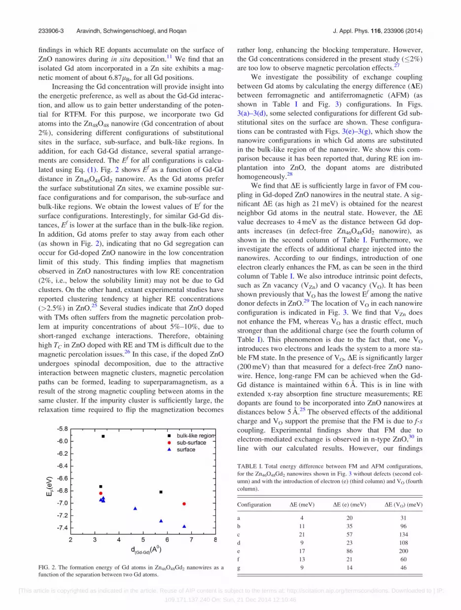
Increasing the Gd concentration will provide insight into
the energetic preference, as well as about the Gd-Gd interac-
tion, and allow us to gain better understanding of the poten-
tial for RTFM. For this purpose, we incorporate two Gd
atoms into the Zn48O48 nanowire (Gd concentration of about
2%), considering different configurations of substitutional
sites in the surface, sub-surface, and bulk-like regions. In
addition, for each Gd-Gd distance, several spatial arrange-
ments are considered. The Ef for all configurations is calcu-
lated using Eq. (1). Fig. 2 shows Ef as a function of Gd-Gd
distance in Zn46O48Gd2 nanowire. As the Gd atoms prefer
the surface substitutional Zn sites, we examine possible sur-
face configurations and for comparison, the sub-surface and
bulk-like regions. We obtain the lowest values of Ef for the
surface configurations. Interestingly, for similar Gd-Gd dis-
tances, Ef is lower at the surface than in the bulk-like region.
In addition, Gd atoms prefer to stay away from each other
(as shown in Fig. 2), indicating that no Gd segregation can
occur for Gd-doped ZnO nanowire in the low concentration
limit of this study. This finding implies that magnetism
observed in ZnO nanostructures with low RE concentration
(2%, i.e., below the solubility limit) may not be due to Gd
clusters. On the other hand, extant experimental studies have
reported clustering tendency at higher RE concentrations
(>2.5%) in ZnO.25 Several studies indicate that ZnO doped
with TMs often suffers from the magnetic percolation prob-
lem at impurity concentrations of about 5%–10%, due to
short-ranged exchange interactions. Therefore, obtaining
high TC in ZnO doped with RE and TM is difficult due to the
magnetic percolation issues.26 In this case, if the doped ZnO
undergoes spinodal decomposition, due to the attractive
interaction between magnetic clusters, magnetic percolation
paths can be formed, leading to superparamagnetism, as a
result of the strong magnetic coupling between atoms in the
same cluster. If the impurity cluster is sufficiently large, the
relaxation time required to flip the magnetization becomes
rather long, enhancing the blocking temperature. However,
the Gd concentrations considered in the present study (�2%)
are too low to observe magnetic percolation effects.27
We investigate the possibility of exchange coupling
between Gd atoms by calculating the energy difference (DE)
between ferromagnetic and antiferromagnetic (AFM) (as
shown in Table I and Fig. 3) configurations. In Figs.
3(a)–3(d), some selected configurations for different Gd sub-
stitutional sites on the surface are shown. These configura-
tions can be contrasted with Figs. 3(e)–3(g), which show the
nanowire configurations in which Gd atoms are substituted
in the bulk-like region of the nanowire. We show this com-
parison because it has been reported that, during RE ion im-
plantation into ZnO, the dopant atoms are distributed
homogeneously.28
We find that DE is sufficiently large in favor of FM cou-
pling in Gd-doped ZnO nanowires in the neutral state. A sig-
nificant DE (as high as 21 meV) is obtained for the nearest
neighbor Gd atoms in the neutral state. However, the DE
value decreases to 4 meV as the distance between Gd dop-
ants increases (in defect-free Zn46O48Gd2 nanowire), as
shown in the second column of Table I. Furthermore, we
investigate the effects of additional charge injected into the
nanowires. According to our findings, introduction of one
electron clearly enhances the FM, as can be seen in the third
column of Table I. We also introduce intrinsic point defects,
such as Zn vacancy (VZn) and O vacancy (VO). It has been
shown previously that VO has the lowest Ef among the native
donor defects in ZnO.29 The location of VO in each nanowire
configuration is indicated in Fig. 3. We find that VZn does
not enhance the FM, whereas VO has a drastic effect, much
stronger than the additional charge (see the fourth column of
Table I). This phenomenon is due to the fact that, one VO
introduces two electrons and leads the system to a more sta-
ble FM state. In the presence of VO, DE is significantly larger
(200 meV) than that measured for a defect-free ZnO nano-
wire. Hence, long-range FM can be achieved when the Gd-
Gd distance is maintained within 6 A. This is in line with
extended x-ray absorption fine structure measurements; RE
dopants are found to be incorporated into ZnO nanowires at
distances below 5 A.25 The observed effects of the additional
charge and VO support the premise that the FM is due to f-scoupling. Experimental findings show that FM due to
electron-mediated exchange is observed in n-type ZnO,30 in
line with our calculated results. However, our findings
FIG. 2. The formation energy of Gd atoms in Zn46O48Gd2 nanowires as a
function of the separation between two Gd atoms.
TABLE I. Total energy difference between FM and AFM configurations,
for the Zn46O48Gd2 nanowires shown in Fig. 3 without defects (second col-
umn) and with the introduction of electron (e) (third column) and VO (fourth
column).
Configuration DE (meV) DE (e) (meV) DE (VO) (meV)
a 4 20 31
b 11 35 96
c 21 57 134
d 9 23 108
e 17 86 200
f 13 21 60
g 9 14 46
233906-3 Aravindh, Schwingenschloegl, and Roqan J. Appl. Phys. 116, 233906 (2014)
[This article is copyrighted as indicated in the article. Reuse of AIP content is subject to the terms at: http://scitation.aip.org/termsconditions. Downloaded to ] IP:
109.171.137.240 On: Sun, 21 Dec 2014 12:10:46

suggest that RTFM can be stabilized in ZnO:Gd nanowires,
by electrons and VO, as FM is favored with a significant
energy gain (DE> 30 meV), which is sufficient to establish
RTFM. This confirms that superparamagnetic phase cannot
be occurred in these nanowires. In this study, we show that,
due to the strong localized nature of the 4f electrons, carriers
are required to establish ferromagnetic exchange in RE-
doped ZnO. On the other hand, in the case of TM-based ZnO
materials, FM can be stabilized with or without carriers.30,31
The large DE obtained in our investigation is an indication
of the possibility of achieving long-range FM with high TC
(>RT) in RE doped ZnO systems, since it is experimentally
demonstrated that, with varying electron concentrations,
high TC can be obtained in n-type ZnO:Gd.32
We also investigate the DOS, as it can provide further
insight into the exchange mechanism. Fig. 4 depicts the DOS
of pristine Zn48O48 nanowire, exhibiting a semiconducting
and nonmagnetic nature, in line with previous calculations.33
The upper part of the valence band (from �4 to 0 eV) is
mainly due to O 2p states. However, the contribution of Zn dstates becomes prominent in the �4 eV to �6 eV range,
which is buried deeply inside the valence band. Zn 3d and O
2p states reveal an overlap between the electronic states,
which results in strong hybridization. The Zn, O and Gd
DOSs for the Zn46O48Gd2 nanowire with and without VO are
shown in Fig. 5, in the top and bottom panels, respectively.
FIG. 3. Different configurations of Zn46O48Gd2 nanowires with two Zn atoms replaced by Gd. The total energy differences between FM and AFM for each
configuration are shown. The VO positions are indicated by green spheres. Note that the FM coupling varies with the distance and location of Gd atoms in the
nanowire.
FIG. 4. The density of states of the pristine Zn48O48 nanowire without Gd
dopants.
FIG. 5. The densities of states of the Zn46O48Gd2 and Zn46O47Gd2 nano-
wires (top and bottom panels), respectively. The projected density of states
of Zn(s), O (p), Gd (d), and Gd (f).
233906-4 Aravindh, Schwingenschloegl, and Roqan J. Appl. Phys. 116, 233906 (2014)
[This article is copyrighted as indicated in the article. Reuse of AIP content is subject to the terms at: http://scitation.aip.org/termsconditions. Downloaded to ] IP:
109.171.137.240 On: Sun, 21 Dec 2014 12:10:46

The spin-up and spin-down DOSs of doped nanowire
are significantly different from that of the pristine nanowire.
For ZnO doped with Gd, a remarkable shift in the Fermi
level into the conduction band, close to the Gd f states, is
observed. The majority Gd f states (spin up) that are located
well below the valence band maximum are fully occupied.
On the other hand, the minority unoccupied Gd f states are
localized in the vicinity of the Fermi level. The Gd d states
in the conduction band overlap with the Gd f-states.
Hybridization of the Gd f states with the states of the host
material occurs at the Fermi level. As a result of introducing
VO, the Gd f state near the Fermi energy becomes partially
occupied by donor electrons. Consequently, the carrier con-
centration around VO is increased, which mediates interac-
tion between the s (mostly from Zn) and f electrons. This is
evident from the DOS, as the s-f coupling is more prominent
than p-f and f-f couplings. Since d orbitals are not contribut-
ing to the partially filled energy bands, the double exchange
picture is inappropriate for describing the exchange interac-
tion in the current context of ZnO:Gd nanowires.34 In this
case, when Fermi level overlaps with the Gd f-state (which
becomes partially filled) donor electrons occupy empty fstates and thus FM coupling occurs.23 The type of carriers
involved in establishing long-range ferromagnetic order
determines the exchange interactions in DMS materials.
Zener’s p-d exchange mechanism, as described by Dietl
et al.1 is weaker and long-ranged, mediated by extended
band of the valence hole states. The double-exchange model
is based on a physical picture of the d electron hopping
between atoms with strong on-site exchange.34 In the present
study of ZnO:Gd nanowires, VO donates two electrons to the
system, mediating the ferromagnetic exchange and hence,
the s-f coupling is more prominent than other mecha-
nisms.34,35 According to our calculations, introducing VZn
does not increase the ferromagnetic coupling energy.
Moreover, p-f exchange interaction mediated by holes is not
possible, as the calculated DOS of Gd-doped ZnO nanowire
shows a shift of Fermi level towards the conduction band,
implying that electrons can mediate FM through s-f interac-
tions. Hence, it can be concluded that the increase in DE (up
to 200 meV) with the introduction of VO is due to this strong
s-f coupling. Thus, the presence of VO is crucial for increas-
ing the s-f coupling (as 4f state is strongly localized) and
therefore promotes long-range RTFM in Gd-doped ZnO
nanowires.
IV. CONCLUSIONS
A systematic study of Gd doping in ZnO nanowires
showed that the energetically favorable substitutional sites
are located on the surface of the nanowire, which is in agree-
ment with previous experimental observations. We have
shown that the exchange coupling between the Gd atoms is
sufficient for establishing RTFM. Introduction of additional
charge or VO increases the ferromagnetic coupling energy by
enhancing the s-f coupling significantly, as Fermi level is
shifted further into the conduction band, close to the Gd fstates. Our findings can be used to understand experimentally
observed RTFM in Gd-doped ZnO nanowires.
1T. Dietl, H. Ohno, F. Matsukura, J. Cibert, and D. Ferrand, Science 287,
1019 (2000).2P. Sharma, A. Gupta, K. V. Rao, F. J. Owens, R. Sharma, R. Ahuja, J. M.
O. Guillen, B. Johansson, and G. A. Gehring, Nature Mater. 2, 673 (2003).3A. Mang, K. Reimann, and S. Rubenacke, Solid State Commun. 94, 251 (1995).4M. H. Huang, S. Mao, H. Feick, H. Q. Yan, Y. Y. Wu, H. Kind, E. Weber,
R. Russo, and P. Yang, Science 292, 1897 (2001).5U. Ozgur, Y. I. Alivov, C. Liu, A. Teke, M. A. Reshchikov, S. Doan, V.
Avrutin, S.-J. Cho, and H. Morkoc, J. Appl. Phys. 98, 041301 (2005).6H. Shi, P. Zhang, S. S. Li, and J. B. Xia, J. Appl. Phys. 106, 023910 (2009).7M. H. N. Assadi, Y. Zhang, R. Zheng, S. P. Ringer, and S. Li, Nanoscale
Res. Lett. 6, 357 (2011).8I. Bantounas, S. Goumri-Said, M. B. Kanoun, A. Manchon, I. Roqan, and
U. Schwingenschlogl, J. Appl. Phys. 109, 083929 (2011).9P. Photongkam, Y. B. Zhang, M. H. N. Assadi, S. Li, D. Yu, M. Lonescu,
and A. V. Pan, J. Appl. Phys. 107, 033909 (2010).10X. Ma, Thin Solid Films 520, 5752 (2012).11M. Ungureanu, H. Schmidt, Q. Xu, H. V. Wenckstern, D. Spemann, H.
Hochmuth, M. Lorenz, and M. Grundmann, Superlattices Microstruct. 42,
231 (2007).12D. Wang, Q. Chen, G. Xiang, J. Yi, S. Bakul, J. Dung, J. Wang, and T.
Wu, Nano Lett. 12, 3994 (2012).13K. Potzger, S. Zhou, F. Eichhorn, M. Helm, W. Skorupa, A. Mucklich, and
J. Fassbender, J. Appl. Phys. 99, 063906 (2006).14A. A. Dakhel and M. El-Hilo, J. Appl. Phys. 107, 123905 (2010).15N. Ney, S. Ye, T. Kammermeier, K. Ollefs, F. Wilhelm, A. Rogalev, S.
Lebegue, A. L. Da Rosa, and A. Ney, Phys. Rev. B 85, 235203 (2012).16Z. Xu, Q.-R. Zheng, and G. Su, Phys. Rev. B 85, 075402 (2012); S.
Haffad, M. Samah, and G. Cicero, Phys. Rev. B 85, 165207 (2012).17R. M. Sheetz, I. Ponomareva, E. Richter, A. N. Andriotis, and M. Menon,
Phys. Rev. B 80, 195314 (2009).18G. Shen, B. Liang, X. Wang, H. Huang, D. Chen, and Z. L. Wang, ACS
Nano 5, 6148 (2011); P. Schio, F. Vidal, Y. Zheng, J. Milano, E. Fonda,
D. Demaille, B. Vodungbo, J. Varalda, A. J. A. de Oliveira, and V. H.
Etgens, Phys. Rev. B 82, 094436 (2010); X. Duan, J. Wang, and C. M.
Lieber, Appl. Phys. Lett. 76, 1116 (2000); Z. Huo, C.-K. Tsung, W.
Huang, X. Zhang, and P. Yang, Nano Lett. 8, 2041 (2008).19G. Kresse and D. Joubert, Phys. Rev. B 47, 558 (1993); G. Kresse and J.
Furthmuller, Phys. Rev. B 54, 11169 (1996).20J. P. Perdew, K. Burke, and M. Erzenhoff, Phys. Rev. Lett. 77, 3865
(1996).21M. Toyoda, H. Akai, K. Sato, and H. K. Yoshida, Physica B 376, 647
(2006).22Y. Li, R. Deng, W. Lin, Y. Tian, H. Peng, J. Yi, B. Yao, and T. Wu, Phys.
Rev. B 87, 155151 (2013).23G. M. Dalpian and S.-H. Wei, Phys. Rev. B 72, 115201 (2005).24P. E. Blochl, Phys. Rev. B 50, 17953 (1994).25M. Ishii, S. Komuro, T. Morikawa, and Y. Aoyagi, J. Appl. Phys. 89, 3679
(2001).26K. Sato, L. Berqqvist, J. Kudrnovsky, P. H. Dederichs, O. Eriksson, I.
Turek, B. Sanyal, G. Bouzerar, H. K. Yoshida, V. A. Dinh, T. Fukushima,
H. Kizaki, and R. Zeller, Rev. Mod. Phys. 82, 1633 (2010); K. Sato, W.
Schweika, P. H. Dederichs, and H. Katayama-Yoshida, Phys. Rev. B 70,
201202 (2004).27K. Sato, T. Fukushima, and H. K. Yoshida, Jpn. J. Appl. Phys., Part 2 46,
L682 (2007); T. Fukushima, K. Sato, H. K. Yoshida, and P. H. Dederichs,
Jpn. J. Appl. Phys., Part 2 45, L416 (2006).28S. Geburt, D. Stichtnoth, S. Muller, W. Dewald, C. Ronning, J. Wang, Y.
Jiao, Y. Y. Rao, S. K. Hark, and Q. Li, J. Nanosci. Nanotechnol. 8, 244
(2008).29A. Janotti and C. G. Van de Walle, Phys. Rev. B 76, 165202 (2007).30K. Sato and H. Katayama-Yoshida, Jpn. J. Appl. Phys., Part 2 40, L334
(2001).31K. Sato and H. K. Yoshida, Jpn. J. Appl. Phys., Part 2 39, L555 (2000).32M. Ungureanu, H. Schmidt, H. V. Wenckstern, H. Hochmuth, M. Lorenz,
M. Grundmann, M. F. Morariu, and G. Gntherodt, Thin Solid Films 515,
8761 (2007).33C. G. Vande Walle, Phys. Rev. Lett. 85, 1012 (2000); X. Wu, D.
Vanderbilt, and D. R. Haman, Phys. Rev. B 72, 035105 (2005).34P. M. Krstajic, F. M. Peeters, A. Ivanov, V. Fleurov, and K. Kikoin, Phys.
Rev. B 70, 195215 (2004).35H. K. Yoshida, K. Sato, T. Fukushima, M. Toyoda, H. Kizaki, V. A. Dinh,
and P. H. Dederichs, Phys. Status Solidi A 204, 15 (2007).
233906-5 Aravindh, Schwingenschloegl, and Roqan J. Appl. Phys. 116, 233906 (2014)
[This article is copyrighted as indicated in the article. Reuse of AIP content is subject to the terms at: http://scitation.aip.org/termsconditions. Downloaded to ] IP:
109.171.137.240 On: Sun, 21 Dec 2014 12:10:46