experimental process development for scanning thermal
TRANSCRIPT
i
Experimental Process Development for Scanning
Thermal Microscopy in Air and Vacuum
Sai Kan Tam
MSc by Research
University of York
Physics
February 2017
ii
Abstract
This thesis explores the procedure of making thermal and force measurements using a
scanning thermal microscope (SThM) in both air and vacuum environments. The atomic force
microscopy(AFM) and SThM literature will be reviewed, including thermal transport at the tip
sample interface and methods of determining the spring constant of the cantilever. The thesis
will then discuss the instruments that are used in the experiment, and the procedure for making
thermal and force measurements. Thermal and force measurements were obtained with five
different samples that cover different thermal and mechanical properties. Silicon, silicon
carbide, mica and PTFE along with a thin film of gold for which the thermal conductivity
would be determined. The topography analysis, interpretation of force and thermal curves will
be discussed and recommendations made about the best ways to attempt quantitative
measurements using these techniques.
iii
Contents
Abstract ...................................................................................................................................... ii
Content ...................................................................................................................................... iii
List of Tables ............................................................................................................................. v
List of Figures ........................................................................................................................... vi
Acknowledgement ................................................................................................................... xii
Declaration ............................................................................................................................. xiii
Chapter 1 Introduction ......................................................................................................................... 1
1.1. Motivation and Introduction ........................................................................................ 1
1.2. Atomic Force Microscopy ............................................................................................ 4
1.3. Scanning Thermal Microscopy ..................................................................................... 7
1.4. Objectives of this project ........................................................................................... 12
Chapter 2 Principle of force and temperature measurements using scanning probes ............... 13
2.1. Heat Transport in SThM ............................................................................................. 13
2.2. Characteristics of a force curve measured by AFM. ................................................. 18
2.3. Characteristic of a thermal measurement and thermal calibration ............................ 24
Chapter 3 Experimental Method ...................................................................................................... 29
Part I: Instrumentation and preparation ................................................................................... 29
3.1. SThM instrumentation and integration to AFM ......................................................... 29
3.2. Sample selection ......................................................................................................... 34
Part II: Experimental procedures ............................................................................................. 36
iv
3.3. Preparation for the force and thermal measurements ................................................. 36
3.4. Methods of topography measurements ....................................................................... 40
3.5. Force measurement and roughness procedure ............................................................ 44
3.6. Calibration of thermal probe and measurements procedure ....................................... 47
Chapter 4 Topography and force curves measured using contact mode and thermal probes .. 54
4.1. Physical dimensions from SEM and spring constant results ..................................... 55
4.2. Topography and roughness analysis .................................................................................. 60
4.3. Force measurements comparison between samples .................................................. 68
4.4. Discussion of the results ............................................................................................ 75
Chapter 5 SThM for thermal conductivity measurements ............................................................ 78
5.1. Thermal calibration and probe signal from the data logger ....................................... 78
5.2. Thermal map and the thermal measurements ............................................................ 88
5.3. Discussion and interpretation of thermal results and thermal conductivity ............ 108
Chapter 6 Conclusion and further developments ......................................................................... 116
List of reference ................................................................................................................................ 122
v
List of tables
Table 3.1 A table summarising the properties of the materials chosen for this thesis. The table
includes the thermal conductivity, hardness and the elastic modulus of the
samples. [35], [36], [37], [38] ............................................................................. 34
Table 4.1 Dimension measurements and spring constant calculation for all the probes. [35],
[36], [38] .............................................................................................................. 56
Table 4.2 Summary of the topography of each material. ........................................................ 67
Table 4.3 Table presenting the sensitivity a from inverting the overall average slope of silicon
carbide. ................................................................................................................. 68
Table 4.4 Retract force measurements using thermal probes. ................................................ 72
Table 5.1 Table of the conversion coefficient of the thermal probes used in thermal
measurements. ...................................................................................................... 86
Table 5.2 Table of temperature measurements from the thermal probe in air, with a current of
0.8mA. .................................................................................................................. 97
Table 5.3 Table of temperature measurements from the thermal probe in vacuum, with a
current of 0.8mA. ............................................................................................... 103
Table 5.4 Table of temperature measurements from thermal probe, measured in 0.8mA. .. 105
Table 5.5. A summary table for overall the data. The table showed the material, the thermal
conductivity, the elastic modulus, the retract force, the change in temperature for
approach, retract and for the data logger. The new elements are the deformation
column, where measuring the temperature dropped after the tip deforms the sample.
The percentage heat loss is calculating the percentage ratio of approach to data
logger. ................................................................................................................ 109
vi
List of figures
Figure 1.1 A generic diagram of the main parts of an atomic force microscope, it consists of
a piezoelectric tube as the main driver of the specimen, a laser and a photodiode
for feedback system a cantilever for scanning. [10] ............................................ 4
Figure 1.2 a) A conventional AFM topography image of a gold sample along with b) the
associated thermal image. The conversion coefficient for the scale bar to voltage
is 2.34Å/V. ........................................................................................................... 7
Figure 1.3 a) A typical shape of a fabricated probe. b) shows the structure of a Wollaston wire.
[18] ....................................................................................................................... 9
Figure 2.1 A schematic diagram showing the thermal pathways of a probe in contact with a
sample. a) This diagram shows the SThM operating in ambient environment. The
setup is the probe when operating in active mode. The heat flow is directed from
the probe to the sample. The heat transport by air, Ggas is also shown in the
diagram. Note that Ggas does not exist when the setup is operating in vacuum. b)
A detailed diagram of the dotted circle area in figure 2.1a), showing the heat flow
paths from the tip to the sample. In both the environments, the heat transported
by the radiation Grad and by mechanical contact Gmc exist. The blue area in the
ambient environment represents the water droplets formed by condensation. The
heat transport via water is represented by Gw. Note that Gw does not exist in
vacuum. The diagrams are modified from Poon [25] presentation. ................. 13
Figure 2.2. A typical force measurement diagram of SiC sample and operated in air. The
diagram described the probe position at each point from the starting position
where the probe starts recording the data, approaching to contact point where the
probe makes contact with the sample surface. The tip keeps pressing on until the
tip stop at the pre-set displacement range labelled as tip stopping point. The tip
will then retract from the surface, the surface adhesive force is keeping the tip on
the surface and bending the cantilever, a hysteresis is formed during the tip is
retracting. When the tip gained enough force that overcomes the surface force,
the tip will snap out and retract to the starting position. .................................... 19
vii
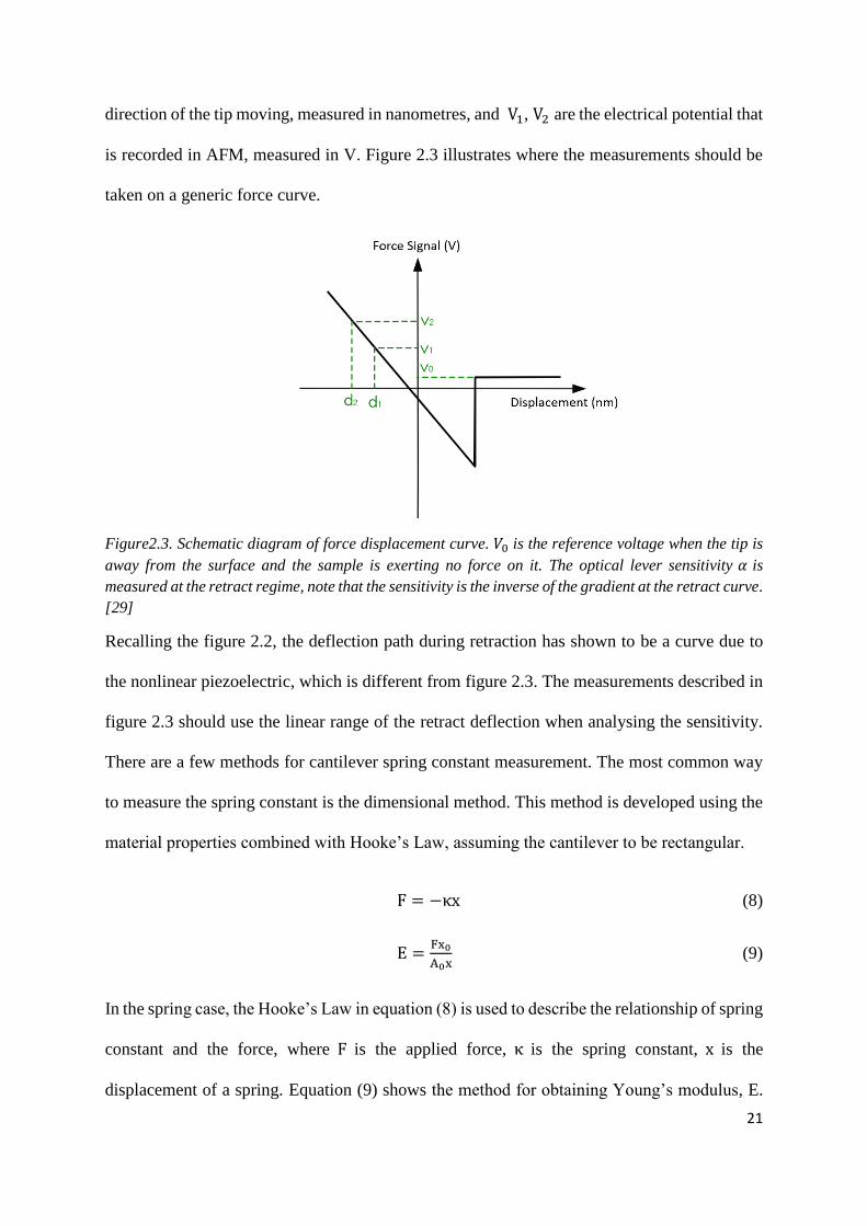
Figure2.3. Schematic diagram of force displacement curve. V0 is the reference voltage when
the tip is away from the surface and the sample is exerting no force on it. The
optical lever sensitivity α is measured at the retract regime, note that the
sensitivity is the inverse of the gradient at the retract curve. [29] ..................... 21
Figure 2.4 A schematic diagram demonstrating the reference cantilever method using a large-
scale cantilever against the AFM cantilever. a) The AFM cantilever is pressed on
a large-scale cantilever that has known property. b) When a force is applied by
the AFM cantilever, both cantilevers will bend as different rate, since both
cantilevers are exerting the same force, the spring constant is measured by the
deflection of the cantilever. [33] ........................................................................ 23
Figure 2.5 A schematic thermal measurement of SiC in air using a fabricated resistor probe
in active mode. The arrows indicate the motion and position of the probe
throughout the measurement. The position at which the probe snaps into the
surface is marked as the contact point. ............................................................. 24
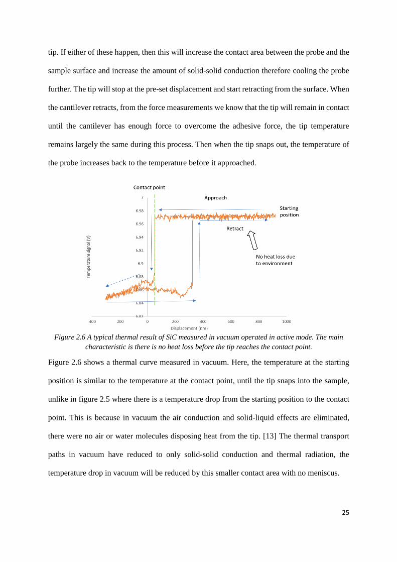
Figure 2.6 A typical thermal result of SiC measured in vacuum operated in active mode. The
main characteristic is there is no heat loss before the tip reaches the contact point.
............................................................................................................................ 25
Figure 2.7 A force curve and a thermal curve to verify the interpretation of the thermal curve.
The intersection of both curves at the contact point and the snap out point are used
to verify the temperature change on the thermal curve. .................................... 26
Figure 2.8 The typical shape for the thermal calibration in air. The calibration curve includes
the Peltier temperature and the probe voltage both plotted against time. .......... 27
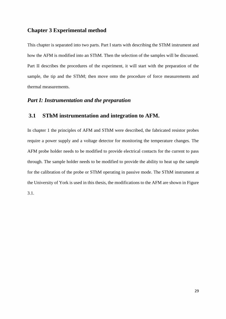
Figure 3.1 A photograph of SThM set up at the University of York. Including the data logger,
probe power supply, Peltier power supply and detection circuit, the vacuum
facility and the AFM. The AFM control PC is the main control for the AFM. 30
Figure 3.2 a) A comparison between the thermal probe holder (left) and the contact probe
holder (right). b) A photograph of the thermal probe connector with a thermal
probe attached. ................................................................................................... 31
viii
Figure 3.3 A circuit diagram of the power supply of the probe. The probe is represented as a
variable resistor as each probe will have a variation in resistance. The arrow
showed the two variable resistors that controls the main voltage applying to the
tip and the fine adjustment to the voltage, labelled in the diagram. [34] .......... 32
Figure 3.4 The AFM feedback module panel showing the cable connection and the switch for
feeding the thermal signal into the AFM. .......................................................... 33
Figure 3.5 An SEM image illustrating a) the width and the length measurements from top
view, b) thickness measurements from the side view. ....................................... 36
Figure 3.6 The estimation of the tip apex of a) the thermal probe and b) the contact probe.
............................................................................................................................ 37
Figure 3.7 The figure of the sample arrangement on the heater. .......................................... 38
Figure 3.8 A schematic diagram showing the measurements made in a force curve. The
difference of Vmin and V0 is the adhesive force dF being measured. The line of
best fit for sensitivity measurements is noted. ................................................... 45
Figure 3.9 A typical result from the data logger for thermal calibration. ............................. 48
Figure 3.10 Figure of thermal calibration in vacuum heated at 60℃, the temperature jump
during cooling is marked. .................................................................................. 49
Figure 3.11 A typical measurement of probe voltage against Peltier temperature, a line is
fitted for estimating the conversion coefficient from voltage to temperature. .. 50
Figure 3.12 Illustration showing a close up of a thermal hysteresis with explanation of how
to measure the change in temperature. .............................................................. 52
Figure 4.1 shows the SEM image for all probes used in this project. Figure a)-c) are the
thermal probes A-C and d) is the contact probe D, the figures above were
measured with the scale bar of 10 μm. .............................................................. 55
Figure 4.2 The impurities on the cantilever of probe A, the impurity is located towards the
holder on the left-hand side of the picture. This could potentially affect the spring
constant estimation. ........................................................................................... 57
ix
Figure 4.3 The SEM image of probe B with layer of palladium resistor coating peeling off
after measuring a set of thermal measurement. The scale bar of the figure is
100nm. ............................................................................................................... 59
Figure 4.4 Silicon carbide topography measured with a) contact probe and b) measured with
thermal probe C. The figures represent a similar area of the silicon carbide. ... 60
Figure 4.5. Roughness analysis of gold thin film. ................................................................ 63
Figure 4.6. Roughness analysis of mica. .............................................................................. 63
Figure 4.7. Roughness analysis of PTFE. ............................................................................. 64
Figure 4.8. Roughness analysis of silicon. ........................................................................... 64
Figure 4.9. Roughness analysis of silicon carbide. ............................................................... 65
Figure 4.10 Force measurement results of silicon carbide measured in air with a) the contact
probe D and b) the thermal probe C. ................................................................. 69
Figure 4.11 A diagram illustrating the force measurements that exceeded the AFM limit. Two
gradients were drawn and the intercepts were used to determining the adhesive
force. .................................................................................................................. 70
Figure 4.12. A diagram showing the typical force measurement result of silicon after the offset
of sensor limit. ................................................................................................... 71
Figure 4.13 Force result of PTFE in vacuum, measured in three different areas showing the
variation. ............................................................................................................ 74
Figure 5.1 a) A generic result of data logger recording in air. The diagram illustrates each part
of the curve during the experiment. From the beginning there is a potential
difference drop for approach until the tip is in contact with the surface. Then the
potential difference remained during the topography scanning. b) Continue the
same diagram with labels of the measurement spikes, noise spikes and indication
of the data logger change in temperature. The measurement spikes are indicating
the temperature changes during the force and thermal measurements. The noise
spikes are caused by the 40-second periodic instrumental noise. The data logger
change in temperature indicates the temperature difference between the tip in
contact and out of contact of the sample. .......................................................... 79
x
Figure 5.2 Data logger results of mica with 0.8mA in the environment of a) in air and b) in
vacuum. The results are comparing the measurement spikes height to the
temperature when the tip is not in contact in both environments. .................... 81
Figure 5.3 The data logger results of thermal calibration with the probe current of 0.8mA a)
in air and b) in vacuum. ..................................................................................... 83
Figure 5.4 Results of thermal calibration, graph of probe voltage against Peltier temperature
measured in a) air and b) vacuum. ..................................................................... 84
Figure 5.5 A graph of thermal calibration peak with both heating and cooling. .................. 85
Figure 5.6 a) The unprocessed thermal map of SiC in air b) the processed thermal map of SiC
in air. For both figures the conversion 10.02pm/V. ........................................... 87
Figure 5.7 Thermal curve of PTFE measured in vacuum. The thermal curve presented is an
average of 9 curves. The step jump is caused by different responses at each area.
............................................................................................................................ 89
Figure 5.8 Thermal curve of PTFE at 3 different areas measured in vacuum. ..................... 90
Figure 5.9 The thermal curves of a) PTFE and b) SiC measured in air. .............................. 91
Figure 5.10 The results for gold thin film in air. .................................................................. 93
Figure 5.11 Thermal results of Mica in air. .......................................................................... 93
Figure 5.12 Thermal results of PTFE in air. ......................................................................... 94
Figure 5.13 Thermal results of Silicon in air. ....................................................................... 94
Figure 5.14 The results of silicon carbide in air. .................................................................. 95
Figure 5.15 Thermal results of thin film gold in vacuum. .................................................... 99
Figure 5.16 Thermal results of Mica in vacuum. ............................................................... 100
Figure 5.17 Thermal results of PTFE in vacuum. .............................................................. 100
Figure 5.18 Thermal results of silicon in vacuum. ............................................................. 101
Figure 5.19 Thermal results of silicon carbide in vacuum. ................................................ 101
xi
Figure 5.20 The data logger results of silicon in air showing the sample cooling during the
experiment. ...................................................................................................... 107
Figure 5.21 Result of PTFE illustrating the method of calculating deformation temperature
changes. ........................................................................................................... 110
Figure 5.22 The approach temperature change against the thermal conductivity. ............. 112
Figure 5.23 The approach temperature change against the thermal conductivity for small
thermal conductivity. The gold is shown as a horizontal line as the thermal
conductivity is not known. ............................................................................... 113
Figure 5.24 The approach temperature change against the thermal conductivity for small
thermal conductivity. The silicon values have plotted with the silicon oxide
thermal conductivity of 1.1 W/m⋅K. ................................................................ 114

xii
Acknowledgement
I would like to take this chance to thank my supervisors, Prof. Sarah Thompson and Dr. Siew
Wai Poon for the unlimited encouragement, patience and care in this project. Without their
excellent guidance, I probably would never complete this research.
I want to thank my parents for looking after me throughout the time I have been writing, their
constant support and belief has helped me to pass through difficult times.
I want to thank a couple of my friends, Gordon Kam, Lichi Sun and Winky Wong for the
spiritual support.
xiii
Declaration
I declare that this thesis is a presentation of original work and I am the sole author. This work
has not previously been presented for an award at this, or any other, University. All sources
are acknowledged as References.
1
Chapter 1 Introduction
1.1 Motivation and introduction
Classical thermal measurements have been developed for understanding thermal physics for
decades. The classical theories of thermal transportation have been developed for investigating
the thermal properties of materials such as thermal conductivity and the applications have been
widely applied across everyday life. There are many techniques for making thermal
measurements, for example the absolute technique method determines the thermal conductivity
by placing the sample between the heat sink and a heat source, calculating the length of the
heat flow through the sample and obtaining the thermal conductivity by Fourier’s law. [1]
There are other temperature sensors that use different mechanisms such as thermocouples and
resistance thermometers.
When quantum physics was developed the technology and theories advanced further. There
was a better understanding that thermal transport is different on a smaller length scale, for
example the concept of heat carriers was introduced. [2] When making thermal measurements
at a nanoscale, typically less than 100 nanometres [2], a different mechanism of thermal
transportation would be expected. With the advance of fabrication technology, the construction
of materials and electronic components became much smaller. Although classical methods
such as the 3ω method [1] have advanced for thin film materials, the classical methods still
require a large contact area. Non- contact methods for thermal conductivity, such as transient
thermoreflectance techniques measure the thermoreflectance response of the material as a
function of time using a laser and beam splitter [1]. The thermoreflectance method can detect
the thermal conductivity of thin film with a few nanometres thick, but the spatial resolution
with this method can only measure down to 400 nanometres due to the optical limit of
diffraction. [3] Thermal measurements at smaller scale require other techniques. The scanning
2
thermal microscope is capable of measuring the temperature at 10 nanometres [4], it is a
modification to an atomic force microscope, which leads to the introduction to atomic force
microscopy.
Binnig introduced Atomic Force Microscopy (AFM) in 1986 [5], it is a technique which allows
high spatial resolution measurements at the material surface. Later the AFM was modified to
measure various properties, particularly the scanning thermal microscopy that is used in this
thesis. The original AFM modified the scanning tunnelling microscope tip by sticking pieces
of diamond on the end of the cantilever [5], [6]. In modern AFM the tip is no longer diamond,
instead it is usually made of silicon and silicon nitride. [7] The AFM detects the Van der Waals
force on the tip [8], the key features of AFM will be discussed in Section 1.2. AFM can provide
images with spatial resolution better than 0.1 nm, with the advantage of using non-conductive
materials and can be operated in vacuum. AFM has been widely used in material science in
order to study the topographic, tribological, roughness and adhesion characteristics of materials.
[7]
Shortly after AFM was introduced, scientists made modifications for temperature
measurements [9], the modification took the advantage of the high spatial resolution scanning
ability of AFM. The first Scanning Thermal Microscopy (SThM) instrument was introduced
by Williams and Wickramasinghe in 1986 [9]. The principle of their SThM was similar to
AFM, modifying the tip into a thermocouple that allows thermal measurements. As the tip
makes contact with the sample surface, thermal energy transfers either from the sample to the
thermocouple or vice versa, which changes the temperature dependent voltage across the
thermocouple. The voltage measurement could be converted into temperature, along with the
topography, creating a thermal map. Various types of SThM tip have been developed since
using different types of mechanisms, for instance the thermoelectric effect and thermal
3
resistance. The details of the different types of probes will be discussed in Section 1.3. SThM
gives a high spatial resolution thermal image, which makes this technique unique in studying
thermal physics.
SThM now acts as one of the main tools for developing near field thermal physics and in
material science. This thesis will attempt to explore its potential for measuring the thermal
properties of materials at the nanoscale. The thesis will focus on the initial steps of developing
a quantitative method for making thermal and force measurements, the method is capable of
operating the SThM in both air and vacuum environment. Thermal and force measurements
were obtained with five different samples covering different thermal and mechanical properties.
The topography analysis, interpretation of force and thermal curves will be discussed.
The thesis will start by introducing the concept of AFM, the principle of how to make
measurements and what modes they can be operated in, then move onto SThM by describing
the different types of probes and the literature review on the application. Chapter 2 discusses
the physics of thermal transport and how the heat flows in SThM. This then leads to the
discussion on how to interpret the force and thermal measurements. Chapter 3 describes in
detail the instruments being used in this thesis, the experimental setup and process and the
choice of samples. Chapter 4 concentrates on the analysis of the force measurements while
Chapter 5 concentrates on the analysis of the thermal measurements. Chapter 6 is the
conclusion and suggestions for future development.
4
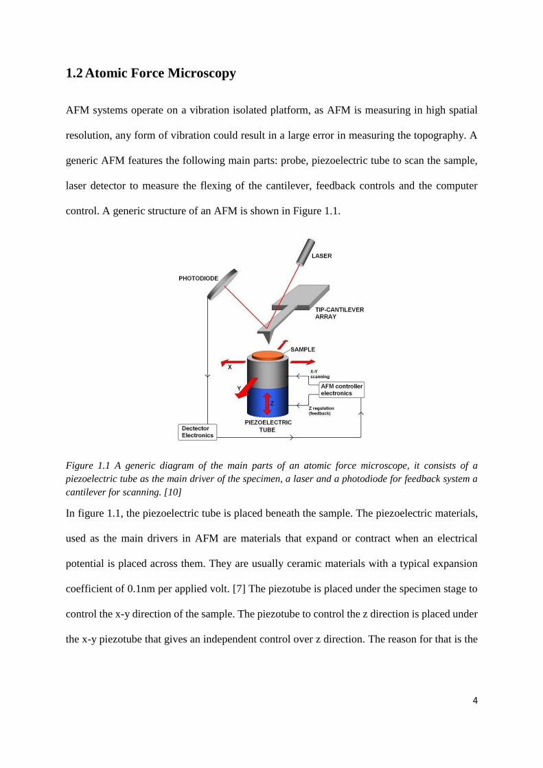
1.2 Atomic Force Microscopy
AFM systems operate on a vibration isolated platform, as AFM is measuring in high spatial
resolution, any form of vibration could result in a large error in measuring the topography. A
generic AFM features the following main parts: probe, piezoelectric tube to scan the sample,
laser detector to measure the flexing of the cantilever, feedback controls and the computer
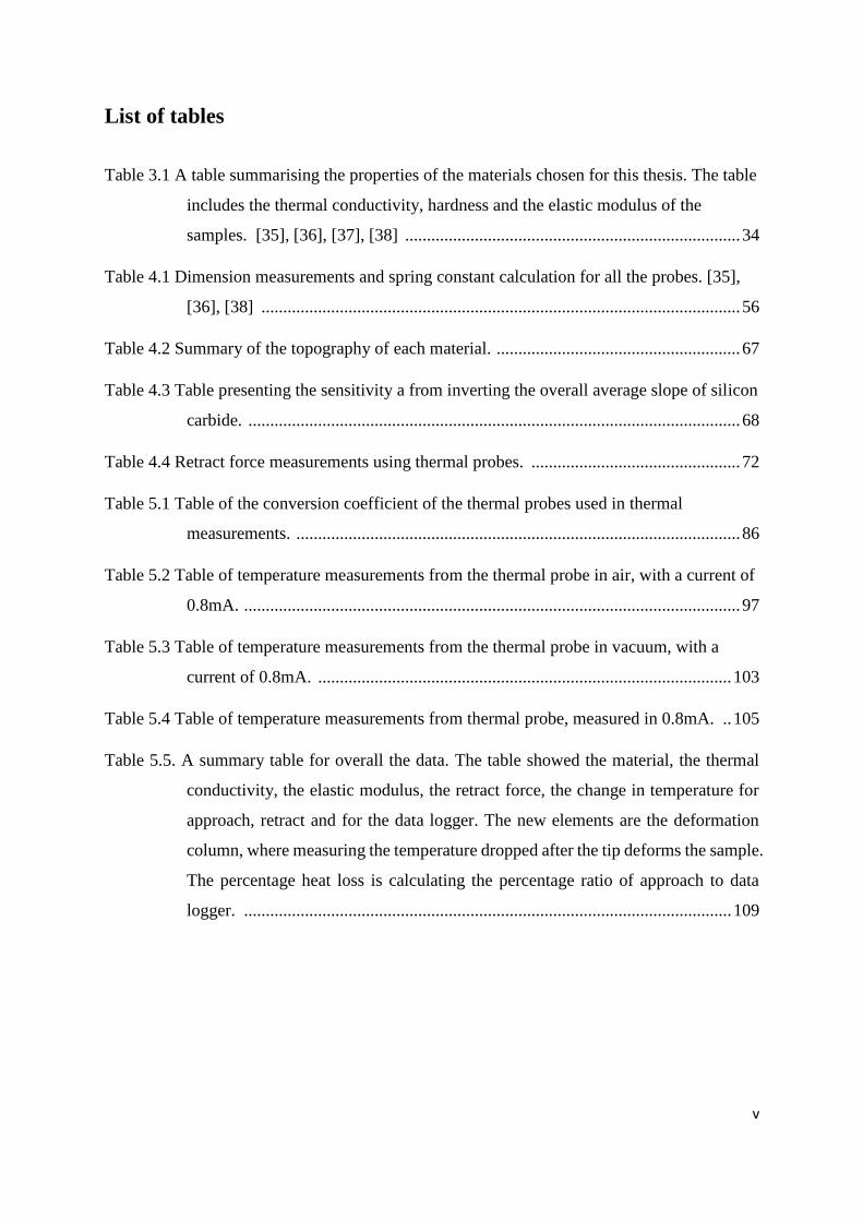
control. A generic structure of an AFM is shown in Figure 1.1.
Figure 1.1 A generic diagram of the main parts of an atomic force microscope, it consists of a
piezoelectric tube as the main driver of the specimen, a laser and a photodiode for feedback system a
cantilever for scanning. [10]
In figure 1.1, the piezoelectric tube is placed beneath the sample. The piezoelectric materials,
used as the main drivers in AFM are materials that expand or contract when an electrical
potential is placed across them. They are usually ceramic materials with a typical expansion
coefficient of 0.1nm per applied volt. [7] The piezotube is placed under the specimen stage to
control the x-y direction of the sample. The piezotube to control the z direction is placed under
the x-y piezotube that gives an independent control over z direction. The reason for that is the
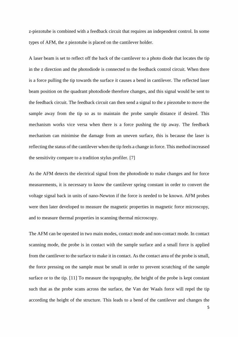
5
z-piezotube is combined with a feedback circuit that requires an independent control. In some
types of AFM, the z piezotube is placed on the cantilever holder.
A laser beam is set to reflect off the back of the cantilever to a photo diode that locates the tip
in the z direction and the photodiode is connected to the feedback control circuit. When there
is a force pulling the tip towards the surface it causes a bend in cantilever. The reflected laser
beam position on the quadrant photodiode therefore changes, and this signal would be sent to
the feedback circuit. The feedback circuit can then send a signal to the z piezotube to move the
sample away from the tip so as to maintain the probe sample distance if desired. This
mechanism works vice versa when there is a force pushing the tip away. The feedback
mechanism can minimise the damage from an uneven surface, this is because the laser is
reflecting the status of the cantilever when the tip feels a change in force. This method increased
the sensitivity compare to a tradition stylus profiler. [7]
As the AFM detects the electrical signal from the photodiode to make changes and for force
measurements, it is necessary to know the cantilever spring constant in order to convert the
voltage signal back in units of nano-Newton if the force is needed to be known. AFM probes
were then later developed to measure the magnetic properties in magnetic force microscopy,
and to measure thermal properties in scanning thermal microscopy.
The AFM can be operated in two main modes, contact mode and non-contact mode. In contact
scanning mode, the probe is in contact with the sample surface and a small force is applied
from the cantilever to the surface to make it in contact. As the contact area of the probe is small,
the force pressing on the sample must be small in order to prevent scratching of the sample
surface or to the tip. [11] To measure the topography, the height of the probe is kept constant
such that as the probe scans across the surface, the Van der Waals force will repel the tip
according the height of the structure. This leads to a bend of the cantilever and changes the
6
laser reflection. The photodiode gives a signal to the computer for the z geometry measurement
at each point. This method is often referred to as constant height scanning mode.
Constant force scanning mode is to maintain the force at a fixed value between the probe and
the surface. This technique is similar to constant height scanning mode, except the deflection
of the cantilever signal from the photodiode is sent to a feedback circuit. The feedback circuit
controls the z piezotube to adjust the height of the probe such that the force between the probe
and sample surface is maintained. Although both the contact scanning modes can provide
topography images, there are some defects and limitations. For example, the force on the
surface could cause friction and bend the probe, the probe could cause damage while moving
on the surface. Due to these limitations, non-contact scanning mode was introduced.
Non-contact scanning mode is a technique which uses the resonance effect of the cantilever.
Unlike the contact force mode, the tip does not constantly contact with the sample surface,
instead the cantilever is oscillating using an additional piezoelectric element. The cantilever is
oscillating at its resonant frequency, when the probe approach to the sample surface, the
cantilever is no longer oscillating in free space. A phase shift is then detected in the resonant
frequency of the cantilever because of the interaction force between the tip and the surface. [7]
From this phase shift, we can determine whether the surface force is attractive or repulsive.
The feedback circuit then sends a signal to adjust the z position in order to maintain the resonant
frequency. [7] [8] While the tip moves across the x-y plane, along with the change in z position,
the surface topography is then generated.
7
1.3 Scanning Thermal Microscopy
The general principle for SThM making thermal measurements is to use a tip with a physical
property that is sensitive to temperature and can be monitored continuously. [12] This property
is usually electrical potential. A constant electrical current is first passed through the fabricated
material at the end of the tip, where the thermal sensor for detecting temperature is located.
When the probe makes contact with the sample surface, the heat flow causes a change in
temperature at the tip, this changes the electrical potential detected across the tip sensor. By
monitoring the value of the voltage changes simultaneously with the topography, a thermal
map is produced. SThM is usually carried out using the contact mode of AFM. The reason is
the thermal measurements are related to the changes of voltage when the tip is in contact with
the sample, a continuous contact with the sample is preferred for SThM.
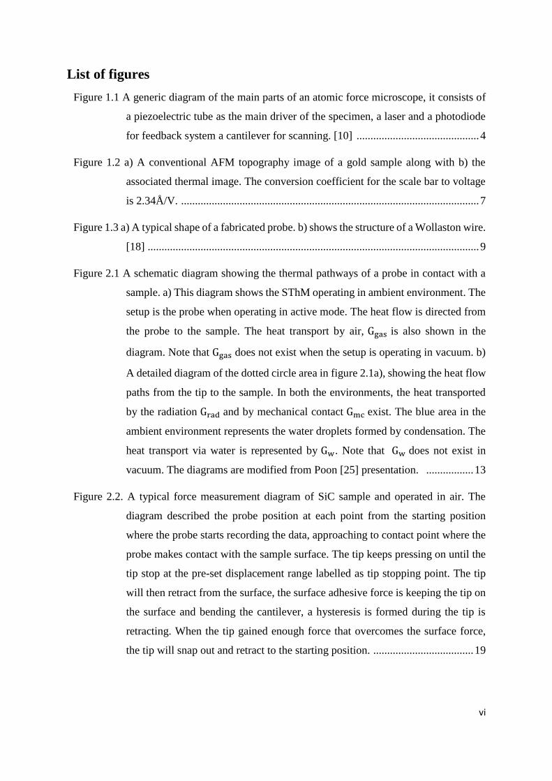
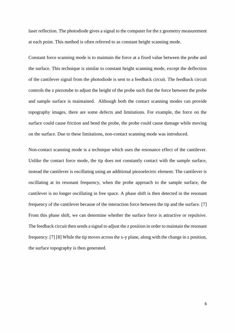
a) b)
Figure 1.2 a) A conventional AFM topography image of a gold sample along with b) the associated
thermal image. The conversion coefficient for the scale bar to voltage is 2.34Å/V.
Figure 1.2 shows a typical result from SThM, it is usually a topography map along with a
thermal image. The pictures show that the thermal image provides some fine details to the
topography, which could suggest the change in tip temperature could help in determining the
surface structure. During the measurement, the tip and the sample could cause a misleading
representation. This is because the contact area between the tip and the sample is dependent on
200nm
45.75 nm
0.00 nm
200nm
2.70 Å
0.00 Å
8
the physical properties of the sample surface and the thermal transport depends on the contact
area, if the contact area changes, the thermal transport changes. [13]
There are several types of SThM probes that have been developed for measuring surface
temperature, each can be classified using its temperature-dependent mechanism. [12] This
thesis will mainly discuss the types of probe using the mechanisms of thermal voltage and
change in electrical resistance; other thermal probes for example fluorescence and thermal
expansion are not covered in this thesis.
A thermocouple profiler is one of the popular probes being used in SThM, where the
temperature is measured by the change in electrical potential at the thermal junction. The
thermocouple profiler was first developed by fabricating two types of materials to form a
thermocouple at the end of an STM tip, the coating is typically about 100nm thick. [8] This
type of probe uses the concept of thermoelectric effect, which offers a direct conversion
between electrical voltage and temperature. [14] Thermocouple probes measure the voltage at
the junction that is in contact with the sample surface and give a spatially resolved temperature
measurement.
A resistance thermometer is another type of probe which monitors the temperature changes
using a voltage measurement. The change in temperature is monitored by applying a constant
current through the sensor. When the temperature of the probe changes, this causes a change
in the electrical resistance of the sensor, which in turn causes a change in electrical potential
across the tip. There is only one type of material fabricated on the AFM tip, therefore the
technology required for making resistance thermometer is less complex [15].
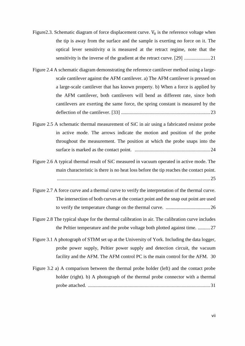
Wollaston wire tips are one of the probes that measured the temperature by the change in
resistance, introduced in 1994 by Pylkki et al. [16] The tip is made by bending a Pt wire, 5 μm-
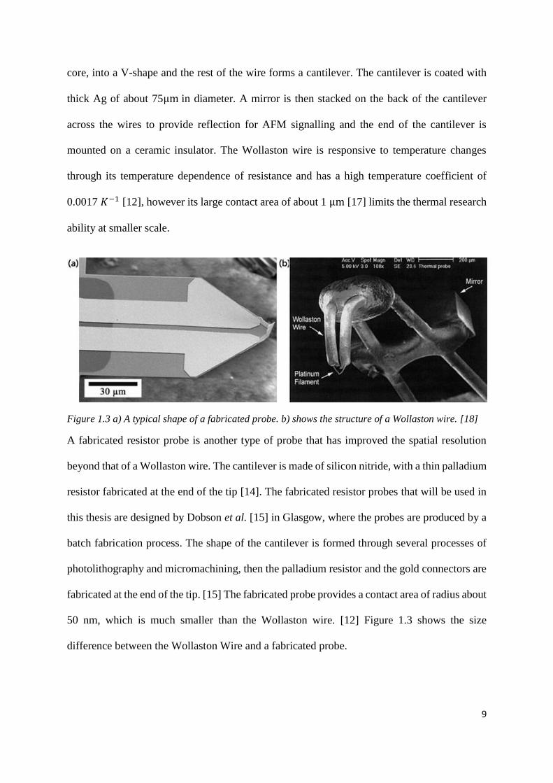
9
core, into a V-shape and the rest of the wire forms a cantilever. The cantilever is coated with
thick Ag of about 75μm in diameter. A mirror is then stacked on the back of the cantilever
across the wires to provide reflection for AFM signalling and the end of the cantilever is
mounted on a ceramic insulator. The Wollaston wire is responsive to temperature changes
through its temperature dependence of resistance and has a high temperature coefficient of
0.0017 𝐾−1 [12], however its large contact area of about 1 μm [17] limits the thermal research
ability at smaller scale.
Figure 1.3 a) A typical shape of a fabricated probe. b) shows the structure of a Wollaston wire. [18]
A fabricated resistor probe is another type of probe that has improved the spatial resolution
beyond that of a Wollaston wire. The cantilever is made of silicon nitride, with a thin palladium
resistor fabricated at the end of the tip [14]. The fabricated resistor probes that will be used in
this thesis are designed by Dobson et al. [15] in Glasgow, where the probes are produced by a
batch fabrication process. The shape of the cantilever is formed through several processes of
photolithography and micromachining, then the palladium resistor and the gold connectors are
fabricated at the end of the tip. [15] The fabricated probe provides a contact area of radius about
50 nm, which is much smaller than the Wollaston wire. [12] Figure 1.3 shows the size
difference between the Wollaston Wire and a fabricated probe.
10
SThM requires extra components to modify an AFM to measure the surface temperature of the
sample, this is usually specific to the type of probes that the SThM is using and the capability
of the AFM. In general, from the probes mentioned above, it is required to constantly monitor
the small change in current through the probe by measuring the voltage across it. This means
that the AFM probe holder must be modified for electrical connections. An additional power
supply is required for providing the current through the probe. A signal recorder which can
feed the signal back to the AFM for monitoring the voltage is also required. The details of the
apparatus modification will be discussed in Chapter 3.
SThM can be operated in active and passive modes. Active mode is to pass a current through
the probe to monitor the change in temperature, with no additional heating of the sample. The
sample is heated up only by the tip, as the current in the probe causes Joule heating. This defines
the direction of heat flowing from the tip towards the sample [19]. Passive mode is opposite to
active mode, where the sample is heated independently by a heater. The current passing through
the tip is smaller and only acts as thermometry, the sample heating being large enough to
overcome the Joule heating by the probe. In this mode therefore, the heat flow is from the
sample towards the probe. The advantage of active mode is that the mechanism of thermal
transport is simpler than passive mode and the heat generation is localised to the tip area.
Research on nanothermal analysis using SThM has been actively developing in recent years.
Majumdar and Shi [13] investigated the heat transfer mechanisms at SThM, which defined the
main thermal transport paths at the tip-sample contact. Weaver et al. [20] developed methods
of mass producing thermal resistive probes as well as designing different configurations. For
example, they suggested there is a strong thermal coupling through air between the tips in dual
cantilever probes. Gomes [17] studied the thermal exchange between probe and the sample, the
result suggested that the environment where the SThM performs affects the heat transport.
11
Prater et al. [21] have reported using infrared AFM on nanoscale infrared spectroscopy, which
could potentially open up nano thermal microscopy for biological use. Robinson et al. [22]
reports the investigation of how shear force affects the contact area of heat transport on the
nanoscale and proposed that the shear force at the thermal junction was dependent on the
materials. Gorbunov et al. [11] measured the surface microthermal properties of low thermal
conductivity materials and reported that local deformation contributes to the thermal
measurements.
The SThM at the University of York has the unusual ability to undertake thermal measurements
in vacuum. The advantage for vacuum is being able to eliminate the gas heating effect between
the probe and the sample, the details of this will be discussed in chapter 2. High vacuum SThM
is starting to get popular for nanothermal analysis. Menges et al. [23] built a high vacuum
SThM at the IBM research laboratory for the research on thermometry at nanoscale. Kim et al.
[24] reported using high vacuum SThM to quantify thermal fields in nanowires during
electromigration.
12
1.4 Objectives of this project
The objective for this project is to explore the potential of using a scanning thermal microscope
for quantitative thermal transport measurement. The scanning thermal microscope used in this
project is based on the atomic force microscope at the University of York. The thesis will start
by introducing the operation of the AFM, then move onto the development of the modification
to SThM. The unusual property of the SThM at York is the ability to undertake thermal
measurements in vacuum. As the SThM at York is still under development, this project aims
to develop an experimental procedure for quantitative measurements in different environments.
Then the project will move onto exploring the topography and the surface features of the
sample. The tip temperature changes will be measured using the SThM and compared within
the set of five different samples that cover different thermal and mechanical properties: silicon, silicon
carbide, mica and PTFE along with a thin film of gold for which the thermal conductivity would be
determined. An attempt to explore the connection between the adhesive force and the
temperature measurement will be presented as well as an attempt to obtain the thermal
conductivity of a thin film sample, and compare this to the bulk value. The project will conclude
with further suggestions on how to improve the experimental procedure and further possible
research directions.
13
Chapter 2 Principle of force and temperature measurements using
scanning probes
This chapter will include the basic theory of SThM. The chapter will start with discussing the
heat transport in SThM followed by the theory behind force curves and methods for measuring
the spring constant of the cantilever. The chapter will conclude with explaining the thermal
measurements, from the heat transport point of view, the complementarity with force
measurements and the thermal calibration.
2.1 Heat Transport in SThM
In SThM, the thermal properties are investigated by mapping the thermal properties to the
topography of a sample. It is important to understand how the thermal energy flows in the
system and what factors could limit the heat flow. There are four main mechanisms of thermal
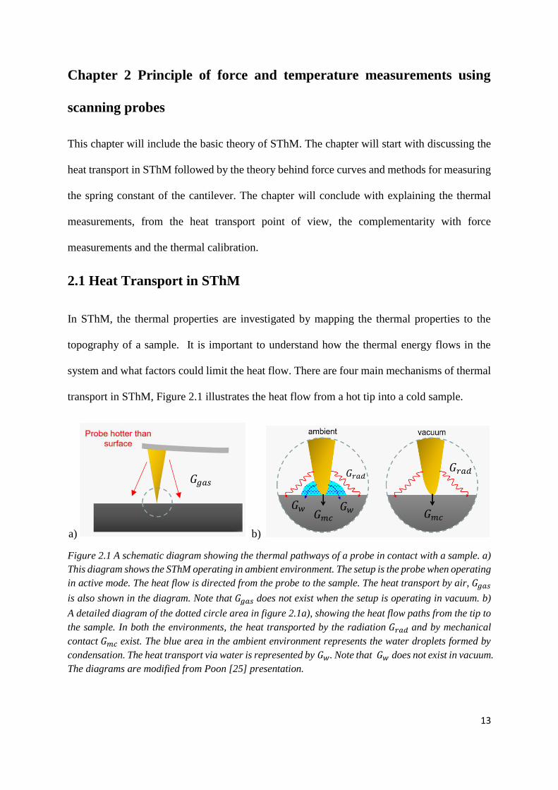
transport in SThM, Figure 2.1 illustrates the heat flow from a hot tip into a cold sample.
a) b)
Figure 2.1 A schematic diagram showing the thermal pathways of a probe in contact with a sample. a)
This diagram shows the SThM operating in ambient environment. The setup is the probe when operating
in active mode. The heat flow is directed from the probe to the sample. The heat transport by air, 𝐺𝑔𝑎𝑠
is also shown in the diagram. Note that 𝐺𝑔𝑎𝑠 does not exist when the setup is operating in vacuum. b)
A detailed diagram of the dotted circle area in figure 2.1a), showing the heat flow paths from the tip to
the sample. In both the environments, the heat transported by the radiation 𝐺𝑟𝑎𝑑 and by mechanical
contact 𝐺𝑚𝑐 exist. The blue area in the ambient environment represents the water droplets formed by
condensation. The heat transport via water is represented by 𝐺𝑤. Note that 𝐺𝑤 does not exist in vacuum.
The diagrams are modified from Poon [25] presentation.
𝐺𝑔𝑎𝑠 𝐺𝑟𝑎𝑑
𝐺𝑤
𝐺𝑚𝑐
𝐺𝑤
𝐺𝑟𝑎𝑑
𝐺𝑚𝑐
14
Figure 2.1a shows a setup of a probe contacting a sample surface, where the probe is heated to
have a higher temperature than the sample. Figure 2.1b shows the thermal energy transfer in
the environment of ambient and vacuum. The four main heat transport mechanisms are shown
and represented by their thermal conductance. The Grad, Ggas, Gw, Gmc, represent heat transport
by radiation, gas conduction, solid-liquid conduction and mechanical conduction respectively.
Gth,c represents the effective thermal conductance of the overall system. The mathematical
representation of Gth,c is proposed by Shi and Majumdar [12] in equation (1)
Rth,c =1
Gth,c=
1
Grad+Ggas+Gw+Gmc (1)
Equation (1) shows that the effective thermal resistance Rth,c , the reciprocal of effective
thermal conductance, Gth,c, which is the sum of the thermal conductance of all mechanisms.
Mechanical, or solid-solid conduction, is a direct energy exchange between the probe and the
sample [8]. The conduction happens when both the probe and the sample are in contact,
therefore during the thermal measurements the direct conduction must be taken into account.
The solid-solid conduction is restricted by the contact area between the tip and the sample, this
can be demonstrated by Fourier’s law of heat in equation (2).
Q̇ = −kAdT
dx (2)
Where Q̇ is the local heat flux, k is the thermal conductivity of the material, A is the area of
conduction, dT is the change in the temperature of two points and dx is the distance between
the point of measurements. When applying equation (2) in SThM, A is the contact area between
the probe and the sample surface. Fourier’s law shows that Q̇ is directly proportional to A,
15
therefore if the contact area of the tip gets infinitely small, the heat transport via conduction
will be infinitely small.
Fourier’s law described the thermal transport system on a macroscopic scale, the properties of
the materials such as the surface structure were not taken into account. In the microscopic
viewpoint, thermal transport is described using the concept of heat carriers. [2] Heat carriers
are carriers that transport energy, resulting in the change in temperature, for example, photons
are the main heat carriers of thermal radiation. [2] Heat carriers can be determined by quantum
mechanics with different possible energy states. In a solid, energy transfer can also be described
using phonon vibration.
Gas conduction happens when the heat transport is via gas molecules in the surrounding air.
Classical treatment of the kinetic theory of gases shows the thermal conductivity of the gas is.
[8]
kg =1
3Cvl (3)
Where kg represents thermal conductivity of the gas, C is the heat capacity per unit volume, l
is the mean free path for intermolecular collision and v is the root mean speed of the molecules.
When the tip heats up far away from the sample, thermal energy will disperse into the air and
heat up the surrounding gas molecules. The hot air molecules move away and convection
occurs. When the tip reaches the sample, the tip-sample distance gets smaller than the mean
free path of the air, the air would then transport heat energy directly and act as a conductor [26],
[27].
16
Thermal radiation happens when SThM is operating in both ambient conditions and in vacuum.
It is possible to model the far field radiation from a classical point of view using the Stefan-
Boltzmann law by assuming the system acts as a black body.
Q̇rad = σA(Thot4 − Tcold
4) (4)
Where Q̇rad is the power emitted by the black body radiation, Thot and Tcold represent the
temperature at the heated end and the cold end, A is the emitting area and σ is the Stefan-
Boltzmann constant, 5.67 × 10⁻⁸ kg s−3 K−4. Assuming the emitting area is the end of the tip,
A is very small. As there is a direct relationship between A and Q̇rad, the power emitted will
also be very small due to the geometry of the probe. Wien’s displacement law models the peak
wavelength of the black body by the following equation.
λmax =b
T (5)
Where λmax is the peak wavelength, T is the absolute temperature and b is the Wien’s
displacement constant, 2.898 × 10⁻³ m ⋅ K. Assuming the typical room temperature is about
300K, when applying to equation (5), the λmax is approximated to 10 μm. The typical size of a
thermal probe is less than 10 μm, therefore the classical theory could not be valid on measuring
thermal transport smaller than this scale. The above classical theory shows that near field
radiation theory is necessary to model heat loss via radiation. It is experimentally challenging
to measure the heat loss due to radiation, this is because the thermal radiation does not play the
main role in nano-thermal transport. [8] In an example of the thermal experiment done in
vacuum, the main transportation methods are solid-solid conduction and thermal radiation.
When the tip is not in contact with the sample, the signal is almost unchanged as the tip was
moved further away.
17
Solid-liquid conduction occurs when the ambient humidity is not zero and a water meniscus
forms on the tip due to condensation. The water meniscus increases the contact area between
the tip and the sample as illustrated in Figure 2.1 shown earlier. The heat energy takes the path
through the water then to the sample. Since the water is acting as a conductor, it is possible to
model the thermal energy with Fourier’s law. Luo et al. [26] suggested a model based on the
Kelvin equation. It is possible to eliminate solid-liquid conduction by performing SThM
measurements in vacuum.
18
2.2 Characteristics of a force curve measured by AFM
Material properties such as hardness and roughness of a surface have effects on thermal transfer
between a thermal probe and surface. For example, for a given contact force, a softer surface
is expected to have a larger contact area with the thermal probe which will contribute to the
solid-solid heat transfer. Fortunately, these properties can be studied using force curve
measurements provided by AFM. This section will provide a detail analysis for measuring the
adhesive force of the sample using the AFM force curves.
In imaging mode, AFM system provides a feedback circuit to maintain a constant contact force
between the tip and the sample. In a force curve measurement, which is done on a fixed surface
position, the contact force is varied by systematic movement of the AFM piezoelectric towards
and away from the sample position. The deflection of the probe cantilever due to this force
variation is recorded simultaneously. An analogous thermal curve can also be recorded on this
sample position when the AFM records the probe thermal voltage instead of cantilever
deflection. Descriptions on thermal curves will be provided in the next section.
A topography scan is required for the SThM to make a force measurement. It should be done
on a smooth area of the sample to avoid any impurities that could affect the adhesive force.
The smoothness of the sample is analysed by measuring the local roughness. A point on the
surface will then be selected by the user to take the force curve measurement. Usually several
points will be selected. The importance of roughness for thermal measurements will be
discussed later.
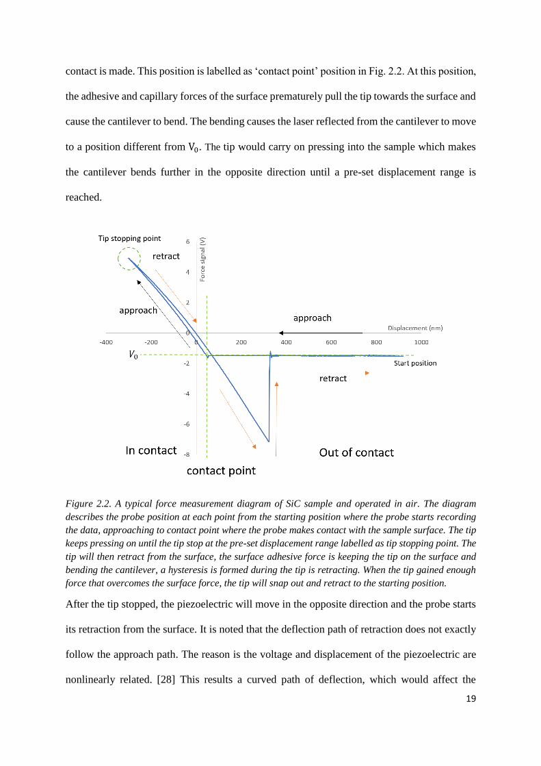
In a force curve measurement, the tip will first be retracted vertically away from the surface to
a selected start position shown in Figure 2.2. The laser position on the photodiode reflected
from this interaction-free cantilever at rest is taken as the reference voltage, V0. The AFM
piezoelectric will then start moving the tip towards the surface (known as tip approach) until a
19
contact is made. This position is labelled as ‘contact point’ position in Fig. 2.2. At this position,
the adhesive and capillary forces of the surface prematurely pull the tip towards the surface and
cause the cantilever to bend. The bending causes the laser reflected from the cantilever to move
to a position different from V0. The tip would carry on pressing into the sample which makes
the cantilever bends further in the opposite direction until a pre-set displacement range is
reached.
Figure 2.2. A typical force measurement diagram of SiC sample and operated in air. The diagram
describes the probe position at each point from the starting position where the probe starts recording
the data, approaching to contact point where the probe makes contact with the sample surface. The tip
keeps pressing on until the tip stop at the pre-set displacement range labelled as tip stopping point. The
tip will then retract from the surface, the surface adhesive force is keeping the tip on the surface and
bending the cantilever, a hysteresis is formed during the tip is retracting. When the tip gained enough
force that overcomes the surface force, the tip will snap out and retract to the starting position.
After the tip stopped, the piezoelectric will move in the opposite direction and the probe starts
its retraction from the surface. It is noted that the deflection path of retraction does not exactly
follow the approach path. The reason is the voltage and displacement of the piezoelectric are
nonlinearly related. [28] This results a curved path of deflection, which would affect the
20
sensitivity measurement shows in figure 2.3. When the tip reaches the contact point again, the
adhesive force from the sample keeps the tip in contact with the surface, i.e. the tip “sticks” on
the surface. This causes the cantilever to bend until it reaches a point where there is enough
force to overcome the adhesive force. The tip will then snap out of the surface and returns to
the reference point at V0.
In the retract direction, the extra adhesive force provided by the cantilever-tip interaction
causes a hysteresis, this extra force in retraction is where the adhesive force is measured. The
point taken for this force is the difference between minimum point before snapping out and at
V0.
The figure 2.2 shows the force curve with a single layer of bulk material, the force curve is
expected to be different when there is an extra surface layer on the surface for example water
or oxidized material.
The AFM system collects the force signals in voltage. Therefore, the raw signal needs to be
converted to force in Newton units. In order to convert this voltage into a force in nano-
Newtons, the spring constant of the probe needs to be known. The conversion can then be done
using Hooke’s Law as follows:
F = κα(V − V0) (6)
α =|d2|−|d1|
V2−V1 (7)
Where F is the force measured in nN, κ is the spring constant of the cantilever, measured in
N/m. V is the potential measured at each point on the force-displacement curve, V0 is the
reference potential, both the potentials are measured in volt. α is the optical lever sensitivity,
which is a measure of the change in displacement d divided by the change in potential V during
retraction. This is represented in equation (7), where d1, d2 are the distance of the vertical
21
direction of the tip moving, measured in nanometres, and V1, V2 are the electrical potential that
is recorded in AFM, measured in V. Figure 2.3 illustrates where the measurements should be
taken on a generic force curve.
Figure2.3. Schematic diagram of force displacement curve. 𝑉0 is the reference voltage when the tip is
away from the surface and the sample is exerting no force on it. The optical lever sensitivity 𝛼 is
measured at the retract regime, note that the sensitivity is the inverse of the gradient at the retract curve.
[29]
Recalling the figure 2.2, the deflection path during retraction has shown to be a curve due to
the nonlinear piezoelectric, which is different from figure 2.3. The measurements described in
figure 2.3 should use the linear range of the retract deflection when analysing the sensitivity.
There are a few methods for cantilever spring constant measurement. The most common way
to measure the spring constant is the dimensional method. This method is developed using the
material properties combined with Hooke’s Law, assuming the cantilever to be rectangular.
F = −κx (8)
E =Fx0
A0x (9)
In the spring case, the Hooke’s Law in equation (8) is used to describe the relationship of spring
constant and the force, where F is the applied force, κ is the spring constant, x is the
displacement of a spring. Equation (9) shows the method for obtaining Young’s modulus, E.
22
A0 is the cross-sectional area of the spring and x0 is the original length of the spring. The
cantilever spring constant was reported by Poggi et al. [30] using the following equation.
κ =Ewt3
4L3 (10)
The notations for equation (10) are the same as in equation (8) - (9), where κ is the spring
constant, E is the Young’s modulus, w is the width of the cantilever, t is the thickness and L is
the length of the cantilever.
In 1993, Cleveland [31] proposed a method of measuring the spring constant of the AFM
cantilever by adding a known mass at the end of cantilever. The principle relies on measuring
the natural frequency of the cantilever before and after adding the known mass, from the
difference of the frequency to obtain the spring constant. As the natural frequency measurement
is independent of the shape of the probe, this method can measure the spring constant with a
more complex cantilever design.
However, as the probe structures are getting more complex with more than one material
involved, it is difficult to measure the Young’s modulus. Sader et al. [32] published a method
to measure the spring constant with an arbitrary shaped probe based on his previous method,
which opened up more possibilities for probe designs and choice of materials. The Sader
method is based on Cleveland method, but instead of adding a physical known mass to the
cantilever, Sader measured the resonance frequency of the AFM cantilever in air and in vacuum.
This method has an advantage that it is not restricted to shape or the material of the cantilever.
κ = MeρctwLωvac2 (11)
Where κ is the spring constant, ωvac is the fundamental radial resonant frequency of the
cantilever in vacuum; t, w and L are thickness, width and length of the cantilever respectively,
23
ρcis the density of cantilever and Me is the normalized effective mass. The advantage of this
method is that the shape of the cantilever is not restricted, this is because the spring constant is
heavily relying on the quality factor when measuring resonant frequency in vacuum. However,
this method requires the density of the cantilever, as the structure of SThM tip becomes more
complicated with more materials, it is challenging to estimate the density of the cantilever.
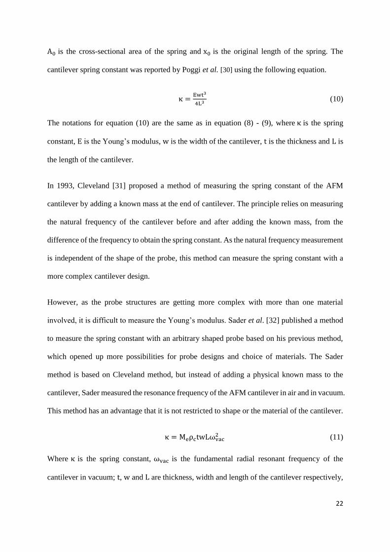
Figure 2.4 A schematic diagram demonstrating the reference cantilever method using a large-scale
cantilever against the AFM cantilever. a) The AFM cantilever is pressed on a large-scale cantilever
that has known property. b) When a force is applied by the AFM cantilever, both cantilevers will bend
as different rate, since both cantilevers are exerting the same force, the spring constant is measured by
the deflection of the cantilever. [33]
The referencing cantilever method is a more recently developed method, the principle is uses
a larger scale cantilever with known spring constant to calibrate the spring constant. Figure 2.4
demonstrates the reference cantilever method. The AFM probe is pressed against a larger scale
cantilever, both cantilever would then bend at different rates. Since the force applied to each
other are balanced, with the known large-scale cantilever spring constant, we can then work
out the spring constant using Hooke’s law. [33]
The dimensional method to estimate the spring constant will be used in this project. The reason
is due to the simplicity of the procedure as this project is aiming to develop a method for
exploring the thermal properties of the material. For this project, a scanning electron
microscope will be used for measuring the dimension of the probe.
24
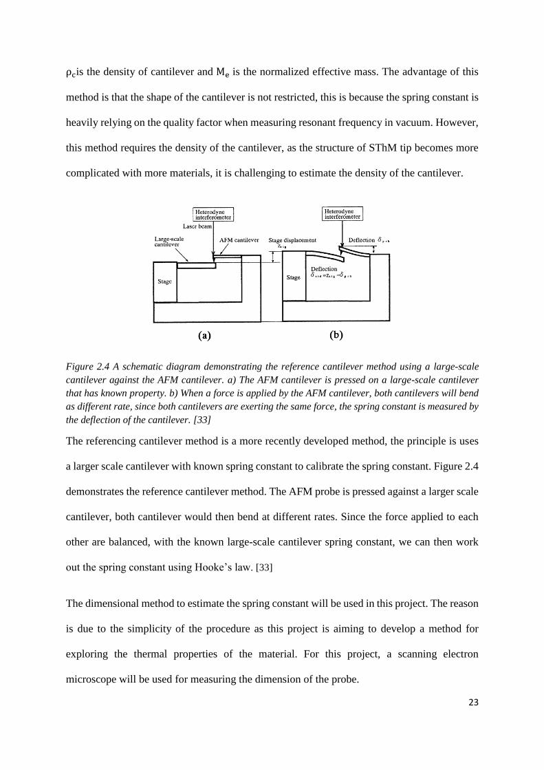
2.3 Characteristic of a thermal measurement and thermal calibration
In section 2.2, the cantilever bending was described along with the force measurement. The
thermal curve follows a similar principle; however, the input channel is used to measure the
voltage corresponding to the temperature. Figure 2.5 shows a generic thermal measurement
measured in air.
Figure 2.5 A schematic thermal measurement of SiC in air using a fabricated resistor probe in active
mode. The arrows indicate the motion and position of the probe throughout the measurement. The
position at which the probe snaps into the surface is marked as the contact point.
The tip is first retracted from the sample surface to the pre-set displacement position, labelled
starting position in figure 2.5, and then starts to approach the surface. The temperature will
start dropping due to air conduction increasing as the tip-sample distance gets smaller. When
the tip gets closer to the sample surface, the tip snaps into the sample surface at the contact
point, this is the same as described in the force measurements. The temperature signal will have
a sudden sharp drop, this is because the solid-solid conduction and solid-liquid conduction
happens and there is suddenly more heat flowing through the interface.
The tip will then continue pressing into the surface as the z-motion continues. The sample
surface will deform if the sample is soft or the tip will deform if the sampler is harder than the
25
tip. If either of these happen, then this will increase the contact area between the probe and the
sample surface and increase the amount of solid-solid conduction therefore cooling the probe
further. The tip will stop at the pre-set displacement and start retracting from the surface. When
the cantilever retracts, from the force measurements we know that the tip will remain in contact
until the cantilever has enough force to overcome the adhesive force, the tip temperature
remains largely the same during this process. Then when the tip snaps out, the temperature of
the probe increases back to the temperature before it approached.
Figure 2.6 A typical thermal result of SiC measured in vacuum operated in active mode. The main
characteristic is there is no heat loss before the tip reaches the contact point.
Figure 2.6 shows a thermal curve measured in vacuum. Here, the temperature at the starting
position is similar to the temperature at the contact point, until the tip snaps into the sample,
unlike in figure 2.5 where there is a temperature drop from the starting position to the contact
point. This is because in vacuum the air conduction and solid-liquid effects are eliminated,
there were no air or water molecules disposing heat from the tip. [13] The thermal transport
paths in vacuum have reduced to only solid-solid conduction and thermal radiation, the
temperature drop in vacuum will be reduced by this smaller contact area with no meniscus.
26
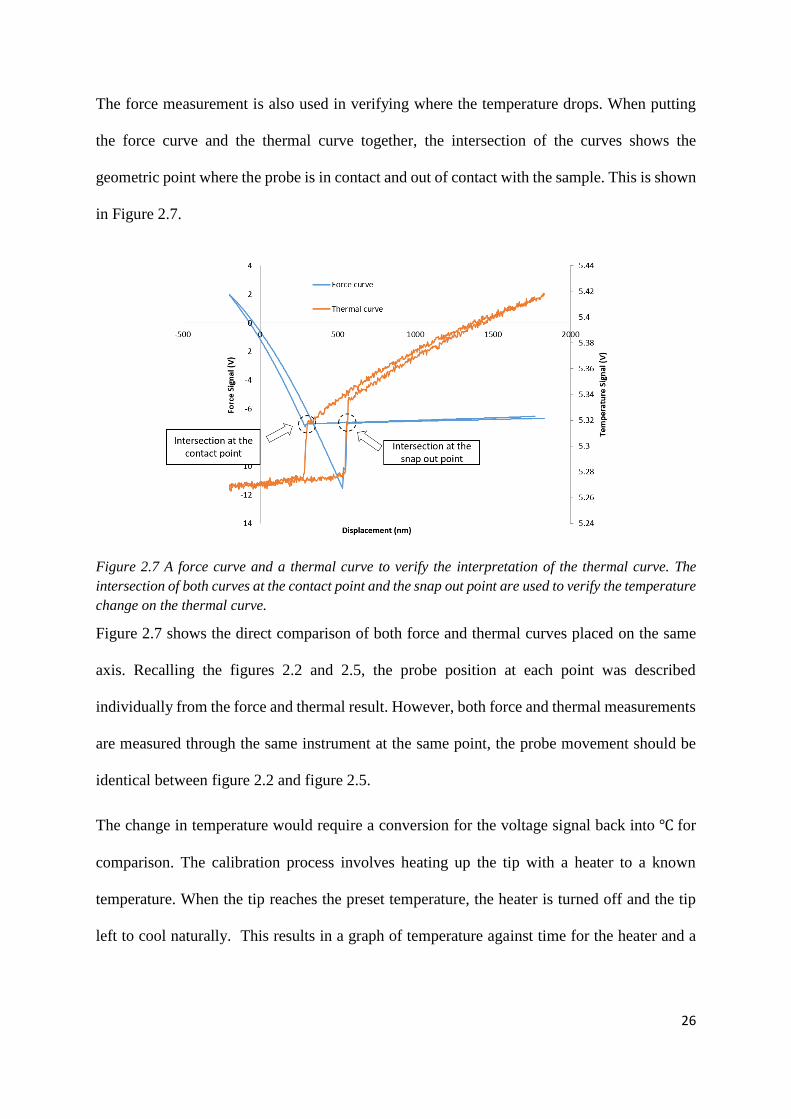
The force measurement is also used in verifying where the temperature drops. When putting
the force curve and the thermal curve together, the intersection of the curves shows the
geometric point where the probe is in contact and out of contact with the sample. This is shown
in Figure 2.7.
Figure 2.7 A force curve and a thermal curve to verify the interpretation of the thermal curve. The
intersection of both curves at the contact point and the snap out point are used to verify the temperature
change on the thermal curve.
Figure 2.7 shows the direct comparison of both force and thermal curves placed on the same
axis. Recalling the figures 2.2 and 2.5, the probe position at each point was described
individually from the force and thermal result. However, both force and thermal measurements
are measured through the same instrument at the same point, the probe movement should be
identical between figure 2.2 and figure 2.5.
The change in temperature would require a conversion for the voltage signal back into ℃ for
comparison. The calibration process involves heating up the tip with a heater to a known
temperature. When the tip reaches the preset temperature, the heater is turned off and the tip
left to cool naturally. This results in a graph of temperature against time for the heater and a
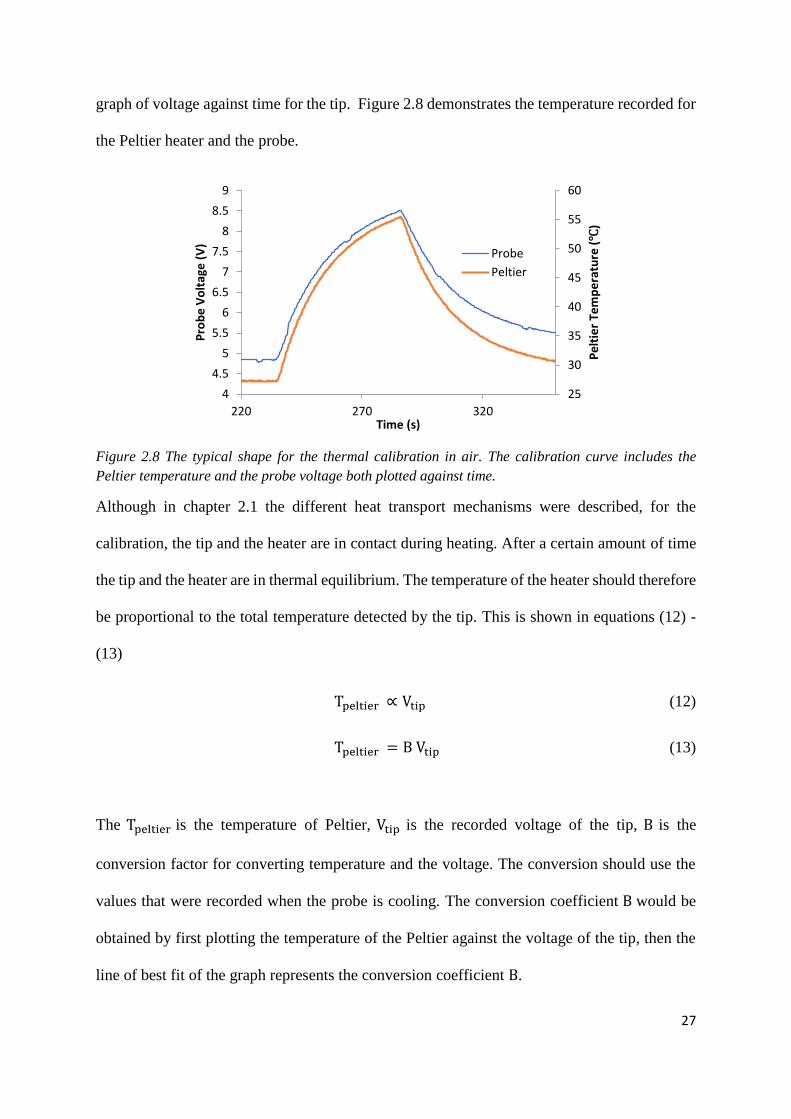
27
graph of voltage against time for the tip. Figure 2.8 demonstrates the temperature recorded for
the Peltier heater and the probe.
Figure 2.8 The typical shape for the thermal calibration in air. The calibration curve includes the
Peltier temperature and the probe voltage both plotted against time.
Although in chapter 2.1 the different heat transport mechanisms were described, for the
calibration, the tip and the heater are in contact during heating. After a certain amount of time
the tip and the heater are in thermal equilibrium. The temperature of the heater should therefore
be proportional to the total temperature detected by the tip. This is shown in equations (12) -
(13)
Tpeltier ∝ Vtip (12)
Tpeltier = B Vtip (13)
The Tpeltier is the temperature of Peltier, Vtip is the recorded voltage of the tip, B is the
conversion factor for converting temperature and the voltage. The conversion should use the
values that were recorded when the probe is cooling. The conversion coefficient B would be
obtained by first plotting the temperature of the Peltier against the voltage of the tip, then the
line of best fit of the graph represents the conversion coefficient B.
25
30
35
40
45
50
55
60
4
4.5
5
5.5
6
6.5
7
7.5
8
8.5
9
220 270 320
Pe
ltie
r Te
mp
era
ture
(℃
)
Pro
be
Vo
ltag
e (
V)
Time (s)
Probe
Peltier
28
The conversion could only provide the change in temperature in ℃, it does not give the
information for the absolute temperature of the thermal map. The reason is the detection circuit
is a balanced bridge circuit, making knowing the actual voltage difficult.
29
Chapter 3 Experimental method
This chapter is separated into two parts. Part I starts with describing the SThM instrument and
how the AFM is modified into an SThM. Then the selection of the samples will be discussed.
Part II describes the procedures of the experiment, it will start with the preparation of the
sample, the tip and the SThM; then move onto the procedure of force measurements and
thermal measurements.
Part I: Instrumentation and the preparation
3.1 SThM instrumentation and integration to AFM.
In chapter 1 the principles of AFM and SThM were described, the fabricated resistor probes
require a power supply and a voltage detector for monitoring the temperature changes. The
AFM probe holder needs to be modified to provide electrical contacts for the current to pass
through. The sample holder needs to be modified to provide the ability to heat up the sample
for the calibration of the probe or SThM operating in passive mode. The SThM instrument at
the University of York is used in this thesis, the modifications to the AFM are shown in Figure
3.1.
30
Figure 3.1 A photograph of SThM set up at the University of York. Including the data logger, probe
power supply, Peltier power supply and detection circuit, the vacuum facility and the AFM. The AFM
control PC is the main control for the AFM.
The AFM used in this project is a JEOL 5200 atomic force microscope, the vacuum facility is
from the original AFM which has not been modified. The vacuum dome is used for providing
high vacuum environment by connecting to a pump. The probe power supply is designed to
have a small current to protect the probe. The AFM sample holder is modified to have a Peltier
heater, a device making use of the Peltier effect to generate heating or cooling at the electrical
junction. The power supply for the Peltier controls the temperature heating of the sample holder.
The Peltier power supply is connected to a 4-pin connector to the sample specimen inside the
AFM. The reading on the Peltier power supply is used for thermal calibration to convert voltage
into temperature. The feedback AFM module is used to switch between the thermal and force
feedback, the data logger computer is used to monitor the probe current. The detail of
calibration process will be discussed later in this chapter.
31
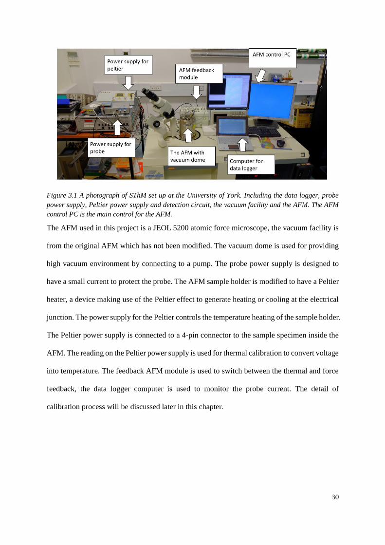
The thermal probe holder was specially designed and produced by Mr John Emery in the
Electronics Workshop at the University of York. The comparison between the thermal probe
holder and the contact probe holder is shown in Figure 3.2.
a) b)
Figure 3.2 a) A comparison between the thermal probe holder (left) and the contact probe holder (right).
b) A photograph of the thermal probe connector with a thermal probe attached.
From figure 3.2a, the design of the thermal probe holder is based on the shape of the contact
probe holder, this is to ensure it fits in the JEOL AFM. On the holder, there is a printed circuit
board with a 4-pin connector to power the probe and a Peltier heater, this is shown in figure
3.2b as well as the two thin gold pins that connect the probe with the power supply. The design
was improved later by having glue placed at the gold pins to increase the strength, the glue
position is labelled in figure 3.2b). Since the data for this project has collected with the new
design, the effect of the probe holder design to the measurements could not be measured.
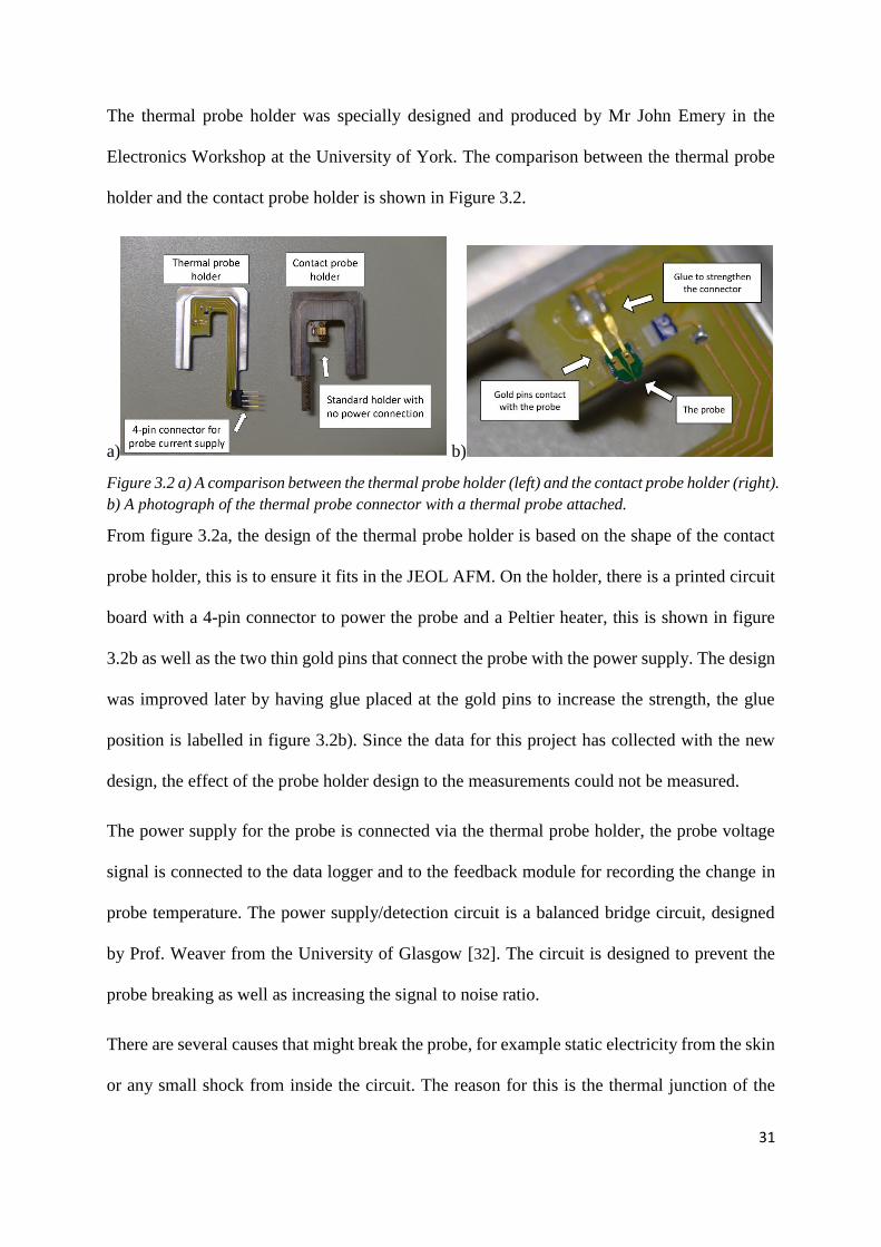
The power supply for the probe is connected via the thermal probe holder, the probe voltage
signal is connected to the data logger and to the feedback module for recording the change in
probe temperature. The power supply/detection circuit is a balanced bridge circuit, designed
by Prof. Weaver from the University of Glasgow [32]. The circuit is designed to prevent the
probe breaking as well as increasing the signal to noise ratio.
There are several causes that might break the probe, for example static electricity from the skin
or any small shock from inside the circuit. The reason for this is the thermal junction of the
32
probe is small, when there is a high voltage applied across the resistor, the heat generated due
to Joule heating would melt the resistor and break the circuit. Before the experiment, the
detection circuit of the probe has to be balanced by the power supply fine adjustment, so that
the change in voltage due to temperature are more easily measured. The circuit diagram is
shown in figure 3.3.
Figure 3.3 A circuit diagram of the power supply of the probe. The probe is represented as a variable
resistor as each probe will have a variation in resistance. The arrow showed the two variable resistors
that controls the main voltage applying to the tip and the fine adjustment to the voltage, labelled in the
diagram. [34]
The power supplies for both Peltier specimen heater and the probe were connected to a data
logger that is connected to a separate laptop. The reason is a separate computer system could
reduce the noise picked up from the AFM system. The detection signal for the probe would
also feed into the AFM feedback circuit. This is because the AFM has the ability to record the
change in temperature while measuring the topography. The connection for this setup is
showed in Figure 3.4.
33
Figure 3.4 The AFM feedback module panel showing the cable connection and the switch for feeding
the thermal signal into the AFM.
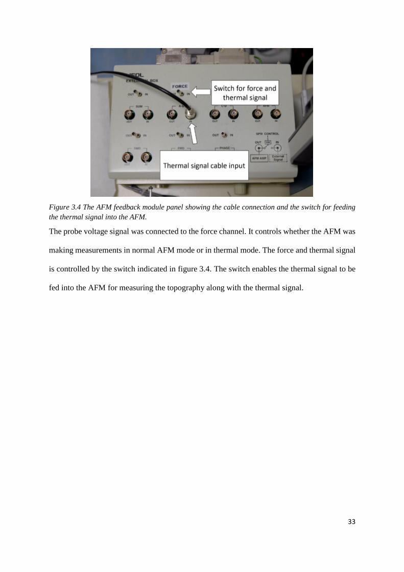
The probe voltage signal was connected to the force channel. It controls whether the AFM was
making measurements in normal AFM mode or in thermal mode. The force and thermal signal
is controlled by the switch indicated in figure 3.4. The switch enables the thermal signal to be
fed into the AFM for measuring the topography along with the thermal signal.
34
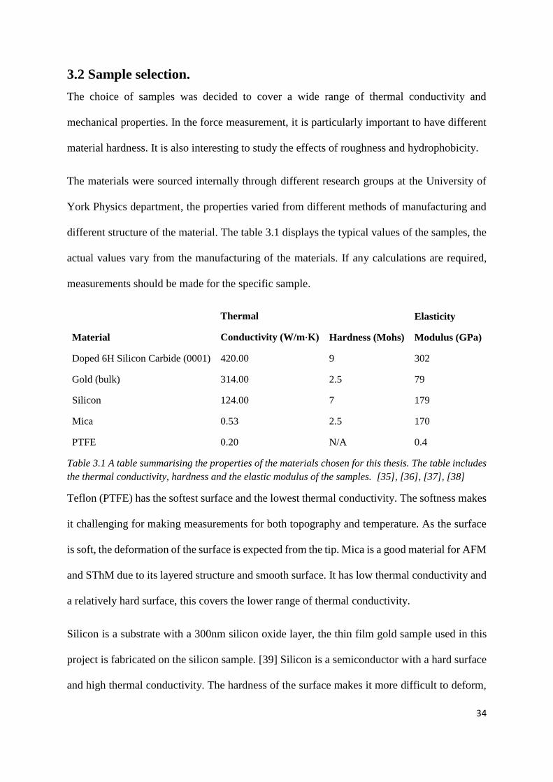
3.2 Sample selection.
The choice of samples was decided to cover a wide range of thermal conductivity and
mechanical properties. In the force measurement, it is particularly important to have different
material hardness. It is also interesting to study the effects of roughness and hydrophobicity.
The materials were sourced internally through different research groups at the University of
York Physics department, the properties varied from different methods of manufacturing and
different structure of the material. The table 3.1 displays the typical values of the samples, the
actual values vary from the manufacturing of the materials. If any calculations are required,
measurements should be made for the specific sample.
Material
Thermal
Conductivity (W/m⋅K) Hardness (Mohs)
Elasticity
Modulus (GPa)
Doped 6H Silicon Carbide (0001) 420.00 9 302
Gold (bulk) 314.00 2.5 79
Silicon 124.00 7 179
Mica 0.53 2.5 170
PTFE 0.20 N/A 0.4
Table 3.1 A table summarising the properties of the materials chosen for this thesis. The table includes
the thermal conductivity, hardness and the elastic modulus of the samples. [35], [36], [37], [38]
Teflon (PTFE) has the softest surface and the lowest thermal conductivity. The softness makes
it challenging for making measurements for both topography and temperature. As the surface
is soft, the deformation of the surface is expected from the tip. Mica is a good material for AFM
and SThM due to its layered structure and smooth surface. It has low thermal conductivity and
a relatively hard surface, this covers the lower range of thermal conductivity.
Silicon is a substrate with a 300nm silicon oxide layer, the thin film gold sample used in this
project is fabricated on the silicon sample. [39] Silicon is a semiconductor with a hard surface
and high thermal conductivity. The hardness of the surface makes it more difficult to deform,
35
therefore the temperature changes would be less dependent on the increase of contact area in
contact.
Silicon carbide is the hardest material from the set. It has the highest thermal conductivity to
cover the 400 W/m⋅K range. It is used in calibrating the sensitivity of the cantilever. The hardest
surface would cause least deformation for thermal measurements. However, it could potentially
damage the probe as the Pd coating is soft.
Thin film gold is the sample for testing the technique, it is a thin film conductor fabricated on
silicon. The thin film of gold is 150nm thick grown on a silicon substrate and patterned by e-
beam lithography. Between the gold and silicon, there is 8nm thick layer of chromium at the
interface to improve the adhesion of gold on the silicon. The sample was grown by Dr Vick at
the University of York and patterned at the University of Leeds. [39] The measurements for
this project will be using the electrical contact pads around the outside, which is an area that
does not have dedicated fabrication pattern.
The challenge is to find the thermal conductivity of this sample, as it is not a bulk material, the
conventional gold thermal conductivity will not be valid. The thin film gold is expected to have
a harder surface than PTFE, this is because metal should be harder than polymers. However,
because the gold is a thin film sample, the surface hardness and thermal conductivity are also
expected to be different from the bulk materials.
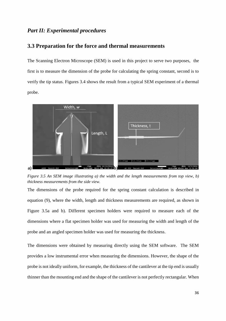
36
Part II: Experimental procedures
3.3 Preparation for the force and thermal measurements
The Scanning Electron Microscope (SEM) is used in this project to serve two purposes, the
first is to measure the dimension of the probe for calculating the spring constant, second is to
verify the tip status. Figures 3.4 shows the result from a typical SEM experiment of a thermal
probe.
a) b)
Figure 3.5 An SEM image illustrating a) the width and the length measurements from top view, b)
thickness measurements from the side view.
The dimensions of the probe required for the spring constant calculation is described in
equation (9), where the width, length and thickness measurements are required, as shown in
Figure 3.5a and b). Different specimen holders were required to measure each of the
dimensions where a flat specimen holder was used for measuring the width and length of the
probe and an angled specimen holder was used for measuring the thickness.
The dimensions were obtained by measuring directly using the SEM software. The SEM
provides a low instrumental error when measuring the dimensions. However, the shape of the
probe is not ideally uniform, for example, the thickness of the cantilever at the tip end is usually
thinner than the mounting end and the shape of the cantilever is not perfectly rectangular. When
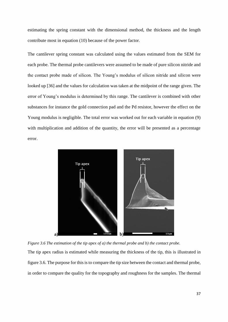
37
estimating the spring constant with the dimensional method, the thickness and the length
contribute most in equation (10) because of the power factor.
The cantilever spring constant was calculated using the values estimated from the SEM for
each probe. The thermal probe cantilevers were assumed to be made of pure silicon nitride and
the contact probe made of silicon. The Young’s modulus of silicon nitride and silicon were
looked up [36] and the values for calculation was taken at the midpoint of the range given. The
error of Young’s modulus is determined by this range. The cantilever is combined with other
substances for instance the gold connection pad and the Pd resistor, however the effect on the
Young modulus is negligible. The total error was worked out for each variable in equation (9)
with multiplication and addition of the quantity, the error will be presented as a percentage
error.
a) b)
Figure 3.6 The estimation of the tip apex of a) the thermal probe and b) the contact probe.
The tip apex radius is estimated while measuring the thickness of the tip, this is illustrated in
figure 3.6. The purpose for this is to compare the tip size between the contact and thermal probe,
in order to compare the quality for the topography and roughness for the samples. The thermal
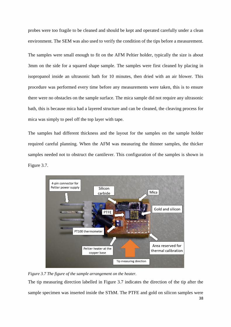
38
probes were too fragile to be cleaned and should be kept and operated carefully under a clean
environment. The SEM was also used to verify the condition of the tips before a measurement.
The samples were small enough to fit on the AFM Peltier holder, typically the size is about
3mm on the side for a squared shape sample. The samples were first cleaned by placing in
isopropanol inside an ultrasonic bath for 10 minutes, then dried with an air blower. This
procedure was performed every time before any measurements were taken, this is to ensure
there were no obstacles on the sample surface. The mica sample did not require any ultrasonic
bath, this is because mica had a layered structure and can be cleaned, the cleaving process for
mica was simply to peel off the top layer with tape.
The samples had different thickness and the layout for the samples on the sample holder
required careful planning. When the AFM was measuring the thinner samples, the thicker
samples needed not to obstruct the cantilever. This configuration of the samples is shown in
Figure 3.7.
Figure 3.7 The figure of the sample arrangement on the heater.
The tip measuring direction labelled in Figure 3.7 indicates the direction of the tip after the
sample specimen was inserted inside the SThM. The PTFE and gold on silicon samples were
39
thicker than silicon carbide and mica, in principle the thicker samples should be further away
for scanning to prevent obstruction when scanning. In the earlier stage of the experiment, the
samples were placed on the original AFM specimen holder with no Peltier heater integrated. It
was then discovered that the AFM could not scan the thinner samples surfaces. The reason for
that is the probe holder was modified for the thermal probe, which offsets the z direction limit.
The silicon carbide and mica were then lifted up by placing a silicon bar underneath. With the
silicon bar in place, both samples were thicker than PTFE and gold on silicon, hence the
arrangement in figure 3.7. At the later stage of the experiment, the AFM specimen holder was
modified to have a Peltier heater integrated for the ability to do thermal calibration in vacuum,
but the layout of the samples was kept. The samples were shifted to one side of the specimen
holder, the purpose for this was to leave an area for performing thermal calibration with the
probe. The calibration procedure will be discussed later in this chapter. The sample specimen
would then be inserted into the AFM and connected to the power supply.
40
3.4 Methods of topography measurements
The electrical resistance of the thermal tip should be measured before and after inserting into
the probe holder. Although the SEM image of the tip should verify whether the tip is damaged
or having any impurities, the electronic connection is verified by the resistance measurements.
The power supply box was connected to the probe holder while inserting it into the AFM. The
power supply for the probe is a balanced circuit; the procedure for balancing the circuit is to
apply a small current less than 0.1mA, when the voltage of the probe is increased as shown on
the data logger, the voltage is then set back to near 0V by adjusting the offset dial on the power
box. After the power box is balanced, then the current was slowly increased to 0.6mA and
0.8mA. The current was chosen to improve the signal to noise ratio while preventing damage
to the tip. The reason for slowly increasing the current is to avoid the sudden electrical shock
that can damage the resistor at the tip. The data logger monitored the voltage in case of
overheating and circuit damaging. The instrumental error is 0.05mA since the current reading
relies on the precision of the engraving on the knob, the only error estimation is half of the
smallest division on the knob. The error is more significant when comparing the thermal results.
The laser adjustment was done once there was a current passing through the probe. This is
because when a current passed through the probe, the Joule heating would bend the cantilever
and the laser spot will need re-adjustment, hence the probe current balancing was done before
the laser adjustment. The laser spot was set to reflect from near the edge of the probe, the laser
signal represents the cantilever deflection caused by the sample surface structure, therefore
having the laser spot closer to the tip provides a more accurate topographic image. The
photodiode also required adjustment for the largest signal of the probe, for thermal probe, the
typical signal is about 3V and the signal for contact probe is larger. The reason is that the
contact probes have a larger reflective surface than the thermal probes and hence the more laser
beam is reflected.
41
The laser signal could be different every time performing the experiment even if the same probe
is used each time. This is because when the probe is inserted to the holder, the positioning of
the probe will be different each time and the laser will not be reflected at the same area of the
tip and hence the variation in the laser signal. The laser signal is adjusted to collect as a high
voltage as possible to improve the signal to noise ratio. If it is at lower voltage signal, the
signal-noise ratio for the cantilever deflection will be lower and reduce the precision of the
force measurements. Note that there is a significant amount of laser signal heating observed
during the setup of the tip. This could contribute to the temperature difference during the
experiment, which should be taken into account as a possible source of error if the laser position
moves during the experiment.
For experiments performed in vacuum, the vacuum dome should be placed after the laser
adjustment and be pumped down overnight. The vacuum is pumped overnight so that the pump
and the pressure is stable before performing any measurements. During the pump down, the
laser and the probe power were advised to be off after the laser adjustment. The laser could
not be adjusted after the vacuum dome is placed, therefore it should be done in advance. The
vacuum should reach 10−4 to 10−5mbar after one night. The specimen was then manually
approached so that it was close to the probe. The process is observed by an optical microscope
and it is important that the sample does not hit the probe. The approach process is then
continued using the JEOL WinSPM software to control the z-piezo tube for the remaining
distance. During the experiment, the laser spot could move on the photodiode. A magnet is
attached on the control knob of the photodiode, the knob could be turned by using this magnet,
while the whole instrument is inside the vacuum dome.
The vacuum is created by placing the vacuum dome on top of the SThM for pumping down.
When preparing the vacuum dome, vacuum grease is used for sealing the gap between the
dome and the SThM, the quality of vacuum grease could directly affect whether the vacuum is
42
sealed entirely. The vacuum pressure was left overnight for stabilisation, however the vacuum
pressure should be monitored during the experiment. The reason is the vacuum reduced the
heat path for cooling the tip. A change in pressure was observed from 10−5mbar to 10−4mbar
and this change did not cause a significant effect on the thermal result.
The quality of the topography was determined by the scan size and the clock rate, while the
filter setting was set at 50kHz by default for both force and thermal measurements. The scan
size is the dimension of one side of a square and the clock rate is the speed for the probe moving
across the area. [29]
The topography scan was chosen to a scan size of 500nm for roughness analysis. The scan size
of the topography should be enough to present the overall sample surface while retaining spatial
resolution for making thermal measurements. The clock time should be optimised for a balance
between scanning time and quality. A slow clock rate can result in a scanning duration of 30
minutes per topography scan. In this project, the scanning duration is optimised to
approximately 10 minutes per scan. The probe requires a minimum time window to respond to
the surface. Such minimum requirement can be found by scanning the sample surface at
different rate and thus determine at which the quality of the scan does not improve significantly
further by inspection.
The thermal probe was expected to have a larger contact area than the contact probe, the
scanning size and the clock rate were optimized for both probes to have the same setting for
comparison. The scanning size and the clock rate in this project was optimised to 500μm with
500μs scanning time for both contact probe and thermal probe. Thermal measurements were
measured by enabling the probe power signal input to the AFM feedback hub.
After setting up WinSPM, the scan was commenced to collect the topography. In addition, after
each scan, the laser signal must be checked. Particularly after scanning on a hard sample with
43
a soft tip, it is possible to cause deformation to the tip after a scan therefore a check on laser
signal would ensure the result is representative. The topography image often required
processing before analysing. This is to improve the contrast of the image to enhance the details
on the topography. The appropriate height scale should be chosen to extract enough detail for
roughness analysis.
44
3.5 Force measurement and roughness procedure.
The force measurements were used to measure the adhesive force of the sample. The roughness
of the sample surface would affect the measurements, therefore when performing the force
measurements, a clean smooth area of the topography should be chosen. The displacement for
the specimen is the distance range for how far away the stage should move and the clock rate
determines the approaching velocity of the sample. These variables needed to be set in the
WinSPM software before measuring the surface force. The displacement value was done by
trials and errors because it was different for each sample. The optimum displacement should
show a continuous curve with the following elements: the starting position, the snap in point
and the snap out point, which were indicated in figure 2.2. The author started by moving the
tip away from the sample for 1000 nm, then decreasing the distance by 100nm to get the
optimum displacement. The clock rate was set to 1ms.
In section 3.3, the spring constant of the cantilever was calculated from the SEM measurements.
The force conversion that was described in equation (6) requires the measurements of
sensitivity, α , as defined in equation (7). The sensitivity measures the displacement per
deflection signal. If the sample surface deforms when the tip is in contact, it would misrepresent
the deflection signal of the cantilever. The sensitivity is chosen to measure from the force
curve of silicon carbide and then apply the same sensitivity to all other samples. Silicon carbide
has the highest surface hardness from the sample set that gives the least surface deformation.
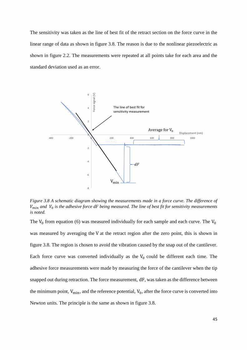
45
The sensitivity was taken as the line of best fit of the retract section on the force curve in the
linear range of data as shown in figure 3.8. The reason is due to the nonlinear piezoelectric as
shown in figure 2.2. The measurements were repeated at all points take for each area and the
standard deviation used as an error.
Figure 3.8 A schematic diagram showing the measurements made in a force curve. The difference of
𝑉𝑚𝑖𝑛 and 𝑉0 is the adhesive force dF being measured. The line of best fit for sensitivity measurements
is noted.
The V0 from equation (6) was measured individually for each sample and each curve. The V0
was measured by averaging the V at the retract region after the zero point, this is shown in
figure 3.8. The region is chosen to avoid the vibration caused by the snap out of the cantilever.
Each force curve was converted individually as the V0 could be different each time. The
adhesive force measurements were made by measuring the force of the cantilever when the tip
snapped out during retraction. The force measurement, dF, was taken as the difference between
the minimum point, Vmin, and the reference potential, V0, after the force curve is converted into
Newton units. The principle is the same as shown in figure 3.8.
46
The force curves were repeated at 3 different areas for each sample. Each area was repeated 3
times and averaged for presentation. All 3 areas were compared and found to be the same
therefore the author was able to average the total 9 points of measurements for reducing the
random error. When the areas are different, the areas were not averaged and this will be noted.
The force measurements are localised measurements, when repeating the experiment, different
parts of the sample surface were chosen to give a fuller representation. For each sample, the
dF at each area was averaged and the error is worked out through the standard deviation. Then
the dF of the sample was obtained by averaging the dF from the three areas. The total error for
the force would be weighted from the errors measured in each area. When comparing the
adhesive force, the error caused by the spring constant was not counted, this is because the
measurements for each sample were performed with the same tip. The spring constant error
should be accounted for when comparing the results using different tips, and the adhesive force
should be normalized accordingly. There are other factors that would affect the adhesive force
measurements. The topography was analyzed before picking the areas for force measurements
to make sure the areas were representative of the surface structure.
47
3.6 Calibration of thermal probe and measurements procedure
As noted in Chapter 3.3, the purpose for thermal calibration is to measure the thermal
sensitivity of the probe, converting voltage to ℃ for analysis. This is because the probes are
not identical and their electrical resistance varies. This resistance variation causes the
difference in thermal sensitivity, therefore the calibration process is required for each new
probe used. The probe resistance was measured by the multimeter before it was inserted into
the probe holder.
The calibration coefficient is measured before starting the force and thermal experiments.
When there is a change of probe, it will require another calibration because each probe will
have different thermal sensitivity. In addition, the tip is observed to have a change of the sensor
shape, therefore when the tip has been used for many experiments, the calibration should be
remeasured. A Peltier heater was used for the thermal calibration with a Pt100 thermometer for
monitoring the heater plate temperature. The Pt100 thermometer, shown in figure 3.7, is a
resistance thermometer which uses the linearity of resistance with temperature for thermometry.
The error of the probe temperature and the voltage are the instrumental errors from the data
logger. Since both variables are collected in the same device, the instrumental errors are the
same.
In figure 3.7 the reserved space on the specimen was prepared for this calibration process. First
a current in the range of 0.6mA to 0.8mA was passed through the probe. The probe would then
approach to the sample, the scan size was set at 0nm with a slow clock time, this would activate
the force feedback on the AFM. The probe would remain in contact with the sample surface
during the calibration so that the vibration effects due to thermal transport were reduced. The
clock time was dependent on how long the calibration was taken, in air the clock time was set
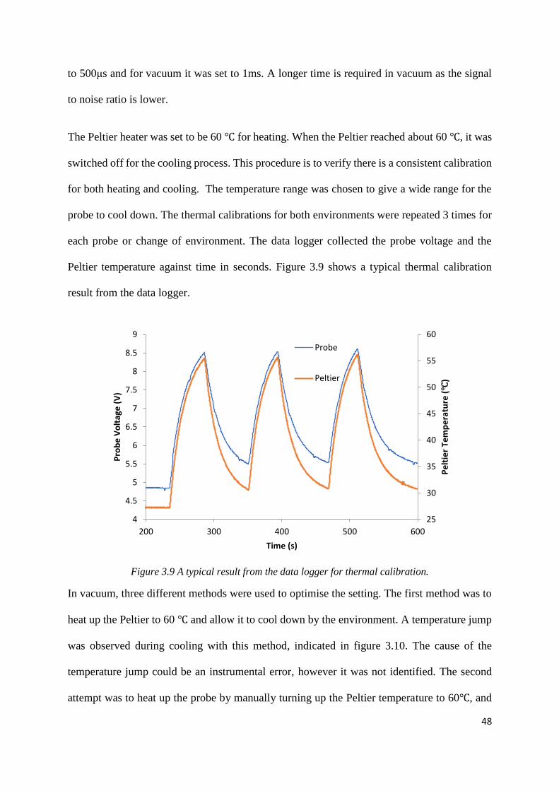
48
to 500μs and for vacuum it was set to 1ms. A longer time is required in vacuum as the signal
to noise ratio is lower.
The Peltier heater was set to be 60 ℃ for heating. When the Peltier reached about 60 ℃, it was
switched off for the cooling process. This procedure is to verify there is a consistent calibration
for both heating and cooling. The temperature range was chosen to give a wide range for the
probe to cool down. The thermal calibrations for both environments were repeated 3 times for
each probe or change of environment. The data logger collected the probe voltage and the
Peltier temperature against time in seconds. Figure 3.9 shows a typical thermal calibration
result from the data logger.
Figure 3.9 A typical result from the data logger for thermal calibration.
In vacuum, three different methods were used to optimise the setting. The first method was to
heat up the Peltier to 60 ℃ and allow it to cool down by the environment. A temperature jump
was observed during cooling with this method, indicated in figure 3.10. The cause of the
temperature jump could be an instrumental error, however it was not identified. The second
attempt was to heat up the probe by manually turning up the Peltier temperature to 60℃, and
25
30
35
40
45
50
55
60
4
4.5
5
5.5
6
6.5
7
7.5
8
8.5
9
200 300 400 500 600
Pe
ltie
r Te
mp
era
ture
(℃
)
Pro
be
Vo
ltag
e (
V)
Time (s)
Probe
Peltier
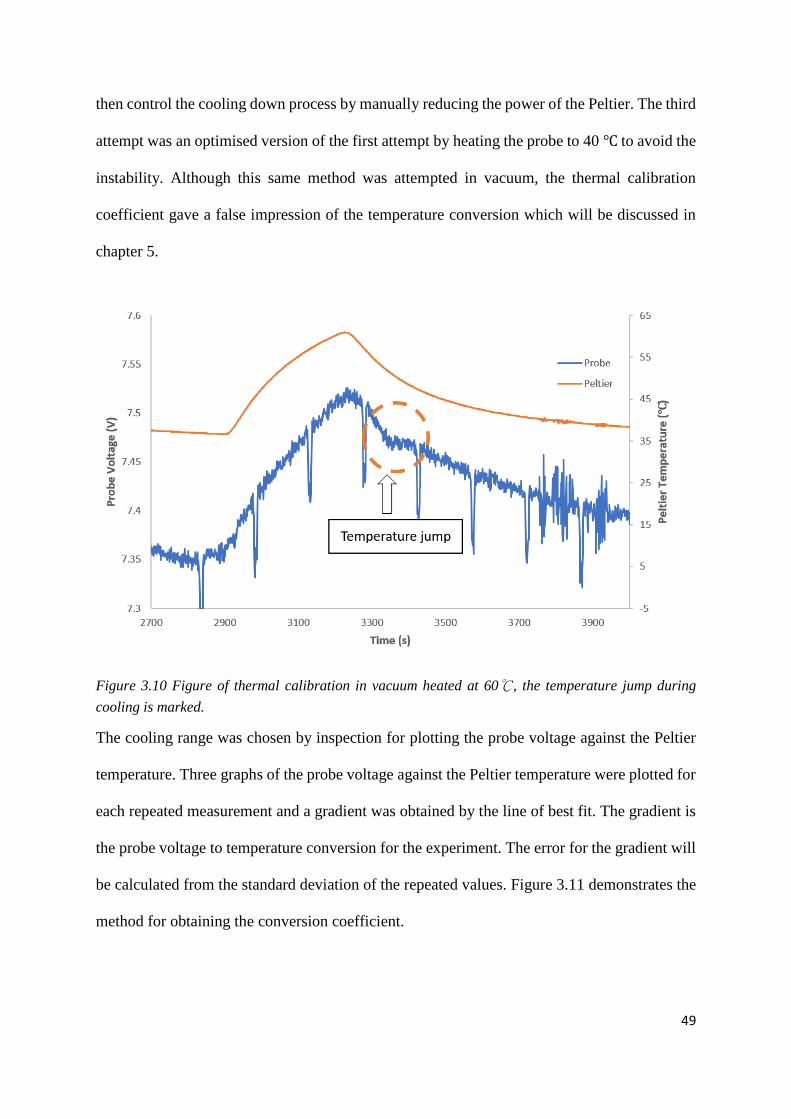
49
then control the cooling down process by manually reducing the power of the Peltier. The third
attempt was an optimised version of the first attempt by heating the probe to 40 ℃ to avoid the
instability. Although this same method was attempted in vacuum, the thermal calibration
coefficient gave a false impression of the temperature conversion which will be discussed in
chapter 5.
Figure 3.10 Figure of thermal calibration in vacuum heated at 60℃, the temperature jump during
cooling is marked.
The cooling range was chosen by inspection for plotting the probe voltage against the Peltier
temperature. Three graphs of the probe voltage against the Peltier temperature were plotted for
each repeated measurement and a gradient was obtained by the line of best fit. The gradient is
the probe voltage to temperature conversion for the experiment. The error for the gradient will
be calculated from the standard deviation of the repeated values. Figure 3.11 demonstrates the
method for obtaining the conversion coefficient.
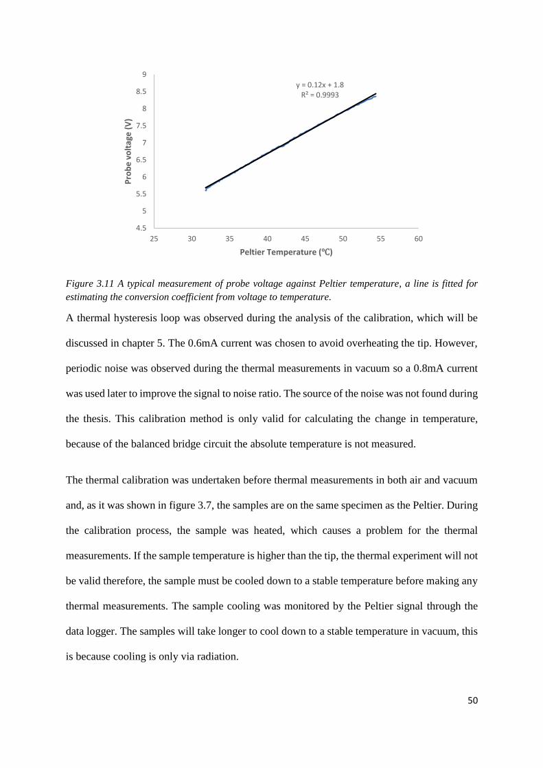
50
Figure 3.11 A typical measurement of probe voltage against Peltier temperature, a line is fitted for
estimating the conversion coefficient from voltage to temperature.
A thermal hysteresis loop was observed during the analysis of the calibration, which will be
discussed in chapter 5. The 0.6mA current was chosen to avoid overheating the tip. However,
periodic noise was observed during the thermal measurements in vacuum so a 0.8mA current
was used later to improve the signal to noise ratio. The source of the noise was not found during
the thesis. This calibration method is only valid for calculating the change in temperature,
because of the balanced bridge circuit the absolute temperature is not measured.
The thermal calibration was undertaken before thermal measurements in both air and vacuum
and, as it was shown in figure 3.7, the samples are on the same specimen as the Peltier. During
the calibration process, the sample was heated, which causes a problem for the thermal
measurements. If the sample temperature is higher than the tip, the thermal experiment will not
be valid therefore, the sample must be cooled down to a stable temperature before making any
thermal measurements. The sample cooling was monitored by the Peltier signal through the
data logger. The samples will take longer to cool down to a stable temperature in vacuum, this
is because cooling is only via radiation.
y = 0.12x + 1.8R² = 0.9993
4.5
5
5.5
6
6.5
7
7.5
8
8.5
9
25 30 35 40 45 50 55 60
Pro
be
vo
ltag
e (
V)
Peltier Temperature (℃)
51
The thermal measurements procedure is similar to the force measurement described in the
chapter 3.5. Once the topography of the samples has been measured and the area is chosen, the
thermal measurements were made by feeding the thermal information into the AFM feedback
module. The data logger was used to monitor the probe voltage during the thermal
measurements. This is to record the change in temperature when the tip is far away from the
sample and to monitor the probe in case of short circuit. The clock setting and the tip
displacement for thermal measurement should be the same as force measurements, this is to
ensure both the force and thermal measurements are comparable.
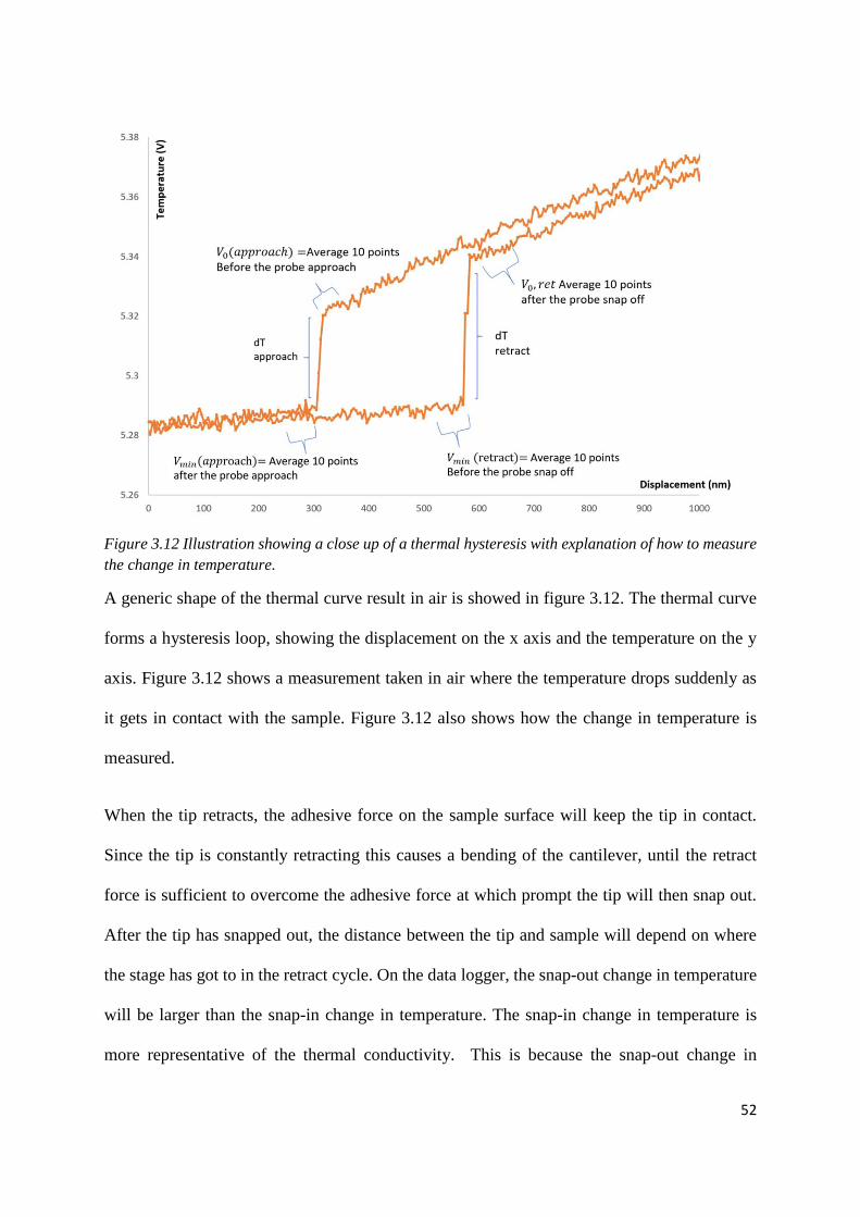
52
Figure 3.12 Illustration showing a close up of a thermal hysteresis with explanation of how to measure
the change in temperature.
A generic shape of the thermal curve result in air is showed in figure 3.12. The thermal curve
forms a hysteresis loop, showing the displacement on the x axis and the temperature on the y
axis. Figure 3.12 shows a measurement taken in air where the temperature drops suddenly as
it gets in contact with the sample. Figure 3.12 also shows how the change in temperature is
measured.
When the tip retracts, the adhesive force on the sample surface will keep the tip in contact.
Since the tip is constantly retracting this causes a bending of the cantilever, until the retract
force is sufficient to overcome the adhesive force at which prompt the tip will then snap out.
After the tip has snapped out, the distance between the tip and sample will depend on where
the stage has got to in the retract cycle. On the data logger, the snap-out change in temperature
will be larger than the snap-in change in temperature. The snap-in change in temperature is
more representative of the thermal conductivity. This is because the snap-out change in
53
temperature is affected by the adhesive force varies between samples. The snap-in change in
temperature is less affected by the mechanical properties of the samples, hence it is more
representative of the thermal properties. Since the snap-in change in temperature happened
during the approach process, we will call this the ‘approach temperature’ and it is marked as
‘dT approach’ in figure 3.12.
The approach temperature measurement is marked in figure 3.12. It is made by measuring the
average temperature of 10 points before and after the tip made contact with the sample surface,
then the difference of these values is the approach temperature. Ten points were chosen as a
balance between averaging over as many points as possible to reduce noise, but making sure
that the value is not affected by real temperature gradient due to the cooling of the tip.
The range of points for measuring the change in temperature is showed in figure 3.12. When
analysing the data, the force curve will be plotted on the same axis with the thermal curve. The
intersection of both curves shows the snap in and snap out point of the tip. The range of points
is then chosen at this intersection by inspection and the range of points will be used for
calculations. The error is estimated by the standard deviation of the measured dT through the
repeated values. There are some parameters to be aware of for the temperature measurements,
for example, the laser signal and the electrical current through the tip will contribute to the
temperature reading. A significant amount of laser signal heating the tip was observed during
the setup of the thermal calibration. This effect is neglected when analysing the change in
temperature in this project, however it should be taken into account when working out the
absolute temperature in the system.
54
Chapter 4 Topography and force curves measured using contact mode
and thermal probes
This chapter presents the results for the mechanical measurements made by the SThM. The
aim of these mechanical measurements is to investigate the relationship between the adhesive
force and the hardness and elastic modulus. Understanding the topography of the sample and
the material properties should provide an aid to interpreting the thermal measurements. For
example, the surface hardness can affect the contact area of the tip and cause a change in
thermal conduction. The force measurements are also used to verify the contact point of the tip
in the thermal measurements, hence the study of the mechanical properties is important for
analysing the thermal measurements too.
This chapter presents the force measurements results including the probe dimensions, the
calculations of the probe spring constant and the force measurements of different sample using
thermal probe. This chapter will conclude by comparing the roughness analysis with the
samples and comparing the force measurements.
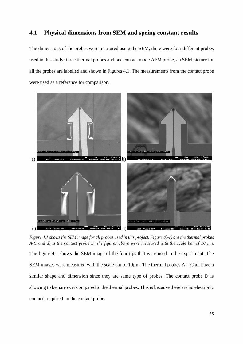
55
4.1 Physical dimensions from SEM and spring constant results
The dimensions of the probes were measured using the SEM, there were four different probes
used in this study: three thermal probes and one contact mode AFM probe, an SEM picture for
all the probes are labelled and shown in Figures 4.1. The measurements from the contact probe
were used as a reference for comparison.
a) b)
c) d)
Figure 4.1 shows the SEM image for all probes used in this project. Figure a)-c) are the thermal probes
A-C and d) is the contact probe D, the figures above were measured with the scale bar of 10 μm.
The figure 4.1 shows the SEM image of the four tips that were used in the experiment. The
SEM images were measured with the scale bar of 10µm. The thermal probes A – C all have a
similar shape and dimension since they are same type of probes. The contact probe D is
showing to be narrower compared to the thermal probes. This is because there are no electronic
contacts required on the contact probe.
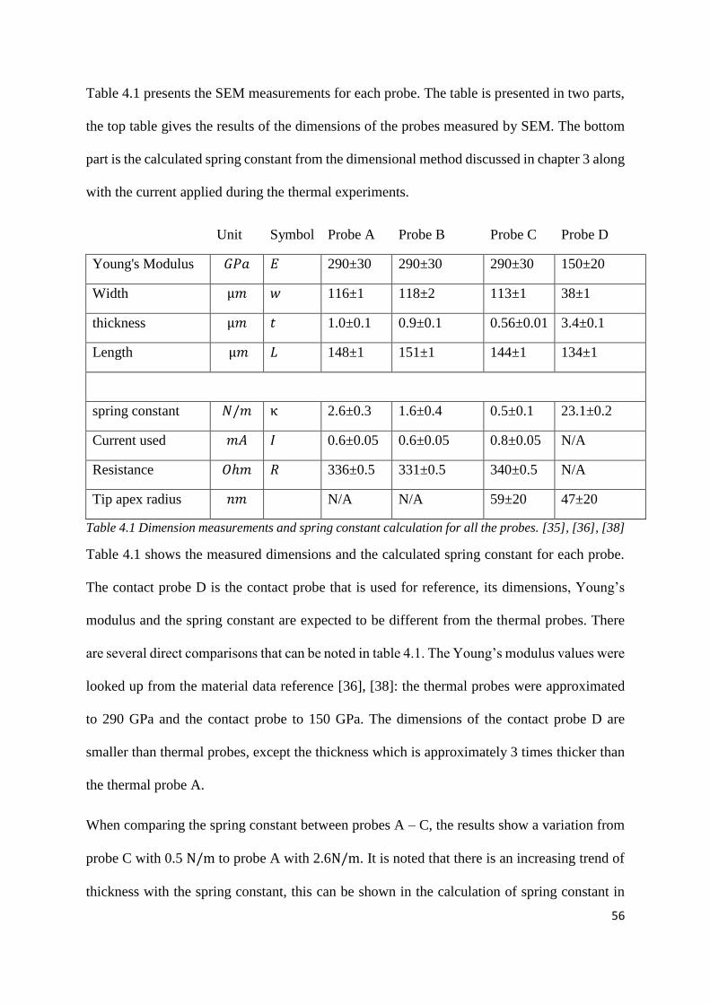
56
Table 4.1 presents the SEM measurements for each probe. The table is presented in two parts,
the top table gives the results of the dimensions of the probes measured by SEM. The bottom
part is the calculated spring constant from the dimensional method discussed in chapter 3 along
with the current applied during the thermal experiments.
Unit Symbol Probe A Probe B Probe C Probe D
Young's Modulus 𝐺𝑃𝑎 𝐸 290±30 290±30 290±30 150±20
Width μ𝑚 𝑤 116±1 118±2 113±1 38±1
thickness μ𝑚 𝑡 1.0±0.1 0.9±0.1 0.56±0.01 3.4±0.1
Length μ𝑚 𝐿 148±1 151±1 144±1 134±1
spring constant 𝑁/𝑚 κ 2.6±0.3 1.6±0.4 0.5±0.1 23.1±0.2
Current used 𝑚𝐴 𝐼 0.6±0.05 0.6±0.05 0.8±0.05 N/A
Resistance 𝑂ℎ𝑚 𝑅 336±0.5 331±0.5 340±0.5 N/A
Tip apex radius 𝑛𝑚
N/A N/A 59±20 47±20
Table 4.1 Dimension measurements and spring constant calculation for all the probes. [35], [36], [38]
Table 4.1 shows the measured dimensions and the calculated spring constant for each probe.
The contact probe D is the contact probe that is used for reference, its dimensions, Young’s
modulus and the spring constant are expected to be different from the thermal probes. There
are several direct comparisons that can be noted in table 4.1. The Young’s modulus values were
looked up from the material data reference [36], [38]: the thermal probes were approximated
to 290 GPa and the contact probe to 150 GPa. The dimensions of the contact probe D are
smaller than thermal probes, except the thickness which is approximately 3 times thicker than
the thermal probe A.
When comparing the spring constant between probes A – C, the results show a variation from
probe C with 0.5 N/m to probe A with 2.6N/m. It is noted that there is an increasing trend of
thickness with the spring constant, this can be shown in the calculation of spring constant in
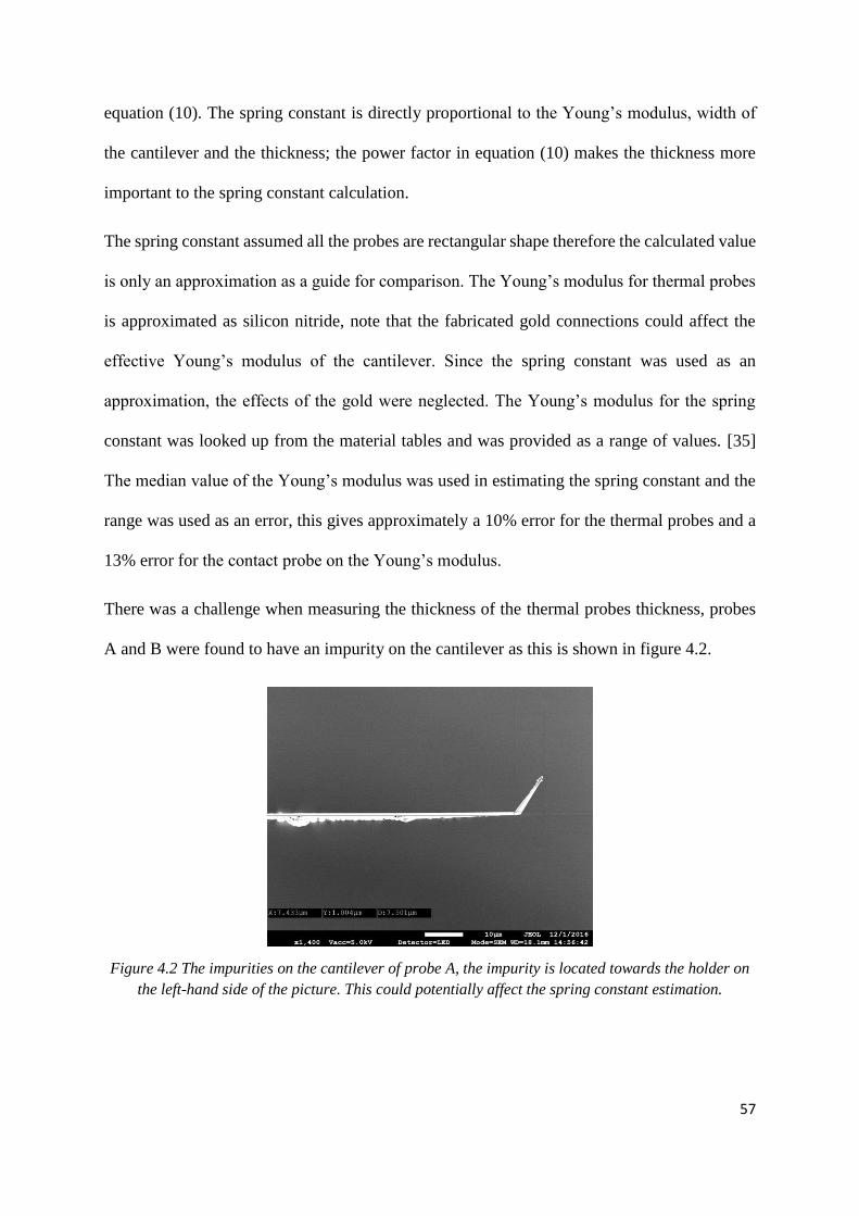
57
equation (10). The spring constant is directly proportional to the Young’s modulus, width of
the cantilever and the thickness; the power factor in equation (10) makes the thickness more
important to the spring constant calculation.
The spring constant assumed all the probes are rectangular shape therefore the calculated value
is only an approximation as a guide for comparison. The Young’s modulus for thermal probes
is approximated as silicon nitride, note that the fabricated gold connections could affect the
effective Young’s modulus of the cantilever. Since the spring constant was used as an
approximation, the effects of the gold were neglected. The Young’s modulus for the spring
constant was looked up from the material tables and was provided as a range of values. [35]
The median value of the Young’s modulus was used in estimating the spring constant and the
range was used as an error, this gives approximately a 10% error for the thermal probes and a
13% error for the contact probe on the Young’s modulus.
There was a challenge when measuring the thickness of the thermal probes thickness, probes
A and B were found to have an impurity on the cantilever as this is shown in figure 4.2.
Figure 4.2 The impurities on the cantilever of probe A, the impurity is located towards the holder on
the left-hand side of the picture. This could potentially affect the spring constant estimation.
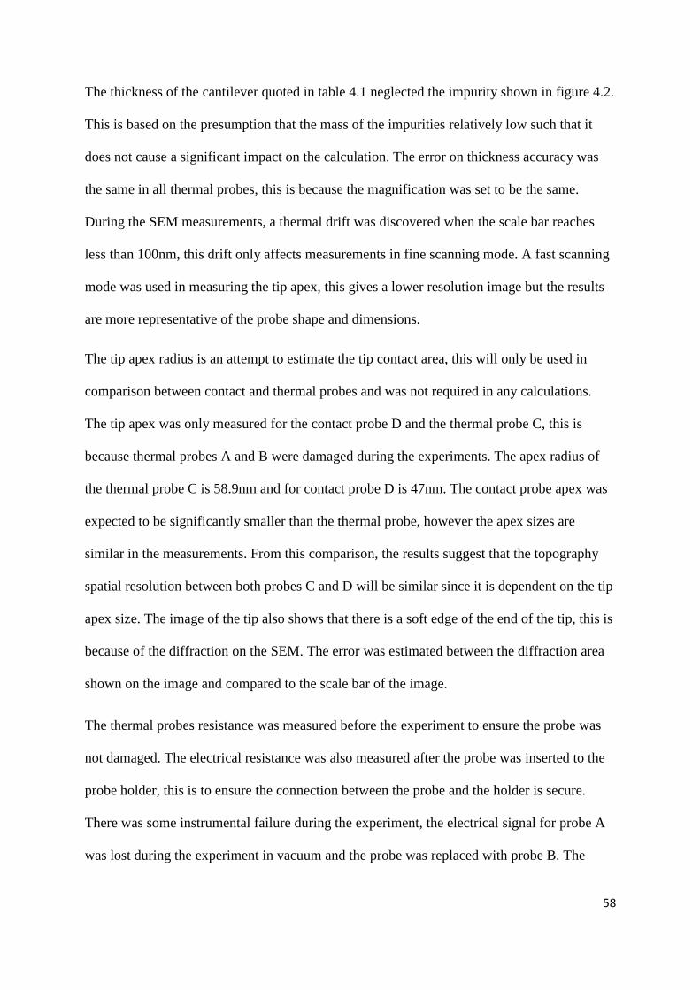
58
The thickness of the cantilever quoted in table 4.1 neglected the impurity shown in figure 4.2.
This is based on the presumption that the mass of the impurities relatively low such that it
does not cause a significant impact on the calculation. The error on thickness accuracy was
the same in all thermal probes, this is because the magnification was set to be the same.
During the SEM measurements, a thermal drift was discovered when the scale bar reaches
less than 100nm, this drift only affects measurements in fine scanning mode. A fast scanning
mode was used in measuring the tip apex, this gives a lower resolution image but the results
are more representative of the probe shape and dimensions.
The tip apex radius is an attempt to estimate the tip contact area, this will only be used in
comparison between contact and thermal probes and was not required in any calculations.
The tip apex was only measured for the contact probe D and the thermal probe C, this is
because thermal probes A and B were damaged during the experiments. The apex radius of
the thermal probe C is 58.9nm and for contact probe D is 47nm. The contact probe apex was
expected to be significantly smaller than the thermal probe, however the apex sizes are
similar in the measurements. From this comparison, the results suggest that the topography
spatial resolution between both probes C and D will be similar since it is dependent on the tip
apex size. The image of the tip also shows that there is a soft edge of the end of the tip, this is
because of the diffraction on the SEM. The error was estimated between the diffraction area
shown on the image and compared to the scale bar of the image.
The thermal probes resistance was measured before the experiment to ensure the probe was
not damaged. The electrical resistance was also measured after the probe was inserted to the
probe holder, this is to ensure the connection between the probe and the holder is secure.
There was some instrumental failure during the experiment, the electrical signal for probe A
was lost during the experiment in vacuum and the probe was replaced with probe B. The
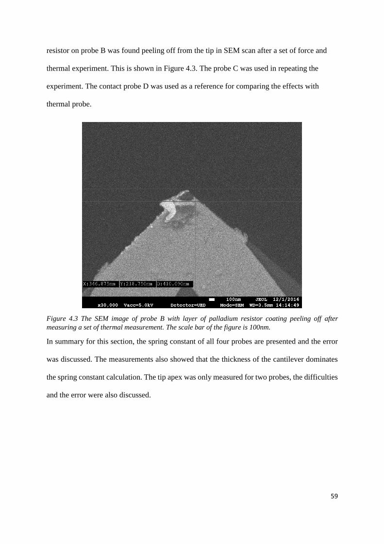
59
resistor on probe B was found peeling off from the tip in SEM scan after a set of force and
thermal experiment. This is shown in Figure 4.3. The probe C was used in repeating the
experiment. The contact probe D was used as a reference for comparing the effects with
thermal probe.
Figure 4.3 The SEM image of probe B with layer of palladium resistor coating peeling off after
measuring a set of thermal measurement. The scale bar of the figure is 100nm.
In summary for this section, the spring constant of all four probes are presented and the error
was discussed. The measurements also showed that the thickness of the cantilever dominates
the spring constant calculation. The tip apex was only measured for two probes, the difficulties
and the error were also discussed.
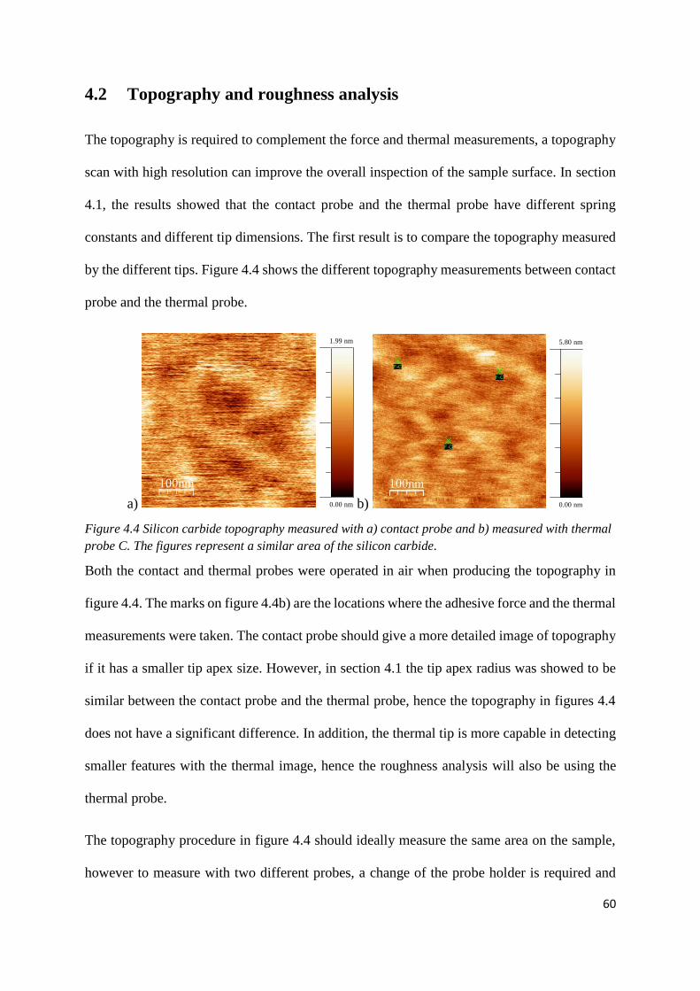
60
4.2 Topography and roughness analysis
The topography is required to complement the force and thermal measurements, a topography
scan with high resolution can improve the overall inspection of the sample surface. In section
4.1, the results showed that the contact probe and the thermal probe have different spring
constants and different tip dimensions. The first result is to compare the topography measured
by the different tips. Figure 4.4 shows the different topography measurements between contact
probe and the thermal probe.
a) b)
Figure 4.4 Silicon carbide topography measured with a) contact probe and b) measured with thermal
probe C. The figures represent a similar area of the silicon carbide.
Both the contact and thermal probes were operated in air when producing the topography in
figure 4.4. The marks on figure 4.4b) are the locations where the adhesive force and the thermal
measurements were taken. The contact probe should give a more detailed image of topography
if it has a smaller tip apex size. However, in section 4.1 the tip apex radius was showed to be
similar between the contact probe and the thermal probe, hence the topography in figures 4.4
does not have a significant difference. In addition, the thermal tip is more capable in detecting
smaller features with the thermal image, hence the roughness analysis will also be using the
thermal probe.
The topography procedure in figure 4.4 should ideally measure the same area on the sample,
however to measure with two different probes, a change of the probe holder is required and
100nm
1.99 nm
0.00 nm
5.80 nm
0.00 nm
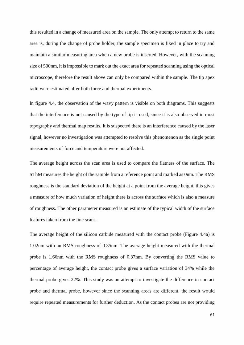
61
this resulted in a change of measured area on the sample. The only attempt to return to the same
area is, during the change of probe holder, the sample specimen is fixed in place to try and
maintain a similar measuring area when a new probe is inserted. However, with the scanning
size of 500nm, it is impossible to mark out the exact area for repeated scanning using the optical
microscope, therefore the result above can only be compared within the sample. The tip apex
radii were estimated after both force and thermal experiments.
In figure 4.4, the observation of the wavy pattern is visible on both diagrams. This suggests
that the interference is not caused by the type of tip is used, since it is also observed in most
topography and thermal map results. It is suspected there is an interference caused by the laser
signal, however no investigation was attempted to resolve this phenomenon as the single point
measurements of force and temperature were not affected.
The average height across the scan area is used to compare the flatness of the surface. The
SThM measures the height of the sample from a reference point and marked as 0nm. The RMS
roughness is the standard deviation of the height at a point from the average height, this gives
a measure of how much variation of height there is across the surface which is also a measure
of roughness. The other parameter measured is an estimate of the typical width of the surface
features taken from the line scans.
The average height of the silicon carbide measured with the contact probe (Figure 4.4a) is
1.02nm with an RMS roughness of 0.35nm. The average height measured with the thermal
probe is 1.66nm with the RMS roughness of 0.37nm. By converting the RMS value to
percentage of average height, the contact probe gives a surface variation of 34% while the
thermal probe gives 22%. This study was an attempt to investigate the difference in contact
probe and thermal probe, however since the scanning areas are different, the result would
require repeated measurements for further deduction. As the contact probes are not providing
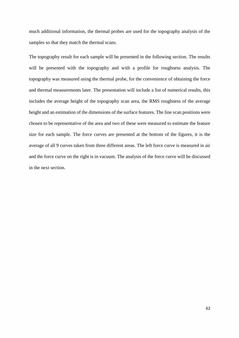
62
much additional information, the thermal probes are used for the topography analysis of the
samples so that they match the thermal scans.
The topography result for each sample will be presented in the following section. The results
will be presented with the topography and with a profile for roughness analysis. The
topography was measured using the thermal probe, for the convenience of obtaining the force
and thermal measurements later. The presentation will include a list of numerical results, this
includes the average height of the topography scan area, the RMS roughness of the average
height and an estimation of the dimensions of the surface features. The line scan positions were
chosen to be representative of the area and two of these were measured to estimate the feature
size for each sample. The force curves are presented at the bottom of the figures, it is the
average of all 9 curves taken from three different areas. The left force curve is measured in air
and the force curve on the right is in vacuum. The analysis of the force curve will be discussed
in the next section.
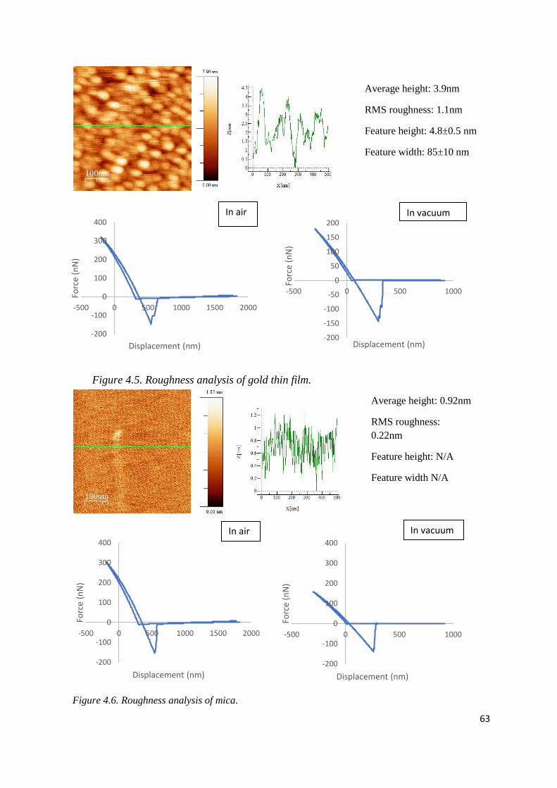
63
Average height: 3.9nm
RMS roughness: 1.1nm
Feature height: 4.8±0.5 nm
Feature width: 85±10 nm
Figure 4.5. Roughness analysis of gold thin film.
Average height: 0.92nm
RMS roughness:
0.22nm
Feature height: N/A
Feature width N/A
Figure 4.6. Roughness analysis of mica.
-200
-100
0
100
200
300
400
-500 0 500 1000 1500 2000
Forc
e (n
N)
Displacement (nm)
In air
-200
-100
0
100
200
300
400
-500 0 500 1000
Forc
e (n
N)
Displacement (nm)
In vacuum
-200
-100
0
100
200
300
400
-500 0 500 1000 1500 2000
Forc
e (n
N)
Displacement (nm)-200
-150
-100
-50
0
50
100
150
200
-500 0 500 1000Fo
rce
(nN
)
Displacement (nm)
In vacuumIn air
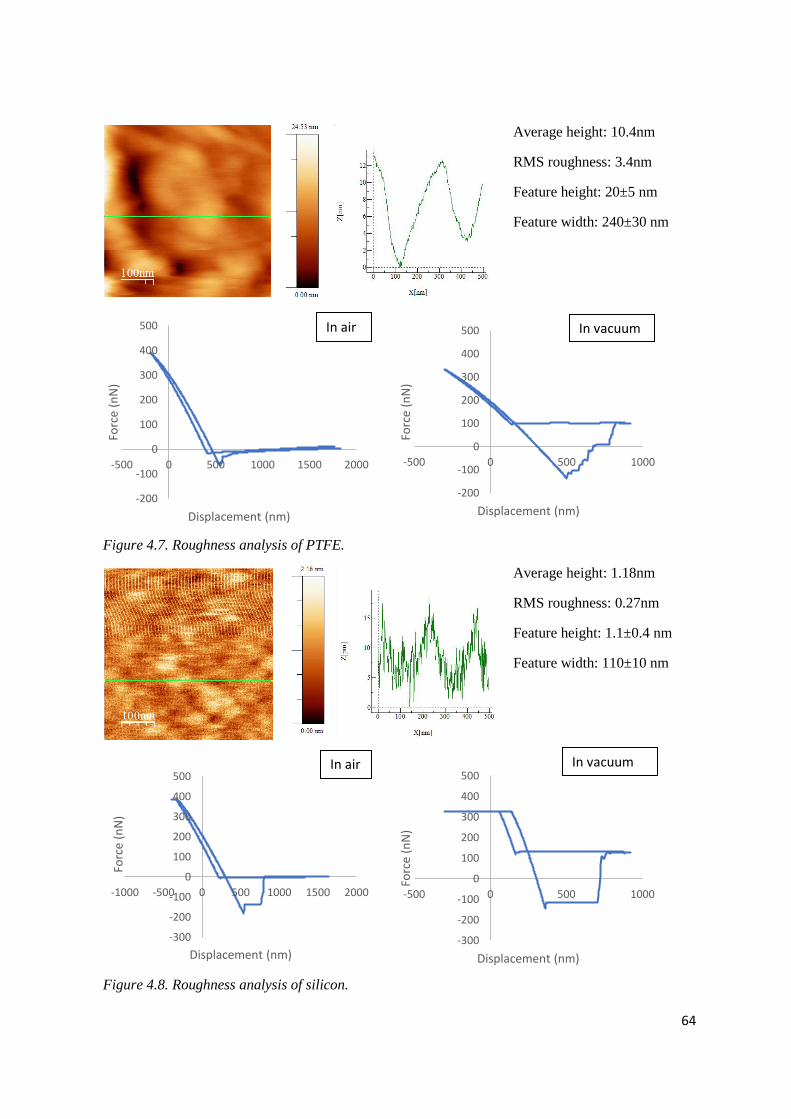
64
Average height: 10.4nm
RMS roughness: 3.4nm
Feature height: 20±5 nm
Feature width: 240±30 nm
Figure 4.7. Roughness analysis of PTFE.
Average height: 1.18nm
RMS roughness: 0.27nm
Feature height: 1.1±0.4 nm
Feature width: 110±10 nm
Figure 4.8. Roughness analysis of silicon.
-200
-100
0
100
200
300
400
500
-500 0 500 1000 1500 2000
Forc
e (n
N)
Displacement (nm)
In air
-200
-100
0
100
200
300
400
500
-500 0 500 1000
Forc
e (n
N)
Displacement (nm)
In vacuum
-300
-200
-100
0
100
200
300
400
500
-1000 -500 0 500 1000 1500 2000
Forc
e (n
N)
Displacement (nm)
In air
-300
-200
-100
0
100
200
300
400
500
-500 0 500 1000
Forc
e (n
N)
Displacement (nm)
In vacuum
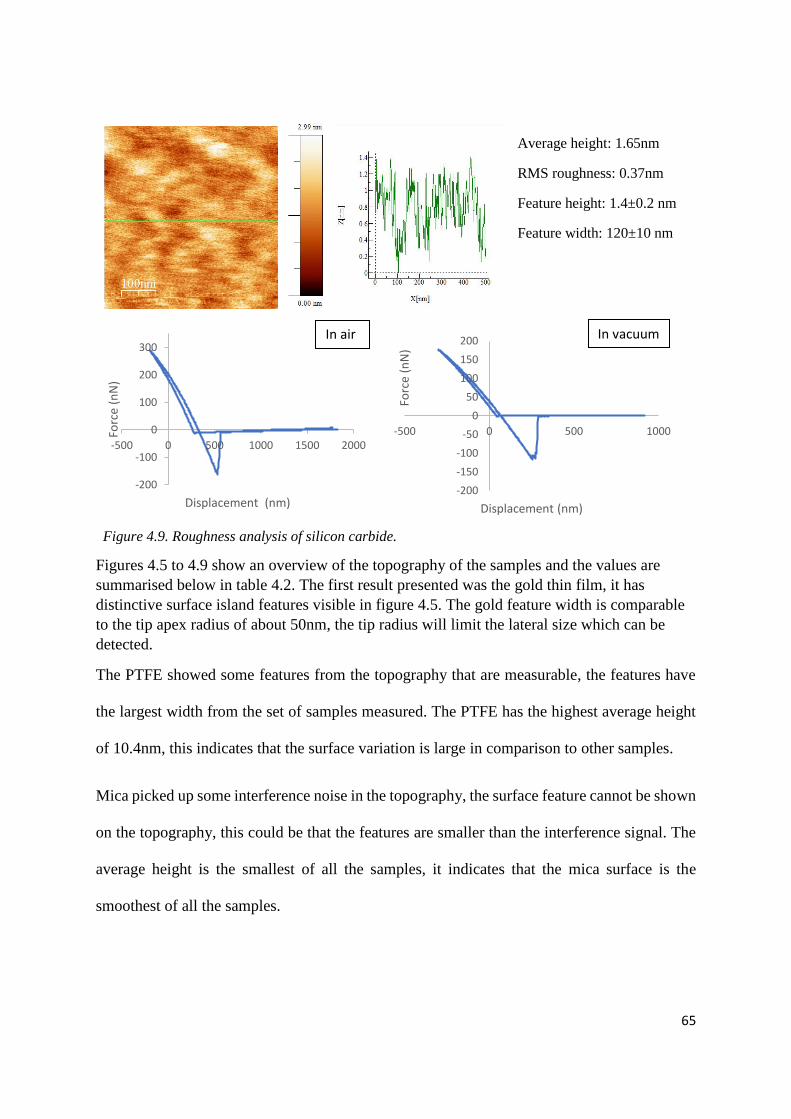
65
Average height: 1.65nm
RMS roughness: 0.37nm
Feature height: 1.4±0.2 nm
Feature width: 120±10 nm
Figure 4.9. Roughness analysis of silicon carbide.
Figures 4.5 to 4.9 show an overview of the topography of the samples and the values are
summarised below in table 4.2. The first result presented was the gold thin film, it has
distinctive surface island features visible in figure 4.5. The gold feature width is comparable
to the tip apex radius of about 50nm, the tip radius will limit the lateral size which can be
detected.
The PTFE showed some features from the topography that are measurable, the features have
the largest width from the set of samples measured. The PTFE has the highest average height
of 10.4nm, this indicates that the surface variation is large in comparison to other samples.
Mica picked up some interference noise in the topography, the surface feature cannot be shown
on the topography, this could be that the features are smaller than the interference signal. The
average height is the smallest of all the samples, it indicates that the mica surface is the
smoothest of all the samples.
-200
-100
0
100
200
300
-500 0 500 1000 1500 2000
Forc
e (n
N)
Displacement (nm)
In air
-200
-150
-100
-50
0
50
100
150
200
-500 0 500 1000
Forc
e(n
N)
Displacement (nm)
In vacuum
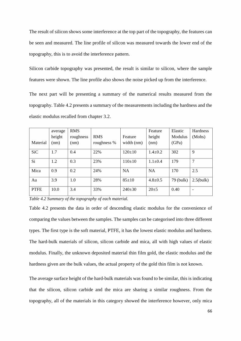
66
The result of silicon shows some interference at the top part of the topography, the features can
be seen and measured. The line profile of silicon was measured towards the lower end of the
topography, this is to avoid the interference pattern.
Silicon carbide topography was presented, the result is similar to silicon, where the sample
features were shown. The line profile also shows the noise picked up from the interference.
The next part will be presenting a summary of the numerical results measured from the
topography. Table 4.2 presents a summary of the measurements including the hardness and the
elastic modulus recalled from chapter 3.2.
Material
average
height
(nm)
RMS
roughness
(nm)
RMS
roughness %
Feature
width (nm)
Feature
height
(nm)
Elastic
Modulus
(GPa)
Hardness
(Mohs)
SiC 1.7 0.4 22% 120±10 1.4±0.2 302 9
Si 1.2 0.3 23% 110±10 1.1±0.4 179 7
Mica 0.9 0.2 24% NA NA 170 2.5
Au 3.9 1.0 28% 85±10 4.8±0.5 79 (bulk) 2.5(bulk)
PTFE 10.0 3.4 33% 240±30 20±5 0.40 -
Table 4.2 Summary of the topography of each material.
Table 4.2 presents the data in order of descending elastic modulus for the convenience of
comparing the values between the samples. The samples can be categorised into three different
types. The first type is the soft material, PTFE, it has the lowest elastic modulus and hardness.
The hard-bulk materials of silicon, silicon carbide and mica, all with high values of elastic
modulus. Finally, the unknown deposited material thin film gold, the elastic modulus and the
hardness given are the bulk values, the actual property of the gold thin film is not known.
The average surface height of the hard-bulk materials was found to be similar, this is indicating
that the silicon, silicon carbide and the mica are sharing a similar roughness. From the
topography, all of the materials in this category showed the interference however, only mica
67
does not show any surface features. The reason is the mica features are smaller than the
interference signal.
The average height of PTFE is the highest at 10nm, this indicates that the PTFE has the roughest
surface. The features showing on PTFE also have the biggest width of 240nm. The PTFE and
thin film gold did not show any interference from the topography. The thin film gold showed
some distinctive island features with 85nm in width and 4.8nm high. The feature width is
comparable to the tip apex radius of about 50nm, the tip radius can affect the lateral size that
gives a lower resolution in width. After converting the RMS roughness into the percentage of
the average height, the percentage shows a weak directly proportional relationship with the
elastic modulus.
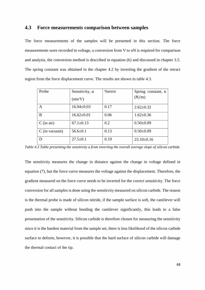
68
4.3 Force measurements comparison between samples
The force measurements of the samples will be presented in this section. The force
measurements were recorded in voltage, a conversion from V to nN is required for comparison
and analysis, the conversion method is described in equation (6) and discussed in chapter 3.5.
The spring constant was obtained in the chapter 4.2 by inverting the gradient of the retract
region from the force displacement curve. The results are shown in table 4.3.
Probe Sensitivity, α
(nm/V)
%error Spring constant, κ
(N/m)
A 16.94±0.03 0.17 2.62±0.32
B 16.62±0.01 0.06 1.62±0.36
C (in air) 67.1±0.13 0.2 0.50±0.09
C (in vacuum) 56.6±0.1 0.13 0.50±0.09
D 27.5±0.1 0.19 23.10±0.16
Table 4.3 Table presenting the sensitivity a from inverting the overall average slope of silicon carbide.
The sensitivity measures the change in distance against the change in voltage defined in
equation (7), but the force curve measures the voltage against the displacement. Therefore, the
gradient measured on the force curve needs to be inverted for the correct sensitivity. The force
conversion for all samples is done using the sensitivity measured on silicon carbide. The reason
is the thermal probe is made of silicon nitride, if the sample surface is soft, the cantilever will
push into the sample without bending the cantilever significantly, this leads to a false
presentation of the sensitivity. Silicon carbide is therefore chosen for measuring the sensitivity
since it is the hardest material from the sample set, there is less likelihood of the silicon carbide
surface to deform, however, it is possible that the hard surface of silicon carbide will damage
the thermal contact of the tip.
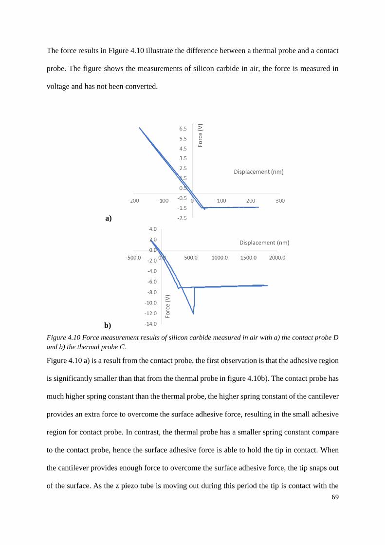
69
The force results in Figure 4.10 illustrate the difference between a thermal probe and a contact
probe. The figure shows the measurements of silicon carbide in air, the force is measured in
voltage and has not been converted.
a)
b)
Figure 4.10 Force measurement results of silicon carbide measured in air with a) the contact probe D
and b) the thermal probe C.
Figure 4.10 a) is a result from the contact probe, the first observation is that the adhesive region
is significantly smaller than that from the thermal probe in figure 4.10b). The contact probe has
much higher spring constant than the thermal probe, the higher spring constant of the cantilever
provides an extra force to overcome the surface adhesive force, resulting in the small adhesive
region for contact probe. In contrast, the thermal probe has a smaller spring constant compare
to the contact probe, hence the surface adhesive force is able to hold the tip in contact. When
the cantilever provides enough force to overcome the surface adhesive force, the tip snaps out
of the surface. As the z piezo tube is moving out during this period the tip is contact with the
-14.0
-12.0
-10.0
-8.0
-6.0
-4.0
-2.0
0.0
2.0
4.0
-500.0 0.0 500.0 1000.0 1500.0 2000.0
Forc
e (V
)
Displacement (nm)
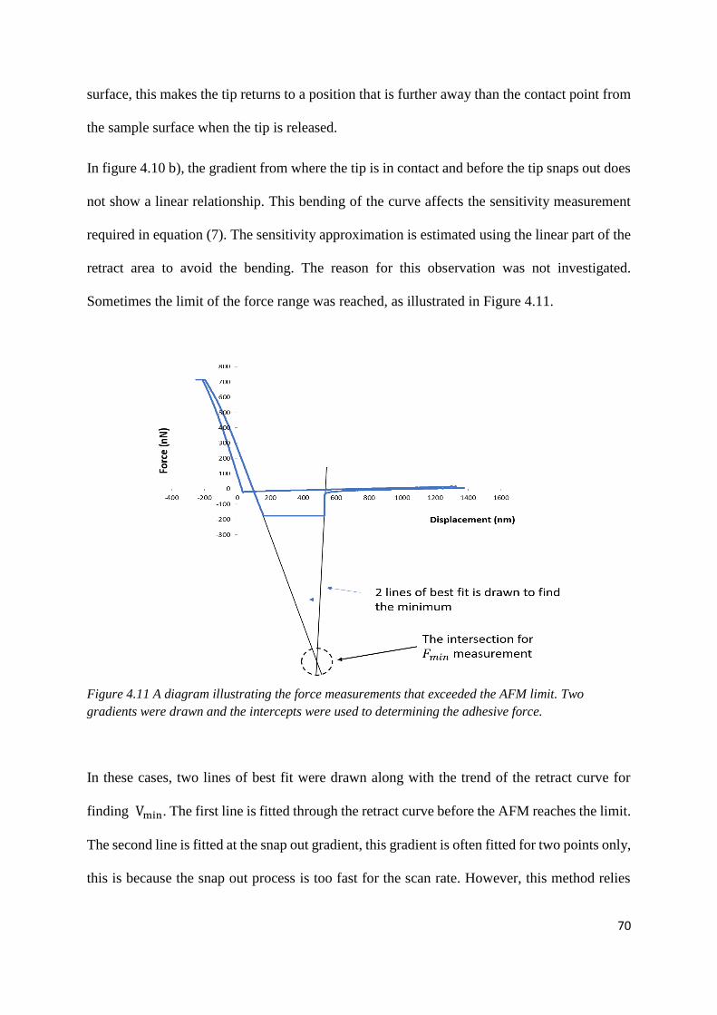
70
surface, this makes the tip returns to a position that is further away than the contact point from
the sample surface when the tip is released.
In figure 4.10 b), the gradient from where the tip is in contact and before the tip snaps out does
not show a linear relationship. This bending of the curve affects the sensitivity measurement
required in equation (7). The sensitivity approximation is estimated using the linear part of the
retract area to avoid the bending. The reason for this observation was not investigated.
Sometimes the limit of the force range was reached, as illustrated in Figure 4.11.
Figure 4.11 A diagram illustrating the force measurements that exceeded the AFM limit. Two
gradients were drawn and the intercepts were used to determining the adhesive force.
In these cases, two lines of best fit were drawn along with the trend of the retract curve for
finding Vmin. The first line is fitted through the retract curve before the AFM reaches the limit.
The second line is fitted at the snap out gradient, this gradient is often fitted for two points only,
this is because the snap out process is too fast for the scan rate. However, this method relies
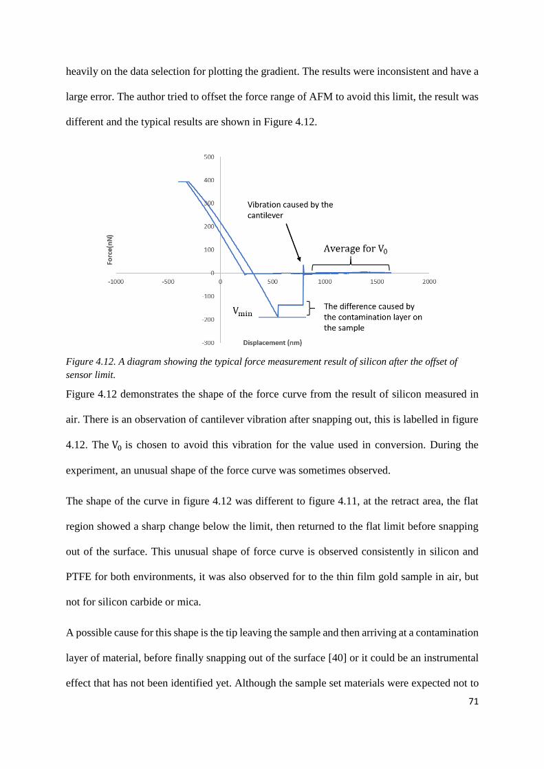
71
heavily on the data selection for plotting the gradient. The results were inconsistent and have a
large error. The author tried to offset the force range of AFM to avoid this limit, the result was
different and the typical results are shown in Figure 4.12.
Figure 4.12. A diagram showing the typical force measurement result of silicon after the offset of
sensor limit.
Figure 4.12 demonstrates the shape of the force curve from the result of silicon measured in
air. There is an observation of cantilever vibration after snapping out, this is labelled in figure
4.12. The V0 is chosen to avoid this vibration for the value used in conversion. During the
experiment, an unusual shape of the force curve was sometimes observed.
The shape of the curve in figure 4.12 was different to figure 4.11, at the retract area, the flat
region showed a sharp change below the limit, then returned to the flat limit before snapping
out of the surface. This unusual shape of force curve is observed consistently in silicon and
PTFE for both environments, it was also observed for to the thin film gold sample in air, but
not for silicon carbide or mica.
A possible cause for this shape is the tip leaving the sample and then arriving at a contamination
layer of material, before finally snapping out of the surface [40] or it could be an instrumental
effect that has not been identified yet. Although the sample set materials were expected not to
72
have a contamination layer, it is possible to have an extra layer of moisture on the sample
surface. It is also expected that there will be a layer of silicon oxide on the silicon surface and
possibly even some residual resist from the patterning process. The Vmin used in the
calculations will use the furthest point of the tip before it jumped to the flat region, this is
marked in figure 4.12. With the V0 described earlier, the retract force was measured.
Table 4.4 presents the retract force results measured using the thermal probe. The result of
thermal probe C only is presented. The table presents force measurements measured in air and
in vacuum. The results are presented in the order of the descending order of elastic modulus.
Results of thermal probe C in air
Results of thermal probe C in vacuum
Material dF(retract)
(nN)
% error Elastic
Modulus
(GPa)
Material dF(retract)
(nN)
% error Elastic
Modulus
(GPa)
SiC 175±2 1.11 302 SiC 133±5 3.9 302
Si 179±2 0.9 179 Si 153±6 3.8 179
Mica 165±0.3 0.2 170 Mica 144±3 2.2 170
Au 144±0.5 0.37 79(bulk) Au 160±4 2.4 79(bulk)
PTFE 77±1 1.38 0.4 PTFE 145±10 6.7 0.4
Table 4.4 Retract force measurements using thermal probes.
The first comparison is the result between the environments. The retract force is generally
larger in air than in vacuum except for gold and PTFE, which were also inconsistent from
previous result using probes A and B. The reason for air to have a larger retract force is in air,
water forms a layer on the sample surface, which has a high surface force and attracts the tip
to the surface. [40] The gold and the PTFE are the least uniform samples, they have a large
variation across the surface, therefore it is challenging for comparing in air and vacuum because
the tip is at different position.
When comparing the results between the samples, a general trend emerged that the silicon,
silicon carbide and mica have similar results. The silicon consistently has a larger adhesive
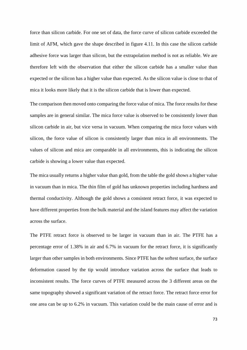
73
force than silicon carbide. For one set of data, the force curve of silicon carbide exceeded the
limit of AFM, which gave the shape described in figure 4.11. In this case the silicon carbide
adhesive force was larger than silicon, but the extrapolation method is not as reliable. We are
therefore left with the observation that either the silicon carbide has a smaller value than
expected or the silicon has a higher value than expected. As the silicon value is close to that of
mica it looks more likely that it is the silicon carbide that is lower than expected.
The comparison then moved onto comparing the force value of mica. The force results for these
samples are in general similar. The mica force value is observed to be consistently lower than
silicon carbide in air, but vice versa in vacuum. When comparing the mica force values with
silicon, the force value of silicon is consistently larger than mica in all environments. The
values of silicon and mica are comparable in all environments, this is indicating the silicon
carbide is showing a lower value than expected.
The mica usually returns a higher value than gold, from the table the gold shows a higher value
in vacuum than in mica. The thin film of gold has unknown properties including hardness and
thermal conductivity. Although the gold shows a consistent retract force, it was expected to
have different properties from the bulk material and the island features may affect the variation
across the surface.
The PTFE retract force is observed to be larger in vacuum than in air. The PTFE has a
percentage error of 1.38% in air and 6.7% in vacuum for the retract force, it is significantly
larger than other samples in both environments. Since PTFE has the softest surface, the surface
deformation caused by the tip would introduce variation across the surface that leads to
inconsistent results. The force curves of PTFE measured across the 3 different areas on the
same topography showed a significant variation of the retract force. The retract force error for
one area can be up to 6.2% in vacuum. This variation could be the main cause of error and is
74
showing in both air and vacuum. This is illustrated in figure 4.13, a force result of PTFE
measured in vacuum. Since the both vacuum and air experiment were completed separately, it
was not possible to mark out the exact same area for measurement, and the variation is therefore
greater.
Figure 4.13 Force result of PTFE in vacuum, measured in three different areas showing the variation.
The retract force is the force of how adhesive the sample surface is when the tip retracts, the
explanation of the curve is explained in chapter 2. The next discussion will be comparing the
results to the roughness of the samples. There is not a clear correlation between the retract force
and the roughness analysis. However, when comparing the retract force with elastic modulus,
samples with higher elastic modulus were observed to have a larger retract force, except for
the gold thin film. The gold thin film was quoted as 79GPa for the elastic modulus, however
this is quoted from the bulk value, whereas the thin film value is not known.
-200
-100
0
100
200
300
400
500
-400 -200 0 200 400 600 800 1000
Forc
e (
nN
)
Displacement (nm)
Area 1
Area 2
Area 3
75
4.4 Discussion of the results
This section discusses the challenges of making force measurements and summarises the
achievements with the aims at the beginning of this chapter. The aim for the force
measurements was to investigate the relationship between the mechanical properties, the
adhesive force and the hardness. The topography improved the understanding of the surface
features including the roughness.
The SEM results for measuring the dimension were first presented, the result showed the
difference in characteristic for both contact and thermal probes. The contact probe has a higher
spring constant when compared to the thermal probes. The contact probe cantilever is
approximately 3 times larger than the contact probe, however, the contact probe is about 3-5
times thicker than thermal probes. The spring constant for each probe was then presented.
Probe C was used for the main result presented in this thesis, the spring constant for probe C is
0.5±0.1 N/m. The contact probe did not show a clear adhesive region in the force curve due to
its high spring constant of 23.1±0.2 N/m.
The challenges such as measuring the thickness due to the impurities and the focusing of the
SEM was discussed. The theory for obtaining the spring constant was an estimation, this could
directly cause a false presentation for the absolute value of force. Other methods of measuring
the spring constant described in chapter 2 could be further investigated. For example, the
possibility for using the reference cantilever method to obtain the spring constant could be
investigated.
The SEM was used to measure the tip dimension for obtaining the spring constant, during this
measurement, the tips condition was found to be unstable after being used for thermal and force
measurements. For example, the palladium resistor coating was found to be peeled off after the
thermal experiment, as shown in figure 4.3. This raised a question about the reproducibility of
76
measurements as the tip changes. The durability of the tip will directly affect the cost for the
experiment and the performance of the tip will affect the accuracy of the measurements.
Therefore, the SEM process was added to check the tip before use.
The next discussion is comments on the roughness analysis. The thin film gold is the only
sample which showed surface features such as islands, resulting from the thin film deposition.
The mica was showed to be a flat surface, the reason could be the features are smaller than the
interference signal. From the average height, mica was shown to be the flattest surface. Further
investigation on the source of interference is more important, particularly for the harder
materials. When comparing the force measurements with roughness, it would also be possible
to set up an experiment of the same type of material with different roughness. The PTFE
showed the greatest variation in average height due to the very soft surface. The consequences
for the surface roughness will be considered for their impact on the thermal properties in the
next chapter.
The results in chapter 4.3 summarised the adhesive force measurements. The change in force
was described as adhesive force in this thesis because it is the amount of force on the surface
that attracts the tip. The difficulties of measuring the adhesive force when it reaches the limit
of the AFM was discussed. The method suggested in this thesis was to estimate the force by
fitting the intersection of two lines. However, this method has given an error on the estimated
force which is not usable, therefore the author attempted to adjust the range of force on the
AFM to avoid the situation and an unusual curve was observed showed in figure 4.12. The
unusual force curve shape was discussed and suggests that there may be a contamination layer
on the sample surface. This contamination layer was consistently detected on silicon, which an
extra layer of silicon oxide was expected on the silicon surface. A contamination layer also
consistently detected on PTFE while the PTFE consistently exhibited to the lowest adhesive
force.
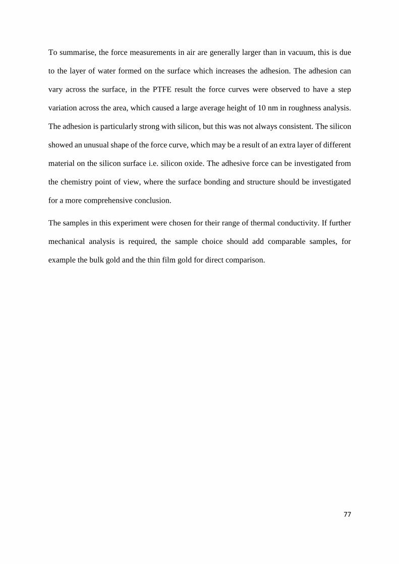
77
To summarise, the force measurements in air are generally larger than in vacuum, this is due
to the layer of water formed on the surface which increases the adhesion. The adhesion can
vary across the surface, in the PTFE result the force curves were observed to have a step
variation across the area, which caused a large average height of 10 nm in roughness analysis.
The adhesion is particularly strong with silicon, but this was not always consistent. The silicon
showed an unusual shape of the force curve, which may be a result of an extra layer of different
material on the silicon surface i.e. silicon oxide. The adhesive force can be investigated from
the chemistry point of view, where the surface bonding and structure should be investigated
for a more comprehensive conclusion.
The samples in this experiment were chosen for their range of thermal conductivity. If further
mechanical analysis is required, the sample choice should add comparable samples, for
example the bulk gold and the thin film gold for direct comparison.
78
Chapter 5 SThM for thermal conductivity measurements
The aim for the thermal measurements is to first compare the thermal effects between air and
vacuum, since the environment can affect the heat path in SThM. The thermal measurements
will also be used to investigate how the mechanical properties affect the thermal results. The
thermal curves of the different samples will be compared and assessed for the feasibility of
making quantitative thermal transport measurements.
This chapter will present the following thermal measurements result. The signal from the data
logger and the thermal calibration will be presented, with a discussion on signal conversion
from voltage to temperature. The topography of each sample will be presented along with the
thermal map and the thermal curve in both vacuum and air. The comparison of the thermal
conductivity and the change in temperature for the different samples will be discussed and the
implications summarised.
5.1 Thermal calibration and probe signal from the data logger
Throughout the thermal experiment, the data logger is constantly monitoring the voltage across
the tip. The data logger is a useful part of the thermal measurements, it collects the temperature
information from the Peltier for thermal calibration. It is also used to alert the situation when
the probe circuit is being damaged during the experiment. The discussion starts with the
explanation of the data logger data. Figure 5.1 shows a typical result from the data logger for
thermal measurements.
79
a)
b)
Figure 5.1 a) A generic result of data logger recording in air. The diagram illustrates each part of the
curve during the experiment. From the beginning there is a potential difference drop for approach until
the tip is in contact with the surface. Then the potential difference remained during the topography
scanning. b) Continue the same diagram with labels of the measurement spikes, noise spikes and
indication of the data logger change in temperature. The measurement spikes are indicating the
temperature changes during the force and thermal measurements. The noise spikes are caused by the
40-second periodic instrumental noise. The data logger change in temperature indicates the
temperature difference between the tip in contact and out of contact of the sample.
80
At the beginning of the data logger recording, the tip is far away from the sample, then the
temperature drops during the approach process. It is noted in figure 5.1a that there is a steep
drop of the temperature during the approach process, this is because the specimen was
approached through a manual process. The distance of the probe and the specimen was
monitored by an optical microscope. Once the specimen is close enough that it cannot be
identified whether it is in contact, the AFM takes over for the fine approach.
When the temperature stops dropping, the tip is in contact with the sample. The tip would then
start scanning the topography of sample. Then the next step of the data logger curve shows the
probe temperature when the tip is measuring the force and thermal measurement. The force
and thermal results were repeated at 3 different points on the sample.
During the force or thermal single point measurements, the tip is programmed to approach and
retract to a pre-defined starting position, and reprogrammed to repeat. This is the procedure
that is programmed inside the AFM. It is obvious that when the tip is not in contact with the
sample, the tip temperature rises as there are fewer heat paths for the tip to cool down, this
causes the measurement spikes indicated in figure 5.1b. After all the measurements were made,
the tip retracts back to the starting position. The temperature would increase back to the value
when the tip is far away from the sample.
The data logger temperature measures the change in temperature between the tip in contact and
out of contact. An average of approximately 20 points were taken before the tip snap out and
after the tip snap out to the environment, the difference between the two values will be used as
the data logger temperature. This is used a reference temperature of heat loss to the environment.
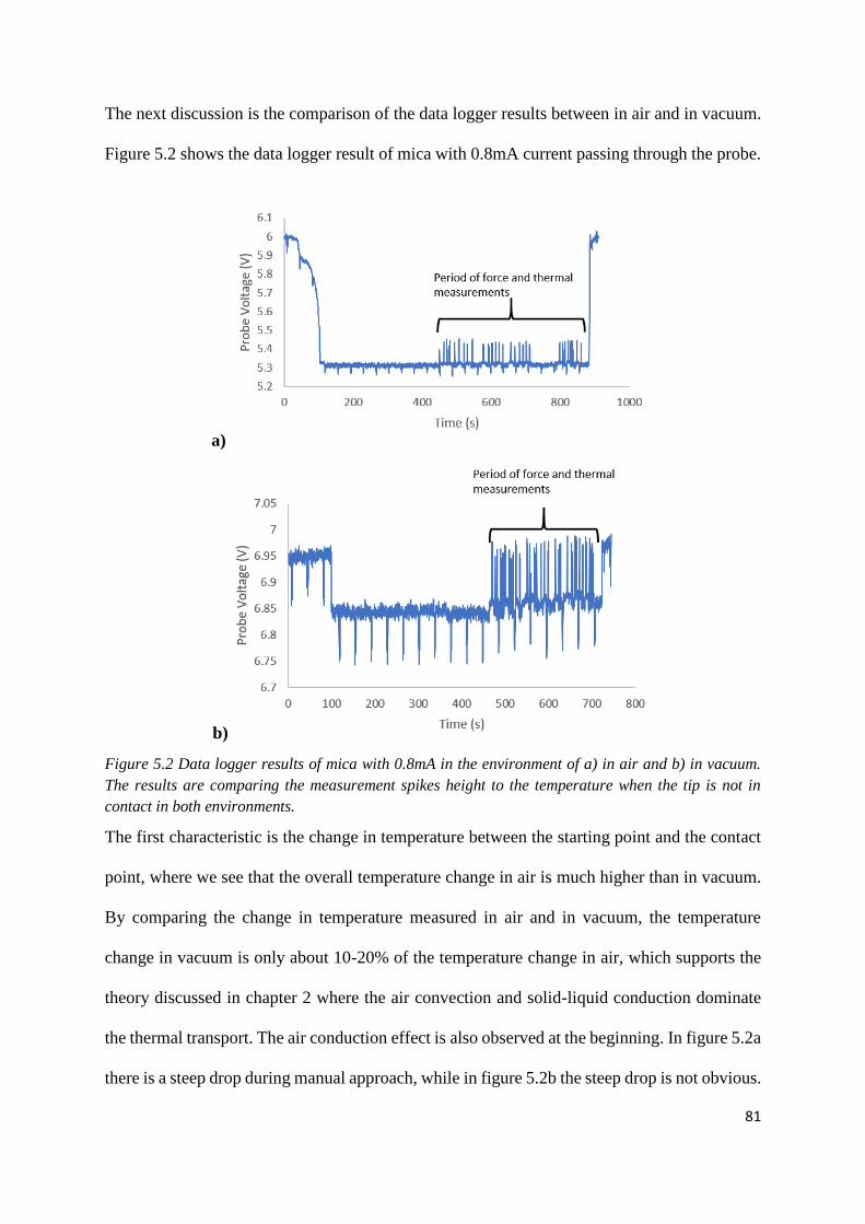
81
The next discussion is the comparison of the data logger results between in air and in vacuum.
Figure 5.2 shows the data logger result of mica with 0.8mA current passing through the probe.
a)
b)
Figure 5.2 Data logger results of mica with 0.8mA in the environment of a) in air and b) in vacuum.
The results are comparing the measurement spikes height to the temperature when the tip is not in
contact in both environments.
The first characteristic is the change in temperature between the starting point and the contact
point, where we see that the overall temperature change in air is much higher than in vacuum.
By comparing the change in temperature measured in air and in vacuum, the temperature
change in vacuum is only about 10-20% of the temperature change in air, which supports the
theory discussed in chapter 2 where the air convection and solid-liquid conduction dominate
the thermal transport. The air conduction effect is also observed at the beginning. In figure 5.2a
there is a steep drop during manual approach, while in figure 5.2b the steep drop is not obvious.
82
This is because figure 5.2a the gas conduction is getting more effective when the tip gets closer
towards the sample, while in vacuum this effect is eliminated.
From both the data logger results in figure 5.2, the noise spikes showed an approximate 40
second periodic noise, the strength of the noise is approximately at 0.02V in air and 0.1V in
vacuum. This noise shows more obviously in vacuum than in air. From figure 5.2 the voltage
drop is about 0.7V while it is about 0.1V for in vacuum. Assuming the strength of the noise is
constant, the signal to noise ratio for air is larger than in vacuum, hence the noise is more
obvious in vacuum as the signal is lower. The source of the noise was not found during the
experiment, the possible reason is the internal electric interference caused by the computer.
The effect of the noise in temperature measurement will be discussed in the next section. The
thermal calibration is set up for measuring the change in temperature, it gives a conversion
from the change in voltage to change in temperature, it does not measure the absolute
temperature of the sample surface.
In air, the heights of the measurement spikes are significantly smaller compared to the data
logger change in temperature due to the heat loss by air. However, in vacuum there are only
radiation and solid-solid conduction for thermal transport, the heat loss due to air conduction
does not exist. Therefore the temperature does not vary with the tip-sample distance when they
are not in contact, hence the probe voltage retracts to its default value between each
measurement.
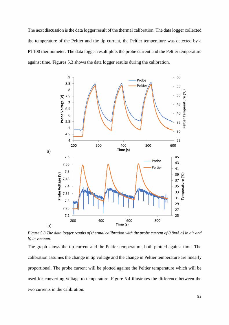
83
The next discussion is the data logger result of the thermal calibration. The data logger collected
the temperature of the Peltier and the tip current, the Peltier temperature was detected by a
PT100 thermometer. The data logger result plots the probe current and the Peltier temperature
against time. Figures 5.3 shows the data logger results during the calibration.
a)
b)
Figure 5.3 The data logger results of thermal calibration with the probe current of 0.8mA a) in air and
b) in vacuum.
The graph shows the tip current and the Peltier temperature, both plotted against time. The
calibration assumes the change in tip voltage and the change in Peltier temperature are linearly
proportional. The probe current will be plotted against the Peltier temperature which will be
used for converting voltage to temperature. Figure 5.4 illustrates the difference between the
two currents in the calibration.
25
30
35
40
45
50
55
60
4
4.5
5
5.5
6
6.5
7
7.5
8
8.5
9
200 300 400 500 600
Pe
ltie
r Te
mp
era
ture
(℃
)
Pro
be
Vo
ltag
e (
V)
Time (s)
Probe
Peltier
25
27
29
31
33
35
37
39
41
43
45
7.2
7.25
7.3
7.35
7.4
7.45
7.5
7.55
7.6
200 400 600 800
Tem
pe
ratu
re (
℃)
Pro
be
Vo
ltag
e (
V)
Time (s)
Probe
Peltier
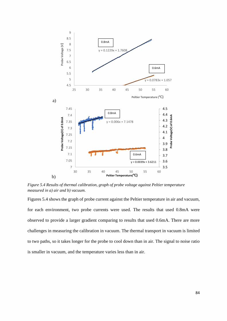
84
a)
b)
Figure 5.4 Results of thermal calibration, graph of probe voltage against Peltier temperature
measured in a) air and b) vacuum.
Figures 5.4 shows the graph of probe current against the Peltier temperature in air and vacuum,
for each environment, two probe currents were used. The results that used 0.8mA were
observed to provide a larger gradient comparing to results that used 0.6mA. There are more
challenges in measuring the calibration in vacuum. The thermal transport in vacuum is limited
to two paths, so it takes longer for the probe to cool down than in air. The signal to noise ratio
is smaller in vacuum, and the temperature varies less than in air.
y = 0.1229x + 1.7608
y = 0.0783x + 1.057
4.5
5
5.5
6
6.5
7
7.5
8
8.5
9
25 30 35 40 45 50 55 60
Pro
be
Vo
ltag
e (
V)
Peltier Temperature (℃)
y = 0.006x + 7.1478
y = 0.0039x + 3.6211
3.5
3.6
3.7
3.8
3.9
4
4.1
4.2
4.3
4.4
4.5
7
7.05
7.1
7.15
7.2
7.25
7.3
7.35
7.4
7.45
30 35 40 45 50 55 60P
rob
e V
olt
age
(V)
of
0.6
mA
Pro
be
Vo
ltag
e(V
) o
f 0
.8m
A
Peltier Temperature(℃)
0.6mA
0.8mA
0.8mA
0.6mA
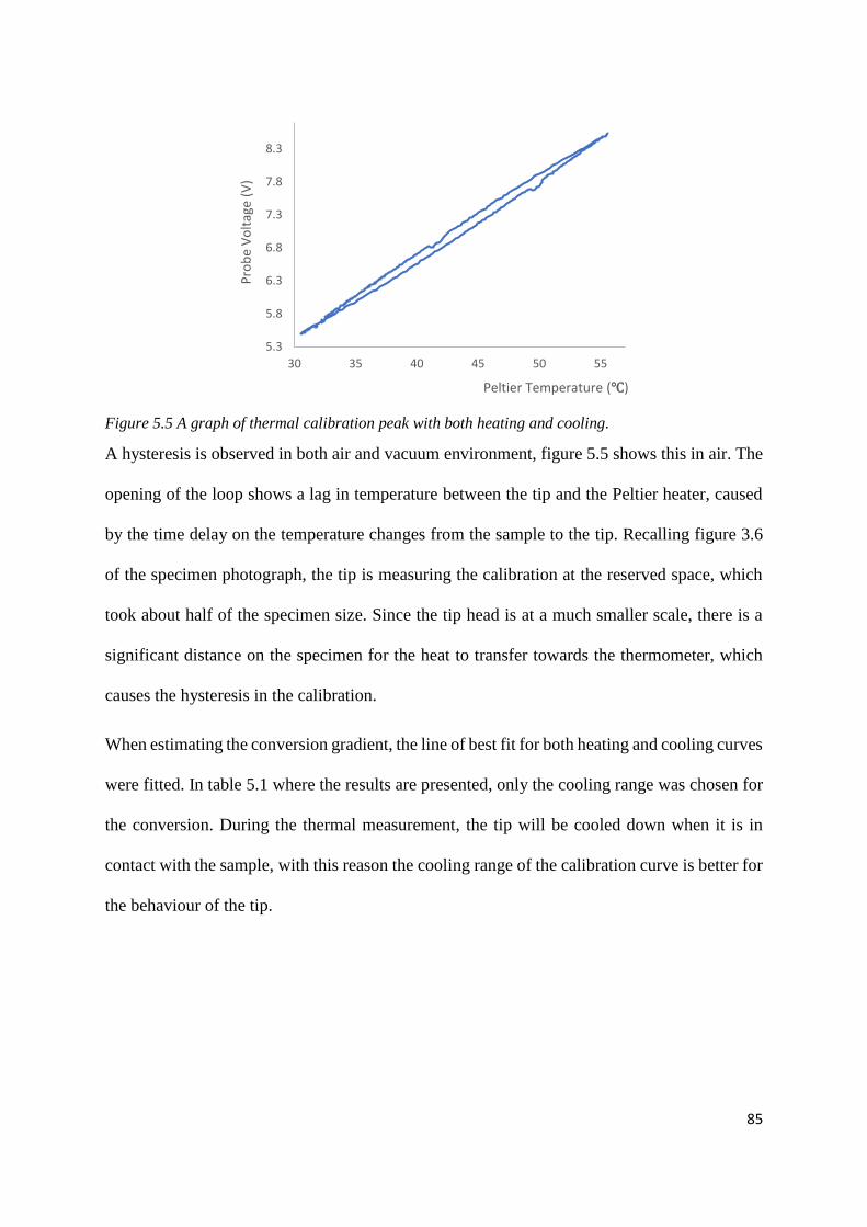
85
Figure 5.5 A graph of thermal calibration peak with both heating and cooling.
A hysteresis is observed in both air and vacuum environment, figure 5.5 shows this in air. The
opening of the loop shows a lag in temperature between the tip and the Peltier heater, caused
by the time delay on the temperature changes from the sample to the tip. Recalling figure 3.6
of the specimen photograph, the tip is measuring the calibration at the reserved space, which
took about half of the specimen size. Since the tip head is at a much smaller scale, there is a
significant distance on the specimen for the heat to transfer towards the thermometer, which
causes the hysteresis in the calibration.
When estimating the conversion gradient, the line of best fit for both heating and cooling curves
were fitted. In table 5.1 where the results are presented, only the cooling range was chosen for
the conversion. During the thermal measurement, the tip will be cooled down when it is in
contact with the sample, with this reason the cooling range of the calibration curve is better for
the behaviour of the tip.
5.3
5.8
6.3
6.8
7.3
7.8
8.3
30 35 40 45 50 55
Pro
be
Vo
ltag
e (V
)
Peltier Temperature (℃)
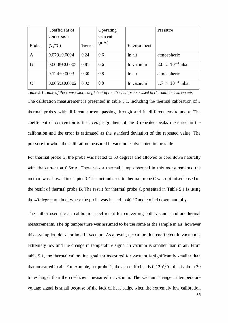
86
Probe
Coefficient of
conversion
(V/℃) %error
Operating
Current
(mA) Environment
Pressure
A 0.079±0.0004 0.24 0.6 In air atmospheric
B 0.0038±0.0003 0.81 0.6 In vacuum 2.0 × 10⁻⁴mbar
C
0.124±0.0003 0.30 0.8 In air atmospheric
0.0059±0.0002 0.92 0.8 In vacuum 1.7 × 10⁻⁴ mbar
Table 5.1 Table of the conversion coefficient of the thermal probes used in thermal measurements.
The calibration measurement is presented in table 5.1, including the thermal calibration of 3
thermal probes with different current passing through and in different environment. The
coefficient of conversion is the average gradient of the 3 repeated peaks measured in the
calibration and the error is estimated as the standard deviation of the repeated value. The
pressure for when the calibration measured in vacuum is also noted in the table.
For thermal probe B, the probe was heated to 60 degrees and allowed to cool down naturally
with the current at 0.6mA. There was a thermal jump observed in this measurements, the
method was showed in chapter 3. The method used in thermal probe C was optimised based on
the result of thermal probe B. The result for thermal probe C presented in Table 5.1 is using
the 40-degree method, where the probe was heated to 40 ℃ and cooled down naturally.
The author used the air calibration coefficient for converting both vacuum and air thermal
measurements. The tip temperature was assumed to be the same as the sample in air, however
this assumption does not hold in vacuum. As a result, the calibration coefficient in vacuum is
extremely low and the change in temperature signal in vacuum is smaller than in air. From
table 5.1, the thermal calibration gradient measured for vacuum is significantly smaller than
that measured in air. For example, for probe C, the air coefficient is 0.12 V/℃, this is about 20
times larger than the coefficient measured in vacuum. The vacuum change in temperature
voltage signal is small because of the lack of heat paths, when the extremely low calibration
87
coefficient is used to convert to temperature, it would result in an overestimation of the sample
temperature change. Therefore, in the following chapters, the thermal measurement units are
converted using only the air calibration respects to the probe.
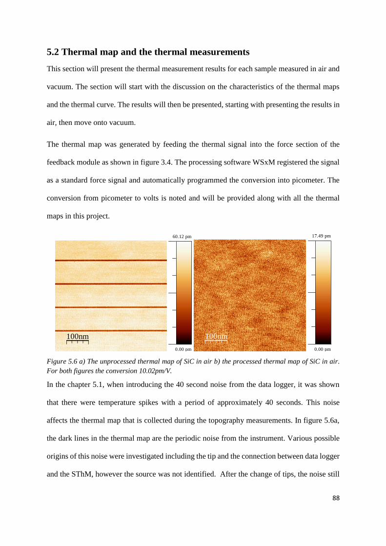
88
5.2 Thermal map and the thermal measurements
This section will present the thermal measurement results for each sample measured in air and
vacuum. The section will start with the discussion on the characteristics of the thermal maps
and the thermal curve. The results will then be presented, starting with presenting the results in
air, then move onto vacuum.
The thermal map was generated by feeding the thermal signal into the force section of the
feedback module as shown in figure 3.4. The processing software WSxM registered the signal
as a standard force signal and automatically programmed the conversion into picometer. The
conversion from picometer to volts is noted and will be provided along with all the thermal
maps in this project.
Figure 5.6 a) The unprocessed thermal map of SiC in air b) the processed thermal map of SiC in air.
For both figures the conversion 10.02pm/V.
In the chapter 5.1, when introducing the 40 second noise from the data logger, it was shown
that there were temperature spikes with a period of approximately 40 seconds. This noise
affects the thermal map that is collected during the topography measurements. In figure 5.6a,
the dark lines in the thermal map are the periodic noise from the instrument. Various possible
origins of this noise were investigated including the tip and the connection between data logger
and the SThM, however the source was not identified. After the change of tips, the noise still
100nm
60.12 pm
0.00 pm
100nm
17.49 pm
0.00 pm
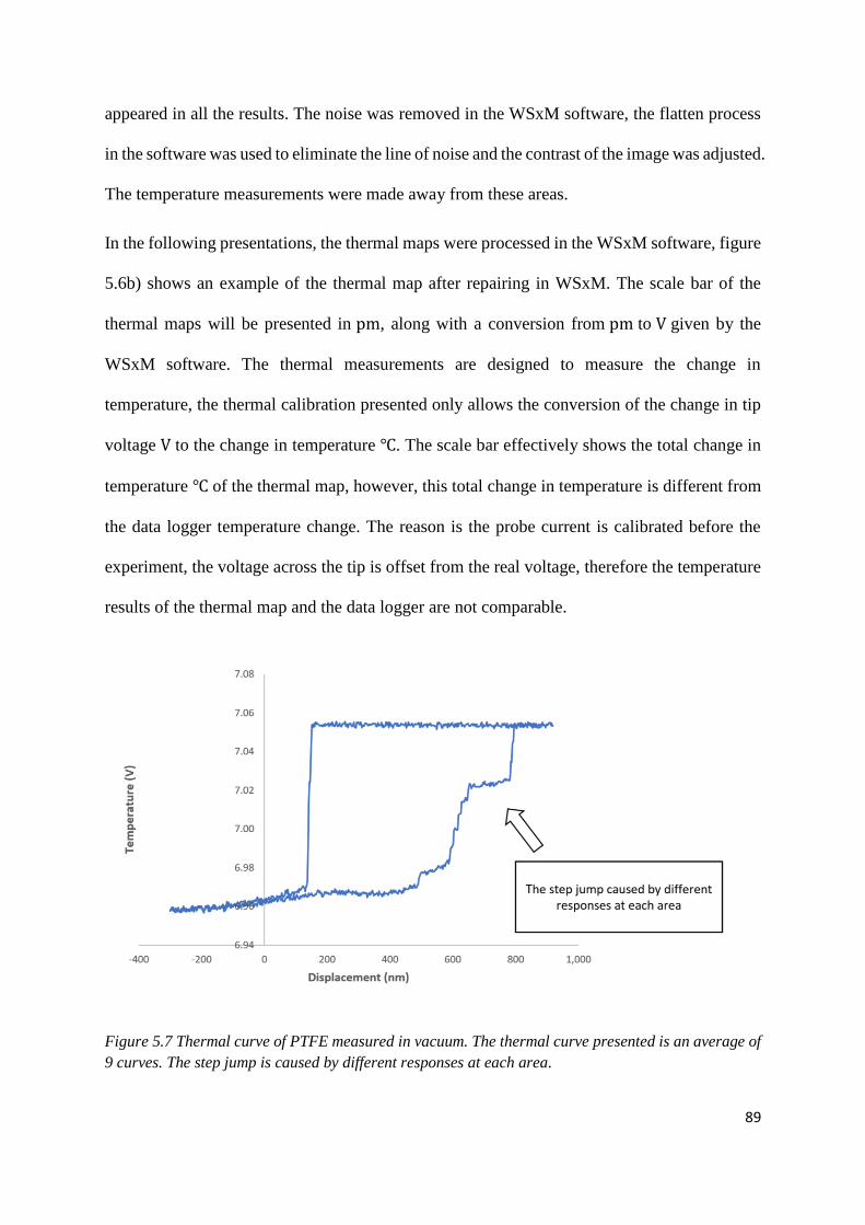
89
appeared in all the results. The noise was removed in the WSxM software, the flatten process
in the software was used to eliminate the line of noise and the contrast of the image was adjusted.
The temperature measurements were made away from these areas.
In the following presentations, the thermal maps were processed in the WSxM software, figure
5.6b) shows an example of the thermal map after repairing in WSxM. The scale bar of the
thermal maps will be presented in pm, along with a conversion from pm to V given by the
WSxM software. The thermal measurements are designed to measure the change in
temperature, the thermal calibration presented only allows the conversion of the change in tip
voltage V to the change in temperature ℃. The scale bar effectively shows the total change in
temperature ℃ of the thermal map, however, this total change in temperature is different from
the data logger temperature change. The reason is the probe current is calibrated before the
experiment, the voltage across the tip is offset from the real voltage, therefore the temperature
results of the thermal map and the data logger are not comparable.
Figure 5.7 Thermal curve of PTFE measured in vacuum. The thermal curve presented is an average of
9 curves. The step jump is caused by different responses at each area.
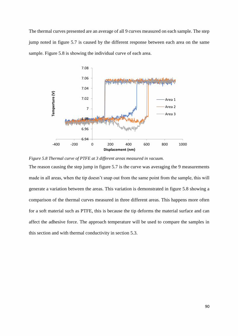
90
The thermal curves presented are an average of all 9 curves measured on each sample. The step
jump noted in figure 5.7 is caused by the different response between each area on the same
sample. Figure 5.8 is showing the individual curve of each area.
Figure 5.8 Thermal curve of PTFE at 3 different areas measured in vacuum.
The reason causing the step jump in figure 5.7 is the curve was averaging the 9 measurements
made in all areas, when the tip doesn’t snap out from the same point from the sample, this will
generate a variation between the areas. This variation is demonstrated in figure 5.8 showing a
comparison of the thermal curves measured in three different areas. This happens more often
for a soft material such as PTFE, this is because the tip deforms the material surface and can
affect the adhesive force. The approach temperature will be used to compare the samples in
this section and with thermal conductivity in section 5.3.
6.94
6.96
6.98
7
7.02
7.04
7.06
7.08
-400 -200 0 200 400 600 800 1000
Tem
pe
rtu
re (
V)
Displacement (nm)
Area 1
Area 2
Area 3
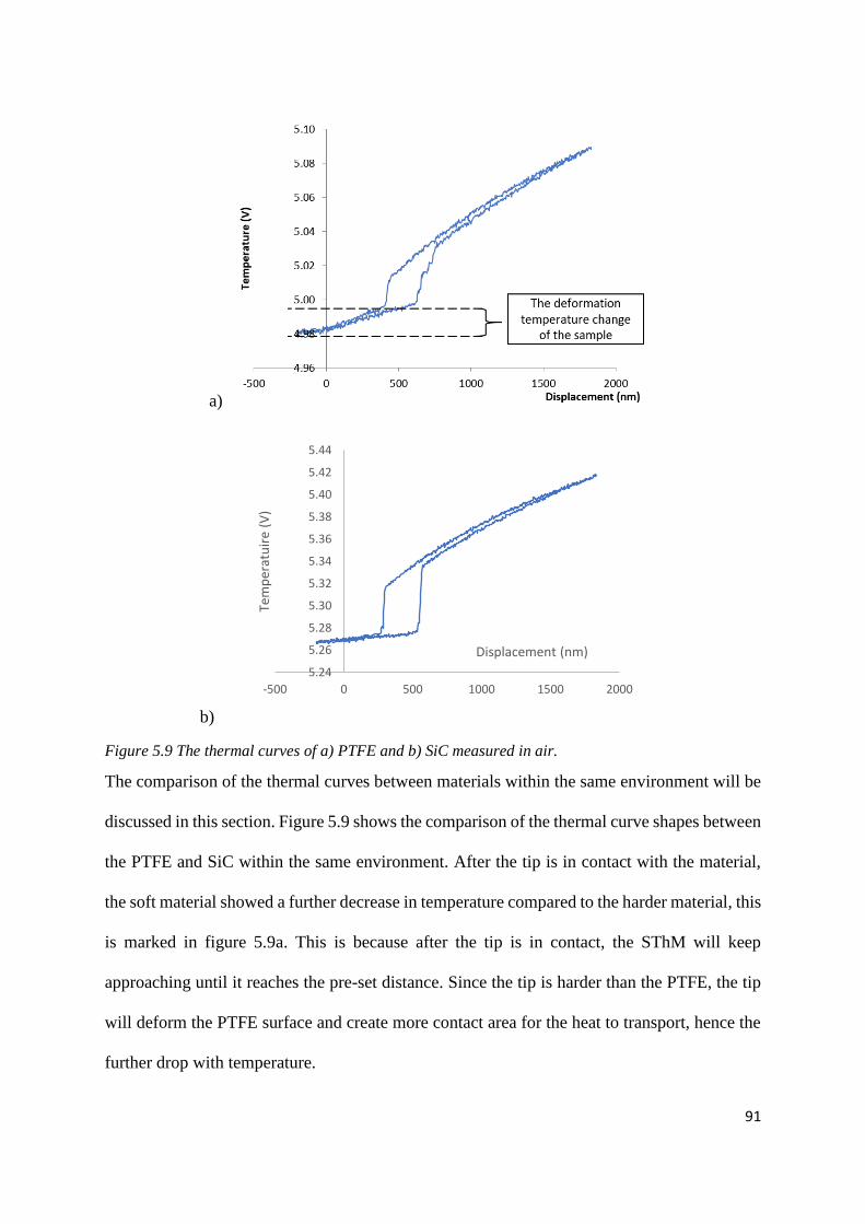
91
a)
b)
Figure 5.9 The thermal curves of a) PTFE and b) SiC measured in air.
The comparison of the thermal curves between materials within the same environment will be
discussed in this section. Figure 5.9 shows the comparison of the thermal curve shapes between
the PTFE and SiC within the same environment. After the tip is in contact with the material,
the soft material showed a further decrease in temperature compared to the harder material, this
is marked in figure 5.9a. This is because after the tip is in contact, the SThM will keep
approaching until it reaches the pre-set distance. Since the tip is harder than the PTFE, the tip
will deform the PTFE surface and create more contact area for the heat to transport, hence the
further drop with temperature.
5.24
5.26
5.28
5.30
5.32
5.34
5.36
5.38
5.40
5.42
5.44
-500 0 500 1000 1500 2000
Tem
per
atu
ire
(V)
Displacement (nm)
92
The next section will present the thermal results measured with the probe current of 0.8mA as
the tips were broken during the measurements using 0.6mA resulting in a change of tip. The
results between the two probes cannot be directly compared without taking into account the
difference of the tip. For example, the tip contact area could be different, which adds another
systematic error. However, the 0.6mA results can still be compared within the set.
The order of presenting each material is the same as the topography results in the previous
chapter. The presentation of figures 5.10 to 5.14 will come in the following sequence from the
left: topography marked with the points where thermal measurements were made, the thermal
image on the right that is along with the topography and then an average thermal curve of the
thermal measurements at the bottom with the corresponding force curve. The thermal curve is
obtained by averaging the curves measured at 3 areas, and at each area the curve is repeated 3
times. The resulting curve shows the average of total 9 curves from one sample. The conversion
values are presented at the bottom of the figures.
At the end of the graphical presentation of the thermal maps, a table of the thermal
measurement results will be presented for each environment. The table will include the
approach, retract and the data logger change in temperatures.
A general discussion on the values within the environment will be discussed with the table. At
the end of the chapter, both numerical results will be combined and compared with further
discussion. The interpretation and further analysis of the data will be presented in chapter 5.4
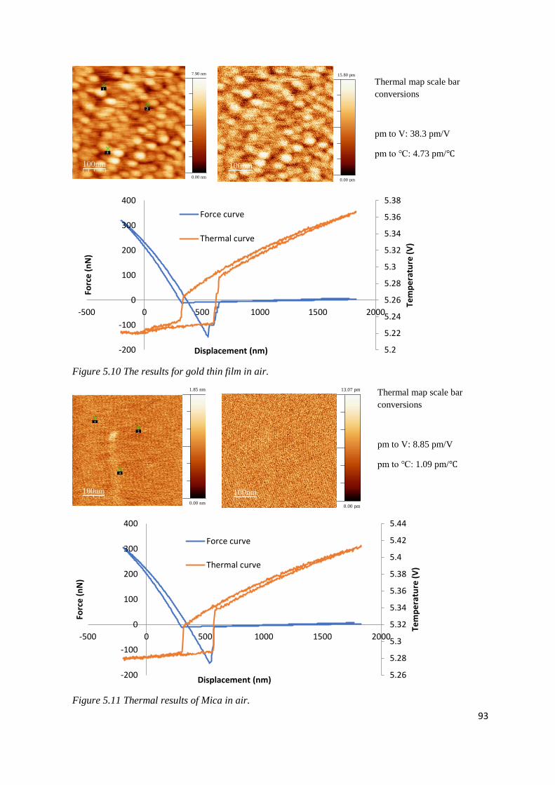
93
Thermal map scale bar
conversions
pm to V: 38.3 pm/V
pm to ℃: 4.73 pm/℃
Figure 5.10 The results for gold thin film in air.
Thermal map scale bar
conversions
pm to V: 8.85 pm/V
pm to ℃: 1.09 pm/℃
Figure 5.11 Thermal results of Mica in air.
7.90 nm
0.00 nm
100nm
15.80 pm
0.00 pm
5.2
5.22
5.24
5.26
5.28
5.3
5.32
5.34
5.36
5.38
-200
-100
0
100
200
300
400
-500 0 500 1000 1500 2000
Tem
pe
ratu
re (
V)
Forc
e (
nN
)
Displacement (nm)
Force curve
Thermal curve
1.85 nm
0.00 nm
100nm
13.07 pm
0.00 pm
5.26
5.28
5.3
5.32
5.34
5.36
5.38
5.4
5.42
5.44
-200
-100
0
100
200
300
400
-500 0 500 1000 1500 2000
Tem
pe
ratu
re (
V)
Forc
e (
nN
)
Displacement (nm)
Force curve
Thermal curve
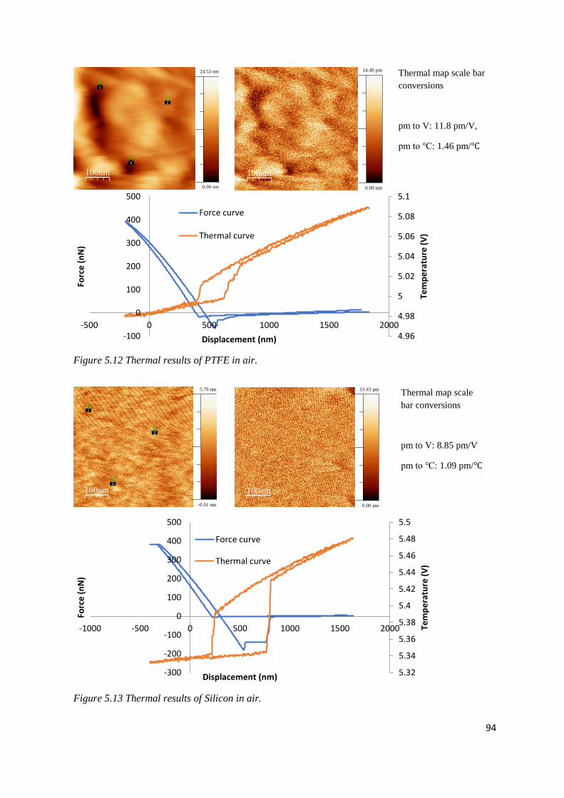
94
Thermal map scale bar
conversions
pm to V: 11.8 pm/V,
pm to ℃: 1.46 pm/℃
Figure 5.12 Thermal results of PTFE in air.
Thermal map scale
bar conversions
pm to V: 8.85 pm/V
pm to ℃: 1.09 pm/℃
Figure 5.13 Thermal results of Silicon in air.
24.53 nm
0.00 nm
100nm
14.40 pm
0.00 pm
4.96
4.98
5
5.02
5.04
5.06
5.08
5.1
-100
0
100
200
300
400
500
-500 0 500 1000 1500 2000
Tem
pe
ratu
re (
V)
Forc
e (
nN
)
Displacement (nm)
Force curve
Thermal curve
5.79 nm
-0.01 nm
100nm
13.43 pm
0.00 pm
5.32
5.34
5.36
5.38
5.4
5.42
5.44
5.46
5.48
5.5
-300
-200
-100
0
100
200
300
400
500
-1000 -500 0 500 1000 1500 2000 Tem
pe
ratu
re (
V)
Forc
e (
nN
)
Displacement (nm)
Force curve
Thermal curve
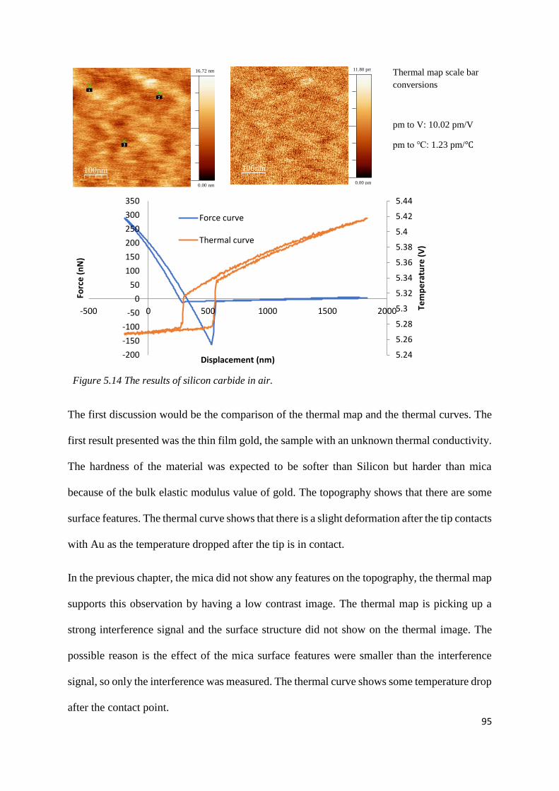
95
Thermal map scale bar
conversions
pm to V: 10.02 pm/V
pm to ℃: 1.23 pm/℃
Figure 5.14 The results of silicon carbide in air.
The first discussion would be the comparison of the thermal map and the thermal curves. The
first result presented was the thin film gold, the sample with an unknown thermal conductivity.
The hardness of the material was expected to be softer than Silicon but harder than mica
because of the bulk elastic modulus value of gold. The topography shows that there are some
surface features. The thermal curve shows that there is a slight deformation after the tip contacts
with Au as the temperature dropped after the tip is in contact.
In the previous chapter, the mica did not show any features on the topography, the thermal map
supports this observation by having a low contrast image. The thermal map is picking up a
strong interference signal and the surface structure did not show on the thermal image. The
possible reason is the effect of the mica surface features were smaller than the interference
signal, so only the interference was measured. The thermal curve shows some temperature drop
after the contact point.
16.72 nm
0.00 nm
100nm
11.80 pm
0.00 pm
5.24
5.26
5.28
5.3
5.32
5.34
5.36
5.38
5.4
5.42
5.44
-200
-150
-100
-50
0
50
100
150
200
250
300
350
-500 0 500 1000 1500 2000 Tem
pe
ratu
re (
V)
Forc
e (
nN
)
Displacement (nm)
Force curve
Thermal curve
96
The PTFE showed some features on the topography. The thermal curve shows that there is a
clear gradient drop after the tip approached the surface as described earlier in this section. The
thermal curve in figure 5.12 shows the step change at the retract temperature path that was
described in figure 5.7. This is due to the soft surface of PTFE that causes different responses
between each area.
The thermal image of silicon is similar to mica, a strong interference signal was collected and
affects the clarity of the thermal map. Although the silicon thermal image showed some surface
features, the noise signal is very similar to mica. The thermal curve shows a clear change in
temperature for approach and retract.
Silicon carbide is the hardest material in the sample set, the topography and thermal map both
collected the interference signal. Some features on the topography can be seen on the thermal
map. The change in temperature was expected to be the largest due to the highest thermal
conductivity from the set, however the temperature change is smaller than Si.
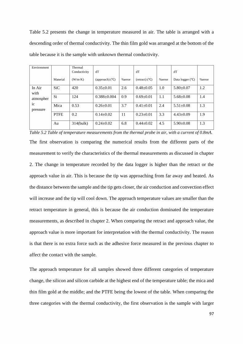
97
Table 5.2 presents the change in temperature measured in air. The table is arranged with a
descending order of thermal conductivity. The thin film gold was arranged at the bottom of the
table because it is the sample with unknown thermal conductivity.
Environment
Material
Thermal
Conductivity
(W/m⋅K)
dT
(approach) (℃) %error
dT
(retract) (℃) %error
dT
Data logger (℃) %error
In Air
with
atmospher
ic
pressure
SiC 420 0.35±0.01 2.6 0.48±0.05 1.0 5.80±0.07 1.2
Si 124 0.388±0.004 0.9 0.69±0.01 1.1 5.68±0.08 1.4
Mica 0.53 0.26±0.01 3.7 0.41±0.01 2.4 5.51±0.08 1.3
PTFE 0.2 0.14±0.02 11 0.23±0.01 3.3 4.43±0.09 1.9
Au 314(bulk) 0.24±0.02 6.8 0.44±0.02 4.5 5.90±0.08 1.3
Table 5.2 Table of temperature measurements from the thermal probe in air, with a current of 0.8mA.
The first observation is comparing the numerical results from the different parts of the
measurement to verify the characteristics of the thermal measurements as discussed in chapter
2. The change in temperature recorded by the data logger is higher than the retract or the
approach value in air. This is because the tip was approaching from far away and heated. As
the distance between the sample and the tip gets closer, the air conduction and convection effect
will increase and the tip will cool down. The approach temperature values are smaller than the
retract temperature in general, this is because the air conduction dominated the temperature
measurements, as described in chapter 2. When comparing the retract and approach value, the
approach value is more important for interpretation with the thermal conductivity. The reason
is that there is no extra force such as the adhesive force measured in the previous chapter to
affect the contact with the sample.
The approach temperature for all samples showed three different categories of temperature
change, the silicon and silicon carbide at the highest end of the temperature table; the mica and
thin film gold at the middle; and the PTFE being the lowest of the table. When comparing the
three categories with the thermal conductivity, the first observation is the sample with larger
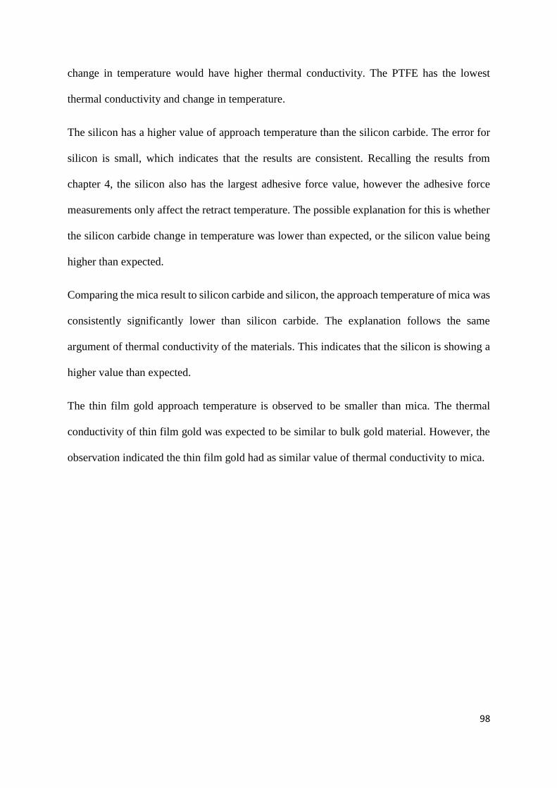
98
change in temperature would have higher thermal conductivity. The PTFE has the lowest
thermal conductivity and change in temperature.
The silicon has a higher value of approach temperature than the silicon carbide. The error for
silicon is small, which indicates that the results are consistent. Recalling the results from
chapter 4, the silicon also has the largest adhesive force value, however the adhesive force
measurements only affect the retract temperature. The possible explanation for this is whether
the silicon carbide change in temperature was lower than expected, or the silicon value being
higher than expected.
Comparing the mica result to silicon carbide and silicon, the approach temperature of mica was
consistently significantly lower than silicon carbide. The explanation follows the same
argument of thermal conductivity of the materials. This indicates that the silicon is showing a
higher value than expected.
The thin film gold approach temperature is observed to be smaller than mica. The thermal
conductivity of thin film gold was expected to be similar to bulk gold material. However, the
observation indicated the thin film gold had as similar value of thermal conductivity to mica.
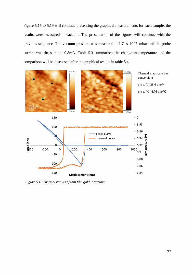
99
Figure 5.15 to 5.19 will continue presenting the graphical measurements for each sample, the
results were measured in vacuum. The presentation of the figures will continue with the
previous sequence. The vacuum pressure was measured at 1.7 × 10⁻⁴ mbar and the probe
current was the same at 0.8mA. Table 5.3 summarises the change in temperature and the
comparison will be discussed after the graphical results in table 5.4.
Thermal map scale bar
conversions
pm to V: 38.6 pm/V
pm to ℃: 4.76 pm/℃
Figure 5.15 Thermal results of thin film gold in vacuum.
18.89 nm
0.00 nm
65.82 pm
0.00 pm
6.84
6.86
6.88
6.9
6.92
6.94
6.96
6.98
7
-150
-100
-50
0
50
100
150
-400 -200 0 200 400 600 800 1000Te
mp
era
ture
(V
)
Forc
e (
nN
)
Displacement (nm)
Force curve
Thermal curve
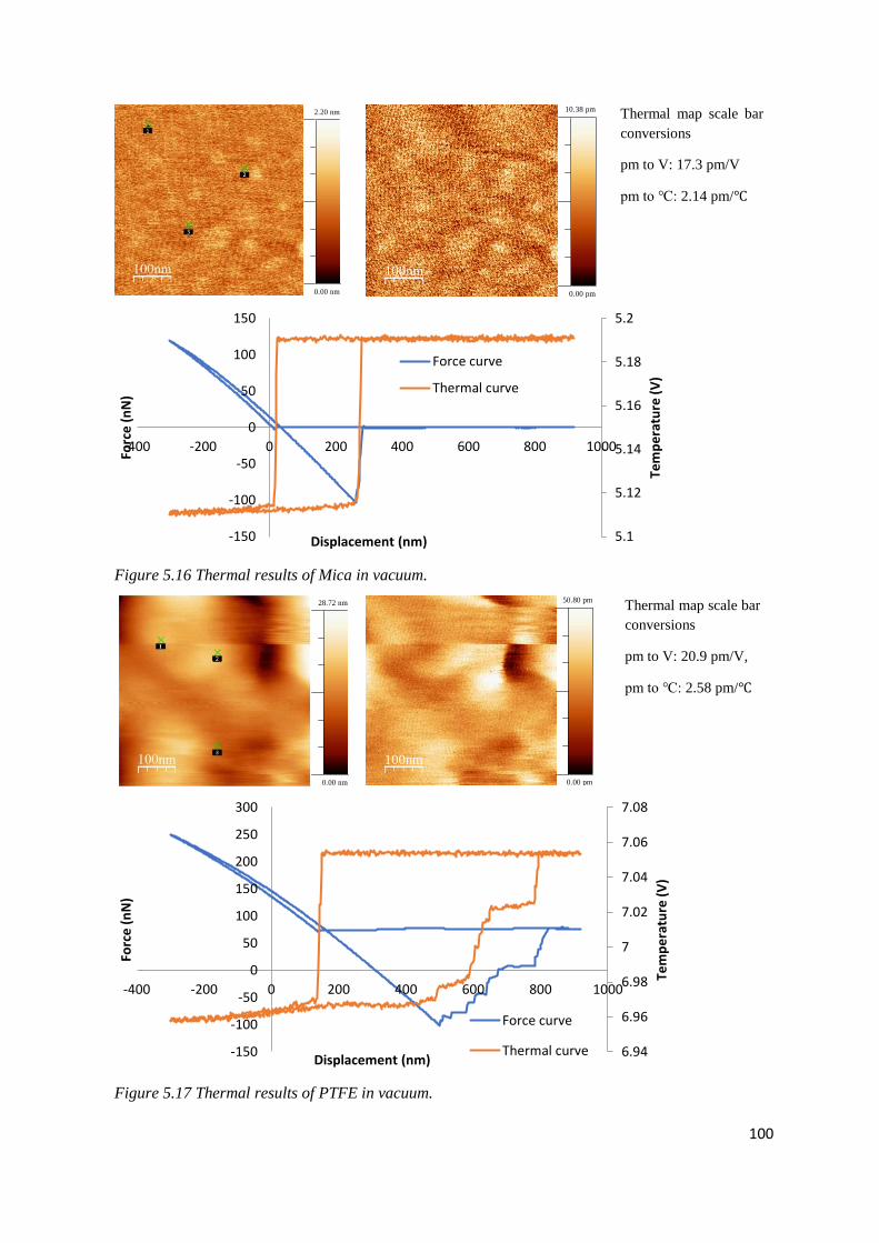
100
Thermal map scale bar
conversions
pm to V: 17.3 pm/V
pm to ℃: 2.14 pm/℃
Figure 5.16 Thermal results of Mica in vacuum.
Thermal map scale bar
conversions
pm to V: 20.9 pm/V,
pm to ℃: 2.58 pm/℃
Figure 5.17 Thermal results of PTFE in vacuum.
2.20 nm
0.00 nm
100nm
10.38 pm
0.00 pm
5.1
5.12
5.14
5.16
5.18
5.2
-150
-100
-50
0
50
100
150
-400 -200 0 200 400 600 800 1000
Tem
pe
ratu
re (
V)
Forc
e (
nN
)
Displacement (nm)
Force curve
Thermal curve
28.72 nm
0.00 nm
100nm
50.80 pm
0.00 pm
6.94
6.96
6.98
7
7.02
7.04
7.06
7.08
-150
-100
-50
0
50
100
150
200
250
300
-400 -200 0 200 400 600 800 1000
Tem
pe
ratu
re (
V)
Forc
e (
nN
)
Displacement (nm)
Force curve
Thermal curve
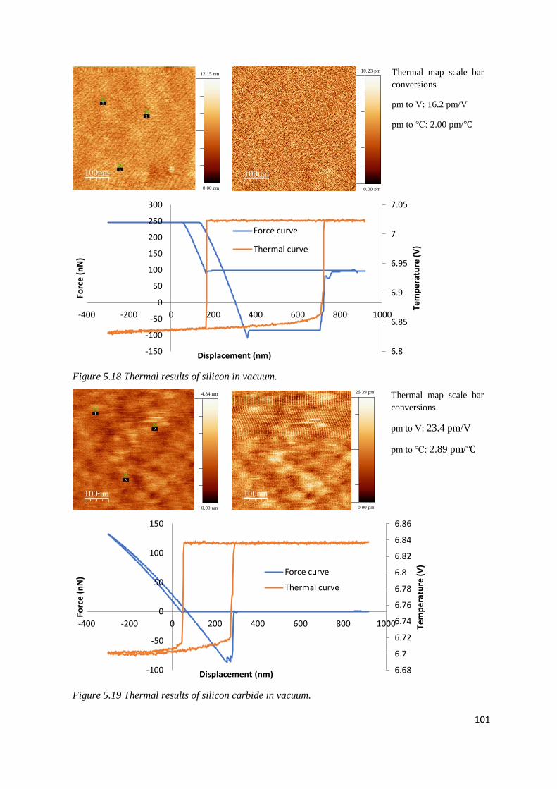
101
Thermal map scale bar
conversions
pm to V: 16.2 pm/V
pm to ℃: 2.00 pm/℃
Figure 5.18 Thermal results of silicon in vacuum.
Thermal map scale bar
conversions
pm to V: 23.4 pm/V
pm to ℃: 2.89 pm/℃
Figure 5.19 Thermal results of silicon carbide in vacuum.
12.15 nm
0.00 nm
100nm
10.23 pm
0.00 pm
6.8
6.85
6.9
6.95
7
7.05
-150
-100
-50
0
50
100
150
200
250
300
-400 -200 0 200 400 600 800 1000
Tem
pe
ratu
re (
V)
Forc
e (
nN
)
Displacement (nm)
Force curve
Thermal curve
4.84 nm
0.00 nm
100nm
26.39 pm
0.00 pm
6.68
6.7
6.72
6.74
6.76
6.78
6.8
6.82
6.84
6.86
-100
-50
0
50
100
150
-400 -200 0 200 400 600 800 1000 Tem
pe
ratu
re (
V)
Forc
e (
nN
)
Displacement (nm)
Force curve
Thermal curve
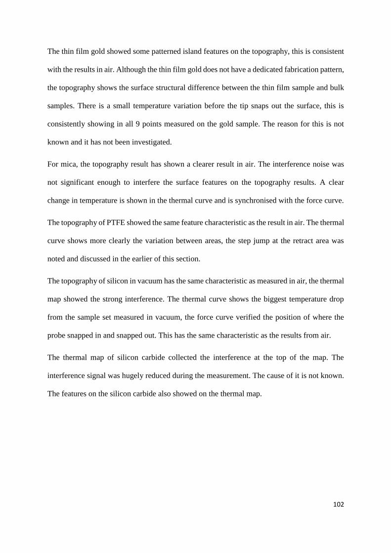
102
The thin film gold showed some patterned island features on the topography, this is consistent
with the results in air. Although the thin film gold does not have a dedicated fabrication pattern,
the topography shows the surface structural difference between the thin film sample and bulk
samples. There is a small temperature variation before the tip snaps out the surface, this is
consistently showing in all 9 points measured on the gold sample. The reason for this is not
known and it has not been investigated.
For mica, the topography result has shown a clearer result in air. The interference noise was
not significant enough to interfere the surface features on the topography results. A clear
change in temperature is shown in the thermal curve and is synchronised with the force curve.
The topography of PTFE showed the same feature characteristic as the result in air. The thermal
curve shows more clearly the variation between areas, the step jump at the retract area was
noted and discussed in the earlier of this section.
The topography of silicon in vacuum has the same characteristic as measured in air, the thermal
map showed the strong interference. The thermal curve shows the biggest temperature drop
from the sample set measured in vacuum, the force curve verified the position of where the
probe snapped in and snapped out. This has the same characteristic as the results from air.
The thermal map of silicon carbide collected the interference at the top of the map. The
interference signal was hugely reduced during the measurement. The cause of it is not known.
The features on the silicon carbide also showed on the thermal map.
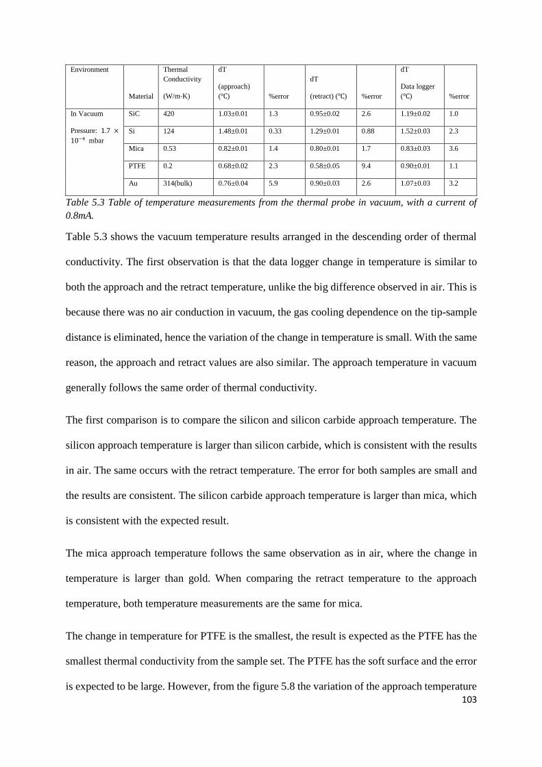
103
Environment
Material
Thermal
Conductivity
(W/m⋅K)
dT
(approach)
(℃) %error
dT
(retract) (℃) %error
dT
Data logger
(℃) %error
In Vacuum
Pressure: 1.7 ×
10−4 mbar
SiC 420 1.03±0.01 1.3 0.95±0.02 2.6 1.19±0.02 1.0
Si 124 1.48±0.01 0.33 1.29±0.01 0.88 1.52±0.03 2.3
Mica 0.53 0.82±0.01 1.4 0.80±0.01 1.7 0.83±0.03 3.6
PTFE 0.2 0.68±0.02 2.3 0.58±0.05 9.4 0.90±0.01 1.1
Au 314(bulk) 0.76±0.04 5.9 0.90±0.03 2.6 1.07±0.03 3.2
Table 5.3 Table of temperature measurements from the thermal probe in vacuum, with a current of
0.8mA.
Table 5.3 shows the vacuum temperature results arranged in the descending order of thermal
conductivity. The first observation is that the data logger change in temperature is similar to
both the approach and the retract temperature, unlike the big difference observed in air. This is
because there was no air conduction in vacuum, the gas cooling dependence on the tip-sample
distance is eliminated, hence the variation of the change in temperature is small. With the same
reason, the approach and retract values are also similar. The approach temperature in vacuum
generally follows the same order of thermal conductivity.
The first comparison is to compare the silicon and silicon carbide approach temperature. The
silicon approach temperature is larger than silicon carbide, which is consistent with the results
in air. The same occurs with the retract temperature. The error for both samples are small and
the results are consistent. The silicon carbide approach temperature is larger than mica, which
is consistent with the expected result.
The mica approach temperature follows the same observation as in air, where the change in
temperature is larger than gold. When comparing the retract temperature to the approach
temperature, both temperature measurements are the same for mica.
The change in temperature for PTFE is the smallest, the result is expected as the PTFE has the
smallest thermal conductivity from the sample set. The PTFE has the soft surface and the error
is expected to be large. However, from the figure 5.8 the variation of the approach temperature
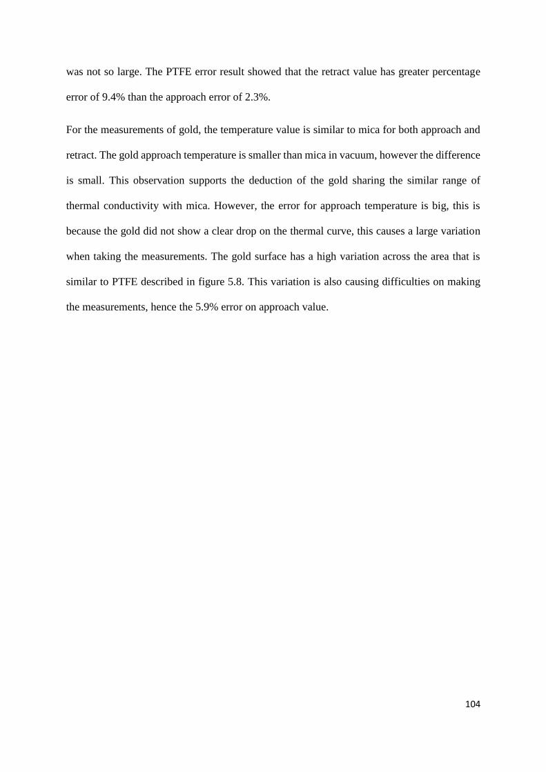
104
was not so large. The PTFE error result showed that the retract value has greater percentage
error of 9.4% than the approach error of 2.3%.
For the measurements of gold, the temperature value is similar to mica for both approach and
retract. The gold approach temperature is smaller than mica in vacuum, however the difference
is small. This observation supports the deduction of the gold sharing the similar range of
thermal conductivity with mica. However, the error for approach temperature is big, this is
because the gold did not show a clear drop on the thermal curve, this causes a large variation
when taking the measurements. The gold surface has a high variation across the area that is
similar to PTFE described in figure 5.8. This variation is also causing difficulties on making
the measurements, hence the 5.9% error on approach value.
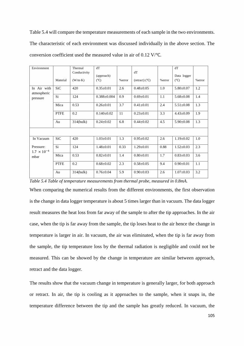
105
Table 5.4 will compare the temperature measurements of each sample in the two environments.
The characteristic of each environment was discussed individually in the above section. The
conversion coefficient used the measured value in air of 0.12 V/℃.
Environment
Material
Thermal
Conductivity
(W/m⋅K)
dT
(approach)
(℃) %error
dT
(retract) (℃) %error
dT
Data logger
(℃) %error
In Air with
atmospheric
pressure
SiC 420 0.35±0.01 2.6 0.48±0.05 1.0 5.80±0.07 1.2
Si 124 0.388±0.004 0.9 0.69±0.01 1.1 5.68±0.08 1.4
Mica 0.53 0.26±0.01 3.7 0.41±0.01 2.4 5.51±0.08 1.3
PTFE 0.2 0.140±0.02 11 0.23±0.01 3.3 4.43±0.09 1.9
Au 314(bulk) 0.24±0.02 6.8 0.44±0.02 4.5 5.90±0.08 1.3
In Vacuum
Pressure:
1.7 × 10⁻⁴
mbar
SiC 420 1.03±0.01 1.3 0.95±0.02 2.6 1.19±0.02 1.0
Si 124 1.48±0.01 0.33 1.29±0.01 0.88 1.52±0.03 2.3
Mica 0.53 0.82±0.01 1.4 0.80±0.01 1.7 0.83±0.03 3.6
PTFE 0.2 0.68±0.02 2.3 0.58±0.05 9.4 0.90±0.01 1.1
Au 314(bulk) 0.76±0.04 5.9 0.90±0.03 2.6 1.07±0.03 3.2
Table 5.4 Table of temperature measurements from thermal probe, measured in 0.8mA.
When comparing the numerical results from the different environments, the first observation
is the change in data logger temperature is about 5 times larger than in vacuum. The data logger
result measures the heat loss from far away of the sample to after the tip approaches. In the air
case, when the tip is far away from the sample, the tip loses heat to the air hence the change in
temperature is larger in air. In vacuum, the air was eliminated, when the tip is far away from
the sample, the tip temperature loss by the thermal radiation is negligible and could not be
measured. This can be showed by the change in temperature are similar between approach,
retract and the data logger.
The results show that the vacuum change in temperature is generally larger, for both approach
or retract. In air, the tip is cooling as it approaches to the sample, when it snaps in, the
temperature difference between the tip and the sample has greatly reduced. In vacuum, the
106
temperature was not cooled by the air conduction, when the tip snaps in, the change in
temperature is then larger. Although there is a much smaller contact area in vacuum, the signal
is larger.
From both environments, the gold results are similar to mica. In both cases, the approach
temperature of gold is larger than mica. The retract temperature and the data logger results are
smaller, however, the retract values are less reliable as described in chapter 2. Therefore,
judging by the approach temperature, the gold thin film is expected to have similar thermal
conductivity to mica.
The error presented in the table is the variation of the measurements taken at all the 9 areas, it
was calculated using the standard deviation of the repeated values. The error for retract values
was expected to be larger in air than the approach values because the snap out point is not
repeatable. However, the variation was not big and the error is similar for both attract and
retract.
The error analysis for this section only discusses the numerical error that was able to be
measured during the measurements. However, there are more factors that could affect the
numerical results. During the experiment in both environments the pressure and the humidity
were not controlled, this could affect the amount of water forming on the sample surface. The
hysteresis effect described in figure 5.5 was noted as an error when measuring the thermal
calibration. This effect was not taken into account when calculating the change in temperature.
However, since all of the temperatures were converted through the same calibration coefficient
and only the change in temperature was measured, the contribution of this error would be the
same for all thermal values.
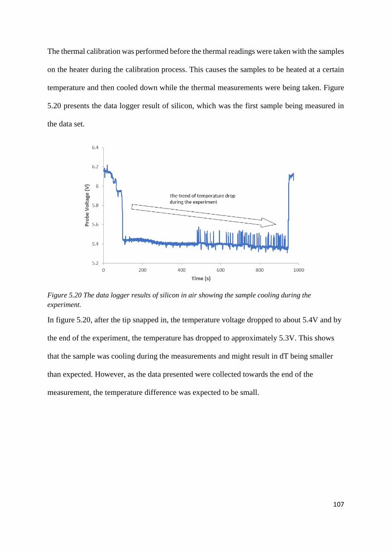
107
The thermal calibration was performed before the thermal readings were taken with the samples
on the heater during the calibration process. This causes the samples to be heated at a certain
temperature and then cooled down while the thermal measurements were being taken. Figure
5.20 presents the data logger result of silicon, which was the first sample being measured in
the data set.
Figure 5.20 The data logger results of silicon in air showing the sample cooling during the
experiment.
In figure 5.20, after the tip snapped in, the temperature voltage dropped to about 5.4V and by
the end of the experiment, the temperature has dropped to approximately 5.3V. This shows
that the sample was cooling during the measurements and might result in dT being smaller
than expected. However, as the data presented were collected towards the end of the
measurement, the temperature difference was expected to be small.
108
5.3 Discussion and interpretation of thermal measurements and
thermal conductivity
In section 5.2, the graphical results measured in both air and vacuum were presented, the
general observations and the comparison were discussed according to the environment. The
numerical result of approach, retract and the data logger change in temperature were compared
for both environments.
This section will continue the analysis of the thermal data, the analysis will discuss the
interpretation of the physics from the results of both chapters 4 and 5 as presented in the
summary table 5.5.
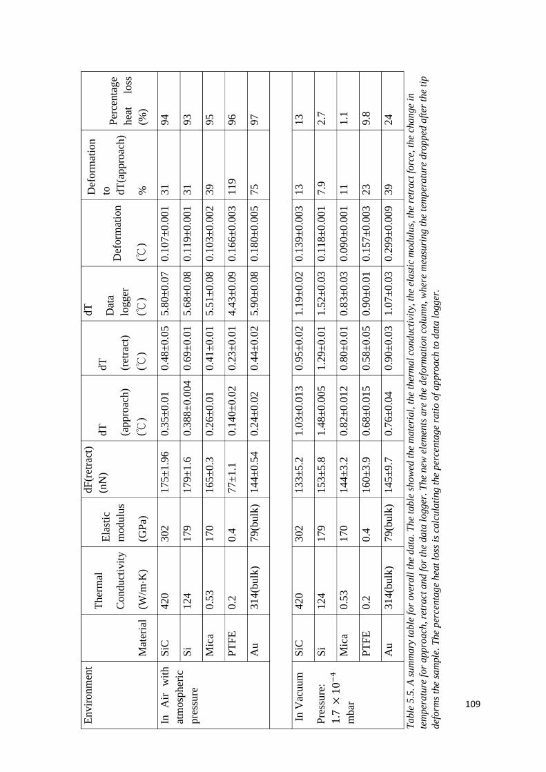
109
E
nv
iro
nm
ent
Mat
eria
l
Ther
mal
Conduct
ivit
y
(W/m
⋅K)
Ela
stic
modulu
s
(GP
a)
dF
(ret
ract
)
(nN
) dT
(appro
ach)
(℃)
dT
(ret
ract
)
(℃)
dT
Dat
a
logger
(℃)
Def
orm
atio
n
(℃)
Def
orm
atio
n
to
dT
(appro
ach)
%
Per
centa
ge
hea
t lo
ss
(%)
In
Air
w
ith
atm
osp
her
ic
pre
ssure
SiC
420
302
175±
1.9
6
0.3
5±
0.0
1
0.4
8±
0.0
5
5.8
0±
0.0
7
0.1
07±
0.0
01
31
94
Si
124
179
179±
1.6
0.3
88±
0.0
04
0.6
9±
0.0
1
5.6
8±
0.0
8
0.1
19±
0.0
01
31
93
Mic
a 0.5
3
170
165±
0.3
0.2
6±
0.0
1
0.4
1±
0.0
1
5.5
1±
0.0
8
0.1
03±
0.0
02
39
95
PT
FE
0.2
0
.4
77±
1.1
0.1
40±
0.0
2
0.2
3±
0.0
1
4.4
3±
0.0
9
0.1
66±
0.0
03
119
96
Au
314(b
ulk
) 7
9(b
ulk
) 144±
0.5
4
0.2
4±
0.0
2
0.4
4±
0.0
2
5.9
0±
0.0
8
0.1
80±
0.0
05
75
97
In V
acuum
Pre
ssu
re:
1.7
×1
0−
4
mbar
SiC
420
302
133±
5.2
1.0
3±
0.0
13
0.9
5±
0.0
2
1.1
9±
0.0
2
0.1
39±
0.0
03
13
13
Si
124
179
153±
5.8
1.4
8±
0.0
05
1.2
9±
0.0
1
1.5
2±
0.0
3
0.1
18
±0
.00
1
7.9
2.7
Mic
a 0.5
3
170
144±
3.2
0.8
2±
0.0
12
0.8
0±
0.0
1
0.8
3±
0.0
3
0.0
90±
0.0
01
11
1.1
PT
FE
0.2
0
.4
160±
3.9
0.6
8±
0.0
15
0.5
8±
0.0
5
0.9
0±
0.0
1
0.1
57±
0.0
03
23
9.8
Au
314(b
ulk
) 7
9(b
ulk
) 145±
9.7
0.7
6±
0.0
4
0.9
0±
0.0
3
1.0
7±
0.0
3
0.2
99±
0.0
09
39
24
Ta
ble
5.5
. A
sum
ma
ry t
ab
le f
or
ove
rall
the
data
. T
he
table
show
ed t
he
mate
rial,
the
ther
mal
conduct
ivit
y, t
he
ela
stic
mo
dulu
s, t
he
retr
act
fo
rce,
th
e ch
an
ge
in
tem
per
atu
re f
or
app
roach
, re
tra
ct a
nd
fo
r th
e da
ta l
ogger
. T
he
new
ele
men
ts a
re t
he
def
orm
ati
on c
olu
mn, w
her
e m
easu
rin
g t
he
tem
per
atu
re d
rop
ped
aft
er t
he
tip
def
orm
s th
e sa
mple
. T
he
per
centa
ge
hea
t lo
ss i
s ca
lcula
ting
the
per
centa
ge
rati
o o
f a
ppro
ach
to
data
lo
gger
.
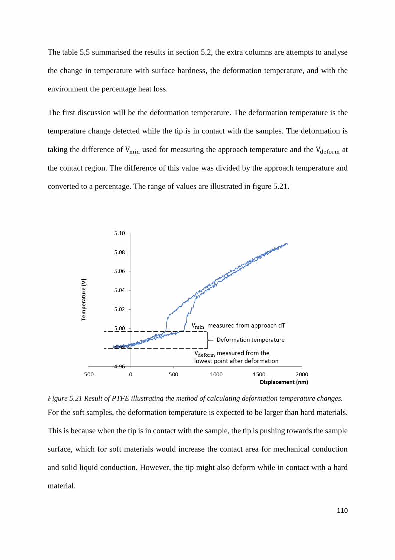
110
The table 5.5 summarised the results in section 5.2, the extra columns are attempts to analyse
the change in temperature with surface hardness, the deformation temperature, and with the
environment the percentage heat loss.
The first discussion will be the deformation temperature. The deformation temperature is the
temperature change detected while the tip is in contact with the samples. The deformation is
taking the difference of Vmin used for measuring the approach temperature and the Vdeform at
the contact region. The difference of this value was divided by the approach temperature and
converted to a percentage. The range of values are illustrated in figure 5.21.
Figure 5.21 Result of PTFE illustrating the method of calculating deformation temperature changes.
For the soft samples, the deformation temperature is expected to be larger than hard materials.
This is because when the tip is in contact with the sample, the tip is pushing towards the sample
surface, which for soft materials would increase the contact area for mechanical conduction
and solid liquid conduction. However, the tip might also deform while in contact with a hard
material.
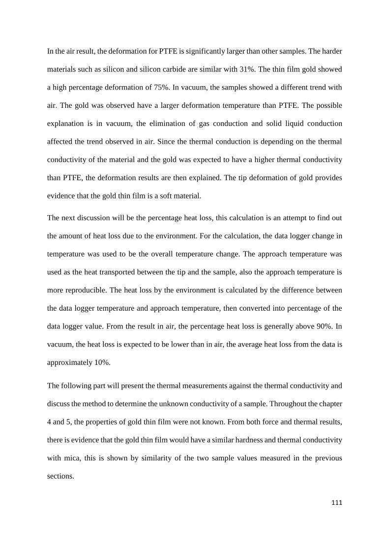
111
In the air result, the deformation for PTFE is significantly larger than other samples. The harder
materials such as silicon and silicon carbide are similar with 31%. The thin film gold showed
a high percentage deformation of 75%. In vacuum, the samples showed a different trend with
air. The gold was observed have a larger deformation temperature than PTFE. The possible
explanation is in vacuum, the elimination of gas conduction and solid liquid conduction
affected the trend observed in air. Since the thermal conduction is depending on the thermal
conductivity of the material and the gold was expected to have a higher thermal conductivity
than PTFE, the deformation results are then explained. The tip deformation of gold provides
evidence that the gold thin film is a soft material.
The next discussion will be the percentage heat loss, this calculation is an attempt to find out
the amount of heat loss due to the environment. For the calculation, the data logger change in
temperature was used to be the overall temperature change. The approach temperature was
used as the heat transported between the tip and the sample, also the approach temperature is
more reproducible. The heat loss by the environment is calculated by the difference between
the data logger temperature and approach temperature, then converted into percentage of the
data logger value. From the result in air, the percentage heat loss is generally above 90%. In
vacuum, the heat loss is expected to be lower than in air, the average heat loss from the data is
approximately 10%.
The following part will present the thermal measurements against the thermal conductivity and
discuss the method to determine the unknown conductivity of a sample. Throughout the chapter
4 and 5, the properties of gold thin film were not known. From both force and thermal results,
there is evidence that the gold thin film would have a similar hardness and thermal conductivity
with mica, this is shown by similarity of the two sample values measured in the previous
sections.
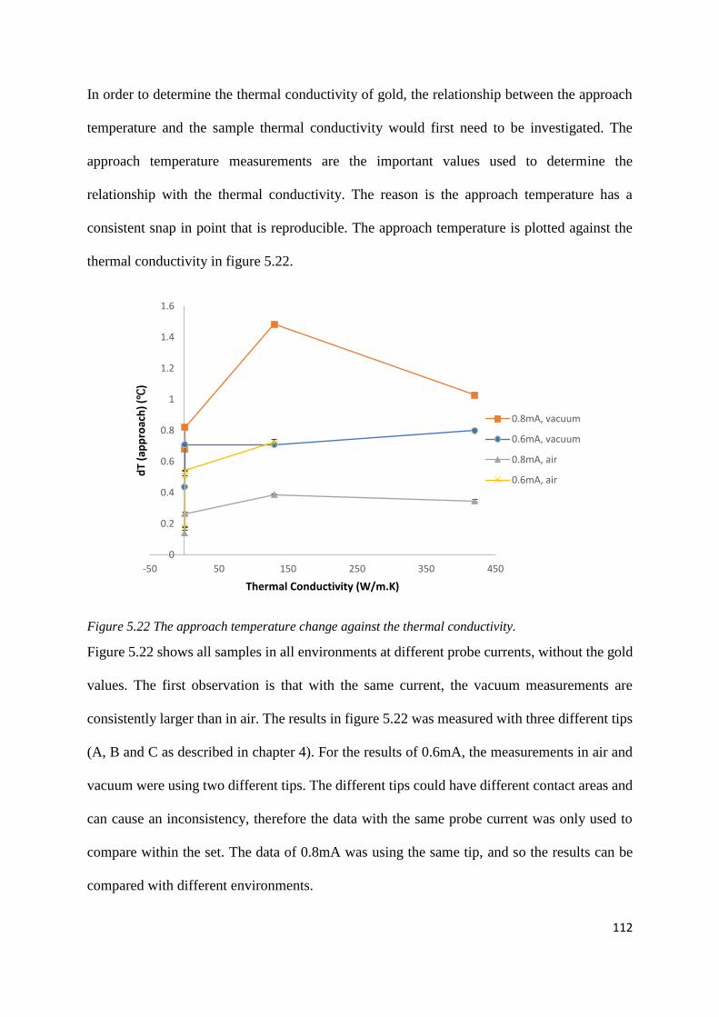
112
In order to determine the thermal conductivity of gold, the relationship between the approach
temperature and the sample thermal conductivity would first need to be investigated. The
approach temperature measurements are the important values used to determine the
relationship with the thermal conductivity. The reason is the approach temperature has a
consistent snap in point that is reproducible. The approach temperature is plotted against the
thermal conductivity in figure 5.22.
Figure 5.22 The approach temperature change against the thermal conductivity.
Figure 5.22 shows all samples in all environments at different probe currents, without the gold
values. The first observation is that with the same current, the vacuum measurements are
consistently larger than in air. The results in figure 5.22 was measured with three different tips
(A, B and C as described in chapter 4). For the results of 0.6mA, the measurements in air and
vacuum were using two different tips. The different tips could have different contact areas and
can cause an inconsistency, therefore the data with the same probe current was only used to
compare within the set. The data of 0.8mA was using the same tip, and so the results can be
compared with different environments.
0
0.2
0.4
0.6
0.8
1
1.2
1.4
1.6
-50 50 150 250 350 450
dT
(ap
pro
ach
) (℃
)
Thermal Conductivity (W/m.K)
0.8mA, vacuum
0.6mA, vacuum
0.8mA, air
0.6mA, air
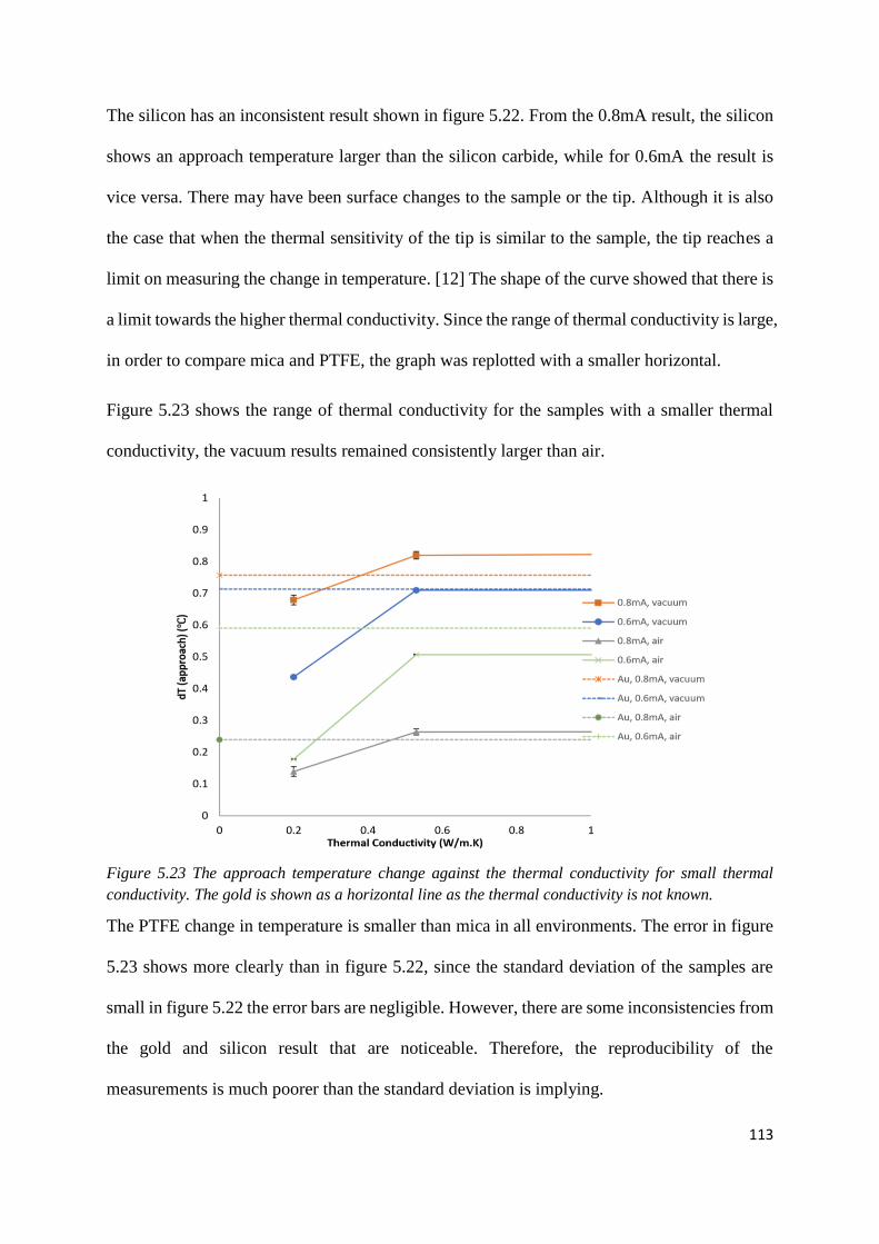
113
The silicon has an inconsistent result shown in figure 5.22. From the 0.8mA result, the silicon
shows an approach temperature larger than the silicon carbide, while for 0.6mA the result is
vice versa. There may have been surface changes to the sample or the tip. Although it is also
the case that when the thermal sensitivity of the tip is similar to the sample, the tip reaches a
limit on measuring the change in temperature. [12] The shape of the curve showed that there is
a limit towards the higher thermal conductivity. Since the range of thermal conductivity is large,
in order to compare mica and PTFE, the graph was replotted with a smaller horizontal.
Figure 5.23 shows the range of thermal conductivity for the samples with a smaller thermal
conductivity, the vacuum results remained consistently larger than air.
Figure 5.23 The approach temperature change against the thermal conductivity for small thermal
conductivity. The gold is shown as a horizontal line as the thermal conductivity is not known.
The PTFE change in temperature is smaller than mica in all environments. The error in figure
5.23 shows more clearly than in figure 5.22, since the standard deviation of the samples are
small in figure 5.22 the error bars are negligible. However, there are some inconsistencies from
the gold and silicon result that are noticeable. Therefore, the reproducibility of the
measurements is much poorer than the standard deviation is implying.
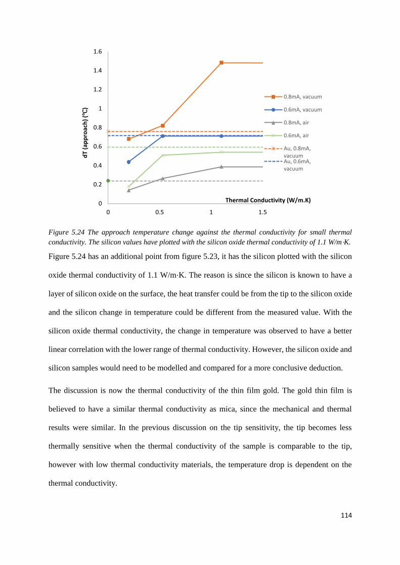
114
Figure 5.24 The approach temperature change against the thermal conductivity for small thermal
conductivity. The silicon values have plotted with the silicon oxide thermal conductivity of 1.1 W/m⋅K.
Figure 5.24 has an additional point from figure 5.23, it has the silicon plotted with the silicon
oxide thermal conductivity of 1.1 W/m⋅K. The reason is since the silicon is known to have a
layer of silicon oxide on the surface, the heat transfer could be from the tip to the silicon oxide
and the silicon change in temperature could be different from the measured value. With the
silicon oxide thermal conductivity, the change in temperature was observed to have a better
linear correlation with the lower range of thermal conductivity. However, the silicon oxide and
silicon samples would need to be modelled and compared for a more conclusive deduction.
The discussion is now the thermal conductivity of the thin film gold. The gold thin film is
believed to have a similar thermal conductivity as mica, since the mechanical and thermal
results were similar. In the previous discussion on the tip sensitivity, the tip becomes less
thermally sensitive when the thermal conductivity of the sample is comparable to the tip,
however with low thermal conductivity materials, the temperature drop is dependent on the
thermal conductivity.
0
0.2
0.4
0.6
0.8
1
1.2
1.4
1.6
0 0.5 1 1.5
dT
(ap
pro
ach
) (℃
)
Thermal Conductivity (W/m.K)
0.8mA, vacuum
0.6mA, vacuum
0.8mA, air
0.6mA, air
Au, 0.8mA,vacuumAu, 0.6mA,vacuum
115
The thermal conductivity of the thin film gold is estimated by comparing the percentage
difference of the change in temperature with the thermal conductivity of mica. The gold change
in temperature was first calculated as a percentage range of mica, which gives a 16% difference.
The gold thin film thermal conductivity is estimated at the range of 0.44 – 0.62 W/ m⋅K,
compared to the bulk material of 314 W/ m⋅K. The thin film value was expected to be much
smaller than the bulk material due to the geometric constraints. [1] The thermal conductivity
estimation of this gold thin film sample is likely to be due in part to its structure and surface,
for example, the size of surface features, the thickness and roughness. Further investigation on
thin film samples would require modelling layers of different materials, in this gold thin film
example, the layer of silicon oxide on the silicon base and the chromium adhesive should also
be modelled.
116
Chapter 6 Conclusions and further developments
This chapter will summarise the work completed, the results achieved and suggest future
developments for this project.
Different methods for measuring the spring constant of the AFM cantilever were considered
and the SEM method chosen and used due to its practicality. The spring constant for the thermal
tips has successfully been measured as a range of 0.5 – 2.6 N/m and the contact tip spring
constant has been measured as 23.1 N/m. The spring constant of the contact tip has been shown
to have a much higher spring constant than the thermal tip. The spring constant has been used
in converting deflection to force units. One challenge for this is there are impurities on the
cantilever, for which the effect on the spring constant is unknown. The Young’s modulus was
estimated as that of silicon nitride, as the structure of the probes gets more complex, the
Young’s modulus can directly affect the spring constant calculated. The thermal resistor was
found to be peeling off from the tip after an experiment. Hence the tip verification using SEM
was added as a standard procedure before thermal experiments.
The methodology of force and thermal measurements were presented in Part II of chapter 3.
The topography, force and thermal measurements for each sample were presented in Chapter
4 and Chapter 5. For some samples having a high adhesive force such as silicon, the AFM
reached a limit regardless of the measurement environment. A method for obtaining the
adhesive force from this data was suggested using a line of best fit of the data, which inevitably
introduced an additional error. Some force curves also could not be fitted with a straight line,
due to deformation of the surface. The other method suggest was offsetting the range on the
AFM, this then revealed a force curve with an unusual shape which it is thought is caused by
a surface layer, which could be contamination, or an instrumental effect.
117
A method of thermal calibration of the thermal tips was presented. The data logger was used
to monitor the potential of the tip and the temperature signal from the PT100 thermometer. For
the thermal calibration, a hysteresis was observed between the heating and the cooling in both
air and vacuum. Various calibration methods were attempted for vacuum however, the
conversion coefficient was shown to be 20 times smaller than calibration in air due to the poorer
thermal contact between the heater. The conversion coefficient in vacuum would give a result
that is overestimating the changing of temperature of the sample. It was therefore decided that
the thermal calibration coefficient measured in air be used for converting the temperature signal
in vacuum as well. A 40-second periodic noise was observed throughout the experiment in
vacuum. The conversion factor was measured as 0.124 V/℃, this was used for converting the
signal to temperature for the results in chapter 5. In the thermal map analysis, a 40-second noise
was also observed across the images. The thermal probe holder broke during the experiment
due to the heavy usage on the SThM. The probe holder was consequently improved by having
extra glue placed at the gold pin to increase the strength for secure the tip, however further
design improvements are desirable.
The thermal measurements showed that the retract changes of temperature are not consistent
for interpretation due to the effect of the adhesive force, therefore the approach temperature
should be used for interpreting the material properties. In the last discussion on the force curves,
a contamination layer of material was shown to affect the thermal curve as well. The
contamination layer could be oxidized material or a thin layer of liquid. This leads to a
discussion on the approach temperature. When there is a layer of material on the surface while
making the thermal measurement, the tip will first arrive at the contamination material before
reaching the sample, the contamination material can cause a change in temperature and provide
a misleading impression of the measurement. Thermal modelling, for example using a
simulation program such as COMSOL, is necessary to interpret multilayer effects.
118
The topography was measured on scan areas of 500nm x 500nm. A spatial resolution of
approximately 20nm for both the topography and thermal measurements was achieved. This
provides a much better spatial resolution for thermometry than traditional methods. The data
was repeated at three different points and three repeated measurements at each point. The idea
was to measure the variation of the measurements across the surface. The error on the adhesive
force and temperature has been shown to be small in general. However, for samples with a soft
surface such as PTFE, the roughness variation of 33% was shown to be large across the
different areas on the same scan indicating a large distribution in both adhesive force and
temperature measurements. Recording the change in tip temperature as the tip presses into the
sample also gives a measure of sample hardness, it has shown that for the soft surface, there is
a larger deformation temperature. The PTFE has shown a range 23-119% of deformation-
approach temperature ratio. The gold sample has shown to have a soft surface with the
deformation temperature of 39-75%.
The comparison between each sample was presented in both chapter 4 and 5, as well as a
comparison of measurements made in air and vacuum. The results showed that there is a 90%
heat loss of heat from the tip to the air in ambient conditions, whilst the losses are only about
10% in vacuum. This suggests that the vacuum environment can provide a better temperature
signal as the temperature difference between the tip and the sample is greater leading to a larger
temperature drop despite losing the solid-liquid conduction path. It was demonstrated across
all sample sets that the temperature drop in vacuum was greater than in air.
Silicon carbide was the hardest material from the sample set, and does have the highest thermal
conductivity. The mechanical and thermal properties gave consistent results in general,
however, the adhesive force was smaller than expected when compared to silicon and mica.
The change in temperature was also expected to have a higher value than observed, due to its
119
high thermal conductivity. The silicon carbide has a similar roughness to silicon, the average
height for the silicon carbide is 1.7nm while the silicon has 1.2nm. Both samples exhibited an
interference while measuring the topography.
The silicon gave the unusual shape when measuring the adhesive force which may be due to
the silicon oxide layer. The temperature drop was less consistent than the silicon carbide and
similar to mica. This may be a result of the additional layer of silicon oxide reducing the value
of thermal conductivity.
The PTFE is the softest material and had the lowest thermal conductivity from the sample set.
The soft surface of PTFE caused a large variation for both force and thermal measurements.
The adhesive force was shown to be low as expected. However, the PTFE showed the force
curves have shown an unusual shape in all environments. The possible reasons could be the
moisture left on the surface, or the sample surface deforming during the measurements.
Another possible reason is the PTFE absorbed the isopropanol that has applied for cleaning
however, further investigation would be required to test this. Although the deformation from
PTFE caused a big variation when measuring the approach temperature, the PTFE has the
lowest value of temperature drop for all environment.
The mica results were consistent being at the centre of each scale. The mica is expected to be
the cleanest sample, due to the layered structure, mica is cleaned by simply cleaving the top
layer. However, the surface features could not be seen from the topography because of the
smooth surface, only some features were detected in the vacuum topography measurements.
The thermal properties are similar to gold, and consistently larger than the PTFE.
The thin film gold is known to have a 150nm thickness, it is the targeted material for estimating
the thermal conductivity. The thin film gold surface was shown to be islanded due to the
120
evaporation process and appeared very different to the other bulk materials. Both the force and
thermal results are similar to mica, which implied that the range of thermal conductivity would
also be similar to mica. The curve of approach temperature against the thermal conductivity
was then plotted in chapter 5. The gold thin film thermal conductivity was estimated to be in
the range of 0.44 – 0.62 W/m⋅K. The thermal conductivity of thin film gold is expected to have
a smaller value to bulk material due to size effects.
This project has explored the use of SThM and provided an experimental procedure for
quantitative measurements using the SThM. There are some key results that could improve the
future development for the SThM at the University of York, and possible directions for future
research.
One of the key outcomes of this project is to examine the tip condition before performing any
experiment. This thesis has shown that the condition of the tip could vary during the experiment.
Using the SEM for inspection is suggested as a standard routine.
Most significantly, the vacuum environment was shown to provide a larger temperature drop
and has a potential to achieve higher resolution than air because of absence of water meniscus
formed. The flatter curve gives a more accurate representation of the sample change in
temperature. The pressure of the vacuum was left until it stabilized, it would be interesting to
see the effect on the same sample with different pressure.
When recording the temperature change, the experimenter should monitor the sample
temperature from the data logger. This thesis has shown that the sample can sometimes still be
cooling during the experiment adding an additional error, particularly in vacuum, where the
cooling paths are limited. In addition, it would be useful to mark the area on the sample for
reproducibility by returning to the same area.
121
The probe holder was shown to not be very robust under frequent use. The design of the holder
could be improved by following the similar design to the standard AFM holder, where a wire
is used to lock the tip position rather than slotting it in. This could reduce the chance for the
probe hitting the gold pin during the insertion process and improve the durability.
There are several areas that could possibly develop in the future from this research. The sample
selection could be expanded by including samples with thermal conductivity between mica and
silicon. This could provide more evidence for the relationship between the change in
temperature and thermal conductivity. The direction of using different materials as the tip
resistor would be an interesting research. The tip used in this project was a palladium resistor,
which has the thermal conductivity about 70W/m⋅K. From the results, the probe reached the
sensitivity limit when the sample thermal conductivity is similar or higher than the tip. If the
thermal conductivity of the tip material is increased, it could potentially increase the range of
materials which can be studied to higher thermal conductivity samples. The result has
highlighted the impact on the thermal transport measurements due to the material properties.
For example, the surface structure such as islands on a thin film, the dimensions such as bulk
material and thin film material all affect the measurements. The surface properties such as the
silicon oxide can also impact on the surface thermal properties. Modelling is needed to further
interpret the data, however there is a potential to apply the technique to study these effects.
In summary, this thesis has achieved the objectives for exploring the potential of using an
SThM for quantitative thermal measurements. If the points raised in this thesis are put into
practice, then the SThM can be successfully used to measure the thermal properties with a
spatial resolution of approximately 20nm, with the temperature resolution up to 0.01℃. The
range of thermal conductivities which can be measured is limited to the tip properties,
currently 70 W/m⋅K.
122
List of reference
[1] D. Zhao, “Measurement Techniques for Thermal Conductivity and Interfacial Thermal
Conductance of Bulk and Thin Film Materials,” J. Electron. Package, no. 4, p. 138, 2016.
[2] G. Chen, “Nanoscale Energy Transport and Conversion,” Oxford University Press, 2005.
[3] J. Christofferson, D. Vashaee and A. Shakouri, "Real Time Sub-micron Thermal Imaging Using
Thermoreflectance," Defense Technical Information Center, 2001, 2001.
[4] F. Menges, P. Mensch, H. Schmid, H. Riel, A. Stemmer, B. Gotsmann, “Temperature Mapping
of Operating Nanoscale Nevices by Scanning Probe Thermometry," Nature Communication ,
vol. 7, no.10874, 10 Sep 2015.
[5] G. Binnig, “Atomic Force Microscope,” USA: IBM San Jose Research Laboratory, 1986.
[6] G. Binnig, “Scanning Tunneling Microscopy,” Switzerland: IBM Zurich Research Laboratory,
1983.
[7] P. Eaton, “Atomic Force Microscopy”, Oxford Scholarship Online, 2010.
[8] A. Majumdar, "Scanning Thermal Microscopy," Annual Review of Material Science, vol. 29,
no. 1, pp. 505-585, 1999.
[9] C. Williams, H. Wickramasinghe, "Scanning Thermal Profiler," Appl. Phys. Lett. , vol. 49, no.
23, pp. 1587-1589, 1986.
[10] Department of Pharmacology, University of Virgina, [Online]. Available:
https://pharm.virginia.edu/files/2014/01/AFM2.jpg. [Accessed 11 10 2017].
[11] V. Gorbunov, "Probing Surface Microthermal Properties by Scanning Thermal Microscopy,"
Langmuir, vol. 15, no. 24, pp. 8340-8343, 1999.
[12] S. Gomès, "Scanning Thermal Microscopy: A Review," Phys. Status Solidi, vol. 212, no. 3, pp.
477-494, 2015.
[13] L. Shi, A. Majumdar, “Thermal Transport Mechanism at Nanoscale Point Contacts," J. Heat
Transfer, vol. 124, no. 2, pp. 239-337, 2001.
[14] P. Hawkes, “Advances in Imaging and Electron Physics", France: Elsevier, 2015.
[15] P. Dobson, J. Weaver and G. Mills, "New Methods for Calibrated Scanning Thermal
Microscopy (SThM)," in Sensors, IEEE, 2007.
[16] R. Pylkki, "Scanning Near-field Optical Microscopy and Scanning Thermal Microscopy,"
Japanese Journal of Applied Physics, vol. 33, pp. 3785-3790, 1994.
[17] S. Gomès, "DC Thermal Microscopy: Study of the Thermal Exchange Between A Probe and A
Sample," Measurement Science and Technology, vol. 10, pp. 805-811, 1999.
[18] " Scanning Thermal Microscopy (SThM)," Park system, [Online]. Available:
http://www.parkafm.com/index.php/park-spm-modes/99-thermal-properties/252-scanning-
thermal-microscopy-sthm%0A.. [Accessed 11 10 2017].
123
[19] P. Tovee, "Nanoscale Spatial Resolution Probes for Scanning Thermal Microscopy of Solid
State Materials," Journal of Applied Physics, vol. 112, no. 11, 114317, 2012.
[20] J. Weaver. et. al., "Microelectronic Engineering Batch Fabricated Dual Cantilever Resistive
Probe for Scanning Thermal Microscopy," Microelectronic Engineering, vol. 88, no. 8, pp.
2435-2438, 2011.
[21] C. Prater, "Nanospectroscopy and Nanospectrometry - Using Heat to Map Materials at
Nanoscale," in University of York, York, UK, 2016.
[22] B. Robinson, "Correlation of Heat Transport and Shear Forces in Nanoscale Junctions," in
University of York, York, UK, 2016.
[23] F. Menges, Heike Riel, A. Stemmer, B. Gotsmann, "Nanoscale Thermometry by Scanning
Thermal Microscopy," Review of Scientific Instruments, vol. 87, 2016.
[24] K. Kim, W. Jeong, W. Lee, P. Reddy, "Ultra-High Vacuum Scanning Thermal," ACS Nano,
vol. 6, no. 5, pp. 4248-4257, 2012.
[25] S. Poon, "Thermal Imaging and Magnetotransport on the Nanoscale?," in University of York,
York, UK, 2016.
[26] K. Luo, Z. Shi, A. Majumdar, "Sensor Nanofabrication, Performance, and Conduction
Mechanisms in Scanning Thermal Microscopy," Journal of Vacuum Science & Technology B:
Microelectronics and Nanometer Structures, vol. 15, no. 2, p. 349, 1997.
[27] J. Booth, "Defining the Role of Gas Conduction in Scanning Thermal Microscopy," University
of Glasgow, 2013.
[28] JPK Instruments, "A Practical Guide to AFM Force Spectroscopy and Data Analysis," JPK
Instruments, [Online]. Available: https://www.jpk.com/app-technotes-img/AFM/pdf/jpk-tech-
force-spectroscopy.14-2.pdf. [Accessed 02 01 2018].
[29] Instructions JSPM-5200 Scanning Probe Microscope, Japan: JEOL, 2005.
[30] M. Poggi, "A Method for Calculating the Spring Constant of Atomic Force Microscopy
Cantilevers with a Nonrectangular Cross Section," Analytical Chemistry, vol. 77, no. 4, p. 1192,
2005.
[31] J. Cleveland, S. Manne, "A Nondestructive Method for Determining the Spring Constant of
Cantilevers for Scanning Force Microscopy," Review of Scientific Instruments, vol. 64, no. 2,
p. 403, 1993.
[32] J. Sader, J. Chon, P. Mulvaney, "Calibration of Rectangular Atomic Force Microscope
Cantilevers," Review of Scientific Instruments, vol. 70, no. 10, p. 3967, 1999.
[33] A. Torii, M.Sasaki, K. Hane, "A Method for Determining the Spring Constant of Cantilevers for
Atomic Force Microscopy," Measurement Science and Technology, vol. 7, no. 2, p. 179, 1999.
[34] J. Weaver, [Private Communication], UK, 2006.
124
[35] "Material Property Data," MatWeb, [Online]. Available: http://www.matls.com/. [Accessed 11
10 2017].
[36] "Material: Silicon (Si), Bulk - MEMS Clearinghouse," Memsnet, [Online]. Available:
https://www.memsnet.org/material/siliconsibulk/. [Accessed 11 10 2017].
[37] "Properties Handbook - Teflon PTFE," DuPont Fluoroproducts:, [Online]. Available:
http://www.rjchase.com/ptfe_handbook.pdf. [Accessed 11 10 2017].
[38] M. Hopcroft, W, Nix, T. Kenny, "What is the Young's Modulus of Silicon?," Journal of
Microelectromechanical Systems, vol. 199, no. 2, p. 229, 2010.
[39] A. Vick, [Private Communication], UK, 2016.
[40] "F-d Spectroscopy," Park AFM, [Online]. Available:
http://www.parkafm.com/images/spmmodes/Force/Force-Distance-Spectroscopy.pdf.
[Accessed 11 10 2017]