electron, hole and exciton self-trapping in germanium doped silica glass from dft calculations with...
TRANSCRIPT
www.elsevier.com/locate/nimb
Nuclear Instruments and Methods in Physics Research B 255 (2007) 188–194
NIMBBeam Interactions
with Materials & Atoms
Electron, hole and exciton self-trapping in germanium doped silicaglass from DFT calculations with self-interaction correction
Jincheng Du a,1, L. Rene Corrales a,*, Kiril Tsemekhman b, Eric J. Bylaska a
a Fundamental Science Directorate, Pacific Northwest National Laboratory, P.O. Box 999, MSIN K1-83 Richland, WA 99352, USAb Department of Chemistry, University of Washington, USA
Available online 31 January 2007
Abstract
Density functional theory (DFT) calculations were employed to understand the refractive index change in germanium doped silicaglasses for the trapped states of electronic excitations induced by UV irradiation. Local structure relaxation and excess electron densitydistribution were calculated upon self-trapping of an excess electron, hole, and exciton in germanium doped silica glass. The results showthat both the trapped exciton and excess electron are highly localized on germanium ion and, to some extent, on its oxygen neighbors.Exciton self-trapping is found to lead to the formation of a Ge E 0 center and a non-bridging hole center. Electron trapping changes theGeO4 tetrahedron structure into trigonal bi-pyramid with the majority of the excess electron density located along the equatorial line.The self-trapped hole is localized on bridging oxygen ions that are not coordinated to germanium atoms that lead to elongation of the Si–O bonds and change of the Si–O–Si bond angles. We carried out a comparative study of standard DFT versus DFT with a hybrid PBE0exchange and correlation functional. The results show that the two methods give qualitatively similar relaxed structure and charge dis-tribution for electron and exciton trapping in germanium doped silica glass; however, only the PBE0 functional produces the self-trappedhole.� 2006 Elsevier B.V. All rights reserved.
PACS: 61.80.Az; 61.80.Ba; 71.15.Mb; 78.55.Qr
Keywords: Germanium doped silica glass; Ultraviolet radiation effect; Self-trapped exciton; Electronic structure; Density functional theory; Hybridfunctional
1. Introduction
Radiation induced electronic excitations lead to the for-mation of defects that change the electrical and opticalproperties of silica based materials [1,2]. The self-trappingof holes, excess electrons, and excitons along with any cor-responding structural relaxations play important roles inthe radiation induced defect formation processes [1–4].
0168-583X/$ - see front matter � 2006 Elsevier B.V. All rights reserved.
doi:10.1016/j.nimb.2006.11.066
* Corresponding author. Present address: The University of Arizona,Department of Chemistry, and Material Science and Engineering, Tucson,AZ 85721, United States.
E-mail addresses: [email protected] (J. Du), [email protected] (L.R. Corrales).
1 Present address: Department of Chemical Engineering, University ofVirginia, Charlottesville, VA 22904, United States.
Detailed understanding of charge trapping in silica is thusof fundamental importance in the fabrication of radiationresistant metal-oxide semiconductor devices and opticalfibers, and in the production of fiber Bragg gratings(FBG) for photonic devices that are based on photo-induced refractive index change in germanium doped silicaglasses [5].
Photorefractive behavior of germanium doped silicaglass is considered to be associated with the irradiationinduced defect generation [4,6]. Two mechanisms havebeen proposed for the photo-induced defect formation pro-cesses [4]. The first mechanism is the conversion of oxygendeficiency centers (ODC) into Ge E 0 centers (three-foldcoordinated germanium atom with a trapped electron)through a one-photon absorption process. The secondmechanism is the generation of a germanium electron cen-
J. Du et al. / Nucl. Instr. and Meth. in Phys. Res. B 255 (2007) 188–194 189
ter (GEC) and self-trapped hole (STH) through a two-pho-ton absorption. The latter mechanism requires the com-bined energy of two photons of the irradiation laser to belarger than the band gap of the irradiated glass. Prolongedirradiation leads to the conversion of GEC into Ge E 0 cen-ters [6]. Despite large number of experimental and theoret-ical works on the subject, an accurate atomic level pictureof the defect formation and transformation of these defectsis still lacking. Detailed structural information of the for-mation and transformation of these defects are highlydesirable for better understanding of the photorefractivephenomena in germanium doped glasses and improvementof the writing efficiency during the fabrication of FBGs. Inthis work, we have focused on the mechanism of the two-photon absorption induced GEC and STH formation ingermanium doped silica glass.
Defects in germanium doped silica glasses have beenstudied previously using ab initio methods on cluster mod-els for paramagnetic centers such as GEC, Ge E 0 and ger-manium lone pair center to calculate the correspondingEPR hyperfine coupling constants [7]. It was found thatby trapping an excess electron, the four-coordinated ger-manium atom undergoes orthorhombic distortion, andwhere the negatively charged cluster is energetically morefavorable than the neutral one [7]. Similar electron capturewas not found in a pure silica cluster, indicating that a ger-manium atom is needed to trap an excess electron in silicaglass [7]. Cluster models have also been used to study elec-tron trapping in oxygen deficient germanium defect centers[8] where it was found that the electron trapped on one ofthe two germanium atoms with a corresponding ortho-rhombic distortion [8]. Recent studies of the oxygen defi-ciency centers (ODC) [9] and the formation of a Ge E 0
center through hole trapping [10] in germania glass werecarried out in periodic systems using plane-wave DFT.The formation energy of the ODC in germania glass wasfound to be much smaller than in silica glass, which sug-gests higher oxygen deficiency center concentration andexplains higher photosensitivity in germania doped glasscompared to pure silica glass [9]. In this paper, we alsouse plane-wave DFT to study the excess electron, holeand exciton self-trapping in germanium doped silica glassin a cubic box with periodic boundary condition to simu-late the condense phase environment.
Standard DFT functionals are known to suffer from theself-interaction error [11]. In particular, the self-interactionleads to the delocalization of electronic states being energet-ically more favorable than their localized states [12]. As aresult, in many cases, LDA and GGA functionals areunable to reproduce charge or spin localization as well asthe charge or exciton self-trapping phenomena [13,14]. Inthis work we use the hybrid PBE0 functional [15] that hasbeen shown to have a small or vanishing self-interactionerror, to examine the electron, hole and exciton self-trapping in germanium doped silica glass. Finally, wecompare the PBE0 results with the standard DFT GGApredictions.
2. Theory
2.1. Standard DFT calculations
We start with the standard generalized gradient approx-imation (GGA) for exchange and correlation functional(PW91) as implemented in the VASP software package[16,17]. We employed the plane wave basis set and ultrasoftpseudo-potentials. The plane wave cutoff was 396 eV. Dueto the large size of the simulation cell (72 atoms), singlegamma point sampling was used for the Brillouin zoneintegration. The convergence criterion was 10�5 eV forelectronic energy. Structure optimization was performedusing the conjugate-gradient method with a convergencecriterion for the forces acting on each atom being smallerthan 0.01 eV/A. Spin polarized calculation was used forcharged defects and the excitonic state. To calculate thehole or excess electron trapping, one electron was removedor added to the relaxed neutral structure, and com-pletely relaxed again. Homogenous background countercharges were applied for the charged systems. For theexciton calculation, the triplet state was simulated byintroducing two unpaired electrons. In all the relaxations,no bond stretching or breaking was introduced to forcelocalization of the charge densities contrary to the ear-lier calculations in quartz [18]. All charge localizationwas naturally achieved under structural relaxation. Badercharge analysis was used to determine the charge distribu-tion [19].
The ground state silica glass structure with 24 SiO2 unitswas obtained by optimizing the initial configuration withinthe framework of DFT from a classical MD simulation. Agermanium atom was then substituted for a silicon atom,giving a GeO2 concentration of about 4.2%, and the struc-ture was further optimized with DFT. Several substitutionsat different silicon sites, including those of most strainedsites obtained from bond angle and bond length correlationplots [20], were made and led to similar final structure ofthe germanium oxygen tetrahedra. The Ge–O distancesrange from 1.71 A to 1.80 A with an average value of1.76 A, in good agreement with experimental Ge–O dis-tance of 1.74 A in vitreous GeO2.
2.2. DFT with hybrid functionals
Based on the extensive experience of applications of thehybrid functionals [21,22] to finite systems, including thesimulations of clusters imitating the correspondingextended systems, we expect that the hybrid functionalscan perform better than standard GGA functionals in thesimulation of self-trapping phenomena. This expectationis also justified by the observation that the constructionof hybrid PBE0 functional is similar to the rational behindthe Perdew–Zunger self-interaction corrected DFT [23] sothat the self-interaction error in PBE0 should be very small[15]. The hybrid DFT calculations are carried out using amodified version of NWCHEM [24].
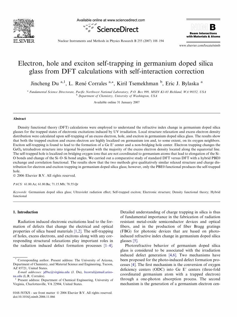
Fig. 1. Structure of and excess spin distribution at the germanium electroncenter (GEC). (a) DFG GGA calculations, (b) PBE0 calculations. Listedbond length in A and bond angles in degrees.
Table 1Percentage of excess charge density on the atoms of a GEC center
DFG GGA PBE0
Ge 55 58O1 17 17O2 7 7O3 5 4O4 13 13Total 97 99
The atom number is the same as in Fig. 1.
190 J. Du et al. / Nucl. Instr. and Meth. in Phys. Res. B 255 (2007) 188–194
The DFT total energy of electronic system with hybridfunctionals may be written as
EHybrid-DFT ¼Xr;i
Zwr;iðrÞ �
1
2r2 þ V extðrÞ
� �wr;iðrÞdr
þ 1
2
Z ZqðrÞqðr0Þjr� r0j drdr0 þ aEExch½fwg�
þ bEx½q1; q2� þ Ec½q1; q2�;
where a and b are constants, Exbqa,qbc is a semi-local ex-change functional, Ecbqa,qbc is the semi-local correlationfunctional and Eexch[{W}] is the exact (Fock) exchange en-ergy given by the standard expression
EExch½fwg� ¼ �1
2
Xr
Xocc
n;m
Z Zqr
nmðrÞqrmnðr0Þ
jr� r0j drdr0; ð1Þ
where
qrnmðrÞ ¼ w�r;nðrÞwr;mðrÞ:
In the NWChem plane-wave pseudo-potential DFT code,the exact exchange and the hybrid functional PBE0[21,22] are implemented using the formalism of maximallylocalized Wannier functions (MLWF) [25]. In general,Wannier orbitals are related to the set of Bloch functionsby the transformation
wnðr� RiÞ ¼Z
BZe�k�Riwn;kðrÞdk; ð2Þ
and form a complete and orthonoromal set. In principle,any set of Bloch functions related to the eigenfunctionsby a unitary transformation can be used in (2) leading toa manifold of the sets of Wannier functions. The MLWFminimize the spread functional and, therefore, are welllocalized inside the unit cell provided that the unit cell issufficiently large and the system is not metallic. For a typ-ical semiconductor, a unit cell with linear size of the orderof 10 A is usually sufficient to consider the Wannier func-tions centered in different unit cells (i.e. corresponding todifferent Ri in (2)) having negligible overlap. With theMLWF, Eq. (1) takes the form:
EExch wf g½ �
¼ � 1
2
Xocc
r;n
Xocc
r0;m
drr0
Z Zw�r;nðrÞwr0 ;mðrÞ
�
�fscreenedðjr� r0jÞw�r0;m r0ð Þwr;nðr0Þdrdr0�; ð3Þ
where the screened interaction is practically equal to theCoulomb potential inside a (large) unit cell and quicklyfalls off to zero outside it thereby eliminating the long-range Coulomb repulsion of Wannier functions centeredin different unit cells. The summation in (3) goes over theoccupied Wannier orbitals in a single unit cell making thenumber of terms in (3) critically smaller than in (1) whereadditional integration over two Bloch vectors is required.The sum in (3) is further simplified by the fact that, even
inside one unit cell, each Wannier function significantlyoverlaps with only a fraction of other orbitals.
3. Results and discussion
3.1. Electron self-trapping: the germanium electron center
Germanium impurities have been known to act as deepelectron traps in alpha quartz [3]. Our DFT calculationsalso indicate that germanium atoms are good electron trapsin silica glass. Fig. 1 shows the atomic configuration andthe excess electron density distribution in the self-trappedelectron state in Ge-doped silica glass. The electrons arelargely localized on germanium and the oxygen ions coor-dinated to it, which account for 97% and 98% of the excessdensity in standard DFT GGA and DFT with a hybridPBE0 functional calculation, respectively (show in Table1). The original GeO4 tetrahedral structure undergoes largerelaxation upon electron trapping: two bonds are elongated
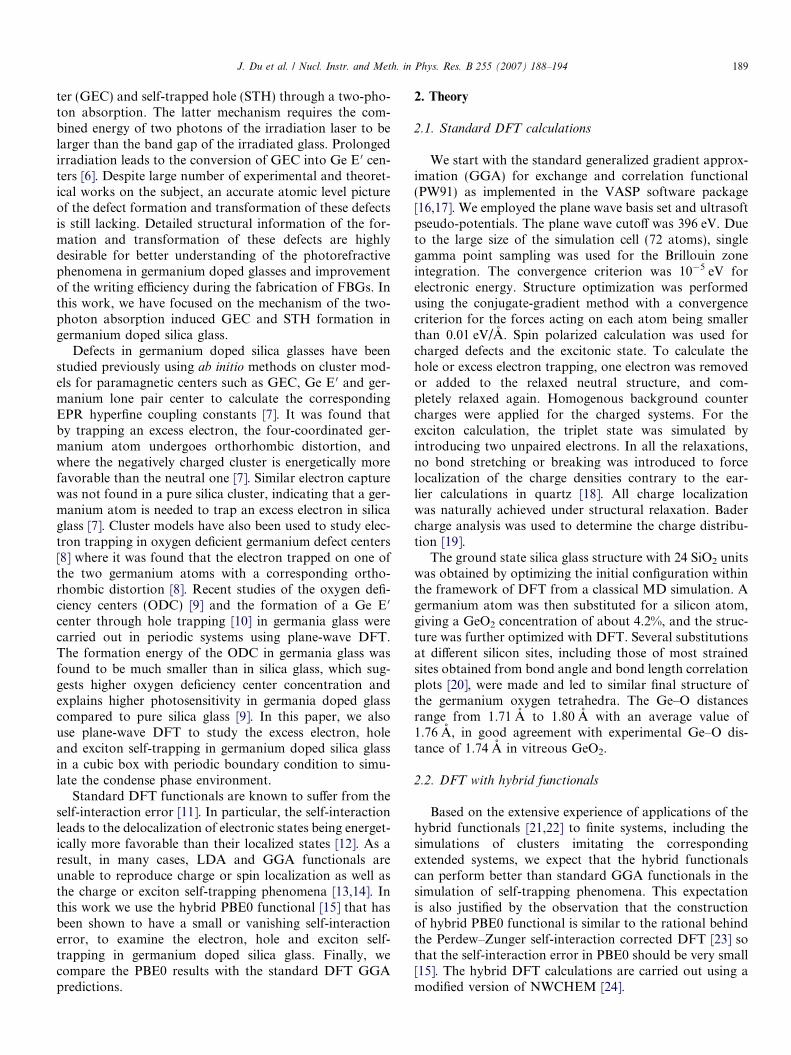
Fig. 2. Excess charge density distribution of hole trapping from DFTGGA (a) and PBE0 (b) calculations. Large yellow ball: silicon, small redball: oxygen, medium green ball: germanium. Hole densities are repre-sented in silver non-spherical spheres around atoms. In (a) hole density isdistributed among many oxygen atoms while in (b) hole density islocalized on two bridging oxygen. Two figures are centered at differentatoms for clarity. (For interpretation of the references in colour in thisfigure legend, the reader is referred to the web version of this article.)
J. Du et al. / Nucl. Instr. and Meth. in Phys. Res. B 255 (2007) 188–194 191
by about 0.2 A and the final configuration closely resem-bles the trigonal bipyramid with the excess electron densityon the equatorial position. The excess spins are mainlylocated on the center germanium atom but also partly dis-tributed over the other oxygen ions that are coordinated tothe germanium. Two oxygen ions with elongated Ge–Obonds have higher excess spin than the two equatorial oxy-gen ions with unperturbed Ge–O bonds, with the formerbeing 12–17% and the latter 4–7%. These results are ingood agreement with the observed EPR spectra of GECcenters in germanium doped silica glass: the Ge(1) center(i.e. the GEC located on an isolated germanium atom,the same as the configuration used in our calculations)shows an orthorhombic structure signal [26] with the twoof the four oxygen atoms of the Ge(1) center having higherspin polarization than the rest [27].
DFT GGA and PBE0 calculations give very similarresults of electron trapping in Ge-doped silica in terms ofboth the final local structure and excess electron distribu-tion. Only small differences exist in the percentage of excesscharges on O3 and the O1–Ge–O4 bond angle, with thePBE0 results giving slightly smaller O3 excess charges andsmaller O1–Ge–O4 bond angle. This can be due to thestrong electron affinity of a germanium atom that over-comes the tendency of charge delocalization of the GGAcalculations. Thus, in standard DFT GGA calculations,charge localization around germanium can still beobserved.
The GEC configuration from our simulation agrees ingeneral with the cluster calculations by Pacchioni and Maz-zeo [7]. They found similar orthorombic distortion uponelectron trapping on the germanium site. However, thestructural relaxation is larger in our DFT calculations.The two Ge–O bond length elongations are greater than0.2 A in the present calculation compared to 0.1 Aobtained in the cluster calculations. The spin density onthe two oxygen atoms with elongated Ge–O bonds makesup 40% of the total excess spin density from our calculationcompared to 17% from the cluster calculation. This mustbe related to the finite size effect in the cluster calculationwhere the boundary atoms were capped with fixed hydro-gen atoms that restrict the structural relaxation. Our simu-lations take the bulk effect into account by using a largersystem and periodic boundary conditions. The cluster cal-culations showed that the negatively charged cluster hadlower energy (by 1.6 eV in DFT calculations) than the neu-tral cluster. In our calculations, DFT GGA shows the neg-atively charged system is about 3 eV less stable than theneutral system while DFT with PBE0 predicts the two havesimilar energy with the negatively charged system higher inenergy by 0.2 eV.
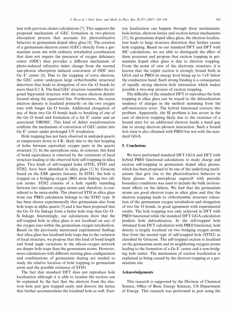
3.2. Self-trapped holes
The hole self-trapping was not observed in alpha quartzfor temperatures down to 4 K but was found to exist in sil-ica glasses [3]. The germanium atom was considered to act
as hole traps in quartz, and the germanium atom pairs werefound to be deeper traps than single germanium atoms [3].Fig. 2 shows the excess charge density distribution in holetrapping from DFT GGA (Fig. 2(a)) and PBE0 (Fig. 2(b))calculations. Standard DFT GGA calculations predict(Fig. 2(a)) hole densities being delocalized among the oxy-gen ions in the silica glass. DFT with PBE0, however, wasable to achieve the hole trapping in Ge-doped glass. Similarresults were found for hole trapping in pure silica glasswhere only DFT with SIC successfully localized holes [28].
The total excess charge density is largely localized ontwo bridging oxygen (BO) atoms (where a BO is an oxygenatom linking two silicon atoms) with percentages being71% on one (labeled O1) and 20% on the other (labeledO2). The rest of the excess electron density is localized ontwo other BOs with percentages being 4% and 6%, respec-tively. This configuration is consistent with the STH2 struc-ture as proposed by Griscom [1]. STH2 is a meta-stablehole center where the hole rapidly tunnels between two
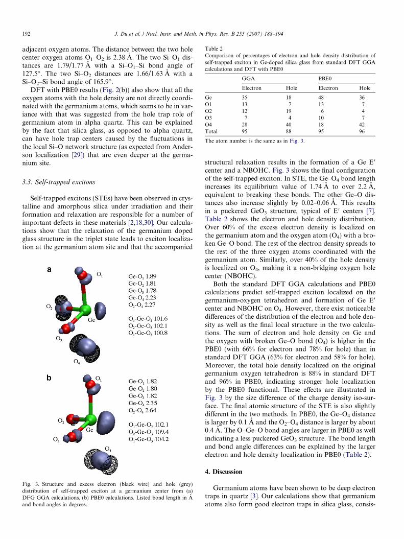
Table 2Comparison of percentages of electron and hole density distribution ofself-trapped exciton in Ge-doped silica glass from standard DFT GGAcalculations and DFT with PBE0
GGA PBE0
Electron Hole Electron Hole
Ge 35 18 48 36O1 13 7 13 7O2 12 19 6 4O3 7 4 10 7O4 28 40 18 42Total 95 88 95 96
The atom number is the same as in Fig. 3.
192 J. Du et al. / Nucl. Instr. and Meth. in Phys. Res. B 255 (2007) 188–194
adjacent oxygen atoms. The distance between the two holecenter oxygen atoms O1–O2 is 2.38 A. The two Si–O1 dis-tances are 1.79/1.77 A with a Si–O1–Si bond angle of127.5�. The two Si–O2 distances are 1.66/1.63 A with aSi–O2–Si bond angle of 165.9�.
DFT with PBE0 results (Fig. 2(b)) also show that all theoxygen atoms with the hole density are not directly coordi-nated with the germanium atoms, which seems to be in var-iance with that was suggested from the hole trap role ofgermanium atom in alpha quartz. This can be explainedby the fact that silica glass, as opposed to alpha quartz,can have hole trap centers caused by the fluctuations inthe local Si–O network structure (as expected from Ander-son localization [29]) that are even deeper at the germa-nium site.
3.3. Self-trapped excitons
Self-trapped excitons (STEs) have been observed in crys-talline and amorphous silica under irradiation and theirformation and relaxation are responsible for a number ofimportant defects in these materials [2,18,30]. Our calcula-tions show that the relaxation of the germanium dopedglass structure in the triplet state leads to exciton localiza-tion at the germanium atom site and that the accompanied
Fig. 3. Structure and excess electron (black wire) and hole (grey)distribution of self-trapped exciton at a germanium center from (a)DFG GGA calculations, (b) PBE0 calculations. Listed bond length in Aand bond angles in degrees.
structural relaxation results in the formation of a Ge E 0
center and a NBOHC. Fig. 3 shows the final configurationof the self-trapped exciton. In STE, the Ge–O4 bond lengthincreases its equilibrium value of 1.74 A to over 2.2 A,equivalent to breaking these bonds. The other Ge–O dis-tances also increase slightly by 0.02–0.06 A. This resultsin a puckered GeO3 structure, typical of E 0 centers [7].Table 2 shows the electron and hole density distribution.Over 60% of the excess electron density is localized onthe germanium atom and the oxygen atom (O4) with a bro-ken Ge–O bond. The rest of the electron density spreads tothe rest of the three oxygen atoms coordinated with thegermanium atom. Similarly, over 40% of the hole densityis localized on O4, making it a non-bridging oxygen holecenter (NBOHC).
Both the standard DFT GGA calculations and PBE0calculations predict self-trapped exciton localized on thegermanium-oxygen tetrahedron and formation of Ge E 0
center and NBOHC on O4. However, there exist noticeabledifferences of the distribution of the electron and hole den-sity as well as the final local structure in the two calcula-tions. The sum of electron and hole density on Ge andthe oxygen with broken Ge–O bond (O4) is higher in thePBE0 (with 66% for electron and 78% for hole) than instandard DFT GGA (63% for electron and 58% for hole).Moreover, the total hole density localized on the originalgermanium oxygen tetrahedron is 88% in standard DFTand 96% in PBE0, indicating stronger hole localizationby the PBE0 functional. These effects are illustrated inFig. 3 by the size difference of the charge density iso-sur-face. The final atomic structure of the STE is also slightlydifferent in the two methods. In PBE0, the Ge–O4 distanceis larger by 0.1 A and the O2–O4 distance is larger by about0.4 A. The O–Ge–O bond angles are larger in PBE0 as wellindicating a less puckered GeO3 structure. The bond lengthand bond angle differences can be explained by the largerelectron and hole density localization in PBE0 (Table 2).
4. Discussion
Germanium atoms have been shown to be deep electrontraps in quartz [3]. Our calculations show that germaniumatoms also form good electron traps in silica glass, consis-
J. Du et al. / Nucl. Instr. and Meth. in Phys. Res. B 255 (2007) 188–194 193
tent with previous cluster calculations [7]. This supports theproposed mechanism of GEC formation in two-photonabsorption process that accounts for photorefractivebehavior in germanium doped silica glass [4]. The creationof a germanium electron center (GEC) directly from a ger-manium atom site with ordinary tetrahedral coordinationthat does not require the precursor of oxygen deficiencycenter (ODC) thus provides a different mechanism ofphoto-induced refractive index change from the normalone-photon absorption induced conversion of ODC intoGe E 0 center [6]. Due to the trapping of extra electron,the GEC center undergoes large orthorhombic structuraldistortion that leads to elongation of two Ge–O bonds bymore than 0.2 A. The final GEC structure resembles the tri-gonal bipyramid structure with the excess electron densitylocated along the equatorial line. Furthermore, the excesselectron density is localized primarily on the two oxygenions with longer Ge–O bonds. Additional elongation ofany of these two Ge–O bonds leads to breaking of one ofthe Ge–O bond and formation of a Ge E 0 center and anassociated NBOHC. This kind of defect transformationconfirms the mechanism of conversion of GEC center intoGe E 0 center under prolonged UV irradiation.
Hole trapping has not been observed in undoped-quartzat temperature down to 4 K, likely due to the fast hoppingof holes between equivalent oxygen pairs in the quartzstructure [3]. In the amorphous state, in contrast, this kindof bond equivalency is removed by the variations of localstructure leading to the observed hole self-trapping in silicaglass. Two kinds of self-trapped holes (STH), STH1 andSTH2, have been identified in silica glass [1] by Griscombased on the ESR spectra features. In STH1, the hole istrapped on a bridging oxygen (BO) atom linking two sili-con atoms. STH2 consists of a hole rapidly tunnelingbetween two adjacent oxygen atoms and, therefore, is con-sidered to be meta-stable. The observed STH in silica glassfrom our PBE0 calculation belongs to the STH2 type. Ithas been shown experimentally that germanium also formhole traps in alpha quartz [3] and it has been proposed thatthe Ge–O–Ge linkage form a better hole trap than Ge–O–Si linkage. Interestingly, our calculations show that theself-trapped hole in silica glass is not localized on any ofthe oxygen ions within the germanium oxygen tetrahedron.Based on the previously mentioned experimental findingsthat silica glass has localized hole traps due to the variationof local structure, we propose that this kind of bond lengthand bond angle variations in the silicon-oxygen networkare deeper hole traps than the germanium atoms. However,more calculations with different starting glass configurationand combinations of germanium doping are needed tostudy the relative location of hole trapping to germaniumatom and the possible existence of STH1.
The fact that standard DFT does not reproduce holelocalization although it is able to localize the exciton canbe explained by the fact that the electron from the elec-tron–hole pair gets trapped easily and distorts the latticethat further accommodates the localized hole as well. Exci-
ton localization can happen through three mechanisms:hole-lattice, electron-lattice and exciton-lattice mechanisms[31]. In germanium doped silica glass, the electron localiza-tion leads to large structure distortion that further causeshole trapping. Based on our standard DFT and DFT withSIC calculations, we are able to distinguish the effect ofthese processes and propose that exciton trapping in ger-manium doped silica glass is due to electron trapping.From the point of view of the electronic structure, it isknown that the triplet exciton is strongly bound both inGGA and in PBE0 its energy level being up to 3 eV belowthe conduction band. Such strong binding is a consequenceof equally strong electron–hole interaction which makespossible a two-step process of exciton trapping.
The difficulty of the standard DFT to reproduce the holetrapping in silica glass can be traced to the delocalizationtendency of charges in the method stemming from theself-interaction error. The hybrid functional corrects thisproblem. Apparently, the SI problem is less severe in thecase of electron trapping likely due to the existence of abound state for an additional electron inside a band gapdue to strong electron–phonon interaction. Such a boundhole state is also obtained with PBE0 but not with the stan-dard GGA.
5. Conclusions
We have performed standard DFT GGA and DFT withhybrid PBE0 functional calculations to study charge andexciton self-trapping in germanium doped silica glasses,which has been proposed to be one of the underlying mech-anisms that give rise to the photorefractive behavior inthese glasses. An amorphous supercell with periodicboundary conditions was used to include the bulk environ-ment effects on the defects. We find that the germaniumatoms are good electron traps in silica glass and that theelectron trapping leads to orthorhombic structure relaxa-tion of the germanium oxygen tetrahedron and elongationof two Ge–O bonds, in good agreement with experimentalresults. The hole trapping was only achieved in DFT withPBE0 functional while the standard DFT GGA calculationpredicts hole delocalization. In the self-trapped holeobtained from DFT calculation with PBE0 functional, holedensity is largely localized on two bridging oxygen atomsthat form the second type of self-trapped hole (STH2) asclassified by Griscom. The self-trapped exciton is localizedon the germanium atom and its neighboring oxygens atomsleading to the formation of a Ge E 0 center and a non-bridg-ing hole center. The mechanism of exciton localization isexplained as being caused by the electron trapping at a ger-manium site.
Acknowledgements
This research is supported by the Division of ChemicalScience, Office of Basic Energy Sciences, US Departmentof Energy. This research was performed in part using the
194 J. Du et al. / Nucl. Instr. and Meth. in Phys. Res. B 255 (2007) 188–194
Molecular Science Computing Facility in the William R.Wiley Environmental Molecular Sciences Laboratory(EMSL) at the Pacific Northwest National Laboratory(PNNL). The EMSL is funded by DOE’s Office of Biolog-ical and Environmental Research. The Pacific NorthwestNational Laboratory is operated by Battelle for the USDepartment of Energy.
References
[1] D.L. Griscom, Phys. Rev. B 40 (1989) 4224.[2] N. Itoh, T. Shimizu-Iwayama, T. Fujita, J. Non-Cryst. Solids 179
(1994) 194.[3] W. Hayes, T.J.L. Jenkin, J. Phys. C Solid State Phys. 19 (1986) 6211.[4] H. Hosono, H. Kawazoe, J. Nishii, Phys. Rev. B 53 (1996) 53.[5] K.O. Hill, Y. Fujii, D.C. Johnson, B.S. Kawasaki, Appl. Phys. Lett.
32 (1978) 647.[6] J. Nishii, K. Fukumi, H. Yamanaka, K. Kawamura, H. Hosono,
H. Kawazoe, Phys. Rev. B 52 (1995) 1661.[7] G. Pacchioni, C. Mazzeo, Phys. Rev. B 62 (2000) 5452.[8] T. Uchino, M. Takahashi, T. Yoko, Appl. Phys. Lett. 79 (2001) 359.[9] T. Tamura, G.H. Lu, R. Yamamoto, M. Kohyama, Phys. Rev. B 69
(2004) 195204.[10] T. Tamura, G.H. Lu, M. Kohyama, R. Yamamoto, Phys. Rev. B 70
(2004) 195204.[11] E.J. Bylaska, K. Tsemekhman, F. Gao, Phys. Scripta. T 124 (2006)
86.[12] M. d’Avzeac, M. Calandra, F. Mauri, Phys. Rev. B 71 (2005) 205210.
[13] J. Lagsagaard, K. Stokbro, Phys. Rev. B 61 (2000) 12590.[14] R.M. Van Ginhoven, D.C. Johnson, K.A. Peterson, M. Dupuis, L.R.
Corrales, J. Chem. Phys. 118 (2003) 6582.[15] K. Tsemekhman, E.J. Bylaska, H. Jonsson, Phys. Rev. Lett.,
submitted for publication.[16] G. Kresse, J. Furthmuller, Comput. Mater. Sci. 6 (1996) 15.[17] G. Kresse, J. Furthmuller, Phys. Rev. B 54 (1996) 11169.[18] J. Song, H. Jonsson, L.R. Corrales, Nucl. Instr. and Meth. B
166&167 (2000) 451.[19] G. Henkelman, A. Arnaldsson, H. Jonsson, Comput. Mater. Sci. 36
(2006) 354.[20] J. Du, A.N. Cormack, J. Am. Ceram. Soc. 88 (2005) 2532.[21] A.D. Becke, J. Chem. Phys. 98 (1993) 5648.[22] A.D. Becke, J. Chem. Phys. 104 (1996) 1040.[23] J.P. Perdew, A. Zunger, Phys. Rev. B 23 (1981) 5048.[24] R.A. Kendall, E. Apra, D.E. Bernholdt, E.J. Bylaska, M. Dupuis,
G.I. Fann, R.J. Harrison, J. Ju, J.A. Nichols, J. Nieplocha,T.P. Straatsma, T.L. Windus, A.T. Wong, Comput. Phys. Commun.128 (2000) 260.
[25] N. Marzari, D. Vanderbilt, Phys. Rev. B 56 (1997) 12847.[26] E.J. Friebele, D.L. Griscom, G.H. Sigel, J. Appl. Phys. 45 (1974)
3424.[27] R.J. McEachern, J.A. Weil, B. Sawyer, Solid State Commun. 81
(1992) 207.[28] M. Gabriel, Ph.D. thesis, University of Washington, Seattle, 2007.[29] P.W. Anderson, Phys. Rev. 109 (1958) 1492.[30] R.M. Van Ginhoven, H. Jonsson, L.R. Corrales, J. Non-Cryst. Solids
352 (2006) 2589.[31] K. Tanimura, N. Itoh, Nucl. Instr. and Meth. B 33 (1988) 815.