atomic layer deposition of hafnium oxide on germanium substrates
TRANSCRIPT
Atomic layer deposition of hafnium oxide on germanium substratesAnnelies Delabie, Riikka L. Puurunen,a! Bert Brijs, Matty Caymax,b! Thierry Conard,Bart Onsia, Olivier Richard, Wilfried Vandervorst,a! Chao Zhao, Marc M. Heyns, andMarc MeurisInteruniversity Micro Electronics Center (IMEC), Kapeldreef 75, B-3001 Leuven, Belgium
Minna M. Viitanen, Hidde H. Brongersma, and Marco de RidderCalipso bv, Den Dolech 2, Postbus 513, 5600 MB Eindhoven, The Netherlands
Lyudmila V. Goncharova, Eric Garfunkel, and Torgny GustafssonDepartment of Physics and Astronomy and of Chemistry, and Laboratory for Surface Modification, RutgersUniversity, 136 Frelinghuysen Road, Piscataway, New Jersey 08854
Wilman TsaiIntel Corporation, SC1-05, 2200 Mission College Boulevard, Santa Clara, California 95054-1549
sReceived 5 May 2004; accepted 13 December 2004; published online 7 March 2005d
Germanium combined with high-k dielectrics has recently been put forth by the semiconductorindustry as potential replacement for planar silicon transistors, which are unlikely to accommodatethe severe scaling requirements for sub-45-nm generations. Therefore, we have studied the atomiclayer depositionsALD d of HfO2 high-k dielectric layers on HF-cleaned Ge substrates. In thiscontribution, we describe the HfO2 growth characteristics, HfO2 bulk properties, and Ge interface.Substrate-enhanced HfO2 growth occurs: the growth per cycle is larger in the first reaction cyclesthan the steady growth per cycle of 0.04 nm. The enhanced growth goes together with islandgrowth, indicating that more than a monolayer coverage of HfO2 is required for a closed film. Aclosed HfO2 layer is achieved after depositing 4–5 HfO2 monolayers, corresponding to about 25ALD reaction cycles. Cross-sectional transmission electron microscopy images show that HfO2
layers thinner than 3 nm are amorphous as deposited, while local epitaxial crystallization hasoccurred in thicker HfO2 films. Other HfO2 bulk properties are similar for Ge and Si substrates.According to this physical characterization study, HfO2 can be used in Ge-based devices as a gateoxide with physical thickness scaled down to 1.6 nm. ©2005 American Institute of Physics.fDOI: 10.1063/1.1856221g
I. INTRODUCTION
Germanium is a high-performance device material dueto its narrow band gap, high mobility and low dopant acti-vation temperatures. It has recently been put forth by thesemiconductor industry as a potential replacement for planarsilicon, which is unlikely to accommodate the severe scalingrequirements for sub-45-nm transistor generations. However,a major technological drawback to the use of Ge is the dif-ficulty in growing an insulating oxide comparable to SiO2 inSi technology. Deposited high-k materials may provide a so-lution for the gate dielectric of Ge-based transistors. Indeed,the successful use of a ZrO2 dielectric film in Ge field-effecttransistorssFETsd has recently been demonstrated.1 The low-field mobility for the Ge/ZrO2 FETs was twice that ofSi/SiO2 FETs.1
High-performance devices in the sub-45-nm technologymode should reach the equivalent oxide thicknesssEOTd tar-gets below 0.8 nm. For ZrO2 and HfO2 dielectrics with akvalue of 20–25, this means that films thinner than 4 nmshould be deposited. Atomic layer depositionsALD d is asuitable technique to deposit uniform films in the nanometer
thickness range.2,3 In order to function as a gate dielectric,the layer should also be smooth and contain no holes. As theALD growth behavior can depend on the substrate,4–8 it isimportant to investigate and compare the growth character-istics and morphology of the dielectric films on the specificsubstrates. At least two ALD growth characteristics are af-fected by the substrate. A first growth characteristic is thegrowth per cycleor growth rate, defined as the total amountof material deposited per reaction cycle.6 The growth percycle can be expressed as thickness incrementsnmd or asincrease of areal densitysnumber of atoms/nm2d.6 A secondgrowth characteristic influenced by the substrate is thegrowth mode,9 which refers to the way the deposited materialis arranged on the substrate; the material can be deposited asislands, or in a more favorable case as a closed two-dimensional layer.
For the ALD of HfO2 on Si substrates, using HfCl4 andH2O precursors, both growth per cycle and growth modehave been investigated for different surfacepreparations.4,8,10–15The growth per cycle can accurately bedetermined by means of a Rutherford backscattering spec-troscopysRBSd as the number of Hf atoms/nm2. The growthper cycle as thickness can be obtained from the RBS Hfcoverage assuming a value for the HfO2 density,6 or fromellipsometry if the layers are thicker than about 10 nm.16,17
adAlso at K.U. Leuven, INSYS, Kasteelpark Arenberg, B-3001 Leuven, Bel-gium.
bdElectronic mail: [email protected]
JOURNAL OF APPLIED PHYSICS97, 064104s2005d
0021-8979/2005/97~6!/064104/10/$22.50 © 2005 American Institute of Physics97, 064104-1
Downloaded 04 Jan 2006 to 128.6.64.161. Redistribution subject to AIP license or copyright, see http://jap.aip.org/jap/copyright.jsp
On the other hand, the experimental determination of thegrowth mode is less straightforward. Essentially, we want tomonitor the composition of the top surface of the sample andobserve how fast the substrate intensity decreases as a func-tion of the Hf coverage. Therefore, very surface sensitivetechniques, such as low-energy ion scatteringsLEISd ortime-of-flight secondary-ion-mass spectrometrysTOFSIMSdshould be used. The combination of RBS and TOFSIMS hasshown that the growth per cycle dependence on the substratecan give a first indication of the growth mode. Strong inhi-bition effects in the first ALD cycles have been associatedwith islandlike morphology and poor electrical properties ofthe dielectric layer.4,8,11,15,18Growth inhibition is very pro-nounced on hydrogen- terminated Si substrates and may berelated to the low reactivity of the HfCl4 precursor with Si–Hbonds. The introduction of more reactive Si–OH groups, forexample, by chemical oxidation4 or by remote plasmatreatments,13 leads to a more constant growth per cycle and amore two-dimensional growth mode. LEIS has demonstratedHfO2 layer closure after ten reaction cycles for ALD onchemical oxide substrates.12
In this contribution, we investigate the ALD of HfO2 onGe substrates by means of several complementary analysistechniques. Both growth per cycle and growth mode arestudied using RBS, TOFSIMS, and LEIS. The Ge interfacewill be particularly important with respect to device perfor-mance. Therefore, the Ge interface is also investigated bymeans of x-ray photoelectron spectroscopysXPSd and me-dium energy ion scatteringsMEISd. Cross-sectional trans-mission electron microscopysTEMd, x-ray diffractionsXRDd, and TOFSIMS depth profiling further characterizethe HfO2 layer on Ge substrates.
II. EXPERIMENTAL DETAILS
A. HfO 2 layer growth
Prior to deposition, 100-mm Ges100d substrates werecleaned for 5 min in a 2% HF solution, rinsed in de-ionizedwater, and dried in clean room air. Both Ges100d and miscutGes100d substrates were used. The miscut was 5.7° towardss111d. The results for miscut Ges100d were not different fromthe results for Ges100d. HfO2 was deposited in an ASMALCVD™ Pulsar 2000 reactor, integrated on a Polygon™8200 platform.19 All depositions were performed at 300 °Cwith HfCl4 and H2O precursors. The pressure in the reactorwas 1 Torr. The cycle numbers ranged between 1 and 300.The pulse and purge times were optimized for HfO2 filmsgrown in tens to hundreds of ALD reaction cycles. The op-timized process gave uniform HfO2 films over the 100-mmGe wafers. Reactant doses below that needed for saturationcaused a sharp thickness decrease at the back end of thewafer. Small changes in the pulse and purge times did notaffect the amount of material deposited. Uniform film thick-ness and low sensitivity towards pulse and purge times indi-cated that surface saturation was obtained and ALD condi-tions prevailed.
B. XPS
Ge/HfO2 samples were analyzed by XPS after severalweeks of air exposure. XPS measurements were performedin a Quantum 2000 from PhisQ1d using a monochromaticAl Ka radiation in a high-power modes100 W, measuringspot 100m, scanned over 14003500 m2d. The angle be-tween the axis of the analyzer and the sample surface was90°. The amount of C was found to be,10 at. %, which is anormal contamination level for samples stored in ambient air.The Ge2p line, corresponding to a kinetic energy of 260 eV,was detectable only for HfO2 samples of less than 60 cycles.Thicker HfO2 layers attenuate the Ge2p signal too much.Due to a strong overlap between the O2s sfrom HfO2d andthe Ge3d peak, this region could not be used to analyze theoxidation of the Ge interface. The Ge3s lines gave chemicalinformation about the bottom interface. Standard sensitivityfactors were used to convert peak areas to atomic concentra-tions. The thickness of the GeO2 and HfO2 layers was esti-mated by means of a three-layer model calculation.20 Theescape mean free paths of the photoelectrons was calculatedusing the Tanuma–Powell–PennsTPP2d formula.21
The HF-cleaned Ge substrate was also characterized byXPS. The air exposure between cleaning and XPS measure-ment was limited to less than 15 min. The Ge3d lines wereanalyzed.
C. RBS
RBS was performed in a RBS400 EndstationsCharlesEvans and Associatesd which is installed around a 6SDH-12MV tandem sNational Electrostatics Corporationd. Themeasurements were performed with a 1-MeV He+ beam in arotating random mode. The scatter angle was 168°. The ac-cumulation dose was 20mC. Beam current was limited to5 nA to avoid pile up in the electronics. A beamchopper wasused for normalization. TheRUMP simulation code was ap-plied to calculate the areal density of Hfsnumber ofatoms/cm2d.
D. LEIS
LEIS measurements were performed with 3-keV4He+
and20Ne+. First a4He+ measurement was performed to get ageneral impression of the surface composition, using an iondose of 2.131013 ions/cm2 to measure one spectrum. Mea-surements with 3-keV20Ne+ were performed directly afterthe 4He+ measurements using an ion dose of 1.131013 ions/cm2. For each sample the analysis was basedupon an average of three spectra to obtain adequate statistics.There was a linear dependency between the Hf and Ge in-tensities, which allows a reliable determination of maximumHf and Ge intensities by extrapolation. The surface fractionsof Hf and Ge were calculated by dividing the Hf and Geintensity by their maximum intensities.
Cleaning the sample surface prior to LEIS analysis isinevitable as organics, adsorbed during air exposure betweensample preparation and LEIS analysis, diminish the surfacespectrum intensity. Two different cleaning methods prior toLEIS analysis were used: low-energy atomic oxidation andcalcination. Low-energy atomic oxidation was performed at
064104-2 Delabie et al. J. Appl. Phys. 97, 064104 ~2005!
Downloaded 04 Jan 2006 to 128.6.64.161. Redistribution subject to AIP license or copyright, see http://jap.aip.org/jap/copyright.jsp
room temperature with 10−4-mbar oxygen pressure. Theminimum time needed to obtain a clean surface by atomicoxidation was determined for a sample consisting of5-cycles HfO2 deposited on a HF-cleaned Ge. An increase ofthe complete spectrum intensity was observed with increas-ing oxidation time, indicating a decreasing content of organ-ics. Extrapolation of the results after 0, 3, 6, and 9-min oxi-dation indicated that 15 min was sufficient to obtain a cleansurface. In a second cleaning method, samples were first cal-cined for 20 min at 300 °C using an oxygen pressure of200 mbar. After calcination, samples were oxidized usingatomic oxygen. Subsequent atomic oxidation treatments didnot change the LEIS spectrum, suggesting a fully cleanedsurface after calcination. However, the HfO2 peak area wassystematically lower after calcination than after atomic oxi-dation. This indicates that the surface was altered during cal-cination: either HfO2 has clustered or GesO2d has segregatedto the surface. Only LEIS results after the first cleaningmethod, atomic oxidation only, will therefore be used foranalysis of the HfO2 growth mode.
E. TOFSIMS
All TOFSIMS measurements were performed using anIon TOF-IV instrument using a 10-keV Ar+ analysis ionbeam. Normalized intensities were calculated by dividing theHf and Ge intensity by the signal measured on a pure HfO2
or Ge surface. For the depth profiles, a dual beam setup witha 500-eV Ar+ ion beam was used.
F. MEIS
The MEIS instrumentsHigh Voltage Engineering B.V.,Amersfoort, the Netherlandsd has been described in detailelsewhere.22,23 Protons with an energy of 98.80±0.08 keVwere used. Backscattered ion energies were analyzed with ahigh-energy-resolution toroidal electrostatic detector24,25
sDE/E,0.1%d. Depth profiles of the elements were ob-tained from simulations of the measured backscattered ionenergy distribution assuming that the film densities areknown or can be extrapolated from known data. The scatter-ing geometry used had the incident beam aligned in thef001gdirection, deviating,5.7° from macroscopic surface normal,due to the miscut of the Ge substrate wafer. Therefore, thedata were acquired at a scattering angle of 130.7°. Prior toMEIS analysis, the samples were exposed to air for severaldays. Only minor top surface carbon contamination was de-tected.
G. TEM
Cross-sectional TEM specimens were prepared by con-ventional ion milling and observed in Jeol 200CX and Phil-ips CM30 TEMs at 200 and 300 kV, respectively.
H. XRD
A high-temperature grazing incidence x-ray diffractionsHT-GI-XRDd was performed with au-u XRD diffracto-meter s3003 TT Seifert, Ahrensburg, Germanyd using a
CuKa source radiation and an incidence angle of 3°. Thediffractometer is equipped with a parabolic multilayer mirrorfor parallel beam optics and a furnace forin situ high-temperature XRD tests. The sample was heated from roomtemperature to a test temperature, at which a scan in the 2urange from 20 to 40 takes about 30 min. After the scan, thesample was heated to a higher temperature for a new scanwith the same schedule.
III. RESULTS
A. XPS
First, XPS measurements were performed to characterizethe uncleaned and HF-cleaned Ge substrate. The Ge3d linessspectrum not shownd were measured at binding energy be-tween 28 and 35 eV and were separated into substrate Geand oxidized Ge. After HF clean, the binding energy of theoxidized Ge peak significantly reduced in intensity andshifted from 33 to 32 eV. This indicates that the native oxideon the uncleaned Ge wafer, consisting mainly of GeO2, wasetched during HF clean. Only a limited amount of suboxides0.2–0.3 nmd was present after the HF cleansTable Id.
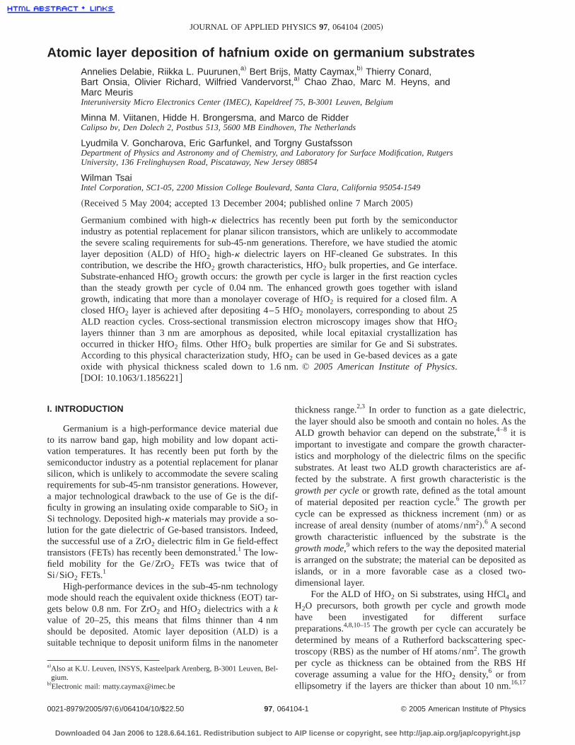
Second, XPS was used to characterize the Ge interfaceof samples with 40, 60, and 80 cycles of HfO2. The Ge3swere separated into substrate Gesat 182.2 eVd and interfa-cial GeO2 sat 184.9 eVd fFig. 1sadg. As expected, the inten-sity of the Ge signal decreased with increasing Hf coverage.The thickness of the GeO2 interfacial layer, as deduced froma three-layer model, was smalls0.3 nmd sTable Id. The Hf4fpeaks consisted of one single doublet with a peak position at17.2 eV fFig. 1sbdg. No indications for metallic Hf or Hfsuboxides were observed.
B. RBS
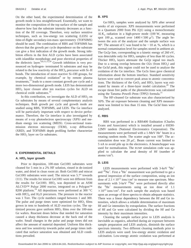
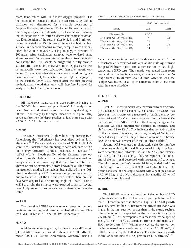
The RBS Hf content as a function of the number of ALDcycles is shown in Fig. 2. The growth per cycle in the firstten ALD reaction cycles is shown in Fig. 3. The ALD growthwas enhanced by the Ge substrate; the growth per cycle washigher in the first reaction cycles than in the steady regime.The amount of Hf deposited in the first reaction cycle is7.6 Hf/nm−2. This corresponds to almost one monolayer ofHfO2 s9.15 Hf/nm−2d, as calculated from the bulk density ofHfO2 s9.68 g cm−3d.6,26 Within few cycles, the growth percycle decreased to a steady value of about 1.1 Hf nm−2, or0.040 nm assuming the bulk density. Thus, the steady growthis similar as the case of HfO2 growth on Si substrates.4,15
TABLE I. XPS and MEIS GeOx thicknesssnmd. * not measured.
Sample
GeOx thicknesssnmd
XPS MEIS
HF-cleaned Ge 0.2–0.3 *HF-cleaned Ge+30-cycles HfO2 * 0.3HF-cleaned Ge+40-cycles HfO2 0.3 *HF-cleaned Ge+60-cycles HfO2 0.4 0.3HF-cleaned Ge+80-cycles HfO2 0.4 *
064104-3 Delabie et al. J. Appl. Phys. 97, 064104 ~2005!
Downloaded 04 Jan 2006 to 128.6.64.161. Redistribution subject to AIP license or copyright, see http://jap.aip.org/jap/copyright.jsp
C. LEIS
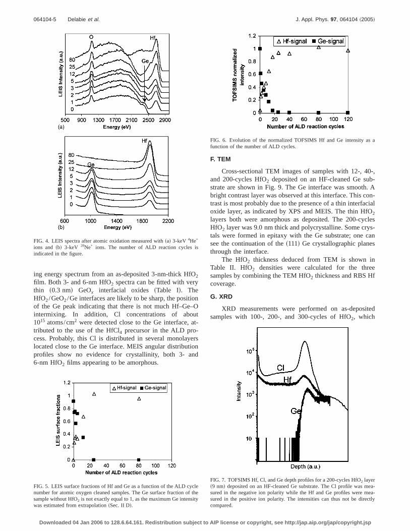
Figures 4sad and 4sbd, respectively, show the4He+ and20Ne+ LEIS spectra measured after atomic oxidation onsamples with different number of HfO2 cycles. Peaks of O,Ge, and Hf were clearly visible. No other elements wereobserved. The surface of the pure Ge wafers0 cyclesd wasoxidized, as shown by the O peak in the LEIS spectrumfFig.4sadg. With increasing number of cycles, the Ge peak de-creased and the Hf peak increased. After 25 cycles, the Gesurface was fully covered by HfO2, as shown by the absence
of a Ge peak in the20Ne+ spectrumfFig. 4sbdg. From thispoint, the Hf peak in the4He+ spectrum substantially broad-ens to the low-energy side. Asymmetric broadening origi-nates from ion scattering of Hf atoms below the surface.27
The HfO2 and Ge surface fractions, calculated by nor-malizing the LEIS Hf and Ge signals, are shown in Fig. 5.The HfO2 surface fraction increased and the Ge surface frac-tion decreased with the number of ALD reaction cycles, asexpected. After 25 cycles; the HfO2 film covers the surfacecompletely.
D. TOFSIMS
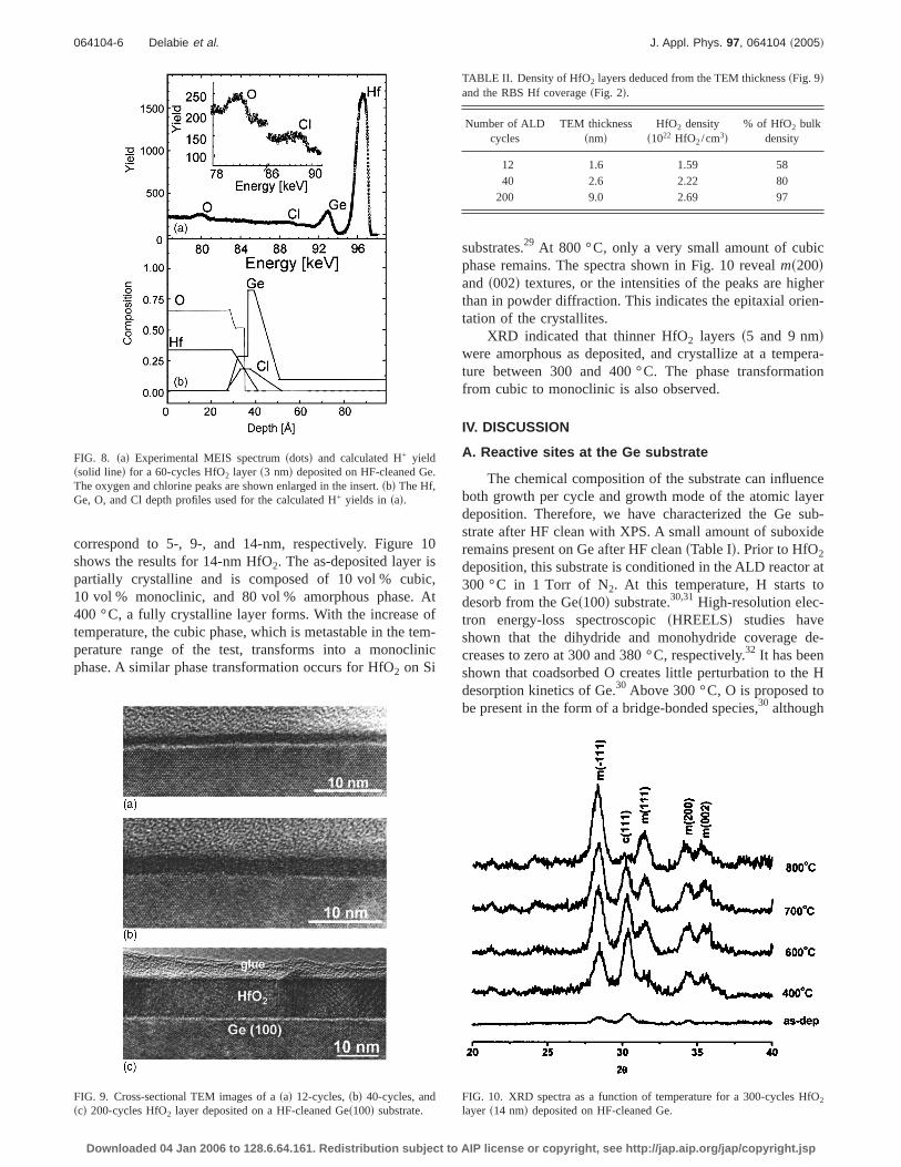
Figure 6 shows the evolution of the normalized Hf andGe intensities at the top surface, as measured by TOFSIMS.Similarly as in LEIS, the HfO2 intensity increased and theGe intensity decreased with the number of cycles. TheTOFSIMS Hf signal follows the same trend as LEIS, withsaturation around 25 reaction cycles.
TOFSIMS was also used to achieve a depth profile of theHf, Cl, and Ge intensitiessFig. 7d. No significant amount ofGe was observed in the HfO2 bulk. The shape of the Clprofile for HfO2 deposition on Hf-cleaned Ge is similar tothat for HfO2 deposited on Si substrates,28 with a Cl peak atthe bottom HfO2 interface.
E. MEIS
MEIS was used to estimate film composition and inter-facial oxide thickness. Figure 8 shows a proton backscatter-
FIG. 1. XPS spectra forsad Ge3s and sbd Hf4f for a sample with80-cycles HfO2 deposited on HF-cleaned Ge.
FIG. 2. Hf coverage measured by RBS as a function of the number of ALDreaction cycles on HF-cleaned Ge substrates.
FIG. 3. Growth per cycle from RBS in the first ten ALD reaction cycles forHF-cleaned Ge and oxygen-free Ge. The black line shows a trend linethrough the RBS data. This trend line is used for growth mode simulations.
064104-4 Delabie et al. J. Appl. Phys. 97, 064104 ~2005!
Downloaded 04 Jan 2006 to 128.6.64.161. Redistribution subject to AIP license or copyright, see http://jap.aip.org/jap/copyright.jsp
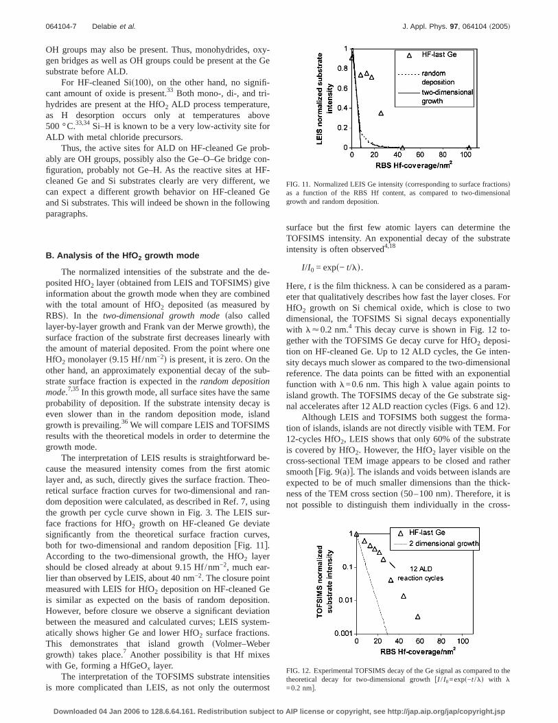
ing energy spectrum from an as-deposited 3-nm-thick HfO2
film. Both 3- and 6-nm HfO2 spectra can be fitted with verythin s0.3 nmd GeOx interfacial oxides sTable Id. TheHfO2/GeO2/Ge interfaces are likely to be sharp, the positionof the Ge peak indicating that there is not much Hf–Ge–Ointermixing. In addition, Cl concentrations of about1015 atoms/cm2 were detected close to the Ge interface, at-tributed to the use of the HfCl4 precursor in the ALD pro-cess. Probably, this Cl is distributed in several monolayerslocated close to the Ge interface. MEIS angular distributionprofiles show no evidence for crystallinity, both 3- and6-nm HfO2 films appearing to be amorphous.
F. TEM
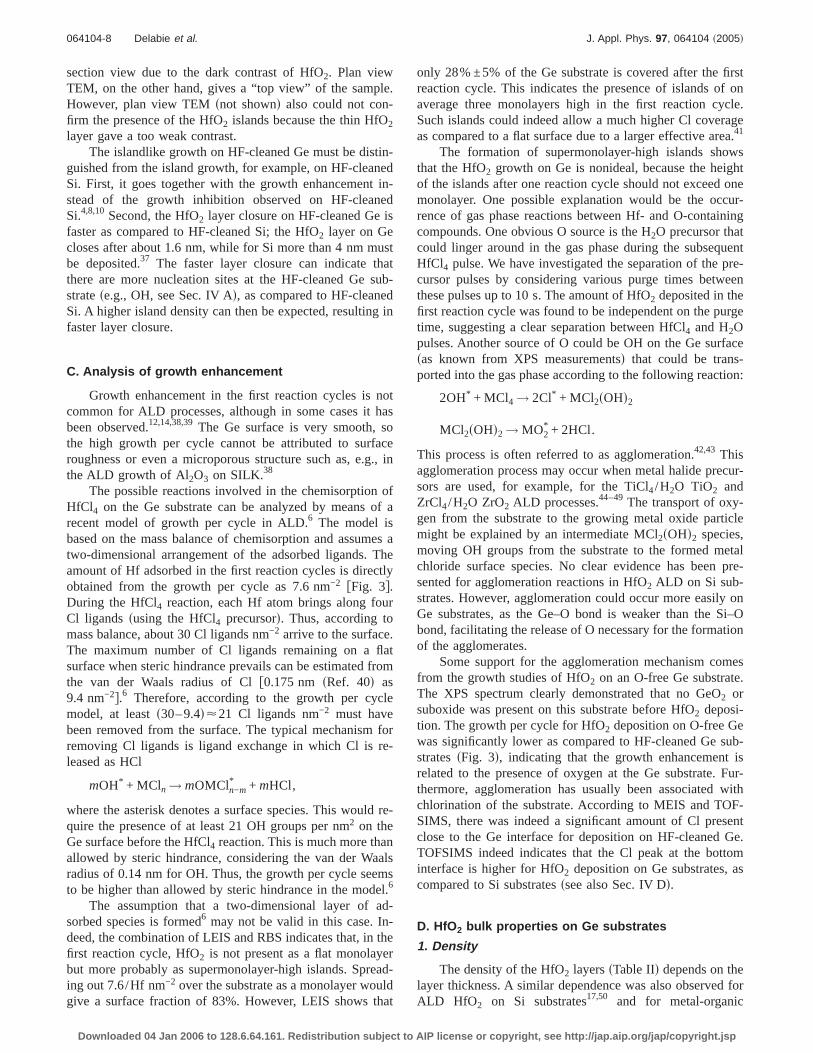
Cross-sectional TEM images of samples with 12-, 40-,and 200-cycles HfO2 deposited on an HF-cleaned Ge sub-strate are shown in Fig. 9. The Ge interface was smooth. Abright contrast layer was observed at this interface. This con-trast is most probably due to the presence of a thin interfacialoxide layer, as indicated by XPS and MEIS. The thin HfO2
layers both were amorphous as deposited. The 200-cyclesHfO2 layer was 9.0 nm thick and polycrystalline. Some crys-tals were formed in epitaxy with the Ge substrate; one cansee the continuation of thes111d Ge crystallographic planesthrough the interface.
The HfO2 thickness deduced from TEM is shown inTable II. HfO2 densities were calculated for the threesamples by combining the TEM HfO2 thickness and RBS Hfcoverage.
G. XRD
XRD measurements were performed on as-depositedsamples with 100-, 200-, and 300-cycles of HfO2, which
FIG. 4. LEIS spectra after atomic oxidation measured withsad 3-keV 4He+
ions and sbd 3-keV 20Ne+ ions. The number of ALD reaction cycles isindicated in the figure.
FIG. 5. LEIS surface fractions of Hf and Ge as a function of the ALD cyclenumber for atomic oxygen cleaned samples. The Ge surface fraction of thesample without HfO2 is not exactly equal to 1, as the maximum Ge intensitywas estimated from extrapolationsSec. II Dd.
FIG. 6. Evolution of the normalized TOFSIMS Hf and Ge intensity as afunction of the number of ALD cycles.
FIG. 7. TOFSIMS Hf, Cl, and Ge depth profiles for a 200-cycles HfO2 layers9 nmd deposited on an HF-cleaned Ge substrate. The Cl profile was mea-sured in the negative ion polarity while the Hf and Ge profiles were mea-sured in the positive ion polarity. The intensities can thus not be directlycompared.
064104-5 Delabie et al. J. Appl. Phys. 97, 064104 ~2005!
Downloaded 04 Jan 2006 to 128.6.64.161. Redistribution subject to AIP license or copyright, see http://jap.aip.org/jap/copyright.jsp
correspond to 5-, 9-, and 14-nm, respectively. Figure 10shows the results for 14-nm HfO2. The as-deposited layer ispartially crystalline and is composed of 10 vol % cubic,10 vol % monoclinic, and 80 vol % amorphous phase. At400 °C, a fully crystalline layer forms. With the increase oftemperature, the cubic phase, which is metastable in the tem-perature range of the test, transforms into a monoclinicphase. A similar phase transformation occurs for HfO2 on Si
substrates.29 At 800 °C, only a very small amount of cubicphase remains. The spectra shown in Fig. 10 revealms200dand s002d textures, or the intensities of the peaks are higherthan in powder diffraction. This indicates the epitaxial orien-tation of the crystallites.
XRD indicated that thinner HfO2 layers s5 and 9 nmdwere amorphous as deposited, and crystallize at a tempera-ture between 300 and 400 °C. The phase transformationfrom cubic to monoclinic is also observed.
IV. DISCUSSION
A. Reactive sites at the Ge substrate
The chemical composition of the substrate can influenceboth growth per cycle and growth mode of the atomic layerdeposition. Therefore, we have characterized the Ge sub-strate after HF clean with XPS. A small amount of suboxideremains present on Ge after HF cleansTable Id. Prior to HfO2
deposition, this substrate is conditioned in the ALD reactor at300 °C in 1 Torr of N2. At this temperature, H starts todesorb from the Ges100d substrate.30,31 High-resolution elec-tron energy-loss spectroscopicsHREELSd studies haveshown that the dihydride and monohydride coverage de-creases to zero at 300 and 380 °C, respectively.32 It has beenshown that coadsorbed O creates little perturbation to the Hdesorption kinetics of Ge.30 Above 300 °C, O is proposed tobe present in the form of a bridge-bonded species,30 although
FIG. 8. sad Experimental MEIS spectrumsdotsd and calculated H+ yieldssolid lined for a 60-cycles HfO2 layer s3 nmd deposited on HF-cleaned Ge.The oxygen and chlorine peaks are shown enlarged in the insert.sbd The Hf,Ge, O, and Cl depth profiles used for the calculated H+ yields in sad.
FIG. 9. Cross-sectional TEM images of asad 12-cycles,sbd 40-cycles, andscd 200-cycles HfO2 layer deposited on a HF-cleaned Ges100d substrate.
TABLE II. Density of HfO2 layers deduced from the TEM thicknesssFig. 9dand the RBS Hf coveragesFig. 2d.
Number of ALDcycles
TEM thicknesssnmd
HfO2 densitys1022 HfO2/cm3d
% of HfO2 bulkdensity
12 1.6 1.59 5840 2.6 2.22 80
200 9.0 2.69 97
FIG. 10. XRD spectra as a function of temperature for a 300-cycles HfO2
layer s14 nmd deposited on HF-cleaned Ge.
064104-6 Delabie et al. J. Appl. Phys. 97, 064104 ~2005!
Downloaded 04 Jan 2006 to 128.6.64.161. Redistribution subject to AIP license or copyright, see http://jap.aip.org/jap/copyright.jsp
OH groups may also be present. Thus, monohydrides, oxy-gen bridges as well as OH groups could be present at the Gesubstrate before ALD.
For HF-cleaned Sis100d, on the other hand, no signifi-cant amount of oxide is present.33 Both mono-, di-, and tri-hydrides are present at the HfO2 ALD process temperature,as H desorption occurs only at temperatures above500 °C.33,34 Si–H is known to be a very low-activity site forALD with metal chloride precursors.
Thus, the active sites for ALD on HF-cleaned Ge prob-ably are OH groups, possibly also the Ge–O–Ge bridge con-figuration, probably not Ge–H. As the reactive sites at HF-cleaned Ge and Si substrates clearly are very different, wecan expect a different growth behavior on HF-cleaned Geand Si substrates. This will indeed be shown in the followingparagraphs.
B. Analysis of the HfO 2 growth mode
The normalized intensities of the substrate and the de-posited HfO2 layersobtained from LEIS and TOFSIMSd giveinformation about the growth mode when they are combinedwith the total amount of HfO2 depositedsas measured byRBSd. In the two-dimensional growth modesalso calledlayer-by-layer growth and Frank van der Merwe growthd, thesurface fraction of the substrate first decreases linearly withthe amount of material deposited. From the point where oneHfO2 monolayers9.15 Hf/nm−2d is present, it is zero. On theother hand, an approximately exponential decay of the sub-strate surface fraction is expected in therandom depositionmode.7,35 In this growth mode, all surface sites have the sameprobability of deposition. If the substrate intensity decay iseven slower than in the random deposition mode, islandgrowth is prevailing.36 We will compare LEIS and TOFSIMSresults with the theoretical models in order to determine thegrowth mode.
The interpretation of LEIS results is straightforward be-cause the measured intensity comes from the first atomiclayer and, as such, directly gives the surface fraction. Theo-retical surface fraction curves for two-dimensional and ran-dom deposition were calculated, as described in Ref. 7, usingthe growth per cycle curve shown in Fig. 3. The LEIS sur-face fractions for HfO2 growth on HF-cleaned Ge deviatesignificantly from the theoretical surface fraction curves,both for two-dimensional and random depositionfFig. 11g.According to the two-dimensional growth, the HfO2 layershould be closed already at about 9.15 Hf/nm−2, much ear-lier than observed by LEIS, about 40 nm−2. The closure pointmeasured with LEIS for HfO2 deposition on HF-cleaned Geis similar as expected on the basis of random deposition.However, before closure we observe a significant deviationbetween the measured and calculated curves; LEIS system-atically shows higher Ge and lower HfO2 surface fractions.This demonstrates that island growthsVolmer–Webergrowthd takes place.7 Another possibility is that Hf mixeswith Ge, forming a HfGeOx layer.
The interpretation of the TOFSIMS substrate intensitiesis more complicated than LEIS, as not only the outermost
surface but the first few atomic layers can determine theTOFSIMS intensity. An exponential decay of the substrateintensity is often observed4,18
I/I0 = exps− t/ld.
Here,t is the film thickness.l can be considered as a param-eter that qualitatively describes how fast the layer closes. ForHfO2 growth on Si chemical oxide, which is close to twodimensional, the TOFSIMS Si signal decays exponentiallywith l<0.2 nm.4 This decay curve is shown in Fig. 12 to-gether with the TOFSIMS Ge decay curve for HfO2 deposi-tion on HF-cleaned Ge. Up to 12 ALD cycles, the Ge inten-sity decays much slower as compared to the two-dimensionalreference. The data points can be fitted with an exponentialfunction with l=0.6 nm. This highl value again points toisland growth. The TOFSIMS decay of the Ge substrate sig-nal accelerates after 12 ALD reaction cyclessFigs. 6 and 12d.
Although LEIS and TOFSIMS both suggest the forma-tion of islands, islands are not directly visible with TEM. For12-cycles HfO2, LEIS shows that only 60% of the substrateis covered by HfO2. However, the HfO2 layer visible on thecross-sectional TEM image appears to be closed and rathersmoothfFig. 9sadg. The islands and voids between islands areexpected to be of much smaller dimensions than the thick-ness of the TEM cross sections50–100 nmd. Therefore, it isnot possible to distinguish them individually in the cross-
FIG. 11. Normalized LEIS Ge intensityscorresponding to surface fractionsdas a function of the RBS Hf content, as compared to two-dimensionalgrowth and random deposition.
FIG. 12. Experimental TOFSIMS decay of the Ge signal as compared to thetheoretical decay for two-dimensional growthfI / I0=exps−t /ld with l=0.2 nmg.
064104-7 Delabie et al. J. Appl. Phys. 97, 064104 ~2005!
Downloaded 04 Jan 2006 to 128.6.64.161. Redistribution subject to AIP license or copyright, see http://jap.aip.org/jap/copyright.jsp
section view due to the dark contrast of HfO2. Plan viewTEM, on the other hand, gives a “top view” of the sample.However, plan view TEMsnot shownd also could not con-firm the presence of the HfO2 islands because the thin HfO2
layer gave a too weak contrast.The islandlike growth on HF-cleaned Ge must be distin-
guished from the island growth, for example, on HF-cleanedSi. First, it goes together with the growth enhancement in-stead of the growth inhibition observed on HF-cleanedSi.4,8,10Second, the HfO2 layer closure on HF-cleaned Ge isfaster as compared to HF-cleaned Si; the HfO2 layer on Gecloses after about 1.6 nm, while for Si more than 4 nm mustbe deposited.37 The faster layer closure can indicate thatthere are more nucleation sites at the HF-cleaned Ge sub-stratese.g., OH, see Sec. IV Ad, as compared to HF-cleanedSi. A higher island density can then be expected, resulting infaster layer closure.
C. Analysis of growth enhancement
Growth enhancement in the first reaction cycles is notcommon for ALD processes, although in some cases it hasbeen observed.12,14,38,39The Ge surface is very smooth, sothe high growth per cycle cannot be attributed to surfaceroughness or even a microporous structure such as, e.g., inthe ALD growth of Al2O3 on SILK.38
The possible reactions involved in the chemisorption ofHfCl4 on the Ge substrate can be analyzed by means of arecent model of growth per cycle in ALD.6 The model isbased on the mass balance of chemisorption and assumes atwo-dimensional arrangement of the adsorbed ligands. Theamount of Hf adsorbed in the first reaction cycles is directlyobtained from the growth per cycle as 7.6 nm−2 fFig. 3g.During the HfCl4 reaction, each Hf atom brings along fourCl ligands susing the HfCl4 precursord. Thus, according tomass balance, about 30 Cl ligands nm−2 arrive to the surface.The maximum number of Cl ligands remaining on a flatsurface when steric hindrance prevails can be estimated fromthe van der Waals radius of Clf0.175 nm sRef. 40d as9.4 nm−2g.6 Therefore, according to the growth per cyclemodel, at leasts30–9.4d<21 Cl ligands nm−2 must havebeen removed from the surface. The typical mechanism forremoving Cl ligands is ligand exchange in which Cl is re-leased as HCl
mOH* + MCln → mOMCln−m* + mHCl,
where the asterisk denotes a surface species. This would re-quire the presence of at least 21 OH groups per nm2 on theGe surface before the HfCl4 reaction. This is much more thanallowed by steric hindrance, considering the van der Waalsradius of 0.14 nm for OH. Thus, the growth per cycle seemsto be higher than allowed by steric hindrance in the model.6
The assumption that a two-dimensional layer of ad-sorbed species is formed6 may not be valid in this case. In-deed, the combination of LEIS and RBS indicates that, in thefirst reaction cycle, HfO2 is not present as a flat monolayerbut more probably as supermonolayer-high islands. Spread-ing out 7.6/Hf nm−2 over the substrate as a monolayer wouldgive a surface fraction of 83%. However, LEIS shows that
only 28% ±5% of the Ge substrate is covered after the firstreaction cycle. This indicates the presence of islands of onaverage three monolayers high in the first reaction cycle.Such islands could indeed allow a much higher Cl coverageas compared to a flat surface due to a larger effective area.41
The formation of supermonolayer-high islands showsthat the HfO2 growth on Ge is nonideal, because the heightof the islands after one reaction cycle should not exceed onemonolayer. One possible explanation would be the occur-rence of gas phase reactions between Hf- and O-containingcompounds. One obvious O source is the H2O precursor thatcould linger around in the gas phase during the subsequentHfCl4 pulse. We have investigated the separation of the pre-cursor pulses by considering various purge times betweenthese pulses up to 10 s. The amount of HfO2 deposited in thefirst reaction cycle was found to be independent on the purgetime, suggesting a clear separation between HfCl4 and H2Opulses. Another source of O could be OH on the Ge surfacesas known from XPS measurementsd that could be trans-ported into the gas phase according to the following reaction:
2OH* + MCl4 → 2Cl* + MCl2sOHd2
MCl2sOHd2 → MO2* + 2HCl.
This process is often referred to as agglomeration.42,43 Thisagglomeration process may occur when metal halide precur-sors are used, for example, for the TiCl4/H2O TiO2 andZrCl4/H2O ZrO2 ALD processes.44–49The transport of oxy-gen from the substrate to the growing metal oxide particlemight be explained by an intermediate MCl2sOHd2 species,moving OH groups from the substrate to the formed metalchloride surface species. No clear evidence has been pre-sented for agglomeration reactions in HfO2 ALD on Si sub-strates. However, agglomeration could occur more easily onGe substrates, as the Ge–O bond is weaker than the Si–Obond, facilitating the release of O necessary for the formationof the agglomerates.
Some support for the agglomeration mechanism comesfrom the growth studies of HfO2 on an O-free Ge substrate.The XPS spectrum clearly demonstrated that no GeO2 orsuboxide was present on this substrate before HfO2 deposi-tion. The growth per cycle for HfO2 deposition on O-free Gewas significantly lower as compared to HF-cleaned Ge sub-stratessFig. 3d, indicating that the growth enhancement isrelated to the presence of oxygen at the Ge substrate. Fur-thermore, agglomeration has usually been associated withchlorination of the substrate. According to MEIS and TOF-SIMS, there was indeed a significant amount of Cl presentclose to the Ge interface for deposition on HF-cleaned Ge.TOFSIMS indeed indicates that the Cl peak at the bottominterface is higher for HfO2 deposition on Ge substrates, ascompared to Si substratesssee also Sec. IV Dd.
D. HfO2 bulk properties on Ge substrates
1. Density
The density of the HfO2 layerssTable IId depends on thelayer thickness. A similar dependence was also observed forALD HfO 2 on Si substrates17,50 and for metal-organic
064104-8 Delabie et al. J. Appl. Phys. 97, 064104 ~2005!
Downloaded 04 Jan 2006 to 128.6.64.161. Redistribution subject to AIP license or copyright, see http://jap.aip.org/jap/copyright.jsp
chemical-vapor deposition sMOCVDd HfO2 on Sisubstrates.50 The low density of the thinnest layers couldreflect their island morphology. For closed HfO2 layers onGe substrates, a density of more than 80% of the bulk den-sity is obtained. This is in agreement with the density ofALD HfO 2 deposited on Si substrates with similarthickness.4,17
2. Ge/Hf intermixing
TOFSIMS depth profilessFig. 7d indicate no significantconcentration of Ge in the HfO2 bulk, in contrast to what isobserved, for example, for HfO2 deposited by MOCVD onHF-cleaned Ge substrates.51
3. Impurities
Both TOFSIMS and MEIS show some Cl in the ALDHfO2 films due to the use of the HfCl4 precursor. TOFSIMSindicates a similar bulk Cl content for Ge and Si substrates.However, the Cl peak at the bottom interface is higher for Gesubstrates. This could be due to substrate chlorination reac-tions associated with the agglomeration process. MEIS indi-cates a Cl content close to the Ge interface of about10 Cl/nm2. As this Cl content corresponds to about onemonolayer, the Cl is probably distributed in several mono-layers located close to the Ge interface.
4. Crystallization behavior
Cross-sectional TEM, XRD, and MEIS show that thinHfO2 layers s,9 nmd are amorphous as deposited. XRDshows that a 14-nm-thick HfO2 layer is partially crystalline,with some HfO2 grains oriented in epitaxy with the Ge sub-stratesFig. 10d. XRD and TEM disagree on the critical HfO2thickness at which crystallization starts to occur. With TEM,crystals are already observed in a 9-nm HfO2 layer. On theother hand, XRD shows no diffraction peaks for a 9-nmHfO2, but they appear for a 14-nm HfO2 layer. The sensitiv-ity of XRD is probably not sufficient to detect a limitedamount of crystalline phase. Alternatively, the crystallites ob-served in a 9-nm layer by TEM might have grown in such anorientation that grazing incidence XRD cannot detect them.
The fact that thin films are amorphous implies that alsothicker layers are amorphous in the first stages of the depo-sition process. As such, epitaxial crystallization occurs in alater stage of the ALD process, not during the ALD gas-substrate reactions itself. The presence of small amounts ofO or Cl at the Ge interface and the lattice mismatch betweenthe Ge and HfO2 probably locally hinders full epitaxial crys-tallization of the HfO2 film. Local epitaxial ZrO2 crystalswere also observed for a 5.5-nm ZrO2 layer deposited byALD on HF vapor-cleaned Ges100d substrates39 and forHfO2 deposited by MOCVD on Ge.51
The crystallization behavior as a function of tempera-ture, as studied by means of XRD, is similar for Ge and Sichemical oxide substrates.29 A fully crystalline layer formsduring a thermal treatment at low temperature. With the in-crease of temperature, the transformation from cubic to
monoclinic phase is observed. The main difference for Geand Si substrates is that no epitaxial crystallization was ob-served on Si.
E. The Ge interface
The interface between HfO2 and the Ge channel will beparticularly important in regard to device performance. First,the presence of low-quality Ge oxide or suboxide may de-grade the electrical performance. Second, the thickness of theinterfacial layer swith low-k valued directly adds to theequivalent oxide thicknesssEOTd of the high-k stack. Itshould therefore be as thin as possible if subnanometer EOTtargets are aimed for.
The cross-sectional TEM imagessFig. 9d show a smoothGe interface with no obvious indication of an interfaciallayer. XPS and MEIS investigations both indicate the pres-ence of a thinsabout 0.3 nmd oxide interfacial layer. More-over, the XPS binding energy of the Ge3s lines indicates thatthe chemical composition of the interfacial layer is GeO2.
The stability of the interfacial oxide layer during air ex-posure is important in case the gate is subsequently depositedex situ. For nonclosed HfO2 layers deposited on Ge, ellip-someter measurements show a thickness increase during airexposure due to interfacial oxide growth. LEIS also indicatesthat nonclosed HfO2 layers on Ge are not stable during cal-cinations at 300 °C. For ZrO2 and Al2O3 layers deposited onSi substrates, it has also been reported that interfacial oxideforms easily during air exposure when the high-k layers arenot fully closed.37,52 Closed HfO2 layers on Ge, on the otherhand, are stable during air exposure.
V. CONCLUSIONS
We have demonstrated the atomic layer deposition ofHfO2 on HF-cleaned Ge substrates using the HfCl4 and H2Oprecursors. According to this physical characterization study,the physical thickness of HfO2 dielectric layers grown onHF-cleaned Ge can be scaled down to about 1.6 nm. Opti-mization of the surface preparation resulting in a more two-dimensional growth mode may allow the further scaling ofdielectrics layers to less than 1.6 nm. A second critical issuefor the ultimate scaling of the Ge/high-k stacks is the inter-facial layer. A promising observation for HfO2 stacks depos-ited on HF-cleaned Ge is that the bottom interfacial layer isless than 0.4 nm thin. The scaling potential combined withthe high mobility of the Ge substrate makes the Ge/high-kstacks promising for high-performance complementarymetal-oxide semiconductorsCMOSd applications.
ACKNOWLEDGMENTS
Jan Vansteenbergen is acknowledged for substantial as-sistance with Ge substrate cleaning. Jan Willem Maes, OttoLaitinen, and Hilde De WittesASM Belgiumd are kindlyacknowledged for their contribution in the preparation of theHfO2 samples. The authors are grateful to Umicore for pro-viding the Ge substrates. Cees van der Marel and PaulPijpers from Philips Electronics Nederland B.V., Eindhovenare kindly acknowledged for XPS analysis of the Ge/HfO2
samples. One of the authorssR.L.Pd acknowledges a post-
064104-9 Delabie et al. J. Appl. Phys. 97, 064104 ~2005!
Downloaded 04 Jan 2006 to 128.6.64.161. Redistribution subject to AIP license or copyright, see http://jap.aip.org/jap/copyright.jsp
doctoral fellowship by IMEC/K.U. Leuven and support fromthe Academy of FinlandsGrant Nos. 105364 and 202633d.
1C. O. Chui, H. Kim, D. Chi, B. B. Triplett, P. C. McIntyre, and K. C.Saraswat, Tech. Dig. - Int. Electron Devices Meet.2002, 437.
2S. M. George, A. W. Ott, and J. W. Klaus, J. Phys. Chem.100, 13121s1996d.
3M. Ritala and M. Leskelä, inHandbook of Thin Film Materials, edited byH. S. NalwasAcademic, New York, 2002d, Vol. 1, p. 103.
4M. L. Greenet al., J. Appl. Phys.92, 7168s2002d.5A. Sattaet al., J. Appl. Phys.92, 7641s2002d.6R. L. Puurunen, Chem. Vap. Deposition9, 249 s2003d.7R. L. Puurunen, Chem. Vap. Deposition10, 159 s2004d.8R. L. Puurunen, J. Appl. Phys.95, 4777s2004d.9H. Lüth, Surfaces and Interfaces of SolidssSpringer, Berlin, 1993d, p. 94.
10M. A. Alam and M. L. Green, J. Appl. Phys.94, 3403s2003d.11M. Caymaxet al., ALD2002 Conference, 19–21 August 2002, Seoul, Ko-
rea sunpublishedd.12S. Haukka, M. Tuominen, E. Vainonen-Ahlgren, E. Tois, and W.-M. Li,
203th meeting of the Electrochemical Society, 24 April–2 May 2003 Paris,Francesunpublishedd.
13A. Delabieet al., Mater. Res. Soc. Symp. Proc.745, 179 s2003d.14D. Blin et al., 203th Meeting of the Electrochemical Society, 24 April–2
May 2003, Paris, Francesunpublishedd.15E. P. Gusev, C. Cabral, Jr., M. Copel, C. D’Emic, and M. Gribelyuk,
Microelectron. Eng.69, 145 s2003d.16W. Vandervorstet al., Mater. Res. Soc. Symp. Proc.745, 23 s2003d.17H. Benderet al., Proc.-Electrochem. Soc.3, 223 s2003d.18T. Conard, W. Vandervorst, J. Petry, C. Zhao, W. Besling, H. Nohira, and
O. Richard, Appl. Surf. Sci.400, 203 s2003d.19ALCVD™ and Polygon™ 8200 are trademarks of ASM International nv.20P. S. Cumpson, Surf. Interface Anal.29, 403 s2000d.21S. Tanuma, C. J. Powell, and D. R. Penn, Surf. Interface Anal.21, 165
s1994d.22F. van der Veen, Surf. Sci. Rep.5, 199 s1985d.23T. Gustafsson, H. C. Lu, B. W. Busch, W. H. Schulte, and E. Garfunkel,
Nucl. Instrum. Methods Phys. Res. B183, 146 s2001d.24R. M. Tromp, M. Copel, M. C. Reuter, M. Horn von Hoegen, J. Speidell,
and R. Koudijs, Rev. Sci. Instrum.62, 2679s1991d.25W. H. Schulte, B. W. Busch, E. Garfunkel, T. Gustafsson, G. Schiwietz,
and P. L. Grande, Nucl. Instrum. Methods Phys. Res. B1883, 16 s2001d.26R. C. Weast and M. J. Astle,CRC Handbook of Chemistry and Physics
sCRC, Florida, 1994d, p. B-73–166.27G. C. van Leerdam, K.-M. H. Lenssen, and H. H. Brongersma, Nucl.
Instrum. Methods Phys. Res. B45, 390 s1990d.
28S. Ferrari, G. Scarel, C. Wiemer, and M. Fanciulli, J. Appl. Phys.92, 7675s2002d.
29C. Zhao, G. Roebben, M. Heyns, and O. van der Biest, Key Eng. Mater.206, 1285s2002d.
30S. M. Cohen, Y. L. Yang, E. Rouchouze, T. Jin, and M. P. D’Evelyn, J.Vac. Sci. Technol. A10, 2166s1992d.
31J. Y. Lee, J. Y. Maeng, A. Kim, Y. E. Cho, and S. Kim, J. Chem. Phys.118, 1929s2003d.
32L. Pagagno, X. Y. Shen, J. Anderson, G. Schirripa Spagnolo, and G. J.Lapeyre, Phys. Rev. B34, 7188s1986d.
33Y. J. Chabal, G. S. Higashi, K. Raghavachari, and V. A. Burrows, J. Vac.Sci. Technol. A 7, 2104s1989d.
34D. W. Greve, Mater. Sci. Eng., B18, 22 s1993d.35M. de Ridderet al., J. Phys. Chem. B106, 13146s2002d.36R. L. Puurunen and W. Vandervorst, J. Appl. Phys.96, 7686s2004d.37H. Benderet al., in Extended Abstracts of International Workshop on Gate
Insulator, edited by M. Hirose, S. Sakai, and H. IwaisBusiness Center forAcademic Societies Japan, Tokyo, 2001d, p. 86.
38J. W. Elam, C. A. Wilson, M. Schuisky, Z. A. Sechrist, and S. M. George,J. Vac. Sci. Technol. B21, 1099s2003d.
39H. Kim, C. O. Chui, K. C. Saraswat, and P. C. McIntyre, Appl. Phys. Lett.83, 2647s2003d.
40G. E. Rodgers,Introduction to Coordination, Solid State, and DescriptiveInorganic ChemistrysMcGraw–Hill, Singapore, 1994d, p. 164.
41For example, the RBS Hf coverage and LEIS HfO2 surface fraction in thefirst cycle can be reproduced assuming a cylindrical shape of the HfO2
islands with height of 1 nm and radius 0.3 nm, with a distribution of oneisland per nm2. The cylindrical configuration would allow a much highermaximum Cl coverage, of about 23 Cl/nm2.
42S. Haukka, E.-L. Lakomaa, and A. Root, J. Phys. Chem.97, 5085s1993d.43S. Haukka, E.-L. Lakomaa, O. Jylhä, J. Vilhunen, and S. Hornytzkyj,
Langmuir 9, 3497s1993d.44P. J. Kooyman, P. van der Waal, P. A. J. Verdaasdonk, K. C. Jansen, and H.
van Bekkum, Catal. Lett.13, 229 s1992d.45A. Kytökivi, E.-L. Lakomaa, and A. Root, Langmuir12, 4395s1996d.46M. Ritala and M. Leskelä, Thin Solid Films225, 288 s1993d.47M. Ritala, M. Leskelä, L.-S. Johansson, and L. Niinistö, Thin Solid Films
228, 32 s1993d.48M. Ritala and M. Leskelä, Appl. Surf. Sci.75, 333 s1994d.49M. Ritala, M. Leskelä, L. Niinistö, T. Prohaska, G. Friedbacher, and M.
Grassenbauer, Thin Solid Films250, 72 s1994d.50M. Caymaxet al., Mater. Res. Soc. Symp. Proc.765, D2.6.1s2003d.51S. Van Elshocht, Mater. Res. Soc. Symp. Proc.809, 287 s2004d.52W. F. A. Beslinget al., J. Non-Cryst. Solids303, 123 s2002d.
064104-10 Delabie et al. J. Appl. Phys. 97, 064104 ~2005!
Downloaded 04 Jan 2006 to 128.6.64.161. Redistribution subject to AIP license or copyright, see http://jap.aip.org/jap/copyright.jsp