electron-doping induced semiconductor to metal transitions
TRANSCRIPT
1
Electron-Doping Induced Semiconductor to Metal
Transitions in ZrSe2 Layers via Copper Atomic
Intercalation
Zahir Muhammad1, Kejun Mu1, Haifeng Lv2, Chuanqiang Wu1, Zia ur Rehman1, Muhammad
Habib1, Zhe Sun1,* , Xiaojun Wu2 and Li Song1,*
1National Synchrotron Radiation Laboratory, CAS Center for Excellence in Nanoscience, CAS
Key Laboratory of Strongly-coupled Quantum Matter Physics, University of Science and
Technology of China, Hefei, Anhui, 230029, China.
2CAS Key Laboratory of Materials for Energy Conservation, Synergetic Innovation Centre of
Quantum Information & Quantum Physics, CAS Center for Excellence in Nanoscience, and
Department of Material Science and Engineering, University of Science and Technology of China,
Hefei, Anhui 230026, China.
KEYWORDS: Layered Materials, Phase Transition, Angle Resolved Photoemission
Spectroscopy, Electron Doping

2
ABSTRACT: Atomic intercalation in two dimensional (2D) layered materials can engineer the
electronic structure at the atomic scale, bringing out tunable physical and chemical properties
which are quite distinct in comparison with pristine one. Among them, electron-doped engineering
induced by intercalation is an efficient route to modulate electronic states in 2D layers. Herein, we
demonstrate a semiconducting to the metallic phase transition in zirconium diselenide (ZrSe2)
single crystal via controllable incorporation of copper (Cu) atoms. Combined with first-principles
density functional theory (DFT) calculations, our angle resolved photoemission spectroscopy
(ARPES) characterizations clearly revealed the emergence of conduction band dispersion at M/L
point of Brillouin zone due to Cu-induced electron doping in ZrSe2 interlayers. Moreover, the
field-effect transistor (FET) fabricated on ZrSe2 displayed a n-type semiconducting transport
behavior, while the Cu-intercalated ZrSe2 posed linear Ids vs Vds curves with metallic character
shows n-type doping. The atomic intercalation approach has high potential for realizing transparent
electron-doping systems for many specific 2D-based electronics.
3
Layered transition metal dichalcogenides (TMDCs) MX2 (M = Mo, W, Zr, Hf; X = S, Se)
semiconductors have captivated widespread interest due to their significant superior physical and
electrical properties.1-6 The crystalline forms of 2D materials have been the subject of intense
investigation owing to their unique physical properties7, such as direct electronic bandgap in the
single-layer limit8-12, valence band (VB) splitting12-16, valley degree of freedom17-21, and excitonic
nature of optical band spectra22-26. Artem et al. recently observed the, the co-occurrence of
exchange splitting and giant SOC in graphene at the same time with good magnetic
characteristics27. Thus, TMDCs are considered as an ideal materials for p–n junctions28, field–
effect transistors with high mobility of electrons29-31, memory and switching devices32,
optoelectronics and photovoltaic applications33. These layered materials can also be found in
different forms of hybrid or in heterostructure forms.34-37 Particularly, the atomic phase
engineering can result in observation of tremendous novel physical and electronic phenomena.38-
42 Among them, the intercalation of electron-donating atoms has been an effective method to
modulate intrinsic electronic properties, such as shifting the fermi level to higher or lower energy43,
changing band gap characteristics44- 46 and inducing phase transitions.47, 48 Morosan et al. reported
that the phase transition arising at Fermi level in Cu-intercalated TiSe2 could give rise to the new
superconducting state in TiSe2.49 Topological phase transition occurred in BiTl(S1−δSeδ)2 and
Bi2Se3, as well as superconductivity in CuxZrTe2-y with different doping ratio of Se, Co-
phthalocyanine and Cu atoms respectively.50-52 Similarly, Tsipas et al. recently observed the
semimetallic phase with massless Dirac Fermions is in ZrTe2.53 The structure and electronic
properties of the materials can be ascribes as a semiconductor or a semimetallic states with a small
indirect or direct gap can be suppressed by intercalation or elemental doping.3, 16, 18-22, 31, 49
Likewise, the semiconductor to metal transition was witnessed MoTe2 by strain or structural and
4
electronic phase transition by W substitution.54 In principle, the states of quantum matter: charge
density waves, insulators, and superconductors can be ascribed from the spectral energy gap with
different bandgap structures.55-57 Therefore, the fundamental changes in the band structure can
provide vital information for considering and controlling physical and electronic properties.58
In this particular work, we synthesized Cu-intercalated zirconium diselenide (ZrSe2) single
crystals via chemical vapor transport technique (CVT), and investigated the change in electronic
properties in comparison with pristine ZrSe2 by combining synchrotron-based Angle Resolved
Photoemission Spectroscopy (ARPES) with first-principles density functional theory (DFT)
calculations. With the intercalation of Cu atoms, more electrons fill the bottom of conduction
bands of ZrSe2, which change the electronic structure from semiconducting to metallic characters.
Notably, this presented intercalation approach does not induce notable changes of crystal structure
and overall band dispersions, indicating its high potentials for clean electron doping systems.
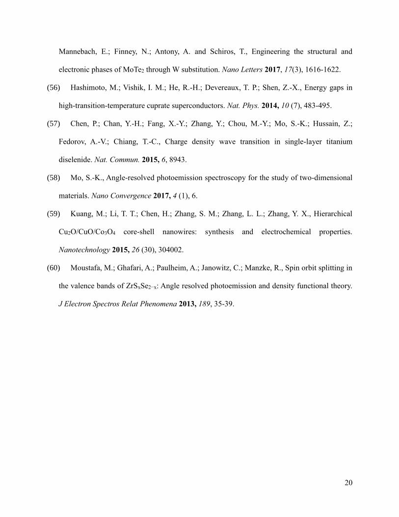
A high quality ZrSe2 and Cu intercalated ZrSe2 (CuxZrSe2, x = 0.07, x value was determined
by ICP) single crystals were synthesized via an improved CVT method. The experimental detail
of CVT synthesis is provided in the experimental part of the paper. The single crystal X-ray
diffraction (XRD) patterns recorded on ZrSe2 and Cu0.07ZrSe2 samples at room temperature are
shown in Fig. 1. The (001), (002), (003) and (004) peaks indicate the high quality single crystals
of both samples. The diffraction peaks emerged at the same angles in both ZrSe2 and Cu0.07ZrSe2,
with a small change in the c-lattice constant from 6.1889Å to 6.2035Å after Cu-intercalation along
(001) plane calculated from XRD. Similarly, the peak intensities of Cu0.07ZrSe2 are enhanced,
which is due to its increased crystallinity and other growth process. Highly crystalline large-sized
single crystals of ZrSe2 and Cu0.07ZrSe2 can be seen inside the XRD figure having a typical lateral
size of ~0.8-1cm with silver grey colour and hexagonal shape respectively.
5
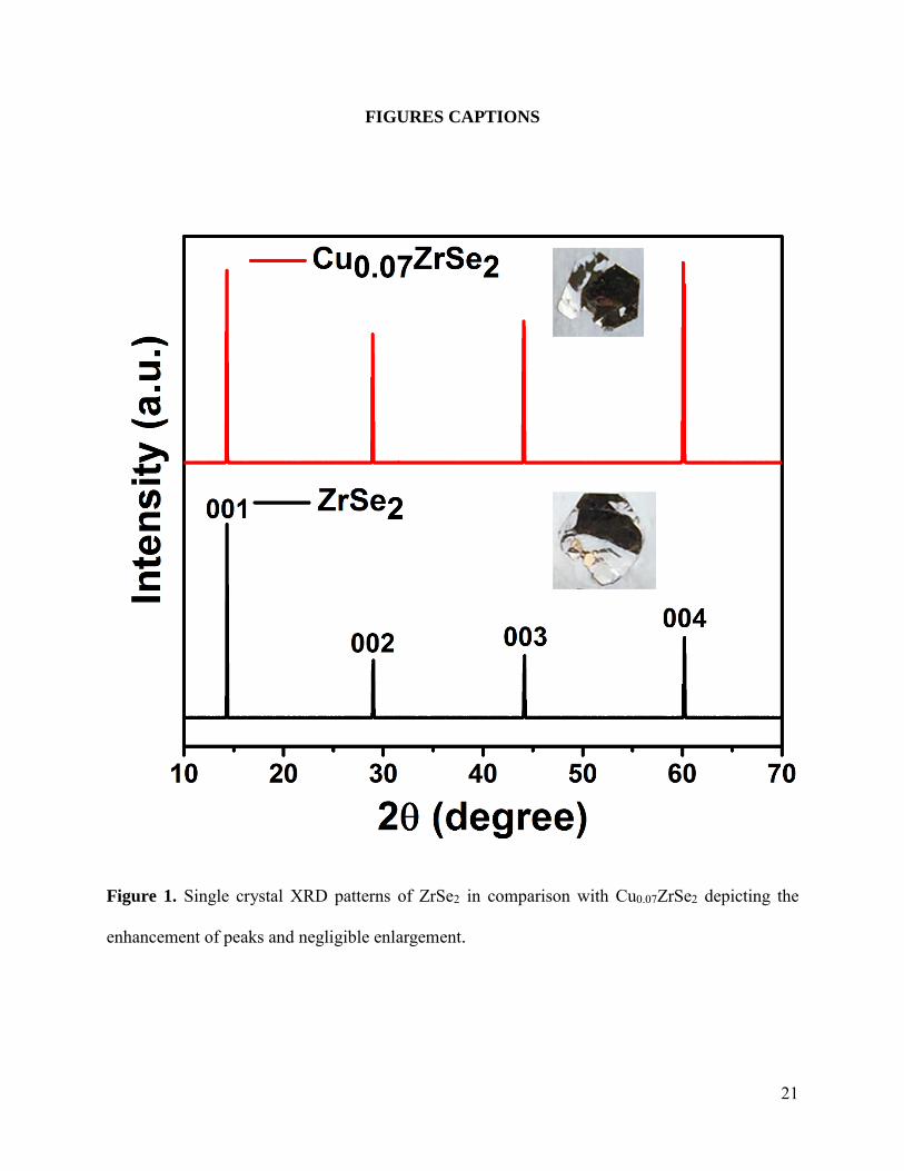
To investigate the chemical compositions and elemental ratio in the grown crystals, X-ray
photoelectron spectroscopy (XPS) was performed. Typical XPS spectra of ZrSe2 and Cu0.07ZrSe2
are shown in Fig. 2. For ZrSe2, the obvious Zr 3d (Zr-3d5/2, Zr-3d3/2) peaks at 183.05 eV and 185
eV are displayed, along with clear Se 3d (Se-3d5/2, Se-3d3/2) peaks at 53.55 eV and 54.2 eV. These
peak positions indicate the similar chemical bonding state for both ZrSe2 and Cu0.07ZrSe2, with a
small displacement of Zr-3d3/2 to lower energy, while donating electron to Se atoms and Se-3d to
higher energy due to the emergence of electrons from Zr and Cu atoms in case of Cu0.07ZrSe2.
Moreover, Fig. 2(c) shows Cu 2p (Cu-2p3/2 and Cu-2p1/2) peaks at 932.2 eV and 952.2 eV. There
is no satellite peak of Cu2+ in the obtained Cu0.07ZrSe2 crystals, instead Cu+1 peak is visible. This
can be ascribed to the electron donation from the intercalated Cuo atoms to ZrSe2 layers, resulting
in Cu+1 state that is consistent with previous Cu-substituted compounds.59
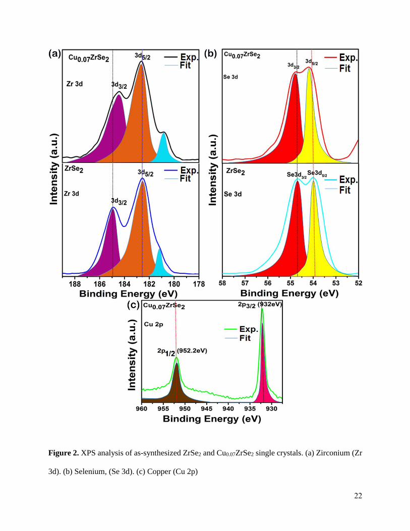
In order to investigate the detailed local microstructure, compositions and topographical
information with an atomic arrangement, we employed a high resolution scanning transmission
electron microscopy (STEM) on Cu0.07ZrSe2. Fig. 3(a) is typical Z-contrast high resolution image
recorded through STEM, showing the surface topography of atoms. It reveals a regular structure
with perfect hexagonal atomic arrangement as indicated by inset red line frame. The microstructure
of Cu0.07ZrSe2 is similar to that of pristine ZrSe2 (see HRTEM image in Fig. S1). Fig. 3(b) shows
a sketch of elemental configuration of ZrSe2 with a hexagonal arrangements. The layered structure
(Zr-Se) is indicating the hexagonal structure of Cu0.07ZrSe2 having two planes of Se atoms
separated by Zr atoms with Cu ions randomly intercalated between the layers. Similarly, Fig. 3(c)
shows a uniform structure of different layers with a d-spacing of about 2.29 Å that corresponds to
(002) and Zr-Zr atom bond length of 1.73 Å corresponding to (003) lattice plane. From the d-
spacing, it has been observed that Cu0.07ZrSe2 have the same layers spacing as that of ZrSe2, with
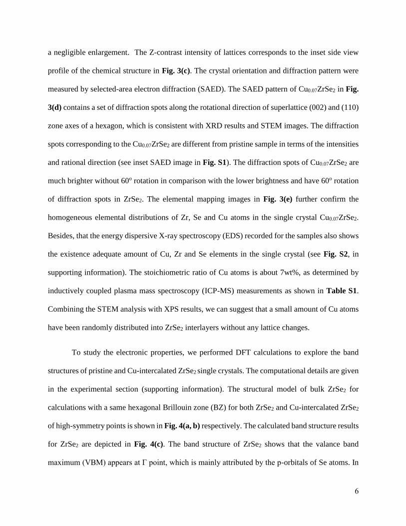
6
a negligible enlargement. The Z-contrast intensity of lattices corresponds to the inset side view
profile of the chemical structure in Fig. 3(c). The crystal orientation and diffraction pattern were
measured by selected-area electron diffraction (SAED). The SAED pattern of Cu0.07ZrSe2 in Fig.
3(d) contains a set of diffraction spots along the rotational direction of superlattice (002) and (110)
zone axes of a hexagon, which is consistent with XRD results and STEM images. The diffraction
spots corresponding to the Cu0.07ZrSe2 are different from pristine sample in terms of the intensities
and rational direction (see inset SAED image in Fig. S1). The diffraction spots of Cu0.07ZrSe2 are
much brighter without 60o rotation in comparison with the lower brightness and have 60o rotation
of diffraction spots in ZrSe2. The elemental mapping images in Fig. 3(e) further confirm the
homogeneous elemental distributions of Zr, Se and Cu atoms in the single crystal Cu0.07ZrSe2.
Besides, that the energy dispersive X-ray spectroscopy (EDS) recorded for the samples also shows
the existence adequate amount of Cu, Zr and Se elements in the single crystal (see Fig. S2, in
supporting information). The stoichiometric ratio of Cu atoms is about 7wt%, as determined by
inductively coupled plasma mass spectroscopy (ICP-MS) measurements as shown in Table S1.
Combining the STEM analysis with XPS results, we can suggest that a small amount of Cu atoms
have been randomly distributed into ZrSe2 interlayers without any lattice changes.
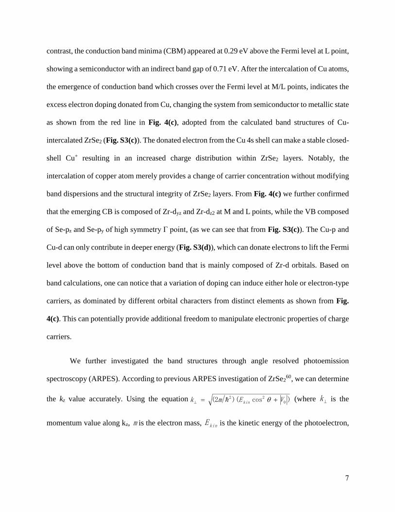
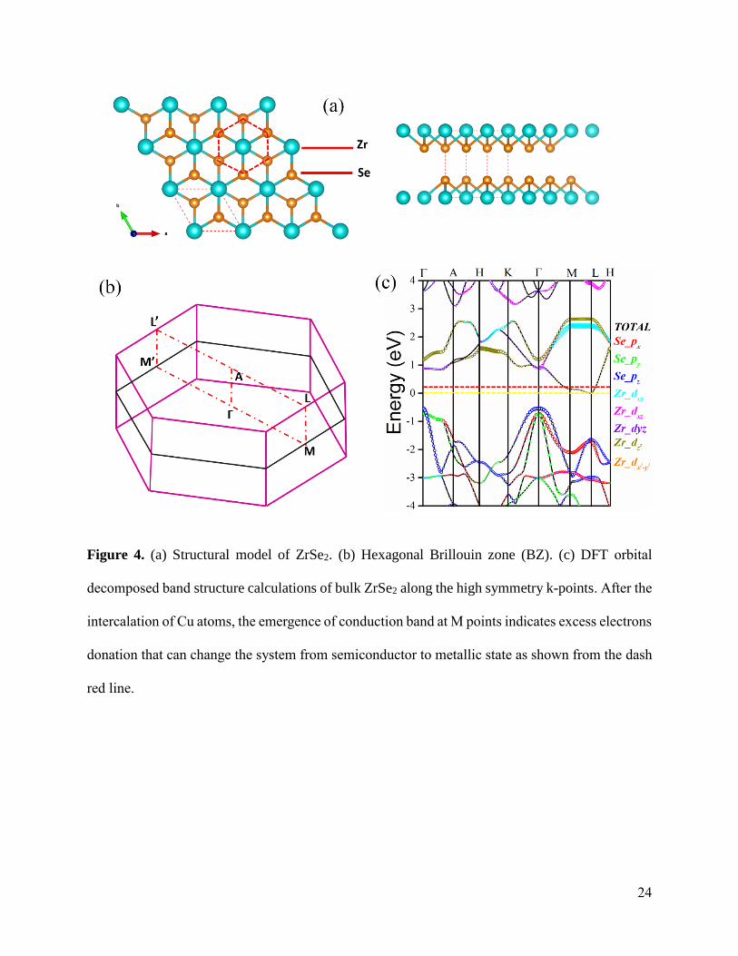
To study the electronic properties, we performed DFT calculations to explore the band
structures of pristine and Cu-intercalated ZrSe2 single crystals. The computational details are given
in the experimental section (supporting information). The structural model of bulk ZrSe2 for
calculations with a same hexagonal Brillouin zone (BZ) for both ZrSe2 and Cu-intercalated ZrSe2
of high-symmetry points is shown in Fig. 4(a, b) respectively. The calculated band structure results
for ZrSe2 are depicted in Fig. 4(c). The band structure of ZrSe2 shows that the valance band
maximum (VBM) appears at Γ point, which is mainly attributed by the p-orbitals of Se atoms. In
7
contrast, the conduction band minima (CBM) appeared at 0.29 eV above the Fermi level at L point,
showing a semiconductor with an indirect band gap of 0.71 eV. After the intercalation of Cu atoms,
the emergence of conduction band which crosses over the Fermi level at M/L points, indicates the
excess electron doping donated from Cu, changing the system from semiconductor to metallic state
as shown from the red line in Fig. 4(c), adopted from the calculated band structures of Cu-
intercalated ZrSe2 (Fig. S3(c)). The donated electron from the Cu 4s shell can make a stable closed-
shell Cu+ resulting in an increased charge distribution within ZrSe2 layers. Notably, the
intercalation of copper atom merely provides a change of carrier concentration without modifying
band dispersions and the structural integrity of ZrSe2 layers. From Fig. 4(c) we further confirmed
that the emerging CB is composed of Zr-dyz and Zr-dz2 at M and L points, while the VB composed
of Se-pz and Se-py of high symmetry Γ point, (as we can see that from Fig. S3(c)). The Cu-p and
Cu-d can only contribute in deeper energy (Fig. S3(d)), which can donate electrons to lift the Fermi
level above the bottom of conduction band that is mainly composed of Zr-d orbitals. Based on
band calculations, one can notice that a variation of doping can induce either hole or electron-type
carriers, as dominated by different orbital characters from distinct elements as shown from Fig.
4(c). This can potentially provide additional freedom to manipulate electronic properties of charge
carriers.
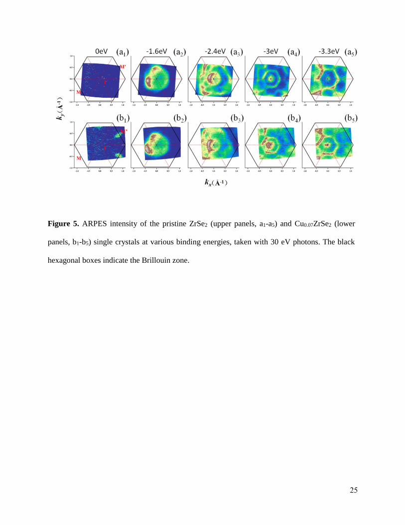
We further investigated the band structures through angle resolved photoemission
spectroscopy (ARPES). According to previous ARPES investigation of ZrSe260, we can determine
the kz value accurately. Using the equation )cos)(2( 022 VEmk kin (where k is the
momentum value along kz, m is the electron mass, kinE is the kinetic energy of the photoelectron,
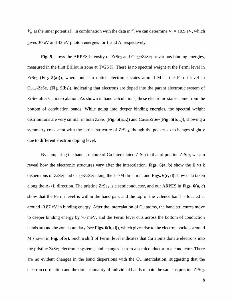
8
0V is the inner potential), in combination with the data in60, we can determine V0 = 10.9 eV, which
gives 30 eV and 42 eV photon energies for Γ and A, respectively.
Fig. 5 shows the ARPES intensity of ZrSe2 and Cu0.07ZrSe2 at various binding energies,
measured in the first Brillouin zone at T=26 K. There is no spectral weight at the Fermi level in
ZrSe2 (Fig. 5(a1)), where one can notice electronic states around M at the Fermi level in
Cu0.07ZrSe2 (Fig. 5(b1)), indicating that electrons are doped into the parent electronic system of
ZrSe2 after Cu intercalation. As shown in band calculations, these electronic states come from the
bottom of conduction bands. While going into deeper binding energies, the spectral weight
distributions are very similar in both ZrSe2 (Fig. 5(a2-5)) and Cu0.07ZrSe2 (Fig. 5(b2-5)), showing a
symmetry consistent with the lattice structure of ZrSe2, though the pocket size changes slightly
due to different electron doping level.
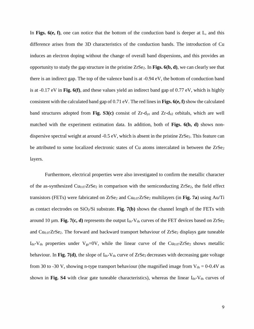
By comparing the band structure of Cu intercalated ZrSe2 to that of pristine ZrSe2, we can
reveal how the electronic structures vary after the intercalation. Figs. 6(a, b) show the E vs k
dispersions of ZrSe2 and Cu0.07ZrSe2 along the Γ->M direction, and Figs. 6(c, d) show data taken
along the A->L direction. The pristine ZrSe2 is a semiconductor, and our ARPES in Figs. 6(a, c)
show that the Fermi level is within the band gap, and the top of the valence band is located at
around -0.87 eV in binding energy. After the intercalation of Cu atoms, the band structures move
to deeper binding energy by 70 meV, and the Fermi level cuts across the bottom of conduction
bands around the zone boundary (see Figs. 6(b, d)), which gives rise to the electron pockets around
M shown in Fig. 5(b1). Such a shift of Fermi level indicates that Cu atoms donate electrons into
the pristine ZrSe2 electronic systems, and changes it from a semiconductor to a conductor. There
are no evident changes in the band dispersions with the Cu intercalation, suggesting that the
electron correlation and the dimensionality of individual bands remain the same as pristine ZrSe2.
9
In Figs. 6(e, f), one can notice that the bottom of the conduction band is deeper at L, and this
difference arises from the 3D characteristics of the conduction bands. The introduction of Cu
induces an electron doping without the change of overall band dispersions, and this provides an
opportunity to study the gap structure in the pristine ZrSe2. In Figs. 6(b, d), we can clearly see that
there is an indirect gap. The top of the valence band is at -0.94 eV, the bottom of conduction band
is at -0.17 eV in Fig. 6(f), and these values yield an indirect band gap of 0.77 eV, which is highly
consistent with the calculated band gap of 0.71 eV. The red lines in Figs. 6(e, f) show the calculated
band structures adopted from Fig. S3(c) consist of Zr-dyz and Zr-dz2 orbitals, which are well
matched with the experiment estimation data. In addition, both of Figs. 6(b, d) shows non-
dispersive spectral weight at around -0.5 eV, which is absent in the pristine ZrSe2. This feature can
be attributed to some localized electronic states of Cu atoms intercalated in between the ZrSe2
layers.
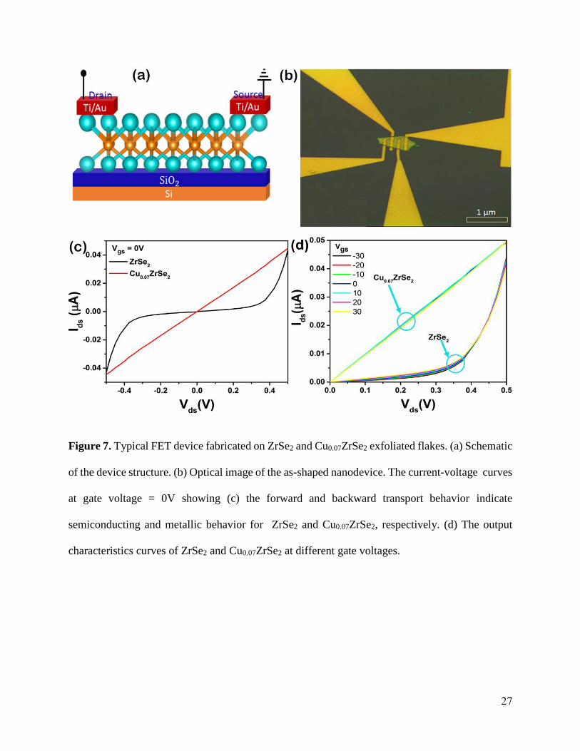
Furthermore, electrical properties were also investigated to confirm the metallic character
of the as-synthesized Cu0.07ZrSe2 in comparison with the semiconducting ZrSe2, the field effect
transistors (FETs) were fabricated on ZrSe2 and Cu0.07ZrSe2 multilayers (in Fig. 7a) using Au/Ti
as contact electrodes on SiO2/Si substrate. Fig. 7(b) shows the channel length of the FETs with
around 10 µm. Fig. 7(c, d) represents the output Ids-Vds curves of the FET devices based on ZrSe2
and Cu0.07ZrSe2. The forward and backward transport behaviour of ZrSe2 displays gate tuneable
Ids-Vds properties under Vgs=0V, while the linear curve of the Cu0.07ZrSe2 shows metallic
behaviour. In Fig. 7(d), the slope of Ids-Vds curve of ZrSe2 decreases with decreasing gate voltage
from 30 to -30 V, showing n-type transport behaviour (the magnified image from Vds = 0-0.4V as
shown in Fig. S4 with clear gate tuneable characteristics), whereas the linear Ids-Vds curves of

10
Cu0.07ZrSe2 for all input gate voltages indicated Ohmic contact like behaviour between the metal
electrodes with no tuneable character, strongly confirming the metallic behaviour.
In summary, we have controllably intercalated Cu atoms into layered ZrSe2 single crystal
via an improved CVT method, and comparatively studied the changes of microstructure and
electronic structure of the ZrSe2 and Cu0.07ZrSe2 by using first-principles calculations and ARPES.
Both our DFT calculations and experimental results clearly revealed the presence of the metallic
state in Cu0.07ZrSe2 with an indirect bandgap nature that is very different from the semiconducting
character in ZrSe2. Similarly, the FET results further confirmed the semiconductor to metallic
phase transition in ZrSe2 after the intercalation of Cu atoms. These results are highlighting the
significance of atomic intercalation-induced electron doping in 2D layered materials, which might
be a vital trend for future valleytronic and electronics applications.
11
ASSOCIATED CONTENT
Supporting Information. Experimental section, CVT growth procedure, ARPES measurement,
theoretical calculations, additional characterization and results.
AUTHOR INFORMATION
Corresponding Author
*E-mail: [email protected] (Z.S.); [email protected] (L.S.)
Author Contributions
+Z.M. and K.M. contributed equally to this work. L.S. and Z.S. supervised the project and
designed the experiments. Z.M. carried out most of the experiments and analyzed the data. K.M.
and Z.S. performed ARPES measurement and analysis. H.L. and X.W. performed the DFT
calculations. C.W., Z.U.R. and M.H. partially contributed to experimental characterizations. Z.M.,
K.J.M., Z.S., X.W. and L.S. analyzed the data and co-wrote the paper. All authors discussed the
results and commented on the manuscript.
ACKNOWLEDGMENT
The authors acknowledge the financial support from the MOST (2017YFA0303500,
2017YFA0402901, 2016YFA0200602, 2014CB848900, 2014CB921102), NSFC (U1532112,
U1532136, 11574280, 11190022), CAS Key Research Program of Frontier Sciences (QYZDB-
SSW-SLH018) and CAS Interdisciplinary Innovation Team. Z.M. acknowledges the CSC
12
(Chinese Scholarship Council) Program. L.S. acknowledges the support from Key Laboratory of
Advanced Energy Materials Chemistry (Ministry of Education) Nankai University, and Key
Laboratory of the Ministry of Education for Advanced Catalysis Materials and Zhejiang Key
Laboratory for Reactive Chemistry on Solid Surfaces (Zhejiang Normal University). We
thanks the Hefei Synchrotron Radiation Facility (Angle Resolved Photoemission Spectroscopy
and Photoemission Endstations, NSRL), and the USTC Center for Micro and Nanoscale Research
and Fabrication for helps in characterizations.
Notes
The authors declare no competing financial interests
13
REFERENCES
(1) Balendhran, S.; Walia, S.; Nili, H.; Ou, J. Z.; Zhuiykov, S.; Kaner, R. B.; Sriram, S.; Bhaskaran,
M.; Kalantar‐zadeh, K., Two‐dimensional molybdenum trioxide and dichalcogenides. Adv.
Funct. Mater. 2013, 23 (32), 3952-3970.
(2) Butler, S. Z.; Hollen, S. M.; Cao, L.; Cui, Y.; Gupta, J. A.; Gutiérrez, H. R.; Heinz, T. F.; Hong,
S. S.; Huang, J.; Ismach, A. F., Progress, challenges, and opportunities in two-dimensional
materials beyond graphene. ACS Nano 2013, 7 (4), 2898-2926.
(3) Tan, C.; Zhang, H., Two-dimensional transition metal dichalcogenide nanosheet-based
composites. Chem. Soc. Rev. 2015, 44 (9), 2713-2731.
(4) Xia, F.; Wang, H.; Xiao, D.; Dubey, M.; Ramasubramaniam, A., Two-dimensional material
nanophotonics. Nat. Phot. 2014, 8 (12), 899-907.
(5) Wang, X.; Huang, L.; Jiang, X.-W.; Li, Y.; Wei, Z.; Li, J., Large scale ZrS2 atomically thin
layers. J. Mater. Chem. C 2016, 4 (15), 3143-3148.
(6) Zhang, M.; Zhu, Y.; Wang, X.; Feng, Q.; Qiao, S.; Wen, W.; Chen, Y.; Cui, M.; Zhang, J.; Cai,
C., Controlled synthesis of ZrS2 monolayer and few layers on hexagonal boron nitride. Journal
of the Amer. Chem. Soc. 2015, 137 (22), 7051-7054.
(7) Bhimanapati, Ganesh R., et al. "Recent advances in two-dimensional materials beyond
graphene. ACS Nano 2015, 9, 11509.
(8) Splendiani, A.; Sun, L.; Zhang, Y.; Li, T.; Kim, J.; Chim, C.-Y.; Galli, G.; Wang, F., Emerging
photoluminescence in monolayer MoS2. Nano letters 2010, 10 (4), 1271-1275.
(9) Kumar, A.; Ahluwalia, P., Electronic structure of transition metal dichalcogenides monolayers
14
1H-MX2 (M= Mo, W; X= S, Se, Te) from ab-initio theory: new direct band gap semiconductors.
EPJ B 2012, 85 (6), 186.
(10) Ellis, J. K.; Lucero, M. J.; Scuseria, G. E., The indirect to direct band gap transition in
multilayered MoS2 as predicted by screened hybrid density functional theory. Appl. Phys. Lett.
2011, 99 (26), 261908.
(11) Zhang, Y.; Chang, T.-R.; Zhou, B.; Cui, Y.-T.; Yan, H.; Liu, Z.; Schmitt, F.; Lee, J.; Moore,
R.; Chen, Y., Direct observation of the transition from indirect to direct bandgap in atomically
thin epitaxial MoSe2. Nat. Nanotech. 2014, 9 (2), 111-115.
(12) Jin, W.; Yeh, P.-C.; Zaki, N.; Zhang, D.; Sadowski, J. T.; Al-Mahboob, A.; van Der Zande,
A. M.; Chenet, D. A.; Dadap, J. I.; Herman, I. P., Direct measurement of the thickness-
dependent electronic band structure of MoS2 using angle-resolved photoemission spectroscopy.
Phys. Rev. Lett. 2013, 111 (10), 106801.
(13) Roldán, R.; Silva‐Guillén, J. A.; López‐Sancho, M. P.; Guinea, F.; Cappelluti, E.; Ordejón,
P., Electronic properties of single‐layer and multilayer transition metal dichalcogenides MX2
(M= Mo, W and X= S, Se). Adp 2014, 526 (9-10), 347-357.
(14) Zhu, Z.; Cheng, Y.; Schwingenschlögl, U., Giant spin-orbit-induced spin splitting in two-
dimensional transition-metal dichalcogenide semiconductors. Phys. Rev. B 2011, 84 (15),
153402.
(15) Sun, L.; Yan, J.; Zhan, D.; Liu, L.; Hu, H.; Li, H.; Tay, B. K.; Kuo, J.-L.; Huang, C.-C.;
Hewak, D. W., Spin-orbit splitting in single-layer MoS2 revealed by triply resonant Raman
scattering. Phys. Rev. Lett. 2013, 111 (12), 126801.
15
(16) Alidoust, N.; Bian, G.; Xu, S.-Y.; Sankar, R.; Neupane, M.; Liu, C.; Belopolski, I.; Qu, D.-
X.; Denlinger, J. D.; Chou, F.-C., Observation of monolayer valence band spin-orbit effect and
induced quantum well states in MoX2. Nat. commun. 2014, 5, 4673.
(17) Miwa, J. A.; Ulstrup, S.; Sørensen, S. G.; Dendzik, M.; Čabo, A. G.; Bianchi, M.; Lauritsen,
J. V.; Hofmann, P., Electronic Structure of Epitaxial Single-Layer MoS2. Phys. Rev. Lett. 2015,
114 (4), 046802.
(18) Riley, J. M.; Mazzola, F.; Dendzik, M.; Michiardi, M.; Takayama, T.; Bawden, L.;
Granerød, C.; Leandersson, M.; Balasubramanian, T.; Hoesch, M., Direct observation of spin-
polarized bulk bands in an inversion-symmetric semiconductor. Nat. Phys. 2014, 10 (11), 835-
839.
(19) Mak, K. F.; He, K.; Shan, J.; Heinz, T. F., Control of valley polarization in monolayer MoS2
by optical helicity. Nat. Nanotech. 2012, 7 (8), 494-498.
(20) Xiao, D.; Liu, G.-B.; Feng, W.; Xu, X.; Yao, W., Coupled spin and valley physics in
monolayers of MoS2 and other group-VI dichalcogenides. Phys. Rev. Lett. 2012, 108 (19),
196802.
(21) Zeng, H.; Dai, J.; Yao, W.; Xiao, D.; Cui, X., Valley polarization in MoS2 monolayers by
optical pumping. Nat. Nanotech. 2012, 7 (8), 490-493.
(22) Yu, H.; Cui, X.; Xu, X.; Yao, W., Valley excitons in two-dimensional semiconductors.
Nat. Sci. Rev. 2015, 2 (1), 57-70.
(23) Cheiwchanchamnangij, T.; Lambrecht, W. R., Quasiparticle band structure calculation of
monolayer, bilayer, and bulk MoS2. Phys. Rev. B 2012, 85 (20), 205302.
16
(24) Komsa, H.-P.; Krasheninnikov, A. V., Effects of confinement and environment on the
electronic structure and exciton binding energy of MoS 2 from first principles. Phys. Rev. B
2012, 86 (24), 241201.
(25) Ugeda, M. M.; Bradley, A. J.; Shi, S.-F.; Felipe, H.; Zhang, Y.; Qiu, D. Y.; Ruan, W.; Mo,
S.-K.; Hussain, Z.; Shen, Z.-X., Giant bandgap renormalization and excitonic effects in a
monolayer transition metal dichalcogenide semiconductor. Nat. Mater. 2014, 13 (12), 1091-
1095.
(26) Qiu, D. Y.; Felipe, H.; Louie, S. G., Optical spectrum of MoS2: many-body effects and
diversity of exciton states. Phys. Rev. Lett. 2013, 111 (21), 216805.
(27) Rybkin, A. G.; Rybkina, A. A.; Otrokov, M. M.; Vilkov, O. Y.; Klimovskikh, I. I.; Petukhov,
A. E.; Filianina, M. V.; Voroshnin, V. Y.; Rusinov, I. P.; Ernst, A.; Arnau, A., Magneto-spin-
orbit graphene: interplay between exchange and spin-orbit couplings. Nano letters 2018.
(28) Späh, R.; Elrod, U.; Lux‐Steiner, M.; Bucher, E.; Wagner, S., PN junctions in tungsten
diselenide. Appl. Phys. Lett. 1983, 43 (1), 79-81.
(29) Podzorov, V.; Gershenson, M.; Kloc, C.; Zeis, R.; Bucher, E., High-mobility field-effect
transistors based on transition metal dichalcogenides. Appl. Phys. Lett. 2004, 84 (17), 3301-
3303.
(30) Gan, W.; Han, N.; Yang, C.; Wu, P.; Liu, Q.; Zhu, W.; Chen, S.; Wu, C.; Habib, M.; Sang,
Y., A Ternary Alloy Substrate to Synthesize Monolayer Graphene with Liquid Carbon
17
Precursor. ACS Nano 2017, 11 (2), 1371-1379.
(31) Koenig, S. P.; Doganov, R. A.; Seixas, L.; Carvalho, A.; Tan, J. Y.; Watanabe, K.; Taniguchi,
T.; Yakovlev, N.; Castro Neto, A. H.; Ozyilmaz, B., Electron doping of ultrathin black
phosphorus with Cu Adatoms. Nano Lett. 2016, 16 (4), 2145-2151.
(32) Lee, P.; Said, G.; Davis, R.; Lim, T., On the optical properties of some layer compounds.
J. Phys. Chem. Solids 1969, 30 (12), 2719-2729.
(33) Britnell, L.; Ribeiro, R.; Eckmann, A.; Jalil, R.; Belle, B.; Mishchenko, A.; Kim, Y.-J.;
Gorbachev, R.; Georgiou, T.; Morozov, S., Strong light-matter interactions in heterostructures
of atomically thin films. Science 2013, 340 (6138), 1311-1314.
(34) Shi, S.-F.; Wang, F., Two-dimensional materials: Atomically thin pn junctions. Nat.
Nanotech. 2014, 9 (9), 664-665.
(35) Niu, T.; Li, A., From two-dimensional materials to heterostructures. Prog. Surf. Sci. 2015,
90 (1), 21-45.
(36) Huang, C.; Wu, S.; Sanchez, A. M.; Peters, J. J.; Beanland, R.; Ross, J. S.; Rivera, P.; Yao,
W.; Cobden, D. H.; Xu, X., Lateral heterojunctions within monolayer MoSe2–WSe2
semiconductors. Nat. Mater. 2014, 13 (12), 1096-1101.
(37) Kane, C. L.; Mele, E. J., Quantum spin Hall effect in graphene. Phys. Rev. Lett. 2005, 95
(22), 226801.
(38) Lee, D. S.; Riedl, C.; Beringer, T.; Neto, A. C.; von Klitzing, K.; Starke, U.; Smet, J. H.,
Quantum Hall effect in twisted bilayer graphene Phys. Rev. Lett. 2011, 107 (21), 216602.

18
(39) Abanin, D.; Pesin, D., Interaction-induced topological insulator states in strained graphene.
Phys. Rev. Lett. 2012, 109 (6), 066802.
(40) Bao, C.; Yao, W.; Wang, E.; Chen, C.; Avila, J.; Asensio, M.C.; Zhou, S., Stacking-
dependent electronic structure of trilayer graphene resolved by nanospot angle-resolved
photoemission spectroscopy. Nano letters 2017, 17(3), 1564-1568.
(41) Han, W.; Kawakami, R. K.; Gmitra, M.; Fabian, J., Graphene spintronics. Nat. Nanotech.
2014, 9 (10), 794-807.
(42) Tributsch, H., Photo-intercalation: Possible application in solar energy devices. Appl. Phys.
A: Mater. Sci. & Processing 1980, 23 (1), 61-71.
(43) Wang, Y.-L.; Xu, Y.; Jiang, Y.-P.; Liu, J.-W.; Chang, C.-Z.; Chen, M.; Li, Z.; Song, C.-L.;
Wang, L.-L.; He, K., Structural defects and electronic properties of the Cu-doped topological
insulator Bi2Se3. Phys. Rev. B 2011, 84 (7), 075335.
(44) Kang, M., Kim, B., Ryu, S.H., Jung, S.W., Kim, J., Moreschini, L., Jozwiak, C., Rotenberg,
E., Bostwick, A. and Kim, K.S., 2017. Universal mechanism of band-gap engineering in
transition-metal dichalcogenides. Nano letters, 17(3), pp.1610-1615.
(45) Ruppert, C.; Aslan, O.B.; Heinz, T.F., Optical properties and band gap of single-and few-
layer MoTe2 crystals. Nano letters 2014, 14(11), 6231-6236.
(46) N. Nair, M.; Palacio, I.; Celis, A.; Zobelli, A.; Gloter, A.; Kubsky, S.; Turmaud, J.P.; Conrad,
M.; Berger, C.; de Heer, W.; Conrad, E.H., Band gap opening induced by the structural
periodicity in epitaxial graphene buffer layer. Nano letters 2017, 17(4), 2681-2689.
(47) Zhao, J.; Ou, H.; Wu, G.; Xie, B.; Zhang, Y.; Shen, D.; Wei, J.; Yang, L.; Dong, J.; Arita,
M., Evolution of the Electronic Structure of 1T−CuxTiSe2. Phys. Rev. Lett 2007, 99 (14),
146401.
19
(48) Liu, Q.; Ishikawa, R.; Funada, S.; Ohki, T.; Ueno, K.; Shirai, H., Highly Efficient Solution‐
Processed Poly (3, 4‐ethylenedio‐xythiophene): Poly (styrenesulfonate)/Crystalline–Silicon
Heterojunction Solar Cells with Improved Light‐Induced Stability. Adv. Energy Mater. 2015,
5 (17).
(49) Morosan, E.; Zandbergen, H.; Dennis, B.; Bos, J.; Onose, Y.; Klimczuk, T.; Ramirez, A.P.;
Ong, N.P. and Cava, R.J., Superconductivity in CuxTiSe2. Nat. Phys. 2006, 2, 544.
(50) Xu, S.-Y.; Xia, Y.; Wray, L.; Jia, S.; Meier, F.; Dil, J.; Osterwalder, J.; Slomski, B.; Bansil,
A.; Lin, H., Topological phase transition and texture inversion in a tunable topological insulator.
Science 2011, 332 (6029), 560-564.
(51) Caputo, M.; Panighel, M.; Lisi, S.; Khalil, L.; Santo, G.D.; Papalazarou, E.; Hruban, A.;
Konczykowski, M.; Krusin-Elbaum, L.; Aliev, Z.S.; Babanly, M.B.; Manipulating the
topological interface by molecular adsorbates: adsorption of Co-phthalocyanine on
Bi2Se3. Nano letters 2016, 16(6), 3409-3414.
(52) Machado, A. J. S.; Baptista, N. P.; de Lima, B. S.; Chaia, N.; Grant, T. W.; Corrêa, L. E.;
Renosto, S.T.; Scaramussa, A.C.; Jardim, R.F.; Torikachvili, M.S. and Aguiar, J.A., Evidence
for topological behavior in superconducting CuxZrTe2− y. Phys. Rev. B 2017, 95(14), 144505.
(53) Tsipas, P.; Tsoutsou, D.; Fragkos, S.; Sant, R.; Alvarez, C.; Okuno, H.; Renaud, G.; Alcotte,
R.; Baron, T. and Dimoulas, A., Massless Dirac Fermions in ZrTe2 Semimetal Grown on InAs
(111) by van der Waals Epitaxy. ACS Nano 2018, Jan 9.
(54) Song, S.; Keum, D.H.; Cho, S.; Perello, D.; Kim, Y. and Lee, Y.H., Room temperature
semiconductor–metal transition of MoTe2 thin films engineered by strain. Nano letters
2015, 16(1), 188-193.
(55) Rhodes, D.; Chenet, D.A.; Janicek, B.E.; Nyby, C.; Lin, Y.; Jin, W.; Edelberg, D.;
20
Mannebach, E.; Finney, N.; Antony, A. and Schiros, T., Engineering the structural and
electronic phases of MoTe2 through W substitution. Nano Letters 2017, 17(3), 1616-1622.
(56) Hashimoto, M.; Vishik, I. M.; He, R.-H.; Devereaux, T. P.; Shen, Z.-X., Energy gaps in
high-transition-temperature cuprate superconductors. Nat. Phys. 2014, 10 (7), 483-495.
(57) Chen, P.; Chan, Y.-H.; Fang, X.-Y.; Zhang, Y.; Chou, M.-Y.; Mo, S.-K.; Hussain, Z.;
Fedorov, A.-V.; Chiang, T.-C., Charge density wave transition in single-layer titanium
diselenide. Nat. Commun. 2015, 6, 8943.
(58) Mo, S.-K., Angle-resolved photoemission spectroscopy for the study of two-dimensional
materials. Nano Convergence 2017, 4 (1), 6.
(59) Kuang, M.; Li, T. T.; Chen, H.; Zhang, S. M.; Zhang, L. L.; Zhang, Y. X., Hierarchical
Cu2O/CuO/Co3O4 core-shell nanowires: synthesis and electrochemical properties.
Nanotechnology 2015, 26 (30), 304002.
(60) Moustafa, M.; Ghafari, A.; Paulheim, A.; Janowitz, C.; Manzke, R., Spin orbit splitting in
the valence bands of ZrSxSe2−x: Angle resolved photoemission and density functional theory.
J Electron Spectros Relat Phenomena 2013, 189, 35-39.
21
FIGURES CAPTIONS
Figure 1. Single crystal XRD patterns of ZrSe2 in comparison with Cu0.07ZrSe2 depicting the
enhancement of peaks and negligible enlargement.
22
Figure 2. XPS analysis of as-synthesized ZrSe2 and Cu0.07ZrSe2 single crystals. (a) Zirconium (Zr
3d). (b) Selenium, (Se 3d). (c) Copper (Cu 2p)
23
Figure 3. Microstructural characterizations of Cu0.07ZrSe2 single crystal through scanning
transmission electron microscopy (STEM). (a) Typical STEM image with Z-contrast. (b)
Structural configurations of bulk and side view of layered structure with Cu atom between the
layers. (c) High resolution STEM image with specified layers identification and (d) SAED patterns
of Cu0.07ZrSe2. (e) The elemental mapping image shows the uniform distribution of Zr, Se and Cu
elements, respectively.
24
Figure 4. (a) Structural model of ZrSe2. (b) Hexagonal Brillouin zone (BZ). (c) DFT orbital
decomposed band structure calculations of bulk ZrSe2 along the high symmetry k-points. After the
intercalation of Cu atoms, the emergence of conduction band at M points indicates excess electrons
donation that can change the system from semiconductor to metallic state as shown from the dash
red line.
25
Figure 5. ARPES intensity of the pristine ZrSe2 (upper panels, a1-a5) and Cu0.07ZrSe2 (lower
panels, b1-b5) single crystals at various binding energies, taken with 30 eV photons. The black
hexagonal boxes indicate the Brillouin zone.

26
Figure 6. (a, b) The photoemission intensity plots along Γ->M direction of pristine ZrSe2 and Cu
intercalated ZrSe2 single crystals, respectively. The data were taken using 30 eV photons. (c, d)
The photoemission intensity plots along A->L high direction of pristine ZrSe2 and Cu0.07ZrSe2,
respectively, taken using 42 eV photons. (e, f) The spectral weight of conduction bands around the
zone boundary in panels b and d, respectively. The red dashed lines indicate the band dispersions
from DFT calculations (adopted from Figure 4 (c)), consists of Zr dyz and dz2 orbitals.
27
Figure 7. Typical FET device fabricated on ZrSe2 and Cu0.07ZrSe2 exfoliated flakes. (a) Schematic
of the device structure. (b) Optical image of the as-shaped nanodevice. The current-voltage curves
at gate voltage = 0V showing (c) the forward and backward transport behavior indicate
semiconducting and metallic behavior for ZrSe2 and Cu0.07ZrSe2, respectively. (d) The output
characteristics curves of ZrSe2 and Cu0.07ZrSe2 at different gate voltages.
28
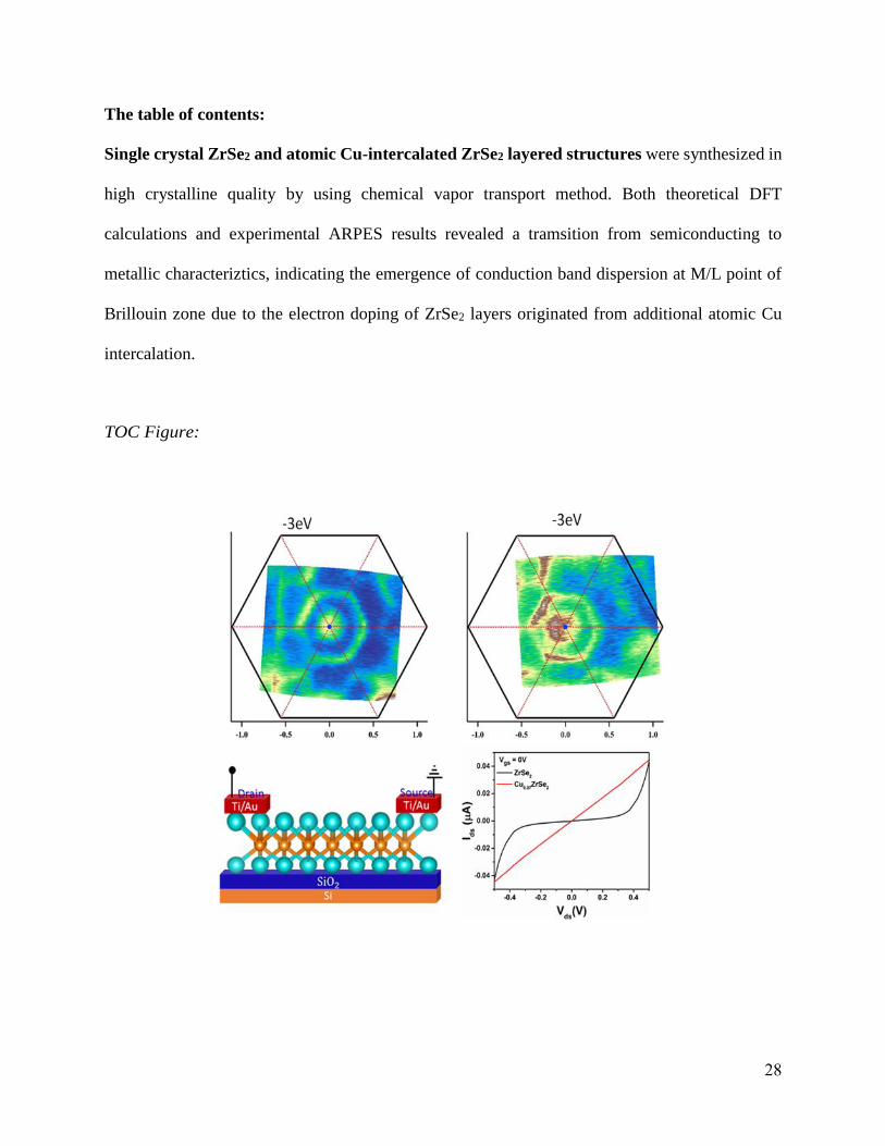
The table of contents:
Single crystal ZrSe2 and atomic Cu-intercalated ZrSe2 layered structures were synthesized in
high crystalline quality by using chemical vapor transport method. Both theoretical DFT
calculations and experimental ARPES results revealed a tramsition from semiconducting to
metallic characteriztics, indicating the emergence of conduction band dispersion at M/L point of
Brillouin zone due to the electron doping of ZrSe2 layers originated from additional atomic Cu
intercalation.
TOC Figure: