compound semiconductor spad arrays
TRANSCRIPT
Compound Semiconductor SPAD arrays
Eric S. Harmon, Mikhail Naydenkov, and James T. Hyland LightSpin Technologies, Inc. P.O. Box 30198, Bethesda, MD 20824-0198
ABSTRACT
Single photon avalanche diodes (SPADs) are revolutionizing ultra-sensitive photodetection applications, providing single photon sensitivity, high quantum efficiency and low dark noise at or near room temperature. When aggregated into arrays, these devices have demonstrated the ability to operate as photon number resolving detectors with wide dynamic range, or as single-photon imaging detectors. SPAD array performance has reached a point where replacing vacuum tube based MCP and PMT photodetectors for most applications is inevitable. Compound semiconductor SPAD arrays offer the unique proposition to tailor performance to match application specific wavelength, speed and radiation hardness requirements. We present a theoretical framework describing performance limits to compound semiconductor SPAD arrays and our latest experimental results detailing the performance of GaAs SPAD arrays. These devices achieve nanosecond rise and fall times, excellent photon number resolving capability, and low dark count rates. Single photon number resolving is demonstrated with 4% single photon detection efficiency at room temperature with dark count rates below 7 Mcps/mm2. Compound semiconductor SPAD arrays have the opportunity to provide orders of magnitude improvement in dark count rate and radiation hardness over silicon SPAD arrays, as well as the ability to detect wavelengths where silicon is blind.
1. INTRODUCTION Individual SPAD devices have been developed for more than 40 years1, beginning with the discovery of the single photon sensitivity of silicon APDs2 in 1970, with accelerating developments over the past 20 years as the full potential of highly integrated SPAD arrays was realized. Historically, there have been two major thrusts in the development of SPAD arrays – those using silicon, and those using compound semiconductors – most notably InGaAsP alloys. The advanced manufacturing technology available for silicon enabled rapid commercialization of non-imaging silicon SPAD arrays3,4,5, and imaging arrays of silicon SPADs are emerging6,7
. With the intense interest in eye-safe ladar and quantum-secure communications, InGaAsP SPAD arrays are also beginning to emerge8,9. Essentially, SPAD array development has been largely limited to silicon and InGaAsP. In this paper, we present an analysis of compound semiconductor SPAD arrays, develop a primary figure of merit for comparing SPADs and SPAD array devices, and provide guidelines for choosing the optimal solid-state semiconductor technology for SPAD arrays. A comprehensive review of SPAD array function and the development of a figure of merit for SPAD performance are followed by experimental results showing that high performance can be achieved when using compound semiconductors.
2. GEIGER MODE FUNDAMENTALS
The primary focus of this paper is SPAD arrays operating in Geiger mode. For certain APD designs, it is possible to momentarily exceed the breakdown voltage yet exhibit zero avalanche current because no free carriers are available to initiate avalanche multiplication. When a subsequent free carrier becomes incident on the gain region of the device, it becomes possible to initiate a Geiger avalanche event where the current grows exponentially over time due to the positive feedback between electron and hole ionization events. A quenching circuit is used to prevent catastrophic breakdown by temporarily reducing the APD bias to below breakdown, and, after a specified dead time, resets the excess bias to the APD. The dead time is necessary to allow for all free carriers to be swept out of the device active region, as
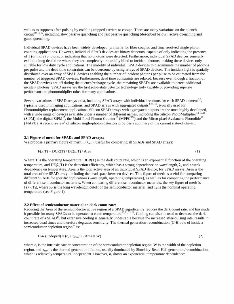
well as to suppress after-pulsing by enabling trapped carriers to escape. There are many variations on the quench circuit10,11,12, including slow passive quenching and fast passive quenching (described below), active quenching and gated quenching. Individual SPAD devices have been widely developed, primarily for fiber coupled and time-resolved single photon counting applications. However, individual SPAD devices are binary detectors, capable of only indicating the presence of 1 (or more) photons, or indicating that no photons were detected. Furthermore, individual SPAD devices generally exhibit a long dead time where they are completely or partially blind to incident photons, making these devices only suitable for low duty cycle applications. The inability of individual SPAD devices to discriminate the number of photons per pulse and the dead time constraints can be overcome by using arrays of SPAD devices. The incident light is spatially distributed over an array of SPAD devices enabling the number of incident photons per pulse to be estimated from the number of triggered SPAD devices. Furthermore, dead time constraints are relaxed, because even though a fraction of the SPAD devices are off during the quench/recharge cycle, the remaining SPADs are available to detect additional incident photons. SPAD arrays are the first solid-state detector technology truly capable of providing superior performance to photomultiplier tubes for many applications. Several variations of SPAD arrays exist, including SPAD arrays with individual readouts for each SPAD element6,8, typically used in imaging applications, and SPAD arrays with aggregated outputs3,4,5,13, typically used for Photomultiplier replacement applications. Silicon SPAD arrays with aggregated outputs are the most highly developed, with a wide range of devices available under a number of different names, including the Silicon PhotoMultiplier14,15,16 (SiPM), the digital SiPM17, the Multi-Pixel Photon Counter18 (MPPCTM) and the Micro-pixel Avalanche Photodide19 (MAPD). A recent review3 of silicon single-photon detectors provides a summary of the current state-of-the-art. 2.1 Figure of merit for SPADs and SPAD arrays: We propose a primary figure of merit, F(λ,T), useful for comparing all SPADs and SPAD arrays:
F(λ,T) = DCR(T) / DE(λ,T) / Area (1)
Where T is the operating temperature, DCR(T) is the dark count rate, which is an exponential function of the operating temperature, and DE(λ,T) is the detection efficiency, which has a strong dependence on wavelength, λ, and a weak dependence on temperature. Area is the total active area of an Individual SPAD device; for SPAD arrays, Area is the total area of the SPAD array, including the dead space between devices. This figure of merit is useful for comparing different SPADs for specific applications (wavelength, operating temperature), as well as for comparing the performance of different semiconductor materials. When comparing different semiconductor materials, the key figure of merit is F(λC,T0), where λC is the long wavelength cutoff of the semiconductor material, and T0 is the nominal operating temperature (see Figure 1). 2.2 Effect of semiconductor material on dark count rate: Reducing the Area of the semiconductor active region of a SPAD significantly reduces the dark count rate, and has made it possible for many SPADs to be operated at room temperature20,21,22,23. Cooling can also be used to decrease the dark count rate of a SPAD10, but extensive cooling is generally undesirable because the increased after-pulsing rate, results in increased dead times and therefore degrades sensitivity. The thermal generation-recombination (G-R) rate of inside a semiconductor depletion region24 is: G-R (undoped) = (ni / τSRH) × (Area × W) (2) where ni is the intrinsic carrier concentration of the semiconductor depletion region, W is the width of the depletion region, and τSRH is the thermal generation lifetime, usually dominated by Shockley-Read-Hall generation/recombination, which is relatively temperature independent. However, ni shows an exponential temperature dependence:
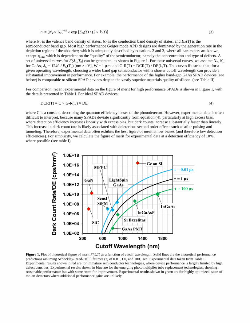
ni = (NV × NC)0.5 × exp [EG(T) / (2 × kBT)] (3) where NV is the valence band density of states, NC is the conduction band density of states, and EG(T) is the semiconductor band gap. Most high performance Geiger mode APD designs are dominated by the generation rate in the depletion region of the absorber; which is adequately described by equations 2 and 3, where all parameters are known, except τSRH, which is dependent on the “quality” of the semiconductor, namely the concentration and type of defects. A set of universal curves for F(λC,T0) can be generated, as shown in Figure 1. For these universal curves, we assume NV, NC for GaAs, λC = 1240 / EG(T0) [nm × eV], W = 1 µm, and G-R(T) = DCR(T) / DE(λ,T). The curves illustrate that, for a given operating wavelength, choosing a wider band gap semiconductor with a shorter cutoff wavelength can provide a substantial improvement in performance. For example, the performance of the higher band-gap GaAs SPAD devices (see below) is comparable to silicon SPAD devices despite the vastly superior materials quality of silicon (see Table II). For comparison, recent experimental data on the figure of merit for high performance SPADs is shown in Figure 1, with the details presented in Table I. For ideal SPAD devices;
DCR(T) = C × G-R(T) × DE (4)
where C is a constant describing the quantum efficiency losses of the photodetector. However, experimental data is often difficult to interpret, because many SPADs deviate significantly from equation (4), particularly at high excess bias, where detection efficiency increases linearly with excess bias, but dark counts increase substantially faster than linearly. This increase in dark count rate is likely associated with deleterious second order effects such as after-pulsing and tunneling. Therefore, experimental data often exhibits the best figure of merit at low biases (and therefore low detection efficiencies). For simplicity, we calculate the figure of merit for experimental data at a detection efficiency of 10%, where possible (see table I).
Figure 1. Plot of theoretical figure of merit F(λ,T) as a function of cutoff wavelength. Solid lines are the theoretical performance predictions assuming Schockley-Reed-Hall lifetimes (τ) of 0.01, 1.0, and 100 µsec. Experimental data taken from Table I. Experimental results shown in red are for immature semiconductor technologies, where device performance is largely limited by high defect densities. Experimental results shown in blue are for the emerging photomultiplier tube replacement technologies, showing reasonable performance but with some room for improvement. Experimental results shown in green are for highly optimized, state-of-the-art detectors where additional performance gains are unlikely.
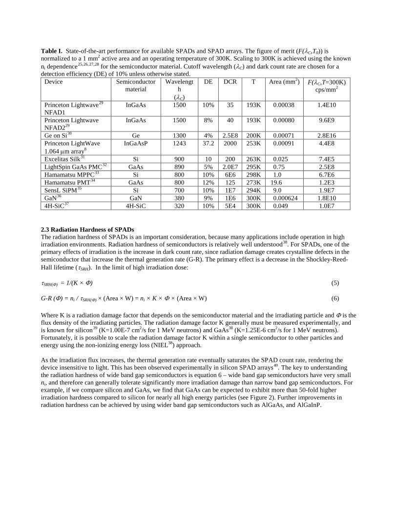
Table I. State-of-the-art performance for available SPADs and SPAD arrays. The figure of merit (F(λC,T0)) is normalized to a 1 mm2 active area and an operating temperature of 300K. Scaling to 300K is achieved using the known ni dependence25,26,27,28 for the semiconductor material. Cutoff wavelength (λC) and dark count rate are chosen for a detection efficiency (DE) of 10% unless otherwise stated.
Device Semiconductor material
Wavelength
(λC)
DE DCR T Area (mm2) F(λC,T=300K) cps/mm2
Princeton Lightwave29 NFAD1
InGaAs 1500 10% 35 193K 0.00038 1.4E10
Princeton Lightwave NFAD229
InGaAs 1500 8% 40 193K 0.00080 9.6E9
Ge on Si30 Ge 1300 4% 2.5E8 200K 0.00071 2.8E16 Princeton LightWave 1.064 µm array8
InGaAsP 1243 37.2 2000 253K 0.00091 4.4E8
Excelitas Silk31 Si 900 10 200 263K 0.025 7.4E5 LightSpin GaAs PMC32 GaAs 890 5% 2.0E7 295K 0.75 2.5E8 Hamamatsu MPPC33 Si 800 10% 6E6 298K 1.0 6.7E6 Hamamatsu PMT34 GaAs 800 12% 125 273K 19.6 1.2E3 SensL SiPM35 Si 700 10% 1E7 294K 9.0 1.9E7 GaN36 GaN 380 9% 1E6 300K 0.000624 1.8E10 4H-SiC37 4H-SiC 320 10% 5E4 300K 0.049 1.0E7
2.3 Radiation Hardness of SPADs The radiation hardness of SPADs is an important consideration, because many applications include operation in high irradiation environments. Radiation hardness of semiconductors is relatively well understood38. For SPADs, one of the primary effects of irradiation is the increase in dark count rate, since radiation damage creates crystalline defects in the semiconductor that increase the thermal generation rate (G-R). The primary effect is a decrease in the Shockley-Reed-Hall lifetime (τSRH). In the limit of high irradiation dose: τSRH(Φ) = 1/(K × Φ) (5) G-R (Φ) = ni / τSRH(Φ) × (Area × W) = ni × K × Φ × (Area × W) (6) Where K is a radiation damage factor that depends on the semiconductor material and the irradiating particle and Φ is the flux density of the irradiating particles. The radiation damage factor K generally must be measured experimentally, and is known for silicon39 (K=1.00E-7 cm2/s for 1 MeV neutrons) and GaAs38 (K=1.25E-6 cm2/s for 1 MeV neutrons). Fortunately, it is possible to scale the radiation damage factor K within a single semiconductor to other particles and energy using the non-ionizing energy loss (NIEL38) approach. As the irradiation flux increases, the thermal generation rate eventually saturates the SPAD count rate, rendering the device insensitive to light. This has been observed experimentally in silicon SPAD arrays40. The key to understanding the radiation hardness of wide band gap semiconductors is equation 6 – wide band gap semiconductors have very small ni, and therefore can generally tolerate significantly more irradiation damage than narrow band gap semiconductors. For example, if we compare silicon and GaAs, we find that GaAs can be expected to exhibit more than 50-fold higher irradiation hardness compared to silicon for nearly all high energy particles (see Figure 2). Further improvements in radiation hardness can be achieved by using wider band gap semiconductors such as AlGaAs, and AlGaInP.
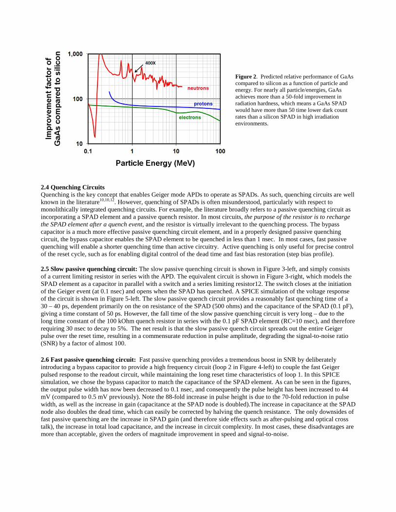
Figure 2. Predicted relative performance of GaAs compared to silicon as a function of particle and energy. For nearly all particle/energies, GaAs achieves more than a 50-fold improvement in radiation hardness, which means a GaAs SPAD would have more than 50 time lower dark count rates than a silicon SPAD in high irradiation environments.
2.4 Quenching Circuits Quenching is the key concept that enables Geiger mode APDs to operate as SPADs. As such, quenching circuits are well known in the literature10,10,12. However, quenching of SPADs is often misunderstood, particularly with respect to monolithically integrated quenching circuits. For example, the literature broadly refers to a passive quenching circuit as incorporating a SPAD element and a passive quench resistor. In most circuits, the purpose of the resistor is to recharge the SPAD element after a quench event, and the resistor is virtually irrelevant to the quenching process. The bypass capacitor is a much more effective passive quenching circuit element, and in a properly designed passive quenching circuit, the bypass capacitor enables the SPAD element to be quenched in less than 1 nsec. In most cases, fast passive quenching will enable a shorter quenching time than active circuitry. Active quenching is only useful for precise control of the reset cycle, such as for enabling digital control of the dead time and fast bias restoration (step bias profile). 2.5 Slow passive quenching circuit: The slow passive quenching circuit is shown in Figure 3-left, and simply consists of a current limiting resistor in series with the APD. The equivalent circuit is shown in Figure 3-right, which models the SPAD element as a capacitor in parallel with a switch and a series limiting resistor12. The switch closes at the initiation of the Geiger event (at 0.1 nsec) and opens when the SPAD has quenched. A SPICE simulation of the voltage response of the circuit is shown in Figure 5-left. The slow passive quench circuit provides a reasonably fast quenching time of a 30 – 40 ps, dependent primarily on the on resistance of the SPAD (500 ohms) and the capacitance of the SPAD (0.1 pF), giving a time constant of 50 ps. However, the fall time of the slow passive quenching circuit is very long – due to the long time constant of the 100 kOhm quench resistor in series with the 0.1 pF SPAD element (RC=10 nsec), and therefore requiring 30 nsec to decay to 5%. The net result is that the slow passive quench circuit spreads out the entire Geiger pulse over the reset time, resulting in a commensurate reduction in pulse amplitude, degrading the signal-to-noise ratio (SNR) by a factor of almost 100. 2.6 Fast passive quenching circuit: Fast passive quenching provides a tremendous boost in SNR by deliberately introducing a bypass capacitor to provide a high frequency circuit (loop 2 in Figure 4-left) to couple the fast Geiger pulsed response to the readout circuit, while maintaining the long reset time characteristics of loop 1. In this SPICE simulation, we chose the bypass capacitor to match the capacitance of the SPAD element. As can be seen in the figures, the output pulse width has now been decreased to 0.1 nsec, and consequently the pulse height has been increased to 44 mV (compared to 0.5 mV previously). Note the 88-fold increase in pulse height is due to the 70-fold reduction in pulse width, as well as the increase in gain (capacitance at the SPAD node is doubled).The increase in capacitance at the SPAD node also doubles the dead time, which can easily be corrected by halving the quench resistance. The only downsides of fast passive quenching are the increase in SPAD gain (and therefore side effects such as after-pulsing and optical cross talk), the increase in total load capacitance, and the increase in circuit complexity. In most cases, these disadvantages are more than acceptable, given the orders of magnitude improvement in speed and signal-to-noise.

Figure 3. (left) simplified circuit diagram of a slow passive quenching circuit, showing that the quench current is forced to flow through the passive quench resistor, and therefore is slow due to the long time constant of the passive quench resistor in series with the SPAD capacitance. (right) Detailed SPICE model of the slow passive quench circuit.
Figure 4. (left) simplified circuit diagram of a fast passive quenching circuit, showing the fast current loop that bypasses the passive quench resistor (loop 2). (lower left) Detailed SPICE model of the slow passive quench circuit (right) Detailed SPICE model of the fast passive quench circuit.
Figure 5. SPICE simulation results for slow passive quench and fast passive quench circuits. (left) output voltage when driving 50 Ohms. The dotted line shows the slow passive quench circuit output multiplied by 100 to make it visible. The slow passive quench output is substantially degraded. (right) Voltage across the APD, with a nominal breakdown voltage of 49V. Both circuits are capable of quenching the APD, with the reset time determined by RQ × (CSPAD + Cbypass).
+-
Vbias RQ
Ground
Rload
Loop 1
SPAD

2.7 SPAD arrays and passive quenching When SPAD elements are connected in monolithic arrays (such as is common with SiPMs, MPPC devices, and LightSpin’s GaAs Photomultiplier Chip™ presented here), the array of SPAD elements increase the load capacitance, degrading the speed of the output pulses. The passive quench circuitry may be modeled as shown in Figure 6. We therefore take the fast passive quench (CQ = CD) and slow passive quench (CQ=0) for a hypothetical array of 3600 SPADs in parallel (i.e. 3 mm x 3mm array of 50 um pitch SPADs), with the results shown in Figure 7. We observe that fast passive quenching exhibits a 20-fold faster rise time, and a 3-fold increase in pulse height, resulting in substantial improvements to both timing performance and SNR.
Figure 6. Equivalent circuit diagram41 of the Photomultiplier ChipTM. Ntot is the total number of SPAD elements, Nf is the number of SPAD elements that are simultaneously fired, RQ is the quench resistance, CQ is the bypass capacitance across the quench resistance, CD is the SPAD capacitance, and i(t) is the time dependent SPAD pulse.
Figure 7. Comparison of SPICE simulation of fast passive quenching and slow passive quenching when used to model a 3600 element monolithic SPAD array with aggregated readout.
3. EXPERIMENTAL RESULTS
LightSpin Technologies, Inc., has developed several generations of GaAs SPAD devices and SPAD arrays, herein referred to as Photomultiplier Chips™. LightSpin’s proprietary PIN diode layer structure is fabricated at a commercial vendor. SPAD devices are mesa isolated, and a monolithic fast passive quench circuit is incorporated for every SPAD device. LightSpin has successfully fabricated 1 mm × 1 mm and 3 mm × 3 mm arrays. These arrays use hexagonal close packing of round mesas with approximately 45 µm diameter active regions to achieve a fill factor in excess of 40%. The SPAD density is 360/mm2. Microscope photographs of the various devices is shown in Figure 8.
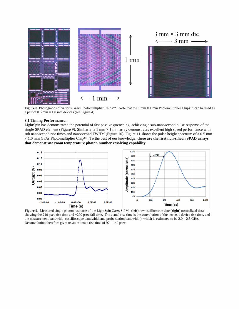
Figure 8. Photographs of various GaAs Photomultiplier Chips™. Note that the 1 mm × 1 mm Photomultiplier Chips™ can be used as a pair of 0.5 mm × 1.0 mm devices (see Figure 4) 3.1 Timing Performance: LightSpin has demonstrated the potential of fast passive quenching, achieving a sub-nanosecond pulse response of the single SPAD element (Figure 9). Similarly, a 1 mm × 1 mm array demonstrates excellent high speed performance with sub nanosecond rise times and nanosecond FWHM (Figure 10). Figure 11 shows the pulse height spectrum of a 0.5 mm × 1.0 mm GaAs Photomultiplier Chip™. To the best of our knowledge, these are the first non-silicon SPAD arrays that demonstrate room temperature photon number resolving capability.
Figure 9. Measured single photon response of the LightSpin GaAs SiPM. (left) raw oscilloscope date (right) normalized data showing the 210 psec rise time and ~200 psec fall time. The actual rise time is the convolution of the intrinsic device rise time, and the measurement bandwidth (oscilloscope bandwidth and probe station bandwidth), which is estimated to be 2.0 – 2.5 GHz. Deconvolution therefore gives us an estimate rise time of 97 – 140 psec.

Figure 10. (left) Measured single photon pulse response of a 1 mm × 1 mm GaAs Photomultiplier Chip mounted in a ceramic dip package with two 4 mm bond wires. We estimate the bond wire inductance to be 2 nH, and the device capacitance to be 36 pF, giving a resonance frequency of 600 MHz, resulting in a calculated rise time of 590 psec. Measured rise time is 600 psec. (right) Measured single photon pulse response of a 0.5 mm × 1 mm GaAs Photomultiplier using a probe station. Rise time is 700 psec.
Figure 11. Pulse height spectrum from a 0.5 mm × 1.0 mm GaAs Photomultiplier Chip™ consisting of an array of 180 passively quenched SPAD elements (approximately 45 µm diameter).
3.2 Dark count rate and Detection Efficiency Next, we measure the single photon detection efficiency at 635 nm. The experiment setup uses CW illumination of the GaAs Photomultiplier Chips™ with a constant current operation of a light emitting diode (LED). First, we measure the quantum efficiency of the Photomultiplier Chip™ using a calibrated silicon photodiode with a precision 0.5 mm × 1.5 mm aperture to match the active area of the GaAs Photomultiplier Chip (see Figure 12). Next, we adjust the LED intensity to obtain a known photocurrent in the device (generally achieved by adjusting the photocurrent to > 1 nA, and then attenuating the light with a suitable ND filter to achieve an incident photoelectron current of around 10 pA). Then, we measure both light counts and dark counts as a function of bias to obtain the internal detection efficiency (IDE). Finally, detection efficiency is calculated by multiplying the internal detection efficiency by the quantum efficiency. Figure 13-left shows the dark count rate as a function of bias, Figure 13-right shows the single photon detection efficiency as a function of bias, and Figure 14 shows the single photon detection efficiency as a function of dark count rate for a 0.5 mm × 1.5 mm GaAs Photomultiplier Chip™ at room temperature. These GaAs Photomultiplier Chips™ incorporate SPAD elements with an active diameter of 45 µm and a SPAD density of 360 SPADs/mm2.
-50
0
50
100
150
200
0 5 10 15 20 25
Volta
ge (m
V)
Time (ns)

Figure 12.Room Temperature quantum efficiency as a function of wavelength using CW LEDs as an illumination source and a calibrated silicon photodiode to measure incident flux. The quantum efficiency is quite high despite the fact that these devices do not have a specific anti-reflection coating and the geometrical fill factor is about 50%.
Figure 13. Single photon performance of a 0.5 mm × 1.5 mm GaAs Photomultiplier Chip™ with a Breakdown voltage of approximately 54.1V. (left) Dark Count rate as a function of bias voltage. (right) Detection Efficiency as a function of bias voltage when illuminated by a 635 nm LED. 4% Detection efficiency is achieved at about 1.2 V of excess bias.
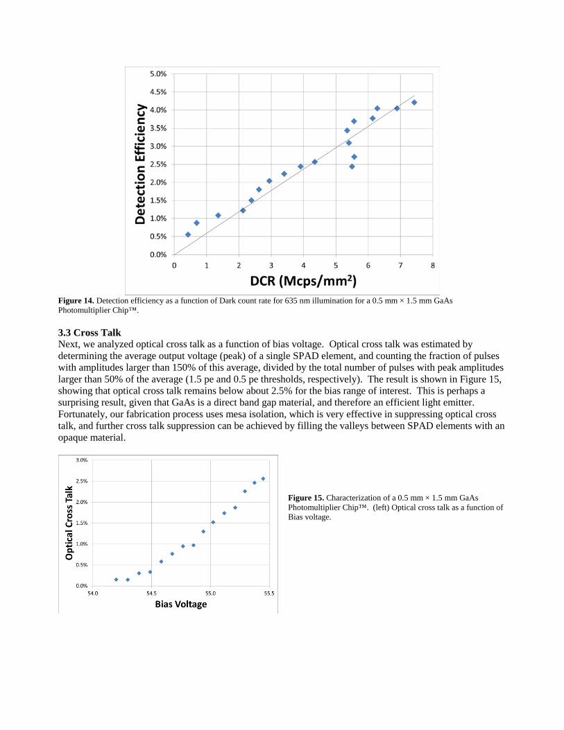
Figure 14. Detection efficiency as a function of Dark count rate for 635 nm illumination for a 0.5 mm × 1.5 mm GaAs Photomultiplier Chip™. 3.3 Cross Talk Next, we analyzed optical cross talk as a function of bias voltage. Optical cross talk was estimated by determining the average output voltage (peak) of a single SPAD element, and counting the fraction of pulses with amplitudes larger than 150% of this average, divided by the total number of pulses with peak amplitudes larger than 50% of the average (1.5 pe and 0.5 pe thresholds, respectively). The result is shown in Figure 15, showing that optical cross talk remains below about 2.5% for the bias range of interest. This is perhaps a surprising result, given that GaAs is a direct band gap material, and therefore an efficient light emitter. Fortunately, our fabrication process uses mesa isolation, which is very effective in suppressing optical cross talk, and further cross talk suppression can be achieved by filling the valleys between SPAD elements with an opaque material.
Figure 15. Characterization of a 0.5 mm × 1.5 mm GaAs Photomultiplier Chip™. (left) Optical cross talk as a function of Bias voltage.

4. CONCLUSION In conclusion, we have analyzed the performance of monolithically integrated SPAD arrays and developed a figure of merit useful for comparing the performance of a wide range of single photon detector technologies. LightSpin has experimentally demonstrated, for the first time, the potential of SPAD arrays built from a compound semiconductor (GaAs) to exhibit high performance, photon number resolving detection capability, in a free running mode at room temperature. The GaAs Photomultiplier Chip™ achieves a single photon detection efficiency of 4% at a dark count rate of less than 7 Mcps/mm2 and with optical cross talk below 2.5%. Individual GaAs SPAD elements have demonstrated a rise time of less than 200 ps, and monolithic GaAs SPAD arrays have demonstrated sub-ns rise times and full width half maximums, making these devices suited for a wide range of Photomultiplier replacement applications.
REFERENCES
[1] McIntyre, R. J., “On the Avalanche Initiation Probability of Avalanche Diodes Above the Breakdown Voltage,”
IEEE Trans. Electron. Dev. v. 20(7) Pp. 637 – 641 (1973) [2] Webb, P. P., and McIntyre, R. J., “Single photon detection with avalanche photodiodes,” Bulletin of the American
Physical Society II, v. 15 Pp. 813 (1970). [3] Musienko, I., “State of the art in SiPM’s,” Industry-academia matching event on SiPM and related technologies,
CERN, 16-17 February 2011, http://indico.cern.ch/materialDisplay.py?contribId=11&sessionId=7&materialId=slides&confId=117424
[4] Dolgoshein, B., “Large area silicon photomultipliers: performance and applications,” 4th International Conference on New Developments in Photodetection, Beaune, France - June 19-24, 2005: http://beaune.in2p3.fr/beaune05/cdrom/Sessions/dolgoshein.pdf
[5] Sadygov, Z., Olshevski, A., Chirikov, I., Zhelenznykh, I., Novikov, A., “Three advanced designs of micro-pixel avalanche photodiodes: Their present status, maximum possibilities and limitations,” Nuclear Instruments and Methods in Physics A, v. 567, pp. 70 – 73 (2006).
[6] Aull, B. F., Loomis, A. H., Young, D. J., Heinrichs, R. M., Felton, B. J., Daniels, P. J., and Landers, D. J., “Geiger-Mode Avalanche Photodiodes for Three-Dimensional Imaging,” Lincoln Laboratory Journal, v. 13(2) Pp 335 – 345 (2002) http://www.ll.mit.edu/publications/journal/pdf/vol13_no2/13_2geigermode3d.pdf
[7] Gersbach, M., Maruyama, Y., Trimananda, R., Fishburn, M. W., Stoppa, D., Richardson, J. A., Walker, R. J., Henderson, R. K., Charbon, E. “A Time-Resolved, Low-Noise Single-Photon Image Sensor Fabricated in Deep-Submicron CMOS Technology,” J. Solid-State Circuits 47(6), Pp 1394-1407 (2012)
[8] Entwistle, M., Itzler, M. A., Chen, J., Owens, M., Patel, K., Jiang, X., Slomkowski. K. and Rangwala, S.. “Geiger-mode APD Camera System for Single Photon 3-D LADAR Imaging,” Proc. SPIE v. 8375, paper 83750D (2012).
[9] Jiang, X., Itzler, M. A., O’Donnell, K., Entwistle, M., Slomkowski, K. “InGaAs/InP Negative Feedback Avalanche Diodes (NFADs) and Solid State Photomultipliers (SSPMs),” Proc. SPIE v. 8375, Paper 83750U (2012)
[10] Brown, R. G. W., Ridley, K. D., and Rarity, J. G., “Characterization of silicon avalanche photodiiodes for photon correlation measurements. 1: Passive quenching,” Applied Optics v. 25(22) Pp. 4122 – 4126 (1986)
[11] Brown, R. G. W., Jones, R.. Rarity, J. G. and Ridley, K. D., “Characterization of silicon avalanche photodiodes for photon correlation measurements. 2: Active quenching,” Applied Optics v. 26(12) Pp 2383 – 2389 (1987)
[12] Tisa, S., Zappa, F., Tosi, A., and Cova, S. “Electronics for single photon avalanche diode arrays,” Sensors and Actuators A, v. 140, Pp 113 – 122 (2007)
[13] Harmon, E. S. and Salzman, D. B., “Solid state microchannel plate photodetector,” U. S. Patent Application 2004/0245592 (May 1. 2004)
[14] http://sensl.com/ [15] http://www.excelitas.com/ProductPages/Single_Photon_Counting_Modules_SPCM.aspx [16] http://www.photonique.ch/Products_SSPM_main.html#1.0SSPMs [17] http://www.research.philips.com/initiatives/digitalphotoncounting/ [18] http://sales.hamamatsu.com/en/products/solid-state-division/si-photodiode-series/mppc.php [19] http://www.zecotek.com/EN/photo_detectors/new_generation_solid-state_photo-detectors/ [20] Vasile, S., Gothoskar, P., Farrell, R. and Sdrulla, D., “Photon detection with high gain avalanche photodiode
arrays,” IEEE Trans. Nuclear Science, v. 45, p. 720 (1998).
[21] Ghioni, M., Cova, S., Rech, I., and Zappa, F. “Monolithic Dual-Detector for Photon-Correlation Spectroscopy with
wide Dynamic Range and 70-ps Resolution,” IEEE J. Quantum Electronics, v. 37, p. 1588 (2001). [22] Rochas, A., Pauchard, A.R.. Besse, P-A., Pantic, D., Prijic, Z. and Popovic, R.S. “Low-Noise Silicon Avalanche
Photodiodes Fabricated in Conventional CMOS Technologies,” IEEE Trans. Elect. Dev., v. 49, p. 387 (2002). [23] Kindt, W. J., and van Zeijl, H.W., “Modelling and Fabrication of Geiger mode Avalanche Photodiodes,” IEEE
Trans. Nuclear Science, v. 45, p. 715 (1998). [24] Pierret, R. F. Advanced Semiconductor Fundamentals in Modular Series on Solid State Devices, v. VI, edited by R.
F. Pierret and G. W. Neudeck, Addison-Wesley Publishing [25] Vurgaftman, I., Meyer, J. R., Ram-Mohan, L. R., “Band parameters for III-V compound semiconductors and their
alloys,” J. Appl. Physics, v. 89(11), Pp 5815 – 5875 (2001) [26] Vurgaftman, I. and Meyer, J. R., “Band parameters for nitrogen-containing semiconductors,” J. Appl. Physics v.
94(6) Pp. 3675 – 3696 (2003) [27] Silicon properties: http://www.ioffe.ru/SVA/NSM/Semicond/Si/bandstr.html [28] Ge properties: http://www.ioffe.ru/SVA/NSM/Semicond/Ge/bandstr.html [29] Yan, Z., Hamel, D. R., Heinrichs, A. K., Jiang, X., Itzler, M. A. and Jennewein, T. “An ultra low noise telecom
wavelength free running single photon detector using negative feedback avalanche diode,” Rev. Sci. Instrum., v. 83, paper 073105 (2012)
[30] Lu, Z., Kang, Y., Hu, C. , Zhou, Q., Liu, H-D and Campbell, J. C., "Geiger-Mode Operation of Ge-on-Si Avalanche Photodiodes," IEEE J. Quantum Electronics. V. 47(5) Pp 731 – 735 (2011)
[31] Bérard, P., Couture, M., Deschamps, P., Laforce, F. and Dautet, H., "Characterization study of a new UV� SiPM with low dark count rate", New Developments in Photon Detection, Lyon, France, July 4 – 8, 2011
[32] See section 3 [33] 3 mm x 3 mm data sheet: http://www.hamamatsu.com/resources/pdf/ssd/mppc_techinfo_e.pdf [34] Hamamatsu part # H7421-50, http://www.hamamatsu.com/resources/pdf/etd/m-h7421e.pdf [35] FM series: http://www.sensl.com/downloads/ds/DS-MicroFM.pdf [36] Cieck, E., Vashaei, Z., McClintock, R., Bayram, C., Razeghi, M. "Geiger-more operation of ultraviolet avalanche
photodiodes grown on sapphire and free-standing GaN substrates," Appl. Phys. Lett. v. 96, paper. 261107 (2010) [37] Bai, X., Liu, H-D, McIntosh, D. C., and Campbell, J. C."High-Detectivity and High-Single-Photon-Detection-
Efficiency 4H-SiC Avalanche Photodiodes," IEEE J. Quantum Electronics v. 45(3) Pp. 300 -- 303 (2009) [38] Claeys, C., and Simoen, E., Radiation Effects in Advanced Semicondutor Materials and Devices, Springer Series in
Materials Science 57, Springer, New York (2002). [39] Osborne, M. D., Hobson, P. R., and Watts, S. J. “Numerical Simulation of Neutron Radiation Effects in Avalanche
Photodiodes,” IEEE Trans. Electron. Dev. 47(3), pp. 529 – 536 (2000). [40] Bohn, P., Clough, A., Hazen, E., Heering, A., Rohlf, J., Freeman, J., Los, S., Cascio, E., Kuleshov, S., Musienko,
Y. and Piemonte, C. “Radiation Damage Studies of Silicon Photomultipliers,” NIMA v 598(3) Pages 722-736 (2009)
[41] Seifert, S., van Dam, H. T., Huizenga, J., Vinke, R., Dendooven, P., Lohner, H. and Schaart, D. R., “Simulation of Silicon Photomultiplier Signals,” IEEE Trans. Nuclear Science, v. 56 (6) Pp. 3726 – 3733 (2009)