semiconductor nanoparticles
TRANSCRIPT

Semiconductor Nanoparticles
M. BANGAL1, S. ASHTAPUTRE1, S. MARATHE1, A. ETHIRAJ1,
N. HEBALKAR1, S. W. GOSAVI1, J. URBAN2 and S. K. KULKARNI1,*1Department of Physics, University of Pune, Pune 411007, India;
e-mail: [email protected] Haber Institute der Max Planck Gesellschaft, Berlin D-97074, Germany
Abstract. Semiconductor nanoparticles exhibit size dependent properties, when their size is
comparable to the size of Bohr diameter for exciton. This can be exploited to increase fluorescence
efficiency or increase the internal magnetic field strength in doped semiconductors. Nanoparticles
are usually unstable and can aggregate. It is therefore necessary to protect them. Surface
passivation using capping molecules or by making coreYshell particles are some useful ways. Here
synthesis and results on doped and un-doped nanoparticles of ZnS, CdS and ZnO will be discussed.
We shall present results on coreYshell particles using some of these nanoparticles and also discuss
briefly the effect of Mn doping on hyperfine interactions in case of CdS nanoparticles.
Key Words: coreYshell, doping, ESR, semiconductor nanoparticles, TEM.
1. Introduction
Since last two decades there has been an explosive growth of research in the field
of nanomaterials. Several review articles and books have been published on
different aspects of nanomaterials. See for example [1Y8]. Nanomaterials may be
in the range of 1 to 100 nm size and one can reduce the dimension in one, two or
all three directions to obtain thin films, wires or dots, respectively. Nanomaterials
can be of various shapes too and properties may change according to size and/or
shape. These materials may be metals, semiconductors, metal oxides, organic
materials or biomaterials. Thus there is a tremendous scope to design new
materials with unusual properties.
Amongst the various types of nanomaterials, semiconductor nanoparticles
have been widely investigated. This is quite understandable. Semiconductors
have been useful in making devices. The drive towards miniaturization of
electronic components and integration to accommodate huge number of them in
small volume has been there for decades. This has enabled to have very
compact digital watches, calculators, computers, laptops etc. In fact Moors’ law
* Author for correspondence.
Hyperfine Interactions (2005) 160:81–94
DOI 10.1007/s10751-005-9151-y # Springer 2005

predicted in 1960 has now reached its limits in such a way that any further
reduction in size changes the materials properties. Dimensions of some of the
devices are now in the nanometer range. Electronic structure of nanomaterials
may be different compared to corresponding bulk material. This has lead to
interesting devices like single electron transistors, tunnel junctions, magnetic
spin valves etc. which do not have bulk counterparts. Besides this, at nano
scale, semiconductor materials like silicon that are not optoelectronic materials
due to indirect band gap have showed strong luminescence in visible range [9].
Moreover they exhibit emission which is size dependent luminescence. Some
groups have showed [10Y13], for IIYVI and IIIYV semiconductors, the change in
band gap with particle size.
Materials with zero dimensions i.e. the ones whose all three dimensions are
reduced to nanometer regime are known as quantum dots or simply nano-
particles. There is a variety of nanoparticles. A few possibilities are illustrated
schematically in Figure 1. We have synthesized a large number of oxides, sul-
phides, coreYshell particles, self-organized islands of Ge/Si, fullerenes, Diluted
Magnetic Semiconductor (DMS) nanoparticles like TiO2 doped with cobalt and
metallic multilayers like Fe/Si, Cu/Ni Co/Pt etc. Here we will discuss a variety of
semiconductor nanoparticles viz. ZnS, CdS and ZnO, their synthesis and some
optical properties. We shall then discuss how nanoparticles can be encapsulated
inside some robust shell of silica or how to anchor such particles on silica for
exploiting large surface area of silica particles. We also discuss how doping with
Figure 1. Some possible nanostructures: (a) surface passivated nanoparticles (b) different shapes
of nanoparticles (c) coreYshell particles (d) self assembly, and (e) multilayers.
82 M. BANGAL ET AL.

manganese can alter the splitting of energy levels in CdS nanoparticles causing
changes in the internal magnetic field of the nanoparticles.
2. Experimental
Synthesis of semiconductor nanoparticles was carried out using a chemical route
known as chemical capping. In this procedure, some inert organic long chain
molecules are used to passivate the surface of the particles so that the particles do
not agglomerate or ripen to form larger particles. This ensures that the
nanoparticles synthesized using some particular set of parameters yields stable
nanoparticles with uniform size distribution. Figure 2 shows the flow chart of
synthesis procedure used to synthesize ZnS, CdS and ZnO nanoparticles having
<8 nm particle size. Details of synthesis are given below.
2.1. SYNTHESIS OF NANOPARTICLES
2.1.1. ZnS nanoparticles
Zinc sulphide nanoparticles were synthesized using zinc acetate [Zn (CH3CO2)2
2H2O], N, N-dimethylformamide [HCON(CH3)2], sodium sulphide [Na2S], thio-
glycerol [HSCH2CH(OH)CH2OH], sodium hydroxide [NaOH] and ethanol
[C2H5OH]. Synthesis was carried out as follows. Zinc acetate (2.2 mM in 50
ml ethanol) was mixed with thioglycerol (3.5 mM in 50 ml ethanol) in DMF
medium and both were stirred together for 30 min. Sodium sulphide (0.55 mM in
8 ml ethanol) was slowly mixed over a period of 4 h. The reaction was carried
out at room temperature under nitrogen atmosphere. The solution was constantly
stirred using a magnetic stirrer. Sodium hydroxide solution was then added till
pH of the solution was 8. The whole solution was then refluxed for 14 h.
Nanoparticles of ZnS were then obtained by size selective precipitation method
[14] described as follows. The colloidal solution of nanoparticles in ethanol was
concentrated using roto-evaporator. To this concentrated solution acetone, a non-
solvent, was added slowly till flocculation was obtained which was then allowed
to settle down. The supernatant was removed and flocculate was centrifuged to
get precipitate enriched with largest crystallites in the sample. Precipitate was
washed repeatedly using methanol. Dispersion of precipitate in ethanol and size
selective precipitation was repeated till no further sharpening in sample’s ab-
sorption spectrum had been seen.
2.1.2. CdS nanoparticles
Non-aqueous solutions of cadmium acetate [Cd (CH3CO2)2 I 2H2O], thioglycerol
and sodium sulfide prepared in ethanol were used to synthesize CdS nanoparti-
SEMICONDUCTOR NANOPARTICLES 83

cles. Thioglycerol was used as a capping agent. Cadmium acetate solution (0.1 M
in 25 ml ethanol) was taken in reaction vessel and stirred continuously using
magnetic stirrer. After two hours, thioglycerol (0.95 M in 25 ml ethanol) was
added dropwise to cadmium acetate solution and stirred for two more hours.
Finally sodium sulfide solution (0.1 M in 25 ml ethanol) was added and the
solution was stirred continuously for 4 h. The synthesis was carried out at room
temperature under nitrogen atmosphere to prevent the oxidation of nanoparticles.
Size-selective precipitation method discussed above was used to obtain the
Figure 2. Procedure for synthesis of different nanoparticles (a) ZnS, (b) CdS and (c) ZnO
nanoparticles. Variation of thioglycerol gives particles of different sizes.
84 M. BANGAL ET AL.

monodispersed particles. Precipitate was separated by centrifugation and washed
with acetone and diethyl ether. It was then vacuum dried to get CdS nano-
particles in powder form.
2.1.3. ZnO nanoparticles
Zinc oxide nanoparticles were synthesized using zinc chloride [ZnCl2 I 2H2O],
methanol [CH3OH], sodium hydroxide and thioglycerol. The synthesis was
carried out in non-aqueous medium. The solutions were prepared in methanol.
Thioglycerol was used as capping agent. Sodium hydroxide (0.1 M in 100 ml
methanol) was stirred for 30 min. Thioglycerol (0.1 M in 20 ml methanol) was
added drop wise to above solution and stirring was continued further for 60 min.
Zinc chloride (0.1 M in 20 ml methanol) solution was then slowly added to this
solution. The solution was then stirred for 180 min. The precipitate obtained by
size selective procedure was washed with methanol and dried to get ZnO nano-
particles in powder form.
2.1.4. Doping of nanoparticles
For manganese doping both in ZnS and in CdS nanoparticles, manganese salt
(MnCl2 I H2O) was added to the respective metal salts in the solution form and
resulting solution was stirred for 2 h before adding capping agent to the solution.
After that the same synthesis procedure described above was used to synthesize
doped nanoparticles. Doping of other elements can be achieved by using
corresponding salts.
2.2. COREYSHELL PARTICLES
2.2.1. Synthesis of SiO2 particles
Figure 3 shows the flow chart explaining various steps used in synthesizing silica
particles, encapsulation of nanoparticles or coating of nanoparticles in general.
Following the procedure developed by Stober et al. [15], we synthesized SiO2
particles. Here we use tetraethylorthosilicate, water and ammonia. A solution of
ethanol, water and ammonium hydroxide in the molar ratio 49:31:4 was used.
The solution was stirred at room temperature for 30 min and TEOS (1M) was
added to it. Solution was further stirred for 3 h. Centrifugation and drying in
ambient resulted in silica powder. By varying the reaction time, spherical silica
particles of different sizes (50 nmY0.1 mm) could be obtained. In most of the
cases particles with very narrow size distribution (1Y3%) could be obtained.
2.2.2. Encapsulation of nanoparticles inside SiO2
The synthesis procedure used to obtain silica particles can be further extended
to encapsulate the nanoparticles inside silica. Here we have encapsulated man-
SEMICONDUCTOR NANOPARTICLES 85
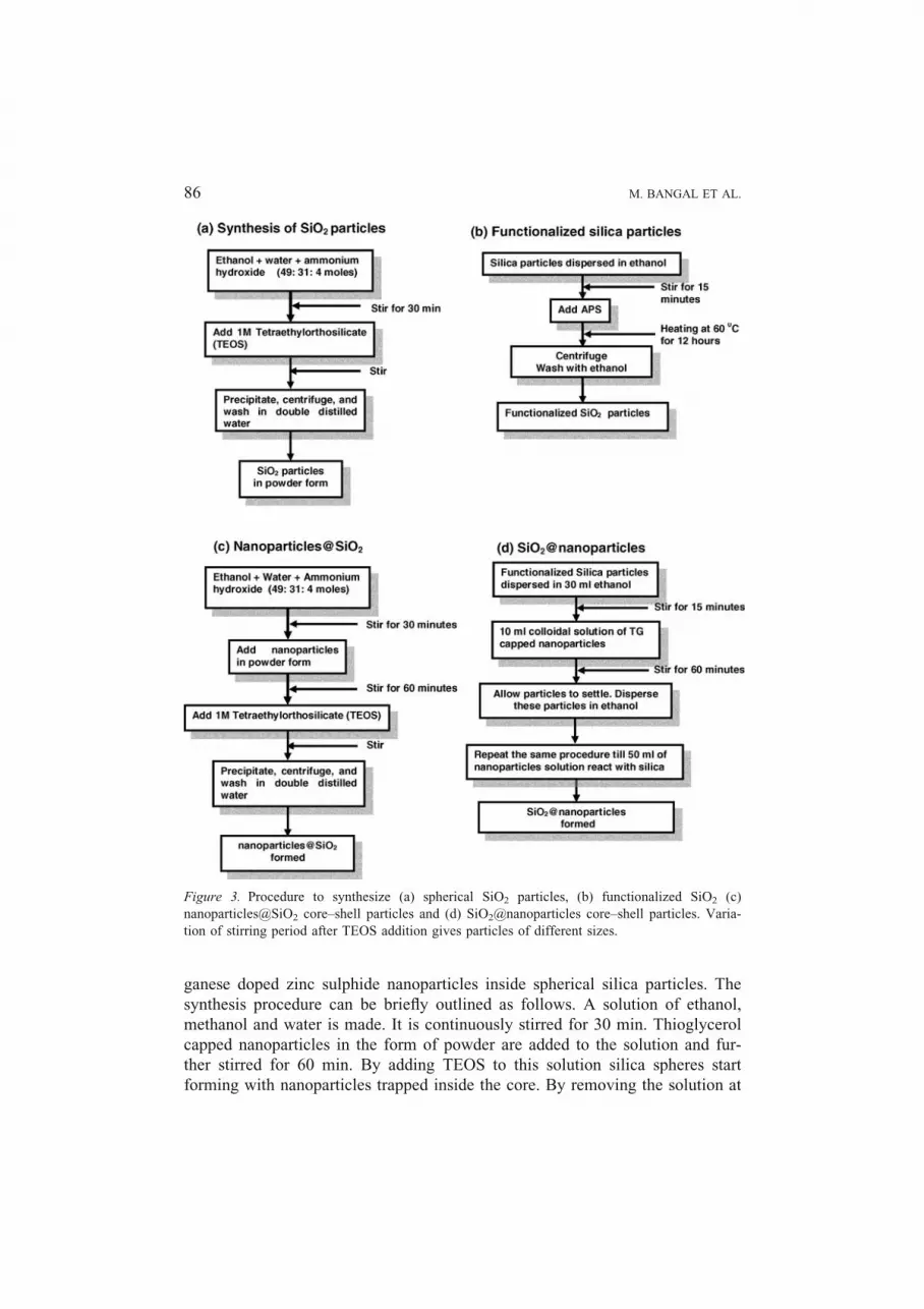
ganese doped zinc sulphide nanoparticles inside spherical silica particles. The
synthesis procedure can be briefly outlined as follows. A solution of ethanol,
methanol and water is made. It is continuously stirred for 30 min. Thioglycerol
capped nanoparticles in the form of powder are added to the solution and fur-
ther stirred for 60 min. By adding TEOS to this solution silica spheres start
forming with nanoparticles trapped inside the core. By removing the solution at
Figure 3. Procedure to synthesize (a) spherical SiO2 particles, (b) functionalized SiO2 (c)
nanoparticles@SiO2 coreYshell particles and (d) SiO2@nanoparticles coreYshell particles. Varia-
tion of stirring period after TEOS addition gives particles of different sizes.
86 M. BANGAL ET AL.

different intervals coreYshell particles of different sizes can be obtained. It may
be pointed out that in this case many nanoparticles are trapped inside each silica
sphere.
2.2.3. Functionalization of SiO2 particles
Bifunctional molecule 3-aminopropyltrimethoxysilane (APS) has three [jOCH3]
groups and one [NH2j(CH2)3-] group bonding to a silicon atom. Therefore it can
link with two different types of molecules or particles. This has been used by
various groups to bind nanoparticles to larger particles of silica or polymers and
has been reviewed in [16, 17]. Here we use similar approach and attach TG
capped ZnS nanoparticles and CdS nanoparticles to SiO2 particles. One can
control the amount of particles added to the shells using the procedure used here.
Silica particles are dispersed in ethanol and stirred for 15 min. To this solution
APS (1 � 10j3 M) was added. The solution was then heated to 60-C and stirred
continuously at this temperature for 12 h. Solution was allowed to cool to room
temperature, and was centrifuged to obtain a precipitate. Precipitate was finally
washed in ethanol.
2.2.4. Coating SiO2 particles with nanoparticles
APS functionalized silica particles were mixed in ethanol along with TG capped
nanoparticles, either of CdS or ZnS. Using different concentration of nanopar-
ticles one can get thin or thick coating of nanoparticles on silica. See Figure 3 for
flow chart.
2.3. CHARACTERIZATION
Characterization of above mentioned nanoparticles and coreYshell particles has
been carried out using different techniques like optical absorption, fourier
transform infra red spectroscopy, photoluminescence, X-ray diffraction, electron
spin resonance and transmission electron microscopy. The description of
samples (liquid or powder) and instruments is briefly given below.
2.3.1. Optical absorption
The samples were analyzed using Shimadzu 300 double beam spectrometer by
dispersing them in ethanol in case of ZnS, CdS and methanol in case of ZnO.
Pure ethanol and methanol were used as reference for ZnS, CdS and ZnO, re-
spectively. Spectra were recorded from 600 to 200 nm.
2.3.2. Fourier transform infra red spectroscopy
Samples for FTIR analysis were prepared in the form of pellets. Powder samples
of nanoparticles or coreYshell were mixed with KBr powder and pellets were
SEMICONDUCTOR NANOPARTICLES 87

formed. Shimadzu 8400 spectrometer was used to record the spectra in the
300Y4000 cmj1 frequency region.
2.3.3. Photoluminescence spectroscopy
Spectra were acquired using Perkin-Elmer LS-50 model. The dry powder sam-
ples were held in a powder sample holder. Spectra were recorded from 200 to
350 nm in excitation mode and 350 to 700 nm in emission mode using ap-
propriate filters.
2.3.4. X-ray diffraction
X-ray Diffraction of powder samples was carried out on Philips PW1840 powder
diffractometer. Copper radiation (CuK� 1.54 A) was used in the analysis with
nickel filter.
2.3.5. Electron spin resonance
The powder samples were analyzed using Brucker EMX-X band ESR spec-
trometer. The microwave source frequency was 9.5 GHz and 100 kHz mod-
ulation was used.
2.3.6. Transmission electron microscopy
Philips CM 200 FEG microscope equipped with a field emission gun was used
for TEM analysis of the samples. EDAX analysis also could be carried out using
this microscope. For the analysis, powder samples were dispersed in ethanol and
a drop of solution was placed on õ5 nm thick carbon film on copper grid. After
air drying, the grid was inserted in the microscope and using 200 KeV energy
images were acquired.
3. Results and discussion
Nanoparticles of IIYVI semiconductors have been investigated for a long time for
their optical properties [18Y20]. As the particle size reduces below the Bohr size
of exciton, the energy gap increases and can be observed as shift in the ab-
sorption edge in UVYVIS absorption spectra. Band gaps for zinc sulphide, zinc
oxide and cadmium sulphide bulk materials are 3.68 eV, 3.35 eV and 2.4 eV
respectively [21]. The absorption edges are expected at 337 nm for ZnS, 370 nm
for ZnO and 517 nm for CdS. As showed in Figure 4, the absorption spectra for
ZnS, ZnO and CdS nanoparticles are well shifted from their bulk values. In case
of ZnO the binding energy of exciton is 60 meV. This is quite large compared to
88 M. BANGAL ET AL.

thermal energy available at room temperature (õ25 meV) to destroy the exciton.
Therefore in ZnO, exciton is detectable even at room temperature. However ZnS
(29 meV) and CdS (27 meV) excitons with very low binding energies are des-
troyed and are not detectable for bulk semiconductors of CdS or ZnS. However
one can detect well defined excitonic peaks even for ZnS and CdS at room
temperature, when CdS and ZnS are in the form of nanoparticles. Average
particle sizes can be determined using the widths of X-ray diffraction peaks. In
the present case the particle sizes are 1.1 nm for ZnS, 3.1 nm for ZnO and 3.6 nm
for CdS particles. The presence of excitonic peak is expected theoretically too
[22, 23]. Depending upon the preparation method there are variations in the
quality of spectra obtained.
Semiconductor nanoparticles are quite useful as biological labels, barcoades,
display screens etc [24Y26]. Advantage with semiconductor nanoparticles is that
they are photostable i.e., unlike many organic dyes they do not show degradation
of luminescence intensity after some time. Besides they can be excited with any
of the wavelengths in UV range rather than some fixed wavelength. It has also
been showed [2, 7, 28] that efficiency for luminescence is large in case of
nanoparticles compared to their bulk materials. Thus it is possible to excite
photoluminescence in different nanoparticles using a single wavelength. In
250 300 350 400 450 500 550
UV-Vis absorption
bulk
bulk
bulk
ZnS
CdS
ZnO
Ab
sorb
ance
(A
rb. U
nit
s)
Wavelength (nm)
Figure 4. UVYVis absorption spectra for ZnS (1.1 nm), CdS (3.6 nm) and ZnO (3.1 nm)
nanoparticles.
SEMICONDUCTOR NANOPARTICLES 89

Figure 5, photoluminescence for ZnS, ZnO and CdS nanoparticles has been
showed. Nanoparticles in general have higher quantum efficiency of lumines-
cence as compared to their bulk counterparts. Mechanism of luminescence of
ZnS, CdS and ZnO nanoparticles has been discussed widely in the literature, see
e.g. [27, 28].
Interestingly it is possible to coat the chemically capped nanoparticles on
SiO2 particles. SiO2 particles of 50Y500 nm size are well suited to adsorb such
1Y5 nm size particles. Figure 6 (a) shows TEM images of SiO2 particles while
Figure 6 (b) and (c) show SiO2 particles coated with CdS and ZnS respectively.
Such coated particles often known as coreYshell particles are written as core
(material)@shell (material). Thus SiO2 core and CdS coating is written as
SiO2@CdS. If CdS would get encapsulated inside SiO2 then this would be
written as CdS@SiO2. The details are reported elsewhere [29, 30]. However it
can be mentioned here that there is no significant change in the properties of
nanoparticles due to such coating of nanoparticles. FTIR analysis (not shown
here) indeed showed the presence of TG molecules as well as APS [29, 30]. This
type of core Y shell particles would be useful for some applications where large
number of well dispersed nanoparticles are required.
In some applications, specially the biological applications, it is necessary to
use water soluble materials. SiO2 particles are water soluble. Therefore fluo-
rescent nanoparticles can be encapsulated inside SiO2 particles forming coreYshell particles. Advantage with this type of coating is that, nanoparticles can be
excited with UV radiation as SiO2 are found to be nearly transparent to UV
radiation. We have found [31] that by encapsulating nanoparticles inside silica
particles the photoluminescence increases. Increase in luminescence is due to
protection provided by silica shell.
Transition metal doping, specially in IIYVI semiconductors, is further interes-
ting for the applications in spintronics [32]. Recently there have been reports
about observation of giant magnetic field in nanoparticles of CdS doped with Mn
Figure 5. Photoluminescence of different nanoparticles.
90 M. BANGAL ET AL.

in absence of zero external magnetic field [33]. This leads to observation of large
splitting of exciton sub levels which has been interpreted as due to increase in the
electronYhole interaction in nanoparticles. Also it is possible to observe ferro-
magnetism in nanoaprticles as discussed for (GaMn)As system [34]. Pileni group
[35] has showed that there are concentration dependent changes in ESR spectra
Figure 6. Transmission electron micrographs of (a) silica particles, (b) coreYshell particles of
SiO2@CdS and (c) coreYshell particles of SiO2@ZnS.
SEMICONDUCTOR NANOPARTICLES 91

for CdS doped with Mn ions, synthesized using inverse miceller route. It is thus
interesting to dope IIYVI semiconductor nanoparticles to obtain ferromagnetism
or even large paramagnetic moment in them. We have therefore initiated the
investigations of Mn doped nanoparticles. Figure 7 shows ESR spectra for Mn
doped CdS nanoparticles (3.8 T 0.2 nm). It can be seen that six line pattern
characteristic of isolated Mn ion doping, converts to a single line characteristic of
strong MnYMn ion interaction similar to that discussed earlier [36, 37] for Mn
doped in ZnS. Note that in Figure 7 the spectra are for CdS nanoparticles having
same size but varying concentration of Mn ions. These results are in qualitative
agreement with some earlier work on differently prepared nanoparticles of CdS
doped with Mn [33, 35]. In order to assess the utility of doped IIYVI semi-
conductor nanoparticles as spintronics materials, more experiments would
however be necessary.
4. Conclusions
Stable semiconductor nanoparticles and coreYshell particles can be synthesized
using chemical routes. Quality of nanoparticles and coreYshell particles is quite
good and such particles would be useful for biological labeling, barcodes or
fluorescent materials for display screens. Doped nanoparticles may find
applications in spintronics too. However more experiments would be necessary
in future to evaluate this aspect.
Figure 7. Electron spin resonance study of Mn doped CdS nanoparticles.
92 M. BANGAL ET AL.

Acknowledgement
SKK thanks UGC, India for a continuous support. This work has been supported
by DST, India and Volkswagenstiftung, Germany.
References
1. Jacak L., Hawrylak P. and Wojs A., Quantum Dots, Springer, Berlin Heidelberg New York,
1997.
2. Gaponenko S. V., Optical Properties of Semiconductor Nanocrystals, Cambridge, 1997.
3. Davis J. H., Physics of Low Dimensional Structures, Cambridge, 1998.
4. Banyai L. and Koch S. W., Semiconductor Quantum Dots, World Scientific Series on Atomic,
Molecular and Optical Physics, Vol. 2, 1993.
5. Kelly M. J., Low Dimensional Semiconductors, Clarendon, 1995.
6. Jaros M., Physics and Applications of Semiconductor Microstructures, Clarendon, 1989.
7. Moriarty P., Rep. Prog. Phys. 64 (2001), 297.
8. Gleiter H., Prog. Mater. Sci. 33 (1989), 223.
9. Canham L. T., Appl. Phys. Lett. 57 (1990), 1046.
10. Brus L. E., J. Chem. Phys. 80 (1984), 4403.
11. Lee J., Sunder V. C., Heine J. R., Bawendi M. G. and Jensen K. F., Adv. Mater. 12 (2000),
1102.
12. Henglein A., Top. Curr. Chem. 143 (1988), 113.
13. Wang W. and Herron N., J. Phys. Chem. 95 (1991), 525.
14. Murray C. B., Norris D. J. and Bawendi M. G., J. Am. Chem. Soc. 115 (1993), 8706.
15. Stober W. and Fink A., J. Coll. Int. Sci. 26 (1968), 62.
16. Caruso F., Adv. Mater. 13 (2001), 11.
17. Liz-Marzan L. M., Correa-Durate M. A., Pastorza-Santos I., Mulvaney P., Ung T., Giersig M.
and Kotov N. A., Handbook of Surfaces and Interfaces of Materials, Nalwa H. S. (ed.),
Nanostructured Material, Micelles and Colloids, Vol. 3, 2001, p. 189.
18. Brus L. E. and Trautman J. K., Phil. Trans. R. Soc. Lond. A 353 (1995), 313.
19. Chestnoy N., Hull R. and Brus L. E., J. Chem. Phys. 85 (1986), 2237.
20. Bawendi M. G., Steigerwald M. L. and Brus L. E., Ann. Rev. Phys. Chem. 41 (1990), 477.
21. Sze S. M., Physics of Semiconductor Devices, Wiley, Delhi, 1981.
22. Lippens P. E. and Lanoo M., Phys. Rev., B 39 (1989), 10935.
23. Ramakrishna M. V. and Friesner R. A., Phys. Rev. Lett. 67 (1991), 629.
24. Bruchez M., Moronne M., Gin P., Weiss S. and Alivisatos A. P., Science 281 (1998), 2013.
25. Gaponik N., Radtchenko I. L., Sukhorukov G. B., Weller H. and Rogasch A. L., Adv. Mater.
14 (2002), 879.
26. Battersby B. J., Bryant D., Meutermans W., Matthews D., Smythe M. L. and Trau M., J. Ame.
Chem. Soc. 122 (2000), 2138.
27. Masumoto Y., In: Shionoya S. and Yen W. M. (eds.), Phosphor Handbook, CRC, Boston, p. 71.
28. Kulkarni S. K., In: Nalwa H. S. (ed.), Encyclopedia of Nanoscience and Nanotechnology,
Vol. X, Ame. Sci. Pub., USA.
29. Hebalkar N., Kharrazi S., Ethiraj A., Urban J., Fink R. and Kulkarni S. K., J. Coll. Int. Sci.
278 (2004), 107.
30. Ethiraj A. S., Hebalkar N, Sainkar S. R., Urban J. and Kulkarni S. K., Surface Engineering 20
(2004), 367.
31. Ethiraj A. S., Hebalkar N., Kulkarni S. K., Pasricha R., Urban J., Dem C., Schmitt M., Kiefer
W., Weinhardt L., Joshi S., Fink R., Heske C., Kumpf C. and Umbach E., J. Chem. Phys.
118 (2003), 8945.
SEMICONDUCTOR NANOPARTICLES 93

32. Sato K. and Yoshida H. K., Semicond. Sci. Tech. 17 (2002), 367.
33. Hofmann D. M., Meyer B. K., Ekimov A. I., Merculov I. A., Efros A. L., Rosen M., Couino
G., Gacoin T. and Boilot J. P., Sol. State Comm. 114 (2000), 547.
34. Sapra S., Sarma D. D., Sanvito S. and Hill N. A., Nano Lett. 2 (2002), 605.
35. Levy L., Feltin N., Ingert D. and Pileni M. P., J. Phys. Chem. B 101 (1997), 9153.
36. Borse P. H., Srinivas D., Date S. K., Vogel W. and Kulkarni S. K., Phys. Rev., B 60 (1999),
8659.
37. Kennedy T. A., Glasser E. R., Klein P. B. and Bhargava R. N., Phys. Rev. B 52 (1995),
R14356.
94 M. BANGAL ET AL.