electrical characterization of thermomechanically stable ysz membranes for micro solid oxide fuel...
TRANSCRIPT
Solid State Ionics 181 (2010) 322–331
Contents lists available at ScienceDirect
Solid State Ionics
j ourna l homepage: www.e lsev ie r.com/ locate /ss i
Electrical characterization of thermomechanically stable YSZ membranes for microsolid oxide fuel cells applications
I. Garbayo a, A. Tarancón a,b,⁎, J. Santiso c, F. Peiró d, E. Alarcón-LLadó e, A. Cavallaro c, I. Gràcia a,C. Cané a, Neus Sabaté a
a CNM-IMB (CSIC), National Institute of Microelectronics, CSIC, Campus UAB, 08193 Bellaterra, Barcelona, Spainb IREC, Catalonia Institute for Energy Research, Dept of Advanced Materials for Energy Applications, Josep Pla 2, B2, PB, 08019, Barcelona, Spainc CIN2, CSIC/ICN, Research Center in Nanoscience and Nanotechnology, CSIC, Campus UAB, 08193 Bellaterra, Barcelona, Spaind MIND-IN2UB, Electronics Department, University of Barcelona, c/Martí i Franquès 1, 08028 Barcelona, Catalonia, Spaine Institute Jaume Almera (CSIC), c/Lluís Solé i Sabarís s.n., 08028 Barcelona, Spain
⁎ Corresponding author. CNM-IMB (CSIC), NationalCSIC, Campus UAB, 08193 Bellaterra, Barcelona, Spain.
E-mail address: [email protected] (A. Taran
0167-2738/$ – see front matter © 2010 Elsevier B.V. Adoi:10.1016/j.ssi.2009.12.019
a b s t r a c t
a r t i c l e i n f oArticle history:Received 22 September 2009Received in revised form 15 November 2009Accepted 29 December 2009
Keywords:Micro SOFCYSZPLDFree-standing membraneTEMEIS
Yttria-stabilized zirconia free-standing membranes were fabricated by pulsed laser deposition on Si/SiO2/Si3N4 structures for developing silicon-based micro devices for micro solid oxide fuel cell applications. Theirmechanical stability under working conditions was evaluated satisfactorily by applying thermal cycling tothe membranes. Membranes mechanically stable at operating temperatures as high as 700 °C were obtainedfor deposition temperatures in the range between 400 and 700 °C. Thermomechanical behavior as measuredby X-ray microdiffraction was correlated with the evolution of the microstructure with the temperature fromTEM analysis, comparing as-deposited and post-deposition annealed membranes. Electrical properties ofboth yttria-stabilized zirconia films and membranes were studied by DC conductivity and impedancespectroscopy, respectively. A difference of almost one order of magnitude was measured between bulk andstressed films while conductivities close to the bulk were observed for YSZ membranes. Values of areaspecific resistance of 0.15 Ωcm2 were measured at temperatures below 450 °C for 240 nm thick YSZmembranes deposited at 600 °C and annealed at the same temperature for 2.5 h.
Institute of Microelectronics,
cón).
ll rights reserved.
© 2010 Elsevier B.V. All rights reserved.
1. Introduction
Power supply of portable electronic devices has become an activeresearch field because of the proliferation of devices such as laptops ormobile phones. Due to their long life time, high power density andintegrability, micro batteries and micro fuel cells appear as promisingpower generators to cover these needs. Among others, the mostpromising types of fuel cells for portable applications are the so-calledmicro-polymer electrolyte fuel cells (µPEMFCs) and, after recentadvances, micro-solid oxide fuel cells (µSOFCs) [1,2]. In particular,µSOFCs present advantages like a high efficiency in energy conversion,large energy density and the capability of operation using differentfuels (including hydrocarbons). Moreover, miniaturization of SOFCsby both reduction of the electrolyte thickness and integration intoMicro Electro Mechanical Systems (MEMS) have been shown as aneffective strategy for reducing the operating temperature andsubsequently the thermal response time (warm-up and cycling), theenergy consumption and the materials reactivity. Recent successfulexperiences from ETH Zurich [3,4], Stanford [5–7] and Harvard [8]
have triggered increasing interest in this field, showing the potentialof micro SOFC at temperatures below 500 °C. For a comprehensivereport on the current status of development of micro-SOFCs refer tothe extensive review by Evans et al. [2].
As previously mentioned, one of the key points for the develop-ment ofmicro-SOFCs is the reduction of the electrolyte thickness to thesub-millimetre range to trivially decrease the electrolyte contributionto the total resistance. In addition, both the reduction of the electrolytethickness to values comparable to the grain size and the reduction ofthis grain size to the nanoscale have been proposed as strategies forincreasing the ionic conductivity based on thin films [9,10] and surfaceexchange [5]. Although big efforts have been devoted to understandthese and other effects of nanoscale on ionic transport there is still anongoing controversy over it. This is mainly due to the fact that thinfilms cannot be prepared without a substrate, which intrinsicallydifficult any type of characterization because of both the stress inducedby the substrate and the forced in-plane geometry of the measure-ment. In particular, electrical, mechanical and (micro) structuralcharacterization presents significant problems [11–14].
In the case of micro-SOFCs, comprehensive understanding of theionic conduction across the electrolyte as well as the evolution withthe temperature of the (micro) structure and mechanical stress of theinvolved thin films is of the utmost importance for the final
323I. Garbayo et al. / Solid State Ionics 181 (2010) 322–331
performance of the device. Moreover, in all of the reported micro-SOFCs [2], the active area is indeed restricted to the free-standing partof the thinfilm; therefore, special emphasis should be put in its specificcharacterization. However, very few papers have been devoted to thisalthough strong differences are expected between attached thin filmsand suspended areas, e.g. in the stress state [15–17] and therefore theelectrical behaviour [12,18]. For instance, it is well-known thatimportant residual stresses are present in PLD fabricated YSZmembranes depending on different deposition conditions [14,15]but the effect of this on the thermomechanical stability, crystallinity orelectrical behaviour of the membrane remains still unclear.
This work evaluates and throws light on some of these aspects byelectrically characterizing yttria-stabilized zircona (YSZ), the state-of-the-art electrolyte material for SOFCs, using an approach based onfree-standing membranes that allow a direct access to cross-planeproperties. Self-supported YSZ membranes on Silicon-based micro-platforms were fabricated for this goal using Pulsed Laser Deposition(PLD). This study puts particular emphasis on the critical point of thestress evolution of the membrane with the temperature, i.e. thethermomechanical stability, and the correlation of this mechanicalevolution with the electrical behaviour and microstructural changes.In-plane and cross-plane conductivity of the membrane wereevaluated by DC and AC measurements while the (micro) structuralcharacterization was carried out by transmission electron microscopy(TEM), micro X-ray diffraction (micro-XRD) and micro Ramananalysis. The here presentedmicroplatforms have been also discussedas the initial step for a future integration of micro-SOFCs into MEMS.
2. Experimental
2.1. YSZ-free standing membranes micro fabrication
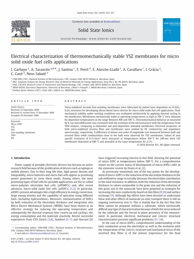
The technological flow of the free-standingmembranes fabricationprocess is shown in Fig. 1 and detailed in reference [15]. Beforedepositing YSZ some micromachining steps were required. Singlecrystal (100)-oriented p-type silicon wafers of 100 mm diameter and300 µm thick were thermally oxidized to obtain a 100 nm thick layerof SiO2. Afterward, low pressure chemical vapor deposition (LPCVD)was used to grow 300 nm thick layers of Si3N4 (Fig. 1a). Aphotolithographic step on the back side of the wafer was carried outto allow defining pre-membrane opening windows on the siliconnitride (Fig. 1b). Back side anisotropic etching performed in a KOHsolution selectively removed the silicon, and stopped when reachingthe dielectric layer of SiO2 at the wafers front side, in order to obtainSiO2/Si3N4 membranes. Finally, wet etching in HF solution was carriedout to remove the remaining SiO2 layer yielding free-standingmembranes of Si3N4 (Fig.1c). Silicon nitride square membranes of300 nm of thickness and different sizes (from 50×50 µm2 to820×820 µm2) were obtained. After that, the wafer was diced inchips of 1.2 x 1.2 cm. These chips were used as a substrate fordepositing YSZ layers by Pulsed Layer Deposition (PLD) yieldingSi3N4/YSZ membranes (Fig. 1d). Yttria-stabilized zirconia (8 mol%Y2O3–ZrO2) thin films of different thicknesses, from 60 nm to 240 nm,were deposited in this step. A KrF excimer laser (Lambda Physik-Compex Pro 201, using a wavelength of λ=248 nm and a pulsewidth≈20 ns with a repetition rate of 10 Hz) was focalized on atarget of YSZ with an energy density of ca. 2 J/cm2 per pulse. Theoxygen partial pressure inside the deposition chamber varied in therange of 2.1–2.4·10−2 mbar and the target-to-substrate distance wasof 70 mm. YSZ thin films were deposited at different substratetemperatures, from Ts=200 °C to 800 °C.This set of conditions wasadapted from a previous work from Infortuna et al. [14] in order toobtain fully dense and homogeneous YSZ thin films. A final ReactiveIon Etching (RIE) step was used to remove the 300 nm of Si3N4 torelease the YSZ layers forming free-standing membranes of theelectrolyte (Fig. 1e). The silicon nitride etching process was carried
out under an atmosphere of CHF3/O2 (3:1) at a total pressure of6.7×10−2 mbar. It was controlled by monitoring the thicknessreduction of the Si3N4 frame layer using reflectometry (due to the10× slower rate etch for YSZ an extra time etching of 30 s, over thetotal time of 180 s, was applied to ensure total removal of residualSi3N4).
Specific chips compatible with transmission electron microscopesample holders, i.e.3 mm diameter, were also manufactured formicrostructural characterization purposes by adding some extrasteps on the micro fabrication process (Fig. 1b*–e*). A 2×2 mm2
square was created around the membrane by opening the siliconnitride layer from the back side. After wet etching with HF and KOH, anotch around the membrane was formed. This precut alloweddetaching the sample from the silicon frame by levering. Thesespecific chips allowed studying free-standing membranes of YSZ byTEM analysis without any additional preparation.
2.2. Mechanical characterization of YSZ membranes
The residual stress of the YSZ free-standing membranes wascharacterized by X-raymicro diffraction (XRD) in a Bruker-D8 Advancediffractometer with a four circle goniometer and GADDS-HiStardetector. The equipment presents a parabolic mirror and a doublepinhole collimator in the primary beam, which allows reducing thebeam divergence in both the diffraction and axial planes, makingpossible the accurate determination of the planar spacing withoutsubstantial defocalization problems in a wide range of different ψangles from zero to almost 75 degrees [19]. Moreover, the small size ofthe X-ray spot area (300 μm diameter) allows for local residual stressanalysis in the area of the self-supported YSZ membranes. Theobservation of the variation of the angular position of the (111)reflection as a function of the tilt angle was used to calculatedifferences on the stresses, according to the so-called “sin2ψ method”[19,20]. A detailed discussion of the application of this technique tothe membranes here presented as well as the YSZ constantsemployed, e.g. Young's modulus, Poisson's ratio or elastic stiffnessconstants, can be found on reference [15].
In order to analyze the thermomechanical stability of the YSZmembranes, thermal cycling from room temperature to the IT-SOFCrange of temperatures (500 °C–700 °C) was studied. Samples wereheated using a ramp rate of 0.7 °C/min and then maintained atTa=500 °C, 600 °C or 700 °C for 2,5 hours and cooled down with thesame ramp rate to room temperature.
2.3. Structural characterization of YSZ membranes
The microstructure of the released YSZ membranes was charac-terized by different methods. The influence of the fabricationparameters on the microstructure, i.e. grain size and crystallinity ofthe YSZ membranes, was studied by Transmission Electron Micros-copy (TEM) by using a JEOL JEM-2100microscope operating at 200 kV.60 nm thick membranes fabricated at different deposition tempera-tures (Ts=200 °C, 400 °C, 500 °C, 600 °C and 700 °C), were used forTEM analysis. The grain size was evaluated on TEM images byaveraging their long and short side over more than 500 particles indifferent images for each sample (only grains in diffraction conditionswere used to assure good contrast). To estimate the crystallinity of thematerial, angle-dependent bright field diffraction contrast imagingwas used as in reference [21]. According to Rupp et al. [21], TEMimages of the same area of the membrane were obtained at differenttilt angles and regions showing change in contrast during tilting wereassociated to well-crystallized grains presenting crystal planes indiffraction conditions. Covering a wide range of tilt angles (from 0º to11º), bright regions were ascribed to amorphous areas. An imagecomposition overlapping the dark areas reached along the tiltingallowed roughly evaluating the amorphous-to-crystalline phase ratio.
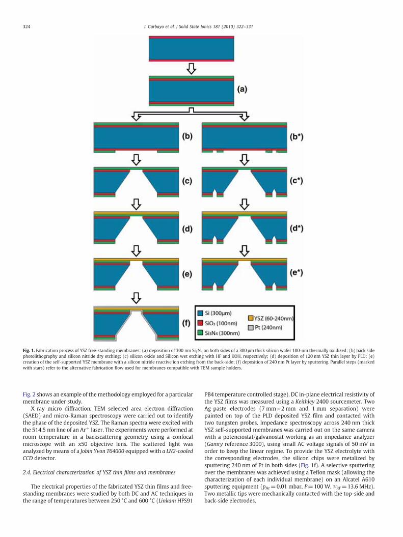
Fig. 1. Fabrication process of YSZ free-standing membranes: (a) deposition of 300 nm Si3N4 on both sides of a 300 μm thick silicon wafer 100-nm thermally oxidized; (b) back sidephotolithography and silicon nitride dry etching; (c) silicon oxide and Silicon wet etching with HF and KOH, respectively; (d) deposition of 120 nm YSZ thin layer by PLD; (e)creation of the self-supported YSZ membrane with a silicon nitride reactive ion etching from the back-side; (f) deposition of 240 nm Pt layer by sputtering. Parallel steps (markedwith stars) refer to the alternative fabrication flow used for membranes compatible with TEM sample holders.
324 I. Garbayo et al. / Solid State Ionics 181 (2010) 322–331
Fig. 2 shows an example of themethodology employed for a particularmembrane under study.
X-ray micro diffraction, TEM selected area electron diffraction(SAED) and micro-Raman spectroscopy were carried out to identifythe phase of the deposited YSZ. The Raman spectra were excited withthe 514.5 nm line of an Ar+ laser. The experiments were performed atroom temperature in a backscattering geometry using a confocalmicroscope with an x50 objective lens. The scattered light wasanalyzed by means of a Jobin Yvon T64000 equipped with a LN2-cooledCCD detector.
2.4. Electrical characterization of YSZ thin films and membranes
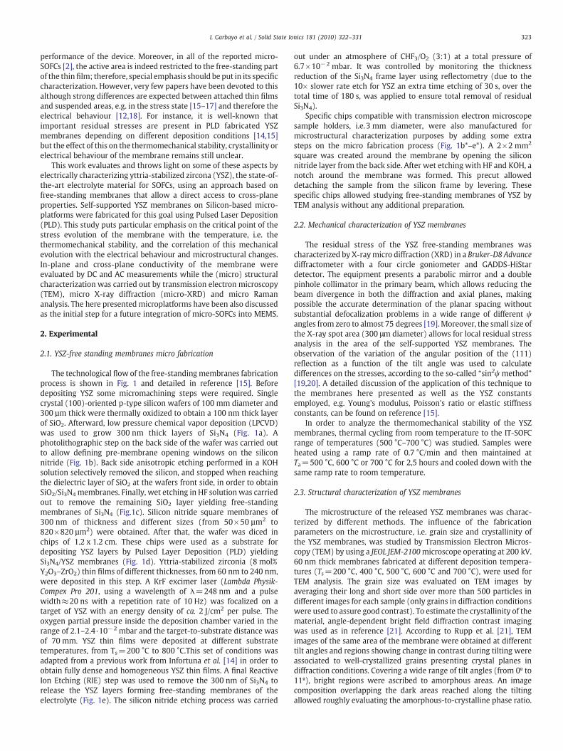
The electrical properties of the fabricated YSZ thin films and free-standing membranes were studied by both DC and AC techniques inthe range of temperatures between 250 °C and 600 °C (Linkam HFS91
PB4 temperature controlled stage). DC in-plane electrical resistivity ofthe YSZ films was measured using a Keithley 2400 sourcemeter. TwoAg-paste electrodes (7 mm×2 mm and 1 mm separation) werepainted on top of the PLD deposited YSZ film and contacted withtwo tungsten probes. Impedance spectroscopy across 240 nm thickYSZ self-supported membranes was carried out on the same camerawith a potenciostat/galvanostat working as an impedance analyzer(Gamry reference 3000), using small AC voltage signals of 50 mV inorder to keep the linear regime. To provide the YSZ electrolyte withthe corresponding electrodes, the silicon chips were metalized bysputtering 240 nm of Pt in both sides (Fig. 1f). A selective sputteringover the membranes was achieved using a Teflon mask (allowing thecharacterization of each individual membrane) on an Alcatel A610sputtering equipment (pAr=0.01 mbar, P=100W, νRF=13.6 MHz).Two metallic tips were mechanically contacted with the top-side andback-side electrodes.
Fig. 2. Cumulative TEM bright field images of the microstructure of YSZ free-standing membranes (deposited at 700 °C and annealed at 600 °C for 2.5 h.) after tilting from 0° to 11°with steps of 1°. Intermediate stages are presented: (a) 0° (b) 0° to 4°, (c) 0° to 8° and (d) 0° to 11°. Evolution of the same small area is squared with solid line and detailed on thecorner; grain contrast by tilting is clearly observed in (a) and (b) zoom images.
325I. Garbayo et al. / Solid State Ionics 181 (2010) 322–331
3. Results and discussion
First of all, it is important to remark that the fabrication process ofthe YSZ self-supported membranes is highly reliable (see an image ofthe released membrane in Fig. 3a). In order to quantify this it ispossible to define a survival rate (SR) as the ratio between the totalnumber of fabricated membranes and the membranes broken afterthe deposition (the statistic was carried out over more than onehundred membranes). Membranes deposited at Ts=200, 400, 600and 700 °C yielded a high survival rate (SR N90%) while thosedeposited at Ts=800 °C presented very low survival rate (SR b20%).Due to this low survival rate, membranes deposited at 800 °C have notbeen considered any more in the rest of the study.
3.1. Microstructural and mechanical characterization of as-depositedYSZ free-standing membranes
Fig. 3b and c show the typical microstructure of an as-depositedYSZ thin film (SEM cross-section image) and a free-standing YSZmembrane (TEM image). Fig. 3c and d show TEM images illustratinghow dense the YSZ layers are, this high density was observedindependently on the substrate temperature deposition. In addition,YSZ films with high uniformity were fabricated; film thicknessuniformity was measured for tens of samples by visible lightreflectometry yielding values below ±0.5% over the membranearea. These features are essential for the membranes to be suitablefor micro SOFCs applications: the presence of porosity or pinholes willreduce dramatically the power generation efficiency and inhomoge-neous thickness could generate hot spots due to local high currentdensities.
The fabricated YSZmembranes show grain sizes on the order of tennanometers for the whole set of deposition conditions (see histo-grams in Fig. 4 for the particular cases of Ts=200 °C, 400 °C and700 °C). For the YSZ membranes under study, a microstructural
enhancement, based on the improvement of the grain interconnec-tivity and the higher level of crystallinity, is promoted by thedeposition temperature as shown in Figs. 4 and 5. In particular,Fig. 4d shows a close comparison of the microstructure whenincreasing the deposition temperature; the enhancement of thegrain interconnectivity with temperature can be observed as well-faceted grains and better-defined grain boundaries. Fig. 5a and bquantitatively evaluate the amorphous-to-crystalline phase ratio byusing the previously described TEM angle-dependent bright fielddiffraction contrast imaging (see Section 2.3). Increasing the operat-ing temperature from Ts=200 °C to Ts=700 °C reduces the percent-age of amorphous phase (white area in the Fig. 5) from 16% to 4%vol.Therefore, better cristallinity and grain connectivity is observedincreasing the deposition temperature until best values are obtainedfor Ts=700 °C.
Fig. 6 depicts the stress evolution of the as-deposited membranes(closed symbols) from an almost free-stress state for the lowestdeposition temperature, Ts=200 °C to a compressive stress atTs=700 °C (S∼ −2 GPa) crossing a minimum at Ts=400 °C(S∼−4 GPa). These stress magnitudes are in line with the observa-tions of Carneiro et al. [22] and Knoll et al. [23], who obtainedcompressive stress values of some GPa in sputtered YSZ films for highenergetic deposition conditions (high power densities and substratebias). However, it is difficult to compare because a wide variety ofstress levels can be found in the literature depending on thedeposition conditions, e.g. significantly lower values on the order offew hundreds of compressive MPa are reported by Quinn et al. [13] orGao et al. [24].
The trend of the stress as a function of the deposition temperatureobtained in Fig. 6 is similar to the originally reported by Thornton andHoffman [25] for metal thin films. According to Thornton andHoffman, for the range of temperatures covered in this work thecombined effects of two main opposite contributions yield amaximum in compressive stress [15,25]: (i) a linearly increasing
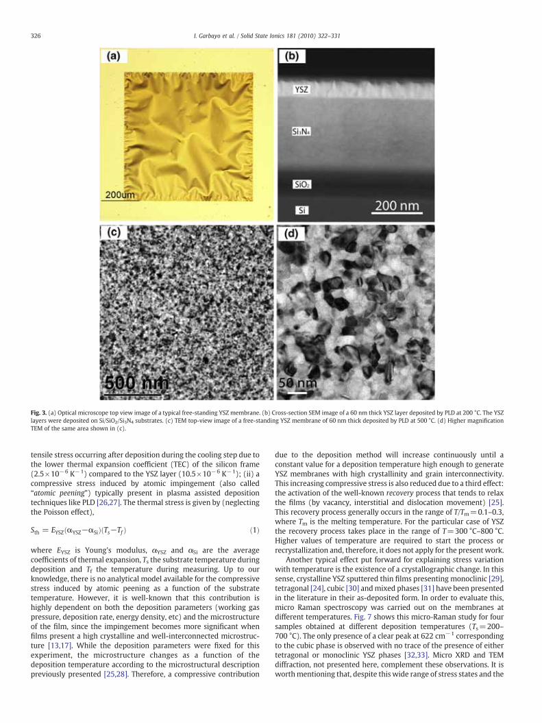
Fig. 3. (a) Optical microscope top view image of a typical free-standing YSZ membrane. (b) Cross-section SEM image of a 60 nm thick YSZ layer deposited by PLD at 200 °C. The YSZlayers were deposited on Si/SiO2/Si3N4 substrates. (c) TEM top-view image of a free-standing YSZ membrane of 60 nm thick deposited by PLD at 500 °C. (d) Higher magnificationTEM of the same area shown in (c).
326 I. Garbayo et al. / Solid State Ionics 181 (2010) 322–331
tensile stress occurring after deposition during the cooling step due tothe lower thermal expansion coefficient (TEC) of the silicon frame(2.5×10⁻⁶ K−1) compared to the YSZ layer (10.5×10⁻⁶ K−1); (ii) acompressive stress induced by atomic impingement (also called“atomic peening”) typically present in plasma assisted depositiontechniques like PLD [26,27]. The thermal stress is given by (neglectingthe Poisson effect),
Sth = EYSZðαYSZ−αSiÞðTs−Tf Þ ð1Þ
where EYSZ is Young's modulus, αYSZ and αSi are the averagecoefficients of thermal expansion, Ts the substrate temperature duringdeposition and Tf the temperature during measuring. Up to ourknowledge, there is no analytical model available for the compressivestress induced by atomic peening as a function of the substratetemperature. However, it is well-known that this contribution ishighly dependent on both the deposition parameters (working gaspressure, deposition rate, energy density, etc) and the microstructureof the film, since the impingement becomes more significant whenfilms present a high crystalline and well-interconnected microstruc-ture [13,17]. While the deposition parameters were fixed for thisexperiment, the microstructure changes as a function of thedeposition temperature according to the microstructural descriptionpreviously presented [25,28]. Therefore, a compressive contribution
due to the deposition method will increase continuously until aconstant value for a deposition temperature high enough to generateYSZ membranes with high crystallinity and grain interconnectivity.This increasing compressive stress is also reduced due to a third effect:the activation of the well-known recovery process that tends to relaxthe films (by vacancy, interstitial and dislocation movement) [25].This recovery process generally occurs in the range of T/Tm=0.1–0.3,where Tm is the melting temperature. For the particular case of YSZthe recovery process takes place in the range of T=300 °C–800 °C.Higher values of temperature are required to start the process orrecrystallization and, therefore, it does not apply for the present work.
Another typical effect put forward for explaining stress variationwith temperature is the existence of a crystallographic change. In thissense, crystalline YSZ sputtered thin films presenting monoclinic [29],tetragonal [24], cubic [30] andmixed phases [31] have been presentedin the literature in their as-deposited form. In order to evaluate this,micro Raman spectroscopy was carried out on the membranes atdifferent temperatures. Fig. 7 shows this micro-Raman study for foursamples obtained at different deposition temperatures (Ts=200–700 °C). The only presence of a clear peak at 622 cm−1 correspondingto the cubic phase is observed with no trace of the presence of eithertetragonal or monoclinic YSZ phases [32,33]. Micro XRD and TEMdiffraction, not presented here, complement these observations. It isworthmentioning that, despite this wide range of stress states and the
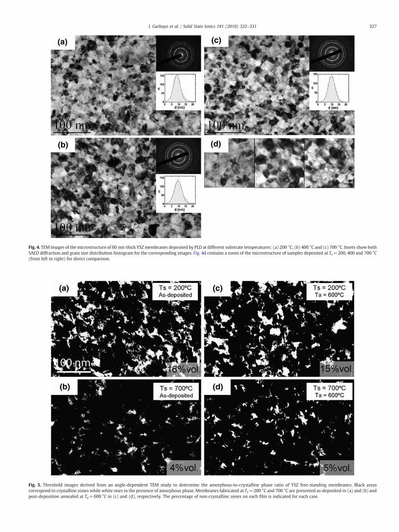
Fig. 4. TEM images of themicrostructure of 60 nm-thick YSZmembranes deposited by PLD at different substrate temperatures: (a) 200 °C, (b) 400 °C and (c) 700 °C. Insets show bothSAED diffraction and grain size distribution histogram for the corresponding images. Fig. 4d contains a zoom of the microstructure of samples deposited at Ts=200, 400 and 700 °C(from left to right) for direct comparison.
Fig. 5. Threshold images derived from an angle-dependent TEM study to determine the amorphous-to-crystalline phase ratio of YSZ free-standing membranes. Black areascorrespond to crystalline zones while white ones to the presence of amorphous phase. Membranes fabricated at Ts=200 °C and 700 °C are presented as-deposited in (a) and (b) andpost-deposition annealed at Ta=600 °C in (c) and (d), respectively. The percentage of non-crystalline zones on each film is indicated for each case.
327I. Garbayo et al. / Solid State Ionics 181 (2010) 322–331
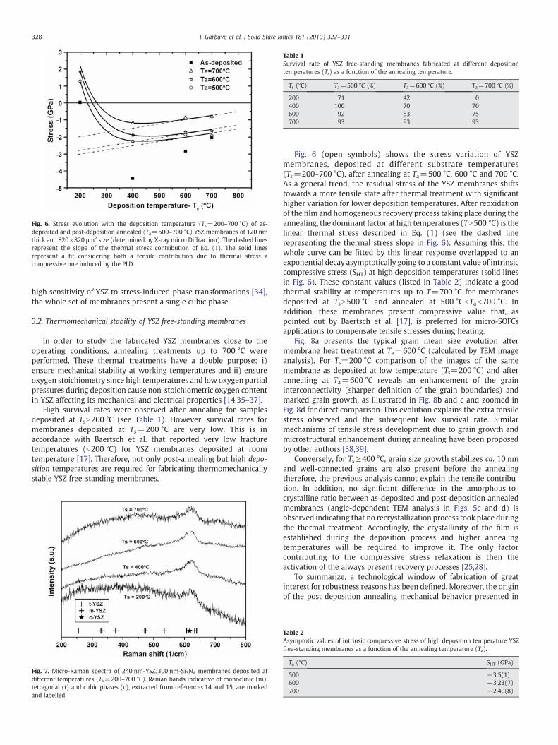
Fig. 6. Stress evolution with the deposition temperature (Ts=200–700 °C) of as-deposited and post-deposition annealed (Ta=500–700 °C) YSZ membranes of 120 nmthick and 820×820 μm2 size (determined by X-ray micro Diffraction). The dashed linesrepresent the slope of the thermal stress contribution of Eq. (1). The solid linesrepresent a fit considering both a tensile contribution due to thermal stress acompressive one induced by the PLD.
Table 1Survival rate of YSZ free-standing membranes fabricated at different depositiontemperatures (Ts) as a function of the annealing temperature.
Ts (°C) Ta=500 °C (%) Ta=600 °C (%) Ta=700 °C (%)
200 71 42 0400 100 70 70600 92 83 75700 93 93 93
328 I. Garbayo et al. / Solid State Ionics 181 (2010) 322–331
high sensitivity of YSZ to stress-induced phase transformations [34],the whole set of membranes present a single cubic phase.
3.2. Thermomechanical stability of YSZ free-standing membranes
In order to study the fabricated YSZ membranes close to theoperating conditions, annealing treatments up to 700 °C wereperformed. These thermal treatments have a double purpose: i)ensure mechanical stability at working temperatures and ii) ensureoxygen stoichiometry since high temperatures and low oxygen partialpressures during deposition cause non-stoichiometric oxygen contentin YSZ affecting its mechanical and electrical properties [14,35–37].
High survival rates were observed after annealing for samplesdeposited at TsN200 °C (see Table 1). However, survival rates formembranes deposited at Ts=200 °C are very low. This is inaccordance with Baertsch et al. that reported very low fracturetemperatures (b200 °C) for YSZ membranes deposited at roomtemperature [17]. Therefore, not only post-annealing but high depo-sition temperatures are required for fabricating thermomechanicallystable YSZ free-standing membranes.
Fig. 7. Micro-Raman spectra of 240 nm-YSZ/300 nm-Si3N4 membranes deposited atdifferent temperatures (Ts=200–700 °C). Raman bands indicative of monoclinic (m),tetragonal (t) and cubic phases (c), extracted from references 14 and 15, are markedand labelled.
Fig. 6 (open symbols) shows the stress variation of YSZmembranes, deposited at different substrate temperatures(Ts=200–700 °C), after annealing at Ta=500 °C, 600 °C and 700 °C.As a general trend, the residual stress of the YSZ membranes shiftstowards a more tensile state after thermal treatment with significanthigher variation for lower deposition temperatures. After reoxidationof the film and homogeneous recovery process taking place during theannealing, the dominant factor at high temperatures (TN500 °C) is thelinear thermal stress described in Eq. (1) (see the dashed linerepresenting the thermal stress slope in Fig. 6). Assuming this, thewhole curve can be fitted by this linear response overlapped to anexponential decay asymptotically going to a constant value of intrinsiccompressive stress (SHT) at high deposition temperatures (solid linesin Fig. 6). These constant values (listed in Table 2) indicate a goodthermal stability at temperatures up to T=700 °C for membranesdeposited at TsN500 °C and annealed at 500 °CbTab700 °C. Inaddition, these membranes present compressive value that, aspointed out by Baertsch et al. [17], is preferred for micro-SOFCsapplications to compensate tensile stresses during heating.
Fig. 8a presents the typical grain mean size evolution aftermembrane heat treatment at Ta=600 °C (calculated by TEM imageanalysis). For Ts=200 °C comparison of the images of the samemembrane as-deposited at low temperature (Ts=200 °C) and afterannealing at Ta=600 °C reveals an enhancement of the graininterconnectivity (sharper definition of the grain boundaries) andmarked grain growth, as illustrated in Fig. 8b and c and zoomed inFig. 8d for direct comparison. This evolution explains the extra tensilestress observed and the subsequent low survival rate. Similarmechanisms of tensile stress development due to grain growth andmicrostructural enhancement during annealing have been proposedby other authors [38,39].
Conversely, for Ts≥400 °C, grain size growth stabilizes ca. 10 nmand well-connected grains are also present before the annealingtherefore, the previous analysis cannot explain the tensile contribu-tion. In addition, no significant difference in the amorphous-to-crystalline ratio between as-deposited and post-deposition annealedmembranes (angle-dependent TEM analysis in Figs. 5c and d) isobserved indicating that no recrystallization process took place duringthe thermal treatment. Accordingly, the crystallinity of the film isestablished during the deposition process and higher annealingtemperatures will be required to improve it. The only factorcontributing to the compressive stress relaxation is then theactivation of the always present recovery processes [25,28].
To summarize, a technological window of fabrication of greatinterest for robustness reasons has been defined. Moreover, the originof the post-deposition annealing mechanical behavior presented in
Table 2Asymptotic values of intrinsic compressive stress of high deposition temperature YSZfree-standing membranes as a function of the annealing temperature (Ta).
Ta (°C) SHT (GPa)
500 −3.5(1)600 −3.23(7)700 −2.40(8)
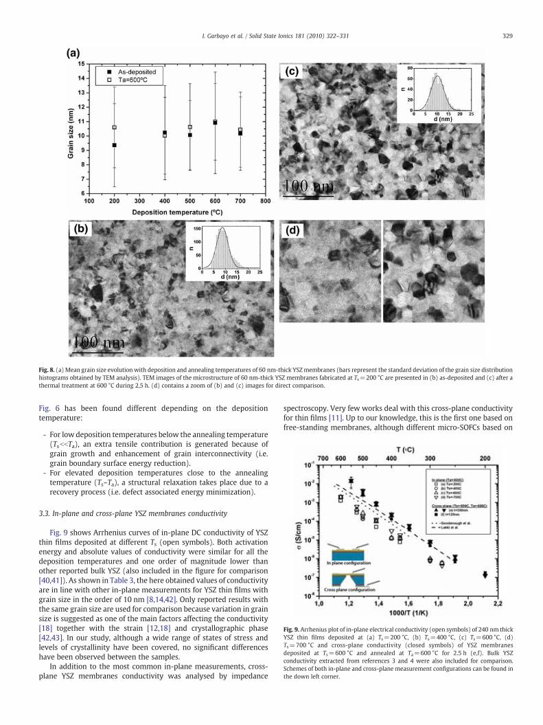
Fig. 8. (a) Mean grain size evolution with deposition and annealing temperatures of 60 nm-thick YSZmembranes (bars represent the standard deviation of the grain size distributionhistograms obtained by TEM analysis). TEM images of the microstructure of 60 nm-thick YSZ membranes fabricated at Ts=200 °C are presented in (b) as-deposited and (c) after athermal treatment at 600 °C during 2,5 h. (d) contains a zoom of (b) and (c) images for direct comparison.
Fig. 9. Arrhenius plot of in-plane electrical conductivity (open symbols) of 240 nm thickYSZ thin films deposited at (a) Ts=200 °C, (b) Ts=400 °C, (c) Ts=600 °C, (d)Ts=700 °C and cross-plane conductivity (closed symbols) of YSZ membranesdeposited at Ts=600 °C and annealed at Ta=600 °C for 2.5 h (e,f). Bulk YSZconductivity extracted from references 3 and 4 were also included for comparison.Schemes of both in-plane and cross-plane measurement configurations can be found inthe down left corner.
329I. Garbayo et al. / Solid State Ionics 181 (2010) 322–331
Fig. 6 has been found different depending on the depositiontemperature:
- For low deposition temperatures below the annealing temperature(TsbbTa), an extra tensile contribution is generated because ofgrain growth and enhancement of grain interconnectivity (i.e.grain boundary surface energy reduction).
- For elevated deposition temperatures close to the annealingtemperature (Ts–Ta), a structural relaxation takes place due to arecovery process (i.e. defect associated energy minimization).
3.3. In-plane and cross-plane YSZ membranes conductivity
Fig. 9 shows Arrhenius curves of in-plane DC conductivity of YSZthin films deposited at different Ts (open symbols). Both activationenergy and absolute values of conductivity were similar for all thedeposition temperatures and one order of magnitude lower thanother reported bulk YSZ (also included in the figure for comparison[40,41]). As shown in Table 3, the here obtained values of conductivityare in line with other in-plane measurements for YSZ thin films withgrain size in the order of 10 nm [8,14,42]. Only reported results withthe same grain size are used for comparison because variation in grainsize is suggested as one of the main factors affecting the conductivity[18] together with the strain [12,18] and crystallographic phase[42,43]. In our study, although a wide range of states of stress andlevels of crystallinity have been covered, no significant differenceshave been observed between the samples.
In addition to the most common in-plane measurements, cross-plane YSZ membranes conductivity was analysed by impedance
spectroscopy. Very few works deal with this cross-plane conductivityfor thin films [11]. Up to our knowledge, this is the first one based onfree-standing membranes, although different micro-SOFCs based on
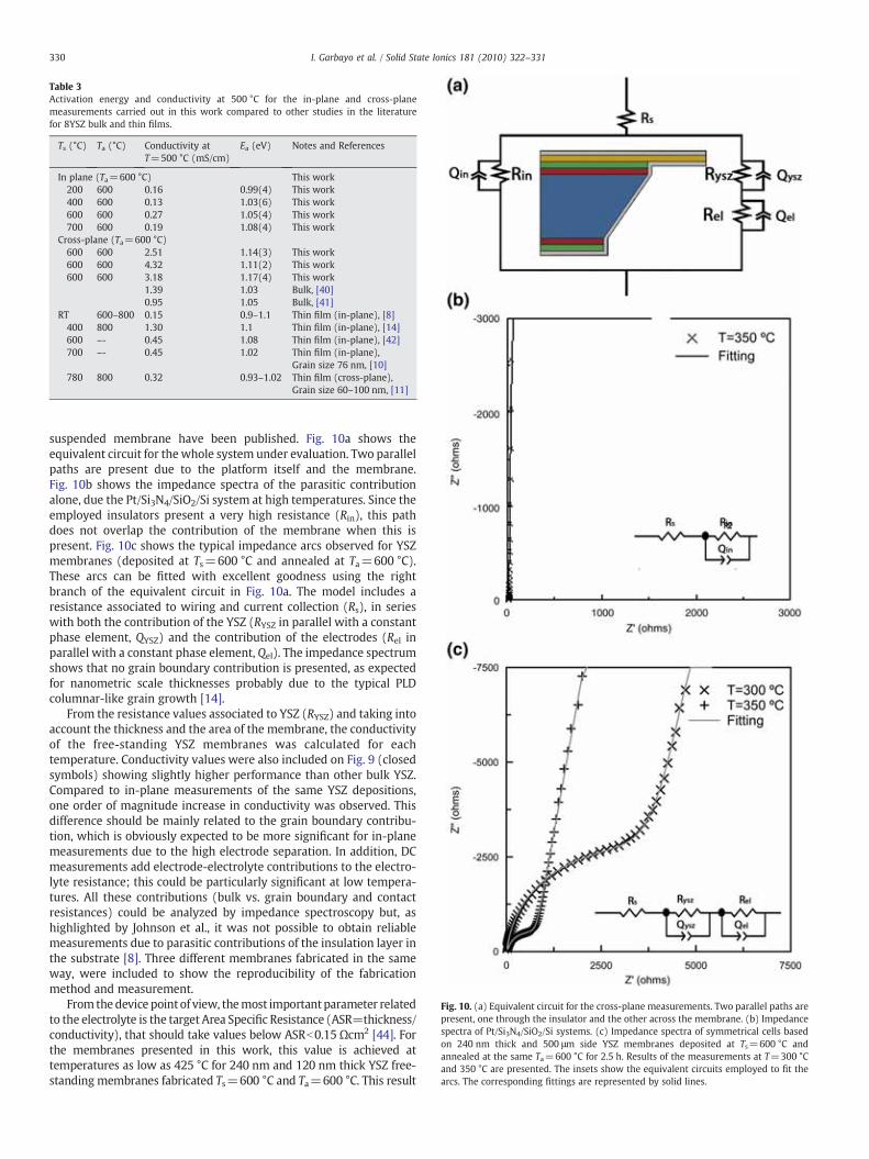
Table 3Activation energy and conductivity at 500 °C for the in-plane and cross-planemeasurements carried out in this work compared to other studies in the literaturefor 8YSZ bulk and thin films.
Ts (°C) Ta (°C) Conductivity atT=500 °C (mS/cm)
Ea (eV) Notes and References
In plane (Ta=600 °C) This work200 600 0.16 0.99(4) This work400 600 0.13 1.03(6) This work600 600 0.27 1.05(4) This work700 600 0.19 1.08(4) This work
Cross-plane (Ta=600 °C)600 600 2.51 1.14(3) This work600 600 4.32 1.11(2) This work600 600 3.18 1.17(4) This work
1.39 1.03 Bulk, [40]0.95 1.05 Bulk, [41]
RT 600–800 0.15 0.9–1.1 Thin film (in-plane), [8]400 800 1.30 1.1 Thin film (in-plane), [14]600 –- 0.45 1.08 Thin film (in-plane), [42]700 –- 0.45 1.02 Thin film (in-plane),
Grain size 76 nm, [10]780 800 0.32 0.93–1.02 Thin film (cross-plane),
Grain size 60–100 nm, [11]
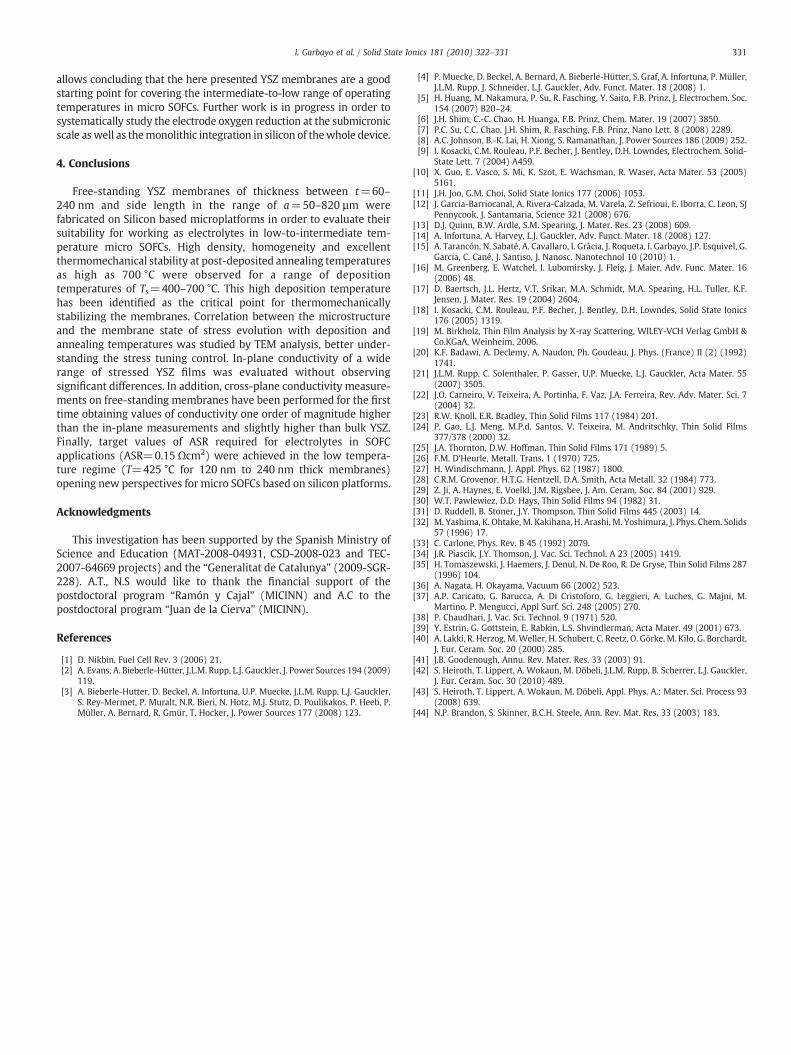
Fig. 10. (a) Equivalent circuit for the cross-plane measurements. Two parallel paths arepresent, one through the insulator and the other across the membrane. (b) Impedancespectra of Pt/Si3N4/SiO2/Si systems. (c) Impedance spectra of symmetrical cells basedon 240 nm thick and 500 μm side YSZ membranes deposited at Ts=600 °C andannealed at the same Ta=600 °C for 2.5 h. Results of the measurements at T=300 °Cand 350 °C are presented. The insets show the equivalent circuits employed to fit thearcs. The corresponding fittings are represented by solid lines.
330 I. Garbayo et al. / Solid State Ionics 181 (2010) 322–331
suspended membrane have been published. Fig. 10a shows theequivalent circuit for the whole system under evaluation. Two parallelpaths are present due to the platform itself and the membrane.Fig. 10b shows the impedance spectra of the parasitic contributionalone, due the Pt/Si3N4/SiO2/Si system at high temperatures. Since theemployed insulators present a very high resistance (Rin), this pathdoes not overlap the contribution of the membrane when this ispresent. Fig. 10c shows the typical impedance arcs observed for YSZmembranes (deposited at Ts=600 °C and annealed at Ta=600 °C).These arcs can be fitted with excellent goodness using the rightbranch of the equivalent circuit in Fig. 10a. The model includes aresistance associated to wiring and current collection (Rs), in serieswith both the contribution of the YSZ (RYSZ in parallel with a constantphase element, QYSZ) and the contribution of the electrodes (Rel inparallel with a constant phase element, Qel). The impedance spectrumshows that no grain boundary contribution is presented, as expectedfor nanometric scale thicknesses probably due to the typical PLDcolumnar-like grain growth [14].
From the resistance values associated to YSZ (RYSZ) and taking intoaccount the thickness and the area of the membrane, the conductivityof the free-standing YSZ membranes was calculated for eachtemperature. Conductivity values were also included on Fig. 9 (closedsymbols) showing slightly higher performance than other bulk YSZ.Compared to in-plane measurements of the same YSZ depositions,one order of magnitude increase in conductivity was observed. Thisdifference should be mainly related to the grain boundary contribu-tion, which is obviously expected to be more significant for in-planemeasurements due to the high electrode separation. In addition, DCmeasurements add electrode-electrolyte contributions to the electro-lyte resistance; this could be particularly significant at low tempera-tures. All these contributions (bulk vs. grain boundary and contactresistances) could be analyzed by impedance spectroscopy but, ashighlighted by Johnson et al., it was not possible to obtain reliablemeasurements due to parasitic contributions of the insulation layer inthe substrate [8]. Three different membranes fabricated in the sameway, were included to show the reproducibility of the fabricationmethod and measurement.
From thedevice point of view, themost importantparameter relatedto the electrolyte is the target Area Specific Resistance (ASR=thickness/conductivity), that should take values below ASRb0.15 Ωcm2 [44]. Forthe membranes presented in this work, this value is achieved attemperatures as low as 425 °C for 240 nm and 120 nm thick YSZ free-standing membranes fabricated Ts=600 °C and Ta=600 °C. This result
331I. Garbayo et al. / Solid State Ionics 181 (2010) 322–331
allows concluding that the here presented YSZ membranes are a goodstarting point for covering the intermediate-to-low range of operatingtemperatures in micro SOFCs. Further work is in progress in order tosystematically study the electrode oxygen reduction at the submicronicscale aswell as themonolithic integration in silicon of thewhole device.
4. Conclusions
Free-standing YSZ membranes of thickness between t=60–240 nm and side length in the range of a=50–820 µm werefabricated on Silicon based microplatforms in order to evaluate theirsuitability for working as electrolytes in low-to-intermediate tem-perature micro SOFCs. High density, homogeneity and excellentthermomechanical stability at post-deposited annealing temperaturesas high as 700 °C were observed for a range of depositiontemperatures of Ts=400–700 °C. This high deposition temperaturehas been identified as the critical point for thermomechanicallystabilizing the membranes. Correlation between the microstructureand the membrane state of stress evolution with deposition andannealing temperatures was studied by TEM analysis, better under-standing the stress tuning control. In-plane conductivity of a widerange of stressed YSZ films was evaluated without observingsignificant differences. In addition, cross-plane conductivity measure-ments on free-standing membranes have been performed for the firsttime obtaining values of conductivity one order of magnitude higherthan the in-plane measurements and slightly higher than bulk YSZ.Finally, target values of ASR required for electrolytes in SOFCapplications (ASR=0.15 Ωcm2) were achieved in the low tempera-ture regime (T=425 °C for 120 nm to 240 nm thick membranes)opening new perspectives for micro SOFCs based on silicon platforms.
Acknowledgments
This investigation has been supported by the Spanish Ministry ofScience and Education (MAT-2008-04931, CSD-2008-023 and TEC-2007-64669 projects) and the “Generalitat de Catalunya” (2009-SGR-228). A.T., N.S would like to thank the financial support of thepostdoctoral program “Ramón y Cajal” (MICINN) and A.C to thepostdoctoral program “Juan de la Cierva” (MICINN).
References
[1] D. Nikbin, Fuel Cell Rev. 3 (2006) 21.[2] A. Evans, A. Bieberle-Hütter, J.L.M. Rupp, L.J. Gauckler, J. Power Sources 194 (2009)
119.[3] A. Bieberle-Hutter, D. Beckel, A. Infortuna, U.P. Muecke, J.L.M. Rupp, L.J. Gauckler,
S. Rey-Mermet, P. Muralt, N.R. Bieri, N. Hotz, M.J. Stutz, D. Poulikakos, P. Heeb, P.Müller, A. Bernard, R. Gmür, T. Hocker, J. Power Sources 177 (2008) 123.
[4] P. Muecke, D. Beckel, A. Bernard, A. Bieberle-Hütter, S. Graf, A. Infortuna, P. Müller,J.L.M. Rupp, J. Schneider, L.J. Gauckler, Adv. Funct. Mater. 18 (2008) 1.
[5] H. Huang, M. Nakamura, P. Su, R. Fasching, Y. Saito, F.B. Prinz, J. Electrochem. Soc.154 (2007) B20–24.
[6] J.H. Shim, C.-C. Chao, H. Huanga, F.B. Prinz, Chem. Mater. 19 (2007) 3850.[7] P.C. Su, C.C. Chao, J.H. Shim, R. Fasching, F.B. Prinz, Nano Lett. 8 (2008) 2289.[8] A.C. Johnson, B.-K. Lai, H. Xiong, S. Ramanathan, J. Power Sources 186 (2009) 252.[9] I. Kosacki, C.M. Rouleau, P.F. Becher, J. Bentley, D.H. Lowndes, Electrochem. Solid-
State Lett. 7 (2004) A459.[10] X. Guo, E. Vasco, S. Mi, K. Szot, E. Wachsman, R. Waser, Acta Mater. 53 (2005)
5161.[11] J.H. Joo, G.M. Choi, Solid State Ionics 177 (2006) 1053.[12] J. Garcia-Barriocanal, A. Rivera-Calzada, M. Varela, Z. Sefrioui, E. Iborra, C. Leon, SJ
Pennycook, J. Santamaria, Science 321 (2008) 676.[13] D.J. Quinn, B.W. Ardle, S.M. Spearing, J. Mater. Res. 23 (2008) 609.[14] A. Infortuna, A. Harvey, L.J. Gauckler, Adv. Funct. Mater. 18 (2008) 127.[15] A. Tarancón, N. Sabaté, A. Cavallaro, I. Gràcia, J. Roqueta, I. Garbayo, J.P. Esquivel, G.
Garcia, C. Cané, J. Santiso, J. Nanosc. Nanotechnol 10 (2010) 1.[16] M. Greenberg, E. Watchel, I. Lubomirsky, J. Fleig, J. Maier, Adv. Func. Mater. 16
(2006) 48.[17] D. Baertsch, J.L. Hertz, V.T. Srikar, M.A. Schmidt, M.A. Spearing, H.L. Tuller, K.F.
Jensen, J. Mater. Res. 19 (2004) 2604.[18] I. Kosacki, C.M. Rouleau, P.F. Becher, J. Bentley, D.H. Lowndes, Solid State Ionics
176 (2005) 1319.[19] M. Birkholz, Thin Film Analysis by X-ray Scattering, WILEY-VCH Verlag GmbH &
Co.KGaA, Weinheim, 2006.[20] K.F. Badawi, A. Declemy, A. Naudon, Ph. Goudeau, J. Phys. (France) II (2) (1992)
1741.[21] J.L.M. Rupp, C. Solenthaler, P. Gasser, U.P. Muecke, L.J. Gauckler, Acta Mater. 55
(2007) 3505.[22] J.O. Carneiro, V. Teixeira, A. Portinha, F. Vaz, J.A. Ferreira, Rev. Adv. Mater. Sci. 7
(2004) 32.[23] R.W. Knoll, E.R. Bradley, Thin Solid Films 117 (1984) 201.[24] P. Gao, L.J. Meng, M.P.d. Santos, V. Teixeira, M. Andritschky, Thin Solid Films
377/378 (2000) 32.[25] J.A. Thornton, D.W. Hoffman, Thin Solid Films 171 (1989) 5.[26] F.M. D'Heurle, Metall. Trans. 1 (1970) 725.[27] H. Windischmann, J. Appl. Phys. 62 (1987) 1800.[28] C.R.M. Grovenor, H.T.G. Hentzell, D.A. Smith, Acta Metall. 32 (1984) 773.[29] Z. Ji, A. Haynes, E. Voelkl, J.M. Rigsbee, J. Am. Ceram. Soc. 84 (2001) 929.[30] W.T. Pawlewiez, D.D. Hays, Thin Solid Films 94 (1982) 31.[31] D. Ruddell, B. Stoner, J.Y. Thompson, Thin Solid Films 445 (2003) 14.[32] M. Yashima, K. Ohtake, M. Kakihana, H. Arashi, M. Yoshimura, J. Phys. Chem. Solids
57 (1996) 17.[33] C. Carlone, Phys. Rev. B 45 (1992) 2079.[34] J.R. Piascik, J.Y. Thomson, J. Vac. Sci. Technol. A 23 (2005) 1419.[35] H. Tomaszewski, J. Haemers, J. Denul, N. De Roo, R. De Gryse, Thin Solid Films 287
(1996) 104.[36] A. Nagata, H. Okayama, Vacuum 66 (2002) 523.[37] A.P. Caricato, G. Barucca, A. Di Cristoforo, G. Leggieri, A. Luches, G. Majni, M.
Martino, P. Mengucci, Appl Surf. Sci. 248 (2005) 270.[38] P. Chaudhari, J. Vac. Sci. Technol. 9 (1971) 520.[39] Y. Estrin, G. Gottstein, E. Rabkin, L.S. Shvindlerman, Acta Mater. 49 (2001) 673.[40] A. Lakki, R. Herzog, M.Weller, H. Schubert, C. Reetz, O. Görke, M. Kilo, G. Borchardt,
J. Eur. Ceram. Soc. 20 (2000) 285.[41] J.B. Goodenough, Annu. Rev. Mater. Res. 33 (2003) 91.[42] S. Heiroth, T. Lippert, A. Wokaun, M. Döbeli, J.L.M. Rupp, B. Scherrer, L.J. Gauckler,
J. Eur. Ceram. Soc. 30 (2010) 489.[43] S. Heiroth, T. Lippert, A. Wokaun, M. Döbeli, Appl. Phys. A.: Mater. Sci. Process 93
(2008) 639.[44] N.P. Brandon, S. Skinner, B.C.H. Steele, Ann. Rev. Mat. Res. 33 (2003) 183.