electrical characteristics of aluminum-zirconium oxide-barium magnesium fluoride-p silicon mis...
TRANSCRIPT

AD-A253 0000
t/
PROCEEDINGS
3rd InternationalSymposium
on
IntegratedFerroelectrics
Ap; ~ i9 9.-13566
Colorado Springs April 3-5, 1991

COMPONENT PART NOTICE
THIS PAPER IS A COMPONENT PART OF THE FOLLOWING C0MILATION REPORT:
TITLE: Proceedings of the International Symposium on Integrated Ferroelectrics
(ISIF) (3rd) Held in Colorado Springs, Colorado on 3-5 April 1991.
To ORDER THE COMPLETE COMPILATION REPORT, USE AD-A253 000
THE COMPONENT PART IS PROVIDED HERE TO ALLOW USERS ACCESS TO INDIVIDUALLY
AUTHORED SECTIONS OF PROCEEDING, ANNALS, SYMPOSIA, ETC. HOWEVER, THE (4VPONENTSHOULD BE CONSIDERED WITHIN THE CONTEXT OF THE OVERALL COMPILATION REPORT AND
NOT AS A STAND-ALONE TECHNICAL REPORT.
THE FOLLOWING COMPONENT PART NUMBERS COMPRISE THE COMPILATION REPORT:THRU
AD): AD-P006 638 AD-PO06 694
AD#: AN#:
AD#: A])#:
Aceoestoa For
I_ _ '; a m_____.__NTIF,
( Disr±M1t i/I
I'aland/or,Dist j Special
DTIFr F 5463 OPI: DTIC-TID

ISIF-91
3rd International Syposiumon
Integrated Ferroelectrics
April 3, 4, and 5, 1991Antlers Hotel, Colorado Springs, Colorado
Sponsored by:University of Colorado at Colorado Springs
Defense Advanced Research Projects Agency (DARPA)Gordon & Breach Science Publishers, Inc. - or
Naval Postgraduate School - .
Storage Technology CorporationUniversity of Colorado Foundation, Inc. ,,
Statement A per telecon Dr. Wallace Smith ly-
ONR/Code 1131 Distr-bjt 1 ein/
Arlington, VA 22217-5000 AvIllability Codes-- va•' -l -,an-d/or
NWW 6/2/92 Dist Speolal

Copyright 1991International Symposium on
Integrated Ferroelectrics
Printed in the United States of America
B*6
P.

3rd ISIF-91 COMMITTEE
Carlos A. Paz de AraujoSYMPOSIUM CHAIRMAN
Rudolf PanholzerSYMPOSIUM Co0CHARMA
James F. ScottTECNICAL PROGRAM CHAIRMAN
Alona S. MillerSYMPOSIUM COORDINMATIR

TABLE OF CONTENTSFOREWORDCarloe A. Paz do Arauja (chairman)
SESSION I MATERIALSChair: George W. Taylor
Ferroelect~ric Memory Programs in Canada .......................................................1Michael Sayer
Recont Advances in the Deposition of Ferroaslcric Thin Films ......................................10S.B. Krupanidhi
Advances in Processing and Properties of Pwanisdt Thit-Fi~ms forFRAMs, DRAMs. and Deoooupirg Ce p aca.......................................................3 30S.K. Dey. C.K. Badingay, J. J. Lee. T.K Gloerutad, and C.TA Suchicital
Fast Decay Component of the Remarient Polarization in Thin Film PZT CApeclbors ............................. 44Joseph M. Benedetto, Randall A. Moore, and F. Barry McLean
SESSION 11 LASER ABLATION DEPOSITIONChair: Leonard Schwie
Ferroelectric P rTLOThin Films on Epitaxal Y-Ba-Cu-O ................................................. 54R~ ~ ~' Raes,1Z.mK&in B. Wlikens. F. 118mma. T. Sand%,
J. Bullington, J. M. Tarascon, and J. Evans
Pulsed Laser Deposition (PID) of Oriented Bismuth Titanate Filmsfor Integrated Electronic Applications................................................................................ 62H . Buhay, S. Sinharoy, M.H. Franoombe, W.H. Kasner, J. T&Mvechio. BK. Park,N.J. Doyle, D.R. Lampe. and M. Polinsky
Filament-Assisted Pulsed Laser Deposition of Epitdaxi PbZr.Ti1.O 3 Films:Morphological and Electrical Chrceiain..............................................................................7R.E. Leuchtner, K.S. Grabowskci. D.B. Chrisey, and J.S. Horwitz
Preparation, Microstructure, and Ferroelectric Properties of Lase-Deposlted ThinBaT00 3 and Lead Zlironate-litanae Films ......................................................................... 87P.S. Brady, B.J. Rod. KW. Bennett LP. Cook, P.K Schenck, M.D. Vaudin,W. Wang-Hg. and CM. Chiang
Pulsed Excimer Laser Deposition of Ferroelectric Thin Films.................................................... 100S.B. Knupanidhii, D. Roy, N. Maffei, and C.J. Pang
SESSION Ill DEVICE PHENOMENAChair T.S. Kalkur
Process Dependent Electrical Characteristics and Equivalent Circui Model ofSol-Gel BasedPZT Capacitors..................................................................................... 116T. Mihara, H. Watanabe, H. Yashimorl, C.A. Paz do Araujo, B. Melnldc, and LD. McMilan
Device Effects of Various Zrffl Ratios of PZT Thin-Fims Prepared by Sal-Gel Method........................ 139H. Watanabe, T. Mihara, and CA. Paz do Araujo
Statiscal Theory of Fatigue in Ferroelectric Devices ............................................................. 151C.A. Paz do Arauja. R. Zuleeg, T. MOhar, H. Wataabe. A. CArriw.,LD. Mc~illan, and J.F. Scott
C-V and I-V Simulatons of Meta Ferroelectric Sloan Capped and UncappedBaM 4 Devices Using Pieces 11-B ................................................................................ 169Deng-Yuan Chen, C.A. Paz do Arajo, and LD. McMilla
d.c. Leakcage Currents In Ferroelectric Memories ................................................................. 176J.F. Scott, B.M. Melnidi, CAL Paz do Arajuo. LD. McMillen, and R. Zubee
Preparation of PbTIO Thin Films by L#ase Ablation.............................................................. 185Masanad Okuyama, faaul Mal, and Yfshihio H~nAMeaw
IV

SESSION IV EUROPEAN INTEGRATED FERROELECTAICSChair Willam A. Geideman
Application of Metal Alkwxides In the Synthesis of Oxides ..........................................195Ml. LYanovskaya, E.P. Turevskaya, V.G. Kessler, I.E. Cbvintseva, WWd N. Ya. Turova
Ferroelectric Thin Film Research in France .................................................................... 2...6P. Gaucher, S.P. Faure, and P. Barboux
SESSION V DETECTORS AND SENSORS: OPTICAL EFFECTSChair: Gone Haertling
Thin Ferroelectric Films for Thermal Detector Applications ...................................................... 215F. Amnger, A Patel. N.M. Shorrocks. C. Trundle, and R.W. Whalmore
SoWl.G Derived Ferroelectric: Thin Films In Silicon Mboromacnhiig............................................ 231C.-C. Hsueh, T. Tamagawa, C. Ye. A. Helgeson, and D.L. Polsa
Thin Piezoelectric VDF-TrFE Copolymer Films for Data Storage................................................ 245Peter Guthner, Joachim Glat-Reichenbach, Doris Schilling, and Klaus Dransfeld
Photovoltages in Ferroeledtric Films.............................................................................. 251P.S. Brody and B.J. Rod
Ph~otoresponse from Thin Ferroelectuic Films of Lead Zironate Tkanae....................................... 262Sarka Thakoor, Anil P. Thakoor, and Stephen E. Bernacid
Study of the Optical Propeuties of RIF Supttered Lithium Niobate Thin Films ................................... 278Charles Hung-Jia Huang and Thomas A. Rabeon
SESSION VI THEORYChair: Rainer Zukee
Theory of Conduction and Brealtdown In Perovalde Thin Films................................................ 288Rainer Waser and Marelke Klee
On Polarization Reversals in Ferroeledtrics ...................................................................... 306Yoshihiro Ishlbashi
Fast Reversal Process in Real Ferroelectrics .................................................................... 315V. Ya. Shur, A.L. Gruverman, N. Yu. Ponomarv.v E.L. Rumnyantsev, and NA. Tonkachyova
SESSION Vill THEORY AND MODELSChair~ Paul Beale
Numerical Analyses of Ferroelectric Characteristics for Memory Use by Using a Lattice Model............... 326Masayoshi Omura, Hideo Adachi, and Yoshihiro Ishblashi
Rejuvenation of Forroelednric Fatigue in Modified Lead Ziroonate Titanste CeramicsNear Totragonai-Rhornbohodral Morphotropic Phase Boundary................................................ 335Wuyi Pan and Cheng-Feng Wue
A Generalized Ferroelectric Capacitor Modeling Methdolobgy .................................................. 344Douglas E. Dunn
Characterization and Modeling of Thin-Film Ferroeldui CapacitorsUsing C-V Analysis................................................................................................ 354Ciaran J. Brennan
SESSION Vill TESflNQChair~ Thomas A. Rabeon
Ferroelectric Memory Evaluation and Development System .................................................... 364David W. Boodurant
Characterization df PZT Films Fatigued at Low Frequency...................................................... 368R.A. Uipeles, B.A. Morgan. and M.S. Leung
Aspects of Fatigue and Rapid Depolarization in Thin Film PZT Capeciors..................................... 376R.D. Namby. J.R. Schrwu*, M.S. Rodgers, and S.L. Miler
v

SESSION IX MEMORY DEVICESChair: Jan. Alexander
Integration of Ferroelectric PZT Capacitors with GaAs JFET Devices ................................390S.Y. Wu and Win. A. Geideman
Anomalous Remanent Polarization in Ferroelectric Caaios..................................... 0Norman E. Abt
SESSION X PROCESSING IChair: James McGarrity
A High-Capacitance PZT-on-Ta2O~ Memory Cell with a Chemically StableElectrode Suitable for Sub-Micron Processing..................................................................... 414M. Azuma, T. Nasu, S. Katsu, T. Otsuki, and G. Kano
Improved Switching Endurance of Lead Zirconate-litanate Capacitors forNonvolatile Memory Aplctos....................................................................................43I.K. Naik, LE. Sanchez, S.Y. Wu, and B.P. Maderic
Crack-Free PZT Thin Films Micropattemed on Silicon Substrate for Integrated Circuits........................ 444Moloo Toyama, Naoto Inoue, Masanod Okuyama. and Yoshibiro Hamakawa
Ferroelectric Pb(Zr,Ti)03 Thin Films Prepared by Planar Multi-Target Sputtering............................... 453R. Bruchhaus, H. Huber, D. Pitzer, and W. Wersing
Electrical Results of Multilevel and Homogeneous Ferroelectric Capacitors..................................... 461J.D. Cuchiaro, B.M. Melnick, and C.A. Paz de Araujo
Ferroelectrics for Silicon VLSI ...................................................................................... 475Sheng T. Hsu and Israel H. Kalish
SESSION XI PIEZO-PYRO-OPTICAL INTEGRATED FERROELECTRIC DEVICESChair: Henry Stadler
Integrated SAW-AO Optical Switch on Si .......................................................................... 492Tadashi Shiosaki, Naoki Kitamura, and Akira Kawabata
Electronic Emission by Nanosecond Switching in PUZT.......................................................... 501Hartmut Gundel
SESSION XII PROCESSING 11Chair: Joe Evans
Ferroelectric Pb(Zr 11)0 Thin Films Prepared by Gas Jet Deposition........................................... 515C.L. Hwang, B.A. Cheon'.'TP. Ma, J.W. Golz, Y.D. Di, B.L. Halpem, and J.J. Schmitt
Process Technology Developments for GaAs Ferroelectric Nonvolatile Memory ............................... 524LE. Sanchez, I.K. Nalk, S.H. Watanabe, I.S. Leybovich, J. H. Madok, and S.Y. Wu
Solution Chemistry Effects in Pb(Zr,Th)03 Thin Film Processing ................................................. 535R.W. Schwartz, B.C. Bunker, D.B. Dimtos, R.A Awssink, B.A. Tuttle,D.R: Tallant, and l.A. Weinstock
Statistical Investigation of Sol-Gel Lead Titanate (PT) Processing ............................................... 547BJA. Melnick, R. Gallegos, and C.A. Paz de Araulo
Low Temperature Processing of Ferroelectric Thin-Films andAmorphous Ferroelectricity.......................................................................................... 561Ron Xu, Vuhuan Xu, and John D. Mackenzie
Chemical Aspects of Pb-Zr-Ti Oxide Thin Film Syntheses by PE-MOCVDBelow 5000C........................................................................................................ 571Wiliam T. Petuskey, David A. Richardson, and Sandwip K. Dey
Pbr10 3 Thin Films Grown by Organometallic Chemical Vapour Deposition..................................... 598G.J.M. Dormans, M. DeKeilser, and P.K. Larsen
vi

SESSION XIII ELECTRODING miW ALTERNATIVE MATERIALSChair: George Rohrer
Bottomn Electrodes for Integrated Pb(ZrjICT hin 1* Films ..........................................612Philip D. Hren, S.H. Rlou, H.N. AJ-Sharesf, M.~S. Amesen, 0. Auceldo, and A.l KIngon
Electrica Characteristics of Aluminwm-Zlwrooum Oxide-Barium Magnesium
T.S. Kakcur, R.Y. Kwor, L Levenson, and L Kammerdiner
Thin Film Lithium Niobate for Use in Silicon Based Devices .................................................... 637Timothy A. Rlost~ He Un, Thomas A. Rabson, Robed C. Baumann,and J.M. McDavid
Electrical Switching In Lithium Nioabte Thin Films ............................................................... 644Timothy A. Rost, He Un. and Thomas A. Rabson
SESSION XIV PROCESSING TECHNOLOGYChair. Lewis Cohn
Liquid Source CVD ................................................................................................ 4L.D. Mctillan, C.A. Paz de Araujo, T. Roberts, J. Cuchiaro, M. Scott, J.F. Scott
Sputter Deposition of Ferroeledtric Thin Films ................................................................... 668Angus 1. K~ingon, H.N. AI-hareef, KD. Gillford, T.M. Grasttinger, S.H. Ron,P.D. Hren, 0. Aucielo, and S. Bernacki
UHV Processing of Ferroelectric Barium Magnesium Fluoride Films and Devices ............................. 674S. Sinharoy, D.R. Lamnpe, H. Buhay, and M.H. Franoombe
INDXDEX ..... ........................................................................................................ 85

(this page blank)
vii

PROCEEDINGS OF THE3RD INTRNATIONAL SYMPOSIUM ON INTEGRATED FEIROELECIRICS
FOREWORD
The field of Integrated Ferroelectrics has now grown to a level of activity wellbeyond the initial expectations of the early pioneers. In june 1955, the magazineScientific American published an article on the possible use of ferroelectricmaterials in computer memories. However, the technology that finally entered themarket was the ferrite core memory. After the initial success of ferrite corememories in the early sixties, attention to ferroelectric memories returned withseveral groups studying ways to implement ferroelectric thin-films (and singlecrystals) in a variety of devices. Efforts included everything, from opticallyaddressed memories to pyroelectric focal plane arrays.
The technology driver, the nonvolatile fast access ferroelectric memory wasstill a primitive device based primarily on the single point array architecture usedby the analogous ferrite core devices. By the early seventies, attempts to makeferroelectric field effect transistors (FETs) met with the advent of the successfuldevelopments in semiconductor devices such as the many forms of tunnelingnonvolatile FETs and the first Dynamic Random Access Memories (DRAMs).
Ferroelectric thin-films were not very well understood at that time, and thelack of device physics models that could explain the parasitics encounterred in theferroelectric storage cell, led to the virtual shut down of further activity in the field.Today, after seven years of rebirth, this field is well in its way to become part of themainline research in integrated circuits.
Several factors contributed to this ressurgence in relevance. Firstly, afterdecades of growth, the semiconductor based nonvolatile memories have failed toprovide endurance results beyond one hundred thousand cycles. In fact, the norm isonly ten thousand cycles in most implementations of Electronically ErasableProgrammable Read Only Memories (EEPROMs). Also, the erase/write times of thesedevices are still in the millisecond range and limitations in density still persist.
With the advent of very sophisticated synthesis and deposition techniques,ferroelectric devices are now becoming the hope for the future in the area ofnonvolatile memories. But the applications, as seen in these proceedings, go waybeyond nonvolatile memories. Researchers have rediscovered the utility offerroelectrics as high dielectric constant capacitors opening new possibilities for theability to manufacture an all planar very high density DRAM. Applications to neuralnetworks, integrated optics, micromachines and Monolythic Microwave IntegratedCircuits (MMICs) are burgeoning. The field is also expanding in the integratedsensors area, as shown in some of the papers contained herein.
This 3rd International Symposium on Integrated Ferroelectrics stands as amilestone in this field. It is here that approximately two hundred people from overten countries confirmed the maturity of the field and the utility of further research.It is here that the lines of interdiciplinary research fused into the fundamentalparadigms of materials, processes and devices which set the field on its own as aunique area of research. It is here that this field is set apart from being the vagueexplorations of ferroelectric materials applied to semiconductor devices of the past.For now, at least, this field is self-contained in practice and broad enough inapplications to render itself worthy of scientific inquiry for the benefit of mankind.
Carlos A. Paz de AraujoEditor
ix

AD-P006 638FERROELECTRIC MEMORY PROGRAMS IN CANADAIIIIIIII
MICHAEL SAYERDepartment of Physics, Queen's University, Kingston,Ontario, Canada K7L 3N6
Abstract Thin film PZT ferroelectrics have been fabricated inCanada since 1976 by magnetron sputtering and more recently byacetate-based sol gel processing and are now being considered forimplementation into commercial communications systems. Processingbased on rapid thermal annealing has shown marked advantages forcrystallization into the required perovskite phase. Applicationsbased on the piezoelectric properties of PZT films are shown tohave an interesting potential for a range of devices.
INTRODUCTION
Thin film lead zirconate titanate (PZT) technology began in Canada atQueen's University in 1976 through the magnetron sputtering of pressedpowder targets prepared from ground sintered ceramics supplied toQueen's university through a collaboration with Almax Industries Ltdof Lindsay, ON, a company manufacturing large piezoelectric PZTceramics for sonar transducers. Developments since that time have ledto the integration of such ceramics wiO-h silicon technology on themicron scale using both physical and chemical techniques. Inferroelectrics, the potential high speed, high packing density and lowswitching voltage of ferroelectric random access memory (RAM) devicesis of industrial interest to Northern Telecom Electronics of Ottawa,The incentive is to provide sufficient memory to personalizetelephone handsets, to provide local telephone number storage, and tofacilitate on-line software updates and back-up memory without theintervention of service personnel. The piezoelectric properties ofsuch films have been adapted to a range of ultrasonic and electro-optic devices in association with the Industrial Materials Institute,Boucherville, Qu 1,2. Work on the design aspects of ferroelectric RAMis in progress at the University of Toronto, and on chemical vapourdeposition of PZT-type compounds at McMaster University.
Ferroelectric and Piezoelectric Oxide FilmsSince 1970, ferroelectric ox piezoelectric materials which have been (Jactively examined in the form of thin films include:
Piezoelectrics: ZnO, cds, AlN, LiNb0 3, PbTio3:PbZrO3 (PZT)Ferroelectrics: BaTi0 3 , PbTi0 3 and PZTElectro-optic : PbTi03 :PbZrO3 :La (PLZT)
The type of application and the principal fabrication methods usedsince 1970 are shown in Figure 1. 1

N. SAYER
1970 1975 1980 1985 1990Exploratory Piezoelectric
Electro-optic
Non-volatileRAM
Evaporation Magnetron Sputtering
Ion Beam Reactive SputteringMetal/Organic Decomposition
SOL GEL
MOCVDLaser AblationIon Beam
FIGURE 1 Ferroelectric film fabrication processes andapplications
The earliest commercial piezoelectric applications were those byHickernell using ZnO for surface acoustic wave substrates 3, atechnology which has now been commercialised in Japan for surfaceacoustic wave filters for TV -IF applications. In more complex oxidesit is of interest that, contrary to expectations, thin films oflithium niobate or barium titanate have not been as successful as thelead based perovskite ferroelectrics based on PZT. It is argued inthis paper that this is due to the role of lead in PZT-type compounds,in that the volatility of Pbo both allows the film composition toachieve stoichiometry during annealing 4, and that the structure isable to crystallise rapidly by fast diffusion processes.
Film FabricationIn RF magnetron sputtering a disadvantage of ceramic targets is thatchanges in target stoichiometry occur during sputtering. since metaltargets have potentially more reproducible properties, reactive multi-element target sputtering in oxygen 5,6 has been employed using asectored lead, zirconium and titanium target 7. In more recent workchemical methods utilising an acetate based sol gel process have beenapplied with similar success ',9. The flow process for this method isshown in Figure 2.
2

FERROELECTRIC MEMORY PROGRAMS IN CANADA
SPb(CHCOO),.3H 2O IB: CHCOOHI C: Zr(CIH0)I D: Ti[(CH) 2C
Dissolve A in B at 80C Mix C and DA:B = 2 g:lml Stir
SMix and Stir
Prepare
Add OHCHCH 2OH and H2 Thinner filmsto form stock solution I-I
-ISpin coat to form wet tDilute with H 2O 0HC2HO- film on substrate ln
Prepare 8500 rpm, 20 s and CH CH2CH2OHMultilayer
films Fire at 4000C
IAnneal at52C
[ PZT 7Film
Figure 2: Flow process for acetate based sol gel PZT
The original objective for this system was to use a carboxylic acid
like acetic acid to chelate alkoxides to stabilise the gel against
uncontrolled hydrolysis during use, and to control the firing of the
film using high boiling point organic additives to reduce crack
formation and enhance adhesion. A particular feature of our current
solutions is an ability to fire films to the full PZT perovskitestructure and properties at relatively low temperatures. Films ofthickness 0.2-0.4 pm can be fired directly on a hotplate in air at4000C although a better process route for films of about 1 pmthickness prepared by spin or dip coating is shown in Figure 3. Threetemperatures are significant, Ti, at which the gel fully matures anddries, T2, when organic removal is virtually complete and an amorphous
oxide film is achieved, and T3, when crystallisation into theperovekite phase is complete. For films > 0.8 pm, greater control ofthe process is achieved if the film is processed under vacuum in stage1, at 0.1 atm air in stage 2 and at atmospheric pressure in stage 3.The inset indicates that rapid crystallisation to the requiredperovskite structure starts at 4506C and is complete at 5200C.
3

M. SAYER
600T3
T (C) Crystallleation
40 Organic removal T2Crtalaio400 --- - _
Pb(Ac) melts (285 C) Crya."aISof 1
200 T Rate.
LT31
0 450 TWO1 550
time (Min)
Figure 3 Process route to sol gel film crystallization
Processing within this temperature range is of interest in that itallows crystallisation of perovskite films on aluminum metallisations.Figure 4 shows x-ray diffraction patterns for a film crystallised onaluminum. A second feature of significance is that crystallisationoccurs directly into the perovskite phase with little evidence for acompeting non-ferroelectric pyrochlore phase.
Al
Si ~520°C
S400 C
20 30 40 50 60
TWO THETA (DEGREES)
Figure 4 (a) Film crystallisation on aluminium on a hotplate at5200C 10. Temperature ramped from 4006C in 5 mins.
Films crystallised on aluminum tend to show similar values ofpolarisation to those crystallized on platinum, but generally have a
4

FERROELECTRIC MEMORY PROGRAMS IN CANADA
higher coercive field. This is possibly due to an oxide formation atthe Al-PZT interface.
Rapid Thermal ProcessingIt is of importance to understand film growth aid crystallisationprocesses in order to implement advanced processing methods for PZTfilms which are compatible with silicon technology. Techniques whichare important for this purpose are rapid thermal processing 11 in whichfilm annealing is accomplished by a computer controlled bank of heatlamps, and glancing angle x-ray diffraction which uses a grazingincidence x-ray beam to probe crystal structures at various depthsbelow the surface of a film 12. using these techniques it has beenpossible to reduce processing times for PZT films from periods ofhours to tens of seconds with consequent reduced degradation ofunderlying electrode structures, and to investigate the sequence ofphases which arise during crystallisation from an amorphous film. Itis also possible to deduce whether crystallisation nucleates withinthe bulk or at the interface with the substrate.
1.00Heating Rote 0 0
0-0 - 200C/Sec0.8 *--* - 10C/sec
a A - Amorphous(10C/S.c)
0.6-¢Holding Time
InZ, 3 sec
1 0.4
5 02SOL-GEL PZr0.2-0
//0.0- I 0*.Ze
400 450 500 550 600 650 700 750TEMPERATURE ( - C)
Figure 5: RTA crystallisation of alcohol based sol gel PZT films
Figure 5 shows the crystallisation kinetics of alcohol based 13 sol gelPZT films on platinum substrates in air using an AG AssociatesHeatpulse 410 Rapid Thermal Annealing Facility 14. Ramp rates of 10 and2000C/s are shown with a hold time of 3 s. The firing temperature forthis alcohol based system is in the range 600 - 7500C which ispossibly somewhat higher than for the acetate system given in Figure3. but the degree to which crystallisation occurs by RTA within a
5

M. SAYER
period of seconds is remarkable. XRD studies indicate that in thiscase, crystallisation nucleates at the interface with the substrate incontrast with sputtered films which nucleate throughout the bulk. workis now in progress to assess the degree to which the substrateinfluences such crystallisation.
Kumar et al 15,16 have shown that pulsed thermal processing can provideunique information with respect to reaction sequences duringcrystallisation and particularly have demonstrated the crucial role ofoxygen deficient lead oxides in PZT processing. Figure 6 shows theprogressive changes in the x-ray diffraction patterns which occur fora sputtered PZT film which is sequentially thermally pulsed for thetimes and temperatures shown in the diagram.
600°C/5 see
PZT (d)
secPZT + PT3 + PZ + Pbo(ss)
z E- (C)
u5500C5 sec PT3 + PZ + PbO(ss)
E--J (b)
As grown
S~(a)
20 25 30 35 40 45 50 55 60 65
20 (DEGREES)
Figure 6 Pulsed Thermal Processing of PZT by RTA
A careful comparision with similar results for the individualcomponents (PbO, PbTi0 3 and PbZro3 ) shows that the as-grown filmconsists of crystalline a-Pb02 in a matrix of amorphous zirconia andtitania, and the first step causes the formation of PbTi03, PbZr0 3 andan oxygen-deficient lead oxide Pbo 1 .44 . The latter plays a crucial rolein the subsequent steps in the formation of PZT since PbTi0 3 and
6

FERROELECTRIC MEMORY PROGRAMS IN CANADA
PbZr03 show little reactivity unless sufficient excess PbO is presentto facilitate the intergrowth of the two phases. If too little ispresent, the reactions will not proceed to completion, if too much ispresent phase intergrowth is again inhibited. This kind of informationis crucial in the design of processing routes towards fullycrystallised PZT, and the results demonstrate that rapid thermalprocessing provides an unique new tool to aid in understanding thesolid state reactions involved.
Substrate Selectionone of the major current problems in device development is the
electrode metallisation at the silicon/PZT interface. This plays anumber of roles - as a low resistance electrode, as a barrier layer toprevent the diffusion of lead into underlying silicon structures, andas a method of influencing the crystallisation of the PZT film. In theearly stages of film development, stannic oxide or indium tin oxidetransparent conducting coatings were selected as the bottom electrode,. While this electrode was initially chosen for its stability for
high temperature processing under oxygen, it turned out that adhesionbetween PZT and ITO was strong and crystallisation was enhanced onsubstrates of this nature. Unfortunately, the resistance of thecoating after processing is intrinsically higher than optimum forferroelectric RAM, and unacceptable limitations on the frequencyresponse are incurred as shown in the plot of dielectric constant vsfrequency in Figure 7 17. There is also evidence of diffusion of leadinto the oxide 18. continuing efforts are being made to define anappropriate electrode system. Platinum is currently the material ofchoice, but this is not particularly desirable for use in a silicon-based technology because of its potential for introducing electronicdefects in silicon. The nature of the top and bottom contacts may alsohave significance for the aging of ferroelectric films under switchedexcitation. Electrical data has been seen 19 in both dielectricconstant and polarisation studies which is consistent with thepostulate that the effective area of the electrodes decreases withtime. This has been correlated with spalling of the electrode underthe high applied field and is consistent with a suggestion by Smyth20 that oxygen release from the matrix due to the high fieldat the electrode could give rise to high stresses in the electrode
region.
Piezoelectric Applications of Thin Film PZTA number of interesting piezoelectric devices could expand thepotential opportunities for thin film ferroelectrics. In planar
7

M. SAYER
1000
800
E ' 600
400
200
0
2 3 4 5 6 7 Iog(co)Figure 7 Frequency dispersion in e' due to a high resistance
electrode
geometry, sputtered electro-optic switches based on lanthanum-dopedPZT are being actively explored. However multilayer sol-gel processingallows the fabrication of relatively thick PZT coatings on non-planarsurfaces such as metal wires or cylinders 21 or on optical fibres 22.
In the case of wires, a range of coaxial pressure transducers andsensors has been developed for medical and biological applications 21.
In the case of optical fibres, the development of an in-line opticalphase modulator is being explored in which compressive stressesimposed on a metallized fibre by an ac voltage applied to a coaxialPZT element modulates the transmission of light within the fibre 23. Itis very possible that even if the development of ferroelectric RAM isa major commercial success, fabrication will of necessity be confinedto major semiconductor manufacturers having dedicated processinglines. Thin film piezoelectric devices could be the focus ofsignificant niche markets in sensors, actuators and electronicdevices. since the requirements for electrodes and reproducibilitywill remain, the results of the marriage of ceramics and silicon seenin ferroelectric RAM will support this activity also.
CONCLUSIONSIt is clear that ferroelectric films can be fabricated of thicknessdown to less than 0.1 pm with properties which equal those of the bulkmaterial. The lower limit on thickness seems to be a moving targetwhile the upper limit is associated with the development of crackswithin the film during processing. Processing methods are becoming ofincreasing reliability with techniques such as rapid thermal annealingmaking complex oxide film fabrication a true semiconductor technology.
8

FERROELECTRIC MEMORY PROGRAMS IN CANADA
The current emphasis is on sol gel processing with its advantages in
simplicity, range of film thicknesses, and ease of compositional
variation. However, the compatibility of sputtering with many VLSI
processing methods suggests that it should not be discarded too
precipitously. Further work is required on the mechanisms of gelation
and crystallisation in both sol gel and sputtered films. major niche
markets are apparent not only in ferroelectric RAM, but also in
piezoelectrics, transducers and electro-optic devices.
Acknowledgements
This work was supported through the Ontario Centre for materials
Research from the Premiers Technology Fund of the Government of
Ontario and by the Natural sciences and Engineering Research council
of Canada.
References
1. C.K.Jen, K.Sreenivas and M.Sayer, J.Acoust. Soc. Amer. 84.26(1988)
2. C.K.Jen, C.Neron, G.Yi, M.sayer, M.Castonguay and J.D.N.Cheeke,Mat. Sci. Eng. A122. 21 (1990)
3. F.S.Hickernell, Proc. 1980 IEEE ultrasonics Symy. 1 (1980)4. K.Sreenivas and M.Sayer, J.Appl.Phys. 64,1484 (1988)5. K.Sreenivas, M.Sayer and P.Garrett, Thin Sol. Films 178j,251 (1989)6. E.M.Griswold, M.Sayer and I.D.Calder, can.J.Phys (in press) (1991)7. A.Croteau and M.Sayer in V.E.Wood (Ed.), Proc.6th IEEE Symp. on
Applications of Ferroelectrics Bethlehem, PA, p606 (1986)8. G.Yi, Z.Wu and M.Sayer, J.Appl.Phys. 64,2717 (1988)9. G.Yi, Z.Wu, M.Sayer, C.K.Jen, and J.F.Bussiere Ceramic Thin Films,
American ceramic society10. G.Yi and M.Sayer, Ceram. Bull. July 1 (in press) 199111. C.V.R.Vasant Kumar, M.Sayer, R.Pascual, D.T.Amm, Z.Wu and
D.M.Swanston, Appl.Phys.Letts. 58,1161 (1991)12. R.Pascual, M.Sayer, C.V.R.Vasant Kumar and Li Zou, J.Appl.Phys.
(in press) (1991)13. K.D.Budd, S.K.Dey and D.A.Payne, Brit. Ceram. Proc. 36,109 (1985)14. Z.Wu, R.Pascual and M.Sayer, Proc. Mat. Res. Soc. Sympos., San
Diego 1991 (in press)15. C.V.R.Vasant Kumar, R.Pascual and M.Sayer, J.Appl.Phys. (in press)
(1991)16. C.V.R.Vasant Kumar, R.Pascual and M.Sayer, Proc. 3rd Int. Conf. on
Integrated Ferroelectrics, may 199117. M.Sayer, A.Mansingh, A.K.Arora and A.Lo, Ferroelectrics
(submitted) 199118. K.Sreenivas, M.Sayer, T.Laursen, J.L.Whitton, R.Pascual,
D.J.Johnson, D.T.Amm, F.I.Sproule, D.I.Mitchell, M.J.Graham,S.C.Gujrathi and K.Oxorn, Mat. Res. Soc. Proc. Ferroelectric ThinFilms, 200, 255 (1990)
19. D.J.Johnson, D.T.Amm, E.Griswold, K.Sreenivas, G.Yi and M.Sayer,Mat. Res. Soc. Proc. Ferroelectric Thin Films. 200, 289 (1990)
20. D.M.Smyth, Proc. 3rd Int. Conf. on Integrated Ferroelectric (1991)21. G.Yi, M.Sayer, Z.Wu, C.K.Jen and J.F.Bussiere, Electron. Letts
25, 907 (1989)22. C.K.Jen, M.Sayer, G.Yi and J.F.Biassiere, us Patent #485,91823. G.Yi, M.Sayer, C.K.Jen, J.C.H.Yu and E.L.Adler, 1989 IEEE
ultrasonics Symp. 1231 (1989)
9

RECENT ADVANCES IN THE DEPOSITION OF FERROELECTRIC THIN
FILMS
S.B. Krupanidhia)
Materials Research Laboratory, Pennsylvania State University, University Park, PA
16802.
_ABSTRACT Recent developments in ferroelectric thin film deposition involving__ • plasma based approaches, are described, which include a) multi-magnetron sputter
deposition, b) Multi-ion-beam reactive sputter (MIBERS) deposition, c) Pulsed___ excimer laser ablation and d) ECR (Electron cyclotron resonance) plasma assisted
deposition. These methods commonly prevailed intrinsic low energy ion bombardmentduring the growth process, which may be used for the control over composition,
-• crystallization temperature and microstructure. A low energy (60 - 75 eV) ionbombardment of the ferroelectric Pb(ZrTi)0 3 thin films indicated a reduction in thephase formation/crystallization temperature, improved the electrical properties,microstructure and the surface smoothness. Discussion is presented exphasizing theeffects of low energy bombardment in different deposition processes. Recent findingsusing rapid thermal annealing process are also described.
INTRODUCTION
Earlier attempts of depositing ferroelectric thin films were mostly limited by the
complexities involved in depositing multi-component systems, while the application interests
were only confined to developing thin film capacitors using large k materials such as barium
titanate. Most recently, however, development of ferroelectric thin films has been well
motivated with the latest advances in thin film growth processes and offered the opportunity
to exploit phenomena such as polarization hysteresis, pyroelectricity, piezoelectricity and
electrooptic activity of ferroelectric materials1. The application of ferroelectric films to
radiation hard non-volatile memories has become quite attractive 2 (also called
FERRAMS), as they offer fast read and write cycles, low switching voltages (3-5 V), non-
volatility, longer endurance (1012 cycles) 3. Several growth techniques were involved
a) Also with Dept. of Engg. Science & Mechanics
92-16103IIEIEIEIIIIIIII10

historically to develop ferroelectric thin films, including thermal4 , flash 5 and e-beam6
evaporations, magnetron 7 and ion beam8 sputtering, sol-gel9, CVD (chemical vapor
deposition)10 and MOCVD (metal-oranic chemical vapor deposition)11. Despite the
consistent progress in the growth of ferroelectric thin films, a) low temperature processing
(with films exhibiting device quality properties), b) controlled grain size and density and c)
uniform homogeneity over large area still remain as major tasks of research. Present paper
describes some latest growth techniques, which are being widely explored (as well as in
author's laboratory at MRLIPenn State), for the deposition of ferroelectric thin films.
STATUS OF FERROELECTRIC THIN FILM GROWTH
Magnetron sputtering technique was mostly employed for the deposition of multi-component
ferroelectric thin films12 . However, recent advances in thin film growth technology made
it possible to employ a vast variety of techniques, involving either physical or chemical
transport of the species. Sol-gel (solution based) technique also received significant
attention due to its apparent process simplicity13 . In most of the attempts (irrespective of
nature of species transport), the crystallinity was solely obtained by thermal energy
(substrate heating or post-deposition annealing). However, in the plasma based techniques,
either intrinsic or extrinsic energetic species bombardment during the thin film growth is
believed to enhance the growth process 14 in terms of, a) reduction in growth/process
temperature, b) control of properties via modifying the grain structure, density and nature
of crystallinity, and c) modify the surface morphology.
The range of bombarding energies varies in different techniques and also depend on
the nature of ion excitation, such that the ion bombardment assistance could be used to the
benefit of modifying/controlling the properties of the ferroelectric thin films. Few selective
growth processes were chosen for the comparison of intrinsic ion bombarding energies and
are listed in Table.1, similar to that shown earlier15 and the choice of techniques was done
by matching with the current efforts at author's laboratory, which involve low energy
bombardment during the growth of multi-component ferroelectric oxide films.
11

Table.I Comparison of bombarding energies in different deposition techniques.
Nature of Deposition Energy of Bombarding Source of Species Energy
Process Species (eV)
Magnetron sputtering 100 - 1000 Substrate Biasing
Ion Beam Sputtering 50 - 1000 Ion Beam Source
Electron Cyclotron 5 - 50 ECR plasma
Resonance (ECR)
Excimer Laser Ablation 10 - 100 Ablated Species
LATEST GROWTH PROCESSES FOR. FERROELECTRIC THIN FILMS
Development of ferroelectric thin films pose several stringest restrictions to satisfy the
requirements in the phase formation, crystallization and the microstructure development.
Following techniques were devised to commensurate with the current demands and the
ferroelectric phase is realized over large areas.
Multi-magnetron sputtering
Magnetron sputter deposition had been the most popular dry technique for depositing
ferroelectric thin films. Majority of efforts appeared in the literature used compound
ceramic targets of desired composition as the starting material 16. Evidences of success for
growing ferroelectric thin films by this technique, however, often suffered from the following
drawbacks: a) limited control over the composition of the films, due to the large differences
in the sputter yields and as a result the preferential deficiency of volatile elements in the
films. Often, in case of Pb-based perovskites, the starting targets had to be made Pb rich to
compensate for any subsequent losses during the deposition, b) the presence of negative ions
during sputtering of oxide targets has been established to bombard the growing film
12

uncontrollably and damage the surface and influence the surface stoichiometry and the
growth morphology and c) low deposition rates with oxide targets.
TARGET 2
Figure 1. Schematic of multi-mangnetron sputtering system.
Reactive sputtering of multi-elemental metal targets had been attempted as an
alternate approach to allow better control over film composition as well as achieving higher
sputter rates17. However, the target has to be replenished with the most volatile
component (fresh Pb metal in case of PZT) for subsequent depositions, which tends to
influence the distribution of volatile species in the final film composition. Reactive
magnetron sputtering with multiple targets, while each target consisting of one element in
the composition, has been reported to grow excellent PLT (La modified PbTiO 3 ) thin
filmsis and was considered to be a more successful alternate approach to ceramic targets,
to grow good quality ferroelectric thin films for the following reasons: a) Control over the
composition of the final film via the independent control of sputter rates of individual
targets and allows the in-situ altering of composition during growth and b) offers high rates
of deposition due to the reactive sputtering of metal targets.
13

The schematic of our multi-magnetron sputter deposition system, similar to that
reported in the literature1 8 , is shown in Fig.1. The system consists of three magnetron
cathodes of 7.5 cms diameter, vertically mounted at an angle of 200 with respect to the
central axis, such that all the targets are focussed to a common focal point while ensuring
a large overlapping area from each target. A substrate holder was arranged in front of the
target which is capable of moving in and out (for changing the target-substrate distance) and
also features simultaneous rotation, dc biasing and substrate heating. As the present
approach offers flexibility of varying the amounts of each component in the film
composition, the effect of depositing power ratios via composition on the crystallinity of the
films was examined 19 . It was observed with PbTiO 3 thin films that the films with excess
Pb content encouraged (110) oriented growth while the presence of stoichiometric Pb
content favored a preferred oreintation along (100) direction.
Multi-Ion Beam Reactive Sputter (MIBERS) Deposition
Most of the physical vapor deposition techniques prevail intrinsic energetic particle
bombardment of the depositing film which has often been maneuvered to improve the film
quality under controlled bombardment 20 . In plasma based deposition techniques such as
magnetron sputter deposition, the flux density and the energy of the sputtered species are
inseparable and limited opportunities exist to introduce controlled bombardment (e.g.,
substrate biasing) during the thin film growth. However, ion beam sputter deposition
technique has been established to offer the following unique features:2 1
a) Independent control of flux density and energy of the sputtered species,
b) Lower operating pressures during thin film growth ensures better quality of films and
c) The possibility of concurrent low energy ion bombardment (usually with reactive
oxygen species) of the growing thin films. This sort of bombardment also offers
additional benefits such as increasing adatom mobility, providing extra energy to
supplement thermal energy to the species during nucleation thus reducing the
crystallization temperature.
Ion beam sputter deposition technique has not been explored extensively for the
14

growth of multi-component oxide thin films such as ferroelectrics, while most of the efforts
were towards using a compound ceramic target 22. Very recently, few alternative attempts
are evident in the literature involving ion beam sputter deposition to grow ferroelectric thin
films23' 24 . A multi-ion beam sputter deposition approach has been devised in our lab at
MRLI Penn State,25 in which three independent metal targets of Pb, Zr and Ti were
individually sputtered by high energy focused ion beam sources and the schematic
illustration of our system is shown in Fig.2.
KAUFMANON SOURCE
BOMBA"DNO ION THICNESSWRTE MONITORFLUX DENSITY METER
ROTATABLE SUBSTRATE HOL.DER WITTH HEATER
Figure 2. Schematic of MIBERS (multi-ion beam reactive sputteringsystem.
Three individual metal targets about 7.5 cm diameter were coordinately arranged so
that a uniform profile of sputtered species was obtained. A fourth ion source was used to
bombard the growing film at an incident angle of 350 with respect to the normal of substrate
surface. An ion flux density measurement probe was placed beside the substrates to measure
the flux density of bombarding ions at the substrate. This measurement, in conjunction with
the atomic flux density determined from the thickness monitor, establishes a parameter
known as the ion/atom ratio which is critical to achieve reproducible bombarding effects.
15

1.4 , ,,1.4
, Pb 1.3O A ZrII • T i 1 .2 - ,T1.2 1.1
0)01.1.
S1.1 - -" •..•. 1.0-
1E1.0 -0.9......... .... .. %.
a:: 0.8 -.•, 0.9 0.8(0 0 Thickness 0.7c 0.8
0.6'" 0.7
"Edge Certer Edge 0.5
0.6 0.4-5 -4 -3 -2 -1 0 1 2 3 4 5
Radial Distance,R (cm)
Figure 3. Radial distribution of Pb, Zr and Ti elements and thicknessas well over a diameter of 4". (R is the distance from center to anypoint across diameter)
The deposition rates of individual targets were measured as a function of ion beam
voltage, while the ion beam current and oxygen partial pressures were kept constant. The
beam voltage determines the energy of the sputtered ions which is to be kept above a
threshold level necessary to initiate sputtering of each metal. Small quanitites of molecular
oxygen was bled into the chamber during the deposition to creaste a reactive environment
for the oxidation of the sputtered metal species. By adjusting the powers on individual
targets, stoichiometric PZT films could be grown and a Zr/Ti of 50/50 is mainly focused
in the present work. Significantly appreciable uniformity in homogeneous distribution in the
composition and thickness are achieved by this technique and is illustrated in the Fig.3. It
may be seen that a variation in compositional homogeneity of < 5% and thickness by about
7% was obtained with MIBERS technique, over a diameter of 10 cm, which was observed
reproducibly.
16

UV Excimer Laser Ablation
Pulsed laser ablation is another film deposition technique in which a plume of ionized andejected material is produced by high intensity laser irradiation of a solid target. Mostcommonly, UV excimer lasers are being employed for this purpose and the wavelength ofthe radiation is tuned by the lasing gas composition, such as ArF (193 nm), KrF (248 nm),
UVKrF grade lens
Excimer targetlaser
30 KV TC5 Hz
.4 ,, substrate holder248 nra quartz port and totm600 • eaterto temp
heater assembly controller
topump
Figure 4. Schematic of UV excimer laser ablation system.
KCI (222 nm), XeF (351 nm) and XeC! (308 nm), while KrF (248 nm) has been mostdominantly employed due to its high energy laser pulse output 26. The ablation of thematerial is always perpendicular to target surface irrespective of the angle of incidence oflaser beam and the generated plasma is composed of neutrals, ionized atomic and mostlymolecular species. This technique has been popularly employed for the successful depositionof high Tc superconductors and currently being exploited for the growth of device qualityin-situ stoichiometric ferroelectric thin films, such as Bi4Ti30 12
27,28 and PZT29,'.Inspite of few limitations of the technique, such as the occurrence of particulates on thesurface of the film and the thickness unevenness, the laser ablation offers several
17

advantages, such as: a) composition of the film is similar to that of target b) low
crystallization temperatures because of the high excitation energy of the photo-fragments
in the laser produced plasma, and c) high deposition rates.
Fig.4 shows the schematic of our laser ablation system arrangement. The output of
6 , 1 1 1 2.0Pb/Zr+Ti Zr/Ti
As-grown 0 V a A5 Annealed * y A
mTorr 100 0.1 100 0.1o 1.5
4 o0
00NN
0S2 N
S•-0 --- ,---. o~
0 I I 0.0
0 1 2 3 4 5 6
Energy Fluence (J/cmn2 )Figure 5 Variation of Pb/(Zr+Ti) and Zr/Ti ratio with laser fluenceand partial pressure of oxygen in ex-situ crystallized films.
a KrF excimer laser beam at 5Hz and 248 nm was used in the present work. The beam is
focussed by a UV grade piano-convex lens and was brought into the chamber through a
quartz port. The incoming beam was incident onto the target at an angle of 450. The beam
energy density was varied by changing the laser spot size on the target. The stability of the
energy of the incoming beam was regularly monitored by an energy meter. Fig.5 illustrates
the results on the composition of the films deposited on silicon and platinum coated silicon
substrates at ambient temperature. It can be seen that the ZriTi ratio remained almost
same and close to that of the target. However, the films showed a persistent change in Pb
content as the fluence was increased. It is apparent that below the onset of the non-thermal
ablation for a certain fluence, the material is removed from the target by a thermally
18

assisted process which leads to preferential evaporation of lead from the target culminating
in a higher amount of lead in the film. However, as the fluence level for ablation was
reached ( >2 J/cm2), stoichiometric amounts of various oxides were deposited.
Electron Cyclotron Resonance (ECR) Plasma Assisted Growth
Employing plasma reactions by glow discharge has become an important research subject
in recent years,31 while the frequency of the glow discharge has been changed from dc to
microwave regions. Electron Cyclotron Resonance (ECR) plasma stream enhanced
deposition is an emerging technology and allows the deposition of high quality thin films at
relatively lower substrate temperatures32. This significant process is achieved by
-GGal- -G2
Figure 6. Schematic of ECR system coupled to magnetron sputtering.
enhancing the plasma excitation efficiency and by the acceleration effect of ions with
moderate energies on the deposition reaction, using a microwave ECR source and a plasma
extraction by a divergent magnetic field. Besides the efforts of depositing simple optical
19

oxides33, most recently, efforts are also evident to deposit ferroelectric complex oxide thin
films34'35. The attractive features of ECR plasma stream for the deposition of
ferroelectric thin films are the following: a) enhancement of low temperature deposition
process, b) even at very low pressures, the plasma density in an ECR plasma is much higher
than the conventional capacitive RF plasma, c) wide operating pressure range of 10-5 - 10-1
Torr, d) ions arriving at the sample are of low energy, in the range of 5 - 50, which could
be used to enhance the adatom mobility. The deposition sources (magnetrons) were
arranged with an oblique angle with respect to the ECR source, as shown in Fig.6. It was
observed, with such arrangement, the ECR plasma coupling enhanced the distribution of the
components uniformly over large areas (15 cm diameter) as well as enhancing the
ferroelectric properties of PZT thin films.
LOW ENERGY ION BOMBARDMENT INDUCED EFFECTS
It has been pointed out above that the plasma based physical vapor deposition techniques
involve intrinsic low energy bombardment during the thin film growth directly or indirectly.
In our attempts to gain an understanding, we have conducted the low energy ion
bombardment by a Kaufman source (60-1000 eV), while the film growth was carried on by
MIBERS technique. Following discussion is mostly confined to the low energy ion beam
assistance and its subsequent effects on the crystallization/phase formation and electrical
properties of PZT of near morphotropic phase boundary composition.
Effect on Crystallization
Normally, enhanced crystallization by energetic ion bombardment is evidenced by a
reduction in either crystallization or epitaxy temperature. Similar bombardment induced
crystallization enhancement was observed for PZT (50/50) thin films and the results are
shown in Fig.7. Films were deposited, with near stoichiometric composition on Pt coated Si
substrates.Films grown without the secondary ion bombardment assumed only pyrochlore
20

phase at 550°C (Fig.7a), whereas the films growrn under low energy ion (O2+/O+)
PtOill)
Per.(loll
V Po Per.Pt• (0011 (0 02)(2 0 Mt n er
a:Pyr.(.22
(2 y2l Pyr.Il
('11") L 4401
20 30 40 50 60 70
28(deq.)
Figure 7. XRD patters of PZT films with a) no bombardment and b)bombardment.
bombardment at an energy of 75 eV and a beam current of 3 mA showed a dominant
perovskite phase (Fig.7b). Considering the fact that usually temperatures in excess of 6500C
were necessary to induce crystallinity by either substrate heating or post-deposition
annealing, the low ion energy assistance reduced the crystallization temperature to relatively
lower magnitudes.
Effect on Electrical Properties
a) Dielectric Behavior
The effect of low energy bombardment has further been examined in terms of
measuring the low field dielectric constant and dissipation factors as functions of
crystallization temperatures (To). The dielectric behavior was investigated at a frequency of
100 KHz on PZT films in MFM (Metal-Ferroelectric-Metal) configuration and the results
21

are shown in Fig.8. In general, after attaining the perovskite phase (Tc >600°C), these films
1500 . . . . . 0.106- o Unbombarded 0.09
1250 - *0 Bombarded 0.080
250 / 0 -0.07S1000 -• U
C 0.06 La_o 0o 750 0.05 o. 0
"4..' 0.04 a.S500 - 0.03
V250 - - 0.0
tan6- v Unbombardec 0.01v Bombarded0 1 , 1 1 1 ' 0.00
500 600 700 800
Crystallization Temperature (0C)
Figure & Effect of low energy bombardment on the dielectricbehavior of MIBERS grown PZT films.
showed relatively high dielectric constant (800 - 1200) and low dissipation factors (0.02-0.03)
which are comparable to those of bulk ceramic PZT of the same composition36. It can
be seen from the figure that for Tc = 550°C, the films deposited under low energy
bombardment have higher dielectric constant than the non-bombarded films, and consistent
with the fact of reduction in crystallization temperature.
b) Polarization Switching
The low energy ion beam assistance further showed improvements in the polarization
behavior in PZT films. The polarization switching behavior was examined in the present
films using an automated modified Sawyer-Tower circuit. Typically, the ferroelectric
22

_35 9 , 15004 E EC No Bombardment
3o30 v EC BombardmentCo . . 125 ' E0 03o v\ o o O.25
- ~- 100~
C 20 0
o / - - 50 Z
0 t-,
50a6070500 3
a-. 10 Ef P No Bombardment ol6aR 0
0C 0P Bombarded 25
E MIBER - PZT
hysteresis loops showed a remanent polarization of about 26 AC/cm2 and a coercive fieldof about 60-70 kV/cm. However, the low energy off-normal incident ion beam appeared to
improve the polarization behavior consistent with other properties and the results are shownin Fig.9. A common trend is that within the regime of crystallization temperatures, Pr
showed a consistent increase with the temperature and corresponding decrease in the Ec andin case of bombardment, Pr is higher and Ec is lower for each corresponding temperature.
It may be noted that the bombarded films, a) might have attained better crystallinity for
each crystallization temperatures, b) gained higher degree of (001) orientation and c) might
have had better electrode-film interfaces on both sides since the films had denser and
smoother surfaces.
RAPID THERMAL ANNEALING PROCESS
Most recently, a rapid thermal annealing (RTA) tecvhnique using heat lamps has been
23

popularly applied to IC processing37 , developing low resistance ohmic contacts38 and
oxidation of silicon for growing ultra thin gate dielectrics 39. This novel technique process
to reduce the thermal budget by minimizing the processing time to only a few seconds and
has recently been applied to crystallize ferroelectric thin films. Typical combination of a
temperature of 600°C for about 20 sec offered pure perovsldte phase PZT thin films and
a systematic study of several combinations of temperature and time yielded a generalized
picture, in comparison with oven annealing process, as shown in Fig.10. It may be seen that7200 1- T Severes5ooI Perovskite Pb loss Ci
+ + Pyrochiore /
" • Perovskite
40 zne 2, N
20 UnreactedI
500 550 600 650 700 750
T(C)
Figure 10. Generalized representation of RTA versus oven annealingeffects in PZT films.
at temperatures less than 600oC, longer annealing times were necessary to attain pureperovskite phase, because in short annealing times, films showed either insufficient reaction
or the presence of dominant pyrochlore phase. However, temperatures in excess of 600°C
are effective in imparting pure perovskite phase even at durations as short as 10 seconds.
Extended duration at these temperatures did not improve any further perovslite phase and
instead, showed evidences of interface reactions. These results were compared with those
obtained by conventional oven annealing and are shown in Fig.10. Upto temperatures of
24

600oC, even for the durations of 2 hours, PZT films showed a mixture of perovskite and
pyrochlore phases and annealing beyond 7000C caused severe Pb losses. Thus for
conventional furnace annealing of PZT thin films, slightly large amounts of excess Pb were
needed to compensate for the loss accompanied the crystallization. These observations
prompted us to notice the differences in temperature-time combinations based upon the Pb
content present in the films prior to annealing.
40 , 200
_V P-RTA Pr- OVEN34 5 Ec RTA Ec- OVEN - 180
35U
30 140o Li
-120 :
00•. 25
a--100
C 2E 0)
o 2o-•°.o 80 0
n 60
1 5 L500 600 700 800
Annealing Temperature (0C)
Figure 11. Ferroelectric behavior of RTA and oven annealed PZTfilms.
It was obsreved that the presence of excess Pb in the starting film made it relatively
easier to induce perovskite phase on a reproducible basis in a wide range of temperatures
and time combinations (zone 1 in Fig.10), however, exhibited a high degree of porosity due
to reevaporation of excess Pb during annealing. Relatively low or stoichiometric Pb content
in the as-grown films prompted more accurate control of annealing temperature-time
combinations in a relatively narrower region (zone 2 in Fig.10) which repeatedly showed
better morphology and dense grain structure.
The quality of RTA processed films in comparison with the oven annealed, was
25

further evaluated by measuring their ferroelectric properties and are shown in Fig.11. Films
showed a typical dielectric constant of 700-1300 and a dissipation factor of less than 0.03
reproducibly. It may be noted that the RTA processed PZT films exhibited dielectric
constants as high as 700 at annealing temperatures of 550oC while the oven annealed films
showed significantly lower dielectric constant which may be attributed to the presence of
pyrochlore phase. Similar property enhancement was observed for ferroelectricity in that
the RTA processed films exhibited a remnant polarization of 25 pC/cm2 at 550oC, while
the oven annealed films needed higher annealing temperatures to reach those values.
In the formation of thin film PZT ceramics, a two step phase formation such as
amorphous - pyrochlore and pyrochlore - perovskite during the conventional annealing
process, is often reported. Such phase formation kinetics is dependent on the combination
of temperature and time of annealing. However, in the present case, due to fast rise time
in the RTA process, it may be realistic to assume that a single step phase formation process
exists, in that a direct transition from amorphous to perovskite phase occurs, thus
eliminating the pyrochlore phase formation. Besides, it may also be understood in terms
of release of an instantaneous energy during the fast heating process and crystallization
similar to that observed in amorphous semiconductor thin films as "explosive
crystallization"40. Such sudden release of energy might tend to raise the local temperatures
to mugh higher values than the observed and leads to an improved crystallinity at relatively
lower set annealing temperatures. More studies are in progress to gain a clear
understanding of phase formation and nucleation kinetics during RTA processing of
ferroelectric thin films.
SUMMARY
Most recent advances in the growth processes for the deposition of ferroelectric thin films
were examined. Multi-magnetron sputter deposition offers the capability of controlling the
films structure via composition and reasonable uniformity in thickness and composition. The
combined nature of flux and energy of species offered less flexibility of controlling properties
via bombardment. Excimer laser ablation appeared to offer highest deposition rates and
26

stoichiometric films close to the starting target, however, the process needs more
optimization for thickness and composition uniformity over large areas. Multi-ion beam
reactive sputtering (MIBERS) offered excellent control over composition and thickness
uniformity over large areas, reproducibly. Low energetic ion bombardment in controlled
conditions, (e.g., using a Kaufman source (60-1000 eV)) offered potential to reduce the
phase formation / crystallization temperature, control the orientation, modify the grain
structure (finer grains) and density, and enhance the properties (crystallinity, dielectric and
ferroelectric), compared to other techniques which involve no such controlled
bombardment. It will be much beneficial if a better understanding of low energetic ion-
surface interactions is established for multi-component ferroelectric oxide thin films. RTA
process appeared to be an excellent alternate approach to induce crystallinity in the
amorphous thin films of ferroelectric compositions and besides reducing the thermal budget,
it also offered better dielectric and ferroelectric properties, improved density. Since RTA
process has already been accepted in the existing semiconductor technology, its adaption to
ferroelectric thin films processing would be quite appropriate.
ACKNOWLEDGEMENTS
The author thanks the financial assistance from DARPA (Grant # N00014-89-J-1976) for
carrying out the present work and gratefully acknowledges the encouragement received from
Prof. LE. Cross.
REFERENCES
1. M.H. Francombe and S.V. Krishnaswamy, J. Vac. Sci. & Technol.A. 8. 1382 (1990).
2. J.F. Scott and C.A. Araujo, Science 246, 1400 (1989).
3. LE. Sanchez, S.Y. Wu and I.K. Naik, Appl. Phys. Lett. 5 2399 (1990).
4. A. Mansingh and S.B. Krupanidhi, J. Appl. Phys., 51, 10, 5408 (1980).
5. A. Mansingh and S.B. Krupanidhi, Thin Solid Films, 8, 4, 359 (1981).
6. M. Oikawa and K. Toda, Appl. Phys. Lett., 29, 491 (1976).
27

7. S.B. Krupanidhi, N. Maffei, M. Sayer and K. El-Assal, J. AppI. Phys.. 54. 6601 (1983).
8. R.N. Castellano and L.G. Feinstein, I. AppI. Phys., 50. 4406 (1979).
9. K.D. Budd, S.K. Dey and D. A. Payne, Br. Ceram. Proc., 3617(18)
10. M. Kojima, M. Okuyama, T. Nakagawa and Y. Hamakawa, Jp~n. J. Appi2. Phys., 22,Suppl.2, 14 (1983).
11. M. Okada, S. Takai, M. Aniemiya arnd K. Tominaga, Jv2n. J. Appi. Phys., L8, 1030(1989).
12. S.B. Krupanidhi and M. Sayer, J. Vac. Sci. & Technol.A2, 2, 203, (1984).
13. S.K. Dey and R. Zuleeg, Ferroclectrics 108l, 37 (1990).
14. J.E. greene, S.A. Barnett, J.E. Suncigren, and A. Rochett, in Ion Beam Assisted FilmGrowth, edited by T. Itoh (Elsevier, Amsterdam, 1989), p.101.
15. R.Roy, K.F. Etzold, and J.J. Cuomo, MRS Symposium Proceedings, 20, (1990),p.141.
16. H. Adachi, T. Mitsuyu, 0. Yamazaki, and K. Wasa, J. Appi. Phys., 60, 736 (1986).
17. K. Sreenivas and M. Sayer, J.Appl. Phys., jj4, 1484 (1988).
18. K. Wasa, H. Adachi, K. Hirochi, T. Matsushima, and K. Setsune, J. Mater. Res. 6,1595 (1991).
19. K. Terao, S. Leiphart, and S.B. Krupanidhi, Proceedings of fifth US-Japan seminaron Dielectrics and Piezoelectric Ceramics, Kyoto, Japan (1990), p.95.
20. J.M.E. Harper, J.J. Cuomo, R.J. Gambino, and H.R. Kaufman, in Ion BombardmentModification of Surfaces. Fundamentals and Applications, eds. 0. Auciello and R.Kelly, (Elsevier Science Publishers B.V., Amsterdam, 1984).
21. J.J. Cuomo, S.M. Rossnagel, and H.R. Kaufman, eds. Handbook of ion beamprocessing Technology, Noyes Publications, NJ (1990).
22. R.N. Castellano and L G. Feinstein, J. A1212. Phys. 50, 4406 (1979).
23. A.I. Kingon, T.M. Graetinger, S.H. Rou, H.N. AI-Shareef, K.D. Gifford, P.D. Hemnand O.H. Auciello, in Proceedings of fifth US-Japan Seminar on Dielectric andPiezoelectric ceramics Kyoto, Japan, (Dec. 1990), p.324.
24. D. Xiao, Z. Xiao, J. Zhu, Y. Li and H. Guo, Ferroelectrics, L08, 59 (1990).
28

25. S.B. Krupanidi, H. Hu, and V. Kumar, J. Appl. Phys., (1991 In press).
26. R.K. Singh and J. Narayan, Phys. Rev. B 41. 8843 (1990).
27. H. Buhay, S.Sinharoy, W.K. Kasner, M.H. Francombe, D.R. Lampe and E. Stepke,App2. Phys. Lett. 58. 1470 (1991).
28. N. Maffei and S.B. Krupanidhi, Appl. Phys. Lett. (1991 In Press).
29. D. Roy, S.B. Krupanidhi and J.P. Dougherty, J. Appi. Phys., 69 7930 (1990).
30. K.L. Saengr, R.A. Roy, K.F. Etzold and J.J Cuomo, Mater. Res.Symp. Proc. 200, 115(1990).
31. D.B. Beach, IBM J. Res. Dev. 34, 6, 795 (1990).
32. M. Ohkubo, Jpn. J. Appl. Phys., 27,7, L1271 (1988).
33. K. Machida and H. Oikawa, J. Vac. Sci. & Technol. B4, 818 (1986).
34. M. Okuyama, Y. Togani, and Y. Hamakawa, Appl. Surf. Sci., 33/34, 625 (1988).
35. Y. Masuda, A. Baba, H. Masomoto, T. Goto, M. Minakata and T. Hirai, Proceedingsof fifth US-Japan meeting on Dielectric and Piezoelectric ceramics, Kyoto, Japan,(Dec. 1990), p.3 3 7 .
36. B. Jaffe, W.R. Cook, and H. Jaffe, Piezoelectric Ceramics (Academic, New York,1971), p.142.
37. T. Hori and H. Iwasaki, IEEE Electron Device lettrs, 10, 64 (1989).
38. LH. AlMen, L.S. Hung, K.L.Kavanagh, J.R. Phillips, A.J. Yu and J.W. Mayer, Appl.Phys. Lett. 51, 326 (1987).
39. J. Nulman, J.P. Krusius and A. Gat, IEEE Trans. Electron Device Letters, EDL-6,205 (1985).
40. R. Messier, T. Takamori, and R. Roy, J. Non-Cryst. Solids. 8 816 (1972).
2

ADVANCES IN PROCESSING AND PROPERTIES OF PEROVSKITETHIN-FILMS FOR FRAMs, DRAMs, AND DECOUPLING CAPACITORS
S.K. DEY, C.K. BARLINGAY, J.J. LEE, T.K. GLOERSTAD and
0 C.T.A. SUCHICITAL.44t
Department of Chemical, Bio and Materials Engineering andMO Centers for Solid State Science/Electronics Research,
Arizona State University, Tempe, AZ 85287-6006, U.S.A.
I • Abst[ct Highly oriented, dense, and crack-free ferroelectric and paraelectric thin-filmson three inch diameter Pt / Ti / Si3N4 / Si (100) substrates were obtained by polymericsol-gel processing. Ferroelectric PZT thin-films were fabricated at temperatures as low as550'C within 15 minutes by rapid thermal annealing. The films heat treated at 700 "C for5 minutes were single grain thick and exhibited Pr, Ps,, and Ec in the ranges of 29-32gC/cm2, 44-53 =C/cm2, and 50-60 ky/cm, respectively, and high speed switching timesbelow 5 ns on 30x30 jun 2 electrodes. A switching time of 2.7 ns was observed on 19x19ptm 2 area electrodes at a field of 200 kV/cm. Results of low and high fieldcharacterization on paraelectric PLT thin-films which were conventionally heat treatedindicated that it has an excellent potential for use in ULSI DRAMs and as decouplingcapacitors. These films showed a high charge storage density (15 ;tC/cm2) and a lowleakage current (0.5 ItA/cm 2) at a field of 200 kV/cm. Also, the charging time for acapacitor area of I gpm2 at 200 kV/cm was estimated to be 0.10 ns.
INTRODUCTION
Recently, there has been increasing interest in perovskite thin-films due to theirhigh permittivities and bistable polarization states.1-8 The bistable nature of PbZrO3-
0o PbTiO3 or PZT ferroelectric thin-films offers the potential for binary memories that are
- truly non-volatile and radiation hard.' 4 Reading or writing is accomplished with a pulseof sufficient magnitude and duration.2 Switching times below 3 ns are required for thefabrication of fast switching ferroelectric random access memories (FRAMs).9Nq_
ý • For a number of high speed non-switching applications, there is a critical need
for chip integrated dielectric materials with low leakage currents, high dielectricstrengths, and high dielectric permittivities. 5-8.'0 Ferroelectric PZT thin-films are also
being explored for these unipolar applications 6", which in our view, present a number
30

S.K. DEY, C.K. BARLINGAY, J.J. LEE, T.K. GLOERSTAD and C.T.A. SUCHICITAL.
of disadvantages. The large difference between the switched polarization, Psp, and the
remanent polarization, Pr, in the saturation arm of the hysteresis loop, is due to the
contributions of the linear capacitive charge and also from the relatively slow and time
dependent polarization switching processes. These latter processes, namely, domain
reorientation and phase switching, not only pose a potential fatigue problem but also can
increase loss tangent, tan 8, and severely limit the charging and discharging speeds of
the capacitors.5 Therefore, non-switching cubic paraelectric (i.e., non-ferroelectric)
dielectrics with extremely high permittivity, should offer significant advantages over
their ferroelectric counterparts for unipolar non-switching operations such as in ULSI
DRAMs and decoupling capacitors. For example, Pb-based ferroelectric perovskite can
be transformed into cubic paraelectric perovskite by chemical modification. Thus, a
28 mol% lanthanum modified lead titanate (PLT) in chip integrated form would be a
suitable choice for the aforementioned applications, due in part to the simple
composition that would lend itself to ease of processing.
A trend towards the integration of linear and non-linear dielectric thin-films onto
semiconductors has led to the progress in the understanding of organometallic precursor
synthesis, thin-film fabrication, interfacial effects, and the evolution of the
microstructure and their influences on electrical properties. To date, research efforts of
our group have focused on the thin-film chemical processing techniques, namely
polymeric sol-gel2,3,5 .12,1 3 and plasma enhanced chemical vapor deposition
(PECVD).14. 15 These routes have a number of advantages over physical vapor
deposition methods including; low processing temperature (<550 0C), excellent
compositional control, thickness and lateral film homogeneity without cracking, high
purity, ease of fabrication over large areas with conformal step coverage, and
moderately low cost with a short processing cycle.
The processing of perovskite dielectric capacitors will be preceded by IC
fabrication steps to incorporate circuit elements within the semiconductor substrate.
This will impose severe restrictions on the flexibility in processing of the ferroelectric
thin-films. Most critical restriction will be the heat treatment temperature, since it is
necessary to preserve the structure of the underlying device. It is believed that rapid
thermal annealing (RTA) of the dielectric thin-film will help maintain dopant profiles in
the underlying semiconductor read/write circuits due to the reduced time and temperature
of processing. Additionally, it is envisioned that dense thin-films can be obtained with
the combination of densification additives and RTA.
31

PROCESSING AND PROPERTIES OF PEROVSKITE THIN-FILMS
This paper reports and discusses the recent developments in our laboratory on
sol-gel processing along with the static and dynamic electrical properties of perovskitedielectric thin-films. In this study, two different perovskite thin-films were fabricated
and electrically characterized to determine their potential for specific applications, i.e.,a) a switching ferroelectric Pb(Zr0.52Ti0.48)O3 for high speed switching FRAMs, andb) a non-switching paraelectric (Pbl-.axLax)TiO 3 (ca=1.32, x=0.28) for ULSI
DRAMs and decoupling capacitors. Additionally, the use of rapid thermal annealing(RTA) in achieving dense and crack-free ferroelectric thin-films, at temperatures as low
as 550 *C is demonstrated.
EXPERIMENTAL
Thin-Film Fabrication
Zr (or La) and Ti methoxyethoxide were reacted with anhydrous Pb-acetate
under dry nitrogen using standard Schlenk technique to synthesize the precursorPb-Zr-Ti (or Pb-La-Ti) complex. Niobium methoxyethoxide was added in the required
quantity in PZT solutions. Details of the fabrication procedure for PZT and PLT thin-films were reported previously. 2.5.12.13 The precursor solution was then hydrolyzed in
the presence of basic catalyst (NH 4OH) and aged to form the spin casting solution. This
solution was spin cast onto three inch diameter Pt / Ti / Si3N4 / Si (001) wafers at 2000rpm for 80 seconds. A typical thickness of 1000 A per layer was obtained. Thin-films
(0.5 gim) were fabricated with multiple depositions accompanied by heating at 350 0Cfor 1 minute between layers and for 15 minutes after the last layer. The final
crystallization and sintering of PLT thin-films was carried out by conventional tubefurnace at 700 *C for 20 minutes in air. The PZT thin-films were however, heat treated
at 550-700 °C for 5-15 minutes using an AG Associates Heat Pulse 610 rapid thermalannealing (RTA) furnace.
The capacitor area was defined by top gold electrodes, which were deposited by
sputtering using a laboratory scale sputter coater. Low field measurements were carriedout on a HP4192 multifrequency LCR meter with an oscillation level of 15 mV(i.e., 300 V/cm). Polarization-field (P-E) properties were evaluated using the standardSawyer-Tower circuit in conjunction with a HP54503A Digitizing Oscilloscope and
32

S.K. DEY, C.K. BARLINGAY, J.J. LEE, T.K. GLOERSTAD and C.T.A. SUCHICITAL.
Wavetek Model 191 20MHz Pulse/Function Generator. The leakage current (I-V)
characteristic was measured on a HP4145 picoampere current meter. Switching and
charging times were defined as the time required for the maximum transient current to
decrease by 90 percent. The switching and charging transient measurements (I-t) were
done with a "Digital Signal Analyzer" (Tektronix DSA 602) and a mercury wetted relay
pulse generator. The latter instrument was rated for high amplitude (SOV), high current
(1A) and short rise and fall times (1 ns) of the pulse.1'6
RESULTS AND DISCUSSIONS
Ferroelectric PZT Thin-Films
Densification and Microstructure
Conventional furnace sintering (at 700 *C for 0.5 hr) of PZT (52/48) with 15%
excess PbO showed intergranular porosity.Z12 This was due to the slow heating rate in
the furnace that caused the removal of organics and crystallization to occursimultaneously. Incomplete densification of the amorphous gel-matrix prior to
crystallization also contributed to the residual porosity. This lead to trapped pores in the
rigid crystalline matrix which were difficult to remove, and therefore, required extreme
thermal treatments for full densification of the polycrystalline matrix. 17
The removal of residual organics followed by the densification of the
amorphous gel-matrix in thin-films, prior to crystallization, was possible by using a
rapid rate of heating (250 *C/s) in a halogen lamp RTA furnace. Additionally, the
incorporation of excess PbO1 3 or niobium as sintering additive was essential for the
complete densification of stoichiometric thin-film products. For example, the siteoccupancies for niobium modified stoichiometric PZT (A/B=I) is given by equation 1:
PbNbxTilxO3+xa .---- > [Pb1.xr2V"xg]A[NbxTi1.xIBO3 + X/2 PbO (1)
The substitution of niobium at the B-site forms lead vacancies which expedites mass
transfer and therefore, densification."s
An effective heat treatment schedule was comprised of an initial organic removal
step followed by the densification of the amorphous films (at 500 *C for 15 minutes).Finally, dense polycrystalline microstructures developed between 550-700 °C within 5to 15 minutes. Figure 1 illustrates a SEM micrograph of PZT(52/48) thin-film with
33

PROCESSING AND PROPERTIES OF PEROVSKITE THIN-FILMS
Owl
Figure 1: SEM micrograph of a 0.5 gm PZT (52/48) thin-film with 15% excess
PbO additive, crystallized and sintered at 700 'C for 5 minutes.
15% excess PbO, that was crystallized and sintered in the RTA at 700 'C for 5 minutes.
The film exhibited submicron grains (0.2-0.6 gim) with a columnar growth habit
(Figure 2). A dense microstructure was also obtained for 2% niobium modifiedPZT(52/48), but with a narrow grain size (0.4-0.6 gim) distribution.19
Figure 2: Cross-sectional view of 0.5 gm PZT (52/48) thin-film with 15% excess
PbO additive, crystallized and sintered at 700 'C for 5 minutes; showing columnar
grain growth.
34

S.K. DEY, C.K. BARLINGAY, JJ. LEE, T.K. GLOERSTAD and C.T.A. SUCHICITAL.
Interestingly, films that were heat treated at temperatures as low as 550"C for 15
minutes also developed dense polycrystalline microstructres with grain sizes in the rangeof 0.4-1.0 pgm. A typical microstructure of the thin-film heat treated at this low
temperature is illustrated in Figure 3. X-ray diffraction carried out on all these thin-filmsrevealed the perovskite crystal structure and absence of any other second phase. Thisresult was surprising because in certain compositions upto 15% excess lead was added
to stoichiometric PZT to expedite densification. Since there exists a narrow range ofcation stoichiometry in PbO-TiO2 and PbO-ZrO 2 systems 1s, the excess lead is expected
to be in the form of an amorphous or nanocrystalline second phase. High resolutionTEM studies would be required to confirm this. Futhermore, highly oriented PZT (111)
thin-films were observed on platinum (111) passivated silicon.
Figure 3: SEM micrograph of a 0.5 p.m PZT (52/48) thin-film, sintered at 550"C
for 15 minutes.
High Field Characterization
Stable 100 Hz-lKHz hysteresis loops were obtained on sub-micron PZT thin-
films (with 1 mm diameter electrodes) using 10 and 15 Vp (peak voltage) sinusoidal
waves. The remanent polarization (Pr), switched polarization (Psp), and coercive field
(Ec) for PZT(52/48) with 15% excess PbO were in the ranges of 29-32 p.C/cm 2 , 44-58
p.Cjcm 2, and 50-55 kV/cm, respectively. A well saturated hysteresis loop is illustrated
in the inset of Figure 4 for PZT(52/48) with 15% excess lead oxide. The beneficial
effect of PbO is clearly manifested in the improved density and therefore, the hysteresis35

PROCESSING AND PROPERTIES OF PEROVSK1TE THIN-FILMS
properties of these PZT films as the quantity of excess PbO is increased. For example,
stoichiometric PZT thin-films with 0*, 5% and 15% excess lead compositions exhibited
Pr and Ec in the ranges of 8-10, 14-20, 29-32 gC/rcm 2 and 95-100, 75-80, 50-55
kV/cm, respectively. The niobium modified PZT(52/48) showed a very low coercive
field of 30-35 kV/cm and remanent polarization of 18 gC/cm2 .
Figure 4 illustrates a 6.7 KHz pulse switching experiment result, performed on
1mm diameter PZT(52/48) thin-film capacitors with 15% excess lead additive. A full
switching transient (fs) is obtained by applying a positive voltage pulse to the thin-film
which was initially polarized negatively (-Pr) with a negative voltage pulse. Similarly a
non-switching (ns) is obtained by applying a second positive voltage pulse to the thin-
film which was previously polarized positively with the first positive pulse. The
integrated area of the switching transient (i.e., sp, obtained by subtracting ns from fs
140
PZT 52/48 Pr - 30 iAC-m 2
120 -Electrode: 1mm diaThickness: 0.5un - ooHZ P.P" sI ;aCm
2
3 0V pp E - Okv'Cm
100 - ~~Full E-0100 " • Transient (fS)
Pulse 0.P,..0 Pulse
Input .. utput80 - 1 50O
W" " Test Circuit
S60 - s trise- 1X1 0"-s
"40 Non.Swtrh ._. +1OVTransient - -- -10(ns) 1 10"a Puls
20 Sequence
SwitchingTransient (sp)
0 1 2 3 4 5 6 7 8
t [4s]
Figure 4: Circuit diagram, pulse sequence, and transient characteristics (for two
positive pulses only) of 0.5 gm PZT (52/48) thin-film with 15% excess PbO.
The corresponding Sawyer-Tower hysteresis loop in the inset.
36

S.K. DEY, C.K. BARLINGAY, JJ. LEE, T.K. GLOERSTAD and C.T.A. SUCHICITAL.
transient) was found to be 0.8x10⁻⁷C for a applied field of 200 kV/cm. This switched
charge obtained from the pulse measurements is about 60 percent of the low frequency
hysteresis Pr value. Note that the long switching time (> 5 11s) is a result of the electrical
time constant of the measuring circuit. Therefore, the effect of reducing the capacitance
(C) can be clearly seen in Figure 5 where the measurement was carried out on a smaller
area (30x30 gim 2 ) electrode and a switching time below 5 ns was observed.
Furthermore, a switching time of 2.7 ns was observed on 19x19 jtm2 area electrodes at
a field of 200 kV/cm.
60
PZT 52/4850 fs Electrode: 30x3O0LM2 -
Thickness: 0.51j~n40
ns
30 Sp
% 2 20
10 -
¶0
0 2 3 4 5 6 7 8
t [nsJ
Figure 5: Full switching (fs), non-switching (ns) and switching (sp) transients
obtained on 30x30 jim 2 Pt electrodes deposited on PZT(52/48) thin-film fired at
700"C for 5 minutes.
Note that the rise time (1 ns) of the pulse used to generate Figure 5, now
appears to be the limiting factor for measuring the intrinsic switching speed. Scott et.
al.2° reported, switching times faster that 100 ns for PZT (54/46) thin-films but their
measurements were also limited by the rise time of the input pulse. Currently, studies
are underway to extract the domain dynamical parameters, and therefore the mechanisms
of high speed switching in thin ferroelectric films.
37

PROCESSING AND PROPERTIES OF PEROVSKITE THIN-FILMS
Non-Switching Paraelectric PLT Thin-Films
All electrical characterization were carried out on 0.5 gim PLT(28) thin-films
with the pure cubic perovskite phase which were conventional sintered at 700 °C for 20
minutes.
Low Field Properties
In the frequency range of 100 Hz to 13 MHz, polycrystalline PLT thin-films
exhibited dispersionless dielectric permittivity (Cr) and loss tangent (tan 8) values of
-1400 and 0.015 at room temperature, respectively. An area independent Er value was
observed in the range of 438x438 jim2 to 25x25 jim2 . The Er value decreased by 13
percent as the temperature was varied from 20 °C to 100 °C.5
Polarizaton-Electric Field (P-E) Characteristics
The P-E characteristics were evaluated by connecting the sample on a typical
Sawyer-Tower circuit (Fig. 6(a)) with an input sine wave of 100 Hz. Fig. 6(b)-(d)
illustrate the P-E characteristics of PLT(28) thin-films under different peak voltage (Vp).
In Figure 6(b), with a Vp of 2V (40 ky/cm), the effective Cr (calculated from the slope)
equals 1400, and the thin-film is a linear capacitor. The corresponding polarization, or
charge storage density, is 5.7 giC/cm 2 . On increasing Vp (Figures 6(c) and (d)), the
polarization tends towards saturation and the effective Fr diminishes. For example, the
effective Er is -850 at Vp of 10V (200 kVlcm), while the polarization is 15 jC/cm2.
Charging Time
The charge storage densities and charging times were estimated from varying
amplitude pulse voltage experiments.5.7 The field dependence of the charge storage
density was in agreement with data obtained by the P-E measurements. The plots(Figure 7) of the total charging time (tT) versus capacitor area (Ac) for different electric
fields followed the relation:
tT = 2.303(RLC) + tp = tc + tp (2)
where RL, the load resistor, and C, the field dependent capacitance. Note that tT is
38

S.K. DEY, CK. BARLINGAY, J.J. LEE, T.K. GLOERSTAD and C.T.A. SUCHICITAL.
a V.
Functio O Thickness: 0.5 IjmOnerator "c-a Ares: 90 x 90 Wun2
V,: 0.19 nF (a)F 10VHz C,;31.15 nF
_C tan 8 of C.,: 0.015tan 8 of C,: 0.0015
-4 6.6NE 3.3 '
0 (b)__-3.3__ _ _ _ _ _ _ _ _ _ _ _ _ _ _ _ _ _ _ _ _
IL -6.6-48 -32 -16 0 16 32 48
Electric Field (kV I cm)
-13.2
E 6.6
"'°0 (C).;-6.6
0.-13.2-120 -80 -40 0 40 80 120
Electric Field (kV I cm)
C-4 19.8
0 0 (d)S-9.9
0. -19.8-240 -160 -80 0 80 160 240
Electric Field (kV I cm)
Figure 6: (a) Sawyer-Tower circuit and P-E characteristics of 0.5 pm rLT(28)thin-film at Vp of(b) 2V, (c) 5V, and (d) 1OV.
comprised of the intrinsic charging time (tc), and the test set-up parasitic capacitance(tp). From the intercept of Figure 7, the value of tp was determined to be 0.7 lis; whichimplies that tc is -1.4 jIs (since tT = 2.1 Its) at E=100 kV/cm for a capacitor area, Ac, of10,000 jrm2. Simple extrapolation to dimensions of Ac -1 pm 2, enables one to estimatea tc of -0.14 ns at 100 kV/cm.The charging times for different fields are tabulated in theinset of Figure 7.
39

PROCESSING AND PROPERTIES OF PEROVSKITE THIN-FILMS
40 -Voltage U t. PLT(28)(Fleld) Ac1-I0000M 2 AC - 1pmo2 Thickness: 0.5 pm
3V 1.5ps 0.15ns R.: 3.3 kQ(6OkV/cm}9) _ _ __1_
30 5V 1.4ps 0.14ns 0ýlOOkVIcm)
1OV 1.0ps 0.10ns
.200kVIcm) I
10 140kVc
20
0 100000 200000
Area (prm 2 )
Figure 7: Charging time as a function of electrode area at different electric fields
for 0.5 prm PLT(28) thin-film.
Electrical Conduction
The effective SiO2 field is defined5s8 as
E ff, sio2 = (Eapp •ar, diel.) / rsiO2 (3)
where p is the applied field on the dielectric thin-film, and r. dkgj. and Ersio2 are the
dielectric permittivities of dielectric thin-film and SiO2 , respectively. This equation
implies that dielectric thin-films with the same Eff. si have the same amount of charge
storage density. The leakage current density versus Eeff si2 for a PLT thin-film is
compared with SiO221, Ta20522 , and ferroelectric PZPl thin-films in Figure 8. Since the
E. value of PLT thin-film is high, a 3V (Vapp) across a PLT thin-film corresponds to an
effective SiO2 field (Eff. sio2 ) of 20 MV/cm. In this high Eeff. sio2 regime, note that
the PLT thin-film exhibits superior leakage characteristic to the aforementioned dielectric
40

S.K. DEY, C.K. BARLINGAY, JJ. LEE, T.K. GLOERSTAD and C.T.A. SUCHICITAL.
thin-films. The leakage current densities at Eeff' SiO2 of 20, 30 and 45 MV/cm
(i.e., EaPP of 60, 100 and 200 kV/cm, respectively) are 0.30, 0.38 and 0.50 p±A/cm 2 ,
respectively.
10 -2
S10-3.
10-4; Si02
4,* 10 -5= ; PZT(50150)
S...
. 10-6:
S 1071 PLT(281
S 10 -810-9
* 9
10-0 10 20 30 40
Effective SiO2 Field (MV/cm)
Figure 8: Comparison of leakage current density of paraelectric 5000A PLT(28)
thin-film with 200A SIO 221, 640A Ta20 522 and 4000A ferroelectric PEP thin-
films.
In future, sol-gel processing of PLT thin-films coupled with RTA has the
potential to obtain dense microstructures as illustrated earlier in this paper for
ferroelectric PZT thin-films. Consequently, the charge storage density will increase and
the leakage current density will decrease significantly for a given applied field.
Furthermore, the low value of the leakage current density (e.g., 0.50 pA/cm2 ) at veryhigh Eeff, Sio2 (i.e., 45 MV/cm), gives one the freedom to reduce the thickness (<<0.5
gm) of PLT thin-films in order to obtain higher capacitances for a given area and
voltage; thus increasing the p*tential for higher density circuits.
41

PROCESSING AND PROPERTIES OF PEROVSKITE THIN-FILMS
CONCLUSIONS
The removal of residual organics followed by the densification of the
amorphous gel-matrix in thin-films, prior to crystallization, was possible by using a
rapid rate of heating (250 °C/s) in a halogen lamp RTA furnace. Additionally, theincorporation of excess PbO (15%) or niobium (2%) as sintering additive was essential
for the complete densification of stoichiometric PZT thin-films. The PZT(52/48) thin-films with 15% excess lead oxide additive exhibited Pr, Psp, and Ec in the ranges of
29-32 gC/cm 2 , 44-58 ;tC/cm 2, and 50-60 kV/cm, respectively. Dense and crack free
PZT thin-films were obtained at temperatures as low as 550 *C. The reduced processing
time and temperature using rapid thermal annealing would help maintain the dopant
profiles in the underlying semiconductor read write circuits. A switching time of 2.7 nswas observed on a 19x19 Ipm 2 ferroelectric capacitors at a field of 200 kY/cm. These
studies demonstrate that high speed switching ferroelectric memories that are non-
volatile can be integrated onto Pt passivated Si wafers.
28 mol% La modified PbTiO3 or PLT(28) thin-films have been successfully
fabricated by the sol-gel route. A high charge storage density (15 gC/cm2) and lowleakage current density (0.50 WA/cm 2 ) has been illustrated in this study. Additionally,
the charging time for 1 gm2 capacitor has been estimated to be 0.1 ns at 200 kV/cm.
The use of paraelectric (non-switching) PLT thin-films with linear dielectriccharacteristic offers significant advantages over conventional dielectrics (e.g., SiO2 andTa2O5) and is also preferable to ferroelectric thin-films for use in ULSI DRAMs and as
decoupling capacitors.
ACKNOWLEDGEMENTS
This work was supported by the Defence Advanced Research Project Agency(DARPA). The authors would like to thank Brad Lawrence and Bill Roth of Hitachi,
Nissei Sangyo America Limited for microstructural analysis of the films.
REFERENCES
1. J. Free, Popular Science, 86, April (1990).2. SK. Dey and R. Zuleeg, Ferroelectrics, 108, 37 (1990).3. S.K. Dey and R. Zuleeg, Ferroelectrics, 112, 309 (1990).4. The First and Second Symp. on Integrted Ferroelectrics, Eds. C. A. Araujo and
G.W. Taylor, Ferroelctrics, 112 (1990) and 116 (1991).5. S.K. Dey and JJ. Lee, submitted to IEEE Trans. Electron Device (1991).
42

S.K. DEY, C.K. BARLINGAY, LJ. LEE, T.K. GLOERSTAD and C.T.A. SUCHICITAL.
6. L.H. Parker and A.F. Tasch, IEEE Circuit and Devices Magazine, 17, Jan.(1990).
7. D. Sudhama. J.C. Carrano, L.H. Parker, V. Chikarmane, J.C. Lee, A.F.Tasch, W. Miller, N. Abt and W.H. Shepherd, Mat. Res. Soc. Sym, Proc.,200, 331 (1990).
8. R. Moazzami, C. Hu and W.H. Shepherd, IEEE Electron Device Lett., 11,454, Oct. (1990).
9. L.J. Schwee, Ferroelectrics, 116, 157 (1991).10. D.A. Chance, C.W. Ho, C.H. Bajorek and M. Sampogna, IEEE Trans. Comp.
Hybrids, ManWac. Technol., CHMT-5, 368 Dec. (1982).11. D. Henning and K.H. Hardtl, Phys. Stat. Sol. (a), 3, 465 (1970).12. A.R. Modak and S.K. Dey, Ceram. Trans. 15, "Materials and processes for
Microelectronic systems", edited by K.M. Nair, R. Pohanka and R.C.Buchanan, 477 (1990)
13. A. R. Modak, M.S. Thesis, Chem. Bio. and Mat. Engg., Arizona StateUniversity (1991).
14. W.T. Petuskey, D.A. Richardson and S.K. Dey, Ferroelectrics, This issue.15. D.A. Richardson, W.T. Petuskey and S.K. Dey, Proc. of the Symp. on
Ferroelectric Films, 93rd Annual Meeting of the American Ceramic Society,Cincinnati, Ohio, April (1991).
16. T.K. Gloerstad, L.T. Clark, R.O. Grondin and S.K. Dey, submitted to IEEETrans. Instrumentation and Measurement (1991).
17. A.R. Modak and S.K. Dey, Ferroelectrics, This issue.18. R.L. Holman and R.M. Fulrath, J. Am. Ceram. Soc., S5, 192 (1972)19. C.K. Barlingay and S.K. Dey, Proc. of the Symp. on Rapid Thermal and
Integrated Processing, MRS Spring Meeting, Anaheim CA, April (1991).20. J. F. Scott, L. Kammerdiner, M. Parris, S. Traynor, V ottenbacher, A.
Shawabkeh and W. F. Oliver J. Appl. Phy., 64, 787 (1988).21. W. Ting, P.C. Li, G.Q. Lo, J. Lee and D.L. Kwong, Solid State Electronics,
34, 38 (1991).22. C. Hashimoto, H. Oikawa and N. Honma, IEEE Trans. Electron Device,
ED-36, 14, Jan. (1989).
43

FAST DECAY COMPONENT OF THE REMANENT POLARIZATIONIN THIN-FILM PZT CAPACITORS
JOSEPH K. BENEDETTO, RANDALL A. MOORE, AND F. BARRY McLEANHarry Diamond Laboratories, Adelphi, MD 20783, U.S.A.
Abstract The remanent polarization (2P,) of thin-film PZT0 • capacitors was examined using a voltage pulse method. The amount
of polarization remaining after a "write" pulse was found to be afunction of both the time between the write and read pulses and theduration of the write pulse. The 2P. was found to decreasesignificantly from 3 ps to 100 ms after the initial write. In somecases the remanent polarization decayed by almost 70 percent inthis time regime. The fast decay component of 2P, was alsoobserved to be dependent on the duration of the write pulse (thewrite pulse width). The longer the write pulse was applied thesmaller the fast decay component became, leaving more measurablecharge retained after 100 ms.
INTRODUCTION
Thin ferroelectric (FE) PZT films developed for use as non-volatile (NV)
memory storage capacitors are expected to have read/write times of less
than 100 ns, with corresponding read/write pulse widths on the order of
50 ns or less. It is generally accepted that a remanent polarization
(2P,) of at least 1 pC/cm2 measured with these short read pulses will be
sufficient to reliably discriminate between a stored "I" or "0." The
fast read/write times of 50 ns are relatively easy to obtain on the
small capacitors (approximately 100 pm2 or less) intended for use in NV
random access memories (RAMs). However, fatigue and retention data on
these small devices are difficult to measure "off-chip" with an external
circuit (e.g., Sawyer-Tower(iU integrating capacitor), and it is
L important to verify the 1-pC/cm2 threshold under worst-case fatigue and
TM W retention conditions. In a memory circuit the polarization state will
CD• be evaluated by a differential sense amplifier and sense capacitors "on-W -
chip," making it possible to measure the small amount of switched___ charge from one of these small capacitor elements.
Because of the difficulty in performing routine measurements and
also in manufacturing small capacitor elements, a large portion of the
data that currently exist on the fatigue and retention behavior of thin-
film ferroelectric PZT capacitors was obtained using relatively large
44

J. M. Benedetto, R. A. Moore, and F. B. McLean
area shadow mask capacitors. This paper presents data from shadow mask
dot capacitors which imply that results obtained from these larger area
capacitors using relatively slow read/write pulses may overestimate the
amount of charge available in a memory element. This is particularly
true with hysteresis loop measurements, where the measured remanent
polarization can be much larger than that measured by a fast pulse
method on small area capacitors. The data presented in this paper show
the measured 2P. decreases as a function of the time between a write and
read pulse for time regimes from 3 ps to 1 s, and that 2P. (at a fixed
read time) increases with increasing write pulse width (while holding
the read pulse width constant). These results may be related to the"self reversal," or unstable partial switching first reported in certain
bulk ferroelectric materials. (2-4]
EXPERIMENTAL TECHNIQUES
Three different types of sol-gel PZT ferroelectric samples were used in
this work, denoted as samples A, B, and C. Sample A was a 170-nm-thick
film of PZT (52/48) (zirconium/titanium) with platinum electrodes. The
area for all sample A capacitors was 14.8 x 10⁻⁴ cm2 . Sample set B was
the same ferroelectric PZT as set A but with 1.59 x 10⁻⁴ cm2 area
platinum electrodes deposited by the HDL Semiconductor Electronic
Materials Technology Laboratory. Sample set C used a 400-nm-thick film
of PZT (53/47) with the same 1.59 x 10⁻⁴ cm2 platinum electrodes used in
sample set B.
The electrical characterization of the PZT films for this work
consisted of two separate voltage pulse measurements. The first was
designed to measure the decay of 2P, shortly after a write pulse. The
second measurement was designed to examine the effects on the longer
term retention as a function of the width of the write pulse. We use
the terms write pulse and read pulse to be consistent with memory
application. Writing a "i" was arbitrarily chosen to be a positive
pulse applied to the top electrode of the sample, while a "0" would be
a negative pulse to the top electrode. In all cases a positive going
pulse (applied to the top electrode) was used to perform a read, and the
charge was measured on an integrating capacitor. A small charge on the
integrating capacitor after a read would mean the capacitor had stored
45

FAST DECAY COMPONENT OF THE REMANENT POLARIZATION IN THIN-FILM PZT CAPACITORS
a "I" while a relatively large charge would mean a "0" had been
previously written to the FE. We used a series of "set" or "pre-
conditioning" pulses to "firmly" polarize the PZT into the opposite
state into which it was about to be written. This was done to minimize
any possible effects of the samples' previous history and to provide a
worst-case condition for a write.
Fast 2P1 Decay Measurement
To measure the fast decay of 2P1 as a function of time between
read/write pulses we used the pulse train shown in figure 1. The top
portion of the figure shows the pulse train used to a write a "0" while
the bottom portion shows the pulse train used to a write a "I." Notice
that there is a series of five pulses opposite in polarity to that of
the write pulse prior to the application of the write pulse. These are
the set pulses as discussed above. There was a fixed delay period of
2 s between the set pulses and the write pulse. Following the write
pulse there was a variable delay of between 3 ps and I s before the
application of the read pulse (note that the read pulse was always
positive regardless of the polarity of the write). The difference
between the charge measured by the read pulse for a stored "l" and a
stored "0" is the amount of polarization that would be available for a
Polarization Changed4V Write.
t0#
Fixed ReadDelay Variable
-4 V .. Delay
Polarization Not Changed
4 V ........4V VariableDelay
Fixed Writ PReadJIDelay'1
-4 V
FIGURE 1 Pulse train used to measure switched (upper portion offigure) or unswitched (lower portion of figure) charge as a functionof read/write time delay.

J. M. Benedetto, R. A. Moore, and F. B. McLean
memory circuit to sense, and this difference as a function of time
between read/write pulses is shown in the results section.
Sas a Function of Write Pulse Width
Figure 2 shows the pulse train used to determine the effect of varying
the width of the write pulse on 2Pr. Similar to the fast 2P.
measurement discussed above, the pulse trains begin with five set pulses
with opposite polarity to the write pulse. The same fixed 2-s delay
between the set pulses and the write pulse was used. Notice that in
this measurement the wait time between write and read pulses is fixed
at 1 s, in contrast to the variable time delay discussed above, and the
width of the write pulse is varied instead. Again, the data presented
in the results section is the difference between a stored "0" and a
stored "I". It is important to note that all of the write pulse widths
were adjusted for rise time so that the width recorded was actually the
time at full voltage. For example, if it took 250 ns for the voltage
to rise to 95 percent of its full voltage and a 10-ps pulse was desired,
the pulse width was set to 10.25 ps. This is especially important to
consider for the shorter pulses, 0.5 ps and less, where the rise time
is on the order of the width.
Set Ferroeleotric Write '' Read Pulse
to 'known'
state
1s Is
S,, lOusVariablewidth
Write '0' Read Pulse
-fJ'f-LjLI]L a Variable Iwidth
10 us-
FIGURE 2 Pulse train used to measure switched (upper portion offigure) or unswitched (lower portion of figure) charge as a functionof write pulse width.
47

FAST DECAY COMPONENT OF THE REMANENT POLARIZATION IN THIN-FILM PZT CAPACITORS
RESULTS
Figures 3a and 3b show the fast remanent polarization decay for three
different samples. Figure 3a shows the raw data for 2P. while figure
3b shows the data normalized to their respective values at 3-ps. There
is a significant loss in 2P,, in the time regime of 3 jus to 100 ins. For
example, the 2P,, for sample A dropped from approximately 24 pAC/cm2 at
3 jus to only about 7 pC/cm2 at 100 ins, and similar losses of 2P" were
observed for samples B and C. As the time between the read/write pulses
becomes greater than 100 ins, the 2P,, value appears to stabilize to a
30
04
E 2-
20 -....
01 -,ifp I*piip IIj I_ I ll IIll a p
1.06-06 1.06-08 1.06-04 1.06-03 1.06-02 1.06-01 1.06.00 1.06.01Write/Read Delay (s)
Sample A -4- Sample B * Sample C
1.2
04
E0 ... ... .. ........ ........................... ... ..... .....
20 .8 .. ...........
L00 0 6.. . ............... ................... ...
1.06-06 1.06-08 1.06-04 1.06-03 1.06-02 1.06-01 1.06.00 1.06.0Write/Read Delay (a)
Sample A -4 sample B * Sample C
FIGURE 3 Switched charge (remanent polarization) versus write/readdelay time. 3a is the raw data; 3b is data normilized to theirrespective values at 3 us.
48

J. M. Benedetto, R. A. Moore, and F. B. McLean
long-term retention level. Measurements performed with a time delay
between the read/write pulses of a few seconds to the order of a year
is generally known as a retention measurement. An important implication
of these results is that, in general, two different time regimes exist
in the time-dependent description of 2P,. At times less than 1 s, the
fast depolarization component dominates the polarization degradation,
whereas at times greater than I s, the fast decay component has
saturated and the long-term retention characteristics become important.
Figure 4 shows the data for sample A from figure 3a with additional
data points plotted for the 1 s read/write delay time. The additional
data also show 2P. at 1 s for write pulse widths of 0.5 ps and 0.5 s.
In all cases the read pulse was held constant at 10 ps. These data show
that the amount of charge remaining 1 s after a write pulse is dependent
upon the length of the write pulse. A 0.5-ps write pulse left the
smallest charge (5 uC/cm2), while a 0.5-s write pulse left significantly
more charge (14 pC/cm2) than either the 10- or 0.5-ps write pulse. At
this time we are not able to determine how the write pulse width affects
the fast depolarization for times less than 1 s. With improved
instrumentation we hope, in future work, to further examine the fast
depolarization component as a function of time beginning at 3 ps for
variable write pulse widths (while holding the read pulses constant).
25C04E
..1......................O. .s....... ......................
S10 us write
.C2
0.6 us wrile
co10
1.0E-06 tOE"05 1.0E'04 tOE-03 1.0E'02 tOE-01 1.0E*O0 tOE001Write/Read Delay (r)
- Sample A
PZT(63147) 170 nm
FIGURE 4 Switched charge versus write/read delay time for sample A.Three different write pulse widths are shown at ls delay.
49

FAST DECAY COMPONENT OF THE REMANENT POLARIZATION IN THIN-FILM PZT CAPACITORS
The write pulse width dependence on the retention at a fixed
write/read delay of I s for samples A, B, and C is shown in figure 5.
The width (which we define as the time at full voltage as discussqd in
the previous section) of the write pulse was varied from 0.1 ps to 0.5
s for samples B and C and from 0.5 ps to 0.5 s for sample A. The three
samples consistently show a loss in the 2P, as the width of the write
pulse is shortened. The 2P. for samples A and B show a relatively
strong dependence on the write pulse width while sample C shows a
somewhat smaller effect. Since we have plotted the data as a function
of the time at full voltage and not just the write pulse width, these
data cannot be explained by pulse rise time limitations. Further, from
switching current measurements taken on these three sets of samples, we
believe that "full" switching is obtained before the end of the shortest
write pulse. The switching current measurements were performed by
measuring the current across a resistor during the write pulse. In all
cases the peak of the current pulse occurred at the leading edge of the
write pulse and from the data presented in figures 4 and 5, it appears
that the amount of 2P. that can be measured after a write pulse is
dependent both upon the time after the write pulse and on the duration
of the write pulse.
DISCUSSION
There are several possible physical mechanisms that may be responsible
for our observations, although with the limited amount of experimental
20
E
C
1 1 s Write/Read Delay0.
1.0E-07 1.0-E06 1.0E-05 10E-04 1.0-E03 1.06E02 1.06E01 1.0E*00Time & Full Voltage (sec)
Sample A --4- Sample B --*- Sample C
FIGURE 5 Switched charge (remanent polarization) versus write pulsewidth (defined as time at full voltage) for all three sample sets.
50

J. M. Benedetto, R. A. Moore, and F. B. McLean
data currently available we can really do little more than offer
reasonable speculations as to the underlying causes. A possible
candidate mechanism underlying the rapid decay of 2Pm,--either directly
or indirectly- -is the buildup and then subsequent relaxation (discharge)
of space charge within the PZT film or in interfacial layers near the
electrodes. Possible sources of space charge buildup include: mobile
charges within the bulk of the film (such as ions, oxygen vacancies, or
hopping transport of trapped electronic charges)15.'6; formation of
Schottky depletion regions near the interfaces or grain boundaries;
injection of charge from the electrodes into localized interface traps,
or into the bulk (although it is difficult to envision achieving
significant space charge buildup by charge injection into the bulk with
the very short write pulses); and the reorientation of electric dipoles
associated with defect/impurity complexes151 which yields an effective
space charge polarization. In all cases the space charge is induced in
response to the applied switching (write) field, leading to an effective
internal charge separation or polarization with the concomitant buildup
of internal spice charge fields. The induced internal fields would be
directed opposite to the applied write field (as charge motion occurs
to screen or reduce the total field seen by the charges). Then after
the write field is removed there would be a relaxation (or discharge)
of the internal space charge fields as the charge state of the film
tends to move back toward one of charge neutralization. As the internal
charge relaxes, there would be a corresponding drop in the internal
fields, which may underlie the approximate log-time decay of 2 Pr, due
to the coupling of the rate of space charge relaxation with the internal
fields.
There are at least two possibile ways that the internal space
charge buildup and subsequent relaxation could cause the observed fast
depolarization. First, the space charge polarization could contribute
directly to the total polarization, i.e., the space charge separation
in itself contributes a significant fraction of the early time
polarization (within microseconds after the end of the write pulse),
which then decays with time as the space charge relaxes back toward the
net neutral state. The second possibility, however, is that the space
charge fields act in a more indirect fashion to effect the rapid
depolarization, namely, by inducing a partial polarization reversal of
51

FAST DECAY COMPONENT OF THE REMANENT POLARIZATION IN THIN-FILM PZT CAPACITORS
the spontaneous polarization. In this case the internal space charge
fields- -directed opposite to the polarization induced by the write
pulse--would serve as initiation fields for polarization reversal at
nucleation sites or at weakly stabilized domain walls such that reverse
polarization growth is possible in response to relatively weak reverse
electric fields. Again, the rate of observed polarization decay
decreases in time as the internal space charge is discharged. Note that
in this case the actual space charge component of the total observed
polarization may be small, yet effect a large change in 2P,. Finally,
for the case of actual reversal of the spontaneous polarization, we
cannot rule out root causes other than induced space charge fields, for
example, mechanical strain effects or perhaps a distribution of internal
fields due to existing charged defects (not induced by the switching
fields).
Within the framework of our present speculations we also offer
several comments regarding the increase in polarization retention at 1
s write/read delay with increasing write pulse duration (Fig. 5).
First, with increasing write pulse widths the induced space charge
distributions may tend to become more stabilized, for example, an
increasing fraction of mobile charges may find their way to and become
trapped at various defects, grain boundaries, domain walls, or near the
ferroelectric-electrode interfaces; and consequently this charge
component is not able to relax upon removal of the write field. Then,
if the space charge polarization constitutes some sizeable fraction of
the observed 2P., this portion corresponding to the trapped or
stabilized charge would effectively become part of the long-term (>1 s)
retained polarization. Along similar lines, domain walls that are only
weakly stabilized for short write pulses may become increasingly more
stabilized by the presence of trapped space charge localized near the
domain walls, or perhaps by strain fields associated with the trapped
charge buildup. Yet another possibility is that--even though our
switching current measurements indicate that most switching occurs
rapidly, before the end of the shortest write pulse--we cannot rule out
a slow, continued increase in polarization with increasing write time.
This increase in the switched polarization is associated with the
gradual release of initially pinned domain walls during the longer write
pulse times.
52
J. M. Benedetto, R. A. Moore, and F. B. McLean
SmeR
This work has presented data that show a substantial loss in 2P, in
times less than 1 s after a write pulse for three different sample sets.
The amount of 2P. remaining 1 s after a write pulse was also found to
be dependent upon the write pulse width, i.e., increasing the write
pulse width increased 2 Pr. We have provided some discussion on the
mechanisms that may be responsible for this behavior. The discussion
is necessarily speculative in nature and more experimental data need to
be obtained on the fast depolarization and retention properties,
especially on the time dependence of the fast depolarization for a
series of various write times, before the mechanisms can be fully
understood.
The fast 2P. decay and write pulse width data presented in this
paper have important implications for testing FE films for use as the
storage element in NV memories. In general, it appears that pulse
testing will be more reliable than hysteresis loop measurements as long
as a delay of >100 ms exists between the write and read pulses.
Shortening the delay time could cause a large overestimation of the
switched charge (Fig. 3). Also, based on the write pulse width data
(Fig. 5), larger area test devices may overestimate 2P1 because of the
longer write/read pulses that are required to drive the large
capacitance compared with the shorter pulses to be used in actual memory
devices.
1. C. B. Sawyer and C. H. Tower, Phys. Rev. 35, 269 (1930).
2. G. W. Taylor, J. Appl. Phys. 37, 593 (1966).
3. G. W. Taylor, J. Phys. Soc. Japan 28, Supp, 389 (1970).
4. J. C. Burfoot and G. W. Taylor, Polar Dielectrics and TheirAoolications, Univ. California Press (1979) p. 46.
5. D. M. Smyth, Ferroelectrics j16, 117 (1991).
6. H. M. Duiker, P. D. Beale, J. F. Scott, C. A. Paz de Araujo, B. M.Melnick, J. D. Cuchiaro, and L. D. McMillan, J. Appl. Phys. 68,5783 (1990).
53

AD-P006 642
\ FERROELECTRIC PbZr 0 .2 Ti0 .803 THIN FILMS ON EPITAXIAL
Y-Ba-Cu-O
R.Ramesh, A.Inam, W.K.Chan, B.Wilkens, F.Tillerot, T.Sands and J.M.Tarascon
Beilcore, Red Bank, NJ 07701.
J.Bullington and J.Evans
Radiant Technologies
Albuquerque, NM 87106.
ABSTRACT
Using a combination of pulsed laser deposition and sol-gel processing, we have
fabricated epitaxial PbZro.2Tio.80 3 / YBa2Cu307.x heterostructures on single
crystalline [001] LaA103. Rutherford back-scattering studies show the composition
to be the same as the nominal starting composition. Transmission electronmicroscopy shows the existence of a randomly oriented polycrystalline microstructure
in the PZT layer with a grain size of about 500-l1OOOA. Microscopic pores were alsoobserved in the PZT layer. The PZT film exhibits ferroelectric hysteresis with a
iaturation polarization of 22-25gC/cm 2 (at 7.5V, lkHz), a remanence of 5-6gpC/cm 2
and a coercive field of about 40kV/cm.
mmcc
" • INTRODUCTION
4M There is now considerable interest in thin film ferroelectrics for a variety of1W applications that includes mainly high speed, non-volatile solid state memories 1,2.
Among many types of ferroelectric materials the lead zirconate titanate (PZT) class of
54

perovskites and its derivatives are being intensively examined as memory materials.
Typically, sub-micron thick films are deposited onto Pt coated Si wafers using a
variety of thin film deposition techniques 3 "6 . Pulsed laser deposition (PLD), with its
considerable success in the growth of high quality cuprate superconductor thin films,
has emerged as an exciting new deposition technique for the growth of ferroelectric
PZT films, although problems related to cationic stoichiometry and phase purity still
remain 1,2.
In earlier papers, the growth of high quality epitaxial thin films and
heterostructures of bismuth titanate ferroelectric films by PLD was demonstrated 7 ,8 .
It was also shown that the cuprate superconductors could be used as suitable bottom
electrodes at room temperature. Epitaxial cuprate superconductor/bismuth titanate
heterostructures were grown in-situ on single crystal SrTiO 3 , LaA1037 and on [001]Si 8 with a yttria- stabilized ZrO2 buffer layer for this purpose. In order to test the
efficacy of the YBa2Cu3O7.x (YBCO) film as the bottom electrode for other
ferroelectrics, we have grown PZT films on it by conventional sol-gel processing.
The motivation for such an experiment was two-fold : (i) the results obtained from
these experiments can be directly compared with those obtained with conventionally
prepared films, i.e., those grown on Pt electrodes ; (ii) study the role of the YBCO
layer as a suitable structural and chemical template that would promote the growth of
well oriented or even epitaxial PZT films by sol-gel processing, which is currently a
more mature processing route for making PZT films3 ,9 . In this letter, we report first
results of the ferroelectric properties of PbZr0 .2 Ti0.80 3 thin films grown on single
crystalline c-axis oriented YBa2Cu30 7 thin films.
I1OOA of epitaxial, c-axis oriented YBCO thin films were grown on lcm x 1cm
[001] LaA10 3 wafers by PLD1 0 . X-ray diffraction showed these films to be c-axis
oriented with a rocking angle of 0.50 for the (00 5 )YBCO peak. 4000A thick
PbZrO.2TiO.80 3 films were grown on the epitaxial YBCO layer by acetic acid based
sol-gel processing the details of which are described earlier 3 ,9 . The heterostructures
were characterized structurally using x-ray diffraction, scanning electron
microscopy(SEM), and transmission electron microscopy (TEM). The ferroelectric
properties of the film were evaluated using a Sawyer-Tower circuit, a pulsed testing
system (Radiant Technologies, RT 66A) and the dielectric dispersion properties were
studied using a HP 4192A impedance analyzer.
X-ray diffraction spectra obtained from the heterostructure showed that there was
no degradation in the crystalline quality of the YBCO layer due to the growth of the
55

PZT overlayer. All the "001" lines from the c-axis oriented YBCO film are observedin the x-ray diffraction pattern. The diffraction peaks from the perovskite PZT arevery weak indicating either an amorphous material or a very small grain size (alongwith random orientation of the grains). Diffraction peaks from the oxygen or leaddeficient pyrochlore phases are not observed in the x-ray diffraction patterns.Rutherford Backscattering analysis showed that the composition of the PZT layer isclose to the nominal starting stoichiometry. Auger depth analyses showed that thereis very little interdiffusion between the two layers. Scanning electron microscopy of
the surface showed a very smooth surface morphology, Fig. 1, that was infrequentlydisturbed by spherical particulates. These particles are readily identified as thosearising from the YBCO deposition step.
Figure 1: A scanning electron micrograph illustrating the smooth surface after thegrowth of the PZT layer. The large blob is an example of occasional "laser particles"from the YBCO layer.
56

Closer examination of the surface in the SEM as well as by planar sectiontransmission electron microscopy revealed microscopic pin holes in the PZT layer.Planar section were prepared by Argon ion milling from the back side of the wafer,leaving an electron transparent PZT thin film. Fig.2(a) is a low magnification
transmission electron micrograph of a planar section prepared from theheterostructure. A very uniform, randomly oriented polycrystalline microstructure
with an average grain size of 500-IOOOA was observed in the PZT layer. Selectedarea electron diffraction showed ring patterns, indicative of a very small grain size,polycrystalline microstructure. At higher magnifications, microscopic pin-holes wererevealed, as illustrated in the micrograph in Fig.2(b). No intergranular phases wereonserved in these films. interesting feature of the microstructure is the absence of thetwinned structure that is generally characteristic of these ferroelectrics. It is likely thatthe very small grain size in these films prevents the release of the cubic-tetragonaltransformation strain by twinning1 1.
Figure 2: (a) A low magnification tramsmission electron micrograph illustrating the
polycrystalline fine-grained microstructure of the PZT layer.
57

Ph-
Figure 2(b) a higher magnification micrograph showing the presence of 300-500A
sized pores at the triple grain junctions of the grains. Note the absence of any
transformation twins in the ferroelectric film.
Ferroelectric hysteresis loops were obtained at various frequencies and applied
voltages using a Sawyer-Tower circuit as well as a pulsed testing set-up. The
measurement method is schematically illustrated in Fig.3(a). Since two electrodes of
the same area are used as the input and output, this acts as a 1:1 voltage divider and
hence the actual applied voltage on each capacitor is half the total applied voltage.
Fig.3(b) shows typical hysteresis loops obtained at a frequency of lIkHz for applied
voltages of 2.5V, 5V and 7.5 V. The saturation polarization at 7.5V is 224C/cm 2
while the remanence is 5-6gC/cm 2 . The corresponding coercive field is about
40kV/cm. Data from the pulsed measurements are also presented in the inset toFig.3. The observed DP value of 14-15 gC/cm2 is quite sufficient for the
ferroelectric to be used as a memory device. We have also carried out preliminary
fatigue testing of the heterostructures at a frequency of 10kHz in an alternating field
of 6Volts. The capacitors showed a 20% drop in DP after 107 cycles and a 40%
58

WGoldZ WGold
PZTPulse DataAP = 14.7 gC / cm2
C = .87 nFK(eff) = 730p = 10 7 j.cm
Ec = 40 kV I cm
Virtual Ground Modeor Sawyer-Tower Mode
I kHz
IResistance
Compensated
x-axis : 1 div = 65 kV / cmy-axis : 1 div = 5.00 gC / cm 2
Figure 3: (a) A schematic illustration of the set-up used to test the ferroelectric
properties of the heterostructures; (b) ferroelectric hysteresis loops measured using a
Sawyer-Tower circuit at lkHz for three different voltages (2.5V, 5V and 7.5V).
59
•A1

drop after 108 cycles. The shape and magnitude of the hysteresis loops do not
change appreciably with frequency up to 10kHz. At higher frequencies, there is a
progressive drop in the saturation and remnant polarization, due to the shrinking of
the hysteresis loop.The dielectric dispersion behaviour was examined using an impedance analyzer in
the frequency range of 5Hz to 13MHz. Fig.4 shows the dielectric constant, k', andthe loss tangent, tana, as a function of frequency. The dielectric constant is relatively
unchanged up to a frequency of about 400 kHz after which it drops dramatically to avery small value. At around the same frequency, the loss tangent shows a very
strong maximum, indicative of an intrinsic loss mechanism in the film. The losstangent is typically in the range of 2-5% at lower frequencies.
1000 10-k'
z- tanD
) 100Coou
• .1
10- .01102 103 104 101 10O
Frequency, HzFigure 4: Frequency dependence of the dielectric constant, k', and loss tangent, tanD
for the PZT/YBCO heterostructure.
In summary, we have demonstrated that the cuprate superconductors, specificallyY-Ba-Cu-O, can be used as epitaxial bottom electrodes for the growth of ferroelectric
thin film capacitors. The epitaxial nature of the bottom electrode influences the
orientation of the ferroelectric film, although the film is still polycrystalline due to theprocessing route (sol-gel). Further improvements in the microstructure and electrical
properties should be possible by close optimization of the processing parameters.
60

REFERENCES
1. See for example, Proc. of Materials Research Society Spring MeetingSymposium on "Ferroelectric Thin Films", Eds. E.R.Myers and A.Kingon,Materials Research Society, PittsburghPA, April 1990; G.H.Haertling, JILVacSci. ec.. 9, 414(199 1).
2. Proc. of Third Int. Symp. on Integrated Ferroelectrics, Colorado Springs, CO,April 1991 (this conference).
3. S.K.Dey and R.Zuleeg. Ferroelectrics. 108, 37(1990).4. C.A.Paz de Araujo, L.D.McMillan, B.M.Melnick, J.D.Cuchiaro and J.F.Scott,
Ferroelectrics. 104, 241(1990).5. Y.Sakashita, T.Ono, H.Segawa, K.Tominaga and M.Okada, JI. of App!. Phys..
f2f8352(1991); G.A.C.M.Spierings, M.J.E.Ulenaers, G.L.M.Kampschoer,H.A.M.van Hal and P.K.Larsen, J1. of App!. Phys.. 70.2290(1991).
6. K.lijima, R.Takayama, Y.Tomita and I.Ueda, JI. of App!. Phys.. 60,2914(1986); K.Sreenivas and M.Sayer, Ji. of Appl. Phis.. 64, 1484(1988).
7. R.Ramesh, A.Inam, B.Wilkens, W.K.Chan, D.L.Hart, K.Luther, andJ.M.Tarascon, Scene 2,944(1991); H.Buhay, et.al., App! Phys. Lett.. 58,1470(1991).
8. R.Ramesh, A.Inam, B.Wilkens, W.K.Chan, T.Sands, J.M.Tarascon,J.Bullington and J.Evans, AURL PhysJ&Let, in press.
9. S.K.Dey, K.D.Budd and D.A.Payne, IEEE Trans. UFFC. 35, 80(1988); seealso papers in Refs.l1,2.; R.W.Vest and J.Xu, lecdcs 93,~2~ 21(1989).
10. A.lnam, et~al., A9pp1, Phys. Lett.. 54,908(1988).11. B.G.Demczyk, A.G.Khatchaturyan and G.Thomas, Scrip~ta Metallurgica.
21,967(1987).
61
PULSED LASER DEPOSITION (PLD) OF ORIENTED BISMUTH TITANATE FILMSFOR INTEGRATED ELECTRONIC APPLICATIONS
H. BUHAY, S. SINHAROY, M. H. FRANCOMBE, W. H. KASNER,J. TALVACCHIO, B. K. PARK, AND N. J. DOYLEWestinghouse Science & Technology Center1310 Beulah Road, Pittsburgh, PA 15235
3 D. R. LAMPE AND M. POLINSKYWestinghouse Advanced Technology Division
- Nursery and Winterson Roads, Baltimore, MD 21203
Abstract In this paper we describe recent successes of growth ofepitaxial bismuth titanate (BTO) films by pulsed laser deposition(PLD) suitable for electro-optic and electrical switching devicestructures, and fabrication of an improved gate structure for aferroelectric memory FET (FEMFET). TEM and x-ray results indicatethat excellent crystalline quality BTO films were achieved onLaAlO . Polarization switching was demonstrated for BTOcapacitors with epitaxial superconducting YBa Cu3 0 as the lowerelectrode. Using an SiO2 buffer layer, a BTO0Si s~ructure wasfabricated and direct charge modulation in the Si by polarizationreversal in the BTO was demonstrated.
INTRODUCTION
Since the growth of stoichiometric 1 and epitaxial2 films of
ferroelectric bismuth titanate, Bi 4Ti3O12 (BTO), by rf sputtering 0s
demonstrated in these laboratories, it has become apparent that films
of this material offer several important and unique application
__ opportunities in integrated electronics. These potential applications
derive from an unusual combination of several useful properties, such
__-- as high electro-optic contrast switching effects under low address
__ fields, demonstrated feasibility of direct integration in silicon
___ FET's as a gate dielectric, and the capability of high specific
capacitance associated with low dielectric loss.
The unique electro-optic switching behaviour of BTO crystals has
already been duplicated in sputtered epitaxial films to achieve an X-Y
addressed display.3 For this purpose, single-domain film
62

H. BUHAY, S. SINHAROY, M. H. FRANCOMBE, D. R. LAMPE, W. H. KASNER
structures were required with the spontaneous polarization and optic
axis lying in the plane of the film. Similarly, experimental Si-based
memory structures were successfully fabricated in which switching
between the "zero" and "one" states was produced by reversing the
ferroelectric polarization in the BTO gate dielectric of an FET. 4
Finally, high-value (0.3 UF/cm2 ) and low-loss (tan 6 = 0.005)
capacitors were fabricated on metallized silicon substrates at growth
temperatures of about 550"C.
Despite these early successes with sputtered films of BTO, serious
growth problems were often encountered due to the low deposition rates
available, to the Bi2 0 3-rich composition needed in the target, and to
the influence of ion bombardment at the substrate. These effects led1
to particle formation in the films, cracking of epitaxial layers and
interdiffusion with the substrate material.4 In particular, the the
interdiffusion with Si surfaces produced tunneling barriers which
promoted anomalous, injection-dominated switching in ferroelectric FET
memories (FEMFETs).
Recent studies by Buhay et al.5,6 and also by Ramesh et al.7 have
demonstrated that high-quality films of BTO can be grown on a variety
of substrates, and epitaxially on MgO, by pulsed laser deposition
(PLD), using approaches similar to those developed for growth of oxide
superconductor layers. We have shown that, unlike the situation with
sputtering, stoichiometric targets can be used to yield particle-free
films of excellent structural and electrical quality, displaying
essentially bulk ferroelectric properties. Moreover, growth could be
achieved at high rates and low substrate temperatures under conditions
compatible with the processing needs of semiconductor integrated
circuits. In the present paper we describe recent extensions of the
PLD method to epitaxial growth of BTO films suitable for electro-optic
and electrical switching device structures, and to fabrication of
improved gate dielectrics for FEMFET arrays.
EXPERIMENTAL
Film deposition was carried out using a Lumonics HyperEx-460
industrial laser operating on the KrF transition at 248 nm at pulse
energies up to 300 mJ, with pulse durations of 20-30 nsec and
repetition rates up to 65 Hz. The films were prepared, as previously
63
PULSED LASER DEPOSITION OF ORIENTED BISMUTH TITANATE FILMS
described,5,6 with an estimated laser fluence, on the stoichiometric
BTO ceramic target, of 2 J/cm 2, laser pulse rate of 10 Hz, and oxygen
flowing at a pressure of 200 mTorr. For these conditions, and for
nominal substrate temperatures used in the range 500-700*C, films were
grown to a typical thickness of 1 micron, at a rate of about
30 nm/min. Structural characterization was performed using X-ray
diffractometry and rocking curve measurements, X-ray oscillation and
Weissenberg patterns, electron diffraction and transmission electron
microscopy (TEM). The composition of the layers was evaluated using
electron microprobe techniques. Capacitance and conductance
measurements were made over the frequency range 10-500 kHz using a
Boonton bridge, and ferroelectric hysteresis studies were carried out
with a modified Sawyer-Tower circuit.
The epitaxial BTO films studied here included BTO/LaAlO3 (001),
bi-layer structures of the type BTO/YBCO/LaAlO 3 (001) and
BTO/YBCO/YSZ(100) and tri-layer structures of the type
BTO/SrTiO3IYBCOILaAlO3 (001) and BTO/SrTiO3IYBCOIYSZ(001). MIS
structures involving BTO deposits on thin (100-200A) buffer layers of
CaF2 and SiO2 on (001)Si were also prepared for electrical C-V
measurements. In the bi- and tri-layer structures the epitaxial films
of YBCO (YBa 2 Cu3 0 7 ) and SrTiO3 were pre-deposited in a separate vacuum
system by rf magnetron sputtering. In the case of silicon substrates,
CaF2 and SiO2 were pre-deposited by vacuum sublimation and thermaloxidation respectively.
RESULTS
Epitaxial Structures on (001)LaAlO3 and Zirconia (YSZ) Substrates
LaA10 3 (001) substrates provide an excellent lattice match to the
paraelectric (high-temperature) tetragonal (001) face of BTO (-l%
compared to 2% for SrTiO3 and 10% for MgO). BTO films were grown at
nominal substrate temperatures of 600, 675, and 750*C. Examination by
X-ray diffractometry indicated in each case primarily the
ferroelectric orthorhombic phase with a very strong c-axis (normal)
crystal orientation. X-ray Weissenberg patterns confirmed a well-
oriented epitaxial structure with BTO(001) I/ LaAlO3 (001), and with
a-b twinning in the (001) plane of the substrate, i.e. BTO[100] and
(010] // LaAO 3(110] (see Figure 1). X-ray rocking curve studies
64

H. BUHAY, S. SINHAROY, M. H. FRANCOMBE, D. R. LAMPE, W. H. KASNER
FIGURE 1 X-ray Weissenberg pattern of BTO film grown at 750*C onLaAlO3 ( 100).
yielded FWHM values depending sensitively on growth temperature.
Increasing the growth temperature from 600 through 675 to 750C
produces a dramatic improvement in film quality, with the
corresponding FWHM widths changing as shown in Figure 2.
TEM studies performed on the 750*C sample gave confirmation of the
twinned structure (Figure 3). Small area diffraction (SAD) measured
in the twinned areas (different contrast regions in Figure 3a and 3b)
showed the orientations of the a-b axes differ by 90* rotation and the
twin boundaries are parallel to the film axes. Two types of
boundaries observed were: (a) straight boundaries (Figure 3a)
probably associated with formation of twins directly at the growth
temperature near the Curie point (Tc) transition, and (b) curved
boundaries (Figure 3b) tentatively attributed to formation of
ferroelectric domains on cooling below Tc. These results suggest that
the true film growth temperature may differ from that measured at the
heater surface by as much as 60-80*C. However, single domain film
structures of quality adequate for optical waveguide modulators can
probably be achieved by growing further above the Tc transition.
65

PULSED LASER DEPOSITION OF ORIENTED BISMUTH TITANATE FILMS
0.6 .
015
034
Q2
0.1
600 650 700 750Growth Temprature OC
FIGURE 2 FWHM of X-ray rocking curve about (0014) versus temperaturefor BTO film of Figure 1.
Good-quality epitaxy of BTO was also obtained in the various bi-
and tri-layer, (001) oriented samples on LaA1O3 and yttria-stabilized
ZrO 2* In each case, the BTO c-axis was normal to the substrate plane.
In the case of the structures with YBCO, a narrow temperature window
was established for BTO growth which led to ferroelectric behaviour
without degradation of the superconducting transition at 90K in the
YBCO. Using gold top electrodes, hysteresis loops of the type shown
in Figure 4 were displayed. The measured polarization at partial
saturation (4.3 pCcmn 2) agrees well with the bulk crystal value
parallel to the c-axis, but the coercive field (200-300 kVlcm) is
anomalously high. These structures provide a unique example of
highly-ordered, lattice-matched electrode/ ferroelectric interfaces,
which should possess high stability and reduced fatigue, for example,
in semiconductor memory configuration.
66

H. BUHAY, S. SINHAROY, M. H. FRANCONBE, D. R. LAM4PE, W. H. KASNER
(a)
(b)
FIGURE 3 TElls of same BTO film of Figures 1 and 2: (a) straighttwin boundaries; (b) curved twin boundaries.
67

PULSED LASER DEPOSITION OF ORIENTED BISMUTH TITANATE FILMS
FIGURE 4 Hysteresis loop measured at 2 kHi for BTO/SrTiO /YBCO/YSZstructure. Scale: Vertical, 3.5 pC/cm per large division;Horizontal, 310 kVycm per large division.
MIS Structures on Silicon
These structures were explored with the aim of establishing whether
PLD films of BTO on Si (with or without dielectric buffer layers)
might exhibit switching behaviour free from the charge injection
effects encountered previously with sputter-deposited BTO layers.
BTO structures prepared by PLD without such buffer layers were in fact
found to display injection effects, and will not be discussed further
here. The results for BTO structures using CaF2 or SiO2 as a buffer
layer are discussed further below. The BTO/CaF2 dielectric structure
was deposited on a standard VHSIC CMOS wafer (4-8 Ohm-cm p-Si epi-++
layer grown on 0.005-0.02 Ohm-cm p Si substrate). The BTO/SiO2
structure was deposited on a gridded (6 am wide N+ lines spaced 60 /Lm
apart) standard wafer. In both cases a mercury probe having an area-3 2
of 0.64 X 10⁻³ cm was used as the top electrode. The BTOICaF2 and
BTO/SiO2 test structures and C-V plots are shown in Figures 5 and 6
respectively.
The test structure of Figure 5 was intended to simulate a FEMFET
that is incorporated in a P-well CMOS VLSIC memory, i.e., an N-channel
FEMFET. Thus, as the gate voltage sweeps from +5 volts to -5 volts in
the C-V hysteresis curve of Figure 5, the capacitance of the gate
dielectric stack increases as the depletion-region "inversion charge
68

H. BUHAY, S. SINHAROY, M. H. FRANCOMBE, D. R. LAMPE, W. H. KASNER
Test Cross-Section:Area - .64E-3CM2
0
Mercury Capillary= .5
Bi4 T 3 0 1 2 (400 nm)
CaF2 (10 nm) U
P (-) EP0~-.
(P++ ) Substrate Voltage (V)
FIGURE 5 Test structure and C-V hysteresis result for a CaF 2-buffered BTO film on a standard VHSIC CMOS Si wafer.
layer" becomes an "accumulation charge layer", with the disappearance
of the series depletion-region capacitance at approximately the
threshold voltage. The shift of the threshold from enhancement mode
toward depletion mode in response to negative programming (Vgate = -5
volts) indicates positive charge trapped near the semiconductor-gate-
dielectric interface rather than a negative sheet of charge that would
arise if the negative gate reoriented the ferroelectric dipoles to the
positive end adjacent to the negative gate. Thus, the polarity of the
threshold shift of the C-V plot (arrow directions shown in Figure 5)
for the BTOICaF 2 structure is consistent with the interpretation that
charge is being injected from the Si surface into traps near the
BTO/CaF2 interface (injection type on/off switching).
The test structure of Figure 6 includes more of the FEMFET
(namely, the NMOST source/drain implants) to greatly facilitate both
pulsed and endurance C-V measurements. Consequently, in the C-V plot
of Figure 6, the lower apparent capacitance is shunted back to its
higher value by an inversion layer whose source of electrons is the
source/drain grid implant that is shorted to the substrate. Only
during the transition from an accumulation layer (arising from a
negative gate bias) to the inversion layer (associated with a positive
gate bias) does the gate capacitance drop to a minimum value at a gate
voltage near the effective threshold voltage. Thus, from the gridded-
69

PULSED LASER DEPOSITION OF ORIENTED BISMUTH TITANATE FILMS
Test Cross-Section:Area -. 64E-3CM2
0x -
Mercury Capillary .5Bi4Ti30121500nm) i
60- I
(N-) -5 0 5Voltage (V)S(P÷÷) Substrate
FIGURE 6 Test structure and C-V hysteresis result for aSio -buffered BTO film on a gridded wafer.
2
wafer C-V hysteresis curve of Figure 6, the negative memory-gate
programming gives the enhancement mode (normally OFF) while the
positive memory gate programming gives the depletion mode (normally
ON). The polarity of the threshold shift of the C-V plot (arrow
directions shown in Figure 6) for the BTOISiO2 structure is opposite
of that in Figure 5 and is indicative of ferroelectric switching.
That is, for 5-volt programming, the reversible ferroelectric
polarization dominated when charge tunnelling and trapping was
inhibited by the good quality SiO2 buffer layer. The CaF2 buffer
layer, however, permitted so much charge tunnelling and trapping that
it completely dominated over any likely ferroelectric polarization
switching. The faster BTO ferroelectric switching is the desired goal
for NDRO FERRAM operation.
SUMMARY
Pulsed laser deposition has been used, in conjunction with a
stoichiometric target, to deposit a variety of BTO epitaxial
structures on (001) crystal substrates of LaAlO3 and YSZ. By
controlling the growth temperature, it was possible to form high-
quality BTO capacitors with epitaxial superconducting YBCO as the
lower electrode, and to demonstrate polarization switching. Using
70

H. BUHAY, S. SINHAROY, M. H. FRANCOMBE, D. R. LAMPE, W. H. KASNER
SiO2 buffer layers, BTO/Si MIS structures also were grown, and the
feasibility of direct charge modulation in the Si by polarization
reversal in the BTO was demonstrated.
ACKNOWLEDGEMENTS
The authors would like to thank B. A. Fleischmann, V. A. Toth, B. A.
Blankenship, and J. Uphoff for preparing the BTO films and electrodes
for ferroelectric hysteresis measurements and characterization of the
superconducting films. We appreciate assistance in interpreting the
x-ray and TEM results provided by W. J. Takei and J. Greggi. J. T.
acknowledges support from AFOSR contract F-49J0-88-C-0039 for
preparation of the epi YBCO films and buffer layers.
REFERENCES
1. W. J. Takei, N. P. Formigoni and M. H. Francombe, J. Vac. Sci.Tech. 7, 442 (1970).
2. W. J. Takei, S. Y. Wu and M. H. Francombe, J. Crystal Growth 28,188 (1975).
3. S. Y. Wu, W. J. Takei and M. H. Francombe, Ferroelectrics 10, 209
(1976).
4. S. Y. Wu, IEEE Trans. Electron Devices ED-21, 499 (1974).
5. H. Buhay, S. Sinharoy, W. H. Kasner, M. H. Francombe, D. R. Lampeand E. Stepke, Proc. 7th Int. Symp. Appl. Ferroelectrics (1990).
6. H. Buhay, S. Sinharoy, W. H. Kasner, N. H. Francombe, D. R. Lampeand E. Stepke, Appl. Phys. Lett. 58, 1470 (1991).
7. R. Ramesh, K. Luther, B. Wilkens, D. L. Hart, E. Wang, A. Inam,X. D. Wu and T. Venkatesan, Appi. Phys. Lett. 57, 1505 (1990).
71

Filament-Assisted Pulsed Laser Deposition of Epitaxial PbZr.Til.x03Films: Morphological and Electrical Characterization
W R.E. Leuchtner*, K.S. Grabowski, D.B. Chrisey, and J.S. Horwitzqt _ Code 4670, Naval Research Laboratory, Washington, D.C., 20375-5000
CO• Abstract A modification of the conventional pulsed laser deposition__ technique was employed, whereby a low energy electron.emitting filament
was placed between the target and the substrate (-20 Vfilament/substrate bias) in order to produce reactive species (02 and0-) during deposition. Using this modification, epitaxial thin films ofPbZrXTi 1 _x 3 (PZT, 0 5 x 5 0.6) were prepared in situ on virgin (100) MgOand (100) Pt/(100) MgO substrates at a substrate temperature of 550*Cand in an oxygen ambient (0.3 Torr). The topography of films preparedwithout a filament on virgin MgO were porous and composed of grains ofabout 1000 A in diameter. As the emission current was increased from0 to 400 pA, the grain size decreased to less than 100 A with aconcomitant decrease in the porosity. The nucleation of crystallitesof other orientations was observed at emission currents greater thanabout 500 AA. Trilayer structures (Pt/PZT/Pt/<I00>MgO) were fabricatedfor electrical measurements. Non-filament-assisted PZT cells usuallyfailed because of a high probability of conductive paths through the PZTlayer. Filament-assisted films were much less prone to this problem.Typical remanent polarizations and coercive fields were 15-20 AC/cm2 and30-50 kV/cm, respectively.
Introduction
Pulsed laser deposition or PLD is a rapidly emerging technique for
the production of high quality thin films of multicomponent materials.
While not new, 1 the method has gained considerable attention in the
fabrication of high temperature superconductors. 2. 3,4 A logical
extension of these efforts is to apply the method to thin film
fabrication of other perovskite materials. In the case of
__ ferroelectrics, e.g., the lead based ceramic PbZrTi 1_xO 3 (PZT) and it's
doped variants, high quality thin films offer great promise as non-
_ volatile memories and highly responsive electrooptic waveguides. 5 06 07
A fundamental but poorly understood problem with polycrystalline
PZT is it's loss of remanent polarization with cycling (fatigue) and
* - Office of Naval Technology Postdoctoral Research Associate
72

R.E. LEUCHTNER, K.S. GRABOWSKI, D.B. CHRISEY, AND J.S. HORWITZ
with time (ageing). In an effort to improve the performance of PZT as
well as shed light on the mechanisms responsible for these phenomena,
we have fabricated oriented, single phase films of PZT at a variety of
compositions (0 : x • 0.6), focussing special attention near the
morphotropic phase boundary (x - 0.54).
Results from previous investigations 8' 9' 10 of PZT deposition by
PLD identified several key processing parameters, which include
substrate material and temperature, laser fluence, and gas ambient and
it's pressure. These studies indicated that congruent vaporization of
the target did not ensure a stoichiometric composition of the film. In
particular, an oxygen pressure 0.2 to 0.3 Torr was necessary to maintain
the lead content of the film. Oriented and sometimes epitaxial
perovskite films could be obtained under appropriate deposition
conditions however, a non-ferroelectric metastable phase (referred to
herein as pyrochlore) was frequently observed. Although it was found
that pyrochlore content could be minimized when the substrate
temperature was maintained between 550-575°C, it was difficult to
control the relative mixture of the perovskite and pyrochlore phases
within this narrow temperature window. In addition, the morphology of
the films was unsuitable for electrical characterization and dielectric
trilayers (Au/PZT/Pt) frequently shorted.
The present study reports on the growth of phase pure, oriented PZT
films using a novel PLD experimental arrangement which employs an
electron emitting filament. The filament-assisted deposition (FAD)
involves the emission of low energy electrons into the oxygen ambient
during deposition. Oxygen anions (02- and 0-) are likely formed by
attachment processes which have been well characterized. 11 The use of
the filament had a profound influence on film morphology and crystal
structure. Detailed crystallographic analysis of the present films and
specifics on the FAD process, however will be presented elsewhere.12
Trilayer films produced by FAD are easily amenable to electrical
characterization and preliminary results demonstrate hysteretic behavior
similar to that of other techniques.13 In addition, the use o7 the
filament has led to a substantial decrease in the occurrence of shorting
compared with non-FAD films.
73

FILAMENT-ASSISTED PULSED LASER DEPOSITTON OF EPITAXIAL PZT
Experimental
The experimental apparatus has been described in detail
previously. 8-10 Briefly, an excimer laser beam (30 nsec duration, 248
nm) was first spatially filtered by placing a 0.16 cm diameter orifice
at the focus of 50 cm focal length lens and recollimated using a second
50 cm focal length lens. A third lens (50 cm focal length) was used to
focus the laser light onto a PZT target to a spot size roughly 0.06 cm2
in area. Typical laser beam energies were between 100 and 150 mJ/pulse
(1.7 - 2.5 J/cm2 ). The vaporized material was collected on a heated
substrate about 4 cm away at an angle of 45° from the incident laser
beam. Depositions were usually performed at a dynamic pressure of 0.3
Torr of oxygen (5-10 standard cm3/minute). The substrate was heated to
550°C as indicated by a thermocouple placed in the substrate heater
block.
For those films prepared by FAD, an electron emitting filament was
inserted between the target and substrate. A 0.005" diameter platinum
wire was coated with a thin film of BaZrO3 to enhance emission of
electrons. 14 During the deposition, the coated wire was resistively
heated to incandescence and held at a constant bias potential (typically
-20 V) with respect to the grounded substrate holder. Electrons were
thermionically emitted and, under these oxygen pressures and fields (8-
20 V/cm), should have attached to oxygen, 11' 15 while concomitantly being
transported toward the substrate. The identity and rates at which these
anions can be produced have been well-studied under low field
conditions.16' 17 While more direct experimentation is required, it is
believed that a large fraction of the emitted electrons were consumed
first by dissociative attachment to molecular oxygen to form 0-, which
subsequently underwent a charge exchange with oxygen to form 02-. At
these pressures, direct three-body attachment is possible at low
electron energies (5 0.1 eV).18
From the measurements of Kwok et. al.19 , an estimate of the number
density of ablated species in the region between the filament and
substrate should be less than about 1 x I01 4/cm 3 while that of the
ambient molecular oxygen was calculated to be between about 4 x 10¹⁵ and
1 x 10¹⁶ /cm 3 , depending upon the local temperature. Consequently, the
oxygen anions (ca. 1 x i0' 4/cm 3 ) will rarely encounter the laser ablated
species in the gas phase. Therefore, under the low fields employed, a
74

R.E. LEUCHTNER, K.S. GRABOWSKI, D.B. CHRISEY, AND J.S. HORWITZ
steady flux of oxygen anions (a mixture of 0- and 02-) arrived at the
surface. In addition, due to the numerous gas phase collisions in
transit, the anions arrived at the substrate surface with near thermal
energies (about 0.2 eV).
Two filament geometries were employed during these investigations.
A circularly shaped emitter was found to produce a relatively uniform
film in terms of morphology and crystal quality. A linear filament was
employed in order to understand more clearly the electrostatic field
conditions, hence the flux of anions on the substrate surface. The
linear filament was placed closer to the substrate surface (I versus 2.5
cm for the circular filament) to further enhance its influence. In both
cases, the substrates were centered symmetrically below the filaments.
PZT pellets were fabricated from stoichiometric quantities of PbO,
ZrO2 and PbTiO3 powders, pressed and then calcined at 500 °C for one
hour. Pellets were pressed with either a cold vertical press
(approximately 3.5 x 10⁴ psi) or with an isostatic press (1.0 x 10⁵ psi).
The density of the isostatically pressed targets was approximately 6.5
g/cm3 compared to about 5.8 g/cm3 for the vertically pressed targets
(bulk PZT density is 7.9 g/cm3). This small increase in density had a
large effect on the deposition rate and yielded two to three times more
material per laser shot (about 2.5 A/shot) compared to the vertically
pressed pellets. In addition, about an order of magnitude fewer
particulates were oFserved for these denser targets.
X-ray diffraction was used to characterize the crystal structure
of the deposited films. The relative amounts of the pyrochlore and
perovskite phases were determined by measuring the strongest x-ray
diffraction peak of each ((001) for perovskite and either (222) or (400)
for pyrochlore). Elastic backscattering (EBS, 6.2 MeV He2+) was used to
measure the metals content of the films, and using the bulk density of
PZT, allowed for the determination of the film thicknesses.
Deposited films were examined with a scanning electron microscope
(SEM). This microscope was also equipped to perform energy dispersive
analysis of x-ray fluorescence (EDAX). Films deposited directly on
virgin MgO required a conducting layer for analysis. A thin film (100-
200 A) of Au was sputter-coated onto the PZT for this purpose.
The electrical characterization was performed using a ferroelectric
test system (RT-66A, Radiant Technologies) and hysteresis measurements
75

FILAMENT-ASSISTED PULSED LASER DEPOSITION OF EPITAXIAL PZT
were performed on trilayer samples. The Pt base electrode was typically
deposited by PLD onto <100> MgO using a high purity platinum foil
target. Deposition rates were typically 0.1 A/shot and film thicknesses
ranged from 750-1200 A. Smooth, epitaxial metal films were obtained
with deposition conditions of 0.05 Torr of oxygen and substrate
temperatures of 450-500°C. Deposition conditions outside of this range
produced Pt films of degraded crystalline and morphological quality.2 0
For a few specimens, the substrate used was Pt-coated silicon, 21 where
sputter deposition was used to deposit a Pt layer on top of a series of
buffer layers.
The PZT middle layer was deposited on top of the Pt bottom layer.
Typically, PZT films of between 0.3-1.0 pm were prepared. The samples
were cooled in 760 Torr of oxygen and then removed from the chamber; 500
pm diameter dots (typically gold) were subsequently deposited at room
temperature by either electron beam evaporation or sputtering. The
latter technique was preferred for reproducibility and ease of use.
Results and Discussion
I. Structure and Morphology
PZT/M&O
Initial investigations of PZT depositions on MgO substrates without
a filament were plagued with the presence of the metastable, non-
ferroelectric fcc phase (known as pyrochlore). The variant identified
by x-ray diffraction was a rather disordered form of pyrochlore which
nevertheless formed with a strongly preferred orientation ((111) or
(100)), as did the perovskite phase (001). The quantity of the
pyrochlore relative to that of perovskite was difficult to control. The
amount pyrochlore in the non-FAD films ranged from between one-fifth to
3 times the perovskite content as determined by x-ray diffraction.
A rapid decrease in the pyrochlore as a function of emission
current was observed for films prepared by the FAD process. Using a
circular filament, the ratio of pyrochlore to perovskite decreased by
over five orders of magnitude as the emission current was varied between
0 and 600 pA. The films were completely pyrochlore-free (< 0.02%) at
about 450-500 AA. For emission currents greater than about 500 AA,
other orientations, e.g., (110) and (111), of PZT were observed. A
76

R.E. LEUCHTNER, K.S. GRABOWSKI, D.B. CHRISEY, AND J.S. HORWITZ
dramatic change in surface structure was observed as well.
In Figure 1, electron micrographs at four different emission
currents: 0, 200, 400, and 600 MA are shown. In the case of 0 uA
emission current (the filament is hot but is biased positively to
prevent electron emission), the surface appears porous. EDAX analysis
suggested that the intergranular regions were almost completely void of
the oxide ceramic. The grains were small and had an average width of
about a 1000 A. A morphology of this nature is inappropriate for
microelectronics applications since it would provide conductive paths
between the top and bottom electrodes. The surface morphology and phase
composition of this specimen is identical to one prepared without a
filament.
At an emission current of 200 pA, no visible change in the surface
structure was apparent although the amount of pyrochlore phase observed
decreased by over 100 fold.' 2 When the emission current was increased
to 400 MA, a dramatic transition to a smooth and non-granular surface
occurred. Closer inspection revealed grains with an average diameter
of less than 100 A. After the emission current was further increased
to 600 MA, the surface became rougher again and additional orientations
of the perovskite phase appeared. Apparently, the nucleation of
randomly oriented crystallites was promoted at higher emission currents.
It is interesting to'note that while the film growth mechanism appears
to change, the metal composition as determined by EBS remained constant
and identical to that of the target.12
In an attempt to understand the influence of the emission current,
the circular filament was replaced with a linear filament and moved
closer to the substrate (about 1 cm). In Figure 2, three micrographs
are shown which were taken at three different locations on the PZT film
as indicated by the arrows. The film was deposited onto a 0.5 x I cm
(100) MgO substrate centered under the filament as indicated by the
dotted lin- in the figure.
A clear transition is evident in the morphology across the film
surface perpendicular to the filament axis. Figure 2a shows the
morphology near the edge of the substrate and was very similar to that
of films produced at 0 and 200 MA emission current (see Figure 1). As
one moves toward the central region of the substrate (section directly
below the filament), a change to the smooth, non-granular surface was
77

FiLA.>IiN'-ASS ISI'ET PULSESD LASER DEPOSITUION OF EIiT'TT) P.
-~4 -' -
p~~ Q ** e'% 5?tit
4.04
Figu;~re% 1.~ SE -rgahnofaA
1)0pbj-dp- of -e~ c daig'i- o.t) A h
andt(d 0A(s() A.-
* 78

R.E. LEUCHTNER, K.S. GRABOWSKI, D.B. CHRISEY, AND J.S. HORWITZ
0.5 cm
0
Figure 2. PZT morphology as a function of location using a linearfilament geometry with 600 pA emission current. Dotted lineindicates filament position over substrate, (100) MgO.
79

FILAMENT-ASSISTED PULSED LASER DEPOSITION OF EPITAXIAL PZT
observed.
The linear geometry was expected to more clearly show the effect
of the filament. Since the field-induced drift velocity of the oxygen
ions is about 2-3 times greater than the transverse diffusive
motion, 11' 1 5 the oxygen anions produced will move more rapidly toward the
surface under the influence of the electric field than diffusing
perpendicular to it. The reaction rates for electron capture have been
measured,1 6 .17 therefore the chemical and physical description of this
system is relatively straightforward. Details of this analysis and the
implications of filament shape and proximity will be presented
elsewhere. 22
Given the propensity for oxygen anion formation under these low
field conditions, it is believed that these species were primarily
responsible for the dramatic crystallographic and morphological changes
observed. It is surprising however that ion impact of such low energy
(5 0.2 eV) can have such a tremendous influence on the film structure.
It is possible that the anions make the surface more chemically
reactive, which would in turn reduce the mobility of surface atoms and
grain boundary segregation.
Au/PZT/Pt/MgO
Initial efforts to deposit PZT (non-FAD) for the purpose of
electrical characterization used platinum-coated silicon as the
substrate and yielded films composed predominantly of pyrochlore. To
overcome this difficulty, PLD was used to deposit epitaxial Pt on (100)
MgO. 20 The morphology of PZT grown on epitaxial Pt was also strongly
influenced by FAD and showed a variety of different morphological
structures compared to those films prepared on MgO. In Figure 3, the
most commonly observed morphologies for PZT deposited onto (100) Pt
films are presented. Figure 3a shows an FAD film in which 400 pA
emission current was used during the deposition. While it was found
that slightly larger emission currents were required to remove the
pyrochlore phase on Pt compared to depositions on MgO,'1 2 the film surface
became smoother as the emission current was increased from 0 to 400 pA.
This was in striking contrast to the morphology of a non-FAD PZT
deposition on epitaxial (100) Pt (Figure 3b) where the surface is
composed of a high density (i.e. no pores present) of small grains (5
80

1K. S C!1(CS1I D . B. C:BRI 51K', AND I. S. IiOR,'ITZ
'VL
I (W. -" ~ A ii
1)81 iI s o';,lr

FILAMENt-ASSISTED PULSED LASER DEPOSITION OF EPITAXIAL PZT
250 A diameter). In Figure 3c, a higher magnification of a region near
that of Figure 3b shows the grains are columnar in structure. This
granular structure was typical of films produced by non-FAD and was also
observed in FAD films which were prepared with low emission currents.
II. Electrical Characterization
Preliminary electrical measurements on the PZT films produced by
PLD were performed in order to determine typical remanent polarization,
Pr, and the potential, Ec, required for switching. These results were
then evaluated to determine the effect of crystal orientation. Although
several of the FAD films still contained a few percent of pyrochlore,
they rarely shorted, even in the presence of particulates. Non-FAD
films, characterized by the granular structure shown in Figure 3b and
c, frequently shorted. In addition, thinner non-FAD PZT films usually
contained large intergranular regions (e.g., where the large columnar
grains are visible in Figure 3c) which were attractive sites for
aggregation of metal used in the top electrode.
Figure 4 shows hysteresis loops measured for four different PLD
trilayers. In (a) and (b) measurements are presented for the only two
non-FAD films which did not fail (2 out of several hundred). In (a),
the loop is for a film on Pt-coated silicon while (b) is on (100)
Pt/(lO0) MgO. The computed values for P, and E, are also included in the
figure. Although these cells contained about 25-50% of the pyrochlore
phase, the values of P, and Ec are comparable to values obtained by
others." 3 It should be noted that all films in Figure 4 were of similar
thickness and ranged between 3400 and 4000 A. This corresponds to
coercive fields on the order of 30 to 50 kV/cm.
The lower curves, (c) and (d), are representative measurements made
on 64 cells (only 2 failed) prepared using the FAD method. While more
data is required to substantiate the behavior of PZT material subjected
to anion bombardment, it was apparent from the measurements taken so far
that the ferroelectric behavior (Pr and Ec) are similar to non-FAD
produced films. More experimentation however, is required in order to
determine reliable variance of Pr and Ec as a function of emission
current. While these films contained some pyrochlore (between 1 and 10
%), it was surprising that their remanent polarizations were not larger
since an enhancement of Pr with c-axis orientation was expected compared
82

R.E. LEUCHTNER, K.S. GRABOWSKI, D.B. CHRISEY, AND J.S. HORWITZ
Polarization (AJC/CM 2 ) Polarization (tiC/cm )
C)
i--
m 9:>s"
M MH 0-091"d 0
Lo: M
S0 0
rt* o0
0>
prt
nri .to
" rt00
C- " 0
0
:2C)
83

FILAMENT-ASSISTED PULSED LASER DEPOSITION OF EPITAXIAL PZT
to polycrystalline films.
Some cells (both FAD and non-FAD) had large components of non-
remanent polarization and it was not possible to get saturation before
electrical breakdown. Some cells were very lossy ('football' shaped
hysteresis loops), while still maintaining a large dc resistivity (> 109
ohm-cm). In those films that had a large pyrochlore content, this may
be explained by the fact that pyrochlore compounds are known to be good
ionic conductors when they contain a certain degree of defects or anion
disorder 23
One sample (12 cells) prepared at high emission currents (1200 jiA),
showed smaller Pr (roughly 5-8 MC/cm2 ). These loops had shapes which
were similar to hysteresis data presented for cells which had been
aged. 13 It is possible that the anions produce defects in the films
which at high fluxes, poison or degrade the ferroelectric response.
Vacancy defects and space charge effects have been postulated to be
partly responsible for ageing observed in oxide ferroelectrics. 2 4 This
phenomenon becomes even more important as the grain size becomes
smaller. 25
Conclusion
An electron emitting filament was used to produce low energy oxygen
anions which arrived at the substrate surface and made it more
chemically reactive to the arriving atoms from the laser vaporization.
These anions affected both the structure and morphology of the deposited
film. On virgin MgO, a progression from a granular surface to a smooth
one as the emission current increased from 0 to 500 MA was observed.
At values greater than about 500 MA, the surface quality degraded.
While a morphological transition was not as clear in the case of PZT
films deposited on (100) Pt, a smoother film was obtained at 400 MA
compared to the non-FAD film which was cr ,sed of columnar grains.
The anions appeared to encourage the growth of the perovskite phase
compared with the growth of the fcc pyrochlore phase. The ratio of
pyrochlore to perovskite decreased by over five orders of magnitude with
a concomitant increase in the smoothness of the film. The reasons for
this enhancement are not entirely clear and require further study.
Current efforts are aimed at determining the influence of defects on the
growth and nucleation of the pyrochlore phase.
84

R.E. LEUCHTNER, K.S. GRABOWSKI, D.B. CHRISEY, AND J.S. HORWITZ
Preliminary determination of typical hysteretic behavior of
filament-assisted films grown via pulsed laser deposition was
accomplished. These films were found to be reliably short-free and give
remanent polarization and coercive field values at least as good as
polycrystalline PZT films produced by other methods. It is not clear
why an enhancement of the remanent polarization was not observed for c-
axis oriented films. This may be a consequence of excess electrons
being trapped within the PZT lattice. Future investigations will pursue
the long-term behavior of these films in an effort to gain insight into
the role of the oxygen anions as well as to shed light on the fatigue
and ageing mechanisms.
Acknowledgements
One of us (REL) would like to acknowledge financial support fromthe Office of Naval Technology. We wish to acknowledge the assistanceof Dr. R. Gossett (NRL) for the EBS measurements, Dr. M. Kahn (NRL) fordiscussions concerning PZT, and Dr. S. Bernacki (Raytheon) for the Pt-coated silicon and electrical measurements on the initial non-FAD films.
References1. H.M. Smith and A.F. Turner, Appl. Opt., 4, 147 (1965); H. Schwarz
and H.A. Tourtellotte, J. Vac. Sci. 6, 373 (1968).
2. T. Venkatesan, X.D. Wu, B. Dutta, A. Inam, M.S. Hedge, D.M. Huang,C.C. Chang, L. Nazar, and B. Wilkens, Appl. Phys. Lett. 54, 581(1989).
3. R.K. Singh, J. Narayan, A.K. Singh, and J. Krishnaswamy, Appl.Phys. Lett. 54, 2271 (1989).
4. B. Roas, L. Schultz, and G. Endes, Appl. Phys. Lett. 53, 1557(1988).
5. J.F. Scott and C.A. Paz de Araujo, Science 246, 1400 (1989).
6. G.H. Haertling and C.E. Land, J. Am. Ceram. Soc. 54, 1 (1971); G.H.Haertling, ibid, 303 (1971).
7. see, e.g., R.A. Roy, K.F. Etzold, and J.J. Cuomo, in MaterialResearch Society Symposium Proceedings, vol. 200, p. 141, E.R.Myers and A. Kingon, eds., 1990.
8. K.S. Grabowski, J.S. Horwitz, and D.B. Chrisey, Ferroelectrics I16,19 (1991).
9. J.S. Horwitz, K.S. Grabowski, D.B. Chrisey, and R.E. Leuchtner,"In-situ Deposition of Epitaxial PbZrxTi 1jO3 Thin Films by PulsedLaser Deposition", accepted for publication, Appl. Phys. Letý..
85

FILAMENT-ASSISTED PULSED LASER DEPOSITION OF EPITAXIAL PZT
10. D.B. Chrisey, J.S. Horwitz, and K.S. Grabowski, in MaterialsResearch Society Symposium Proceedings, vol. 191, p. 25, D.C. Paineand J.C. Bravman, eds., 1990.
11. Electron-Molecule Interactions and Their Applications, Vol. 1 & 2,L.G. Christophorou, ed., Academic Press, Inc., New York, N.Y., 1984and references therein.
12. R.E. Leuchtner, K.S. Grabowski, J.S. Horwitz, and D.B. Chrisey,"Filament-Assisted Pulsed Laser Deposition of Epitaxial PbZrxTi-_xO3
Films: Crystallographic and Physical Characterization", manuscript
in preparation.
13. "Proceedings of the Second International Symposium on IntegratedFerroelectrics", Ferroelectrics 116 (1990); Material ResearchSociety Symposium Proceedings, vol. 200, E.R. Myers and A. Kingon,eds., 1990.
14. D. MacNair, Rev. Sci. Instr. 38, 124 (1967).
15. The Mobility and Diffusion of Ions in Gases, E.W. McDaniel and E.A. Mason, John Wiley and Sons, New York, N.Y., 1973.
16. R.W. Crompton and M.T. Elford, Aust. J. Phys. 26, 771 (1973); I.D.Reid and R.W. Crompton, ibid 33, 215 (1980).
17. L.G. McKnight, Phys. Rev. A 2, 762 (1971); ibid 4, 1043 (1971).
18. For electron energies between about 4 and 10 eV, dissociativeattachment will predominate and at energies below about 1 eV,three-body attachment will predominate in the uptake of electrons.In the regime between 1 and 4 eV, a combination of both processesis expected. See ref. 11 for more information.
19. N.H. Cheung, Q.Y. Ying, J.P. Zheng, and H.S. Kwok, J. Appl. Phys.69, 6349 (1991).
20. R.E. Leuchtner, D.B. Chrisey, J.S. Horwitz, and K.S. Grabowski,"The Preparation of Epitaxial Platinum Films by Pulsed LaserDeposition", to be submitted to J. Coatings.
21. Samples provided by Raytheon Corporation, Lexington, Mass.
22. R.E. Leuchtner, D.B. Chrisey, J.S. Horwitz, and K.S. Grabowski, to
be published.
23. P.K. Moon and H.L. Tuller, Sol. St. lonics, 28 470 (1988); ibid,
Mat. Sci.& Eng., BI 171 (1988).
24. M. Takahashi, Jpn. J. Appl. Phys. 9, 1236 (1970); S. Takahashi,
ibid, 20, 95 (1980).
25. K. Okazaki and K. Nagata, J. Am. Cer. Soc. 56, 82 (1973).
86

AD-P006 645
PREPARATION, MICROSTRUCTURE, AND FERROELECTRIC PROP-ERTIES OF LASER-DEPOSITED THIN BATIO 3 AND LEADZIRCONATE-TITANATE FILMS
P. S. BRODY, B. J. ROD, K. W. BENNETTHarry Diamond Laboratories, Adelphi, MD 20783L. P. COOK, P. K. SCHENCK, M. D. VAUDIN, W. WONG-NG, AND C.K. CHIANGNational Institute of Standards and TechnologyGaithersburg, MD 20899
Abstract: Ferroelectric thin films of BaTiO 3 and lead zirconate titanate,PbZr0.53Ti04 7O3 (PZT), have been prepared by pulsed excimer laserdeposition. The microstructure and crystallography of these films havebeen studied by scanning electron microscopy (SEM), energy dispersive 0x-ray spectrometry (EDX), transmission electron microscopy (TEM), x-ray diffraction (XRD), and differential scanning calorimetry (DSC). Elec- (D
trical properties, including remanent polarization, dielectric loss, and r',dielectric constant, have been measured. Also, switched remanent polar- =Mization has been measured under conditions of continuous cycling.
INTRODUCTION
Interest in ferroelectric thin films has increased recently, due to the realizationthat the use of these materials may provide practical and improved nonvolatilesilicon integrated random access memory (RAM).1 Ferroelectric thin films haveother applications as well, including optical switches and waveguides, andsensors and actuators. The tetragonally distorted perovskite forms of leadzirconate titanate (PZT) and BaTiO 3 are the most extensively studied and usedbulk ferroelectric materials, and have also become leading candidates for thinfilm applications.
In a series of papers2"10 we have described progress in the use of the laser
deposition method to produce ferroelectric thin films. Our earliest studiesdemonstrated that PZT films could be deposited using the Nd /YAG laser.2-3
Subsequently, we were able to show that these films, although characterized
87

P. S. BRODY ET AL
by a rough surface morphology, could be made ferroelectric.4'5 Next, we ap-
plied the excimer laser to thin film deposition, and were able to produce films
having markedly smoother surfaces,6 although these were not ferroelectric.
Most recently, we have succeeded in producing excimer-deposited films hav-
ing both improved surfaces as well as ferroelectric properties.7"10 The present
paper builds upon these results and reports new results on the characterization
of PZT and BaTiO 3 thin films produced by the excimer laser deposition
method. Laser deposition presents, we believe, a very important route for the
preparation of ferroelectric thin films.
THIN FILM DEPOSITION AND PROCESSING
Pulsed laser deposition was used to prepare thin films of BaTiO3 and PZT
from dense stoichiometric ceramic targets. The laser was operated at 193 nm
(ArF). Films were deposited on <100> silicon substrates which had been coated
with a titanium bond layer about 25 nm thick, followed by a 200-nm-thick
platinum layer. Depositions took place in an evacuated chamber, with a back-
ground oxygen pressure of 13.33 Pa. This pressure was maintained by a con-
tinuously metered oxygen flow combined with a differential pumping ar-
rangement. The laser beam was brought into the chamber and onto the target
at an incidence angle of -35° through a windowed vacuum port. The laser was
pulsed at 20 Hz, with 23-ns pulse duration. Fluence was -30 J/cm2, with 100
mJ per pulse. The substrate-to-target distance was 2 to 3 cm. The geometry of
the deposition system is shown in Fig. 1. During deposition, a luminous plume
was produced, the axis of which was perpendicular to the target surface. The
laser beam was scanned across the rotating target by an external focusing lens,
which was moved under computer control at the rate necessary to ensure
comparable exposures on each area of the target. Using this arrangement it
was possible to avoid production of deep troughs in the target surface, andinstead, material was removed relatively evenly from the surface, thereby
prolonging the useful life of the target. Deposition times ranged up to 1 hr at
deposition rates of -2 I±m/hr. The as-deposited films showed optical interfer-
ence fringes, indicating a variation in thickness near the edges. Rotation of the
substrate during deposition promoted increased uniformity of film thickness,
and resulted in films without interference fringes over a central 1 to 1.5-cm 2
region. While the use of this effect was limited by the size of our chamber, we
88

THIN BaTiO 3 AND LEAD ZIRCONATE-TITANATE FILMS
N Substrate
e bplumePlasma
Target
FIGURE 1. Arrangement for deposition of films using excimer laser.
believe the idea of dual nonconcentric rotation axes for target and substrate
could be applied to produce films uniform over much larger areas.
In the present study films were deposited on both unheated and heatedsubstrates. The substrate heater used a geometry similar to Fig. 1, in which therotating Si substrate was resistively heated by passing 1.5 to 2.5 A through it at
an applied potential of 6 to 12 V. The temperature was maintained during the
depositions by operating the heating power source, a dc supply, in the con-stant current mode. At first the temperature was slowly raised to the desiredpoint manually to avoid thermal runaway. Temperatures were estimated by
optical pyrometry at incandescent temperatures (i.e., T > 5500C).Due to Pb volatility, it was not possible to deposit PZT on substrates
heated to incandescent temperatures. Instead, substrates were heated to a
temperature below incandescence-estimated, as above, to be at -400 1C. Otherfilms were deposited on unheated substrates. To complete a post-depositional
annealing step for all PZT films, the wafer substrate was inserted into a pre-heated box furnace for times ranging from 15 min to several hr.
MICROSTRUCTURAL CHARACTERIZATION
GeneralBefore the electrical measurements, the laser-deposited films were examinedby SEM/EDX, TEM (including hot stage work), Raman scattering, profilo-
89

P. S. BRODY ET AL
metry, and XRD (Ni-filtered Cu Ka radiation, theta/two-theta diffractometer).
In the as-deposited state on unheated substrates, all films were amor-
phous, based on both x-ray and electron diffraction. By comparison with films
prepared by the Nd/YAG method (Fig. 2), we found the surfaces of the
excimer films were relatively smooth (Fig. 3), with only a few widely scattered
FIGURE 2. Microstructure of Nd/YAG-deposited PZT film (SEM).
FIGURE 3. Microstructure of excimer-deposited PZT thin film (SEM).
90

THIN BaTiO 3 AND LEAD ZIRCONATE-TITANATE FILMS
ejecta present (e.g., at upper left of Fig. 3). Profilometry measurements on theexcimer-deposited films indicated an average surface roughness of nearly 0.07;Lm for both BaTiO 3 and PZT films. Most of this roughness was caused by a
few widely scattered ejecta.
BaTiO3
Excimer-deposited thin films were prepared from a dense ceramic target of acommercial formulation known as ceramic "B," which contained 5 mol%
CaTiO3. Preliminary TEM-hot-stage experiments were completed on very thinexcimer-deposited films which had been formed directly on electron-transpar-ent carbon substrates. Most of the results of this study have been described inref. 6, where it was noted that, with heating, amorphous BaTiO 3 particulates
crystallized directly to tetragonal BaTiO3. On the basis of this information, wedecided to deposit BaTiO 3 directly on a heated substrate, with the aim ofcausing crystallization to occur at the vapor plume/film interface, as filmgrowth proceeded. Using the heated substrate assembly described above, wedeposited a film at dull red heat, estirmated at 750°C. This crystalline BaTiO3
film had a very dense microstructure, and showed apparent cubic (rather than
tetragonal) symmetry, on the basis of both XRD and TEM-electron diffraction.It also had considerable preferred orientation, with <100> perpendicular to the
substrate surface. The grains were elongated parallel to the crystallographicalignment axis. A TEM micrograph for a section perpendicular to the align-ment axis is shown in Fig. 4, where it can be seen that the average grain size in
this section is in the range 25 to 50 nm. The grains were rodlike and measured
at least 250 nm in the elongated direction. This film was not ferroelectric, andwas found to have a dielectric constant of -100. Another film deposited in
similar fashion, although also having apparent cubic symmetry on the basis ofthe x-ray pattern (Fig. 5), was ferroelectric (to be described below). Raman datafor this ferroelectric thin film showed that in spite of an apparently cubic x-raypattern which did not exhibit splitting, the material had Raman lines at wave-numbers characteristic of tetragonal symmetry.11
PZTTo prepare PZT thin films, we used a dense ceramic of a commercial formula-
tion known as "PZT 5A." Initial TEM studies6 indicated lead loss due to elec-tron beam heating, so crystallization studies were not completed in the TEM.However, noting that the as-deposited PZT films were amorphous, we carried
out studies to investigate the crystallization process by DSCA,9 a method
91

P. S. BRODY ET AL
FIGURE 4. Microstructure of excimer-deposited BaTiO 3 thin film deposited on
heated substrate (-750°C) (TEM).
IL I I Ifi t I
(200)
300(002)
CL
0.!S200
100
44 45 46
Two-theta (degrees)
FIGURE 5. XRD data for ferroelectric excimer-deposited BaTiO 3 thin film. Notelack of tetragonal splitting.
92

THIN BaTiO 3 AND LEAD ZIRCONATE-TITANATE FILMS
commonly employed for glassy materials. The DSC data suggested a glasstransition near 300°C. We then attempted to deposit films at a substrate tem-perature of -400'C (i.e., above the glass transition temperature), so that the
mobility of deposited material would permit good densification. Crystalliza-tion was then completed after deposition by annealing in air under isothermal
conditions. Since the DSC data indicated a broad crystallization maximumnear 500 'C, we chose an annealing temperature of 600 *C. This yielded unex-pectedly large crystallites, as shown in Fig. 6, where it can be seen that theindividual crystallites averaged 4 to 5 pIm across. On the basis of EDX analyses,
production of correct film stoichiometries using the excimer system was moreof a problem for PZT than for BaTiO3. The portions of the films depositedaway from the vapor plume axis could not be crystallized completely; rather,they contained PZT crystals in a lead-depleted, glassy matrix. Areas of the filmdeposited directly in front of the plume could be crystallized completely,however, and so these areas were used for the electrical measurements re-ported below. XRD patterns for films prepared in this fashion were similar tothose for the BaTiO3, in that they showed a lack of t (Fig. 7).
FIGURE 6. Microrstructr oartially crysta ize excim-er- e!posited PZT thin
film (reflected light microscope).
93

P. S. BRODY ET AL
400 1 1 1 1
300
S200
100
(200)
(002)
0 I I I I42 43 44 45 46
Two-theta (degrees)
FIGURE 7. XRD data for ferroelectric excimer-deposited PZT thin film. Noteagain the lack of tetragonal splitting.
DIELECTRIC AND FERROELECTRIC PROPERTIES
GeneralDielectric and ferroelectric properties were studied using parallel plate capaci-tor structures. To form these structures we deposited an array of square Ptelectrodes on the sundce of the film by sputtering using a shadow mask. Theresulting capacitors were investigated using a Hewlett-Packard 4275A LCR
meter* and a four-probe technique; capacitance and dissipation factors weremeasured at 1 mV. Ferroelectric hysteresis measurements for determiningremanent polarization were made using a Sawyer-Tower circuit and aHewlett-Packard 8116A pulse/function generator at sinusoidal applied volt-ages of ±5 V. We measured decay of remanent polarization and dielectric
constant with cycling at 200 kHz.
"Certain commercial equipment, instruments, or materials are identified in this paper in orderto adequately specify the experimental procedure. Such identification does not imply recom-mendation or endorsement by the U.S. Government.
94

THIN BaTiO 3 AND LEAD ZIRCONATE-TITANATE FILMS
BaTi 3
A 2-gm-thick BaTiO 3 film, with microstructural and crystallographic character-
istics as described in the previous section, was measured and shown to give a
ferroelectric hysteresis loop (Fig. 8) with a remanent polarization of 4.3 gC/cm2 at an applied field of 180 kV/cm. Because of the thickness of this film it
was not possible to fully investigate the dependence of remanent polarization
on applied field. The dielectric constant for this film was calculated to be
-1300, a value close to the bulk dielectric constant for BaTiO3 ceramic "B."
PZTA 180-nm-thick PZT film was shown to give ferroelectric hysteresis loops as
indicated in Fig. 9. There is no clear tenidency for saturation of the remanent
polarization in Fig. 9. Fig. 10 indicates the effect of applied field on remanent
polarization. The highest measured remanent polarization was 13.5 gC/cm2 at
600 kV/cm. The switching behavior was measured for single 8-V negative and
positive pulses as shown in Fig. 11.
The remanent polarization shows no indication of decay over the timeinterval of Fig. 11. Fig. 12 shows decay of the switched remanent polarization
as a function of switching cycles (fatigue), as determined from hysteresis loop
20 a a a a
20--10E
.2
Cu0
0~
-10
-20 _
-200 -100 0 100 200
Applied field (kV/cm)FIGURE 8. Polarzation vs. applied field for 2-1gm excimer-deposited BaTIO 3
thin film measured at 10 kHz.
95

P. S. BRODY ET AL
40
30
20
.2-10
0CL -20
-30
-40 m . ,I
-1000 -800 -600 -400 -200 0 200 400 600 800 1000
Applied field (kV/cm)
FIGURE 9. Polarization vs. applied field, showing nested hysteresis loops, for180-nm excimer-deposited PZT film (annealed at 600"C); measured at 10kHz.
20
15
N.10
a:
0 100 200 300 400 500 600 700
Peak applied voltage (kV/cm)
FIGURE 10. Remanent polarization vs. applied field for same film as in Fig. 9.
96

THIN BaTiO 3 AND LEAD ZIRCONATE-TITANATE FILMS
30-
20 - Voltage pulse
- 10. .Apr. 6.9 . /CM,.2
CY I"0 lim•o e (ms)
.,,~20 40 60 80. 100 120 t140 160 180 200
-10
-20
-30-
FIGURE 11. Polarization vs. time for 8-V positive and negative pulses for samefilm as Fig. 9.
7 700
6 ---- mp600
5 S oo8
3" + oo2 1200
400!
0
0106 107 108 109 1010 1011
Switched cyclesFIGURE 12. Remanent polarization and dielectric constant vs. cumulative
switching cycles at 200 kHz for same film as Fig. 9.
measurements. It appears that the decay begins to level off at 1010 cycles. Thevalue of the dielectric constant, as determined from the measured capacitanceand by assuming a homogeneous film, also decayed with cycling (Fig. 12). Thedissipation factor (Fig. 13) showed relatively less change with cycling. Thesefatiguing data are similar to those obtained on PZT films prepared by othermethods.
97

P. S. BRODY ET AL
0.07
0.06
0.05-O.O5
S0.04
0.03-
0.02
0.01I ,I !I, ,
0106 1O7 108 0 9 1010 1011
Switched cyclesFIGURE 13. Dissipation factor as a function of cumulative switching cycles at
200 kHz for same film as in Fig. 9.
CONCLUSIONS
Dense smooth thin films of BaTiO 3 and PZT were prepared on Pt-coated sili-con using the pulsed excimer laser deposition technique. Ferroelectric BaTiO3
films can be formed directly on substrates heated at dull red heat. To produce
ferroelectric PZT films, however, it was necessary to use a lower substrate
deposition temperature, followed by post-deposition annealing. The PZTferroelectric thin films have polarization/switching characteristics required for
memory applications; the BaTiO 3 thin films have not been fully investigated.Fatigue properties of the PZT thin films are similar to those prepared by other
methods.
REFERENCES
1. J. F. Scott and C. A. Paz de Aroujo, Science, 240 (1989), 1400.2. L. P. Cook, P. K. Schenck, J. Zhao, E. N. Farabaugh, C. K. Chiang, and M.
D. Vaudin, in Ceramic Thin and Thick Films, Ceramic Trans. 11, B. V.Hiremath, editor (Amer. Ceram. Soc., Westerville, OH, 1990), 99-107.
3. P. K. Schenck, L. P. Cook, J. Zhao, J. W. Hastie, E. N. Farabaugh, C. K.Chiang, M. D. Vaudin, and P.S. Brody, in Beam-Solid Interactions: PhysicalPhenomena, Mater. Res. Soc. Symp. Proc., 157, J. A. Knapp, P. Borgesen,and R. A. Zuhr, editors (Mater. Res. Soc., Pittsburgh, PA, 1990), 587-592.
98

THIN BaTiO 3 AND LEAD ZIRCONATE-TITANATE FILMS
4. P. S. Brody, J. M. Benedetto, B. J. Rod, K. W. Bennett, L. P. Cook, P. K.Schenck, C. K. Chiang, and W. Wong-Ng, "Microstructure and Ferroelec-tric Properties of Lead Zirconate-Titanate Films Produced by LaserEvaporation," to be published in Proceedings of the 7th International Sympo-sium on Applications of Ferroelectrics (ISAF) (IEEE, Univ. Illinois,Champaign-Urbana, 6-8 June 1990).
5. C. K. Chiang, L. P. Cook, P. S. Brody, and J. M. Benedetto, in FerroelectricThin Films, Mater. Res. Soc. Symp. Proc. 200, E. R. Myers and A. I.Kingon, editors (Mater. Res. Soc., Pittsburgh, PA, 1990), 133-138.
6. L. P. Cook, M. D. Vaudin, P. K. Schenck, W. Wong-Ng, C. K. Chiang, andP. S. Brody, in Evolution of Thin-Film and Surface Microstructure, Mater.Res. Soc. Symp. Proc. 202, C. V. Thompson, J. Y. Tsao, and D. J. Srolovitz,editors (Mater. Res. Soc., Pittsburgh, PA, 1991), 241-246.
7. W. Wong-Ng, T. C. Huang, L. P. Cook, P. K. Schenck, M. D. Vaudin, C.K. Chiang, and P. S. Brody, "PZT Films Prepared by the Pulsed LaserDeposition Technique," to be published in Proceedings of the InternationalConference on Materials and Process Characterization for VLSI (ICMPC '91),R. C. McDonald and T. C. Huang, editors.
8. L. P. Cook, W. Wong-Ng, T. Huang, P. K. Schenck, M. D. Vaudin, C. K.Chiang, and P. S. Brody, Thermal Processing of Laser-Deposited BaTiO3,ibid.
9. L. P. Cook, P. K. Schenck, M. K. Vaudin, C. K. Chiang, W. Wong-Ng,"Processing of Laser-Deposited Thin Films of BaTiO 3 and PZT," to bepublished in Ferroelectric Films, Proc. AcerS Symp. Cincinnati, OH (April1991), A. S. Bhalla and K. M. Nair, editors (Amer. Ceram. Soc.,Westerville, OH, 1991).
10. C. K. Chiang, W. Wong-Ng, P. K. Schenck, L. P. Cook, M. D. Vaudin, P. S.Brody, B. J. Rod, and K. W. Bennett, "Characterization of Lead Zirconate-Titanate Thin Films Prepared by Pulsed Laser Deposition," to be pub-lished in Phase Transformation Kinetics in Thin Films, Mater. Sci. Symp.Proc. 230, ed. by M. Chen, M. Thompson, R. Schwartz, and M. Libera(Mater. Res. Soc., Pittsburgh, PA, 1991)
11. L. H. Robins, unpublished data, NIST, 1991.
99

PULSED EXCIMER LASER DEPOSITION OF FERROELECTRIC
THIN FILMS
( _ S. B. Krupanidhia), D. Roy, N. Maffei and C. J. Peng
__ Materials Research Laboratory, Pennsylvania State University, University
o P Park, PA 16802.
ABSTRACT Pulsed UV excimer laser ablation was employed to deposit__ multi-axial, bi-axial and uni-axial ferroelectric compositions of PZT, bismuth
titanate and lead germanate respectively. In general, a fluence lower than 2J/cm 2 caused a preferential evaporation of volatile components, resulting instoichiometric imbalance. However, the fluences beyond 2 J/cm2 enabled thedeposition of stoichiometric thin films of multi-component oxide systems. Theintrinsic bombardment due to the energetic ablated species during the thinfilm deposition seemed to influence the composition, structure, orientationand the electrical properties. The electrical characterization of ferroelectricfilms indicated a dielectric constant of 800-1000, a Pr of 32AC/cm2 and Ec of130KV/cm for polycrystalline PZT films and the corresponding quantitieswere measured to be 150, 7 MC/cmM2 and 20 KV/cm for in-situ crystallized c-axis preferred oriented bismuth titanate films. Lead germanate thin filmsoriented along c-axis (003) showed a dielectric constant of 30, a P, of 2.5/LC/cmr2 and Ec of 55 KV/cm.
INTRODUCTION
o Most recent interests in ferroelectric thin films are directed towards exploring the
-EM applications in piezoelectric1, pyroelectric 2, electro-optic3 and radiation hard non-
volatile memory devices4. Potential non-volatile memory applications warranted
S) ~ assertive attention due to its promise of high access speed, possibility of high
density and low operating voltage in addition to the non-volatility and radiation
hardness 4'5 . A plethora of deposition techniques have been successfully used to
a) Also with Dept. of Engg. Science & Mechanics.
100

S. B. Krupanidhi, D. Roy, N. Maffei and C. J. Peng
synthesize ferroelectric thin films, including RF magnetron6" 1 , ion-beam
sputtering12' 13 electron cyclotron resonance (ECR) plasma stream 14, metal
organic decomposition (MOD)15, metal-organic chemical vapor deposition
(MOCVD)16'" and sol-gel synthesiss'8 22.
Reproducible synthesis of stoichiometric ferroelectric films has been a hard
task to execute due to larger differences in volatilites in the complex composition.
The accomplishment of pulsed laser ablation in depositing high quality
superconducting films is regarded to be persistent with the deposition of in-situ
stoichiometric ferroelectric films. Most recently, successful deposition of
Bi4Ti30 1223 and PZTU by excimer laser ablation has been reported.
Present paper highlights our attempts to apply pulsed laser ablation technique
to deposit in-situ crystalline and stoichiometric, multi-component oxide films of
ferroelectrics. Studies were done on a multi-axial Pb based perovskite, such as PZT
(PbZr05. 2Ti0.4sO 3), a bi-axial system such as bismuth titanate (Bi4Ti30 12) and a uni-
axial system such as lead germanate (Pb5Ge 3OIJ).
EXPERIMENTAL
The output of a KrF excimer laser beam operating at 5Hz and 248nm wavelength
was used in the present work. The =600mJ was focussed by a uv grade plano-
convex lens of 50cm focal length and was brought into the chamber through a
quartz port. The incoming beam was incident onto the target at an angle of 45-.
The beam energy density or fluence was varied by changing the laser spot size on
the target by altering the lens to target distance. The stability of the energy of the
incoming beam was regularly monitored by an energy meter, made by Coherent
(Model# Lasersure II). Attention was also drawn towards the regulation of beam
shape and reproducibility of the spot size. The deposition pressure was controlled
by an MKS flowmeter which operated in conjunction with a gas flow controller.
Stoichiometric sintered targets of PZT of near morphotropic phase boundary
composition (PbZr0.52Ti0.48O 3), bismuth titanate (Bi4Ti3O12) and lead germanate
(Pb5Ge3O11) were prepared by ceramic powder processing. The sintered density of
the targets were about 95% of theoretical density to facilitate efficient absorption
101

Pulsed excimer ablated ferroelectric thin films
of the laser beam. Care was taken so that the targets were monophasic which was
confirmed by X-ray diffraction pattern. The targets were mounted on a copper disc
with high temperature silver cement.
A freshly polished target surface was used for each deposition and the target
was mounted on a motor driven rotary shaft for a continuous rotation at a constant
rpm during the ablation process to ensure uniform ablation rate. Platinum coated
silicon substrates were placed parallel to the target at a distance of =3cm. Films
thus deposited at room temperature at various partial pressures of oxygen and
fluences were annealed in flowing oxygen at 6500C for 2hr (ex-situ crystallization).
Also films were grown in-situ crystallized by employing an electrically heated mount
on which the substrates were placed and mechanically clamped for attaining
uniformity of temperature.
The crystallographic structure of the films was examined by X-ray diffraction
(XRD) and the chemical composition of the films was determined by energy
dispersive spectroscopy (EDS) while the surface morphology was examined by
scanning electron microscopy (SEM). Gold electrodes were deposited on the top
surface of the films for electrical characterization and the dielectric properties were
measured as a function of frequency by using a low frequency (LF) impedance
analyzer. The ferroelectricity in the laser ablated films was investigated in terms of
polarization hysteresis behavior by employing a computer controlled modified
Sawyer-Tower circuit. The fatigue of polarization reversal was studied by combining
a fast pulse generator and the automated Sawyer-Tower circuit.
RESULTS AND DISCUSSIONS
Multiaxial System (PZT)
PZT (PbZr0.52Ti0.48O 3) has a perovskite structure with a Curie temperature of
386"C and lattice parameters of a= b= 4.036 A and c= 4.146 A. For a composition
in the vicinity of morphotropic phase boundary, the possible polarization directions
are eight along <111> and six along <100>, a total of fourteen, making the
system a multi-axial one.
102

S. B. Krupanidhi, D. Roy, N. Maffei and C. J. Peng
The composition of the films deposited on silicon and platinum coated silicon
substrates at ambient temperature, were determined using the EDS method for as
grown and annealed films and the results are shown in Figure 1. It can be seen that
6 , , I I , 2.0Pb/Zr+Ti Zr/Ti
As-grown 0 V D a•5 Annealed * T a A
rnTorr 100 0.1 100 0.1o 1.5
0l 4 .o00
0 1- A -. A
03 1l2-o-- .1.0 4 5NL
N
' .' ' .
0 1 2 3 4 5 6
Energy Fluence (J//cm2 )
Figure 1 Variation of Pb/(Zr+Ti) and Zr/Ti ratio with laser fluenceand partial pressure of oxygen in ex-situ crystallized films.
the Zr/Ti ratio remained almost same and close to that of the target which
elucidates that the Zr/Ti ratio is almost independent of the laser fluence in the
films irrespective of the oxygen pressure and the annealing temperatures of 650"C
and 7000C.' However, the films showed a persistent change in Pb content as the
fluence was increased. Slight reduction in Pb content with increasing laser fluence
is consistent with earlier reports.25'2 It is apparent that below the onset of the
non-thermal ablation for a certain fluence the material is removed from the target
by a thermally assisted process which leads to preferential evaporation of Pb27
from the target culminating in a higher amount of Pb in the film. However, as the
fluence level reached the ablation regime, stoichiometric amounts of various oxides
were deposited onto the substrate, as may be observed from Figure 1.
Figure 2 shows the variation of Pb as a function of substrate temperature at
103

Pulsed excimer ablated ferroelectric thin films
2.0
a 0.1 mTorr0 100 mTorr
:• • 100% Oxygen1.520 ~100% Oxygen," m•, • •,• 4J/cn2
0.50.5
0 100 200 300 400 500 600 700
Substrate Temperature (c)
Figure 2 Variation of Pb/(Zr+Ti) ratio with partial pressure of oxygenand substrate temperature in films deposited at 4 J/cm2.
different partial pressures of oxygen for the films deposited at 4 J/cm2. The films
deposited at 0.1 mTorr showed sharper drop in Pb content than the films deposited
at 100 mTorr at temperatures above 400 0C. It may also be seen from the figure
that there exists a decrease in Pb content in the films deposited at an oxygen
pressure of 0.1 mTorr, while the substrate temperature was increased to 600-C.
However, as the ablation pressure was raised to 100 mTorr, the Pb content in the
films became almost independent of growth temperature. This behavior may be
associated with the modified sticking co-efficients of Pb due to the oxidation at
higher pressures and resulted in a balanced stoichiometry at elevated substrate
temperatures. These observations also suggest that higher oxygen pressures in the
range of 100mTorr are necessary to maintain stoichiometry in the PZT films
deposited at higher temperatures and also indicates no need of higher pressures for
the films deposited at room temperature.
Figure 3 shows the X-ray diffraction patternis of the annealed PZT films
deposited on platinum coated Si sulstrates at 2-5 J/cm2 fluences and 1.0 mTorr
104

S. B. Krupanidhi, D. Roy, N. Maffei and C. J. Peng
of partial pressure of oxygen. All the patterns of the ex-situ crystallized films
consistently evidenced polycrystallinity with mainly (100) and (110) orientation.
Minor amounts of pyrochlore phase were also noticed with a perceptible trend
among the films deposited at various fluences. The relative peak intensity ratio
S~(d)
(C
0W
20 30 40 50 60 702e (Degrees)
Figure 3 XRD patterns for the films deposited at different fluences at1 mTorr of oxygen pressure and annealed at 650oC: a) 2 J/cm2; b) 3J/cma; c) 4 J/cm2; d)5 J/cm2.
between the pyrochlore and perovskite peaks increased as the fluence was
increased while the substrates were kept at room temperature. The average
crystallite sizes were calculated from the peak widths at the half maxima of in the
X-ray diffraction patterns by Scherrer'r formula.23 The crystallite sizes were
calculated to be 140, 215, 230 and 280 A respectively for the films deposited at 2,
3, 4 and 5 J/cm2, indicating another trend that the crystallite size of the films
increased with the fluence. The proportionality between the crystallite size and
fluence could be attributed to the fact that the ejected material in the plume would
have higher energy (of the order of several eV)2' as the fluence went up and tends
to enhance the growth of the crystallites.
The fluence dependence of the in-situ crystallized PZT films is also shown in
Figure 4. The films deposited at 500 oC at different energies of 2 and 4 J/cm2 (fig
4c and 4d) showed pyrochlore phase. In case of 4 J/cm2, the Pb deficient
pyrochlore phase peak was quite strong. As the growth temperature was raised to
105

Pulsed excimer ablated ferroelectric thin films
0M
'.d
(a
20 30 40 50 60 7D
Figure 4 XRD patterns for the films deposited at: a) 2 J/cm2, 1.0mTorr, 600oC; b) 4 J/cma, 1.0 mTorr, 600oC; c) 2 J/cm2, 100 mTorr,500C,; d) 4 J/cma, 100 mTorr, 500C.
600 °C, both the energies of 2 and 4 J/cma offered films with perovskite phase,
while the (110) peak intensities were relatively weaker in case of high energy (4
J/cma). These results suggest the presence of several competing phenomena,
including a) scattering of volatile species at low energies and low pressure; b)
energetic particle bombardment at higher fluences and high substrate temperature
induced Pb escape at low pressures, leading to Pb deficiency. The presence of
higher pyrochlore peak (fig 4d) or lower perovskite peak (fig 4b) may also be
attributed to the higher kinetic energy of the material ejected in the plume and the
bombardment of the growing film causing a preferential loss of some of the
constituents.
The dielectric properties were measured on the PZT films sandwiched
between the bottom platinum and the top gold electrodes. The small signal
dielectric data was obtained by using an HP low frequency impedance analyzer.
The variation of dielectric constant and dissipation factor of the excimer laser
ablated films as a function of laser fluence are shown in Figure 5. Such dependence
on fluence is believed to reflect via compositional variations at lower laser fluences.
The dielectric constant increased from about 400 to 1000 and the dissipation factor
decreased from 0.3 to .03 as we increased the fluence from 1 to 2 J/cm2. As
stoichiometric amount of Pb began to be present around 2 J/cma, the dielectric
106

S. B. Krupanidhi, D. Roy, N. Maffei and C. J. Peng
1200 , , , 0.40
* Tand 0.35
4- ~0.30 .
C 02900 0
cn 0.250
0 C0.20 o
00
0.15 .2-S600 "n
0.100
0.05
300 - 1 0.000 1 2 3 4 5 6
Energy Ruence (J/cm 2)
Figure 5 Dielectric constant and loss factor as a function of fluence forfilms with thickness of 0.5 14m.
constant rose notably and the dissipation factor improved compared to the films
deposited at 1 J/cma. As the fluence approached 5 J/cm2, there might be a
possibility of slight departure from stoichiometry due to intrinsinc bombardment
and caused slight reduction in the dielectric constant. Films of typical thickness of
O.5Spm exhi'bited a E- 800-1000 and a tan6 of 0.03 at 100KHz frequency.
48I-
46
E 32.
0 0
4-00.~ -32
-32
- =40-,00 "200 0 200 400 OW0
Electric Field (KV/cm)
Fi•gue 6 Ferroelectric behavior of the film deposited with 2J/cm2 at0.1 mTorr and annealed at 650C.
The ferroelectricity was investigated by observing the polarization hysteresis
107

Pulsed excimer ablated ferroelectric thin films
using an automated Sawyer-Tower circuit at 1 KHz frequency. The results are
shown in figure 6 which indicate a remanent polarization of 32t&C/cm2 and the
coercive field of 130KV/cm for the PZT films. The remanent polarization may be
found close to that normally observed for bulk ceramics. The relatively higher
coercive field compared to that of bulk PZT may be associated with the small
grained microstructure of the films.
Bi-axial system (Bismuth Titanate)
Bismuth titanate (Bi 4Ti30 12) has a layered pervoskite structure consisting of Bi202
layers interleaved with Bi2Ti30 10 pervoskite like layers. The Curie temperature is
6760C and the lattice parameters are a= 5.448 A, b= 5.410 A and c= 32.84 A. The
polarization vector in bismuth titanate is inclined at a small angle (-40) to the a-b
plane. This leads to two polarizations: one along the a-axis , P. =50 MC/cm2, and
the other along the c-axis, P.,=4 MC/J/cm2 and hence this composition has been
termed bi-axial. The coercive fields are 50 kV/cm along the a-axis and 3-5 kV/cm
along the c-axis.29 The low coercive field along the c-axis makes bismuth titanate
an attractive gate dielectric in ferroelectric field effect transistor.30
Earlier w%-mpts to deposit device quality bismuth titanate thin films were done
involving r.f. sputtering technique. 3' Excess Bi20 3 was needed in the sputtering
target to obtain crystalline films (due to the preferential sputtering of bismuth and
its high volatility). Sputtering offered low deposition rates and also resulted in
interdiffusion with the substrate at the high temperatures needed for single-phase
film growth. Recently, bismuth titanate thin film deposition has been reported by
the pulsed laser technique.32' 33 Following presents some of our results on excimer
laser ablated bismuth titanate thin films.
Figure 7 shows the XRD patterns for films deposited with different laser
fluences (1-9 J/cm2) at 6000C and in an oxygen partial pressure of 50 mTorr. It
may be seen that at fluences less than 2 J/cm2, the presence of Bi rich bismuth
titanate phase (Bi 12TiO20) was detected, however, such Bi rich phases were not
observed in films deposited at fluences higher than 2 J/cm2. These results suggest
that at lower fluences the possible preferential evaporation of volatile component
108

S. B. Krupanidhi, D. Roy, N. Maffei and C. J. Peng
2000 i l i I ii I I II IvI 'I i I
1800-1600-
,,0- - - ,100-~ 0C
£0
C 0 2 30 40 50 60 7Ang00(20
-" looo •
F J/Cro5 60 J/cm2
400
to 20 30 40 50 60 70Angle (2G)
Figur 7 XRD patterns for the films deposited at various fluences at
50 mTorr and at a substrate temperature of 600GC.
(Bi in the present case) might have occurred. At higher fluences strictly the
ablation regime was reached and this lead to the deposition of stoichiometric
bismuth titanate thin films. It may also be pointed out that as the fluence was
increased upto 7 J/cmz, films attained slightly improved preferred orientation and
also the crystallite size increased. However, at 9 J/cm2, the presence of pyrochlore
phase became more significant. These results suggest an intrinsic bombardment by
the energetic ablated species assisting crystallization upto 7 J/cm2 and further
increase in fluence might have caused probable loss of Bi leading to the appearance
of noticeable pyrochlore phase.
The room temperature permittivity and dissipation factor at 100 kHz were
found 150 and 0.015 respectively, for the films deposited at 6000C, 200 mTorr
oxygen partial pressure and 3 J/cm2. The permittivity was comparable to that
reported by others32 and showed no dispersion with frequency indicating that the
measured quantity was representative of the bulk. The dissipation factor was quite
low and indicative of high resistivity of films. The ferroelectric behavior in the c-
axis preferred oriented bismuth titanate films was estimated in terms of Pr= 7
MC/cmM2 at a coercive field of 20 KV/cm. Studies are in progress to obtain
controlled oriented films and correlation with polarization switching behavior.
109

Pulsed excimer ablated ferroelectric thin films
Uniaxial system (Lead Germanate)
Lead germanate (Pb5Ge 3O01) is another attractive candidate in which the
ferroelectricity was first reported by Iwasaki et. al along with its piezoelectric,
dielectric and electro-optic properties34. Lead germanate belongs to optically
active (enantiomorphous) space group P3. The interesting feature of this material
is that the optical rotatory power along the ferroelectric c-axis changes its sense by
the reversal of the spontaneous polarization. In addition, it also exhibits a remanent
polarization of about 4 pC/cm2 at a coercive field of about 25 KV/cm along the
uni-axial (003) polar direction, making it suitable as another candidate for memory
applications. Thin films of lead germanate were made, in the past, by thermal
evaporation 35, flash-evaporation36 and dc reactive sputtering37 methods. Here
we present our preliminary results on lead germanate thin films prepared, for the
first time, by excimer laser ablation method.
The results of the composition analysis obtained by EDS for lead germanate
films are shown in Fig. 8, which were grown onto unheated substrates. It may be
2.0
0S............ . ................
0- .
N 0 As-Grownn0
1.0 0 Annealed 6500C/2 hrs
Targ.......rTet Composition
0.5 I I I I
0 1 2 3 4 5 6Energy Density (J/cm 2)
Figure 8 Compositions of as-grown and annealed lead germanate filmsas function of energy densities.
seen from the figure that the composition of as-grown films are quiet close to that
of target and close to stoichiometry (Pb/Ge = 1.67) as well. The slight increase of
Pb content at 5J/cm2 energy density towards more close to stoichiometric level
110

S. B. Krupanidhi, D. Roy, N. Maffei and C. J. Peng
may be due to the energy density dependent composition variation via secondary
effects such as bombarding and is consistent with the observations made for other
multi-component oxides. Films deposited at various energy densities were annealed
by at 6500C for 2 hrs, and despite the infinitismal Pb loss (within 0.7 mol%), the
compositions were found still quite close to the target as shown in Fig. 8. The film
composition after annealing seems to have been controlled by stoichiometric
requirement of the compound.
The structure of the lead germanate films, deposited at different energy
densities under different ablation pressures, was studied iL. terms of XRD. Films
annealed at temperatures as high as 500oC, showed random polycrystalline
structure, irrespective of the ablation energy density. However, further elevation of
annealing temperatures up to 6500C, introduced a preferred orientation and the
results are shown in Fig. 9. The Pb5Ge3O0n films deposited onto a Pt coated silicon
(a) 2 4/cm"Unheoted Substrate10-2 Tarr N,
RTA 600*C x 10 sec(0001) Sapphire Substrate
00
oW • J/cm2 0
W Unheated Substrate 0
5 x 1O4 Tarr 0- Annealed 650*C 1 2 hrs
; (IM) Pt'Si Substrete
1 ~ A A-e ,p , , p p P . . I p p p p I p I I1 I i
20 30 40 50 602e (degree)
Figure 9 XRD patterns of c-axis oriented films obtained under twodifferent growth conditions. Open circles denote Pb 3GeO 5 phase andopen triangles indicate unknown phases.
substrates at an energy density of 5J/cma attained a strong (003) preferred
orientation, which also happens to be the unique spontaneous polarization axis of
lead germanate.
The dielectric behavior of lead germanate films was studied on the films of
both (003) and (300) orientations, in terms of small signal dielectric constant. The
room temperature dielectric constant was found to be about 30 for (003) oriented
111

Pulsed excimer ablated ferroelectric thin films
film whereas it was about 24 for the a-axis oriented (300) film. The temperature
dependent dielectric behavior exhibited a clear onset of ferro-paraelectric phase
transition at the Curie temperature, Tc of about 175oC for (003) oriented films
consistent with the single crystal. However, such phase transition is absent in (300)
oriented films as predicted for a-axis orientation. 33
The ferroelectricity in lead germanate (003) films in terms of polarization
hysteresis is shown in Fig. 10 showed a remanent polarization of about 2.5 MC/cm2
4 ,
(003) Pb Ge 055 31
E
:2-0
,u~ -2"650 3
--4- 1 t 1
-150-100 -50 0 50 100 150
Applied Electric Field (kV/cm)
Figure 10 Ferroelectric hysteresis loop of c-axis preferred orientedPb5Ge 3O11 films on Pt/Si substrate with growth conditions are the sameas Fig. 9(b).
with a coercive field of 55 kV/cm. Good square polarization hysteresis loops were
observed, however at relatively larger coercive fields, which may be associated with
the presence of small amounts of second phase, as shown in Fig.9 and also to the
probable growth stress.
IV. CONCLUSIONS
In conclusion, stoichiometric ferroelectric films of multi-axial (PZT), bi-axial
(bismuth titanate) and uni-axial (lead germanate) nature were successfully prepared
by pulsed excimer laser ablation of stoichiometric targets both at room and
elevated substrate temperatures. The composition of the film was clearly dependent
on the fluence in the low energy densities. Beyond a fluence of 2 J/cm2, the
112

S. B. Krupanidhi, D. Roy, N. Maffei and C. J. Peng
composition of the films showed no dependence on the ablation fluence. A
correlation between the fluence, ablation pressure and substrate temperature has
been established. In the absence of substrate temperatures, low energy and low
ablation pressures seemed to offer stoichiometric films. However, in the case of
elevated substrate temperatures, higher oxygen pressures for ablation were found
necessary to accompany high energy densities, whereas lower energy densities (2
J/cm2) needed only lower oxygen pressures. The intrinsic bombardment due to
energetic ablated species seemed to play an important role in defining the
composition of the perovskite phase as well as the grain structure.
The electrical characterization of polycrystalline PZT films indicated typical
E' of 900 and a tan6 of 0.02. The ferroelectric properties indicated a P,=35
C/cmM2 and E,=130-140 KV/cm. Similar characterization on c-axis preferred
oriented polycrystalline bismuth titanate (Bi4Ti3O12) films indicated a dielectric
constant of 150, a Pr of 7 4C/cmM2 and a coercive field of 20 KV/cm. Lead
germanate (Pb 5Ge3 O11) films oriented along c-axis (003) clearly exhibited a ferro-
paraelectric phase transition at 1750C while the ferroelectricity at room
temperature was observed in terms of remanent polarization of 2.5 AC/cm2 at a
coercive field of 55 kV/cm.
The overall observations made in our attempts of depositing multi-axial, bi-
axial and uni-axial ferroelectric multi-component oxides, suggest that the excimer
laser ablation is a viable growth technique to deposit in-situ stoichiometric thin
films and close control over process conditions offer possibilities of tailoring the
physical properties. With efforts extended to improving the uniformity of deposition
over large areas, excimer laser ablation may be considered as a practical approach
in developing usable ferroelectric thin films. A close process-structure-property
correlation studies in a variety of ferroelectric compositions are in progress.
ACKNOWLEDGEMENTS
The authors gratefully acknowledge the financial support to DARPA grant
#N00014-89-J-1976, Tetrad and Ben Franklin grants.
113

Pulsed excimer ablated ferroelectric thin films
REFERENCES
1. M. Kojima, M. Sunagawa, H. Seto, Y. Matsui and Y. Hamakawa, Jp2n. J. A~pD.Phys. 2Z Suppl.1, 255 (1982).
2. M. Okuyama. and Y. Hamakawa, Ferroelectrics _63 243 (1985).
3. T. Kawaguchi, H. Adachi, K. Setsune, 0. Yamazaki and K. Wasa, Appi. Opt..23, 2187, (1984).
4. S. Y. Wu, Ferroelectrics. 11, 379 (1976).
5. C. A. Araujo, L D. McMillan, B. M. Melnick, I. D. Cuchiaro and I. F. Scott,Ferroelectrics, 104. 241 (1990).
6. W. J. Takel, N. P. Formigoni and MA H. Francornbe, J. Vac. Sc. Technol.. 7,442 (1969).
7. S. B. Krupanidhi, N. Maffei, M. Sayer and K. EI-Assal, J. AppI1. Phys.. 54 661(1983).
8. K. Iijima, Y. Tomita, R. Takayama and 1. Ueda, JI AppI. Phys.. 60,361 (1986).
9. H. Adachi, T. Mitsuyu, 0. Yamazaki and K. Wasa, J. Appl. Phys. 60 736(1986).
10. K. Sreenivas and M. Sayer, J. AppI. Phys. §,4. 1484 (1988).
11. M. Matsubara, S. Miura, Y. Miyasaka and N. Sohata, J. AppI. Phys. ffi 5826
(1989).
12. R. N. Castellano and L G. Feinstein, J. Appi. Phys. 50. 4406 (1979).
13. H. Hu, V. Kumar and S. B. Krupanidhi, Communicated to J. AppI. Phys.(1991).
14. M. Okuyama, Y. Togani and Y. Hamakawa, App1. Surf. Sci.. 3334 625 (1988).
15. R. W. Vest, Ferroelectrics 1J.Z, 53 (1990).
16. M. Kojima, M. Okuyama, T. Nakagawa and Y. Hamakawa, Jp2n. J. Appi. Phys..2Z, Suppl.2, 14 (1983).
17. M. Okada, S. Takai, M. Amemiya and K. Tominaga, Jpn. J. AppI. Phys. 28.1030 (1989).
18. K. D. Budd, S. K. Dey and D. A. Payne, Br. Ceram. Proc.. A, 107 (1985).
114

S. B. Krupanidhi, D. Roy, N. Maffei and C. J. Peng
19. J. Fukushima, K, Kadaira and T. Matsushita, J. Mater. Sci.. .19 595 (1985).
20. G. Yi, Z. Wu and M. Sayer, J. A~pp. Phys. 64, 2717 (1988).
21. D. A. Payne, Bull. Am. Phys. Soc.. 34, 991 (1989).
22. S. K. Dey and R. Zuleeg, Ferroelectris 108~,37 (1990).
23. H. Buhay, S. Sinbaroy, W. H. Kasner and M. H. Francombe, Proceedings ofthe International Symposium on Applications of Ferroelectrics, Urbana, IL,June 6-8, (1990) [IEEE Trans. Ultrason. Ferroelectr. Freq. Control (to bepublished)].
24. D. Roy, S. B. Krupanidhi and J. P. Dougherty, J. Api 69s. 2 7932 (1991).
25. K. L Saenger, R. A. Roy, K. F. Etzold and J. J. Cuomo, Materials ResearchSociety Symp. Proc.. 200 (1990).
26. T. Venkatesan, X. D. Wu, A. aina, Y. Jeon, M. Croft, E. W. Chase, C. C.Chang, J. B. Wachtman, R. W. Odom, F. diBrozolo and C. A. Magee, App].Phys. Lett., 53, 1431 (1988).
27. A. Morimoto, S. Otsubo, T. Shimizu, T. Minamikawa, Y. Yonezawa, H Kidohand T. Ogawa, Materials Research Soc. fyin. Proc.- 200 (1990).
28. B. D. Cullity, Elements of X-ray Diffraction 2nd Ed., Page 102, Addison-Wesley (1978).
29. M. E. Lines and A. M. Glass, Principles and Applications of ferroelectrics; andRelated Materials~ (Oxford Univ. Press, 1977).
30. A. Mansingh and S. B. Krupanidhi, J. Ap. Phs.. 515274 (1981).
31. S.Y. Wu, J. AppIl. Phys.. 50, 4314 (1979).
32. H. Buhay, S. Sinharoy, W. K. Kasner, M. H. Francombe, D. R. Lampe, andE. Stepke, A~ppi. Phys. Lett., 58.,1470 (1991).
33. R. Ramesh, K. Luther, B. Wilkens, D. L Hart, E. Wang, J. M. Tarascon, A.aina, X. D. Wu, and T. Venkatesan, AppI. Phys. Lett.. 57, 1505 (1990).
34. H. Iwasaki, S. Niyazawa, H. Koisumi, K. Sugii and N. Nizeki, J. Appl. Phys.43. 4933 (1972).
35. A. Mansingh and S. B. Krupanidhi, J. AppI. Phys. 515408(1980).
36. A. Mansingh and S. B. Krupanidhi, Thin Solid Films. 80, 359 (1981).
37. H. Schmitt, H. E. Mueser and R. Karthein, F. Icctii 50. 141 (1984).

PROCESS DEPENDENT ELECTRICAL CHARACTERISTICS ANDEQUIVALENT CIRCUIT MODEL OF SOL-GEL BASED PZT CAPACITORS
TAKASHI MIHARA, HITOSHI WATANABE, HIROYUKI YOSHIMORIOlympus Optical Co., LTD. 2-3 Kuboyama-choHachioji-shi, Tokyo 192, Japan
= C.A. PAZ DE ARAUJO, BRAD MELNICKUniversity of Colorado at Colorado Springs
0-L. D. MCMILLAN
._ •Symetrix Corp., 5055 Mark Dabling Blvd.Colorado Springs CO 80918
Abstract Studies of electrical properties and an equivalent circuitmodel is developed for ferroelectric PZT(Ti = 60%) thin film capacitorsmade by sol-gel spin coating with Pt electrodes. The equivalent circuitconsists of two major parts: serial space charge capacitorsdemonstrating surface effects and parallel elements modeling the innerpolycrystalline ferroelectric regions. This model is based on devicephysics which can demonstrate both the measured capacitance voltagecharacteristics and hysteresis curves. From the model fit to the data,an estimate of the space charge concentration at the surface and innergrain boundary region of 5x10 2 ° cm3 and 1x10 18 cm3 respectively ismade. Further electrical characterizations such as pulse switching andpolarization degradation (fatigue) have also been studied. Using theequivalent circuit, other characteristics such as the switching time canbe studied showing its dependence on applied voltage and capacitorarea. The applied voltage dependence of fatigue is shown via anempirical equation where the degradation rate is electric field activated.
__ • INTRODUCTION
(O• Recently, research on solid state ferroelectric nonvolatile memories has
intensified dramatically '. This level of activity has been aided by the
(•J search for properties such as nonvolatility, radiation hardness, fast
_switching time and so on. However, a serious obstacle to large scale
production of ferroelectric memories is the limitation imposed by reliability
shortcomings such as fatigue and unknown retention limit 3. Systematic
studies and measurement data are not widely available yet, but views of
116

MIHARA, WATANABE, YOSHIMORI, ARAUJO, MELNICK, MCMILLAN
the physical mechanisms which cause fatigue are available 4,5 . In order to
improve degradation of retention and endurance, quantitative investigations
are required using integrated device structures which posses familiar solid
state effects such as surface states, space charge regions, domain pinning
and domain motion control. These characterizations should be done in the
same manner as with other semiconductor devices in the past. A first step
may be to study device modeling or equivalent circuits of the thin film
ferroelectric capacitors. These must be of great value for both circuit
designers and the investigation of device physics. However, very few
studies of an equivalent circuit have been proposed at this time6 '7 . Also,
these models involve basic phenomenology due to the lack of qualitative
and quantitative comparisons with measurement data. Presently, more
refined device models are needed to explain thin-film devices in their
integrated environment (e.g., parasitic devices, etc.) and effects not seen
in bulk devices.
We have studied a realistic equivalent circuit model based on device
physics including space charge effects. Since our model is directly
connected with the concentration of space charge, we can compare it to
real measurement data, such as capacitance voltage and hysteresis
characteristics, and can estimate the electrical characteristics predicted by
space charge effects. We have also investigated the basic electrical
properties, such as switching and fatigue, in order to get some information
for memory applications.
This paper consists of two parts. Part 1 describes the equivalent
circuit study of our sol-gel derived thin-film ferroelectric capacitors. Part 2
summarizes switching and fatigue properties of PZT.
PART 1: EQUIVALENT CIRCUIT
Basic Device Physics of Thin-Film Ferroelectric Caoacitors
For a long time, researchers have considered that a ferroelectric material
consisted of an ideal uniform polarization connected with a parallel linear
117

PROCESS DEPENDENT ELECTRICAL CHARACTERISTICS
capacitor and a parallel high resistor. Several investigators considered this
as a semiconductor with a large band gap and extremely low carrier
mobility8 . Recently, C.A. Paz de Araujoe proposed a three-capacitor serial
model containing depletion capacitors, and also showed that the voltage
dependence of capacitance was explained by a depletion capacitance with
an index 3.0. Currently, the data show that a ferroelectric PZT thin film
(made by sol-gel) contains such depletion layers. Specifically, in the case
of thin film ferroelectric capacitors, it is now widely recognized that there
are space charge regions at both of the surfaces facing the electrodes and
at the interfaces between grain boundary regions.
Figure 1 shows the microstructure and a composite equivalent circuit
network model of ferroelectric thin film. As schematically shown, the
ferroelectric thin film consists of two major regions; the surface region and
the internal microcrystalline region. Since the surface region is exposed to
high temperature annealing, this area becomes a n-type semiconductor due
to the lack of oxygen in which the excess oxygen vacancies have a shallow
donor level, as recognized by Khanzig'° and discussed in the defect
chemistry literature 1'" 12. The surface n-layer has been shown by several
researchers using auger electron analysis which indicates a significant
oxygen depletion region near the electrode region13 . The internal region of
capacitors consists of many microcrystalline grains, which are in fact
internal surfaces with a high saturation of oxygen vacancies and probably
a non-perovskite structure. Even if each grain forms a complete perovskite
lattice, there still may be significant oxygen vacancies produced by PbO
migration during annealing'1 ' 2
Taking into consideration this microstructure, a complex equivalent
circuit network can be built as shown in Figure 1 (b). The interface between
the surface defective layer and the electrode is explained as a Schottky
barrier. However, the interface between the surface layer (Schottky region)
and the internal region which has a p-n junction like structure seems to be
dominant. The internal microcrystalline region contains a set of circuit
118

MIHARA, WATANABE, YOSHIMORI, ARAUJO, MELNICK, MCMILLAN
•i • Electrode
. Schottky barrierSchottky depletion region
f •Surface defective region(n-type)Surface depletion layer(pn type)
Ferroelectrac grains(p-type)
Grain boundary depletion region
"Domain or mismatch region.(from stress of grain bounbary)
Boundary region
+ : Space charge or certain state
(a) Micro structure in ferroelectric thin capacitors.
Grain element
Schottky dep.layer
r Z pn dep.layer II }
Grain network
(b) The full network equivalent circuit model.
Figure-1. The microstructure and the realistic circuit model of ferroelectric
thin film capacitors.
elements consisting of a resistor, a linear capacitance, an ideal polarization
source and a depletion layer capacitor. However, this circuit model is too
complex to analyze and make useful comparisons with the measurement
data. Therefore, a simplified model is derived which can be justified in view
of its remarkable agreement with measured parameters.
Simplified EQuivalent Circuit
Figure 2 shows the simplified equivalent circuit model derived from the
119

PROCESS DEPENDENT ELECTRICAL CHARACTERISTICS
complex model of Figure 1. All surface effects are compressed into two
simple serial capacitors, each of which acts as a depletion capacitor whose
capacitance have a specific applied voltage dependence (Csl and Cs2).
The internal network is also compressed into one parallel circuit with four
essential elements: an effective parallel resistance (Rp) including both the
DC resistivity and dielectric loss, an upward parallel depletion capacitor
(Cpl), a downward parallel depletion capacitor (Cp2), and an ideal
polarization (Pideal) which acts as a voltage controlled current source. This
source is only due to domain motion.
Electrical Characteristics of Each Elements
Each element should be explained in terms of device physics equations.
These equations are written as follows:
Top Pideal Ideal polarization
Rp ResistanceCsl (Dielectric loss &Roc)
R• CFideal Cpl Upward parallelSCp2 Downward parallel
Depletion capacitors
Csl Upward serialCs2 Cs2 Downward serial
Depletion capacitors
Bottom
Figure-2. An equivalent circuit model adopted in this study.
(1) Ideal polarization
The ideal polarization source can be derived by the derivative of the Landau
free energy description of a ferroelectric. In our case, this free energy does
not include any contributions from space charge such as donors and
acceptors which exist in actual devices because these are parasites shown
120

MIHARA, WATANABE, YOSHIMORI, ARAUJO, MELNICK, MCMILLAN
as the other elements in the circuit. Translating the standard form of the
Landau electric field (i.e., the first derivative of the free energy) to a
voltage-to-charge relationship, yields
V = k/'Q + k2"Qs + k3"Q5(1)
Where V and Q are applied voltage and accumulated charge respectively
(V = Ed and Q =PA), k1, k2 and k3 are all fitting parameters proportional to
the standard a, f, and y of the Landau energy.(2) Resistance
The parallel resistor consists of two parts. A DC resistance and an AC
resistance which is caused by dielectric loss induced by the energy
dispersion of electronic dipoles. This can be written as
1p= + Rdc (2)Cp*D*2n'f
Where D is the dielectric loss tangent factor, Cp is the equivalent parallel
capacitor, f is the frequency of the applied signal and Rd, is DC resistance.
This DC resistance is estimated by the DC leakage current over the range
of applied voltage. It is very hard to show both the dielectric constant (of
Cp) and Rd, because many effects due to the microstructure (such as
interface effects 14 and grain boundary"5 effects), affect these
measurements. Because the resistance is extremely large in a well built
device, its effect is merely a phase shift (when the sinusoidal input is used
in a Sawyer-Tower circuit) which causes a small broadening of the
hysteresis curve.
(3) Deoletion capacitors
All depletion capacitors act as very important elements in our study
because their capacitance strongly depends on the applied voltage and
controls the shape of the hysteresis loop. A standard space-charge
capacitance of an abrupt junction is used.
121

PROCESS DEPENDENT ELECTRICAL CHARACTERISTICS
Cp= ¢ve 2 y)-(lI,* ) (3)CP ý qNi, )(3)
Where, e, is the dielectric constant of the space charge layer, E. is the
permeability of freespace, q is the unit charge, Nb is the space charge
concentration, Vu is the built-in potential, V is the applied voltage and n is
the ideality factor determined by the space charge profile if n = 2, this is the
expression of the capacitance of an abrupt p-n junction or a Schottky
barrier with constant space charge concentration. In this study, it is
assumed that the dependence of the space charge concentration is as
shown in equation (3), because n is not expected to be ideal.
Calculation Method
The detailed calculations are eliminated from this paper due to a
restriction of the number of pages. In general, a computer program
calculates both the charge and voltage on each element simultaneously.
In the case of the parallel circuit, the total charge of the system is the sum
of the charge of each capacitor and the total applied voltage is the same
across each one. In the case of the serial circuit, the voltage of the circuit
from end to end is the sum of the voltage forced on each element and the
charge of each elements is kept constant.
Comparison with Capacitance Voltage Characteristics
Before the comparison with the measured CV curve, the method of
measurement should be discussed in order to eliminate ambiguity caused
by the composite applied signal of the CV measurement itself.
An example of a CV curve from a typical sample is shown in Figure
3. Typically this is measured using an LCR meter with 1OKHz frequency
and a 50 mV superimposed sinusoidal signal. The sample is a thin film
ferroelectric PZT capacitor made by a sol-gel spin coating method which is
described elsewhere"6 . Figure 3 shows both the positive (solid line) and
122

MIHARA, WATANABE, YOSHIMORI, ARAUJO, MELNICK, MCMILLAN
negative (dashed line) sweep direction applied on the top electrode of an
Initially unpolled film (see extra line in the positive quadrant).
3 ---- Positive/ Negati
1f=l KHz Va = 50mV
PZT(Ti--60%) film (t=283 nm)
-6 -3.6 -1.2 0 1.2 3.6 6Volts (V)
Figure-3. The CV characteristic of a ferroelectric PZT thin film capacitor.
Since the CV curves contain too much information to compare with
the calculated results, we must decompose the CV data into the several
parts which the equivalent circuit models consist of. Initially, it is possible
to eliminate the serial surface capacitors of well saturated samples, because
their capacitance must be very large in comparison with the capacitance of
the internal region.
Therefore the total capacitance is the sum of each parallel element.
Figure 4 shows the decomposed CV curves from Figure 3 using the parallel
circuit model. The depletion capacitance in the second column is extracted
as capacitance with a polarization in the same direction as the applied
voltage. The capacitance due to polarization is the capacitance with a
123

PROCESS DEPENDENT ELECTRICAL CHARACTERISTICS
polarization opposite to the direction of the applied voltage. The unpolled
(virgin) state is the capacitance with randomly orientated state. The
polarization induced capacitance may be caused by many factors such as
a response to domain motion, a fraction of ionic polarization as well as
space charge or some defects. However, the space charge (depletion)
capacitance, can be compared with the calculated capacitance directly.
Total capacitance
0 j - - -• , . . . I . •
Depletion capacitance
E
e= Due to polarizationCLCo
Due to virgin state0
1.5
-6 -3 3 3
Volts MV
Figure-4. Extracted parallel components of a CV curve of a ferroelectriccapacitor.
124

MIHARA, WATANABE, YOSHIMORI, ARAUJO, MELNICK, MCMILLAN
Figure 5 shows the comparison of measured CV data along with three
calculated results which are obtained by the different models explained by
(a) only an ideal polarization, (b) an ideal polarization with a parallel linear
capacitor and (c) the model (an ideal polarization with parallel depletion
capacitors) developed in this paper. In all cases, the zero bias dielectric
constant is the dielectric constant of the parallel linear capacitor. Only the
result of the model with parallel depletion capacitors can satisfy the
measured data with accuracy both in the value of the capacitance and its
dependence to applied voltage. The fitting parameters for PZT are the
space charge concentration INb in equation (2)], which is about 5x10"7
cm3 , and the index n in equation (3), which is about 3.0. This value of the
index n is exactly the same as derived before9.
5 1 1 1 1 1 1 1 1 1 1 "
PZT(Ti=60%) t=282 nm
4 0 Measured
C(tiFI 3 LPara-Lin-ýCaý ý.
cm2)2 -Para-Dep-Cap-
-1.
Ideal PMV
-6 -4 -2 0 2 4 6
Volts (V)
Figure-5. Calculated CV characteristics as compared with a measured data.
Comparison with Measured Hysteresis Curves
Figures 6 & 7 show the comparison with a measured hysteresis curves.
125

PROCESS DEPENDENT ELECTRICAL CHARACTERISTICS
The hysteresis curves are obtained by a conventional Sawyer-Tower circuit
at room temperature. The applied voltage is a sine wave with a standard
frequency of 1 KHz. This measuring frequency is not significant because
the shape of hysteresis curves for PZT, over a wide frequency range of
1OOHz up to 1OOKHz, are almost the same. The parallel circuit shown in
Figure 6 is used to illustrate that the serial space charge capacitances on
the surface are still needed to complete the fit. And contrary to other
researchers, linear capacitors in any place in the equivalent circuit are
insufficient to show the loss of squareness typical in thin-film devices.
Equivalent circuit Modeling
40With Parallel Cd PZT(Ti=60%) t=250 nm
0
E 20-40~~
0 0
-6 -4 -2 0 2 4 6
Volts (V)
(a) Comparison with measured hysteresis curve.
Top Device parametersIdeal polarization & Rpkl -2 Pr 16M sCk2 0 D 0.02
volt M
Rp cp Pideal U 3Cpl.Cp2Nbl 8E 17
C2 Nb2 15E 17Vbi 0.8n 3e 600
Bottom
(b) Device parameters of circuit model.
Figure-6. The calculated hysteresis curves using a parallel depletioncapacitor model compared with measured data.
126

MIHARA, WATANABE, YOSHIMORI, ARAUJO, MELNICK, MCMILLAN
Figure 7, which adds the surface capacitances shows a remarkable fit to
the data. Using this model, especially due to the effects of both the serial
and parallel depletion capacitors, it is possible to fit not only the whole
shape of the hysteresis curve, but also the space-charge effects on the
hysteresis. Furthermore, the broadening of the hysteresis curve and
increase in the coercive voltage is induced by the surface depletion layer.
The shape of the hysteresis shoulder around zero bias is brought about by
the inner depletion region around the grain boundaries. Finally, the fitting
parameters of a typical hysteresis for PZT are estimated as follows: the
space charge concentration at surface is about 5x10 2 0 cm3 and near the
grain boundaries is about lx1018 cm"3 as shown in these figures. Since we
assumed the dielectric constant to be an average value of over the film,
these values should be considered a rough estimated.
The Soace Charge Dependence of Hysteresis Curve
As a final discussion to part one, we show two important calculated results
which can provide some useful understanding of the effects of space
charge. Figure 8 shows the surface space charge concentration
dependence of the calculated hysteresis curve. The surface in our model
shows a large amount of electrons (n +), therefore this has a small impact
in the hysteresis because the width of the depletion layer becomes very
small and the capacitance extremely large. This is expected because the
high concentration of oxygen vacancies are fully ionized and a large number
of electrons are emitted to the conduction band. In any case, large
capacitances at the surface yields a square hysteresis loop. Figure 9 shows
the internal space charge concentration dependence of a calculated
hysteresis loop. In the case of internal depletion capacitance, since the
amount of space charge around the grain boundary directly affects the total
capacitance. The shoulder of the hysteresis and the apparent dielectric
constant (the linear part of the curve) is greatly influenced by this
parameter. This further elucidates the impact of the microstructure on the
dielectric properties of these devices.
127

PROCESS DEPENDENT ELECTRICAL CHARACTERISTICS
Equivalent circuit Modeling40
Complete model PZT(Ti=60%) t=250 nm;oE 0
00:000
-20 CluaeS~o Measured
-40-6 -4 -2 0 2 4 6
Volts (V)
(a) Comparison with measured hysteresis curve.
Top Device parametersIdeal polarization & Rpk1 -2 Pr 16 iLCCsl k2 0 D 0.02
R Cp Pideal k3 3Cpl,Cp2 CslCs2Nbl 8E 17 Nbl 5E 20C2 Nb2 15E 17 Nb2 5E 20Vbi 0.8 Vbi 0.8cs2 3 n 3e 600 e 600
Bottom
(b) Device parameters of circuit model.
Figure-7. The calculated hysteresis curve using the complete modelcompared with measured data.
128

MIHARA, WATANABE, YOSHIMORI, ARAUJO, MELNICK, MCMILLAN
40 . .Serial space charge dependence
E 20
0 +±
-20
-6 -3 0 3 6
Volts (V)
Figure-8. The surface space charge concentration dependence of the
calculated hysteresis curve.
40Parallel space charge
CY2 dependence
0 +
o 1E17
-40-6 -3 0 3 6
Volts (V)
Figure-9. The internal space charge concentration dependence of the
calculated hysteresis curve.
129

PROCESS DEPENDENT ELECTRICAL CHARACTERISTICS
PART 2: SWITCHING AND FATIGUE IN PZT
Pulses Switching Characterization
The switching kinetics theory in ferroelectric devices have been studied
successfully by the application of the earlier theory of Avrami to specific
ferroelectrics 17. Recently these theories have been applied to several
ferroelectric thin films' 8 ' 9 . The shape of the switching response can be
well explained by this theory. However, in spite of these efforts, in the
view point of application to circuits, this theory is sometimes too
complicated to be used in circuit analysis. On the other hand, very fast
switching times of less than 5 nanoseconds have been observed on thin
(60 nm) and small (150 pm2) area PZT capacitors". Because of such high
switching speeds, the fine details of nucleation and domain growth may be
ignored. Therefore, a simple characterization of switching using Merz2'
equation is sufficient for a first order circuit model. A modified version of
Merz 21 equation is
tQ=R 1A1 +
(4)
Where Q, is the total switching charge, R, is the load resistance, A, is the
area of the capacitor, V. is the coercive voltage, Vt is the output voltage
measured across a 50 ohms series load resistor, t, is specific raise time of
input pulse which is determined by the output impedance of pulse generator
used.
Figure 10 shows an example of pulse switching response of a 1Ox10
pm 2 PZT thin film capacitor. The definition of switching time in our
evaluation is the time required to transfer 90% of the charge from the
ferroelectric capacitor through the load resistance. The switching time of
this sample is estimated to be 24 nanoseconds which is almost the same
as the rise time of the input pulse (25 nanoseconds). Therefore, the
ultimate switching time under a virtual zero rise time input signal is
130

MVIHARA, WATANABE, VOSHIMORI, ARAUJO, MELNICK, MCMILLAN
5.... ................... .........Af =10*10 gpm2 @R.T.
C)(U
0- o -------
-3 i n(N) ni : 5 8 t&C /cm 20-=385C/M
0 10 20 30 40Time (nsec)
Figure-i 10. The switching curves on a 1 Ox 10 y2 capacitor.
100 1 1 1 1 1
-ts (ns) =0.0194 Af + 22.95
? 80
5OX5
C~40Z- 30x3O
*. 20x2O3l: 20 x Measured
- -Calculated
0
0 30Area (urn2)
Figure-i 1. Area dependence of measured switching time compared withMerz2' model.
131

PROCESS DEPENDENT ELECTRICAL CHARACTERISTICS
expected to be of sub nanosecond value. Figure 11 shows the area
dependence of switching time based on equation (4).
The discrepancy between the measured and calculated results is attributed
to the rise time. Using these results, it can be estimated that the intrinsic
switching time of a smaller capacitor of 2x2 pm2 is expected to be less
than 0.1 nanoseconds. Figure 12 shows the applied voltage dependence
of switching times with calculated result. The agreement between the
measurement and the theory is quite good. The switching times saturate
at a voltage beyond 4 volts (for PZT).
Af =20*20 i&m2
--- ts = (QnI*Af*RL)I(V-Vc) + tO'I)
* o Positive
2 49
Vc =. Volts28
PZT(Ti=60%) film (t=283 nm)
S 1 2 3 4 5Volts (V)
Figure-12. The pulse height dependence of measured switching times ascompared with Merz2t model.
The Degradation of Remanent Polarization by Fatigue
The purpose of this study is to empirically determine the device degradation
known as fatigue. Hysteresis curves are measured after each fatigue step
at which a continuous bipolar pulse train is forced into a device loaded with
a 50 ohm resistor in series, instead of conventional pulse measuring4"2¶.
The frequency of each fatigue cycle is 1 MHz with 50% duty cycle. The
reason this method was adopted in this study is that a hysteresis curve
132

MIHARA, WATANABE, YOSHIMORI, ARAUJO, MELNICK, MCMILLAN
includes useful information to study the degradation mechanism. Applied
voltages and fields during the fatigue cycles are 6 volts, or an equivalent
field of 212 KV/cm. Figure 13 shows the hysteresis curves after each
fatigue step up to 1x10 9 cycles along with the initial state. Each state of
degradation is shown clearly in the hysteresis shape by this measurement.
Figure 14 shows the shape parameters of hysteresis versus fatigue cycles
on a semi-logarithmic plot. Where P, and P. are the remanent polarization
and saturated polarization respectively. The notation (+) and (-) show
positive and negative polarization direction with respect to the applied
signal. Although all parameters have a logarithmic dependence, because
the difference between P, and P. is almost constant, all major change
occurs mostly to the remanent polarization. Based on the model presented
in Section 1, this indicates that the active area which controls device
behavior occurs near the surface regions and not in the internal region as
other researchers have described4" 4 .
Useful empirical equations can be derived form this fatigue data.
Figure 15 shows the cycle dependence of the switching charge (equivalent
to Pr(+)-Pr(-)) under several applied voltages. As expected, the degree of
degradation has a significant dependence on the applied voltage. This
means that the screening due to the n + region is very significant. This
also translates into a voltage dependent broadening of the depletion region
into the p-type body of the device. Figure 16 shows the applied voltage
dependence of the 50% degradation point, of N(50) cycle. This is the
point where the remanent polarization declines to 50% of initial state.
N(50) is proportional to the reciprocal of the applied voltage. Such a
behavior is similar to hot electron effects in silicon field effect transistors.
Using a least square approximation to this data, a useful equation which
predicts the 50% point as a function of the applied voltage can be found.
Thus,
N (50) = Exp (43.581V1 + 11.58)
133

PROCESS DEPENDENT ELECTRICAL CHARACTERISTICS
30 • , , .... I . ... .I - ... - | II. .1 ..... ..... I .... I'' | "
FPZT(Ti=60%) film (t=283 nm) • •,
18
ES 6
f_0H)zBio0r
0 -6
-18
-30-5 -3 -1 0 1 3 5
Volts (V)
Figure-13. Hysteresis curves after each fatigue step (1 071- 0 9) for PZT.
PZT(Ti=60%) film (t=283 nm)
24 Parameter= A*Ln(Nc) + B
c:Li0) Pr(+)-Pr(-)
to 12
106 107 108 109 1010
Cycle (Nc) f = 1MHz (Bipolar)
Figure-14. The cycle dependence of several hysteresis parameters.
134

MIHARA, WATANABE, YOSHIMORI, ARAUJO, MELNICK, MCMILLAN
30 . . .. "1 . - .
N PZT(Ti=60%) film (t=283 nm)
24 N• Pr(+)-Pr(-) A*Ln(Nc) + BN~ N
G18, 10:
L 18
a. BA 12 N++
6 X
0NN N
106 107 108 109 101N loll
Cycle (Nc) : f = 1 MHz (Bipolar)
Figure-1 5. The cycle dependence of 2Pr (Equivalent switching charge).
volts
7 6 51010 ,, " u. . .. . . . ' n.. . '" ' ' u.. .,' ''
PZT(Ti=60%) film (t=283 nm)
S109 `C+
0U7
o 108
a,N(50) = exp(43.58/Vap + 11.88)
107 ; . v.... 1 .. . .1-. .9...1.. .2 . . .. 21. .
. .13 .16 ,19 .22 .25l1/Volt
Figure-16. Applied voltage dependence of specific cycles at 50%degradation of 2Pr (Equivalent switching charge).
135

PROCESS DEPENDENT ELECTRICAL CHARACTERISTICS
According to this equation, if 5.5 volts is the maximum applied
voltage (TTL + 10%) N(50) can be estimated to be 4x10 8 cycles. On the
other hand if it is required, N(50) of up to lx10" cycles, the applied
voltage should be designed below 3.24 volts. As a more general equation,
the following empirical relation representing remanent polarization is
introduced:
2Pr = (4.271/V - 3.34) Log (Nc) + 22.511Vf + 59.21
(6)
Where 2Pr means Pr( +) - Pr(-). This equation contains both the number of
cycles and the applied voltage. This equation is required to design the
memory support analogue circuitry such as the sense amplifier. In the view
point of device physics, this kind of equation is the indispensable first step
for studying this degradation mechanism. Araujo, et al.22 , has proposed
tow state-cluster models which derives equation 6 from first principal.
SUMMARY AND CONCLUSIONS
A study of the electrical characterization and an equivalent circuit
model are described for integrated thin-film capacitors of ferroelectric
PZT(Ti = 60%) for thickness circa 300 nm made via the sol-gel spin coating
method using Pt electrodes. Several key results can be summarized as
follows:
(1) An equivalent circuit model which consisted of space-charge
capacitors comprising the surface effects and several parallel elements
explaining the inner polycrystalline (grain induced) ferroelectric film behavior
are studied. This model achieved remarkable accuracy in representing the
measured capacitance voltage characteristics and hysteresis curves.
(2) The estimated space charge density at the surface and inner grain
boundary regions of our capacitors are about 5x10 2" cm 3 and 1x101 8 cm3
respectively, both control the lack of squareness of the hysteresis curve.
136

MIHARA, WATANABE, YOSHIMORI, ARAUJO, MELNICK, MCMILLAN
(3) A prediction of sub-nanosecond switching speeds with
reasonable TTL compatible voltages without dielectric breakdown shows
an intrinsic switching time of 0.1 nanoseconds in PZT.
(4) An empirical model of fatigue degradation shows that sol-gel
PZT has a 50% charge loss of 4x10" cycles (1MHz pulses) when 5.5 V (TL
+ 10%) is applied. A V1 voltage dependence is also clearly determined by
the measurements. A complete charge vs log(t) equation (including voltage
dependence) is also determined.
Finally, there is strong evidence that the locus of degradation is the
surface. This is clearly shown by the voltage dependence of P, and E. -
both susceptible to the surface screening effect induced by electron
emission into the conduction band via the shallow donor sites caused by
oxygen vacancies.
REFERENCES1. J.F. Scott, C.A. Paz de Araujo and L.D. McMillan Ultrasonic
Symposium. 299 (1989)2. J.F. Scott and C.A. Paz de Araujo Science, 246,1400 (1989)3. J.T. Evans, J.M.D. Levey and J.A. Bullington, Proc of CMC89. 218,
(1989)4. H.M. Duker, P.D. Beal, J.F. Scott, C.A. Paz de Araujo, B.M. Melnick,
J.D. Cuchiaro and L.D. McMillan, Applied Physics, 11, 5783 (1990)5. D.M. Smyth, Ferroelectrics. 116,117 (1991)6. C.A. Paz de Araujo, NVMTR, Session 3 (1989)7. A.K. Kulkarni, G.A. Rohrer, S. Narayan, L.D. McMillan, Ferroelectrics,
116. 95 (1991)8. V.M.Fridkin, Ferroelectric Semiconductors. (1974), Translated from
Russian (1980) Consultants Bureau, New York and London9. C.A. Paz de Araujo, (private communication) circa 195910. W. Kanzig, Phys. Rev., 98, 549 (1955)11. L.L. Hench and J.K. West, Principles of Electric Ceramics, John Willy
and Sons 165, (1990)12. D.M. Smyth, Ferroelectrics. 116,117, (1991)13. L.E. Sanches, D.T. Dion, S.Y. Wu, and I.K. Naik, Ferroelectrics,
116,1, (1991)14. J.F. Scott, C.A. Paz de Araujo, B.M. Melnick, L.D. McMillan and R.
Zuleeg (this symposium proceeding)15. D.Y. Wang and K. Umeya J.Am.Ceram.Soc, 73,1574,(1990)16. B.M. Melnick, J.D. Cuchiaro, L.D. McMillan, C.A. Paz de Araujo and
J.F. Scott, Ferroelectrics. 109, (1990)17. Y. Ishibashi and Y. Takagi, J.Phys.Soc. Jpn, 31, 506 (1971)
137

PROCESS DEPENDENT ELECTRICAL CHARACTERISTICS
18. K. Dimmler, M. Parris, D. Butler, S. Eaton, B. Pouligny, J.F. Scott andY. Ishibashi, J,.AoL.Ebyf, 61, 5467 (1987)
19. J.F. Scott, L. Kammerdiner, M. Parris, S. Traynor, V. Ottenbacher, A.Schwabkeh and W.F. Oliver, J.ApjLEby1, 64, 787 (1988)
20. B.P. Maderic, L.E. Sanches and Y. Wu, Ferroelectrics. 116 65 (1991)21. W.J. Merz, JAQ.gJPyfi, 27, 938 (1956)22. C.A. Paz de Araujo (this symposium proceeding)
1381
in|

00CcD-
DEVICE EFFECTS OF VARIOUS Zr/Ti RATIOS OF PZTTHIN-FILMS PREPARED BY SOL-GEL METHOD 0
H. WATANABE, T. MIHARAOlympus Optical Co Ltd., Hachioji, Tokyo, 192 Japan
C. A. PAZ DE ARAUJOMicroelectronics Research LaboratiriesUniversity of Colorado at Colorado Springs
Abstract PZT, PbZr1TI,.03, thin-films with various Zr/Ti ratios, 100/0(lead zirconate) to 0/100 (lead titanate), were prepared by the sol-gelmethod. Basic electric properties, dielectric constant, tan a, P-Ehysteresis curve, switching properties were measured respectively asa function of composition. Dielectric constant indicated a specific peakvalue (-1100) around the morphotropic phase boundary betweentetragonal and rhombohedral phase. Satisfactory low-voltage saturatedhysteresis curves were observed for the compositions of PZT(90/1 0)through PZT(20/80). The remanent polarization and the coercive fieldincreased as the titanium content decreased. The result of X-raymeasurement showed that the lattice constants of thin-Film PZT aredifferent from bulk ceramics for compatible compositionS. Theboundary, on which the c/a ratio must be 1 (rhombohedral phase), wasslightly shifted to PbTiO 3 side. This distortion in crystal structure isconsidered to be due to the thin-film effect, which the lattice mismatchbetween the platinum substrate and the PZT layer, restricted the ionsto position into proper cites.
INTRODUCTION
Ferroelectric thin-films consisting of a perovskite structure, such as PZT,
are currently being investigated as high potential materials for micro-device
applications such as non-volatile random access memory"2 , infrared
detectors, surface acoustic wave devices and other optoelectronic devices.
For each of device application there is a need to ahve a corresponding
variations of PZT compositions. However, there has not been many reports
dealing with such a detail composition study"5 .
Many preparation techniques for PZT thin-films have been reporteo,
139 92-16112

H. WATANABE, T. MIHARA, C.A. PAZ DE ARAUJO
such as electron beam deposition, rf sputtering, ion beam sputtering, laser
ablation, metallorganic compound thermal decomposition (MOD)e, sol-gel7"1 2
and MOCVD. Although these techniques have merits and limitations, sol-
gel process has the advantage of easy control of composition and
homogeneity.
In this paper, we studied electrical properties of PZT thin-film with
various Zr/Ti ratios, which should be the basic information required for the
many applications using the sol-gel preparation method.
EXPERIMENTAL PROCEDURE
Substrate preparation involved dc-magnetron sputter deposition of 200A
titanium layer, as an adhesive layer, and following 2,OOOA platinum bottom
electrode onto 5000A silicon dioxide on (100) silicon wafer, as shown in
Figure 1.
Pt 2oooAl00pm x lUOijm
Sol-gel PZT- 3oooA" --------
Pt 2000 : .... ... ...... ..Tii 200A-'Sio2 5000A
Si substrate
Figure 1 Device structure
Figure 2 shows preparation process for various compositions for sol-
gel PZT thin films. Lead zirconate solution and lead titanate solution were
prepared respectively by a conventional sol-gel method. Then, two
solutions were mixed together into each ratio.. The mixed solutions were
hydrolized with proper amount of water and acidic solution and spun onto
platinum metallized silicon substrates. Film thickness was about 3,OOOA
140

DEVICE EFFECTS OF VARIOUS Zr/Ti RATIOS OF PZT THIN-FILMS
consisting of multi-layer structure controlled by the molarity of the coating
solution and spinning speed. The coated films were dried on a hot plate to
remove the solvent and annealed in an electric furnace at 600 - 7500C for
1 hour in 100% oxygen ambient. Then, a platinum top electrode, with
thickness of 2,OOOA was deposited. Capacitors with 100 pm x 100 pm of
area were patterned by ion beam etching.
Zr precursor Pb precursor Ts precursor+ + +-
Solvent Solvent Solvent
Common solvent preparation
'IIPbZrO3 solution PbTiO3 solution
Hydrolysis
Spin coat
Dr~yZn
Sin ering
Top electrode deposition
Figure 2 Sol-gel fdm preparation process
RESULTS
Microstructures
Crystallinity of prepared PZT films was measured by X-ray diffractometer.
Figure 3 shows typical diffraction patterns of various composition of PZT
thin-films, (a)PZT(O/1 00), (b)PZT(20/80), (c)PZT(50/50) and (d)PZT(90/1 0).
It is well known that [111 is a preferred orientation of platinum layer
deposited onto silicon dioxide. Our sol-gel PZT thin films showed
polycrystalline phase on such [1111 orientated platinum substrate.
Measured lattice constants of sol-gel PZT thin films were slightly
different from bulk ceramics for compatible composition.
141

H. WATANABE, T. MIHARA, C.A. PAZ DE ARAUJO
"Z. 5D
ý.Ra
PZT(O/IO0)
SAO.5. SSI(
PZT(2('80) -
2.5
ILI
[.gg PZT(50/50)
•'• -x -
PTr(90/10)x
U2.5
10 20 30 40 50 60 70
20 [']
Figure 3 X-ray diffraction pattern of aol-gel PZT thin film on PvSiO2/Si substrate
142

DEVICE EFFECTS OF VARIOUS Zr/Ti RATIOS OF PZT THIN-FILMS
In Figure 4, the lattice constant of thin films are compared with bulk data' 3 .
The boundary between tetragonal and rhombohedral phase, on which the
c/a ratio must be 1, was shifted to PbTiO 3 side. This distortion in PZT
crystal structure is considered to be due to the thin-film effect 4, which
seems to be caused by the lattice mismatch and/or thermal expansion
coefficient between the platinum substrate and the PZT layer, restricting
the ions to position into improper sites. In our results, this deviation in
lattice parameters was larger than that reported by Tohge et al.4 This fact
indicates that relatively large mechanical stress remains in our thin films.
However, there was no sign of the large stress in apparent voltage shift or
asymmetrical shape of hysteresis curves. Even after long post anneals to
reduce stress, our sol-gel films did not change their lattice parameters and
electrical properties. Also, ICP quantitative analysis showed no
composition differences between the thin films and stock solutions used in
this work.
Electrical Prooerties
Dielectric constant (E) and tan 6 were measured on our PZT capacitors
using an HP-4275A LCR meter. Figure 5 shows dielectric constant and tan
6 for each composition at 10kHz, 100kHz and 1 MHz. The dielectric
constant curve has a peak at the morphotropic phase boundary (MPB). The
peak value is above 1,000. It is larger than that of bulk PZT, which usually
shows 600 to 80014 values of the dielectric constant at room temperature.
The same tendency of the dielectric constant of rf-sputtered PZT thin films
was reported by Ueda et al. 3 The frequency dependence of dielectric
constant of each composition is shown in Figure 6. From 10 kHz to 2
MHz, all films showed constant values of E.
The temperature dependence of the dielectric constant for each Zr/Ti
ratio is shown in Figure 7 from room temperature to 3000C. At any
temperature, the fitting curves shows a peak at the morphotropic boundary.
A sign of declining Curie point with zirconium ratios is observed at the
90/10, 80/20 and 70/30.
143

H. WATANABE, T. MIHARA, C.A. PAZ DE ARAUJO
4.0: I I I I 1 I4.2"
4.20 -4 "- ~~M PB ..
-a=b
"4.10 C 40
-c a=b=c )•,
CA)C- thi film
S4.00- -4.00
S- Pt a=3.924
0 10 20 30 40 50 60 70 80 90 100
x% of PbTiO3 in PZT
Figure 4. Lattice constant of verious Zr/Ti ratio of PZT
120 1 1 I I i 1 1
:0 'I OkH~z110 - 1 - -- - 10kHz
1MHz100 -- . . d 2OOmV
90 a o -__ Rhombohedral Tetragonal
a 0 U . -
C 6
S7 0 . . - 4 -.. . ..
U 600 1'-
Z 500 . . .-- i- . . 0.10
400 -0.08
-- 0.06
20 0.04
100 - 0
0 00 0.1 0.2 0.3 0.4 05 0.6 0.7 0.8 0.9 1.0
x of Pb(Zrn-xT6)Oa
Figure 5. Dielectric parameters of sol-gel PZT thin films at room temperature
144

DEVICE EFFECTS OF VARIOUS Zr/Ti RATIOS OF PZT THIN-FILMS
1 20L; - _ __ _ _ _ __ _ _ _
1000 -~(60140) 4 o 0-
90 - --. _
80 (70130)80 0
~700 -
0 0600 --- -4~- ~-
(80120)
500
4~ (901100)
200-
0.1 01 O 1 10
Frequency [MHz]
Figure 6. Frequency dependence of dielectric constant of sol-gel pZT thin films
2200 1 1
2000- -
180 -.---- - -~----~--- (50150)
-- 10 -I(60140)
1400 - --
1000--- .- .- --.--- (30170)
40
00 100 2)0 300
Temperature It!I
Figure 7. Temperature dependence of dielectric constant at 100 kB[Z
145

H. WATANABE, T. MIHARA, C.A. PAZ DE ARAUJO
The hysteresis properties were measured by a conventional Sawyer-
Tower bridge circuit with a 1 kHz sine wave. Figure 8 shows the
sequential change of typical hysteresis curves of PZT(1 00/0) to PZT(O/1 00)
at applied voltages of +t4 and ±6 volts. All films showed good low
voltage saturation and perfect symmetry in their hysteresis curves. The
remanent polarization (P,) and coercive voltage (V,) increased as Zr/Ti ratio
decreased from 100/0. This coercive voltage is low enough to be
compatible with any IC devices. However, films of PZT(20/80) to
PT(0/1 00) extremely expanded their hysteresis shape at an applied voltage
above ± 10 volts. This phenomenon means that films with titanium rich
compositions tend to be very leaky. It was considered that the leaky films
were due to lead loss and oxygen defects in the microstructure, as the
result of unsuitable preparation conditions, probably unecessarily high
temperature during annealing.
Figure 9 shows the relation between P,, E, and PZT compositions. P,
showed a peak of 9.8 pC/cm2 at around 35/65, and Ec increased with the
titanium ratio. The meshed area, indicated in Figure 10, shows that
hysteresis curves in this region were extremely leaky. The solid lines are
measured data of P, and E.; real values may be shown by the dotted line.
Figure 10 shows the switching parameters for each composition.
Applied square pulses were ±5 volts with 1 microsecond width. P,
calculated with switching charge and switching time are shown. Switching
charge increased with titanium ratios and dropped from 20/80 to 100%
PbTiO 3 . The switching speed slightly increased as the total amount of
switching charge.
The remanent polarization measured for our sol-gel PZT thin films was
generally lower than those reported by other investigators4 '0 . Details in
preparation condition supposedly caused this difference. The
crystallographic distortion seen in the previously mentioned result of X-ray
diffraction is considered as one of the causes for the low remanent
polarization and the high coercive field.
146

DEVICE EFFECTS OF VARIOUS ZrITi RATIOS OF PZT THIN-FILMS
10010406
-90/10 -35165
80120 OOF30170
n 7013020180
ow -10/90& -"_-
-60/40010
OF -55145
-50/50
_n
Figure 8 Hysteresis curves at ±4 and ±6 volts
147

H. WATANABE, T. MIHARA, C.A. PAZ DE ARAUJO
IN ! 90Rhombohedrail Tetragonal 80 1 ....... • ..........-* . ... ...... • ............. i. . .. ,........ . . -......... .•..... ... ....... • - - 8
1.4. .----- 4- ---- ----- . . ............ - . 7... . . .
! i i iI tPr / /U I , : 1 ,~''4L•:.ak .0
0 -
1 I i region. - -------.. • -40 0C
- 0-. __D1S - -20SI II :i:i I:0
2 10 1_!_i2E -i It: I at 1 kHz, : 10
So i it t ::Iii:i Ii i io
0 0.1 0.2 0.3 0.4 0.5 0.6 0.7 0.8 0.9 1.0
x of Pb(Zri-xTi-)Qi
Figure 9. Hysteresis parameters of sol-gel PZT thin films
." 1 8 " I ! 1 I I
E Rhombohedral Tetragonal.. ..... .... .... .... .. . .... -. ......."... . ... • .....1 6 . ......... -- ........... i. ........ -. ........
1 4L i i . : i I
a. I I : ___•:
1 2 Ii ! 1 i+: 1 I I !60
0:::So:.' /l' __¶--" v1 8 ... ---- -......----- 0 0•• 00
. 0 I E---- ......... .. " ,Do0 la6 E
C 4 1 00 10
02 50~Hi 2 T hL Pr.aw - at 1 psec,*5V 50 V0, 0
0 0.1 0.2 0.3 0.4 0.5 0.6 0.7 0.8 0.9 1.0
x of Pb(Zri-xT6)03
Figure 10. Switching parameters of sol-gel PZT thin films
148

DEVICE EFFECTS OF VARIOUS Zr/Ti RATIOS OF PZT THIN-FILMS
SUMMARY
We have reported the electrical properties of PZT thin film capacitors with
various composition prepared by sol-gel method in this paper. Some
interesting results are summarized below.
1. PbZr.TIl1.0 3 thin films with various Zr/Ti ratios were easily obtained by
sol-gel method.
2. PZT thin film has a larger dielectric constant (above 1,000), than bulk
ceramic with a compatible composition.
3. All films showed high quality hysteresis properties with low voltage
saturation and good symmetry.
4. The hysteresis properties showed a gradual transition from PbZr0 3 to
PbTi0 3 without any drastic change at the morphotropic phase
boundary (MPB). Electrical parameters such as dielectric constant
showed a peak value at around the MPB, however, crystallographic
phase diagram for our sol-gel PZT thin film significantly shifted to
PbTiO 3 side.
REFERENCES
1. J F. Scott and C.A. Paz de Araujo, Mol Electron, (1987) 206-2142. G.C. Messenger and F.N. Coppage, IEEE Transactions on Nuclear
Science, 31[6] (1988) 1461-14663. I. Ueda, K. lijima, and K. Kugiyama, Abstract of the fifth U.S.-Japan
seminar on dielectric and piezoelectric ceramics, IV- 11 (1990) 316-319
4. N. Tohge, S. Takahashi, and T. Minami, J.Am.Ceram.Soc., 74[11(1991) 67-71
5. T. Shiosaki and T. Okamura, Abstract of the fifth U.S.-Japan seminaron dielectric and piezoelectric ceramics, IV-14 (1990) 329-332
6. J. Fukushima, K. Kodaira, and T. Matsushita, J. Mater.Sci., 19 (1984)595-598
7. K.D. Budd, S.K Day, and D.A. Payne, Proc.Brit.Ceram.Soc., 36(1985) 107-121
8. K.D. Budd, S.K. Day, and D.A. Payne, Proc.Material Research SocietySymp., 73 (1986) 71 1-716
9. C.J. Chen, E.T. Wu, Y.H. Xu, K.C. Chen, and J.D. Mackenzie,Proc.CMC (1989) 185-188
10. V.K. Seth and W.A. Schluze, Proc.CMC (1989) 175-184
149

H. WATANABE, T. MIHARA, C.A. PAZ DE ARAUJO
11. C. Chen, D.F. Ryder,Jr., and W.A. Spurgeon, J.Am.Ceram.Soc.,72[81 (1989) 1495-1498
12. R.W. Vest and J. Xu, IEEE Transactions on Nuclear Science, _561(1988)711-717
13. G. Shirane and K. Suzuki, J.Phys.Soc.Japan, 7(1952) 33314. B. Jaffe, R.S. Roth, and S. Marzullo, J.Res.NatI.Bur.Stand.(U.S.),,5j
(1955) 239
150

STATISTICAL THEORY OF FATIGUE IN FERROELECTRIC DEVICES 0 =
a.-C. A. PAZ DE ARAUJO, R. ZULEEGMicroelectronics Research Laboratories, Dept. of Electrical andComputer Engineering, University of Colorado at Colorado Springs
T. MIHARA, H. WATANABEOlympus Optical Corporation, Ltd., Tokyo, Japan
A. CARRICODept. of Physics, U. Fed. do R.G. do Norte, Brazil; MicroelectronicsResearch Laboratories, Dept. of Electrical and Computer Engineering,University of Colorado at Colorado Springs
L. D. MCMILLANSymetrix Corporation, Colorado Springs, Colorado
J. F. SCOTTDept. of Physics, University of Colorado at Boulder
Abstract A simple model of fatigue in ferroelectric thin-films isdeveloped from first principles. The core of the model is thedistribution of pinning and coercive energies due to the polycrystallinenature of the material. Also, because domain nucleation for thin-filmsseem to be surface dominant, and surface space-charges are usuallypresent, the model assumes that the pinning energies are field activateddue to surface screening effects. The model is based on the wellknown two-state cluster theory in statistical physics. Further resultsfrom the model include the log (t) dependence of fatigue as a directconsequence of a gaussian distribution of pinning energies. And, forthe first time a theoretical description of the V1 dependence of fatigueis also described. The model is tested using fatigue data of sol-gelderived integrated (Si) PZT capacitors.
INTRODUCTION
For many years researchers have faced three important degradation
mechanisms in ferroelectric materials - fatigue, aging, and retention. The
standard theoretical treatment of these phenomena stem from the original
5 92-1611311li1K lllllt ii ill llll

ARAUJO, MIHARA, WATANABE, CARRICO, ZULEEG, MCMILLAN, SCOTT
work of Street and Wooley in 19491. In that work, it was demonstrated
that domain walls in pinned states (deep wells) do not contribute to the
overall polarization. That treatment was later adapted to ferroelectrics (the
original was in connection to magnetic viscosity) by Mason in 19552.
Mason2 related the potential energy to the elastic relaxation of domains wall
in BaTiO 3 under residual stress.
Recently, ferroelectric thin-films operating in the high field regime with
the aim of being used as non-volatile memory elements 3 has brought back
the need to investigate this problem. Empirical results of fatigue (i.e.
degradation in stored charge over continuous square pulse bipolar stress)
show the same log (t) dependence which numerous researchers identified
as aging of the dielectric properties4 .5 .e.7 .
While aging is a small signal measurement between long time
intervals, fatigue and retention are responses to high frequency pulses with
several orders of magnitude difference in amplitude. Retention is similar
with aging insofar it is a response to a signal taken between very long time
intervals.
This paper has the basic premise that in all cases the degradation
comes from Debye relaxation of shallow wells - or even barrier free wells -
and, that frozen dipoles (deeply pinned walls or single dipoles) do not fully
participate in the switching-relaxation mechanism. Although this point of
departure is the same as before, the model ignores the fine microscopic
details of the pinning energies and assumes that the variety of shallow
wells is a direct consequence of the distribution of unit cells in a
polycrystalline lattice. Different charge arrangements lead to distribution
in coercivity (especially in the surface and grain boundaries), which in turn
lead to further pinning of free dipoles by the space-charge generated by the
already pinned sites in such defective regicns.
This argument becomes the basis to extend the Debye relaxation
treatment over a polycrystalline matrix as described below. The tools of
statistical mechanics are used to average over an infinite distribution of
152

STATISTICAL THEORY OF FATIGUE IN FERROELECTRIC DEVICES
coercive energies. However, the process of fatigue is shown to arrive as
a consequence of a continuous relaxation current which flows whether the
device is under continuous stress (fatigue) or aging (or shelf-life retention).
This relaxation is derived and shown to appear in the time between pulses
or small signal measurements.
Finally, this paper shows that the total energy stored in the capacitor
leads to the V1 dependence in the rate of fatigue and the initial charge.
The model also shows explicitly the temperature dependence and the effect
of space-charge in the apparent coercivity as shown in the hysteresis
measurements. The surprising dependence of coercivity on applied voltage,
before and after fatigue in ceramic thin-films is also easily accommodated
in the theoretical treatment shown below.
THEORY
Before proceeding to develop the theoretical framework of the model, it is
necessary to define some quantities and conventions. In this paper,
N - total number of dipoles per cm 3
N+= number of dipoles in the up (positive) positionN. = number of dipoles in the down (negative) positionq*= dipole charge (= Ze; where Z = atomic number)Q - Q+ +Q. (where Q+,. = (+/-) q' N+,.) is the total stored charge.
P = Polarization (scalar) - Q6/vol, where 6 = dipole displacement
With these quantities defined, the following basic equations can be
easily understood:
P = q" N8 (p. - p_)
(1)
Where p, = N+/N and p. = N./N are the dipole densities.
153

ARAUJO, MIHARA, WATANABE, CARRICO, ZULEEG, MCMILLAN, SCOlT
The dipole conservation condition is
p, (t) + p. (t) = 1 (for all times)
(2)
and, the dipolarization (relaxation) current is
dt(3)
where is the A electrode area.
Finally, the depolarization current can be written from (1) and (2) as,
(4)
where Q0 = q* NA6
Equation (4) clearly shows that any change in the dipole densities p+
and p. lead to a depolarization current. These changes can be forced,
causing one species of dipoles increase at the expense of the other (this is
the case of polarization reversal) or, if both species exist there is a leakage
relaxation current if the net rate of change do not equal zero (i.e. dp/dt ;d
0).
A. Two-State Model
Figure 1 shows a double well for the potential energy of dipoles that have
pinning energy (deeper well) as an asymmetry. This is the point of
departure of considering relaxation from the deeper well or shallow barrier
(low coercivity). Whether this represents a dipole or a domain wall is
unimportant at this point in view that only an energy picture of the physical
situation is required. Assuming Boltzmann statistics, Mae has shown that
the rate equations for state transition are
154

STATISTICAL THEORY OF FATIGUE IN FERROELECTRIC DEVICES
dp, 1 1- p,(t) + - exp (-EIkT) p_
(5)
dp- 11_ - p, (t) - - exp (-EIkT) p.
(6)where, Ep pinning energy
1 1- - - exp (-EclkT)T To
(7)
and E. = coercive energy of the barrier
= barrier transit time when T =
Ec
Fig. 1 - Double-well with pinning energy for asingle cluster.
With the aid of equations (5) and (6) the spontaneous depolarization
current can be shown to be
155

ARAUJO, MIHARA, WATANABE, CARRICO, ZULEEG, MCMILLAN, SCOTT
(8)where
Ql = 2Q, [1 + exp (-E,/kT)J p, (t)
(9)and
p+ (t) = f + A exp (-rt)
(10)
is the solution of equations (5) and (6) using the conservation condition of
equation (2).
The parameters in equation (10) are as follows:
f = I/ [ exp (E£IkT) +1
(11)
A = p.(o) -f
(12)
r = (11v,) exp (-EIkT) [1 +exp (ElkT)]
(13)
B. Two-State Clusters
So far, the depolarization current (equation (8)) shows simply an
exponential decay via equations (9) and (10). We now proceed to
156

STATISTICAL THEORY OF FATIGUE IN FERROELECTRIC DEVICES
demonstrate the lot(t) dependence by arriving at a new form for Q1
(equation (9)) when the polycrystalline nature of the material is taken into
consideration. Again, Ma 8 provides us with a brilliant insight which has
been used in magnetic rocks'. The total energy of the system as a function
of time is described as
E(t)= ff E p. (t) N (E,. E,)dEp dEc+ E, (7)
(14)
Equation (14) simply states that the total energy is found by taking an
average over the energy distributions due to E, and E. over the dipole
density population. The energy Eo(T) which is only temperature dependent
is the energy at time equal zero - i.e., just after storage in the capacitor.
It is not clear from equation (14) how the time dependence will
eventually appear in the integral. Because of the limited space, the reader
is requested to refer to reference8 for details.
Before we proceed with the results of two important conditions
affecting equation (14), let us review the physical model of the ferroelectric
capacitor. Figure 2 shows a ferroelectric capacitor and the description of
the domains within each grain. The key point here is that each grain may
have similar domains. The counting process proceeds by placing similar
domains in bins called clusters (see Figure 3). The it cluster represents the
set of all domains from wherever grain which have the same pinning energy
and barrier energy (same E.). In other words, each cluster is a two state
system and we add the energy of all clusters.
Two limiting cases are easily grasped:
Case 1: All clusters have the same E, and E. (Fatipue-Free Condition)
This means that the density of states is
N(Ep ,EJ) = 6 (EP - Ep6) 8 (Ec - EJ.)
(15)
157

ARAUJO, MIHARA, WATANABE, CARRICO, ZULEEG, MCMILLAN, SCOTT
Where EPO and E.0 is the common pinning and barrier energy for all clusters
and 6(e) is the delta function. In this case, the integral vanishes and
E(t) =E0 (T)
(16)
DOMAIN STRUCTURE
MAY CONTAIN DOMAINSOF THE TYPE FOUND INith GRAIN
SDOMAIN STRUCTUREOF THE ith GRAIN FOR STATISTICAL COUNTINGMAY CONTAIN DOMAINS PURPOSES, DOMAINS OF EQUALOF THE TYPE FOUND IN COERCIVITY AND PINNING ENERGYkth GRAIN ARE GROUPED INTO SAME CLUSTER
Fig. 2 - Ferroelectric capacitor showingdomains of similiar EP and E, withineach grain.
The result shown in equation (16) means that the total energy is time
independent - i.e., no fatigue is possible. This is the fatigue-free condition.
In a capacitor
E(t) CV2=1 QV
2 2(17)
Where C is the capacitance per unit area.
158

STATISTICAL THEORY OF FATIGUE IN FERROELECTRIC DEVICES
Equation (16) is rewritten as
Q(t) = 2E(= = 2Eo(T)V V
(18)
It was discussed above that Eo(t) is the time independent part of the energy
integral. This is
Eo(T) = f EPfN, EpE) dE dE)exp(£,,lkT) +1 P
(19)
Defining equation (18) as
1Eo (7) =- Q. (7)V
(20)
Using equation (17) above, and considering that at time equal zero, the
initial polling charge is 2PA (where P, is the residual polarization and A is
the area - the factor 2 is the full swing of the polarization reversal). Then,
fatigue free condition of equation (16) can be rewritten as, (using equations
(18) and (20)),
Q(t) = PA(21)
Case 2: Clusters have a gaussian distribution of E. and E. (log (t) condition)
Assuming that there are mean values for Ep and EC - namely, EPO and EW.
But, there is a normal distribution of these energies, such that:
N (EP, Ej) = g,(EP) g2 (Ec)
(22)
159

ARAUJO, MIHARA, WATANABE, CARRICO, ZULEEG, MCMILLAN, SCOTT
where
g 1(E) = N, exp[ ' P,)2
(23)
92 (E) = N2 exp[2 A E ,2 (24)
where N1 and N2 have the usual meaning
(11 /G2x) A) where A =AE, AE,
It is clear from (22) that the pinning energies are statistically
independent of the barrier heights. This is very reasonable in view that the
barrier height is due to the dipole moment of the B-site atom in an AB03
perovskite lattice. And, the pinning energy is due to a completely random
defect site such as an oxygen vacancy.
It is only when these gaussian conditions are invoked that the total
energy integral (equation (14)) reduces to
E(t) = [E0 (7) + b,] - a, In (tlT,)(25)
This is the log(t) dependence found in empirical fatigue and aging results.
The parameters in equation (25) are:
a., = EP,, p * (o) kTr A E, (26)
b, = E•, p (o0)4n22A/ E, 1 (27)
160

STATISTICAL THEORY OF FATIGUE IN FERROEI.ECTRIC DEVICES
Equation (25) can be rewritten using the same arguments of equation(17) to yield Q(t) - the more familiar form of fatigue. In this case
Q(t) = b(J) - a(I') ln(4•o)
(28)
where
b(V) = r.T ~I (intercept) (9
and
a()= 2a..,(slope of fatiue curve)V
(30)
Equations (29) and (30) clearly show the well known experimentalresult that the slope and intercept of the Q(t) vs log(t) curve are dependenton 1/V. Figures 3 and 4 show this dependence of a(V) and b(V) from PZT
data.
Fig. 3 - Domain bins (clusters) for counting
process.
161

ARAWO, MIHARA, WATANABE, CARRICO, ZULEEG, MCMIU.AN, SCOTT
3
(A)
.93 J!i-Volt *9 a
Fig. 4 - Dependence of the slope of thefatigue curve on applied voltage.
7'
0 00
I~it +0.21
I/volt.2
Fig. 5 - Dependence of the intercept of thefatigue curve on applied voltage.
162

ARAUJO, MIHARA, WATANABE, CARRICO, ZULEEG, MCMILLAN, SCOTT
where a(v) is as before, In(.) was changed to log (H) and
b1 (V) - b((V) - a(V) In((l,
(32)
For the device in the data of Figures 4 and 5,
a(I) 427 3.34V
(33)
and
b(Y) = 22.51 + 59.21V
Another way of writing the fatigue equation (equation (31)) which has the
usual empirical form is,
2P, (n) = (4.271V -3.34) log(n) + (22.51/V + 59.21)(34)
Using equation (34) the 50% point can be estimated at 5V to be 109. Or,
in more general terms,
n..,•f= 10 where x = [b()12a(V)n
(35)
which also yields the final life as nF = (n -- )2 = 1018 cycles. (The pulse
train of all this data had a frequency of 1 Mhz.)
163

ARAUJO, MIHARA, WATANABE, CARRICO, ZULEEG, MCMILLAN, SCOTT
In fact, in Figure 6, the E. vs V curve after fatigue is a power-law with
voltage. In order to appreciate the significance of this result, the reader
needs to be made aware of other factors outside the subject of this paper
(see 10). However, if E0(V) is seen as the surface field of the ferroelectric
in the n+ side, it is possible to write
E= = Es ( ) + E, (36)
which is analogous to the potential drop across a depletion region11 , i.e.,
0 = 0" , (v))
(37)
where the surface potential near the contact is
0 qNb W(V) 2 (38)
2e, e.
E0 o is the coercivity of the n+ region and W(V) and Nb are the depletion
layer and the background (p-type) uncompensated ion concentration in the
bulk of the film.
In our case, Ec Old and Ea oslV)
where d = total device width.
If we assume that most of the pinning occurs at the surface (which is
plausible in thin-films due to mist nucleation sites residing on the surface),
the pinning energy can be written as
W(V)M
or
E, = E, (V) + Eco (40)
164

STATISTICAL THEORY OF FATIGUE IN FERROELECTRIC DEVICES
DISCUSSION
Figure 6 shows a charge vs In(cycles) fatigue curve for a PZT with [Ti] =
60%. It is clear that the model is in good agreement with the data.
However, we still must account for the discrete nature of the fatigue
pulses.
24
4 ,0 181 . . ...... ~.. I-.. . . .
6 is
Cycle (C)
Fig. 6 - Fatigue curve for PZT showing log(t) dependence.
Assuming a continuous bipolar pulse train with zero rise time, the
fatigue equations are modified as follows:
Let t = n;, where r. = pulse width, n is the cycle index, then Q(t)
becomes Q(n), or:
Q(n) =b 1 (V) - a(V) log (n)
(31)
165

STATISTICAL THEORY OF FATIGUE IN FERROELECTRIC DEVICES
The detailed analysis of the artifacts in testing due to the discreetness
of the pulse train is omitted here due to the lack of space. However, the
error is easily detected in the residue of the slope in equation (33) - notice
the extra -3.34 term which is not accounted by the theory as shown in
equation :30). The absolute error is hard to calculate because there are
also experimental errors. In any case, the model does exceptionally well in
showing many aspects of the data.
Voltage Activation of Pinning Energy
A final word must be added to explain our initial assertion that the pinning
energy is voltage activated. Mihara, et al.' 0 has shown that the surface
layers of a ferroelectric thin-film capacitor is a space-charge region formed
by an n+ -p junction induced by oxygen vacancies. The screening of the
applied field by this surface layer is shown in Figure 7. The measured
coercivity is unexpectedly voltage dependent and follows a power law
similar to the voltage drop across a depletion layer capacitor in reverse bias.
125 .... ... I - I .... =
188 BEFORE FATIGUE
2?75
ui 58UIJ5AFTER FATIGUE
25
8 1.5 3 4.5 6 7.5
Applied voltage.'V)
Fig. 7 - Apparent coercivity versus appliedvoltage. (A) Before fatiguing and (B)After Fatigue. (PZT thin-film capacitors).
166

STATISTICAL THEORY OF FATIGUE IN FERROELECTRIC DEVICES
Equation (39) completes the model by providing a plausible ansatz to the
data of Figure 7. It is clear that after fatigue, most of the applied voltage
drops across a space charge region (there are no more free switching
dipoles). In this case, E. no longer saturates. The power law curve
supports the argument that EP is voltage dependent and originates from the
potential drop across the surface space charge region. In reference 10 this
is further elaborated via the CV characteristic of a ferroelectric device. As
the device fatigues there is a broadening of the CV neo-gaussian peaks.
This means a distribution of coercivities, which in turn correlates well with
a non-saturating E, vs V curve (a broad and continuous spectrum of Er).
Thus, the pinning energy can be calculated from the E. vs V plot of Figure
6. Further discussion on this and the built-in potential embedded in W(V),
the depletion layer width will be shown elsewhere1 2 .
CONCLUSIONS
Fatigue in ferroelectric thin-films has been modelled using a statistical
mechanic description of the material with emphasis on the surface layer.
The model correctly describes the log(t) dependence of the fatigue curve.
The slope and intercept 1/V dependence is also accounted for with good
accuracy. Predictions for 50% duty cycle for sol-gel PZT is in agreement
with the empirical results. The voltage activated pinning energy is
described in terms of the potential drop across an n--p surface layer in
agreement with the equivalent circuit model shown elsewhere1". The
overall argument of the model is also in agreement with past theoretical
results that invoke frozen states in pinning energy wells.
ACKNOWLEDGEMENTS
The authors wish to thank Ms. Linah Pritchard for typing this manuscript.
This work was supported in part by Navy SBIR Contract #NO0164-89-C-
0166.
167

ARAUJO, MIHARA, WATANABE, CARRICO, ZULEEG, MCMILLAN, SCOTT
REFERENCES
(1) Street, R., and Woolley, J.C., 1949, Proc. Phys. Soc. A, 6Q2, 562.(2) Mason, W.P., 1955, J. Acoust. Soc. America, 27, 73.(3) Scott, J.F., and Paz de Araujo, C.A, 1991, Science, 246, 1400,
1989.(4) Plessner, KnW., 1956, Proc. Phys. Soc.(London), 69[444B], 1261-68.(5) McQuarrie, M.C., and Buesjen, W.R., 1955, Ceramic Bull.,34,12,402.(6) Uchida, N., and Ikeda, T., 1968, Jap. J. of Appl. Phys.,7, N. 10,1219.(7) Burkhanov, A., and Shilnikov, A., 1989, Ferroelectrics, 90, 39.(8) Ma, S.K., Statistical Mechanics, World Scientific, Philadelphia, 1985.(9) Dasgusta, C., Ma, S-k., and Hu, C-k., 1979 Phys. Rev.B, 20,9,p.383.(10) Mihara, T., Watanabe, H., Yoshimori, H., Paz de Araujo, C.A.,
Melnick, B., and McMillan, L.D., these proceedings.(11) Grove, A.S., Physics and Technology of Semiconductor Devices, John
Wiley and Sons, Inc., New York, 1967.(12) To be published ISIF-92.
168

LDC-V AND I-V SIMULATIONS OF METAL FERROELEC- Q•TRIC SILICON CAPPED AND UNCAPPED BaMgF 4 DE-VICES USING PISCES II-B 1
DENG-YUAN CHEN, C.A. PAZ DE ARAUJO, and L.D. MCMILLAN 0Microelectronics Research Laboratories, University of Colorado at Col-orado Springs, Colorado Springs, CO 90933-7150 and Symetrix Corpo-ration, 5055 Mark Dabling Blvd. Suite #100, Colorado Springs, CO80918
Abstract Simulation of BaMgF 4 metal-ferroelectric-silicon field effecttransistors (MFSFETs) are presented based on experimentally derivedCV data shown recently in the literature. A standard 2-D semicon-ductor device simulator (PISCES II-B) is used. The modulation of thesemiconductor surface is modelled by adding the net BaMgF 4 (cappedwith ZrO2 or not), polarization charge to the interface charge. The modelcorrectly describes the experimental CV behavior including the sense ofthe CV curve (indicating pure ferroelectric modulation). The effect ofthreshold voltage modulation by the ferroelectric is also examined. Thedevice model clearly shows the adaptive transistor behavior of the IDSvs. Vg(P,) characteristics. These simulations are being used as tools fordevice design and process integration towards the development of non-destructively read ferroelectric memories.
INTRODUCTION
Metal ferroelectric silicon field effect transistor (MFSFET) has been studied since 1963[1-12]. BaMgF 4 has been proposed as a prospective ferroelectric material for nondestruc-
tive readout (NDRO) and radiation hard (Rad Hard) MFSFET device (121. PISCES II-B
is a standard two-dimentional, two-carrier semiconductor simulator [131. In this paper,
an interface charge model is proposed to simulate the polarization charge of capped anduncapped BaMgF 4 MFSFET device. The C-V and I-V characteristics are simulated
using PISCES II-B.
MFSFET DEVICE SIMULATION
'This research work was funded by SBIR (SDIO) DNA contract # DNA 001-90--C-0004.
92-16114169 1!33l l I13hh

CHEN, ARAUJO, AND MCMILLAN
The Interface Charge Model
A basic characteristics of ferroelectric material is the hysteretic behavior relating polar-
ization P and applied field Ea. When Ea is cut off, P does not go to zero but remains
at a finite value, called the remanent polarization, P,.
The interface charge model is that the ferroelectric material of MFSFET device
is assumed the linear dielectric material with the fixed charge on both of the dielectric
material interfaces. The fixed charge density Q! is defined by
Qf = ±P9
where q = 1.602 x 10- 9 C is unit charge.
Qf may be implemented into the "INTERFACE" card of PISCES II-B input file.
C-V Simulation
Fig. 1 and Fig. 2 show the uncapped and capped MFS structure with the interface
charge model for PISCES II-B simulation.
Bias 8as Ba
* o, I . . . .N
I0 r -r-?, + +++ .5-9YBaMgF4 o /-f -!BaMgF4 BaFof BaMgFI DaMgF4
I i 7 l
(a) Forward Sweep b) Reverse Sweep (a) Forward Sweep (b) Reverse Sweep
Fig. 1 Metal Uncapped Ferroelectric Silicon Structure Fig. 2 Metal Capped Ferroeiectric Silicon StructureFor PISCES I1-8 Simulation., 0.Pt/q. For PISCES 11-. Simulaton, Q=,Pq.
Fig. 3 shows the effects of the thickness of ZrO2 capping on BaMgF 4 on C-V
curves. They are 100 A, 300 A, and 500 A, respectively. The thickness of BaMgF 4 is
1800 A. The dielectric constant and remanent polar;zation P, of BaMgF 4 are assumed
8.0(11] and 0.175pC/cm 2 . The dielectric constant of ZrO 2 is assumed 10. The p-type
substrate doping concentration is 1.25 x 10¹⁵ cM- 3 , and the simulation ac frequency is
1KHz. Fig. 3 shows that as the thickness of ZrO2 increases the capacitance decreases
170

C-V AND I-V SIMULATION OF BaMgF4 MFSFET DEVICE
but the width of the C-V curve does not change.
Fig. 4 shows the effects of the thickness of capped BaMgF 4 on C-V curves. They
are 1200 A, 1800 A, and 2400 A, respectively. The dielectric constant and the rema-
nent polarization P, of BaMgF 4 are 8 and 0.1751&C/cm 2. The thickness and dielectric
constant of ZrO2 are 300 A and 10. The p-type substrate doping concentration is
1.25 x 101 5 cm-3. The simulation ac frequency is 1KHz. Fig. 4 shows that as the
thickness of BaMgF 4 increases the capacitance decreases and the width of C-V curve
becomes larger as well.
• ~~. A i .
US
Fig. 5shows the eet of Z10heC- tckes N, uncpp d i B meF n d- capped s.g
They are 1200 A, 1800 A, and 2400 A, respectively. The dielectric constant and the
remanent polarization P, of BaMgF4 ax-- 8 and 0.1751&C/cm 2. The p-type substrate
doping concentration is 1.25 x lO15cm-3. The simulation ac frequency is 1KHz. Fig. 5
shows almost the same effect as Fig. 4 does.
Fig. 6 shows the effects of the dielectric constant of capped BaMgF4 on C-V
curves. they are 8, 14, and 21, respectively. The thickness and remanent polarization
are 1800 Aand 0.175,uC/cm2 . The thickness and dielectric constant Of ZrO2 are 300A
and 10. The p-type substrate doping concentration is 1.25 x 10¹⁵CM-3s. The simulation
ac frequency is 1KHz. Fig. 6 shows that as the dielectric constant of BaMgF4 increases
the capacitance increases and the width of the C-V curve become smaller as well.
Fig. 7 shows the effects of the p-type substrate doping concentration on C-V
curves. They are 5.0 x 10Sacra-s, 1.25 × 1015cm-3, and 1.0 x 101scm -3 , respectively.
The remanent polarization, the dielectric constant and the thickness of BaMgF4 are
171

CHEN, ARAUJO, AND MCMILLAN
0.1751AC/cm 2 , 8, and 1800 A, respectively. The dielectric constant and the thickness of
Zr0 2 are 10 and 300 A. The simulation ac frequency is 1KHz. Fig. 7 shows that as the
doping concentration increases the lower line of the C-V curve becomes higher. It seems
that the shift of the C-V lower line becomes much larger as the doping concentration is
higher than 1.25 x 101 5cm-3 .
2 -- o a, AS49 -o1400 0 a- 19
R; 5 C - Av M e n uo Im, son of uncapped Ba.0• R g. 6 C-V wMdi M W ormt kec € Pum inq of BaM OF4
4w
-o,- tOWClAcm-2
, ---
1 oi " 4 4 4
Me v
-3
49 -1 6 -0 4 S 5 1
Bim4 ..6 • 46
4 0 6 I
S7 O-v w Mt O Wt su b* * , c en ta o P4 8 C-v db Mism t a nu
Fig. 8 shows the effects of the remanent polarization of BaMgF4 on C-V curves.
They are O.041uC/crn2, O.0811C/cm2, and 0.17514/zC/c2, respectively. The dielectric
172

C-V AND I-V SIMULATION OF BaMgF4 MFSFET DEVICE
constant and the thickness of BaMgF 4 are 8 and 1800 A. The dielectric constant and
the thickness of ZrO2 are 10 and 300 A. The p-type substrate doping concentration
is 1.25 x 101 5 cm- 3 . The simulation ac frequency is 1KHz. Fig. 8 shows that as the
remanent polarization of BaMgF 4 increases the capacitance does not change but the
width of the C-V curve becomes larger.
Fig. 9 shows the simulation results and experimental data of C-V curve. The
parameters chosen for simulation are: the dielectric constant and the thickness of ZrO2
are 10 and 300 A; the dielectric constant and the thickness of BaMgF 4 are 8 and 1800
A; the remanent polarization of BaMgF 4 is 0.175juC/cm 2; the p-type substrate doping
concentration is 1.25 x 101 5 cm-3; and the simulation ac frequency is 1KHz. The pa-
rameters reported [1I' of the experimental data are: the thickness of ZrO2 is 300 A; the
dielectric constant and the thickness of BaMgF 4 are 8 and 1799 A; the p-type substrate
concentration is about 1.25 x 101 5 cm-3 .
vs vg vs
* SaIgF4
Fig. 10 Metal Cawped Ferroalectic Silcon Field EffectTanistor Structure For Subthrshwd Characteristics
S9 R- co bo t kma fdo go db
Obviously, the interface charge model does not include: (1) the effect of non ideal
contacts, (2) the effect of the substrate impurity on the properties of the ferroelectric
material (i.e., BaMgF 4 ), and (3) the effect of other interface phenomena.
Subthreshold Current Simulation
Fig. 10 shows the metal capped ferroelectric silicon field effect transistor structure for
subthreshold current simulation.
Fig. 11 shows the effects of the thickness of capped BaMgF 4 on the subthreshold
characteristics. They are 900 A, 1200 A, 1500 A, and 1800 A, respectively. The dielectric
173

CHEN, ARAUJO, AND MCMILLAN
constant and the thickness of ZrO2 are 10 and 300 A. The dielectric constant and the
remanent polarization of BaMgF4 are 8 and 0.175�C/cm 2 . The drain voltage is 0.5 V.
Fig. 11 shows that there are two threshold voltages for a MFSFET device. The threshold
voltage shift is due to the polarization characteristics of the ferroelectric material. As
the thickness of BaMgF4 increases the shift of the threshold voltage becomes larger.
'S.If
U.
U.
I -�-3OO AI -o-400 A
j U. -- USA -�--5OO A
U. -�-12OO A
'V -�-1SeO-o-1500A 4 4 5 S 4 64 4 4 B 1 4 S I
Vg (V)
Rg. 11 �ub w. Vg whi �UU� t4dauin ci cWgNd B�dV4 FIg. 12 � �m. Vg wW, dfbm�t t�dmm If ZICI
U.
'S.
U.
0.05 �dwn2U. -6-&17SI�dcm�2 U.
-a- 0.4 uC/n2U.
fU.2
'S. '@4
I -a- k.21U.
- -a--- - --IS -'S 4 0 5 U IS
VgM U. � * 5 4 4 I IS
VIM
FI. 13 hs* w. VI aOl .WUW tutinwi pa��a Fig. 14 h* VI uU� Umm� dmh�I� uu�t �
Fig. 12 shows the effects of the thickness of ZrO2 on the subthreshold character-
istics. They are 200 A, 300 A, 400 A, and 500 A, respectively. The dielectric constant
174

C-V AND I-V SIMULATION OF BaMgF4 MFSFET DEVICE
and the thickness of BaMgF 4 are 8 and 1800 A. The remanent polarization of BaMgF 4
is 0.175AC/cm 2 . The dielectric constant of ZrO 2 is 10. The drain voltage is 0.5 V. Fig.
12 shows that as the thickness of ZrO 2 increases the threshold voltage shift becomes
larger.
Fig. 13 shows the effects of the remanent polarization of BaMgF 4 on the subthresh-
old characteristics. They are 0.08/hC/cm 2, 0.175/hC/cm2 , and 0.4AC/cm2 , respectively.
The dielectric constant and the thickness of BaMgF 4 are 8 and 1800 A. The dielectric
constant and the thickness of ZrO 2 are 10 and 300 A. The drain voltage is 0.5 V. Fig. 13
shows that as the remanent polarization increases the threshold voltage shift becomes
larger.
Fig. 14 shows the effects of the dielectric constant of BaMgF 4 on the subthreshold
characteristics. They are 8, 14, and 21, respectively. The remanent polarization and
the thickness of BaMgF 4 are 0.175/1C/cm 2 and 1800 A. The dielectric constant and the
thickness of ZrO 2 are 10 and 300 A. The drain voltage is 0.5 V. Fig. 14 shows that as
the dielectric constant of BaMgF 4 increases the threshold voltage shift becomes smaller.
CONCLUSION
The C-V curve and I-V curve of MFSFET are simulated by interface charge model
using PISCES II-B. The remanent polarization and dielectric constant and the thickness
of the ferroelectric material (BaMgF 4 ) layer, the dielectric constant and thickness of
the capping (ZrO 2) layer, and the substrate doping concentration are sensible to the
simulation results. Therefore, the MFSFET device may be designed by the interface
charge model using PISCES I1-B simulation.
REFERENCES
1 J.L. Moll, et al, IEEE Trans. Electron Dev., ED-lO, 338 (1963)2 S. S. Perlman, et al, IEEE Trans. Electron Dev., ED-12, 816 (1967)3 G.G. Teather, et al, Solid-State Electronics, 11, 527 (1968)4 J.C. Crawford, et al, IEEE Trans. Electron Dev., ED-16, 525 (1969)5 S.Y. Wu, IEEE Trans. Electron Dev., ED-21, 499 (1974)6 S.Y. Wu, Ferroelectrics, 11, 379 (1976)7 M. Okuyama, et al, Jap. J. Appl. Phys., 18, No.6 (1979)8] T.A. Rabson, et al, Ferroelectrics, 109, (1990)91 H.B. Meadows, Master Thesis, UCCS (1986)10] A.R. McGowan, Master Thesis, UCCS (1986)11] J.R. Kulkarni, Master Thesis, UCCS (1991)121 Westinghouse, Proposal for Ferroelectric Thin Films for I. C. (1990)
[13) M.R. Pinto, et al, PISCES II-B User's Manual, Stanford University (1985)
175

d.c. Leakage Currents in Ferroelectric Memories
J. F. Scott, B. M. Melnick, C. A. Araujo,L. D. McMillan, and R. ZuleegSymetrix Corp., Colorado Springs, CO 80918 andThe University of Colorado, Boulder, CO 80309-0390and Colorado Springs, CO 80933-7150
O ABSTRACT
Experimental data on d.c. leakage currents in leadzirconate titanate thin films (210 nm) are presented.The data show a flat, ohmic response up to a thresh-hold of approximately 2.0 V, above which they satisfya modified Child's Law, with a perfectly quadraticdependence: I = aV . This suggests that at 5 Voperation the film behaves as a fully depleted device.The difficulty in distinguishing between Frenkel-Poole,Schottky emission, and true space-charge limitedcurrents is briefly discussed.
INTRODUCTION
The presence of and effect of space charge in ferroelectricmemories has been a recent source of controversy, with someauthors maintaining that there is negligible space chargeand others attempting to quantify large effects in PZTthin-film memories arising from space charges at grainboundaries and/or electrode interfaces. In the most extremecase of data presented publicly, the entire switched chargein some so-called ferroelectric memories arises from spacecharge, in our opinion; these are purely electret effectsand can be simulated by a circuit model consisting of back-to-back diodes. Such electret devices can be useful (theUS Army used electret-based field telephones as late as theKorean War), but they are not useful in high-speed RAMs.
We estimate in our PZT thin-film memories that 10-20% of theswitched charge is electret-like space charge, primarily atthe electrode-ferroelectric interface (not at grainboundaries, since the grains in thin PZT films are columnarand often extend from one electrode to the other); 80-90% ofthe switched charge is displacement current due to latticepolarization.
92-1611517611111111III IIN I

SCOTT, MELNICK, ARAUJO, McMILLAN, AND ZULEEG
There are three general ways to measure space charge effectsquantitatively in ferroelectric thin films: The first iscapacitance C(V) data. Measurement of C(V) is normally donevia a slow ramp voltage (e.g., 0 to 10V in 10 sec) on whichis superimposed a low-voltage oscillation (e.g., 0.1 V at 10kHz). For reasgns discussed in many textbooks, such asHench and West, the capacitance measured in this way is acomplicated function of that at the high oscillation fre-quency (10 kHz) plus that of the main frequency in the Four-ier transform of the ramp voltage (0.1 Hz). The latter meas-ures primarily the response of the interfacial space charge.As a result, the capacitance measured by such C(V) testing istypically larger than that determined by hysteresis loops at60 Hz or 1 kHz. The extra capacitance in the C(V) data,compared with the hysteresis data, is due to space chargeand can permit the latter to be estimated quantitatively.The secogd technique to measure space charge is discussed byOkazaki. He measures the switching time for switchingferroelectrics from + to - and then from - to +. At equalfields one of these processes will be faster than the other-- a phenomenon known as "waiting time" effect. However,if one compares the switching at equal times rather thanequal fields, the difference between the + and - fields forequally fast response is just 2Es, where E is the space-charge field. Okazaki estimates for PZT that E is typicallyabout 14 kV/cm. The third technique for measuring spacecharge is that of current-voltage measurements, I(V). Thetheory for these I(V) currents is reviewed briefly in thesection below.
THEORY
A rather detailed theory of I(V) current in insulators hasbeen published recently by Hamann et al. For the case ofdiscrete trapping energies their results are reproduced inFig. 1 below. The principal characteristics of the log-logplot for I(V) shown in this figure are, first, that it isohmic (slope 1.0) below a certain voltage threshholdcorresponding to the lowest trap energy (in eV). Above thatthreshhold there is a series of discrete steps (which inpractice will probably be smeared out). And finally, abovethe highest trap energy, the I(V) dependence is perfectlyquadratic (slope 2.0 on the log-log plot), corresponding tomodified Child's Law behavior2 It is very important to notein this graph that the I = aV portion of the plot does notextrapolate to the origin. Hence, efforts to fit I(V) datato a formula such as I = bV + aV will generally fail andare not based upon correct physics.
In Fig. 2 we show typical I(V) data for a 216 nm thicksol-gel PZT film of about 40/60 Zr-Ti composition. This isan undoped, virgin film (not fatigued). Its response islinear (ohmic) up to about 1.8V, after which a quadratic
177

d.c. Leakage Currents in Ferroelectric Memories
/// V
I / I ILII/
/ I• ~/
s I ~ vVi / II
/ IIl III
I 4I
/I I I I
Zn V
Fig. 1. Theoretical dependence of leakage current Iversus applied d.c. voltage V. This log-log plotassumes a small number of discrete trap energies.Ref. 3.
I5 - I I I
5/E -
I -
w
0
0 2 4 6 8 10VOLTS
Fig. 2. Experimental dependence of d.c. leakagecurrent I(V) for a 40/60 PZT film 210 nm thick. Notethe break in slope at about 1.9 V.
178

SCOTT, MELNICK, ARAUJO, McMILLAN, AND ZULEEG
dependence sets in. In Fig. 3 below we show the same datareplotted on a log-log plot, which makes the linear andquadratic regimes more explicit. In all of the data setslike the ones shown here, 510 points (every 20 mY) weresampled; and the sampling time was about 40 ms per point.
It is useful to compare these results with those ofother workers. Dey and Zuleeg have shown by measuring I(T)temperature dependence for leakage currents that in similarsol-gel PZT films the current is characterized by Frenkel-Poole emission, with an activation energy of 1.44 eV at 5Voperation. Some unpublished data were also taken at 1OV,but no data were presented to permit accurate I(V) curvesto be fitted to theoretically hypothesized dependences. AsSze emphasizes in his classic text, "For large space chargeeffect, the tunneling characteristic is found to be verysimilat to the Schottky-type emission." In Fig. 4 we showthe results of trying to fit one data set of I(V) for PZTto Schottky emission, Frenkel-Poole emission, and field(tunneling) emission. The Frenkel-Poole formula gives areasonable fit over the entire range from 0 to 1OV, but forall of our data sets, the modified Child's Law always gavea better fit; visual inspection of the data in Fig. 2reveals a fairly sharp break in I(V) at just below 2V, abovewhich a different (quadratic) dependence is manifest.
6PZT
5
IMV SLOPE - 2.04
3--33
c2-
SLOPE 0.90
0
-1
-2 I I I I I I I I I-0.8 -0.4 0 0.4 0.8 1.2 1.6 2.0 2.4
In V
Fig. 3. Log-log plot of the I(V) data in Fig. 2,showing ohmic region below 2V, Child's Law above 2V.
179

d.c. Leakage Currents in Ferroelectric Memories
8
7
6 A
45
-4 BZ
3
•2
0 REUI-EKF•• • • -
0 2 4 6 8 10VOLTAGE (V)
Fig. 4. Attempts to fit PZT d.c. leakage currents I(V)to Schottky emission (A), Frenkel-Poole emission (B),and field emission (C).
EXPERIMENT
Effect of Y3+ Doping
Doping with donors or acceptors should influence leakagecurrent behavior. In PZT the primary d.c. conductipnmechanisms involve both holes and oxygen vacancies. Whenyttrium is doped into PZT • goes i +as plence 3+ and issubstitutional for both Pb and Zr /Ti . As a result,it is somewhat self-compensating; but empirically we findthat 1 to 2 molar % of Y will reduce the leakage current intypical sol-gel PZT films by about 100. This may be usefulin extending lifetime and in particular minimizing failuredue to d.c. breakdown.
Effect of Fatigue
The d.c. leakage currents in PZT films usually exhibit aremarkable change after repetitive polarization reversals:Invreasesief x!00 in current density are noted after only10 to 10 cycles. We have proposed that this is due toa change ig work function at the electrode-ferroelectricinterface. 8This hypothesis is supported by theoreticalcalculations as well as the known change in work functionfor monolayer and sub-monolayer coverage of Pt [111]electrode surfaces by oxygen. Two independent tests of thishypothesis involve Auger spectroscopy (depth profiles ofoxygen concentration) and the role of Ti electrodes, bothof which are discussed below. The numerical value of 9workfunction change required to explain our data afte A0cycles iF from 0.33 eV (before fatigue) to about 0.6-0.7 eVafter. We ignore the role o; space charge at grainboundaries (favored by Waser )in our model because grainsin PZT are columnar, often extending from one electrode to
180

SCOTT, MELNICK, ARAUJO, McMILLAN, AND ZULEEG
the other.
Auger Data
In our most recent publication on this topic, Auger datawere presented that support these ideas. Firstly, theoxygen concentration through the PZT film was shown to behighly non-uniform, with large vacancy concentrations neareach electrode; although some of these vacancies will becompensated, such compensation will be incomplete, result-ing in large space charge densities near the electrodes.Secondly, after fatigue this vacancy density increased. Inspecimens with one gold electrode and one platinum electrodethe increase in oxygen vacancies was observed at only thePt electrode. We believe that this is due to the porosityof some sputtered Pt electrodes. If the Pt were completelyimpervious to oxygen, the oxygen vacancy concentrationin the PZT would rise as a function of fatigue but saturateat a value limited by the electrochemical steady-state.In this case we might expect the switched charge or remnantpolarization Pr to decrease as a function of switchingcycles, but to reach asyTtotically a modest, non-zerovalue as cycles go to 10 . However, if oxygen iscontinuously lost through a porous Pt electrode, theelectrochemical reactions will proceed until extremelylarge densities of oxygen vacancies are produced, perhapsresulting in dendritic growth of conducting pathways in thePZT film. Both of these kinds of behavior have beenreported in different PZT memories. We believe that the"good" memory films have impervious Pt and yield finiteremnant polarizations without failure after long periodsof polarization-reversal cycling; the "bad" films that"crash" to zero switched charge are probably losing oxygenthrough porous electrodes.
Effect of Titanium Electrodes
Many laboratories add a thin (20 - 50 nm) layer of Ti betweenthe thick (200 nm) Pt electrode and the silicon IC. Thisimproves mechanical adhesion and prevents peeling of the Ptoff the silicon. Under optimum conditions this is a goodprocessing step. However, if the Pt is porous, as discussedabove, the Ti will worsen the failure mechanism by acting asan electrochemical sink for the diffusing oxygen. Rutile(TiO ) can form as a reaction product at the Ti/Pt interfaceand Thus enhance the generation rate for oxygen vacancies,causing failure.
HYPERSONIC SWITCHING
The general aim of the present study is to analyze effectsthat might influence the switching time and current. Inparticular, space charge effects do this by reducing inter-nal electric fields and/or pinning domain walls. Therefore
181

d.c. Leakage in Ferroelectric Memories
it is interesting to end this paper with a considerationof the criteria involved in determining the ultimateswitching speed in ferroelectric memories. Three differentgroups at this meeting have shown that the fundamentalswitching time in PZT is about 1.0 ns; Dey, Larsen, andGundel have 9independently measured this time via differenttechniques. What limits faster sytching? In this sectionwe examine the new results by Shur and apply them to thispractical question.
A long-standing controversy in ferroelectric switchingis whether domain wallyican achieve supersonic or evenhypersonic velocities. Evidence based upon I(t) tran-sient responses to applied voltages definitely show thatthe displacement current peaks (in high fields) at a timeshort compared with the 1ýransit time for longitudinal ortransverse sound waves. In one experiment there was anabrupt change of apparent domain velocity as appliedvoltage wj increased to a threshhold where v(domain) =v(sound). In another experiment only a smooth inyjeasein v(domain) was noted with no threshhold behavior. Itis impossible, however, to infer from such data that domainvelocities actually exceed the speed of sound; it is equallylikely, a priori, that there is instead simply extensivehomogeneous or inhomogeneous nucleation throughout theferroelectric, with only slow domain wall motion ofindividual domains. 10
In the present volume the work of V. Shur shows thatin lead germanate, even at very high fields E, theindividual domain wall speeds never exceed v(sound). Whathappens instead is coherent, correlated domain nucleationin front of the leading edge of an existing domain wall.We believe that this is triggered by the Coulomb field atthe domain wall. In fact, the distance from the existingwall at which nucleation occurs is a direct measure of thescreening length in the ferroelectric.
The net result is that the displacement current I(t)travels across the ferroelectric not at the group velocityof the soliton-like domain wall [ca. v(sound)], but insteadat the phase velocity of the correlated nucleation front,which may be much greater than v(sound).
One may contrast this situation with the case ofmagnetic domf•ns, where Kreines' group in Moscow hasdemonstrated directly that when magnetic field B isincreased such that v(magnon) = v(sound), a Cerenkov-likeemission of acoustic phonons occurs (in a cone whose angleis related to v[magnon]/v[sound]). In the magnetic caseno coherent nucleation of domains occurs. Why do ferro-electrics not exhibit this Cerenkov emission of acousticphonons as v(domain) -> v(sound)? And why do magnets notexhibit correlated nucleation? The answer, we think, isthat magnetic domain walls are spatially extended and have noCoulomb field (there are no magnetic monopoles!). Therefore,the correlated nucleation in front of a moving domain wall,which is apparently energetically favored in ferroelectrics,is inoperative in magnets.
182

SCOTT, MELNICK, ARAUJO, McMILLAN, AND ZULEEG
30 0.30 I
o r Pt(111) + +
+ +
0 +
LU= I -00r
, sr I
2 4 6 0 9.0
APPLIED VOLTAGE (VOLTS) OXYGEN COVERAGE (1014 ATOMS/cr2
)
Fig. 5. Change in space- Fig. 6. Work function mismatchcharge current I(V) as work change at Pt [ill] electrodefunction mismatch varies from interface with oxygen coverage0.33 eV to 0.66 eV (Ref. 8). (Ref. 16).
SUMMARY
We have presented some d.c. leakage current data I(V) onPZT (40/60) at ambient temperatures, together with modelsto fit the data. The data imply a dominance of space-charge limited current (modified Child's Law) above 2 V.However, it is not trivial to separate out contributionsfrom Schottky and Frenkel-Poole emission. In the presentsystem the current characteristics are modified by theelectrochemical generation of oxygen vacancies thataccumulate near the electrodes. This entails a concommitantrelease of oxygen. We believe that the oxygen ions changethe work fuyction at the Pt electrode surface (by about 0.3eV after 10 cycles); this modifies the height and shapeof the Schottky barrier there. At the same time, theoxygen vacancies left behind contribute to the space charge.Therefore, for this particular model, it is impossible toseparate the Schottky emission characteristics from thespace-charge current characteristics; one necessarilyentails the other. The particular I(V) formalism we haveemployed in the space-charge limited case (modified Child'sLaw) actually assumes ohmic contacts. In view of the pre-ceding comments about Schottky-barrier formation at the Pt-- PZT interface, this is not correct. A correct, but morecomplicated description will incorporate simultaneously thechange in Schottky barrier with oxygen accumulation, and thechange in space charge with oxygen vacancy accumulation nearby.
183

d.c. Leakage Currents in Ferroelectric Memories
Finally, some attempts have been made to explain therole of correlated domain nucleation at high fields inferroelectric memories, to resolve an old controversyconcerning the maximum switching speed in ferroelectrics.If space charge pjblems are minimized in PZT memories,by doping (e.g, Y ) or by optimized electroding, this isthe speed which can be expected in thin-film RAMs. In PZTit is apparently about 1.0 ns.
REFERENCES
1.) L. L. Hench and J. C. West, Principles of ElectronicCeramics (Wiley, New York, 1990).
2.) K. Okazaki, H. Igarishi, K. Negata, and A. Hasegawa,Ferroelectrics 7, 153 (1974).
3.) C. Hamann, H. Burghardt, and T. Frauenheim, ElectricalConduction Mechanisms in Solids (VEB, Berlin, 1988).
4.) S. Dey and R. Zuleeg, Ferroelectrics 109, 1643 (1990).5.) S. Sze, Physics of Semiconductor Devices (Wiley, New
York, 1981).6.) R. Waser, T. Baiatu, and K.-H. Hardtl, J. Am. Ceram.
Soc. 73, 1645, 1654, 1663 (1990).7.) J. F. Scott, B. M. Melnick, C. A. Araujo, L. D. McMillan,
and R. Zuleeg, J. Appl. Phys. (in press, May 1, 1991).8.) R. H. Tredgold, Space Charge Conduction in Solids
(Elsevier, Amsterdam, 1966), pp. 7 5 - 7 9 .9.) S. Dey, this volume; P. Larsen, this volume; H. Gundel,
this volume.10.)V. Shur, this volume.11.)E. Fatuzzo and W. J. Merz, Ferroelectricity (North-
Holland, Amsterdam, 1967).l.•. i. . btaaler, J. appl. Phys. 29, 1485(1958).13.)B: Binggeli and E. Fatuzzo, J. Appl. Phys. 36, 143i
(1965).14.)H. L. Stadler and P. J. Zachmanidis, J. Appl. Phys.
34, 3255 (1963).15.)S. 0. Demokritov, A. I. Kirilyuk, N. M. Kreines, V.
I. Kudinov, V. B. Smirnov, and M. V. Chetkin, Pis'maZh. Eksp. Teor. Fiz. 48, 267 (1988).
16.)J. Nowotny and N. Sloma, 'Work Function of OxideCeramic Materials," Surface and Near-Surface Chemistryof Oxide Materials, edited by J. Nowotny an6 L. C.Dufour (Elsevier, Amsterdam, 1988).
ACKNOWLEDGMENTS
The work at the University of Colorado was supported in partby NSF grant DMR89-18900 and by ARO grant DAAL-03-90-G0002;the work at Symetrix was supported by DARPA and by the USNaval Support Center (Crane, IN).
184

AD-P006 652
PREPARATION OF PbTi0 3 THIN FILMS BY LASER ABLATION
MASANORI OKUYAMA, TADAYUKI IMAI and YOSHIHIRO HAMAKAWADepartment of Electrical Engineering,
Faculty of Engineering Science, Osaka University,
Machikaneyama-cho 1, Toyonaka, Osaka 560
Abstract PbTi0 3 thin films have been deposited on Si or Ptsubstrates by laser ablation method using ArF excimer or YAGlaser. Species evaporated in the vacuum have been studied bymass analysis, and the measured Pb and Ti are not oxidized.Spacial distributions of the deposition rates on the substrate havebeen studied as a parameter of laser fluence. The excimer lasergives better films than the YAG. Perovskite films have beenobtained at substrate temperature - 400 T and appropriateambient 02 gas pressure.
INTRODUCTION
In recent years, much attention has been gathered on ferroelectric thin
films from viewpoins of their wide application to electronic devices such
as nonvolatile memory, infrared sensor, ultrasonic sensor, low- thresh-
old-voltage electroluminescent device and optoelectronic devices.
Especially integrated nonvolatile memory has been developed
remarkably by combining Si LSI with Pb-included perovskite films such
as PZT, PLZT and PbTi0 3. PbTi0 3 shows good pyroelectric and
piezoelectric properties as well as large D-E hysteresis and large
dielectric constant. Ferroelectric property of PbTiO3 is much better in
c-axis direction than in the others as crystalline direction having large
dielectric polarization is c-axis. The conventional deposition methods
such as sputtering, CVD and chemical processing' 3 damage the
substrates as substrate temperature during the deposition is very
92-16116185~lllllll

M. OKUYAMA, T. IMAI and Y. HAMAKAWA
high( - 600 *C ) and particles having high kinetic energy impinge on
growing film. Therefore, c-axis-oriented PbTiO3 films are desired to be
prepared at low temperature without the damage. Recently, laser
ablation method has been exploited to prepare high-Tc superconduct-
ing oxide films and given good films4 -6. The composition of the films
prepared by the laser ablation is very close to that of the target, andthe deposition apparatus is very simple. Moreover, it is expected that
the crytstalization can occur at relatively low substrate temperature
because molecules ablated from the target are highly excited. Quite
recently, this laser ablation method has been also used for preparation
of ferroelectric films 7 -1Z. In this paper, we have studied a series ofexperimental data of the laser ablation of PbTiO3 and characterization
of the prepared films.
DEPOSITION OF PbTi0 3 FILM
Lasers used for the ablation are Nd:YAG laser (1064nm) or ArF excimerlaser (193nm). The target is PbTiO3 ceramic disk of 8cm in diameter and
6mm thick, and contains excess PbO of 10 wt.%. The schematic view of
the deposition apparatus is illustrated in Fig.1. Substrates of Si wafer
or Pt sheet were set on the sample holder hung over the target, and the
substrate face is parallel to the target face. The substrate temperature
Plume Substrate Quartz
I! I windowMirsVacuumpump-']Pulsed
Target [1•laser
FIGURE 1. Schematic view of apparatus for laser ablation of PbTi03.
186

PREPARATION OF PbTiO3 THIN FILMS BY LASER ABLATION
TABLE I. Deposition condition of PbTiO3 thin films
Target PbTiO3 ceramic disk containing
excess PbO of 10wt.%
Substrate Si wafer, Pt sheet
Substrate temperature R.T. - 600 C
Gas pressure 10-1 _ 10- 5 Torr
Laser YAG(1064nm), Excimer(193nm)Repetition frequency 0.03 , 10Hz
Total shot number 100 , 5,000 times
Beam size 2.5 x 0.5 , 0.10 x 0.3cm2
Energy 2.8 - 4 , 0.025 -• 0.1J/shot
Fluence 0.5 -* 4.OJ/(cm2 -shot)
Target-substrate distance -- 3 , 1.2cm
during the deposition, Ts, was monitored by a thermocouple attached to
the holder, and was controlled from room temperature to 600 OC by a
heater in the holder. The chamber was evacuated to pressure of -10- 5Torr before 02 gas was introduced up to the pressure lower than
10-'Torr. Detailed deposition condition is shown in Table I. Laser
fluence(energy density) defined as energy per shot divided by
irradiated area was 0.5-4.oJ/(cm2 - shot) although Otsubo et al. used ArF
laser at 6.oJ/(cm' . shot)7 . The laser beam was focused onto the target
in the vacuum chamber through a quartz lens and a window. Luminous
plume was extended from the irradiated point on the target in the
direction vertical to the target face. After the deposition, the film was
cooled down to room temperature naturally. Film thickness wasmeasured by a stylus instrument(DEKTAK) for the film striped by
etching or deposition with a mask.
The ablated molecules were monitored by a quadru-pole mass
analyzer (ULVAC MSQ-400) measuring species of mass-charge ratio of
1-400, when the ArF excimer laser was used for the deposition. The
tube of the analyzer was connected with the chamber and was directed
to the irradiated point at an angle of incidence of about 63 ° to the
target face. A peak is found at m/e=48(Ti) in the spectra, but there are
187

M. OKUYAMA, T. IMAI and Y. HAMAKAWA
40 0 03
4
"2 i: m/e 47-48 0 00
S= 2 TI :m/e=48 0-- 11ArF EXCIMER LASER 00 - j ArF Excimer Laser
z 0
n~n"Wf < 3.3J/(crm2 -shot)
"LM 4 Mr 6
zZo3- 2 _ Pb :m/e=208
4
2 Pb: rm/e 206-209 3 o3 c 3
1 2 0 0 0
01o, , 1 2 3 0 . . . . . . .. ..000"_1110" 10* "=i 1 10' 10"1FLUENCE (J/(cnM.shot)) PRESSURE (Tow)
FIGURE 2. Amounts of Pb and Ti FIGURE 3. Amounts of Pb and Ti
atoms evaporated by ArF laser atoms evaporated by ArF laseras a function of laser fluence, as a function of Oz pressure
measured by quadru-pole mass measured by quadru-pole mass
analyzer. analyzer.
no peaks at m/e=64(TiO) and 80(Tioz) even at oxygen pressure
10-zTorr. So the Ti is not oxidized in the vapor. Peaks are observed
at some m/e of Pb isotopes, but there are no peaks corresponding to
PbO and PbO2 at 10- 2Torr. So Pb is not oxidized in the vapor too.
Figure 2 shows amounts of Pb and Ti atoms as a function of fluence ofthe ArF excimer laser. The amount is a peak value of the spectrum. The
amount of lead atoms increases very much with increase of the laser
fluence, while that of titanium atoms doesn't change so much. These
results are inconsistent to the general fact that the film composition is
close to that of the target In the laser ablation, and so detailed study is
required more. Figure 3 shows amounts of Ti and Pb as a function of 02
pressure. Ti decreases abruptly with increasing 02 pressure, but Pb is
almost constant. Mass of Ti(48) is a little close to mass of oxygen
188

PREPARATION OF PbTiO., THIN FILMS BY LASER ABLATION
(a) (b)
FIGURE 4. SEM micrographs of the thin films deposited on Si using
(a) YAG laser and (b) ArF excimer laser.
molecule(32) in comparison with that of Pb(208), and so momentum
exchange induced by impact with 0., is remarkably larger in Ti than in
Pb. Therefore, Ti is easily scattered in wider direction and amount of
Ti measured by mass spectrometer is reduced in high pressure region.
Figures 4 (a) and (b) show the SEM micrographs of the surface of
the films deposited at about 10 "'Torr with the YAG laser and the ArF
excimer iazer, respectively. The fluence of the YAG laser and the ArF
laser on the target is 2.8J/(cm2 . shot) and 3.4J/(cm- . shot), respective-
ly. There exist many droplets less than a couple of micrometers in the
films deposited by both the lasers. The droplets are apparently fewer
on the sample of the excimer laser than on one of the YAG. Better films
can be prepared with the laser of shorter wave length than the YAG.
This reason might be due to highly excited state of the ablated particles
and large absorption coefficient of the target material in the case using
ArF laser. So the experiments using the excimer laser are mainly
described below.
CHARACTERIZATION OF DEPOSITEDFILM
The angular dependence of quantity of the molecules ablated from the
target is characteristic of the laser ablation, related to the shape of the
189

M. OKUYAMA, T. IMAI and Y. HAMAKAWA
3. . . . . 0.6
Ts: R.T. 0 ' 1.43J/in'shotO.
0 0 ArFExcimer Loser
"0e = 0.1-
0.
A0.95ON/cmashot 0UTs:(a.ht
2. 0.4- .D'eTo s a
ofr thcns ftinfls- nto o ae le
:z
z 0.
C3 0.1(a 4 4 - 0 2 4C
deposited by ArF laser deposited by ArF laser.
plume. The film thickness varies very much along with the film surface.
Examples of spacial distribution of the film thickness on the substrate
are shown in Fig.5. The films were deposited on Si at room temperature
when the target was irradiated 5,000 times by the excimer laser. The
laser spot size and fluence on the target was 3 x 1mm 2 and 0.95-1.90
J/(cm 2 -shot), respectively. The solid lines in Fig.5 are the values
calculated from the angular distribution function of cos0 . ( ;
deposition angle) which was obtained empirically in the laser deposition
of YBCO thin films by Venkatesan et al'. The measured values of
thickness of the film deposited at 1.90J/(cm2 .- shot) fit well with the
calculated values, but show a little discrepancy with the calculated
when the fluence decreases. The maximum thickness is obtained at the
point of the substrate vertical to the irradiated spot of the target. The
maximum values normalized by number of the shots, those are defined
as deposition rates, are plotted against the laser fluence in Fig. 6. The
deposition rate varies linearly with the laser fluence in the range of
fluence of 0.5-2.0J/ (cm 2 . shot), having a threshold fluence.
X-ray diffraction measurement(XRD) has been carried out using
Cu-K a at room temperature. Figure 7 shows X-ray diffraction
190

PREPARATION OF PbTi03 THIN FILMS BY LASER ABLATION
3xlOsTorr Ts: R.T.
Ts:.400C 3x1 Trr
1008C M6 '6 Torr
5X1 , Tort
4000C
i~w
4000C ..
-=0 =- =
a _ c3 a ~600C _ _ _ __ _ _ _
1x1O'Torr
A20 30 40 50 60 20 30 40 50 60
20 (deg.) 29(deg.)
FIGURE 7. XRD patterns of FIGURE 8. XRD patterns of films
films deposited by ArF laser deposited by ArF laser as a
as a parameter of substrate parameter of Oz gas pressure.
temperature. Gas pressure was Substrate temperature was 400 *C.
S10- STorr w ithout am bient 02.
patterns of the films grown on Si substrates at several temperatures.
The fluence was 1.7J/(cmz. shot), and the total shot number was 5,000.
The gas pressure was _ 10-5 Torr and no Oz gas was introduced. The
patterns are not so different from each other in the samples grown
between room temperature and 400 TC. Two peaks in the patterns
correspond to (101) and (211) perovskite structure, and are also very
close to the peaks of lead crystal. F.W.H.M. of the (101) peak decreases
with rising temperature and has the minimum value in the film
deposited at Ts - 400 TC. Whether the films deposited at substrate
temperatures lower than 400 SC with no Oz ambient are PbTIO 3 and/or
191

M. OKUYAMA, T. IMAI and Y. HAMAKAWA
(a) Ts: 500*C
0.1 Torr
(b) Ts: RT.annealed
51 F-3 at 650oC
20 30 40 50 602 0 (deg.)
FIGURE 9. XRD patterns of the films (a) deposited at 500 °C and
0.1Torr on Si by ArF laser, and (b) deposited on Si at room
temperature and - 10- 5 Torr and annealed at 650 C for 3hours in
Oz ambient.
lead could not be clearly identified. But some information about atomic
bonds in the films was obtained from X-ray photo-electron spectros-
copy (XPS) measurement. Binding energies for Pb 4f and Tiz, peaks of
the deposited films were proven to be closer to the energies of PbO and
TiOz rather than those of Pb and Ti, respectively. Therefore, the
probability still remains that grains of PbTi0 3 crystal exist in the film
at low substrate temperature although sensitive depth in XPS measure-
ment is very small. The other peaks, e.g. (001) peak, appear above Ts -•
500 OC and peaks for Ti0 2 are also found at Ts - 600 OC. Lead might
reevapolate from the film at high temperature. The patterns of thefilms grown on Pt substrates are similar to these on Si. The difference
of these two substrate materials is that obvious PbTiO3 perovskite
phase is obtained in the films deposited at rather lower temperature on
Pt substrates than on Si ones. XRD patterns in Fig. 8 show dependence
of the crystallinity in 02 atmosphere. The deposition was done at 400
"TC, the target was lighted 5000 times and the fluence was
1.7J/(cmz .shot). Non-oriented PbTi0 3 perovskite film is obtained atlxlO-3Torr. The film deposited at 500 C and O.lTorr on Si shows good
192

PREPARATION OF PbTiO3 THIN FILMS BY LASER ABLATION
(a)as deposited
0 C
-. -- (b) annealedS8 at 6000C
20 30 40 50 60
2 0 (degree)
FIGURE 10. XRD patterns of the films (a) deposited at 500 OC and
- 10-Torr on Si by YAG laser, and (b) annealed at 600 SC for
3hours in Oz ambient.
crystalline property. The X-ray diffraction pattern of this film is shown
in Fig. 9(a). Moreover, crystalline property of the films deposited even
at room temperature in low pressure could be improved by annealing.Figure 9(b) shows X-ray diffraction pattern of the film which was
deposited at room temperature and _ 10-5 Torr and was annealed at
650 °C for 3hours in Oz ambient. The annealing at 400 OC improves
crystalline state of the film deposited at 400 *C. The films deposited by
YAG laser show the similar tendency of the crystalline state to that by
ArF laser. The crystalline state of the film deposited by YAG laser is
improved with increasing the substrate temperature and the annealing.
Figure 10 shows XRD patterns of the films (a) deposited at _ 10-5 Torr
and room temperature and (b) annealed at 600 SC for 3 hrs.
SUMMARY
PbTi0 3 thin films were prepared by laser ablation method using ArF
and YAG lasers. Perovskite phase has been obtained in the film
deposited in Oz ambient of 1 x 10⁻³Torr at substrate temperature of 400
SC. Tx•e annealing treatment at 650 SC is also effective to obtain
193

M. OKUYAMA, T. IMAI and Y. HAMAKAWA
perovskite films. The amount of lead atoms emitted from the target isvery much dependent on the laser fluence although the laser ablation
method is known as a deposition method conserving the stoichiometric
ratio. On the other hand, the amount of evaporated Ti changes a littlewith change of the fluence. More detailed experiments are needed to
know behavior of the ablation from the target, reaction on the
substrate and deposition of the film in order to obtain good quality
PbTiO3 thin film.
ACKNOWLEDGEMENTS
The authors wish to thank Dr. M. Nakatsuka, Dr. H. Daido, Mr. Soh and
Mr. Asahara of Institute of Laser Engineering of Osaka University for
their support to use YAG laser. The authors are indebted to Mr. C.
Sada, Dr. K. Inoue, and H. Tabata and 0. Murata for their of help.
REFERENCES
1) M. Okuyama and Y. Hamakawa: Ferroelectrics, 63 (1985) 243.2) K. lijima, Y. Tomita, R. Takayama and I. Ueda: J.LARRLYbL, 60
(1986) 361.3) K. D. Budd, S. K. Dey and D. A. Payne: Br. Ceram. Proc., 36 (1985) 107.4) D. Dijkamp, T. Venkatesan, X. D. Wu, S. A. Shaheen, N. Jisrawi, Y. H.
Min-Lee, W. L. Mclean and M. Croft: ADDI. Phys. Lett., 51 (1987) 619.5) S. Witanachchi, H. S. Kwok, X. W. Wang and D. T. Shaw: ApDI. Phys.
L-etL, 53 (1988) 234.6) T. Venkatesan X D Wu, A. Inam and J. B. Wachtman: ARV P~hfya
Lett., 52 (1988) 1193.7) S. Otsubo, T. Maeda, T. Minamikawa, Y. Yonezawa, A. Morimoto and T.
Shimizu: Jpn. J. Avpl. Phys., 29 (1990) L133.8) R. Ramesh, A. Inam, W. K. Chan, B. Wilkens, D. L. Hart and J. M.
Tarascon, 3rd Int. Symp. on Integrated Ferroelectrics, ColoradoSprings, 1991.
9) H. Buhay, S. Sinharoy, W. H. Kasner, M. H. Francombe, B. K. Park, W.J. Takei, N. J. Doyle, D. R. Lampe and E. Stepke, 3rd Int. SvmR. onIntegrated Ferroelectrics, Colorado Springs, 1991.
10) D. Roy, S. B. Krupanidhi and J. P. Dougherty, 3rd Int. Symp. onIntegrated Ferroelectrics, Colorado Springs, 1991.
11) K. S. Grabowski, R. E. Leuchtner, J. S. Horwitz and D. B. Chrisey,3rd Int. Symp. on Integrated Ferroelectrics, Colorado Springs, 1991.
12) R. E. Reuchtner, K. S. Grabowski, J. S. Horwitz and D. B. Chrisey,3rd Int. Svmp. on Integrated Ferroelectrics, Colorado Springs, 1991.
194

APPLICATION OF METAL ALKOXIDES IN THE SYNTHESIS OF OXIDES
In(Di M.I.YANOVSKAYA, E.P.TUREVSKAYA, V.G.KESSLER,
SI.E.OBVINTSEVA, N.Ya.TUROVALYa.Karpov Institute of Physical Chemistry, Obukha St.,10,
O ~ 103064, Moscow, USSR.O • Department of Chemistry, Moscow State University,0. • Lenin Hills, 117234, Moscow, USSR.
Abstract. Powders and thin films of the following qimple and complex oxidesOhave been obtained from metal alkoxides: M"TiO 3 (M=Mg, Ca-Ba),
MM B/03 (M=SrBa,M'=Mg-Zn; B=Nb,Ta); MNbO 3 (M=Li,Na);Zr•O43; bTVO3- PZT, PLZT-materials; M 2 B0 4 (M=Li,Na; B=Mo,W),B2BO6 (B='Mo,W)%; LxWO3 ,WO3P, MoO 3, Bi 2 0 3 -WO3(solid solutions),Wte0 3,Y 3Fe5 O12 ; YBa2Cu3 0.7 _x;' Bi2Sr 2 CaCu2Ox; Bi2 Sr2Ca2Cu 3Ox. Forsynthesis of metal alkoxides and solutions containing two or more elementselectrochemical technique (the anodic dissolution of metals in alcohols) hasbeen used. Analysis of different examples emphasises that considerableattention in sol-gel chemistry of oxides should be paid to decomposition ofM(OR)n with elimination of ether and formation of oxoalkoxides, containingM-O-M' bonds - the basis of future oxide phases.
The present report concerns the works in the field of sol-gel technology with
application of metal alkoxides as precursors which have been performed in
Moscow since 1978 in two scientific centres - in Karpov Institute of Physical
Chemistry and in the Moscow State University. These works are a natural
continuation of the studies of chemistry of alkoxides which have been carried out
at the Chair of Inorganic Chemistry of the Moscow State University since early
sixties.
It is well known that hydrolysis of metal alkoxides is nowadays extensively
used for preparation of oxides in the form of fine powders, glasses, films. The
advantages of this method (high quality of oxide powders, their purity,
homogeneity, dispersity, as well as certain versatility and ease of processing)
determine special interest to this route of preparation of oxides. We were first of
all concerned with the synthesis of complex oxide materials which have different
applications in the form of powders and thin films. Synthesis of the following
materials has been studied: M 1 1TiO 3 (M=MgCa-Ba); MM 1/ 3 B21 / 30 3
(M=Sr,Ba,M=Mg, Zn; B=NbTa); MNbO3(M=Li,Na),ZrTiO 4 , PbTiO3 ; PZT,
PLZT-materials; M2 B0 4 (M=Li,Na;B=Mo,W), Bi 2 BO6 (B=MoW); LixWO3 ;
Bi2 0 3 -WO3 (solid solutions); YFeO 3 ; Y3 Fe5 O 12 , WO3 ; MoO 3; TiO2 -RuO 2 ;
YBa2Cu 3 OT7 x; Bi2 Sr 2 CaCu2 Ox; Bi 2 Sr2 Ca 2Cu 3Ox [1-9]. The properties of the
synthesized materials were compared with the oroperties of the same materials
195 92-16117IIIHIIIIhImuIlIINIIli

M.I.Yanovskaya et al.
obtained by traditional techniques (e.g. precipitation from aqueous solutions) in
order to find the cases were application of metalalkoxides proved really fruitful.
In all the cases formation of a complex oxide material includes three stages:
1) Preparation of mixed complex solution in organic solvent which includes all
the elements of the future oxide composition; 2) Hydrolysis of the solution; 3)
Heat treatment of the hydrolysis product.
It is quite clear by now that future successful application of metal alkoxides
in the synthesis of oxides is impossible without comprehensive understanding of
all chemical processes which ensure transformation from alkoxides to oxides.
The first problem concerns synthesis of metal alkoxides and their solutions.
Usually transition metal alkoxides are synthesized by the exchange reaction [10]:
MCln + nROH + nNH3 3- M(OR)n + nNH4 CIThis method however has got many disadvantages: poor yields, environmental
contaminations, absence of universal technique for synthesis of different
alkoxides. Although it has been also used in our laboratory practice, for large
scale syntheses of transition metal alkoxides highly efficient electrochemical
technique which gives no wastes or environmental contaminations has been used
[11-14]:
electrosynthesisM + ROH 3 M(OR)11 + nH 2
M = YLnTi,Zr,Sn,NbTa,Cr,Mo,W,Ni,Ca,Cu
The electrochemical technique proves especially fruitful for preparation of
solutions containing two or more alkoxide derivatives. Solutions obtained by this
way (e.g. the methoxyethoxide Y-Ba, Zr-Ti, Zr-Y, Ba-Zn-Nb, Ba-Zn-Ta
solutions) demonstrate unique properties as precursors for thin films technology.
For the metals which undergo reduction in the course of electrosynthesis the
improved exchange technique has been suggested:MCIn + nNaOR - M(OR),, + NaCI
which allows us to obtain alkoxides with quantitative yields [15].
In order to optimize the conditions for preparation of the alkoxide solution,
to chose the proper alkoxide derivative and the organic solvent solubility
diagrams for the tri-component systems M(OR),,-M(OR)in-L (L=ROH, ArH,
THF) have been studied [16-20]. In many cases the knowledge of these data
allowed us to simplify the technique for preparation of the complex alkoxide
solution. For instance, drastic enhancement of the solubility of Mg and Al
alkoxides which is due to formation of complexes in solutions allows us to obtain
196

Metal oxides from alkoxides
solutions with the composition of Mg[AI(OEt) 412 directly by dissolution of the
two metals in EtOH without application of any catalysts (Fig.1). The spinel filmsEtON MgAI 2 0 4 may be obtained directly
from these solutions. On the other hand20
Mg[AI(OEt)4] 2 which is volatile even at
40 atmospheric pressure is especially
S40 convenient precursor for the CVD of
spinel films [21].
to %Solutions applied for synthesis of a
series of perovskites were obtained by
l(oft)3 MWORtJ 2 t•(OEt)E01 2 M(OEt) 2 direct interaction of metals with alcoholic
solutions of transition metal alkoxides (it
Fig.1 Solubility diagram is noteworthy that the "acidic" alkoxide
at 20 0 C in the system plays the role of a catalyst, in its absenceMg(OEt)2-AI(OEt)3-EtOH Mg or alkaline metals interact with
alcohols very slowly):
Ba + Ti(OR) 4 + ROH -p "BaTi(OR) 6 " + H2
Ba + 1/3Mg + 2/3Ta(OBu)5 + ROH - "BaMgl/ 3Ta2 / 3 (OR) 6 " + H2
Ba + 1/3Mg + 2/3Nb(OBu) 5 + ROH - "BaMgl/3Nb2 /3(OR) 6 " + H2
..................................................................................................
R = Et, PrO, Bu, CH3OC 2 H4 OH
Recently different authors suggested that decomposition of metal alkoxides
with elimination of ether may take place at low temperature [22-24]:
RO OR-R 2 0 ' /
M(OR)n MOx(OR)n_2x M -O- M
RO 7/ OR
This reaction is especially characteristic in the case of simple and double
alkoxides of molybdenum and tungsten. For instance interaction of sodium and
tungsten or molybdenum ethoxides at low temperature results in precipitationfrom the solutions of highly crystalline NaW0 4 , NaMoO 4 respectively in
accordance with the following reactions:
200 C2NaOEt + MoO2 (OEt) 2 -- Na 2 MoO4 + Et2 0
200 C2NaOEt + WO(OEt) 4 -. Na 2WO4 + Et 2 0
197

M.I.Yanovskaya et al.
Crystallization of complex oxide from solutions of alkoxides in organic solvent is
a surprising fact and may be regarded as the limiting case of the above reaction
(complete loss of the OR groups).
By now it is apparent that this type of decomposition which leads to the
partial loss of OR is characteristic of transition metal alkoxides and usually
occurs to a certain extent in their alcoholic solutions (and even sometimes in pure
alkoxides on prolonged storage). Alongside with hydrolysis this reaction isresponsible for the formation of M-O-M bridges in solutions, thus being a path to
formation of oxo-products, the basis for the future oxide phases. Naturally this
reaction plays an important role in sol-gel technology, although its significance
has not yet been completely realized.
In the numerous techniques for preparation of complex oxides the alkoxidesolutions are being refluxed for some hours before hydrolysis. Some authors
explain the necessity of this procedure by the formation of complex metal
alkoxides in the solutions [25,261. Now it is clear that refluxing fastens reaction
of decomposition with elimination of ether and formation in solution ofoligomeric oxoalkoxides, continuation of refluxing sometimes leads to
precipitation of oxoalkoxide polymers.
Another way of formation of oxoalkoxides lies in oxidation of M(OR)n-x
derivatives of the lower oxidation states. The latter are formed on reduction of
alkoxides by hydrogen evaluated in the course of interaction with active metals or
in electrochemical processes [27]: 02Ti(OR) 4 + [H t] -I b Ti(OR) 3 02 (OR) 3Ti-O-Ti(OR) 3
This reaction explains the higher extent of formation of oxo-complexes in the
case of preparation of the complex solution by direct dissolution of metals in
comparison with solutions obtained by mixing of simple alkoxides:
M(OR)n + M(OR)m - M(OR) 1.. M'(OR)m
M + M'(OR)m + ROH- MMyOx(OR)11 j+n_2x + H2
Among complex oxide materials studied by us special attention has been
paid to BaTiO 3 . After the classical work of Mazdiyasni [281 concerning synthesis
of BaTiO 3 from alkoxides this method has been discussed often, however results
seemed somewhat contradictory.
Solubility diagrams in the tri-component systems Ba(OR) 2 -Ti(OR) 4 -
L(R=Et,Pri,Bu; L=ROH,C 6H 6 ) have been studied. In all the systems the most
stable are the complexes of the composition BaTi4 (OR)IS. The ethoxide complex
has been isolated in the form of single crystals. The data of its structural analysis
198

Metal oxides from alkoxides
are represented in the Fig.2. In the butoxide system this complex presumably
exists only in solution (which may be testified by the only branch of solubility of
Ba(OBu) 2 which goes along the 1:4 section) (Fig.3).
At the same time in all the solutions decomposition is accompanied by
formation of bimetallic oxoalkoxides:
Ba(OBu) 2 + Ti(OBu) 4 , BaTiOx(OBu) 6 _2 x + Bu 2 0
The rate and the depth of this decomposition increases with dilution of the
solution and enhancement of Ba:Ti ratio in it.
5 014 011310(14)
0018) 007)
U TjO .:::0(1 5)
Fig.2 Molecular structure of BaTi4 (OEt) 18
X-ray structural analysis of the crystals Ba 4 Ti4 0 4 (OPr') 16 " 3.5 priOH which
have been isolated in accordance with the following reaction:Ba + Ti(OPri)4 + Pr'OH - BaTiO(Oer') 4 .7/8PriOH
allows us to make certain assumptions concerning the structures of oxoalkoxides
(Fig.4). The basis of the molecule is a distorted cube with the alternating Ba and
O atoms. The 0 atoms are bonded to the five-coordinated Ti atoms. Thus the Ba-
0-Ti bonds (with the very short Ti-O bonds) are formed already on the stage of
the oxoalkoxide, which ensures homogeneity of distribution of metals in the
future complex oxide phase.
199

M.I.Yanovskaya et al.
EtOM n-BuON
2020
(E
80 0
r N1 (OEt)4 41 2"t 1B2 Ba(OEt)2 ¶(OBu)4 4:j 1:1 Ba(OB) 2
Fig.3 Solubility diagrams at 20'C in the systems(a) Ba(OEt)2 - Ti(OEt)4 - EtOH
4:1= BaTi4 (OEt) 18; 2:1= BaTi2 (OEt 10" 5EtOH; 1:2 =Ba4 Ti2 O(OEt) 14" 8EtOH(b) Ba(OBu) 2 - Ti(OBu) 4 - BuOH
and the products of decomposition in accordance with the following reaction:nTi(OR) 4 + mBa(OR) 2 - - Ba "1 TiOx(OR)y + R2O
Thermolysis of oxoalkoxides at 8000 C results in tetragonal BaTiO 3 . Formation of
the oxoalkoxides in solutions determines their very good film-forming properties
and stability on storage, particularly towards air moisture. The controlled
hydrolysis of these precursors results in crystalline BaTiO 3. On the other hand
hydrolysis of thealkoxide solutions which did not undergo decomposition with
excess of water leads to amorphous product, crystallization of BaTiO 3 occurs on
continued refluxing of the mixture with excess H 20. In this variant synthesis of
BaTiO 3 practically does not differ from the well-known method based on the
interaction of aqueous solution of Ba(OH) 2 with Ti(OR) 4 [29-311. The detailed
study of all the conditions of the latter method allows us to obtain BaTiO 3 of very
high quality, these powders are used for production of capacitors.This method has been also extended for synthesis of a series of complex
perovskites. In these cases synthesis is performed in two steps, e.g..:
BuOH(or CH3 OC 2 H4 OH)1) Mg + 2Ta(OBu) 5 - "MgTa2 (OBu) 12 "
80-100°C2) Ba(OH) 2 + 1/3"MgTa2 (OBu) 12 " - 1 BaMgl/ 3Ta2 /30 3
Sintering of thus obtained powders gives ceramic materials with high Q-factor.
200

Metal oxides from alkoxides
0(24a)
00124)
BoaO) O(19u1
0(0 0 050 )
01(2o) T- 0(23(20a
\\Tio TOlW •...
0(2a) a
0(4* 118a) 0014a)
Baa|
Fig.4 Molecular structure of BaTiO(OPri) 4 , 7/8 priOH (molecule I); (There aretwo independent molecules in the structure which differ only in the number of
Pr'OH! solvatng groups: [BaTiO(Ol~r')4] ,4 Pr'OH (I) and
The abovediscussed examples concerned syntheses of crystalline oxides
under extremely mild conditions - practically directly in the course of hydrolysis,i.e. before evaporation of the solvent (t•IO100C).
Formation of LiNbO3 gives an example of crystallization occurring in the
course of elimination of the residual alkoxide groups on thermal treatment of the
hydrolysis product [5]. Minute crystallites of LiNhO3 appear directly on the
hydrolysis stage, which has been confirmed by electron diffraction study of the as-
prepared samples. However the crystallites are distributed in the amorphous
matrix which contains residual alkoxide groups. Intensive crystallization takesplace in the temperature range of 300-600°C which coincides with the main
weight loss connected with elimination of residual alkoxide groups.
Crystallization of LiNbO 3 from the amorphous matrix was also studied by
means of second harmonic generation of the laser beam (SHG). This method
proved exceptionally fruitful for the study of crystallization of non-
201
I 0I22a)

M.I.Yanovskaya et al.
centrosymmetric phases, and may be used in these cases as an indicator of
crystallization.
This technique has been also used for study of crystallization of Bi2 WO6 andBi 2MoO 6 [6]. However the paths of crystallization of the two ferroelectric
compounds differ greatly. Solutions of Bi and W ethoxides in EtOH are quite
stable, on their hydrolysis amorphous precipitates are formed; residual organicgroups are eliminated from the precipitates at 350-4000 C while crystallization ofBi 2WO6 occurs at 4500 C. At this temperature SHG signal is first registered
testifying to appearance of the non-centrosymmetric phase. In the case of
synthesis of Bi 2MoO 6 application of ethoxide solutions proved a failure, as far as
at any ratio of the initial metal alkoxide in the ethoxide solution precipitation of
pseudocubic phases with different Bi:Mo ratio occurs. That is why
methoxyethoxide solutions were used for synthesis of Bi2 MoO 6 . Hydrolysis of
such solutions which are quite stable, results in precipitation of the crystalline
powder at room temperature. The powder practically does not contain residual
alkoxide groups; SHG signal is registered already for the as-prepared samples.
Application of metal alkoxides proved especially fruitful in the thin films
technology. Metal alkoxides solutions are used for application of thin films by
dipping or spinning techniques. Just as in the case of powder synthesis the key
problem is the correct choice of the alkoxide precursors.
Alkoxide derivatives of two different series MO(OR) 4 and M0 2 (OR) 2 were
used for preparation of molybdenum and tungsten sols [7]*). Application of these
compounds allowed us to suggest a new method for preparation of stable tungstenand molybdenum sols containing no foreign electrolytes. The study of the sols by
means of electronic spectroscopy and X-ray small angle scattering suggests that
colloids obtained from WO(OR) 4 should be described as "polymeric sols"
consisting of polymeric chains which in the course of hydrolysis are organizedinto three-dimensional network. The structure of such a network is first of all
determined by the [water]:[alkoxide] ratio in solution. On the other hand
molybdenum sols are "particulate" colloids with the dense polymolybdate nucleus.
The nature of the sols determines the structure and the properties of thefilms obtained from these solutions. Interrelation between the nature of sols and
the morphology of the films is in a good agreement with the scheme suggested by
*)Mo alkoxides of the MoO(OR) 4 series decompose far more readily than the
derivatives of W, that is why MoO 2 (OR) 2 were used for preparation of stable sols.
202

Metal oxides from alkoxides
Brinker for hydrolysis of Si(OR)4 . Films obtained from the tungsten and
molybdenum sols demonstrate photo- and electrochromic properties.
Metal alkoxides were used for preparation of the complex oxide films. One
of the first examples studied was preparation of LiNbO 3 crystalline films [5].Films were applied from the ethoxide solutions of LiNb(OEt) 6 . The main
difficulties lied in preparation of high quality films without cracks and "bubbles",
they have been overcome by application of dilute solutions with successive
operations of solution application and thermal treatment; morphology of the filmsis also sensitive to the traces of moisture in solutions and its ageing.
At present films of a wide range of perovskites are being underinvestigations. The following films have been obtained: BaTiO 3 ,
BaM1 / 3B2 /30 3 (M-Mg,Zn; B=NbTa); PbMgl/ 3 B2 /303(B=NbTa); PbTiO 3 ,PbTixZrl-xO 3 . For application of this films electrochemically prepared
oxoalkoxide solutions are widely used. Crystallization of ferroelectric phases has
been successfully studied by SHG technique.With the discovery of high-temperature superconductivity a series of
publications concerning synthesis of superconductors from metal alkoxides
appeared. We succeeded in preparation of superconducting films of two systems
YBa2Cu 3 O7 _x and Bi-containing materials[8]. Solutions in methoxyethanol wereused as precursors. After heat treatment at 950 and 8000 C respectively highly
oriented films YBa 2 Cu3 07_x (Tc=70K) and Bi2Sr2CaCu 2 0x (T,=80K) have beenobtained. Although there are few superconducting phases in the Bi-containing
system, it is usually the above-mentioned phase that crystallizes readilyregardless the composition of the initial solution. Increase of the content of the
Bi 2 Sr 2 Ca2Cu3 0x phase with Tc-110K occurs with partial substitution of Bi by
Pb.
The abovedescribed examples demonstrate that the proper processing makes
metal alkoxides unique precursors for oxide synthesis. However only careful study
of all the stages of oxide synthesis together with complete understanding of its
chemical foundations may lead to oxide materials of high quality.
REFERENCES
1. M.I.Yanovskaya, N.Ya.Turova, E.P.Turevskaya et al., lzv.Akad. NaukSSSR.Neor2.Mater.,17,No.2, 307 (1981).
2. M.I.Yanovskaya and N.Ya.Turova, Ibidem, 19, No.5, 693 (1983).3. M.I.Yanovskaya, E.P.Turevskaya, N.Ya.Turova et al., Ibidem, 23, No.4, 658
(1987).
203

M.I.Yanovskaya et al.
4. M.I.Yanovskaya, T.V.Rogova, S.A.Ivanov et alj. Mater. Sci. Lett., §, 274(1987).
5. M.I.Yanovskaya, E.P.Turevskaya, A.P.Leonov et al., J. Mater. Sci. 23, 385(1988).
6. I.E.Obvintseva, M.I.Yanovskaya, S.I.Kucheiko et al., Izv. Akad. Nauk SSSR.NeorX. Mater., 2, No.1, 90 (1989).
7. M.1.Yanovskaya, I.E.Obvintseva, V.G.Kessler et al., J.Non-Cryst. Solids. j124.1550(990).
8. M.I.Yanovskaya, E.P.Turevskaya, N.Ya.Turova et at., Ferroelectrics, jjA0j, 39(1990).
9. E.P.Turevskaya, N.Ya.Turova, M.I.Yanovskaya et al., Sverkhprovodimost, 31No.9 (1990).
10. D.C.Bradley in Preparative Inorganic Reactions, v.2, edited by W.L.JoIly,Interscience Pubi. N-Y-London, Sydney, 1965.
11. V.A.Shreider, E.P.Turevskaya, N.I.Kozlova and N.Ya.Turova, Inorg. Chim.Acta, 53, L73 (1981).
12. T.V.Rogova, N.Ya.Turova, B.V.ihadanov, Koord. Khim. fl, 784 (1985).13. S.I.Kucheiko, N.Ya.Turova, V.A.Shreider, Zh.Obsh.Khim., 55, 2396 (1985).14. N.Ya.Turova and V.G.Kessler, Ibidem, 60, 113 (1990).15. N.Ya.Turova, T.V.Rogova, N.I.Kozlova et al., Koord. Khim. 9, 1244 (1983).16. A.V.Novoselova, N.Ya.Turova, E.P.Turevskaya et al., Izv. Akad. Nauk SSSR,
Neorg. Mater., 15, 1055 (1979).17. E.P.Turevskaya, N.Ya.Turova and A.V.Novoselova, Koord Khim., 9, 755
(1983).18. T.V.Rogova, N.Ya.Turova, N.I.Kozlova, Ibidem, 1.2, 762 (1986).19. S.1.Kucheiko, N.Ya.Turova, Ibidem, jf3, 1057 (1987).20. E.P.Turevskaya, N.Ya.Turova, A.V.Novoselova, DokI.Akad. Nauk SSSR,
242, 883 (1978).21. M.I.Karpovskaya, N.Ya.Turova, N.I.Kozlova et al., Doki. Akad. Nauk SSSR,
239, 334 (1978).22. V.G.Kesster, N.Ya.Turova, A.I.Yanovsky et al., Zh. Ohsh. Khim., AOQ, 2769
(1990).23. Yu.A.Buslaev and Yu.V.Kokunov, Izv. Akad. Nauk SSSR. Neorg. Mater., 4,
537 (1968).24. O.Poncelet, W.J.Sartain and L.Hubert-PI'alzgraf, Inorg. Chem., 28, 263
(1989).25. J.S.Smith, R.T.Dotlof and K.S.Mazdiyasni, J. Amer. Ceram. Soc., 53, 91
(1970).26. S.Hirano and K.Kato, Advanced Ceram. Mater., 2, No 2, 142 (1987).27. A.N.Nesmeyanov, O.V.Nogina and R.Kh Freidlina, Izv.Akad. Nauk SSSR,
Ser.Khim., 1956, 373.28. K.S.Mazdiyasni, R.T.Dolloff, J.S.Smith, I. Amer. Ceram. Soc. 52, No.10,
523 (1969).29. S.S.Flaschen, I. Amer. Ceram. Soc. 77, No. 12, 6194 (1955).30. K.Kiss, J.Magder, M.S.Vukasovich and R.J.Lockhart, J. Amer. Ceram. Soc.,
49, No.6, 291 (1966).31. F.Chaput and J.P.Boilot, J.Mater. Sci. Lett., 6, No.9, 1110 (1987).
204

AD-P006 654
FERROELECTRIC THIN FILM RESEARCH
IN FRANCE
P. GAUCHER*, S. P. FAURE*,**, P. BARBOUX** ""
*THOMSON CSF, Laboratoire Central de Recherches,
Orsay** CNRS, Universit6 de Paris VI, Chimie de la mati~re condens6e
Abstract : After a review of the research made on thin film deposition in France,this work presents the comparison between two chemical deposition methods forPZT films : sol-gel method based on low molecular weight precursors and sol-vent, and MOD (Metallo-Organic Deposition) process based on a hydrophobicsolvent. The influence of the viscosity of the solvent and of the solubility of wa-ter is shown with regard to stability and drying properties. The final electricalproperties of the ferroelectric films are also compared such as the hysteresis loopwhich characterizes the most important properties for memory application : coer-cive voltage and rectangularity.
INTRODUCTION
Ferroelectric materials have a lot of applications in relation with the non linearity andof the hysteresis of the internal polarisadon P as a function of field E, which is describedby the well known hysteresis loop P(E). Historically, the high dielectric constant of ba-rium titanate due for a great part to the presence of domain walls, was the first industrialapplication for capacitors in the years 1950. About a decade later, the piezoelectric pro-perties of poled PZT were used for ultrasonic transducers and sensors, mainly for sub-
92-16118

marine activities (sonars). The optical properties of ferroelectrics like lithium niobate arealso of interest for electro-optic devices (wave modulation or frequency doubling) andthe electrostrictive properties of ferroelectric relaxors like PMN are studied for actuatorsapplications.
Unfortunately, the non linear phenomena appear at high fields (generally greater than106 Vm- 1) and this has limited their use up to now as discrete components working (orpoled) under high voltages. With the develoement of thin film deposition methods, theintegration of all these devices in the semi-conductor technology is now possible with
- working voltages as low as 5 Volts and high surface capacitance due to the very lowthickness of the layers (typically less than lItm). During the last decade, only polymerferroelectrics were studied as thin layers because of their high forgeability, and the tech-nology is presently used for hydrophones and studied at THOMSON LCR for pyroelec-tric detectors1 or fast computers based on a neural concept2 . But the polymer material,
.• because it is only partially crystallized, has a higher coercive field than the ceramic withthe consequence that, despite the low coercive voltage obtainable by thinning, break-down of the dielectric may occur before saturation. To improve cristallinity of polymerfilms, some experiments are presently made at Thomson LCR by thermal evaporation ofcopolymer on monocrystalline substrates3 .
The semi-conductor activity has a large experience in physical methods of deposition.That is the reason why these methods would be preferred by manufacturers if available.Unfortunately, the synthesis of multicomponent systems by conventional sputtering isvery difficult and original methods have to be developped. For this reason, a few labora-tories in France have initiated research in RF magnetron with a ceramic target (IUTOrsay4 ), facing target sputtering (CEA LETI Grenoble 4 ), and Ion Beam Sputter Depo-sition (Institut d'Electronique Fondamentale, Orsay 5 ).
Compared to the physical methods of deposition, the chemical methods are giving mo-re and more results because of their higher versatiility concerning the chemical formula-tion and the better control of the exact stoichiometry which is the most important para-meter in the processing of dense ceramics.
Among all of the chemical methods already published in the litterature, it is very diffi-cult to decide, at this time, what is the best concerning the initial goal of the research :improving high surface capacitance (related to the purity of the phase) with low leakagecurrent and high rectangularity of the hysteresis loop for a thickness as small as possi-ble. The methods differ by the raw material used, the nature and the amount of solvent,the additives used for improving the stability and the rheological properties of the sol,and the drying and annealing step. Two kinds of methods exist for chemical processingof the liquid precursor : the "sol-gel" process is based on the concept of hydrolysis of acomplex alcoxyde 6 , the "MOD" process is based on the use of high molecular weightfor the precursors and the solvent7 . Some experiences have been made in France on thinfilm synthesis of barium titanate by an original MOD process (CNRS Orldans8 ), and by
a sol gel process (Ecole Polytechnique Palaiseau 9 ).
In this paper, we shall outline the differences between two different processes develop-ped simultaneously in both laboratories of Thomson and CNRS for PZT ceramic filmsand based on MOD and sol-gel method.
206

I. LIOUID PRECURSOR PROCESSING
The chart in fig 1 describes the primary steps for both processes. The sol-gel processnecessitates more operations than the MOD concerning the preparation of the sol, butthe final steps are qualitatively similar. We shall detail these different steps in the follo-wing, but we can already notice the two basic differences at the top of the chart:
-in sol-gel, we speak about "dissolution" instead of "mixing" in MOD because ofthe nature of the lead precursor (solid for sol-gel and liquid for MOD), but also becausethe dissolution has to be made at high temperature during several hours, contrary tomixing which is made very easily at room temperature.
- the term "non reactive solvent" used in MOD means that no exchange reactionis likely to occur between the solvent and the dissolved species, which is unlikely in sol-gel where the alcohol can modify the environment, and so the reactivity, of the metalprecursor. This assumption is in fact not verified indeed, and the chemistry of MOD is-perhaps not qualitatively different than that of sol-gel.
3kSO-EL MOD
IDissolution of Pb, Mixing of alkoxideZr. Ti in alcohol or carboxylaye in"Reflux -a non reactive
complex alkoxide solvent
Distillation --- > eliminate ester--- > pure alkoxide
Stabilization with AjsIv
13-diketone and amine viscosity and(HMTA) concentration
Hydrolysis
EAgeing
Spncating
Drying300-350CC
Firing 650C]
FIGURE 1 sol-gel and MOD process chart
207

-1) Dissolution of metals
In both processes, titanium and zirconium are introduced as alkoxides (propoxides orbutoxides) which are in liquid form (pure liquid or solution). Lead carboxylate (acetateor 2-ethyl-hexanoate) was used as a cheap commercial precursor.
In the sol-gel process, the acetate is in a solid form, and hydrated : after removal of thewater in an oven, this salt cannot be dissolved in any alcohol (propanol, butanol or 2-ethyl-hexanol), but the presence of a titanium alkoxide allows dissolution. The assumedchemical reaction :
Pb (COOR)2 + Ti (OR')4 - ----- > TiPbO2 (OR')2 + 2R-COO-R'
has been made possible even with pure alkoxide (Ti n-butoxide) under reflux. The ester(butyl acetate) produced in this transesterification reaction has been separated by dis-tillation to isolate the complex alkoxyde in a liquid form. It is pointed out that no wateris formed which would lead to hydrolysis of the alkoxide. The nature of the formed spe-cies is presently studied.
In the MOD process, the lead 2-ethyl hexanoate was provided either in solution (AlphaVentron product) or in solid form (Strem chemicals product), but can be in any case dis-solved in 2-ethyl-hexanol, octanol or a mixture of them with butanol. The advantage of2-ethyl-hexanol or octanol is in the strong limitation of the hydrolysis rate due to the ve-ry low solubility of water in these solvants. On the photo shown in fig 2, we comparequalitatively the effect of pouring upon water the following compounds:
- pure titanium butoxide
- titanium butoxide in solution with butanol (which moderately dissolves water)
- titanium butoxide in solution with octanol (hydrophobic solvant)
In the last case, the hydrolysis appears only at the interface between the water and thesolvant and does not progress inside the upper phase. In the first two cases instead, thereis a "bulk" hydrolysis because of the possibility for the water molecules to reach the al-koxide molecules everywhere in the solvent. This explains the apparent stability of al-koxide solution in hydrophobic solvent.
FIGURE 2 : Illustration of the difference of hydrolysis behavior of titanium n-butoxidesolutions poured in pure water : pure alkoxide (left), with butanol solvent (middle) andwith octanol solvent (right). The last solvent, hydrophobic, leads to 2-dimensionnal hy-
drolysis at the interface with water.
208

-2) Stabilization of the solsBecause of the instability of the alcohol based sol-gel solution towards hydrolysis, it is
impossible to use it on a photoresist spinner : the ambiant moisture causes hydrolysisduring the coating and before the film has reached its equilibrium thickness. It is thusnecessary to stabilize the product by addition of external ligands. Acetylaceton (acac)can be used in proportions of 1 mole/mole of PZT10 . The resulting solution is more sta-ble, except for its color that change from clear yellow to red within a few months, butthis does not seem to affect the results.Nevertheless, the viscosity of the solution is much lower than in the MOD process, es-
pecially for the higher concentrations up to 0.5 moles/1 (fig 3 ). For a 0.5M solution inbutanol, the viscosity is only 3.5 cstokes instead of more than 6 for MOD. The thicknessof the deposited film being related to kinematic viscosity 1 1, the films obtained by thismethod are thinner and more deposition steps are necessary for a given final thickness.
6,-T20 'C0 SOL-GEL
R EMOD
.54,0
3,00,1 0,2 0,3 0,4 0,5 0,6Concentration (mole/I)
FIGURE 3 Influence of concentration on kinematic viscosity of the sols.
A method for increasing viscosity in the sol-gel process is to add a polymerizing agentlike Hexamethylene-tetramine (HMTA) 11. The mechanism of formation of a very vis-cous resin (about 14 cstokes for 0.5M solution) with very good wetting properties is notwell undersood. We suppose that a resin is formed by the polyaddition of amine groupsto acetylaceton.
II. SPIN COATING AND DRYING
The sols are coated at 4000 rpm with a Headway photoresist spinner during 20s on pla-tinium coated silicon substrates. Drying of the films is performed in a tunnel oven hea-ted with Infra red lamps (Radiant Inc). The temperature on the layer is supposed to belarger than 300°C in the middle of the tunnel. Further deposition can be made after thisdrying step without redissolving the film.Problems of cracking of film cracking upon drying have already been described in ano-
ther paper 13 where the influence of viscosity and spin rate is pointed out. For a givenviscosity, sol-gel layers give rise to more cracks because of the larger rate of gelationcompared to the rate of evaporation of the solvent. As shown in fig 4, if the reticulationof the sol occurs before the evaporation of the solvent, a shrinkage parallel to the sub-strate is the cause of cracks. Instead, in MOD process where the solvent lowers the gela-
209

tion rate (mainly because of its hydrophobic nature), the film first shrinks in a directionperpendicular to the substrate during evaporation, and the reticulation occurs later. Thiscan be easily checked by drying a drop of each sol at about 100*C : MOD leads to a ve-ry viscous and continuous resin and sol-gel leads to a dry powder.
MODrLUt_
SOLUTION COLLOIDAL SOL
0.00 0.0.0 1
EVAPORATION RETICULATION
tttt tt
RETICULATIONEVAPORATION
S~tttt tt
CRACKS
FIGURE 4: Schematic desciption of the successive steps during drying of sols of equalconcentation from MOD and sol-gel process explaining the formation of cracks for too
concentrated sols in sol-gel.
III. HIGH TEMPERATURE ANNEALIN
After 3 to 6 coating and drying steps, the films are heat treated in a conventionnal fur-nace. The temperature is raised up to 650 - 680TC in 1 hour, then maintained during 2hours and decreased down to room temperature in 1 hour. All the firing cycle is perfor-med under pure oxygen.The difference of decomposition behaviour between sol-gel and MOD have been des-
cribed elsewhere 12 . The main advantage of sol-gel is the lower weight loss between 200and 500°C because of the partial hydrolysis of the complex alkoxide with either addedwater or ambiant moisture. In MOD process instead, a larger mass is lost during annea-
210

ling, but the weight loss occurs at lower temperature.
IV. ELECTRICAL MEASUREMENTS
For electrical characterizations, aluminium square dots are deposited onto the surfaceof the film by direct evaporation. Their size is 1.2X1.2mm 2 .
Hysteresis loops are measured with a conventionnal Tower-Sayer circuit at 40 Hz. Fig5 shows the comparison between sol-gel and MOD layer made both by 6 depositionsteps of 0.5M solutions. The lower viscosity of the sol-gel solution is the cause of thelower coercive voltage, resulting from a lower thickness. The thickness measured fromMEB observations are respectively 0.3 and 0.6i•m.
Polarizad om ( pC/co 2)
$0•
10-
.J .. .. ... .-30
-50 0 50
Voltage (voles)
FIGURE 5: Hysteresis loops of films made by 6 depositions of 0.5M sols by sol-geland MOD.
For better comparison between the processes, the number of deposition for each me-thod has been adjusted to get the same thickness (about 0.5n for 0.3M solutions). Thefollowing results are made with these comparative samples.
The capacitance of sol-gel films are always larger than that of MOD films, whateverthe concentration. The variation of capacitance shown in fig. 6 is due to the thicknessvariation of the film with concentration of the precursor sol. It is surprising that capaci-tance is not increasing when we decrease the concentration for MOD process. This isprobably due to a poor crystallization of the very thin layers. About the same behaviouris seen for the coercive voltage (fig 7), with lower values obtained or MOD (between 2and 5 Volt).
211

30- 0 aoz.oM.
120'
10.
00,2 0,3 0,4 ,1S
Concentration (moek/)
FIGURE 6: Capacitance (1.44 mm2 dots) for MOD and sol-gel films
12
S o SOL-GEL
4,
0,2 0,3 0,4 O'S o,6Concentration (mole/I)
FIGURE 7: Coercive voltage (1.44 mm2 dots) for MOD and sol-gel films
The most important parameter for memory application is the rectangularity of the loop,given by the ratio P1/Ps of the remanent polarization on the saturation polarization. Thisratio defines the ability of the material to provide a difference during the reading of amemory cell, between a switching and a non switching pulse. A switching pulse corres-ponds to the reading of a bit 1 and a non switching pulse corresponds to the reading of abit 0. When the rectangularity is equal to 1, the non switching pulse will release a nullcharge and the switching one a charge equal to 2Pr With a rectangularity equal to zero,both switching and non switching pulses will release the same charge. The discrimina-tion between bits 0 and 1 is so related to rectangularity.
The rectangularity Pr/Ps of the loops are compared for both processes in fig 8. At lowconcentrations, rectangularity decreases steeply for MOD process. It remains almostconstant, with higher values, for sol-gel.
212

O's- 0 SOL-GEL6,50 UMOD
9:0140-L.
0,30
0,200,2 0,3 0,4 0,5
Concentration (mole/l)
FIGURE 8: Rectangularity (1.44mm 2 dots) for MOD and sol-gel films
V. DISCUSSION
There is an apparent contradiction between the observed results of electrical measure-ments : the higher capacitance of sol-gel layers should be related to a better purity andcrystallinity of the phase, and this is in agreement with the better rectangularity. But thehigher coercive voltage should lead to an opposite conclusion. The reason of that couldbe a larger concentration of lead vacancies in MOD films. This defect is well known asa coercive field depressor in bulk PZT, because of its action on the domain wallmobility14.
The fact that the capacitance does not depend on concentration for MOD process maybe attributed to a more difficult phase crystallization, especially for very thin layers. Inthe same conditions, sol-gel allows better cristallisation , which is not surprising becauseof the prereaction of the constituants during the processing of the sol.
VI. CONCLUSION
At this time, both processes can give satisfaction concerning the electrical results.MOD permits an easy processing and an easy introduction of dopants . It is suitable forthick layers with a small number of deposition steps because of the high viscosity of thesolvent. The stability of the solutions is mainly due to the hydrophobic nature of thissolvent which prevents the solute species from hydrolysis, except at the interface bet-ween moisture and solution. The gelation of the film might occur slowly during the eva-poration of the solvent.
Sol-gel is a more sophisticated process with very promising possibilities, but physicalparameters like viscosity or wettability are not easy to control and the stability of the
213

sols is limited. So it is necessary to add some stabilizing and polymerizing agents (acac,HMTA) at the end of the sol processing to improve these properties and prevent the filmfrom cracking during the drying step.
The determining parameter for MOD is the solubility of water in the solvent, its visco-sity and its boiling point. For sol-gel, the use of cross linking agents seems to be una-voidable to get a spinnable sol with good rheological properties and finally low coerci-ve field and high rectangularity.
REFERENCES
1. P. ROBIN, H. FACOETTI, D. BROUSSOUX, G. VIEUX and J.L. RICAUD, Revuetechnique Thomson CSF, 22(1), 143-186, (1990)2. J. M. VIGNOLES, E. de CHAMBOST and F. MICHERON, Ferroelectrics, 93,
8017, (1989)3. B. SERVET, S. RIES, P. ALNOT, . DESBAT, Int Conf on Polymer-solid Interfaces,
Namur (Belgium), Sept 19914. E. CATIAN, B. AGIUS, H. ACHARD, J.P. JOLY, 7th European Meeting of Ferroe-
lectricity (EMF7), July 1991, Dijon, France (to be published in Ferroelectrics)5. D. BOUCHIER et al, EMF7 (see ref 4)6. C. J. BRINKER, in "Transformation of organometalics into common and exotic ma-
terials" pp 261-78, (1988)7. R.W. WEST, Ferroelectrics, 102, 53-69, (1990)8. C. PROUST, Doctorate Thesis, Orleans 19909. F. CHAPUT and J. P. BOILOT, 6th CIMTEC Milan, June 1986 (ed P. Vincenzini,
1987)10. P. GAUCHER, S. LEQUIEN, J. P. GANNE, S. P. FAURE and P. BARBOUX, 7th
Int Symp on the AppI of Ferroelectrics, Urbana (IL) June 6-8, 1990. (To be published in"IEEE ultrasonics and frequency control")
11. I. VALENTE, S. FAURE, P. GAUCHER, J. LIVAGE, French Patent n* 89 15174,Nov 20, (1989)12. N. L. ALLINGER et al, Inorganic chemistry §25.2, Worth Publ Inc NY 197113. P. GAUCHER, J. P. GANNE, S. P. FAURE and P. BARBOUX, EMF7 (see ref 4)14. T. SHROUT, A. SAFARI, W.A. SCHULZE, Ferroelectrics letters, 44, 227-33,
(1983)
NOTE : This work has been made under support of french Minist~re de la Rechercheet de la Technologie.
214

AD-P006 655
THIN FERROELc.kIkL FILMS FOR THERMAL DETECTOR APPLICATIONS
F. AINGER, A. PATEL, N.M. SHORROCKS, C. TRUNDLE, ANDR.W. WHATMOREGEC-Marconi Materials Technology Ltd,Caswell, Towcester, Northants, NN12 8EQ, UK
ABSTRACT
The deposition of thin films of lead scandium tantalate(Pb(Sc½Ta)O• ) have been investigated by two processingroutes. fn the first, progress is reviewed for chemicalvapour deposition in a purpose built low pressure reactor,utilising suitable modified proprietary precursors.Deposition has been studied over the temperature range400-800 0 C and, in general, amorphous films result whichconvert to crystalline perovskites on subsequent annealing.However, inclusion of hydroxy compounds in the vapour traincatalyses the crystallisation process and enhances the growthrate at above 6000C. It was found that the best thin films,in terms of density and morphology, are formed at lowdeposition rates 1-2pm/hr. The perovskite phase is obtainedif the gas phase composition is controlled throughout growth.The choice of precursors, gas compositions and growthconditions will be described. In the second process, leadscandium tantalate thin films (;1prm) were deposited using amodified sol-gel solution route. This was achieved byspin-coating a solution of metallo-organic compounds ofscandium and tantalum followed by lead, onto suitablesubstrates and firing and annealing the films at 800-10OOuC.These firing temperatures gave films with grain sizes rangingfrom 0.5-4pm, which are single phase perovskite.Permittivity, dielectric loss and field induced pyro-electricity have been measured against field and temperatureto assess the pyroelectric figure-of-merit, F of filmsobtained from both film deposition process. The F, forsol-derived films indicates a performance similar Vo that ofbulk ceramic material.
92-16119
215
F. AINGER et al
INTRODUCTION
Interest in the growth of thin film ferroelectric materials
has grown rapidly in recent years. The interest can primarily be
attributed to the need to reduce the cost and complexity involved
in thinning and polishing ceramic materials, along with the need to
produce coherent layers of the material onto given substrate
materials.
Much interest has centred on thin film growth of lead
lanthanum zirconate titanate (PLZT), lead zirconate titanate (PZT)
and lead titanate for electro-optic, piezoelectric and pyroelectric
applications.
The principal techniques used for deposition of thin films for
these materials have been rf and magnetron sputteringi- 3 . The
sputtering of multicomponent oxide materials is complicated by the
difficulty in fabricating suitable targets to obtain the correct
composition.
Although several other thin film deposition techniques are
* available, in this present study, we will be reviewing 2 techniques
in particular: (I) Metal-Organic Chemical Vapour Deposition
(MOCVD), (ii) Sol-Gel deposition, for the growth of lead scandium
tantalate (Pb(Sc Ta k)03 PST) thin films.
PST is a perovskite structured (Figure 1) relaxor
ferroelectric oxide and is an important member of a class of
ferroelectric compounds exhibiting diffuse
ferroelectric-paraelectric phase transitions. Unlike the
conventional pyro-electrics with high transition temperatures, the
first order transition of ceramic PST is at 280C. It is therefore
used in an induced pyroelectric mode, ie, with an applied bias
field4 . Under these conditions, a high figure of merit (FD),
12 x 10 -bPa-8 for dielectric bolometer applications has been
obtained.
216

THIN FERROELECTRIC FILMS FOR THERMAL DETECTORS
A=1 B&=s B'=o O=e
FIGURE 1 Structural model of ordered PST
i) PST Films by MOCVD Processing
MOCVD has necessitated the development of precursors with
the rigorous exclusion of oxygen from their structures and in the
carrier gas during growth. The metal alkyls and hydrides have
been almost exclusively used. These materials have the advantage
of being reasonably volatile at room temperature or below, but
are also very toxic and often pyrophoric.Metal oxide deposition clearly does not require oxygen free
precursors and as a result many workers have opted to use the metal
alkoxides or acetyl acetonate derivatives instead5- 6 . Although
these precursors are less volatile than their alkyl equivalents,
they are much easier to handle and much less toxic. The use of
these precursors at atmosphere pressure tends to result in
interfering homogeneous reactions, which degrade film quality
through powder formation 7 . For this reason, we have used a low
pressure MOCVD system, which also has the added advantage of
increasing the efficiency of the process by reducing the wastage of
precursor during each run.
217

F. AINGER et al
The volatility of most metallorganic compounds is related to
the molecular weight of the species, so that generally, the higher
the molecular weight, the lower the vapour pressure. However,
since metal alkoxides have a strong tendency to oligomerise through
the co-ordination of the metal atom of one molecule with an oxygen
atom on adjacent molecules, they are rarely found as monomers. The
degree of oligomeristion is sensitive to steric factors such as the
number and complexity of the ligands attached to the metals.
An alternative adduct to the alkoxides involves the
p-diketonate ligand. The metal acetylacetonates are generally more
stable than alkoxides to hydrolysis, whilst decomposing
pyrolytically at temperatures in excess of 450 0C. Kwak et al6
report the use of Ra(thd) 2, (thd = Cl1H1902) in the MOCVD growth
of BaTiO3 thin films.
We have synthesised scandium and lead di-methyl heptofluoro
acetyl acetonates (FOD) (Figures 2a and 2b). Such compounds, by
increasing the co-ordination number achieved by the metal atom, are
less prone than alkoxides to high degrees of oligomerisation, and
with substituted fluorinated groups present, the volatility is
often increased as well.
H R 2 R 12 H
I I _I I R• •C cR
- onC
0 0 OV 0I if Pb
Rr %,c. 2 I IIH R C C C--C-R2
R2- C3 F7 HRt-CH3R2 - CH3
FIGURE 2 Structures of scandium and lead precursors
218

THIN FERROELECTRIC FILMS FOR THERMAL DETECTORS
Sc(FOD) 3 is a mobile liquid at room temperature and distils at
110uC at O.ltorr. The lead equivalent (Pb(FOD) 2 ) exists as a
solid at room temperature but melts at around 70 0C and distils at
140 0 C at n.ltorr. The solid nature of this lead precursor has the
advantage that it is safer to handle at room temperature. Tantalum
ethoxide is commercially available and is a liquid at room
temperature, which can be readily volatilised at 500C.
DEPOSITION APPARATUS
The deposition apparatus used in this work is shown
schematically in Figure 3. The apparatus consists of a quartz
reactor containing an RF heated silicon carbide coated graphite
susceptor.
A thermocouple placed in the susceptor is used to control the
substrate temperature. Substrate temperatures of up to 9000C can
be achieved over an area of 25 x 27mm. The reactor is pumped by a
rotary pump and roots blower combination with a butterfly valve
controlled by a capacitance manometer to mainain a set pressure in
the reactor.
The precursors are contained in quartz bubblers which are
individually temperature controlled by the use of oil jackets.
Mass flow controllers are used to control the helium bubbling
through each precursor.
A diluting gas mixture of helium and oxygen flows along the
stainless steel mixing rail (also oil heated) to carry the
precursor vapour into the reactor. A hydroxyl source, such as
water or n-butanol is fed into the end of the reactor between the
precursor inlet and the susceptor. The hydroxyl source reservoir
is temperature controlled and the flow varied using a heated
needle valve. The pipework between the bubblers and the mixing
219

F. AINGER et al
rail, and the reactor inlet are heated to prevent condensation of
the precursors.
SusceptorCapacitance
Sdwale manomee
Ouaflz Rlco
Oil out
co Iooul
Oilnl oo a yo
RRoots
puWMpC:
Throttle valve
Pressure
coMlflowe
controllers
FIGURE 3 Oxide MOCVD deposition system
The temperatures and rates at which gas has been bubbled
through these precursors are listed in Table 1. Substrate
temperatures have been in the range 650-800oC and water has been
used as the hydroxyl source. The amount of water vapour enteringthe reactor has been controlled with a needle valve, and the
temperature of the water reservoir controlled accurately as the
vapour pressure of water varies significantly with temperature.
Run durations from 30 minutes to 6 hours have been used.
220

THIN FERROELECTRIC FILMS FOR THERMAL DETECTORS
The bubbler temperature and gas flow rate of each precursor
has an influence on the-quantity of all the elements in the
deposited film. This makes tuning the deposition parameters to
give stoichiometric films rather time consuming. The growth rate
of the films can be varied from 0.5 to lOpm/hour by changing the
deposition parameters. The films grown at higher growth rates are
very rough and not fully dense. At low growth rates, the films are
smooth and transparent.
The substrate temperature does not seem to influence
significantly whether the perovskite or fcc phase is formed at
temperatures in excess of 650 0C, although the deposition conditions
for stoichiometric films vary for different temperatures. This is
due to the precise thermal breakdown behaviour of the different
precursors. The substrate temperature does have a marked effect on
the grain size of the film. Films grown at 6500C have a grain sizeof about 0.lm (Figure 4a) and those grown at 8000C have a grain
size of over lnm (Figure 4b). The films on sapphire, particularly
at the higher temperatures, show preferred orientation in the X-raydiffraction trace. The perovskite phase films prefer the (220)
plane parallel to the substrate, and the fcc phase films show
either (111) or (200) preferred orientation.
4 pm 4 pm
FIGURE 4 Electron micrographs of PST films on sapphirea) grown at 6500 C; b) grown at 800uC
221

F. AINGER et al
a)
S•00100 -
090080 - 400,70 - cc CL
0060- CLLC
050040 0
020 - -c jCSv w
010 - '
200 30.0 40.0 50.0 60.0 70.0
Degrees 20 (Cu Kx)
x 1103/
180 - Subslra!e Substrate
140 -
* '20.00 - cc•,,, /080o- EY• L" C%1•
200 300 40.0 50.0 60.0 70.0
Degrees 20 (Cu K(a)
3.0FSubstrate Substrate300 --
0250 --
(- C L
1.. . I A M-
200 300 40.0 50.0 60.0 70.0
Degrees 20 (Cu Ka)
FIGURE 5 X-ray diffraction traces of PST on sapphirea) perovskite; b) mixed perovskite and FCC; c) FCC
The phase of the films varied from perovskite (Figure 5a) throughmixed perovskite/fcc (Figure 5b) to fcc phase (Figure 5c). Thecomposition of the gas stream and the composition of the film have
been found to influence whether the perovskite of the fcc phase
forms.
222

THIN FERROELECTRIC FILMS FOR THERMAL DETECTORS
TABLE 1 Pb(ScV.5Ta0. 5 )O3 Deposition Conditions Evaluate
PRECURSOR BUBBLER TEMPERATURE BUBBLE GAS FLOW
RANGE /OC RATE RANGE/SCCM
Pb(FOD) 2 75 - 120 2 - 15
Sc(FOD) 3 60 - 105 2 - 10
Ta(OEt), 40 - 70 2 - 9
To form perovskite, the oxygen content of the gas needs to be
at least 30%; the lead content of the film needs to be at, or
greate than the stoichio- metric value; and the scandium content of
the (atomic %) must exceed the tantalum content. If there is a
large excess of lead oxide in the film, then this is often observed
in X-ray pattern as PbO (litharge) peaks.
Some of the fcc phase films have been annealed for 10 hours at
90 in flowing oxygen with PST spacer powder. Subsequently, the
film were found to have partially converted to the perovskite
phase. has also been shown that longer annealing periods of 40
hours can convert mixed phase films into single phase perovskite.Films have been deposited mainly on sapphire, but also on
other substrates, such as MgO, silicon and Al203 on silicon. The
best results have been achieved on sapphire as the films on the
other substrates crack due to the thermal expansion mismatch.
Reactions between the substrate and the PST have also been seen,
such as the formation of silicides in the films on silicon. The
composition of films deposited with the same parameters on
different substrates has been found to vary. This is probably due
to variations in substrate temperatures arising from differences in
thermal conductivities.
223

F. AINGER et al
ii) PST Films by Sol-Gel Processing
It is well known that if the ceramic preparation of Pb(B'B")O3
perovskites is done by conventional processing, formation of
stablelsed pyrochlore-type phase(s) invariably occurs. The
pyrochlore phases severely degrade the dielectric properties and
the primary cause of the variation in dielectric properties
reported in the literature9 .
To achieve single phase perovskite PST, a similar approach was
used to that pertaining in Pb(MglNb 2/13)03' whereby the two
refractory B-site cations 1c and Ta were prereacted to form thin
films of the wolframite phase ScTaO4 before reaction with PbO, as
shown in the flow diagram below:
ROH
Sc(R') 3 + Ta(OR"), + ("RO) 3Ta(OR) 2 Sc(R') 3 (stock solution)
A
R = CH2CH2OCH 3
R' = CH3COCHCOCH 3
RN = -CH2CH3
A stock solution containing Pb 2+ was also prepared using lead
acetate trihydrate:
Pb(R'COO) 2 + 2ROH + Pb(OR) 2 + 2R'COOH
R = -CH2CH2CH3
R' = -CH3
Precursor solutions were then applied to a substrate via a
0.02pm filter, followed by spin-coating on sapphire substrates at
2000rpm for 30 seconds. Thicker films were processed by multiple
depositions with pyrolysis of organics between layers. ScTaO4
films were typically fired at 800-10000 C for 5 hours. PST films
were obtained by spin coating Pb(OR) 2 solution onto the ScTaO4
film, and then firing at 900-10000 C in PbZrO3 spacer powder.
A typical X-ray diffraction trace for a 41ju thick film after
firing is shown in Figure 6. The peaks are typical for a cubic
perovskite structure with a lattice parameter value of ao = 4.075A,
which is in accordance with earlier resultsI°.
224

THIN FERROELECTRIC FILMS FOR THERMAL DETECTORS
5.00
4.00-
0
S3.00-
S2.00
1.00 iA .a
20.0 30.0 40.0 50.0 60.0 70.0
"0 Degrees 20 (Cu Ka)
FIGURE 6 X-ray diffraction trace of PST film on sapphire
It is also evident from the X-ray trace that a high degree of
orientation along the (100) axis is obtained. We believe that thedegree of orientation in a particular PST film is stronglyinfluenced by the film thickness, and the layering process which
may lead to different film textures. Due to this orientation, the
degree of B-site ordering cannot be estimated from the relative
intensities of superlattice ((111) + (311)) and lattice
reflections.Figure 7 shows (a) surface and (B) cross-sectional SEN
photographs of a 41W PST film. The films exhibited a granular
texture with an approximate grain size of O.5nj. The films were
also fully dense and exhibited none of the fine scale porosity
normally observed in sol-gel films11 .
225

F. AINGER et al
FIGURE 7 Electron micrograph of sol-derived PST film on sapphirea) surface; b) cross-section
iii) Film Dielectric Properties
The electrical properties of films from both process routes
were measured using either chromium/gold interdigitated electrodes
or evaporated aluminium electrodes. Contact to these electrodes
was made by ultrasonic wirebonding, and dielectric and
pyroelectric measurements obtained using a General Radio bridge
type 1615-A and a Wayne Kerr 6425 LCR meter.
Figure 8 (a-c) show the measured properties of the MOCVD grown
PST films. The films show the characteristic peak in the
dielectric constant with temperature (Figure 8a). Both the films
shown are on sapphire substrates, sample A is 1.2pm thick with a
peak dielectric constant of 3 050EO and sample B is 5pm thick with a
peak of 1500O. These values are somewhat low compared to the
ceramic material which has a peak of around 15,000EO. Figure 8b
shows the dielectric loss of 0.2%. Ceramic material has a loss of
around 0.1%. The affect of bias on the peak in the dielectric
constant for sample B is shown in Figure 8c. The resistivity of
sample B at 30 0 C is 2 x 101OQm and the pyroelectric coefficient at
23 0 C and 2V/Wpm was found to be 800CCm-2K-1.
226

THIN FERROELECTRIC FILMS FOR THERMAL DETECTORS
3 A
g 2-
0 20 30 60.
Temperature (0C)
20 40 60'Temperatum (0C)
2\
so0 1\
o... \ x/e
2.6 \ \\04*0 Wba
~40
4
(C)
0 20 40 60TempWatur (0c)
FIGURE 8 Electrical results on annealed PST filmsa) dielectric constant; b) loss; c) effect of bias ondielectric constant
227

F. AINGER et al
The variation of dielectric properties of a 4 pr sol-gel derived
PST film with varying bias field against temperature are shown in
Figures 9(a-b) and It is evident that the behaviour is relaxor
type, with a moderately high dielectric constant 4500 and a broad
maxima. The dielectric con stant was lower than expected (see
above); this low value may be related to the small grain size. The
dissipation factor (tan6) had a minimum value of -0.4%; which Is
higher than expected. The measured induced pyroelectric
coefficients ranged from 500-9004C/m 2/K for bias voltages of
1-3V•B-l, (cf bulk ceramic values of 5000 (iVpm-'), and 2000
(3Vpm-l)). The room temperature dc resistivity of the PST film was
>10 11 Qm, which is comparable to that of bulk ceramic. The film
also showed good dielectric strength, surviving 7 x 10⁶Vm-1.
For sol-gel derived films on GGG (Gadolinium Gallium Garnet)
substrates a marked improvement in the induced pyroelectric
coefficient was observed ranging from 3000-4000pC/m 2/K for bias
voltages of 1-3Vnm-1. This is well over an order of magnitude
greater than the value for, eg, PZT1 2 . Consequently, the figure of
merit, FD defined as FD= P/(Ce'.tanw)) are in the range 7-11 x
lO-Pa-• kfor various sol-derived PST film thicknesses.
ov2-
25V5-
4- 0
3 OV25V
2-~
0 20 40 60 0 20 40
Temperature (°C) Temperature (0C)
FIGURE 9 Electrical results on sol-derived PST filmsa) variation of permittivity under bias vs temperatureb) variation of dissipation factor underbias vs temperature
228

THIN FERROELECTRIC FILMS FOR THERMAL DETECTORS
CONCLUSIONS
It has been demonstrated that complex perovskite oxides can be
deposited by MOCVD and Sol-Gel deposition, using a range of
metal-organic compounds deposited by which are either commercially
available or may be synthesised by standard organic synthesis
procedures. MOCVD the grown films show grain sizes between 0.2 and
1.5pm and have been grown up to 5Wm thick at a growth rate of 1pm/
hour. Furthermore, addition of water or n-butanol to the reactant
gas stream significantly enhances the breakdown of the FOD
precursor to the oxide. This is particularly important for lead as
this is a difficult element to form as the oxide. Also, the
addition of water vapour significantly increases the lead oxide
content; growth rate and the crystallinity of the films. Annealing
of the PST films a 900oC/10 hours has led to a peak dielectric
constant of 3000 and loss of 0.2%.
The sol-gel process involves a two-stage deposition, with a
film scandium tantalate prepared and fired first on a given
substrate. Solutions of lead acetate are then deposited on to the
surface to form a composite film which on firing, diffuses the lead
oxide as liquid phase resulting in perovskite films of PST. Films
obtaine show an average grain size of O.5pin, peak dielectric
constant of 4500, low dissipation factor and high resistivity. The
merit figure FD has been shown to be greater than conventional
pyroelectric material,and approaching that of bulk ceramic PST.
ACKNOWLEDGEMENT
This work has been carried out with the support of Procurement
Executive, Ministry of Defence.
229

F. AINGER et al
REFERENCES
1. S.B. Krupanldhi and M. Sayer, J. Vac. Sci. Technol., A2, (2)pp303- 3 0F (1984).
2. M. Kitabatake, T. Mitsuya, K. Hirochi and K. Wasa, Jpn. J.Appl. Ph s., 22, Suppl. 22-2, pp 3 1-34 (1978).
3. A. Mada, J. .Phs., 49, (8), pp4495-4499 (1978).4. N.M. Shorrocks, R.W. Wiatir-Fe and P.C. Osbond, Ferroelectrics
106, pp387-392 (1990).5. T.7. Kwak, E.P. Boyd and A. Erbil, Appl. Phys. Lett., 53,
pp1 7 0 2 (1988).6. B.S. Kwak, K. Zhang, E.P. Boyd and A. Erbil, J. Appl. Phys.,
69, (2), pp767-772 (1991).7. T.FH. Sladek and W.W. Gilbert, in Proc. III, Int. Chem. Vapour
Deposition Conferences, pp 2 15 -2 3 1 (1982).8. D.C. Bradley, R.C. Mehrotra and D.P. Gaur, 'Metal Alkoxides'
(Academic Press Inc., London, 1978).9. T.R. Shrout and A. Halliyal, Am. Ceram. Soc. Bull., 66 (4),
pp 70 4 (1987).10. C.G.F. Stenger, F.L. Scholton and A.J. Burggraaf, Solid State
Commu., 32, pp989 (1979).11. Tl7ParT-ow and J. Greggi, J. Mater. Res., 2 (5), pp595
(1987).12. N. Tohge, S. Takahashi and T. Minami, J. Am. Ceram. Soc., 74
(1), pp67-71 (1991).
230

AD-P006 656
SOL-GEL DERIVED FERROELECTRIC THIN FILMS IN SILICON jMICROMACHINING
C.-C. HSUEH, T. TAMAGAWA, C. YE, A. HELGESON, and D. L. POLLADepartment of Electrical EngineeringUniversity of MinnesotaMinneapolis, Minnesota 55455
Abstract Ferroelectric thin films have been integrated with siliconmicromechanical structures in the fabrication of microsensor and microactuatorstructures. Both the piezoelectric and pyroelectric effects in thin films of leadzirconate titanate (Pb(ZrxTil-x)03) and lead titanate (PbTiO3) have been used forphysical force sensing (pressure sensor), thermal heat sensing (pyroelectricinfrared detector), and microactuation (mechanical positioner). Solid-statemicromachining is used to form mechanical membranes on a silicon wafer forimplementing easily deformable membranes of structures with a low thermalmass. This paper demonstrates the compatible simultaneous integration of 1) sol-gel deposited ferroelectric thin films, 2) surface-machined micromcnhanicalstructures, and 3) n-well CMOS integrated circuit technologies.
92-16120IINRhhIODlhO
Ferroelectric materials show excellent properties for silicon-based
piezoelectric and pyroelectric microsensor and microactuator applications [1]. In
particular, the piezoelectric coefficients of the perovskite ferroelectric thin films
lead zirconate titanate (Pb(ZrxTil.x) 0 3 or PZT) and lead titanate (PbTiO3) are
approximately 15-30 times larger than that of previously used non-ferroelectric
materials such as aluminum nitride (AIN) and zinc oxide (ZnO). The pyroelectric
properties in these ferroelectric thin films are approximately 100 times larger
than in previously used non-ferroeletric (ZnO) thin films. The large
piezoelectric properties of PZT are therefore ideally suited for integrated
microsensor applications such as 1) pressure sensing [2), 2) tactile force sensing
[3], 3) acceleration measurement [4], and 4) a variety of sensing applications
based on surface-acoustic wave (SAW) devices [5]. The large pyroelectric
response of PbTiO3 are ideally suited for 1) room temperature infrared detection
231

C.-C. HSUEH, T. TAMAGAWA, C. YE, A. HELGESON, and D. L. POLLA
, 16], 2) hot wire anemometry [71, and 3) chemical enthalpimetric detection [8].
Furthermore, the large inverse piezoelectric effect observed in ferroelectric films
. may be suitable for future micromechanical positioner and micromechanical motor
applications [9,10].
Piezoelectric thin films have been used in microsensor applications over the
last twenty years. When combined with silicon electronic circuitry [11], these
films form useful integrated microsensors with 1) low-noise, 2) low power
dissipation, 3) compact size, and minimal interconnection parasitic losses.
Solid-state micromachining [12] has recently been used in forming 0.5-3.0
jim-thick micromechanical membranes of such materials as polycrystalline
silicon, silicon nitride, and aluminum which easily deform in response to an
applied force or implement a low thermal mass structure. These membranes are
often machined through lateral, selective etching techniques known as
micromachining.
This paper considers the use of ferroelectric thin films in integrated
microsensor and microactuator applications. A generic device structure is shown
in Fig. 1. In particular, three processes are integrated on a single silicon chip: 1)
sol-gel ferroelectric deposition, 2) surface-micromachining, and 3) NMOS and n-
well CMOS integrated circuits. Materials and process integration issues are
emphasized. Some case examples of ferroelectric pressure sensors, infrared
detectors, and micromechanical positioners are briefly discussed.
Piezoelectric Top PolysiliconThin Film Electrode Membrane
Lower • TilPt ElectrodeElectrode 0 _•Ai a
Si02
Si Substrate
Fig.1. a) Cross section of a PZT or PbTi0 3 ferroelectric capacitor integrated on asurface-micromachined membrane. b) Optical photograph of PZT (54/46)microstructures (top view).
232

FERROELECTRIC THIN FILMS IN SIUCON MICROMACHINING
MATERIAL PROPERTIES OF SOL-GEL DEPOSITED FERROELECTRIC THIN FILMS
Several sol-gel methods have previously been reported [13-151. The sol-gel
deposited ferroelectric films used in this work start with the preparation of liquid
precursors [16]. Metal-organic starting materials such as alkoxides, acetates,
and inorganics are used. The "sol" is prepared by dispersing the starting materials
in alcohol solvents. Water and catalysts are added to the sol solution to initiate a
series of hydrolysis and polycondensation reactions resulting in the production of a
viscoelastic "gel" network [17]. The sols are then partially hydrolyzed to give
rise to precursor solutions with suitable viscosity for spin-casting.
Spin-casting of the sol-gel material is carried out in much the same manner as
photoresist dispensing. For the microstructures used in the devices of this work,
the sol-gel technique suffers the same limitations as the application of photoresist
over features with varying topology [1]. Device structure design rules and
processing steps were developed to take this limitation into account. Application of
sol-gel films were carried out through successive 800-900 A spin-castings on
polycrystalline silicon membranes with 500-1000 A sputtered platinum
nucleation electrode. Drying and pyrolysis of the films was carried out after
successive spin-castings. A final firing step at 650 0C produced PZT films with a
perovskite structure.
PZT films of 0.1-0.8 gm thickness with various ratios of zirconate to titanate
have been done by sol-gel methods in our laboratory. The device work discussed
below used films of 54% zirconate to 46% titanate. This ratio lies near the
morphotropic phase boundary and can be expected to exhibit strong piezoelectric
properties, although the validity of the bulk material phase diagram for these thin
film samples still requires more investigation. These films have exhibited
excellent microstructure [16] and good ferroelectric properties, although some
variation with deposited film thickness has been observed.
A typical x-ray diffraction spectrum is shown in Fig. 2. A transmission
electron micrograph (Fig. 3) showing the presence of ferroelectric domains
demonstrates that dense PZT films can be obtained by the sol-gel deposition
technique. Although our devices have not been optimized for ferroelectric
properties, conventional Sawyer-Tower electrical characterization techniques
(and TEM and x-ray diffraction) have been used for convenience in evaluating our
processed ferroelectric films. The fatigue characteristics of our films are shown
in the remanent polarization and coercive field versus number of ±10 V electric
cycles plot shown in Fig. 4.
233

C.-C. HSUEH, T. TAMAGAWA, C. YE, A. HELGESON, and D. L POLLA
10. 15. 20. 25. 30. 35. 40. 45. 50. S. 0. 5. 70.
Fig. 2. Typical x-ray diffraction pattern of a sol-gel deposited PZT (54/46) thinfilm used for microsensor applications.
-...... . taO
o to"iitits
6 1tO
Fig. 3. Transmission electron micrograph of a sol-gel deposited PZT thin film. Theobservation of ferroelectric domains indicates excellent dense film quality.
Fig. 4. Dependence of remanent polarization and coercive electric field versus
number of ±110 V cycles for a PZT (54/46) thin film. Area - 2.83x10⁻³
cm2 , thickness - 0.28 rim, cycling frequency - 1 MHz, measurement
frequency - 500 Hz.
~lCROMACIJGAND PRCESSINEGRATION
Micromachining refers to the materials processing techniques used to form
useful micromechanical structures. Two general forms are used: bulk-
micromachining and surface-micromachining. The major difference lies in the
2"34

FERROELECTRIC THIN FILMS IN SIUCON MICROMACHINING
removal of the backside substrate or a sacrificial layer from the surtace of the
wafer. Of the two approaches, we believe surface-micromachining holds more
promise for VLSI systems for the following reasons [18]: 1) no two-sided
photolithography is required, 2) no non-standard chemicals are used, 3) precise
dimensional control can be achieved, and 4) the mechanical integrity of the
substrate is not weakened.
Ferroelectric fabrication begins with either MOS circuits processed up to the
point of source-drain contact opening if integrated microsensor structures are to
be made or with Si3N 4/SiO 2 covered silicon substrates if off-chip electronics are
to be used. A 0.3 jim-thick layer of low-pressure-chemical-vapor-deposited
(LPCVD) silicon nitride and a 0.8 lim-thick layer of phosphosilicate glass (PSG)
are first deposited at 800 oc and 450 oc, respectively. The silicon nitride layer
forms an encapsulation layer to protect the almost finished CMOS circuitry from
subsequent processing of the on-chip sensors and the PSG serves as the sacrificial
oxide spacer used in the formation of sensor membrane structures. The PSG is
patterned and chemically etched to form anchor regions for a subsequent
phosphorus-doped polysilicon microstructure membrane deposition (by LPCVD).
Sensor membrane regions are defined and anisotropically patterned in a
SF6/CCL2F2 plasma by reactive-ion-etching (RIE). A high-temperature anneal
at 1050 oc for one hour is performed in a nitrogen ambient to improve polysilicon
stress properties (191. A 500-1000 A-thick lower platinum electrode is then
sputtered over the entire wafer. The platinum serves the dual purpose of
providing an adhesion/nucleation surface for the subsequently deposited PZT of
PbTiO3 thin film and serves as the lower electrode for piezoelectric and
pyroelectric microsensors.
Sol-gel spin-casting of ferroelectric PZT or PbTiO 3 is then carried out as
previously described. The ferroelectric films are then patterned by either
chemical etching or ion beam sputter etching. Photolithography is then used to
protect the ferroelectric thin films in carrying out a lateral sacrificial etching
step of the PSG layer. This step is commonly called surface-micromachining.
Doubly-supported, suspended, structures are released using 48 wt% hydrofluoric
acid to undercut the PSG spacer layer. The polysilicon membrane therefore forms
an easily deformable structure desirable for force sensing or a low thermal mass
structure necessary for pyroelectric detection. For pressure sensors, the open
side walls of the microbridge are sealed by the directional sputtering of silicon
dioxide.
235

C.-C. HSUEH, T. TAMAGAWA, C. YE, A. HELGESON, and D. L. POLLA
A top electrode to the ferroelectric thin film is then deposited by Ti/Au
evaporation. Contact openings to both the CMOS transistors and sensor bottom
polysilicon electrode are then chemically etched. This is followed by sputtering
aluminum (2% Si) to form interconnects and bonding pads.
Ferroelectric thin film properties are summarized in Table I.
MICROSENSOR CIRCUIT INTEGRATION
There are several key sensor-circuit integration challenges: 1) realization of
properly crystallized ferroelectric thin films on micromechanical membranes, 2)
compatible merging of piezoelectric thin film deposition techniques with a high
performance CMOS process [181, and 3) the ability to carry out necessary
micromachining techniques while ensuring the integrity of both microsensors and
circuits.
The gate of a MOS transistor provides an excellent interface for piezoelectric
capacitors. The high input impedance prevents piezoelectric-induced surface
charge from being drained from the capacitor. A simple integration technique for
PZT thin film sensors is shown in Fig. 5. An induced stress will produce a charge
due to the piezoelectric effect or a change in temperature will produce an induced
charge due to the pyroelectric effect. This charge (or voltage) is transduced to the
gate of an on-chip NMOS transistor. The amplifiers on our test chip had one input
gate connected to a reference potential for bias point control. Alternatively, a
differential amplifier configuration can be used to cancel unwanted signals by
fixing a second PZT element to the silicon substrate (or optically shielding it).
VDD = 10 V
v out
PZTReference P VR
Senso
VA VR VR 1A
I Ref
VEE -5 V
Fig. 5. Basic ferroelectric sensor integration technique.
236

FERROELECTRIC THIN FILMS IN SIUCON MICROMACHINING
Because these voltages are directly transduced to the gate of an on-chip MOSFET
amplifier, the small-signal drain voltage or change in dc operating point voltage
can be conveniently measured for both time-varying and steady-state sensing of
stress and temperature change depending on the specific sensing application. In
either case, for microsensor optimization this requires the highest possible
piezoelectric or pyroelectric coefficients.
Pressure Sensor
As an example, in the design of a thin membrane piezoelectric pressure sensor,
the change in capacitor voltage produced due to sound waves stressing the composite
membrane structure can be found by determining the change in average
polarization of the ferroelectric crystal. The average polarization change depends
on the in-plane stress components ax and ay and is nearly independent of oz.
Pzav = d31(a'xav + C'yav)
Since the electrodes are formed normal to the z axis, the induced charge on the
electrodes is nearly independent of az. From Eqn. (1), the unamplified sensitivity
of this microsensor is 12]
Vm Pzav d31 (a'xav + O'vav)q qCz - qCz
where Cz is the capacitance per unit area between the upper and lower electrodes.
The details of the solution reveal that the sensitivity is linearly dependent on the
side length of the device and is maximized when the membrane is square.
Representative pressure sensor data is shown in Fig. 6.
10
E
o II
- I0
o .1 2
00 1O uN
a. .01 1t 0 = 0 i I
Frequency (Hz)
Fig. 6. PZT-on-polysilicon pressure sensor responsivity versus frequency for a
2.83x1O"3 cm2 acoustic sensor.
237

C.-C. HSUEH, T. TAMAGAWA, C. YE, A. HELGESON, and D. L POLLA
Pyroelectric Infrared Detector
Although pyroelectric sensors have previously been fabricated in a variety of
configurations in both bulk and silicon-compatible forms [6,181, a pyroelectric
material integrated with polysilicon microbridge technology [20] offers the
possibility of achieving an extremely high infrared detectivities at room
temperature. Sol-gel deposition of PbTiO3 thin films on 1.0-1.5 gm-thick
polysilicon membranes offers a key advantage of implementing an extremely low
thermal mass for high sensitivity pyroelectric detection. Its compatibility with
silicon MOS technology makes it an attractive choice for system integration with
signal processing electronics.
The basic pyroelectric responsivity is given as
R = oPAdRd eRT
v +W2l+ O2CE2 J,1+ W2,CT2
where co is the chopping frequency, p is the pyroelectric coefficient, Ad is the
sensor area, Rd is the detector resistance, RT is the thermal resistance to a heat
sink, E is the emissivity, "TE is the electrical time constant, and 'CT is the thermal
time constant.
The infrared detector structure is similar to the generic microsensor shown in
Fig. 1. The sensor makes use of the pyroelectric effect in PbTiO 3 and the
extremely low heat capacity of the composite material structure and low thermal
conductance between the PbTiO 3 element and the underlying silicon substrate. The
measured voltage response is shown in Fig. 7.
Co0
SI 3 1 -0 1 0
Frequency (Na)
Fig. 7. Infrared responsivity of three pyroelectric PbTiO3 -on-polysilicon
infrared detectors operating at room temperature. Active areas are
310x320 pm 2 , 65x70 pm2 , and 15x20 pm 2 .
238

FERROELECTRIC THIN FILMS IN SILICON MICROMACHINING
MICROMECHANICAL DEVICES
Both force sensing and micromechanical actuation are physically governed by
the well-known piezoelectric constitutive relations
D = ESE + eS
T =cES + eE
where D is electric displacement in an electric field E, ES is the dielectric constant
with zero or constant strain, e is the piezoelectric stress constant, S is the
macroscopic strain in the material, T is the externally applied stress, and cE is the
elastic stiffness in the presence of constant or zero electric field. Eqn. (1) relates
electric flux density to the electric field strength (E) and considers induced
polarization resulting from applied stress. Eqn. (2) is a form of Hooke's Law
relating stress to strain and considers strain produced by an applied electric field.
Novel macro- and micro- positioning actuators has been fabricated based on the
inverse piezoelectric effect. The basic device is implemented in a geometry of N
piezoelectric bars connected in a meander line configuration which are
mechanically in series and electrically in parallel [9]. As shown in Fig. 8, each
bar is electroded on two opposing faces parallel to the length of the bar with
electrical connection made to the terminals of a dc variable power supply. The
films on alternating bars are poled in alternating directions to achieve linear
expansion and linear contraction in adjacent bars. Because both ends of the
meanderline are anchored to a silicon substrate, the center of the meander line
experiences a forward displacement equal to N times the change in length of a single
piezoelectric bar. An additive displacement is therefore obtained. The folded
geometry allows substantially large experimental displacement (4 gim when
actuated by 80 V) to be obtained on a microfabricated chip.
The positioning force obtained from the meanderline has been derived by
Robbins, et. al. [9,10]. The force Fpz is given by
Fpz = 2Ed31 wV
where V is the applied voltage, w is the width of the piezoelectric bar, d31 is the
piezoelectric coupling constant (d31 = 2.8x10"1 0 m-V' 1 ), and E is Young's
modulus (7x10¹⁰ N-m2 ) for PZT. Typical piezoelectric actuation forces for this
device are several milli-Newtons.
Additional microactuator device concepts are being explored in our laboratory
239

C.-C. HSUEH, T. TAMAGAWA, C. YE, A. HELGESON, and D. L POLLA
based on ferroelectric thin films. A linear stepper motor on a chip capable of sub-
micrometer controlled movement, or nano-actuation, is currently being
constructed using PZT [21] as shown in Fig. 9.
I.= - t.- it = a.. ...
Fig. 8. a) Schematic diagram of a surface-micromachined meanderlinemicroactuator consisting of a series of PZT-on-polysilicon bars connectedmechanically in series and electrically in parallel.
b) Chip photograph of the micro-meanderline positioner.
Fig. 9. Schematic diagram of a piezoelectric stepper motor on a chip currentlyunder fabrication at the University of Minnesota.
240

FERROELECTRIC THIN FILMS IN SIUCON MICROMAL . ,'NG
The device is constrained by polysilicon rails to undergo motion to one
dimension. An electrode on the bottom of the glider is used with an electrode on the
top of the trench to implement an electrostatic clamp. Motion is implemented
through a novel periodic clamping and releasing technique applied to an
activated/deactivated PZT element that can be described in four steps. First, the
back electrostatic clamp is activated with a large voltage (50 volts max.) to hold
the glider in place. Second, the PZT element is extended by an applied voltage
which moves the center of mass of the entire structure, glider and attached load,
forward. Third, turning off the electrostatic clamp then releases the glider. The
voltage across the PZT is held constant during this step keeping the piezoelectric
material extended and the overall center of mass in the same position as at the end
of the previous step. Fourth, the piezoelectric material is finally snapped back to
its original size by turninig off its applied voltage. This pulls the back of the glider
forward by a small distance d.
Initial success in a prototype PZT macro-version of this device have
demonstrated promising results. For the silicon-based micro-version,
displacement steps on the order of 10 nm are expected with stepping velocities of
micrometers per second.
DISCUSSION OF RESULTS
The use of ferroelectric films in physical microsensor and microactuator
applications has shown promising results in the pressure sensor, infrared
detector, and micro-meanderline positioner demonstrated to date however much
more work needs to be done before practical integrated systems can be realized.
First, for physical microsensors, the voltage (charge) responsivity is linearly
proportional to the ferroelectric film thickness. Our sol-gel deposition technique
has not been able to produce films with thicknesses greater than 0.8 lam without
cracking taking place. We are currently experimenting with rapid annealing
(firing) techniques to solve this problem. Second, the physical microstructures
used in forming membranes require sol-gel spin-casting over topology variations
of 1-4 gm. This is an a priori known limitation of the sol-gel method. We are
therefore currently integrating recessed and fully-recessed microstructures into
our basic fabrication sequence. Third, the large dielectric constants observed in
these ferroelectric films limits the voltage responsivity of the sensors being
studied but gives a significant enhancement in the charge sensitivity over that of
241

C.-C. HSUEH, T. TAMAGAWA, C. YE, A. HELGESON, and D. L POLLA
previously used non-ferroelectric active films. New sensor-circuit integration
schemes are therefore being considered. Fourth, a great deal more information
regarding thin film ferroelectric physics may be needed. For instance, the
measured pyroelectric coefficients and dielectric constants in our PbTiO 3 appear to
exhibit a dependence on film thickness [20]. The operative physical mechanisms
here need to be determined. Finally, the long-term stability, reliability, and
reproducibility of ferroelectric thin films for micromechanical applications has
not been investigated. Although we believe ferroelectric films for
micromechanical applications will have similar electrical reliability
characteristics as ferroelectric films used in memory applications, the effects of
large and repeated mechanical stressing still needs to be addressed.
Ferroelectric PZT and PbTiO3 thin films have been integrated for the first time
in micromachined, silicon-based, sensor and actuator structures. These
ferroelectric films have been deposited by sol-gel depositic~n techniques with
thicknesses ranging from 0.1 to 0.8 p.m. Solid-state micromachining techniques
have been used to form easily deformable membranes and low thermal mass
structures for pressure sensors (based on the piezoelectric effect) and infrared
detectors (based on the pyroelectric effect), respectively. A silicon-based linear
micro-positioner based on the inverse piezoelectric effect in PZT has also been
demonstrated.
The measured piezoelectric and pyroelectric properties of these thin films are
excellent and can successfully reproduced on micromachined platinum/polysilicon
membranes. Although some initial pressure sensor, infrared detector, and micro-
positioner data have been presented, more work is needed in both process
integration and understanding of thin films physics.
ACKNOWLEDGEMENTS
The authors would like to acknowledge helpful contributions form Professors
William P. Robbins and Martha Mecartney of the University of Minnesota. The
help of Messers. Peter Schiller, Wika Tjhen, and Daniel Glumac who have
collectively shared in this work is also greatly appreciated. This work was
supported by NSF (ECS-8906121, ECS-8821103, and Presidential Young
Investigator Award ECS-8814651).
242

FERROELECTRIC THIN FILMS IN SIUICON MICROMACHINING
Table I. Measured pyroelectric properties of ZnO, PZT, and PbTiO3 thin films atT - 300 OK.
Zno PZT PbTiO3
Relstive 1081. 0.10150.400Dielectric :z
Plezoelectric 0511.05 150.50 20Coefficient .d3 ..x .' ... '~ f .(xio-9 )/C'2N...a.
Resistivity 3.9X10⁹ 2.2 x 0~ 7 17108
1. T. Tamagawa, D.L. Polla, and C.-C. Hsueh, "Lead Zirconate Titanate (PZT)Thin Films in Surf ace-M icromach ined Sensor Structures," IEEEInternational Electron Devices Meeting, San Francisco, Dec. 1990.
2. E. S. Kim and R. S. Muller, IC-Processed Piezoelectric Microphone, IEEEElectron Dev. Lett., vol. EDL-7, 254(1987).
3. D. L. Polla, W.T. Chang, R.S. Muller, and R.M. White, "Integrated Zinc Oxide-on-Silicon Tactile Sensor Array," IEEE International Electron DevicesMeeting, Washington, D.C. 1985.
4. P-L. Chen, R. S. Muller, R. D. Jolly, G. L. Halac, R. M. White, A. P. Andrews,T. C. Lim, and M. E. Motamedi, "Integrated Silicon Microbeam PI-FETAccelerometer," IEEE Trans. Electron. Dev., vol. ED-29, 27 (1982).
5. S. W. Wenzel and R. M. White, *A Multisensor Employing an UltrasonicLamb-Wave Oscillator," IEEE Trans. Electron Dev., vol. ED-35, 735(1988).
243

C.-C. HSUEH, T. TAMAGAWA, C. YE, A. HELGESON, and D. L POLLA
6. D. L. Polla, R. S. Muller, and R. M. White, "Fully-Integrated ZnO on SiliconInfrared Detector Array," IEEE International Electron Devices Meeting, SanFrancisco, CA 1984.
7. D. L. Polla, R. S. Muller, and R. M. White, "Monolithic Zinc-Oxide on SiliconPyroelectric Anemometer," IEEE International Electron Devices Meeting,Washington, D.C. 1983.
8. D.L. Polla, R.M. White, and R.S. Muller, "Integrated Chemical-ReactionSensor," Third International Conference on Solid-State Sensors andActuators, Philadelphia, PA 1985.
9. W.P. Robbins, D.L. Polla, and D. Glumac, "High-Displacement PiezoelectricActuator Utilizing a Meander Line Geometry," 1990 Sonics and UltrasonicsSymposium, Honolulu, Hawaii, 1990 and IEEE Trans. on Ultrasonics,Ferroelectrics, and Frequency Control, September 1991.
10. W.P. Robbins, "Theory of High-Displacement Piezoelectric ActuatorUtilizing a Meander Line Geometry," IEEE Trans. on Ultrasonics,Ferroelectrics, and Frequency Control, September 1991.
11. D. L. Polla, R. S. Muller, and R. M. White, "Integrated Multisensor Chip,"IEEE Electron Dev. Lett., vol. EDL-7, 254 (1986). Reprinted inMicrosensors, (R.S. Muller, R.T. Howe, S.D. Senturia, R.L. Smith, and R.M.White, eds.) IEEE Press, New York 1990.
12. K. E. Petersen, "Dynamic Micromechanics on Si: Techniques and Devices,"IEEE Trans. Electron Dev., vol. ED-25, 2141(1978).
13. R. W. Vest and J. Xu, "PbTiO 3 Films for Metalloorganic Precursors," IEEETrans. on Ultrasonics, Ferroelectrics, and Frequency Control, 35, 711(1988).
14. G. Yi, Z. Wu, and M. Sayer, "Preparation of Pb(Zr,Ti)03 Thin Films by SolGel Processing: Electrical, Optical, and Electro-Optic Properties, J. Appl.Phys., 64, 2717 (1988).
15. S. K. Dey and R. Zuleeg, "Integrated Sol-Gel PZT Thin-Films on Pt, Si, andGaAs for Non-Volatile Memory Applications," Ferroelectrics, 108, 37(1990).
16. C.-C. Hsueh and M. L. Mecartney, "TEM Analysis of Sol-Gel Derived andSputtered PZT Thin Films," Mat. Res. Soc. Symp. Proc. 200, 219 (1990).
17. B. J. J. Zelinski and D. R. Uhlmann, J. Phys. Chem. Solids, 45, 1069(1984).
18. D.L. Polla, H. Yoon, T. Tamagawa, and K. Voros "Integration of Surface-Micromachined Zinc Oxide Sensors in n-Well CMOS Technology," IEEEInternational Electron Devices Meeting, Washington, D.C. 1989.
19. H. Guckel, J.J. Sniegowski, T.R. Christenson, S. Mohney, and T.F. Kelly,Sensors and Actuators, 20, 117 (1989).
20. C. Ye, T. Tamagawa, and D. L. Polla, "PbTIO3 Pyroelectric Microsensors,"Sixth International Conference on Solid-State Sensors and Actuators, SanFrancisco, CA, June 26, 1991.
21. J. Judy, D.L. Polla, and W.P. Robbins, A Linear Piezoelectric Stepper Motorwith Sub-Micrometer Displacement and Centimeter Travel," IEEE Trans. onUltrasonics, Ferroelectrics, and Frequency Control, UFFC-37, 428-437,1990.
244

AD-P006 657E~UIh~i|hInhII
" THIN PIEZOELECTRIC VDF-TrFE COPOLYMER FILMS
FOR DATA STORAGE
PETER GUTHNER, JOACHIM GLATZ-REICHENBACH,DORIS SCHILLING and KLAUS DRANSFELDUniversitfit Konstanz, FakultaftfiirPhysik, D-7750 Konstanz, FRG _
ABSTRACT: We used the Scanning Nearfield Acoustic Microscope - a non-touching profilometer with a conducting tip - both to pole thin ferroelectricVDF-TrFE copolymer films and to subsequently monitor the resulting pie-zoelectrically stimulated surface motion. For thin uncovered polymer filmswe were able to measure simultaneously the piezoactivity and the surfacetopography with a lateral resolution of 1 jm.Furthermore we used a focused electron beam to create a poling pattern ofnarrow lateral extension and detected the corresponding local piezoactivityby using the Scanning Nearfield Acoustic Microscope.
INTRODUCTION
In the past the piezoelectric behavior of polyvinylidenefluoride PVDF and vinyli-denefluoride-trifluoroethylene VDF-TrFE copolymer films was measured onlyaveraged over large samples1. These experiments determined the piezoelectricconstant by applying a stress to the polymer film and detecting the generated sur-face charges. More recently also experiments using a Scanning Tunneling Micros-cope (STM) to investigate the local piezoactivity were reported2 .
For both methods it is necessary to cover the sample with metal electrodes.For very thin polymer films (< 100 nm) it is difficult to use a metal top electrodewithout the danger of an electrical short circuit to the bottom electrode.
The Scanning Force Microscopy (SFM) 3 is a new technique to investigatealso non-conducting surfaces with an atomic resolution and to detect magneticstructures4, localized charges5 or ferroelectric domains6. For the experimentsdescribed in this paper we used the Scanning Nearfield Acoustic Microscope(SNAM) 7,8, a special kind of SFM. The SNAM uses the edge of a commercialtuning fork made of quartz as a distance sensor. By approaching the quartz to thesample surface the hydrodynamic interaction attenuates the oscillation of thequartz resonator leading to a reduction of the vibrational amolitude. This can be
245 92-16121"'MI|i""|

P. GUTHNER, J. GLATZ-REICHENBACH, D. SCHILLING and K. DRANSFELD
used to regulate the distance between the edge of the quartz and the sample sur-face.
For technical application, for example for ferroelectric data storage devices,it is of great advantage to work with thin polymer films. With decreasing filmthickness d also the necessary poling voltage is reduced (for d = 50 nm the polingvoltage is about 5 V). It is possible to produce very thin VDF-TrFE copolymerfilms of less than 100 nm thickness by using the spin coating technique.
Copolymer films of vinylidene fluoride and trifluoroethylene P(VDF-TrFE)show ferroelectric properties for a VDF content of more than 50 mol%. Theirmorphology is semi-crystalline, the ferroelectric crystallites are embedded in anamorphous matrix. Investigations of the structure of P(VDF-TrFE) films byscanning electron microscopy9, x-ray diffraction10 as well as synchrotron radiationexperiments1" indicate that the size of the crystallites ranges from 10 to perhaps100 nm.
After poling in sufficiently high electric fields (> 100 MV/m) these poly-mers exhibit a remanent polarization and show both pyroelectric and piezoelec-tric behavior. The dynamic of the polarization process was studied in detail byFurukawa et. al. 12 and by Eberle et. al.13. Switching times below 1 As for very highelectric fields were reported for thick films (d> 1 Asm)1 2 as well as for thin films 14.To investigate the unknown local polarization process a microscopic method hasto be used and will be described in this paper.
One approach to this problem is the use of a STM2. But for STM studies itis necessary to cover the film with a metal film also serving as a poling electrode.This may modify the original properties of the polymer. For the generation ofpolarized regions with small lateral extensions without a limiting top electrode weused a focused electron beam. This method is described elsewhere 15. By applyingthe poling voltage directly to the conducting tip of the Scanning Nearfield Acou-stic Microscope (SNAM) local poling can be achieved and the local poling pro-cess can be observed in situ. To read out the ferroelectrically written informationwe applied a small AC field between the distance sensor and the bottom elec-trode, thus observing the piezoelectrically induced local surface motions of ourthin polymer films.
EXPERIMENTAL SETUP AND TEST OF THE INSTRUMENT
The polymer films were produced by the spin coating technique on well cleanedflat glass plates coated by a 300 nm aluminum layer. Our copolymer had a VDFcontent of 60 mol%. The thickness of the polymer films varied between 0.1 and5 Am. To increase the crystallinity of the samples they were annealed up to 145'Cfor two hours. On top of some of the VDF-TrFE copolymer films a 50 nm thickaluminum electrode was evaporated covering only a part of the sample (0.1 cm 2).
For our experiments on these films we used a Scanning Nearfield AcousticMicroscope (SNAM) 7,8. This microscope is a non-touching profilometer using acommercial tuning fork as a distance sensor having a lateral resolution of about 1Am and a height resolution of 10 nm. In order to measure the piezoelectric sur-
246

THIN PIEZOELECTRIC VDF-TrFE COPOLYMER FILMS FOR DATA STORAGE
face motion of the VDF-TrFE copolymer films, a low frequency (10 - 100 Hz) ACelectric field (approx. 10 V) is applied to the polymer. The stimulated surface mo-tion (approx. 0.4 nm) is detected by the SNAM sensor using the lock-in technique.
Interestingly it is also possible to investigate the local piezoelectric hystere-sis. For this purpose we applied simultaneously a high DC electric field to pola-rize the polymer film and a small AC electric field (having an amplitude of 7 Vand a frequency of 10 Hz) to generate a piezoelectric surface motion. From ananalysis of the local hysteresis loop16 we find a coercive field of about 40 MV/mand a piezoelectric constant of d33 =_ 40 pm/V which agree both with existingresults for thick (d = 2014m) copolymer films 17.
Using our SNAM sensor as a probe it is possible to measure the local piezo-electric activity with a lateral resolution of 1 /m. For this experiment we used apolymer film covered by a round top aluminum electrode having a thickness ofabout 50 nm and a diameter of 3 mm. The area of the polymer film underneaththis metal layer was poled by applying a DC electric field of 100 MV/m for 5minutes at room temperature. The area outside of the top electrode was notpolarized.
il .. ... .:::..:. .:
WA_•
quartz tunin f lork ofthe SNAM sensor ... .
SAI Electrode
U Po~nPo er FimAJ
I Im
10 R~m
FIGURE 1: Left side: A polymer film (60/40 VDF-TrFE, thickness 2/Lm) spin coatedon a metallized glass substrate was covered partly by a 50 nm aluminumlayer. The surface motion - stimulated by an AC electric field - appliedbetween the top and the bottom Al electrode - was measured with theScanning Nearfield Acoustic Microscope (SNAM).Right side: A two dimensional image of the piezoactivity of a partlymetallized VDF-TrFE sample. After poling only the metallized regionshows a high piezoactivity (bright area) whereas the non-metallizedregion is not piezoactive (dark area).
For imaging the locally resolved piezoactivity our SNAM was scanned overthe sample in two dimensions at constant height. At the same time we applied a
247
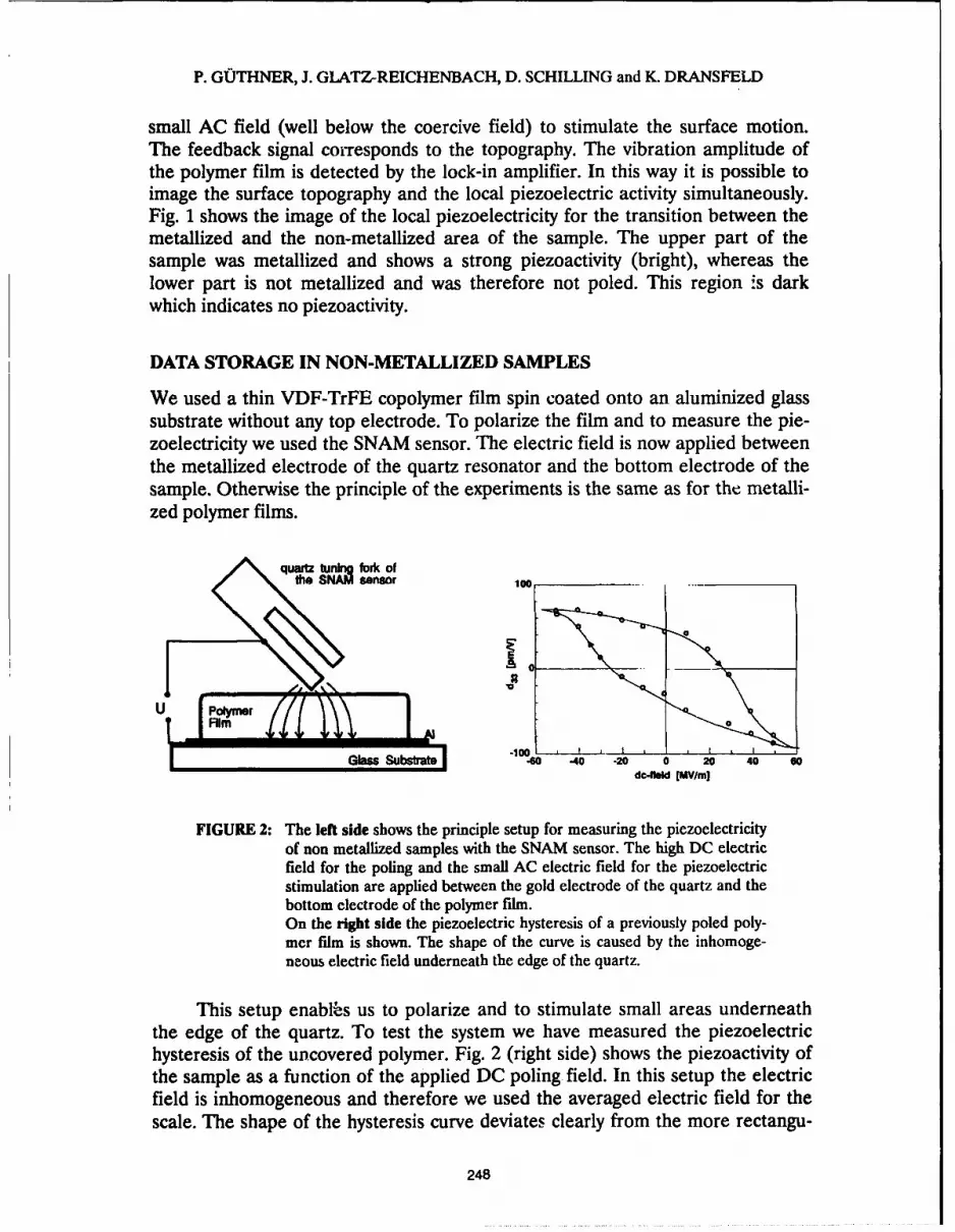
P. GUTHNER, J. GLATZ-REICHENBACH, D. SCHILLING and K. DRANSFELD
small AC field (well below the coercive field) to stimulate the surface motion.The feedback signal corresponds to the topography. The vibration amplitude ofthe polymer film is detected by the lock-in amplifier. In this way it is possible toimage the surface topography and the local piezoelectric activity simultaneously.Fig. 1 shows the image of the local piezoelectricity for the transition between themetallized and the non-metallized area of the sample. The upper part of thesample was metallized and shows a strong piezoactivity (bright), whereas thelower part is not metallized and was therefore not poled. This region ;.s darkwhich indicates no piezoactivity.
DATA STORAGE IN NON-METALLIZED SAMPLES
We used a thin VDF-TrFE copolymer film spin coated onto an aluminized glasssubstrate without any top electrode. To polarize the film and to measure the pie-zoelectricity we used the SNAM sensor. The electric field is now applied betweenthe metallized electrode of the quartz resonator and the bottom electrode of thesample. Otherwise the principle of the experiments is the same as for the metalli-zed polymer films.
quartz tu~ fork of_nsor
U __ __ __ __ _ __ _
Glass Substrate " 40 -20 0 20 40 sodC4Wst [MV/m]
FIGURE 2: The left side shows the principle setup for measuring the piezoelectricityof non metallized samples with the SNAM sensor. The high DC electricfield for the poling and the small AC electric field for the piezoelectricstimulation are applied between the gold electrode of the quartz and thebottom electrode of the polymer film.On the right side the piezoelectric hysteresis of a previously poled poly-mer film is shown. The shape of the curve is caused by the inhomoge-neous electric field underneath the edge of the quartz.
This setup enables us to polarize and to stimulate small areas underneaththe edge of the quartz. To test the system we have measured the piezoelectrichysteresis of the uncovered polymer. Fig. 2 (right side) shows the piezoactivity ofthe sample as a function of the applied DC poling field. In this setup the electricfield is inhomogeneous and therefore we used the averaged electric field for thescale. The shape of the hysteresis curve deviates clearly from the more rectangu-
248

THIN PIEZOELECTRIC VDF-TrFE COPOLYMER FILMS FOR DATA STORAGE
lar loops of ferroelectric polymers measured elsewhere2' 1 2,16,17. This differentbehavior may be caused by the inhomogeneous field such that different regionsunderneath the probe are polarized at different applied DC voltages.
The poling procedure by the metal edge, however, leads to a polarizedregion which was observed to be at least 30/4m. In order to pole smaller areas weused the method of electron beam poling15, a technique which enables us tocreate smaller polarization structures on bare films. The poling structure genera-ted in this way can be investigated on a micrometer scale by the Scanning Near-field Acoustic Microscope.
Sfocusedelectronbeam
polymer
bottom electrode"
10 A~M
FIGURE 3: The principle of electron beam poling is shown on the left side. A barepolymer film is irradiated by a focused electron beam (approx. 5 kcV)."'he penetrating electrons create an electric field towards the groundedbottom Al electrode which leads to a remanent polarization of the poly-mer film.On the right side a two dimensional image of the piezoelectric activity ofa 5 jm thick polymer film measured with the Scanning Nearfield Acou-stic Microscope is shown. The lower part was poled by a focused electronbeam. Bright areas have a strong piezoactivity, dark areas don't showpiezoelectric motion.
We have poled small squares (50 x 50/1m 2) by the technique of electronbeam poling and imaged these samples subsequently with the SNAM. The fieldfor piezo-stimulation was applied again between quartz and bottom electrode,and the corresponding surface motion was detected by the SNAM sensor. Fig. 3shows a two-dimensional image of the piezoactivity of a partly electron beampoled sample. The upper part was not polarized and therefore it shows no piezo-activity (dark), the lower part (bright) was irradiated by a focused electron beamand therefore a piezoactivity was measured. The achieved lateral resolution of
249

P. GUTHNER, J. GLATZ-REICHENBACH, D. SCHILLING and K. DRANSFELD
our technique is better than 1 jm. The minimum detectable piezoactivity in thesethin films is of the order of 1 pm/V.
CONCLUSION
We have demonstrated that it is possible to polarize very thin non-metallizedVDF-TrFE copolymer films locally. At the same time the direction of the polari-zation can be measured locally by monitoring the phase of the piezoelectric sur-face motion. This enables us in principle to write and read digital information onthese samples.
The lateral resolution of our instrument is limited by the geometry of ourtuning fork quartz and can be improved. In order to reach a higher resolutionsimilar experiments using a Scanning Force Microscope (SFM) are in progress.The problems involving the speed of the writing and the reading process will bediscussed elsewhere.
REFERENCES
1. T. Furukawa; IEEE Transactions on Electrical Insulation 24, 375 (1989)2. H. Birk, J. Glatz-Reichenbach, Li-Jie, E. Schreck and K. Dransfeld; J. Vac. Sc. Techn. (3/91)3. G. Binnig, C. F. Quate and Ch. Gerber; Phys. Rev. Lett. 56,930 (1986)4. D. Rugar, H. J. Mamin, P. Guthner, S. E. Lambert, J. E. Stern, I. McFayden and T. Yogi;
J. Appl. Phys 68, 1169 (1990)5. B. D. Terris, J. E. Stern, D. Rugar and H. J. Mamin; Phys. Rev. Lett. 63, 2669 (1989)6. F. Saurenbach and B. D. Terrisw; Appl Phys. Lett. 56, 1703 (1990)7. P. Guithner, U. Ch. Fischer and K. Dransfeld; Appl. Phys. B48, 89 (1989)8. P. Gfithner, E. Schreck, K. Dransfeld and U. Ch. Fischer; in: RJ. Behm, N. Garcia and H.
Rohrer (eds.), Scanning Tunneling Microscopy and Related Techniques; p. 507, Dordrecht1990
9. K. Kimura and H. Ohigashi; Jpn. J. Appl. Phys. 25, 383 (1986)10. H. Ohigashi, S. Akama and K. Koga; Jpn. J. Appl. Phys 27,2144 (1988)11. C. Leonard-Bourgaux, J.-F. Legrand, P. Delzenne and J. Lajzerowicz; Ferroelectrics 109, 327
12. T. Furukawa; Phase Transitions 18, 143 (1989)13. G. Eberle, E. Bihier and W. Eisenmenger; IEEE 1990 Anual Report Conf. Electr. Insul. and
Dielectr. Phenom., p. 41 (1990)14. Li-Jie, E. Schreck and K. Dransfeld; to be published15. D. Schilling, Ph.D. thesis, Universitit Konstanz 1988 (Hartung-Gorre, Konstanz, 1988)16. P. GUthner, J. Glatz-Reichenbach and K Dransfeld; J. Appl. Phys. (5/91)17. T. Furukawa, J. X. Wen, K. Suzuki, Y. Takashina and M. Date, J. Appl. Phys. 56,829 (1984)
250

AD-P006 658IIIIIIIIl
PHOTOVOLTAGES IN FERROELECTRIC FILMS
r
P. S. BRODY AND B. J. RODHarry Diamond Laboratories, U.S. Army LABCOM, Adelphi MD 20783
Abstract: Polarization-dependent steady photovoltaic currents werefound in thin lead zirconate-titanate films on silicon substrate. In addi-tion to a polarization-dependent current, there was a steady non-polar-ization-dependent background current. There were also transient photo-voltaic currents that appeared once, in an initial response to illumination,after the remanent polarization is switched. For mercury arc illuminationand a 0.25-jm-thick, sol gel process, 53/47 Zr/Ti ratio film, the polariza-tion-dependent current was equal to 2.7 A/C per W/cm2.
INTRODUCTION
Steady-state photocurrents that are proportional to remanent polarization arecharacteristic of uniformly illuminated ferroelectric ceramics [1-3]. Reversingthe direction of polarization reverses the direction of the photocurrent. Open-circuit voltages are proportional to the length of ceramic between electrodesand can be very large, greatly exceeding the potential difference of the energygap. This phenomenon is considered anomalous (the anomalous photovoltaiceffect or APE), since the photovoltages do not appear to result from bandbending at contacts or the Dember effect (which is due to gradients in photo-carrier density). A similar high-voltage effect is found in ferroelectric singlecrystals [4]. The single-crystal phenomenon is also identified as an anomalouseffect. There are, however, reasons to believe that the mechanism producinghigh voltages in ceramics differs from that producing such voltages in single
crystals [5].Steady photovoltaic currents are also seen in thin ferroelectric films. High
voltages have not been observed, but a partial dependence on remanent polar-ization has been observed [6]. Current progress in the development of thin filmintegrated ferroelectric-semiconductor structures [7] has made polarization-
92-16122251 oIIIIII II

P. S. BRODY AND B. J. ROD
dependent photovoltages in ferroelectric films a subject of interest. Such photo-
voltages make possible, in principle, an application to nonvolatile, nondestruc-
tive readout memory and to optical correlation [8-10]. In these applications,
information is encoded in the direction and magnitude of the remanent polar-
ization, and readout occurs in the form of polarization-dependent photocur-
rents. Also, polarization-dependent photovoltages have been used to study
remanent polarization decay in ceramics [11], and the same technique may also
be useful for studying the retention of stored memory states in thin film
devices.
In this paper we present the results of a study of photovoltaic phenom-
ena in lead zirconate-titanate (PZT) films. We observed steady photovoltaic
currents that contained both a polarization-dependent component and a polar-
ization-independent component. We also observed photovoltaic current tran-
sients comparable in magnitude to the steady currents. These appeared only inresponse to an initial illumination pulse. We describe our study in detail and
also briefly discuss implications with respect to possible applications.
METHOD OF PRODUCING PHOTOCURRENT AND MEASURINGPOLARIZATION DEPENDENCE
The films studied were sol-gel process, 53/47 Zr/Ti ratio, lead zirconium-
titanate spun cast onto platinum-coated silicon wafers. The platinum was
sputter deposited. The wafers were passivated with a thermally grown SiO2
layer. There was an thin sputter-deposited titanium layer intervening between
the platinum and the oxide. An array of top electrodes, each 150 x 150 gm, was
fabricated by the sputter deposition of platinum using a silicon micromachined
shadow mask. The electrodes were either thick and opaque, or thin (200 A)and semitransparent. The semitransparent electrodes transmitted roughly 10
percent of incident illumination.Each electroded area constituted a thin film ferroelectric capacitor. An
experimental arrangement, based on a probe station, allowed pulse voltages to
be applied to individual ferroelectric capacitors. The arrangement places alinear measuring capacitor in series with the ferroelectric capacitor in a Saw-
yer-Tower configuration, so that the remanent polarization change induced by
a voltage pulse can be measured. The probe station microscope was trinocular
in design. Collimated light from a mercury arc passed through the trinocular
252

PHOTOVOLTAGES IN FERROELECTRIC FILMS
optical train and was focused onto the film. The illumination was controlledwith a camera shutter.
Four probes were used in the experimental arrangement (Fig. 1). Probe 2was used to apply a pulse voltage. Probe I was in contact with the electrode tomeasure the applied voltage. Probe 4 was in contact with the base electrodeand connected the Sawyer-Tower capacitor between the ferroelectric capacitorand ground. Probe 3 contacted the base electrode to measure the voltage onthe Sawyer-Tower capacitor. The charge on that capacitor divided by the areaof the ferroelectric capacitor is the ferroelectric polarization. A digital oscillo-scope was used to record the applied voltages and resulting changes in polar-ization. The contact to probe 2 could also be used to connect the ferroelectriccapacitor to an electrometer. Photovoltages were recorded on a strip chart.
The steady-state photovoltaic output of the films could be characterizedby a photo-emf (electromotive force) in series with a photoresistance. Therewas a characteristic short circuit photovoltaic current (the photovoltaic cur-rent) which did not vary with load resistance. We determined the photovoltaiccurrent by measuring the photovoltage across a 1074-2 load resistor. We deter-mined the photo-emf by measuring the photovoltage across a 1011-Cl resistorwhich constituted effectively an open circuit.
POLARIZATION-DEPENDENT AND NON-POLARIZATION-DEPENDENTPHOTOVOLTAIC CURRENTS
We measured the changes in remanent polarization in the film capacitors that
followed the application of a voltage pulse. The voltage pulses used were
r2 4 TPZT /PZT
/PVTiS///////////02////////' /S
FIGURE 1. Experimental arrangement for applying voltage pulses andmeasuring changes in remanent polarization. Photovoltages weremeasured between probes 1 and 3. The top electrode is a 200-A thickplatinum layer.
253

P. S. BRODY AND B. J. ROD
positive and negative 16-V pulses, 5 l±s in duration, with additional 1-gs rises
and falls.
We found that the film was initially always fully polarized with a nearmaximum negative remanent polarization. We ascertained this by observing
that the application of a negative pulse would produce only a small increase in
this negative remanent polarization. The polarization goes to zero when theapplied voltage goes to zero (trace 1, Fig. 2). We do not know why the capaci-tor elements are initially polarized. It is possible that the capacitors are polar-ized by accumulated negative charge during the sputter deposition of the top
electrodes.
A positive pulse decreased the magnitude of the negative remanent
polarization (trace 2). After being decreased with a positive pulse, it can beincreased back toward its initial value with a negative pulse. We did notice,
however, that the negative pulse, opposite in sign but equal in magnitude tothe preceding positive pulse, did not act to restore completely the initial maxi-
mum negative remanent polarization.
Fig. 3(a) through 3(f) shows the response of capacitor elements withsemitransparent electrodes to illumination pulses. Fig. 3(a) shows the photo-voltaic current from a capacitor in its initial state, before any voltage pulseshave been applied. Fig. 3(b) shows the response after the application of anegative pulse. There is no change in the steady photovoltaic current. The
application of a positive voltage pulse, however, results in a decrease (81, Fig.
E
i60- r_"trc Pr• 30-
.c-30trace 13O)
a
S-60
III I I I I I
0 2 4 6 8 10 12 14
Time (pis)FIGURE 2. Polarization versus time for an initial negative applied pulse (trace
1) and a subsequent positive pulse (trace 2), showing the increment inremanent polarization, APt, when the positive pulse is applied.
254

PHOTOVOLTAGES IN FERROELECTRIC FILMS
T-------- --------------------- L0O.54 nA
(a) (b) (C)S~Iq 5s._ b
(d) (e) (M)
FIGURE 3. Photovoltaic currents for 6-mW/cm2 high-pressure mercury arcillumination. After the initial transient the currents are steady: (a) initialstate, (b) after a negative pulse, (c) after a positive pulse, (d) after thesame positive pulse but a second illumination, (e) after a subsequentnegative pulse, and (f) a second illumination.
3(c)) in the steady photovoltaic current. A subsequent negative pulse nowproduces an increase with respect to the last value (82, Fig. 3(e)).
There are, in addition to the steady photovoltaic currents, large transientcurrents that are comparable in magnitude to the steady currents and thatdecay to the steady levels. These appear only in response to an initial illumina-tion after remanent polarization is switched, as shown in Fig. 3(c), where thecurrent transient is positive following the initial rise, and Fig. 3(e), where it isnegative. They do not appear in response to the illumination pulse when theremanent polarization has not bee#;hanged, as in Fig. 3(a) and (b). The cur-rent discharge occurs only once, and after it decays, a subsequent illuminationpulse does not produce a transient (Fig. 3 (d) and (0). The polarity of the tran-sient is in the direction of the applied voltage and is relatively larger after anegative pulse.
There are smaller, quickly decaying transients (obscured partially by thelarger transients where they occur), which are generally seen in response to theonset of illumination and to the removal of illumination. These are in thedirection of the steady current on the onset illumination and in the oppositedirection when the illumination is blocked. The net integrated current (the netcharge) in these transients is zero. These are most probably pyroelectric in
255

P. S. BRODY AND B. J. ROD
origin characterized by current proportional to the rate of temperature change.We believe that rapid heating by direct absorption produces the more sharply
rising transients when illumination is incident, and conduction cooling to the
substrate produces the less apparent transient, more slowly decaying, when
illumination is removed.
Fig. 4 is a plot of the steady photovoltaic current versus change in rema-
nent polarization. This result shows a linear relation between remanent polar-
ization change and photocurrent. The sign of the current is the same as that of
the applied voltage pulse and the induced remanent polarization. This same
relation is seen for anomalous photovoltages in bulk ceramics [12].
The illumination intensity at the film measured with a calibrated thermo-pile was approximately 6 mW/cm2 after the transmittivity of the electrode is
taken into account. Photovoltaic current was proportional to intensity. Therelation between the change in photovoltaic current and the change in rema-
nent polarization, for this mercury arc illumination, is
Aiph = 2.7 (A/C)/(W/cm2)x area x APr xlo .
-0.6
-0.5
• -0.4.2
-0.30
2• -0.2
-0.1
00 10 20 30 40 50 60 70
Remanent polarization change (±C/crm2)
PTGURE 4. Pbotovoltaic current versus change in remanent polarization formercury arc illumination of 6 mW/cm2. The remanent polarization waschanged with a switching pulse and measured. The capacitor was thenilluminated and the steady photocurrent measured. A new voltage pulsewas then applied and the operation repeated. The figure combinesresults from four capacitors.
256

PHOTOVOLTAGES IN FERROELECTRIC FILMS
The area is that of the electrode in square centimeters, P, is the remanent polar-
ization in coulombs per square centimeter, and 10 is the intensity in watts per
square centimeter.
We note that the change in remanent polarization is that determined
immediately following the application of a pulse (e.g., at I ms). The photocur-
rent was measured about 10 s later. We have assumed no significant decay in
remanent polarization during the 10-s interval.
In addition to the polarization-dependent photocurrent, there is a current
component that is not dependent on remanent polarization. Because of this
component, a large positive applied pulse sufficient to reverse the remanent
polarization of the film does not reverse the direction of the photovoltaic
current, but only decreases its magnitude (see Fig. 3(c)).
Hysteresis loop measurements of film capacitors (Fig. 5) show a near-
saturation-level remanent polarization of 24 gC/cm2. It is reasonable to as-
sume that the 16-V, 5-gs-duration positive pulse applied to the film capacitor
in its initial negative polarization state completely (or almost completely)
switches the direction of the remanent polarization. The initial remanent polar-
ization equal to -P, has been switched from a negative to a positive direction.
From Fig. 4 the negative saturation value of remanent polarization corre-
sponds to a photovoltaic current of -0.54 nA. The photovoltaic current corre-
sponding to the positive saturation remanent polarization (after 50 gC/cm2 has
been switched) is -0.35 nA. The photovoltaic current midway between these
E 36-
0.2
o -36
-480 -360 -240 -120 0 120 240 360 480
Applied field (kV/cm)
FIGURE 5. Hysteresis results for a film capacitor. The driving sinusoidalvoltage is at 1000 Hz. The remanent polarization was 24 gC/cm2 and thecoercive field, 90 kV/cm.
257

P. S. BRODY AND B. J. ROD
must then correspond to zero remanent polarization. If our assumptions con-cerning the complete switching of the polarization are correct, then there must
be a nonswitchable background of -0.44 nA.
To our surprise, steady photovoltaic current outputs were producedfrom capacitors with opaque electrodes as well as capacitors with thin semi-
transparent electrodes. Measurements of photovoltaic currents from circular
opaque electrodes of three different diameters showed these currents to beproportional to the electrode diameter (and thus also perimeter) rather than to
electrode area. This indicates that the electrode perimeter was collecting or
generating the current.This perimeter current must also be a component of the total current for
the case of the capacitors with semitransparent electrodes. For our measure-ments of the change in photovoltaic current versus change in remanent polar-ization which used 150 x 150 gm electrodes (Fig. 4), this perimeter current was
-0.20 mA. The perimeter current is thus a significant portion of the total cur-rent. Perimeter currents could be eliminated by masking, so that the perimeterregion is not illuminated. We note that photocurrents originating from regionsoutside the electrodes would not be switchable even if they result from theAPE. Voltages applied to electrodes produce only short-range fringing fields in
the nonelectroded region and thus would not switch a significant amount ofremanent polarization external to that region. To check this experimentally weobserved photovoltaic currents from opaque electrode capacitors and found
only small to nonexistent changes in the current after applications of voltage
pulses.
SOURCES OF NON-POLARIZATION-DEPENDENT PHOTOVOLTAICCURRENTS
No background currents are observed in typical measurements of APE cur-rents in ceramics and single crystals. These measurements are made with an
arrangement in which the electrodes are uniformly illuminated, and there is nogradient in optical absorption in the direction perpendicular to the electrodes.This has the effect of eliminating photovoltages from similar contacts and
those from gradients in the absorption of light (Dember effect). The arrange-
ment for the films (Fig. 1) is quite different. There is now a gradient in light
absorption in the thickness direction for the strongly absorbed photocarrier-
258

PHOTOVOLTAGES IN FERROELECTRIC FILMS
generating wavelengths used in this study; this results in the possibility both
of Dember effect photovoltages and of photovoltages from similar contacts,
since the contacts are now illuminated at different intensity levels. Photo-voltages from a single metal-ferroelectric contact can easily be observed. Effi-
cent Schottky barrier photodiodes consisting of a transparent gold electrode
and a barium titanate crystal with a reduced surface have been demonstrated
[131.
SOURCE OF POLARIZATION-DEPENDENT PHOTOVOLTAIC CURRENTS
Whether the polarization-dependent steady photovoltaic currents and open-
circuit voltages are the result of a true bulk effect [5,141 or are the result of
surface layer phenomena [12] is not clear. The anomalous photovoltaic effects
both in bulk ceramic and macroscopic single crystals are proportional to lengthin the direction of polarization and can produce large, greater than band-gap
voltages. In truly single macroscopic crystals, the large voltages would have to
result from a fundamental bulk effect producing greater than band-gap volt-
ages. In ceramics, however, the voltages are also observed to be proportional
to the average number of grains per unit length in the direction of the rema-nent polarization [12]. This suggests that the high voltage may simply be the
result of the addition, grain by grain, of ordinary less than band-gap voltages,
which are related to the surface regions of grains [5,12].In limited experiments on thin films we could find no clear dependence
of the photo-emf on film thickness. Otherwise similar films, of 0.25- and 0.6-
gtm thickness, produced open-circuit photovoltages for saturation negative
remanent polarization of -0.52 and -0.46 V, respectively. Because the films are
thin, the electric fields associated with these voltage are large: about 20 kV/cm
for the 0.25-ptm film. The total open-circuit voltages are, however, small: lessthan the 3-eV band gap. The large fields, therefore, do not in themselves imply
a true bulk effect. We think it more likely that the polarization-dependentsteady voltages and currents found in the films have the same origin as those
found in ceramics, namely, the voltages are the result of band bending in space
charge regions on near grain boundaries [12]. Since there is no thickness de-
pendence in the photo-emf of the films, one must also assume that the films
are only one grain thick.
259

P. S. BRODY AND B. J. ROD
TRANSIENT PHOTOVOLTAIC CURRENTS
The large initial photovoltaic current transients seen after the application of a
negative applied voltage pulse has switched remanent polarization are similar
in form to transients observed in single-crystal ferroelectric [15]. In these stud-
ies, an initial illumination pulse results in a large initial transient, and subse-
quent illumination pulses result in transients of considerably reduced magni-
tude. It has been suggested that these currents are produced as illumination-
generated carriers form space charge fields [5]. We suggest a similar source for
the transients in the films. Specifically we suggest that transients are the result
of carriers generated by the illumination moving to screen the existing internal
electric fields associated the existing polarization state. Once the new space
charge distribution is established, there is no illumination-related transient
until polarization switching produces a new internal field structure.
APPLICATIONS
Our study confirms the existence of polarization-dependent photovoltaic
currents in lead zirconate-titanate films on platinum-coated silicon substrates.
We believe it should be possible to take advantage of this phenomenon in
device applications based on the principle of storing information as remanent
polarization and accessing and retrieving it as photocurrents. Such devices
would include nondestructive-readout, nonvolatile-memory RAM (random
access memory) cells and correlators based on photocurrent outputs which are
the product of illumination intensity and remanent polarization. Such applica-
tions should be able to use the presently developing capabilities in fabricating
silicon/lead zirconate-titanate ferroelectric-semiconductor integrated circuits.
The existence of nonpolarization background currents at most limits the
dynamic range of the polarization-dependent response and should not be an
impediment to applications. An increase in the efficiency of producing the
photovoltaic current with respect to illumination intensity is, however, prob-
ably needed if practical applications are to be realized. It is known that this
efficiency can be considerably increased by doping and by using narrow-band
illumination centered near the absorption edge of the film [2,16].
260

PHOTOVOLTAGES IN FERROELECTRIC FILMS
ACKNOWLEDGEMENTS
We would like to thank Dr. S. Bernacki of Raytheon Corporation and Dr. S.Dey of Arizona State University for providing films used in this study.
REFERENCES
1. P.S. Brody, Solid State Commun. 12 (1973), 673.2. P. S. Brody, Solid State Chem. 12 (1975), 193.3. K. Uchino, Y. Miyawaza, and S. Nomura, Jap. J. Appl. Phys. 2 (1982),
1671.4. A. M. Glass, D. von der Linde, and T. J. Negran, Appl. Phys. Lett. 25
(1974), 234.5. V. M. Fridkin, Photoferroelectrics, Springer-Verlag, New York (1979), pp
103, 121.6. V. S. Dharmadhikaru and W. W. Grannemann, J. Appl. Phys. 53 (1982),
8988.7 J.F. Scott and C. A. Paz de Aroujo, Science 246 (1989), 1400.
8. P. S. Brody, U.S. Patent No. 4,126,901 (1978), U.S. Patent No. 4,139,908(1979), U.S. Patent No. 4,144,591 (1979).
9. P. S. Brody, Appl. Phys. Lett. 38 (1981), 153.10. P.S. Brody and Emanuel Katzen, New Nonvolatile Memory with RAM
Capabilities and Intrinsic Radiation Hardness, Harry Diamond Laboratories,HDL-TM-82-14 (1982).
11. B. Jiminez, R. Gomez, J. Mendiola, E. Maurer, and C. Alemany, Ferroelec-trics 45 (1982), 147.
12. P. S. Brody and F. Crowne, J. Electron. Mater. 4 (1975), 955.13. D. A. Sawyer, Appl. Phys. Lett. 13 (1969), 392.14. M. E. Lines and A. M. Glass, Properties and Applications of Ferroelectric and
Related Materials, Clarendon Press, Oxford (1977), p 455.15. A. V. Guinzberg, K.D. Kochev, Yu. S. Kusminov, and T.R. Volk, Phys.
Status Solidi (a) 29 (1975), 309.16. M. Tanimura and K. Uchino, Sensors and Materials, vol. 1 (1988), 47.
261

PHOTORESPONSE FROM THIN FERROELECTRIC FILMS OFLEAD ZIRCONATE TITANATE
SARITA THAKOOR, ANIL P. THAKOORCenter for Space Microelectronics Technology0)Jet Propulsion Laboratory
U' California Institute of Technology(O• Pasadena, California 91109
andCOSTEPHEN E. BERNACKI
Electro-Optics and Strategic Systems Directorate0• Raytheon Equipment DivisionaSudbury, MA 01776
Abstract Bulk (ceramic as well as single crystal)ferroelectric materials are known for their remanent-polarization-dependent photoresponse: a photocurrent(and a photoemf), when illuminated by light with awavelength close to the bandgap of the material. Thispaper reports on observation of a similar photoresponsefrom sol-gel derived polycrystalline thin films of leadzirconate titanate (PZT). The internal field due to theremanent polarization modulates this net photoresponsefrom the ferroelectric material. Thin film ferroelectriccapacitors were fabricated in a sandwich geometry witha transparent top electrode. On illumination with z365nmwavelength (PZT bandgap - 3.5 eV) light.. pulse,photocurrent profiles from such capacitors correspond totheir distinct remanent polarization memory states.Further, such a read-out has negligible effect on themagnitude of the remanent polarization and therefore itis a potential candidate as a non-destructive readout ofthe nonvolatile memory states. The observed photocurrenthas two components: first, a transient spikecoincident with the onset of the illumination pulse, andsecond, a steady dc photocurrent which prevails as longas the light is 'ON'. The steady current responseexhibits a weak dependence on the polarization whereasthe transient response exhibits a distinct polarizationdependence. Our study suggests that the predominantcontribution to the steady photovoltaic current is dueto the asymmetric pair of Schottky junctions at the twointerfaces of the ferroelectric film with the top andbottom electrodes respectively.
92-1612331 5 £1111 3 13111% 111262

INTRODUCTION
With the advent of technology, to deposit ferroelectric
thin films of PZT (lead zirconate titanate) with tailored
stoichiometry, and to successfully integrate them
with conventional silicon technology, ferroelectric non-
volatile memories are now well into their development
phase. 1-4 The memory element consists of a thin film
ferroelectric capacitor, in which the non-volatile storage
is based on the remanent polarization in the ferroelectricthin film. The established readout technique relies on the
transient displacement current modulated by polarization
reversal under applied switching pulse. However, such a
process destroys the stored information, which necessitates
a rewrite operation after every read cycle and complicates
the hardware.
Alternatively, a "poled" ferroelectric element, whenilluminated with a wavelength near its bandgap, generates
a small photocurrent proportional to the remanent
polarization (stored memory) and the incident intensity. 5, 6
If radiation-hard, nonvolatile, ferroelectric memories
could be read non-destructively in terms of the photo-
response (photocurrent or photo-emf) with such contact-less
optical addressing, they would clearly have an impact on
the growing need for rugged and robust solid state memory
systems. Furthermore, a strong motivation for such a
readout arises from the fact that the highly parallel
photoresponse output from an array of memory pixels would
be ideally suited for high performance computing
applications12 , especially those involving parallel
processing and architectures such as large scale artificial
neural networks. In addition, such a non-destructive
263

readout(NDRO) would allow utilization of the full potential
of the ferroelectric capacitor as an analog memory.Non-destructive readout from bulk ferroelectric ceramic
elements has been demonstrated 7' 10 utilizing the remanentpolarization dependent photo-emf. The polarity of the
photo-emf depends on the direction of the remanentpolarization.
This paper reports the first unambiguous observation ofpolarization dependent photocurrent response generated from
ferroelectric thin film capacitors of sol-gel deposited PZT
at zero applied bias.
EXPERIMENTAL DETAILS
The sol-gel PZT thin films (-1700 A) were deposited by a
modified Sayer's Technique8 on oxidized silicon substrateswith an intermediate evaporated Ti/Pt (- 1000 A/1000A) base
electrode. Typically the PZT composition of (Zr/Ti =
52/48) with -18% excess lead was investigated. Thecrystallization of the PZT was done at 550 0 C for 10 minutes
in 100% oxygen.
OPTICAL INPUTh-u (300 nm - 600 nm)
Ii.POLARIZATION '- - TRANSPARENT TOP (Au, PQCONTROL
- FERROELECTRIC LAYER, PZT(0.15 Am - 02 pm)
PHOTO- ._ - BOTTOM ELECTRODE (Pt)RESPONSEOUTPUT -- oS02
SiSUBSTRATE
FIGURE 1 Thin film ferroelectric capacitor(TFFC) teststructure for photoresponse investigation.
264

To complete a standard sandwich capacitor test structure as
shown in Figure 1, thin transparent films of either gold or
platinum were deposited as the top electrode. The top
electrodes were patterned by conventional lift-off
technique as dots of 100A to 250g diameter. The
transmission from 300 nm to 800 nm through the electrode
films (zl00A Pt or z300A Au) was about 30%. Platinum was
significantly more robust, scratch resistant, and thus more
durable than gold in our experiments with the microprobes.
In our photoresponse measurement, a short-arc mercury
lamp was used as the near UV/visible(300nm to 600nm)
illumination source with the strongest line at 365nm. The
choice of this light source was motivated by the bandgap
value of PZT (-3.5eV) that would lead to maximum
photoresponse at about 354nm. The interim focussing
optics delivered a 5mm divergent beam with an intensity of
-0.1 watt/cm2 onto the sample. A shutter controlled by a
solenoid valve allowed a pulse illumination with a minimum
pulse length of 1 sec and a maximum of 99 sec. IV
characteristics of the ferroelectric capacitor on
illumination, even in the unpoled state, exhibited an open
circuit photovoltage and a short circuit current. The high
impedance of the device (resistance =1 to 10 Gigaohms,
capacitance z1 nf) made open circuit voltage measurement a
rather slow process, over several seconds. Short circuit
current measurement was thus an obvious choice.
Photocurrent through a 100 K ohm resistor shorting the
sample, was monitored in response to a pulse of
illumination as described above. To illustrate the
repetitive non-destructive readout, experiments were
conducted by using light chopped by a mechanical chopper.
RESULTS AND DISCUSSION
Typical (Q-V) hysterisis loops with drive voltages ranging
265

from ±2V to ±10V for the ferroelectric capacitors are shown
in fig. 2. The remanent polarization(Pr = 25 AC/cm2) and
coercive voltage value(Vc = 2.3V) as deduced from the
hysterisis loop for ±10V drive signal confirm that the
deposited films are comparable to the state of the art
films used for memory devices.
20 gC/cm2
T
+2VK
FIGURE 2 Hysterisis loops (Q versus V plots) ofPt/PZT(52/48)/Pt TFFC.
Figure 3 shows traces of the photocurrent generated from
the ferroelectric capacitor in response to illumination
pulses of 40sec duration for the two polarization states
corresponding to ±4V poling respectively. There are two
main components to the photoresponse, a transient
response(JT) at the onset of illumination, and a steady
photoresponse(JST) prevailing for the entire duration of the
illumination. The transient component predominantly
exhibits a polarization dependent character, whereas the
steady component has only a weak polarization dependence.
Therefore the transient component is of prime interest for
266

the non-destructive readout (NDRO). The peak value of the
transient essentially reflects the state of the remanent
polarization value. The transient photocurrent response
could be composed of displacement current arising due to:
(a) localized electronic transitions (JE)' (b) space charge
contributions (Js), and (c) pyroelectric contributions
(JPYRO)
ME-- s5,a
E
8 - 40 pAcm2
IL
TIME -'1P F.-5
FIGURE 3 Photocurrent response from a TFFC illuminatedwith a 40sec light pulse. TFFC poled to(a) +4V (b) -4V.
Table 1, summarizes the typical expected rise time and
relaxation time characteristics of these possible
components of the photoresponse as suggested9"11 from
studies on bulk ferroelectrics. When the light is switched
"ON', the transient photocurrent reaches a maximum and then
falls off to a value corresponding to the steady current.
The space charge component of the transient response may be
267

attributed to the screening of the spontaneous polarization
by the photogenerated carriers9 . The relaxation time of the
transient is seen to be dependent on the amount of charge
injected in the capacitor during the "writing " operation,
as is suggested by its dependence on the duration of the
writing pulse. This relaxation may be related to the
relaxation time of the space charge current and is14discussed in details elsewhere
TABLE 1. Photoresponse Component Characteristics
Current Component Rise time Relaxation time
JE =psec zpsec-nsec
is =psec-nsec --ms-seconds
JPYRO =Asec =seconds
JST zpsec *
* steady, while the light is on
If the transient photoresponse would have a pyroelectric
contribution, a transient response would also be expected
in opposite direction at the end of the illumination pulse.
A transient, however, is not observed at the turn -OFF' of
the illumination suggesting that with the illumination
utilized here, the pyroelectric contribution to the
photoresponse is negligible. Although, our PZT films are
not intentionally doped, the trace impurities in the
chemicals utilized for the sol-gel deposition may
contribute to impurity centers within the formed PZT thin
film that may give rise to a displacement current
proportional to the polarization change due to localized11electronic transitions . The observed transient response
is therefore mainly attributed to the contributions due to
the space charge component and probably the localized
268

electronic transitions. Experiments are underway to
further understand the nature of the transient
photoresponse.
ST
Z H 200ucm
E
0
TIME __ý i,_o
wZ 2pNACM 2
-c T00
I! ACQ([UISI~TION 3,I805 H-S! I
TIME __ýi05n
FIgure 4 Photocurrent response from a TFFC illuminatedwith a light, chopped at approximately 10Hzfrequency. TFFC poled to (a) +4V, (b) -4V.
Figures 4a and 4b, present the photoresponse from a
ferroelectric capacitor in its positively poled state and
negatively poled state, respectively, when illuminated with
light chopped by a mechanical chopper run at a 10 Hz
frequency. A repetitive non-destructive readout clearly
differentiating between the polarization states is thus
269

obtained, utilizing the transient photocurrent response.
In fact each of the three polarization dependent components
of the transient response may be useful as nondestructive
readout.12,15
Although the transient response exhibits the dependence
on polarization, the large steady photocurrent background
(only weakly dependent on polarization) offsets the
observed signal to the same polarity for both polarizationdirections. There are atleast five possible mechanisms
contributing to this steady photocurrent component: (a) a
pair of asymmetric Schottky junctions at the top and bottom
electrode-PZT interface, (b) the Dember Effect10, (c) the
photovoltaic effect as observed in bulk ferroelectrics,8-1 0
(d) built/in stress gradients within PZT, and (e) residual
polarization arising due to the slow switching polarization12components . In the following is discussed each mechanism
and its validity with respect to the present observations.
A post-top electrode anneal treatment substantially
suppresses the steady photoresponse, however, the
suppressed steady current still remains weakly dependent on
the polarization state. This is illustrated in figure 5aand 5b, which shows the photoresponse to a 40 second pulse
from a sample that was annealed ( 575 0 C for 3 hours in air)
after deposition of top electrode, in its positive and
negative polarization states respectively. This
observation suggests that the steady current may arise due
to the asymmetry in the two photovoltaic Schottky junctions
at the two interfaces betw.een PZT and the two electrode
layers. The heat treatment (-550 0 C) provided to PZT for
its crystallization probably causes formation of a
photovoltaic junction between PZT and its bottom platinum
electrode. The top electrode, deposited at room
temperature, on the other hand does not form a photovoltaic
junction until the post deposition anneal. After the post-
270

deposition anneal, however, the two virtually identical
junctions situated in opposition to each other, tend tocancel the total photoemf thereby reducing the net
photoemf. A similar suppression of the steady currentenhancing the directional transient response was also
accomplished by voltage soaking the sample for an extendedduration of time ( over few hours) with a ±(2 to 4)V drive
voltage.
S40 pA/cm 20 I
TIME-.]k5 sc
LA-cc~ 20 p/CM 2
TIME-] -SSWc
FIGURE 5 Photocurrent response from a TFFC which wasannealed after top-electrode deposition toillumination with a 40sec light pulse. TFFCpoled to (a) +4V (b) -4V.
The anneal treatment, or equivalently, the fieldtriggered thermal heating in the voltage soak treatment may
271

be responsible for "formation" of the
electrode/ferroelectric interface. C-V measurements are
underway to further understand these observations in terms
of the differences in the band bending at the two
interfaces of the capacitor. This anneal treatment, in
effect, enhances the polarization dependence of the
transient response and thereby can be utilized for a moreefficient NDRO.
The PZT films transmit about 30% of the incident
illumination at 365nm (the strongest line in the source
spectrum). This implies that the resultant charge density
difference along the thickness of the film could cause the
Dember effect. However, the substantial suppression of
the photocurrent on annealing supports the possibility of
the asymmetric Schottky junction as the dominant cause over
that of the Dember effect. Further measurements of the
electron-hole mobilities and the diffusion lengths of the
carriers within the PZT material will allow a precise
assessment of the relative contribution of the Dember
effect.
The steady part of the response is seen to be essentially
independent of the polarization. The photovoltaic effect
in bulk ferroelectrics as reported earlier"'11 is expected toconvey the sense of polarization. The weak dependence on
polarization clearly suggests that this is not the most
significant contribution.
Measurement by the Newton's Ring method of the radius of
curvature of the silicon wafer before and after the
deposition and crystallization of PZT yields = 1.3±0.3
Giga-Pascal tensile stress within the film. If this
stress is non-uniformly distributed along the thickness of
the film, then it could contribute to the observed steady
current. Also, the annealing treatment may very well
serve to relax the existing stress gradient thereby
272

suppressing the steady photocurrent. This possibility
could be verified by applying an external stress gradient
of both a tensile as well as compressive nature and
observing its effect on the photoresponse.
The residual polarization in the film, attributed to slow
switching components 13, could be easily reversed by
application of a voltage soak treatment for about a minute
at 2-4V drive voltage. However, such a single voltage soak
treatment had no effect on the photoresponse
characteristics from the ferroelectric capacitor,
suggesting that photoresponse is not related to residual
polarization. Our observations therefore suggest that
primarily the asymmetric Schottky junction at the two
interfaces is the dominant mechanism giving rise to the
steady photoresponse.
TABLE II Effect of 99 sec continuous illumination (=365nm)on the remanent polarization.
Sample Polarization Value ( in AC/cm )
Description Before illumination After Illumination
# 1 +25 +22
# 1 -25 -26
# 2 +30 +25
# 2 -30 -33
# 3 +22 +20
# 3 -20 -26
# 4 +20 +19
# 4 -20 -20
273

The effect of near UV/visible light illumination on the
stored memory was investigated to establish the overall
potential of this non-destructive readout technique. The
conventional destructive readout technique was used to do
this cross verification. It is noteworthy that the effect
of light on the remanent polarization is directional. In
TABLE II is summarized the effect, of extended cumulative
exposure (z 99 sec ) to illumination (- 365nm ), on the
remanent polarization. The remanent polarization(Pr) on
negatively polarized capacitors is either unchanged or
shows an increase in the negative value of the Pr in
response to an exposure of about 99 sec of continuous
illumination. However, positive Pr values show a definite
decrease in the remanent polarization value in response to
a similar illumination. This suggests that the steady
(a) (b)
-V. v
(C) (d)
FIGURE 6 Schematic representation of effect ofillumination on the memory. (a) and (b)represent the capacitor before illumination inits two states respectively, the arrow suggeststhe direction of polarization. (c) and (d)illustrate the status during illumination, theadditional arrow indicates the direction of thephotogenerated field.
274

photoresponse from the device is, in-fact, responsible for
this effect of overwriting by the light. As illustrated
schematically in figure 6, when the photogenerated field is
in the same direction as the remanent polarization, it
enhances the polarization value and degrades it in the
opposite direction. An ideal pulsed light source with
short pulses(-lons duration), therefore, could be used to
yield a substantial number of real fast non-destructive
readout cycles (>1010), with small change of the remanent
polarization.15
CONCLUSIONS
1. Repetitive, nondestructive readout from individual
ferroelectric memory pixels is indeed feasible
(a) Photoresponse profiles from PZT thin films with noexternal bias applied is polarization dependent.
(b) Extended, cumulative illumination(z 365 nm) for over
99 seconds has a directional effect on the remanent
polarization such that the negative polarization values
are substantiated but the positive polarization values
are degraded (= 15% ).
(c) Transient component of the photoresponse has the
predominant polarization dependence.
2. Steady photocurrent is predominantly due to the pair of
asymmetric Schottky junctions at the two surfaces of the
PZT film. Post-top-electrode annealing suppressed the
steady photocurrent and allowed observation of a
transient response exhibiting sense of polarization by
its direction.
ACKNOWLEDGEMENTS
Useful discussions with Dr. L. E. Cross from Pennsylvania
State University and Dr. A. M. Glass from AT&T are
275

gratefully acknowledged. The work described in this paper
was performed by the Center for Space Microelectronics
Technology, Jet Propulsion Laboratory and California
Institute of Technology, and was sponsored by Defense
Advanced Research Projects Agency through an agreement with
National Aeronautics and Space Administration(NASA).
REFERENCES
1. J. T. Evans and R. Womack, IEEE Journal of Solid-State
Circuits, 23, 1171 (1988).
2. D. Bondurant and F. Gnandinger, IEEE Spectrum,
30(1989).
3. J. F. Scott and C. A. Paz De Araujo, Science, 246, 1400
(1989).
4. S. E. Bernacki et. al. , Proceedings Third
International Symposium on Integrated Ferroelectrics,
April 3-5, 1991, Colorado.
5. C. E. Land, J. Am. Ceram. Soc., 72, 2059 (1989).
6. S. J. Martin, M. A. Butler and C. E. Land, Electronics
Letters, 24, 1486 (1989).
7. P.S. Brody, Appl. Phys. Lett., 38, 153 (1981).
8. G. Yi, Z. Wu and M. Sayer, J. Appl. Phys. 64, 2717
(1988).
9. V. M. Fridkin, Photoferroelectrics, Springer-Verlag
(1979).
10. F. Micheron, J. M. Rouchon and M. Vergnolle,
Ferroelectrics, 10, 15 (1976).
11. A. M. Glass, D. von der Linde, D. H. Auston and T. J.
Negran, J. of Electronic Mat., 4, 915 (1975).
12. S. Thakoor (to be published), Transactions of the
Ceramic Society (1991).
13. S. Thakoor, Proceedings Third International Symposium
on Integrated Ferroelectr.s, April 3-5, 1991,
Colorado.
276

14. S. Thakoor, M.Lakata, and J. Maserjian, (in
preparation).
15. S. Thakoor, J. Perry, and A.P. Thakoor, (in
preparation).
277

o STUDY OF THE OPTICAL PROPERTIES OF RF SPUTTERED(DLITHIUM NIOBATE THIN FILMS
CHARLES HUNG-JIA HUANG and THOMAS A. RABSONo Department of Electrical & Computer Engineering, Rice UniversityHouston, TX 77251-1892
"BM Abstract Lithium niobate optical waveguides were fabricated on(110), and (100) sapphire by both diode and magnetron rf sputtering
at 500-600*C in a flowing Ar/0 2 atmosphere. Light coupling utilizing
a rutile prism coupler was demonstrated. The propagation losses were
obtained by measuring the scattered light from the surface using a fiberprobe. The mode angles were also measured and used to calculate the
thickness and the refractive indices of each sample. X-ray diffractionstudies and the birefringence observed in the films have confirmed the
crystalline nature of the films. The lowest value of attenuation of the
He-Ne laser light propagating in the lithium niobate waveguide sputteredon sapphire was determined to be 1.1 ± 0.1 dB/cm. In addition, the
lowest attenuation in lithium niobate thin film waveguides sputtered on
Si0 2/Si substrates was measured to be 2.3 dB/cm using end-fire coupling
and fiber probing techniques.
INTRODUCTION
For the development of integrated optics the fabrication of low loss waveguideson various substrates is essential.' Since lithium niobate has excellent electro-
optic, nonlinear optical, and piezoelectric properties, 2 it is considered to be a
good candidate of optical materials in integrated optics for applications such
as electro-optic modulation, switching, second harmonic generation, etc.' Tita-
nium in-diffusion (TI) and proton exchange (PE) techniques on bulk crystals
have been used for several years to make low loss optical waveguides. 3 However,
guides made with these methods are difficult to integrate with semiconductor
92-16124~Uht~lhU~IIfl ~278

C. H-J. HUANG AND T. A. RABSON
substrates. Fortunately, thin film technology offers a solution to this problem.
Recently, significant progress has been reported in the region of rf sputtered
lithium niobate on a variety of substrates. Griffel et al.4 has reported the low-
est attenuation (less than 2 dB/cm) and the highest electro-optic coefficient
(1.34 x 10⁻¹² m/V) obtained so far for thin film lithium niobate rf sputtered on
an amorphous glass (Corning 7059) substrate. Hewig and Jain5 also reported
second harmonic generation in a lithium niobate film deposited on a sapphire
substrate. We have grown high quality lithium niobate thin films on SiO 2/Si
and various sapphire substrates and the values of the propagation loss in thosewaveguides are lower than the published data.6 Electrical switching of lithium
niobate thin film has been studied and observed by Rost and colleagues.' More-
over, they have successfully built a MFS (Metal-Ferroelectric-Semiconductor)
transistor using ferroelectric lithium niobate as the gate material,$ which means
that the combination of the technologies of integrated optics, semiconductor mi-
croelectronics, and ferroelectrics is possible in the near future.
FABRICATION
In this paper, thin film lithium niobate rf sputtered on (110), (100) sapphire,
and Si0 2/Si substrates are studied. Sapphire was chosen to be the substrate
because it is transparent in the visible light region, it has a similar lattice struc-
ture to lithium niobate, the lattice mismatch between sapphire and lithium
niobate is small (about 7%), and its much lower refractive index gives excellent
light confinement. Therefore, sapphire is an excellent substrate on which to
epitaxially grow low loss lithium niobate optical waveguides. Since LiNbO 3 is
mainly employed in making electro-optic devices, the maximum field induced
birefringence is certainly desired. For convenience, a modulating electric field
parallel to the c axis of lithium niobate is usually applied, and the guided beam
is excited in the direction normal to the c axis of the film. The field induced
birefringence is thus given by An = -- ½ne3r3E for a wave polarized in the
direction of the c axis. Therefore, both (110) and (100) sapphire substrates
are suitable for growing epitaxial thin film with the c axis in the plane of the
surface. The other substrate used, Si0 2/Si, was selected simply because silicon
is one of the most popular substrates in semiconductor microelectronics.
279

OPTICAL PROPERTIES OF SPUTTERED LITHIUM NIOBATE
TABLE I The sputtering parameters.
Sputterer Diode MagnetronSubstrate (110) A120 3 & SiO 2/Si (110) & (100) A120 3Target LiNbO 3+10%Li 2O pure LiNbO 3Separation 6 cm 5 cmPressure 2-4 mTorr 1-2 mTorrTemperature 500-6000 C 500-6000 CGas ratio 54% Ar + 36% 02 70% Ar + 30% 02Pre-sput. time 30 min 30 minForw. power 150 W 50 WRefl. power 70 W 0 W
Both diode and magnetron rf sputtering systems were used to grow lithiumniobate films. Typical growth conditions are listed in Table I. For the dioderf sputtering system, the target consisted of lithium niobate powder mixedwith 10% lithium oxide to compensate for lithium loss which occurs duringsputtering, while pure fresh lithium niobate powder was used in each run forthe magnetron system. The substrate was heated to a temperature in the regionof 500°C to 600°C during the process to improve the growth of oriented film.The deposition rate under the conditions listed in Table I is about 250 A/hr
using 150 W (70 W reflected) rf power in the diode sputtering system and using50 W in the magnetron system. Note that the magnetron rf sputtering systemalthough operating at a lower power gives the same deposition rate as the diodeone. Lithium niobate thin films fabricated at such a low rate are very uniformand optically transparent. The films were then annealed in either air or 02
atmosphere at 6000 C for a few hours to improve their crystallinity.
X-RAY DIFFRACTION
X-ray diffraction (XRD) has been done to analyze the crystallinity of the thinfilms. One can see in Figure 1 that the sputtered lithium niobate thin filmsare highly oriented crystalline with the c axis parallel to that of the sapphire
substrate. The XRD peaks are listed in Table II. The lattice constants an of the
thin film lithium niobate deposited on (110) and (100) sapphire are calculatedto be 5.144 A and 5.154 A, respectively. These values are in close agreementwith the bulk value of 5.149 A.
280

C. H-J. HUANG AND T. A. RABSON
2.000 -O SAMPLE 121189
1.600 10' -
-1.200 104 n "
8000
4000 0
0 . . .., . , . . • . , . . ' . , . . . , . . .. . . .
20 30. 40 50 60 70 80 90
1200-:SAMPLE 030891-1
1 000-G~oo- g PGoo_4• 800-
200-
0 - : I ' -" • , t•
20 30 40 50 60 70 80 901200 -
SAMPLE 030891-11OOO AFIER ANNEALING P
C..) 600 0" 0"
Ucn
U.'
I-- 400
200
0 L
20 30 40 50 60 70 80 90
SAMPLE 031790
400
S-ý-300 uC")
= 200100
0 L
20 30 40 so 60 70 80 902e (060)
FIGURE 1 XRD of LiNbO 3 sputtered on various sapphire.
281

OPTICAL PROPERTIES OF SPUTTERED LITHIUM NIOBATE
TABLE II X-ray diffraction data of thin film lithium niobate onsapphire.
Substrate 20 Identification Lattice constant(100) sapphire 62.42" (300) LiNbO3 aH=5.1 5 4 A(110) sapphire 34.880 (110) LiNbO3 aH=5.1 4 4 A
Comparing the intensities of the two lithium niobate (300) peaks beforeand after annealing, we confirm that the annealing process has improved thecrystallinity of the thin films. However, since the thickness of the thin filmsis only a few thousand of angstroms, a long annealing period as people usedto do for bulk materials is not preferred. 9 Moreover, the temperature regionfrom 550°C to 6000C is considered to be the optimum condition for annealingafter sputtering. Higher temperatures up to 1000°C had been applied to annealthe sputtered films which then turned out white and opaque after the thermaltreatment. The transparency reduction of the film indicates a higher opticalscattering and propagation loss in the waveguides, which is not desirable.
X-ray diffraction of a film on an amorphous SiO2 buffer layer, shown inFigure 1, has a sharp peak at 32.900 corresponding to a (104) orientation andanother peak at 34.85° corresponding to a (110) orientation. The broadeningat the bottom of these two peaks is due to the amorphous characterisitcs ofthe SiO2 layer. This demonstrates that the films on SiO 2/Si substrates have apolycrystalline quality with some preferred orientation.
OPTICAL PROPERTIES
The film's optical properties, such as refractive index, thickness, and attenu-ation, were examined by beam-coupling into the thin film waveguide utilizinga high index rutile prism coupler,10 as shown in Figure 2. Evaporated Al thinfilm spacers (,- 1000 A) and a steel wire were used to create a tapered air gap
which then increased the coupling efficiency. With this setup we are able to
measure the mode angles and the attenuation in the waveguide simultaneously.
Figure 3 shows the reflectivity of a 6328 A light from a lithium niobate film on
(100) sapphire substrate vs. the angles of incidence, in which the bottoms of
the dips, correspond to the mode angles.
282

C. H-J. HUANG AND T. A. RABSON
TABLE III Thicknesses and refractive indices of the lithium niobate
thin films deposited on sapphire substrates.
Orientation System Mode angles nf:(±0.002) t (±0.0011tm)bTE2 = -4.90* n. = 2.324 t = 0.635pmSTE, = 11.96*
(110) Diode 'TEo = 23.16*
bTM2 = -0.42* ne = 2.244 t = 0.639pm
bTMT1 = 20.37*JTM, "= 36.35*
(100) Magnetron 6 rT = 4.86* no = 2.301 t , 0.2,umbTMo = 7.960 ne = 2.230 t z 0.2pfm
POLARIZED LASER BEAMSSURFACE FIBER PROBEN•ORMAL PROTODIODE
RU'TILE PRISM "'
"SPA E ...........R SPACE
WAVEGUIDE /-4 j
SUBSTRATE
STEELWRE
PNEUMATICALLY-OPERATED COUPUNG HEAD
FIGURE 2 Setup of the prism coupler.
If two or more modes are observed, the thickness t and the refractive index
nf of the film can be evaluated by the mode condition given by Eq. (2.2.12)in Ref. 11. The calculated thickness and refractive indices of lithium niobate
thin films deposited on sapphire substrates are tabulated in Table III. Sincetwo different values of refractive index corresponding to TE and TM waves have
been obtained in each sample and the index difference is larger than the allowed
error, the thin films grown by the rf sputtering method under the conditions
listed in Table I exhibit birefringence and thus are highly-oriented. Note thatin the case of single mode waveguides the thickness and the refractive index
283

OPTICAL PROPERTIES OF SPUTTERED LITHIUM NIOBATE
1.0 1.0
SO. TE 0 • ._TM 0
0.01 0.0I I I I I I I I I I
-10 -5 0 5 10 15 20 -10 -5 0 5 10 15 20ANGLE OF INCEDENCE (DEG) ANGLE OF INCEDENCE (DEG)
FIGURE 3 Guided modes prism coupled into LiNbO 3/(100) A120 3.
can not be calculated at the same time. Therefore, One of the parameters hasto be estimated by other techniques. For example, the thickness of the (100)sample was estimated by counting the color periodicity of the film edge, whichwas then used to calculate the refractive indices of the film.
Assuming the guided optical power is proportional to the intensity of thesurface scattered light, we can then calculate the attenuation in the opticalwaveguide by measuring the surface scattered light. Conventionally, a fiber
probe connected to a lock-in amplifier is used to serve this function. In ourstudies, another technique, namely, the photographic recording method, was
also utilized. The waveguiding streak was photographed, as shown in Figure 4,for a number of different exposures. Only those taken within the linear regionof the film sensitivity were used to calculate the attenuation. Figure 4 shows
the attenuation of TE0 guided mode propagating in lithium niobate waveguide
sputtered on (110) sapphire. The lowest attenuation in our sputtered films was
found to be 1.1 (±0.1) dB/cm which is the smallest value reported so far in theliterature for sputtered lithium niobate films. Since the attenuation is causedby the scattering at the surface of the waveguide and grain boundaries and bythe absorption at the defects, surface flatness and crystalline quality are veryimportant in lowering the attenuation of the film. In general, a higher rf power
creates bigger crystallites, while a lower rf power gives better surface flatness.
Therefore, a trade-off must be made to optimize the deposition rate. For our
magnetron system, 50 W is found to h- the preferred value.
284

C. H-J. HUANG AND T. A. RABSON
3.
2•7
7
0-zS
U'."
S-2
5.3.4 ATTENUATIONs 1.1 1 0.1 dBlcm
USING PRISM COUPUNG
0 0.5 1 1.5 2 2.5WAVEGOWE L,•TH (Cm)
FIGURE 4 A He-Ne light guided in LiNbO 3/(110) A120 3.
Although the attenuation obtained in our work is the lowest value re-ported for sputtered thin film waveguides, it is still not as low as 0.5dB/cm ofwaveguides made by thermal diffusion techniques."1 To lower the attenuation of
the films fabricated by rf sputtering, one must improve the optical uniformityof the film and its surface as well as reduce absorption in the film. Annealing,mechanochemical polishing, and ion-beam etching are promising techniques forfurther reducing the attenuation.
For the lithium niobate thin film rf sputtered on silicon substrates with a2.5 Am SiO 2 buffer layer sandwiched in between, we have demonstrated waveg-uiding via end-fire coupling, which is shown in Figure 5. The attenuation isdetermined to be 2.3 ± 0.1 dB/cm. This is the first time that waveguiding in
lithium niobate thin film on SiO 2/Si has been reported. Since the guided modeswere excited by end-fire coupling, the measured attenuation was an averagedvalue over all of the supported modes. Therefore, it should be lower than 2.3dB/cm for a single mode waveguide. The thick oxide layer makes the couplingmuch easier. However, it is not necessary to have such a thick buffer layer.
Theoretically, only 0.3 Jm of SiO 2 buffer layer thickness is required to reduce
the leakage loss of waveguides on SiO 2/Si substrate to about 0.1 dB/cm if only
coupling of the wave to the silicon substrate is considered.12 Further research
on the properties of these waveguides are currently under investigation, and the
285

OPTICAL PROPERTIES CF SPUTTERED LITHIUM NIOBATE
results will be published in a later paper.
S~10
14
iWt
ATENATION -U 21:0.1 AlcmUSIG END-RRE ýCOUPLING]
0.2 0.4 0.6 0.8 1 1.2 1.4 1.8WAVEGUIDE LENGT (cm)
FIGURE 5 A He-Ne light guided in LiNbO3/SiO2/Si.
CONCLUSIONS
In summary, lithium niobate optical waveguides have been epitaxially deposited
on sapphire and SiO21/Si substrates by both diode and magnetron rf sputtering
t,ýchniques. By Bragg x-ray diffraction analysis, these films were found to be
highly oriented with their c axis parallel to the c axis of the substrates. The
thickness and the refractive index of the films were determined utilizing a futile
prism coupler. The propagation losses were measured to be about 1.1 dB/cm
and 2.3 dB/cm for lithium niobate thin film waveguides deposited on sapphire
and SiO2/Si substrates, respectively. The deposition parameters for sputtering
shown'in Table I effectively produced films with low defect density and optically
smooth surfaces, thereby reducing optical attenuation in the waveguide.
ACKNOWLEDGEMIENTS
This research is supported by the Texas Higher Education Advanced Technol-
ogy Program under grant numbers 4075 and 3604.
286
i rn nnNn.nunn nnn3m n u • -

C. H-J. HUANG AND T. A. RABSON
REFERENCES
1. T. Tamir, Integrated Optics (Berlin, Springer-Verlag, 1979).
2. M. E. Lines and A.M. Glass, Principles and Applications of Ferroelectricsand Related Materials (Oxford. 1977).
3. T. Tamir, Guided-Wave Optoelectronics (Berlin, Springer-Verlag, 1988),4. G. Griffel, S. Ruschin, and N. Croitoru, Appl. Phys. Lett., 54, 1385, (1989).5. G. H. Hewig and K. Jain, J. Appl. Phys., 54, 1, 57, (1983).6. C. H. Huang, H. C. Chui, B. A. Stone, T. A. Rost, and T. A. Rabson, to be
published in the Proceedings of ISAF '90.7. T. A. Rost, H Lin, and T. A. Rabson, to be published in the Proceedings
of ISIF '91.
8. T. A. Rost, H Lin, and T. A. Rabson, to be published in the Proceedings
of ISIF '91.9. L. 0. Svaasand, M. Eriksrud, G. Nakken, and A. P. Grande, J. Crystal Growth,
22, 230, (1974).10. P. K. Tien, Applied Optics, 10, 2395, (1971).11. T. Tamir, Guided-Wave Optoelectronics, (Berlin, Springer-Verlag, 1988).12. N. Nishihara, M. Haruna, and T. Suhara, Optical Integrated Circuits, (New
York, McGraw-Hill, 1989).
287

- THEORY OF CONDUCTION AND BREAKDOWN0_IN PEROVSKITE THIN FILMS
CL---- RAINER WASER and MAREIKE KLEE
Philips GmbH Forschungslaboratorium Aachen,D-5100 Aachen, Federal Republic-of Germany
Abstract. The mechanism of the dc electrical conduction and breakdown ofperovskite-type titanates was investigated by impedance analysis. Based on anacceptor doped SrTiO 3 model material, samples of different microstructures -ceramics, single crystals, and thin films - were employed. This approach allowsus to distinguish conduction contributions of the bulk lattice, grain boundaries,and electrode interfaces. Based on defect chemistry studies, a predominantionic contribution due to mobile oxygen vacancies and an additional p-typeconduction were revealed for the bulk. At interfaces, space charge depletionlayers of 100-500 nm width are formed in which the local conductivity isreduced by approx. four orders of magnitude compared to the bulk. Thinfilms show a similar depression of the conductivity. The combination of thesefacts may be indicative for considering thin films as distributed Schottkybarriers. The field enhancement of the conductivity of thin films and of theinterface depletion layers is compared and discussed.
1. INTRODUCTION
The extent to which properties such as the switching behaviour, the fatigue, and theretention of ferroelectric thin films can be controlled and improved will have anessential impact on a future success of these films in device applications. As pointedout in numerous contributions at the ISIF'91 conference and at earlier meetings, theseelectrical properties are supposed to be up to a large degree determined by theconduction and breakdown mechanism of the films (for example, see Ref. 1).
I ~ Ferroelectric thin films based on perovskite-type materials are extremely complexelectrical systems. Firstly, they are thin films. The dielectric thickness typically rangesfrom 0.1 to 1 gm. Consequently, the influence of the electrode interfaces will be
'• much more pronounced than in compact samples. In addition, the microstructure ofthe films usually is very different from bulk ceramics or bulk single crystals. Secondly,they are ferroelectric. Even in non-ferroelectric perovskite films, the charge transportand polarization properties are not yet understood. Hence, the ferroelectric behaviour
_ superimposes an additional degree of complexity because it significantly affects thepolarization and charge transport in the material. Devoting ourselves to a step-by-stepresearch approach, we will restrict ourselves in this report to non-ferroelectricperovskite-type titanates such as SrTiO3 and BaTiO3 above the Curie temperature.These materials show the same crystal structure and a similar band gap as the
288

R. WASER and M. KLEE
ferroelectric PZT (lead-zirconate-titanate) and are assumed to be governed by acomparable defect structure. Single crystals, ceramics, and thin films of the samecomposition will be compared in order to separate the different conduction andpolarization contributions. In addition, the conductivity enhancement under highelectrical fields will be considered, keeping in mind that fields across films in actualdevices under operating voltages (typically 3 to 5 V) are in the range of 0.5-5.105V/cm. Related to that aspect, the possible nature of the instantaneous dc breakdownwill be discussed briefly.
Under relative low dc fields and at moderate temperatures titanates and othermixed conducting oxides are known to suffer from a long-term resistance degradationdue to an ionic de-mixing process which leads to an increase of the electronic carrierconcentration. While a quantitative model for the degradation kinetics of single crystalsbased on the defect chemistry, the charge transport properties, and the electrodeinterface transfer rates was presented recently [2], research concerning the degradationof titanate thin films is at its very beginning. Comprehensive studies are currentlycarried out at our laboratory and will be presented at a later date.
2. MOBILE SPECIES IN THE CRYSTAL LATTICE
The types and concentrations of charge carriers in the crystal lattice of barium orstrontium titanate are determined by the defect chemistry and are affected by thetemperature, the oxygen partial pressure during annealing, P0 2, and the concentrationof dopants. Lower-valent cations substitutionally accommodated on regular cation sites(e. g. Ni2 + on Ti4 + sites) act as acceptors, while higher-valent cations (e. g. Ce3+ onBa2+ sites) are donors. The defect chemistry of undoped and acceptor doped titanatesin the high temperature regime (approx. T > 900 K) were the subject of severalcomprehensive studies and the reader is referred to the corresponding papers [3-7]and the excellent review Ref. 8. The high temperature regime is characterized byequilibria with the P0 2 of the ambient atmosphere which are established withinreasonable times. Undoped titanates were found to be governed by a lowconcentration of cation vacancies as native acceptors and acceptor-type impurities (Al,Fe, Mn, etc.). The latters have been detected even in samples of highest purity. For
conductivity studies nominally undoped titanates are less suitable because of theundefined and possibly locally varying impurity concent. Slightly acceptor dopedtitanates (e. g. 0.1 at% Ni-doped SrTiO 3 ), instead, represent well-defined modelsystems and were used in the present study.
The defect chemistry of acceptor doped titanates after quenching from hightemperature equilibria to temperatures at which the oxygen content is frozen-in(approx. T < 700 K) has been investigated recently by means of the impedanceanalysis [9]. This temperature regime is relevant for the regular operation and theaccelerated life testing of electronic ceramic components. Fig. I is reproduced fromthis study and shows that annealing under conventionally oxidizing to moderatelyreducing atmospheres leads to a dominant ionic conductivity, gionic, and a certaincontribution by a p-type electronic conductivity, a., The mobile ionic species areoxygen ions which move by a vacancy mechanism. The mobility of the oxygenvacancies, V6, is thermally activated with an activation energy of 1.0 to 1.1 eV whichfits well to high temperature data [5]. In titanates, the holes (and the electrons aswell) can be regarded as polarons which move by a hopping process. The slight, non-activated temperature dependence supports the large-polaron model [10] although the
289

THEORY OF CONDUCTION AND BREAKDOWN ...
O • . I I ' I ' I ,-
-- 2 T =423K FIGURE 1Calculated ()
-4• and measured (o)bulk conductivity of0.1 at% Ni-doped SrTiO3after annealing at 973 Kand different P0 , and
-- -8 subsequent quenc&ing to1 ° 423 K ["9].-10 ... ... inc -I A-12 n-type/ 11
-14~ -. ptype
-14
-16 , p-t I
-20 -10 0 10log P0 2 [Po]
mobilities are relatively small (e. g. Ph = 0.1 cm2 /Vs for Sr 0 .9 7Ba0 .0 3TiO 3 at 1223 K[101) and fall close to those expected for the small-polaron model [11]. Altogether,undoped and acceptor doped alkaline earth titanates today rank among the moststudied and best understood oxides from the defect chemistry's point of view. As faras the bulk crystal lattice is concerned, this does not leave much room for ambiguitiesin interpreting conductivity data with respect to carrier types, concentrations, andmobilities.
Donor doped titanates show a different conduction mechanism due to the verylow concentration of V6. Single crystal and coarse grained ceramic are semiconductingdue to the electron compensation of the donor centers, while fine grained ceramicsintered under oxydizing atmospheres is highly insulating at room temperature due tothe cation vacancy compensation [4]. While in both cases there is virtually no ionictransport in the lattice due to the low mobility of the cation vacancies, oxygen ionsare known to show a certain motion along the grain boundaries under gradients ofthe oxygen activity or the electrical potential [12].
3. IMPEDANCE ANALYSIS IN THE TIME DOMAIN
The impedance of real samples is not only determined by the conductivity of thecrystal lattice. The electrode interfaces (el) and - in the case of ceramics - the grainboundaries (GB) contribute to the total impedance as illustrated by the simplifiedequivalent network in Fig. 2. In the present study, impedance analysis in the timedomain was utilized by recording the time evolution of the current response afterapplying a dc voltage step. Details of this method and the transformation between thetime and the frequency domain are described in Ref. 13. It is well known thationically conducting ceramics as, for instance, stabilized ZrO2 [14] as well as mixedconducting ceramics such as titanates [15, 16] tend to build highly resistive layers at
290

R. WASER and M. KLEE
d el do e d g
FIGURE 2Simplified block model ofa ceramic and simplifiedelectrical equivalentnetwork illustrating theconduction andpolarization contributions.The contributions of bothelectrode interfaces aremerged into branch 'el'.The contributions of allgrains and all grainboundaries are merged
SI into branch 'b' andbranch 'GB', respectively.
electrode grain graininterface bulk boundary
electrode and GB interfaces. These are commonly interpreted as depletion spacecharge layers similar to Schottky barriers at semiconductor interfaces [17].Consequently, the conductivities act and aGB are usually very small compared to abbecause the corresponding layers are depleted by the charge carriers. In conventionalceramics, the depletion layer thicknesses dote and de1 are much smaller than the grainsize:
dgr >> dGB, del. (1)
Hence, the capacities generated by the interfaces (i. e. branches 'el' and 'GB' of theequivalent network in Fig. 2) are large compared to the capacity caused by the bulkof the grains (branch 'b'). In addition, the GB contributions perpendicular to theelectrodes can be neglected because of relation (1). Still, there is a certain mobility ofoxygen ions along GBs. This becomes obvious in either donor doped titanates wherethe ionic conduction in the bulk of the grains is negligible [24] or in very fine grainacceptor doped ceramics where relation (1) is not valid any more (see Sec. 7).
The permittivity in the depletion layers, etB and tel, is equal to the permittivity et,of the crystal lattice in paraelectric ceramics as has been shown recently for SrTiO3[18].
Applying a dc voltage step to a network (Fig. 2) with two dominating branchesleads to a Maxwell-Wagner polarization. In Fig. 3, the voltage stimulation as well asthe current response is shown for a charging period and a discharging period. Atvery short times, when the space charge polarization at the interfaces is still negligible,the current density J is determined by a short-term conductivity as := u(t-+O). Ifrelation (1) is valid, a. is equal to the bulk conductivity ab within a good
291

THEORY OF CONDUCTION AND BREAKDOWN ...
V IE=VID
t FIGURE 3to tSketch of a dc voltage
step experiment. The
voltage stimulation V(t)J and the current density
response i(t) areillustrated for a chargingperiod starting at to anda discharging periodstarting at t'. In the
charging discharging present paper, theperiod presponse is shown on a
log-log scale. Furthermore,the unsigned currentdensity - field ratio li/El
INE1lllcm) is used in order to obtain- caging data in the conductivity
Z 1s" current unit and to compile the"" discharging charging and discharging
U Icurrent response in one diagram.For an explanation of the
-dl !short term conductivity as,I t islDebye relaxation time 7-,and the long term
"(log scale) conductivity oa: see text.
approximation
*h • C. . (2)
The current decays in a manner which is typical for a Debye relaxation:
J - exp (-t/T) . (3)
After a long time, when the polarization process is complete, the residual conductivityur remains left being caused by the leakage through the depletion layers. Switching offthe applied voltage leads to a depolarization current of reversed sign which proceedsuntil the capacitive interface elements are discharged. This discharging process hasbeen included in all studies reported in the present paper.
For further details on the measuring principle see Ref. 13.
4. CONDUCTION THROUGH GRAIN BOUNDARIES OF CERAMICS
A ceramic of 0.1 at% Ni-doped SrTiO 3 was prepared using the conventional mixed-oxide technique. For details see Ref. 9. After sintering at 1613 K for 6 h in oxygenand subsequent isostatic hot-pressing at 1573 K for I h, a porefree ceramic with auniform microstructure and a grain size of 2.5 ± 1.0 im was obtained. Discs of 125ftm, 250 jim, and 500 pm thickness were cut, lapped, polished, and annealed at 973K for 6 h in oxygen. After quenching, electrodes of NiCr alloy (thickness: 6 nm) andAu (150 nm) were applied by evaporation.
Fig. 4a shows the results of dc voltage step experiments at 423 K and different
292

R. WASER and M. KLEE
S_79 ceramicFIGURE 4
(a) Current density - field-- 10i. ratio IJ/EI vs. time t for
a fine grained, 0.1 at%- Ni doped SrTiO ceramicCM at T = 423 K ?or
-- 11 E [Vcml different dc voltage stepsT 423 K 3-104 corresponding to dc fields
in the range from E =
-12 10 V/cm to 3" 104
",, V/cm. The determining-1 - components of the
-1 01 2 3 equivalent network aresketched on top. The
log t [s] discharging curve (dashedline) is shown for E =
- log E [Vlcm] 300 V/cm.
1 2 3 4 5 (b) Field dependence of, the conductivity at t =
300 s in diagram (a),
"*u -12.5 interpreted as theconductivity in the GBspace charge layer OGBaccording to Eq. (8).
- Abscissa from top toc -13.0 bottom: applied field at
tow field varistr the sample E = V/D,ohmic regime regime average voltage drop at a
O GB AVGB, and average1. field across a GB
-13.5 •depletion layer EGB.Thickness of the sample:
log AVGB IV] D = 500 urm.
-2 -1 0 1 Average grain size:0 dg = 2.5 gmn.-14.0 , II I II d Im
2 3 4 5 6- log EOB [VnCM]
field strengths E. The regimes of the IJ/EI curves are formally attributed tocomponents of the schematic equivalent network (Fig. 2). These assignments aresupported by additional experiments using samples of different grain sizes (preparedby varying the sintering temperature) and different sample thicknesses. II is worthwhileto note that the electrode interface branch (el) was not observed presumably due to
the large number of GBs between the electrodes which outweigh the influence of thetwo electrode layers.
The Debye relaxation time r of the Maxwell-Wagner polarization of the GBs is
determined by
T = CeffeO / as (4)
where eeff denotes the effective permittivity of the material when the grains act asshorts. e0 is the vacuum permittivity (8.854" 10-14 As/Vcm). Bascd on geometrical
293

THEORY OF CONDUCTION AND BREAKDOWN ...
considerations for the simple block model of the ceramic and relation (1), eeffobviously is determined by the ratio of the grain size dgr to the GB depletion layerwidth dGB:
Ceff/£GB = dgr/dGB (5)
Inserting (2) and (4) into (5) reveals
dGB = dgr OB 0o (6)
A GB depletion layer width dGB = 115 + 20 nm is evaluated from the data in Fig.4a. The origin of the depletion layer is assumed to be due to donor-type interfacestates. There are indications that these interface charges are active even during thesintering process and lead to a certain segregation of acceptors at the GB [19]. Forthe ceramic used in the present study, a relatively high GB interface charge QGB ofapprox. 7" 10-5 Cb/cm 2 is dctcrmincd using the Schottky approximation for dcpletionspace charge layers [20]:
OTB m e0 dOB ZNiav CNiav (7)
In this relation, cNi.av is the average Ni acceptor concentration in the depletion layertaking into account the segregation. zV.,av represents the average valency of the Nicenters related to the substituted Ti ions and is approx. 2. e0 denotes the unit charge.
The magnitude of dGB is almost independent of the field and of the temperaturewithin the measured range from approx. 350 K to 750 K [21]. This is typical for aSchottky-type depletion space charge layer [17]. Due to the symmetry of a GB, thedepletion layer can be regarded as a back-to-back double Schottky barrier (Fig. 5).
gain GB space chwrg gain(W) bk "-I e buk
FIGURE 5d• Sketch of the conductivity
profile (a) and the energyband diagram (b) across
b a GB in acceptor dopedeee eee titanate ceramics.ese oee/ In (a), @ indicate theeee eeoee eee positively charged (i. e.
d donor type) GB interfacexdG8 X states and e illustrate the
uncompensated acceptorcenters forming a negative
W space charge region.
Wc In (b), Wo, Wv, and WFare the conduction andvalence band edges andthe Fermi level,
WF respectively.WV
GB
294

R. WASER and M. KLEE
According to this model, donor-type GB charges lead to a depletion of the positivelycharged mobile carriers, oxygen vacancies V6 and holes h'. In the depletion layer, theimmobile acceptors form a negative space charge. The width d(,B of the depletionlayer is established in such a way that the positive GB charges are just compensated
by the negative space charge. Fig. 5b qualitatively illustrates the corresponding bendingof the energy bands.
Since the bulk conductivity at is thermally activated (see Sec. 2), the relaxation time"T varies by many orders of magnitude in the stated temperature range. This fact
emphasizes the often neglected importance of recording the current as a function oftime when it is intended to determine and to interpret the conductivity of materials.Another clear indication for the presence of GB depletion layers is the discharging
current which is indistinguishable from the charging current up to approx. t - T (Fig.4a). Hence, the current at short times has to be regarded as a space chargepolarization current and not as a conduction current.
The local conductivity uc-GB in the GB depletion layer is calculated from the long-term conductivity a, and the geometry shown in Fig. 2 in combination with relation(1):
dGB o!o
OGB = "dcg, at ai (8)
For a, <«< at, this equation can be approximated by
GB=doYB (9)aGB - dgr
For 0.1 at% Ni-doped SrTiO3 at low fields and T = 423 K, aGR turns out to bemore than four magnitudes below the conductivity at in the bulk of the grains (Fig.4b). Towards higher temperatures, the difference between ctcB and ab becomessmaller due to a higher activation energy of ocn [21].
In Fig. 4b, aCT is shown as a function of the externally applied field E = V/D.After the Maxwell-Wagner polarization is settled, the grain bulk regions are virtuallyfield free. Based on this, additional abscissa are included in Fig. 4b showing theactual field across the GB depletion layer EGB and the voltage drop &VGB -
EGBdGB. At a low voltage drop, aGB exhibits an ohmic behaviour. Above approx.AVGB = 0.5 V, UGB starts to enhance strongly with incremented voltages. Thisvaristor-type regime is succeeded at very high fields by another ohmic regime. Afurther increase of the external field E is not possible although the ceramic does notyet suffer an instantaneous breakdown. Rather, the onset of the resistance degradationis shifted to such short times at very high fields that the Maxwell-Wagner polarizationof the GBs remains incomplete.
The ohmic regime at low voltages and the varistor regime of GB depletion spacecharge layers in n-type semiconducting ceramics has been consistently interpreted interms of charge transport over a Schottky barrier (see Ref. 20 and references citedtherein). In these ceramics, the energy distribution of the densities of interface statesNGB(W) was found to affect the voltage AVGB at which the enhancement of theconductivity sets in, the slope of the conductivity increase, and the fine structure of theJ-E curve. We assume a similar process to be responsible for the charge transportacross the GB depletion layers in the case of acceptor doped titanates. Further detailsand possible implications of the predominant ionic conduction superimposed on the p-type conduction in the titanates will be reported in Ref. 21.
295

THEORY OF CONDUCTION AND BREAKDOWN ...
5. CONDUCTION THROUGH ELECTRODE INTERFACES AT SINGLECRYSTALS
Samples were cut from a single crystal boule of 0.1 at% Ni-doped SrTiO3(Commercial Crystals Inc.), lapped, and polished to optical quality. Sython W30(Monsanto) was used as a polishing medium. Any mechanical damage to the s- 'acewas found to be below the detectability limit of a SEM [22]. Voltage stepmeasurements were performed for different surface treatments (e. g. annealing at 973K in oxygen before or after polishing) and for different electrode metals (e. g. Au,Al, Cu, Pt). In all these cases, a clear indication for a depletion space charge layer atthe surface was found. An example is given in Fig. 6a. A total depletion layer widthof approx. 1000 nm can be calculated from the data using Eq. (6) appropriately. Fora low voltage step stimulation, we assume that the total layer width is equallydistributed between both electrodes, i. e. dej = 500 nm. At higher voltages, the widthsat the anode and cathode may be different. This aspect has to await furtherclarification using samples with asymmetric electrodes. Compared to the GB depletionlayer doB, the depletion layer at the electrode det is unexpectedly broad. This mayeither be attributed to a high surface charge or it may be enhanced by artefactsintroduced during the surface preparation which are below the SEM detectibility limit.
U @FIGURE 6
S(a) Current density - fieldSb el ratio lJ/El vs. time t for
"w a 0.1 at% Ni doped-n _ SrTiO3 single crystal at T
"• E ItV/cra] 423 K for different dcvoltage steps corresponding
200 to dc fields in the rangeE = 1 V/cm to 200
-10 -a V/cm. The determiningsingle crystal components of the
423K equivalent network are"sketched on top. The
-ii * discharging curve (dashedline) is shown for E =
0 2 3 50 V/cm.- log t [is (b) Field dependence of
the conductivity at t =1500S in diagram (a),interpreted as the
-12 -conductivity in theelectrode interface space
o charge layers ac,. Abscissafrom top to bottom:
' applied field at thesample E = V/D, voltagedrop at an electrode
S-13 interface AVer assumingequal distribution at bothelectrodes, and fieldacross a depletion layerEel. For three datapoints, error bars are
log AVN VI included indicating the-1 -1 0 1 strong decrease in the
* , ireliability when a, getsI close to as at high fields.
3 4 5 Thickness of the sample:-.- log EelV/cmI D = 1500 elm.
296

R. WASER and M. KLEE
For instance, such an artefact could be a ncar-surface layer of a high dislocationdensity possibly establishing additional donor states.
Fig. 6b illustrates the field dependence of the conductivity oa, in the depletionlayer evaluated in the same way as CGOB of the ceramics adapting Eq. (9). Acomparison of Fig. 4b and Fig. 6b shows that the conductivity in the depletion layersof grain boundaries and at electrodes are quite similar. In the low field ohmicregime, ael is in the same order of magnitude as aGR in ceramics indicating the samesituation concerning the degree of depletion of charge carriers. Above a voltage dropAV,, in the depletion layer of approx. 0.5 V (as at GBs in ceramics), the conductivitydeparts from the ohmic behaviour and exhibits a pronounced varistor-type behaviour.At high voltages, a, gets close to oa and, hence, the reliability of the data evaluatedusing Eq. (9) drastically decreases (as indicated by the error bars in Fig. 6b). Basedon the present data it is therefore not possible to judge whether the slope of thevaristor regime of a,, decreases towards high fields before ael comes close to at.
Both the width of the depletion layer d, 1 as well as the conductivity Gel and itsfield dependence are influenced by the annealing before or after the polishing and bythe electrode metal. Details will be given in a forthcoming paper [23].
6. PREPARATION AND STRUCTURE OF TITANATE THIN FILMS
A modified sol-gel process has been developed to deposit doped and undoped SrTiO 3and BaTiO 3 films on Si(100) substrates with a Ti/Pt electrode layer [37]. Solutionscontaining Ba, Sr, Ti, Ni, Mn, and Ce as metal alkoxides, metal carboxylates, andmetal acetylacetonates dissolved in butanol were deposited by spin coating andsubsequent firing at 773 to 973 K in oxygen. Perovskite films with thicknesses of 55nm and 110 nm per coating were obtained using 0.2 M and 0.4 M solutions,respectively. To increase the thickness up to the desired value, the deposition processwas repeated several times. X-ray diffraction (XRD) and scanning electron microscopy
.103
counts /s 0.90 110
0.60 1 z
0.50 , 1 i•
0.40
0.30 2!
0.20 20 2112
0.10 0J 210 11
28.0 30.0 40.0 50.0 60.0 70.0 60.0 90.0 2e in 0
I 100.0 SoT03
Imax 6 100 80. 58- 682640 a20'.0 •t .
28.0 30.0 40.0 5e.8 60.0 70.0 90.0 98.0
FIGURE 7 XRD pattern of a 1 ium thick BaTiO 3 film deposited on a Si/Ti/Pt substrate
297

THEORY OF CONDUCTION AND BREAKDOWN ...
FIGURE 8SEM micrograph of a0.55 aun thick 0.1 at% Nidoped SrTiO 3 filmdeposited on a Si/Ti/Ptsubstrate. The white barindicates a length of 1a•m.
(SEM) studies revealed that all the films reported here crystallize in a single phaseperovskite structure with a random orientation of the crystals on the substrate plane(Fig. 7). Due to the low reaction temperatures of the sol-gel process extremely finegrained ceramic films with grain sizes of 40-90 nm are obtained (Fig. 8). These grainsize data are supported by evaluating the broadening of the XRD lines.
Capacity measurements were carricd out after evaporation of Au electrodes (area:0.01 cm 2 ) on top of the films. The dielectric constants e were 500-800 for theBaTiO3 films and 140-160 for the SrTiO 3 films at 298 K.
7. CONDUCTION THROUGH THIN FILMS
Fig. 9 shows the charging and discharging behaviour of a 0.1 at% Ni-doped SrTiO3
thin film for a voltage V = 2 V (representing E = 3.64 -104 V/cm) for differenttemperatures. As in the ceramic and the single crystal sample, the polarization currentpredominates in the beginning while at long times the current is determined by theconduction through the film. The transition times TT between the polarization and theconduction regime are approx. 0.0015 s (T = 603 K), 0.02 s (543 K), 0.3 s (483K), and 4 s (423 K). An extrapolation to 298 K reveals a -rT of approx. 105 s. Thismeans that any dc measurement at room temperature has to be carried out for atleast one day to determine the true conductivity with a reasonable reliability. SincePZT films (prepared along two alternative sol/gel routes) exhibit qualitatively the samedc voltage step responses (251, we expect similar amounts of time to be needed forreliable conductivity measurements at room temperature.
The eminent difference between the space charge polarization behaviour of theceramic and the single crystal on the one hand and the thin film on the other handis given by the fact that the first shows a Debye relaxation, Eq. (3), while the latter isdescribed by a Curie - von Schweidler law (the so-called "universal law") [131
J - t-. (10)
298

R. WASER and M. KLEE
S-8- thin filmFIGURE 9Current density - field
__ ratio lJ/El vs. time t fora 0.1 at% Ni doped
10 SrTiO 3 thin film at T =423 K, 483 K, 543 K,and 604 K. The charging
503 K )(solid lines) and5,3 K /discharging (dashed lines)
-12K responses for a dc voltageTx 4,23K step of 2 V are shown.
Thickness of the film:0.55 pm.Area of an electrode dot:
-14. 0.011 cm2.
-4 -2 0 2
- og t Is)
For the discharging curves in Fig. 9 (dashed lines), n is decreasing from 0.63 to 0.44when increasing the temperature from 423 K to 603 K.
The Curie - von Schweidler law is reported for a wide range of disorderedsystems such as partially or totally amorphous solid and different materials such asorganic polymers and inorganic compounds. In contrast to a Debye relaxation whichcan be represented by an equivalent network consisting of a resistor and a capacitorin series, a Curie - von Schweidler relaxation corresponds to a distributed RC line ofinfinite length. Different explanations have been offered to explain the behaviourexpressed by Eq. (10):
1. Applying a dc field at materials with a negligible equilibrium concentration offree carriers due to a very large band gap (e. g. SiO2, AI,0 3) leads to chargeinjection at the electrode. The decay of the injection current according to Eq. (10) wasreported to be caused by a trapping of the carriers and a consequent formation of arepulsive space charge [26].
2. A distribution of Debye relaxation times over many orders of magnitude and acorresponding weigth of the underlying processes may lead to a response as describedby Eq. (10). The pros and cons of distributed relaxation time approaches arediscussed in Ref. 13.
3. A many-body interaction model ([13] and ref.s cited therein) explains Eq. (10)for disordered materials on the base of the interaction of individual charges with theirmicroscopic environment and the transition of this interaction during charge transport.This leads to a mutual correlation of all transport events.
We can not yet decide which of these explanations is applicable for our ultra-finegrained titanate films. One may speculate that the situation is possibly determined by acombination of a many-body interaction and a distribution of relaxation times basedon local flucations of the charge carrier concentrations proposed below.
At T = 423 K, the long-term conductivity ot of the 0.1 at% Ni-doped SrTiO 3thin film is approx. 2 10-13 1/Qcm. This more than three orders of magnitude belowthe bulk conductivity of the material ct, = 4.5" 10-10 I/Qcm and close to the residualconductivity in the depletion layers of the electrode interface, ae,, and the GBs, 0(,,which are in the range 2-3"10-14 l/0cm. This indicates unequivocally that thecomplete film is strongly depleted of mobile charge carriers compared to the bulkmaterial. We suppose this depletion to be caused by the facts that the grains are
299

THEORY OF CONDUCTION AND BREAKDOWN
Ceramics: dgr» dGB
d G8 GBFIGURE 10Schematic illustration ofthe conductivity profiles in
x a cross section ofceramics (a) and ultrafine
H =grained thin films (b) asdgr proposed to explain the
different dc voltage stepresponses.
Thin films: dgr < dGB
c i GB GB
d GB
dgr
smaller than the GB depletion layer width in ceramics, d.r < dG(3. and that the filmthickness is in the same range as the electrode interface depletion layer, Dfilm - del.Each of the two facts in itself would be sufficient to cause the depletion. This aspectis important for the discussion of those PZT films which are reported to be singlecrystalline throughout their thickness.
The situation concerning the grain size is sketched in Fig. 10. In ceramics wheredgr >> dc-,B, a pronounced Debye relaxation is observed due to the charging GBcapacities caused 1'v the GB depletion layers via the bulk of the grains as described inSection 4. In the ultra-fine grained thin films, there is obviously no region with abulk conductivity anymore due to dgr < dGB, i. e. due to the overlap of the GBdepletion layers. We assume a distributed spectrum of local conductivities on a levelfar below the bulk conductivity of the material. These conductivity fluctuations may beresponsible for a polarization according to the Curie - von Schweidler law.
The approx. one order of magnitude higher long-term conductivity of the Ni-dopedSrTiO 3 film compared to the conductivity in the depletion layers, a,, and aGB, may beindicative for a charge transport (e. g. of oxygen ions) along the GBs. In conventionalacceptor doped titanate ceramics this route plays only a minor role due to the highionic conductivity in the bulk crystal lattice. In donor doped titanate ceramics the routewas observed [241. Due to the absence of any "bulk" in our Ni-doped SrTiO 3 filmon the one hand and the high density of GBs on the other hand, the chargetransport route along the GBs possibly becomes dominant. Another indication for thisroute is the activation energy of a. The data given in Fig. 9 reveal a value of 0.82± 0.04 eV which is significantly below the activation energy for the oxygen vacancytransport in the bulk lattice of 1.05 ± 0.04 eV [9]. It is known for otherpolycrystalline materials as well that the diffusion along grain boundaries is lessthermally activated than the corresponding diffusion in the bulk [27]. For finalconclusions, however, data about the electronic and the ionic contribution to theconductivity of thin titanate films are required.
300

R. WASER and M. KLEE
8. NATURE OF THE FIELD ENHANCED CONDUCTIVITY
In Fig. 11, the long-term conductivity o, of various titanate thin films at T = 423 Kis displayed as a function of the applied field E. Besides Ni-doped SrTiO3 which wasused as a model material throughout this paper, Ce as a donor dope and Mn as anacceptor dope in BaTiO 3 were studied in addition. The field dependence of theconductivity of the thin films exhibits a similar characteristic as the conductivity of thedepletion layers at GBs and electrode interfaces. At low fields, an ohmic regime isobscrvcd. Above a field of 1.5-3-104 V/cm for the BaTiO 3 films which corrcspondsto voltages in the range from 0.6 to 2 V, the conductivity shows an enhancement overmany orders of magnitude. In the case of the Ni-doped SrTiO3 , the onset of theconductivity cnhanccment occurs at significantly highcr ficlds (E - 2-105 V/cm,corresponding to 10 - 15 V).
Reproducibility tests were performed for the Ce-doped BaTiO3 films. In the ohmicregime, the scatter of a, is less than a factor of two for each 1iim. In the varistorrcgimc (c. g. at E = 105 V/cm), thc scatter increases to a factor of up to five forthe individual films. Due to this fact, the data reported in Fig. 11 should be regardedas showing trends. Further studies including statistical data collection are currentlyperformed by the authors. Despite of this relatively large scatter, it can be stated thatthere is obviously a pronounced influence of the host material (i. e. SrTiO j and
-5
1 -6 --. SrTi0 3 : 0.1 at %Ni t0.55pm /2tt ,0 O71pm
-7 - BaTi03: 0.1 at %Mn .
'E 0 32 pmZ- o0.82 pm Abp05i
,-8 BoTi0 3 : 0.1 at %/Ce/ S/
Q 029 pm,a 0.,9 pm , ,- o
o -9 0.70 pm ,
-10 ' ,/-,0.;,
-i'.° o"Ii/ 1"/.o.o1_- - o" .. a.o-- 1 -
S- a-0o - -, a-- 9.8.-o' _ / o"".. -
-12 I O---- --- 0--0-@ -__'• ,,'D+
T 423K
-13 - ,3 5 6
log E [V/cm]FIGURE 11 Field dependence of the long-term conductivity cr (recorded at t = 300 s r'•rthe dc voltage step) for 0.1 at% Ni doped SrTiO 3, 0.1 at% Mn doped BaTiO 3, and 0.1 at%Ce doped BaTiO3 thin films at T = 423 K. The curves must be considered as preliminaryresults because no statistical evaluation was performed. The arrows indicate breakdownincidences.
301

THEORY OF CONDUCTION AND BREAKDOWN ...
BaTiOj) on the onset field of the varislor regime while the type of dopant in BaTiO 3(i. e. Mn and Ce) does not lead to a significant difference. The latter may beindicative for the fact that the high density of interface states suppresses the influenceof small concentrations of additional donors or acceptors on the conduction process.
No final conclusion can be drawn concerniog the thickness dependence of the ol(E)function. Based on the present data, the film thickness seems to impose no clearinfluence on (he conductivity at a given field in the varistor regime. Due to the scatterof the results, this statement has to be regarded as preliminary.
It can be estimated that the conductivity in the varistor regime must bepredominantly of electror;, nature. The estimation is based on the mass transfer in thecase of an ionic current and the resulting time of material degradation [2]. In theohmic regime the conduction type is not known yet.
There are various mechanisms which lead to an enhancement of the electronicconductivity at high fields. These include material effects such as the field-dependentelectron mobilit*, derived by Stratton [28] and the Poole-Frenkel effect describing thefield-dependent thermoionic emission from traps in the material [29] as well ascontact effects such as the Schottkv emission of electronic carriers from a conductingphase into a dielectric [30] and the space charge limited currents at ohmic contacts[31]. A comprehensive comparison of these effects is given by O'Dwyer [321.
The influence of the field dependence of the electron mobility (i. e. the creation of"hot" electrons or holes) is considered as a less likely cause for the orders ofmagnitude increase of the conductivity in the varistor because in other polar crystals,this effect occurs at higher fields and is less pronounced [32]. The available data areinsufficient to assess the impact of Poole-Frenkel phenomena.
We found that, firstly, the acceptor-doped SrTiO 3 thin films are strongly depletedby charge carriers compared to the bulk crystal lattice of the same composition andthat, secondly, interfaces (GBs as well as electrode interfaces) give rise to suchdepletions. Based on these findings, we regard our titanate thin films as a kind ofSchottky barriers. Compared to the Schottky barriers represented by depletion spacecharge layers at individual interfaces in compact samples, they presumably show adifferent fine structure and possibly should be named "distributed Schottky barriers".Consequently, the current through the film has to be considered as a Schottkyemission across a metal / Schottky barrier / metal system. The onset of the varistorregime and the slope as well as the details of the log a, (log E) curve may then bedetermined by the energy distribution of the interface states, in a similar way astheoretically derived by Pike and Seager for GBs in semiconductors [33].
Space charge limited currents which have been proposed as the cause of theconductivity enhancement of thin perovskite films require ohmic i. e. enrichmentcontacts instead of depletion contacts. Because we always observed pronounceddepletion contacts at titanate single crystals (see SLL. 5), we assume the metal /ceramic interface to behave similarly in the case of thin films. In addition, a modelbased on space charge limited currents will have to explain the strong depletionthroughout the film compared to the bulk. Further studies of the conductivitydependence on the film thickness D will provide essential information since Mott andGurney's law for space charge limited currents predicts j - V2 /D 3 (which correspondsto o - E/D).
Due to the incomplete understanding of the electronic structure of the titanate thinfilms the statements given here should be considered as a working model which stillawaits further confirmations, modifications, or disproofs.
302

R. WASER and M. KLEE
9. BREAKDOWN PROCESS
In a simple classification, the instantaneous failure in a dielectric under very highfields may be either a purely electrical breakdown or a thermal breakdown. In thefirst case, an impact ionization in the material causes an avalanche of electroniccarriers and/or a chemical deterioration [32, 35]. A thermal breakdown occurs whenthe generated Joule heating in the system determined by the product of the currentand the applied voltage leads to an excessive temperature rise. Because of the positivetemperature coefficient of the conductivity, this rise causes an instability and asubsequent thermal runaway.
Using the data at the upper end of the on(E) curves in Fig. 11, a calculationshows that Joule ,:awers in the range between 3 and 100 mW are generated in thefilms of submicron thickness and of approx. 0.01 cm2 area. A consideration of theheat dissipation based on the estimated thermal transfer coefficient of the films andthe thermal conductivity of the substrate reveals a situation which is typical for athermal runaway. This finding is supported by ramp voltage breakdown tests at roomtemperature. In contrast to AIj0• thin films, the current evolution for our BaTiO 3films always exhibits a field enhanced conductivity before the final breakdown sets in[36]. We conclude that titanate thin films fail by a thermal breakdown in contrast to apurely electrical breakdown due to the strongly enhanced high field conductivity.
10. SUMMARY
It is the aim of the present and of continuing studies to understand the behaviour ofperovskite thin films under dc voltage stress. Currently, the major interest behind thisaim is determined by the application of ferroelectric (e. g. PZT) films for non-volatilememory applications.This work is based on three concepts:
1. the use of a simple non-ferroelectric model material (here: acceptor dopedSrTiO3 ),
2. the comparison between single crystals, ceramics, and thin films of the samemodel material in order to judge and to interpret similarities and differences,
3. the separation of polarization and conduction contributions of the current usingthe impedance analysis (here: over many orders of magnitude in time).
The measurements were conducted in the temperature range up to 600 K. From theresults of our investigation, we draw the following conclusions.
-- In the bulk, acceptor doped SrTiO 3 is a mixed ionic-electronic conductor witha predominant ionic conduction due to mobile oxygen vacancies and anadditional p-type conduction.
-- Highly resistive layers are formed at the grain boundaries (layer width: approx.100 nm) and at the electrode interface (approx. 500 nm) in conventionalceramic and single crystal; they are interpreted as Schottky barrieres i. e. asdepletion space charge layers generated by charged interface states.
-- The conductivity in the depletion layers is approx. 4 orders of magnitude belowthe bulk conductivity.
-- At low fields the leakage across the depletion layers shows an ohmicbehaviour.
303

THEORY OF CONDUCTION AND BREAKDOWN ...
-- Above a voltage drop of approx. 0.5 V across a layer the conductivity becomes
field enhanced as expected for the charge transport over a Schottky barrier.SEmpirically, thin films show a similar behaviour as depletion layers with respect
to the low conductivity and the enhancement of the conductivity by high fields.-* Several mechanisms of the field enhanced conductivity in the films may be
considered with some indications favoring the Schottky emission model.The breakdown mode at high fields is a thermal runaway.
ACKNOWLEDGEMENT
We appreciate valuable discussions with Prof. Dr. R. Zuleeg and Dr. P. K. Larsenabout space charge limited currents. We thank W. Brand, A. Wagner, S. Huinten, B.Krafczyk and H. D. Bausen for their support in the preparation and characterizationof the samples.
REFERENCES
[1] C. A. Paz de Araujo, L. D. McMillan, B. M. Melnick, J. D. Cuchiaro, and J. F. Scott,Ferroelectrics 104, 241 (1990).
[2) R. Waser, T. Baiatu, and K. H. Hirdfl, J. Am. Ceram. Soc. 73, 1645, 1654, and1663 (1990).
[3] N.-H. Chan and D. M. Smyth, J. Electrochem. Soc. 123, 1584 (1976).[4] J. Daniels, K. H. Hardtl, D. Hennings, and R. Wernicke, Philips Res. Rep. 31,
489 (1976).[5] N.-H. Chan, R. K. Sharma, and D. M. Smyth, J. Am. Ceram. Soc. 64, 556 (1981).[6] N.-H. Chan, R. K. Sharma, and D. M. Smyth, J. Electrochem. Soc. 128, 1762 (1981).[7] H.-J. Hagemann and D. Hennings, J. Am. Ceram. Soc. 64, 590 (1981).[8] D. M. Smyth, in: Microstructure and Properties of Ceramic Materials,
Proceedings of the First China - U. S. Seminar, Edited by T. S. Yen and J. A.Pask, p. 399, North-Holland Publishing Co., Amsterdam, 1984.
[9] R. Waser, J. Am. Ceram. Soc. (accepted for publication).[10] G. M. Choi, H. L. Tuller, and D. Goldschmidt, Phys. Rev. B 34, 6972 (1986).[11] H. lhrig, J. Phys. C 9, 3469 (1976).[12] K. Okazaki, Adv. Ceram. 1, 23 (1979).[13] A. K. Jonscher, "Dielectric Relaxation in Solids', Chelsea Dielectrics Press Ltd.,
London 1983.[14) T. G. Stratton, D. Reed, and H. L. Tuller, Adv. Ceram. 1, 114 (1983).[15] H.-Y. Lee, S. S. Villamil, and L. C. Burton, IEEE Proc. of the 6th ISAF,
Bethlehem, PA, June 8-11, 1986.[16) H. Neumann and G. Arlt, Ferroelectrics 69, 179 (1986).[17] S. M. Sze, "Physics of Semiconductor Devices", John Wiley & Sons, New York 1981.[18] R. Waser, G. Rosenstein, and S. Oostra, submitted to Ber. Bunsenges. Phys. Chem.[19] Y.-M. Chiang and T. Tagaki, J. Am. Ceram. Soc. 73, 3278 (1990).[20] G. E. Pike and C. H. Seager, Adv. Ceram. 1, 53 (1983).[21] R. Waser, to be submitted to the J. Am. Ceram. Soc.[22] H. Oepen, private communication.[23] R. Waser, to be published.[24] M. Kahn, Am. Ceram. Soc. Bull. 50, 676 (1971).[25] M. Klee, R. Eusemann, and R. Waser, to be published.[26] D. R. Wolters and J. J. an der Schoot, J. Appl. Phys. 58, 831 (1985).[27) P. G. Shewmon, "Diffusion in Solids", McGraw-Hill, New York 1963.[28] R. Stratton, Proc. R. Soc. A 246, 406 (1958).[29) J. Frenkel, Phys. Rev. 54, 647 (1938).[30] P. T. Landsberg, Proc. R. Soc. A 206, 463 (1951).
304

R. WASER and M. KLEE
[31) M. A. Lampert and P. Mark, "Current Injection in Solids", Academic Press, New York1970.
[32] J. J. O'Dwyer, "The Theory of Electrical Conduction and Breakdown in Solid Dielectrics",Clarendon Press, Oxford 1973.
[33]'G. E. Pike and C. H. Seager, J. Appl. Phys. 50, 3414 (1979).[34] 1J. F. Scott, ISIF'91 (see current proceedings).[35] D. R. Wolters and A. T. A. Zegers-van Duijnhoven, J. Vac. Sci. Technol. A5, 1563
(1987).[36] G. Greuel, unpublished results.[37] M. Klee and R. Waser, to be published.
305

ON POLARIZATION REVERSALS IN FERROELECTRICS
YOSHIHIRO ISHIBASHISynthetic Crystal Research Laboratory,
0 • School of Engineering, Nagoya University,Chikusa-ku, Nagoya 464-01, Japan
ABSTRACT
Theoretical aspects of polarization reversals inferroelectrics will be reviewed, with the emphasesplaced on the application of the Kolmogorov-Avramitheory and of a lattice model which the author hasproposed.
INTRODUCTION
Fabrication techniques of ferroelectric thin films have shown a
great deal of progress for last several years, and a considerable
amount of data on polarization reversals (switchings) in
ferroelectric thin films, to be utilized as memories, have been
accumulated.1,2 Under this circumstance, it is extremely
important to promote understanding of the processes of
polarization reversals. It is well known that the switching in
ferroelectrics is a typical example of the nucleation-and-growth
process, where nuclei form here and there, and switched regions
CN•--" grow from such nuclei. The switching takes place inhomogeneously
(. through a specimen. One can apply the Kolmogorov-Avrami theory to3-5such systems-. In the next section an example of the
application of the Kolmogorov-Avrami theory will be shown.
In the characterizations of produced films, quite often
hysteresis loops at high frequencies, not at the commercial
frequency, are observed instead of the switching transient itself.
However, the Kolmogorov-Avrami theory can not be applied directly
for reproducing hysteresis loops. We need therefore some models
for hysteresis loops. In third section, a simple lattice model is
306

proposed in which the existence of nuclei is taken into account,
i.e., positive and negative nuclei are distributed by using random
numbers, and thus inhomogeneous nature of the switching process is6
well incorporated . As will be clarified in what follows, in this
model a set of simultaneous nonlinear rate equations has to be
integrated numerically.
Concluding remarks will be presented in the final section.
THE KOLMOGOROV-AVRAMI THEORY AND ITS APPLICATION TO SWITCHING IN AFERROELECTRIC LIQUID CRYSTAL
Let us take a specimen of an infinite size, and assume that nuclei
of zero size form at time at the rate R( ) per unit area per
unit time and the switched area expands with a constant velocity
v. Then, it is known that the fraction of the switched area is
expressed as
-A (t)q(t) = 1 - e- , (1)
where A(t), the extended area, is calculated as follows.
In films we may have to consider two-dimensional and
5one-dimensional domains (Fig. 1) . The latter domains should be
seen in very anisotropic films. In what follows we show the
quantities for such one-dimensional domains in parentheses.
There are two conceivable "mechanisms" for the switching5,7
process . One is the (homogeneous) case where R(t) is constant
per unit area (length) per unit time, i.e., R(C) = J, and the
other is the (inhomogeneous) case where nuclei exist from the
beginning (we call them latent nuclei) and the domains expand from
them. In the latter case let us use the nucleus density, i. e., N
nuclei per unit area (length). For the constant nucleation case
A(t) = TJv 2t 3/3, (A(t) = Jvt 2), (2)
and for the latent nucleus case
A(t) = lNv2 t2 (A(t) = 2Nvt). (3)
307

It should be noted that, in the above formulas, the index n to t
is given as
n = d + 1 (4)
for the constant nucleation case and as
n =d (5)
for the latent nucleus case, where d is the dimension
characterizing the shape of domains (see Fig. 1). In all q(t) can
be expressed in a form as
q(t) = 1 - e- (t/t0 ), (6)
where t0 is a time scale determined by J, N and v. In actual
cases of switching two mechanisms may be mixed up, and then a
non-integral n may appear as the result of analyses of
experimental data.
In Fig. 2 the temporal variation of switched area in a8surface stabilized ferroelectric liquid crystal is shown8. It is
readily found that experimental data are well fitted by the curve
q(t) = 1 - e-Wt/to0 )2 , (7)
implying that the process is either the constant nucleation case
of one-dimensional domains or the latent nucleus case of
two-dimensional domains. It can be discerned only by direct
microscopic observations, as shown in Fig. 3, where it is seen
that two-dimensional domains expand from latent nuclei.
It is needless to say that the switching current i(t) is
proportional to dq(t)/dt.
A LATTICE MODEL OF POLARIZATION REVERSALS 6
The KA-model, applied to polarization reversals, is only a very
308

0
00
0•-2
IP
d=1 d=2 -1 0 '2LOG(t) ( t:msec}
Fig.l. The dimensionality Fig.2. Temporal evolution ofof the reversed switched area in a surfacedomains, stabilized liquid crystal
DOBAMBC for various appliedvoltages. S(t)/S0 in theordinate corresponds toq(t).
- 1mam - >
I MM
y . 4 , Aox 10iMs 40ms Fig. 3. The micrographs
showing the
. " , -: , A .switching process. •1 :"in a surface
I stabilizedferroelectric
- liquid crystal"i' DOBAMBC.
4A
20 ms 50 ms
30 ms 60ms
309

P
'SS FigL6"vaios ppie
unit f ~t 0.02.
S-0.74
Soo 000 eito
"Fig."4. AFig. 6. Time dependences oft ep ppolarization for
various appliedfields. t is
measured with theunit of mt =0.02.
e=0 e<0 e>0o
Fig. 4. A lattice model, where each "atom"lying in the double minimum potentialinteracts with neighbors. There aresteep potential barriers at p = 1 andp = -0 for positive and negative nuclei,respectively, beyond which "atoms"can not move.
P
c n
30) e=0.6p
-1 [(a) e=0.3
Fig. 5. Temporal evolutions of the spatial dipole distribution inpolarization reversal processes. Solid lines show thenegatively polarized initial state. Adopted parametervalues: X = 5, Y = 1, At = 0.02. (a) e = 0.3 < e =0.385. p_'os are plotted at t/At = 400, 800, ......(b) e = 0.6> e c. Pn' s are plotted at t~t 1 00, 200, ......
310

simplified model of the processes. For example, in the KA-model
usually only two states i.e., the initial state and the stable
final state, are considered, though the extension of the model to
the multi-state cases is not difficult. The boundaries between
various states are considered to be of zero-thickness in the
KA-model, which of course are not so in ordinary cases. The
velocity of the wall (boundary) motion, v, is usually regarded as
constant in the KA-model, irrespective of environment of walls.
Obviously, this is not a good approximation either, because in two
and three dimensional systems, the velocity of domain boundaries
should be dependent on the local curvature. Even in
one-dimensional systems, the wall will be accelerated or
decelerated due to interactions between nearby walls, and with
nuclei.
Under this circumstance, the present author has proposed a
lattice model, where each atom, interacting with nearest
neighbors, moves in the p -type double minimum potential (Fig. 4).
The total energy is expressed as
f = Z[2 Pn2 + Pn 4+I(P n - -2 pPne (8)
where pn denotes the displacement of the n-th atom or the dipole
moment at the n-th site, e applied field, 0( and are model
parameters (rd and '3 can be set to 0 = -l and = 1 without loss
of generality), and K is a parameter denoting the magnitude of
interaction between neighbors. The case IC = 0 corresponds to the
homogeneous polarization switching. The motion of the n-th atom
is governed by
apn -- (9)a a PM
where Y is a viscosity coefficient, except for nucleus sites where
we assume, in addition to eq. (9), that p, ) 1 and p. K -1 if the
i-th atom plays the role of a positive and a negative nucleus,
respectively (i is chosen by random numbers). The eq. (9) is
rewritten, by taking a discrete time step At, as
311

pn (t+At) = Pn(t) - t 1-Pn(t) +pn 3
- 1C [pn+l(t) -2pn(t) + Pn1 l(t)] -e(t)J (10)
The total polarization is, of course, given by
P(t) 1 (11)
Nwhere N is the total number of atoms.
Examples of the switching by rectangular fields are shown in
Fig. 5. In the case of Fig. 5(a) the applied field e is smaller
than e c, the coercive field in the homogeneous system (ec 0.385).
Even in this case the switching proceeds, because positive nuclei
"pull" atoms lying in unfavorable potential wells at the negative
side to positive side. But in the region bounded by negative
nuclei no atom is "pulled", and as a result it can not move beyond
the potential maximum at p = 0, and so the amount of switchable
polarization must be somewhat reduced. In the case of Fig. 5(b)
the applied field is stronger, and switching proceeds faster.
The time dependences of polarization are shown for various
applied fields in Fig. 6. The relationship of the shown time
evolution of the total polarization and the one expected from the
KA-model has been discussed in elsewhere.
By putting in eqs. (8) and (9)
e = e 0 sin 2lft, (12)
where f is the frequency, we can simulate dielectric hysteresis
loops. Details of simulations are described in ref. 9, and the
properties related with hysteresis loops are also discussed there.
CONCLUDING REMARKS
In this paper, the application of the KA-model to
polarization reversals in ferroelectrics has been described, and
312

the proposed lattice model for polarization reversals has been
discussed.
As for the KA-model, it is for sure that it is a powerful
tool for analyzing transient behaviors in polarization reversals.
On the other hand, there remain some problems to be further
studied. For example, it is necessary to derive the KA-formulas
applicable to finite systems. This may be quite important,
because in future memory pixcels will be getting smaller and
smaller, and then the theories which take the sample size into
account must be needed.
As for the lattice model, it is desirable to extend the model
to two-dimensional systems. There one will be able to utilize the
energy function as
i= i{ Pm,n Pm,n
4-KI(Pm Pmln )2+ C2• )pmn-p 2+' -~ Pml Z + P~ m,n-1
K 2 )
(p -np ) - (p - p+-3 [ (m - Pm-l,n+l) + m,n m-l,n-1) ]
Pm,n e } 0 (13)
and the equation of motion as
;t Pm, n (14)
Efforts towards this direction have already been done and the
results will be reported shortly elsewhere.
REFERENCES
1. J. F. Scott and C. A. Araujo: Science 246, 1400 (1989).
2. K. Dimmler, M. Parris, D. Butler, S. Eaton, B. Pouligny, J. F.
Scott and Y. Ishibashi: J. Appl. Phys. 61, 5467 (1987).
313

3. A. N. Kolmogorov: Izv. Akad. Nauk, USSR., Ser. Math. 3, 355
(1937).
4. M. Avrami: J. Chem. Phys. 7; 1103 (1939) 8: 212 (1939),
9; 177 (1941).
5. Y. Ishibashi and Y. Takagi: J. Phys. Soc. Jpn. 31, 506
(1971).
6. Y. Ishibashi: J. Phys. Soc. Jpn. 59, 4148 (1990).
7. Y. Ishibashi; Jpn. J. Appl. Phys. 24, suppl. 24-2, 126
(1985).
8. H. Orihara, Y. Ishibashi and Y. Yamada: J. Phys. Soc. Jpn.
57, 4101 (1988).
9. M. Ohmura and Y. Ishibashi: In this issue.
314

SD-PO06 663
FAST REVERSAL PROCESS IN REAL FERROELECTRICS
V. YA. SHUR, A.L. GRUVERMAN, N. YU. PONOMAREV,
E.L. RUMYANTSEV, N.A. TONKACHYOVA
Ural State University, Sverdlovsk, 620083, USSR
Abstract On the base of comparison of domain dynamics and
transient current the applicability of Kolmogorov's model for the
description of current shape in real ferroelectrics is considered. Theinfluence of electrode edges and inhomogeneity of real samples are
taken into account. The computer modeling of switching process is
carried out. The obtained results can be applied for theimprovement of the description the change of parameters in
Ferroelectric memory devices.
INTRODUCTION
It is known that switching of polarization in ferroelectrics is a result ofarising and growing of domains with preferable polarization direction [11.
Usually this complicated process of domain structure evolution isinvestigated through the measuring of some indirect integral parameters
[2]. The most informative method is a registration of transient current
[3] from which one can calculate some parameters of domain dynamics[4]. However, the theoretical analysis of transient current shape is basedon Kolmogorov's model, which was developed from infinite homogeneous
medium [5]. The present paper is devoted to the clarification of
applicability of this model for real ferroelectric samples. To solve thisproblem we have carried out the direct observation of domain dynamics
and also the measurement of transient current in model crystal.
EXPERIMENT
It is known that fast polarization reversal with switching time less than
100 nsec is the base for creation of modern ferroelectric memory.
Unfortunately, it is impossible to observe directly the fast domain
dynamics in thin films, which is why we have studied as a model the
315 92-16127IIEl IIl I El l! I i:

FIGUREtl 1 Evolution of domain structure during polarization reversal inweak field (E = 1.8'105 V/m); Delay time from the frontof switching voltage pulse: a -2.5 ms; b -4 ms; C -6ms; d -9 ins.
0.9 (. ...317
FIGUR 1 Eolutin ofdomaistrctur duin poarzaio reerali
weakn field (E = 1.8*105 V/rn); Delay time from the frontof switching voltage pulse: a - 2.5 ins; b - 4. ins; C -6
in (s); d - 1.1ins.
317~

FIGURE 3 Evolution of domain structure during polarization reversal insuprstongfield ( E = 1.9*10 6 V/rn); Delay time from the
front of switching voltage pulse: a - 10 mcs; b - 15 mcs;c - 30 mcs; d - 49 mcs.
In this field region as in weak fields prevails the sidewise motion of thewalls, but detail investigations show that mechanism of this motionqualitatively differs from the one observed in weak fields (Fig. 4).
FIGURE 4 Chain-like domain structure arising as a result of correlatednucleation near the moving domain wall in superstrongfield.
318

Near the wall appears a lot of new small domains which organize a
specific chain-like structure. As a result of correlated nucleation thesearising domains are growing and coalescencing with parent domain. Then
a new chain appears and this process repeats once again.It is necessary to draw attention to some more peculiarities of
domain structure evolution during switching. Firstly, the behavior ofdomain structure essentially depends on the quantity and spacedistribution of nucleation sites and residual nonthrow domains because
they determine the number of newly arising domains. Secondly, the
switching always starts at the electrode edges. This boundary effect isvery important in real samples of small surface area when switching is
achieved through the sidewise wall motion (in weak or superstrong field).Thirdly, the interaction of walls of growing domains when they arereproaching each other is observed. In weak fields (Fig. 5) thisinteraction reveals itself through the slowing of wall motion before the
coalescence.
b
FIGURE 5 Interaction of domain walls during polarization reversal in
weak field (E = 1.8*105 V/m); Delay time from the frontof switching voltage pulse: a - 1.5 ms; b - 2.5 ms; c -5.5 ms; d - 7.5 ms.
319

In strong fields (Fig. 6) it leads to the formation of raster-type structure
of newly arising domains.
FIGURE 6 Raster-type domain structure arising in strong field.
THE QUALITATIVE EXPLANATION
In order to explain the observed peculiarities we use the fact that in
broad sense, the formation and evolution of domain structure is nothing
but the kinetics of new phase growth during phase transition. It is clear
that nucleation probability at the given place and consequently the rate
of domain growth depends on the local value of internal field. For
ferroelectric capacitor this value is determined not only by the electric
potential difference between electrodes but also by the sum of
depolarization field of bound charges and screening fields produced by
electrode charges (external screening) and bulk charges (internal screening).
Due to the existence near the crystal surface of so-called dielectric gap
(91 the effect of internal screening is very important and the magnitude
of bound internal field produced by localized bulk charges can be up to
106 V/m. It was shown by us earlier that domain dynamics during
switching strongly depends on the screening effects (101.
320

The existence of dielectric gap leads to the incomplete screening of
the depolarization field in the vicinity of domain wall. The calculated
space distribution of summarized internal field for staying domain wall is
plotted on (Fig. 7. curve 1).
U2
bo
*. \:DIRECTIONI " ql I Itx.
`3 OF MORVEMNT
4 2 0 2 4
DISTANCE FRM DOIMAIN WALL, .Jm
FIGURE 7 The calculated space distribution of internal electric field inthe vicinity of moving domain wall: Velocity of the wall:1 - 0; 2 - 3 m/s; 3 - 10 m/s.
It is seen that nearby domain wall electric field strength reaches its
maximum value. In the case of moving wall behind it appears the
so-called train of depolarization field which decreases the field on the
wall and slows its motion. The length of this train is determined by
the domain wall velocity and the time constant of external screening.
The space distribution of summarized internal field becomes asymmetrical
but even in this case (Fig. 7, curves 2, 3) in front of the wall remains
the maximum of internal field. Such behavior makes it possible to
explain the arising of chain-like domain structure in superstrong field.
321

The estimations of internal field with taking into account
depolarization effects shows that it is decreasing on the walls of narrowdomains. This fact permits to explain the domain interaction just before
the coalescence.The suppression of the arising of new domains in super-strong field
can be explained if we take into account the delay time - the interval
between the moment of voltage applying and the moment when the nucleistart to form. It is known mention that this delay time increases withincreasing of nuclei dimension. The rate between delay time and time of
external field action (switching time in our case) is very important. If
switching time becomes less than delay time for three-dimensional nucleithe polarization reversal will be achieved through the sidewise motion of
existing domain walls and arising the chains of new domains near it. Itis clear that in this case the already existing domain walls in thevicinity of electrode boundary and existing residual domains will play the
main role.
COMPUTER MODELINGTo clarify the influence of observed phenomena on the transient
current the computer modeling of domain structure evolution was carriedout using matrix comprising 80*80 elements. The space distribution ofnewly arising domains (switching elements) was defined by Monte-Carlomethod. The next stage of its evolution involved the switching ofnearest elements (sidewise motion of domain walls). The edge effect was
taken into account by the existence from the very beginning of already
switched elements along the matrix boundary (existence of domain wallsnear electrode edges). This modeling permits nevertheless to explain some
peculiarities observed in experiment. It was shown that the edge effectproduces the initial jump in transient current in accordance with
experimental results (Fig. 8 & 9). The appearance of the observed bendson transient current curve (Fig. 9) while passing from strong tosuperstrong fields can be explained within this model by the diminishing
of the number of newly arising domains.
322

2kA -13.5 kV/cm
B-11 kU/cm.1"4
.0*1 B
0 0.5 1 1.5 2t, ms
compu termode Ling
. Nnuc =35
time
FIGURE 8 The transient currents in strong field and results of
computer modeling for high density of nuclei.
3M3

12A A -21 kU/cm|
8 -19 kU/cm
S8
S4
0 20 40 60 80t, inks
compu ter
mode L in g
Lnc =1 2
L=,
time
FIGURE 9 The transient currents in superstrong field and results ofcomputer modeling for low density of nuclei.
324

CONCLUSIONSWe must conclude that direct observation of domain dynamics during the
switching in real ferroelectrics reveals the influence of boundary effects
and inhomogeneities of internal field distribution on the shape of switchingcurrent. These peculiarities can not be accounted for within the
Kolmogorov's model. This can lead consequently to the misinterpretationof observed experimental results. The obtained results can be applied for
the improvement of the description the change of parameters in
ferroelectric memory devices due to fatigue and affect of externalinfluences.
ACKNOWLEDGEMENTSAuthors are grateful to Prof. J.F. Scott for valuable discussions. Authors
also would like to thank A. Yu. Bunkin for the crystals used in research
and V.M. Kondakov for fine mechanical working of the samples.
REFERENCES1. M.E. Lines and A.M. Glass, Principles and Application of
Ferroelectrics and Related Materials, (Clarendon Press, Oxford, 1977).2. E. Fatuzzo and W.J. Merz, Ferroelectricity, (North-Holland
Publishing Co., Amsterdam, 1967).3. C.Araujo, J.F. Scott, R.B. Godfrey, and L. McMillan, Appl. Phys.
Lett., Vol. 48, No. 21, 1439-1440, (1986).4. K. Dimmler, M. Parris, D. Butler, S. Eaton, B. Pouligny, J.F.
Scott, and Y. Ishibashi, J. Appl. Phys., Vol. 61, No. 12, 5467-547011087).
5. V. Ishibashi and Y. Takagi, J. Phys. Soc. Jap., Vol. 31, No. 2,506-510, 1971).
6. V.Ya. Shur, A.L. Gruverman, V.V. Letuchev, E.L. Rumyantsev, andA.L. Subbotin, Ferroelectrics, Vol. 98, 29-49, (1989).
7. L.D. Landau and E.M. Lifshitz, Statistical Physics, (Pergamon Press,Oxford, 1981).
8. V. Ya. Shur, A.L. Gruverman, and E.L. Rumyantsev, Ferroelectrics,Vol. 1i1, (1990).
9. V.M. Fridkin, ho oferroelectrics, (Springer-Verlag, Berlin, Heidelberg,N.Y. 1979).
10. V. Ya. Shur, A.L. Gruverman, V.P. Kuminov, and N.A.Tonkachyova, Ferroelectrics, Vol. 111, (1990).
325

too
-2 / NUMERICAL ANALYSES OF FERROELECTRICorn CHARACTERISTICS FOR MEMORY USE BY USING Aam, LATTICE MODEL
MASAYOSHI OMURA , HIDEO ADACHIAND YOSHIHIRO ISHIBASHItResearch Dept., Corporate Research Div.
Olympus Optical Co.,Ltd, Hachioji-shi, Tokyo 192, Japan'Synthetic Crystal Research Laboratory, Faculty of EngineeringNagoya University, Chikusa-ku, Nagoya 464-01, Japan
00
t�� Abstract The numerical analyses of fundamental ferroelectric- characteristics for memory use have been carried out by using
S a one-dimensional model of polarization reversal in
ferroelectrics, in which latent nuclei are distributed randomly.___• Studied characteristics include pulse response, hysteresis (P-e
curves), and switching current versus voltage (i-v curves) inferroelectrics. Obtained results have been discussed.
INTRODUCTION
The polarization reversal phenomena in ferroelectric materials arevery important from the view point of its application to ferroelectric
memories.The reversal process has often been analyzed on the basis of
the Kolmogorov-Avrami (KA) model. .3 The KA -model applied to the
polarization reversal is however a very simplified model.
326

M. OMURA, H. ADACHI AND Y. ISHIBASHI
Ishibashi has recently proposed a lattice model on polarizationreversal, by which we can analyze the structure of the domain and
its expansion during switching. 4In this paper we describe the numerical analyses of ferroelectric
characteristics for memory use by using the lattice model. First themethod of it will be mathematically specified. Next the obtainedresults will be reported and discussed.
THEORY
Let us describe the method of numerical analyses in a one-dimensional lattice system representing ferroelectrics. The total freeenergy of this system is written by
N
f= I {XP3+PPA+K( P-Pn-, )2- (1)n=1
where pn is the dipole moment at the nth lattice site, Kc theinteraction coefficient between neighboring atoms and e the applied
field.
a is the function of temperature given as
a= a(T-TO) , a>O ,
where To is the Curie temperature, and we assume that
a <0, 1 >0, .3)
In this model, latent nuclei are assumed to exist and distributedrandomly. We assume that the dipole moments at the positivenucleus sites can take only the values pn > 1 and at the negative
sites pn • -1. The system is divided into many regions bounded bythese nuclei. In the initial state we first establish the equilibrium state
327

NUMERICAL ANALYSES OF FERROELECTRIC CHARACTERISTICS
where the system is negatively polarized. This state corresponds tothe memory state "1".
To study the process of polarization reversal, we have to takeinto account the viscosity which causes the delay in motion ofindividual dipole moment. The time dependence of dipoles can beexpressed as
dt aPn
= " {o(apn+0p - ic(Pn+l-2Pn+Pn-1) " e), (4)
where y is the viscosity coefficient.
The total polarization P is obtained as
NP--,Pn (5)
n=1
and current response is obtained as
idP-dt•
For studying the pulse response we put e as
eo for O<!t <to,
e ={ (7)0 for to< t t
where to is the pulse width, and for studying the hysteresis
characteristic, we put e as
e = e 0sin(2xft),
where f is frequency, eo amplitude and t time.
328

M. OMURA, H. ADACHI AND Y. ISHIBASHI
RESULTS AND DISCUSSION
In the present numerical analyses we took a chain composed of 250atoms (N = 250). 5 atoms are replaced by positive nuclei, 5 moreatoms are also chosen and replaced by negative nuclei. A set ofsimultaneous equation (4) was integrated by the Runge-Kutta method.
Figure 1 shows the results for pulse response, where theparameters are chosen as K = 5, y = 1.0x10⁻⁸, eo = 1.
Figures 1 ( a), 1 ( b) and 1 ( c) show the applied pulse field,polarization response and current response, respectively. Theamplitude of two positive pulses for reading out memory state isabout twice as large as the coercive field. The pulse width is set to50 ns. The memory state changes from the state "1" into the state "0"when the first pulse is applied. When the second positive pulse isapplied in the state "0", we will find the difference between the state"1" and the state "0" in current response as the well-known
destructive read-out.Next let us apply the present technique to study the desirable
pulse shape for the nondestructive read-out.Figures 2 and 3 show the results in the memory state "1" and
in the state "0" for partial switching response, where the parametersare chosen as K= 5, y= 1.0x10 8 , eo = ± 1 and the pulse width to=0.55 tmax. The time tmax is defined as the time at which the switchingcurrent (i ) becomes maximum when the step-type field is applied(eo = 1, di/dt = 0 at t = tmax ).
Figures 2( b) and 3( b) show that the polarizations both in thestate "1" and in the state "0" are not lost even when the read-outpulse is applied. It is also seen that the current responses aredifferent for the state "1" and the state "0" when this narrow pulse isapplied as shown in Figs. 2( c) and 3( c ). Thus, it seems possible todistinguish the state "1" from the state "0". This result indicates thepossibility of the nondestructive read-out.
Figures 4 and 5 show the results for P-e hysteresis curve andi-v curve, which of course depend upon chosen parameter values.
329

NUMERICAL ANALYSES OF FERROELECTRIC CHARACTERISTICS
Figures 4( a ) and 4( b ) show the viscosity coefficient-
dependence of two characteristics. The hysteresis curves show thatas y increases, both polarization and coercive field increase. The i-v
curves show that as y decreases, the peak value of current becomes
larger and the slope becomes steep. The value of the field at thepeak current becomes smaller. It implies that as y decreases, the
switching time becomes shorter.Figures 5( a ) and 5( b ) show the interaction coefficient-
dependence of two characteristics. The hysteresis curves show that
as Kc increases, both polarization and coercive field decrease. The i-v
curves show that as K increases, the peak value of switching current
decreases and the slope does not change much.
CONCLUDING REMARKS
In this paper we have described the numerical analyses of
ferroelectric characteristics performed using a proposed lattice model.Results of pulse response seem to reproduce the experimental data.Thus, the simulations based upon the lattice model will be wellhelpful in designing ferroelectric memories.
REFERENCES
1. A. N. Kolmogorov, Izv. Akad. Nauk. USSR. Ser Math., 3, 355,
(1937).2. M. Avrami, .1. Chem, Phys., Z, 1103, (1939), 8, 212, (1939), 9,
177, (1941).3. Y. Ishibashi and Y. Takagi, J. Phys. Soc. Jpn., 31, 506,
(1971).
4. Y. Ishibashi, J. Phys. Soc. Jpn., 59, 4148, (1990).
33W

M. OMURA, H. ADACHI AND Y. ISHIBASHI
e (a) applied field10.0
5.00 I -
-5.0
-10.0
p (b) polarization750
375
0
-375
-750, ,
(c) current5.0x10+10
"2.5x1"0.0
0
-2.5x10' 10
-5.0x10+10 L0 0.5 1.0
time (p~s)
FIGURE 1 Pulse response. Adopted parameter values a =-1,
P3= 1, K= 5, eo = 1, y = 1.0x10⁸. (a) applied field,(b) polarization response, (c) current response.
331

NUMERICAL ANALYSES OF FERROELECTRIC CHARACTERISTICS
e (a) applied field5
2.5o b
-2.5
-5
p (b) polarization500250
0
-250
-500
I (c) current
5.0x 0,10"€ I ''
2.5x10'1 0
0
-2.5x10" 0
-5.0x10, 10o0 0.2 0.4time (Il)
FIGURE 2 Pulse response. Adopted parameter values" =-1,
p3= 1, K= 5, eo =±1, -y= 1.0x10⁻⁸ . (a) applied field,
(b) polarization response, (c) current response.
332

M. OMURA, H. ADACHI AND Y. ISHIBASHI
e (a) applied field5
2.5
0
-2.5
-5
p (b) polarizafion500
250I
Ito
0
-250
-500
i (c) current
5.0xl 0•°02.5x100 10"
0
-2.5x10"° 0
-5.0x1O'10
0 0.2 0.4lime (pts)
FIGURE 3 Pulse response. Adopted parameter values a =-1,
0 = 1, K=5, eo=+1, y,= 1.0x10⁻⁸. (a) applied field,(b) polarization response, (c) current response.
333

NUMERICAL ANALYSES OF FERROELECTRIC CHARACTERISTICS
P (a) (b)
500 1 x10+6
250 /5x1,•5o
00
-250 -/ 5 - /2 -5x10+5
21 21
-500 x 0+6-5 -2.5 0 2.5 5 -5 -2.5 0 2.5 5
e e
FIGURE 4 The viscosity coefficient (y') dependences of
characteristics. Adopted parameter values: a = -1,
fI = 1, K•= 5, eo = 5, y/2 = 0.667x10- 3 , y = 1.333x10- 3 ,
2'y= 2.667x10- 3 . (a) hysteresis curves (b) i-v curves.
P (a) i (b)500 . .x10+6
250 5x1 05
,/
0 0
-2 5 0 _.- • "55 X 1 ° ÷55 5o-5-00 - "1x10+6
-5 -2.5 0 2.5 5 -5 -2.5 0 2.5 5
e e
FIGURE 5 The interaction coefficient (K) dependences of
characteristics. Adopted parameter values : c= -1,
3 = 1, K = 1 - 20, eo = 5, y' = 1.333x10- 3 . (a) hysteresis
curves (b) i-v curves.
334

AD-P006 665Inlnl1IIII
REJUVENATION OF FERROELECTRIC FATIGUE IN MODIFIEDLEAD ZIRCONATE TITANATE CERAMICS NEAR TETRAGONAL-RHOMBOHEDRAL MORPHOTROPIC PHASE BOUNDARY
WUYI PAN and CHENG-FENG YUEMaterials and Metallurgical Engineering DepartmentNew Mexico Institute of Mining and TechnologySocorro, NM 87801
AbstractRejuvenation of ferroelectric fatigue is investigated in modified leadzirconate titanate ferroelectric ceramics near the tetragonal-rhombohedralmorphotropic phase boundary. Ferroelectric fatigue rejuvenates withchanges in the applied electric field direction. Spontaneous rejuvenationoccurs in the absence of an electric field. A coupling among the appliedelectric field, oxygen vacancy related defect dipoles, and spontaneouspolarizations is proposed to explain ferroelectric fatigue andrejuvenation.
INTRODUCTION
In the past few years, ferroelectric switching has been considered for many potentialapplications1,2, 3. The one that receives most attention is the recent use of ferroelectriclead zirconate titanate (PZT) thin films for non-volatile semiconductor memoryapplications. A limiting factor for the performance of the potential devices isferroelectric fatigue. During ferroelectric fatigue, the ferroelectric polarizationdecreases and the coercive field increases with increasing switching cycles. This leadsto unacceptable device performance.
In spite the practical importance of the problem, the mechanism offerroelectric fatigue is not clear at the moment. Among the previous proposedmechanisms, there are the "microcracking" mechanism4' 5 the "lack of intimateelectrode-ceramic contact" mechanism 6 and the "electrode charge injection"mechanism 7. None of the investigations have shown convincing evidence for theproposed mechanisms. In this paper, we present important experimental evidencesfor the rejuvenation of ferroelectric fatigue and provide the mechanisms offerroelectric fatigue and rejuvenation.
EXPERIMENTAL PROCEDURES
The lead lanthanum zirconate titanate (PLZT) 7/62.5/37.5 ceramic, compositionally atthe tetragonal-rhombohedral morphotropic phase boundary, was used to study therejuvenation of ferroelectric properties with changes in the applied electric fielddirection. The detailed preparation procedures are described in an earlier paper8 . ThePLZT ceramics were cut into bars 6 mm long and 0.6 mm x 0.6 mm cross section.
92-16129W5I 11111 11 I I a I

X direction
Figure 1. Schematics of the cross-section of the PLZT ceramic bar that showsthe different applied electric field directions.
The small cross section and low coercive field of the ceramic composition werenecessary for applying enough electric field to saturate the ferroelectric polarization. Aschematic of the bar cross section is shown in Figure 1 to illustrate the directionchange of the applied electric field. The X and Y directions are normal to the longfaces of the bar.
A gold electrode was sputter deposited onto faces 1 and 2 of the bar. Anelectric field was applied in X direction to fatigue the sample. The electrodes wereremoved by grinding with SiC papers after the sample was fatigued in the Xdirection. Gold was then sputter deposited on faces 3 and 4. Dielectric hysteresisloops were measured and the sample was electrically fatigued in the Y direction. Theelectrodes on faces 3 and 4 were removed again and gold was sputter deposited backonto faces I and 2. After the ceramic sample was fatigued for the second time in the"X direction, it was cut and polished to create surfaces 5 and 6 that were 450 from the"X and Y directions as shown in Figure 1.
Gold was then deposited on faces 5 and 6 for fatigue measurement. Betweeneach direction change, the electrode removal and redeposition took less than 20minutes. The sputter deposition was confirmed to have negligible heating effect onthe samples.
Commercial PZT-5 ceramic samples manufactured by Piezokinetic Inc. wereused for X-ray diffraction study. The piezoelectric d33 coefficient of the as-received,poled ceramics was approximately 400 pCIN. Rectangular plate samples were cutfrom the as- received disk using a diamond blade and then ground to a size of 6mm x4 mm x 0.3 mm. Samples were thermally depoled by heating them above the Curietemperature to 5000C for approximately four hours. X-ray diffraction analysis wasperformed with a computer- controlled Philips X-ray diffractometer. The samples
336

were mounted in the sample holder of the diffractometer in such a way that the major Isurface was incident to the X-ray beam.
A precise analysis of the diffraction peaks corresponding to the pseudocubic200 indices was performed. A 20 interval of 0.20 and 2-second photon collectiontime at each angle position were used. After analysis of the thermally depoledsamples, the major surfaces of the samples were electroded by applying Dupontthick-film conducting paste. The samples were poled by applying a field in excess of50 kV/cm at room temperature for about 20 minutes. The electrodes of the sampleswere then removed by attaching a plastic tape to the electrode and then mechanicallypeeling the electrode off the sample. A slow X-ray scan was then performed on thedc poled samples. The electrode was then applied to the samples again and thesamples were depoled by an ac electric field for about one minute. The amplitude ofthe ac electric field for the ac depoling was about 40 kV/cm. The ac depoled sampleswere electroded and fatigued by applying an ac field of the same amplitude until lessthan 25% of the initial ferroelectric polarization remained. The electrodes were againremoved for the slow X-ray scan. Between post-fatigue X-ray analyses, the sampleswere stored on the shelf at room temperature.
Dielectric hysteresis loops were measured with a Diamant- pepinsky circuit.The frequency of the ac field was 100 Hz for all fatigue measurements. A digitaloscilloscope interfaced to an IBM computer was used for data acquisition. For thePZT-5 ceramic samples, the piezoelectric d33 coefficient was measured after fatigueusing a Berlincout d33 meter.
RESULTS AND DISCUSSION
Rejuvenation of ferroelectric properties due to the change in the appliedelectric field direction is illustrated in Figure 2.A maximum field-induced polarizationof 26 uC/cm2 was initially obtained for an electric field applied in the X direction ofthe sample. After 7.4 x 10⁶ cycles, the induced polarization was reduced to 7gC/cm2. After the field was changed to the Y direction, an initial polarization of 27gC/cm2 was measured. This is approximately equal to the initial polarization in the Xdirection. After 8.4 x 10⁵ cycles, the polarization in Y direction was reduced to 5gC/cm2. When the electric field was changed back to the X direction, a polarizationof 13 uC/cm2 was observed. This is somewhat larger than 7 gC/cm2 at the end of thefirst fatigue in the X direction. After the sample was fatigued for the second time inX direction, it was cut and electroded in the Z direction. An initial polarization 17i.C/cm 2 was measured. The observed rejuvenation with change in applied electricfield direction does not agree with the "microcracking" mechanism proposed bySalaneck et a14. The "microcracking" mechanism is based upon the preferential dropof the applied field across high impedance cracks generated by the incompatibledeformation of the grains in ceramics. However, there is no theoretical basis for thecracks to arrange themselves in a perfect preferred orientation so as to only block thefield that causes fatigue. A possible cause of the above effects, the gradual electrode-ceramic interface decohesion was also confirmed to be not responsible for our goldsputter-deposited samples. A fatigued sample was cut parallel to the major surfaces ofthe sample into three thin wafers. Gold was deposited on the three wafers to test theferroelectric polarizations in the original fatigued directions. It was found that allthree wafersremained fatigued and the differences in the ferroelectric polarizationsfor the threewafers were within the experimental error. If a gradual decohesion of
337

30- 3024: 2418- 18
S12: 12(a) Initial " : After 6
first x-direction 2_& 7-4- 0l'xycles -6S-12
_ 24 18 -18
-3 -24-4 -5-'510
Applied Field (kV/cm) -15-10-5 0 5 10 15
24 - 24 1 118 - 18-12: 12-.6: After &
(b) Initial 0 - - 8.4x cycles ..6:y-direction -12- -12-6- -
-18 - _ ---18-----,-24': - - - ,'4
-30 0 105 3:a '~'
30- 30-24- - 24-18- - 18:12: 12- - - -
(c) Initial 6A After 6-0- 0
second x-direction -6 2.88xl10 cycles--12: -12Z-18 " 1 -
-1 8 - -
-24 -.- . - -24C --~-6 5115-3° '-o'- •' ,~
324. -3 - -
8 1-
-- 1 15
12- 3 - - - -1 2 :
A f e 1 2P
(d) Initial z-direction 6-- After - -Y 5.44xiO'- cycles 0 : •
(45(- from x-direction) -6- '.4 5 yl . -1
122: -2:
-18--e i --24-.24- ---
5s-i0'-t 6 11
Figure 2. Dielectric hysteresis loops measured for different applied fielddirections. a) initial and fatigued (7.41 x 10⁶ cycles) hysteresisloops for a field applied in the X direction; b) initial and fatigued(8.6 x 10⁵ cycles) hysteresis loops for a field applied in the Ydirection, after X direction fatigue; c) initial and fatigued (2.88 x 10⁶cycles) hysteresis loops for a field applied in the X-direction, afterfatigues described in a) and b); and d) initial and fatigued (5.44 x10⁵ cycles) hysteresis loops for a field applied in the Z direction(450 to x direciton) after fatigues described in a), b) and c).
the electrode-ceramic interfaces were responsible for the observed fatigue, the middlewafer would have an unfatigued ferroelectric polarization value.
Four different X-ray diffraction traces recorded from 43.50 to 45.50 range areshown in Figure 3 for PZT-5 ceramic samples. The X-ray diffraction trace in this 20range corresponds to the pseudocubic 1200) peak. For the thermally depoledsamples, the (200) peak split into (200) and (002) peaks due to tetragonal distortion.
338

(200)
thermally dcpoled
poled
A. C. deploed
fatigued
44.00 44. 50 45.CO 45.2 THETA
Figure 3. The Pesudocubic (200) peaks for PZT-5 ceramics after differentthermal and electric treatments.
The intensity of (200) is much higher than (002), implying a random orientation ofthe domains and grains for the thermally depoled samples. The valley between (002)and (200) peaks is much higher than the background noise. This is due to thepresence of (200) peak of the rhombohedral phase which is not resolved. After dcpoling under ambient temperature and pressure, the (002) peak intensity increases atthe expense of (200) due to the domain orientation induced by the poling. By contrastafter ac depoling, the (200) intensity increases slightly with respect to (002), largelydue to the alignment of the c axes of the tetragonal cells parallel to the major surfacesof the samples. Since (002) is still much higher than (200), the ac depoling primarily
33.

randomizes the polar vectors in the two directions of the applied field. Note also thatthe two peaks are not well separated for the ac depoled samples. For the fatiguedsample, 25% of the initial ferroelectric polarization remained; however, both (002)and (200) peaks are very distinct. A deep minimum appears in the middle of the twopeaks to separate them. The two peaks are further separated in 20 values afterfatigue.
We feel that the observed X-ray peak changes accompanied therhombohedral-tetragonal phase change brought about by ferroelectric fatigue. Thefree-energy difference between the rhombohedral phase and the tetragonal phase forthe morphotropic composition is very small. A field-induced rhombohedral-to-tetragonal phase change is expected for the tetragonal phase has a larger spontaneouspolarization than the rhombohedral phase.Therefore it can be more stable under theapplied electric field.
As mentioned previously, the (200) planes of the rhombohedral phase arelargely responsible for the high valley between the two peaks. A conversion ofrhombohedral-to-tetragonal phase reduces the valley between the two peaks andfurther separates the peaks in 20 values. Figure 4 shows the change of X-raydiffraction traces of the fatigued samples after the samples had been stored at roomtemperature for different lengths of time without electric field driving. First of all,the deep minimum between the two peaks gradually disappeared with time.Secondly, the two peaks got close to each other with time. We think that the cause ofthis change is the tetragonal-to-rhombohedral phase change. The tetragonal phase,which was obtained from the rhombohedral phase by fatigue, is not stable under theabsence of the applied electric field. As the X-ray peak changed under the absence ofthe applied electric field, we observed a partial rejuvenation of ferroelectric properties.Figure 5 shows the P-E hysteresis loops for fatigued samples and samples stored atroom temperature for 2.5 months. Apparently, rejuvenation of ferroelectricpolarization occurred.
We think that the coupling between the defects and spontaneous polarizationis responsible for the stabilization of spontaneous polarization under the appliedelectric field. Since the applied electric field is large, it can couple to those defectswhich have a dipole character. Such an orientation of the defects under a prolongedapplication of a dc electric field was demonstrated in an earlier paper9 . Since a dcelectric field can induce an oriented pattern of defect dipoles, an ac electric fieldshould be able to induce a textured pattern of defect dipoles. The defects can interactwith spontaneous polarizations to stabilize their positions. The fatigue is aconsequence of such a stabilization. The d33 coefficient measured after fatigue was130 pC/N. If we substract from it the contribution from the remanent polarizationshown in Figure 5(a), the contribution to the d3 3 coefficient from the stabilizedpolarizations will be less than 130 pC/N. However, the intensity ratio of (002) and(200) peaks for the fatigued sample shown in Fig. 3 indicates a preferred orientationof the polar axes perpendicular the major surfaces of the samples. The polar axesmust have up-down texture, otherwise, the d3 3 coefficient of the fatigued ceramicwould be larger. When the applied electric field changes 900, the defect dipoles whichwere textured in the first direction by fatigue cannot orient with the new electric fieldinstantaneously.Thus, the spontaneous polarizations and defect dipoles decouple as aresult, and consequently, ferroelectric properties rejuvenate. When the applied fieldchanges less than 900, the textured defect dipoles still have projections on the newdirections of the applied electric field;therefore, ferroelectric properties only partiallyrejuvenate.
Pervoskite ferroelectric ceramics that contain oxygen vacancies predominantlyare said to be "hard" in the sense that an oxygen vacancy easily migrates from
340

(002)
2.S r-nomil-S
43.50 44.00 44.50 45.00 45.50
2 THETA
Figure 4. The Pesudocubic {200) peaks for fatigued PZT-5 ceramics differenttimes after fatigue was terminated.
341

2D 2 -2 -S15 • I! "
10 IIi --_ •:,0
_20.- - -0
Figre . _E:kV/crn)0'-20-0 2030'40 0 50 -40 -30 -20 -10 0 10 20 30 4050
E (kV/cm)(a) (b)
Figure 5. Dielectric hysteresis loops of the PZT-5 ceramic: a) at the end offatigue and b) 75 days after fatigue. changes less than 900, thetextured defect dipoles still have projections on the new directions ofthe applied ac electric field therefore, ferroelectric properties onlypartially rejuvenate.
one face center to the other to pin the spontaneous polarization. Under theelectric field driving, the defect dipoles associated with the oxygen vacancies cancouple to the electric field and arrange themselves in a textured pattern. Apparently,there are six <100> directions in a unit cell for defect dipoles to align with. In thetetragonal phase, the coupling between the spontaneous polarizations and the defectdipoles can be perfect because the <100> directions are allowed for both. In therhombohedral phase, the allowed directions for the spontaneous polarization are theeight <111> directions. The coupling between the spontaneous polarizations anddefect dipoles due to the oxygen vacancies cannot be perfect because of the non-zero angle between the <111> and <100> directions.After a tetragonal-rhombohedralphase change in the absence of an applied electric field, the polarizations in therecovered rhombohedral phase are not strongly coupled to the defect dipoles.Consequently, the ferroelectric properties partially rejuvenate.
SUMMARY AND CONCLUSIONS
Ferroelectric fatigue in modified lead zirconate titanate rejuvenates withchange in the applied electric field direction. Spontaneous rejuvenation occurs in theabsence of an applied electric field. The fatigue and rejuvenation can be wellexplained by the coupling among the applied electric field, oxygen vacancy relateddefects, and spontaneous polarization.
342

ACKNOWLEAEMENT
Authors would like to thank Dr. B.A. Tuttle at Sandia National Lab for hiskind assistance and discussions. Appreciation is extended to Dr. A.R. Miller for acritical reading of the manuscript.
REFERENCES
1. D. Bondurant, Ferroelectrics, pp 273-82 (1990).
2. W.Y. Pan, C.Q. Dam, Q.M. Zhang, and L.E. Cross, Appl. Phys. pp 6014-23,(1989).
3. C.E. Land, Amer. Ceram. Soc. pp 905-908 (1988).
4. W.R. Salaneck, Ferroelectrics, pp 23-32, (1975).
5. K. Carl, Ferroelectric, pp 97-101 (1972).
6. C.F. Pulvari and J.R. Sprour, IEEE Transaction on Electron Devices, vol. ED-16, pp 532-535 (1969).
7. D.B. Fraser and J.R. Maldonado, Appl. Phys., pp. 2172-79 (1970).
8. W.Y. Pan, Q.M. Zhang, Q.Y. Jiang and L.E. Cross, Ferroelectrics, pp. 1-15(1988).
9. W.Y. Pan, Q.Y. Jiang and L.E. Cross, Am. Ceram. Soc., C17-C19 (1988).
343

A GENERALIZED FERROELECTRIC CAPACITOR MODELING METHODOLOGY
DOUGLAS E. DUNNNorth Dakota State University, Fargo, North Dakota, U.S.A.
CARLOS A. PAZ de ARAUJOi University of Colorado at Colorado Springs, Colorado U.S.A.
Abstract A generalized ferroelectric capacitor modelingmethodology is presented from a theoretical basis throughimplementation in PSPICE. The approach postulates nonspe-cific sources of mobile charge as the source of nonidealhysteresis characteristics. These charges are modeled asdepletion capacitances in an equivalent circuit model ofthe ferroelectric capacitor, capable of simulating both ACand DC behavior. A parameter extraction software packageis presented, the use of which establishes that the modelparameters may be fit to measured hysteresis data with ahigh degree of accuracy. PSPICE simulation results arethen produced which demonstrate the ability to simulatehysteresis and switching behavior. These results may becorrelated to measured data to identify specific physicalphenomenon, and speed process and device design.
INTRODUCTION
The ultimate goal of a ferroelectric model is to aid in the
development of an optimal dielectric material. Therefore,
the usefulness of the model must lie its ability to provide
a predictive capability, rather than describe what is
already known. To achieve predictive capability in a
single stroke requires a detailed model, constructed at a
fundamental theoretical level. However, this usually
results in a model with too many degrees of freedom to be
truly predictive. There are simply too many unknown
variables to free the model from being an exercise in curve
fitting. The problem with ferroelectric device modeling
92-16130lEIihi WEE

D.E. Dunn and C.A. Paz de Araujo
then is to achieve a model of sufficient detail to be
useful, but simple enough to strongly correlate results to
controllable physical and process variables.
Where multiple unknown physical processes are at work,
the development of a model and the material must proceed
jointly in an iterative fashion. Measured device charac-
teristics may be used to infer physical processes which are
then incorporated in the device model at some level. The
model is then used to predict the proper direction for the
next process iteration. The results produce new measured
data and cycle is repeated. As the model is optimized the
physical processes become better understood, predictive
capability is increased, and the material more easily
characterized and itself optimized.
From this ideological standpoint it is desirable to
begin with a relatively simple model; one which allows for
later enhancements as necessary. This paper describes a
methodology which fosters such an approach. Basic theoret-
ical descriptions are used to link material behavior to
physical processes. An equivalent circuit model then
extends the model to the practical level, such that it can
function in the iterative process just described. Overall
the methodology provides a framework for connecting the
practical aspects of modeling with the theoretical in such
a way that a detailed model may be built from the ground up
in concert with process development.
METHODOLOGY
Assumptions are made at the theoretical, physical, and
circuit modeling levels which divide the ferroelectric
capacitor's behavior into ideal and nonideal components.
Together these components provide both the DC and AC
responses of the capacitor.
345

Generalized Ferroelectric Modeling Methodology
Theoretical Assumptions
The model assumes the polarization, P, and electric field,
E, are related by the Landau/Devonshire polynomial,
B -_ap + pp3 + ypS()
derived from a phenomenological consideration of the
thermodynamic Gibbs free energy.' These two variables are
also related by the Poisson equation. Dividing P into
linear and switching components, P1 and P,, the Poisson
equation takes the form shown below, where p is the total
charge density, and D is the displacement field.
D = e0E + P1 + Ps
V'D = V- GE + V-P.
V.E = (p - V.P,) E (2)
Switching is assumed to follow the basic relationship
shown in Eq. (3), provided the correct functional depen-
dence of the capacitance is known.
i(t)} -. 6[Clvltl}.Vlt}]1 )dt (3)
Physical Assumptions
Physically, an ideal ferroelectric, as described by Eq. (1)
is assumed to underlie all other physical processes which
346

D.E. Dunn and C.A. Paz de Araujo
may give rise to nonideal behavior. Nonideal physical
processes are assumed to be related to sources of mobile
charge within the ideal ferroelectric.
Many possible sources of charge exist, including
ionized impurities, mobile ions, and vacancy states. The
model is completely nonspecific as to the actual source.
It concentrates, rather, on the assumption that the net
effects of these charges are voltage dependent depolariza-
tion fields, which appear as the divergence of Ps in Eq.
(2).
Such fields may occur both within the bulk of the
device at grain boundaries, and near the surface due to the
effect of surface states and Schottky barriers. Determina-
tion of the relative influence of each source of these
fields is left as an application for the model.
Equivalent Circuit Model
An equivalent circuit model may be constructed combining
linear and nonlinear circuit elements based on the physical
assumptions above. The nonideal portion of the capacitor
may be modeled by voltage dependent "depletion" capacitors,
appearing both in series and parallel with an ideal
ferroelectric capacitor, as shown in Figure 1. To first
order, the voltage dependence of the depletion devices may
be characterized by a two parameters as shown in Eq. (4)
below.
C(v) - CoV(
The ideal ferroelectric capacitor must be modeled in
such a way as to reproduce both AC and DC behavior. A
simple approach is shown in Figure 2. A linear capacitor
is used to model the DC response, while the AC switching
347

Generalized Ferroelectric Modeling Methodology
response is modeled by an em-
pirically defined current
source.
This approach has sever-
al disadvantages. First, the
linear capacitor does not
model the nonlinear polariza-
tion charge, and would of
course fail to correctly sim- FIGURE 1 Basic DC model.
ulate hysteresis. Second,
while the current source
could be made to generate the
correct switching current, it
provides no connection to the
underlying physical process,
and so provides no predictive
capability whatsoever.
The approach taken in
this work was to model the FIGURE 2 Primitive AC model.
internal structure of the
ferroelectric by splitting the capacitor into three linear
capacitors in series. The
two internal nodes provideCs locations for the polariza-
S•= tion charge to reside, corre-
sponding to the two states of
Cf + V the device. The movement ofp V charge between these nodes is
Sregulated by a controlled
- voltage source.
The complete model suit-
Cs able for PSPICE implementa-
tion is shown in Figure 3,
FIGURE 3 Complete model, where the depletion capaci-
348

D.E. Dunn and C.A. Paz de Araujo
tors are implemented as reverse biased diodes. (The
parameters CO and n are included in the PSPICE diode
model). The controlled source VP is a constant which
reverses polarity depending on the voltage across the ideal
ferroelectric, VV.
For DC simulation, V effectively switches instanta-
neously, providing a large increase in charge when the
coercive field is reached, and correctly simulating the
nonlinear charge buildup evidenced in the hysteresis loop.
On short time scales this charge movement produces a
displacement current pulse in the external circuit. The
pulse shape is governed by an internal RC time constant, as
well as the RC time constant of the external circuit.
Physically, this equates dipole switching to a first order
relaxation process. While simple, this approach takes the
first step away from the purely empirical approach de-
scribed earlier. In doing so, it provides a starting point
for equating physical processes with controllable par-
ameters.
PARAMETER EXTRACTION
A software package called FCAP (Ferroelectric Capacitor
Analysis Progiam) was developed for this model to handle
the details of linking empirical data with PSPICE simula-
tion. This includes data I/O, parameter optimization and
extraction, and creation of the PSPICE models and circuit
file. The following FCAP results illustrate the parameter
extraction process, and the extent to which it is possible
to fit the model to measured hysteresis data.
The simplest complete version of the model contains
five parameters; the three Devonshire polynomial parame-
ters, and the Co parameter for the series and parallel
depletion capacitors. The parameter n is assumed to be
349

Generalized Ferroelectric Modeling Methodology
1/2, as is the case with a step junction capacitor.Figure 4a shows the optimum fit which can be obtained
using only the three Devonshire parameters. Shown is the
hysteresis curve from an actual device, measured using aSawyer-Tower circuit. Against this, the Devonshire polyno-mial, Eq. (1), is presented from which the ideal hysteresis
is extracted. The reader may note that the fit is defi-cient in two respects. First, the infinite slope of theswitching region is unrealistic. Second, the slope
elsewhere in the fit, which is proportional to the dielec-
tric constant, is less than the measured dielectric
constant.Figures 4b and 4c show optimized 4 parameter fits
including the parallel and series depletion capacitors
I Enrm= ,4Z364• .6 9 YX Er = ,3421629 .6 V
(a) (b)
(d ) ( d
FIGURE 4 The model fitted to data using FCAP (a)ideal 3 parameter model, (b) 4 parameter model includingparallel parasitics, (c) 4 parameter model including seriesparasitics, (d) 5 parameter model including all parasitics.
350

D.E. Dunn and C.A. Paz de Araujo
respectively. In Figure 4b, the parallel device picks up
the higher dielectric constant, but the ideal transition
region is still evident. In Figure 4c, the series device
produces a more realistic spread in the transition region,
while failing to model the high dielectric constant
elsewhere.
The optimized 5 parameter model including both
depletion devices is shown in Figure 4d. Both the high
dielectric constant, and the transition region are fit to
a high level of accuracy. Most of the remaining error may
be attributed to numerical effects. A smoother fit would
be obtained by fitting to a larger number of data points.
Also, in this example the optimization was performed on the
forward voltage sweep half of the hysteresis loop, rather
than the entire loop.
The quality of the fit is compelling circumstantial
evidence that the basic assumptions of the model are at
least to some extent modeling the actual physical processes
at work in the device. Physically, the parallel device
provides an additional source of charge storage, possibly
as depletion regions develop around grain boundaries in the
bulk. The series device prevents the entire dipole charge
from switching at the same time, since for each incremental
unit of dipole charge, an equal amount of charge must first
develop across the surface depletion capacitor, before
other dipoles can switch. This has the effect of spreading
out the switching region of the hysteresis curve.
PSPICE SIMULATION RESULTS
Figures 5 and 6 are results of PSPICE simulations using the
circuit of Figure 3. These results are qualitative in that
they have not been fit to data, but serve to illustrate how
a nonideal hysteresis loop, and switching transient may be
simulated using a single equivalent circuit.
351

Generalized Ferroelectric Modeling Methodology
NONIDEA.. VOLTAGE DEPENDENT FEAPOEICTRIC CWAIPITACE
6OUt/T .-- 03/--/- -- ---.-------------------------.. .. ................ T..........27.. F igu re 5
shows the simu-
6OGU . .. .. . . .. .lation of a Saw-
yer-Tower cir-
* . . ~ cuit containing
the equivalent2OsuV
circuit model
O.Vý'P.for the ferro-
electric device.
-2OY+The resultingcurve is some-
-4~V ----.----- 4-------------------- .-------------------- what leezs smootha% 1 (7) a v (70) +2 69-4
Ti-than measured
FIGURE 5 Sawyer-Tower hysteresis results, primar-
simulation. ily because a
linear capacitor
is used to model
the dielectric constant of the ideal device. Figure 6
shows the exter-NONIM VOTAGEDEPEDENTFEMO CA Svtt~hing Simulationi)
n a1 c u rre nt Oat#/Tia ru 04019 20:34:41 F1...........Tomo ue : 27.
pulse observed
when the voltage
across the equi-
valent circuit 0 A....
switched. 0 6A+. . . . . . . . . . . . . . . . .
SUMMARY 40 4A.......
An integrated0 2A4
approach to mod-
eling ferro- 0 4 .......... ..........................4 .... 4.-----
electric capaci- 09obs~(I(v,)) Iu2.sIo 0, So
tors has been FIGURE 6 Simulation of switching
developed which transient.
352

D.E. Dunn and C.A. Paz de Araujo
links theory and physical processes to an equivalent cir-
cuit and PSPICE simulation. In this approach, nonideal
aspects of device behavior are attributed to mobile
charges, which are modeled as depletion capacitances. The
structure of the ideal ferroelectric is modeled to first
order by an internal RC circuit. A parameter optimization
program demonstrates how accurate fits to hysteresis data
may be obtained. PSPICE simulations demonstrate how the
same model produces both DC and AC results.
This approach may be refined and enhanced as data and
new theories become available. Hopefully the result will
be a basis by which device modeling may be integrated with
process development in a practical way, reducing develop-
ment time while providing the means to understand the
physical processes at work in ferroelectric thin films.
REFERENCE
1. M.E. Lines and A.M. Glass, Principles and Applicationsof Ferroelectrics and Related Materials, (Oxford, NewYork 1977), p.7 2 .
353

CHARACTERIZATION AND MODELLING OF THIN-FILMFERROELECTRIC CAPACITORS USING C-V ANALYSIS
CIARAN J. BRENNAN
The Charles Stark Draper Laboratory, Inc., 555 Technology Square,to _ Cambridge, MA U.S.A
to - Abstract Advances have been made in the electronic chzaacterization and analysis of thin-00 ~film ferroelectric (FE) memory capacitors using capacitance vs. voltage (C-V) measurements.
A mathematical model of the small-signal electrical behavior of the FE capacitor has been___ developed. This analysis shows that the small-signal characteristics of the FE capacitor are
largely determined by the space charge concentrations at the ferroelectric to contact interface.These space charge regions have an adverse effect on the permittivity, coercivity andswitching characteristics of the ferroelectric capacitor. These results will contribute toimproving ferroelectric processing, appraising the quality of ferroelectric devices, anddeveloping device models of the ferroelectric memory capacitors for use in circuit design.
INTRODUCTION
This work is focused on developing a thorough interpretation of the C-Vmeasurements and their implications. Previous work on C-V analysis has beenlargely qualitative in nature"'. The theory of the semiconductor behavior of thin-filmferroelectrics has been used to develop a mathematical model to explain and analyzethe C-V data.
Outline:
1) The interaction between the dielectric switching of the ideal ferroelectric and thespace-charge regions at the contacts are presented.2) An analytical model for the small signal C-V characteristics is developed. The
-• C-V behavior and the switching of the polarization are shown to be modulated by the" • space charges.
S• 3) The significance of the model to ferroelectric device characterization is discussed.
S= FERROELECTRIC SWITCHING AND SPACE CHARGES
Simple model of switching permittivity:This analysis employs a simplified model for the switching dielectric properties of theferroelectric. A more rigorous and complete model of the switching dielectricproperties has been derived from the free energy expression and will be presented inan upcoming article.
The ferroelectric permittivity K is very large in a small region about thecoercive field value (Ec ± 8) due to the switching of the domains. This occurs
354

C.J. BRENNAN
because during switching a very smallchange in the applied electric field l K)
results in a very large change in the .
ferroelectric polarization. Peakpermittivity values of 5,000 or morecan be obtained in high-qualitysamples.6 '7 In the limit that K(Ed-o K
and 8-.0, the following expression -"using the Kronecker delta function I I
describes the permittivity K. The -Es.d .* E,4 E, E,+&
negative sign in the delta function isused when the applied field is Figure 1 Diagram of permittivty vs.increasing in the positive direction; electric field for the idealized ferroelectric.the positive sign is used in thenegative direction. K0 is a constantwhich approximates the non-switching permittivity.
K - Ko +[K(Ec)-Ko].8(E-Ec) (1)
Space Charge Effects:Ferroelectrics ceramics have a large bandgap (3 to 5 eV) and are normally consideredinsulators. However, the large value of spontaneous polarization of the ferroelectrictends to produce immense electric fields at the surface of the ferroelectric crystal.This electric field causes strong band bending and the ionization of trap states in thesurface region of the ferroelectric regardless of the size of the bandgap. Thisionization continues until a surface space charge develops of sufficient magnitude toscreen the internal polarization of the ferroelectric.,' 9
The metallic electrodes in a ferroelectric capacitor form Schottky contacts.The space charge accumulation at theinterface is due to the band-bending Contact Ferroelectric Contact
caused by the Schottky potential, the Spontoneous Polorization
spontaneous polarization, and the L - -•lapplied bias9"0 (Figure 2). The Ef
depolarizing field in the ferroelectricis produced by the difference in space ___---- ___
charge concentrations at the two o cijunctions. Net charge neutrality is g.° in
maintained by opposing electron Figure 2 Band-bending in theferroelectricconcentrations in the metal contacts. capacitor due to the Schottky barriers and
the spontaneous polarization.Charge-Compensation Effects:The electric field is not a linear function of distance in the ferroelectric because K isa function of the electric field. Therefore Poisson's equation must be rewritten:
V.E - P (2)K(E) eo
355

MODELLING FERROELECTRIC CAPACITORS USING C-V ANALYSIS
Integrating, we get:- P .dx (3)EJ K(E) co
The electric field changes slowly in the regions where K is large, i.e., when E is inthe neighborhood of the coercive field value. Figure 3 is a plot of the electric fieldas a function of the distance through the ferroelectric as given in Equation (3).
The neutral region is defined as the region in which the electric field is in thevicinity of its coercive value. The space charge regions are defined as the areas ateach contact where the electric field is large enough to saturate the ferroelectric (E> Ec+b). Ionized traps may be present in the neutral region. However, thecontribution of the ionized traps to the electric field are almost completelycompensated by the large polar displacement of the ferroelectric.
The compensation of the ionized charge by the ferroelectric is important; onlythe neutral region of the ferroelectrichas a large permittivity value - thespace charge regions at the contacts E.ftd S9•w""M POWnIZ•df•
have the much lower saturated 0permittivity. The ferroelectric .c÷ 6-capacitor is a three-layer dielectric .-.- ----------------- ------- -sandwich, that is, a high-permittivityi! v, .layer between two low-permittivitylayers. This is the primary insight in s seosmuonm0i o,the ferroelectric model which follows.By determining the widths of thespace charge under bias one canaccurately predict the electrical Figure 3 Electric field as a function of
characteristics of the ferroelectric distance in the ferroelectric.
capacitor.
THE FERROELECTRIC C-V MODEL
Assumptions:The assumptions for the ferroelectric model are drawn from the discussion above.
1) The ferroelectric has the properties of a wide-bandgap semiconductor. Theoccupancy of trap states near the band edges changes as a function of the Fermienergy.2) A metal contact to the ferroelectric forms a Schottky contact with a characteristicSchottky barrier 10. The difference between the work function of the metal and theelectron affinity of the ferroelectric make the metal the anode and the ferroelectric thecathode.3) Any surface states at the metal-ferroelectric junction can be adequatelycharacterized as a static shift in (B. No dynamic effects involving the change inoccupancy of surface states are considered.
356

C.J. BRENNAN
4) The permittivity of the ferroelectric is given by (1). The permittivity ischaracterized by high peak values around the coercive field Ec, hysteresis, and alower saturated permittivity for E > > Ec.5) The concentration of immobile ionized states p is constant.
Measurements:All the data for the C-V measurements were taken from a commercial ferroelectricmemory integrated circuit. The memory capacitors were measured by probing theintegrated circuit. These ferroelectric devices employ a PZT ferroelectric withruthenium oxide contacts. The capacitors measured 20 microns by 20 microns. Allmeasurements were taken at room temperature.
The Model:The small-signal C-V model simultaneously solves for the voltages across the spacecharge regions and the spontaneous polarization across the neutral region. Weconsider the applied voltage VoP, the voltages across the two space charge regions V,,1and Vc 2, and the voltage developed by the spontaneous polarization in the neutralregion V, 1. The sum of the voltages across the two space charge regions and thevoltage across the neutral region is equal to the total voltage applied.
The capacitance of the thin-film ferroelectric capacitor is modelled as theseries capacitance of the two space charge and the neutral regions. Because thepermittivity of the neutral region is very large compared to the space charge regions,the series capacitance of the neutral region can generally be ignored. The capacitanceof the space charge regions follow the formula for Schottky contacts:
qKe°N (4)
2(V)
C,, is the capacitance per unit area across the space charge region, N is trapconcentration which is assumed to be equal to the ionized charge density p, and Vscis the potential across the space charge region at the junction.
The width of the space charge region W,, is given by:
2 Vc Ke o (5)
The total capacitance Co, for the ferroelectric capacitor is equal to the seriescapacitances of the two space charge region CsIl and Cc2 and the capacitance of theneutral region C,,,.,:
" 1 1 1 (6)
Cscl +CZsc2 +neT .
To calculate the capacitance of the ferroelectric device as a function of voltage, thevalues of Cd, C,,2, and Cn,, must be determined. The capacitance values can be
357

MODELLING FERROELECTRIC CAPACITORS USING C-V ANALYSIS
calculated from the voltages V,,,, V,,2, and Vpo,. The sum of these voltages mustequal the applied voltage Va,,:
Va Vs c2 + scI Vot (7)
V,,, and V,, 2 have opposite polarities because the two junctions face in oppositedirections.
Equatio, (7) serves as one constraining equation for the problem. The secondconstraining equation is simply charge conservation. Therefore, the problem ofcalculating the C-V behavior of the ferroelectric capacitor boils down to determininghow the applied voltage is split between the space charge regions and the spontaneouspolarization.
Obtaining the solution is simplified by examining three different voltageranges: (1) Va,, < 0, (2) 0 < Vot, < 2.VPOL, (3) VaP > 2.VPOL (VPOL is themaximum value of the spontaneous polarization Vp,,,,). The divisions were selectedassuming that the ferroelectric capacitor has been polarized in the negative directionand that the applied voltage is increasing from a negative value to a positive value.If the capacitor was polarized in the positive direction, the three voltage ranges wouldbe chosen with the opposite polarity.
Assume that the ferroelectric capacitor has been fully polarized to its negative state.The negatively biased contact (contact 1) is reverse biased by VoP, Vp,,o, and theSchottky potential i. The other contact (contact 2) is assumed to be at groundpotential. Contact 2 is forward biased, and the voltage across it is the Schottkypotential only, so its capacitance is constant. The C-V behavior in this voltage rangeis governed by the width of the space charge at contact 1, the only quantity affectedby the applied voltage.
The voltages across the three regions of the ferroelectric are: VPoW = VPOL;
V•,2 = C; Vc = -Vop + Vpo + (. Using (4) and (6), the overall capacitance isgiven by:
Cot 1 1 1
___________+ (8)qKeoN qKe°N
2(-V + VPOL +2
The C-V curve of the ferroelectric capacitor follows the Schottky model closely inthis region, and provides a good fit to the experimental data (given appropriatechoices for VPOL, 0, and N).
Equation (8) may be used to extract values for 40 and N from experimentaldata. 0 and N are extracted by iteratively optimizing th2 fit between (8) and theexperimental C-V data for the voltage range between the maximum applied voltageand zero.
The significant event which occurs over the voltage range 0 < V,,p 2.VPOL is the
358

C.J. BRENNAN
transfer of the space charge between the contacts. As the applied voltage sweepsacross this range, the space charge is transferred from the first contact to the secondcontact. No switching of the ferroelectric occurs because the neutral region isshielded from the applied voltage by the redistributed space charge.
First, we must look at the endpoints of this voltage range. When Vap = 0, (7)gives:
V - + VPOL (9)
The spontaneous polarization VPOL maintains the equal and opposite space chargevoltage Vd. When Vap increases in the positive direction, contact 2 becomes reversebiased, and the reverse bias on contact 1 is reduced. The space charge on contact 1shrinks while the space charge at contact 2 grows by an equal amount, as requiredby charge conservation. When Vap= 2.VPOL, (7) gives:
V -V p+V -V - VPOL + (0sc2 ap sci Po1
VYc is now equal to its equilibrium voltage (, and Vp,,o is still equal to its maximumvalue VPOL. Contact 1 is no longer reverse biased, and all the space charge that wasat contact 1 has been transferred to contact 2. The applied voltage 2 VPOL isopposed both by the polarization voltage Vpo, and an additional space charge voltageequal to VPOL at contact 2.
The numerical solution to this problem requires two constraints. The first is(7), which establishes the sum of the voltages. The second constraint is chargeconservation; the space charge removed from contact 1 must be gained by contact 2.If the space charge regions are assumed to have a constant charge density, the totalwidth of the space charge regions is constant over this range:
WSc(Vap) + WSC2 (Vap - 1yCj(0) + SC2(O)
Using (5) and (11) we get an expression for the voltage across one space charge interms of the voltage across the other:
V N Cx (12)Sci(V K 2 ) "--x wl,(0)+ s,,2(0) - V2
Cx is just the collection of constants in (5):
2 -K. c0 (13)- q
W•,,(O) and Ws, 2(0) are found by inserting the conditions for V,,=O given in (9) intothe equation for space charge width (5). Equations (7) and (12) are combined to findVc, and Vsc2. This is done by numerically solving for the root of the followingequation:
359

MODELLING FERROELECTRIC CAPACITORS USING C-V ANALYSIS
Vc 2 - ROOT (Vp - VPOL-V 2 - V (14)
The ROOT function varies Vc•2 until the expression in parentheses equals zero. Thevalue found for Vs,2 is then inserted into (12) to find Vscl. After the space chargevoltages have been found, the Schottky capacitance equations (4) and (6) are appliedto find the small-signal capacitance.
YaP > 2"VPOL:When the applied voltage exceeds 2.VPOL, the space charge at contact 2 increaseswith the applied voltage, and the space charge at contact 1 remains at the minimumwidth established by the Schottky potential 4). The polarity of the ferroelectric regionengulfed by space charge 2 is switched by the large electric field in the space charge.The ferroelectric in the neutral region retains its original polarity. The voltage dueto spontaneous polarization VPot diminishes and then reverses sign as the neutralregion is engulfed by space charge 2. When the applied voltage reaches the pointwhere the space charge extends all the way across the ferroelectric, the switching ofthe ferroelectric is complete.
For this voltage range, V,,, is constant and equal to 4), so the width of spacecharge 1 (WI ) is constant. The width of space charge 2 (W,,2) is determined by thevoltage drop across that space charge.
Cx
sci N (15)
w C- N sc2
Vpol and Vc2 are the two unknowns. Since Vpo, is determined by the Wc 2, which inturn is determined by Vsc2, we can write VpI as a function of Vs,2:
V PO. lot sc2 sc2) (16)V,-vPoL . (VT:"w1tot sci
This equation calculates VPo, in terms of the fraction of the neutral zone which isengulfed by space charge 2. Equations (16) and (7) are combined and the root isfound numerically:
Vc2 ROOT[Vap - 1 po(Vc2) - sc2 + YcI] (17)
Once the space charge voltages have been found, the overall capacitance is calculatedusing the equations for the Schottky junction capacitance (4) and (6).
360

C.J. BRENNAN
RESULTS
The results of the C-V model for C-V PLO.. FSO A FP0 EoE0 C CAPACITOR
one sweep vs. the experimental 2.... odata is shown in Figure 4. The fit , E-S\RE, CVPO
of the calculated curve is excellent 2 , S. ... . PLOT5. 10 .. .. . .......... .... ............... . ./ - - -- -, .......... .............. .........
for applied voltages less than -
VPOL. This indicates that the • -.. .. .. .. .. .. .... .... ----
Schottky contact model for the I ....capacitance is a good one for this o°voltage range. The following D 0 .....device parameters were extractedfrom the C-V data: *0 = .55v,VPOL = .65v, N = 4"10'8/cm 3 , -10 -S 0 VPOL 5 ,o
APPLIED OC 81AS VOLTAGE
I(O=4O0.However, the calculated Figure 4 The calculated C-V plot without
curve deviates from the compensation for finite permittivity.
experimental data for positiveapplied voltages. Two effects can be observed here. First, the peak calculatedcapacitance, which occurs in the range - VPOL : V,,p 5 2.VPOL, is significantlygreater than the measured peak capacitance. Second, the calculated capacitance islower than the measured capacitance for much of the range V,,P > 2-VPOL.
The anomalous calculated peak capacitance is due to the fact that the seriescapacitance of the neutral region has been ignored in the previous calculations. Whenthe applied bias is less than the coercive voltage, the permittivity of the ferroelectricin the neutral region declines, and the series capacitance of the neutral region cannotbe ignored. The permittivity of the ferroelectric under these bias conditions can beinferred from the difference between the theoretical and measured C-V plots. Theadjusted value of the permittivity (Kff) for the low field condition can be calculatedby adding the effective capacitance of the neutral region in series with the small signalcapacitance of the two space charge regions (C,,,).
1 1 Cmeasured
Sc) s+ (18)
This calculation yields K.ff" 5000 for 0 < V,,p < VPOL, and Kef. - 10,000 for -VPOL < V,,p < 0 or VPOL < V,,p < 2.VPOL. This shows that the permittivity ofthe neutral region, though always very large, is at its minimum under low biases thatare not strong enough to maintain the coercive field (Figure 5).
The second discrepancy between the calculated and measured C-V curvesoccurs at voltages above 2.VPOL, where the measured capacitance values aresignificantly greater than the calculated values. The capacitance readings of thesamples tested were observed to decrease steadily over a period of several minuteswhen held at a constant DC bias. The C-V plots shown here, on the other hand,
361

MODELLING FERROELECTRIC CAPACITORS USING C-V ANALYSIS
were taken with a constant bias C-V PLOTS FOR A PEAROILECII., C.IA,.o.O
voltage sweep rate of 50 mV persecond. These preliminary ,observations indicate that the :V, EISURo0 C-V PLOT• ' '° . .. ........................... / + , .......... i..... ....... ..measured C-V plot falls much ,closer to the calculated curve if - LCULA1'U.
the capacitance measurement is . . .............. .
allowed to stabilize for severalminutes at each value of the bias ~0'1m in te at eac va ue o f t e"ia .. .................... •..................... --- ............ ...........................
voltage. The slow relaxation ofthe dielectric properties of theferroelectric has been attributed to -10 5 2OL 5 '10
the slow thermalization of deep APPLIED DC Ja$ VOLTAGE
electron states in the Figure 5 C-V plot compensated for finiteferroelectric 11-13 permittivity at low bias voltages.
CONCLUSION
A model has been derived for the small-signal capacitance vs. voltage (C-V)characteristics of the thin-film ferroelectric capacitor. The ferroelectric capacitor isanalyzed from first principles in terms of the interactions between the polar dielectricproperties of the ferroelectric and the space charge regions which form due to itssemiconducting properties. The ferroelectric capacitor is shown to obey the idealSchottky contact C-V behavior over the non-switching portion of the cycle. Duringthe switching portion of the voltage sweep, the partial switching of the ferroelectricis shown to be governed by the expansion of the space charge regions. The size ofthe space charge regions, in turn, is affected by the polarization of the ferroelectric.
This model has a number of immediate applications. First, the C-V model canbe used to extract important device parameters: the trap concentration, which indicatesthe quality of the ferroelectric; the Schottky barrier potential, which permits anappraisal of the metallization quality; the maximum spontaneous polarization; and thesaturated permittivity of the ferroelectric. Second, the model gives an accurate wayto infer the characteristics of the space charge regions, which are thought to play asignificant role in the aging and wear-out of ferroelectric devices 14-16. Monitoring theC-V characteristics during aging and endurance cycling will provide a means to testthose hypotheses. Third, this small-signal model will constitute a significant part ofa more complete model in the future, which will be used for circuit-level designwork.
REFERENCES
[11 B.H. Meadows, MSEE Thesis, University of Colorado, 1986.[2] S. Narayan, MSEE Thesis, Michigan Technological University, 1987.[31 G. Rohrer, S. Narayan, L. McMillan, and A. Kulkarni, J. Vac. Sci. Technol. A, 6, 1756-1758 (1988).[41 S.E. Adams, MSEE Thesis, Michigan Technological University, 1988.
(5] S.B. Krupanidhi, A. Mansingh, and M. Sayer, Ferroelectrics, 50, 117-122, (1983),
362

C.J. BRENNAN
[6] B. Jaffe, W.R. Cook, & H. Jaffe, Piezoelectric Ceramics. New York: Academic Press, 1971, ch. 4.[71 G. Ark, D. Hcnnings, G. de With, J. AppL Phys., 58, 1619-1625, (1985).[81 R.R. Mehta, B.D. Silverman, and J.T. Jacobs, J. Appl. Phys., 44, 3379-3385, (1973).[91 Fridkin, V.M., Ferroelectric Semiconductors. New York: Consultants Bureau, 1980, ch. 3.[101 V.B. Sandomirskii, S. Khalilov, and E.V. Chensky, Ferroelectrics, 45, 107-115, (1982).[11] V.M. Fridkin, et al., Ferroelectrics, 61, 299-314, (1984).[121 L. Jingde, L. Deming, and H. Di, Ferroelectrics, 70, 7-13, (1986).[13) Z. Liangyixg, Y. Xi, H.A. Mckinstry, and L.E. Cross, Ferroelectrics, 49, 75-79, (1983).[14] C. Alemany, B. Jimenez, J. Mendiola, and E. Maurer, Ferroelectrics, 54, 141, (1984).[15] J.F. Scott, and B. Pouligny, J. Appl. Phys., 64, 1547-1551, (1988).[161 A.K. Kulkarni, G.A. Rohrer, L.D. McMillan, and S.E. Adams, IEEE/IRPS, (1989).
363

AD-P006 668lIMIIIII IIJ 1111111111111 IIJ I ) Ill~llllFERROELECTRIC MEMORY EVALUATION AND DEVELOPMENT SYSTEM
DAVI . BONDURANTRamtron International Corporation, Colorado Springs, Colorado, U.S.A.
Abstract The Ramtron FEDS-1 is an IBM PC/ATm compatible single board16-bit microcomputer with 8-Kbyte program/data memory implemented withnonvolatile ferroelectric dynamic RAM. This is the first demonstration of a newtype of solid state nonvolatile read/write memory, the ferroelectric RAM orFRAM® memory.
FA~x 1208 NONVOATIE FERROELEGTRIC RAM
At the First International Symposium on Integrated Ferroelectrics held in 1989,
Ramtron described the FMx 8101 nonvolatile dynamic RAM test vehicle.' In January
1991, Ramtron announced the availability of the world's first nonvolatile dynamic
RAM built using ferroelectric materials. The FMx 1208 ferroelectric RAM, or FRAM
memory, is the first semiconductor memory to combine the read/write performance
ROURE 1 FMr 120= DIE PHOTO
92-16132IIHU HIHIIH364

D. W. BONDURANT
and unlimited endurance of DRAMs with the nonvolatility of magnetic memory. The
FMx 1208 is a 4,096-bit memory organized 512x8 and fabricated using a 3.0 micron
CMOS technology with integrated ferroelectric storage cells.
Each memory bit consists of two transistors and two ferroelectric capacitors
(two DRAM cells/bit). The memory operates in two modes: dynamic and nonvolatile.
In dynamic mode, the memory uses the high linear dielectric constant of the
ferroelectric capacitor to store data in the form of a charge. The memory must be
periodically refreshed to restore the charge like a normal DRAM. When a system
power loss is detected, the memory can be switched to its nonvolatile mode and data
can be polarized into the ferroelectric capacitors to retain data without power. When
power returns, the polarization state of the capacitors can be detected to restore the
data and continue operation in the dynamic mode.
Bit Line True Bit Une Complement
LineFerroelectric Capacitors
FIGURE 2 DUAL MEMORY CAPACITOR CELL
The memory operates using a single +5 volt power supply with 44mW
maximum dynamic power and is TrL/CMOS compatible at all inputs and outputs.
Operation is synchronous on the high to low transition of the chip enable input.
Read/write cycle time is 500ns and read access is 250ns over the 0-701C
temperature range. The product has a standard bytewide SRAM pinout and is
packaged in a 24-pin ceramic DIP. The FMx 1208 serves an engineering evaluation
vehicle for a series of higher density ferroelectric memories to be announced later in
1991.
365

FERROELECTRIC MEMORY EVALUATION AND DEVELOPMENT SYSTEM
FRAM EVALUATION AND DEVELOPMENT SYSTEM
The FEDS- I FRAM Evaluation and Development System is an IBM PC/AT compatible
single board computer which can be used to functionally evaluate FRAM memory
technology and develop the hardware and software for embedded control applications.
The microcomputer includes an Intel® 8097 16-bit microcontroller and 8-Kbytes of
FRAM main memory (16 FMx 1208 components). The board provides the power
sequencing, refresh and memory arbitration control functions necessary to support
nonvolatile DRAM operation. The main memory is a true dual port memory which
arbitrates between the 8097 microcontroller and host PC processor during operation.
This allows the host PC to fully evaluate the operation and data retention of the FRAM
memory using its software. The host PC can use the FRAM memory for nonvolatile
system storage since it is directly mapped into the PC address space. The host PC
can be used to develop application software targeted for the 8097 controller using
standard Intel assembler and compiler tools. The final object code can be loaded into
the FRAM memory and the microcontroller can be enabled to execute the program. A
public domain monitor program is available for the 8097 which allows software to be
debugged using single step, software breakpoint, symbolic assembly and disassembly
functions.
FIGURE3 FEDS-I BOARD
366

D. W. BONDURANT
8K Byle of FRAMOMemoryoPG'ATO Card Form Factor Daughter Board
Expansion Connector
Power ...AT Co......l Iopl
Meor Contro &eor
Ti0 RS-232
Inel Oeltu Soface
iS$lnan Ihdenclngianoldier oos
FIHURE 4 FEDS-i BLOCK BIAURAM
The impact of a nonvolatile solid state random access read/write memory with
unlimited read/write endurance and a single standard +5 volt power supply on
computer systems will be significant. The FMx 1208 demonstrates that a simple
DRAM cell structure using a ferroelectric thin film capacitor in two storage modes(dynamic and nonvolatile) can accomplish this objective. The FEDS-I system
demonstrates the architecture for new microprocessor systems with a singleferroelectric RAM memory which stores programs and data which can be altered
dynamically at the speed of the computer yet retain all data when power is removed.
This flexibility will reduce the total number of memory devices in the system and
potentially eliminate the need for ferromagnetic secondary memory devices in manysystems.
REFERENCES
i. D. W. Bondurant, Ferroelectronc RAM Memory Family for Citical Data StoragpeProceedings of the First Symposium on Integrated Ferroelectrics (March 19m 9),
pp. 212-215.FRAM Isa registered trademark of Ramtron International Corporation. IBM isa registered trademark o i nternatonal BusinessMachines Corporation. IBM i /AT Isa product and regnstered trademark of International Business Machines Corporaton. Intd lisa registered trademark of Intel Corporation.
367

CHARACTERIZATION OF PZT FILMS FATIGUED AT LOW FREQUENCY
R. A. LIPELES, B. A. MORGAN, and M. S. LEUNGElectronic Technology Center, The Aerospace Corporation, El Segundo, CA
Abstact We report a method using SEM, EDX, SIMS, and polarization-voltagehysteresis data to investigate changes that occur in PZT thin films fatigued using low(below 100 kHz) frequency square waves. Fatigue in PZT capacitors can limit thelifetime of destructive readout ferroelectric memories. Identification of physical andelectronic changes that occur during fatigue will lead to understanding fatiguemechanisms and the development of improved electrode-ferroelectric interfaces.
INTRODUCTION
Fatigue in PZT capacitors can limit the lifetime of destructive readout ferroelectric memories.Identification of the physical and electronic changes that occur during cycling will lead to an
0') understanding of fatigue mechanisms and to the development of improved
(o07o • electrode-ferroelectric interfaces. Reports on the material and electrical properties of thinSferroelectric capacitors,1 and reviews of ferroelectric materials for nonvolatile random access
COi memories2 and dynamic random access memories3 have advanced the understanding offabrication, switching, and degradation issues. These reports show that the development of
ferroelectric films requires a multidisciplinary approach to optimize the physical andI ~electronic properties for memory applications. In this paper, we examine the use of scanning
O electron microscopy (SEM) with energy dispersive x-ray (EDX), secondary ion massspectrometry (SIMS), and polarization-voltage hysteresis measurements to characterize theproperties of ferroelectric films.
EXPERIMENTAL
Ferroelectric lead zirconate titanate (nominal composition PbZro.5Tio.50 3) films werenrepared by two methods. Thick films (0.51im thick) were prepared by the method of Lipeles etd.4 on platinum foil substrates. Silver paint was used to make electrical contact to the film.lhin films (0.1gm thick) prepared by a method similar to Budd et al.5 were obtained on
(V) platinum/titarnum/silicon dioxide-coated silicon.6 Films obtained during early process
V optimization with evident defects of specific types were selected to demonstrate the use ofco diagnostic techniques in improving the film properties.U We used a pulse technique to induce and measure the polarization stored in aI • ferroelectric capacitor. The PUND (for Eositive, Up, Negative, Down) technique uses four
pulses to characterize the remnant polarization.7 Starting with the ferroelectric switched to astate of negative remnant polarization (-Pr), a positive pulse (P) is used to switch theferroelectric to + Pr. An amount of charge equal to 2Pr is measured in a current integrator.Another positive voltage or up pulse, (U), is applied to detect the capacitive part of thedisplacement current. A negative pulse (N) is applied to switch the ferroelectric to the -Prstate. Finally, another negative or down pulse, (D), is applied to measure the capacitive part ofthe displacement current starting from -Pr. Polarization-voltage hysteresis loops and pulsed
3W8

R. A. LIPELES, B. A. MORGAN, AND M. S. LEUNG
measurements of polarization taken at intervals during cycling were made using an RT66A
measuring system obtained from Radiant Technologies in Albuquerque, NM.
RESULTS AND DISCUSSION
Cycling of ferroelectric capacitors results in a loss of their ability to store charge. This
phenomenon, known as ferroelectric fatigue, will limit the lifetime of ferroelectric random
access memory (FRAM) devices. Fatigue was evaluated in a thin PZT film 6 with a gold upper
electrode and a platinum lower electrode. The P-V loops for an unswitched and fatigued
capacitor are shown in Figure la. The saturated value of the polarization is about three times
the remnant polarization due to high capacitance (6.8nF).The effect of cycling three adjacent capacitors on the same substrate using 100 Hz,
1 kHz, and 10 kHz square waves is shown in lb. Fatigue does not depend on the frequency or
the total time under test, but only on the total number of cycles at these low frequencies.The hysteresis loop of a fatigued capacitor is compared to the initial loop in Figure la.
The P-V curve of the fatigued sample shows reduced remnant polarization. After heating the
film to about 100lC for 2 minutes, the remnant polarization increased as shown in Figure 2a.
The coercive voltage has increased and is consistent with the formation of a low dielectric layer
that reduces the electric field in the ferroelectric film. The rate of the fatigue and themagnitude of the coercive energy increase after heating can be used as a rapid test to
characterize ferroelectric properties of a film and its resistance to fatigue.
The net polarization, AP, obtained from the integrated polarization resulting from the P
pulse, Pp, and from the U pulse, PU, was fitted to the equation
AP = (Pp- Pu) = (Pp- Pu)o N-n (1)
where N is the total number of cycles. When the data in Figure lb were fitted to Eq. (1), the
value of the exponent n was 1/4 as shown in Figure 2b.
On this sample, all of the capacitors show a decrease in Pr during fatigue. Heating the
fatigued capacitors resulted in the recovery of the initial value of Pr. The changes in the shape
of the P-V hystersis loop during fatigue are in agreement with the model presented by Miller et
al.8 In that model, the decrease in the value of Pr and the increase in Ec observed during fatigue
is consistent with the formation and growth of low dielectric, nonferroelectric material underthe electrodes or domain wall pinning. The response of the P-V loop to heating is consistent
with removing defects to restore ferroelectric switching.Scanning electron microscopy/energy dispersive x-ray (SEM/EDX) is a technique widely
used for the physical and chemical characterization of coating and bonding problems.
Because ferroelectric films are insulators, problems with charging can affect image quality in
the SEM. Samples with very low conductivity (usually the best samples) will often need either a
thin coating of carbon or gold to act as a conducting layer or a beam of ions to neutralize the
charge on the surface. The micrographs in Figure 3 show the effects of annealing gold
369

CHARACTERIZATION OF PZT FILMS FATIGUED AT LOW FREQUENCY
80 1 Initial
c= 60-E 40- c cy sS20-
=•1 JE8 cycles
0 0 (a)
_-20-
!5-40 01g Z0
S--6" -60 • • fGold/Platinurn Electrodes60100 kHz-
-80 I II I
-3 -2 -1 0 1 2 3APPLIED VOLTAGE
60
450
40 -- 0
0 30 (b)
r 20IS0 10 -0.lgm THICK PZT
SQUARE WAVE
101 102 103 1i0 105 106 1 o ' 108 109
NUMBER OF CYCLESFIGURE 1. (a) Polarization-voltage hysteresis curves with gold electrodes prior to cycling
and after cycling 106 and 108 cycles. (b) degradation of switched polarization.
electrodes on thin PZT films. Prior to annealing, the gold electrode shown in Figure 3a is a
conformal film with a smooth edge as defined by a shadow mask. Little charging of the surface
occurred. This observation can be explained by the trace amount of gold found over most of
the surface by EDX. After annealing at 650"C (Figure 3b), a liquid-like flow has occurred
leading to an uneven edge and more gold on the surface. These results show that gold is
370

R. A. LIPELES, B. A. MORGAN, AND M. S. LEUNG
80 1 1 1 1 1<•60- INITIAL•
-60 -
.8,3 HEAIN -1(a12)
~20
0 0-2
o -4
60-6
-803 -2 -1 0 1 2 3
APPLIED VOLTAGE
10
104 10, 10, 107 108 109NUMBER OF CYCLES
FIGURE 2. (a) Affect ff. heating a fatigued sample compared to original P-V curve. (b) Fitof net polarization and number of cycles to (Eq.) 1.
extremely mobile on the surface at the annealing temperature. Darkening of the film where thegold has receded indicates a reaction with the film that can alter the composition of the PZTand affect its switching properties. SEM was used to investigate the source of shorting in acapacitor. On another thin film shown in Figure 3c, cracks were observed in the underlyingplatinum layer. The cracking pattern indicates that the sputtered platinum film was deposited
371

CHARACTERIZATION OF PZT FILMS FATIGUED AT LOW FREQUENCY
10 Jm
(a) (b)
100 Am
(c)
FIGURE 3. Electron micrographs of gold electrodes on PZT films: (a) unannealed. (h)
annealed at 650°C for 15 minutes. (c) platinum bottom electrode cracking.
under compression. Sputtering conditions could be altered to increase tension in the flim atnd
eliminate the cracking. The effect of switching on the morphology of a thick PZTi' filn on
platinum was investigated using SEM. Silver paint electrodes were used as temporary -r
electrodes on a thick PZT film. After switching through about 1(6 cycles, the capacitor
developed high conductivity. The silver electrodes were rcmoved with toluene in an ultrasonic
bath. The micrograph in Figure 4a showed that small areas of the PZT film pulled out, leaving
372

R. A. LIPEI ES. B. A. MORGAN. AND M. S. IILIN(G
1 a.!-
2 mm(a) ( b)
ir A
20 "m 5 .Lm
(c) (d)
FIGURE 4. Electron micrographs of thick PZT after removal of silver paint electrodes: (a)
shorted capacitor with about 106 cycles. (b) capacitor with about 104 cycles. (c) and (d)
defects on cycled capacitors.
behind holcs near the edge. For comparison, an area of PZT with an electrode that N•as not
extensively cycled showed no holes after the electrode was removed (see Figure 4h). At higher
magnification, holes are clearly seen in the film in Figures 4c and 4d. ID)X data revealed
platinum at the bottom of the holes and a trace of silver remaining on the surface. [he sample
also showed the gray, circular blooms reported by others.' The composition of these gray
373

CHARACTERIZATION OF PZT FILMS FATIGUED AT LOW FREQUENCY
6 ISIMS .I .I_
5 im Ti
-1
5 __ !"- Pb --- "i"'"- / "
S~zr
8 3 'P:,t
0/\ Pt, nio201IPZ Pt/TiI PbTi03
"0.0 0.1 0.2 0.3
DEPTH, arbitrary units
FIGURE 5. Profile of gold/PZT/platinum/titanium/silicon dioxide films on silicon obtained
by secondary ion mass spectrometry. Sample was annealed at 650"C for 30 minutes. Goldwas not detected due to low instrument sensitivity.
areas was analyzed by EDX and found to be the same as the surrounding film. Switching theferroelectric film apparently developed cracks that weakened the film, caused shorting, andallowed the film to be pulled out during ultrasonic cleaning. No such spalling was observed innonswitched areas.
Depth profiling by secondary ion mass spectrometry (SIMS) analysis of the electrodeinterfaces of thin, annealed PZT films was carried out to study the effects of annealing onelectrode metallizations and changes in composition during fatigue. The structure of theinterface of gold on PZT/platinum/titanium/silicon dioxide on silicon is shown in Figure 5.Fatigue did not affect the structure of any interfaces. The PZT layer was very uniform whetheror not it was fatigued. The lead and zirconium concentrations fall simultaneously with the riseof platinum. However, extensive interdiffusion of the titanium layer and platinum occurred inthe original titanium layer. A small amount of lead has also diffused into the titanium layer.Auger electron spectroscopy is being done to determine whether the platinum, titanium, andlead exist as an alloy or as lead titanate. The formation of an oxide could contribute to poor
adhesion of the platinum electrode on the semiconductor. A platinum silicide (probably Pt2Si)is formed on the silicon. The extent of the silicide formation can be used to characterize the
annealed interface.
374

R. A. LIPELES, B. A. MORGAN, AND M. S. LEUNG
SUMMARY
Electrical and physical techniques have been discussed that are useful in characterizingferroelectric films and capacitors. SIMS was used to characterize the PZT/platinum/siliconinterfaces. Physical changes to cycled PZT capacitors were investigated with SEM/EDX. P-Vhysteresis and pulse measurements were used to characterize the electrical properties of PZTfilms cycled at low frequency. Further investigation of the physical and electronic changes that
occur during fatigue in specific structures will help to understand fatigue mechanisms and thedevelopment of improved electrode-ferroelectric interfaces.
ACKNOWLEDGMENTS
We thank N. Marquez for the SIMS data, G. Eng and G. W Stupian for technical discussions,and L. Sanchez and I. Nauk at McDonnell-Douglas Microelectronics for some of the PZTfilms used in this work.
REFERENCES
1. Better Ceramics Through Chemistry Ma R San Francisco (April 1990).2. J. F Scott and C. A. Araujo, S 246, 1400-1405 (1989).3. L. H. Parker and A. F Tasch, IEEE Circuits And Devices 17-26 (January 1990).4. R. A. Lipeles, D. J. Coleman, and M. S. Leung, in Ultrastructure Processing of
Advanced Ceramics edited by J. D. Mackenzie and D. Ulrich, (Wiley Interscience)919-924, (1986).
5. K. Budd, S. Dey, and D. A. Payne, Better Ceramics Through Chemistry II 71 711-716M. 0Rcý.SZ (1986).
6. L. E. Sanchez, D. T Dion, S. Y. Wu, and I. K. Naik, Ferroele.. 116, 1-17 (1991).7. J. F Scott, C. A. Araujo, H. B. Meadows, L. D. McMillan, and A. Shawabkeh, I Appl.
Bhys. 66, 1444-1453 (1989).8. S. L. Miller, R. D. Nasby, J. R. Schwank, M. S. Rodgers, and P. V. Dressendorfer, L
Appl. Phys. 68 6463-6471 (1990).
375

ASPECTS OF FATIGUE AND RAPID DEPOLARIZATION IN THIN
FILM PZT CAPACITORS0
(D- R. D. NASBY, J. R. SCHWANK, M. S. RODGERS, AND S. L.
MILLER
O , Sandia National Laboratories, Albuquerque, New___ Mexico, U.S.A., 87185O--
SAbstract Discrepancies in switched polarizationvalues obtained with pulse measurements and hysteresismeasurements have been observed in ferroelectric PZTthin film capacitors. We attribute the differences aspartially due to the effects of rapid depolarization.To measure rapid depolarization a pulse was applied topole a ferroelectric capacitor; and then a secondidentical pulse of the same polarity was applied aftera specified time. Significant switched charge wasobserved after the second pulse. This depolarizationwas observed to occur in the time frame frommicroseconds to seconds.
Secondly, the effect of cycling voltage on fatiguewas studied on several samples processed by differentvendors. A strong dependence on voltage was obtainedfor one sample which was characterized using a voltageactivation approach. A second sample showed noappreciable effect of cycling voltage on fatigue. Thedifference in behavior demonstrates that thedependence of the fatigue mechanism on voltage canvary significantly depending on the sample.
" This work preformed at Sandia National Laboratorieswas supported by the Defense Advanced ResearchProjects Agency and by U.S. Department of Energy(DE-ACO4-76DP00789).
92-16145IB|J|376

R.D.NASBY, J.R. SCHWANK, M.S. RODGERS, S.L. MILLER
INTRODUCTION
Interest in nonvolatile ferroelectric, FE, memories has
significantly increased in recent years'02 .
Lead-zirconate-titanate, PZT, is the primary material for
the thin film memory development. The number of detailed
studies of the low frequency electrical response of PZT
films, as well as the number of studies of transient or
short time switching behavior of capacitors has
increased. These studies are necessary in order to
understand the behavior of the materials at the
operational speeds of integrated circuit memories. One
effect observed is that pulsed measurements of switched
charge do not always agree with values of remanent
polarization obtained from low frequency hysteresis data.
This may be attributed to loss of polarization which
occurs as a function of time after the applied field is
removed or reduced. In the first section of this paper,
we report on measurement of this loss of polarization,
which we call rapid depolarization. This effect has also
been referred to as AP0O.
We have also investigated the effect of cycling
voltage on device fatigue by varying the electric field
across ferroelectric thin film capacitors. Establishing
the fatigue characteristics of the FE material is
important to determine memory reliability and operational
life performance. It is also important to identify
mechanisms that may accelerate fatigue and provide the
potential for accelerated life and reliability tests.
Specifically, we examine whether or not the fatigue
mechanism is accelerated by voltage. To date no parameter
377

FATIGUE AND RAPID DEPOLARIZATION
has been identified for establishing the reliability ofFE devices from accelerated life tests.
RAPID DEPOLARIZATION EFFECTS
General Discussion And Measurements Techniaues
Studies of depolarization were conducted on FE
capacitors at room temperature, 230C, using aSawyer-Tower circuit 3 . Figure 1 illustrates the appliedvoltage pulse train and the voltage across theintegrating capacitor. The voltage across the integrating
capacitor is proportional to the FE thin filmpolarization. Preceding this pulse sequence the capacitorhad been poled in a negative direction, such that the
first pulse represents the switched charge obtained
during a polarization reversal. The second pulserepresents the nonswitched charge measurement. The time
between these two pulses was varied to vary thedepolarization time.
If no depolarization occurs during this time then the
voltage across the integrating capacitor should be the
same after the second pulse as immediately before thepulse. No charge should switch due to the second pulse;
however, this is not the case. The second pulse results
in an increase in voltage on the integrating capacitor.This is indicated by the difference in voltage
immediately before and immediately after the pulsereturns to zero. For this paper, this difference isdefined as representing the rapid depolarization
occurring during the depolarization time, t. The switched
charge equals CAV. This behavior was studied by Abt 3 and
the switched charge was designated as AP0 .
378

R.D. NASBY, J.R SCHWANK, M.S. RODGERS, S.L. MILLER
Often the depolarization effect is also apparent inthe decay of the voltage across the integrating capacitorafter the field becomes zero. This is also illustrated inFigure 1. This decay does not correspond to circuit RCtime constants. For instance, the decay through the 1megohm input impedance of the digitizer used to measurethe capacitor voltage would be of the order ofmilliseconds where depolarization can be observed in tensof microseconds. The observed decay will be furtherdiscussed in a following paragraph.
For this study the pulse width was a constant value of10 microseconds with rise and fall times of 300nanoseconds. The integrating capacitor voltage wasmeasured within 500 nanoseconds of the time when theapplied field became zero in order to obtaindepolarization data valid in the microsecond range. Theshortest depolarization time measured was 0.7microseconds.
DeDolarization DataDepolarization data is shown for two different samplesin Figures 2 & 3. The samples were fabricated by solutiondeposition techniques by two vendors; the first byKrysalis and the second by National Semiconductor. The
switched charge density on the y axis equals CAV/A,
where A equals the area of the test capacitor. This valueindicates the amount of depolarization occurring in the
time t. Both figures include data taken on samples whichwere cycled to 1E6 cycles. These data represent sampleswhich had suffered little or no fatigue. For the secondcurve in Figure 2, the sample was cycled to 2.5E9 cycles
379

FATIGUE AND RAPID DEPOLARIZATION
at 10 volts which caused the remanent polarization, Pr,
to decrease to approximately half its original value.As indicated, significant depolarization occurred. For
the Krysalis capacitors the amount of depolarization atlonger times equals 25-30% of the Pr value obtained from
hysteresis curves taken a 10 kHz. The initial value of Pr
equaled 8.0 gC/cm2 and after cycling equaled 3.9 gC/cm2.
For these samples, depolarization occurs over a long time
period, with an asymptote being approached in the timeregime of seconds. For times less than a microsecond,
little depolarization appears to take place.The data on National capacitors in Figure 3 indicates
a more rapid depolarization. Most of the depolarizationhas occurred by the 100 microsecond time frame. The
amount of depolarization is significant when compared to
the Pr value of 5.6 gC/cm2 obtained from 10 kHz
hysteresis curves. A rapidly measured Pr, before
significant depolarization, would equal approximately
8.7 gC/cm2 .
The depolarization times varied considerably betweenthe two samples. However, for both samples the dataindicate little depolarization would be observed during a
fast write/read at IC operational speeds and that totaldepolarization would occur for cases of long dataretention. For intermediate times, often occurring in
c apacitor testing, the measurement values could varydepending on the measurement speed.
Effects of Depolarization = oRention AnalysisThe interpretation of data, such as the retention data inFigure 4, may be affected by rapid depolarization. These
380

R.D. NASBY, J.R SCHWANK, M.S. RODGERS, S.L. MILLER
results will be described to illustrate that short time
retention data may include both effects of aging and
depolarization. First the measurement technique is
described.
The plots in Figure 4 are of the retention,
depolarization, and 2Pr data for the Krysalis capacitors
which exhibited the slow depolarization behavior. To
obtain the data in Figure 4 the sample was tested with
the retention pulse sequence shown in Figure 5. This
sequence was repeated after a specified time to obtain
the retetention data as a function of time. The first
pulse yields the retention data, while 2Pr is obtained
from the 2nd and 3rd pulses. The depolarization data was
taken using a similar pulse sequence except the last
pulse was positive. The first pulse then yielded the
depolarization data as a function of time. Following the
depolarization sequence, the retention sequence was rerun
to verify sample stability. There was some drift between
the retention data sets presumably due to the combined
affects of aging during the time between pulses and
deaging due to the pulse sequences. The agreement was
sufficient, however, to illustrate the general behavior
discussed in following paragraphs.
The retention data were measured following the first
pulse approximately 10 microseconds after the field waszero. All subsequent measurements of 2Pr and
depolarization were taken at the same time after the
appropriate pulse became zero. A longer time elapsed
after the pulse became zero and the measurement was taken
than for the previous depolarization data, because a
different and slower test set up was used. However, if
you assume that the depolarization decay rate is the same
381

FATIGUE AND RAPID DEPOLARIZATION
for switched and nonswitched pulses and for negative or
positive pulses, all measurements would include equal
amounts of depolarization. For the sample set shown this
was approximately the case; however, in general, the
decay behavior was not symmetric with pulse polarity.
The decay behavior for the positively switched and
nonswitched pulses appeared the same.
With these assumptions and referring to Figure 4,the value for 2Pr equals the sum of the retention and the
depolarization values. This is shown to be the case. Note
that the slope of the decay is different for the
retention data than for both the retention+depolarization
data and 2Pr data. This is because the retention data
include both the effects of depolarization and aging,
while 2Pr data include only aging. Thus, modeling the
physical process of aging by using retention data could
lead to erroneous conclusions. Also, the retention value
is the relevant value for memory operation, and values of2Pr can significantly overestimate the switchable charge.
VLTAG NDENCE QN FATIGUE
The dependence of fatigue on the electric field is
important for defining device operational voltage and the
cycling life of a device. It is also of interest to
determine if field activation of fatigue occurs,providing a means for accelerated testing of fatigue.
For fatigue tests, capacitors were cycled from 5 to 10
volts using a 300 kHz sinusoidal signal at 230C. Thehysteresis behavior was measured automatically at
specified times at the cycling voltage using a 10 kHz
382

R.D. NASBY, J.R SCHWANK, M.S. RODGERS, S.L. MILLER
sinusoidal signal. Pr values were determined from the
hysteresis data. Samples from two different vendors were
studied and the results for the first sample are given in
Figures 6 & 7 and for the second in Figure 8.
In Figure 6 the fatigue is characterized by examining
the effect of the voltage during cycling on the
normalized remanent polarization. After some early
changes in the normalized Pr values, a region of rapid
decay occurs which is approximately linear in log cycles.
The data were analyzed in this region to obtain the field
dependence.
The number of cycles necessary to produce a given
fractional decay in Pr was determined for each voltage.
In figure 7 the log of the number of cycles which results
in Pr being reduced to 0.7 of its original value is
plotted versus the inverse voltage. A linear dependence
is obtained, which is expected if the degradation in Pr
is field activated. This behavior indicates that
analytical tools and techniques developed to analyze
activated processes 4 may be applied to describe FE
fatigue. The field dependence of diectric breakdown with
time has also been described with a model based on
voltage activation5 . Such dependence has been modelled by
Carlos A. Pax de Araujo, et.al. and reported at this
conference 6 .
A second set of samples from a different supplier was
studied and the results are shown in Figure 8. For these
data there appears to be no discernible effect of
electric field on fatigue to within sample-to-sample
variations. Thus, we observed a large difference in the
effect of cycling voltage on fatigue on samples from two
suppliers. These results indicate each sample type needs
383

FATIGUE AND RAPID DEPOLARIZATION
to be investigated, and that using voltage for
accelerated testing may not be generally applicable.
SUMMARY
Depolarization has been measured on PZT thin films from
two suppliers. The results are summarized as:
(1) Significant rapid depolarization of charge has been
observed; ranging from approximately 25 to 50% of Pr.
(2) The time for most of the depolarization to occur
varied from milliseconds to seconds for the two sample
types.
(3) Short time retention data may contain components of
both aging and depolarization.
(4) Depolarization effects can produce discrepancies
between slow and fast performance measurements.
(5) Because of depolarization, one detects switched
charge when poling with a nonswitching pulse (i.e. write
and read pulses of same polarity). This effect decreases
the difference in sensed charge for detecting a stored
"1" or 00" and thus decreases the sensing margin in the
determination of a stored bit.
Very different response of fatigue to electric field
during cycling has been observed on samples from two
suppliers. One data set indicated a strong dependence of
fatigue with electric field and agreed well with a
voltage activation model. The second sample exhibited
little or no electric field dependence. These results
indicate that increasing the voltage accelerates fatigue
for some materials, but not necessarily for all
materials.
384

R.D. NASBY, J.R SCHWANK, M.S. RODGERS, S.L. MILLER
Acknowledgments The authors acknowledge G. Goddard for
his technical assistance.
REEENCEN
l.Ferroelectric Thin Films, MRS Symposium Proceedings,200 (1990).
2.Proceedinas of the Second Symposium on IntegratedFerroelectrics, .1I6, 1-2 (1991).
3.N Abt, MRS Symposium Proceedings. 2M0, p. 303 (1990).4.S.L. Miller, P.J. McWhorter, W.M. Miller, and P.V.
Dressendorfer, submitted J. Appl. Phys.5.J. Lee, I.C. Chen, and C. Hu, Proc. 26th IRPS. p. 131
(1988).6.C.A. Araujo, T Mihara, A.S. Carrico, R. Zuleeg, L.D.
McMillan, Third International Symnosium on IntegratedFerroelectrics (1991), this conference, to bepublished.
385

FATIGUE AND RAPID DEPOLARIZATION
Input Voltage to Sawyer-Tower Circuit
DepolarizationTime
Output Voltage across Integrating Capacitor
CAV a Depolarization Charge
FIGURE 1. Input and output waveforms for thedepolarization measurement.
2.5 . . . . . . . . . .0
1E6 Cycles o2.0 00
EU 00
0.
E 1.0%.0 o O0
. P2.5E9 Cycles0.5 t t
16-0 lt10 19 10`. so* I- 10- 2 to- I ice1 0 100 1 93lS O
Depolarization Time (s)
FIGURE 2. Amount of depolarization charge versus thedepolarization time for a sample which had been cycledfirst to 1E6 cycles and then 2.5E9 cycles. The samplewas fabricated by Krysalis.
386
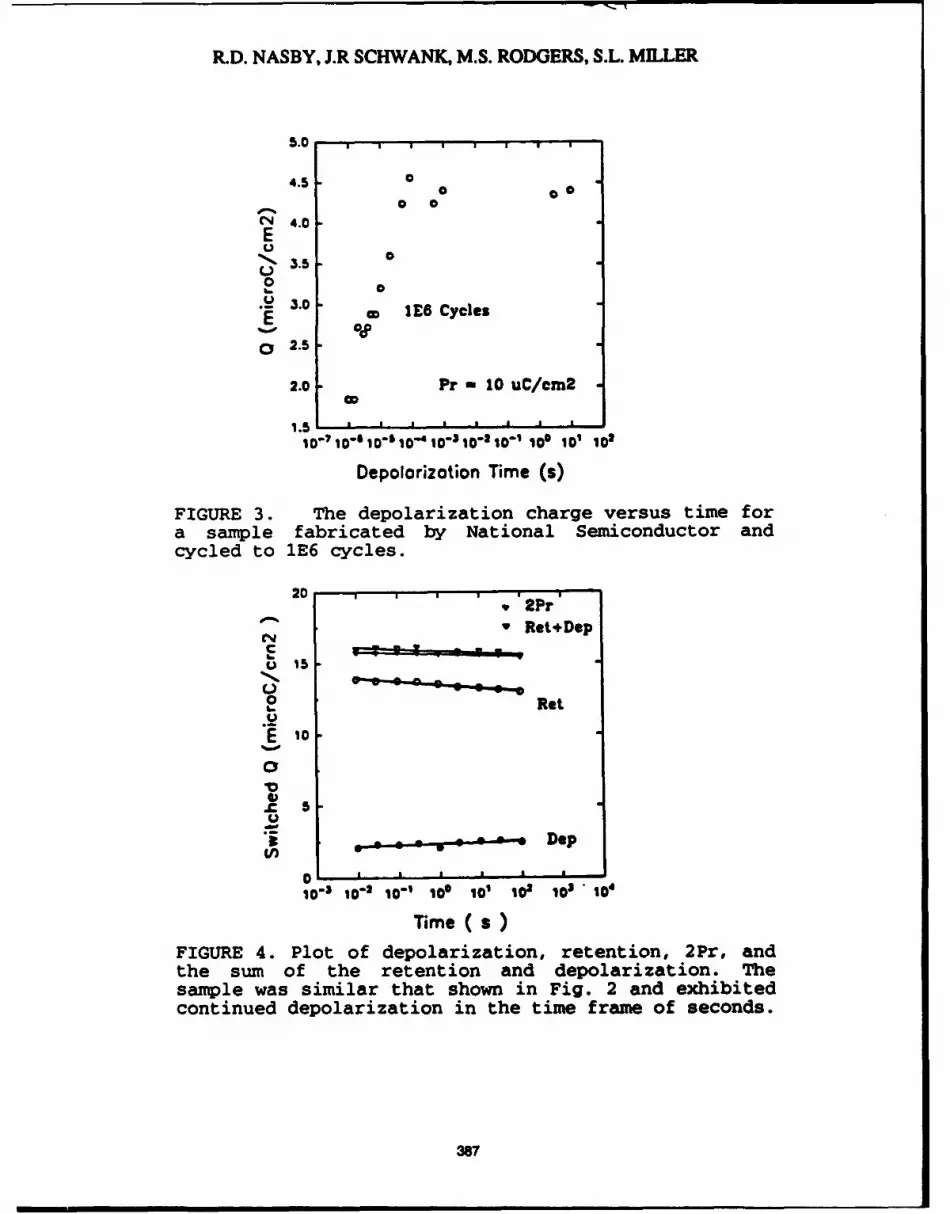
R.D. NASBY, J.R SCHWANK, M.S. RODGERS, S.L. MILLER
5.0 , , , , , ,
4.5 -o0 0
CN1 4.0EUS3.5 0
030
3.0 - IE6 Cycles
o 2.5
2.0 Pr - 10 uC/cm2
1.5 ' ' 6 2 2 I '10" 10-s 0" 10"4 10"-3 10-2 10-1 100 I101 102
Depolorizotion Time (s)
FIGURE 3. The depolarization charge versus time fora sample fabricated by National Semiconductor andcycled to 1E6 cycles.
202Pr
' Ret*DepC
tRaU 15
CY
o RetL_u
"100
.cSu
"i ______.... Dep
Time ( s )
FIGURE 4. Plot of depolarization, retention, 2Pr, andthe sum of the retention and depolarization. Thesample was similar that shown in Fig. 2 and exhibitedcontinued depolarization in the time frame of seconds.
387

FATIGUE AND RAPID DEPOLARIZATION
6
s4
!20
0Iw
o 0 2W0 3W 4W01 W .- f u e
Time (las)
FIGURE 5. Input and output waveforms for themeasurements of retention and 2Pr shown in Fig. 4.
1.2 . I I
1.0 - ,- .5 V
h...
0.
0.2
10 10 107 108 109 1010 oll 1012 I1OU
Cycles
FIGURE 6. The effect of cycle voltage on fatigue.The Pr values were normalized to their value after aninitial 1E6 cycles. The sample thickness was 400nanometers.
388

--- I
R.D. NASBY, J.R SCHWANK, M.S. RODGERS, S.L. MILLER
1012
10"0
U 10I
E
10' Film thickness - 400 nm
10
0.0 0.1 0.2 0.3
1/Voltage (1/V)
FIGURE 7. Voltage activation of fatigue. The number ofcycles which produced a degradation in Pr to 0.7 ofits initial value is plotted versus the reciprocalapplied voltage. These data were determined from theresults shown in Fig. 6.
1.2 , 1 1 1 1
1.0
O 0.8
3 Va04X
0.6B '5
0 0.4 06z
0.2 v 10
0.0 '
103 104 101 100 107 108 10 1010 loll
CyclesFIGURE 8. Fatigue as a function of applied voltagefor a sample which was 170 nanometers thick. Nodiscernable voltage acceleration is apparent.
389

INTEGRATION OF FERROELECTRIC PZT CAPACITORS WITHGaAs JFET DEVICESI,,
MOM S. Y. WU AND W. A. GEIDEMANMcDonnell Douglas Electronic Systems Company, 5301 Bolsa Avenue,
(.0 Huntington Beach, CA 92647
O M Abstract. This invited paper presents the development work on integrationof ferroelectric PZT capacitors with GaAs JFET devices for the fabrication ofhigh density nonvolatile ferroelectric random access memories at McDonnellDouglas Electronic Systems Company. The paper will start with the preparationand characterization of various properties of the PZT films deposited by a sol-geltechnique. It will be followed by the two approaches investigated for the formationof the p+ gates of GaAs JFETs: zinc diffusion and zinc implantation. The processcompatibility and sequence of memory fabrication incorporating these twoapproaches will be described. The difficulties associated with the zinc diffusionapproach will be discussed. Finally, the current effort in the integration of thePZT capacitors and the implanted GaAs JFETs will be presented.
INTRODUCTION
The revived interest in the nonvolatile ferroelectric random access memory (FERRAM)incorporating a ferroelectric thin film with semiconductor technology can be reflectedfrom a large number of papers and attendees at the two recent ferroelectric conferences(1,2). Several companies including the McDonnell Douglas Electronic SystemsCompany (MDESC) have been exploring, designing and fabricating various devicestructures and memory configurations(3 -7). This invited paper intends to present theresults of investigation on the integration of lead-zirconate-titanate (PZT) capacitors withGaAs junction field-effect transistor (JFET) devices performed at MDESC under aDARPA contract. We are currently developing a 4K/2K nonvolatile FERRAM (15). Thebasic memory cell consists of one transistor-one capacitor per cell (for the 4K memory)or two transistors-two capacitors per cell (for the 2K memory). The cross-sectional viewof the one transistor-one capacitor cell structure and its equivalent circuit are illustratedin Figure 1. The PZT capacitor is fabricated alongside the GaAs JFET on the samewafer. This structure offers more flexibility for the integration and optimization of both thePZT capacitor and the GaAs JFET.
E ,
Gab FFE
bwaw
FIGURE 1. Cross-sectional view and the equivalent circuit ofone transistor-one capacitor memory cell.
Several areas which require special attention in the integration of a PZT capacitorand a GaAs JFET have been investigated, namely: PZT capacitor, GaAs JFET, processcompatibility and sequence of integration, and interconnects and dielectric crossovers.They are highlighted In Table 1. In this paper, we will start with the PZT film preparation
390

S. Y. WU AND W. A. GEIDEMAN
and characterization of various properties. It will be followed by the sections describingthe approaches taken to form the p+ gate, and the process compatibility and sequenceof integration of the GaAs JFET with the PZT capacitor for each approach. The currentstatus on the progress of the program will be presented in the last section.
"PZT CAPACITOR
Composition, Structure, Surface Morphology, Film Thickness, Capacitor Size, ContactElectrode, Passivation Layers, Delineation Method, Polarization, Coercive Voltage,Switching Speed, Endurance, Retention, etc.
" GaAs JFET
Source, Drain and Channel Implantations
Gate Formation (Threshold Voltage = 0.2 volt)Ohmic Contacts
"* PROCESS COMPATIBILITY AND SEQUENCE OF FABRICATION
"* INTERCONNECTS AND CROSS-OVER DIELECTRIC LAYER
TABLE 1. Key considerations for PZT capacitor and GaAs JFET integration.
PZT FILM PREPARATION AND CHARACTERIZATION
The PZT films are prepared by a sol-gel technique (8). The precursor materials used arelead acetate, titanium isopropoxide and zirconium n-propoxide. One part of the solutionof lead acetate dissolved in methoxyethanol is mixed with a methoxyethanol solutioncontaining zirconium n-propoxide. The other part of the lead acetate solution is mixedwith another methoxyethanol solution containing titanium isopropoxide. The final stocksolution is formed by mixing these two lead acetate solutions, boiling for a few minutesand slowly cooling to room temperature.
Before spin coating the film, a chemical additive, formamide, is added into thestock solution. Formamide modifies the hydrolysis, polymerization and crystallizationprocesses of the film to prevent it from cracking during the drying and sintering operation(9,10). After spin coating the film, it is dried and sintered in air at 6500C for 15 minutes.The flow diagram showing the preparation of the PZT films is given in Figure 2.
I FIGURE 2. Flow diagram for the sol-gelF'n"Wi AMNO preparation of PZT filmsI- 1
The properties of the PZT films are characterized by various analytical andelectrical techniques. The x-ray diffraction (XRD) analysis is used to determine thestructure and the phase of the films. Figure 3 shows XRD patterns of a 1200A (top) and
391

INTEGRATION OF PZT CAPACITORS WITH GaAs JFET DEVICES
a 600A (bottom) films measured with a small angle Norelco modified x-ray system usingan angle of incidence of 1.50. The films are deposited on Pt/Ti electroded and Si02/SiNpassivated silicon wafers. The Zr/Ti atomic ratio of the films is 60/40. The diffractionpeaks characteristic of the tetragonal structure are clearly seen in these patterns. The(112) and (211) peaks of the 1200A thick film show clearly " splitting. The broad peakcorresponding to (103)/(301) reflections of the 600A thick fMin indicates two side by sidepeaks. These XRD patterns demonstrate that our 60/40 PZT films have a tetragonalstructure at room temperature. This is different from the rhombohedral structure reportedin the bulk ceramics of the same Zr/Ti ratio( 11 ,12). The morphotropic phase boundaryseparating the tetragonal and the rhombohedral phases apparently has shifted fromZr/Ti ratio of 52/48 in the bulk ceramics to a higher ratio in thin films. We attribute thisshift to stresses in these thin films.
FIGURE 3. XRD patterns of 1200A (top) and600A (bottom) 60/40 PZT films
• I J - -L L- -20 2i 40 50 60 70 60 90
26
The surface microstructures of the same films measured from a scanning electronmicroscope are illustrated in Figure 4. The films are very dense, smooth and uniformwith a lateral grain size in the range of 0.2-0.5 pim, which is much smaller than thosereported previously for thicker PZT films( 13 ) and bulk ceramics( 1 4 ).
W-, AQ,
' .• ", ,.•'Z, AA..# i ..
_46l~ t. 6A . • , i . l-,
FIGURE 4. Surface microstructures of 600A (left) and 1200, (right) 60/40 PZT films
392

S. Y. WU AND W. A. GEIDEMAN
The chemical composition of the films is analyzed by Auger electronspectroscopy. Figure 5 shows the Auger depth profiles of the elements of two 600A filmswith Zr/Ti ratios of 50/50 and 60/40. The measured Zr/Ti ratios matched very well withthose of the starting sol-gel formulation. There is a disturbed region of about 50-1 ooA inthickness at the surface. To fabricate PZT capacitors possessing a good upper contact,we perform a heat treatment at 6500C for 15 min. to diffuse the contact metal, gold, intothe films to avoid this non-stoichiometric composition region.
100
Zr/TI - SOSOso Pt
0I--P_
60-
Cr 40I-.
S20 Zr
0 I SO 300 4 SO 600 ?SOOEPTH FROM SURFACE (A)
100
ZrM SW40 FIGURE 5. Auger electron spectroscopy depthSgo profiles of elemental concentrations
PO of 600A 50/50 (top) and 60/40eo /0 (bottom) PZT films
C- 40
w
g0m]0 170 340 510 6O no
OEPT4 FROM SURFACE (A)
The ferroelectric hysteretic properties of the films are studied using a Sawyer-Tower bridge circuit with a 1 KHz sine wave. The hysteresis loop of a 600A thickcapacitor is displayed in Figure 6. The remanent polarization, maximum polarizationand coercive field of the film are 21 p.C/cm 2 , 38 p.C/cm 2 and 75 KV/cm, respectively. Todemonstrate that our thin PZT capacitors could be poled to saturation at 3-5 volts, wegradually increased the applied voltage in steps from 0.8 to 4 volts on a 650A capacitor.At each voltage increment, the maximum polarization, Pmax, remanent polarization andcoercive voltage were measured and plotted in Figure 7. Pmax increased from 8.2gC/cm2 at 0.8 volt to about 39 pC/cm2 at 3 volts. It then increased linearly at highervoltages with the applied voltage. This indicated that the film reached saturation at 3volts. A similar experiment on a 1 oooA thick capacitor also showed that the capacitorreached saturation at 5 volts.
Figure 8 shows the switching time versus capacitor area for a 600A thickcapacitor. We have found that the switching time is linearly proportional to the capacitorarea. The shortest switching time measured was 4 nsec from a 12 x 12 pgm 2 capacitor,which implied that the intrinsic switching time of the film was faster.
393

INT:3RATION OF PZT CAPACITORS WITH GaAs JFET DEVICES
FIGURE 6. Hysteresis loop of a 60A thick 12x12 pm2 capacitor measured at1 KHz (ZrM - 50/50).Scale: V: 13.9 pCtcm2 /Div. H: 167 KV/cm/Div.
so 1.0
Pmax
a vc30" 0.6 ~
SFIGURE 7. Maximum polarization, remanent20o -0.4 o pladzation and coercive veota0
> versus aplied vo•te of a10o .2 thOkf 40x40 pnm2 capacitor
U
0 * 0.00 1 2 3 4 5
APPLIED VOLTAGE (VOLTS)
40'
- 30
20 FIGURE 8. Measured switching time versuscapacitor area of a 600A thick50/50 PZT film.
10,
0 300 600 900 1200 1500 1800
CAPACITOR AREA (jim2)
The switching endurance was measured by applying a 100 KHz square wave of acertain amplitude to the test capacitor In series with a 50 Q resistor. The hysteresis loopwas then measured at various time intervals using a Sawyer-Tower bridge circuit with a1 KHz sine wave of the same amplitude as that of the square wave. The measuredremanent polarization versus the cycling time of a 650A capacitor Is shown in Figure 9.
394

S. Y. WU AND W. A. GEIDEMAN
U
Szo15-
00. 5
I• 0 '7'1'
10 1; o 10 10 10TOTAL NUMBER OF CYCLES
FIGURE 9. Measured remanent polarization versus cycling time of a 650Athick 40x40 gm2 capacitor.
After 1 x 10⁹ cycles, the capacitor retained 27% (4 1iC/cm 2 ) of the initial remanentpolarization when the capacitor was cycled with 2 volt pulses. When the capacitor wascycled with 1.5 volt pulses, the remanent polarization reduced to 3 iC/crm2 , 30% of theinitial value. Since the sensing circuit is capable of detecting a charge as low as1 lxm/cm 2 for the capacitor with an area of 4 x 5 jim2 , the projected life of our capacitorsis estimated to be longer than 1 x 10¹⁰ switching cycles. The memory retention of thecapacitor was also investigated. The result was very encouraging. No change in thestored charge or remanent polarization was observed after 236 days of storage withoutpower.
Our PZT capacitors are delineated by the ion milling technique. This techniquehas been quite successful in delineating capacitor sizes as small as 4x4 gim 2 . Theuniformity of the film quality is also very good, which can be seen from the remanentpolarization values measured from 40x40 gim 2 capacitors over a I x 0.7 in2 areaillustrated in Figure 10. The variation is 10% from the mean.
1 in.I 12.5 12.4 11.7 11.0 9.4 9.4 9.5 11.1 9.5 9.4
12.4 10.0 9.5 9.5 9.4 9.4 10.0 9.9 11.0 9.4
0.7 11.8 11.7 11.0 12.5 Short 12.0 10.0 9.4 13.2 9.4
I 10.0 9.4 9.5 9.4 9.6 10.U 9.5 9.6 9.7 11.0
11.0 9.4 9.5 9.6 g.8 9.8 10.0 10.1 10.2 12.0
Remanent Polarization (IC/cm 2 )
FIGURE 10. Measured remanent polarization of 40x40 pim 2 capacitors over anlxO.7 in2 area.
395

INTEGRATION OF PZT CAPACITORS WITH GaAs JFET DEVICES
FORMATION OF P+ GATE N-CHANNEL GaAs JFETs AND INTEGRATIONWITH PZT CAPACITORS
As shown in Figure 1, the GaAs JFETs are used as access transistors in the memory.These n-channel JFETs must be operated in the enhancement mode with a thresholdvoltage of about 0.2-0.3 volts. At MDESC we have investigated two approaches to formthe p+ gate. The first approach we employed was magnesium implantation followed byzinc diffusion, which was called the zinc diffusion approach, and the other was straightzinc implantation. The process sequences of integration and the experimental resultsusing these two approaches will be described next.
1. Zinc Diffusion Approach:
The zinc diffusion approach is employed first because this method has been wellestablished and adopted as the standard process in our laboratory for the formation ofthe p+ gate enhancement mode n-channel GaAs JFETs. There are four critical hightemperature treatments involved in the fabrication process employing this approach.They are given in Table 2.
1. Post-implant annealing of the source, drain and channel of the JFETat 7500C for 15 minutes in forming gas
2. Spin-coating and sintering of PZT at 6500 for 15 minutes in air andalloying of gold electrode again at 6500C for 15 minutes
3. Zinc diffusion at 6500C for 1 minute in argon
4. NiAuGe ohmic contact alloying at 4400C for 3 minutes in forming gas
TABLE 2. Sequence of critical high temperature processes employingthe zinc diffusion approach.
The PZT film is deposited and sintered (step 2) after the source, drain andchannel post-implant annealing to avoid the PZT from being reduced at 7500C informing gas. The zinc diffusion (step 3) is done after the PZT sintering and the goldupper electrode alloying to prevent zinc from being driven in deep by the two 6500C15 min. heat treatments. But the zinc diffusion at 6500 C for 1 min. in argon is found to bedetrimental to the PZT film and the gold upper electrode. To protect the PZT film duringthe zinc diffusion, we cap it with a layer of diffusion barrier such as silicon nitride (SiN)layer. Figure 11 shows the sequence of the processing steps in cross-sectional view.
I omp'm I . wN . . P..h-ed w4 Eh GM. ORPOW 3"~
~NC2 A K. FIE . dTE
ElTE
3 CPFE ýd NET WOS" IAuPG*
.-.-- ---.- M FE FIGURE 11. Sequence of processing steps4 Rtl MmN W llOW ~ FE. Efth 9" .
aft Qf .CM ,.M .Wd- 0 Ow in cross-sectional view of GaAs, , ;b 1 .4,02 JFET and PZT capacitor using
] Gs.. zinc diffusion approach.5 EA0.. WUl d TE.
396

S. Y. WU AND W. A. GEIDEMAN
There were several problems developed, however, during the zinc diffusion usingthe SiN as the capping layer. First, the SiN reacted chemically with the gold electrodeat 6500C which left holes in the gold electrode. This problem was overcome bydepositing a Pt layer on top of the gold electrode since Pt was found less reactive withSiN than gold at 6500C. Second, the edge coverage by the SiN was poor, whichresulted in zinc penetration through the weak spots at edges of the capacitor andsubsequently destroyed the PZT film. Third, the poor adhesion of the SiN on the uppercontact electrode caused delamination or partial lifting of the SiN layer during the 6500zinc diffusion operation. Because of these difficulties mentioned above, the zincdiffusion approach was not further pursued in our integration study.
2. Zinc Implantation Approach:
The formation of the p+ gate of n-channel GaAs JFETs by the zinc implantation wasinvestigated next after we encountered some difficulties with the zinc diffusion approachmentioned in the previous section. We have found that the zinc implantation has manyadvantages over the zinc diffusion. These advantages are:
1. Elimination of wafer exposure to zinc atmosphere.
2. Zinc implantation can be done before PZT capacitorfabrication.
3. No significant broadening of zinc profile after post-implant rapid thermal annealing and PZT capacitorheat treatments.
4. More controllable than zinc diffusion.
5. More compatible with other processing steps.
The processing sequence incorporating the zinc implantation for the integration of thePZT capacitor and the GaAs JFET is given in Figure 12. The zinc implantation (step 2) isdone before the PZT capacitor fabrication (step 3). This is different from the zincdiffusion approach in which the PZT capacitor is processed before the zinc diffusionstep. Our experiments have shown that the two heat treatments required for the PZT filmsintering and the upper contact electrode alloying in step 3 do not degrade theimplanted p+ gates processed in step 2. They also do not alter the threshold voltage ofthe JFETs, which will be described in the following paragraph.
I ..0 ft" go ft.. tC. Ml-S"W., N.. . .... .... 1 N.
eP.2 a, Mot 00m. tom Ioe -4 A*,. [ TE
L___M~t__jNIA.~Ge
3 Pmal K. FIE TE me tal, I
a= -- -'-- .....- FE FIGURE 12. Sequence of processing stepsQ 0o,.0 in cross-sectional view of GaAs
f£E.T IkNA 9",,o. 00- [ N,+,0 JFET and PZT capacitor using0 CA" zinc implantation approach.
397

INTEGRATION OF PZT CAPACITORS WITH GaAs JFET DEVICES
Initially we found that the threshold voltage of the JFETs varied from +0.8 volts to-0.8 volts across a 3 inch wafer after a post-implant rapid thermal annealing (RTA) at8000C for 5 sec, which is shown in Figure 13. The JFETs in the middle of the wafer werein the enhancement mode (positive threshold voltage) while away from the center theywere in the depletion mode (negative threshold voltage). The histogram illustrating thenumber of JFETs versus the threshold voltage across a 3 inch wafer after the RTA isgiven in Figure 14 (a). The wafer was next given an additional 6500C 30 min heattreatment, simulating the two heat treatments, 6500C 15 min. each, for the PZT filmsintering and the upper contact electrode alloying. The histogram after the 6500C30 min. heat treatment is illustrated in Figure 14(b), which shows no significant shift inthe threshold voltage after the additional heat treatment.
E nmmmm8.00E-0B EDmnmmE6OOCE-01
m ° E-ooo0-2.OOE-O
_ 46 . 0 0E - 0:
1 F-6 .00E-011 0O2 .OGE 01 LJ IIT~
FIGURE 13. Variation on threshold voltage of JFETs across a 3 inch wafer afterRTA at 8000C for 5 sec.
OF %I1GN • 4DESII, "-
W I N1)0w WINOOWd
z z
-2.0 -0.S 0 0. 2 0 -•. .0V H ) VTH (VI
FIGURE 14. Histogram illustrating number of JFETs versus threshold voltageacross 3 inch wafer after RTA only (left) and RTA plus 6500C30 min. heat treatment (right).
398

S. Y. WU AND W. A. GEIDEMAN
The spread in the threshold voltage was due mainly to an uneven heating in theRTA system. This was taken care of after we readjusted the lamps in the RTA system.The spread in the threshold voltage was reduced to about 0.2 Volt as shown inFigure 15 after the RTA only and the RTA plus 6500C 30 min heat treatment. The meanthreshold voltage was higher than the upper margin (-0.5 volt) of the design window.This was later corrected by reducing the zinc implantation energy from 40 KeV to30 KeV. The histogram after the correction is illustrated in Figure 16.
-- ' 1 4*-- -- " '*---DESIGN DESIGN
W IN"DOW WI NOOW1
I I I
I I
z I
I II I
!22VrH <v m <VM
FIGURE 15. Histogram illustrating number of JFETs versus threshold voltageacross 3 inch wafer following RTA after lamp adjustment (left) andRTA plus 6500C 30 min. heat treatment (right).
1 O DESIGN I
WINDOW
w IzI
UMH (VI
FIGURE 16. Histogram illustrating number of JFETs versus threshold voltage aftercorrection of zinc implant energy.
INTEGRATED GaAs JFET AND PZT CAPACITOR MEMORY CELL
After the PZT capacitor is fabricated (step 3 in Figure 12) the wafer is covered with a3000A SiN layer. This SiN and the underlying SiO2 layers over the JFET are nextremoved. The ohmic contacts for the source, drain and gate of the JFET are processed.Following this vias in the SiN for the upper and bottom contacts of the PZT capacitor areopened. After depositing and etching of the first level interconnect we complete theintegration of the GaAs JFET and the PZT capacitor.
399

INTEGRATION OF PZT CAPACITORS WITH GaAs JFET DEVICES
A photograph showing memory cells with integrated GaAs JFETs and PZTcapacitors (after the first level interconnect delineation) is illustrated in Figure 17. Thehysteresis loop of a 40x40 jim2 capacitor and the current-voltage characteristics of theintegrated GaAs JFET are demonstrated in Figure 18. The wafer is next covered with adielectric crossover, either a SiN or a polyimide layer. Vias in the crossover are openedand the aluminum second level interconnects are deposited and delineated. A finished
4K/2K FERRAM is shown in Figure 19. We are currently working on a functionalFERRAM. More detailed experimental results on the latest FERRAM development willbe reported in the two companion papers(1 5 ,16 ).
FIGURE 17. Memory cells with GaAs JFETsand PZT capacitors integratedon the same GaAs wafer (afterthe first level interconnectdelineation)
Pr 20 gC/m2 VTH = 0.27 voltVC= 0.65 volt Gm = 130 m/mm
A = 40x40W1m2 L = 1 gmt = 100nm W= 20 pm
FIGURE 18. Hysteresis loop of 40 x 40 prn2 capacitor and current-voltagecharacteristics of integrated GaAs JFET.
400

S. Y. WU AND W. A. GEIDEMAN
.... ..... . .
FIGURE 19. A finished 4K/2K FERRAM (after the second level interconnectdelineation)
CONCLUSIONS
In this paper we have presented the results of investigation on the integration of PZTcapacitors and GaAs JFETs on the same GaAs wafer for the fabrication of 4K12Knonvolatile ferroelectric random access memories. Several areas such as thepreparation and characterization of the PZT films, formation of the p+ gate, processcompatibility and sequence of integration of the GaAs JFET with the PZT capacitor, andthe current status on our development program have been described.
The PZT films are prepared by a sol-gel technique which uses precursormaterials containing lead acetate, titanium isopropoxide and zirconium n-propoxidemixed with methoxyethanol. A chemical additive, formamide, is added in the precursorsolution to prevent the films from cracking during the drying and sintering operation.Excellent structural, compositional, ferroelectric hysteretic, switching endurance andmemory retention properties have been obtained in these films. They are very dense,smooth and uniform with a lateral grain size of 0.2-0.5 gm. The remanent polarization,maximum polarization and coercive field of a 600A thick capacitor are 21 AC/cm 2 ,38 VC/cm2 and 75 KV/cm, respectively. The films with a thickness of 600-1000A haveexhibited a low saturAion voltage of 3-5 volts. The switching speed of the films is veryfast. The shortest switching time measured from a 12x12 gm 2 capacitor is 4 nsec. Theswitching endurance and memory retention of the capacitors are very encouraging. Theprojected life of the capacitors is estimated to be longer than lx1010 switching cycles.No change in the stored charge or remanent polarization has been observed after 236days of storage without power. The uniformity of the film quality is very good. Thevariation of the remanent polarization measured from 40x40 jIm 2 capacitors over a 1 x0.7 in2 area is less than 10% from the mean.
Two approaches for the formation of the p+ gates of the n-channel GaAs JFETshave been investigated: one is magnesium implantation followed by zinc diffusion,
401

INTEGRATION OF PZT CAPACITORS WITH GaAs JFET DEVICES
which is called the zinc diffusion approach, and the other is the zinc implantationapproach. The sequence of integration and the process compatibility using these twoapproaches have been developed and examined., Due to the poor edge coverage andoccurring of delamination and partial lifting of the SiN capping layer during the 6500Czinc diffusion process, the zinc diffusion approach was not further pursed.
The zinc implantation approach has been quite successful in forming the p+ gatesof the GaAs JFETs. After the lamp adjustment in the RTA system and the correction ofthe zinc implantation energy, we are able to obtain a threshold voltage of 0.2 - 0.5 volts.Using the zinc implantation approach together with the developed processingsequence, we have successfully fabricated PZT capacitors and JFETs on the sameGaAs wafer. Excellent hysteresis loops and current voltage characteristics have beendemonstrated on PZT capacitors and the GaAs JFETs fabricated on the same wafer.Work on the crossover dielectric layer and the second level interconnects is beingcontinued for making a functional 4K/2K ferroelectric random access memory.
ACKNOWLEDGEMENTS
The authors would like to thank Drs. J. Alexander and M. Yoder for their continuedinterest and encouragement. Work has been supported by DARPA under ContractN00014-89-C-0020.
REFERENCES
1. The Seventh International Symposium on Applications of Ferroelectrics, Urbana,Illinois, June 6-8, 1990.
2. The Third International Symposium on Integrated Ferroelectrics, ColoradoSprings, Colorado, April 3-5, 1991.
3. W. A. Geideman and S. Y. Wu, "Progress in Ferroelectric Memory Technology",presented at the 7th International Symposium on Applications of Ferroelectrics,Urbana, IL, June 6-8, 1990.
4. W. A. Geideman, S. Y. Wu, L. E. Sanchez, B. P. Maderic, W. M. Liu, I. K. Naik andS. H. Watanabe, " PZT Thin Films for GaAs Ferroelectric RAM Applications",presented at the Seventh International Symposium on Applications ofFerroelectrics, Urbana, IL, June 6-8, 1990.
5. S. Bernacki, L. Jack, S. Collins, S. Bernstein, Y. Kisler, B. Armstrong, J. Shaw,J. Bullington, J. Evans, B. Bunker and B. Tuttle, "Integration of Ferroelectrics intoSemiconductor Devices", presented at the 3rd International Symposium onIntegrated Ferroelectrics, Colorado Springs, CO, April 3-5, 1991.
6. N. Aft, "Ferroelectrics at National Semiconductor", presented at the 3rdInternational Symposium on Integrated Ferroelectrics, Colorado Springs, CO,April 3-5, 1991.
7. D. Bondurant, "Ramtron's Ferroelectric RAM Evaluation and DevelopmentSystem", presented at the 3rd International Symposium on IntegratedFerroelectrics, Colorado Springs, CO, April 3-5, 1991.
8. L. E. Sanchez, D. T. Dion, S. Y. Wu and I. K. Naik, "Processing andCharacterization of Very Thin PZT Ferroelectric Capacitors by a Sol-Gel Method",presented at the 2nd Symposium on Integrated Ferroelectrics, Monterey, CA,March 6-8, 1990.
9. G. Orcel and L. Hench, K. Non-Cryst. Solids 79, 177 (1986).10. L. L. Hench, G. Orcel and J. L. Nogues, Mat. Res. Soc. Symp. Proc.
73, 35 (1986).11. G. Shirane and K. Suzuki, J. Phys. Soc. Japan 7, 333 (1952).12. E. Sawaguchi, J. Phys. Soc. Japan 8, 615 (1953).13. K. D. Budd, S. K. Dey and D. A. Payne, Proc. Brit. Ceram. Soc. 36, 107 (1985).14. G. H. Haertling and C. E. Land, J. Amer. Ceram. Soc. 54, 1 (1971).
402

S. Y. WU AND W. A. GEIDEMAN
15. L. E. Sanchez, I. K. Nalk, S. H. Watanabe, J. H. Madok andS. Y. Wu, "Process Technology Development for GaAs FerroelectricNonvolatile Memory', presented at the 3rd Symposium on IntegratedFerroelectrics, Colorado Springs, CO. April 3-5, 1991.
16. I. K. Naik, L. E. Sanchez, B. P. Maderic and S. Y. Wu, "Improved SwitchingEndurance of Thin Film Lead-Zirconate-Titanate Capacitors for NonvolatileFerroelectric Memories", presented at the 3rd Symposium on IntegratedFerroelectrics, Colorado Springs, CO, April 3-5, 1991.
4M3

__ANOMALOUS REMANENT POLARIZATION IN FERROELECTRIC
CoCAPACITORS
NORMAN E. ABT
Fairchild Research Center, M/S E 140
National Semiconductor Corporation, Santa Clara, CA 95052-8090
Abstrac An apparent remanent signal seen by the application of voltagepulses to a Sawyer-Tower circuit is described. This 'remanent' is present fortwo pulses in the same direction when no remanent is expected. Variation ofthis signal with fatigue and ageing will be shown. Implications for memory
circuits will also be discussed. Finally, several suggestions of possible
mechanisms will be presented.
INTRODUCTION
Ferroelectric materials have been studied extensively since their discovery early in thecentury. A standard technique for analyzing ferroelectric properties is to measure an
electrical hysteresis loop1. Recently ferroelectric materials have been prepared as thinfilms for use in semiconductor memory applications2. Hysteresis loops using sine
wave excitation were measured for these films. Also, polarization was measured
using single pulses. The pulses mimicked the operation of the memory circuit. Thevalue of the remanent polarization from these two method did not agree. In addition,
when two pulses of the same polarity were applied to a sample there appeared to be a
remanent signal after the second pulse when in principle no switching of dipole
should have occurred and no remanent should be present. In this paper we willexpand on the observations of this phenomenon including its relation to the familiar
ageing and fatigue. The importance of this to memory applications will be discussed
92-16147I m I IIi E| IE II i lu

N. E. ABT
and a new failure mechanism for memories caused by this will be described. Finallyseveral suggestions of possible causes are made.
EXPERIMENTAL OBSERVATIONS
The phenomenon which we call APO can be most easily seen by comparing two pulsesequences shown in figure 1. The output shown is that which would be seen across
the sense capacitor of a Sawyer-Tower circuit. The write and sense pulses areapplied to the top of the ferroelectric capacitor. In the first sequence the pulses are ofopposite polarity. The second pulse, the sense pulse, will cause the dipoles to switchproducing a large remanent labeled API. In the second sequence the two pulses arein the same direction and the sense pulse should not produce switching of dipoles butimmediately after the fall of the pulse a remanent can be seen, labeled APO. In ourwork we used 8p.S pulses though this is seen for all pulse durations. Examining theremanents for the two cases on longer time scales reveals a decay of the signals
(figure 2). Both AP1 and APO follow identical decays except that the API signal is
Write Sense Outputpulse pulse
Remanent signalAP1 after pulse which
reverses state ofMAJ polarization
FL JL__ JiY _P 'Remanent' signalafter pulse whichdoes not reversepolarization
Figure 1. Pulse definitions of API and APO
405

ANOMALOUS REMANENT POLARIZATION IN FE CAPS
offset from zero by a constant. This decay nominally takes lOOmS and follows a -
Log(time) dependence.
AMi
--- --- -lOOmS----
F APO
Figure 2. Decay of remanents follows Log(time)
It is important to see the relation between pulsed measurements and a
hysteresis loop (figure 3). In the usual measurement, as a sine wave is applied the
signal goes around the loop , A-C-B-D-A. For the pulses of
the first sequence of figure 1 the write pulse places the capacitor at point A'. Thesense pulse drives the capacitor following A'-C-B and during the decay in the next
lOOmS from B-B'. The second sequence goes B'-C-B and then during the slowdecay B-B'. From the hysteresis loop Pr = A-B but from the pulses one sees onlyA'-B
Figure 4 shows the change in API, APO, and -APO (APO for two downpulses) with fatigue. The capacitor was cycled with a 5 volt 1Mhz sine wave at roomtemperature. At each read point the cycling was stopped and the signals measuredwith pulses of the form 1- sin(2WWt-2) with f= 80kHz. Note APO does not equal -APO and the difference between API and APO is decaying with fatigue faster than APOitself.
4W6

N. E. ABT
P
iC
• - AP1
vA- --------
D A
Figure 3. Relation of APO and AP1 to hysteresis loop
APO shows only minor changes with ageing (Figure 5). However, there is a
similar test with ageing that does show dramatic change. We have called it imprint
because of its effect on a memory circuit but it is a worst case ageing phenomenon. If
a capacitor is placed in an up state for a prolonged period of time the opposite or
down APO will increase. Similarly, if the capacitor is pulsed down and left there the
up APO will increase. This memory of the previous state cause errors in data for a
circuit as will be shown in the next section. A way to see this is to compare two
ways of doing an ageing experiment. Two pulse sequences are shown in figure 6.
In the first the capacitor is put in a down state before the ageing period and in the
second it is put in an up state. At each read data point the up APO is measured.
Figure 7 compares the result for the two cases. When stored down the up APO
increases while for the stored down case the up APO is roughly constant.
407

ANOMALOUS REMANENT POLARIZATION IN FE CAPS
8
Read/Write Voltage = 5V7 - - ----- Film thickness = 0.4 pm
CM Temperature = 20C
z 50 0 APO
•4 API
5 -APO0 o - --1
I-
z wA
1E+6 1E+7 1E+8 1E+9 1E+10 1E+11 1E+12 1E+13 1E+14
NUMBER OF CYCLES
Figure 4. Fatigue of fully integrated Ferroelectric capacitor
8
g4 APO
2
1
0 0.5 1 1.5 2 2.5 3 3.5Log Time (sec)
Figure 5. Ageing of AP1 and APO
408

N. E. ABT
I I e
---------------- Ageing time delay----------------
L IIe J
---------------- Ageing time delay -------------
Figure 6. Two Cases of an ageing test
0.25
0.20
0.15U 1.8, down
0.10 esu
0.05
0.00.............J10o i001 10 2 10~ 3 1 4 105
Ageing lime(sec)
Figure 7. Change in APO during ageing with capacitorstore up and down.
Efeto esrmnsadCrul
The presence of A~PO puts extra conditions on the measurement of ferroelectricproperties. With pulses the timne delay between poling and reading is critical. NoteFigure 8. Two cases are shown with the timne delay between poling and reading
4M9

ANOMALOUS REMANENT POLARIZATION IN FE CAPS
being tw, and tw2 respectively. Because AMO has a finite decay time in the first case ithas not completed its decay before being read. This produces a smaller value than in
the second case where APO has had more time to decay.twi
1w2
Figure 8. For twl < tw2 APO(twl) < APO(tw2)
(The use of the term 'decay' is somewhat arbitrary. What happens during thisrelaxation time could also be a 'charge buildup' since the mechanism is not known.In either case, it is a charge flow that we are observing and in time the rate of flow
goes to zero.)Measurements of PR made by a CW hysteresis loop will not agree with
pulsed measurements unless APO is taken in to account. The hysteresis loop result
will overstate the true remanent polarization.
One way to use fenoelectric capacitors in a memory circuit is to compare the
remanent signal from two capacitors poled in opposite directions to form one data bit.These will be read by applying the same direction pulse to both (defined as an up
pulse for this discussion). One will switch (that which was stored down) producing
API and the other will not switch (stored up) producing AM0. We can define aT''state as the first capacitor signal greater than the second (AP lrust cap > AP~secon cap)
and, conversely, a V' state as the second signal greater than the first (APOfirs cap <APlsend cap). Ifabit is stored for along time as aTand then written as a'0' the
AM) of the first capacitor will increase and the APO portion of the API from the
410

N. E. ABT
second capacitor may decrease resulting in AP0fit cap > APisecomd cap. The circuitwill read the bit as a '', the previous data will appear 'imprinted' on that bit.
For reliable circuit operation the ferroelectric films must be optimized to
reduce or stabilize APM. This effect can be accelerated with temperature which helpstesting.
ORIGINS OF APO
A few simple tests were run to begin to elucidate the source of this phenomenon.This work was done using PLZT films which covers a wide range of compositions.AP0 was not present or very small for paraelectric compositions. Lateral capacitorswere illuminated with UV light (365nm) which produce no change in electricalresults.
Four pulse sequences which attempt to vary the number of domains oriented
up or down are shown in figure 9. Pulses A and B are used to set the state of thecapacitor while the identical pulse C is used in all cases to read APM. Resulting valuescan be seen in figure 10. All 3 Volts reads, independent of pulses A and B, gave thesame value. Cycling increased the value slightly.
Suggested Models
Trapping is often suggested as a cause of APM but this is not expected to be the cause
because of the lack of APM in the paraelectric film and the null result from the UVexposure. The presence of domains seems a necessary requirement and the following
suggestions are based on that.Depolarization due to reverse fields caused by finite electrode resistance? is
not believed to be the cause because APM remains the same for electrodes of widelydiffering resistance.
We suspect it is a bulk phenomenon of ferroelectric thin films and presentthree possibilities.
411
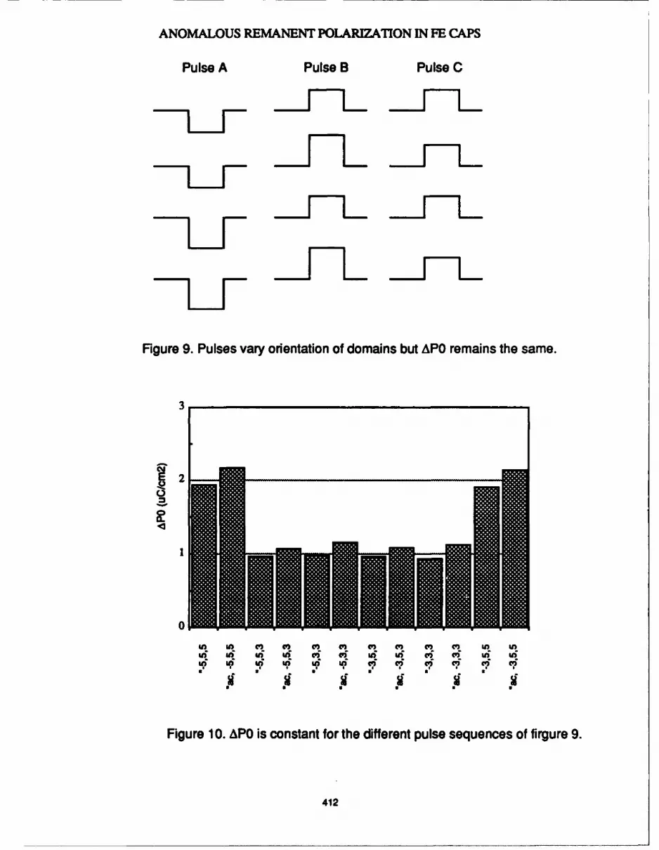
ANOMALOUS REMANENT POLARIZATION IN FE CAPS
Pulse A Pulse B Pulse C
kJhKL
Figure 9. Pulses vary orientation of domains but APO remains the same.
3
2
W) U, I 0 0 0 ) 0 in c) cV) W, W
q~ 1 IQD V; U S; 6 0f f 06 6 06
Figure 10. APO is constant for the different pulse sequences of firgure 9.
412

N. E. ABT
1. Many small domains (on the order of 1OOA) are present. These are aligned
by the applied field but become randomized by thermal energy which is comparable to
the domain energy for this size domain.
2. There is a strong stress vector present in the film. The applied field causes a
domain to grow but in the absence of the external field the surface energy driven by
the stress exceeds the volume energy4 and the domain collapses. This is inherently
asymmetric as the stress vector add differently to the up or down field.3. There is the possibility of a field-induced phase transition for compositions
close to the morphotropic phase boundary5 . A rhombohedral domain may adjoin a
tetragonal domain and in the presence of the applied field at the boundary the
rhombohedral phase may convert and contribute to the polarization. Then the field isremoved it converts back.
CONCLUSIONS
We have shown an electrical measurement on a ferroelectric capacitor which we
believe reveals a new behavior of thin film ferroelectric materials. This component
must be taken into account in describing the remanent polarization of a ferroelectric
capacitor. It can only be seen using pulsed measurement techniques.
Considerably more study of this effect is needed given the complexity of thematerials used and, particularly, given its importance to the functioning of high
density memories.
REERENCE
1 C.B. Sawyer and C.H. Tower, Physical Review, , 269(1930).2 J.T. Evans and R. Womack, IEEE Journal of Solid State Circuits, 23, 1171(1988).
3 B.S. Sharma, S.F. Vogel, and P.I. Prentky, Ferroelectrics, 5., 69(1973).
4 M. Avrami, Journal of Chemical Physics, 9, 177(1941).
5 E. Cross, Personal Communications.
413

AD-P006 673lllil1111111Hilll E
A High-Capacitance PZT-on-Ta205 Memory cell
with a Chemically Stable Electrode Suitable
for Sub-Micron Processing
00_- M. Azuma, T. Nasu, S. Katsu, T. Otsuki and G. Kano
Electronics Research Laboratory
Matsushita Electronics Corporation
A ABSTRACT A high-capacitance Pb(Zrx, Til-x)03 (PZT)-on-Ta205 memory cell suitable for sub-micron processing isproposed, and an experimental capacitor of PZT (Zr/Ti=52/48)-on-Ta2O5 with Ta electrode was prepared. The X-raydiffraction and XMA analysis of the sample showed that PZTreacted with neither Ta nor Ta2OS. The capacitor with 500rnm PZT thickness shows current density of 10-8 A/cm2 at4MV/cm, the breakdown field of 8MV/cm, and the effectivedielectric constant of 40.
INTRODUCTION
The memory device in next generation requires a cell
capacitor which has high charge density and suitability for sub-
micron processing.
Conventional ferroelectric material lead zirconate titanate
Pb(Zrx, Til-x)03 (PZT) used for memory capacitors in silicon VLSI
has the disadvantages of unsuitability of a Pt electrode for sub-
micron processing and of undesirable reaction of poly-silicon and
W electrodes with PZT. A Ta205 capacitor has no such problems, but
has disadvantage of capacitance considerably smaller than that for
PZT.
This paper proposes a high capacitance memory cell suitable
for sub-micron processing by using poly-silicon or W electrodes
under high chemical stability. The proposal is based on the
finding that T205 never reacts with PZT so that a PZT-on-T205
buffer layer impudent to chemical reaction with the above
electrode materials, has high capacitance.
414

EXPERIMENTAL DESIGN
To ensure suitability for sub-micron processing, candidate
metals for electrodes of the PZT capacitor were selected from the
materials in use of current silicon processing. Then, for these
candidate metals, another factor of chemical stability should be
considered.
Two types of undesirable chemical reaction can be occurred at
PZT and the metal surface;
1. metal oxidation
2. metal-lead oxidation
The following reactions with PZT for each candidate metals
are suggested from the oxidation energy of PZT and the metalsshown in figure 1. Oxidation energy of PZT is calculated from that
of PbO, Zr02 and Ti02.
1) Silicon (poly-Si) reduces PZT.(-> Si02)
2) Ta can be oxidized slightly and Ta205 is hard to react
with Pb and PZT.
3) W reacts with Pb in PZT easily and produce PbW04 oxide.
4) Mo reacts with Pb in PZT easily and produce PbMo04 oxide.
These studies show that PZT and Ta205 formations are more
stable than any other formations, indicating suitability of a PZT-
on-Ta205 layer as a chemically stable memory capacitor.
EXPERIMENT
The experimental configuration of the PZT-Ta205 capacitor
sample is shown in Figure 2. Tantalum is used for the bottom
electrodes and Ta205 layer is formed in natively.
SiO2 is prepared with the thickness of 500nm by furnace
oxidation.
Ta metal was deposited on a SiO2/Si Substrate by electron
beam evaporator. The substrate temperature is 1200C and the film
415

thickness is 200nm.
Thin film of Pb(Zro.52,Tio.48)03 was prepared by reactive rf
diode sputtering with a sintered PZT powder containing 10 wt%
excess PbO to compensate for the loss of Pb in the thermal
treatment process. A sputtering gas of 90% Argon and 10% oxygen
was used at the pressure of 1 Pascal. Under applying rf power of
120W, deposition rate was 10nm/min and the film thickness was
500nm. To ensure the film with smooth morphology, the substrate
temperature was set to 180 °C, and after deposition, the thermal
treatment process at 600 °C 15 min in 02 gas has done. The
mophology of the films before and after annealing are shown in
Figure 3 (a) (b). The sputtering conditions are summarized in table
1, and the sputtering system is shown in Figure 4.Top electrode of 200nm Tantalum layer was deposited by using
electron beam evaporator in same conditions with bottom electrode.
The reaction between Ta electrodes and PZT film was studied
by using XRD, XMA and TEM analysis. The evaluation of electric
properties has also done.
RESULTS AND DISCUSSIONS
(1) Reaction between Ta electrode and PZT film
Figure 5 shows X-ray diffraction spectrum of
(a) as sputtered PZT film on Ta/SiO2/Si-substrate
(b) sample after 650°C 15min. annealing in 02
(c) PZT powder reference
The spectrum (b) after annealing shows the clear lines of Ta205
crystal and PZT perovskite ones. From comparison to the spectrum
(a) before annealing, Ta electrode surface seems to be oxidized
during PZT annealing. A TEM photograph (Figure 6) of Ta-PZT
interface after annealing shows that 40nm thick Ta205 layer is
formed in this interface. An XMA analysis with probing depth of
400-500nm shows no particular composition change occurs during
annealing (Table 2).
These results endorse that there is no reaction between Ta205-
416

PZT.
(2) Electric properties of Ta2O5-PZT capacitor
Figure 7 shows the temperature dependence of dielectric
properties of the Ta2O5-PZT capacitor. The effective dielectric
constant is 40 at 25*C, and temperature dependence is originatedfrom ferroelectricity of PZT layer. The effective dielectric
constant can raised by control the thickness of Ta205 layer.
The slight temperature dependence of loss tangent suggests that
the small lack of oxygen in PZT surface region of Ta205 side. This
problem is solved by use of pre-formed thin Ta205 layer.
I-V characteristics of the Ta2Os-PZT capacitor are shown in
Figure 8. The current density is as low as 10- 8 A/cm2 at 4MV/cm,
and breakdown voltage is as high as 8MV/cm.
CONCLUSIONSTo realize a high capacitance memory cell suitable for sub-
micron processing, a multilayer capacitor of PZT-Ta205 capacitor
was proposed.Thermodynamic study of PZT-metal reactions leads chemically
stable system of PZT-Ta205 capacitor.Experimental results endorse that the PZT-Ta205 capacitor is
a promising candidate as a high capacitance memory cell suitable
for the silicon VLSI technology.
ACKNOWLEDGEMENTS
The authors wish to thank Dr.H.Kawamura, Dr.S.Nakajima andDr.H.Takagi for their encouragement and support in this study.
417

REFERENCES
1. R.Moazzami, et al., Tech.Dig. Symp.VLSI Tech., p.15, 1990.
2. J.Carrano, et al., IEDM Tech.Dig., p.255,1989.
3. J.F.Scott, et al., J.Appl.Phys.66(3), p.1444, 1989
4. H.Shinriki, et al., Tech.Dig.Symp.VLSI Tech., p.25, 1989.
5. C.A.Araujo, et al., Ferroelectrics 104, p. 2 4 1 , 1990.
418

Figure Captions
Table 1. Sputter Deposition Conditions of PZT Film
Table 2. Results of XMA Analysis
Figure 1. Oxidation Energy of PZT and Metals
Figure 2. Configuration of PZT-Ta205 Capacitor
Figure 3. SEM Photographs of PZT Film
(a) As Sputter
(b) After Annealing
Figure 4. PZT Sputtering System
Figure 5. X-ray Diffraction Spectrum(a) PZT As Sputter Film
(on Ta Electrode)
(b) PZT Film After Annealing(650*C 15min in 02)
(c) Pb(Zro.52TiO.48)03 Powder
Figure 6. TEM Photograph of PZT-Ta205 Capacitor
Figure 7. Temperature Dependence of Dielectric Properties
Figure 8. I-V Characteristics of PZT-Ta205 Capacitor
419

Table 1. Sputter Deposition Conditions of PZT Film
Sputtering System RF-Diode
Target Pb(Zro.52 TiO4)02 + PbO 1 Owt%Powder
Substrate Ta/Ti on SiO 2 /Si Substrate
Sputtering Gas 1Pa (Ar :02= 90: 10)
Substrate Temperature 1800C
Sputtering Power 120W
Diameter of Target 80mm0
Deposition Rate 1 OOAmm
420

Table 2. Results of XMA Analysis
Intensity (Counts)
Sample Pb Zr Ti 0
As Sputter 5800 1450 3200 18000
AfterAnnealing 5800 1450 2800 16000
Conditions; Accerarate Voltage : 8 kVBeam Current : 0.5 pA
421

Figure 1. Oxidation Energy of PZT and Metals
-200
-300 2bO=PO.
-400 PbO • W
n.o -500- 0o Oz-'
O -600 60
0) 0I6 a42125 aZ0 5S-8
00 P Z T -"-
w Ti02S-900
LL-1000 Z
-1100 I I I I400 600 800 1000
Temperature [ K]
422

Figure 2. Configuration of PZT-Ta2O5 Capacitor
... .... .. ... ...........
S i
423

Figure 3. SEM Photograph of PZT Film(a) As Sputter
PZT
Ta
424

Figure 3. SEM Photograph of PZT Film(b) After Annealing
PZT
Ta
425

Figure 4. PZT Sputtering System
r•Thermol
Substrate controller
fFlow controllerVaccum n gas
Target
H=A •r Oil
RF
426

Figure 5. X-ray Diffraction Spectrum
(a) PZT As Sputter Film(on Ta Electrode)
1:1 (b) PZT Film After Annealing:3 W (6500C 15min in 02)
4-'Co
( c) Pb(Zr0.S2Ti0.48)O3I Powder
20 3b 40o 50 602 0 (degree)
427

Figure 6. TEM Photograph of PZT-Ta205 Capacitor
PZT Film
Ta205
Ta Electrode
428

Figure 7. Temperature Dependence of Dielectric Properties
60o: as grown
(& 50 a: after#t heatent
at IKHz
CO 40-3
0
C) 0 . " 3-_-
10 to42
0 II I I
0 40 80 120 160
Temperature (0C)
429

Figure 8. I-V Characteristics of PZT-Ta205 Capacitor
10.6
S10. 7
CIQ
E
• 10-8
0-910 2 4 6 8 10
Effective Electric Field [MV/cm ]
43W

IMPROVED SWITCHING ENDURANCE OF LEAD ZIRCONATE-TITANATECAPACITORS FOR NONVOLATILE MEMORY APPLICATIONS
I. K. Nalk, L. E. Sanchez, S. Y. Wu and B. P. MadericMcDonnell Douglas Electronic Systems Company5301 Bolsa Avenue, Huntington Beach, CA 92647
Abstra. For nonvolatile memory applications, thin-film ferroelectriccapacitors having high level of switching endurance (or ferroelectric fatigue limit)are required. This paper presents results that demonstrate improved endurancecharacteristics in our semiconductor-device quality, sol-gel derived leadzirconate-titanate (PZT) capacitors compared to other published results undercomparable test conditions. These improved endurance characteristics have beenobtained through continued developments in the PZT film deposition process,electrode metallization and capacitor fabrication techniques. Capacitors with topelectrode of gold, platinum or palladium film and bottom electrode of platinum-titanium film were tested for endurance and related properties of transient current (smresponse, leakage current density, and small-signal capacitance-voltage and 0conductance-voltage characteristics. An alloying heat treatment of the gold or _
platinum top electrode to the PZT film significantly improved the endurance 0"_characteristics, apparently by decreasing the leakage current density. Capacitorswith Pt top electrode that were alloyed at a lower than optimum temperatureexhibited abnormal hysteresis loop changes after mid-109 cycles. Some evidence 0indicated that these changes were related to an increase in the leakage currentdensity.
1. INTRODUCTION
Ferroelectric capacitors based on lead zirconate-titanate (PZT) thin films are
currently being evaluated in nonvolatile memories of different designs. 1-3 Thisresurgence of interest in the use of the ferroelectric property for nonvolatilememory is largely due to the development of ferroelectric thin film depositiontechniques that are compatible with the current semiconductor device and processtechnologies. The nonvolatility of these memory designs stems from the capabilityof storing a charge in the ferroelectric capacitor even when the applied voltage isremoved, for example, as a result of turning the power off. Upon resumption of thepower, the state of the memory cell is restored by a read-out of the charged state ofthe ferroelectric capacitor. Such scheme involving destructive read-out andrewriting entails multiple polarization reversals in the ferroelectric capacitorunder high switching fields. This polarization reversal occurs via ferroelectricdomain switching in the ferroelectric PZT material. With increased number ofpolarization reversal cycles, the polarization in the PZT film is known to decreasegradually, and this polarization degradation is generally known as fatigue in theferroelectric material. In the terminology of semiconductor memories, the number (Nof switching cycles that a memory device can withstand without failing as a memory )is the switching endurance of the device. Thus, improved switching endurance issynonymous with better fatigue characteristic of a ferroelectric capacitor.
Presently, sol-gel and sputter deposition processes for PZT films are thefavored techniques for integrating with the semiconductor processes to developferroelectric nonvolative memory. Even though some limited applications arepossible with the currently-available PZT capacitors, large-scale applications of
431

I. K. Nalk et al.
the ferroelectric memory will depend on the demonstration of high levels ofswitching endurance as well as reliability in the memory capacitors. This paperdeals with the characterization and demonstration of improved fatigue or switchingendurance in the sol-gel derived PZT capacitors for nonvolatile memoryapplications. The improved switching endurance has been obtained throughcontinued developments in the PZT film processes, electrode metallization andcapacitor fabrication techniques.
2. FERROELECTRIC FATIGUE/ENDURANCE
The phenomenon of ferroelectric fatigue has long been known in the bulkferroelectric ceramics 4 . Fatigue characteristics are dependent on many parameterssuch as the chemistry and microstructure of the ferroelectric, electrodemetallization, details of capacitor preparation techniques and details of test methods.Because of this complex nature, fatigue mechanisms are not well-understood even inthe bulk ferroelectrics. In addition, since the applications of bulk ferroelectrics donot require a large number of polarization reversals as does the nonvolatile thin-film memory (>1010 reversal cycles), fatigue of bulk ferroelectrics has notreceived a close examination. Recently, some experimental investigations of fatiguein PZT thin film capacitors have been reported, as discussed below.
Shepherd5 published results of fatigue testing of PZT capacitors prepared usingsol-gel deposited films. A pulse technique was used for measuring the switchablepolarization remaining after various number of switching cycles, which wereapplied as 1 MHz sinusoidal voltage cycles. The results showed that maximumswitchable remanent polarization (Pr) was 6 l±C/cm2 . For capacitors designated astype I with PZT thickness of 4000A, the fatigue limit (i.e. the switching endurance)at useful operating voltage of 5V was about 1010 cycles with Pr of2 gC/cm 2 after 1010 cycles. For another category of capacitors designated astype II that used proprietary electrodes, Pr of 4 gC/cm2 remained after 1011cycles. Fatigue was observed to occur in two stages: an initial period characterizedby a rising polarization during which the domain matrix was presumed to beundergoing restructuring and a second stage during which the polarization decreasedpresumably due to the formation of low dielectric constant layers adjacent to theelectrodes. A more detailed correlation with the PZT microstructure, domainstructure and electrode-ferroelectric interface was not possible within the scope ofthat study.
Johnson et al. 6 investigated the fatigue characteristics of PZT capacitors madeby both sol-gel process and sputter deposition. For the sputtered films, theyexplained the observed fatigue behavior in terms of delamination at theelectrode/PZT film interface. The fatigue limit for the sputtered films was about109 cycles. For sol-gel processed films, the fatigue limit was quite low ( -105cycles) and this low limit was attributed to a dielectric breakdown in the relativelypoorly-prepared sample.
Melnick et al. 7 compared the fatigue characteristics of Pt/PZT/Pt capacitorswith Zr/Ti ratios of 40/60 and 60/40. The PZT films of 2500A thickness weredeposited by a sol-gel technique. The fatigue cycles were applied as pulses and theswitchable polarization was measured intermittently during cycling. They foundthat, up to 109 cycles, the 40/60 PZT composition had better fatiguecharacteristic. Beale and Duiker8 have proposed a qualitative model forferroelectric fatigue in thin films which involves diffusive motion of "point defects"in the film. Under repeated polarization reversal cycles, relatively high-
432

I. K. Nalk et al.
conductivity dendrites are presumed to grow from the electrode/ferroelectricinterfaces as a result of the accumulation of charged point defects at theseinterfaces. This model is claimed to explain several observed features of the fatiguebehavior.
In this paper, we provide some detailed experimental data on the fatigue orendurance characteristics of our PZT capacitors made with sol-gel derived very-thin PZT films. We demonstrate that the electrode metallization, heat treatment ofthe electrode/PZT interface, PZT microstructure and the electric field at which thecapacitors are cycled all have crucial effects on the fatigue characteristics. Byimproving these parameters through materials and process development, we haveachieved improved fatigue characteristics that make these capacitors useful fornonvolatile memory applications.
3. EXPERIMENTS
3.1 Sample Preparation
A cross-section of a typical PZT capacitor employed in this study is shown in Fig. 1.These capacitors were fabricated from thin PZT films deposited by our modified sol-gel process as published before. 9 A brief description of the processing of the PZTfilms and capacitors" is given here. The sul-gel process uses a metallorganic liquidformulation that is spin-coated on a semiconductor wafer (Si or GaAs) in a mannersimilar to that used for photoresist. For capacitor fabrication, the spin-coating isapplied to a wafer that already has the bottom electrode (BE) of Pt(2000A)/Ti(200A) and diffusion barrier films [2000A SiO2 and 1000A silicon nitride (SiN)]between BE and the wafer as shown in Fig. 1. The dried metallorganic coating is thenheat-treated in an oxygen-containing atmosphere at 6500C for 15 min. tocrystallize and densify the PZT film. The Zr/Ti atomic ratio and excess PbO in thePZT film are controlled mainly by the sol formulation and sintering conditions.
TE (Au or Pt; 1000 to 2000A)SZ ,PZT_ (1000 to 2000A)
M -Pt (2000A) BE"__ _ _-_ _ - " Ti (200A)
Sio2 (2000A)SiN (1000•)
I GaAs or Si Substrate
Fig. 1. Cross-section of a typical ion-beam-milled PZT capacitorused in this study. (TE: Top electrode; BE: Bottom electrode.)
In the next step, top electrode (TE) metallization is deposited over the PZT-coated wafer by electron beam evaporation technique. In the present study,following top electrode metallizations have been evaluated: Au(2000A), Au(1000A)/Pt(1000A), Pt(2000A), Pd(2000A). Then individual capacitorsranging in areas from 4 g±m x 4 gim to 40 p.m x 40 p.m are defined by means ofstandard photolithography and ion beam milling techniques. The ion beam milling isdone through both the top electrode and the PZT film in the areas not covered by thephotoresist and stopped at the bottom electrode. After this, the discrete capacitorsare heat-treated and finally electrically tested.
433

I. K. Nalk et al.
3.2 Endurance and Related Measurements
We have characterized the endurance behavior in terms of the variation of theremanent polarization (Pr) as a function of the number of fatigue cycles. Theremanent polarization was obtained from the measured ferroelectric hysteresis loopof the PZT capacitor under test. The hysteresis loopwas measured by means of aSawyer-Tower bridge circuit using 1 KHz sine-wave voltage signal ranging from 3to 6 V. Endurance cycling of the capacitors was done at a frequency of 1 MHz atvoltages from 3 to 6 V. To determine Pr after certain number of fatigue cycles, thecycling was interrupted and the hysteresis loop was measured at 1 KHz. Then thecycling process was resumed to accumulate additional number of cycles.
Microstructures of the fresh and endurance-cycled capacitors were examinedby means of Nomarski phase contrast microscopy up to a magnification of 2000 todetermine if any significant microstructural change had taken place duringendurance cycling.
Complementary electrical tests were performed on the fresh and variousfatigue-cycled capacitors by means of the following techniques: (1) high-precisiond.c. leakage current measurements with a sensitivity of 5 pA. (2) small-signal(30 mV rms) capacitance versus voltage (C-V) and conductance versus voltage (G-V) measurements at 1 MHz. (3) high-precision transient current (I-t)measurements by means of a computer-controlled test system that provided a cleanvoltage signal and time-precision of better than one nanosecond.
4. RESULTS AND DISCUSSION
4.1 Effects of Zr/Ti Ratio
The dependence of the endurance characteristics on the Zr/Ti atomic ratio close tothe morphotropic phase boundary composition is shown in Fig. 2. These data wereobtained from 40 pjm x 40 pim capacitors having 1oooA PZT thickness and 2000AAu top electrode that was alloyed at 6500C. The capacitors with 50/50 Zr/Ti ratiofilms were hysteretic after 1010 cycles while the capacitors with 60/40 and70/30 Zr/Ti ratio films shorted at -109 and -108 cycles, respectively. The filmwith 50/50 Zr/Ti ratio had tetragonal crystal structure as determined by x-raydiffraction and it was predominantly single phase as indicated by both x-raydiffraction and high-resolution phase contrast microscopy. The higher Zr/Ti ratiofilms showed lower initial Pr and slimmer hysteresis loops. In addition, the filmwith 70/30 Zr/Ti ratio had primarily rhombohedral crystal structure. The lowerendurance limits of the capacitors with 60/40 and 70/30 Zr/Ti ratios may berelated to a multiphase structure for these films. These results indicated that thePZT film with tetragonal crystal structure and 50/50 Zr/Ti ratio had the optimumendurance for our sol-gel films. Similar effect of Zr/Ti ratio on the fatigueproperty has also been reported recently by Melnick et al.7 Based on the aboveresults, the PZT composition with 50/50 Zr/Ti ratio was selected as an optimumcomposition with respect to high Pr (i.e. a composition close to morphotrophicboundary) and good endurance characteristics. The results discussed in thefollowing parts are for the PZT films of 50/50 Zr/Ti ratio.
434

I. K. Nalk et al.
am(b
5W(a)- •- ssore(b)
Fig. 2. Dependence of the enduranceC characteristics on the Zr/TI
ia ratio for Au/PZT (100oA)IPt-Ticapacitors.
zSb "Fr.•
Fe
NUMBER OF CYCLES
4.2 Effect of Alloying Heat Treatment of Top Electrode
We have found that a simple heat treatment we call alloying of the top electrode of Auor Pt to the PZT film significantly improves the endurance characteristic of the PZTcapacitor. Typical data showing the endurance improvement upon TE alloying areshown in Fig. 3 for. 40 pln x 40 lim Au/PZT(1000A)/Pt-Ti capacitors. Thealloying treatment for the samples of these data was carried out at 6500C for15 min. in a flowing 02/N2 atmosphere. In addition, this alloying treatment makesthe hysteresis loop more symmetrical compared to that of an unalloyed capacitor andreduces the coercive voltage significantly. We believe that the alloying treatmentestablishes a good contact between the top electrode and the PZT film via diffusion ofthe TE metallizatlon Into PZT to a certain controlled extent. In addition, thediffusion reduces the effects of space charge layers at the electrode/PZT interface.This area deserves further study by means of high-resolution electron microscopyand other complementary electrical and material characterization techniques.
Fig. 3. Improvement In the endurance1 " characteristics as a result
of the alloying heat treatment£ of the top electrode for 40 pm x
40 pIm Au/PZT(1 000A)/Pt-TI
capacitors.NUMBER OF CYCLES
4.3 Effects of Type of Top Electrode Metallization
We have evaluated Au, Au/Pt, Pt and Pd as top electrode metallizations. Au andAu/Pt (overlayer) essentially show the same endurance characteristics since Au Isthe intimate contact to PZT In both cases. Top electrode of Au alone, however,develops some porosity due to reaction between Au and excess PbO In the PZT film
435

I. K. Nalk et al.
during alloying which gives rise to a "fritted" top electrode as shown in Figure 4.To improve the morphology of the top electrode when Au is used, a layer of -1OOOAthick Pt is deposited over the Au film.
Fig. 4. Photomicrograph of a gold top electrode(125 gim diameter dot) alloyed at6500C for 15 min on aPZT film of Zr/Ti ratio 50/50.
h 20 Iimr-
4.3.1 Gold Top Electrode
The endurance characteristics of Pt(IOOOA)/Au(IoooA)/PZT/Pt(2OOOA)-Ti(200A) capacitors with different PZT film thicknesses are shown in Fig. 5. Forthe thinner PZT films (1000A and 1400A), Pr decreased linearly with thelogarithm of the number of fatigue cycles between 105 and 108 cycles. Followingthe logarithmic decay, Pr reaches a stage in which it decreases very slowly. After
1011 cycles, Pr is -3 i.C/cm2 for these capacitors. For the 1900A film, Pr didnot decrease significantly up to 1010 cycles for both voltages, 3 V and 6 Vcorresponding to fields of 158 kV/cm and 316 kV/cm. Typical hysteresis loopsobtained during cycling are shown in Fig. 6 which show negligible change in thehysteresis loop after 1010 cycles at ± 3 V. After 1011 cycles, Pr values decreased
to 3 iLC/cm 2 and 5 t.C/cm2 at switching fields of 158 and 316 kV/cm,respectively. At such high switching fields, these endurance characteristics are the
best published to date. For comparison, Shepherd'sresults 5 were as follows: (1)For his type I capacitors: Pr was 1 p.C/cm 2 after 108 cycles at 150 kV/cm sine-
wave cycling; Pr was 1 tlC/cm2 after 107 cycles at 400 kV/cm; (2) For his type II
capacitors with proprietary top electrodes: Pr was -4 p.C/cm 2 after 1011 cycles
at 125 kV/cm; Pr was -3.5 p.C/cm 2 after 109 cycles at 200 kV/cm.30
-4b- imoA-4w- WA JWAPZT/PITI (3V)
,2o Fig. 5.
Endurance characteristics of gold-1o top-electroded Pt/Au/PZT/Pt-Ti
capacitors with different PZTfilm thicknesses.
I a 7 9 ° 10 111 1210 10 10 10 to 10 10 ,0
NUMBER OF CYCLES
436

I. K. Nalk et al.
a b
Fig. 6. Hysteresis loops of Pt/Au/PZT(1900A)/Pt-Ti capacitorat different stages in the fatigue cycling: (a) initial(-104 cycles) (b) after 1010 cycles.(Scales: x-axis: 1 V/div.; y-axis: 6.25 i±C/cm2 /div.).
We believe that the improved endurance characteristics of our PZT capacitorsare the result of better control of the PZT film chemistry, degree of preferredorientation of the PZT grains and microstructure of the PZT film obtained in themodified sol-gel process. These high-density PZT films have submicron grain size(0.2 to 0.7 p.m range) as shown in Fig. 7 and high aegice of (001) preferredorientation as shown in the x-ray diffraction pattern of Fig, 8. In addition, thealloying treatment significantly improves the electrode/PZT contact interface andthus reduces the space charge effects in the capacitors.
Fig. 7.
Scanning electron photomicrographof the surface of a typical IO00APZT film with Zr/Ti ratio 50/50showing the fine grain size.
702- -110 ,
Fig. 8. X-ray diffraction pattern of a typical IO00A PZTfilm with Zr/Ti ratio 50/50.
437

I. K. Nalk et al.
We have observed significant reduction in the leakage current density of thevery-thin PZT film (2000A or less) capacitors upon alloying of the Au topelectrode. In an unalloyed capacitor, grain boundaries in the PZT film are mostlikely the leakage current paths as a result of impurity segregation and high defectconcentration in the grain boundaries. It is conceivable that diffusion of Au (or forthat matter of other similar noble metal such as Pt as described in the next section)into the grain boundaries during alloying compensates some of the charge carriersin the grain boundaries and thus reduces the leakage current density. Alternatively,diffusion of Au into the grain boundaries might be able to reduce the space chargeeffects at the grain boundaries and improve the endurance characteristics. To ourknowledge, such improvement in the endurance characteristics by electrode alloyinghas not been documented before.
Transient current responses measured on fresh and endurance-cycledPt/Au/PZT(1900A)/Pt-Ti capacitors are shown in Fig. 9. After 1.6 x 10¹⁰fatigue cycles at ± 3 V, the amount of charge switched in a polarization reversal (asindicated by the area between the two curves corresponding to the switching (outer)and nonswitching (inner) current responses) is more than 50% of that for thefresh capacitor. This result validates the fatigue characteristics shown inFig. 5 which were determined using hysteresis loop as the measure of the switchingproperty.
a b
Fig. 9. Transient current response of 40 gm x 40 glm Pt/Au/PZT(1900A)/Pt-Ti capacitors (a) fresh capacitor (b) after1.6x00 10 cycles.(Scales: x-axis: 20 ns/div: y-axis: 4 mA/div.).
Typical results of small-signal C-V and G-V measurements made on fresh andendurance-cycled 40 p.m x 40 p.m Pt/Au/PZT(1900A)/Pt-Ti capacitors are shownin Fig. 10. When cycled at ± 3 V, there was little change in the C-V and G-Vcharacteristics after 1010 cycles. This result was consistent with the fatiguecharacteristics of Fig. 5 that used hysteresis loop as the measure of the changeduring fatigue. When cycled at ± 6 V, as the number of cycles were accumulated, thecapacitance and conductance peaks due to domain switching were reduced. Thisresult indicated that as fatigue progressed, less number of domains responded to thissmall-signal (30 mV rms) voltage compared to a fresh capacitor. Such an effectcan be interpreted as the result of pinning of domain walls as large number ofpolarization reversal cycles (~1010) are applied to the capacitor.
438

I. K. Naik et al.
0o 20
b6s 15
40 0
20 _________ 5
-4.0 -2.0 0.0 2.0 4.0V
Fig. 10. Small-signal C-V and G-V characteristics of 40 ttm x 40 JimPtIAu/PZT(1900A)/Pt-Ti capacitors: (a) fresh capacitor(b) after 1010 cycles at ± 3 V (c) after 1010 cycles ± 6 V.
Endurance-cycled Pt/Au/PZT/Pt-Ti capacitors examined after 1010, 1011and 1012 cycles did not exhibit any significant changes in the microstructures inthe phase contrast microscopy up to a magnification of 2000. Based on theseobservations, microcracking of PZT or major delamination of the top electrode wereconsidered unlikely. Thus, all of the above experimental results were consistentwith a domain pinning model for gradual reduction in Pr with cycling.
4.3.2 Platinum Top Electrode
Capacitors with Pt top electrode showed a slightly different endurance behavioras shown in Fig. 11. After mid-lO9 cycles at ± 3 V, Pt(2000A)IPZT(1OOOA)/Pt-Ti capacitors that were alloyed at 65000 for 15 min showed a blooming-typedistortion of the hysteresis loop. Such typical hysteresis loop distortion is shown inFig. 12 (b) and (c). Small-signal C-V and G-V measurements on such cycledcapacitors did not show any increase in the displacement-related capacitance orconductance; in fact, the peak capacitance and conductance were significantly lowerthan that for a fresh capacitor (Fig. 13). Additionally, high-precision (pA-level)d.c. leakage current measurements on such distorted-loop capacitors showed someincrease in the leakage current: from -40 pA at 4 V for a 20 gIm x 20 jIm freshcapacitor to -70 pA at 4 V for a capacitor cycled to 4 x 10⁹ cycles (Fig. 14). Thisleakage current increase corresponded to a resistivity decrease from 4 x10¹⁰ .0-cm for a fresh capacitor to 2.3 x 10¹⁰ f-cm for the cycled capacitor.Transient current responses of these Pt-electroded capacitors at different stages ofthe endurance cycling are shown in Fig. 15. It is seen that the amount of chargeswitched did not degrade significantly up to 109 cycles. But after 4 x 10⁹ cycles,the switching transient became considerably slower. These results indicated thatthe distortion of the measured hysteresis loop might be due to an increase in theleakage current. Even though the absolute magnitude of the leakage current was stillquite small after mid-109 cycles, the distortion in the hysteresis loop was quitedramatic. This observed distortion of the hysteresis loop qualitatively matches therecent modeling prediction of Miller et al. 10 based on an equivalent circuitapproach.
439

I. K. Naik et al.
Alloying of the Pt TE at a higher temperature (7000C, 5 min) gave capacitorsthat did not show significant hysteresis loop distortion until 8 x10 1 0 cycles(Fig. 11). Still higher temperature of alloying (8000C, 5 sec in a rapid thermalannealing equipment) gave capacitors that did not show distortion up to 2 x 10¹¹cycles. This trend of the effect of alloying temperature showed that the Pt topelectrode requires higher temperature of alloying to get the equivalent improvementin endurance characteristics as the Au electrode.
-- 650C.15m (a)- 700"C.5m (b)
Z 000C.Ss (RTA) (C)
Fig. 11. Endurance characteristics of Pt-topa: a b electroded 40 pm x 40 pm Pt/PZT0 C (100A)/Pt-Ti capacitors alloyed
under different conditions.z
NUMBER OF CYCLES
a b c
Fig. 12. Hysteresis loops of 20 gzm x 20 p•m Pt-top-electroded Pt/PZT(1oooA)/Pt-Ti capacitors: (a) fresh capacitor (b) after5x10 9 cycles (c) after lx10 1 0 cycles. (Scales: x-axis: 1 V/div;y-axis: 12.5 i.C/cm2 /div.).
440

I. K. Naik et al.
150 too
4 i (b) 82
108
500( ~, I I/ I\
-4.0 -2.0 0.0 2.0 4.0BIRS (V )
Fig. 13. Small-signal C-V and G-V characteristics of 40 pm x 40 pmPtIPZT(1oooA)/Pt-Ti capacitors (a) fresh capacitor(b) after 6x1i9 cycles.
V *. 4V /daw4
Fig. 14. D.C. leakage current versus voltage of 20 pm x 20 plm Pt/PZT(Io00A)/Pt-Ti capacitors: (a) fresh capacitor (b) after4x10 9 cycles.
a b c
Fig. 15. Transient current response of 20 pm x 20 p.m Pt-top-electrodedPt/PZT (1OooA)/Pt-Ti capacitors: (a) fresh capacitor(b) after 1l109 cycles (c) after 4x10⁹ cycles(Scales: x-axis: 5 ns/div and y-axis: 4 mA/div).
441

I. K. Naik et al.
4.3.3 Palladium Top Electrode
Palladium (Pd) film proved to be much inferior as a top electrode than Au and Ptfilms. Hysteresis loops of Pd (2000A)/PZT(1000A)/Pt-Ti capacitors in fresh
condition and after 107 cycles are shown Fig. 16. This Pd TE was alloyed at 6500Cfor 15 min in 02/N2 mixture. It is known that Pd forms an oxide much morereadily than Pt or Au. In our experiments, the initial silvery, mirror-finished topPd surface turned rough and blue-black in color after the alloying treatment. Thisresult taken in conjunction with the known results of other electrodes made ofoxide-forming metals such as Cr, V or W demonstrated that any metal that tends tosignificantly deplete oxygen from the PZT film is a poor electrode for obtainingbetter endurance characteristics. By projection, conducting oxides such as indium-tin oxide (ITO), ruthenium oxide (RuO2) or superconducting oxides (such as highTc superconductors) should prove quite effective as electrodes if other processingrequirements can be satisfied.
a ba
Fig. 16. Hysteresis loops of 40 gim x 40 gim Pd-top-electroded Pd/PZT(1oooA)/Pt-Ti capacitor: (a) fresh capacitor (Pr = 5 giC/cm 2 )
(b) after 107 cycles (Pr = 1 jiC/cm2 ). Scales: x-axis: 1 V/div;
y-axis: 12.5 tiC/cm2 /div.
5. CONCLUSIONS
Compared to the results reported in the literature under similar test conditions, wehave demonstrated improved switching endurance limit in the sol-gel derived,semiconductor device-quality PZT thin-film capacitors. In particular, typical
endurance of better than 1011 polarization reversal cycles at 316 kV/cm was
obtained with remanent polarization of 5 l±C/cm2 maintained after 1011 cycles.This endurance improvement was mainly realized through continued developmentsin the PZT thin film processing, electrode metallization and capacitor fabricationtechniques. As a result, our PZT film with 50/50 Zr/Ti ratio sintered on Pt-Tibottom electrode had tetragonal perovskite crystal structure, high degree of {001}preferred orientation and very fine grain size (0.2 to 0.7 gim). For capacitorswith PZT film thickness between 1000A and 2000A, noble metal top electrodes ofAu, Pt and Pd were evaluated. We determined that a heat treatment of the Au or Pttop electrode to the PZT film improved the endurance characteristics significantly,apparently by decreasing the leakage current density. Evidence indicated that theoptimum heat treatment temperature was lower for Au top electrode than that for Ptelectrode. Capacitors with Pt top electrode that were alloyed at a less than optimumtemperature exhibited abnormal changes in the hysteresis loop after extendedcycling (mid-10 9 cycles) that looked like an apparent increase in Pr. These
442

I. K. Nalk et al.
capacitors, however, also showed a small increase in the leakage current densityafter mid-10 9 cycles (from -10 pM/cm 2 to -181jA/cm 2 at 4 V). The endurancebehavior of the well-alloyed Au-and Pt-electroded capacitors seemed to conform toa fatigue model based on the gradual clamping of the domain walls with increasednumber of switching cycles.
ACKNOWLEDGEMENTS
The authors acknowledge useful technical discussions and managerial supportprovided by W. A. Geideman and A. J. McDonald. This work was funded by theDefense Advanced Research Projects Agency.
BEERBENCES
1. C. A. Paz de Araujo and G. W. Taylor, Ferroelectrics JJ&, 215 (1991).(Proceedings of the Second Symposium on Integrated Ferroelectrics,1990).
2. J. F. Scott, C. A. Paz de Araujo and L. D. McMillan, Ferroelectrics, 116,107 (1991).
3. W. A. Geideman, S. Y. Wu, L E. Sanchez, B. P. Maderic, W. M. Liu, I. K. Naikand S. H. Watanabe, 'PZT Thin Films for GaAs Ferroelectric RAM Applications,"Paper presented at the Seventh International Symposium on Applicationsof Ferroelectrics, Urbana, Illinois, June 1990.
4. M. E. Lines and A. M. Glass, "Principles and Applications of Ferroelectrics andRelated Materials", Clarendon Press, Oxford, U.K., p. 117 (1977).
5. W. H. Shepherd, Materials Research Society Symp., Proc. Vol. 200, 277(1990).
6. D. J. Johnson, D. T. Amm, E. Griswold, K. Sreenivas, G. Yi and M. Sayer, ibid,289 (1990).
7. B. M. Melnick, C. A. Paz de Araujo, L. D. McMillan, D. A. Carver andJ. F. Scott, Ferroelectrics,_116, 79 (1991).
8. P. D. Beale and H. M. Duiker, ibid, 111 (1991).9. L. E. Sanchez, D. T. Dion, S. Y. Wu and I. K. Naik, Ferroelectrics, 116, 1
(1991).10. S. L. Miller, R. D. Nasby, J. R. Schwank, M. S. Rodgers and P. V.
Dressendorfer, J. Appl. Phys., f6 (12), 6463 (1990).
443

CRACK-FREE PZT THIN FILMS MICROPATTERNED ON SILICONLn SUBSTRATE FOR INTEGRATED CIRCUITS
cc MOTOO TOYAMA, NAOTO INOUE, MASANORI OKUYAMA,o__ AND YOSHIHIRO HAMAKAWA*o - Seiko Instruments Inc., Takatsuka Unit, 563 Takatsukashinden, Mataudo, Chibafl ___ 271, Japan
*Department of Electrical Engineering, Faculty of Engineering Science,Osaka University, Machikaneyama-cho 1, Toyonaka, Osaka 560, Japan
Abstract Process for getting crack-free lead zirconate titanate (PZT) thin filmsmicropatterned on Si substrate is demonstrated. The PZT film was deposited attemperatures below 300dC by magnetron sputtering using a ceramic target, andthen etched before annealing. After annealed above 500"C to get perovskite phase,the PZT films shows no crack, while PZT films, not patterned, has cracks. Thisresult can be explained as dissipation of stress energy by reduction of the lateralsize of the film. The effects of processing parameters of reactive sputtering andannealing on the morphology of the PZT thin films are presented. Photo-assistetching of the PZT thin films using KrF laser is described, too.
INTRODUCTION
Lead zirconate titanate (PZT) is a promissing material for a ferroelectric thin film
used in integrated memory circuitsl. Preparation of PZT films in a crack-free state is
crucial for the applications. A report 2 was done about a method of getting crack-free
71T films by sol-gel technique. On the other hand, high temperature sputtering has
b.-"- n widely used to prepare PZT films3 "4 but it is a costly process. Instead, we have
studied about preparing a perovskite PZT film by annealing of a low temperature
(<300"C) sputtered films. This paper describes some detailes about the effects of
processing conditions on PZT film morphology and presents a route to suppress cracks
in the PZT films processed by this method.
DEPOSITION AND ANNEALING OF PZT FILMS
Deposition and annealing of PZT films were done on (111) oriented Pt (1200A) filmssputtered beforehand on Si substrates with 1000A SiO2. Ti (1200A) layer was used for
better adhesion between Pt and SiO2 . Deposition conditions of PZT thin films by
magnetron sputtering are summerized on Table I. Sputtering target was a hot
92-16150
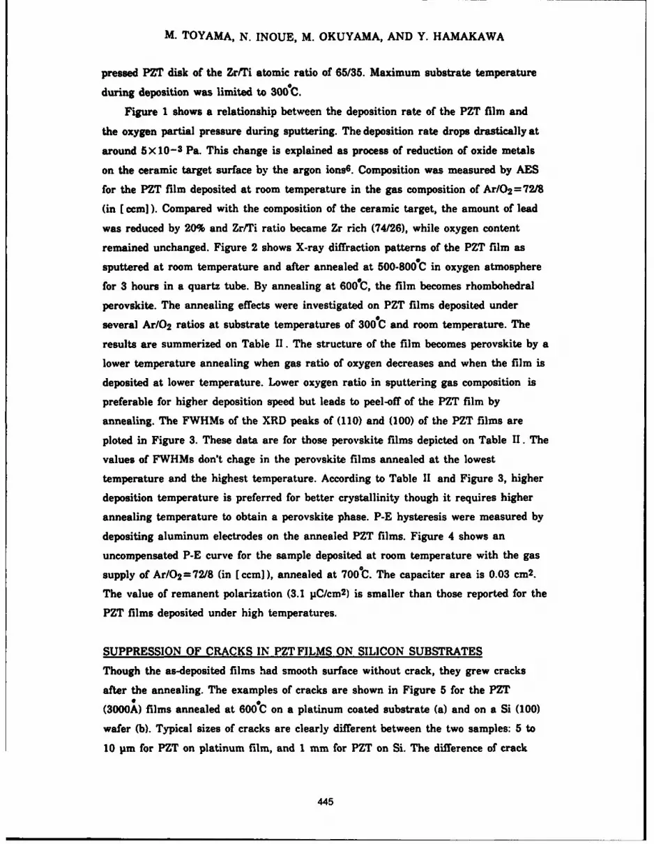
M. TOYAMA, N. INOUE, M. OKUYAMA, AND Y. HAMAKAWA
pressed PZT disk of the Zr/Ti atomic ratio of 65/35. Maximum substrate temperature
during deposition was limited to 3001C.
Figure 1 shows a relationship between the deposition rate of the PZT film and
the oxygen partial pressure during sputtering. The deposition rate drops drastically at
around 5X 10⁻³ Pa. This change is explained as process of reduction of oxide metals
on the ceramic target surface by the argon ions6. Composition was measured by AES
for the PZT film deposited at room temperature in the gas composition of Ar/O2 =72/8
(in [ccm]). Compared with the composition of the ceramic target, the amount of lead
was reduced by 20% and Zr/Ti ratio became Zr rich (74/26), while oxygen content
remained unchanged. Figure 2 shows X-ray diffraction patterns of the PZT film as
sputtered at room temperature and after annealed at 500-800°C in oxygen atmosphere
for 3 hours in a quartz tube. By annealing at 600eC, the film becomes rhombohedral
perovskite. The annealing effects were investigated on PZT films deposited under
several Ar/O2 ratios at substrate temperatures of 300eC and room temperature. The
results are summerized on Table II. The structure of the film becomes perovskite by a
lower temperature annealing when gas ratio of oxygen decreases and when the film is
deposited at lower temperature. Lower oxygen ratio in sputtering gas composition is
preferable for higher deposition speed but leads to peel-off of the PZT film by
annealing. The FWHMs of the XRD peaks of (110) and (100) of the PZT films are
ploted in Figure 3. These data are for those perovskite films depicted on Table II. The
values of FWHMs don't chage in the perovskite films annealed at the lowest
temperature and the highest temperature. According to Table II and Figure 3, higher
deposition temperature is preferred for better crystallinity though it requires higher
annealing temperature to obtain a perovskite phase. P-E hysteresis were measured by
depositing aluminum electrodes on the annealed PZT films. Figure 4 shows an
uncompensated P-E curve for the sample deposited at room temperature with the gas
supply of Ar/0 2= 72/8 (in [ccm]), annealed at 7000C. The capaciter area is 0.03 cm2 .
The value of remanent polarization (3.1 pC/cm 2) is smaller than those reported for the
PZT films deposited under high temperatures.
SUPPRESSION OF CRACKS IN PZT FILMS ON SILICON SUBSTRATES
Though the as-deposited films had smooth surface without crack, they grew cracks
after the annealing. The examples of cracks are shown in Figure 5 for the PZT
(3000A) films annealed at 600"C on a platinum coated substrate (a) and on a Si (100)
wafer (b). Typical sizes of cracks are clearly different between the two samples: 5 to
10 pm for PZT on platinum film, and 1 mm for PZT on Si. The difference of crack
"445

CRACK-FREE PZT THIN FILMS
scales can be attributed to difference in thermal expansion. Data of thermal
expansions for platinum, silicon and PZT (50/50) are listed on Table X. The expansion
from room temperature to 600eC is about the same value between silicon and PZT
(50/50), but, for platinum, the value is more than two times larger. The above results
indicate that, by reducing the scale of PZT films by patterning before annealing,
suppresion of cracks would be possible, because the stress energy caused by difference
in thermal expansion would be dissipated in pattern edges.
Photo-assist etching of PZT films.
PZT films, as deposited at low temperature, were etched by HF solution. But the acid
attacked photoresist (negative type) and adhesion of photoresist to the PZT films was
weak, resulting in low fidelity to the feature of photomask. So, the authors tried
photo-assist etching of PZT films. The samples of PZT films deposited on Si substrates
at room temperature were dipped in KOH solution (10 mol in 1 1 of water). The
etching rate at 50C was 20 A/min. Three kinds of light sources were examined for
photo-assistance: xenon lamp, KrF eximer laser 248 nm (50 mJ/cm 2/shot), and ArF
laser. When a sample was irradiated by the light from xenon lamp, the etching rate
became higher by two times. When a sample was irradiated by KrF laser (100 shots
during 2 minutes of dipping), the etching rate became more than ten times higher.
Light from ArF laser was absorbed by water and had no effect on etching. The photo-
assist etching method seems quite adequate for lithography of ceramic films which has
poor adhesion with photoresist, because photo-assistance doesn't depend on the
adhesion.
The patterned PZT filmes after annealed
Figure 6 is a photograph of PZT films after annealed at 600C in oxygen ambient for
3 hours. These films had been patterned before annealing. In this randomly chosen
photo, larger patterns have cracks while smaller patterns don't. This result verifies
our supposition that cracks would be suppressed by reducing the film size by
patterning. But this tecnique is with reservation; the identical patterns shown in
Figure 7 are of well reduced size, but each film has a crack at the same part (at"neck", one being indicated by an arrow). It seems that stress has concentrated in the"neck" portion. Consideration would be required in designing of PZT patterns to
annihilate crackings by this method.
SUMMARY
In this paper, we have shown a process of getting crack-free PZT thin films deposited
at low temperature and micropatterned on silicon substrate. The process includes
446

M. TOYAMA, N. INOUE, M. OKUYAMA, AND Y. HAMAKAWA
annealing of the low temperature deposited PZT thin film after patterning. The
remanent polarization of the annealed PZT film was smaller (3.1 pC/cm 2) than the
values reported for high temperature deposited films. In order to make the best of our
method, rapid thermal annealing shouled be examined7 for the benefit of reduction of
thermal damages to the underlying devices during annealing as well as during film
deposition. And relations between the pattern shapes of PZT films and growth of
cracks have to be further investigated.
Also reported in this paper is photo-assist etching of PZT thin films. The etching
rate was well enhanced by irradiation of KrF laser in KOH solution. The photo-assist
etching is quite adequate when adhesion of photoresist to ceramic film is no good.
Efforts to improve the process demonstrated in this paper are now under way
including multi-target sputtering in our laboratory.
ACKNOWLEDGEMENT
The authors are grateful to H. Kanda of Seiko I Technoresearch Co., and H Niwa for
their experimental assistance.
REFERENCES
1. J. F. Scott, L. D. McMillan, and C. A. Araujo, Ferroelectrics, 116 147 (1991).2. L. E. Sanchez, D. T. Dion, S. Y. Wu, and I. K. Naik, Ferroelectrics, 116, 1 (1991).3. R. Takayama and Y. Tomita, J. Appl. Phys., 65, 1666 (1989).4. M. Adachi, T. Matsuzaki, T. Yamada, T. Shiosaki, and A. Kawabata, Jpn. J. Appl.
Phys., 26, 550 (1987).5. T. Fukami, S. Fujii, and H. Tsuchiya, Jpn. J. Appl. Phys. 24. Sutpl., 24-2, 410
(1985).6. J. Heller, Thin Solid Films, 7, 1 (1971).7. B. R. Biswa, S. Chandratraya, and A. Pask, J. Am. Ceram. Soc., 58, 729 (1979).8. T. S. Kalkur, J. Kulkarni, Y. C. Lu, M. Rowe, W. Han, and L. Kammerdiner,
Ferroelectrics, 116, 135 (1991).
447

CRACK-FREE PZT THIN FILMS
TABLE I Deposition conditions of PZT thin films.
Substrate Pt(11 1)'Ti/SiO2/Si,Si(100)
Target PZT (65/35)Hot-press 3-in. (P
RF Power 100W (2.2W/cm2)
Sputter Gas Ar/O2 Total Flow 80ccm
Pressure 0.35 Pa
300
S3 0 3l
0 to 00
- .....---------
OXYGEN PARTIAL PRESSURE (Pal
FIGURE I Deposition rate of PZT v.s. oxygen partial pressure.
448

M. TOYAMA, N. INOUE, M. OKUYAMA, AND Y. HAMAKAWA
110
I h
I A2m ) , ,
• .
SO T.J tsputtered
20 do 40 of as
2 THITA IDISUSEII
FIGURE 2 X-ray diffraction patterns for a PZT film, deposited at room
temperature, annealed at 500-800"C, measured at room temperature.
TABLE II Crystallographic structures of annealed PZT thin films deposited
with various gas mixing compositions of oxygen and argon. Upper columns are
about the films deposited at 300tC, and lower columns are about the films
deposited at room temperature.
1023 1%k)(Ar)-+ (02)
0 Amorphous peel off
10 Pyrochlore : Perovskite ]10 phus~m~ -:'Pyrochlioe ,: Perovskite I
1 A Perovskite VK
SO 0 pho. Pyrochlore , Pyrosioe
s0 o Py rochlore :yr..;:gk
90 y Pyrochoor.r
90 Amorphous pyrockteq
RT 300 400 S00 S00 ":00 800
ANNEAL & DEPOSITION ILEFT ENDITEMPERATURE (*C)
449

CRACK-FREE PZT THIN FILMS
0.3 -
6.1
6.
20 4L
uL 0.2 Q
0 50 100Ar 02
(02)
(Ar)+ (02)
(110) (100) Deposition
A 0 R.T.
0 0 300C
FIGURE 3 Full width at half maximum of XRD peaks for annealed PZT
samples.
X: 1OV/div., Y: 3.1pC/cm 2/div
100Hz, Film Thickness= 540nm
FIGURE 4 A hysteresis loop of a PZT sample, deposited on Pt film at room
temperature and annealed at 700rC.
450

M. TOYAMA, N. INOUE, M. OKLYAMA, AND Y. HAMAKAWA
~j'~A
50 P.m 1.,M ý
(a)(b
(a) (5/5)b00
FIGRE5 raks n ZTfimson P lye () ad i410)1

CRACK-FREE PZT THIN FILMS
mm..
lmm' muFIGURE 6 Patterned PZT films after annealing.
1M11
1rmm
FIGURE 7 Patterned PZT films after annealing. One of the cracks at "neck"s
is indicated by an arrow.
452

toi
___ FERROELECTRIC Pb(Zr,Ti)O THIN FILMS PREPARED BYMý PLANAR MULTI-TARGET SPUTTERING
omýR. Bruchhaus, H.Huber, D. Pitzer and W. WersingSIEMENS AG, Corporate Research and Development,Munich, Germany
Abstract Lead zirconate titanate films are depositedusing a planar multi-target sputtering system. Thissystem consists of three metallic targets (Zr,Pb,Ti)and a rotating substrate holding pallet achieving alayer-by-layer growth of the material.Substrates used in this study were oxidised (100)Siwafers with thin sputtered Pt layer. At substrate tem-peratures of about 450 0 C "in situ" (i.e. without post-deposition annealing) deposition of single phase pe-rovskite PZT was obtained. Deposition rate is 3.5nm/min. At substrate temperatures of more than 500 0Cthe layers are poor in lead. ZrTiO4 was identified byx-ray diffraction.The dielectric constant and losses of the PZT filmsvaried from 400-500 and from 0.008-0.015 respectively.The films exhibited a hysteresis loop, remanentpolarization measured was 7 AC/cm2 and coercive fieldstrength 7.5*106 V/m.
INTRODUCTION
The progress made in depositing high quality very thin
ferroelectric films has opened a new era for applications.
Especially their possible integration as nonvolatile
storage element in a high density CMOS-process has
triggered renewed interest in thin ferroelectric films.
Lead zirconate titanate (PZT) has properties which makes it
a potential candidate for these memory applications1. Theie
are different techniques, e.g. evaporation 2 ion-beam
deposition3 , some chemical routes employing sol-gel
techniques 4 - 8 , laser ablation9 and chemical vapor
depositionI 0 for the fabrication of these films.
92-161514I 111311 II 1 1111 111 11 111

R. BRUCHHAUS, H. HUBER, D. PITZER AND W. WERSING
RF J~Ceramic Multi component Facing target Multiple target Multiple targettarget: RF metal target (non planar) (planar)
FIGURE 1. Sputtering geometry and targets for deposition ofmulticomponent oxid films
Besides these, sputtering seems to be a promising and
with standard IC-technology compatible method. Different
kinds of sputtering geometry have been used to deposit mul-
ticomponent oxide films including PZT, Figure 111-14. Thematerials of the PZT family show a wide range of properties
with changing composition (for example Zr/Ti ratio).
Therefore it is advantageous to use a deposition method
where composition of the films can easily be changed. Byusing single target methods this possibility is very
limited due to fixed composition of the target. For every
new composition new targets have to be manufactored
individually.
With multiple target methods the stoichiometry can bevaried simply by the control of power at the targets. We
used a planar multi-target method with three targets where
the deposition rate of each component can individually be
controlled.
EXPERIMENTAL
PZT films were produced by using a modified Perkin El-
mer 4400 sputter system with high vacuum load lock. A sche-
matic diagram of the system is given in Figure 2. Films
were reactively sputtered from metallic targets. Substrate
was rotated during deposition continously with 10 rpm
achieving a layer by layer growth of the film. Target 1 was
a Zr (DC-supply), target 2 a Pb (DC-supply) and target 3 a
454

PZT THIN FILMS PREPARED BY MULTI-TARGET SPUTTERING
Sputtering unitwith 3 8" targets
Pallet with 7resistance heater K
,Heater 2
I /I -
FIGURE 2. Schematic diagram of the sputtering system
Ti (RF-supply). Sequence of deposition during one rotation
of the pallet is Zr - Pb - Ti. With two individually ad-
justable heaters we were able to sustain substrate tempera-
tures of more than 5000C. A heater plate (heater 2) was
located on the pallet the other was a lamp heater (heater
1) fixed at the upper plate of the recipient. Therefore,
during every rotation after the deposition of Ti the lamps
will illuminate the growing film a short period of time.
Substrate temperatures given in this paper refer only to
the heater plate located on the pallet. Typical sputter
conditions are listed in Table 1.
TABLE 1. Sputtering conditions
range for PZT
Gas 50-100%0 50%Pressure 1.2-3.0 Pa 1.4 PaPower Pb 28-245 W 90 W
Ti 1000-1500 W 1500 WZr 150-270 W 250 W
Deposition rate 3-4 nm/min 3.5 nm/min.ubstrate temp. 25->500 0 C about 4506C
455

R. BRUCHHAUS, H. HUBER, D. PITZER AND W. WERSING
Substrates used were oxidised single crystal silicon
wafers deposited with a sputtered bottom electrode of Pt.
Upper electrodes were sputtered Pt layers patterned by
standard lithographic techniques. Electrical measurements
were done on MIM structures ("test capacitors"). Test
capacitor area was about 50,000 Am2
The crystallographic structure of the PZT-films was ex-amined by X-ray diffraction. A SIEMENS F 500 diffractometer
with Cu anode, silicon primary detector and position sensi-
tive detector was used. Dielectric constant (c) measure-
ments were made at room temperature using a Hewlett Packard
4275A multifrequency LCR meter. Measurement frequency was
100 kHz. Polarization hysteresis loops measurements were
taken at room temperature at a frequency of 10 kHz by means
of a Sawyer-Tower-Circuit 1 5 . The sine wave generator was a
Hewlett-Packard 3324A function generator and storage oscil-
loscope a Tektronix 7834A.
RESULTS AND DISCUSSION
The crystallographic structure of the films was depen-
dent on substrate temperature. Figure 3 shows the X-ray
patterns of layers deposited at different substrate tempe-
ratures. Even at 200 0 C indications of crystalline phases
are seen. Peaks of PZT perovskite phase do not appear,
other phases have not been identified yet. At about 450 0C
the film consists of single phase perovskite type PZT.
There is no need for a post-deposition annealing step. The
structure seems to be pseudo-cubic with a lattice constant
of 414 pm. At substrate temperatures above 5000C lines of
PZT are no more seen. The phase exhibits to be ZrTiO4 . De-
spite an increase of power at the lead target compared to
the deposition at 450 0 C the layers are poor in lead as con-
firmed by elemental analysis. It seems to be that during
palett rotation at temperatures above 500 0 C the formation
of ZrTiO4 is completed before lead is sputtered on the sub-
strate.
456

PZT THIN FILMS PREPARED BY MULTI-TARGET SPUTTERING
~Pt
>4
H 5000C
S4500C
2000C
10 20 30 40 50 602e
FIGURE 3. X-ray diffraction patterns offilms deposited at different substratetemperatures
By the continous rotation of the substrate during depo-
sition very thin layers of each element are sputtered
achieving layer growth on an atomic scale. Therefore diffu-
sion distances necessary to form the reaction product are
minimized. The deposition rate is 3-4 nm/min, thus the film
grows about one lattice constant of PZT during every
rotation of the pallet. Our conditions can be compared with3the results of ion beam sputtering3. This group also
suceeded in growing "in situ" perovskite PZT films at
substrate temperatures of 450-550 0 C.
A SEM picture of the PZT surface is shown in Figure 4.
The layer consists of well defined crystallites about 100-
300 nm in size. There are some pores in the microstructure.
This is correlated with a DC-breakdown strength of 105
V/cm. No indications of microcracking are seen.
457

R. BRUCHHAUS, H. HUBER, D. PITZER AND W. WERSING
FIGURE 4. SEM microstructure ofPZT deposited at about 450 0 C
22"
FIGURE 5. Hysterenis loop ofa 400 nm thick film
458

PZT THIN FILMS PREPARED BY MULTI-TARGET SPUTTERING
Single phase "in-situ" grown films were used to inve-
stigate dielectric and ferroelectric properties. The film
thickness ranged from 400 to 570 nm. Electrical results are
encouraging in light of this method and of the low proces-
sing temperatures. Dielectric constant is 400-500, dielec-
tric loss tan 6 is as low as 0.008-0.015 independent of
film thickness. PZT films exhibited hysteresis loops as
shown in Figure 5. Remanent polarization (Pr) is 7 juC/cm2
and coercive field strength (Ec) is 7.5*106 V/m.
Conclusions
PZT films have been produced by using a planar multi-
target sputtering system. At substrate temperatures as low
as about 450 0 C "in situ" (i.e. without post-deposition an-
nealing) growth of perovskite phase material was obtained.
Deposition rate was 3.5 nm/min. Films exhibited hysteresis
loops with Pr=7 AC/cm2 and Ec=7.5*"i6 V/m. The dielectric
constant was 400-500 and the losses 0.008-0.015. At sub-
strate temperatures of more than 500 0 C the layers are poor
in lead and ZrTiO4 was identified by x-ray diffraction.
Acknowledgements
The authors wish to thank Mrs. Jobst for x-ray diffrac-
tion measurements, Mr. Stolz for SEM investigations and Mr.
Lesti and Mr. ZurmUhlen for electrical measurements.
References:
1. D.W. Bondurant and F.P. Gnadinger, IEEE Spectrum,26,30(1989).
2. M. Oikawa and K. Toda, Appl. Phys. Lett.,29,491(1976).3. M.S. Ameen et al. in Ferroelectric Thin Films, edited
by E.R. Myers and A.I. Kingon (Mater. Res. Soc. Proc.200, Pittsburgh, PA 1990), pp. 65-76.
4. J. Fukushima, K. Kodaira and T: Matushita, J.Mater.Sci..19,595(1985).
5. K.D. Budd, S.K. Dey and D.A. Payne, Br. Ceram.Proc..36,486(1985).6. S.K. Muralidkar, Ceram.Bull..63,486(1984).
7. S.K. Dey and R. Zuleeg, Ferroelectrics.108,37(1990).8. G. Yi, Z. Wu and M. Sayer, J.ADRI. Phys..64,2717(1988).
459

R. BRUCHHAUS, H. HUBER, D. PITZER AND W. WERSING
9. S. Otsubo, T. Maeda, T. Minamikawa, Y. Yonezawa, A. Mo-rimoto and T. Shimizu, Jpn. J. Appl.Phvs..29,L133(1990).
10. M. Okada, K. Tominaga, T. Araki, S. Katayama and. Y.Sakashita, Jpn. J. Appl. Phys..29,718(1990).
11. A. Okada, J. Appl. Phys..48,2905(1977).12. K. Sreenivas and M. Sayer,J. ADDl. Phys..64,1484(1988).13. R.A. Roy, K.F. Etzold and J.J. Cuomo in Ferroelectric
Thin Films, edited by E.R. Myers and A.I. Kingon(Mater. Res. Soc. Proc. 200, Pittsburgh, PA 1990),pp. 77-82.
14. H. Adachi, T. Mitsuyu, T. Yamazaki and K. Wasa, Jpn. J.ADDI. Phys.,24, Suppl. 24-3,13(1985).
15. C.B. Sawyer and C.H. Tower, Phys. Rev..35,269(1930).
4600

N Electrical Results of Muftilevel and
=== Homogeneous Ferroelectric Capacitors
J.D. CUCHIARO, B.M. MELNICK, AND C.A. PAZ DE ARAUJOo Symetrix Corporation, Colorado Springs, Colorado and
University of Colorado at Colorado Springs
Abstract Sol-gel deposited ferroelectric capacitors composed of
composite materials are electrically compared to homogeneouscapacitors of the same nature. the composites are derivatives of PTand PZT which are all built by a standardized process. The compositesconsist of doped and homogeneous interfaces in layered structures.The electrical results of hysteresis, dielectric constant, switchingpolarization measurements are used to analyze the samples.
INTRODUCTION
Solution-gelation of metal alkoxides after spin coating as a deposition
technique of ferroelectric materials, creates latitude in capacitor device
construction. Layering achieves different device structures through
changes in molarity (M) spin speed and time of the deposition. Therefore,
thickness variations at select device levels can be tailored for most designs.
For the devices discussed in this paper, the alkoxide homogeneous
capacitors were spun from .9M solutions at 1500 rpm for 20 seconds
yielding an after processing thickness of approximately 2000 A per layer.
These thin films were hydrolyzed before deposition with a combinat&cn ofacetic acid and water for an h factor of 2.0 (h = total moles metal 1
total moles hydrolize
in a glass beaker and filtered with a .2 pm syringe filter. The substrates are
made from p-type < 100 > 5-250-cm 4" silicon test grade wafers on which
2000 A of platinum is sputtered on 200 A of sputtered titanium on 5000
A of thermally grown SiO 2 . After ferroe!ectric deposition, or depositions,
and thermal treatments, another 2000 A platinum layer is sputtered to form
the top plate of the capacitor. The top plate is patterned and etched using
an ion-mill to form 10,000 pm2 capacitors. To ensure contact of the top
92-16152401IMflflhIN~

J.D. CUCHIARO, B.M. MELNICK AND C.A. PAZ DE ARAUJO
electrode to the ferroelectric material, the specimens were contact annealed
in a diffusion furnace under a 5 liter/min 02 flow at 6500C for 1 hour. The
basic ferroelectric capacitor structure is shown in Figure 1.
Basic F.M.
Capacitor Structure
......... ................. X :x.............. ........ ....................
...... .... ....... .........
R.X. :X.- X... ..... .... .. . ........... .......... ........ ............................. x,.. ................ ........... ..................................................... .......... ..... ............................ . . ............. ..................... .........
........... ... ................................. ..... ......... ................. ........ ........... ........................... ................... .................................... .......... ................... .. M........................... :ýý: ..... I-ViAd-h-Wi............... - - ............................................................. ....... ....... X :.......... ............................ ... ......................................... ? ................................. ............................. .. ........................................................ 0 : ....... .... .......... ;X ............. ....................................................... 0 ........................... .......-X ................. ............ ... ..... ................ ... .... ..... ....... ......... .
.......... ..I I I I I I I I ........ ......... .......X,...........I...... ..
....I I I I
............. I I I 1 11 1 1 1 1 ..X ..... .... ....... ...... . .... ...................... ........... ... . ......
................... ...................... ........... .................................... ....................................... .............................. .................................................................................... , .. ý:]*. ix:*.......... ....... . .......... ........................................................................... . .............................. ......................... ...............
..............................
... .. . . . ........ .. .. ..........v 0........................... Xq ......... ...............9 .......................... .......... ....
. ............................... ..............................
.................... X .: .: - - .... ... ...x x x .. . ....... ..................... ........ ....... ................... .....
-*1 ......... : .......
............ X. ............................ :.............. ........................ .. . ............... ........... ............ .. ........ . .............. . . . ........... 6 4 ............................ . ... ... ........................................... ........................ . .. ....... X X X. ..........................................................
... ............ ............................. ..... ...........
Figure 1
MONOLAYER STRUCTURES
The ferroelectric capacitors built and tested resembling the structure of
Figure 1 are as follows: The first two wafers contained PZAT.., one doped
with 5 mole percent boron and the other with 5 mole percent Iodine. The
third and fourth wafers contained PT with the same doping concentrations
of boron and iodine. The probed electrical data is listed in Table 1.
462

ELECTRICAL RESULTS OF MULTILEVEL AND HOMOGENEOUS FERROELECTRIC
Sample PZT #17 5% B PZT #17 5% [ PT #3 5% 8 PT #3 5% I
d 2800 A 2900 2600 2600
Cp 157.2PF 192.3 222 230
Cs 157.2PF 192.3 221.5 229.4
D .014 .01 .012 .019
Rs 0o 00 0o Go
Rp Off Scale Off Scale Off Scale Off Scale
Z 101.0 k C1 82.7 71.9 69.5
e -89.300 -89.4 -89.32 -89.9
K 497.13 629.85 651.91 675.4
4.400 X 5.58 X 5.77 X 5.98 X
E 10.' F/m 10.1 F/m 10' F/m 10-9
Table 1
Ferroelectric property tests were also conducted. Figures 2, 3, 4, &
5 show switching polarization vs voltage and hysteresis curves for PZ.gT.6
#17 5% B, PZ 4 T.6 #17 5% I, PT #3 5% B, TP #3 5% I, respectfully. The
data from the figures of both doped PZ.4T.6 samples do not saturate under
the applied bias. The boron doped sample switches in approximately 650ns
and the iodine doped sample switches in approximately 900ns, or 27.8%
slower. However, the boron dopant yielded a 25.72 pC/cm 2 charge vs the
iodine sample of 24.15, or a 6.1% increase in switched charge. The
increase of switching charge is gained at the cost of 250ns switching time.
It is important to note that undoped PZ.aT6 samples are able to switch in
approximately 200 ns'.
Although the switching time is longer for the iodine doped PZ.,T6
samples, the polarization vs voltage curves show a more consistent amount
4W3

J.D. CUCHIARO, B.M. MELNICK AND C.A. PAZ DE ARAUJO
SWITCHING CURVES s'ellSample Name:PZT417 5%.B
see. n 11016 ... 8 Vopi - S V Thickn•*.. - 29l
.82 A -5 h-1
171121" POLARIZATION vs VOLTAGE Ap "° ""Sample= Name:PZTI17 5%,B* R' - t- .- a f-m - So- Oh,,n
SONe A T.- 17 C _ ft
÷l~l . .. . . . .- . . . . C,-
- 1 2 . .i l n ,O
S 3 5a e 9T 1 13I 1*
VOLTA=I tv)
T.... ... l... • - 69 .. p £
ism ____ ___ ___ ___ ___ ___ ___ ___
-GR0
omw. *..o - . ,c ,,p, n n.s, .
ici-f O. t h. * p Io-*
FIGURE 2
464

ELECTRICAL RESULTS OF MULTILEVEL AND HOMOGENEOUS FERROELECTRIC
" S"'" SWITCHING CURVES I "° '"'Sample Name:PZT#17 5%I
R-0m - Sam It v - S V - am R.624 511 - ohl m, , Troml. 17 c
-. • 4 i " n ... ,
"'' POLRRIZRTION vs VOLTRGE " " "Sample Niame:PZT#17? 5%1I
Mrs*oo - lo .- ITem -so c + P
at~ --
I 3 5 It 13 is
VO.TMZ: (V)
FIGURE 3
465
h *a,.

J.D. CUCHIARO, B.M. MELNICK AND C.A. PAZ DE ARAUJO
SWITCHING CURVES a IV '"sSample Name:PT#3 5%B
Re.. - $) uM. VWp . 5 V Thi0k066 o 1 l
.832 Ott** 50O--jý:1
--
-. 00-nnr
iS SOS IBS
TIME (no.o)
171"" POLARIZATION vs VOLTAGE 'I i l"'Sample Name:PT*3 5%B.
e- Cie o-4
R S - S5 Oh.
Thcl:kn.es6o - ZU N Th.p - 1? C .
"-347 . . . ' ,- •d . . .
-34
I 2 S 7 9 is 13 Is
VOLT"A MV)
@41 @.0..li. *. 6 "* I . .. .. .
1 I u~ 4. * . V . IGURE 4
• * I -M I I* I - t i l
FIGURE 4

ELECTRICAL RESULTS OF MULTILEVEL AND HOMOGENEOUS FERROELECTRIC
""6"4 SWITCHING CURVES 2 Ap "tSample Name:PT#3 5%.I
P.O. - Ima .O2
Vpp -; V Thtk,,... - 29W1 A
932 565
I1865TIME (..go)
17,32.5 POLARIZATION vs VOLTAGE 2 - '"'IsoSample Name:PT#3• 5%jIA'. - ISM
--2 R? - So )h- •
+247 . . . .
I 3 7 9 11 13 1POR TON vV)
Slamllple NaeP* I
FIGURE 5
467
-247

J.D. CUCHIARO, B.M. MELNICK AND C.A. PAZ DE ARAUJO
of switched charge over variable voltages with the iodine dopant (Figure 3).
Both samples begin to switch at approximately the same voltage (3+V),
however, the boron doped sample switches more charge with increasing
voltage (Figure 2). The cause of this phenomena are still under
investigation.
The same tests applied to the B and I doped PT samples showed the
following. Boron makes PT leaky and never fully switches. The leakiness,
however, makes for a very consistent amount of switched charge,
approximately 31 pC/cm 2, as shown by the polarization vs voltage curve of
Figure 4.
Comparing the iodine sample to that of the boron doped sample,
shows that more switched charge is achieved, 36 pC/cm 2 in 750ns. The
switched charge curve of Figure 5 is symmetric, showing that the value of
2Pr achieved in orienting the dipoles is approximately the same, when going
from a positive to a negative state or from negative to a positive state.
From a materials view this is the desired behavior, however, the amount of
charge required for specific device applications will have to be tailored in
the future.
MIXED MATERIAL FERROELECTRIC CAPACITORS
The latitude of doping sol-gel solutions of ferroelectric compositions allows
for the building of completely different ferroelectric materials, one on top
of the other. The two structures shown in Figures 6 and 7 of this nature
were also built and tested. The intention is to show improved electrical
results over homogeneous capacitors by creating polarization and dielectric
gradients near the electrodes to compensate for oxygen poor regions of the
ferroelectric near the platinum interfaces. Previous investigations suggest
that an increase in material coercive field (Ec) is a result of a surface and
sub-surface region with lower Er 2,3 .4 which results in a lower value of
polarization (P) by reducing the bound surface c..rge (Qbound = PA). This
concept is modeled in Figure 6.
468

ELECTRICAL RESULTS OF MULTILEVEL AND HOMOGENEOUS FERROELECTRIC
CONCEPTUAL MODELOF FERROELECTRIC CAPACITOR
Basic F.M.Capacitor Structure
Metal Contact
Oxygen .Doping
Depleted Region
Stiochiometric CenterRegion
vP SubSurface
Region Surface to Metal Interface A Work
Metal Contact Function
FIGURE 6
The model shows that at the surface of the doped ferroelectric/metal
interface there is a v, in the materials work function. Immediately
following is the sub surface region. This contains both changing E and
P values as a function of thickness, d, reaching an equilibrium value near
tha stoichiometric center. To illustrate the electrical properties of the
model, the two capacitor cells of Figures 7 and 8 were built and tested.
In Figure 7 the dielectric constant of sample 9-6-1 at the subsurface
region was lowered by doping PZ.4T8 with 3 mole percent Sn. The
stoichiometric center was built approximately 3 times thicker with undoped
PZ 4T6 . To further enhance the gradient effect sample 9-6-4 contains
PZ 4T.6 with Er of approximately 900 at the stoichiometric center
contacting 3 mole percent Sn doped PT with Er approximately 400 on
both sides. Electrical results of hysteresis, for variable fields created by the
listed applied voltages,
469

J.D. CUCHIARO, B.M. MELNICK AND C.A. PAZ DE ARAUJO
Pt 2000 ATop Electrode
5oo A ..... T. Sn .03
Boto Electrode.......... Pt 2000 ..
2000 A. ........ PZ.4T.6 h 2.0
500...A.PT..Sn...
Bottom... ElcrdPt 2000.....A
SAMPLE ......6-4 .FIGUR 8.....
470 .....

ELECTRICAL RESULTS OF MULTILEVEL AND HOMOGENEOUS FERROELECTRIC
polarization vs applied voltages of 1-16V, and switching curves for 5V are
shown for samples 9-6-1 and 9-6-4 in Figures 9 & 10, respectively. As can
be seen from the Figures, sample 9-6-4 exhibits a better defined hysteresis
at the cost of a lower 2P,. Sample 9-6-4 also switches approximately two
times faster than 9-6-1 without a significant current leakage. This may be
due to sub surface layer dielectric constant of Sn doped PZT not being low
enough to create the desired gradient. In contrast, sample 9-6-4 drastically
reduces the dielectric constant near the metal interface by half using PT in
the sub surface region, thus yielding better measured ferroelectric results.
SUMMARY
In this paper we have shown that by doping sol-gel deposited ferroelectric
PZ 4 T 6 and PT with boron and iodine inherently slower switching times can
be sped up by reducing switched charge. Also, the sol-gel deposition
process enables mixed material capacitors to be built. A capacitor model
requiring mixed materials with different dielectric constants was presented,
and the electrical results of switching, polarization vs voltage, and
hysteresis divulged. Consequently, ferroelectric parameters can be altered
through doping and mixed material construction.
471

ELECTRICAL RESULTS OF MULTILEVEL AND HOMOGENEOUS FERROELECTRIC
1,49, SNITCHING CURVES 'I '-'p1
Sample Name:9 6_1R-.. - 1288 .- 2.9 V.pp - 5 V Thick.*** - 2588 A
0 3 2 l.-58 0h... TieJ°- 17 C
• 83.at.....
-. 032L.. .. .
65 565 1065
TIME (ns.c)
"12:00:11 POLRRIZRTION vs VOLTAGE Ip 191
Sample Name:9_61Ar.. - 12008 u.- Pl - 58 Ohs 5 PP
Thick..... - 2500 q T.op - 17 C + '___250____ Pd
5-4 1
Iv I
-25. L _ .-. _J--J_.L i i i ••:
3 5 7 9 II 13 15VOLTRGE (V)
.0.-.I .e
. 5. S: .. .,
j .'-.-.
FIGURE 9
472

J.D. CUCHIARO, B.M. MELNICK AND C.A. PAZ DE ARAUJO
SWITCHING CURVES I o "'Sample Name:9_6_4
Area - 1299 um-2 Vapp - 5 V Thickness - 3989 A
R1- S OhTtom .,
tao.Pu
98-- - -- .- - S
02
4
65 31S 565
T IM Eo .. ., .
11,32:09 POLARIZATION vs VOLTAGE ' Sa
Sample Name:9_6_4A• .. - 12.0. ...-2 R1Thfck.es. - 3999 A Teap - I? C o Pd
-...........
-le .4 -I -4 --- -4--.
FIGURE 10
473-, -- ,, mm m -- ma ,,, li il i FIG U REI0

ELECTRICAL RESULTS OF MULTILEVEL AND HOMOGENEOUS FERROELECTRIC
REFERENCES
1. B.M. Melnick, J.D. Cuchiaro, L.D. McMillan, C.A. Paz de Araujo andJ.F. Scott, Process Optimization and Characterization of DeviceWorthy Sol-Gel Based PZT for Ferroelectric Memories, Ferroelectrics,1990, Vol. 112, pp. 329-351.
2. X.T. Chen, D.N. Huang, and Z.W. Yin, Proc. 6th IEEE Intis. Symp. onFerroelectrics, June 8-11, p. 62 (1986).
3. L.E. Cross, Ferroelectrics, 76, 262 (1987).4. J.F. Scott et al., J. ADpl. Phys., 64(2) 787 (1988).
474

FERROELECTRICS FOR SILICON VLSI AD-P006 678111 lIiIIII JEHI DI l i JllIIil
SHENG T HSU and ISRAEL H. KALISHDavid Sarnoff Research Center, CN5300 Princeton, NJ
Abstract The application of ferroelectrics to EEPROM, non-volatile SRAMs, and sub-0.5 micron channel length MOS fieldeffect transistors for silicon VLSI can significantlysimplify device fabrication process, increase circuitdensity, and enhance device performance.
INTRODUCTION
The constraints to Very Large Scale Integrated (VLSI) circuitsdevices are; low operating voltage, small device area, thininsulator thickness, shallow junction depth, and practically nolateral diffusion of p-n junctions. Not all of these constraintscan be achieved with the state-of-the-art silicon technologywithout a very complicated fabrication process. The highpermittivity and the polarization properties of ferroelectricdielectric material can be used to solve many of VLSI and ULSIdevices problems. It is shown in this paper that ferroelectricmaterials can be used to reduce EEPROM operation voltage, toform new non-volatile memory devices, and to improve theperformance and packing density of sub-0.5 micron MOStransistors. Since the application of ferroelectrics to DynamicRandom Access Memories, (DRAM), has been discussed by manyinvestigators 1, it will not be discussed here.
475 92-16153"111!1111 11 1111 1111I III JiII N

S. T. HSU AND I. H. KALISH
.EEPBOMell
There are many EEPROM cell structures available. All state-of-the-art EEPROM cells consist of a thin tunnel oxide, a floatinggate polysilicon layer, an inter-polysilicon dielectric, and acontrol gate polysilicon layer. The inter-polysilicon dielectricis either thermally grown oxide or a thermal grown oxide-nitride composite layer. The thickness of the tunnel oxide isabout 80A to 200A. The inter-polysilicon dielectric thickness isequivalent to about 200A to 400A of thermal oxide. The cross-sectional view of a simple stacked gate EEPROM cell is sketchedin Fig.1.
Oxide P,,I
r Dr in
P-Substrate
FIGURE 1 Cross-section view of an EEPROM device
When a voltage, Vpp, is applied-to the control gate. Thevoltage at the floating gate, VF, is given by:
VF CQ (Vpp- ) (1)=Ci + Co C4
476

FERROELECTRICS FOR SILICON VLSI
where Co is the tunnel oxide capacitance, Cl is the inter-
polysilicon insulator capacitance, and OF is the charge stored inthe floating gate. The coupling ratio, CI/(Co+Cl), defines theefficiency with which the voltage at the control gate cancontrol the field intensity at the tunnel oxide and the potentialat the silicon surface. The amount of charge flowing from the
silicon into the floating gate is controlled by the field intensityat the tunnel oxide. For a state-of-the-art device, the couplingration is about 0.3 to 0.5 and the programming voltage is about10 V to 15 V. A sub-0.5 g~m VLSI circuit operates at 2.0 V to 3.5
V internal voltage and 5 V power supply for the input/outputportions of the circuit. The 5 V input/output is required tointerface with the existing electronics components. The highEEPROM programming voltage is either supplied externally or
generated on chip internally. This high programming voltage is aserious reliability concern for the small feature size devices.The programming voltage prevents the further scaling of the
memory device 2.If the inter-polysilicon dielectric is replaced by a wide band
gap ferroelectric dielectric material, the capacitance, C1, will
be very large. The coupling ratio of about one can be obtained.When the amount of charges stored at the floating gate is OF thethreshold voltage of the device is increased by AVT, such that
AVT = QF (2)CI
Since Cl is very large for ferroelectric memory devices a very
large amount of charge in the floating gate is required for a
small increase in threshold voltage. A memory device withcoupling ratio of nearly equal to one is, therefore, of no
practical value. Probably the coupling ratio should be no larger
than 0.8. A thin layer of thermal oxide of thickness between 40Ato 70A may be grown onto the floating gate polysilicon to
enhance the retention time and to reduce the coupling ratio to
477

S. T. HSU AND I. H. KALISH
0.6 to 0.8. The memory array can be programmed and read with
the standard 5 V power supply voltage and 2.0 V to 3.5 Vinternal voltages, respectively. A ferroelectric stacked memory
cell is sketched in Fig.2. The upper polysilicon layer is replaced
by a refractory metal diffusion barrier layer.
Ferroelectric
Oxide
r Dr in
P-Substrate
FIGURE 2 EEPROM device utilizing ferroelectric
inter-polysilicon insulator.
A new ferroelectric non-volatile memory device.
The cross-sectional view of a ferroelectric n-channel memory
transistor is sketched in Fig.3. The source and the substrate of
the device are permanently connected together. A memory gate,
MG, is inserted.' between the control gate, CG, and the source of
an MOS transistor. The insulator of the memory gate is
ferroelectric. A very thin layer of oxide may be grown onto the
silicon surface prior to the ferroelectric deposition. The top
electrode of the memory gate can be either refractory metal or
polysilicon.
478

FERROELECTRICS FOR SILICON VLSI
Source MG CC Drain
P-Substrate
Oxide PZT M Poly N+ p+ = Metal
FIGURE 3 Cross-sectional View of a Ferroelectric
Non-Volatile Memory
When a positive programming voltage, Vpp, is applied to thememory gate with respect to the source of the memory
transistor the ferroelectric dielectric at the MG is polarized
causing the silicon surface under the MG to invert. The channel
under the MG is at the high conductive state. This is the erase
operation. When the memory gate and the source of the deviceare grounded and positive voltages, Vpp+AV and Vpp are applied
to the control gate and the drain of the device, respectively, the
silicon surface under the control gate is very strongly inverted.The channel pinch-off is at the drain side of the memory gate.
The voltage drop across the ferroelectric is about Vpp. The
ferroelectric is polarized to the opposite polarity. The siliconsurface under the memory gate is accumulated. The memory
device is, therefore, programmed to the high resistivity state.The voltage AV can be much smaller than 1 V.
The current flow through the device during the programmingprocess is limited by the conductivity of the surface channel
479

S. T. HSU AND I. H. KALISH
under the memory gate. This programming current is controlledby the channel dopant density of the memory section of thedevice and by the thickness of ferroelectric dielectric. A lowvoltage, Vpp_<5 V, write/erase is possible.
During read operation current flow through the siliconsurface under the control gate and memory gate. There is nocurrent flow through the ferroelectric. As a result the memorycontent is not disturbed by the read operation. Therefore it is astatic memory device. There is no need for memory refreshment.
The area of this device can be minimized by eliminating theN+ layer between the memory gate and the control gate as is
shown in Fig.4. A thicker oxide on the sidewall and on the topsurface of the control gate is required to reduce the couplingbetween the control gate and the memory gate. This thick oxidelayer can be formed by a CVD oxide and etch back technique. It is
Source MG CG Drain
P-Substrate
Oxide M PZT • Poly o N+ • P+ =Metal
FIGURE 4 Cross-sectional view of a high density
ferroelectric memory transistor
480

FERROELECTRICS FOR SILICON VLSI
also possible to thermally grow thicker oxide on the N+ dopedpolysilicon and thinner oxide on the lightly doped silicon. Theratio of these thermal oxide thicknesses can be larger than 10.
The thickness of the control gate sidewall oxide must be keptthin in order to have a good coupling between the surfacechannel under the memory gate and the control gate.
This device can be arranged in a very large memory array. A
3x4 memory array is show in Fig.5. The memory gates of allmemory cells in the array are connected together to a block
erase pad. This non-volatile memory array can be programmed asfollows:
G1 G2 G3 G4
D1 I I /
T1 1 T12 L1, T14
o 1 I I
r17 Ll T32HlT33~ 'iT3
FIGURE 5 A 3x4 ferroelectric memory array
481

S. T. HSU AND I. H. KALISH
First the contents of the array are erased to the "0" state byapplying Vpp to the memory gate, MG, while all other electrodesare grounded. This operation writes all cells in the array totheir high conductive state.
Next we shall explain how to write a selected cell to the "1"state. The source and the programming gate electrodes aregrounded. If the cell T23 is selected voltages Vpp+AV and Vppare applied to the word line, G3, and the bit line, D2,respectively. The ferroelectric of the memory gate of T23 ispolarized causing the silicon surface under the ferroelectric ofthe memory electrode to accumulate holes. There is no surfaceconduction channel under the memory gate of T23 . The memorycell T23 is written to "1" state. The gate voltage of the memorycells TM3, where i•2, is equal to Vpp+AV, but the drains of thesememory cells are at the ground potential. The drain voltage ofmemory cells T2j, where j*3, is equal to Vpp but the gateelectrodes of these memory cells are at the ground potential.The gate and the drain of all other memory cells are at theground potential. Therefore, only the content of T23 memory cellis affected by this write operation. To read the contents of thememory array the internal low voltage of 2.0 V to 5.0 V isapplied to the selected bit line and word line.
NON-VOLATILE SRAM CELL
The equivalent circuit of a state-of-the-art non-volatile SRAMcell is sketched in Fig.6 3, where C1 and C2 are non-volatilememory elements. A control line is used to control thewrite/erase pulses from the common plate to program the non-volatile elements, C1 and C2. Compared to a standard SRAM cellit requires an additional two non-volatile elements, twoswitching transistors, and a programming pulse.
482

FERROELECTRICS FOR SILICON VLSI
Bit Voc Bit
C1 C2 Control Line
Plused Common Plate
FIGURE 6 State-of-the-art Non-volatile SRAM cell.
Bit Vcc
Q1 Q3
C1 C2
G1 G2
CVss Word Line
FIGURE 7 Equivalent circuit of a ferroelectric non-volatile SRAM with a floating capacitor plate.
4W3

S. T. HSU AND I. H. KALISH
The polarization field intensity of a ferroelectric material,such as PZT, is about 100 kV/cm. Therefore, the polarizationvoltage of a 3500 A PZT film is less than 5 V 3. It is possible toused PZT or other ferroelectric materials in a non-volatileSRAM which requires no write/erase operation.
The equivalent circuit of a ferroelectric non-volatile SRAMcell is sketched in Fig.7. The cross-sectional view of the non-volatile SRAM cell is sketched in Fig.8. The addition of theferroelectric capacitors, Ci and C2, does not increase thememory cell area or alter the memory cell layout. The gateelectrode of Q1 and 02 is G1 and that of 03 and Q4 is G2. Thecapacitors, C1 and C2, are the ferroelectric capacitors whichare formed by a floating top electrode and the bottom electrodeon gate G1 and G2, respectively.
Top Electrode Ferroelectric Oxide
• QI / 2
Oxide P+
P-Substrate
Oxide L•PZT E Poly M WN+ P+ Metal
FIGURE 8 Cross-sectional view of Ferroelectric
non-volatile SRAM cell.
484

FERROELECTRICS FOR SILICON VLSI
This ferroelectric non-volatile SRAM does not require a
separate write/erase operation. When the bit line is written tohigh voltage state the voltage at G1 is equal to VSS and that at
G2 is equal to VDD. The ferroelectric dielectric in Ci and C2 are
at least partially polarized at the SRAM operation voltage. Whenthe power supply is shut off the charge at the capacitor is equal
to the remnant polarization charge of the ferroelectric. A smallimbalance of the order of a ten millivolts between the gates of
the two latch inverters enables the SRAM cell to restore thememory content when the power is turned on. Therefore, full
polarization of ferroelectric is not required. Since it requires
only a small imbalance of charges in the storage capacitors thisferroelectric non-volatile SRAM is expected to have a very large
endurance. This ferroelectric non-volatile SRAM can be operated
at a supply voltage of as low as 3 V.
Sub-micron MOS Transistor.
It is well known that the gate electrode of a MOS transistormust overlap the source/drain junction otherwise the drain
current would be very small. The optimum gate overlap to
source/drain junction of a highly reliable and high performanceMOS transistor has been simulated and experimentally proven to
be as large as 0.2 pgm per side by R. Izawa et. al 4 . This
condition is not feasible for sub-micron MOS transistors. Even a0.1 gm per side overlap is not acceptable for a MOS transistorhaving a channel length shorter than 0.4 g~m. A state-of-the-art
sub-0.5 micron MOS transistor is very difficult to optimize forhigh performance and high reliability. Several approaches, such
as GOLD 4, TOPS 5, inverse T gate 6, tilted source/drain ionimplanted HS-GOLD 7, and elevated source/drain structures 8,9
have been proposed to solve this problem. However, their
fabrication processes are very complex and, with the exception
of the elevated source/drain structure, their effective channel
485

S. T. HSU AND I. H. KALISH
length is substantially smaller than the physical width of the
polysilicon gate line, hence increasing the MOS transistor area.
It is shown here that by using a very high permittivity
dielectric, such as ferroelectric material, as the gate sidewallinsulator no gate to source/drain junction overlap is required. A
high performance, highly reliable extremely short channel lengthMOS transistor can be fabricated easily. The cross-sectionalview of a ferroelectric sidewall MOS transistor is sketched in
Fig.9. Since only high permittivity is required, the top and the
bottom ferroelectric electrodes can be eliminated. A thin layerof thermal oxide between the ferroelectric and silicon surfaceis preferred. This thin oxide can prevent the polarization of the
ferroelectric when the gate and the drain are at low an highvoltages, respectively. The fabrication process is very simple
and there is no scaling limitation by the gate overlap to
source/drain junctions.
Source Gate Drain
P+ N+ [ N LD_._D
Ferroelectric
P-substrate
FIGURE 9 Cross-sectional view of a ferroelectric sidewallMOS transistor
486

FERROELECTRICS FOR SILICON VLSI
The qualitative voltage distribution at the sidewall spacerregion of a MOS transistor can be calculated by using theconformal mapping method. Let us locate the gate-source/drainto the x-y axes of the first quadrant of an x-y plane. Thesidewall of the polysilicon is at the y-axis. The x-axis is thesilicon surface of the source or the drain surface. We transferthe normalized (x,y) plane into (u,v) plane in according to therelationship of z = sin w as is shown in Fig.10.
vY
D D' A'
B A 1B'C •X C' so U1 x
z=sin wx=sin u coshv, y=cos u sinh v
FIGURE 10 Conformal Mapping of Gate-Source area.
The voltage in the w-plane is independent of v and is given by:
V(w) i (1)
It can be shown that 10
2sin u-- X+ 1)2+y2-f(x- 1)2+y (4)
therefore,
487

S. T. HSU AND I. H. KALISH
V(z) = Vg u = 'Vg Arcsin((I)(W/(x+ )1)2+y24x-1 ) (5)
The field intensity at a distance y above the silicon surface is
F=V(z) = 2Vg (6)
If there is a thin layer of oxide of thickness, Tox, on the siliconsurface of the source/drain junction, then
F = aV(z) = 2Vg (7)ax F/(Tox2+y2)
In this expression y has the same dimension as that of Tox. Thevoltage drop across the thermal oxide is approximately given by:
VoxVg LiTOx (8)Lj Tox+L 2 x(1-Arctan(T--+))
The voltage Vex increases with the increase of the permittivityL- of the gate polysilicon sidewall dielectric spacer.
The voltage Vex in Eq. (6) is plotted as a function of distancex from the gate electrode in Fig.11 for a thickness of thermaloxide of 10 nm and a permittivity of the polysilicon sidewalldielectric of 500. The voltage across the thermal oxide isnormalized to Vg. The voltage on the surface of the thermaloxide is larger than 70% of the gate voltage when the distanceis less than 0.3 pgm. The larger the permittivity of the sidewalldielectric the larger the voltage on the oxide at a given distancefrom the edge of the gate electrode will be. The voltage at thesurface of the thermal oxide can be controlled by the thicknessof the thermal oxide and the permittivity of the sidewall spacermaterial. The series resistance at the source and drain regionadjacent to the gate electrode decreases with increasing gatebias voltage.
488

FERROELECTRICS FOR SILICON VLSI
S0 .
0
0.1r0.26.30.
> 0.64 . ............ .......................................... : ..............
G E 1.a .v............ a...................... ..e .E 0 . .,.o.,....,o..... .. . . ..... .. .. .. ... .......... ... ...... . . .
0.1 x" 0.2 0 .3 0.4Distance from gate (gmo)
FIGURE 11 Normallized voltage drop across 10 nm of
thermal oxide layer of a composite sidewallspacer with high relative dielectric constant
of 500.
The series resistance can be further reduce by a low doselow energy donor (acceptor) ions implantation into the sourcedrain area of n-channel (p-channel) MOS transistors after thegate polysilicon is etched. This ion implantation formed adepletion or a lightly doped buried surface layer under theferroelectric sidewall spacer with practically no encroachmentinto the gate region. Therefore the conductivity of the sidewallregion is higher than that of the channel region at all gatebiases. The effective channel length of the device is practicallyequal to the width of the polysilicon gate line. The gate voltagemay cause a portion of the ferroelectric sidewall spacers topolarize. The polarization of source side ferroelectric sidewallspacer enhances the conductivity while that of the drain sideincreases the series resistance of the drain sidewall sectionhence reducing the hot carrier effect.
For the sake of comparison we also plotted the normalizedvoltage in the source drain region of MOS transistors with CVDoxide spacers in Fig.12. The device structure is identical to thatused in Fig.11 except that the ferroelectric thin film is replacedby CVD oxide having a relative dielectric constant of 3.9. The
489

S. T. HSU AND I. H. KALISH
voltage at a distance larger than 0.1 pam from the edge of the
gate electrode is less than 10% of the gate voltage . Theadvantage of using a large permittivity dielectric material, suchas ferroelectric, for sidewall spacer of a short channel lengthMOS transistor is obvious.
0.8
>• 0.6
S........ ........... .......Z 0 . ..........2..........
0.1 • 0.2 0.3 0.4
Distance from gate (gam)
FIGURE 12 Normalized voltage drop across the 10 nm of
thermal oxide of a thermal oxide/CVD oxidecomposite spacer. Vg = 1 V
Conclusion
There are many applications of ferroelectrics to silicon VLSI.The polarization property of ferroelectrics can be applied tomany types of memory devices. The high permittivity of
ferroelectrics is very useful for both large scale memory arrayssuch as DRAMs and EEPROMs as well as very small feature sizehigh performance MOS transistors. A new non-volatile memory
cell and a new non-volatile SRAM are shown as examples of theapplication of the polarization properties of ferroelectricsmaterals. The large linear permittivity of ferroelectricmaterials is applied to reduce the operating voltage of EEPROMs
and to improve the performance of sub-0.5 g~m channel length
MOS transistors.
490

FERROELECTRICS FOR SILICON VLSI
BEEEBEEN,
1. J. Carrano, C. Sudhama, J. Lee, A. Tasch, and W. Miller, 1989IEDM Technical Digest, p.255
2. See J. Caywood and S. Lai on 1990 IEDM Short CourseProgram on Non-Volatile Memory.
3. A. K. Goel, International Reliability Symposium, March 26,1990
4. R. Izawa, T. Kure, S. Lijima, and E. Takada, 1987 IEDMTechnical Digest p.38.
5 J. E. Moon, T. Garfinkel, J. Chung, M. Wong, P. K. Ku, and C. Hu,IEEE Electron Device Lett. p. 221, Vol. EDL-11, 1990
6. J. R. Pfiester, F. K. Baker, R. D. Sivan, N. Crain, J. H. Lin, M.Liaw, C. Seelback, C. Gunderson, and D. Denning, IEEEElectron Device Lett. p. 253, Vol. EDL-1 1, 1990
7. T. Buti, S. Ogura, N. Rovedo, K. Tobimatsu, and C. F. Codella,p.617, 1989 IEDM Technical digest.
8. S. T. Hsu, U/S. Patents #4,841,347 and #4,945,0709. J. R. Pfiester, R. D. sian, H. M. Liaw, C. A. Seelbach, and C. D.
Gunderson, p.365, IEEE Electron Device Lett. Vol. EDL-1 1,1990.
10. See Introduction to Complex Variables and Applications. byR. V. Churchill, p.153.
491

INTEGRATED SAW-AO OPTICAL SWITCH ON Si
TADASHI SHIOSAKI, NAOKI KITAMURA and AKIRA KAWABATA_Department of Electronics, Faculty of Engineering,0Kyoto University, Kyoto 606, Japan
Abstract_._ The developments in the integration of the SAW acousto-opticME Bragg deflector of guided optical waves in the ZnO thin film on
a Si substrate and Schottky diode photodetectors on the same Sisubstrate are reported. Thin film lens has been fabricated bymaking use of a gradual film thickness change, the refractiveindex dispersion of the fundamental mode on the film thickness,and the mode cut-off property of the higher order modes in thearea of the concave shaped converging lens of the ZnO film. Theguided optical waves SAW-Bragg deflected, mode selected andlens focused are detected by the Schottky diode photo-detectorincorporated at the boundary between the ZnO film wave guideand the Si substrate. A couple of detectors are located onefor deflected and the other for undeflected waves.
Introduction
Zinc oxide, a member of the hexagonal wurtzite class, has verystrong piezoelectric effect among nonferroelectric material. It has1 arge pit'zoelectric, sizable elasto-optic, electro-optic and nonlinearptic coefficients. It is also optically transparent from 0.4 to 2)imnd electrically highly resistive due to the 3.3eV wide band gap. Thehin film ZnO has been used extensively as a piezoelecric.ransducer for the generation and detection of bulk and surface
10 icoustic waves. The ZnO thin film is usually deposited either underT' __ )r over the electrode array for SAW transducers which can generateCD urface acoustic waves with power enough to attain high diffraction
efficiency in surface acoustooptic devices on nonpiezoelectric____substrates. The ZnO film is also very suitable as an optical
waveguide and can be used as the interaction medium in surfaceacoustooptic and electrooptic devices. 1- 5 Thus, using a low opticalloss ZnO waveguide, it can perform a variety of active and passiveoperations on guided light such as have been proposed for integratedoptical systems. Since optical scattering loss must be kept to aminimum in waveguides, a continued effort has been made to get low-loss ZnO films for optical applications.
We have reported the following results elsewhere. 6
1) Although the optical intensity profile of the scattered lightfrom the ZnO films on glass and Si was a little wavy than that onsapphire, their optical losses were around 0.5dBcm- 1 . The minimum
492

T. SHIOSAKI, N. KITAMURA, A. KAWABATA
loss of O.IdBcm-I was attained for one of the ZnO films on glass.2) Diffraction ratios of 95 and 98 percent for the TEO mode beam (at
632.8nm) were accomplished with the surface-acoustic-wavedeflectors at acoustic powers of 90mW in a ZnO film on glass and80mW in a ZnO film on Si, respectively. 7
3) An electrooptic Bragg diffraction modulator with high diffractionratio was obtained using a low-loss epitaxial ZnO optical waveguideon a sapphire substrate. The unclamped electrooptic coefficientr 3 3 is estimated to be 5.8 x 0lO1 2 m/V, which is much largerthan the clamped value of 2.6 x 10- 1 2 m/V listed in the literature. 8
4) A grating-type Schottky-barrier photo-detector was integratedwith a ZnO optical wavetguide on a silicon substrate. Silicon waschosen as the base material for the future integration of opticaland electronic components.
5) SHG in an as-sputtered ZnO optical waveguide on a fused-quartzsubstrate was performed with a Nd:YAG laser at 1.064ym wavelength.For 150mW fundamental input yower, the observed conversionefficiency was about 4.9 x 10-. The phase-matched interactionlength of 2.5mm was about 125 times larger than the previousresult. The results reveal another potential use of sputtered ZnOfilm in integrated optical applications. 9
In this paper we describe on the integration of a thin filmoptical wave guide, a surface acoustic wave guide, an AO Braggdeflector, a mode index lens, a mode filter and two Schottkyphotodiodes on a Si substrate, where the piezoelectric, acoustic,optic, and acousto-optic properties of ZnO are used.
Materials
A SiO2 layer was used as a buffer layer between the ZnO film andthe Si substrate to decrease the optical absorption of the guided wavein the ZnO film. When the thickness of the Si0 2 layer was about0.5um, surface acoustic waves were not generated on Si substrates withresistivity of several Qcm because, the applied voltage to theinterdigital transducer was nearly short-circuited by the conductiveSi substrate. When n-type Si substrates of 100-120 Qcm with the (100)face and of 1250-2000cm with the (111) face were used, the surfaceacoustic waves were observed on both substrates. The surface acousticwave velocity depends on thicknesses of both Si02 and ZnO films. TheSAW velocity at the thicknesses of 0.5pm for SiO2 and 1.6um for ZnOwa:; 3900m/s. Platinum was used as the Schottky barrier metal. Thisis because the platinum film fabricated by the lift-off technique wasless damaged than other metals during the subsequent ZnO sputtering.The sputtering condition of the ZnO film was as follows: Substratetemperature: 3800 C, atmospheric gas Ar(50%) + 02(50%) at 1.0x10⁻²Torr, target: Li doped ZnO ceramic disc of 100mm in diameter, RF inputpower: 180W, substrate-target distance: 47mm.
Acoustic and Optic Waves
He-Ne laser beam was coupled into the ZnO film with a rutileprism. The optical propagation loss for the fundamental TE mode was
493

a INTEGRATED SAW-AO OPTICAL SWITCH ON Si
about 0.5dB/cm or lower.Fig.1 shows the measuring system of in-plane scattering and
diffraction inherent in the guided optical waves before generating thesurface acoustic waves. Fig.2 shows the experimental results of themeasurement of the in-plane angular dependence of the guided opticalwavP intensity. The intensity at 0 =0.20 is 20dB below the peak value
at 4 =00. The good value reported for a LiNbO3 wave guide is 55dB.The in-plane scattering in the ZnO film on Si is higher maybe because
the ZnO film is polycrystalline and the scattering takes place at thegrain boundary parallel to c-axis.
SUBSTRATE rm-LINE
SOPTICAL FIBER
FICURE 1 The measuring system of in-plane scattering and
diffraction inherent in the guided optical waves.
I TEo MODE
Z10
z
I I I I I I I
0.75 05 025 0 0.25 0.5 0.75IN-PLANE SCATTERING ANGLE (deg)
FIGURE 2 The experimental results of the in-plane angular
dependence measurement of the guided optical wave.
494

T. SHIOSAKI, N. KITAMURA, A. KAWABATA
The normal type interdigital transducers were used to generatethe surface acoustic waves. Fig.3 shows the acoustic frequencydependence of the intensity of the AO-Bragg diffracted He-Ne laserbeam keeping the input rf power constant. As expected, the band widthincreases as the number of pairs of the fingers of the interdigitaltransducer decreases. However, the intensity of the diffracted lightdecreases as it decreases.
crLU
0
a-
A N= 200-0
A f-3=oEU10MHzWI (a)
U-
o-
-J
-20
220 230 240FREQUENCY (MHz)
N=
0
U- 3 - (b)
>-49
220 230 240FREQUENCY ( MHz)
FIGURE 3 The acoustic frequency dependence of the AO-Braggdiffracted He-Ne laser intensity. The number of finger pairsis (a) 20 and (b) 8.
495

INTEGRATED SAW-AO OPTICAL SWITCH ON Si
Integration of Devices
Figure 4 shows the integrated device. The He-Ne 632.8nm laser
light is prism coupled at the right end area of this device, which is
not shown in this figure. The whole dimension of the device is 9mm x
27mm. The Schematic diagram of the Schottky diode area is shown in
Fig.5, and the top view of the diode Pt metal electrode is shown in
Fig.6. 9 0 The optical grade ZnO film can be grown by the planar
magnetron sputter deposition on these bare Si and sputter-deposited Pt
film area as well as on the water-vapor-thermally grown Si0 2 film on
Si.
LENS
PHOTO DIODE
Si SUBSTRATE
FIGURE 4 A schematic diagram of the integrated SAW-AOdeflector, lens, mode filter and photo-detector on Si.
GUIDED WAVE,-ZnO FILM ELECTRODE
(iOz BUFFER LAYER E 1mDEPLETION
LAYER
Si SUBSTRATE
FIGURE 5 A schematic diagram of -5p0the Schottky diode photo-detectorarea. •1d4pm
140 pm 4
FIGURE 6 The top view of the
Schottky diode Pt electrode.
496

T. SHIOSAKI, N. KITAMURA, A. KAWABATA
The thin film mode index lens was fabricated together with themode filter by making use of the optical properties of ZnO.II Thedispersion relation between the effective refractive index and thefilm thickness of the ZnO film is shown in Fig.7. The filmthicknesses T1 and T2 of the optical waveguide and lens areas are, forexample, 0.82jam and 0.20)Jm, or 1.4pm and 0.2pm. The effectiverefractive index nI of the former is higher than the latter n2 as isseen from Fig.7, and therefore a concave-shaped lens gives rise to aconverging lens as shown in Fig.8. The focal length f is calculatedas,12
XW 1.9930-4 1.9w
t3 1.8
w 1.7
S1.6
U3
W 1.457
1.5
THICKNESS ( Pm)
FIGURE 7 The relation between the effective refractive indexand the ZnO film thickness. The SiO2 film of infinitethickness is assumed to be between the ZnO film and Si.
r t rr
TI ,""TZI
FIGURE 8 The schematic diagram of the concave-shaped converginglenses.
497
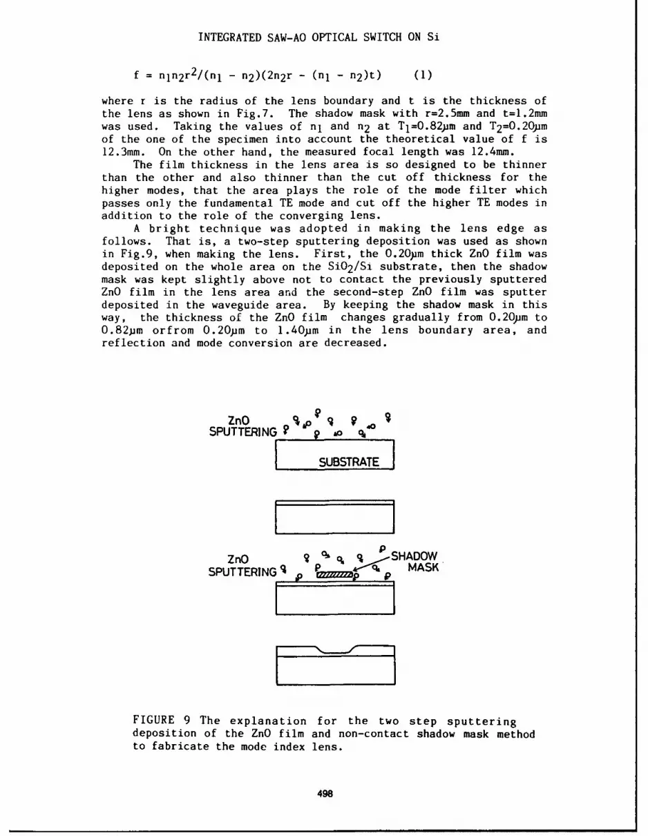
INTEGRATED SAW-AO OPTICAL SWITCH ON Si
f = nln 2 r 2 /(nl - n 2 )(2n 2 r - (nI - n2 )t) (1)
where r is the radius of the lens boundary and t is the thickness ofthe lens as shown in Fig.7. The shadow mask with r=2.5mm and t=1.2mmwas used. Taking the values of nI and n2 at Tl=O.82)im and T2=O.20,umof the one of the specimen into account the theoretical value of f is12.3mm. On the other hand, the measured focal length was 12.4mm.
The film thickness in the lens area is so designed to be thinnerthan the other and also thinner than the cut off thickness for thehigher modes, that the area plays the role of the mode filter whichpasses only the fundamental TE mode and cut off the higher TE modes inaddition to the role of the converging lens.
A bright technique was adopted in making the lens edge asfollows. That is, a two-step sputtering deposition was used as shownin Fig.9, when making the lens. First, the O.20pm thick ZnO film wasdeposited on the whole area on the Si0 2 /Si substrate, then the shadowmask was kept slightly above not to contact the previously sputteredZnO film in the lens area and the second-step ZnO film was sputterdeposited in the waveguide area. By keeping the shadow mask in thisway, the thickness of the ZnO film changes gradually from 0.20um to0.82Pm orfrom 0.20pm to 1.40pm in the lens boundary area, andreflection and mode conversion are decreased.
ZnO % V 0SPUTTERING ? A a
I SUBSRT
I __
zno 0. SHADOWSPUTTERING'I P MASK
FIGURE 9 The explanation for the two step sputteringdeposition of the ZnO film and non-contact shadow mask methodto fabricate the mode index lens.
498

T. SHIOSAKI, N. KITAMURA, A. KAWABATA
The interdigital transducer for the surface acoustic waveacousto-optic Bragg deflector was fabricated by lifting off of thealuminum thin film vacuum evaporated on top of the ZnO film. Thespatial period of the interdigital transducer was 20,um, the apertureis 3mm, and the number of finger pairs is 20 which gives the Q numberof 15 and therefore the Bragg diffraction. The ZnO film thicknessesT1 and T2 are 1.40pm and 0.2Opm, and then the focal length is 11.6mmfor the particular device described below. The separation distance dbetween two focusing points corresponding to the deflected andundeflected is given by the equation
d = 2ftanoB (2)
where OB is the Bragg angle. Taking the spatial period 20um of theinterdigital transducer into account OB is calculated as 0.4550, andthen d is 184)im as f is 11.6mm. Thus center to center separationbetween two photodiodes are designed to be 184)Im as indicated abovein Fig.6.
Only one element that was not incorporated on this device is thelight source. Instead, the He-Ne laser light of 632.8nm wavelengthwas coupled in with a rutile prism.
Results and Discussion
Figure 10 shows the photodiode outputs of the deflected andundeflected lights. The frequency of the surface acoustic wave is195MHz. The bias voltage of the diodes is 7V and the load resistanceis 200kS. The rf pulse duration is ims.
There are several problems to be solved:1) The unwanted scattered light was detected at the photodiode for
<- UndeflectedLight
4.DeflectedLight
0 Level
1 ms/div
FIGURE 10 The photodiode outputs of the deflected andundeflected lights.
499

INTEGRATED SAW-AO OPTICAL SWITCH ON Si
deflected light.2) The electrical resistivity of Si was chosen to be high enough to
give a good SAW interdigital transducer, and this the resistivitygave the slow response in the photodetectors.
3) The radio frequency noise was observed in the photodetector.This noise coupled from the interdigital transducer to thedetector.
4) The band width of surface acoustic wave should be increased byusing a phased array transducer, tilted-finger chirp transducer, ormulLi tilted-array transducer.
Rererences
1. P.K. Tien, R. Ulrich, and R.T. Martin, Appl. Phys. Lett., 14, 291(1969).
2. J.M. Hammer, D.J. Channin, M.T. Duffy and J.P. Wittkle, Appl.Phys. Lett., 21, 358 (1972).
3. K. Setsune, T. Mitsuyu, and K. Wasa, Japan, Jn. J._ Appl. Phys.,22, Suppl.22-3, 173 (1983).
4. T. Shiosaki, S. Ohnishi, Y. Murakami and A. Kawabata, J. Cryst.Growth, 45, 346 (1978).
5. T. Shiosaki, S. Ohnishi and A. Kawabata, J. Appl. Phys., 50, 3113(1979).
6. T. Shiosaki, Ceramic Transactions Vol.14 (The American CeramicSociety) pp.197-210.
7. M.S. Wu, A. Azuma, T. Shiosaki and A. Kawabata, IEEE Transactionson Ultrasonics, Ferroelectrics and Frequency Control, 36, 442(1989).
8. M.S. Wu, T. Shiosaki and A. Kawabata, IEEE J. of QuantumElectronics, 25, 252 (1989).
9. T. Shiosaki, S. Fukuda, K. Sakai, H. Kuroda and A. Kawabata,Jpn. J.>4Appl. Phys., 19, 2391(1980).
10. C.C. Tseng and S. Wang, Appl. Phys. Lett., 26, 632 (1975).11. B.U. Chen, E. Marom and A. Lee, Appl. Phys. Lett., 31 263(1977).12. J.M. Hammer, D.J. Channin, M.T. Duffy and C.C. Neil, IEEE J.
Quantum Electron., QE-11, 138(1975).
500
L__ _ _ _ _ _ _ _ _ _ _ _ _ _ _ _ _ _ _ _ _ _ _ _ _ _ _ _ _ _ _ _ _ _ _ _ _

AD-P006 680I/0mIl1lII
ELECTRON EMISSION BY NANOSECOND SWITCHING IN PLZT
HARTMUT GUNDEL
Technische Universitdt Berlin, Institut far Theoretische Elektrotechnik, EN 2,Einsteinufer 17. 1000 Berlin 10
ABSTRACT Copious electron emission from a PLZT ceramic surface takes placeeither when the surface is illuminated with laser pulses, or when short 2high-voltagepulses are applied. In the latter case, charge densities of up to 5 pC/cm and currentdensities of some ten of amperes per square centimetre have been measured. Depending LIon the position of the material in its phase diagram, different behaviour of the I)emission has been observed. Consequently the pulsed electron beam varies with respectto its pulse length, its amplitude, and its risetime. Further investigation of these data C,related to the corresponding material state might be a good diagnostic method, Iinteresting for the switching dynamics in the ns-region. Moreover, a direct application Ias a pulsed "Ferroelectric Electron Beam Source" is envisaged, as the emission does notrely on vacuum, but also works in low pressure gas or plasma. A maximum repetitionfrequency of 2 MHz has been established. An improvement of all data of the emittedelectron beam seems feasible.
INTRODUCTION
Electron emission from ferroelectrics had already been observed as far back as 1964,when Belayev and BendrikovaI investigated the influence of the state of spontaneouspolarization in triglycine sulfate and Rochelle salt on the intensity of photostimulatedexoelectron emission. In the following a large number of materials has been examinedby several groups in order to study the switching dynamics and the domain wall motionprocesses in ferroelectric single crystals as well as in ceramics. Investigations have been
performed using d.c. and a.c. electric fields as well as pulsed voltage, with thermalstimulation, and under the influence of light illumination. The experiments have beenundertaken at air athmosphere, in low pressure gas, and under vacuum. As a commonresult, it turned out, that the effiency to generate electrons seems to be correlated tothe rate of polarization change in the used material. Since almost all irvestigations weremainly directed at the surface layers and the kinetics of the corresponding material,but not at the generation of intense beams, electron emission however had been pure.Emitted electron currents were 10-I 1 A/cm 2 at its best 2, and mostly even less. In 1973
the thermally stimulated field emission was used by Briunlich to illuminate a target for
x-ray generation . Here 10 9 A/cm2 have been achieved. A review on earlierpublications concerning electron emission from ferroelectrics was given by Biedrzycki
in 19864 .
501

HARTMUT GUNDEL
The present work describes copious electron emission, orders of magnitudehigher than reported before, as it has been demonstrated recently by fast switching,using the methods of pulsed power technique and plasma physics5 -13. Summarizing
these investigations, in the following chapters a simple and tentative model of theemission process is proposed, the experimental technique is described, selected resultsare presented and discussed, and an outlook to possible applications and furtherimprovements is given.
THE EMISSION PROCESS
The dielectric displacement of a ferroelectric is written as D = co E + P , where E isthe applied electric field, co is the dielectric constant and P is the polarization of thematerial. The polarization is a sum P = co X E + Ps + Pd , the first term being the
polarisability of the material, the second representing the spontaneous alignment Ps ofthe dipols, and the last taking into account a polarisation Pd due to existing defects. Xis the dielectric suszeptibility of the material.
The dielectric displacement varies with the applied electric field and doesnormally not vanish at zero field, since the spontaneous polarization is permanent.
Additionally the polarization Pd may contribute by affecting the normal hysteresis loop
of a ferroelectrics1 4. Provided the polarization due to defects does not reverse in anexternal field, and if all defects are polarized in the same direction, a biased hysteresisloop appears . In the case of opposite directed polarization in neighbouring regions adouble hysteresis loop results . It is similar to the well known double hysteresis loop of
an antiferroelectric state. If Pd does reverse with an external field, then the coercivefield depends on both the sign and magnitude of Pd and the field required to switch
the defects.
In a steady state the ferroelectric appears neutral to its outer world because anyremanent polarization is immediately compensated by free charge carriers. Thus surface
charge densities of 30 uC/cm2 or even higher can exist in a normal equilibrium statewithout effecting the surrounding. However, there are several possibilities to disturb
this charge equilibrium for a transient time, generating a surplus of equally labelled
charges at opposite faces of the affected volume. Such a mechanism which can changethe polarization inside the material and which is fast enough not to be compensatedinstantaneously, results in a high potential at the surface. Under proper experimentalconditions charged particles can be liberated and accelerated thereby. In the presentcase conditions are chosen in order to achieve a surplus of negative charges at the
emitting surface, resulting in electron emission. The electrons are drawn from levelswhich are preferable from the energy point of view. These may be screening charges
of PSI electrons trapped by the defects, or others. As the external induced change ofthe polarization developes, the surface potential behaves in time, and the emission isenhanced or reduced. The emission characteristic is governed by external manipulation
and can be controlled up to a certain degree. Moreover, a sophisticated diagnosticmethod, resolving space and time, to observe the electrons may give a picture of the
502

ELECTRON EMISSION BY NANOSECOND SWITCHING IN PLZT
polarization dynamics of the ferroelectric surface.
There are different processes to achieve a fast change of the polarization of the
material (see also Ref. 5):- heating or cooling across a phase-transition boundary from or to the ferroelectric
(FE) state;- transitions between the FE phase and the antiferroelectric (AFE) or paraelectric
(PE) phases, by applying pulsed stress;
- transitions between the AFE or PE phases and the FE phase, by applying a pulsedelectric field;
- (partial) reversal of Ps inside the ferroelectric phase, by high voltage pulses;
- illumination by laser light (photo assisted domain switchingl5);
or any combination of these processes.For repetitive emission, heating across a phase boundary does not seem to be a
good method. The need for periodical cooling of the sample to its original state poses
problems if emission with high repetition rates is envisaged.
Phase shift caused by stress pulses is possible within less than 100 ns 16-18During shock-depoling experiments, released currents of up to 500 Amperes have beenmeasured on the electrodes, when pulsed pressure (1-10 GPa) was applied 1 9 . However,most of these experiments were of destructive character and the release of electrons to
vacuum was not investigated.
A fast change of Ps induced by high-voltage pulses, by phase shift, and/or by
(partial) reversal of Ps is the main method used in the experiments presented below.Phase shift offers the advantage that the material after emission relaxes back to its
state prior to the voltage pulse. Thus no resetting process has to be undertaken.Reversal inside the FE phase necessarly needs an active resetting, either by applyingpulses with alternating polarity, or by pulsing from a low continous potential level tothe opposite polarity. The emission dynamics in detail will be strongly correlated to theactual material under use, taking into account the kind of phase transition (1 st or 2 nd
order, or DPT), nucleation and domain wall motion, grain properties, defect concen-
tration, homogeneousity, ect.
A few experiments with laser-induced electron emission were performed. Theywill not be described here, since there is detailed information in Ref. 8.
EXPERIMENTAL TECHNIQUE
The composition of the PLZT ceramics used was 2/95/5 and X/65/35, with X equal 7,
8, 9 or 10. The first number refers to the percentage of the lanthanum content, and thefollowing numbers indicate the established Zr/Ti ratio of the samples. The materialswere prepared by conventional oxide sintering.*)
*) The samples were supplied by Prof. Handerek from the Institut of Physics of the
University of Silesia in Katowice, Poland
503

HARTMUT GUNDEL
At roomtemperature PLZT 2/95/5 is antiferroelectric and has an AFE-FE-PEphase sequence with rising temperature; PLZT 7/65/35 is in the rhombohedral FEstate; PLZT 8/65/35 is close to the phase boundary separating the rhombohedral andtetragonal phases; the 9 and 10/65/35 materials are in the region of speudo-ferroelectricity near to the PE phase boundary. As a common feature all these materialsposess the characteristics of diffuse phase transitions (DPTs). Typical values of thedielectric constant are between several hundred and several thousand, and the specificelectrical resistivity is high. Comprehensive information about the mechanical, theelectrical, and the optical properties, and a phase diagram can be found in Refs. 20 to29, and in other publications.
insulation, Solid electrode AG o..----
Grid eleeetrroe
-ý FE- arerial
10 -.014 mm E SE
FIGURE 2: Scheme of the experimental set-up with HV-pulse inducedelectron emission. FE - Ferroelectric sample, SE - Solid electrode, GE - Gridelectrode, FC - Measuring electrode, G - Graphite, I - Insulator, AG -Auxiliary grid, P - Pump, HV - High voltage
The disk-shaped samples, about I mm thick and up to 17 mm in diameter, werecoated with evaporated gold electrodes of 10 mm diameter, solid on one side and inform of a striped grid on the opposite face. The interconnected 200 pum wide goldstripes were separated by bare stripes of the same width. The electroded part of thegrid enables electric fields to be applied; the bare part of the sample serves as emittingsurface. The sample edge and the bare-sample surface around the electrode werecovered with an insulating layer. This has to be designed in such a way that high-voltage pulses up to 5 kV may be applied without danger of breakdown across thesample edges. Fig. 2 shows a scheme of the sample geometrie and a diagram of themechanical set-up. The grid electrode (GE) of the PLZT sample (FE) is orientedtowards the vacuum of the camber and was grounded during all experiments. Thesupport for the sample is equipped with a heating element and a thermocouple whichare not shown. The measuring electrode (FC) cosists of a graphite cup (G). The
collected electron current was measured time-resolved with an oscilloscope. To measure
504

ELECTRON EMISSION BY NANOSECOND SWITCHING IN PLZT
the emitted charge, the current was passively integrated on a proper condenser.Auxiliary grids (AG) could be inserted in between the PLZT sample and the measuringelectrode. These grids, which consist of metal plates with a fine metallic mesh in thecentre, were used for acceleration or deceleration of the emitted electrons, and servedas protection against high-frequency noise from the HV-circuit components.
Prior to emission the samples were prepoled with a d.c. electric field of about 2kV/cm, applied as negative voltage to the grid electrode. After poling for half an hourat 20 K above the corresponding Curie temperature, the samples were cooled downunder the same field strength to room temperature, through the PE-FE and FE-AFEphase boundary for PLZT X/65/35 and PLZT 2/95/5 respectively.
To initiate the emission, negative high-voltage pulses were applied to the rearelectrode SE. They were generated in a low impedance HV-pulse circiut, mainlyconsisting of a storage capacity, a fast-rising high-power transistor switch, and atransition line of low impedance into the load. In order to achieve high-current pulsesto measure the emitted charge as a function of the field growth rate, up to fourcircuits were used parallel, resulting in charging currents of almost 500 Amperes. Moredetails on the HV-pulse circuit, the diagnostic methods, and the mechanical set-up canbe found amongst others in Refs. 9 and 13.
RESULTS
Many experiments have been performed which demonstrate electron emission fromPLZT ceramics, and most of the data were already presented in previous publications.Therefore the results are only discussed briefly, and the reader finds references tospecial papers for more detailed information. The electron emission was investigated as
7,10a function of the applied electric field strength, of the sample temperature7 , of thefield growth rate1 0 " 3 , of the surrounding gas pressure , and of the repetitionfrequency13 of the pulses. The energy of the emitted electrons was estimated byapplying a decelerating field7 '9 .
PLZT 2/95/5 CERAMIC EMITTERS
Electron emission depends strongly on the applied electric field strength and varieswith the temperature of the sample, as the ferroelectric properties also changeaccording to the phase diagram. The influence of the applied electric field strength onthe emitted charge density can be seen in Fig. 3a, measured for a few constanttemperatures as a parameter. The emission process starts at a threshold field of about 7to I1 kV/cm, which increases with decreasing temperature and reaches about 20kV/cm at room temperature. As higher electric fields are applied, there is a strongincrease in the emitted current and charge. The electron emission is also enhanced byincreasing the temperature of the ferroelectric ceramics. All curves Q(E)T are clearlydivided into two regions of different slope.
505

HARTMUT GUNDEL
15tC 132"CI 125"C4SO /Ix450
-300 K 111C
!S K
S 10 20 30E (kV/cml
FIGURE 3a The emitted electron charge density as a function of the appliedelectric field strength at different temperatures near the AFE-FE phasetransition.
0 0
450 045 0 0 CL
0 0
a.-600 55 .5
30 -- 500 45 -43OO C
0 r,
0 ~~0000 P-40.S3
0 50 POO 150 TC
FIGURE 3b Emitted electron charge density (Q) capacity (C), rssac
(Rp), and thermostimulated current (Its) as a function of temperature in the
vicinity of the AFE-FE phase transition.
The temperature dependence of the emitted charge in relation to the dielectric
properties of PLZT 2/95/5 can be seen in Fig. 3b. At a constant electric field strength,
the sample was slowly heated across the AFE-FE diffuse phase-transition boundary.
506

ELECTRON EMISSION BY NANOSECOND SWITCHING IN PLZT
This temperature region is characterized by the broad local maximum of the capacity
curve C(T). At higher temperatures, the capacity of the sample increases further, and a
more distinct maximum occurs at the FE-PE phase transition at 235"C, which is notshown in the figure. Near to the AFE-FE phase transition, a steep rise of the emittedcharge density takes place. There is an evident correlation between the maximum ofthe emitted charge and the temperature dependences on the sample capacity (C) andthe resistance (Rp), which was measured with an a.c. field of I kHz. The maximum ofthe thermostimulated current (Its), which was recorded during heating of the previouslypre-poled sample, also coincides with the AFE-FE phase transition.
As mentioned before, the emission process relies on a change of polarization,which has to be fast enough so as not to be compensated. As a consequence, the totalemitted charge as well as the current and charge density should increase, whilechanging the same amount of polarization in less time. The emitted charge density as a
function of the field growth rate is shown in Fig. 4. Near the threshold electric field(lowest trace, 20 kV/cm), the charge density increases with the field growth-rate, butreaches saturation. With a higher electric field strength, saturation of the emittedcharge density does not seem to be reached in the range investigated (upper trace, 35kV/cm). The increase of the emitted charge is identical to an increase in the currentamplitude, since the emission time decreased slightly with increasing field growth-rates.
1.5 I
0.5
20kV/cmp , I I I
0 100 z00 300 400 500 600Fietd growth rate |kV/Imm.ps$l
FIGURE 4 FIGURE 5
FIGURE 4 The emitted charge density (Qe) as a function of the electric fieldgrowth rate for three different electric field amplitudes.
FIGURE 5 The begin of electron emission (upper trace) correlated to theapplied negative HV pulse (lower trace). The time has been 10 ns per smalldivision.
In Fig. 5 the time correlation between the applied negative HV pulse (lower
trace) and the begin of the electron emission can be seen (integrated current, upper
trace). After the voltage has reached the threshold, there is a distinct delay of about 30
ns to the start of the emission. Within the limits of experimental error, no dependence
507

HARTMUT GUNDEL
from the applied field or from the field growth rate could be stated. As a general fact
it should be noted, that the electron emission process always lastet about 50 to 100 ns
(FWHM) even with electric fields applied for a much longer period. The total emitted
current consists of many short current spikes13 . The resolution of its time structure (5
to 10 ns) however has been limited by the rise time of the used Faraday Cup and by
the bandwidth of the oscilloscope.
- 2.5 kV
-2.0kW
-1.5 kV
-1.0 kV
-0.5 kV -
OV ------
FIGURE 6 The emitted electron current at different decelerating fields
A rough information of the energy distribution of the emitted electrons can be
found in Fig. 6. A deceleration potential (UD) has been applied to an auxiliary grid
between the emitting surface and the Faraday Cup. Here the current signal decreases
homogeneously as the potential increases. This is evidence for all electron energies
occuring during the whole emission time.
IE]
FIGURE 7 The emitted electron current (upper trace, 0.4A/cm2/small div.)induced by HV pulses (lower trace, I kV/small div.) of I.1 MHz repetition rate.
The emission as a function of repetition rate of the HV pulses has been
investigated up to 2 MHz, which was experimental restricted by the pulsgenerator. In
Fig. 7 the first 5 pulses of a burst with 20 pulses each separated by about 900 ns can
508

ELECTRON EMISSION BY NANOSECOND SWITCHING IN PLZT
be seeii (upper trace) correlated to the HV pulses (lower trace). There is a small visible
decrease of the HV amplitude, which is due to a too low charging capacity in the HVpulse circuit. One can see, that the first electron-beam pulse amplitude is about 20%
higher than the following ones, which are detached with jitter values comparable to
those found in all emission experiments. The emitted electron currents were about2 21.5A/cm2 . The average charge density was about 250 nC/cm
PLZT X/65/35 CERAMIC EMITTERS
Electron emission has been measured as a function of temperature. For PLZT 8/65/35
in Fig. 8 the emitted charge density is shown together with dielectric data, likecapacity and resistance of the FE, and with the sum of pyroelectric andthermostimulated current. This resultant current has been measured separately by
E
C
, .,I PLzT-8/65/35 / I\-" 2.5
-I4I
-t. /* .2
I I\!
1 I
/
S• / 0.5
- " I- I , I
20 40 60 80 100 120 140 160 TC[CI
FIGURE 8 Electron emission correlated to the materials dielectric properties.
changing the temperature quickly, whereas the other results have been achieved duringslow heating of the sample. A clear correlation between the maxima ofelectron emission and the resultant current has been found. At this temperature theresistance has a minimum and the capacity shows an anomaly which is known fromother investigations as well. For the materials 7 and 9/56/35 similar behaviour wasfound 10 , although it has not been as distinct as in the case of PLZT 8/65/35.
The emission characteristic as a function of the applied electric field has beeninvestigated for di,"Oerent X/65/35 materials. In Fig. 9 three curves for a lanthanumcontent of 8, 9 and 10% can be seen, each having only one slope unlike in the case of
509

HARTNUT GUNDEL
PLZT 2/95/5. No clear difference in the threshold field has been visible amongst these
materials; however, as the lanthanum content increases (i.e. the distance from room
temperature to the FE-PE phase boundary gets closer), the emission is stronger and the
same amount of charge can be emitted with much less field applied.
PLUTEl 8/65/35
S--9165/35-- 10/65/35
0.75-
S I I/
0.25-
5 10 iS 20 E, CkV/cn
FIGURE 9 The emitted charge as a function of the applied electric field.
The influence of the field growth rate on the emitted charge density is shown
in Fig. 10 for three different electric fields. Similar as for PLZT 2/95/5 the emitted
charge density reaches saturation at high field growth rates only for lower applied
electric fields. For higher fields no saturation effect has been observed.!I
015 25kV/c.
Io , II I , t ' ++•
A IA0.10, _____________--_
, , ji i +0.05 oo.5kV/c.'I
0 - 2Ok0 /ca j0 10 002I
Ridd growth rate IkV/iAM.MsJ_
FIGURE 10 FIGURE I I
FIGURE 10 Electron emission as a function of field growth rateFIGURE II Time correlation between emission and applied HV pulse
A significant difference to the results from PLZT 2/95/5 is shown in Fig. 11, where
the time correlation between the applied HV pulse (lower trace) and the start of
510

ELECTRON EMISSION BY NANOSECOND SWITCHING IN PLZT
electron emission (integrated current signal, upper trace) can be seen. In the frame of
error no delay between both signals could be resolved. On the contrary to PLZT 2/95/5
the total emission time was much longer and has been determined by the HV-pulse
length. Again the total pulse consisted of many short spikes. No high repetition rate
experiments could be performed, since the amplitude of the second pulse decreased
strongly if pulse sequences with more than a few Hz were applied.
DISCUSSION
The investigated materials can be characterized by qualitativly different emission
behaviour. One the one side there is PLZT 2/95/5, showing short and very sharp
electron pulses, allowing repetitive emission, but posessing a distinct delay time
between the threshold electric field being applied and the start of the emission. PLZT
X/65/35 on the other side emits instantaneously once the threshold field is reached and
continues emitting up to the end of the HV pulse. Repetitive emission however is not
possible. The reason for this different behaviour has to be found in the dynamics of
polarization change in these two material groups.To induce a phase shift AFE-FE by electric field (PLZT 2/95/5), first
nucleation of FE domains in the AFE matrix is necessary, and then domain wall
motion has to enlarge the FE region. The nucleation process might by correlated to the
measured delay to emission; nucleation then has to be independent from the fieldgrowth rate and the absolute value of the threshold electric field which is depending on
temperature, since no dependence on these parameters could be measured. At
temperatures nearer to the phase transition boundary the emission increases, which is in
accordance to the lowering of the coercive field.Within the FE phase there are two regions, one with rhombohedral and the
other with tetragonal structure, being refered to as 'soft' and 'hard', since they reveal
different coercive field. Assumed both FE phases can be induced, the two different
slopes in the Q(E) characteristic of PLZT 2/95/5 could be explained. The difference
between both fields is almost constant while changing the absolute value with
increasing temperature.
The apperance of many short electron spikes seem to be a successive switching
of grains, each having slightly different coercive field. This is supported by the fact,
that electron energies of the whole measured spectrum can be observed at any time of
the pulse.
The possibility to achieve high repetition rates with pulses of only one polarity
is an strong suppport that a phase shift takes place; immediately when the HV pulse is
switched off, the material relaxes back to the non-polar state prior to emission and no
resetting is necessary. The restorage of the emitted charge may be explained by
injection from the electrodes, since the ohmic conductivity of the material is to low to
generate charge equilibrium in less than 500 ns. When the polarization relaxes back
however the potential between the bare-sample surface and the electrode grid is just
opposite directed than during emission. For a short time thus high fields may arise,
511

HARTMUT GUNDEL
strong enough to allow considerable currents quickly leading to a compensated surface30state
PLZT 8/65/35 has rhombohedral symmetry at room temperature and posesses twin
domains with compensated antiparallel PS vectors2 9 " When the HV pulse is applied no
nucleation process of suitable oriented domains is necessary, but domain wall motion
may start immediately from one of the twins. This might be a reason for the observed
lack of delay between the application of the threshold electric field and the begin of
electron emission. Normally twinning of domains may be removed permanently by
electical field14 ' therefore emission induced by unipolar electric field should be
impossible once all the material is oriented by the successive pulses. This is true for
material without prepoling where no emission behaviour could be observed. The
prepolarization process which is substantial for emission seems to play a double role: It
may (partially) direct the twin domain perpendicular at the sample surface, and thereby
increase the switchable part of the ceramics. Additionally existing defects may be
separated resulting in a shift of the hysteresis loop. The internal fields generated as a
result of this process might be a reason for forming twin domains again when the HV
pulse excitation is over. Repetitive emission then would be possible as it has been
measured with rates up to a few Hz only. Due to the complexity of the phase diagram
of the investigated PLZT X/65/35 materials, however, in this case theie is up to now
no conclusive explanation of the phenomena of electron emission.
OUTLOOK AND APPLICATIONS
Investigations on electron emission from ferroelectrics are just in the beginning as
compared to the well established conventional electron sources. From FE materials
there exist compositions that emit during only a few tens of nanoseconds, which is very
restricted in time, and others that emit continuously for a much longer period, as long
as the HV pulse is applied. Current and charge densities vary by two orders of
magnitude. The relaxation time to the previous state, which allows repetitive emission
to take place, ranges from less than 500 ns to almost seconds. Up to now, the physical
limits of the emission processes from ferroelectric ceramics are neither reached
experimentally nor known theoretically. However, although on the one hand the big
difference of results makes an extensive interpretation difficult, on the other hand it
enables one to find a satisfactory material, that delivers the desired electron-beam data
for many different applications. Interesting features of the so called 'Ferroelectric
Electron Beam Source' (FEBS) are almost arbitrary emission cross-section, emission
without external extraction fields allowing to modulate the beam easily, the lack of
need of ultra-high vacuum, and the possibility to emit even in low pressure gas or
plasma.
Consequently, the beam from the FEBS is well suited for example as for pre-
ionization, for triggering high-power gas and vacuum switches, for generating primary
electron beams for injection into linacs, and for generating secondary electron and ion
512

ELECTRON EMISSION BY NANOSECOND SWITCHING IN PLZT
beams by sputtering from solid targets. Basic experiments have been undertaken, which
demonstrate its feasibility for HV switching3 1 , and for electron and ion beamgeneration 3 2 . A summary of potential applications and its latest experimental resultsare reported in Ref. 33.
Beside possible applications a fundamental interest on electron emission arises
since its behaviour is strongly correlated to the dynamics of the material. Thus a newinstrument has been found to investigate phase shift and polarization reversal, providedtechniques are applied which allow to measure in the pico-second region. These arealready available and may be useful to find intrinsic switching and fastest relaxationtimes.
Particular interest is directed to emission experiments from ferroelectric thin
films. Such emitters should be driven by very low voltages only and will find a widerange of applications using integrated material technologies.
ACKNOWLEDGEMENT
I am very grateful to Dr. H. Riege and to Prof. J. Handerek, with whom I haveperformed most of the experiments during my stay at CERN, Geneva.
LITERATURE
1. L. M. Belayev, G. G. Bendrikova, Fiz, Tverdogo Tela 6 (1964) 6452. G. I. Rozenman, V. A. Okhapkin, Yu. L. Chepelev, V. Ya. Shur, JETP Lett.
39 (1984) 4773. P. Braunlich, United States Patent No. 3,840,748 from Oct. 8, 19744. K. Biedrzycki, phys. stat. sol (a) 93 (1986) 503-5085. H. Gundel, H. Riege, E.J.N. Wilson, J. Handerek, K. Zioutas, Nuc!. Instrum.
Methods A 280 (1989) 1-66. H. Gundel, H. Riege, E.J.N. Wilson, J. Handerek, K. Zioutas, Ferroelectrics 94
(1989) 337-3417. H. Gundel, J. Handerek, H. Riege, E.J.N. Wilson, K. Zioutas, Ferroelectrics 109
(1990) 1378. K. Geissler, H. Gundel, H. Riege, J. Handerek, ADDI. Phys. Lett. 56 (10) (1990)
895-8979. H. Gundel, H. Riege, E.J.N. Wilson, J. Handerek, K. Zioutas, Ferroelectrics 100
(1989) 1-1610. H.Gundel, J. Handerek, H. Riege, E.J.N. Wilson, Ferroelectrics 110 (1990) 18311. J. Handerek, Proc. Bendor Workshop on Short Pulse High Current Cathodes, Bendor
1990, p. 73, Edition Frontieres 1990, ISBN 2-86332-092-012. H. Gundel, Proc. Bendor Workshop on Short Pulse High Current Cathodes, Bendor
1990, p. 305, Edition Frontieres 1990, ISBN 2-86332-092-013. H. Gundel, J. Handerek, H. Riege, J. Awl. Phys. 69 (1991) 975-98214. M.E. Lines, A.M. Glass, Princioles and Apolications of Ferroelectrics and Related
Materials, Clarendon Press, Oxford 197715. G.H. Haertling, Ferrroelectrics 75 (1987) 25-5516. P. C. Lysne, J. Awl. Phys. 49 (1978) 429617. J. J. Dick, J. E. Vorthman, J. AwRl. Phys. 49 (1978) 249418. J. A. Mazzie, JA. LEyb 48 (1977) 1368
513
HARTMUT GUNDEL
19. W. Mock, Jr., W. H. Holt, L AwlI. Phys. 50 (1979) 274020. C. G. F. Stenger, A. J. Burggraaf, J. Phys. Chem. Solids 41 (1980) 17 and 2521. K. Wojcik, J. Blaszcak, J. Handerek, Ferroelectrics 70 (1986) 122. Z. W. Yin, X. T. Chen, X. Y. Song, J. W. Feng, Ferroelectrics 87 (1988) 8523. A. Sternberg, Ferroelectrics 91 (1989) 5324. S. Miga, K. Wojcik, Ferroelectrics (1989)25. Z. Ujma, J. Handerek, Phase Transitions 3 (1983) 12126. J. Handerek, J. Kwapulinski, M. Pawelczyk, Z. Ujma, Phase Transitions 5 (1985)8127. J. Handerek, J. Kwapulinski, Z. Ujma, K. Roleder, Ferroelectrics 81 (1988) 25328. Z. Ujma, J. Handerek, Phys. Status Solidi A 28 (1975) 48929. J. Handerek, K. Roleder, Ferroelectrics 76 (1987) 15930. Paper in preparation31. H.Gundel, H. Riege, J. Handerek, K.Zioutas, ADDl. Phys. Lett. 54(21) (1989)
2071-207332. H.Gundel, H. Riege, Anol. Phys. Lett. 56(16) (1990) 1532-153433. H. Gundel, J. Handerek, H. Kuhn, H. Riege, E.J.N. Wilson, Proc. 2nd European
Particle Accelerator Conference, Nice 1990, p. 712, Edition Fronti~res 1990, ISBN2-86332-090-4
514

AD-P006 681
FERROELECTRIC Pb(ZrTi)0 3 THIN FILMS PREPARED BY GAS JETDEPOSITION
C.L. HWANG, B.A. CHEN*, T.P. MACenter for Microelectronic Materials and StructuresYale University, New Haven, CT 06520*Current address : IBM, Essex Junction, VT 05452
J.W. GOLZ, Y.D. DI, B.L HALPERN, and JJ. SCHMYITSchmitt Technology Associates, New Haven, CT 06511
Abstract Lead-zirconate-titanate thin films were successfully codeposited in amodest vacuum environment using a novel Gas Jet Deposition (GJD) process.The GJD process utilizes supersonic carrier gas jets to efficiently transfer thedepositing species to substrates. High throughput, large coating area, and easycontrol of film stoichiometry make the GJD unique among various depositiontechniques. GJD deposited PZT films exhibit excellent ferroelectric properties.Unlike other films reported in the literature, only one preferred orientation([110]) was found in our films grown on Pt electrode. Fatigue tests show thatthe films are quite stable under ac voltage stress.
INTRODUCTION
Recently, the possibility of applying ferroelectric materials to new generations of
integrated circuits has aroused interest in lead-zicornate-titanate (PZT) filmsI 3. The
current methods employed to deposit these films include sputtering, sol-gel, and laser
ablation. In this paper, we report our recent results on PZT films fabricated by a
novel gas jet deposition4-6 technique. High deposition rates and large coating areas
can be achieved. Some attractive properties, such as one preferred orientation of the
polycrystalline PZT films and their high endurance have been found. All of these
indicate that GJD could be a viable candidate for future development of PZT films for
a variety of applications.92-16156
GAS JET DEPOSITION (GJ) TECHNIQUE lIl| fl| IAIn a GJD system, depositing species are convected from the sources to the substrates
by supersonic jets. The jets are formed by running gases such as helium, oxygen, or
argon through a nozzle into a lower pressure environment to achieve supersonic veloc-
515

C.L.HWANG, B.A.Cr.,i, T.P.MA, J.W.GOLZ, ETAL
"AI•, C02 + HeS.... Themnal PbO
""::• "Ti, Zr evapoation.sputtering source
... ~ targets sn~Heated _
Ar 02
Fig. 1 Schematic diagram of Gas Jet Deposition for PZT
ity6 above 1 kmn/sec. The jets are directed toward the substrates during deposition. A
variety of sources derived from thermal evaporation, sputtering, gases, and chemical
vapors can be incorporated in the nozzles for codeposition.
Figure 1 shows a schematic representation of the GJD system for depositing PZT
films. The chamber pressure is maintained at 1 tort during deposition by a high
volume mechanical pump. The pump down time is only several seconds, which is
much faster than that required for a typical sputtering system. Substrates are mounted
on a carousel which is spun at 2 to 3 rps, and moved up and down to enhance uniform-
ity. Under full load condition, the total coating area can be as large as 500 cm2 .
Three jets are used to deposit PZT films : (1) He and 02 are used to convect
thermally evaporated PbO into the chamber, (2) the Zr and Ti sources come from DC
sputtering of pure metal targets; (3) a third jet of pure oxygen is used to enhance the
oxidation of PZT films during deposition. The deposition parameters are discussed
next.
The PbO flux is controlled by its source temperature which is set between 700 °C
to 830 0C. Figure 2 shows that the PbO deposition rate is an exponential function of
the source temperature. Figure 3 shows the time dependence of the PbO deposition
rate at 704 0 C. It is apparent that the rate reaches a stable state after running for 5
minutes, which is the usual pre-fire time before deposition.
The deposition rates of Zr and Ti are controlled by the dc sputtering power. For a
given dc voltage ( set at 500-550 V ), the sputtering power is proportional to the cur-
516

FERROELECTRIC Pb(Zr,Ti)O 3 THIN FILMS PREPARED BY GJD
LO 2.0-
.. 0.8 R.202eV
S0.60.4 LO *w•*O5mgim n .Uas
0.2 • T =704 °C
0.00I .o0700 72o 740 760 780 80 0 10 20 30
Temperatre (VC) Time ( mn )
Fig 2. Deposition rate of PbO Fig. 3 Deposition rate of PbO
as a function of source as a function of time attemperature a fixed temperature
SLO .I 4 :.
Zrj>A•0.6. 2, -* T
J 0.4 Zr
0.0 -4 0 1 ' - In0 20 40 60 S0 10 0 10 20 30 40 .50
Sputtering Current (mA) Tme ml(n)
Fig 4. Deposition rate of Zr, Ti Fig. 5 Deposition rate of Zr, Ti
as a function of sputtering as a function of time at
current a fixed temperature
rent. In our set-up Ar acts as the sputtering gas and He is used as a carrier gas. Figure
4 shows the relationship between the Zr, Ti deposition rates and sputtering current.
Figure 5 indicates that both the Zr and Ti sources are stable after running for 5
minutes. A small rise in deposition rate after running for 30 minutes is observed in
both Zr and Ti sources. This may be attributed to the temperature rise of the metal
targets. This is not a problem for films less than 200 nm thick. For thicker films,
additional cooling can be incorporated to solve the problem.The composition of the deposited PZT film is controlled by adjusting the relative
deposition rates between the PbO, Ti, and Zr sources. In principle, through proper
control of these parameters, a variety of film compositions may be achieved.
517

C.LHWANG, B.A.CHEN, T.P.MA, J.W.GOLZ, ET.AL
Al 200am
PZT 800nm
Pt sonmSiO2 SOOnm
SiP
Fig. 6 PZT test capacitor structure
After 6 hours annealing
PZT (1 10)
Pt(11)
Before annealingPt(111) PZMUM0
S, ,60 40 35 30 20
2 0 ( degree )
Fig. 7 X-ray diffraction patterns of PZT films
SAMPLE PREPARATION
Figure 6 shows the structure of the test PZT capacitors used in this study. A thermallygrown SiO 2 layer acts as a buffer layer between the Si substrate and the Pt electrode.
The Pt layer of 100 nm is sputtered onto the SiO2 and then annealed at 400 0C to
improve its crystallinity and adhesion. Since Pt tends to peel off from SiO2 , in somecases a thin ( 5 - 10 run ) layer of Cr or Ti is thermally evaporated on SiO2 to improvethe adhesion of Pt. The PZT film is then deposited by the GJD technique describedabove, with a substrate temperature ranging from room temperature to 650 0C. Post-
deposition annealing is done at 400 0C to 600 OC in air for 2 to 7 hours. Al electrodesare thermally evaporated on PZM films to form the test capacitors.
518

FERROELECTRIC Pb(ZrTi)0 3 THIN FILMS PREPARED BY GJD
Fig. 8 SEM picture of the surface of a PZT7 film
P? *;Ct;. 66 :,.C:
Vert. 1961 counts Nlp. I Ela se
,Pb
S i
Ti
4- WO Rane. 16236ke 1. 11 4•
Integral 6 l 52741
Fig. 9 EDS spectrum of a P ZT film
FILM STRUCTRE
The crystalline structure of the 051) deposited PZT films are examined by x-ray dif-fraction (XRD). The crystallinity of the PZT films depends on the substrate tempera-
7n
tures during deposition and annealing as usually reported,. Films deposited below 400are amorphous. The typical X-ray diffraction pattern of a stoichiometric PZT film
deposited at 600 °C before and after annealing are shown in Fig. 7. The most strikingfeature is that only one preferred orientation for perovskite PZT, (110), was found
either before or after annealing. The small peak at 30.2 degree in the annealed samplecan be attributed to excessive lead oxide. No pyrochlore structure was found before orafter annealing. We believe that the preferred orientation arises from the special way
519

C.L.HWANG, B.A.CHEN, T.P.MA, J.W.GOLZ, ET.AL
SSi... 40,
: . T i0
S Pt .40 r........ 250 .0 250
Time (scc) Electric Field (kV / cm)
Fig. 10 SIMS data Fig. 11 P-E. hysteresis loop of PZT film
that the film is deposited in the GJD system; in particular the high speeds of the vapors
arriving at the substrate may play an important role.
The average grain size as estimated from the x-ray diffraction peak width is
around 150 nm. Figure 8 shows an SEM picture of the surface topography after
annealing. No microcracks have ever been observed in any of GJD deposited PZT
films before or after annealing.
COMPOSITION
The compositions of the PZT films were examined with a JEOL JXA-8600 elec-
tron microprobe using energy dispersive spectrometer (EDS) and wavelength disper-
sive spectrometer (WDS). The EDS data in Fig. 9 show the presence of only Pb, Zr,
Ti, and Si. The energies of the Zr La line and Pt Ma line are nearly the same, and are
inseparable with the resolution of the system. We then employed WDS, which pos-
sesses higher resolution, to get a quantitative ratio between Pb, Zr, and Ti. As expect-
ed the composition varies with process parameters. Stoichiometric films with Ti/Zr
ratio between 0.55/0.45 to 0.45/0.55 were achieved. A detailed study of the relation-
ship between the process parameters and the film composition remains to be carried
out.
Additional analysis was done by SIMS. Figure 10 shows the SIMS data for a
520

FERROELECTRIC Pb(ZrTi)0 3 THIN FILMS PREPARED BY GJD
1E-7 -9
200 °C (A / cma) Ea=033eV
I(A) Device Area = 5E3 cm2 -11Thickness = 800nmn
f 2S °C
1E-10 . , -130.0 V (Volt) 7.0 0.0022 0.0028 0.0034
I/T ( K")
Fig. 12 Leakage current at 25 and Fig. 13 Temperature dependency of200 °C leakage current
25.0
> l=10nA1&4
0 .0 . ... .. . . . . . 1 . 1 0 ' I I I I
0.0 500. 0 310 620
Time ( sec ) Electric Field ( kV cmn)
Fig. 14 Constant current stress Fig. 15 Hard breakdown of PZT films
stoichiometric PZT film. It is evident that the composition is constant along the depthof the film. The levels of carbon and nitrogen contamination are very low, despite thefact that the film was deposited in a modest vacuum environment evacuated by amechanical pump.
ELECTRICAL PROPERTIES
Figure 11 shows a typical P-E hysteresis loop using a Sawyer-Tower circuit with a 1.0kHz triangular wave. The remnant polarizations of GJD PZT films range from 6uC/cm2 to 13 uC/cm2, depending on the thickness of the film. The typical coercivefield is around 140 kV/cm. The dielectric constants of the films range from 370 to1300 among various samples.
!21

C.L.HWANG, B.A.CHEN, T.P.MA, J.W.GOLZ, ET.AL.
2I
00 00 0
6~
a
01.000o*07 I.000*08 1.000e*09 1.000e*10 1.00001 1 1.000* 12
Numewr of cydq (-*o to yOV)
Fig. 16 Fatigue Stress
The I-V characteristics are shown in Fig. 12-15. Figure 12 shows the leakage
current both at room temperature and 200 °C. The temperature sensitivity of theleakage current, which is an important consideration for device application, is further
studied and shown in Fig. 13. The activation energy is found to be 0.33 eV. Constant
current stress experiment was employed to study electron trapping properties. Thedata in Fig. 14 suggest that electron trapping is not severe in GJD PZT films. Asshown in Fig. 15, hard breakdown rather than soft breakdown has been typically
observed. In general, smaller devices exhibit higher breakdown fields, suggesting the
breakdown event occurs at weak spots which are randomly distributed.Fatigue stress was done with a 1 MHz sine wave of 10 V amplitude. The results
are shown in Fig. 16 for a device-. of 20 umn x 40 um in size. Although slight reduction
in the remnant polarization was observed after 1010 cycles, it levels off and remains
approximately the same up to 1011 cycles. Data for longer fatigue test are not yetavailable at the time of writing. The results indicate that GJD deposited PZT films are
more stable than most PZT films made by other deposition techniques. We suspect
that improved endurance may be linked to the fact that the GJD film has only one
preferred,.rientation Further work is needed to clarify the underlying mechanism.
CONCLUSION
Gas jet deposition of ferroelectric PZT thin films has been successfully demostrated.
Large coating areas and high deposition rates can be achieved by the GJD technique.
Preliminary measurements show good ferroelectric properties. Two unusual features
are especially worth noting : (1) the GJD PZT films exhibit only one preferred orienta-
522

FERROELECTRIC Pb(ZrTi)0 3 THIN FILMS PREPARED BY GJD
tion, (110), and, (2) no serious degradation is observed under ac voltage stress up to1011 cycles. Both features may be intimately related, and they both arise from thespecial way that the films are deposited. The underlying mechanisms and the relation-
ship between these properties remain to be studied.
ACKNOWLEDGEMENT
This work was supported by grants from the Semiconductor Research Corporation,
Office of Naval Research Contract No. N00014-80-C-0002, and DARPA Contract No.DAAHO0-90-C-0653. The author wants to thank Dr. T. Tamagawa at U. of Minneso-ta and Mr. C. Beggy of Yale U. for their assistance in many parts of the work. Thefatigue test was performed by Dr. Tamagawa. Also thanks to Dr. Brian Doyle ofDigital Equipment Co. for the SIMS data.
REFERENCE
1. D. Bondurant and F. Gnadinger, IEEE Spectrum, , 30, July (1989)
2. J.F. Scott and C.A. Paz de Araujo, Science, 2 1400 (1989)
3. L.H. Parker and Al F. Tasch, IEEE Circuits and Device Magazine, 6, 17, Jan.
(1990)
4. Jerome J. Schmitt, U.S. Patent No. 4788082 (1988)
5. R. Iscoff, Semiconductor International, 14, 50, (1991)
6. J.B.Fenn, Applied Atomic Collision Vol. 5., ( Academic Press, 1987 ), p. 349
7. A. Okada, J. of Apvl. Phys., 48, 2905 (1977)
523

PROCESS TECHNOLOGY DEVELOPMENTS FOR GaAs FERROELECTRICNONVOLATILE MEMORY
L. E. Sanchez, I. K. Nalk, S. H. Watanabe, I. S. Leybovich,J. H. Madok and S. Y. WuMcDonnell Douglas Electronic Systems Company5301 Bolsa Avenue, Huntington Beaich, CA 92647
Abstract. Fabrication of nonvolatile memories utilizing ferroelectricpolarization charge of lead zirconate-titanate (PZT) thin film capacitors requiresthe integration of the PZT capacitor process with the semiconductor deviceprocesses. This paper discusses the development of enabling process technology for
Go a integration of PZT capacitors with GaAs junction field-effect transistors (JFET) onCO a GaAs wafer for the fabrication of a GaAs ferroelectric random access memory
(FERRAM). Individual processes for PZT capacitors and GaAs JFETs are describedX= briefly first. The PZT capacitor process utilizes sol-gel deposition of PZT thino films, while the GaAs JFET process is based on selective ion implantations of silicon
and magnesium directly into the GaAs wafer. The integration of these two chemically_ i different processes has been accomplished through process innovations in the areas
of sintering of PZT film, ion implantation in GaAs, interconnect metallization andI - patterning of this metallization. Successful operation of the nonvolatile memory
cell has been demonstrated in a memory test circuit fabricated using this integratedprocess technology.
1. INTRODUCTION
Development activities for nonvolatile memories based on the ferroelectricpolarization charge of lead zirconate-titanate (PZT) thin films have seen aresurgence in recent years. 1 ,2 Generally, this type of memory integrates asemiconductor switch with a ferroelectric capacitor that can retain a charged stateeven in the absence of an applied voltage. McDonnell Douglas Electronic SystemsCompany (MDESC) has been developing a nonvolatile memory that integrates GaAsjunction field-effect transistor (JFET) switches with ferroelectric thin-filmcapacitors on a GaAs wafer. The JFET used is an enhancement-mode, n-channeltransistor and the capacitor has a PZT thin film as the ferroelectric material. Inaddition to the nonvolatility, the combination of the GaAs JFET with the PZTcapacitor would offer a high-speed performance, extreme radiation hardness andlow-power circuit operation. In this paper, we discuss the process technologydevelopments for the fabrication of a 4K bit GaAs ferroelectric random accessmemory (FERRAM). The 4K bit FERRAM is a vehicle for developing anddemonstrating the feasibility of this new technology. Our objective is todemonstrate that we have developed the required enabling process technology andthat a fully-functional 4K bit GaAs FERRAM is imminent.
2. MEMORY CELL AND CIRCUIT
A single memory cell of this experimental 4Kbit FERRAM consists of one GaAs n-channel JFET pass-transistor and one PZT capacitor as shown in Fig. 1. Capacitorswith four different areas (4x4, 5x5, 7.5x5 and 9x5 jim2 ) have been incorporatedin the 4K bit memory design to study the effect of the amount of the polarizationcharge on the memory performance. At the device level, the GaAs JFET technologyrequires that the coercive voltage of the capacitor be less than 1 V and the saturation
92-16157111111iN 11W 1111152

L. E. Sanchez, I. K. Naik et al.
voltage be 3 V or less. At the circuit level, two circuit designs are being evaluatedfor the 4K bit memory. The design one which is configured as 512 x 8 bits uses across-coupled sense amplifier. The second design uses a differential senseamplifier which is incorporated in a test module of the reticle. These device andmemory circuit designs serve as the initial vehicle for developing FERRAMfabrication processes which are described in this paper.
(a)
Fig. 1. (a) Cross-section and (b) layout of asingle memory cell of the experimentalS~ FERRAM.
S= • •(b)
Cett Dimensiong 40 um x 46 umCapacitor- Dimension: 4 um x 4 urn
3. INDIVIDUAL DEVICE PROCESSES
3.1 Process for PZT Capacitor Fabrication
We have adapted and modified the sol-gel process for depositing semiconductordevice-quality PZT thin films (500 to 2000A thickness) as reported recently. 3 ,4The ferroelectric capacitors made with these films have demonstrated the requiredcharacteristics for nonvolatile memories. 3 This sol-gel process uses ametallorganic liquid formulation that is spin-coated on a semiconductor wafer in amanner similar to the photoresist. For capacitor fabrication, the spin-coating isapplied on a wafer that already contains the bottom electrode made of Pt(2000A)/Ti(200A) films. The dried metallorganic coating is then heat-treated inan oxygen-containing gas atmosphere at 650 to 7000C to crystallize and densify thePZT film. The details of this process have been discussed in reference 3.
In the next step, top electrode metallization, Au (2000A) or Au(500A)/Pt(1500A), is deposited over the entire wafer by the electron beamevaporation technique. Then individual capacitors ranging in size from 40 gim x40 lgm to 4 pgm x 4 g~m are defined by means of standard photolithography and ionbeam milling techniques. The ion beam milling is done through both the topelectrode and the PZT film in the field areas down to the bottom electrode.Subsequently, another photoresist mask defines the bottom electrode which is thenion milled in the same manner to complete the capacitor fabrication.
525

L. E. Sanchez, I. K. Naik et al.
We have found that alloying of the top electrode metal to the PZT film bymeans of a heat treatment at 600 to 7000C improves the capacitor ferroelectriccharacteristics very significantly. This alloying treatment makes the hysteresisloop more symmetrical, reduces the coercive voltage 3 and improves the fatiguecharacteristic. 5 It was determined that, during the alloying treatment, a smallamount of liquid phase is formed through a reaction between Au metallization and theexcess PbO in the PZT film. This reaction appears to facilitate the formation of anintimate electrode contact with the PZT film. It also appears to reduce the effectivethickness of the PZT dielectric of the capacitor through diffusion of Au into PZTwhich results in lower coercive voltage and saturation voltage of the capacitor.Thus, this simple alloying treatment makes the poling of the capacitor easier by theperipheral switching circuit.
Typical properties of our PZT capacitors are as follows: coercive voltage of0.6 to 0.8 V, saturation voltage of about 3 V and remanent polarization (Pr) of 15to 20 giC/cm 2 for capacitor area range of 4x4 i.m2 to 40x40 p.m2 (Fig. 2). ThePZT film corresponding to these properties has a Zr/Ti atomic ratio of 50/50, -3mole percent excess PbO, and thickness of 1000 to 2000A.
Fig. 2. A typical hysteresis loop of the sol-gelderived 10 I~m x 10 jim PZT filmcapacitor Pt/Au/PZT (1oooA)/Pt-Ti.[X axis: voltage (one large div. = 1 V);Y axis: polarization (One large div. =8 pC/cm 2 )]
3.2 GaAs JFET Pilot Line Process
During the 1980s, MDESC developed a VLSI-capable GaAs JFET process for low-power, radiation-hard, high-speed digital ICs. This process has been used as thebaseline or starting process for the development of GaAs FERRAM. The mainfeatures of the n-channel JFET process, as described in Ref. 6, are as follows: (a)selective Si+ ion implantation directly into GaAs wafer to form n-channel, sourceand drain (b) selective Mg+ implantation followed by zinc diffusion to form p+ gate(c) furnace annealing to activate the implants (d) standard Ni/Ge/Au metal contactsfor source and drain (e) Ti/Pt/Au first-level interconnect that is patterned bymeans of ion beam milling (f) sputter-deposited silicon nitride (SiN) as the inter-level dielectric (g) Ti/Pt/Au second-level interconnect patterned by ion beammilling. As an example, this baseline process uses 11 mask layers for fabricationof a 4K bit GaAs static RAM that does not contain nonvolatile PZT capacitor elements.
In the following section, we discuss the developments that were necessary tointegrate the PZT capacitor with GaAs JFET for the fabrication of GaAs FERRAM.Significant modifications to the baseline GaAs JFET process had to be made to achievecompatibility between the two processes.
526

L. E. Sanchez, I. K. Naik et al.
4. PROCESS INTEGRATION
The first conceptual integration of the PZT process and the GaAs JFET pilot lineprocess to fabricate a GaAs FERRAM is depicted in the general process sequence inFig. 3. This process integration, however, turned out to be more difficult thananticipated. Several processing-related problems arose as the integrationexperiments were carried out. These problems and their solutions are discussed inthis section.
JFET/FERROELECTRIC(FE I PROCESS WITH ZINC DIFFUSION)
.DePA Imial SN, I1ft11 N.. NC. P .Annel &d Elch GaO. Oepos SW02
El N.[ Nc Fig. 3. General process sequence for
2 PeeBE..FEw TE P+ integration of the PZT process
.. TE and the GaAs JFET process using
3 J S BE zinc diffusion approach.3. Ca F ET w SAuGe
*FE4 R814 S excep4 evw FE. Eld, SM0.
Zinc DAIo Open Cwaa Wrdmw. Oi.--DGapO NiAUGS ed A"o Ohmic
. Nitride
ElGaAsS. Elch iV.mn "BE S TE.
4.1 Arsenic Contamination of PZT
High-quality PZT capacitors, in terms of high remanent polarization, low coercivevoltage, symmetrical hysteresis loop, and low leakage current, are obtained whenthe PZT film has stoichiometric composition, in particular no oxygen deficiency orexcess. For this reason, the PZT film has to be sintered in a high oxygen partialpressure atmosphere (Ž_0.2 atm) at elevated temperatures (550 to 7000C for asol-gel film). However, GaAs is unstable in oxygen-containing atmosphere at suchtemperatures. In our initial experiments, it was found that arsenic-containinggaseous species evolved from the open GaAs areas when a PZT film was sintered onGaAs in an 02/N2 mixture. Surface chemical analyses by Auger electronspectroscopy of PZT films sintered on GaAs wafers with exposed backside revealedpresence of arsenic in the PZT films. Such arsenic-contaminated PZT films yieldeddegraded hysteresis loop as shown in Fig. 4. This loop has lower Pr than normal (6
iiC/cm2 vs. 15 gC/cm2 ) and it does not attain saturation. Further experimentsshowed that even a small exposed rim area of GaAs at the wafer edge couldcontaminate PZT in the proximity of this rim area. These observations taught usthat the GaAs wafer has to be sealed completely (both faces as well as the edges) toavoid As-contamination of the PZT film during sintering. This wafer sealing is doneby depositing a 1 oooA thick silicon nitride (SiN) film on both faces and the edges ofthe GaAs wafer by means of reactive ion beam sputtering. The SiN film has provenan effective encapsulant of GaAs wafer for sintering PZT films on GaAs.
527

L. E. Sanchez, I. K. Naik et al.
Fig. 4. Degraded hysteresis loop due toarsenic contamination ofthe PZT film during sinteringof the PZT film on GaAs wafer.
4.2 Zinc Diffusion versus Zinc Implantation
In process integration experiments, we investigated the effects of zinc diffusionstep, which is used in the baseline process for the formation of p+ gate of the JFET,on the properties of the PZT capacitors. Individual silicon nitride (SiN) and silicondioxide (SiO2) layers were evaluated as the encapsulant to protect the PZTcapacitors during the zinc diffusion treatment. A wafer with a blanket 4000A thickSiN layer over the patterned PZT capacitors was subjected to argon atmosphere at6500C for 60 sec. Another similar wafer was subjected to argon containing zincvapor at 6500C for 60 sec, which is a typical zinc diffusion operation: done in anopen tube furnace using zinc metal as the source.The results of the wafer subjected to the argon ambient will be describedfirst. The adhesion of the silicon nitride layer on gold (top electrode) and platinum(bottom electrode) was not completely satisfactory. Interference patterns wereobserved on both gold and platinum electrodes in some areas (about 50% of thewafer), indicating that lifting of the silicon nitride layer occurred. Cracking andpeeling of the layer were also observed in parts of the wafer.
We noticed roughening of the gold electrode after the argon treatment. Someelectrodes developed discoloration in small areas, as shown in Fig. 5(a). When thesilicon nitride capping layer was removed, we discovered that there was no gold inthese small areas as shown in Fig. 5(b). Apparently the silicon nitride layerreacted with gold during the 6500C 60 second heat-treatment and developed holes inthe gold electrode. Ferroelectric hysteresis loops were measured on the 40 x 40pgm 2 capacitors on this wafer. A typical hysteresis loop is illustrated in Fig. 6. The
Fig. 5. Microstructures of PZTcapacitors after heat treatmentin argon at 6500C for 60 sec:(a) Gold top electrode areawith silicon nitride cappinglayer (b) The same afterremoving the silicon nitridecapping layer.
a b etONb
528
-., l .. . . ..

L. E. Sanchez, I. K. Naik et al.
switched polarization and the remanent polarization were both lower than thosebefore the argon heat treatment. The former was 37.5 tlC/cm2, a drop of 14%, andthe latter was 16 tLC/cm 2 , a drop of 28%.
Fig. 6. A typical hysteresis loop of a40 gim x 40 lim capacitor withgold top electrode and siliconnitride capping layer after heattreatment in argon at 6500C for60 sec.
The wafer subjected to the zinc-argon atmosphere also developed similarsurface structure on the gold electrode, as described in the previous paragraph. Ona few capacitors which were not protected well by the silicon nitride capping layer,zinc entered through cracks and reacted both with the gold top electrode and thesurrounding platinum electrode. The gold metal was degraded by the zinc vapor asshown in Fig. 7. Electrical testing showed that this capacitor had shorted out duringthe zinc-argon heat treatment. Fig. 8 shows the hysteresis loop of a capacitoraround which silicon nitride had not cracked. As a result of the zinc-argontreatment, the hysteresis loop became slim, and the remanent polarizationdecreased to 4 j.C/cm2 , which was a decrease of about 82% from the initial value.
Fig. 7. Microstructure of gold electrodes ofsilicon nitride-capped PZT capacitorsafter heat treatment in zinc-argonatmosphere at 6500C for 60 sec.The capacitor at upper right was notprotected well by the capping layer.
529

L. E. Sanchez, I. K. Naik et al.
Fig. 8. Hysteresis loop of a gold-electrodedcapacitor with silicon nitridecapping layer after heat treatmentin zinc-argon atmosphere at 6500Cfor 60 sec.
Wafers coated with a 4000A of sputtered SiO2 were also subjected to thezinc-argon treatment at 6500C for 60 seconds. The adhesion of the SiO2 on the goldand platinum electrodes seemed to be worse than that of silicon nitride. Highstresses in the SiO2 layer were believed to cause it to wrinkle and crack. Duringthe zinc-argon heat treatment, zinc also penetrated through the cracks and reactedwith the gold top electrode, as in the case with the silicon nitride layer. A similarroughening and discoloration was also observed on the gold electrodes well-coveredwith the SiO2 layer. A chemical reaction might have occurred between the SiO2 andthe gold electrode.
The above results led to the conclusion that the zinc diffusion technique is notrobust enough to be reliably and reproducibly used when PZT capacitors are presenton the GaAs wafer. As an alternate approach, we considered zinc ion implantation inGaAs followed by a rapid thermal annealing (RTA). This approach has been shown tobe a viable process for forming very thin (-1OOOA) p+ layers in GaAs withoutsignificant broadening of the zinc profile 7 . Zinc ion implantation followed by RTAin forming gas eliminates the need for exposure of the GaAs wafer with PZTcapacitors to zinc vapor atmosphere which seems to be the most detrimental part ofthe zinc diffusion step toward PZT capacitors. Furthermore, the steps of zincimplantation and RTA can be carried out before PZT capacitor fabrication thusavoiding any problems of capacitor degradation. From the point of view of processreliability and robustness, the zinc implantation is more controllable and morecompatible with other processing steps. Based on these considerations, we decided toimplement zinc ion implantation and RTA for the fabrication of GaAs FERRAM. AFERRAM process sequence that uses zinc ion implantation and RTA is shown inFig. 9. This process sequence has yielded integrated structures of enhancement-mode JFETs and PZT capacitors whose test results are discussed in section 5.
I 04"AVOeN W 5uE N. NC. OMNpI M
n2. af b Ow Dop Owe NC hNw]
-- - - - : a= Fig. 9. General process sequence for* t,,, FERRAM fabrication using
"--""."- "EJf M,,,, zinc ion implantation andf=-------==--: --------- 3L 0 re rapid thermal annealing.
,4. C.04 FR O aJ'• T0 goIr. Owm, oo IN 0] d
.a - FIE -E" SO ~M t
.W., OPOM A.00 AW.
$ If* vim III. aNO TIE.
530

L. E. Sanchez, I. K. Naik et al.
4.3 New Metallization
First-level interconnect Ti/Pt/Au used in the baseline JFET process also gaveproblems in the integrated FERRAM processing. This noble metal interconnect wasnot chemically etchable and its patterning in the baseline process was done by ionbeam milling. The ion beam milling worked well when the wafer topography wasplanar. But when it was used to pattern the Ti/Pt/Au interconnect on the GaAswafers containing PZT capacitors, the bottom and top electrodes of the capacitorsremained shorted after the patterning was completed. Even after a considerableovermilling time, these capacitor shorts could not be eliminated. Scanning electronmicroscopy (SEM) of the ion-milled structures showed evidence of a remanentmetal film along the edges of the encapsulating SiN (Fig. 10). It appeared that ionmilling was not able to completely remove the metallic layer along the edges of theSiN capping over the capacitors. Further analysis by means of an electron potentialprobe in conjunction with SEM conclusively proved the presence of this shortingpath. These shorts occurred in spite of the precautions taken to obtain uniform ionmilling through rotation of the wafer and use of an oblique (450) angle of ion beamincidence on the wafer. From these results, it was concluded that the nonplanartopography of the FERRAM wafer at this stage prevented a successful use of ion beammilling for patterning the first-level interconnect.
/Fig. 10. Back-scattered-electron-mode scanning
electron micrograph of a typical shortedcapacitor after ion beam milling of thefirst-level interconnect Ti/Pt/Au.
To solve the above problem, we decided to use an interconnect metallizationthat can be readily dry-etched by means of the current state-of-the-art techniqueof reactive ion etching (RIE). Based on our experience, we selected refractorymetal tungsten(W)-base interconnect for this purpose. The metallization consistedof a two-layer sandwich: W-N (250A)/W (2500A). The W-N layer which was aW-nitrogen solid solution with -30 atom percent nitrogen, provided a good ohmiccontact to the p+ GaAs gate while the thicker W layer reduced the resistivity of theinterconnect. This sandwich metallization was deposited as a blanket layer in asingle pump-down in a magnetron sputter deposition system using a W target. Thepatterning was then carried out using SF6 gas in an RIE system. This interconnectscheme has been successfully used on the GaAs FERRAM wafer. A photomicrographof the memory cells with integrated GaAs JFETs and PZT capacitors after the first-level interconnect is shown in Fig. 11.
531

L. E. Sanchez, I. K. Naik et al.
Fig. 11 A photomicrograph of the memorycells with integrated GaAs JFETs andPZT capacitors after the first-levelinterconnect.
To complete the wafer-level IC fabrication, the following steps are thencarried out: an inter-level dielectric of 5000A SiN or 7000A polyimide isdeposited vias are etched in the inter-level dielectric by means of RIE, second-levelinterconnect metal of aluminum is deposited by a sputter deposition and patternedby means of RIE. Electrical test results of the integrated devices fabricated by thisprocess are presented in the following section.
5. ELECTRICAL TEST RESULTS
Typical hysteresis loop of the PZT capacitor (40 gim x40 gim) and current-voltage(I-V) characteristics of the GaAs JFET both fabricated on the same GaAs wafer areshown in Fig. 12. These tests were made at the first-level interconnect stage of theprocessing sequence. The hysteresis loop is almost identical to that obtained onindividually-processed capacitors on a wafer that has not gone through the JFETprocess part. Also, the JFET characteristics are comparable to those of theindividually-processed GaAs JFETs. This result demonstrates that the majorproblems of process integration for combining PZT capacitor with GaAs JFET havebeen resolved.
Pr 20c IICM 0.27 voa
V= 0.65 vot Gm = 130 mS/mm
(a) (b)
Fig. 12. (a) Typical hysteresis loop of a 40 pm x 40 gim PZT capacitorand (b) I-V characteristics of GaAs JFET (1 gim gate length x20 gIm width) both on the same GaAs wafer after completionof the first-level interconnect.
532

L. E. Sanchez, I. K. Naik et al.
Successful operation of a nonvolatile memory cell has been demonstrated in atest circuit which is a 6-cell memory circuil shown in Fig. 13. This test circuitcontains the same size PZT capacitors and GaAs JFETs as the 4k FERRAM, namely4 gim x 4 lim and 7.5 lim x 5 plm capacitors and 1 lIm gate-length x 20 lim widthJFETs. The electrical test for this demonstration was carried out in the followingmanner. WRITE operations for the binary states 0 and 1 were performed on thememory cells using a supply voltage of 5 V. Then the power to the circuit wasturned off for five minutes. Upon turning the power on again, READ operations weredone on the previously-written cells. Typical results of such WRITE and READoperations are shown in Fig. 14. It is seen that the cell stored the state that waswritten before the power-down and maintained it when the power was off. When thecell was read again after the power-down, the same state as that written before thepower-down was read back. This result demonstrated functionality of thenonvolatile memory cell.
iiA t t,C. ... 1_"
AIWRIITE READ WRITE READAL 2 0 0
Fig. 13. Photomicrograph of a 6-cell Fig. 14. WRITE and kEAD pulse responsesmemory test circuit after with power turned off betweencompletion of second-level the WRITE and READ operationsinterconnect, demonstrating nonvolatility of
the memory cell.
Four kilobit GaAs FERRAM ICs have been fabricated using the processesdiscussed in this paper. Detailed results of the electrical testing of this GaAsFERRAM will be presented in the near future.
We have demonstrated important enabling processes necessary for integratingferroelectric PZT capacitors with GaAs JFETs on the same GaAs wafer forfabrication of a nonvolatile ferroelectric memory. Integrated process sequencedeveloped using these individual processes has been successfully used to fabricatenonvolatile memory cells, test circuits and elements of 4K bit GaAs FERRAM. Theseintegrated PZT capacitor-GaAs JFET structures have shown the functionalitynecessary for operation of a nonvolatile GaAs ferroelectric memory.
ACKNOWLEDGEMENTS
The authors acknowledge useful technical discussions and managerial supportprovided by W. A. Geideman, A. J. McDonald and G. L. Troeger and technical supportprovided by the Microelectronics Center personnel. This work was funded by theDefense Advanced Research Projects Agency.
533

L. E. Sanchez, I. K. Naik et al.
REFERENCES
I. C. A. Paz de Araujo and G. W. Taylor, Ferroelectrics, 116, 215 (1991).(Proceedings of the Second Symposium on Integrated Ferroelectrics, 1990).Also, Ferroelectrics, 1Q.4, 241 (1990).
2. J. F. Scott, C. A. Paz de Araujo and L. D. McMillan, Ferroelectrics,J11, 107 (1991).
3. L. E. Sanchez, D. T. Dion, S. Y. Wu and I. K. Naik, Ferroelectrics, M16, 1(1991). (Proceedings of the Second Symposium on IntegratedFerroelectrics, 1990.)
4. L. E. Sanchez, S. Y. Wu and I. K. Naik, Appl. Phys. Lett., a (24),2399 (1990).
5. I. K. Naik, L. E. Sanchez, B. P. Maderic and S. Y. Wu, "Improved SwitchingEndurance of PZT Capacitors for Nonvolatile Memory Applications", Paperpresented at the Third International Symposium on IntegratedFerroelectrics, April 1991. (Published in this volume.)
6. R. Zuleeg, J. K. Notthoff and G. L. Troeger, in Gallium ArsenideTechnology, Vol. 2, D. K. Ferry, Editor, H. W.Samms and Company,Indiana, U.S.A., p. 95 (1989).
7. I. K. Naik, J. Electrochem. Soc., 13, 1270 (1987).
534

00
SOLUTION CHEMISTRY EFFECTS IN Pb(Zr,Ti)03THIN FILM PROCESSING
R. W. SCHWARTZ, B. C. BUNKER, D. B. DIMOS, R. A. ASSINK,B. A. TUTITLE, D. R. TALLANT, and I. A. WEINSTOCK
Materials and Process Sciences Directorate, Sandia National Laboratories,P.O. Box 5800, Albuquerque, NM 87185 U.S.A.
(Received June 14, 1991)
Ferroelectric thin films in the PZT compositional family were prepared by two different solutiondeposition methodologies. The approaches were based on the use of carboxylate and alkoxide precursors,and acetic acid. Solution aging and mixing order effects on thin film microstructure and ferroelectricproperties were studied. Films prepared from 15 day old solutions had a lower remanent polarization _
(1.4 p.C/cm2 ) and higher coercive field (256 kV/cm) than films prepared from 1 day old solutions _ -
(Pr = 18.7 ±C/cm 2 ; Ec = 55.2 kV/cm). Raman, FTIR, and NMR spectroscopies were employed toconfirm the role of acetic acid in the process, and to begin to understand why changes in solution 0__chemistry can so dramatically affect the resulting film microstructure and properties. FTIR spectroscopyindicated that in addition to acting as a solvent, acetic acid also serves as a chemical modifier in the two ( Eprocesses. That is, it reacts with the alkoxide precursors on a molecular level, replacing the alkoxy Oligands. Ester formation was also observed by both FTIR and NMR spectroscopy. The formation of thisby-product implies the simultaneous formation of water, and therefore, in-situ hydrolysis and condensation 0of the precursors. -I-
INTRODUCTION
Ferroelectric Pb(Zr,Ti)0 3 (PZT) thin films have been prepared by a variety of physicaland chemical deposition methods. The physical methods that have been used, include:sputtering from oxide1 or elemental metal targets; 2 molecular beam epitaxy; 3 ion beamdeposition;4 and various laser ablation techniques. 5 Chemical solution depositionmethods, including: sol-gel; 6 MOD (metallo-organic decomposition);"7' 8 and hybridapproaches; 9 have also been used with success to fabricate PZT thin films. Solutiondeposition approaches are of interest because of the low capital investment costs, theability to closely control composition, and the relative ease of process integration withstandard Si wafer technology. Further, the films prepared by solution deposition methodshave displayed ferroelectric properties comparable to those of bulk ceramics. While thethin films prepared by chemical methods are typically polycrystalline, the ability to preparehighly oriented thin films has been noted.1 O.11 Solution deposited thin films have alsobeen reported to possess high electro-optic retardations. 12
Sol-gel, MOD, and hybrid deposition methods are based on the use of metallo-organic precursors. Three different classes of precursors have been used: (i) metalalkoxides, M(OR)x; (ii) metal carboxylates, M(OOCR)x; and (iii) metal acetylacetonates,M(C5H702)x; where R is an alkyl group, and x is the valence of the metal. Sol-gelmethods generally use metal alkoxide precursors, and maintain close control over thereaction conditions to form mixed metal alkoxide species, which serve as molecularbuilding blocks for the development of the desired crystalline structure. 13 Hydrolysisconditions are then manipulated to control the nature of the polymeric species in solution,prior to deposition of the thin film. In contrast to sol-gel approaches, MOD methodstypically use carboxylate precursors with large org 7 c moieties, such as 2-ethylhexanoate
535

R. W. Schwartz et al.
and neodecanoate ligands. 7 The method is more straightforward than the sol-gelapproach, since the precursors are typically water insensitive. However, due to the highorganic content of the films, cracking problems are frequently encountered. Recently,Haertling has developed an alternate MOD route which utilizes precursors with smallcrorganic groups, which may allow for the preparation of thin films which exhibit lesstendency toward cracking. 14 Hybrid solution deposition methods generally use lowmolecular weight carboxylate and alkoxide precursors, namely, acetates and propoxidesor butoxides. In these methods, less attention is given to control of the hydrolysisconditions, due to the use of chemical modifiers, which diminish the hydrolysis rates ofthe alkoxides.
Although there are obvious differences between the three approaches, in general, thefollowing steps are involved: (i) dissolution (and reaction) of the cation precursors in acommon solvent; (ii) tailoming of solution characteristics, such as viscosity; (iii) depositionof the films by spin-casting or dip-coating; (iv) low temperature heat treatment for organicpyrolysis and conversion to an inorganic amorphous intermediate; and (v) highertemperature heat treatment for densification and crystallization into the desired phase. Wemight expect that changes in any of the processing steps outlined above could potentiallyaffect not only the nature of the species obtained in the subsequent step, but the final filmmicrostructure and electrical properties as well. For example, changes in the precursorreactivity or hydrolysis conditions are known to change the nature of the polymericspecies in solution. 15 In turn, variations in the nature of the solution polymeric .peciesaffect the nature of the wet film, especially residual organic removal and crackingtendency during drying. 16 The resulting changes in the physical and structural propertiesof the dried amorphous film, i.e., its structural free volume, porosity and surface area,define the free energy of the film, and therefore, its densification and crystallizationbehavior, and the ceramic microstructure and associated properties which are obtained. 17
Thus, the parameters used in each step of the overall processing route, from solutionpreparation conditions, to heat treatment temperatures. times and ramp rates, 18 serve todefine the ferroelectric properties of the film.
One problem with the use of chemical deposition methods is the lack of afundamental understanding regarding the effects of solution chemistry variations, andstructural evolution behavior, on film dielectric and ferroelectric properties. And from areview of theý results reported for films prepared by different solution depositionapproaches, we can see there are indeed significant differences in dielectric andferroelectric properties, crystallization temperatures, and thin film microstructures. Wehave also noted similar effects of variations in solution chemistry. For films which weresubjected to identical heat treatment conditions following deposition, different ceramicmicrostructures and electrical properties were observed for solutions prepared underdifferent conditions. Since the reasons for these effects are, at the present time, unclear,consistent control of film microstructure and ferroelectric properties is difficult.Preparation of property-optimized films is not possible.
The focus of the present study is to begin to address the underlying reasons for theobserved differences noted above, by using a variety of characterization techniques atdifferent process points. Since the final film properties can conceivably be affected byvariations at any stage in the preparation process, e.g., from variations in the nature of thesolution polymeric species, or differences in the physical and structural characteristics ofthe amorphous film, we need to consider using characterization techniques which providestructural information on different size scales. Multinuclear NMR can provideinformation about the local chemical environment of different species, while SAXS (smallangle x-ray scattering) can provide information on a larger size scale, describing the sizeand shape of the polymeric species in solution. 15 The microstructural features of the filmsmay be characterized by SEM and TEM, and the macroscopic physical properties of theamorphous films may be determined by depositing the films onto SAW (surface acousticwave) devices. 19
536

Solution Chemistry Effects in PZT Thin Film Processing
Finally, the effects of solution chemistry variations on crystallization anddensification behavior may also be determined. Raman spectroscopy may be used tostudy metastable and stable crystalline phase development, while ellipsometry can be usedto monitor consolidation behavior. The potential use of various characterizationtechniques at different process points is shown in Table I. Our goal is to use thesecharacterization techniques to understand, on a fundamental level, the effects of variationsin solution chemistry on structural evolution and thin film electrical and optical properties,so that processing conditions which lead to the development of optimal properties can bedetermined.
Table I
Applicability of characterization techniques to the study of structural evolution insolution processing of thin films.
Liquid Film
Precursors Rxn. Prod. Solution Wet Amorphous Crystalline
Technique
NMR * * *
FTIR * * *
SAXS * * * *
Raman * * *
SAW *
Ellipsometry * *
TEM * *
SEM *
Elec. Prop. *
EXPERIMENTAL
Thin film preparation
We fabricated the thin films of the present study by using two different hybrid solutiondeposition approaches. Flow diagrams are shown in Figure 1. For both approaches, thefilm composition was PZT 53:47 with 5 mol % excess Pb. In the first approach, asequential precursor addition (SPA) method, based on an approach reported by Sayer andco-workers, 9 was used. Lead acetate trihydrate* was dissolved in acetic acid* anddehydrated by heating to 105°C. The other precursors, zirconium butoxide-butanol§ andtitanium isopropoxide,* were then added sequentially as the solution was cooled.Solution viscosity characteristics were tailored through further additions of acetic acid,water, and methanol. In the second approach, an inverted mixing order (IMO) approach
• Aldrich Chemical Company, Inc.; Milwaukee, WI
§ Alfa Products; Ward Hill, MA
537

R. W. Schwartz et al.
L Dissolve Pb(OAc)2"3H 2 0 in HOAc 1 Add Ti(OiPr)4 to Zr(OnBu) 4 "BuOH IApproximate ratio: 1 g/2 ml while stirring
[ Heat to 1050C to de-hydrate 1 React for 5 minutes then addCool to 750 C 4 moles HOAc/mole M(OR)4
I I
Add Zr(OnBu) 4 "BuOH to solution Quench reaction with MeOH 1Continue stirring and cool to 650C j______________
Add Ti(OiPr)4 to solution I Add Pb(OAc)4 (90% in HOAc)Stir and continue cooling Heat to 850C to dissolve
Add H 2 0 and MeOH II Cool to 700C, then add additional 1Approximate ratio: 1:4 j HOAc and MeOH
I I
Dilute to 0.4 M with HOAc Cool to 600C then add additional HOAca H
_________________Iand H20I(a) (b)
Figure 1. Flow diagrams for: (a) Sequential Precursor Addition (SPA) process; and (b) Inverted MixingOrder (IMO) process.
was used. Titanium isopropoxide was first added to zirconium butoxide-butanol.Methanol and acetic acid were then added, followed by addition of lead (IV) acetatek. Atthis point, the solution was heated to 850C to dissolve the lead precursor. Finally,additional methanol, acetic acid and water were added. Solution concentration for bothapproaches was 0.4 M. Immediately before deposition, the solutions were filtered with a0.2 gam syringe filter. The thin films were deposited onto electroded silicon substrates byspin-casting at 3000 rpm for 50 seconds. Following deposition, the films were heattreated for 5 minutes at 300'C to pyrolyze residual organic species. Typically, five layerfilms were prepared. Crystallization was accomplished by heat treatment at 650'C for 30minutes. A 15'C per minute ramp rate was used. The fired film thickness, determined byellipsometry, was approximately 0.40 p.m for the SPA films and 0.45 gIm for the IMOfilms.
Thin film characterization techniques
FTIR spectra were obtained at a resolution of 4 cm-1 using a Nicolet 7199 FTIRspectrometer equipped with a I-N2 cooled HgCdTe detector. Samples were examined ascapillary films between two KBr windows. The 'H NMR spectra were accumulated onan IBM AC-200 operating at 200 MHz. Tetramethylsilane (0.0 ppm) was used as aprimary reference standard with acetone (2.19 ppm) used as a secondary referencestandard. Raman spectra were obtained using a computer-controlled, scanning, doublemonochromator equipped with holographic gratings and a photon-countingphotomultiplier tube. The films were illuminated with the laser beam focused to a 0.1 x 2mm line. The 514.5 nm argon laser line, with an intensity of 200 mW, was used forexcitation. Background features (Rayleigh scatter, fluorescence) were removed byempirical fitting procedures. SEM photomicrographs were obtained with a Hitachi S-800operating at 20 keV. Dielectric properties were measured using an HP 4194A impedanceanalyzer at 10 kHz. Ferroelectric hysteresis loops were obtained with a RadiantTechnologies RT66A ferroelectric test system.
538

Solution Chemistry Effects in PZT Thin Film Processing
RESULTS AND DISCUSSION
Our interest in the characterization of solution chemistry effects was prompted by ourobservations on the extent of the effects which changes in solution mixing conditions, andsolution aging, can have on film microstructure and ferroelectric properties. Typicalresults for these effects are shown in Figures 2 and 3. Figure 2 shows the effects ofsolution aging (1 versus 15 days) on the film microstructure and ferroelectric properties offilms prepared by the SPA process. The films were prepared using identical depositionand heat treatment conditions. The film prepared from the "fresh" solution wascharacterized by a microstructure consisting primarily of the perovskite phase, whichcrystallized with a "rosette" appearance, i.e., spherulitic crystallization behavior, from apyrochlore matrix.20 The presence of a minor amount of a residual pyrochlore phase isalso indicated. Even though the microstructure was somewhat diphasic in nature, adielectric constant of - 400 and a loss tangent of 0.038 were measured at 10kHz. Theferroelectric properties of the film (Fig. 2a) were also very good. Although the loop wasslightly open, a remanent polarization of 18.7 giC/cm 2 and a coercive field of 55.2 kV/cmwere observed. In contrast, the film prepared from the "aged" solution (Fig. 2b)displayed a porous, poorly defined microstructure and poor electrical properties.Although the film exhibited some hysteresis, a very low remanent polarization (Pr =1.4 giC/cm 2), and a high coercive field (Ec = 256 kV/cm), were measured. The dielectricconstant at 10kHz was 80.
Shown in Figure 3 are the effects which variations in solution chemistry, i.e., SPAversus IMO processing, can have on film microstructure and ferroelectric properties. Incontrast to the diphasic microstructure of the film prepared by the SPA process (Fig. 3a),the film prepared by the IMO process (Fig. 3b) was characterized by a single phase
1.0 gim 1.0 gim
PC/cm 2 gC/cm 2
(8.75/div) (0.46/div)
Volts Volts(3.O0fdiv) (3.75/div)
1 (a) (b)
Figure 2. Effect of solution aging on thin film microstructure and ferroelectric properties for filmsr•r-pared by the SPA process: (a) solution age, I day; and (b) solution age, 15 days.
539

R. W. Schwartz et al.
0.5 gm 0.5 4m
giC/cm 2 'C/cm2
(8.75/div)(120dv
Volts V Volts(3 V/div) (3.251div)
(a) (b)Figure 3. Effect of the solution preparation process on film microstructure and ferroclectric properties:
(a) SPA process; and (b) IMO process.
perovskite, fine grain microstructure. The grain size, and overall nature, of thismicrostructure would seem to indicate that a different crystallization process wasfollowed. The dielectric and ferroelectric properties of the IMO processed film were alsobetter than those of the film prepared by the SPA process. A dielectric constant of 835and a loss tangent of 0.030 at 10 kHz were measured. The hysteresis loop for this filmdisplayed significantly less resistive leakage than the film prepared by the SPA process,and was characterized by a higher remanent polarization, 26.2 jiC/cm 2, and a lowercoercive -1ld, 43.3 kV/cm.
We •.-pect that one of the key aspects of both the SPA and the IMO processes is therole which acetic acid plays in the processes. From the reports of Doeuff and co-workerson the effects of acetic acid additions to titanium alkoxides, 21-23 we might predict that inthese preparation procedures, acetic acid will also serve as more than a simple solvent.That is, as in the processing of bulk TiO 2 gels from titanium alkoxides, 2 1 in theprocessing of PZT films, acetic acid might act as a chemical modifying agent by reactingwith the alkoxide precursors at a molecular level, replacing at least some of the alkoxygroups, and thus, altering the precursor hydrolysis and condensation characteristics. Ifthis is indeed the case, we would also expect the production of reaction by-products, e.g.,free alcohols. Other reactions involving acetic acid (which are discussed below) can leadto the formation of water and ester compounds (methyl, isopropyl or n-butyl acetate).
We have used FTIR and NMR spectroscopies to address these issues and ourresults are shown in Figures 4 through 6. Figure 4 shows the FTIR spectrum for a4.0:0.5:0.5 molar mixture of acetic acid, zirconium butoxide-butanol, and titaniumisopropoxide. This mixture is nearly identical to that used in the initial part of the IMOprocedure. The predominant spectral features include two intense bands centered at
1570 cm-1 and 1440 cm-1, which are due to the asymmetric and symmetric COO
540

Solution Chemistry Effects in PZT Thin Film Processing
In
W
U)0
1to 00100 io i�o o 0o o �o, ooWAVENUMBER
Figure 4. FTIR spectrum of a 4.0:0.5:0.5 mixture of HOAc, Zr(On~Bu)4.BuOH, and Ti(O'Pr)4.
stretching vibrations of the acetate ligand, respectively. 22 ,24 ,25 The band separation of~ 130 cm-1 is indicative of bidentate acetate coordination.25 From the informationavailable, it is not possible to determine unequivocally whether the acetate groups arebridging: Zr-OAc-Zr, Zr-OAc-Ti, or Ti-QAc-Ti; or simply chelating (i.e., bound to onlyone metal). For titanium compounds, Von Thiele has reported that for simple bidentatechelating acetate ligands, a band separation of 80 cm-1 is expected, while for bidentatebridging coordination, a band separation of 160 cm-1, close to the observed value of130 cm-1, is expected.2 5 The fact that one of these peaks is present as a doublet, and theother peak shows a distinct shoulder, is perhaps indicative of bridging acetate groups ofdifferent nature. The mere presence of these bands, however, confirms that acetic acidreacts with the alkoxide precursors at a molecular level; i.e., it is a chemical modifier inthe processing of PZT by the IMO method. We expect analogous behavior in the SPAprocess.
The presence of other bands in the FTIR spectrum are also of interest. The shoulderat - 1740 cm"1 and the peak at 1250 cm-1 are consistent with the formation of an estercompound; 21.26 in the present case, either isopropyl or n-butyl acetate. This "by-product"is possibly formed due to the reaction of acetic acid with an alcohol according to:
ROH + CH3COOH --+ ROOCCH3 + H20 .(1)
The alcohol (ROH) may be the excess butanol associated with the zirconium alcoholateprecursor, isopropanol resulting from an alkoxy exchange reaction between the titaniumisopropoxide and the butanol from the alcoholate, or alcohol resulting from thereplacement of the alkoxy ligands with acetate ligands, as shown in Rxn. 2:
CH3COOH + M(OR)x --> M(OR)x.I(OOCCH 3) + ROH . (2)
Rxn. 1 also indicates that we can expect the (in-situ) formation of water, which mayinitiate the hydrolysis and condensation of the precursor alkoxides, leading to theformation of polymeric zirconium/titanium oxo-acetate-alkoxide species in the solution.
541

R. W. Schwartz et al.
The rate and extent of the condensation of these species will depend on the degree ofreplacement of the more easily hydrolyzed alkoxy ligands (of the original alkoxideprecursors) by acetate groups. If the in-situ generated water does indeed initiatehydrolysis and condensation, close control of the times and temperatures utilized in PZTsolution processing will be critical, since the extent of hydrolysis and condensation will bedependent on the amount of by-product (water) formed.
Finally, the peaks below 1200 cm 1 are most likely due to C-O and M-O stretchingvibrations of the alkoxides, 27,28 indicating that all of the alkoxy groups of the precursorsare not replaced under the present conditions. Some of these peaks may also possibly beassigned to free alcohols or free acetic acid, which is responsible for the peak at1718 cm 1 .21
The results of our NMR spectroscopic investigations are shown in Figures 5 and 6.Figure 5 shows the IH NMR spectrum for the SPA solution. The most intense peaks aredue to the solvents, H20 and MeOH, and XOAc, where X is H, a metal cation, or analkyl group. The XOAc resonance is split into a narrow and a broad component.Addition of acetic acid to this sample contributes to the intensity of the broad component.Thus, we believe that the broad component corresponds to free acetic acid which isexchanging with acetic acid that is complexed with a metal (i.e., chelated acetate). Theobserved linewidth may be the result of homogeneous broadening due to the highmolecular weight of the metal clusters and/or inhomogeneous ..raadening due to thedistribution of chemical shifts of the acetate ligand in its various bonding sites. The
II x 40 HOCH CH 2 CH 2 CH3
It I * I
.0 3.8 3.6
6.0 5.5 5.0 4.5 4.0 3.5 3.0 2.5 2.0 1.5 1.0 0.5 0.0
PPM
C OH
1ý0 00 CH COX [X=Me~i Pr,n Bu]
CH OCCH301/COX [X=H,M]
6.0 5.5 5.0 4.5 4.0 3.5 3.0 2.5 2.0 1.5 1.0 0.5 0.0
PPMFigure 5. IH NMR spectrum of the SPA solution. A small amount of acetone was added as a
reference.
542

Solution Chemistry Effects in PZT Thin Film Processing
narrow component of the XOAc resonance arises from the acetate group of the estercompounds formed by Rxn. 1, i.e., the reaction of acetic acid with alcoholic species. 29
This result is thus in agreement with the results of our FTIR studies, which indicated theprobable existence of esters in these solutions.
We can also see in Figure 5 that the resonances for each of the alcohols (MeOH,PriOH, and BunOH) have both major and minor components. Since our FTIR resultsimplied the formation of ester compounds, we might suspect that one component of theresonances would be due to the ester compounds. In fact, the observed chemical shifts ofthe minor components agree with the literature values29.30 for their corresponding esters.Also, as would be expected, the total intensity of the alcoholic minor components is equalto the intensity of the narrow XOAc resonance. The 1H NMR spectrum of the IMOsolution displayed similar resonances, but exhibited less ester formation. This implies theformation of less water via Rxn. 1, which may potentially reduce the degree ofcondensation of the polymeric species which are formed.
In an attempt to further determine the nature of the (oligomeric or) polymericPb(Zr,Ti)Ox(OAc)y(OR)z species present in the solution, solvents and by-products wereeliminated from the solution. The sample was prepared by halting the (SPA) preparationprocess after adding the titanium precursor and removing any by-products which mighthave been formed by vacuum distillation. The dried powder thus obtained was dissolvedin 99% D2 0 and the IH NMR spectrum was then obtained. The spectrum for thissample, shown in Figure 6, was characterized by intense peaks due to water and acetate.
11 x4HOCH CH CH CHj
H
HOCH
+t
6.0 5.5 5.0 4.5 4.0 3.5 3.0 2.5 2.0 1.5 1.0 0.5 0.0
PPM
+ = spinning side bandAcetone (ref) .
',0o
0C COX [X=H,MJ
C Co
6.0 5.5 5.0 4.5 4.0 3.5 3.0 2.5 2.0 1.5 1.0 0.5 0.0
PPM
Figure 6. 1H NMR spectrum of dried SPA solution dissolved in D20. A small amount of acetonewas added as a reference.
543

R. W. Schwartz et al.
The water peak is expected due to the protio impurities in the deuterium oxide and thegeneration of water via Rxn. 1, which was not removed by vacuum distillation. Theminor components of the Me, i-Pr, n-Bu resonances are no longer present, indicatingremoval of the esters, due to their high vapor pressures. Free methanol has beencompletely removed, and through comparison of the peak intensities in Figures 5 and 6,we can see that the PriOH concentration is now much less than the BunOH concentration.This trend is expected, because of the relative volatilities of MeOH, PriOH, and BunOH.Also, in this sample, the broad XOAc resonance is much broader than in the neat solutionsample. Probably, most of the free acetic acid has been removed, and the remaining aceticacid (acetate) is chelated to the metals. Addition of a small amount of acetic acid to thesample narrows and shifts the XOAc resonance considerably. Compared to the acetateresonance, the resonances for PriOH and BunOH are narrow. Further, the width andposition of the butanol resonances do not change with the addition of butanol to thesample, indicating that the resonances are in fact due to free butanol. The NMR resultsthus imply that there are, at most, only a few alkoxy ligands remaining on the polymericPb(Zr,Ti)Ox(OAc)y(OR)z species, i.e., the original isopropyl and n-butyl ligands havebeen replaced by acetate ligands. The polymeric species formed in these solutions is thus,essentially, oxo-acetate in nature, i.e., Pb(ZrTi)Ox(OAc)y.
In addition to studying the local chemical environment of solution species, as wasaccomplished by NMR spectroscopy, it is possible to study the nature of the films on alarger size scale. We have used Raman spectroscopy to study the structural evolution ofthe films as a function of heat treatment, and the results are illustrated in Figure 7. For allsamples, a heating rate of 15'C/min., and hold time of 30 minutes, were used. Theamorphous films (350 and 4000C) displayed only a broad peak at a Raman shift of
I I I I " I
- - - _600 0 C
/ --------- 550.C•/ •....... 500.C;, • / ...•\............... 450. C
"r" 40 0 C
'V\ %-1/ 1. .!.... . ."21,, /i ¾. \..
I• , '"I' " ' . A,,.,,
S...... ....-;,'{ .41 . '1 X -JS.-. ..
100 200 300 400 500 600 700 800 900 1000
Raman Shift (cm-i)
Figure 7. Effects of heat treatment on the Raman spectrum of SPA derived PZT thin films.
544

Solution Chemistry Effects in PZT Thin Film Processing
- 750 cm 1 . The result is similar to that observed previously for sol-gel derived leadtitanate powders. 26 As the heat treatment temperature was increased from 400'C to550*C, the peak present in the amorphous films shifted to higher wavenumber, a peak at- 275 cm-1 appeared; and a sharp peak at - 140 cm-1 appeared. The intense sharp peak at- 140 cm-1 was assigned to an anatase-like structure.3 1 The assignment of this peak to aPbO phase was considered, however, the spectral match was not as good as for anatase.As the heat treatment temperature was further increased, from 550'C to 600°C, the peakdue to the anatase-like phase disappeared; and new bands associated with crystallizationinto the perovskite phase appeared at 210 cm-1, 265 cm-1 , 560 cm-1, and 740 cm-1 . Dueto the concomitant behavior of the bands, it seems possible that the anatase-like phase isinvolved in a solid state reaction leading to the formation of the desired perovskite phase.Similar behavior was noted for films prepared by the IMO process, although thedisappearance of the anatase-like phase, and the appearance of bands associated with theperovskite phase, were observed to occur at lower temperatures.
CONCLUSIONS
Variations in solution chemistry have been observed to cause dramatic differences in filmmicrostructures and ferroelectric properties. As a first step to understanding theunderlying reasons for these effects, we have used spectroscopic characterizationtechniques to: (i) define the role of acetic acid in the solution preparation process;(ii) determine the nature of the solution polymeric species; and (iii) characterize thestructural evolution of the thin films into the desired crystalline phase. FTIR analysisconfirmed that acetic acid serves not only as a solvent, but also as a chemical modifier inthe solution processing of PZT thin films. We thus expect that the hydrolysis andcondensation behavior of the resulting species will be significantly different than the initialalkoxide precursors. Further, due to the formation of water as a by-product, care needs tobe taken to control to the extent and nature of in-situ hydrolysis and condensation.
NMR spectroscopy was used to study the local chemical environment of thepolymeric species formed in solution. Results indicate that the acetate group from aceticacid chelates the cation precursors, and that the polymeric species formed is oxo-acetate innature. The NMR spectra for the SPA and IMO solutions were qualitatively similar,however, the spectrum for the SPA solution indicates more extensive formation of estercompounds for this process. Therefore, we would also expect the formation of morewater in this process, which could conceivably result in polymeric species of a morehighly condensed nature. We hope that with further such studies, we can develop thelevel of understanding necessary to design a solution deposition route which has highlycontrollable chemistry and will lead to the fabrication of property-optimized ferroelectricthin films.
ACKNOWLEDGEMENTS
This work was supported by the U.S. Department of Energy under contract DE-AC04-76DP00789. Wewould like to acknowledge our technical discussions with D. M. Haaland and with J. Bullington ofRadiant Technologies. We would also like to thank B. A. Dodd, C. L. Hernandez, T. J. Zender, D. A.Schneider, R. L. Simpson, and H. D. T. Jones for excellent technical support. We gratefully acknowledgethe use of microscopy facilities in the Dept. of Chemical Engineering at the University of New Mexico.
REFERENCES
1. M. Adachi, et al., lap. J. Appl. Phys., Vol. 26 (4), 550 (1987).2. K. Sreenivas, M. Sayer, and P. Garrett, Thin Solid Films, Vol. 172, 251 (1989).
545

R. W. Schwartz et al.
3. A. 1. Kingon, et al., in Ferroelectric Thin Films, eds., E. R. Myers and A. 1. Kingon (Mat. Res.Soc., Pittsburgh, 1990) pp. 45-56.
4. M. S. Ameen, et al., in Ferroelectric Thin Films, eds., E. R. Myers and A. I. Kingon (Mat. Res.Soc., Pittsburgh, 1990) pp. 65-76.
5. K. L. Saenger, et al., in Ferroelectric Thin Films, eds., E. R. Myers and A. I. Kingon (Mat. Res.Soc., Pittsburgh, 1990) pp. 115-120.
6. K. D. Budd, S. K. Dey, and D. A. Payne, Brit. Ceram. Soc. Proc., Vol. 36, 107 (1985).7. R. W. Vest and J. Xu, Ferroelectrics, Vol. 93, 21 (1989).8. J. Fukushima, K. Kodaira, and T. Matsushita, J. Mater. Sci., Vol. 19, 595 (1984).9. G. Yi, Z. Wu, and M. Sayer, J. Appl. Phys., Vol. 64 (5), 2717 (1988).10. D. S. Hagberg and D. A. Payne, in Ferroelectric Thin Films, eds., E. R. Myers and A. I. Kingon
(Mat. Res. Soc., Pittsburgh, 1990) pp. 19-24.11. K. D. Budd, Ph.D. Thesis, University of Illinois, 1985.12. D. B. Dimos, C. E. Land, and R. W. Schwartz, to be published in Ceramic Transactions, 1991.13. W. G. Klemperer, V. V. Mainz, and D. M. Millar, in Better Ceramics Through Chemistry II, eds.,
C. J. Brinker, D. E. Clark, and D. R. Ulrich (Mat. Res. Soc., Pittsburgh, 1986) pp. 3-13.14. G. H. Haertling, Ferroelectrics, Vol. 116, 51 (1991).15. K. D. Keefer, in Better Ceramics Through Chemistry, eds. C. J. Brinker, D. E. Clark, and D. R.
Ulrich (North-Holland, New York, 1984) pp. 15-24.16.. C. J. Brinker, A. J. Hurd, and K. J. Wall, in Ultrastructure Processing of Advanced Ceramics, eds.,
J. D. Mackenzie and D. R. Ulrich (Wiley & Sons, Inc., New York, 1988) pp. 223-240.17. C. J. Brinker, et al., in Science of Ceramic Chemical Processing, eds., L. L. Hench and D. R. Ulrich
(Wiley & Sons, Inc., New York, 1986) pp. 37-51.18. B. A. Tuttle, et al., in Ferroelectric Thin Films, eds., E. R. Myers and A. I. Kingon (Mat. Res. Soc.,
Pittsburgh, 1990) pp. 159-165.19. G. C. Frye, et al., in Better Ceramics Through Chemistry II, eds., C. J. Brinker, D. E. Clark, and
D. R. Ulrich (Mat. Res. Soc., Pittsburgh, 1986) pp. 349-354.20. A. H. Carim et al., accepted for publication in J. Am. Ceram. Soc., Vol. 74 (1991).21. S. Doeuff, et al., J. Non-Cryst. Sol., Vol. 89, 206 (1987).22. S. Doeuff, M. Henry, and C. Sanchez, Mat. Res. Bull., Vol. 25, 1519 (1990).23. S. Doeuff, et al., Inorg. Chem., Vol. 28, 4439 (1989).24. K. Nakamoto, Infrared and Raman Spectra of Inorganic and Coordination Compounds (Wiley-
Interscience, New York, 1963).25. K. H. Von Thiele and M. Panse, Z. Annorg. Allg. Chem., Vol. 441, 23 (1978).26. S. Li, R. A. Condrate, and R. M. Spriggs, Spec. Lett., Vol. 21 (9&10), 969 (1988).27. R. E. Riman, et al., in Better Ceramics Through Chemistry, eds., C. J. Brinker, D. E. Clark, and
D. R. Ulrich (North-Holland, New York, 1984) pp. 233-238.28. J. V. Bell, et al., Anal. Chem., Vol. 25 (11), 1720 (1953).29. C. J. Pouchert, The Aldrich Library of NMR Spectra. Edition II (Aldrich Chemical Company, Inc.,
Milwaukee, 1983).30. N. S. Bhacca, et al., NMR Spectra Catalog (Varian Associates, 1962).31. R. J. Capwell, F. Spagnolo, and M. A. DeSesa, Appl. Spec., Vol. 26 (5), 537 (1972).
546

STATISTICAL INVESTIGATION OF SOL-GEL LEAD TITANATE(PT) PROCESSING
B. M. MELNICKCondensed Matter Physics Department, University of __
Colorado, '-_--Microelectronics Research Laboratory, University of W0Colorado at Colorado Springs,and CO
Symetrix Corporation. =
R.GALLEGOS ___
Microelectronics Research Laboratory, University of |Colorado at Colorado Springs.
C. A. PAZ DE ARAUJOMicroelectronics Research Laboratory, University ofColorado at Colorado Springs,andSymetrix Corporation.
A There are three stages involved in thesuccessful application of a thin film sol-gel oxide,(1) solution synthesis, (2) application, and (3) postapplication treatments. Each stage contains manyprocessing steps that can be varied in order tooptimize the thin film for various applications. Thiswork entails a statistical investigation of a thinfilm sol-gel PT process for use in memoryapplications.
Statistical experimental design yields a maximumamount of information for a minimum amount of effort.Candidate controllable variables (factors) andresponses are first identified. A screeningexperiment is then conducted to identify the mostimportant factors based on the identified responses.A full-factorial experiment is then conducted tofurther evaluate the important factors. Finally, aresponse surface analysis is performed in order tooptimize the important factors. Responses such asswitching charge (2Pr), endurance and dielectricmeasurements are used to analyze the sol-gel leadtitanate.
INTRODUCTION
In order to integrate ferroelectric thin films into
semiconductor memories, engineers must understand how the
92-161595I4 II I II III II!E III Nl II,

MELNICK, GALLEGOS AND ARAUJO
various processing steps impact the electrical
characteristics of the ferroelectric material.Additionally, by thoroughly understanding the interactionsbetween processing parameters and the physical and
electrical characteristics of the ceramic thin films, the
devices can be designed to operate in the appropriateregimes. Statistical experimental design (known in
industry as design of experiments) is ideally suited for
this type of analysis.This paper describes a design of experiments (DOE)
that shows how processing steps effect the standard sol-
gel lead titanate (PT) process that has been developed at
the University of Colorado at Colorado Springs. Since astable sol-gel PT stock solution process with a shelf lifeof one year exists at UCCS, the design focused only on
steps that follow the stock solution synthesis. The VAXVMS version of RS was employed to aid in the design and
analysis of the experiment.
REVIEW OF EXPERIMENTAL DESIGN
Although this paper does not discuss in any detail the
fundamentals of the statistical approach used in
experimental design, the overall strategy involved is
summarized here. The design normally consists of severalphases. Depending on the degree of information that is
needed, an experimental design using all or part of thephases can be formulated.
Assuming that an objective has already beendetermined, candidate control variables (factors) and
system responses to the changes in these factors must beidentified. A phase I screening experiment may then be
performed. Screening experiments are used to identify the
major factors or "big knobs" of the system and should be
performed whenever a large number of factors need to be
examined. The most common types of screening experimentsused are the Plackett-Burman and the fractional factorial.A fractional-factorial design should be used when the
548

STATISTICAL INVESTIGATION OF LEAD TITANATE PROCESSING
number of factors does not exceed eight. For nine to
twenty factors, a 20 run Plackett-Burman design is
recommendedl. Plackett-Burman designs,unlike fractional-
factorial designs, will not separate main effects from all
of the higher order interactions, but the most important
factors for the given responses can be identified. Once
the screening experiment has been performed, the major
factors are further examined during Phase II and Phase III
experimentation.
Phase II experimentation consists of design space
exploration of the major factors determined in the first
phase. Full factorials are used to separate main effects
from interactions and to determine where in the design
space the system should operate. Phase III
experimentation utilizes central composite design to
investigate linear effects, interactions, and curvature of
responses. A central composite inscribed design (CCI) is
implemented when the phase III factor settings are not to
be exceeded. CCIs do not characterize the entire Phase II
space. The information near the "corners" must be
extrapolated (Figure la). A central composite
circumscribed design (CCC) may be used if the Phase III
factor settings may be slightly exceeded. The entire
Phase III space is covered when using a CCC and all
information within the space may be interpolated from
acquired data (Figure ib). Response surfaces (contour
plots of how the responses vary due to changes in the
factors) and ANOVA tables, which quantify the quality of
the response surface models, are all generated from the
information obtained using the central composite design.
Contour plots not only show where optimum points are
located, but can also aid in process control by allowing
an engineer to see the trends of a response due to changes
in the factors.
Verification of the optimum points should then be
performed as a final phase (Phase IV) to the design.
Normally, a minimum of five runs are used. All optimum
points should be within a 95% confidence interval, as
549

MELNICK, GALLEGOS AND ARAUJO
determined by the models, before implementing the design
into a product line.
(a) (b)
FIGURE 1 A schematic representation of thedifferences between a) central composite inscribed andb) central composite circumscribed Phase III designs.
EXPERIMENT
The goal of this work was to optimize an existing sol-gel
lead titanate process that had been developed at the
University of Colorado at Colorado Springs
Microelectronics Research Laboratory. Any sol-gel thin
film process is made up of several steps such as stock
solution synthesis, pre-deposition hydrolization,
deposition, annealing, and post anneal processing. Each
of these general categories can be further broken down to
the specific processes and variables contained within
these processes. Due to the fact that a stable lead
titanate stock solution with a known shelf life of one
year was already in existence at the beginning of this
work, the following design covered steps after the
synthesis of the PT stock solution.
Phase I Factors and Responses
Due to limitations on time, man power, and available
material, a seven factor fractional factorial was designed
using the variables listed in Table 1. The variables and
550

STATISTICAL INVESTIGATION OF LEAD TITANATE PROCESSING
high and low limits were chosen based on previous
TABLE I Phase I factors and levels.
Factor -Level +Level
H2 0 h-factor 1 2
Acid h-factor .75 1.25
Hot plate dry time 60 sec. 300 sec.
Hot plate dry temp. 156 C 307 C
Furnace anneal time 15 min. 60 min.
Furnace anneal temp. 550 C 750 C
Furnace anneal ambient 02 N2
experience with sol-gel lead titanate processing. The
hydrolyzing factor (h-factor) is defined as
h-factor = [hydrolyzing agent]/[metal]. (1)
A design that investigates the effects of rapid thermal
processing is planned for future work. Since this work
was intended to aid in memory applications, the responses
chosen were: dielectric constant, 2Pr positive, 2Pr
negative, % fatigue initial (see Equation 2), and %
fatigue following 1E6 switching cycles (see Equation 3).
% fatigue initial = (2 Prinit- 2 PrlE6)/ 2 Prinit (2)
% fatigue 1E6 = (2 PrlE6- 2 PrlE8 )/ 2 PrlE6 (3)
The results of the 16 run Phase I fractional-factorial
screening experiment determined that the most significant
factors were the acid h-factor, the furnace temperature,
the hot plate temperature, and the furnace ambient. Since
the furnace ambient is either N, or 02, this variable was
set to the most favorable position which was 02. The less
significant factors were H2 0 h-factor, hot plate time, and
the furnace time. These variables were set to 1.5, 60
seconds, and 30 minutes respectively for the remainder of
551

MELNICK, GALLEGOS AND ARAUJO
the design.
Phase II and Phase III Design and Results
Due to limited material, manpower, time, and because
previous experience had already shown that the operating
space was suitable, a Phase II design space exploration
was not conducted. Phase III consisted of a three factor,
20 run central composite inscribed design. The Phase III
design is listed in Table II. The same responses listed
TABLE II Phase III CCI design.
Sample# Acid h-factor HP temp.(C) Furn. temp.(C)
1 1.3 450 5882 1.4 291 6253 1.3 250 5884 1.3 350 5255 1.3 350 5886 1.3 350 5887 1.4 409 5508 1.3 350 5889 1.4 409 62510 1.4 291 55011 1.1 409 62512 1.1 291 62513 1.3 350 58814 1.3 350 58815 1.0 350 58816 1.5 350 58817 1.3 350 58818 1.3 350 65019 1.1 409 55020 1.1 291 550
in the Phase I section were used to evaluate the Phase III
samples.
Once the responses were measured for the Phase III
samples, the data was used to generate statistical models
and response surface plots. Table III shows a typical
analysis of variance (ANOVA) for one of the measured
responses. The ANOVA table allows an engineer to evaluate
how well the response surface model predicts the actual
data. The total (Corr.) line describes the statistics of
the raw data. The regression (broken into linear and non-
552

STATISTICAL INVESTIGATION OF LEAD TITANATE PROCESSING
linear portions) describes the statistics of the leasc
TABLE III Typical analysis of variance (ANOVA)table. The table shown describes the % fatiguebetween 1E6 and 1E8 cycles for the positive switchingpolarization.
source DOF Sum of Mean F-ratio Signif.Squares Square
Total(Corr.) 19 3684972Regression 5 2491004 498201 5.84 0.0041Linear 3 381165 127055 1.49 0.2604Non-linear 2 2109839 1054919 12.37 0.0008
Residual 14 1193968 85283Lack of
fit 9 867011 96335 1.47 0.3493Pure error 5 326956 65391
R-sq. = 0.6760R-sq.-adj. = 0.5603
squares model generated by the RS software. The residual
describes the statistics between the predicted error of
the responses and the actual responses. The two mostimportant quantities to evaluate from ANOVA tables are the
significance column and the R-squared/adjusted R-squared
statistics. The significance statistic determines theprobability that the F-ratio will occur given the number
of degrees of freedom. For the regression statistics, a
smaller significance implies a better model. The sum of
squares of the regression divided by the sum of squares of
the total gives the R-squared. The R-squared gives anidea of how much of the total variation in the response is
explained by the model. The higher the R-squared (up to a
maximum of 1), the better the model. R-squared values aresomewhat dependent on the degrees of freedom (DOF) of the
system, so an adjusted R-squared is calculated thatremoves this dependence.
The actual response surface plots are shown in
Figures 2-7. Since the Phase III samples used a CCI
design, all data outside of the exclusion area is
553

MELNICK, GALLEGOS AND ARAUJO
extrapolated information and would not fall within a 95%
confidence interval. Figures 2-4 show the percent fatigue
data at constant hot plate temperatures of 325 0 C, 3500 C
and 400 0 C respectively, while varying the acid h-factor
and furnace temperature. Figures 5-7 show the dielectric
constant and switching polarizations at constant hot plate
temperatures of 300 0 C, 350 0 C and 400 0 C respectively, while
also varying the acid h-factor and furnace temperature.
Three dimensional plane representations containing fatigue
and switching data are shown in Figures 8 and 9.
DISCUSSION
The response surface curves presented in Figures 2-7
indicate some interesting trends. In Figures 5-7 the
dielectric constant data indicates no interaction between
hot plate temperature and dielectric constant. The
dielectric constant does, however, interact with the
furnace temperature and acid h-factors.
The switching polarizations follow the same trends as
the dielectric constant, except that the switching
polarizations interact with and depend on the hot plate
temperature. For constant furnace temperature and acid h-
factor, the switching polarizations appear to increase
with increasing hot plate temperatures.
The analysis of the percent fatigue models are more
complicated. The models predict a region in which the
initial fatigue of the ferroelectric capacitors actually
decreases at the lower furnace temperatures and acid h-
factors. This effect has been observed in various other
samples manufactured at the UCCS facility and published by
Dey and Zuleeg for sol-gel PZT 2 . One possible explanation
for this effect may be that the films are initially very
defective and charge traps are being filled during the
early cycling. The models which describe the percent
fatigue between 1E6 and 1E8 cycles predict a decrease in
554

STATISTICAL INVESTIGATION OF LEAD TITANATE PROCESSING
FATJMI-. FAT_.P..SM. FAT-PJNIT. EXCLUSIONHPTEMP - 325
-.• ....... . . . . . . . . .
so ..........
.................. .F .+
... "........ 2 0 ............ ... ....................................
- . .. ..... .
.. _ ._.:... •. •:• _ . .. -- a.......... t...
HP - P -N.
MOT, 50 o
s.w s.O s.4 s.m l.ae s.a .tl i, .4 s.sa i.sa sm. .i s.w $.a l.a 5.1O 1.15 5.54 l.a 5,.N 5.41 5,4B .441|41 1.41 l.a
AC.lACT
FATjL.IMFATP-IN
............ FAT.... ,XNI T- EXCLUSION
Figure 2 Percent fatigue data at constant hot platetemperature of 3250 C, while varying the acid h-factorand furnace temperature.
FAT-M-AM. FAT.J.JM. FAT.J5NIT. EXCLUSIONNP-TEW~N - 350
........ 4010
R
77 .. ** to ............... ............................ to......................
E ........
M.
............... 0 i40
ACJ4FACT
FATJ4.JM-FAT.P-JN
................FAT..P.JNIT- EXCLUSION
Figure 3 Percent fatigue data at constant hot plate
temperature of 3500C, while varying the acid h-factorand furnace temperature.
555

MELNICK, GALLEGOS AND ARAUJO
FATJCI.M, FAT.P-IM. FAT-P.ZNIT. EXCLUSIONHP.TEMIP - 400
t ,---+--+-
N m ................. ............. ..
7 ..... 60
.20
...... ..... ....
F..R3 0 .... . .... 7 08.......
N 606FAT . M
. .. . ...........FAT....NT
- EXCLUSION
Figure 4 Percent fatigue data at constant hot plate, .. .. .... .. .. .... ....... ..... •. 1 0, ,
tempeatur of 40 wi the ai hfc"'Pý3 ••.............. ..•
ACjqiFACT
S........... F TP -JNX-- EXCLUSION
Figure 4 Diercentri fandiwithin data at constanthoplthtptetemperature of 400°C, while varying the acid hfco
and furnace temperature.
EPS. NSW. PSW. EXCLUSIONHP.JEMP - 00
............ . . . . . . . . . . . . . . . . . . .
26'0
F I ' A ......... 50 | 46 0 34 40PUA XLSO
Fiur 5 Dilcti and... switching..... dat at..constant.hot Ttetmeaueo30Cwievrigtecdh-aTo and... furac. tmpeatre
E 047ý--............ ..... ..........56..

STATISTICAL INVESTIGATION OF LEAD TITANATE PROCESSING
Va8. N45W. P5W. EXCLUSION
...............0
240
F as -440
4-6
P
45 0 460 22as3
1.61.6.04101.0 6 1.19 1.1 3 A 1.14 1.18 1.18 2.80 2.8 1.34 1.1111.10618 2 .39 -8 .04 X- .3 0 1.z 1.42 S. " 1.401 2.4 2.80
ACVj4ACT
- -- EPS- NS5W
... ........... PSW- EXCLUSION
Figure 6 Dielectric and switching data at constanthot plate temperature of 3500C, while varying the acidh-factor and furnace temperature.
EPS. 14514 PSW. EXCLUSIONtHPGEMP- 400
______
T0
..................-.... U....
Fiue7 DeetiAn wicigdt tcntnhoN lt eprtr f400 ,wievrigteaih-factor..... and..furnace.temperature.
T 2 0 .. ......7

MELNICK, GALLEGOS AND ARAUJO
FAT._P_...IM
* *.~ -~,FAT-.P.414-HPTEMP 325X,/
Figure 8 Three dimensional contour plot of thepercent fatigue at constant hot plate temperaturewhile varying the acid h-factor and furnacetemperature.
P8W
PsWHP-TEMP -325
_TEMP
Figure 9 Three dimensional contour plot of theswitching polarization at constant hot platetemperature while varying the acid h-factor andfurnace temperature.
558

STATISTICAL INVESTIGATION OF LEAD TITANATE PROCESSING
the response at two conditions; high acid h-factor/high
furnace temperature, and low acid h-factor/low furnace
temperature. Hot plate conditions which yield favorable
percent fatigue between IE6 and IE8 are as follows: high
acid h-factor and high furnace temperature at a hot plate
temperature of 325 0 C or a low acid h-factor and low
furnace temperature at a hot plate temperature of 400 0 C.
CONCLUSIONS
Statistical experimental design was used to obtain the
maximum amount of information from a minimum number of
samples. For the experimental design presented in this
paper, the acid h-factor, furnace temperature, hot plate
temperature and furnace ambient were the most significant
factors as determined by screening experiments. Further
response surface experimentation using a central composite
design identified two optimum regions of operation. For a
hot plate temperature of 325 0 C, a high acid h-factor
combined with a high furnace temperature is recommended.
For a hot plate temperature of 400 0 C, a low acid h-factor
combined with a low furnace temperature is recommended.
This work has determined that, for memory applications
using the process developed at the University of Colorado
at Colorado Springs, sol-gel lead titanate should be
processed under the following conditions:
1. Hot plate temperature = 325 0 C
2. Acid h-factor = 1.45
3. Furnace temperature = 625 0C
4. Furnace ambient = 02
5. H2 0 h-factor = 1.5
6. Hot plate time = 60 seconds
7. Furnace time = 30 minutes.
559

MELNICK, GALLEGOS AND ARAUJO
1. S. Wolf and R. N. Tauber, Silicon Processing for theVYLSIE ra, (Lattice Press, California, 1986), pp. 618-645.
2. S. K. Dey and R. Zuleeg, Ferroelectrics, 112, pp. 309-319 (1989).
560

LOW TEMPERATURE PROCESSING OF FERROELECTRIC THIN FILMSAND AMORPHOUS FERROELECTRICITY
tn-REN XU, YUHUAN XU, AND JOHN D. MACKENZIE O,Department of Materials Science and EngineeringUniversity of California, Los Angeles, CA 90024
Abstract LiNbO3 thin films on various substrates were fabricated from sol-gel oprocess. Epitaxial growth of LiNbO3 on sapphire(012), single crystal LiTaO3( 110)and single crystal LiNbO 3(00 1) were found. Water addition in the solution prior tofilm deposition was found to be unnecessary. Crystallization temperature wasbetween 350"C and 450"C in air. Amorphous gel films stabilized at temperaturesranging from 25"C to 250"C at different Li/Nb ratios were also found to show P-Ehysteresis loops. Pr and Ec values were in the same order of magnitude as those ofsingle crystal LiNbO3 . Pyroelectric coefficients were measured. Auger and IRspectra were used to study the gel film composition and structure. X-ray andelectron diffractions were used to confirm the amorphousness of these gel films.Amorphous ferroelectricity was used to account for these observations.
INTRODUCTION
Crystalline lithium niobate has attracted great interest in the past few decades because of
its excellent ferroelectric, piezoelectric, acoustic, and electrooptic properties. 1
Conventional processing techniques include Czochralski method2 for single crysstals and
other thin film fabrication methods such as r.f. sputtering 3 and other techniques. 4
Sol-gel process has been applied to the lithium niobate thin film fabrications and highly
oriented crystalline films were made at low temperatures. 5 These were led by
investigations of solution structures and detailed analysis of the processing conditions. 6
Although the potential of epitaxial thin films of lithium niobate by sol-gel has been
demonstrated,5, 7 little is known about the epitaxial relationship of this system with
various single crystal substrates, nor is the epitaxial growth kinetics well understood.
Water addition to the solution prior to film depositon often leads to instability and
subsequent precipitaion or gelation. Therefore, stable solution or modified processing
conditions are needed for viable control of its structure as well as the structure of the gel
film, which in turn governs the crystallization process during heat-treatment.
S92-16160 1111111111111U111

REN XU, YUHUAN XU, AND JOHN D. MACKENZIE
Amorphous ferroelectricity was first suggested by Lines8 and partially
experimentally demonstrated 9 on rapidly quenched LiNbO3 and LiTaO 3 glasses, where a
ferroelectric or ferroelectric like phase transitions were reported at temperatures below
crystallization temperature. Other observations of ferroelectric or ferroelectric-like phase
transition in LiNbO3 and PZT systems 10 -12 have been reported in the past where RF
sputtering was also used to form amorphous films of these systems. However, there has
been no report of P-E hysteresis loops and pyroelectric coefficients of these materials,
mainly due to the difficulties in making these amorphous materials in large enough
quantities and geometries suitable for measurements of properties. Despite these
previous reports, the confirmation of amorphous ferroelectricicy still awaits more
conclusive experiments. Observation of P-E hysteresis and improvement of processing
technique are needed for this purpose.
In this paper we report briefly our initial attempt in utilizing sol-gel process to
fabrications of both crystalline and amorphous ferroelectric thin films of the lithium
niobate system. The sol-gel processing of crystalline LiNbO3 resulted in nearly single
crystal films, and the processing of amorphous lithium-niobium oxide system resulted in
stable ferroelectric thin films that did not require heat-treatment temperature higher than
100 'C. Structural information was obtained from X-ray, electron diffractions, IR and
Auger spectra. Reliability of these observations are discussed on the basis of
complimentary experiments.
EXPERIMENTAL PROCEDURES
(M) Solution synthesis and gel film deposition
The crystalline ferroelectric thin films studied in this work were stoichiometric LiNbO3 ,
while the amorphous ferroelectric thin tilms were of four different compositions. As
shown in Table 1, sample No. 1 is stoichiometric and the same composition was used for
both crystalline and amorphous film studies. Sample No.2 through No.4 were used for
amorphous film studies.
Commercial lithium metal, 99.95% purity from Morton Thiokol, was used to react
with absolute ethyl alcohol of appropriate volume to form LiOC2H5 solution and this was
then mixed with commercial Nb(OC 2H5)5 , 99.99% from Aldrich. The resulting solution
was refluxed for 24 hours and then stored in dry atmosphere. Gel films were deposited
onto various substrates by spin coating. H20 were not added to the solution
562

LOW TEMP. PROC. FERROELECT., AMORPH. FERROELECTRICITY
TABLE 1 Summary of properties of amorphous ferroelectric thin films.
SAMPLE No. I No. 2 No.3 No.4
CompositionLi/Nb 1:1 1:2 1:3 0:1
LithiumConcentration (M) 0.500 0.167 0.125 0.000
NiobiumConcentration (M) 0.500 0.333 0.375 0.500
Thickness (A) 2100 2300 2560 2870
Pr (RLC/cm 2) 10 14 9 18
Ec (kV/cm) 110 86 65 24
RefractiveIndices 1.43 1.13 1.13 1.15
PyroelectricCoefficient at28 "C (nC/cm2K) 24 8
for two reasons: (1) addition of water results in either precipitation or gelation in a
relatively short period of time, while dry solutions are stable for months. (2) in the
presence of ambient moisture at 50% relative humidity, full hydrolysis was estimated to
take only less than a minute for a 6000 A thick as-spun liquid film with 0.6 (M) lithium
or niobium concentration. In other words, full hydrolysis is often accomplished during
the spin coating process. Auger analysis of as-spun film showed less than 6% of the
original alkoxy groups in LiNb(OC 2H5)6 remained in the gel film.
(2) Crystalline ferroelectric thin films
Gel films with the same composition as that of sample No. 1 in Table 1. were coated on
the following single crystal substrates: silicon (I 1l), silicon (100), sapphire (012),
LiTaO3 (110) and LiNbO3 (001). These films were heat-treated at 1 "C/min heating rate
up to 450 'C in air for 5 hours. X-ray diffraction patterns are shown in Figure 1. It is
readily seen that polycrystalline films of LiNbO3 were formed on silicon (I l) and
563

REN XU, YUHUAN XU, AND JOHN D. MACKENZIE
silicon (100). Highly preferrentially oriented LiNbO 3 film was formed on sapphire
(012). Nearly single crystal films were formed on LiTaO3 (110) and LiNbO3 (001).
o -
LN/5i( 11I) Z -
LN/Si(400)
LN/SAP(012)je.
JLz j L ... ,A A A
LNILT(1 10)
LN/LN(006)
10 30 50 70
TWO THETA
FIGURE 1 Epitaxial growth of LiNbO 3, heat treated in the same batch.
These epitaxial relationships are summarized in Table 2. Films deposited on silicon (I11)
and heat-treated up to different temperatures are shown in Figure 2., which shows that
TABLE 2 Epitaxial relations of LiNbO 3 on various single crystal substrates.
SINGLE CRYSTAL silicon silicon Sapphire LiTaO3 LiNbO 3
SUBSTRATES (111) (100) (012) (110) (001)
XRD Peaksof Substrates (111) (400) (012) (110) (006)
XRD Peaks poly- poly-of LilbO3 film crystalline crystalline (012),(300) (110) (006)
564

LOW TEMP. PROC. FERROELECT.. AMORPH-. FERROELECTRICITY
the crystallization temperature in our process was between 350 'C and 450 *C.
75%0
( 0 0~
0125
250
10 30 so 70
Two Theta
FIGURE 2 X-ray diffraction patterns of films deposited on silicon (I111) and
beat-treated to different temperatures.
(3) Amor~hous ferroelectric thin films
The amorphous gel films with starting compositions shown in Table 1, samples No. 1
FIGURE 3 Electron diffraction pattern of sample No. 1.
W56

REN XU, YUHUAN XU, AND JOHN D. MACKENZIE
through 4, were deposited on Au passivated silicon wafers and stabilized at 100 "C in air
for 2 hours. X-ray diffraction showed that these were amorphous. Electron diffraction
of sample No. I is shown in Figure 3, where diffused rings also indicate the amorphous
nature of the film. High resolution electron microscopy also confirmed that no
crystallites with size larger than 20 A were observed. 13 Auger profile, as shown in
Figure 4, of the film stabilized at 200 "C in air for I hour showed nearly stoichiometric
compositions with very small amount oxygen defficiency and minute residual carbon.
100 ..so0 LN/Si(ili), 200"C/air/Ihr
Silicon;S~ Oxygen
S60
0 4 0< • Lithium
0
0 400 800 1200 1600
DEPTH (Angstroms)
FIGURE 4 Auger compositional profile of the film stabilized at 200 "C in air for 1
hour.
Nominal formula of this film was found to be Lil.0 1 Nbo. 99(OC 2H5)o.0602. 75. The exact
cause of the oxygen defficiency is not clear. IR spectra of the room temperature
LN2S*CS0.6
LN 120C/SminU 02 2
Li bO3 (STD)
0.)
0 o000 2000 300 4o00 5000
Wavenumber (cm- 1 )
FIGURE 5 IR spectra of sample No. I on silicon (I 11), double side polished,
stabilized at different temperatures.
566

LOW TEMP. PROC. FERROELECT., AMORPH. FERROELECTRICITY
film of sample No. 1 and the same film stabilized at 120 "C for 5 minutes, both deposited
on double side polished silicon wafers, are shown in Figure 5. IR spectrum of LiNbO 3
crystal dispersed in KBr pellet is also shown in Figure 5 for comparison. Absorption 1
and 2 are attributed to the vibrations of Nb-O octahedron. 14 Absorption 3 is attributed to
the streching mode of C-O bond, while absorption 4 is the contribution of H-O bond
from wither HOC2H5 or H20. Comparison between these three spectra suggested the
similarity in the local atomic arrangements in these samples.
Electrical characterizations were conducted with a Pt/gel film/Au sandwitch structure.
A modified Sawyer-Tower bridge was used for P-E hysteresis loop measurements.
Dielectric measurements were made with an HP-4192A impedence analyser.
Figure 6 (a) through 6 (d) show the hysteresis loops of gel films No. 1 through No.4
coated on Au passivated silicon wafers. Data are summarized in Table 1. Pr and Ec
values were found to be in the same order of magnitude of those of single crystal
LiNbO3. Pyroelectric coefficients of samples No. 1 and No.4 were measured and
detailed disscussions will be published separately. 15
P (ILCIcm 2 ) P (pC/cm 2 )
20 30
E (kVlcm) (kV/cm)
500 400
(a) (b)
P (pC/cm 2 ) P (piC/cm 2 )
is 60ý
7 (kV/cm) Ir (ky/cm)
400 150
"(c) (d)
FIGURE 6 P-E hysteresis loops of sample No. I through No.4 coated on gold,
measured with a modified Sawyer-Tower bridge at 50 Hz.
The above observations strongly suggest that the observed P-E hysteresis behavior
was due to amorphous ferroelectricity. Samples No. I through No.4 have different
lithium to niobium ratios and deviation from LiNbO 3 stoichiometry indicates that the P-E
hystcresis did not pertain only to stoichiometries known to give rise to crystalline
567

REN XU, YUHUAN XU, AND JOHN D. MACKENZIE
ferroelectricity. In order to exclude any possible complications of interface effects
between gel film and the substrates, ground powder of bulk gel was used to
independently confirm the hysteresis loops. In this experiment, ground dry gel powder
with composition same as sample No. I was heat-treated as 100 "C in air for 2 hours.
X-ray diffraction was conducted to confirm the amorphousness of the gel powder afterheat treatment. The gel powder was then dispersed in acetone and droped on to polished
surface of copper plate. A second copper plate was then pressed on to the other side of
the powder layer and hysteresis loops were recorded from such sample. This indicates
that the observed hysteresis loops were not the result of any interface effect. Anotherindependent experiment was conducted to estimate the characteristic Maxwell relaxation
time of the 100 °C stabilized gel film coated on fused quartz by measuring its dielectric
constant and electrical conductivity. The electrical conductivity was measured to be 10-6
Q l(-cm-1, and dielectr4ic constant was 5. The relaxation time was estimated to be well in
the order of 104 second. This is in sharp contrast with the frequency used in the
hysteresis loop measurements, which was 50 Hz and some up to 12 kHz. Therefore, the
hysteresis loops could not be caused by the very slow space charge effect or electronic
charge effects for the very indulating films in this study. The organic content as
determined by Auger profile was less than 6% for room temperature films and no more
than I% for films stabilized at 200 °C in air for 1 hour. Therefore, it was our conclusion
that the residual organic groups could not have contributed to the overall observed
polarizations.
Structurally we proposed1 6 the importance of highly distorted metal-oxygen
polyhedra which are probably the predominate structure in the amorphous gel films. This
distortion, random in both magnitude and orientation, allows the existence of permenant
electric dipoles pointing in random directions. These dipoles are separated from eachother for less than 10 A, smaller than the typical coherent length of 10 to 500 A for
ferroelectrics1 7, and each individual dipoles are reversible, hence giving rise to
ferroelectricity in the amorphous phase.
Similar observations were made on amorphous BaTiO 3 , Pb(Zro.9 Tio. 1)3 and
(Sr0 .6 1Ba0 .39)Nb 2O6. Qualitative hysteresis loops of these systems were recorded.
CONCLUSIONS
In this work we have reported the epitaxial relationship of crystalline LiNbO3 with
various single crystal substrates. The processing conditions were different from
568

LOW TEMP. PROC. FERROELECT., AMORPH. FERROELECTRICITY
previously reported. Water addition seem to be unnecessary and the stability of the
solution can be significantly enhanced by avoiding water addition.
We have established the feasibility of using sol-gel method to fabricate amorphous
ferroelectric thin films for the first time. Quantitative P-E hysteresis loops of an
amorphous ferroelectric material was observed also for the first time. In combination
with the pyroelectric current measurement, which confirms the persistence of the
polarized state, and the complimentary experiments of gel powder and Maxwell relaxation
time, we conclude the existance of amorphous ferroelectricity. The successful application
of sol-gel technique permits fabrication and stabilization of ferroelectric materials at near
room temperatures. The low processing temperature in turn allowed deposition of
ferroelectric thin films on a much larger variety of substrates than before. The
independence of the chemical composition of the amorphous ferroelectric materials
suggests a significantly broader range of oxide systems as possible candidates for the
amorphous ferroelectric materials, thus allowing the fabrication not only of Ithe
amorphous counter part of known crystalline ferroelectrics, but also of amorphous oxides
not known as ferroelectric in their crystalline form. The compositional deviation of
mixed-oxide amorphous ferroelectrics from the crystalline stoichiometry would provide
oppotunities for fin-tuning the various interdependent properties of thin films.
ACKNOWLEDGEMENT
The authors acknowledge Mr. C. H. Cheng, Mr. N. Desimone and Y. H. Kao for their
help in some of the experiments, Professor L. Eyring and Dr. Z. C. Kang for their help
in HREM experiments. This work was sponsored by the Air Force Office of Scientific
Research, Directorate of Chemical and Atmospheric Sciences under grant No.
AFOSR-88-0066.
REFERENCES
I. M. M. Abouelleil and F. J. Leonberger, J. Am. Ceram. Soc., 72 [81, 1311-21(1989).
2. S. Abrahams, H. Levinstein and J. Reddy, J. Phys. Chem. Solids., 27, 1019-26(1966).
3. S. Takada, M. Ohnishi, H. Hayakawa and N. Mikoshiba, Appl. Phys. Lett., 241101, 490-92 (1974).
4. P. K. Tien and A. A. Ballman, J. Vac. Sci. Technol., 12 [41, 892-904 (1975).5. S. Hirano and K. Kato, Mat. Res. Soc. Symp. Proc., 155, 181-90 (1989).
569

REN XU, YUHUAN XU, AND JOHN D. MACKENZIE
6. S. Hirano and K. Kato, Adv. Ceram. Mater., 2 [21. 142-45 (1987).7. D. P. Partlow and J. Greggi, J. Mater. Res., 2 f51, 595-605 (1987).8. M. E. Lines, Phys. Rev. BI5, 388-95 (1977).9. A. M. Glass, M. E. Lines, K. Nassau and J. W. Shiever, Appl. Phys. Lett.. 31 [41,
249-51 (1977).10. T. Mitsuyu and K. Wasa, Javan. J. ApRI. Phys., 20, L48 (1981).11. M. Kitabatake, T. Mitsuyu and K. Wasa, J. Non-Cryst. Solid., 53, 1-10 (1982).12. H. Engelmann, N. Kraemer and U. Gonser, Ferroelectrics, 100, 127-34 (1989).13. R. Xu, Z. C. Kang, L. Eyring and J. D. Mackenzie, to be published.14. J. D. Axe and D. F. O'Kane, ADDl. Phys. Lett., 9, 58 (1966).15. Y. H. Xu, R. Xu and J. D. Mackenzie, to be published.16. R. Xu, Y. H. Xu and J. D. Mackenzie, submitted to Phys. Rev. B.17. W. N. Lawless and A. M. Glass, Ferroelectrics, 29, 205-208 (1980).
570

co_ CHEMICAL ASPECTS OF Pb-Zr-Ti OXIDE THIN FILM SYNTHESES BY
PE-MOCVD BELOW 5000C
(0 WILLIAM T. PETUSKEY and DAVID A. RICHARDSONDepartment of Chemistry, Arizona State University, Tempe, AZ 85287-1604
SANDWIP K. DEYDepartment of Chemical, Bio & Materials Engineering and Center for Solid StateElectronics Research, Arizona State University, Tempe, AZ 85287-6006
Abstract The general features of the chemistry in synthesizing lead zirconiumtitanate thin films by PE-MOCVD are discussed based on a preliminary experimentalinvestigation. A qualitative model was constructed as a guide for optimizing theformation of the perovskite phase in the as-deposited condition. This was based onconcepts of crystal chemistry of the perovskite and pyrochlore structures and theobserved deposition kinetics. Currently, thin films containing up to 92 vol %perovskite have been formed below 500'C in the as-deposited condition. Sufficientlatitude remains in adjusting the operating parameters that the formation of phasepure perovskite is considered possible. A thermodynamic analysis of the solid statesuggests that low temperature thermal equilibration will yield minority lead-richphases. Consequently, nonequilibrium processing techniques such as plasmaprocessing are considered necessary. Ferroelectric hysteresis was observed for filmsreceiving post deposition anneals.
INTRODUCTION
The purpose of this paper is to discuss several issues of the chemistry in synthesizing thin
films of the perovskite structured Pb(Zr,Ti)0 3 (or PZT) by plasma-enchanced, metal
organic chemical vapor deposition (PE-MOCVD). The observations and conclusions
presented are based on a combination of thermodynamic and preliminary experimental
studies. Details of the latter are presented elsewhere1 ,2 . We discuss here what we
consider as the important characteristics in solid state chemistry, precursor chemistry and
the processing parameters which control the formation of the perovskite phase in the as-
deposited condition. Based upon observed experimental trends, an understanding is
emerging on the conditions that are necessary for forming a phase pure perovskite.
Several simple mechanistic explanations are offered based on crystal chemistry and
reaction kinetics. Some of these concepts may be applicable to other fabrication
techniques such as sputter deposition, e-beam deposition, iaser ablation, etc.
At this early stage of research, the models and conclusions presented are preliminary
and are subject to further investigation. We are primarily concerned with phase chemistrv
92-161615IU1 D11 D1 1 ItlU

W. T. PETUSKEY, D. A. RICHARDSON, and S. K. DEY
rather than microstructural development since without 100% of the perovskite phase, the
ferroelectric properties and microstructure of these films are of little significance.
Nevertheless, several details of microstructure are discussed. We also demonstrate
ferroelectric hysteresis in films that have received a post-deposition anneal.The emphasis is on forming thin-film perovskite structures below 500'C since, for
the applications intended, it is desirable to avoid excessive heating of the underlying
semiconductor substrate 3. Such low temperature- may be a disadvantage for alternate
fabrication processes because of the sluggishness of various reactions. This may be
overcome for gas phase reactions using plasmas induced by radio-frequency coupling
(13.56 MHz). Compared to thermal decomposition processes, a 10 to 40 fold increase in
deposition rates can result due to the plasma. This effect is equivalent to raising the
temperature of the reaction without substantially raising the temperature of the substrate.
In addition, the interaction of a plasma with solid interfaces will likely stimulate surface
relaxation processes. We observe that the perovskite content of the thin films is greatly
influenced by the plasma power which is probably related to structural rearrangements on
the solid surface. Thus, plasma power density becomes an important experimental
control in achieving 100% perovskite at low temperatures.
BACKGROUND
Impetus for Research
The driving force for this work is to develop a reliable and consistent technology for
synthesizing thin films of complex oxide compounds of a wide range of compositions.
One interesting class of materials are based on the oxygen octahedral network represented
by such structures as perovskites and tungsten bronzes. Such materials as LiNbO3,
BaTiO3, (Pb,La)(Zr,Ti)0 3 (i.e., PLZT) and (Sr,Ba)Nb 20 6 (i.e., SBN) are attractive for
their appealing physical properties such as high permittivities, large electromechanical
coupling coefficients, ferroelectricity, pyroelectricity and electro-optic effects4 .5. In
particular, Pb(Zr,Ti)03 (or PZT) thin films are being evaluated for a variety of
applications including non-volatile computer memories, neural network components and
integrated capacitors6-8. The success of these is contingent on developing a reliable thin-
film technology which is IC compatible.
There are other capable techniques emerging which may meet these needs. Within
our research group, work on thin films produced by polymeric solution-gelation (sol-gel)
have shown promise9 ,10 . Dense, crack-free ferroelectric films of Pb(Zr0.52Ti0.48)O3
572

CHEMICAL ASPECTS OF Pb-Zr-Ti-O THIN FILMS BY PE-MOCVD
have been produced on 3 inch diameter Pt-passivated silicon substrates at temperatures aslow as 550*C. The dense microstructure shown in Fig. I represents what is currently
possible. Very good electrical properties have been obtained on films 0.5 gm thick
(residual polarizations of Pr = 29-32 g.C/cm 2 , switched polarization of Psp = 44-53
p.C/cm 2 and coercive fields of Ec = 50-60 kV/cm). Switching times less than 3 ns have
been observed for 30 X 30 pgm 2 capacitors. However, despite these successes, CVD
and, particularly, PE-MOCVD may offer additional advantages.
Figure 1. Microstructure of dense thin film of Pb(Zr0.52Ti0.4 8)O3 on Pt passivatedsilicon substrate. Film was fabricated by sol-gel synthesis and represents what ispossible by alternative synthetic techniques.
Chemical vapor deposition has a demonstrated routine utility in the microelectronics
and integrated optics industries1 1 . Aside from Si0 2 , CVD is usually employed for
processing nonoxide semiconductor materials. Inherent advantages include high purity,
low processing temperature, short processing cycle and excellent control of composition,
thickness and lateral film homogeneity. In general, CVD may also offer high quality,
conformal step coverage. The current challenge for PE-MOCVD is to prove these
advantages for fabrication of PZT thin films.
573

W. T. PETUSKEY, D. A. RICHARDSON, and S. K. DEY
To our knowledge, this is the first study to use rf-plasma to assist in the
decomposition reactions for making PZT thin films. However, recently, there have been
several investigations of thermal CVD. An early investigation of Kojima, et a112 usedvolatile chlorides of lead, zirconium and titanium to produce films between 400 to 800°C.
Unfortunately, the ferroelectric properties of their films were compromised by dissolvedchlorine. Recent investigations have relied on commercially available metal organic
compounds as volatile precusors and found them more suitable for low temperature
synthesis. Many of these have concentrated on PbTiO 313-1 7 and only recently on the
more complex PZT system 18.
Phase Thermochemistry
In approaching a new chemical system for synthesis by CVD, it is valuable totheoretically examine the solid state equilibria in terms of parameters that can be controlled
or measured. Thermodynamic calculations allow the most stable state to be specified interms of temperature, composition and partial pressures. If experimental results comply
with thermodynamic predictions then the calculations provide a useful tool for predicting
the outcome of experiments On the other hand, if there is a deviation, comparisons
between results and calculations allows the nature of reaction mechanisms to be studied.This has been used successfully for various CVD reactions such as on nonoxide
ceramics 19 .
A particularly useful manner for presenting thermodynamic data for solid oxidesystems are stability diagrams which plot the ranges of stability of solid phases as a
function of oxygen partial pressure and cation composition. Both parameters are
controllable in a thermal CVD reactor. Figure 2 plots the stability fields for solids in the2 b-Zr-Ti-O system at 480'C and with a fixed Zr:Ti ratio of 53:47. The vertical lines and
shaded fields correspond to the single phases whereas the open fields refer to two and
three phase equilibria.
Figure 2 was calculated for 480°C using a modified version of the computer program
SOLGASMIX-PV 20 and thermodynamic data obtained from a variety of literature
sources 21' 22. A number of approximations were required, however, which affects
somewhat the accuracy of the diagram. First, of the two titanium zirconate compounds,
Ti2ZrO6 has been identified as the low temperature phase although its stability has not
been experimentally verified below 800°C 23. Its stability at 480'C is simply assumed
here. The free energy of forming Ti2ZrO 6 was obtained using an enthalpy of formation
of -3,010 kJ/mol which was estimated from the enthalpies of formation for the
574

CHEMICAL ASPECTS OF Pb-Zr-Ti-O THIN FILMS BY PE-MOCVD
component oxides TiO2 and ZrO2 and assuming a stabilization of about -27 kJ/mol. Thelatter accounts for 0.9% of the total free energy of formation which was judged to bereasonable considering the modest structural differences relative to TiO2 and ZrO 2. Anentropy of formation was assumed to be equal to the geometrical sum of those of thebinary oxides (-558 J/mol.K ). The free energy of forming PbTi30 7 was approximatedby optimizing enthapy (-3,043 kJ/mol) and entropy (-575 J/mol.K) of formation so that itwas consistent with the low temperature phase equilibria reported by Eisa, et a124.
4800C
-4 PbO PZT PZT+ +
PT3 T 2Z-8 + +
PZT T2Z ZrO 2log [P0 2 (atm)]
-12 .
-16
-20NPb(I) + PZT
Pb(I) + PZT + PT3
-24 - Pb(I) + PZT + T 2Z
Pb(I) + T2Z + Zr02-28
0 1.0
Pb 0- (Ti + Zr)
Overall ratio Zii = 5Y7
PZT =Pb(Zr,Ti)0 3 PT 3 -PbTi 3OA T2Z =Ti2ZrO 6
Figure 2. Calculated phase stability diagram for the Pb-Ti-Zr-O system at 480*C and afixed ratio of Zr/Ti = 53/47 (morphotropic composition). Phase fields represent thethermodynamically most stable combination of solid phases as a function of the systemcation composition and oxygen partial pressure. Calculations assumed that thepyrochlore phase was metastable for all compositions.
575

W. T. PETUSKEY, D. A. RICHARDSON, and S. K. DEY
Only two solid solutions were thought to be of importance at 480'C, namely,
Pb(Zr,Ti)03 and (Pb,Ti)O. Lacking any specific thermodynamic data, both were
assumed to be ideal solid solutions relative to their pure end members. The resulting
errors are expected to be small considering the large range of oxygen activities shown on
the diagram. In addition, the solubility of TiO2 in PbO is small and, therefore, has little
effect on the final appearance of the diagram.
One serious concern in evaluating Fig. 2 is the omission of a "pyrochlore" phase.
Several investigations on the low temperature synthesis of PZT compounds indicate the
formation of a "pyrochlore-like" structure that appears over a wide range of
compositions 25,26. It seems to be metastable for most compositions since subsequent
annealing causes transformation to other phases. However, it does not seem to transform
easily, or even at all, for lead poor compositions where the cation fraction Xpb < 0.42.
Although this may indicate that it is thermodynamically stable under some conditions,
without more definitive information, it is assumed to be metastable for all conditions.
Therefore, the pyrochlore does not appear in these calculations.
In general, the perovskite structured PZT is stable at high oxygen partial pressures
above about 10-25 atm 02 (10-20 Pa). The vertical line near the center of the diagram
indicates the homogeneous phase is stable. It coexists with PbO for high concentrations
of lead and with PbTi30 7, Ti2ZrO6 and ZrO 2 for successively smaller amounts of lead.
At low oxygen partial pressures, it equilibrates with liquid lead.
The zirconium and titanium fractions in the perovskite phase was also calculated as a
function of oxygen partial pressure for the various multiphase equilibria shown in Fig. 2.
Note that the perovskite composition does not necessarily reflect the cation ratios as that
for the entire system (i.e., Zr/Ti = 53/47), since other phases may co-exist. Figure 3
summarizes those compositions for three different regimes of lead content. For high lead
contents, the perovskite is slightly zirconium rich relative to the morphtropic composition
PZT 53/47 because PbO has the capacity to dissolve small amounts of titanium oxide.
This implies that perovskites with precisely the morphotropic composition cannot be
attained at thermal equilibrium. It is only at low oxygen partial pressures in the range of
about 10-20 to 3 x 10-22 atm 02 that the perovskit. composition of Pb(Zr0 .53Ti 0 .47)O3
would appear to be stable by itself with no other phase. At successively lower oxygen
partial pressures, the composition of the perovskite shifts increasingly to the zirconium
rich side, where PbZrO 3 is the most stable perovskite composition at the lowest oxygen
pressure.
576

CHEMICAL ASPECTS OF Pb-Zr-Ti-O THIN FILMS BY PE-MOCVD
4800Cintermediate
lead rich lead equilibriaequilibria /
o T F lead poori41 equilibria
-4
PZT
-16 +
-8 -
T2Zlog [Po(atm)]PZT
2b-PTPZT
0 10
ST2Z-16 --- +
rZrO2
• -20 j --Pb(I) +PT
Pb(I) + PZT + PT3 -
-24 - 'Pb(I) + PZT T2Z •
-2 Pb(I) + T2ý :+ ZrO2./
0 1.0
Zr
Overall ratio Zi = 53 47
PZT =Pb(Zr,Ti)0 3 PT3 =PbTi3O 7 T2Z =Ti2ZrO 6
Figure 3. Relative fraction of zirconium, x, of perovskite phase, Pb(ZrxTil.x)03, in
equilibrium at 480'C with various phases as a function of oxygen partial pressure.Corresponds to calculated stability diagram shown in Fig. 2 for three differentcomposition regimes for lead, i.e., lead rich, intermediate lead and lead poorcompositions.
These results suggest that it may be desirable to rely on synthetic techniques which
avoid thermodynamic equilibration of the solid phases with oxygen in the gas phase.
577

W. T. PETUSKEY, D. A. RICHARDSON, and S. K. DEY
This would be necessary in order to obtain single phase perovskites with themorphotropic composition. Most CVD reactions on this system are typically carried outbetween 10-4 to 1 atm 02. The consequence is to produce minor quantities of a lead richphase in contact with the perovskite if the process is entirely thermally driven. Therefore,plasma assisted CVD may reveal an additional advantage since the injection of if energygreatly upsets the system chemistry from approaching a quasi, thermal equilibrium state.
EXPERIMENTAL SET-UP
Details of the experimental work leading to this presentation are described elsewhere1 ,2,however, it is useful to review some of the special characteristics of the reactor systemused. Figure 4 illustrates three cabinets housing the primary functions of the CVDapparatus. The gas reactant injection system consists of four mass flow controllers whichcontrol the supply rates of oxygen and argon. The argon gas streams are directed throughbubblers containing the liquid precursors for lead, titanium and zirconium. Since thevapors of these metal organic compounds do not saturate their gas carriers in general,their concentrations were determined via a gravimetrically calibrated procedure.
The reactor cabinet consists of a furnace, the reaction chamber through which the gasreactants are conducted, if-plasma generation equipment and susceptor. The substratesits on a quartz platform within a quartz reaction tube (7.0 cm inner diameter, 92 cmlength). This platform is itself a closed end quartz tube which ;i:olates the graphitesusceptor, rf-antenna and matching network from the reactants and substrate. Thesusceptor, which is connected to the end of the antenna, is radiatively heated by twelvequartz lamps (400 V, 4600 W each) arrayed parallel to the reaction tube. Substrates canbe controllably heated from room temperature to greater than 1600'C.
The gas reactants were conducted individually through separate lines in a watercooled, stainless steel injector to prevent their premature, thermal decomposition. Theywere combined prior to the injection into the plasma, at a distance of about fivecentimeters from the substrate surface. To prevent premature plasma-assisted precursordecomposition, a special nozzle was designed to prevent the plasma from penetrating intothe injector and down the gas lines. The plasma was generated using a 13.56 MHzfrequency generator and matching network which could be tuned to minimize reflectedpower, that normally was no greater than 1 W. Forward plasma powers between 20 to30 W were typically used for this study. The plasma was mostly contained in an effective
578

CHEMICAL ASPECTS OF Pb-Zr-Ti-O THIN FILMS BY PE-MOCVD
volume of about 250 cm 3 formed between injector and susceptor, because the injector
was electrically grounded.
Aro 1Fume Exhaust
V um Pump
Lamps RETO I
13.56 MHz RF Generator
Figure 4. Schematic arrangement of PE-MOCVD apparatus which is comprised ofthree primary cabinets; the gas reactant injection system, the reactor with quartz lampfurnace and plasma generator, and the pumping and exhaust system.
The gas products were directed from the reactor to the pumping and exhaust cabinet
through particle filters, an automatically controlled throttling valve for maintainingconstant pressure, a thermal decomposition unit (TDU) for removing undecomposedtoxic components and the vacuum pump. The pump itself was charged with perfluoro
polyether oil (PFPE) appropriate for oxygen service and capable of pumping at a rate of
50 cfm.Initial experimental results were found to be sensitive to the geometry and dimensions
of the reactor. Therefore, great care was taken in maintaining these variables constant
throughout this study.
579

W. T. PETUSKEY, D. A. RICHARDSON, and S. K. DEY
Precursors
The precursors used include the tertiary butoxides of titanium and zirconium,
tetraethyl lead, and oxygen, i.e., tert- Ti(OC4H9)4, tert- Zr(0C 4H9)4, Pb(C2H5)4 and 02.
Argon was used as a carrier for each of the metal components. The first three are liquid at
ambient temperatures and exhibit convenient ranges of vapor pressures for CVD as
shown in Fig. 5. The vapor pressures of the two tert- butoxides at room temperature and
TEL at 00C are similar, at about 0.06 torr, which is useful for controlling the supply of
reactants. In the following paragraphs, some of the pertinent characteristics and systhesis
procedure of these precursors are discussed. However, more thorough description of
their characteristics are given in reviews by Bradley27 for the metal alkoxides and Shapiro
and Frey for TEL28 .
Tetraethyllead (TEL)
a-, 00._
Ti(OBut),0 -1 Z\ Ou)
-20 50 100
Temperature (C)
Figure 5. Vapor pressures of liquid precursors as a function of temperature.
The tertiary butoxides of zirconium and titanium exhibit the highest vapor pressures
of the alkoxide series principally because they exist as monomeric species. Unlike n-,
580

CHEMICAL ASPECTS OF Pb-Zr-Ti-O THIN FILMS BY PE-MOCVD
iso- and sec-butoxides, intermolecular coordination is low due to steric hindrances. The
configuration of the carbon and oxygen atoms in a butoxy group, as illustrated below,
CH3 H CH3
CH3 - C - CH2 - CH3 - C CH3 - CI tIHCH2 CH3
CH3
isobutyl sec- butyl tert- butyl
essentially shields the oxygen atom from interacting with metals of neighboring
molecules. This is particularly effective for tetravalent transition metals such as Ti(OBut)4
and Zr(OBut)4 where the surrounding arrangement of twelve methyl groups is quite
dense. Another reason for the high vapor pressures of these butoxides is their low
molecular weights relative to the other tertiary alkoxides. The butoxide is the smallest
tertiary group possible.
The butoxides of titanium and zirconium were synthesized in our laboratory using the
procedures outlined by Mehrotra 29 . The process begins with an alkoxide, such as an
ethoxide or iso-propoxide, and an organic ester, such as tert- butyl acetate. The alkoxy
group is exchanged yielding the tert- butoxide according to the reaction
MOR)4 + 4CH 3COOR' = M(OR')4 + 4CH 3COOR (1)
where R refers to either ethyl or isopropyl and R' refers to tert- butyl. The reaction is
driven to completion by fractionating out the volatile ester product. After a final
distillation step, the tert-butoxide obtained was quite pure (>99%). The purity could be
measured from 1H NMR (300 MHz) spectra by the dominance of the tert- butyl protons
(chemical shift, 8 = 1.201 ppm) over protons associated with organic impurities. Yields
for this process varied from 20 to 85% of theoretical depending on whether the reaction
began with ethoxide or iso-propoxide precursors, respectively.
As concerns volatile lead sources, tetraethyllead (TEL) was considered best for a
number of reasons. Although at room temperature, its vapor pressure of 0.410 torr is
nearly an order of magnitude greater than those of titanium and zirconium sources, it is a
more practical choice relative to most other alternatives. However, its vapor pressure at
581

W. T. PETUSKEY, D. A. RICHARDSON, and S. K. DEY
0°C is comparable to that of Ti(OBut)4 and Zr(OBut)4 . The vapor pressure of
tetramethyllead is excessively high at 40 torr and is considerably more difficult for safehandling. The vapor pressures of most oxyorganolead compounds is quite low.
Synthesis of volatile organolead compounds is hazardous due to their toxicity.
Consequently, TEL was chosen as a lead source since it was desirable to reduce thenumber of steps necessary for purification prior to its introduction into the CVD reactor.
TEL was obtained commercially (E.I. du Pont de Nemours & Co.) in the form of a 10 wt
% solution in 2,2,4 trimethylpentane (for safer transport) and purified by a carefullycontrolled vacuum distillation procedure. (The importance in taking necessary safety
precautions in distilling TEL cannot be overemphasized.) After a two stage distillation
process, the purity was checked by 1H NMR (300 MHz) where TEL is identified by asingle strong peak (chemical shift, 8 = 1.41 ppm) 28.
RESULTS & DISCUSSION
Our discussion focuses on explaining the variations in perovskite content found in thefilms. It was found to depend on the substrate, deposition rate, gas composition and
plasma power. These are discussed at length in following sections but, prior to that, the
operating conditions and some general characteristics of the films are described.
General Characteristics of Films
The typical operating conditions for PECVD experiments are outlined in Table I. A series
of experiments were conducted for three different pressures, that is, 1000, 310 and 160
mtorr. As expected, a decrease in pressure was found to suppress the deposition rate due
to lower reactant concentrations. Interestingly, the percentage of the perovskite phasewas found to increase correspondingly which is discussed later. Film deposition was
carried out on silicon substrates with and without platinum passivation layers.
Orientation of the silicon was on the (111) planar surface. Deposition times ranged from50 to 140 minutes which, depending on the operating conditions, yielded films anywherefrom 0.5 to 12.5 gtm thick. Thermal decomposition of gases without plasma gave
significantly lower deposition rates. The phase content of the films were determined from
x-ray diffraction peak intensities. This yielded semiquantitative values which were useful
for comparative analysis. The compositions of the films were determined reliably by
electron probe microanalysis since they were sufficiently thick.
582

CHEMICAL ASPECTS OF Pb-Zr-Ti-O THIN FILMS BY PE-MOCVD
Table I. General process parameters for PE-MOCVD of
PZT
Substrate temperatures: 425-4950CPressures: 160, 310, 1000 mtorrDeposition times: 50-140 minRF Power (forward): 20 or 30 W
(reflected): 1 WGas flow rates: Ti carrier 4-15 sccm
Zr carrier 1-10 sccmPb carrier 2-10 sccm02 10-300 sccm
Source temperatures: Ti 240 C
Zr 240 CPb OC
02 240C
Generally, experimental runs conducted at the higher pressures did not yield filmscontaining any perovskite phase, except at higher if-power. These contained mostly a
pyrochlore phase with other minority phases. It was only at 160 mtorr, for the 20 W rf-
power series, where the perovskite appeared routinely in significant amounts. The x-ray
pattern of the film which gave the highest perovskite content in the as-deposited condition
(92%) is shown in Fig. 6a. The substrate was platinum-passivated silicon and the film
composition corresponded nominally to the formula Pb0.84 (Zr0.33Ti0.67)03. The
perovskite phase appears to be fairly well developed with peak intensities that are
suggestive of a random orientation of the grains.
Evidence of a second phase appears at 20 = 290 which is likely the pyrochlore phase
seen under other conditions. After a post-deposition anneal at 650'C in air for 1 hour, all
evidence of this second phase disappears. Tetragonal splitting of the diffraction peaks is
more clearly evident in the pattern shown in Fig. 6b.
While this paper is concerned mostly with the as-deposited condition, there are a few
interesting comments that can be made about films receiving a post-deposition anneal.
No attempt was made to optimize annealing conditions, however, we found that films
existing initially as a pyrochlore phase could be converted completely to the perovskite
below 500*C for lead rich compositions. One example concerns a film with the nominal
composition Pbl.03(Zr0.50Ti0.50)03. After annealling for 24 hours at 480*C in air, the
583

W. T. PETUSKEY, D. A. RICHARDSON, and S. K. DEY
PZT- 13 Pt
Q Pbo.8 4 (Zr 0.33 Ti 0.67)03
On Pt-passivated Si
o CI,-'-
cli
00
20 30 40 50 60 70 80 90
20
(6a)
PZT-13 Pt PA0
Pbo.84 (Zr 0.33 Ti 0.67)03
On Pt-passivated Si
03 Cý
o ~±o
20 30 40 50 60 70 80 90
20
(6b)Figure 6. X-ray (CuKa) pattern of 1 jim thick film of Pb0.s 4 (Zr0. 3 3Ti0.67)O3
produced by PE-MOCVD on Pt passivated silicon at 490°0C, 160 metort and 20 W plasmapower. (a) As-deposited condition. Film consists otf 92 vol % perovskite and smallamounts of pyrochlore phase in the as-deposited condition. (b) After receiving a postannealing treatment of 650°0 C for 1 hour, the pyrochiore phase has disappeared.
584

CHEMICAL ASPECTS OF Pb-Zr-Ti-O THIN FILMS BY PE-MOCVD
pyrochlore converted completely to a well formed perovskite as indicated by the
diffraction pattern in Fig. 7. One important detail is that there is strong preferential
orientation as is indicated by the intensity of the (100) reflection appearing at 20 = 21.7'.
The measured relative intensity of 40% is significantly stronger than the 12% normally
associated with random orientation 3 0. This was a common characteristic of such
transformations in thin films after a post anneal.
PZT-10 Si PA
Pbl.03 (Zr 0.5 Ti 0.5)03
On Silicon
So
20 30 40 50 60 70 80 90
20
Figure 7. X-ray (CuKo) pattern of Pbl. 0 3(Zr0.5 0Ti0.50)O3 thin film produced by PE-
MOCVD on (11 1)Si after receiving a low temperature post anneal treatment at 4800 C for24 hours. Shows complete conversion to the perovskite phase with a significant degreeof orientation. (designation PZT-1OSi PA)
The ideal microstructure would be PZT thin films that are 100% dense. So far, using
PE-MOCVD, we have managed to obtain dense films of TiO2 and ZrO2 only. An
example is shown in Fig. 8 for a 2.9 p.m TiO2 film grown at 4501C. The grains are
columnar, and appearing to be about 0.3 g~m in diameter. Both rutile and anatase phases
were identified. However, the microstructural characteristics change when lead is
introduced into the system. Figure 9 shows a section of a mixed pyrochlore-perovskite
with a nominal composition of Pb0.82 (Zr0.33Ti0.67)O3. The film was deposited onto Pt
585

W. T. PETUSKEY, D. A. RICHARDSON, and S. K. DEY
passivated silicon, where during a post anneal, the platinum layer separated from the film.A columnar structure that seems somewhat porous, is evident for the top 1.8 gim of thePZT layer. However, the bottom 0.8 gtm appears to be more dense, exhibiting a
somewhat different morphology. It is not clear what leads to this transition, although it isa characteristic typical of many films deposited on platinum.
1 Lm
Figure 8. Dense microstructure of TiO2 thin film produced by PE-MOCVD on siliconsubstrate at 450'C.
The type of substrate used was found to have a significant effect on the perovskite
content in the as-deposited film. No perovskite was found to form directly on silica,
polycrystalline alumina and sapphire substrates. However, films deposited directly onsilicon were found to contain up to 37% perovskite in the as deposited condition.Platinum substrates were found to be most appropriate for direct perovskite formation. Inall cases for the 160 mtorr series of experiments, between 8 to 92 vol % perovskite
formed depending on the experimental conditions of the reactor.The ferroelectric hysteresis properties of PZT capacitors derived from PE-MOCVD
thin films were measured on a standard Sawyer-Tower circuit. Generally, none of the as
deposited films exhibited hysteretic characteristics, principally because they were notphase pure perovskite. However, such behavior was observed in films receiving
additional annealing. Figure 10 illustrates a 100 Hz hysteresis loop obtained on a PZT(33/67) thin film (1 pin) on Pt passivated silicon. It is the same film as discussed earlierfor Fig. 6b. The magnitudes of Pr, Psp and Ec were 12 p.C/cm 2, 16 gC/cm 2 , and 54
586

CHEMICAL ASPECTS OF Pb-Zr-Ti-O THIN FILMS BY PF--MOCVI)
Figure 9. Columnar microstructure of Pb0. 8 2(Zr0.3 3Ti0.67 )03 thin film produced h\PE-MOCVD onl platintum passivated silicon at 425°C. 300 retorr and 20 W rf power.Film converted to the perovskite phase after receiving a post deposition antneal treatmentof 650'C for 1 hour. The platinum underlayment separated from the film during thisan neal.
kV/cm, respectively. The low value of Pr is attributed to residual porosity in the films.
Control of Composition
One of tile most important advantages for using a plasma for the deposition of PZ7I"
materials is compositional control. Figure Il correlates the metal fraction of tlhc deposit
with the metal fraction in the vapor phase for experimental rins conducted at 4X02C. The
composition of the solid was measured by electron probe microanalysis (EPMA) and the
composition of tile gas phase was measured from the gravimetric losses of the bubblers
containing the liquild precursors. In Fig. 1 la, the lead and zirconium fractions are plotted
only. The titanium fraction is not plotted since it represents redundant inloniation. The
scatter observed is associated with the uncertainties in measuring metal fraction of the ,as
phase.
The most striking feature of Fig. 1 la is that when using a plasma there is a direct,
linear correspondence between gas and solid. This is clearly shown for the compositions
ranging from 10 to 42% zirconium and from about 33 to 75(/- lead. In contrast, the
results from a single thernal CVVD experiment at 480'C shows a large dceviation from thi,
one-to-one relationship. F.vidently the deposition efficiency of each netal d1uri i1gi a
thermal process is not tile same where zirconium deposits most efficiently and lead
587

W. T. PETUSKEY, D. A. RICHARDSON, and S. K. DEY24 PECV0
24 PZT Pr 12 PC/cm2 16 IC/c2S12 A-1 mm 0
I-IOO0W
S0 . ..
**12 12 •Ec =54 kV/cm
24
-160 -120 -80 -40 0 40 80 120 160
E[kV/Cm]
Figure 10. Sawyer-Tower ferroelectric hysteresis loop of PE-MOCVD derived PZT(33/67) thin film (1gm) shown in Fig. 6b.
deposits least efficiently. The molecular redistribution of atoms in the gas phase is likelythe reason for these diverging deposition characteristics. On the other hand, an rf plasmaintroduces sufficient energy to the gas to overcome the differences in stability, thus
leveling the effective deposition rates.Figure 1 lb shows these results redrawn schematically to emphasize the systematic
trends. The degree of compositional control is indicated by the steepness of the slope of
the curves. That is, a shallow slope indicates a high sensitivity of the film composition
to the gas composition. This means that small variations in the gas composition leads toproportionately greater variations in the film composition. In making ferroelectric PZTs,
the compositions desired for each metal is indicated by the shaded areas, where typically
50% lead, 25% titanium and 25% zirconium are sought. For their respective ranges,compositional control of both lead and zirconium for thermal decomposition processes isrelatively difficult compared to plasma processes. This is indicated by their relatively
shallow slopes compared to that for the plasma processes. On the other hand, titaniumdeposition from thermal and plasma processes are more or less equivalent.
It is to be expected that the thermal decomposition processes are more complicated
than what was implied in Fig. 11 which corresponds to only one temperature. Moleculardistributions in the gas phase are usually very sensitive to temperature and, therefore willinfluence the deposition characteristics of each metal differently. Such behavior has often
been seen for thermal CVD of other compounds such as SiC 19.3 1. Rf-plasma mayovercome some of these temperature effects.
Effect of Plasma Power on Deoosition RateThere are two effects that an rf-plasma may have on the rate of deposition. The most
obvious is simply increasing the reactivity of the gas phase. This arises from the
588

CHEMICAL ASPECTS OF Pb-Zr-Ti-O THIN FILMS BY PE-MOCVD
4800C
1.0 - , . , - ,
SS lead. 0 * zirconium'L• 0.8
0•0.60
C 0.6 - plasma
thermal rFC
0.4 C3
U" * • thermal
0.2 .
0.0 " * ' ' " ' '0.0 0.2 0.4 0.6 0.8 1.0
Metal Fraction in Deposit
(lla)
generation of ionized, energetic particles which, through subsequent gas phase collisions,
generates reactive molecules consisting of the metal components. In this study, the
plasma couples primarily with both oxygen (02) and argon since they are the most
abundant (55-90% 02 and 45-10% Ar depending on pressure). These are ionized
producing free electrons and cationic Epecies. In the case of oxygen, a small percentage
of molecules are split into monatomic species. Presumably, these interact with molecules
in the gas phase producing fragmented, ionized species carrying the metal components
which are more reactive.
The increased reactivity appears as an increase in the deposition rate with plasma
power. A simple comparison is made in Table II between deposition rates from thermal
decomposed and plasma decomposed gases at 1000 mtorr, 450°C and approximately the
same gas flow conditions. Two different deposition rates are defined. One is simply the
589

W. T. PETiJSKEY, D. A. RICHARDSON, and S. K. DEY
1.0
S0 .
S0 .
Pb, thermal
IW
0.80
o.
0.6 0 K
0~0.4
cc
fG0.2
0.00.0 0.2 0.4 0.6 0.8 1.0
Metal Fraction in Deposit
(l1b)
Figure 11. Correlation of the metal fraction in CVD grown PZT films and the fractionmetal composition of the gas reactant. (a) Shows linear relationship of experimental datafor PE-MOCVD grown films and compares this to the large deviation of thermal MOCVDgrown thin film. (b) Schematic representation of compositional relationships betweengas and solid film compositions for both plasma and thermal MOCVD processes.
direct linear growth rate of the films. The second is the linear growth rate adjusted for the
absolute concentration of reactants. In either case, the effect of a 20 W plasma is
substantial, where the adjusted deposition rate is 14 times greater than without the
plasma.
The principal advantage in increasing reactivity due to a plasma is that thin films can
be deposited at lower temperatures than is practical for thermal processes. Although there
is no direct evidence in this case, it is likely that the temperature dependence of deposition
rates are not as strong for plasma processes since the intended effect of the plasma is to
overcome many of the thermodynamic and activation barriers in forming reactive
molecular species 32. Presuming that this is true, thin film synthesis will become less
590

CHEMICAL ASPECTS OF Pb-Zr-Ti-O THIN FILMS BY PE-MOCVD
Table II. Deposition rates for thermal and plasma stimulated CVDat 450'C, 1000 mtorr and 22 sscfm total carrier flow
rate
AdjustedDeposition Rate Deposition Rate
(pWm/hr) (gim/mol.hr)
Thermal 0.34 240
Plasma (20 W) 12.5 3300
temperature sensitive and more reproducible.
Despite these advantages, other problems arise. When deposition rates are too high,
the structural reorganization at solid surfaces cannot keep pace with the rate at which more
components arrive. This leads to the formation of disordered crystal structures or even
metastable crystal structures which are locked by subsequent layers. More is discussed
later on this issue as it pertains to the interplay of perovskite versus pyrochlore formation.
The second effect of a plasma is actually a reversal of the deposition process at
sufficiently high plasma powers. Plasma etching occurs due to the high energy collision
of ions on the substrate surface. Qualitatively for our reactor geometry, we observed that
surfaces actually recede with plasma powers greater than about 40 to 45 W. For
somewhat lower power levels, Table III compares typical deposition rates measured for
experiments operated at 20 and 30 W. Both the actual and adjusted deposition rates
decrease substantially with higher power settings. This is in contrast to Table II which
shows deposition rates to increase at low power settings.
The combination of these two effects suggests that a maximum in the deposition rates
should be evident as a function of plasma power. This is shown schematically in Fig.
12. On one hand, reactivity is expected to increase monatonically with the rf-power. On
the other hand, the surface etching effect, while small at low power settings, is expected
to be proportionately large at high power settings. Etching appears here as a negative
deposition rate. The combination of the two effects gives a net deposition rate which is
positive for low power settings but negative at high power settings.
Effect of Deposition Rate and Plasma on Crystal Structure
The perovskite content in the films is dependent on a number of factors. These include
temperature, pressure, reactant concentrations and plasma power. The mechanism is
591

W. T. PETUSKEY, D. A. RICHARDSON, and S. K. DEY
Table III. Effect of high plasma power on deposition rate and perovskitecontent at 480"C 300 mtorr.
Actual and AdjustedRF-Power Perovskite Content Deposition Rates
(Watts) (volume %) (pmnVhr) (gtmnmol-hr)
20 0 1-2.0 1100-1500
30 22 0.7 540
perceived to be a trade-off between the rate that components are deposited and the speedwith which those components rearrange themselves on the solid surface. If deposition is
too fast for surface rearrangement, then a higher entropy, metastable structure forms.These are the conditions that are thought to lead to the formation of the pyrochlore
structure as opposed to the perovskite.
Referring again to Table III, the perovskite content increases with an increase inplasma power. No perovskite was found to form for any case involving 20 W plasmapower for the 300 and 1000 mtorr series of experiments. Only the pyrochlore phase was
found. However, a higher plasma power of 30 W served to stimulate 22 vol %perovskite formation in the as-deposited condition. This occurs concurrently with adecrease in the deposition rate as discussed previously. It would appear that the more
energetic bombardment of the surface by plasma particles serves to agitate the surface,
thus increasing surface mobility of the ions. Therefore, barriers in forming the perovskite
structure can be overcome.
In general, the deposition rate is inversely dependent on the reactant concentrationwhich is controlled through the mass flow controllers and hydrostatic pressure. With aplasma power of 20 W, the deposition rates decrease with decreasing pressure as was
observed in proceeding from 1000 to 300 to 160 mtorr1'.2. At this lowest pressure,
significant contents of perovskite were observed in nearly all cases but no perovskite
phases were observed at the higher pressures1 . Significantly, the deposition rates on theorder of 0.5 gm/hr (300 to 1000 gm/mol.hr adjusted rate) at 160 mtorr are lower than
rates typically found at 300 mtorr (1.0 to 2.0 pnm/hr lineal; 900 to 1500 4m/mol-hradjusted) and at 1000 mtorr (8.3 to 12.5 ptm/hr lineal; 3200 to 3300 gtm/mol-hr adjusted).
This supports the notion that conditions favorable for perovskite formation must
correspond to sufficiently low deposition rates.
592

CHEMICAL ASPECTS OF Pb-Zr-Ti-O THIN FILMS BY PE-MOCVD
Plasma Enhanced Reaction
DepositionRate
Ne rowth Rate
Srf -Power
Surface Etching
Figure 12. Schematic representation of the effects of plasma power on the depositionrate of PZT thin films by PE-MOCVD. One effect is to increase gas phase reactivity withplasma power which increases the deposition rate. Second effect is plasma etching ofsolid surface. Overall net effect is shown as bold line.
The evidence seen thusfar suggests that the pyrochlore structure is favored over the
perovskite structure for high deposition rates. To understand this, it is worthwhile
reviewing pertinent details of their crystal chemistries. The perovskite structure in the
context of Pb(Zr,Ti)0 3 compositions is a relatively dense packing of ions. Lead is
coordinated by twelve oxygen atoms, whereas the zirconium and titanium ions arecoordinated by six oxygens. These two polyhedra share trigonal faces such that each leadion is surrounded by eight nearest neighboring cations (Zr and Ti) and, similarly,
zirconium and titanium are surrounded by eight lead ions.The primary distinction between the pyrochlore and perovskite structures is the
oxygen coordination about lead. The general formula for most lead based pyrochlores is
Pb2-8(Zr,Ti)207.x , where x is very near unity in many cases32 . The stoichiometric
parameter, 8, is assumed to be near zero for the sake of these arguments. Interestingly,
the ionic ratios for the pyrochlore is nearly the same as that for the perovskite. As in the
perovskite, both titanium and zirconium are 6-fold coordinated, although the octahedra
are thought to be significantly more distorted if the structure of the pyrochlore thin film issimilar to geologic pyrochlores 33. On the other hand, lead is coordinated by only about
six oxygen atoms. With an increase in the oxygen stoichiometric parameter, x, this
coordination can increase to a maximum of eight which is still significantly less than the
12-fold coordination found in perovskites.
593

W. T. PETUSKEY, D. A. RICHARDSON, and S. K. DEY
In forming a crystalline structure from the gas phase, the specific structure that is
formed depends on the rate of surface structural rearrangements that can be
accommodated before the next, overlying layer is deposited. It would seem here that thepyrochlore is easier to form than the perovskite since it requires lead to be surrounded by
only six oxygen atoms. For sufficiently fast deposition rates and sufficiently slow
surface mobilities, the pyrochlore structure is fixed in place rather than the perovskite.Conversely, it would be necessary to slow the deposition rate and increase the kinetics of
surface rearrangements in order to form the perovskite structure.
This assessment suggests what is necessary to obtain 100%, phase pure perovskite in
the as-deposited conditions. The most important operating parameters are pressure (or
reactant concentration) and plasma power. In the extreme, it would be desirable to reduce
the operating pressure to as low as is possible while still maintaining a plasma. It is alsodesirable to increase the plasma power as much as possible while still allowing a net
positive deposition rate. The combined effect would be to give very low deposition rates
but high surface mobilities. Practical growth rates will probably require that extremeconditions not be used. However, our experiences suggest this will not be necessary and
that the goal of 100% perovskite can be attained. After preliminary experimentation, we
have achieved 92 voi % perovskite in the as-deposited state. Much experimental latitude
remains for optimizing experimental controls which leaves us with a very optimistic
outlook on the ultimate success of PE-MOCVD for fabricating ferroelectric thin filmsbelow 500'C.
SUMMARY
The results of a preliminary experimental study on the plasma enhanced chemical vapor
deposition of lead zirconium titanate shows that it is possible to produce thin films whichare predominantly the perovskite phase below 500'C in the as-deposited condition. Most
of the details of experimental procedure and results are reported elsewhere1 ,2 . This paper
generalizes the important features of the solid state chemistry of the thin films, theprecusor chemistry and operating parameters of the plasma process. A mechanistic model
is proposed which is meant as a guide for optimizing the experimental parameters for
producing the ferroelectric phase. This model is constructed from an understanding of
the crystal chemistries of the perovskite and pyrochlore structures and the deposition
kinetics of thin films. The concepts proposed are thought to be applicable to other
vacuum synthesis techniques.
594

CHEMICAL ASPECTS OF Pb-Zr-Ti-O THIN FILMS BY PE-MOCVD
The utility of a if-plasma is two-fold in assisting deposition and perovskite formation.First, it increases the reactivity of the gas phase such that decomposition can be carried
out expeditiously at temperatures lower than is practical for thermal decompositionprocesses. Second, it stimulates crystal reconstruction at the solid surfaces. This allows
the formation of the perovskite phase which is more difficult to form than the less dense,metastable pyrochlore. In terms of deposition kinetics, it is desirable to form films at a
low rate and under moderately high plasma powers. Correspondingly, the important
experimental controls are pressure, reactant concentration and plasma power. Pressure
should be low (approximately 100 mtorr) but not so low as to extinguish the plasma.Plasma power should be high, but not so high as to etch solid surfaces at an excessive
rate.
The results indicate that the conditions necessary for producing 100% perovskite arewell within practical limitations. After only a few experiments, the best results obtained
thus far has been 92 vol % perovskite formed in the as-deposited condition on Pt-passivated silicon substrates at 490'C, 20 W rf-plasma power and 160 mtorr pressure.
There remains considerable latitude in the adjustment of these experimental parameters to
achieve the goal of phase pure perovskite. Consequently, the prospects for PE-MOCVD
thin film ferroelectrics are optimistic.
A theoretical thermodynamic study was also conducted on the solid state Pb-Zr-Ti-O
system. It reveals that it may be difficult to obtain the morphotropic composition PZT
(53/47) due to the tendency for a lead oxide phase to form with a small solubility of
titanium. That is to say, for thermally equilibrated systems, perovskite PZTs will formwith minor quantities of a lead rich phase for most oxygen partial pressures for which
most synthesis techniques operate. On the other hand, synthesis at oxygen partial
pressures so low that lead oxides are not stable will lead to the formation of phase pure
perovskites of this composition. Alternately, nonequilibrium processing techniques suchas with plasma processing may also overcome this limitation.
Finally, ferroelectric hysteresis was observed of thin films produced by PE-MOCVDwhich had received a post deposition anneal. This was observed for films annealedbelow 500'C, as well as, at higher temperatures'. The small remanent polarizations
observed were attributed to porous microstructures. However, it is thought, that the
conditions proposed for improving the output of the perovskite phase in the as-deposited
condition will also assist in the production of dense microstructures as well, thus
improving their ferroelectric properties.
595
S. . ... . ... .. ..... ...... .......... .. .... ... .... . . .... .. ..... . .... . .... . . . . . . . . . . . . . .

W. T. PETUSKEY, D. A. RICHARDSON, and S. K. DEY
ACKNQWVLEDEMENTS
The authors would like to thank A.M. Yates, R.A. Nieman, and C.K. Barlingay for
their assistance with x-ray, NMR, and electrical characterization. W.T. Petuskey
gratefully acknowledges an internal grant from Arizona State University in providing the
start-up funds for constructing the PE-MOCVD reactor.
REFERENCES
1. D. A. Richardson, Plasma Assisted Chemical Vapor Deposition of Lead Zirconium
Titanate Thin Films, Ph.D. dissertation, Arizona State University, May, 1991.
2. D. A. Richardson, C. J. Kuo, W. T. Petuskey and S. K. Dey, in Proc. of the Symp.
on Ferroelectric Films, 93rd Annual Meeting of the American Ceramic Society,
Cincinnati, Ohio, April 28 - May 2, 1991. (in press).
3. C. A. P. de Araujo and G. W. Taylor, (eds.), Ferroelectdcs,vol !16. pts 1&2. (spec.
edition, Gordon & Breach, 1991).
4. J. C. Burfoot and G. W. Taylor, Polar Dielectrics and Their Applications, (Univ. of
California, Berkeley and Los Angeles, 1979).
5. B. Jaffe, W. R. Cook and H. Jaffe, Piezoelectric Ceramics, (Academic, New York,
1970).
6. D. Bondurant, Ferroelectrics. 112,273(1990).
7. L. T. Clark, S. K. Dey and R. 0. Grondin, Ferroelectrics. 116,205(1991).
8. J. Carrano, C. Sudhama, J. Lee, A. F. Tasch and W. Miller, in IEDM Tech. Dig.
(1989) 255-258.
9. S. K. Dey and R. Zuleeg, Ferroelectrics. 112, 309 (1990).
10. A. R. Modak and S. K. Dey, in Ceramic Transactions. vol. 15: Materials and
Processes for Microelectronic Systems, K. M Nair, R. Pohanka and R. C.
Buchanan (eds.), (American Ceramic Society, Columbus, Ohio, 1990) pp. 477-487.
11. J. Hsieh, D. E. Ibbotson, J. A. Mucha and D. L. Flamm, in Mat. Res. Soc. Symp.
Proc.. Vol. 165. G. Lucovsky, D. E. Ibbotson and D. W. Hess, (eds.), (Materials
Research Society, Pittsburgh, 1990), pp. 107-112.
12. M. Kojima, M. Okuyama, T. Nakagawa and Y. Hamakawa, Jpn. J. Appl. Phys..
22, 14 (1983).13. B. S. Kwak, E. P. Boyd and A. Erbil, Appl. Phys. Lett.. 53, 1702 (1988).
14. S. G. Yoon and H. G. Kim, J. Electrochem. Soc.. 135. 3137 (1988).
15. C. J. Brierly, C. Trundle, L. Considine, R. W. Whatmore, and F. W. Ainger,Ferroelectrics. 91,181 (1989).
596

CHEMICAL ASPECTS OF Pb-Zr-Ti-O THIN FILMS BY PE-MOCVD
16. S. L. Swartz, D. A. Seifert, G. T. Noel and T. R. Shrout, Ferroelectrics. 93, 37
(1989).
17. F. W. Ainger, C. J. Brierley, M. D. Hudson, C. Trundle and R. W. Whatmore, in
Mat. Res. Soc. Symp. Proc, Vol, 200, (Materials Research Society, Pittsburgh,
1990), pp.37 - 47.
18. Y. Sakashita, T. Ono, H. Segawa, K. Tominaga and M. Okada, Proc. of Second
International Ceramic Science and Technology Congress, Meeting of Electronics
Division, American Ceramic Society, Orlando, Florida, Nov 12-15, 1990, to be
published.19. G. S. Fischman and W. T. Petuskey, J. Am. Ceram. Soc.. 68, 185 (1985).
20. T. M. Besmann, "SOLGASMIX-PV, A Computer Program to Calculate Equilibrium
Relationships in Complex Chemical Systems", Report ORNL/TM-5775, Oak Ridge
National Laboratories, 1977.
21. R. A. Robie, B. S. Hemingway and J. R. Fisher, Thermodynamic Properties of
Minerals and Related Substances at 298.15 K and I Bar Pressure and at Higher
Temperatures, U. S. Geological Survey Bulletin 1452, (1979).
22. K. H. Hardtl and H. Rau, Sol. State Comm.. 7, 41 (1969).
23. A. E. McHale and R. S. Roth, J. Am. Ceram. Soc...69, 827 (1986).
24. M. A. Eisa, M. F. Abadir and A. M. Gadalla, Trans. J. Br. Ceram. Soc.. 79, 100
(1980).
25. K. lijima, Y. Tomita, R. Takayama, I. Ueda, J. Appl Phys.. 60, 361 (1986)26. B. A. Tuttle, R. W. Schwartz, D. H. Doughty and J. A. Voigt, Mat. Res. Soc.
Symp. Proc.. vol. 200, (Materials Research Society, Pittsburgh, 1990) pp. 159-
166.
27. D. C. Bradley, Chem. Rev., 89,. 1317 (1989).
28. H. Shapiro and F. W. Frey, The Organic Compounds of Lead, (Wiley, New York,
1968), pp. 61-70, 104-128.
29. R. C. Mehrotra, J. Am. Chem. Soc.. 76, 2266 (1954).
30. K. Kakegawa, J. Mohri, T. Tkahashi, H. Yamamura and S. Shirasaki, Sol. State
Comm.. 24, 769 (1977).31. A. I. Kingon, L. J. Lutz, P. Liaw and R. F. Davis, J. Am. Ceram. Soc.. 66. 558
(1983).
32. 0. Muller and R. Roy, Crystal Chemistry of Nonmetallic Materials. vol. 4: Maior
Ternary Structural Families, (Springer, New York, 1974).
33. A. F. Wells, Structural Inorganic Chemistry, 5th ed., (Oxford Univ. Press, Oxford,
1984), pp. 258, 604-605.
597

PbTiO3 THIN FILMS GROWN BY ORGANOMETALLICCHEMICAL VAPOUR DEPOSITION
G.J.M. DORMANS, M. DE KEIJSER AND P.K. LARSENCD Philips Research Laboratories, 5600 JA Eindhoven, The Netherlands.
_ Abstract We have used organometallic chemical vapour depositionI - (OMCVD) to deposit ferroelectric PbTiO3 films on both single crys-
talline (001)SrTiO 3 and oxidized Si substrates provided with a platinumelectrode, using the precursors titanium-iso-propoxide and tetra-ethyl-lead.
Epitaxial PbTiO3 layers were grown on (001)SrTiO 3 at temperaturesaround 700 VC. The epitaxial nature of the c-axis oriented PbTiO3 is con-firmed by Rutherford backscattering spectrometry including channeling,x-ray diffraction (XRD) and high-resolution electron microscopy. A min-imum channeling backscatter yield of - 3 % is obtained under optimalconditions.
Polycrystalline PbTiO3 films have been deposited on the platinizedSi substrates at temperatures between 400 'C and 550 VC. XRD showsthat the films are of a single-phase perovskite-type structure. For a layerdeposited at 400 'C followed by an anneal at 700 'C we measured an E,of '-, 100 kV/cm, an P, of - 55 /C/cm 2, and a switching time < 50 ns.This latter value was limited by the instrumental set-up.
INTRODUCTION
For a widespread application of integrated ferroelectrics an IC-compatible de-
position technique is required to grow ferroelectric thin films. The deposition
techniques most frequently used are sputtering and spin-coating. A promis-
ing altei native technique is chemical vapour deposition (CVD), which has the
92-16162598
G.J.M. DORMANS, M. DE KEIJSER AND P.K. LARSEN
advantage that dense thin films of high purity can be grown at high growth
rates on large-area substrates with very good step coverage. For the growth of
oxidic materials CVD has the additional advantage that high oxygen pressures
can be applied.
The feasibility of (OM)CVD for the growth of the ferroelectric mate-
rial PbTi03 has been demonstrated by several research groups using vari-
ous precursors". Recently, we have shown1° that hetero-epitaxial layers of
PbTi0 3 can be grown on lattice-matched (001)SrTiO 3 substrates using the
precursors tetra-iso-propoxy-titanium (Ti(OC3 H7 )4 = TIP) and tetra-ethyl-
lead (Pb(C2H5 )4 = TEL) at temperatures around 700 VC.
The growth of PbTiO3 from TEL and TIP by OMCVD can be qualitatively
described by the overall chemical reactions 1-3:
Pb(C2H5 )4 + 3/202 --+ PbO + 2H 20 + 4C 2H4 (1)
Ti(OC3 H7 )4 -- Ti0 2 + 2H 2 0 + 4C3 H6 (2)
PbO + TiO2 -, PbTiO3 (3)
These reactions show that TEL is oxidized by 02 to form PbO, whereas
TIP is thermally decomposed to form TiO2 . The primary reaction products
are H20 and the volatile hydrocarbons C 2H4 and C 3H6 which are easily re-
moved via the gas phase. According to reaction 3, stoichiometric PbTiO3 can
be formed by matching the rates of formation of PbO and TiO2.
In this paper we first extend our earlier work on the growth of PbTiO3
on SrTiO3 '0. The hetero-epitaxial nature of the c-axis oriented films is ev-
idenced by x-ray diffraction (XRD), Rutherford backscattering spectrometry
(RBS) ,using channeling experiments, and high-resolution electron microscopy
(HREM).
Next, some preliminary results are presented regarding the growth of poly-
crystalline PbTiO3 on oxidized Si substrates with a platinum electrode. Single-
phase PbTiO3 films are formed at temperatures between 400 'C and 550 VC.
599

PbTi0 3 THIN FILMS GROWN BY OMCVD
dQ 02
N2
mass flow controllerP P
- - - pneumatic valve
pressure gauge
RF-coil
TIP TEL
o N2
FIGURE 1 Experimental set-up for the growth of PbTiO3 by OMCVD.
The layers are characterized electrically by measuring the ferroelectric hys-
teresis and switching behaviour.
EXPERIMENTAL
The deposition experiments were performed in a vertical quartz reactor with
an inner diameter of 53 mm connected to a conventional gas mixing system
(Figure 1).
Substrates are placed on an inductively heated silicon susceptor oriented
perpendicular to the gas flow. The susceptor is rotated at ,-' 50 rpm to improve
the layer homogeneity. The temperature of the susceptor is measured with a
thermocouple inside the susceptor which is calibrated against the substrate
temperature measured with a dual-wavelength pyrometer.
The precursors used for the growth of PbTiO3 were TIP (Strem Chemicals,
99.9 %) and TEL (Billiton Precursors, 99.999 %). Dried 02 and N2 were used
as the oxygen source and carrier gas respectively.
The partial pressures of TEL and TIP in the reactor (PTEL and PTIP) are
600

G.J.M. DORMANS, M. DE KEIJSER AND P.K. LARSEN
calculated from their known vapour pressures at the evaporation temperature
(pi(T)), the ratio of the flow through the bubbler (0j) and the total flow
through the reactor (,0) and the ratio of the bubbler pressure (Pi,b) and reactor
pressure (P,). The total flow and reactor pressure were kept constant at 0.5
standard litres per minute (SLM) and 20 mbar respectively. The pressures in
the bubblers are only slightly higher than the reactor pressure. They depend
on the flows 4i and are measured directly behind the bubblers (Figure 1).
(001)SrTiO3 and oxidized Si wafers provided with a platinum electrode
were used as substrates without any pre-treatment.
Layer thicknesses and growth rates were calculated from optical inter-
ference spectrometry using the wavelength-dependent index of refraction of
PbTiO3 and from the RBS random backscatter yield from the lead atoms (in
atoms/cm2 ) assuming that the layers consist of PbTiO3 with a theoretical
density of 7.92 x 10²² atoms/cm3 . With optical interference spectrometry,
layer thicknesses down to - 1000 A can be accurately measured. Above this
thickness, the results for both methods are, within the experimental accuracy,
identical.
For the measurement of the ferroelectric properties of the PbTiO3 layers
deposited on platinized Si, gold contacts were sputtered on top of the PbTiO3
layer through a shadow mask with various spot sizes.
EPITAXIAL PbTiO3 ON (001)SrTiO 3
At room temperature, PbTiO 3 has a tetragonal perovskite-type crystal struc-
ture with the polarization direction along the c axis. The bulk values for the
lattice constants of PbTiO3 are 3.904 A for the a axes and 4.152 A for the c
axis " SrTiO 3 is a cubic perovskite at room temperature with a lattice con-
stant of 3.905 A, which is nearly identical to the a axes of PbTiO3. Therefore,
(001)SrTiO 3 is a suitable substrate for the hetero-epitaxial growth of c-axis
601

PbTiO3 THIN FILMS GROWN BY OMCVD
TABLE 1 Conditions for the growth of epitaxial PbTiO3 on (001)SrTiO3
and polycrystalline PbTiO3 on platinized Si.
SrTiO3 Pt/Si
Temperature (CC) > 700 400 - 550
Po2 (mbar) 1- 12 1-4
TTEL (OC)a -10 - 20 -10 - 10
TTIp (OC)a 15- 35 18
PTEL (10-3 mbar)b 0.5- 5 0.5- 5
PTIP (10-1 mbar)b 0.5 - 5 1 - 4
"Temperature of evaporation. bPartial pressure in reactor.
oriented PbTiO3.
PbTiO3 layers were grown on (001)SrTiO 3 under the conditions given in
Table 1. The growth rate was 0.1 - 0.5 Am/hour.
A general problem in the growth of multi-component materials like PbTiO3
is to control the composition of the film. According to equation 3, the rates
of formation of PbO and TiO2 have to be equal to form only single-phase
stoichiometric PbTiO3. Therefore, the composition of the layer will depend
critically on the process parameters like PTEL, pT'p, and the substrate temper-
ature. However, we found 12 that for the growth of PbTiO3 on SrTiO 3 above
700 'C the composition of the layer no longer depends on these parameters.
This is attributed to a self-controlling mechanism in which the excess of PbO
evaporates.
In Figure 2 we show the Auger spectrum of a PbTiO3 layer grown at 700 9C
after removal of a thin surface layer by Ar sputtering. There is no indication
of the presence of any carbon in the layer above the Auger detection limit
(_- 1 at%). Obviously, the oxidation of TEL and the decomposition of TIP
(reactions I and 2) do not lead to incorporation of organic residues in the film.
em2

G.J.M. DORMANS, M. DE KEIJSER AND P.K. LARSEN
FIGURE 2 Auger spectrum of aPbTiO3 layer grown on SrTiO 3 at
700 "C. The spectrum is taken afterSremoval of - 50 A by Ar-sputtering.
There is no indication of any car-bon present above the detection limit(-. 1 at%)
100 2MO 3OO5W 7 )0 8NO 90O
Kink -- W leV]
02) 0 T FIGURE 3 XRD pattern of a-0 ST,3 PbTiO3 layer grown at 700 "C. Only
_ the (001) reflections of the PbTiO 3 film$00), and the (001)SrTiO 3 substrate are ob-f oserved.
( 003)
L J0.
00 200 400 00 00.0 10.0 120 140.0 100
The epitaxial nature of the PbTiO3 films on (001)SrTiO3 is first evidenced
by XRD. Figure 3 shows a characteristic XRD pattern for such a film. Besides
the reflections of the (001)SrTiO3 substrate, only the (001) reflections of the
PbTiO3 film are observed. Because the c axis of PbTiO3 is larger than the
cubic axis of SrTiO 3, they appear at lower diffraction angles than the cor-
responding SrTiO3 reflections. There is no indication of any other phase or
orientation in the film. Note, however, that the presence of a-axis oriented
PbTiO3 cannot be excluded as these reflections coincide with those of the
substrate.
A commonly used method for the characterization of the epitaxial quality is
channeling RBS. In this method the beam of high energetic He-ions is directed
along one of the crystal axes of the film and/or the substrate. The ratio of the
yields (Xmi.) of backscattered He-ions in this channeling configuration and in
a random orientation is an indication of the epitaxial quality of the film.
603

PbTi0 3 THIN FILMS GROWN BY OMCVD
0Energy [M5VJ FIGURE 4 RBS spectrum of the0 I PbTiO3 layer from Figure 3. The
measured spectrum is drawn with afull line, the simulated spectrum fora 1200 A stoichiometric PbTiO3 onSrTiO 3 with a broken line. Also, the
Measured (001) channeled spectrum is shown./ - The backscatter minimum yield Xmin
is 1 3 % for this layer.Simulation 1200 A PbTO3
0 Channeled (001) T. Sr P,
tOO 200 300 400
Channel
FIGURE 5 HREM picture of thePbTiO3 /SrTiO 3 interface. The [001]direction is indicated. The anglebetween the [101] direction of thePbTiO3 film and the 11011 direction oftae SrTiO 3 substrate is measured tobe 1.8'.
In Figure 4 we show a random and channeled RBS spectrum of a layer
grown under optimal conditions. Also shown is a simulation of a spectrum
of a 1200 A thick stoichiometric PbTiO3 layer on a SrTiO3 substrate. This
simulated spectrum coincides with the measured random spectrum. From the
channeled spectrum a Xmin of - 3 % can be calculated, which indicates the
hetero-epitaxial nature of the PbTiO 3 film.
Finally, a HREM picture shows the epitaxial orientation of a PbTiO 3 layer
grown on SrTiO3 (Figure 5). The transition from the substrate to the film is
nearly atomically sharp. The tetragonality of the c-axis oriented PbTiO3 film
can also be inferred from this micrograph.
To summarize, these experiments have shown that OMCVD using TEL
604

G.J.M. DORMANS, M. DE KEIJSER AND P.K. LARSEN
and TIP is a suitable technique for growing epitaxial PbTiO3 thin films on
lattice-matched (001)SrTiO3 substrates.
POLYCRYSTALLINE PbTiO3 ON Pt/Si
To exploit the ferroelectric properties of PbTiO3 it is necessary to sandwich
the ferroelectric film in between two electrodes. The most commonly used
electrode material is platinum. When deposited on silicon or on silicon oxide
at room temperature, this platinum is polycrystalline. Hence, a PbTiO3 film
grown on top of such an electrode will also be polycrystalline.
Here we present some preliminary results on the growth of PbTiO3 on
platinized Si in the temperature range of 400 'C to 550 'C (See Table 1).
At higher temperatures, the recrystallization and coagulation of the Pt-layer
results in the formation of pinholes and Pt-droplets. For such an incoherent
layer we observed a reaction between the underlying Si0 2 and PbO or PbTi03
to form lead-silicates.
In the temperature range of 400 'C to 550 'C, there is no self-regulating
mechanism controlling the cuomiposition of the film as in the case of PbTiO3
films on SrTiO3 substrates above 700 9C. At low temperatures, the growth
rate for the formation of TiO2 is limited by the decomposition of TIP and
the formation of PbO by the oxidation of TEL. These growth rates are then
temperature dependent. This temperature dependence is characterized by an
activation energy which is not the same for TiO 2 and PbO. Therefore, in this
kinetically controlled regime, both the thickness and the composition of the
layer will depend on PTEL, PTIP and the substrate temperature.
At higher temperatures, the diffusion of the molecular species from the
bulk of the reactor gas-phase to the substrate becomes rate-limiting. Now
the temperature dependence of the growth rate is controlled by the diffu-
sion coefficients of the diffusing species. Since these diffusion coefficients are
605

PbTi03 THIN FILMS GROWN BY OMCVD
0 0(200)
0,0) 0(200) C(2320D) b
(001 (100)% 0 P f0 g Oo PbT. A &0 P0TO3
1_~o (100) a 4 A S0.zD 0 P0,1 (110) P(110) 0 a (100) 0
00 0
0 0fi 0 Lo0000 900 •
100 200 30 00 600 700 000 100 200 300 40.0 500 600 700 000 100 200 300 400 500 W00 700 80028[DWIl - 29 0l1 ] - 2efDqg] -
FIGURE 6 XRD patterns for PbTiO3 layers grown on platinized Si at 550 cC(a) and at 400 cC (b). Pattern (c) is from the same layer as in (b) but afteran anneal at 700 'C for 30 minutes. In (a) and (c) only reflections belongingto the substrate, the electrode and the tetragonal PbTiO3 film are observed.In (b) additional reflections from an excess of PbO are observed.
hardly temperature dependent, the growth rate and composition of the layer
will depend mainly on PTEL and PTip (i.e. PTEL/PTIP) and no longer on the
substrate temperature. The transition from the kinetically controlled regime
to the diffusion-limited regime also depends on the flow dynamics in the re-
actor. Therefore, factors such as the reactor geometry, the gas-flow rate, the
reactor pressure and the residence time of the precursors in the reactor are
of importance. Okada et al. I found that in their reactor at a pressure of 8
mbar, the diffusion-controlled regimes for TiO2 from TIP and for PbO from
TEL and 02 start at - 550 'C and -, 520 'C respectively. In our experiments
at a reactor pressure of 20 mbar we found these temperatures to be ,-, 400 'C
for TiO2 and ,-, 500 "C for PbO. Hence, the composition of the layers above
500 'C will depend mainly on PTEL/PTIP, and below this temperature also on
the substrate temperature.
In Figure 6a we show an XRD pattern for an 3500 A thick layer grown at
550 "C and PTEL/PTIP= 0.2. Only the tetragonal phase of PbTiO3 is observed.
It was confirmed by Auger measurements and x-ray fluorescence (XRF) that
the layer consists of equal amounts of Pb and Ti. The reflections are sharp
which indicates that the layer is well crystallized. The crystallites have a
random orientation.
606

G.J.M. DORMANS, M. DE KEIJSER AND P.K. LARSEN
FIGURE 7 SEM pictures from the layers of which the XRD patterns areshown in Figure 6. PbTiO3 grown at 550 "C (a), at 400 'C (b) and at 400 'Cfollowed by an anneal at 700 'C (c).
Attempts to measure the ferroelectric properties of this layer failed because
the size of the crystals is comparable with the layer thickness (Figure 7a). This
resulted in a layer with a very rough morphology and, hence, in electrical
shorting between the bottom and top electrodes.
In order to suppress the formation of these large crystals, layers were grown
at lower substrate temperatures. However, below 500 CC the growth process
is kinetically controlled. As shown before, the composition is then strongly
temperature dependent. At 400 CC a Pb/Ti ratio of 1 is obtained for PTEL/PTIP
ý-- 3. This indicates, that at these lower temperatures the oxidation of TEL
is much slower than the decomposition of TIP, which is already near the
diffusion limited regime. Figure 6b shows the XRD pattern of a 5000 A thick
layer deposited at. 400 `C and PTEL/PTIp= 3. At this temperature the layer
is already crystallized to PbTiO 3. Compared with the layer grown at 550 `C,
the reflections are smaller and broader. This indicates that the grain size of
the layer grown at. 400 'C is smaller than that of the layer grown at 550 V.
This is confirmed by an SEM picture of this layer (Figure 7b) which shows a
much smoother layer than the one grown at 550 CC. In the XRD pattern there
is also an indication of the presence of PbO.
The electrical measurements for this layer show that it is insulating. H-ow-
ever, for this as-deposited layer no hysteresis could be measured. Therefore,
the layer was post-annealed at 700 "C for 30 minutes in air. The XRD-pattern
607

PbTiO3 THIN FILMS GROWN BY OMCVD
1=0kHz a FIGURE 8 Hysteresis loop (a) andd =0. 5jm m current-voltage curve (b) of a PbTiO3A = 7.8.10-5 c layer grown on platinized Si at 400 EC
:L 50- and post-annealed at 700 'C. The XRD
r 25 pattern and SEM picture of this layerare shown in Figures 6c and 7c.
-10 -5 5 10-05 - V (Volt)-50
-1.0-
-1.5
of this layer is shown in Figure 6c. The only difference with the as-deposited
pattern is the absence of the reflections belonging to PbO. The SEM picture of
the annealed layer (Figure 7c) shows that the layer has roughened somewhat,
but that it is still much denser than the layer deposited at 550 'C.
This post-annealed layer now shows ferroelectric behaviour. The hystere-
sis loop and the current-voltage (i-V) curve are presented in Figure 8. The
hysteresis measurement was done using a Sawyer-Tower circuit. The i-V mea-
surements were made with triangular signals. We find a coercive field strength
(E,) of 100 kV/cm and a remanent polarization (P,) of 55 jiC/cm2. The value
of P, mates to that of single-crystalline PbTiO3 13. This is remarkable as the
XRD pattern reveals no preferential c-axis orientation of the layer.
It was found that at higher electrical field strengths (> 200 kV/cm) the
layer becomes conducting. This behaviour is non-linear and time-dependent.
608

G.J.M. DORMANS, M. DE KEIJSER AND P.K. LARSEN
FIGURE 9 Switching behaviour of aPbTiO3 layer grown on platinized Si at400 'C followed by an anneal at 700 'C.The signal V(t) is shown for the first
E -(solid line) and second (broken line)9 - pulse of a double pulse of 300 kV/cm.
Ara V(t) is developed over a resistance ofS- it" Area =8000 pm2 8 1/3 Ql in series with the ferroelectricI % .. capacitor. In (a) the switched polar-
0 "------- -- ization (AP,) = 95 /LC/cm2 and the, non-switched polarization (AP,.) =
b time(20ms/div) go 41 /LC/cm 2 . In (b), AP,2 = 103 iC/cm2
I and AP, = 40 /C/cm2 .
E2Sno Area =2000 pm 2
•0
time (10 ms/div)
At present we are trying to find the cause of this conductivity. The switching
behaviour of the layer is presented in Figure 9. The experimental set-up for
these measurements is described in detail elsewhere 14. The measurements
were performed by applying double bipolar pulses with a width of 200 ns, a
delay of 1.8 its between the two pulses of the same polarity and a delay of
12.5 ms between the first pulse of one polarity and the first following one of the
other polarity (i.e. a period of 25 ms). This was done for top gold electrodes
with a surface area of 8000 pm2 and 2000 'm 2. The switching times for these
areas, as determined by the time at which the current is 1/10 of the maximum
current, are 80 ns and 45 ns respectively. In both cases the switching time is
determined by the instrumental set-up"5 . The ratio of the displaced charge
for a switching and a non-switching pulse (AP,/AP,,,) is - 2.5 for both areas.
609

PbTiO3 THIN FILMS GROWN BY OMCVD
SUMMARY
PbTiO3 thin films can be grown by OMCVD using the precursors TEL and
TIP. Above 700 0C on (001)SrTiO 3 substrates always single-phase stoichiomet-
ric PbTiO3 is formed due to a self-controlling growth mechanism. The films
are c-axis oriented and epitaxial with, under optimal conditions, an RBS (001)
channeling minimum yield of - 3 %.
On oxidized Si substrates with a platinum electrode, single phase polycrys-
talline PbTiO3 films are grown at temperatures between 400 'C and 550 'C.
At the higher temperatures, relatively large crystals are formed giving a rough
layer morphology. No ferroelectricity is measured due to the presence of many
conducting channels through this rough film causing electrical shorting be-
tween the top and bottom electrode. Layers grown at 400 'C are more dense
and isolating. After a post-anneal at 700 'C they show hysteresis behaviour
with a P, of 55 pC/cm2 and an Ec of 100 kV/cm. The layers can be switched
with a time constant < 50 ns. This iiaeasured value is instrumentally limited.
The ratio of switched and non-switched charge is - 2.5. At electric fields
> 200 kV/cm non-linear and time-dependent conduction is observed.
ACKNOWLEDGEMENT
The authors wish to thank P.J. van Veldhoven for technical assistance, L. van
IJzendoorn and W. Lathouwers for RBS, A. Mouwen and M. Ossekoppele for
XRD, N. Bemelmans for SEM, P. Oosting and W. van de Wijgert for AES,
T. Brandsma for optical interference spectrometry , H. Zandbergen (Uni-
versity of Delft) for HREM, J. Borstrok and M. Meulendijk for XRF and
G. Kampsch6er for electrical measurements.
610

G.J.M. DORMANS, M. DE KEIJSER AND P.K. LARSEN
REFERENCES
1. M. Kojima, M. Okuyama, T. Nakagawa and Y. Hamakawa, Jpn. J.Appi. Phyjs., 24 (suppl. 22-2), 14-17 (1983).
2. M. Okuyama and Y. Hamakawa, Ferroelectrics, 63, 243-252 (1985).
3. B.S. Kwak, E.P. Boyd and A. Erbil, Appi. Ph1ys. Lett., 53, 1702-1704(1988).
4. Soon-Gil Yoon and Ho-Gi Kim, J. Electrochem. Soc., 135, 3137-3140(1988).
5. Soon-Gil Yoon and Ho-Gi Kim, Thin Solid Films, 165, 291-302 (1988).
6. S.L. Swartz, D.A. Seifert, G.T. Noel and T.R. Shrout, Ferroelectrics,93, 37-43 (1989).
7. C.J. Brierley, C. T~rundle, L. Considine, R.W. Whatmore and F.W. Ainger,Ferroelectrics, 91, 181-192 (1989).
8. M. Okada, H. Watanabe, M. Murakami, A. Nishiwaki and K. Tomita,J. Ceram. Soc. Jpn. Inter. Ed., 96, 676-682 (1988).
9. M. Okada, S. Takai, M. Amemiya and K. Tominaga, Jpn. J. Appl.Phys., 28, 1030-1034 (1989).
10. M. de Keijser, G.J.M. Dormans, J.F.M. Cillessen, D.M. de Leeuw andH.W. Zandbergen, Appl. Phys. Lett., in press.
11. Landolt Biirnstein, 111/16a, (Springer-Verlag, Berlin, Heidelberg, NewYork, 1981), p. 77.
12. G.J.M. Dorinans, P.J. van Veldhoven and M. de Keijser, to be published.
13. V.G. Gavrilyachenko, R.I. Spinko, M.A. Martynenko and E.G. Fesenko,Soy. Phys. -Solid State, 12, 1203-1204 (1970).
14. G.A.C.M. Spierings, M.J.E. Ulenaers, G.L.M. Kampschoer, H.A.M. vanHal and P.K. Larsen, J. Appl. Phys., in press.
15. P.K. Larsen, G.L.M. Kampschoer, M.J.E. Ulenaers, G.A.C.M. Spieringsand R. Cuppens, Appl. Phys. Lett., in press.
611

BIITOM ELEC'RODES FOR III IERATED Pb(ZI)03 FILMS
00 =m PHILIP D. HREN, S. H. ROU, H. N. AL-SHAREEF, M. S. AMEEN*,(00 0. AUCIELLO**, AND A. I. KINGON- North Carolina State University, Department of Materials Science andEngineering, Raleigh, NC 27695-7919; * Materials Research Corporation,
i Orangeburg, NY 10962; *"Also Microelectronics Center of North Carolina,Research Triangle Park, NC, 27709-2889.
a..Abstrac Lower electrodes for Pb(ZrTi)0 3 (PZT) used in ferroelectricrandom access memories must have good electrical conductivity and mustinteract as little as possible with the PZT film. We have evaluated a numberof bottom electrodes for use with PZT films deposited by ion beam sputterdeposition These electrodes include Pt, Pt/Ti, RuO2 , ReO3, and CoSi2ISi 3N4 ,all on SiO2/Si; and TiN and Pt on MgO. Films were studied by XTEM, Augerdepth profiling, X-ray microanalysis, and XRD. Important issues for platinuminclude: a) microstructure (porous for magnetron spuered Pt); b) rapid leaddiffusion through porous Pt; c) adhesion (improved by raising depositiontemperature or by adding a titanium layer); and d) hillock formation (related tocompressive stress in platinum). RuO2 has good conductivity and has noapparent interfacial layer with PZT. Each of the remaining substrates hasdrawbacks: CoSi 2 forms a surface oxide; ReO3 has poor phase stability; TiNoxidizes and loses conductivity.
INTDMQUCTION
A surge of interest in the synthesis of ferroelectric films has occurred in the last few
years. A wide variety of techniques has been used to deposit the films. The history of
ferroelectric films and of the various fabrication methods is described in a recent article by
Roy, Etzold and Cuomo.I An important issue that is mentioned in this review is the
interaction of the ferroelectric film with the substrate during growth or during further
processing. This interaction can take the form of diffusion of substrate species into the
ferroelectric film, the diffusion of film species into the substrate, or the formation of a
dielectric layer at the interface. Any of these events can be harmful to the properties of
the film. Considering the importance of this question, there has been relatively little
92-16163ifluuu~hI612

PHILIP D. HREN et al.
investigation of the nature of the film/substrate reaction. In particular, only a handful oftransmission electron microscopy (TEM) studies of ferroelectric film interfaces have
appeared. 2' 3 In this report we use TEM to study the interaction of lead zirconate titanate(PZT) films with a variety of substrates. Our emphasis is on the following issues: a) lead
diffusion through the platinum layer in the system PZT/Pt/SiO2/Si; b) the microstructureof the Pt layer, and hence its resistance to lead diffusion, depends on how the Pt layer is
deposited; c) adhesion of ion-sputtered Pt on SiO2 is highly dependent on the deposition
temperature. Other substrates that are studied in less detail are the following:
RuO2/SiO2, TiN/MgO, ReO3/SiO2/Si, Pd/SiO2/Si, PtSi/Si, and CoSi2/Si 3N4/SiO2/Si.
In order to guide our investigation of electrodes for PZT deposition,we found it
useful to compile a list of all substrates mentioned in the literature. This list is given in
Table I. The survey covers papers and abstracts from Jan. 1, 1990, through May 1991.
A total of 72 papers and abstracts were surveyed. The list covers major meetings on
ferroelectrics and major journals and is not exhaustive, but should be representative of
substrates in common use.
Of the conducting substrates, several could be eliminated from consideration. Bar-
silicon without a buffer layer shows a tendency to oxidize during deposition of
ferroelectric films, as has been observed by Matsubara et al.2 during the deposition ofSrTiO3 on bare silicon. The interfacial layer of SiO2 has a relatively low dielectricconstant of 3.9, and even thin (4 nm) layers of SiO2 caused the overall dielectric constantof the SrTiO3/SiO2 combination to deteriorate markedly. Platinum on silicon, Pt/Si,readily forms a silicide as low as 200*C, and this silicide in turn will oxidize, asMatsubara et al.2 also observed. Indium tin oxide, or ITO, on glass has the advantage ofbeing transparent. However Sreenivas et al.4 observe that lead readily diffuses into theITO layer, and the conductivity of ITO degrades above 300'C. Platinum and titanium foilshould be good substrates, but they offer little prospect for use in circuits which integratesilicon-based electronics and ferroelectrics. Of the remaining substrates on the list, wehave concentrated on Pt/SiO2/Si, Pt/MgO, and Pt/Ti/SiO2/Si as being the mostpromising. Other substrates which we have investigated which receive either one or zeromentions are RuO2/SiO2/Si, TiN/MgO, ReO3/SiO2/Si, Pd/SiO2/Si,CoSi2/Si3N4ISiO2/Si, and PtSi/Si. The non-conducting substrates are listed in Table Ifor reference only and will not be discussed in this paper.
613

BOlTOM ELECTRODES FOR INTEGRATED PZT FILMS
TABLE I Substrates for PZT, PLZT, and PbTiO3 deposition, ranked by
frequency of mention (out of 72 articles).
(conducting) TIN/MgO 1 SrTiO3 4
bare Si 22 Pt/MgAI204 1 SiO2/Si 4
Pt/Si 19 TiNx/SiO2/Si 1 Ta2Os/Ta
Pt/MgO 6 ZrNx/SiO2/Si 1 /SiO2JSi 1
ITO/glass 5 poly-Si/Si 1 AIN 1
Pt/SiO2/Si 5 Pt/Al203 1 Al203/Si 1
Pt foil 3 Pt/SrTiO3 1 MgA1204 1
bare GaAs 3 Pt/glass 1 Si3N4/GaAs 1
Pt/Ti/Si 2 SiO2/GaAs 1
Ti foil 1 (non-conducting) TiOx/SiO2/Si 1
Pt/GaAs 1 A1203 21 KTaO3 I
Pt/Ta/Si 1 fused qtz., glass, ZrOx/SiO2/Si 1
Ti/glass 1 fused silica 15 ZrO2/Si I
PtSi 1 MgO 13
EXPERIMENTAL
A computer-controlled ion beam sputter deposition system was used to deposit many of
the films mentioned in this study. This equipment has been described elsewhere. 5,6
Specifically, the following films were deposited by this method: Pb(ZrTi)0 3 (PZT),
RuO2, Pt, ReO3, and TiN. The deposition conditions for each of these films are listed in
Table II.
The following details were common to all the depositions listed: only elemental
metal targets were used (no oxides), the beam voltage was 1400 V; the beam gas was
krypton. The chamber pressure was 0.6 to 1.0 x 10⁻⁶ Torr before a run, 2 -6 x 10⁻⁴ Torr
during run. Flowing gases were directed at the substrate with a 0.5 cm dia. tube about 5
cm from the substrates. Typical distances used were 13.5 cm. from ion gun to target and
10 cm from target to substrate. Targets were 7 cm in diameter. Some platinum films
were deposited in a Denton DESK IT DC magnetron sputter deposition chamber at 50
mTorr and 20 watts.
614

PHILIP D. HREN et al.
TABLE II Deposition conditions for films produced by ion beam
sputtering.
Film produced PZT RuO2 Pt ReO3 TiN
Thickness (nm) 100 100 100 20 100Beam current (mA) 8-20 20 20 20 20Deposition rate (A/min) 10 30 40 30 10
Substrate temp.(OC) 600 350 400 375 700Gas flowing 02 02 none 02 N2
The following substrates were used: single crystal Mg(001) annealed at 12000 C,1100 Ao thermally oxidized SiO2/Si, and rapid thermal annealed Ti on SiO2/Si (600°C for
60 sec. in flowing argon). Electron microscopy was done on a Hitachi H-800 at 200
KV. X-ray microanalysis was done on the H-800 and on a Philips EM 400. Electron
microscope samples were prepared by standard dimpling and ion milling; samples on
MgO were prepared following a chemical etching and milling procedure developed in our
laboratory. 7
Preliminary stress measurements were done using a Zygo Mark IV interferometer.The surface profile of a silicon piece, about 520 nun thick and 6x6 mm in area, was
determined, and the stress in the thin film was determined by use of a wafer bendingformula.8
Samples were annealed in air in a standard box furnace. Vacuum anneals weredone in a quartz tube furnace; the tube was evacuated with a liquid-nitrogen trappeddiffusion pump to a pressure of 10-6 Torr during an anneal.
An important requirement for a lower electrode is that it adhere well to the substrate.Lack of adhesion of the lower electrode was a problem in the case of two substrates,platinum and ruthenium dioxide. There were several factors which influenced theadhesion of the platinum, namely: a) the substrate temperature during platinumdeposition; b) the mode of platinum deposition, i.e. dc magnetron sputtering vs. ionbeam sputtering; c) the underlying substrate, i.e. whether the platinum was depositedonto SiO2 or onto Ti/Si02; and d) whether a second ion beam was used during ion beamsputter deposition to mix atoms at the interface and improve adhesion. These factors andtheir effect on adhesion are given in Table MI. The term "good adhesion" means that the
615

BOTTOM ELECTRODES FOR INTEGRATED FZT FILMS
platinum film passed the adhesive tape test and showed no peeling, including afterdeposition of a PZT film on the platinum.In general, platinum deposited with ion beam sputter deposition required that the
substrate be held at elevated temperature, or that a second ion beam be used, for the
platinum to adhere well. The microstructure of the platinum is described in a latersection.
In the case of ruthenium dioxide, the deposition temperature was again crucial.
The substrate in all cases was SiO2JSi. For substrate temperatures above 350'C, good
adhesion was observed, whereas below this temperature the RuO2 films lost adhesion by
developing blisters, which are characteristic of compressive stress in the films.
TABLE III Adhesion of platinum.
Substrate Substrate Deposition Second ion Good
temp. technique beam adhesion
SiO2/Si RT ion beam no noSiO2/Si RT dc magn. no yesSiO2/Si 4000C ion beam no yes
Si02/Si RT ion beam yes yes
Ti/SiO2/Si RT ion beam no yes*
Ti/SiO2/Si 4000C ion beam no yes
MgO RT ion beam no no
MgO RT dc magn. no yes
MgO 4000C ion beam no yes
* this film lost adhesion after a PZT film was deposited.
DIFFUSION THROUGH PLATINUM
Room temperature magnetron sputtered Pt on SiO2/SiThe properties of a platinum film are strongly dependent on their microstructure. In
articles in which platinum films are used as lower electrodes for PZT films, one very
seldom finds any description of how the platinum films are deposited. One must assume
that many of these platinum films are deposited by magnetron
sputtering at room temperature, which is a common method for depositing platinum.
However, we have found through TEM examination of the microstructure of the
616

PHILIP D. HREN et al.
S, 0.2 pm
FIGURE I PZT film on Pt/SiO2/Si; Pt deposited at RT in DC magnetron
sputter system. Pb has diffused through Pt layer to react with SiO2 and form
amorphous lead silicate.
platinum films that magnetron sputtered films are highly porous and are very poor
diffusion barriers for lead, as will be seen in the following examples.In Fig. 1 is shown a cross-section of a PZT film on Pt/SiO2JSi, where the platinum
was deposited at room temperature in a dc magnetron. The PZT film was deposited at
500'C over a deposition time of two hours. The platinum, originally very small-grained,
has coalesced into larger grains, which however have holes in between them. The SiO2
layer below the platinum has been transformed into an amorphous lead silicate phase by
the diffusioa of lead during the PZT deposition. The presence of lead was detected by
EDS in the electron microscope. A thicker platinum film of 7000 A also deposited at
room temperature showed the same result, namely that lead diffused through to the SiO2layer and converted the Si0 2 to lead silicate. The lead loss to diffusion makes control of
the stoichiometry of the IZT film difficult and a denser platinum microstructure is highly
desirable.
617

BOTIOM ELECTRODES FOR TEGRATED PZT FILMS
0.2 gm
FIGURE 2 Room temperature ion beamn sputtered platinum showing dense
grains.
RT ion beam sputter deposited Pt on Ti/SiO2/SiAt room temperature, platinum will not adhere directly to SiO 2, therefore an intermediateTi layer is needed. For these depositions, the RTA Ti described in the experimentalsection is used. The microstructure of room temperature ion beaam sputtered Pt onTi/SiO2/Si is shown in Fig. 2. The grains are densely packed and no voids are visible.The microstructure of a similar ion beam sputtered Pt layer on Ti/SiO2/Si is shown inFig. 3, where the Pt layer is still thick but the other layers have not been ion milled away.The Pt layer peeled after PZT deposition, so that no study could be made of leaddiffusion through the platinum.
High temperature ion beam sputter deposited Pt on Ti/SiO0/SiIf the substrate was at elevated temperature during Pt deposition, the Pt layer adhered toTi/SiO2/Si, anc continued to adhere even after a PZT layer was deposited on theplatinum. The microstructure of the platinum deposited at 400'C was very similar to thatof annealed room temperature deposited platinum. A PZT layer was deposited onto thehigh-temperature deposited platinum, and there was no trace of
618

PHILIP D. HREN et al.
l 0.3 gm
FIGURE 3 Platinum layer on Ti/SiO2/Si deposited at room temperature by ion
beam sputter deposition; platinum layer is too thick for its grain structure to be
imaged.
lead in the SiO2 layer. That is, the combination of titanium and lead was sufficient to
stop the diffusion of lead.
HILLOCKS IN PLATINUM
Hillocks are thin, elevated parts of a thin film which extend out from the film surface,
often to a distance of several film thicknesses. They commonly form during heat
treatments of metal films in which the film is in a state of compressive stress for long
periods of time. They have been observed in Ni, Al, Pb, and several other metals and
alloys.9 -11 However, a search of the literature revealed no published work on generation
of hillocks in platinum. We have observed hillock generation during anneals of platinum
films on SiO2/Si and on MgO. In Fig. 4, which is a cross-section electron micrograph,
one can see a hillock in a platinum film on Ti/SiO2/Si. The platinum was deposited at
room temperature by ion beam sputter deposition, then the Pt/Ti/SiO2/Si sample was
annealed in air at 600°C for one hour, during
619

BOTTOM ELECTRODES FOR INrEGRATED PZT FILMS
Seo Pt nodule
SiO2
FIGURE 4 Pt/Ti/SiO2/Si structure. Pt was deposited at room temperature,
then annealed one hour in air at 600'C. During the anneal a platinum nodule
or hillock was formed.
which time the appearance of the platinum surface changed from mirror-like and metallicto cloudy. Optical microscopy of the surface indicated numerous small defects on thesurface, which correspond to the hillock in Fig. 4.
Another example of a hillock is shown in Fig. 5, in which a PZT film has beendeposited onto a platinum film on MgO. The PZT deposition was done at 550)C for twohours. A hillock has again formed in the platinum layer, and this time it has penetratedthrough the PZT layer. The hillock would most likely cause a catastrophic short if thisstructure were part of a ferroelectric memory.
A careful study of the circumstances of the formation of hillocks in platinum wouldinclude a measurement of the state of stress in the platinum as a function of temperature.
Such a study is under way as of this writing. However, two preliminary roomtemperature stress measurements have been made. A stress measurement was made atroom temperature of two samples of Pt/SiO2/Si. The platinum platinum was deposited
onto SiO2/Si at 430)C. The stress in the films was determined by a wafer bendingformula8 and found to be 5x10 9 dyn/cm2
620

PHILIP D. HREN et al.
*w Platinum Tumor
FIGURE 5 PZT film deposited on Pf/MgO. The Pt was deposited at 4000C
on the MgO; the PZ film was deposited at 550 °C on the P/MgO; both were
deposited by ion beam sputter deposition. During the PZT deposition a
platinum tumor or hillock formed.
for a 200 nm film and 7.4x 10⁹ dyn/cm 2 for a 250 nm film. If we assume bulk values for
the thermal expansion coefficients of platinum and silicon 12 , and bulk values for the
elastic properties of platinum, then the platinum films will be in compressive stress at a
temperature of 550'C, at which temperature PZT is deposited. Sputtered films are
usually compressive at room temperature 13 , but increasing the deposition temperature
could be expected to causes them to have zero or tensile stress, as is the case for
evaporated metal films.14 The compressive stress at the PZT deposition temperature may
be the cause of the hillocks.
621

BOTFOM ELECTRODES FOR INME.RATED FZT FILMS
Si
Si0.5g
FIGURE 6 PtVTi/SiO2/Si sample annealed in vacuum at 600°C for one hour;,
no hillocks were observed, determined by XTEM and optical microscopy.
In the case of Pt on SiO2/Si, the annealing atmosphere had an importaivt effect on
the generation of hillocks. Three identical platinum films were annealed at 600*C for one
hour, one in air, another in a vacuum furnace at lxlO"6 Tort, and the third in a vacuum
chamber backfilled with oxygen to lxl0"3 Torr. The one annealed in air (shown in
Fig. 4) showed a high density of hillocks, the one in vacuum showed no hillocks (seen in
Fig. 6), and the one annealed in a partial pressure of oxygen showed an intermediate
density of hillocks. At the moment we have no convincing explanation for this behavior,
but the following facts may be noted. The surface energy of platinum oxide and platinum
dioxide is considerably lower than that of platinum, based on their relative melting points
(1772 0 C for Pt, 450 and 5500C for PtO and PtO2).15 Therefore, the configuration of a
thin hillock leaving the surface with a high surface area causes a relatively small increase
in surface energy so long as there is sufficient oxygen available to create a monolayer or
two of platinum oxide. In this situation, the reduction in elastic strain in the compressed
platinum film is a powerful driving force for the diffusion of platinum out of the film into
the growing hillock.
One more observation was made on the hillock formation, which does not seem to
fit in this picture neatly. If platinum is deposited on SiO2/Si by ion beam sputtered
622

PHILIP D. HREN et al.
deposition at temperatures of 530°C or higher, hillocks are observed on the platinum film.The oxygen and water partial pressures during this process should be less than lxlO06
Torr, which should not be sufficient to maintain a monolayer coverage of Pt oxide on the
surface of the growing film, yet hillocks appear nonetheless. The situation is complicated
by the arrival of new platinum atoms from the deposition process, which makes a
comparison to a simple anneal of a platinum film less direct.The formation of hillocks in a platinum film is clearly a complicated issue, but one
of major importance for successful use of platinum as a lower electrodes. Some of theissues we are currently addressing are: a) what is the state of stress of the platinum at
elevated temperature; b) how does the formation rate of hillocks depend on stress leveland annealing atmosphere; c) whether platinum films deposited with different techniquesand at different temperatures behave the same way with regard to hillock formation.
RUTHENIUM DIOXIDE
Ruthenium dioxide is an attractive candidate for a lower electrode for PZT films. It is aconductor with a resistivity of 50-100 pLQ-cm, its conductivity will not degrade in an
oxidizing environment, and it has been shown to be a good diffusion barrier. We havedeposited RuO2 by ion beam sputter deposition at a temperature of 250 to 3500C.Improved adhesion was obtained at the higher temperature, as noted above. A cross
section of PZT film on RuO2/SiO2/Si is shown in Fig. 7. The RuO2 is fine grained andhas a smooth top surface. The composition of the structure shown in this figure was
studied by EDS. No lead was observed in either the SiO2 or in the RuO2, and no Ru wasfound in the PZT film. The RuO2 had resistivity of 50 JVQ-cm, measured by a four-point
probe. As of this writing, no electrical measurements have been performed on thisstructure, since the optimal deposition conditions on RuO2/SiO2/Si are different from the
conditions on MgO, our usual substrate, and consequently single-phase PZT had not
been formed.
OTHER SUBSTRATESSeveral other substrates have been studied less intensively, and will be described below.Each has shown some deficiency making it a less promising candidate for a lower
electrode for PZT.
623

BOTTOM ELECTRODES FOR INTEGRATED PZT FILMS
' "i•Si
epoxy
FIGURE 7 PZT film on RuO2/SiO2/Si. No interfacial phase is visible, and no
diffusion into the substrate was observed by EDS.
Rhenium trioxide at first glance appears to be a good candidate, since it is a
conducting oxide like RuO2. However, the vapor pressure of ReO3 is 120 mTorr at
3000C and 2.3 Torr at 400oC.16 ReO3 decomposes to ReO2 and Re207, and Re2O7 is
even more volatile than ReO3. ReO2 is stable to higher temperatures, but unfortunately
neither ReO2 nor Re2O7 is a conductor. 16 One ReO3 oxide deposition was done with the
conditions shown in Table II. The resistivity was about 60 poi-cm, indicating that most
probably a mixture of Re metal and ReO2 was formed. In general, it probably is difficult
to deposit the desired ReO3 phase, and even then its stability is highly suspect.
Cobalt disilicide showed a tendency to oxidize. This layer, as reported by
Matsubara et al.2 in the case of SrTiO3 on bare silicon, can degrade the dielectric constant
of a ferroelectric film even when only 4 nm thick.
Titanium nitride is a good conductor as deposited, but shows a tendency to oxidize
to TiNO, which is a poor conductor. Auger data for a PZT film deposited on TiN/MgO,
indicates that oxygen has penetrated a large distance into the TiN, and therefore created an
extra dielectric layer between the TiN and the PZT.
624

PHILIP D. HREN et al.
CONCLUSION
Platinum, the most common lower electrode, shows great resistance to oxidation, but
must be used with care. Adhesion to SiO2/Si can be a problem. The microstructure ofplatinum is porous when deposited at room temperature in a dc magnetron. This porosity
provides avenues for lead diffusion, which occurs readily and enables lead to react with
an underlying SiO2 layer to form lead silicate. Ruthenium dioxide shows promise as anelectrode. Other candidates, including ReO3, CoSi2, and TiN, have serious drawbacks.
ACKNOWLEDGEMENTS
Support for this work was provided by NSF and by DARPA/ORD. We are grateful for
the assistance of MCNC in providing oxidized silicon and titanium coated silicon wafers,
and for the use of their electron microscope facility. Thanks also to the Analytical
Instrumentation Facility at NCSU for the use of the Hitachi electron microscope and the
Zygo optical interferometer for stress measurements.
REFERENCES
1. R. A. Roy, K. F. Etzold, and J. J. Cuomo, in Ferroelectric Thin Films, edited byE. R. Myers and A. I. Kingon (Mater. Res. Soc. Symp. Proc. 2M, Pittsburgh,PA, 1990), p. 141.
2. S. Matsubara, T. Sakuma, S. Yamamichi, H. Yamaguchi, and Y. Miyasaka, inFerroelectric Thin Films, edited by E. R. Myers and A. I. Kingon (Mater. Res.Soc. Symp. Proc. 2M, Pittsburgh, PA, 1990), p.2 4 3 .
3. K. F. Etzold, R. A. Roy, K. L. Saenger, and J. J. Cuomo, abstract presented at93rd annual meeting of the American Ceramic Society, April 28 - May 2, 1991,Cincinnati, Ohio.
4. K. Sreenivas, M. Sayer, T. Laursen, J. L. Whitton, R. Pascual, D. J. Johnson,D. T. Amm, G. I. Sproule, D. F. Mitchell, M. M. Graham, S. C. Gujrathi, andK. Oxorn, in Ferroelectric Thin Films, edited by E. R. Myers and A. I. Kingon(Mater. Res. Soc. Symp. Proc. 200, Pittsburgh, PA, 1990), p. 255.
5. M. S. Ameen, T. M. Graettinger, S. H. Rou, H. N. Al-Shareef, K. D. Gifford,0. Auciello, and A. I. Kingon, in Ferroelectric Thin Films. edited by E. R. Myersand A. I. Kingon (Mater. Res. Soc. Symp. Proc. 2M, Pittsburgh, PA, 1990),p. 65.
6. A. I. Kingon, 0. Auciello, M. S. Ameen, S. H. Rou, A. R. Krauss, Appl. Phys.LejL, 55, 301 (1989).
7. S. H. Rou, in Specimen Preparation for Transmission Electron Microscopy ofMaterials II, edited by R. Anderson (Mater. Res. Soc. Symp. Proc. 199,Pittsburgh, PA, 1990), p. 225.
8. R. W. Vook and F. Witt, J. Aplb.. Phy,, 3M, 2169 (1965).
625

BOTTOM ELECTRODES FOR IWrERATED PZr FILMS
9. C. J. Santoro, J. Electrochem. Soc.. 11_0, 361 (1969).10. M. Ronay and C. F. Aliotta, Ebjo..Mag., 4A , 161 1980).11. J.Y. Kim and R. E. Hummel, Phys. Sta. Sol. ,A, 122. 255 (1990).12. Y. S. Touloukian, ed., Thlemnhysical oerties of Mat (IF/Plenum,
New York, 1979), vol. 15.13. J. A. Thornton, J. Tabock, and D. W. Hoffman, ITin Solid Films, CA, 111
(1979).14. E. Klokholm, J. Vac. Sci. Technol.. 6, 138 (1969).15. R. C. Weast, ed., CRC Handbook of Chemistry and Physics (CRC Press, Boca
Raton, FL, 1990), p. B- 114.16. K. B. Lebedev, The Chemistry of Rhenium (Butterworths, London, 1962),
p. 15.
626

ELECTRICAL CHARACTERISTICS OF ALUMINUM-ZIRCONIUM OXIDE-BARIUM MAGNESIUM FLUORIDE-p SILICON MIS CAPACITORS
02CD-T.S. KALKUR, R.Y. KWOR, L. LEVENSON* AND L. KAMMERDINER**Microelectronics Research Laboratories, Department ofElectrical and Computer Engineering, University of Coloradoat Colorado Springs, 80933-7150.* Department of Physics, University of Colorado at Colorado
Springs, 80933-7150** Ramtron Corporation, Colorado Springs, CO
Abstract
The Barium Magnesium Fluoride films have been depositedon p-Si wafers at a temperature in the range of 400-4500 C inan ion assisted deposition system. X-ray diffractionanalysis shows that the films are polycrystalline in nature.The BMF films were encapsulated with an electron beam
evaporated ZrO2 film of thickness 300 0 A. The capacitance-
voltage (C-V) charactersitics of Aluminum-ZrO2 -BMF-p Si MIS
capacitors show hysteresis and the direction of thehysterisis correponds to ferroelectric polarization in theBMF film. The shift in threshold voltage was found to dependon bias voltage, ramp rate as well as measurementtemperature.
INTRODUCTION
Recently, there has been tremendous interest in the useof ferroelectric materials like Lead Zirconate Titanate(PZT) and Bismuth titanate for non-volatile memoryapplications (1-3). Most of the memory elements demonstratedwith these materials are based on metal-ferroelectric-metalcapacitor structures. In these types of memories, wheneverthe memory device undergoes a read cycle, the informationhas to be written back immediately because the memory readout is distructive. With increase in read cycles, the memoryelement gets fatigued and puts limitation on its usage. Anon-distructive memory element can be implemented, byincorporating the ferroelectric material as the aate
627 92-16164Iiuamh0u0

T.S. KALKUR et al.
insulator of a metal-insulator-semiconductor field effecttransistor (MISFET) (4). This implementation requires thestudy of metal-ferroelectric-semiconductor characteristics.There were some studies on incorporating PZT and BismuthTitanate as gate materials (5,6). Becuause of the growth ofoxides at ferroelectric-semiconductor interface as well asinterdiffusion of ferroelectric and semiconductor during theannealing process, it was not possible to modulate theconductivity of semiconductor at the semiconductor-ferroelectric interface. The hysteresis observed in the C-Vcharacteristics was predominantly due to charge injection atthe ferroelectric - semiconductor interface. Recently,fluoride based ferroelectrics are attracting the attentionof many investigators because of the possibilty ofincorporating them as gate insulators (7,8). In this paper,we are reporting the electrical characteristics of bariummagnesium fluoride (BMF) based MIS capacitors.
SAMPLE PREPARATION
The silicon wafers used for the study were 4" diameter(100) p-type and had resistivities in the range of 6.8 to 10ohm.cm. The ion-cluster beam system used for the depositionof BMF film is shown in the fig.l. Although the system hadthree ion sources, single ion source was used for thedeposition of BMF. The vacuum in the deposition chamber
before the substrate heating was 7x10- 9 torr. Equimolarquantities of Barium flouride and magnesium fluoride wasmixed in a tantalum crucible and the charge was initiallyheated to its melting point. The crucible was then cooled toroom temperature. The substrate temperature during the film
deposition was 400 0 C and the barium magnesium fluoride was
deposited at a rate of 20A per second. The vacuum during the
deposition of BMF was 1xl0-7 torr. The thickness of the filmduring the deposition process was monitored using quartzcrystal monitor. After the film deposition, the substrates
were cooled to room temperature. For some wafers, 300 0 A ofZrO2 was evaporated by electron beam evaporation with
substrate at room temperature, as an encapsulation layer.The top electrode for the MIS structure was fabricated byevaporating aluminum through the shadow mask. The oxide atthe backside of the wafer was etched in buffered
hydrofluoric acid. A layer of aluminum of thickness 2000 0 Awas deposited on the backside of the wafer.
628

ELECTRICAL CHARACTERISTICS OF
1f-g0-- nlo.Q.QoJ--
•-,-l-Subilhole Inlel ofreactlve gas
knilged IIII
cluster +Vew hma
Accnleratingelectrode
*p.
.aa
Ion Source ,
Evacuation
Fig.l1 Ion cluster beam deposition system used todeposit BMF.
..0
44
.0
o M9 Si 2
Fig.2 EDAX spectra showing the relative peakC
heights for Ba and Mg.
629

T.S. KALKUR et al.
RESULTS AND DISCUSSION
The surface morphology of the as deposited BMF film wassmooth and no cracking or flaking of the film was observed.When the film was etched in dilute nitric acid (20%), thesurface of the silicon wafer did not show any degradationsuggesting that there is negligble interaction of BMF filmon silicon. The refractive index of the film as determinedby an ellipsometer was found to be 1.43. The x-raydiffraction analysis of the film showed that the film ispolycrystalline in nature and the diffraction peaks
corresponds to orthorombic phase with a=4.130 °A, b=5.819 0 A,
and c=14.5100 A. The energy dispersive X-ray spectra (EDAX)of the BMF film on silicon is shown in fig.2. The EDAXspectra of the films did not show significant changes due tosuccessive depositions with the same charge from thecrucible. This shows that BMF evaporates through sublimationprocess without decomposition.
The device structure used for the study is shown infig.3. The capacitance-voltage (C-V) characteristics of BMFbased MIS capacitor determined at a frequency of 1 MHz isshown in fig.4. The C-V curves clearly show regions ofaccumulation, depletion and inversion. The hysterisis in theC-V curve was 3V for a bias change of -5V to 5V. The C-Vcurve determined at a frequency of 20 kHz is shown in fig.4The thresold voltage shift did not change significantly dueto the change in measurement frequency. Comparison of fig.4and fig.5 shows that there is smearing in the C-Vcharacteristics at high frequencies. This is due to thepresence of interface states at the BMF-silicon interface.The variation of threshold shift with bias voltage swing ata measurement frequency of 1 MHz is shown in fig.6.Initially, with increase in bias voltage swing from + 3V to+11V, the threshold voltage shift was found to increase. Theincrease in bias voltage swing above 11 volts resulted insaturation in the threshold voltage shift. Further increasein bias voltage swing resulted in slight decrease ofthreslod voltage shift. This might be due to the injectionof charge at Si-BMF interface. Even at a bias swing of +3V,
the threslod voltage shift was 2V and this shows that withproper design of sense amplifier, it is possible to writethe information at low voltages compared to that of MNOSstructure. The variation in accumulation capacitance withapplied bias is also shown in fig.6. With increase inapplied bias voltage, the accumulation capacitance was found
630

ELECTRICAL CHARACTERISTICS OF
to increase and this might be due to the increase indielectric constant due to ferroelectric polarization.
Aluminium -4-
Zr02 -4--BMF
P-Si
Aluminium -N
Fig.3 Device structure used for the electricalcharacterization.
6 I
Capacitor Area 1OOLx1OqL=
BMF Thickness - 30000 AS ZrO2 Thickness - 3000 A
S44Measurement freq. 106 Hz
AAdto
-4 -2 0 2 4APPLIED BIAS IN VOLTS
Fig. 4 Capacitance-Voltage characteristics ofAl-ZrO2 -BMF-p Si MIS capacitors. Time for a bias
change of .2V-.1 sec. Meas. freq. 106 Hz.
631

T.S. KALKUR et al.
Capacitor Area 100oLmx10qL
"BMF Thickness- 30000 A.ZrO2 Thickness - 300°A.
SMeasurement freq. 20 kHz
.5 0
I..
4-4
0I-
-4 -2 0 2 4
APPLIED BIAS IN VOLTS
Fig.5 Capacitance-Voltage characteristics ofAl-ZrO2 -BMF-p Si MIS capacitors. Meas. Freq.
=20 KHz.
W 7 4.8 44'-P
> -4.66-
4.4 •
w ~4.20 4-
.0 4.0 u
> -3.8
14)
o 2 3.6
.9 1 1 .2 4 6 8 10 12 14
Amplitude of applied bias in volts
Fig.6 Variation of threshold voltage shift andaccumulation capacitance with amplitude of biasvoltage. Time for bias change of .2V=. 1 sec.
632

ELECTRICAL CHARACTERISTICS OF
Fig.7 shows the variation in the threshold voltageshift and accumulation capacitance with the measurementfrequency between 10kHz and 2 MHz. The threshold voltageshift was not found to change significantly with themeasurement frequency. But the accumulation capacitance wasfound to be strongly dependent on the measurement frequencyand this is due to various dielectric losses taking place inthe BMF or in the Si wafer at high frequencies (9).
4J 6 4.4. 3.3 4•
0
4J-S3.24-'
5 •45
m0
0 -4 .04
, 3.0r-1
0V 3.
-2.9-43 5 6 7
Log of measurement frequency
Fig.7 Variation of Threshold voltage shiftand accumulation capacitance with measurementfrequency.
The shape of the C-V curve was found to dependent onthe time for the change in bias voltage. Fig.8 shows the C-Vcharacteristics of BMF MIS capacitor for a bias voltagechange of .2V for a time of 10 seconds. Comparison of Fig.4and Fig.7 shows that, the C-V curve has become considerablyslimmer with increase in time for the change of biasvoltage. Fig.9 shows the variation in the shift inthreshold voltage and accumulation capacitance with time forbias voltage change of 0.2V. The decrease in thresholdvoltage shift with increase in time for bias change is dueto the injection of charges at the BMF-Si interface. Theaccumulation capacitance was found to increase with increasein time for bias change. This shows that, at faster rates ofbias change, the polarization does not get saturated.
633

T.S. KALKUR et al.
61
Capacitor Area 100jLmx10qLm
BMF Thickness - 30000 A OEN I-
r- 4 ZrO2 Thickness - 3000A
Z Measurement freq. 10 6 Hz
z 2--
0.U
U
-4 -2 0 2 4APPLIED BIAS IN VOLTS
Fig.8 C-V characteristics of A1-ZrO2 -BMF-p Si
MIS capacitors. Time for bias change of .2V=10 Seconds.
M--4
> 4 -_5 44
0)
>U
o 2t.)
-4jO, 4 =
4J (
14-4
0.010 0.100 1.000 5.000 10.000
Time for bias change of .2V
Fig.9 Variation of shift in threshold voltageand accumulation capacitance with time forbias voltage change.
634

ELECTRICAL CHARACTERISTICS OF
Fig.10 shows the C-V curves for the MIS capacitors at ameasurement temperature of 80 0 C. The shift in thresholdvoltage was found to depend on the temperature of thedevice. The shift in threshold voltage gets reduced withincrease in device temperature. Fig.ll shows the variationin threshold voltage shift and accumulation capacitance withdevice temperature. The shift in threshold voltage reducesdrastically when the device temperature increases above
60 0 C. This might be due to the ionic conduction taking placein the fluoride film.
61
Capacitor Area 10oLmxlo*Lm
BMF Thickness - 3000 0 AzS4 -4------ ZrO2 Thickness - 3000A
SMeasurement freq. 10 6 Hz
-4 -.5U -492-
U41.
-4 -2 0 2 4APPLIED BIAS IN VOLTS
Fig.lo C-V characteristics of Al-ZrO2 -BMF-p SiMIS capacitor. Time for a bias change of.2 V is .1 sec. Measurement temperature = 800C.
CONCLUSIONS
The MIS characteristics of ICB deposited BMF films showhysteresis in the C-V characteristics. The direction ofhysteresis corresponds to ferroelectric polarization. Theshift in threshold voltage was found to increase withincrease in bias voltage. The shift in threshold voltage didnot change significantly with measurement frequency. Thehysteresis in the C-V characteristics was found to decreasewith increase in time for bias voltage change as well asincrease with temperature.
635

T.S. KALKUR et al.
> 45.0
"4 3-
o 4 J
3 4.8
4.7
* 24.74.4
4j040 00 -9.4> 4.6 41
provdin IC failty
o 4.5.0
140 4.
3.J.. c0t L. .mmrinr . .Pars S.4Tayer V
E1 0 20 40 60 80 100
Temperature in C
Fig.t11 Variation oS threshold voltage shift
and accumulation capacitance with temperature.
ACKNOWLEDGEMENT
The authors are grateful to Mitsubishi Corporation forproviding ICB facility.
REFERENCES
1. S.S. Eaton D.B. Butler, M. Parris,D. Wilson and H.2. C.A. Araujo and G.W. Taylor, Ferroelectrics, vol.116, 215(1991)3. J.F. Scott, L. Kammerdiner, H. Parris, S. Trayner, V.Ottanbachar, A. Shawbkeh and W.C. Oliver, J. Appl. Phys. 64(2) 787 (1988)4. Yoshio Nishi and Hisakazu uizuka, Silicon IntegratedCircuits, Part A, 121 (1981)5. T.S. Kalkur, George Argos and L. Kammerdiner, MRSProceedings, vol. 200, 313 (1990)6. T.S. Kalkur, J.R. Kulkarni, Y.C. Lu, M.Rowe, W.Han and L.Kammerdiner, Ferroelectrics, vol.116, 135 (1991)7. M.H. Francombe and S.V. Krishnaswamy, MRS Proceedings,vol.200,179 (1990)8. H. Buhay, S. Sinharoy, W.H. Kasner, M.H. Francombe, D.R.Lampe and E.Stepke, Proc.7th Symp. on Applications ofFerroelectrics, University of Illinois at Urbana-Champion,June 6-8 (1990).9. L. Manchanda and M. Gurvitch, IEEE Electron DevicesLett., 9, 180 (1988)
636

THIN FILM LITHIUM NIOBATE FOR USE IN SILICON BASED DEVICES
0"TIMOTHY A. ROST, HE LIN and THOMAS A. RABSON CIE
Department of Electrical and Computer Engineering, Rice University,P.O. Box 1892, Houston, TX 77251
ROBERT C. BAUMANN and J.M. McDAVIDTexas Instruments, P.O. Box 655012, Dallas, TX 75265 8 ,Abstract The incorporation of a thin film of lithium niobate (LiNbO3) in aconventional MOS (metal-oxide-semiconductor) structure gives the possibility oftwo fundamentally different types of computer memory architectures. One, basedon ferroelectric switching involves the reorganization of charge in the transistorchannel to compensate for the change in polarization. Another, based on the bulkphotovoltaic effect, involves a shift in the transistor threshold with exposure todiffering intensities of incident light. With the use of a molybdenum liftoff process,transistors have been fabricated in which LiNbO 3 replaces the usual gate oxide ofan MOS transistor. Transistor parameters such as the transconductance, outputconductance, and amplification for these devices are reported.
INTRODUCTION
The interest in ferroelectric thin films stems from the possibility of fabricating useful
devices based on this technology. One such device, the metal-ferroelectric-semiconductor
field effect transistor (MFSFET), has received attention by integrating the ferroelectric film
into a conventional semiconductor device [1-41. This MFSFET, fabricated with silicon, is
shown in figure 1. This device takes advantage of the relatively mature silicon technology
while introducing the novelty of the ferroelectric film. It is possible to consider this device
for several different applications including nonvolatile memories [1,2], optical detection
[3], and as an aid in the understanding of the band structure and interface properties of
MFS devices [4].
The unique combination of optical and electrical properties of LiNbO 3 warrant that it
also be considered for use in a MFSFET device. LiNbO3 has a number of features
exhibited in the bulk that could be exploited in such a device. These include the bulkphotovoltaic effect, the extremely high resistivity of bulk material, and the ferroelectric
properties of LiNbO3. Observed switching transients and photocurrents in thin films of
92-16165637ll I 1 ! II

ferroelectric VG VD
.. .... .. ..
..... ... .... .. ... ... .. ... .... ••" ....iiiiiiiliiiiiiiiiiiii
pt-woosificon
FIGURE 1 A metal-ferroelectric-semiconductor field effect transistor (MFSFET).
LiNbO3 deposited on silicon [5], suggest that it is worthwhile to investigate LiNbO3 in a
MFSFET device, for applications in electrical switching computer memory architectures
and optical-electronic computer memories. This research focuses on the first step toward
that goal, the fabrication and determination of conventional MOS transistor parameters for
the LiNbO3 MFSFET.
EXPERIMENTAL
To fabricate a transistor it was necessary to isolate small areas of LiNbO3 on silicon. This
was accomplished with a molybdenum liftoff process which was developed at Texas
Instruments. Thin films of lithium niobate were rf sputter deposited on the patterned
silicon wafers. The details of the deposition procedure are given elsewhere [6]. After the
deposition, a thin layer of gold was thermally evaporated on top of the LiNbO 3 film. The
wafer was then subjected to several etching steps to fabricate MFS capacitors and
transistors. A schematic outline of these steps is shown in figure 2. A 30% H20 2 etch step
removes all of the molybdenum and thus all the LiNbO3 not directly in contact with the
silicon. This step was used to isolate MFS capacitors. A second etch step, 4.9% HF,
removes the oxide, allowing electrical connection to the source and drain areas. This
completes the fabrication of an MFSFET transistor. LiNbO3 can be subjected to these
etchants since it is very chemically unreactive.
A number of factors played an important role in yielding usable devices. These
included the temperature of the wafer during deposition, LiNbO3 and Au film thicknesses,
and the temperature and length of the etch steps during liftoff. A photograph of two of the
638

a)
Layer Thicknesses:
........ . Gold <1500ALiNbO 3 <7000AMolybdenum -3000A
b) Plasma Oxide -9000A. . .. Thick Oxide -8500A
..... .. . . . M etallization
LiNb0 3
C)Molybdenum
-X '--:-XPlasma Oxide
_DField OxideS G D
,Diffusion
.. .......... !S ilicon
FIGURE 2 Molybdenum liftoff process for fabricating LiNbO3 MFS transistors:a) prior to deposition, b) after LiNbO3 and Au deposition, c) after H202 etch step,and d) after HF etch step.
best devices is shown in figure 3. Figure 3a shows a 25 x 25 pim device and figure 3b
shows a 2 x 2 gam transistor gate after all the etch steps are complete. The gate area is the
lighter rectangle in figure 3. As can be seen, the edges of these devices were sharply
delineated. The best devices were selected for further analysis. For electricalmeasurements the wafer was placed on a gold-coated wafer chuck in a shielded, light tight
enclosure. Small tungsten probes were positioned to make contact with the gate, and
639

a)
b)
W¢;L
, 1
FIGURE 3 LiNbO 3 MFS transistors after etching is complete: a) 25 x 25 pm gatearea and b) 2 x 2 ýim gate area.
640

the source and drain areas. The gate leakage for the best devices was measured to be very
low, indicating that the liftoff was successful.
TRANSISTOR PROPERTIES
The properties of the resulting transistor structures were measured with the HP4145
semiconductor parameter analyzer. This was used to provide the transistor curve traces
shown in figure 4 and 5. From these curve traces, several basic transistor parameters can
be determined. The transconductance is given by:
9M=aIDSaVG vDS
and the output conductance is
80 ........................................
7 0 ........................-....................... ......................... ........................ ...............................................V =3v
506
3 0 ....................... . ....----"........... .... ....................... ........................ .................. .... .•.. V
.... .. ................. ........................ .. ....
.. ......0 ........................ .......... ............ 4....................... .................. ;....... ................... : vVG=
0 ~VG= 0v
0 0.5 1 1.5 2 2.5 3Vos (v)
FIGURE 4 Transistor curve trace for 25 x 25 gim device.
641

ID(uA)
12.0O0
1.2OO0•/div
.0000 •
. 0000 3. 000VOS .3000/div V)
FIGURE 5 Transistor curve trace for 2 x 2 p.m device.
9-:aIDSaVDS VG
By dividing the transconductance by the output conductance, the amplification factor can
be determined. This is
gd
These parameters give one indication of the quality of the transistor.
The gate current was extremely low, measured to be 14.0 pA at VG = 1 volt, VDS = 2
volts for the 25 x 25 pm device. The output conductance for both transistors was
calculated at VG = 2 volts (in saturation), and the transconductance was calculated at VDS
=2 volts with VG from 2 to 3 volts. The results of these measurements are shown in
642

TABLE 1 Summary of measured parameters for LiNbO3 MFS transistors.
gate area 25x25 ptm 2x2 gim
transconductance 35 gS 2.2 gIS
output conductance 0.67 ptS 1.3 p.S
amplification factor 52.5 1.65
table 1. By dividing the transconductance by the output conductance, a rough measure of
the amplification of the device can be obtained.
CONCLUSIONS
A liftoff process has been used to isolate small areas of LiNbO3 on silicon in the
fabrication of MFSFET devices. LiNbO3 has a number of interesting properties which
merit attention for this type of application. Of particular interest are the optical and
ferroelectric properties of this device. LiNbO3 is also compatible with the molybdenum
and oxide etchants used during the liftoff process. The measured parameters of these
devices indicate that LiNbO3 can be used as the gate insulator of an MFSFET and that this
technology is compatible with silicon based devices. The interface state density and the
optical and ferroelectric switching operation of this device will be reported in forthcoming
papers.
ACKNOWLEDGEMENTS
This research has been supported by the Texas Higher Education Advanced TechnologyProgram under grant #3604 and by grants from Motorola and Texas Instruments.
REFEE~NCES
1. S.Y. Wu, IEEE Trans. Electron.. Devices, ED-21(8), pp. 499-503, 1974.2. S.Y. Wu, Ferroelectrics, 11, pp. 379-383, 1976.3. K. Sugibuchi, Y. Kurogi, and N. Endo, J. Appl. Phys., 46(7), pp. 2877-2881,
1975.4. J. Schulz, ST. Koch, P. Wirfel, W. Ruppel, U. Thiemann, and W.v. MUnch,
Ferroelectrics, 99, pp. 87-100, 1989.5. R.C. Baumann, T.A. Rost, and T.A. Rabson, Materials Research Society
Symposium Proceedings, 200, pp. 31-36.6. T.A. Rost, Ph.D. Thesis, Rice Univeraily, 1991.
643

ELECTRICAL SWITCHING IN LITHIUM NIOBATE THIN FILMS
TIMOTHY A. ROST, HE LIN, and THOMAS A. RABSONID M Department of Electrical and Computer Engineering, Rice University,
P.O. Box, 1892, Houston, TX 77251
O w_ Abstrac The ferroelectric switching properties of thin films of lithium niobatea._ • (LiNbO3 ) on silicon have been investigated. The polarization is shown to bepartially reversible with an applied electric field at room temperature. The sampleswere films of LiNbO3 which were magnetron sputter deposited on siliconsubstrates. A double pulse method was used to investigate the ferroelectricswitching properties of the films. Evidence for partial stable switching of theLiNbO3 film was observed at a field of roughly 500 kV/cm.
INTRODUCTION
Much is known about the ferroelectric lithium niobate (LiNbO3). It has been one of the
most intensely researched bulk materials due to its unique combination of optical, acoustic,
electrical, and ferroelectric properties. Despite this attention, relatively little is known about
the polarization reversal, or switching processes in LiNbO3, especially at or near room
temperature. This is primarily due to the previous emphasis of depositing thin film
LiNbO3 on insulators such as quartz and sapphire for the fabrication of thin film
waveguides, and, the large coercive field of LiNbO3. With the advent of techniques for
depositing high quality thin films of LiNbO3 on silicon substrates [1], it is possible to
consider a closer examination of the switching properties of this material.
There have been several studies investigating the polarization reversal process in
LiNbO3 . The research which produced the currently accepted value of 71 g.C/cm 2 for the
value of the spontaneous polarization of LiNbO3 was done by Camlibel [2]. A pulsed field
method was used to induce polarization reversal in 30 micron thick LiNbO3 platelets at
room temperature. Contact was made to the platelet with liquid electrodes consisting of a
solution of LiCl. A 35 ms voltage pulse was then placed across the sample and the
resulting charge flow was integrated on a capacitor. With a coercive field of 300 kV/cm the
polarization in the platelet switched and the charge that flowed was used to calculate the
spontaneous polarization of 71 g.C/cm 2 .This was the first direct measurement of the
spontaneous polarization of LiNbO3 at room temperature.
92-1616611111,11111111 lK 64

potential oxygen
energy w * lithium
distance
FIGURE 1 A double well potential energy diagram of the Li ion in LiNbO3.
a) b)Positive
dipole end
+ .7 A
0 oxygen
EII • 0 niobium
_________ S lithium
Positivedipole end
FIGURE 2 Arrangement of atoms in LiNbO3 a) before, and b) after polarizationreversal.
645

More recently, Haycock and Townsend used ionizing radiation in the form of an
electron beam in the presence of an applied field to bring about permanent domain reversal
at temperatures significantly below the Curie temperature [3]. This, and earlier work by
Ballman and Brown on LiTaO3 [41, suggest a reversal mechanism in the transport of the
lithium ion across the oxygen plane as shown in figure 1. Since there are two stable
positions for the Li ion, its potential energy is a double well centered about the oxygen
plane. For reversal, the lithium ion must move .7 A to cross the oxygen plane. Since
LiNbO3 is a 1-d ferroelectric, this action completely reverses the orientation of the c axis
of the crystal, thereby reversing the polarization. This is shown in figure 2.
EXPERIMENTAL
Thin films of LiNbO 3 were grown on (111) silicon substrates by if magnetron sputtering
[Ii]. The substrates were p-type, .001 2-cin and were chemically etched to remove
contaminants and oxides prior to sputtering. The target consisted of LiNbO3 powder
(99.9995%) which was replaced after every deposition. This arrangement also allowed the
examination of a wide variety of target stoichiometries. X-ray diffraction and electron
diffraction techniques were used to prove the films were oriented stoichiometric LiNbO3
[11. The orientation of the c axis was shown to be normal to the silicon surface. This
orientation is ideal for exploiting the ferroelectric nature of the films for devices. To make
electrical contact, an array of aluminum contacts was thermally evaporated on the surface
of the film. The wafer was placed on a gold coated wafer chuck in a light tight enclosure
for measuring the electrical and ferroelectric properties of the film.
A double pulse method was used to examine the switching properties of these films.The pulser was a model AVR-3-PN-PS-RU3 from Avtech Electrosystems which was
capable of providing two positive pulses followed by two negative pulses at amplitudes of
up to 150 volts. This type of setup was used to distinguish between stable and unstable
full and partial switching. It is also very easy to differentiate between ferroelectric
switching and dielectric breakdown with this arrangement. These pulses were applied to
the sample and the resulting current was observed as a voltage across a 50 Q current
viewing resistor. The magnitude of all four pulses was kept the same and was increased
until behavior other than simple charging and discharging of the linear dielectric
component was observed.
The ferroelectric switching transients produced from two different films are shown in
figure 3. Sample LN2/l5/91 exhibited stable partial switching with pulses of 20 volts
applied across the .36 j.im film. This corresponds to a coercive field of roughly
646

FIGURE 3 Stable switching transients produced with sample LN2/15/91. Thevertical axis is 2 volts/division and the horizontal axis is 500 ns/division. Theapplied pulses were 500 ns in duration and 20 volts in amplitude. The magnitudewas the same for both the positive and negative pulses.
FIGURE 4 Unstable full switching transients exhibited by sample LN2/28/91.The vertical axis is 25 volts/division and the horizontal axis is 500 ns/division. Theapplied pulses were 500 ns in duration and 120 volts in magnitude. The magnitudewas the same for both the positive and negative pulses.
647
500 kV/cm. The amount of switched charge was used to calculate a spontaneous
polarization of roughly 5 j±C/cm2 for this sample. A second sample made under identical
conditions exhibited unstable full switching as shown in figure 3b. The coercive field fo1
this sample was 4 MV/cm 2 and the amount of charge which flowed corresponded to aspontaneous polarization of approximately 60 g•C/cm 2.
CONCLUSIONS
The orientation of thin film LiNbO3 on silicon is reversible with the application of an
electric field at room temperature. Stable partial switching was observed at roughly 500
kV/cm with a switched charge of 5 p.C/cm 2 . Unstable full switching was also observed on
another film with an applied field of 4 MV/cm producing a switched charge of 60 .tC/cm2 .The measured coercive field is slightly higher than that obtained by Camlibel et al [2]. This
is possibly due to a number of factors including depolarizing fields, interface and electrode
effects, and the lower degree of crystallinity associated with thin film LiNbO3.
ACKNOWLEDGEMENTS
This research has been supported by the Texas Higher Education Advanced TechnologyProgram under grant #3604 and by grants from Motorola and Texas Instruments.
REFERENCES
1. T.A. Rost, Ph.D. Thesis, Ric.eUn.riv.t.y, 1991.
2. I. Camlibel, J. Appl. Phys, 40(4), pp. 1690 - 1693, 1969.
3. P.W. Haycock and P.D. Townsend, Appl. Phys. Lett., 48(11), pp. 698-700, 1986.
4. A.A. Ballman and H. Brown, Ferroelectrics, 4, pp. 189-194, 1972.
648

LIQUID SOURCE CVD (O
L.D. MCMILLAN, C.A. PAZ DE ARAUJO, T. ROBERTS, 3MJ. CUCHIARO, M. SCOTT, J. SCOTT 0mSymetrix Corporation, Colorado Springs, Colorado
Abstract This work entails an investigation of a new method fordepositing complex thin films by injecting stoichiometrically correctliquid sources into a vacuum chamber such that thin films are formedon silicon substrates at room temperature under closely controlledconditions 1 .
INTRODUCTION
The interest in new multi-element compound thin films for various
electronic, optical, and other device applications, has increased significantly
over the past few years. Until recently, however, deposition of such films
could be accomplished by only a rather limited number of methods, such "
as evaporation, sputtering, MBE, spin-coating, spray-coating, CVD, etc. All
of these methods are now evolving technologically and finding applications I l
in such a wide range of disciplines that it is quite difficult to accurately
compare the merits of each system. We can, however, state the following
in general terms of film complexity, stoichiometric control, purity, etc.
Most vacuum deposition techniques, such as evaporation, sputtering,
MBE, etc., are well established in the IC industry. Such methods can be
used to produce extremely clean thin films of single element, or in some
cases, multi-component films in a controlled manner. In the case of
sputtering, however, compound material target construction can be quite
slow and expensive, especially if new and/or different materials are being
interchangeably deposited on a regular basis.
1 Funded in part by the U.S. Navy under NSWC/Symetrix SBIR contract N60921-83-
C-0036.
649

L. MCMILLAN, C. ARAUJO, T. ROBERTS, J. CUCHIARO, M. SCOTT, J. SCOTT
CVD techniques, on the other hand, utilize various source (precursor)
gases which are mixed and reacted under exact conditions of temperature
and pressure to produce multi-element compound thin films in a closed
environment. 2 Film stoichiometry can generally be changed from run to
run if the proper precursor gas sources are available at reasonable costs.
In many cases, however, such precursor gases are either not readily
available for many of the complex compounds of interest and/or they are
extremely toxic and difficult to use under normal operating conditions.
For some of the above reasons, many investigators are now turning
to sol-gel, MOD or other wet chemical synthesis techniques to derive many
of the new complex ferroelectric, superconductor and other materials.
Such wet chemical techniques enable quick turn around of new and often
very complex, multi-element compounds in a very expedient and
economical manner. The sol-gel, MOD and other solutions are generally
deposited by spin-coating at atmospheric pressure and room temperature.
Such techniques, although quite effective, do not generally achieve the film
cleanliness of vacuum depositions. It seems obvious that, even with all of
the thin film deposition techniques presently available, there should be a
means by which the positive merits of wet chemistry and vacuum
technology could be combined in the same system. It was with this in
mind that Symetrix Corporation constructed the system described in this
paper and continues to develop the liquid source CVD technology. 3
LIQUID SOURCE CVD MACHINE AND RELATED PROCESSES
The initial design for a liquid source CVD system (Figure 1) evolved from
discussions at Symetrix Corporation in 1987 regarding the limitations of
2 McMillan, Price and Goldman, "Deposition of Silicon Nitride," U.S. Patent No.
4,279,947 (issued 21 July 1981, Motorola).
3 It may be inappropriate to include this technology in the family of chemical vapordeposition (CVD) methods because the source materials, reaction temperatures,etc. are considerably different than w'lat are normally accepted as standard CVDconditions.
650

LIQUID SOURCE CVD
existing thin film deposition equipment. It was quite evident at that time
that most of the commercially available thin film deposition equipment was
incapable of consistently depositing stoichiometrically correct films of multi-
component compounds. Even though sputtering, evaporation, CVD and
other technologies were well established in the IC industry, most of these
deposition techniques had inherent limitations when it came to depositing
multi-element compounds containing more than three or four elements.
LIQUID SOURCECHEMICAL VAPOR DEPOSITION 4
1987 Concept'
COLDTRAP
FIGURE 1: PHOTO ENHANCED CHEMICAL VAPOR DEPOSITIONACTIVATION SYSTEM
We originally believed that simply injecting a fine mist of a
stoichiometrically correct compound into a vacuum chamber should enable
us to deposit films (in vacuum) in much the same way that MOD and sol-
SU.S. Patents Pending: Serial Numbers: 290,468, 470,800, PCT/US89/605882,071660428.Foreign Patent's Pending: Serial Numbers: 4846990,2-502119, 90-701908.(Symetrix: McMillan, Araujo, Roberts)
5 McMillan & Araujo: First Presented to U.S. Government Agencies in 1988.
651

L. MCMILLAN, C. ARAUJO, T. ROBERTS, J. CUCHIARO, M. SCOTT, J. SCOTT
gel films are deposited at atmospheric pressure by spray coating. Many of
the original (1987) assumptions associated with the design and
construction of a system to accomplish this, however, proved to be either
incorrect or extremely difficult to prove. A few of the more significant
problems encountered during the execution of this project are outlined
below:
o Injecting any kind of a liquid into a vacuum system is not a
commonly accepted practice. Most vacuum pumping systems quickly
become contaminated if moisture is present in the system. In order to
solve this problem, the Symetrix engineers decided to create a very fine
mist of the (sol-gel) source materials in such a way that the mist could be
mixed with an inert carrier gas prior to injection into the vacuum chamber.
o Sol-gel (and other) liquid sources are not easily incorporated into
a gas stream. Conventional bubblers and sprayers were considered, but
subsequent experimentation indicated that such systems do not work
properly in conjunction with a vacuum environment. Eventually, after
considerable experimentation with various configurations of ultrasonic
generators, we arrived at a design that proved to be quite efficient for
creating a fine mist with small quantities of sol-gel in a vacuum connected
environment (see Figure 2).
o Gassified (misted) sol-gel tends to coat (or clog up) everything that
it comes into contact with. This includes valves, feed lines, vacuum
chambers, pumps, etc. Solution of this problem involved utilization of inert
carrier gasses, minimization of water and oxygen in the system and special
valving configurations that allowed system purging with argon and/or
nitrogen.
O Achieving uniform (stoichiometrically correct) film depositions onto
four-inch silicon (and other) substrates, after the liquid source mist has
been introduced into the vacuum chamber, proved to be one of our most
difficult problems. A number of different injection nozzles, substrate
heaters, exhaust (vacuum) controls, etc., were tried with little success. In
652

LIQUID SOURCE CVD
general, the mist would merely form discontinuous droplets on the
substrate instead of a continuous film. We finally discovered, after
considerable effort, that by placing a barrier plate in close proximity to the
substrate surface, rotating the substrate and injecting the mist through a
specially designed (circular) manifold such that the mist became confined
to a small region of vacuum directly over the substrate, a reasonably good
film could be deposited (See Figure 3).
FIGURE 2: ULTRASONIC CHAMBER
FIGURE 3: SUBSTRATE HOLDER AND INJECTION MANIFOLD(INSIDE VACUUM CHAMBER)
653
L. MCMILLAN, C. ARAUJO, T. ROBERTS, J. CUCHIARO, M. SCOTT, J. SCOTT
o In general, sol-gels, MOD solutions, etc., that have been prepared
for spin coating will not work in the machine as presently configured. As
indicated above, water (commonly used for hydrolysis of sol-gel stock
solutions) and viscous liquids will not form a mist in the ultrasonic
generator chamber and may clog the lines, valves, etc. After
experimentation with various additives such as propanol, 2-
methoxyethanol, formamide, etc., we finally discovered that the addition
of approximately 15% (by volume) of methanol to the sol-gel solution
solved the problem.
o Perhaps the biggest surprise came from our work with RF, ultra-
violet and thermal energy sources inside the vacuum chamber. We found
that the addition of RF energy to the sol-gel mist merely created carbon
containing films. In like manner, ultra violet radiation during deposition
formed powder deposits on the substrates and inside the vacuum chamber.
Heating the substrate and/or pulsing the surface of the substrate with
infrared radiation (RTA) during deposition dried the mist (droplets) before
they could form a continuous film.
This difficult evolution of problems, solutions, design changes, etc.,
eventually led to the present machine design and the process parameters
for PZT described below (refer to Figures 4 and 5).
654

LIQUID SOURCE CVD
VACUUM CONTROLSYSTEM CONSOLE
FIGURE 4: THE SYMETRIX LSCVD MACHINE IN ITS PRESENTCONFIGURATION
TYPICAL PROCESSING PARAMETERS
O Ultrasonic Source Temperature (DEG.C.): 40-50"O Base Pressure Prior to Deposition (UV): 1 x 10"T"O Base Pressure During Deposition (mm Hg'): 500-575O Substrate/Vacuum Chamber Temperature
During Deposition: RT
O Deposition Rate (Angstroms/Min): 100-200
O Post Processing Pressure (mm Hg): 200-300
FIGURE 5: LSCVD PROCESSING PARAMETERS FOR DEPOSITINGTHIN FILMS OF PZT
855

L. MCMILLAN, C. ARAUJO, T. ROBERTS, J. CUCHIARO, M. SCOTT, J. SCOTT
EXPERIMENTAL RESULTS
Figures 6 and 7 show typical hysteresis and switching curves achieved
with ferroelectric capacitors built with LSCVD deposited PZT. No
significant electrical differences between spin-coated and LSCVD deposited
films have been noted to date.
21:02:14 HYSTERESIS CURVE 20 Jun 1991
UncompensatedSample Name:LM205
Rrea - 7850 um,,2 Vapp - 5 V Thtckneos - 1890 R+ C2 - 4.E-9 Farads Temp - 17 C Frequency- 1909 Hz+-21
Prp: +4.86uC/cm-2Prn -4.51uC/cm ^2S2PP +4.S56uC/tm^2
U Ecp- +34.08kV/caEcn- +8.&SkVzc.
09
00.
-21
-2.92E+02 9 +2.92E+02
Eapp lied (kVcm) DEVICE 91,TLT WITH PZTDEPOSITEC BY LSCVO
FIGURE 6: TYPICAL HYSTERESIS CURVE FOR DEVICE BUILTWITH LSCVD DEPOSITED PZT
656

LIQUID SOURCE CVD
21:45t24 SWITCHING CURVES 28 Jun 1991
Sample Name:LM205Rea - 7950 um-2 Vapp - 16 V Thtckness - 1898 A
.1R Soh me Tom .- 7 C alle.Ihd
A Pp- .61.51 uC/ce'2
ctup - $4.0 n..e
PflhIt Ifl uf.?tnsw•*c,
a Pu- .36.74 C.-F
t. - 25.5 nie.
NeIgtt.Oi t tehd
9 -C Pn- -54.93 uC'le.?I.- tote - 59.4 .. *a
0Pd- -31.56 hC.'e-Z
teed - 38.6 n9e.
65 165 265
TIME (nrec) :7. :Z1-EýS:7EO e' -S~
FIGURE 7: TYPICAL SWITCHING CURVES FOR DEVICE BUILTWITH LSCVD DEPOSITED PZT
CONCLUSIONS
Liquid Source CVD offers the potential for depositing extremely complex,
stoichiometrically correct, thin films at low temperatures in a vacuum
environment. Symetrix has deposited films of PZT ,nd other materials,
ranging in thickness from 300 to 20,000 Angstroms, with the machine
described in this paper. We have, therefore, proven the feasibility of the
basic concept of using liquid sources for vacuum deposition of thin films.
This achievement, however, should be considered as only the basis for a
much greater effort to achieve the machine capability to design and
manufacture new compound materials for all kinds of new passive, as well
as electrically active, devices and coatings.
Photographs by Marlene Roberts
657

SPUTTER DEPOSITION OF FERROELECTRIC THIN FILMS
CD -o ANGUS I. KINGON, H. N. AL-SHAREEF, K. D. GIFFORD, T. M.GRAETTINGER, S. H. ROU, P. D. HREN, 0. AUCIELLO* and
CD S. BERNACKItNorth Carolina State University, Department of Materials Science and
O M Engineering, Raleigh, NC 27695-7919; * also Microelectronics Center ofa.. - North Carolina, Research Triangle Park, NC 27709-2889; t RaytheonCompany, Sudbury, MA 01776.
Abstr Ferroelectric films are typically deposited by a variety oftechniques, the two most common being chemical methods (sol-gel,metalorganic decomposition) and sputtering. In this paper we briefly reviewthe sputtering techniques, and then discuss ion beam sputter deposition ingreater detail. In particular, ion beam sputter deposition of epitaxial leadzirconate titanate (PZT) films is described. It is shown that the films withcompositions close to the morphotropic boundary typically show well-developed ferroelectric hysteresis loops, Pmax around 45 p.C/cm 2 , and Praround 20 p.C/cm 2. In comparison with typical polycrystalline sol-gel PZTfilms, however, coercive fields of thin epitaxial films are large (120 - 200kV/cm for 95 nm films). The pulsed fatigue behavior is remarkably similar to apolycrystalline non-oriented sol-gel PZT film investigated for comparison. Thesimilarities suggest that the aging behavior may be dominated by theelectrodes, which were Pt in both systems.
INTRODUCTION
Sputter deposition has been the most commonly used of all the vapor-phase techniques
for the synthesis of ferroelectric thin films. The RF sputter deposition of Bi4Ti3O 12 films
was reported more than twenty years ago1, followed by a number of studies on plasma
sputtered BaTiO3 . Pb(ZrTi)03 (PZT) and other ferroelectric thin films have also been
synthesized by sputter deposition.2-20
In order to make some critical comments regarding sputter deposition, it is
necessary to separate the two major categories, namely ion beam and plasma sputter
deposition. The techniques are shown schematically in Figure la and lb. In the plasma
sputtering techniques (RF or DC), a plasma is maintained between cathode and anode.
The plasma causes neutral and ionic species to be sputtered from the negatively
92-16168//i IMIIf l~ l l/II Ii658

ANGUS 1. KINGON et al.
a
OCR
Ion Source Holder
"E" FIELD-9 FIELD TargelfCathode)
Negative High Voltage
Sputere MagnetilSpce Fielde Line
El0 e Er l aretros
FIGURE 1111Sk11et ofc M aosutering tech iniqe:ag o ea pteig
b) magnetron sputtering; c) (next page) off-axis magnetron sputtering.
659

SPUTITER DEPOSITION OF FERROELECTRIC THIN FILMS
C
S•-us GUN 11MAGNETRON SOURCE
WAFER HOLDER
360'O ntATION
CERAMIC HEATR.
NEGATIVE ION IMPACT AREA'/ I
sHuTTER DARK SPACE SHIELD
//
/
FIGURE 1 (conL) c) off-axis magnetron sputtering.
biased target (cathode). Sputtered species are deposited on the positively biased substrate(anode). The plasma can be magnetically confined: this introduces the variant known as"magnetron" sputtering. The techniques are known collectively as plasma sputtering and
all are characterized by the fact that, to a greater or lesser extent, the plasma interacts with
the film growing upon the substrate.
Ion beam sputter deposition utilizes a primary ion beam, typically 500-5000 eV,
which impinges upon the target, and causes sputtered species, mostly neutral atoms, to
deposit onto the substrate. Salient advantages and disadvantages of the two sputteringtechniques are summarized in Table L. The most important features of the two techniques
will be discussed in the next sections.
PLASMA SPUTTERIN
In plasma sputtering, the plasma-film interaction can have undesirable effects onthe composition and structure of the films. The outstan, e undesirable phenomenonin plasma sputter deposition is that known as the "negative ion effect." This effect
660

ANGUS I. KINGON et al.
TABLE I Summary comments regarding ion beam and plasma sputterdeposition as applied to ferroelectric oxide films.
Ion Beam Sputter Plasma SputterDeposition Deposition
Variants Ion beam assisted; RF; DC; magnetron;multiple ion beam; multimagnetronmulti-target
Advantages • Plasma separated • High rate forfrom substrate sputtering of metals
• Controllable ion beam * Has been scaled forenergies large commercial
- Variable geometries processespossible • Can sputter up to
- Can sputter from pressures of 600same spatial mTorrlocation
• Flexibility
Disadvan- - Ion scattering - Negative ion effecttages from targets can be • More difficult to
deleterious to film adapt to multipleproperties targets
• Low deposition ratesfor oxide targets
involves the production of energetic negative oxygen ions during the
sputtering of oxide targets, or their generation in an oxygen-rich plasma. Both speciesare accelerated towards the substrate and impact on the growing film, where they canproduce sputtering and compositional changes. 21 The "negative ion effect"has been extensively investigated for the case of sputtering from YBa2Cu3OT.x targets,where it has been demonstrated that re-sputtering and compositional changes of the filmare severe. 2 1
Two main solutions to these problems have been investigated. The first is tosputter-deposit films in a relatively high oxygen background gas pressure, so that
energetic oxygen species are thermalized by collisions with oxygen atoms in the plasmabetween the target and the substrate.22 The second is to position the substrateperpendicular or at an angle to the target and outside the target's line of sight (in the off-axis position).23 This placement minimizes the bombardment of the film by oxygenspecies, which are mostly moving in a direction perpendicular to the target surface (seeFig. 1c). Both solutions have the side effect of substantially reducing the deposition rateto values below those characteristic of ion beam sputter deposition. Off-axis sputteringhas the additional side effect of introducing compositional variation across the substrate
661

SPUTTER DEPOSITION OF FERROELECTRIC THIN FILMS
because of unevenness of sputtered flux density in the off-axis position. It is important
to note that the "negative ion effect" has not been specifically studied for the case of oxide
ferroelectric film deposition. The effect of the energetic ions on film structures,
microstructure, and defect structure are therefore not yet known.
ION BEAM SPUTTERING
A major advantage of the ion beam sputter deposition method is that the plasma
used to generate the ions is confined to the ion source and is isolated from the growing
film. Ions are extracted from the plasma, accelerated by biased grids, and form a high
current (10-100 mA), broad ion beam with energies in the range 500-1500 eV. The most
commonly used ion source is that based on the design by Kaufman.24 The ion beam is
directed at an appropriate target, where it sputters atoms and/or molecules and generates
a sputtered flux of target atoms with an energy distribution peaked in the range of 3-10
eV, depending on the ion/target atom mass ratio.25 The sputtered flux energy distribution
has a tail of energetic atoms with energies up to several hundreds of eV. In addition, the
beam ions can scatter off the target with energies up to a sizable fraction of the incident
beam energy. These energetic sputtered and scattered ions can impact on the growing
film and produce re-sputtering (leading to compositional changes) and gas
incorporation.2 1 The high-energy fraction of the scattered ions is larger when the ion
beam is directed at a relatively large angle of incidence with respect to the target.26 The
effect of scattered ions can be reduced or eliminated by increasing the beam atomic mass
relative to the target atomic mass and by optimizing the beam-target-substrate geometry.
The choice of beam species and system geometry can be done effectively with the
assistance of a computer model, such as the 'TRIM" code.2 7 Extensive calculations have
been performed for the case of deposition of YBa2Cu3OT7.x2. Similar calculations havebeen conducted, to a lesser extent, for the case of ion beam interaction with KNbO3
films.26
Another issue for both plasma and ion beam sputtering of multicomponent
ferroelectric oxides is the choice of targets. The use of a single, multicomponent oxide
target is convenient and common. However, the composition of the sputtered flux can
change with time because of preferential sputtering25, and it can require considerablepresputtering to stabilize the target surface composition before a steady state sputtering
flux is achieved. 29 This is a relatively minor problem for laboratory scale deposition;
however it is more serious for commercial production volumes. It is for this reason, and
662

ANGUS I. KINGON et al.
for ease of altering composition, that several groups have utilized multiple elemental
targets.20 ,30 Sreenivas and Sayer20 used a magnetron sputtering system with a disk-
shaped multi-element target containing pie-like slices of Pb, Zr and Ti metals. The
composition of the flux could be altered by changing the relative size of each slice.
An advanced variant of a technique involving an ion beam and elemental targets
has been described by the present authors.3 1 In this case, elemental targets are
sequentially sputtered by a broad ion beam generated by a Kaufman-type ion source. An
important feature of this method is that the sputtered flux is monitored by a quartz crystal
resonator (QCR), which sends a feedback signal to a computer that controls the amount
of material sputtered from each target. This control is used to produce films of a desired
stoichiometry.. The utilization of this system for ferroelectric thin films is described in
the following section.
A variant of the ion beam technique involves directing a separate ion beam at each
elemental target.32 In this case, films are produced by co-deposition of elemental film
components. A disadvantage, in comparison with single ion beam deposition, is that the
sputtered fluxes do not originate from the same spatial location. This can be a problem if
the composition of the film is not stoichiometrically "self-correcting." Our present results
suggest that ferroelectric KNbO3 is partially "self-correcting" (i.e. single phase KNbO3
results from fluxes over some defined rgg• of K:Nb ratios), but that PZT is not, due to
the accommodation of an excess or deficiency of PbO by formation of a defect pyrochlore
phase. This issue must be further investigated.
In the remainder of this paper we describe the use of the computer-controlled ion
beam sputter deposition technique developed by us for the production of epitaxial PZT
thin films, and the resultant film properties.
EXPERIMENTAL PROCEDURE
Ion beam sputtered PZT films prepared for this study were deposited on two types of
substrate, namely, (001) MgO and Pt /(001)MgO. (Sol-gel films are described at the end
of this section). The bottom electrodes (Pt) were typically 0.2 Wm thick, and were also
deposited using ion beam sputtering.
The deposition system used in this study was described in detail elsewhere. 3 1 It
consists of the following components: a stainless steel chamber evacuated by a
turbomolecular pump to a base pressure of -5x 10⁷ torr, a Kaufman type ion source, a
rotating target holder, a substrate holder/heater assembly, and a quartz crystal resonator
663

SPUTTER DEPOSITION OF FERROELECTRIC THIN FILMS
TABLE II Typical sputtering conditions.
Base Pressure 5x10⁻⁷ torr
Deposition Pressure 3x10⁴ torr
Substrate Temperature 500-600"C
Ion Energy 1400 eV
Beam Current (Pb) 8 mA
Beam Current (Zr, Ti) 20 mA
Sputtering Gas Kr
Kr Flow Rate 1.5 sccm
Oxygen Flow Rate 6.5 sccm
(QCR). The QCR measures the thickness of each layer of elemental species deposited
and sends a feedback signal to the computer. When the programmed thickness of an
elemental layer has been deposited, the computer switches the beam off, rotates the
holder to position the next target in front of the ion beam and turns the beam on.. This
sequence is repeated for each component of the film.
Films were deposited by sputtering Zr, Ti, and Pb metallic targets. Molecular
oxygen was incorporated into the film by introducing it into the growing film from a jet
directed at the substrate surface. Typical film thickness were 0.1 pm and the over all
deposition rate was -3 nm/min.
The substrate temperature was measured by a thermocouple bonded to a dummy
substrate, which in turn was silver pasted on to the heater plate close to the substrate
where the PZT was deposited. An optical pyrometer was used to verify the thernocouple
reading. Table UI shows the sputtering conditions used in a typical deposition.
The films were characterized by X-ray diffraction, scanning electron microscopy,
transmission electron microscopy (TEM), Rutherford backscattering, and ferroelectric
measurements. Hysteresis and fatigue measurements were performed using the RT66A
Ferroelectric Tester from Radiant Technologies, 33 and the associated "Fatigue" program.
Platinum contact dots of 200 ji diameter and 1000A thickness were deposited by
plasma sputtering through a contact mask.
Sol-gel films studied were obtained from the Raytheon Company. The sol-gel
films have a Ti:Zr ratio of 53:47, are 1700A thick, and were crystallized at 550*C for 10
rmin. in an 02 atmosphere. The substrate used was Pt/Ti/SiO2/Si, where the SiO2, Pt,
and Ti films were each 1O00A thick, the SiO2 was grown by thermal oxidation, and the
Pt and Ti were evaporated.
664

ANGUS I. KINGON et al.
RESIILTS AND DISCUSSION
Control of Perovskit/PrcM hlore Formation
The control of PZT film composition and consequently, the perovskite/pyrochlore ratio
has proven to be rather difficult. The pyrochlore content of the films is a sensitivefunction of substrate temperature, oxygen flow rate or partial pressure and the PbO fluxarriving at the substrate (relative to oxygen and Zr + Ti fluxes). The dependence ofpyrochlore formation on deposition temperature has been reported by manyresearchers1 4, 34. Our group finds a two-phase mixture of perovskite and pyrochlore
PZT in the temperature range 420-5000C. At or above 500WC we can find conditions forthe formation of single phase PZT. These results are consistent with those of Castellano
et al.35
The dependence of pyrochlore content on oxygen flow rate or partial pressure isillustrated in Figure 2. Figure 2a shows that the film lead content increased withincreasing oxygen flow rate into the chamber. X-ray diffraction of the same films
indicates that all films for which the oxygen flow rate was below about 6.5 sccm (duringdeposition) had a mixture of PZT and pyrochlore. Films deposited with an oxygen flowrate of 6.5 sccm or higher had single phase PZT. The oxygen partial pressure wasmeasured as a function of flow rate for each deposition. Figure 2b shows that a linearrelationship between the flow rate and the oxygen pressure exists. The oxygen partialpressure in the vicinity of the substrate has a marked effect upon the Pb stickingcoefficient and hence pyrochlore content in the films. We are presently investigatingwhether the oxygen partial pressure additionally affects the formation of pyrochlorethrough the formation of Pb-rich intermediate phases at certain oxygen activities.
Microstructural Charcterization of Epitaxial PZ Films on Pt/100)Mg
The epitaxial growth of PZT films on Pt/MgO(100) has been examined by TEM. Aselected area diffraction pattern for the PZT/Pt/MgO structure is shown in Figure 3a. The
good alignment of the PZT, Pt and MgO diffraction spots reveals the epitaxialrelationship among these multiple layers.
A dark field electron micrograph of the cross sectional microstructure of a PZT thin
film on a Pt/MgO substrate is shown in Figure 3b. The MgO substrate and the platinumlayer show dark contrast, because the PZT (110) reflection was used to form this image.
The fairly uniform contrast indicates the epitaxial nature of the PZT thin film.
665

SPUTTER DEPOSITION OF FERROELECTRIC THIN FILMS
a
4.5
- 3.5
.. 3
"- 2.5
2 ----1.0 2.0 3.0 4.0 5.0 6.0 7.0 8.(0 9.0
Oxy'gen Flow Rate (sccr)
b
2.0 104
U 02 Partiaii Pre.".urC -
A Background Prr,,,,tir"1.5 10 4
.
AA
5.0 105
0.0 10 0I
0 2 4 6 8 10 12
O\\,igen Flo\% Rate (•ccm)
FIGURE 2 a) film lead content vs. 02 flow rate; b) 02 partial pressure vs.
02 flow rate.
666

ANGUS I. KINGON et al.
a
b
ZTr
MgO 0.1 gm
FIGURE 3 a) Electron diffraction pattern of plan-view PZT/Pt/MgO sample
showing alignment of the PZT and Pt films to the substrate; b) cross-sectional
dark-field electron micrograph of PZT/Pt/MgO; PZT (110) reflection is used.
667

SPU'ITER DEPOSITION OF FERROELECTRIC THIN FILMS
The thickness of the PZT film is close to 90 nm. Note that the PZT/Pt interface is rough.
This may be due to the enhanced surface diffusion of the platinum in the oxygen-richenvironment during the PZT deposition. More details on the platinum surface structure
are given in another report in this volume.36
Ferroelectric PErties of Films
Hysteresis curves for an ion beam sputter deposited PZT film (Ti:Zr ratio of 50:50,
deposition temperature 600*C, thickness 1000A), and for a sol-gel deposit,-d film
(described in the experimental section) are shown in Figures 4a and 4b. Values of Pmax,
Pr, Ec, and Keff obtained for both films are in the ranges 43-50 g/m 2, 16-25 ptC/cm 2 ,
5.5x10 6-l.4x10 7 V/m, and 1250-1380, with differences between the films of less than a
factor of two. The sputter deposited films were grown on Pt/MgO and the sol-gel films
were deposited on Si/SiO2fri/Pt substrates. Pt top electrodes were used for both types
of films. The sol-gel film showed a lower coercive field than the sputter deposited film
by approximately half an order of magnitude, but the sputter deposited film displayed
somewhat higher resistivity.
The fatigue results for the sputter deposited and the sol-gel film are shown in
Figures 5a and 5b, respectively. P* represents the change in polarization of the sample
when a square wave pulse varying from zero volts to the maximum voltage (in this case
+5 volts) is applied to the sample. Both films show similar results in that the polarization
begins a significant decrease at 106 cycles with the polarization being reduced to half its
original value at 109 cycles. The need for more fatigue studies is evident since electrode
effects could be playing a significant role in the fatigue of these films.
CONCLUSIONS
Sputtering techniques for deposition of fenroelectric films are reviewed, and ion beam
sputter deposition is described in greater detail. The microstructure of epitaxial
PZT/Pt/MgO has been examined by transmission electron microscopy. Ferroelectric
properties of epitaxial ion beam sputter and polycrystalline sol-gel deposited PZT films
are compared. Both types of films had well-developed hysteresis loops for
compositions near the morphotropic boundary. The epitaxial films had somewhat higher
coercive fields, but somewhat higher resistivity than the sol-gel film. The fatigue
behavior of the two films is very similar despite the significant difference in
668

ANGUS 1. KINGON et al.
a 50 - _ _ _ _ _ _ _ _
40
00
0
-4
cu -61 5-03- 1
40-30
-40
E 20
50
30
-40
-50
-6 -5 -4 -3 -2 -1 0 1 2 3 4 5 6
Volts
FIGURE 4 a) Hystersis loop for ion beami sputtered PZT film; b) loop forsol-gel PZT film.
669

SPUT1ER DEPOSITION OF FERROELECIRIC THIN FILMS
a __• 8.6 gts
T29.0 gs 5 V
60b •4
40
C4O
ER 20
U
C 0
j 20
C -4 0
-60
1 102 1 106 108 1010
Cycles
40
E 200
C
~ 20
0 -40I.
-60
1 102 104 106 108 1 010
Cycles
FIGURE 5 a) Pulse train for fatigue test; b) fatigue behavior for ion beamsputtered PZT film; c) fatigue behavior for sol-gel PM1 film.
670

ANGUS I. KINGON et al.
their crystallinity, suggesting that electrode properties may have a dominant effect on
fatigue behavior.
ACKNOWEDGEMENTS.
This project was supported by DARPA/ORD and NSF.
1. W. J. Takei, N. P. Formigoni, and M. H. Francombe, Appl. Phys. Lett,, 1,
256 (1969).2. I. H. Pratt and S. Firestone, J. Vac. Sci. Techn., L. 256 (1971).
3. Y. Shintani and 0. Tada, J. Appl. Phy. 4A1 2376 (1970).
4. H. Schafer and H. Schmitt, F trcs,, 22, 779 (1978).
5. T. Nagatomo, T. Kosaka, S. Omori, and 0. Omoto, F, 3L. 681
(1981).
6. J . C. Olson, D. F. Stevison, and I. Bransky, Ferrole r~ics 3U,685(1981).
7. V. S. Dharmadhikari and W. W. Grannemann, J. Vac. Sci. Technol. A. I,
483 (1983).
8. T. L. Rose, E. M. Kelliher, A. N. Scoville, and S. E. Stone, J. ApRl.x PhX
£53706 (1984).9. A. Mansingh, C. V. R. Vasanta Kumnar, J. Mater. Sci. Lett, 7, 1104
(1988).
10. K. Kushida and H. Takeuchi, Apl. PhyJs. Lett. % 1800 (1987).
11. K. Iijima., Y. Tomita, R. Takayama, and L Ueda, J 6Appl.0, 361
(1986).12. S. Matsubara, S. Miura, Y. Miyasaka, and N. Shohata, JA92L byL, k,
5826 (1989).13. A. Okada,L ppl.hyL,.4L 2905 (1977).
14. A. Okada, JAppl, L. 42, 4495 (1978).
15. Y. Shintani, K. Sato, M. Sakamoto, H. Fukuda, and 0. Tada, lwazLJ
Agpl.xys., 12, 573 (1978).16. T. Fukami, S. Fujii, and H. Tsuchiya, Japan J. AppM. Phys., 2,4, 410 (1985).
671

SPUTTER DEPOSITION OF FERROELECTRIC THIN FILMS
17. S. B. Krupanidhi, N. Maffei, M. Sayer, and K. E1-Assal, J. App2. Phys., 54,
6601 (1983).
18. M. Adachi, T. Matsuzaki, T. Yamada, T. Shiosaki, and A. Kawabata,
Japan J. Appl. Phys, 2k, 550 (1987).
19. K. Sreenivas, M. Sayer, D. J. Baar, and M. Nishioka, Appl. Phys. Lett.,
52, 709 (1988).
20. K. Sreenivas and M. Sayer, J. Appl. Phys., 64, 1484 (1988).
21. S. M. Rossnagel and J. J. Cuomo, in Thin Film Processing and
Characterization of High Temperature Superconductors, ed. by J. M. E.
Harper, R. J. Colton, and L. C. Feldman (Am. Inst. of Phys., New York,
1988), AIP Conf, Proc., j15, 106.
22. H. Adachi, K. Hirochi, K. Setsune, M. Kitabatake, and K. Wasa, ARpL
Phys Lett., a, 2263 (1987).
23. R. L. Sandstrome, W. J. Gallager, T. R. Dinger, R. H. Koch, R. H.
Laibowitz, R. B. Kleinsasser, R. J. Gambino, B. Bumble, and M. F.
Chisolm, App., Phys. Lett., 53, 444 (1988).
24. P. D. Reader and H. R. Kaufman, J. Vac. Sci. Technol., 12, 1344 (1975).
25. 0. Auciello and R. Kelly, eds., Ion Bombardment Modification of Surfaces:
Fundamentals and Applications (Elsevier, the Netherlands, 1984).
26. 0. Auciello, M. S. Ameen, A. I. Kingon, A. R. Krauss, and M. A. Ray,
Mat. Res. Soc. Conf. Proc., 151, 287 (1990).
27. J. P. Biersack and W. Eckstein, ApL. Ehy , 34, 73 (1984).
28. M. S. Ameen, 0. Auciello, A. I. Kingon, A. R. Krauss, and M. A. Ray,
Amer. Inst. Phys. Conf. Proc., 200 (1990).
29. M. Hong, S. H. Liou, D. D. Bacon, G. D. Grader, J. Kwo, A. R. Kartan,
and B. A. Davidson, Appl. Phys. Lett.. 5, 2102 (1988).
30. T. Fukami and M. Naoe, Trans. lEE J10 I. A, 278 (1983).
31. A. R. Krauss, 0. Auciello, A. I. Kingon, M. S. Ameen, Y.L. Liu, T.Barr,
T. M. Graettinger, S. H. Rou, C. S. Soble, and D. M. Gruen, ARVL.Sur
SL., 46, 67 (1990).
32. D. Pavuna, B. J. Kellett, B. Dwir, J. H. James, A. Gauzzi, J. Faulkner, M.
Affronte, and F. K. Reinhart, SPE CoLf. Proc., I=2 166 (1990).
33. Radiant Technologies, 1009 Bradbury Dr. SE, Albuquerque, NM 87106.
34. H. Adachi, T. Mitsuya, S. Yamajaki, and K. Waso, JAppl hy. 60, 736
(1986).
35. R. N. Castellano and L. G. Feinstein, JA1LIb., IQ, 4406 (1979).
672

ANGUS I. KINGON et al.
36. P. D. Hren, S. H. Rou, H. N. Al-Shareef, M. S. Amneen, 0. Auciello,
and A. I. Kingon, to be published in F rIcics (1991).
673

UHV PROCESSING OF FERROELECTRIC BARIUM MAGNESIUM FLUORIDE FILMSAND DEVICES
___ S. SINHAROY, D. R. LAMPE, H. BUHAY, and M. H. FRANCOMBE___ Westinghouse Science & Technology Center, 1310 Beulah Road,
Pittsburgh, PA 15235, and Westinghouse Advanced TechnologyDivision, Nursery and Winterson Roads, Baltimore, MD 21203
1=
Abstract - Barium magnesium fluoride (BaMgF 4 ) has recently emergedas a strong candidate for application as the gate dielectric inferroelectric random access memory (FERRAM) devices withnondestructive readout (NDRO). In earlier papers we reported thesuccessful growth of oriented BaMgF films on Si(100) and othersubstrates in a ultrahigh vacuum (UftV) system, as well as theresults of the structural and electrical characterization of theseferroelectric films. In the present paper, we review some of theearlier results, and also examine the effect of variations in thegrowth temperature and various post-growth anneals on thestoichiometry, crystallinity, orientation, and electricalcharacteristics of the BaMgF4 films. Initial attempts atintegrating the ferroelectric field-effect transistor (FEMFET)with the standard CMOS VLSIC processing, as well as the effect ofadding a thin capping layer of SiO2 on the BaMgF 4 will also bedescribed.
INTRODUCTION
Recent advances in the development of high quality thin films of
ferroelectric perovskite type materials (mainly lead-zirconate-
titanate, PZT), have created renewed interest in ferroelectric
nonvolatile random access memory (FERRAM) devices. At the present
time, several groups are actively pursuing the development of
, - capacitive FERRAM devices, where a thin film ferroelectric capacitor
memory element is formed either adjacent to or directly above the
I • standard silicon or gallium arsenide integrated circuit (IC)
elements. 1 However, FERRAMs based on this concept suffer not only
from the design and fabrication problems associated with the
integration of the ferroelectric PZT capacitor elements to the
+Supported in part by DARPA Contract No. N00014-90-C-0159
674

S. SINHAROY, D. R. LAMPE, H. BUHAY, and M. H. FRANCOMBE
appropriate transistor circuitry in the underlying semiconductor IC,
but also from serious intrinsic problems associated with PZT, such as
fatigue and endurance. In addition, these devices provide destructive
readout only, i.e. the stored information must be rewritten after
every read operation. The preferred memory device is a nondestructive
readout (NDRO) FERRAM, where the ferroelectric thin film is integrated
directly into the semiconductor memory field effect transistor (FET)
as the gate dielectric in it, providing not only nonvolatility, but
also nondestructive readout. We have recently proposed such a
device 2 ' 3 , where a thin film of barium magnesium fluoride (BaMgF 4 ) is-
used as the gate dielectric.
Ferroelectricity in bulk single crystals of BaMF 4 (where M = Mg,
Co, Ni, or Zn) was first discovered by Eibschutz et al 4 in 1969.
These materials did not receive attention for capacitive memory device
applications, because of their low spontaneous polarization compared
to most oxide ferroelectrics, even though their low permittivity
values are very attractive. However, for ferroelectric memory
devices, a useful figure of merit is given by the spontaneous
polarization P divided by the product of dielectric constant C and5 5
coercive field E . As pointed out recently by Scott et al, thisc
dimensionless ratio, which is of the order of unity for PZT, is
actually larger in ferroelectrics such as BaMgF 4 , whose smaller
spontaneous polarization (8 versus 41 #C/cm for PZT) is more than
compensated by its lower dielectric constant (two orders of magnitude
smaller than that of PZT). We have already reported 2,3,6 the
successful growth of thin films of ferroelectric BaMgF 4 on silicon and
other substrates by evaporation in ultrahigh vacuum (UHV). As has
been shown in our previous publications, UHV growth of this non-oxide
ferroelectric film on a clean substrate results in very low interface
state density, an essential requirement for the FET-type device
application proposed by us. Structurally, the most desirable film
orientation for this particular type of device is with the a-axis (the
polarization axis) of the BaMgF 4 film perpendicular to the
semiconductor substrate surface. Film growth conditions and initial
structural, ferroelectric, and electrical characterization results
were presented in our earlier papers.2,3,6 In this paper, we briefly
review those results, and then present some new results on the effect
675

UHV PROCESSING OF FERROELECTRIC BARIUM MAGNESIUM FLUORIDE FILMS
of film orientation on the ferroelectric hysteresis properties, as
well as the effect of a capping layer on the capacitance-voltage (C-V)
hysteresis properties of BaMgF 4 films grown on Si(100).
EXPERIMENTAL
BaMgF 4 films were grown on 4-inch Si(100) wafers in a modified VG V80H
molecular beam epitaxy (MBE) system. The MBE system, designed
originally to accomodate 3-inch wafers, was modified to accommodate
4-inch wafers following a procedure described in a separate7
publication. The pressure in the growth chamber was usually in the
low 10-10 Tort range, and increased to the mid-to-upper 10-8 Torr
range during film growth. The films were grown by evaporating an
equimolecular mixture of BaF2 (99.995%) and MgF 2 (99.99%) powders,
thoroughly mixed by ball milling, and contained in a pyrolytic
graphite crucible. The crucible temperature during film growth was
maintained at 1075%C to 1100*C, resulting in a growth rate of about
0.2 nmlsec. Substrate cleaning in the case of silicon consisted of a
modified chemical cleaning procedure immediately prior to insertion in
the UHV c amber, followed by in situ thermal cleaning at 900C for 10
to 20 minutes. Growth temperatures in the range of 250*C to 5500C,
and various post-growth anneals were attempted. The films ranged in
thickness from 100 nm to 500 nm.
Structural properties of the BaMgF 4 films were analyzed by
detailed X-ray analysis. A modified Sawyer-Tower bridge was used for
the ferroelectric hysteresis measurements. Capacitance and
conductance measurements over the frequency range of 5 kHz to 5CO kHz
were performed using a Boonton model 75C direct capacitance bridge. A
mercury probe was used for these measurements, as well as for
capacitance-voltage (C-V) measurements on these films.
RESULTS AND DISCUSSION
A. 400C to 550"C Growth
As has demonstrated previously 6, X-ray analysis of films grown in this
temperature range confirmed that their diffraction patterns matched
those of stoichiometric BaMgF 4 , with the orthorhombic crystal
structure of the ferroelectric phase. A glancing-angle X-ray
676

S. SINHAROY, D. R. LAMPE, H. BUHAY, and M. H. FRANCOMBE
diffraction pattern for a film grown at 350C and then vacuum-annealed
at 600C for 30 minutes, indicated a weak fiber texture. All films
grown in this temperature range were found to be crystalline with
preferred alignments or, at temperatures above 500*C, multiple
epitaxial orientations. Details of the X-ray oscillation and
Weissenberg patterns will be presented elsewhere.8 A sketch showing
the orientation typical of films grown at 500C on Si(100), derived
from the X-ray results, is shown in Figure 1.
Ba Mg F4 Film
(BMS-3)
Si [001l
BMF [001.1BMF~t xBMF (011)
/ BMF [0111
BMF [1001k'
Si [1101
FIGURE 1 Multiple epitaxial orientations of a BaMgF 4 film grownon Si(100) at 500*C. Only one of the four epitaxial componentsderived from X-ray oscillation and Wissenberg patterns have beenshown by the dashed lines in the Figure. The other components canbe generated by rotating 90* about BMF(O11) three times.
B. 200C to 375*C Growth and Post-anneal
All films grown in this temperature range were found to be amorphous
as grown. However, it proved possible to crystallize them by
annealing at temperatures above 400*C. A su -ary of the X-ray
analysis results for various post-annealed films is given in Table 1.
Under vacuum annealing at temperatures ranging from 400C to 700*C,
crystallization led to two different results. In one case a mixed
677

UHV PROCESSING OF FERROELECTRIC BARIUM MAGNESIUM FLUORIDE FILMS
TABLE 1 BaMgF 4 /Si(100) post-anneal summary.(125-300 nm films, UHV grown at 200-375*C)
Post-Anneal Film Structure (X-ray)
None Amorphous
Vac-anneal 1 hr each at (011) multiple epi structure with
400. 500. 600. & 7000C some (010) fiber texture each case
Vac-anneal 6000C. 0.5 hr Multi-epi + more (010) fiber texture
or
Polycrystalline + multi-epi as above
H2-anneal 1 hr each at
4000C Amorphous
5000C Poly + some (011) orientation
6000C Poly + (100) fiber texture BaF 2
7000C Only (100) fiber texture BaF 2
film orientation developed containing the multiple epitaxial (011)
components depicted in Figure 1, together with a more pronounced (010)
fiber-textured component. In the other case, the film was
polycrystalline, while at the same time exhibiting some of the
multiple epitaxial structure referred to above. Appearance of the
epitaxial structures suggests that these may already have been present
in the as-grown film, but were simply not detectable due to the poor
crystallinity. The emergence of the (010) textured component is
probably consistent with the known morphology of bulk crystals of
BaMgF , which have been shown to exhibit a strong (010) cleavage
plane. The reason for the discrepancy between these two results is
not understood at this time.
Hydrogen furnace anneal for one hour at 400C did not produce
crystallinity in the amorphous films. However, 500*C anneal resulted
in polycrystalline films with some (011) orientation. Partial
dissociation of the polycrystalline film was observed after 600"C
anneal, 'and after hydrogen anneal at 700C the film appeared to have
completely dissociated The dissociation process apparently involved
678

S. SINHAROY, D. R. LAMPE, H. BUHAY, and M. H. FRANCOMBE
selective loss of MgF 2, preceded presumably by reduction to metallic
magnesium. The residual BaF 2 phase was observed to develop a strong
(100) fiber texture.
C. Hysteresis and Capacitance Measurements
Most of the efforts to study ferroelectric hysteresis behavior were
confined to film structures grown on highly doped silicon wafers with
conductivity (n-type) in the range 0.005 to 0.02 f-cm. Counter-
electrode structures used included both vacuum-deposited metal
contacts of Al, Au, or Pt, and also a mercury probe. In general, the
mercury probe arrangement proved to be most successful for these
measurements.
The hysteresis effects observed depended sensitively on the
conditions used for film growth and/or annealing. Essentially, no
signs of hysteresis were detected in highly oriented films grown at
elevated temperatures. This is probably consistent with the fact that
in the strong orientations observed for films grown thus far on (100)
Si, the ferroelectric a-axis lies parallel to the substrate surface
(see e.g. Figure 1), with no component of polarization aligned to the
applied field. In those cases where a more randomly oriented
crystalline structure had developed during growth (Table 1), little
evidence of loop formation was seen at fields up to about 400 kV/cm,
where premature breakdown usually occurred.
The clearest evidence of polarization switching was found for
films grown initially in the amorphous state at 350*C and then vacuum
annealed at 600*C to develop a crystalline structure (Table 1). In
this case, the hysteresis loop was observed to open gradually as the
switching field was increased slowly above about 400 kV/cm, and
appeared to attain almost complete saturation before breakdown occured
in the range 0.85 to 1.OxlO6 V/cm. The switched polarization (P ) for
such films was about 1.5 /C/cm 2, and the coercive field (E c) about 175
kV/cm. The loop is compared with that for a 10 micron thick bulk6
crystal, recently studied by us, in Figure 2. The discrepancy with
the bulk values, of P - 8.5pC/cm and E - 95.4 kV/cm, can probably
be attributed to crystal orientation effects and film stress
respectively. In particular, the low value of P is qualitatively6S
consistent6 with the fibered film texture. This texture pattern
679

UHV PROCESSING OF FERROELECTRIC BARIUM MAGNESIUM FLUORIDE FILMS
BalgF4 St(100) BarigF4 (O10)
(a) (b)
FIGURE 2 Hysteresis loop at 2kHz for a) BaMgF ISi(100) grown at3500C and vacuum-annealed at 600*C for 30 minutes. Thickness =200 nm. Vertical scale: 1.2 #SC/cm per large division; horizontalscale: 250 kV/cm per large division; b) BaMgF 4 single crystalalong the polarization axis. Thickness = 10 pm. Vertical scale:3.75 /AC/cm per large division; Horizontal scale: 47.7 kV/cm perlarge division.
suggests that the ferroelectric a-axes of the crystallites are
distributed over an angular range of up to 20* from the substrate
surface.6As we reported earlier , the dielectric permittivity and
dissipation value for the film referred to above were fully consistent
with those for bulk single crystals, and the permittivity (f = 8-9)
measured showed only a weak dispersion with frequency. Thus, despite
the low measured value of polarization, the effective figure of merit
for memory applications referred to in the introduction, still lies
close to unity (i.e. almost identical to that of PZT).
D. Initial Integration with VLSIC Processing
As reported in our previous publications,36 BaMgF4 films grown on
4-inch diameter Si(100) wafers used in the standard one-micron CMOS
VLSIC process exhibited excellent C-V hysteresis characteristics (14
volt memory window in response to +20 Volt programming voltage) that
remained virtually undiminished after nearly 14 million endurance
cycles of polarization reversal. We also described3 a fabrication
scheme for the integration of the ferroelectric memory field-effect
transistor (FEMFET) into the standard VLSIC process.3 The desire to
achieve a more robust MISFET gate dielectric capable of handling
larger electric fields to give greater breakdown resistance led to the
680

S. SINHAROY, D. R. LAMPE, H. BUHAY, and M. H. FRANCOMBE
idea of using a well characterized "capping layer" such as SiO 2 or
Si 3N Additionally, the capping layer provides better memory gate
adhesion and facilitates memory-gate stack photoengraving. A final
reason for the capping layer was to protect the VLSIC silicon
fabrication facilities from any adverse effects from the chemical
constituents of the BaMgF 4 ferroelectric. Figure 3 is a C-V
hysteresis plot obtained with a BaMgF 4 film capped with a low
temperature SiO2 film. The substrate in this case was a gridded
Si(100) wafer as illustrated in the figure. The 12 Volt memory window
observed in this case is slightly lower than that observed without the
capping layer, but is still more than adequate for the memory device
application. The memory window remained undiminished after 20 million
endurance cycles.
Test Cross-Section:
Area - .64E-3CM 2 Initial Plot ID: BMF-SI-2-2SW2
0
Mercury Capillary - M oCapin Laye (3 m 5.--- 12 V.BaMgF 4 (230 nm) W ; -' -- Window - -
p r; --
-
--
2-M m r
( N+ ) /07 -. .. (501 i mv'/sec" Sweep) -0.L
P++ ) Substrate -20 0 20
Voltage (V)
FIGURE 3 Test structure and C-V hysteresis results of aSio2 -capped BaMgF 4 film on gridded Si(100).
Incorporation of the standard TiW metallization was the next
processing step attempted with the BaMgF 4 films. Early results for
wet engraving of 200 nm BaMgF 4 grown at 350C, capped with 50 nm LTO
followed by 300 nm TiW, with a 30 minute anneal in Forming gas were
encouraging, as seen in the C-V hysteresis plot of Figure 4. The C-V
plot exhibited a memory window of 10 volts in response to the same +20
Volt programming voltage that was used earlier. Thus, the BaMgF 4
films maintain good ferroelectric switching properties through all the
681

UHV PROCESSING OF FERROELECTRIC BARIUM MAGNESIUM FLUORIDE FILMS
Sample: BMF- Si- 27i ---. . • - . .... - . . .----- , -,, ---. , --
APA
T ~ ~ ~~ ~ ~~~ ..... ........... . . ......... .... t.......i~ .5 .-- .................
N ...... ... ... .. ..... " -...............
C0 ..... ...X ......... ........ .. . .....I.. . ." .- . ..... ., ." . . . .." . . -.. ..... .........
-20, • 20
FIGURE 4 Initial C-V hysteresis results following wet engravingof a 200 nm BaMgF film on pip Si(100), with a 50 nm LTO cappinglayer and 300 nm 4iW with 30 minute anneal in Forming gas at400*C. The BaMgF 4 film was grown at 350*C.
processing steps that have been attempted so far. The next step will
be the fabrication of the actual transistor, allowing the measurement
of switching speed, and other intrinsic properties such as fatigue and
aging, radiation hardness, etc.
SUMMARY
In summary, we have reviewed the current status of UHV-grown
ferroelectric BaMgF 4 films on Si(100), and the progress towards
integrating these structures with the standard CMOS VLSIC processing
for a FERRAM device. It has been shown that stoichiometric BaMgF 4
films can be grown by congruent evaporation from a BaF2 and MgF2 mixed
powder source. Films grown at temperatures 400*C to 550*C possess a
multiple epitaxial structure with the polarization axis (a-axis) in
the Si(100) plane. Films grown in the 200*C to 375*C range are
amorphous as grown, but can be crystallized into a polycrystalline
form through higher temperature anneal in various atmospheres and
682

S. SINHAROY, D. R. LAMPE, H. BUHAY, and M. H. FRANCOMBE
vacuum. The Ps is lower and the Ec is higher for these BaMgF 4 films
compared to those measured for the bulk single crystals, because of
the polycrystalline nature of the films. The films exhibit excellent
C-V hysteresis characteristics which remain essentially unaffected by
the incorporation of a thin SiO2 capping layer and a TiW metallization
layer as part of standard processing steps.
ACKNOWLEDGEMENTS
The authors wish to thank N. J. Doyle, W. J. Takei, and E. Stepke for
valuable technical contributions, and J. M. Bogdon and J. H. Rieger
for technical assistance.
REFERENCES
1. C. A. Paz de Araujo and G. W. Taylor, Ferroelectrics 116, 215(1991).
2. S. Sinharoy, H. Buhay, M. G. Burke, D. R. Lampe, and T. M. Pollak,IEEE Transac. Ultrason. Ferroelectrics and Freq. Control, Specialissue on Ferroelectric Thin Films, November 1991 (in press).
3. D. R. Lampe, S. Sinharoy, E. Stepke, and H. Buhay, Proc. 7th Int.Symp. Appl. Ferroelectrics, 1990 (in press).
4. M. Eibschutz, H. J. Guggenheim, S. H. Wemple, I. Camlibel, andM. Didomenico, Jr., Phys. Lett. 29A, 409 (1969).
5. J. F. Scott, L. D. McMillan, and C. A. Araujo, Ferroelectrics 116,147 (1991).
6. S. Sinharoy, H. Buhay, M. H. Francombe, W. J. Takei, N. J. Doyle,J. R. Rieger, D. R. Lampe, and E. Stepke, J. Vac. Sci. Technol. A,May/June 1991 (in press).
7. J. M. Bogdon, S. Sinharoy, and A. J. Noreika, J. Vac. Sci. Technol.A, July/August 1991 (in press).
8. M. H. Francombe, S. Sinharoy, N. J. Doyle, H. Buhay, and W. J.Takei, Appl. Phys. Lett. (to be published).
683

A Hsueh, C.-C., 231 Polla, D.L., 231Abt, Norman E.. 404 Huber, H., 453 Ponomarev, N.Yu., 315Adachi, Hideo, 326 Hung-Jia Huang, Charles, 278 RAinger, F., 215 Hwang, C.L., 515 Rabson, Thomas A., 278, 637, 644AI-Shareef, H.N., 612, 658 1 Ramesh, R., 54Ameen, M.S., 612 Imal, Tadayuki, 185 Richardson, David A., 571Auciell, 0.., 612, Iamai, A., 54 Roberts, T., 649Azumall, M., 414,5 Inoue, Naoto, 444 Rod, B.J., 87, 251
AzmM,44Ishibashi, Voshihiro, 306, 326 Rodgers, M.S., 376B K Rost, Timothy A., 637, 644Barboux, P., 205 Kalish, Israel H., 475 Rou, S.H., 612, 658Barlingay, C.K, 30 Kakur, T.S., 627 Roy, D., 100Baumann, Robert C., 637 Kammerdiner, L., 627 Rumyantsev, E.L., 315Benedetto, Joseph M., 44 Kan, G., 414 SBennett, K.W., 87 Kasner, W.H., 62 Sanchez, I.E., 431, 524Bernacki, Stephen E.. 262, 65 Katsu, S., 414 Sands, T., 54Bondurant, David W., 364I Kawabata, Akira, 492 Sayer, Michael, 1Brennan, Ciaran J., 35 Kessler, V.G., 195 Schenck, P.K., 87Brody, P.S., 87, 251 Kingon, Angus 1., 612, 658 Schilling, Doris, 245Bruchhaus, R., 453 Kitamura, Naoki, 492 Schmitt, J.J., 515Buhay, H., 62, 674 Klee, Mareike, 288 Schwank, J.R., 376Bullington, J., 54 Krupanidhi, S.B., 10, 100 Schwartz, R.W., 535Bunker, B.C., 53 Kwor, R.V., 627 Scott, J.F., 151, 176, 649C L Scott, M., 649Carrico, A., 151 Lampe, D.R., 62, 674 Shiosaki, Tadashi, 492Chan, W.K., 54 Larsen, P.K., 598 Shorrocks, N.M., 215Chen, Deng-Yuan, 169 Lee, J.J., 30 Snhary, V.5., 62,67Chen, B.A., 515 Luhnr .. 2SnaoS,6,7Chiang, C.K., 87 Leuchner, R.E., 728 Suchicital, C.T.A., 30Chrisey, D.B., 72 Levenson, L., 627 TCook, L.P., 87 Leybovich, l.S., 524 Tallant, D.R., 535Cuchiaro, J.D., 461, 649 Lin, He, 637 Taivaochio, J., 62D Lipeles, R.A., 368 Tamagawa, T., 231DeKeijser, M., 598 M Tarascon, J.M., 54Dey, Sandwip K., 30, 571 Me T.P., 515 Thakoor, Anil P., 262Di, Y.D., 515 Mackenzie, John D., 56 Thakoor, Sarita, 262Dimos, D.B., 53 Maderic, B.P., 431 Tillerot, F., 54Dormans, G.J.M., 59 Madok, J.H., 524 Tonkachyova, N.A., 315Doyle, N.J., 62 Maffei, N. 10 Toyama, Motoo, 444Dransfeld, Klaus, 245 PJcDavi J.M., 63 Trunldle. C., 215Dunn, Douglas E., 344 McLean, F. Barry 44 Turevskaya, E.P., 195
E McMillan, L.D., 116, 151, 169, 176,549 Turova, N. Va., 195Evans, J., 54 Me~ifck, B.M., 116, 176,461,547 Tuttle, B.A.. 535
FMihara, T., 116,139,151 VFaue .. 0 Miller, S.L., 376 Vaudin, M.D., 87Frauroe, S.P., 205 67 Moore, Randall A., 44 wFrno bGH,6,7 Morgan, B.A., 36 Waser, Rainer, 288
GalgsR.54 N Watanabe, H., 116, 139, 151Gallhego, P., 20 Nak, I.K., 431,524 Watanabe. S.H.. 524
GaucerP.,205Nasby, R.D., 376 Weinstock, l.A., 535Geideman, Win. A., 39 Nasu, T., 414 Wersing, W., 453Gifford, K.D., 65 Whatmore, R.W., 215Glatz-Reichenbach, Joachim, 245 0Gloerstad, T.K., 30 Obvintseva, I.E., 195 Wong-Ng, W., 87Golz, J.W., 515 Okuyama, Masanoni, 185,444 Wu, S.Y., 390,431,524Grabowski, K.S., 72 Omura, Masayoshi XGraettinger, T.M., 65 Otsuki, T., 414 Xu, Ren, 561Gruverman, A.L., 315 P Xu, Vuhuan, 561Gundel, Hartmut, 501 Pan, Wuyi, 335 YGuthner, Peter, 245 Park, B.K., 62 Yanovskaya, M.L., 195H Patel, A., 215 Ye, C., 231Halpemn, B.L., 515 Paz de Araujo, C.A., 116, 139, 151, 169, Yoshimod, H., 116Hamakawa, Voshihiro, 185,444 176, 481, 547,6549 Vije, Cheng-Fong. 335Helgeson, A., 231 Peng, C.J., 100Horwitz, J.S., 72 Petuskey, W~illiam T., 571 ZuleR 5,7Hren, Philip D., 612, 658 Pitzer, D., 453ZueR,1,17Hsu, Sheng T., 475 Poflnky, M., 62
685