effects of dwell time on the fatigue life of sn3.8ag0.7cu and sn3.0ag0.5cu solder joints during...
TRANSCRIPT
Effects of Dwell Time on the Fatigue Life of Sn3.8Ag0.7Cu and Sn3.0Ag0.5Cu Solder Joints During Simulated Power Cycling
D. Chan1, D. Bhate1, G. Subbarayan1, D. Love2, R. Sullivan3
1School of Mechanical Engineering, Purdue University, West Lafayette, IN 47907-2088 Phone: (765) 494-9770
Fax: (765) 494-0539 Email: [email protected]
2Sun Microsystems, Palo Alto, CA 94303-4900 3High Density Packaging Users Group (HDPUG), Scottsdale, AZ 85253
Abstract Compared to Sn-Pb solder joints, our understanding of the
fatigue of SnAgCu solder joints is far from complete. The challenges to achieving a complete understanding of SnAgCu solder joint fatigue arise partly from their significantly different creep behavior and vulnerability to microstructure evolution (aging). In this paper, we present results from thermal fatigue tests carried out with the help of a simulated power cycling tester. The test specimens were 1.27mm pitch Ceramic Ball-Grid Array (CBGA) components with two lead-free solder alloy compositions - Sn3.8Ag0.7Cu and Sn3.0Ag0.5Cu. The components were subjected to hot dwells at 100oC for 10, 30 and 60 minutes to study the effect of dwell time on the fatigue life – a total of 48 components were tested. The resulting failure data was fit to a Weibull distribution. The packages were stored at room temperature prior to testing and the effect of the time of storage on the fatigue life was also studied. Finite element analyses were performed to study the effect of hot dwell time on the fatigue life of the CBGA component. 1. Introduction
SnAgCu solder alloys have already replaced Sn-Pb alloys as the material for solder joints in many consumer electronics applications. These solder alloys differ from the tried and trusted Sn-Pb alloys in two major ways. Firstly, the creep behavior of SnAgCu solder alloys is significantly different from that of Sn-Pb alloys and requires in particular, consideration of the primary creep in addition to the steady state creep for a valid representation of its constitutive behavior [1-3]. Secondly, SnAgCu solder alloys undergo significant aging (microstructure evolution) which manifests itself as a change in material behavior [4]. Both these issues are very relevant to the problem of life prediction of a solder joint subjected to thermomechanical fatigue.
Solder joint fatigue has been the subject of a great deal of study. Challenges to estimating fatigue life arises due to the geometrical complexity of the packages involved, variable environmental conditions that impose strong thermomechanical effects, and perhaps most importantly, the material behavior of the solder alloys. After decades of research on Sn-Pb solder alloy systems, these challenges have been met by extensive experimental characterization and through the use of finite element models coupled with (mostly empirical) fatigue models [5]. However, due to the significance of primary-creep and aging in SnAgCu solder alloys, which hitherto (for Sn-Pb solder alloys) were not
considered to be important, there are gaps in our understanding of fatigue life prediction for SnAgCu solder joints. Any experimental or/and modeling effort that attempts to make such predictions must account for these two factors in order to obtain meaningful results.
In this paper, the results of a study on thermomechanical fatigue by means of experiments on CBGA components with Sn3.8Ag0.7Cu and Sn3.0Ag0.5Cu solder joints are presented, along with a companion finite element modeling study. A time-hardening creep model developed previously for Sn3.8Ag0.7Cu [3] was implemented to account for the primary and secondary creep behavior of the solder in the finite element model. The packages were stored at room temperature prior to testing and the effect of room temperature aging on the fatigue life was studied.
2. Experimental Procedures
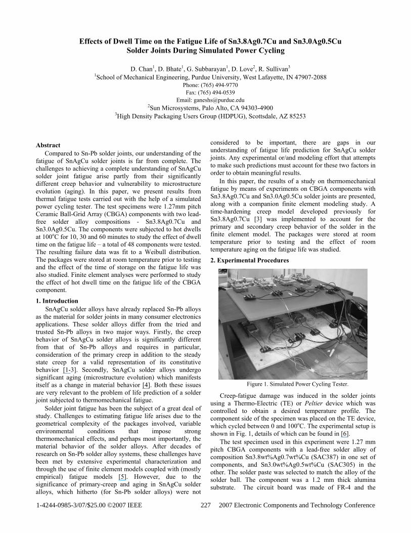
Figure 1. Simulated Power Cycling Tester.
Creep-fatigue damage was induced in the solder joints using a Thermo-Electric (TE) or Peltier device which was controlled to obtain a desired temperature profile. The component side of the specimen was placed on the TE device, which cycled between 0 and 100oC. The experimental setup is shown in Fig. 1, details of which can be found in [6].
The test specimen used in this experiment were 1.27 mm pitch CBGA components with a lead-free solder alloy of composition Sn3.8wt%Ag0.7wt%Cu (SAC387) in one set of components, and Sn3.0wt%Ag0.5wt%Cu (SAC305) in the other. The solder paste was selected to match the alloy of the solder ball. The component was a 1.2 mm thick alumina substrate. The circuit board was made of FR-4 and the
1-4244-0985-3/07/$25.00 ©2007 IEEE 227 2007 Electronic Components and Technology Conference
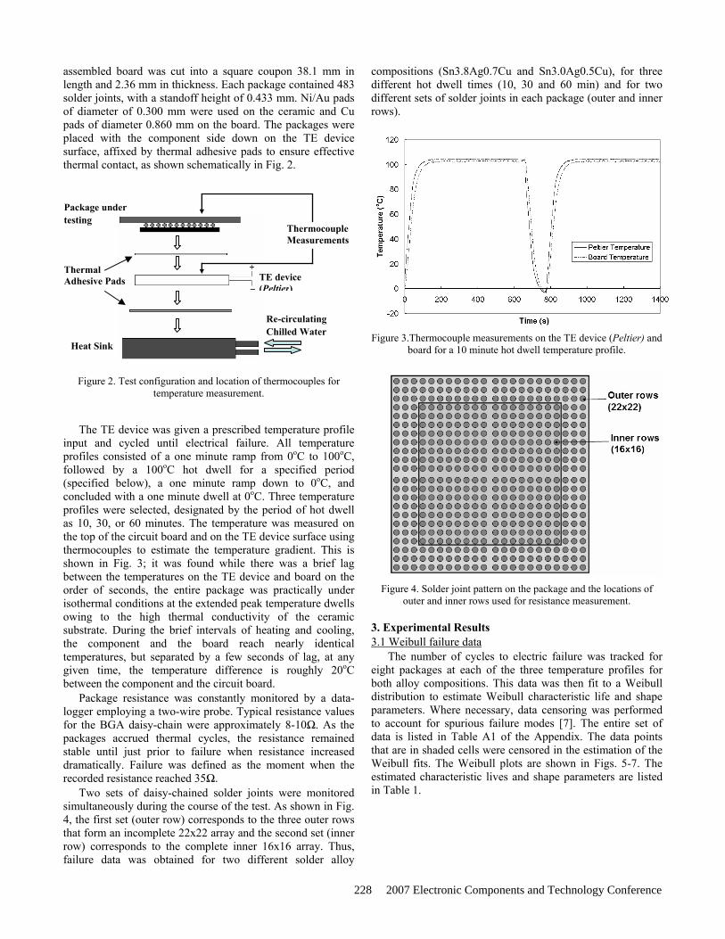
assembled board was cut into a square coupon 38.1 mm in length and 2.36 mm in thickness. Each package contained 483 solder joints, with a standoff height of 0.433 mm. Ni/Au pads of diameter of 0.300 mm were used on the ceramic and Cu pads of diameter 0.860 mm on the board. The packages were placed with the component side down on the TE device surface, affixed by thermal adhesive pads to ensure effective thermal contact, as shown schematically in Fig. 2.
Figure 2. Test configuration and location of thermocouples for temperature measurement.
The TE device was given a prescribed temperature profile
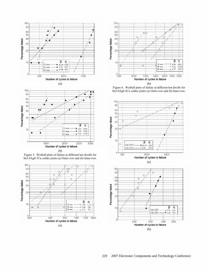
input and cycled until electrical failure. All temperature profiles consisted of a one minute ramp from 0oC to 100oC, followed by a 100oC hot dwell for a specified period (specified below), a one minute ramp down to 0oC, and concluded with a one minute dwell at 0oC. Three temperature profiles were selected, designated by the period of hot dwell as 10, 30, or 60 minutes. The temperature was measured on the top of the circuit board and on the TE device surface using thermocouples to estimate the temperature gradient. This is shown in Fig. 3; it was found while there was a brief lag between the temperatures on the TE device and board on the order of seconds, the entire package was practically under isothermal conditions at the extended peak temperature dwells owing to the high thermal conductivity of the ceramic substrate. During the brief intervals of heating and cooling, the component and the board reach nearly identical temperatures, but separated by a few seconds of lag, at any given time, the temperature difference is roughly 20oC between the component and the circuit board.
Package resistance was constantly monitored by a data-logger employing a two-wire probe. Typical resistance values for the BGA daisy-chain were approximately 8-10Ω. As the packages accrued thermal cycles, the resistance remained stable until just prior to failure when resistance increased dramatically. Failure was defined as the moment when the recorded resistance reached 35Ω.
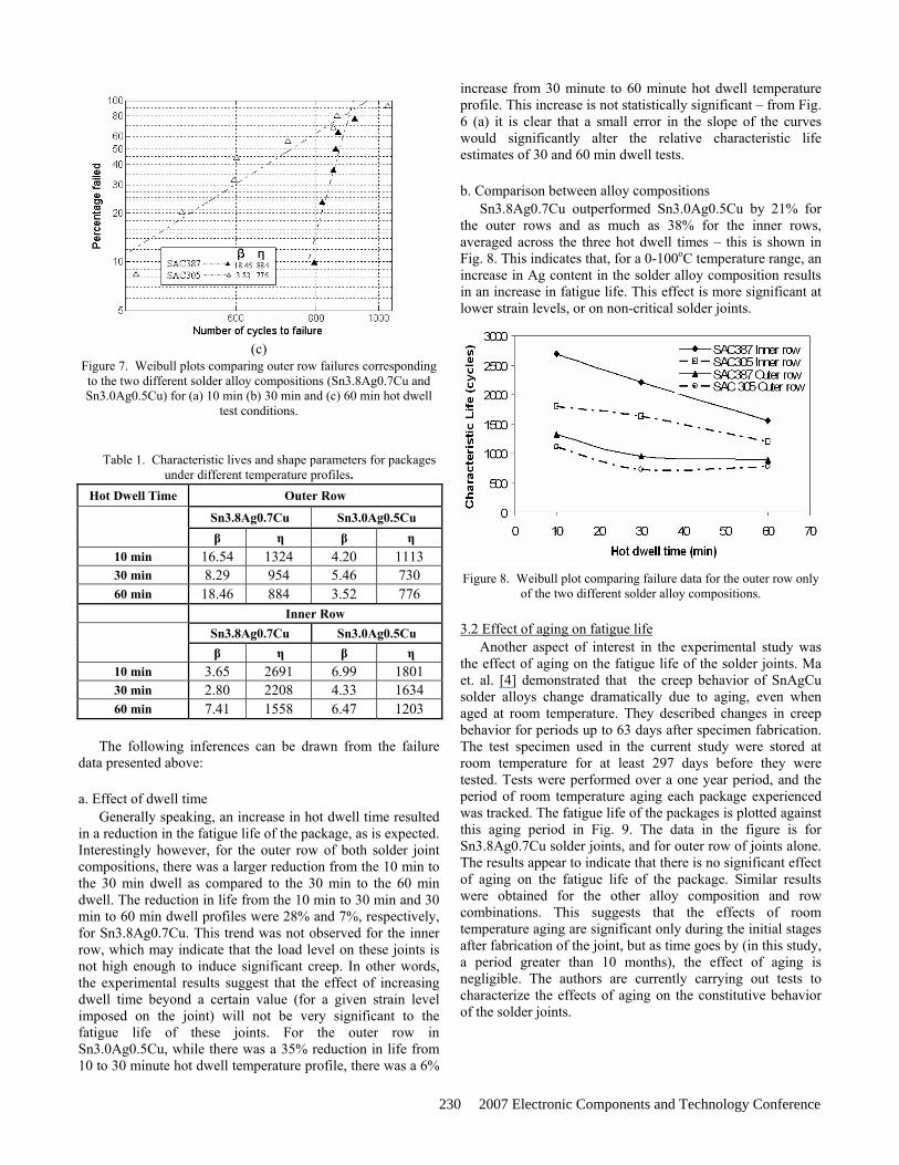
Two sets of daisy-chained solder joints were monitored simultaneously during the course of the test. As shown in Fig. 4, the first set (outer row) corresponds to the three outer rows that form an incomplete 22x22 array and the second set (inner row) corresponds to the complete inner 16x16 array. Thus, failure data was obtained for two different solder alloy
compositions (Sn3.8Ag0.7Cu and Sn3.0Ag0.5Cu), for three different hot dwell times (10, 30 and 60 min) and for two different sets of solder joints in each package (outer and inner rows).
Figure 3.Thermocouple measurements on the TE device (Peltier) and board for a 10 minute hot dwell temperature profile.
Figure 4. Solder joint pattern on the package and the locations of outer and inner rows used for resistance measurement.
3. Experimental Results 3.1 Weibull failure data
The number of cycles to electric failure was tracked for eight packages at each of the three temperature profiles for both alloy compositions. This data was then fit to a Weibull distribution to estimate Weibull characteristic life and shape parameters. Where necessary, data censoring was performed to account for spurious failure modes [7]. The entire set of data is listed in Table A1 of the Appendix. The data points that are in shaded cells were censored in the estimation of the Weibull fits. The Weibull plots are shown in Figs. 5-7. The estimated characteristic lives and shape parameters are listed in Table 1.
TE device (Peltier)
Re-circulating Chilled Water
Package under testing
Heat Sink
Thermal Adhesive Pads
Thermocouple Measurements
228 2007 Electronic Components and Technology Conference
(a)
(b)
Figure 5. Weibull plots of failure at different hot dwells for Sn3.8Ag0.7Cu solder joints (a) Outer row and (b) Inner row.
(a)
(b)
Figure 6. Weibull plots of failure at different hot dwells for Sn3.0Ag0.5Cu solder joints (a) Outer row and (b) Inner row.
(a)
(b)
229 2007 Electronic Components and Technology Conference
(c)
Figure 7. Weibull plots comparing outer row failures corresponding to the two different solder alloy compositions (Sn3.8Ag0.7Cu and Sn3.0Ag0.5Cu) for (a) 10 min (b) 30 min and (c) 60 min hot dwell
test conditions.
Table 1. Characteristic lives and shape parameters for packages
under different temperature profiles. Hot Dwell Time Outer Row
Sn3.8Ag0.7Cu Sn3.0Ag0.5Cu β η β η
10 min 16.54 1324 4.20 1113 30 min 8.29 954 5.46 730 60 min 18.46 884 3.52 776
Inner Row Sn3.8Ag0.7Cu Sn3.0Ag0.5Cu β η β η
10 min 3.65 2691 6.99 1801 30 min 2.80 2208 4.33 1634 60 min 7.41 1558 6.47 1203
The following inferences can be drawn from the failure
data presented above: a. Effect of dwell time
Generally speaking, an increase in hot dwell time resulted in a reduction in the fatigue life of the package, as is expected. Interestingly however, for the outer row of both solder joint compositions, there was a larger reduction from the 10 min to the 30 min dwell as compared to the 30 min to the 60 min dwell. The reduction in life from the 10 min to 30 min and 30 min to 60 min dwell profiles were 28% and 7%, respectively, for Sn3.8Ag0.7Cu. This trend was not observed for the inner row, which may indicate that the load level on these joints is not high enough to induce significant creep. In other words, the experimental results suggest that the effect of increasing dwell time beyond a certain value (for a given strain level imposed on the joint) will not be very significant to the fatigue life of these joints. For the outer row in Sn3.0Ag0.5Cu, while there was a 35% reduction in life from 10 to 30 minute hot dwell temperature profile, there was a 6%
increase from 30 minute to 60 minute hot dwell temperature profile. This increase is not statistically significant – from Fig. 6 (a) it is clear that a small error in the slope of the curves would significantly alter the relative characteristic life estimates of 30 and 60 min dwell tests. b. Comparison between alloy compositions
Sn3.8Ag0.7Cu outperformed Sn3.0Ag0.5Cu by 21% for the outer rows and as much as 38% for the inner rows, averaged across the three hot dwell times – this is shown in Fig. 8. This indicates that, for a 0-100oC temperature range, an increase in Ag content in the solder alloy composition results in an increase in fatigue life. This effect is more significant at lower strain levels, or on non-critical solder joints.
Figure 8. Weibull plot comparing failure data for the outer row only of the two different solder alloy compositions.
3.2 Effect of aging on fatigue life
Another aspect of interest in the experimental study was the effect of aging on the fatigue life of the solder joints. Ma et. al. [4] demonstrated that the creep behavior of SnAgCu solder alloys change dramatically due to aging, even when aged at room temperature. They described changes in creep behavior for periods up to 63 days after specimen fabrication. The test specimen used in the current study were stored at room temperature for at least 297 days before they were tested. Tests were performed over a one year period, and the period of room temperature aging each package experienced was tracked. The fatigue life of the packages is plotted against this aging period in Fig. 9. The data in the figure is for Sn3.8Ag0.7Cu solder joints, and for outer row of joints alone. The results appear to indicate that there is no significant effect of aging on the fatigue life of the package. Similar results were obtained for the other alloy composition and row combinations. This suggests that the effects of room temperature aging are significant only during the initial stages after fabrication of the joint, but as time goes by (in this study, a period greater than 10 months), the effect of aging is negligible. The authors are currently carrying out tests to characterize the effects of aging on the constitutive behavior of the solder joints.
230 2007 Electronic Components and Technology Conference
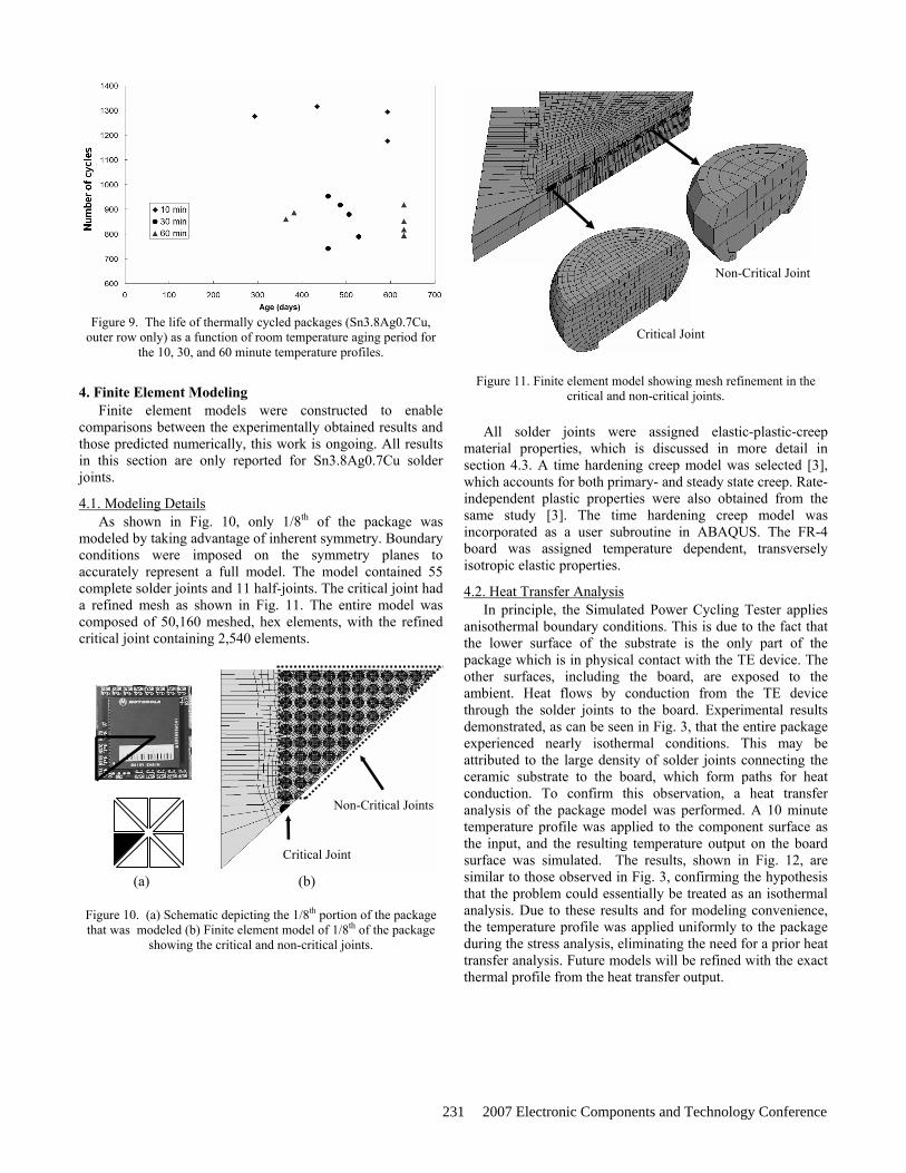
Figure 9. The life of thermally cycled packages (Sn3.8Ag0.7Cu, outer row only) as a function of room temperature aging period for
the 10, 30, and 60 minute temperature profiles.
4. Finite Element Modeling
Finite element models were constructed to enable comparisons between the experimentally obtained results and those predicted numerically, this work is ongoing. All results in this section are only reported for Sn3.8Ag0.7Cu solder joints.
4.1. Modeling Details As shown in Fig. 10, only 1/8th of the package was
modeled by taking advantage of inherent symmetry. Boundary conditions were imposed on the symmetry planes to accurately represent a full model. The model contained 55 complete solder joints and 11 half-joints. The critical joint had a refined mesh as shown in Fig. 11. The entire model was composed of 50,160 meshed, hex elements, with the refined critical joint containing 2,540 elements.
(a) (b)
Figure 10. (a) Schematic depicting the 1/8th portion of the package that was modeled (b) Finite element model of 1/8th of the package
showing the critical and non-critical joints.
Figure 11. Finite element model showing mesh refinement in the critical and non-critical joints.
All solder joints were assigned elastic-plastic-creep
material properties, which is discussed in more detail in section 4.3. A time hardening creep model was selected [3], which accounts for both primary- and steady state creep. Rate-independent plastic properties were also obtained from the same study [3]. The time hardening creep model was incorporated as a user subroutine in ABAQUS. The FR-4 board was assigned temperature dependent, transversely isotropic elastic properties.
4.2. Heat Transfer Analysis In principle, the Simulated Power Cycling Tester applies
anisothermal boundary conditions. This is due to the fact that the lower surface of the substrate is the only part of the package which is in physical contact with the TE device. The other surfaces, including the board, are exposed to the ambient. Heat flows by conduction from the TE device through the solder joints to the board. Experimental results demonstrated, as can be seen in Fig. 3, that the entire package experienced nearly isothermal conditions. This may be attributed to the large density of solder joints connecting the ceramic substrate to the board, which form paths for heat conduction. To confirm this observation, a heat transfer analysis of the package model was performed. A 10 minute temperature profile was applied to the component surface as the input, and the resulting temperature output on the board surface was simulated. The results, shown in Fig. 12, are similar to those observed in Fig. 3, confirming the hypothesis that the problem could essentially be treated as an isothermal analysis. Due to these results and for modeling convenience, the temperature profile was applied uniformly to the package during the stress analysis, eliminating the need for a prior heat transfer analysis. Future models will be refined with the exact thermal profile from the heat transfer output.
Critical Joint
Non-Critical Joint
Critical Joint
Non-Critical Joints
231 2007 Electronic Components and Technology Conference
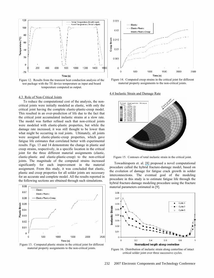
Figure 12. Results from the transient heat conduction analysis of the
test package with the TE device temperature as input and board temperature computed as output.
4.3. Role of Non-Critical Joints To reduce the computational cost of the analysis, the non-
critical joints were initially modeled as elastic, with only the critical joint having the complete elastic-plastic-creep model. This resulted in an over-prediction of life due to the fact that the critical joint accumulated inelastic strains at a slow rate. The model was further refined such that non-critical joints were modeled with elastic-plastic properties, but while the damage rate increased, it was still thought to be lower than what might be occurring in real joints. Ultimately, all joints were assigned elastic-plastic-creep properties, which gave fatigue life estimates that correlated better with experimental results. Figs. 13 and 14 demonstrate the change in plastic and creep strains, respectively, in a specific location in the critical joint for the three different material assignments (elastic, elastic-plastic and elastic-plastic-creep) to the non-critical joints. The magnitude of the computed strains increased significantly for each improvement in the material assignment. From this study, it was concluded that elastic, plastic and creep properties for all solder joints are necessary for an accurate and complete model. All the results reported in the following sections are obtained through such simulations.
Figure 13. Computed plastic strains in the critical joint for different
material property assignments to the non-critical joints.
Figure 14. Computed creep strains in the critical joint for different
material property assignments to the non-critical joints.
4.4 Inelastic Strain and Damage Rate
Figure 15. Contours of total inelastic strain in the critical joint.
Towashiraporn et. al. [8] proposed a novel computational procedure called the hybrid fracture-damage model, based on the evolution of damage for fatigue crack growth in solder interconnections. The eventual goal of the modeling procedure in this study is to estimate fatigue life through the hybrid fracture-damage modeling procedure using the fracture material parameters estimated in [9].
Figure 16. Distribution of inelastic strain along centerline of intact
critical solder joint over three successive cycles.
232 2007 Electronic Components and Technology Conference
A key requirement of the hybrid modeling approach is the accurate computation of inelastic strains in the critical solder joint at the interface of interest. The evolution of these strains over a few simulated cycles allows extrapolation to a much larger number of cycles [8]. The distribution of inelastic strains in the critical solder joint on the component side, is shown in Fig. 15. The evolution of the total inelastic strain over three cycles is shown in Fig. 16. The accumulation of inelastic strain, in general, occurs at different rates at different material points in the solder joint and will change as the crack starts to propagate. As a result, it is important that the inelastic strains be tracked at every point at the interface where the fatigue crack propagation is to be simulated.
Figure 17. Rate of damage change along the centerline during crack growth: the rate is constant until approximately 0.7 normalized crack
length, after which the rate of damage increases exponentially [8].
The computation of inelastic strain allows for the estimation of a damage measure at each node at the interface [8]. It is this damage measure that is used in the fracture criterion. Typically, as shown in [8] and reproduced in Fig. 17 here, the rate of change of damage per cycle is constant for the majority of the life of the solder joint, corresponding to a normalized crack length of approximately 0.7. Beyond this point, the damage accumulates exponentially and the crack progresses rapidly. These details are not obtained from the application of a Coffin-Manson type life model.
5. Summary This study focused on addressing the effects of dwell time
and aging on the prediction of fatigue life in a solder joint. The key contributions of this study are summarized below:
i. The results of the experimental study suggest that, for the SnAgCu solder compositions studied, increasing hot dwell times beyond a certain limit is unlikely to have a significant effect on the fatigue life of the package. This time limit is determined by the strain level imposed on the critical solder joint.
ii. Aging at room temperature beyond a period of (at least) 10 months does not seem to have a significant effect on the fatigue life of SnAgCu solder joints.
iii. For a 0-100oC temperature range, an increase in Ag content in the solder alloy composition (from 3.0 % to 3.8 %) results in an increase in fatigue life, which is
more significant at lower strain levels corresponding to non-critical solder joints.
iv. Although the Simulated Power Cycling Tester generates anisothermal conditions in principle, in packages with high solder joint density, the problem may be effectively modeled as an isothermal one. This can be verified using thermocouples during testing and via a finite element heat transfer analysis.
v. In the finite element modeling study, it was found that a complete consideration of the creep behavior in all joints, including the non-critical ones, is essential for an accurate estimation of damage accumulation.
Finite element modeling is in progress to predict fatigue life non-empirically and study the effect of dwell time.
Acknowledgments The first four authors dedicate this paper to our co-author,
colleague and friend, Bob Sullivan, who unexpectedly passed away during the course of this project. The authors would also like to thank the High Density Packaging Users’ Group (HDPUG) for financial and technical support as well as providing assembled components for testing.
References 1. Plumbridge, W.J., “The analysis of creep data for solder
alloys,” Soldering & Surface Mount Technology, Vol. 15, No. 1 (2003), pp. 26–30.
2. J.-P. Clech, “An Extension of the Omega Method to Primary and Tertiary Creep of Lead-Free Solders,” Proceedings of Electronic Components and Technology Conference, 2005.
3. Bhate, D., Chan, D., Subbarayan, G., Chiu, T.C, Gupta, V., Edwards, D., “Creep and Low Strain Rate Behavior of Sn3.8Ag0.7Cu and Sn1.0Ag0.5Cu Alloys: Development of Valid Constitutive Models,” submitted to IEEE Transactions on Components and Packaging Technologies.
4. Ma H., Suhling, J.C., Lall, P., Bozack, M.J. “Reliability of the Aging Lead Free Solder Joint,” Proceedings of Electronic Components and Technology Conference, 2006, pp. 849-864.
5. Lee, W.W., Nguyen, L.T., Selvaduray, G.S., “Solder joint fatigue models: review and applicability to chip scale packages”, Microelectronics Reliability, Vol. 40, No. 2 (2000), pp. 231-244.
6. Setty, K., Subbarayan, G., Nguyen, L., “Powercycling Reliability, Failure Analysis and Acceleration Factors of Pb-free Solder Joints”, Proc. Electronic Components and Technology Conference, 2005, pp. 907-915.
7. O’Connor, P.D.T, Practical Reliability Engineering, John Wiley and Sons, Ltd. (West Sussex, England, 2002), pp. 84-85.
8. Towashiraporn P., Subbarayan G.S., Desai C.S., “A hybrid model for computationally efficient fatigue fracture simulations at microelectronic assembly interfaces”, International Journal of Solids and Structures, Vol. 42 (2005), pp. 4468-4483.
9. Bhate, D., Chan, D., Subbarayan, G., Chiu, T.C, Gupta, V., Edwards, D., “Fatigue Crack Growth and Life Descriptions of Sn3.8Ag0.7Cu Solder Joints: A
233 2007 Electronic Components and Technology Conference
Computational and Experimental Study,” to be presented at the Electronics Components and Technology Conference, Reno, NV, 2006.
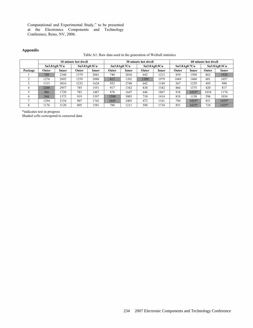
Appendix Table A1: Raw data used in the generation of Weibull statistics
10 minute hot dwell 30 minute hot dwell 60 minute hot dwell Sn3.8Ag0.7Cu Sn3.0Ag0.5Cu Sn3.8Ag0.7Cu Sn3.0Ag0.5Cu Sn3.8Ag0.7Cu Sn3.0Ag0.5Cu
Package Outer Inner Outer Inner Outer Inner Outer Inner Outer Inner Outer Inner 1 749 2340 1379 2041 740 2036 642 1213 859 1509 862 1920 2 1276 2692 1259 2088 417 1202 1399 1979 1069 1460 601 1057 3 1315 3016 1232 1624 952 2748 642 1149 567 1229 495 990 4 2260 2957 785 1551 917 1342 838 1342 866 1375 420 817 5 586 1720 783 1487 878 1647 646 1867 918 1435* 1034 1174 6 568 1375 919 1397 1580 3003 710 1414 818 1150 596 1034 7 1294 2154 907 1742 1645 2405 472 1161 794 1435* 851 1435* 8 1176 3120 805 1581 788 1211 588 1734 851 1435* 724 1435*
*indicates test in progress Shaded cells correspond to censored data
234 2007 Electronic Components and Technology Conference