effect of rapid thermal annealing on nanocrystalline tio2 thin films synthesized by swift heavy ion...
TRANSCRIPT

This article appeared in a journal published by Elsevier. The attachedcopy is furnished to the author for internal non-commercial researchand education use, including for instruction at the authors institution
and sharing with colleagues.
Other uses, including reproduction and distribution, or selling orlicensing copies, or posting to personal, institutional or third party
websites are prohibited.
In most cases authors are permitted to post their version of thearticle (e.g. in Word or Tex form) to their personal website orinstitutional repository. Authors requiring further information
regarding Elsevier’s archiving and manuscript policies areencouraged to visit:
http://www.elsevier.com/copyright

Author's personal copy
Applied Surface Science 258 (2012) 7855– 7859
Contents lists available at SciVerse ScienceDirect
Applied Surface Science
j our nal ho me p age: www.elsev ier .com/ loc ate /apsusc
Effect of rapid thermal annealing on nanocrystalline TiO2 thin films synthesizedby swift heavy ion irradiation
Madhavi Thakurdesaia,∗, D. Kanjilalb, Varsha Bhattacharyyaa
a Department of Physics, University of Mumbai, Santa Cruz (E), Mumbai 400098, Indiab Inter University Accelerator Centre, Aruna Asaf Ali Marg, New Delhi 110067, India
a r t i c l e i n f o
Article history:Received 24 October 2011Received in revised form 10 April 2012Accepted 13 April 2012Available online 3 May 2012
Keywords:TiO2 nanoparticlesElectronic excitationRTA annealing
a b s t r a c t
Irradiation by swift heavy ions (SHI) is unique tool to synthesize nanocrystalline thin films. We havereported transformation of 100 nm thick amorphous films into nanocrystalline film due to irradiation by100 MeV Ag ion beam. Oblate shaped nanoparticles having anatase phase of TiO2 were formed on thesurface of the irradiated films. In the present investigation, these films are annealed at 350 ◦C for 2 min inoxygen atmosphere by Rapid Thermal Annealing (RTA) method. During RTA processing, the temperaturerises abruptly and this thermal instability is expected to alter surface morphology, structural and opticalproperties of nanocrystalline TiO2 thin films. Thus in the present work, effect of RTA on SHI inducednanocrystalline thin films of TiO2 is studied. The effect of RTA processing on the shape and size of TiO2
nanoparticles is studied by Atomic Force Microscopy (AFM) and Scanning Electron Microscopy (SEM).Glancing Angle X-ray Diffraction (GAXRD) studies are carried to investigate structural changes induced byRTA processing. Optical characterization is carried out by UV–vis spectroscopy and photoluminescence(PL) spectroscopy. The changes observed in structural and optical properties of nanocrystalline TiO2 thinfilms after RTA processing are attributed to the annihilation of SHI induced defects.
© 2012 Elsevier B.V. All rights reserved.
1. Introduction
TiO2 is an important wide band gap semiconductor which hasthree crystalline polymorphs namely rutile, anatase and brookite.Currently nanocrystalline TiO2 films are widely synthesized due totheir wide technological applications in the field of photovoltaic,photochromic devices, thin film solar cells, gas and humidity sen-sors, etc. [1,2]. Irradiation by swift heavy ions (SHI) at MeV energiesis an excellent tool for nanostructuring of thin films [3,4].
Swift heavy ions lose energy in materials mainly via inelasticcollisions with the atomic electrons. Along the trajectory of ion,a trail of defects known as latent track may be formed depend-ing on the type of the ion, its energy and the physical property ofthe materials [5]. During irradiation a large amount of energy getsconfined almost instantaneously along the latent track of nanomet-ric dimensions. This leads to the formation of molten state alongthe latent track. Depending upon the surface properties, nanosizedhillocks are formed on the surface from the ion-induced melt dueto mechanical stresses arising from the thermal expansion [3,6,7].
∗ Corresponding author. Present address: Department of Physics, Birla College,Kalyan 421304, India. Tel.: +91 0251 2230740; fax: +91 0251 2231029.
E-mail addresses: [email protected], [email protected](M. Thakurdesai).
The process of amorphous to nanocrystalline phase transition isdiscussed more rigorously else where [3,4,8–10]
We have reported transformation of amorphous thin films ofTiO2 into nanocrystalline films by using SHI irradiation [3]. Forma-tion of oblate nano-hillocks on the surface TiO2 films was observedwhen the films were irradiated by 100 MeV Ag ion beam at a fluenceof 1 × 10¹² ions cm−2 and 1 × 10¹³ ions cm−2. The phase of thesenanocrystalline films was mainly anatase. Ag ion induced defectsin observed amorphous to nanocrystalline phase transformationhelp in process of nucleation [8,9]. However further step of ther-mal annealing is sometimes necessary to annihilate the SHI induceddefects as this excessive defect concentration may influence thefilm properties [11].
It is reported that in case of TiO2, thermal annealing often resultsin phase transformation and physicochemical properties of TiO2 arealtered. Also the stability of surface features of the nanocrystallineTiO2 films on thermal annealing are of key importance since theydetermine the technological impact of surface interaction with thesurroundings [12].
Thus to examine the effect of temperature variation on thestability of the nanostructures formed on the surface, these SHI irra-diated films are processed by Rapid Thermal Annealing (RTA). RTAis popular annealing method in semiconductor processing as it is ashort time technique due to fast rise in temperature [13]. Also RTAprocessing improves the crystalline quality of the film and anneals
0169-4332/$ – see front matter © 2012 Elsevier B.V. All rights reserved.http://dx.doi.org/10.1016/j.apsusc.2012.04.089

Author's personal copy
7856 M. Thakurdesai et al. / Applied Surface Science 258 (2012) 7855– 7859
the defects [14]. Aim of present work is to study the effect of RTAprocessing on grain size and shape, structural and optical propertiesof nanodimentional TiO2 films synthesized by SHI irradiation.
2. Experimental
2.1. Synthesis of nanocrystalline TiO2 films
In the present investigation 100 nm thick films of TiO2 weredeposited using Pulsed Laser Deposition (PLD) method on fusedsilica substrate in oxygen atmosphere. These PLD deposited thinfilms were irradiated by 100 MeV Ag ion beam at a fluence of1 × 1012 ions cm−2 and 1 × 10¹³ ions cm−2 using 16 MV pelletronfacility at IUAC, New Delhi, India. The details of film deposition andirradiation process are described in detail elsewhere [3].
2.2. The RTA processing
The irradiated films were subsequently annealed by RTA methodusing indigenously built RTA system developed in the Departmentof Physics, University of Mumbai. The heating rate was approxi-mately 120 ◦C/s. The irradiated films were annealed at 350 ◦C for2 min. Oxygen gas was passed through out the heating and coolingprocess.
The surface morphology of the films before and after RTAprocessing is studied by Atomic Force Microscopy (AFM) usingNanoscope III. The surface of the films after RTA processing isalso studied by Scanning Electron Microscopy (SEM) using JEOLJSM 840 scanning microscope. The phase identification beforeand after RTA processing is carried out by Glancing Angle X-Ray Diffraction (GAXRD) using Bruker D8 diffractometer. Opticalabsorption studies are carried by UV–vis spectroscopy using CARY5000 double beam photospectrometer and photoluminescence(PL-spectroscopy) using spectrofluorimeter SPEX-Fluorolog.
3. Results
3.1. AFM study
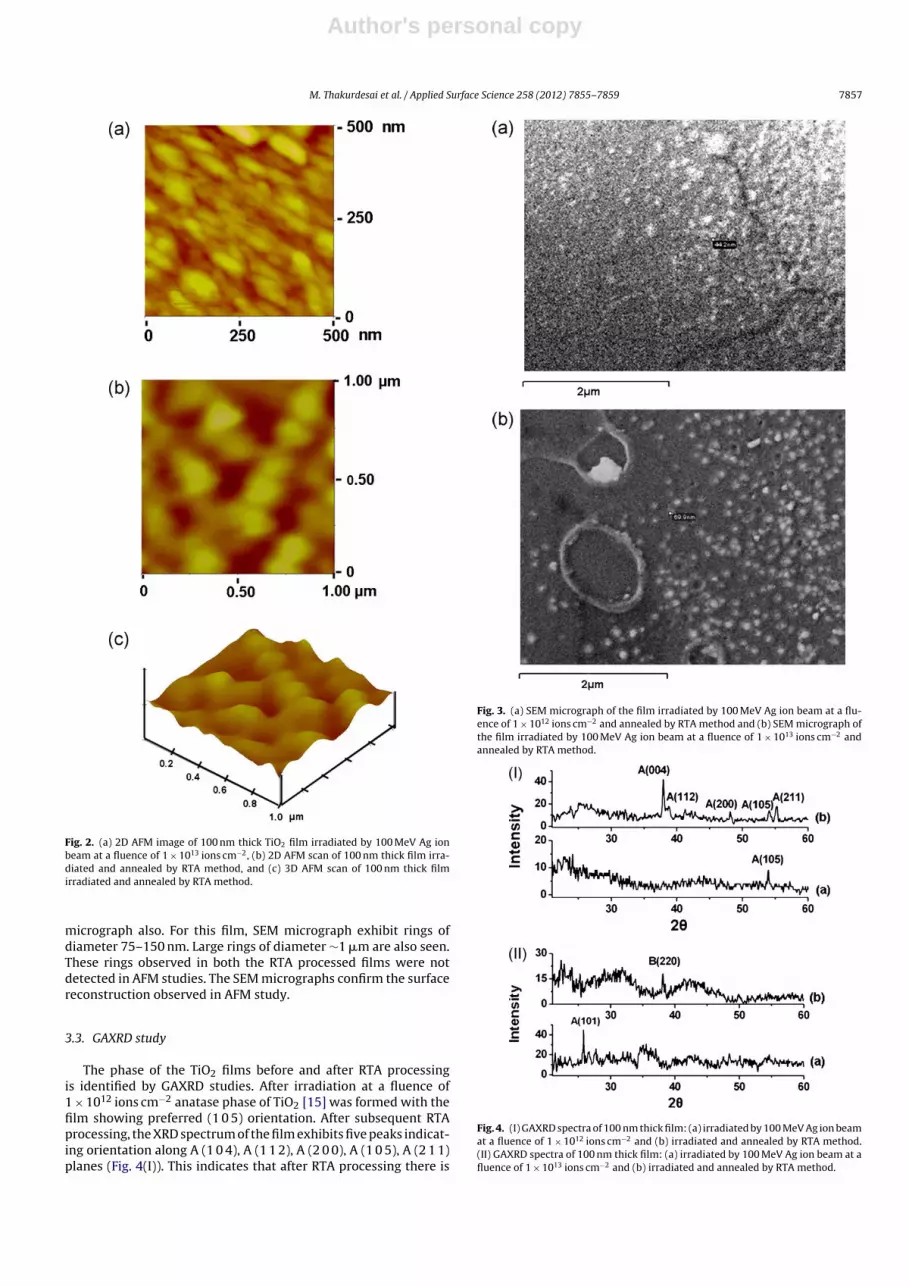
Fig. 1(a) shows 2-D AFM images of film irradiated at a flu-ence of 1 × 10¹² ions cm−2. Oblate particles having diameter 25 nmalong semiminor axis and 60 nm along semimajor axis were seenon the surface. After RTA processing, shape of particles changesfrom oblate to circular and the particle radius reduces to ∼20 nm[Fig. 1(b) and (c)]. There is no significant change in surface rough-ness value after RTA processing.
Fig. 2(a) shows 2-D AFM image of film irradiated at fluence of1 × 1013 ions cm−2. Elongated particles having large aspect ratio(30 nm along semiminor axis and 80 nm along semimajor axis) areseen on the surface. After annealing by RTA method these oblateparticles merge into each other and form large circular clusters hav-ing diameter ∼200 nm [Fig. 2(c)]. In this film also surface roughnessvalue does not change significantly.
It can be inferred that both the films underwent surface recon-struction during the RTA process. In the film irradiated at a fluenceof 1 × 10¹² ions cm−2 the grain fragmentation is observed due toRTA processing. On the other hand in the film irradiated at a fluenceof 1 × 10¹³ ions cm−2 grains merged into each other as an effect ofRTA processing.
To our opinion, the fragmentation of grains occurred in both thefilms as a result of RTA processing. The grains in the film irradi-ated at a fluence of 1 × 10¹² ions cm−2 were initially separate. Thussmaller grains formed after RTA processing remain separate fromeach other.
Fig. 1. (a) 2D AFM image of 100 nm thick TiO2 film irradiated by 100 MeV Ag ionbeam at a fluence of 1 × 10¹² ions cm−2, (b) 2D AFM image of 100 nm thick filmirradiated and annealed by RTA method, and (c) 3D AFM image of 100 nm thick filmirradiated and annealed by RTA method.
However, the grains in the film irradiated at a fluence of1 × 1013 ions cm−2 were very close to each other before RTA pro-cessing. Thus the smaller grains formed after RTA processing, againmerged into each other to form big clusters.
3.2. SEM study
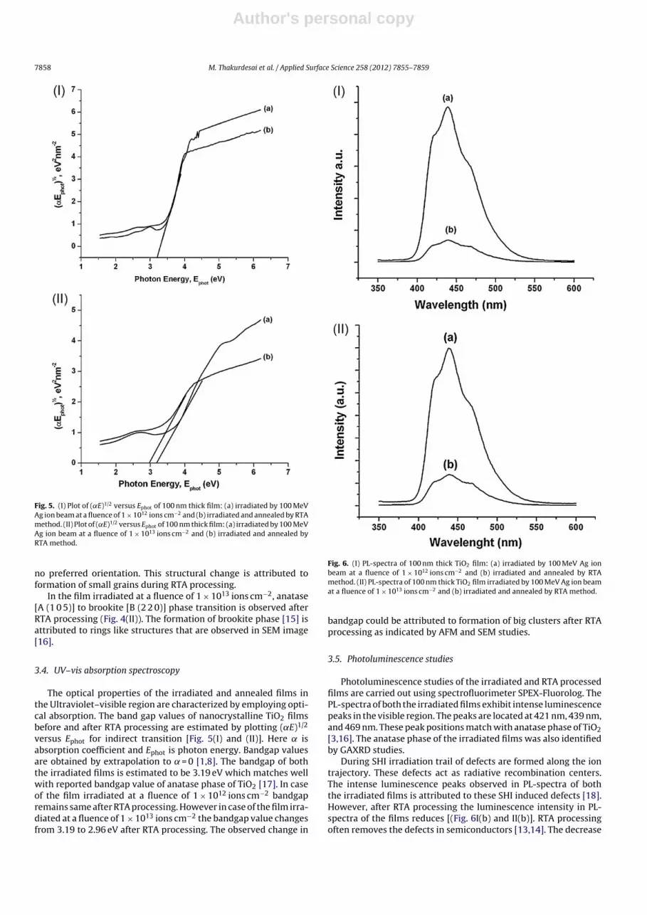
Fig. 3(a) shows SEM micrograph of the film irradiated at a fluenceof 1 × 10¹² ions cm−2 and subsequently annealed by RTA method.As seen in AFM study, SEM images too show small clusters of radius∼22 nm. Further SEM image also shows formation of small tinyrings all over the surface. The diameter of these rings is estimatedto be ∼60 nm. Fig. 3(b) shows SEM micrograph of the film irradi-ated at a fluence of 1 × 10¹³ ions cm−2 and subsequently annealedby RTA method. The surface of these films shows mixed features.As seen in AFM images, clusters of size ∼60 nm are seen in SEM
Author's personal copy
M. Thakurdesai et al. / Applied Surface Science 258 (2012) 7855– 7859 7857
Fig. 2. (a) 2D AFM image of 100 nm thick TiO2 film irradiated by 100 MeV Ag ionbeam at a fluence of 1 × 10¹³ ions cm−2, (b) 2D AFM scan of 100 nm thick film irra-diated and annealed by RTA method, and (c) 3D AFM scan of 100 nm thick filmirradiated and annealed by RTA method.
micrograph also. For this film, SEM micrograph exhibit rings ofdiameter 75–150 nm. Large rings of diameter ∼1 �m are also seen.These rings observed in both the RTA processed films were notdetected in AFM studies. The SEM micrographs confirm the surfacereconstruction observed in AFM study.
3.3. GAXRD study
The phase of the TiO2 films before and after RTA processingis identified by GAXRD studies. After irradiation at a fluence of1 × 1012 ions cm−2 anatase phase of TiO2 [15] was formed with thefilm showing preferred (1 0 5) orientation. After subsequent RTAprocessing, the XRD spectrum of the film exhibits five peaks indicat-ing orientation along A (1 0 4), A (1 1 2), A (2 0 0), A (1 0 5), A (2 1 1)planes (Fig. 4(I)). This indicates that after RTA processing there is
Fig. 3. (a) SEM micrograph of the film irradiated by 100 MeV Ag ion beam at a flu-ence of 1 × 10¹² ions cm−2 and annealed by RTA method and (b) SEM micrograph ofthe film irradiated by 100 MeV Ag ion beam at a fluence of 1 × 10¹³ ions cm−2 andannealed by RTA method.
Fig. 4. (I) GAXRD spectra of 100 nm thick film: (a) irradiated by 100 MeV Ag ion beamat a fluence of 1 × 10¹² ions cm−2 and (b) irradiated and annealed by RTA method.(II) GAXRD spectra of 100 nm thick film: (a) irradiated by 100 MeV Ag ion beam at afluence of 1 × 10¹³ ions cm−2 and (b) irradiated and annealed by RTA method.
Author's personal copy
7858 M. Thakurdesai et al. / Applied Surface Science 258 (2012) 7855– 7859
Fig. 5. (I) Plot of (˛E)1/2 versus Ephot of 100 nm thick film: (a) irradiated by 100 MeVAg ion beam at a fluence of 1 × 10¹² ions cm−2 and (b) irradiated and annealed by RTAmethod. (II) Plot of (˛E)1/2 versus Ephot of 100 nm thick film: (a) irradiated by 100 MeVAg ion beam at a fluence of 1 × 10¹³ ions cm−2 and (b) irradiated and annealed byRTA method.
no preferred orientation. This structural change is attributed toformation of small grains during RTA processing.
In the film irradiated at a fluence of 1 × 10¹³ ions cm−2, anatase[A (1 0 5)] to brookite [B (2 2 0)] phase transition is observed afterRTA processing (Fig. 4(II)). The formation of brookite phase [15] isattributed to rings like structures that are observed in SEM image[16].
3.4. UV–vis absorption spectroscopy
The optical properties of the irradiated and annealed films inthe Ultraviolet–visible region are characterized by employing opti-cal absorption. The band gap values of nanocrystalline TiO2 filmsbefore and after RTA processing are estimated by plotting (˛E)1/2
versus Ephot for indirect transition [Fig. 5(I) and (II)]. Here ̨ isabsorption coefficient and Ephot is photon energy. Bandgap valuesare obtained by extrapolation to ̨ = 0 [1,8]. The bandgap of boththe irradiated films is estimated to be 3.19 eV which matches wellwith reported bandgap value of anatase phase of TiO2 [17]. In caseof the film irradiated at a fluence of 1 × 10¹² ions cm−2 bandgapremains same after RTA processing. However in case of the film irra-diated at a fluence of 1 × 10¹³ ions cm−2 the bandgap value changesfrom 3.19 to 2.96 eV after RTA processing. The observed change in
Fig. 6. (I) PL-spectra of 100 nm thick TiO2 film: (a) irradiated by 100 MeV Ag ionbeam at a fluence of 1 × 10¹² ions cm−2 and (b) irradiated and annealed by RTAmethod. (II) PL-spectra of 100 nm thick TiO2 film irradiated by 100 MeV Ag ion beamat a fluence of 1 × 10¹³ ions cm−2 and (b) irradiated and annealed by RTA method.
bandgap could be attributed to formation of big clusters after RTAprocessing as indicated by AFM and SEM studies.
3.5. Photoluminescence studies
Photoluminescence studies of the irradiated and RTA processedfilms are carried out using spectrofluorimeter SPEX-Fluorolog. ThePL-spectra of both the irradiated films exhibit intense luminescencepeaks in the visible region. The peaks are located at 421 nm, 439 nm,and 469 nm. These peak positions match with anatase phase of TiO2[3,16]. The anatase phase of the irradiated films was also identifiedby GAXRD studies.
During SHI irradiation trail of defects are formed along the iontrajectory. These defects act as radiative recombination centers.The intense luminescence peaks observed in PL-spectra of boththe irradiated films is attributed to these SHI induced defects [18].However, after RTA processing the luminescence intensity in PL-spectra of the films reduces [(Fig. 6I(b) and II(b)]. RTA processingoften removes the defects in semiconductors [13,14]. The decrease
Author's personal copy
M. Thakurdesai et al. / Applied Surface Science 258 (2012) 7855– 7859 7859
in luminescence intensity after RTA processing indicates that RTAprocessing has annihilated most of the SHI induced defects.
4. Conclusion
The 100 nm thick films of TiO2 irradiated by Ag ion beamat a fluence of 1 × 10¹² ions cm−2 and 1 × 10¹³ ions cm−2 responddifferently to Rapid Thermal Annealing (RTA). In case of thefilm irradiated at a fluence of 1 × 10¹² ions cm−2 oblate particlestransform to circular nanoparticles of radius ∼20 nm after RTAprocessing. Though preferential orientation of the film changesafter RTA processing the phase of the film does not change. In thefilm irradiated at a fluence of 1 × 10¹³ ions cm−2 oblate nanopar-ticles formed after irradiation merge after RTA processing. Thisfilm undergoes structural transformation after RTA processing. Thebandgap value of this film also changes due to cluster formationafter RTA processing. The luminescence intensity in PL-spectra ofboth the films reduces after RTA processing indicating defect anni-hilation. The structural and optical changes observed after RTAprocessing are attributed to the annihilation of swift heavy ioninduced defects.
Acknowledgements
Authors are grateful to IUAC (Inter University Accelerator Cen-tre), New Delhi for beamtime allotment. Authors are also grateful toDST, India for providing AFM and GAXRD facility at IUAC New Delhi,India under IRPHA project. Authors are thankful to Dr. Pratap Ray-chaudhury, TIFR Mumbai for providing the PLD facility. One of theauthors (M.T.) wants to thank UGC, New Delhi for the award of FIPleave.
References
[1] T. Nambara, K. Yoshida, L. Miao, S. Tanemura, N. Tanaka, Thin Solid Films 515(3096) (2007).
[2] R. Zallen, M.P. Moret, Solid State Communications 137 (2006) 154.[3] M. Thakurdesai, D. Kanjilal, V. Bhattacharyya, Applied Surface Science 254
(2008) 4695.[4] A. Audouard, E. Balanzat, J.C. Jousset, D. Lesueur, L. Thome, Journal of Physics:
Condensed Matter 5 (1993) 995.[5] J. Kaur, S. Singh, D. Kanjial, S.K. Chakravarty, Digest Journal of Nanomaterials
and Biostructures 4 (2009) 729.[6] G. Szenes, Nuclear Instruments and Methods in Physics Research Section B 191
(2002) 27.[7] P. The Venard, J.P. Dupin, V.T. Binh, S.T. Purcell, V. Semet, D. Guillot, Nuclear
Instruments and Methods in Physics Research Section B 166–167 (2000)788.
[8] M. Thakurdesai, T. Mohanty, J. John, T.K. Gundu Rao, P. Raychaudhuri, V. Bhat-tacharyya, D. Kanjilal, Journal of Nanoscience and Nanotechnology 8 (2008)4231.
[9] T. Mohanty, P.V. Satyam, D. Kanjilal, Journal of Nanoscience and Nanotechnol-ogy 6 (2006) 2554.
[10] M. Kumar, P.G. Ganesan, V.N. Singh, B.R. Mehta, J.P. Singh, Nanotechnology 19(2008) 175606.
[11] I.M. Dharmadasa, G.J. Tolan, M. Cazaux, Semiconductor Science and Technology23 (2008) 3.
[12] I.N. Kholmanov, E. Barborini, S. Vinati, P. Piseri, A. Podesta, C. Ducati, C. Lenardi,P. Milani, Nanotechnology 14 (2003) 1168.
[13] F. Liua, C. Yanga, T. Rena, A.Z. Wangb, J. Yuc, L. Liua, Journal of Magnetism andMagnetic Materials 309 (2007) 75–79.
[14] B. Liu, J. Gao, K.M. Wu, C. Liu, Solid State Communications 149 (2009) 715.[15] JCPDS Powder X-ray Data Sheet.[16] D. Pan, N. Zhao, Q. Wang, S. Jiang, X. Ji, L. An, Advanced Materials 17 (2005)
1991.[17] D. Luca, L.S. Hsu, Journal of Optoelectronics and Advanced Materials 5 (2003)
835.[18] M. Kumar, F. Singh, S.A. Khan, A. Tripathi, D.K. Avasthi, Journal of Physics D:
Applied Physics 39 (2006) 2935.