effect of hpht annealing on the photoluminescence of synthetic diamonds grown in the fe–ni–c...
TRANSCRIPT
Diamond and Related Materials 12(2003) 2147–2168
0925-9635/03/$ - see front matter� 2003 Elsevier B.V. All rights reserved.doi:10.1016/S0925-9635(03)00256-5
Effect of HPHT annealing on the photoluminescence of syntheticdiamonds grown in the Fe–Ni–C system
A. Yelisseyev *, S. Lawson , I. Sildos , A. Osvet , V. Nadolinny , B. Feigelson , J.M. Baker ,a, b c c d e f
M. Newton , O. Yuryevag d
Institute of Mineralogy and Petrography SB RAS, Novosibirsk 630090, Russiaa
DTC Research Centre, Belmont Road Maidenhead SL6 6JW, UKb
Institute of Physics, Tartu, Estoniac
Institute of Inorganic Chemistry SB RAS, Novosibirsk 630090, Russiad
Research centre «Basis», 12 Fakultetsky per., Moscow 125080, Russiae
Department of Physics, University of Oxford, Clarendon Laboratory, Parks Road, Oxford OX1 3PU, UKf
Department of Physics, University of Warwick, Coventry CV4 7AL, UKg
Received 16 November 2001; accepted 3 July 2003
Abstract
The photoluminescence(PL) spectra of synthetic diamonds(SD) containing high concentrations of nitrogen and nickelimpurities have been examined in both as-grown samples and the ones annealed at 1950 or 2200 K. A large number of zero-phonon lines(ZPLs), including two tens of vibronic PL systems, have been identified and their behaviour on annealing has beenstudied, one-third of documented lines have also been observed in natural diamonds. An analysis of their behaviour on annealingallows their division into three main groups, namely:(I) The systems present in as-grown SD, but which disappear after annealingat 1950 K;(II) The systems, which appear after annealing at approximately 1950 K, but their intensity is lower or they disappearcompletely after annealing at 2200 K;(III ) The system, whose intensity increases after annealing at 1950 K and does not decreaseafter further annealing at 2200 K. A combined optical and ESR study allowed one to identify the systems of group I withindividual impurities, whereas the items within group III were associated with nickel–nitrogen complexes containing a singlenickel ion in the divacancy position surrounded by a few(nG2) nitrogen atoms. The systems within group II are related to arelaxed single nickel defect(nickel ion in divacancy position) and simple nickel–nitrogen complexes, containing a single nitrogenatom. The PL excitation spectra were measured for 15 most intense PL systems. A broad absorption band in the annealed SD,with a peak approximately 450 nm and a superimposed fine structure, was decomposed into individual components, related to theNE1, NE2 and NE3 paramagnetic centres. The lower excited states of these three centres are split withDEs125 meV, 62 meVand 221 meV, respectively, while the spin-allowed electronic transitions take place only to the upper sublevel.� 2003 Elsevier B.V. All rights reserved.
Keywords: Diamonds; Defects; Optical spectroscopy; Nickel; Luminescence
1. Introduction
A number of elements within the periodic table wasfound as impurities in diamondw1x, but a considerablepart of them is supposed to be associated with inclusionswhereby as only some of the impurity elements such asH, B, N, Si w1x, Ni w2–4x, Co w5x, W w6x, He, Li, O,Ne, P, Ti, Cr, Zn, As, Zr, Ag, Xe, Ta and Tlw7x werefound to form optically active centres after doping
*Corresponding author: Tel.:q7-3832-333756; fax:q7-3832-333843.
E-mail address: [email protected](A. Yelisseyev).
during the growth or the ion implantation. Thus, theywere positively identified as being atomically bonded tothe diamond lattice. From more than 500 known opticalcentres, a vast majority is due to nitrogen. Recently,nickel and cobalt were shown to produce numerousdifferent optical centres under certain doping, irradiation,and annealing conditions and this work is in progress.Other impurities give rise, as a rule, to only onecharacteristic centre per species.The impurities incorporated into the lattice during a
standard high-pressure high-temperature(HPHT) growthof synthetic diamond(SD) are present mainly as indi-
2148 A. Yelisseyev et al. / Diamond and Related Materials 12 (2003) 2147–2168
vidual atoms(or ions) in substitutional or interstitialpositions. Nitrogen defects are the most thoroughlystudied ones and the single-substitutional nitrogen atomis the most common defect in a synthetic diamond(itis called the C centre). The HPHT annealing of suchdiamonds atTG1900 K stimulates the migration ofnitrogen atoms and their aggregations to form pairs(Acentres), and subsequently complexes containing up tofour nitrogen atoms(B centres). Other nitrogen–vacan-cy complexes such as N V(H3) or N V (N3) may also2 3
be formed during annealing. SD is usually grown froma melt such as Fe–Ni–C or Fe–Co–C, which acts as asolvent–catalyst for the diamond growth. To date theincorporation of Ni and Co was experimentally proved,but there is no evidence of Fe being atomically incor-porated into the diamond lattice. It is important tounderstand how large ions of transition metals can beincorporated in a dense diamond lattice. A particularinterest in transition metals is based also on the fact thatthe alloys of nickel, cobalt and iron, or pure metals, areused in most commercial HPHT syntheses of diamond.For Ni-containing SD, which has a low nitrogen
content (-10 ppm), the most typical feature in theabsorption spectrum is a doublet at 883.15 and 884.5nm with an associated broad band centered approxi-mately 680 nmw8x. Both in absorption and luminescencespectra, these two zero-phonon lines(ZPLs) demonstratea well-pronounced fine structure related to five-nickelisotopesw9x. According to uniaxial stress measurements,this centre has trigonal symmetry and is related to adefect with gs2.3285 andss1y2 (NIRIM2) in theESR spectraw3x. When the nitrogen concentration ishigh ()50 ppm) nickel forms different defects, whichare responsible for the absorption lines at 494 and 658nm. These are associated with the substitutional nickelion (Ni ) with gs2.0319 andss3y2 in ESR (W8y
s
centrew10x).More than 30 absorption lines appear as a result of
the HPHT annealing of Ni-containing nitrogen-rich SDwhen temperature is high enough for the nitrogenmigration to occurw11x. These lines can be grouped intofive vibronic systems related to nickel–nitrogen com-plexes, but their detailed structure has not been deter-mined. In Refs.w12,13x, it was shown that the group oflines between 460 and 480 nm and the broad bandcentered approximately 450 nm are related to the para-magnetic nickel–nitrogen complexes NE1, NE2 andNE3. Here, the Ni ion is in a 3d state in the di-vacancy7
position and it is surrounded by two(NE1) or threenitrogen atoms(NE2, NE3). In the present investigation,the effect of annealing was studied by using moresensitive photoluminescence techniques. Such tech-niques are particularly important for the systems withlong PL decay-times(in the region of microsecond tomillisecond) and low oscillator strengths, which aretypical of transition metalsw5,14x. Because of what was
said, most of the Ni-related systems are weaklyexpressed in cathodoluminescence spectra where theones with dipole electronic transitions and short decaytimes are pronouncedw5x.According to a recent revieww15x there are approxi-
mately 25 systems in the PL spectra of SD, but only afew of them have been associated with Ni-containingdefects. The overwhelming majority of systems arerelated to nitrogen centres or radiation damage defects.In the annealed SD grown from the Ni–Fe–C system,the most typical features under UV excitation are fourvibronic systems with ZPLs at 488.9, 496.7, 523.2 and793.6 nm. The first three correlate, respectively, withthe above-mentioned paramagnetic NE2, NE1 and NE3nickel–nitrogen complexesw12x, whereas the last one isrelated to NE8 complex with four nitrogen atomsw16x.Two Ni-related vibronic systems with ZPLs at 727.4and 746.9 nm were excited by visible light in Ref.w5xand their photoluminescence excitation(PLE) spectrain 450–520 nm region were given in Ref.w17x. Visiblelight produces some other PL systems with ZPLs at598, 622 and 752 nm in annealed SD and their PLEspectra were given in Ref.w18x.The present paper represents a detailed investigation
of the PL spectra from a carefully characterized set ofSD—both as-grown and annealed. The samples wereexamined by the absorption spectroscopy in the visibleand the IR regions and by ESR spectroscopy. A largenumber of new spectral features, which are only presentin the as-grown and annealed diamonds with significantconcentrations of both nitrogen and nickel, were identi-fied. Related to the different stages of aggregationproduced by annealing they can be divided into threemain groups: from simple defects such as individualionsyatoms typical of the as-grown SD(group I) tocomplicated nickel–nitrogen complexes containing asmany as 5 nitrogen atoms(group III). Only the systemsrelated to the most complicated defects are typical ofnatural diamonds(ND). For the first time it is possibleto separate vibronic systems related to intermediatedefects containing a relaxed nickel ion or the latter in acomplex with a single nitrogen atom(group II): suchdefects transform to group III defects under annealingat higher temperature. PLE spectra were measured forthe most intense systems and this allowed the reproduc-tion of absorption spectra.
2. Experimental details
2.1. Samples
For this study, approximately 20 synthetic diamondswith linear dimensions of 5–6 mm and without visibleinclusions were grown by the temperature-gradient tech-nique in the Fe–Ni–C system. A press-less poly-anvilset-up of the split-sphere type was used and the growth
2149A. Yelisseyev et al. / Diamond and Related Materials 12 (2003) 2147–2168
Table 1Concentration of nitrogen C, C , A, B centres in synthetic and natural diamonds under investigationq
Sample aC1344 NC aC1282 aCq1332 NCq aA1282 NA aB1282 NB N qN qN qNC Cq A B
cmy1 ppm cmy1 cmy1 ppm cmy1 ppm cmy1 ppm ppm
338 3.78 141.8 5.13 1.0 6.5 2.81 46.3 – – 194.6ANE1 3.0 112.5 12.11 0.8 5.2 9.88 163 – – 280.7C727 -0.2 -7 17.16 -0.2 -1 17.13 282.6 – – ;282.6AC840 -0.2 -7 7.1 -0.2 -1 4.3 70.9 2.8 222.3 ;292.9
temperature and pressure were approximately 1600 Kand 5.5 GPa, respectively. The growth run duration wasabout 100 h. Some stones were additionally annealedfor 4 h at either 1950 K or 2200 K by using the samehigh-pressure apparatus as was used for the growth. Fora comparison, some diamonds were grown in a Ni-freesystem by using the Fe–C solvent–catalyst. A numberof natural diamonds, selected from Yakutian pipes, fromthe collection of Dr E. Sobolev, were also examined.These were of ultramafic paragenesis, formed in rockswith a relatively high nickel content. The as-growncrystals were of dominantly octahedral habit and exhib-ited a bright yellow colour in transmission whereby asafter annealing at 1950 K they remained yellow butbecame much lighter and after annealing at 2200 K thesamples become light-green.
2.2. Optical and ESR measurements
The IR absorption spectra were measured at RT byusing a Perkin–Elmer 1170 FTIR spectrometer operatingfrom 400 to 4000 cm with a resolution of up to 1y1
cm . The absorption coefficients were calculated byy1
scaling the spectra so that the absorption coefficient ofthe intrinsic two-phonon absorption at 1995 cm isy1
equal to 12.5 cm w8x. The SD spectra were theny1
decomposed into three components, which arise fromthe C, A and N nitrogen defectsw1,19x. The positivelyq
charged nitrogen is believed to form when a C-centredonates its electron to a substitutional nickel ion Ni ,s
thus forming the paramagnetic Ni defectw19x. Afterys
the following spectral decompositionw20x, the nitrogenconcentration was calculated by using the relationshipsgiven in referencesw21–23x:
-1N ppms 25"2 a cmŽ . Ž . Ž .C 1130-1N ppms 37.5"2 a cmŽ . Ž . Ž .C 1344-1N ppms 16.5"2 a cmŽ . Ž . Ž .A 1282-1N ppms 6.5"1 a cm s N - ppm (1)Ž . Ž . Ž . Ž .Cq 1332 Ni
wherea is the absorption coefficient at a certain wavenumber, given in(cm ).y1
ND, which exhibits a strong yellow-green PL, containnitrogen mainly in the A and B forms(the latter formis believed to be four nitrogen atoms tetrahedrallycoordinated around a vacancy). ND contain also usually
B9 centres with the main bands at 1360 and 1430cm , more known as a ‘platelets’ and oriented parallely1
to the(100) crystallographic plane: they are consideredto be made up predominantly of carbon interstitialsreleased in the formation of the B centresw24x. At firstthe B9 bands were subtracted from the IR absorptionspectra, afterwards the remaining spectrum was decom-posed into C, A and B components. The concentrationof nitrogen in B-aggregates was calculated by using therelationshipN (ppm)s(79.4"8)=a , given in w25x.B 1282
UV, visible and near IR absorption spectra weremeasured by using a Perkin–Elmer Lambda 19 spec-trometer in combination with an Oxford Instrumentsliquid helium cryostat operating in the temperature rangefrom 4.2 to 300 K. The light beam was directed throughthe opposite(111) faces of the crystals. The PL spectrawere found to depend strongly on the wavelength of theexciting light and the PL was excited by using severallight sources(1 kW Xe lamp, CW Ar and He–Neq
lasers), which cover the near UV and visible regions.The PL spectra were dispersed via a double-grating 0.8m monochromators.ESR spectra were obtained by using E109 Varian or
ER 200D-5RC Bruker spectrometers operating in X andQ bands. The concentrations of the following paramag-netic centres were estimated: C centres(P1 defects inESR terminology); Ni w3,13x; NE4 centres(nickel ionsy
s
in a 3d state in a di-vacancy positionw13x); NE1–NE37
and NE8 nickel–nitrogen complexes as described inSection 1
3. Experimental results
3.1. State of impurity defects according to IR absorptionspectroscopy
The results of decomposing the spectra into mainnitrogen forms are given in Table 1. For the as-grownSD spectrum(SD �338) is typical of the Ib type: thedominating part of nitrogen is in C-form system although;24% is in an aggregated A-form, there is also someinput (approx. 3.3%) from N (Table 1). For SDq
�ANE1, annealed at 1950 K, further aggregation takesplace: the input from A-centres increases to 58% where-as those from C-form and N falls to 40% and 2%,q
respectively. The annealing at 2200 K brings to an
2150 A. Yelisseyev et al. / Diamond and Related Materials 12 (2003) 2147–2168
Fig. 1. Absorption spectra, recorded at 80 K in visible to NIR regionfor as grown(1), annealed at 1950 K(2), 2200 K(3) SD and naturalAC 840 sample(4). Spectrum(2) is shifted upwards for clarity. Inthe insert: detail of spectrum(1) with 657.9 and 732.7 nm vibronicsystems.
almost complete nitrogen aggregation in A-form(SD�C727). The IR spectrum of a ND�AC840 with strongyellowish–green PL from the S2 and S3 systems,demonstrates a sum of A, B-nitrogen defects and intense(5.2 cm ) B9-band at 1360 cm . From total 292 ppmy1 y1
of nitrogen, approximately 24% is an input of A-defects.The N input was reliably determined from the intensityq
of 1332 cm line only for as-grown SD and the ones,y1
annealed at 1950 K, whereas in SD after annealing athigher temperature and natural stones the decompositionis hampered by strong signals from A and A, B centres,respectively. According tow20x the nickel concentrationin Ni form is ;6.5 ppm in the studied SD samplesS
and it decreases at annealing because of the defecttransformation process.
3.2. ESR
According to the ESR measurements the total concen-tration of ESR active nickel is up to 5 ppm in the as-grown diamonds synthesized at approximately 1600 K.The vast majority of this nickel is present as tetrahedrallyco-ordinated Ni defects. Only approximately 1–2% isy
s
found as NE4 defects where the Ni ion is in a 3d state7
and has an octahedral coordinationw13x. For the sam-ples, which were annealed at 1950 K, the concentrationof Ni centres decreased to less than 10% of its initialy
s
value whereas the main nickel-related defects becamethe NE1 nickel–nitrogen complexes, representing a con-centration of approximately 10% of the initial Niy
s
concentration. The concentrations of NE2 and NE3complexes are around three times lower than NE1complexes. The 2200 K annealing results in a furtherreduction of the Ni content to a value less than 1% ofy
s
its initial value, whereas the NE1 content remainsapproximately the same as after the 1950 K annealing.At the same time the concentrations of both the NE2and NE3 defects increases by a factor of 2–3. Some ofthe nickel was present in the form of NE8 and NE9nickel–nitrogen complexes(these contain fourw16x andfive nitrogen atoms, respectively, and the latter will formthe subject of another publication). It should be notedthat the quoted concentrations of paramagnetic defectsare probably approximate due to the experimental diffi-culties associated with making accurate measurementson inhomogeneous samples and difficulties associatedwith overlapping hyper-fine structure. The ESR resultsare given to show the general trends appearing as aresult of the annealing. In particular, it is worth notingthat the total concentration of ESR active nickel defectsin the annealed samples is considerably less than thatmeasured for the as-grown samples; a clear indicationthat a significant fraction of the Ni-related defects, whichare formed on annealing, are non-paramagnetic.
3.3. Absorption in the visible and near IR region
In Fig. 1, the absorption spectra of as-grown andannealed SD are compared to that of a natural typeIaAyB diamond. For the as-grown diamond the thresh-old of the transmission edge is located near 550 nmand, in consequence, the samples exhibit an intenseyellow colour. Two vibronic systems were found: onewith ZPL’s at 647.5, 650.2 and 657.8 nm (with replicasdue to interaction with a 61 meV phonon) and thesecond one with ZPL at 732.7 nm (and phonon replicaswith hvs52 meV (see inset in Fig. 1)). For the firstsystem, the fine structure results from the excited statesplitting of the defect, which has a tetragonal symmetry,and is associated with the paramagnetic Ni defectw26x.y
s
For the annealed samples, the transmission edge isshifted to shorter wavelengths and a broad band withmaximum approximately 450 nm and the associatednarrow lines between 460 and 480 nm become observ-able. Another vibronic system has ZPL at 793.6 nm anda broad band centered approximately at 710 nm(Fig. 1,curve 3). After annealing at 1950 K a rich array of finestructure was found in the 450–570 nm region, as haspreviously been observed in Refs.w4,11,26x. The behav-iour of lines on annealing is different as illustrated inFig. 2a. The lines at 546.8 and 553.1 nm were found tobe photo-induced at UV illuminationw27x.The 450 nm band and the associated structure between
460 and 480 nm were found to be the result of asuperposition of three individual systems related to theparamagnetic defects NE1, NE2 and NE3w12x. Thesesystems have been isolated for the first time by usingthe photoluminescence excitation technique. An exami-nation of the ZPL intensities of lines vs. the annealingtemperature reveals that the behaviour of the lines at
2151A. Yelisseyev et al. / Diamond and Related Materials 12 (2003) 2147–2168
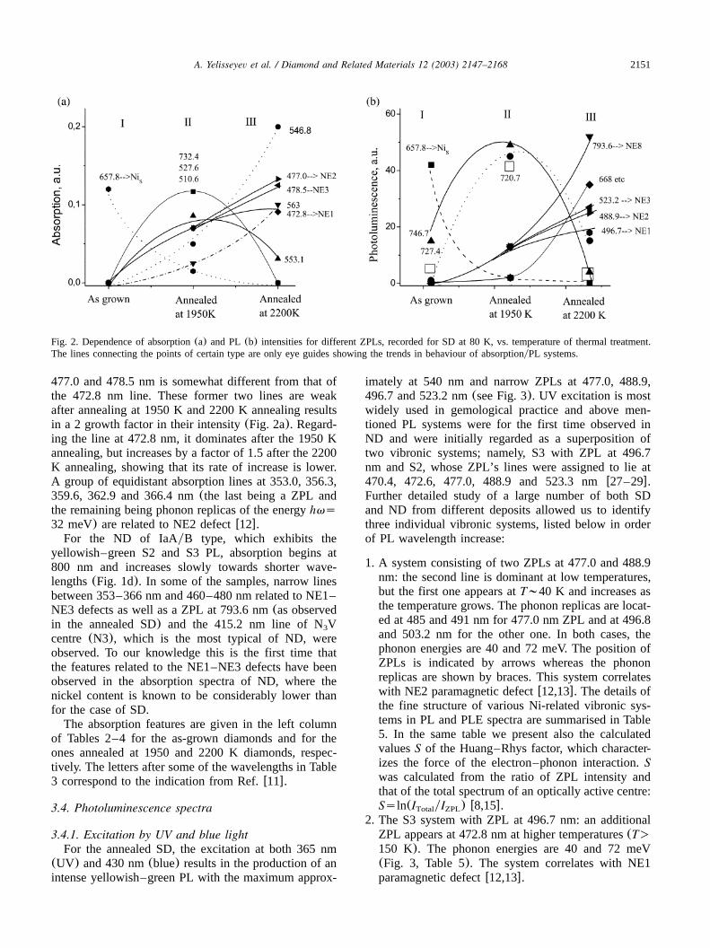
Fig. 2. Dependence of absorption(a) and PL(b) intensities for different ZPLs, recorded for SD at 80 K, vs. temperature of thermal treatment.The lines connecting the points of certain type are only eye guides showing the trends in behaviour of absorptionyPL systems.
477.0 and 478.5 nm is somewhat different from that ofthe 472.8 nm line. These former two lines are weakafter annealing at 1950 K and 2200 K annealing resultsin a 2 growth factor in their intensity(Fig. 2a). Regard-ing the line at 472.8 nm, it dominates after the 1950 Kannealing, but increases by a factor of 1.5 after the 2200K annealing, showing that its rate of increase is lower.A group of equidistant absorption lines at 353.0, 356.3,359.6, 362.9 and 366.4 nm(the last being a ZPL andthe remaining being phonon replicas of the energyhvs32 meV) are related to NE2 defectw12x.For the ND of IaAyB type, which exhibits the
yellowish–green S2 and S3 PL, absorption begins at800 nm and increases slowly towards shorter wave-lengths(Fig. 1d). In some of the samples, narrow linesbetween 353–366 nm and 460–480 nm related to NE1–NE3 defects as well as a ZPL at 793.6 nm(as observedin the annealed SD) and the 415.2 nm line of N V3
centre (N3), which is the most typical of ND, wereobserved. To our knowledge this is the first time thatthe features related to the NE1–NE3 defects have beenobserved in the absorption spectra of ND, where thenickel content is known to be considerably lower thanfor the case of SD.The absorption features are given in the left column
of Tables 2–4 for the as-grown diamonds and for theones annealed at 1950 and 2200 K diamonds, respec-tively. The letters after some of the wavelengths in Table3 correspond to the indication from Ref.w11x.
3.4. Photoluminescence spectra
3.4.1. Excitation by UV and blue lightFor the annealed SD, the excitation at both 365 nm
(UV) and 430 nm(blue) results in the production of anintense yellowish–green PL with the maximum approx-
imately at 540 nm and narrow ZPLs at 477.0, 488.9,496.7 and 523.2 nm(see Fig. 3). UV excitation is mostwidely used in gemological practice and above men-tioned PL systems were for the first time observed inND and were initially regarded as a superposition oftwo vibronic systems; namely, S3 with ZPL at 496.7nm and S2, whose ZPL’s lines were assigned to lie at470.4, 472.6, 477.0, 488.9 and 523.3 nmw27–29x.Further detailed study of a large number of both SDand ND from different deposits allowed us to identifythree individual vibronic systems, listed below in orderof PL wavelength increase:
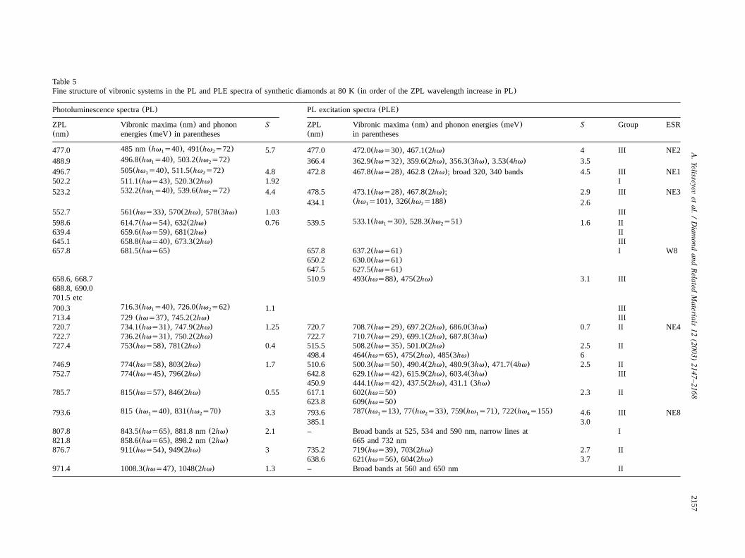
1. A system consisting of two ZPLs at 477.0 and 488.9nm: the second line is dominant at low temperatures,but the first one appears atT;40 K and increases asthe temperature grows. The phonon replicas are locat-ed at 485 and 491 nm for 477.0 nm ZPL and at 496.8and 503.2 nm for the other one. In both cases, thephonon energies are 40 and 72 meV. The position ofZPLs is indicated by arrows whereas the phononreplicas are shown by braces. This system correlateswith NE2 paramagnetic defectw12,13x. The details ofthe fine structure of various Ni-related vibronic sys-tems in PL and PLE spectra are summarised in Table5. In the same table we present also the calculatedvaluesS of the Huang–Rhys factor, which character-izes the force of the electron–phonon interaction.Swas calculated from the ratio of ZPL intensity andthat of the total spectrum of an optically active centre:Ssln(I yI ) w8,15x.Total ZPL
2. The S3 system with ZPL at 496.7 nm: an additionalZPL appears at 472.8 nm at higher temperatures(T)150 K). The phonon energies are 40 and 72 meV(Fig. 3, Table 5). The system correlates with NE1paramagnetic defectw12,13x.
2152 A. Yelisseyev et al. / Diamond and Related Materials 12 (2003) 2147–2168
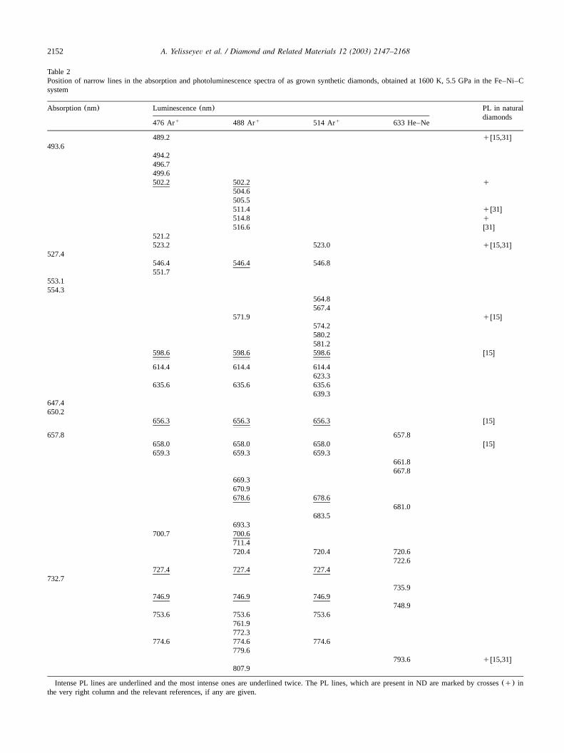
Table 2Position of narrow lines in the absorption and photoluminescence spectra of as grown synthetic diamonds, obtained at 1600 K, 5.5 GPa in the Fe–Ni–Csystem
Absorption(nm) Luminescence(nm) PL in natural
476 Arq 488 Arq 514 Arq 633 He–Nediamonds
489.2 qw15,31x493.6
494.2496.7499.6502.2 502.2 q
504.6505.5511.4 qw31x514.8 q516.6 w31x
521.2523.2 523.0 qw15,31x
527.4546.4 546.4 546.8551.7
553.1554.3
564.8567.4
571.9 qw15x574.2580.2581.2
598.6 598.6 598.6 w15x
614.4 614.4 614.4623.3
635.6 635.6 635.6639.3
647.4650.2
656.3 656.3 656.3 w15x
657.8 657.8658.0 658.0 658.0 w15x659.3 659.3 659.3
661.8667.8
669.3670.9678.6 678.6
681.0683.5
693.3700.7 700.6
711.4720.4 720.4 720.6
722.6727.4 727.4 727.4
732.7735.9
746.9 746.9 746.9748.9
753.6 753.6 753.6761.9772.3
774.6 774.6 774.6779.6
793.6 qw15,31x807.9
Intense PL lines are underlined and the most intense ones are underlined twice. The PL lines, which are present in ND are marked by crosses(q) inthe very right column and the relevant references, if any are given.
2153A. Yelisseyev et al. / Diamond and Related Materials 12 (2003) 2147–2168
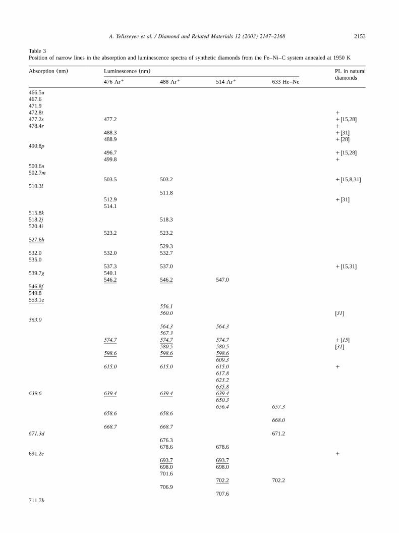
Table 3Position of narrow lines in the absorption and luminescence spectra of synthetic diamonds from the Fe–Ni–C system annealed at 1950 K
Absorption(nm) Luminescence(nm) PL in natural
476 Arq 488 Arq 514 Arq 633 He–Nediamonds
466.5u467.6471.9472.8t q477.2s 477.2 qw15,28x478.4r q
488.3 qw31x488.9 qw28x
490.8p496.7 qw15,28x499.8 q
500.6n502.7m
503.5 503.2 qw15,8,31x510.3l
511.8512.9 qw31x514.1
515.8k518.2j 518.3520.4i
523.2 523.2527.6h
529.3532.0 532.0 532.7535.0
537.3 537.0 qw15,31x539.7g 540.1
546.2 546.2 547.0546.8f549.8553.1e
556.1560.0 w31x
563.0564.3 564.3567.3
574.7 574.7 574.7 qw15x580.5 580.5 w31x
598.6 598.6 598.6609.3
615.0 615.0 615.0 q617.8623.2635.8
639.6 639.4 639.4 639.4650.3656.4 657.3
658.6 658.6668.0
668.7 668.7671.3d 671.2
676.3678.6 678.6
691.2c q693.7 693.7698.0 698.0701.6
702.2 702.2706.9
707.6711.7b
2154 A. Yelisseyev et al. / Diamond and Related Materials 12 (2003) 2147–2168
Table 3(Continued)
Absorption(nm) Luminescence(nm) PL in natural
476 Arq 488 Arq 514 Arq 633 He–Nediamonds
720.6722.6
725.5727.4 727.4 727.4
732.7a733.6 733.5
734.0735.8
742.3746.9 746.9 746.9
747.8749.2 q
753.0 753.3756.0 756.4
774.0 774.0 q793.6 793.6 793.6 qw15,31x
807.9822.4
3. The third system has ZPL at 523.2 nm with phononreplicas at 532 and 539 nm, corresponding to 40 meVand 70 meV phonon energies, respectively(Fig. 3,Table 5); the system is believed to be an opticalanalogue of the NE3 paramagnetic nickel–nitrogencomplexw12,13x.The relative intensities of the variousZPLs change with the variation of the excitationwavelengths. Under UV excitation, the 488.9 and523.2 nm lines dominate, whereas the 496.7 nm(S3)ZPL is most intense at 430 nm excitation. Thesevariations are due to different absorption spectra,which can be reconstructed basing on the results ofPLE measurements(see Section 3.5). In Fig. 2b thevariations of ZPL intensity vs. the annealing temper-ature are shown. It can be seen that the ZPLs at496.7, 488.9 and 523.2 nm, which are present in PL,follow behaviour similar to the ZPLs at 472.8, 477.0and 478.5 nm in absorption spectra. In the same waythe rate of S3 increase is lower in the 1950–2200 Krange than the ones for two other lines(I y2200
I ;1.6 and 2–2.4, respectively). The series of1950
sharp depressions, which are superimposed on thebroad 540 nm PL band(Fig. 3), correspond to theZPLs, which are observed in absorption; the mostintense ones are located at 527.6, 546.8, 553.1 and546.8, 563.0 nm for diamonds, annealed at 1950 Kand 2200 K, respectively. They are clearly a result of‘self-absorption’ of the emitted light, which is con-firmed by the fact, that they exhibit the same anneal-ing behaviour as when they are observed in theabsorption spectra.
4. In the near-IR region an intense vibronic system withZPL at 793.6 nm and phonon replicas at 815, 831(hvs40, 70 meV) can be observed in line with
systems 1–3 responsible for yellow–green PLw16,27,28x. The emission can be excited by differentwavelengths in the UV to near-IR range. This centrehas absorption at the same wavelength(793.6 nm):thus, the corresponding line is resonant in absorptionand PL. The 793.6 nm system correlates with theparamagnetic NE8 defect, which is believed to be anickel–nitrogen complex with four nitrogen atomsw16x and is found usually in annealed SD. Theelectron–phonon coupling of the centre has a mod-erate value, withSs3.5 w15x, a dipole electronictransition with the dipole momentds4=10 C my30
and ts9.7=10 s PL lifetime takes placew15x.y8
This PL system was also found to be typical of NDwith yellow–green PLw22,28,29x. It should be notedthat although these vibronic systems are typical ofthe annealed SD, nevertheless they are sometimesfound in the as-grown one. The latter takes place inspecific areas near the seed, around inclusions(in theareas of non-stationary growth) or near growth-sectorboundaries, where the degree of nitrogen aggregationis enhancedw30x.
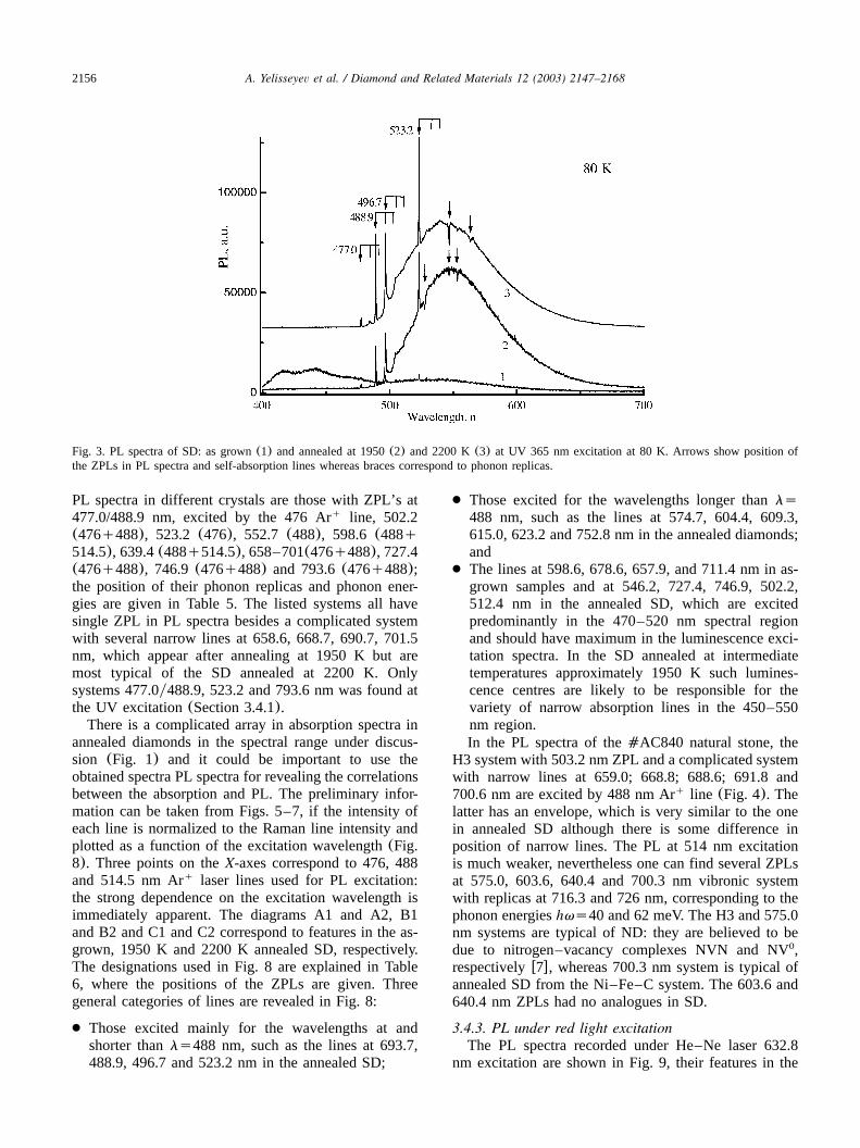
In PL spectra of typical ND� AC840 of ultramaficparagenesis in addition to the above mentioned foursystems one can find the N3 vibronic system with ZPLat 415.2 nm(Fig. 4).
3.4.2. PL spectra under Ar laser excitationq
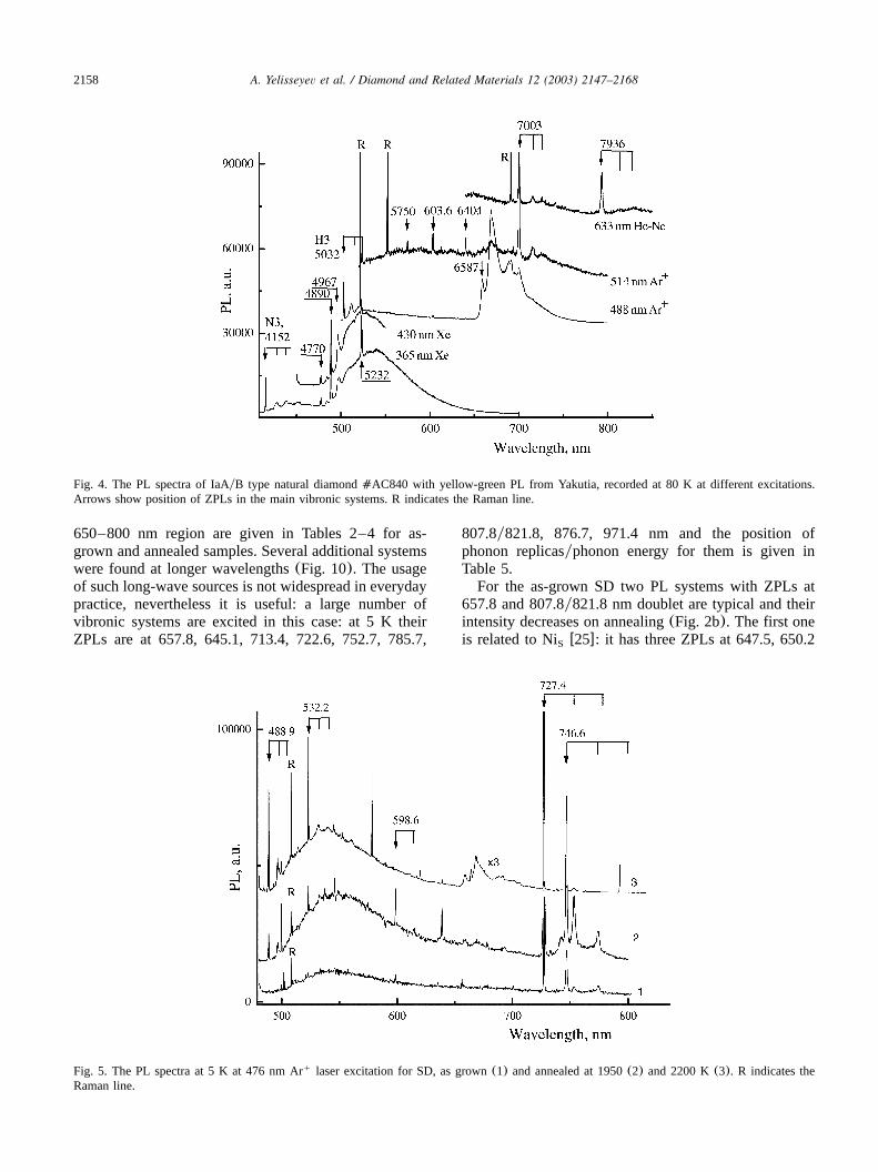
A large array of PL lines was found when excitingwith an Ar laser: These are presented for the as-grownq
synthetics and those annealed at 1950 and 2200 K. ThePL spectra, recorded at 5 K under 476, 488 and 514.5nm excitation are given in Figs. 5–7, respectively. Theposition of narrow lines in PL spectra at different
2155A. Yelisseyev et al. / Diamond and Related Materials 12 (2003) 2147–2168
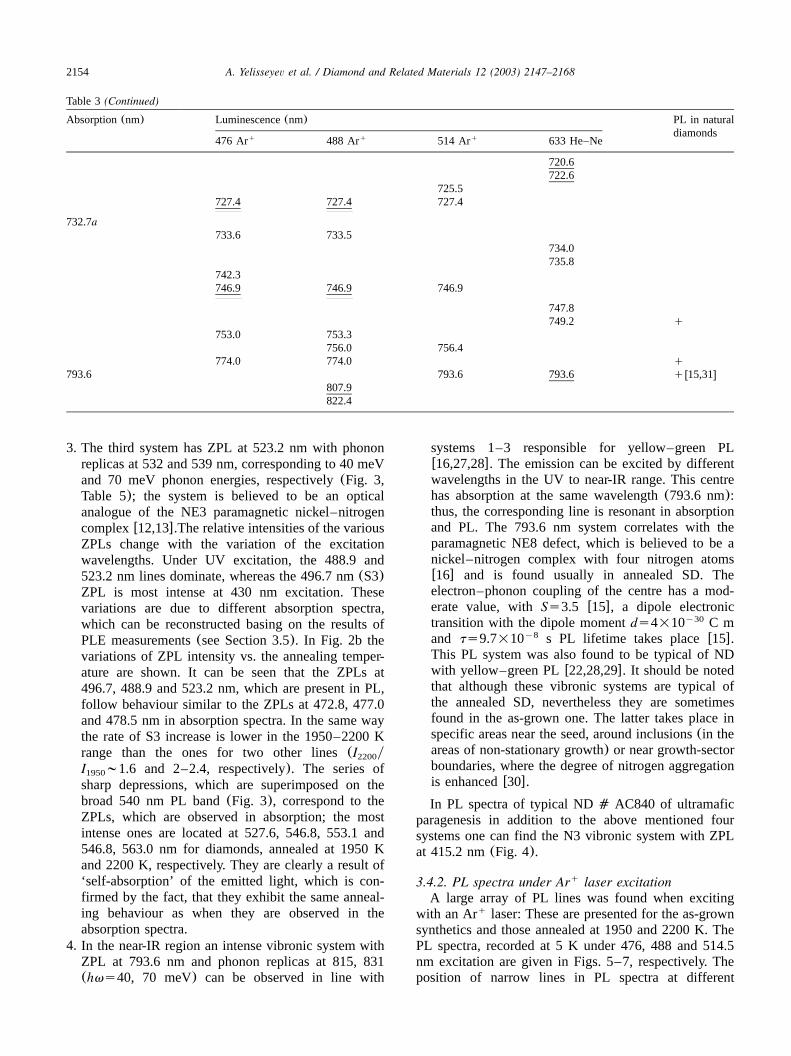
Table 4Position of narrow lines in the absorption and luminescence spectraof synthetic diamonds from the Fe–Ni–C system annealed at 2200 K
Absorption(nm) Luminescence(nm) PL in naturaldiamonds
466.5467.6471.9472.8477.2 477.1 qw15,28x478.4
480.3487.8488.9 qw15,28x492.9496.7 496.7 qw15,29x497.7499.7 qw31x
501.6502.4511.3 q512.4 q517.2 qw31x
523.0 523.0529.1535.5536.6541.7 541.8
544.9 544.9 544.8 qw31x546.3 546.3 546.3 qw31x
547.9548.4
553.1552.7 qw31x560.3 560.3 w31x561.3562.4
563.0564.5566.7
567.8568.8 568.8570.5573.7 573.7 q582.8 q
578.2 q580.6 580.7 q582.8 qw15x
591.5 w31x604.4 w31x
611.3 w31x613.5616.7619.9623.7 623.3638.7 638.7 638.8
639.8 w31x641.0 w31x645.1 w31x
647.9650.3651.5655.1
658.7 658.7
659.2
Table 4(Continued)
Absorption(nm) Luminescence(nm) PL in naturaldiamonds
663.2664.1668.7 668.7
667.9671.6
673.4676.3
675.5681.3
682.8685.0
688.8 688.8 688.8690.0 690.0
691.0691.6
693.5 693.8 q694.2
696.8696.6 698.5
700.3 q701.3703.9705.5 705.5
706.7713.4
714.9 q720.6722.6
726.6727.4 727.4
728.8736.0
738.5 q741.2 741.5746.6 746.6750.4751.4 q752.8 752.8 752.7 752.7758.9763.2772.5774.2 774.1
793.6 793.6 qw15,28x
excitation by all available laser sources(Ar and He–q
Ne lasers) is documented also in Tables 2–4 for SD ofdifferent prehistory(as grown and annealed at 1950 Kand 2200 K, respectively) in comparison with thefeatures in absorption spectra(very left column). Mostof the lines are ZPLs and for some of them it waspossible to separate the replicas due to electron–phononinteraction. In such a case, ZPL and replicas are shownby arrow and braces in Figs. 5–7, respectively. Thespectra are vertically displaced for clarity and normal-ized to the Raman line(marked R in the figures). Thespectra were recorded with a spectral slit width of 0.1nm; the position of lines is given with the accuracy of"0.2 nm. The vibronic systems most often recurring in
2156 A. Yelisseyev et al. / Diamond and Related Materials 12 (2003) 2147–2168
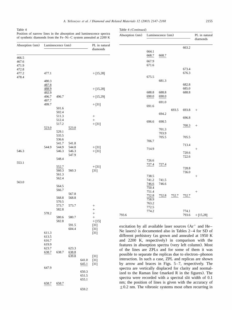
Fig. 3. PL spectra of SD: as grown(1) and annealed at 1950(2) and 2200 K(3) at UV 365 nm excitation at 80 K. Arrows show position ofthe ZPLs in PL spectra and self-absorption lines whereas braces correspond to phonon replicas.
PL spectra in different crystals are those with ZPL’s at477.0/488.9 nm, excited by the 476 Ar line, 502.2q
(476q488), 523.2 (476), 552.7 (488), 598.6 (488q514.5), 639.4(488q514.5), 658–701(476q488), 727.4(476q488), 746.9 (476q488) and 793.6(476q488);the position of their phonon replicas and phonon ener-gies are given in Table 5. The listed systems all havesingle ZPL in PL spectra besides a complicated systemwith several narrow lines at 658.6, 668.7, 690.7, 701.5nm, which appear after annealing at 1950 K but aremost typical of the SD annealed at 2200 K. Onlysystems 477.0y488.9, 523.2 and 793.6 nm was found atthe UV excitation(Section 3.4.1).There is a complicated array in absorption spectra in
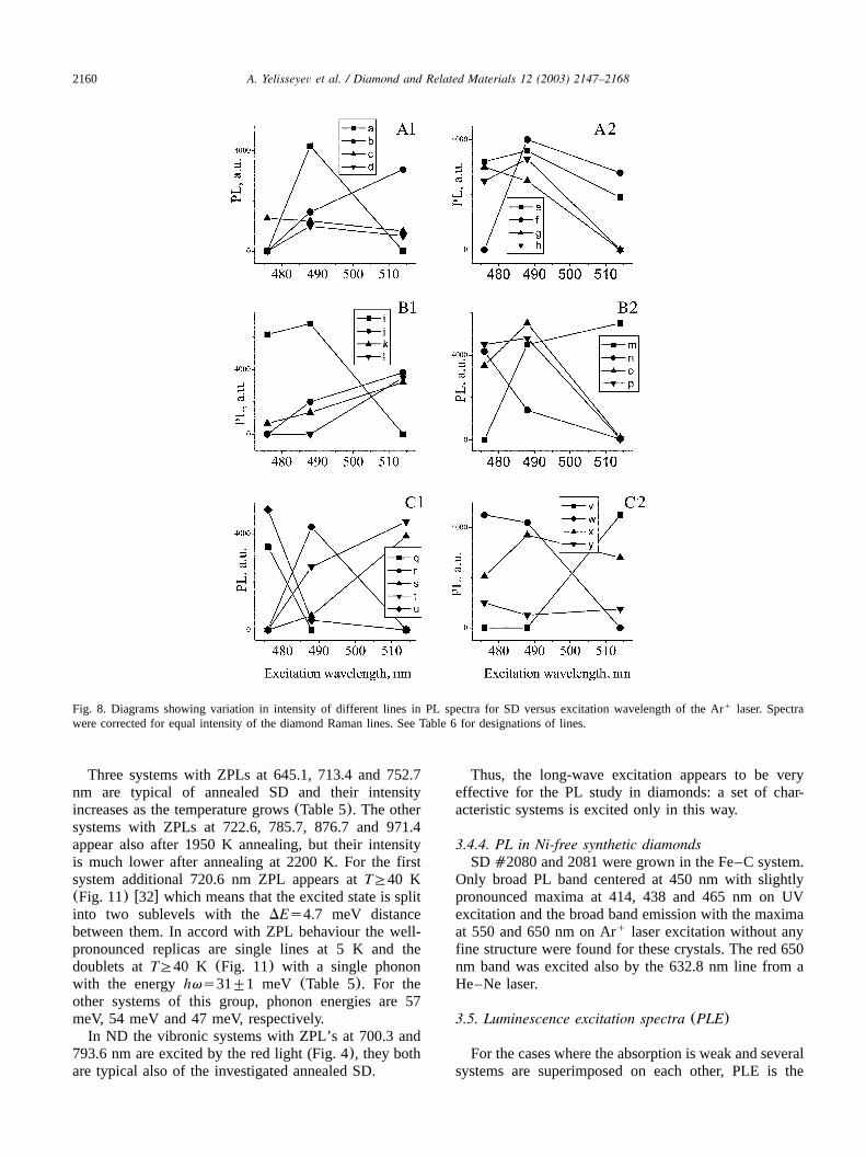
annealed diamonds in the spectral range under discus-sion (Fig. 1) and it could be important to use theobtained spectra PL spectra for revealing the correlationsbetween the absorption and PL. The preliminary infor-mation can be taken from Figs. 5–7, if the intensity ofeach line is normalized to the Raman line intensity andplotted as a function of the excitation wavelength(Fig.8). Three points on theX-axes correspond to 476, 488and 514.5 nm Ar laser lines used for PL excitation:q
the strong dependence on the excitation wavelength isimmediately apparent. The diagrams A1 and A2, B1and B2 and C1 and C2 correspond to features in the as-grown, 1950 K and 2200 K annealed SD, respectively.The designations used in Fig. 8 are explained in Table6, where the positions of the ZPLs are given. Threegeneral categories of lines are revealed in Fig. 8:
● Those excited mainly for the wavelengths at andshorter thanls488 nm, such as the lines at 693.7,488.9, 496.7 and 523.2 nm in the annealed SD;
● Those excited for the wavelengths longer thanls488 nm, such as the lines at 574.7, 604.4, 609.3,615.0, 623.2 and 752.8 nm in the annealed diamonds;and
● The lines at 598.6, 678.6, 657.9, and 711.4 nm in as-grown samples and at 546.2, 727.4, 746.9, 502.2,512.4 nm in the annealed SD, which are excitedpredominantly in the 470–520 nm spectral regionand should have maximum in the luminescence exci-tation spectra. In the SD annealed at intermediatetemperatures approximately 1950 K such lumines-cence centres are likely to be responsible for thevariety of narrow absorption lines in the 450–550nm region.In the PL spectra of the�AC840 natural stone, the
H3 system with 503.2 nm ZPL and a complicated systemwith narrow lines at 659.0; 668.8; 688.6; 691.8 and700.6 nm are excited by 488 nm Ar line(Fig. 4). Theq
latter has an envelope, which is very similar to the onein annealed SD although there is some difference inposition of narrow lines. The PL at 514 nm excitationis much weaker, nevertheless one can find several ZPLsat 575.0, 603.6, 640.4 and 700.3 nm vibronic systemwith replicas at 716.3 and 726 nm, corresponding to thephonon energieshvs40 and 62 meV. The H3 and 575.0nm systems are typical of ND: they are believed to bedue to nitrogen–vacancy complexes NVN and NV ,0
respectivelyw7x, whereas 700.3 nm system is typical ofannealed SD from the Ni–Fe–C system. The 603.6 and640.4 nm ZPLs had no analogues in SD.
3.4.3. PL under red light excitationThe PL spectra recorded under He–Ne laser 632.8
nm excitation are shown in Fig. 9, their features in the
2157A
.Yelisseyev
etal.
/D
iamond
andR
elatedM
aterials12
(2003)2147–2168
Table 5Fine structure of vibronic systems in the PL and PLE spectra of synthetic diamonds at 80 K(in order of the ZPL wavelength increase in PL)
Photoluminescence spectra(PL) PL excitation spectra(PLE)
ZPL Vibronic maxima(nm) and phonon S ZPL Vibronic maxima(nm) and phonon energies(meV) S Group ESR(nm) energies(meV) in parentheses (nm) in parentheses
477.0 485 nm(hv s40), 491(hv s72)1 2 5.7 477.0 472.0(hvs30), 467.1(2hv) 4 III NE2488.9 496.8(hv s40), 503.2(hv s72)1 2 366.4 362.9(hvs32), 359.6(2hv), 356.3(3hv), 3.53(4hv) 3.5496.7 505(hv s40), 511.5(hv s72)1 2 4.8 472.8 467.8(hvs28), 462.8(2hv); broad 320, 340 bands 4.5 III NE1502.2 511.1(hvs43), 520.3(2hv) 1.92 I523.2 532.2(hv s40), 539.6(hv s72)1 2 4.4 478.5 473.1(hvs28), 467.8(2hv); 2.9 III NE3
434.1 (hv s101), 326(hv s188)1 2 2.6552.7 561(hvs33), 570(2hv), 578(3hv) 1.03 III598.6 614.7(hvs54), 632(2hv) 0.76 539.5 533.1(hv s30), 528.3(hv s51)1 2 1.6 II639.4 659.6(hvs59), 681(2hv) II645.1 658.8(hvs40), 673.3(2hv) III657.8 681.5(hvs65) 657.8 637.2(hvs61) I W8
650.2 630.0(hvs61)647.5 627.5(hvs61)
658.6, 668.7 510.9 493(hvs88), 475(2hv) 3.1 III688.8, 690.0701.5 etc700.3 716.3(hv s40), 726.0(hv s62)1 2 1.1 III713.4 729(hvs37), 745.2(2hv) III720.7 734.1(hvs31), 747.9(2hv) 1.25 720.7 708.7(hvs29), 697.2(2hv), 686.0(3hv) 0.7 II NE4722.7 736.2(hvs31), 750.2(2hv) 722.7 710.7(hvs29), 699.1(2hv), 687.8(3hv)727.4 753(hvs58), 781(2hv) 0.4 515.5 508.2(hvs35), 501.0(2hv) 2.5 II
498.4 464(hvs65), 475(2hv), 485(3hv) 6746.9 774(hvs58), 803(2hv) 1.7 510.6 500.3(hvs50), 490.4(2hv), 480.9(3hv), 471.7(4hv) 2.5 II752.7 774(hvs45), 796(2hv) 642.8 629.1(hvs42), 615.9(2hv), 603.4(3hv) III
450.9 444.1(hvs42), 437.5(2hv), 431.1(3hv)785.7 815(hvs57), 846(2hv) 0.55 617.1 602(hvs50) 2.3 II
623.8 609(hvs50)793.6 815 (hv s40), 831(hv s70)1 2 3.3 793.6 787(hv s13), 77(hv s33), 759(hv s71), 722(hv s155)1 2 1 4 4.6 III NE8
385.1 3.0807.8 843.5(hvs65), 881.8 nm(2hv) 2.1 – Broad bands at 525, 534 and 590 nm, narrow lines at I821.8 858.6(hvs65), 898.2 nm(2hv) 665 and 732 nm876.7 911(hvs54), 949(2hv) 3 735.2 719(hvs39), 703(2hv) 2.7 II
638.6 621(hvs56), 604(2hv) 3.7971.4 1008.3(hvs47), 1048(2hv) 1.3 – Broad bands at 560 and 650 nm II
2158 A. Yelisseyev et al. / Diamond and Related Materials 12 (2003) 2147–2168
Fig. 4. The PL spectra of IaAyB type natural diamond�AC840 with yellow-green PL from Yakutia, recorded at 80 K at different excitations.Arrows show position of ZPLs in the main vibronic systems. R indicates the Raman line.
Fig. 5. The PL spectra at 5 K at 476 nm Ar laser excitation for SD, as grown(1) and annealed at 1950(2) and 2200 K(3). R indicates theq
Raman line.
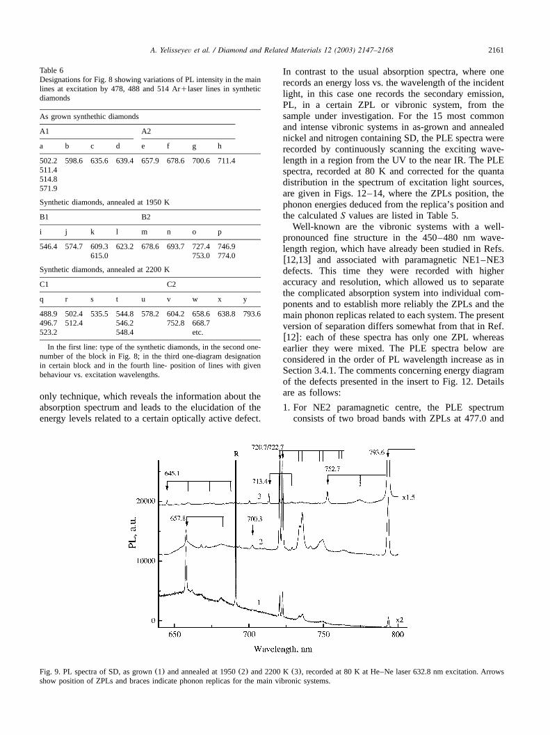
650–800 nm region are given in Tables 2–4 for as-grown and annealed samples. Several additional systemswere found at longer wavelengths(Fig. 10). The usageof such long-wave sources is not widespread in everydaypractice, nevertheless it is useful: a large number ofvibronic systems are excited in this case: at 5 K theirZPLs are at 657.8, 645.1, 713.4, 722.6, 752.7, 785.7,
807.8y821.8, 876.7, 971.4 nm and the position ofphonon replicasyphonon energy for them is given inTable 5.For the as-grown SD two PL systems with ZPLs at
657.8 and 807.8y821.8 nm doublet are typical and theirintensity decreases on annealing(Fig. 2b). The first oneis related to Ni w25x: it has three ZPLs at 647.5, 650.2S

2159A. Yelisseyev et al. / Diamond and Related Materials 12 (2003) 2147–2168
Fig. 6. The PL spectra at 5 K at 488 nm Ar laser excitation for SD, as grown(1) and annealed at 1950(2) and 2200 K(3). R indicates theq
Raman line.
Fig. 7. The PL spectra at 5 K at 514 nm Ar laser excitation for SD, as grown(1) and annealed at 1950(2) and 2200 K(3). R indicates theq
Raman line.
and 657.8 nm in absorption spectra(Table 2, column1), which shows that the excited state is split into threesublevels. Additional PL lines due to radiative transitionsfrom the upper sublevels of the excited state appear atthe higher temperature of 100–120 K. For the second
system, both ZPLs at 807.8 and 821.8 nm are observedat low temperatures: the ground state is likely to be splitinto two sublevels. Both PL systems demonstrate pho-non replicas with the 65 meV energy for all ZPLs(Table5).
2160 A. Yelisseyev et al. / Diamond and Related Materials 12 (2003) 2147–2168
Fig. 8. Diagrams showing variation in intensity of different lines in PL spectra for SD versus excitation wavelength of the Ar laser. Spectraq
were corrected for equal intensity of the diamond Raman lines. See Table 6 for designations of lines.
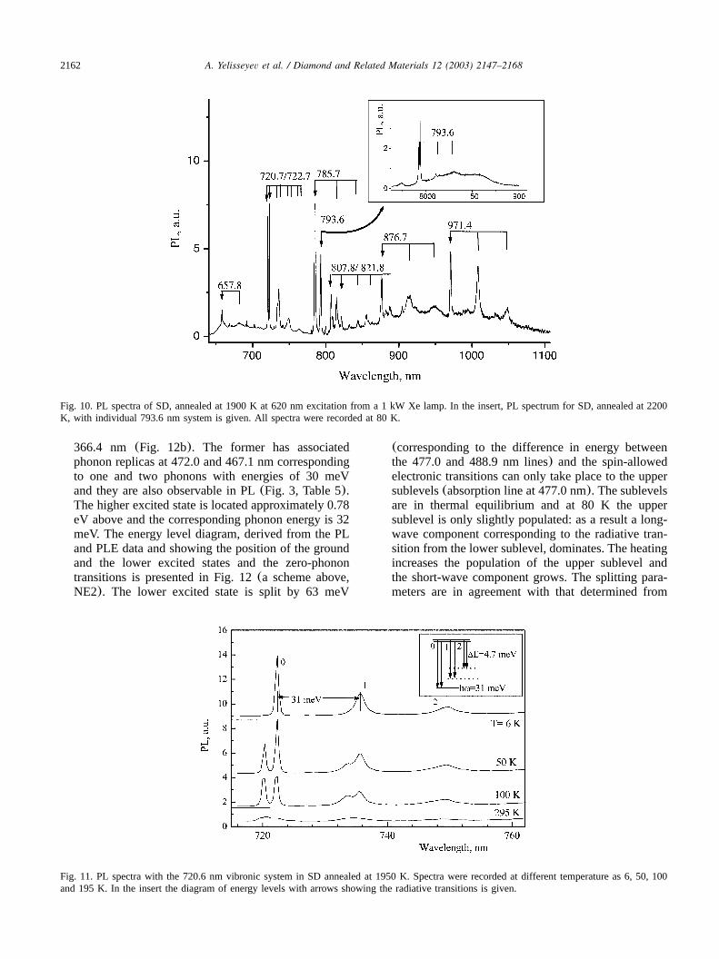
Three systems with ZPLs at 645.1, 713.4 and 752.7nm are typical of annealed SD and their intensityincreases as the temperature grows(Table 5). The othersystems with ZPLs at 722.6, 785.7, 876.7 and 971.4appear also after 1950 K annealing, but their intensityis much lower after annealing at 2200 K. For the firstsystem additional 720.6 nm ZPL appears atTG40 K(Fig. 11) w32x which means that the excited state is splitinto two sublevels with theDEs4.7 meV distancebetween them. In accord with ZPL behaviour the well-pronounced replicas are single lines at 5 K and thedoublets atTG40 K (Fig. 11) with a single phononwith the energyhvs31"1 meV (Table 5). For theother systems of this group, phonon energies are 57meV, 54 meV and 47 meV, respectively.In ND the vibronic systems with ZPL’s at 700.3 and
793.6 nm are excited by the red light (Fig. 4), they bothare typical also of the investigated annealed SD.
Thus, the long-wave excitation appears to be veryeffective for the PL study in diamonds: a set of char-acteristic systems is excited only in this way.
3.4.4. PL in Ni-free synthetic diamondsSD�2080 and 2081 were grown in the Fe–C system.
Only broad PL band centered at 450 nm with slightlypronounced maxima at 414, 438 and 465 nm on UVexcitation and the broad band emission with the maximaat 550 and 650 nm on Ar laser excitation without anyq
fine structure were found for these crystals. The red 650nm band was excited also by the 632.8 nm line from aHe–Ne laser.
3.5. Luminescence excitation spectra (PLE)
For the cases where the absorption is weak and severalsystems are superimposed on each other, PLE is the
2161A. Yelisseyev et al. / Diamond and Related Materials 12 (2003) 2147–2168
Table 6Designations for Fig. 8 showing variations of PL intensity in the mainlines at excitation by 478, 488 and 514 Arqlaser lines in syntheticdiamonds
As grown synthethic diamonds
A1 A2
a b c d e f g h
502.2 598.6 635.6 639.4 657.9 678.6 700.6 711.4511.4514.8571.9
Synthetic diamonds, annealed at 1950 K
B1 B2
i j k l m n o p
546.4 574.7 609.3 623.2 678.6 693.7 727.4 746.9615.0 753.0 774.0
Synthetic diamonds, annealed at 2200 K
C1 C2
q r s t u v w x y
488.9 502.4 535.5 544.8 578.2 604.2 658.6 638.8 793.6496.7 512.4 546.2 752.8 668.7523.2 548.4 etc.
In the first line: type of the synthetic diamonds, in the second one-number of the block in Fig. 8; in the third one-diagram designationin certain block and in the fourth line- position of lines with givenbehaviour vs. excitation wavelengths.
Fig. 9. PL spectra of SD, as grown(1) and annealed at 1950(2) and 2200 K(3), recorded at 80 K at He–Ne laser 632.8 nm excitation. Arrowsshow position of ZPLs and braces indicate phonon replicas for the main vibronic systems.
only technique, which reveals the information about theabsorption spectrum and leads to the elucidation of theenergy levels related to a certain optically active defect.
In contrast to the usual absorption spectra, where onerecords an energy loss vs. the wavelength of the incidentlight, in this case one records the secondary emission,PL, in a certain ZPL or vibronic system, from thesample under investigation. For the 15 most commonand intense vibronic systems in as-grown and annealednickel and nitrogen containing SD, the PLE spectra wererecorded by continuously scanning the exciting wave-length in a region from the UV to the near IR. The PLEspectra, recorded at 80 K and corrected for the quantadistribution in the spectrum of excitation light sources,are given in Figs. 12–14, where the ZPLs position, thephonon energies deduced from the replica’s position andthe calculatedS values are listed in Table 5.Well-known are the vibronic systems with a well-
pronounced fine structure in the 450–480 nm wave-length region, which have already been studied in Refs.w12,13x and associated with paramagnetic NE1–NE3defects. This time they were recorded with higheraccuracy and resolution, which allowed us to separatethe complicated absorption system into individual com-ponents and to establish more reliably the ZPLs and themain phonon replicas related to each system. The presentversion of separation differs somewhat from that in Ref.w12x: each of these spectra has only one ZPL whereasearlier they were mixed. The PLE spectra below areconsidered in the order of PL wavelength increase as inSection 3.4.1. The comments concerning energy diagramof the defects presented in the insert to Fig. 12. Detailsare as follows:
1. For NE2 paramagnetic centre, the PLE spectrumconsists of two broad bands with ZPLs at 477.0 and
2162 A. Yelisseyev et al. / Diamond and Related Materials 12 (2003) 2147–2168
Fig. 10. PL spectra of SD, annealed at 1900 K at 620 nm excitation from a 1 kW Xe lamp. In the insert, PL spectrum for SD, annealed at 2200K, with individual 793.6 nm system is given. All spectra were recorded at 80 K.
Fig. 11. PL spectra with the 720.6 nm vibronic system in SD annealed at 1950 K. Spectra were recorded at different temperature as 6, 50, 100and 195 K. In the insert the diagram of energy levels with arrows showing the radiative transitions is given.
366.4 nm (Fig. 12b). The former has associatedphonon replicas at 472.0 and 467.1 nm correspondingto one and two phonons with energies of 30 meVand they are also observable in PL(Fig. 3, Table 5).The higher excited state is located approximately 0.78eV above and the corresponding phonon energy is 32meV. The energy level diagram, derived from the PLand PLE data and showing the position of the groundand the lower excited states and the zero-phonontransitions is presented in Fig. 12(a scheme above,NE2). The lower excited state is split by 63 meV
(corresponding to the difference in energy betweenthe 477.0 and 488.9 nm lines) and the spin-allowedelectronic transitions can only take place to the uppersublevels(absorption line at 477.0 nm). The sublevelsare in thermal equilibrium and at 80 K the uppersublevel is only slightly populated: as a result a long-wave component corresponding to the radiative tran-sition from the lower sublevel, dominates. The heatingincreases the population of the upper sublevel andthe short-wave component grows. The splitting para-meters are in agreement with that determined from
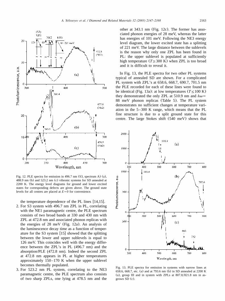
2163A. Yelisseyev et al. / Diamond and Related Materials 12 (2003) 2147–2168
Fig. 12. PLE spectra for emission in 496.7 nm(S3, spectrum A) (a),488.9 nm(b) and 523.2 nm(c) vibronic systems for SD annealed at2200 K. The energy level diagrams for ground and lower excitedstates for corresponding defects are given above. The ground statelevels for all centres are placed atEs0 for convenience.
Fig. 13. PLE spectra for emission in systems with narrow lines at658.6, 668.7, etc.(a) and at 793.6 nm(b) in SD annealed at 2200 K(a), group III and in system with ZPLs at 807.8y821.8 nm in as-grown SD(c).
the temperature dependence of the PL linesw14,15x.2. For S3 system with 496.7 nm ZPL in PL, correlatingwith the NE1 paramagnetic centre, the PLE spectrumconsists of two broad bands at 330 and 430 nm withZPL at 472.8 nm and associated phonon replicas withthe energies of 28 meV(Fig. 12a). An analysis ofthe luminescence decay time as a function of temper-ature for the S3 systemw15x showed that the splittingbetween the lower and upper sublevels is equal to126 meV. This coincides well with the energy differ-ence between the ZPL’s in PL (496.7 nm) and theabsorption/PLE (472.8 nm). Indeed the second ZPLat 472.8 nm appears in PL at higher temperaturesapproximately 150–170 K when the upper sublevelbecomes thermally populated.
3. For 523.2 nm PL system, correlating to the NE3paramagnetic centre, the PLE spectrum also consistsof two sharp ZPLs, one lying at 478.5 nm and the
other at 343.1 nm(Fig. 12c). The former has asso-ciated phonon energies of 28 meV, whereas the latterhas energies of 101 meV. Following the NE3 energylevel diagram, the lower excited state has a splittingof 221 meV. The large distance between the sublevelsis the reason why only one ZPL has been found inPL: the upper sublevel is populated at sufficientlyhigh temperature(TG300 K) when ZPL is too broadand it is difficult to reveal it.
In Fig. 13, the PLE spectra for two other PL systemstypical of annealed SD are shown. For a complicatedPL system with ZPL’s at 658.6, 668.7, 690.7, 701.5 nmthe PLE recorded for each of these lines were found tobe identical (Fig. 13a): at low temperatures(TF100 K)they demonstrated the only ZPL at 510.9 nm andhvs88 meV phonon replicas(Table 5). The PL systemdemonstrates no sufficient changes at temperature vari-ation in the 5–300 K range, which means that the PLfine structure is due to a split ground state for thiscentre. The large Stokes shift(540 meV) shows that
2164 A. Yelisseyev et al. / Diamond and Related Materials 12 (2003) 2147–2168
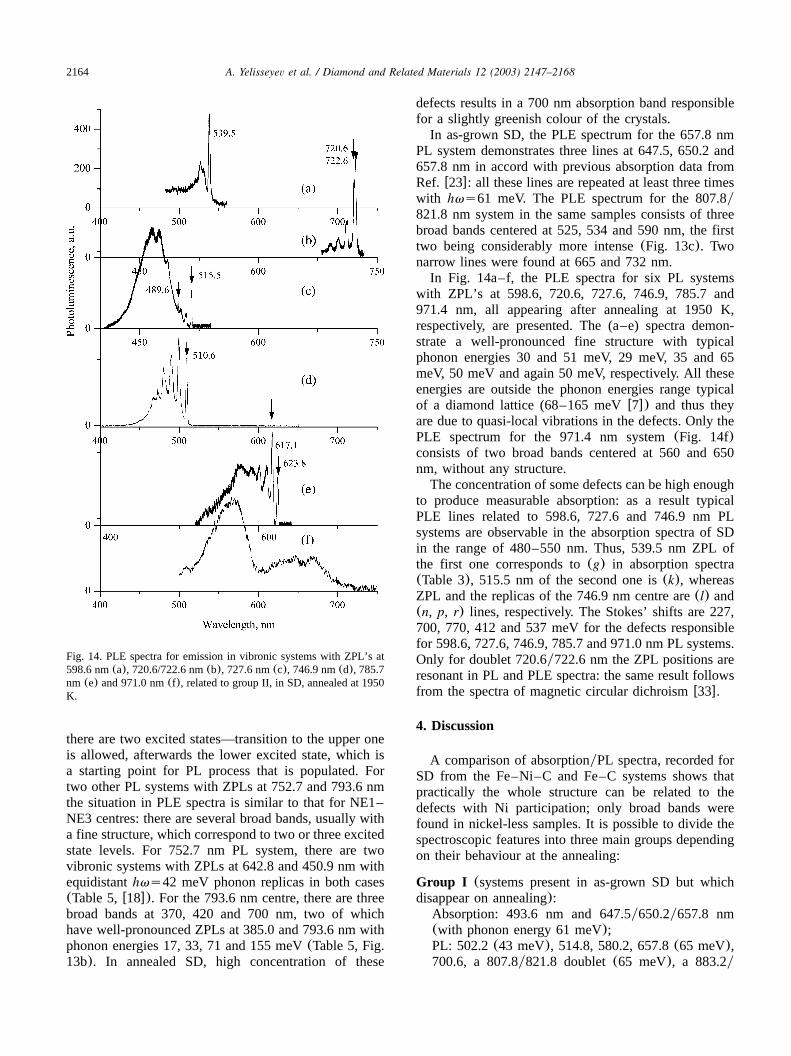
Fig. 14. PLE spectra for emission in vibronic systems with ZPL’s at598.6 nm(a), 720.6/722.6 nm(b), 727.6 nm(c), 746.9 nm(d), 785.7nm (e) and 971.0 nm(f), related to group II, in SD, annealed at 1950K.
there are two excited states—transition to the upper oneis allowed, afterwards the lower excited state, which isa starting point for PL process that is populated. Fortwo other PL systems with ZPLs at 752.7 and 793.6 nmthe situation in PLE spectra is similar to that for NE1–NE3 centres: there are several broad bands, usually witha fine structure, which correspond to two or three excitedstate levels. For 752.7 nm PL system, there are twovibronic systems with ZPLs at 642.8 and 450.9 nm withequidistanthvs42 meV phonon replicas in both cases(Table 5,w18x). For the 793.6 nm centre, there are threebroad bands at 370, 420 and 700 nm, two of whichhave well-pronounced ZPLs at 385.0 and 793.6 nm withphonon energies 17, 33, 71 and 155 meV(Table 5, Fig.13b). In annealed SD, high concentration of these
defects results in a 700 nm absorption band responsiblefor a slightly greenish colour of the crystals.In as-grown SD, the PLE spectrum for the 657.8 nm
PL system demonstrates three lines at 647.5, 650.2 and657.8 nm in accord with previous absorption data fromRef. w23x: all these lines are repeated at least three timeswith hvs61 meV. The PLE spectrum for the 807.8y821.8 nm system in the same samples consists of threebroad bands centered at 525, 534 and 590 nm, the firsttwo being considerably more intense(Fig. 13c). Twonarrow lines were found at 665 and 732 nm.In Fig. 14a–f, the PLE spectra for six PL systems
with ZPL’s at 598.6, 720.6, 727.6, 746.9, 785.7 and971.4 nm, all appearing after annealing at 1950 K,respectively, are presented. The (a–e) spectra demon-strate a well-pronounced fine structure with typicalphonon energies 30 and 51 meV, 29 meV, 35 and 65meV, 50 meV and again 50 meV, respectively. All theseenergies are outside the phonon energies range typicalof a diamond lattice (68–165 meVw7x) and thus theyare due to quasi-local vibrations in the defects. Only thePLE spectrum for the 971.4 nm system(Fig. 14f)consists of two broad bands centered at 560 and 650nm, without any structure.The concentration of some defects can be high enough
to produce measurable absorption: as a result typicalPLE lines related to 598.6, 727.6 and 746.9 nm PLsystems are observable in the absorption spectra of SDin the range of 480–550 nm. Thus, 539.5 nm ZPL ofthe first one corresponds to(g) in absorption spectra(Table 3), 515.5 nm of the second one is(k), whereasZPL and the replicas of the 746.9 nm centre are(l) and(n, p, r) lines, respectively. The Stokes’ shifts are 227,700, 770, 412 and 537 meV for the defects responsiblefor 598.6, 727.6, 746.9, 785.7 and 971.0 nm PL systems.Only for doublet 720.6y722.6 nm the ZPL positions areresonant in PL and PLE spectra: the same result followsfrom the spectra of magnetic circular dichroismw33x.
4. Discussion
A comparison of absorptionyPL spectra, recorded forSD from the Fe–Ni–C and Fe–C systems shows thatpractically the whole structure can be related to thedefects with Ni participation; only broad bands werefound in nickel-less samples. It is possible to divide thespectroscopic features into three main groups dependingon their behaviour at the annealing:
Group I (systems present in as-grown SD but whichdisappear on annealing):Absorption: 493.6 nm and 647.5y650.2y657.8 nm(with phonon energy 61 meV);PL: 502.2(43 meV), 514.8, 580.2, 657.8(65 meV),700.6, a 807.8y821.8 doublet(65 meV), a 883.2y
2165A. Yelisseyev et al. / Diamond and Related Materials 12 (2003) 2147–2168
884.9 nm doublet(60 meV) and broad bands at 450nm and 650 nm.
Group II (systems, which appear after annealing at1950 K but decrease in intensity or disappear completelyafter annealing approximately 2200 K):Absorption: 510.6(50 meV), 515.5(35, 65), 527.6nm, 539.5, 553.1 nm(54), 732.7 nm(52).PL: 499.6, 503.2(H3, 41 meV), 537.3, 546.2, 574.7,598.6 (54 meV), 639.4 (59 meV), 678.6, 693.7,706.9, 720.6y722.6 (31 meV), 727.4 (58 meV),746.9 (58 meV), 753.0, 774.0, 785.7(57 meV),876.7(59 meV) and 971.4 nm(47 meV).
Group III (systems which appear after annealingapproximately 1950 K and are stronger after annealingat 2200 K):Absorption: 472.8, 477.0, 478.5, 546.8, 563.0 and793.6 nm.PL: 477.0(40, 72 meV), 487.8, 488.9(40, 72 meV),496.7 (40, 72 meV), 523.2 (40, 72 meV), 535.2,552.7 (33 meV), 645.1 (40 meV), 700.3 (40, 62meV), 713.4(37 meV), 752.7(45 meV), 793.6(40,70 meV). The same behaviour is also demonstratedby a complicated system including a set of ZPL’s at658.6, 668.7, 693.7 and 701.6 nm.
In the list above only the most intense lines andvibronic systems are given whereas all the lines arelisted in Tables 2–4. The behaviour on annealing forsome of them is shown in Fig. 2a,b.It is important that all groups I–III contain the systems
well identified basing on the ESR results. They are 657nm (A, PL) and 883.2y884.9 nm(PL) systems associ-ated with substitutional and interstitial nickel ions, Nis
and Ni , respectively, for group I; 720.6y722.6 nmi
system related to relaxed Ni in the divacancy position(NE4) for group II and, at least, 472.8, 477.0, 478.5,793.6 nm systems(nickel–nitrogen complexes NE1,NE2, NE3, NE8, respectively) for group III. It is obviousthat as grown diamonds contain an impurity in the formof individual atoms in the lattice(group I), whereasannealing at approximately 2200 K produces complicat-ed nickel–nitrogen complexes with a number of nitrogenatoms nG2 (group III). An analysis of the intensityincrease rate for the systems of group III(Fig. 2a, Fig.3b) allows one to suppose that the number of partici-pating nitrogen atomsn or the complicity of the defectsincreases in a setn (S3)-n (488.9);n (523.2)-n(793.6)-n (for the centre, responsible for the systemwith ZPL’s at 658.6, 668.7, 693.7, 701.6 nm). For thefirst four defects, this set coincides very well with thepresent structure data from ESR:ns2 (NE1)-n(NE2)sn (NE3)s3-ns4(NE8) w12,13,16x. A similarinformation concerning the sequence of defect transfor-mation was obtained when examining the SD obtainedat 1750 K with the impurity aggregation degree varying
along the sample and lowering from a seed to outerfacesw34x. Group II is supposed to contain the defects,which are the products from those of group I: thus theNE4 centre is a relaxed form of Ni , which has capturedS
an additional vacancy. This allows stresses in the dia-mond lattice, due to large mismatch in host and nickelionic radii, to be removed; other defects can also containalso a single nitrogen atom.Such defects appear at the first stage of the nitrogen
migration process when nickel captures the first nitrogenatom, but they transform to more complicated ones athigher temperatures. There are some differences in thebehaviour of the most typical and very intense systemswith ZPLs at 727.4 and 746.9 nm: The second oneappears at lower temperature and disappears relativelyfaster than the first one. NDs demonstrate only thesystems related to group III, which confirms their long-term after-growth taking place at a temperature, whichis high enough for the nitrogen mobility and the impurityaggregation. The same conclusion follows from the IRspectroscopy: single nitrogen atom(C-defect) is a dom-inating nitrogen form in as-grown SD with some inputfrom nitrogen pairs, which increases on annealing. NDscontain nitrogen as more complicated N V and B3
defects, which need higher temperature andyor longertime for their formation. It is possible that some of theoptically active centres are not Ni–N–V complexes, butalso Ni–N–V–X where X is some yet undetectedimpurity.It is interesting to compare the obtained information
with the typical features of optical centres containingheavy impurity atoms according to Refs.w6,7x:
i. A relatively low electron–phonon interaction and theresulting low values of the Huang–Rhys factorSF1were predicted in Ref.w7x. From Table 5, one cansee thatS varies in a wide range from 0.4 to 6 inPLyPLE spectra and for a vast majorityS)1. Max-imum S values in the 2.5–6 range are typical ofcomplicated nickel–nitrogen complexes of group III,whereas those of group II are usually 0.4–2.5(Table5);
ii. Low phonon energy of Ni-containing defects wasexpected: 44 and 29 meV phonon energies werepredicted for the defects containing one Ni atom ortwo, respectivelyw6,7x. Typical phonon energies inTable 5 are also low enough(29–60 meV both inPL and PLE spectra) and they are outside 68–165meV range of the diamond lattice: the correspondingvibrations are related to quasi-local ones. One canfind the 40 meV phonon, which is believed toindicate the vacancy participationw7x, in the phononspectra of the main nickel–nitrogen complexes(Table 5);
2166 A. Yelisseyev et al. / Diamond and Related Materials 12 (2003) 2147–2168
iii. The widths of the phonon replicas should be verysmall for the defects with heavy ionsw7x. Indeed,replicas are very narrow, particularly for some sys-tems of group II such as 598.6 nm(with DEs5.7meV replica width), 720,7 nm(3.5), 727.4(5.7) and785.7 (4.3), etc.; but for the systems of group IIIthey are comparable with the ones in typical nitrogendefects;
iv. Low energy phonon replicas are expected to form awell-pronounced equidistant(in energy scale) struc-ture. To understand the situation, it is enough to lookthrough the PLE spectra in Figs. 12–14. The well-pronounced equidistant structure is present only forthe systems with ZPL’s at 477.0 (NE2), 722.6, 510.6and may be 617.1/623.8 nm systems.
Thus, the features noted in Refs.w6,7x take place insome cases, nevertheless there are some other importantfactors, which determine the mentioned parameters. Oneof such factors is the participation of nitrogen atoms,which mask the heavy ion-related properties in compli-cated centres.The other important question is, why so many spec-
troscopic features are observed in diamonds. A varietyof new systems in the PL spectra of nickel and nitrogencontaining SD can be understood by taking into accountthe following features:
1. According to ESR data, Ni ion can occupy differentsites in a diamond lattice: interstitial(Ni ), substitu-i
tional (Ni ) and divacancy positions(NE4 defect);S
2. Each of the present impurities can occur in differentcharge states: nitrogen can be neutral or positivelychargedw20x, whereas nickel is also inclined to chargestate variation: from 0 or even(y1) to (q2). Thepossibility of changing the charge state of nickel–nitrogen complexes under X-irradiation or illumina-tion was demonstrated in Ref.w35x on an example ofNE1 centre;
3. Since nitrogen and nickel are strongly pronounceddonor and acceptor, respectively, they are inclined toform donor–acceptor pairs and more complicatedcomplexes, where specific spectroscopic features canbe a result of different relative position of individualcomponents(isomers) as in the case of NE2 and NE3nickel–nitrogen complexes. The complexes contain-ing four and five nitrogen atoms in the first coordi-nation sphere of the transition metal ion have alreadybeen found and are under study;
4. One can suppose the existing of some intermediatedefects where donor and acceptor components are atsome distance of each other and the first attempts touse this approach for explaining fine structure in450–550 nm region in absorption spectra of syntheticdiamonds are knownw36x;
5. As it was noticed in Refs.w6,7x, for the defects withheavy atoms such as Ni, the low widths of the
corresponding phonon replicas are typical. As a result,a number of narrow lines in the optical spectraincrease and there is a problem with distinguishingthe real ZPLs among them.
Thus, a variety of spectroscopic features in diamondsenriched in nitrogen and nickel should be expected,particularly taking into account a high sensibility of PLtechniques. It is possible to predict the same situationfor boron- and cobalt-doped diamonds. The furtherimportant task is to determine the structure of theobserved optically active defects. The most widespreadand reliable technique is ESR, but it is always difficultto prove the unambiguous correlation between the opti-cal and magnetic signals. For the case of 496.7, 488.9,523.2 and 793.6 nm PL systems and NE1–NE3, NE8in ESR this correlation is based on combined investi-gation of hundreds of natural diamonds from differentdeposits as well as of many SD obtained at differentgrowth and annealing conditions(Fig. 2). The stoneswith a certain dominating system, such as those fromArkhangelsk deposits with the main S3(NE1) systemsare of large importance. The other evidence of S3 andNE1 correlation is their similar behaviour under X-rayirradiation and the illumination by different wavelengthsw35x, while no other defects demonstrate any changes.The correlation between 488.9 nm, 523.2 nm, and 793.6nm systems and NE2, NE3, NE8 in ESR, respectively,seems to be less reliable because both NE2 and NE3contain ns3 nitrogen atoms and NE8 hasns4: it isobvious that the formation conditions are very similarfor all of them and they appear usually all together. Itis obvious that a direct confirmation of such correlationrequires using optically detected magnetic resonance,the uniaxial stress and a magnetic field effect on thefine structure of optical spectra. Concerning a muchlarger number of optically active defects in comparisonwith the paramagnetic ones, one can suppose that thereare two reasons:(1) PL technique is many orders moresensitive than ESR; and(2) A considerable part of theformer may be non-paramagnetic.One of the important problems is to determine the
position of the defect groundyexcited levels in theforbidden band. This information cannot be obtaineddirectly from the PLyPLE measurements. One usuallyrecommends taking structureless absorptionyPLE bandsas the one corresponding to the electronic transitionsfrom the levels, lying deep inside the forbidden bandand related to some point defect, to the band with acontinuous energy spectrum. However, such an approachis not valid for a diamond where at least two defectssuch as a negatively charged vacancy V and B nitrogeny
complex are known to have at low temperature a well-pronounced vibronic structure(in ND1 and N9 vibronicsystems, respectively) both in absorption and photocon-ductivity (PC) spectra, although the corresponding excit-
2167A. Yelisseyev et al. / Diamond and Related Materials 12 (2003) 2147–2168
ed states are situated above the conduction band(CB)edgew37x. Structured PC spectra mean that point defectlevels are superimposed on the continuous spectrum ofthe CB without a complete mixing. An alternativeapproach is based on the estimating of minimum energyof the photons, which produce the light sum storage inthe thermoactivation spectroscopy. Such storage takesplace only when free charge carriers are produced andcaptured by some remote shallow traps. For annealedSDs with dominating NE1–NE3 nickel–nitrogen com-plexes both in optical absorptionyPLE spectra and ESR,the storage was found to begin when the excitingwavelength is shorter than 500 nm at 80 Kw24x. Thenormalized spectral dependence of the light sum storageefficiency for all three peaks at 160, 350 and 600 Kcontains two well-pronounced peaks with the maximaat 450 and 350 nm(Fig. 5 in Ref.w24x). It means thatthe bottom of the conduction band is located near 2.5eV above the ground state of NE1–NE3 defects, whichare similar in structure and are expected to have a closeposition of their level inside the forbidden band. Adistance between the ground state level of the pointdefect and the conduction band can be obtained alsofrom the photo-ESR measurements: when illuminatinga sample with the photon energies larger than thisdistance one experiences the lowering of the ESR signal,as some of the paramagnetic defects become ionisedand generated electron is captured on some shallowtraps. Our experiments gave similar results for theionisation of the NE1 defectw35x. These changes arereversible: the counter process takes place on heating oron illuminating by red light. A recent detailed study ofphoto-ESR for the W8 system, which is responsible for657.8 nm PL and associated with Ni defect, identifiedy
S
the position of the ground state level asEs2.49 eVunder CB w38x, thus the lower sublevel of the splitexcited state is 0.61 eV from CB. The question aboutthe location of the levels due to other defects remainsopen.
5. Conclusions
A large number of narrow lines in low-temperaturePL spectra at different excitation for synthetic nickel-and nitrogen-containing diamonds were documented,more than 20 vibronic systems were identified, some ofthem for the first time, and their behaviour on annealinghas been studied. About one-third of these lines havealso been observed in natural diamonds from variousdeposits. An analysis of their behaviour on annealingallows one to divide them into three main groups:
I. The systems, existing in as-grown synthetic dia-monds, which decrease in intensity on annealing;
II. The systems, which appear after annealing at approx-imately 1950 K, but their intensity is lower or theydisappear completely after annealing at 2200 K;
III. The systems, whose intensity is higher after anneal-ing at 2200 K than after annealing at 1950 K.
From previous IR spectroscopy and ESR results, thesystems of group I can be identified with individualimpurity ions such as negatively-charged substitutionalnickel (Ni ). The systems within group II are relatedy
s
to a relaxed single nickel defect(nickel ion in divacancyposition) and intermediate nickel–nitrogen complexes,containing single nitrogen atom. The systems of groupIII are associated with more complicated nickel–nitro-gen complexes with several(nG2) nitrogen atomsaround nickel.The PLE spectra were measured for 15 most intense
PL systems and the information about their absorptionspectra was derived. A structured absorption band cen-tered at 450 nm in natural and annealed syntheticdiamonds was decomposed into individual components,which are related to different paramagnetic nickel–nitrogen complexes(NE1–NE3). The lower excitedstates of these three centres were found to split into twosublevels withDEs125 meV, 62 meV and 221 meV,respectively, whereas in absorption the spin-allowedelectronic transitions take place only to the upper sub-level. The group III systems are the most widespreadones in natural samples, which is in agreement with thepresent consensus concerning the geological time scalesduring which crystals have been at high pressure andtemperature in the earth’s mantle.
Acknowledgments
This work was supported by the Russian Foundationof Basic Research grant 98-05-65283, 99-05-64641 and02-05-65075; Estonian Science Foundation grant 4512.A.P.Y. and V.A.N. thank the Royal Society and MertonCollege for visiting Research Fellowship.
References
w1x J.E. Field (Ed.), The Properties of Natural and SyntheticDiamond, 1992, 710.
w2x M.I. Samoilovich, G.N. Bezrukov, V.P. Butuzov, JETP Lett. 14(1971) 325.
w3x J. Isoya, H. Kanda, J.R. Norris, J. Tang, M.K. Bowman, Phys.Rev. B 41(1990) 3905.
w4x A.T. Collins, M. Stanley, J. Phys. D 18(1985) 2537.w5x S. Lawson, H. Kanda, K. Watanabe, I. Kiflawi, Y. Sato, A.
Collins, J. Appl. Phys. 79(8) (1996) 4348.w6x J.W. Steeds, N.C. Burton, A.R. Lang, D. Pickard, Y. Shreter,
J. Butler, POLYSE 95, 11(1995).w7x A.M. Zaitsev, Phys. Rev. B 61(2000) 12909.w8x G. Davies, Chem. Phys. Carbon 13(1977) 1.w9x M.H. Nazare, A.J. Neves, G. Davies, Phys. Rev. B 43(1991)
14 916.w10x J.H.N. Loubser, W.P. van Ryneveld, Nature 211(1966) 517.
2168 A. Yelisseyev et al. / Diamond and Related Materials 12 (2003) 2147–2168
w11x S. Lawson, H. Kanda, J. Appl. Phys. 73(8) (1993) 3967.w12x V. Nadolinny, A. Yelisseyev, Diamond Relat. Mater. 3(1993)
17.w13x V. Nadolinny, A. Yelisseyev, O.P. Yuryeva, B. Feigelson, Appl.
Magn. Res. 12(1997) 543.w14x M.E. Pereira, in: R.P. Rao(Ed.), Luminescence: Phenomena,
Materials and Devices, Nova Science Publishers Inc, NY, 1992,p. 137.
w15x A.M. Zaitsev, in: M. Prelas, G. Popovici, L. Bigelow(Eds.),Handbook of Industrial Diamonds and Diamond Films, Decker,NY, 1998, pp. 227–376.
w16x V. Nadolinny, A. Yelisseyev, J.M. Baker, M.E. Newton, D.Twitchen, S.C. Lawson, et al., J. Phys.: Condens. Matter 11(1999) 7357.
w17x A. Yelisseyev, A. Osvet, S. Lawson, V. Nadolinny, I. Sildos,B. Feigelson et al., Diamond Conference, Royal Holloway1998, 23.1.
w18x I. Kypriyanov, V. Gusev, Y. Borzdov, A. Kalinin, Y. Palyanov,Diamond Relat. Mater. 8(1999) 1301.
w19x D. Fisher, S.C. Lawson, Diamond Relat. Mater. 7(1998) 299.w20x S.C. Lawson, D. Fisher, D. Hunt, M. Newton, J. Phys.:
Condens. Matter 10(1998) 6171.w21x D. Fisher, S.C. Lawson, Diamond Relat. Mater. 7(1998) 299.w22x I. Kiflawi, A.E. Mayer, P.M. Spear, J.A. Van Wyk, G.S. Woods,
Philos. Mag. B69(1994) 1141.w23x S.R. Boyd, I. Kiflawi, G.S. Woods, Philos. Mag. B69(1994)
1149.w24x G.S. Woods, Proc. Royal Soc. London A407(1986) 219.
w25x S.R. Boyd, I. Kiflawi, G.S. Woods, Philos. Mag. B72(N3)(1995) 351.
w26x M.H. Nazare, J.C. Azevedo, L.M. Rino, Proceedings on Dia-mond, Bristol, 1993, 25.
w27x A. Yelisseyev, V. Nadolinny, Diamond Relat. Mater. 4(1995)177.
w28x Yu.A. Kluyev, A.M. Naletov, V.I. Nepsha, Sov. J. Phys. Chem.56 (1982) 524, in Russian.
w29x V.E. Ilyin, E.V. Sobolev, O.P. Yuryeva, Sov. Phys. Solid State12 (1971) 1721, in Russian.
w30x A. Yelisseyev, V. Nadolinny, B. Feigelson, S. Terentyev, S.Nosukhin, Diamond Relat. Mater. 4(1996) 1113.
w31x G.O. Gomon, Diamond: Optical Properties and Classification,Mashinostroyeniye, Moscow-Leningrad, 1966, p. 147.
w32x A. Osvet, A. Yelisseyev, B. Feigelson, N. Mironova, I. Sildos,Radiat. Effects Defects Solids 447(1–2) (1998) 339.
w33x Th. Pawlik, C. Noble, J.-M. Spaeth, J. Phys.: Condens. Matter10 (1998) 9833.
w34x A. Yelisseyev, V. Nadolinny, Yu. Babich, D. Fisher, S. Lawson,B. Feigelson, Diamond Relat. Mater. 11(N1) (2002) 22.
w35x V. Nadolinny, A. Yelisseyev, O. Yuryeva, A. Hofstaetter, B.Meyer, B. Feigelson, Diamond Relat. Mater. 7(1998) 1558.
w36x B. Dischler, W. Rothemund, C. Wild, C. Locher, H. Biebl, P.Koidl, Phys. Rev. 49(3) (1994) 1685.
w37x E. Sobolev, A. Yelisseyev, Sov. J. Struct. Chem. 17(5) (1976)933, in Russian.
w38x R.N. Pereira, W. Gehlhoff, N.A. Sobolev, A.J. Neves, D.Bimberg, J. Phys.: Condens. Matter 13(2001) 8957.