digital ic applications lab manual - google groups
TRANSCRIPT

DIGITAL IC APPLICATIONS
LAB MANUAL
(R16 BATCH: 2018-19)
III B.TECH I SEMESTER
PREPARED BY
Mr.Nehru Jarpula., B.Tech, M.Tech Assistant Professor
Mr.MD Moinoddin.,B.Tech,M.Tech Assistant Professor
DEPARTMENT OF
ELECTRONICS AND COMMUNICATION ENGINEERING

DICA LAB MANUAL
Department of ECE Joginpally B.R.Engineering College
DIGITAL IC APPLICATIONS LAB
INDEX
S.NO. NAME OF THE EXPERIMENT PAGE NO.
1 EXP 1: Design a 16 x 4 priority encoder using two 8 x 3
priority encoder
1
2 EXP 2: Design a 16 bit comparator using 4-bit comparator 4
3 EXP 3: Design a module 53 counter using two decade
counters
6
4 EXP 4: Design a 450 KHz clock using NAND/ NOR gates 8
5 EXP 5: Design a 4-bit pseudo random sequence generator
using 4-bit ring counter
11
6 EXP 6: Design a 16 x 1 multiplexer using 8 x 1 multiplexer 13
7 EXP 7: Design a 16 bit adder/ subtractor using 4-bit adder/
subtractor ICs
16
8 EXP 8: Plot the transform characteristics of 74H, LS, HS
series ICs
18
9 EXP 9: Design a 4-bit gray to binary and binary to gray
converter
24
10 EXP 10: Design a two digit 7-segment display unit using this
display the mod counter of experiment 3
27
11 EXP 11: Design an 8-bit parallel load and serial out shift
register using two 4-bit shift register
29
12 EXP 12: Design an 8-bit serial in and serial out shift register
using two 4-bit shift register
31
13 EXP 13: Design a ring counter and twisted ring counter using
a 4-bit shift register
33
14 EXP 14: Design a 4 digital hex counter using synchronous
one digit hex counter
36
15 EXP 15: Design a 4 digital hex counter using asynchrounous
one digit hex counter
38
16 Appendix 40
17 References 66

DICA LAB MANUAL
Department of ECE Joginpally B.R.Engineering College
EXPERIMENT -1
DESIGN A 16 X 4 PRIORITY ENCODER USING TWO 8 X 3
PRIORITY ENCODER
AIM:
To design a 16 x 4 priority encoder using two 8 x 3 priority encoders.
Components required Equipment required Accessories required
IC: 74F148-2 No.
74F00 -1 No.
Digital IC trainer kit – 1No. Patch cords- 1Bunch
CIRCUIT DIAGRAM:
FIG 1.1: CIRCUIT OF 16 x 4 PRIORITY ENCODER

DICA LAB MANUAL
Department of ECE Joginpally B.R.Engineering College
TRUTH TABLE:
INPUTS OUTPUTS
D15 D14 D13 D12 D11 D10 D9 D8 D7 D6 D5 D4 D3 D2 D1 D0 Y0 Y1 Y2 Y3
1 1 1 1 1 1 1 1 1 1 1 1 1 1 1 0 0 0 0 0
1 1 1 1 1 1 1 1 1 1 1 1 1 1 0 X 0 0 0 1
1 1 1 1 1 1 1 1 1 1 1 1 1 0 X X 0 0 1 0
1 1 1 1 1 1 1 1 1 1 1 1 0 X X X 0 0 1 1
1 1 1 1 1 1 1 1 1 1 1 0 X X X X 0 1 0 0
1 1 1 1 1 1 1 1 1 1 0 X X X X X 0 1 0 1
1 1 1 1 1 1 1 1 1 0 X X X X X X 0 1 1 0
1 1 1 1 1 1 1 1 0 X X X X X X X 0 1 1 1
1 1 1 1 1 1 1 0 X X X X X X X X 1 0 0 0
1 1 1 1 1 1 0 X X X X X X X X X 1 0 0 1
1 1 1 1 1 0 X X X X X X X X X X 1 0 1 0
1 1 1 1 0 X X X X X X X X X X X 1 0 1 1
1 1 1 0 X X X X X X X X X X X X 1 1 0 0
1 1 0 X X X X X X X X X X X X X 1 1 0 1
1 0 X X X X X X X X X X X X X X 1 1 1 0
0 X X X X X X X X X X X X X X X 1 1 1 1

DICA LAB MANUAL
Department of ECE Joginpally B.R.Engineering College
PROCEDURE:
1. Assemble the circuit as per the fig: 1.1 on the digital IC trainer kit.
2. Switch ON the power supply
3. Apply the logic inputs as per the truth table
4. Check the logical outputs when LEDs are ON/OFF
PRECAUTIONS:
1. Check the connections before applying power
2. Care should be taken while verifying the operation of the circuit with truth table
RESULT:
The 16 x 4 priority encoder using two 8 x 3 priority encoders is designed and its operation is
studied and verified.
INFERENCES:
The 16 X 4 encoder can be used in keyboards and other applications.
VIVA QUESTIONS:
1. Explain the purpose of the priority feature in encoders.
2. Give the applications of encoders.
3. Describe the 74LS148 octal to binary priority encoder.
4. Describe the 74HC147 decimal to BCD priority encoder.

DICA LAB MANUAL
Department of ECE Joginpally B.R.Engineering College
EXPERIMENT -2
DESIGN A 16 BIT COMPARATOR USING 4-BIT COMPARATOR
AIM:
To design a 16 bit comparator using 4-bit comparator
Components required Equipment required Accessories required
IC: 74LS85-4 Digital IC trainer kit – 1No. Patch cords- 1Bunch
CIRCUIT DIAGRAM:
Fig 2.1: CIRCUIT DAIGRAM OF 16 BIT COMPARATOR
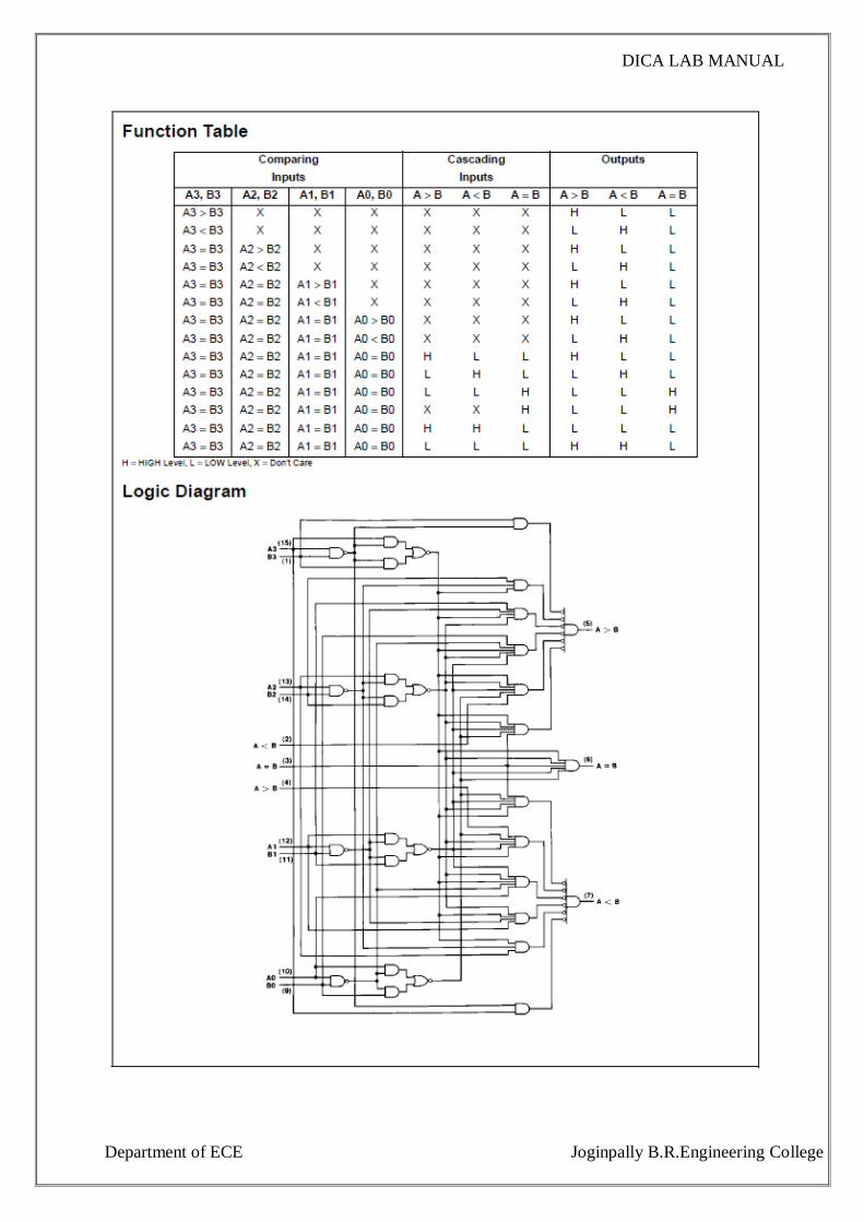
TRUTH TABLE:

DICA LAB MANUAL
Department of ECE Joginpally B.R.Engineering College
PROCEDURE:
1. Assemble the circuit as per the fig: 2.1 on the digital IC trainer kit.
2. Switch ON the power supply
3. Apply the logic inputs as per the truth table
4. Check the logical outputs when LEDs are ON/OFF

DICA LAB MANUAL
Department of ECE Joginpally B.R.Engineering College
PRECAUTIONS:
1. Check the connections before applying power
2. Care should be taken while verifying the operation of the circuit with truth table
RESULT:
16 bit comparator using 4-bit comparator is designed and its operation is studied and verified.
INFERENCES:
By designing and verifying a 16 bit comparator, it can be understood how large data
comparisons can be accomplished in complicated digital systems.
VIVA QUESTIONS:
1. Describe 74LS85 4-bit magnitude comparator.
2. The binary number A=1011 and B=1010 are applied to inputs of a 74LS85.
Determine the outputs
3. The following waveforms are applied to the comparator as shown. Determine the
output (A=B) waveform.

DICA LAB MANUAL
Department of ECE Joginpally B.R.Engineering College
EXPERIMENT -3
MODULO 53 COUNTERS USING 2 DECADE COUNTERS
AIM:
Design and verify the function of modulo 53 counter using 2 decade counters
Components required Equipment required Accessories required
ICs: 74LS90- 2 No.
74LS20- 1 No.
Digital IC trainer kit – 1No. Patch cords- 1Bunch
Switch (push button) : 1 No.
Resistors: 1K - 1No
10K-1 No.
CIRCUIT DIAGRAM:
Fig 3.1: CIRCUIT OF MODULO 53 COUNTER USING 2 DECADE COUNTERS

DICA LAB MANUAL
Department of ECE Joginpally B.R.Engineering College
TRUTH TABLE:
SW CLOCK D7 D6 D5 D4 D3 D2 D1 D0 O/P
Pressed X 0 0 0 0 0 0 0 0 (00)
Released ↓ 0 0 0 0 0 0 0 1 (01)
” ↓ . . . . . . . . .
” ↓ . . . . . . . . .
” ↓ . . . . . . . . .
” ↓ . . . . . . . . .
” ↓ 0 1 0 1 0 0 1 1 (53)
” ↓ 0 0 0 0 0 0 0 0 (00)
PROCEDURE:
1. Assemble the circuit as per the fig: 3.1 on the digital IC trainer kit.
2. Switch ON the power supply
3. Apply the logic inputs as per the truth table
4. Check the logical outputs when LEDs are ON/OFF

DICA LAB MANUAL
Department of ECE Joginpally B.R.Engineering College
PRECAUTIONS:
1. Check the connections before applying power
2. Care should be taken while verifying the operation of the circuit with truth table
RESULT:
Modulo 53 counter using 2 decade counters is designed and its operation is studied and
verified.
INFERENCES:
By designing and executing this experiment, one can learn using decade counter (74LS90)
how to design any no. of digits counters which count any events etc
VIVA QUESTIONS:
1. Explain how propagation delays affect the operation of a counter
2. Design a counter that will have any specified sequence of states
3. What is the difference between a 4-bit binary counter and a decode counter
4. How many states does a modulo 14 counter have? What is the minimum number of
flip-flop required?

DICA LAB MANUAL
Department of ECE Joginpally B.R.Engineering College
EXPERIMENT -4
DESIGN A 450 KHZ CLOCK USING NAND/ NOR GATES
AIM:
To design a 450 KHz clock using NAND/ NOR gates
CLOCK GENARATOR USING NAND GATES
Components required Equipment required Accessories required
IC: 74LS00 Digital IC trainer kit- 1No. Patch cords- 1Bunch
Resistors (Pot):
1K POT- 1No.
Capacitor- 0.01µF- 1No.
CLOCK GENARATOR USING NOR GATES
Components required Equipment required Accessories required
IC: 74LS02 Digital IC trainer kit- 1No. Patch cords- 1Bunch
Resistors (Pot):
1K POT- 1No.
Capacitor: 0.01µF- 1No.
CIRCUIT DIAGRAM:
Fig 4.1: CIRCUIT DAIGRAM OF 450 KHz CLOCK USING NAND GATES
DICA LAB MANUAL
Department of ECE Joginpally B.R.Engineering College
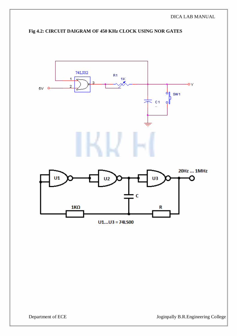
Fig 4.2: CIRCUIT DAIGRAM OF 450 KHz CLOCK USING NOR GATES

DICA LAB MANUAL
Department of ECE Joginpally B.R.Engineering College

DICA LAB MANUAL
Department of ECE Joginpally B.R.Engineering College
DESIGN:
NAND GATE:
Let SW be pressed and capacitor be initially discharged. Let A=5V
O/P of NAND gate is 5V and capacitor charges through R.
RC = T= 0.1tp, Let tp = 10µsec
Let tr = 2.2 Rc = 2.2 x 1 µsec = 2.2usec
RC = 1µsec
Let R=100Ω
C=1/100 µF =0.01µF
R=1K pot
NOR GATE:
Let SW be pressed and capacitor be initially discharged. Let A=0V
O/P of NOR gate is 5V and capacitor charges through R.
RC = T= 0.1tp, Let tp = 10µsec
Let tr = 2.2 Rc = 2.2 x 1 µsec = 2.2usec
RC = 1µsec
Let R=100Ω
C=1/100 µF =0.01µF
R=1K pot
PROCEDURE:
NAND GATES:
1. Assemble the circuit as per the fig: 4.1 on the digital IC trainer kit.
2. Switch ON the power supply
3. Observe the output on CRO by adjusting the potentiometer.
4. Check the output clock. It should be 450KHz
NOR GATES:
1. Assemble the circuit as per the fig: 4.2 on the digital IC trainer kit.
2. Switch ON the power supply

DICA LAB MANUAL
Department of ECE Joginpally B.R.Engineering College
3. Observe the output on CRO by adjusting the potentiometer.
4. Check the output clock. It should be 450KHz
PRECAUTIONS:
1. Check the connections before applying power
2. Care should be taken while verifying the operation of the circuit with truth table
RESULT:
450 KHz clock using NAND/ NOR gates is designed and its operation is studied and verified.
INFERENCES:
By executing this experiment, one can design low cost clock generator, without using custom
built clock generators which are not economical
VIVA QUESTIONS:
1. What is the principle involved in the design of a clock generator using NAND gate
2. Design a clock generator of frequency 300KHz using NOR gates
3. Give various applications of NAND & NOR gates

DICA LAB MANUAL
Department of ECE Joginpally B.R.Engineering College
EXPERIMENT -5
DESIGN A 4-BIT PSEUDO RANDOM SEQUENCE GENERATOR
USING 4-BIT RING COUNTER
AIM:
To design and verify a 4-bit pseudo random sequence generator using 4-bit ring counter
Components required Equipment required Accessories required
IC: 74LS195- 1No.
74LS86- 1No.
Digital IC trainer kit- 1No. Patch cords- 1Bunch
CIRCUIT DIAGRAM:
Fig 5.1: CIRCUIT DAIGRAM OF 4BIT PSEUDO RANDOM SEQUENCE GENERATOR

DICA LAB MANUAL
Department of ECE Joginpally B.R.Engineering College
TRUTH TABLE:
DICA LAB MANUAL
Department of ECE Joginpally B.R.Engineering College
PROCEDURE:
1. Assemble the circuit as per the fig: 5.1 on the digital IC trainer kit.
2. Switch ON the power supply
3. Apply the logic inputs as per the truth table
4. Check the logical outputs when LEDs are ON/OFF
PRECAUTIONS:
1. Check the connections before applying power
2. Care should be taken while verifying the operation of the circuit with truth table
RESULT:
4-bit pseudo random sequence generator using 4-bit ring counter is designed and its operation
is studied and verified.
INFERENCES:
Pseudo random sequence generator’s applications in digital systems is understood, especially
in applications like image cryptography, etc
VIVA QUESTIONS:
1. Give applications of pseudo random sequence generator.
2. What is meant by pseudo random sequence generator?
3. How can a capacitor generate a random numbers?
4. How does pseudo random number generator work?

DICA LAB MANUAL
Department of ECE Joginpally B.R.Engineering College
EXPERIMENT -6
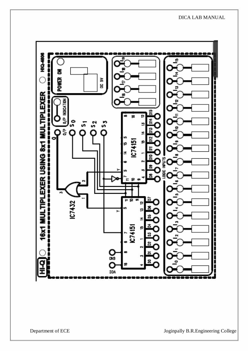
DESIGN A 16 X 1 MULTIPLEXER USING 8 X 1 MULTIPLEXER
AIM:
To design a 16 x 1 multiplexer using 8 x 1 multiplexer
Components required Equipment required Accessories required
IC: 74LS151- 2No.
74LS00- 1No.
74LS04- 1No.
Digital IC trainer kit-1No. Patch cords- 1Bunch
CIRCUIT DIAGRAM:
Fig 6.1: CIRCUIT DAIGRAM OF 16 x 1 MULTIPLEXER USING 8 x 1 MULTIPLEXER
DICA LAB MANUAL
Department of ECE Joginpally B.R.Engineering College

DICA LAB MANUAL
Department of ECE Joginpally B.R.Engineering College
TRUTH TABLE:
S3 S2 S1 S0 O/P
Y
0 0 0 0 I0
0 0 0 1 I1
0 0 1 0 I2
0 0 1 1 I3
0 1 0 0 I4
0 1 0 1 I5
0 1 1 0 I6
0 1 1 1 I7
1 0 0 0 I8
1 0 0 1 I9
1 0 1 0 I10
1 0 1 1 I11
1 1 0 0 I12
1 1 0 1 I13
1 1 1 0 I14
1 1 1 1 I15
PROCEDURE:
1. Assemble the circuit as per the fig: 6.1 on the digital IC trainer kit.
2. Switch ON the power supply
3. Apply the logic inputs as per the truth table
4. Check the logical outputs when LEDs are ON/OFF
PRECAUTIONS:
1. Check the connections before applying power
2. Care should be taken while verifying the operation of the circuit with truth table
RESULT:
16 x 1 multiplexer using 8 x 1 multiplexer is designed and its operation is studied and
verified.

DICA LAB MANUAL
Department of ECE Joginpally B.R.Engineering College
INFERENCES:
One can use these devices in various electronic communication systems (digital), real time
embedded system where multiple data processing is needed.
VIVA QUESTIONS:
1. Describe to 74LS151 and the 74LS157A multiplexer
2. How do you expand a multiplexer to handle more data inputs
3. Explain how the multiplexer can be used as a logic function generator
4. Give applications of multiplexer

DICA LAB MANUAL
Department of ECE Joginpally B.R.Engineering College
EXPERIMENT -7
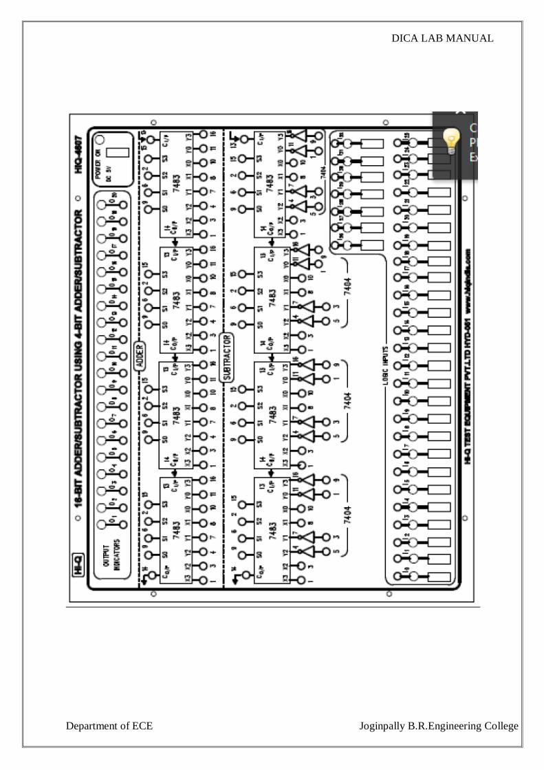
DESIGN A 16 BIT ADDER/ SUBTRACTOR USING 4-BIT ADDER/
SUBTRACTOR ICS
AIM:
To design and verify a 16 bit adder/ subtractor using 4-bit adder/ subtractor ICs
Components required Equipment required Accessories required
IC: 74LS283-2No.
74LS86-2No.
74LS02-1No.
Digital IC trainer kit- 1No. Patch cords-1Bunch
CIRCUIT DIAGRAM:
Fig 7.1: CIRCUIT DAIGRAM OF 16 BIT ADDER/SUBTRACTOR
DICA LAB MANUAL
Department of ECE Joginpally B.R.Engineering College

DICA LAB MANUAL
Department of ECE Joginpally B.R.Engineering College
TRUTH TABLE
FUNCTION:
Mode: 0 Addition
Mode: 1 Subtraction

DICA LAB MANUAL
Department of ECE Joginpally B.R.Engineering College
Theory:-
IC 7483 is a 4 bit parallel adder which consists of four interconnected full adders along with
the look ahead carry circuit. Here we are constructing the 16 bit adder/subtractor by
cascading the four 7483 ICs.
16 BIT ADDER :
A15A2A1A0 is a 4 bit input word 'A' and B15B2B1B0 is the second 4 bit input word 'B'. Cin0
is the input carry. The IC adds the 4 four bit words along with input carry to produce a 4 bit
sum and a one bit carry-out. Cout3 represents the output carry. S3,S2,S1,S0 represents sum
output with S3 as the MSB.In odrder to design an 8 bit adder, we require two IC 7483s
cascaded as shown in the figure above.
16bit adder/subtactor using 4 bit adder/subtractor
3 of 7Adder-1 is the LSB adder and it adds the four LSB bits of the two 8-bit input words ie
A15−A0 and 153−B0. The carry input of first adder is supposed to be 0.Hence the carry in pin
of LSB IC is connected to the ground. So the first IC adds the LSB bits of A and B, and
produces S3–S0 that is, LSB of sum, along with acarry out Cout3.This Cout3 of adder-1 is
connected to Cin0 input of Adder-2. The second adder adds this carry and the four MSB bits
of numbers A15−A0 and B15−B0 to produce MSB sum S7–S4 along with final carry out bit
Cout7.Thus adder-1 and adder-2 when cascaded as shown in the figure can add two 8-
bitwords. Cout7 of adder-2 acts as the final output carry and the sum output is from S7
though S0
16 BIT SUBSTRACTOR:
As with the binary adder, we can also have n number of 1-bit full binary subtractor connected
or “cascaded” together to subtract two parallel n-bit numbers from each other. For
exampletwo 4-bit binary numbers. We said beforethat the only difference between a full
adder and a full subtractor was theinversion of one of the inputs.So by using an n-bit adder
and n number of inverters (NOT Gates), the process ofsubtraction becomes an addition as we
can use two’s complement notation on allthe bits in the subtrahend and setting the carry input
of the least significant bit to alogic “1” (HIGH).Then we can use a 4-bit full-adder ICs such
as the 74LS283 and CD4008 toperform subtraction simply by using two’s complement on the
subtrahend, Binputs as X – Y is the same as saying, X + (-Y) which equals X plus the
two’scomplement of Y.
16bit adder/subtactor using 4 bit adder/subtractor
4 of 7If we wanted to use the 4-bit adder for addition once again, all we would need todo is
set the carry-in (CIN) input LOW at logic “0”. Because we can use the 4-bitadder IC such as
the 74LS83 or 74LS283 as a full-adder or a full-subtractor theyare available as a single
adder/subtractor circuit with a single control input for selecting between the two operations
PROCEDURE:
Procedure:-
Adder:
1. Apply the inputs A0-A15 and B0-B15 along with carry.
2. And observe S0-S15 and Cout.
Subtractor:
1. Apply the inputs A0-A15 and B0-B15 through not gates

DICA LAB MANUAL
Department of ECE Joginpally B.R.Engineering College
along with barrow.
2. And observe the output by taking the 2;s compliment of Binputs.
PRECAUTIONS:
1. Check the connections before applying power
2. Care should be taken while verifying the operation of the circuit with truth table
RESULT:
A 16 bit adder/ subtractor using 4-bit adder/ subtractor ICs is designed and its operation
is studied and verified.
INFERENCES:
It is understood that the dual function of both addition and subtraction can be implemented
with a simple addition of exclusive OR gates.
VIVA QUESTIONS:
1. How do you expand the 4-Bit adder to accomplish 8-Bit and 16-Bit addition
2. Explain method used for fast addition
3. Describe 74LS182 look ahead carry
4. Explain the working of N-Bit subtractor with the help of neat block diagram

DICA LAB MANUAL
Department of ECE Joginpally B.R.Engineering College
EXPERIMENT -8
PLOT THE TRANSFER CHARATERSTICS OF 74H, LS, HS SERIES
ICs
AIM:
Plot the transfer characteristics of 74H, LS, HS series ICs
Components required Equipment required Accessories required
ICs: 74LS04-1No.
74HC04-1No.
74HCT04-1No.
Digital IC trainer kit-1No. Patch cords-1Bunch
THEORY:
74LS Series ICs
The 74LS (Low-power Schottky) family (like the original) uses TTL (Transistor-Transistor
Logic) circuitry which is fast but requires more power than later families. The 74 series is
often still called the 'TTL series' even though the latest ICs do not use TTL!
74HC Series ICs
The 74HC family has High-speed CMOS circuitry, combining the speed of TTL with the
very low power consumption of the 4000 series. They are CMOS ICs with the same pin
arrangements as the older 74LS family. Note that 74HC inputs cannot be reliably driven by
74LS outputs because the voltage ranges used for logic 0 are not quite compatible, use
74HCT instead.
74HCT Series ICs
The 74HCT family is a special version of 74HC with 74LS TTL-compatible inputs so
74HCT can be safely mixed with 74LS in the same system. In fact 74HCT can be used as
low-power direct replacements for the older 74LS ICs in most circuits. The minor
disadvantage of 74HCT is a lower immunity to noise, but this is unlikely to be a problem in
most situations.
74LS family TTL characteristics
Supply: 5V ±0.25V, it must be very smooth, a regulated supply is best. In addition
to the normal supply smoothing, a 0.1µF capacitor should be connected across the
supply near the IC to remove the 'spikes' generated as it switches state, one capacitor
is needed for every 4 ICs.

DICA LAB MANUAL
Department of ECE Joginpally B.R.Engineering College
Inputs 'float' high to logic 1 if unconnected, but do not rely on this in a permanent
(soldered) circuit because the inputs may pick up electrical noise. 1mA must be
drawn out to hold inputs at logic 0. In a permanent circuit it is wise to connect any
unused inputs to +Vs to ensure good immunity to noise.
Outputs can sink up to 16mA (enough to light an LED), but they can source only
about 2mA. To switch larger currents you can connect a transistor.
Fan-out: one output can drive up to 10 74LS inputs, but many more 74HCT inputs.
Gate propagation time: about 10ns for a signal to travel through a gate.
Frequency: up to about 35MHz (under the right conditions).
Power consumption (of the IC itself) is a few mW.
74HC and 74HCT family characteristics
The CMOS circuitry used in the 74HC and 74HCT series ICs means that they are static
sensitive. Touching a pin while charged with static electricity (from your clothes for
example) may damage the IC. In fact most ICs in regular use are quite tolerant and
earthing your hands by touching a metal water pipe or window frame before handling
them will be adequate. ICs should be left in their protective packaging until you are ready
to use them.
74HC Supply: 2 to 6V, small fluctuations are tolerated.
74HCT Supply: 5V ±0.5V, a regulated supply is best.
Inputs have very high impedance (resistance), this is good because it means they
will not affect the part of the circuit where they are connected. However, it also
means that unconnected inputs can easily pick up electrical noise and rapidly change
between high and low states in an unpredictable way. This is likely to make the IC
behave erratically and it will significantly increase the supply current. To prevent
problems all unused inputs MUST be connected to the supply (either +Vs or
0V), this applies even if that part of the IC is not being used in the circuit!
Note that 74HC inputs cannot be reliably driven by 74LS outputs because the
voltage ranges used for logic 0 are not quite compatible. For reliability
use 74HCT if the system includes some 74LS ICs.
Outputs can sink and source about 4mA if you wish to maintain the correct output
voltage to drive logic inputs, but if there is no need to drive any inputs the maximum
current is about 20mA. To switch larger currents you can connect a transistor.
Fan-out: one output can drive many inputs (50+), except 74LS inputs because these
require a higher current and only 10 can be driven.
Gate propagation time: about 10ns for a signal to travel through a gate.
Frequency: up to 25MHz.
Power consumption (of the IC itself) is very low, a few µW. It is much greater at
high frequencies, a few mW at 1MHz for example.

DICA LAB MANUAL
Department of ECE Joginpally B.R.Engineering College
CIRCUIT DIAGRAM AND TRANSFER CHARACTERISTICS:
FIG 8.1: CIRCUIT DIAGRAM OF 74LS04: FIG 8.2: TRANSFER CHARACTERSISTICS OF 74LS04:
FIG 8.3: CIRCUIT DIAGRAM OF 74H04: FIG 8.4: TRANSFER CHARACTERSISTICS OF 74H04:

DICA LAB MANUAL
Department of ECE Joginpally B.R.Engineering College
FIG 8.5: CIRCUIT DIAGRAM OF 74HS04: FIG 8.6: TRANSFER CHARACTERSISTICS OF 74HS04:
PROCEDURE:
74LS04:
1. Assemble the circuit as per the fig: 8.1 on the digital IC trainer kit.
2. Switch ON the power supply
3. Apply the input voltage = 0 and note down the output.
4. Repeat step 3 for input voltages = 1V,2V,3V,4V,5V and note down the corresponding
outputs
74H04:
1. Assemble the circuit as per the fig: 8.3 on the digital IC trainer kit.
2. Switch ON the power supply
3. Apply the input voltage = 0 and note down the output.
4. Repeat step 3 for input voltages = 1V,2V,3V,4V,5V and note down the corresponding
outputs
74HS04:
1. Assemble the circuit as per the fig: 8.5 on the digital IC trainer kit.
2. Switch ON the power supply
3. Apply the input voltage = 0 and note down the output.
4. Repeat step 3 for input voltages = 1V,2V,3V,4V,5V and note down the corresponding
outputs

DICA LAB MANUAL
Department of ECE Joginpally B.R.Engineering College
TRAINER BOARD DIAGRAM

DICA LAB MANUAL
Department of ECE Joginpally B.R.Engineering College
OBSERVATIONS:
74LS04:
S.NO. VOLTAGE I/P VOLTAGE O/P
1 0V
2 1V
3 2V
4 3V
5 4V
6 5V
74HC04:
S.NO. VOLTAGE I/P VOLTAGE O/P
1 0V
2 1V
3 2V
4 3V
5 4V
6 5V
74HS04:
S.NO. VOLTAGE I/P VOLTAGE O/P
1 0V
2 1V
3 2V
4 3V
5 4V
6 5V
PRECAUTIONS:
1. Check the connections before applying power
2. Care should be taken while verifying the operation of the circuit with truth table
RESULT:
The transfer characteristics of 74H, LS, HS series ICs are studied, observed, and verified.
INFERENCES:
The difference among 74H, LS, & HS series ICs is understood and also the applications of
HCT series is understood which is popularly used nowadays.

DICA LAB MANUAL
Department of ECE Joginpally B.R.Engineering College
VIVA QUESTIONS:
1. Give the applications of 74H, LS, HS series ICs
2. What are the supply voltages, propagation delays, fan in and fan out of 74H, LS, HS
series ICs

DICA LAB MANUAL
Department of ECE Joginpally B.R.Engineering College
EXPERIMENT -9
DESIGN A 4-BIT GRAY TO BINARY AND BINARY TO GRAY
CONVERTER
AIM:
To design a 4-bit gray to binary and binary to gray converter
Components required Equipment required Accessories required
ICs: 74LS86-1No. Digital IC trainer kit-1No. Patch cords-1Bunch
CIRCUIT DIAGRAM:
Fig 9.1: CIRCUIT DAIGRAM OF 4-BIT BINARY AND BINARY TO GRAY CONVERTER

DICA LAB MANUAL
Department of ECE Joginpally B.R.Engineering College
TRUTH TABLE:

DICA LAB MANUAL
Department of ECE Joginpally B.R.Engineering College
PROCEDURE:
1. Assemble the circuit as per the fig: 9.1 on the digital IC trainer kit.
2. Switch ON the power supply
3. Apply the logic inputs as per the truth table
4. Check the logical outputs when LEDs are ON/OFF
PRECAUTIONS:
1. Check the connections before applying power
2. Care should be taken while verifying the operation of the circuit with truth table
RESULT:
A 4-bit gray to binary and binary to gray converter is designed and its operation is studied
and verified.
INFERENCES:
The applications of code converters, especially binary to gray conversion are understood. The
use of binary to BCD code converter is also understood.
DICA LAB MANUAL
Department of ECE Joginpally B.R.Engineering College
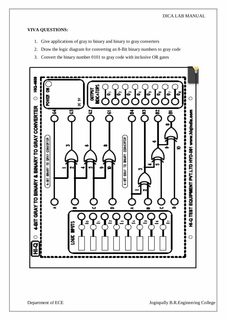
VIVA QUESTIONS:
1. Give applications of gray to binary and binary to gray converters
2. Draw the logic diagram for converting an 8-Bit binary numbers to gray code
3. Convert the binary number 0101 to gray code with inclusive OR gates

DICA LAB MANUAL
Department of ECE Joginpally B.R.Engineering College
EXPERIMENT -10
DESIGN A TWO DIGIT 7-SEGMENT DISPLAY UNIT USING THIS
DISPLAY MODE COUNTER OF EXPERIMENT 3
AIM: To design a 2 digit seven segment display using the display mode counter of
experiment 3.
Components required Equipment required Accessories required
ICs: 74LS47- 2 No.
CA 7-Segment – 2 No.
Digital IC trainer kit-1No. Patch cords-1Bunch
Resistors:330Ω - 14 No.s
1K Ω - 1 No
10K Ω - 1 No.
CIRCUIT DIAGRAM:
Fig 10.1: CIRCUIT DIAGRAM OF 2 DIGIT SEVEN SEGMENT DISPLAY USING THE
DISPLAY MODE COUNTER

DICA LAB MANUAL
Department of ECE Joginpally B.R.Engineering College
TRUTH TABLE:
SW D7 D6 D5 D4 D3 D2 D1 D0 MSD LSD FUNCTION
Pressed X X X X X X X X 8 8 Lamp Test
Released 0 0 0 0 0 0 0 0 No disp. No disp. Regular function
” 0 0 0 0 0 0 0 1 No disp. 1 ”
” . . . . . . . . . . ”
” . . . . . . . . . . ”
” 0 0 0 1 0 0 0 0 1 0 ”
” . . . . . . . . . . ”
” . . . . . . . . . . ”
” . . . . . . . . . . ”
” 0 1 0 1 0 0 1 1 5 3 ”
” 0 0 0 0 0 0 0 1 0 1 ”
PROCEDURE:
1. Assemble the circuit as per the fig: 10.1 on the digital IC trainer kit.
2. Switch ON the power supply
3. Apply the logic inputs from the modulo 53 counter as shown in the truth table
4. Check the output on 7-segment display.

DICA LAB MANUAL
Department of ECE Joginpally B.R.Engineering College

DICA LAB MANUAL
Department of ECE Joginpally B.R.Engineering College
PRECAUTIONS:
1. Check the connections before applying power
2. Care should be taken while verifying the operation of the circuit with truth table
RESULT:
A 2 digit seven segment display using the display mode counter of experiment 3 is designed
and its operation is studied
INFERENCES:
The decimal counter outputs can be well visualized with the help of 7-segment modules.
VIVA QUESTIONS:
1. Would you select a decoder/driver with active- High or active?
2. What are the features of IC 74LS47
3. What are the uses of LT, RBI and BI/RBO

DICA LAB MANUAL
Department of ECE Joginpally B.R.Engineering College
EXPERIMENT -11
DESIGN AN 8-BIT PARALLEL LOAD AND SERIAL OUT SHIFT
REGISTER USING TWO 4-BIT SHIFT REGISTERS
AIM:
To design an 8-bit parallel load and serial out shift register using two 4-bit shift registers
Components required Equipment required Accessories required
ICs: 74LS195-2No. Digital IC trainer kit- 1No. Patch cords- 1Bunch
CIRCUIT DIAGRAM:
Fig 11.1: CIRCUIT DAIGRAM OF 8-BIT PARALLEL LOAD AND SERIAL OUT
SHIFT REGISTER

DICA LAB MANUAL
Department of ECE Joginpally B.R.Engineering College
FUNCTION TABLE:
PROCEDURE:
1. Assemble the circuit as per the fig: 11.1 on the digital IC trainer kit.
2. Switch ON the power supply
3. Apply the logic inputs as per the function table.
4. Check the logical outputs when LEDs are ON/OFF
PRECAUTIONS:
1. Check the connections before applying power
2. Care should be taken while verifying the operation of the circuit with truth table

DICA LAB MANUAL
Department of ECE Joginpally B.R.Engineering College
RESULT:
An 8-bit parallel load and serial out shift register using two 4-bit shift registers is designed
and its operation is studied
INFERENCES:
The parallel load and serial out shift register can be used in interfacing BCD switch which
has 4 bit data. This 4-bit data can be read serially using only three signals which save the
input output ports when interfacing with microcontrollers.
VIVA QUESTIONS:
1. Explain how parallel in serial out shift register operate
2. Describe about the shift register 74LS195
3. Give applications of parallel in serial at shift register
4. Discuss the 74HC165 8-Bit parallel load shift register

DICA LAB MANUAL
Department of ECE Joginpally B.R.Engineering College
EXPERIMENT -12
DESIGN AN 8-BIT SERIAL IN AND SERIAL OUT SHIFT
REGISTER USING TWO 4-BIT SHIFT REGISTERS
AIM:
To design an 8-bit serial in and serial out shift register using two 4-bit shift registers
Components required Equipment required Accessories required
ICs: 74LS195-2No. Digital IC trainer kit-1No. Patch cords-1Bunch
CIRCUIT DIAGRAM:
Fig 12.1: CIRCUIT DAIGRAM OF 8-BIT SERIAL IN AND SERIAL OUT SHIFT
REGISTER

DICA LAB MANUAL
Department of ECE Joginpally B.R.Engineering College
FUNCTION TABLE:
PROCEDURE:
1. Assemble the circuit as per the fig: 12.1 on the digital IC trainer kit.
2. Switch ON the power supply
3. Apply the logic inputs as per the function table
4. Check the logical outputs when LEDs are ON/OFF
PRECAUTIONS:
1. Check the connections before applying power
2. Care should be taken while verifying the operation of the circuit with truth table
RESULT:
An 8 -bit serial in and serial out shift register is designed using two 4-bit shift registers and its
operation is studied
INFERENCES:
To interface multiple BCD switches, cascading of shift register, the data can be read with the
help of serial in and serial out option in the shift register.
VIVA QUESTIONS:
1. Explain how serial in and serial out shift register operate
2. Give applications of serial in and serial out shift register
3. How many clock pulses are required to enter a byte of data serially into an 8-Bit shift
register
4. Describe how a bidirectional shift register operates

DICA LAB MANUAL
Department of ECE Joginpally B.R.Engineering College

DICA LAB MANUAL
Department of ECE Joginpally B.R.Engineering College
EXPERIMENT -13
DESIGN A RING COUNTER AND TWISTED RING COUNTER
USING A 4-BIT SHIFT REGISTER
AIM:
To design a ring counter and twisted ring counter using a 4-bit shift register
A. RING COUNTER
Components required Equipment required Accessories required
ICs: 74LS195- 1No. Digital IC trainer kit- 1No. Patch cords- 1Bunch
CIRCUIT DIAGRAM:
Fig 13.1: CIRCUIT DAIGRAM OF COUNTER AND TWISTED RING COUNTER
USING A 4-BIT SHIFT REGISTER

DICA LAB MANUAL
Department of ECE Joginpally B.R.Engineering College
TRUTH TABLE:
PROCEDURE:
1. Assemble the circuit as per the fig: 13.1 on the digital IC trainer kit.
2. Switch ON the power supply
3. Apply the logic inputs as per the truth table
4. Check the logical outputs when LEDs are ON/OFF

DICA LAB MANUAL
Department of ECE Joginpally B.R.Engineering College
B. TWISTED RING COUNTER/ JOHNSON’S COUNTER
Components required Equipment required Accessories required
74LS195 Digital IC trainer kit Patch cords
CIRCUIT DIAGRAM:
Fig 13.2: CIRCUIT DIAGRAM OF TWISTED RING COUNTER
TRUTH TABLE:

DICA LAB MANUAL
Department of ECE Joginpally B.R.Engineering College
PROCEDURE:
1. Assemble the circuit as per the fig: 13.2 on the digital IC trainer kit.
2. Switch ON the power supply
3. Apply the logic inputs as per the truth table
4. Check the logical outputs when LEDs are ON/OFF
PRECAUTIONS:
1. Check the connections before applying power
2. Care should be taken while verifying the operation of the circuit with truth table
RESULT:
A ring counter and twisted ring counter is designed using a 4-bit shift register and its
operation is studied
INFERENCES:
One can use ring counters in hardware logic design (e.g. ASIC and FPGAdesign) to
create complicated finite state machines.
One can use Johnson or Twisted Ring Counters as:
1) Divider of clock inputs by varying their feedback loops.
2) A 3-stage Johnson Ring Counter could be used as a 3-phase, 120 degree phase shift
square wave generator.
3) A stepper motor controller.
VIVA QUESTIONS:
1. Determine the sequence of Johnson counter
2. Explain how a ring counter produces a specified sequence
3. Explain the operation of Johnson counter
4. Explain the operation of Johnson

DICA LAB MANUAL
Department of ECE Joginpally B.R.Engineering College

DICA LAB MANUAL
Department of ECE Joginpally B.R.Engineering College
EXPERIMENT -14
DESIGN A 4 DIGIT HEX COUNTER USING SYNCHRONOUS ONE
DIGIT HEX COUNTER
AIM:
To design a 4 digit hex counter using synchronous one digit hex counter
Components required Equipment required Accessories required
ICs: 74LS163A-4No.
74LS04-1No.
Digital IC trainer kit- 1No. Patch cords- 1Bunch
CIRCUIT DIAGRAM:
Fig 14.1: CIRCUIT DAIGRAM OF 4 DIGIT HEX COUNTER

DICA LAB MANUAL
Department of ECE Joginpally B.R.Engineering College
TRUTH TABLE:
PROCEDURE:
1. Assemble the circuit as per the fig: 14.1 on the digital IC trainer kit.
2. Switch ON the power supply
3. Apply the logic inputs as per the truth table
4. Check the logical outputs when LEDs are ON/OFF
PRECAUTIONS:
1. Check the connections before applying power
2. Care should be taken while verifying the operation of the circuit with truth table
RESULT:

DICA LAB MANUAL
Department of ECE Joginpally B.R.Engineering College
A 4 digital hex counter is designed using synchronous one digital hex counter and its
operation is studied
INFERENCES:
We can use synchronous hex counters in fast counting applications but the clock signal may
be loaded.
VIVA QUESTIONS:
1. Describe IC 74LS163A binary counter synchronization
2. Give application of x hex counter

DICA LAB MANUAL
Department of ECE Joginpally B.R.Engineering College

DICA LAB MANUAL
Department of ECE Joginpally B.R.Engineering College
EXPERIMENT -15
DESIGN A 4 DIGITAL HEX COUNTER USING ASYNCHRONOUS
ONE DIGIT HEX COUNTER
AIM:
To design a 4 digital hex counter using asynchronous one digit hex counter
Components required Equipment required Accessories required
ICs: 74LS93A-4No. Digital IC trainer kit-1No. Patch cords-1Bunch
CIRCUIT DIAGRAM:\
Fig 15.1: CIRCUIT DAIGRAM OF 4 DIGITAL HEX COUNTER

DICA LAB MANUAL
Department of ECE Joginpally B.R.Engineering College
FUNCTION TABLE:
MR=1 Reset a counter in Q15…….Q0 = 0……0
MR=0 Clock I/P↓ counts clock cycles continues counting after applying the
clock.
PROCEDURE:
1. Assemble the circuit as per the fig: 15.1 on the digital IC trainer kit.
2. Switch ON the power supply
3. Apply the logic inputs as per the truth table
4. Check the logical outputs when LEDs are ON/OFF
PRECAUTIONS:
1. Check the connections before applying power
2. Care should be taken while verifying the operation of the circuit with truth table
RESULT:
A 4 digital hex counter is designed and using asynchronous one digit hex counter and its
operation is studied
INFERENCES:
The asynchronous hex counters can be used in applications where loading of clock signals
should be avoided. But these are used in low speed applications.
VIVA QUESTIONS:

DICA LAB MANUAL
Department of ECE Joginpally B.R.Engineering College
1. Describe 74LS163A binary counter
2. Give applications of x hex counter

DICA LAB MANUAL
Department of ECE Joginpally B.R.Engineering College
APPENDIX
I. DATASHEET OF 74LS148

DICA LAB MANUAL
Department of ECE Joginpally B.R.Engineering College

DICA LAB MANUAL
Department of ECE Joginpally B.R.Engineering College
II. DATASHEET OF 74LS00

DICA LAB MANUAL
Department of ECE Joginpally B.R.Engineering College
III. DATASHEET OF 74LS85
DICA LAB MANUAL
Department of ECE Joginpally B.R.Engineering College
DICA LAB MANUAL
Department of ECE Joginpally B.R.Engineering College
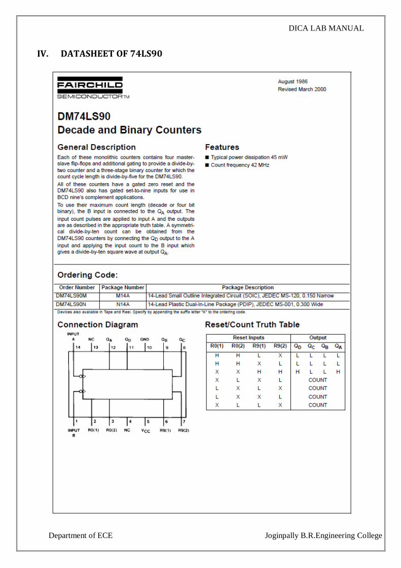
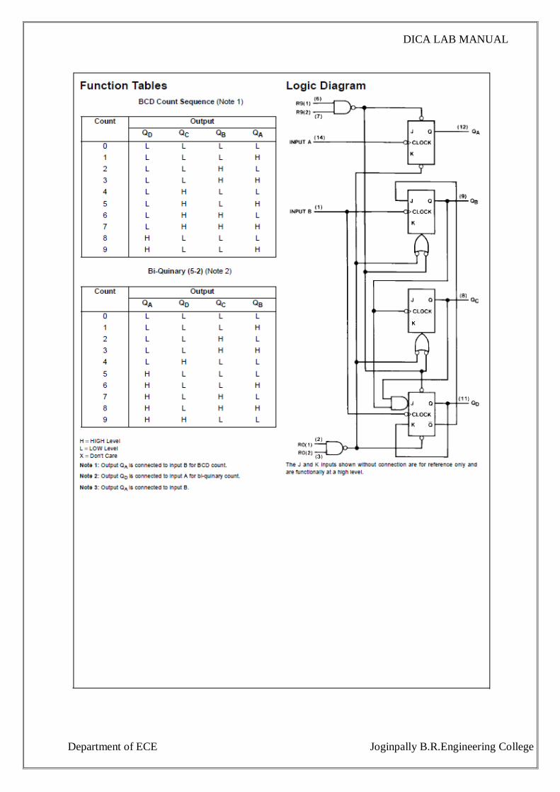
IV. DATASHEET OF 74LS90
DICA LAB MANUAL
Department of ECE Joginpally B.R.Engineering College

DICA LAB MANUAL
Department of ECE Joginpally B.R.Engineering College
V. DATASHEET OF 74LS02

DICA LAB MANUAL
Department of ECE Joginpally B.R.Engineering College
VI. DATASHEET OF 74LS195

DICA LAB MANUAL
Department of ECE Joginpally B.R.Engineering College

DICA LAB MANUAL
Department of ECE Joginpally B.R.Engineering College
VII. DATASHEET OF 74LS86
DICA LAB MANUAL
Department of ECE Joginpally B.R.Engineering College
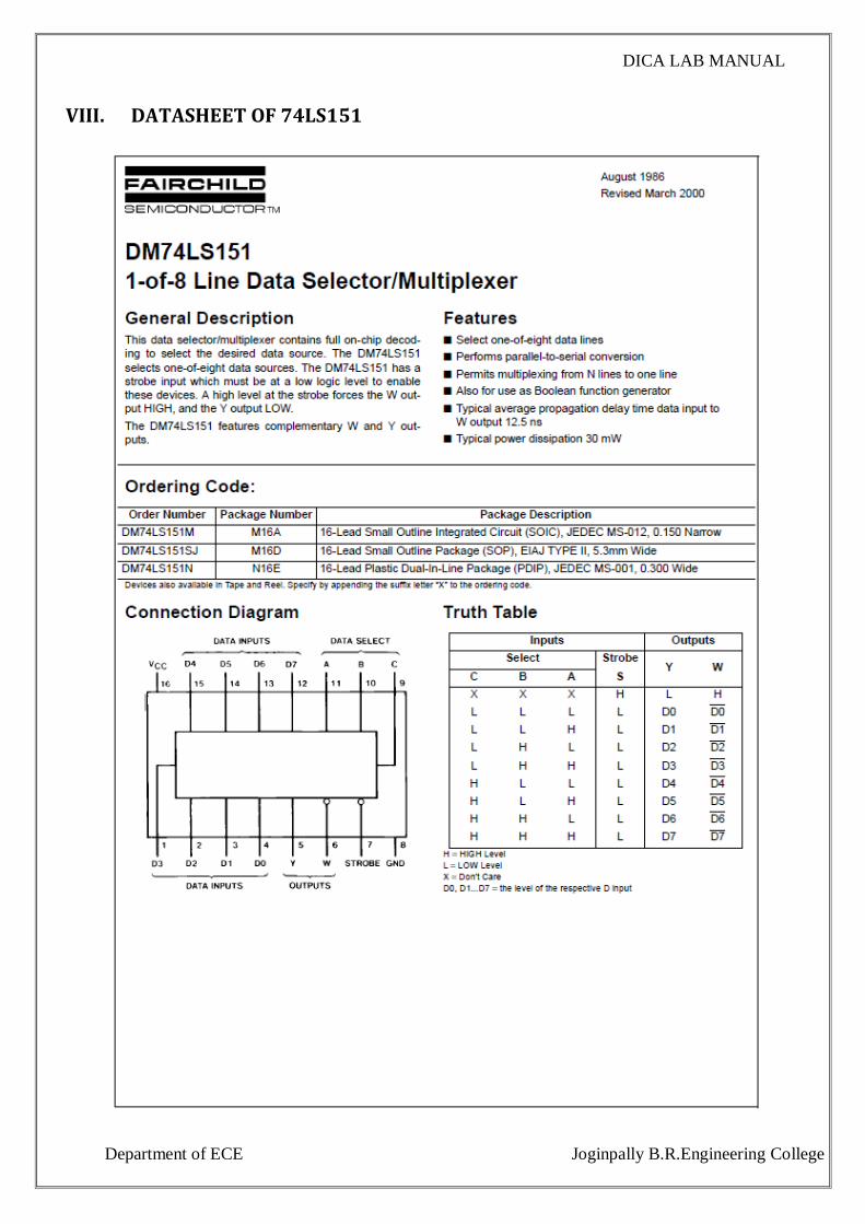
VIII. DATASHEET OF 74LS151

DICA LAB MANUAL
Department of ECE Joginpally B.R.Engineering College
IX. DATASHEET OF 74LS283

DICA LAB MANUAL
Department of ECE Joginpally B.R.Engineering College

DICA LAB MANUAL
Department of ECE Joginpally B.R.Engineering College
X. DATASHEET OF 74LS47

DICA LAB MANUAL
Department of ECE Joginpally B.R.Engineering College

DICA LAB MANUAL
Department of ECE Joginpally B.R.Engineering College
XI. DATASHEET OF 74LS163A

DICA LAB MANUAL
Department of ECE Joginpally B.R.Engineering College
DICA LAB MANUAL
Department of ECE Joginpally B.R.Engineering College
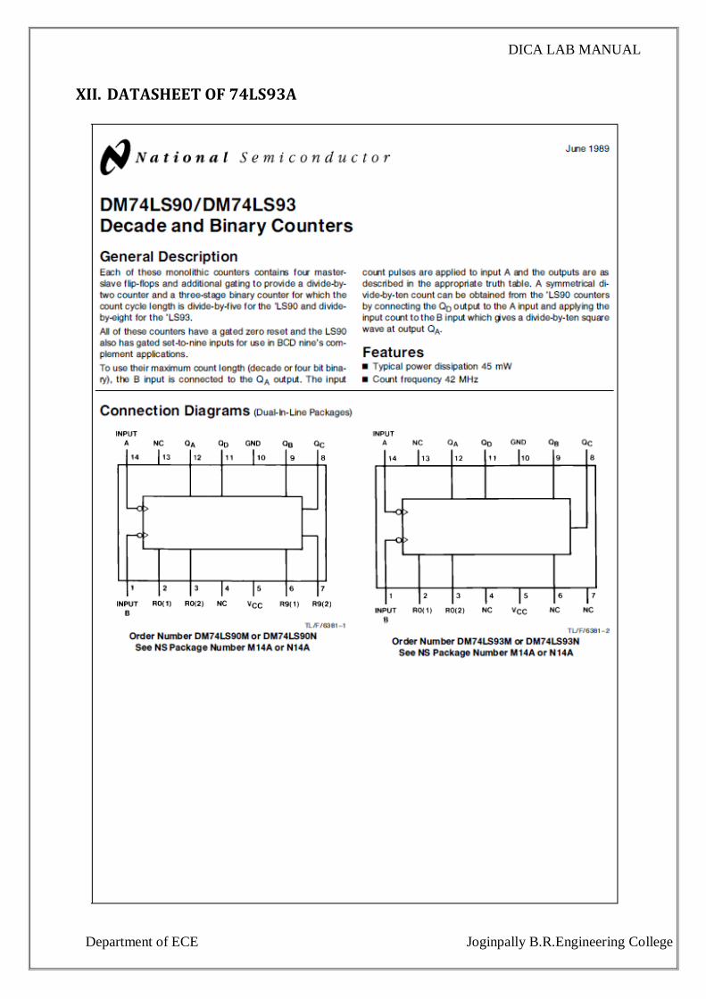
XII. DATASHEET OF 74LS93A

DICA LAB MANUAL
Department of ECE Joginpally B.R.Engineering College

DICA LAB MANUAL
Department of ECE Joginpally B.R.Engineering College
XIII. CA SEVEN SEGMENT MODULE

DICA LAB MANUAL
Department of ECE Joginpally B.R.Engineering College
XIV. DATASHEET OF 74LS04
DICA LAB MANUAL
Department of ECE Joginpally B.R.Engineering College
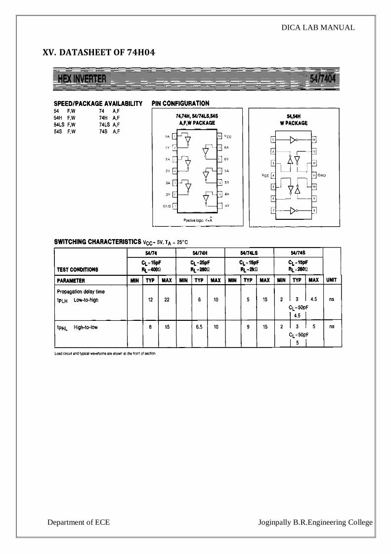
XV. DATASHEET OF 74H04

DICA LAB MANUAL
Department of ECE Joginpally B.R.Engineering College
XVI. DATASHEET OF 74HCT04

DICA LAB MANUAL
Department of ECE Joginpally B.R.Engineering College

DICA LAB MANUAL
Department of ECE Joginpally B.R.Engineering College
XVII. DATASHEET OF 74LS20

DICA LAB MANUAL
Department of ECE Joginpally B.R.Engineering College
REFERENCES
1. Digital fundamentals - Floyd and jain
2. Digital IC applications – A.P. Godse, D.A.Godse
3. Digital principles and applications – Albert Paul, Donald P. Leach
4. Digital Electronics: Principles, Devices and Applications – Anil K Maini
5. Fundamentals of Digital Circuits – Anand Kumar
6. Digital Electronics and Logic Design – Somnathan Nair
7. www.wikipedia.org
8. https://www.allaboutcircuits.com
9. https://www.ece.ncsu.edu/research/ecs/dc