digital circuits - encyclopedia of life support systems
TRANSCRIPT

UNESCO – EOLS
S
SAMPLE C
HAPTERS
CIRCUITS AND SYSTEMS - Digital Circuits - Christian Piguet
©Encyclopedia of Life Support Systems (EOLSS)
DIGITAL CIRCUITS Christian Piguet CSEM, Neuchâtel, & EPFL, Lausanne, Switzerland Keywords: Digital, Boolean, VHDL, CMOS technology, Binary Decision Machine, Microcontroller, DSP Processor, Low Power. Contents 1. Introduction 2. Boolean Logic and Combinational Circuits 3. VHDL Description of Combinational Circuits 4. Logic Gates in CMOS Technology 5. Design of CMOS Circuits 6. Finite State Machines 7. Binary Decision Diagrams 8. Binary Decision Machines 9. Design of a Very Simple Microprocessor 10. Microcontrollers 11. DSP Processors 12. Low power in digital circuits 13. Conclusion Glossary Bibliography Biographical Sketch Summary This chapter presents the design of digital systems and circuits, starting from Boolean logic, logic gates and CMOS transistors, as it is the mainstream technology to implement digital circuits. The design methodology to implement logic circuits in CMOS transistors is presented, starting from the Karnaugh map. With logic gates, one can design finite state machines which are sequential machines comprising a combinational circuit and a clocked register. Microprocessors are also digital circuits, and their design will be presented step by step, starting from programmable finite state machines, then introducing binary decision machines from which the design of very simple microprocessors can be easily explained. More complex microprocessors like available microcontrollers and DSP processors are also described. Finally, as power consumption is the main problem today for all digital circuits, several techniques of power reduction are presented. 1. Introduction Digital circuits are well-known from very long time ago, based on switches that adopt a very simple model: on or off. So one can use Boolean expressions, true and false, implemented as Vdd and Vss or “1” and “0”. The spectacular development of digital
UNESCO – EOLS
S
SAMPLE C
HAPTERS
CIRCUITS AND SYSTEMS - Digital Circuits - Christian Piguet
©Encyclopedia of Life Support Systems (EOLSS)
circuits comes from the microelectronics technology, starting with the vacuum tubes used as switches, transistors invented in late 1947 and integrated circuits in 1958, to recent single chips which could contain more than one billion of switches. The ITRS roadmap, established and reviewed annually by experts of semiconductor companies, proposes a roadmap for the next 15 years. Predictions for 2022 are 11 nanometers technologies, about 70 billions of transistors, more than 10 GHz frequency, nominal voltage of about 0.8 Volt and maximum 130 watts of power consumption. However, for economical reasons, nobody can predict if we will see such a technology or we will see saturation before this 11 nanometer node. The ITRS roadmap is however not limited to the technology scaling and proposes to look at three different axes: • More Moore (continuing the technology scaling towards 11 nanometers) • More than Moore (introducing heterogeneity in single chips with analog, special
memories, microsystems such as sensors and actuators, energy scavenging devices, antennas, optics, on top or besides of the chips)
• Beyond CMOS (new nano-switches, such as nanowires, nanotubes, molecular switches, etc.. aiming at outstanding performances mainly in power consumption reduction).
However, this chapter will start from the beginning, looking at the design of digital circuits starting from Boolean logic. 2. Boolean Logic and Combinational Circuits Boolean expressions, i.e. statements that are true or false, are used for electronic circuits as true and false are easily translated into “1” and “0” (or Vdd=supply voltage and Vss=ground). Boolean variables like A, B, C,… take only values “1” and “0”. Logical operations are NOT (complementation), OR (addition) and AND (multiplication). Boolean expression like (A B) + C means that first the product A B (AND operation) is evaluated and then ORing the result with C. If we assume a circuit with three inputs A, B and C, there are 8 possible input states. The output Z can be defined with a truth table depicted in Table 1. A truth table is a model of a combinational circuit for which each input state defines a single output. In other words, the output depends only on the input state and not from some internal memorized state, as it is the case in sequential circuits.
ABC Z 000 1 001 0 010 1 011 1 100 1 101 1
UNESCO – EOLS
S
SAMPLE C
HAPTERS
CIRCUITS AND SYSTEMS - Digital Circuits - Christian Piguet
©Encyclopedia of Life Support Systems (EOLSS)
110 0 111 1
Table 1. Truth Table of Function Z
Using the truth table of Table 1, it is possible to synthesize the corresponding electronic circuit. Each input state which has its output at “1” is called a minterm. The function Z is therefore the logical sum of all the minterms. One has:
Z ABC ABC ABC A BC A BC ABC= + + + + + This Boolean equation can be implemented by 6 AND gates with 3 inputs (implementation of the 6 minterms) and with an OR gate with 6 inputs (the outputs of the 6 AND gates). Such an implementation is far from being minimal. It can be simplified by using theorems about Boolean Logic like ( 1X X+ = ). The first term and the fourth term of the Z equation can be simplified ( )A A BC BC+ = . The same process
can be applied to 2nd and 3rd terms, as well as the two last terms. One has:
( )Z + ( ) ( ) A A BC AB C C AC B B BC AB AC= + + + + = + +
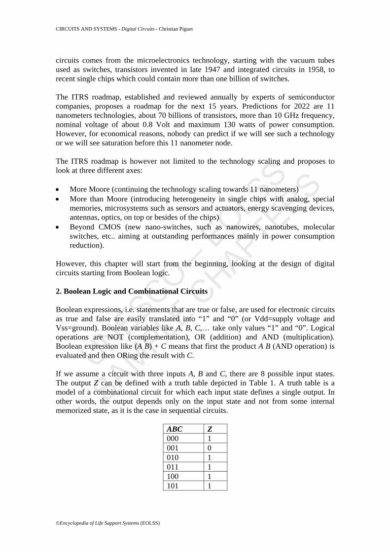
This process is a quite difficult task for more complex functions. It why the normal process is to transform the truth table into a Karnaugh map (Figure 1). It is the same representation than the truth table, but the cubes are arranged (00, 01, 11, 10) in such a way that blocks of “ones” can be identified much more easily. The goal is to identify the minimum number and the largest blocks of “1”. In Figure 1, one identifies three blocks of “1” containing each two cubes. It is easy to find the Z equation. For instance, the vertical block of “1” in the second column is defined for 0A = and for 1B = , so it is the AB block. The resulting Z equation is therefore: Z + BC AB AC= + It is the same that the equation obtained after simplification of the equation derived from the minterms.
Figure 1. Karnaugh Map of Function Z
UNESCO – EOLS
S
SAMPLE C
HAPTERS
CIRCUITS AND SYSTEMS - Digital Circuits - Christian Piguet
©Encyclopedia of Life Support Systems (EOLSS)
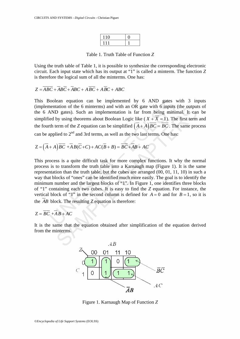
The implementation of this equation requires only 3 AND gates with two inputs followed by an OR gate with only three inputs (Figure 2). So the cost in terms of number of transistors is drastically reduced (nearly a factor 4) compared to the equation derived from the minterms. Such an implementation has been used in the past when small integrated circuits containing a few logic gates were available. These small integrated circuits were assembled on a printed board to implement the function of Figure 2. Today, with submicron CMOS technologies, digital circuits are designed using high-level hardware description languages (Section 3) and the design of basic CMOS cells are directly synthesized in CMOS transistors (Sections 4 and 5).
Figure 2. Implementation of Z in terms of NOT, AND and OR gates 3. VHDL Description of Combinational Circuits To cope with the complexity of digital circuits containing several millions of MOS transistors (in 2010, some microprocessors with their cache memories reach 1 billion of MOS transistors), it is impossible to use Karnaugh maps. A high-level language is the only way to describe a complex digital circuit. Today, two such languages are used: VHDL and Verilog. Then a CAD tool called a logic synthesizer is capable of translating this input description into a net-list of basic cells like NOR, NAND, XOR gates, but also 1-bit adders, flip-flops, latches, multiplexers, decoders, etc… Obviously, a VHDL description of a complete microprocessor comprises hundreds to thousands of pages and in this chapter, one is forced to present VHDL with a very small example: 1-bit full adder. A VHDL description provides two views of the circuit called design units: • an external view or entity • an internal view or architecture The entity defines the circuit name, its inputs and outputs and some optional parameters. It is therefore completely separated of the function. The internal view describes the architecture, and this can be achieved at three levels of abstraction: • behavioral level (what the circuit does, not its structure) • dataflow or RTL (register transfer language), mainly logical equations for
combinational circuits • structural, a net-list based on other components such as basic gates
UNESCO – EOLS
S
SAMPLE C
HAPTERS
CIRCUITS AND SYSTEMS - Digital Circuits - Christian Piguet
©Encyclopedia of Life Support Systems (EOLSS)
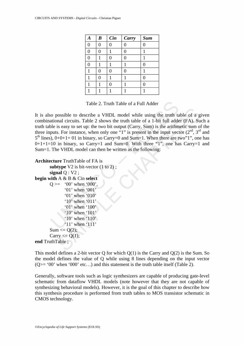
A B Cin Carry Sum 0 0 0 0 0 0 0 1 0 1 0 1 0 0 1 0 1 1 1 0 1 0 0 0 1 1 0 1 1 0 1 1 0 1 0 1 1 1 1 1
Table 2. Truth Table of a Full Adder
It is also possible to describe a VHDL model while using the truth table of a given combinational circuits. Table 2 shows the truth table of a 1-bit full adder (FA). Such a truth table is easy to set up: the two bit output (Carry, Sum) is the arithmetic sum of the three inputs. For instance, when only one “1” is present in the input vector (2nd, 3rd and 5th lines), 0+0+1= 01 in binary, so Carry=0 and Sum=1. When there are two”1”, one has 0+1+1=10 in binary, so Carry=1 and Sum=0. With three “1”, one has Carry=1 and Sum=1. The VHDL model can then be written as the following: Architecture TruthTable of FA is subtype V2 is bit-vector (1 to 2) ; signal Q : V2 ; begin with A & B & Cin select Q >= ‘00’ when ‘000’, ‘01’ when ‘001’ ‘01’ when ‘010’ ‘10’ when ‘011’ ‘01’ when ‘100’ ‘10’ when ‘101’ ‘10’ when ‘110’ ‘11’ when ‘111’ Sum <= Q(2); Carry <= Q(1); end TruthTable ; This model defines a 2-bit vector Q for which Q(1) is the Carry and Q(2) is the Sum. So the model defines the value of Q while using 8 lines depending on the input vector (Q>= ‘00’ when ‘000’ etc…) and this statement is the truth table itself (Table 2). Generally, software tools such as logic synthesizers are capable of producing gate-level schematic from dataflow VHDL models (note however that they are not capable of synthesizing behavioral models). However, it is the goal of this chapter to describe how this synthesis procedure is performed from truth tables to MOS transistor schematic in CMOS technology.

UNESCO – EOLS
S
SAMPLE C
HAPTERS
CIRCUITS AND SYSTEMS - Digital Circuits - Christian Piguet
©Encyclopedia of Life Support Systems (EOLSS)
4. Logic Gates in CMOS Technology The CMOS technology is today the mainstream technology, and even with beyond CMOS devices, the corresponding switches will have similar models than CMOS transistors. Transistor models for the design of CMOS basic cells are very simple. They are simple switches (Figure 3). The N-ch MOS device is conducting (“on” state) with a gate 1G = and non-conducting (“off” state) with 0G = . The P-ch MOS device is conducting with a gate 0G = and non-conducting with 1G = .
Figure 3. MOS Transistor Model The structure of a CMOS combinational circuit is defined by a set of N-ch and P-ch transistors as well as by a set of nodes, i.e. interconnections between transistors. A serial-parallel network of transistors can be designed by successive serial or parallel composition operations. Such a network has always two nodes y and z that are the end points of the network. Figure 4 shows various networks such as a basic network with a single transistor as well as two networks resulting of the application of the two serial and parallel composition operations. Finally, an example of a complex transistor network is depicted. In a transistor network (Figure 4), as all the inputs xi are at ‘0’ or ‘1’, each transistor is either conducting or non-conducting. If there is a conducting path from y to z (Figure 4), the network is conducting and it is non-conducting in the other case. The Conduction Function of the network is defined like the following: C(X1, X2, ...., Xn) is =1 if the network is conducting and =0 if it is non-conducting.
Figure 4. Serial-parallel networks
UNESCO – EOLS
S
SAMPLE C
HAPTERS
CIRCUITS AND SYSTEMS - Digital Circuits - Christian Piguet
©Encyclopedia of Life Support Systems (EOLSS)
Some examples of Conduction Functions are the following: • a single N-ch MOS controlled by x has a conduction function CN=x (Figure 4) • a single P-ch MOS controlled by x has a conduction function CN=NOT(x), as a P-
ch transistor is “on” with a ‘0’ on its gate (Figure 3) • the conduction function Cs of two serial networks with C1 and C2 as Conduction
Functions is the logical AND of C1 and C2, due to the fact that the two serial networks have to be conducting to have a conducting path between y and z : Cs = C1 * C2
• the conduction function Cp of two parallel networks with C1 and C2 as Conduction Functions is the logical OR of C1 and C2, due to the fact that only one network of the two networks has to be conducting to have a conducting path between y and z : Cp = C1 + C2
Another type of expression is the Structural Expression which is directly derived from the transistor network. In the last example of Figure 4 (at the right), one can see a transistor network. One can extract from this network a Structural Expression called zN or zP depending if it is implemented with N-ch or P-ch transistors. Serial composition of transistors implies an AND operation and parallel composition of transistors implies an OR operation in the structural expression. Assuming N-ch transistors, the structural expression Nz of Figure 4 is: ( ) ( )1 2 3 * 2 3Nz x x x x x= + + + .
What is the relationship between Conduction Functions and Structural Expressions? To a structural expression corresponds a unique conduction function, but several structural expressions can correspond to the same conduction function. It is due to the fact that several serial and parallel transistor schematics can provide the same conduction function. One has:
( ) ( )NC X1, X2, ...., Xn zN X1, X2, ...., Xn=
( ) ( ) ( ) ( )( )PC X1, X2, ...., Xn zP NOT X1 , NOT X2 ...., NOT Xn= For the N-ch network, one can derive the conduction function CN by copying the structural expression zN. However, for zP, as P-ch transistors are conducting with a ‘0’ on their gates, the P-ch conduction function CP is obtained from the structural expression zP by inverting each input variable. A simple combinational circuit is constructed by two N-ch and P-ch serial-parallel networks of transistors, connected as shown in Figure 5, and for which the two conduction functions are complementary. Each N-ch et P-ch network is characterized by a conduction function:
( ) ( )0C X1, X2, ....., Xn for N ch and C1 X1, X2, ....., Xn for P ch− − The goal of the CMOS logic style is to have always one of the two Nch and P-ch networks non-conducting and the other conducting. On one hand, there is always a

UNESCO – EOLS
S
SAMPLE C
HAPTERS
CIRCUITS AND SYSTEMS - Digital Circuits - Christian Piguet
©Encyclopedia of Life Support Systems (EOLSS)
conducting path between the output z and Vdd or Vss, and on the other hand, the result is that there is never a conducting path between Vdd and Vss. It is why CMOS technology is a low-power logic style, which is not the case of N-MOS logic style in which a load resistance between Vdd and the output results in a permanent current when the output is ‘0’.
Figure 5. CMOS Combinatorial Circuit One has the following relation: ( ) ( )( )0 1C X1, X2, ....., Xn NOT C X1, X2, ....., Xn= Figure 5 shows the structure of a CMOS gate with conduction functions C0 and C1. To represent the two N-ch and P-ch networks of a CMOS gate in a single expression, one can write the symmetrical logical equation like the following:
( ) [ ] ( )0 1z C X1, X2, ...., Xn 0 C X1, X2, ...., Xn [1]= + The symbol [0] means that the N-ch network is connected to Vss (logic 0) and [1] means that the P-ch network is connected to Vdd (logic 1). One has to notice that CMOS gates are always inverting gates (or negative gates). It is not possible to implement directly a positive gate like a buffer or a AND gate. To implement a buffer, one has to design two inverters in series, so two negative gates in series. For implementing a AND gate, one has to design a NAND gate followed by an inverter. So the building blocks of the CMOS are inverting gates and some design methodologies are based on this observation, providing efficient implementations.
UNESCO – EOLS
S
SAMPLE C
HAPTERS
CIRCUITS AND SYSTEMS - Digital Circuits - Christian Piguet
©Encyclopedia of Life Support Systems (EOLSS)
- - -
TO ACCESS ALL THE 41 PAGES OF THIS CHAPTER, Visit: http://www.eolss.net/Eolss-sampleAllChapter.aspx
Bibliography Unger S. H. (1997). The Essence of Logic Circuits. IEEE Press, New-York, second Edition. [Basics of Boolean Logic]
Uyemura J. P. (1992). Circuit Design for CMOS VLSI. Kluwer Academic Publishers, 1992. [Basics of CMOS logic]
Weste N., Eshraghian K. (1985). Principles of CMOS VLSI Design : A Systems Perspective. Addison Wesley, 1985. [Basics of CMOS logic]
Piguet C., Zahnd J. , Stauffer A., Bertarionne M. (1984). A Metal-Oriented Layout Structure for CMOS Logic. IEEE J. of Solid-State Circuits SC-19, No 3, pp. 425-436, June 1984 [First description of logic circuits implemented with branches]
Masgonty J. M. et al. (1991). Technology- and Power-Supply-Independent Cell Library. CICC'91, May 12-15, 1991, San Diego, USA. [Proposal of branch-based Standard Cell Libraries]
Piguet C. et al. (199). Low-Power Low-Voltage Digital CMOS Cell Design. PATMOS'94, Oct. 17-19, Barcelona, Spain, pp. 132-139. [Design of low-power logic cells]
Piguet C. [1991]. Logic Synthesis of Race-Free Asynchronous CMOS Circuits. IEEE J. of Solid-State Circ., Vol SC-26, No 3, March 1991, pp. 371-380. [how to design sequential cells like flip-flops using asynchronous design]
Piguet C., Zahnd J. (1998). Signal-Transition Graphs-based Design of Speed-Independent Basic Cells. PATMOS'98, October 6-8, 1998, Copenhagen, Denmark. [the design of flip-flops using asynchronous STG methodology]
Piguet C. (1996). Low-Power Design of Finite State Machines. Proc. PATMOS'96, pp. 25-34, September 23-27, 1996, Bologna, Italy. [Introduction of gated clocks in Finite State Machines]
Cerny E., Mange D., Sanchez E., (1979). Synthesis of Minimal Binary Decision Trees, IEEE Trans. Computers, Vol. C-28, No 7, 1979, pp. 472-482. [How to simplify Binary Decision Diagrams].
Clare C. (1973). Designing Logic Systems Using State Machines. McGraw-Hill, New-York, 1973. [The first book on Binary Decision Machines]
Boute R. T. (1976). The Binary-Decision Machine as Programmable Controller. EUROMICRO Newsletter, Vol. 2, No 7, 1976, pp. 16-22. [One of the first implementation of a Binary Decision Machines]
Mange D. (1986). A High-Level-Language Programmable Controller. Part I: A Controller for Structured Microprogramming. Part II: Microcompilation of the High-Level-Language Micropascal. IEEE MICRO Vol. 6, No 1, 1986, pp. 25-41, and No 2, 1986, pp. 47-63. [How to compile a small high-level language on controllers similar to BDM].
Zsombor-Murray P. J. A. et al. (1983). Binary-Decision-Based Programmable Controllers. Part I, II, III, IEEE MICRO,1983, Vol. 3, No 4, pp. 67-83, No 5, pp. 16-26 et No 6, pp. 24-39. [Design of BDM]
Piguet C. (1983). Design Methodology for Full Custom CMOS Microcomputers. INTEGRATION, the VLSI Journal, No 1, 1983, pp. 335-350. [Desig of first low power microcontrollers for ASIC circuits]
UNESCO – EOLS
S
SAMPLE C
HAPTERS
CIRCUITS AND SYSTEMS - Digital Circuits - Christian Piguet
©Encyclopedia of Life Support Systems (EOLSS)
Fitzpatrick D. T. et al. (1981). A RISCy Approach to VLSI. VLSI Design, No 4, 1981, pp. 14-20. [The first RISC computers]
Patterson D. A., Séquin C. H. (1982). A VLSI RISC. IEEE Computer Vol. 15, No 9, 1982, pp. 8-21. [The first RISC computers]
Piguet C. (1990), Binary-decision and RISC-like machines for semicustom design. Microprocessors and microsystems, Vol 14, No 4, May 1990, pp. 231-240. [From BDM to first very simple microcontrollers]
Piguet C. et al, (1997). Low-Power Design of 8-bit Embedded CoolRISC Microcontroller Cores. IEEE JSSC, Vol. 32, No 7, July 1997, pp. 1067-1078. [A complete description of the RISC 8-bit CoolRISC microcontroller]
Frantz G. (2000). Digital Signal Processor Trends. IEEE Micro, November-December 2000, pp. 52-59. [An introduction to DSP processors]
Arm C et al. (2006). Low-Power Quad MAC 170 μW/MHz 1.0 V MACGIC DSP Core. ESSCIRC 2006, Sept. 19-22. 2006, Montreux, Switzerland. [Description of the design of a powerful DSP processor with 4 MAC in parallel called MACGIC]
Arm C. et al. (2009). Low-Power 32-bit Dual-MAC 120 uW/MHz 1.0 V icyflex DSP/MCU Core. IEEE J. of Solid-State Circuits (JSSC), Vol. 44, No 7, July 2009, pp. 2056-2065. [Description of the design of a processor combining control and DSP called icyflex]
Christian Piguet, Editor (2005). Low-Power Electronics Design. CRC Press, 2005, ISBN 0-8493-1941-2 [Description of all aspects related to the reduction of power consumption in integrated circuits]
Vittoz E. A. (1994). Low Power Design : Ways to Approach the Limits. Plenary Address ISSCC'94, February 16-18 1994, San Fransisco, USA. [General overview of power consumption reduction techniques]
Schuster C. et al. (2004). Leakage reduction at the architectural level and its application to 16 bit multiplier architectures. PATMOS ’04, Santorini Island, Greece, September 15-17, 2004. [How to design digital architectures that present the lowest total power, so dynamic power and leakage] Biographical Sketch Christian Piguet was born in Nyon, Switzerland, on January 18, 1951. He received the M. S. and Ph. D. degrees in Electrical Engineering from the Ecole Polytechnique Fédérale de Lausanne, Switzerland, respectively in 1974 and 1981. He joined the Centre Electronique Horloger S.A., Neuchâtel, Switzerland, in 1974. He worked on CMOS digital integrated circuits for the watch industry, on low-power embedded microprocessors as well as on CAD tools based on a gate matrix approach. He is now Scientific Coordinator and responsible of SoC program at the CSEM Centre Suisse d'Electronique et de Microtechnique S.A, Neuchâtel, Switzerland. He is presently involved in the design and management of low power integrated circuits in CMOS technology. His main interests include the design of very low-power microprocessors and DSPs, low-power standard cell libraries, gated clock and low-power techniques including leakage reduction and variability as well as asynchronous design. He is Professor at the Ecole Polytechnique Fédérale Lausanne (EPFL), Switzerland, and also lectures in VLSI and microprocessor design at the ALaRI Master at the University of Lugano, Switzerland. He is also a lecturer for many postgraduate courses in low-power design in various countries in Europe. Christian Piguet holds 32 patents in digital design, microprocessors and watch systems. He is author and co-author of more than 200 publications in technical journals and of books and book chapters in low-power digital design. He was the editor of the CRC Press book “Low-Power Electronics design”, 2004. He has served as reviewer for many technical journals. He also served as Guest Editor for the July 96 JSSC Issue and TVLSI Feb. and March 2004 issues. He is member of steering and program committees of numerous conferences and has served as Program Chairman of PATMOS'95 in Oldenburg, Germany, co-chairman at FTFC’99 in Paris, Chairman of the ACiD’2001 Workshop in Neuchâtel, Co-Chair of VLSI-SOC 2001 in Montpellier and Co-Chair of ISLPED 2002 in Monterey. He was Chairman of the

UNESCO – EOLS
S
SAMPLE C
HAPTERS
CIRCUITS AND SYSTEMS - Digital Circuits - Christian Piguet
©Encyclopedia of Life Support Systems (EOLSS)
PATMOS executive committee during 2002. He was Low-Power Topic Chair at DATE 2004-2006. He was “Distinguished Lecturer” in IEEE CAS for 2004-2005 and has given many talks in this context. He was on the Executive Committee of DATE 2007. He was Program Co-Chair of VLSI-SoC 2008 in Rhodes. He was Program Co-Chair of FETCH 2009, General Chair of FTFC 2009 in Neuchâtel and Program Co-chair of ISCAS 2010 in Paris.