detached growth: unfolding four decades growth mystery into vertical directional solidification...
TRANSCRIPT
International Journal of Scientific and Research Publications, Volume 4, Issue 5, May 2014 1 ISSN 2250-3153
www.ijsrp.org
Detached Growth: Unfolding Four Decades Growth
Mystery into Vertical Directional Solidification
Technique on Earth
D. B. Gadkari
Department of Physics Mithibai College Mumbai-400056 India
Abstract- Since 1993, the vertical directional solidification
(VDS) technique has been shown experimental evidences for the
total detached growth for InSb/GaSb ingots grown- without seed,
without wall contact, without coating and without external
pressure. Detached growth and apparition of spontaneous gap
performs a trick to the entire ingot by the self-detached growth
and self-pressure difference. Among the ingots grown by VDS
technique, 80% ingots slide out easily, 15% ingots were
entrapped in the conical region of the ampoule, and 5% ingots
were attached to the ampoule wall. Three types of detached
growths have been investigated. Concepts of meniscus
conversion from concave to convex and concave crystal-melt
interface shape have been predicted from the strong evidence of
experimental analysis. Experimental statistics for the detached
growth and its mystery of the four decades is unfolded. The
qualitative physical model has been proposed on the basis of
experimental statistics as “A new crystal growth process”
Index Terms- A1. Electronic materials, A1. Semiconductors, B1.
Crystal growth, B1. Solidification, C1. Etching, C1. Optical
microscopy, D1. Crystal structure, D1. Hall Effect
I. INTRODUCTION
1.1 Crystal growth in space
he vision and mission of manufacturing perfect crystals in
space began in the 1960’s in the Apollo era and manufacturing of
semiconductor materials continued in the 1970’s. On the earth, a
major problem in semiconductor device manufacturing was
variation in impurity doping on both macroscopic and
microscopic scales. Directional solidification in microgravity has
repeatedly showed detachment of solids that grew without
complete contact with the ampoule wall. In occurrence of
detachment, dislocation densities were greatly reduced, and the
nucleation of new grains and twins were sometimes completely
eliminated. In 2001, reports were published on “Microgravity
effects on materials processing: A review” by Wilcox and Regel.
A comprehensive survey of the detached crystal growth in
microgravity is cited in literature [1].
1.2 Detached crystal growth
The detached growth was first observed spontaneously in
space experiments performed on NASA Skylab-III mission-1974
[2]. It was established that diffusion-controlled, steady state
segregation was achieved during InSb and InSb:Te solidification,
which never accomplished on earth. A mechanism involving the
semiconductor growth angle, its wetting angle at the crucible
wall and the crucible surface roughness is reported for de-wetting
of InSb in microgravity by Duffar et.al. [3]. Regel and Wilcox
[4] had proposed the Moving Meniscus Model (MMM) to
explain the detached phenomenon. In MMM, there is a gap
between the ingot and the ampoule wall, but the melt remains in
contact with the ampoule wall [5]. The pressure difference is
developed by entry of dissolved gas into the gap, which is
rejected by the growing solid, and released across the meniscus.
Duffar et.al. [6] performed solidification of InSb, GaSb and
GaInSb alloys under microgravity condition to study the
chemical segregation. On the basis of experimental result,
semiconductor could have high contact angles due to slight
pollution (Duffer) of gases. Another phenomenon based on
pressure difference between the hot and cold sides of melt
(Wilcox) were proposed for the thermodynamic wetting angle.
Therefore, these two mechanisms can lead to steady state de-
wetting as observed experimentally- first by a high contact
angles due to pollution and second by a high pressure at the cold
side. The gap width and the gas pressure practically never been
measured in space experiment, though, it is proposed the de-
wetting phenomenon on earth with help of an excess gas pressure
at the cold side [7]. Remarkable progress and impressive
achievements made in detached bulk crystal growth during the
last decade are compiled in the recent book [8, 9].
T
International Journal of Scientific and Research Publications, Volume 4, Issue 5, May 2014 2
ISSN 2250-3153
www.ijsrp.org
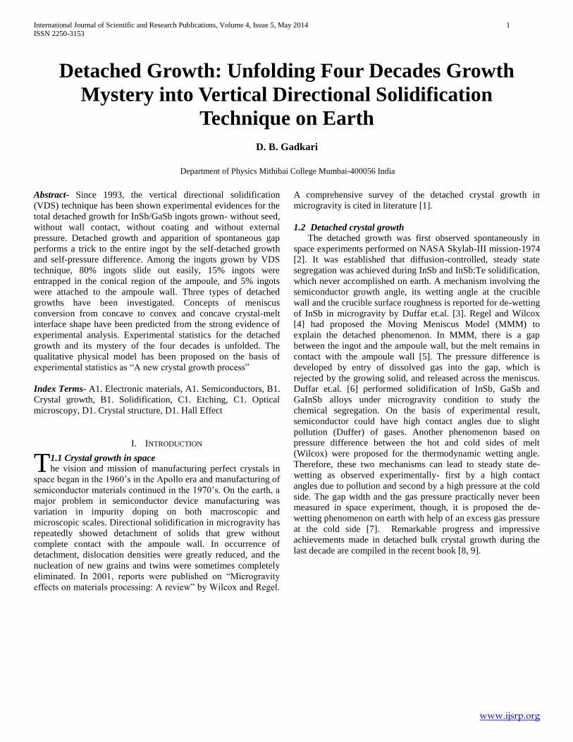
Fig.1 Schematic drawing shows the ingot growth process into Vertical Bridgman, Czocharlski and Vertical directional
solidification. It also shows typical detached growth inside ampoule and its free movement for the ingot grown by VDS technique.
Inset is the furnace temperature profile for different set temperature for 550, 750, 850 degrees and its respective temperature
gradient.
1.3 Detached growth models
The progresses made in models of the detached crystal in last
decade have been given in [5, 7, 10-12]. For detached growth,
three models are considered in our research work, i.e. i) Moving
Meniscus Model by Wilcox and co-workers [4, 5], ii) Capillary
Model by Duffar and co-workers [5, 6], and iii) Thermo-
Capillary model by Derby and co-workers [12]. The capillary
model based on hydrostatic approximation of the free surface and
the static meniscus is described by the Young (1805) and Laplace
(1806) capillary equation. A comprehensive detached crystal
growth models are cited in literature [13-24].
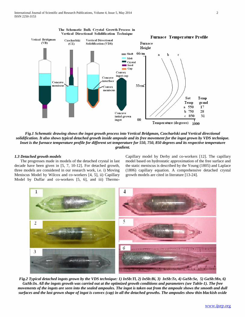
Fig.2 Typical detached ingots grown by the VDS technique: 1) InSb:Tl, 2) InSb:Bi, 3) InSb:Te, 4) GaSb:Se, 5) GaSb:Mn, 6)
GaSb:In. All the ingots growth was carried out at the optimized growth conditions and parameters (see Table-1). The free
movements of the ingots are seen into the sealed ampoules. The ingot is taken out from the ampoule shows the smooth and dull
surfaces and the last grown shape of ingot is convex (cap) in all the detached growths. The ampoules show thin blackish oxide
International Journal of Scientific and Research Publications, Volume 4, Issue 5, May 2014 3
ISSN 2250-3153
www.ijsrp.org
layer, which acts as the encapsulation on ingot surfaces. Thus it assists to satisfy the detached condition by increase in thermal
contact angle so that the detached growth occurs spontaneously into VDS growth process.
1.4 Crystal growth process in VDS
Detached growth in vertical directional solidification (VDS)
technique is experiment effort for the bulk crystal growth process
in terrestrial laboratory. Experimental results from 1993 have
been reported in initial publishing [25] and Indian patent [26]. It
showed enhancement in crystals quality: InSb [27], InSb:Te [28],
InSb:Tl [29], InSb:Ga [30-31], InSb:Bi [32], InSb:N [33], GaSb
[34], GaSb:Mn [35], GaSb:In [36], GaSb:Se [37] and
improvement in physical properties [38].
II. EXPERIMENTAL PROCEDURE
2.1 Bulk crystal growth process
The classical methods of melt growth are Czochralski (CZ)
and Vertical Bridgman (VB), see Fig.1. In crystal growth by
Czochralski method, the periodic variations in impurity
concentration are grown because of the rotation of the crystal, i.e.
rotational striations. The closely spaced striations in both
Czochralski and Bridgman-grown crystals have grown by
buoyancy-driven convection. This leads to the thermal stress,
which increases defects and dislocation density. To reduce the
defect density in bulk materials, a modified crystal growth
process is necessary. VDS technique for the growth of detached
bulk crystals of high quality has been proposed. Detached growth
in VDS depends on the ampoule cone geometry, filled inert gas,
thermal field, capillarity effect, thermocapillary effect, self-
detachment and self-pressure differences. VDS technique could
be an innovative effort to grow bulk crystals of the high quality.
The experimental observations into VDS have been explained
similar to that used to predict the influence of gravity on
detachment.
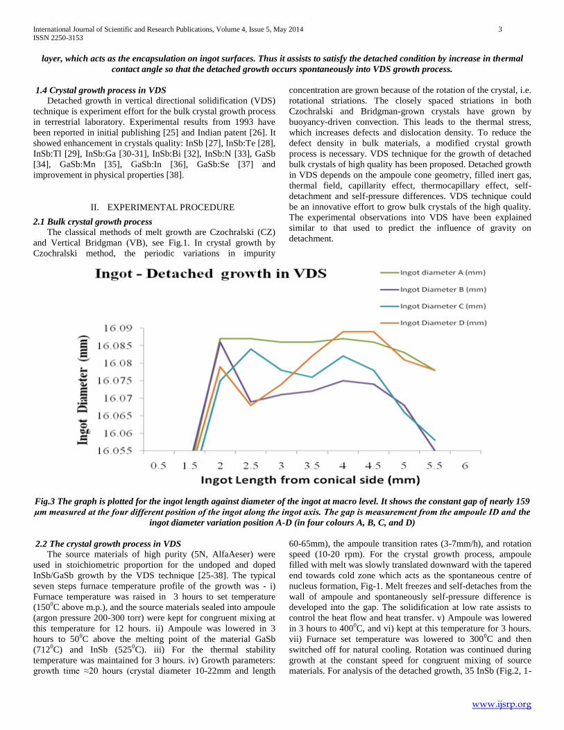
Fig.3 The graph is plotted for the ingot length against diameter of the ingot at macro level. It shows the constant gap of nearly 159
μm measured at the four different position of the ingot along the ingot axis. The gap is measurement from the ampoule ID and the
ingot diameter variation position A-D (in four colours A, B, C, and D)
2.2 The crystal growth process in VDS
The source materials of high purity (5N, AlfaAeser) were
used in stoichiometric proportion for the undoped and doped
InSb/GaSb growth by the VDS technique [25-38]. The typical
seven steps furnace temperature profile of the growth was - i)
Furnace temperature was raised in 3 hours to set temperature
(1500C above m.p.), and the source materials sealed into ampoule
(argon pressure 200-300 torr) were kept for congruent mixing at
this temperature for 12 hours. ii) Ampoule was lowered in 3
hours to 500C above the melting point of the material GaSb
(7120C) and InSb (525
0C). iii) For the thermal stability
temperature was maintained for 3 hours. iv) Growth parameters:
growth time ≈20 hours (crystal diameter 10-22mm and length
60-65mm), the ampoule transition rates (3-7mm/h), and rotation
speed (10-20 rpm). For the crystal growth process, ampoule
filled with melt was slowly translated downward with the tapered
end towards cold zone which acts as the spontaneous centre of
nucleus formation, Fig-1. Melt freezes and self-detaches from the
wall of ampoule and spontaneously self-pressure difference is
developed into the gap. The solidification at low rate assists to
control the heat flow and heat transfer. v) Ampoule was lowered
in 3 hours to 4000C, and vi) kept at this temperature for 3 hours.
vii) Furnace set temperature was lowered to 3000C and then
switched off for natural cooling. Rotation was continued during
growth at the constant speed for congruent mixing of source
materials. For analysis of the detached growth, 35 InSb (Fig.2, 1-
International Journal of Scientific and Research Publications, Volume 4, Issue 5, May 2014 4
ISSN 2250-3153
www.ijsrp.org
3) and 37 GaSb (Fig.2, 4-6) ingots were grown. Experimental
optimized growth parameters confirmed from the growth of 72
ingots showed in Table-1. It has been investigated that 80%
ingots slide out easily from the ampoules, 15% ingots were
entrapped into conical region, and 5% ingots were attached to the
wall of ampoule.
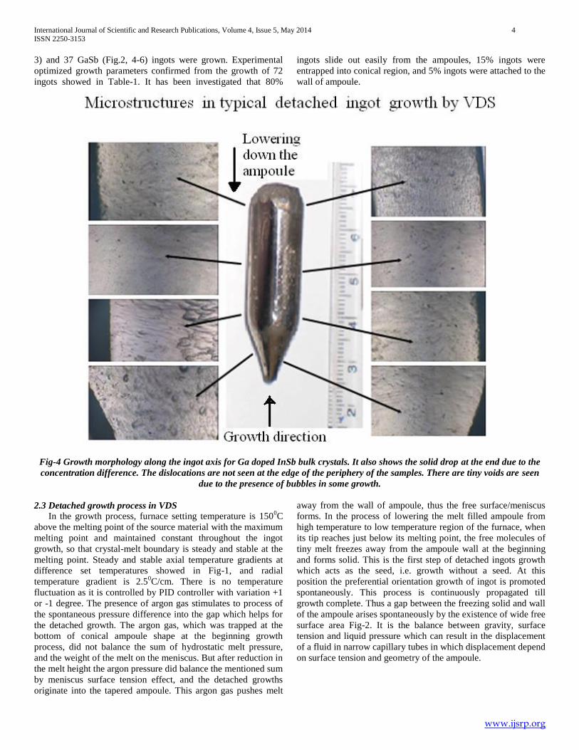
Fig-4 Growth morphology along the ingot axis for Ga doped InSb bulk crystals. It also shows the solid drop at the end due to the
concentration difference. The dislocations are not seen at the edge of the periphery of the samples. There are tiny voids are seen
due to the presence of bubbles in some growth.
2.3 Detached growth process in VDS
In the growth process, furnace setting temperature is 1500C
above the melting point of the source material with the maximum
melting point and maintained constant throughout the ingot
growth, so that crystal-melt boundary is steady and stable at the
melting point. Steady and stable axial temperature gradients at
difference set temperatures showed in Fig-1, and radial
temperature gradient is 2.50C/cm. There is no temperature
fluctuation as it is controlled by PID controller with variation +1
or -1 degree. The presence of argon gas stimulates to process of
the spontaneous pressure difference into the gap which helps for
the detached growth. The argon gas, which was trapped at the
bottom of conical ampoule shape at the beginning growth
process, did not balance the sum of hydrostatic melt pressure,
and the weight of the melt on the meniscus. But after reduction in
the melt height the argon pressure did balance the mentioned sum
by meniscus surface tension effect, and the detached growths
originate into the tapered ampoule. This argon gas pushes melt
away from the wall of ampoule, thus the free surface/meniscus
forms. In the process of lowering the melt filled ampoule from
high temperature to low temperature region of the furnace, when
its tip reaches just below its melting point, the free molecules of
tiny melt freezes away from the ampoule wall at the beginning
and forms solid. This is the first step of detached ingots growth
which acts as the seed, i.e. growth without a seed. At this
position the preferential orientation growth of ingot is promoted
spontaneously. This process is continuously propagated till
growth complete. Thus a gap between the freezing solid and wall
of the ampoule arises spontaneously by the existence of wide free
surface area Fig-2. It is the balance between gravity, surface
tension and liquid pressure which can result in the displacement
of a fluid in narrow capillary tubes in which displacement depend
on surface tension and geometry of the ampoule.
International Journal of Scientific and Research Publications, Volume 4, Issue 5, May 2014 5
ISSN 2250-3153
www.ijsrp.org
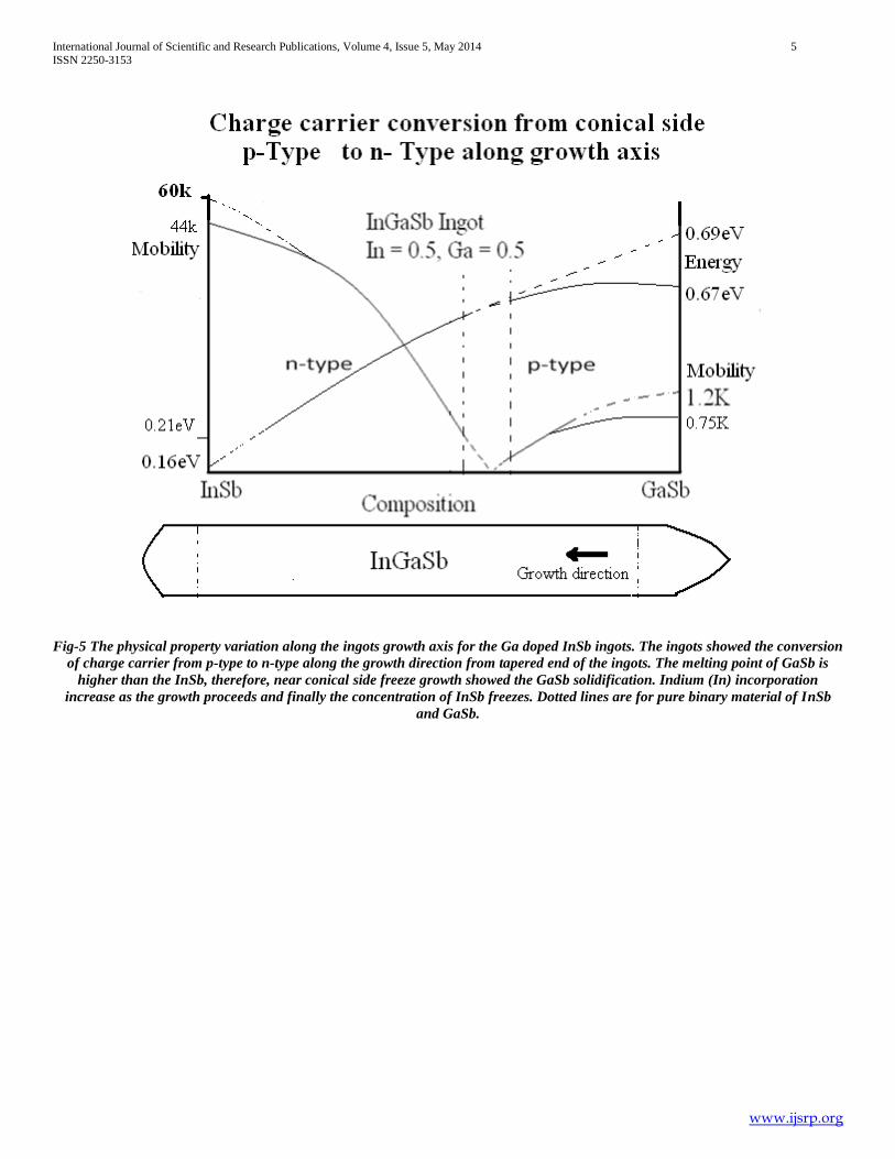
Fig-5 The physical property variation along the ingots growth axis for the Ga doped InSb ingots. The ingots showed the conversion
of charge carrier from p-type to n-type along the growth direction from tapered end of the ingots. The melting point of GaSb is
higher than the InSb, therefore, near conical side freeze growth showed the GaSb solidification. Indium (In) incorporation
increase as the growth proceeds and finally the concentration of InSb freezes. Dotted lines are for pure binary material of InSb
and GaSb.
International Journal of Scientific and Research Publications, Volume 4, Issue 5, May 2014 6
ISSN 2250-3153
www.ijsrp.org
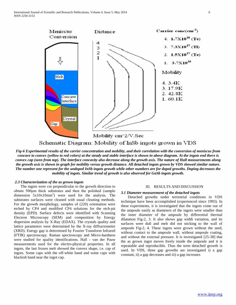
Fig-6 Experimental results of the carrier concentration and mobility, and their correlation with the conversion of meniscus from
concave to convex (yellow to red colors) at the steady and stable interface is shown in above diagram. At the ingots end there is
convex cap (seen from top). The interface concavity also decrease along the growth axis. The nature of Hall measurements along
the growth axis is shown in graph for mobility versus growth distance. All detached ingots grown by VDS showed similar nature.
The number one represent for the undoped InSb ingots growth while other numbers are for doped growths. Doping decreases the
mobility of ingots. Similar trend of growth is also observed for GaSb ingots growth.
2.3 Characterization of the as grown ingots
The ingots were cut perpendicular to the growth direction to
obtain 500μm thick substrates and then the polished (sample
dimension 5x10x10mm3) were used for the analysis. The
substrates surfaces were cleaned with usual cleaning methods.
For the growth morphology, samples of (220) orientation were
etched by CP4 and modified CP4 solutions for the etch-pit
density (EPD). Surface defects were identified with Scanning
Electron Microscopy (SEM) and composition by Energy
dispersion analysis by X-Ray (EDAX). The crystals quality and
lattice parameters were determined by the X-ray diffractometer
(XRD). Energy gap is determined by Fourier Transform Infrared
(FTIR) spectroscopy. Raman spectroscopy and Micro-hardness
were studied for quality identifications. Hall - van der Pauw
measurements used for the electro-physical properties. In all
ingots, the last frozen melt showed the convex shape, i.e. cap of
ingots. Some caps with the off-white band and some caps with
blackish band near the ingot cap.
III. RESULTS AND DISCUSSION
3.1 Diameter measurement of the detached ingots
Detached growths under terrestrial conditions in VDS
technique have been accomplished (experienced since 1993). In
these experiments, it is investigated that the ingots come out of
the ampoule easily as diameters of the ingots were smaller than
the inner diameter of the ampoule by differential thermal
dilatation Fig-2, 3. It also shows gap width variation, and its
surfaces were dull and melt did not sticking to the wall of
ampoule Fig-2, 4. These ingots were grown without the seed,
without contact to the ampoule wall, without ampoule coating,
and without the external pressure. It is investigated [25-38] that
the as grown ingot moves freely inside the ampoule and it is
repeatable and reproducible. Thus the term detached growth is
used. In VDS, three gap growths are investigated i) a gap
constant, ii) a gap decreases and iii) a gap increases
International Journal of Scientific and Research Publications, Volume 4, Issue 5, May 2014 7
ISSN 2250-3153
www.ijsrp.org
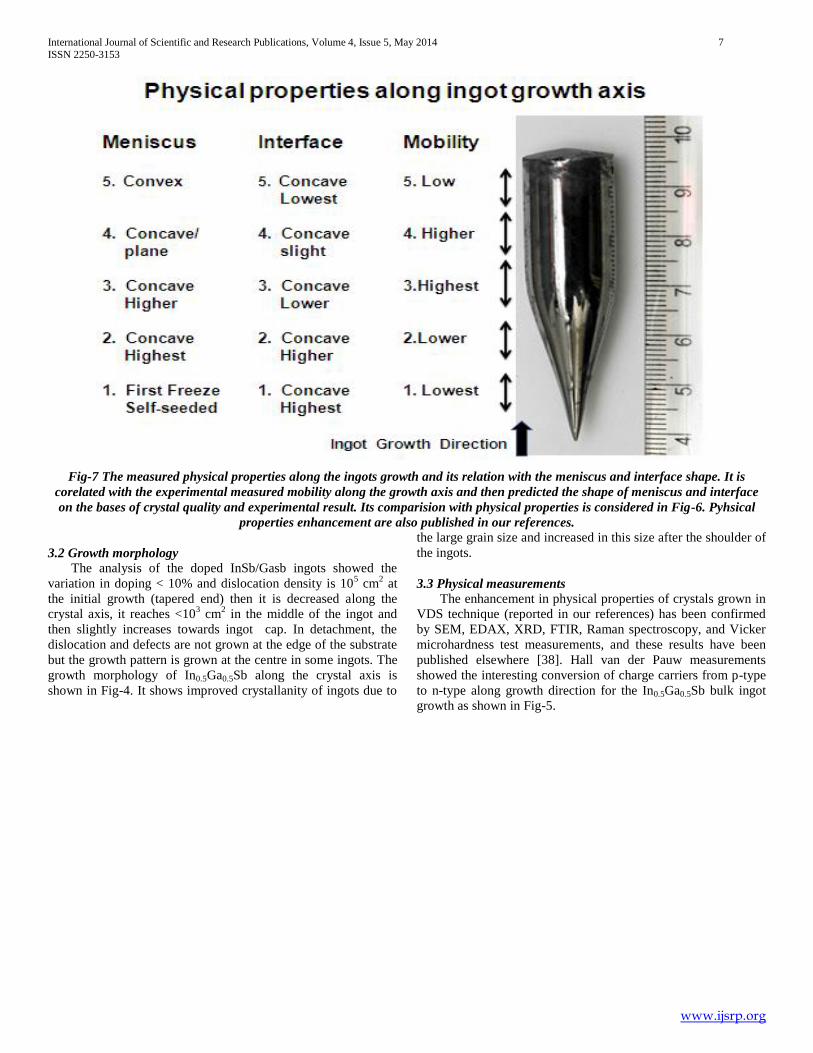
Fig-7 The measured physical properties along the ingots growth and its relation with the meniscus and interface shape. It is
corelated with the experimental measured mobility along the growth axis and then predicted the shape of meniscus and interface
on the bases of crystal quality and experimental result. Its comparision with physical properties is considered in Fig-6. Pyhsical
properties enhancement are also published in our references.
3.2 Growth morphology
The analysis of the doped InSb/Gasb ingots showed the
variation in doping < 10% and dislocation density is 105 cm
2 at
the initial growth (tapered end) then it is decreased along the
crystal axis, it reaches <103 cm
2 in the middle of the ingot and
then slightly increases towards ingot cap. In detachment, the
dislocation and defects are not grown at the edge of the substrate
but the growth pattern is grown at the centre in some ingots. The
growth morphology of In0.5Ga0.5Sb along the crystal axis is
shown in Fig-4. It shows improved crystallanity of ingots due to
the large grain size and increased in this size after the shoulder of
the ingots.
3.3 Physical measurements
The enhancement in physical properties of crystals grown in
VDS technique (reported in our references) has been confirmed
by SEM, EDAX, XRD, FTIR, Raman spectroscopy, and Vicker
microhardness test measurements, and these results have been
published elsewhere [38]. Hall van der Pauw measurements
showed the interesting conversion of charge carriers from p-type
to n-type along growth direction for the In0.5Ga0.5Sb bulk ingot
growth as shown in Fig-5.
International Journal of Scientific and Research Publications, Volume 4, Issue 5, May 2014 8
ISSN 2250-3153
www.ijsrp.org
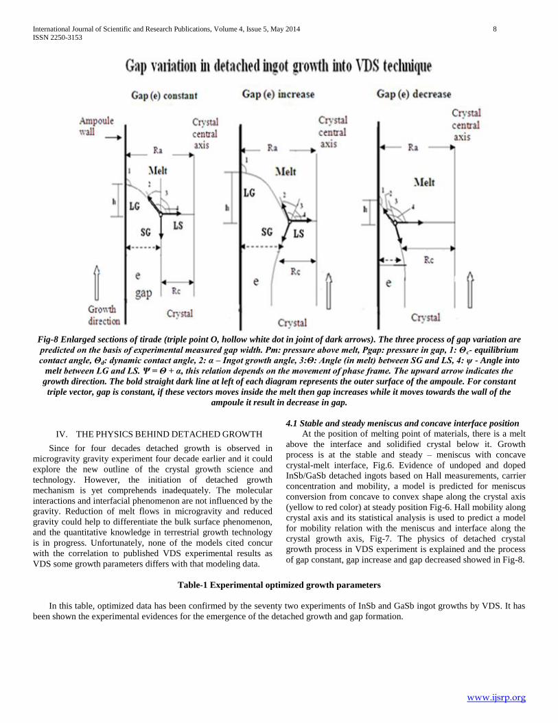
Fig-8 Enlarged sections of tirade (triple point O, hollow white dot in joint of dark arrows). The three process of gap variation are
predicted on the basis of experimental measured gap width. Pm: pressure above melt, Pgap: pressure in gap, 1: Θc- equilibrium
contact angle, Θd: dynamic contact angle, 2: α – Ingot growth angle, 3:Θ: Angle (in melt) between SG and LS, 4: ψ - Angle into
melt between LG and LS. Ψ = Θ + α, this relation depends on the movement of phase frame. The upward arrow indicates the
growth direction. The bold straight dark line at left of each diagram represents the outer surface of the ampoule. For constant
triple vector, gap is constant, if these vectors moves inside the melt then gap increases while it moves towards the wall of the
ampoule it result in decrease in gap.
IV. THE PHYSICS BEHIND DETACHED GROWTH
Since for four decades detached growth is observed in
microgravity gravity experiment four decade earlier and it could
explore the new outline of the crystal growth science and
technology. However, the initiation of detached growth
mechanism is yet comprehends inadequately. The molecular
interactions and interfacial phenomenon are not influenced by the
gravity. Reduction of melt flows in microgravity and reduced
gravity could help to differentiate the bulk surface phenomenon,
and the quantitative knowledge in terrestrial growth technology
is in progress. Unfortunately, none of the models cited concur
with the correlation to published VDS experimental results as
VDS some growth parameters differs with that modeling data.
4.1 Stable and steady meniscus and concave interface position
At the position of melting point of materials, there is a melt
above the interface and solidified crystal below it. Growth
process is at the stable and steady – meniscus with concave
crystal-melt interface, Fig.6. Evidence of undoped and doped
InSb/GaSb detached ingots based on Hall measurements, carrier
concentration and mobility, a model is predicted for meniscus
conversion from concave to convex shape along the crystal axis
(yellow to red color) at steady position Fig-6. Hall mobility along
crystal axis and its statistical analysis is used to predict a model
for mobility relation with the meniscus and interface along the
crystal growth axis, Fig-7. The physics of detached crystal
growth process in VDS experiment is explained and the process
of gap constant, gap increase and gap decreased showed in Fig-8.
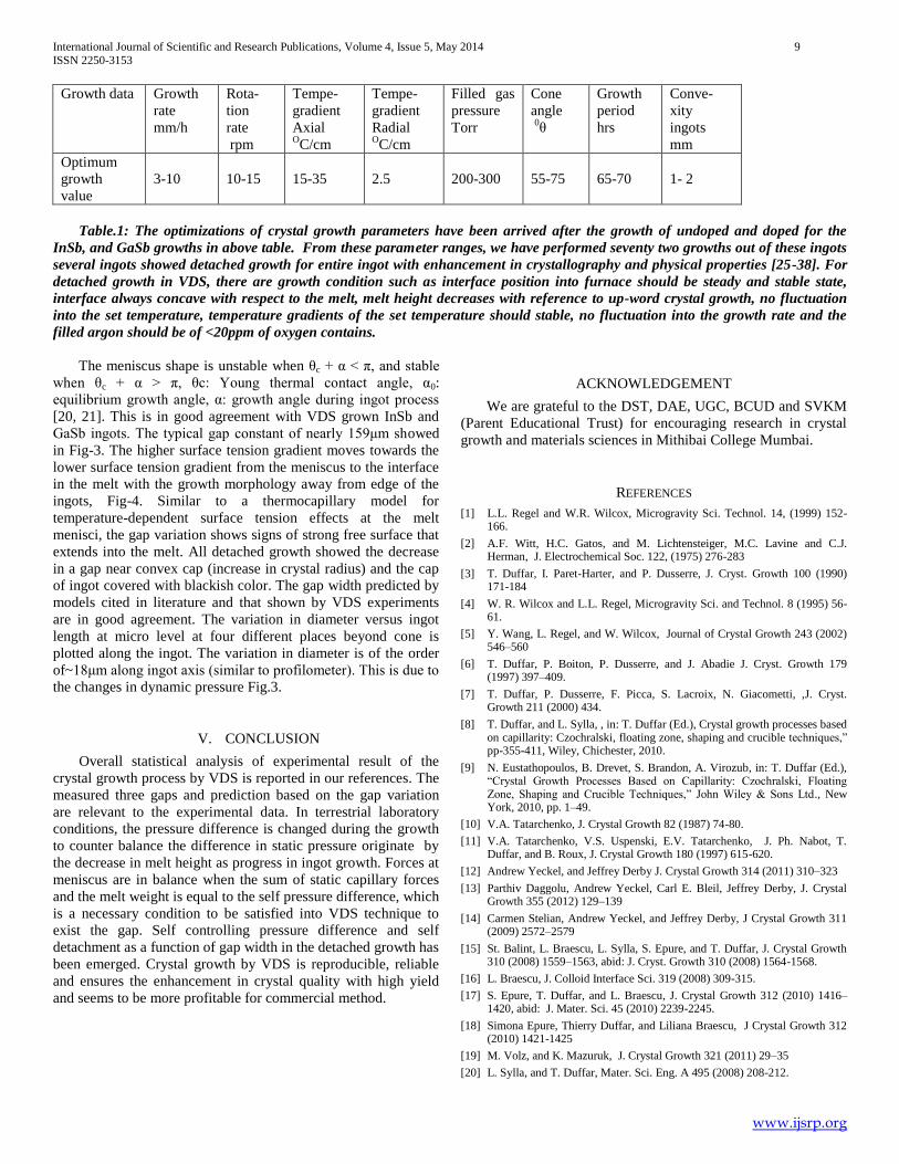
Table-1 Experimental optimized growth parameters
In this table, optimized data has been confirmed by the seventy two experiments of InSb and GaSb ingot growths by VDS. It has
been shown the experimental evidences for the emergence of the detached growth and gap formation.
International Journal of Scientific and Research Publications, Volume 4, Issue 5, May 2014 9
ISSN 2250-3153
www.ijsrp.org
Growth data Growth
rate
mm/h
Rota-
tion
rate
rpm
Tempe-
gradient
Axial OC/cm
Tempe-
gradient
Radial OC/cm
Filled gas
pressure
Torr
Cone
angle
0θ
Growth
period
hrs
Conve-
xity
ingots
mm
Optimum
growth
value
3-10
10-15
15-35
2.5
200-300
55-75
65-70
1- 2
Table.1: The optimizations of crystal growth parameters have been arrived after the growth of undoped and doped for the
InSb, and GaSb growths in above table. From these parameter ranges, we have performed seventy two growths out of these ingots
several ingots showed detached growth for entire ingot with enhancement in crystallography and physical properties [25-38]. For
detached growth in VDS, there are growth condition such as interface position into furnace should be steady and stable state,
interface always concave with respect to the melt, melt height decreases with reference to up-word crystal growth, no fluctuation
into the set temperature, temperature gradients of the set temperature should stable, no fluctuation into the growth rate and the
filled argon should be of <20ppm of oxygen contains.
The meniscus shape is unstable when θc + α < π, and stable
when θc + α > π, θc: Young thermal contact angle, α0:
equilibrium growth angle, α: growth angle during ingot process
[20, 21]. This is in good agreement with VDS grown InSb and
GaSb ingots. The typical gap constant of nearly 159μm showed
in Fig-3. The higher surface tension gradient moves towards the
lower surface tension gradient from the meniscus to the interface
in the melt with the growth morphology away from edge of the
ingots, Fig-4. Similar to a thermocapillary model for
temperature-dependent surface tension effects at the melt
menisci, the gap variation shows signs of strong free surface that
extends into the melt. All detached growth showed the decrease
in a gap near convex cap (increase in crystal radius) and the cap
of ingot covered with blackish color. The gap width predicted by
models cited in literature and that shown by VDS experiments
are in good agreement. The variation in diameter versus ingot
length at micro level at four different places beyond cone is
plotted along the ingot. The variation in diameter is of the order
of~18μm along ingot axis (similar to profilometer). This is due to
the changes in dynamic pressure Fig.3.
V. CONCLUSION
Overall statistical analysis of experimental result of the
crystal growth process by VDS is reported in our references. The
measured three gaps and prediction based on the gap variation
are relevant to the experimental data. In terrestrial laboratory
conditions, the pressure difference is changed during the growth
to counter balance the difference in static pressure originate by
the decrease in melt height as progress in ingot growth. Forces at
meniscus are in balance when the sum of static capillary forces
and the melt weight is equal to the self pressure difference, which
is a necessary condition to be satisfied into VDS technique to
exist the gap. Self controlling pressure difference and self
detachment as a function of gap width in the detached growth has
been emerged. Crystal growth by VDS is reproducible, reliable
and ensures the enhancement in crystal quality with high yield
and seems to be more profitable for commercial method.
ACKNOWLEDGEMENT
We are grateful to the DST, DAE, UGC, BCUD and SVKM
(Parent Educational Trust) for encouraging research in crystal
growth and materials sciences in Mithibai College Mumbai.
REFERENCES
[1] L.L. Regel and W.R. Wilcox, Microgravity Sci. Technol. 14, (1999) 152-166.
[2] A.F. Witt, H.C. Gatos, and M. Lichtensteiger, M.C. Lavine and C.J. Herman, J. Electrochemical Soc. 122, (1975) 276-283
[3] T. Duffar, I. Paret-Harter, and P. Dusserre, J. Cryst. Growth 100 (1990) 171-184
[4] W. R. Wilcox and L.L. Regel, Microgravity Sci. and Technol. 8 (1995) 56-61.
[5] Y. Wang, L. Regel, and W. Wilcox, Journal of Crystal Growth 243 (2002) 546–560
[6] T. Duffar, P. Boiton, P. Dusserre, and J. Abadie J. Cryst. Growth 179 (1997) 397–409.
[7] T. Duffar, P. Dusserre, F. Picca, S. Lacroix, N. Giacometti, ,J. Cryst. Growth 211 (2000) 434.
[8] T. Duffar, and L. Sylla, , in: T. Duffar (Ed.), Crystal growth processes based on capillarity: Czochralski, floating zone, shaping and crucible techniques,” pp-355-411, Wiley, Chichester, 2010.
[9] N. Eustathopoulos, B. Drevet, S. Brandon, A. Virozub, in: T. Duffar (Ed.), “Crystal Growth Processes Based on Capillarity: Czochralski, Floating Zone, Shaping and Crucible Techniques,” John Wiley & Sons Ltd., New York, 2010, pp. 1–49.
[10] V.A. Tatarchenko, J. Crystal Growth 82 (1987) 74-80.
[11] V.A. Tatarchenko, V.S. Uspenski, E.V. Tatarchenko, J. Ph. Nabot, T. Duffar, and B. Roux, J. Crystal Growth 180 (1997) 615-620.
[12] Andrew Yeckel, and Jeffrey Derby J. Crystal Growth 314 (2011) 310–323
[13] Parthiv Daggolu, Andrew Yeckel, Carl E. Bleil, Jeffrey Derby, J. Crystal Growth 355 (2012) 129–139
[14] Carmen Stelian, Andrew Yeckel, and Jeffrey Derby, J Crystal Growth 311 (2009) 2572–2579
[15] St. Balint, L. Braescu, L. Sylla, S. Epure, and T. Duffar, J. Crystal Growth 310 (2008) 1559–1563, abid: J. Cryst. Growth 310 (2008) 1564-1568.
[16] L. Braescu, J. Colloid Interface Sci. 319 (2008) 309-315.
[17] S. Epure, T. Duffar, and L. Braescu, J. Crystal Growth 312 (2010) 1416–1420, abid: J. Mater. Sci. 45 (2010) 2239-2245.
[18] Simona Epure, Thierry Duffar, and Liliana Braescu, J Crystal Growth 312 (2010) 1421-1425
[19] M. Volz, and K. Mazuruk, J. Crystal Growth 321 (2011) 29–35
[20] L. Sylla, and T. Duffar, Mater. Sci. Eng. A 495 (2008) 208-212.
International Journal of Scientific and Research Publications, Volume 4, Issue 5, May 2014 10
ISSN 2250-3153
www.ijsrp.org
[21] L Peng, W Zhang , Y Li, and H Meng, J Engineering Thermophysics 32(12) December 2011, 2009-2012, abid: “Microgravity Sci. Technol (2010) 22:179–183 & 171–177
[22] Lamine Sylla, and Thierry Duffar, J. Crystal Growth 324 (2011) 53–62
[23] V.A. Tatarchenko, Kluwer Academic Publishe, Dordrecht, 1993, and V. A. Tatarchenko in: Handbook of Crystal Growth, vol. 2b, pp-1011 ed. D.T.J. Hurle. North-Holland, Amsterdam
[24] A. Yeckel, and J. Derby, in: P. Capper (Ed.), “Bulk Crystal Growth of Electronic, Optical & Optoelectronic Materials,” Wiley, Chichester, 2005, pp. 73–119.
[25] D. B. Gadkari Proceeding NSGDSC-2009, November 19-21, 2009 p 42-49, MRSI-Mumbai Chapter India.
[26] D. B. Gadkari, K. B. Lal, B. M. Arora, Indian Patent: 139/BOM/1999 (1999), & 192132 (2004).
[27] Dattatray Gadkari, J. Chemistry and Chemical Engineering 6 (3) (2012) 250-258
[28] Dattatray Gadkari AIP Con proc. 1512 (2013) 856-857
[29] Dattatray Gadkari J Material Science and Engineering A2 (3) (2012) 1-10
[30] D.B. Gadkari, P. Shashidharan, N.A. Ghokhale, K.B. Lal, A.P .Shah and B.M. Arora, Ind. J, Pure & App. Phy. 37 (1999) 652-656, abid: Ind. J, Pure & App. Phy. 38 (2000) 237-242
[31] D.B. Gadkari, P. Shashidharan, N.A.Ghokhale, K.B. Lal and B.M. Arora Bulletin of Materials science, Vol.24, No.4 (2001) 475-482
[32] D S Maske, M Joshi, R Choudhary, and D B Gadkari, AIP Conf. Proc. 1512, 876- 877 (2013).
[33] M Joshi D Maske, R Choudhary, B M Arora and D B Gadkari, AIP Conf. Proc. 1536, (2013) 877-878.
[34] D. B. Gadkari, and B.M. Arora, Transaction of Materials Society of the Japan 34(3) (2009) 571-574.
[35] D B Gadkari, Journal of Chemistry and Chemical Engineering Vol. 6 (1) (2012) 65-73,
[36] Dattatray Gadkari, Material Chemistry and Physics 139 (2013) 375-382
[37] Rashmi Choudhary Manisha Joshi, Dilip Maske, and Dattatray Gadkari, AIP Conf. Proc. 1536 (2013) 333-334.
[38] D.B. Gadkari, J Material Science and Engineering 3 (5) (2013) 1-10
AUTHORS
First Author – D. B. Gadkari, Department of Physics Mithibai
College Mumbai-400056 India, E-mail: [email protected];