designing high-performance electronics for today's
TRANSCRIPT
WHITE PAPER
Contents
Introduction .................................................................2
The Challenges ...........................................................2
The Solution ................................................................3
Conclusion ...................................................................5
Further Information ..................................................6
Designing High-Performance Electronics for Today’s Hyperconnected Systems
With the rapid evolution of hyperconnected devices that are managing constant and
near-instantaneous data from anywhere and at any time, designing at each new
technology node must overcome design and integration complexity. To do so requires
automated solutions to process the scale of modern designs. Cadence® system analysis
solutions operate on unimaginably huge amounts of data, scaling algorithms to be
massively parallel in the cloud, and delivering and supporting software in an enterprise
environment. These solutions—including Clarity™ 3D Solver, Celsius™ Thermal Solver, and
Sigrity™ SystemSI™ technology—provide semiconductor and system companies with an
integrated end-to-end solution to help today’s electronic designers do their best work.
Designing High-Performance Electronics for Today’s Hyperconnected Systems
2www.cadence.com
IntroductionThe world of technology is evolving rapidly. The fifth generation of cellular networks enabled a new era of connected devices, but the data-thirsty world is already looking forward to the next-generation communication systems. Promised speeds are estimated at 100X faster than 5G for massive connectivity to the internet with extreme capacity, coverage, reliability, and ultra-low latency, enabling a wide range of new services made possible through innovative and resilient technologies. The 6G technology market is expected to facilitate immense improvements in AI, hyperscale computing, machine learning (ML), autonomous driving, and other smart device segments. The terahertz (THz) frequencies of 6G introduce massive challenges in hardware; faster devices with low power will be a necessity. The next generation of wireless technology, Wi-Fi6 (802.11ax), is already making big waves in network connectivity and user experience improvements with explosive speed, low latency, and 4X capacity for connected devices. 112G SerDes has established its place in high-speed data transmission, spawning new design and analysis challenges.
The goal is to manage constant and near-instantaneous data from anywhere and at any time. The self-driving car must be able to make a split-second decision whether to brake or continue, a robotic surgery must not pause for the next step, and of course, the military cannot be effective with yesterday’s weapons. The electronic devices in these multi-domain segments must be equipped to handle these speeds and low-latency response times, while the design teams creating these devices are tasked with delivering new, differentiated products faster and more efficiently, despite the ever-growing complexity of both silicon and software. These high-performance technologies rely on a complex system architecture that increases the risk to schedules. The EDA industry must speed up its complex design processes to support further technological development.
The ChallengesAt smaller process nodes, design complexity increases and creates electromagnetic (EM) dependencies between various components like the analog, digital, and RF modules, requiring specialized skills. An even bigger challenge is integrating them into a system, involving different dimensions of complexity and expertise. Design maestros perform specialized tasks like circuit simulation, layout, and EM analysis. Most of the legacy tools performing these tasks require a certain level of manual intervention and design knowledge, emphasizing the need for specialized skills to perform these tasks. The steep learning curve needed for tool adaption overburdens the engineers, and the need for functional expertise makes hiring arduous, posing new challenges to the management.
Mixed-Signal Designs Increase Complexity
Contrary to the conventional wisdom, analog signals are not disappearing from the advanced chip designs, rather they are becoming more crucial. The rising number of devices with sensors capturing real-time data that is analog in nature means that designs are packed with more analog circuitry and large blocks of mixed-signal IP. This escalating complexity poses several challenges due to more digital circuits in the analog IP and the increased susceptibility of digital design to noise and disruption. The challenges include parasitic RLC effects, stronger layout-dependent signal integrity (SI) issues, and increased circuit sensitivity. The analog and digital experts who previously worked in silos are now required to understand and address the mixed-signal behavior. Digital designers must consider the analog nature of the signal, such as coupling issues, slew rate, and impedance matching. Analog designers need to appraise the noise developed by digital circuits around it and make their circuitry robust and verified for the noise produced by the digital circuits around its territory. The non-optimal analog circuit performance due to inadequate design knowledge exchange is leading to inefficient floorplanning across fabrics.
Fragmented Flows Due to Integration Issues
Lack of integration between EDA tools creates significant inefficiencies in the design flows. Analog/RF design engineers often use different schematic tools for mixed-signal designs or purely analog/RF designs, leading to different schematic drive layout flows to capture different portions of the fabric. Some of the challenges are the need for recreating the schematics for the production PCB flow; separate schematic entries for III-V, packaging, simulation, and design; and different schematic leads to the SIP isolating it from the IC flow. All of these make end-to-end simulation harder. The solution is to have a single flow driving the schematic tools for different portions of the design, which is tightly integrated with the solvers. Better integration and a single schematic-driven design save time to recreate schematics.
Designing High-Performance Electronics for Today’s Hyperconnected Systems
3www.cadence.com
More and More Analysis Requirements
System-level challenges of SoC designs are on the rise. Resolving EM radiation, SI issues, thermal issues, and electrome-chanical challenges are critical to ensure the performance of any electronic system, especially at smaller footprints. EM analysis is imperative to verify if the signals meet the performance specifications and whether the design has unintended EM interactions in the circuit: SI affects EM coupling, the signal quality directly affects the EM interference emissions and susceptibility, thermal impacts performance. And in a worst-case scenario, if the temperature increases beyond the threshold, the IC malfunctions or is permanent damaged.
To combat these challenges, what is needed is a system design solution that can extract models without simplification, simulate and analyze complex electromechanical systems, and deliver the mandated performance without over-designing.
The SolutionAn effective and efficient solution uses the right set of tools and flows to address scalability, performance, and accuracy in the design and analysis of systems, both at the component level and at the system level. Designers are often forced to circumvent the capacity and performance limitations of tools by sacrificing detailed design representation in favor of higher levels of design data abstraction to meet design schedules. They need SoC and system-level tools that support the following to produce the next generation of high-frequency products:
f Highest level of built-in accuracy
f Co-design and co-simulation approach
f Single well-integrated flow, not fragmented by multi-vendors
f Single point of support and integration between the design and analysis
f Minimum set-up time
f Facilitates collaboration across design teams to address the challenges
For the electrical and thermal analysis challenges, the tools must provide value at the system level. The tool must support in-design and electrothermal signoff for on-chip and off-chip devices and interconnect. It must also be capable of modeling cross-domain coupling effects. An on-chip EM-IR solution is required to produce a detailed thermal model, which is then consumed by a system-level thermal analysis solution to include the packaging and PCB (the largest natural heat spreader) along with any heatsinks in the design. The tool must provide the engineer with thermal gradient information and thermal stress calculations. An updated chip thermal map must also be generated, which can be fed back into the chip-level EM-IR tool to help accurately perform chip power analysis and IR drop analysis.
SI issues throw challenges to the engineers from the chip level to the package and across multiple boards. A power-aware SI methodology requires a certain level of upgrades to modeling and simulation techniques and adequate simultaneous switching noise (SSN) characterization of memory interfaces. With a combination of complete model libraries, advanced tools, and engineering expertise, today’s SI engineers can systematically address the challenges related to modern buses and data rates.
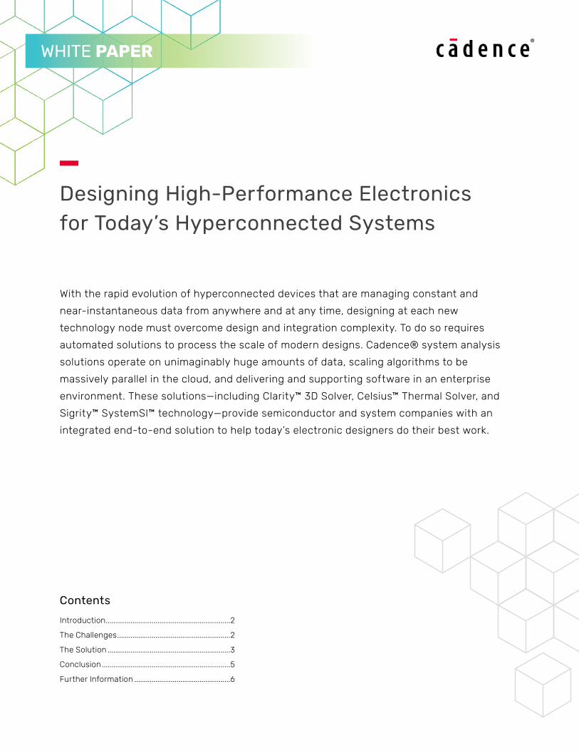
Accurate 3D modeling is the most reliable method to achieve structure optimization and high-speed compliance of complex structures. A high-fidelity interconnect design is a critical factor for high-speed signaling, such as 112G SerDes interfaces that are highly susceptible to any change in impedance that negatively impacts the bit error rate (BER). The speed and capacity limitations of legacy field solver technology require users to partition the structure into smaller segments to manage as per the local computing constraints. This pseudo-3D approach creates the risk that the resulting final model may contain inaccuracies due to artificial effects from the superficial model boundaries. Designers need the ability to merge mechanical structures with their system design and model the electrical-mechanical interconnect as a single model.
While true 3D modeling and analysis of such structures are difficult for current legacy tools to handle, simulating them with board and IC packages cannot be done without parallelization—for scalability and simulation performance (Figure 1). If the parallelization can work on computers in the cloud with a smaller memory footprint, it becomes cost-effective, too.
Designing High-Performance Electronics for Today’s Hyperconnected Systems
4www.cadence.com
Accurate Pre-Fabrication EM Interference Signoff and Analyzing EM Radiation Compliance
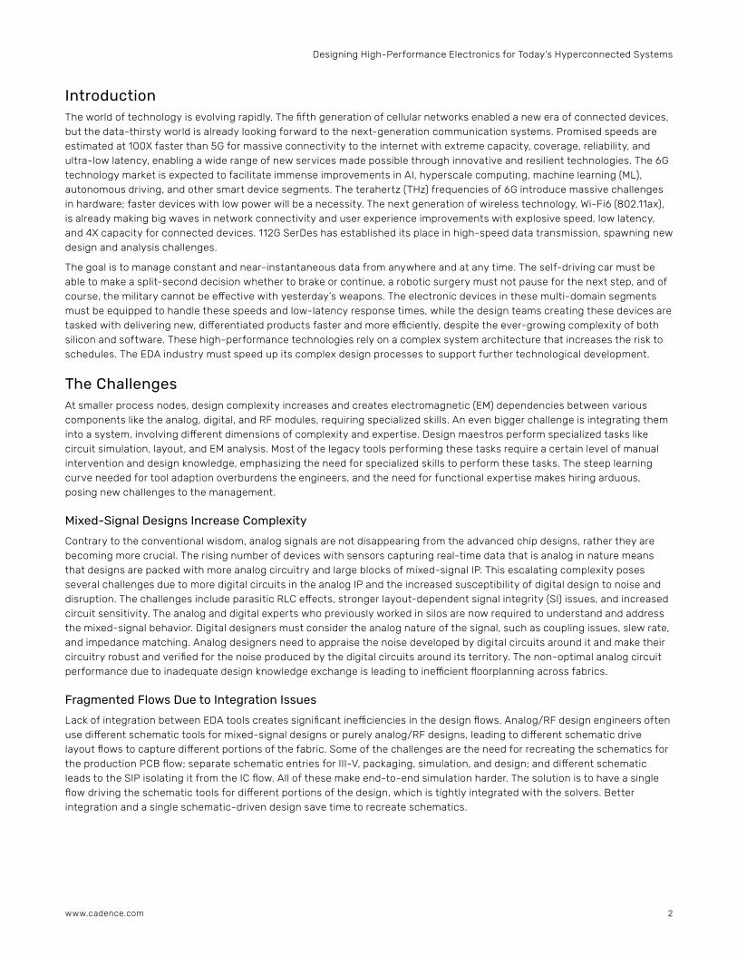
Driven by the inability of legacy tools to go beyond the module level and perform accurate system-level modeling and perfor-mance optimization while minimizing EM interference and radiation, designers are forced to use a methodology that includes several rounds of prototyping and trips to an anechoic chamber. Even though the anechoic test will be needed for final compliance, a competent finite-difference time-domain (FDTD) solver (Figure 2) can reduce dependence on anechoic chambers, especially in the early phases of product design, analysis, optimization, and fabrication.
Ensuring Thermal Compliance
Thermal effects on electrical performance have always existed and have been a challenge in electronic designs. Thermal sets the maximum operating frequency as increased electrical content generates more heat, which in turn affects the system performance. IC heat generation is mainly a function of switching frequencies and operating conditions, and how the heat generated is dissipated/transferred out of the system depends on the environmental conditions. These two problems must be solved together, but no legacy solutions can do this.
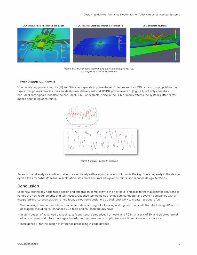
What is needed is a thermal solver that supports not only static and transient thermal analysis, but conduction (finite element analysis (FEA)) and convection (computational fluid dynamics (CFD)) approaches (Figure 3).
Figure 2: Simulation of an antenna
Figure 1: Real measurement from PAM4 silicon (left) compared with modeled output (right)
Designing High-Performance Electronics for Today’s Hyperconnected Systems
5www.cadence.com
Power-Aware SI Analysis
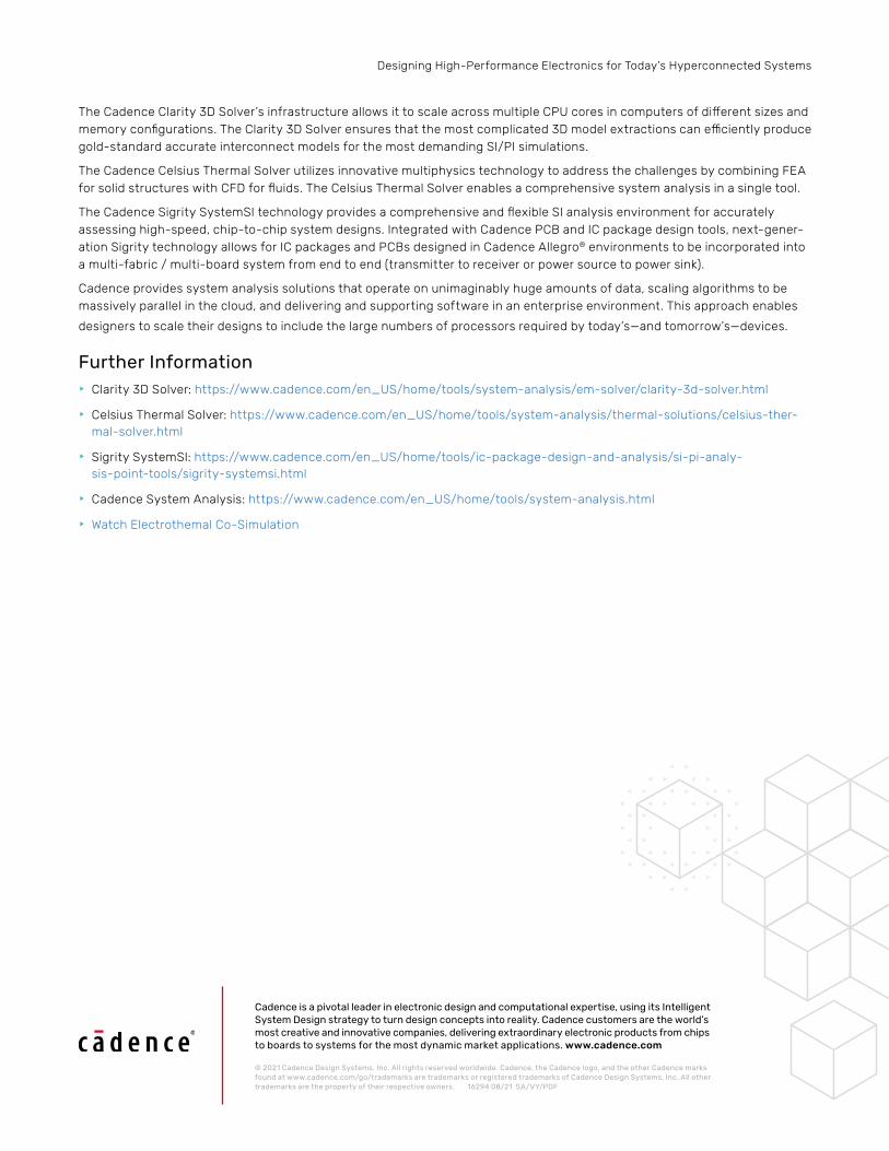
When analyzing power integrity (PI) and SI issues separately, power-based SI issues such as SSN can also crop up. While the typical design workflow assumes an ideal power delivery network (PDN), power-aware SI (Figure 4) not only considers non-ideal data signals, but also the non-ideal PDN. For example, noise in the PDN primarily affects the system’s jitter perfor-mance and timing constraints.
An end-to-end analysis solution that works seamlessly with a signoff analysis solution is the key. Operating early in the design cycle allows for “what if” scenario exploration, sets more accurate design constraints, and reduces design iterations.
ConclusionEach new technology node takes design and integration complexity to the next level and calls for new automated solutions to handle the new requirements and techniques. Cadence technologies provide semiconductor and system companies with an integrated end-to-end solution to help today’s electronic designers do their best work to create products for:
f Silicon design creation, simulation, implementation, and signoff of analog and digital circuits; off-the-shelf design IP; and IC packaging, including ML-enhanced EDA tools and ML-enabled EDA flows
f System design of advanced packaging, safe and secure embedded software, and PCBs; analysis of EM and electrothermal effects of semiconductors, packages, boards, and systems; and co-optimization with semiconductor devices
f Intelligence IP for the design of inference processing in edge devices
Figure 4: Power-aware SI analysis
Figure 3: Simultaneous thermal and electrical analysis for ICs, packages, boards, and systems
Designing High-Performance Electronics for Today’s Hyperconnected Systems
Cadence is a pivotal leader in electronic design and computational expertise, using its Intelligent System Design strategy to turn design concepts into reality. Cadence customers are the world’s most creative and innovative companies, delivering extraordinary electronic products from chips to boards to systems for the most dynamic market applications. www.cadence.com
© 2021 Cadence Design Systems, Inc. All rights reserved worldwide. Cadence, the Cadence logo, and the other Cadence marks found at www.cadence.com/go/trademarks are trademarks or registered trademarks of Cadence Design Systems, Inc. All other trademarks are the property of their respective owners. 16294 08/21 SA/VY/PDF
The Cadence Clarity 3D Solver’s infrastructure allows it to scale across multiple CPU cores in computers of different sizes and memory configurations. The Clarity 3D Solver ensures that the most complicated 3D model extractions can efficiently produce gold-standard accurate interconnect models for the most demanding SI/PI simulations.
The Cadence Celsius Thermal Solver utilizes innovative multiphysics technology to address the challenges by combining FEA for solid structures with CFD for fluids. The Celsius Thermal Solver enables a comprehensive system analysis in a single tool.
The Cadence Sigrity SystemSI technology provides a comprehensive and flexible SI analysis environment for accurately assessing high-speed, chip-to-chip system designs. Integrated with Cadence PCB and IC package design tools, next-gener-ation Sigrity technology allows for IC packages and PCBs designed in Cadence Allegro® environments to be incorporated into a multi-fabric / multi-board system from end to end (transmitter to receiver or power source to power sink).
Cadence provides system analysis solutions that operate on unimaginably huge amounts of data, scaling algorithms to be massively parallel in the cloud, and delivering and supporting software in an enterprise environment. This approach enables
designers to scale their designs to include the large numbers of processors required by today’s—and tomorrow’s—devices.
Further Informationf Clarity 3D Solver: https://www.cadence.com/en_US/home/tools/system-analysis/em-solver/clarity-3d-solver.html
f Celsius Thermal Solver: https://www.cadence.com/en_US/home/tools/system-analysis/thermal-solutions/celsius-ther-mal-solver.html
f Sigrity SystemSI: https://www.cadence.com/en_US/home/tools/ic-package-design-and-analysis/si-pi-analy-sis-point-tools/sigrity-systemsi.html
f Cadence System Analysis: https://www.cadence.com/en_US/home/tools/system-analysis.html
f Watch Electrothemal Co-Simulation