power electronics
TRANSCRIPT


Power Electronics


Branko L. Dokić • Branko Blanuša
Power ElectronicsConverters and Regulators
Third Edition
123

Branko L. DokićBranko BlanušaFaculty of Electrical EngineeringUniversity of Banja LukaBanja LukaBosnia-Herzegovina
ISBN 978-3-319-09401-4ISBN 978-86-7466-492-6
ISBN 978-3-319-09402-1 (eBook)
DOI 10.1007/978-3-319-09402-1
Library of Congress Control Number: 2014947697
Springer Cham Heidelberg New York Dordrecht London
1st edition: © Elektrotehnicki fakultet Banja Luka 20002nd edition: © Akademska misao 2007
© Springer International Publishing Switzerland 2015This work is subject to copyright. All rights are reserved by the Publisher, whether the whole or part ofthe material is concerned, specifically the rights of translation, reprinting, reuse of illustrations,recitation, broadcasting, reproduction on microfilms or in any other physical way, and transmission orinformation storage and retrieval, electronic adaptation, computer software, or by similar or dissimilarmethodology now known or hereafter developed. Exempted from this legal reservation are briefexcerpts in connection with reviews or scholarly analysis or material supplied specifically for thepurpose of being entered and executed on a computer system, for exclusive use by the purchaser of thework. Duplication of this publication or parts thereof is permitted only under the provisions ofthe Copyright Law of the Publisher’s location, in its current version, and permission for use must alwaysbe obtained from Springer. Permissions for use may be obtained through RightsLink at the CopyrightClearance Center. Violations are liable to prosecution under the respective Copyright Law.The use of general descriptive names, registered names, trademarks, service marks, etc. in thispublication does not imply, even in the absence of a specific statement, that such names are exemptfrom the relevant protective laws and regulations and therefore free for general use.While the advice and information in this book are believed to be true and accurate at the date ofpublication, neither the authors nor the editors nor the publisher can accept any legal responsibility forany errors or omissions that may be made. The publisher makes no warranty, express or implied, withrespect to the material contained herein.
Printed on acid-free paper
Springer is part of Springer Science+Business Media (www.springer.com)

Foreword
Review of the Book “Power Electronics”by Branko L. Dokić and Branko Blanuša
The book “Power Electronics” by Branko L. Dokić and Branko Blanuša containsten chapters, and deals with the most significant items of power electronics. It iswell organized with lot of examples, figures, and tables.
The first chapter is “Introduction.” In this chapter basic elements, as well assome circuits and components used in power electronics are briefly presented.Chapter 2 covers basic semiconductor components, “Diodes and Transistors,” andparticularly covers their use as switches in power electronics circuits. Chapter 3 isfocused on “Regenerative Switches.” The description is wide and detailed and thischapter may be of interest not only for students, but also for professionals who usethese components in practice.
Chapter 4 is “PWM DC/DC Converters.” The converters are classified. Allbasic topologies of these converters are analyzed in detail in both continuouscurrent mode (CCM) and discontinuous current mode (DCM).
“Control Modules” are presented in Chap. 5. This chapter contains a number ofcontrol circuits used in power electronics. This chapter may be of interest not onlyfor professionals in the field of power electronics, but also in related fields such asautomotive control, pulse electronics, etc.
Chapter 6 covers “DC/AC Converters–Inverters”. This chapter is comprehen-sive and covers the most important converter topologies and the most common usedcontrol techniques, such as selective harmonic elimination, unipolar and bipolarPWM technique, and space vector modulation.
The next chapter is AC/DC converters, i.e., rectifiers. This chapter contains allbasic topologies from uncontrolled half bridge and full bridge rectifiers to con-trolled thyristor and transistor ones. Also, some commonly used control techniquesare presented. PWM rectifiers and their applications are also discussed.
Two previous chapters are followed by the eighth chapter, which covers “AC/AC Converters.” The chapter describes single-phase and three-phase AC/AC
v

voltage converters and both direct and indirect frequency AC/AC converters. Also,an overview of matrix converters and their applications is presented in this chapter.
Chapter 9 contains a comprehensive description of “Resonant Converters.”Basic topologies are covered; series resonant converters, parallel resonant con-verters, series–parallel converters, class E resonant converters, zero voltage andzero current switching converters, and some control circuits used in resonantconverters.
Finally, Chap. 10 covers multilevel converters. Basic topologies of DC/DC andDC/AC multilevel converters are presented. Also, some widely used controltechniques, such as multilevel PWM, space vector modulation, space vector con-trol, and selective harmonic elimination, are briefly discussed in this chapter.
Every chapter contains a set of solved problems that facilitate understanding ofthe related field. Also, every chapter is concluded with a list of problems from thepresented topics.
Overall, the impression is that the book presents a comprehensive coverage ofpower electronics. It covers a wide range of topics relevant to power electronics. So,it might be used both as a textbook for students and as a reference book forpracticing engineers.
In my opinion, there is a significant academic and theoretical contribution madeby this book.
Therefore, I am glad to recommend the book “Power Electronics” by Branko L.Dokić and Branko Blanuša to be published.
November 2013 Vladimir KatićNovi Sad Faculty of Technical Sciences
University of Novi SadNovi Sad
Serbia
vi Foreword

Review of the Book “Power Electronics,” Authoredby Branko L. Dokić and Branko Blanuša
The book “Power Electronics” by Branko L. Dokić and Branko Blanuša is struc-tured into ten chapters, and covers wide area of power electronics.
The first chapter is “Introduction”, and briefly reviews parts of signals andsystems theory as used in power electronics, as well as some circuit theory andbasic components used in power electronics. Chapter 2 covers “Diodes and Tran-sistors,” with emphasis on their application in power electronics. This chapterpresents a wide and detailed coverage of the topic, which might be of interest inareas other than power electronics. Chapter 3 is still focused on components,“Regenerative Switches.” The coverage is detailed again, and might be used as areference in the area.
Coverage of topics specific to power electronics starts with Chap. 4, “PWM DC/DC Converters.” The converters are classified, and their steady-state operation isanalyzed in detail and includes a discussion of loss mechanisms.
Chapter 5, “Control Modules,” is again a chapter that might be a reference bothin power electronics and in related fields. The chapter describes a number of circuitsused to control power electronic systems, and illustrates their application. Thepresentation is general enough to be used even outside power electronics.
Chapter 6 covers “DC/AC Converters–Inverters”, i.e., inverters. The coverage iscomprehensive, covers both inverter topologies and their control, including spacevector modulation. The chapter is followed by its natural complement, AC/DCconverters, i.e., rectifiers. Again, the coverage is complete, starting from uncon-trolled rectifiers, progressing toward phase controlled rectifiers and high powerfactor PWM rectifiers. Besides, bidirectional converters based on inverters arecovered. Operation of rectifiers is illustrated by numerous simulation outputdiagrams.
The previous two chapters are naturally followed by a chapter that covers “AC/AC Converters,” i.e., cycloconverters. The chapter covers both naturally commu-tated converters and converters with forced switching, and discusses a problem ofbidirectional switch realization and commutation of unidirectional switches in anassembly that results in a bidirectional switch.
Chapter 9 covers “Resonant Converters”. Many topologies are covered: seriesresonant converter, parallel resonant converter, class E resonant converters, zerovoltage switching, and zero current switching. The coverage is comprehensive.
Finally, Chap. 10 presents multilevel converters, and besides being labeled as“introduction” the presentation covers the most important topics: converter struc-tures, operation, and control topics including selective harmonic elimination.
Foreword vii

Overall, the impression is that the book presents a complete view and com-prehensive coverage of power electronics, and that it might be used both as atextbook for students and as a reference book for practicing engineers. It is worth tomention that the chapters are accompanied by a list of problems that addresspresented topics.
Based on the facts listed above, I can recommend the book “Power Electronics”by Branko L. Dokić and Branko Blanuša, to be published.
August 2013 Predrag PejovićBelgrade
viii Foreword

Preface
Nowadays, “Power Electronics,” basically deals with conversion and control ofelectrical power using electronic converters based on semiconductor powerswitches. Historically, the evolution of power electronics has generally followed thesemiconductor power device evolution. Power solid-state devices are the heart andsoul of modern power electronics equipment. Therefore, the age of power solid-state electronics is often called the second electronics revolution. Development ofmicroelectronic controllers has made revolutionary advances in power electronics.
Power electronics circuits are an integral part of all electronics equipments.Power supply is the heart of all electronic circuits. For low-power consumptionunits or for portable operation, a battery is often used. For example, in a powersupply system for a laptop computer, DC/DC converter converts lithium batteryvoltage into the output voltages required by the load. AC mains supply is generallyused as a primary power supply for high power circuits. In almost all cases, thispower requires conversion to the appropriate DC voltage by AC to DC converters.Besides DC to DC and AC to DC converters, typical applications of power elec-tronics include conversion of an unregulated DC voltage to a regulated one, con-version of DC to AC, and conversion of an AC power source from one amplitudeand/or frequency to another amplitude and/or frequency.
DC to DC converters and DC to AC inverters provide natural interfaces withdirect energy sources such as solar cells, thermoelectric generators, fuel cell un-interruptible power sources. Commercial applications of power electronics includeindustrial motor drives, electrical vehicle power and drive system, as communi-cations equipment, off-line power systems for computers, robotic technology,inverter systems for renewable energy generation applications, etc. In the twenty-first century, power electronics will have a large impact on industrial automation,energy conservation, utility systems, transportation, and environmental protection.
Power electronics includes application from ranges less than one watt (battery-operated portable equipment) to more than a few 100 or 1,000 W in motor drives orin rectifiers and inverters that interface DC transmission lines to the AC utilitypower system. In view of the fact that high efficiency is essential in all powerprocessing applications, the key element is the switching converter. A small power
ix

loss and hence high energy efficiency cannot be met by linear electronics where thesemiconductor devices are operated in their active (linear) region. That is the reasonthat switched mode of semiconductor devices (transistors or thyristors) are used inswitching converters. When a switch operates in the off state, its current is close tozero, and when it operates in the on state, its voltage drop is very small. In eitherstate, its power dissipation is low. If the switching device is ideal, either the devicevoltage in on state or the device current in off state is zero so that power dissipationis also zero. Efficiency depends on switching frequency because real devices absorbsome power when transition between on and off states and vice versa. Efficiency isimproved by use of new switching devices, new circuit topologies, modern controltechniques, and new ways of manufacture.
The book “Power Electronics: Converters and Regulators” is structured into tenchapters.
Chapter 1 is “Introduction,” and briefly reviews parts of signals and systemstheory as used in power electronics, as well as some circuit theory and basiccomponents used in power electronics.
Chapter 2 covers “Diodes and Transistors,” and particularly covers their use asswitches in power electronics circuits. Power MOS transistors, IGBT and somestandard driver and snubber circuits are also described in this chapter.
Chapter 3 is still focused on devices, “Regenerative Switches.” The mostimportant regenerative switches are covered including new powerful devices suchas the Emitter Turn-Off Thyristor (ETO) and Insulated Gate Bipolar Thyristor(IGCT).
Coverage of topics specific to power electronics starts with Chap. 4, “PWM DC/DC Converters.” All basic topologies are analyzed in both Continuous (CCM) andDiscontinuous Current Mode (DCM). This chapter also includes discussion of lossmechanisms in these converters.
“Control Modules” are presented in Chap. 5. Basic principles and characteristicsof PWM control modules are covered. The chapter describes a number of circuitsused to control power electronic systems, and illustrates their application.
Chapter 6 covers “DC/AC Converters,” i.e., inverters. One-phase and three-phase bridge inverters are presented. Also, the most used control techniques arediscussed, unipolar and bipolar PWM and space vector modulation.
Chapter 7 is followed by its natural complement, AC/DC Converters, i.e.,rectifiers. The coverage starts from uncontrolled rectifiers, progressing toward phasecontrolled rectifiers and high power factor PWM rectifiers. The most commonlyused control techniques are presented, as well as some application with the PWMrectifiers.
Chapter 8 covers “AC/AC Converters.” This chapter describes single-phase andthree-phase AC/AC voltage converters and both direct and indirect frequencyconverters. Also, an overview of matrix converters and their applications is pre-sented in this chapter.
Chapter 9 contains description of “Resonant Converters.” Many topologies arecovered: series resonant converter, parallel resonant converter, class E resonant
x Preface

converters, zero voltage and zero current switching converters, and some controlcircuits used in resonant converters.
Chapter 10 covers “Multilevel Converters.” Basic topologies of DC/DC andDC/AC multilevel converters are presented. Also, some widely used controltechniques, such as multilevel PWM, space vector modulation and selective har-monic elimination, are briefly discussed in this chapter.
The book “Power Electronics: Converters and Regulators” is primarily intendedfor students of electrical engineering. A significant part of the book was createdfrom authors’ teaching materials for the subjects Pulse Electronics and PowerElectronics at the Faculty of Electrical Engineering, University of Banja Luka in thelast 15 years. This is third revised and updated edition. In relation to the twoprevious issues from 2000 and 2007, which were intended for Serbian and Croatianlanguage readers (ex-Yugoslavia countries), this issue has have more than one thirdof the content altered. The alterations are in the form of: completely or partially newchapters, such as Multilevel Converters, Space Vector Modulation, Active Rectifier,PWM Rectifiers, Matrix Converters, Power Factor Correction, and number ofproblems at the end of every chapter.
For the design of power electronic converters, different knowledge from elec-trical engineering fields is required, such as theory of electrical circuits, electronics,electromagnetics, theory of control systems, and heat transfer. In addition, semi-conductor elements in switched mode are highly nonlinear, and analysis of thecircuits is quite complex. Therefore, simplified models are used in this book withexplanation of the basic processes and essential phenomena. This is followed bywaveforms of characteristic voltages and currents, which should complete under-standing of electrical circuits operation. Numerous solved examples in each chaptershould help students better understand the book material. Besides, we usedexamples to introduce ways of thinking about the problems, methods of analysis,and use of approximations. For some problems the results obtained by PSPICEsimulation are presented. At the end of each chapter, unsolved problems are given,which should help the students to test their knowledge and stimulate thinking aboutthe material presented in the chapter.
The authors thank their colleagues Prof. Predrag Pejović from the Faculty ofElectrical Engineering in Belgrade and Prof. Vladimir Katić from the Faculty ofTechnical Sciences in Novi Sad, whose suggestions significantly contributed to thecontent of this book. Also, we thank Dr. Vojislav Aranđelović from the Institute ofNuclear Physics Vinča—Belgrade and Dr. Zoran Jakšić from the Institute ofPhysics—Belgrade, who with content and linguistic corrections improved theintelligibility of the text as a whole.
Branko L. DokićBranko Blanuša
Preface xi


Contents
1 Introduction . . . . . . . . . . . . . . . . . . . . . . . . . . . . . . . . . . . . . . . . 11.1 Types of Signals. . . . . . . . . . . . . . . . . . . . . . . . . . . . . . . . . 11.2 Root-Mean-Square and Average Values of Periodic Signals . . . 51.3 Power of Periodic Currents . . . . . . . . . . . . . . . . . . . . . . . . . 91.4 Switching Elements. . . . . . . . . . . . . . . . . . . . . . . . . . . . . . . 161.5 Magnetic Elements . . . . . . . . . . . . . . . . . . . . . . . . . . . . . . . 24
1.5.1 Chokes . . . . . . . . . . . . . . . . . . . . . . . . . . . . . . . . . 261.5.2 Transformers . . . . . . . . . . . . . . . . . . . . . . . . . . . . . 27
1.6 Capacitors . . . . . . . . . . . . . . . . . . . . . . . . . . . . . . . . . . . . . 301.7 Radio-Frequency Interference . . . . . . . . . . . . . . . . . . . . . . . . 331.8 Cooling of Components . . . . . . . . . . . . . . . . . . . . . . . . . . . . 35References. . . . . . . . . . . . . . . . . . . . . . . . . . . . . . . . . . . . . . . . . . 41
2 Diodes and Transistors . . . . . . . . . . . . . . . . . . . . . . . . . . . . . . . . 432.1 Diode as a Switch. . . . . . . . . . . . . . . . . . . . . . . . . . . . . . . . 43
2.1.1 The Temperature Characteristics . . . . . . . . . . . . . . . . 472.1.2 Dynamic Diode Characteristics . . . . . . . . . . . . . . . . . 502.1.3 Schottky Diodes . . . . . . . . . . . . . . . . . . . . . . . . . . . 542.1.4 The Selection of Pulse Diodes . . . . . . . . . . . . . . . . . 56
2.2 Bipolar Transistor as a Switch . . . . . . . . . . . . . . . . . . . . . . . 582.2.1 The Cut Off Region . . . . . . . . . . . . . . . . . . . . . . . . 592.2.2 The Saturation Region . . . . . . . . . . . . . . . . . . . . . . . 672.2.3 Static Transfer Characteristic . . . . . . . . . . . . . . . . . . 722.2.4 Dynamic Inverter Characteristics. . . . . . . . . . . . . . . . 752.2.5 Nonsaturated Switch . . . . . . . . . . . . . . . . . . . . . . . . 922.2.6 Capacitatively Loaded Inverter . . . . . . . . . . . . . . . . . 962.2.7 Inductively Loaded Switch. . . . . . . . . . . . . . . . . . . . 1012.2.8 Transistor Selection. . . . . . . . . . . . . . . . . . . . . . . . . 1102.2.9 Driver Circuits . . . . . . . . . . . . . . . . . . . . . . . . . . . . 116
xiii

2.3 Power MOS Transistor as Switch . . . . . . . . . . . . . . . . . . . . . 1172.3.1 Power VDMOS Transistor . . . . . . . . . . . . . . . . . . . . 1192.3.2 Power BiMOS Switch . . . . . . . . . . . . . . . . . . . . . . . 1212.3.3 Static Parameters . . . . . . . . . . . . . . . . . . . . . . . . . . 1232.3.4 Safe Operation Area . . . . . . . . . . . . . . . . . . . . . . . . 138
3 Regenerative Switches . . . . . . . . . . . . . . . . . . . . . . . . . . . . . . . . . 1433.1 Unijunction Transistor . . . . . . . . . . . . . . . . . . . . . . . . . . . . . 145
3.1.1 Temperature Characteristics . . . . . . . . . . . . . . . . . . . 1483.1.2 Programmable Unijunction Transistor . . . . . . . . . . . . 1503.1.3 Complimentary UniJunction Transistor . . . . . . . . . . . 1543.1.4 Pulse Generators . . . . . . . . . . . . . . . . . . . . . . . . . . . 1563.1.5 Non-standard Applications . . . . . . . . . . . . . . . . . . . . 161
3.2 Thyristors . . . . . . . . . . . . . . . . . . . . . . . . . . . . . . . . . . . . . 1663.2.1 Triode Thyristor—SCR . . . . . . . . . . . . . . . . . . . . . . 1663.2.2 Gate Assisted Turn-Off Thyristor . . . . . . . . . . . . . . . 1883.2.3 Asymmetric Thyristor . . . . . . . . . . . . . . . . . . . . . . . 1893.2.4 Reverse Conducting Thyristor . . . . . . . . . . . . . . . . . 1893.2.5 Gate Turn-Off Thyristor. . . . . . . . . . . . . . . . . . . . . . 1903.2.6 MOS Thyristor . . . . . . . . . . . . . . . . . . . . . . . . . . . . 1913.2.7 Insulated Gate Control Thyristor . . . . . . . . . . . . . . . . 1923.2.8 Emitter Turn-Off Thyristor . . . . . . . . . . . . . . . . . . . 1963.2.9 Photo-thyristor . . . . . . . . . . . . . . . . . . . . . . . . . . . . 1993.2.10 Unilateral Switch . . . . . . . . . . . . . . . . . . . . . . . . . . 1993.2.11 Double Switch—SBS . . . . . . . . . . . . . . . . . . . . . . . 2003.2.12 Diode Thyristors . . . . . . . . . . . . . . . . . . . . . . . . . . . 2003.2.13 TRIAC . . . . . . . . . . . . . . . . . . . . . . . . . . . . . . . . . 203
References. . . . . . . . . . . . . . . . . . . . . . . . . . . . . . . . . . . . . . . . . . 209
4 PWM DC/DC Converters . . . . . . . . . . . . . . . . . . . . . . . . . . . . . . 2114.1 Forward Converters. . . . . . . . . . . . . . . . . . . . . . . . . . . . . . . 213
4.1.1 Analysis of the Basic Circuit . . . . . . . . . . . . . . . . . . 2144.2 Galvanically Isolated Forward Converter . . . . . . . . . . . . . . . . 2404.3 Boost Converter . . . . . . . . . . . . . . . . . . . . . . . . . . . . . . . . . 246
4.3.1 Analysis of the Basic Scheme. . . . . . . . . . . . . . . . . . 2464.3.2 Variation of the Output Voltage . . . . . . . . . . . . . . . . 2524.3.3 Boundary Between the Continuous and
the Discontinuous Mode . . . . . . . . . . . . . . . . . . . . . 2554.3.4 Discontinuous Mode . . . . . . . . . . . . . . . . . . . . . . . . 2564.3.5 Power Losses . . . . . . . . . . . . . . . . . . . . . . . . . . . . . 258
xiv Contents

4.4 Indirect Converter . . . . . . . . . . . . . . . . . . . . . . . . . . . . . . . . 2604.4.1 Boundary Between the Continuous and
the Discontinuous Mode . . . . . . . . . . . . . . . . . . . . . 2634.4.2 Discontinuous Mode . . . . . . . . . . . . . . . . . . . . . . . . 2634.4.3 Indirect Converter with Galvanic Separation. . . . . . . . 267
4.5 Push–Pull (Symmetric) Converters . . . . . . . . . . . . . . . . . . . . 2754.5.1 Analysis of Idealized Circuit in Continuous Mode . . . . 2774.5.2 Output Characteristics . . . . . . . . . . . . . . . . . . . . . . . 2854.5.3 Selection of Components . . . . . . . . . . . . . . . . . . . . . 2884.5.4 DC Premagnetization of the Core . . . . . . . . . . . . . . . 2964.5.5 Half-Bridge Converter . . . . . . . . . . . . . . . . . . . . . . . 2974.5.6 Bridge Converter . . . . . . . . . . . . . . . . . . . . . . . . . . 2984.5.7 Hamilton Circuit . . . . . . . . . . . . . . . . . . . . . . . . . . . 301
4.6 Ćuk Converters . . . . . . . . . . . . . . . . . . . . . . . . . . . . . . . . . 3024.6.1 Elimination of the Current Ripple . . . . . . . . . . . . . . . 3054.6.2 Ćuk Converters with Galvanic Isolation . . . . . . . . . . . 306
References. . . . . . . . . . . . . . . . . . . . . . . . . . . . . . . . . . . . . . . . . . 309
5 Control Modules. . . . . . . . . . . . . . . . . . . . . . . . . . . . . . . . . . . . . 3115.1 Basic Principles and Characteristics of PWM
Control Modules. . . . . . . . . . . . . . . . . . . . . . . . . . . . . . . . . 3125.1.1 Circuit Analysis . . . . . . . . . . . . . . . . . . . . . . . . . . . 3145.1.2 Simple PWM . . . . . . . . . . . . . . . . . . . . . . . . . . . . . 317
5.2 Voltage-Controlled PWM. . . . . . . . . . . . . . . . . . . . . . . . . . . 3235.3 Current-Controlled PWM. . . . . . . . . . . . . . . . . . . . . . . . . . . 324
5.3.1 Compensated PWM . . . . . . . . . . . . . . . . . . . . . . . . 3275.4 IC Control Modules . . . . . . . . . . . . . . . . . . . . . . . . . . . . . . 330
5.4.1 Control Module TL494 . . . . . . . . . . . . . . . . . . . . . . 3375.4.2 Control Module SG1524/2524/3524 . . . . . . . . . . . . . 3415.4.3 Control Module TDA 1060 . . . . . . . . . . . . . . . . . . . 352
Reference . . . . . . . . . . . . . . . . . . . . . . . . . . . . . . . . . . . . . . . . . . 357
6 DC/AC Converters–Inverters . . . . . . . . . . . . . . . . . . . . . . . . . . . 3596.1 Single-Phase Voltage Inverters . . . . . . . . . . . . . . . . . . . . . . . 360
6.1.1 Pulse-Controlled Output Voltage. . . . . . . . . . . . . . . . 3656.2 Pulse-Width Modulated Inverters . . . . . . . . . . . . . . . . . . . . . 368
6.2.1 Unipolar PWM. . . . . . . . . . . . . . . . . . . . . . . . . . . . 3736.3 Three-Phase Inverters . . . . . . . . . . . . . . . . . . . . . . . . . . . . . 377
6.3.1 Overmodulation (ma > 1). . . . . . . . . . . . . . . . . . . . . 3836.3.2 Asynchronous PWM . . . . . . . . . . . . . . . . . . . . . . . . 384
Contents xv

6.4 Space Vector Modulation. . . . . . . . . . . . . . . . . . . . . . . . . . . 3846.4.1 Space Vector Modulation—Basic Principles . . . . . . . . 3846.4.2 Application of Space Vector Modulation
Technique . . . . . . . . . . . . . . . . . . . . . . . . . . . . . . . 3876.4.3 Direct and Inverse Sequencing . . . . . . . . . . . . . . . . . 390
6.5 Real Drive Influence . . . . . . . . . . . . . . . . . . . . . . . . . . . . . . 391References. . . . . . . . . . . . . . . . . . . . . . . . . . . . . . . . . . . . . . . . . . 394
7 AC/DC Converters–Rectifiers . . . . . . . . . . . . . . . . . . . . . . . . . . . 3957.1 Half-Wave Single-Phase Rectifiers . . . . . . . . . . . . . . . . . . . . 3967.2 Full-Wave Rectifiers . . . . . . . . . . . . . . . . . . . . . . . . . . . . . . 397
7.2.1 Commutation of Current . . . . . . . . . . . . . . . . . . . . . 4007.3 Output Filters . . . . . . . . . . . . . . . . . . . . . . . . . . . . . . . . . . . 404
7.3.1 Capacitive Filter . . . . . . . . . . . . . . . . . . . . . . . . . . . 4047.3.2 L Filter . . . . . . . . . . . . . . . . . . . . . . . . . . . . . . . . . 408
7.4 Voltage Doublers . . . . . . . . . . . . . . . . . . . . . . . . . . . . . . . . 4107.5 Three-Phase Rectifiers . . . . . . . . . . . . . . . . . . . . . . . . . . . . . 4117.6 Phase Controlled Rectifiers . . . . . . . . . . . . . . . . . . . . . . . . . 416
7.6.1 Full-Wave Thyristor Rectifiers . . . . . . . . . . . . . . . . . 4177.6.2 Three-Phase Thyristor Bridge Rectifiers . . . . . . . . . . . 424
7.7 Twelve-Pulse Rectifiers . . . . . . . . . . . . . . . . . . . . . . . . . . . . 4267.8 Rectifiers with Circuit for Power Factor Correction . . . . . . . . . 4297.9 Active Rectifier . . . . . . . . . . . . . . . . . . . . . . . . . . . . . . . . . 432
7.9.1 Active Rectifier with Hysteresis Current Controller . . . 4337.10 PWM Rectifiers . . . . . . . . . . . . . . . . . . . . . . . . . . . . . . . . . 436
7.10.1 Advanced Control Techniques of PWM Rectifiers. . . . 4417.10.2 PWM Rectifier with Current Output . . . . . . . . . . . . . 4457.10.3 PWM Rectifiers in Active Filters . . . . . . . . . . . . . . . 4507.10.4 Some Topologies of PWM Rectifiers. . . . . . . . . . . . . 4507.10.5 Applications of PWM Rectifiers . . . . . . . . . . . . . . . . 452
References. . . . . . . . . . . . . . . . . . . . . . . . . . . . . . . . . . . . . . . . . . 455
8 AC/AC Converters . . . . . . . . . . . . . . . . . . . . . . . . . . . . . . . . . . . 4578.1 Single-Phase AC/AC Voltage Converters . . . . . . . . . . . . . . . . 457
8.1.1 Time Proportional Control . . . . . . . . . . . . . . . . . . . . 4648.2 Three-Phase Converters . . . . . . . . . . . . . . . . . . . . . . . . . . . . 4668.3 Frequency Converters . . . . . . . . . . . . . . . . . . . . . . . . . . . . . 468
8.3.1 Direct Frequency Converters . . . . . . . . . . . . . . . . . . 4688.4 Introduction to AC/AC Matrix Converters . . . . . . . . . . . . . . . 478
8.4.1 Basic Characteristics . . . . . . . . . . . . . . . . . . . . . . . . 4788.4.2 Bidirectional Switches . . . . . . . . . . . . . . . . . . . . . . . 481
xvi Contents

8.4.3 Realization of Input Filter . . . . . . . . . . . . . . . . . . . . 4828.4.4 Current Commutation . . . . . . . . . . . . . . . . . . . . . . . 4838.4.5 Protection of Matrix Converter . . . . . . . . . . . . . . . . . 4868.4.6 Application of Matrix Converter . . . . . . . . . . . . . . . . 488
References. . . . . . . . . . . . . . . . . . . . . . . . . . . . . . . . . . . . . . . . . . 491
9 Resonant Converters. . . . . . . . . . . . . . . . . . . . . . . . . . . . . . . . . . 4939.1 Resonant Circuits . . . . . . . . . . . . . . . . . . . . . . . . . . . . . . . . 4959.2 Resonant Converters of Class D . . . . . . . . . . . . . . . . . . . . . . 499
9.2.1 Series Resonant Converters . . . . . . . . . . . . . . . . . . . 5019.2.2 Parallel Resonant Converters . . . . . . . . . . . . . . . . . . 5099.2.3 Series–Parallel Resonant Converter . . . . . . . . . . . . . . 512
9.3 Series Resonant Converters Based on GTO Thyristors . . . . . . . 5149.4 Class E Resonant Converters . . . . . . . . . . . . . . . . . . . . . . . . 5189.5 DC/DC Converters Based on Resonant Switches . . . . . . . . . . 521
9.5.1 ZCS Quasi-resonant Converters . . . . . . . . . . . . . . . . 5239.5.2 ZVS Quasi-resonant Converters . . . . . . . . . . . . . . . . 5319.5.3 Multiresonant Converters . . . . . . . . . . . . . . . . . . . . . 537
9.6 ZVS Resonant DC/AC Converters . . . . . . . . . . . . . . . . . . . . 5399.7 Soft Switching PWM DC/DC Converters. . . . . . . . . . . . . . . . 540
9.7.1 Phase Shift Bridge Converters . . . . . . . . . . . . . . . . . 5419.7.2 Resonant Transitions PWM Converters . . . . . . . . . . . 547
9.8 Control Circuits of Resonant Converters . . . . . . . . . . . . . . . . 5519.8.1 Integrated Circuit Family UCx861-8 . . . . . . . . . . . . . 5539.8.2 Integrated Circuits for Control of Soft
Switching PWM Converters . . . . . . . . . . . . . . . . . . . 556
10 Introduction to Multilevel Converters . . . . . . . . . . . . . . . . . . . . . 55910.1 Basic Characteristics . . . . . . . . . . . . . . . . . . . . . . . . . . . . . . 55910.2 Multilevel DC/DC Converters. . . . . . . . . . . . . . . . . . . . . . . . 563
10.2.1 Time Interval: nT < t < nT + DT, n = 0, 1, 2,… . . . . 56510.2.2 Time Interval: nT + DT < t < (n + 1)T . . . . . . . . . . . 565
10.3 Multilevel Inverters . . . . . . . . . . . . . . . . . . . . . . . . . . . . . . . 57310.3.1 Cascaded H-Bridge Inverters . . . . . . . . . . . . . . . . . . 57310.3.2 Diode-Clamped Multilevel Inverters . . . . . . . . . . . . . 57810.3.3 Flying Capacitor Multilevel Inverter . . . . . . . . . . . . . 58010.3.4 Other Multilevel Inverter Topologies . . . . . . . . . . . . . 582
10.4 Control of Multilevel Inverters . . . . . . . . . . . . . . . . . . . . . . . 58510.4.1 Multilevel SPWM. . . . . . . . . . . . . . . . . . . . . . . . . . 586
Contents xvii

10.4.2 Space Vector Modulation. . . . . . . . . . . . . . . . . . . . . 58910.4.3 Space Vector Control . . . . . . . . . . . . . . . . . . . . . . . 59010.4.4 Selective Harmonic Elimination . . . . . . . . . . . . . . . . 591
References. . . . . . . . . . . . . . . . . . . . . . . . . . . . . . . . . . . . . . . . . . 592
Bibliography . . . . . . . . . . . . . . . . . . . . . . . . . . . . . . . . . . . . . . . . . . . 593
Index . . . . . . . . . . . . . . . . . . . . . . . . . . . . . . . . . . . . . . . . . . . . . . . . 595
xviii Contents

Chapter 1Introduction
Power electronics in a broader sense implies the part of electronics that is used inelectric power. This is the equipment utilized in systems for control and regulationof electric power supplies and in systems for the regulation of electric drives. Powerelectronics includes various types of electric power converters, such as convertersof AC to DC current, DC to AC, DC to DC, converters of different types of energy(thermal, nuclear, and light) into electric energy, etc. Since most of the equipmentbased on power electronics contains converters of some type, very often the conceptof power electronics is understood as converter electronics.
In essence, a power electronics apparatus consists of a power part and a controlpart. The power component, serving for the transfer of energy from the source to theload, consists of power electronic switches, electric chokes, transformers, capaci-tors, fuses, and sometimes resistors. A combination of these elements is used tomake different converter circuits adjusted to the mode of the primary supply and thecharacter of the load. Energy losses within a converter should be as small aspossible. Consequently, the semiconductor elements of the converter are mainlyoperated in the pulse (switching) mode. They may be either controllable (transis-tors, thyristors) or noncontrollable (diodes). The control or information blockcontrols the regulating (mostly switching) elements of the converter. The control, orregulation, is accomplished on the basis of the information the control block hascollected from the power part of the apparatus. Mostly the information concerns theoutput voltage, load current or current/voltage of a critical element of the converter(e.g. transistor). The control block can functionally be a very complex electronicassembly consisting of either analogue or digital elementary assemblies.
1.1 Types of Signals
There are various types of signals (voltage/current) used in the transferring ofenergy from the primary source to the load and in the control of this transfer(Fig. 1.1).
© Springer International Publishing Switzerland 2015B.L. Dokić and B. Blanuša, Power Electronics,DOI 10.1007/978-3-319-09402-1_1
1

Input and output voltages or currents are mainly either harmonic functions oftime (Fig. 1.1a) or time-independent. The time-independent signals (Fig. 1.1b) arecalled direct current signals as they act in only one direction. The most frequentforms of signals inside power electronics equipment are rectangular (Fig. 1.1c).These signals are obtained at the outputs of the DC voltage supplied switchingcircuits as a consequence of the operation of the ON/OFF switch. A rectangular
T/2 T 3T/2 2T t
v
t
t
t
t
t
t
i
vi
vi
vi
vi
vi
vi
(a)
(b)
(c)
(d)
(e)
(f)
(g)
Fig. 1.1 The most frequent voltage and current waveforms in power electronics circuits
2 1 Introduction
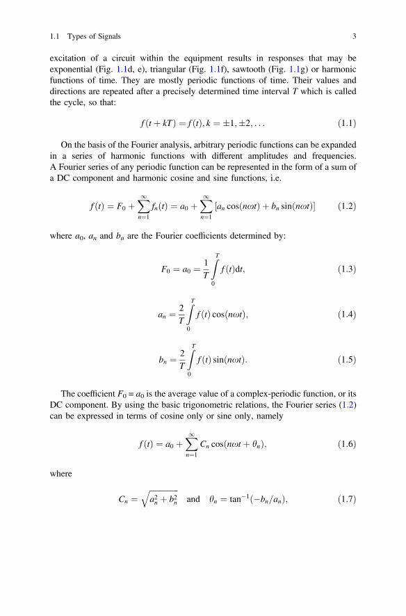
excitation of a circuit within the equipment results in responses that may beexponential (Fig. 1.1d, e), triangular (Fig. 1.1f), sawtooth (Fig. 1.1g) or harmonicfunctions of time. They are mostly periodic functions of time. Their values anddirections are repeated after a precisely determined time interval T which is calledthe cycle, so that:
f t þ kTð Þ ¼ f tð Þ; k ¼ �1;�2; . . . ð1:1Þ
On the basis of the Fourier analysis, arbitrary periodic functions can be expandedin a series of harmonic functions with different amplitudes and frequencies.A Fourier series of any periodic function can be represented in the form of a sum ofa DC component and harmonic cosine and sine functions, i.e.
f ðtÞ ¼ F0 þX1n¼1
fnðtÞ ¼ a0 þX1n¼1
½an cosðnxtÞ þ bn sinðnxtÞ� ð1:2Þ
where a0, an and bn are the Fourier coefficients determined by:
F0 ¼ a0 ¼ 1T
ZT0
f ðtÞdt; ð1:3Þ
an ¼ 2T
ZT0
f ðtÞ cosðnxtÞ; ð1:4Þ
bn ¼ 2T
ZT0
f ðtÞ sinðnxtÞ: ð1:5Þ
The coefficient F0 = a0 is the average value of a complex-periodic function, or itsDC component. By using the basic trigonometric relations, the Fourier series (1.2)can be expressed in terms of cosine only or sine only, namely
f ðtÞ ¼ a0 þX1n¼1
Cn cosðnxt þ hnÞ; ð1:6Þ
where
Cn ¼ffiffiffiffiffiffiffiffiffiffiffiffiffiffiffia2n þ b2n
qand hn ¼ tan�1ð�bn=anÞ; ð1:7Þ
1.1 Types of Signals 3

i.e.
f ðtÞ ¼ a0 þX1n¼1
Cn sinðnxt þ hnÞ; ð1:8Þ
where
Cn ¼ffiffiffiffiffiffiffiffiffiffiffiffiffiffiffia2n þ b2n
qand hn ¼ tan�1ðan=bnÞ: ð1:9Þ
The coefficient C1 is the amplitude of the first or the basic harmonic whosecircular frequency ω = 2π/T is equal to the frequency of the complex-periodicfunction. The higher frequency terms (2ω, 3ω, 4ω, …) are called higher harmonics.In Fig. 1.2a symmetric rectangular signal (dash-dot line) is represented by the sumof only the first three members of the Fourier series (full line). This rectangularsignal contains only odd harmonics. Its Fourier series is:
f tð Þ ¼ F sin xtð Þ þ F3sin 3xð Þ þ F
5sin 5xtð Þ þ F
7sin 7xtð Þ þ � � � ; ð1:10Þ
where F is the amplitude of the basic harmonic. With a higher number of harmonicsthe sum would come closer to the rectangular function, while the infinite sum wouldproduce a complete rectangular form of the signal.
t
v v v + +
vv
v
v
v1 1
3
3
2
2
T/5
T/3
T
Fig. 1.2 A symmetric rectangular signal (dash-dot line) and its Fourier equivalent (full line)consisting of only the first three terms of the Fourier series
4 1 Introduction

1.2 Root-Mean-Square and Average Valuesof Periodic Signals
The root-mean-square (RMS) value of a variable periodic current is equal to thevalue of a DC current which would develop the same amount of heat during thesame time interval within the same resistor, i.e. which does the same amount ofwork. The work of the periodic current through a resistor R over a period T isdetermined by:
W1 ¼ZT0
vðtÞiðtÞdt ¼ZT0
½RiðtÞ�iðtÞdt ¼ RZT0
i2ðtÞdt; ð1:11Þ
whereas the work of the DC current equal to the RMS value of the variable currentin the same resistor over the same period T is
W2 ¼ RI2rmsT : ð1:12Þ
By equating these two works, i.e. W1 = W2, it follows that the RMS value of aperiodic current is
Irms ¼
ffiffiffiffiffiffiffiffiffiffiffiffiffiffiffiffiffiffiffiffiffiffi1T
ZT0
i2ðtÞdt
vuuut : ð1:13Þ
Similarly, the RMS value of a periodic voltage is obtained as:
Vrms ¼
ffiffiffiffiffiffiffiffiffiffiffiffiffiffiffiffiffiffiffiffiffiffiffi1T
ZT0
v2ðtÞdt
vuuut : ð1:14Þ
For example, for a harmonic voltage v(t) = VM sin(ωt) the RMS value is:
Vrms ¼
ffiffiffiffiffiffiffiffiffiffiffiffiffiffiffiffiffiffiffiffiffiffiffiffiffiffiffiffiffiffiffiffiffiffiffiffiffi1T
ZT0
V2M sin2ðxtÞdt
vuuut ¼
ffiffiffiffiffiffiffiffiffiffiffiffiffiffiffiffiffiffiffiffiffiffiffiffiffiffiffiffiffiffiffiffiffiffiffiffiffiffiffiffiffiffiffiffiffiV2M
T
ZT0
½1� cosð2xtÞ�dt
vuuut ¼ VMffiffiffi2
p ¼ 0:707VM ;
ð1:15Þ
1.2 Root-Mean-Square and Average Values of Periodic Signals 5

and the RMS value of a harmonic current of the form i(t) = IM sin(ωt) is:
Irms ¼ IM=ffiffiffi2
p¼ 0:707 IM : ð1:16Þ
The RMS value denotes the real influence of a harmonic current or voltage. Forthis reason it is mostly used without the index rms and is shortly denoted by I orV. For example, V = 220 V is the rms value of the mains voltage. Its amplitude isVM = √2 × 220 = 310 V.
For a periodic function of a rectangular form (Fig. 1.3), determined by (1.17),
iðtÞ ¼ IM;
0;
�0� t\T1 ¼ DTDT\t\T;
ð1:17Þ
the rms value is
Irms ¼
ffiffiffiffiffiffiffiffiffiffiffiffiffiffiffiffiffiffiffiffiffiffiffiffiffiffiffiffiffiffiffiffiffiffiffiffiffiffiffiffiffiffiffiffiffiffiffiffiffi1T
ZDT0
I2Mdt þZTDT
02dt
8<:
9=;
vuuut ¼ffiffiffiffiffiffiffiffiffiffiffiffiffiffiffiffiffiffiffi1TI2MðDTÞ
r¼ IM
ffiffiffiffiD
p; ð1:18Þ
where D = TI/T is the duty cycle of the rectangular pulse.The average value of a periodic signal within one period is defined as:
fav ¼ 1T
ZT0
f ðtÞdt: ð1:19Þ
For a current of a rectangular form, according to Fig. 1.3, it is
Iav ¼ 1T
ZDT0
IMdt ¼ DIM : ð1:20Þ
i(t)
MIIrms =
t
1T 2T
DT T
IM D Iav = IM D
Fig. 1.3 A current of a rectangular form of duty cycle 0 < D < 1, its RMS and average vales
6 1 Introduction

Practically, the average value represents the area between the pulse and the timeaxis over a single period, divided by that period. The average value of a harmonicsignal of the form f(t) = FM sin(ωt) is zero since it consists of two equal areas withopposite signs (positive and negative half-periods). In some of the circuits of powerelectronics, such as rectifiers, the use is made of the rectified current (Fig. 1.4),where all the parts are positive, while the original form of the wave is retained. Thecycle of such a signal is T/2, and the mean value is
Iav ¼ 1T=2
ZT=20
IM sinðxtÞdt ¼ 2IMp
� 0:637 IM : ð1:21Þ
For complex-periodic currents the use is made of the form factor, as the measureof the discrepancy from the harmonic form, defined as
k ¼ Irms
Iav¼ I
Iav: ð1:22Þ
The form factor of a rectangular current according to Fig. 1.3 is k = IM√D/(IMD) = 1/√D whereas for a rectified harmonic current it is k = (IM/√2)/(2IM/π) = π/(2√2) = 1.11.
As a measure of the discrepancy of a periodic signal from the harmonic form of acurrent/voltage signal the use is often made of either the distortion factor
DF ¼ I1rms
Irms
; ð1:23Þ
or of the total harmonic distortion
THD ¼ffiffiffiffiffiffiffiffiffiffiffiffiffiffiffiffiffiffiffiffiffiffiI2rms � I21rms
pI1rms
¼ffiffiffiffiffiffiffiffiffiffiffiffiffiffiffiffiffi1� DF2
p
DF; ð1:24Þ
i(t)=IM |sin(ω t)|
MIIav = 0,637 IM
tT/2T
Fig. 1.4 The rectified harmonic current and its mean value
1.2 Root-Mean-Square and Average Values of Periodic Signals 7

where I1rms is the RMS value of the first harmonic and
Irms ¼ffiffiffiffiffiffiffiffiffiffiffiffiffiffiffiffiffiX1n¼0
I2nrms
s¼
ffiffiffiffiffiffiffiffiffiffiffiffiffiffiffiffiffiffiffiffiffiffiffiffiffiffiffiffiffiffiffiffiffiI20 þ
X1n¼1
Inffiffiffi2
p� �2
vuut ð1:25Þ
is the total rms value of a complex-periodic current. In (1.25) I0 is the DC com-ponent, and In is the amplitude of the n-th harmonic. If the DC component is zero,the total harmonic distortion is
TDH ¼P1n¼2
I2nrms
I1rms
: ð1:26Þ
Example 1.1 Determine the effective (rms) value of v tð Þ¼5þ 10 sin x1t þ 30�ð Þþ12 sin x2t þ 60�ð Þ for:(a) x2 ¼ 2x1
(b) x2 ¼ x1:
When the sinusoids are of different frequencies, and the terms are orthogonal,rms value is:
Vrms ¼ffiffiffiffiffiffiffiffiffiffiffiffiffiffiffiffiffiffiffiffiffiffiffiffiffiffiffiffiffiffiffiffiffiffiffiffiffiV2 þ V2
1rms þ V21rms
q¼
ffiffiffiffiffiffiffiffiffiffiffiffiffiffiffiffiffiffiffiffiffiffiffiffiffiffiffiffiffiffiffiffiffiffiffiffiffiffiffiffiffiffiffiffiffi52 þ 10ffiffiffi
2p
� �2
þ 12ffiffiffi2
p� �2
s¼ 12:12V
(a) First, we combine sinusoids using phasor addition:
10 sin x1t þ 30�ð Þ þ 12 sin x1t þ 60�ð Þ ¼ 14:66 sinðx1tÞ þ 15:39 cos x1tð Þ¼ 21:25 sin x1t þ 46�ð ÞV:
The voltage function is then expressed as:
v tð Þ ¼ 5þ 21:25 sinðx1t þ 46�ÞV
The rms value of voltage v is:
Vrms ¼ffiffiffiffiffiffiffiffiffiffiffiffiffiffiffiffiffiffiffiffiffiV2 þ V2
1rms
q¼
ffiffiffiffiffiffiffiffiffiffiffiffiffiffiffiffiffiffiffiffiffiffiffiffiffiffiffiffiffiffi52 þ 21:25ffiffiffi
2p
� �2s
¼ 15:83V
8 1 Introduction

1.3 Power of Periodic Currents
The product of the instantaneous values of a periodic voltage across a load and thecurrent through the load is the instantaneous power:
p tð Þ ¼ v tð Þi tð Þ: ð1:27Þ
Since the instantaneous values of the voltage or current could have differentsigns, the instantaneous power can in general be positive or negative. The power ispositive if the energy is transferred from the source to the load and negative if theenergy is transferred from the load to the source. A typical example of a loadinvolving positive and negative instantaneous power is a coil and a capacitor drivenby a harmonic signal. If, for example a coil of inductance L is connected to avoltage V(t) = VM sin(ωt), the current through the coil will be shifted by −π/2 withreference to the voltage and the instantaneous power will be
p tð Þ ¼ VMcos xtð Þ½ � IMcos xt � p=2ð Þ½ � ¼ 1=2VMIMsin 2xtð Þ:
The frequency of the instantaneous power will be double the voltage frequency(Fig. 1.5). The shaded area between the curve p(t) and the time axis (Fig. 1.5)represents this work. During the first and the third quarter of the cycle this work ispositive, i.e., the work of the source is converted to the energy of the magnetic fieldof the coil. During the other two quarters of the cycle (the second and the fourth)this work is negative, meaning that the energy of the magnetic field is returned backto the source.
During the intervals of negative instantaneous power, the coil behaves like asource and the source like a load. Energy is thus being exchanged between thesource and the coil. Consequently, the total work of the source is zero and theaverage power is also zero.
The same conclusions may be drawn if a capacitor is driven by a harmonicsignal. In two quarters of the cycle, the capacitor accumulates the electrostatic
i(t)p(t) v(t)
T/2 T
ω t
Fig. 1.5 Instantaneous powerof a coil driven by a harmonicsignal
1.3 Power of Periodic Currents 9

energy from the source and during the other two quarters this energy is returnedback to the source. Consequently, here too the average power is equal to zero.
The average or active power is the one that does the work. For periodic currentsit is defined by the time interval equal to one cycle:
P ¼ 1T
ZT0
pðtÞdt: ð1:28Þ
It can be shown that in the case of a capacitor the average power from the sourceis zero. If a capacitor is driven by a rectangular signal
P ¼ 1T
ZT0
VDCiCðtÞdt ¼ VDC
1T
ZT0
iCðtÞdt24
35 ¼ VDCIcav; ð1:29Þ
where
Icav ¼ 1T
ZT0
iCðtÞdt; ð1:30Þ
is the average current through the capacitor, then the voltage across the capacitor is
VCðt0 þ TÞ ¼ VCðt0Þ þ 1C
Zt0þT
t0
iCðtÞdt: ð1:31Þ
Since it has been assumed that the voltage across the capacitor (source voltage)was periodic, i.e. VC(t0 + T) = VC(t0) it follows that:
1C
Zt0þT
t0
iCðtÞdt ¼ VCðt0 þ TÞ � VCðt0Þ ¼ 0: ð1:32Þ
By comparing (1.32) and (1.30), one comes to the conclusion that the averagecurrent through the capacitor is zero, thus the average power is also zero. It isshown in the same way that the average value of the voltage across a coil driven bya periodic rectangular current is also zero.
It can thus be concluded that either a coil or a capacitor dissipate no power if drivenby a periodic signal. For this reason, they are called nondissipative elements. Sinceminimum dissipation of power is one of the basic requirements in the design ofvarious efficient converters, coils and capacitors are the basic elements of thesecircuits together with the switching circuits generating periodic voltages and currents.
10 1 Introduction

Example 1.2 A coil of inductance L = 1 mH and a capacitor of capacitance 1 μFconnect blocks B1 and B2 (Fig. 1.6a) and B3 and B4 (Fig. 1.6b), respectively. Thecurrent through the coil and the voltage across the capacitor are linear periodicfunctions determined by
iLðtÞ ¼ 10Aþ 1A0:75ms t;
11A� 1A0:25ms t;
(
t0 \ t\ t0 þ 0:75ms; t0 þ 0:75ms\ t\ t0 þ T ¼ t0 þ 1ms;
ð1Þ
vC tð Þ ¼ 11V� 10V0:75ms t;
1Vþ 10V0:25ms t;
(
t0\t\t0 þ 0:75ms; t0 þ 0:75ms\ t\ t0 þ T ¼ t0 þ 1ms:
ð2Þ
Draw the variations of the voltage across the coil and the current through thecapacitor and determine their average values.
The voltage across the coils is
VL ¼ LdiLdt
¼ L 1A0:75ms ¼ 1 10�3 1A
0:75 10�3 ¼ 43 V ¼ Vþ
L ;
�L 1A0:25ms ¼ �1 10�3 1A
0:25 10�3 ¼ �4V ¼ V�L ;
(t0\t\t0 þ 0:75ms
The current and the voltage of the coil are drawn in Fig. 1.7.The areas above and below the time axis within one cycle are mutually equal but
of the opposite signs.Namely
A ¼ VþL 0:75 ¼ 4=3V 0:75ms ¼ 1 10�3 Vs
A ¼ V�L 0:25 ¼ �4V 0:25ms ¼ �1 10�3 Vs:
1B 2BLi
Lv3B 4B
CvCi
(a) (b)
Fig. 1.6 Blocks B1 and B2 connected over coil (a) and capacitor (b)
1.3 Power of Periodic Currents 11

The average value of the voltage across the coil is
VLav ¼ 1T
Zt0þT
t0
VL tð Þdt ¼ 1T
Zt0þ0:75
t0
VþL dt þ
ZTt0þ0:75
V�L dt
264
375
¼ 1T
4=3 0:75� 4 0:25ð Þ ¼ 1T
A� Að Þ ¼ 0
The current through the capacitor is:
iC ¼ CdvCdt
¼ �C 10V0:75ms ¼ �1 10�6F 10V
0:7510�3 s ¼ � 403 mA ¼ I�C ;
C 10V0:25ms ¼ 1 10�6F 10V
0:2510�3 s ¼ 40mA ¼ IþC ;
(
The voltage and the current of the capacitor are drawn in Fig. 1.8.The areas below and above the time axis are
�A ¼ I�C 0:75ms ¼ �403
mA 0:75ms ¼ �10As;
þA ¼ IþC 0:25ms ¼ 40mA 0:25ms ¼ þ10As:
The average current through the capacitor is
ICav ¼ 1T
Zt0þT
t0
iC tð Þdt ¼ 1T
�Aþ Að Þ ¼ 0
t
t0 t0 + 0.75ms t0 +1ms t0 +2mst0 +T+0.75ms
iLILM =11A
V L = -4V-
V L V+
= 43
ILm =10A
-A
A
T
t
Fig. 1.7 Waveforms of the current and voltage the coil for the circuit shown in Fig. 1.6a
12 1 Introduction

In general, however, when the load is an impedance Z = |Z|ejφ, there will be aphase shift φ between the current and the voltage. If V = VMcos(ωt), then i = IM cos(ωt − φ) and the power active power is
P ¼ VMIM1T
ZT0
½cosðxtÞ�½cosðxt � uÞ�dt ¼ 12T
VMIM
ZT0
cosudt; ð1:33Þ
i.e. since VM = √2Vrms and IM = √2Irms,
P ¼ VrmsIrmscosðuÞ ¼ VIcosðuÞ: ð1:34Þ
Thus, the active power is the product of the rms values of the voltage and thecurrent and the cosine of the angle between the load voltage and the current. Thepower is maximum when the load voltage and the current are in phase (φ = 0),which is the case of a purely resistive load. In a resistor the electric energy isconverted to thermal energy. If φ = ±π/2, as in the case of a coil or capacitor, cos(φ) = 0, and the active power in these elements is zero.
The phasor diagram of the voltage and a current which is phase shifted by φ isshown in Fig. 1.9. Bearing in mind (1.34), the work is performed only by voltagecomponent V cosφ which is in phase with the current, so V cosφ is called thevoltage component for active power. In addition, there is a passive component Vsinφ, which is orthogonal to the current vector. This component does not performany work, i.e., it does not transform the electrical work of the source, so thecorresponding power is called the reactive power and it is equal to
t
t0 t0 +0.75ms t0 +1ms t0 +2mst0 +T+0.75ms
vC
VCM=11V
I C= 40mA+
I C mA- = - 40
3
VCm =10V
-A
A
-A
A
0.75ms 0.25ms
iC
T Tt
Fig. 1.8 Waveforms of the voltage and current the capacitor for the circuit shown in Fig. 1.6b
1.3 Power of Periodic Currents 13

Q ¼ 12VMIM sinu ¼ VI sinu: ð1:35Þ
The reactive power is understood as the energy alternatively exchanged betweenthe source and the load. The vector sum of the active and reactive powers
S ¼ Pþ jQ ð1:36Þ
is the apparent power. Its modulus is
S ¼ Sj j ¼ffiffiffiffiffiffiffiffiffiffiffiffiffiffiffiffiffiP2 þ Q2
p¼ VI: ð1:37Þ
Thus, the apparent power is the product of the rms values of the load voltage andthe current.
The ratio of the active and apparent powers is called the power factor:
PF ¼ PS¼ cosu: ð1:38Þ
Therefore, the power factor of harmonic currents and voltages is cosφ. If thecurrent or the voltage is a complex-periodic function, then (1.38) should be mul-tiplied by the distortion factor (1.23), i.e.
PF ¼ DF cos : ð1:39Þ
Example 1.3 A nonsinusoidal voltage is v tð Þ ¼ 5þ 10 sin 2p50 t þ 30�ð Þþ15 sin 4p50 t þ 45�ð Þ. This voltage is connected to the load which is a serial con-nection of a 10 Ω resistor and a 10 mH inductance.
(a) Determine the power absorbed by the load, and(b) derive an expression for the load current.
VsinV ϕ
cosV ϕ
ϕ
I
ϕ
QS
P
(a)
(b)
Fig. 1.9 The components of a voltage phasor for active and reactive powers (a) and powertriangle (b)
14 1 Introduction

(a) The power absorbed by the load can be determined by the next equation:
P ¼ I2rmsR: The DC current term is: I0 ¼ V0R ¼ 0:5A:
The amplitudes of the ac current terms are
I1 ¼ V1ffiffiffiffiffiffiffiffiffiffiffiffiffiffiffiffiffiffiffiffiffiffiffiffiffiR2 þ x1Lð Þ2
q ¼ 10ffiffiffiffiffiffiffiffiffiffiffiffiffiffiffiffiffiffiffiffiffiffiffiffiffiffiffiffiffiffiffiffiffiffiffiffiffiffiffiffiffiffiffi102 þ 2p50 0:01ð Þ2
q ¼ 0:98A
I1 ¼ V1ffiffiffiffiffiffiffiffiffiffiffiffiffiffiffiffiffiffiffiffiffiffiffiffiffiR2 þ x2Lð Þ2
q ¼ 15ffiffiffiffiffiffiffiffiffiffiffiffiffiffiffiffiffiffiffiffiffiffiffiffiffiffiffiffiffiffiffiffiffiffiffiffiffiffiffiffiffiffiffi102 þ 4p50 0:01ð Þ2
q ¼ 1:45A
The rms value of the load current is
Irms ¼ffiffiffiffiffiffiffiffiffiffiffiffiffiffiffiffiffiffiffiffiffiffiffiffiffiffiffiffiffiffiffiffiffiffiffiI20 þ I21;rms þ I22;rms
q¼
ffiffiffiffiffiffiffiffiffiffiffiffiffiffiffiffiffiffiffiffiffiffiffiffiffiffiffiffiffiffiffiffiffiffiffiffiffiffiffiffiffiffiffiffiI20 þ
I1ffiffiffi2
p� �2
þ I2ffiffiffi2
p� �2
s
¼ffiffiffiffiffiffiffiffiffiffiffiffiffiffiffiffiffiffiffiffiffiffiffiffiffiffiffiffiffiffiffiffiffiffiffiffiffiffiffiffiffiffiffiffiffiffiffiffiffiffiffiffiffi0:52 þ 0:98ffiffiffi
2p
� �2
þ 1:45ffiffiffi2
p� �2
s¼ 1:33A
The power absorbed by the load is
P ¼ 1:332 10 ¼ 17:69W:
(b) The phase angles of the ac current terms are
u2 ¼ 45� � arctg4p50 0:01
10
� �¼ �11�u1 ¼ 30� � arctg
2p50 0:0110
� �¼ 0�
The load current can be expressed as
i tð Þ ¼ 0:5þ 0:98 sin 2p50 tð Þ þ 1:45 sin 4p50 t � 11�ð ÞA
Example 1.4 The waveforms of voltage and current at a single phase load arerecorded and presented in the analytical form:
v tð Þ ¼ 100þ 320 sin 2p50 tð ÞVi tð Þ ¼ 20 sin 2p50 t � p
4
� �þ 20 sin 2p100 t � p
3
� �A
1.3 Power of Periodic Currents 15
Determine:
(a) the power absorbed by the load, and(b) the power factor.
(a) The power absorbed by the load is determined by computing the absorbedpower at each frequency
P ¼ V0I0 þXni¼1
ViIi2
� �cos #i � wið Þ ¼ 320 20
2cos
p4
� �¼ 2:26 kW
(b) The power factor is calculated by Eq. (1.38)
PF ¼ PS¼ P
VrmsIrms
The rms values of the load current and voltage are:
Vrms ¼ffiffiffiffiffiffiffiffiffiffiffiffiffiffiffiffiffiffiffiffiffiffiffiffiffiffiffiffiffiffiffiffi1002 þ 320ffiffiffi
2p
� �2s
¼ 247:38V
Irms ¼ffiffiffiffiffiffiffiffiffiffiffiffiffiffiffiffiffiffiffiffiffiffiffiffiffiffiffiffiffiffiffiffiffiffiffi20ffiffiffi2
p� �2
þ 20ffiffiffi2
p� �2
s¼ 20A
The power factor is
PF ¼ 2260247:38 20
¼ 0:46:
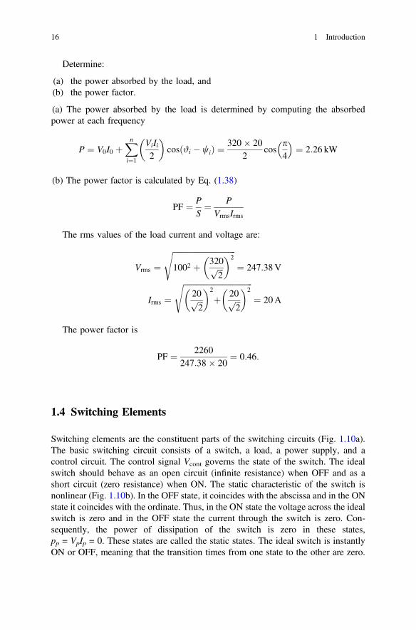
1.4 Switching Elements
Switching elements are the constituent parts of the switching circuits (Fig. 1.10a).The basic switching circuit consists of a switch, a load, a power supply, and acontrol circuit. The control signal Vcont governs the state of the switch. The idealswitch should behave as an open circuit (infinite resistance) when OFF and as ashort circuit (zero resistance) when ON. The static characteristic of the switch isnonlinear (Fig. 1.10b). In the OFF state, it coincides with the abscissa and in the ONstate it coincides with the ordinate. Thus, in the ON state the voltage across the idealswitch is zero and in the OFF state the current through the switch is zero. Con-sequently, the power of dissipation of the switch is zero in these states,pp = VpIp = 0. These states are called the static states. The ideal switch is instantlyON or OFF, meaning that the transition times from one state to the other are zero.
16 1 Introduction

No electronic switch, however, behaves ideally. A real switching element ischaracterized by:
• finite resistance when OFF,• nonzero resistance when ON,• transition times from ON to OFF state and vice versa greater than zero, and• dissipation of power in the switch.
The static and dynamic characteristics of a real switch are shown in Fig. 1.11. Inmost cases, the voltage in the on state and the current in the off state are negligible.Thus, the power of dissipation of a real switch in the static state is also negligible. Inthe transient condition, while changing the state of the switch, both current andvoltage are present (Fig. 1.11b) and the instantaneous value of dissipation may besignificant.
The transition times from one static state to the other are dependent on thefrequency characteristics of the switching element, the character of the load, and thecontrol circuit. They do not depend on the switching cycle T. Therefore, the averagepower dissipated by a switching element will grow with the decrease of T. Dynamicpower dissipation at high frequencies may be considerable. For this reason, the
t
t
t
t
Off
On
Off
On state
Off stateIp
Vp
Vcont
VDC/RL
VDC
ip
Vp
Pp=VpIp
Vp
Vcont
Control
Ip
Pr
Switch
Power supply
ZL
LoadV
(a)
(b)
(c)
Fig. 1.10 Basic circuit (a), static characteristic of an ideal switch (b), and the current Ip, voltage Vp,
and power dissipation pp of an ideal switch (c) for a DC power supply (VDC) and resistive load RL
1.4 Switching Elements 17

maximum frequency of a switching circuit is limited not only by the turn-ON/turn-OFF times but also by the permitted power dissipation of the switch. This isparticularly true for power switches and it is this type of switch that is predomi-nantly used in power electronics.
The power semiconductor elements like diodes, bipolar or MOS transistors,thyristors, and BiMOS transistors are used as the switching elements. A commonrequirement for all of these elements is that the control of signals carrying con-siderable power has to be done by as short turn-ON/turn-OFF times as possible.
Power diodes can be classified into three groups: general purpose, very fast, andSchottky. The operating voltages and currents of general purpose diodes may rangeup to 3,000 V and 3,500 A, and those of very fast diodes up to 3,000 V and1,000 A. The reverse recovery times are in the range from several hundredsnanoseconds to several microseconds. Schottky diodes have lower forward voltagesand very short recovery times (below 10 ns). However, the reverse saturationcurrent grows with the power of the diode so the characteristics are limited to 100 Vand 300 A. Diodes are two terminal devices. This limits their applications asswitches as the control load circuits are common.
Power bipolar transistors (PBT) are characterized by a very small collector-emitter on (saturation) resistance, from several mΩ to several tens of mΩ. Owing tothis, the collector-emitter on (saturation) voltage is within the limits of 0.5–1.5 Veven at very high collector currents. The maximum voltages and currents range upto 1,200 V and 400 A. The maximum frequency of the pulse DC/DC convertersusing PBT as switches runs up to several tens (20–30) of kilohertz. PBTs asswitches are mainly used in the common-emitter connection. The control is
p
V
V
P
p
V
V
p
p
psr
p
cont
DC
On state
Off state
On
Off
t
t
t
i p
t
T
(a) (b)
Fig. 1.11 Characteristics of a real switch: static (a) and dynamic (b)
18 1 Introduction

implemented via a base circuit. If a turned-ON transistor is to reach the saturationregion, in addition to the forward bias of the base-emitter junction, a sufficientlylarge base current is required so that the base-collector junction is also forwardbiased. Consequently, the control circuit requires a relatively large power.
The power MOS transistors have recently been finding an increased use in thepulse converters. They are faster than PBTs and the maximum frequency of theconverters based on power MOS devices ranges up to 100–200 kHz. The ratedvoltages and currents are smaller than those of PBT and are within the range of1,000 V and 50 A, respectively. The input impedance of MOS transistors is high (ofthe order of 109 Ω), thus for their control it is sufficient to provide the correspondinggate-source voltage. Since the gate current is practically zero, there is no dissipationin the control circuit. Therefore, an MOS transistor is a voltage controlled switchcompared to a PBT which is a current controlled switch.
The basic weakness of power MOSFETs is a relatively large on resistance (fromseveral hundreds mΩ up to several Ω). This was the reason for the development ofseveral types of BiMOS transistors which unite good properties of both bipolartransistors (small on resistance) and MOS (negligible driving current). One of thesetypes is the insulated gate bipolar transistor (IGBT). Its input characteristics are likethose of an MOS transistor and the output characteristics are like those of a PBT.The maximum voltages and currents range up to 1,200 V and 400 A and themaximum frequencies up to several tens of kHz (like PBT). The frequency char-acteristics of the static induction transistors (similar to JFET) have been improved.The maximum ratings of this type of transistor are 1,200 V, 300 A, and 100 kHz.
The characteristics and symbols of nonregenerative semiconductor switches(diodes, BT, and MOSFET) are shown in Table 1.1.
The thyristor is a representative of the regenerative switches (the switches wherethe change of state is supported by a positive feedback). In addition to the regen-erative process, the essential difference compared to the PBT and MOSFET is inthat the thyristors are turned on by feeding short pulses (several tens of millisec-onds) to the gate. After switch-ON, a thyristor remains on even if the driving signalis removed from the gate. For the PBT and MOSFET devices the driving signalmust be present throughout the on state. Thyristors are very powerful elements. Themaximum voltages and currents range up to 10,000 V or A, respectively. Today awhole family of thyristors is commercially available. Each member of this family isspecific regarding both its characteristics and its applications. The V–I character-istic, the symbol, and the equivalent circuit are shown in Table 1.2. A standardthyristor (SCR) is turned on by a positive pulse at the gate, but it cannot be turnedoff by a gate signal. The gate turn-off (GTO) and self-turn-off (SITH) are the self-turn-off thyristors. They are turned on by positive and turned off by negative pulsesat the gate. The maximum voltages and currents of GTO thyristors are respectively4,000 V and 3,000 A, and of SITH thyristors 1,200 V and 300 A. The maximumfrequency of SITH is high and ranges up to several hundred kHz. Another thyristortype can be turned off at the gate. This is the MOS-controlled thyristor (MCT). Its
1.4 Switching Elements 19

maximum ratings are 1,000 V and 100 A. A triac is an AC switch. Practically, itconsists of two thyristors in anti-parallel connection and its characteristic in the Iand III quadrants is symmetric. Its maximum ratings are 1,200 V, 300 A, and400 Hz.
The reverse conduction thyristor (RCT) also can conduct in both half-cycles ofan AC voltage. Practically, this is a thyristor with a diode in anti-parallel connec-tion, the diode conducting during the negative half-cycle. The maximum ratings ofthe RCT are 2,500 V, 1,000 A forward, and 400 A reverse current.
In addition to the triode-type thyristors, there are several types of the diode-typethyristors (two-terminal devices without a control terminal). The four-layer diodeand diac belong to this group. They are mainly used as switches for triggeringthyristors.
Table 1.3 gives the comparative values of the basic parameters of semiconductorpower switches. The qualitative characteristics of the most frequently usedswitching elements are presented in Table 1.4.
Table 1.1 Characteristics and symbols of nonregenerative switches
I I > I II
I
I
I
I
I
I
I II
I
C Bn B1
CC
C
D
C
D
C
D
D DD
B
V CE
VV
V
V
CECE
CE
DS
V CE
V DS
UB1
V CE
V DS
V
V
GS
GS
V
VV
AK
AK
AK
B
G
G
C
C
D
E
S E
S
A
K
V >
V
V
GSn
GSn
GS1
GS1
V
V
GS1
GS1
V >
RealCharacteristic
IdealCharacteristicSymbolElement
Diode
Bipolar NPNTransistor
IGBT
MOSFET
20 1 Introduction

Table 1.2 Symbols, equivalent circuits, and V–I characteristics of regenerative switchesU
N I
L A
T E
R A
L
UJT /
UT
niJunctionransistor
CUJT /
CUT
omplementarynijunctionransistor
PUT /
PUT
rogrammable nijuctionransistor
BOD /
BD
reakOveriode
SUS /
SUS
iliconnilateralwitch
SCR /
SCR
iliconontrolledectifier
GATT /GATT
atessistedurn-offhyristor
GTO /
GTurn
ate-off
LASCR /
LASCR
ightctivated
Type CharacteristicSymbol Equivalent circuitName
E
E
B
B
B
B
B
B
B
B
1
1
2
2
2
2
1
1
E
E
A
A
A
A
A
A
G
G
G
G
K
K
K
K
K
K
A
A
A
A
G
K
K
K
K
+
G G
G
Ideal
Real
(continued)
1.4 Switching Elements 21

Table 1.2 (continued)B
I L
A T
E R
A L
AGT /
AGT
mplify ingatehyristor
MCT /
MC
OSontrolled
Thyristor
SCS /
SCS
iliconontrolledwitch
ASCR /
A
R
ssymetrical
c tiffier
SC
iliconontrolled
DIAC /
DAC
iode
TrigerDIAC NPN
/
SIDAC /
SDAC
iliconiode
SBS /
SBS
iliconaterialwitch
TRIAC /
TRAC
iode
RCT /
RCT
everseonductinghyristor
A
A
A
A
G
AG
G
GG
G G
K
K
K
K
AAG
KGK
K
KG
G
A
G
As SCR As SCR
MT
MT MT
MT MT
MT
MT
MT
MTMT
MT
MT
MT MT
MT
MT
MT
MT
MT
MT
1
1 1
1 1
1
1
1
11
2
2
2 2
2
2
2
2
2
2
G G
22 1 Introduction

In order to obtain a better idea about the characteristics of individual elements,Fig. 1.12 illustrates their applications with respect to frequency, voltage, andcurrent [2].
Table 1.3 Characteristics of semiconductor power switches [1]
Class Type Maximum volt-age/current (V/A)
Maximum fre-quency (kHz)
Switchingtime (μs)
Onresistance
Diode Generalpurpose
5,000/5,000 1 100 0.16 mΩ
Very fast 3,000/1,000 10 2–5 1 mΩ
Schottky 40/60 20 0.23 10 mΩ
Thyristors SCR 5,000/5,000 1 200 0.25 mΩ
RCT
GATT 2,500/400 5 40 2.16 mΩ
GTO
SITH 2,500/1,000 5 40 2.1 mΩ
MCT
1,200/400 20 8 2.24 mΩ
4,500/3,000 10 15 2.5 mΩ
4,000/2,200 20 6.5 5.75 mΩ
600/60 20 2.2 18 mΩ
Bipolartransistors
Darlington 400/250 20 9 4 mΩ
400/40 20 6 31 mΩ
630/50 25 1.7 15 mΩ
1,200/400 10 30 10 mΩ
MOSFET 500/8.6 100 0.7 0.6 Ω
1000/4.7 100 0.9 2 Ω
500/50 100 0.6 0.4 Ω
IGBT 1,200/400 20 2.2 18 mΩ
SIT 1,200/300 100 0.55 1.2 Ω
Table 1.4 Qualitativecharacteristics of switchingelements containing controlelectrode
Element Power Speed
BJT Medium Medium
MOSFET Low High
SCR High Low
GTO High Slow
IGBT Medium Medium
MCT Medium Medium
1.4 Switching Elements 23

1.5 Magnetic Elements
Pulse transformers, chokes, and resonant coils have found applications among theavailable magnetic elements. Transformers are used for galvanic separation andimpedance matching, and chokes are used for filtering. These elements operate atfrequencies above 20 kHz and their dimensions are much smaller compared to thoseused in linear converters. The basic equation of the mid- and high-frequencytransformers can be written in the form
V1 ¼ 4N1SBf ; ð1:40Þ
where VI is the rectangular input voltage, NI is the number of primary turns, S is thecross-section of the magnetic core, B is the maximum value of induction in the core,and f is the operating frequency. The product NIS is a measure of the volume andweight of a transformer as NI is the measure of the amount of copper used and S is themeasure of the magnetic material used. For a given input voltage, the volume and
2 kV
1 kV
3 kV
4 kV
5 kV
Voltage
Current
Frequency500 A 1000 A 1500 A 2000 A 3000 A
1 MHz
100 kHz
10 kHz
1 Hz
Thyristor
GTO thyristors
MCT
BJTIGBT
MOSFET
Fig. 1.12 Maximum characteristics of semiconductor power switches with respect to frequency,voltage, and current
24 1 Introduction

weight are thus inversely proportional to the product Bf. If it is assumed that in mainstransformers that B = 1.8 T, then Bf = 1.8 × 50 = 90 T/s. For pulse transformers themaximum induction is about 0.3 T. If the frequency is 30 kHz, then Bf = 9,000 T/s.This means that pulse transformers are capable of transferring considerably higherpowers per unit volume and weight compared to the mains transformers.
Owing to an increased operating frequency, special materials like ferrites orhighly alloyed laminated metal must be used in pulse transformers. Ferrite cores arepredominantly used. Namely, it is technologically simple to fashion the requiredshapes of cores which facilitates the realization of optimally designed transformers.Moreover, bulk conductivity of ferrite cores is very low so that eddy current lossesare practically negligible. Mainly the EC, EE, U or X cores are used. For an opti-mally designed transformer, it is necessary to have data about its magnetic materialand the core geometry. Table 1.5 presents the data for effective lengths of magneticforce lines le, cross-sections Se, and volumes Ve of some of the standard ferrite cores.
Total losses in magnetic material consist of hysteresis, residual, and eddy currentlosses. In ferrite cores hysteresis losses prevail. These losses increase with fre-quency and maximum variation of induction ΔB per switching cycle. Cataloguesspecify maximum induction for bipolar symmetric driving, Bac = ΔB/2. In order toprevent shifting of the core to the saturation region, most of the time Bac < 0.3T, butat frequencies close to 1 MHz the limitation is between 30 and 50 mT. Figure 1.13shows the losses in materials N49 and N59 (manufacturer Siemens) for Bm = 50 mTat frequencies 500 kHz and 1 MHz.
Table 1.5 Geometric dimensions of some of the standard ferrite cores
Class of core Type le (cm) Se (cm2) Ve (cm
3)
Pot P 7 × 4 1 0.07 0.07
P 11 × 7 1.59 0.159 0.252
P 14 × 8 2 0.25 0.5
P 30 × 19 4.5 1.36 6.1
P 42 × 29 6.86 2.65 18.2
EE EE 20 4.3 0.31 1.34
EE 30 6.7 0.6 4
EE 42/20 9.7 2.4 23.3
EE 55/25 12.3 4.2 52
EC EC 35 7.74 0.84 6.53
EC 52 10.5 1.8 18.8
EC 70 14.4 2.79 40.1
U U 15 4.8 0.32 1.54
U 25 8.6 1.05 9.03
U 57 16.3 1.71 27.9
1.5 Magnetic Elements 25

1.5.1 Chokes
Chokes are magnetic elements made of copper wire wound around ferromagneticcores. The job of a choke designer is to:
• select the core and determine the air gap if required,• calculate the cross-section, length, and the number of turns of the copper wire, and• select the mode of winding.
The basic parameter of a choke is its inductance. If the core contains an air gap,then the inductance is approximately
L ¼ l0leRl=S
N2; ð1:41Þ
where l is the length of magnetic force lines of each individual part of the core madeof the same magnetic material and with a constant cross-section, S is the cross-section of the core, μo = 4π × 10−7 H/m is magnetic permeability of the vacuum, μeis the effective magnetic permeability, and N is the number of turns. The effective
PL[ m
W/c
m3 ]
0
50
20
150
100N49
200
250
0 40 60 80 100 120
N59
PL
[ mW
/cm
3 ]
0
200
20
T [ oC]
600
400
N49800
1000
0 40 60 80 100 120
N59
T [ oC]
(a)
(b)
Fig. 1.13 Losses in ferrite materials N49 and N59 as functions of temperature at frequencies500 kHz (a) and 1 MHz (b) and for Bm = 50 mT
26 1 Introduction

permeability is defined as the resulting permeability of a core consisting of mate-rials with different permeabilities. It depends on the shape and dimensions of thecore and particularly on the width of the air gap in the magnetic material.
The effective length of magnetic force lines le is defined as
le ¼ ðRl=SÞ2Rl=S2
; ð1:42Þ
and the effective magnetic cross-section is
Se ¼ leRl=S
: ð1:43Þ
The effective magnetic volume is determined by
Ve¼leSe: ð1:44Þ
Now the choke inductance can be written in the form
L ¼ l0leSeleN2: ð1:45Þ
It is quite difficult to determine the effective magnetic permeability of a corecontaining an air gap. For this reason, the manufacturers give the values of theinductance factor AL which represents the inductance of the choke consisting of thecore and one turn. The inductance of the coil of a choke is
L ¼ ALN2: ð1:46Þ
The inductance factor AL is determined experimentally by measuring theinductance of a coil containing only one turn and it is presented in the form of adiagram like the one in Fig. 1.14. The inductance factor AL of ferrite cores rangesfrom 5 to 10,000. It depends on the type of material and core dimensions. For largercores, the inductance factor AL is larger. In addition, AL is dependent on the air gapof the core (Fig. 1.15).
1.5.2 Transformers
Transformers consist of at least two inductively coupled windings. The windingsare galvanically separated, thus only the transfer of AC signals is possible. Theinput winding is called the primary, and the output is the secondary. Voltageinduced in the secondary can be lower, or higher, or equal to the primary voltage.The ratio of the secondary and the primary voltage is determined by the ratio of thenumber of the secondary and the primary windings. Under the influence of the
1.5 Magnetic Elements 27

10
10
10
10
10
10 20 100 200 1000
-5
-4
-3
-2
-1
L (
H)
N
100
25
40
63
160
250
400
630
10001600
A=2500
A N x x 10L2 -1
2
Fig. 1.14 Choke inductanceas function of the number ofturns for different values ofinductance factor AL
10
10
0.02 0.1 1.0 mm
2
3
AL
5
5
d
10 1
Fig. 1.15 Inductance factoras function of the width of theair gap of ferrite core profileE20 made of material N27(Siemens)
28 1 Introduction

magnetic flux caused by the voltage V1 in the primary winding, the electromotiveforces E1 and E2 will be induced in the primary and the secondary windings,respectively
E1 ¼ 4:44 10�4fN1BmSe; Vð Þ; ð1:47Þ
E2 ¼ 4:44 10�4fN2BmSe; Vð Þ; ð1:48Þ
where f(Hz) is the driving frequency, N1 and N2 are the respective numbers of turnsin the primary and in the secondary, Bm(T) is the amplitude of magnetic inductionin the core, and Se(cm
2) is the effective cross-section of the core. If the voltagedrops in the windings are neglected, then V1 = E1 and V2 = E2 and the ratio ofvoltage transformation is
n ¼ V1
V2¼ N1
N2ð1:49Þ
Since the inductance factors of the primary and the secondary are equal, itfollows that:
n ¼ V1
V2¼ N1
N2¼
ffiffiffiffiffiL1L2
rð1:50Þ
If the secondary is loaded, the current I2 will flow. The currents of the primary I1and the secondary I2 will maintain magnetic equilibrium if I1N1 = I2N2, giving
I1I2
¼ N2
N1¼ 1
n: ð1:51Þ
A real transformer can be replaced by the equivalent circuit in Fig. 1.16 con-sisting of a T equivalent circuit and an ideal transformer. Real losses within atransformer are modeled by the stray inductance Le. The coupling coefficientk depends on the degree of coupling of the magnetic fields of the windings. Forferromagnetic transformer cores, k is close to unity because almost all magneticfield lines close within the transformer core. The Ohmic resistances of the
V1 V2
Le Le
Lm N1 N2
++
n:1
n=N1/N2
ideal transformer
N1 N2
ideal transformer
Lm≈LeV1
+ +
V2
(a)(b) (c)
Fig. 1.16 Real transformer (a) and its equivalent circuits (b) and (c) (Lm = kI1, Le = L1 − Lm)
1.5 Magnetic Elements 29

transformers used in electronics are negligible. Consequently, these transformerscan be represented by a parallel connection of a coil, whose inductance is equal tothe inductance of the primary winding, and an ideal transformer with a transfor-mation ratio n = N1/N2 (Fig. 1.16c).
1.6 Capacitors
Capacitors have found a very wide application in power electronics. Typicalapplications are:
• protection circuits of power switches,• various types of filters,• resonant circuits of converters for achieving the conditions of soft commutation
of switching elements,• AC circuits for power factor correction,• pulse DC/DC converters for DC component separation,• circuits for forced turning on and off of semiconductor switches (bipolar tran-
sistors and thyristors) etc.• Globally, they can be classified in three groups:• ceramic,• film and• electrolytic.
Figure 1.17 shows the areas of capacitance and the permitted operating voltagesfor the three groups of capacitors.
Vol
tage
(V
)
1
10
102
103
104
10-12
Capacitance (F)10-10
10-8 10-6 10-4 10-2
Ceramic
Film
Electrolytic
Fig. 1.17 Areas of capacitance and permitted operating voltages
30 1 Introduction

The basic function of a capacitor is to accumulate electrical energy in the form ofelectric charge. The electric charge Q and the accumulated energy EC are deter-mined by
Q ¼ CVC; ð1:52Þ
EC ¼ 12CV2
C; ð1:53Þ
where VC is the voltage applied to the capacitor and C is its capacitance. Thecapacitance C is directly proportional to the surface S of the electrodes andinversely proportional to the thickness d of the dielectric layer between them, thus:
C ¼ e0erSd
: ð1:54Þ
Relative dielectric constants εr for different materials are shown in Table 1.6.A capacitor can be represented by the equivalent circuit shown in Fig. 1.18,
where RS = ESR is the equivalent series resistance and LS = ESL the equivalentseries inductance. The series resistance is the basic cause of dissipation in acapacitor and it is most often expressed by the power factor tanδ defined as
Table 1.6 Relative dielectricconstants εr of standarddielectric materials
Dielectric εrVacuum 1
Air (atmosphere) 1.00059
Ceramic 20–12,000
Ta2O3 10–25
Glass 4–9.5
Al2O3 7
Polystyrene and polypropylene 2.5
Polycarbonate 2.8
Impregnated paper 2.6
C
RS
iC
LSC
ESLESR
V
Fig. 1.18 Equivalent circuit of capacitor
1.6 Capacitors 31

tan d ¼ xCRS: ð1:55Þ
The power factor tanδ is given in catalogue data for capacitors.ESL represents the series inductance of the terminals of the internal structure of a
capacitor. Besides being dependent on the type of capacitor, the values of theparasitic elements ESR and ESL depend on packaging and method of mounting in acircuit. The total impedance of a capacitor is determined by
Z xð Þ ¼ RS þ j xLS � 1xC
� �; ð1:56Þ
and its modulus is shown in Fig. 1.19. The minimum of the impedance modulus isequal to the resistance RS and it is obtained at the intrinsic resonance frequency
xr ¼ 1ffiffiffiffiffiffiffiffiLSC
p : ð1:57Þ
Below this frequency, the impedance is of the capacitive character and theinfluence of ESL can be neglected. For ω > ωr the influence of ESL prevails.
One electrode of electrolytic capacitors is usually made of aluminum or tanta-lum. A thin oxide layer serving as dielectric is formed on that electrode. The otherelectrode is electrolyte in either liquid or solid state. The electrode carrying thedielectric must always be at positive potential. The electrolytic capacitors shouldhave large values of ESR and ESL. This has a negative effect on the properties ofthe converters where these capacitors are used in the output filters. The ripple of theoutput voltage is increased and the stability of the control module is decreased
Ζ (Ω
)
0.1
1
101
f (Hz)
0.04
0.01
100
10
102 103 104 105106 107 108
-40oC
-25oC
0oC20oC
85oC
1/ωC
ωLs
Rs
0.055
Fig. 1.19 Impedancemodulus of aluminumelectrolytic capacitor 100 mF/63 V as a function offrequency
32 1 Introduction

owing to the difficulties in the design of the compensator in the feedback loop. Forthis reason, it is recommendable to use a parallel connection of several capacitors oflower capacitance instead of one large capacitor. In addition, it is recommendablethat a ceramic or film (polypropylene) capacitor of small ESR and ESL is connectedin parallel with the electrolytic capacitor. The influence of the parasitic elements ofESR and ESL can be reduced if specially designed four-terminal capacitors are usedin the output filter.
Tantalum capacitors have a high-specific capacitance (high capacitance for smalldimensions and low values of ESR and ESL). ESR and ESL tantalum chipcapacitors have especially low values.
The dielectric of ceramic capacitors is ceramic material. Depending on thecomposition of the ceramic material, two main classes of ceramic capacitors can bedefined. The relative dielectric constant of class I capacitors is below 500 (εr < 500).The capacitance does not depend on supply voltage. These capacitors have smallpower losses even at high frequencies (tanδ is about 0.15 % at 1 MHz). They areused in resonant circuits, as timing elements, for filtering, etc. The relative dielectricconstant of class II capacitors ranges from 1,000 to 10,000. Their capacitance is anonlinear function of voltage and temperature. They have higher power losses (tanδis about 3 % at 1 MHz) than the class I capacitors. Owing to high values of εr, thecapacitance is relatively high compared to dimensions.
The dielectric of film capacitors is usually a thin film of polypropylene (MKPcapacitors) or of polyester (MKT capacitors). Very often, these dielectrics arecombined with metallized paper, resulting in improved ability of enduring largevoltage pulses. The film capacitors are mainly used in pulse circuits involving veryfast voltage variations dv/dt.
1.7 Radio-Frequency Interference
In the instants of the change of state of a power switch, a very large change ofvoltage and current per unit time (from 106 to 109 A/s or V/s) is generated. This isthe reason that the pulse converters generate interference, both conductive andelectromagnetic. Through the input and the output contacts of a converter, con-ductive interference acts upon the primary source and also upon the load. This maycause erroneous operation of electronic equipment whether it is supplied from theprimary source or by a converter.
A converter irradiates electromagnetic interference into the surrounding space.This may hinder the operation of the nearby electronic equipment. For this reason,the removal of radio-frequency interference is one of the key problems in the designof pulse converters. Interference cannot be entirely eliminated, but it can be reducedto within permitted limits. The limits for permitted interference are defined byvarious national standards and international regulations (among the best knownones is MIL-STD-461). The interference, which propagates along cables in the formof high frequency currents, is classified as symmetric (between the supply chords)
1.6 Capacitors 33

and nonsymmetric, which closes through the ground. Symmetric interference at theinput of a converter, as a consequence of the AC component, appears at the internalimpedance of the input capacitor. Nonsymmetric interference at the input is closed,by means of the parasitic capacitance of the circuit or by inductive couplingbetween some of the parts, through the ground.
Symmetric interference at the output is caused by the AC component of theoutput current on the internal impedance of the output capacitor. It is for this reasonthat at the output four-terminal electrolytic capacitors with low series impedanceshould be used. The circuit of nonsymmetric interference at the output is closedthrough the load and the ground.
The AC components of the input current, generating interference on the supplylines, can be eliminated or reduced to permitted limits. This is accomplished byinserting a filter between the primary source and the stabilizer, or converter, asshown in Fig. 1.20. The filter shown in Fig. 1.20a attenuates the primary sourcecurrent created by the stabilizer, which behaves like a pulse load. Considerably,more efficient are the circuits shown in Fig. 1.20b, c. In these cases, “isolation” ofthe stabilizer from the input and the output lines is accomplished. In this way thestabilizer “floats” in its own oscillations. This is carried out by introducing chokesin both the input and the output lines of the stabilizer. The problems caused byinterference are most efficiently solved if interference is taken into considerationthroughout the design and production of a converter. In doing so, the parasitic
Input
Input
To convert
Toconvert
Toconvert
C
L
Input
(a)
(b)
(c)
Fig. 1.20 Typical filter cellsfor interference reduction,simple L, C filter (a) and moreefficient circuits (b and c)
34 1 Introduction

capacitance can be reduced and the lengths and the surfaces of the loops containingpulse currents can be minimized. In addition, the connection of the converter is ofimportance, bearing in mind the technical requirements.
1.8 Cooling of Components
The electronic components of power electronics are loaded by significant voltagesand currents, which leads to significant dissipation and heating of these compo-nents. Consequently, the internal temperatures of the components can be consid-erably higher than that of the surrounding environment. The excessive heating,particularly of semiconductor components, not only degrades their basic charac-teristics and cuts their lifetimes, but can also lead to catastrophic failures. To avoidthis, a designer must strictly take care of the mode of removing the heat, i.e., ofcomponent cooling. The elements for the removal of heat are called heat sinks.
If heating of the components is excessive, cooling is carried out by fans. Moreoften, however, large surfaces of a heat-conducting material are mounted on thecomponents and they collect the heat. Sometimes the chassis of the equipment isused for that purpose. Heat sinks are manufactured as specific components. Mostfrequently, they are plates or profiled ribs made of aluminum or copper (Fig. 1.21).Profiled ribs are more frequently used since they possess larger surfaces and betterdrain (radiate) heat. Usually they are black colored to radiate heat better.
High-power components carrying heat sinks should be mounted in such a waythat an air stream naturally flows over them. Sometimes cabinets are perforated toenable circulation of air.
Fig. 1.21 Rib-profiled heat sinks
1.7 Radio-Frequency Interference 35

The component case is mounted directly on the chassis or on the heat sink if anelectric contact between them is permitted. For instance, transistors are mounted inthis way if the collector is grounded (the collector is connected to the case). If thecollector does not have a ground potential, then the case is isolated from the heatsink by a thin insulator layer (Fig. 1.21). Most often it is a thin mica plate which isthe electric insulation of the case from the chassis or the heat sink. On the otherhand, mica is a good conductor of heat and provides a good transfer of heat fromthe case to the heat sink.
Power dissipation causes heating of semiconductor devices. The highest tem-perature is at the junction which carries the highest current density. The maximumpermitted temperature of silicon junctions is within the limits of (170–200) °C.However, a majority of manufacturers guarantee the component characteristicsgiven in datasheets up to a silicon junction temperature of 125 °C. The heat at thejunction is transferred to the component case and from the case, through the iso-lation layer, to the heat sink (Fig. 1.22). Within this system, temperature is dis-tributed in such a way that it is the highest in the junction (chip) and drops acrossthe case and the heat sink to the ambient temperature. The distribution is equivalentto the distribution of potentials in an electrical network. Thus, the system for heatremoval (component cooling) can be considered through a thermal equivalentcircuit (Fig. 1.22b).
Temperatures are equivalent to potentials. The characteristic temperatures are:
• Tj—p-n junction temperature,• Tc—case temperature,• Ts—sink temperature• Ta—ambient temperature.
The temperature drops across the thermal resistances are:• Rjc—junction-case resistance,
Fig. 1.22 Multi-layer heat transfer from a semiconductor plate (chip) to the environment (a) andthermal equivalent circuit (b)
36 1 Introduction

• Rcs—case-sink resistance and• Rsa—sink-ambient resistance.
The total resistance between the junction and the ambient is the sum of theprevious three resistances, i.e.,
Rja ¼ Rjc þ Rcs þ Rsa ¼ Tj � TaPd
ð1:58Þ
and is equal to the ratio of the temperature difference junction-ambient and thedissipated power. The thermal resistance is expressed in °C/W.
The thermal resistance junction-case Rjc of transistors and integrated circuits isdetermined on the basis of the dependence of the maximum permitted power ofdissipation Pdmax on the case temperature (Fig. 1.23). This characteristic is usuallygiven in datasheets of power components and circuits. The function Pdmax = f(Tc) isapproximately constant for Tc < 50 °C and for Tc > 50 °C it drops linearly. The rateof this drop depends on the type of case. The slope of the curve is determined by thethermal resistance which is defined as:
Rjc ¼ Tj � TcPdmax
¼ Tjmax � 50 �CPDM
: ð1:59Þ
At the maximum permitted junction temperature, Tjmax, the maximum powerdissipation is equal to zero. For instance, for Tjmax = 150 °C and PDM = 50 W, thethermal resistance junction-case is
Rjc ¼ 150� 50 �C50W
¼ 2 �C=W: ð1:60Þ
The thermal resistance indicates the capability for heat removal. A higherresistance means a higher temperature difference between two points in the coolingsystem. In other words, higher thermal resistance means inferior removal of heat.
Typical values of thermal resistance Rjc are within limits from 0.2 °C/W forpower transistors up to 1,000 °C/W for low power transistors. These values depend
PDM
Pdmax [W]
Tc [°C]Tjmax50°C
Fig. 1.23 Typicaldependence of the permittedmaximum dissipation on casetemperature Tc
1.8 Cooling of Components 37

on the type of case (material and component size) (Table 1.7). In order to reduce thethermal resistance Rjc the collector of power transistors is often electrically andthermally connected to the case.
If the power dissipation of a semiconductor component is higher than Pdh
(Table 1.7) a heat sink is required. Otherwise, semiconductor could be damaged ordestroyed.
The thermal resistance case-heat sink Rcs depends not only on the type of casebut also on the insulating material between the case and the sink (Table 1.8).
The thermal resistance heat sink—ambient Rsa depends on the shape, size,position and material of the heat sink. Table 1.9 gives orientational values forthermal resistance Rsa for several different heat sinks.
The transfer of heat between a sink and the environment is carried out byirradiation and convection. Thermal resistance due to irradiation is given by theStefan-Boltzmann law
Prad ¼ 5:7 10�8EAðT4s � T4
a Þ; ð1:61Þ
Table 1.7 Approximatevalues of junction-caseresistance Rjc, junction-ambient resistance Rja andpower of dissipation Pdh forwhich a heat sink is requiredat 25 °C
Case Rjc (°C/W) Rja (°C/W) Pdh (W)
TO-3 metal 3 40 2.80
TO-39 metal 20 120 0.65
TO-202 plastic 7 70 1.56
TO-220 plastic 3 60 1.80
Table 1.8 Orientationalvalues of the resistancebetween case and heat sinkfor different insulationmaterials
Case Insulation layer RCS (°C/W)
TO-3 Mica 0.5
TO-3 Beryllium oxide 0.07
TO-220 Silicon jelly 0.6
TO-220 Mica plate and silicon jelly 0.8
Table 1.9 Orientationalvalues of the resistancebetween heat sink andambient for several types ofheat sinks
Heat sink Length(mm)
Width(mm)
Height(mm)
Rsa
(°C/W)
Ribbed 75 120 120 0.9
Ribbed 150 120 120 0.5
Plate of blackaluminum
125 125 3 2.5
Plate of blackaluminum
175 175 3 1.6
38 1 Introduction

where Prad(W) is irradiated power, E is emissivity (for black colored aluminumE = 0.9), A(m2) is the external surface, Ts(K) is the sink temperature, and Ta(K) isthe ambient temperature. Thermal resistance due to radiation is:
Rsa;rad ¼ DTPrad
¼ Ts � Ta5:7 10�8EAðT4
s � T4a Þ
ð1:62Þ
For instance, if Ts = 120 °C = 393 K, Ta = 20 °C = 293 K, and heat sink is madeof black oxidized aluminum, then:
Rsa;rad ¼ 0:12A
ð1:63Þ
Power dissipation through convection is determined by [2]
Pconv ¼ 1:34AðDTÞ1:25d1:25vert
ð1:64Þ
where A(m2) is the vertical surface, ΔT is the temperature difference between thesink surface and the ambient, and dvert(m) is the vertical dimension. Thermalresistance due to convection is given by
Rsa;conv ¼ DTPconv
¼ 11:34
ðdvertDT
Þ0:25 ð1:65Þ
For dvert = 10 cm and ΔT = Ts − Ta = 100 °C
Rsa;conv ¼ 0:13A
: ð1:66Þ
Total thermal resistance between a sink and the ambient temperature can beconsidered as a parallel connection of the radiation and convection resistances, i.e.,
Rsa ¼ Rsa;rad � Rsa;conv
Rsa;rad þ Rsa;conv: ð1:67Þ
These are only approximate expressions for calculation of the thermal resistancesink-ambient.
Problems
1:1. Calculate the mean and rms value of the current whose waveform is shown inFig. 1.24.
1:2. The voltage and current of a load are periodic function with T = 10 ms. Theirfunctions are described byDetermine:
1.8 Cooling of Components 39

(a) the instantaneous power, and(b) the average power.
v tð Þ ¼10V 0\t\5ms
0 5ms\t\1ms
(
i tð Þ ¼3A 0\t\6ms
�1A 6ms\t\10ms
(
1:3. A voltage source v(t) = 100 cos(2π50 t) [V] is applied to a nonlinear load,resulting in nonsinusoidal current: i(t) = 4 + 10 cos(2π50 t +30°) + 20 cos(4π50 t +45°) [A]. Determine:
(a) the power absorbed on the load,(b) the power factor, and(c) the total harmonic distortion of the load current.
1:4. Waveforms of voltage and current on a single-phase load are recorded andharmonics are presented in Fig. 1.25a, b. Determine:
(a) the power absorbed by the load, and(b) the power factor.
i(t)
t[ms]
2A
20 40 60
Fig. 1.24 The waveform of the current, saw tooth shape
0 0.005 0.01 0.015 0.02 0.025 0.03-40
-30
-20
-10
0
10
20
30
40
time [s]
volta
ge[V
]
-14.14
0 0.005 0.01 0.015 0.02 0.025 0.03-20
-15
-10
-5
0
5
10
15
20
time[s]
curr
ent[A
]
-14.14
7.071
(a) (b)
Fig. 1.25 Harmonics of recorded signals on the load a voltage, b current
40 1 Introduction

1:5. Determine total thermal resistance between the sink and the ambient for asemiconductor component if A ¼ 20 cm2; dvert ¼ 5 cm; E ¼ 0:8; Ts ¼ 125 �Cand Ta = 15 °C.
References
1. Rashid, M. H.: Power Electronics. Prentice-Hall International, Inc., Upper Saddle River (1993)2. Mohan, N., et al.: Power Electronic-Converters, Applications and Design. Wiley, New York
(1995)
1.8 Cooling of Components 41


Chapter 2Diodes and Transistors
In all basic circuits of the pulse DC/DC or DC/AC voltage converters, the switchingelements are transistors (bipolar and unipolar) and diodes. In the analysis of a basiccircuit, transistors and diodes have been considered as ideal switches (zero on-resistance, infinite off-resistance, and instantaneous transition from one state to theother). However, they are not ideal switches but have real parameters, in boththe static and dynamic modes of operation. The influence of these parameters on thecharacteristics of pulse converters is considerable, particularly on the efficiencyfactor. For this reason, in this chapter, a description is given of the basic switchingcharacteristics of transistors (bipolar and unipolar) and diodes. An analysis ispresented of the modes of control of transistor switches and the optimum controlcircuits are given. The analysis is of a general character and applies to all pulseassemblies using diodes or transistors as switches.
2.1 Diode as a Switch
The static characteristic of a p-n junction diode is nonlinear and is determined by
Id ¼ Is eVd=mdut � 1� �
ð2:1Þ
where Is is the reverse saturation current, md is the correction factor (md = 2 forsmall currents—in the vicinity of the knee of the characteristic and md = 1 at highercurrents), ϕt is the temperature potential. The static characteristic (Fig. 2.1) consistsof three regions: conduction region (low-resistance), cut off (high-resistance), andbreakdown. The region where the operating point is found depends on the voltageapplied to the diode. Therefore, a diode can be used as a switch because itsresistance can be controlled by the applied voltage.
When a diode is forward biased and if Vd > VDt, where VDt is the conductionthreshold voltage, the diode is on (conducting). Then its resistance is small (from 10to 100 Ω). Since the threshold voltage of Si diodes is VDt = (0.5–0.6) V, in theconduction region Vd ≫ mϕt, and exp(Vd/mdϕt) ≫ 1, so the current is
© Springer International Publishing Switzerland 2015B.L. Dokić and B. Blanuša, Power Electronics,DOI 10.1007/978-3-319-09402-1_2
43

Id � Is eVd =ðmd utÞ ð2:2Þ
The dynamic diode resistance is the reciprocal value of the dynamic diodeconductance and is defined by
rd ¼ 1dId=dVd
����Vd¼const
¼ md ut
IDQ; ð2:3Þ
where IDQ is the diode current at the quiescent operating point Q. Any increase ofthe diode current IDQ decreases the dynamic resistance. For instance, forIDQ = 1 mA, rd = 26 Ω and for IDQ = 26 mA, rd = 1 Ω. It has been assumed thatϕt = 26 mV and md = 1. It should be emphasized that (2.3) is the p-n junctionresistance. The total resistance between the anode and the cathode is increased bythe resistance of the base (substrate), which is typically 10–100 Ω, i.e., Rd = rd + rb.At high currents the resistance rb is dominant and the V-I characteristic in thatregion is almost linear.
In many practical applications a conducting diode can be approximated, with asatisfactory accuracy, by a straight line of the slope determined by RD and a voltagesource VDt (Fig. 2.2a). Then
Vd ¼ VDt þ RDID: ð2:4Þ
On the other hand, in the majority of diode applications as a switch, the resis-tance of the driving circuit, which determines the current IDQ in the quiescentoperating point Q, is much higher than RD so that the voltage variation across thediode is negligible. The diode is then replaced by a voltage source VD and itscharacteristic is drawn as a straight line that passes through the operating pointQ and is orthogonal to the VD axis (Fig. 2.2b). Typically VD = 0.7–0.8 V andincludes a voltage drop of 0.1–0.2 V across RD.
sIkaBV
BREAKDOWNREGION
CUT OFF REGIONCONDUCTION
REGION
Q
dI
Vd = VakDtV
dV
+ dI
≈
Fig. 2.1 The static diode characteristic
44 2 Diodes and Transistors

When a diode is reverse biased, i.e., VAK < 0, and if |VAK| > mdφt, then exp(VD/mdφt) ≪ 1 and the current through the diode is equal to the reverse saturationcurrent IDF = −IS. Namely, already at VAK = −0.2 V from (2.1) it follows thatID = −0.98IS. This means that at very small reverse voltages the cathode-anodecurrent is saturated at −IS. The measurements, however, indicate that the reversecurrent is considerably larger than IS. This difference is largely due to generation-recombination of charge carriers in the transition region of the p-n junction. Atreverse bias, the concentration of charge carriers in the depleted region drops wellbelow the equilibrium concentration. Consequently, recombination is decreased andgeneration prevails. Owing to the generation of electron–hole pairs a reverse currentproportional to the volume of the depleted region Sd and the rate of generation ofpairs G = ni/(2τo) arises, i.e.,
IG ¼ Sqni2 s0
d; ð2:5Þ
where S is the p-n junction area, d is the width of the transition region, ni is theintrinsic concentration of free charge carriers, τ0 is the lifetime of carriers in thetransition region. It is well known that the width of the transition region increaseswith increasing the reverse bias, thus causing the increase of the reverse current dueto increased generation of the electron–hole pairs:
IG ¼ Sqni2 s0
d0 1� VI
uk
� �n
; ð2:6Þ
where VI is the reverse voltage, φk is the contact potential, d0 is the width of thedepletion region at VI = 0, n = 1/2 for abrupt and n = 1/3 for a p-n junction with alinear distribution of impurities.
The reverse saturation current IS obtained on the basis of the diffusion theory ofthe p-n junction is determined by
dI
VdDtV
dV
+
dI
+
RD
VDtQ
dI
Vd
dV
+
dI
+
VDIDQ
(a) (b)
Fig. 2.2 The practical approximations of the V-I characteristic in the conduction region and thecorresponding diode equivalent circuits (dashed line—real characteristic)
2.1 Diode as a Switch 45

Is ¼ SqDp pn0Lp
þ Dn np0Ln
� �; ð2:7Þ
where Dp, Lp, and Dn, Ln are the respective diffusion coefficients and the diffusionlengths for the holes and electrons, respectively, pno is the concentration of holes inn-type semiconductor, npo is the concentration of electrons in p-type semiconductor.In the majority of practical applications the p-n junction is highly asymmetric sincethe concentration of holes ppo in the p-type region is much higher than the con-centration of electrons in the n-type region. Therefore, a p+n− junction is the mostfrequent one. Then, ppo ≫ nno and the hole current in (2.7) is much higher (severalorders of magnitude) than the electron current. The reverse saturation current is thus
Is � Isp ¼ SqDppn0Lp
: ð2:8Þ
Applying the relations pp0nn0 = ni2 and Lp = Dpτ0 one obtains:
IGIs
¼ 12d
Lp
nn0ni
: ð2:9Þ
For instance, for a silicon diode with the following parameters: d = 10−4 cm,Lp = 2 × 10⁻² cm, nn0 = 2.5 × 1015 cm−3, and ni = 1.9 × 1010 cm−3 the ratio of thereverse generation current IG to the reverse saturation current IS is IG/IS ≈ 300. Atvoltages of approximately 10 volts this ratio may become several thousands.Therefore, the total reverse current of a diode is shown in Fig. 2.3.
Fig. 2.3 Reverse currentdensity versus reverse voltagefor linear and abrupt p-njunction
46 2 Diodes and Transistors

II ¼ Is þ IG � IG : ð2:10Þ
Thus for linear and abrupt junctions the current density characteristic of a diodeaccording to (2.6) is parabolic. In practice, however, the reverse characteristic of adiode is often replaced by a straight line tangential to the operating point R with asegment −IR0 on the ordinate (Fig. 2.4a). This means that a diode can be replacedby a parallel connection of a current source IR0 and a leakage (reverse) resistance RI
(Fig. 2.4a). Then
Id ¼ �ðIRO þVd=RIÞ: ð2:11Þ
Reverse resistance RI ranges from several tens kΩ (power diodes) to severalhundreds MΩ. The resistance of the driving circuit is usually much lower than RI,and the change of the reverse current can be neglected. The diode is then replacedby a current source IRR > IR0 (Fig. 2.4b) which is specified for a given reversevoltage VI. The reverse current IRR is usually between 10−12 and 10−6 A for silicondiodes. Since this current is directly proportional to the surface of the p-n junction,this means that IRR of power diodes is large and can be of the order of mA.
When the reverse voltage is higher than the breakdown voltage of a p-n junction,the diode behaves like a Zener diode if the current is limited. Typical values of thebreakdown voltage are between several V up to 100 V. For a high voltage diode thisvoltage ranges from several 100 V up to several kV.
2.1.1 The Temperature Characteristics
The basic static parameters of a diode as a switch are the reverse current IR whendiode is not conducting and the forward bias voltage VD when it is conducting. Inmany applications the temperature sensitivities of these parameters are of
dI
Vd
Vd
+
R
RVd
+
IR0R
IR0
+
IR
A
K
Id
IR
(a) (b)
Fig. 2.4 The approximations of V-I characteristic and the corresponding equivalent circuits in thereverse region (dashed lines—real characteristics)
2.1 Diode as a Switch 47

considerable influence on the temperature sensitivities of the functional parametersof the circuits incorporating diodes.
The reverse current is approximated by (2.5). All parameters except ni areconstants independent on temperature, whereas the temperature dependence of ni
2 isdetermined by:
n2i ¼ AT3e�Vg=ut ; ð2:12Þ
where T is temperature in K, A = 1.5 × 1032 cm6 K3, Vg is the bandgap voltage andat room temperature it is 1.11 V. Voltage Vg is also temperature dependent and forsilicon it is approximately determined by1
VgðtÞ ¼ Vg0 �3:6� 10�4 T; ð2:13Þ
where Vg0 = 1.21 V is the bandgap voltage for silicon at absolute zero. The reversecurrent thus can be written in the form
IR ¼ BT3=2 e�Vg=ð2utÞ; ð2:14Þ
where:
B ¼ qSA1=2 d2s0
: ð2:15Þ
After differentiating (2.14) over temperature and rearranging it, the temperaturecoefficient of the reverse current is obtained as
dIRIRdT
¼ 12T
3þ Vg0
ut
� �: ð2:16Þ
At room temperature T0 = 300 K, the temperature potential is φ = 26 mV,Vgo = 1.21 V and
dIRIRdT
����T0
¼ 0:08251�C
� �ð2:17Þ
Very often, however, a more practical expression for IR = f(T) is used
IRðTÞ ¼ IRðT0Þ2T�T0Tx ; ð2:18Þ
where IR(T0) is the current IR at temperature T0 and Tx is the temperature variationwith respect to T0, which doubles the value of IR. Tx can be calculated by equating(2.14) and (2.18) which gives
48 2 Diodes and Transistors

32ln
T
T0þ Vg
2ut
ut
utðT0Þ� 1
� �¼ T � T0
Txln 2: ð2:19Þ
If (T − T0)/T0 ≪ 1 the logarithm of the temperature ratio can be written in theform
lnTT0
¼ In 1þ T � T0Tx
� �� T � T0
Tx: ð2:20Þ
Since φt /φt(T0) = T/T0, from (2.19) and (2.20) it follows that:
Tx ¼ 2 ln 23þ Vg=ut
T0: ð2:21Þ
At room temperature (T = 300 K) for a silicon diode Tx = 9 °C. This would meanthat the reverse current doubles for each 9 °C. Here the influence of the reversesaturation current is neglected. It can be shown that its variation with temperature ishigher by a factor of 2 (it doubles for each 4.5 °C) since the generation current isproportional to ni (IG ≈ IR * ni) whereas the injection current is proportional to n2iðIS � n2i Þ. Due to the influence of the temperature variations of IS it is accepted inpractice that the total reverse current doubles for each 10 °C, i.e.
IR ¼ IRðT0Þ2T�T010 �C : ð2:22Þ
It should be stressed that for small silicon diodes the current IR(T0) is quite smalland in many applications its temperature variation is of no importance.
The forward bias voltage Vd is also a function of temperature. The case of highcurrents ID, when md = 1, will be considered first. Now the diffusion currentcompared to the generation-recombination current is dominant and using (2.2),(2.7), and (2.12), taking that pn0 ¼ n2i =ND and np0 ¼ n2i =NA, one obtains
Vd ¼ Vg � ut lnDT3
ID: ð2:23Þ
where D is a temperature independent constant. By differentiating Vd in terms oftemperature at a constant current ID it follows
dVd
dT¼ Vd
Tþ dVg
dT� ut
T3þ Vg
ut
� �: ð2:24Þ
At room temperature for Vd = 0.7 V
2.1 Diode as a Switch 49

dVd
dT¼ 700
300� 0:36� 26
3003þ 1110
26
� �¼ �2
mV�C
:
Therefore, the temperature coefficient of the forward bias voltage is negative.Typically, Vd decreases by 2 mV if the temperature increases by 1 °C. It should bestressed that the expression (2.24) is general because it is also valid for low cur-rents. Then md = 2 and the generation-recombination current proportional to ni isdominant instead of IS, so that
Vd ¼ Vg � 2ut lnPT3=2
ID; ð2:25Þ
where P is a temperature independent constant. By differentiating (2.25) in terms ofT one obtains after rearrangement that at low currents dVd/dT is determined by(2.24). From (2.24), it is noticeable that the temperature coefficient depends on theposition of the operating point. For instance, for VD = 0.6 V, dVd/dT = 2.32 mV/°Cand for VD = 0.8 V, dVd/dT = 1.66 mV/°C. In general, it can be said that dependingupon the operating regime the temperature coefficient of the forward bias voltage iswithin the range −1.5 to −2.5 mV/°C.
2.1.2 Dynamic Diode Characteristics
In addition to the static parameters in the switching regime, it is important to knowthe dynamic response of the diode. The dynamic characteristics of the diode aredetermined by the transition processes, i.e., the turn-on/turn-off transition times inresponse to a pulse drive.
Let the diode be driven through a resistance R by a pulse voltage source varyingbetween –V2 and V1 (Fig. 2.5). The turn-on processes at the instant t = 0 will beconsidered first. For t < 0 VI = −V2 the diode is reverse biased and off. A change ofthe input voltage at t = 0 turns on the diode. If R is much higher than the dioderesistance, the current through the diode is
R
D
ID
II
VI
+
VI
tV1
-V2
pn
XW
pn0t1
tt3
t2
8
(a) (b)Fig. 2.5 The basic diodeswitching circuit (a) anddistribution of holes in then-region (b)
50 2 Diodes and Transistors

ID ¼ V1 � VD
R� V1
R; ð2:26Þ
because VI ≫ VD. It is known that the diode current is proportional to the gradient ofthe injected holes at the edge of the transition region, i.e.,
ID ¼ �qSDpdpdx
jx¼0 ¼V1
R¼ const: ð2:27Þ
During the turn-on process, the hole concentration at the edge of the transitionregion grows from the equilibrium concentration pno to the concentration deter-mined by the steady state voltage applied across the diode. Since the currentthrough the diode is constant, the change of the hole concentration at the edge of thetransition region is also constant (Fig. 2.5b). Practically the steady state is estab-lished after a period somewhat longer than the lifetime of the holes, τp.
In general, the spatial concentration of holes in the n region during turn-on(Fig. 2.5b) is determined by the diffusion equation:
Dpo2 Dpnð Þox2
¼ o Dpnð Þot
þ Dpnsp
; ð2:28Þ
where Δpn = pn − pn0 is the excess hole concentration in the n region. The equationgoverning the excess hole charge can be obtained if Eq. (2.28) is multiplied byqSdx and integrated along the neutral region from x = 0 to x = w. Therefore:
qSDpoðDpnÞox
����w
� oðDpnÞox
����0
� �¼ d
dtZw
0
qSD pn dxþ 1sp
Zw
0
eSD pn dx: ð2:29Þ
Since the hole charge is determined by
Qp ¼ Zw
0
qSDpndx ð2:30Þ
and taking into account (2.27), Eq. (2.29) can be written in the form
Ipð0Þ � IpðwÞ ¼ dQp
dtþ Qp
sp: ð2:31Þ
In the same way, it is possible to derive the equation for the excess electrons inthe neutral region. In practice, however, the impurity concentrations of the twosides of the junction are distinctly asymmetric, thus NA ≫ ND, pn0 ≫ np0 andconsequently Qp ≫ Qn. This indicates that the influence of holes on the dynamicprocess is dominant. Due to this, the index “p” in (2.31) can be replaced by “d”.Since Ip(0) − Ip(w) ≈ Ip(0) = Id it follows
2.1 Diode as a Switch 51

Id ¼ dQd
dtþ Qd
sd: ð2:32Þ
This is the charge control equation and it represents the basic relation betweenthe diode current and the excess minority carriers charge in the dynamic operatingmode of the diode. In the steady state for a conducting diode dQd/dt = 0 andId = Qd/τd. The injection process is in equilibrium with the recombination process.In other words, a dynamic equilibrium between injection and recombination hasbeen established. The amount of charge in the vicinity of the transition region isconstant and proportional to the current through the diode.
At the instant to the input voltage abruptly changes from +V1 to −V2. The diodeis reverse biased, but the current through the diode does not drop immediately to thevalue of the reverse current. On the contrary, for some time the diode conducts withlow resistance in the reverse direction (cathode–anode), the current being deter-mined by the external elements. Namely, if Vd ≪ V2, the reverse current through thediode is
I1 � V2=R2 ¼ const: ð2:33Þ
When, at the instant t = to the diode is abruptly reverse biased, the direction ofthe field applied to the p-n junction will change. The direction of the applied field isfrom the cathode towards the anode and it supports movement of the minoritycharge carriers. Thanks to this, the excess holes from the n region return to thep region. The direction of the change of the hole concentration at the edge of thejunction is altered (Fig. 2.6a). Since the current is constant, the slope of the holeconcentration at the edge of the junction is also constant. During this time the piledup charge clears away. A constant reverse current (low diode resistance) will existas long as the hole concentration at the edge of the junction is greater than zero.
The duration of this phenomenon is called the discharge time, often the accu-mulation or storage time. It is denoted by ts. Therefore, during ts the charge piled upin the vicinity of the p-n junction clears away, i.e., during ts the diode retains lowresistance.
Putting Id = II into Eq. (2.32) and using the initial condition Qd(0) = τdID, oneobtains that the change of the excess hole charge is
QdðtÞ ¼ sd ID þ IIð Þe�t=sd � IIsd : ð2:34Þ
From the condition Qd(ts) = 0 and (2.34) the storage time is
ts ¼ sd lnð1þ ID=IIÞ: ð2:35Þ
Therefore, the storage time is lower if the forward current is lower (Fig. 2.7a),since the stored charge is lower. On the other hand, the storage time is lower if thereverse current is higher (Fig. 2.7b), because the process of clearing away the storedcharge is faster.
52 2 Diodes and Transistors

Figure 2.6 shows the variations of the current and voltage of a diode in thetransient regime. At the instant t = to voltage undergoes a negative swing
DV ¼ rsðID � IIÞ: ð2:36Þ
Here rs is the Ohmic resistance of the diode and ID− II is the current swing throughthe diode at the initial moment. During ts the voltage across the diode drops to a value−rsII. After ts the diode is obviously reverse biased. The turn-off process continuesuntil the reverse current IR is attained. The current through the diode reduces and thevoltage across it grows more negative. This time is called the fall time and is denoted
tt
<<< tttt
t =
t→∝t
t=
2
10
0 1 2 3
3 I
p(0,0)
p
p
n
n0
x
id
I =
I I =
V
V
R
R
D
I -DI D
R1
I
I
( )I
I
1
2
1
2
t
t
tt t
t
t
t
t
t
t
0
0
0p
s f
I
I
II
II
r
r
rs
s
s
V
-V
d
2
(a)
(b)
(c)
Fig. 2.6 Variation of the hole concentration (a), current (b), and voltage (c) during the turn-offprocess
2.1 Diode as a Switch 53

by tf. Practically, during tf the capacitor formed by the reverse biased p-n junction ischarged. The total turn-off time of the diode ts + tf is called the recovery time (denotedby tr), or sometimes the reverse recovery time (denoted by trr).
It has been shown that the duration of the transient process is directly propor-tional to the lifetime of the minority carriers. For this reason in order to reduce τp inthe n region in fast diodes one introduces the recombination centers, most fre-quently the atoms of gold. In this way, it is possible to obtain τp < 1 ns. Fast diodes,however, have larger reverse saturation currents and lower breakdown voltages.The lifetime of holes in diodes with gold atoms increases with temperature, namely:
spðTÞ ¼ spðT0ÞðT=T0Þr; ð2:37Þ
where r is a constant; for low injections in silicon it amounts to 3.5 and in ger-manium 2.2. For instance, for a temperature increase from 213 K (−60 °C) to 353 K(+80 °C) the average lifetime in silicon increases nearly six times. The duration ofthe transient process thus largely depends upon temperature.
2.1.3 Schottky Diodes
It is known that the junction of a metal and a weakly doped semiconductor pos-sesses rectifying properties. For instance, at an aluminum—n-type silicon junction,when the donor concentration in silicon is ND < 5 × 1018 cm−3, a Schottky barrier isformed and the junction is conductive in one direction and nonconductive in theother. A structure metal—n-type semiconductor with typically ND < 1016 cm−3
makes a Schottky diode.A Schottky barrier at a metal-semiconductor junction depends upon the type of
metal and is within limits 0.58 and 0.85 V. This barrier, similarly to that of a p-njunction, prevents the diffusion of electrons from metal to semiconductor in a
d
t
I
I
I
I
D1
I
D2
D3
0
id
t
I
I
I
I
D
I4
I3
I2
t t ts1 s2 s3
i i i1 2 3
t t ts1 s2 s3
i
i
i
i1
2
3
4
0
(a) (b)
Fig. 2.7 The illustration of the dependence of storage time on forward current for a constantreverse current (a) and on reverse current for a constant forward current (b)
54 2 Diodes and Transistors

nonbiased diode. A positive polarization of the diode (metal is at a higher potential)decreases the potential barrier and electrons from semiconductor cross over tometal. A reverse polarization increases the potential barrier and widens the spacecharge region which prevents the movement of electrons. The diode is then notconducting. On the semiconductor side the phenomena are identical to those in ap-n junction.
The static V-I characteristic of a Schottky diode is similar to that of a p-njunction diode (Fig. 2.8) and can be written in the form
Id ¼ ID0ðeVd=ut � 1Þ; ð2:38Þ
where the reverse saturation current is
ID0 ¼ KSBT2e�/B=ut : ð2:39Þ
KSB is a constant which is determined experimentally and ϕΒ is the Schottkybarrier. The reverse current of a Schottky diode is three to four orders of magnitudehigher than the reverse current of a p-n junction diode of the same surface. For ajunction with a surface of S = 100 μm2 the reverse current is within the limits2 × 10−14 A and 1 nA, depending on the material used.
Except for the difference in the reverse currents the threshold voltages of aSchottky and a p-n junction diodes are quite different. For a Schottky diode thisvoltage is typically 0.3 V whereas for a Si p-n diode it is approximately 0.6 V. Dueto the smaller potential barrier the temperature coefficient of the forward voltage fora Schottky diode is smaller than that of a p-n junction diode (Fig. 2.8b). Byneglecting one in the brackets of Eq. (2.38) and having in mind (2.39) it follows
dVd
dTjDId¼0 ¼
Vd
T� ut
T2þ /B
ut
� �: ð2:40Þ
0.2 0.4 0.6
I[mA]
V[V]
1
2a)
Schottky diode
b) Si p-n diode
≈1.0 nA b)
≈1.0 µA a)
1.2 1.4 1.6 1.8 2.0 2.2 2.40.01
0.1
1
10
102
103
Schotkky diode[A
/cm
2 ]
dV/dT [mV/°C]
Si p-n diode
(a) (b)
Fig. 2.8 V-I characteristic of Schottky diode (a) and temperature coefficient of forward voltage (b)
2.1 Diode as a Switch 55

For a Schottky diode with aluminum at room temperature ϕΒ = 0.7 V. If VD istaken to be 0.4 V, one obtains that dVd/dT = –1.2 mV/°C. The experimentallyobtained characteristics for the p-n junction and Schottky diodes (Fig. 2.8b) showthat the temperature coefficient of a Schottky diode is smaller by about 0.4 mV/°C.
Schottky diodes are faster. In p-n junction diodes current is carried predomi-nantly by minority carriers. Owing to their accumulation around the junction adelay arises in the turn-off process. In Schottky diodes the electrons are free chargecarriers in metal and majority carriers in semiconductor. Current is thus carried bymajority carriers and there is no effect of accumulation of minority carriers. Thanksto this Schottky diodes are considerably faster compared to p-n junction diodes. Therecovery time of small-signal Schottky diodes is typically less than 0.1 ns.
2.1.4 The Selection of Pulse Diodes
For a good selection of a diode in each specific circuit, it is necessary to know itsoperation well, the circuit properties and manufacturer’s data. These data areusually given in the form of maximum ratings of the static parameters in theforward and the reverse regions and the parameters of the transient state. Usuallythe following parameters are given at 25 °C:
• the maximum reverse voltage VI or VR (this is the maximum negative voltagestill not causing the breakdown),
• the maximum reverse current IR or II (this is the current at VI),• the maximum forward dc current ID or IF,• the maximum forward dc voltage VD at the current ID,• the maximum permitted power PD (often this information is given instead of ID
or VD),• the maximum allowed junction temperature Tjmax (this is most often the tem-
perature at which the reverse current is not greater than the given value of II.Otherwise, the maximum p-n junction temperature is 90 °C for germanium and175 °C for silicon diodes),
• the diagram of the permitted forward current versus temperature (Fig. 2.9a) and• the diagram of the permitted power versus case temperature (Fig. 2.9b).
These data are given for diodes regardless of their purpose. In particular, forpulse diodes, the following additional data are given:
• the maximum forward current IDM, when the current through the diode is pulsed(often the pulse width for a given IDM is specified), and
• the maximum recovery time trr (usually both the forward and the reverse cur-rents of the transient regime are given for which the specified trr is guaranteed).
Table 2.1 contains the maximum ratings of the basic parameters for some typesof power, low-power, and Schottky diodes.
56 2 Diodes and Transistors

The dependence of the forward DC current on the ambient temperature Ta(Fig. 2.9a) shows that for Ta < 60 °C the forward current is constant ID = 2 A in thegiven example. Above this temperature, the permitted forward current drops and forTa = Tjmax it is zero.
2
1
60 120 175
Pjmax
Tco Tjmax
Pj[W]
Ta [°C]Ta [°C]
ID [mA](a) (b)
Fig. 2.9 The permitted forward current as a function of the ambient temperature (a) and thepermitted junction power as a function of the case temperature (b)
Table 2.1 The basic parameters of different types of diodes
Type The characteristics at 25 °C
Ip[A] IDM[A] VD[V] ID[A] VI[V] IR/VI[mA] trr,max[ns]
Power diodes
10 ms Tj = 100 °C Tj = 100 °C ID = II = 10 mA
BYW 77-50
25 500 0.85 20 50 2.5 35
BYW 78-200
50 1500 0.85 50 200 5 60
BYW 08-100
80 1500 0.92 80 100 5 60
BYT 03-400
3 60 1.3 3 400 0.5 2
BYT08P-300A
8 100 1.3 8 300 2.5 2.2
Low power diodes
8.3
1N4149 0.2 0.5 – – 75 50 × 10−5 4
1N4151 0.2 0.5 1 0.05 45 50 × 10−5 2
1N4152 0.2 0.5 0.88 0.02 40 50 × 10−5 2
1N3070 0.2 0.5 1 0.1 200 100 × 10−5 5
Schottky diodes
Bat 17 0.3 – 0.6 10 4 0.25 × 10⁻³ <5 (τ < 100 ps)
2.1 Diode as a Switch 57

The power dissipated in a diode is PD = VDID and it behaves as a source of heat.Consequently, the diode temperature increases. Thus, the process of self-destructionis possible as the influence of the current temperature coefficient which is positiveprevails over the voltage temperature coefficient which is negative. Above thehousing temperature Tc0 the maximum permitted power of the junction decreases(Fig. 2.9b). In the range Tc0 < T < Tjmax
Tjmax � TC0Pjmax
¼ Tjmax � TCPj
; ð2:41Þ
where Tc is the housing temperature, Pj is the permitted, and Pjmax is the maximumpermitted junction power. From (2.41) it follows:
Pj ¼ Tjmax � TcRjc
; ð2:42Þ
where
Rjc ¼ Tjmax � Tc0Pjmax
: ð2:43Þ
is the thermal resistance between the junction and the housing. A part of the heat isexchanged between the housing and the ambient. In relation to this, the thermalresistance housing-ambient is defined as the difference between the junction-housing resistance and the total resistance, i.e.,
Rca ¼ Tjmax � TaPj
� Rjc: ð2:44Þ
The removal of heat is facilitated by mounting the diode on a heat sink. Thejunction temperature is then
Tj ¼ Pj Rjc þ Rch þ Rha
þ Ta; ð2:45Þ
where Rch and Rha are the respective resistances housing-heat sink and heat sink-ambient.
2.2 Bipolar Transistor as a Switch
The applications of diodes as switches are quite limited owing to the fact that adiode is a two-terminal device so the control and the controlled circuits are thesame. A transistor is a three-terminal device and the control circuit is separated fromthe load. In accordance with this, it is a standard switching element. In principle,transistors can be connected to a switching circuit in three different configurations:
58 2 Diodes and Transistors

common-emitter, common-base, or common-collector. As a rule, however, tran-sistors are used as switches in the common-emitter configuration. Namely, in thiscase it is the highest ratio of the load current (collector current) to the input controlcurrent (base current), which maintains the on state of the transistor. In other words,this configuration requires the least power for performing control which is the basicrequirement for any switch.
In addition to the transistor being used as the switch, the basic switching circuitcomprises a load and a power supply (Fig. 2.10a). Depending upon the position ofthe operating point the transistor will be in one of the three possible regions:saturation, cut off, or active region (Fig. 2.10b). As a switch the transistor is eitherin saturation or is cut off. The saturation corresponds to the on-state and cut off tothe off-state of the switch. These are the static states of the switch. For the analysisof the parameters of the switch use will be made of the Ebers-Moll equations givenin the following form
IC ¼ aNIE � IC0 eVBC=ðmcutÞ � 1� �
; ð2:46Þ
IE ¼ aI IC þ IE0 eVBE=ðmcutÞ � 1� �
; ð2:47Þ
where αΝ and αΙ are the respective current gain coefficients of the transistor in thecommon-base connection for the direct (normal) and reverse modes, IC0 isthe collector current with the emitter circuit open, IE0 is the emitter current with thecollector circuit open, mc and me are the respective correction coefficients of thecollector and emitter p-n junctions. Like in the case of the diode mc and me are 2 atlow currents and 1 at medium currents.
2.2.1 The Cut Off Region
In the cut off region the transistor as a switch is in the off state. It would be ideal ifthe collector current in this state, i.e., the load current, were equal to zero. In reality,
VBE
VCE
RC
VCC
T
IC
VCE
active region
saturation region
cut off region
VCC
ICS
A
B
IB=0
IBS
IB>IBS
IBIC
(b)(a)
Fig. 2.10 The basic switching circuit (a) and operating regions of transistors (b)
2.2 Bipolar Transistor as a Switch 59

however, this current does exist. Its value depends on the method the transistorshave been switched off. Each of these methods will be analyzed.
1. Both p-n junctions are reverse biased, i.e. VBC < 0 and VBE < 0
Let ∣VBC ∣ ≫ mcφt and ∣VBE ∣ ≫ meφt (these conditions are already fulfilled if VBC
and VBE are several 100 mV since φt = 26 mV and max{me, mc} = 2). Then:
eVBC=mcut � 1 and eVBEmeut � 1;
and from (2.46) and (2.47) it follows:
IC ¼ aN IE þ IC0 ð2:48Þ
IE ¼ aI IC � IE0 : ð2:49Þ
From (2.48) and (2.49), having in mind that
aI IC0 ¼ aNIE0 ð2:50Þ
one obtains that the collector and the emitter currents, when both junctions arereverse biased, are determined by:
IC ¼ 1� aI1� aIaN
IC0; ð2:51Þ
IE ¼ � aIð1� aNÞaNð1� aNaIÞ IC0: ð2:52Þ
Typical values of the current coefficients are αΝ = 0.96 − 0.995 andαΙ = 0.3 − 0.7. At small currents, these values are several time smaller. Thus, αΝαΙ ≪ 1 and
Ic � 1� aIð ÞIC0\IC0 ; ð2:53Þ
IE � � aIbN
IC0; ð2:54Þ
where
bN ¼ aN1� aN
ð2:55Þ
is the common emitter current gain. The transistor can be replaced by the simplifiedequivalent circuit (Fig. 2.11a). The negative base current is given by
60 2 Diodes and Transistors

IB � �ð1� aI þ aI=bNÞIC0: ð2:56Þ
At small currents, βN ranges from 1 to 5 and αΙ ≪ 1 so that IC ≈ IC0, IE ≈ 0, andIB = –IC0. The transistor equivalent circuit is shown in Fig. 2.11b. This is, therefore,equivalent to the open emitter. Since IC = –IB, it is customary that the collector-basecurrent is denoted by ICBO (open emitter collector-base current) and is often called—the reverse base current. It is straightforward to show that VBE < 0 when the emitter isopen. Namely, by introducing IE = 0 and IC = IC0 in (2.47) one obtains:
VBEO ¼ meut lnð1� aNÞ ¼ �meut ln ð1þ bNÞ: ð2:57Þ
For me = 2 and βN = 3, VBEO = –72 mV. The current ICB0 is temperaturedependent and, like the reverse diode current, it doubles with every 10 °C oftemperature increase, i.e.
ICBOðTÞ ¼ ICBOðT0Þ2T�T010 �C : ð2:58Þ
Usually ICB0 at room temperature is of the order of nA and for power transistorsof the order of μA. In most practical applications, ICBO can be neglected and thetransistor can be considered an open circuit (Fig. 2.11c).
2. The second method of achieving cut off is obtained when: VBE = 0 and VBC < 0
i.e., when the base and emitter are short circuited and the collector junction isreverse biased. For ∣VBC ∣ ≫ mcφt from (2.46) and (2.47) it follows:
IC ¼ IC01� aNaI
; ð2:59Þ
IE ¼ aI IC ¼ aI1� aNaI
IC0: ð2:60Þ
C
E
B
C
E
B
C
E
B
ICB0(1-αI)ICB0
(αI / βN) ICB0
-IB
(a) (b) (c)
Fig. 2.11 The simplified equivalent circuits of transistor in the cut off region when both junctionsare reverse biased
2.2 Bipolar Transistor as a Switch 61

Since αNαI ≪ 1, then: IC ≈ IC0, IE ≈ αIIC0. The base current is IB = IE −IC = −(1 − αI)IC0. Since αI ≪ 1, IB ≈ −IC0. Therefore, when the base and emitter areshort circuited (VBE = 0) the currents are approximately as if VBE < 0 or the emitterwas open, i.e.
IC � �IB ¼ ICBO; IE � 0: ð2:61Þ
3. Transistor will be cut off when: IB = 0, VBC < 0
i.e., if the base is open and the collector junction is reverse biased. By replacingIC = IE = ICEO in (2.46) and since ∣VBC ∣ >> mcφt it follows:
ICEO ¼ IC01� aN
¼ bN þ1ð Þ IC0 : ð2:62Þ
In this case, the transistor can be replaced by the equivalent circuit of Fig.2.12.Therefore, if the base is open, the collector current is βN + 1 times greater than ICBO.It should be emphasized that βN at small currents is typically from 1 to 5, andICEO = (2–6)ICBO. The open base voltage VBE = VOBE can be obtained from (2.47)by the replacement IE = IC = ICEO:
VOBE ¼ meut lnð1þ bN=bIÞ[ 0: ð2:63Þ
For instance, for βN = 3, βI = 0.25 and me = 2, VOBE = 133 mV.The characteristics of the currents IC, IE, IB versus voltage VBE, for VBC < 0
(Fig. 2.13) show that the transistor is cut off when VBE < VOBE. In practice it be maybe assumed that a transistor is cut off if VBE < VBEt, where VBEt is the voltage VBE atthe knee of the characteristic IB = f(VBE). VBEt is the conduction threshold voltageand for silicon transistors it is typically 0.5–0.6 V.
Very often it is not convenient to realize the cut off state by VBE < 0 or VBE = 0.The third case (IB = 0) should be avoided since the current ICB0 is relatively largeand, as will be shown, the voltage limitations of transistors are then the mostsignificant. For this reason the cut off state is often realized by a resistor R betweenthe base and the emitter (Fig. 2.14a). The resistor R is chosen so that VBE < VOBE.
Then the base current is negative and it is certain that VBE > 0. The smaller VBE the
C
E
B ICB0
IB=0
Fig. 2.12 The open baseequivalent circuit
62 2 Diodes and Transistors

smaller collector current. Therefore it is assumed that VBE is approximately zero, i.e. VBE ≪mcφt. Since ∣VBC ∣≫ mcφt the emitter current is:
IE ¼ aI IC þ IEO eVBE=ðmeutÞ � 1� �
� aI IC þ IEOVBE
meut; ð2:64Þ
IC ,IE ,IB
ICE0=(βN+1)ICB0
VBE=me ϕ t ln(1-aN)
VBE=me ϕt ln (1+βN / βI)
VBE
-ICB0
ICB0
IC
IE
IB
Fig. 2.13 Transistor currents in the cut off region
100
0.5
1.5
2.5
1
2
1000 10000 10 10 105 6 7
Ic0=5mA IC
IC
IC
A
B
C
IB
IB
IB
R [W]
R
IB
T
+VCC
IC , IE
Fig. 2.14 The realization of the cut off state by a resistor (a) and the dependencies of the emitterand collector currents on resistor R for IC0 = 5 μA, (b) with αN = 0.8, αI = 0.3(A) αN = 0.7, αI = 0.1(B), and αN = 0.3, αI = 0.1(C)
2.2 Bipolar Transistor as a Switch 63

and the collector current is determined by (2.48). Since
VBE ¼ R IC � IEð Þ; ð2:65Þ
by using (2.64) and (2.48) one obtains:
IC ¼ aNmeut þ aI IC0RaNð1� aNaIÞmeut þ aIð1� aNÞIC0R IC0; ð2:66Þ
IE ¼ aIaNmeut þ RIC0
aNð1� aNaIÞmeut þ aIð1� aNÞIC0R IC0: ð2:67Þ
It is straightforward to show that VBE = 0 and IB = 0 are both special cases of thecut off state caused by a resistor between the base and emitter. Namely, from (2.66)and (2.67) it follows that R = 0 results in (2.59) and (2.60) and R → ∞ results in(2.62). On the basis of the variations of collector and emitter currents as functionsof R (the R axis is shown in the logarithmic scale) (Fig. 2.14b) it follows that for theresistor R values below several kΩ the currents IC and IE are approximately as if thebase and emitter were short circuited. Thus, the practical values of R are withinlimits from several hundred Ω to several kΩ.
2.2.1.1 The Voltage Limitations
When a transistor is off, the collector junction is always reverse biased andsometimes the emitter junction is reverse biased too. Care must be taken that thereverse voltage is lower than the breakdown voltage. The impurity concentrations inthe emitter barrier of diffused transistors are quite high and the emitter-basebreakdown voltages are small, typically between 5 and 7 V, rarely 9 V. The reversevoltages of the emitter junction are usually smaller than the breakdown voltage. Thereverse voltage of the collector junction is higher. The impurity concentration in thecollector barrier is smaller and the breakdown voltage is higher and depends on theconnection of the transistor. At high reverse voltages, the process of avalanchemultiplication of carriers in the collector barrier appears leading to an abruptincrease of the collector current. In fact, due to the multiplication the parameters αNand ICBO exhibit sharp increase so the collector current in the common-base con-nection is expressed by
IC ¼ MaNIE þMICBO; ð2:68Þ
where
M ¼ 11� VCB=BVCBOð Þn ð2:69Þ
64 2 Diodes and Transistors

is the multiplication factor. BVCBO is the base-collector breakdown voltage at theopen emitter (IE = 0), and n is the parameter depending upon the impurity con-centration of the less-doped region. For abrupt and linear p-n junctions n rangesfrom 2 to 6. If the emitter is open (IE = 0), IC = MICBO. In the breakdown regionM → ∞ and IC → ∞ which is obtained for VCB = BVCBO.
When a transistor is in the common-emitter connection, the breakdown phe-nomena are more complex and the collector current in the breakdown region is:
IC ¼ MaN1�MaN
IB þ MICBO1�MaN
: ð2:70Þ
For IB = 0 the breakdown occurs at MαN = 1 resulting in:
BVCEO ¼ BVCBOffiffiffiffiffiffiffiffiffiffiffibþ 1n
p : ð2:71Þ
Thus, for instance, if BVCBO = 60 V, n = 4, and βN = 50, then BVCE0 = 22.6 V.Therefore, the breakdown voltage of an open base transistor is several times lowercompared to the open emitter situation (Fig. 2.15).
Most often the transistor is cut off by a resistor between the base and emitter(Fig. 2.14a). The base-emitter voltage is then negligibly small and the breakdownvoltage of the transistor is equal to the collector–emitter voltage. It is usuallydenoted by BVCER. By introducing in (2.66) the substitutions αN = MαN andIC0 = MIC0 and from the condition that IC → ∞ it follows (Fig. 2.16).
BVCER ¼ BVCBO
ffiffiffiffiffiffiffiffiffiffiffiffiffiffiffiffiffiffiffiffiffiffiffiffiffiffiffiffiffiffiffiffiffiffiffiffiffiffiffiffiffiffiffiffiffiffiffiffiffiffiffi1� mutaN þ RICO
mutaN þ aIRICOaNaI
n
s: ð2:72Þ
In the limiting cases when R→∞ (2.73) transforms into (2.71) and when R = 0,BVCER = BVCEK (K-base and emitter short circuited), where
a) b)
IB=0 IE=0
IC
VCBVCE0 BVCB0
Fig. 2.15 The illustration of the breakdown characteristic of a transistor in common-emitter(a) and common-base (b) connection
2.2 Bipolar Transistor as a Switch 65

BVCEK ¼ BVCBO
ffiffiffiffiffiffiffiffiffiffiffiffiffiffiffiffiffiffi1� aNaI
np
:
This expression can also be obtained directly from (2.59). Figure 2.17 shows thenormalized voltage BVCER as a function of R, according to (22.72). At small valuesof R the breakdown voltage is approximately the same as if the base and emitterwere short circuited, i.e. BVCER ≈ BVCEK. Consequently, it may be concluded thatthe currents and breakdown voltage of a transistor, when the resistor R is withinlimits from several 100 Ω to several kΩ, are nearly the same as if the base andemitter were short circuited (Figs. 2.14 and 2.17). The breakdown voltage is thenonly 10–20 % lower than the maximum breakdown voltage BVCB0 and the collectorcurrent is somewhat higher (up to 10 %) than ICB0.
IB=0
VCBVCE0 BVCB0
R→∞
R=0R2 R1
R2>R1
BVCER BVCEK
Fig. 2.16 Illustration of thedependence of the breakdownvoltage from the resistance R
Fig. 2.17 Normalizedbreakdown voltage asfunction of R for IC0 = 5μA,αN = 0.98, αI = 0.5, m = 1.5and for n = 3 and n = 5
66 2 Diodes and Transistors

Example 2.1 For the switch of Fig. 2.10 determine breakdown voltage in thefollowing cases
(a) R → ∞,(b) The resistance between the base and the emitter is R = 20 kΩ, and R = 100 Ω.
The circuit of Fig. 2.10 has: BVCBO = 80 V, αN = 0,983, αI = 0.1, IC0 = 50 nA,φt = 25 mV and n = 4.
If R → ∞ base is broken, the collector current is equal to emitter current (ICE0)and using the Ebers-Moll model, the emitter (collector) current is (2.59)
ICE0 ¼ IC01� aN
:
In the breakdown region the parameters αN and IC0 are multiplied by a multi-plication factor M ¼ 1
1� BVCBBVCB0
� �n, where BVCB is the breakdown voltage of the p-n
junction collector–emitter in a general case, and BVCBO is the breakdown voltage ofthe collector-base p-n junction with the broken emitter. From the breakdowncondition 1 − αN → 0 one obtains (2.71)
BVCEO ¼ BVCBOffiffiffiffiffiffiffiffiffiffiffiffiffiffibN þ 1n
p ¼ 28:67V:
(a) If there is a resistor R between the base and the emitter of the transistor, usingthe Ebers-Moll model of transistor and multiplying in breakdown voltageregion coefficients αN and IC0 by the factor of multiplication, the breakdownvoltage of p-n junction collector-base (BVCER) is equal to (2.72):
BVCER ¼ BVCBO
ffiffiffiffiffiffiffiffiffiffiffiffiffiffiffiffiffiffiffiffiffiffiffiffiffiffiffiffiffiffiffiffiffiffiffiffiffiffiffiffiffiffiffiffiffiffiffiffiffiffi1� mutaN þ RIC0
mutaN þ aIRIC0aNaI
s; wheremc ¼ me ¼ m:
(b) For R = 20 kΩ is obtained BVCER = 75.92 V, and for R = 100 Ω is obtainedBVCER = 75.96 V.
2.2.2 The Saturation Region
When VBE > VBEt, the transistor is on and it may be either in the active or in thesaturation region. In the active region the collector current is IC = βIB + ICEO ≈ βIBand:
2.2 Bipolar Transistor as a Switch 67

VCE ¼ VCC � bRCIB: ð2:73Þ
(The omission of the index ‘N’ implies that the normal current gains β and α areconsidered). Increasing the driving current IB reduces the VCE voltage down to thelimiting value VCE = VCES for IB = IBS when the operating point is in the positionB (Fig. 2.10b). If IB further increases above the value IBS, the collector–emittervoltage and the collector current do not change and are determined by:
VCE ¼ VCES; ICS ¼ VCC �VCES
RCð2:74Þ
It is said then that the transistor is in saturation, since the response (the collectorcurrent ICS or the voltage VCES, in saturation) does not change with the excitation(base current). This is because both of the p-n junctions are forward biased and thetransistor loses its amplifying ability that it had in the active region owing to thereverse bias of the base-collector junction. A forward bias of the collector junction,i.e.,
VBC [VBCt ð2:75Þ
is, thus, the condition for the transistor saturation, where VBCt is the conductionthreshold of the collector junction. Since VBC = VBE − VCE, from (2.73) and (2.75)one obtains that the transistor is in saturation if:
IB � VCC � ðVBE � VBCtÞbRC
ð2:76Þ
The collector–emitter voltage in saturation is:
VCES ¼ VBE � VBC: ð2:77Þ
By substitution of (2.77) in (2.76) the saturation condition can be expressed inthe following form
IB � IBS; ð2:78Þ
where
IBS ¼ VCC � VCES
bRC¼ ICS
bð2:79Þ
is the base current at the boundary between the active and the saturation region.Because maintaining a transistor in saturation requires a driving current not smallerthan IBS, the transistor is usually called a current controlled switch. As a measure ofsaturation, the factor or degree of transistor saturation is often defined
68 2 Diodes and Transistors

Fs ¼ IB=IBS ¼ bIB=ICS;
where IB is the base current keeping the transistor in saturation. To determine thesaturation condition one may use (2.75) or (2.78). It should be emphasized that thecondition (2.75) is more general because (2.78) is valid only if the load is not acomplex impedance. From (2.77), (2.46), and (2.47) it follows
VCES ¼ ut lnaN ½IB þ ICSð1� aIÞ
aI ½aNIB � ICSð1� aNÞ : ð2:80Þ
It has been assumed that mc = me = 1. For ICS = 0 voltage VCES is minimal anddetermined by
VCESmin ¼ VCESO ¼ utln1aI: ð2:81Þ
This means that compared to the origin the IC− VCE characteristics are shifted tothe right by the value VCESO (Fig. 2.18). For diffused transistors 0.3 < αI < 0.7, and9.3 mV < VCES < 31.3 mV. These limits should be increased by a factor of 1.2–1.5because at small currents the correction factor is mc > 1.
The temperature coefficient of the voltage VCES is equal to the difference of thecorresponding coefficients of the emitter and the collector diodes, i.e.:
dVCES
dT¼ dVBE
dT� dVBC
dT: ð2:82Þ
In view of (2.24)
dVCES=dT ¼ VBE=T � VBC=T ¼ VCES=T : ð2:83Þ
Saturation region
Reverse active region
IC
VCE
VCES0
IC
VCE
Active region
Satu
ratio
nQ
uazi
-sat
urat
ion
(a) (b)
Fig. 2.18 The output characteristics in saturation of a transistor having a small (a) and large(b) collector body resistance
2.2 Bipolar Transistor as a Switch 69

Therefore, the temperature coefficient of the voltage VCES is positive and at roomtemperature (T = 300 °K) it is dVCES/dT = (0.33 − 0.66) mV/°C.
The collector–emitter resistance of a transistor in saturation is determined by:
rces ¼ dVCES
d ICS
����IB¼const
¼ ut
IB
11þ bI þICS=IB
þ 1b� ICS=IB
� �ð2:84Þ
For βΙ = 1, β = 50, and IB = 1 mA at ICS = 10 mA, rces ≈ 2.8 Ω and atICS = 40 mA, rces ≈ 3.2 Ω. This resistance should be increased by summing with theresistance of the collector body rc. The total collector resistance in saturationrcs = rces + rc is typically 5–10 Ω (for low power transistors).
Over the major part of the saturation region the resistance rcs is nearly constant.By approaching the active region (weak saturation), however, the second memberin the brackets in (2.84) sharply rises with ICS. At the boundary of the saturationregion and the active region ICS/IB = β and rces → ∞ which, if the characteristic isideal, corresponds to resistance rce of a transistor in the active region. The increaseof rces in weak saturation, particularly for power transistors, is also a consequenceof their technological structure. This region is often called the region of quasi-saturation (Fig. 2.18b). Namely, for high voltage power transistors the resistance ofthe epitaxial layer can be significant. When a transistor is strongly saturated, thecollector p-n junction is strongly forward biased and the concentration of chargecarriers is very high. The resistance of the epitaxial layer is low and does notinfluence the characteristics in saturation. In the region of quasi-saturation thecollector p-n junction is weakly forward biased and the concentration of chargecarriers is reduced which leads to an increase of the resistance. This is particularlycharacteristic for transistors having a wide epitaxial layer (power and high voltagetransistors). In transistors having a narrow epitaxial layer, or having no epitaxiallayer, the quasi-saturation region practically does not exist.
A transistor in saturation can be replaced by the collector and emitter diodes(Fig. 2.19a) because both of the p-n junctions are forward biased. The equivalentcircuit is shown in Fig. 2.19b. The resistance rbs ranges from several tens Ω up toseveral hundreds Ω and rcs from several up to 10 Ω. Most of the time these
C
E
B
C
E
B CB
E
DC
DE
rbs rcs
VBEt VCES0 VBES VCES
(a) (b) (c)
Fig. 2.19 The equivalent circuits of a transistor in saturation
70 2 Diodes and Transistors

resistances can be neglected and thus the simplified equivalent circuit of a transistorin saturation can be used, as shown in Fig. 2.19c. Typical voltage values are:VBES = (0.7–0.8) V and VCES = (0.1–0.2) V.
Example 2.2
(a) For a switch shown in Fig. 2.20 calculate the collector–emitter voltage whenthe transistor is in saturation for RC → ∞ and RC = RB.
(b) Determine the collector–emitter resistance for the transistor in saturationregion (rCES)
The circuit of Fig. 2.20 has: RB = 4.7 kΩ, αN = 0.952, αI = 0.3, φt = 25 mV,VBES = 0.75 V and VCC = VBB = 15 V.
(a) Based on the Ebers-Moll model, the voltage between the collector and theemitter of a bipolar transistor in the state of saturation (VCES) (2.80) thefollowing expression can be derived:
VCES ¼ ut lnaN IBþICS 1�aIð Þ½
aI aNIB�ICS 1�aNð Þ½ ¼ ut lnaN 1þbN
FS1�aIð Þ
h iaI aN�bN
FS1�aNð Þ
h i ; ð2:85Þ
where
FS ¼ IBIBS
¼ bRC
RB
VBB � VBES
VCC � VCES
:
For RC → ∞, the current ICS → 0, and on the basis of (2.85) the voltagebetween the collector and the emitter in the state of saturation is
VCES ¼ ut ln1aI
¼ 31mV:
VCC
RC
RB+VBB T
IC
VC
Fig. 2.20 Simple circuit withthe bipolar transistor as aswitch
2.2 Bipolar Transistor as a Switch 71

For RC = RB the factor of transistor saturation FS ≈ β = 20. Based on expression(2.80), the collector–emitter voltage for a bipolar transistor in the saturation regionis VCES = 44.6 mV.
(b) The collector–emitter dynamic resistance for a bipolar transistor in the sat-uration region rCES is (2.84)
rCES ¼ dVCES
dICESIB¼const ¼ ut
IB
���� 1
1þ bI þ bNFS
þ 1
bN � bNFS
" #:
For RC → ∞ the dynamic resistance is
rCES ¼ ut
IB
11þ bI
þ 1bN
� �¼ 6:18X:
For RC = RB the collector–emitter resistance is
rCES ¼ ut
IB
12þ bI
þ 1bN � 1
� �¼ 3:83X:
2.2.3 Static Transfer Characteristic
It is customary that the static states of a switching circuit are defined by the voltagetransfer characteristic which represents the dependence of the output on the inputvoltage, i.e. Vo = f(VI). There are three parts of the characteristic (Fig. 2.20). In thefirst part VI < VBEt ≈ 0.5 V and the transistor is off. In the vicinity of VBEt thetransistor is in the region of weak conduction. However, the collector current is stillnegligible compared to ICS. Let VBE/(meφt) = 5. Then, from (2.46) and (2.47)
IC ¼ 1þ aIe5
1� aaIICO � aIe
5ICO; ð2:86Þ
and the output voltage is
VOH ¼ VOðVBEtÞ ¼ VCC � RCaI e5 IC0: ð2:87Þ
Let, e.g. VCC = 5 V, RC = 1 kΩ, and αI = 0.3. Then VOH = VCC – 223 ×10−6V ≈ VCC for IC0 = 5 nA and VOH = VCC –223 × 10−3V ≈ VCC for IC0 = 5 μA.Thus, the voltage drop across this resistance is negligible compared to VCC. For this
72 2 Diodes and Transistors

reason, it is taken that for all voltages VI < VBEt the transistor is off and the outputvoltage is equal to the supply voltage VCC.
In the second part of the characteristic the transistor is in the active region.According to (2.46), (2.47), and (2.50), the collector current is:
IC ¼ aI1� aaI
IC0 eVi
me ut þ IC01� aaI
: ð2:88Þ
Since now α ≈ 1, ααI ≈ αI, the second member in (2.88) is negligible and
VO ¼ VCC � bI IC0RCeVi
meut : ð2:89Þ
The output voltage drops quickly with the increase of VI until the transistorenters the saturation region. The difference
DVI ¼ VBESt �VBEt ð2:90Þ
is the transition region width of the transfer characteristic. VBESt is the input voltagefor which the transistor is at its boundary between the active and the saturationregion. This voltage can be obtained from (2.89) for Vo = VCES. This voltage shouldbe increased by the voltage drop across the base resistance rbs. At last one obtains
DVI ¼ rbsICSb
þ ut lnICS
bI IC0� VBEt: ð2:91Þ
Typically ΔVI = (0.1–0.2) V. In general, however, the width of the transitionregion is defined as the difference between the input voltages for which the voltagegain is −1, i.e. dVo/dVI = −1.
The voltage difference between the high and the low output levels is theamplitude of the output voltage, i.e.,
Vm ¼ VOH �VOL ¼ VCC �VCES � VCC :
The input voltage for which the unity gains straight line crosses the transfercharacteristic (point T in Fig. 2.21) is called the threshold voltage Vt of theswitching circuit. Consequently, here VBEt < Vt < VBESt. Owing to the smalltransition region width ΔVI it is mainly taken that Vt ≈ VBEt and for silicon tran-sistors typically Vt ≈ 0.6 V. The transfer characteristic (Fig. 2.21) is inverting (lowinput results in high output and vice versa) and the switching circuit is called aninverter. Since the transistor is a current controlled switch, but the voltage controlpredominates, a resistor RB is inserted in the base (Fig. 2.22a).
A realistic inverter circuit, its drive, and the response are shown in Fig. 2.22.The high input level is VIH = VBB1. The transistor must then be in the saturationregion, i.e.
2.2 Bipolar Transistor as a Switch 73

IB ¼ VBB1 � VBES
RB� IBS: ð2:92Þ
From (2.92) and (2.79) it follows:
RB � bRCVBB1 � VBES
VCC � VCES
ð2:93Þ
usually VBB1 = VCC >> VBES. The current gain β depends on the collector currentand temperature (Fig.2.21) and one should perform calculations using its minimumvalue. Therefore, under the specified operating conditions a transistor will be insaturation if
P1
P2
T
V O =
V I
VCES
VCC
VBEt Vt VBESt
VO
VI
ΔVI
Fig. 2.21 Transfer characteristic
VI
VO
T
VCC
RC
RB
VI
VO
VCES
VCC
VBB1
-VBB2
VI
VO
VCES
VCC
VBB1
VIL
t0 t0
t
t
t
t
(b) (c)
(a)
Fig. 2.22 Inverter (a) and idealized pulse waveforms of driving and response voltages (b, c)
74 2 Diodes and Transistors
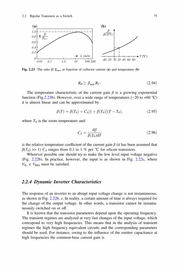
RB � bmin RC: ð2:94Þ
The temperature characteristic of the current gain β is a growing exponentialfunction (Fig.2.23b). However, over a wide range of temperatures (−20 to +60 °C)it is almost linear and can be approximated by
bðTÞ ¼ bðT0Þ þ CA 1þ bðT0Þ½ T � T0ð Þ; ð2:95Þ
where T0 is the room temperature and:
CA ¼ dbbðT0ÞdT ð2:96Þ
is the relative temperature coefficient of the current gain β (it has been assumed thatβ(Τ0) >> 1) CA ranges from 0.1 to 1 % per °C for silicon transistors.
Wherever possible one should try to make the low level input voltage negative(Fig. 2.22b). In practice, however, the input is as shown in Fig. 2.22c, whereVIL < VBEt must be satisfied.
2.2.4 Dynamic Inverter Characteristics
The response of an inverter to an abrupt input voltage change is not instantaneous,as shown in Fig. 2.22b, c. In reality, a certain amount of time is always required forthe change of the output voltage. In other words, a transistor cannot be instanta-neously switched on or off.
It is known that the transistor parameters depend upon the operating frequency.The transient regimes are analyzed at very fast changes of the input voltage, whichcorrespond to very high frequencies. This means that in the analysis of transientregimes the high frequency equivalent circuits and the corresponding parametersshould be used. For instance, owing to the influence of the emitter capacitance athigh frequencies the common-base current gain is
IC [mA]
ββmax
ββ (20ºC)
T [ºC]0 20 40 60 80-40 -200.01 0.1 1.0 10 100 200
0
0.2
0.4
0.6
0.8
1.0
(a) (b)
Fig. 2.23 The ratio β/ βmax as function of collector current (a) and temperature (b)
2.2 Bipolar Transistor as a Switch 75

a ¼ a01þ jxCere
; ð2:97Þ
where α0 is the low frequency current gain, ω is the circular frequency, Ce and re arethe respective emitter capacitance and resistance. By putting the time constant
Cere ¼ 1=xa ð2:98Þ
one obtains
aðxÞ ¼ a01þ jx=xa
: ð2:99Þ
Figure 2.24 illustrates the frequency characteristic of the current gain α. At thecut off frequency the gain is, by definition, 3 dB lower, i.e. √2 times lower. Thus, ωa
is the circular cut off frequency of a transistor in the common-base connection. Thedominant influence on the emitter capacitance, while the transistor is on, is due tothe diffusion capacitance. The time constant (2.98) is equal to the base time con-stant, τα. Since the diffusion capacitance is approximately:
Ced �W2
B2Dn
re; ð2:100Þ
then
ra ¼ 1xa
� W2B
2Dn; ð2:101Þ
where WB is the basewidth and Dn is the diffusion constant. Therefore, the narrowerthe base, the shorter the time constant τa, and the higher the cut off frequency ωa.
αo
αo
√2
α
ffα
βo
βo
√2
β
1
fβf
ft
(a) (b)
Fig. 2.24 Frequency characteristics α(ω) (a) and β(ω) (b)
76 2 Diodes and Transistors

The diffusion constant of electrons in silicon is about 2.5 times higher than thatof holes. Thus, an npn transistor under the same conditions possesses about 2.5times higher cut-off frequency compared to a PNP transistor.
The current gain of a transistor in the common-emitter connection is
bðxÞ ¼ aðxÞ1� aðxÞ ¼
b01þ jx=xb
; ð2:102Þ
where β0 = α0/(1 − α0) is the low frequency signal gain,
xb ¼ 1� a0ð Þxa ¼ xa
b0 þ1ð2:103Þ
is the angular cut off frequency of the common-emitter connection, and its timeconstant is
sb ¼ 1=xb ¼ ðb0 þ 1Þ=xa ¼ ðb0 þ 1Þsa: ð2:104Þ
The cut off frequency ωβ is thus β0 + 1 times lower than ωα and the time constantis β0 + 1 times higher than τa. Figure 2.23b shows the frequency characteristic ofthe gain β. The manufacturers often give the unity gain frequency fT. This is thefrequency at which | β(fT) | = 1 and fT is also called the frequency range of thetransistor gain. From the condition | β(fT) | = 1 and Eq. (2.102) it follows that
fT ¼ffiffiffiffiffiffiffiffiffiffiffiffiffib0 � 1b0 þ 1
sfa � fa; ð2:105Þ
because β0 >> 1. Typical values for fT range from several hundreds MHz to severalGHz.
Equations (2.99) and (2.102) can be used for the analysis of the transient modeswhen the transistor is in the active region. In general, however, a transistor as aswitch goes through all regions. For this reason the general charge control methodis more suitable for the dynamic analysis of switches. Analogously to diode pro-cesses, a change of the charge of minority carriers in the base dQ/dt is caused by thechange of the base current, ib(t), and the recombination of minority carriers in thebase –Q/τ, i.e.
dQdt
¼ ibðtÞ � Qs: ð2:106Þ
In the active region of a transistor in the common-emitter connection τ = τβ and
dQdt
þ Qsb
¼ ibðtÞ: ð2:107Þ
2.2 Bipolar Transistor as a Switch 77

The collector current is proportional to the base charge, i.e.
icðtÞ ¼ bsb
QðtÞ: ð2:108Þ
Equation (2.107) applies for the active region if RC = 0. However, RC > 0 and itdoes have an influence on the time constant. Namely, in the active region thecollector junction is reverse biased and behaves like a capacitor. If the averagevalue of the capacitance of this junction is denoted by Cc, the transistor can beconsidered as a “pure” transistor plus the capacitor Cc (Fig. 2.25). The current ib isexpressed by (2.107) and
ibðtÞ ¼ CcdVBC
dtþ dQ
dtþ Qsb
: ð2:109Þ
If the change of the voltage VBE is neglected, then
dVBC
dt¼ � dVCE
dt� RC
d icdt
: ð2:110Þ
In view of (2.108), from (2.109) and (2.110) it follows
dQdt
þ Qsbe
¼ sbsbe
ibðtÞ; ð2:111Þ
where
sbe ¼ sb þ bCcRc: ð2:112Þ
Thus, the influence of the collector capacitance manifests itself as an increase ofthe time constant. If a transistor is in the common-base connection, then, accordingto (2.112) and (2.104)
VCC
RC
T
ib i’b
CCdVBC
dt
CC
Fig. 2.25 Equivalent circuitin the active region
78 2 Diodes and Transistors

sae ¼ sa þ Cc RC : ð2:113Þ
The capacitance Cc depends upon the transistor type and usually is within therange from the order of pF to the order of fF. The general solution of (2.111) isgiven by:
QðtÞ ¼ e
�tsbe Zt
0
sbsibðtÞe
tsbedt þ Qð0Þ
264
375; ð2:114Þ
where Q(0) is the integration constant and represents the charge at the beginning ofthe analyzed transient process.
2.2.4.1 Transistor Turn On
The transient regime of an inverter (Fig. 2.21) caused by an abrupt input drive(Fig. 2.22b) will be considered. Up to the instant to the transistor is off. Both p-njunctions are reverse biased and can be considered capacitors of medium capaci-tances Cc and Ce. At to the input voltage abruptly changes from −VBB2 to +VBB1
(Fig. 2.27a). At this instant the transistor turn-on process begins and unfolds in twophases. During the first phase (Fig. 2.27) the capacitor Ct = Cc + Ce must berecharged. The collector current at this instant is zero so that Cc and Ce are prac-tically connected in parallel. At the beginning
VBEðtÞ ¼ VBB1 � VBB1 þVBB2ð Þ e� tCt RB : ð2:115Þ
For VBE(td1) = VBEt the emitter diode becomes conductive and
td1 ¼ Ct RB lnVBB1 þVBB2
VBB1 �VBEt
� Ct RB ln 1þ VBB2
VBB1
� �: ð2:116Þ
VCC
RC
T
CC
+VBB1RB
CEVBB2+
VBE
t0
Fig. 2.26 Equivalent circuitfor delay time tdl
2.2 Bipolar Transistor as a Switch 79

After td1, during td2 ≈ 0.22τa, the collector current is zero. This delay is theconsequence of the finite time required for the transportation of charge carriersthrough the base. The total delay time of the beginning of the response (collectorcurrent or output voltage) is thus
VI
VBB1
-VBB2
ib
ic
Q(t)
ie
t
t
t
t
t
IB1
-ICB0
ICS
βIB1
τβ IB1
τβIBS
t0 t1
-IB2
ΔIB
IB2=0
-βIB2
-τβ IB2
IB2=0
ΔIB
IB1
trtd ts tf
ti
tu
(a)
(b)
(c)
(d)
(e)
Fig. 2.27 Pulse waveforms of excitation voltage (a), base current (b), collector current (c), basecharge (d) and emitter current (e)
80 2 Diodes and Transistors

td ¼ td1 þ td2: ð2:117Þ
Usually td1 >> td2 and td ≈ td1. After td the collector current increases. Byintroducing in (2.114)
ibðtÞ ¼ VBB1 �VBE
RB¼ IB1 ð2:118Þ
and Q(0) = 0, because there are still no excess minority charge carriers, from(2.114) and (2.108) it follows
icðtÞ ¼ b IB1 1� e� tsbe
� �: ð2:119Þ
The increase of the collector current ends by turning the transistor enters satu-ration, i.e.
icðtrÞ ¼ ICS : ð2:120Þ
From (2.119) and (2.120) the rise time is
tr ¼ sbe lnb IB1
b IB1 � Ics¼ sbe ln
IB1IB1 � IBS
: ð2:121Þ
The total turn-on time of the transistor is
tu ¼ td þ tr: ð2:122Þ
After tr the collector current is constant (Fig. 2.27c) and the charge in the baseincreases until a steady state is reached (Fig. 2.27d).
2.2.4.2 Transistor Turn Off
While in saturation, both p-n junctions of the transistor are forward biased. Both theemitter and the collector inject minority carriers into the base. By superimposing thecharges of the normal and the reverse active modes the total distribution of chargein the base is obtained (Fig. 2.28a). The shaded part represents the charge in excesscompared to the one at the boundary between the active and the saturation states.
The turn-off process of transistor is initiated at the instant t = t1 by a negativechange of input from +VBB1 to −VBB2. As long as the concentration of minoritycarriers at the emitter-junction boundary is greater than zero a negative base currentwill flow
2.2 Bipolar Transistor as a Switch 81

IB2 � VBB2=RB: ð2:123Þ
This current “sweeps” the accumulated charge in the base. The turn-off processalso unfolds in two phases. During the first phase the collector current remainsconstant, i.e. IC = ICS (Fig. 2.27). During that time the excess charge (the shadedpart in Fig. 2.28a) which is the consequence of the forward bias of the collectorjunction is “swept away”. This process lasts as long as the concentration of theminority carriers at the collector junction is greater than zero. The collector currentis constant since the slope of the distribution at the end of the base is constant(curves 2 and 3 in Fig. 2.28b). At the end of this interval, which is called the storagetime ts, the concentration of minority carriers at the boundary of the collectorjunction is zero. Practically, the excess charge has been “swept away” and thetransistor “returned” from saturation to the active region.
The change of Q(t) in the base during ts can be determined from (2.114). For thispurpose: ib = −IB2 and the initial charge is Q(0) = τsIB1, where τs is the timeconstant of the transistor in saturation. This time constant depends upon timeconstants in the forward and the reverse modes. Usually 0.5τβ < τs < 2τβ. It isgenerally taken that τs ≈ τβ. During ts the collector junction is forward biased and τβe≈ τβ. Based on this, from (2.114) it follows:
QðtÞ ¼ � sb IB2 þ sb IB1 þ IB2ð Þ e� tsb: ð2:124Þ
From the condition Q(t) = Qs = τβIBS and (2.124) ts is
ts ¼ sb lnIB1 þ IB2IBS þ IB2
: ð2:125Þ
xW WB B
Q
BQ
1
n
n
b
b08
76
5
4
3
2
1
tS
x
Q = τS IB1
QN = QS = τB IBS
(a) (b)
Fig. 2.28 The distributions in base: of the charge in saturation (a) and the concentration ofelectrons during the turn-off process (b)
82 2 Diodes and Transistors

After ts the collector current decreases. The collector junction is reverse biasedand the time constant τβe is valid. From (2.114) and (2.108) together with the initialcondition Q(0) = Qs = τβIBS it follows
icðtÞ ¼ b ðIb2 þ IBSÞe�t=sbe � bIB2: ð2:126Þ
The turn-off process ends when ic(tf) = 0 and the fall-off time of the collectorcurrent is
tf ¼ sbe lnð1þ IBS=IB2Þ: ð2:127Þ
The total turn-off time is
ti ¼ ts þ tf : ð2:128Þ
In practice, it is often VBB2 = 0. This means that the base turn-off current isIB2 = 0. The process of clearing charge carriers from the base is then slower (dottedlines for the variations of ic and Q in Fig. 2.27) and is practically due to recom-bination. The storage time in this case is approximately
ts � sb lnIB1IBS
¼ sb lnFs; ð2:129Þ
where Fs is the saturation factor. In theory, from the condition ic(tf) = 0 and forIB2 = 0, tf → ∞. For this reason the condition is ic(tf) = 0.1ICS and
tf � 2:3sbe ¼ 2:3ðsb þ bCC RCÞ: ð2:130Þ
When VBB2 = 0, the resistance between the base and the emitter should be assmall as possible in order to speed up the process of clearing the piled up charge. Itshould be pointed out that the above analysis is approximate. First of all the basecurrent is not constant throughout the turn-off time. In addition, the time constant ofthe transistor changes. For ic = |IB2|, the slope of the minority carrier distribution inthe base at the junction boundary is zero (curve 5 in Fig. 2.28b). Until then thebasewidth is wB. After that the concentration gradient at the junction boundarychanges direction (curve 6 in Fig. 2.28b) and the emitter current becomes negative(Fig. 2.27). At nb = nbo the effective base width decreases and so does the transistortime constant. All this is very complex for a mathematical description.
A particular attention should be paid to turning off the transistor by a large basecurrent when |IB2| > ICS. The minority carrier distribution in the base and the pulsewaveforms of the currents for this case are shown in Fig. 2.29. The emitter current isthen negative IES2 = ICS + IB2 = ICS − |IB2| < 0. The minority carrier distributioncurves in the base exhibit maxima (curves 2 and 3 in Fig. 2.29a). The minority carrierconcentration decreases at both the emitter and the collector junctions. In that case,the equilibrium concentration may be reached at the emitter junction first (Fig. 2.29).
2.2 Bipolar Transistor as a Switch 83

One speaks then about the emitter clearance of the excess charge in the base.Since at tse at the collector junction nb > nb0, the transistor goes to the reverse activemode (the emitter junction reverse biased and the collector junction forwardbiased). The emitter storage time can be determined from the condition
QðtseÞ ¼ ssbI
IES2 ¼ ssbI
ðIB2 � ICSÞ: ð2:131Þ
on the basis of (2.124) and (2.131) one obtains
tse ¼ ss lnIB1 þ IB2
IB2=aI � Ics=bI: ð2:132Þ
The emitter clearance will happen if tse < ts, and from (2.125) and (2.132) it turnsout that the base current in that case must be
IB2 [ ICSð1þ bI=bÞ: ð2:133Þ
After tse the emitter current decreases and the collector current increases(Fig. 2.29b) until the minority carrier concentration at the collector junction equals
ts
tse
3
2
t1
nB
nb0
wB x
ib
ic
ie
IB1
ICS
IB2
IES2
ts
tse
t
t
t
(a)
(b)
Fig. 2.29 Minority carrier distribution in the base (a) and transistor currents if IB2 > ICS (b)
84 2 Diodes and Transistors

the equilibrium concentration. The transistor then goes from the reverse activeregion to the cut-off region. The currents fall to their steady state values (IC ≈ ICBO,IB ≈ −ICBO, IE ≈ 0). The effective basewidth narrows because both p-n junctions arereverse biased and the transistor time constant is several times smaller than τa. Thismeans that the decrease of the currents IB, IC, and IE is very fast.
Example 2.3 For the circuit from Fig. 2.30 and the excitation shown in Fig. 2.31determine:
(a) the resistance RC so the transistor is in saturation with a factor of saturation 5,and
(b) the transistor turn on (tON) and the turn off (toff) time.
The circuit of Fig. 2.30 has R = 2 kΩ, βmin = 20, τβ = 100 ns, Cc = 4 pF,Ce = 10 pF, VBE = 0.6 V, VBES = 0.7 V, VBE = 0.6 V, VCES = 0.1 V andVCC = 12 V.
(a) The coefficient of saturation is equal to the quotient of the base current thatkeeps the transistor in the saturation region and the base current of thetransistor, which is the boundary between the active and the saturation region:
FS ¼ I 0B1IBS
:
VCC
RC
RIB
VOiC
Fig. 2.30 Bipolar transistorswitch
IB
IB=5mA
IB= -1mAt1 t2
t
Fig. 2.31 Waveform ofcurrent excitation for thecircuit shown in Fig. 2.30
2.2 Bipolar Transistor as a Switch 85

The base current when the transistor is in the saturation region is (Fig. 2.30)
I 0B1 ¼ IB1 � VBES
R¼ 4:65mA: ð2:134Þ
The base current which holds the transistor at the boundary between the activeand the saturation region is
IBS ¼ ICSb
¼ VCC � VCES
bRC: ð2:135Þ
From (2.134), (2.135) and the conditions of the task is obtained that
RC ¼ FS VCC � VCESð ÞbI 0B1
¼ 634X:
(b) The turning on time of the transistor is equal to the sum of td and tr
Interval t1 < t < t1 + td (time td)To determine the time td the equivalent scheme shown in Fig. 2.32 can be used
The voltage between the emitter and the base is equal to (Fig. 2.32)
vBEðtÞ ¼ IB1R� IB1Rþ VC0ð Þe� tCRekv :
From the condition vBE(td) = VBet one obtains
td ¼ CekvR lnIB1Rþ VCO
IB1R� VBEt
¼ 6:83 ns:
Interval t1 + td < t < t1 + td + tr (time tr)To determine the time tr the general charge control method for the dynamic analysis ofswitches is suitable. Change of the minority carriers concentration in the base dQ/dt iscaused by the change of the base current, ib, and the recombination ofminority carriersin the base. The current ib is constant during this period and approximately equal to
C ekv =Cc+Ce = 14pF
V C0 =IB2RB =2V
I RB vBECekvVCO
Fig. 2.32 Circuit of charging equivalent input parasitic capacitance while turning on the switchfrom Fig. 2.30
86 2 Diodes and Transistors

I0B1. In this time interval, the transistor is in the active mode, so the collector p-njunction is reverse biased and the capacitance of the p-n junction has to be taken intoaccount. So, for the determination of the time tr the following equation is used:
dQðtÞdt
¼ I 0B1 �QðtÞsbe
; where sbe ¼ sb þ bRCCC: ð2:136Þ
Based on the initial condition Q(t1 + td) = 0, the condition for the transistorentering the saturation region Q(t1 + td + tr) = τβIBS and on the solution of theEq. (2.136) the time tr is calculated as
tr ¼ sbe ln1
1� 1=FS¼ 33:4 ns:
The turning on time of the transistor is equal to: tON = td + tr = 40.23 ns.The turning off time of the transistor tOFF is equal to the sum of ts and tf.
Interval t2 < t < t2 + ts (time ts)In this interval, the transistor is in saturation, both p-n junctions are forward biasedand Eq. (2.106) can be applied. The initial condition is Qðt2Þ ¼ sbI 0B1, and a pre-requisite for the end of this interval is that the transistor is at the boundary betweenthe saturation and active region Q(t2 + ts) = τβIBS. By solving Eq. (2.106) with theabove mentioned conditions one obtains
tS ¼ sb lnI 0B1 � I 0B2IBS � I 0B2
¼ 149:2 ns; where I 0B2 ¼ IB2 þ VBES=R:
Interval t2 + ts < t < t2 + ts + tf (time tf)At the beginning of this interval, the transistor is at the boundary between thesaturation and the active region. The initial condition is Q t2 þ tsð Þ ¼ sbI 0B1, and theprerequisite for the end of this interval is that the transistor is turned offQ(t2 + ts + tf) = 0. By solving the equations
dQðtÞdt
¼ I 0B2 �QðtÞsbe
:
with the above conditions one obtains
tf ¼ sbe lnI 0B2 þ IBS
I 0B2¼ 130 ns:
The turning off time of the transistor is tOFF = ts + tf = 279.2 ns.
2.2 Bipolar Transistor as a Switch 87

2.2.4.3 Optimum Drive
It has been shown that the times tr, ts, and tf are dependent on the base currents IB1and IB2. The rise time can be written in the form
tr ¼ �sbe lnð1� IBS=IB1Þ: ð2:137Þ
The lower the ratio IBS/IB1 the smaller tr. If IB1 >> IBS, (2.137) can be expandedto a Maclaurin series and since it is known that ln(1 − x) ≈ −x for x << 1, oneobtains
tr � sbeIBS=IB1 ¼ ðsa þCc RCÞICS=IB1: ð2:138Þ
A small ratio IBS/IB1 = ICS/βIB1 = 1/FS <<1 can be accomplished either by asmall current ICS or by a large current IB1.
The condition IB1 >> IBS for a small tr means strong saturation of the transistor(Fs >> 1) which implies a long storage time ts. On the other hand, from (2.126) itfollows that ts = 0 for IB1 = IBS, i.e., if the transistor is at the boundary between theactive and the saturation region. In that case, however, tr → ∞. Therefore, therequirements for small tr and ts are mutually contradictory. The compromise is thedrive shown in Fig. 2.33. While the transistor is being driven on, the base current isIB = IB1 >> IBS, and upon reaching saturation it drops to IB = IBS (Fig. 2.33).According to (2.127) the larger IB2, the shorter tf. Therefore, the optimum waveformof the base current is as shown in Fig. 2.33. If IB2 >> IBS, then, upon expansion of(2.127) to a Maclaurin series, it is approximately
tf � ðsa þCc RCÞICS=IB2: ð2:139Þ
Both tr and ts are smaller if IBS or ICS are smaller. This current can be madesmaller by increasing the resistance RC. This, however, helps decreasing tr and tfonly for small values of RC (Fig. 2.34) when CcRC << τa. If CcRC << τa, times tr and
ib
IB1
t
-IB2
IBS
Fig. 2.33 Optimumwaveform of base current
88 2 Diodes and Transistors

tf are almost independent of RC. In practice, RC is usually within several hundreds Ωto several kΩ.
2.2.4.4 Speed Up Capacitor
In practice, the base current shown in Fig. 2.33 can only approximately be realized.One of the possibilities is the application of a speed up capacitor (Fig. 2.35a).Usually, R1 is the internal resistance of the drive and
R1 � RB : ð2:140Þ
The variations of the base and the collector current are shown in Fig. 2.36b. Thecapacitor is a short circuit for abrupt changes and
ibð0Þ ¼ IB1 ¼ VCC �VBE
R1� VCC
R1: ð2:141Þ
tr, tf
RC
RCopt
Fig. 2.34 Rise time and falltime as functions of collectorload
RB
RC
VO
CB
VC0+R1
vI
VCC
t
t
t
vIVCC
To/2 To/2
To
IB
IBS
ib(0) IB∞
t1 t2
-ib(0)iC
ICS
T
(a) (b)
Fig. 2.35 Basic switching circuit comprising a speed up capacitor (a) and the pulse waveforms ofthe base and collector currents for a pulse drive (b)
2.2 Bipolar Transistor as a Switch 89
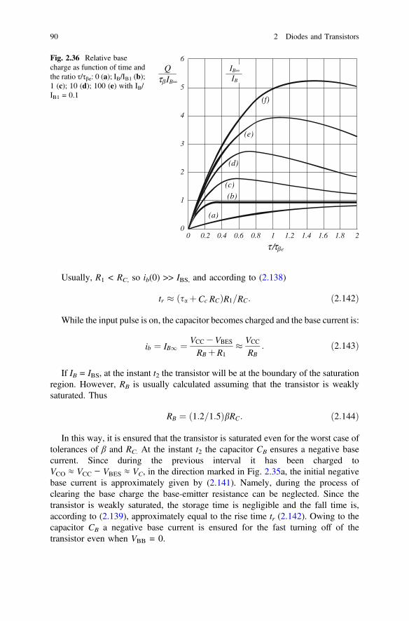
Usually, R1 < RC, so ib(0) >> IBS, and according to (2.138)
tr � ðsa þCc RCÞR1=RC: ð2:142Þ
While the input pulse is on, the capacitor becomes charged and the base current is:
ib ¼ IB1 ¼ VCC �VBES
RB þR1� VCC
RB: ð2:143Þ
If IB = IBS, at the instant t2 the transistor will be at the boundary of the saturationregion. However, RB is usually calculated assuming that the transistor is weaklysaturated. Thus
RB ¼ 1:2=1:5ð ÞbRC: ð2:144Þ
In this way, it is ensured that the transistor is saturated even for the worst case oftolerances of β and RC. At the instant t2 the capacitor CB ensures a negative basecurrent. Since during the previous interval it has been charged toVCO ≈ VCC − VBES ≈ VC, in the direction marked in Fig. 2.35a, the initial negativebase current is approximately given by (2.141). Namely, during the process ofclearing the base charge the base-emitter resistance can be neglected. Since thetransistor is weakly saturated, the storage time is negligible and the fall time is,according to (2.139), approximately equal to the rise time tr (2.142). Owing to thecapacitor CB a negative base current is ensured for the fast turning off of thetransistor even when VBB = 0.
00
1
2
3
4
5
6
0.2 0.4 0.6 0.8 1 1.2 1.4 1.6 1.8 2
(a)
(b)(c)
(d)
(e)
(f)
Qτβ IB∞
τ /τβe
IB∞IB
Fig. 2.36 Relative basecharge as function of time andthe ratio τ/τβe: 0 (a); IB/IB1 (b);1 (c); 10 (d); 100 (e) with IB/IB1 = 0.1
90 2 Diodes and Transistors
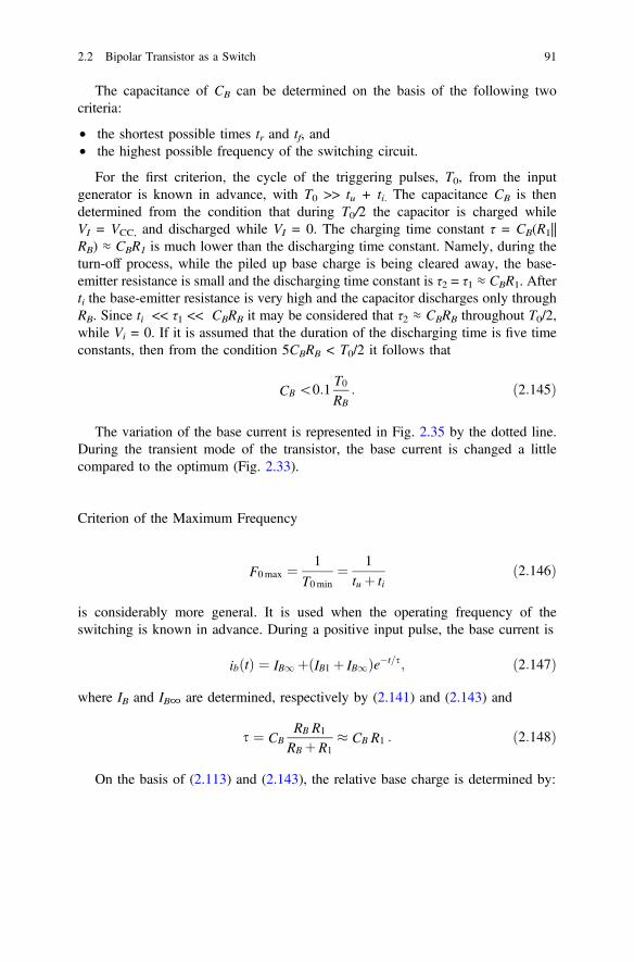
The capacitance of CB can be determined on the basis of the following twocriteria:
• the shortest possible times tr and tf, and• the highest possible frequency of the switching circuit.
For the first criterion, the cycle of the triggering pulses, T0, from the inputgenerator is known in advance, with T0 >> tu + ti. The capacitance CB is thendetermined from the condition that during T0/2 the capacitor is charged whileVI = VCC, and discharged while VI = 0. The charging time constant τ = CB(R1||RB) ≈ CBR1 is much lower than the discharging time constant. Namely, during theturn-off process, while the piled up base charge is being cleared away, the base-emitter resistance is small and the discharging time constant is τ2 = τ1 ≈ CBR1. Afterti the base-emitter resistance is very high and the capacitor discharges only throughRB. Since ti << τ1 << CBRB it may be considered that τ2 ≈ CBRB throughout T0/2,while Vi = 0. If it is assumed that the duration of the discharging time is five timeconstants, then from the condition 5CBRB < T0/2 it follows that
CB \0:1T0RB
: ð2:145Þ
The variation of the base current is represented in Fig. 2.35 by the dotted line.During the transient mode of the transistor, the base current is changed a littlecompared to the optimum (Fig. 2.33).
Criterion of the Maximum Frequency
F0max ¼ 1
T0min
¼ 1tu þ ti
ð2:146Þ
is considerably more general. It is used when the operating frequency of theswitching is known in advance. During a positive input pulse, the base current is
ibðtÞ ¼ IB1 þ IB1 þ IB1ð Þe�t=s; ð2:147Þ
where IB and IB∞ are determined, respectively by (2.141) and (2.143) and
s ¼ CBRB R1
RB þR1� CB R1 : ð2:148Þ
On the basis of (2.113) and (2.143), the relative base charge is determined by:
2.2 Bipolar Transistor as a Switch 91

QðtÞsb
¼ IB1 þ ss� sbe
IB1 � IB1ð Þ e�t=s � IB1 þ ss� sbe
IB1 � IB1ð Þ� �
e�t=sbe :
ð2:149Þ
This function is represented in Fig. 2.36 for different ratios τ/ τβe. Without thecapacitor CB (τ = 0, curve a) the steady state charge Q∞ = τβ ΙΒ∞ is establishedexponentially. The rise time in this case is by far the largest. If
s ¼ sk � IB1IB1
sbe: ð2:150Þ
then the increase of Q(t) to its steady state value is very fast. For τ > τk, Q(t) exhibitsa maximum (curves c, d, e). If the storage time ts should be minimal, the positiveinput pulse must be present until a steady state in the base (Q∞ = τβIB∞) isestablished. From that point of view, the optimum is τ = τk (curve b in Fig. 2.36).According to this, and bearing in mind (2.141) and (2.143) the optimum capaci-tance is
CBopt ¼ sbe�RB: ð2:151Þ
It is said then that the compensation of the charges in the base and the capacitoris achieved. If it is assumed that after a steady state in the base is established thetransistor is in weak saturation, i.e., RB ≈ βRC, then, bearing in mind (2.112)
CBopt ¼ Cc þsa=RC: ð2:152Þ
It may be concluded that in the case τ >> τk (curves d and e) the storage time ts canbe very large if condition T0 > tr is not satisfied. Thus, CB according to (2.152) isthe optimum value with respect to the maximum frequency of the switch.
2.2.5 Nonsaturated Switch
Another type of the switching circuit comprising an optimum drive is shown inFig. 2.37a. The diode D keeps the base-collector voltage at the value VBC = VD
when the transistor is on. If VD < VBCt, where VBCt is the threshold voltage of thecollector p-n junction, then the transistor will be in the active region. A majority ofthe circuits of this type uses Schottky diodes because VDS ≈ 0.4 V < VBCt. Thisdiode keeps the transistor in the active region, but close to saturation since
VoL ¼ VBE�VD ¼ 0:7� 0:4 ¼ 0:3V � VCES;
thus these circuits are often called the circuits based on the nonsaturated switchcircuits. On the other hand, when the diode becomes conductive, it activates the
92 2 Diodes and Transistors

negative feedback loop which does not allow the transistor to go to saturation. Forthis reason these circuits are sometimes called the switching circuits comprisingnonlinear feedback.
Let the drive be abrupt (Fig. 2.37b). For t < t0 the transistor and the diode are offand V0 = VCC. Upon a positive voltage step at the input at instant t = t0, thetransistor is switched on by the constant base current given by (2.118). The diode isoff and the collector current is determined by (2.119). The output voltage is
VOðtÞ ¼ VCC � bIB1RCð1� e�t=s0 Þ; ð2:153Þ
where:
VI
ib
ic
Q(t)
VO
VBB1
-VBB2
IB1
IBS
βIB1
τβIBS
VCC
τβIB1
τβIB
t0 t1
IB
IB2
IB20
VBE -VD
τβIB2
β IB2
IC =βIB
tr ts
t
t
t
t
t
VI
VO
TRB
RC
VCC
DIB1
IB2
(a)
(b)
(c)
(d)
(e)
(f)
Fig. 2.37 Nonsaturated switch (a) and pulse waveforms of input (b) and output (f) voltages, base(c) and collector (d) currents, and base charge (e)
2.2 Bipolar Transistor as a Switch 93

s0be ¼ sb þ bRCðCc þ CdÞ �
; ð2:154Þ
and Cd is the average capacitance of the reverse biased diode. The diode is turnedon at instant t1 when
Vdðt1Þ ¼ VBE �VOðt1Þ ¼ VDt : ð2:155Þ
From (2.154) and (2.155) it follows that
t1 ¼ s0be lnb IB1
bIB1 � VCC�ðVBE�VDtÞRC
: ð2:156Þ
Since the current IB1 through RB is constant, upon switch-on of the diode, thebase current will decrease by an amount corresponding to the diode current
IB1 ¼ ID þ IB: ð2:157Þ
After t1 the current through RC
IRC ¼ VCC �ðVBE �VDÞRC
� ICS ð2:158Þ
is constant because the variations of VBE and VD are negligible. SinceVCE = VBE − VD = 0.7 − 0.4 = 0.3 V is only by 0.1 or 0.2 V greater than VCES, itmeans that the transistor is nearly in the saturation region and that IRc ≈ ICS. It can,therefore, be said that the switch-on of the diode ends the switch-on of the tran-sistor. Indeed, expressions (2.121) and (2.156) are approximately the same sinceIRc ≈ ICS. Thus, t1 = tr is the rise time of the collector current.
The diode keeps the transistor in the active region, thus
IC ¼ b IB ¼ ID þ IRC : ð2:159Þ
By combining (2.157) and (2.159) it follows that
IB ¼ IRCbþ 1
þ IB1
bþ 1: ð2:160Þ
Since IRc ≈ ICS = βIBS, the base current is
IB ¼ aIBS þ IB1bþ 1
: ð2:161Þ
This means that the base current is somewhat higher than IBS and also than thecollector current IC = IRc + ID > ICS (Fig. 2.37d), and the transistor is certainly inthe active region (IBS and ICS are the saturation currents of the transistor without the
94 2 Diodes and Transistors

diode). The waveform of the base current during the turn-on process is optimal(Figs. 2.37 and 2.33). Irrespective of the value of IB1 the transistor after tr is close tothe boundary between the active and the saturation region. This means that the turn-on may be established by a large base current
IB1 VCC �ðVBE �VDÞbRC
; ð2:162Þ
and bearing in mind (2.138)
tr � sa þðCc þCdÞRC IRC=IB1: ð2:163Þ
On the basis of (2.163) and (2.118) it follows that
RB � bRCVBB1 � VBE
VCC � ðVBE � VDÞ : ð2:164Þ
If VBB1 = VCC >> VBE, then RB << βRC. Usually, RB and RC are of the sameorder of magnitude, it is even possible that RB < RC.
After a negative step change of the input voltage at t = t1, the base currentbecomes negative (Fig. 2.37c) and the transistor is turning off. The output voltageremains constant for some time until the collector current becomes equal to thecurrent through RC. During this time, the diode is conducting and
IB20 ¼ IB2 þ ID ¼ IB2 þaðIB1 � IBSÞ; ð2:165Þ
where
IB2 � VBB2=RB: ð2:166Þ
Since the initial charge is Q(0) = τβΙΒ, from the condition Q(ts) = τβIBS and on thebasis of (2.114) the storage time is:
ts ¼ sb lnIB1 þ IB2
a IB1 þ IB2 þIBS=bþ 1: ð2:167Þ
The condition IBS/(1 + β) << αIB1 + IB2 is always satisfied and
ts ¼ sb lnIB1 þ IB2a IB1 þ IB2
: ð2:168Þ
Because α ≈ 1, ts → 0. If VBB2 = 0, then IB2 = 0 and:
ts ¼ sb ln 1=a ¼ sb lnð1þ 1=bÞ � sb�b ¼ sa : ð2:169Þ
2.2 Bipolar Transistor as a Switch 95

Therefore, although the transistor is in the active region, there exists a storagetime but it is negligible.
After ts, the diode is off and the fall-off time of the collector current is determinedby (2.127) or (2.130) but Cc should be replaced by Cc + Cd.
The nonsaturated switches are most widely used in digital circuitry. A Schottkydiode with a transistor makes a Schottky transistor (Fig. 2.38a). A commonproperty of these circuits is high speed. However, the dissipation of the transistor isincreased because while conducting it is in the active region, which is a weakness ofthis type of circuit.
If instead of a Schottky diode a silicon diode is used, it is necessary to useanother diode (Fig. 2.38b). The collector junction here is not biased(VBC = −VD2 + VD1 ≈ 0) and the low level output voltage VOL = VBE is increased.The resistor R reduces the base-emitter resistance when the transistor is off.
2.2.6 Capacitatively Loaded Inverter
The output of an inverter is often loaded by a capacitor (Fig. 2.39). The influence ofthis capacitor on the transient mode is very noticeable. First of all, the transistorcannot go to saturation until this capacitor is discharged. The high level of theoutput voltage is not reached when the transistor is turned off, but when thecapacitor is charged.
Let the drive be abrupt (Fig. 2.37b). Upon a positive voltage step at the input, thetransistor turn-on process starts. Taking into account the collector junction capac-itance, the collector current is
icðtÞ ¼ VCC �VO
RC� C
dVO
dtþ Cc
dVBC
dt¼ b
sbQðtÞ; ð2:170Þ
R
Tr
D
D
2
1
⇒
(a) (b)
Fig. 2.38 Schottky transistor (a) and a nonsaturated switch comprising a silicon diode (b)
96 2 Diodes and Transistors

where the charge Q(t) in the base is determined by Eq. (2.109). If the variation ofthe voltage VBE is neglected, then dVBC/dt = dVO/dt and from (2.109) and (2.170)one obtains
sbsd2VO
dt2þ sbe þ s dVO
dtþ VO ¼ VCC � bRCIB1 ð2:171Þ
where
s ¼ RCðCC þ CÞ; ð2:172Þ
and τβc is determined by (2.112). The solution of Eq. (2.171) can be written in theform
VOðtÞ ¼ A1 ep1 t þA2 e
p2 t þVCC �bRCIB1; ð2:173Þ
where p1 and p2 are the roots of the characteristic equation
p2 þ sbe þ ssbs
pþ 1sbs
¼ 0: ð2:174Þ
The constants A1 and A2 are determined from the initial conditions
VO 0ð Þ ¼ VCO ¼ VCC; dVO=dtð Þt¼0 ¼ 0;
thus
A1 ¼p2 bRCIB1p2 � p1
; A2 ¼p1 bRCIB1p1 � p2
: ð2:175Þ
VCC
RC
T
CC
VI
RB
C
VO
Fig. 2.39 Capacitivelyloaded inverter
2.2 Bipolar Transistor as a Switch 97
The rise time tr in this case is determined from the condition that the collectorjunction is forward biased, i.e.,
VBC trð Þ ¼ VBE�VO trð Þ ¼ VBCt;
that is
VOðtrÞ ¼ VBE �VBCt ¼ VCES : ð2:176Þ
Equation (2.173) is transcendent and in general cannot be solved explicitly. If,however, the condition
x ¼ 4sbs.ðsbe þ sÞ2 � 1; ð2:177Þ
is fulfilled, then the roots of the characteristic equation are:
p1 � sbe þ ssbs
; p2 � 1sbe þ s
: ð2:178Þ
Since the condition (2.177) applies, |p1| >> |p2| and the influence of the root p1can be neglected. Then, (2.173) reduces to
VOðtÞ ¼ VCC �bIB1RC 1� e� t
sþsbe
� �; ð2:179Þ
and on the basis of (2.172) one obtains
tr ¼ sbc lnbIB1
bIB1 � ðVCC �VCESÞ=RC¼ sbc ln
bIB1bIB1 � ICS
; ð2:180Þ
where
sbc ¼ sbe þ s ¼ sb þ ðbþ 1ÞCc RC þCRC: ð2:181Þ
By comparing (2.180) and (2.121) it may be noticed that the influence of thecapacitance C reduces to the increase of the time constant by CRC. Of course, thisconclusion is correct only if condition (2.177) applies. The left-hand side in (2.177)is maximal for τ = τβe, amounting
xmax ¼ sbesb þ bCcRC
: ð2:182Þ
Thus, xmax < 1 meaning that (2.180) applies for a wide range of C values. Themaximum error is around the capacitance value
98 2 Diodes and Transistors

C ¼ sb�Rc þ ðb� 1ÞCc ð2:183Þ
which is obtained for τ = τβe.The capacitor C does not have any influence on the storage time ts, because in
that interval Vo = VCES = const. During tf Eq. (2.171) applies but IB1 should bereplaced by IB2 = VBB2/RB. It can be shown that if (2.177) applies
VOðtÞ � VCC þbRc IB2 �RcðICS þb IB2Þ e�t=sbe : ð2:184Þ
Charging of the capacitor ends when VO = VCC and from (2.179) one obtains:
tf � ½sb þðbþ 1ÞCc RC þCRC lnð1þ IBS=IB2Þ: ð2:185Þ
If VBB2 = 0, i.e. IB2 = 0, then tf is determined from the condition VO = 0.9VCC,
and
tf � 2:3 � ½sb þðbþ 1ÞCc RC þCRC: ð2:186Þ
By comparing tr and tf of the inverter with and without a capacitor, it may beconcluded that the influence of C reduces to increasing the time constant of thetransistor. It should be emphasized that (2.185) and (2.186) are approximate since itis possible that the transistor is off (ic = 0) before the capacitor is charged. Then tfconsists of two intervals: the first t1 ending at ic(tf) = 0 and the second when C isbeing charged through the resistor RC.
In practice it is often
CRC sb þ ðbþ 1ÞCcRC: ð2:187Þ
In such a case, the transistor can be considered an ideal switch. During the turn-on process the operating point will instantaneously move from the position A to theposition B (Fig. 2.40a). The transistor is in the active region and the collectorcurrent is IC = βIB1 (Fig. 2.40b). The fall time of the collector voltage tr is deter-mined by (2.180) where, in view of (2.187), τβc ≈ CRC.
For a negative input voltage step the transistor is instantaneously turned off(ic = 0 Fig. 2.40b). The capacitor C charges through RC and
tf � 3RCC: ð2:188Þ
For fast switching circuits, this time is unacceptably large. For this reason, morecomplex inverters, having lower output resistance when the output voltage is high,are used.
Two versions of such circuits are most frequently used (Fig. 2.41). In the circuitof Fig. 2.41a when Tr1 is off, Tr2 is on in the active region. The output resistance isROH = RC/(1 + β2) and the rise time of the output voltage is
2.2 Bipolar Transistor as a Switch 99

tf � 3CRC�ðb2 þ1Þ: ð2:189Þ
The shortcoming of this circuit is that the low level of the output voltage isincreased. Namely, when Tr1 is in saturation, the diode D is conducting, Tr2 is offand
VOL ¼ VD þVCES1 : ð2:190Þ
For this reason, the more complex inverter of Fig. 2.41b is more frequently used.While Tr1 and Tr2 are in saturation, Tr3 is off. The only purpose of the diode D hereis that Ir3 is to be off while Tr1 and Tr2 are conducting. If Tr1 and Tr2 are off, Tr3 is inthe active region and the output resistance is ROH ≈ RC/(1 + β3), and the chargingtime of the capacitor is determined by (2.189).
RC
RB
VI
VO
T1
T2
D
C
RCVCC
VCC
RC
C
VI
RBT1
T2
T3
DVO
(a) (b)
Fig. 2.41 Inverters with low output resistance in both static states
I
I Q
Q
VVVV
C
B1
CS S
ST
iCCCEStCES
A
BI
Iβ
I
tt t
C
B1
CS
tr
0 1
I(a) (b)
Fig. 2.40 Path of the operating point (a) and change of collector current when CRC ≫ τβ + (β + 1)CcRC (b)
100 2 Diodes and Transistors

2.2.7 Inductively Loaded Switch
In practice, the switch is sometimes inductively loaded. Typical examples of suchloads are electromagnetic relays, motors, and various types of pulse circuits havingtransformer coupling. Figure 2.42a shows an inverter having an inductive load.Most often the collector winding is inductively coupled with a secondary windingdriving a load whose resistance referred to the primary is denoted by R0. Thepeculiarity of a inductive load is that for fast variations (high frequencies) it behaveslike a large resistance and in the quasi-stationary states it accumulates the elec-tromagnetic energy which may exert a considerable influence upon the convertercharacteristics. The collector current ic is determined by (2.119). For the circuit ofFig. 2.42a, it is
icðtÞ ¼ VCC � VO
R0þ 1L
Zt
0
VCC � VOð Þdt: ð2:191Þ
Upon differentiation of (2.191) one obtains a differential equation whose solu-tion, with initial condition VO(0) = VCC, is
VOðtÞ ¼ VCC � ss� sbe
b IB1R0ðe�t=s � e�t=sbeÞ; ð2:192Þ
where
s ¼ L=R0: ð2:193Þ
The time tr required by the transistor to go to saturation is determined fromcondition (2.176). Equation (2.192), however, is transcendent and in general can
R
L R
V
V
+V
TrB
0
I
0
CC
V
V
I I I
i
V
V
V-
BB1
CC
CS0CS1 CSm
C
I
0
BB2 t t t
t
t
0 1
t tr s
(a)
(b)
Fig. 2.42 Inverter having an inductive load (a) and the responses of collector current and voltageto a pulse drive (b)
2.2 Bipolar Transistor as a Switch 101

not be solved explicitly. On the other hand, usually τ >> τβe, i.e. tr << τ. Thenexp(−t/τ) ≈ 1 and
VOðtÞ � VCC � bIB1R0ð1� e�t=sbeÞ: ð2:194Þ
Now, from (2.176) and (2.194) it follows that
tr � sbe lnbIB1
bIB1 � ICSO; ð2:195Þ
where
ICSO ¼ VCC � VCES
R0: ð2:196Þ
Therefore, tr is the same as if the collector load were RC = R0. This is due to thefact that the resistivity of the winding during tr is very high and its influence can beneglected.
However, the situation τ << τβe is possible. This occurs when the resistance Ro isvery high (Ro → ∞) as in the case of electromagnetic relays. Then tr << τβ, and exp(−t/τ) ≈ 1 so
VOðtÞ � VCC � bIB1Lsb
ð1� e�t=sÞ: ð2:197Þ
By taking ln(1 − x) ≈ –x for x << 1, from (2.195) it is approximately
tr � sbVCC
bIB1R0¼ sa
VCC
IB1R0: ð2:198Þ
Therefore, if R0 → ∞, then t → 0. This means that a transistor loaded by anelectromagnetic relay is practically turned on instantly.
After tr the transistor is in saturation. The voltage across the winding VCC − VCES
is constant and the winding current will increase linearly. The collector current(Fig. 2.42b) is
icðtÞ ¼ ICSO þVCC �VCES
Lt: ð2:199Þ
During the time interval t1 − t0 = T1, the transient regime in the winding does nothave to be completed. More frequent is the other case (Fig. 2.42b). Then the
102 2 Diodes and Transistors

resistance RB is determined from the condition that for t = T1 the transistor isweakly saturated, i.e.
IB1 ¼ VBB1 �VBES
RB� 1
bICS1 ¼ 1
bICSO þVCC �VCES
LT1
h i; ð2:200Þ
giving
RB � bVBB1 � VBES
VCC � VCES
R0þ VCC � VCES
LT1
: ð2:201Þ
At an instant t = t1, when the input voltage becomes negative, the output voltageremains constant while the excess charge piled up in the base is cleared. This is thestorage time ts, during which the collector current increases according to (2.199).Since the base charge is controlled by the base current, the change of Q(t) is as forthe inverter loaded by RC. Therefore, the time ts is determined by (2.125) and
IBS ¼ ICSmb
¼ 1bic T1 þ tsð Þ: ð2:202Þ
Usually ts << T1 and the maximum collector current is
ICSm ¼ ICSO þVCC �VCES
LðT1 þ tsÞ � ICSO þVCC �VCES
LT1 : ð2:203Þ
This current must be lower than the maximum permitted collector current(ICSm < ICD), resulting in the condition
L[VCC �VCES
ICD � ICSOT1 : ð2:204Þ
After ts expires, the collector current decreases and is determined by (2.126). Byintroducing (2.126) in (2.191), differentiating the obtained equation and solving itfor Vo, and using the initial condition VO(0) = VCES ≈ 0, one obtains
VOðtÞ ¼ VCCð1� e�t=sÞ þ R0ðICSm þ bIB2Þs� sbe
sðe�t=s � e�t=sbeÞ: ð2:205Þ
If the factor in front of the second bracket is denoted by VO0, then (2.205) can bewritten as:
vOðtÞ ¼ VCCð1� e�t=sÞ þ VOo e�t=s � VOo e
�t=sbe ¼ v1 þ v2 � v3: ð2:206Þ
2.2 Bipolar Transistor as a Switch 103

The dependence (2.206) for τ ≫ τβe is shown in Fig. 2.43 and the followingconclusions may be drawn. The output voltage increases faster than the collectorcurrent decreases. During the fall time tf, given by (2.127), a situation whenVo ≫ VCC is possible. The maximum output voltage is approximately
VOM � VCC þ R0ðVCC T1=Lþ bIB2Þ: ð2:207Þ
Owing to this the dissipation of the transistor P(t) = ic(t)Vo(t) is rather high(Fig. 2.43).
Example 2.4 For the circuit of Fig. 2.44
(a) Explain how the accumulated electromagnetic energy returns to the source(b) Determine the maximum inverse voltage that appears at the diode D2.(c) Determine the time of core transformer demagnetization tx assuming that all
the energy accumulated in the magnetization inductance returns to the source.(d) Show the waveforms of the voltage on the transistor collector, the voltage on
the secondary winding and the current through that winding using PSPICEsoftware package.
V00
V0M
VCC
ICSm
iC
IC0
tf t
t
t
p(t)
V0
V0=V1+V2-V3
V2
V1V3
Fig. 2.43 Collector current,output voltage Vo, and powerof dissipation P during theturn-off process of transistor
104 2 Diodes and Transistors

The circuit of Fig. 2.44 has VCC = 80 V, N = 5, IL = 5 A, Lm = 100 μH,f = 10 kHz and D = 0.5
(a) During the turning off process of the transistor T, a negative change of currentoccurs through the magnetizing inductance what induces a correspondingvoltage. This voltage is transferred to the secondary side in the ratio 1:N, andin dependence on how transformer is wounded, it provides direct polarizationof the diode D2. If we ignore the voltage drop on the diode while it conducts,during the period the diode D2 conducts the secondary winding voltage isVCC. This voltage transferred to the primary side is VCC/N, so the maximumvoltage at the collector of the transistor is equal to VCC(1 + 1/N).
(b) The maximum inverse voltage on a diode is reached when the transistor is on.In this case the voltage on the anode is equal to −NVCC, and the maximuminverse voltage on the diode is
(c)
12LmI
2L ¼ VCC
ILNtx2) tx ¼ NILLm
VCC
¼ 31:25 ls:
(d) See Fig. 2.45.
Fig. 2.45 Waveform of voltage on the transistor collector
VI
VCC
1:N
ILD1 D2
TR
Fig. 2.44 Switch withbipolar transistor andinductive load at which theaccumulated electromagneticenergy returns to the source
2.2 Bipolar Transistor as a Switch 105

VD;inv ¼ VCC � ð�NVCCÞ ¼ ð1þ NÞVCC ¼ 480V:
Assuming that all accumulated energy in the magnetizing inductance returns tothe source, the following expression can be written (Figs. 2.46 and 2.47)
2.2.7.1 Transistor Protection
The voltage VOM must be lower than the collector-base breakdown voltage
VOM\BVCBO: ð2:208Þ
Otherwise, the transistor must be protected. The switching circuits in relays andin blocking generators are protected by adding a diode (Fig. 2.48a). WhenVo > VCC + VDt, the diode is conducting and it limits the output voltage(Fig. 2.48b). The use of a Schottky diode is recommendable. The collector current(Fig. 2.48b) increases exponentially because the resistance of the winding, rL,cannot be neglected.
Fig. 2.46 Waveform of voltage on transformer secondary winding
Fig. 2.47 Waveform of current through transformer secondary winding
106 2 Diodes and Transistors

The increased dissipation during the turn-off process of the transistor is anotherproblem. The dynamic losses are exactly then at the maximum. In order to reducethem, the increase of the collector voltage should be slowed down until the currentfalls to zero. This is accomplished by using the so called dv/dt or snubber circuits(Fig. 2.49a). These circuits are often referred to as the circuits for shaping thetransistor load line or the transistor turn-off protection circuits. An efficient snubbercircuit should: limit the maximum collector voltage below the breakdown voltage,slow down the output voltage ascent until collector current falls and ensure that thetotal losses in the transistor and the dv/dt circuit are minimal. All this, to a gooddegree, is provided by the DRC dv/dt circuit (Fig. 2.49a). During the turn-offprocess the diode is conducting and the capacitor C is charged, thus slowing downthe rate of ascent of the output voltage. An accurate analysis would be quitecomplicated. Therefore only the approximate relations satisfactory for practical
+V
0
CC
Lr
r
L
L
D
Tr
V
V
V
CC
0
CC
ic
t
t
without D
with D
V
(a) (b)
Fig. 2.48 Protection of transistor (a) and pulse waveforms of the collector current and outputvoltage when a relay is the load (b)
+V
0
CC
L
D
C
RTr
VCC
ic
t
t
tp(t) Without DRC
V
(a)
(b)
Fig. 2.49 Protection DRC circuit during transistor turn-off process (a) and the correspondingpulse waveforms (b)
2.2 Bipolar Transistor as a Switch 107

calculations are given here. The accumulated electromagnetic energy is transferredto the capacitor, so it can be written that
12LI2Lm ¼ 1
2CV2
OM; ð2:209Þ
where ILM = ICSM is the maximum current of the winding. From (2.209) and(2.199) it follows that the maximum output voltage is
VOM ¼ VCC
sþ T1ffiffiffiffiffiffiLC
p : ð2:210Þ
where τ = L/Ro. On the other hand, if tr and tf are the maximum rise time of theoutput voltage and the maximum fall time of the collector current, respectively, thenit can be written that
12CV2
OM ¼ ICSM VOMðtr þ tf Þ2
: ð2:211Þ
On the basis of (2.211) and (2.209) the capacitance is approximately
C ¼ ðtr þ tf Þ2.L: ð2:212Þ
In practice the values of the capacitance C are between several nF and severalhundreds nF. When the transistor is on, the diode is off and the capacitor dischargesthrough the resistor R. If the discharge time is taken to be 3RC, then it has to be:
D Load
LS DS
DS
RS
VCC
vC
vi
iC
T
Fig. 2.50 Turn-on protectioncircuit at a switch with bipolartransistor
108 2 Diodes and Transistors

R� T1min3C
; ð2:213Þ
where T1min is the minimum conduction time of the transistor.Besides the turn-off, there is the turn-on protection circuit (Fig. 2.50). The aim of
this protective circuit is to reduce the speed of increase of the collector current andthus to reduce the dissipation on the transistor when the switch is turning on(Fig. 2.51). This protection circuit consists of the inductance LS connected in thecollector circuit of the switching transistor and the diode DS connected in anti-parallel with the inductance LS.
Due to a rather large time constant τ = LS/rS (rS—series connection of the dioderesistance in on state and the resistance of the inductor LS), the resistance RS can beconnected in series with the diode DS. The goal is to increase the time constant, sothe inductor can ensure the use of accumulated energy in the time interval whenthe transistor T is turned off. In this case it is necessary to take into account themaximum collector voltage of the transistor, because the discharge current of the
iC
vC
0
0
t
t
VCC
VCES
without protection circuit
with protection circuit
ts
0 t
without protection circuit
with protection circuit
PT
Fig. 2.51 Waveforms of thecollector current, the collectorvoltage and power dissipationon bipolar transistor duringthe switch turn of processwithout turn on protectioncircuits and with a turn onprotection circuit
2.2 Bipolar Transistor as a Switch 109

inductance LS generates voltage on the resistor RS which increases the total voltageon the collector of the transistor.
There is also a combined protection circuit that reduces losses in the bipolartransistor when the switch is turning on and turning off (Fig. 2.52). The function ofthe turn-on protection circuits is assumed by the inductance LS, the diode DS and theresistor RS. On the other hand, the role of the turn-off protective circuits is played bythe capacitance CS, the diode DS and the resistor RS. These elements ensure aprotective function in the same manner as already described for the turn-on andturn-off protection circuits.
2.2.8 Transistor Selection
The key element in the pulse converters and voltage stabilizers is the switchingtransistor. As a rule, it is in a heavy duty operating mode (high current while on,high voltage while off, and significant voltages and currents during transients). Forthis reason considerable attention should be paid to the design of the optimumdriving and dv/dt circuits and to the selection of the transistor. If the transistor is tooperate reliably, its limitations must be strictly taken into consideration. This pri-marily concerns the limitations as regards the voltage, current, and dissipation.
The maximum voltage is limited by the breakdown voltages BVCB0 and BVCE0
(Sect. 2.2.1.1). In power transistors a secondary breakdown may appear. It mani-fests itself by an abrupt decrease of the collector–emitter voltage accompanied by asimultaneous increase of the collector current (Fig. 2.53). It occurs when both thevoltage and the current are large simultaneously. The secondary breakdown startswhen the current concentrates to a small area of the junction which leads to aconsiderable rise in temperature, creating a so called “hot spot”. This gives rise to
D Load
LS
CS
RS
VCC
vC
vi
iC
T
DS
Fig. 2.52 Combinedprotection circuit of switchwith bipolar transistor
110 2 Diodes and Transistors

the thermal regenerative process which is a characteristic of power transistors.However, in addition to the thermal instability at high collector currents, an elec-trical instability appears there, which creates the conditions for avalanche injectionof majority carriers at the collector junction. This is particularly marked in the highvoltage switching transistors having a lightly doped collector region. The ionicelectric field appears exactly at the surface between the light doped regions andcauses the avalanche injection of the charge carriers. In order to eliminate as muchas possible the mechanisms leading to thermal and electrical instabilities, efforts arebeing made to eliminate any crystal defects, metallic impurities, interstitials, etc. Inaddition, a maximally efficient heat removal should be ensured. Figure 2.53 showsthe transistor output characteristics for IB = 0 and IB ≠ 0.
In Fig. 2.53 the characteristics are extended by dotted lines in order to show whatthey would be like if there were no secondary breakdown which appears at the pointsP and P′. Between the points V and O and V′ and O′ the collector–emitter resistanceis very low. If the transistor were then switched off, it would return to the originalcharacteristics without a visible damage. If, however, the current is not limited andthe operating point reaches the position O or O′, the junction temperature may reachthe melting point causing failure and permanent damage to the transistor. Figure 2.53also shows the limitations: the maximum current ICM, the maximum voltage VCEM
(VCEM < BVCEO), the maximum dissipation, and the hyperbola limiting theappearance of the secondary breakdown. They all make the region of reliableoperation of the transistor as represented by the surface VCEM–C–B–A–ICM.Therefore, at high VCE the limitation is the breakdown voltage, at low VCE thelimitation is the maximum current, and between the points A and B the limitation isthe maximum dissipation.
The maximum permitted dissipation is determined by the maximum junctiontemperature which is for silicon transistors between 170 and 200 °C. Namely, thepower P = VCEIC generated in the transistor is converted to heat. For this reason the
I =0
I ≠0
VV BV
I
I
C
B
B
CECEM CE0
CM
CE0
SecondarybreakdownC
P
P'
B
PdmaxV
AV'
O O'IFig. 2.53 Outputcharacteristics of a powertransistor in the region ofsecondary breakdown
2.2 Bipolar Transistor as a Switch 111

temperature of the crystal is always higher than that of the environment. Atexcessive temperatures the transistor will either be suddenly destroyed or itscharacteristics will degrade gradually.
The heat developed in the transistor is transferred through the case and the heatsink to the environment. In steady state:
Pd ¼ VI ¼ Tj � TaRjc þRca
; ð2:214Þ
where Tj and Ta are the temperatures of the junction and ambient temperature,respectively. Rjc is often called the internal thermal resistance. It is constant andranges from several tenths of °C/W for low power transistors up to several tens of°C/W for high power transistors. The external thermal resistance depends upon themeans of heat transfer from the case to the environment. It is highest when the caseis free in the air. The heat transfer can be considerably improved by means of heatsinks. In principle, heat sink is a metal surface on which the transistor is mounted.In this way Rca is considerably decreased. Good dimensioning and mounting of aheat sink are very important, particularly if the dissipation is high. As a rule, as soonas the power generated in a transistor exceeds 100 mW, an adequate heat sinkshould be used.
Manufacturers often give diagrams showing the dependence of the maximumpermitted power on ambient temperature for different values of Rca. A typicalexample of such a diagram is shown in Fig. 2.54. Ideal cooling is obtained when theexternal thermal resistance is zero (Rca = 0) and the case temperature is equal to theambient temperature (Tc = Ta). Such cooling is possible if the transistor is forexample immersed in oil. At low temperatures up to 25 °C the permitted power isconstant.
Manufacturers give the Safe Operating Area (SOA) for a given ambient tem-perature. SOA respects all the limitations mentioned previously. It is different forDC and pulse operating modes (Fig. 2.55a). The narrower the pulse, the wider thearea of reliable operation.
Manufacturers often give SOA separately when the device is conducting(Fig. 2.55a) and also when it is off (Fig. 2.55b).
[ C]aT °
[W]P
25 50 100 150
5
10
15
20ideal colingwith a heat sink
without a heat sink
Fig. 2.54 An illustration of the dependence of the permitted power on temperature for differentthermal resistances
112 2 Diodes and Transistors

The region of operation at reverse bias is extended because the collector currentis then very low and the breakdown voltage is higher. This region is often called theReverse-Bias Safe Operating Area (RBSOA). Figure 2.56 shows SOA and RBSOAof the power transistors UMT 13006 and UMT 13007.
The dependencies of the current gain and saturation voltage on the collectorcurrent (Fig. 2.57) are very important for the selection of a good transistor. They areimportant since here β is lower and VCES is higher than the correspondingparameters of low power transistors (below 1 W). The maximum frequency of theswitching transistors depends on the turn-on and turn-off times. These character-istics too are usually given as functions of the collector current (Fig. 2.58) for aspecified test circuit. The curves in Fig. 2.55 are given for an inverter comprisingresistors RB = 5 V/IB and RC = 125 V/IC for IC/IB = 5 (Fig. 2.56).
ICM
Pdmax
5
10
15
50 100 150 200 250 VCE [V]
IC
I C[A
]
Impulse (10ms)
Secondarybreakdown VEB1<VEB2<VEB3
BVCE VCE
VEB1
VEB2
VEB3
(a) (b)
Fig. 2.55 Safe Operating Area at forward bias (a) and reverse bias of the emitter p-n junction (b)
0.2 00.45 10 1020 2050 50100 100200 200500 500 1000
0.50.1
0.2
0.41
2 1
554
2
10 10
20
20
40
PDD
ISB
10ms 20ms1msD.C.
UMT13006
UMT13006UMT13007
UMT13007
VCE [V] VCEX(SUS) [V]
VBE ≤ -5VIC ≤ 100°C
I C [
A]
I C [
A]
(a) (b)
Fig. 2.56 SOA of switching transistors UMT 13006 and 13007 manufactured by UNITRODE,when on (a) and when off (b)
2.2 Bipolar Transistor as a Switch 113

The minimum cycle of the control pulses of a switching transistor should be fiveto ten times longer than the sum of the turn-on and the turn-off times, i.e.Tmin = (5–10)(td + tr + ts + tf).
For an optimum use of a power transistor the snubber and driving circuits shouldbe designed very carefully. An optimum driving circuit should have the followingproperties:
Satu
rati
on v
olta
ge [V]
β
2 .05.05 .050.1 0.10.2 0.20.3 0.31 12 25 5
5 0.1
0.2
0.5
1
2
5
10
20
50
100
200
V =5V
100 C°
100C°
25 C°
25 C°
25 C°
100 C°-55 C° -55 C°
-55 C°
CEI /I =5C b
IC [A] IC [A]
(a) (b)
Fig. 2.57 Current gain β (a) and saturation voltages VBES and VCES (b) as functions of collectorcurrent for power transistors UMT 13006 and UMT 13007
0.10.2 0.20.5 0.51 12 25 510 1010 10
20 20
50 50
100 100
500 500
1000 1000
t [ns
] tr
td
100°C
25°C
IC [A]IC [A]
t [ns
]
0.1
VCC =125VIC / IB = -5
100°C
25°C
100°C
25°C
ts
tf
VCC =125VIC / IB = -5
(a) (b)
Fig. 2.58 The transient times at turn-on (a) and turn-off (b) as functions of collector current fortransistors UMT 13006 and UMT 13007 for a pulse drive by VBB1 = +6 V and VBB2 = −4 V
114 2 Diodes and Transistors

• The driving current should be sufficiently high to render dynamic losses are aslow as possible. Upon turn-on of the transistor, the driving circuit should pro-vide the control of the degree of saturation.
• In order to render the falloff time of the collector current as short as possible andto minimize dynamic losses, turning off of the transistor should be “forced” by alarge negative current. In doing so, care should be taken that the emitterclearance does not occur. It is desirable that the emitter junction is reverse biasedwhile the transistor is off. If this is not possible, then the emitter-base resistanceshould be low so that the collector current is approximately ICO and thebreakdown voltage is maximal.
• The consumption of the driving circuit should be as low as possible.• The circuit should be as simple as possible.
Usually the optimum drive is accomplished by a speed up capacitor. Itscapacitance is determined by the criterion of the minimum duration of the transientmode (Sect. 2.2.4). Very often, for very powerful converters the power and thecontrol parts are galvanically separated by a transformer coupling in the drivingcircuit. In that case the role of the speed up capacitor may be taken over by the thirdwinding (Fig. 2.59a).
During the turn-off process of the transistor Tr1, the previously accumulatedenergy in the transformer primary is returned to the power source VCC via the thirdwinding. Since this winding is wound up in the opposite direction compared to theother two, a negative voltage is induced in the secondary and it provides a negativebase current of the power transistor Tr2 which is quickly turned off. The resistanceR1 is determined from the condition that at the end of the interval of conduction thetransistor Tr2 is in weak saturation. Tr2 is actively cut off by the resistor R2.Typically, its value is from 50 to 100 Ω.
Fig. 2.59 Transformer driving circuit (a) and pulse waveforms of voltage Vp1 and base current (b)
2.2 Bipolar Transistor as a Switch 115

2.2.9 Driver Circuits
In order to improve the dynamic characteristics of the switch adequate excitationand driver circuits are used. The Baker clamp circuit is shown in Fig. 2.60. Thiscircuit not only ensures better dynamic characteristics but also when the transistor isin off state, causes that both of the p-n junctions are reversely biased. The diode D2
and D1 provide the collector p-n junction voltage around 0 V.The transistor does not enter saturation, but works instead in the active region
close to the saturation region, so that it has a shorter turn off time for the sameexcitation (tS = 0). When the input voltage is negative, the base is not broken, butthe diode D3 provides a negative polarization of the emitter p-n junction.
A Totem pole drive is shown in Figure 2.61. The dynamic characteristics of theswitch are significantly improved by such a circuit. In this driver circuit using aspeed up capacitor and a complementary pair of transistors T2 and T3 an
RC
vCE
TRB
D1
D2
D3
vi
VCCFig. 2.60 Baker clampcircuit
RC
V+
vO
TRB
VCC
vi
R2
R1
T1
T2
T3
CB
Fig. 2.61 Totem pole driver
116 2 Diodes and Transistors

approximately β +1 times higher base current is obtained during the transistortransition processes compared to the case when only a speed up capacitor is used.The circuit works as follows. When the input vi is low, the transistor T1 leads and itscollector current excites the transistor T2. The transistor T2 provides the base currentthrough the speed up capacitor which turns on the transistor T.
When the transistor T turns off the input vi is high, and the transistor T1 is turnedoff, as well as the transistor T2. The voltage on the speed up capacitor CB providesdirect polarization of the transistor T3 and ensures the flow of the base current of thetransistor T, which turns it off.
2.3 Power MOS Transistor as Switch
MOS transistors are increasingly replacing bipolar transistors in the pulse powersupplies. A significant advantage of a MOS power transistor over a bipolar one is inthat their input resistance is very high (of the order of 108–109 Ω) so that the inputcurrents are of the order of nA. Thanks to this the consumption of the driving circuitis negligible, since for control purposes it is necessary to provide only the corre-sponding gate—source voltage. For this reason these transistors are called thevoltage controlled components. Since the MOS transistors are unipolar, they do notincorporate the effect of storage of minority charge carriers, and consequently thereis no storage time in the turn-off process. The duration of the transient mode isalmost one order of magnitude shorter compared to that of the bipolar transistors.Thanks to this, the operating frequency is increased from several tens of kHz forbipolar transistors to hundreds (100–200) kHz for MOS transistors. The draincurrent is characterized by a negative temperature coefficient, so the MOS tran-sistors are thermally very stable. Therefore, the conditions for the appearance of thesecondary breakdown are reduced to minimum. The main shortcoming of the MOStransistors is a higher on-resistance and therefore a higher quasi-stationary dissi-pation. Table 2.2 presents the comparative characteristics of the bipolar and MOSpower transistors.
Owing to large voltages and currents in the operating modes of power transistorsthere exist significant peculiarities in the manufacturing technology of the con-ventional MOS transistors. Fortunately, the static V-I characteristics are of nearly ofthe same form for all of them:
ID ¼ bn f ðVgs;VdsÞ; ð2:215Þ
where f(Vgs,Vds) is the function of the bias voltages depending upon the position ofthe operating point, and
2.2 Bipolar Transistor as a Switch 117

bn ¼lneox2tox
WL
ð2:216Þ
is a constant of MOS transistors expressed in A/V2 and does not have the meaningof the gain as it does for bipolar transistors. This constant thus depends on electronmobility in the channel μn, the dielectric constant of the oxide εox, the thickness ofthe oxide below the gate tox, the width W and the length L of the channel. Theparameters μn and εox are constants of the technological process. Therefore, thedrain current can be increased if the width of the channel,W, is increased, the lengthof the channel, L, is decreased, or the thickness of the oxide, tox, is decreased. Thedecrease of tox is limited by the gate breakdown voltage. If the length of the channelis decreased below a certain limit, the drain-source breakdown voltage will bedecreased because the breakdown would occur as a punch-through. In this wayinstead of increasing the power one would decrease it. At the beginning of thedevelopment of the power MOS transistors (the first ones appeared in 1978) largedrain currents have been obtained by increasing the channel width. However, thisdoes have its shortcomings. First of all, this increases the necessary surface of thesilicon wafer which reduces the production yield.
Table 2.2 Comparative characteristics of the power bipolar and MOS transistors
Parameter Bipolar MOS
Input resistance Low High (of the order 109 Ω)
Drive Current controlled Voltage controlled
Gain 100–2000 Not defined
Turn-on time (50–500) ns (10–200) ns
Turn-off time (500–2000) ns (10–600) ns
Charge carriers Minority Majority
Storage time (1–5) μs Does not exist
Cut off frequency Below 100 MHz Of the order of GHz
Substrate resistance 0.3 Ω (0.03–2) Ω
SOA Poor (the appearance of thesecondary breakdown)
Good (there is no secondarybreakdown)
Thermal stability Circuit additions required No additions required
Parallel operation With special coupling only No additions required
Adjustable to LSI circuits No Yes
Driving signal (0.1–10) A Max 100 mA at Rc = 50 Ω,VG = 5 V
Driving circuit Complex Simple
Reverse voltage High (VR > 1,500 V) Low (VR < 1,000 V)
Transfer characteristic(IC = f(VBE), ID = f(VGS))
Exponential At small currents quadratic,at high currents linear
Transconductance High Low
118 2 Diodes and Transistors

Currently, MOS power transistors are produced by connecting in parallel a largenumber of transistors on the same wafer. Usually this is done by using the so calledvertical structure where the contacts of the drain and the source are on the oppositesides and the current flows vertically through the substrate. This allows a higherdensity of MOS cells since the depletion region spreads through the substratevertically not laterally.
The VMOS transistor was among the first MOS power transistors based on theabove principle (Fig. 2.62). The letter V originates from the shape of the profile ofthe grooves made in silicon by etching. The deficiency of these transistors is relatedto the problems of controlling this technical process. In addition, the channel is inthe (111) plane so the mobility of carriers is reduced by 25 % and a higher thresholdvoltage is required. These are the main reasons that the production of these tran-sistors has exhibited a decline.
2.3.1 Power VDMOS Transistor
To make a short channel one needs a double diffusion: a deep diffusion of p-typeimpurities first and then a shallow diffusion of n-type impurities. Both diffusions arecarried out through the same opening. The length of the channel is the differencebetween the lateral diffusions of the p-type and n-type impurities, i.e. L = Xjp − Xjn.
There are two types of these transistors lateral—LDMOS and vertical—VDMOS.At present the use of the polysilicon-gate VDMOS (Vertical Double-diffusedMOS)prevails (Fig. 2.63).
The gate and the source contacts are on the upper side and the drain is on thelower side of the silicon wafer. The source and the drain are separated by a lowdoped n type epitaxial layer so that the breakdown voltage BVDS is quite high(several hundreds V). The length of the channel is shorter than 1 μm and the draincurrent of the transistor is large (several tens A). The source and substrate are shortcircuited so that these transistors always operate at VBS = 0. The substrate and the
SiO2SiO2
GATESOURCE
DRAIN
P
N -
N +
P
N -
N +
PN + N + N + N +
current current
channelchannel channel
Fig. 2.62 Cross section of apower VMOS transistor
2.3 Power MOS Transistor as Switch 119

drain make a parasitic diode (Fig. 2.64) which is reverse biased and has no influ-ence in the normal mode, at VDS > 0. If VDS < 0 this diode will conduct and limitthe drain-source voltage to approximately −1 V. In some applications this is usedfor transistor protection. Besides the diode, there is a parasitic vertical NPN tran-sistor (Fig. 2.64c). However, the base and the emitter are short circuited and thetransistor effect does not appear.
A power VDMOS consists of a large number (several tens of thousands) of basiccells—small transistors connected in parallel. Their positioning can be of anypolygonal form. It turns out that the hexagonal form is optimal and such VDMOS iscalled HEXFET. Some other commercial names are also used. For instance, Sie-mens’ name is SIPMOS (SIemens Power MOS), Motorola’s is TMOS. T in thisname illustrates the flow of current that proceeds through the channel horizontallyand then turns vertically towards the drain. Thus a letter T is formed by the currentflows of two neighboring elements (Fig. 2.63).
SiO2SiO2
GATESOURCE
DRAIN
P
N -
N +
P
N -
N +
PN + N + N + N +
current current
channelchannel channel
Fig. 2.63 Cross section of a polysilicon gate VDMOS power transistor
G
NP
+
+
S S
D D
N
NG
(a) (b) (c)
Fig. 2.64 Parasitic elements (a) and symbols of VDMOS transistors including parasitic diode(b) and parasitic transistor (c)
120 2 Diodes and Transistors

2.3.2 Power BiMOS Switch
Several structures of BiMOS transistors simultaneously having good features of thebipolar and the MOS transistors have been developed so far. One of these is theinsulated gate bipolar transistor—IGBT (Insulated Gate Bipolar Transistor). Aname often used is the Conductivity Modulated FET or shortly COMFET. Motorolautilizes the commercial name GEMFET (Gain Enhanced MOSFET). Its crosssection, equivalent circuit, and symbol are shown in Fig.2.65. Practically, aCOMFET is a vertical DMOS transistor having the n+ region replaced by a p+
region. Under normal operating conditions, when the drain is forward biased withrespect to the source, the junction p+n− is forward biased. Holes from the p+ regionare injected into the n− region. Thus the concentration of free charge carriers in theweakly doped drain region increases, leading to a reduction of the resistance RDD.The effect of modulation of the resistance RDD by excess charge carriers is identicalto the one in bipolar transistors when the resistance rcc is reduced.
If the drain is negative, the p+n− junction is reverse biased. Therefore, the currentthrough the parasitic diode of the DMOSFET (the collector junction of the NPNtransistor—Fig. 2.65b) does not flow. Consequently, the parasitic diode can not beused here for keeping a negative voltage.
The output characteristics of an IGBT (Fig. 2.66) start as the diode characteristicof the drain p+n− junction. At high currents (ID > IDA) the pile-up effect appears andthe on voltage is lower than that of the corresponding VDMOS. Practically thevertical PNP transistor is then in quasi-saturation. In this way the total resistanceRDS reduces five times. With these transistors drain currents of several hundredsamperes are possible.
From Fig. 2.65 it can be noted that an IGBT is a four-layer (thyristor) structure.The thyristor effect will not arise if the current gain of the NPN transistor and theresistance RBE are very small. Practically, the base and the emitter of this transistor
RN
(mod
)
n+ n+
COLLECTOR
p+
p+p p
n -
EMITTER
GATE
RN
(mod
)
C
C
GG
D
S
(a) (b)
(c)
Fig. 2.65 Cross section (a), equivalent circuit (b), and symbol of IGBT (c)
2.3 Power MOS Transistor as Switch 121

are connected as in a VDMOS transistor. If, on the other hand, RBE and αnpn aresufficiently high, the structure from Fig. 2.65 behaves like an MOS thyristor(Fig. 2.67a, b). The thyristor effect already appears at gate voltages of the order of3 V. Then, the PNP transistor starts conducting first, and it is followed by the NPNtransistor. The positive feedback will act if αnpn + αpnp > 1. The advantage of anMOS thyristor over a standard thyristor is that it can be switched on by a very lowpower. Another type of BiMOS switch is the cascade connection of the MOS andthe bipolar transistors (Fig. 2.67c).This is often called the emitter switch.
The switch is controlled by the gate of the MOS transistor, Mn. When Mn is off,the bipolar transistors are also off. Since the emitter is now “open”, the breakdownvoltage of the transistor Tr1 is maximal and amounts to BVCBO. On the other hand,during the turn-off all current flows into the base circuit since IE = 0. Thanks to thisthe storage and the falloff times of the collector current are very short. The drain-source voltage of Tr1 when off is practically VBB. This means that one can use a lowbreakdown voltage MOS transistor (up to several tens of V), so its on resistance isvery small (less than 0.1Ω). If Mn is on, Tr1 is also on because of the base currentfrom the battery VBB. Therefore, in this switch the use is made of the advantagesthat include a low breakdown voltage MOSFET, simple control, a low RDS resis-tance, and a high speed as well as the advantages of the common-base bipolar
ID
IDAA
“quasi sat.”
VDS
R’DD
Fig. 2.66 Outputcharacteristics of IGBT
N
N
+
+-
P
T
MR
R
V
P
be
B
BB
A A
A
K
G
K
r1
nG
(a) (b) (c)
Fig. 2.67 Equivalent circuit (a), symbol of MOS thyristor (b), and emitter BiCMOS switch (c)
122 2 Diodes and Transistors

transistor (high breakdown voltage and high speed). A serious shortcoming of thisswitch is that it can be realized only by discrete components. Two transistors aretherefore required, one bipolar and one MOS.
2.3.3 Static Parameters
The static characteristics of the standard MOS transistors (long channel transistors)can be described by the following equations
ID ¼ bn 2 VGS �Vtnð ÞVDS �V2DS
�; VDS \VDS �Vtn ð2:217Þ
in the nonsaturated (Ohmic) region, and by
ID ¼ bn VGS �Vtnð Þ2; VDS [ VGS �Vtn ð2:218Þ
in the saturated region (constant current region). Vtn is the threshold voltage of thetransistor (the gate-source voltage at which the inversion layer, i.e. a channel, isformed). The constant βn is given by (2.216). The boundary between the saturatedand the nonsaturated region is determined by
VDS ¼ VGS �Vtn : ð2:219Þ
Due to a very short length of the channel, the characteristic ID = f(VDS) of powerMOS transistors is somewhat modified. At small values of the voltage VDS (2.217)applies to a good approximation. In this part the function ID = f(VDS) is almostlinear. Since the channel is very short, it is subjected to a very high electric field andthe electron mobility is decreased. At a certain critical field Kc the critical speed isreached and after that the drain current is almost constant. The voltage VDSC = LKc,
at which the saturation is reached, is lower than the voltage VDS determined by(2.217) except for small values of VGS.
The static output characteristics are shown in Fig. 2.68a. For VGS < Vtn thetransistor is off. The drain current IDSS is then equal to the reverse saturation currentof the diode between the drain and the source. IDSS is of the order of μA and usuallycan be neglected. The breakdown occurs at a voltage BVDS equal to the breakdownvoltage of the mentioned diode. Its value is within limits of several tens of V up toseveral hundreds of V (500–600 V). The appearance of the second breakdown ispossible owing to the parasitic bipolar structure, but this occurs very rarely.
The transfer characteristic ID = f(VGS), at VDS = const. (Fig. 2.68b), at thebeginning of the active region (between the points A and B) is parabolic andafterwards it is approximately linear. Here also the power and the standard MOStransistors are different.
The linearity of the function ID = f(VGS) in the saturation region is particularlysignificant when the MOS transistor is used in power amplifiers.
2.3 Power MOS Transistor as Switch 123

For the switching functions of the MOS transistor only the cut off and the linear(Ohmic) regions are of interest. When off, the transistor can be replaced by a currentgenerator IDSS (Fig. 2.69a). Typically the threshold voltage Vtn is from 2 to 4 V andits temperature coefficient kt is negative, ranging from 4 to 6 mV/oC. It can, thus, bewritten that Vtn temperature is
Vtn ¼ Vtn0 � ktðT � T0Þ; ð2:220Þ
where T and T0 are the actual and the room temperature, respectively, andVtn0 = Vtn(T0).
The output voltage VDS of a turned-on transistor should be as small as possible.Then, VGS–Vtn ≫ VDS and the quadratic member in (2.217) can be neglected
ID � 2 bnðVGS �VtnÞVDS : ð2:221Þ
The constant βn depends on temperature because electron mobility is a functionof temperature
(a) (b)I
V VI
V =3V
V BV
D D
DS GSDSS
GS
DSC DS
[A] [A]
[V] [V]
V =V -VDS GS tn
8
7
6
5
5 5
50 100 150 2 4 6200
10 10
15 15
20 20
4
A
A
C
I
Fig. 2.68 Static characteristics of a power MOS transistor—output (a) and transfer (b)
IDSS
G
D
S
D
S
G
RDS
VGS<Vtn VGS-Vtn<<VDS
(a) (b)
Fig. 2.69 Equivalent circuits of a power MOS transistor in the on (a) and off (b) states
124 2 Diodes and Transistors

lnðTÞ ¼ l0n ðT=T0Þ�n; ð2:222Þ
where n is within limits 1.52 < n < 2.5, μon = μn(T0), and T0 [K] is the roomtemperature. Now, on the basis of (2.214) and (2.218)
bnðTÞ ¼ bn0 ðT=T0Þ�n; ð2:223Þ
where βno = βn(T0). Finally, it turns out that the drain current versus temperature is
ID ¼ 2 bn0ðVGS �Vtn0ÞVDS ðT=T0Þ�n 1þ ktVGS �Vtn0
ðT � T0Þ� �
: ð2:224Þ
The temperature coefficient of this current is obtained by differentiating (2.224)over T, at VGS = const. and VDS = const.
After rearrangement one obtains:
dIDdT
¼ 2 bn0 VDS 1� nþ nT0T
� �kt � n
TVGS �Vtn0ð Þ
h i: ð2:225Þ
Figure 2.70 shows the function ID = f(VGS) and the normalized temperaturecoefficient of this current as functions of VGS at different temperatures forVDS = 0.5 V. It can be seen that at low values of ID the temperature coefficient ispositive, whereas at higher values of ID it is negative. The zero temperature coef-ficient is at VGSO which is obtained by equating (2.225) to zero
VGSO ¼ Vtn þ Tnkt : ð2:226Þ
For instance, for n = 2, kt = −6 mV/oC, Vtn0 = 2 V, and at room temperatureT = 300 K from (2.226) it follows VGSO = 2.9 V. In practice, as a rule, when a
I
V =0.5V
V
TT T <<
T T2
D
DS
GS
12 0
0 1n=2k = -6mV/ °C
T2 =200°K
V =2Vttn0
V [V]GS02
dI /dTD
2β n0VDS×10
3
6
2-2
-6
-1
-1.4
-1.6
32 4 5
T
T0 =300°KT
1 =450°K
(a) (b)
Fig. 2.70 Drain current (a) and normalized temperature coefficient of drain current (b) asfunctions of VGS at different temperatures according to (2.220) and (2.221), respectively
2.3 Power MOS Transistor as Switch 125

transistor is on, VGS ≫ VGSO and the drain temperature coefficient is negative. Thisis an important property. Thanks to this, MOS components are temperature self-compensating. This means that a positive internal thermal feedback cannot possiblyarise which leads bipolar transistors to the secondary breakdown. In other words,MOS transistors are not prone to the “thermal run-away”.
The most important parameter of an MOS power transistor while conducting isthe on resistance, RDS. It consists of several components such as the resistance ofthe metal and the metal contacts of the source, the resistance of the n+ regions of thedrain and source. Those prevailing, however, are the channel resistance, RDL, andthe resistance of the drain region, RDD. Therefore
RDS ¼ RDL þRDD : ð2:227Þ
Using (2.217), the channel resistance is:
RDL ¼ 1dID =dVDS
� 12 bn VGS �Vtnð Þ ð2:228Þ
and it decreases with increasing VGS. However, the influence of RDD is moreimportant, i.e. RDD ≫ RDL. This is the resistance of the n-epitaxial layer of thedrain, determined by
RDD � 1q ln ND
dS; ð2:229Þ
where ND is the donor concentration in the n-layer of the drain, d is the thickness ofthis layer, and S is the total surface of the MOSFET. Since the breakdown voltageBVDS also depends on μn and ND of the epitaxial layer, then also RDD = f(BVDS).For instance, for SGS power transistors it is approximately
RDD BVDSð Þ ¼ RDD BVDSOð Þ BVDS
BVDSO
� �K
; ð2:230Þ
where the constant K depends on the voltage range of BVDS:
• K = 1.8 for low voltage transistors (50–100 V),• K = 2.5 for high voltages (100 up to 500 V) and• K = 2.7 for breakdown voltages greater than 500 V.
BVDSO is the lowest breakdown voltage in the range considered. For SGS powerMOS transistors with breakdown voltages from 500 up to 1000 V
RDDð1000VÞ ¼ RDDð500VÞ 1000V500V
� �2:7
¼ 7:3RDDð500VÞ: ð2:231Þ
126 2 Diodes and Transistors

Thus, the resistance RDD, and consequently the resistance RDS increase expo-nentially with the breakdown voltage. For instance, RDS is typically from severaltenths of Ω to several Ω if BVDS < 100 V, whereas for transistors having abreakdown voltage in the range of 300 V < BVDS < 500 V this resistance is fromseveral Ω up to 10 Ω.
The resistance RDS is highly temperature dependent. Namely, in view of (2.228),(2.229), (2.223), and (2.220) one can write
RDL ¼ 12 bn0ðGS�Vtn0Þ
ðT= T0Þn1þ kt
VGS �Vtn0ðT � T0Þ
¼
¼ RDLðT0Þ ðT= T0Þn1þ kt
GS�Vtn0ðT � T0Þ
;
ð2:232Þ
RDD ¼ dqNdS ln0
T
T0
� �n
¼DD ðT0Þ T
T0
� �n
: ð2:233Þ
Since k1(T − T0)/(VGS − VO) << 1, then
RDS ¼ RDL T0ð Þ þ RDD T0ð Þ½ T=T0ð Þn ¼ RDS T0ð Þ T=T0ð Þn : ð2:234Þ
Figure 2.71 shows the normalized drain-source on resistance RDS as a functionof temperature for different values of the constant n. For instance, for n = 2 anincrease of temperature from 300 to 450 K results in the increase of the resistanceRDS 2.25 times. It should be emphasized that the voltage VDS of a conductingtransistor is almost temperature-independent because RDS increases with tempera-ture and ID decreases with temperature.
200
0.4
0.6
0.8
1
1.2
1.4
1.6
1.8
2.0
2.2
2.4
2.6
2.8
250 300 350 400 450
n=2.5
n=2
n=1.5
T [ºK]
RDS
RDS (T0)Fig. 2.71 Normalized drain-source on-resistance of anMOS transistor as a functionof temperature for n = 1.5,n = 2, n = 2.5 if T0 = 300 K
2.3 Power MOS Transistor as Switch 127

2.3.3.1 Dynamic Parameters
The parasitic inter-electrode capacitances have a dominant influence on the tran-sient mode of MOS switching circuits (Fig. 2.72a). At the places where the metallicelectrode of the gate overlaps with the diffused n+ regions of the source and drain,parasitic capacitances Cgs and Cgd exist between the gate and the source andbetween the gate and the drain, respectively. In addition, there is also a capacitanceCds of the reverse biased drain-substrate p-n junction (the source and the substrateof power MOS transistors are short circuited). All these capacitances are dependenton the drain-source voltage. Owing to the large surface areas of power transistors,the average values of these capacitances are quite high, typically from a hundred toseveral hundreds of pF.
For power transistors, the manufacturers give data for the input
Ciss ¼ Cgs þCgd; ð2:235Þ
feedback
Crss ¼ Cgd ð2:236Þ
and output capacitance
Coss ¼ Cds þ Cgd: ð2:237Þ
The dependencies of these capacitances on voltage VDS are shown in Fig. 2.72b.All this applies only for the static conditions. During transients, however, the inputand the output capacitance are increased due to Miller’s effect. The transient modewill be analyzed on an example of a switch loaded by a resistor RD (Fig. 2.73a). It isassumed that the generator with an internal resistance Rg produces a driving voltageVg, which undergoes step changes.
G
D
S
Cgd
Cgs
Cds
VDS [V]
C [pF]
600
1200
1800
2400
10 20 30 40
TC = 25ºCf = 1MHzVGS = 0V
Ciss
Coss
Crss
(a) (b)
Fig. 2.72 Inter-electrode capacitances (a) and dependencies of input, feedback, and outputcapacitances on the drain-source voltage (b)
128 2 Diodes and Transistors

The channel of power MOS transistors is very short so that the transition time ofthe electric charge between the source and the drain is negligible. In other words,this means that the transition mode is determined primarily by the charging anddischarging times of the inter-electrode capacitances.
Figure 2.74 shows the pulse waveforms of the responses of the voltages gate-source, drain-source, and drain current to a step-voltage drive. At the instant t1when Vg = VGG the input capacitance Ciss starts charging,
vgsðtÞ ¼ VGG 1� e�t
CissRg
� �: ð2:238Þ
As long as VGS < Vtn, the transistor is off, i.e. ID = 0 and VDS = VDD. Therefore,there is a delay in the turn-on process of the transistor. From (2.238) and conditionVGS(tdr) = Vtn, it follows that
tdr ¼ Ciss Rg lnVGG
VGG �Vtn
: ð2:239Þ
After tdr the drain current increases rapidly. The voltage VDS slowly decreasesuntil the operating point reaches the Ohmic region. Then both the drain current andthe drain-source voltage decrease rapidly as the resistance RDS is very small (severaltenths of Ω up to several Ω). The trajectory of the operating point in Fig. 2.73b isdenoted by dotted lines. Thus, time tr can be determined from the condition that thevoltage drain-source is at the boundary between the active and the saturation region.In practice, however, the approximate expression
tr � 2:2Rg Ciss : ð2:240Þ
is often used. Upon application of a negative drive at (t = t2), the voltage VDS andthe current ID are changed little. Here too, similarly to bipolar transistors, thereexists a delay time, which is not caused by the piled-up charge but by the fact that
ID
VDSVDDVDStVDSn
VDD
RD
Vgg=VGG
Vgs=VDSt+VtnCgd
Cgs
Cds
Vo
Vg
Rg
VDD
RD
M
(a) (b)
Fig. 2.73 Inverter based on a power MOS transistor (a) and the trajectory of the operating pointduring transient (b) denoted by dotted lines
2.3 Power MOS Transistor as Switch 129

the transistor remains in the saturated region as long as VDS < VGS − Vtn. Because inthat region the characteristic is almost identical for different values of VGS, thecurrent ID and the voltage VDS will change very little. The delay time tdf at thefalloff of VGS can be determined from the condition
vgsðtdfÞ ¼ VGGe� tdf
CissRg ¼ VDSt þ Vtn; ð2:241Þ
where VDSt is the voltage VDS at the boundary between the active and the saturatedregion. From (2.237) one obtains
p(t)=IdVds
VDD
Vds
VDSnVDSt
Id tdr
tr tdf
tf
VDSt +Vtn
VGG
Vtn
Vgs
Vg
VGG
t1 t2 t
t
t
t
t
Fig. 2.74 Pulse waveforms of voltages VGS and VDS, current ID, and dissipation P(t) for a stepdrive if the internal resistance of the generator is Rg
130 2 Diodes and Transistors

tdf ¼ Ciss Rg lnVGG
VDSt þVtn
: ð2:242Þ
After tdf the current ID decreases and the voltage VDS increases. WhenVGS(t) = Vtn, the transistor is at the turn-on/turn-off threshold, thus ID ≈ 0. Thefalloff time of the drain current is determined by
tf ¼ Ciss Rg ln 1þ VDSt=VDStð Þ: ð2:243Þ
After tf the output capacitance is charged by the load current.During both delays, tdr and tdf, power dissipation in the transistor is small so that
these times are not critical. During tr and tf power dissipation is significant(Fig. 2.74) and it is important that these times are short. Obviously, the rate ofchange of the voltage VGS will have a considerable influence on the transient mode.For this reason, one should keep the resistance Rg as low as possible.
If the voltage VGS changed abruptly like Vg (Rg = 0), the delay times and tf wouldbe negligible. The time tr would be determined by the time of discharging theoutput capacitance Coss by a large drain current of the transistor in the saturationregion.
Finally, it should be emphasized that the waveforms in Fig. 2.74 are approximateand that they illustrate only qualitatively the transient process. Namely, the Miller‘seffect and the voltage dependencies of the inter-electrode capacitances have notbeen taken into account. For instance, during tr and tf the capacitance Cgd due toMiller’s effect is transferred to the input with a multiplying factor of (1 + Av), whereAv = |dVDS/dVGS| is the voltage gain. Then Ciss = Cgs + (1 + Av)Cgd, and itsdependence on VGS at VDS = 5 V and VDS = 10 V is shown in Fig. 2.75.
3k
2k
1k
0.5k0 2 4 6 8 10
t
t
t
trVgs [V]
Cis
s [p
F]
VDS =5V
VDS =10V
Vu
Vtn
Ciss
Ciss0
Vgs
td
Tron
Troff
trtd
Cissm
(a) (b)
Fig. 2.75 Input capacitance of transistor MTM5N40 as a function of gate-source voltage (a) andreal variations of input capacitance and gate-source voltage for an exponential drive (b)
2.3 Power MOS Transistor as Switch 131

The real variation of the voltage VGS is shown in Fig. 2.75b. Namely, after td, thevoltage across the capacitor Cgs remains for some time almost constant because theinput current re-polarizes the feedback capacitance Cgd.
Even though the mentioned effects have not been taken into account in thederived equations, they are significant because they indicate the character of thedependence of the transient mode.
2.3.3.2 Driving Circuits
On the basis of the previous analysis, it may be concluded that the drive will beoptimal if the following conditions are met:
• the internal resistance of the driving generator is very low,• the driving generator has a large current capacity so that it can very quickly
charge and discharge the input capacitance of the transistor, and• the voltage of the driving generator VGG is sufficiently high so that the transistor
is fully on (the operating point is in the region of constant resistance RDS).
It is difficult to meet all these conditions. The driving circuits are, as a rule, muchsimpler than they are for bipolar transistors. Since the static input resistance of anMOS transistor is very high, it can be driven directly by the output of a CMOSbuffer (Fig. 2.73). For this purpose, the CMOS buffers having equal sink and sourcecurrents, like CD4007, CD4041, and CD4069, are recommended. Otherwise, therise and the fall time of the drive of the power MOS transistor will be different.
Here, only the changes of the output voltage Vo = VGS of a CMOS buffer-inverterwill be considered as their influence on the transient mode of a power transistor isthe greatest. The corresponding inter-electrode capacitances are denoted inFig. 2.76a. Their variations with the voltage VDS will be neglected.
All inter-electrode capacitances can, by means of Miller’s theorem, be reduced tothe equivalent input and output capacitances (Fig. 2.76b). According to this theorem,if two branches are coupled by a capacitance C, they can be decoupled in such a waythat C is referred to the input capacitance Ce1 and the output capacitance Ce2,
Ce1 ¼ C 1�Avð Þ; Ce2 ¼ C Av�1ð Þ=Av;
where Av is the voltage gain. The total voltage changes at the input and at theoutput of a CMOS inverter are equal, but of the opposite signs, so Av1 = −1. If thegain of a power transistor is denoted by Av2, one obtains
CI ¼ Cgsn þCgsp þ2ðCgdn þCgdpÞ and ð2:244Þ
CO ¼ Cdsn þCgsp þ2ðCgdn þCgdpÞ þ Cgs þð1þ jAv jÞCgd : ð2:245Þ
The capacitances of a CMOS transistor are at least two orders of magnitudelower, thus their influence on the transient mode can be neglected. Therefore,
132 2 Diodes and Transistors

CO � Cgs þð1þ jAv jÞCgd : ð2:246Þ
On the other hand, the charging and discharging times of the input capacitanceC1 can also be neglected. This means that the gate voltage of a CMOS inverter willbe abrupt if the input voltage change V1 is abrupt. In this case, the trajectory of theoperating point of a CMOS inverter during transient mode is as shown in Fig. 2.77a.
While V1 = 0 (t < t1) Mn is off and Mp is on, so Vo = VGS = VDD. At t = t1 Mp isswitched off and Mn is switched on. Practically, it may be considered that thechannel of the PMOS transistor is instantaneously cut off, and IDp = 0. The capacitorCo is being discharged by the current of the NMOS transistor, and
Vgs ¼ VDD � 1
Ci
Zt
0
Idndt ð2:247Þ
C
C
C
V
V
C
C
C
C
C
M
M
MM
gsn
gdn
gd
ds
gs
DS
gs
qdp
qsp
dsn
dsp
n
n
I
I
Dp
Dn
+VDD
V VI 0 CC 0I⇒
C
(a) (b)
Fig. 2.76 CMOS inverter driving circuit (a) including the parasitic capacitances and theequivalent circuit for analyzing the transient mode (b)
0
tr1
t
t
|Vdsp |=|V
dsp -Vtp |
V gsn=
V dsn-V tn
Vqsp =VDD
IDn
A1A2IDp
|Vqsp|=VDD
IDn
IDp
B1 B2
VDD
V0
tr2tf1 tf2
|Vtp|
Vgs
VDD
VDD -Vtn
0.1(VDD - Vtn)
t1 t2
VDD
VI
(a) (b)
Fig. 2.77 Trajectory of the operating point of a CMOS inverter (a) and its output voltage (b) for astep input drive
2.3 Power MOS Transistor as Switch 133

At t = t1 + 0 the operating point is in the position A1 (Fig. 2.77a). Thus, Mn is inthe saturated region and
Idn ¼ bn ðVDD �VtnÞ2 : ð2:248Þ
From (2.243) and (2.244) it follows that
Vgs ¼ VDD � bn ðVDD � VtnÞ2CO
t: ð2:249Þ
This variation of the voltage VGS proceeds during the time tf1, while Mn is in thesaturated region (between points A1 and A2). This time is determined from thecondition:
Vgsðtf Þ ¼ VDD �Vtn ð2:250Þ
and the Eq. (2.245).Finally,
tf 1 ¼ CO
bn VDD � Vtnð ÞVtn
VDD �Vtn
: ð2:251Þ
For t > tf1 Mn is in the nonsaturated region, and:
VgsðtÞ ¼ VDD �Vtn � bnCO
Zt
0
2 VDD �Vtnð ÞVgs �V2gs
h idt ð2:252Þ
Upon differentiation of (2.248), after the separation of the variables VGS andt and reintegration, it follows that
VgsðtÞ ¼ 2ðVDD � VtnÞ1þ et=sn
; ð2:253Þ
where the time constant is
sn ¼ CO
2 bnðVDD �VtnÞ : ð2:254Þ
The transient mode ends when the capacitor C0 is fully discharged (VGS = 0).Theoretically this implies an infinite time. For this reason, the practical conditionfor the completion of the transient mode is when the voltage across the capacitorreaches 10 % of the voltage at the start of the considered interval, i.e.,
Vgsðtf Þ ¼ 0:1ðVDD � VtnÞ: ð2:255Þ
134 2 Diodes and Transistors

From (2.253) and (2.255), it follows that
tf 2 ¼ 2:9 sn: ð2:256Þ
The total fall time of Vgs is tf = tf1 + tf2. In view of (2.251) and (2.256)
tf ¼ 2sn 1:45þ Vtn
VDD � Vtn
� �: ð2:257Þ
From t = t2, when again V1 = 0, the process of charging of CO starts, but thistime by the current IDp of the transistor Mp. Namely, it may be assumed that Mn isoff instantaneously, and
VgsðtÞ ¼ Vco þ 1
Ci
Zt
0
Idpdt ð2:258Þ
where VC0=VGS (t2 − 0) = 0 is the initial voltage across the capacitor Co. Theoperating point follows the trajectory O − B1 − B2 − VDD (Fig. 2.77a). Thus, therise time of the voltage VGS consists of two-time intervals, tr1 and tr2. During thefirst interval, Mp is saturated and
Idp ¼ bp ðVDD þVtpÞ2 : ð2:259Þ
Now, on the basis of (2.258) and (2.259) and from condition | VDSp| = |VGSp −Vtp| or VGS(tr1) = |Vtp|, there follows:
tr1 ¼ CO
bnðVDD þVtpÞjVtp j
VDD þVtp
: ð2:260Þ
During the interval, tr2 Mp is in the active region, so
Idp ¼ bp½2ðVDD þVtpÞðVDD �VgsÞ � ðVDD �VgsÞ2: ð2:261Þ
On the basis of (2.258) and (2.259) and with the initial conditionVCo = VGS(tr1) = |Vtp| one obtains
Vgs ¼ VDD �2VDD þVtp
1þ et=sp; ð2:262Þ
where
sp ¼ CO
2 bpðVDD þVtpÞ : ð2:263Þ
2.3 Power MOS Transistor as Switch 135

According to (2.262) the steady state, when Vgs = VDD, will be reached after aninfinite time. For this reason, tr2 will be determined using a practical condition,according to which
VDD �Vgsðtr2Þ ¼ 0:1ðVDD þ VtpÞ: ð2:264Þ
Thus, like in the case of the determination of tf2, tr2 is the interval during whichthe operating point completes 90 % of the trajectory while Mp is in the activeregion. Now, from (2.262) and (2.264)
tr2 ¼ 2:9sp: ð2:265Þ
The total rise time tr1 + tr2 is thus
tr ¼ 2 sp 1:45þ jVtp jVDD þVtp
� �: ð2:266Þ
If the CMOS transistors are symmetrical, i.e., βn = βp and Vtn = |Vtp|, then τn = τpand tf = tr. Typical for the CD4000 series of CMOS integrated circuits is that Vtn = |ttp| = 1.5 V and the supply voltage is within limits 3 V < VDD < 18 V. The practicalvalues are, however, VDD > 5 V. Now, the rise and the fall time are:
tr ¼ kvp sp; tf ¼ kvn sn; ð2:267Þ
where the constants kvn and kvp depend on VDD and range from 3.1 up to 3.75. Thedenominators in (2.254) and (2.263) are respectively equal to the reciprocal valuesof the channel resistance of NMOS and PMOS transistors in the active region.Therefore, it can be written that
tf ¼ kvnCORDSN; tr ¼ kvpCORDSP: ð2:268Þ
The manufacturers give the output currents IDSN and IDSP for certain values ofVDSN, VDSP, and VDD. Most often VDSN = |VDSP| = 0.5 V. On this basis, one cancalculate the approximate values of the resistances RDSN and RDSP. Namely
RDSN � VDSN=IDSN; RDSP � VDSP=IDSP: ð2:269Þ
Thus, e.g. for CMOS inverters CD4069 at VDD = 10 V and VDSN = |VDSP| = 0.5 V, IDSN = |IDSP| = 2.6 mA, and
tf ¼ tr ¼ 3:6CO 0:5=2:6 � 0:7CO ns½ ;CO in pF½ :
On the basis of the previous simple expressions the rise and the fall time of the gate-source voltage of a power MOS transistor can easily be calculated. If the reduction
136 2 Diodes and Transistors

of these times is required, two alternatives (Fig. 2.78) are recommended. In the firstinstant, theM inverters are connected in parallel. Then, the transistor resistances andtimes tr and tf are also M times lower, i.e.,
tf ¼ kvn COVDSN
MIDSN; tr ¼ kvpCO
VDSP
MIDSPð2:270Þ
In the second alternative (Fig. 2.75b), a complimentary pair of these transistors isused. The current gains of these transistors should be as high as to ensure fastercharging or discharging of the capacitor CO. The method of galvanic isolation of thecontrol circuit of the DC/DC converter from the driving circuit is also shown(Fig. 2.75b). The isolation is carried out by an opto-coupler (OC). Pulse trans-formers are also used for this purpose. The Schmitt trigger reshapes the pulses ofthe opto-coupler output and filters out the slow-varying noise components. Thanksto the regenerative character of the Schmitt trigger operation the drive of the bipolartransistors as a function of time is almost ideal.
Example 2.5 Compare the dynamic characteristics of the switch from Fig. 2.73awith those from Fig. 2.79 for the same excitation using PSPICE software package.The supply voltage is VDD = 100 V, βn = βp = 100 and the excitation voltage is thepulse with an amplitude 15 V, frequency 50 kHz and Rg = 100 Ω.
2
3
T
VCC
CST
T
r1
r2
1(a) (b)
Fig. 2.78 Driving circuit for M CMOS inverters (a) and for a complimentary pair of bipolartransistors (b) when galvanically separated from the control circuit by an opto-coupler
Rgvg
VGG
Rd
VDD
T1
T2
Mn
Fig. 2.79 Inverter with MOS transistor and a pair of complementary bipolar transistors inexcitation circuit
2.3 Power MOS Transistor as Switch 137

(a) Comparison of dynamic characteristics of the switch from Fig. 2.73a withthose from Fig. 2.79 for the same excitation and using PSPICE softwarepackage are presented in Figs. 2.80 and 2.81.
2.3.4 Safe Operation Area
In the course of transistor selection, care must be taken that the operating point doesnot leave the safe operation area. Like in the case of the bipolar transistors this areais limited by the breakdown voltage, the maximum current, the permitted dissi-pation and, for MOS transistors also by the maximum on resistance (Fig. 2.82).
The maximum drain voltage is determined by the drain-source breakdownvoltage BVDS when the gate and source are short circuited. As already mentioned,the secondary breakdown is a rare phenomenon in MOS transistors. Also, care mustbe taken with the maximum gate voltage BVGS even though this parameter is notincluded in the SOA definition. BVGS is the breakdown voltage of the gate oxidethat results in a permanent damage to the transistor. The thickness of the oxide isaround 0.1 μm and the gate breakdown voltage is 20 V < BVGS < 40 V. In lowpower transistors, a Zener diode is built into protect the gate against breakdown.
Time
0s 5us 10us 15us 20us 25us
V(2)
0V
40V
80V
120V
Fig. 2.80 Waveform of output voltage for a switch with MOS transistor and a circuit to speed uptransition processes
Time
0s 5us 10us 15us 20us 25us
V(2)
0V
40V
80V
120V
Fig. 2.81 Waveform of output voltage for a switch with MOS transistor and without circuit tospeed up transition processes
138 2 Diodes and Transistors

The gate-source capacitance of MOS transistors intended for currents of several Aand higher is large (from several hundreds to several thousands pF) so that thesedevices do not need a Zener diode. Practical experience, however, shows that thegate breakdown is the most frequent cause of failure. For this reason, an externalprotection of the gate by fast diodes is recommendable. This is particularly relevantfor circuits likely to undergo fast variations of currents and voltages with significantamplitudes (spikes). It is good practice that the driving circuit is sufficiently pow-erful in order to be able to share the load of possible “spikes”.
The maximum drain current is limited by the maximum junction temperature anddepends on the case temperature Tc, or on the power of dissipation Pd and thecooling efficiency. The junction temperature can be written as:
Tj ¼ Tc þRjc Pd ; ð2:271Þ
where Rjc is the junction-case thermal resistance. Since the power of dissipation in atransistor is Pd = ID
2RDS, the maximum transistor current is
IDmax ¼ffiffiffiffiffiffiffiffiffiffiffiffiffiffiffiffiffiffiffiffiTjmax � TcRDS Rjc
s: ð2:272Þ
In the pulse mode of operation, the maximum current is increased because thetemperatures of the crystal and the case are decreased.
The maximum dissipation is limited by the thermal stability. Namely, thegreatest losses are in the resistance RDS. As shown (Fig. 2.71), this resistanceincreases exponentially with temperature. Due to this dissipation increases and it ispossible that, if cooling is not properly designed, a thermal instability may occurcausing junction burn up. In the pulse mode, the permitted dissipation dependsupon the duty cycle. For shorter pulses, the permitted dissipation is higher(Fig. 2.83).
1 10 100 1000VDS [V]
0.1
1
10
20
I D[A
]
R DSm
ax
IDmax
Pd
IDM
Pdim
10µs
100µs
1ms
10ms100ms
BVDS
DC current
safe operation area
Fig. 2.82 Safe operation area of a power MOSFET
2.3 Power MOS Transistor as Switch 139

The maximum value of the resistance RDS also limits the safe operation area.This limitation becomes significant at high drain currents and it is proportionallyless significant as RDS is lower.
Figure 2.83 shows the operating areas of three types of power MOS transistorsmanufactured by SGS. The differences are only in the values of breakdown voltages.
It should be emphasized that the catalogue data on SOA curves are not veryreliable in practical applications. First of all, they do not include limitations due tothe gate voltage. They also do not take into account the speeds of the current orvoltage changes, etc. The restrictions given are primarily the boundaries beyond,which the reliable operation of the device cannot be guaranteed. In any specificcase, the designer should determine the safe operation area taking into account thedevice ratings and the peculiarities of the application.
Problems
2:1 It is known that αF = 0.99, αR = 0.01, BVCBO = 80 V and n = 4. Determine thebreakdown voltage of a bipolar transistor with ZE, if:
(a) both p-n junctions are reversely biased,(b) the base is broken, and(c) the base and the emitter are short-circuited.
2:2 For the circuit from Fig. 2.48a determine the minimum value of resistance Rin the circuit to avoid transistor breakdown. The parameters of the circuit are:Vcc = 15 V, BVCBO = 60 V, L = 10 mH, f = 20 kHz, VCES = 0.2 V and D = 0.5.Assume that the transistor turn off time is much shorter than the time constantL/R0. The transistor excitation signal is shown in Fig. 2.84.
1
0.1
1
2
2 4 610 100
2 24 46 68 8 8
2
2
4
4
4
6
6
6
8
8
8
10
I0 [A]
R DSmax
VCG [V]
1ms
10ms100ms
30ms
100ms
SGS P476/576SGS P475/575SGS P474/574
D.C
Fig. 2.83 Safe operationareas of power VDMOStransistors manufactured bySGS
140 2 Diodes and Transistors

2:3 For the circuit from Fig. 2.48a determine:
(a) the required on time of the switch for which the peak energy stored inthe inductor is 1 J, and
(b) the value of the resistance R0 connected in a series with the diode D toobtain a switching frequency of 100 kHz.
The circuit has VCC = 12 V and L = 10 mH. Assume that the transistor andthe diode are ideal.
2:4 Design the turn off snubber circuit shown in Fig. 2.49a if VS = 150 V,IL = 10A and tf = 0.6 μs. The switching frequency is f = 100 kHz, and theduty factor is D = 0.4. The voltage on the switch should reach VS, when thecurrent through the switch reaches 0. A time equal to 5 time constants isnecessary to discharge the capacitor when the switch is closed.
2:5 For the circuit from Fig. 2.60 determine the resistance RB so that ID1 = 2ID2 insteady state if VCC = 60 V, RC = 50 Ω, β = 20 and Vpn = 0.7 V. The excitationsignal is a pulse with an amplitude of 10 V.
2:6 Determine the turn on time for the switch from Fig. 2.73 if Ciss = 5 nF,VCC = 80 V, RD = 10 Ω and Rg = 100 Ω. The excitation signal is a pulse withVGG = 15 V.
2:7 Determine the turn off time for the switch from Fig. 2.79 if the supply voltageis VDD = 100 V, βn = βp = 100 and the excitation voltage is a bipolar pulsewith an amplitude of 15 V, frequency 50 kHz and Rg = 100 Ω.
VBB
vI
tDT
0
T
Fig. 2.84 Excitation signalfor the circuit from Fig. 2.48a
2.3 Power MOS Transistor as Switch 141


Chapter 3Regenerative Switches
A special group of semiconductor switches are those comprising elements withsuch properties that each change of state is accompanied by positive feedback, or bya regenerative (cumulative) process. Their static I–V characteristic has the shape ofthe letter “S” (Fig. 3.1), so they are often called the “S” elements. Their I = f(V) function consists of three distinct regions. In the first region, specified by V < Vp
and I < Ip, the switch is off and this is the high-resistance region. P is the breakingpoint and its coordinates are the breakpoint voltage Vp and the current Ip. Thebreakpoint current is the lowest current for which dV/dI = 0. The third region is thelow-resistance region and it is specified by I > Iv and Vv < V < Vp. V is the lowestpoint of the characteristic. Vv and Iv are the minimum voltage and the minimumcurrent, respectively. Iv can be defined as the minimum current for which dV/dI = 0.
The region of negative differential resistance is between the points P and V, sincea current increase is accompanied by a corresponding decrease of the voltage. Thisis the region of instability and the operating point cannot remain in it. Namely, atthe points P and V, where dV/dI = 0, the regenerative process supporting the changeof the state of the switch is initiated. Thus, each change of state from the region I tothe region III and vice versa is accompanied by a regenerative (cumulative) process.
In the analysis of the circuits containing the regenerative switches, the I–Vcharacteristic is usually approximated by linear segments in each region (Fig. 3.2).Figure 3.2 also shows the corresponding equivalent circuits of the switch in thestable regions (I and III). The resistances R1 and R2 in the off and on (saturation)states are determined by the slopes of the linear segments in the correspondingregions.
The resistance of the switch in the off state is defined as
RI ¼ VP
IP � II; ð3:1Þ
where I1 is the current of the switch at V = 0. Usually this current is negative and isoften called the reverse current. Its value varies from switch to switch from severalnA to several tenths of μA. The resistance R1 ranges from 100 kΩ to 100 MΩ.Since, as a rule, regenerative switches are very powerful (currents in the on state
© Springer International Publishing Switzerland 2015B.L. Dokić and B. Blanuša, Power Electronics,DOI 10.1007/978-3-319-09402-1_3
143

reach 100 A), R1 and I1 can usually be neglected. Then, the switch can be con-sidered open and its characteristic in the open state coincides with the “V” axis(Fig. 3.2b).
The resistance of the switch in the on state is defined as
IV
IP
V
II VVVP V
P
Negative resistance region or transtition region
Reg
ion
of c
ondu
ctio
n or
sa
tura
tion
I
Cut-off region
Fig. 3.1 Static characteristic of a regenerative switch
IV
VV
VP V
I
VV0
RS
VV0
V
V
RI
II
IV
VV
VP V
I
VV0
VVV
VI I
(a) (b)
Fig. 3.2 Linearized characteristics and the corresponding equivalent circuit for a regenerativeswitch (a, b)
144 3 Regenerative Switches

RS ¼ ðVV � VV0Þ=IV ; ð3:2Þ
where Vv0 is the minimum conduction voltage (for the conduction current I = 0)(Fig. 3.2a). The equivalent circuit of the switch is made of a series connection of theresistance Rs and the voltage generator Vv0 (Fig. 3.2a). Usually Vv0 ≈ Vv and thecorresponding linear segment are vertical with respect to the “V” axis (Fig. 3.2b).Practically, the resistance Rs is within the limits of several tenths of Ω to 10 Ω andcan be neglected. This means that a switch in the on state can be replaced by avoltage generator Vv (Fig. 3.2b). The voltage Vv is typically 1 V, seldom (2–3) V asit is for unijunction transistors.
3.1 Unijunction Transistor
The unijunction transistor, or UJT, is one of the oldest semiconductor elements.Compared to the standard transistor a UJT has only one p-n junction. Cross-sectionsof some early designs are shown in Fig. 3.3a. The substrate is n-type semiconductorcontaining a low concentration of impurities. At two ends of the substrate there aremetallic contacts of the bases B1 and B2. Approximately halfway, somewhat closerto the base B2, a heavily doped p-type emitter region is diffused. Since, there is onlyone p-n junction (like in a diode) and two bases, in the early days it was often calledthe two-base diode.
The principle of operation and the basic characteristics of UJT will be describedusing the model Fig. 3.3b. The diode replaces the p-n junction and RB1 and RB2 arethe respective resistances between the base contacts and the p-n junction. The totalresistance of the n-type substrate between the base contacts is
RBB ¼ RB1 þ RB2 ð3:3Þ
typically 5–10 kΩ.
P
B2
B1
E
N
RBB E
B2
B1
VE
RB2
RB1
DIE
VE
+
K
IB2
(a) (b)Fig. 3.3 Cross-section(a) and model of unijunctiontransistor (b)
3 Regenerative Switches 145

The input static characteristic IE = f(VE) will be analyzed first. The supplyvoltage is fed between the two bases so VB1B2 > 0. If VE = 0, the diode D is reversebiased because the cathode voltage is
Vk ¼ RB1VB2B1
RBB
: ð3:4Þ
The input current is equal to the reverse saturation current of the diode, i.e.,IE = −IEO and, depending on the UJT type, it ranges from several tens of nA to 10μA. Now, let VE increase. As long as the diode does not turn-on, its I–V charac-teristic is the input characteristic of the UJT in the off state. At VE = VK the inputcurrent is IE = 0. When the input voltage becomes higher than VK by the thresholdvoltage of the diode VDt, the diode starts conducting. The holes from the p-typeregion of the emitter are injected into the n-type region of the substrate. Since,VB2B1 > 0, the electric field in the n-type substrate directs holes toward the base B1.Owing to this in the region of B1 free electrons are generated in order to preservethe charge neutrality. The conductivity of the semiconductor material is given by
r ¼ q nln þ plp� �
; ð3:5Þ
where q = 1.6 × 10⁻¹⁹ (C) is the electron charge, μn and μp are the respectiveelectron and hole mobilities. Since, direct polarization of the p-n junction increasesthe electron and hole concentrations in the B1 region, the conductivity of the regionincreases and the resistivity RB1 decreases. Owing to this VK decreases and thevoltage across the diode increases. This leads to an enhanced injection of holesfrom the p-type region and a further decrease of the resistance RB1. The resultingprocess of resistivity modulation has a regenerative character. Since, the voltage VK
decreases while the input current increases, the input static characteristic in thatregion have a negative differential resistance. The regenerative process ends withRB1 in saturation. Namely, owing to the increased concentrations of electrons andholes their mobilities are reduced, and after a certain period of time an equilibriumis established between the increasing concentrations n and p and the decreasingmobilities μn and μp. The modulation of resistivity is thus completed. Further on theresistivity remains constant, with a value ranging from several Ω up to several tensof Ω. Now UJT is conducting and its input characteristic IE = f(VE) are close to thecharacteristic of the conducting emitter-base diode B1 with base B2 open (IB2 = 0).
The regenerative process is thus initiated by the start of the diode conductionwhen dV/dI = 0 (point P in Fig. 3.4a). Therefore, the breakpoint voltage is
VP ¼ VK þ VDt ¼ gVB2B1 þ VDt; ð3:6Þ
where
g ¼ RB1
RBB
¼ RB1
RB1 þ RB2ð3:7Þ
146 3 Regenerative Switches

is the resistance ratio ranging from 0.4 to 0.8. The breakpoint current IP is typicallyseveral hundreds of nA up to 10 μA (Fig. 3.5).
As previously stated, the IE-VE characteristics of UJT in the saturation region arealmost as the I–V characteristic of the E-B1 diode with IB2 = 0. UJT will remain inthis region as long as the current IE does not drop to the minimum conductioncurrent Iv. Then the process of regenerative modulation of the resistivity of base B1
restarts. For IE = Iv, due to the reduction of emitter current, the concentrations n andp have dominant influence on the resistance RB1. Since now the concentrationsn and p are decreasing, RB1 will increase. Owing to this the voltage VK increasesand the current IE decreases still more. The process ends with the reverse biaseddiode D and the re-established value of RB1 of the UJT in the cut off region.The range of values of the current Iv is from several hundreds of μA to 10 mA andthe minimum conduction voltage Vv is typically 2–3 V. Both Iv and Vv aredependent on the base-to-base voltage VB2B1. For instance, for UJT type 2N4851-51an increase of the base-to-base voltage from 10 to 30 V causes the minimumconduction current Iv to rise by a factor of 1.55.
IV
-IE0
I
VE
P
VK VP
VV
I B2 =
0
V’B2B1
V’’B2B1
V’B2B1>V’’
B2B1
V
E
B2
B1
(a) (b)
Fig. 3.4 Static characteristic (a) and symbol of the unijunction transistor (b)
110 15 20 25 30
1.1
1.2
1.3
1.4
1.5
1.6
2N4851-53TA =25°C
VV
, I V
( n
orm
. VB
2B1=
10V
)
VB2B1 [V]
Fig. 3.5 Normalized IV andVV as functions of base-to-base voltage VB2B1
3.1 Unijunction Transistor 147

The static I–V characteristic and the symbol of UJT are shown in Fig. 3.4. Thepart of this characteristic in the region of negative differential resistance is shown bydotted lines because this is the unstable region, i.e., the operating point is fleeting.At the edges of this region the regenerative process of the resistivity modulation isinitiated. When UJT is cut off, this process arises at VE = VP and UJT is on whenIE = Iv. Consequently, the basic parameters of a UJT are the breakpoint voltage VP
and minimum conduction current Iv.
3.1.1 Temperature Characteristics
The reverse emitter current IEO and the reverse saturation current of the diode increasewith temperature. The temperature characteristics of both the current Iv and the voltageVv for a UJT type 2N4851-3 (Fig. 3.6) are decreasing functions of temperature.
The breakpoint voltage is also temperature dependent. The constant η decreaseswith temperature. Since, temperature variations of RB1 and RB2 are approximatelythe same, the temperature coefficient of the constant η is by more than one order ofmagnitude smaller than the corresponding coefficient of the resistance RBB andusually it can be neglected. Thus, from (3.6) it follows
dVp
dT� dVDt
dT\0 ð3:8Þ
Therefore, VP decreases with temperature. Manufacturers of UJTs quote that(3.8) is approximately –2.7 mV/°C.
Since, the functional parameters of the circuits using UJTs are most sensitive tovariations of VP, this voltage should be temperature stabilized. The standardpractice is to add a resistance R (Fig. 3.7). Now
1.41.31.21.11.0-9-8-7-6-60 -40 -20 0 20 40 60 80
0-50 -25 0 25 50 75 100 125 150 175
2
4
6
8
10
12
(a)
(b)
1.5
VV
IV
VB2B1 = 10V
2N4651-53
2N4651-53
T [°C]T [°C]
VV
n -
I Vn
RB
B[k
W]
Fig. 3.6 IV and VV normalized at T = 25 °C as functions of temperature at VB2B1 = 10 V (a) andbase-to-base resistance RBB of UJT 2N4851-3 as function of temperature (b)
148 3 Regenerative Switches

Vp ¼ gVBB
1þ R=RBB
þ VDt: ð3:9Þ
Over the temperature range –55 to +125 °C the resistance RBB varies approxi-mately linearly (Fig. 3.6b) and can be expressed as
RBBðTÞ ¼ RBBðT0Þ 1þ T � T0ð Þar½ �; ð3:10Þ
where T0 is the room temperature. The temperature coefficient αr is approximately8 × 10−3 (°C−1). Therefore, R/RBB reduces, the first member in (3.9) increases withtemperature and it could compensate the negative variation of 8 × 10⁻³ (°C−1)voltage VDt.
If one assumes that η, VBB, and R are temperature independent, by differentiating(3.9) in terms of T, one obtains
dVp
dT¼ gVBB
ð1þ R=RBBÞ2RR2BB
dRBB
dTþ dVDt
dT: ð3:11Þ
In practice it is always R ≪ RBB. By equating (3.11) to zero, one obtains theresistance R which results in a complete temperature compensation of the breakpoint voltage VP
R � � dVDt=dTar
RBB
gVBB
: ð3:12Þ
Let dVDt/dT = −2.7 mV/°C and α = 8 × 10⁻³ (°C−1). Then
R � 0:34RBB
gVBB
: ð3:13Þ
The practical values of the resistance R range from several hundreds Ω up to 1 kΩ.In order to limit the emitter current when the UJT is turned on, a resistance R0 is
inserted in the circuit of the base B1 (Fig. 3.7b). Typical values of this resistance arefrom several tens of Ω up to 100 Ω. In this case the breakpoint voltage is
+VBB
R
+VBB
R
R0
(a) (b)
Fig. 3.7 Practical UJT circuits for breaking voltage stabilization (a) and limitation of current IE inthe state of conduction (b)
3.1 Unijunction Transistor 149

Vp ¼ gVBB
1þ R0=RB1
1þ ðRþ R0Þ=RBB
þ VDt: ð3:14Þ
By assuming that the temperature coefficients of RB1 and RB2 are equal and thatR + R0 ≪ RBB, the resistance Ri at which dVP/dT = 0 is determined by the equation
R ¼ 1� gg
R0 � dVDt=dTar
RBB
gVBB
: ð3:15Þ
Therefore, when R0 is used, the resistance R should be increased by a factorR0(1 − η)/η.
3.1.2 Programmable Unijunction Transistor
The programmable unijunction transistor (PUT) is a regenerative switch havingadjustable (programmable) basic parameters. It belongs to the group of four-layerstructures (Fig. 3.8a), but its static characteristics and applications are identical tothose of the UJT. It can be modeled by a pair of complimentary bipolar transistors(Fig. 3.8b). The notation of terminals (A—anode, K—cathode, and G—gate) isanalogous to that of thyristors.
A complete PUT is obtained by adding the resistors R1 and R2 (Fig. 3.9). Thiselement is completely equivalent to a unijunction transistor and its terminals aredenoted in the same way. In order to explain its principle of operation, let the inputvoltage (the emitter voltage of the PNP transistor) increase from 0 to VBB. AtVE = 0, Tp is certainly cut off. At the same time the transistor Tn is also cut off. Thegate voltage is
VG ¼ R1
R1 þ R2VBB: ð3:16Þ
P
N
P
N
p
n
pn
p
n
A
K
G
A
G
K
Tn
Tp
G
K
A
(a) (b) (c)Fig. 3.8 Structure (a), model(b), and symbol of PUT (c)
150 3 Regenerative Switches

Since, VBEp = VE − VG, for VE < VG the emitter junction of the transistor Tp isreverse biased and the emitter current is IEO ≈ (αPI/αPN)ICO, where αPI and αPN arethe respective common base reverse and direct current gains of the PNP transistor.Tp starts conducting at VE = VG + VEBt. Since, ICp = IBn, Tn is also turned on. Forany increase of ICp by ΔICp, the current ICn will increase by βnΔICp. The basecurrent of Tp is increased by approximately the same amount causing an increase ofcurrent ICp of βpΔIBp. Consequently, the current feedback loop is closed which endsby turning the PUT on when both transistors go into saturation. The breakpointvoltage is
Vp ¼ R1
R1 þ R2VBB þ VEBt: ð3:17Þ
The input voltage of a PUT in saturation is
VES ¼ VEBSp þ VCESn ¼ VECSp þ VBESn ¼ 0:7=1V: ð3:18Þ
The resistance in this region is only several Ω and usually can be neglected.During the decrease of the input current PUT will remain in the saturation region
as long as the transistor Tn is in saturation. Tp is the first to cross from the saturationto the active region. Then IBn = ICp = αpIE ≈ IE. When Tn is in the active region, theregenerative process arises again, leading to the turning off of both transistors.Therefore, the minimum conduction current is the saturation base current of thetransistor Tn, i.e., IV = IBSn. If the base current of the transistor Tp is neglected, andtaking into account that VCESn < VBB, it can be written that
Iv ¼ IBSn ¼ VBB
bnR2: ð3:19Þ
E(A)
(G)
(K)
Tn
Tp
K
E(A)
(a) (c)
IV
IP
IE0
VV
VP V
P
I
IES
VES
B2
B1
B2
B1
VBB
R2
R1
VE
ICp
IBn
IE
(b)
Fig. 3.9 Complete model of PUT (a), its I–V characteristic (b), and a four terminal PUT (c)
3.1 Unijunction Transistor 151

The minimum conduction voltage is
Vv ¼ VEBp þ VCESn � VES: ð3:20Þ
The essence of the programmability of PUT is in the fact that the basicparameters VP and IV can be adjusted by changing the resistances R1 and R2. Somemanufacturers make resistors on a single-crystal substrate. Such PUTs have fourterminals (Fig. 3.9c).
The programmability is accomplished by adding external resistors in the basecircuit of B2 or B1.
The breakpoint voltage is temperature dependent because VEBt is temperaturesensitive. Temperature compensation can be accomplished in several ways(Fig. 3.10). First (Fig. 3.10a), since the diode D is always conducting, the break-point voltage is determined by
Vp ¼ R1
R1 þ R2VBB þ VEBt � VD � R1
R1 þ R2VBB; ð3:21Þ
under condition
RD � R1R2
R1 þ R2:
Usually 100 kΩ < R < 1 MΩ. Secondly, two diodes are used. Then:
Vp ¼ R1
R1 þ R2VBB þ VEBt � 2R1
R1 þ R2VD: ð3:22Þ
If one assumes that VD = VBEt, then temperature compensation is achieved forR1 = R2 and VP = 0.5 VBB. Therefore, for a given VBB the breakpoint voltage isfixed. For the same purpose use is made of compensation by a transistor
PUT
RD
+VBB
R2
R1
D PUT
R1
R2
D1
+VBB
D2
R1
R2
+VBB
R4
R3
T
PUT
(a) (b) (c)
Fig. 3.10 Temperature compensation of the PUT breaking voltage by diodes (a, b) andcompensation transistor (c)
152 3 Regenerative Switches

(Fig. 3.10c) which together with the resistors R1 and R2 makes a voltage multiplier.If the base current is neglected, the current through R3 and R4 is I = VBE/R4, and thecollector-emitter voltage is
VCE ¼ ð1þ R3=R4ÞVBE: ð3:23Þ
Now the breakpoint voltage is
VP ¼ R1
R1 þ R2VBB þ VEBt � R1
1þ R3=R4
R2 þ R2VBE: ð3:24Þ
By equating the second and the third member in (3.24) and for VBE = VBEt oneobtains that VP is temperature independent if
R2=R1 ¼ R3=R4: ð3:25Þ
Then
VP ¼ VBB
1þ R3=R4: ð3:26Þ
In selecting the resistors care must be taken that the transistor is on, i.e.,
R4VBB
R1 þ R2 þ R3 þ R4[VBEt: ð3:27Þ
Usually R1 + R2 ≫ R3 + R4 and the condition (3.27) reduces to
R4
R1 þ R2VBB [VBEt: ð3:28Þ
In addition to the programmability of the voltage VP and the current IV there areother significant advantages of a PUT over a UJT. The voltage VV of a PUT islower, which extends the range of the supply voltages VBB. The resistance RBB isbelow 10 kΩ and the base-to-base current ranges from 1 to 10 mA. The base-to-baseresistance of a PUT is R1 + R2 and it can be selected within the limits of onehundred Ω up to several hundreds MΩ. If a large minimum conduction current is notrequired, then R1 and R2 should be selected from the range of several tens kΩ up toseveral hundreds kΩ. This means that the base-to-base current of a PUT can beconsiderably lower than that of a UJT. Also, the reverse current of the emitter diode(anode) of a PUT is lower by at least one order of magnitude.
Example 3.1 For a circuit of Fig. 3.7b determine dVP/dT if
(a) R = 0 and(b) R = Ropt.
3.1 Unijunction Transistor 153

The circuit from Fig. 3.7b has: VBB = 10 V, η = 0.6, RBB = 8 kΩ and dVDt/dT = −2.7 mV/°C.
(a) Taking that η, VBB, and R do not depend on temperature, by differentiation ofEq. (3.9) in a function of temperature and inclusion R = 0 in expression (3.11)one obtains
dVP
dT¼ dVDt
dT¼ �2:7mV=�C:
(b) The value of the resistance for which dVp/dT ≈ 0 is obtained by calculating theexpression (3.12)
Ropt � 0:34RBB
gVBB
¼ 453X:
3.1.3 Complimentary UniJunction Transistor
The Complimentary UniJunction Transistor (CUJT) consists of a p-type substrateinto which an n-type emitter is diffused (Fig. 3.11a). The principle of its operation isidentical to that of a UJT. The polarization of the electrodes is different so the staticcharacteristic is in the third quadrant (Fig. 3.11d). The main advantage of CUJTover UJT is that the majority carriers in the emitter are electrons so it can be used athigher frequencies. Furthermore, the minimum conduction voltage is somewhatlower, typically 1.5 V. This extends the range of supply voltages.
Today CUJTs are manufactured by planar technology, like monolithic integratedcircuits. This is a four-layer structure comprising an n-type substrate (Fig. 3.12).The diffused resistors RB1 and RB2 are manufactured together with the activestructure. The model containing two complimentary transistors is shown in
N
B2
B1
E
P
E
B2
B1
RB2
RB1
DVB2B1
+
IB1
(a) (b)
E
B2
B1
(c)
IV
IE0
VV
VPVE
P
IE(d)
Fig. 3.11 Structure (a), model (b), symbol (c), and static characteristic of a CUJT (d)
154 3 Regenerative Switches

Fig. 3.12b. The shortcoming of this element compared to that of a UJT is that itsemitter junction breakdown voltage is several times lower. Usually it is 8–9 Vwhereas for UJTs it is around 30 V. This limits the application of CUJTs to a supplyvoltage range of VBB = 15 V.
Table 3.1 presents the parameters of conventional UJT 2N2647, CUJT D5K1,and PUT 2N6027.
P1
N1
P2
N2
E
(a)
E
B2
Tn
Tp
(b)B1
RB1
RB2
substrate
B2
B1
RB1
RB2
Fig. 3.12 Basic structure(a) and transistor model of aplanar CUJT (b)
Table 3.1 Comparative characteristics of various unijunction transistors
Parameter UJT 2N2647 CUJT D5K1 PUT 2N6027
Min Max Min Max Min Max At Unit
Break pointcurrent IP
– 2 – 5 – 2 aRG = 10 kΩ,UG = 10 VRG = 1 MΩ
μA
Constant η 0.68 0.82 0.58 0.62 x x –
Base-to-baseresistanceRBB
4.7 9.1 5.5 8.2 x x –
Reverse emit-ter currentIEO
– 0.2 – 0.01 – 0.01 μA
Breakdownvoltage BVBE
30 – 8 – 40 V
Minimumconductioncurrent IV
8 1 0.07 RG = 10 kΩVG = 10 V
mA
Minimumconductionvoltage VV
– 2 – 1.5 1 V
a RG ¼ R1þR2R1�R2
; VG ¼ R1R1þR2
VBB; x—programmable
3.1 Unijunction Transistor 155

3.1.4 Pulse Generators
Unijunction transistors have found main application in simple and inexpensive RCpulse generators. The design of this type of generator requires the use of only oneunijunction transistor (Fig. 3.13). This is possible because the static characteristic ofa UJT has a region of negative differential resistance. The regenerative process,typical for relaxation generators, occurs within UJT or PUT.
An analysis of a UJT-based pulse generator (Fig. 3.13a) is further given. Thescheme and the principle of operation of a PUT-based generator are exactly thesame. The pulse waveforms of the voltages VE and V0 are shown in Fig. 3.14a.During the time interval T1 the UJT is off. If the reverse current IE and the resistanceR1 are neglected (R1 ≫ RE), then the capacitor CE will be charged by VBB via RE
and
VEðtÞ ¼ VBB � ðVBB � VCO1Þe�t
CERE ; ð3:29Þ
where VCO1 is the voltage across CE at the end of the conduction of UJT, T2. At
VE T1ð Þ ¼ VP; ð3:30Þ
the UJT turns on and, on the basis of (3.29) and (3.30), one obtains
T1 ¼ CERE lnVBB � VCO1
VBB � VP; ð3:31Þ
where the breakpoint voltage, VP, is determined by (3.14). At the end of theregenerative process the UJT is on. The resistance RS between the emitter and thebase B1 is then only several Ω, and can be neglected.
At the start of this interval the operating point is in the position Q (Fig. 3.14b).Now, the capacitor CE is discharging. The emitter current decreases and is deter-mined by
iEðtÞ ¼ VBB � VEB1
RE þ R0þ VP � VEB1
R0� VBB � VEB1
RE þ R0
� �e�t=s; ð3:32Þ
VE
VO
+VBB
RE
CE
R
R0
UJTVE
VO
+VBB
RE
CE
R1
R0R2
PUT
(a) (b)Fig. 3.13 Pulse generatorscomprising UJT (a), or PUT(b)
156 3 Regenerative Switches

where
s ¼ CER0RE
RE þ R0:
As a rule, the resistance R0 is between 10 and 100 Ω and R0 ≪ RE. Now, themember in the brackets in (3.32) can be neglected and τ ≈ CER0, so
iEðtÞ � VBB � VBB1
REþ VP � VEB1
R0e�
tCER0 : ð3:33Þ
Quasi-stable interval T2 ends at
iE T2ð Þ ¼ IV : ð3:34Þ
Now, VEB1 = Vv, and from (3.33) and (3.34)
T2 ¼ CER0 lnðVP � VVÞ=R0
IV � ðVBB � VV Þ=RE: ð3:35Þ
After T2 UJT is off again and the capacitor CE is discharging. The initial voltageacross the capacitor is VCO1 = V(T2) = Vv + R0Iv ≈ Vv, and finally
T1 ¼ CERE lnVBB � VV
VBB � VP: ð3:36Þ
The cycle of oscillation is T = T1 + T2. Since RE ≫ R0, then T1 ≫ T2 and T ≈ T1.
VP
VE
P
IE
(b)
V
RSRO+RS
dynamic trajectory
Q
VE
VOVP -VES
ROIV
VV +ROIV
VP
VBB
T1 T2
t
t
(a)
Fig. 3.14 Pulse waveforms (a) and dynamic trajectory of the operating point of the pulsegenerators from Fig. 3.13 (b)
3.1 Unijunction Transistor 157

The condition of oscillation is determined by the position of the static load linewith respect to the static characteristic of the UJT (Fig. 3.15a). The static conditionsare determined for the circuit without the timing capacitor (Fig. 3.15b). The loadline is
VE ¼ VBB � REIE: ð3:37Þ
because RE ≫ R0. For the oscillating mode of the generator the load line must crossthe static characteristic of UJT in the region of negative differential resistance. Thus,at VEB1 = Vv it must be IE < Iv, and from (3.37)
RE [ ðVBB � VV Þ=IV ¼ REmin; ð3:38Þ
and at VE = VP, IE > IP, therefore it follows
RE\ðVBB � VPÞ=IP ¼ REmax: ð3:39Þ
Allowing for example Iv = 1 mA, Vv = 2 V, IP = 1 μA, η = 0.6, and VBB 10 V.Then, VP ≈ ηVBB ≈ 6.7 V and on the basis of (3.38) and (3.39), 8 kΩ < RE < 3.3 MΩ. Therefore, the timing resistor RE can be varied over a wide range. For thepurpose of ensuring a soft transition from the saturation region to the negativedifferential resistance region it is recommendable that the lowest resistance of RE isseveral times higher than the minimum value determined by (3.38).
The value of the timing capacitance CE can also be varied over a very wide range(from several nF to several tens of μF). The minimum capacitance is limited by theturn-on (tu) and turn-off (ti) times of the unijunction transistor. Usually, these timesare between one hundred and several hundreds of ns. Since, the minimum quasi-stable interval must be Tmin > tu + ti, it follows that the minimum capacitance CE isfrom several nF to several tens of nF.
IV
IP
V
VV
VP VE
P
I
VBB -VV
RE
VBB
REmin<RE<REmax
VBB -VP
RE
VE
RE R
R0<<R
+VBB
IE
(a) (b)
Fig. 3.15 Position of load line (a) of an oscillating generator and the equivalent circuit fordetermination of static conditions (b)
158 3 Regenerative Switches

Sometimes the UJT is used when designing generators that have simultaneouslyoutputs of saw tooth and rectangular wave-shapes. A standard generator of this typeusing a PUT is shown in Fig. 3.16. The function of the timing resistor here is takenover by the current generator comprising elements Tr, Dz, R, and Rz producing thecurrent
I0 � ðVBB � VEB � VzÞ=R: ð3:40Þ
While the PUT is off, the variation of voltage VE is linear
VEðtÞ ¼ VV þ IVR0 þ I0Ct: ð3:41Þ
From condition (3.30) and on the basis of (3.41) it follows that
T1 ¼ CVP � ðVV þ IVR0Þ
I0: ð3:42Þ
The region of oscillation (Fig. 3.16b) is limited by
IP\I0\IV : ð3:43Þ
In addition, the collector junction of the transistor must not be forward biased, i.e., VP < Vz + VCBt, giving
Vz [R1
R1 þ R2VBB: ð3:44Þ
The places of the resistance Rz and the Zener diode can be interchanged. Then,the condition Vz < VBBRz/(R1 + R2) has to be satisfied.
Simple generators based on UJT are highly asymmetric (T1 ≫ T2). By adding onetransistor (Fig. 3.17) one obtains a generator where it is possible that T1 < T2. When
IV
IP
V
VEP
IE
(b)
IOmax
IOmin
IOmin<IO<IOmax
operation area
VZ +VCBt
VO
VE
VG
RO R1
R2RZ R
DZ
CE
PUT
T
G
+VBB
T1 T2
(a)
IO
Fig. 3.16 PUT-based function generator (a) and its operation area (b)
3.1 Unijunction Transistor 159

the UJT is cut off, Tr is on and vice versa. The pulse waveforms at characteristicpoints are shown in Fig. 3.17b. While the UJT is cut off, Tr is in saturation so
VE ¼ VBB � ðVBB � VV þ VBEtÞe�t
R2C: ð3:45Þ
This quasi-stable period ends when VE(T1) = VP so that:
T1 ¼ R2C lnVBB � VV þ VBEt
VBB � VP: ð3:46Þ
Now the UJT is in the saturation region and Tr is cut off. The capacitor C chargesvia resistor R1 in the opposite direction and so
VBEðtÞ ¼ VBB � VBB � VP � VV þ VBESð Þe� tR1C: ð3:47Þ
The next change of state occurs at VBE(T2) = VBEt so on the basis of (3.47)
T2 ¼ R1C lnVBB � VP � VV þ VBES
VBB � VBEt
: ð3:48Þ
Equation (3.48) applies if
IEðT2Þ ¼ VBB � VV
R2þ VBB � VBEt
R1[ IV ; ð3:49Þ
therefore it follows
R1\VBB � VBEt
Iv � VBB � VVð Þ=R2: ð3:50Þ
The restrictions on the resistance R2 are defined by (3.38) and (3.39), i.e.,
UJTT
RC R1 R2 R
C
VBE VE
VC
IE
+VBB
VBE
VBES
-(VP -VBES)
VE
VC
VP
VV
VBB
VCES
VBEt
t
t
t
(a) (b)
Fig. 3.17 Oscillator based on UJT and transistor Tr (a) and the voltage waveforms (b)
160 3 Regenerative Switches

VBB � VP
IP\R2\
VBB � VV
IV: ð3:51Þ
In the static conditions the transistor Tr should be in the saturation region. Forthis reason
R1\bRCVBB � VBES
VBB � VCES
� bRC: ð3:52Þ
3.1.5 Non-standard Applications
It is possible to use a UJT for designing monostable and bistable multivibrators. Inthe stable state of a monostable multivibrator, re-triggering enabled (Fig. 3.18), UJTis cut off and its static load line crosses its I–V characteristic in the saturation region(Fig. 3.18b). Therefore, it is required that (VBB − VV)/RE > IV, therefore, it is
RE\ðVBB � VVÞ=IV : ð3:53Þ
Tr is turned on by a positive pulse. This will cause a reduction of the emittercurrent of the UJT by factor β, i.e., by the amount corresponding to the collectorcurrent of the transistor Tr. This should bring the operating point into the region ofnegative differential resistance, i.e.,
ðVBB � VVÞ=RE � bIB\IV ; ð3:54Þ
and this turns off the UJT. Thus, the minimum resistance is bounded by
RE [VBB � VV
IV þ bIB: ð3:55Þ
IV
VV
VP
VE
P
IE
(b)
V
VBB
VBB
RE
RBT CE
RE
VB2VE
+VBB
VOK
UJT
(a)
Fig. 3.18 Monostable multivibrator re-triggering enabled (a) and the position of its static load line(b)
3.1 Unijunction Transistor 161

During the positive triggering pulse the capacitor C will be discharged. Tr is thenin saturation, i.e., VE = VCES. At the trailing edge of the triggering pulse Tr is turnedoff and the capacitor CE starts charging. Then
VE ¼ VBB � VBB � VCESð Þe� tCERE : ð3:56Þ
The quasi-stable interval TM ends when VE(TM) = VP so that, on the basis of(3.56) and bearing in mind that VBB ≫ VCES,
TM ¼ CERE lnVBB
VBB � VPþ Dt; ð3:57Þ
where Δt is the width of the positive triggering pulse.In the re-triggering mode a triggering pulse arrives before VE reaches the value
of the breakpoint voltage of the UJT. Thus, the condition for re-triggering is
VE T0ð Þ\VP: ð3:58Þ
Since Tr is turned on, during Δt CE is discharged to the initial value VE = VCES.At the end of Δt, Tr is turned off and the capacitor CE restarts charging (Fig. 3.19).Throughout this period the UJT is turned off. If one assumes thatVP = ηVB2 + VDt ≈ ηVBB, then, on the basis of (3.58) and (3.56), the re-triggeringcondition can be written in the form
CERE\� T0ln 1� gð Þ : ð3:59Þ
VOK
VE
VB2
VVVCES
VP
VBB
(1-η)RBB
R+(1-η)RBBVBB
RBB
R+RBBVBB
Re-triggeringTM TM
TOΔt
Fig. 3.19 Voltage pulse waveforms of a UJT based monostable multivibrator
162 3 Regenerative Switches

It is possible to design a monostable multivibrator having the UJT cut off duringthe stable state. In that case, the static load line crosses the I–V characteristic in thecut off region. This position of the load line is shown by dotted lines in Fig. 3.18b.
Among the nonstandard applications a very simple Schmitt trigger will bedescribed (Fig. 3.20). This possibility is quite obvious since the input characteristicof UJT is in the form of a hysteresis loop. Here, the lower threshold of the Schmitttrigger is controlled by the resistor RE. The upper threshold is determined by
VTH ¼ VP þ REIP � VP: ð3:60Þ
In the course of decreasing the input voltage, the UJT turns off when IE = IV.Then, VEB1 = Vv and the lower threshold of the Schmitt trigger is
VTL ¼ REIV þ VV : ð3:61Þ
The hysteresis voltage
VH ¼ VP � VV � REIV : ð3:62Þ
can be controlled by changing the resistance RE over the range from 10 V down toseveral hundreds mV. The maximum value of RE is limited by the condition thatupon turn-on the UJT is in the saturation region, i.e., (VP − VV)/RE > IV, or VH > 0.Therefore, it follows
RE\ðVP � VVÞ=IV : ð3:63Þ
The minimum resistance RE is limited by the maximum permitted emitter currentIEmax. Namely
RE [VImax � VV
IEmax
; ð3:64Þ
+VBB
R
UJTVI
VB2
(a)
VIL VIH
VM VH
VI
VB2
VBB
R+RBB
(1-η)RBB
R+(1-η)RBBVBB
(b)
Fig. 3.20 Schmitt trigger based on UJT (a) and its transfer characteristic (b)
3.1 Unijunction Transistor 163
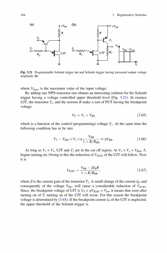
where VImax is the maximum value of the input voltage.By adding one NPN transistor one obtains an interesting solution for the Schmitt
trigger having a voltage controlled upper threshold level (Fig. 3.21). In essenceUJT, the transistor Tr, and the resistor R make a sort of PUT having the breakpointvoltage
VP ¼ Vx þ VBE ð3:65Þ
which is a function of the control (programming) voltage Vx. At the same time thefollowing condition has to be met
VV � VBEt\Vx\gVBB
1þ R=RBB
� gVBB: ð3:66Þ
As long as V1 < Vx, UJT and Tx are in the cut off region. At V1 = Vx + VBEt, Txbegins turning on. Owing to this the reduction of VB2B1 of the UJT will follow. Nowit is
VB2B1 ¼ VBB � bIBR1þ R=RBB
; ð3:67Þ
where β is the current gain of the transistor Tx. A small change of the current IB, andconsequently of the voltage VBE, will cause a considerable reduction of VB1B2.Since, the breakpoint voltage of UJT is VP = ηVB2B1 + VDt, it means that soon afterturning on of Tr turning on of the UJT will occur. For this reason the breakpointvoltage is determined by (3.65). If the breakpoint current IP of the UJT is neglected,the upper threshold of the Schmitt trigger is
V
V
VV - V
V
+V +V
I
X
0
BB CES
i
BB BB
R RR
E EC
R R
Tr
UJT UJT
VI
(a) (b)
Fig. 3.21 Programmable Schmitt trigger (a) and Schmitt trigger having increased output voltageamplitude (b)
164 3 Regenerative Switches
VTH ¼ Vx þ VBE þ REIBP ð3:68Þ
From the condition
Vx þ VBE ¼ Vp ¼ gVBB � bRIBP1þ R=RBB
þ VDt
it follows that the base current IBP at which the UJT turns on is
IBP ¼ VBB
bR1� Vx
gVBB
1þ RRBB
� �� �: ð3:69Þ
Since, this current is very low, the member REIBP in (3.68) can be neglected and
VTH � Vx þ VBE: ð3:70Þ
Immediately upon the UJT being turned on, the transistor Tr is turned off. Thusits only task is to initiate the turning on of the UJT. Therefore, the lower threshold isdetermined by (3.61).
The output voltage amplitude VM of the Schmitt triggers in Figs. 3.20 and 3.21 isrelatively small (VM < 0.5 V). By adding a PNP transistor (Fig. 3.21b), theamplitude is VM = VBB − VECS ≈ VBB. In order to keep Tr in the saturation regionwhen the UJT is conducting, it has to be
VBB � VEB
RB2� VEB
R[
VBB � VECS
bRCð3:71Þ
Since, VBB ≫ VEB and RB2 = (1 − η)RBB, and taking into account that themember VEB/R can be neglected, from (3.71) it follows:
RC [1� gb
RBB: ð3:72Þ
Therefore, if the UJT is off, Tr must also be off. Thus, RVBB/(R + RBB) < VEBt,therefore, for VBB ≫ VEBt
R\VEBt
VBB
RBB: ð3:73Þ
For example, for VBB = 10 V, RBB = 8 kΩ, η = 0.6, β = 50, and VEBt = 0.6 V; onthe basis of (3.72) and (3.73) one obtains RC > 640 Ω and R < 480 Ω. The choicecan be Rc = 1.5 kΩ and R = 320 Ω.
3.1 Unijunction Transistor 165

3.2 Thyristors
The thyristor is general name for a family of four-layer semiconductor switchescomprising three p-n junctions. Often, however, this concept implies a completegroup of regenerative switches. Within this concept the unijunction transistorbelongs to the thyristor group. Broadly speaking, the thyristor (Greek thyra—gate)is a bistable switch having a regenerative transition from the high-resistance to thelow-resistance region and vice versa. The ranges of controlled currents and voltagesare very wide. The nominal values of currents of the present day thyristors rangefrom several mA up to several thousands of A and the nominal values of voltagesextend up to 10,000 V.
3.2.1 Triode Thyristor—SCR
The triode thyristor is representative of the four-layer elements and it is oftenreferred to as thyristor. It comprises three electrodes (anode, cathode, and controlelectrode—gate). The load is connected in the anode–cathode circuit and the controlis realized via the gate. Since, the triode thyristor is most frequently used in ACcircuitry as a rectifier (conducts in one direction only, like a diode) having acontrolled conduction angle, the abbreviated name Silicon Controlled Rectifier(SCR) is almost universally accepted.
The thyristor structure and a typical distribution of impurities are shown inFig. 3.22. Technologically, the initial material is a highly resistive N1 region havingtypical concentration of donor dopants from 1014 to 1015 cm−3.
G
K
A
N2
P2
N1
P1
A
K
J1
J2
J3
0 50 100 150 200 2501014
1015
1016
1017
1018
1019
P1 N1 N2P2
ND
, N
A[c
m-3
]
α [µm]
(a) (b)
Fig. 3.22 Thyristor structure (a) and typical distribution of dopant concentrations (b)
166 3 Regenerative Switches

On both sides are deeply diffused p-type regions. The first p-region P1 is theanode emitter. The cathode emitter is made of the n+-type diffused region N2. Thus,a thyristor consists of three p-n junctions.
At forward bias, when VAK > 0, the outside junctions J1 and J3 are forwardbiased and the central junction J2 is reverse biased. The thyristor current is thendetermined by the current of the reverse biased p-n junction. Practically, the fullapplied voltage VAK is across junction J2. Owing to the low dopant concentration,the space charge region is located in the N1 region (shaded area in Fig. 3.22). Thethyristor will crossover from the cut off to the conduction region when the voltageVAK is equal to the breakdown voltage of the central p-n junction.
In order to simplify the explanation of the turn-on and turn-off mechanisms, it iscustomary to represent the thyristor using a two-transistor model (Fig. 3.23).
The regions N1 and P1 are common for the PNP and NPN transistors. Allowingthe gate to be open, i.e., IG = 0. At VAK > 0, both emitter junctions are forwardbiased, whereas the common collector p-n junction is revere biased. The transistorsare, thus, in the active forward regions. Since at IG = 0 the anode and cathodecurrents are equal, then
IA ¼ apIA þ ICBOp þ anIA þ ICBOn; ð3:74Þ
Therefore, it follows
IA ¼ ICBOp þ ICBOn1� an þ ap
� � ¼ 2ICBO1� an þ ap
� � ; ð3:75Þ
where αn and αp denote the common-base current gains of transistors Tn and Tp,respectively. If the individual currents of the collector junction are equal, then itstotal current is ICBOp + ICBOn = 2ICBO.
A
G
K
Tn
Tp
(b) (c)
A
K
G
(a)
G
K
A
P1
P2
2P2
2
N1
2N1
2
N2 IG
αpIA+ICB0p αnIK+ICB0n
IK
IA
Fig. 3.23 Two-transistor model of the thyristor (SCR) (a and b) and its symbol (c)
3.2 Thyristors 167

At small currents IA the gains αn and αp are very small (Fig. 3.25a), andIA = IK ≈ 2ICBO. An increase of the voltage VAK ≈ VCBn = VCBp causes the currentICBO to increase gradually, so αn and αp also increase. When VAK becomes suffi-ciently large, in the reverse biased barrier of J2 the process of avalanche multi-plication starts. The thyristor is in the forward breakdown region (region betweenthe points B and P in Fig. 3.24). In the breakpoint P the regenerative process startsby turning on of the thyristor with both transistors Tn and Tp in the saturationregion. Namely, an increase of the base current of the transistor Tn will cause itscollector current to increase βn times the base current. Since, icn = ibp, the collectorcurrent of the transistor Tp will increase βn βp times. Thus, the closed loop currentgain is βn βp. If the regenerative process is to start, it has to be
bpbn � 1; ð3:76Þ
therefore the thyristor turn-on condition follows in the form
an þ ap ¼ 1: ð3:77Þ
The same result is obtained on the basis of Eq. (3.75) and the condition thatIA → ∞. The current IA, to which (3.77) applies, is the breakpoint current IP(Fig. 3.25a).
The anode current of the thyristor in the off state, at IG = 0, is so small that thecondition (3.77) is impossible to reach without a considerable increase of VAK. Ifone assumes that the multiplication factors of electrons and holes are equal, thenone can write that the anode current in the breakdown region is
IA ¼ 2ICBOM1�Mðan þ apÞ ; ð3:78Þ
Conduction region
Regeneration region
I
I =0
I
I
I =0
II >>I
I
I
I
I
I
I
V V V V
A
G
G3
G3
G
G3 G2 G1
G2
G2
G1
G1
H
P
H PM PM0 AK
BForward breakdown
region
High resistance(cut off) region
Reverse cut offregion
Reverse breakdownregion
P
Fig. 3.24 Static I–V characteristic of SCR
168 3 Regenerative Switches

where the multiplication factor is
M ¼ 11� ðVAK=BVJ2Þn ; ð3:79Þ
where BVJ2 is the breakdown voltage of the central p-n junction. By lettingIA → ∞, at VAK = VPMO, from (3.78) and (3.79) one obtains the breakpoint voltage
VPMO ¼ BVJ2 nffiffiffiffiffiffiffiffiffiffiffiffiffiffiffiffiffiffiffiffiffiffiffiffiffiffiffi1� ðan þ apÞ
qð3:80Þ
In order to have a VPMO as high as possible, the gain of one of the transistors hasto be quite small. Usually, this is the transistor Tp (Fig. 3.23), since its base (regionN1) is very wide.
If, however, IG > 0, the thyristor will turn-on sooner, i.e., VPM < VPMO
(Fig. 3.24). Namely, due to a positive IG the thyristor current is higher, so αn and αpare higher which leads to the turn-on at lower voltages VAK. Now
IK ¼ IA þ IG; ð3:81Þ
and the anode current is
IA ¼ anIG þ 2ICBO1� an þ ap
� � : ð3:82Þ
Therefore, the turn-on condition is again αn + αp = 1. The difference is that αnand αp increase primarily due to current IG. This is exactly why the breakpointvoltage is inversely proportional to the gate current IG (Fig. 3.24). Practically, if IGis sufficiently high, the break point voltage could be only several V (Fig. 3.25b).Consequently, the breakpoint voltage of the SCR is programmable by the gatecurrent within limits from several V up to the value of the breakpoint voltage atIG = 0, VPMO.
αn+αp
αn
αp
αn+αpαnαp
1.2
1.0
0.8
0.6
0.4
0.2
IP
IA 0 25 50 75 90 125
10
102
103
104
VPMO
IG [mA]
VPM [V](a) (b)Fig. 3.25 Current gains αn
and αp of transistors Tn and Tpas functions of the anodecurrent (a) and thedependence of the break pointvoltage on the gate current (b)
3.2 Thyristors 169

In the conduction region both transistors are saturated, the anode-to-cathodevoltage is
VAKS ¼ VCESj j þ VBESj j ð3:83Þ
and, depending on the anode current, it ranges from 0.7 V up to 2 V. It should beemphasized that no gate current is needed in the state of conduction. Therefore, thethyristor is a switch that requires a relatively small drive only during turn-on. Thismakes the essential difference between the thyristor and the bipolar transistor as aswitch. Namely, a transistor requires a permanent and relatively high drivethroughout the state of conduction. For instance, if a transistor, maintaining acollector current of about 20 A, is to be in saturation, the base current of at least 1 Ais required.
The thyristor will remain in the on state (the region of low resistance) as long asthe anode current is higher than the holding current, IH. The holding current is thelowest anode current maintaining the thyristor in the state of conduction with thegate open (IG = 0). Namely, at IA = IH the regenerative process is restarted andowing to the reduction of IA it leads to the turning off of the thyristor. Typical valuesof IH are within the range from several hundreds μA up to 10 mA.
At reverse bias (VAK < 0), the outside p-n junctions J1 and J3 of the thyristor arereverse biased. Because of that the regenerative process does not arise in the regionof reverse breakdown. The current-voltage characteristic in this region is verysimilar to the I–V characteristic of a reverse biased diode. Since, the region N1 isonly weakly doped, i.e., its resistance is much higher compared to that of the regionN2, most of the applied voltage appears across the junction J1 and the influence ofthe junction J3 can be neglected. The breakdown occurs either due to the avalancheprocess or due to the spreading of the transition region of the junction J1 over theentire region N1 up to the junction J2. However, since the region N1 is quite wide,the breakdown is mainly caused by the avalanche process.
3.2.1.1 Characteristics of Control Electrode (Gate)
As already emphasized, a controlled turn-on of a thyristor occurs at the momentwhen the positive gate current IG causes a positive anode-to-cathode bias, VAK > 0.After the thyristor is turned on, no gate drive is required. Moreover, it is then of nouse because it only heats up the thyristor. In addition, there is no use of a negativeanode bias since it increases the reverse anode current (Fig. 3.24). Because of allthis, the gate should be pulse driven. The driving pulse should have the requiredgate current IG, the voltage VG, and a sufficient length TG.
The time TG is several μs. Practically, however, TG is between 10 and 20 μs andthe gate Ig − Vg characteristics are called the static thyristor characteristics(Fig. 3.26). Practically, these are the I–V characteristics of the P2N2 junction and
170 3 Regenerative Switches

they are determined by the minimum (rgmin) and maximum (rgmax) gate resistances.The gate voltage has to be higher than the threshold voltage of the p-n junctionwhich is about 0.5 V. The region of safe turn-on of the thyristor is the cross-hatchedregion shown in Fig. 3.26. The maximum voltage VGM is several V and themaximum gate current IGM ranges from 100 mA for low power thyristors up to theorder of one A for power thyristors. On the right-hand side the operating region islimited by the hyperbola of permitted dissipation. This is power which will notcause any damage to the p-n junction. Owing to the temperature dependence of thep-n junction voltage, triggering of a thyristor is not reliable in the region of thecharacteristics without cross-hatch. Therefore, at lower temperatures the region ofsafe triggering is narrower.
In order to accomplish the exactly defined instant of thyristor triggering, it has tobe driven by current pulses of much higher level compared to those correspondingto the static conditions. In other words, an overdrive current pulse is applied. In thisway the influence of temperature variations of the gate characteristics is reducedand very short triggering times are accomplished.
Example 3.2 The characteristics of a directly biased thyristor are shown in Fig. 3.27.Determine the power losses on the thyristor for excitations shown in Fig. 3.28a, b.
10 20 30 40 50 60 70 IGM
Ig [mA]
Vg [V]
3
2
1.5
VGM
1Vg(T2)Vg(T1)
(T1>T2)
T1 T2=Tmin
Turn on impossible
Turn on possible
r gmax
Max. voltage
Gate dissipation
Max
. cur
rent
Reliable turn on
rgmin
Fig. 3.26 Static start-up characteristics of a thyristor
3.2 Thyristors 171

Voltage on the thyristor when it is directly biased (Fig. 3.27) is: VTH = VTH0 +rTiTH, where VTH0 = 1.2 V, and VTH = 0.8/25 = 32 mΩ. In a general case powerlosses on the thyristor in the period T are equal to
pTH ¼ 1T
ZT0
iTHðtÞvTHðtÞdt ð3:84Þ
Substituting the expression for the voltage on the thyristor when it is directlybiased into Eq. (3.55) one obtains
pTH ¼ 1T
ZT0
iTH tð Þ VTH0 þ rTHiTH tð Þð Þdt
¼ VTH01T
ZT0
iTH tð Þdt þ rTH1T
ZT0
i2TH tð Þdt24
35 ¼ VTH0ITH;sr þ rTHI
2TH;eff :
ð3:85Þ
iTH [A]
vTH [V]
25
1.2 2
Fig. 3.27 Characteristics of thyristor in direct polarization
15
T/2 T t
iTH[A] iTH[A]
tT/2 T 3T/2
(a) (b)
Fig. 3.28 Thyristor current—rectangular form (a), form of sine half-wave (b)
172 3 Regenerative Switches

If the current through the thyristor is as shown in Fig. 3.28a, the average value ofthe current is ITHsr = 15/2 = 7.5 A, and the effective value of the current isITHeff ¼ 15=
ffiffiffi2
p ¼ 10; 6A: Substituting these values in Eq. (3.85) one obtains
pTH ¼ 7:5� 1:2þ 0:032� ð10:6Þ2 ¼ 12:63W:
In a case, when the current has the form of a sine half-wave (Fig. 3.28b) theaverage value of the current through the thyristor is:
ITHsr ¼ 1T
ZT=20
20 sinðxtÞdt ¼ 20p
¼ 6:36A:
The effective value of the current through the thyristor is ITHeff ¼ ITHmax
2 ¼ 10A:Substituting these values in Eq. (3.85) one obtains
pTH ¼ 6:36� 1:2þ 0:032� 102 ¼ 10:83W:
3.2.1.2 Effect of the Rate of Anode Voltage Change (dv/dt Effect)
The previous analysis of the turn-on process is valid only under the assumption thatthe anode voltage changes are slow. At high rates of anode voltage variationsturning on of a thyristor will be faster. Since, the collector p-n junctions of tran-sistors Tn and Tp are reverse biased, they can be considered as a capacitor(Fig. 3.29a). If the voltage drop across the forward biased emitter junctions isneglected, the current through this capacitor is
i ¼ CCB
dVA
dtþ VA
dCCB
dt� 1
2CCB
dVA
dt; ð3:85Þ
since CCB * 1/√UA.Thus, the anode current is proportional to the rate of change of the anode
voltage. At high rates of dVA/dt this current may become significant. As the currentrises, the current gains αn and αp increase and the turn-on conditions are fulfilled atlower input voltages (3.77). In other words, the turn-on occurs at smaller voltagescompared to the static breakpoint voltage VPMO. Therefore, the capacitive currentcauses the thyristor to turn-on in accordance with the same mechanism as that of thegate current. Figure 3.29b shows the dependence of the breakpoint voltage of athyristor on the rate of change of the anode voltage and temperature. As the tem-perature increases, this dependence becomes more pronounced because the con-stants αn and αp are higher. Moreover, this effect is more pronounced for powerthyristors since the capacitance CCB is proportional to the cross section S. Thisphenomenon is often called the dv/dt effect or dv/dt capability.
3.2 Thyristors 173

In device specifications it is defined as the maximum value of (dVA/dt)M whichwill not cause the turn-on process of a thyristor. It ranges from 10 V/μs up to about100 V/μs.
It is possible to increase the capability dv/dt in several different ways (Fig. 3.30).A capacitor CS between the anode and cathode (Fig. 3.30a) reduces the rate of theanode voltage increase. The anode-to-cathode voltage now increases exponentially.In the limiting case when the voltage VAA changes abruptly, the condition must besatisfied that
VAA
R0CS\
dVA
dt
� �M; ð3:86Þ
from which the value of capacitance CS is calculated. For a given thyristor (dVA/dt)is an item of the catalog specifications. In order to reduce the discharge current ofCM at the beginning of thyristor conduction, the resistor RS is added (dotted lines inFig. 3.30a).
The effect of the two protection methods of Fig. 3.30 is the same. The differenceis in that Rg in Fig. 3.30b is external whereas in Fig. 3.30c this is the resistance ofthe P2 region which is on one side short circuited by the cathode (denoted by KS inFig. 3.30c). In both cases a part of the capacitive current is shunted through thisresistor to the cathode. This reduces the emitter current of Tn and therefore the gainαn. A thyristor with the short circuited emitter (Fig. 3.30c) could have a very largebreakpoint voltage VPMO (over several thousands volts) at the open gate because thegain αn is very small.
The effect of reducing αn can be explained by the two-transistor model of athyristor in terms of the resistor RS between the gate and the cathode. Excluding theshort circuited emitter the gain is
T
n
p
A
K
CCB
i
VA
5001 10 100
1000
1500
V [V]PM0
dV VA
dt ms[ ]
T=20°C
T=100°C
(a) (b)
+
T
Fig. 3.29 High frequency thyristor model (a) and break point voltage versus the rate of anodevoltage change and with temperature as parameter (b)
174 3 Regenerative Switches

an ¼ Icn � IconIEn
¼ Icn � IconIK
: ð3:87Þ
Including the short circuited emitter, the current IEn is, due to the longitudinalresistance RS, smaller than Ig by the amount of the branching current IS. Namely
IK ¼ IEn þ IS: ð3:88Þ
Now, the effective current gain of the transistor Tn can be defined as
anef ¼ Icn � IconIEn þ IS
¼ Icn � IconIEnð1þ IS=IEnÞ ¼
an1þ IS=IEn
: ð3:89Þ
For small values of RS, or Rg it is possible that IS/IEn ≫ 1, thus αnef ≪ αn.
Example 3.3
(a) Determine the values of the elements in Fig. 3.31 in order to provide dv/dt protection of a thyristor if f = 2 kHz (switching frequency),
S ¼ dv=dtðmaxÞ ¼ 100V=ls and L ¼ 50lH:
The input voltage has sharp change from 0 to Vs equal to 200 V.
CS
RS
RO
+VAA
RP
+VAA
Rg
N2
KS
RS
N1
P1
P2
A
G K
(a) (b) (c)
Fig. 3.30 Protection (snubber) circuits (a and b) and the thyristor having short circuited emitterfor the purpose of reducing the dv/dt effect (c)
SCRR
C
L
VS
+i(t)
Fig. 3.31 Thyristor snubber circuit
3.2 Thyristors 175

(b) Determine power losses in the protection circuit.
(a) After the sharp change of the input voltage, the current through thesnubber RC circuit can be described by the following differential equation
LdiðtÞdt
þ RiðtÞ þ 1C
ZiðtÞdt ¼ VS:
By transformation from time (t) to complex (s) domain one obtains
s2 þ 2nx0sþ x20
� �I sð Þ ¼ Vs=L; ð3:90Þ
where x0 ¼ 1ffiffiffiffiffiLC
p and n ¼ R2
ffiffiffiCL
q.
Following the same approach for the voltage on the thyristor, the fol-lowing expression can be derived
v0 tð Þ ¼ VS � Ldi tð Þdt
; where s ¼ CR: ð3:91Þ
Solving Eqs. (3.90) and (3.91) and taking into account conditions i(0) = 0and v0(0) = 0 the following expression is obtained for the current iiðtÞ ¼ Vs
R2nffiffiffiffiffiffiffiffi1�n2
p e�nx0t sinxt (A) and for the voltage on the thyristor
v0 ¼ Vs 1� e�nx0t cos xtð Þ � nffiffiffiffiffiffiffiffi1�n2
p sin xtð Þh in o
(V) where ω is the oscil-
lation frequency equal to x ¼ x0
ffiffiffiffiffiffiffiffiffiffiffiffiffi1� n2
p.
If the damping factor is ξ > 0.5, for instance ξ = 0.7 the maximum rate ofthe thyristor voltage change is S ¼ 2Vsx0n ¼ VsR=L:From the expression for S it follows R ¼ SL
Vs¼ 25X:
The capacitance of the snubber circuit is equal to (Fig. 3.45)
C ¼ 4n2LR2 ¼ 158 nF:
(b) Losses on the resistor R in the snubber circuit are proportional to accu-mulated energy in the capacitor C and they are approximately equal to
PR ¼ CV2s f ¼ 12:64W:
3.2.1.3 Effect of the Rate of Anode Current Change (di/dt Effect)
Conventionally designed thyristors have a side positioned control electrode(Fig. 3.32c). Immediately upon the action of a positive pulse at the control elec-trode, the full voltage Vg will appear only at the part of junction J2 nearest to the
176 3 Regenerative Switches

gate terminal. Owing to the voltage drop across the transversal resistance RS of theregion P2, the remote parts will be at a lower potential, thus at a lower forward bias.Therefore, at the beginning of conduction, the electron injection from the N2 regionwill be marked only in the vicinity of the gate (denoted by an arrow in Fig. 3.32c).This means that at the beginning only a narrow part of the thyristor is conductingwhereas the major part is in the off state. Owing to a high current density at thisnarrow part the dissipation in this part is the highest, which may lead to overheatingof the junction and to destruction of the element. This is particularly true for veryfast increase of the anode current. Namely, the anode current does not attain auniform distribution but is concentrated to a narrow conduction region. If the rate ofincrease diA/dt is smaller than the maximum permitted (diA/dt)M, the current due tothe regenerative process will be distributed homogeneously across the cross sectionand therefore no damage to the thyristor will occur.
The power thyristors have a larger surface and consequently larger a cross-section resistance RS, thus they are more sensitive to the di/dt effect than the lowpower thyristors. At higher temperatures this effect is more pronounced. Since, (diA/dt)M varies from sample to sample, the (di/dt) capability is defined as the worst case.Typical values of di/dt capability are several tens of A/μs.
Figure 3.32 shows two designs of thyristors with increased di/dt capabilities. Inthe first case (Fig. 3.32a) the gate is in the middle, surrounded by the cathode.
In this way, the initial conduction surface of the junction is considerably larger,consequently the initial anode current distribution is more uniform. For powerthyristors, however, this improvement is not sufficient. For this reason thyristorshaving an amplifying gate are designed (Fig. 3.32b). At the gates surrounding thecentral gate a field is induced making these gates active. Practically, there is onepilot thyristor which controls the operation of the two main thyristors (Fig. 3.32c).In addition to the more homogenous distribution of the anode current, this systemallows operation with very small control signals. In fact, the pilot thyristor amplifiesthe gate signal.
A
GK KG
A
P
N
P RS RS
NN NN
P
N
P
RS RS
A
K
G
(a) (b) (c)
Fig. 3.32 Thyristor with central gate (a) and with amplifying gates (b and c)
3.2 Thyristors 177

3.2.1.4 Turn-On Time
Usually a thyristor is turned on by the gate current. During the turn-on process theanode voltage could be considered constant and VAA < VPMO. A test circuit having aresistive load is shown in Fig. 3.33a. If one allows instant increase of the gatecurrent, the turn-on condition by an abrupt current drive is fulfilled. After a certainperiod, referred to as the turn-on time, the anode voltage and current will attain theirstationary values. The turn-on time consists of two parts, the delay time td and therise time tr.
The delay time td is defined as the time required by the anode current to reach10 % of its stationary value in the state of conduction. This time is a consequence ofthe finite period required by minority carriers to cross the base-collector regions N1
and P2. Because of this, the regenerative process resulting in increasing of theanode current does not arise immediately. In other words, a certain time is requiredto allow the carriers to cross certain thyristor regions. The wider the base regions N1
and P2, the longer is the delay time. For high-voltage thyristors, having a wide P2
base, the time td is quite long. In this situation, the thyristor should be turned on bya higher gate current because td reduces with an increasing IG (Fig. 3.33c). Duringthe rise time tr the anode current increases from 0.1 to 0.9 IA. The most part of thisperiod corresponds to the propagation time. It was already mentioned that at thebeginning of thyristor conduction only the part of the cathode close to the gate isconducting. The time required for the whole cathode to become conductive is thepropagation time. For very powerful thyristors this time may be several hundreds ofμs long. The rise time of the anode current is not only dependent on the thyristordesign, but is also load-dependent. For instance, if the load is inductive, the risetime will depend much more on the load inductance than on the thyristorparameters.
td tr
tu
0.1 IA
0.9 IA
IA
ig
IG
t0 t
t 0.1 0.2 0.4 0.5 1 2 4 50.1
0.2
0.4
0.5
1
2
4
IG [A]
IA = 100A
ig
+VAA
RP
(a) (b) (c)
Fig. 3.33 Turn-on test circuit (a), anode current response to abrupt gate drive (b), and delay timeas function of gate current at IA = 100 A (c)
178 3 Regenerative Switches

3.2.1.5 Turn-Off Time
While a thyristor is on, all p-n junctions are forward biased and both transistors arein saturation. Owing to this, particularly for power thyristors, there are considerablepiled-up charges in all four parts of the thyristor. Figure 3.34a shows the corre-sponding minority carrier distributions. The most part of the charge is stored in theregion N1 because this region is the widest and the least conductive. The concen-trations of the minority carriers in the anode and cathode emitters (regions P1 andN2) are negligible because the conductivities of these regions are very high. If athyristor is to be turned off, the piled-up charge has to be cleared away. This isaccomplished mainly by cutting off or reversing the bias of the anode circuit. In thecase of cutting off the anode circuit, the anode current drops below the holdingcurrent. The piled-up charge is cleared away by recombination. Consequently, theturn-off time is quite long. The reversal of the polarity of the anode voltage is themost frequent and the most reliable method of turning off the thyristor. Then,similarly to the processes in diodes and bipolar transistors, the piled-up charge iscleared away by the negative anode current. The larger this current, the fasterclearing away. Figure 3.34b shows the response of the anode current to an abruptchange of the anode supply voltage from +VAA to –VAA. In the interval from t0 to t1the anode current is negative, determined by the external elements of the circuit.Within this time the minority carrier concentration at the junction J3 drops to zero.In the interval from t1 to t2 the anode current reduces because the voltage at junctionJ3 increases. This interval is very short because the breakdown of these junctions ofonly several volts occurs very quickly. After this, in the interval from t2 to t3clearing away of the carriers from the junction J1 is continued. The anode currentduring this interval is constant. At the instant t3 the minority carrier concentration atthe junction J1 is zero. After that the anode current decreases until the capacitanceof the reverse biased junction J1 is charged, when iA = 0.
The time from to to t4 is the thyristor recovery time tc. However, the thyristor isstill not off. Namely, although the external junctions are reverse biased, the con-centrations of the charge carriers in the N1 and P2 regions are above their static
tC
IR
t0 t1 t2 t3
IA
iA
VAA
+VAA
-VAA
t
t
P1 N1 P2 N2
Qp
Qn
(a) (b)
Fig. 3.34 Distribution of minority carriers in a conducting thyristor (a) and the response of theanode current to the reversal of the anode voltage (b)
3.2 Thyristors 179

levels because the junction J2 is forward biased. Owing to this, in case of a forwardbias of the anode circuit, the thyristor would be switched on at anode voltagesbelow VPMO. In other words, the thyristor is still not capable of blocking a positiveanode voltage. It is able to do that only if the excess minority carriers around thejunction J2 are cleared away. This clearing away is accomplished by recombinationbecause the anode current is negligible. Consequently, the turn-off time ti of athyristor is the elapsed time from the reverse bias of the anode circuit until thethyristor is again capable of blocking a positive anode voltage at the maximumpermitted value and at the maximum permitted rate of its change. Typically, it isseveral tens of μs, and for fast thyristors it is of the order of 1 μs. It should beemphasized that the gate voltage will influence the turn-off time: it will increase it ifpositive or decrease it if negative. This is understandable because a positive voltagesupports the regeneration within a thyristor and negative, by extracting the positivecharge from the P1 region, suppresses the regeneration.
Figure 3.35 shows the responses of the anode current and voltage to a realcurrent drive of the gate during the turn-on and the anode supply voltage during theturn-off processes. Upon the polarity of the anode voltage being reversed, the anodecurrent is also reversed.
ig , VAA
t
t
IG
+VAA
VAA
td tr
tu
ts
tc
ti
IRMt0
iA , VAA
+VAA
-VAA
0.1 IA
0.9 IA
iA
Fig. 3.35 Responses of anode current and voltage to real driving currents of the gate and anodesupply voltage
180 3 Regenerative Switches

The anode voltage remains unchanged during the time interval ts. This intervalcorresponds to the interval t0 to t1 (Fig. 3.34b). During ts the anode current reachesits maximum negative value IRM.
3.2.1.6 Turning On (Triggering) and Off
In principle, switching circuits can be divided into two groups: the circuits fed bythe anode circuit of the thyristor and the circuits having a completely separatesource of triggering signals. A triggering signal could be DC, low frequency, orpulsed. A power supply having thyristor-controlled load current could be DC orAC. As it has already been mentioned, turning off of the thyristor is not carried outby the gate but by the anode circuit, except for a special type of thyristors (GTO).The most reliable way of turning off is by applying a reverse bias to the anode-to-cathode circuit. In an AC power supply this is carried out automatically, at thebeginning of the negative half-cycle. For a DC power supply, however, turning offis more complicated. It is usually done by one of the three methods (Fig. 3.36).
The least used method is turning off by breaking the anode current (Fig. 3.36a)because the switch Pr, either mechanical or semiconductor, has to be very powerful.In addition, during the switch-on of Pr, as a consequence of a sudden anode voltagechange, the undesired triggering of the thyristor may occur.
Turning off by short circuiting the thyristor (Fig. 3.36b) is the simplest, but notthe most reliable. The transistor is on only for a short while, so it can be low power.When on, it should take upon itself the major part of the anode current so that itdrops below the holding current value (IA < IH)
VAA � VH
R0� bIB\IH : ð3:92Þ
A revere biased anode is the most reliable method of turning off. This isaccomplished by adding a low power thyristor SCR2 and a commutating capacitor
VTR1
VTR2
VA VAA
VH1
-VCO+VH2
R RO
C
+VCO
VTR1VTR2
RO
+VAA +VAA
SCR SCR2 SCR1
RBT
IB
βIB
RO
+VAA
SCR
(a) (b) (c) (d)
Pr
Fig. 3.36 Methods of turning off the thyristor in a DC power supply by breaking the anodecurrent (a), short circuiting the thyristor (b), reverse biased anode (c) and the voltage waveforms incharacteristic points (d)
3.2 Thyristors 181

C (Fig. 3.36c). The main thyristor SCR1 is turned off by turning on the auxiliarythyristor SCR2. Namely, while SCR1 is on, SCR2 is off and the capacitor is chargedthrough R in the direction indicated in Fig. 3.36c. By triggering SCR2 the anodevoltage of SCR1 becomes negative (Fig. 3.36d) leading to turning off of SCR1.Instead of SCR2 it is possible to use a transistor (bipolar or MOS).
In the design of triggering circuits there is no significant difference whether thesupply is AC or DC. Figure 3.37a shows a simple triggering circuit involving afront-resistor fed from a common power supply. The diode D is used only with anAC supply in order to block the negative half-cycle. With a DC supply the thyristoris triggered by turning on the switch Pr. In case of an AC voltage VA, triggering canbe accomplished without the switch Pr. The instant of triggering, by adjusting thegate current required for triggering (Fig. 3.37), is programmed by the resistance RG.By RG it is possible to achieve that the SCR is completely nonconductive or that itconducts at least during a half-cycle up to a full cycle. Thus, the angle of con-duction can be varied within limits. Figure 3.38b shows the waveforms of thecharacteristic currents and voltages of an AC supply.
Triggering treshold
ig
VAK
io
t
t
t
αV
αOK
SCRPr
RG
D
RO
iO
VAA
or
(a) (b)
Fig. 3.37 Triggering circuit fed from a common supply (a) and the waveforms of the gate andload currents and the anode-to-cathode voltage for an AC supply (b)
ig
VAK
io
αV
(b)
t
t
tαV
IG
TV TZ
VAA
RO
iO
SCR
VG
+RG Pr
(a)
Fig. 3.38 Triggering circuit having separated supplies (a) and the anode voltage and current foran AC supply when the thyristor is a static switch (b)
182 3 Regenerative Switches

If the supply of the triggering circuit is separate (Fig. 3.38), the angle of con-duction can practically be controlled within limits 0° ≤ αv ≤ 180°. Moreover, it isoften required that the thyristor is conducting for a certain number of half-cyclesand then blocked for another number of half-cycles (Fig. 3.38). The switch Prserves for controlling the intervals of conduction Tv and blocking Tz. The resistanceRG should be chosen so that the thyristor is triggered at the minimum voltage VAA.In these applications the thyristor is often called the static switch.
3.2.1.7 Triggering Circuits Based on UJT
The basic pulse generator circuit using an unijunction transistor belongs to thegroup of the most popular thyristor triggering circuits. In this application the outputfrom the base B1 of the UJT is connected to the gate of the thyristor, directly(Fig. 3.39a) or by a pulse transformer (Fig. 3.39b) or an optocoupler. The instant oftriggering is adjusted by the timing elements RE and CE. After the UJT is switchedon, each pulse can trigger the thyristor at a positive anode voltage. The voltageacross R1, when the UJT is off, has to be below the minimum triggering voltage ofthe thyristor, i.e.,
R1IBB\VGKmin; ð3:93Þ
where
IBB ¼ VBB
RBB þ R2 þ R1: ð3:94Þ
Since RBB ≫ R1 + R2, from (3.92) and (3.93) it follows
R1\VGKmin
VBB
RBB ¼ R1max: ð3:95Þ
+VBB
RE
CE
R1
R2
SCR
RO
VAA +VBB
RE
CE
R2
SCR
RO
VAA
1:1
UJT UJT
(a) (b)
Fig. 3.39 UJT-based oscillators for thyristor triggering
3.2 Thyristors 183

For instance, if VBB = 24 V, RBB = 6 kΩ, and VGKmin = 0.4 V, thenR1max = 100 Ω.
The triggering circuits from Fig. 3.39 require a separate power supply VBB. Inthe phase controlled circuits the triggering circuit is fed from a common AC supply(Fig. 3.40). Here the oscillator is fed by a Zener diode and a common resistor Rz.The first oscillator pulse turns the thyristor on. The voltage across it reduces toapproximately 1 V so that the oscillator is cut from the supply and stops generatingpulses. Thus, the gate current exists only until the thyristor is switched on. Duringthe negative half-cycle the Zener diode operates as a forward biased diode. Owingto this a negative current will flow through the load. However, since Rz ≫ Ro, thiscurrent is very low. The operation of the circuit from Fig. 3.40 is illustrated inFig. 3.40b. The phase control (variation of the angle of conduction) is accomplishedby the variations of the timing elements RE and CE.
It is often required that the triggering circuit is galvanically separated from theprimary source. This is accomplished by a mains transformer (Fig. 3.41). Here theoscillator is fed throughout the positive half-cycle. Then it generates triggeringpulses. However, only the first triggering pulse is active. All others are passive andhave no influence since the thyristor is on. Thus, the angle of conduction is con-trolled by the timing elements RE and CE. During the negative half-cycle Dz isforward biased and it cuts the oscillator supply. Meanwhile, the capacitor CE isdischarged so that the synchronism is automatically established (triggering at thesame instant during each half-cycle) since CE charges from the beginning duringeach positive half-cycle. The resistance Rg reduces the influence of noise in the gate
t
t
t
t
t
VAA
VAK
-VD
VAK
VAA
VZ
VP
iO
1
E
B1
SCR
A
K
UJTDZ
R
C
RZ
R2
R1G
E
1
B1
RO
iOVAA
(a) (b)
aVaOK
Fig. 3.40 UJT based oscillator in a phase controlled circuit (a) and the characteristic waveforms (b)
184 3 Regenerative Switches

circuit and it ranges from one hundred Ω up to several kΩ. Here it is not necessarysince the resistance R1 is in a UJT-based oscillator, thus the current of a PUT in theoff state is considerably lower and cannot turn-on the thyristor.
In the circuits analyzed so far the thyristor was connected in a half-wave rectifiercircuit. The circuit from Fig. 3.42 controls the phase in both half-cycles of the loadcurrent. The diode bridge D1–D4 rectifies the negative half-cycle and feeds the PUTbased oscillator during both half-cycles. The first triggering pulse from the oscil-lator, either in the positive or in the negative half-cycle, turns on the thyristor and itconducts until the mains voltage changes the polarity. By varying the cycle of theoscillator from 1 to 7.8 ms, the angle of conduction is controlled within limits from21.6° up to 168.5°.
RZ
DZ
CE
PUT
RE R2
R1
Rg
RO
220V
Fig. 3.41 Galvanically separated triggering circuit based on PUT in a phase controlled circuit of ahalf-wave rectified voltage
RZ
DZ
CEPUT
RER2
R1
RO
D1
D2
D3
D4
T12N4442
20V
15k , 2W
250k1k
1k
MPU 131
0.1mF
100
MDA 990-3Bridge D1 D2_
aV
aV
IO+
IO-
IO+
IO-
20V
Fig. 3.42 Phase control in a full-wave rectifier
3.2 Thyristors 185

Example 3.4 For the circuit from Fig. 3.43 determine:
(a) the value of the resistance Rx so the average value of the current through theload Rp, Lp is 5 A, and
(b) the average value of the current through the diodes in the diode bridge.(c) Sketch the voltage waveforms in the marked points.
Remark, vs(ωt)=ffiffiffi2
p � 220 sinð2x50tÞ, η = 0.6.
(a) The angle γ at which the Zener diode is turned on is determined from thecondition VSM sin c ¼ VZ ) c ¼ arcsin VZ
VSM¼ 0:064 rad:
The thyristor angle of triggering is determined from the condition that thedesired average current through the load is
I0 ¼ 1p
Zp
a
VSM sin xtð ÞR
d xtð Þ ¼ VSM
Rp1þ cos að Þ;
where α is the angle of triggering.From the expression for the average value of the load current, the value of the
angle α is calculated as
a ¼ arccosI0RpVSM
� 1� �
¼ 2:08 rad:
Based on the calculated angle α, the RC time constant is determined as
ta ¼ ax
¼ a2p50
¼ 6:62ms:
The capacitor charging circuit which generates the required time constant isshown in Fig. 3.44.
RG
D
D1 D3
D4 D2
vs
1
2TH
LP
RP
10mH
10
15k
DZ
20V
RX
C100nF
R1
100
R2
100
3
Fig. 3.43 An example of phase control of full-wave rectifier
186 3 Regenerative Switches

Since, the angle γ is very small it can be considered that the Zener diode leads atthe beginning of each period of the diode rectifier output voltage. The anode voltageVA of a unijunction transistor is equal to
VA tð Þ ¼ VZ � VZe� t
RXC:
The resistance RX is determined from the condition for the desired angle of thethyristor triggering.
VA tað Þ ¼ VDk þ gVB2B1
� gVB2B1 ¼ gVZ :
From the expression for the voltage on the anode of the unijunction transistor andthe conditions for the unijunction transistor turn-off, next expressions are obtained
ta ¼ RXC ln1
1� g; and
RX ¼ taC ln 1
1�g
¼ 72:25 kX:
(b)
IDsr ¼ I02¼ 2:5A:
(c) Voltage waveforms of marked points 1,2 and 3 of circuit from Fig. 3.43 areshown in Fig. 3.45.
C
RX
100nF
VZ
VA
Fig. 3.44 RC circuit forgeneration of the requiredtime constant
3.2 Thyristors 187

3.2.2 Gate Assisted Turn-Off Thyristor
A Gate Assisted Turn-off Thyristor (GATT) is a thyristor where the turn-off processis gate assisted. It is mainly used at high frequencies. Namely, the turn-off time ofconventional thyristors could be as high as several tens of μs, which reducesconsiderably the useful frequency range. This is particularly true of the high-voltage(over 1,000 V) thyristors. A GATT operating at voltages in excess of 1,000 V couldhave a turn-off time of only several μs. The acceleration of the turn-off process isaccomplished by applying a negative bias to the gate. This helps clearing away the
0 π 2π3/π2 3/π5
3/π2 3/π50 π 2π
0 π 2π
VSM =311V1 [V]
V2 [V]VSM =311
ω t [rad]
ω t [rad]
ω t [rad]
V3 [V]
VZ =20
Fig. 3.45 Voltagewaveforms of marked points1, 2 and 3 of circuit fromFig. 3.43
188 3 Regenerative Switches

piled-up charge in P2 base and eliminates the possibility of a forward bias at thejunction J3.
Like a thyristor having an increased dv/dt capability, GATT makes use of thecathode-emitter short circuits and for more powerful components distributed orinter-digital gates are applied. Since turning on of thyristors having inter-digitalgates requires high gate currents, GATTs are usually designed with amplifyinggates. Their structure is similar to that shown in Fig. 3.32 except that they have twoturn-off electrodes. The auxiliary electrode is connected to the main (central)electrode via a (bypass) diode. During turn-on this diode is reverse biased andduring turn-off it is conducting and bypasses the “pilot” thyristor. The bypass diodecan be external or integrated.
3.2.3 Asymmetric Thyristor
Asymmetric Semiconductor Controlled Rectifier (ASCR) is an asymmetric thyris-tor. It has a very narrow n-base. Owing to this its reverse breakdown voltage is only20–30 V. However, narrowing the base reduces the on voltage and the turn-on time.Thanks to this the power losses in ASCR are smaller than those of conventionalthyristors.
3.2.4 Reverse Conducting Thyristor
Owing to the small reverse breakdown voltage of ASCR, an anti-parallel diode isusually connected. An Reverse Conducting Thyristor (RCT) is a reverse conductingthyristor having an integrated anti-parallel diode. Its cross section and symbol areshown in Fig. 3.46. Practically a fast thyristor and a fast diode are integrated into asingle component. The reverse voltage of the thyristor is equal to the forward
`
Isolation region
DiodeThyristorA
G KEtched channel
n+ n+ n+ n+ p+
n+p+
n
p
A
K
G
(a) (b)
Fig. 3.46 Cross section (a) and symbol of a reverse conducting thyristor (RCT) (b)
3.2 Thyristors 189

voltage of the diode. The basic problem in designing a reverse conducting thyristoris that between the diode and the thyristor region good isolation is required. Thisisolation blocks the penetration of the excess charge carriers from the conductingdiode to the thyristor which could cause a considerable slowing down of the thy-ristor turn-off process. The isolation is accomplished by introducing a high-resis-tance region between the components in the p and n bases.
3.2.5 Gate Turn-Off Thyristor
A gate turn-off thyristor (GTO) is a thyristor which is turned on or off by the gate.Its cross section, two-transistor model, and symbol are shown in Fig. 3.47. Turningoff is achieved by a negative gate current. In order to initiate the regenerativeprocess, both transistors during turn-off have to be in the active region. Thus, thebase current of Tn has to be lower than the saturation base current, i.e.,
IBn ¼ aPIA � IG IBns ¼ 1� a0ð ÞIAbn
: ð3:96Þ
From (3.96) it follows that the minimum gate current, required for turning off thethyristor, is determined by
IG � aP þ an � 1an
IA: ð3:97Þ
Consequently, it is possible in principle to turn-off any thyristor by the gate.However, for this a very high gate current, even higher than the anode current,would be required. For instance, if αn = αp = 0.95, then, according to (3.97),
A
G
K
Tn
Tp
(b) (c)
A
K
G
(a)
IG
αpIA (1-αp)IA
IK
IA
IBn
N1
P1
P2
N2 N2
K G
A
Fig. 3.47 Cross section (a), two-transistor model (b), and symbol of GTO thyristor (c)
190 3 Regenerative Switches

IG > 0.95 IA. The ratio of the anode and the gate current required for turn-off is oftencalled the turn-off current gain and is determined by
AI ¼ IAIG
¼ anan þ aP � 1
: ð3:98Þ
For conventional thyristors AI ≈ 1. In order to make the gate turn-off processpractically possible, the condition AI ≫ 1 has to be met. This, according to (3.98),means that the sum of current gains αn should be approximately 1, but αn + αp > 1and αp should be as small as possible. If, e.g., αn = 0.8 and αp = 0.21, then AI = 80.
High αn and low αp in GTO thyristors are technologically accomplished inseveral ways. The cross section of the structure of a GTO thyristor is shown inFig. 3.47. The p-emitter surface is small, so αp is small. On the other hand, the n-emitter surrounds the gate, so its effective surface is large and consequently αn islarge.
If the standard circuit for triggering GTO thyristor (Fig. 3.48) is used, turn-on isaccomplished by the trailing edge and turn-off by the leading edge of the triggeringpulse fed to the base of the transistor Tr1. The capacitor Cg plays the same role as aspeed-up capacitor in the base of a bipolar transistor. It allows a large initial gatecurrent in both turn-on and turn-off phases of a GTO thyristor. While Vok = 0, Tr1 isoff, whereas Tr and the thyristor are on. The capacitor Cg is charged in the directiondenoted in Fig. 3.48. The gate-cathode of the thyristor is reverse biased exactly bythis voltage and provides a negative gate current which turns off the thyristor whenTr2 is off and Tr1 is on (Vok = VBB).
3.2.6 MOS Thyristor
An MOS-Controlled Thyristor (MCT) is a thyristor controlled by an MOS tran-sistor. It is often denoted as an MOS SCR. Its fabrication belongs among the newthyristor technologies. The transistor model of an MCT is shown in Fig. 3.49. By
D
VOKT1
RB RC
T2
CG
RG
+GTO
VAA
RO
+VCCFig. 3.48 Triggering circuitof a GTO thyristor
3.2 Thyristors 191

feeding a positive pulse to the gate of the NMOS transistor, Mn, the regenerativeswitch made up of a complimentary pair of transistors Tn and Tp is turned on. Assoon as Mn is on, Tp is also on. Its collector current makes a voltage drop across theresistance RBE which turns on Tn. Then, the regenerative process is started and thetriggering pulse does not have any effective influence. A significant feature of MCTis that the input resistance of the gate is very high (of the order 109 Ω), so it can bedriven by very low power signals. Thanks to this it can be driven directly by theoutput of a CMOS buffer (Fig. 3.49c). The input of an MOS transistor is of acapacitive nature. Due to this the gate voltage change is exponential which slowsdown the turn-on process. In order to accelerate the process of charging of thiscapacitor, a circuit with several buffers connected in parallel is usually applied. If anabrupt drive of the gate is required, and this is the case when the triggering pulse isvery narrow, a speed-up capacitor is used (Fig. 3.49d).
In parallel with this capacitor a resistor R and a diode D are connected in order toallow discharging of the capacitor C and provide a low impedance between the gateand the cathode of the thyristor in the on state. The resistance ranges from 1 kΩ upto several tens of kΩ, and the capacitance from 1 to 10 nF.
3.2.7 Insulated Gate Control Thyristor
The Insulated Gate Control Thyristor (IGCT) is a powerful semiconductor device.Its characteristics are similar to those of the GTO thyristors, whose turning on andoff is controlled by the gate current. Unlike the GTO thyristor, IGCT have much
M
n
n
R
R
BE
0
Tp
A
G
K
(a)A
KG
CMOS
VAA
(b)
(c)
(d)
R
C
D
T
Fig. 3.49 Transistor model (a), symbol (b), and CMOS drive of MCT: simple (c) and optimum(d)
192 3 Regenerative Switches

greater turning off gate current than the GTO, which results in complete eliminationof minority carriers from the lower p-n junction and a shorter turn-off time. The ideawas to get a switching component with a low voltage drop and low losses in the onstate, and the ability to rapidly turn-off with minimal switching losses. This meansthat such a switch in the on state should behave as a rectifier, a low resistance ofconductive structure, should have a low value of the anode-cathode voltage, andduring the turning off process it should behave as a transistor in order to achievegood dynamic characteristics.
It is known that the turning off of the GTO transistor can be realized by the gatecurrent. The goal is to have a turn-off time as short as possible. While a GTO isturning off, the gate current is sharply increasing (close to the anode current) beforethe anode voltage begins to rise. In this case, known as the “unity gain turn-off”, or“hard-driven” [1] NPN transistor turns off the first (Fig. 3.50a), and then a PNPtransistor with open base assumes the basic function of turning off the GTO thyristor(Fig. 3.50b). If the storage time of the GTO thyristor (the time from the momentwhen negative voltage between the gate and the cathode appears to the momentwhen the thyristor anode voltage start to rise) is ts, the negative voltage between thegate and the cathode. When the thyristor is turned off gate voltage is VGoff, and thetotal inductance of gate is LGt. Then the maximum turning off current is
IGMoff ¼ VGoff tsLGt
: ð3:99Þ
Based on (3.99), it can be concluded that the maximum turn-off current can beincreased by increasing the voltage VGoff and the time ts, and reducing the induc-tance LGt. Using the state-of-the-art technology it is difficult to increase VGoff and ts,so the only solution is to reduce the LGt. The reduction of the gate inductance isachieved by the special technology of IGCT, so the maximum turn-off current canbe 1,000 A and more. IGCT is made of two basic components. One is a GCTthyristor placed in a disk case (similar to the GTO thyristor) and the other is a gateunit, placed as close as possible to the GTO on the same printed circuit board(Fig. 3.51).
(a) (b) A
Ik
IA
k
G
IG
A
G
IA=IG
Hard driven turn-off
Fig. 3.50 Two transistorsmodel (a) and hard driventurn off of GTO thyristor (b)
3.2 Thyristors 193

This design reduces the total inductance of the gate by up to 100 times (order ofa few nH) compared to the GTO thyristor and according to (3.99) increases theturn-off gate current so this current approaches close to the anode current, the “unitygain turn-off.”
The symbol of IGCT and the waveforms of the current and the voltage for atypical IGCT 600A/700 V during its turning off are shown in Figs. 3.52 and 3.53,respectively.
Typical waveforms of the IGCT current and the voltage during transition fromthe thyristor mode operation (condition state) to the transistor mode (transientprocess during turning off) are shown in Fig. 3.53. Upon receiving the control
Fig. 3.51 IGCT [1]
K (Cathode)
A (Anode)
G (Gate)
Fig. 3.52 Symbol of IGCT
194 3 Regenerative Switches

pulse, the cathode current and the gate current rapidly decrease (absolutelyincreasing). When the cathode current drops to 0, the anode voltage begins toincrease. At the same time the anode current is sharply decreasing, and the gatecurrent increases (IGCT is turning off). In the steady state when the IGCT is turnedoff IA = 0, IG = 0, IK = 0, and VA has a value of the anode voltage in the off state.
The gate has a specially designed power supply unit. This is a low voltage sourceconnected via an isolation transformer to the gate unit that is usually at a differentvoltage relative to the source (Figs. 3.51 and 3.54).
This can be a problem if the IGCT is used in high-voltage converters, becausethe necessary isolation transformers are larger, and it is often difficult to apply areliable method of isolation. Also, an external power source increases the price anddecreases the efficiency and reliability of the system.
0
200
400
600
800
-200
-400
-600
-80010 15 20 25
200
400
600
800
-200
-400
-600
-800
VA
IA
Ik
IG
t [µs]
I [A] V [V]
5
IA – anode current
VA – anode voltage
IG – gate current
Ik – cathode voltage
Legend:
Fig. 3.53 Waveforms of current and voltage for a typical IGCT 600 A/700 V during its turning off
3.2 Thyristors 195

In relation to the GTO thyristor the IGCT has the following advantages:
• higher dv/dt capability,• no need for a turn-off snubber circuit,• lower switching losses and• significant reduction of the turn-on and the turn-off time (the ability to work at a
higher frequency than the GTO).
Some of the areas where IGCT is applied are:
• frequency converters,• current or voltage inverters,• high power electric motor drives,• resonant serial or parallel inverters and• power system protection.
3.2.8 Emitter Turn-Off Thyristor
The emitter turn-off thyristor (ETO) is a hybrid high power MOS-GTO component(device). Compared to the GTO thyristor it has a higher nominal current, voltage,and the ability of gate control via MOS transistors. In this way, it provides lowpower consumption of the control circuit. In addition to this, it is characterized byan operating frequency greater than the GTO and IGCT, a wider working area forinverse polarization, lower conduction losses, significant turn-off capability, built-incurrent sensitivity and low cost.
The symbol and the equivalent circuit of ETO are shown in Figs. 3.55 and 3.56,respectively. The emitter switch Qe is connected in series with the GTO thyristorand the switch Qg is connected with the gate.
Each of these switches comprises a number of MOS parallel connected tran-sistors in order to increase the current capability.
The ETO thyristor is turned on by turning on the switch Qe, turning off theswitch Qg and injection gate current into GTO thyristor through G2. The appliedvoltage VQe directs the cathode current toward the gate. The voltage VQe can beclose to the breakdown voltage of the MOS transistor which is significantly larger
Isolation transformer
Power supply
Gate unit
IGCT unit
Fig. 3.54 Gate powered by low voltage through isolation transformer
196 3 Regenerative Switches
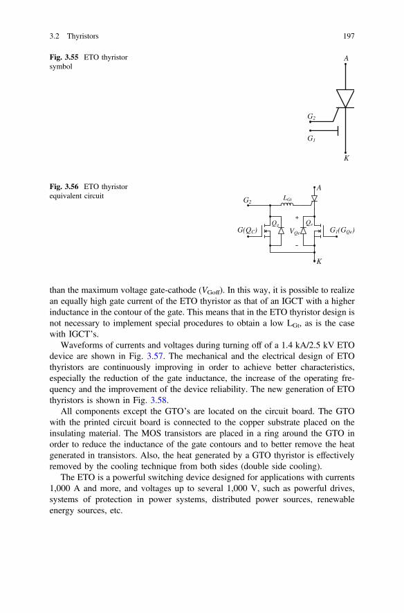
than the maximum voltage gate-cathode (VGoff). In this way, it is possible to realizean equally high gate current of the ETO thyristor as that of an IGCT with a higherinductance in the contour of the gate. This means that in the ETO thyristor design isnot necessary to implement special procedures to obtain a low LGt, as is the casewith IGCT’s.
Waveforms of currents and voltages during turning off of a 1.4 kA/2.5 kV ETOdevice are shown in Fig. 3.57. The mechanical and the electrical design of ETOthyristors are continuously improving in order to achieve better characteristics,especially the reduction of the gate inductance, the increase of the operating fre-quency and the improvement of the device reliability. The new generation of ETOthyristors is shown in Fig. 3.58.
All components except the GTO’s are located on the circuit board. The GTOwith the printed circuit board is connected to the copper substrate placed on theinsulating material. The MOS transistors are placed in a ring around the GTO inorder to reduce the inductance of the gate contours and to better remove the heatgenerated in transistors. Also, the heat generated by a GTO thyristor is effectivelyremoved by the cooling technique from both sides (double side cooling).
The ETO is a powerful switching device designed for applications with currents1,000 A and more, and voltages up to several 1,000 V, such as powerful drives,systems of protection in power systems, distributed power sources, renewableenergy sources, etc.
G2
G1
A
K
Fig. 3.55 ETO thyristorsymbol
LGtG2
G(QC) G1(GQe)
K
A
Qg Qe
+
VQe
Fig. 3.56 ETO thyristorequivalent circuit
3.2 Thyristors 197

0
500
1000
1500
2000
2500
3000
-500
-1000
-1500
-2000
2 4 6 8 10 12 14 16
500
1000
1500
2000
2500
3000
-500
-1000
-1500
-2000
VA
IA
Ik
IG
t [µs]
I [A] V [V]
Fig. 3.57 Waveforms of 1.4 kA/2.5 kV ETO thyristor during its turning off
Fig. 3.58 New generation ETO [2]
198 3 Regenerative Switches

3.2.9 Photo-thyristor
Photo-thyristors are light-controlled devices. In terms of the electrical and physicalcharacteristics they are identical to the standard thyristors driven by electric signals.Consequently, their applications are exactly the same. The difference is only in thetype of drive used. Most of the photo-thyristors also have a gate terminal. It is usedfor the additional control of the sensitivity by the level of the light signal.
Practically, the only structural difference between a photo-thyristor and a stan-dard thyristor is that in one part of the case, usually on the top cover, the photo-thyristor has a built-in optical lens serving to optically control the thyristor.
3.2.10 Unilateral Switch
A Silicon Unilateral Switch (SUS) is a low power thyristor having the controlelectrode (gate) on the anode side. Between the gate and the cathode a low voltageZener diode is built-in. The equivalent model, symbol, and static characteristic areshown in Fig. 3.59.
The structure of a SUS and its characteristic are almost the same as those of aPUT. The difference is only that a SUS has a built-in Zener diode, so its breakpointvoltage is fixed and amounts to
Vp ¼ VZ þ VEBt ð3:100Þ
where Vz is the breakdown voltage of the Zener diode and VEBt is the thresholdvoltage of the PNP transistor. The voltage Vz ranges from several volts up to severaltens of volts.
G
A
K
IH
IP
VH VP VAK
P
IA(c)
G
A
K
(a) (b)
Fig. 3.59 Equivalent model (a), symbol (b), and static characteristic of a unilateral switch (c)
3.2 Thyristors 199

3.2.11 Double Switch—SBS
Compared to the SUS which is capable of only one-directional conduction, anSilicon Bilateral Switch (SBS) is a bilateral (two-directional) switch. Its transistormodel and static characteristic are shown in Fig. 3.60. Therefore, an SBS consists oftwo anti-parallel SUSs. The Zener voltages are equal so the characteristic in the Iand III quadrants is symmetric. The breakpoint voltage of the SBS in Fig. 3.60 isVP ≈ 7.5 V. The SUS and SBS are low voltage regenerative switches. Althoughthey are manufactured as individual components, they are usually manufactured asan integral part of an integrated circuit. As separate components they are mainlyused in the triggering circuits of thyristors and triacs.
3.2.12 Diode Thyristors
The diode thyristors are regenerative switches with two terminals. The breakpointvoltage of a given component is fixed and, like for an open gate thyristor, deter-mined by the breakdown voltage of the central p-n junction. The diode thyristorscan be divided into two groups: unilateral and bilateral.
The four-layer diode is a unilateral component (Fig. 3.61). It is often called theBreak Over Diode (BOD). Practically this is a thyristor without a gate. It turns onwhen the anode-to-cathode voltages reaches the break point voltage VP or when asudden change of the anode voltage occurs (dV/dt effect). Turning off of the four-layer diode occurs when the anode current decreases to the value of the minimumconduction current IV, i.e., IH. Namely, in that case βnβp > 1, or αn + αp > 1(Fig. 3.61b) like during the turn-on process, so a regenerative process is established.The current IV is usually within the limits from several mA up to several tens of mA.
IH
VP V
I
-VP
-IH
G
A1
A2
A1
A2
G
RB
15k
RB
15k
6.8V
6.8V
SUS1 SUS2
(a) (b)
Fig. 3.60 Transistormodel (a), static characteristic and symbol of the bilateral regenerative switch (b)
200 3 Regenerative Switches

As a rule, the four-layer diodes are less powerful devices than the thyristors.They are mainly used as switching elements in pulse circuits, oscillator circuits, asreplacements for unijunction transistors, as protection elements, etc.
Figure 3.62 shows the basic circuit of a pulse generator based on a four-layerdiode. The principle of operation, static conditions, and limitations are identical tothose of the corresponding generators based on unijunction transistors. Here anadditional condition is valid that VAA > VP.
DIode AC switch (DIAC) is a bilateral (symmetric) diode thyristor. Its crosssection and static characteristic are shown in Fig. 3.63. Practically, it consists of twofour-layer diodes in anti-parallel connection. Namely, the regions P1 and N3 and P2
and N2 are short circuited. When VAK > 0, the p-n junction J3 is reverse biased, sothe left-hand side of the component behaves like a four-layer diode having the shortcircuited p-n junction J3. At the breakdown of the junction J2 the current through itinitially bends, in parallel to junction J3, toward the cathode. Owing to this, at thejunction P2 a voltage drop arises which makes a forward bias for the junction J3. Inthis way, the region N2 becomes active, leading to the initiation of the regenerativeprocess and switching of the component to the state of conduction. The junction J3is reverse biased and has no influence.
IV
VPVAK
IA
VP1
A
K
(a)
IP
VV
αn+αp
αn αp
P V
IP IV
cut-off active region
saturation
1
IA
(b)
Fig. 3.61 Symbol and static characteristic (a) of a four-layer diode and the operating regions ofthe current gains of the equivalent complimentary transistor pair versus anode current (b)
VP
VP -VV
ROIV
VV+ROIV
VA
VKt
t
CA
RO
VK
RA
+VAA
VA
(a) (b)
Fig. 3.62 Four-layer diode in an oscillator circuit (a) and characteristic voltage waveforms (b)
3.2 Thyristors 201

If, however, VAK < 0, the junction J3 is reverse biased and J4 is short circuited.Now the left hand side behaves like a four-layer diode. When the breakdown of thejunction J1 occurs, the current through this junction runs in parallel with thejunction J4 because it is not biased. This current makes a positive voltage dropacross the region P1 and provides a forward bias for the junction J4. Owing to thisthe region N3 also becomes active.
If the breakdown voltages of the junctions J1 and J2 are equal, then the staticcharacteristics in the I and III quadrants are completely symmetric (Fig. 3.63b).
Therefore, a DIAC can conduct in both directions, from anode to cathode andvice versa, depending upon polarity of the applied voltage. For this reason theexternal terminals are usually not called anode and cathode because this makes senseonly with DC components. Their common name is the “main terminals” and they aredenoted as MT1 and MT2. Sometimes they are simply denoted as A1 and A2.
Like a four-layer diode, DIAC is a component of relatively low power. Thebreakpoint voltages are usually several tens of V. DIAC is used as a switchingelement in various pulse circuits, most frequently in the circuits based on TRIACs.It is off whenever the load current drops to the SIDAC holding current (Fig. 3.64b).
IV
VPVA
IA
-VP
-IV
P
P VV
-VV
V
N2
N1
P1
A(K)
K(A)
(a)
N3
J1
J2
J3
J4
P2+
+
(b)
MT2
MT1
A(K)
K(A)
(c)
Fig. 3.63 Cross section (a) I–V characteristic (b), and symbol of DIAC (c)
t
t
V-VS
iO
(b)
IH
IH
+VP
-VP
IH
90º<θV<180º
V-
VS
RO
iO
(a)
Fig. 3.64 SIDAC as a switch in an AC circuit (a) and voltage and current waveforms (b)
202 3 Regenerative Switches
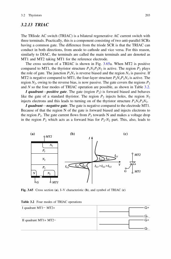
3.2.13 TRIAC
The TRIode AC switch (TRIAC) is a bilateral regenerative AC current switch withthree terminals. Practically, this is a component consisting of two anti-parallel SCRshaving a common gate. The difference from the triode SCR is that the TRIAC canconduct in both directions, from anode to cathode and vice versa. For this reason,similarly to DIAC, the terminals are called the main terminals and are denoted asMT1 and MT2 taking MT1 for the reference electrode.
The cross section of a TRIAC is shown in Fig. 3.65a. When MT2 is positivecompared to MT1, the thyristor structure P1N1P2N2 is active. The region P2 playsthe role of gate. The junction P1N3 is reverse biased and the region N3 is passive. IfMT2 is negative compared to MT1, the four-layer structure P2N1P1N3 is active. Theregion N2, owing to the reverse bias, is now passive. The gate covers the regions P2
and N so the four modes of TRIAC operation are possible, as shown in Table 3.2.I quadrant—positive gate. The gate (region P2) is forward biased and behaves
like the gate of a standard thyristor. The region P2 injects holes, the region N2
injects electrons and this leads to turning on of the thyristor structure P1N1P2N2.I quadrant—negative gate. The gate is negative compared to the electrode MT1.
Because of that the region N of the gate is forward biased and injects electrons tothe region P2. The gate current flows from P2 towards N and makes a voltage dropin the region P2 which acts as a forward bias for P2-N2 part. This, also, leads to
MT2
MT1
MT1
G
G
(a) (b) (c)
N
NN
N
P
P
3
2
1
2
1
I
II
I
II
I
II
G1
G1G1
G2
G2G2
G3
G3G3
I
V> >
MT2
Fig. 3.65 Cross section (a), I–V characteristic (b), and symbol of TRIAC (c)
Table 3.2 Four modes of TRIAC operations
I quadrant MT1− MT2+
II quadrant MT1+ MT2−
3.2 Thyristors 203

turning on of the structure P1N1P2N2. Of course, this requires a higher gate currentcompared to the situation when the gate is positive.
III quadrant—negative gate. In this case terminal MT1 is positive compared toMT2 and the direction of the current of a conducting TRIAC is from MT1 towardMT2. The gate is negative compared to MT1, as a consequence the region N-P2 isforward biased and the electrons from N are injected into the P2 region. Theseelectrons are “collected” by the P2-N1 junction that leads to triggering of the thy-ristor structure P2N1P1N3.
III quadrant—positive gate. Now the gate is positive compared to MT1. Theactive part of the gate is the region P2 between N and N2. The junction P2-N2 isforward biased and it emits electrons “collected” by the P2-N1 junction. This, like inthe previous case, leads to the turning on of the TRIAC. Upon turn-on, the region Ndoes not participate in conduction since the current flows in the direction of themetallization. In both cases of the operation in the III quadrant the gate acts as a“remote” control electrode. Under these conditions turning on of the TRIACrequires the largest gate current (critical current) owing to the relatively poor col-lecting efficiency of the forward biased junction P2N1. The lowest critical current isin the I quadrant at a positive bias of the gate. In general, the limits of the criticalcurrent and the triggering voltage of the TRIAC are similar to those of SCRs,except that a TRIAC can also be triggered by negative pulses.
It has already been emphasized that in SCRs, owing to the pile-up of minoritycarriers, problems may arise at turning off. This is more pronounced for TRIACsnot only because they consist of thyristors but also because a considerably shortertime is available for the turn-off process. For AC voltage operation SCRs haveavailable a sufficiently longer time. Indeed, after the current drops below IH, thepositive half-cycle ends and the negative half-cycle starts so SCRs have sufficienttime to turn-off. A TRIAC, however, is able to conduct during the negative half-cycle so a very short time is available for it to turn-off. Practically this is the timeduring which the voltage changes its polarity, i.e., during zero crossing, when thecurrent is below the minimum conduction current. If the change of voltage polarityis fast, the TRIAC may continue conducting in the opposite direction.
It is exactly because of this that the operating frequencies of TRIACs are limitedto couple of hundreds Hz and at present are usually below 500 Hz.
Triggering of TRIACs. The triggering circuits are similar to those of SCRs withthe exception that a TRIAC could also be triggered by negative pulses duringpositive or negative half-cycles of AC voltage. Consequently, for TRIAC triggeringthe bilateral switching elements are required.
The triggering circuit consisting of a resistance R1 and a switch Pr (Fig. 3.66)uses a common power supply. R1 serves for adjusting the level of the mains voltageat which the TRIAC is turned on if the switch is on.
The triggering circuit using a separate power supply (Fig. 3.67) is realized byusing a CMOS buffer. The transistor Tr provides the necessary triggering current. Ifthe total output current from the CMOS buffer is IDP, then the gate current of theTRIAC is Ig = (β + 1)IDP, where β is the current gain of the transistor Tr. Thiscurrent has to be greater than the critical gate current, i.e., IGT < (β + 1)IDP. The
204 3 Regenerative Switches

resistance Rg ranges from several tens of Ω up to several hundreds of Ω. In anycase, the condition (β + 1)Rg > RDP has to be fulfilled, where RDP is the total outputresistance of the CMOS buffer when the output is high (PMOS transistor is on). Inthe absence of a triggering pulse the TRIAC is off and the load current is i0 = 0(Fig. 3.67b). If the TRIAC stays on after the triggering pulse ends, it remains onuntil the anode voltage changed its polarity. Throughout the action of the triggeringpulse the TRIAC is on. This method of control is often called the TPC-control(Time Proportional Control). It is therefore based on the principle of the ratio of thetime the TRIAC is on to the time the TRIAC is off. It is customary to synchronizethe turn-on instant with the zero crossing of the AC voltage. The shortcomings ofthe phase method (the control of the conduction angle of each half-cycle) comparedto the TPC method are the low power factor owing to the nonsinusoidal waveformof the load current and the presence of noise in the mains network due to abruptcurrent changes when the TRIAC or the thyristor is turned on.
A typical TRIAC triggering circuit for the phase control of the load current(Fig. 3.68) uses a two-directional regenerative switch (DIAC, SBS, SIDAC) in thegate circuit. In this way the angle of conduction control is accomplished in both thepositive and the negative half-cycles.
The TRIAC is, namely, triggered by each turn-on of the bilateral switch. Timeconstant RC, and consequently the angle of TRIAC conduction, is varied bypotentiometer R1. When the voltage across the capacitor C reaches the value of thebreak point voltage VP during the positive half-cycle, or –VP during the negative
i0
Pr
Pr
TAC
R0
R1
i0
220V
50Hz
(a) (b)
Fig. 3.66 Common supply TRIAC triggering circuit (a) and the waveform of the load current (b)
R
g
0
ii00
+V V
V
VCCAA
0K
0K
Trt
t
(a) (b)
R
Fig. 3.67 CMOS triggering circuit (a), and waveforms of the excitation voltage and the outputcurrent (b)
3.2 Thyristors 205

one, the two-directional switch will be turned on. This causes triggering of theTRIAC and discharge of the capacitor C. Then, V1 = VH + VGK = 1.5–2 V until thecurrent of the two-directional switch drops below the holding current IH. Thisoccurs immediately before the zero crossing of the mains voltage. The corre-sponding voltage waveforms are shown in Fig. 3.68b, with the linearized voltage V1
across C. The dotted lines show the variations of the voltages V1 and V0 across theload Ro for a smaller value of R. In such a situation the TRIAC is turned on earlierso its angle of conduction is greater (θv2 > θv1).
The typical values of the timing elements are several μF to several hundreds ofμF for the capacitance C and several kΩ to several hundreds of kΩ for the resistanceR. The breakpoint voltages of the two-directional switches are from 10 V to severalhundreds of V, depending upon the type of the switch. The choice of the TRIACdepends upon the load current, i.e., the load resistance R0 and the maximum ACvoltage. The break point voltage of the TRIAC at the open gate (IG = 0) should begreater than the maximum operating voltage. The load resistances usually rangefrom several Ω to hundred Ω.
Triggering by zero crossing. It has already been emphasized that triggering of aTRIAC during a half-cycle would cause abrupt current changes and the appearanceof noise. The noise can be removed by filtering. However, at high powers thesefilters can become very bulky and expensive. Because of that, noise is removed byelimination of its causes. This is done by designing a triggering circuit to turn-onthe TRIAC during zero crossing of the AC voltage.
One of the possibilities to implement the zero-crossing triggering of the TRIAC isshown in Fig. 3.69. Owing to the RC network the gate voltage precedes the voltagebetween the main electrodes, creating in this way the conditions for triggering at verysmall voltages and allowing the switch Pr to open. The triggering of the TRIAC will
t
t
V- V1
VO
(b)
VP
-VP
θV1
θV2
θV1
θV2
R1
R2
C
1220V50Hz
RO
R
(a)
Fig. 3.68 Triggering circuit of a bilateral regenerative switch (a) and voltage waveforms at theinput VP, load V0, and capacitor V1 (b)
206 3 Regenerative Switches

occur at a very small positive voltage through the capacitor C1, the resistor R3, andthe diodes D1 and D2. Owing to this charging of the capacitor C2 through the diodeD3 will proceed as long as the input voltage is increasing. After that, while the inputvoltage decreases, the diode D3 will be off and the capacitor C2 will dischargethrough the diode D2 which is turned on. In this way C2 provides the gate currentwhich will keep TRIAC in the state of conduction during the negative half-cycleeven if meanwhile the switch Pr is turned on. Thus, in the circuit from Fig. 3.69 theTRIAC is always conducting an integer number of cycles. Also, it should beemphasized that during the negative input voltage the turn-on cannot occur. In otherwords, both turning on and turning off occur at the positive zero crossing.
The integrated circuits used as the triggering circuits at zero crossing areavailable today. Their application simplifies considerably the control circuits of thethyristor circuits (SCRs and TRIACs).
Problems
3:1 Determine the resistance RB in the circuit from Fig. 3.36b to ensure turning offof the thyristor. The voltage on the thyristor in the on state can be neglected.The circuit in Fig. 3.36b has VAA = 100 V, R0 = 50 Ω, VBB = 15 V (high levelof control voltage on the base of the transistor Tr) and β = 50.
3:2 If the latching time (minimal duration of trigger pulse) is tL = 8 μs, determinethe anode current IL (thyristor current at the moment TL) in the circuit shown inFig. 3.70.
3:3 For the circuit in Fig. 3.71 determine the angle when the thyristor starts toconduct, so that the average value of a current through the load is 1 A. Thevoltage drop on the diodes in the on state is 0.7 V, and the diode resistance canbe neglected.
Fig. 3.69 Zero crossingtriggering of the TRIAC
3.2 Thyristors 207

3:4 Determine the resistance of the resistors in the circuit shown in Fig. 3.72 toprovide a reliable turn-on of the thyristor. For the circuit from Fig. 3.72 it isknown that Vcon = 5 V, VGmin = 3 V and IGmin = 20 mA.
3:5 The characteristics of a forward biased thyristor are shown in Fig. 3.27. Deter-mine power losses on the thyristor for the thyristor current shown in Fig. 3.73.
3:6 For the circuit shown in Fig. 3.74 determine the interval of time t1 after whichthe current will fall to 0. The thyristor is turned on in the moment t = 0. Thediode and the thyristor can be considered ideal. It is known that iC(0) = 0,
+VDC
120V
X1
2N2575 R1
10
L1
10mH
Fig. 3.70 Simple circuit with the thyristor as a switch
v1
30mVf=1kHz
Vcon
RP
15
D1 D4
D2 D3
X1
Fig. 3.71 Bridge rectifierwith the thyristor in a loadbranch
Vcon
VS
SCR
L D
R1
R2
Fig. 3.72 Turning on thethyristor in circuit with theinductive load
208 3 Regenerative Switches

vC(0) = VI and iL = 5 A (current through LL can be taken as constant). Thecircuit in Fig. 3.74 has: VI = 100 V, IL = 5 A, C = 1 μF andx0 ¼ 1ffiffiffiffiffi
LCp ¼ 105 rad=s:
3:7 To control the power on a load with a resistance of 100 Ω the circuit shown inFig. 3.68 is used. The breakdown voltages of the diac are ±25 V, while thevoltages on the diac and the triac in the on state can be neglected. The circuit isconnected to the power network 220 V, 50 Hz. The circuit in Fig. 3.68 hasR = 50 kΩ and C = 0.1 μF.
(a) Determine the angle when the triac starts to lead.(b) Draw the waveform of the load voltage.
References
1. Zhang, B.: Development of advanced emitter turn-off (ETO) thyristor, Doctoral dissertation,USA (2005)
2. Sandia National Laboratories: Emitter turn-off (ETO) thyristor, FY2001 energy storage systemspeer review (2001)
D
ci
LCIV
LiThi
LL
+
+
TH
LvCv
Fig. 3.74 One part ofresonant circuit with thethyristor as a switch
T/2
ITh
tT
10
20
[A]
Fig. 3.73 The waveform of the thyristor current
3.2 Thyristors 209


Chapter 4PWM DC/DC Converters
In principle, the pulse DC/DC converters consist of two parts, a basic circuit and aregulating assembly. The basic circuit comprises of switches (usually a transistorand a diode), a choke and/or a transformer, and a capacitor. By turning on and offthe switches in a controlled manner, the required amount of energy is transferredthrough the switches and the low frequency filter (the choke and the capacitor) fromthe input to the load. In this way, the output voltage is proportional to the ratio ofthe on and off time intervals of the switch. This ratio, thus the output voltage, iscontrolled by the control block (CB).
Depending on the configuration of the elements in the basic circuit, there areseveral different DC/DC converters. Globally, however, they could be classified asconverters without galvanic isolation and those with galvanic isolation (the input andthe output are separated by a transformer or an optocoupler). The classification ofthese two groups could be made as shown in Fig. 4.1. On the other hand, all thesedevices can be split into four groups: forward (direct), flyback (indirect), push–pull(symmetric), andĆuk converters. The peculiarity ofĆuk converters is that in additionto the electromagnetic energy transfer (similar to other converters) they also useelectrostatic energy transfer. This type of converter also comprises coupled input–-output coils which serve to eliminate the variations of the input and output currents,the property significant from the point of view of elimination of pulse disturbances.
The classification according to the mode of control, or regulation, of the outputvoltage is shown in Fig. 4.2. The self-oscillating converters are simple from thedesign point of view, but their efficiency factor η is the lowest. They are mainlyused for supplying small loads (up to several tens of watts). The widest applicationtoday finds DC/DC converters using pulse width modulation (PWM). The outputvoltage is controlled by varying the ratio of the on and off times of the switch with aconstant frequency of switching.
Over the past 10 years an ever increasing attention has been paid to the resonantconverters. It is considered that the future in the design of efficient power suppliesbelongs to this type of converter. The essential difference of resonant power con-verters compared to other converter types is that the state of the switch is changed atthe zero crossing of the current or voltage. Owing to this the dissipation of theswitching elements is very low and the efficiency factor of the resonant converters
© Springer International Publishing Switzerland 2015B.L. Dokić and B. Blanuša, Power Electronics,DOI 10.1007/978-3-319-09402-1_4
211
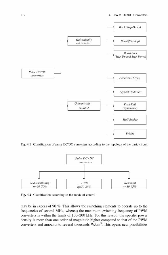
may be in excess of 90 %. This allows the switching elements to operate up to thefrequencies of several MHz, whereas the maximum switching frequency of PWMconverters is within the limits of 100–200 kHz. For this reason, the specific powerdensity is more than one order of magnitude higher compared to that of the PWMconverters and amounts to several thousands W/dm3. This opens new possibilities
Pulse DC/DC converters
Galvanically not isolated
Galvanically
isolated
Buck (Step-Down)
Boost (Step-Up)
Boost-Buck (Step-Up and Step-Down)
Forward (Direct)
Flyback (Indirect)
Push-Pull (Symmetric)
Half-Bridge
Bridge
Fig. 4.1 Classification of pulse DC/DC converters according to the topology of the basic circuit
Pulse DC / DC converters
Self-oscillating η=60-70%
PWM η=70-85%
Resonantη=80-95%
Fig. 4.2 Classification according to the mode of control
212 4 PWM DC/DC Converters

in designing compact power supplies which can, together with the standard ICs,constitute a part of the layout of a printed circuit board. If the period from 1970 upto the late 1980s can be qualified as the period of PWM converters, it is certain that1990s were the period of resonant converters.
In the resonant converter, energy is redistributed within a resonant circuit con-sisting of a coil and a capacitor. In this process, the energy is proportional to thesquare of the current through the coil and to the square of the voltage across thecapacitor. The output voltage depends on the operating frequency. It is at the highestwhen the operating and the resonant frequency are equal.
A separate group of pulse DC/DC converters consists of coil-less converters. Asthe name indicates, they do not make use either of coils or of transformers. The onlyaccumulating element is the capacitor. The basic circuit is made of a switched-capacitor network. These networks are suitable for the hybrid form of design, andsometimes for monolithic integrated circuit. Until recently these converters, as a rule,have been auxiliary power supplies with low output currents (several tens of mil-liamperes). Over the past several years, they have been given increased attention andare envisaged to be in the mainstream for designing supplies of portable and pocketequipment of low consumption and containing one battery as the primary powersource [1]. This is the reason that they have been classified as a separate group eventhough their basic application does not belong to power electronics but to supplyingelectronic equipment of low consumption (pocket calculators, mobile phones, etc.).
4.1 Forward Converters
The simplest version of a DC/DC converter is the forward converter without gal-vanic input–output separation (Fig. 4.3). Owing to the type of connection betweenthe transistor Tr, the choke L, and the load, this circuit is often called the seriesconverter. The term “forward” indicates that the energy from the source is directlyforwarded to the load. With the transistor conducting, the energy of the source issimultaneously transferred to the load and accumulated by the choke.
The diode D is then off. When the transistor is off, the circuit is closed through theturned-on diode and the energy accumulated by the choke is transferred to the load.The output voltage depends on the ratio of the intervals when the transistor is on or off
Tr
VI
+ +
- -
VR 0L
(PWM)
D C
L
T
CM
Fig. 4.3 Basic circuit offorward converter
4 PWM DC/DC Converters 213

and is lower that the input voltage. Because of such ratio of the input and the outputvoltages (Vo < VI), this type of converter is often called the step-down converter.
Depending on the value of the control signal the transistor and the diode arealternately on and off. At the input of the LC filter, if the turn-on and turn-off timesof the transistor and diode are neglected, a rectangular voltage with pulses ofvariable duration is established. The amplitude of these pulses is approximatelyequal to the input voltage. The diode D ensures the current flow when the transistorTr is off. The role of the choke L is to pass to the output only the DC componentwhich is equal to the mean value of the voltage at the input of the filter during onecycle of the control signal
Vav ¼ 1T
Zs
0
VI dt � VI
sT¼ DVt; ð4:1Þ
where τ is the duration and T is the cycle, while D = τ/T is the duty cycle of thecontrol signal. The capacitor C corrects the AC components across the load, RL.
According to (4.1), it would appear that the variation of the output voltage isproportional to the variation of the nonstabilized input voltage. However, the outputvoltage, or a fraction of it, is fed to the control module. This module generatessquare signals for turning on and off of the controlling transistor. The variation ofthe output voltage of the converter modulates the duration of the pulses τ at theoutput of the control module. This closed system of automatic control, through theaction of the control module, maintains the output voltage constant irrespective ofthe variations of the input voltage or of the load current.
4.1.1 Analysis of the Basic Circuit
In this section, some basic relations between the parameters characterizing theoperation of the converter are derived. For the purpose of this analysis severaljustifiable assumptions have been made.
In the first part, it will be assumed that the transistor and the diode are idealswitches (instantaneous switch-on and switch-off, the on-resistance negligible, theoff resistance infinite), and that the output voltage Vo and the current Io are constant.When the transistor Tr is on, the diode is off (Fig. 4.4). The current through thechoke increases from the minimum value ILm (at the switch-on) to the maximumvalue ILM (at the switch-off of the transistor). If VI and Vo are constant, the variationof the choke current is governed by the following differential equation
VI ¼ LdiLdt
þ rLiL þ Vo; ð4:2Þ
214 4 PWM DC/DC Converters

where rL is the active resistance of the choke. The solution of (4.2) can be expressedas:
iLðtÞ ¼ VI � Vo
rL1� e�t=sL
� �þ ILme�t=sL ; ð4:3Þ
where τL = L/rL. It has been shown that the coefficient of efficiency would bemaximal if T/τL < 0.05, because the active resistance of the choke can then beneglected. In the design of the choke, therefore, care should be taken to ensure rL assmall as possible. In such a case, by expanding the exponential terms in (4.3) inMaclaurin series and after justifiable approximations, it turns out that
iLðtÞ ¼ ILm þ VI � Vo
Lt: ð4:4Þ
The maximum value of the choke current is at t = τ, so
ILM ¼ ILm þ VI � Vo
Ls: ð4:5Þ
C CV VV VI I0 0
L LT T
t
t
V
iI
I
L
L
LM
Lm
V -VI 0
DT=DT T-DT
T
R RL LD D
r r(a) (b)
(c)
Fig. 4.4 Equivalent circuits of forward converter during intervals 0 < t <DT (a) andDT < t < T−DT(b), and the corresponding variations of the voltage and current of the choke (c)
4.1 Forward Converters 215

During τ < t < T − τ, the voltage of the control pulse is zero, so the transistor Tr isoff and the diode D is on (Fig. 4.4). Then the current through the choke is
iLðtÞ ¼ ILM � Vo
Lt; ð4:6Þ
and its minimum value is
ILm ¼ ILM � Vo
LðT � sÞ: ð4:7Þ
From (4.4) and (4.6), it can be seen that the current iL(t) is a linear function oftime. The load current is equal to the average value of the current through thechoke, i.e.,
IO ¼ ILm þ ILM2
: ð4:8Þ
The variation of the current through the choke is equal to the difference betweenthe maximum and the minimum values, i.e.,
D iL ¼ VI
LTDð1� DÞ ð4:9Þ
where D = τ/T is the duty cycle of the control pulse. Obviously, the variation of iLwhen the transistor is on is equal to the variations of iL when the transistor is off, i.e.,
VI � Vo
Ls ¼ Vo
LðT � sÞ; ð4:10Þ
therefore, it follows that
Vo ¼ sVI
T¼ DVI: ð4:11Þ
4.1.1.1 Output Voltage Variation
The variation of the output voltage can be determined, if the variation of the currentthrough the filter capacitor is known
iC ¼ iL � IO: ð4:12Þ
216 4 PWM DC/DC Converters

Figure 4.5 shows the variations of the currents iL and iC and the variations of theoutput voltage (voltage across the capacitance). The average value of the currentthrough the capacitor is zero, whereas its variation is equal to the variation of thecurrent through the choke, i.e., ΔiC = ΔiL. While iL > Io, the capacitor is beingcharged and the output voltage increases, whereas for iL < Io, the capacitor is beingdischarged and the output voltage decreases. The variation of the output voltage hastwo components, the capacitive Δvc′ (Fig. 4.5d) and the resistive Δvc″ (Fig. 4.5e),caused by the equivalent series resistance of the capacitor. The AC components are,for clarity, drawn out of proportion. The resistive component, which is in phasewith the current ic, can become dominant at high frequencies if the choice of thecapacitor is wrong.
This may have particularly undesirable consequences in the relay converterswhere due to this voltage component a considerable shift in the nominal frequencyof the controlling transistor may occur. For this reason in the design process, inaddition to the selection of a capacitor having a low series resistance, it is oftenrequired that its capacitance is considerably higher than the optimum value
Controlsignal T=1/f
T-
t
t
t
t
t
t
(a)
(b)
(c)
(e)
(d)
(f)
i
i
Δi /2Δi /2
Δi /2
ΔiΔi /2
ΔV''
ΔV'
ΔV
Δi /2
Δi /2
Δi /2
Δi =
I
I
i (t) i (t)V''
V'
V
V =DV
I
L
L
L
LL
LC
C
C
0
C
C
C
C
C
C
LM
C
CC2
C
C
0
0
0
R
R
≈ 0 IV DV=
Fig. 4.5 Voltage and currentwaveforms, control signal (a),current iL (b), current iC (c),capacitive component ofvoltage vC (d), resistivecomponent of voltage vC(e) and output voltage (f)
4.1 Forward Converters 217

according to other criteria (small weight or small volume). The variation of theoutput voltage is equal to the sum of the capacitive and the resistive component ofthe voltage across the capacitor, i.e.,
voðtÞ ¼ 1C
Z t
0
iC dt þ RCiC: ð4:13Þ
When the transistor is on, taking into account (4.12), it follows that
iCðtÞ ¼ VI � Vo
Lt � D I
2; ð4:14Þ
where ΔI = ΔiL, so
voðtÞ ¼ VI � Vo
2LCt2 þ RC
VI � Vo
L� D I
2C
� �t � D I
2RC: ð4:15Þ
When the transistor is off, the currents through the choke L and the capacitorC decrease
iCðtÞ ¼ D I2
� Vo
Lt;
and the variation of the output voltage is
voðtÞ ¼ � Vo
2LCt2 þ D I
2C� RC
Vo
L
� �t þ D I
2RC: ð4:16Þ
By differentiating (4.15) and (4.16) over time and equating them to zero, oneobtains that the output voltage is maximum and minimum at the followingrespective instants
t1 ¼ s2� sC and t2 ¼ T � s
2� sC;
where τC = CRC. The maximum and the minimum are shifted to the left by τCcompared to the case when the value of RL can be neglected. The maximumvariation of the output voltage (peak-to-peak) is equal to the difference between itsmaximum and minimum values
Dvo ¼ Voð1� DÞ8LCf 2
þ Vo
2LCf 2DsCT
� �; ð4:17Þ
218 4 PWM DC/DC Converters

where the first member is the capacitive component Δvc′ and the second is theresistive component Δvc″. If the notation ξ = τc/T is introduced, then
Dvo ¼ Voð1� DÞ8LCf 2
1þ 4 n2
Dð1� DÞ� �
: ð4:18Þ
From Fig. 4.6, it is obvious that for τc > 0.3T, the dominant influence on thevariation of the output voltage is due to the resistive component. In the course ofselecting the value of the capacitor and the frequency of operation of the controllingtransistor, the care should be taken that
sC\0:1 T : ð4:19Þ
From (4.18) it is possible to determine the value of the product LC, which wouldresult in the variation of the output voltage smaller than the permitted maximum
LC[Voð1� DÞDVof 2
1þ 4n2
1� D
� �: ð4:20Þ
The right-hand side of (4.20) is at the maximum when D = Dmin. Therefore, it isrequired that
LC[Voð1� DÞDVof 2
1þ 4n2
Dmin 1� Dminð Þ� �
: ð4:21Þ
4.1.1.2 Quasi-static Mode of Transistor
The maximum collector–emitter voltage of the transistor in the quasi-stable state isequal to the input voltage, i.e., VCEmax = VI. While Tr is off the collector current iszero and when it is on, its current is equal to the current through the choke
2
1
0.1 0.3 0.5 0.7 0.9
V /(
)
ΔV
0
02
D
0.3
0.5
0.1
0.01
ξ= /T=const.
8LC
f
C
Fig. 4.6 Normalizedvariation of output voltage asfunction of D and ξ
4.1 Forward Converters 219

(Fig. 4.7). Therefore, the maximum collector current is equal to the maximumcurrent through the choke and is determined by (4.5), whereas its average value is
ICsr ¼ IIsr ¼ ILm þ DiL=2; ð4:22Þ
where ILm and ΔiL are determined by (4.7) and (4.9), respectively.From (4.23) it follows that,The input converter current and the collector current are equal. Since the circuit
is assumed ideal, there are no losses in the converter, so the average value of theinput power is equal to the output power, i.e.,
VIIIsr ¼ VoIo: ð4:23Þ
IIav=Io ¼ Vo=VI ¼ 1=D: ð4:24Þ
This indicates that an ideal converter behaves like a transformer whose trans-formation ratio is equal to the reciprocal value of the duty cycle of the control pulses.
From Fig. 4.7, it can be seen that the forward DC/DC converter behaves like atypical pulse load of the primary source involving high rates of current changes, di/dt. This generates noise which is transferred through the primary source to otherparts of the equipment. It is for this reason that the corresponding filters are ofteninserted between the primary source and the input of the DC/DC converter.
Condition of Continuity of the Current Through the Choke
The above analysis applies under the condition that the current through the choke iscontinuous. This condition will be met if
IO [DiL2
; ð4:25Þ
t
t
V
i
i /2
II
I I =I +
B
L
L
LMI =C I
Lm Isr Lm
T
ΔΔ
T- 66
Fig. 4.7 Control voltage and collector current of transistor
220 4 PWM DC/DC Converters

or
IO [Vo
2LTð1� DÞ: ð4:26Þ
From (4.26) it follows that the minimum inductance of the first choke of theoutput filter which still results in a linear current through the choke is
Lmin ¼ Vo
IO
Tð1� DÞ2
: ð4:27Þ
In order that the current through the choke be continuous for any value of thesupply voltage (4.27) should be calculated taking into account the minimum dutycycle (the maximum value of the input voltage and the minimum value of theoutput voltage).
Example 4.1 Design a forward converter (Fig. 4.3) if VI = 48 V, Vo = 18 V,RL = 10 Ω, and the variation of the output voltage is less than 0.5 %. The convertershould operate in the continuous mode.
On the basis of (4.11), the duty cycle of the control pulses is
D ¼ VO=VI ¼ 18V=48V ¼ 0:375:
The minimum inductance for the continuous operating mode is determined by(4.27). If it is assumed that the frequency of the control pulses is 40 kHz, it follows
Lmin ¼ Vo
2Iofð1� DÞ ¼ RLð1� DÞ
2f¼ 10� ð1� 0:375Þ
2� 40� 106 Hz¼ 78 lH:
Allowing the inductance to be 25 % higher than the minimum inductance, i.e.,
L ¼ 1:25Lmin ¼ 97:5 lH:
The current variation through the choke is
DiL ¼ VI
Lfð1� DÞD ¼ 48� ð1� 0:375Þ � 0:375
ð97:5� 10�6Þð40� 103Þ ¼ 2:88A:
The average value of the current through the choke is equal to the load current, i.e.,
IL ¼ IO ¼ VO=RL ¼ 18V=10X ¼ 1:8A:
4.1 Forward Converters 221

The maximum and minimum choke currents are, respectively,
ILm;M ¼ IO þ DiL=2 ¼ 1:8Aþ 2:88A=2 ¼ 1:8Aþ 1:44 ¼ 3:2A;
ILm;m ¼ IO � DiL=2 ¼ 1:8A� 2:88A=2 ¼ 1:8A� 1:44 ¼ 0:36A:
By neglecting the ESR of the capacitor in (4.17), it follows
C[1� D
8Lf 2ðDV0=V0Þ ¼1� 0:375
8ð97:5� 10�6Þð40� 103Þ � 0:005¼ 100 lF:
4.1.1.3 Discontinuous Mode
Depending on the fact whether the current through the choke is continuous ordiscontinuous within a single cycle, one can distinguish two modes of operation ofthe converter:
• continuous when the current of the choke is continuous, and• discontinuous when the current of the choke is zero over a part of the cycle T.
The boundary between these two modes is reached when the minimum current ofthe choke ILm = 0. Whether a converter having specified parameters of the circuitelements will operate in the continuous or the discontinuous mode will be dependenton the load resistance. The limiting value of the load current IoL is obtained when theinequality sign > in (4.25) and (4.26) is replaced by the equality sign, so that
Iol ¼ Vo
2LTð1� DÞ ¼ VIT
2LDð1� DÞ: ð4:28Þ
Since Iol = Vo/RLl, having in mind (4.28), the load resistance for which theconverter is at the boundary between the continuous and the discontinuous mode isdetermined by
RLg ¼ 2LTð1� DÞ : ð4:29Þ
The limiting load current Iol is a quadratic function of the duty cycle (Fig. 4.8).Its maximum, taking into account (4.28), is at D = 0.5
IOl max ¼ VIT8L
: ð4:30Þ
If the load resistance is increased above the value specified by (4.29), the con-verter crosses to the discontinuous operating mode (Fig. 4.8b). During the cycleD2T the choke current is equal to zero, thus the voltage across the choke is also zero.
222 4 PWM DC/DC Converters

The load current during this interval is provided by the capacitor only. Since theaverage value of the voltage across the choke is zero, the surfaces above and underthe time axis are equal, i.e.,
ðVI � VoÞDT ¼ VoD1T ; ð4:31Þ
therefore, it follows that
Vo
VI
¼ DDþ D1
; ð4:32Þ
where D + D1 < 1. The maximum current of the choke is equal to its variation ΔiL,so that
ILM ¼ Vo
LðD1TÞ: ð4:33Þ
The output current is equal to the average current through the choke, i.e.,
Io ¼ ILM þ 02
ðDþ D1ÞTT
¼ ILM2
ðDþ D1Þ ð4:34Þ
By combining (4.34) with (4.33), (4.32), and (4.30) it follows that
Io ¼ VIT2L
DD1 ¼ 4IolmaxDD1; ð4:35Þ
t
t
t
A
V
V
i
I
I
I =V T/(8L)
I
V
V
VL
B
L
LM
0g
0gmax I
0
I
0
0
-
-
T
DT D TD T
12
-A10.5 D
V = Const.I
(a)
(b)
Fig. 4.8 Load current at the boundary between the continuous and discontinuous operating modes(a) and the current and voltage of the choke in the discontinuous mode (b)
4.1 Forward Converters 223

or
D1 ¼ Io4IolmaxD
: ð4:36Þ
By introducing (4.36) into (4.32) it turns out that in the discontinuous mode
Vo
VI
¼ D2
D2 þ IO=ð4IolmaxÞ ð4:37Þ
If the input voltage is constant, then Vo will decrease with the increase of theload current Io (Fig. 4.9) up to the boundary between the continuous and thediscontinuous mode. Above this boundary (Io > Iol), the output voltage does notdepend on the load current. The boundary between the continuous and the dis-continuous mode as a function of the duty cycle D is a parabola (dotted lines inFig. 4.9) having its maximum at D = 0.5 (Eq. 4.28). Therefore, if the load isvariable, the converter may cross from one operating mode to the other. If thetransition to the discontinuous mode is not permissible, a fixed load Rp should beconnected in parallel with the load which will ensure at RL = R0Lmax that Io > Iol.
For the worst case when D = 0.5, it should be ensured that
Vo= RpjjRLmax
� [ Iolmax ¼ VIT= 8Lð Þ: ð4:38Þ
In the limiting case, when it is required that the converter operates in the con-tinuous mode, if the load is not connected (RLmax → ∞), the fixed load is
Rp �Vo=Iolmax: ð4:39Þ
The presence of Rp lowers the factor of efficiency because the power Vo(Vo/Rp) isa net loss.
I / I
V
V =Const.
V /
0 0gmax
I
I
0
00 0.5 1.0 1.5 2.0
0.25
0.50
0.75
1.0
Discontinous Continuousmode
0.1
0.3
0.5
0.7
0.9
1.0D=
Fig. 4.9 Normalized output characteristics of a forward converter versus duty cycle of controlpulses
224 4 PWM DC/DC Converters

Example 4.2 For a forward converter specified by VI = 24 V, L = 200 μH,C = 1,000 μF, f = 1/T = 10 kHz, D = 0.4, and RL = 20 Ω:
(a) check the operating mode and determine the output voltage,(b) determine the duty cycle of the control pulses for which the converter operates
at the boundary between the continuous and the discontinuous mode,(c) determine the value of the fixed resistance (“idle resistance”) so that the loaded
converter operates in the continuous mode.
(a) The operating mode is checked on the basis of the variations of the currentthrough the choke. At first it will be assumed that the current through thechoke is continuous. Then, the average value of this current is equal to the loadcurrent, i.e.,
IL ¼ IO ¼ VO=RL ¼ DVI=RL ¼ 0:4� 24=20 ¼ 0:48A:
On the basis of (4.9) it follows that
DiL ¼¼ VI
LfDð1� DÞ ¼ 24� 0:4ð1� 0:4Þ
ð200� 10�6Þð10� 103Þ ¼ 2:88A
Since ΔiL/2 = 2.88/2 = 1.44 > IO = 0.48 A, the continuity condition (4.25) isnot met. Therefore, the current through the choke is discontinuous and theconverter operates in the discontinuous mode when the transfer characteristicis determined by (4.37), so that
Vo
VI
¼ D2
D2 þ ðVo=RLÞ=ð4IogmaxÞ ;
where, on the basis of (4.30), Iolmax = (VIT)/(8L) = 24/(8 × 200 × 10−6 ×10 × 103) = 1.5 A. Therefore,
Vo
24¼ 0:42
0:42 þ ðVo=20Þ=ð4� 1:5Þ ¼0:16
0:16þ Vo=20;
thus it follows that
V2o þ 19:2Vo � 460:8 ¼ 0;
or Vo = 13.9 V.The waveforms of the voltage and current of the choke are shown in
Fig. 4.10a.
4.1 Forward Converters 225

(b) At the boundary between the continuous and the discontinuous mode ΔiL/2 = IO = Vo/RL, so according to condition (4.9), the limiting duty cycle is
Dg ¼ 1� 2LfRL
¼ 1� 2� ð200� 10�6Þ � ð10� 103Þ20
¼ 0:8:
The output voltage is Vo = DlVI = 0:8� 24 ¼ 19:2 V. The waveforms of thevoltage and the current of the choke are shown in Fig. 4.10b.
(c) On the basis of (4.28) it follows that the output current at the boundarybetween the continuous and the discontinuous mode is
Iog ¼ VIT2L
Dð1� DÞ 24� 0:4� ð1� 0:4Þ2� ð200� 10�6Þ � ð10� 103Þ ¼ 1:44A
Taking into account (4.9), the limiting value of the load is
RLg ¼ 2LTð1� DÞ ¼
2� ð200� 10�6Þ � ð10� 103Þ1� 0:4
¼ 23¼ RP � RL
RP þ RL
;
and the “idle resistance” is Rp = 10 Ω.
t( s)
V
V
V
V
i
ii
I =
I =1.92A
V
V
V
V =-13.9V
V =-19.2V
V =10.1V
V =4.8V
V
L
L
L
L
L
L
L
LM
LM
I
I
I
0
0
0
0
0
-
-
-
-
-L
DT=2A
40 40
10080
(DT) (T)
(T)(D )
-0.88A
-0.88Ag
t( s)
(a)
(b)
Fig. 4.10 The waveforms ofthe voltage and the current ofthe choke in discontinuous(a) and continuous(b) operating mode
226 4 PWM DC/DC Converters

4.1.1.4 Energy Relations in Quasi-stable States
The following considerations are related to power losses in quasi-stable states whenthe transistor, or the diode, is on or off, under the assumption that the condition ofcontinuity of the current through the choke is met.
Power Losses in Transistor
The average power loss in a transistor, during one cycle, when it is on and saturated,is determined by the expression
Pts ¼ 1T
Zts0
vceðtÞ icðtÞ dt: ð4:40Þ
The variations of the collector–emitter voltage and collector current areapproximately linear,
vceðtÞ ¼ VceðILmÞ þ DVce
tst and
icðtÞ ¼ ILm þ DIcts
t;ð4:41Þ
where ts is the time interval when the transistor is in saturation, ILm is the minimumcurrent through the choke, ΔIC = ΔiL = ILM − ILm is the variation of the collectorcurrent, and vce(t) is the collector–emitter voltage of the transistor upon the turn-on,determined by
Vce ILmð Þ ¼ ut ln N ILmð Þ þ N ILmð Þ þ bNbI
� �ILmC
� �: ð4:42Þ
ΔVce is the variation of the collector–emitter voltage when the transistor is on.
DVce ¼ VceðILMÞ � VceðILmÞ ¼ ut lnNðILMÞ þ NðILMÞ þ bN
bI
� �ILMDIc
NðILmÞ þ NðILmÞ þ bNbI
� �ILmDIc
ð4:43Þ
where βN and βI are the coefficients of the current gain in the normal and the reversemode of operation. Introduction of (4.41) into (4.40), upon rearrangement, gives
Pts ¼ tsT
Vce ILmð ÞILm þ 12
DVceILm þ Vce ILmð ÞDIð Þ þ DVceILm3
� �: ð4:44Þ
4.1 Forward Converters 227

Taking into account (4.9), the final expression is
Pts ¼ tsTDVceIO
12þ VceðILmÞ
DVce
þ 112
TVo
LIo
� �1� Dð Þ
� �� �: ð4:45Þ
The ratio Pts/Ptsmax versus duty cycle is shown in Fig. 4.11a for different valuesof the parameter a1 = TVo/(LIO). Ptsmax is the maximum average power loss in thetransistor that occurs at D = 1, which is understandable, since the transistor ispermanently on. For a1 > 0.6, Pts exhibits maximum (dotted lines in Fig. 4.11a).Under realistic conditions, however, this maximum will not occur, because thecondition for this maximum is in contradiction to the condition for the continuity ofthe current through the choke.
It straightforwardly shown that the average power loss of the turned-off tran-sistor within one cycle is expressed by
Ptz ¼ 1� Dð ÞVIICO; ð4:46Þ
where ICO is the collector current with the open emitter circuit.
Power Losses in Diode
The average power loss in the diode during one cycle when it is on is determined by
Pd ¼ 1T
ZTs
i2d tð ÞRd dt þ 1T
ZTs
id tð ÞVDt dt; ð4:47Þ
0.1 0.3 0.5 0.7
0.1
0.5
12
1
a1= =constTV0
LI0
D
Pts
/Pts
max
0.2
0.4
0.50.7
0.8
1 1.5 2 2.5
1/D
0
0.2
0.4
0.6
0.8a1=6 4
21
0Pd /(
I 02 R
d)
a1=const
(a)(b)
Fig. 4.11 Relative average power loss as function of D in the conducting transistor (a) and in theconducting diode (b)
228 4 PWM DC/DC Converters

where id(t) is the diode current as function of time, Rd is the differential resistance ofthe diode, and VDt is the turn-on voltage of the diode (for silicon diodes, it is about0.6 V). The current through the diode is approximately linear,
id tð Þ ¼ ILm � DIt
T � s: ð4:48Þ
If the power dissipated by the differential resistance of the diode is denoted byPd1, then from (4.47) and (4.48) it follows
Pd1 ¼ Rd 1� Dð ÞI2O 1þ 112
DIIO
� �2" #
: ð4:49Þ
It is straightforward to show that the second member in (4.47) is
Pd2 ¼ VDtIO 1� Dð Þ: ð4:50Þ
With (4.9) in mind, the total average power loss in a turned-on diode isexpressed by
Pd ¼ I2ORd 1� Dð Þ 1þ 112
TVo
LIO
� �2
1� Dð Þ2" #
þ IOVDt 1� Dð Þ: ð4:51Þ
The differential diode resistance is approximately determined by
Rd ¼ DVd=DId;
Rd ¼ DVd=DId;
where ΔId = ILM − ILm and DVd ¼ vdðILMÞ � vdðILmÞ ¼ mut lnILMþIDSILmþIDS
, or takinginto account that the reverse saturation current of the diode IDS ≪ ILM,m
DVd � mut lnILMILm
� �: ð4:52Þ
The maximum power Pd occurs at D = Dmin. By increasing D (decreasing VI),the power loses in an open diode decreases monotonically (Fig. 4.11b). The averagepower losses during one cycle in a turned-off diode is
Pdz ¼ DVIIDS; ð4:53Þ
where IDS is the reverse saturation current of the diode.
4.1 Forward Converters 229

Power Losses in Choke
If the Ohmic resistance of the choke is denoted by RL, then the average power losesin the choke while the transistor is conducting is determined by
P0L ¼ 1
T
Zs
0
RLi2LðtÞ dt; ð4:54Þ
where
iLðtÞ ¼ ILm þ DIst: ð4:55Þ
By rearranging (4.54) and (4.55), one obtains
P0L ¼ DI2ORL 1þ 1
12TVo
LIO
� �2
1� Dð Þ2" #
: ð4:56Þ
The power losses in the choke while the diode is on are determined by (4.49),but with Rd replaced by RL, i.e.,
P00L ¼ IORLð1� DÞ 1þ 1
12TVo
LIO
� �2
ð1� DÞ2" #
: ð4:57Þ
The total power losses in the choke are PL = PL′ + PL″, i.e.,
PL ¼ IORL 1þ 112
TVo
LIO
� �2
1� Dð Þ2" #
: ð4:58Þ
Power Losses in Capacitor
The average power losses during one cycle in the series resistance of the capacitorof the output filter are determined by
PC ¼ 1T
Zs
0
i2C1ðtÞRC dt þ 1T
ZTs
i2C2ðtÞRC dt; ð4:59Þ
where ic1(t) and ic2(t) are the respective variations of the capacitor current (Fig. 4.3)when the control pulse is present and when the control pulse is not present. Since
iC1ðtÞ ¼ DI2
2ts� 1
� �;
230 4 PWM DC/DC Converters

the first member in (4.59) is
P0C ¼ DRC
D I2
12: ð4:60Þ
When the control pulse is not present
iC2ðtÞ ¼ DI2
1� tt � s
� �; ð4:61Þ
so the second member in (4.59) is determined by
P00C ¼ RC 1� Dð ÞDI
2
12: ð4:62Þ
The total power loses in RL is the sum of PC′ and PC″ , i.e.,
PC ¼ RC
12TLVo 1� Dð Þ
� �2: ð4:63Þ
4.1.1.5 Dynamic Losses of the Transistor and Diode
The previous section dealt with the analysis of power losses in quasi-stable states. Ithas been assumed that the transistor and the diode were the ideal switching ele-ments (instantaneous turn-on and turn-off). In practice, however, the situation isdifferent. The turn-on and turn-off times of the transistor and the diode cannot beneglected, particularly at higher frequencies. During the transition cycle the tran-sistor is in the active region and the dissipation is highest. The question may beasked, what is the contribution of the dynamic losses compared to the total losses inthe semiconductor (active) elements? It is clear that the dynamic losses compared tothe total losses decrease proportionally to the decrease of the frequency. However,the minimum frequency is limited by other requirements (ripple in the outputvoltage, weight, volume of the converter, etc.).
Particular attention should be paid to the problem that may arise if the speeds of thetransistor and diode are of the same order. These problems manifest themselves duringthe turn-on process of the transistor, because it is then that the transistor could beoverloaded. As long as the diode is not on, the collector load of the transistor is veryhigh (small impedance), so the amplitude of the current pulses increases (currentshifts). These current pulses are transferred to the converter output and they increasethe ripple of the output voltage. For this reason, the diode should be much faster thanthe transistor, or the turn-on process of the transistor should be slowed down.
In general, the driving stage of the switching transistor introduces its own delaybecause the base current is not an abrupt but an exponential function. Therefore, in
4.1 Forward Converters 231

the considerations which follow it will be taken into account that the base currentrises exponentially, determined by the time constant τb.
The transition phenomena in semiconductor devices will be analyzed byapplying the charge control method which allows unique determination of turn-on/turn-off and delay times of the transistor and the diode and the variations of thecurrents during these intervals.
Transistor Turn On and Diode Turn Off
The variation of the current through the choke during the transient process isnegligibly small. The amplitude of the overshoots of the collector current(Fig. 4.12) depends on the selected transistor and diode.
The variation of the base current of the controlling transistor during the turn-onprocess is
ibðtÞ ¼ Ib 1� e�t=sb� �
; ð4:64Þ
where τb—time constant of the base circuit, and Ib—constant base current. Thecollector current can be determined by applying the equation of charge continuitywithin the base region (Chap. 2). Since the initial condition is Q(0) = 0, then
icðtÞ ¼ bIb 1� 11� sb
sc
e�tsc þ
sbsc
1� sbsc
e�tsb
" #; ð4:65Þ
where β is the common emitter current gain of the transistor and τc = τβ = 1/(2πfβ),and fβ is the cutoff frequency of the common emitter current gain. Upon applicationof the reverse bias, the diode is still conducting for some time. Namely, until theexcess minority carriers surrounding the p–n junction are completely swept away,the diode will be in the state of conduction. The current through it is
idðtÞ ¼ ILm � icðtÞ; ð4:66Þ
where ILm is the minimum current through the choke.It is of interest to determine the storage time of the diode (the time of discharge),
because during that time the diode has a very small resistance and makes a high
i (t)CI
I I
CM
Lm LM
t
Fig. 4.12 Waveform of collector current
232 4 PWM DC/DC Converters

load for the transistor. The fall time of the diode current in this case can beneglected. By applying the charge control method the delay time can be uniquelydetermined. Namely, the solution of the continuity equation gives the variation ofthe charge in the vicinity of the p–n junction of the diode
QðtÞ ¼ e�t=sdZs
0
idðtÞe�t=sd dt þ Qð0Þ8<:
9=;; ð4:67Þ
where id(t)—is the variation of the current through the diode, Q(0)—is the initialcharge in the diode and τd—is the time constant of the diode. Since Q(0) = τdILm,
taking into account (4.66) and (4.65), the solution of (4.67) is obtained in the form
QðtÞ ¼ I1sd � bIbsd 1� e�t=sb þ s2csc � sbð Þ � sc � sdð Þ e�t=sc � e�t=sd
� ��
þ s2bsb � scð Þ � sb � sdð Þ e�t=sb � e�t=sd
� ��:
ð4:68Þ
At the end of the storage time, the excess charge in the vicinity of the p–njunction is zero, i.e.,
QðtrÞ ¼ 0: ð4:69Þ
From (4.69) and (4.68), after rearrangement, it follows
1N
¼ 1� K1e�tr=sc � K2e�tr=sc þ K3e�tr=sb ; ð4:70Þ
where N ¼ bIbI1,—the coefficient of saturation of the transistor after turn-on,
K1 ¼ s2dsc � sdð Þ sb � sdð Þ ;
K2 ¼ s2csc � sbð Þ sC � sdð Þ , and
K3 ¼ s2bsc � sbð Þ sb � sdð Þ :
ð4:71Þ
Owing to a mathematical inconsistency in certain relations between time con-stants while solving (4.67), there are restrictions to the validity of Eq. (4.70). Twoextreme cases are of practical interest.
4.1 Forward Converters 233

1. When τb ≈ 0, then
icðtÞ ¼ bIb 1� e�t=sc� �
: ð4:72Þ
2. If τc ≈ 0 (τc ≪ τb), it follows that
icðtÞ ¼ bIb 1� e�t=sb� �
: ð4:73Þ
In the first case (τb ≈ 0) it follows
1N
¼ 1þ sdsc � sd
e�tr=sd � scsc � sd
e�tr=sc
; ð4:74Þ
and in the second (τc ≪ τb)
1N
¼ 1þ sdsb � sd
e�tr=sd � sbsb � sd
e�tr=sd : ð4:75Þ
The graphical solution of Eqs. (4.70), (4.74), and (4.75) for different ratios of thetime constants, τd/τc and τb/τc, is shown in Fig. 4.13a, b. It is obvious that the storagetime decreases with an increase of the coefficient of transistor saturation and with adecrease of the time constant of the base current. Figure 4.14 shows the dependenceof the storage time on the ratio of the time constants of the diode and the transistor(τd/τc) with the coefficient of saturation of the transistor taken as a parameter.
Of particular interest is to establish how the amplitude of the current pulsesdepends on the ratio of the time constants of the diode and the transistor. In the casewhen τd > τc and τb ≈ 0 the overshoots of the transistor current could be very high.Namely, it could then be assumed that the transistor is turned on instantaneously, sothe current through the transistor, while the diode is still conducting, is equal to βIb(Fig. 4.15).
0.51
1.5
22.5
33.5
4
0
N
123456789
101112
1 2 3 4 5 6 7 8 9 10 1 2 3 4 5 6 7 8 9 10
N
0.00.51.52.5
b / c=3.5
d / c=0.9
t r /
d
t r /
d
0.0
0.20.40.6
b / c=0.8
d / c=0.1
Fig. 4.13 Rise time as a function of the coefficient of transistor saturation
234 4 PWM DC/DC Converters

When the storage time ts is determined, it is then straightforward to determinethe current overshoots for each specific case. Therefore, the maximum collectorcurrent is
Im ¼ bIb 1� 11� sb=sc
e�tr=sc þ sb=sc1� sb=sc
e�tr=sb
� �: ð4:76Þ
Figure 4.16a, b shows a graphical representation of the dependence of the ratioICM/ILm on the transistor saturation coefficient for different ratios of the time con-stants sd=sc and sb=sc.
The dependence of the amplitude of the current pulses on the time constants isshown in Fig. 4.17.
It can be seen that the amplitude of the collector current increases with theincrease of the saturation coefficient (the transistor is turned on faster) and with the
1
2
01 100.1
N=5
N=2
t s /
c
d / c
Fig. 4.14 Storage time asfunction of collector anddiode currents
C
I
I Ib
Lm LM
t
i (t)
i (t)d
t
β
ts
Fig. 4.15 Waveforms of τd/τcwith the saturation factor as aparameter
4.1 Forward Converters 235

increase of the time constant τd (tr increases). However, by increasing the timeconstant of the base current, ICM decreases. Therefore, in the design of a converter adiode having as small time constant τd as possible should be selected, and ifnecessary, the turn-on process of the transistor should be slowed down byincreasing τb.
Transistor Turn-Off
If the transistor is turned off by a negative base current –Ib2 and with the initialcondition Q(0) = τcICM/β, the application of the charge control method gives thecollector current
icðtÞ ¼ ðILM þ bIb2Þe�t=sc � bIb2; ð4:77Þ
where ICM is the maximum current of the choke of the output filter. The turn-offtime of the transistor can be determined from the condition ic(t) = 0, so
1.5 1.1
2 1.2
2.5 1.3
3 1.4
3.5 1.5
4 1.6
1 12 23 34 45 56 67 78 89 910 101 1
N N
0.5
0.81.5
3.5
0.4I CM
/IL
m
I CM
/IL
m
d / c=0.9 b / c=0 d / c=0.1
b / c=0
(a) (b)
Fig. 4.16 Maximum collector current as a function of the saturation factor N with the ratio of thetime constants sd=sc (a) and sb=sc (b) taken as a parameter
0 1 2 3 4
1
2
3
4
5
I CM
/IL
m
b / d
b << cb = d
b >> c
Fig. 4.17 ICM as function ofthe ratio of the time constants
236 4 PWM DC/DC Converters

tf ¼ sc ln 1þ 1N2
� �; ð4:77aÞ
where 1/N2 = (ILM/βIb2). If the negative base current is not provided (N2 = 0), theturn-off time can be determined from the condition ic(tf) = 0.1ILM, therefore, takinginto account (4.77), it follows that tf = 2.3τc.
Power Losses
Power losses in semiconductor devices during transient processes consist of thelosses during the storage time of the diode and the losses during the transistor turn-off process while the diode is conducting. Figure 4.18 shows the waveforms of thetransistor and diode voltages and currents obtained with the integrated control at50 kHz. Solid lines show current variations, and dotted lines voltage variations.During the transistor turn-on and turn-off, it may be assumed that the collector–-emitter voltage is approximately equal to the input voltage.
Power losses in the transistor during turn-on are defined by
Ptr ¼ VI
T
Ztr0
icðtÞ dt: ð4:78Þ
According to (4.65) and (4.78) it follows
Ptr ¼ VINðILmÞILmT
tr �sc 1� e�tr=sc� 1� sb=sc
� sb 1� e�tr=sb� 1� sc=sb
( ): ð4:79Þ
t
t
tr tt
iC VCE
ICM
ILm
iC (t) VCE (t)
T-
ILmVd (t)
ILM id(t)id Vd
Fig. 4.18 Voltage andcurrent waveforms
4.1 Forward Converters 237

Figure 4.19a shows the relative dependence of the dynamic power losses in thetransistor during its turn-on on the ratio τb/τd, for different ratios τd/τc. The powerlosses in the transistor during turn-off are defined by
Ptf �VI
T
Ztf0
icðtÞ dt: ð4:80Þ
where ic(t) and tf are expressed by (4.77) and (4.78), respectively. The solution of(4.80), taking into account (4.78), turns out to be
Ptf ¼ VIN2ILMT
sc 1� e�tf=sc� � 1� 1
N2
� �tf
� �: ð4:81Þ
If instead of tf in (4.81) one introduces (4.77a), then
Ptf ¼ VIILMscT
1� N2 ln 1þ 1N2
� �� �: ð4:82Þ
By adding (4.79) and (4.82), one obtains the dynamic losses in the transistorduring its turn-on and turn-off.
From the dependence of relative power losses in the transistor during turn-off onthe factor N2 (Fig. 4.19b) it is noticeable that increasing of N2 decreases the powerof losses, thus one should strive to make N2 > 1. Since the turn-off time of powertransistors is quite long, it is necessary to provide a negative base current in order tospeed up the turn-off process.
The dynamic losses in the diode can be determined in a way similar to the oneapplied to the transistor. During the storage time the variation of the voltage acrossthe diode can be neglected so it could be assumed that Vd = VDt and
0 01 12 23 34 45 56 6 7 8 9 10
0.50.10.2
0
1
1.50.5
2
2.5 1
3
b / d
d << c
d = d
d >> c
N2
Ptr /(
VI I L
m f
d)
Ptr /(
VI I L
m f
c)
(a) (b)
Fig. 4.19 Dynamic losses in the transistor during turn-on (a) and during turn-off (b)
238 4 PWM DC/DC Converters

P0dd ¼
VDt
T
Ztr0
idðtÞ dt; ð4:83Þ
where the diode current is expressed by (4.66). From (4.83), upon rearrangement,one obtains that the average power of dissipation in the diode within one cycleduring the storage time is
P0dd ¼ VDtILm ftr � VDt
VI
Ptr; ð4:84Þ
where Ptr is expressed by (4.79). The average power losses in the diode within onecycle during the transistor turn-off process are defined by
P00dd ¼
VD
T
Ztf0
idðtÞ dt: ð4:85Þ
Now the diode current is
idðtÞ ¼ ILM � icðtÞ; ð4:86Þ
where the collector current of the transistor ic(t) is given by (4.77). Uponrearrangement
P00dd ¼ VDILM f tf � VD
VI
Ptf ; ð4:87Þ
where Ptf is determined by (4.82). The total power of dynamic losses is determinedby (4.84) and (4.87). Since VDt ≈ VD
Pdd ¼ VDf ðILmtr þ ILMtfÞ � VD
VI
ðPtr þ PtfÞ: ð4:88Þ
4.1.1.6 Parameter Optimization
The calculation of the optimum parameters is one of the most important, and at thesame time the most complex, tasks in the design of any system, thus the same isvalid in the design of DC/DC converters. It comprises the exact description of theprocesses, power relations in all circuits and elements, the selection of a criterionfunction, and the corresponding optimization algorithm. The mathematical modelsof the circuits and devices include nonlinear functions; therefore the optimizationcan only be performed with the aid of a computer.
4.1 Forward Converters 239

The optimization criteria depend on the goals, technical requirements, and outputparameters. The most frequent technical requirements for converters are: maximumvariation of the input voltage, output voltage stabilization, output power, electricaland thermal regimes. The goal functions are usually minimum weight, volume,price and maximum factor of efficiency. Consequently, optimization can be per-formed by parts. The problem of optimization as a whole can be solved through theapplication of specific subroutines for optimization of individual goal functions.Basically, the most complex and at the same time the most important problem in thedesign of converters is the optimization of the factor of efficiency. It is clear that thethermal regime, particularly the regimes of the semiconductor devices, is dependenton the power losses. Closely related are the cooling problems and also the volumeand the weight of the cooling system whose share in the overall measures of theconverter is very significant. Consequently, by determining the maximum factor ofefficiency the solution is obtained not only for the problem of minimum losses butalso for the problem of minimum weight and volume.
From the analysis of power losses it can be concluded that the total losses aredependent on three independent parameters: the saturation coefficient of the tran-sistor (N), the frequency of the controlling transistor (f), and the time constant of thebase current (τb). These are the parameters that a designer has to determine whenselecting an adequate transistor and diode in accordance with the specific technicalrequirements. Therefore, the task of designing a minimum-loss converter (maximumcoefficient of efficiency) is reduced to the determination of optimum parameters N, f,and τb. It should be noted that the listed parameters have limitations which areautomatically introduced into the process of searching for the optimum values.
There are a number of optimization methods for nonlinear functions of severalvariables: the gradient method, method of second derivatives, and method of directsearch. For practical reasons, here is the most suitable method of direct search.
4.2 Galvanically Isolated Forward Converter
Another class of DC/DC converters is the forward converter with galvanicallyisolated input and output (Fig. 4.20). In this converter, after the transistor Tr isturned on, the energy from the primary circuit is transferred directly to the sec-ondary. Simultaneously, through the diode D1 (D2 is off) this energy is accumulatedin the choke and fed to the load. While Tr is off, the energy from the choke is fed tothe load by the diode D2. During this interval the core of the transformer isdemagnetized through the third winding which is connected to the primary sourceby the diode D3. In this process one part of the energy is returned to the input.
The third winding has to be closely coupled with the primary winding in order toavoid voltage spikes while Tr is turning off. Usually these two windings have thesame number of turns. Then, the collector voltage of Tr while off approaches 2VI.
The presentation of the voltage and current waveforms in Fig. 4.20b implies thatthe transformer and the switching elements (transistor and diodes) are ideal, and
240 4 PWM DC/DC Converters

that the variation of the output voltage is negligibly small. The current through thechoke while Tr is conducting is given by
iLðtÞ ¼ ILm þVI
n � Vo
L0t; ð4:89Þ
and while Tr is off
D
DT
D
2
3r
1 i
i
i
L
D3
C
L
V R
V
V
0
0 L
B
I
C
i
i
i
C
D3
L LL
V
V
V
V / VV
2V
0
0
B
CE
I
I 0
0
I
TDT
I 0
DTT
I
I
Lm
LM
n -
-
(a)
(b)
Fig. 4.20 Forward converter with separated input and output (a) and voltage and currentwaveforms (b) in continuous mode
4.2 Galvanically Isolated Forward Converter 241

iLðtÞ ¼ ILM � Vo
L0t; ð4:90Þ
where ILm and ILM are the minimum and maximum currents through the choke Lo,respectively. By equating the increase and the decrease of the current iL the outputvoltage is obtained as
Vo ¼ DVI
n; ð4:91Þ
where D = T1/T is the duty cycle of the control pulses (the ratio of the interval ofconduction of Tr and the total cycle T = T1 + T2), and n is the ratio of the primaryand the secondary number of turns. Thus, the output voltage does not depend on theload current but only on the duty cycle of the control pulses (VI and n are constants).
The above analysis has been made under the assumption that the current throughthe output choke was continuous. This is possible; however, while the transistor isoff the current drops to zero. Since filtering of the output voltage would then bemuch more difficult, this mode is considered unsuitable and to be avoided. If thediscontinuity of the current through the choke Lo is to be avoided, the load currenthas to be higher than the average value of the ripple of the current iL, i.e.,
I0 [DiL2
¼ ILM � ILm2
: ð4:92Þ
Since ILM = iL(DT), from (4.89) and (4.91) the boundary between the continuousand the discontinuous mode of operation is
I0 [VIT2nL0
D 1� Dð Þ ¼ Iog: ð4:93Þ
Figure 4.21 shows the normalized output characteristics of the converter fordifferent values of the duty cycle. In the discontinuous operating mode (to the left ofthe dotted line) the output voltage is dependent on the load current. For this reasonthe discontinuous mode should be avoided. This is accomplished by connecting aconstant load to the output (zero or intrinsic load) similarly to the converter withouta galvanic separation between the input and the output.
The collector current of the transistor linearly increases and consists of themagnetization current of the primary winding and the current of the output windingreferred to as the primary circuit, i.e.,
ic ¼ iLnþ VI
LIt: ð4:94Þ
The collector current reaches maximum at the end of transistor conduction(t = DT), so
242 4 PWM DC/DC Converters

ICmax ¼ ILMn
þ nVo
LIT: ð4:95Þ
The magnetization current is represented by cross-hatched areas in Fig. 4.20b.Most of the time it can be neglected, so ICmax ≈ ICM/n.
After the transistor is off, the demagnetization diode D3 conducts and ensures theflow of the discharging current from the core of the transformer. The voltage of thethird winding, approximately equal to −VI, is referred to as the primary windingvoltage. Owing to this the collector voltage is higher than VI. Since the coredischarging winding usually has the same number of turns as the primary, themaximum collector voltage is
VCEmax ¼ 2VI: ð4:96Þ
Then the magnetization and demagnetization times are equal, so (4.96) appliesduring the interval DT (Fig. 4.20b). This also means that the maximum ratio pulse/(no pulse) has to be less than 0.5.
The required volume of the transformer core can be calculated by
V ¼ lolcI2magLI
B2max
; ð4:97Þ
where Bmax is the maximum induction in the given material, μo and μc are physicalconstants and
Imag ¼ nTVo
LI
is the magnetization current of the core.
0 0.1 0.2I
V
n
n
0 0nI LV TI
=
nV V
0
I= =D
0.5D=0.6
0.4
0.5
0.2
Discontinuous Continuous mode
Fig. 4.21 Normalized output voltage as function of the load current and duty cycle
4.2 Galvanically Isolated Forward Converter 243

If the breakdown voltage of the selected transistor is lower than 2VI
(BVCBO < 2VI), the half-bridge forward converter using two transistors is recom-mended (Fig. 4.22). The transistors are controlled so that they are both on or off.When off, the diodes D1 and D2 are conducting, so
VCEmax � VI: ð4:98Þ
It should be emphasized that the forward converter can be used in a multioutputversion (Fig. 4.23). The output voltages are practically independent. Their ratio isequal to the ratio of the number of the secondary turns.
The favorable features of the forward converters are:
• relative simplicity,• the ripple (maximum variation) of the output voltage is significantly smaller
than that of the flyback converters.
D
D
D
T
T
D
D
4
1
2
r1
r2
5
3L
V R
V
V
0
0 L
B
I
C
Fig. 4.22 Half-bridge forward converter
D
D
TD
D
D
3
5
1
2
r
1
2
4
L
L
V
V
R
R
1
2
01
02
L1
L2
V I
C
C
-
+T1
Fig. 4.23 Two-output forward converter
244 4 PWM DC/DC Converters

• the dimensions of the transformer are small and an air gap is not required, and• there is no risk of the transformer core saturation.
Unfavorable features of the converters having isolated output are:
• the breakdown voltage of the switching transistor has to be twice the inputvoltage (the exception is the half-bridge circuit),
• a separate winding is required for the demagnetization of the core.
Example 4.3 A forward converter having galvanic isolation (Fig. 4.20) is charac-terized by the following parameters: VI = 48 V, Lo = 0.4 mH, C = 100 μF, N1/N2 = 1.5, N1/N3 = 1, R1 = 10 Ω, f = 35 kHz, D = 0.4, and L = 5 mH. Determine:
(a) the output voltage,(b) the maximum and minimum currents through the choke Lo,(c) the maximum collector current of the transistor,(d) the load resistance when the converter operates at the boundary between the
continuous and the discontinuous mode.
(a) According to (4.91): Vo = DVI(N1/N2) = 0.4 × 48/1.5 = 12.8 V(b) The average value of the current through the choke Lo is equal to the load
current, II = IO = Vo/RL12.8/10 = 1.28 A.
The change of the current through the choke Lo is
DiL ¼ VI=ðN1=N2Þ � Vo
LoDT ¼ ð48=1:5� 12:8Þ � 0:4
ð0:4� 10�3Þð35� 103Þ ¼ 0:55A;
so the maximum and the minimum value are
ILM ¼ IO þ DiL=2 ¼ 1:28þ 0:55=2 ¼ 1:55A
ILm ¼ IO � DiL=2 ¼ 1:28� 0:55=2 ¼ 1A
(c) Taking into account (4.95) it follows
ICmax ¼ ILMN1=N2
þ VON1=N2
L1T ¼ 1:55
1:5þ 12:8� 1:5ð5� 10�3Þð35� 103Þ ¼ 0:55A;
IOg ¼ VO
RLg
¼ VI
2ðN1=N2ÞLof Dð1� DÞ;
(d) so
RLg ¼ 2Lof = 1� Dð Þ ¼ 2 0:4� 10�3� 35� 103�
= 1� 0:4ð Þ ¼ 46:67X:
4.2 Galvanically Isolated Forward Converter 245

4.3 Boost Converter
The supply voltages of some parts or of a complete unit are often higher than thevoltage of the primary source, like in portable professional equipment where bat-teries are the primary source. In such cases the conversion and stabilization of thevoltage is carried out mainly in two ways. The conventional solution employs a socalled push–pull converter where the increase of the output voltage is accom-plished, among other means, by an adequate transformer. The output voltage can befrom several times to several hundred times higher than the input voltage. When thevoltage ratio is 1 < Vo/VI < 5, the DC/DC converters—voltage boosters are mainlyused. The basic scheme of such a converter is shown in Fig. 4.24.
At the output of the control module (CB) a sequence of pulses is generated and fedto the switching transistor Tr. When the output of the control module is high, thetransistor Tr is on and in saturation. The current and magnetic flux in the core startincreasing. The diodeD is off and it separates the load from the low-resistance part ofthe circuit (collector–emitter of the transistor). The load current is maintained by theenergy stored in the capacitor. When the output of the control module is low, thetransistor is off. Then the magnetic flux in the choke decreases and the electromotiveforces in the winding are pulling in the direction opposite to that while the transistorwas on. The diode is conducting and the output voltage is the sum of the input voltageand the voltage across the choke. The current through the choke decreases and reachesits minimum when the transistor is switched on. This cycle is repeated periodically.
The power delivered to the load can be divided in two parts. The first part isdelivered directly by the input voltage (VI) source. The second part is obtained onaccount of the electromagnetic energy that was stored in the choke while thetransistor was in saturation. The ratio of the conduction and the nonconduction timeof the transistor controls the stored electromagnetic energy and consequently theratio of the output and the input voltage.
4.3.1 Analysis of the Basic Scheme
For the purpose of the analysis of the basic parameters the following justifiableassumptions will be made: the transistor and diode are ideal switches (instantaneous
VI
+ +
VR 0L
PWM(CM)
L
C
D
Tr
Fig. 4.24 Basic scheme ofboost converter
246 4 PWM DC/DC Converters

turning on or off, the on-resistance is negligibly small, the off resistance is infinitelylarge), the Ohmic resistance of the choke is negligible, the output voltage Vo and theload current Io are constant.
When the transistor is on, the complete input voltage is across the choke, so
VI ¼ LdiLdt
: ð4:99Þ
By integrating the last equation, one obtains the current through the choke
iLðtÞ ¼ ILm þ VI
Lt; ð4:100Þ
where ILm is the minimum current through the choke. After the transistor is turnedoff, the circuit is closed through the load RL, the diode, the choke L, and the inputVI. By neglecting the voltage drop across the diode, it follows
VI � Vo ¼ LdiLdt
: ð4:101Þ
The integration of (4.101) gives
iLðtÞ ¼ ILM þ VI � Vo
Lt; ð4:102Þ
where ILM is the maximum current through the choke. The minimum and maximumcurrents through the choke are obtained at the instant when the transistor is turnedon and off, respectively. Namely
ILm ¼ ILM þ VI � Vo
LT � sð Þ; ð4:103Þ
ILM ¼ ILm þ VI
Ls: ð4:104Þ
By equating the changes of the current through the choke while the transistor ison and off, it turns out that
Vo ¼ VI
ð1� DÞ : ð4:105Þ
The variation of the output voltage as function of the duty cycle is shown inFig. 4.25a. It can be seen that the output voltage is always higher than the inputvoltage. Since usually D < 0.8, the output voltage can be controlled within limitsVI < Vo < 5VI. Essentially, the limitation on the ratio Vo/VI is imposed by the realparameters of the elements of the converter. Namely, the resistances of the con-ducting transistor and diode are greater than zero. The series resistance of the
4.3 Boost Converter 247

capacitor and the windings exists. The transient times are also not zero. All thesecontribute to the real characteristic Vo/VI = f(D) shown by the dashed line inFig. 4.25a. The influence of the real parameters is particularly marked for largevalues of the duty cycle.
Since it has been assumed that the scheme was ideal, the power losses in theconverter are negligible, thus PI = Po, or
VIIIsr ¼ V0IO: ð4:106Þ
From (4.105) and (4.106) it turns out that the ratio of the output current and theaverage value of the input current of the converter is
IOIIsr
¼ 1� D: ð4:107Þ
Example 4.4 Draw the characteristics Vo/VI = f1(D) and η = f2(D) of a boostconverter with rL/RL = 0.01 or rL/RL = 0.05, where rL is the series resistance of thechoke and RL is the load resistance.
If other elements of the converter were ideal the power losses would exist only inthe series resistance rL of the choke. The input power is P1 = Po + PrL, or
VIIIsr ¼ I2IsrrL þ VoIO:
The average value of the current through the choke is determined by (4.107), so
VI
IO1� D
¼ rLI2O
ð1� DÞ2 þ VoIO:
V V
V V
I
I
i
0L
II
LM
Lm
L
V -VI 0
00 0.2 0.4 0.6 0.8 1.0
2
6
8
10
12
4
real
idealt
t
-A
A
(a) (b)
Fig. 4.25 Normalized output voltage as function of the duty cycle (a) and the current and voltagewaveforms of the choke (b)
248 4 PWM DC/DC Converters

Since IO = Vo/RL, it turns out that
Vo
IO¼ 1
1� D1
1þ rLRLð1�DÞ2
: ð4:108Þ
The coefficient of efficiency is specified as
g ¼ Po
Po þ PrL¼ V2
o=RL
V2o=RL þ rLI2Isr
¼ V2o=RL
V2o=RL þ rL
ðVo=RLÞ2ð1�DÞ2
¼ 11þ rL
RLð1�DÞ2: ð4:109Þ
On the basis of (4.108) and (4.109) follows
Vo
VI
¼ g1� D
¼ gVo
VI
� �ideally
:
Functions Vo/VI = f1(D) and η = f2(D) are shown in Fig. 4.26. It is obvious thatlosses in the series resistance of the choke rise sharply as the duty cycle approachesunity.
4.3.1.1 Operating Modes of the Transistor and Diode
The maximum currents and the maximum reverse voltages of the transistor anddiode should be determined. Figure 4.25b shows the variation of the currentthrough the choke, the transistor, and the diode as a function of time, neglectingtransient phenomena. The maximum current of the transistor is equal to the max-imum current of the choke ILM.
0 00 0
1 0.2
2 0.4
3 0.6
4 0.8
5 1.0
6
7
0.20.3 0.4 0.4 0.60.1 0.2 0.5 0.6 0.7 0.8 0.80.9 1.0 1.0
VV
0
I
IdealIdeal(r =0)
(r =0)L
L
rr
rr
RR
RR
L
L
L
L
L
L
L
L
=0.01=0.01
=0.05=0.05
D D
η
Fig. 4.26 Vo/VI = f1(D) and η = f2(D)
4.3 Boost Converter 249

It is of practical interest, however, to determine the relation between the maxi-mum transistor current and the load current. Since the load current is given by
ID ¼ ILm þ ILM2
ð1� DÞ;
it is straightforwardly shown that
Icmax ¼ IOT
T � s� VI � Vo
2LðT � sÞ: ð4:110Þ
From (4.105) and IO = Vo/RL it follows that
ICmax=IO ¼ 11� D
þ RLT2L
Dð1� DÞ: ð4:111Þ
Figure 4.27 shows the ratio ICmax/Io as a function of the duty cycle and with theconstant K1 = RLT/L taken as a parameter. The maximum current through the diodeis equal to the maximum current through the transistor.
By neglecting the voltage drop across the diode, the collector–emitter voltage ofthe transistor, when off, is equal to the output voltage. The same conclusion may bedrawn for the reverse voltage of the diode, i.e.,
VCB ¼ VDinvj j ¼ VI=ð1� DÞ:
In order to reduce the currents and the reverse voltages of the semiconductordevices, a three-terminal choke is used (Fig. 4.28).
This also simplifies the design of the control module because for a given ratioVo/VI the variation of the duty cycle is reduced. Let N12 and N13 be the number ofturns between the points 1 and 2 and 1 and 3, respectively, and their ratio n = N13/N12. It can be shown that the output voltage as a function of the transformation ration is expressed by
0.21
3
5
7
9
11
40
20
102
0.4 0.6 0.8 1.0
D
IICM
0
Fig. 4.27 Normalizedmaximum current as functionof the duty cycle
250 4 PWM DC/DC Converters

Vo ¼ VI 1þ nD1� D
� �: ð4:112Þ
Therefore, (4.105) is a special case of (4.112) for n = 1. Figure 4.29a presents thedependence of the output voltage on the duty cycle with the transformation ratiotaken as a parameter.
If the reverse voltage of the transistor is critical, the circuit in Fig. 4.29a is used.The maximum collector-base voltage in this case is lower than the output voltageand amounts
V
V
V
V
I
I
0
0
1
1
2
2
3
3
D
D
R
R
L
L
C
C
CM
CM
+
+
+
+
-
-
-
-
T
T
r
r
L
(a)
(b)
Fig. 4.28 Converter usingthree-terminal chokes withswitching transistor (a), anddiode (b) connected to middleterminal
V V
V V0 CBmax
I 0
1 00 10.1 0.3 30.5 50.7 70.9 10
2
3
4
0.8
0.5
0.4
0.2
51.0
D n
n=0.2
D=0.80.4
0.4
0.2
0.8
1.6
3.26.4
12.8n=Const. D=Const.
0.6
(a) (b)
Fig. 4.29 Normalized output voltage (a) and normalized collector–base voltage as functions ofn and D (b)
4.3 Boost Converter 251

VCBmax ¼ Vo
1þ Dðn� 1Þ : ð4:113Þ
Equation (4.113) applies only if n > 1, whereas for n < 1 (Fig. 4.29b)VCBmax = Vo. Figure 4.29b presents the dependence of VCBmax/Vo on the transfor-mation coefficient n with the duty cycle D taken as a parameter.
The maximum reverse voltage of the diode is
VDinv ¼ nVI
1� D: ð4:114Þ
4.3.2 Variation of the Output Voltage
The variation of the output voltage is equal to the variation of the voltage across thecapacitor. While the transistor is on, the load current is kept constant on the accountof the discharge of the capacitor C. The variation of the voltage across the capacitoris then
v0c ¼ VCmaxe�t=CRL ; ð4:115Þ
where VCBmax is the maximum output voltage which is obtained at the end of theinterval when the transistor is off. At t = τ = DT the output voltage is at minimumand its variation is determined by
Dv0c ¼ VCmaxð1� e�DT=CRLÞ: ð4:116Þ
In order to keep the load current constant, the condition DT ≪ CRL has to befulfilled, so (4.116) is approximately
D v0c � VCmax
DTCRL
: ð4:117Þ
Since Δvc′ ≪ Vo and taking into account (4.105), it follows that
D v0c �TVI
CRL
D1� D
: ð4:118Þ
The resistive component of the voltage variation across the capacitor isexpressed by ic(t)RC and it represents the voltage drop across the series activeresistance of the capacitor. The maximum value of this voltage is obtained at theend of the pause, and it amounts
252 4 PWM DC/DC Converters

Dv00c ¼ RCICmin; ð4:119Þ
where
ICmin ¼ VI
RLð1� DÞ2 �VIT D2L
ð4:120Þ
is the minimum collector current. The overall variation of the output voltage is
DVo ¼ Dv0c þ Dv00c ¼VI
RL
T DCð1� DÞþ
RCD
ð1 - D)2� TDRLRC
2L
� �: ð4:121Þ
From (4.121), one can determine the minimum value of the capacitance forwhich the variation of the output voltage does not exceed a permitted variation
C[VoT
RL DVo
Dþ tgd2p
11� D
� K1Dð1� DÞ2
� �� �; ð4:122Þ
where K1 = TRL/L and tgδ is the tangent of the angle of losses of the capacitor.Figure 4.30 shows the relative dependence of the minimum capacitance on the
duty cycle with the constant tgδ/(2π) as parameter. It can be seen that for a givenΔVo the minimum capacitance increases with an increase of the duty cycle and thisdependence is more pronounced for higher values of tgδ.
Example 4.5 The boost converter (Fig. 4.24) is characterized by the followingparameters: VI = 50 V, τ = DT = 50 μs, L = 250 μH, and RL = 2.5 Ω. The transistorand the diode can be considered ideal. One should determine:
(a) the frequency of control pulses for which the output voltage is 75 V, and theconverter operates in the continuous mode,
(b) the average values of the input and the output current,(c) the capacitance of the output capacitor for which the variation of the output
voltage is not greater than 1 %.
0.5
1.0
1.5
2.0
2.5
1
0.15
0.015
0.1 0.3 0.5 0.7 0.9
D
C
R Δ /V
min
VL 0 0
Ttg /(2 ) Const.δ π =
Fig. 4.30 Minimumcapacitance versus duty cycle
4.3 Boost Converter 253

(a) According to (4.105) it follows that D = 1 − VI/Vo = 1 − 50/75 = 1/3, and fromDT = 50 μs: T = 50/D = 50 × 3 = 150 μs, or f = 1/T = 6.66 kHz.
(b) The average value of the load current is Io = Vo/RL = 75/2.5 = 30 A, andaccording to (4.107) the average value of the input current is
IIav ¼ IO= 1� Dð Þ ¼ 30= 1� 1=3ð Þ ¼ 90=2 ¼ 45A:
The variation of the current through the choke is
DiL ¼ VI
LDT ¼ 50
250� 10�6 50� 10�6 ¼ 10A:
The maximum and the minimum current through the choke are respectively
ILM ¼ IIsr þ DiL=2 ¼ 45þ 10=2 ¼ 50A;
ILm ¼ IIsr � DiL=2 ¼ 45� 10=2 ¼ 40A:
The variations of the current and the voltage of the choke are shown inFig. 4.31a.
t( s)
t( s)
V
Vi (A)
i (A)
i =10A
V L
LL
C
L
I crms
I =50V
50
50
150 200
150 200
(DT) (T)
25
404550
-10
-20
30
0
V V )=-25V0 I-(-
Δ
(21.3A)
(a)
(b)
Fig. 4.31 Variations of the current and the voltage of the choke (a) and the waveform of thecurrent through the capacitor (b)
254 4 PWM DC/DC Converters

(c) Since the ESR of the output capacitor is neglected, the variation of the outputvoltage is determined by (4.116), so
C[TD
RLðDVo=VoÞ ¼50� 10�6
25� 0:01¼ 200 lF:
The waveform of the current through the capacitor is shown in Fig. 4.31b.From this it follows that the average square value of the current through thecapacitor is
ICeff ¼ ICrms ¼
ffiffiffiffiffiffiffiffiffiffiffiffiffiffiffiffiffiffiffiffiffiffiffiffi1T
ZT0
i2CðtÞ dt
vuuut ¼
ffiffiffiffiffiffiffiffiffiffiffiffiffiffiffiffiffiffiffiffiffiffiffiffiffiffiffiffiffiffiffiffiffiffiffiffiffiffiffiffiffiffiffiffiffiffiffiffiffiffiffiffiffiffiffiffiffiffiffiffiffiffiffiffiffiZ500
302 dt þZ1000
10100
t � 20� �2
dt
vuuut ¼ 21:3A:
ICrms ¼ 21:3A:
4.3.3 Boundary Between the Continuousand the Discontinuous Mode
The previous analysis applies if the current through the choke is continuous. At theboundary between the continuous and the discontinuous mode the minimum currentthrough the choke is zero (Fig. 4.32a), so the average value of the current throughthe choke at this boundary is
ILg ¼ DiL=2 ¼ ILM=2 ¼ VI
2LDT ¼ VoT
2LDð1� DÞ: ð4:123Þ
i L
LM
Lg
Lm
I
I
I =0
V T
V T
V T
0
0
0
2 L
L
L
D( 1 - D)
DT T t
A
VV
)VV
LI
I 0--(
I
I
I
I
0g
0g
Lg
Lg2
1
27
8
0.25 0.5 0.75 1.01/3
-A
.tsnoC=V0
D
(a)(b)
Fig. 4.32 The current and voltage of the choke as functions of time (a) and the output current andthe average current through the choke at the boundary between the continuous and thediscontinuous mode as functions of the duty cycle (b)
4.3 Boost Converter 255

The average value of the current through the choke in the voltage boosters isequal to the average value of the input current. By combining (4.123) and (4.107)one obtains that the output current IOg at the boundary of the continuous mode is
IOg ¼ ILgð1� DÞ ¼ VoT2L
Dð1� DÞ2: ð4:124Þ
The usual requirement is that the output voltage is constant. The boundarycurrents IOg and ILg versus duty cycle, at VO = const., are shown in Fig. 4.32b.
The current through the choke has a maximum at D = 0.5
ILgmax ¼ TVo
8L¼ 0:125
TVo
L; ð4:125Þ
whereas the maximum of the output current at the boundary is
IOgmax ¼ 227
TVo
L¼ 0:074
TVo
L; ð4:126Þ
at D = 1/3. The values of the boundary currents ILg and IOg can be expressed interms of their maximum values
ILg ¼ 4Dð1� DÞILgmax; ð4:127Þ
IOg ¼ 274Dð1� DÞ2IOgmax: ð4:128Þ
4.3.4 Discontinuous Mode
As a consequence of an increase of the load resistance or a decrease of the loadcurrent the converter switches over to the discontinuous operating mode. Allowingthe input voltage and the duty cycle in this process to be constant (in practice, theduty cycle varies to keep the output voltage constant, but this does not change thevalidity of the analysis under the assumption D = const.).
The current and the voltage of the choke are zero during (D + D1)T < t< T, whichcorresponds to the interval D2T (Fig. 4.33a). This leads to a decrease of the averagevalue of the current through the choke IL and an increase of the output voltage.Namely, the current iL ≠ 0 during (D + D1)T, its average value during one cycle is
IL ¼ ILM2
ðDþ D1ÞTT
¼ VIDT2L
ðDþ D1Þ: ð4:129Þ
256 4 PWM DC/DC Converters

On the other hand, the integral part of the voltage across the choke during onecycle is zero, or the absolute values of the areas above and below the time axis areequal, i.e.,
VIDT ¼ �ðVI � VoÞDIT; ð4:130Þ
therefore
Vo
VI
¼ Dþ D1
D1: ð4:131Þ
i L LM
L
I
I =V TI
2 L )D+D(D
DT D TD T
t
t
t
V
V
V
)VV
L
B
I
I 0--(
1
1
2
T
V = Const.0
I / I
4=V
2=V
52.1=V
V /
V /
V /
0 0 gmax
I
I
I
0
0
0
00 0.5 0.75 1.00.25 1.25
0.25
0.50
0.75
1.0
Discontinuous Continuousmode
D
1/3
A
-A
(a)
(b)
Fig. 4.33 Current and voltage of the choke in the discontinuous mode (a) and the duty cycle asfunction of the normalized output current and ratio Vo/VI at a constant output voltage (b)
4.3 Boost Converter 257

Since the power losses of an ideal circuit are negligible, PI = Po and
IOIIsr
¼ D1
Dþ D1: ð4:132Þ
The input current and the current through the choke are equal, so IIav = IL. Bycombining (4.133) and (4.129) it turns out that the output current in the discon-tinuous mode is
IO ¼ VIT2L
DD1: ð4:133Þ
In practice, the usual requirement is that Vo = const. in the discontinuous modetoo. This can be accomplished by varying the duty cycle D as a function of theoutput current while keeping the ratio Vo/VI constant. From (4.123), (4.125), and(4.126) one obtains that
D ¼ffiffiffiffiffiffiffiffiffiffiffiffiffiffiffiffiffiffiffiffiffiffiffiffiffiffiffiffiffiffiffiffiffiffiffiffiffiffiffiffiffiffiffiffi427
Vo
VI
Vo
VI
� 1� �
IOIOgmax
s: ð4:134Þ
Figure 4.33b shows the duty cycle as a function of the normalized output currentfor different values of the ratio Vo/VI. The dashed line parabola is the boundarybetween the continuous and the discontinuous mode.
4.3.5 Power Losses
Power losses in individual elements will be analyzed in the manner similar to theone applied for the forward converters. Power losses in the saturated transistor aredefined by
Pts ¼ 1T
Zts0
Rsi2cðtÞ dt; ð4:135Þ
where Rs is the output resistance of a saturated transistor. If the turn-on and the turn-off time of the transistor are neglected and taking into account (4.105), from(4.135), after rearrangement, it turns out that
Pts ¼ I2ORs
D
ð1� DÞ2 1þ 112
VoTIOL
� �2
D2ð1� DÞ4" #
: ð4:136Þ
258 4 PWM DC/DC Converters

The resistance Rs is defined by
Rs ¼ DV ce
DIc¼ V ceðILMÞ � VceðILmÞ
ILM � ILm; ð4:137Þ
where ILM and ILm are the maximum and the minimum transistor current, respec-tively and ΔVce is the variation of the collector–emitter voltage of a saturatedtransistor.
The average power losses during one cycle in a conducting diode is expressed by
Pd ¼ I2ORd
11� D
1þ 112
VoTIOL
� �2
D2ð1� DÞ4" #
þ VDtIO; ð4:138Þ
where Rd is the differential resistance of the diode
Rd ¼ DVd=DId;
ΔVd is the variation of the voltage and ΔId = ILM − ILm is the variation of the currentof the conducting diode.
Figure 4.34a and b show the relative power losses of the conducting transistorand the diode as functions of the duty cycle with the constant VoT/(IoL) asparameter.
It can be shown that the average power losses during one cycle in the Ohmicresistance of the choke and in the series resistance of the capacitor are respectively
PL ¼ I2ORL
1
ð1� DÞ2 1þ 112
VoTIOL
� �2
ð1� DÞ4" #
; ð4:139Þ
0.1 0.1
2
2
1
3
4
4
6
8
10
12
14
16
18
20
0.3 0.30.5 0.50.7 0.8
P P -V I
R
R
ts d Dt 0
L
L
I R I R0 0S d2 2
D D
T
T
L
L
=Const.
=Const.
21
21
11
11
5
5
1 1
(a) (b)
Fig. 4.34 Normalized losses in the transistor (a) and normalized losses in the diode (b)
4.3 Boost Converter 259

PC ¼ I2ORC
D1� D
þ 112
VoTIOL
� �2
D2ð1� DÞ3" #
: ð4:140Þ
The average power losses during one cycle in the nonconducting transistor anddiode are respectively
Ptz ¼ VIIco; ð4:141Þ
Pdz ¼ VIIDoD
1� D: ð4:142Þ
This analysis concerns the losses during the quasi-stable intervals. The dynamiclosses in the semiconductor devices (diode and transistor) can be determined in amanner similar to the one applied for the forward converters.
4.4 Indirect Converter
The basic circuit is shown in Fig. 4.35. When the MOS transistor M is on, energy isaccumulated in the choke. Simultaneously, the diode is off and it separates the inputfrom the output. The load current is provided by the capacitor C. During the nexthalf-cycle, while the transistor M is off, the diode is on. Now the energy isexchanged between the choke and the capacitor whereby the capacitor makes up forthe energy lost during the previous half-cycle.
Therefore, here the transfer of energy from the input to the output is indirect(intermediary). Namely, during one half-cycle the input energy is accumulated inthe choke and in the next half-cycle, when the choke is separated from the input, theaccumulated energy is transferred to the output load. Sometimes the term “accu-mulation” is used since the energy during one half-cycle is accumulated in thechoke and in the second half-cycle it is transferred to the load.
M
VI
+
+-
-
VR 0L
PWM(CM)
L C
D
+
I I
I
S 0
0
Fig. 4.35 Basic circuit of aindirect converter
260 4 PWM DC/DC Converters

When the transistor M is on (VG = VGG), the voltage across the choke is constantand equal to VL = VI − VDS ≈ VI (Fig. 4.36), so the current through the choke is alinear function of time
iLðtÞ ¼ ILm þ VI
Lt: ð4:143Þ
The diode is off, and the load current is provided only by the capacitorC (Fig. 4.36, during 0 < t < DT).
During the second half-cycle (T − DT), when the transistor is off (VG = 0), anelectromotive force of the opposite sign is induced in the choke. Therefore, thevoltage across the choke changes the sign, switching the diode to the state ofconduction, so VL = −Vo − VD ≅ –Vo. The capacitor is now being recharged by theenergy accumulated in the choke (Fig. 4.36, for DT < t < T). If the variation of theoutput voltage is neglected, the current through the choke is determined by
iLðtÞ ¼ ILM � Vo
Lt: ð4:144Þ
In (4.143) and (4.144), ILM and ILm are the maximum and the minimum currentthrough the choke, respectively. The variations of the current iL in both half-cyclesare equal
C CV VV V
V V
I IL L
0 0
L LL Li i
+ +
- -
M M
t
t
t
A
-A
V
V V
iI
I I
V
V
L
G GG
L
LM
Lm0
I
0-
DT T
R RL L
- -D D
0 t DT≤ ≤ DT t T≤ ≤
Fig. 4.36 Voltages andcurrent of the choke and theequivalent circuit of theindirect converter
4.4 Indirect Converter 261

VI
LDT ¼ Vo
LT 1� Dð Þ; ð4:145Þ
therefore, it turns out that
Vo ¼ VI
D1� D
: ð4:146Þ
Since losses in idealized converter circuits are negligible, the power of the loadis equal to the power of the primary source, i.e., PI = VIII = VoIo, and taking intoaccount (4.146)
Io ¼ II1� DD
: ð4:147Þ
Depending on the duty cycle D any relation between the input and the outputvoltage is possible (Vo > VI or Vo ≤ VI). Namely, for D > 0.5, Vo > VI; for D < 0.5,Vo < VI and for D = 0.5, Vo = VI. For this reason these converters are often calledStep Up/Step-Down or Buck–Boost converters.
In addition, the output voltage is of the opposite polarity with respect to the inputvoltage, so the converter in Fig. 4.34 is often called the reverse or invertingconverter.
The ratio Vo/VI as a function of the duty cycle D is shown in Fig. 4.37. The solidline corresponds to the idealized circuit Eq. (4.14).
If real parameters of the circuit elements are taken, the function Vo/VI = f(D) isshown by the dashed line in Fig. 4.37. The drain–source voltage of the turned-offtransistor is
VDS ¼ VI þ Vo ¼ VI= 1� Dð Þ ð4:148Þ
00
1
2
3
4
0.2 0.4 0.5 0.6 0.8 1.0
VV
0
I
D
Ideal
Real
Fig. 4.37 Ratio Vo/VI asfunction of duty cycle D
262 4 PWM DC/DC Converters

Therefore, the breakdown voltage of the transistor has to be BVDS > VI/(1 − D),which may be several times larger than the input voltage. For instance, if D = 0.8,BVDS > 5VI.
4.4.1 Boundary Between the Continuousand the Discontinuous Mode
At the boundary of the continuous mode at t = T, the current through the choke iszero. With (4.144) in mind, the average current through the choke at the boundarybetween the continuous and the discontinuous mode is
ILg ¼ 12ILM ¼ VI
2LDT ¼ VoT
2Lð1� DÞ: ð4:149Þ
The output current is IO = IL − II, and according to (4.149) and (4.147)
IOg ¼ VoT2L
ð1� DÞ2: ð4:150Þ
The maximum values of the currents at the boundary are for D = 0
ILgmax ¼ VoT2L
¼ IOgmax ð4:151Þ
Now (4.150) can be written in the form
IOg ¼ IOgmax 1� Dð Þ2: ð4:152Þ
4.4.2 Discontinuous Mode
In the discontinuous mode, the current and the voltage of the choke are zero duringthe interval D2T (Fig. 4.38a). The average value of the current through the choke is
IL ¼ VIT2L
DðDþ D1Þ: ð4:153Þ
The absolute values of the areas above and below the time axis of the waveformof the choke voltage (shaded areas in Fig. 4.38a) are equal, i.e.,
VIDT ¼ VoD1T ; ð4:154Þ
4.4 Indirect Converter 263

therefore it follows that
Vo
VI
¼ DD1
: ð4:155aÞ
From the condition that the input and the output power are equal (Po = PI) and(4.155a) it follows
IOII
¼ D1
D: ð4:155bÞ
On the other hand, the output current is Io = IL − II, thus from (4.155b) and(4.153) one obtains
IO ¼ VIT2L
DD1 ¼ VoT2L
D21 ¼ IOgmax
VI
Vo
� �2
D2: ð4:156Þ
In order to maintain the output voltage constant the duty cycle has to be madevariable. For this reason, it is useful to consider the dependence of the duty cycle onthe load current at Vo/VI = const. From (4.156) it follows
D ¼VO
VI�
ffiffiffiffiffiffiffiffiffiffiffiIO
IOgmax;
qIO\IOg; discontinuous mode
const.; IO [ IOg; continuous mode
(ð4:157Þ
Equation (4.157) is shown graphically in Fig. 4.38b. The dashed line denotes theboundary between the continuous and the discontinuous mode. In the range of thecontinuous mode, the duty cycle does not depend on the output current but only onthe ratio Vo/VI.
t
t
t
A
V
V V
i
I
V
V
L
GGG
L
LM
I
0-
DT T
DT D TD T
12
-A
V = Const.0
I / I
V =3
V =1
V =0.25
V /
V /
V /
0 0gmax
I
I
I
0
0
0
00 0.5 0.75 1.00.25 1.25
0.25
0.50
0.75
1.0
DiscontinuousContinuous
mode
D
(a)
(b)
Fig. 4.38 Current and voltage of the choke in the discontinuous mode (a) and the duty cycle asfunction of the normalized output current and ratio Vo/VI at Vo = const. (b)
264 4 PWM DC/DC Converters

Example 4.6 For the indirect converter in Fig. 4.39:
(a) derive expressions for the Vo/VI versus duty cycle D in continuous mode,(b) draw the waveforms of voltages and currents of the transistor, the inductor and
the diode,(c) derive expressions for Vo/VI as a function of the duty cycle D in the discon-
tinuous mode, and(d) repeat (b) for the discontinuous mode.
(a) In the case of D < 1/2 it follows that Vo < VI, while if D > 1/2 one obtains thatVo > VI. In the continuous mode the waveforms of the marked voltages andcurrents are shown in Fig. 4.40a.
For the time interval 0 < t < DTS, when transistor T leads, we geti1 ¼ iL; v1 ¼ 0; i2 ¼ 0; v2 ¼ VI þ VO; vL ¼ VI. In this time interval the
input voltage source delivers energy to the inductor.In the interval DTS < t < TS, the diode D leads, and the inductor delivers energy
to the load, so it follows
i1 ¼ 0; v1 ¼ VI þ VO; i2 ¼ iL; v2 ¼ 0; vL ¼ �Vo:
Based on the condition that the average value of the voltage on the inductor isequal to 0 it follows
vL ¼ 0 ) VIDTS � Vo 1� Dð ÞTS ¼ 0 ) Vo
VI
¼ D1� D
;IOII
¼ 1� DD
Po ¼ PIð Þ:
1CIV
1v 2v+++
Lv C R
+
ov
1i
Li 2i
Fig. 4.39 Indirect DC/DC converter
4.4 Indirect Converter 265

(b) Waveforms of voltages and currents at the transistor, diode and inductor areshown in Fig. 4.40a.
(c) For discontinuous mode it can be written that
i
tDTI maxL
t
i-i
t
vV +V
t
i
t
v
t
v
-V
0
0
0
0
0
0
i
D T
V
i
V
V
L
Lmax
s 1 s
1
Lmax
1
I
I o
2 Lmax
2 V +VI o
o
L
I
o
C
tDTT
t
i
i
i
t
vV +V
t
i i
t
v
t
ii
i
I
0
0
0
0
0
0
s
s
1
L1
L0
1I o
2 L1
iL0
2
V +VI o
L
L0
L1
0
(a) (b)
Fig. 4.40 Waveforms of marked voltages and currents of indirect converter for continuous (a),and discontinuous working mode (b)
266 4 PWM DC/DC Converters

Dþ D1ð ÞTS � t � TS; iL ¼ 0; i2 ¼ 0;
i1 ¼ 0; vL ¼ 0; v2 ¼ Vo; v1 ¼ VI;
vL ¼ 0 ) VIDTS � VoD1TS ¼ 0
) Vo
VI
¼ DD1
) D1 ¼ DVI
Vo
;
IO ¼ i2 ¼ 12iLmaxD1 ) iLmax ¼ Vo
LD1TS
) IO ¼ VoTS2L
D21 ¼
VoTS2L
D2 V2I
V2o
¼ Vo
R
) Vo
VI
� �2
¼ RTS2L
D2 ¼ D2
k; k ¼ 2L
RTS;
Vo
VI
¼ Dffiffiffik
p :
The operating conditions in the continuous mode are obtained from theboundary value for the parameter D1, which is D1 = 1 − D. From this condition itfollows
k ¼ D2 VI
Vo
� �2
) kB ¼ D2 1� Dð Þ2D2 ;where kB ¼ 1� Dð Þ2:
For k > kB converter is in the continuous mode and D1 > 1 − D. For k < kB theconverter is in the discontinuous mode and D1 < 1 − D.
(d) The waveforms of voltages and currents at the transistor, the diode and theinductor for the discontinuous mode are given in Fig. 4.40b.
4.4.3 Indirect Converter with Galvanic Separation
The indirect converter with galvanic isolation (flyback converter) (Fig. 4.41) hasfound a very wide use. Here in addition to the galvanic separation of the input andoutput, it is possible to have multiple outputs. The output can be of the same sign asthe input. The switching transistor is less loaded (lower maximum current) com-pared to the basic circuit in Fig. 4.35.
The principle of operation is the same as for the basic circuit (Fig. 4.35). Thisconverter uses a choke with a double winding. The current flows alternately throughthe primary and the secondary. While the transistor M is on (0 < t < DT), the diodeis off, so that the current flows only through the primary winding. During thesecond quasi-stable interval (DT < t < T), the diode D is on and the transistor M is
4.4 Indirect Converter 267

off. The energy accumulated in the primary is transferred to the load via the sec-ondary. In the idealized equivalent circuit (Fig. 4.41), the transformer is representedby an ideal transformer, having a transformation ratio n = N1/N2, and the windinghaving magnetization inductance Lm.
During the interval 0 < DT (Fig. 4.42a), the primary voltage is V1 = VI = const.and the primary current is
iI ¼ ILm;m þ VI
Lmt; 0� t�DT ð4:158Þ
where ILm,m is the minimum magnetization current. The primary and the secondarywinding are wound up in the opposite directions, thus the secondary voltage isnegative and the diode is off (iD = 0). The current IDS of the conducting transistor isequal to the input current, and it reaches maximum at t = DT, i.e.,
IIM ¼ ILm;M ¼ IDSM ¼ ILm;m þ VI
LmDT : ð4:159Þ
During DT < t < T, the transistor M is off and the diode is conducting(Fig. 4.42b). The secondary voltage is equal to the output voltage, so the primaryvoltage is VI = nVo. The current of the magnetization winding
iLm ¼ ILm;M � nVo
Lmðt � DTÞ; DT � t� T ; ð4:160Þ
is referred to the secondary as
iD ¼ niLm ¼ nILm;M � n2Vo
Lmt; DT � t� T; ð4:161Þ
D
iii 0S
P V R
V
V
V
0 L
G
DS
I
C+
+
-
n:1
M
Fig. 4.41 Flyback converterhaving galvanic separation
268 4 PWM DC/DC Converters

The average value of the voltage VI is zero. In other words, the areas of thevoltage VI waveform with respect to the time axis are equal, i.e.,
VIDT ¼ nVo 1� Dð ÞT; ð4:162Þ
therefore it follows that
Vo ¼ VI
n¼ D
1� D: ð4:163Þ
V V1 1
N :N N :N1 12 2
+ + +
+ +
+ +
- - -
- -
- -
i i
L LL L
m m
m m
M M
V V
V VV
I I
0 00
0=i iD D
Transformer TransformerI II II I0 0
DD
2V =
0=ii DSDS
t
t
t
t
tV
V
i
i
i
I
I =
I
I
I
I
I
V
V
1
g
L
D
Lm
Lm,m
LmM
Lm,M
Lm,M
Lm,m
Lm,m
DSM
I
0
DT T
n
n
n
n
I 0
-n
DT
A
-A
(1-D)T
(a) (b)
(c)
Fig. 4.42 Equivalent circuits of the idealized circuit (a) and (b) and the characteristic waveformsin the continuous mode (c)
4.4 Indirect Converter 269

Therefore, compared to the basic circuit (Fig. 4.35) the output voltage of theflyback converter with galvanic separation is lower n = N1/N2 times.
The DC component of the output current IO is equal to the average value of thesecondary current, or of the diode D, i.e.,
IO ¼ 1T
ZT0
iDðtÞ dt ¼ nT
ZTDT
ILm;M � nVo
Lmt � DTð Þ
� �dt: ð4:164Þ
After rearrangement it follows that
IO ¼ nð1� DÞ ILm;M þ ILm;m
2þ nVo
LmDT
� �: ð4:165Þ
The preceding analysis concerns the continuous mode of the current through themagnetization winding. In the discontinuous mode in the part of the quasi-stableinterval T − DT, when the transistor is off, the magnetization current iLm and thevoltage VI are equal to zero. Namely,
iLm ¼0; 0� t�DTILm;M � nV
Lmðt � DTÞ; DT � t�ðDþ D1ÞT
0; ðDþ D1ÞT � t�DT ;
8<: ð4:166Þ
while
V1 ¼VI; 0� t�DT�nVo; DT � t�ðDþ D1ÞT0; ðDþ D1ÞT � t�DT :
8<: ð4:167Þ
The positive and the negative area of the waveform of the voltage VI with respectt the time axis are equal, i.e.,
VIDT ¼ nVoD1T ; ð4:168Þ
therefore it follows that
Vo
VI
¼ DnD1
: ð4:169Þ
In the idealized circuit, the input and the output power are equal(PI = VIII = Po = VoIo), and the ratio of the average values of the input and theoutput current is
270 4 PWM DC/DC Converters

IOII
¼ nD1
D; ð4:170Þ
where
II ¼ 1T
ZT0
iIðtÞ dt ¼ 1T
ZDT0
VI
Lmt ¼ VIT
2LmD2: ð4:171Þ
On the basis of (4.171), (4.169), and (4.168) it follows that
nVo
VI
¼ D2
2IOn; ð4:172Þ
where
IOn ¼ IO=ðnVIT=LmÞ ¼ IOLmnVIT
ð4:173Þ
is the normalized output current. The normalized output static characteristics nVo/VI = f(Ion) for different values of the duty cycle are shown in Fig. 4.41. At theboundary between the continuous and discontinuous mode the output voltagesvalues according to (4.172) are equal, i.e.,
D1� D
¼ D2
2IOng; ð4:174Þ
where IOng is the normalized boundary value of the output current
IOng ¼ D 1� Dð Þ=2: ð4:175Þ
The maximum value of the drain–source voltage of a nonconducting transistor is
VDSmax ¼ VI þ nVo ¼ VI= 1� Dð Þ: ð4:176Þ
Thus, the breakdown drain–source voltage has to be (Fig. 4.43)
BVDS [VI 1� Dð Þ: ð4:177Þ
If this condition is not met, a circuit using two transistors (Fig. 4.44) is used.Both transistors are simultaneously on or off. In the off state of M1 and M2, thediodes D1 and D2 are conducting and keep the drain–source voltage to valueVDSmax = VI + VD ≈ VI.
4.4 Indirect Converter 271

The output of the flyback converter can be multiplied easily (Fig. 4.45). The coreof the transformer is common. For each additional output a secondary winding, adiode and a capacitor are required. In doing so, it is possible to realize positive ornegative outputs. A negative output is obtained by the inverse winding of thesecondary and by inverting the diode.
The favorable properties of the flyback converters are:
• simplicity and low cost,• insensitivity to shorting the output, and• easy multiplication of the output.
00
1
2
3
4
5
0.04 0.08 0.1 0.14 0.18 0.2
VV
0
I
Continuousmode
D = 0.4D = 0.5
D = 0.6
D = 0.7
D = 0.8
D = 0.2
I =
I = D (1-D) / 2
0n
0ng
I 0 mLn V TI
n
Discontinuous
Fig. 4.43 Normalized outputstatic characteristics nVo/VI = f(Ion) for different valuesof the duty cycle
D
D
D
V R0 LVI C+
++
-
n:1
M
M
1
2
3
1
2
Fig. 4.44 Flyback converterusing two transistors (half-bridge converter)
272 4 PWM DC/DC Converters

The shortcomings are:
• drain current of the transistor is quite high,• high stray inductance,• the need for high power transformers in order to avoid core saturation (the cores
with an air gap are used), and• at high output current a large capacitor is required for filtering the output
voltage.
Example 4.7 The indirect (flyback) converter in Fig. 4.41 has VI = 24 V, n = 3,Lm = 1 mH, RL = 5 Ω, C = 100 mF, f = 50 kHz and Vo = 5 V (semiconductorcomponents can be considered ideal).
(a) Calculate the duty ratio D in the continuous working mode.(b) Calculate currents at the transistor and the diode.(c) Derive an expression for VO/VI in the discontinuous working mode.(d) Draw the waveforms of voltages and currents at the transistor and the diode for
the continuous and the discontinuous mode.
(a) Magnetization is done from the primary side of the transformer and demag-netization from the secondary side. A transformer with an air gap is used.Also, there are vS = vP/n (always) and id = nit (only during the transition
DT
D
D
V
V
V
01
02
03
C
C
C
+
+
+
++
+
+
11
2
3
VI
1
2
3
M
Fig. 4.45 Three-outputflyback converter
4.4 Indirect Converter 273

process), where id is the diode current and it is the transistor current. Theaverage current of the magnetization inductance is equal to 0, so the followingequations can be written (Fig. 4.46).
VIDTS ¼ nVo 1� Dð ÞTS ) VO
VI
¼ Dn 1� Dð Þ ) D ¼ 0:384:
(b)
Ii ¼ id ¼ Id1 þ Id02
1� Dð Þ ¼ Vo
RL
;
Id1 þ Id0 ¼ 2Vo
RL 1� Dð ÞId1 � Id0 ¼ Vo 1� Dð ÞTSn2
Lm
) Id1 ¼ Vo
RL 1� Dð Þ þn2Vo 1� Dð ÞTS
2Lm¼ 1:9A analogously
Id0 ¼ Vo
RL 1� Dð Þ �n2Vo 1� Dð ÞTS
2Lm¼ 1:346A:
It1 ¼ Vo
nRL 1� Dð Þ þVIDTSLm
¼ 0:725A
It0 ¼ Vo
nRL 1� Dð Þ �VIDTSLm
¼ 0:357A:
(c) For the discontinuous mode the following equations can be written
VIDTS ¼ nVoD1TS ) Vo
VI
¼ DnD1
IO ¼ Vo
RL
¼ I0d1D1
2; D1 ¼ 2Vo
RLId1;
I0d1 ¼ nI
0t1 ¼ n
VIDTSLm
) D1 ¼ 2VoLmnRLVIDTS
) V2o
V2I
¼ D2RLTS2Lm
;
k ¼ 2LmRLTS
) Vo
VI
¼ Dffiffiffik
p ) Vo ¼ VIDffiffiffik
p :
(d) Fig. 4.46.
274 4 PWM DC/DC Converters

4.5 Push–Pull (Symmetric) Converters
This converter belongs to the group of symmetric converters because, compared tothe forward and flyback converters, it utilizes the magnetization curve of thetransformer in both quadrants. Practically, a symmetric converter (Fig. 4.47) con-sists of two forward converters operating in push–pull, often called the counter-cycle converters. One of the converters consists of transistor Tr1 and diode D1 andthe other of transistor Tr2 and diode D2, including, of course, the correspondingtransformer windings. One converter is active alternately to the other so that doublepower is obtained at the output compared to the basic forward converter. Namely,during one cycle of the control pulses the energy is transferred twice to the outputchoke Lo via the transformer. The energy accumulated in Lo is transferred to theload when both transistors are off, also twice within one cycle. Therefore, withinone cycle a push–pull converter performs twice the action of the forward converter.
__ continuous mode,
- - - discontinuous mode
t0
it
I't1
I t1
id
It0
DTs Ts
t0
I'd1
Id1
Id0
vt
t0
V +nvI
vI
D1
-vd
t0
-vO
-(v +v /n)I
o
o
Fig. 4.46 Waveforms ofvoltages and currents attransistor and diode incontinuous and discontinuouscurrent mode for the converterfrom Fig. 4.41
4.5 Push–Pull (Symmetric) Converters 275

The transistors are controlled in such a way that they must not be on simulta-neously in order to avoid short-circuiting of the transformer. Therefore, the dutycycle has to be
D ¼ sT\0:5; ð4:178Þ
where τ is the interval of conduction of one of the transistors. For this reason theduty cycle for a half-cycle is often defined:
d ¼ sT=2
¼ 2D: ð4:179Þ
Since the transistors Tr1 and Tr2 must not be on simultaneously, the maximumtime of conduction is
smax ¼ T2� toff ¼ T
2� ðts þ tfÞ; ð4:180Þ
where toff is the turn-off time, ts is the storage time, and tf is the falloff time of thecollector current. Therefore
d\smax
T=2¼ 1� toff
T=2: ð4:181Þ
The difference
TDT ¼ T2� s ð4:182Þ
D
D1
C
C
P
P
μ
μ
11
2
L
VVVV
T
T
V
V
R
0
00P
CE1
r1
r2
I
L
LC
+ -+
+
+
I
i
i
i
i
i
i
i
i
0
L
+N /2 N /21 2
D2i
D2
Fig. 4.47 Basic circuit of a push–pull converter
276 4 PWM DC/DC Converters

is called the safety pause or the dead time and it denotes the interval when bothtransistors are off. The minimum dead time is TDTmin = toff.
The favorable property of the push–pull converter compared to the forwardconverter is that the transformer and the output filter are smaller, thus a higheroutput power is possible with the same type of transistor. The shortcomings are:there are more components in the basic circuit and the rectifier assemblies are morecomplex.
4.5.1 Analysis of Idealized Circuit in Continuous Mode
The continuous mode implies a mode where the current through the output choke isalways greater than zero. In order to obtain the basic relations between voltages andcurrents, the idealized circuit of a push–pull converter will be analyzed first. Thisimplies that:
• the transistors and the diodes are ideal switches (instantaneous switch-on andswitch-off, short circuit when on, open circuit when off),
• the conduction times of transistors are equal (τ1 = τ2),• the Ohmic resistances of the transformer and the choke are negligible (zero),• the stray magnetic flux is negligible, and• the load current Io and the output voltage Vo are constant.
Figure 4.48 shows the waveforms of the characteristic voltages and currents inthe idealized circuit. Depending on the levels of transistor currents one cycleconsists of four different intervals.
4.5.1.1 I Interval
This interval starts at t = 0 and ends at t = t1. At the beginning of the interval (t = 0)the transistor Tr1 is turned off so that both transistors are off. The equivalent circuitduring this interval is shown in Fig. 4.49a. The primary circuit is open. Since thereare no variations of the magnetic flux, the secondary voltage is zero.
Both diodes are on and they close the circuit for the current through the choke. Ifthe resistances of the diodes D1 and D2 are equal, each of them takes one half of thechoke current. The current Is which maintains the magnetic flux accomplishedpreviously by the magnetization current, Iμm, also flows through the diodes D1 andD2. Until the primary circuit is open (the transistors are off) this current cannot flow.Because only Tr1 was open previously, it follows that
NI
2ip ¼ �N2
2Is � N2
2Is þ N1
2Ilm þ N2
2IL2� N2
2iL2: ð4:183Þ
4.5 Push–Pull (Symmetric) Converters 277

V
V
V
V V
V /n
V
VVV
L
V
BE1
BE2
CE1
LI
I
0
00
0
0
CE2
I II III IV0 t t t t1 2 3 4
t
t
t
t
t
t
t
t
t
t
t
(1- )T/2 δT/2
T/2 T
2V
2V
V
V
V
I
I
I
I
Ii
i
i
ii
i
i
i
i
iμ
μm
μm
μmC1
C2
D1
D2
L
μm4fL1
= δ
I /n
I /2I
I /2
I
I /n
II I
Lm
LMLM
Lm
Lm
LM
LMLm
0
n2
n
L
-
---
0
δ
Fig. 4.48 Current and voltage waveforms of the idealized circuit in the continuous operatingmode
278 4 PWM DC/DC Converters

Since ip = 0, the secondary equivalent of the magnetization current is determinedby
Is ¼ 12nIlm; ð4:184Þ
where
n ¼ N1=2N2=2
:
This current flows through the diode D1 in the reverse direction. This is possiblebecause one half of the choke current flows through D1 in the forward direction. Inorder to have positive total current, one half of the minimum choke current has to be
ILm2
[ Is: ð4:185Þ
This is, at the same time, the condition of continuity.Since the secondary voltage is zero and the voltages across diodes are negligible,
the voltage across the choke is VL = −Vo = const. The current through the choke isthus linear and is represented by
iLðtÞ ¼ ILM � Vo
L0t; 0� t� t1; ð4:186Þ
where ILM is the maximum current through the choke. The currents through thediodes D1 and D2 are, thus, determined by:
D
D
1
2
P
μ
L
LL LLT
T
V
VVV
VV
0
21r1
r2
0
SPCE2
CE1L
C
+ -
i
i
ii
ii
i
i
L
L
D1C1
D2
S
N / 2 N / 2 21VI
D
D
1
2
L
V
V
0
0
L
C
+ -
ii
i
i
i
LD1
L
L
L
N
N
2
2
1
1
22
2
2
A
iD2
(a) (b)
Fig. 4.49 Equivalent circuit in the I interval (a) and in the II interval (b) with the indicateddirections of the voltages and currents
4.5 Push–Pull (Symmetric) Converters 279

iD1 ¼ 12iL � Is ¼ 1
2ðILM � nIlm � Vo
L0tÞ;
iD2 ¼ 12iL þ Is ¼ 1
2ðILM þ nIlm � Vo
L0tÞ:
ð4:187Þ
The collector–emitter voltages of the transistors are equal to the input voltage, i.e.,
VCE1 ¼ VCE2 ¼ VI: ð4:188Þ
4.5.1.2 II Interval
In the II interval (t1 < t < t2) the transistor Tr2 is on and Tr1 is off (VCE2 = 0, iC1 = 0).The diode D1 is off and D2 is on (Fig. 4.49b). Since the secondary circuit containingthe diode D1 is open, then:
N1
2ip ¼ N1
2il þ N2
2is;
Vo þ Vp � VCE2 ¼ 0:ð4:189Þ
From (4.189) one obtains
iC2 ¼ �il þ iLn
and Vp ¼ �Vo; ð4:190Þ
because VCE2 = 0, ip = −iC2, and is = −iL. Since the primary voltage is constant,from Vp = L1diμ/dt it follows that the magnetization current is
il ¼ Ilm � VI
LIt � t1ð Þ: ð4:191Þ
The voltage across the choke is
VL ¼ �Vs � Vo: ð4:192Þ
In additions, Vp/Vs = n, so
VL ¼ VI
n� Vo: ð4:193Þ
Because VL = const., the current through the choke is linear determined by
iL ¼ ILm þVI
n � Vo
L0ðt � t1Þ: ð4:194Þ
280 4 PWM DC/DC Converters

Since D1 is off (iD1 = 0), iD2 = i. The collector–emitter voltage of the noncon-ducting transistor (Tr1) is
VCE1 ¼ VI � Vp ¼ 2VI; ð4:195Þ
and the collector current of the conducting transistor (Tr2)
iC2 ¼ �Ilm þ VI
L1ðt � t1Þ þ 1
n
VI
n � Vo
L0ðt � t1Þ þ ILm
� �: ð4:196Þ
4.5.1.3 III Interval
In this interval both transistors are off again, but this time at the beginning of theinterval Tr2 switches from the conducting to the nonconducting state. The equiv-alent circuit (Fig. 4.50) is the same as for interval I. The accumulated magneticenergy in the choke Lo is now transferred to the load. By an analysis analogous ofthe I interval, one obtains the following relations
Is ¼ n2Ilm;
VL ¼ �Vo;VCE1 ¼ VCE2 ¼ V1;
iLðtÞ ¼ ILM � Vo
L0t � t2ð Þ:
ð4:197Þ
Now the secondary equivalent of the magnetization current flows through thediode D2 in the reverse direction. The currents through D1 and D2 are
D
D
1
2
L
V
V
0
0
L
C
+ -
ii
i
i
i
i
i
LD1
D2
L
L
L
S
1
1
2
2
D
D
1
2
P
μ
L
T
T
V
V
VV
V
VV
0
r1
r2
0
I
SP
CE2
CE1L
C
++
+
-
-
-
i
i
ii
i
i
i
i
L
L
D1C1
D2
S
(a)(b)
Fig. 4.50 Equivalent circuit in the III interval (a) and in the IV interval (b)
4.5 Push–Pull (Symmetric) Converters 281

iD1 ¼ 12iL þ Is ¼ 1
2ILM þ nIlm � Vo
L0ðt � t2Þ
� �;
iD2 ¼ 12iL þ Is ¼ 1
2ILM � nIlm � Vo
L0ðt � t2Þ
� �:
ð4:198Þ
4.5.1.4 IV Interval
The situation in this interval is presented in Fig. 4.50b. The equivalent circuit issimilar to the one of the II interval (Fig. 4.49b) except that the states of thetransistors and diodes are reversed (Tr1 and D1 are conducting, Tr2 and D2 are off).Therefore, the analysis can be carried out analogously to the one carried out for theII interval. The primary voltage has changed the polarity (Vp = V1) becauseVCE1 = 0 = V1 − Vp. The magnetization current is now
il ¼ �Ilm þ VI
L1t � t3ð Þ; ð4:199Þ
and the currents through the choke, the diode D1, and the transistor Tr1 are
iL ¼ iD1 ¼ ILm þVI
n þ Vo
L0ðt � t3Þ;
iC1 ¼ �Ilm þ VI
LIðt � t3Þ þ 1
nILm þ
VI
n � Vo
L0ðt � t3Þ
� �:
ð4:200Þ
The characteristic voltages are
VCE2 ¼ 2VI; Vs ¼ VI
n; VL ¼ VI
n� Vo: ð4:201Þ
The maximum magnetization current Iμm can be obtained by introducing in(4.199) iμ(t4) = Iμm or in (4.191) iμ(t2) = Iμm. If it is assumed that the conductiontimes of the transistors Tr1 and Tr2 are equal, i.e.,
t4 � t3 ¼ t2 � t1 ¼ dT2; ð4:202Þ
it turns out that
Ilm ¼ VId T2
2LI¼ VId
4LIf: ð4:203Þ
Finally, it may be stressed again that during the intervals t2 − t1 and t4 − t3 theenergy directly transferred to the load via the transformer. At the same time
282 4 PWM DC/DC Converters

magnetic energy is accumulated in the output choke, Lo, which is transferred to theload during intervals t1 − 0 and t3 − t2 when both transistors are off.
By equating the positive (I and III intervals) and negative (II and IV intervals)changes of the current through the output choke, one obtains
Vo
Lot2 ¼ Vo
Loðt3 � t2Þ ¼
VI
n � Vo
Loðt2 � t1Þ ¼
VI
n � Vo
Loðt4 � t3Þ: ð4:204Þ
Taking into account (4.201) and t3 − t2 = (1 − δ)(T/2), from (4.204), afterrearrangement, it follows
Vo ¼ dVI
n¼ 2D
VI
n: ð4:205Þ
Consequently, the output voltage does not depend on the load current, but onlyon the duty cycle.
The load current is equal to the average value of the current through the choke, i.e.,
I0 ¼ 1T
ZT
0
iL dt ¼ 21T
Zð1�dÞT=2
0
ILM � Vo
Lot
� �dt þ 1
T
ZdT=20
ILm þVI
n � Vo
L0t
� �dt
264
375;
ð4:206Þ
therefore it follows that
Io ¼ 12ðILM þ ILmÞ: ð4:207Þ
The variation of the current through the choke is determined by
DiL ¼ ILM � ILm ¼VI
n � Vo
LodT2: ð4:208Þ
From (4.207), (4.208), and (4.205) it follows that the maximum and the mini-mum current through the choke, as functions of the load current and the duty cycle,are given by
ILM ¼ Io þ 12DiL ¼ Io þ VI
4nLofdð1� dÞ;
ILm ¼ Io � 12DiL ¼ Io � VI
4nLofdð1� dÞ:
ð4:209Þ
The ripple of the output voltage is determined by the variation of the voltageacross the capacitor C of the output filter which can be expressed as
4.5 Push–Pull (Symmetric) Converters 283

vcðtÞ ¼ 1C
Zt
0
icðtÞ dt; ð4:210Þ
where
icðtÞ ¼ iLðtÞ � IO: ð4:211Þ
In interval I, when both transistors are off, from (4.186), (4.207), (4.208), and(4.202) it follows
icðtÞ ¼ DiL2
� 2DiLð1� dÞT t; t 2 0; ð1� dÞ T
2
� �: ð4:212Þ
From (4.210) and (4.211) it turns out that the variation of the voltage across thecapacitor during interval I is
vcðtÞ ¼ DiL2C
t � DiLCð1� dÞT t2: ð4:213Þ
The current and the voltage during interval II are determined by
icðtÞ ¼ �DiL2
þ 2DiLdT
t; ð4:214Þ
vcðtÞ ¼ �DiL2C
þ 2DiLCdT
t2; t 2 0; d
T2
� �: ð4:215Þ
The variations of ic(t) and vc(t) during intervals I and II (0 < t < T/2) are shown inFig. 4.51. In intervals III and IV (T/2 < t < T) they repeat periodically. Themaximum and the minimum voltages across the capacitor occur at the instants whenthe first derivatives of (4.213) and (4.214) are equal to zero.
Upon rearrangement, it follows
VCmax ¼ DiLT16C
ð1� dÞ; ð4:216Þ
V
V
V
V
C
Cmax
Cmin
C
Δi
Δi
i
L
L
C
2
2
-
(1- )T/2 δ T/2
t
i C
δ
Fig. 4.51 Voltage and current waveforms of the output capacitor
284 4 PWM DC/DC Converters
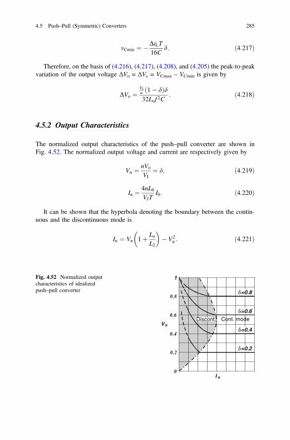
vCmin ¼ �DiLT16C
d: ð4:217Þ
Therefore, on the basis of (4.216), (4.217), (4.208), and (4.205) the peak-to-peakvariation of the output voltage ΔVo = ΔVc = VCmax – VCmin is given by
DVo ¼VI
n ð1� dÞd32Lof 2C
: ð4:218Þ
4.5.2 Output Characteristics
The normalized output characteristics of the push–pull converter are shown inFig. 4.52. The normalized output voltage and current are respectively given by
Vn ¼ nVo
VI
¼ d; ð4:219Þ
In ¼ 4nL0VIT
I0: ð4:220Þ
It can be shown that the hyperbola denoting the boundary between the contin-uous and the discontinuous mode is
In ¼ Vn 1þ LoL2
� �� V2
n : ð4:221Þ
δ=0.8
δ=0.6
δ=0.4
δ=0.2
Vn
nI
Discont. Cont. mode
1Fig. 4.52 Normalized outputcharacteristics of idealizedpush–pull converter
4.5 Push–Pull (Symmetric) Converters 285

To the left of the hyperbola is the discontinuous mode where the output voltageis a function of the load current. In this mode the current through the choke duringone cycle is zero at two subintervals. The discontinuous mode should be avoideddue to the instability of the output voltage. In order to avoid the break of the currentthrough the choke, the minimum load current has to be
Iomin [DiL2
: ð4:222Þ
From (4.221) and (4.208) the continuous operating mode condition is
Lo [ð1� dÞ2fIomin
Vo: ð4:223Þ
The output characteristics are influenced by some realistic parameters not con-sidered in the idealized circuit. These are, first of all, the stray flux of the transformer,the reverse conduction of the diode, and the output resistance of the converter. Forinstance, at the turn-on of the transistor Tr2, the commutation of the current from thediode D1 to the diode D2 is not instantaneous because of the existence of strayinductances whose resistance to the change of the magnetic flux has to be overcome.The same process occurs at the turn-on of Tr1 (t = t3 in Fig. 4.49) when the com-mutation of the current from D2 to D1 takes place. Figure 4.53a shows a simplifiedequivalent circuit immediately after the transistor Tr2 is turned on. The current i2 has
L
D
D
S
V 1
1
2
I
i
ii
i
i
L
21
D1
D2
+
VIn/
I
V VV
V
I
I
t t
t
t
t
i
i
LM
L I0
0
μm
Lm
1 Z
D1
D1
n
1
2
2
L σS-
(1- )T/2δ
δ T/2n -
-
t
t
d1
d1
I LM12
(a)
(b)
Fig. 4.53 Equivalent circuit during commutation of current from D1 to D2 (a) and real variationsof currents iD1 and iD2 (b)
286 4 PWM DC/DC Converters

such a direction that the current through D1 reduces and through D2 increases. Thecommutation is ended when iD1 drops to zero (Fig. 4.53b). Then the circuit is in thestate described in interval II. By assuming that during td1 the variations of the chokecurrent iL = ILm and the magnetization current are negligible, it can be shown that thecommutation time is
tD1 � ILm � nIlm2VI
nLrs; ð4:224Þ
where Los is the total stray inductance of the secondary. The time during which thesecondary voltage is zero and the choke voltage is –Vo, is extended by td1(Fig. 4.53b). The same process occurs immediately upon the switch-on of thetransistor Tr1. Now the commutation time is determined by the time required for thecurrent through D2 to drop to zero.
Practically the interval of energy accumulation by the choke Lo is shortened bytd1. This means that the output voltage decreases. This is obtained from (4.204)when t2 is increased and t2 − t1 = t4 − t3 decreased by td1, i.e.,
1� dð Þ T2þ td1
� �Vo ¼ d
T2� td1
� �VI
n� Vo
� �: ð4:225Þ
From (4.225) it follows
Vo ¼ d 1� 2td1T
� �VI
n: ð4:226Þ
Because td1 is load current dependent, since ILm = f(IO) (4.209), the outputvoltage is also load current dependent even in the continuous mode (Fig. 4.54). Thereduction of the output voltage increases with an increase of the stray inductance. Itis very important to take care that the quality of the transformer is good so that thestray inductance is as small as possible.
Vn
δ=0.8
δ=0.5
δ=0.3
a
a
a
b
b
b
c
c
c
Discont.Cont. mode
In
Fig. 4.54 Normalized outputcharacteristics versus strayinductance: a Los = 0, b Los1, cLos2 (Los1 < Los2)
4.5 Push–Pull (Symmetric) Converters 287

The output characteristics are also affected by the output resistance of the con-verter. With respect to the output terminals a converter can be represented by avoltage source Voo and its internal resistance Ro. Then
Vo ¼ Voo
1þ R1R2
¼ Voo � RoIO; ð4:227Þ
where Ro is the output resistance of the converter and Voo = Vo for Ro = 0.Increasing the load current increases the losses in Ro which reduces the outputvoltage across the load. By combining (4.226) and (4.227) it turns out that theoutput voltage is
Vo ¼ d 1� 2td1T
� �VI
n� RoIO: ð4:228Þ
The final qualitative form of the output characteristics is achieved when the slopedue to the stray inductance, shown in Fig. 4.54, is increased by the correspondingslope due to the output resistance.
4.5.3 Selection of Components
Transistors and diodes. The basic requirements are related to the maximum currentor power, breakdown voltage, and dynamic characteristics (turn-on and turn-offtimes). In general, transistors and diodes with minimal turn-on and turn-off timesshould be selected. The maximum collector–emitter voltage is 2VI, so the break-down voltage of the transistor should be
BVCB0 [ 1:2-1:5ð Þ2VImax; ð4:229Þ
where VImax is the maximum value of the input voltage and (1.2–1.5) is the safetyfactor. The maximum permitted collector current (catalog data) has to be
Icd [ 1:5Icmax ð4:230Þ
where ICmax is the maximum collector current in the circuit and 1.5 is the safetyfactor. ICmax is determined according to the maximum load. Then ΔiL ≪ IO, so itmay be assumed that ILM ≈ ILm ≈ IO, and
ICmax � IOn: ð4:231Þ
The worst case is that the conducting transistor is in saturation, i.e.,
288 4 PWM DC/DC Converters

IB [ICmax
bmin; ð4:232Þ
where βmin is the minimum common emitter current gain of the transistor. Usuallythe minimum saturation factor is (1.2–1.5), so
IB ¼ 1:2� 1:5ð Þ IOnbmin
: ð4:233Þ
In order to keep the base current as low as possible (lower losses in the controlcircuit), a high βmin transistor should be selected. For power transistors it is standardthat βmin is several tens.
The maximum current through the diode is equal to the maximum currentthrough the choke (4.209). Since at maximum load the variation of the currentthrough the choke can be neglected, the maximum permitted diode current has to be
IDd [ 1:2-1:5ð ÞIO: ð4:234Þ
The maximum reverse voltage across the diode occurs during intervals II and IV.Then
VDR ¼ VL þ Vo þ VImax
n: ð4:235Þ
The voltage across the choke VL is given by (4.193), so
VDR ¼ 2VImax
n: ð4:236Þ
If a safety factor of at least 1.3 is taken, the breakdown voltage of the diodes has to be
BVD [ 1:3VDR: ð4:237Þ
Owing to the smallest storage time during the turn-off process, Schottky diodesare recommendable.
Control module frequency. In order to avoid short-circuiting of the transformerduring transients, control of the push–pull converters is carried out in two shiftedphases. This shift in terms of time is a safety pause, often called “dead time”. Thehalf-cycle of the control pulses has to be
T2[ smax þ TDTmin; ð4:238Þ
where TDmin = toff = ts + tf is the minimum dead time and:
4.5 Push–Pull (Symmetric) Converters 289

smax ¼ dmax
T2¼ n
Vo
VImin
T2
ð4:239Þ
is the maximum conduction time of the transistor. From (4.238) and (4.239) oneobtains
T[2TDTmin
1� n Vo
VImin
: ð4:240Þ
Compared to the characteristics of a selected transistor, the minimum cycleshould be approximately ten times longer than the maximum sum of the turn-on andturn-off times. Usually the frequency of the control pulses is several tens of kHz.
Output filter. The value of the capacitor C is determined on the basis of therequired peak-to-peak variation of the output voltage, Vpp, i.e.,
DVo\Vpp: ð4:241Þ
From (4.241) and (4.218) it follows that
C[dð1� dÞ32Lo f 2
VI
nVpp
: ð4:242Þ
On the other hand, the capacitor has to be selected to withstand the rms current:
Iceff ¼ffiffiffiffiffiffiffiffiffiffiffiffiffiffiffiffiffiffiffiffiffiffiffiffi2T
ZT=2
o
i2cðtÞ dts
; ð4:243Þ
where ic(t) is the current through the capacitor determined by (4.212) and (4.214).Upon rearrangement one obtains
Iceff ¼ dð1� dÞ4
ffiffiffi3
pLo f
VI
n: ð4:244Þ
The maximum voltage across the capacitor has to be higher than the maximumpossible output voltage VI/n obtainable for δ = 1. The capacitor should be of thehigh frequency type having as low series resistance as possible.
The inductance of the output choke is usually determined from the condition thatthe variation of the current through the choke should be much smaller than themaximum load current, i.e.,
DiL ¼ dð1� dÞ2Lo fo
VI
n\0:1Io: ð4:245Þ
290 4 PWM DC/DC Converters

Therefore
Lo [ 5dð1� dÞL0f0
VImax
n: ð4:246Þ
When condition (4.242) is fulfilled, further calculation is the same as for a DCchoke. The number of turns is determined by
N ¼ffiffiffiffiffiffiffiffiffiffiffiffiffiffiLolefAef
HB
r; ð4:247Þ
where B and H are the selected magnetic induction and magnetic field, respectively,Aef is the effective cross section of the core, and Ief is the average length of themagnetic line. The air gap is approximately determined by
Iv ¼ l0N2Aef
Lo; ð4:248Þ
where μo = 4 × 10⁻⁷ [H/m] is the magnetic permeability of vacuum.The cross section of the copper wire is determined by
Scu ¼AwFw
N¼ d2p
4; ð4:249Þ
where Aw is the core opening area, Fw is the filling factor (catalog data for theselected core).
In order that the converter operates in the continuous mode, the output is loadedby a zero (intrinsic) load. The resistance of this load is determined from (4.223)when IOmin = Vo/RLmax
RLmax\2fLo1� d
: ð4:250Þ
Transformer. The transformer is of the high frequency type. Typical operatingfrequencies are from several tens of kHz to 100 kHz. The basic requirements asregards the selection of the core are low losses, small dimensions, and the ability oftransferring the maximum power. With the geometric characteristics Aw, Aef, andFw of the selected core, the maximum power that can be transferred to the load isdetermined by
Pomax �ffiffiffi2
pfJBAwAfeFw; ð4:251Þ
4.5 Push–Pull (Symmetric) Converters 291
where J is the current density in the conductor. The flux change in the primarywinding is proportional to the input voltage. Namely
VI ¼ Np
2dUdt
¼ NI
22BAef
dT=2: ð4:252Þ
The number of turns of the primary (assuming the worst case VImax, δmax = 1) is
N1
2¼ VImax
4AefBf: ð4:253Þ
The number of turns of the secondary is
N2
2¼ N1=2
n: ð4:254Þ
The transformation ratio, n, depends on the ratio of the input and the outputvoltage (4.205). As high as possible n is recommended in order to keep the tran-sistor current low. However, according to (4.179), there is a limit because of thelimitation on δ. Usually 0.2 ≤ δ ≤ 0.9. The filling factor δ, within permitted limits,varies with the variation of the input voltage VImin ≤ VI < VImax. If the average valueof δ is used, i.e.,
ds ¼ dmin þ dmax
2
one obtains
n ¼ 2dsVImax
Vo
11þ VImax=VImin
: ð4:255Þ
The cross section of the conductor is determined by
Scu ¼Irms
J; ð4:256Þ
where Irms is the rms value of the current through the conductor. In the primarywinding this current is equal to the rms value of the transistor current, i.e.,
Irmsp ¼ Irmst ¼ffiffiffiffiffiffiffiffiffiffiffiffiffiffiffiffiffiffiffiffiffi1T
ZT
0
i2cðtÞ dts
; ð4:257Þ
where ic is the collector current of one transistor. In the worst case, when the loadcurrent is maximum, the variations of the current through the choke are negligible.
292 4 PWM DC/DC Converters

Then, during τ = δΤ/2, while the transistor is on, the collector current is approxi-mately constant ic ≈ Iomax/n. Therefore
Irmsp ¼ffiffiffiffiffiffiffiffiffiffiffiffiffiffiffiffiffiffiffiffiffiffiffiffiffiffiffiffi1T
ZdT=2
0
I2omax
n2dt
s¼ Iomax
n
ffiffiffid2
r: ð4:258Þ
In (4.258) it should be assumed that δ = δmax. On the basis of (4.257) and (4.258)the diameter of the primary conductor is calculated as
dp ¼ 2
ffiffiffiffiffiffiffiffiffiffiffiffiffiffiffiffiffiffiffiffiffiffiffiffiffiIOmax
nJp
ffiffiffiffiffiffiffiffiffidmax
2
rs: ð4:259Þ
The rms value of the secondary current is equal to the rms value of the currentthrough the diode. By assuming, like in the case of the transistor, that the load currentis maximum, the variation of the current through the diode is shown in Fig. 4.55.
From Irmss ¼ IrmsD ¼ffiffiffiffiffiffiffiffiffiffiffiffiffiffiffi1T
RT0i2D dt
rand Fig. 4.55 one obtains that
Irmss ¼ffiffiffiffiffiffiffiffiffiffiffi1þ d
p
2IOmax: ð4:260Þ
Therefore
ds ¼ 2
ffiffiffiffiffiffiffiffiffiffiffiffiffiffiffiffiffiffiffiffiffiffiffiffiffiffiffiffiffiffiffiffiffiffiffiffiffiffiffiffiffiffiffiffiffiffiffiffiffi1þ dmax
p2pJ
IOmax
s: ð4:261Þ
While winding up the transformer care should be taken that the stray magneticflux remains as low as possible. For this reason the height of the winding should beas small as possible, and the width of the winding as large as possible. The distancebetween one pair of half-windings primary–secondary has to be as small as pos-sible. Since in one half-cycle the current flows through the half-windings I and IIIand in the other half-cycle through the half-windings II and IV, the manner ofarranging the windings is shown in Fig. 4.56.
i
II
D1
0max
0max
(1- )T/2 δ T/2
12
tTT2
δ
Fig. 4.55 Variation of the current through the diode D1 at maximum load current when DiL ≪ Io
4.5 Push–Pull (Symmetric) Converters 293

The inductances of the primary winding, L1, and of the secondary winding, L2,are expressed by
LI ¼ lolaNp
2
� �2 1Cj
; L2 ¼ LIn2
; ð4:262Þ
where μo is the relative permeability of the core and Cc [1/mm] is constant of thetransformer core.
Example 4.8 The push–pull converter shown in Fig. 4.47 has VI = 24 V, n = N1/N2 = 1.5, D = 0.2, L0 = 100 μH, RL = 5 Ω, C = 1 mF and f = 25 kHz (semiconductorcomponents can be consider ideal). The magnetization inductance of the trans-former Lm is equal to 1 mH.
(a) Determine the output voltageVo versus duty ratio D in continuous workingmode.(b) Determine the minimum and maximum current of the inductor L0.(c) Determine currents at the transistor.(d) Draw waveforms of voltages and currents at the transistor and the diode for
continuous working mode.
(a) The output voltage Vo can be calculated from the Eq. (4.205)Vo ¼ 2VID
n ¼ 6:4V:(b) The average current of the inductor L is equal to
IO ¼ VO
RL¼ iL ¼ IL1þIL0
2 ¼ 1:28A:The maximum and the minimum current ofthe inductor L can be calculated from (4.209) (Fig. 4.57)
ILM ¼ IO þ DiL2
¼ IO þVI
n � Vo
L0dT2¼ 2:05A,
ILM ¼ IO � DiL2
¼ IO �VI
n � Vo
L0dT2¼ 0:51A:
(c)It1 ¼ ILM
nþ Im ¼ 1:26A;
It0 ¼ ILmn
� Im ¼ 0:41A; 2Im ¼ VIDTSLm
¼ 0:192A:
(d) See Fig. 4.57.
N
N
N
N
1
1
2
2
2
2
2
2
I
II
III
IV
1 5
2 63
4 8
7
IV
II
III
I
Fig. 4.56 The manner of winding up the transformer
294 4 PWM DC/DC Converters

iI
It0
IIn
0 tDT T /2 T /2 + DT T
i
I
0 t
iI
I I2
0 t
I
2
i
2
0 t
2
v 2V
0 t
V
v
0 t
In
I
t1
t1
LMLm
m
s s s s s
t2
m
LM
Lm
d1
R1L0
L 0
ILM
ILMILm
ILm
id2
t1
t2
I
I
VI
2VI
InLm
InLM
Fig. 4.57 Waveforms ofvoltages and currents attransistor and diode for theconverter from Fig. 4.47
4.5 Push–Pull (Symmetric) Converters 295

4.5.4 DC Premagnetization of the Core
DC premagnetization or asymmetric magnetization of the core is introducedbecause of:
• unequal voltage drops on the conducting transistors,• unequal conduction times of the transistors caused by the difference in the
dynamic characteristics (times ts and tf) or by asymmetry of the base drivingcircuits, and
• imperfect manufacture of the transformer or unequal number of turns of some ofthe windings.
The third cause can be avoided by careful manufacturing procedure, but not thefirst two. Namely, the discrepancies in characteristics (parameter spread) from onetransistor to another are inevitable and can be quite noticeable. Besides, thesediscrepancies are random and they are a consequence of the nature of the tech-nological process itself so they can not be exactly calculated in advance. A con-sequence of the quoted phenomena is different length of pulses in the transformerprimary (Fig. 4.58). This leads to the appearance of a DC component Vav whichcauses a DC premagnetization current to flow through the primary winding.
Iav ¼ Vav
rp: ð4:263Þ
Owing to the small Ohmic resistance rp of the primary, this current may besignificant. This causes a shift of the operating point along the HB magnetizationcurve which may, followed by the same change of the magnetic flux, lead to thesaturation of the core at one side (Fig. 4.56). When the core goes into saturation, theinductance of the transformer drops, and the currents of the primary and the tran-sistor increase sharply. The appearance of large instantaneous values of transistorcurrents, unless a protection is provided, may lead to transistor destruction.
V
V
P
srV -VI CE1
V >VCE CE2
V -VI CE2-( (
t
11 2
2
>
B B
B
H HH
sr
sr
(a)
(b)
Fig. 4.58 Creation of the DCcomponent of the primary(a) and the magnetizationcurves for symmetric (b) andasymmetric magnetization ofthe core (c)
296 4 PWM DC/DC Converters

The problem of the core saturation can be resolved by a drastic reduction of themaximum permitted induction in the transformer core or by an air gap in the core.This, however, reduces considerably the efficiency of the transformer, since only asmall part of the hysteresis loop is used. By doing so one also loses the basicfavorable feature of the push–pull converters compared to other types.
In principle, the asymmetry problem can be eliminated by the permanent controlof the integral transformer voltage and correction of the times of transistor con-duction. However, such solutions are very complex. In practice the problem ofincreasing transistor current due to asymmetry is quite successfully solved byinsertion of capacitors in series with the transformer.
4.5.5 Half-Bridge Converter
The common point, M, of the half-bridge converter (Fig. 4.59) is between thecapacitors C1 = C2 at a potential VI/2. For this reason the transformer voltage variesbetween –VI/2 and VI/2 and the maximum collector–emitter voltage of the transistoris VCEmax = VI. Therefore, compared to the basic push–pull converter circuit thevoltage load is halved.
The capacitor C3 in series with the transformer primary eliminates the flow ofDC current through the transformer. Owing to the alternate conduction of thetransistors Tr1 and Tr2 the capacitor C3 will pass alternately positive and negativepulses of amplitude VI/2. Thus a low series resistance, nonpolarized capacitor has tobe used. Several capacitors connected in parallel are often used.
When the conduction times of the transistors are equal, the DC voltage across C3
is zero. If these times are different, a DC voltage will appear across this capacitorwhich will compensate the DC component in the transformer primary and thusminimize the chance for the transformer core saturation.
D D1 2 L
V
T
T
V
R
0
0
r2
r1
DC
L
+
C
C
C
C
2
1
3
0
+
TM
Fig. 4.59 Half-bridgepush–pull converter
4.5 Push–Pull (Symmetric) Converters 297

The approximate value of C3 is chosen by applying the condition that theresonant frequency of the series resonant primary circuit is several times lower thanthe operating frequency of the converter, i.e.,
fr ¼ 12p
ffiffiffiffiffiffiffiffiLrC
p � 0:15-0:4ð Þ 1T; ð4:264Þ
where C is the total capacitance of the primary and Lr = n2Lo is the outputinductance referred to the primary. The half-bridge converter is used when theprimary source is AC voltage 110 and 220 V (Fig. 4.60).
The relaxation of the voltage load of the transistors is then very significant. Thediodes D5 and D6 keep the reverse collector–emitter voltages of the transistors.
In fact, their purpose is twofold:
• They protect transistors against reverse conduction and possible destruction.Namely, if the load is cut off abruptly, the flux in the transformer increases. Thiscauses oscillations which may induce reverse emitter–collector bias (collector ata lower potential). Then either D5 or D6 turns on and keeps the collector–emittervoltage at VCE = VD.
• When the corresponding transistor turns off, they direct the energy of the strayinductance back to the DC source.
4.5.6 Bridge Converter
The difference compared to the half-bridge converter is that the capacitors C1 andC2 are replaced by the transistors Tr1 and Tr2 (Fig. 4.61). The transistor pairs in thearms of the bridge (Tr1 with Tr3 and Tr2 with Tr4) are on and off alternately,
D
D
D
D
D
D
D
D
8
7
5
2
4
1
3
6
LT
T
0r1
r2
C
C
C
1
2
3 V0C110V∼
220V∼
Fig. 4.60 Half-bridge converter having AC input 110 and 220 V
298 4 PWM DC/DC Converters

connecting the transformer primary alternately to one or to the other side of theinput. The primary voltage is thus +VI or –VI. In one arm of the bridge when one ofthe transistors is on, the other is off (e.g., when Tr1 is on, Tr2 is off and vice versa) so
VCEmax ¼ VI: ð4:265Þ
Therefore, the voltage load is halved and the current load is the same as that ofthe basic push–pull converter.
Both half-bridge and bridge converters have simpler transformers compared tothose of the basic push–pull converter. This can be further simplified if only oneprimary and one secondary are used (Fig. 4.62). Then a diode rectifier bridge(diodes D1–D4) is used in the secondary circuit. The pulse waveforms of thecharacteristic voltages and currents are shown in Fig. 4.62b.
When the transistor pair Tr1 and Tr3 is on, the core of the transformer is mag-netized in one direction, whereas when the pair Tr2 and Tr4 is on, it is magnetized inthe other direction of the magnetization curve. This creates a variation of themagnetic flux in the core. The AC rectangular voltage induced in the secondary isrectified by the diode bridge. The rectified voltage is Vr = VI/n and the variation ofthe current through the choke in this interval is
DiL1 ¼ VI=n� Vo
LodT2: ð4:266Þ
When none of the transistor pairs is on, the circuit of the magnetization currentcloses through the diode bridge. The transformer is short-circuited. The magneticflux is the same as when the transistors went off. Within this interval the energy
D
D L0
C1V0C
D
D
3
4
T
T
r3
r4
D
D
1
2
T
T
r1
r2
V
+
I
Fig. 4.61 Bridge circuit of the push–pull converter
4.5 Push–Pull (Symmetric) Converters 299

accumulated in the output choke is transferred to the load through the diode bridge.The rectified voltage is then Vr = 0. The current through the output choke decreasesand its variation in this interval is
DiL2 ¼Vo
LI1� dð Þ T
2: ð4:267Þ
By equating (4.266) and (4.267) one obtains:
Vo ¼ dVI
n: ð4:268Þ
The influence of the realistic parameters is similar to the one identified for thebasic push–pull converter. Here the emphasis should be placed on the phenomenaarising during the turn-on and the turn-off processes. During the turn-on current
V
V
V
V
V
V R0
L
L
CE1
CE2
r LVI C
+
+ -
T
DD
DD
N N
21
34
1 2
TT
TT
r3r4
r2r1
L I
i
i
i
i
0
L
P
1
1
I
I
I
i
i
i
i
0
0
0
1
1
L
P
V
V
V
V
V VV
CE1
CE2
P
P
L C
C
V
V
VV
V
V
V
V /2
V /2
I
I
I
I
I
L2
L1
I
I
T T
T/2
δT/2 DT
δT/2 DT
t t
t
t
t
t
t
t
t t
ΔI
ΔI
ΔI L
Δ
(a)
(b)
Fig. 4.62 Bridge circuit including diode bridge rectifier (a) and the characteristic pulse waveforms (b)
300 4 PWM DC/DC Converters
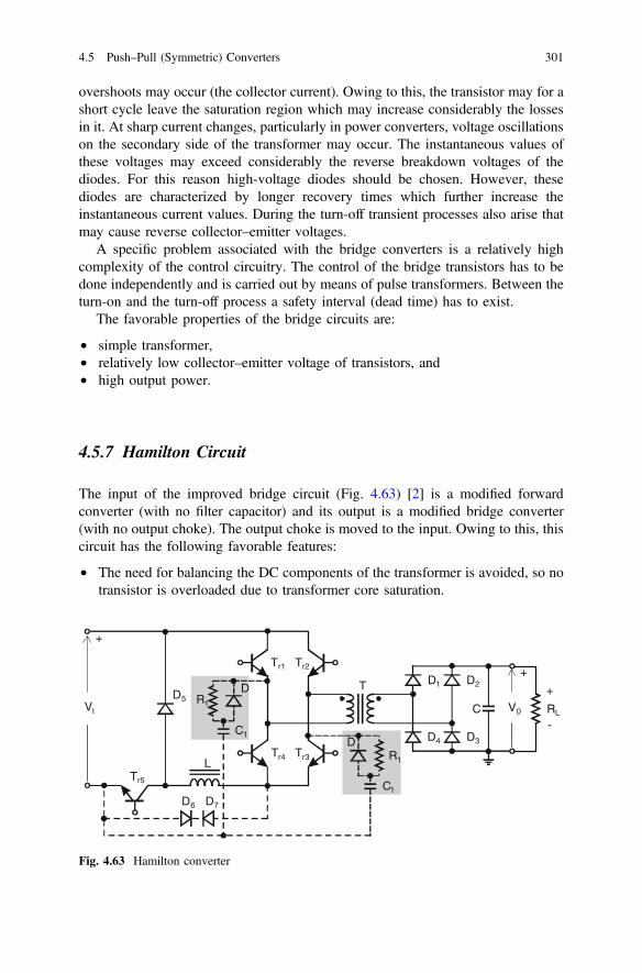
overshoots may occur (the collector current). Owing to this, the transistor may for ashort cycle leave the saturation region which may increase considerably the lossesin it. At sharp current changes, particularly in power converters, voltage oscillationson the secondary side of the transformer may occur. The instantaneous values ofthese voltages may exceed considerably the reverse breakdown voltages of thediodes. For this reason high-voltage diodes should be chosen. However, thesediodes are characterized by longer recovery times which further increase theinstantaneous current values. During the turn-off transient processes also arise thatmay cause reverse collector–emitter voltages.
A specific problem associated with the bridge converters is a relatively highcomplexity of the control circuitry. The control of the bridge transistors has to bedone independently and is carried out by means of pulse transformers. Between theturn-on and the turn-off process a safety interval (dead time) has to exist.
The favorable properties of the bridge circuits are:
• simple transformer,• relatively low collector–emitter voltage of transistors, and• high output power.
4.5.7 Hamilton Circuit
The input of the improved bridge circuit (Fig. 4.63) [2] is a modified forwardconverter (with no filter capacitor) and its output is a modified bridge converter(with no output choke). The output choke is moved to the input. Owing to this, thiscircuit has the following favorable features:
• The need for balancing the DC components of the transformer is avoided, so notransistor is overloaded due to transformer core saturation.
DD
DDD
DD
DD
V R
R
R
C
C
0 L
1
1
1
1
VI C
+
+
-
T 21
34
5
76
TT
T
T
T
4r 3r
r2
r5
r1
L
+
Fig. 4.63 Hamilton converter
4.5 Push–Pull (Symmetric) Converters 301

• The limiting diodes (D6 and D7—dotted lines in Fig. 4.63) very efficientlysuppress output voltage transients that may arise due to sharp changes of theload and/or due to a sharp turn-on of the converter at a very high duty cycle.
Except for moving the choke from the output to the input, this circuit includesanother two significant changes. The transistor Tr5 and the diode D5 have anadditional control function. The transistors Tr1–Tr4 in the bridge operate with a fixedduty cycle of 50 %. Consequently, the control of the output voltage is carried out bythe transistor Tr5. This simplifies considerably the control circuit which is quitecomplex for the basic bridge circuit.
With the R–C–D network (dashed line in Fig. 4.63) the total reduction of thedynamic losses in the transistors is one order of magnitude higher compared to thebasic bridge circuit. The selection of C and R in accordance with the followingequations is recommended
C ¼ ILtfVI þ VD
; ð4:269Þ
R ¼ 16fC
; ð4:270Þ
where IL is the maximum current through the choke, tf is the falloff time of collectorcurrent and VD is the voltage across the limiting diodes D5 and D6. By introducing acurrent monitor in the circuit of the input choke it is possible, by means of a fastcircuit and overcurrent protection, to keep efficiently the currents of all semicon-ductor elements below selected values.
Various authors emphasize that from the analysis of the idealized circuit onecannot identify a need for Tr5. The additional transistor Tr5, the diode D5, and thechoke which is moved from the output to the input can well be justified if one looksat the phenomena arising in real circuits (circuits involving real parameters).
4.6 Ćuk Converters
By synthesizing the basic circuits of the forward and flyback converters Dr. SlobodanĆuk has obtained several topologies of DC/DC converters which have been calledĆukconverters. A common property of these converters, making them different from othertypes, is that beside the electromagnetic, they also have the electrostatic energytransfer. In addition, Ćuk converters include a system of the coupled input–outputcoils which theoretically permits a complete elimination of current variations at theinput and the output of the converter. This is very important from the point of view ofelimination of the pulse noise inherent to all pulse DC/DC converters.
The basic circuit of a Ćuk converter (Fig. 4.64), similarly to a flyback converter,behaves like an inverter (the input and the output voltage are of the opposite
302 4 PWM DC/DC Converters

polarities), where the absolute value of the output voltage may be lower, higher orequal to the input voltage. To show this an idealized converter circuit will beconsidered (the transistor and the diode are ideal switches, output voltage andcurrent are constant, power losses in the circuit are negligible).
When the transistor Tr is in saturation, the diode is off (Fig. 4.65a). The voltageacross the input choke L1 is constant and
iLI ¼ IL1m þ VI
LIt: ð4:271Þ
LL
L2L1
D
V
R
0
LVI C
C
+
++ -
-
-
M
21
i
i
i
ii
C2
C1
0
2
1
Fig. 4.64 Basic circuit of Ćuk converter
LL
L
L1 L1M
L1m
L
V
V
R
C1
0
L
C
V
V V
C C2
C1C2+
+
+
-
-
-
-
-
21
2
1
ii
I
i
i
i
i I
I
i
C21
I
C1
0
2
d
DS α
1V
V V
LL
L
L
V
R
0
LVI
C
V
C
C1
C2+
+
++-
-
--
-
21
2
1
i
i
i
i
i
C2
C1
0
2
d
1
V
V
t
t
t t1 20
0
DT
DT
T
T
ΔI
L2
L2
L2M
L2m
i
I
I
I
t
t
0DT
DT
T
T
ΔI
ΔV
2
2
C2
C2
i
i
t
t
0
0
1
VI
+
-
(a)
(b)
(c)
Fig. 4.65 Equivalent circuits during quasi-stable intervals t1 (a), t2 (b), and the characteristicwaveforms of the voltages and currents (c)
4.6 Ćuk Converters 303

Within this interval the energy accumulated in C1 is transferred to the choke andto the load. If the variation of the voltage across C1 is neglected and taking intoaccount the assumption that the output voltage is constant, the voltage across L2 isalso constant. Therefore
iL2 ¼ IL2m � VC1 � Vo
L2t: ð4:272Þ
During the quasi-stable interval t2 = (1 − D)T the transistor is off and the diode ison (Fig. 4.65b). Now the currents through the chokes L1 and L2 decrease linearlyand are determined by
iL1 ¼ IL1M � VC1 � VI
L1t; ð4:273Þ
iL2 ¼ IL2M � Vo
L2t: ð4:274Þ
The positive and negative changes of these currents are equal (Fig. 4.56c), i.e.,
VI
L1DT ¼ VC1 � VI
L11� Dð ÞT; ð4:275Þ
VC1 � Vo
L2DT ¼ Vo
L21� Dð ÞT: ð4:276Þ
From (4.275) it follows that
VC1 ¼ VI
1� D; ð4:277Þ
and from (4.276) and (4.277)
Vo ¼ D1� D
VI: ð4:278Þ
The variations ΔI1 and ΔI2 of the respective currents iL1 and iL2 are determined by
DII ¼ DVI
fLI; ð4:279Þ
DI2 ¼ DVI
fL2; ð4:280Þ
where f = 1/T is the frequency of the control pulses. If L1 = L2 then ΔI1 = ΔI2. Thevoltages across the chokes are equal in both quasi-stable states. During the interval t1
304 4 PWM DC/DC Converters

VL1 ¼ VI; VL2 ¼ VC1 � Vo ¼ VI; ð4:281Þ
and during the interval t2
VL1 ¼ VC1 � VI ¼ D1� D
VI ¼ Vo; VL2 ¼ Vo: ð4:282Þ
While the transistor is off, the capacitor C1 is charged by the input current. If theaverage value of this current is I1, then peak-to-peak variation of the voltage acrossC1 is approximately given by
DvC1 � 1CI
Zt20
II dt ¼ IIð1� DÞC1f
: ð4:283Þ
If the losses in the circuit are neglected, then VIII = VoIO and
II ¼ D1� D
IO; ð4:284Þ
where IO is the load current.The characteristic voltage and current waveforms are shown in Fig. 4.65c.
Example 4.9 The Ćuk converter shown in Fig. 4.64 has VI = 12 V and D = 0.6.Determine the output voltage Vo.
As the average value of voltage at each inductance equal to 0, it can be writtenthat
vL1 ¼ 0 : VIDTS ¼ VC1 � VIð Þ 1� Dð ÞTS ) VC1 ¼ VI
1� D;
vL2 ¼ 0 : VC1 � Voð ÞDTS ¼ Vo 1� Dð ÞTS ) Vo ¼ DVC
) Vo ¼ D1� D
VI ¼ 18V:
4.6.1 Elimination of the Current Ripple
The main favorable property of Ćuk converters is the existence of the possibility toeliminate the ripple from the input and/or the output current. This is accomplishedby coupling both coils with a common core (Fig. 4.66).
This is possible since the variations of the voltages across these coils are equal.By a suitable choice of the coupling coefficient it is possible to eliminate completelythe ripple of the currents. Figure 4.66a shows an example of a Ćuk converter havingcoupled coils for the purpose of elimination of the output current ripple.
4.6 Ćuk Converters 305

The relations valid for the circuit will remain unchanged if the capacitor C1 issplit in two series capacitors C1A and C1B, so that the total capacitance is C1 and if athird choke is added (Fig. 4.64b) under the condition that L3 ≫ L1 and L3 ≫ L2.Since the impedance of the third choke is much higher, its influence on the basicrelations within the circuit is negligible. This, however, allows the elimination ofthe ripple of the input and output currents by coupling L3 with L1 and L2. All threecoils are wound on a common core.
4.6.2 Ćuk Converters with Galvanic Isolation
If the third coil, L3, is replaced by an isolation transformer one obtains a Ćukconverter with galvanic isolation (Fig. 4.67). By coupling the transformer with thecoils L1 and L2 (Fig. 4.67b) it is possible to eliminate completely the ripple of boththe input and the output current.
The transformer and the input and output coils are wound on the same core. It isdifficult to achieve such coupling that the current ripple is eliminated entirely. Forthis reason in practice tuning coils of small inductance on the primary or/andsecondary side are used.
L
L
L
D
D
V
V
R
R
0
0
L
L
VI C
C
C
CC
+
+
-
-
+
++
-
--
-
-
M
2
2
1 i
i
i
i
i
i
i
2
2
1
1
1
2
2
2
2
1
1B1AL
L
VI M
1
3
i1
t
t
t
t
(a)
(b)
Fig. 4.66 Ćuk converters comprising coupled coils for elimination of the ripple: (a) of the outputcurrent, (b) of the input and output currents
306 4 PWM DC/DC Converters

It should be emphasized that, with the assumption that the transformer is ideal,the relations between voltages and currents in the circuit remain the same as in thenonisolated circuits. The difference is that the circuits in Fig. 4.65 have positiveoutput voltages and that the transistor and diode are loaded more, since they alsoconduct the current with regard to the input or output.
Thanks to the capacitors CA and CB there is no DC component in the transformerwindings. This allows a full exploitation of the core which, compared to flybackconverters, considerably reduces the size of the transformer.
Problems
4:1 Design a buck converter (Fig. 4.3) if VI = 48 V, Vo = 18 V, RL = 10 Ω so thevariation of the output voltage is less than 0.5 %. The converter should operatein the continuous mode.
4:2 For the buck converter from Fig. 4.3, which has all components ideal (a)derive expressions for the Vo/VI in continuous mode, and (b) calculate anddraw the waveforms of voltages and currents at the transistor and the diodeduring one period of the control signal.
4:3 The forward converter from Fig. 4.20a has: VI = 36 V, Lo = 0.5 mH, R = 10 Ω,C = 150 mF, N1/N2 = 2, N1/N3 = 1, f = 50 kHz and D = 0.3. All the usedcomponents are ideal.
L
L
D
D
V
V
R
R
0
0
L
L
C
C
C
C
+
+
-
-
+
+
-
-
-
-
2
2
i
i
i
i
2
2
2
2
2
2
1B
1B
t
t
C
C
+
+
-
-
i
i
1
1
1A
1A
L
L
V
V
I
I
M
M
1
1
i
i
1
1
t
t
(a)
(b)
Fig. 4.67 Ćuk converters comprising galvanic isolation and current ripple elimination: (a) of theoutput current and (b) of both input and output currents
4.6 Ćuk Converters 307

(a) Determine the output voltage Vo and the minimum and the maximumcurrent in the inductor Lo.
(b) Determine the output voltage ripple ΔVo.(c) Draw the waveforms of voltages and currents at the transistor and the
inductor Lo.
4:4 The boost converter (Fig. 4.24) is characterized by the following parameters:VI = 20 V, L = 100 μH, C = 100 μF, f = 15 kHz, D = 0.6, and RL = 50 Ω. Thetasks are
(a) show that the current through the inductor is discontinuous and determinethe output voltage,
(b) determine the maximum current through the inductor, and(c) determine the idle resistance so that at RL = 50 Ω the converter operates
at the boundary between the continuous and the discontinuous mode.
4:5 The flyback converter shown in Fig. 4.41 has VI = 48 V, N1/N2 = 2, D = 0.4,f = 25 kHz and RL = 10 Ω
(a) Determine the output voltage Vo.(b) Determine the transformer magnetizing inductance, such that the mini-
mum inductor current is 40 % of the average.
4:6 The flyback converter shown in Fig. 4.68 has the following parameters:VS = 50 V, D = 0.385, f = 40 kHz, Lm = 500 μH, C = 200 μF, N1/N2 = 3 andR = 5 Ω. Calculate and draw the waveforms of the following variables: vo, ip,iD and iC.
4:7 The push–pull converter from Fig. 4.47 has VS = 48 V, N1/N2 = 2,Lo = 0.5 mH, C = 200 μF, RL = 10 Ω, D = 0.3 and f = 25 kHz
(a) Determine the output voltage Vo and its ripple.(b) Determine the average, minimum and maximum current in the inductor Lo.(c) Draw the currents of the inductance Lo and the diodes D1 and D2.
tv
C LR
+
Ov
OID
IV
1:n
tiT
+SDT
ST
pI
dv
+
di+
SvSL+
pv
Fig. 4.68 Indirect flyback converter with galvanic isolation
308 4 PWM DC/DC Converters

4:8 The push–pull from Fig. 4.47 has the following parameters: VS = 48 V,D = 0.4, f = 35 kHz, L = 400 μH, C = 100 μF, N1/N2 = 1.5, N1/N3 = 1 andR = 10 Ω. Calculate and draw the waveforms of the following variables: vo, iL,it1 and iD1.
4:9 The Ćuk converter from Fig. 4.64 has the following parameters: VI = 18 V,L1 = L2 = 1 mH, C1 = C2 = 20 μF, D = 0.6, R = 10 Ω and f = 20 kHz.
(a) Determine the output voltage.(b) Determine average, minimum and maximum current in L1 and L2.
References
1. Rashid, M.H.: Power Electronics, Prentice-Hall International, Inc. (1993)2. Calkin, E.T., Hamilton, B.H.: A conceptually new approach for regulated DC to DC converters
employing transistor switchers and pulsewidth control. IEEE Trans. Ind. Appl. IA-12(4),369–377 (1976)
4.6 Ćuk Converters 309


Chapter 5Control Modules
The control modules (CM) of the pulse voltage stabilizers close the automaticcontrol loop between the input (pulse amplifier and power transistor) and the output(output LC filter) of the stabilizer, which maintains the load voltage constant withina pre-assigned accuracy. Control is accomplished by converting the error signal intoa pulse sequence, which drives a pulse amplifier.
There are several different structures of control modules. In principle, however,they can all be divided into two groups. The first group consists of the CM having arelay transfer characteristic. Depending on the value of the input signal, the outputstage of the control module is either on or off. Stabilizers having this type of CM arecalled relay or two-state stabilizers. This group is classified into the pulse DC/DCconverters with linear microelectronic stabilizers. The second group consists ofcontrol modules generating sequences of pulses of variable duty cycles. The dutycycle is error signal dependent with the frequency remaining constant—pulse-widthmodulation (PWM), or the frequency is variable with the pulse width remainingconstant—frequency pulse modulation (FPM) (in some cases both types of mod-ulation proceed simultaneously).
In a relay voltage stabilizer, the output voltage is compared with a stable voltagereference. The comparison is continuous and the state at the output of the controlmodule changes when the error signal (the difference between the output and thereference voltage) reaches a level equal to the value of the voltage hysteresis of theCM relay characteristic. In a pulse-width modulation stabilizer, the error signalchanges the state of the CM at discrete time intervals. Thus, it could be said that thedynamic properties of the relay stabilizers are superior to those of the pulse-widthmodulation stabilizers. However, the advantage of the relay stabilizers as regardsthe continuity of the comparison does not show because the dynamic characteristicsof all pulse stabilizers are mostly determined by the characteristics of the output LCfilter. On the other hand, the relay stabilizers suffer from a number of shortcomings.First of all, the frequency of control pulses is dependent on the load current and theinput voltage variations. This leads to considerably more rigorous requirements forthe output filter design. Also, the variable component of the output voltage containssignificantly more harmonics that are often undesirable. This also applies to theFPM stabilizers. The operating frequency of the pulse-width modulation stabilizers
© Springer International Publishing Switzerland 2015B.L. Dokić and B. Blanuša, Power Electronics,DOI 10.1007/978-3-319-09402-1_5
311

is either constant or its variations are very small. This is exactly the reason that inpractice a CM based on pulse-width modulation is more commonly employed.
The control modules involving current programming where the ratio signal/pause is determined by the time required that the current through the switch reachesa certain value (current threshold) are becoming increasingly interesting. The cur-rent threshold is determined by the control signal of the control module. The CMinvolving current programming is characterized by a precisely defined currentthrough the switch, an overload protection, an even distribution of the load whenoperating in parallel and superior control dynamics. Two techniques of currentprogramming are in use: constant frequency and constant pause but variablefrequency.
Control modules employing constant frequency and a variable duty cycle aremost widespread today. These are, therefore, circuits based on the pulse-widthmodulation (PWM). These circuits will be analyzed in this chapter.
5.1 Basic Principles and Characteristics of PWM ControlModules
The basic block-scheme of a pulse-width modulator (PWM), shown in Fig. 5.1,consists of two comparators A and B (B involves hysteresis—Schmitt trigger), twocurrent generators, an electronic switch Sw, and a timing capacitor C. The currentgenerator switch Sw, the capacitor C, and the comparator B constitute a generator oftriangular voltage. The triangular voltage form V2 (Fig. 5.1b) is generated throughthe process of charging and discharging of the capacitor C by the constant currentsI1 and I2. Namely, if the output of the comparator B is at a low voltage level, theswitch Sw is in position (5.1). Then, the capacitor is charged by the current I1 andthe voltage V2 grows:
AOutput
I I1 2
P
V
VV
2
1
DD
Cr
+
1 2
VVV
V
V
V
V V V
TH
20
TL
2
B
A
1 1 2
t
t
t
2VM
T
(a)
(b)
S.T.
Fig. 5.1 Basic block-scheme of a PWM (a) and the voltage waveforms (b)
312 5 Control Modules

V2ðtÞ ¼ VTL þ 1CI1t:
When the voltage level is high at the output of comparator B, the generator ofcurrent I2 is on and the voltage V2 is
V2ðtÞ ¼ VTH � 1CI2t:
VTH and VTL are the respective high and low threshold voltages of the Schmitttrigger (ST). The state of its output changes at the instant when V2 equals VTH orVTL, and the cycle of generator oscillation is
T ¼ C1I1þ 1I2
� �VH ; ð5:1Þ
where VH is the width of the voltage hysteresis of ST. The amplitude VM and theDC component V20 of the triangular voltage are defined by
VM ¼ VH
2; V20 ¼ VTH þ VTL
2: ð5:2Þ
DC component V20 coincides with the center of the hysteresis of the ST, i.e.,V20 = Vch.
Pulse-width modulation is accomplished by feeding the triangular voltage V2 anda fraction of the output voltage to the inputs 1 and 2 of the comparator A
V1 ¼ k0V0; ð5:3Þ
where 0 < k0 < 1. If V1 > V2, at the output of the comparator A there will be a lowvoltage level, but if V1 < V2, the output will be at high a voltage level (Fig. 5.1).Obviously, by varying the voltage V1, the time intervals of the signal and the pauseat the output of the comparator A will vary. The frequency will be constant andequal to the frequency of the triangular voltage. By using the time diagrams of thevoltages V1 and V2 (Fig. 5.1), it can be shown that the time interval of the signalwithin one cycle T, neglecting the variation of V1, is determined by
s ¼ V20 þ VM � V1
2VMT ¼ VTH � V1
VHT : ð5:4Þ
The static characteristic of PWM is the dependence of the duty cycle D of thecontrol pulses on the variation of the output voltage of the stabilizer (Fig. 5.2).PWM is realized in the linear region of the static characteristic. For V1 < V20 – VM,
D = 1 and for V1 > V20 + VM, D = 0, the system of automatic control is interruptedand the control transistor of the DC/DC converter will remain in either the on or theoff state.
5.1 Basic Principles and Characteristics of PWM Control Modules 313

5.1.1 Circuit Analysis
The instability of the output voltage of the stabilizer as a function of the circuitparameters will be analyzed first. To keep the output voltage unchanged within thepre-assigned limit ΔV0 when the input voltage varies by ΔVI, it is necessary that theduty cycle is changed by ΔD. With (4.11) in view
DD ¼ V0 þ DV0
VI þ DVI� V0
VI; ð5:5Þ
where VI and V0 are the nominal values of the input and the output voltage,respectively. On the other hand, a change of V0 will cause a change of VI
DV1 ¼ k0DV0: ð5:6Þ
The change of the duty cycle is proportional to the change of the input voltage VI
and the slope of the static characteristic of the control module, i.e.
DD ¼ dDdV1
DV1: ð5:7Þ
By differentiating (5.4) over VI and introducing (5.7), one obtains
DD ¼ � k02VM
DV0: ð5:8Þ
By equating (5.5) and (5.8), taking into account that always V0 ≫ ΔV0, theinstability of the output voltage is obtained as
do ¼ DV0
V0¼ 2VMdI
k0VI 1þ dIð Þ ; ð5:9Þ
where δI = ΔVI/VI is the instability of the input voltage. The coefficient of voltagestabilization is defined as
VV
V V
120
M M
0.5
1
DFig. 5.2 Static characteristicof PWM, the dependence ofduty cycle D of the controlpulses on the variation of theoutput voltage of the stabilizer
314 5 Control Modules

Kn ¼ dIdo
¼ k0VI 1þ dIð Þ
2VM: ð5:10Þ
The output resistance of the stabilizer depends on the coefficient of stabilizationand is determined by
Ro ¼ RL
Kn
V0DIcavVIDIL
¼ 2DIcavkoð1þ dIÞ
V0
V2IVM : ð5:11Þ
From (5.10) and (5.11), it is seen that the coefficient of stabilization and the outputresistance are dependent on the amplitude VM of the auxiliary signal of the controlmodule. The coefficient of stabilization is inversely proportional to the amplitude VM
and the output resistance directly. Therefore, the amplitude of the triangular voltageshould be as small as possible. However, it is certain that there exists a low limitbelow which the pulse-width modulation will not proceed. For instance, if VM = 0,then V2 = k0V0 (Fig. 5.3) and relay stabilization is accomplished. At that, the fre-quency fr of the control transistor is known in advance and is dependent on theparameters of the output LC filter, the input voltage VI, and the load current IL. Letthe frequency of the triangular voltage be several times higher than fr. Then, whenVM increases, it is possible that the operating frequency of the stabilizer fs fallsbetween f and fr, i.e., fr < fs < f (Fig. 5.3c). In that case, as shown in Fig. 5.3c, thechange of the load current or of the input voltage leads to a step change of theoperating frequency of the stabilizer, thus to an instability of the operation. A furtherincrease in the amplitude of the triangular voltage leads to an operating mode wherefr = f (Fig. 5.3d). The pulse-width modulation is accomplished. The principle ofpulse-width modulation will be realized if at instants t0, t2, and t4, when the state atthe output of the control module is changed, the following condition is fulfilled:
i (t)
V (t) V (t)
L
21
II I
12
0
t
t
t t t t t0 1 2 3 4
T
V (t)
V (t)
V (t)
V (t)
2
2
1
1
V
V
K
K
0
0
0
0
t
t
t
t
t
t
t
t
t
t
t
t
0
0
1
1
2
2
3
3
4
4
T
T
2VM
VK 00
(a)
(b)
(c)
(d)
Fig. 5.3 Voltage waveforms for different amplitudes of the auxiliary voltage (a, b, c and d)
5.1 Basic Principles and Characteristics of PWM Control Modules 315

dV2
dt
��������[ dV1
dt
��������: ð5:12Þ
After differentiating (4.15) over t and rearranging, one obtains
dV1
dt
��������t¼s
¼ 4k0fDþ 2n
Dþ 4n2�ð1� DÞDV0; ð5:13Þ
where the change of the output voltage ΔV0 is given by (4.17). From the timediagram of Fig. 5.1b, it can be shown that
V2ðtÞ ¼ VTL þ 2VM
aTt; ð5:14Þ
where 0.5 < a < 1 is the coefficient of asymmetry of the triangular voltage.From (5.14), one obtains
dV2
dt
�������� ¼ 2VM
af : ð5:15Þ
By combining (5.12), (5.13), and (5.15), it follows that
VM [ 2ak0Dþ 2n
Dþ 4n2�ð1� DÞDV0: ð5:16Þ
The condition (5.12) has to be fulfilled for all values of the duty cycle(Dmin <D <Dmax). Since the right-hand side of (5.16) is maximal when the duty cycleis minimum, the minimum amplitude of the triangular voltage will be dependent onDmin. From (5.16), it is also seen that VM depends on the coefficient of asymmetry ofthe triangular voltage and that it is minimal for a = 0.5 and maximal for a = 1.
The dependence of the error of the amplitude VM, according to (5.16), withrespect to a purely capacitive change of the output voltage (ξ = 0), on the constant ξwith the duty cycle D as parameter is expressed as
DVM ¼ VM � DVc
DVc¼ 2n
Dþ 2n:
For instance, for D = 0.2 the error is from 50 to 90 %. Inequality (5.16) allowsthe selection of the optimum amplitude of the triangular voltage for any ξ. Theusual practice is that ξ is not greater than 0.1. For instance, for ξ = 0.1, Dmin = 0.2and a symmetrical triangular voltage, it follows that
VM [ 1:6 k0DV0: ð5:17Þ
316 5 Control Modules

5.1.2 Simple PWM
From (5.17), it can be seen that the amplitude of the triangular voltage should be ofthe same order of magnitude as the maximum variation of the output voltage of thestabilizer. This variation, depending on various technical requirements, is usuallywithin several hundreds of mV. If the permissible variation of the output voltage ishigher than several tens of mV, one can use the simple circuit shown in Fig. 5.4a asPWM, where the resistor R replaces the current generators. The output of theSchmitt trigger is inverted. The input resistance of ST has to be much higher thanR. The ST with a resistance and a capacitance constitutes a stable generator with thecycle of oscillation
T ¼ RC lnVOH � VTLð ÞVTH
VOH � VTHð ÞVTL
: ð5:18Þ
VOH is the voltage of logical one at the output of ST, whereas the voltage of logicalzero is neglected. Since the capacitor is charged and discharged through theresistance R, the variation of V2(t) is exponential (Fig. 5.4b). Owing to this, thestatic characteristic of the control module will be nonlinear. It will be almost linearif the voltage hysteresis is much smaller than the lower threshold, i.e.
VH ¼ VTH � VTL � VTL: ð5:19Þ
Then, the variation of voltage V2 compared to its DC component is negligiblysmall, so the current through the resistance R is constant and its direction dependson the voltage at the output of ST. When the voltage at this output is high, thecurrent charging the capacitor is
I1 � VOH � V20
R; ð5:20Þ
C B
V
V
1
2
R
A
V
VV
V (t)
TH
TL
20
2
t t1 2
t
(a) (b)
Fig. 5.4 Basic block-scheme of a simple PWM (a) the waveform of the auxiliary voltage (b)
5.1 Basic Principles and Characteristics of PWM Control Modules 317

where V20 = (VTH + VTL)/2. Then
V2ðtÞ ¼ VTL þ I1Ct: ð5:21Þ
From the above equation and the condition V2(t1) = VTH, one obtains
t1 ¼ RCVTH � VTL
VOH � V20¼ RC
VH
VOH � V20: ð5:22Þ
Now the voltage at the output of ST is low and the capacitor is charged in theopposite direction by the current
I2 � V20 � VOL
R� V20
R; ð5:23Þ
where the low voltage level is VOL ≈ 0. Therefore
V2ðtÞ ¼ VTH � V20
RCt: ð5:24Þ
The next change of state at the output of ST will occur at V2(t2) = VTL, so that
t2 ¼ RCVTH � VTL
V220¼ RC
VH
V20: ð5:25Þ
The cycle time T = t1 + t2 is thus
T ¼ RCVH
V20 1� V20=VOHð Þ : ð5:26Þ
In order to obtain a symmetric triangular voltage, the currents I1 and I2 have tobe equal, wherefrom it follows that the DC component should be equal to one halfof the high-voltage level
V20 ¼ VOH
2: ð5:27Þ
Quite often, however, a sawtooth voltage (a = 1) is used as the auxiliary voltage.Then, the stability of the frequency is higher. The basic block-scheme of thesawtooth voltage generator shown in Fig. 5.5 contains a non-inverting Schmitttrigger. The additional element is the transistor Tr, which enables discharge of thecapacitor C. When the condition (5.19) is fulfilled, the current generator can be
318 5 Control Modules

replaced by a resistor. The input resistance of ST has to be very high. Let the outputof ST be low. Tr is then off and C is being charged
VcðtÞ ¼ VTL þ 1CIt: ð5:28Þ
From Vc(T1) = VTH and (5.21), it follows
T1 ¼ CVH
I: ð5:29Þ
Now the output of ST is high and Tr is on and in the active region. The capacitorC is being discharged, so
VcðtÞ ¼ VTH � 1C
bIB � Ið Þt; ð5:30Þ
where β is the current gain of the transistor Tr. This quasi-stable interval ends atVc(T2) = VTL
T2 ¼ CVH
bIB � I: ð5:31Þ
If the generator waveform should be sawtooth, then it is mandatory that T1 ≫ T2,thus βIB ≫ I. Then
T2 � CVH
bIB; ð5:32Þ
and the cycle time of the auxiliary voltage is T = T1 + T2 ≈ T1. Here too, the DCcomponent of the auxiliary voltage is equal to the center of the hysteresis.
C
+ VCCAuxiliaryvoltage
Tr
ST
IV
V
TH
TL
T T1 2
Fig. 5.5 Basic block-scheme of the sawtooth voltage generator
5.1 Basic Principles and Characteristics of PWM Control Modules 319

Example 5.1 Determine the base current of the transistor Tr in circuit shown inFig. 5.5, so that it is T1/T2 = 100. The transistor current gain β is 100.
From (Eq. 5.22) and (Eq. 5.24), it follows that
T1T2
¼ bIB=I � 1 ¼ 100; so IB ¼ 1:01 I:
5.1.2.1 Auxiliary Voltage Generators in Integrated Circuit Form
Figure 5.6 shows the basic scheme of a generator of symmetric triangular voltagecontaining one current generator. This approach is employed when the generator isimplemented as a constituent part of a monolithic (integrated) circuit. Thanks to thecurrent mirror constituted by the transistors Tr1 and Tr2 the capacitor is charged anddischarged by the current I of the generator. Namely, when the output is low, Tr3 iscut off. Owing to this, Tr1 and Tr2 are off. The diode D is conducting and C is beingcharged by the current I. It is implied that the input current of the ST is obviouslynegligibly small. Then
vcðtÞ ¼ VTL þ ICt: ð5:33Þ
When the output of ST is high, Tr3 is saturated. Tr1 and Tr2 are on and the diodeD is off. The currents of the transistors Tr1 and Tr2 for this half-cycle are marked inFig. 5.6. It is implied that the characteristics of the transistors are identical. Then
IC2 ¼ bbþ 2
I:
+V V
V
CCTH
TL
C STI I
IβI
B B
C2
BD
I
TT
T
r2r1
r3
Fig. 5.6 Basic scheme of thegenerator of symmetrictriangular voltage
320 5 Control Modules

Since D is off, the capacitor C is being discharged by the current Ic2. For β ≫ 2,Ic2 ≈ I and
vcðtÞ ¼ VTH � ICt: ð5:34Þ
The cycle of oscillation is
T ¼ 2CVH
I: ð5:35Þ
One of the possible versions of the current generator is shown in Fig. 5.7. IE isthe polarization current of the transistor. If the emitter junction voltages of Tr1 andTr2 are equal, the voltage drop across R is VCC – Vc. Since the base current of Tr2can be neglected, the current I is equal to the current through R, i.e.
I ¼ VCC � Vx
R: ð5:36Þ
By introducing (5.35) in (5.36), the frequency of the generator
f ¼ 1T¼ 1
2RCVCC
VH1� Vx
VCC
� �ð5:37Þ
is obtained as a linear function of the control voltage Vx.The stability of the frequency and amplitude of the triangular voltage are
dependent on the thresholds of ST. In addition to a high stability, a possibility for asimple threshold control with negligibly small variations from circuit to circuitshould exist. All this can be accomplished by using the basic scheme of ST shownin Fig. 5.8. The differential comparators K1 and K2 have the respective thresholds
VT1 ¼ VREF; VT2 ¼ R2
R1 þ R2VREF: ð5:38Þ
+VCC
II
T
T
T
r2
r3
r1
E
VX
R
Fig. 5.7 Constant currentsource
5.1 Basic Principles and Characteristics of PWM Control Modules 321

VREF is the output of the reference voltage source common for the whole integratedcircuit of which ST is only a small part. Thanks to the RS latch, the transfercharacteristic at the outputs Q and �Q is of the hysteresis form.
Let the input rise from 0 to VCC. For Vi = 0, at the outputs of K1 and K2 one hasS = 1 and R = 0. Therefore, Q = 0. At Vi = VT2 < VT1, R = 1, but the state at theoutput of the RS latch does not change because S = R = 1. Only when Vi = VT1. S = 0and the output Q becomes high. When the input decreases from VCC to 0, sinceVT1 > VT2 the output of K2 changes first and becomes high at Vi = VT1. Since bothinputs of the latch are now high, i.e., S = R, the state of the output remainsunchanged (Q = 1). Only when Vi = VT2, R = 0, and the latch is erased (Q = 0).Therefore, in the course of a positive variation of the input voltage the outputQ becomes high when Vi = VTH = VT1, whereas for a negative variation Q becomeslow when Vi = VTL = VT2. Thus, the thresholds of the ST are given by
VTH ¼ VREF; ð5:39Þ
VTL ¼ R1
R1 þ R2VREF: ð5:40Þ
It should be emphasized that the RS latch can be realized by applying NOR logiccircuitry. Then, compared to Fig. 5.8 the inputs of K1 and K2 should be changed.Namely, the comparator K1 should be non-inverting (Vi to “+” and VREF to “−”input), whereas K2 should be inverting.
Example 5.2 A symmetrical triangular voltage generator is realized using the cir-cuits shown in Figs. 5.6 and 5.8. Its voltage is changed from 2 to 6 V. Determine:
(a) The reference voltage VREF and the resistance R1 if R2 = 2 kΩ.(b) The capacitance C, if I = 32 μA, and the frequency of generator is f = 40 kHz.(a) Triangular voltage varies between the thresholds of the Schmidt trigger, so that
VTL = 2 V and VTH = 6 V. From (Eq. 5.39) follows VREF = 6 V, and based on(Eq. 5.40) one obtains R1 = 2R2 = 4 kΩ.
(b) From (Eq. 5.34) it follows that
V
V
V
V
REF
TH
TL
i
+
+
-
-
R
R
1
2
Q
Q
S
R
K1
K2
Fig. 5.8 Basic scheme of anintegrated Schmitt trigger
322 5 Control Modules

C ¼ I2 VTH � VTLð Þf ¼
32� 10�6
2 6� 2ð Þ � 40� 103¼ 100 pF:
5.2 Voltage-Controlled PWM
The pulse-width controller (PWM) is in the feedback loop between the output andthe input of a DC/DC converter. The feedback loop maintains the constant designedoutput irrespective of the input voltage or load variations. The x control is realizedin such a way that a variation of the input signal of the feedback loop, or of thePWM, changes the width of the control pulse applied to the switch at a constantfrequency. Depending on the character of the PWM input signal, voltage or current,one deals with:
• voltage control or• current control.
The block diagram of a voltage-controlled forward DC/DC converter is shown inFig. 5.9. Since the variations of the output voltage are very small (below 100 mV),the control signal is taken from the output of the error amplifier EA so that
V1 ¼ Vc ¼ AvðkoV0 � VREFÞ; ð5:41Þ
R
R
R
1
L
2
Erroramplifier
PWMcomparator
EA
V
V
REF
C
Auxiliary oscillator
C
V
V
V
H
TH
TL
C
L
f
f
VI V0D
M
PWM
T
T
DT
Fig. 5.9 Block diagram of a voltage-controlled forward converter
5.1 Basic Principles and Characteristics of PWM Control Modules 323

where Av is the voltage gain of the error amplifier, VREF is the temperature andvoltage compensated reference voltage, and
ko ¼ R2
R1 þ R2: ð5:42Þ
A sample of the output voltage variation is taken from the voltage divider R1, R2,it is compared with the reference voltage, and amplified by the error amplifier.Amplification Av is calculated to ensure that within the permitted range of thevariations of the output voltage V0, the control voltage Vc remains within limits
VTL\Vc\VTH; ð5:43Þ
where VTH and VTL are the threshold voltages of the Schmitt trigger of the auxiliaryoscillator.
Since for the forward DC/DC converter V0 = DVI = (τ/T)VI, from (5.4) it follows
V0 ¼ AVVREFVI=VH
1þ AVkoVI=VH1þ VTH
AVVREF
� �: ð5:44Þ
In practice, it is always VI > VH, k0 < 1 and Av ≫ 1. The ratio of the upperthreshold VTH of the Schmitt trigger and the reference voltage VREF may be arbi-trary, but for the majority of PWM integrated circuits 0.5 < VTH/VREF < 2. Bearingthis in mind, it follows that Amk0VI=VH � 1 and 1 � Vth=ðAmVrefÞ so
V0 � VREF
ko¼ 1þ R1
R2
� �VREF: ð5:45Þ
Therefore, the output voltage depends neither on the load current nor on theinput voltage of the converter, but only on the reference voltage VREF and theresistance ratio R1/R2.
Example 5.3 If VREF = 4 V and R1 + R2 = 1 kΩ, determine the R1 and R2 so that theoutput voltage is 5 V.
From (Eq. 5.45) it follows thatR1/R2 = V0/VREF − 1 = 0.2, so R2 = 433 Ω and R1 = 567 Ω.
5.3 Current-Controlled PWM
In addition to the voltage control, current control of PWM DC/DC converters isalso used. In essence here one has two feedback loops: the voltage and the currentone (Fig. 5.10a). The voltage loop acts through the error amplifier to the PWMcomparator. The elements of this loop determine the level of the output voltage V0.
The other feedback loop is current-based. It consists of a small (ten to several
324 5 Control Modules

hundreds of mΩ) resistor Rf used as a current sense and a voltage amplifier A. Withrespect to the voltage PWM control, the amplifier A and the resistor Rf are anequivalent of a generator of auxiliary signals. Consequently, the auxiliary signal isdefined as
V2 ¼ ARf iL: ð5:46Þ
Since the changes of the current iL are approximately linear, this auxiliary signalis also of a triangular form. An RS latch set by the pulses from a constant frequency(f = 1/T) oscillator of rectangular pulses and reset by the output of the PWM
R
R
RR
R
ii
ii
i
R
R
1
f
f
f
f
L
L
LL
L
L
2
erroramplifier
PWMcomp.
Amplifier
EA
V
V
(V )
REF
C
C
C
L
f
f
V0D
M
PWM
VI
A
A
LATCHQ
S R A
+
S
R
Q
t
t
t
t
I
I
I0
LM
Lm
Δ i L
=V2
DT
T
Oscillator
(a)
(b)
Fig. 5.10 Block diagram of a current-controlled forward converter (a) and the characteristicwaveforms (b)
5.3 Current-Controlled PWM 325

comparator is introduced in order to ensure a constant frequency of control pulses.At the output of the RS latch, the pulses with a cycle T and a width DT, dependenton the output current I0, are obtained.
The principle of operation is illustrated by the waveforms of the current throughthe coil and the characteristic voltages (Fig. 5.10b). A pulse at the S input of the RSlatch sets its output to the high level, i.e., Q = 1. The transistor M is now on and thediode D is off. With the assumption that the output voltage is constant, the currentthrough the choke Lf will be linear
iLðtÞ ¼ ILm þ VI � V0
Lft ¼ Ic þ m1t; ð5:47Þ
where
m1 ¼ di1dt
¼ VI � V0
Lfð5:48Þ
is the slope of the increase in the current iL, and ILm = Ic is the minimum currentthrough the choke equal to the minimum control current Ic. As long as V2 < VC, theoutput of the PWM comparator is low. When these two voltages become equal, i.e.
V2 ¼ ARf ILM ¼ ARf Ic ¼ Vc; ð5:49Þ
the output of the PWM comparator becomes high and resets the RS latch. SinceQ = 0, the transistor M is off and the diode D is on. The current through the chokedecreases
iLðtÞ ¼ Ic � V0
Lft ¼ Ic � m2t; ð5:50Þ
where
m2 ¼ diLdt
�������� ¼ V0
Lfð5:51Þ
is the decreasing slope of the current iL and
Ic ¼ ILM ¼ Vc
ðARf Þ ; ð5:52Þ
is the maximum of the control current of the choke. The current iL will continuedecreasing until the next setting pulse. The output current is equal to the mean valueof the maximum choke current, i.e.
326 5 Control Modules

Io ¼ ILM þ ILm2
¼ Ic � DiL2
: ð5:53Þ
According to (5.39), (5.52), and (5.53), it can be written that
Io ¼ Vc
ARf� 12V0
Lfð1� DÞT ; ð5:54Þ
where D is the duty cycle of the control pulses. Therefore, the output currentdepends on the control voltage Vc. The feedback system controls the output current,so the output could be looked at as a source of controlled current.
The output voltage of the forward DC/DC converter is
V0 ¼ DVI ¼ IoRL ð5:55Þ
The second terms in (5.53) and (5.54) are usually negligible, so by combining(5.55), (5.34), and (5.41) one obtains
V0 � VREF
ko¼ 1þ R1
R2
� �VREF: ð5:56Þ
The result of this brief analysis, expressed by (5.54) and (5.56) shows that in thecurrent-controlled converters, the current feedback controls the output current andthe voltage feedback controls the output voltage. The output current and themaximum current through the switch are limited by the current loop and noadditional current protection is required. This is one of the advantages of thecurrent-controlled converters over the voltage-controlled ones. It can be shown thatthe output circuit of a current-controlled converter is a first-order system containingone pole. The maximum phase shift between the control voltage and the outputvoltage is −90°. The circuit of the feedback loop is very stable and allows simplecompensation of the error amplifier. The response to variations of the input voltageand load current is very fast.
A shortcoming of the basic current-controlled PWM is a high sensitivity to noiseat duty cycles in excess to 0.5. For this reason, additional compensation isintroduced.
5.3.1 Compensated PWM
The problem of instability is solved by introducing a compensation signal Vk whichis added to the control voltage (Fig. 5.11). The compensation signal is a negativesawtooth voltage generated by an oscillator and synchronous with the pulses settingthe latch. In this way, a linearly decreasing control signal is obtained at the input ofthe PWM comparator
5.3 Current-Controlled PWM 327

vc ¼ v0c þ vk ¼ ARf iL � dvkdt
� �t ¼ Vc � dvk
dt
� �t ð5:57Þ
or
ic ¼ Ic � mct; ð5:58Þ
where mc = (dvk/dt)/(ARf) is the slope of the control current change.
Fig. 5.11 Compensated PWM (a) and the characteristic waveforms (b)
328 5 Control Modules

The characteristic waveforms for D > 0.5 are shown in Fig. 5.11. The distur-bance ΔI1 will be suppressed within several cycles. Of course, several conditionshave to be satisfied.
From the condition iL(DT − ΔT1) = ic(DT − ΔT1) and using (5.47) and (5.58), itturns out that
DT1 ¼ DI1m1 þ mc
: ð5:59Þ
On the other hand, ΔI2 is by mcΔT1 lower compared to the case of an undisturbedcontrol signal, i.e.
DI2 ¼ m2DT1 � mcDT1 ð5:60Þ
By combining (5.59) and (5.60), one obtains
DI2DI1
¼ m2 � mc
m1 þ mc: ð5:61Þ
The system will be stable if ΔI2 < ΔI1, thus the stability condition is
m2 � mc
m1 þ mc\1; ð5:62Þ
or
mc [ m2�m1ð Þ=2: ð5:63Þ
For the worst case, when m1 = 0, the stability condition reduces to
mc [m2
2¼ V0
2L: ð5:64Þ
With mc > m2/2, the converter will operate with good stability for any value ofthe duty cycle within the range 0 < D < 1.
The preceding analysis of control and stability is valid for the forward DC/DCconverters. The mode of control of other converters is the same, and the solution forthe stability problem is very similar.
In addition to the already mentioned advantages of the current control comparedto the voltage control of DC/DC converters, one should also mention the simple andreliable paralleling of the outputs. Parallel operation is employed when a loadcurrent higher than the output current of a single converter is required. Paralleloperation of current-controlled converters can be accomplished by using only oneerror amplifier (Fig. 5.12). The control voltage Vc is common. Independentadjustment of parameters G1, G2, and G3 in each of the converters ensures a correctdistribution of the load current.
5.3 Current-Controlled PWM 329

5.4 IC Control Modules
At present, the realization of control modules in the form of integrated circuits issimplified considerably. Several well-recognized families of the monolithic inte-grated circuits have been produced performing pulse-width modulation which, withaddition of several discrete components, achieve very reliable control of DC/DCconverters. These circuits differ among themselves in the number of functions theycan perform. As a standard, however, they all comprise a PWM comparator, anauxiliary voltage generator (triangular or sawtooth), an error amplifier, a referencevoltage source, and one or two outputs. Individually, some include a pulse diode,some current and/or voltage protection, duty cycle limitation, “soft start,” thepossibility of shutdown, etc.
Figure 5.13 shows a block diagram of a control module comprising the elementsmet in the majority of the monolithic circuits of this type.
The aim is to use the model of a hypothetical control module in order to explainthe functions of individual sub-modules and the mode of use of the correspondinginput terminals. The model is universal and covers all significant sub-modules andfunctions of the present-day integrated circuits performing control functions. On thebasis of this, it is expected that each designer should be able to very quicklyunderstand the possibilities of any IC control module.
R
R
R
1
L
2
erroramplifier
EAVREF
C0 V0
I
I
I
01
02
03
Currentcontrolledconverter
CCC1 G V
G V
G V
1
2
3
C
C
VC
CCC2
CCC3
C
Fig. 5.12 Parallel connection of three current-controlled DC/DC converters
330 5 Control Modules

The PWM comparator and the oscillator (auxiliary signal generator) are the basicparts of a pulse-width modulator. They have been described in the precedingparagraphs.
Phase shifter When two output channels are used individually, like in thepush–pull and bridge converters, the output pulses have to be phase shifted so thatthe power pulse transistors would not be on simultaneously. A phase shifter consistsof a T flip-flop and two NOR logic circuits. When OMC = 1, AND circuits are
+
+
-
-
CS
IN
CS
N.IN
COMP.
CDT
SHD
Erroramplifier +
+
-
-
Dead timecomparator
Currentlimitation
Compensat .
Errorsignal
PWMcomparator
R
Shutdown
OscillatorReference
voltagesource
T
T
T
Q
Qr
1
2
1
2
DTT FF
Q
O
Internalsupply
Channel A
VREF
Output mode OMC
I
K
OSCCDT
V
V
TH
TH
G
DT DTDT
Error signal (VSG)
OMC
DT
K
T=K+DT
Q
Q
Q
Q
1
2
V>VGS
1 2
THQ =Q =0
Drivediscontinued
OMC,Two-phase outputs =1, Q Q=0 Single-phase outputOMC = 0
Q =Q
1
1 2
Channel BDead time
control
(a)
(b)
Fig. 5.13 General block diagram of a PWM control module (a) and the voltage waveforms (b)
5.4 IC Control Modules 331

enabled to pass the outputs Q and �Q. The T flip-flop divides by two the PWMfrequency. The NILI circuits are enabled by the outputs Q and �Q. During the outputpulse at the PWM comparator when Q = 1 (�Q = 0), the upper NOR circuit isdisabled (Q1 = 0 – Tr1 off), and the lower is enabled and the transistor Tr2 is on untilT = 0. Within the next cycle, the situation is reversed. Therefore, the cycle of thepulses at the output channels A and B is TA = TB = 2T0, and their widths are equal tothe duration of the modulated pulses at the output of the OR circuit, i.e., τA,B = τ (seeFig. 5.13b). Since τA,B = T0, the maximum duty cycle per channel is Dmax = 50 %.
Output Mode Control (OMC) The outputs Q1 and Q2 could be of the samephase (Q1 = Q2) as it is required by the converters having only one switchingtransistor. The output mode (single- or two-phase) is selected through OMC input.If OMC = 0, the AND circuits are disabled and they “isolate” the flip-flop from theNOR circuits. The NOR circuits are then acting within the inverter having a com-mon input T so that Q1 = Q2 = T, and the cycle is TA = TB = T0 (Fig. 5.13b). Inprinciple, the maximum duty cycle can be Dmax = 100 %. In this mode, the emittersand the collectors of the transistors Tr1 and Tr2 are connected in parallel. Thisdoubles the output current.
Dead-Time Comparator (DTC) limits the maximum duty cycle so that alwaysDmax < 100 %. In the single-phase mode, it limits the minimum off time of thetransistors Tr1 and Tr2 to a value higher than the maximum off time of the switchingtransistors of the pulse voltage converters. It is usually assumed that tDT = 4 % T0meaning that the maximum duty cycle is Dmax = 96 %. In the two-phase mode,DTC determines the maximum phase shift. This is necessary in order to avoid, forexample, that the power switching transistors in a push–pull circuit are on simul-taneously. The dead time tDT is adjusted by the voltage VDT at the “+” input ofDTC. This voltage has to be within limits
VTL\VDT\VTH; ð5:65Þ
where VTL and VTH are the minimum and maximum sawtooth (triangular) voltagesof the oscillator. If I is the current charging the timing capacitor Ct of the oscillator,then
tDT ¼ CtVDT � VTL
I: ð5:66Þ
For tDT/T = 0.04, from (5.29) and (5.66) one obtains
VDT ¼ VTL þ 0:04 VH : ð5:67Þ
The voltage VDT is fed to DTC input from the output of the reference voltagegenerator via a resistive divider. New generation ICs, however, have a built-in VDT
source as the voltage offset of the dead-time comparator. This voltage determinesthe minimum dead time (maximum duty cycle) and the additional control
332 5 Control Modules

(amplification) is accomplished by the external elements at DTC input (usually aresistive divider supplied by VREF).
Error amplifier (EA) serves to amplify the output voltage variation. Dependingon the specific application (type of the pulse converter), EA can be inverting or non-inverting. In the inverting connection (Fig. 5.14), a part of the output voltage is fedto the + input of the amplifier. The impedances Z1 and Z2 in the feedback loopdefine the gain and stability of the amplifier. Z1 and Z2 are usually of resistive–-capacitive type.
The currents of power converters are very high. Their pulse character is the sourceof both inductive and capacitive disturbances. For this reason, it is often required thatthe output part of the converter is galvanically separated from the control part.Without this, it would be difficult to realize a stable feedback system including thecontrol module. The galvanic separation is accomplished either by a transformer orby an opto-coupler. In the case of an opto-coupler, care should be taken of thebreakdown voltages of the diode and the transistor of the opto-coupler and of thethermal instability of the photo-current. The opto-coupler operates in the linearmode. Figure 5.15 shows an example of galvanic separation by an opto-coupler. Thetemperature stabilization is realized by a current generator comprising the transistorTr1, the Zener diode Z1, and the resistor R3. The transistor also serves as an amplifier.The low-pass filter R1–C1 increases the stability. The potentiometer R0 adjusts theoperating point in order to obtain an optimum intensity of the diode light.
A simpler but more expensive solution (Fig. 5.16) includes feeding of the photo-diode by a special shunt controller TL431 (Fig. 5.17). The controller comprises aninternal 2.5 V voltage reference. It could be supplied by a 5-V source, and theoutput voltage can be programmed externally up to 36 V. Its temperature coefficientis very small (50 ppm/oC). The resistor R6 and the capacitor C2 (Fig. 5.16) allowfrequency compensation.
Current Limit (CL) Over-current protection is accomplished by a CL compar-ator connected as shown in Fig. 5.18. The threshold voltage of the comparator, Vt, istypically between 100 and 200 mV. Let Ip be the maximum permitted current of thepulse transistor Tr1. With RsIp < Vt, the output of the comparator is passive. IfRsIp > Vt, the output of the comparator CL is changed. It blocks the output stage ofthe control module (T1 and T2 in Fig. 5.13a) through the PWM comparator. Theresistance Rs which initiates the protection action is therefore Rs = Vt/Ip.
V
V
V
0
0
REF+ +- -
R
R
1
2
EA EA
IC CM
COMP.
Z ZZ Z2 2
1 1
y
x (0<x<1)
(0<y<1)
IC CM
Fig. 5.14 Possible connections of the error amplifier
5.4 IC Control Modules 333

+
-
RC
C
C
R
R R
21
2
0
1
4 5
IC CM
R A
R
OC
3 1
6
1
ZLcomp
+
TL431
Fig. 5.16 Galvanic isolation having LED driven by shunt controller TL431
+
-
REF A
K
R
Ref. R
A
K
2.5V
(a)(b)
Fig. 5.17 Block diagram (a) and symbol of programmable controller TL431 (b)
T
V
r1
0
+
-
R
R
R
R
R C
C
OC
C
Z
D
3
2
1
0
L 3
3
1
1
1
1EA
IC CM
+
-
Fig. 5.15 Separation by an opto-coupler
334 5 Control Modules

Let Vt = 200 mV and Ip = 5 A. Then Rs = 0.04 Ω. The comparator CL canoperate in the linear mode if a resistor is connected between its input and output. Inthis way, the converter can be controlled by using the so-called current program-ming technique. The current sense Rs (Fig. 5.18) is placed in the circuit of theswitching transistor and controls its current. However, the input and the output partsare often galvanically separated. The output ground is then separated from theground of the control circuit. Then the current limit sense can be connected directlyto the output (Fig. 5.18b). In the normal operating mode, the current IL is lower thanthe maximum permitted current, the transistor Tr1 is off, and the protection circuit ispassive. The protection is activated at the current ILmax when
ILmaxRs ¼ VBE1 þ IB1R1: ð5:68Þ
The transistor Tr1 is turned on, which leads to turning on of the transistor Tr atthe input of the shutdown. The capacitor C1 serves for filtering out random shut-downs caused by pulse disturbances. When Tr is off, C1 is discharged through theresistor R1. The output is in this way protected against over-current and short circuit.It should be stressed that both protection techniques shown in Fig. 5.18 may beused in a single converter.
As a rule, Rs is inserted in a high-current branch. Therefore, the resistors of thistype have to be very powerful. This may cause problems in powerful converterswhere a transistor is used as the comparator (Fig. 5.18b), because the thresholdvoltage Vt = VBE ≈ (0.6 – 0.7) V is quite high. If there are problems with the resistorRs, the use of a pulse transformer as the current sense is recommended (Fig. 5.19).The current transformer T1 detects the over-current conditions. Since only theprimary windings of the current transformer are in the high-current branch, where
+
-
V V
R
T
P S
S
r
IC
CLcomp.
I R
R
R
I
I
RC
IC MC
SHDT
T
2
1
S
C1
B1
L
L1
r
r1
-
+(a)
(b)
Fig. 5.18 The circuit of the current protection comparator (a) and the additional protection of theoutput (b). SHD is the shutdown input
5.4 IC Control Modules 335

the power losses are negligible, this type of protection is often called non-dissi-pative. Across the resistor R1 in the secondary winding of the transformer, a voltageVs = IsR1 is developed (Is is the secondary current). The diode D3, the resistor R2,and the capacitor C1 rectify and filter-out the voltage Vs. When the rectified voltagebecomes Vs = Vz + VBE, the Zener diode Z1 and the transistor Tr are turned on. Sincethe transistor Tr is in the shutdown circuit, the converter will be turned off.
If np and ns are the numbers of turns of the primary and secondary windings,respectively, then np/ns = Is/Ip, which allows the determination of the number ofturns of the secondary winding so that current protection is activated at the primarycurrent Ipmax
ns ¼ npR1 Ipmax
Vz1 þ VD3 þ VBE
af ; ð5:69Þ
where af is the correction factor of the R2C1 filter. Of course it is possible that n = 1.Soft-Start Circuit It is often required, particularly for powerful converters, to
introduce a certain delay in entering the steady-state operation mode in order toavoid instantaneous current and/or voltage strikes and the transformer saturationproblems at turn-on. A standard circuit for the soft-start consists of an RC net whichgradually introduces the control module to the operation mode (Fig. 5.20). Whenthe power supply is turned on, the capacitor C is empty, and the PWM comparatoris blocked. The input voltage of the comparator increases exponentially, and thepulses at its output gradually increase. When the capacitor is charged, the diode D1
separates the output of the error amplifier from the capacitor. In case of a temporaryturning off of the converter, the diode D2 allows a quick discharge of the capacitor.In this way, the capacitor is prepared so that after a brief interruption it can grad-ually introduce the converter to the normal mode of operation. New IC families ofcontrol modules have the resistor R replaced by an internal current source. Then, thesoft-start function is accomplished by the capacitor as the only external circuitelement.
D Z
DV V
T
I
RR
R
CC
IC CM
SHD
31
1
I 0
1
L
32
1
01
-
+
+ +
L
S
Fig. 5.19 Over-current protection circuit using current transformer T1
336 5 Control Modules

Shutdown Through this input, the converter is forcibly turned off by discon-tinuing the drive generated by the control module. Practically, this function isaccomplished by the transistor Tr. Normally, Tr is off and the output of the inverterI is low and does not have any influence on the outputs Q1 and Q2. If the base of Tris turned on, the transistor will go into saturation. The output of I is now high, so thetransistors T1 and T2 are off (Q1 = Q2 = 0) irrespective of the DT, K, and OMC. Inthis way, the drive provided by the control module is discontinued.
Example 5.4 Determine the current IL of the protection circuit in Fig. 5.18b atwhich the shutdown circuit is activated if Rs = 0.2 Ω, R1 = 200 Ω,VEB1 = 0.7 V,β1 = 50 and VBEt = 0.7 V.
The shutdown circuit is activated when the transistor Tr starts to lead, i.e., at
IC1RL ¼ b1IB1RL ¼ VBET ¼ 0:6V: ð5:70Þ
The transistor Tr1 starts to lead before the transistor Tr, so from (Eq. 5.68) itfollows that
IB1 ¼ ILmaxRS � VEB1
R1: ð5:71Þ
From (5.68) and (5.69) it follows that
ILmax ¼ 1RS
VEB1 þ R1
b1RLVBEt
� �� VEB1
RS¼ 0:7V
0:2X¼ 3:5A
5.4.1 Control Module TL494
A typical example of a PWM constant frequency control module is IC TL494whose block diagram is shown in Fig. 5.21. Since this block diagram is very similarto the general block diagram (Fig. 5.13), only the peculiarities of IC TL494 will bementioned.
V
V
REF
REF
+
+ --
R
OSC.C
D
D
1
2
PWMcomp.
EA
+Feedback
signal
Error signal
Fig. 5.20 Soft-start circuit
5.4 IC Control Modules 337

The oscillator generates the auxiliary sawtooth voltage when the timing ele-ments, the capacitor CT and the resistor RT, are connected to the terminals 5 and 6.The oscillator frequency is determined by
fo ¼ 1:1= RTCTð Þ: ð5:72Þ
The internal offset of the dead-time comparator is 0.12 V, which determines theminimum dead time to 4 % of the cycle of the oscillator. This means that themaximum duty cycle for the single-phase output (OMC = 0, i.e., V13 = 0) is 96 and48 % for the two-phase mode (OMC = 1). Then, the input 4 is connected to thenegative pole of the input voltage by a several kΩ to 10 kΩ resistor. When the deadtime should be increased, the input 4 is connected to a resistive divider fed by theoutput of the voltage reference. The voltage V4 can be varied from 0 to 3.3 V.
The PWM comparator contains a built-in 0.7-mA current source, which providesa soft start. The non-inverting input of this comparator is driven by the outputs oftwo error amplifiers. One of the amplifiers brings the error signal to the output ofthe DC/DC converter and the other may serve as the current limit. Figure 5.22shows one of the possible ways of setting (“programming”) the output voltage. Theresistors R1 and R2 set the quiescent operating point of the error amplifier. Byequating the currents through these two resistors, since V1 = V2, the positive outputvoltage (Fig. 5.22a) is determined by
V0 ¼ 1þ R1
R2
� �VREF; ð5:73Þ
+
+
+ +
-
-
- -
DTC
0.7V
0.7mV
0.12V
Oscillator6
13
5
RC
4
1
2
16 7 14
12
3 15Error
amplifier
CK
Q
Q
8
9
10
11
Flip flopQ
Q
Output control(OMC)
1 2
Voltage reference V
V
V (5V)
CC
CC
1
2
REF
TT
Dead timecontrol
Dead timecomparator
PMW Comp.
Fig. 5.21 Block diagram of control module TL494
338 5 Control Modules

and the negative (Fig. 5.22b) by
V0 ¼ �R1
R2VREF: ð5:74Þ
The dynamics of the error signal is determined by the elements of the negativefeedback circuit (between terminals 2 and 3) which determine the gain and stabilityof the error amplifier.
An example of a push–pull pulse voltage converter illustrating the method ofconnecting IC TL494 is shown in Fig. 5.23.
On the basis of TL494, a whole family of the control module integrated circuitshas been developed. For example, Unitrode is manufacturing the family UC493A,
V
V
REF
0
+
-
R
R
1
2
EA
1
2
3
V
V
REF
0
+
-
R
R
1
2
3
1
2
EA
(a) (b)
Fig. 5.22 Setting the output voltage: positive (a) and negative (b)
Vref OC D C R
V
E EC
C
Gnd14 13 4 16 5 6 7 9 10
11
8112 47
47
10 Fμ0.01 F
0.01 F
0.001Fμ
100 F35V100 F
35V
10kΩ
22kΩ
4.7kΩ
15kΩ
33kΩ
4.7kΩ
4.7kΩ240
10MΩ
T T T
CC
1 2
2
1
+15
3
3
-
-+
CompTIP.32
TIP.3220T#28 120T
#36
120T#3620T
#28
L=3.5mH
++
+
-1
T1
V =28VdcI =200mA
0
0
+
-
V =8 do 20VdcI
TL494
IN4934
IN4934
μμ
μ
μ
Fig. 5.23 Typical application of IC TL494 in a push–pull voltage converter [1]
5.4 IC Control Modules 339

UC493AC, UC494A, UC494AC, UC495A, UC495AC, UC495B, UC495BC,which is an advanced version of the basic circuit TL494. Additional letters A and Bdenote the extended temperature range (−55 up to +125 °C) and AC and BC theindustrial temperature range (0 up to +70 °C).
In the general block diagram of the circuits UC493, UC494, and UC495(Fig. 5.24), the parts specific only for some of the circuits are clearly marked. Forinstance, UC493 and UC495B at the input of one of the error amplifiers have an 80-mV built-in voltage offset. When this amplifier is used as the over-current pro-tection comparator, the resistance of the current sense Rs = 0.08/IM [Ω] (IM is themaximum current in the controlling branch) is seven to eight times lower comparedto the situation when Rs is connected between the base and the emitter of thetransistor. Only the control modules UC495A and UC495B have additional outputcontrol and over-voltage protection. The additional output control at the input is asfollows.
Steering Control (SC) is via a synchronized D flip-flop when SC exists and via anon-synchronized T flip-flop (D = Q) when SC does not exist. For instance, whenOC = 1, for SC = 0 only the output transistor Tr1 is enabled, whereas for SC = 1only Tr2 is enabled.
Example 5.5 For the push–pull converter shown in Fig. 5.23 it is necessary to:
(a) Determine the oscillator frequency of the control module TL494.(b) Determine the minimum dead time that the controller can generate.(c) If the reference voltage is VREF = 5 V and the resistor R1 = 20 kΩ, determine
the resistance of resistor R2 so the output voltage is 24 V.
+
+
-
-
1
1
80mV
Error amp.
Non-inv. input
Inv. input
Comp. PWMcomp.
(UC493 & UC495B)(UC495A & UC495B)
Dead timecontrol
≈0.1V
OscillatorRC
T
T
PWMComparator
DT
Q
Q
Control
(UC495A & UC495B)
Output control
C
CE
E
1
1
1
1
39V
3k Ω
Referenceregulator
VZ
V
V
Ground
CC
REF
UV
L/O
Non-inv. input
Inv. input
Fig. 5.24 General circuit diagram of the family UC493, UC494, and UC495
340 5 Control Modules

(a) The oscillator frequency is determined by fo ¼ 1:1=RTCT . Since RT = 1nF andRT = 15 kΩ, it follows fo ¼ 1:1
15�103�10�9 ¼ 73:3 kHz:(b) The minimum dead time is 4 % of the oscillator cycle, so
TTD ¼ 0:04=fo ¼ 0:545 ls:
(c) The positive output voltage (Fig. 5.22a) is determined by V0 ¼ 1þ R1R2
� �VREF.
So, R2 ¼ R1V0
VREF�1
¼ 5:26 kX:
The over-voltage protection is used in high-voltage applications (VI > 40 V)(Fig. 5.25). When VI > 40 V, the Zener diode is operating and the IC supply voltageis VCC = Vz + VBE ≈ 39.7 V.
All circuits shown in Fig. 5.24 are provided with the under-voltage lockout (UVL/O) shutdown. When the input voltage is below the upper threshold of the Schmitttrigger, the IC is off. The upper threshold is 3.5 V minimum, usually 6.5 V. Thevoltage hysteresis is about 300 mV.
5.4.2 Control Module SG1524/2524/3524
When it had been manufactured, IC SG1524 (Fig. 5.26) became the standard in thisarea. Currently, it is being manufactured by several integrated circuits manufacturers.It comprises almost all the elements (blocks) required for an efficient control of thepulse converters.
The dead time of IC SG1524 is determined by the duration of the pulses at theoscillator output (Fig. 5.26b). In principle, the oscillator is realized as shown inFig. 5.5, thus the duration of the positive pulse is determined by the dischargingtime of the capacitor CT, approximately given by (5.32). Within that time, bothNOR circuits at the output are disabled (their outputs are low irrespective of otherinputs) so that the output transistors have no drive. This is, therefore, the dead timetDT. Its dependence on CT (Fig. 5.27c) ranges from 0.5 up to 3 μs.
RS
3K
IC Supply
V >40VI12
15
7
V
V
CC
Z
39V
Fig. 5.25 IC supply whenVI > 40 V
5.4 IC Control Modules 341

The maximum duty cycle per output is 45 %. If tDT should be increased, con-necting a 100-pF capacitor between the terminal 3 and ground is recommended. Ifthis is not sufficient, the limitation of the maximum duty cycle (increase of tDT) canbe accomplished by limiting the voltage at the output of the error amplifier(Fig. 5.27d).
The oscillator frequency is approximately given by
f � 1:18
RT ½kX� CT ½lF� ½kHz]; ð5:75Þ
7
9
3
E
E
A
B
K (comp. output)
Q
Q
DT
Ref.Regulator
Oscillator
FLIPFLOP
V
C
C
E
E
R
C
I
A
B
A
B
T
T
+5VInt.
supply
(ramp)
COMP
+5V
+5V
+5V
+5V +5V
EA CL
VREF
Comp.
Outputoscill.
Inv. input
Non-inv. input
10K
SG 152425243524
1K-CS
+CS
Shutdown
15
3
6
7
9
1
2
5
16
12
11
4
5
10
12
11
(a)
(b)
Fig. 5.26 Block diagram of control module SG1524 (temperature range –55 up to +125 °C),SG2524 (−25 up to 85 °C), and SG3524 (0 up to 70 °C) (a) and the characteristic waveformsillustrating dead-time appearance (b)
342 5 Control Modules

and its dependence on the timing elements is shown in Fig. 5.27b. The practicalvalues of the capacitance CT are within limits 0.001 μF < CT < 0.1 μF and resistance1.8 kΩ < RT < 100 kΩ. This provides a frequency range from 120 Hz up to500 kHz. An external synchronization of pulses by approximately 3 V can berealized via the terminal 3. The resistance of this terminal with respect to ground isapproximately 2 kΩ. The time constant CTRT has to be chosen so that the internalcycle is somewhat longer than the cycle of the synchronizing pulses.
When synchronous operation of several modules SG1524 is required, the out-puts of all oscillators have to be connected together, all terminals for CT have to beconnected together with one timing capacitor connected to the common terminal,and one timing resistor connected to one of the RT terminals. The remaining RT
terminals may be left open or connected to VREF.The frequency characteristic of the error amplifier (Fig. 5.27a) depends on the
value of the resistor RF connected between the terminal 9 and ground. When
90
80
70
60
50
40
30
20
10
0
-10 100 100
1K
1K
10K
10K
100K
100K
1M
1M 10M
R =∝
R =1MΩ
R =300k Ω
R =100kΩ
R =30kΩ
F V =20VT =25 C°
I
j
V =20VT =25 C°
I
j
V =20VT =25 C°
I
j
C =0.001 FμC =0.003 FμC =0.001 FμC =0.03 FμC =0.1 Fμ
T
T
T
T
T
F
F
F
F
RF9
1 2 5 10 20 50 100
0.0010.1
0.4
1
4
10
0.004 0.01 0.04 0.1
f(Hz) R (HZ)
f(H
z)
A(d
B)
t(
s)μ
C ( F)
V0
DT
T
T
16
9
8
V
COMP.
GROUND
REFIN916
5K
μ
(a) (b)
(c)
(d)
Fig. 5.27 Frequency characteristic of the error amplifier (a), oscillator frequency as function oftiming elements CT and RT (b), dead time as function of CT (c), and a possibility of increasing tDT (d)
5.4 IC Control Modules 343

RF < 30 kΩ, the limitations on the maximum value of duty cycle arise (increasedtDT). The unity gain is at frequency fT = 2 MHz.
The current sense Rs of the circuit for current limitation (Fig. 5.28a) is insertedbetween the terminals 4 and 5. The current limitation arises when the transistor Tr1is turned on. If the voltage drop across R1 is neglected (IB1 ≪ IC2) and becauseIB2 ≪ IC2, the threshold voltage (initiation of the current protection) is
V45t ¼ VOS ¼ �VBE2 þ R2I1 þ VBE1 ¼ R2I1 ¼ 200mV:
R1 and C1 are the compensating elements. One of the terminals for the currentlimitation may be grounded. For instance, if the terminal 5 is grounded, the terminal4 is used as an additional terminal for the shutdown. Namely, if the terminal 4 is leftopen, then the output will be shutdown (IB1 = I1 and Tr1 is in saturation) and when itis grounded, the output is enabled since Tr1 is off (VBE1 = −I1R2 + VBE ≈ −0.2 V +0.4 V = 0.4 V < VBEt1). For the current limiting circuit having a foldback char-acteristic (Fig. 5.28b)
VBE1 ¼ �VOS þ VBE2 � R2
R1 þ R2V0 þ ImRs; ð5:76Þ
where Im is the current through Rs when Tr1 is turned on and VOS = 0.2 V. SinceVBE1 ≈ VBE2, then
Im ¼ 1
RsVos þ R2
R1 þ R2V0
� �: ð5:77Þ
In this way, the short-circuit current is
Im3\Isc ¼ Vos
Rs\Im ð5:78Þ
Figure 5.29 shows a typical application of IC SG3524 in a push–pull DC/DCconverter 160 V/+50 V, 100 W. The soft-start elements are separately shown.
RR
CEA
1
5 4
T
Tr1
r2
- +CS
12
I1
Comp. V0
R
R
R
+
-
S
1
2
5
4CS
L
D
(a) (b)
Fig. 5.28 Current limiting circuit (a) and current limitation having a foldback characteristic (b)
344 5 Control Modules

Terminals 4 and 5 for current limitation have not been used here. The switchingtransistors are MOS power transistors BUZ41A. The driving pulse frequency is50 kHz and the oscillator frequency 100 kHz.
The input and output stages of a specific Ćuk converter using SG1524 (IC1) areseparated by the transformer T and the opto-coupler IC2.
The peculiarity of this converter (Fig. 5.30) is that the output voltage could behigher, lower, or equal to the input voltage. Namely, V0 = 12 V, while the inputvoltage varies from 10 to 40 V. This has been achieved owing to the fact that thecontrol module operates as a pulse-width and a pulse-frequency modulator simul-taneously. This is accomplished by replacing the resistor at terminal 6 by a voltage-to-current converter (Tr6, R11, R12, and R13). The charging current of the timingcapacitor CT = C6 is now
IC6 ¼ VI � 1þ R13=R12ð ÞVBE
R13 þ R11 1þ R13=R12ð Þ ; ð5:79Þ
and according to (5.29) the oscillator frequency is
fo � IC6C9VH
ð5:80Þ
a linear function of the input voltage. VH = 3 V is the swing of the sawtoothvoltage. By varying the input voltage from 10 to 40 V, the frequency varies from 25to 160 kHz. The resistor R11 should be R11 > 3 kΩ to ensure a reliable start of the
+-1
8 4 5
14
13
15
9
SG3524
2
7
6
16
Logic
ErrorAmp.
1K
19K50kΩ
0.1 Fμ
0.001Fμ
0.47 Fμ0.1 Fμ
0.001Fμ
1000 F100V
μ
1000 F100V
μ
0.01 FCermic
μ
0.01 FCeramic
μ
0.002 Fμ
REF.
4.3K OSC.
5K
100Ω 15Ω
15Ω100Ω
240Ω
240Ω
5K
+2.5V
+5V REF.
12
11
BUZ41A
BUZ41A
BYT28-300
BYT28-300
BYT28
L
L
0
0
+
+
-
-T1
COM
-50V
+50V
+15V
0.1 Fμ
+5V
+160V
VREF
47kΩ
CT+
2N3906
TO PIN #9
Soft start circuit
Fig. 5.29 Push–pull converter using IC SG3524
5.4 IC Control Modules 345
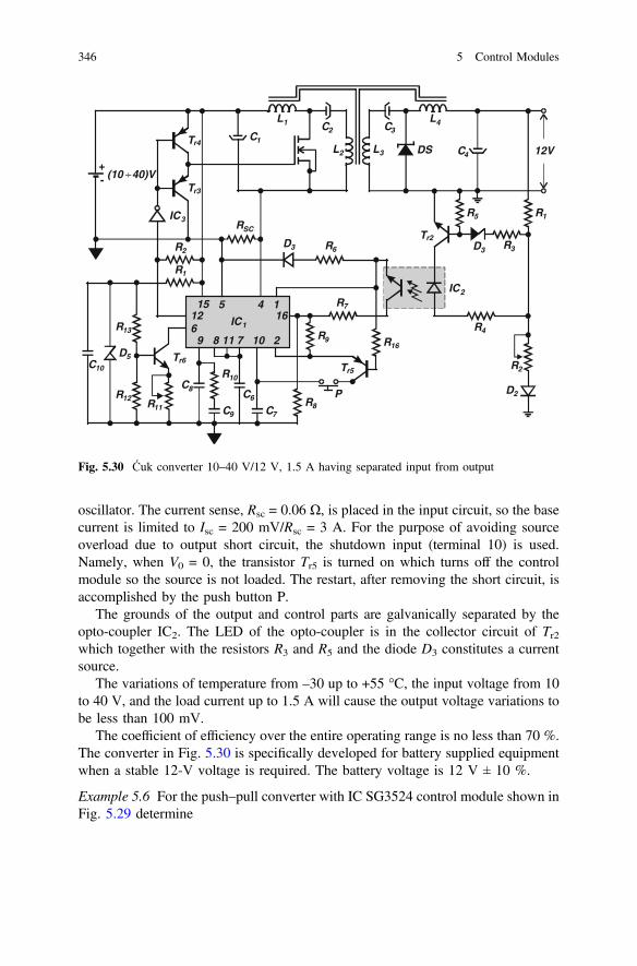
oscillator. The current sense, Rsc = 0.06 Ω, is placed in the input circuit, so the basecurrent is limited to Isc = 200 mV/Rsc = 3 A. For the purpose of avoiding sourceoverload due to output short circuit, the shutdown input (terminal 10) is used.Namely, when V0 = 0, the transistor Tr5 is turned on which turns off the controlmodule so the source is not loaded. The restart, after removing the short circuit, isaccomplished by the push button P.
The grounds of the output and control parts are galvanically separated by theopto-coupler IC2. The LED of the opto-coupler is in the collector circuit of Tr2which together with the resistors R3 and R5 and the diode D3 constitutes a currentsource.
The variations of temperature from –30 up to +55 °C, the input voltage from 10to 40 V, and the load current up to 1.5 A will cause the output voltage variations tobe less than 100 mV.
The coefficient of efficiency over the entire operating range is no less than 70 %.The converter in Fig. 5.30 is specifically developed for battery supplied equipmentwhen a stable 12-V voltage is required. The battery voltage is 12 V ± 10 %.
Example 5.6 For the push–pull converter with IC SG3524 control module shown inFig. 5.29 determine
C
CC
C CL L
L L
CR
RR
R
D
D
R
R
IC
IC
R
C CR
R R
R
R
R
R
R
R
RD
DC8
1
4
2 31 4
2 3
1010
1112
13
5
3
1
2
3
2
IC1
SC
9 78
916
7
4
5
3
1
2
63
26
9
15
8 11 10 2
15 4
61612
7
T
T
T
T
Tr5
r3
r2
r4
r6
P
DS 12V+- (10 40)V÷
Fig. 5.30 Ćuk converter 10–40 V/12 V, 1.5 A having separated input from output
346 5 Control Modules
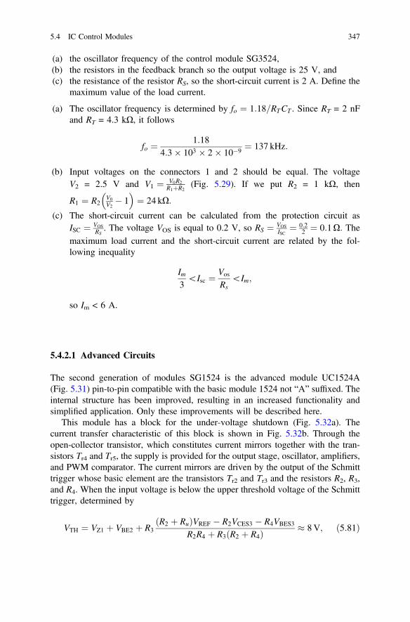
(a) the oscillator frequency of the control module SG3524,(b) the resistors in the feedback branch so the output voltage is 25 V, and(c) the resistance of the resistor RS, so the short-circuit current is 2 A. Define the
maximum value of the load current.
(a) The oscillator frequency is determined by fo ¼ 1:18=RTCT . Since RT = 2 nFand RT = 4.3 kΩ, it follows
fo ¼ 1:184:3� 103 � 2� 10�9 ¼ 137 kHz:
(b) Input voltages on the connectors 1 and 2 should be equal. The voltageV2 = 2.5 V and V1 ¼ V0R2
R1þR2(Fig. 5.29). If we put R2 = 1 kΩ, then
R1 ¼ R2V0V2� 1
� �¼ 24 kX:
(c) The short-circuit current can be calculated from the protection circuit asISC ¼ VOS
RS. The voltage VOS is equal to 0.2 V, so RS ¼ VOS
ISC¼ 0:2
2 ¼ 0:1X: Themaximum load current and the short-circuit current are related by the fol-lowing inequality
Im3\Isc ¼ Vos
Rs\Im;
so Im < 6 A.
5.4.2.1 Advanced Circuits
The second generation of modules SG1524 is the advanced module UC1524A(Fig. 5.31) pin-to-pin compatible with the basic module 1524 not “A” suffixed. Theinternal structure has been improved, resulting in an increased functionality andsimplified application. Only these improvements will be described here.
This module has a block for the under-voltage shutdown (Fig. 5.32a). Thecurrent transfer characteristic of this block is shown in Fig. 5.32b. Through theopen-collector transistor, which constitutes current mirrors together with the tran-sistors Tr4 and Tr5, the supply is provided for the output stage, oscillator, amplifiers,and PWM comparator. The current mirrors are driven by the output of the Schmitttrigger whose basic element are the transistors Tr2 and Tr3 and the resistors R2, R3,and R4. When the input voltage is below the upper threshold voltage of the Schmitttrigger, determined by
VTH ¼ VZ1 þ VBE2 þ R3R2 þ Ruð ÞVREF � R2VCES3 � R4VBES3
R2R4 þ R3 R2 þ R4ð Þ � 8V; ð5:81Þ
5.4 IC Control Modules 347

Tr3 is in saturation, the transistors of the current mirrors are off and so is thesupply of the blocks feeding the current mirrors. Therefore, only for VI > 8 V thesupply for all blocks is provided. Then Tr2 is in saturation and Tr3 is off. Duringdecreasing of the input voltage the current mirrors will be turned off when the inputvoltage becomes equal to the lower threshold of the Schmitt trigger. Then, Tr3 isturned on and goes to saturation, whereas Tr2 is turned off. Since at VI = VTL Tr2 isin the active region, it follows that
VTL ¼ VZ1 þ VBE2 þ R3 þ R1= 1þ b2ð ÞR3 þ a2R2
ðVCC � VBEt3Þ � 7:4V; ð5:82Þ
+
+
+
-
-
-C/L
E/A
COMP
CL(+)
INV. INPUT
COMP.
NON-INV. INPUT
CL(-)
200mVV
V
I
I
R
E
E
V
C
C
C
V
T
B
AT
B
A
REF
OSC.
RAMP
OSC.
PWMLatch
SR
S
I
U.VSENSE
CLOCK
INTERNALSUPPLY
FLIPFLOP
+5V REF.STABILIZER
10k Ω
1kΩSHUTDOWN
GROUND
5
2
7
4
1
6
13
12
16
14
10
11
3
15
9
8
Fig. 5.31 Block diagram of control module UC1524A
TT
TT
r2r4
r5
r3
VV REFI
R
R RR
Z
1
421
1
1615
151.2k Ω
8.7kΩ50kΩ50kΩ
6V
5VREGULATOR
V (V)I
I (
mA
)C
C
00302010
T =-55 C°
40
1
2
3
4
5
6
7
8j
25 C°125 C°
(a) (b)
Fig. 5.32 Under-voltage shutdown block (UV SENSE or UV L/O) (a) and its current transfercharacteristic (b)
348 5 Control Modules

where α2 is the common-base current gain of Tr2. The voltage hysteresis isVH = VTH – VTL = 60 mV.
The error amplifier (Fig. 5.33) is almost the same as in the earlier version of1524. The difference is only that it is now supplied by VI instead of by VREF. In thisway, the range of the input voltage of the amplifier is extended to VI – 2 V. Theoutput voltage of the amplifier is limited by the Zener diode Z1 to the value V9 ≤6 V. The over-current amplifier (Fig. 5.33) through R1 has a built-in voltage offsetVos = R1(100 μA) = 200 mV. As long as the voltage between the terminals 4 and 5V45 < 200 mV, Tr8 is off and so is Tr6. The PWM comparator is then controlled onlyby the outputs of the oscillator and error amplifier. When V45 > 200 mV, Tr11 willbe off and Tr8 on. Since via the current mirror Tr9 – Tr10, Ic9 = 0, ICS = Ibb, so Tr6 ison and reduces the voltage at the input of the PWM comparator. The duty cycle ofoutput pulses is reduced or the output is turned off.
The resistance of the current sense, which is inserted between 4 and 5, therefore, is
Rs ¼ 0:2
Im½A] ½X�: ð5:83Þ
In addition to operating as a comparator, the over-current amplifier can alsooperate in the linear mode. Its open-loop gain is about 80 dB. The circuit corre-sponding to the linear mode (Fig. 5.34) is similar to that of the error amplifier. Theimpedances in the feedback loop determine the voltage and frequencycharacteristics.
The over-current amplifier can be used for additional control of the dead time(Fig. 5.34b). The maximum duty cycle is
PWMCOMP.
2kΩ
2kΩ
VI
200mA 100mA
T T
T
T
T
T
T T
T
T
R
R
T
T
r1 r2
r9
r6
r10
r3
r8 r11
r7
r12
2
1
r4
r5
100 Aμ 100mA 100mA
+CS
-CL
Z16V
INV.
IN
ERRORAMPLIFIER
OVER-CURRENTAMPLIFIERCOMP.
8
2
1
15
4
5
9
Fig. 5.33 Basic scheme of error amplifier and over-current limiter
5.4 IC Control Modules 349

Dmax½%� � 40 0:2R1
R2þ 1
� �� 1
� : ð5:84Þ
The resistance R1 should be higher than 100 kΩ. Then, its influence on the gainof the error amplifier is negligible.
In addition to the PWM comparator, the UC1524A circuit also comprises aPWM latch. The latch has two write inputs (S) and one erase input (R). With eachpositive pulse at the oscillator output, determining the minimum dead time, the
EA1
2
-+
ZIN 1
ZF1
ZS
CL1
2
-+
ZIN 2
ZF2
9 EA CL1 4
92 5
- -
+ +R
R
2
1(a) (b)
Fig. 5.34 Over-current amplifier circuits corresponding to the linear mode (a) and to the mode ofmaximum duty cycle limitation (b)
INV.
NI.
CL(+)
CL(-)
EA
CL
COMP.
4.7K
3.3K
3.3K 66K
27K 0.015
R
C
SHD
C
V V
E E
COSC
T
T
A
I REF
A B
B
GND
REF.
UC1524A
0.1
0.01
0.1
2N2222
PIC600
0.033Ω
150Ω
CORE:2616PA 1003B7N:33T AWG 19
200 Fμ200 F40V
μ V05V/5A
0.005
VI
10-40V
+
-
Fig. 5.35 Forward converter (10–40) V/5 V, 5 A based on UC1524A
350 5 Control Modules

latch is erased. Each pulse at the PWM comparator output writes the latch. Addi-tional writing is performed via the shutdown input.
As long as this input exists (VSHD > 2.4 V), the latch is written so that the outputof the OR circuit is high and the output transistors are off. The latch increases thestability of PWM. It filters out the disturbances that may appear at the output of thePWM comparator as a consequence of the fast disturbances at the outputs of theerror and over-current amplifiers. In addition, the latch enables a very fast responseto the shutdown.
Figure 5.35 shows a typical example of IC UC1524A application in a forwardconverter. The function of switching is performed by the hybrid switching circuitPIC 600.
There are several types of control modules which are only improvements of thebasic circuit 1524. For instance, the circuit UC1525A (Fig. 5.36) comprises a softstart. The outputs have low impedances and could sink or deliver currents up to500 mA. The UC1527A circuit is identical to 1525 except for the output stagewhich is the complement of the 1525 output (Fig. 5.36). Within this set is alsoUC1526A/2525A/3526A which, additionally, comprises a block for temperatureprotection.
10
8
2
1
9
7
5
6
3
12
15
13
13
11
11
14
14
4
16
ERR. AMPL.
COMP.
PWMLatch
S
S
50 Aμ
R
OSCILLATOR
U.VL/C
FLIPFLOP
OSCILLATOR OUT.
INTERNALSUPPLY
VREF
REGULATOR+V
V
V
I
C
C
OUTPUT A
OUTPUT A
OUTPUT B
OUTPUT B
UC1525A OUTPUT STAGE
UC1527A OUTPUT STAGE
GROUND
SINHR.
R
C
T
T
DISCHARGE
COMP.
INV. INPUT
NON-INV. INPUT
SOFT START
SHD
VI
5K
5K
Fig. 5.36 Block diagrams of control modules UC1525A and UC1527A
5.4 IC Control Modules 351

5.4.3 Control Module TDA 1060
The structure of the control module TDA 1060 (Fig. 5.37) is in no way specific. Forthis reason only the specifications of terminals and functions of individualparameters will be presented here.
In addition to the reference voltage source with the typical value VREF = 3.72 V,this circuit contains an internal voltage source VZ = 8.4 V at the pin 2. The fre-quency of the sawtooth generator is determined by external elements Cx and Rx andcan be adjusted within limits 50/100 kHz. Typical values of the timing elements arewithin limits 5 kΩ < Rx < 40 kΩ and 1 nF < Cx < 100 nF. The frequencydependence on the values of the timing elements Rx = R7 and Cx = C8 is shown inFig. 5.38a. The input 9 SYN serves for external synchronization of the generator.The frequency of the synchronizing oscillator has to be lower than that of the basicoscillator. If external synchronization is not used, the pin 9 should be connected tothe pin 2. The FW input FW (feed-forward) (pin 16) is connected to an externalresistive divider connected between the input and the common pin 12. WhenV16 > VZ, the additional control of the duty cycle is accomplished by varying the
+---
+
+
+
+
+
+
-
-
-
-
-
-SAWTOOTHGENERATOR
REF.VOLTAGE
FBGA
MOD
DFM
CM
S
S
Q
Q
Q
R
R
R
R
0.6
0.48V
0.6V
100Ω1kΩ
STABILIZEDSUPPLY
EN V VCC EE
Q
Q
C
E
VZ
FW SINCH.R CX X CLOCK
PWMMODULATOR3
45
6
11
10 1 12
130.6V
98716
2
14
15
TDA1060
0.6V
Fig. 5.37 Block diagram of TDA 1060; A; B; T (suffix A is for temperature range 0 up to 70 °C,B is for –55 up to +150 °C, and T for –25 up to +125 °C)
352 5 Control Modules

input voltage. D0 denotes the duty cycle for V16 ≤ VZ. If this additional control isnot used, the input FW should be connected to the pin 12.
The input DFM (pin 6) serves to program the maximum duty cycle and therealization of the soft start. The minimum dead time, similar to the 1524 circuit, isdetermined by the duration of the short pulse (discharging time of C) at theoscillator output. Then tDTmin/Tosc ≈ 5 % (Tosc is the oscillator cycle), and themaximum duty cycle is Dmax ≈ 95 %. A decrease of the maximum duty cycle isobtained by a decrease of the voltage at the input 6 when V6 < 0.6 VZ (Fig. 5.39a).This is accomplished by connecting the input DFM to the resistive divider fed bythe output Vz of the voltage stabilizer.
The time constant of the soft start is determined by the capacitor connectedbetween the pins 6 and 12 and the resistors R6–2 and R6–12. Figure 5.39b shows thedependence of the minimum duty cycle of the soft start on the sum of resistancesR6–2 + R6–12 with the maximum duty cycle as a parameter. If the input DFM is notused, it should be connected to VZ by a resistor of approximately 5 kΩ. Theoperating conditions of the error amplifier are established via the inputs FB(feedback) and GA (gain adjustment), similarly to other control modules.
CM (pin 11) is the current protection input. The peculiarity of this circuit is thatit comprises two comparators for over-current protection having thresholdsVT1 = 480 mV and VT2 = 600 mV. As soon as V11 = VT1, the upper RS latch iserased and the output is disabled. Then the transistor with 100 Ω in the emitter isturned on through Q. The capacitor C6 at DFM input is discharged through thistransistor. After that, the soft-start procedure is initiated. If the CM input is not used,it should be connected to the pin 12. The over-voltage protection and the outputtransformer core saturation protection are controlled by the SAT input (pin 13). Thecore saturation signal obtained during transient processes is generated by a separatewinding used as a current sensor. When VSAT > 600 mV, the output transistor is off.If the VSAT input is not used, it should be connected to pin 12.
200
100
10
80
8
60
6
40
4
20
22 2.5 3.5 4.53 4 5
R =5k Ω
10kΩ
20kΩ
40kΩ
7f
(kH
z)
C (nF)8
D/D
0
V /V16 Z
0.60
0.2
0.4
0.6
0.8
1
1 1.4 1.8 2.2 2.6 3
(a) (b)
Fig. 5.38 Frequency as function of the timing elements (a) and relative duty cycle as function ofratio V16/VZ (b)
5.4 IC Control Modules 353
EN (Enable)—pin 10 is the enable input, TTL compatible. If EN = 0, the outputis blocked. Therefore, shutdown is accomplished through EN. When subsequently ahigh level (VEN > 2.4 V) is fed, the converter goes to the soft-start mode. Normally,EN is high. If it is not used, it should be connected to VZ (pin 2).
The MOD (5) input is used for additional control of the maximum duty cycle orof the voltage gain of the error amplifier. It can also be used in the current controlloop, specifically the one with fold back characteristic. If the input MOD is notused, it should be connected to the pin 2.
Figure 5.40 shows the scheme of a DC/DC converter 20–30 V/12 V, 10 Aillustrating the connection of IC TDA 1060. The input and output power parts arestandard.
The mains converter and stabilizer 220 V/12 V, 10 A based on TDA 1060(Fig. 5.41) is a forward pulse converter having the input and the output separated.At the maximum output load, the efficiency coefficient is higher than 80 %.
The mains voltage 220 V ± 10 % is rectified by a bridge rectifier and filtered by a500 μF/350 V capacitor. The resistor 100 kΩ, connected in parallel with thecapacitor, serves for its discharging after the converter is switched off. At the sametime, the mains voltage is fed to the primary winding of the transformer T4, whichtogether with the bridge rectifier BY164 and a 680-μF capacitor ensures the initi-ation of the operation of the control part of the converter at the switch-on. Thecapacitor 100 μF, connected to the pin 6 of IC TDA 1060, is charged through aresistive divider 4.7/10 kΩ. Upon charging of this capacitor, lasting about 0.8 s, theduty cycle changes from 0.1 to 0.5. In this way the so-called “soft start” is provided,i.e., the switching transistor is protected against burn-up during the switch-onprocess. The driving circuit is made of the transistor BD 230, the transformer T3,and the associated elements.
While the transistor BVX 80 is open, the diode BYW 30150, connected in serieswith the secondary winding of the transformer T1, is conducting and energy is
Dm
ax
0.10
0.2
0.4
0.6
0.8
1
0.2 0.3 0.4 0.5 0.6 0.7
RR + R
6-12
6-12 6-2
80
60
40
20
010 103 4
R +R ( )Ω6-2 6-12
%)
(D
0
D =90%max
70%
50%
30%
(a) (b)
Fig. 5.39 Maximum duty cycle (a) and minimum duty cycle of the soft start (b) as functions ofthe external resistors between pins 6 and 2 (R6–2) and 6 and 12 (R6–12)
354 5 Control Modules

accumulated in the choke L1. When the transistor is off, this diode stops conducting,and another diode connected to the ground opens enabling the transfer of energy tothe load. A part of the DC voltage obtained in this way, via a divider 2.5/2.2/1.2 kΩ,is fed to the DC amplifier in TDA 1060 and from there to the comparator (also withinTDA 1060), which at its second input obtains a sawtooth voltage with a constantfrequency and amplitude. At the output of this comparator, one obtains a signalwhose signal/pause ratio is proportional to the output voltage of the converter.
12,13,14,161 2 6 7 8 4 3
4K7 12K
10K 25K
2K5
100K 1K
2K2
3n3
2n2
1n/500V
1K2
1K
11151K
3n33n3
BD230
270R
T
T
T
T
3
2
4
1
3R3
100R
27R
BUX 80
1K2
1n5/100V
100n
330R
330R
330R
1K
80/ 0.5φ 20/ 0.5φ
72/ 0.5φ
8/ 2φ
72/ 1φ
20/ 0.5φ BY 208
BY 206
+680 Fμ
500 F350V
μ
6.8 F/40Vμ
BY 164
BY 164
TDA 1060
5K
100K
220V
BYW30150
BY208
+ + + + +
12V/10A
5 x 2200 /16V
15V
L2
BY208
μ
Fig. 5.41 Forward pulse converter 220 V/12 V, 10 A using TDA 1060
R
R
R
RR
R
R R
RR
R
R
R
C
CC C C
L L L
C
CC
C
C
1
2
3
76
10
5 11
134
12
8
9
5
32 9 10
1 2 3
7
41
7
6
47
(100K)
1K
(1K)
2K7 560
33mΩ4K7
2K5
12K
1K2 6 4 3 7 8
330μ
100μ100μ 470016V
μ 10016V
μ
330μ6.3V 6.3V 3n3
10n100n
1nF
115 11
TDA 1060
12,13,14,16
BD234
2N5671
T
T
r1
r2
560
1K
(20 30) V÷ 12V/10AMWR3040
+ +
Fig. 5.40 Forward DC/DC converter 20–30 V/12 V, 10 A based on control module TDA 1060
5.4 IC Control Modules 355

Upon the switch-on of the converter, the control and driving circuits are suppliedby its output, relieving in this way the transformer T4. The transformer T2, togetherwith the associated elements, serves for current protection of the converter. Thethreshold of the current protection is adjustable.
The basic technical specifications are as follows: input voltage 220 V ± 10 %/50 Hz, output voltage 12 V, maximum output current 10 A, operating frequencyapproximately 20 kHz, output voltage regulation 0.01 V/A, and output rippleapproximately 100 mV.
Problems
5:1 (a) A PWM controller has a sawtooth pulse oscillator frequency of f = 20 kHz.Determine the RC time constant of the soft-start circuit (Fig. 5.20) if theconverter enters the operation mode after a time interval of t = 10 T = 10/f when power supply is switched on. The reference voltage is VREF = 10 V.(b) Draw the waveforms of the voltage on capacitor and the output voltage ofthe PWM comparator from the moment when power supply is switched on tothe moment when the converter enters its operation mode. Sawtooth voltagechanges from VTL = 2 V to VTH = 6 V.
5:2 Explain the difference between PWM with voltage and with current control5:3 Draw the waveforms of pulse voltage at the output of NOR circuits of the
PWM controller (Fig. 5.13a) in the time interval of 5 TOSC, where TOSC is theperiod of sawtooth oscillator voltage. In this interval the error signal increaseslinearly from 2 to 3.5 V, if the sawtooth oscillator voltage changes from 0 to4 V. Discuss two cases:
(a) OMC =1 and(b) OMC = 0.
In both cases determine the maximum duty factor if the DC voltage at theinput of the dead-time comparator is VDT = 0.12 V.
5:4 Determine the maximum current of forward converters with controllerUC1524A (Fig. 5.35) if the current sense monitor RS = 0.02 Ω is connected inseries between the inductor and the converter output. Using the circuit fromFig. 5.34 explain how to implement over-current control.
5:5 Draw the scheme of the boost rectifier with controller SG1524 (Fig. 5.26a) andcalculate the elements of the control circuit if switching frequency is 50 kHz,the maximum transistor current IM = 5 A, the input voltage VI = 12 ± 10 %, theoutput voltage V0 = 15 V and the dead time tDT = 0.9 μs.
356 5 Control Modules

5:6 Draw the scheme and calculate the elements of the controller UC1527(Fig. 5.36) in a push–pull converter with the following parameters:VI = 12 V ± 10 %, V0 = 5 V, and IOM = 5 A. The switching frequency of thepower MOS transistor is 60 kHz. Explain the function of each element con-nected to IC UC1527. Determine the maximum duty factor.
5:7 For the control module of the forward converter with UC1524A (Fig. 5.35)
(a) Determine the maximum converter current Im(b) Determine the ratio R1/R2 (Fig. 5.34b) so that the maximum duty factor is
0.9.
5:8 Determine the elements RX and CX of the PWM circuit TDA 1060 (Fig. 5.38),so it runs at a frequency of f = 100 kHz. On this basis, determine the minimumdead time and the maximum duty factor of the control signals. Explain howthe soft-start circuit is realized.
Reference
1. Chryssis, G.: High-Frequency Switching Power Supplies: Theory And Design. McGraw-HillInc., New York (1984)
5.4 IC Control Modules 357


Chapter 6DC/AC Converters–Inverters
DC/AC converters are used in situations when the primary source is DC (battery,DC motor-generator, solar cells, etc.) and the loads require an AC supply. Since aDC source is inverted to an AC source of energy, DC/AC converters are oftencalled the inverters. This is not quite correct since the inverter is only one, althoughbasic, part of a DC/AC converter (Fig. 6.1). The inverter alone cannot meet therelatively strict technical requirements, such as the accuracy of maintaining theoutput voltage or current, low harmonic content, high coefficient of efficiency, andsmall size. For this reason the DC/AC converters consist of the following functionalblocks:
• DC current or voltage source,• control module,• inverter,• output filter, and• current or voltage regulator.
The control module provides driving signals for the switching elements (tran-sistors or thyristors) of the inverter. It consists of an oscillator of monophase pulsesor a generator of multiphase pulses.
In fact, the generator of multiphase pulses is made of logic circuits, which attheir outputs give square pulses shifted by a certain phase angle π/n (n is the numberof phases of the converter).
The basic function of the converter is to convert a DC voltage to a sequence ofsquare AC pulses. For this reason an output filter is inserted between the load andthe inverter with the task of extracting the fundamental harmonic from the sequenceof the square pulses so that the voltage across the load would differ as little aspossible from the sinusoidal form.
The current and voltage regulator maintains a preassigned value of the ACoutput voltage and limits the output current to avoid overloading the converter.
© Springer International Publishing Switzerland 2015B.L. Dokić and B. Blanuša, Power Electronics,DOI 10.1007/978-3-319-09402-1_6
359

6.1 Single-Phase Voltage Inverters
The bridge voltage inverter (Fig. 6.2a) is the basic circuit of DC/AC converters. TheDC power source operates in the voltage generator mode. If the inverter is fed froma rectifier, a sufficiently large capacitor Cg is connected in parallel with its input inorder to filter out higher harmonics of the voltage. The voltage inverters create avoltage +VDC across the load (Fig. 6.2b). This is accomplished by the operation oftwo pairs of switches (S1, S2) and (S3, S4). While one pair is on, the other is off.Assuming that the switches are ideal, when the first pair (S1, S2) is on, the point A ison the +, the point B is on the—pole of the power source and v0 = VAB = VDC . Inthe second half-cycle the pair (S3, S4) is on, the point A is on the (–) pole and thepoint B is on the (+) pole of the power source so that v0 = −VDC.
The switches (S1, S4), or (S3, S2), must not be on simultaneously because the DCpower source would be short circuited.
If the load were resistive, the current i0 would also have the form of squarepulses having amplitudes +VDC /RL while S1 and S2 are on and −VDC /RL while S3
GENERATOR OFMULTI-PHASE
PULSES
DC SOURCE
INVERTER OUTPUTFILTER
CURRENTOR VOLTAGEREGULATOR
OSCILLATOR
CONTROL MODULE
Vo =VAC
Vi =VDC
Fig. 6.1 Block diagram of a DC/AC converter
i
i
i
i
VDC g
S S
S S
1 3
4 2
load
V0
i0
+ -
+
-
-
+
+V
I
-V
-I
DC
M
DC
M
V
i
0
0
t
t
T/2 T/2
VDC /RL
C
-VDC /RL
(a) (b)
Fig. 6.2 Basic scheme of an inverter (a) and the timing diagram of the voltage and load current (b)
360 6 DC/AC Converters–Inverters

and S4 are on (dashed lines in Fig. 6.2b). In practice, however, the load is usuallyresistive-inductive or mainly inductive. For this reason Fig. 6.2b shows the form ofthe current corresponding to an inductive load. In this case, the load current in onehalf-cycle has both positive and negative values. This means that the switchesshould be able to conduct in both directions.
For the switches transistors (bipolar or MOS) or thyristors are used. Two-directional conduction of the switches is provided by the anti-parallel connection ofa thyristor/transistor and a diode (Fig. 6.3). Figure 6.3 shows an inverter based onbipolar transistors and the output filter for extracting the fundamental harmonic.The transformer T separates galvanically the inverter from the load and output filter.Thus, the equivalent load of the inverter is mainly inductive.
Let the equivalent load of the inverter be a series connection of a resistor R andan inductor L, with the condition ωL >> R. Then the load current is determined bythe differential equation where the saturation voltages VCES of the transistors con-ducting in saturation are neglected. Then, the next differential equation can bewritten
Ldi0dt
þ Ri0 ¼ VDC: ð6:1Þ
The initial conditions depend upon the interval of observation. Within theinterval 0 < t < T/2 the load current increases from its minimum to its maximumvalue, whereas within the interval T/2 < t < T the current i0 decreases from itsmaximum to its minimum value. Since the pulses are symmetric, the absolutevalues of the maximum, IM, and the minimum, Im, current are equal, i.e. Im = −IM sothe initial conditions are:
i0 0ð Þ ¼ �IM ; i0 T=2ð Þ ¼ IM : ð6:2Þ
V
V
V
V
V
V
DC
ac
B1
B4
B3
B2
1
D
D
D
D
1
4
3
2
V0
i
i
i
i
i
i
i
i i
i0
D4
D1
DC
C1
C4
D2
D3 C3
C2
+
+
-
-
T T1 3
T T4 2
LL C
1
2 2C
Fig. 6.3 Voltage inverterbased on bipolar transistors
6.1 Single-Phase Voltage Inverters 361

After solving Eq. (6.1) and combining the solution with (6.2), it turns out that
i0 ¼VDC
R � IM þ VDC
R
� �e�t=s; 0� t�T=2; ðaÞ
� VDC
R þ IM þ VDC
R
� �e� t�T
2ð Þ=s; T=2� t� T ðbÞ
(ð6:3Þ
where the time constant is τ = L/R. Therefore, in the interval 0 < t < T/2 the loadcurrent increases, whereas in the interval T/2 < t < T it decreases. Since i0(T/2) = IM,
from (6.3) it follows that
IM ¼ VDC
R1� e�T 2sð Þ
1þ e�T 2sð Þ : ð6:4Þ
For instance, if VDC = 10 V, L = 1 mH, R = 0.4 Ω, and f = 100 Hz, then from(6.4) IM = 19 mA. If the load were purely resistive R = 0.4 Ω, the maximum currentwould be IM = VDC /R = 25 A.
The current waveforms are shown in Fig. 6.4. Each half-cycle T/2 consists oftwo intervals. For instance, in interval 0 < t < t1 the diodes D1 and D2 are con-ducting, whereas in t1 < t < T/2 the diodes D1 and D2 are off and the transistors T1and T2 are on. From the condition i0(t1) = 0, and Eq. (6.3) it follows that
t1 ¼ s ln 1þ IMRVDC
� �: ð6:5Þ
This time is equal to t2, the time when the load current is conducted byD3 and D4.The thermal losses in the resistor R are determined by I2rms, where the root mean
square value of the load current is
Irms ¼
ffiffiffiffiffiffiffiffiffiffiffiffiffiffiffiffiffiffiffiffiffiffi1T
ZT0
i2oðtÞdt
vuuut ¼
ffiffiffiffiffiffiffiffiffiffiffiffiffiffiffiffiffiffiffiffiffiffiffiffiffiffiffiffiffiffiffiffiffiffiffiffiffiffiffiffiffiffiffiffiffiffiffiffiffiffiffiffiffiffiffiffiffiffiffiffiffiffiffiffiffiffiffiffiffiffiffi2T
ZT=20
VDC
R� IM þ VDC
R
� �e�t=s
� �2dt
vuuut : ð6:6Þ
The average currents of transistors and diodes are determined by (6.7) and (6.8),respectively
ICav ¼ 1T
ZT=20
i0ðtÞdt ¼ VDC
RT2� t1
� �1Tþ IM þ VDC
R
� �sTðe� T=2ð Þ=s � e�t1=sÞ;
ð6:7Þ
IDav ¼ 1T
Zt10
i0ðtÞdt ¼ �VDC
Rt1Tþ IM þ VDC
R
� �sTð1� e�t1=sÞ: ð6:8Þ
362 6 DC/AC Converters–Inverters

Example 6.1 A single-phase inverter based on thyristors (Fig. 6.5a) has a purelyinductive load L = 1 mH. Draw the timing diagrams and calculate the averagevalues of the currents through the thyristors and the diodes if VDC = 10 V andf = 50 Hz. The thyristors and the diodes can be considered ideal.
When the thyristors Th1 and Th2 are on, the voltage across the load is v0 = +VDC,
and when Th3 and Th4 are on then v0 = −VDC. For this reason the current throughthe coil will be linear since Ldi0/dt is equal either +VDC or –VDC. Taking intoaccount the initial conditions it follows that
i0ðtÞ ¼ �IM þ VDC
L t; 0� t� T=2;IM � VDC
L t; T=2� t� T :
i =
i =
i =
i
i
i
i
C1
C3
D1
D3
C2
C4
D2
D4
+V
I
I
I
I
I
I
-V
-I
-I
DC
M
M
M
M
M
M
DC
M
M
V
i
i
0
0
DC
t
t
t
t
t
t
t
t
t
1
2
i
Fig. 6.4 Waveforms of thevoltage across the load andcurrents through: load,transistors, diodes, and powersupply
6.1 Single-Phase Voltage Inverters 363

The diodes D1 and D2 are on within interval 0 < t < T/2 up to t1, or i0(t1) = 0wherefrom it follows
t1 ¼ L IMVDC
¼ T4; since i0ðT=2Þ ¼ IM ¼ VDC
4LT ¼ 25A:
Therefore, the diodes and the thyristors are conducting during intervals of T/4,thus their average values are equal and amount to
IAav ¼ IDav ¼ 1T
12T4IM
� �¼ IM
8¼ 3:125A:
The waveforms of the voltage v0 and of the characteristic currents are shown inFig. 6.5.
So far only bridge inverters have been considered. The half-bridge inverters(Fig. 6.6) which are also in use consist of two switches and two capacitors.
The capacitors have the same capacitance and each one takes one half of the DCvoltage (VDC/2). The transistors are alternatively on and off. Since the voltages acrossthe capacitors are always VDC/2, the voltage across the load is either +VDC or −VDC.
i =
i =
i =
i =
i =
i =
i =
i =
i
i
i
i
i
i
i
i
A1
A1
D3
D3
D1
D1
A3
A3
A2
A2
D4
D4
D2
D2
A4
A4
+V
I
I
I
I
-V
I
I
DC
M
M
M
M
DC
M
M
V
i
i
i
i
0
0
DC
A
D
t
T/2 T/2
t
t
t
t
Th Th
Th Th
1 3
4 2
L
V0
D D4 2
D D1 3
i
i
i
i
i
i i
ii
i
0
D1
DC
D3
D2
A1 A3
A2A4
D4
+V
(a)
(b)
DC
Fig. 6.5 Thyristor single-phase inverter (a) and waveforms of the voltage v0 and the characteristiccurrents (b)
364 6 DC/AC Converters–Inverters

6.1.1 Pulse-Controlled Output Voltage
The control pulses should be phase-shifted so that the switches give zero voltageacross the load at the start and at the end of each half-cycle (Fig. 6.7). Thus, oneobtains
v0ðtÞ ¼þVDC; a�xs� p� a;�VDC; pþ a�xs� 2p� a;0; 0�xs� a; p� a�xs� pþ a; 2p� a�xs� 2p:
8<: ð6:9Þ
load
M1
M2
D1
D2
V0+
C
C
+VDC /2
+VDC /2
+VDC
Fig. 6.6 Half-bridge inverter
OpenS1
S2
S3
S
S SS S S
V
V
V
V
V
V
S SS S S
0 00
4
2 21 1 1
0
0
DC
DC
DC
DC
4 42 3 3
Closedswitches
-
-
0
α α α α
π 2π ωt
Closed
(a)
(b)
Fig. 6.7 Real states ofswitches (a) and thecorresponding waveform ofthe output voltage of theinverter from Fig. 6.2a (b)
6.1 Single-Phase Voltage Inverters 365

This is necessary for two reasons. In this way the simultaneous conduction of S1and S4 or of S2 and S3 is avoided. Practically, this would be possible duringtransition if for example S1 were turning on, S4 were turning off, and vice versa.During that time the DC power source would be short-circuited. In order to avoidthat, the control pulses have to be phase-shifted at least for the maximum durationof the transition process. The sequence of turning on the switches should preventthe formation of a low Ohmic loop in parallel with the DC power source. This isrelated to the problem of non-overlapping (overlapping) which will be consideredin more detail in the chapter dealing with real driving.
In this chapter the phase-shifted control pulses are of interest from another pointof view. Namely, it is possible to control the voltage of the fundamental harmonicthrough the angle of the phase-shift. The mean square value of the voltage inFig. 6.7 is determined by
Vrms ¼
ffiffiffiffiffiffiffiffiffiffiffiffiffiffiffiffiffiffiffiffiffiffiffiffiffiffiffiffiffiffiffi1p
Zp�a
a
V2DCdðxtÞ
vuuut ¼ VDC
ffiffiffiffiffiffiffiffiffiffiffiffiffiffi1� 2a
p
r: ð6:10Þ
The Fourier series of this signal is
voðtÞ ¼X1k¼1
Vn sin½ð2k � 1Þxt� ð6:11Þ
and it contains odd harmonics. If the odd harmonics are denoted by n = 2k − 1,taking into account the symmetry of the square pulses the amplitudes are
Vn ¼ 2p
Zp�a
a
VDC sinðnxtÞdðxtÞ ¼ 4VDC
npcosðnaÞ: ð6:12Þ
Therefore, the amplitude of each harmonic is a function of the angle α whichcorresponds to the zero voltage across the load. It is important to emphasize that byan adequate choice of α individual harmonics can be eliminated. Namely, if
a ¼ 90�=n; ð6:13Þ
the n-th harmonic will be eliminated. If α = 30o, then V3 = 0, meaning that the thirdharmonic is eliminated. Then the amplitude of the fundamental harmonic isV1 = (4VDC/π)cos(30
o) = 1.1VDC. The fifth harmonic is eliminated if α = 90o/5 = 18o, and the amplitude of the first harmonic will be V1 = 1.2VDC.
Total harmonic distortion can be reduced by reducing individual harmonics (seeExample 6.2).
366 6 DC/AC Converters–Inverters

Example 6.2 The load of the inverter from Fig. 6.2 is inductive-resistive withL = 25 mH and R = 10 Ω. If VDC = 100 V and f = 50 Hz determine the totalharmonic distortions of the voltage and current at
(a) α = 0 and (b) α = 30o.The amplitudes of the harmonics in the Fourier series of the load current are
determined by
In ¼ Vn
Zn¼ Vnffiffiffiffiffiffiffiffiffiffiffiffiffiffiffiffiffiffiffiffiffiffiffiffiffi
R2 þ ðnxLÞ2q ¼ 4� 100=ðnpÞ � cosðnaÞffiffiffiffiffiffiffiffiffiffiffiffiffiffiffiffiffiffiffiffiffiffiffiffiffiffiffiffiffiffiffiffiffiffiffiffiffiffiffiffiffiffiffiffiffiffiffiffiffiffiffiffiffiffiffiffi
102 þ ½nð2p� 50Þ � 0:025�2q ;
and the amplitudes of the voltage harmonics across the load are given by (6.12).The individual values of Vn and In are given in Table 6.1.
The total harmonic voltage distortion is determined by
THDv ¼ffiffiffiffiffiffiffiffiffiffiffiffiffiffiffiffiffiffiffiffiffiffiffiffiffiV2rms � V2
1;rms
qV21;rms
:
(a) Vrms = VDC, V1;rms ¼ V1ffiffi2
p ¼ 4VDCffiffi2
pp¼ 90:07V;
THDv ¼ffiffiffiffiffiffiffiffiffiffiffiffiffiffiffiffiffiffiffiffiffiffiffiffiffiffiffiffi1002 � 90:072
p
90:07¼ 43:43
90:07¼ 0:482 ¼ 48:2%:
(b) On the basis of (6.10), the rms value of the voltage across the load for α = 30o is
Vrms ¼ 100
ffiffiffiffiffiffiffiffiffiffiffiffiffiffiffiffiffiffiffiffiffiffi1� 2� 30
180
r¼ 81:6V;
V1;rms ¼ 4VDC
pcos a
� �=
ffiffiffi2
p¼ 110=
ffiffiffi2
p¼ 77:92V;
THDv ¼ffiffiffiffiffiffiffiffiffiffiffiffiffiffiffiffiffiffiffiffiffiffiffiffiffiffiffiffiffiffi81:62 � 77:922
p
77:92¼ 24:23
77:92¼ 0:311 ¼ 31:1%:
Table 6.1 The individual values of Vn and In
n fn (Hz) Zn (Ω) Vn (V) In (A)
α = 0 α = 30°
1 50 12.71 127.3 110.2 1 50
3 150 25.59 42.4 0 3 150
5 250 40.52 25.5 22.1 5 250
7 350 55.88 18.2 15.7 7 350
9 450 71.39 14.1 0 9 450
6.1 Single-Phase Voltage Inverters 367

The total harmonic distortion of load current is determined by (1.26), soaccording to the values given in the Table 6.1 one has
THDI ¼
ffiffiffiffiffiffiffiffiffiffiffiffiffiffiffiffiP1n¼2
I2nrms
s
I1rms
¼
ffiffiffiffiffiffiffiffiffiffiffiffiffiffiffiffiffiffiffiffiffiffiffiffiffiffiffiffiffiffiffiffiffiffiffiffiffiffiffiffiffiffiffiffiffiffiffiffiffiffiffiffiffiffiffiffiffiffiffiffiffiffiffiffi1:65ffiffi
2p
�2þ 0:63ffiffi
2p
�2þ 0:32ffiffi
2p
�2þ 0:2ffiffi
2p
�2r
10:01=ffiffiffi2
p ¼ 0:18 ¼ 18%;
(b) THDI ¼
ffiffiffiffiffiffiffiffiffiffiffiffiffiffiffiffiffiffiffiffiffiffiffiffiffiffi0:54ffiffi
2p
�2
þ 0:28ffiffi2
p �2
r8:67=
ffiffi2
p ¼ 0:07 ¼ 7%:
6.2 Pulse-Width Modulated Inverters
It has been shown in Chap. 4 that the ratio of the output and the input voltage ofDC/DC converters is directly proportional to the duty cycle of the control pulseswith a constant frequency and a variable duration. Pulse-width modulation is usedin inverters for the purpose of regulating the amplitude and the frequency of theoutput voltage. In the inverter circuits it is even more complex because it is requiredthat one obtains approximately sinusoidal (quasi-sinusoidal) voltage of a preas-signed frequency (usually 50 or 60 Hz) at its output.
The pulse-width-modulated (PWM) inverters use a harmonic control (modu-lating) signal, whereas the carrier signal is triangular, as in DC/DC converters.A PWM module consists of:
• a sinusoidal oscillator with a frequency f1 (normally 50 or 60 Hz) which gen-erates the control signal,
• a generator of triangular voltage (carrier signal) whose frequency fs is severaltimes higher than f1,
• a comparator with complementary outputs (Fig. 6.8).
The pulse frequency at the comparator output is equal to the frequency of thecarrier signal fs, and the duration of the pulses depends on the ratio of the instan-taneous values of the voltages of the control and carrier signals. Since these pulsescontrol the states of the inverter switches, the switches will also operate at thefrequency fs modulated by the ratio of the turn-on and the turn-off time. Conse-quently, it follows that
mo ¼ þVDC; Vc [VtM S1 and S2 are turned onð Þ�VDC; Vc\VtM ðS3 and S4 are turned onÞ
ð6:14Þ
which is illustrated in Fig. 6.9. Since the output voltage varies between +VDC and–VDC, these PWM are bipolar modulators. Because the frequency of the carriersignal is much higher than the frequency of the sinusoidal control signal, i.e., fs >> f1,
368 6 DC/AC Converters–Inverters
it may be assumed that the control voltage Vc during the cycle Ts is approximatelyconstant (Fig. 6.9). Then, based on Fig. 6.9, the average value of the output voltage is
V0av ¼ 1Ts
ZTs�t1
t1
�VDCdt þZTsþt1
Ts�t1
VDCdt
264
375: ð6:15Þ
Because in the interval 0 < t < Ts : Vtr = −VtM + (4VtM /Ts)t, from the conditionVtr(t1) = Vc it follows that
t1 ¼ Ts4
1þ Vc
VtM
� �: ð6:16Þ
V
V
V
sin
s
C
t
t
T = 1/f
T
s
s
s
T = 1/f
T =1/f
1
1
1
1= f (V / V )1 1
+VDC
-
Single-phaseinverter
load
V0
Control module
Comparator
Fig. 6.8 Block diagram of a single-phase PWM inverter
V
-V
-V
DC
tM
tM
DC
V
V
v
V
0
0av
tr
C
t
Ts
Ts
Ts
Tstt
t1
1
1
- +
V
Fig. 6.9 Waveforms ofcharacteristic voltages in oneperiod of the carrier signal
6.2 Pulse-Width Modulated Inverters 369

From (6.15) and (6.16) it follows that
V0av ¼ Vc
VtMVDC: ð6:17Þ
If
Vc ¼ VcMsin xtð Þ; ð6:18Þ
then
V0av ¼ VcM
VtMVDC sinðxtÞ ¼ maVDC sinðxtÞ; ð6:19Þ
where
ma ¼ VcM
VtMð6:20Þ
is the factor of amplitude modulation, equal to the ratio of the sinusoidal controlsignal and the triangular carrier signal. On the basis of (6.19) one can draw a veryimportant conclusion that the average value of the output voltage is a sinusoidalfunction having the frequency of the control signals f1 (dashed line in Fig. 6.10b)and the amplitude
V0M ¼ maVDC �VDC; ð6:21Þ
because the amplitude modulation factor ma < 1.In addition to the factor of amplitude modulation a definition is also made of the
factor of frequency modulation as the ratio of the frequencies of the carrier and thecontrol signals, i.e.,
mf ¼ fsf1: ð6:22Þ
Even though mf >> 1, the control signal is not constant within one cycle Ts. Forthis reason the output voltage will contain higher harmonics, whereas (6.19) givesits fundamental harmonic. The higher harmonics appear around the carrier fre-quency (Fig. 6.10c) and its integer multiples, more precisely around the harmonicsmf, 2mf, 3mf, … For instance, if mf = 15, harmonics 15, 17, 13, …, 31, 33, 29, etc.will exist.
Table 6.2 presents the normalized Fourier coefficients for individual harmonicsversus the factor of amplitude modulation. It should be noted that the coefficients inTable 6.1 are almost independent of mf if mf > 9.
370 6 DC/AC Converters–Inverters

From Table 6.2 it can be noted that the amplitudes of some harmonics may behigher than the amplitude of the fundamental harmonic. A favorable circumstanceis that the higher harmonics are at considerably higher frequencies and can readilybe filtered out. This is a significant advantage of the inverters based on PWM. Thehigher the carrier frequency is, the less difficult the problem of filtering will be. Themaximum frequency fs is limited by dynamic losses in semiconductor switches.
0
v
vv
v
vv
cont
contcont
tr
trtr
t
t
1fs
t = 0
<>
T : onT : on
T : offT : off
AA
AA
-+
+-
,,
-
0.00.20.40.60.81.01.2
1 m
m = 0.8, m = 15
2m 3m
(m + 2) (2m + 1) (3m + 2)
f
a f
f f
f f f
(V )A o h
V /2d
v , fundamental harmonic =(V )AoA 0 1
Harmonic of f1
V
V
0
0
2
2
0
(a)
(b)
(c)
Fig. 6.10 Voltage waveforms (a and b) and frequency spectrum of the inverter based on bipolarPWM (c)
6.2 Pulse-Width Modulated Inverters 371

Thus, fsmax of the inverters based on bipolar transistors is from ten to several tenskHz, whereas for MOS transistors it is about a 100 kHz.
Example 6.3 A bridge PWM inverter should provide alternating voltage at a fre-quency f = 50 Hz across an R-L load (R = 10 Ω, L = 20 mH). The amplitudemodulation factor is ma = 0.8 and the frequency modulation factor is mf = 21. Theinput DC voltage is VDC = 100 V. It is required to determine:
(a) the amplitudes of the fundamental harmonics of the output voltage and loadcurrent,
(b) THD of the load current, and(c) power dissipation in the resistive component of the load.(a) According to (6.19) the amplitude of the fundamental harmonic is
V01 ¼ maVDC ¼ 0:8� 100 ¼ 80V:
The amplitudes of the harmonics of the load current are
I ¼ V0h
Zh¼ V0hffiffiffiffiffiffiffiffiffiffiffiffiffiffiffiffiffiffiffiffiffiffiffiffiffi
R2 þ ðhxLÞ2q ; ð6:23Þ
and the amplitude of the fundamental harmonic of the load current is
I01 ¼ 80Vffiffiffiffiffiffiffiffiffiffiffiffiffiffiffiffiffiffiffiffiffiffiffiffiffiffiffiffiffiffiffiffiffiffiffiffiffiffiffiffiffiffiffiffiffiffiffiffiffiffiffiffiffiffiffiffiffiffiffiffiffiffiffi102 þ ð1� 2� p� 50� 0:02Þ2
q ¼ 6:39A:
Table 6.2 Normalized harmonics of bipolar PWM [1]
Harmonic 0.2 0.4 0.6 0.8 1.0
1 (fundamental) 0.2 0.4 0.6 0.8 1.0
mf 1.242 1.15 1.006 0.818 0.601
mf ± 2 0.016 0.061 0.131 0.220 0.318
mf ± 4 0.018
2mf ± 1 0.190 0.326 0.370 0.314 0.181
2mf ± 3 0.024 0.071 0.139 0.212
2mf ± 5 0.013 0.033
3mf 0.335 0.123 0.083 0.171 0.113
3mf ± 2 0.044 0.139 0.203 0.176 0.062
3mf ± 4 0.012 0.047 0.104 0.157
3mf ± 6 0.016 0.044
372 6 DC/AC Converters–Inverters

(b) Since mf = 21, the first higher harmonics are h = 19, h = 21, and h = 23. On thebasis of Table 6.1 it follows that
V021 ¼ 0:818� 100 ¼ 81:8V;
V19 ¼ V023 ¼ 0:22� 100 ¼ 22V:
The currents of these harmonics are determined by (6.24). The power dissipatedby individual harmonics on the resistive component of the load is determined by
Ph ¼ I20h;rmsR ¼ I0hffiffiffi2
p� �2
R:
The calculated values of harmonics for the voltage, load current, and absorbedpower are presented in Table 6.3.
THD of the load current is determined by (1.26) and
THDI ¼ffiffiffiffiffiffiffiffiffiffiffiffiffiffiffiffiffiffiffiffiffiffiffiffiffiffiffiffiffiffiffiffiffiffiffiffiffiffiffiffiffiffiffiffiffiffiffiffiffiffiffiffiffiffiffið0:13Þ2 þ ð0:44Þ2 þ ð0:11Þ2
q4:79
¼ 0:098 ¼ 9:8%:
(c) The dissipation on the resistor R is
P ¼X
Ph ¼ 229:4þ 0:2þ 1:9þ 0:1 ¼ 231:6W:
6.2.1 Unipolar PWM
The output voltage of the inverters based on PWM, described in the precedingsections, varies between +VDC and –VDC. For this reason these inverters are calledthe bipolar PWM inverters, or the inverters based on bipolar PWM. Compared tothem, the output voltage of the unipolar PWM inverters varies between 0 and +VDC
or between 0 and −VDC. Here, the switches in the branches A and B (Fig. 6.11) donot change the states simultaneously like they do in the inverters based on bipolarPWM. The arms A and B of the bridge are separately controlled by comparing in
Table 6.3 The calculated values of harmonics for the voltage, load current and absorbed power
h fh(Hz) V0h(V) Z0h(Ω) I0h(A) I0hrms(A) Ph(W)
1 50 80.0 11.81 6.78 4.79 229.4
19 950 22.0 119.8 0.18 0.13 0.2
21 1,050 81.8 132.3 0.62 0.44 1.9
23 1,150 22.0 144.8 0.15 0.11 0.1
6.2 Pulse-Width Modulated Inverters 373

turns the triangular voltage of the carrier with the positive (Vc) and negative (−Vc)control voltages. For a positive control voltage it follows
Vc [Vtr : S1 on; S4 off; VAN ¼ þVDC;
Vc\Vtr : S4 on; S1 off; VAN ¼ 0:ð6:24Þ
From the comparison of −Vc and the triangular signal (Fig. 6.12) it follows:
�Vc [Vtr : S3 on; S2 off; VBN ¼ þVDC
�Vc\Vtr : S2 on; S3 off; VBN ¼ 0:ð6:25Þ
The voltage levels from Eqs. (6.24) and (6.25) are represented in Fig. 6.12b, c.The output voltage (Fig. 6.12d) is the voltage difference between the points A andB, i.e.,
Vo ¼ VAN � VBN : ð6:26Þ
In accordance with the previous equations Table 6.4 shows the states of theswitches and the levels of characteristic voltages. When both switches in the upperor lower half of the bridge are on, the output voltage is zero. The load current flowsin the loop S1–D3 or S3–D1 or S4–D2 or S2–D4, depending upon the direction of i0.Within these intervals the current idc of the primary source is zero.
The output voltage (Fig. 6.12d) consists of the bipolar package of the pulse-widthmodulated square pulses. Within one cycle of the control voltage these pulses varybetween 0 and +VDC, whereas in the next cycle they vary between 0 and −VDC .Owing to this the first harmonics appear around the frequency 2mf f1, and the secondaround 4mf f1 (Fig. 6.12e). Therefore, compared to a bipolar PWM, the frequenciesof harmonics have doubled, which is a significant advantage of the unipolar PWM.The parameters of the fundamental harmonic are the same as for the bipolar PWM.The amplitude is V0M1 = maVDC and the frequency is equal to the control signalfrequency f1.
D
DD
D
1
4
3
2
V =V -V0 A B
i
i
0
dc
S S
S S
1 3
4 2
A BV DC load
N
+
-
Fig. 6.11 Principally schemeof single-phase voltageinverter for which unipolarPWM is applied
374 6 DC/AC Converters–Inverters

0
0
0
vv ctr
t
t
t
t
V
V
v
V
v
V
0
0
0
0
0
0
T
T
B+
A+on
on
v
v
V
AN
BN
DCma
(= VAN -VBN )
-
-
0.00.20.40.60.81.0
1 m
ma = -0.8, mf = -15
2m 4m3m
(2m + 1)(2m -1)
f f ff
ff
(V )V
0
0
h
harmonic of f1
h
0
(-v )c
-vc -vtr
vc > vtr
VDCma
(a)
(b)
(c)
(d)
(e)
Fig. 6.12 Waveforms (a, b, c, and d) and frequency spectrum of a single-phase inverter based onunipolar PWM
6.2 Pulse-Width Modulated Inverters 375

In addition to twice higher harmonics, the voltage variation across the load of theunipolar PWM is one half of that of a bipolar PWM, which reduces stress imposedon components during transients.
Table 6.5 shows the normalized Fourier coefficients Vh/VDC of the unipolarPWM.
All switches for the described procedure of unipolar PWM operate at the fre-quency of the carrier signal, and thus have to be high-frequency switches. Anothertype of unipolar PWM uses two low-frequency switches (operating at the controlfrequency) and two high-frequency switches. The state of the switches S1 and S4(the left-hand side of the bridge) depend on the ratio of Vc and Vtr, whereas thestates of the switches S2 and S3 (the right-hand side of the bridge) depend onwhether the control signal is positive or negative (Table 6.6).
The characteristic voltage waveforms are shown in Fig. 6.13. These invertersposses lower dynamic losses caused by the transient processes in the semiconductorswitches.
Table 6.4 The states of the switches and voltage levels of a single-phase inverter based onunipolar PWM
Closed switches VAN VBN V0 = VAN − VBN
S1, S2 VDC 0 VDC
S4, S3 0 VDC −VDC
S1, S3 VDC VDC 0
S2, S4 0 0 0
Table 6.5 Normalized Fourier coefficients Vh/VDC of an inverter based on unipolar PWM asfunctions of the amplitude modulation factor ma [2]
hma harmonic 1 0.9 0.8 0.7 0.6 0.5 0.4 0.3 0.2 0.1
h = 1 1.00 0.90 0.80 0.70 0.60 0.50 0.40 0.30 0.20 0.10
h = 2mf ± 1 0.18 0.25 0.31 0.35 0.37 0.36 0.33 0.27 0.19 0.10
h = 2mf ± 3 0.21 0.18 0.14 0.10 0.07 0.04 0.02 0.01 0.00 0.00
Table 6.6 Turn-onconditions of switches
Closed switch Condition
S1 Vc > Vtr
S2 Vc > 0
S3 Vc < 0
S4 Vc < Vtr
376 6 DC/AC Converters–Inverters

6.3 Three-Phase Inverters
Sometimes it is required to convert a DC voltage to a three-phase AC voltage. Thesupply and control of induction motors are typical examples. The basic circuitdiagram of the three-phase inverter (Fig. 6.14) consists of three pairs of bilateralswitches (switch Si diode Di) and the phase loads in this case in the star connection.The pairs of switches in each arm (S1, S4), (S3, S6), and (S2, S5) are complementary,i.e., when one is closed, the other is open.
V VV VC Ctr tr
t
t
t
t
0
0
0
V
V
V = V - V
AN
BN
0 AN BN
+V
+V
+V
-V
DC
DC
DC
DC
V01
0
(b)
(a)
(c)
(d)
Fig. 6.13 Waveforms of a PWM inverter (a, b, c and d) having two high-frequency and two low-frequency switches
6.3 Three-Phase Inverters 377

The state of the switches changes in T/6 = 60° phase steps (Fig. 6.15a), whichprovides the line and phase voltages as shown in Fig. 6.15b, c. Since within onecycle all six switches close and open once, these inverters are called the six-stepinverters.
The frequency of the fundamental harmonic of the output voltage is that of theswitches. The third harmonic and its integer multipliers as well as all even har-monics are suppressed. This means that the present harmonics are
n ¼ 6k � 1; k ¼ 1; 2; . . . ð6:27Þ
If the load is an ungrounded star, the Fourier coefficients of the line and phasevoltages are:
Vh;L�L ¼ 4VDC
npcos
np6
���������; ð6:28Þ
Vh;L�N ¼ 2VDC
3np2þ cos
np3
�� cos n
2p3
� �� ���������: ð6:29Þ
PWM is also applicable to three-phase inverters.The advantages are the same as for the single-phase inverters. Thus, the fre-
quency of the fundamental harmonic of each phase is equal to the frequency of thesinusoidal control voltage. The amplitude of this harmonic can be controlled by theratio of the control and the carrier signal. Higher harmonics appear at the carriersignal frequency and the integer multipliers of this frequency, which facilitatesfiltering of the output voltage. Each pair of the switches (S1, S4), (S3, S6), and (S2,S5) requires one control (reference) signal. These three control voltages are phaseshifted by 120° (Fig. 6.16). The conditions when the switches are closed are givenin Table 6.7.
Higher harmonics will be reduced if the modulation factor is an odd multiple of3, i.e., if the frequency of the carrier signal is 3, 9, 15, 21, 27, … times higher thanthe control signal frequency.
D D
D D D
S S S
S S S
1 3 5
4 6 2
1 3 5
4 6 2
+
-VDC
AB
C
IA
N
D
Fig. 6.14 Basic circuitdiagram of a three-phasevoltage inverter
378 6 DC/AC Converters–Inverters

The Fourier coefficients of the line voltages are
Vh3 ¼ffiffiffiffiffiffiffiffiffiffiffiffiffiffiffiffiffiffiffiA2h3 þ B2
h3
q; ð6:30Þ
S2
S3
S4
S5
S6
Closed Open
v
v
v
v
v
i
v
+V
+V
V
V
V
V
+V
-V
-V
-V
AB
CA
AN
BN
CN
A
BC
DC
DC
DC
DC
DC
DC
DC
DC
DC
DC
0
0
0
0
t
t
t
t
t
t
t
2
2
1
1
3
3
3
3-
S1(a)
(b)
(c)
(d)
Fig. 6.15 Cycle of changesof the states of switches (a),line voltages (b), phasevoltages for a load connectedas ungrounded star (c), andthe current of phase A for anR-L load (d)
6.3 Three-Phase Inverters 379

Table 6.7 Conditions for theclosed switches
Closed switch Condition
S1 VAC > Vtr
S2 VCC > Vtr
S3 VBC > Vtr
S4 VAC < Vtr
S5 VCC < Vtr
S6 VBC < Vtr
v
v
v
v
vv =
v
V V V VAC BC CCtr
t
t
t
t
A
A
B
BAB
AN
-
iA
(a)
(b)
(c)
Fig. 6.16 Triangular carrier and sinusoidal control signals of a three-phase PWM inverter atma = 0.7 andmf = 0.9 (a), the characteristic voltages (b), and the current in phase A for anR-L load (c)
380 6 DC/AC Converters–Inverters

where
Ah3 ¼ Vh sinnp2
�sin
np3
�; ð6:31Þ
Bh3 ¼ Vh sinnp2
�cos
np3
�: ð6:32Þ
The normalized values of these coefficients are shown in Table 6.8.
Example 6.4 Determine the total harmonic distortion of the load current for the six-step inverter shown in Fig. 6.13. The resistive-inductive load, R = 10 Ω andL = 20 mH, is in the star connection. The DC input voltage is VDC = 100 V and thefundamental frequency of the output voltage should be f = 50 Hz.
The amplitudes of the Fourier components of the line voltage are determined by(6.30). The amplitudes of the load currents are
Ih ¼ Vh;L�N
Zh¼ Vh;L�Nffiffiffiffiffiffiffiffiffiffiffiffiffiffiffiffiffiffiffiffiffiffiffiffiffi
R2 þ ðhxLÞ2q ¼ Vh;L�Nffiffiffiffiffiffiffiffiffiffiffiffiffiffiffiffiffiffiffiffiffiffiffiffiffiffiffiffiffiffiffiffiffiffiffiffiffiffiffiffiffiffiffiffiffiffiffiffiffiffiffiffiffiffiffiffiffi
102 þ ðh� 2p� 50� 0:02Þ2q :
The calculated values of Vh, L–N and Ih are presented in Table 6.9.The total harmonic distortion of the load current is determined by (1.26). From
this and Table 6.9 it follows that
THDI ¼
ffiffiffiffiffiffiffiffiffiffiffiffiffiffiffiffiffiP1h¼2
I2h;rms
s
I1;rms
¼ffiffiffiffiffiffiffiffiffiffiffiffiffiffiffiffiffiffiffiffiffiffiffiffiffiffiffiffiffiffiffiffiffiffiffiffiffiffiffiffiffiffiffiffiffiffiffiffiffiffiffiffiffiffiffiffiffiffiffiffi0:272 þ 0:142 þ 0:062 þ 0:042
p
4:17¼ 0:075 ¼ 7:5%:
The most often met case is when the factor of frequency modulation is chosen sothat it is an odd multiple of the number three. In this case, the phase voltages at thecarrier frequency will have the same amplitude and their phase displacement will beequal to 0. As a result, the harmonics of line voltages at this frequency will be 0.
For linear modulation (ma ≤ 1) the amplitude of the first harmonics changeslinearly with the change of the amplitude modulation factor, so the expressions forphase and line voltages have the form
V1;LN ¼ maVDC
2
V1;LNrms ¼ maVDC
2ffiffiffi2
p
V1;LLrms ¼ffiffiffi3
pffiffiffi2
p maVDC
2¼
ffiffiffi3
p
2ffiffiffi2
p maVDC:
ð6:33Þ
6.3 Three-Phase Inverters 381

Tab
le6.8
Normalized
FouriercoefficientsVh3/VDCof
thelin
evo
ltagesof
athree-ph
asePW
Minverter
[2]
hmaHarmon
ic1
0.9
0.8
0.7
0.6
0.5
0.4
0.3
0.2
0.1
h=1
0.86
60.79
90.69
30.60
60.52
00.43
30.34
60.26
00.17
30.08
7
h=mf±2
0.27
50.23
20.19
00.15
00.11
40.08
10.05
30.03
00.01
30.00
3
h=2m
f±1
0.15
70.22
10.27
20.30
70.32
10.31
30.28
20.23
20.16
50.08
6
382 6 DC/AC Converters–Inverters

For ma = 1: V1;LLrms ¼ 0:612VDC:
6.3.1 Overmodulation (ma > 1)
In the case of overmodulation (ma > 1) the amplitude of the control signal is largerthan the amplitude of the triangular signal and the amplitude of the first harmonic isnot a linear function of the amplitude modulation factor. With an increasing ma theoutput voltage has a waveform similar to the waveform of the voltage of the six-step inverter. The dependence of the effective value of the line-to-line voltagefundamental harmonic on the amplitude modulation factor is shown in Fig. 6.17.
With the transition to the overmodulation region the amplitude of the outputvoltage fundamental harmonic increases, but this dependence is not linear. For
ma = 3.24 the amplitude has the maximal value V1;LLrms
� �max¼
ffiffi6
pp VDC and this
value is equal to that of a six-step inverter. Also, unlike the linear modulation, inthis case there are harmonics at lower frequencies besides the harmonics at thefrequency of the carrier signal and its integer multiple.
Table 6.9 The calculated values of Vh, L–N and Ih
n Vh,L-N (V) Zn(W) Ih(A) Ih,rms(A)
1 63.6 11.8 6.39 4.17
5 12.73 33.0 0.38 0.27
7 9.09 45.1 0.20 0.14
11 5.79 69.8 0.08 0.06
13 4.90 82.3 0.06 0.04
0 ma1 3,24
linear
(over-modulation)ma>1
0,612
6=0,78
V1LL,rms
VDC
(square) (six-step)
Fig. 6.17 Effective value of the fundamental harmonic of line voltage versus amplitudemodulation factor [2]
6.3 Three-Phase Inverters 383

6.3.2 Asynchronous PWM
For synchronous PWM the frequency modulation factor is an integer. In asyn-chronous PWM the switching frequency is constant, while the frequency of fun-damental harmonic is changed, and mf may not be an integer. As a consequencesubharmonics may occur with a frequency lower than the frequency of the firstharmonic. Although small in amplitude, these harmonics can cause significantcurrents in predominantly inductive loads, which should be taken into account.
6.4 Space Vector Modulation
Space vector modulation (SVM) is a very important contemporary control tech-nique of power converters. Its main application is control of three-phase voltagecontrolled DC/AC converters, but it is also used for control of other types ofconverters such as AC/DC power converters, resonant three-phase inverters, mul-tilevel converters, matrix converters, etc.
Today there are a number of different variants of SVM, which differ with respectto the complexity of realization and the quality of the results.
6.4.1 Space Vector Modulation—Basic Principles
A three-phase symmetrical power supply system is observed. In this system, onlytwo currents and two voltages are linearly independent, while the third current orvoltage can be expressed as a linear combination of the other two. Introducing analgorithm that includes coupling of the third phase with the first two better resultscan be achieved.
By applying the Clark transformation three dependent variables a, b, c are trans-formed into two independent variables α, β (Fig. 6.18). For simplicity it is assumedthat the a-axis coincides with the α- axis in the orthogonal α, β coordinate system. Theprojection of the current vector is ¼ iaa0 þ ibb0 þ icc0, where a0; b0ic0 are the unitvectors, which lie on the a, b and c axis, respectively, to the α and β axis gives
ia ¼ ia � 12ib � 1
2ic;
ib ¼ffiffiffi3
p
2ib �
ffiffiffi3
p
2ic;
ð6:34Þ
or presented in the matrix form
384 6 DC/AC Converters–Inverters

iaib
� �¼ 1 � 1
2 � 12
0ffiffi3
p2 �
ffiffi3
p2
" # iaibic
24
35: ð6:35Þ
Analogously, by the same transformation of voltages it is obtained that
vavb
� �¼ 1 � 1
2 � 12
0ffiffi3
p2 �
ffiffi3
p2
" # vavbvc
24
35: ð6:36Þ
A three-phase inverter bridge controlled by the space vector modulation tech-nique is shown in Fig. 6.19. The input voltage is DC and the output voltages are thephase voltages va, vb and vc.
It is known that the switches in the same branch of the inverter bridge must notsimultaneously lead, because in that case a DC voltage source is short-circuited.This means that if one knows the states of the upper switches in the bridge, thestates of the lower switches of the inverter bridge are also known and vice versa.
One binary variable is assigned to each switch of the inverter bridge, A (for Sa1),B (for Sb1) and C (for SC1) and the state of the binary variable is 1 if the
b
120
i
c
a
120
ii s
Fig. 6.18 Transformation ofcurrent vector from three-phase a, b, c system tostationary α, β coordinatesystem
Sa1 Sb1 Sc1
Sa2 Sb2 Sc2
va
vb
vc
+
VDC
Fig. 6.19 Three-phaseinverter bridge
6.4 Space Vector Modulation 385

corresponding switch is closed, and 0 if the switch is opened. With these threebinary variables eight different states can be presented, i.e., any situation in whichthe converter can be found (Table 6.10). Vectors of the stator voltage applied to thecontrol sequence of binary variables 000-111 in the α, β coordinate system arepresented in Fig. 6.20.
The vectorsV1 � V6 end up in the points, which represent vertexes of a regularhexagon and they divide the regular hexagon into six segments, regular triangles(Fig. 6.20). Vectors of the stator voltage applied to the control sequence of binaryvariables 000-111 in the α, β coordinate system are presented in Fig. 6.20. Theamplitudes of these vectors are equal among themselves and their value is
Vab
��� ��� ¼ ffiffiffiffiffiffiffiffiffiffiffiffiffiffiffiv2a þ v2b
q¼ VDC: ð6:37Þ
The vectors V0 and V7 are zero vectors and upon the application of these vectorsthe line to line voltages are equal to 0.
Using two adjacent vectors and possibly a zero vector any voltage vector whosetip lies inside a regular hexagon defined by the vectors V1 � V6 can be obtained. Inother words, we can get a voltage vector of a desired amplitude and phase. The
Table 6.10 Applied switching sequence and phase voltages associated with the correspondingswitching states
Switching sequence Vector Phase voltages vα vβva vb vc
ABC V0 0 0 0 0 0
ABC V1 VDC 0 0 VDC 0
AB�C V2 VDC VDC 0 12VDC
ffiffi3
p2 VDC
�AB�C V3 0 VDC 0 � 12VDC
ffiffi3
p2 VDC
�ABC V4 0 VDC VDC −VDC 0
ABC V5 0 0 VDC � 12VDC �
ffiffi3
p2 VDC
ABC V6 VDC 0 VDC12VDC �
ffiffi3
p2 VDC
ABC V7 VDC VDC VDC 0 0
V6(ABC)
V1(ABC)
V2(ABC)V3(ABC)
V4(ABC)
V5(ABC)
V0,V7
I
II
III
IVV
VI
Fig. 6.20 Vectors of statorvoltages for applied controlsequence 000-111 in α, βcoordinate system
386 6 DC/AC Converters–Inverters

obtained voltages at the inverter output vab, vbc, and vca must make a symmetricalthree-phase system, which means that the output voltage vector describes a circlewith the corresponding frequency. This determines the voltage amplitude of thethree-phase inverter controlled by the space vector modulation technique, and thisamplitude is equal to the radius of a circle inscribed in the hexogen defined by thevectors V1 � V6:
Vab
��� ���max
¼ffiffiffi3
p
2VDC: ð6:38Þ
The maximum value of the three-phase inverter phase voltage controlled by thespace vector modulation technique is
VLNmaxð ÞSVM¼23Vab
��� ���max
¼ffiffiffi3
p
3VDC; ð6:39Þ
and the maximum rms value of the line to line voltage is equal to
VLLrmsð ÞSVM¼ffiffiffi3
pffiffiffi2
pffiffiffi3
p
3VDC ¼ 1ffiffiffi
2p VDC: ð6:40Þ
The maximum rms value of the line to line voltage that can be obtained for thesame input voltage by the sine pulse width modulation technique (forma = 1) (6.33) is
VLLrmsð ÞSM¼ffiffiffi3
p
2ffiffiffi2
p VDC: ð6:41Þ
Comparing the obtained expressions for the rms values of the line to linevoltages, one obtains from (6.40) and (6.41)
VLLrmsð ÞSVMVLLrmsð ÞSM
¼1ffiffi2
p VDCffiffi3
p2ffiffi2
p VDC
¼ 2ffiffiffi3
p : ð6:42Þ
From Eq. (6.42) one can conclude that for the space vector modulation techniqueand the same input voltage, a higher effective value of the line to line voltage can beobtained, than if the sine PWM technique is applied.
6.4.2 Application of Space Vector Modulation Technique
Suppose that the voltage vectorV whose amplitude isV ¼ Vj jand the phase isu Vð Þ ¼# should be realized (Fig. 6.21). The vector V is in first sector, so it can be realized byapplying the vectors V1, V2 and one zero vector V0 or V7 (Fig. 6.22). The period
6.4 Space Vector Modulation 387

T divided into three time intervals, the interval t1 in which the vectorV1 is applied, t2 inwhich the vector V2 is applied and the interval t0 when a zero vector is applied.
The times t1, t2, and t0 are determined by the following expressions
t1 ¼ V
Vab
��� ���max
Tsinp3� #
�
t2 ¼ V
Vab
��� ���max
Tsin #ð Þ
t0 ¼ T � t1 � t2:
ð6:43Þ
In the next period, it was assumed that the amplitude of the vector V is constantand that it remains in the first quadrant, the angle θ is changed, and thus the timeintervals t1 and t2 are changed. The implementation of the space vector modulationalgorithm is presented by the block diagram in Fig. 6.23. Based on the reference
value obtained from the controller v�a; v�b
�, the amplitude V�j j and the phase
h� ¼ u V�ð Þ the reference vector V� is determined. The angle h� determines thesegment containing the vector V� from the condition
0�#� � N � 1ð Þ p3\
p3: ð6:44Þ
VV 2
V 1
V
Fig. 6.21 Reference vector and vectors defining the boundaries of the sector in which is thereference vector
0 T 2Tt
V1(ABC) V2(ABC) V1 V2 V0
t1 t2 t0 t1 t2 t0
V7(ABC)or
V7
orV0(ABC)
Fig. 6.22 Control sequence generating the reference voltage vector V
388 6 DC/AC Converters–Inverters

When the segment N is determined, the vectors VN and VNþ1 are determined aswell as the time intervals in the which vectors VN , VNþ1 and the zero vector V0ð7Þshould be applied.
The control of switches in the inverter is such that the following voltage vector isrealized:
V� ¼ VNtNTþ VNþ1
tNþ1
Tþ V0ð7Þ
T � tN þ tNþ1ð ÞT
: ð6:45Þ
In order to obtain the vector V , the vectors V1, V2and V0ð7Þ can be applied in adifferent order, direct sequencing V1, V2 and V0ð7Þ and inverse sequencing V2, V1
and V0ð7Þ. The waveforms of phase voltages when direct sequencing and one zero
vector are applied, for example V0 ABC� �
, are shown in Fig. 6.24.
Regulator reference values v , v* *
=arctg (v ⁄v )
V=|v |= v 2+v 2* **
* *
Determination of segment number N
Determination of applied vector: VN, VN+1, V0(7)
Determination of time interval: tN, tN+1, t0
Generation of vectorV=VN (tN/T) + VN+1 (tN+1/T) + V0(7) (t0/T)
Fig. 6.23 Implementation ofspace vector modulationalgorithm
6.4 Space Vector Modulation 389

6.4.3 Direct and Inverse Sequencing
To prevent greater heating, the zero vector can be alternatively applied first to onegroup of switches and then to another group (one group of switches remains longerin the on state), so that the vector V0 is used in the even segments and the vector V7in the odd segments. If direct and inverse sequencing are alternatively applied weget d–i or i–d sequencing. Figure 6.24 shows d–i sequencing with changing of zerovector. By such sequencing, there is only one switch commutation during the periodT, i.e., a total 3-switch commutation in the inverter during one period is obtained.Choosing the appropriate sequencing techniques and the zero vector, optimizationwith respect to the number of switch commutation and switch stresses can beachieved. Inverse sequencing with a change of zero vector is shown in Fig. 6.25.
As previously mentioned, there are several different variants of SVM. A veryimportant application of this technique is for the multilevel converter, which will bemore discussed in Chap. 10.
T 2T 3Tt
V1 V2 V0 V1 V2 V0 V1 V2 V0
t
t
t
0
0
0
va
vb
vc
VDC
VDC
VDC
t11 t12 t10 t21 t22 t20 t31 t32 t30
CBA CBACBA
Fig. 6.24 Waveforms of phase voltages when direct sequencing and zero vector V0 ABC� �
areapplied
390 6 DC/AC Converters–Inverters

6.5 Real Drive Influence
In the previous considerations of inverters the switches have been assumed ideal.Therefore, simultaneous closing of one switch and opening of the other in the samearm of the bridge was possible. In reality, however, this cannot be done becausethere exist finite closing and opening times of the switches. During the transientregimes of ideally driven switches (Fig. 6.26a) the primary source could be short-circuited by the switches S1 and S4 (Fig. 6.26a). Namely, while one of the switchesis closing, the other is opening and within certain interval they are both conducting.To avoid this, the closed switch has to open before the open switch starts closing.Therefore, in reality there has to be a time shift Δt (Fig. 6.26c) between the changeof states of the switches in the same arm. The interval Δt ranges from several toseveral tens of microseconds for fast switches, while for the slow switches it isseveral hundreds of microseconds. Several names are used for the interval Δt: idlingtime, dead time, non-overlap time, etc. This interval introduces a certain offset inthe output voltage. For PWM inverters this offset is approximately determined by
DV0 ¼2DtTS
VDC; i0 [ 0� 2Dt
TSVDC; i0\0;
(ð6:46Þ
where Ts is the cycle of the carrier signal.
T 2T 3Tt
V1 V2 V7 V2 V1 V0 V1 V2 V7
t
t
t
0
0
0
va
vb
vc
VDC
VDC
VDC
ABC ABC ABC ABC ABC ABC ABC ABC ABC
Fig. 6.25 Waveforms of phase voltages when inverse sequencing and changing of zero vector areapplied
6.5 Real Drive Influence 391

The transfer characteristic V0(Vc) for the case with ideal switches crosses theorigin (Fig. 6.27a), whereas with real switches it is shifted by +ΔV0, where the signdepends on the direction of the output current. The influence of Δt to the outputvoltage is illustrated in Fig. 6.27b.
In the design of an inverter, or more precisely of its control module, it isnecessary to introduce the non-overlap time. It is determined on the basis of thedynamic pulse characteristic of the semiconductor switches at given loads.
Problems
6:1 The single-phase full-bridge inverter from Fig. 6.2a has a square-wave voltageacross a series R-L load. The switching frequency is 50 Hz, the DC inputvoltage is 250 V, and the load is a serial connection of R = 10 Ω andL = 50 mH.
(a) Determine expression for the load current and(b) The power absorbed by the load.
6:2 The square-wave inverter from Fig. 6.2 has a DC source VDC = 250 V and theload is a serial R-L connection with R = 10 Ω and L = 20 mH. The switchingfrequency is 50 Hz.
+
t t
S1
S4
D1
D4
VDC
S1
S4
(a)
(b)
(c)
Fig. 6.26 One arm of the inverter bridge (a) and the states of ideal (b), and real switches (c)
V0(t)
i0(t)
V0
Real
Ideal
i0<0
i0>0ΔV0
ΔV0
Δt=0
VC
(a)
(b)
Fig. 6.27 The real (dashed) and ideal (full line) characteristics V0 (Vc) of PWM inverter (a) andthe influence of idling time Δt on output voltage (b)
392 6 DC/AC Converters–Inverters

(a) Determine the peak value of the load current in a steady state.(b) Draw the waveform of the load current and determine the time intervals
when each switch component is conducting.
6:3 A single-phase full-bridge inverter has a DC source 150 V, and the load is aserial R-L connection with R = 10 Ω and L = 20 mH. The switching frequencyis 50 Hz, and the switching scheme is shown in Fig. 6.7a.
(a) Determine the angle α, so the rms value of the output voltage at thefundamental frequency is 117 V.
(b) Determine the THD of the load current.
6:4 Calculate the rms values of the fundamental harmonic and some of the higherharmonics of a single-phase inverter based on PWM if VDC = 300 V, ma = 0.8,mf = 39, and f1 = 47 Hz.
6:5 A DC source supplies an inverter with bipolar PWM control. The effectivevalue of the output voltage on the fundamental frequency of 50 Hz is 220 V.The load is a serial R-L connection with a resistance R = 10 Ω and aninductance L = 50 mH.
(a) Specify the amplitude modulation ratio if the DC voltage is 444 V.(b) If the frequency modulation ratio is 21, determine the THD of the load
current.
6:6 A full-bridge single-phase PWM inverter has a DC source 150 V, and the loadis a serial R-L connection with R = 10 Ω and L = 20 mH. The fundamentalfrequency is 50 Hz and the amplitude modulation factor is 0.8. Determine theTHD of the load current if mf = 15 when
(a) bipolar PWM is applied,(b) unipolar PWM is applied.
6:7 The switches of the six-step inverter from Fig. 6.14 are controlled according tothe time diagram shown in Fig. 6.15b.
(a) Draw the waveforms of currents through the switches and the diodes.(b) Draw the waveforms of the phase voltages va, vb, and vC.(c) For the voltage va calculate the rms value and the amplitude of the first
harmonic.
6:8 The six-step three-phase inverter from Fig. 6.14 has a 511 V DC voltagesource, and its output frequency varies in the range 25–50 Hz. The load is Y-connected with a serial connection of R = 10 Ω and L = 20 mH in each phase.Determine the range of the rms values of the fundamental component of theload current when the frequency is varied.
6:9 To control the three-phase inverter the space vector modulation technique isused. The reference voltage vector V has an amplitude of 0.6 VDC, a frequency50 Hz, and a phase θ = 75°.
6.5 Real Drive Influence 393

(a) Determine the reference phase voltages va, vb and vc.(b) Define the switching frequency and the corresponding vectors, which
should be applied to realize the reference vector.(c) Define the time intervals in which the corresponding vectors are applied.
References
1. Mohan N. et al.: Power Electronic-Converters, Applications and Design. Willey, New York(1995)
2. Hart D.W.: Introduction to Power Electronics, Prentice-Hall (1997)
394 6 DC/AC Converters–Inverters

Chapter 7AC/DC Converters–Rectifiers
AnAC/DC converter usually interconnects the primary source and a DC/DC con-troller (Fig. 7.1). In the supply systems where a high stability of the DC voltage isnot necessary, the application of DC/DC controllers is not required. An AC/DCconverter usually consists of:
• transformer,• rectifier,• filter, and• control block of the rectifier.
The transformer adjusts the primary AC source to the input of the rectifier andseparates galvanically the primary source (usually the mains network) from theload. The rectifier converts (rectifies) the AC energy to DC. In that sense, it is thebasic subassembly of an AC/DC converter and because of that many people implythat the rectifier is a complete AC/DC converter. A rectifier comprises diodes and/orthyristors. The voltage and the current at the output of a rectifier are subject toconsiderable pulsations and for that reason their filtering is necessary. The filters areusually very simple and comprise of a capacitor and/or achoke.
The control block of the rectifier controls the angle of the thyristor conductionand in this way controls the output voltage and current. In such a situation, one talksof controlled rectifiers. The controlled rectifier consists of thyristors or transistors. Adiode rectifier is not controlled. In that case, the rectifier does not have a controlblock. In some cases, a transformer is not required. When the primary AC voltage isdirectly fed to the input of the rectifier it is then, as a rule, a controlled rectifier.
This chapter is dedicated to rectifiers. They can be divided on the basis of themode of their connection to the AC network, or on the basis of the mode of usingthe energy from the AC source, or on the basis of the character of the output voltageand the degree of its control. With respect to the mode of using the energy from theAC source rectifiers can be one-sided (half-wave) or two-sided (full-wave).
© Springer International Publishing Switzerland 2015B.L. Dokić and B. Blanuša, Power Electronics,DOI 10.1007/978-3-319-09402-1_7
395

7.1 Half-Wave Single-Phase Rectifiers
The simplest rectifier includes only one diode (Fig. 7.2a). The diode conducts onlyduring the positive half-cycle of the secondary voltage. If the voltage drop acrossthe diode is neglected, the voltage across the load will be equal to the secondaryvoltage, i.e.,
vo ¼ vs ¼ VSM sinðxtÞ; 2kp�xt� 2k þ 1ð Þp; k ¼ 0; 1; 2; . . . ð7:1Þ
where VSM is the amplitude of vs. During the negative half-cycle the diode isblocked and vo = 0. Therefore, one obtains a sequence of pulses (positive half-cycles) across the load (Fig. 7.2b). These pulses ought to be averaged and for thatpurpose filters are used at the output of the rectifier. The DC component of theoutput voltage is determined by
Vo ¼ 12p
Zp0
VSM sinðxtÞdðxtÞ ¼ VSM
p; ð7:2Þ
Control block
DC/DC controller
Rectifier FilterTransformer
AC/DC CONVERTER
V
Primary AC source
V_+
Fig. 7.1 The block diagram of an AC/DC converter
VS
V0
t
D
RL V0VS+
V
VSM =√2 VrmsV0av =0.45 Vrms
V0(a)(b)
Fig. 7.2 Half-wave rectifier (a) and its output voltage (b)
396 7 AC/DC Converters–Rectifiers

where as the root mean square value of the voltage VS is
Vrms ¼
ffiffiffiffiffiffiffiffiffiffiffiffiffiffiffiffiffiffiffiffiffiffiffiffiffiffiffiffiffiffiffiffiffiffiffiffiffiffiffiffiffiffiffiffiffiffiffiffiffiffi12p
Zp0
½VSM sinðxtÞ�2d xtð Þ
vuuut ¼ VSMffiffiffi2
p : ð7:3Þ
Thus the DC component is
Vo ¼ ðffiffiffi2
p=pÞVrms � 0:45Vrms:
The relatively small value of the DC component and the connection of the trans-former to the load only during one half-cycle point are a poor use of the energysource. The average value of the current is not zero, which has an adverse influenceon the transformer characteristics. In addition, the output voltage ripple is quitehigh. Due to all these reasons, a half-wave rectifier is very seldom used.
7.2 Full-Wave Rectifiers
Two-sided rectifiers rectify both half-cycles. For this reason, they are often calledthe full-wave rectifiers. Two types can be distinguished: rectifiers having a center-tapped secondary winding and two-sided rectifiers having a diode (thyristor) bridge(Graetz bridge).
A single-phase full-wave rectifier having a center-tapped secondary winding hastwo diodes (Fig. 7.3a). When the input voltage is positive D1 is conducting and D2
is blocked. During the negative half-cycle D2 is conducting and D1 is blocked. Thedirection of the current in both cases is the same so that the negative half-cycle
V
V =
V 0.45V≈
VV -V
V -V
V
0
0
0av Srms
0Ms
s
D
D
S
t
t
δV
V V
S
S 0
D
D
RL
2
1
+
+
i
i
i
positivehalf-cycle
negative half-cycle
L
L
L
+
-V
(a) (b)
Fig. 7.3 Single-phase full-wave rectifier having center-tapped secondary (a) and its outputvoltage (b)
7.1 Half-Wave Single-Phase Rectifiers 397

appears on the positive side at the output (Fig. 7.3b). During each of the half-cycles,the current flows only through one half of the secondary winding, consequently thesecondary winding has to contain a double number of turns.
The maximum reverse voltage across the diode is twice the amplitude of thesecondary voltage. Therefore, the breakdown voltage of the diode has to be
BVD [ 2VSM: ð7:4Þ
The maximum permitted current through the diode has to be higher than themaximum expected load current.
In reality, the voltage across a conducting diode is greater than zero and,depending upon the load current, it amounts 0.7 to 1 V. The voltage VD of the diodecan justifiably be neglected only if Voav ≫ VD. At small voltages, the influence ofVD should be taken into account. The output voltage is zero during δ/ω, where δ isthe angle when both diodes are blocked (Fig. 7.3b).
The second type of the full-wave rectifier is a Graetz bridge rectifier (Fig. 7.4a).It consists of four diodes in a bridge circuit. During each half-cycle, one pair of thediodes is conducting (during the positive one D1 and D2, during the negative D3 andD4). Here too the load current in both half-cycles flows in the same direction so theoutput voltage is of the same polarity. The DC component of the full-wave rectifiersis twice the current of the half-wave rectifiers, i.e.,
DD D
4 2
2 4D , on D , on
D , off D , off1 3
3 1
VS V0
D D4 2
D D1 3
RL
V0
t
≈
V = 2 V√0M 0rms
V 0.9 V0av 0rms
VS
RL
D
D
D
D
1
3
4
2
i
i
i
i
+
-
-
+
V
D
(a) (b)
(c)
Fig. 7.4 A Graetz (bridge) full-wave rectifier (a), an alternative representation (b), and thewaveform (c)
398 7 AC/DC Converters–Rectifiers

V0 ¼ 2pVSM ¼ 0:9Vsrms: ð7:5Þ
In addition, the ripple is considerably smaller. The diodes of the Graetz bridgeshould have the maximum current higher than the maximum load current and thebreakdown voltage BVD higher than the amplitude of the secondary voltage. i.e.,
BVD [VSM: ð7:6Þ
By comparing full-wave rectifiers it may be concluded that a Graetz bridge,although having two more diodes, has an advantage because it uses a transformerhaving one half of the number of turns in the secondary and diodes having one halfof the breakdown voltage. Of course the need for four diodes is a disadvantage ofthe Graetz bridge, not from the point of view of the used-up material but because ofthe doubled voltage across the diodes and the doubled dissipation in them. This isparticularly inconvenient at small DC voltages, when the voltage drop across thediodes cannot be neglected. Because of that the efficiency factor is considerablyreduced.
It should be emphasized that the manufacturers offer the Graetz bridge as anelement in a single case. Also the diode pairs for the other type of the full-waverectifier are manufactured as a single element.
By altering the directions of the diodes, a negative voltage rectifier is obtained.Some electronic systems (e.g., the systems containing linear electronic circuits)require positive and negative voltages with respect to the ground. The rectifiers ofsuch power supplies are designed using one Graetz bridge and a transformer havingthe center-tapped secondary winding (Fig. 7.5a). Now, both halves of the secondaryare active throughout the cycle. For instance, during the positive half-cycle by theupper part of the secondary and the diode D1− the load RL is supplied by the current
V
+V
-V
01
02
0
0
t
t
V
V
S
S
V
V
01
02
D D4 2
D D1 3
RL
RL
i
i
i
i
+
+
-
-
V
V(a) (b)
Fig. 7.5 The double full-wave single-phase rectifier (a) and the waveforms of the output voltagesV01 and V02 (b)
7.2 Full-Wave Rectifiers 399

i+. At the same time, by the lower part of the secondary and the diode D2 the loadRL is supplied by the current i+. During the negative half-cycle, the diodes D3 andD4 provide the flow of the current i− through the load RL in the same direction as thecurrent i+. The waveforms of the output voltages are shown in Fig. 7.5b.
7.2.1 Commutation of Current
The commutation of the currents (taking over the current by one group of diodesfrom the other group of diodes) in ideal rectifiers occurs instantly. In reality,however, this is not possible owing to the inductances in the commutation loop.These inductances in the commutation loop are mainly the sums of the inductancesof the commutation network referred to the secondary side of the network and thestray inductances of the windings. The commutation time is usually expressed interms of an angle called the angle of commutation or the angle of coverage.
A real secondary circuit of a transformer can be represented by a series ofconnection to a generator vs and an inductance LS (Fig. 7.6a). Let a Graetz bridgeoperate in the constant output current mode. Then for an ideal rectifier (LS = 0) thecurrent of the primary source would be is = +I0 during the positive and is = −I0during the negative half-cycle (Fig. 7.6e). In reality, however, the inductance LSresists any change and at the beginning of conduction of one pair of the diodes theother pair will stay turned on for a while. This happens at the beginning of eachhalf-cycle. Then all four diodes are conducting, the output voltage is v0 = 0(Fig. 7.6c), and the inductance LS takes over the voltage (Fig. 7.6d).
The relationships at the beginning of the positive half-cycle will be considered.For ωt > 0 the diodes D1 and D2 are conducting. Due to the action of LS the diodesD3 and D4 do not turn off immediately. During their conduction, there are threecurrent loops (Fig. 7.6b). If diodes were ideal (VD = 0) the following would hold
vL ¼ Lsdisdt
¼ vs ¼ VSM sinðxtÞ: ð7:7Þ
The current of the turned on diodes D1 and D2 is iD1 = iD2 = ik, whereas the currentof the turned off diodes D3 and D4− is iD3 = iD4 = I0 − ik. The line current isdetermined by
is ¼ �Io þ 2ik ð7:8Þ
The commutation process will go on until the current through the diodes D1 and D2
becomes I0, when the diodes D3 and D4 are turned off.Therefore, the process of taking over of the current by the diodes, as a conse-
quence of the real drive of the rectifier circuit, has an important influence on the
400 7 AC/DC Converters–Rectifiers

rectifier characteristics. The waveforms of the voltage and the current change andhigher harmonics appear in the rectified voltage and the load current. The averagevalue of the rectified voltage decreases and is determined by
VS
V0
D D4 2
D D1 3
A
B
LS
iS I0
+
-
VS
V0
D D4 2
D D1 3
B
LS
iS
I
I
I
0
0
0
+
+
-
-
i
i
k
k
ω t
ω t
ω t
V
V
I
0
L
S
γ
V =V0av 0av
L =0
L
L =0
L =0
S
S
S
S
2ωπ-
(a)
(c)
(d)
(e)
(b)
Fig. 7.6 Real drive of a Graetz bridge in the constant output current mode (a and b), constantcurrent at the beginning of the positive half-cycle and the waveforms of the output voltage (c),voltage across inductance (d), and source current (e)
7.2 Full-Wave Rectifiers 401

Voav ¼ 1p
Zpc
VSM sinðxtÞdðxtÞ
¼ 1p
Zp
0
VSM sinðxtÞdðxtÞ �Zc
0
VSM sinðxtÞdðxtÞ24
35: ð7:9Þ
The solution of (7.9) gives
Voav ¼ 2VSM
p� VSM
pð1� cos cÞ; ð7:10Þ
where γ is the angle of commutation. Taking (7.7) into account it follows that
Zc
0
VSM sinðxtÞdðxtÞ ¼Zc
0
LSdisdt
dðxtÞ ¼xLS
ZI0�I0
dis ¼ 2xLSIo: ð7:11Þ
By combining (7.11) with the second member of (7.10) one obtains
cos c ¼ 1� 2xLsVSM
Io; ð7:12Þ
and the average value of the output voltage is
Voav ¼ 0:9Vsrms � 2xLsp
Io ¼ Voav LS¼0j � 2xLsp
Io: ð7:13Þ
Now let the Graetz bridge operate in the constant output voltage mode (Fig. 7.7a).This situation is very close to reality when the rectifier is loaded by a large capacitor.The equivalent circuit of the rectifier is represented in Fig. 7.7b. The diodes D1 andD2 start conducting at an angle θb when |vs| reaches Vo (Fig. 7.7c), i.e.
Vo ¼ VSM sin#b: ð7:14Þ
The current i0 reaches its maximum at ωt = θp when the voltage across theinductance becomes negative, or when the condition |vs| = Vo is met again. Owingto the symmetry of the half-cycle
hp ¼ p� hb: ð7:15Þ
Because of the action of LS the diodes D1 and D2 will stay turned off for a whileuntil the areas A and B (Fig. 7.7d) become equal. While the current flows throughthe diodes
402 7 AC/DC Converters–Rectifiers

vL ¼ Lsdidt
¼ VSM sinðxtÞ � V0: ð7:16Þ
By integrating (7.16) one obtains
i0 xtð Þ ¼ 1xLs
ZxtHb
½VSM sinðxtÞ � V0�dðxtÞ; ð7:17Þ
where θb ≤ ωt ≤ θf. The angle θf when i0 is zero again is determined from thecondition
V
V
S
S
+
-
LS
i0
I0av
ω t
ω t
0 θ θ+πθ θb bp f
VL
A B
π
V
V
VS
D D4 2
D D1 3
+
-
A
B
LS
is V0 0
0
D
(a)
(c)
(d)
(b)
Fig. 7.7 Graetz bridge in the constant output voltage mode (a), the equivalent circuit (b), and thecorresponding waveforms (c and d)
7.2 Full-Wave Rectifiers 403

ZHf
Hb
vLðxtÞdðxtÞ ¼ZHf
Hb
½VSM sin xtð Þ � V0�dðxtÞ ¼ 0; ð7:18Þ
which corresponds to equating the surfaces A and B (Fig. 7.7d). The average valueof the output current is
Io ¼ 1p
ZHf
Hb
i0ðxtÞdðxtÞ: ð7:19Þ
7.3 Output Filters
The output voltage of a rectifier varies over a very wide range, from practically zeroto the maximum of the secondary voltage. For this reason at the output of a rectifieruse is made of filters which reduce the harmonic currents through the load and theripple of the output voltage. In practice, two types of filters are mostly used: thecapacitive filter for small currents and the L filter for large load currents.
7.3.1 Capacitive Filter
The load to be supplied is usually resistive. Thecapacitive filter consists of only onecapacitor of high capacitance, or appropriate connection of capacitors connected inparallel with the load (Fig. 7.8a). It supports the output voltage across the load andsupplies the current at small values of the rectified secondary voltage. The peak-to-peak variation of the output voltage is considerably smaller than its average value.The diode pairs are conducting only at small intervals within a half-cycle when therectified secondary voltage is higher than the voltage across the capacitor. Thenvo = vs. During the remaining part of the half-cycle, the diodes are off and thecapacitor discharges exponentially through the load RL. By using the notation ofFig. 7.8b, the output voltage can be written in the following form
VðxtÞ ¼VSMsinðxtÞj j; a�xt� b and pþ a�xt� pþ bD1 andD2 conductingð Þ D3 andD4 conductingð ÞðVSMsinbÞe�ðxt�bÞ=ðxRLCÞ otherwise all diodes are offð Þ:
8<: ð7:20Þ
The angle β at which the diodes stop conducting can be determined by equating theslopes of functions (7.20)
404 7 AC/DC Converters–Rectifiers
ddðxtÞ ½VSM sinðxtÞ� ¼ VSM cosðxtÞ ð7:21Þ
and
ddðxtÞ ½ðVSM sin bÞe� xt�bð Þ= xRLCð Þ� ¼ ðVSM sin bÞ � 1
xRLC
� �e� xt�bð Þ= xRLCð Þ:
ð7:22Þ
At ωt = β these slopes are equal, thus it follows
VSM cos b ¼ VSM sin b�xRLC
: ð7:23Þ
V
M
m
V0av
VS
ω t
ω t
iα α+π β+πβπ 3π
2 2
id
I0
V0
VDV
0
0
V VSV0
D D4 2
D D1 3
RLC
I
i
0
d
A
B
V
(a)
(b)
Fig. 7.8 Single-phase Graetzrectifier with a capacitive filter(a) and the voltage andcurrent waveforms (b)
7.3 Output Filters 405

From (7.23) β is
b ¼ tan�1 �xRLCð Þ ¼ �tan�1 xRLCð Þ þ p: ð7:24Þ
In practice the time constant RLC is quite large, so
b � p=2;VSMsinb ¼ VSM: ð7:25Þ
In other words, the capacitor provides the load current during π/2 + kπ ≤ ωt ≤(k + 1)π + α; k = 1, 2, … The angle α can be determined from the condition
VSM sinðpþ aÞj j ¼ ðVSM sin bÞe� xt�bð Þ= xRLCð Þ: ð7:26Þ
Since β ≈ π/2, then
sinðpþ aÞj j ¼ e� p=2það Þ= xRLCð Þ: ð7:27Þ
The minimum value of the output voltage is determined by
Vom � VSMe� p=2það Þ= xRLCð Þ: ð7:28Þ
Usually ωRLC ≫ π so α ≈ π/2 and
Vom � VSMe�p= xRLCð Þ ¼ VSM sin a: ð7:29Þ
The peak-to-peak variation of the output voltage is determined by
DVo ¼ VSM � Vom � VSMð1� e�p= xRLCð ÞÞ: ð7:30Þ
Taking into account that ωRLC ≫π,
e�p= xRLCð Þ � 1� pxRLC
; ð7:31Þ
the variation of the output voltage is
DVo � VSM
pxRLC
¼ VSM
2fRLC: ð7:32Þ
It should be emphasized that (7.30) is a rough estimate of the variation of Vo
basically because of the rough estimate of the angle α at which the diodes startconducting. Usually α < π/2.
Example 7.1 A fullwave rectifier (Fig. 7.8a) with acapacitive filter hasVseff = 220 V, f = 50 Hz, R = 220 Ω and C = 100 μF.
(a) Determine an expression for the load current.
406 7 AC/DC Converters–Rectifiers

(b) Determine the average value of the load current.(c) Calculate the maximum change of the load voltage.(d) Draw the waveforms of the load voltage and the current through the capacitor
using PSPICE software.
(a) Voltage on the load can be calculated following the expression (7.20). Theangle β at which the diodes stop conducting can be determined by equating theslopes of functions (7.20). Solving Eq. (7.21) one obtains
b ¼ p� arctgðxRCÞ ¼ 1:71 rad:
The angle α is determined from the condition that the capacitor begins to recharge(7.26). Solving Eq. (7.26) one obtains α = 0.76. The load current is equal to vp/R, sothe expression for the load current can be written as
ip xtð Þ ¼ 1:41 sin xtð Þ ½A�; 0:8�xt� 1:71
1:4e��xt�1:71
6:91 ½A�; 1:71�xt� pþ 0:8
�
(b) The average value of the load current is
Ipsr ¼ 1p
Z1:710:8
1:41 sinðxtÞdðxtÞþZpþ0:8
1:71
1:4e��xt�1:71
6:91 dðxtÞ24
35 ¼ 1:22A:
(c) Themaximum change in the load voltage is determined as the difference betweenthe maximum and the minimum voltage on the load (Figs. 7.9 and 7.10)
DVp ¼ Vpmax � Vpmin ¼ VSM � VSM sin a ¼ 87:9V :
Fig. 7.9 Voltage on the capacitor for the circuit shown in Fig. 7.8a
7.3 Output Filters 407

7.3.2 L Filter
For supplying large load currents use is made ofL filters consisting of a seriesinductance L and a parallel capacitance C (Fig. 7.11a). The action of these filtersdistinctly depends on the load current. When this current is small, the filter behavesas if it were capacitive since the influence of thechoke can be neglected because theaccumulated energy (LI2/2) is small. Then the current through the diodes flows onlyin a fraction of the half-cycle, in the vicinity of the maximum value of the mainsvoltage (Fig. 7.11b), when the input voltage of the filter is higher than the outputvoltage. By increasing the load current, the energy of thechoke increases and alsoincreases the angle of conduction of the diodes owing to the counter-electromotiveforce supporting the existing current through the choke.
In this process, the output voltage decreases with increasing the load current.This operating mode is called the mode of the discontinuous choke current. Thecurrent through the choke will flow throughout the whole cycle (the continuousmode) if the load current is higher than certain critical value I0k. Then the angle ofdiode conduction is 180, i.e., the diodes are conducting alternately throughout thewhole half-cycle. In this mode (I0 > I0k), the average value of the output voltagedoes not depend on the load current (Fig. 7.12). Then theL filter can be analyzed inthe steady state harmonic mode driven by a full-wave rectified sine function whoseFourier series expansion is
Vi ¼ 2VSM
p� 4VSM
3pcosð2xtÞ � 4VSM
15pcosð4xtÞ þ � � � ð7:33Þ
To make higher harmonics negligible, it is necessary to have the impedance of thecapacitor at these frequencies much lower compared to the impedance of thechoke,i.e.,
Fig. 7.10 Current through the capacitor for the circuit shown in Fig. 7.8a
408 7 AC/DC Converters–Rectifiers

XC ¼ 1=2xC � XL ¼ 2xL; ð7:34Þ
This condition is usually satisfied since the capacitance C and the inductance L arequite large. By neglecting the harmonics higher than the second, it is obtained thatthe output voltage is the sum of the average value and the second harmonic(Fig. 7.11c). The average value is
Vosr ¼ 2VSM
p; ð7:35Þ
and the amplitude of the second harmonic across the load, since I/(2ωC) ≪ RL, is
Vo2 �1
2xC
2xL4VSM
3p¼ VSM
3px2LC: ð7:36Þ
V
i
i
V0
V0
ω t
ω t
a b
iL
V0av
VS ViV0
D D4 2
D D1 3
RLC
Ii
0
L
+
L
A
B
V(a)(b)
Fig. 7.11 Single-phase Graetz bridge with an L filter (a) and the characteristic waveforms in themodes of discontinuous (b) and continuous choke current (c)
av
II00K
VFig. 7.12 Regulationcharacteristics of the L filter
7.3 Output Filters 409

The ripple factor is
FT ¼ Vo2
Vosr
¼ 16x2LC
ð7:37Þ
and in this mode is not dependent on the load current.The critical load current isdetermined from the condition of continuity of the current through the choke. In thiscase the DC load current, Io = Voav/RL, should be higher or equal to the amplitude ofthe second harmonic of the choke current IL2ω. If the impedance of the capacitor ismuch lower than the load resistance, i.e., I/(2ωC) ≪ RL then
IL2 ¼ 2VSM
3pxL¼ I0K: ð7:38Þ
From the condition of continuity I0 > I0k it will be met if
RL � 3xL: ð7:39Þ
In the design of an L filter, one starts from the maximum load resistance RLmax.For this value, on the basis of (7.39), the critical inductance is determined as:
LK ¼ RLmax= 3xð Þ: ð7:40Þ
The capacitance is determined from the relation 1/(ωC) ≪ Lkω. If the loadresistance varies over a wide range, and if the output is a fixed load the criticalinductance is calculated according to this value.
7.4 Voltage Doublers
The circuit for doubling a DC voltageconsists of two half-wave rectifiers connectedto the same secondary but with reverse connected diodes and with two seriescapacitors (Fig. 7.13a). During the positive half-cycle the capacitor C1 is chargedthrough the diode D1 and during the negative half-cycle the capacitor C2 is chargedthrough the diode D2. The capacitances are equal and quite large. Figure 7.13bshows the voltage waveforms across the capacitor and across the output. Eventhough the mains voltage is rectified as if by a full-wave rectifier, each of thecapacitor discharges as in a half-wave rectifier. For this reason the ripple is quitehigh and it increases with the reduction of the load resistance. Therefore this circuitis used only at small load currents.
410 7 AC/DC Converters–Rectifiers

7.5 Three-Phase Rectifiers
In industrial applications, where three-phase AC voltages are available, it is rec-ommendable to use three-phase rectifiers. At the output of this type of rectifiercompared to the single-phase rectifiers, the DC component is higher, the ripple ofthe output voltage is lower, and the output power is higher. Three-phase rectifiershave favorable features for equipment and installations requiring high power, wherevery high DC currents and relatively high voltages are necessary. Most frequentlythese are full-wave bridge rectifiers (Fig. 7.14a). As in the single-phase rectifiers, asimple capacitive filter is used at the output.
In order to facilitate understanding, a real rectifier circuit (Fig. 7.14a) is sim-plified by assuming an idealized drive and by replacing a real load by a currentgenerator (Fig. 7.14b). Due to neglecting the series inductances of the drivinggenerators (Fig. 7.14b), the output current I0 flows through one diode of the upper
√V =2V 20 Srms
VS C
C
1
2
RL
D2
D1
+
+
+
-
-ω t
V
V
V
V = V +V
V
S
C1
0 C1 C2
C2
(a) (b)
Fig. 7.13 The voltage doubler (a) and voltage waveforms (b)
0D
D
D
D
D
D
2
1
6
3
4
5a
b
c
I0
+ -
+ -
+ -
VPn
VNn
n
++
- -
nV0
D D D4 6 2
D D D1 3 5
RLC
i
i
i
a
b
c
A a
B b
C cV
(a) (b)
Fig. 7.14 Three-phase bridge rectifier (a) and its ideal equivalent circuit (b)
7.5 Three-Phase Rectifiers 411

group and one diode of the lower group of diodes. In the upper group the diodehaving the anode at the highest potential will conduct. The other two are reversebiased, thus they are off. In the lower group only the diode having the cathode at thelowest potential will conduct. The output voltage is equal to the difference of thevoltages at the points P and N compared to the neutral point n, i.e.,
Vo ¼ VPn � VNn: ð7:41Þ
Since one diode of the upper group and one diode of the lower group are alwaysconducting, the voltages VPn and VNn are equal to one of the AC voltages Van,Vbn orVcn (Fig. 7.15a). So, the output voltage consists of the six segments of the linevoltage during one cycle (Fig. 7.15b). For this reason, these rectifiers are oftencalled the six-pulse rectifiers. The output voltage during one cycle practicallyconsists of six sinusoidal peaks (Fig. 7.15b) thus its ripple is small and the averagevalue is close to the amplitude of the line voltages. Each diode conducts during120°. They conduct in pairs (6, 1), (1, 2), (2, 3), (3, 4), (4, 5), (5, 6), and (6, 1). Thephase currents are determined by
ia ¼ id1 � id4; ib ¼ id3 � id6;ic ¼ id5 � id2 ð7:42Þ
and are represented in Fig. 7.15c. Thus the current of, e.g., the phase a is
ia ¼I0 if D1 conducting
� I0 if D4 conducting
0 if D1 andD4 are turned off
8><>: ð7:43Þ
The maximum reverse voltage of a diode is equal to the amplitude of the linevoltage. The output voltage is cyclic with the cycle π/3. The corresponding Fourierseries is
voðtÞ ¼ V0 þX1
n¼6;12;18
Vn cosðnx0t þ pÞ; ð7:44Þ
where the average value is
V0 ¼ 1p=3
Z2p=3p=3
VLLM sinðxtÞdðxtÞ ¼ 3VLLM
p¼ 0:955VLLM: ð7:45Þ
Therefore, the average value of the output voltage is approximately equal to theamplitude of the line voltage, VLLM. The amplitudes of the harmonics are
412 7 AC/DC Converters–Rectifiers

Vn ¼ 6VLLM
pðn2 � 1Þ ; n ¼ 6; 12; 18; . . . ð7:46Þ
The harmonics of the output voltage are at frequencies 6 kω, k = 1, 2, 3,…, becausethe cycle of the output voltage is 1/6 of the cycle of the input voltage. This is also anadvantage of a three-phase rectifier compared to a single-phase rectifier. The ACcomponents are at higher frequencies and are of smaller amplitudes, so they can befiltered out more readily. Owing to their bipolar shape the currents have odd
ωt
ωt
ωt
ωt
ωt
ωt=0
V0av
v
v
v
v v v
0
Nn
Pn
an bn cn
A√2V =VLL LLM
0
0
0
0
π π6 6
-
120° 120°
120° 120°60 °D1
D6
D3
D2
D5 D5 D5
D2
D3
D6
D1
D4 D4
i
i
i
a
b
c
0
(a)
(b)
(c)
Fig. 7.15 Waveforms of voltages and currents of a three-phase rectifier operating in the constantload current mode
7.5 Three-Phase Rectifiers 413

harmonics 5, 7, 11, 13, 17, 23,…, because those involving integer factor 3 are zero.The amplitude of the first harmonic is
Is1 ¼ 2p
ffiffiffi3
pI0; ð7:47Þ
whereas the amplitudes of the higher harmonics are
In ¼ Is1=n; n ¼ 5; 7; 11; 13; . . . ð7:48Þ
As already stressed at the beginning, the preceding analysis dealt with a sim-plified circuit of the rectifier (Fig. 7.14b). The analysis of a real rectifier circuitshould be taken into account the series inductance of the line drive and the influenceof the filter capacitor. Owing to the series inductance, like in a single-phase rectifier,the current commutation is not instantaneous. This leads to a certain reduction ofthe output voltage. The filter capacitor at the output supports the output voltage sothat the rectifier operates closer to the constant output voltage mode than to theconstant current mode. Because of that, the diodes will not conduct 120° each butonly while the line voltage is higher than the voltage across the capacitor. The effectis similar to that in single-phase rectifiers.
Example 7.2 For the battery charger with a three-phase rectifier (Fig. 7.16)
(a) Draw waveforms of the line to line input voltages, the load voltage and thefrequency characteristics of the load current using PSPICE software package.
(b) Using PSPICE software package and Fourier analysis of the circuits fromFig. 7.16 determine the average value and sixth harmonic of the currentthrough the load.
(a) The waveforms of the line to line input voltages, the load voltage and thefrequency characteristics of the load current are presented in Figs. 7.17 and7.18 respectively.
v
DL
o
1
24
R
p
i
o
D D
D D D
5 3
3x380V50Hz
V
B
B6
220 H
110V
5Ω
μ
Fig. 7.16 Three-phasebattery charger
414 7 AC/DC Converters–Rectifiers

(b) Fourier components of load current I(r).
DC Component = 8.026711E+01
Fig. 7.17 Waveforms of line to line input voltages and load voltage for the rectifier from Fig. 7.16
Fig. 7.18 Frequency characteristics of load current for the rectifier from Fig. 7.16
HarmonicNo (Hz)
Frequencycomponent
Fouriercomponent
Normalized(deg)
Phase phase(deg)
Normalized
1 5.000E+01 3.962E-01 1.000E+00 9.910E+01 0.000E+00
2 1.000E+02 7.468E-01 1.885E+00 −6.934E+01 −2.675E+02
3 1.500E+02 1.925E-01 4.860E-01 6.163E+01 −2.357E+02
4 2.000E+02 7.949E-01 2.006E+00 1.032E+02 −2.932E+02
5 2.500E+02 1.850E-01 4.669E-01 1.232E+01 −4.832E+02
6 3.000E+02 4.913E+00 1.240E+01 8.827E+01 −5.063E+02
7 3.500E+02 3.585E-01 9.049E-01 1.293E+01 −6.808E+02
8 4.000E+02 3.179E-01 8.025E-01 1.406E+02 −6.522E+02
9 4.500E+02 1.411E-01 3.561E-01 5.046E+01 −8.414E+02
10 5.000E+02 2.639E-01 6.662E-01 5.142E+01 −1.042E+03
11 5.500E+02 6.559E-02 1.656E-01 −5.347E+01 −1.144E+03
12 6.000E+02 8.898E-01 2.246E+00 −1.151E+02 −1.304E+03
13 6.500E+02 1.317E-01 3.324E-01 −7.653E+01 −1.365E+03
14 7.000E+02 3.288E-01 8.299E-01 −1.054E+02 −1.493E+03
7.5 Three-Phase Rectifiers 415

On the basis of Fourier analysis it is obtained that the average value and sixthharmonic are I0 = 80.26 A and I6 = 12.4 A.
7.6 Phase Controlled Rectifiers
In phase controlled rectifiers thyristors are used instead of diodes. The averagevalue of the output voltage is controlled by controlling the start of thyristor con-duction. This will be considered in the example of ahalf-wave thyristor rectifier(Fig. 7.19).
The waveforms of this circuit, assuming that the thyristor was ideal, are shownin Fig. 7.19b. The thyristor starts conducting when a short pulse is fed to its gate.The input voltage is then transferred to the load. The thyristor turns off when theinput voltage becomes negative. Therefore, the output voltage during one cycle is
vo ¼VSM sinðxtÞ; 0�xt� p
0; p�xt� 2pþ a
(ð7:49Þ
Since the load is resistive, the current i0 follows the variation of vo.If the load is inductive-resistive (Fig. 7.20a), the thyristor will not turn off at the
zero voltage crossing, but will continue conducting until the current i0 becomes zero(Fig. 7.20a). Owing to that the output contains a negative component. The delayedturning off of the thyristor is the consequence of the phase shift of the current i0introduced by the inductance L. The angle is calculated from the condition i0(β) = 0(Fig. 7.20).
ωt
ωt
V
i
V
0
0
g
α α+π 2π 2πV0
Vg
VS
+
i0
RL
Th
ωt
(a)
(b)
Fig. 7.19 A half-wave thyristor rectifier (a) and the voltage and current waveforms (b)
416 7 AC/DC Converters–Rectifiers

By varying the angle α the average value of the output voltage can be controlledfrom zero to the maximum value which is obtained for α = 0. In order to accomplishthat, there must be a generator of synchronization pulses for triggering of thethyristor in such a way that the angle α can be varied from 0 to 180° (0 ≤ α ≤ π). Ablock diagram of such generator is shown in Fig. 7.21a. It consists of a source of themains synchronization voltage vsin, a generator of a saw tooth voltage vts, a com-parator, and a differentiator. The voltage vsin synchronizes the saw tooth voltagewith the zero crossing of the sin function. When the saw tooth voltage is equal tothe control voltage, i.e., when vts = vsin, the output of the comparator becomespositive. At the output of the buffer B a short pulse is generated. Its durationdepends on the time constant RC. Since the buffer B is synchronized with vsin, thepulse vg will appear only during the positive half-cycle.
Since vts = VtsM(ωt/π), from the condition vts(α/ω) = Vcon., it follows that
a ¼ p Vcon:=VtsMð Þ ¼ 180� Vcon:=VtsMð Þ; ð7:50Þ
where Vtsm is the amplitude of the saw tooth voltage. Therefore, by varying thecontrol voltage within the limits 0 ≤ Vcon. ≤ VtsM the angle α can be controlledwithin the limits 0 ≤ α ≤ π.
There are several types of integrated circuits, such as TCA780, developed for thetriggering of thyristors and control of the angle α according to (7.50).
7.6.1 Full-Wave Thyristor Rectifiers
Two types of the full-wave thyristor rectifiers are used. A full-wave thyristor rec-tifier with a purely resistive load and a center-tapped secondary is shown inFig. 7.22. The triggering pulses Vg1 and Vg2 are phase shifted by π so that thethyristor Th1 is triggered at angles 2 kπ + α, and the thyristor Th2 at (2k + 1)π + α,k = 1, 2, 3, … Such a generator can be made if the circuit in Fig. 7.21a is added to
V0VS
+
T i
I
0
g R
L
h
ω t
ω t
V
V
V
V
V
V
V
s
s
0
L
L
0
g
α
i R0
β
(a)
(b)
Fig. 7.20 Ahalf-wave thyristor rectifier loaded by inductance and capacitance (a) and thecorresponding voltage waveforms (b)
7.6 Phase Controlled Rectifiers 417

V
V
V
V
V
REF
con.
g
K
ts
t
Gener.sawth.voltage
+
-Comp.
C
Vsin. R
B
Diferenc.
V
V
V
con.
t
g
V
V V
V
sin.
ts tsM
ts
t
t
t
t
αω
V
(b)
(a)
Fig. 7.21 A generator of triggering pulses for driving the thyristor (a) and the correspondingvoltage waveforms (b)
0
V0av
ω tα π+α 2π+α
Th
Th
1
2
VS
VS
V
V
V
g1
g2
+
+
+V0
RL
-
- -
V
(a) (b)
Fig. 7.22 A full-wave single-phase thyristor rectifier with a center-tapped secondary (a) and thewaveform of the output voltage (b)
418 7 AC/DC Converters–Rectifiers

another differentiator synchronized with the negative half-cycle of Vsin. At itsoutput, one will obtain pulses Vg2 for triggering Th2.
Before any thyristor is turned on the output voltage is zero, and when one of thethyristors is on, then vo = |vs| (Fig. 7.22b). The average value of the output voltage isdetermined by
Voav ¼ 1p
Zpa
VSM sinðxtÞdðxtÞ ¼ VSM
pð1þ cos aÞ: ð7:51Þ
Since α can be controlled within the limits 0 ≤ α ≤ π and in these limits −1 ≤ cosα ≤1, it follows that
0�Voav �VSM=p: ð7:52Þ
The average value of the load current is Ioav = Voav/RL, and its root mean squarevalue is
Iorms ¼
ffiffiffiffiffiffiffiffiffiffiffiffiffiffiffiffiffiffiffiffiffiffiffiffiffiffiffiffiffiffiffiffiffiffiffiffiffiffiffiffiffiffiffiffiffiffiffiffiffi1p
Zp
a
VSM
psinðxtÞ
� �dðxtÞ
vuuut ¼ VSM
R
ffiffiffiffiffiffiffiffiffiffiffiffiffiffiffiffiffiffiffiffiffiffiffiffiffiffiffiffiffiffiffiffiffiffi12� a2p
þ sinð2aÞ4p
r: ð7:53Þ
The allowed load of the thyristor bridge rectifier is the R-L type (Fig. 7.23b).With this load, two operating modes are possible:
• discontinuous and• continuous.
In the first mode, the load current does not flow during the whole of the cycle(Fig. 7.23b), and in the second it is continuous (Fig. 7.23c). Owing to the reactivecomponent of the load the conducting pair of thyristors remains on after the polarityof the input voltage has changed. They conduct until the current through them dropsto zero. If this happens before the second thyristor pair is triggered, the operatingmode is discontinuous. If the conducting pair of thyristors is still conducting at themoment of triggering of the second pair, the current through the load will becontinuous (Fig. 7.23c).
In the first case, the load current is non-zero during α ≤ ωt ≤ β and it amounts to
i0 xtð Þ ¼ VSM
ZL½sinðxt �HÞ � e� xt�að Þ= xsð Þ sinða�HÞ�; a�xt� b ð7:54Þ
where
7.6 Phase Controlled Rectifiers 419

ZL ¼ffiffiffiffiffiffiffiffiffiffiffiffiffiffiffiffiffiffiffiffiffiffiffiR2 þ ðxRÞ2
q; H ¼ tan�1ðxsÞ and s ¼ L=R:
During the positive half-cycle of the input voltage while α ≤ ωt ≤ β the thyristorsTh1 and Th2 are conducting whereas the other pair Th3 and Th4 are off. The pair Th1and Th2 is turned off at the instant β/ω. The thyristors Th3 and Th4 are turned on atthe instant (π + α)/ω, so that during the time interval β/ω ≤ t ≤ (π + α)/ω allthyristors are off and the load current is zero. Thus, the discontinuous mode willexist if
b\pþ a: ð7:55Þ
The boundary between the continuous and the discontinuous modes is defined byβ = π + α, i.e. by
io pþ að Þ[ 0: ð7:56Þ
On the basis of (7.54) and (7.56), it follows that
sinðpþ a�HÞ � e� pþa�að Þ= xsð Þ sinða�HÞ 0: ð7:57Þ
Since sin(π + α − θ) = sin(θ − α), (7.57) reduces to
V0
ω t
ω t
ω t
ω t
i
i
0
0
α
α
β
π
π
π
π+ α
π+α
2π
2π
VS V0
Th
Th
Th
Th
1
4
3
2
R
L
V0(a)
(b)
(c)
Fig. 7.23 A thyristor single-phase bridge rectifier with an R-L load (a) and the output current andvoltage in the discontinuous (b) and continuous mode (c)
420 7 AC/DC Converters–Rectifiers

1� e�p= xsð Þ�
sinð#� aÞ 1; ð7:58Þ
where from it follows that
a� h ¼ tan�1 xL=Rð Þ: ð7:59Þ
Therefore, the continuous mode will be sustained if condition (7.59) is satisfied.The DC component (average value) of the output voltage for the continuous modeis determined by
Voav ¼ 1p
Zpþa
a
VSM sinðxtÞdðxtÞ ¼ 2VSM
pcos a: ð7:60Þ
Example 7.3 For the rectifier in Fig. 7.24 determine the average value of thevoltage across the load, the average load current, and the average values of thethyristor and the diode currents if the load is:
(a) resistance R,(b) a series connection of the resistance R and the inductance L.
It is known that VSM = 311 V, f = 50 Hz, R = 10 Ω, ωL > R, and α = π/3.
(a) The load is the resistor R.
The average value of the voltage across the load is
Vo ¼ 1p
Zp
a
VSM sinðxtÞdðxtÞ ¼VSM
p1þ cos að Þ ¼ 311
p1þ 0:5ð Þ ¼ 148:5V:
V
T
T T
ZS
1
2
3
4
L VO
T
D
Fig. 7.24 Full-wave thyristorrectifier
7.6 Phase Controlled Rectifiers 421

The average value of the load current is
I0 ¼ V0=R ¼ 14:85V:
For a purely resistive load, there is no current through the diode, so Id0 = 0.The average value of the thyristor current is one half the load current.
(b) The load is a series R-L circuit.
The average values of the load voltage and the load current are the same as in thecase (a). Since the load is inductive, the current through the load is continuous andthe diode D conducts when all thyristors in the bridge are off.
The average value of the current through the diode is Id0 = α/π · I0 = 4.95 A, andthe average value of the current through the thyristor is also It0 = (π − α)/π · I0 = 4.95 A.
Example 7.4 Determine the average value of the load current for the rectifier fromFig. 7.25 and draw the waveforms of the load current and the load voltage usingPSPICE software package.
It is known that vs(ωt) = 311sin(ωt)V, f = 50 Hz, R = 10 Ω, Ls = 10 mH, ωL > R,and α = π/3.
Let us consider the instant of turning on of the thyristors Th1 and Th2, if thethyristors Th3 and Th4 were conducting before them. Due to the inductivity of thesource, the source current will lag behind the source voltage, so the thyristors Th3and Th4 are turned on for some time while the thyristors Th1 and Th2 take over theload current. If the angle of commutation is denoted by γ, the average value of theload current is
Io ¼ 1pR
Zpþa
aþc
VSM sinðxtÞdðxtÞ ¼VSM
pR½cosðaþ cÞ þ cos a�:
During the commutation process, all four thyristors are conducting so the voltageacross the inductance Ls is equal to the source voltage vs, i.e.,
V
T
T T
S
1
2
3
4
VO
TL S
I O
Fig. 7.25 Full-wave rectifierwith the effect of sourceinductance
422 7 AC/DC Converters–Rectifiers

vLs ¼ vs for a�xt� aþ c:
The current through the inductance Ls can be determined following theEq. (7.11)
iLsðxtÞ ¼1
xLs
Zxta
VSM sinðxtÞdðxtÞ � Io: ð7:61Þ
The commutation will be finished when the current through the inductance Lsbecomes equal to the load current, i.e.
iLs aþ cð Þ ¼ Io ¼ VSM
xLscos a� cos aþ cð Þ½ � � Io: ð7:62Þ
From (7.62) the angle of commutation is
cos a� cos aþ cð Þ ¼ 2xLsIoVSM
) cos aþ cð Þ ¼ cos a� 2xLsIoVSM
: ð7:63Þ
From (7.62) and (7.63), the average load current is (Figs. 7.26, 7.27)
Io ¼ 2VSM
pRcos a� xLsIo
VSM
� �¼ 2VSM
pRcos a� 2xLsIo
pR;
and
Io ¼ 2VSM cos apRþ 2xLs
¼ 2 311 0:510pþ 4p 50 0:01
¼ 8:25A:
Fig. 7.26 Waveform of the load voltage for the rectifier shown in Fig. 7.25
7.6 Phase Controlled Rectifiers 423

7.6.2 Three-Phase Thyristor Bridge Rectifiers
The topology of the thyristor bridge rectifier (Fig. 7.28a) is the same as that of thecorresponding diode rectifier. The difference in the principle of operation is that thediodes are conducting when forward biased and the thyristors conducts if a trig-gering pulse is present in the gate circuit together with the forward bias. This is theway of controlling the angle of conduction and consequently the average value ofthe output voltage. If the angle of triggering is α, the output voltage waveform is asshown in Fig. 7.28b and its average value is determined by
Vo ¼ 1p=3
Z2p=3þa
p=3þa
VLLM sinðxtÞdðxtÞ ¼ 3VLLM
pcos a: ð7:64Þ
Compared to Vo of the three-phase diode rectifier (7.45) the factor cosα is presenthere. If the angle of triggering is greater than π/3 (α > π/3), the rectifier operates inthe discontinuous mode of the load current. Then the average value of the outputvoltage is determined by
Vo ¼ 1p=3
Zpp=3þa
VLLM sinðxtÞdðxtÞ ¼ 3VLLM
p½1þ cosðp=3þ aÞ�: ð7:65Þ
Example 7.5 For the battery charger realized with a three-phase thyristor bridgerectifier (Fig. 7.29)
(a) Determine the change in the angle of triggering the thyristors so the loadcurrent is held constant during charging of the battery s (for the minimumbattery voltage, the angle of thyristor triggering is α = 45°).
(b) Draw the waveform of the load voltage if the angle of thyristor triggering isα = 45° using PSPICE software package.
Fig. 7.27 Waveform of the load current for the rectifier shown in Fig. 7.25
424 7 AC/DC Converters–Rectifiers

(a) The average value of the battery charging current is
Io ¼ Vo � Vbat
R:
If the voltage of the battery cell at the beginning of charging is 1.8 V, and the angleof thyristor triggering is α = 45°, then the average charging current is equal to
V
0
0av
tω
α
V0ZL
isa
i
i
sb
sc
A a
B b
C c
Th
Th
Th
Th
Th
Th
1
4
3
6
5
2
+
V
(a)
(b)
Fig. 7.28 A three-phase thyristor bridge rectifier (a) and the output voltage waveforms for aresistive load (b)
v
THL
o
1
24
R
p
i
o
TH TH
TH TH TH
5 3
3x380V50Hz
VB6
220 H
55*(1.8 2.4)V
20 Ω
μ
Fig. 7.29 Battery chargerwith three-phase thyristorbridge rectifier
7.6 Phase Controlled Rectifiers 425

Io ¼ ð3VLLM=pÞ cosðp=4Þ � ð1:8 55Þ20
¼ 13:23A:
When the batteries are full, the cell voltage is 2.4 V. To ensure the same chargingcurrent, the thyristor triggering angle is equal to
a ¼ arccosR Io þ ð55 2:4Þ
3VLLM=p
� �¼ 0:623 rad � 36�:
The change in the angle of triggering the thyristors during the battery charging isΔα = 45–36° = 9° (Fig. 7.30).
(b) See Fig. 7.30.
7.7 Twelve-Pulse Rectifiers
In the cases when the primary power source is three-phase and a higher DC outputvoltage is required multipulse rectifiers are used. The twelve-pulse rectifiers havefound practical applications. Such a rectifier consists of 2 six-pulse three-phaserectifier rectifiers connected in series. One six-pulse rectifier is supplied through aY-Y transformer, and the other through a Y-δ transformer (Fig. 7.31). So, the tworectifier output voltages have a phase shift of π/6.
The highest average value of the output voltage is obtained if α = 0, i.e., if therectifiers behave as a diode rectifier
Fig. 7.30 Line to line input voltages and load voltage for the rectifier from Fig. 7.29
426 7 AC/DC Converters–Rectifiers

Vomax ¼ VLLM sinp6þ p
3
� þ VLLM sin
p6þ p
4
� ¼ VLLM sin
7p12
� �þ VLLM sin
5p12
� �¼ 2VLLM cos
p12
� ¼ 1:932VLLM:
ð7:66Þ
In the general case, the average value of the output voltage is (Fig. 7.31):
Vo ¼ Vo1 þ Vo2 ¼ 3VLLM
pcos aþ 3VLLM
pcos a ¼ 6VLLM
pcos a: ð7:67Þ
Besides the average value (zero harmonic), the spectrum of the six-pulse three-phase rectifier output voltage containsharmonics with a frequency equal to theproduct of the frequency of the source and the number n ¼ 6k; k 2 N.
The output voltage of a twelve-pulse rectifier has harmonic frequencies, whichare multiples of 12 times the frequency of source 12kx1; k 2 N, where ω1 is thefrequency of source.
It is interesting to make a similar analysis of the input currents at six pulses andtwelve-pulses rectifiers. Besides the harmonic at the frequency of source, the inputcurrent of a six-pulses rectifier containsharmonics (Fig. 7.32)
A B C
Y-Ycoupling
Y-Δcoupling
iS2
iS1
Th11 Th31 Th51
Th41 Th61 Th21
Th12 Th32 Th52
Th42 Th62 Th22
Load
iO
vO1
vO2
vO
Fig. 7.31 Twelve-pulses thyristor rectifier
7.7 Twelve-Pulse Rectifiers 427

Isn ¼ Is1n; Is1 ¼ 2
ffiffiffi3
pI0; n ¼ 6k þ 1 ðSect: 7:6Þ
The input current of the twelve-pulse rectifier from Fig. 7.31 is
is ¼ is1 þ is2 ð7:68Þ
where
is1 ¼ 2ffiffiffi3
p
pI0 cos x1t � 1
5cos 5x1t þ 1
7cos 7x1t � 1
11cos 11x1t þ 1
13cos 13x1t � � � �
� �
is2 ¼ 2ffiffiffi3
p
pI0 cos x1t þ 1
5cos 5x1t � 1
7cos 7x1t � 1
11cos 11x1t þ 1
13cos 13x1t þ � � �
� �:
ð7:69Þ
From (7.68) and (7.69) it is obtained that
is ¼ 4ffiffiffi3
p
pI0 cos x1t � 1
11cos 11x1t þ 1
13cos 13x1t � . . .
� �ð7:70Þ
Besides the harmonic at the frequency of source, the input current of the twelve-pulse rectifier contains harmonics n ¼ 12k � 1; k 2 N :
Based on the foregoing it can be concluded that the twelve-pulse rectifiercompared to a six-pulse rectifier has:
• higher average value of the output voltage,• less ripple of the output voltage,• less influence of higher harmonics to the output voltage and the supply current.
A power system has the practical limitation of 12 pulses, because of the largeexpense of producing high-voltage transformers with an appropriate phase shift. Inindustrial applications, such rectifiers are realized up to 48 pulse.
Fig. 7.32 Waveforms of three-phase rectifier output voltages and output voltage of twelve-pulserectifier when input voltage is 3 × 380 V, 50 Hz
428 7 AC/DC Converters–Rectifiers

7.8 Rectifiers with Circuit for Power Factor Correction
Rectifiers are often the input stage of many power electronic devices, such asindirect AC/AC frequency converters, uninterruptible power supply sources, con-verters in AC electrical drives, etc.
On the other side, the previously discussed rectifiers have an input current thatsignificantly deviates from the sinusoidal shape and its spectrum is a rich withharmonics that are close to the fundamental harmonic. Diode and thyristor rectifiersare nonlinear loads, and as such they are a source of harmonics in the input current.These harmonics cause problems in the distribution network as well as an increaseof reactive power, higher losses in the transmission network, voltage distortion,higher EMI, etc.
In order to better understand the problems, a single-phase diode rectifier isobserved. Seen from the input, the characteristics of the rectifier should be such thatthe input current has a sinusoidal shape and in a phase with the input voltage. In theother words, the rectifier should behave as a pure resistance load (Fig. 7.33). Theresistance Re in Fig. 7.33 is not a real resistance, but shows how the power of an ACsource should be delivered to a DC load. This resistance is known as the Loss FreeResistor (LFR) [1].
Since the control of the rectifier output variable is required, the resistance Re iscontrolled by the signal vc. The waveform of voltage at the output of the Graetzbridge and its desired shape are shown in Fig. 7.34a, b, respectively.
The output voltage of the Graetz bridge and its desired shape are purely DC, sothe DC/DC converter with the output-to-input voltage ratio as shown in Fig. 7.35should be put between the rectifier and the load. Therefore, it is necessary that theDC/DC converter be regulated by a controller. The input variables of the controllerare iG and vG (voltage and current of the Graetz bridge) and its output variable in thesimplest realization is the duty ratio of the switching transistor D(t). The voltagetransfer ratio of the DC/DC converter (Fig. 7.35) is 1:M(D(t)), where
M D tð Þð Þ ¼ VVSM sin xtð Þj j : ð7:71Þ
In this way, the rectifier topology shown in Fig. 7.36 is obtained. Based on theobtained relationship between the output and the input voltage of the DC/DCconverter it is concluded that its transmission ratio changes from V/VSM to infinity.
iS
Re(vC)vS~
Fig. 7.33 Loss free resistor
7.8 Rectifiers with Circuit for Power Factor Correction 429

VSM
V
vG
vO
ω t
ω t
vO(t)=V
vG(t)=|VSM sin(ωt)|
(a)
(b)
Fig. 7.34 Waveform of voltage at output of Graetz bridge rectifier (a) and its desired shape (b)
ωt
vG
vO
VVSM
π 3π2π
Fig. 7.35 Waveform of DC/DC converter output voltage in rectifier with circuit for power factorcorrection
DC/DC convertervS C R
iS
iG
vO
Controler
D(t)
iO
+
vG
D1
D2
D3
D4
Fig. 7.36 DC/DC converter for power factor correction connected to the output of Graetz bridgerectifier
430 7 AC/DC Converters–Rectifiers

One of the converters that can provide such a transmission ratio is the boostconverter, on condition that V/VSM ≥ 1.
If power losses in the rectifier are neglected, the output power is equal to theinput power,
ps tð Þ ¼ vs tð Þis tð Þ ¼ vG tð ÞiG tð Þ ¼ vo tð Þio tð Þ ð7:72Þ
io tð Þ ¼ V2SM sin2 xtð Þ
VRe¼ V2
SM 1� cos 2xtð Þ2VRe
: ð7:73Þ
By filtering the current i0, which is a function of the capacitance C connected inparallel with the load, the average value of the current through the load R is
Io ¼ V2SM
2VReð7:74Þ
The topology of the rectifier with a circuit for power factor correctionbased onthe use of a boost DC/DC converter is shown in Fig. 7.37 [1]. The boost converter,depending on the working conditions, can be in continuous or discontinuous currentmode.
If the boost converter works in continuous mode and the inductance L hasnegligible influence to low order harmonics then the duty ratio can be written in thefollowing form
M D tð Þð Þ ¼ 11� D tð Þ : ð7:75Þ
From (7.71) and (7.75) it is obtained that
D tð Þ ¼ 1� vgV: ð7:76Þ
vS C R
iS
iG
vO
Controler
D(t)
iO
+
vG T
D L
Fig. 7.37 Rectifier with boost converter for power factor correction [1]
7.8 Rectifiers with Circuit for Power Factor Correction 431

The condition that the boost converter works in continuous mode is that the averagevalue of the current through the inductance L is greater than a half of its changes, i.e.,
IG [DiG2
;
IG ¼ VG
Re;DiG2
¼ VG
2LD tð ÞT;
ð7:77Þ
where VG is the average value of the voltage vg. From (7.76) and (7.76) the con-dition for the CCM work of converter is obtained
VG
Re[
VG
2L1� vg
V
� T ) Re\
2LT 1� vg
V
� : ð7:78Þ
The right side of expression (7.78) has the maximum value if vG = VSM, so DCMwill be reached if
Re [2L
T 1� vSMV
� : ð7:79Þ
If Re has a value between the values given in Eqs. (7.78) and (7.79) the boostconverter will operate in DCM if vG is small, or if vG is approaching VSM theconverter will work in CCM. It should be noted that for the discontinuous mode theeffective resistance of the boost converter Reff ¼ 2L
TD2 tð Þ does not necessary coincide
with the emulated resistance Re, and in this case is necessary to modify theinequalities which define the boundary between the continuous and the discontin-uous modes.
Also, some other topologies of DC/DC converters giving the appropriate ratio 1:M(D(t)), such as buck-boost, Ćuk, SEPIC, or their variations with pulse transformerin some designs, can be used for the realization of the rectifier with circuit for powerfactor correction.
7.9 Active Rectifier
Inactive rectifier techniques, diodes and thyristors are replaced with actively con-trolled switches such as transistors, usually MOSFET or IGBT, or with fullycontrolled thyristor units such as GTO or IGCT.
Active rectifiers are often used for power factor correction, so the input currentfollows the input voltage, thereby eliminating the input reactive currents, andeventually increasing the efficiency of the system.
432 7 AC/DC Converters–Rectifiers

They can be realized as single-phase or poly-phase (usually three-phase), voltageor current rectifiers. A variety of linear and nonlinear techniques were developed fortheir control.
The active rectifier with a hysteresis controller and the PWM rectifiers has foundsignificant application.
7.9.1 Active Rectifier with Hysteresis Current Controller
Theactive rectifier with a hysteresis current controller is a converter whose reali-zation is simple from the standpoint of regulation, and which gives a good per-formance in terms of power factor correction and input current shape. An activesingle-phaseboost rectifier with a current controller is shown in Fig. 7.38 [2].
The switches S1, S2, S3 and S4 are usually MOS transistors, orIGBTs, but it isalso possible to use fully controlled thyristors. This rectifier operates as follows.The reference input current is
* is obtained by scaling the input voltage vs, so that it isin phase with the input voltage and has a sinusoidal shape. The current is
* iscompared with the measured current is and the difference Δis = is
* − is is fed to thehysteresis controller.
If Δis > 0, the current is is lower than the reference, and it should be increased.For an input voltage vs > 0 the current is will increase if vs > vab. This condition canbe achieved if vab = −vo, S3 and S4 are turned on (Figs. 7.39 and 7.40), or vab = 0 S4and D2 are turned on (Fig. 7.41), and in the case when S3 and D1 (Fig. 7.41) areturned on.
L
vs
S1D1
S3D3
S4D4
S2D2
iO
C R vO=VDC
+
is
is* Δis=is-isC
a
Hysteresis regulator
S1 S2 S3 S4
*
is
vL
b
Fig. 7.38 Active single-phaseboost rectifier with hysteresis controller
7.9 Active Rectifier 433

Analogously, during the negative half-cycle of the input voltage vs the current ishas the opposite direction, so the current is increases if vs < vab.This condition isachieved if vab = v0, the switches S1 and S2 are turned on, or vab = 0, the switch S1,and the diode D3 are turned on, or the switch S2 and the diode D4 are turned on.
If Δis < 0, the current is is greater than the reference, so it should be reduced. Forthe positive half-cycle of the input voltage vs it will be achieved if vs < vab i.e.vab = vo. This corresponds to the case when all the transistor switches are turned off,and the current contour is closed through the diodes D1 and D2. During the negativehalf-cycle of the input voltage vs the current is will decrease if vs > vab i.e. vab = −vo.This will be achieved if all the transistor switches are turned-off, and the currentcontour is closed through the diodes D3 and D4.
vsR
LS1 S3
S4 S2
C
is
Fig. 7.39 Increasing thecurrent is when vs > 0 so thattwo switches S3 and S4 areturned on
vsR
LS1
D1S3
S4 S2
C
is
Fig. 7.40 Increasing thecurrent is, when vs > 0 so thatone switch S3 and diode D1
are turned on
vsR
LS1 S3
S4 S2D2
C
is
Fig. 7.41 Increasing thecurrent is, when vs > 0 so thatone switch S4 and diode D2
are turned on
434 7 AC/DC Converters–Rectifiers

The switching control sequences of the rectifier from Fig. 7.38 are shown inTable 7.1, and the waveforms of the input current and its reference are shown inFig. 7.42.
Based on the state of the switches that define the flow of electrical current, it canbe concluded that the increase of current can be achieved for both polarities of theinput voltage if either the two transistors are turned on, or one transistor and adiode. If two transistors are turned on, the voltage applied to the inductance islarger, so the increase of current is higher.
The state when the two diodes D1 and D2 are turned on while vs > 0, or thediodes D3 and D4 are turned on while vs < 0, corresponds to the work of the dioderectifier and in these intervals the output capacitance Co is charged.
The advantages of such a rectifier realization are reflected in the following:
(1) power factor close to 1 and(2) less current harmonics.
Disadvantages are:
(1) higher switching losses and(2) variable switching frequency.
Table 7.1 Control of switches in rectifier with hysteresis current controller
Polarity vs Turned-on switches Voltage vab Current flow is+ S3, S4 −VDC
+ S3, D1 0
+ S4, D2 0
+ D1, D2 +VDC
− S1, S2 +VDC
− S1, D3 0
− S2, D4 0
− D3, D4 −VDC
ΔIs
is, is*
ωt
is
is*
Fig. 7.42 Waveforms ofinput current and its reference
7.9 Active Rectifier 435

The selected strategy has a significant effect on the rectifier features (one or twotransistor switches are turned on when the current is increases), the inductance Land the extent of the current hysteresis.
7.10 PWM Rectifiers
PWM rectifiershave many advantages compared to the conventional diode or thy-ristor rectifiers, so in recent years they have found significant application. Transis-tors, thyristors, or completely controlled thyristors are used as switchingcomponents. Today, two basic rectifier topologies are widely accepted,boost rectifierwith voltage output (Fig. 7.43) and buck rectifier with current output (Fig. 7.44) [3].
Besides the power factor correctionand a near-sinusoidal input current shapecompared to the conventional diode and thyristor rectifiers, the PWM rectifiers havethe following advantages:
• stabilization and regulation of DC link voltage (current)• lower harmonic distortion of line current,• bidirection power flow from the primary source to load and back from load to
the source.
The last characteristic is very important for application of the rectifiers in electricdrives. Besides the advantages, the PWM rectifiers have certain disadvantagescompared to the diode (thyristor) rectifiers. These disadvantages are primarilyrelated to complex regulation and higher switching losses. Also, due to electro-magnetic interference, it is necessary to use a low pass filter between the powerlines and the PWM rectifiers. The voltage boost three-phase PWM rectifier has
Lc
Lb
Lavsa
vsb
vsc
Ta1Da1
Tb1Db1
Tc1Dc1
Ta2Da2
Tb2Db2
Tc2
C vO=VDC
Dc2
Fig. 7.43 Three-phase PWM boost rectifier
436 7 AC/DC Converters–Rectifiers

found the widest application among the PWM rectifier topologies. The mainfunction of a rectifier is to maintain the output voltage VDC on a pre-defined DCvalue. To achieve this, it is necessary to implement the feedback contour by theoutput voltage (Fig. 7.45). The output voltage VDC is compared with the referentvoltage V�
DC. The error information is introduced in the controller. This controllercontrols the switches, defines on and off states of switches, in the by way of thecurrent i0 or the voltage vo, to maintain the output voltage on the reference valueðV�
DCÞ. The current i0 can have both directions, one that corresponds to the rectifierworkingmode, current flows from the AC source to the DC load and the capacitorCo is charged, and the opposite direction that corresponds to the inverter workingmode, current flows from the load to the AC source, when the capacitor Co isovercharged.
Besides this regulatory contour, usually there is also an internal, mostly currentcontrolled contour.
The converter from Fig. 7.45 is four-square and it can work as a (Fig. 7.46) [4]
(a) rectifier with unity power factor,(b) inverter with unity power factor,(c) capacitive source with zero power factor, and(d) reactive source with zero power factor.
From the practical side, the most important application of this converter is as arectifier and inverter with a low content of input current harmonics and a powerfactor close to one.
Lc
Lb
Lavsa
vsb
vsc
Ta1
Da1
Tb1
Db1
Tc1
Dc1
Ta2
Da2
Tb2
Db2
Tc2
iO=IDC
L
Dc2
Ca Cb Cc
Fig. 7.44 Three-phase PWMbuck rectifier
7.10 PWM Rectifiers 437

The control of switches in a rectifier bridge is similar to that of the active rectifierwith a hysteresis current regulator. To that purpose one branch of the single-phaserectifier from Fig. 7.47 is observed with the PWM generated control signals and thereference signal with the frequency of 50 Hz (Fig. 7.48).
If the direction of the phase current is as shown in Fig. 7.47, the switch Sb2, orthe diode Db1 can be turned on. If the switch Sb2 is turned on, the current contour
Lc
Lb
Lavsa
vsb
vsc
Sa1Da1
Sb1Db1
Sc1Dc1
Sa2Da2
Sb2Db2
Sc2Dc2
iO
Controller
Sa1 Sa2 Sb1 Sb2 Sc1 Sc2
C Load
vO=VDC
VDC*
IDC
Fig. 7.45 Three-phase PWM boost rectifier with control structure by the output voltage
isc
vsc
isc
vsc
isc
vsc
isc
vsc
(a) (b)
(c) (d)
Fig. 7.46 Four operation modes of voltage PWM rectifier
438 7 AC/DC Converters–Rectifiers

can be closed over one of the lower diodes, a or c phase, or through one of theabove switches, a or c phase (inverter operation mode, the current direction isopposite compared to that in Fig. 7.47). If the diode Db1 and one lower diode areturned on, the capacitor Co is charged. For this operation of the rectifier theinductance Lsb is very important, because the voltage induced on it allows turningon the diode Db1.
Analogously, for the opposite direction of the current isb the transistor Sb1 or thediode Db2 is turned on.
To ensure complete control of the inverter, the diode can conduct only if onetransistor in the bridge is turned on. This is achieved if the voltage on the capacitor
Lsbvsb
Sb1Db1
Sb2Db2
iO
C Load
IDC
vO=VDCisbn
Fig. 7.47 One branch of the single-phase PWM rectifier from Fig. 7.45
0 0.002 0.004 0.006 0.008 0.01 0.012 0.014 0.016 0.018 0.020
0.2
0.4
0.6
0.8
1PWM control signal of switch Sb1
0 0.002 0.004 0.006 0.008 0.01 0.012 0.014 0.016 0.018 0.020
0.2
0.4
0.6
0.8
1PWM control signal of switch Sb2
Fig. 7.48 One phase of three-phase boost rectifier with PWM control signals that lead to switchesSb1 and Sb2
7.10 PWM Rectifiers 439

is greater than the maximum line to line voltage. Otherwise it may happen that thePWM rectifierworks as a three-phase diode bridge rectifier.
One control scheme of three-phase boost PWM rectifier with voltage externaland current internal loop is shown in Fig. 7.49.
The reference values of the phase currents are compared to the measured valuesand their difference is kept in a PWM controller. A particular phase current shouldbe increased or decreased in order to maintain the DC link voltage at a given valueand keep the appropriate phase position between the input current and voltagephase.
Depending on the current direction, this converter can operate as aboost rectifier,when power flows from the source to the load (the direction of the current i0 is tothe load) or as a buck inverter, when power flows from the load to the source (thedirection of the current i0 is from the load). This method of rectifier control hascertain drawbacks. Control is realized by the present value of current references thatare sinusoidal. In this case the current regulator must be fast. It is usually imple-mented as a hysteresis controller, or with the periodic sampling, characterized by avariable frequency of the control signal. The result is the appearance of lowfrequency subharmonics. Also, the three-phase currents in the steady state are time-variable functions, they are linearly dependent and instead of regulation by thethree, it is more practical to realize regulation by two linearly independent variables.
Lsc
Lsb
Lsavsa
vsb
vsc
Sa1Da1
Sb1Db1
Sc1Dc1
Sa2Da2
Sb2Db2
Sc2Dc2
iO
C Load
IDC
vO=VDC
PWM controller
Sa1 Sa2 Sb1 Sb2 Sc1 Sc2
Voltage regulator
VDC+
ΔVDC
VDC
IM
IM sin(ω t +ϕ)
IM sin(ω t − 2π/3+ϕ)+
+
+
*
isa isa
isb isb
isc isc*
*
*
Δisa Δisb Δisc
IM sin(ω t − 4π/3+ϕ)
Fig. 7.49 Control of three-phase boost PWM rectifier with voltage external and current internalcontrol loop [4]
440 7 AC/DC Converters–Rectifiers

7.10.1 Advanced Control Techniques of PWM Rectifiers
Control techniques for PWM rectifiers are extensively researched. Depending onthe mapping of control variables from a stationary to a rotational coordinate systemthey can be classified into two categories (Fig. 7.50) [3]:
1. Voltage oriented control—VOC2. Virtual flux oriented control—VFOC
Input currents in the d, q rotating system (VOC, VFOC), or the information aboutthe active and reactive power at the DPC technique are used as control variables.
7.10.1.1 Orientation of Rotating D, Q Coordinate System Towardthe Line Voltage Vector (VOC-Voltage Oriented Control)
The principle of orientation of the d,q rotating coordinate system toward the linevoltage is shown in Fig. 7.51. The first three-phase independent voltages aretransformed in two independent voltages (Clarke transformation) and then used todetermine the position of the d,q coordinate system #eð Þ relative to the stationaryα,β coordinate system (Fig. 7.52).
vsa ¼ vs�� �� cos #eð Þ
vsb ¼ vs�� �� sin #eð Þ
#e ¼ arctgvsbvsa
� � ð7:80Þ
The assumptions for phase resistance and phase inductance are:Ra = Rb = Rc = R and La = Lb = Lc = L.
CONTROL TECHNIQUES FOR PWM RECTIFIER
VOLTAGE BASED CONTROL
VIRTUAL FLUX BASED CONTROL
Voltage Oriented
Control (VOC)
Voltage Oriented-Direct Power Control
(V-DPC)
Virtual Flux Oriented
Control (VFOC)
Virtual Flux Oriented-Direct Power Control
(VF-DPC)
Fig. 7.50 Control strategies for PWM rectifier
7.10 PWM Rectifiers 441

7.10.1.2 Orientation of Rotating D,Q Coordinate System Towardthe Virtual Flux Vector—VFOC
This technique for positioning the rotational d, q coordinate system is most simplyexplained so the resistance Ra = Rb = Rc = R and inductance La = Lb = Lc = L areobserved like the stator resistance and the stator inductance of a virtual AC motor,whose line voltages vab, vbc and vca are induced, due to the effects of a virtualmagnetizing flux (Fig. 7.53).
Let theWaL and WbL be the components of the virtual flux vectorin the stationaryα, β coordinate system. Denote with vL the input voltage vector of the converter, vs–is the vector of induced voltage, is– is the vector of induced current, and v; W arevectors of the voltage and the flux of the inductance L, respectively (Fig. 7.54). Forthe vectors of the virtual voltage and the flux it can be written that
WL ¼ Ws þW
dWL
dt¼ vs þ L
disdt
ð7:81Þ
Lsc, Rsc
Lsb, Rsb
Lsa, Rsavsa
vsb
vsc
Converter
abc
θe
vsα vsβ
α ,β
αβ
θe
Fig. 7.51 Procedure fordetermining the position ofline voltage vector
β
αθe
dvs
ω eq
vsβ
vsα
Fig. 7.52 Orientation of d,q coordinate system towardthe line voltage vector—VOC
442 7 AC/DC Converters–Rectifiers

If the vector equation in (7.81) is expressed over the components in the α, βcoordinate system, the following equations are obtained
dWaL
dt¼ vsa þ L
disadt
dWbL
dt¼ vsb þ L
disb0
dt
ð7:82Þ
or
WaL ¼ Zvsa þ L
disadt
� �
WbL ¼ Zvsb þ L
disbdt
� �
#L ¼ arctgWbL
WaL
� � ð7:83Þ
The rotational d, q coordinate system is oriented so that the virtual flux vec-torcoincides with the d axis, and the angular speed xL of the coordinate system isequal to the virtual flux angular speed. Position of the rotational d, q coordinatesystem relative to stationary α, β is equal to angle ϑL (Fig. 7.54). One of the mostfrequently applied control techniques for PWM rectifiers is VOC (Fig. 7.55). Thecurrent controller is realized in the d, q coordinate system, usually as a linear PIcontroller.
Lc
Lb
Lava
vb
vc
Ra
Rb
Rc
Regenerative converter
AC virtual machine
a
b
c
Fig. 7.53 Model to determine the virtual flux
β
αθL
ΨαL
dLω L
iL
q
iq
id
ΨβL
v
vsvI
LΨ
Fig. 7.54 Orientation of d, q coordinate system toward virtual flux—VFOC
7.10 PWM Rectifiers 443

The outputs of the controller are the output references that are led to the PWMmodulator. The modulator is usually implemented as a sine-wave, or SV modulator.The waveforms of the input current and their spatial vector are shown in Fig. 7.56.Based on the space vector of the input currents, it can be concluded that there is acertain asymmetry between the vector components in a real system, as well as thepresence of higher harmonics. It is therefore desirable to filter the input current,especially if it is used in the control algorithm (Fig. 7.55).
A comparative review of techniques for the control of PWM rectifiersis shown inTable 7.2. Besides the previously described technique for the control of PWMrectifiers, there are the other techniques (Fig. 7.50). Each of them has advantages
abcαβ
αβθe
Lsa Lsb Lsc
vα
vβ
abcαβ
αβdq
iα
iβ
Rectifier bridgeCo
Load
Sa Sb Sc
va vcvb
iO IDC
VDC
+*
PI
+
id Δid
iq Δiq
iq=0*
d - current PI regulator
q - current PI regulator
VDC
id*
dqαβ
vd
vq
*
*
vd
vq
*
*
SVM
Sa
Sb
Sc
Fig. 7.55 Voltage PWM rectifier with VOC control circuit
0 0.005 0.01 0.015 0.02 0.025 0.03 0.035 0.04 0.045 0.05-1
-0.8
-0.6
-0.4
-0.2
0
0.2
0.4
0.6
0.8
1
t, s
I α,Iβ p
.u.
IαIβ
-0.6 -0.4 -0.2 0 0.2 0.4 0.6
-0.5
-0.4
-0.3
-0.2
-0.1
0
0.1
0.2
0.3
0.4
0.5
Iα, p.u.
I β, p.u
.
Phase Currents Space Vector(a) (b)
Fig. 7.56 Waveforms of α and β components of input current vector (a), Space vector of inputcurrents (b)
444 7 AC/DC Converters–Rectifiers

and disadvantages and the choice of a particular technique depends on the specificcharacteristics required from the PWM rectifier.
Generally, the DPC techniques have many advantages, particularly the VF-DPC.They give better a input power factor than the VOC and VFOC techniques, they aresimpler and do not require an internal current control loop. Their general deficiencyis a variable switching frequency, thus for applications where a fixed switchingfrequency is required, the VOC or VFOC techniques have to be used.
7.10.2 PWM Rectifier with Current Output
The PWM rectifier with current output should be realized so that the desired valueof load current is i0 = IDC. The input is connected to anAC power source, usually asymmetrical three-phase AC power supply system. A PWM current rectifier withrelated control logic is shown in Fig. 7.57. Unlike the PWM rectifier with voltageoutput, the rectifier with the current output does not have an outputcapacitive filter,but has a capacitive input filter. The function of this filter is to remove the highercurrent harmonics which appear as consequence of the applied PWM controltechniques, so the input current is has a shape close to sinusoidal.
Table 7.2 Comparative overview of techniques for the control of PWM rectifiers [5]
Controltechnique
Advantages Drawbacks
VOC Fixed switching frequencyAdvanced PWM strategies can be usedSimple A/D converters can be used
Power factor is lower than forDPCComplex algorithmCoordinate transformation isrequired
DPC Good dynamic characteristicsNo inner current regulation loopNo coordinate transformationDecoupled active and reactive powercontrol
Variable switching frequencyFast microprocessors and A/Dconverters requiredHigh inductance and samplefrequency needed
VFOC Fixed switching frequency (simple inputfilter)Advanced PWM strategies can be usedSimple A/D converters can be used
Input power factor is less thenfor VF-DPCComplex algorithmCoordinate transformation isrequired
VF-DPC Simple power estimation algorithm (easy toimplement in a DSP)Lower sampling frequency than for DPCGood dynamic characteristicsNo inner current regulation loopNo coordinate transformationDecoupled active and reactive powercontrol
Variable switching frequencyFast microprocessors and A/Dconverters required
7.10 PWM Rectifiers 445

In the realization of the PWM rectifier control circuit with current output certainpeculiarities must be taken into account. The AC input has a predominantlycapacitive character, so that the input side must not be short connected and at onemoment only one upper (Sa1,Sb1, Sc1) and one lower switch (Sa2, Sb2, Sc2) canconduct. On the other side, the DC bus has current character, so the current circuitsmust not be broken at any moment. At least one upper and one lower switch mustbe turned on. The permissible states of the PWM rectifier switches and the values ofthe input currents that correspond to these states are shown in Table 7.3.
Usually, besides the basic functions of control circuit to maintain output currenton desired value, it is also required that the input current be synchronized with theinput voltage, i.e. to achieve an appropriate phase shift between the input phasecurrents and voltages.
To control the PWM rectifier with current output similar techniques are used asthose for the PWM rectifier with voltage output. The voltage oriented controltechnique with control of active and reactive power applied to the PWM rectifierwith current output is shown in Fig. 7.57. The orientation of the d, q system is alongthe vector of input line voltages (Fig. 7.52).
Rsc,Lsc
Rsb,Lsb
Rsa,Lsavsa
vsb
vsc
Sa1
Da1
Sb1
Db1
Sc1
Dc1
Sa2
Da2
Sb2
Db2
Sc2
iO=IDCL
Dc2
Csa Csb Csc
Load
PWM modulator
Sa1 Sa2 Sb1 Sb2 Sc1 Sc2
PI
+ IDC*
IDC
X
abc
dq
ic*ib*ia*
abc
dq
++
θe
isq isd
isdq*
**
Rsa=Rsb=Rsc=Rs
Lsa=Lsb=Lsc=Ls
drive logic
ia
ib
ic
Reactive power compensation
Fig. 7.57 PWM current rectifier with control logic
446 7 AC/DC Converters–Rectifiers

The expressions for active and reactive powerin the rotating d, q system for thesystem invariant in amplitude are
p ¼ 32
vsdisd þ vsqisq �
q ¼ 32
vsqisd � vsdisq � ð7:84Þ
Since the orientation of the vector vs is such that it coincides with the d axis,from (7.84) it follows that
p ¼ 32vsdisd
q ¼ � 32vsdisd
ð7:85Þ
Assuming that vs�� �� = const. from (7.85) it can be concluded that theactive power is
controlled by the d component of the input current (isd) and the reactive power bythe q component (isq).
Example 7.6 To control a PWM rectifier, the VFOCtechniques is used. Theamplitude of the virtual flux vector is 1.52 Wb, and its frequency is 50 Hz. Thevector of line current has an amplitude equal to 12 A and a phase displacement of135°. Determine the instantaneous active and reactive power at the input of thethree-phase PWM voltage rectifier.
Instantaneous power at the input of PWM rectifier can be calculated usingcomplex notation:
Table 7.3 Permissible states of PWM rectifier switches and values of input currents thatcorrespond to these states
Switch State Input current
Sa1 Sb1 Sc1 Sa2 Sb2 Sc2 ia ib ic1 0 0 0 0 1 1 IDC 0 −IDC0 1 0 0 0 1 2 0 IDC −IDC0 1 0 1 0 0 3 −IDC IDC 0
0 0 1 1 0 0 4 −IDC 0 IDC0 0 1 0 1 0 5 0 −IDC IDC1 0 0 0 1 0 6 IDC −IDC 0
1 0 0 1 0 0 7 0 0 0
0 1 0 0 1 0 8 0 0 0
0 0 1 0 0 1 9 0 0 0
7.10 PWM Rectifiers 447

p ¼ Re vL i�L�
q ¼ Im vL i�L� ð7:86Þ
The line voltage vector in the d, q rotating coordinate system oriented toward thevirtual flux vector is
vL ¼ dWL
dtþ jxLWL: ð7:87Þ
The instantaneous power can be calculated as:
vL i�L ¼ dWL
dti�L þ jxLWLi
�L: ð7:88Þ
Since the coordinate system is oriented toward the virtual flux vector, it follows that
WLq ¼ 0 i:e:WL ¼ WLd ð7:89Þ
For sinusoidal and symmetrical line voltage in steady state it is
dWLd
dt¼ 0: ð7:90Þ
The components of the line current vectors are
iLd ¼ IL�� ��cos# ¼ 3:1A and
iLq ¼ IL�� ��sin# ¼ 11:59A:
ð7:91Þ
From (7.87), (7.88) and taking into account Eqs. (7.89) (7.90) and (7.91) it can bewritten
vL � i�L ¼ jxWLdðiLd � jiLqÞ ¼ xWLdiLq þ jxWLdiLd
p ¼ xWLdiLq ¼ 5:534 kW
q ¼ xWLdiLq ¼ 1:48 kVar
The reference current isd i�sd �
is obtained from the controller of the DC linkcurrent which is typically realized as a linear PI controller (Fig. 7.57). Based on thereference of the reactive powerand a new reference of the q component the inputcurrent vector i�sq is generated. The inverse Park’s transformation is used to get thereference of the input current vector i�s which is utilized as a control variable in the
448 7 AC/DC Converters–Rectifiers

PWM modulator. To generate control signals different modulation techniques canbe used: sinusoidal modulation, selective harmonic elimination, space vectormodulation, etc.
Theinput filter generates an error in the reference input current vector, and it isnecessary to make its compensation. This compensation can be realized accordingto the scheme shown in Fig. 7.58, from the equation of the input circuits in steadystate (Fig. 7.59):
is ¼ ic þ i
vs ¼ Rsis þ Lsdisdt
þ 1CS
Zis � i �
dtð7:92Þ
The compensating current vector i�comp is added to the reference current vector i�swhich gives the vector i�
i�d ¼ i�sd þ i�compd
i�q ¼ i�sq þ i�compq; ð7:93Þ
and it leads to the PWM modulator.Besides the described one, there are many other control techniques for PWM
rectifiers that differ the complexity of the control algorithm and that relate to thequality of the output current, the possibility of power factor correction, filtering theinput current, etc.
isd
vs
isq* *
Reactive power compensation
i*
i*comp
Fig. 7.58 Compensation of input current vector [6]
vs
Rs Ls
ic
iis
Cs
Fig. 7.59 Circuit for determination of compensating current vector
7.10 PWM Rectifiers 449

7.10.3 PWM Rectifiers in Active Filters
PWM rectifier can be used in the circuit foractive filtering. An example is a theshunt active filter shown in Fig. 7.60 [7]. The active filter is realized as a three-phase, two level PWM rectifier with a voltage output. This filter provides a con-trolled current if which is added to the current i0(due to nonlinear loads this currentcan deviate significantly from the sinusoidal shape) in order to obtain a sinusoidalshape of the line current is = if + i0.
The advantages of thus realized active filter are:
• load balancing, and• harmonic compensation.
Besides the good features, active filters have certain disadvantages, such as thecomplex control, higher switching losses, as well as problems related to electro-magnetic interference. Due to the occurrence of electromagnetic interference(switching noise that exists in the input currents), it is necessary to use small low-pass filter between the power line and the active filter.
7.10.4 Some Topologies of PWM Rectifiers
In the previous exposition of PWM rectifiers attention was given to those topologiesthat have found the most practical applications and to the techniques for the controlof such rectifiers. Besides those described, there are rectifier topologies for specificapplications.
A three-phaseboost rectifier is presented in Fig. 7.61. Its main advantage is apossibility to increase the output voltage. Furthermore, this topology provides astable output voltage with very small variations, and it can be used for power factorcorrection.
A Wienna rectifier is presented in Fig. 7.62. This rectifier belongs to the classofAC/DC converters with current input and voltage output.
AF
Loadvs
if
iois
C
Fig. 7.60 Three-phase active shunt filter with nonlinear load
450 7 AC/DC Converters–Rectifiers

Lsc
Lsb
Lsavsa
vsb
vsc
Da1 Db1 Dc1
Da2 Db2
C
D
Dc2
S
Load
isb
isa
isc
Fig. 7.61 Three-phase boost rectifier
LsaSa
LsbSb
LscSc
Da+ Db+ Dc+
Da- Db- Dc-
Da1
Da2
Da3
Da4
Db1
Db2
Db3
Db4
Dc1
Dc2
Dc3
Dc4
isa
isb
isc
C1
C2
Load
Fig. 7.62 Wienna rectifier
7.10 PWM Rectifiers 451

Unlike the three-phase PWM rectifier with voltage output (Fig. 7.43) Wiennarectifierhas only three controlled switches, so its control is simplified. This rectifierforces less stress on the switches compared to the PWM rectifierswith voltageoutput. To control the rectifier directly the current control is usually applied, butalso other control techniques such as space vector modulationcan be utilized.
The advantages of this rectifier are that it is an inexpensive and robust converterthat meets the requirements for the “Clean Power Conversion” considering thepossibility of the converter in the input power factor correction [8]. The drawbackof this converter is reflected primarily in the fact that this is a one-way converterwhich only can work in the rectifier mode.
7.10.5 Applications of PWM Rectifiers
PWM rectifiers have found wide use in the realization of modern converters. Themost commonly used is the three-phase PWM rectifier with a voltage output(Fig. 7.43) and the PWM rectifier with a current output (Fig. 7.44). In this sectiononly some of many applications of the PWM rectifiers are presented. A driveconverter for three-phase induction motors is shown in Fig. 7.63.
Symmetrical three-phase voltage is fed to the input of the PWM rectifier whichprovides a stable DC voltage and input power factor control. Over the three-phaseDC/AC converter one obtains a three-phase voltage with the required amplitude andfrequency for supplying the induction motor.
The use of the PWM rectifier enables power flow from the motor to the source(energy recuperation) which is important if the motor works in generator mode.
The power supply system for a traction induction motor is shown in Fig. 7.64.The motor is powered by a primary three-phase power source. In generator mode, itbehaves as a source of electrical energy and the drive converter operates as a PWMrectifier and charges the battery. In a case of primary power failure, the converteroperates as a PWM inverterand the motor is supplied from the battery.
Lc
Lb
Lavsa
vsb
vsc
Sa1Da1
Sb1Db1
Sc1Dc1
Sa2Da2
Sb2Db2
Sc2
C
Dc2
Da11
Sb11Db11
Sc11Dc11
Da21
Sb21Db21
Sc21Dc21
Sa11
Sa21
IM
Fig. 7.63 Application of three-phase PWM voltage rectifier in theinduction motor drive converter
452 7 AC/DC Converters–Rectifiers

A PWM rectifier with control logic for aDC traction motor is shown in Fig. 7.65The voltage on the secondary winding is rectified by the PWM rectifier. Additionalfiltering and the motor voltage regulation is achieved by using the buck DC/DCconverter. This topology allows energy recuperation during the generator mode aswell as dynamic braking. The control logic consists of the external voltage contourwhich provides DC voltage at the desired value and the inner contour with thecurrent controller and the PWM modulator (Sect. 7.10.1).
These are just some of the PWM rectifier applications, which have found theirplace as converters in renewable energy sources, uninterruptible power supplydevices, drive inverters,multilevel converters, etc.
Sa1Da1
Sb1Db1
Sc1
Sa2Da2 Sb2Db2 Sc2Dc2
Dc1
vsa
vsb
vsc
Electronic switch selector
IM
transformer
Soft
sta
rt s
enso
rs
and
filt
ers
Battery pack
+
Fig. 7.64 Electric “Bus” system for power supplying of induction motor with the possibility ofregenerative braking and battery supplying [4]
L
Sa1Da1
Sb1Db1
S1D1
Sa2Da2
Sb2Db2
S2
C
D2
Co M
PWM modulator
Voltage controller
x
Sa1
Sa2
Sb1
Sb2
IDC IDC*
IDC
VREF
VDC
*VDCTransformer secondary
Sinusoidal signal of constant amplitude
Fig. 7.65 PWM rectifier for power supply of DC traction motor
7.10 PWM Rectifiers 453

Problems
7:1 A single-phase diode bridge rectifier (Fig. 7.4b) has an R-L load with R = 10 Ωand L = 50 mH. The AC source is vs tð Þ ¼ 220
ffiffiffi2
psin 2p50tð Þ. Determine
(a) the average load current, and(b) the power factor.
7:2 The full-wave diode bridge rectifier (Fig. 7.4b) has a load with a serial con-nection of R = 10 Ω, L = 50 mH and VDC = 100 V. The AC source isvs tð Þ ¼ 220
ffiffiffi2
psin 2p50tð Þ. Determine
(a) the power absorbed by the DC source,(b) the power absorbed by the resistor, and(c) the power factor.
7:3 The full-wave rectifier from Fig. 7.8a has a load resistance R = 250Ω. The ACsource is vs tð Þ ¼ 220
ffiffiffi2
psin 2p50tð Þ. Determine the filter capacitance so that
the peak to peak output voltage ripple is 2 % of the maximum output voltage.7:4 A controlled single-phase bridge rectifier (Fig. 7.23a) has an R-L load with
R = 100 Ω and L = 50 mH. The AC source is vs tð Þ ¼ 220ffiffiffi2
psin 2p50tð Þ. The
delay angle is α = 45°. Determine
(a) the average load current, and(b) the power factor
7:5 A three-phase diode bridge rectifier is supplied by a 380 V rms line to line50 Hz voltage. The R-L load is a serial connection of a resistor R = 50 Ω andan inductor L = 25 mH. Determine
(a) the average load current,(b) the rms source current, and(c) the power factor.
7:6 The six-pulse controlled three-phase rectifier shown in Fig. 7.28a has anR-L load with R = 25 Ω and L = 50 mH. The delay angle is α = 45°. The ACsource is a symmetrical 380 V rms line to line 50 Hz voltage. Determine
(a) the average load current, and(b) the amplitude of the sixth harmonic of the load current.(c) Draw the input line to line voltages and the output voltage
7:7 The twelve-pulse controlled three-phase rectifier shown in Fig. 7.31 has an R-L load with R = 10 Ω and L = 50 mH. The delay angle is α = 30°. The ACsource is a symmetrical line to line 380 V rms, 50 Hz voltage.
(a) Determine the average value of the output voltage.(b) Determine the average value of the load current.(c) Calculate the expression for the input AC current.(d) Draw the waveforms of the output voltages.
454 7 AC/DC Converters–Rectifiers

7:8 For the rectifier with PFC circuit from Fig. 7.37 determine the maximum valueof the emulated resistance Re so the converter works in CCM. The converterhas L = 10 mH and an output voltage 48 V DC. The switching frequency isf = 20 kHz. The input voltage of the rectifier is AC 24 V rms, 50 Hz.
7:9 To control the PWM rectifier with current output shown in Fig. 7.44 the VOCtechnique is used. The input filter has C = 1 mF, L = 100 mH and R = 10 Ω.Determine the compensation current if the input voltage is three-phase ACwith 380 V rms line to line, 50 Hz.
References
1. Ericson, R., Maksimović, D.: Fundamentals of Power Electronics. Springer, New York (2001)2. Santiago, W., Birchenough, A.G.: Single Phase Passive Rectification Versus Active Rectifi-
cation Applied to High Power Stirling Engines. Glenn Research Center, Cleveland (2006)3. Malinowski, M., Kazmierkovski, M.P., Trzynadlowski, A.: Review and comparative study of
control techniques for three-phase PWM rectifiers. Elsevier, Math. Comput. Simul. 63, 349–361(2003)
4. Rodrigez, J.R., Dixon, J.W., Espinoza, J.R., Ponti, J., Lezana, P.: PWM regenerative rectifiers:state of art. IEEE Trans. Indus. Electron. 52(1), 5–22 (2005)
5. Malinowski, M.: Sensorless control strategies for three phase PWM rectifiers. Ph.D thesis,Warsaw University of Technology, Poland (2001)
6. Salo, M., Tuusa, H.: A vector controlled current-source PWM Rectifier with a novel currentdamping method. IEEE Trans. Power Electron. 15(3), 464–470 (2001)
7. Ivanovic, Z., Dokic, B., Blanusa, B., Knezic, M.: Boost converter efficiency optimization inwind turbine. In: 14th International Power Electronics and Motion Control Conference EPE-PEMC (2010)
8. Radomski, G.: Analysis of Wienna rectifier. Electr. Power Qual. Utilization J. XI(1) (2005)
7.10 PWM Rectifiers 455


Chapter 8AC/AC Converters
AC/AC converters connect an AC supply to an AC load and thereby control thecurrent, voltage, and rms power of the load. In essence, they convert AC voltage/current at one level to AC voltage/current at another level or AC voltage at onefrequency to AC voltage at another frequency. Therefore, they are classified as:
• AC/AC voltage converters, and• AC/AC frequency converters.
They can be single-phase or polyphase (mostly three-phase).AC/AC voltage converters control the rms value of the load voltage at a constant
frequency. Usually they are used for controlling the power for heaters or for startingAC motors.
AC/AC frequency converters change the frequency of the voltage/current of theload compared to the frequency of the source. They may be direct or indirect(having a DC internal stage). They are mainly used for controlling the speed of ACmotors or for induction heating.
The main switching elements of the conventional AC/AC converters are thy-ristors and triacs.
8.1 Single-Phase AC/AC Voltage Converters
A single-phase voltage converter consists of a pair of anti-parallel (inverse-parallel)thyristors Th1 and Th2 and a control module CM (Fig. 8.1a). Instead of the thyristorsTh1 and Th2 one triac TC may be used (Fig. 8.1b).
The thyristor Th1 is conducting during a part of the positive cycle, and thethyristor Th2 is conducting during the same part of the negative cycle of the inputvoltage. In principle, the angle of conduction, α, may be controlled within the limits0 < α < π. Within each cycle the load current exists when one of the thyristors is on,i.e., for α < ωt < π and π + α < ωt < 2π. In general, the angles of conduction of the
© Springer International Publishing Switzerland 2015B.L. Dokić and B. Blanuša, Power Electronics,DOI 10.1007/978-3-319-09402-1_8
457

thyristors do not have to be the same. The rms value of the load voltage or the loadcurrent is controlled by varying the angle of conduction α of the thyristors Th1 andTh2. For this reason this principle of control is known as the phase method ofconverting an AC voltage.
The general conditions and characteristics of these converters can be summa-rized as follows:
• The thyristors must not be on simultaneously. One is conducting during a part ofthe positive, and the other during a part of the negative half-cycle of the inputvoltage. The conducting thyristor is switched off at zero crossing of the currentduring the change of its direction.
• The load voltage is equal to the input voltage during conduction of one of thethyristors, whereas while both thyristors are off the load voltage is equal to zero.
• The average values of the source and load currents are zero when the angles ofconduction of the thyristors are equal.
• The voltages across the thyristors are equal to zero while one of the thyristors isconducting, whereas while they are off the voltages across them, Vth, are equalto the input voltage.
• The average value of the current of each thyristor is greater than zero becausethe thyristor conducts only in one direction. If the angles of conduction of thethyristors are the same, then the rms value of the current of each of them is 1/√2times the rms value of the load current.
i
0
0
TH
TH
1
2
Vth+Z
Z
V
V
V
V
V
V
V
V
VV
V
V
V
L
L
0
0
i
i
i
i
i
i
g2
g2
g1
g
g1
CM
TC
ii
00
t
t
α
α
α
α
α
α
π
π
π
2π
2π
2π
ω t
ω t
ω t
π+
π+
π+
i0
(a)
(b)
(c)
Fig. 8.1 Single-phase voltage converters (a and b) and voltage and current waveforms for aworking (resistive) load (c)
458 8 AC/AC Converters

The control module (CM), generates short pulses which trigger the thyristors via theirgates. CM is synchronized so that a triggering pulse comes to the gate of the thyristorTh1 during the positive and to the gate of the thyristor Th2 during the negative half-cycle of the input voltage. Thus, the CM determines the angles of conduction of thethyristors. When these angles are equal, this is denoted as the symmetrical control.
Resistive loadIn the case of a purely working (resistive) load the output voltage v0 and the currenti0 are in phase (Fig. 8.1c). If the input voltage is a harmonic function of time vi = VM
sin(ωt), the output voltage during one cycle is
v0ðxtÞ ¼VM sinðxtÞ; a\xs\p; aþ p\xs\2p
0; otherwise:
(ð8:1Þ
Since the control is symmetric, the average values of the source and the loadcurrents are equal to zero. The average values of the thyristor currents are
ITh;av ¼ 12p
Zp
a
VM
RLsinðxtÞ dðxtÞ ¼ VM
2pRLð1þ cos aÞ; ð8:2Þ
where RL is the load resistance.Since the waveforms of the output voltage during the positive and negative half-
cycles are symmetric, the rms value of this voltage is
V0;rms ¼
ffiffiffiffiffiffiffiffiffiffiffiffiffiffiffiffiffiffiffiffiffiffiffiffiffiffiffiffiffiffiffiffiffiffiffiffiffiffiffiffiffiffiffiffiffiffi1p
Zpa
½VM sinðxtÞ�2dðxtÞ
vuuut ¼ VMffiffiffi2
pffiffiffiffiffiffiffiffiffiffiffiffiffiffiffiffiffiffiffiffiffiffiffiffiffiffiffiffiffiffiffi1� a
pþ sinð2aÞ
2p
r: ð8:3Þ
The dependence of the rms value of the output voltage on the angle of conduction isthe control characteristic of an AC/AC voltage converter (Fig. 8.2). For α = 0, theload voltage is a sine function equal to the rms value of the source voltage (V0,
rms = VM/√2). If α = 180°, both thyristors are permanently off and the output voltageis equal to zero.
The rms values of the load and source currents are equal
I0;rms ¼ II;rms ¼ V0;rms
RL: ð8:4Þ
Using (1.38), the load power factor is
PF ¼V20;rms
.RL
VI;rms V0;rms
�RL
� � ¼ VMffiffi2
pffiffiffiffiffiffiffiffiffiffiffiffiffiffiffiffiffiffiffiffiffiffiffiffiffiffi1� a
p þ sinð2aÞ2p
qVM
� ffiffiffi2
p ¼ffiffiffiffiffiffiffiffiffiffiffiffiffiffiffiffiffiffiffiffiffiffiffiffiffiffiffiffiffiffiffi1� a
pþ sinð2aÞ
2p
r: ð8:5Þ
8.1 Single-Phase AC/AC Voltage Converters 459

Since each of the thyristors is conducting one half of the symmetric load current,the rms value of the thyristor current is
ITh;rms ¼ I0;rmsffiffiffi2
p : ð8:6Þ
The inverter currents are not sinusoidal, but complex periodic functions of time. Inview of (1.22), (8.2), and (8.6) the form factor is:
k ¼ ITh;rms
ITh;av¼
pffiffiffiffiffiffiffiffiffiffiffiffiffiffiffiffiffiffiffiffiffiffiffiffiffiffi1� a
p þ sinð2aÞ2p
q1þ cos a
: ð8:7Þ
Example 8.1 An AC/AC voltage converter made of two thyristors in anti-parallelconnection (Fig. 8.1a) and driven by a harmonic 220 V, 50 Hz voltage is loaded bya resistor RL = 2.2 Ω. The holding voltage of the thyristors is VH = 1 V and theresistance while conducting rd = 5 mΩ. If the required power of the load (heater) isPL = 11 kW, determine:
(a) angle of conduction of the thyristors,(b) load power factor,(c) power of dissipation in one of the thyristors, and(d) form factor of the thyristor current.
(a) The rms value of the load voltage is determined by
V0;rms ¼ffiffiffiffiffiffiffiffiffiffiPLRL
p ¼ffiffiffiffiffiffiffiffiffiffiffiffiffiffiffiffiffiffiffiffiffiffiffiffiffiffiffiffiffiffi11� 103 � 2:2
p¼ 155:56V ¼ 220V
� ffiffiffi2
p, so taking into
account (8.3)
220ffiffiffi2
p ¼ 220
ffiffiffiffiffiffiffiffiffiffiffiffiffiffiffiffiffiffiffiffiffiffiffiffiffiffiffiffiffiffiffi1� a
pþ sinð2aÞ
2p
r;
where from it turns out that α = π/2.
(b) From (8.5) it follows that for α = π/2 the power factor is PF ¼ ffiffiffiffiffiffiffi0:5
p ¼ 0:707.
0 °
0.2
0.4
0.6
0.8
1.0
40 ° 80 ° 120 ° 160 ° 180 °α
V0r
ms
V0r
ms M
Fig. 8.2 Normalized controlcharacteristic of a phase AC/AC voltage converter
460 8 AC/AC Converters

(c) The power of dissipation in one of the thyristors is determined by
PD ¼ VHITh;av þ rdI2Th;rms, and in view of (8.2), (1.30), and (8.4)
PD ¼ VH
ffiffiffi2
pVI;rms
2pRLð1þ cos aÞ þ rd
ffiffiffi2
pVI;rms
� �22R2
L1� a
pþ sinð2aÞ
2p
� �¼ 35W:
(d) From (8.7) it follows that the form factor of the thyristor current is
k ¼p
ffiffiffiffiffiffiffiffiffiffiffiffiffiffiffiffiffiffiffiffiffiffiffiffiffiffiffiffiffiffi1� p=2
p þ sinð2aÞ2p
q1þ cosðp=2Þ ¼ p
ffiffiffiffiffiffiffiffi1=2
p2
¼ 0:35 p:
Predominantly inductive loadA predominantly inductive load implies an R-L load (Fig. 8.3) where the influenceof the inductance is predominant. The inductance changes the character of the loadcurrent and voltage. Compared to a purely resistive load, where the current and thevoltage are in phase, here the inductance slows down the variations of the loadcurrent (Fig. 8.3b). For this reason there exists a phase delay of the load currentcompared to the phase of the load voltage. In other words, the current i0 flowsthrough the load and the corresponding thyristor after the source voltage hascrossed zero, reaching the zero value at an angle ωt = β in the next half-cycle of theinput voltage, Vi (Fig. 8.3b). Owing to this the angle of thyristor conduction isincreased to β−α, and the output voltage exhibits both positive and negative abruptchanges during one half-cycle (Fig. 8.3b).
Let a positive triggering pulse be applied to the gate of the thyristor Th1 at ωt = α.Then Th1 turns on. By neglecting the voltage drop across Th1 one may write
vi ¼ VM sinðxtÞ ¼ Ri0ðtÞ þ Ldi0ðtÞdt
: ð8:8Þ
The solution of (8.8) is
i0ðtÞ ¼VM
Zsinðxt �HÞ � sinða�HÞe a�xtð Þ= xsð Þh i
; a\xs\b;
0; otherwise:
8<: ð8:9Þ
where
Z ¼ffiffiffiffiffiffiffiffiffiffiffiffiffiffiffiffiffiffiffiffiffiffiffiR2 þ ðxLÞ2
q; H ¼ tan�1ðxL=RÞ and s ¼ L=R: ð8:10Þ
8.1 Single-Phase AC/AC Voltage Converters 461

The angle ωt = β, at which the load current crosses zero is determined from thecondition:
i0ðbÞ ¼ VM
Zsinðb�HÞ � sinða�HÞe a�bð Þ= xsð Þh i
¼ 0: ð8:11Þ
The rms value of the load voltage is determined by
V0;rms ¼
ffiffiffiffiffiffiffiffiffiffiffiffiffiffiffiffiffiffiffiffiffiffiffiffiffiffiffiffiffiffiffiffiffiffiffiffiffiffiffiffiffiffiffiffi1p
Zb
a
V2M sin2ðxtÞdðxtÞ
vuuut ¼ VMffiffiffi2
pffiffiffiffiffiffiffiffiffiffiffiffiffiffiffiffiffiffiffiffiffiffiffiffiffiffiffiffiffiffiffiffiffiffiffiffiffiffiffiffiffiffiffiffiffiffiffiffiffiffiffiffiffiffiffiffiffiffiffiffiffiffiffiffiffiffi1p
b� aþ 12sinð2aÞ � 1
2sinð2cÞ
� s:
ð8:12Þ
This voltage has the highest value if the angle α is such that the correspondingthyristor is turned on when the other is turned off. This angle is called the criticalcontrol angle:
ac ¼ b� p: ð8:13Þ
0
TH
TH
1
2
Vth
R
V
V
V
V
V
V
V
V
L
0
i
i
i
th
i
g2
g1
i
i0
0
t
t
α
α
α
β
β
β
α
α
α
π
π
π
2π
2π
ω t
ω t
ω t
π+
π+
π+
i
(a)
(b)
Fig. 8.3 Single-phase AC/AC converter having an R-L load (a) and the corresponding voltage andcurrent waveforms (b)
462 8 AC/AC Converters

Example 8.2 For a single-phase AC/AC converter having an R-L load (Fig. 8.3a) itis known that R = 1.73 Ω, L = 3.185 mH, and that the source voltage is harmonicwith Vs,rms = 220 V and f = 50 Hz. One should determine:
(a) the critical conduction angle, αc,(b) the turning off angle, β, and the power factor at α = π/4.
(a) From (8.11) and (8.13) it follows that
ac ¼ arctgðxL=RÞ ¼ p=6:
(b) The turning off angle β of the thyristor is a function of the angle of conductioncontrol, α, and it is determined from (8.11), i.e.
sinðb�HÞ � sinða�HÞeða�bÞ=ðxL=RÞ ¼ 0;
or from: b�axL=R þ ln sinðb�HÞ½ � ¼ ln sinða�HÞ½ �; for α = π/4, β = 210°
In order to determine the load power factor, it is necessary to determine the rmsvalue of the load voltage or current. The rms value of the current is
I0;rms ¼
ffiffiffiffiffiffiffiffiffiffiffiffiffiffiffiffiffiffiffiffiffiffiffiffiffiffiffiffiffiffiffiffi1p
Zb
a
i20ðxtÞdðxtÞ
vuuut ;
and, taking into account (8.9)
I20;rms ¼I2Mp
Zb
a
sinðxt �HÞ � sinða�HÞeða�xtÞ=ðxL=RÞh i2
dðxtÞ ¼ I2MpðI1 � I2 þ I3Þ;
I2 ¼ 2Zba
sinðxt �HÞ sinða�HÞeða�xtÞ=ðxL=RÞdðxtÞ
¼ 2ðxL=RÞ sinða�HÞffiffiffiffiffiffiffiffiffiffiffiffiffiffiffiffiffiffiffiffiffiffiffiffiffiffi1þ xL=Rð Þ2
q ðsin a� sin eða�bÞ=ðxL=RÞÞ and
I1 ¼Zb
a
sin2ðxtÞdðxtÞ ¼ b� a2
� 12cosðbþ a� 2HÞ sinðb� aÞ;
I3 ¼Zb
a
sin2ða�HÞe2ða�xtÞ=ðxL=RÞ ¼ xL=R2
sin2ða�HÞ½1� e2ða�bÞ=ðxL=RÞ�:
Since α = π/4 and β = 210°, then I1 = 1.56 A, I2 = 0.184 A, and I3 = 0.02 A. Therms value of the load current is
8.1 Single-Phase AC/AC Voltage Converters 463

I0;rms ¼ffiffiffi2
pVs;rmsffiffiffiffiffiffiffiffiffiffiffiffiffiffiffiffiffiffiffiffiffiffiffi
R2 þ ðxLÞ2q
ffiffiffiffiffiffiffiffiffiffiffiffiffiffiffiffiffiffiffiffiffiffiffiffiffiffiffiffiffiffi1pðI1 � I2 þ I3Þ
r¼ 103:8A:
The load power factor is
PF ¼ I0;rmsRL
Vs;rms
¼ 103:8� 1:73220
¼ 0:82:
At α = αc, the angle of conduction of each thyristor is 180°, thus the variations ofthe current and the voltage are continuous and sinusoidal, so the rms value of theoutput voltage is V0;rms ¼ VM
� ffiffiffi2
p. The same mode also exists for 0 < α < αc. If
α < αc, the triggering pulse has to be sufficiently wide so that it is present at theinstant β/ω when the other thyristor is turned off, i.e., Δt > (αc − α)/ω, where Δt isthe width of the triggering pulse. If, however, Δt < (αc − α)/ω, the triggering pulseof the other thyristor ends before the currents stops flowing through the conductingthyristor. Consequently, this thyristor remains turned off, i.e., its turning on isskipped. At α < αc the rms value is equal to the rms value of the source, i.e.,V0;rms ¼ VM
� ffiffiffi2
p. For this reason the range α < αc is called the uncontrolled range of
the converter where the variation of α does not influence the variations of the rmsvalues of the load voltage and current.
8.1.1 Time Proportional Control
In the time-proportional control of the AC/AC converters the thyristors are on for anumber of cycles and are off for another number of cycles. The same circuits as thoseof the phase control (Figs. 8.1a and 8.3a) are used. The difference is in that in thephase control one thyristor conducts during a part of one half-cycle and the otherthyristor conducts during a part of the other half-cycle. In the time proportionalcontrol during the time Ton the thyristors are conducting during full half-cycles of theAC voltage and during the time Toff they are off so the load current and voltage areequal to zero. During the time Ton at each zero crossing of the AC voltage thethyristors are synchronously turned on and off, so the load current retains the sameform. On the other hand, during Toff the triggering pulses are not applied, the anti-parallel thyristors are off and the load is separated from the AC source.
The advantage of time-proportional control compared to phase control is in thatthe thyristors are conducting during a full half-cycle of the voltage. In this way anyabrupt changes of the voltage and current, which arise when the switching is not atvoltage zero crossing, are avoided.
The shortcoming of this method is that the energy from the mains is taken inpulses. The average power of the load is controlled by varying the ratio of con-duction, Ton, and nonconduction, Toff, times of thyristors Th1 and Th2. Namely
464 8 AC/AC Converters

PL;av ¼ TonTon þ Toff
PLM ; ð8:14Þ
where PLM ¼ V2s;rms
.RL is the maximum load power without applied control
(Toff = 0). If the interval Ton + Toff is kept constant, and the conduction time of thethyristors Ton is varied, the pulse-width method of control is carried out (Fig. 8.4).
Example 8.3 To the control thyristors in the circuit shown in Fig. 8.1a the TPCtechnique is applied. If the thyristors are turned on for m = 25 periods of inputvoltage and turned off for n = 75 periods determine:
(a) the rms value of the output voltage,(b) the power factor, and(c) the average and rms values of the thyristor current.
It is known that Vseff = 220 V, fs = 50 Hz and RL = 10 Ω.
(a)V0;rms ¼
ffiffiffiffiffiffiffiffiffiffiffiffiffiffiffiffiffiffiffiffiffiffiffiffiffiffiffiffiffiffiffiffiffiffiffiffiffiffiffiffiffiffiffiffiffiffiffiffiffiffiffiffiffiffiffiffiffiffiffiffiffim
mþ n1p
Zp0
VSM sin xtð Þð Þ2d xtð Þ
vuuut ¼ VSMffiffiffi2
pffiffiffiffiffiffiffiffiffiffiffiffim
mþ n
r
¼ Vs;rms
ffiffiffic
p ¼ 110V; c ¼ mmþ n
:
(b)I0;rms ¼ V0;rms
R¼ 11A; PR ¼ I20;rmsR ¼ 121� 10 ¼ 1210W;
S ¼ Is;rmsVs;rms ¼ I0;rmsVs;rms ¼ 2420W; PF ¼ PR
S¼ ffiffiffi
cp ¼ 0:5:
(c)ITh;av ¼ m
mþ n12p
Zp0
VSM
Rsin xtð Þd xtð Þ ¼ 2:47A;
ITh;rms ¼ I0;rmsffiffiffi2
p ¼ 7:77A:
VT T
V
th
0on off
thV
V
V
V
i
i
g2
g1
t
t
ω t
ω t
Fig. 8.4 The principle of the time proportional control
8.1 Single-Phase AC/AC Voltage Converters 465

8.2 Three-Phase Converters
Three-phase converters may be looked upon as a combination of three single-phaseconverters. The load can be either in a star (Fig. 8.5a) or in a triangle connection.The currents through the phase loads are controlled by the turn-on angle, α, of eachthyristor. The instantaneous value of the voltage of each phase of the load dependsupon which of the thyristors are on and that, again, depends on the turn-on angle ofthe thyristors. If 0 < α < π/3 two or three-phases are always conducting, if π/3 < α <
TH THTH THTH
1
2 43 65
a b c
R R R
NTSR
n
v
v
v
v
v
v
v
v
v
v
an
an
an
an
RS
RS
RT
RT
RN
RN
ω t
ω t
2
2
2
2
180°
195°
150°
135°
90°
75°
30°
(α)
TH
(a)
(b)
(c)
Fig. 8.5 A three-phase AC/AC voltage converter havinga resistive load Y-connected(a), the load voltage van for:α = 30° (b) and α = 75° (c)
466 8 AC/AC Converters

2π/3 one or two phases are always conducting, and if 2π/3 < α < π only one phasecan be conducting.
The rms value of the output voltage varies from the maximum value, at α = 0,which corresponds to a direct connection between the load and the source, to zero,at α = 150° (Fig. 8.6). For α > 150° there is no interval when any of the thyristors isforward biased while the triggering pulse is applied to the gate. Therefore, theoutput voltage is zero.
Example 8.4 The three-phase AC/AC converter shown in Fig. 8.5a has a resistiveload R = 20 Ω. The converter is supplied by three-phase voltage, 380 Vrms, 50 Hz.
Draw the waveforms of the voltage at the resistor R (a-phase load) for α = π/6and α = π/2 using PSPICE software package.
See Figs. 8.7 and 8.8.
Van
rms
Van
rms M
0º0
0.2
0.4
0.6
0.8
1.0
º041º021º001º08º02 º06º04α
Fig. 8.6 The normalized rms value of the output voltage of a three-phase AC/AC converterhaving a resistive load as function of the turn-on angle
Fig. 8.7 A-phase load voltage for α = π/6 and for converter shown in Fig. 8.5
8.2 Three-Phase Converters 467

8.3 Frequency Converters
The frequency converters can be:
• indirect, and• direct (cycloconverters).
In the indirect frequency converters the input voltage of frequency f1 is convertedto a DC voltage first and then the DC voltage is converted to an AC voltage with afrequency f2 >< f1. Therefore, these converters consist of AC/CD (rectifier) and DC/AC (inverter) converters (Fig. 8.9). CF is the filter capacitor. The frequency and therms value of the output voltage are controlled though the control input of theinverter. The frequency f2 can be controlled over a wide range so that it can beeither lower or higher than the source frequency. Any of the inverter typesdescribed in Chap. 9 can be used.
The basic shortcoming of the indirect frequency converters is the double energyconversion. This increases the size and reduces the coefficient of efficiency.
8.3.1 Direct Frequency Converters
Indirect frequency converters AC source is directly converted to an AC responsewhose frequency is, as a rule, lower than the source frequency. The basic blockdiagram of the simplest converter of this type (Fig. 8.10a) is the same as that of thephase voltage converter using anti-parallel thyristors (Fig. 8.1a). The difference is inthe CM, or in the sequence of thyristor triggering.
Here, the CM during n voltage cycles of the source frequency f1 generates thetriggering pulses only for the thyristor Th1, and then through the same number ofcycles feeds the triggering pulses to the gate Th2. The AC load voltage consists ofn + 1 positive and the same number of negative half-cycles of the input voltage.
Fig. 8.8 A-phase load voltage for α = π/2 and for converter shown in Fig. 8.5
468 8 AC/AC Converters

The half-cycle of the load voltage is
T22
¼ nT1 þ T12
¼ T12ð2nþ 1Þ; ð8:15Þ
Therefore, it follows that the output voltage frequency is
f2 ¼ f12nþ 1
: ð8:16Þ
The filter at the output eliminates higher harmonics. The rms value of the outputvoltage is controlled by varying the control angle of the thyristors (Fig. 8.10c).
DC
DC
AC
VI sin (ω t1) ωV sin ( t )0 2CF
+ +
Control
AC
Fig. 8.9 The basic block diagram of an indirect frequency converter
TH
TH
1
2V
V
V
V
V
V
0
0
0
i
i
i
CM
R
T /2
T /2
T /2
1
1
2
ω t
ω t
(a)
(b)
(c)
Fig. 8.10 A simple direct frequency converter (a) and output voltage V0 for thyristor controlangles: α = 0 (b) and α > 0 (c)
8.3 Frequency Converters 469

The simplest direct converter (Fig. 8.10a) is based on the half-wave rectificationof the input voltage. However, the use of more complex circuits based on the full-wave rectification (Fig. 8.11a) is more common. The switches S1–S4 are bi-direc-tional. In one half-cycle only the positive full-wave rectification is performed,whereas in the other half-cycle only the negative full-wave rectification is per-formed (Fig. 8.11b). The voltage at the input of the filter contains three positivehalf-cycles obtained through the rectification of the input voltage by means ofturning on the switches sequentially per half-cycle: (S1, S4), (S2, S3), and (S1, S4). Inthe other half-cycle three negative half-cycles are generated by the same sequenceof turning on the switches, which are now conducting in the opposite direction. Theoutput voltage is the envelope of the voltage at the input of the filter. For this reasonthese converters are often called the direct envelope frequency converters. Thefrequency of the output voltage in the presented example (Fig. 8.11) is three timeslower than the input voltage frequency. The rms value of the output voltage can becontrolled by varying the control angle of the switches (thyristors and triacs).
S
S
S
S
S
S
S
v
v
S
1,4
1,4
1,4
3
2
2,3
2,3
f
f
4
v
v
i
0
+ +
- -
Filter
ω t
ω t
ω t
2π/ω1
6π/ω1
S1
v =V sin 2)(ω0iv =V sin( 1)ωI tt
(a)
(b)
(c)
(d)
Fig. 8.11 The basic circuitdiagram of a direct envelopefrequency converter (a) andvoltage waveforms of the:input (b), non-filtered (c), andfiltered output voltage (d)
470 8 AC/AC Converters

There are two modes of control. In the previously described envelope converter(Fig. 8.11c) the control angle, α, within one cycle is the same for all thyristors. Inthe second mode the angle of control, within each half-cycle, varies for each pair ofthyristors, from a minimum to a maximum and again to the minimum value(Fig. 8.12b). These converters are called the phase controlled frequency converters.The output voltage of these converters is closer to the sine function. Consequently,the filters of the phase converters are simpler and smaller in size than those of theenvelope converters. The direct envelope converters of a three-phase voltage offrequency f1 and the single-phase converters of frequency f2 < f1 are often called thecycloconverters (Fig. 8.13). Their output voltages are closer to the sine functionbecause the number of pulses within one cycle is higher.
The cycloconverters of Fig. 8.13 have two groups of thyristors. The group Aconducts positive and group B conducts negative peaks of the phase voltages(Fig. 8.14).
During the first half-cycle, the cathode group (A) of the thyristors is enabled viathe input EA of the CM. Th1, Th2, Th3 and Th1 are turned on sequentially. In the nexthalf-cycle the anode group (B) of the thyristors is enabled to conduct the negativepeaks of the phase voltages. The number of peaks n of the positive and negativevoltages depends on the width of the enable pulses EA and EB. The frequency of theload voltage of the three-phase converter is determined by
f2 ¼ 32nþ 1
f1: ð8:17Þ
The rms value of the output voltage is controlled by the control angle α.Increasing this angle lowers the rms value of the output voltage. The output voltagebecomes more irregular and enriched by higher harmonics. In some applications ofcycloconverters a need appears for three-phase outputs. This can be accomplishedby six-thyristor converters (Fig. 8.15).
vf
v0
v
v0
vi
0
ω t
ω t
ω t
vf
Fig. 8.12 The voltage waveforms of a phase controlled frequency converter
8.3 Frequency Converters 471
TH
TH
TH
TH
TH 6
2
5
3
4
+
-
V R0 L
G G
E E
G GG G1 6
A B
2 53 4
T
S
R
Control module
TH1
Fig. 8.13 The circuit diagram of a cycloconverter
v 0
ω t
ω t
ω t
ω t
ω t
T S R
G1G1,G2,
G3
G4,G5,G6
G1
G4
G1 G1
G4
G2 G2
G5
G3 G3
G6
E
E
A
B
Fig. 8.14 Load voltagewaveforms of a three-phasecycloconverter and controlpulses of the thyristor groupsfor zero control angle
472 8 AC/AC Converters

i
i
i
v
van
v
v
a
b
c
an
bn
cn
R
S
T
ω t
ω t
0
0
R
R
R
R
R
R
S
S
S
S
T
T
T
T
v’an
i’a
v’bnvbn
i’b
(a) (b)
Fig. 8.15 A cycloconverter having a three-phase input and output (a) and the waveforms of theload voltage and current of the phases a and b (b)
8.3 Frequency Converters 473

The control of the thyristor groups should be synchronized with the phasevoltages. The control angle is equal for all phases. The frequency of the single-phase load voltage of a cycloconverter may be three times higher than that of thethree-phase source. The cycle-converters having enforced commutation are used forthis purpose (Fig. 8.16). The thyristors are controlled in such a way that during onecycle of the source voltage one part of the positive and one part of the negative half-cycle is transferred to the load (Fig. 8.16b). At any time during this transfer onlyone thyristor can be on. If the control angle is defined from the instant when thepositive/negative voltages of two phases are equal until the instant when the cor-responding thyristor is turned on to transfer a part of the positive/negative half-cycleof the third phase, then
p2þ xtg � a� 5p
6; ð8:18Þ
where ωtg is the angle of the reliable turn-off of the thyristor.
v
v
V
R
a
b
c
0
L
Th
Th
Th
Th
Th
Th
1
3
5
2
4
6
+
+
+
+
-
-
-
R
S
T
v vv vv vVa ab bc c0
ω t
α
α
ω t
ωt
g
g
v(a)
(b)
Fig. 8.16 A cycloconverter having enforced commutation (a) and the load voltage waveforms ofa purely resistive load (b)
474 8 AC/AC Converters

In most cases ωtg ≪ π/2 (usually ωtg < 5°), and α is calculated from the instantof the enforced commutation. The conducting thyristor is turned off at the instantwhen its current is about to change direction.
Example 8.5 The line-commutated frequency trippler shown in Fig. 8.16a has an R-L load and a frequency of three-phase AC source equal to 50 Hz. The thyristor turn-off time is 100 μs. Determine the power factor for a Y-Y transformer with atransmission ratio n. The normalized average value of the thyristor current IN versusthyristor triggering angle α for different angles / and the relations between theangle of thyristor conduction γ and the angle of triggering α for different values of /are shown in Fig. 8.17a, b, respectively.
In a given circuit only one thyristor leads at one moment. The existence of aninterval tq in which two phases are short-circuited across two thyristors with zerocurrent enables proper function of the circuit. In this converter, the input frequencyis multiplied with the factor which is a function of the number of the input phases mand an integer (optional). In this case, the output frequency is three times higherthan the input. When a much higher output frequency is required, the consequencesare a suboptimal input power factor and a lower degree of utilization efficiency ofsemiconductor components. Each input phase with the associated pair of thyristorscan be considered a single-phase AC controller that supplies the load during a partof the period.
The waveforms of the load voltage are shown in Fig. 8.16b. The maximumallowed angle of conduction for thyristors in the tripler from Fig. 8.16a
cmax ¼ p=3� xStq rad½ �; ð8:19Þ
Fig. 8.17 Normalized average value of thyristor current IN versus thyristor triggering angle α fordifferent angles / (a), relations between the angle of thyristor conduction γ and the angle oftriggering α for different values of / (b)
8.3 Frequency Converters 475

where tq is the thyristor turn-off time. An interval with zero current must exist, sothe inequality tq � toff is satisfied during the each commutation.
The required value for the angle α can be determined from the diagram shown inFig. 8.17b (using only the subset of curves below the line γ = γmax). The intersectionof the lines and the curve gives an approximate value of the angle /
/ ¼ arctgxsLR
; ð8:20Þ
where ωs is the frequency of the power source determining the lower limit for theangle α. The upper limit for the angle α is 180° for all types of load.
If IN is the normalized average value of the thyristor current and IRN is thenormalized rms value of the thyristor current, these currents can be read from thediagram (Fig. 8.17a) for any value of the angle α. The rms value of the load currentfor the tripler shown in Fig. 8.16a is
I0;rms ¼ffiffiffi3
p ffiffiffi2
pIRNIBASE
�A½ �: ð8:21Þ
The base load current is
IBASE ¼ffiffiffi2
pV
ZA½ � ð8:22Þ
and the impedance modulus is
Z ¼ R2 þ x2SL
2� 1=2X½ �; ð8:23Þ
so the rms value of load current can be expressed as
I0;rms ¼ 2ffiffiffi3
pIRNVZ
A½ �: ð8:24Þ
The average value of the thyristor current is
ITh;av ¼ IN � IBASE A½ �: ð8:25Þ
An inverse voltage will appear at the nonconducting thyristor in the pair ofthyristors connected in antiparallel. The maximum value of this voltage is
VAK;PEAK ¼ffiffiffi3
p�
ffiffiffi2
pV V½ �: ð8:26Þ
The current of the transformer secondary winding s supplies the converter, andits rms value is
476 8 AC/AC Converters

I2 ¼ V2IRNIBASE ¼ 2VZ
IRN A½ �; ð8:27Þ
The apparent power at the load is
S2 ¼ 3VI2 ¼ 6V2
ZIRN VA½ �: ð8:28Þ
The load current i0 has a sequence in which it is equal to zero. As consequence,there is no energy transfer between the transformer windings at that time. If thetransformer has a Y-Y connection and a turns ratio equal to n, then the rms current ofthe transformer primary is
I1 ¼ 1n
I22 �I0;rms
3
� �2" #1=2
A½ �: ð8:29Þ
Substituting Eqs. (8.24) and (8.27) in (8.29) it is obtained
I1 ¼ I2n
1� 13
� 1=2¼
ffiffiffi23
rI2n
A½ �: ð8:30Þ
The apparent power of the transformer primary is
S1 ¼ 3nVI1 ¼ffiffiffi6
pVI2 ¼
ffiffiffi23
rS2 VA½ �: ð8:31Þ
The converter output power is
P0 ¼ RI20;rms ¼ 12V2
Z2 I2RNR W½ �: ð8:32Þ
The power factor of the transformer primary is
PF ¼ P0
S1: ð8:33Þ
Substituting (8.28), (8.31) and (8.32) into (8.33) is obtained
PF ¼ffiffiffi2
pIRN cos/ ð8:34Þ
8.3 Frequency Converters 477

8.4 Introduction to AC/AC Matrix Converters
8.4.1 Basic Characteristics
Matrix converters can be used for all types of converters in which the primarysource is DC or AC. On the other hand, the matrix converter topologies arecommonly associated with the direct AC/AC converters. This is the reason why thebasic characteristics of these converters will be given for three-phase AC/ACconverters. The reason for the interest in matrix converters is that they have severaladvantages compared to the standard indirect AC/AC converters of the rectifier-inverter type.
These advantages are [1]:
• Sinusoidal waveforms of input and output values with a minimal presence ofhigher harmonics;
• Bidirectional flow of energy is enabled with full power factor control;• Requirements for energy storage elements of significant dimensions and a short
lifetime, such as capacitors are minimal.
On the other hand, the matrix converters have some drawbacks. These are:
• A larger number of semiconductor components is required for their realizationthan for the conventional indirect AC/AC converters;
• Monolithic bidirectional switches are not produced, so a combination of uni-directional switches must be used as a bidirectional switch;
• They are sensitive to input voltage disturbances.
A matrix converter with a three-phase voltage input and a three-phase currentoutput is shown in Fig. 8.18. The capacitive filter is on the input side and theinductive filter is on the output side. However, the matrix power converter consistsof nine bidirectional switches that allow for any input to be connected with anyoutput. The maximum number of switching states is 29 = 512. The input terminalsof the matrix converter shown in Fig. 8.18 must not be short-circuited. Also, theoutput terminals have inductive character and the output current contour must notbe broken. With these limitations the maximum number of the allowed states for a3 × 3 matrix converter is limited to 27.
Define a switching function of each switch as
Sij ¼1; switch Sij on
0; switch Sij off
( )i ¼ a; b; cf g; j ¼ A;B;Cf g ð8:35Þ
478 8 AC/AC Converters

The previously described constraints can be presented by the following expression:
Saj þ Sbj þ Scj ¼ 1; j ¼ A;B;Cf g ð8:36Þ
Assume that the input and the output voltages are represented by input and outputvectors
Vi ¼vaðtÞvbðtÞvcðtÞ
24
35; Vo ¼
vAðtÞvBðtÞvCðtÞ
24
35 ð8:37Þ
The relationship between the input and the output voltage can be set by the transfermatrix that represents the states of switches in the matrix converter during theobserved period.
vAðtÞvBðtÞvCðtÞ
24
35 ¼
SaAðtÞ SbAðtÞ ScAðtÞSaBðtÞ SbBðtÞ ScBðtÞSaCðtÞ SbCðtÞ ScCðtÞ
24
35�
vaðtÞvbðtÞvcðtÞ
24
35 Vo ¼ SVi ð8:38Þ
A relationship between the input and the output currents in matrix form can beestablished in a similar way.
Ii ¼iaðtÞibðtÞicðtÞ
264
375; Io ¼
iAðtÞiBðtÞiCðtÞ
264
375
Ii ¼ ST I0
ð8:39Þ
n
va
vb
vc
a
b
c
Ca Cb Cc
A B C
va vb vc
SaA SaB SaC
SbA SbB SbC
ScA ScB ScC
Fig. 8.18 Three-phase AC/AC matrix converter withvoltage inputs and currentoutputs
8.4 Introduction to AC/AC Matrix Converters 479

ST is the transpose matrix of the matrix S. Equations (8.38) and (8.39) giverelations between the input and the output values and these relationships are used asthe basis for a modulation control strategy for the matrix converter. Assuming thatthe bidirectional switches operate at a much higher frequency than the frequency ofthe first harmonic, the desired amplitude can be obtained by choosing the dutyfactors of switches for the applied switching sequence. Let mij(t) be a duty factor ofthe switch Sij defined by mij = tij/T, where 0 < mij < 1, i = {a, b, c}, j = {A, B, C}. IfT is the period of the matrix converter switching sequence, then the low frequencytransfer matrix M can be represented in the form
M ¼maAðtÞ mbAðtÞ mcAðtÞmaBðtÞ mbBðtÞ mcBðtÞmaCðtÞ mbCðtÞ mcCðtÞ
24
35: ð8:40Þ
Through this matrix the basic relations for the fundamental low-frequency com-ponents of the output voltage and the input current are given in the form
V0ðtÞ ¼ M � ViðtÞIiðtÞ ¼ M � I0ðtÞ
ð8:41Þ
There are no accumulation elements between the input and the output sides ofthe matrix converter so the output voltage is generated directly from the input. Theduration of each period is controlled so that the average value of the output voltagefollows the desired waveform. Therefore, the switching period must be significantlyshorter than the fundamental period of the input and the output voltage.
As a result, without going into the overmodulation area (ma > 1) the maximum
output voltage isffiffi3
p2 of the maximum input voltage. In the over modulation it is
possible to achieve a higher transfer ratio, but as a consequence there is an increaseof harmonic distortion of the output voltage and the input current.
A SPWM-modulated three-phase inverter supplied by the output voltage of a DCbus can have only two values of the output voltage (+VDC or −VDC), where +VDC isthe voltage of the DC bus. A matrix converter shows the characteristics of a directAC/AC converter. The output voltage of a matrix converter can have only the valueof one input voltage va, vb, or vc. Depending on which switch is on, one input voltageis passed to the output, and its values are time-variable (Fig. 8.19a). The waveformsof the output voltage vAB and the current iA are shown in Fig. 8.19. The input voltageis symmetrical three-phase and the rms value of the line to line voltage is 380 V. Theload is a symmetric, serial L-R connection with L = 1 mH and R = 2 Ω.
Higher harmonics of the input current appear around the switching frequency.Their value can be comparable with the fundamental harmonic, and thus it isnecessary to use an appropriate filter in order to reduce the input current harmonics.The control of the power factor and low harmonic distortion of the input currentfrom the standpoint of power quality are very attractive characteristics of the matrixconverter.
480 8 AC/AC Converters

8.4.2 Bidirectional Switches
The matrix converters require the use of bidirectional switches, which can conductelectric current in both directions and have the ability to block a certain voltage.Also, it is necessary to use discrete switches in order to obtain an adequateswitching cell. Some realizations of bilateral switches suitable for use in matrix
0 0.01 0.02 0.03 0.04 0.05 0.06 0.07 0.08-600
-400
-200
0
200
400
600
time [s]
Out
put
volta
ge V
AB
0 0.01 0.02 0.03 0.04 0.05 0.06 0.07 0.08-150
-100
-50
0
50
100
150
time [s]
Out
put
curr
ent
i A
(a)
(b)
Fig. 8.19 Waveforms of output voltage vAB (a) and output current iA (b) for a three-phase AC/ACmatrix converter
8.4 Introduction to AC/AC Matrix Converters 481

converters are shown in Fig. 8.20. A bilateral switch with two diodes connected inantiparallel and two IGBT transistors is shown in Fig. 8.20b. The diodes have afunction to increase the switch voltage block capability. The advantage of thisconfiguration compared to the one shown in Fig. 8.20a is in reducing conductionlosses. When the switch is turned on, only two switching components conduct. Forthe current direction from the point 1 to the point 2, the transistor T1 and the diodeD1 conduct and for the opposite direction of current the transistor T2 and the diodeD2 conduct. Another advantage of this configuration is in independent control ofcurrent direction. The disadvantage is in the need to use mutually isolated electriccircuits for gate control of the IGBT transistors T1 and T2.
In the switching topology shown in Fig. 8.20c two NPT-IGBT transistors areconnected in antiparallel, which ensures an inverse blocking capability. The basicadvantages of this solution are the reduction of the number of semiconductorcomponents and the reduction of conducting losses. One of the important tasks inthe control of the matrix converters is to provide a reliable commutation from onebilateral switch to another. So, a special attention must be devoted to synchroni-zation and duration of the control signals led to the switches.
8.4.3 Realization of Input Filter
Theinput filter is the interface between the matrix converter input and a primaryACsource. Its main task is to minimize changes in the matrix converter input voltageand to prevent injection of unwanted current harmonics to the AC source. Theexistence of current harmonics results in higher voltage distortion, and has effect onthe operation of the entire converter.
Several different topologies for matrix converter input filters were proposed(Fig. 8.21). Generally, the design of input filters for matrix converters supplied fromthe primary AC system must meet the following requirements [1]:
(a) reduction of noise caused by operation of switches,(b) small angular displacement between the filter input voltage and the current,
and(c) providing the overall system stability.
D3
D2
D1
D4
1 2TT2
T1
1 2
D1
D2
T2
T1
1 2
(a) (b) (c)
Fig. 8.20 Realization of some bilateral switches suitable for use in matrix converter, with fourdiodes (a), with two diodes connecting in antiparallel and two IGBT tranistors (b), and with twoNPT-IGBT transistors connected in antiparallel (c)
482 8 AC/AC Converters

A simple capacitive filter is shown in Fig. 8.21. To satisfy the EMI standardsrelated to the attenuation of higher harmonics in the spectrum of output voltage andinput current, such filter should have capacitors with a significant capacitance. Onthe other hand, such a capacitive filter inserts significant phase displacementbetween the filter input current and the line-to-neutral voltage. These are reasonswhy the LC filter, shown in Fig. 8.21b, is more commonly used. Such filter can bedesigned to attenuate the most significant harmonics in the input current (producedby the converter), typically in the range between the first harmonic frequency andthe switching frequency. However, due to time asymmetry in control signalpropagation, some uncharacteristic and unwanted harmonics, whose value can besignificant, may appear. The filter does not attenuate them. For this reason anadditional damping resistor is used (Fig. 8.21c).
The design of the input filter of a matrix converter is a complex task, and it canbe considered an issue of utmost importance, since it has to satisfy the request toreduce the input current harmonic distortion, to comply to the EMI standards, tofulfill the requirement for a low output impedance, and to achieve an overall systemstability.
8.4.4 Current Commutation
A reliablecurrent commutation between the switches in a matrix converter is morecomplicated for realization than in the case of the indirect AC/AC converter with aDC link between two converter units. Current commutation is essential for theoperation of the matrix converter. The commutation process in a matrix convertermust be actively controlled all the time, and two basic rules must be met. Twobilateral switches must not be simultaneously connected to the same output
Ca Cb Cc
a
b
c
Ca Cb Cc
a
b
c
La
Lb
Lc
Ca Cb Cc
a
b
c
La
Lb
Lc
Ra
Rb
Rc
(a) (b)
(c)
Fig. 8.21 Basic input filter configurations used in matrix converters. (a) capacitive filter,(b) second order L-C filter, (c) L-C filter with damping resistor
8.4 Introduction to AC/AC Matrix Converters 483

(Fig. 8.22a). This would cause a short-circuit between the two inputs and theoccurrence of significant currents leading to a damage to the converter. Also theinductive load current must not be interrupted, because this would cause appearanceof significant overvoltages that can also cause damage to the converter (Fig. 8.22b).
These two requirements are contradictory, because the switches cannot instantlychange their state due to the propagation of control signals and the time required forthe change of a switch state.
In the simplest form of current commutation the basic rule is intentionallyviolated. Specifically, one switch (e.g., SbA) is turned on before the switch con-nected to the same output is turned off (e.g., SaA). This would normally cause ashort-circuit of the two phases. However, the existence of the phase inductance willslow down the current increase, and in this way a safe commutation will be realized.This commutation method is not desirable, because the commutation time signifi-cantly increases and causes problems related to the switch control. Another pos-sibility is the existence of a dead time so that in a short time interval all switchesconnected to one output phase are switched off. In this case, the clamping orsnubber circuits must be used to provide a continuous current flow.
However, this solution is impractical for several reasons. The realization ofsnubber circuits for a bilateral switch is more complex and commutation losses areincreased.
A more reliable method that meets the previously defined rule uses a four-stepcommutation strategy [2]. The application of this strategy ensures the control of thecurrent through the switch. The obvious condition is that switches are implemented,thus enabling the control of the current through them. Three switches SaA, SbA, andScA connected to the output phase A are shown in Fig. 8.23. The current iA is theload current of the phase A. First, the direction of the current through the switch andthe inactive switch unit is determined. For the current direction shown in Fig. 8.23these are the switch SaA and the switch unit SaA2. In this way, the process ofcommutation starts when the switches that participate in commutation leave thesteady state and move through the transition state until a new steady state isestablished.
Ca Cb Cc
La
Lb
Lc
a
b
c
iAA
SaA
SbA
ScA
Ca Cb Cc
La
Lb
Lc
a
b
c
iAA
SaA
SbA
ScA
(a) (b)
Fig. 8.22 Illegal states, short circuit between two input phases (a) and inductive load currentinterruption (b)
484 8 AC/AC Converters

In the next step (step 2), the switching unit of the next switch is turned on. It isthe SbA1 switch unit for the switch SbA and the direction of the current is shown inFig. 8.23. In the third step, the switch unit of the switch SaA1 that previouslyconducted is switched off. A new steady state is established in the fourth step byturning on the second switch unit SbA2 of the active switch SbA. The time interval Ttrbetween the two stationary states is determined by the characteristics of the switch.The corresponding time diagrams of the switch units during the commutationprocess are shown in Fig. 8.24. A high level of the signal corresponds to the on-state of the switch and the low level to the off-state of the switch.
This method allows the current commutation from one switch to another, andthere is no occurrence of short circuiting between the two input stages or aninterruption of the load current. The advantage of this method is a reduction ofswitching losses (the use of soft switching techniques), so this method is oftencalled the semi soft current commutation [3].
Also, there is a 2-step switching in which the active switching unit change onlyat the switch that is active. During the commutation only the active switching unitsparticipate. These are the units through which the electric current flows at thebeginning and at the end of commutation. A time diagram for the 2-step switchingcommutation in the case of turning off the switch SaA and turning on the switch SbAand the direction of current iA as in the Fig. 8.23 is shown in Fig. 8.25.
Resonant techniques are also used in the matrix converter. Beside the reductionof the switching losses as the main advantage of these control techniques, they can
SaA1
SaA2
DaA2
DaA1
SbA1
SbA2
DbA2
DbA1
ScA1
ScA2
DcA2
DcA1
iA
Load
c
b
a
Fig. 8.23 Connection of theone-phase load over bilateralswitches to a three-phaseinput
8.4 Introduction to AC/AC Matrix Converters 485

be used to solve the problem of current commutation. The problems in the appli-cation of the resonant techniques for matrix converters are an increased number ofthe used components and complex control.
8.4.5 Protection of Matrix Converter
Similarly to the other static converters, the matrix converters must have an adequateprotection against overvoltage and overcurrent that can lead to damage of semi-conductor components. Overvoltages occur in matrix converters for two primaryreasons. One is the appearance of overvoltages at the input lines, and the other is anerror or inaccuracy in the control of switches, which can lead to a load current
SaA1
SaA2
SbA1
SbA2
ScA1
ScA2
1 1 1
0 0
1
0 0 0 0
0 0
1 1 1
0 0 0 0
1
00000
00000
H
L
H
L
H
L
H
L
H
L
H
L
n step transient process
Ttr
Fig. 8.24 Time diagrams of control signals for 4-step semi-soft current switching commutationbetween two bilateral switches
486 8 AC/AC Converters

interruption and the voltage spikes on the switch. In practice, this happens usually atinductive loads such as AC motors. Overcurrents occur due to the short-circuitingof two input phases of the converter (Fig. 8.22a), or because of ground faults.
An often used protective circuit consists of a capacitor block connected over adiode bridge to all input and output lines of the matrix converter (Fig. 8.26).
This protection circuit provides the protection of the matrix converter from theinput and the output side. In the case of an emergency shut-down of the converter,the inductive load is disconnected from the converter. A destructive overvoltagewill not appear on the matrix converter switches because the energy accumulated inthe inductive load will be transmitted through the diode bridge to the capacitorblock.
SaA1
SaA2
SbA1
SbA2
ScA1
ScA2
1 1 1
0 0
0 0 0 0
0 0
1 1 1
0 0 0 0
00000
00000
H
L
H
L
H
L
H
L
H
L
H
L
td
Ttr
0
0
Fig. 8.25 Time diagrams ofcontrol signals for 2-stepsemi-soft current switchingcommutation between twobilateral switches
8.4 Introduction to AC/AC Matrix Converters 487

8.4.6 Application of Matrix Converter
Because of its good characteristics, as described previously, the matrix converterplays a significant role in some practical applications. The appearance of new typesof switches and technologies of their production, as well as of microcontrollers andDSP processors with high processing powers and low cost, decrease the importanceof some drawbacks of the matrix converters for practical applications, like the useof bilateral switches, and the need for complex control algorithms. The matrixconverters have found the most important use in the controlled AC motor drives.The standard inverter topology, which includes a rectifier, a DC link with acapacitor and an inverter block is shown in Fig. 8.27a. If the diode bridge rectifier,which is not reversible, is used, it is necessary to have a branch with a resistor and aswitch for breaking. Also, this rectifier is a significant source of harmonics in theinput current, so it is necessary to use the DC reactor (DCL) for the reduction ofinput current harmonics. Instead of this converter topology it is possible to use onlyone matrix converter, which is much simpler, cheaper, and allows bidirectionalpower flow (Fig. 8.27b). This is one reason why the matrix converters are suitablefor the use in electric traction vehicles.
The advantages of the matrix converter in comparison to the conventionalindirect converter in Fig. 8.27a are:
• bidirectional power flow,• unity input power factor and the input current shape close to sinusoidal, and• there is no DC link capacitor block, so the weight and dimensions of the
converter are significantly reduced.
One application of a matrix converter in a diesel electric locomotive is shown inFig. 8.28. The matrix converters MC1 and MC2 are used to power the traction
D1a D3a D5a D1A D3A D5A
D6A D4A D2AD6a D4a D2a
CR
INPUT FILTER MATRIX CONVERTER
LOAD
va
vb
vc
Fig. 8.26 Clamp circuit as common protection for all bilateral switches of matrix converter
488 8 AC/AC Converters

Motor
Rectifier PWM inverter
+Charge-up circuit
Braking unit Electrolytic
capacitor
DCLInverter
=
Inpu
t fil
ter
Motor
(a)
(b)
Fig. 8.27 Some topologies of AC/AC converters used in electric drives (a) conventional indirectconverter type rectifier-inverter (b) matrix converter
CF AB AC TF1 TF2 AF1 AF2
Rectifier
Inverter
CC
Storage Battery
Auxiliary drive system
1AC/110V
DC110V
MC3 MC4 MC5 MC6 MC7
TM2 TM3TM1
MC1
TM5 TM6TM4
MC2
Traction drive system
Generator
Fig. 8.28 Block diagram of the drive system of a diesel-electric locomotive [4]
8.4 Introduction to AC/AC Matrix Converters 489

motors TM1–TM6, and MC3–MC6 for the auxiliary drive (air conditioning,compressor,cooling of traction motors, etc.). The MC7 converter has a three-phaseAC input and is used for obtaining a single-phase AC output voltage with an rmsvalue of 110 V.
Problems
8:1 The single-phase AC/AC converter shown in Fig. 8.1a has a 220 Vrms, 50 Hzsource and load resistance of 25 Ω. The delay angle is 45°. Determine:
(a) the rms load voltage,(b) the average and the rms current of the thyristors,(c) the power absorbed by the load, and(d) the power factor.
8:2 The single-phase AC/AC converter shown in Fig. 8.1a has a 220 Vrms, 50 Hzsource. The load is a resistance of 10 Ω. Determine the delay angle of thethyristors so the power delivered to the load is 1 kW.
8:3 The single-phase AC/AC converter shown in Fig. 8.3a has a 220 Vrms, 50 Hzsource. The load consist of a resistance R = 15 Ω and an inductance L = 25 mHconnected in series. The delay angle is 45°. Determine:
(a) the rms load current, and(b) the power absorbed on the load.(c) Draw the waveforms of the load voltage and the voltage across the
thyristors.
8:4 The heater of a laser photocopier machine is designed for a nominal voltage of130 Vrms. The supply voltage is 220 Vrms, 50 Hz. To obtain the desiredvoltage, an AC/AC converter with TPC is used. Draw a scheme of the appliedinverter. Calculate the number of periods of the input voltage n when thethyristors conduct and the number of periods m when the thyristors are turnedoff if T = m + n = 60 ms. Calculate the power factor. Is it possible to get aconverter output voltage of exactly 130 Vrms at the given conditions?
8:5 A three-phase Y-connected AC/AC controller has a 380 Vrms, 50 Hz line toline source (Fig. 8.5a). The load in each phase is a resistance of R = 15 Ω. Thedelay angle is 90°
(a) Draw the waveforms of the voltage at the resistor R (b-phase load).(b) Determine the thyristor voltage stress.
8:6 Describe the working principle, i.e., explain how to get the desired frequencyand amplitude of the output signal for thecycloconverter shown in Fig. 8.11a.Sketch the waveform of the input and the output voltage for the case when thefrequency of the input voltage is 50 Hz and the required output voltage fre-quency is 16 2
3 Hz.
490 8 AC/AC Converters

References
1. Matteini, M.: Control techniques for matrix converters adjustable speed drives, Ph.D thesis,Bologna, Italy (2001)
2. Wheeler, P., et al.: Matrix converters: a technology review. IEEE Trans. Indus. Electron. 49(2)(2002)
3. Wheeler, P.: A review of multi-level matrix converter topologies. In: Power Electronics,Machines and Drives—PEMD, IEEE (2008)
4. Kai, S., Danning, Z., Lipei, H., Matsuse K.: Application of matrix converter in auxilary drivesystem for diesel locomatives. In: Industry Application Conference, IEEE (2005)
References 491


Chapter 9Resonant Converters
DC/DC converters based on pulse-width modulation (PWM) suffer from twoserious drawbacks. In the course of turning on and off of the power switches, veryfast voltage dv/dt and current di/dt changes occur. These changes, which may be inexcess of 108 V/s or A/s, cause the appearance of electromagnetic interference(EMI) which may exceed the permitted level of conductive interference in thepower lines. On the other hand, during each change of switch state there isincreased power dissipation owing to the simultaneous existence of the voltageacross and current through the switch. Typical changes of the current and voltage ofa switch are shown in Fig. 9.1a. Due to a reactive character of the load in alltopologies of DC/DC converters, the voltage change lags behind the current changeor vice versa. Therefore, it could happen that the maximum current through theswitch is established in the course of its closing and that the voltage across it is stillthe same as when it was open. A typical example of this is the MOS transistorswitch. Until the voltage across the switch drops to zero the switch will dissipateconsiderable power. A similar phenomenon occurs during the opening of theswitch. All this causes the operating point to move closer to the boundary of thesafe operating area (SOA) (Fig. 9.1b). The total power of dissipation in the switch isequal to its mean value within one cycle. If it is assumed that the variations of thecurrent and voltage during transients are linear, then
Pd ¼ 1T
ZT0
vidt� IONVOFFðton þ toffÞf ; ð9:1Þ
where ION is the current in the closed state, VOFF is the voltage in the open state, tonand toff are the closing and opening times, respectively, and f is the frequency of theswitch. Therefore, the power of dissipation is directly proportional to the frequencyand the duration of the transient process ton + toff. If the frequency is sufficientlyhigh that the cycle is close to ton + toff, the dissipation will be excessive(PD ≈ IONVOFF). This not only degrades the coefficient of efficiency but also maycause a catastrophic failure of the switch.
© Springer International Publishing Switzerland 2015B.L. Dokić and B. Blanuša, Power Electronics,DOI 10.1007/978-3-319-09402-1_9
493

Consequently, the limiting factor for increasing the frequency is determined bythe dynamic losses in the switches. On the other hand, in order to reduce thedimensions and increase the power density of power converters, it is necessary toincrease the frequency because this leads to smaller dimensions of the capacitorsand magnetic components.
The answer to the requirement to increase both the frequency and the coefficientof efficiency is sought through the reduction of dynamic power losses. A solutioncan be accomplished if zero voltage and/or current are provided during commu-tation, as shown in Fig. 9.2. If either voltage or current is approximately zero duringtransient, the dynamic losses will be negligible irrespective of the operating fre-quency of the switch. The trajectory of the operating point (Fig. 9.2b) is close to thecoordinate axis away from the SOA boundaries. The values of changes dv/dt and di/dt are considerably smaller and so is the EMI.
The converter topologies providing the above conditions are called the resonantconverters, because they use resonant circuits for shaping the forms of voltage andcurrent. If the commutation of a switch occurs at zero voltage across it, then theseare the Zero Voltage Switching (ZVS) converters and if the commutation is at zerocurrent, then these are the Zero Current Switching (ZCS) converters.
ttoffton
v
iIONVON
VOFF
pd
t
v
i
ION
VOF
turning -on
turning-off
SOA
VON
(a) (b)
Fig. 9.1 Typical changes during transient processes of the current and voltage in the conventionalswitching circuits (a) and boundary of the safe operating area (SOA) (b)
t
v
iION
V
(a) (b)
ON
VOFF
pd
t
v
i
ION
VOFF
turning-on
turning-off
SOA
VON
Fig. 9.2 The changes when the switch commutation is at zero voltage and zero current (a) andboundary of the safe operating area (SOA) (b)
494 9 Resonant Converters

Since the voltages and currents of the oscillatory circuits are harmonic, thecommutation of switches is synchronous with the voltage and/or current zerocrossing. The rises of the currents or voltages of the switch are gradual so thestresses caused by EMI are not generated. For this reason these converters are oftencalled the soft commutation converters.
There are various criteria for the classification of resonant converters. Globally,however, they can be classified in four groups:
• resonant converters of class D,• resonant converters of class E,• converters based on resonant switches, and• PWM soft commutation converters.
9.1 Resonant Circuits
Since resonant circuits are a constituent part of all resonant converters, a briefrecapitulation of the basic characteristics of these circuits is due. There are twotypes of resonant circuits: series and parallel. An unloaded series resonant circuit isshown in Fig. 9.3. The initial conditions at t = t0 are IL0 and VC0 and are denoted byfigures in square brackets.
The state of the circuit can be described by the following equations:
LrdiLdt
þ vC ¼ VDC; ð9:2Þ
iL ¼ CrdvCdt
: ð9:3Þ
C
L
r
r
vc [VC0]+
-+-
VDC 0
0.5
0.751.0
- 0.5
180 ° 360 °
i
iv
v
L
L
C
C
t
IL0 = 0.5, VC0 = 0.75
iL [IL0](a)
(b)
Fig. 9.3 The unloaded series resonant circuit (a) and normalized variations of il and Vc (b), withinitial conditions IL0 = 0.5 and VC0 = 0.75
9 Resonant Converters 495

The solutions of these equations for t ≥ t0 are
iLðtÞ ¼ IL0 cosxðt � t0Þ þ VDC � VC0
Z0sinxðt � t0Þ ð9:4Þ
vCðtÞ ¼ VDC � ðVDC � VC0Þ cos½x0ðt � t0Þ� þ Z0IL0 sin½x0ðt � t0Þ�; ð9:5Þ
where
x0 ¼ 2pf0 ¼ 1ffiffiffiffiffiffiffiffiffiffiLrCr
p ; ð9:6Þ
is the resonant circular frequency and
Z0 ¼ffiffiffiffiffiffiffiffiffiffiffiffiLr=Cr
pð9:7Þ
is the characteristic impedance. The normalized waveforms of the voltage vc and thecurrent iL with respect to VDC and VDC/Z0, respectively, are shown in Fig. 9.3b. Letthe resonant circuit be loaded by the current generator I0 in parallel with a capacitor(Fig. 9.4). The current I0 is constant. By using (9.2) and bearing in mind that now
iL ¼ I0 þ CrdvCdt
; ð9:8Þ
it turns out that
iLðtÞ ¼ I0 þ ðIL0 � I0Þ cos½x0ðt � t0Þ� þ VDC � VC0
Z0sin½x0ðt � t0Þ�; ð9:9Þ
vCðtÞ ¼ VDC � ðVDC � VC0Þ cos½x0ðt � t0Þ� þ Z0ðIL0 � ILÞ sin½x0ðt � t0Þ�: ð9:10Þ
In the special case of VC0 = 0 and IL0 = I0
iLðtÞ ¼ I0 þ VDC
Z0sin½x0ðt � t0Þ�; ð9:11Þ
vCðtÞ ¼ VDC � f1� cos½x0ðt � t0Þ�g: ð9:12Þ
In addition to the characteristic impedance Z0 and the circular frequency ω0, thethird essential parameter of an oscillatory circuit is the quality factor
Q ¼ x0LrR
¼ 1x0CrR
¼ Z0R; ð9:13Þ
496 9 Resonant Converters

where R is the series resistance. The frequency characteristic of a series resonantcircuit (Fig. 9.5) consists of its impedance and the phase shift between the currentand the voltage as a function of frequency. At the resonant frequency the impedanceis purely resistive. For high Q factors, the sensitivity of the impedance to frequencyvariations around ω0 is very high. It can be considered that to the left of thefrequency ω0 − Δω/2 the character of the oscillatory circuit can be consideredmainly capacitive, and to the right of the frequency ω0 + Δω/2 it is mainlyinductive.
0
0.5
1.0
2.0
-0.5
i
v
L
C
C
L
r
r
VC [VC0 ]
+
-
+
-VDC
I0
i
iL [ IL0 ]
C
180° 360° ωt
iL vC
(a)
(b)
Fig. 9.4 A loaded series resonant circuit (a) and the waveforms for VC0 = 0 and IL0 = 0.5 (b)
C
C
L
L
r
r
r
r
R
Z
Z( )
R
Q
Q > >
Q
Q
Q
Q
3
3
2
2
1
1
R90°
-90°
Z( )
= v- i0
0
Fig. 9.5 The frequency characteristic of a series resonant circuit
9.1 Resonant Circuits 497

Irrespective of the Q factor, for ω < ω0 the capacitive influence is dominant,whereas for ω > ω0 the inductive influence prevails.
A parallel oscillatory circuit fed by a constant current IDC is shown in Fig. 9.6. Itis straightforward to show that
iLðtÞ ¼ IDC þ ðIL0 � IDCÞ cos½x0ðt � t0Þ� þ VC0
Z0sin½x0ðt � t0Þ�; ð9:14Þ
vC tð Þ ¼ Z0ðIDC � ILOÞ sin½x0ðt � t0Þ� þ VC0½cosx0ðt � t0Þ�: ð9:15Þ
If the parallel resistance is R, the Q factor is determined by
Q ¼ x0RCr ¼ Rx0Lr
¼ RZ0
: ð9:16Þ
In an ideal case (R → ∞) the impedance Zp at a circular frequency ω0 isinfinitely large and it is very sensitive to the variations of ω around ω0 (Fig. 9.6b).To the left of ω0 the impedance is mainly inductive, and to the right of ω0 it ismainly capacitive.
C R
L
L r
r
r
+
+
+
-
--
I =IL θ
V =VLθ
i
v
Zp
VC [VC0]IDC
(a)
(b) Zp
s
s
0
0
Q
90°
0
-90°
= v- i
iL [IL0]
ω
ω ω
ω
Fig. 9.6 A parallel resonant circuit (a) and its frequency characteristic (b)
498 9 Resonant Converters

9.2 Resonant Converters of Class D
Resonant DC/DC converters of class D consist of a DC/AC converter (inverter), arectifier, and a filter (Fig. 9.7). The load of the inverter, which may be a half-bridge(Fig. 9.7a) or a full-bridge (Fig. 9.7b) circuit, is a resonant circuit. The advantagesand disadvantages of one of these topologies compared to the other has alreadybeen explained in Chap. 4. The peculiarity of the half-bridge resonant inverters isthat in some connections, like in the series resonant converter, the capacitive dividermay carry out the function of the resonant capacitor under the condition that Cd =Cr/2. In the other half-bridge connections the capacitors Cd are large and behavelike voltage dividers. The resonant circuits are driven by square voltage pulsesformed in the process of turning on and off of a transistor. The operating mode ofthe inverter depends upon the ratio of the operating frequency of the switch and theresonant frequency of the oscillatory circuit. The lowest dynamic losses in tran-sistors are in the discontinuous mode of the current of the resonant coil which ariseswhen f > f0.
The characteristic waveforms of the switch and coil currents are shown inFig. 9.8. Since the current through the coil lags behind the voltage across it, at theinstant the transistor is turned on, its antiparallel diode will conduct. For this reasonthe transistor is turned on when the voltage across it is zero, thus its dynamic lossesare negligible.
iLr
V
(a)
(b)
DC
D1
D2M2
M1
Cd
Cd
Resonantcircuit
Filter andloadiD
vDS
n:1
Inverter
VODC
VDC
D1
D2M2
M1 D3M3
M4 D4
n:1
Inverter
VODCResonantcircuit Filter and
load
Fig. 9.7 The basic circuit diagram of a DC/DC converter of class D, a half-bridge (a), and a full-bridge (b)
9.2 Resonant Converters of Class D 499

If an MOS transistor is used as the switch, the topology of the resonant convertershould ensure that it is turned on at zero voltage across it because of the parasiticcapacitance between the drain and the source which, for power MOS transistors, isof the order of several hundreds pF if not more. When an MOS transistor is turningon, the voltage across it will exist until the parasitic capacitance is discharged. Thecurrent through it ID = Kn(VGS – Vm)
2 is larger than the load current (Fig. 9.9b) andthis causes a considerable dissipation by the transistor, approximately
PD ¼ 1=2CDS VDSOFF � VDSONð Þ2f : ð9:17Þ
Therefore, it is very important that an MOS transistor is turned on when thevoltage across it is zero (very small). Then VDSOFF = VDSON ≈ 0 and PD ≈ 0.
The voltage at the output of the oscillatory circuit is fed to the input of a rectifiervia a transformer. The rectified voltage is filtered and one obtains its DC componentat the output. Usually, the output voltage of these converters is controlled byvarying the switching frequency, i.e., by frequency modulation (FM). If the load orthe input voltage variations are large, the required range of the frequency variationsis wide. Owing to the frequency dependence of the magnetic elements and the
iLr
t
iD
t
D on
tv
M on
vDS
t
VDC
T=1/f
Fig. 9.8 The waveforms atf < f0
500 9 Resonant Converters

output filter, the characteristics of the converter may deviate considerably from thedesigned optimum. On the other hand, for distributed power supplies there is nopossibility of synchronization because the loads are different, so the convertersoperate at different frequencies.
This generates a wide spectrum of interference. In order to avoid this problem,the recent practice is to use control circuitry operating at a constant frequency butwith a variable phase shift of the pulses driving the transistors in the bridge.Depending on the position of the load with respect to the elements of the resonantcircuit, the converters of class D may be divided in three basic groups:
• series resonant converters,• parallel resonant converters, and• series–parallel (hybrid) converters.
9.2.1 Series Resonant Converters
The load of this type of converters is connected in series with the oscillatory circuit.The half-bridge topology without a matching transformer (Fig. 9.10) is consideredhere. The AC current is rectified by a full-wave rectifier so that the current iL flowsthrough the load RL. The capacitor of the output filter is large, so that it may beconsidered that the output is DC voltage containing negligible high frequencycomponents.
The input capacitors are sufficiently large that they may be considered a voltagesource ±VDC/2. Therefore, the voltage between the points A and B varies from−VDC/2 to +VDC/2. When M1 is on, then VAB =+VDC/2, whereas while M2 is onVAB = −VDC/2. The constant output voltage V0 is reflected back between the pointsB and B′. The voltage VBB′ is +V0 or –V0 depending on which pair of diodes in therectifier is conducting. If the series resistance of the resonant circuit is neglected, theequivalent circuit of the converter becomes a simple circuit (Fig. 9.10b). Thepolarities of the voltage generators VAB and VBB′ are dependent on the direction of
Fig. 9.9 A standard MOS switch (a) and the trajectory of the operating point during the turn-onprocess of the transistor (b), when the resonant principle is not applied
9.2 Resonant Converters of Class D 501

the current through the coil. For instance, when the current through the coil isiL > 0, it will then flow through M1 if it is on and in that case VAB = VDC/2. If,however, M1 is off, the positive current iL will flow through the diode DM2 and thenVAB = −VDC/2. The situation is similar during the cycle when either M2 or DM1 ison. Therefore, it follows that:
iL [ 0M1 on VAB ¼ þVDC=2;VB0B ¼ þV0
DM2VAB ¼ �VDC=2;VB0B ¼ þV0
�ð9:18Þ
iL\0M2 on VAB ¼ �VDC=2;VB0B ¼ �V0
DM1 on VAB ¼ þVDC=2;VB0B ¼ �V0
�ð9:19Þ
The polarity of VB′B is dependent on the direction of the current iL.The current iL may be continuous or discontinuous, so one may speak of the
continuous or discontinuous mode of converter operation. The mode of operation isdependent on the ratio of the resonant frequency and the operating frequency of theswitches, f.
M
M
D D D
DD D
iL V
V
V
V
V
V
C
0
0
DC
VDC
DC
DC
2
1
M2 4 2
M11 3
CL rr
++
+
+
--
-
-
-+
B'2
2
2
C
C R
C
B
B0 L
(a)
CLrr
A B'
B B
(b)
Fig. 9.10 A half-bridge resonant DC/DC converter (a) and its equivalent circuit (b)
502 9 Resonant Converters

9.2.1.1 Discontinuous Mode (ω < ω0/2)
On the basis of (9.18) and (9.19) and the equivalent circuit of the converter(Fig. 9.10b), the equivalent circuits are drawn within the characteristic time inter-vals (Fig. 9.11). At the beginning of the cycle, at ω0t0 the transistorM1 is on and thecurrent iL starts increasing from zero. The initial voltage across the capacitor isVc0 = −2V0.
After the first half cycle of the coil current, at ω0t1, M1 is turned off and anegative current iL starts flowing via DM1 since M2 is off. After the current iL hasdropped to zero again at ω0t2, it remains at zero because all transistors and diodesare off. This state remains unchanged until the transistor M2 is turned on, at ω0t3.The coil current is interrupted over the interval ω0(t3 − t2) when the voltage acrosscapacitor Cr is constant and amounts VC0 = 2V0. Since VC0 < VDC/2 + V0, it followsthat V0 < VDC/2. By turning on the transistor M2 at ω0t3, the negative current iL willflow through it. This half cycle is complementary to the previous, but now M2 is on
C
C
C
C
L
L
L
L
r
r
r
r
r
r
r
r
V
V
V
2V
V(= -2V )
V
V
V
V
V
V
DC
DC
DC
0
C0
0
DC
DC
0
0
0
0
2
2
2
2
i = -
i = +
i = +
i = -
L
L
L
L
D DM1 M2M M
t
0t2iL
VC
+
-
A A
A A
B' B'
B' B'
B B
B B
1 2
180° 180°
inte
rrup
tion
inte
rrup
tion
one cycle
0
turned on
0t1
0t0 0t3
Fig. 9.11 The waveforms and equivalent circuits in the discontinuous mode
9.2 Resonant Converters of Class D 503

first and then DM2 is on, the current iL is negative at first and then becomes positive.It ends by an interval of current discontinuity when all transistors and diodes are off.
In this mode the transistors are turned off at zero current and zero voltage (theantiparallel diode is on), and they are turned on at zero current, but not at zerovoltage, which increases the dynamic losses at turn on. For this reason this mode isused in low frequency applications and with thyristors as the switches.
9.2.1.2 Continuous Mode (ω0/2 < ω < ω0)
The waveforms of the current iL and the voltage vc for this mode are shown inFig. 9.12. The transistor M1 is turned on at ω0t0. Both the current and the voltageare nonzero which increases the losses at turn on. The transistors are turned off atthe current zero crossing (M1 at ω0t1, M2 at ω0t3). The diodes do not conductthroughout the half cycle similar to the discontinuous mode. The diode current istaken over by the transistor of the other arm when turned on. For instance, thecurrent of the diode DM1 is taken over by the transistor M2 at ω0t2.
C
C
C
C
L
L
L
L
r
r
r
r
r
r
r
r
V
V
V
V
V
V
V
V
DC
DC
DC
DC
0
0
0
0
2
2
2
2
i = -
i = +
i = +
i = -
L
L
L
L
D DM1 M2M M
iL VC
A A
A A
B' B'
B' B'
B B
1 2
one cycle
turned on
0t1 0t2
0t30t0
t
Fig. 9.12 The waveforms of the continuous mode at ω0/2 < ω < ω0
504 9 Resonant Converters

Because of the presence of the current and voltage at the turn on of transistors,the MOS transistors are not suitable as the switches in this mode. This mode is alsoused in low frequency applications and with thyristors as the switches.
9.2.1.3 Continuous Mode at ω > ω0
In this mode the transistors are turned on at zero current and zero voltage, and theyare turned off at nonzero current. The characteristic waveforms are shown inFig. 9.13. At ω0t1 the transistor M1 is turned off and its current is taken over by thediode DM2.
Owing to the high voltage across the resonant circuit, which in this interval isVAB = VDC/2 – V0, the diode current quickly reaches the zero crossing, at ω0t2(Fig. 9.13).
As soon as the diode DM2 is turned on, the conduction of the transistor M2 isenabled so that it takes over the current iL as soon as it becomes negative. Since thediode DM2 is on at the instant of turning on of the transistor M2, it is turned on at
C
C
C
C
L
L
L
L
r
r
r
r
r
r
r
r
V
V
V
V
V
V
V
V
DC
DC
DC
DC
0
0
0
0
2
2
2
2
i = -
i = +
i = -
i = +
L
L
L
L
D D DM1 M1 M1M1 M2
one circle
tt1
iL
VC
t2 t0
0 00ω ω ω
ω
Fig. 9.13 The continuous mode at ω > ω0
9.2 Resonant Converters of Class D 505

zero current and zero voltage. Therefore, the turn-on losses are negligible. Since M2
takes over the negative current, the turn-off time of the diode DM2 is not critical.Practically, its turn-off time can be as long as the interval of conduction of M2.Therefore, the diodes can be of a medium speed. At the commutation frequencies ofthe order of several hundred kHz, the function of the antiparallel diodes can betaken over by the internal drain-substrate diodes of the MOS transistors.
In one sense a drawback of the continuous mode at ω > ω0 is that the transistorsare not turned off at zero current and zero voltage conditions. This drawback is notsignificant if the switches are MOS transistors because they have the intrinsiccapacitance drain–source CDS, which does not allow a fast rise of the voltage VDS.
Therefore, CDS behaves as a nondissipative snubber circuit. If the capacitance CDS
is small, an external capacitance CS with a value dependent on the commutationcurrent is connected between the drain and the source (Fig. 9.14).
Series resonant converters with a transformer coupling between the inverter andthe rectifier are often used (Fig. 9.14). The use of a transformer allows a better loadmatching and galvanic separation of the input and the output. By the transformationratio n one can set the designed ratio of the input and the output voltages. In theseries connection with a transformer, the resonant capacitor Cr blocks the DCcomponent of the primary current of the transformer, preventing in this way thepremagnetization current and core saturation.
The resonant circuit behaves as a filter which suppresses higher harmonics andpasses only the fundamental harmonic. Since it passes only harmonic current, the
VDC
D1
D2M2
M1
CrLr
D3 M3
M4D4
vo
Cs Cs
Cs Cs
Cf Ro
Io
Vo
n:1
Fig. 9.14 A bridge series resonant DC/DC converter having a transformer coupling andnondissipative snubber capacitors
506 9 Resonant Converters

input voltage can be represented by its fundamental harmonic only. Therefore, theanalysis of the resonant converters is well approximated by the circuit analysismethods involving harmonic currents. A realistic equivalent circuit of the converterof Fig. 9.10 is shown in Fig. 9.15a, where R is the equivalent load resistance. Sincethe input and the output are the sequences of symmetric bipolar square pulses±VDC/2 and ±V0, respectively, the amplitudes of the fundamental harmonics are
VI1M ¼ 4ðVDC=2Þp
¼ 2VDC
p; ð9:20Þ
VO1M ¼ 2VO
p: ð9:21Þ
The output current is the full-wave rectified current iL. Its mean value is theoutput current I0. If the current iL is approximated by a harmonic current ofamplitude IL1, the mean value is
IO ¼ 2IL1p
ð9:22Þ
V /
V /
V
V
(V / )
VV =V
V =V v =V
0I
I 0
a
a b'
DC
DC
0
0
DC
2222
2
2 / CL rrA B'
B B
Re
1.41.21.00.80.60
0.1
0.2
0.3
0.4
0.5
0/ = f/f 0
Q = 0
Q = 1
Q = 2
Q = 3Q = 4
LS
LS
LS
LS
LS
4V0 /π π
ωω
Fig. 9.15 The equivalent circuit of the series resonant converter (a) and its normalized frequencycharacteristics with Q factor as a parameter (b)
9.2 Resonant Converters of Class D 507

The equivalent output resistance can be expressed as the ratio of the voltage andcurrent at the output of the resonant circuit, i.e.,
Re ¼ VO1M
IL1¼ 4VO=p
pIO=2¼ 8
p2VO
IO¼ 8
p2RL: ð9:23Þ
The frequency characteristic of the converter is the ratio of the output and theinput voltage as a function of frequency. A simple analysis of the circuit(Fig. 9.15a) shows that
VO ¼ VDC
2Re
Re þ j XL � XCð Þ����
���� ¼ VDC=2ffiffiffiffiffiffiffiffiffiffiffiffiffiffiffiffiffiffiffiffiffiffiffiffiffiffi1þ XL�XC
Re
� �2r ; ð9:24Þ
XL ¼ xLr; XC ¼ 1=xCr: ð9:25Þ
If the Q factor of the converter is defined with respect to the load RL, i.e.,
Q ¼ x0LrRL
¼ 1x0CrRr
; ð9:26Þ
then (9.24) can be written in the form
VO
VDC=2¼ 1ffiffiffiffiffiffiffiffiffiffiffiffiffiffiffiffiffiffiffiffiffiffiffiffiffiffiffiffiffiffiffiffiffiffiffiffiffiffiffiffiffiffiffiffiffiffiffiffiffiffiffiffiffiffiffiffiffiffiffiffiffiffi
1þ ðQLSp2=8Þ2½ðx2=x0Þ2 � 1�2q : ð9:27Þ
Therefore, the frequency characteristic is also dependent on the quality factor,QLS (Fig. 9.15b). The sensitivity of the characteristic reduces with the reduction ofQLS. In the limiting case of an unloaded converter (RL → ∞), the output voltage isindependent of frequency and equal to VDC/2. Consequently, the output voltage of aloaded series resonant converter is set to the designed value by selecting thecommutation frequency of the switches in the range ω > ω0.
Example 9.1 Determine the output voltage of the series resonant DC/DC converterof Fig. 9.10, if VDC = 100 V, Lr = 30 μH, Cr = 0.08 μF, RL = 10 Ω, and f = 120 kHz.
The resonant frequency of the oscillatory circuit is:
f0 ¼ 12p
ffiffiffiffiffiffiffiffiffiffiLrCr
p ¼ 1
2pffiffiffiffiffiffiffiffiffiffiffiffiffiffiffiffiffiffiffiffiffiffiffiffiffiffiffiffiffiffiffiffiffiffiffiffiffiffiffiffiffiffiffiffiffiffiffiffiffiffi30� 10�6 � 0:08� 10�6
p ¼ 102:7 kHz:
The commutation frequency is higher than the resonant frequency, thus theconverter operates in the continuous mode at f > f0.
The equivalent resistance of the equivalent circuit is Re = (8/π2)RL = 8.11 Ω . TheQ factor is QLS = ω0Lr/RL = 2π · (102.7 × 103) × (30 × 10−6)/10 = 1.94.
508 9 Resonant Converters

The normalized commutation frequency is f/f0 = 120 kHz/102.7 kHz = 1.17.On the basis of (9.27), it follows that
VO ¼ 100V=2ffiffiffiffiffiffiffiffiffiffiffiffiffiffiffiffiffiffiffiffiffiffiffiffiffiffiffiffiffiffiffiffiffiffiffiffiffiffiffiffiffiffiffiffiffiffiffiffiffiffiffiffiffiffiffiffi1þ ð1:94p2=8Þ2ð1:172 � 1Þ2
q ¼ 40:1V:
9.2.2 Parallel Resonant Converters
In this type of converters the load is connected in parallel with the resonant capacitor(Fig. 9.16). A transformer coupling is desirable but not mandatory. The inductanceof the coil of the output filter L0 is quite high so, taking into account that thecommutation frequency is high, practically only the DC component of the outputcurrent can get through. Therefore, it may be considered that the current in thetransformer secondary is ±I0, and its direction is dependent on the conducting pair ofdiodes in the rectifier. On the side of the primary, this current is ±I0/n (Fig. 9.16b),where n is the transformation ratio of the transformer. The voltage VAB at the inputof the resonant circuit is ±VDC, and its polarity is dependent on the conducting pairof switches in the inverter bridge. For instance, if M1 and M4 are conducting, thenVAB =+VDC, and if M2 and M3 are conducting, thenVAB = −VDC.
The simplified equivalent circuit of the converter (Fig. 9.16b) may be useful inthe analysis of the variations of the current iL and the voltage Vc of the oscillatorycircuit which influence the state of the individual pairs of switches Mi, DMi (i = 1, 2,3, 4) in the inverter bridge. In this analysis Eqs. (9.9) and (9.10) are used.
VDC
n:1+
M1
M2
M3
M4
DM1
DM2
DM3
DM4
Lr
Cr
B’
B
Lr
C0 RL
D1 D3
D4 D2
I0
V0
Lr
Cr± I0 /n±VDC
A
B B
B’
(a)
(b)
Fig. 9.16 Parallel resonant bridge converter (a), and the simplified equivalent circuit (b)
9.2 Resonant Converters of Class D 509

As in the case of the series resonant converters, several modes of operation arepossible. One discontinuous and two continuous modes are characteristic. Thediscontinuous mode exists at low commutation frequencies approximately up toω0/2. Within a certain time interval both the coil current iL and the voltage acrossthe resonant capacitor Vc are equal to zero. During this period one of the transistorpairs is turned on, thus the turn-on losses are negligible. Turning off occurs at thechange of the current direction, or at the current zero crossing.
The output voltage is controlled by controlling the duration of the interval ofzero coil current and zero voltage across Cr.
The two continuous modes of operation are different: one is below and the otheris above the resonant frequency. In the mode below ω0 (ω0/2 < ω < ω0) there are nolosses at turning off since the current is zero. However, the transistors are turned onat a nonzero current iL which is being taken over from the diode of the other arm ofthe bridge. Therefore, the diode has to be very fast.
The continuous current iL and voltage Vc will also exist above the resonantfrequency (ω > ω0). The difference compared to the preceding continuous modeis that now there are no losses at turning on because it happens naturally at thecurrent zero crossing. However, the turning off is forced. The losses during theprocess of turning off can be reduced considerably by applying a nondissipativeprotection capacitor in parallel with every switch (as in the series convertersFig. 9.14).
In the analysis of the parallel converter it will be assumed that the voltage acrossthe resonant capacitor is harmonic. The input voltage of the converter and the inputcurrent of the diode rectifier will be represented by their first harmonics. Theequivalent circuit is shown in Fig. 9.17a. The amplitude of the first harmonic of theoutput voltage, referred to the primary side of the transformer is
Vb ¼ nðpVO=2Þ: ð9:28Þ
The primary current is a sequence of symmetric bipolar pulses ±I0 such that theamplitude of the first harmonic is
Ib ¼ 4IO=ðnpÞ: ð9:29Þ
The equivalent resistance RL is
Re ¼ Vb
Ib¼ n2p2
8RL; ð9:30Þ
where RL = V0/I0. Since the amplitude of the fundamental harmonic of the inputsignal is Va = 4VDC/π, from the analysis of the simple circuit of Fig. 9.17a, itfollows that
510 9 Resonant Converters

VO ¼ 8VDC
n2p2ffiffiffiffiffiffiffiffiffiffiffiffiffiffiffiffiffiffiffiffiffiffiffiffiffiffiffiffiffiffiffiffiffiffiffi1� XL
XC
� �2þ XL
Re
� �2r ¼ 8VDC
n2p2ffiffiffiffiffiffiffiffiffiffiffiffiffiffiffiffiffiffiffiffiffiffiffiffiffiffiffiffiffiffiffiffiffiffiffiffiffiffiffiffiffiffiffi1� x2
x0
� �2� 8
n2p2QLP
� �2r ; ð9:31Þ
where QLP = RL/(ω0Lr) is the quality factor and ω0 = 1/√(LrCr) is the circularfrequency of the oscillatory circuit. The normalized frequency characteristic isshown in Fig. 9.17b.
In the range of the discontinuous mode (ω < ω0/2) the output voltage does notdepend on the Q factor, which means that it does not depend on the load, and is alinear function of frequency. The converter in this region behaves like an idealvoltage source. In the range of the continuous mode, in addition to the frequency,the output voltage is also load dependent. Its value can be higher or lower than theinput voltage VDC which was not the case with the series resonant converters.
-V
V
V
V
VV /
4V nVva
DC
DC
0
0
DC0
DC 0/ /2
0.2 0.4 0.6 0.8 1.0 1.2 1.40
0.8
1.6
2.4
3.2
4.0
4.8
8.6
t t
C
L
r
r
a b
Re
Discontinuousmode
Continuousmode
/ = f/f0 0
π π(a)
(b)
ωω
Fig. 9.17 The equivalent AC circuit of a parallel resonant DC/DC converter (a) and itsnormalized frequency characteristic (b) for n = 1
9.2 Resonant Converters of Class D 511

Example 9.2 Determine the output voltage of a parallel resonant converter with notransformer coupling, if VDC = 100 V, Lr = 8 μH, Cr = 0.32 μF, RL = 10 Ω, andf = 120 kHz.
The resonant frequency of the oscillatory circuit is x0 ¼ 1=ffiffiffiffiffiffiffiffiffiffiLrCr
p ¼625� 103 1=s, and ω/ω0 = 2π × 120/625 = 1.21. The Q factor is QLP =RL/(ω0Lr) = 2.
On the basis of (9.31), it follows that
V0 ¼ 8� 100V
p2ffiffiffiffiffiffiffiffiffiffiffiffiffiffiffiffiffiffiffiffiffiffiffiffiffiffiffiffiffiffiffiffiffiffiffiffiffiffiffiffi1� 1:212ð Þ2þ 8
2p2� �2q ¼ 121:4V
9.2.3 Series–Parallel Resonant Converter
In this type of resonant converters the capacitor of the oscillatory circuit is split intwo parts. One is connected in series with the coil, and the other is in parallel withthe load. Therefore, the oscillatory circuit together with the load constitutes aseries–parallel combination. This type of converters is often called the hybridconverter.
In the half-bridge connections of the series–parallel resonant converters thecapacitors of the capacitive divider are often used as the series capacitors of theoscillatory circuit (Fig. 9.18).
The capacitors Cs and Cp can be of the same value. It can be shown that this isthe optimum choice at high load resistances. The analysis procedure is the same asfor the previous two types of converters. The equivalent AC circuit is shown inFig. 9.19a. On the basis of this circuit, one obtains
VDC
D1
D2M2
M1
CpLr
vo
Co RL
Vo
Lo
Cs
2
Cs
2n:1
Io
BB'A
Fig. 9.18 A series–parallel resonant DC/DC converter
512 9 Resonant Converters

VO
VDC
¼ 4
np2
ffiffiffiffiffiffiffiffiffiffiffiffiffiffiffiffiffiffiffiffiffiffiffiffiffiffiffiffiffiffiffiffiffiffiffiffiffiffiffiffiffiffiffiffiffiffiffiffiffiffiffiffiffiffiffiffiffiffiffiffiffiffiffiffiffiffi1þ CP
CS1� x2
x20
� �2þQ2
Sxx0
þ x0x
� � s ; ð9:32Þ
where
Q ¼ x0LrRe
¼ 8p2n2
x0LrRL
¼ 8p2n2
QLS: ð9:33Þ
The normalized frequency characteristic, with Q as a parameter, is shown inFig. 9.19b.
The dependence of the output voltage on frequency exists even for an openoutput.
va Cp Re
Lr
vo
Cs
t
va
VDC
πbV2
t
vo
Vo
2O
Vnπ
3
ωωo
Vo
Vb
Qs=1
5
2
4
Cs=Cp
(a)
(b)
Fig. 9.19 The equivalent circuit of a hybrid resonant converter (a) and its frequency characteristicfor n = 1 (b)
9.2 Resonant Converters of Class D 513

By choosing Qs to be between 4 and 5, high efficiency is retained even at smallloads because the current of the oscillatory circuit reduces. The parallel capacitor Cp
can be connected at the secondary side of the transformer for the purpose ofmatching, if it is used. The stray inductance of the transformer is then included inthe resonant inductance.
Example 9.3 Determine the output voltage of a series–parallel resonant DC/DCconverter from Fig. 9.18, if VDC = 100 V, Lr = 50 μH, Cr = CP = 0.1 μF, RL = 10 Ω,n = 1.2, and f = 75 kHz.
The resonant frequency of the oscillatory circuit is x0 ¼ 1ffiffiffiffiffiffiffiLrCr
p ¼ 447210 1=s and
ω/ω0 = 2π · f/ω0 = 1.0537.The Q of the circuit is determined from 9.3
Q ¼ 8p2n2
QLS ¼ 1:2587:
On the basis of (9.32), it follows
V0 ¼ 4� 100V
1:2 � p2ffiffiffiffiffiffiffiffiffiffiffiffiffiffiffiffiffiffiffiffiffiffiffiffiffiffiffiffiffiffiffiffiffiffiffiffiffiffiffiffiffiffiffiffiffiffiffiffiffiffiffiffiffiffiffiffiffiffiffiffiffiffiffiffiffiffiffiffiffiffiffiffiffiffiffiffiffiffiffiffiffiffiffiffi1� 1:05372ð Þ2þ1:25872 1:0537� 0:949ð Þ2
q ¼ 111V
9.3 Series Resonant Converters Based on GTO Thyristors
The elementary connection of a series resonant converter based on the GTO thy-ristor as a switch is shown in Fig. 9.20. In order to achieve resonance, the induc-tance Ls should be at least one order of magnitude larger that L1 and the capacitanceC0 should be at least twice the value of the capacitance C1.
The operating mode of the converter is very complex. A complete analysis ispossible only with the aid of a computer. For this reason, a brief analysis will begiven of an unloaded converter in two limiting cases: short and long intervals of
V V
V
L
L
DC 0
1
1
S ii 10
C
C
1
0
CM
a
b
Fig. 9.20 The basic circuit ofa series resonant converterbased on GTO thyristors
514 9 Resonant Converters

conduction of the GTO thyristor. The analysis is simplified and aims at showingonly the qualitative relations in the circuit.
The characteristic wave forms for the case of short conduction of the thyristorare shown in Fig. 9.21a.
While the GTO thyristor is off, current i1 oscillates around zero at the resonantfrequency
x0 ¼ 1ffiffiffiffiffiffiffiffiffiffiL1 Ct
p ;Ct ¼ C1 C0
C1 þC0ð9:34Þ
The maximum value of this current is determined by
I1m ¼ VDC
Z1¼ VDC
ffiffiffiffiffiffiC1
L1
r; ð9:35Þ
and its instantaneous value is
i1ðtÞ ¼ I1m sinx0t: ð9:36Þ
The existence of the oscillations in the circuit implies that within each cycle thevoltage V1 drops to zero (minimum value). Its instantaneous value is approximatelyexpressed by
GTO
GTO
DC
DC
In
1m
DC
DC
DC
DC
V
V
V -I
II
MV
MV
V
V
V
V
V
V
1
0
0
0
1
off
CC
1
0
t
t
t
t
0
0
0
0
Z1
L0
V
V
I
V
VV
V
1
0
1
DC
DC
DC
DC
CC +CCC
11 0
00
t
t
t
0
0
0Z1
0
(a) (b)
ω
Fig. 9.21 The waveforms of the unloaded converter for short (a) and long conduction of the GTOthyristor (b)
9.3 Series Resonant Converters Based on GTO Thyristors 515

V1ðtÞ ¼ VDC 1� cosx0tð Þ; ð9:37Þ
Therefore, it follows that the maximum value is V1m = 2VDC. Thus this voltageoscillates between 0 and 2VDC, and its mean value is equal to the input voltage,VDC. The maximum value of the output voltage depends on the capacitance ratioC1/C0 and it approximately amounts
V0M ¼ VDC 1þ C1
C0
� �; ð9:38Þ
while its maximum variation is
DV0M ¼ V0M �VDC ¼ VDCC1
C0: ð9:39Þ
The turning on of the GTO thyristor is synchronized with the zero crossing ofthe current i1. Then the capacitor C1 is very quickly discharged. Since the con-duction time is very short and coincides with the minimum of the voltage V1, theconduction of the GTO thyristor does not influence the waveforms.
The waveforms in the case of long conduction of the GTO thyristor are shown inFig. 9.21b. While the GTO thyristor is on, C1 discharges, so V1 = 0. Now, themaximum of the oscillating current is
I1M ¼ MVDC
Z1; ð9:40Þ
where
M ¼ffiffiffiffiffiffiffiffiffiffiffiffiffiffiffiffiffiffiffiffiffiffiffiffiffiffiffiffiIoff Z1VDC
� �2
þ1
s; ð9:41Þ
and Ioff is the current through L1 due to the current I0. The maximum value of thevoltage across C1 is determined by
V1M ¼ VDC 1þMð Þ; ð9:42Þ
and the corresponding variation is
DV1M ¼ MVs: ð9:43Þ
It follows from (9.42) that the maximum multiplication factor is
Mmax ¼ VTM
VDC
� 1; ð9:44Þ
516 9 Resonant Converters

where VTM = V1M is the maximum permitted voltage across the thyristor. Forinstance, if VDC = 300 V, VTM = 1,200 V, then Mmax = 3. This means that themaximum value of the current through L1 has grown three times when the con-duction interval of the GTO thyristor was increased to the maximum permittedvalue as determined by the maximum voltage across the GTO thyristor.
As already shown (Fig. 9.21) the output voltage of an unloaded converter isharmonic. In order to obtain a DC voltage across the load this voltage should berectified. For this purpose one can use the standard techniques of half-wave or full-wave rectifiers. Three such circuits are shown in Fig. 9.22. Depending on thedirections of the diodes, the output voltage can be positive (Fig. 9.22a) or negative(Fig. 9.22b).
It is, however, often required to realize galvanic separation of the load. This maybe accomplished by a separation transformer whose primary is the choke Ls(Fig. 9.23). With the opposite direction of winding of the secondary, one wouldobtain an indirect series resonant converter.
RC
C
00
Sa
bRC
C
00
S
+
-a
b
RC
C
00
S
+
-
a
b
(a) (b)
(c)
Fig. 9.22 The circuits for rectifying the AC voltage (a, b and c)
V
V
L
L
DC
0
1
S
C
C
1
0
CM
RC 00
D
+
+Fig. 9.23 A direct seriesresonant converter containinga separation transformer
9.3 Series Resonant Converters Based on GTO Thyristors 517

9.4 Class E Resonant Converters
The basic circuit is the class E resonant inverter (Fig. 9.24). It consists of a switch, aparallel capacitor C1, a series resonant circuit Lr, Cr, an input choke Lf, and anoutput load RL. Instead of an MOS transistor, the switch may be a bipolar transistoror a thyristor. By turning the switch on and off, the oscillation conditions are createdfor the oscillatory circuit which results in an almost harmonic current through theload. In addition to the very simple topology, the efficiency of this inverter is veryhigh, up to 96 %. Therefore, it is correct to say that the inverter in Fig. 9.24 isamong the most efficient inverters developed so far.
The inductance of the input choke should be sufficiently high so that the vari-ations of the current through it are negligible. In that case the input with VDC and Lfcan be considered a current source IDC. While the resonant circuit LrCr gives aharmonic current through the load, the capacitor C1 provides optimum conditionsfor the change of state of the switch from the point of view of the minimumdynamic losses.
A class E resonant inverter operates at a frequency somewhat higher than theresonant frequency ω0 = 1/√(LrCr). When the transistor is on, it makes a shortcircuit for capacitor C1 (Fig. 9.25b), so VDS = 0 and iDS = iD – i0. Since C1 isdischarged, zero voltage conditions for turning off of the transistor are ensured.Until the current through the transistor drops to zero, the variation of the voltageacross C1 is small and the dynamic losses during the turn off are negligible.
The equivalent circuit of the converter while the transistor is off is shown inFig. 9.25c. The current through capacitor C1 is
iC1 ¼ IDC þ i0 ¼ C1dVDS
dt: ð9:45Þ
At the instant the transistor is turned on, it takes over the current of the capacitorC1. Consequently, the zero voltage and zero current conditions during the turn onare obtained if
VDSðt0Þ ¼ 0 ð9:46Þ
dVDS=dt t0j ¼ dVC1=dt t0j ; ð9:47Þ
Lf
VDC
LrCr
M RLC1
vo
io
iC1iDIb
vGS D
Fig. 9.24 The basic circuit of the class E inverters
518 9 Resonant Converters

because at dv/dt = 0 the current through C1 is equal to zero. The beginning of thecycle of conduction of the transistor M is denoted by t0. Equations (9.46) and (9.47)are the conditions for the optimum operation of the class E inverters when thedynamic losses are negligible. The optimum conditions, at the duty cycle of thepulses controlling the transistor D = 0.5, may be expressed in the following way
RL ¼ 84þ p2
V2DC
PO� 0:5768
V2DC
PO; ð9:48Þ
C1 ¼ 8pð4þ p2ÞRLx
� 0:1836RLx
; ð9:49Þ
Lr ¼ QRL=x; ð9:50Þ
I
I I
I
iDS =IDC + i0
i i
V
V =V
V
i
i i
DC
DC DC
DSM
DS C1
GS
C1
C1
DS
0
0 0
t
t
t
t
tt0 0
T = 1 / f
M on M off
C Lr r
R RL LM
M
VC1C Lr r
iC1 =IDC + i0
(a)
(b) (c)
Fig. 9.25 The waveform of the class E inverter at the optimum operating conditions (a) and theequivalent circuits when the transistor is on (b) and when it is off (c)
9.4 Class E Resonant Converters 519

Cr ¼ 1
Q� pðp2�4Þ16
� �RLx
� 1Q� 1:1525ð ÞRLx
; ð9:51Þ
where P0 is the input power and Q is the quality factor of the resonant circuit Lr, Cr,and RL. The minimum inductance of the choke, which ensures that the ripple of theinput current is below 10 %, when the above conditions are still valid, is
Lfmin ¼ 2ðp2=4þ 1ÞRL
f� 7RL=f : ð9:52Þ
The optimum mode of operation, therefore, is dependent on the load. Matchingtechniques exist that reduce this dependence. It should be emphasized that theoptimum conditions are different for D ≠ 0.5. The nearly harmonic form of theoutput current is obtained if the Q factor is greater than 7 (Q > 7). The outputvoltage is changed by a small variation of the frequency. By increasing the com-mutation frequency, if f > f0 = 1/(2π√(LrCr)), the output current and voltage arereduced.
Except in optimum conditions, a class E inverter may also operate in subopti-mum or nonoptimum conditions, which arise when the load is variable. IfRL < RLopt (9.48), the voltage across the capacitor will reach zero value with anegative slope (dv/dt < 0) so that its current is iC1 = C1dvC/dt < 0. Therefore, thefirst optimum mode condition (9.46) is met, but the second (9.47) is not. However,then the antiparallel diode will turn on and keep a zero voltage across the switch(Fig. 9.26). The transistor will turn on again at VDS = 0. The function of this diodecan be carried out by the internal p-n junction substrate-drain of the MOS transistor.This is the suboptimum mode.
The nonoptimum mode arises when RL > RLopt. Then, none of the two optimummode conditions is met. The transistor will be turned on at a positive voltage(VDS > 0) which will increase dynamic losses. This mode should be avoided.
The advantages of class E resonant inverters is the circuit simplicity (single-transistor structure), high efficiency (up to 96 %), and an almost harmonic loadcurrent resulting in negligible EMI. The operating frequency may be several MHz.It is limited by the input capacitance of the MOS transistor and is approximatelyfM ≈ 0.2/(2πCDSSRL). By applying the corresponding matching circuit the optimumor suboptimum mode of operation can be accomplished for an arbitrary load.
A drawback of the class E inverters are quite high amplitudes of the current andvoltage of the switch which may amount up to several times the correspondinginput DC values VDC and IDC. Consequently, their application is restricted to thecircuits having low voltages of the primary source VDC.
Adding a rectifier to the output of a class E inverter results in a resonant DC/DCconverter. The rectifier could be a standard half-wave or full-wave rectifier. Therectifier of the DC/DC converter in Fig. 9.27 is also a class E. The switching losses
520 9 Resonant Converters

in its diodes are minimized because they change the state at small voltage variationsdv/dt. Therefore, the converters in Fig. 9.27 is called the E2 DC/DC converter.
9.5 DC/DC Converters Based on Resonant Switches
A resonant switch consists of a switching element (transistor or thyristor) and anoscillatory circuit. The oscillatory circuit shapes the current and voltage of theswitch so that the commutation (turning on/off) is carried out at zero voltage. Theresonant switches performing zero current commutation (Fig. 9.28) are called ZeroCurrent Switches (ZCS) and those performing zero voltage commutation (Fig. 9.29)are called Zero Voltage Switches (ZVS).
The resonant LC circuit of a ZCS switch, consisting of the coil Lr and thecapacitor Cr, shapes the current through the switching element. The resonant coil Lr
M on M off
i
i
V
i
DS
C1
C1
D
t
t
t
t
D on
Fig. 9.26 The waveforms of a class E resonant inverter in the suboptimum mode
Lf
VDC
LrCr
M RC1
Vo
Cf
D2
D1
Fig. 9.27 The resonant E2 converter
9.4 Class E Resonant Converters 521

resists fast current changes in the switching transistor by keeping the current, duringthe switch-on process at a near-zero value until the voltage across Pr becomesnegligibly small. While Pr is closed the current flowing through it is, due to theresonant circuit, of resonant character, i.e., contains current zero crossing. Thisenables turning off the switch at zero current.
The resonant capacitor Cr of the ZVS switches (Fig. 9.29) is short-circuitedwhile Pr is closed. Therefore, during opening of Pr it will keep the voltage across Pr
approximately zero until the current through Pr drops to a negligible value.While Pr is open, the oscillations of the voltage in the oscillatory circuit involve
voltage zero crossing. If this zero crossing is synchronized with the drive of theswitch, turning on is completed at zero voltage.
The switching element is a bipolar or MOS transistor together with an anti-parallel diode (two-quadrant current switch) or with a series diode (two-quadrantvoltage switch). The functions of these diodes will be explained by specificexamples of DC/DC converters.
The topologies of DC/DC converters are obtained by replacing the switchingelements of the PWM converters, described in Chap. 5, with resonant switches. Inthis way two basic groups of converters based on the resonant switches areobtained:
• Quasi-resonant converters—QR, and• Multiresonant converters—MR.
The name “quasi-resonant” originates from the fact that the resonant process isestablished only during one half cycle. Taking into account the type of resonantswitches, two groups of the quasi-resonant converters can be distinguished:
• ZCS quasi-resonant converters (ZCS-QR), and• ZVS quasi-resonant converters (ZVS-QR).
Pr Lr
Cr
Lr
Cr
PrSwSw
Fig. 9.28 The ZCS resonant switches
Lr
Cr
Pr LrPr
Cr
Sw Sw
Fig. 9.29 The ZVS resonant switches
522 9 Resonant Converters

9.5.1 ZCS Quasi-resonant Converters
The operating principle of the ZCS quasi-resonant converters will be explained bythe example of the buck (step-down) converter (Fig. 9.30). A ZCS-QR converter isobtained by a direct replacement of the transistor T of the PWM forward converterof Fig. 5.1 by the ZCS resonant switches of Fig. 9.28. In this way one arrives at twoversions of the buck ZCS-QR converters, Figs. 9.30 and 9.33. Owing to the internalstructure of the substrate-drain of an MOS transistor it could conduct in the oppositedirection if the source were on a higher potential. In order to prevent this, the diodeDs is connected in series with the transistor M so that the switching element canconduct only in one direction.
In the analysis of the quasi-static states, one starts from the same assumptions asin the case of the PWM converters, i.e.,
• filter inductance Lf is sufficiently high that the variations of the current throughthe filter can be neglected, thus its current is approximately constant and equal toI0, and
• the diodes and transistors are ideal switches.
The variations of the current of the resonant coil and of the voltage of theresonant capacitor within one switching cycle of the transistor M are shown inFig. 9.31a. Let the transistor M turn on at an instant t = 0. Before this, it was off andthe diode D was on, thus iL = 0 and VCr = 0. After turning on of the transistor, thediode remains on until the current through the coil becomes greater than I0(Fig. 9.31b).
Initially, the coil takes over the whole of the voltage and does not allow a quickrise of the current through the transistor, this rise being linear since VCr = VD = 0. Inthis way, the condition that the transistor turns on at zero voltage and zero current isfulfilled. Upon turning off the diode at the instant t1, the LC oscillatory circuit(Fig. 9.31c) causes iL and VCr through the turned-on transistor to become oscilla-tory. The voltage across the capacitor lags (it is phase shifted) behind current iL,which at t = t2 becomes zero. Although the transistor is still on, the current throughthe coil Lr cannot change direction owing to the series diode Ds. Therefore, after t2,iLr = 0. After t2 M can be turned on. Therefore, the condition of turning off at zero
VDC
DM
M
Lr Lf
Cr D
DS
Cf Ro
iLr
vCr
Io
Vo
Fig. 9.30 The ZCS-QR forward converter
9.5 DC/DC Converters Based on Resonant Switches 523
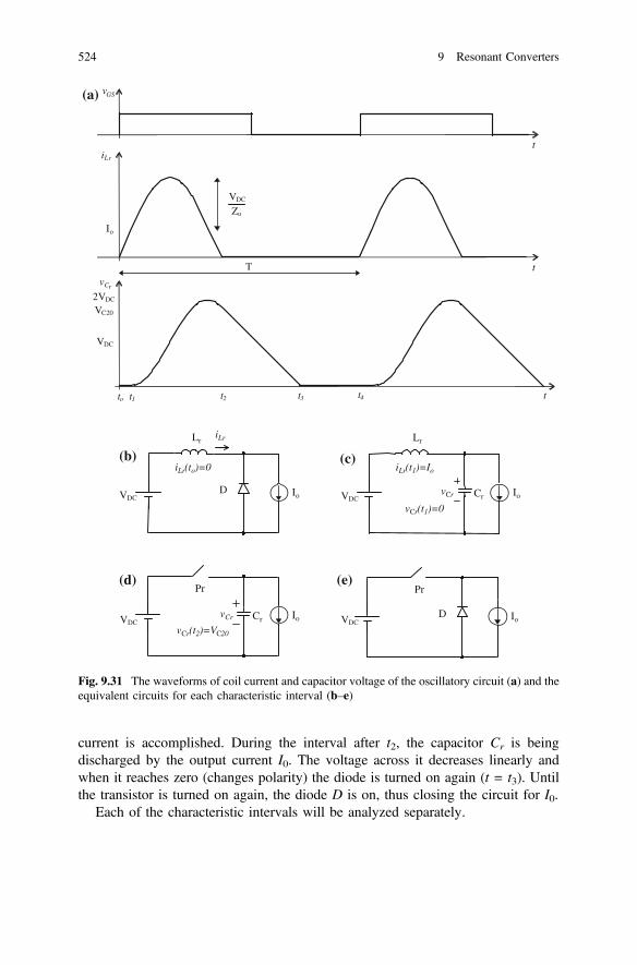
current is accomplished. During the interval after t2, the capacitor Cr is beingdischarged by the output current I0. The voltage across it decreases linearly andwhen it reaches zero (changes polarity) the diode is turned on again (t = t3). Untilthe transistor is turned on again, the diode D is on, thus closing the circuit for I0.
Each of the characteristic intervals will be analyzed separately.
iLr
VDC
Lr
D Io
iLr(to)=0(b)
(d)
vCr IoCr
vCr(t2)=VC20
Pr
D Io
(e)Pr
vCr
Lr
Io
iLr(t1)=Io
Cr
vCr(t1)=0
(c)
VDC
VDC VDC
t
VDC
vCr
to t1 t2 t4t3
2VDC
t
Io
iLr
VDC
Zo
T
VC20
t
vGS(a)
Fig. 9.31 The waveforms of coil current and capacitor voltage of the oscillatory circuit (a) and theequivalent circuits for each characteristic interval (b–e)
524 9 Resonant Converters

9.5.1.1 Interval T0–1 (0 ≤ t ≤ t1)
The transistor and the diode are on. The initial current of the coil Lr is zero. SinceVLr = VDC, the coil current is
iLrðtÞ ¼ 1Lr
Z t
0
VDCdt ¼ VDC
Lrt: ð9:53Þ
At t = t1, iLr(t1) = I0 and the diode is turned off. By using (9.53), it turns out that
T0�1 ¼ t1 ¼ LrI0=VDC: ð9:54Þ
9.5.1.2 Interval T1–2 (t1 ≤ t ≤ t2)
By turning off the diode, the oscillatory circuit LrCr is established (Fig. 9.31c) andthe following equations apply
VCrðtÞ ¼ VDC � LrdiLrðtÞdt
; ð9:55Þ
iCr tð Þ ¼ iLr tð Þ � I0: ð9:56Þ
The solution of these differential equations, with the initial conditions iL(t1) = I0and VCr(t1) = 0, is
iLrðtÞ ¼ I0 þ VDC
Z0sin½x0ðt � t1Þ�; ð9:57Þ
VCrðtÞ ¼ VDCf1� cos½x0ðt � t1Þ�g; ð9:58Þ
where Z0 = √(LrCr) is the characteristic impedance of the oscillatory circuit andω0 = 1/√(LrCr) is the resonant frequency. As long as VCr(t) < VDC the currentthrough the coil increases. It reaches its maximum at VCr = VDC, or by taking intoaccount (9.58), at ω0(t − t1) = π/2. From this and equation (9.58), it follows that themaximum transistor current is
9.5.1.3 Interval T2–3 (t2 ≤ t ≤ t3)
The equivalent circuit for this interval is shown in Fig. 9.31d. The transistor M isturned off at zero current and the capacitor Cr is discharged by I0, thus:
9.5 DC/DC Converters Based on Resonant Switches 525

VCr ¼ VC20 � I0Cr
ðt � t2Þ: ð9:59Þ
Therefore, VCr(t) decreases linearly. At its zero crossing, the diode D is turned onand keeps the voltage across the capacitor at zero value. This is the end of this timeinterval. From the conditions VCr(t3) = 0 and (9.59), it follows
T2�3 ¼ ðt3�t2Þ ¼ VC20Cr
I0: ð9:60Þ
9.5.1.4 Interval T3–4 (t3 ≤ t ≤ t4 = T)
Within this interval the transistor is off and the diode is on, so iLr = 0 and VCr = 0.The equivalent circuit is shown in Fig. 9.31e. This interval ends by turning on thetransistor, so
T3�4 ¼ t4 � t3 ¼ T � T0�1 þ T1�2 þ T2�3ð Þ: ð9:61Þ
9.5.1.5 The Output Voltage
Ideally, without losses, the output voltage can be determined on the basis of theenergy balance. Within one cycle, the energy of the power source Ws is equal to theenergy absorbed by the load W0, where
WS ¼Z t
0
pSðtÞdt ¼ VDC
ZT0
iLrðtÞdt; ð9:62Þ
W0 ¼Z t
0
p0ðtÞdt ¼ V0I0T : ð9:63Þ
Considering (9.53) and (9.57), it turns out that
WS ¼ VDC
Zt10
VDCtLr
dt þ VDC
Zt2t1
I0 þ VDC
Z0sinx0 t � t1ð Þ
dt
¼ VDCI0t12þ t2 � t1ð Þ þ VDCCr
I01� cosx t2 � t1ð Þð Þ
¼ VDCI0T0�1
2þ T1�2 þ T2�3
� �:
ð9:64Þ
From Ws = W0 one obtains
526 9 Resonant Converters

VO ¼ VDC
T0�1=2þ T1�2 þ T2�3
T: ð9:65Þ
It is obvious that (9.65) is similar to (4.11) which defines the output voltage of aPWM forward converter as V0 = VDC τ/T, where τ is the interval while the switchingelement is on. The interval τ of PWM converters is equivalent to the quasi-resonantinterval of a quasi-resonant converter τQR, where
sQR ¼ T0�1=2þ T1�2 þ T2�3 ð9:66Þ
Therefore, (9.65) can be written in the form
V0 ¼ VDC
sQRT
: ð9:67Þ
In this way a complete analogy is obtained for the output voltage of the PWMand the quasi-resonant forward converters. Since τQR < T, the output voltage issmaller than the input voltage like in the PWM forward converters.
The τQR is denoted as quasi-resonant because the resonant changes are only apart of the whole cycle. From (9.54), (9.60), and (9.63) it is obvious that time τQR isa function of the output current I0, the input voltage VI, and the parameters of theoscillatory circuit Lr, Cr. Therefore, by varying the load and the input, the voltageτQR changes and so does the output voltage, V0. Maintaining a constant outputvoltage is possible if the cycle time T or the frequency of the control pulses isvaried. An increase of the control frequency increases the output voltage.
Figure 9.32 shows the dependence of the normalized output voltage (V0/VDC) onthe normalized frequency, f/f0 with the load constant aL = RL/Z0 as a parameter. Thesensitivity of the function V0/VDC = Φ(f/f0) increases with decreasing the load
0.00
0.20
0.40
0.60
0.80
1.0010.0 5.0 2.0 1.0
0.20 0.40 0.60 0.80 1.00
V
V <V
V0
0
DC
f / f0
DC
a = 0.5L
Fig. 9.32 The frequencycharacteristic of the ZCS-QRforward converter
9.5 DC/DC Converters Based on Resonant Switches 527

(increasing of RL). Without the diode Ds the internal diode of the MOS transistorwould conduct the negative current of the resonant coil. In that case the quasi-resonant interval is shortened and the output voltage is an approximately linearfunction of frequency
V0 � VDC=f 0ð Þf ;
regardless of the load. In this case, however, a part of the energy accumulated in theresonant capacitor is returned to the primary source instead of contributing to theoutput current.
Example 9.4 The parameters of the ZCS-QR converter of Fig. 9.30 are VDC = 12 V,Cr = 0.1 μF, Lr = 810 μH, I0 = 1 A, and frequency f = 100 kHz. Determine:
(a) the output voltage, the maximum transistor current, and the maximum reversevoltage of diode D,
(b) frequency f at which the voltage is 6 V, at the same current,(c) the maximum frequency.
The circular frequency and the characteristic impedance of the oscillatory circuitare, respectively,
x0 ¼ 1 ffiffiffiffiffiffiffiffiffiffi
CrLrp ¼ 1
� ffiffiffiffiffiffiffiffiffiffiffiffiffiffiffiffiffiffiffiffiffiffiffiffiffiffiffiffiffiffiffiffiffiffiffiffiffiffiffiffiffiffiffiffiffiffiffiffiffið0:1� 10�6Þð10� 10�6Þ
q¼ 106 rad/s;
Z0 ¼ffiffiffiffiffiffiffiffiffiffiffiffiLr=Cr
p¼
ffiffiffiffiffiffiffiffiffiffiffiffiffiffiffiffiffiffiffiffiffiffiffiffiffiffiffiffiffiffiffiffiffiffiffiffiffiffiffiffiffiffiffiffiffiffiffiffiffiffiffið10� 10�6Þ=ð0:1� 10�6Þ
q¼ 10X:
The characteristic time intervals are
T0�1 ¼ t1 ¼ I0Lr=VDC ¼ 1� ð10� 10�6Þ=12 ¼ 0:833 ls:
T1�2 ¼ t2 � t1 ¼ 1x0
pþ arcsinZ0I0VDC
¼ 1
106pþ arcsin
1 � 1012
¼ 4:13 ls:
T2�3 ¼ t3 � t2 ¼ CrVDS
IOf1� cos½x0ðt2 � t1Þ�g
¼ 0:1� 10�6� �� 12
1½1� cosð106 � 4:13� 10�6Þ� ¼ 1:86 ls:
The quasi-resonant interval is τQR = T0–1/2 + T1–2 + T2–3 = 6.4065 μs.
528 9 Resonant Converters

(a) The output voltage is
VO ¼ VDCsQR=T ¼ VDCsQRf ¼ 12� ð6:4065� 10�6Þ � ð100� 106Þ ¼ 7:69V:
• The maximum transistor current is IDSM = I0 + VDC/Z0 = 1 + 12 V/10 Ω = 2.2 A.• The maximum reverse voltage of the diode D is equal to the maximum voltage
across the resonant capacitor, i.e., VCrM = 2VDC = 2 × 12 = 24 V.
(b) When the output current I0 and the output voltage V0 do not vary, then thequasi-resonant interval does not depend on the output voltage, and
f ¼ VOðVDCsQRÞ ¼ 6V=ð12V� 6:406msÞ ¼ 78 kHz:
(c) The cycle of control pulses has to be
T [ t3 ¼ T0�1 þ T1�2 þ T2�3 ¼ 0:833þ 4:13þ 1:86 ¼ 6:82 ls; and fmax
¼ 1=Tmin ¼ 1=t3 ¼ 146 kHz:
The ZCS-QR forward DC/DC converter based on the resonant switch inFig. 9.28a is shown in Fig. 9.33a. Initially, at t = 0, the transistor M is off, the diodeD is on, so the voltage across the resonant capacitor is VDC, and the current of theresonant coil is zero. Therefore, the transistor is turned on at zero current. Duringthe quasi-resonant interval τQ, while the transistor is on and the diode is off, theoscillatory character of iL and VCr, involving zero crossing, is established. Owing tothis, the transistor turning off at zero current is enabled. In fact, the principle is thesame as for the circuit in Fig. 9.30. The waveforms and the equivalent circuits foreach characteristic time interval presented in Fig. 9.33 clearly indicate the processesin the circuit.
The general characteristics of the ZCS-QR forward converter can be summarizedas follows:
• The current of transistor M is approximately zero at turn on and turn off, thusdynamic losses are negligible.
• The maximum current is load dependent (IDSM = I0 +VDC/Z0).• The diode D is turned on at small voltage variations dv/dt so the requirements
regarding its choice are not tight.• In order to enable the transistor to be turned off at zero current, the current of the
resonant coil should reach zero value, which is obtained if its amplitude ishigher than the output current, i.e., VDC/Z0 > I0. On the basis of this, it followsthat the condition for turning off the transistor at zero current is formulated asZ0V0/VDC < R < ∞.
9.5 DC/DC Converters Based on Resonant Switches 529

RLC
C
C
C
C
C
LL
L
L
f
r
r
r
r
r
fr
r
r
V0
V
V
V
C
C
D
D
Mr
r
+
+
-
-
i
i
t
t
t
VDC
VDC
VDC
V0
V / Z
V
DC
DC
0
I0
t t t t t0 1 2 3 4T =1/f
2
TT T T
0-1
1-2 2-3 3-4
V V
V
V
DCDC
DC
DC
L L
L
Lr r
r
r
I I
I
I 0
0
0
0
(a)
(b)
(c) (d) (e)
(f)
Fig. 9.33 The second version of a ZCS-QR forward converter (a), characteristic waveforms (b),and equivalent circuits within one cycle (e–f)
530 9 Resonant Converters

9.5.2 ZVS Quasi-resonant Converters
The ZVS quasi-resonant DC/DC converters are obtained by replacing the switchingelement of a PWM converter by a ZVS resonant switch. The principle of theoperation of the ZVS-QR converters will be considered by presenting the exampleof the forward converter (Fig. 9.34), assuming that the current of the output chokeLf is approximately I0 and that the transistor and the diode are ideal switches.
The waveforms of the voltage across the resonant capacitor Cr and the currentthrough the coil Lr are shown in Fig. 9.35a. Prior to the instant t0 = 0, when thecycle begins, the transistor M is on. The current through the transistor is I0. Thecapacitor Cr is empty (VCr = 0). The diode D is off. At an instant t0 the transistor isturned off at zero voltage. After that, the current I0 flows through Cr and Lr(Fig. 9.35b) and the voltage across the transistor increases linearly. The variation ofthis voltage while the current through the transistor is decreasing is negligible, sothe dynamic losses at turning off are negligible. At the instant t1, when VCr = VDC,the voltage across the diode D changes its direction and the diode turns on(Fig. 9.35c). The series oscillatory circuit LrCr is established and so are the oscil-latory variations of the voltage VCr and the current iLr involving zero crossings.Upon zero crossing of the voltage VCr, the antiparallel diode DM will turn on andlimit further variations of VCr, thus VCr = 0. Then the control pulse turns thetransistor M on, ensuring a zero voltage turn on. In order to determine the outputvoltage it is necessary to determine the quasi-resonant cycle. For this purpose thecircuit will be analyzed by intervals.
9.5.2.1 Interval T0–1 (0 ≤ t ≤ t1)
The transistor M and the diode D are off. The equivalent circuit of the converter,including the initial conditions, is shown in Fig. 9.35b. The voltage across thecapacitor Cr is
VCr tð Þ ¼ I0Cr
t: ð9:68Þ
RLC
C
LL
L
f
r
fr
r
V0
VC
DM
r+ -
i
VDC VD
DM
Fig. 9.34 The ZVS-QR forward converter
9.5 DC/DC Converters Based on Resonant Switches 531

t
VDC
vCr
ZoIo
T
iLr
t
Io
to t1 t2 t4t3
-Io
IL20
t
vG
t
vD
VDC
T1-2 T2-3 T3-4T0-1
t2'
(d)
VDC Io
Lr
D
(e)
VDC Io
Lr
(b)
VDC
Lr
Io
Cr
iLr(t0)=I0(c)
VDCF
Lr
D Io
Cr
T0-1 T1-2
M
T2-3 T3-4
MDM
(a)
vCr(t0)=0 vCr(t1)=VbiLr(t1)=I0
iLr iLr
iLr=I0iLr
iLr(t2)=IL20
Fig. 9.35 The waveforms within one cycle of the ZVS-QR forward converter (a), and theequivalent circuits (b–e)
532 9 Resonant Converters

Since the current through the coil is constant, the voltage drop across it isnegligible and the voltage across the diode is
VD ¼ VDC � VCr tð Þ: ð9:69Þ
This interval ends when the diode is turned off, i.e., at VD(t) = 0, and
T0�1 ¼ t1 ¼ CrVDC
I0: ð9:70Þ
9.5.2.2 Interval T1–2 (t1 ≤ t ≤ t2)
The transistor is off, whereas the diode is on (Fig. 9.35c). Now
LrdiLrðtÞdt
þ VCrðtÞ ¼ VDC; ð9:71Þ
iCrðtÞ ¼ CrdVCrðtÞ
dt; ð9:72Þ
and the initial conditions are marked in Fig. 9.35c. The solution of this set ofequations is given by
iLrðtÞ ¼ I0 cos½x0ðt � t1Þ�; ð9:73Þ
VCrðtÞ ¼ VDC þ I0Z0 sin½x0ðt � t1Þ�; ð9:74Þ
where ω0 is the circular resonant frequency and Z0 is the characteristic impedanceof the oscillatory circuit. The maximum drain–source voltage of the transistor isequal to the amplitude of the voltage across capacitor Cr, VCr, i.e.,
VDSM ¼ VCrM ¼ VDC þ I0Z0 ¼ VDS þ I0ffiffiffiffiffiffiffiffiffiffiffiffiLr=Cr
p: ð9:75Þ
This interval ends at VCr(t2) = 0, so
T1�2 ¼ t2 � t1 ¼ 1x0
pþ arcsinVDC
I0Z0
: ð9:76Þ
The current of the resonant coil at the end of this interval is
IL20 ¼ I0 cos½x0ðt2 � t1Þ�: ð9:77Þ
The voltage across the capacitor may become zero only if I0Z0 > VDC, thereforeit turns out that the maximum resistance of the load which still permits turning on ofthe transistor at zero voltage is
9.5 DC/DC Converters Based on Resonant Switches 533

RLmax ¼ Z0 V0=VDCð Þ: ð9:78Þ
9.5.2.3 Interval T2–3 (t2 ≤ t ≤ t3)
Both diodes, D and DM, are on. The antiparallel diode DM conducts the negativecurrent of the coil Lr toward the primary source. The transistor M should turn onbefore the instant t2 in order to take over the positive current iL. Therefore, in theinterval T2–3 the coil is connected to the primary source by a low resistance(Fig. 9.35d). The voltage across the coil Lr is constant and equal to VDC, so the coilcurrent increases linearly, i.e.,
iLr tð Þ ¼ IL20 þ 1Lr
Zt3t2
VDCdt ¼ IL20 þ VDC
Lrt: ð9:79aÞ
This interval ends by turning off the diode D at iLr(t) = I0, and from (9.79a)
T2�3 ¼ t3 � t2I0 � IL20VDC
Lr ¼ I0LrVDC
½1� cosðx0T1�2Þ�: ð9:79bÞ
9.5.2.4 Interval T3–4 (t3 ≤ t ≤ t4)
The transistor is on and the diode is off. The equivalent circuit is as shown inFig. 9.35e. The current I0 flows via the transistor which keeps the voltage across Cr
at zero value until it is turned on again within the next cycle.
9.5.2.5 Output Voltage
The voltage across the diode D (Fig. 9.35a) is the input voltage of theoutput filter.Therefore, the output voltage can be calculated as the average value of the voltageVD, i.e.,
V0 tð Þ ¼ 1T
ZT0
VD tð Þdt: ð9:80Þ
According to Fig. 9.35a, and taking into account (9.69), it turns out that
VD tð Þ ¼VDC 1� t=t1ð Þ; 0\t\t10 t1\t\t3VDC t3\t\T :
8<: ð9:81Þ
By combining (9.80) and (9.81) one obtains:
534 9 Resonant Converters

V0 ¼ VDC 1� sQRT
� �; ð9:82Þ
where, analogously to the ZCS-QR converters,
sQR ¼ T0�1=2þ T1�2 þ T2�3; ð9:83Þ
is the quasi-resonant interval. Since this interval is load-current-dependent, theoutput voltage is also a function of the load (Fig. 9.36). The load constant isdependent on the frequency characteristics of the converter in Fig. 9.36.
According to (9.78), the permitted range of load variations still allowing zerovoltage turning on the transistor is
0\RL\Z0 V0=VDCð Þ:
The output voltage is a function of the frequency of the control pulses of thetransistor M. Increasing this frequency causes the output voltage to drop. At aconstant voltage VDC and output current I0 the quasi-resonant interval is constant,whereas the interval T3–4 varies.
At first glance there is no corresponding analogy between the V0/VDC ratios ofthe ZVS-QR and the PWM converters like the one existing between the ZCS-QRand the PWM converters. This is only apparent, because in the quasi-resonantinterval τQR of the ZVS-QR converters the transistor is off, whereas in the PWMduring τ it is on. With respect to the interval in the PWM converters when thetransistor is off, the output voltage is
V0 ¼ VDC
sT¼ VDC
T � soffT
¼ VDC 1� soffT
� �: ð9:84Þ
0.00
0.20
0.40
0.60
0.80
0.900.80
0.50
0.20
1.00 2.0 1.0
0.20 0.40 0.60 0.80 1.00
V
V < V
V0
0
DC
f / f0
DC
a =0.10L
Fig. 9.36 The normalizedfrequency characteristic of theZVS-QR forward converter
9.5 DC/DC Converters Based on Resonant Switches 535

Consequently, the analogy between the ZVS-QR and the PWM converters iscomplete.
The general characteristics of the ZVS-QR DC/DC forward converters can besummarized as follows:
• The switching element is turned on and off at approximately zero voltage acrossit, thus the switching losses are negligible.
• Since the dynamic losses are small these converters may operate at very highfrequencies (up to 10 MHz).
• The output capacitance of the transistor is a constituent part of the resonantcapacitor Cr and has no adverse influence on the operation of the converter.
• The maximum voltage across the transistor is higher than that of the PWMconverters and is load dependent (VDSM = VDC + Z0I0). The breakdown voltageof the transistor has to be higher than VDSM at the maximum current I0.
• The capacitance of the reverse biased diode D, during the interval when it isturned off, together with the resonant coil may cause undesirable oscillationswhich induce additional losses and control problems.
Example 9.5 The following parameters of a ZVS-QR forward converter are known:VDC = 20 V, Lr = 1 μH, Cr = 0.047 μF, and I0 = 5 A. One should determine:
(a) the switching frequency so that the output voltage is V0 = 10 V,(b) the maximum voltage across the switching element, and(c) the maximum resistance of the load still permitting the zero voltage turning on
of the transistor.
The parameters of the resonant circuit are
x0 ¼ 1� ffiffiffiffiffiffiffiffiffiffiffiffiffiffiffiffiffiffiffiffiffiffiffiffiffiffiffiffiffiffiffiffiffiffiffiffiffiffiffiffiffiffiffiffiffi
10�6 � ð0:047� 10�6Þq
¼ 4:61� 106 rad/s;
Z0 ¼ffiffiffiffiffiffiffiffiffiffiffiffiLr=Cr
p¼
ffiffiffiffiffiffiffiffiffiffiffiffiffiffiffiffiffiffiffiffiffiffiffiffiffiffiffiffiffiffiffiffiffiffiffiffiffiffiffiffiffiffi10�6=ð0:047� 10�6Þ
q¼ 4:61X:
The time intervals
T0�1 ¼ t1 ¼ VDCCr=I0 ¼ 20� ð0:047� 10�6Þ=5 ¼ 0:188 ls:
On the basis of (9.76) and (9.79a), respectively,
T1�2 ¼ t2 � t1 ¼ 14:61� 106
arcsin20
5� 4:61
� �þ p
� 0:9 ls;
T2�3 ¼ t3 � t2 ¼ 5� 10�6
201� cos 4:61� 106 � 0:9� 10�6� �� � ¼ 0:37 ls;
the quasi-resonant interval is τQR = T0–1/2 + T1–2 + T2–3 = 1.36 μs.
536 9 Resonant Converters

(a) From (9.82) it follows
f ¼ 1sQR
1� VO
VDC
� �¼ 1
1:36� 10�6 1� 1020
� �¼ 3:67 kHz:
(b) According to (9.75), the maximum voltage drain–source of the transistor is
VDSM ¼ 20Vþ 5A� 4:61X ¼ 43V:
(c) With reference to (9.78), the maximum resistance of the load still permittingthe zero voltage turning on the transistor is
RLmax ¼ 4:61X1020
¼ 2:61X:
9.5.3 Multiresonant Converters
The multiresonant (MR) ZVS converters have one additional capacitor and a diode(Fig. 9.37). The capacitor CD includes the capacitance of the reverse biased diodewhich was causing the undesirable oscillations in the ZVS-QR converters.
Here, the oscillations through CD are taken into account and controlled. Anexample of a ZVS-MR forward DC/DC converter is shown in Fig. 9.38. Comparedto the topology of the corresponding ZVS-QR converter it differs only by thecapacitor CD. During time intervals when the diode is on, the capacitor CD is short-circuited and has no influence. When the diode is off and the transistor is on,CD = Cr1 and together with Lr it forms an oscillatory circuit. During time intervalswhen both the transistor and the diode are off, the capacitor CD together with CM
forms a resonant capacitor Cr2 = CDCM/(CD + CM). Therefore, oscillatory circuitsmade of different elements are active in different time intervals. In one of these, theresonant capacitor is Cr1 = CD and in the other Cr2 = CD||CM. For this reason theseconverters are denoted as multiresonant.
The general characteristics of ZVS-MR converters can be summarized asfollows:
• All main parasitic elements of the converter are included in the resonant ele-ments. The switching elements change states at zero voltage so the dynamiclosses are negligible. Therefore, they can operate at very high frequencies(10 MHz) and reach high power densities (>50 W/inch3).
• Compared to the ZVS-QR converters the maximum voltage across the transistoris lower, but the current in the oscillatory circuit is increased so the ohmic lossesare increased.
9.5 DC/DC Converters Based on Resonant Switches 537

Lr
CM
Pr
CDD
Sw
Fig. 9.37 A ZVS multiresonant switch
VDC
Lr Lf
D Cf Ro
iLr IoDM
M
CM
VoCD
+ _vCM
vCDvGS
vGS
tiLr
t
t
t
Io
VDC
VDC
to t1 t2 t3 t4
vCD
vCM
(a)
(b)
Fig. 9.38 A ZVS multiresonant forward converter (a) and its waveforms (b)
538 9 Resonant Converters

9.6 ZVS Resonant DC/AC Converters
The ZVS resonant DC/AC converters (Fig. 9.39a) are essentially the simplifiedclass E resonant inverters where the reactive Lf–Cf net is a function of the resonantLr–Cr net. On the other hand, since the resonant capacitor Cr is connected in parallelwith the Pr switch, the circuit in Fig. 9.39a is a resonant converter where thecommutation of the switching element is at zero voltage. According to this, a ZVSresonant DC/AC converter is a loaded ZVS. The load may be, for example, a motorhaving the internal inductance sufficiently high so that the motor current within oneresonant cycle may be considered constant. Therefore, the load in Fig. 9.39a isrepresented by a current generator I0. Since the basic application of a DC/ACconverter is supplying a load byAC current when the primary source is DC, theoriginal name of this group of converters is the resonant DC-phase (link) inverters.
In the initial state, the switch Pr is on (Fig. 9.39c). The current through theresonant coil increases linearly. When iLr reaches the value of the load current, I0,the current through the switch becomes zero. The switch Pr is then turned off. SinceVCr = 0, turning off occurs at zero voltage and a very small (ideally zero) current.Upon the turn off of the switch, there remains a loaded oscillatory circuit(Fig. 9.39d), whose current and voltage are, respectively,
V
V V
V 2V
DC
DC DC
DC DC
Pr DC
C
r
r
VCr
VCr
VCr
L
L L
L
L
L L
r
r r
r
r
r r
i
i
i i
I
I I
I
0
0 0
0
t
t
(a)
(b)
(c) (d)
Fig. 9.39 A ZVS resonantDC/AC converter (a), thewaveforms (b), andequivalent circuits (c and d)
9.6 ZVS Resonant DC/AC Converters 539

iLrðtÞ ¼ I0 þ VDC
Z0sin½x0ðt � t0Þ�; ð9:85Þ
VCrðtÞ ¼ VDC½1� cosðx0tÞ�; ð9:86Þ
where Z0 is the characteristic impedance of the oscillatory circuit. Therefore, thesevariations are harmonic with zero voltage across the capacitor at the beginning andat the end of each resonant cycle. Thus the switch control should be synchronizedso that it turns on or off when VCr is close to zero. The control pulse frequency isapproximately equal to the frequency of the oscillatory circuit. The switch is ononly during short intervals, required by the resonant coil to accumulate the energyfrom the DC source. While the switch is on, the coil current is close to I0 so thecurrent through the switch is very small. Since turning on and off of the switchoccurs at zero voltage, thedynamic losses of the converter due to the change of thestates of the switch are negligible.
The described concept of the DC/AC converters can be implemented in three-phase PWM inverters (Fig. 9.40). The switch and the diode are the constituent partsof the three-phase bridge. The commutation of the switch in each arm of the bridgeis performed when the voltage across the resonant capacitor reaches zero value.
9.7 Soft Switching PWM DC/DC Converters
The soft switching implies the change of the states of the switch at very lowvoltages, currents, and dissipations of the switch. Ideally, the switch would changethe states at zero current and zero voltage. In practice different techniques ofapproximately zero current or zero voltage commutation of the switch are in use.
VDC Cr
Lr
A
B
C
Sa
Da
Sb
Db
Sc
Dc
Sa’
Da’
Sb’
Db’
Sc’
Dc’
Fig. 9.40 A ZVS resonantDC/AC three-phase inverter
540 9 Resonant Converters

Dynamic losses in both cases are negligible. In that sense all resonant converters arethe converters involving soft switching.
The emphasis on soft switching in resonant converters is aimed at stressing thatsome sort of advanced technique in the resonant converters is being introduced(constant frequency control, the maximum current or voltage reduction, etc.). Eachimprovement, however, causes impairment of some other parameters.
In this section two PWM topologies involving soft switching are described. Intheir quasi-static states they correspond to the conventional PWM converters, butthe changes of states of the switch involve soft switching. These are:
• the phase shift bridge converters, and• the resonant transitions PWM converters.
These converters retain all the good properties of the conventional PWM con-verters (operation at a constant frequency, small maximum voltage and current ofthe switch, and small ohmic losses) and at the same time reduce dynamic losses andstresses in the circuit that occur because of large voltage and current variations. Softswitching in phase shift bridge converters is accomplished through the parasiticelements of the circuit utilizing the phase shifted control pulses of the switchingelements. Therefore, if the control module is excluded, the basic topology remainsthat of the conventional PWM bridge converters.
The topology of the resonant transitions PWM converters is modified by aresonant switch which ensures a resonant change of the voltage across the mainswitching element only during its commutation.
9.7.1 Phase Shift Bridge Converters
The topology of the basic circuit of a phase shift bridge converter (Fig. 9.41) is infact a bridge connection of the symmetric converter (Fig. 4.29). The coil Lr(Fig. 9.39) is not a separate element. It is an equivalent inductance comprising ofthe stray inductance of the transformer and a possible inductance of the circuitconnections. It is extracted here for the purpose of facilitating the explanation of theprinciple. The capacitors Ci and the diodes Di (i = 1, …, 4), also do not representseparate components; they are actually the substrate-drain p-n junctions of the MOStransistors Mi, which behave like capacitors at reverse polarization and like smallresistors at forward polarization.
The peculiarity of the phase shifted bridge converters, compared to the con-ventional converters, is the system of control which enables the active use of theparasitic elements of the components already present in the circuit. As emphasizedby the name, the control is carried out by the phase shifted pulses. The conventionalPWM connections allow the conduction of the diagonal switches of the bridge only.In these converters, during preparations for soft switching, either both upper andboth lower transistors of the bridge are conducting. This interval is controlled by the
9.7 Soft Switching PWM DC/DC Converters 541

dead times of the phase shifted pulses at the transistor gates. Therefore, the role ofthe dead time in the phase shifted connections is twofold:
• it prevents simultaneous conduction of the transistors of the same arm of thebridge, and
• it enables the preparation for the soft switching of the transistors.
The control pulse frequency on all phases is constant, with a 50 % duty cycle.The duty cycle of the secondary voltage of the transformer is phase shift dependent.For this reason the output voltage is a function of the phase shift. Therefore,compared to the conventional PWM converters where the output voltage is con-trolled by varying the duty cycle and the resonant converters where this control isaccomplished by varying the frequency, the output voltage of these converters iscontrolled by varying the phase shift of the control pulses at a constant frequency.The phase shift of the control pulses of the transistors in the opposite arms of thebridge is variable. The pulses of the same arm (M1–M2 or M3–M4) are counter-phased with the dead time for the preparation of the soft switching.
The principle of operation of the phase shift PWM converters will be explainedwith the aid of the waveforms (Fig. 9.42) and equivalent circuits for each charac-teristic interval (Fig. 9.43). The state in the circuit and the variations of the primarycurrent and the characteristic voltages will be monitored from the moment t0 whenthe high voltage level in the transformer secondary is established.
9.7.1.1 Interval T0–1 (t0 ≤ t ≤ t1)
In this interval the gate voltages of the transistors M1 and M4 are high and thesetransistors are on. The other two transistors are off since Vg2 = Vg3 = 0. Theequivalent circuit is shown in Fig. 9.43a. The voltage of the transformer primary isVp = VDC. The transfer of energy to the load in this interval is identical to the one in
D4D2
D3 M3C3
M4
VDC
D1M1
Lr
C1
M2 C2 C4
Io
Cf Ro
Vo
Lf
vp
vg1
vg2
vg3
vg4
n:1:1
vspi
D5
D6
Fig. 9.41 A phase shifted bridge converter
542 9 Resonant Converters

t5t1
vg1
vg4
vg2
vg3
ip
to t2 t3 t4
t
t
t
tvp
t
t
vs
t
Im
I2
VDC
n
I1
VDC
T
De(T/2)
T/2 T/2
(a)
(b)
(c)
(d)
Fig. 9.42 The waveforms of control pulses at the gates of the transistors (a), voltage and currentof the primary (b and c), and secondary voltage of the transformer (d)
M2
M3M1
VDC
ip
vp
M4
Lr
M2
M3M1
VDC
Im
vp
M4
Lr
iC3
C3
C4
iC4
iD3
D3
iM3
M2
M3M1
VDC
ip
vp
M4
Lr
iC1
C1
C2
iC2
iD3
D3
iM3
M2
M3M1
VDC
ip
vp
M4
Lr
M2
M3M1
VDC
ip
vp
M4
Lr
VDC
I1
(a) (b) (c)
(e)(d)
Fig. 9.43 The equivalent circuits of the converter within the characteristic time intervals. (a) T0–1,(b) T1–2, (c) T2–3, (d) T3–4, (e) T4–5
9.7 Soft Switching PWM DC/DC Converters 543

the conventional converters. Since the voltage of the primary is constant, its currentis a linear function of time. It can be expressed as the output current referred to theprimary side of the transformer, i.e.,
ipðtÞ ¼ I1 þ VDC=n� V0
nLfðt � t0Þ; ð9:87Þ
where I1 is the initial primary current and n is the transformation ratio of thetransformer. This interval ends at the instant the transistor M4 is turned off whenVg4 = 0. This turning off occurs at zero voltage since the capacitor is empty whileM4 is on.
9.7.1.2 Interval T1–2 (t1 ≤ t ≤ t2)
This interval is equal to the dead time of the control pulses of the transistors in theright arm of the bridge, i.e.,
T1�2 ¼ tD34: ð9:88Þ
Only the transistor M1 is on (Fig. 9.43b). Now C4 is being charged and C3
discharged since it was previously charged to VDC by the residual primary currentIpM. This is the maximum primary current. The variation of this current withininterval T1–2 is negligible so the charging of C4 and discharging of C3 are by aconstant current and with a linear voltage variation.
Consequently, the primary and the secondary voltage of the transformer alsovary linearly (Fig. 9.42b, d). The capacitor C3 should discharge to zero voltage.Since the voltage variation across C3 and C4 is
DVCe ¼ IpMCe
t; Ce ¼ C3 þ C4; ð9:89Þ
from condition ΔVCe(T1–2) = VDC, it follows that the dead time is
tD3;4min ¼ CeVDC
IpM : ð9:90Þ
9.7.1.3 Interval T2–3 (t2 ≤ t ≤ t3)
The end of the interval T1–2 and the beginning of the interval T2–3 coincide with thepositive pulse at the gate of the transistor M3, when the transistor is turned on. Thisturning on is at zero voltage because C3 has discharged previously. During theinterval T2–3 both upper transistors of the bridge, M1 and M3, are on. The primaryand the secondary voltages are equal to zero. Therefore, the primary of the trans-former in this interval is short-circuited. The current through the primary is the
544 9 Resonant Converters

secondary current referred to the primary which is approximately a linear functionof time, i.e.,
ip tð Þ ¼ IpM � V0
nLft � t2ð Þ: ð9:91Þ
This interval ends at Vg1 = 0 when M1 is turned off. Thus T2–3 is the timebetween the pulses Vg1 and Vg3.
9.7.1.4 Interval T3–4 (t3 ≤ t ≤ t4)
The transistor M1 is off. This turning off occurred at zero voltage. Only the tran-sistor M3 remains on (Fig. 9.43d). This time interval is determined by the dead timeof the control pulses of the transistors M1 and M2 in the left arm of the bridge and isapproximately equal to one quarter of the resonant interval, i.e.,
T3�4 ¼ tD1;2 �p2
ffiffiffiffiffiffiffiffiffiffiLrCr
p: ð9:92Þ
The capacitor C1 is being charged and C2 is discharged by the current appearingdue to the energy accumulated in the resonant coil. In order to discharge C2 to zeroand to prepare M2 for soft switching in the next interval, the energy accumulated inthe coil Lr has to be sufficient to discharge C2 and charge C1, i.e.,
12LrI
22 [
12C1 þ C2VDC
2 ¼ 12CeVDC
2; ð9:93Þ
where I2 is the primary current of the transformer at instant t3. From (9.93), itfollows that the current has to be
I2 [VDC
ffiffiffiffiffiffiffiffiffiffiffiffiCe=Lr
p; ð9:94Þ
which is met at high output loads. If the condition (9.94) is not met at the maximumvoltage VDC and at the minimum load in the designed range of load variations, thena separate coil is used for the resonant coil. This increases the energy required forcharging C1 and discharging C2 necessary for the preparation of soft switching.
The use of a separate resonant coil reduces the slope of the primary currentwithin interval t3 < t < t5 where
ip tð Þ ¼ Ii � VDC
Lrðt � t3Þ: ð9:95Þ
This increases the duration of the interval t5–t3 and decreases the effective valueof the duty cycle, De, of the pulses in the transformer secondary which finallydecreases the range of the output voltage variations.
9.7 Soft Switching PWM DC/DC Converters 545

9.7.1.5 Interval T4–5 (t4 ≤ t ≤ t5)
At the instant t4 a positive pulse turns on the transistor M2. If C2 is dischargedduring the previous interval, this turning on occurs at zero voltage. Therefore, inthis interval the diagonal transistors, M2 and M3, are on (Fig. 9.43e) causing theprimary current to change direction and its value is approximately determined by(9.95). Within this interval both of the rectifying diodes are on and the secondary ofthe transformer is short-circuited (Vs = 0). At the instant t5, when the primarycurrent is –I1, one of the rectifying diodes is turned off and the secondary voltage isVs = VDC/n.
After t5, the transfer of energy to the load is the same as in a conventional PWMconnection. In fact, the interval after t5 is analogous to interval T0–1, because thenew cycle, with reference to the secondary, begins at instant t5. The rectified voltageat the output is equal to the mean value of the secondary voltage, i.e.,
VO ¼ 1T=2
ZT=20
VSðtÞdt ¼ 1T=2
ZDe T=2ð Þ
0
VDS=ndt ¼ DeVDC=n; ð9:96Þ
where De is the effective value of the duty cycle of the pulses in the transformersecondary.
The general characteristics of the phase shift PWM converters can be summa-rized as follows:
• The transistors are turned on or off at zero voltage which reduces significantlythe dynamic dissipation.
• The elements for the preparation of soft switching are the parasitic elements ofthe already used components so the negative effects of the parasitic elements areeliminated.
• By reducing the voltage and current variations the reduction of the generatedinterference (EMI and RFI) is accomplished.
• The maximum voltage across transistors is equal to the input voltage, as with theconventional circuits. The maximum currents in the bridge are higher than thosein conventional circuits, but they are considerably lower than the currents of theresonant topologies.
Example 9.6 The soft switching PWM DC/DC converter (Fig. 9.41) has the fol-lowing parameters: VDC = 50 V, n = 1.5, Lf = 10 μH, and f = 100 kHz.
(a) Determine the effective value of a duty cycle so that the output voltage is 20 V.(b) Determine the maximum primary current if its value at the beginning of the
period is 1 A.
(a) The output voltage is (9.96): VO ¼ DeVDC
n ) De ¼ nVOVDC
¼ 0:6:(b) Primary current increases during the interval T0–1 when the transistors M1 and
M4, are turned on. This current is the sum of the initial current and the output
546 9 Resonant Converters

current referred to the primary side of transformer (9.87), and its maximumvalue is reached at the moment t = t1
IpM ¼ I1 þVDC
n � VO
nLfDeT=2 ¼ 3:67A
9.7.2 Resonant Transitions PWM Converters
The resonant transitions PWM converters are made by modifying the correspondingtopologies of the conventional PWM converters in order to provide the softswitching of the switching element. This has been accomplished by the resonantelements, LrCr, and one auxiliary switch. The resonant capacitor is connected inparallel with the main switch, whereas the coil is in series with the auxiliary switch.This ensures a zero voltage transition and the abbreviated notation for this type ofconverters is ZVT-PWM (Zero Voltage Transition-PWM).
Practically, each conventional PWM topology can be modified into a softswitching circuit. This will be explained here taking the example of a voltagebooster (Fig. 9.44). The main switch is the MOS transistor M. Its internal diode isDM. The auxiliary switch is M1.
The diode D1 limits the maximum voltage of the transistor M1 to the value of theoutput voltage, V0. It is assumed, like with the conventional converters, that theinductance Lf and the capacitance Cf are sufficiently large to consider the currentthrough Lf and the voltage across Cf in the quasi-static states constant. In otherwords, it may be assumed that the converter is fed by a constant current source IDCand that the load is a constant voltage source. In the present analysis, the timingdiagrams (Fig. 9.45) and the equivalent circuits in the characteristic time intervals(Fig. 9.46) will be used.
vg
iMiLr
DM
D1
IDC
Ro
Lf
VDCM
Lr
Cr
D
M1
Cf Vo
vg1
iD
vD_ +
vM1
_
+
vM
Fig. 9.44 A ZVT-PWM boost converter based on the soft switching
9.7 Soft Switching PWM DC/DC Converters 547

9.7.2.1 Interval T0–1 (t0 ≤ t ≤ t1)
Until t = t0 both transistors are off (Vg = V1 = 0) and the diode D is on. At t = t0,Vg1 = VGG and M1 is turned on. The resonant coil is then connected in parallel withthe output (Fig. 9.46a). Therefore, the current through it increases linearly:
vM1
to
IDC
Vo
vM
iLr
IDC
vg
iM
vD
iD
Vo
Vo
IDC
t1 t2 t3 t4 t5 t6 t7
t
t
t
t
t
t
t
t
TD
T
vg1
Fig. 9.45 The characteristic waveform of a PWM resonant boost converter
VoLrIDC Cr
IDC Lr IDC Lr
Lr
VoIDC IDC CrIDC VoIDC
D
M1 M1
M
D1
M M
D
(a)
(d) (e)
(b) (c)
(f) (g)
Fig. 9.46 The equivalent circuits corresponding to different time intervals. (a) T0–1, (b) T1–2,(c) T2–3, (d) T3–4, (e) T4–5, (f) T5–6, (g) T6–7
548 9 Resonant Converters

ILr tð Þ ¼ V0
Lrt: ð9:97Þ
The current through the diode D is iD = IDC – iL. At the instant t1, wheniD(t1) = 0, the diode is turned off and ends this interval which is determined by
T0�1 ¼ t1 � t0 ¼ IDCLr=VO: ð9:98Þ
The diode D is turned off at small variations dv/dt and di/dt. Therefore, theinterval T0–1 is the interval of the soft turning off of the diode D.
9.7.2.2 Interval T1–2 (t1 ≤ t ≤ t2)
The turned off diode separates the output from the resonant coil. Since M is turnedoff, an oscillatory circuit is formed in parallel with it (Fig. 9.46b). The capacitor Cr
discharges and the current through Lr continues to increase (Fig. 9.45). The char-acter of these variations is harmonic.
This interval ends at the instant t2 when the voltage across Cr drops to zero, i.e.,when VM(t2) = 0. It can be shown that this interval is equal to one quarter of thecycle of oscillation of the oscillatory circuit, i.e.,
T1�2 ¼ t2 � t1 ¼ p2
ffiffiffiffiffiffiffiffiffiffiLrCr
p: ð9:99Þ
9.7.2.3 Interval T2–3 (t2 ≤ t ≤ t3)
In this interval the internal diode DM of the transistor M is on, so VM = Vd = 0,which ensures the zero voltage turning on of the transistor M. This condition isensured at the end of the previous interval, so it could be that T2–3 = 0. Never-theless, T2–3 > 0 and it is a standby interval which warrants that the capacitor Cr isdischarged to zero before the transistor M is on. Namely, the delay in turning on thetransistor M compared to the transistor M1 should be
TD � T0�1 þ T1�2 ¼ IDCLrVO
þ p2
ffiffiffiffiffiffiffiffiffiffiLrCr
p: ð9:100Þ
Equation (9.100) is the condition for soft switching. This delay time is not loaddependent as it was for the phase shift PWM converters.
If this condition is met at the minimum output voltage, it is valid for the wholerange of variations of V0. The time TD should be much shorter than the cycle of thecontrol pulses if the ratio V0/VDC is not to be degraded.
9.7 Soft Switching PWM DC/DC Converters 549

9.7.2.4 Interval T3–4 (t3 ≤ t ≤ t4)
The transistor M1 is off, whereas M is on (Fig. 9.46d). The diode D is on soVM1 = V0. The current of the resonant coil decreases linearly and at t4 drops to zero.Meanwhile, the energy accumulated by Lr is transferred to the load. The intervalT3–4 is not a critical parameter because it is shorter than the time of conduction ofthe transistor M.
9.7.2.5 Interval T4–5 (t4 ≤ t ≤ t5)
At an instant t4 the diode D1 is turned off. The diode D is off and it separates themain switch from the output (Fig. 9.46e). This interval is equal to that in a con-ventional converter (voltage booster).
9.7.2.6 Interval T5–6 (t5 ≤ t ≤ t6)
At the beginning of this interval the voltage Vg falls to zero and the transistor M isturned off. The resonant capacitor is charged by the current IDC (Fig. 9.46f) and
VMðtÞ ¼ IDCCr
t: ð9:101Þ
This interval is ended by turning on of the diode D at VM(t0) = V0, giving:
T5�6 ¼ CrIDCV0
: ð9:102Þ
9.7.2.7 Interval T6–7 (t6 ≤ t ≤ t7)
The transistors M and M1 and the diode D1 are off, whereas the diode D is on(Fig. 9.46g), transferring the energy from the input to the load. This interval is equalto that in a conventional voltage booster.
The general characteristics of the ZVT-PWM voltage boosters are summarizedas follows:
• The soft switching of the main transistor M and the diode D is realized, but thesame is not valid for the auxiliary transistor. However, it proceeds at consid-erably lower power levels and thus it is not critical.
• The maximum voltages across the transistors and diodes are the same as in theconventional converters.
550 9 Resonant Converters

9.8 Control Circuits of Resonant Converters
The analysis presented in the preceding sections shows that the output voltage ofthe majority of the topologies of resonant converters is dependent on the switchingfrequency. For this reason the switching frequency is the basic control parameter ofthese converters, and the main part of the control circuitry is the voltage-to-fre-quency converter, often called the voltage controlled oscillator (abbreviated VCO).Together with the error amplifier, the VCO is in the feedback loop between theoutput and the control input of the switching elements of the converter.
The other group of control circuits operates at a constant frequency, but with avariable phase shift of the control pulses of different phases. The feedback elementsof these control circuits control the time shifts of the pulses that regulate theswitching elements of the resonant converters.
A wide selection of integrated circuits developed for the purpose of controllingthe resonant converters are available on the market. All these circuits consist ofstandard blocks like the control circuits of PWM converters. These blocks includeerror amplifier, auxiliary oscillator, voltage reference source, logic block, andprotection block. The standard functional inputs and outputs are: different outputoptions, soft start, shutdown, dead time control, etc.
The peculiarities of some of the control circuits are related to the specifictopologies of the converters. Peculiar in that respect are the control circuits of theconverters based on resonant switches having one quasi-stable interval constant andthe other variable. For this reason these circuits, in addition to the VCO, comprise aone-shot (monostable) multivibrator MM (Fig. 9.47) which determines the constantduration of control pulses. There are two groups:
• control circuits of ZCS resonant converters (Fig. 9.47a), and• control circuits of ZVS resonant converters (Fig. 9.47b).
The output voltage of a converter based on resonant switches depends on thequasi-resonant interval τQR and the control pulse frequency. The quasi-resonantinterval is kept constant during:
• the conduction time (ton) of the switching element in ZCS converters, and• the nonconduction time (toff) of the switching element in ZVS converters.
The difference between the fraction of the output voltage kV0 (0 < k <1) and thevoltage reference VREF is amplified by the error amplifier.
The VCO is a generator of short pulses, like the one shown in Fig. 5.5, where thecurrent charging the capacitor is a function of voltage VEA at the output of the erroramplifier (EA) (Fig. 9.47).
Since the VCO triggers the one-shot multivibrator, the frequency of pulses at theoutput of MM is equal to the VCO frequency
9.8 Control Circuits of Resonant Converters 551

f � I VEAð ÞCVh
; ð9:103Þ
where C and Vh are the capacitor and voltage hysteresis of the Schmitt trigger in theVCO (Fig. 5.5), and IEA is the current charging the capacitor C programmed by theoutput of theerror amplifier. The constant quasi-stable interval of these pulses isdetermined by the quasi-stable interval of MM (Fig. 9.48). The MM circuits of theZCS and ZVS converters are the same except for the outputs which are comple-mentary. The quasi-resonant intervals τQR, as shown in Sect. 9.5, are dependent onthe input voltage VDC and the load current I0. In the ZCS converters the maximumquasi-resonant interval τQR is at the minimum VDC and the maximum I0, whereas inthe ZVS at the maximum VDC and the minimum I0. Therefore, the end of theconstant part of the control pulse is synchronized with the zero crossing of currentor voltage (Fig. 9.48).
The circuits for the detection of the zero crossing of current (Fig. 9.47a) orvoltage (Fig. 9.47b) are thus a constituent part of the control circuitry. The elementsof the one-shot multivibrator are so designed that its quasi-stable interval isTM > τQRmax, i.e.,
• TM = tonmax for control circuits of ZCS converters, and• TM = toffmax for control circuits of ZVS converters.
CONTROL CIRCUIT
VCOMMton max
ZCD
SWITCH CURRENT
Outputstage
vGSVREF
FROM OUTPUT
(a)
(b)
OF CONVERTER
(kVo)
Vo
EAVEA
t on
VCOMM
toff max
ZVD
vGS
VREF
(kVo)
CONTROL CIRCUIT
Vo
EAVEA
t off
Outputstage
SWITCH VOLTAGE
FROM OUTPUTOF CONVERTER
Fig. 9.47 The basic blocks of the control circuits of ZCS (a) and ZVS resonant converters (b). EAerror amplifier, VCO voltage controlled oscillator, MM monostable (one-shot) multivibrator, ZCDand ZVD are zero current and zero voltage detectors, respectively.
552 9 Resonant Converters

Upon detection of a zero crossing of the current, at the output of an AND circuitone obtains the low level of the control pulse in the ZCS converters. The high levelof the control pulse in the ZCS converters is obtained when the voltage across theswitching element crosses zero. Therefore, the beginning of the constant interval ofthe control pulse is synchronized with the beginning of the quasi-stable interval ofMM, and its end is synchronized with the zero crossing of the current or voltage ofthe switching element.
The block of the output stage has to provide a sufficiently powerful drive of theswitching element. Since the switching elements are usually MOS transistors, theoutput stage charges and discharges the input capacitance of the MOS transistorCISS = CGS + CGD. CISS of powerful MOS transistors ranges from several hundredup to several thousand pF. The rise and fall times of the control pulses of the highfrequency resonant converters are of the order of several hundred picoseconds up to1 ns. Therefore, the output stage has to provide quite high currents for charging anddischarging of CISS, up to the order of several A, so usually the bipolar transistorsconnected in push–pull configuration are used at the output. It should be empha-sized that the charging and discharging current pulses are very short (shorter than1 ns), so the average value of the output current is negligible.
A constituent part of the output stage is the enable circuit of the output tran-sistors. This circuit is driven by the output signals of the auxiliary blocks, such assoft start signals, under voltage control, shutdown control, etc.
9.8.1 Integrated Circuit Family UCx861-8
The UCx861-8 family of integrated circuits is manufactured by Unitrode. Codex denotes the operating temperature range:
• x = 1: −55 °C < TA < 125 °C,• x = 2: −25 °C < TA < 85 °C,• x = 3: 0 °C < TA < 70 °C.
MM(ZCS)
MM(ZVS)
VCD
T =const.
T = f(V )
TM M
t
t
onmax
offmax
t
t
t(a)
(b)
(c)
0
Fig. 9.48 The voltagewaveforms at the outputs ofVCO (a) and MM controlcircuit having constant ton(b) and toff (c) of theswitching element
9.8 Control Circuits of Resonant Converters 553

Codes 861–868 denote the specific application depending on whether the con-trolled object is:
• ZCS or ZVS quasi-resonant converters,• one or two transistors converters,• DC/DC or DC/AC converters.
The block diagram of the control circuit of the family UCx861 to UCx868 isshown in Fig. 9.49. The basic blocks are: the error amplifier EA, the voltagecontrolled oscillator VCO, the monostable multivibrator MM, the zero voltage/current detector ZD, and the output stage together with control logic. The resistorsRa, Rm, and the capacitor Cv are connected at the input of the VCO. The resistors Rm
and Ra determine the currents of the internal current generators of the VCO requiredfor charging capacitor Cv. These currents are dependent on the output voltage of theerror amplifier. If this voltage is lower than 0.6 V (turn on voltage of a diode), VCOoperates at the minimum frequency determined by
fmin ¼ DVEA
RmCV� 3:6
RmCV: ð9:104Þ
Then the current generator containing Ra is off. The maximum frequency of theVCO corresponds to the maximum voltage of the error amplifier, 5 V − Vd, isdetermined by
fmax ¼ 3:6RakRmð ÞCV
: ð9:105Þ
Ra
Rm
Cv
R
C
ZD
VREFEA
Range
RminCvco
RC 9
Fig. 9.49 Block diagram of the control circuits of family UCx861 to UCx868, including theexternal timing elements
554 9 Resonant Converters

The total variation of the frequency, or the range of the frequency control, is
Df ¼ fmax � fmin ¼ 3:6RaCV
: ð9:106Þ
Therefore, Rm determines the minimum frequency of the VCO and Ra deter-mines the range of its variation. The maximum frequency is limited to 1 MHz.
The error amplifier is supplied by the internal 5 V supply. The maximum var-iation of the output voltage is approximately ΔV ≈ 5 V − 2VD ≈ 3.6 V, and on thebasis of (9.107)
DVEA=Df ¼ RaCV : ð9:107Þ
The sensitivity of the zero current/voltage detector of the comparator, ZD, is0.5 V. When the voltage at the detecting terminal drops below 0.5 V, the ZDcomparator cuts the quasi-stable interval of the monostable multivibrator MM,determined by the time constant RC. The MM circuit contains two internal com-parators having thresholds VZ1 ≈ 1.4 V and VZ2 ≈ 3.2 V so that the maximum quasi-stable interval is TMmax = RC and the minimum TMmin = 0.3RC (Table 9.1).
The auxiliary blocks of the integrated circuits of the family UCx861-8 are:
• internal power supply 5 V,• the under voltage lock out block (UVLO),• the block of error detection and reference voltage source.
Their functions are the same as those of the PWM control circuits described inChap. 6.
There are, of course, integrated control circuits of the resonant converters byother manufacturers. By the structure, all these circuits are similar, but they differ intheir functional possibilities. For instance, Philips circuit NE5580 can be used forthe control of the majority of resonant topologies. The maximum frequency is10 MHz.
Table 9.1 Options in the family of integrated circuits UCx861-8
Integrated circuit Constant time UVLO thresholds (V) Outputs
UC1861 toff 16.5/10.5 Complement
UC1862 toff 16.5/10.5 Paralleled
UC1863 toff 8/7 Complement
UC1864 toff 8/7 Paralleled
UC1865 ton 16.5/10.7 Complement
UC1866 ton 16.5/10.5 Paralleled
UC1867 ton 8/7 Complement
UC1868 ton 8/7 Paralleled
9.8 Control Circuits of Resonant Converters 555

9.8.2 Integrated Circuits for Control of Soft Switching PWMConverters
The control pulses of the bridge arms are phase shifted (Fig. 9.50). By varying thephase shift the output voltage is changed directly. The preparation of the softswitching is carried out during the dead time between the pulses of the same arm.The block diagram of this concept is shown in Fig. 9.50. It consists of a standardPWM circuit and a logic block for generating four-phased signals.
The dead times of the right tDR and left tDL arms of the bridge are set by thedelay lines. The four-phased signals are obtained by one T flip-flop and twoexclusive OR circuits (Fig. 9.50).
The outputs of the exclusive OR circuits exist only when the inputs are different.Owing to this the signals of the lines Φ3 and Φ4 are delayed compared to thechanges of the signals Φ3 and Φ4 by the time DT, where D is the duty cycle and T isthe cycle of pulses at the output of the single-phase PWM circuit. The effectivevalue of the duty cycle De is, owing to the dead times, somewhat smaller than D.
vg1
DT
DELAY
tDL
T
Q
Q
vg2
vg3
vg4
tDD
PWM φ 1
φ 2
φ 3
φ 1
DELAY
DELAY
DELAY
(a)
(b)
Fig. 9.50 The block diagram of the control circuit of the phase shift bridge converter (a) and thewaveforms of the signals at the inputs of the logic circuit and delay lines (b)
556 9 Resonant Converters

Unitrode is the manufacturer of the integrated circuit family UCx875-8 devel-oped for control of the phase shift PWM converters. Dead times are generated bythe delay time blocks. These delays are independently programmable.
Microlinear is the manufacturer of the integrated circuit ML4818 for control ofthe phase shift bridge converters (Fig. 9.51) which operates at frequencies up to500 kHz. The BiCMOS option of this circuit ML4828 can operate at frequencies upto 1 MHz. Except for the output logic block for generating the four-phased output,other blocks are available as standard PWM control circuits.
Problems
9:1. The circuit shown in Fig. 9.10a has the parameters VDC = 100 V, RL = 5 Ω,Cr = 0.5 μF, Lr = 10 μH, and f = 75 kHz. Determine the output voltage of theconverter.
9:2. The circuit shown in Fig. 9.10a has the parameters VDC = 50 V and RL = 5 Ω.The desired output voltage is V0 = 20 V and the switching frequencyf = 75 kHz. Select suitable values of Lr and Cr.
9:3. The circuit shown in Fig. 9.16a has the parameters VDC = 100 V, RL = 5 Ω,Cr = 0.1 μF, Lr = 25 μH, and f = 120 kHz. Determine the output voltage of theconverter.
9:4. The circuit shown in Fig. 9.16a has the parameters VDC = 15 V, RL = 15 Ω,n = 1, and f = 120 kHz. The desired output voltage is 20 V. Determine suitablevalues for Lr and Cr.
10
13
11
2
5
8
12
9
4
24
20
VREF
V
V
V
V
CC
CC
CC
CC
A2 OUT
16
A1 OUT
17
B1 OUT
22
B2 OUT
21
RDELAY
14
*GND
Fig. 9.51 Block diagram of control circuit ML 4818
9.8 Control Circuits of Resonant Converters 557

9:5. Determine the output voltage of a series–parallel resonant DC/DC convertershown in Fig. 9.18: if VDC = 80 V, Lr = 40 μH, Cr = CP = 0.03 μF, RL = 10 Ω,n = 2, and f = 150 kHz.
9:6. The parameters of the ZCS-QR converter shown in Fig. 9.30 are VDC = 12 V,Cr = 0.3 μF, Lr = 4 μH, I0 = 5 A, and frequency f = 100 kHz. Determine theoutput voltage, the maximum transistor current, and the maximum frequency.
9:7. The following parameters of a ZVS-QR forward converter shown in Fig. 9.34are known: VDC = 20 V, Lr = 4 μH, Cr = 0.1 μF, I0 = 5 A, and f = 25 kHz.Determine:
(a) the output voltage, and(b) the maximum inductor current and the ccapacitor voltage.
9:8. A ZVS resonant DC/AC converter shown in Fig. 9.39a has the followingparameters: VDC = 20 V, Lr = 5 μH, Cr = 0.05 μF, and I0 = 2 A. Determine theexpressions for the inductor current and the capacitor voltage.
9:9. The soft switching PWM DC/DC converter (Fig. 9.41) has the followingparameters: VDC = 48 V, n = 2, Lf = 10 μH, f = 100 kHz,C1 = C2 = C3 = C4 = 0.01 μF, and De = 0.5.
(a) Determine the output voltage.(b) Determine the maximum primary current if its value at the beginning of
the period is 1.2 A.(c) Determine the minimum value of the interval tD3,4 so the capacitor C3 is
discharged to zero voltage.
558 9 Resonant Converters

Chapter 10Introduction to Multilevel Converters
10.1 Basic Characteristics
Multilevel converters have found an important position among applications as high-power converters. Also, they are widely used in renewable energy sources wheremultilevel converters appear as a link between renewable sources, such as wind,fuel cells, photovoltaic modules from one side and high-power loads from the otherside. Power converters for high-power AC motors, systems for reactive powercompensation, Flexible Alternative Current Transmission Systems (FACTS) devi-ces and inverters in tracking vehicles have become typical applications in whichmultilevel converters are used.
The main advantages of multilevel converters compared to the traditionaltopologies are [1]:
• smaller harmonic distortion,• lower voltage stress on semiconductor components,• lower EMI,• higher efficiency,• the possibility of converter implementation without magnetic material compo-
nents (transformers, inductors,…).
In addition to the presented advantages, multilevel converters have disadvan-tages such as:
• the need to use a larger number of semiconductor components,• realization of voltage balance on the capacitors in various converter topologies,• some multilevel inverter topologies require power supply from mutually isolated
DC sources.
A general trend in power electronics is increasing the switching frequency inpower converters. Switching frequency is increased for two basic reasons. The firstone is harmonic distortion reduction (simple filtration) and the second is size
© Springer International Publishing Switzerland 2015B.L. Dokić and B. Blanuša, Power Electronics,DOI 10.1007/978-3-319-09402-1_10
559

reduction of passive components. On the other hand, increasing the switchingfrequency leads to higher switching losses, which is especially marked in switchesused at higher voltages. In order to reduce the voltage stress of switches, one mayuse instead a series connection two or more switches, thus dividing the appliedvoltage to a number of series connected switches. The inverter branch, where theswitch is replaced with two switches connected in series is shown in Fig. 10.1 [2].
This connection sets a number of problems related to control of switches thatshould be addressed:
(a) Static and dynamic voltage sharing on the switches. From the standpoint of thedynamic voltage balance, it is necessary that both switches commutate at thesame moment. Otherwise, the switch that is turned off faster would have towithstand all voltage.
(b) Total dv/dt, generated during the commutation of the series connectedswitches is equal to the sum of dv/dt values generated by each switch. Thus, asignificant dv/dt value can have unwanted effect to low-voltage circuits, and itbecomes necessary to apply additional protection from EMI.
(c) From the viewpoint of voltage control, an increased number of switches doesnot give a greater freedom in the selection of voltage levels, because the seriesconnected switches must behave like one switch. The voltage at the point A isVDC or 0, and the harmonic that appears at the switching frequency has asignificant value.
(d) Increasing the number of series, connected switches does not solve theproblem, actually dv/dt effect becomes more expressed and complicates thecontrol of series connected switches.
The idea is to use the elements for balanced distribution of voltage stress onswitches, instead of simultaneously turning on and off the series connectedswitches. A branch of an inverter bridge with a capacitive voltage divider andcoupling diodes is shown in Fig. 10.2. Depending on the state of the switch, thenumber of voltage levels in the point A is increased by one. If an internal switch is
+
SA1
SA2
SA3
SA4
VDC
2
VDC
2
VDC
A is
VDC
+
SA1
SA2
SA3
SA4
VDC
2
VDC
2
VDC
A isVDC
(a) (b)
Fig. 10.1 The inverter branch, where the switch is replaced with two switches connected in series,when two upper switches are closed (a), and when two lower switches are closed (b)
560 10 Introduction to Multilevel Converters

turned on (depending on the current, this may be SA2 or S0A2), and the externalswitch SA1 or S0A1 is turned on, then VA=VDC/2. In dependence of the state of theswitches, the point A can be in one of the three voltage levels 0, VDC/2 and VDC.
Whenever VA=VDC/2, electric current flows through a capacitor. If the current isbilateral and equally flows through the both capacitors, a voltage balance ismaintained and the voltage across the capacitors is approximately VDC/2. However,if the current is is unilateral, there is a voltage imbalance and the voltages on thecapacitors are not at the desired value.
The maintenance of voltage balance on capacitive voltage dividers is one of therequirements that must be implemented through an appropriate converter control.By applying proper control techniques for the topology as shown in Fig. 10.2, onlyone pair of switches is turned on for every half-period. Voltage VA changes between0 and VDC/2 during one-half of a period, and between VDC/2 and VDC during theother half of the period. With this control strategy, a change of the output voltage isachieved by one pair of switches for one half-period and by another pair of switchesfor the other half-period.
Similar result can be achieved if instead of capacitive voltage divider, only one“flying” capacitor is used (Fig. 10.3). In this topology, it is not necessary to useclamping diodes. At the same time, two inner or two outer switches must not beturned on. The capacitor is short circuited (two inner switches are turned on), or avoltage imbalance appears on the capacitor and high current flows through theclosed switches (two outer switches are turned on). The permissible states of theswitches for the converter topology presented in Fig. 10.3 are shown in Fig. 10.4.For the circuit shown in Fig. 10.3, voltage balance is automatically set to VDC/2.Also, the switches (SA1; S0A1) and the switches (SA2; S0A2) are not turned on andturned off at the same time, so the maximum dv/dt of the converter leg shown inFig. 10.3 is equal to dv/dt of one switch.
By an analogous approach, a four-level converter leg with clamping diodes(Fig. 10.5a) and a flying capacitor (Fig. 10.5b) can be realized. In this case, theoutput voltage levels are 0, VDC/3, 2VDC/3, and VDC.
+
SA1
SA2
SA2'
SA1'
VDC
2
VDC
2
AisVDC
C
C
+
+
DA1
DA2
Fig. 10.2 Three-levelconverter leg with acapacitive voltage divider andclamping diodes
10.1 Basic Characteristics 561

The reasons for the introduction and implementation of multilevel converters aredescribed in Sect. 10.1. A further description of these converters follows in thischapter. Multilevel conversion is used in different types of conversion, AC/DC,DC/AC, DC/DC, and AC/AC, thus the corresponding types of multilevel convertersare distinguished.
+
SA1
SA2
SA2'
SA1'
AisVDC
C+VDC
Fig. 10.3 Three-level converter leg with a flying capacitor
+
SA1
SA2
SA2'
SA1'
AisVDC
C+VDC
2
VA=VDC
+
SA1
SA2
SA2'
SA1'
AisVDC
C+VDC
2
VA=VDC
2
+
SA1
SA2
SA2'
SA1'
AisVDC
C+VDC
2
VA=VDC
2
(a)
(c) (d)
(b)
+
SA1
SA2
SA2'
SA1'
AisVDC
C+VDC
2
VA=0
Fig. 10.4 Permissible states of switches in a three-level converter leg with a flying capacitor (a, b,c and d)
562 10 Introduction to Multilevel Converters

10.2 Multilevel DC/DC Converters
Multilevel DC/DC converters are used in converters where the input is DC voltage,while a higher DC voltage is required at the output, which cannot be achieved bythe standard DC/DC boost converter. Also, multilevel DC/DC converters arecommonly used as interfaces between primary low-voltage DC sources, such asphotovoltaic modules, fuel cells, batteries or superconducting magnetic energystorages (SMES) and high-voltage multilevel inverters which are used as driveconverters for high-power AC motors, or for connection to electrical grid [3]. In thisapplication, multilevel DC/DC converter is used for balance of DC voltages at themultilevel inverter input and in this way complex control of multilevel inverter forthis reason is avoided.
An important application of these converters are renewable energy sources. Onthe other hand, the participation of renewable energy sources in total producedelectrical energy is increasing.
Another challenge is the transformer-less realization of a multilevel DC/DCconverter with a significant ratio between the output and the input voltage. Amultilevel boost DC/DC converter is shown in Fig. 10.6 [1]. The basis of thisconverter is a transformer-less conventional boost DC/DC converter, while theincrease of the output voltage is realized by increasing the number of voltage levelsat the output. The output voltage depends on the number of the output voltagelevels (n) and is equal to nVo1 (Vo = nVo1) (Fig. 10.6). Operating principle of theconverter from Fig. 10.6 can be explained through the example of a four-level boostDC/DC converter (Fig. 10.7). For simplicity, we will assume that the duty factor ofthe switch S is equal to 0.5. There are two intervals in a single operating period ofthe converter, as shown in Fig. 10.6.
+
SA2
SA3
SA3'
SA2'VDC
3
VDC
3
AisVDC
C
C
+
+
SA1
SA1'
VDC
3
+C
D1
D2
D4
D3
+
SA2
SA3
SA3'
SA2'
VDC
3
VDC
3
AisVDC
CA2
CA2'
+
+
VDC
3
+ CA1
SA1
SA1'
(a) (b)
Fig. 10.5 Four-level converter leg with capacitive voltage divider and clamping diodes (a) andflying capacitors (b)
10.2 Multilevel DC/DC Converters 563

+
+
S
+
+
Vo1
Vo1
2vo1
vo1
+VI
L
vL
+Vo1
nVo1=VO
+Vo1
Vo1
Vo1
+
Vo1
(n-1)Vo1
Ro
Fig. 10.6 Multilevel boost DC/DC converter [1]
C1
C5
+
+
+
C3
S
D1
D2
D3
D4
D5
C2
+
+
C4
vc2
vc4
vc1 =vo1
vc3 =vo1
vc5=vo1
3vo1
2vo1
vo1
+VI
L
C1
C5
+
+
+
C3
S
D1
D2
D3
D4
D5
C2
+
+
C4
vc2
vc4
vc1 =vo1
vc3 =vo1
vc5=vo1
3vo1
2vo1
vo1
+VI
L
(a () b)
Fig. 10.7 Four-level boost DC/DC converter for switched-on state (a) and for switched-off state(b)
564 10 Introduction to Multilevel Converters

10.2.1 Time Interval: nT < t < nT + DT, n = 0, 1, 2,…
In this time interval, the switch S is turned on. The negative electrode of thecapacitors C4 and C5 are at the same voltage potential. The inductor L is connectedto VI and accumulates energy from the primary source. Also, during that periodvoltage becomes balanced between the capacitors in the circuit. If the voltage on thecapacitor C5 (vC5) is higher than the voltage on the capacitor C4 (vC4), the diode D5
is turned on and C5 clamps C04s voltage across the diode D5 and the switch S. Also,
if the voltage vC5 + vC3 is higher than vC4 + vC2, the diode D2 is turned on and thecapacitors C5 and C3 clamp the capacitors C2 and C4 through the diode D2 and theswitch S (Fig. 10.7a).
10.2.2 Time Interval: nT + DT < t < (n + 1)T
The switch S is turned off. The energy accumulated in the inductor L is delivered tothe output capacitors. The diode D5 is turned on and feeds across the source VI andthe inductor L the capacitor C5. If the voltage VI + vL + vC4 (vL is the voltage at theinductance L) is higher than the voltage vC5 + vC3, the diode D3 is turned on and thecapacitor C3 is charged. Analogously, if the voltage VI + vL + vC4 + vC2 is higherthan vC5 + vC3 + vC1, D1 is turned on and C1 is charged. Turning on the diodes D5,D3 i D1 is simultaneous.
Compared to the conventional transformer-less boost topology of the DC/DCconverter, this multilevel topology, besides obtaining a higher output voltage,provides some other benefits. Due to system limitations, and primarily because oflosses in the inductance L, the conventional boost DC/DC converter has the ratioVO/VI limited to 5. Also, when a higher ratio VO/VI is required, the converter comesout of the quasilinear region and enters the nonlinear region. In the multilevelconverter shown in Fig. 10.6, the quasilinear region is extended to higher values ofthe duty factor D, and the desired value of the output voltage VO can be achievedunder optimum converter operating conditions with a duty factor of 0.5. Thedependence of the voltage ratio VO/VI on the duty factor for different values of rL/Ro
is shown in Fig. 10.8. The resistance rL is the parasitic resistance of the inductanceL and Ro is the load resistance (Fig. 10.6).
Based on the known condition that the average value of voltage on the induc-tance L is equal to 0, one can write
vL ¼ VI � ILrLð ÞDþ VI � iLrL � Vo1ð Þ 1� Dð Þ ¼ 0 ð10:1Þ
The first term of Eq. (10.1) is valid when the switch S is turned on(nT < t < nT + DT), and the second when the switch S is turned off(nT + DT < t < (n + 1)T). From (10.1) it can be written
10.2 Multilevel DC/DC Converters 565

VI ¼ ILrL þ Vo1 1� Dð Þ ¼ ILrL þ VO
N1� Dð Þ ð10:2Þ
The current IL is the average value of the current through the inductance L. It canbe determined from the condition of equality of the input and the output power
VLIL ¼ VOIO ¼ V2O
RO
IL ¼ VO1�DN RO
ð10:3Þ
Incorporating (10.3) in (10.2) one obtains
VI ¼ NVO
1� DrLRO
þ VO 1� Dð ÞN
VO
VI¼ 1
N1�Dð Þ
rLRO
þ 1�DN
ð10:4Þ
Currents through the semiconductor components in the lower levels of theconverter are higher than currents in the upper levels of the converter, which is oneof the drawbacks of this topology. This is one of the characteristics of this type ofmultilevel converters, and various modifications of the basic topology are used inorder to realize the balance of currents through the switches.
Example 10.1 The four-level DC/DC converter shown in Fig. 10.7 has VI = 12 V,RO = 10 Ω, rL = 0.2 Ω and D = 0.4. Determine
0 0.1 0.2 0.3 0.4 0.5 0.6 0.7 0.8 0.9 10
2
4
6
8
10
12
14
16
Duty factor D
Vo
/ Vi
rl/Ro=0.001
rl/Ro=0.002
rl/Ro=0.005
rl/Ro=0.01
Fig. 10.8 Dependence ofvoltage ratio VO/VI on dutyfactor for different values ofrL/Ro
566 10 Introduction to Multilevel Converters

(a) the output voltage, and(b) the average value of the inductor current.
(a) The output voltage can be determined by Eq. (10.4)
VO ¼ VIN
1�DrLRO
þ 1�DN
¼ 42:35 V:
(b) The average value of the current iL can be determined from the condition ofequality of the input and the output power and according to Eq. 10.3, it is
IL ¼ NVO
1� Dð ÞRO¼ 28:23A:
Multilevel DC/DC converters are also used as interfaces between the DC sourcesand multilevel inverters in order to achieve uniform voltage distribution on theinput capacitors of the inverters. A four-level two-quadrant DC/DC converter isshown in Fig. 10.9 [3]. This converter can operate as a boost or buck depending onwhether power flows from the DC source to the inverter or vice versa.
S5 D5
L
S3 D3
S1 D1
S7
D7
S6
D6
S4
D4
S2
D2
C3
C1
+
+
+
C2
VC3
VC2
VC1
iL
V I
+
Fourlevel
inverter
IM
ias
ibs
ics
C1 =C 2 =C 3
Fig. 10.9 Four-level two-quadrant boost multilevel DC/DC converter connecting DC source andmultilevel inverter
10.2 Multilevel DC/DC Converters 567

In many applications power flow is unidirectional, from the DC source to theload, thus a simpler converter topology can be used (Fig. 10.10) than that shown inFig. 10.9. Five different states of switches in the converter from Fig. 10.10 areshown in Fig. 10.11. The states 0 and 4 (Fig. 10.11a, e) are typical for a conven-tional boost DC/DC converter. For the case shown in Fig. 10.11 when an inductionmotor is the load, the capacitor C2 tends to discharge, so the state 1 is inserted in theswitching sequence to increase voltage on the capacitor C2 (Fig. 10.11b).
The secondary function of these converters is to balance voltages on the upperand the lower capacitor. This is done in the state 2 (Fig. 10.11c) and the state 3(Fig. 10.11d). The state 2 or the state 3 is inserted after the state 1 for transitionfrom the state 0 to the state 4, or before the state 1 for transition from 4 to 0. Theswitching sequence applied during one period is shown in Fig. 10.12. One period inthe operation of the DC/DC converter shown in Fig. 10.10 makes control sequencesthat correspond to the converter transition from the state 0 to 4 and vice versa fromthe state 4 to 0. The assumption is that during the period T, the state 0 is applied inthe interval d1T, the state 1 in the interval d2T, the state 2 or 3 in the interval d3T,and the state 4 in the interval 1� d1 þ d2 þ d3ð Þ½ �T . The interval d2T is increased ordecreased depending on how much the voltage on the capacitor C2 should increase.The interval d3T is shorter and is used to maintain the voltage balance between theupper and the lower capacitors. The states 2, or 3 will be active depending onwhether it is necessary to increase the voltage vC1, or vC3. If it is necessary toincrease the voltage vC1, the state 2 would be active.
For a multilevel DC/DC converter, as in the conventional two-level converter, itis necessary to determine the expressions for the output voltage Vo, the averagevalue of current through the inductance L, the ripple of the current iL(ΔiL), and the
S3
L
S2
S1
C3
C1
+
+
+
C2
vC3
vC2
vC1
iL
VI
+
Fourlevel
inverterIM
ias
ibs
ics
C1 =C 2 =C 3
D1
D2
D3
D4
Fig. 10.10 Four-level one-quadrant boost multilevel DC/DC converter connecting DC source andmultilevel inverter
568 10 Introduction to Multilevel Converters

time intervals d1, d2, and d3 in which different states of the converter are applied.For this purpose, we assume that the inverter is loaded with a resistant load, theresistors R1, R2, and R3 (Fig. 10.13).
Assuming that:
1. In the steady state, the voltages on the capacitors are equal with a value VO/3,i.e., vC1 = vC2 = vC3 = VO/3, where VO is the converter output voltage.
L
C3
C1
C2
iL
VDC
+
Fourlevel
inverterIM
isa
isb
isc
State 0
L
C3
C1
C2
iL
VDC
+
Fourlevel
inverterIM
isa
isb
isc
State 1
L
C3
C1
C2
iL
VDC
+
Fourlevel
inverterIM
isa
isb
isc
State 2
L
C3
C1
C2
iL
VDC
+
Fourlevel
inverterIM
isa
isb
isc
State 3
L
C3
C1
C2
iL
VDC
+
Fourlevel
inverterIM
isa
isb
isc
State 4
(a)
(c) (d)
(b)
(e)
Fig. 10.11 Possible switching states of the four-level one-quadrant DC/DC converter fromFig. 10.10, State 0 (a), State 1 (b), State 2 (c), State 3 (d), and State 4 (e)
10.2 Multilevel DC/DC Converters 569

2. The duration of the switching states does not depend on the direction of theswitching sequences, i.e., whether the converter transition is from the state 0–4,or vice versa. In other words, during one period the state 1 lasts d
2 T for aswitching sequence 0–1–2/3–4 and the same time for a switching sequence 4–2/3–1–0. The same is valid for other converter states. The relationship between theoutput and the input voltage of the DC/DC converter from Fig. 10.13 can bedetermined from the assumption that the average value of voltage on theinductance L during the period T is equal to 0 (VL = 0), so
0 1
3
2
4
0 1
2
3
Fig. 10.12 Switching sequence for four-level DC/DC converter from Fig. 10.10 [3]
S3
S2
S1
C3
C1
+
+
+
C2
vC3
vC2
vC1
VI
+
D1
D2
D3
D4
R3
R1
R2
L
Fig. 10.13 Four-level one-quadrant converter with resistance load
570 10 Introduction to Multilevel Converters

VL ¼ VId1 þ VI � VO
3
� �d2 þ VI � 2VO
3
� �d3
þ VI � VOð Þ 1� d1 � d2 � d3ð Þ ¼ 0
VI ¼ VO 1� d1 � 2d23
� d33
� �;VO
VI¼ 1
1� d1 � 2d23 � d3
3
ð10:5Þ
The average value of the current iL (IL) can be determined from the condition thatthe input and the output power are equal. Neglecting losses in the converter, andassuming that the average current at the capacitor during the period T is equal to 0,it is obtained
VIIL ¼VO
3VO
3R3þ VO
3VO
3R2þ VO
3VO
3R1
VIIL ¼V2O
91R1
þ 1R2
þ 1R3
� �
IL ¼ V2O
9VI
1R1
þ 1R2
þ 1R3
� � ð10:6Þ
To determine the ripple current, it is necessary to calculate the change of currentfor every converter state. The switching sequence 0–1–2/3–4 will be observed. Letthe I1 be the current through the inductance L after the state 0, I2 at the end of thestate 1, I3 at the end of the state 2/3 and I4 at the end of the state 4, or half a period.Based on the above, we can write expressions for the currents I1, I2, I3 and I4
I1 ¼ IL þ VI
2Ld1T
I2 ¼ IL þ VI
2Ld1T þ 3VI�VO
6Ld2T
I3 ¼ IL þ VI
2Ld1T þ 3VI�VO
6Ld2T þ 3VI�2VO
6Ld3T
I4 ¼ IL þ VI
2Ld1T þ 3VI�VO
6Ld2T þ 3VI�2VO
6Ld3T þ VI � VO
2L1� d1 � d2 � d3ð ÞT
ð10:7Þ
During the second half of the period, the change of the current iL is the same,except that the applied switching sequence is 4–2/3–1–0 (Fig. 10.14).
The maximum change of the current iL
DiL ¼ 2 max I1; I2; I3f g � ILð Þ ð10:8Þ
d1, d2 and d3 are determined on the basis of a known value of the voltage VI andthe required value for the output voltage VO. The value of d3 is selected to be smalland constant, because in this interval a voltage balance is maintained on thecapacitors C1 and C3.
10.2 Multilevel DC/DC Converters 571

In the time intervals d12 T\t\ d1þd2
2 T and 1� d1þd22
� �T\t\ 1� d1
2
� �T the state 1
is active and the center capacitor is charged. In this state, the change in voltageacross the capacitor C2 is higher than across the capacitors C1 and C3. If e2 is anerror of voltage vc2, e2 ¼ v�C2 � vC2, where v�C2 is the reference value of voltagevC2 v�C2 ¼ VO=3
� �, then a linear PI controller can be used to determine the value of
d2, and its input is e2, and the output d2. The value d1 can be determined on thebasis of the output voltage, if the values of VI, d2 and d3 are known (Eq. 10.5).
The topologies and the control of DC/DC multilevel converters are subjects ofextensive research. Only some topologies of these multilevel converters and theircharacteristics are described in this section.
Example 10.2 Four-level one-quadrant DC/DC converter shown in Fig. 10.13 hasthe parameters VI = 48 V, R1 = R2 = R3 = 5 Ω and L = 100 μH. The appliedswitching sequence is 0–1–2–4 when d1 = 0.25, d2 = 0.1 and d3 = 0.02. Determine:
(a) the output voltage, and(b) the average value of the current through the inductor L.
(a) Output voltage (Eq. 10.5) is equal to
VO ¼ VI
1� d1 � 2d23 � d3
3
¼ 71 V:
(b) Following the Eq. (10.6), the average value of the inductor L current is:
IL ¼ V2O
9VI
1R1
þ 1R2
þ 1R3
� �¼ 712
9 � 48 0:2þ 0:2þ 0:2ð Þ ¼ 7 A:
d1+d2
2d12
d1+d2+d3
2
12
0 1
I4
-IL
I2
I3
I1
iL
t/T
0 1 2/3 4 4 2/3 10
Fig. 10.14 Graph of currentiL during one period [3]
572 10 Introduction to Multilevel Converters

10.3 Multilevel Inverters
Among multilevel converters, the multilevel DC/AC converters have an importantplace. There are many AC consumers like AC motors in controlled electric driveswith powers above 1 MW, while their supply voltages are several kV and more.
Another important area of application of these converters are renewable energysources, where these converters are used for the connection of wind generators,photovoltaic modules, fuel cells, etc., to electrical grid.
Besides the previously mentioned properties (Sect. 10.1), the multilevel invertershave several advantages over conventional two-level inverters [4]:
• Lower voltage stress on switches, also dv/dt stress; therefore electromagneticcompatibility problems can be reduced;
• Input current has lower harmonic distortions;• Multilevel inverters can operate at the fundamental frequency, but also at higher
switching frequencies when the PWM technique is applied.
There are many topologies of multilevel inverters, but the following four majorconverter structures have the widest use:
• cascaded H-bridges converters with separate DC sources,• diode-clamped multilevel inverters,• flying capacitors, and• hybrid topologies.
Different modulation techniques are used for the control of multilevel inverters,like sinusoidal pulse width modulation, selective harmonic elimination (SHE),space vector modulation and others. These techniques are modified for the use inmultilevel inverters.
10.3.1 Cascaded H-Bridge Inverters
A cascaded multilevel H-bridge inverter consists of a number of cascade connectedH-bridge single-phase inverters supplied from separate DC sources. A cascaded m-level H-bridge inverter is shown in Fig. 10.15. It consists from p single-phaseinverters, and their number is determined by the inverter level m = 2p + 1.Depending on the state of the switches, three voltage levels can be obtained at theoutput of each inverter +VDC (S1k and S2k are turned on), 0 (S1k and S3k, or S2k andS4k are turned on) and −VDC (S3k and S4k are turned on), k = 1, 2, …, p.
The output voltage is equal to the sum of the single-phase inverter outputvoltages vo ¼ vo1 þ vo2 þ � � � vop. The waveforms of a 11-level inverter outputvoltage and the output voltages of each cascade-connected single-phase inverter areshown in Fig. 10.16.
10.3 Multilevel Inverters 573

S1p-1 S3p-1D3p-1
S4p-1 S2p-1D2p-1
+
D1p-1
D4p-1
VDCp-1=VDC
S1p S3pD3p
S4p S2pD2p
+
D1p
D4p
VDCp=VDC
S12 S32D32
S42 S22D22
+
D12
D42
VDC2=VDC
S11 S31D31
S41 S21D21
+
D11
D41
VDC1=VDC
vo
nvo1
vo2
vop-1
Fig. 10.15 CascadedH-bridge p-level inverter
574 10 Introduction to Multilevel Converters
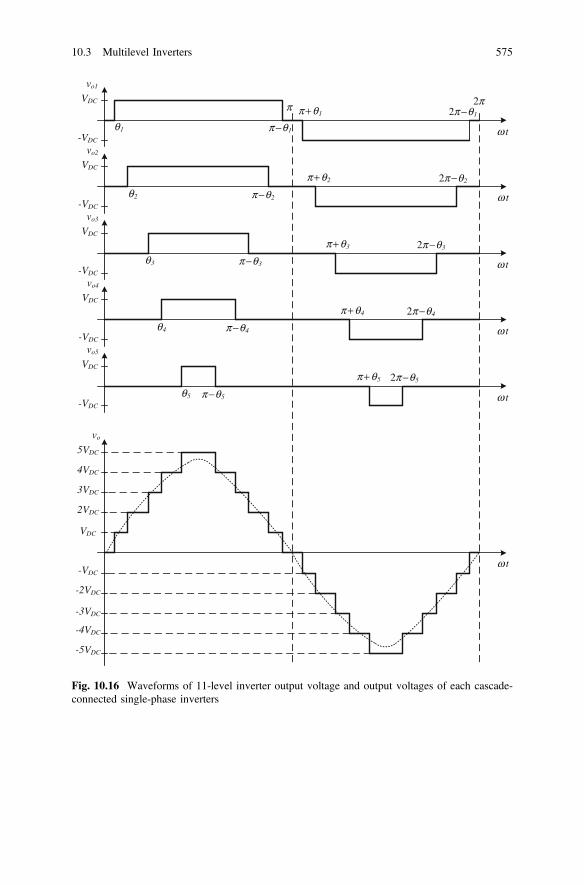
VDC
-VDC
vo1
VDC
-VDC
vo2
VDC
-VDC
vo3
VDC
-VDC
vo4
VDC
-VDC
vo5
π
VDC
-VDC
2π
θ1 π −θ1
θ2 π −θ2
θ3 π −θ3
θ4 π −θ4
θ5 π −θ5
π +θ5 2π −θ5
π +θ4 2π −θ4
π +θ3 2π −θ3
π +θ2 2π −θ2
π +θ1 2π −θ1
ω t
ω t
ω t
ω t
ω t
ω t
4VDC
-2VDC
3VDC
5VDC
2VDC
-3VDC
-4VDC
-5VDC
vo
Fig. 10.16 Waveforms of 11-level inverter output voltage and output voltages of each cascade-connected single-phase inverters
10.3 Multilevel Inverters 575

The output voltage of each single-phase inverter can be expressed as
vok ¼þVDC; #K\xt\p� #K
0; 0\xt\#K ; p� #K\xt\pþ #K ; 2p� #K\xt\2p
�VDC; #K �xt� pþ #K\xt\2p� #K
8><>:
k ¼ 1; 2; 3; 4; 5
ð10:9Þ
This voltage is vo ¼ vo1 þ vo2 þ vo3 þ vo4 þ vo5 and the following expressioncan be obtained:
vo xtð Þ ¼X
n¼1;5;7...
4VDC
npcos n#1ð Þ þ cos n#2ð Þ þ � � � þ cos n#5ð Þ½ �sin nxtð Þ ð10:10Þ
The harmonics that have a dominant influence on the total harmonic distortion ofthe output voltage (5, 7, 11, 13) can be eliminated by the appropriate choice of theangle θk (10.10). Also, the output voltage of a multilevel inverter is closer to asinusoidal form and has lower harmonic distortion than the conventional single-phase two-level bridge inverter. Because the single-phase H-bridge inverters areproduced as particular modular units, the desired topology of the multilevel inverteris obtained by connecting these units in cascade. On the other hand, every single-phase H-bridge requires a separate DC power supply.
This limits the application of this inverter topology to those cases in which anumber of separate DC sources is sufficient.
A multilevel inverter for the power supply of a three-phase AC motor, or abattery charger is shown in Fig. 10.17 [5]. It is a three-phase multilevel inverter andeach phase has a five single-phase bridge supplied from separate DC 48 V sources.
Example 10.3 The cascaded 11-level H-bridge inverter shown in Fig. 10.15 hasseparate DC sources with identical voltages equal to 24 V. The control angles of theswitches are θ1 = 15°, θ2 = 30°, θ3 = 45°, θ4 = 60°, and θ5 = 75°. Determine theamplitude of the fundamental harmonic of the output voltage.
According to (10.10), the amplitude of the fundamental harmonic of the outputvoltage is equal to
V1 ¼ 4VDC
pcos h1 þ cos h2 þ cos h3 þ cos h4 þ cos h5ð Þ
��������
¼ 4� 24p
cos 15� þ cos 30� þ cos 45� þ cos 60� þ cos 75�ð Þ����
���� ¼ 100:1 V:
Another topology of multilevel cascade inverter includes a transformer and usesthe standard three-phase, two-level inverter modules (Fig. 10.18) [6]. In order toadd up the converter voltage, the outputs of the inverter modules need to be syn-chronized with the displacement of 120° between each phase. The phasor diagram
576 10 Introduction to Multilevel Converters

of the multilevel inverter from Fig. 10.18 is shown in Fig. 10.19. The phasevoltages at the output of the inverter modules are ak, bk and ck (k = 1, 2, 3). Anisolated transformer is used to provide the voltage boost. These isolating trans-formers with a 1:1 ratio generate voltages a2b1; c1a3 and b3c2 from the outputvoltages of the AC inverter modules b3a3; a2c2 and c1b1, respectively (Fig. 10.19).
In this way, the required values of the line voltages AB, BC, and CA areobtained. The advantages of the proposed multilevel inverter shown in Fig. 10.18are as follows:
• Due to the modular design, the switching components in the inverter moduleshave a lower voltage stress. Also, this inverter design allows easy maintenance;
• Lower dv/dt effect;
H bridge inverter
H bridge inverter
H bridge inverter
H bridge inverter
H bridge inverter
H bridge inverter
H bridge inverter
H bridge inverter
H bridge inverter
H bridge inverter
H bridge inverter
H bridge inverter
H bridge inverter
H bridge inverter
H bridge inverter
+ + +
+ + +
+ + +
+ + +
+ + +
tobatterycharger
Control Switch Charge Drive
Motor
48V
Fig. 10.17 Three-phase cascade 11-level H-bridge inverter for power supplying three-phase ACmotor, or battery charger
10.3 Multilevel Inverters 577

• Lower harmonic distortion of the output voltage and current, especially theoutput current if the load is an AC motor;
• A high capacitor in the DC link is not necessary due to the balanced load.
The proposed system is suitable for power supply of V/f controlled electricaldrives in a wide range of operating speeds. Also, the output transformers providehigher output voltages and prevent the formation of current circuits within theinverter modules.
10.3.2 Diode-Clamped Multilevel Inverters
In comparison to other multilevel inverters, the diode-clamped multilevel invertertopologies are attractive from economic reasons and because of their high efficiency
3 phase inverter module
3 phase inverter module
3 phase inverter module
M
a1
b1
c1
a2
b2
c2
a3
b3
c3
+VDC
+VDC
+VDC
C
B
A
Fig. 10.18 Three-phase multilevel inverter with isolated transformers [6]
1
2 3
a1
b1
c1
a3
b3
c3 a2
b2
c2
Fig. 10.19 Phasor diagram ofthe inverter from Fig. 10.18
578 10 Introduction to Multilevel Converters

in fundamental frequency switching. Also, all their phases share a common DClink, which minimizes the capacity requirements of the converter.
The basic principles of the diode-clamped multilevel inverter and its advantagesover the conventional 2-level invertors were described for one leg of an inverterbridge in Sect. 10.1. This three-phase multilevel inverter topology has applicationsin the high power AC electrical drives, static var compensation, and high-voltagesystem interconnection.
Besides the good characteristics of these converters, there are certain practicalproblems in their application related to dynamic voltage stress on switches andvoltage balance on the intermediate DC levels. The voltage balance of the capac-itors will be held only if the average value of the current through the capacitorsduring one period of the output voltage is 0. This is one of the reasons why thediode-clamped multilevel invertors are used in back-to-back converters, i.e., twoidentical multilevel inverters are connected to a common DC link. One multilevelconverter works as rectifier, and another as inverter. This connection allows powertransmission in both directions, so it is most commonly used to couple two syn-chronous systems, or to power a three-phase AC motor from an AC source. If thediode-clamped multilevel inverter is used for one direction power transmissionfrom a DC source to an AC load, the DC/DC converter is placed between the DCsource and the multilevel inverter input. The role of this DC/DC converter is tomaintain the voltage balance at the input of the multilevel inverter (see, e.g.,Figs. 10.9 and 10.10). A three-phase 5-level diode-clamp inverter is shown inFig. 10.20.
The voltage on the capacitors C1–C4 is VDC, and the voltage stress across eachswitch is limited to VDC through the clamping diodes.
Each leg has four complementary switch pairs. The complementary switch pairsfor the leg b are Sb1; S0b1
� �; Sb2; S0b2� �
; Sb3; S0b3� �
and Sb4; S0b4� �
. If one switch in thepair is turned on, the second is turned off, and vice versa. The state of the switchesis controlled, so that in any moment, four switches are turned on. The outputvoltage of each phase is determined by the state of the switches. Thus, we canobserve the output voltage of the phase B in relation to the lowest level of the inputvoltage. If the four lower switches S0b1; S
0b2; S
0b3 and S0b4 are turned on, then vb = 0. If
one upper and three lower switches Sb1; S0b2; S0b3; S
0b4 are turned on, then vb = VDC.
The maximum voltage vb = 4VDC would be reached if four upper switches Sb1, Sb2,Sb3 and Sb4 were turned on and four lower switches S0b1; S
0b2; S
0b3 and S
0b4 were turned
off. In this topology, it is obvious that the voltage stress across each diode is notequal. In fact, the diode D1 must block VDC, the diode D2 must block 2VDC, and thediode D3 must block 3VDC. If the inverter design is such that each blocking diodehas the same voltage rating, two diodes connected in series should be used insteadof the diode D2, and three diodes connected in series instead of the diode D3. Thismeans that the number of diodes required for each phase of the inverter is equal ton� 1ð Þ n� 2ð Þ, where n is the number of the output voltage levels.
Example 10.4 Define the necessary number of clamping diodes for a three-phase 6-level diode-clamped inverter, so that each diode blocks a voltage equal to VDC. If
10.3 Multilevel Inverters 579

the output voltage of the phase a is equal to 2VDC determine which switches in thebranch a are turned on.
The necessary number of diodes is 3(n − 1)(n − 2) = 3(6 − 1)(6 − 2) = 60, where3 is the number of phases, and n = 6 is the number of the output voltage levels. Theswitches Sa1; Sa2; S0a3 and S0a4 are turned on.
10.3.3 Flying Capacitor Multilevel Inverter
The structure of this inverter is similar to that of the diode-clamped inverter exceptthat instead of using clamping diodes, capacitors are used in their place. A four-level flying capacitor inverter is shown in Fig. 10.21.
This topology has a ladder structure of DC side capacitors. The voltage at eachadjacent capacitive branch is different and the voltage difference defines the size ofthe output voltage step, which is equal to VDC. The main advantage of the flyingcapacitor inverter in relation to the diode-clamped multilevel inverter is that it hasredundancies for inner voltage levels. In other words, it is possible to have two ormore different valid switch combinations in order to obtain the same output voltage.
Sc4
Sc3
Dc4
Dc3
Sc2
Sc1
Dc2
Dc1
Sc4'
Sc3'
Dc4'
Dc3'
Sc2'
Sc1'
Dc2'
Dc1'
D1
D2
D3
D3
D2
D1
Sb4
Sb3
Db4
Db3
Sb2
Sb1
Db2
Db1
Sb4'
Sb3'
Db4'
Db3'
Sb2'
Sb1'
Db2'
Db1'
D1
D2
D3
D3
D2
D1
Sa4
Sa3
Da4
Da3
Sa2
Sa1
Da2
Da1
Sa4'
Sa3'
Da4'
Da3'
Sa2'
Sa1'
Da2'
Da1'
D1
D2
D3
D3
D2
D1
va
vb
vc
+
+
+
+
VDC
VDC
VDC
VDC
C 1
C3
C 2
C 4
Fig. 10.20 Three-phase 5-level diode-clamped inverter
580 10 Introduction to Multilevel Converters

Furthermore, the flying capacitor topology has phase redundancy (it relates togeneration of phase voltage), while diode-clamped inverters only have a lineredundancy (relates to generation of line-to-line voltage). This feature is importantbecause it allows the use of control techniques for voltage balance of capacitivebranches. The number of the redundant states depends on the output voltage. Thiswill be considered for the phase a. If va = 4VDC (four upper switches Sa1, Sa2, Sa3,Sa4 are turned on), or va = 0 (four lower switches S0a1; S
0a2; S
0a3; S
0a4 are turned on),
there are no redundant states. If the voltage va = 3VDC, the allowed switches statesare as shown in Table 10.1. For this case, the number of redundant states is 2. Asimilar analysis can be made for other voltage levels.
Sc4
Sc3
Dc4
Dc3
Sc2
Sc1
Dc2
Dc1
Sc4'
Sc3'
Dc4'
Dc3'
Sc2'
Sc1'
Dc2'
Dc1'
Sb4
Sb3
Db4
Db3
Sb2
Sb1
Db2
Db1
Sb4'
Sb3'
Db4'
Db3'
Sb2'
Sb1'
Db2'
Db1'
Sa4
Sa3
Da4
Da3
Sa2
Sa1
Da2
Da1
Sa4'
Sa3'
Da4'
Da3'
Sa2'
Sa1'
Da2'
Da1'
va
vb
vc
+
+
+
+VDC
VDC
VDC
VDC
+ rail
Cc1
Cc21
Cc22
Cc31
Cc32
Cc33
C1
C2
C3
C4
Cb1
Cb21
Cb22
Cb31
Cb32
Cb33
Ca1
Ca21
Ca22
Ca31
Ca32
Ca33
rail
Fig. 10.21 Three-phase 5-level flying capacitor inverter
Table 10.1 Switching states of three-phase 5-level flying capacitor inverter for Va = 3VDC
Output voltage Switching states
Sa4 Sa3 Sa2 Sa1 S0a4 S0a3 S0a2 S0a13VDC 0 1 1 1 0 0 0 1
4VDC − VDC 1 1 1 0 1 0 0 0
4VDC − 3VDC + 2VDC 1 0 1 1 0 0 1 0
10.3 Multilevel Inverters 581

In this type of multilevel inverter, it is also needed to maintain voltage balanceon the capacitors. This is accomplished by applying appropriate control sequences,so the inner capacitors equally charge and discharge during one period. One periodof the voltage va is shown in Fig. 10.22.
If the output voltage V3 is obtained as 3VDC, the capacitors Ca3 are discharged.On the other hand if the output voltage V3 is obtained as 4VDC − 3VDC + 2VDC, thecapacitors Ca3 are discharged. In order to maintain a voltage balance, the number ofcharging and discharging cycles of the inner capacitors during each period shouldbe equal. If the control sequence V3–V4–V3 is applied, as shown in Fig. 10.22, onlytwo switches change their state, one is turned on, and the second is turned off.
Besides the advantages of this inverter topology that include the phase redun-dancy, there are also certain drawbacks. These are [4]:
• The voltage level tracking for all the capacitors is complicated. Also, pre-charging all of the capacitors to the same voltage level is a complex task.
• Switching utilization and efficiency are poor.• A large number of capacitors is both more expensive and bulkier than the
clamping diodes in a diode-clamped multilevel inverter.
10.3.4 Other Multilevel Inverter Topologies
The generalized topology of a multilevel inverter, the so-called P2 topology ispresented in Fig. 10.23 [7]. This topology allows automatic maintenance of the
V4
V3
V2
V1
V0
va
t
V3 = 3VDC
(C3a discharging)
4VDC
V3 = 4VDC - 3VDC + 2VDC
(C3a charging)
Fig. 10.22 Waveforms of voltage va during one period
582 10 Introduction to Multilevel Converters

voltage balance without a support of other circuits, for an arbitrary number ofvoltage levels at the output, and regardless of load characteristics.
The voltage stress on the switches and the capacitors is the same and is equal toVDC. The topology of the basic cell is simple. It consists of two complementaryswitches connected in parallel with a capacitor (Fig. 10.23). By turning on the lowerswitch, the lower voltage is forwarded to the next level, and by turning on the upperswitch, the higher voltage is forwarded to the next level. The difference betweenthese two voltages is equal to the voltage on the capacitor (VDC).
S21
S22
D21
D22
S23
S24
D23
D24
S11
S12
D11
D12
S1
S2
D1
D2
S31
S32
D31
D32
S33
S34
D33
D34
S35
S36
D35
D36
Sn1
Sn2
Dn1
Dn2
Sn3
Sn4
Dn3
Dn4
Sn 2n-3
Sn 2n-2
Dn 2n-3
Dn 2n-2
Sn 2n-1
Sn 2n
Dn 2n-1
Dn 2n
+ VDC
C11
C21
C22
C
C31
C32
C33
Cn n-1
Cn n
Cn1
Cn2
vo
2leveL
3leveL
4leveL
Level n
+
+
+
+
+
+
+
VDC
+
+
+
VDC
VDC
VDC
VDC
VDC
VDC
VDC
VDC
VDC
Basic cell
Fig. 10.23 Topology of so-called P2 multilevel inverter and its basic cell
10.3 Multilevel Inverters 583

Besides the basic topology described previously, there is a significant number ofnew multilevel inverter topologies. These topologies are derived from the existingones and represent their improvement.
The hybrid multilevel inverter is a combination of the cascaded H-bridge mul-tilevel and the diode-clamped multilevel inverter. This implementation reduces therequired number of separate DC sources. Figure 10.24 [4] shows one branch of the
Sa1
Sa2
Da1
Da2
Sa1'
Sa2'
Da1'
Da2'
Sb1
Sb2
Db1
Db2
Sb1'
Sb2'
Db1'
Db2'
Sa3
Sa4
Da3
Da4
Sa3'
Sa4'
Da3'
Da4'
Sb3
Sb4
Db3
Db4
Sb3'
Sb4'
Db3'
Db4'
C
C
C
C
a
n
+ VDC
2
+ VDC
2
+ VDC
2
+ VDC
2
+
+VDC
Fig. 10.24 One branch of the 9-level hybrid inverter
584 10 Introduction to Multilevel Converters

three-phase hybrid inverter with two cascaded connected cells, each cell consistingof a 5-level diode-clamped multilevel inverter.
In this way, we get a 9-level inverter with only two separate DC sources perphase, or a total of six separate sources for the whole three-phase inverter. For therealization of the same inverter with a standard H-bridge inverter modules, 16separate DC sources are needed.
Example 10.5 For one branch of the 9-level hybrid inverter shown in Fig. 10.24define the switching states, the voltages at the output of the inverter modules andthe output voltage of the inverter.
The switching states, the voltages at the output of inverter modules and theoutput voltage of the 9-level hybrid inverter are shown in Table 10.2.
In order to reduce switching losses and increase efficiency, multilevel invertertopologies with resonant circuits for soft-switching are also used.
10.4 Control of Multilevel Inverters
Modulation techniques used in multilevel inverters can be classified according tothe applied switching frequency (Fig. 10.25) [7]. Techniques popular in industrialapplications that work at higher switching frequencies are the sine PWM and thespace vector modulation technique. They can be simply expanded from 2-level tomultilevel invertors.
Techniques that work at lower frequencies are characterized by a smaller numberof switching cycles during one period and a staircase shape of the output voltage.More commonly used techniques are the SHE and the space vector control (SVC).
Table 10.2 Switching states, voltages at the output of inverter modules and the output voltage ofthe 9-level hybrid inverter
Turned on switches Vaa0 Va0 n Van ¼ Vaa0 þ Va0 n
Inverter A Inverter B
S0a1; S
0a2; Sa3; Sa4 S
0b1; S
0b2; Sb3; Sb4 �VDC �VDC �2VDC
S0a1; S
0a2; Sa3; Sa4 S
0b1; Sb2; Sb3; Sb4 �VDC �VDC=2 �3VDC=2
S0a1; Sa2; Sa3; Sa4. S
0b1; Sb2; Sb3; Sb4 �VDC=2 �VDC=2 �VDC
S0a1; S
0a2; S
0a3; S
0a4 S
0b1; Sb2; Sb3; Sb4 0 �VDC=2 �VDC=2
S0a1; S
0a2; S
0a3; S
0a4 S
0b1; S
0b2; S
0b3; S
0b4
0 0 0
S0a1; Sa2; S
0a3; S
0a4 S
0b1; S
0b2; S
0b3; S
0b4
VDC=2 0 VDC=2
S0a1; Sa2; S
0a3; S
0a4 S
0b1; Sb2; S
0b3; S
0b4
VDC=2 VDC=2 VDC
S0a1; Sa2; S
0a3; S
0a4 Sb1; Sb2; S
0b3; S
0b4
VDC=2 VDC 3VDC=2
Sa1; Sa2; S0a3; S
0a4 Sb1; Sb2; S
0b3; S
0b4
VDC VDC 2VDC
10.3 Multilevel Inverters 585

10.4.1 Multilevel SPWM
A simple and often used modulation technique for multilevel inverters is theSPWM.
In order to achieve a better DC link utilization at high modulation, a thirdharmonic with a magnitude equal to 25 % of the fundamental one is injected in thereference signal (third harmonic injection PWM-THPWM) (Fig. 10.26). Otherinteresting carrier-based multilevel PWM techniques are the subharmonic PWM(SH-PWM) and the Switching frequency optimal PWM (SFO-PWM). For the SH-PWM techniques for an n-level inverter, n−1 carriers with the same frequency ft andthe same amplitude VtM are introduced such that the bands they occupy are con-tiguous [8]. A reference signal with the amplitude VcM and the frequency fc has itszero centered in the middle of the triangular carrier set. The reference is continu-ously compared with each of the carrier signals. If the reference is greater than thecarrier, the control signal is a such that the corresponding output voltage level ishigh. Otherwise, if the reference is lower than the carrier, then the correspondingoutput voltage level is low.
The carrier signals, the sinusoidal reference signal with an amplitude modulationfactor ma = 0.8, and the waveform of one output phase voltage for a 5-level diode-clamped inverter are shown in Fig. 10.27. In n-level multilevel inverter, the amplitudemodulation index ma and the frequency modulation index, mf, are defined as
ma ¼ VcM
n� 1ð ÞVtM; mf ¼ ft
fcð10:11Þ
Example 10.6 Define the amplitude and the modulation factor of a 5-level diode-clamped inverter if fC = 50 Hz, ft = 1.35 kHz, VtM = 1 V, and VcM = 3.6 V.
Multilevel modulators
Fundamental switching frequency
High switching frequency PWM
Space Vector Control (SVC)
Selective Harmonic
Elimination (SHE)
SpaceVector
Modulation(SVM)
Multilevel modulators
Fig. 10.25 Classification of modulation techniques used in multilevel inverters
586 10 Introduction to Multilevel Converters

According to Eq. (10.11), the amplitude modulation index ma and the frequencymodulation index, mf are
ma ¼ VcM
n� 1ð ÞVtM¼ 3:6
4:1¼ 0:9; mf ¼ 1350
50¼ 27:
The SFO-PWM method [9] is similar to the SH-PWM with the difference thatthe third harmonic is added to each of the carriers. The voltage Voffset is theinstantaneous average of the maximum and minimum of the three reference volt-ages vca, vcb and vcc
Voffset ¼ max vca; vcb; vccð Þ �min vca; vcb; vccð Þ2
ð10:12Þ
and it is subtracted from each of the individual reference voltages, so that the newreference voltages are
vcaSFO ¼ vca � voffsetvcbSFO ¼ vcb � voffsetvccSFO ¼ vcc � voffset
ð10:13Þ
0 0.002 0.004 0.006 0.008 0.01 0.012 0.014 0.016 0.018 0.02-1
-0.8
-0.6
-0.4
-0.2
0
0.2
0.4
0.6
0.8
1
time [s]
carr
ier
and
refe
renc
e si
gnal
s at
TH
PW
M m
odul
atio
n
Fig. 10.26 Carrier sets and reference signal for one phase of a 4-level multilevel inverter whenTHPWM modulation technique is applied (ma = 0.8, fc = 50 Hz, and ft = 750 Hz)
10.4 Control of Multilevel Inverters 587

An example of the realization of analog circuits that generate reference signalsusing the SFO-PWM method is shown in Fig. 10.28.
There are also the SHEPWM methods that enable the generation of the inverteroutput voltage with a small value of the THD. This technique gives the freedom inthe choice of phase the displacement between the carrier signals. They can be inphase, with opposite phases, or phase-shifted by a certain angle. Similarly to thecase of SPWM applied to 2-level invertors, these modulation techniques, whenapplied to multilevel invertors, give a lower harmonic distortion, and the first higherharmonics appear around the carrier signal frequency.
vt
0
1
2
3
4
0
1
2
3
4
t
t
tt
t1
vc
Fig. 10.27 Carrier sets, sinusoidal reference signal and waveform of one output phase voltage for5-level inverter
588 10 Introduction to Multilevel Converters

10.4.2 Space Vector Modulation
The Space Vector Modulation (SVM) represents an extension of the SVM tech-nique discussed for three-phase 2-level inverters (Sect. 6.4). This technique can beused for control of all types of multilevel inverters. A control scheme based on theSVM for a three-phase 3-level inverter is shown in Fig. 10.29. There is a third zerovector (222), besides the two zero vectors (000), (111) which are at 2-levelinverters. This zero vector corresponds to the case when all three phases are at thehighest voltage level. The appropriate voltage vector is obtained by the sameprinciple as for the 2-level invertors. Suppose that the voltage which should begenerated is V� (Fig. 10.29). In this case, an appropriate vector can be generatedusing the three vectors that determine the regular triangle containing the peak of thevector V�. The starting point is the vector which has an even redundancy 100 (211)or 110 (221). The control sequence is realized by applying two vectors which differin only one switching state. In this way only one commutation is necessary for thetransition from one state to another. There are the following control sequenceswhich can be applied:
(a) 211-210-110-100(b) 221-211-210-110
+
-
+
-
+
-
vca
2R
2R
R
vcaSFO
vcbSFO
vccSFO
vcb
vcc
Da’ Db’ Dc’
Da Db Dc
Fig. 10.28 An example ofanalog circuits that generatereference signals with SFO-PWM method [4]
10.4 Control of Multilevel Inverters 589

In this case, reverse sequences are not explicitely considered. The vectorsV1; V2;V3 are applied in the time intervals t1, t2 and t3, respectively, andt1 + t2 + t3 = T.
In order to obtain a lower number of commutations intervals, t1 is divided intotwo intervals kt1 (0 < k < 1) in which the vector V1 is applied and second interval (1−k) t1 in which the second vector V1 V0 is applied. Taking this into account, theoutput vector is generated in the form
V� ¼ V1kt1 þ V2t2 þ V3t3 þ V1 V0� �
1� kð Þt1T
ð10:14Þ
Of course, the applied vector V0 is different from the zero vector 000. Theapplication of the SVM in multilevel inverters has the following benefits:
• good utilization of the DC link,• small current ripple, and• a relatively simple hardware implementation.
This algorithm is complicated for a greater number of inverter voltage levels. Inthis case, the number of redundant switching states and the instances of selection ofcontrol sequences significantly increase.
10.4.3 Space Vector Control
The SVC technique works at lower switching frequencies. Here the average valueof the reference voltage is not generated during one period, as is the case withSVMs. The basic idea of the SVC is to select the vector that gives the minimumspatial error in relation to the reference voltage vector V�. This technique is
V*
210
220120020
021
022200
201
202102002
012
122011
211100
112001
212101
121010
110221
Fig. 10.29 SVM controlscheme for three-phase 3-level inverter
590 10 Introduction to Multilevel Converters

interesting for multilevel inverters with a larger number of voltage levels, becausethe error between the applied voltage and the reference vector in this case is small.However, with the reduction of the voltage level numbers, the error in the appliedvoltage increases, and with it the load current ripple.
10.4.4 Selective Harmonic Elimination
One way of eliminating low-frequency harmonics in spectrum of the inverter outputvoltage is the SHE technique. This technique can be explained on the example ofmultilevel H-bridge inverters. The output voltage has a staircase form (Fig. 10.18)and with an appropriate selection of the angles when the switches are turned on, thedominant harmonics can be eliminated. For the angles #k; k ¼ 1; 2; . . .; p (10.10)one has #1\#2\ � � �\#p\ p
2. By an appropriate selection of the angle #k one caneliminate up to n−1 lower harmonics, while low-pass filters can be used to suppresshigh-order harmonics. For an 11-level H-bridge inverter (Fig. 10.17) with anappropriate selection of the angles #k; k ¼ 1; 2; . . .; 5, the most important low-orderharmonics that can be eliminated are 5, 7, 11, and 13.
In this case, it is necessary to form a set of five equations with five unknowns.Four equations are formed on the basis of a request for the elimination of har-monics, and the fifth equation is obtained from the condition that the amplitude ofthe first harmonic should correspond to the reference value, i.e., to the amplitudemodulation factor ma ¼ pV1
4VDC, where V1 is the fundamental output voltage of the
inverter
cos 5#1ð Þ þ cos 5#2ð Þ þ cos 5#3ð Þ þ cos 5#4ð Þ þ cos 5#5ð Þ ¼ 0cos 7#1ð Þ þ cos 7#2ð Þ þ cos 7#3ð Þ þ cos 7#4ð Þ þ cos 7#5ð Þ ¼ 0cos 11#1ð Þ þ cos 11#2ð Þ þ cos 11#3ð Þ þ cos 11#4ð Þ þ cos 11#5ð Þ ¼ 0cos 13#1ð Þ þ cos 13#2ð Þ þ cos 13#3ð Þ þ cos 13#4ð Þ þ cos 13#5ð Þ ¼ 0cos #1ð Þ þ cos #2ð Þ þ cos #3ð Þ þ cos #4ð Þ þ cos #5ð Þ ¼ ma:
ð10:15Þ
This system of equations cannot be solved by analytical methods, and numericalprocedures have to be used instead. Also, this method works at the fundamentalfrequency.
Problems
10:1 A four-level flying capacitor converter leg is shown in Fig. 10.5b. Define allpermissible switching states and the output voltage for each of these states.
10:2 The four-level DC/DC converter shown in Fig. 10.7 has VI = 12 V,RO = 10 Ω, and D = 0.5. Determine the change of the output voltage whenthe ratio rL/RO changes from 0.01 to 0.1.
10.4 Control of Multilevel Inverters 591

10:3 The four-level one-quadrant DC/DC converter shown in Fig. 10.13 has theparameters VI = 24 V, R1 = R2 = R3 = 10 Ω and L = 100 μH. The appliedswitching sequence is 0–1–3–4 when d2 = 0.1 and d3 = 0.02
(a) Determine d1, so that the output voltage is 96 V.(b) Determine the maximum change of the current iL.
10:4 The cascaded 11-level H-bridge inverter shown in Fig. 10.17 has separateDC sources whose voltages are identical and equal to 48 V. The controlangles of the switches are: θ1 = 15°, θ2 = 30°, θ3 = 45°, θ4 = 60°, andθ5 = 75°. Determine the amplitude of the fifth harmonic of the output voltage.
10:5 Define the permissible switching states of the phase b for a three-phase 5-level flying capacitor inverter if Vb = 2VDC.
10:6 To control a three-phase multilevel inverter, the SFO-PWM technique isused. If the control signals are vca = 1.7sin(2π50t), vcb = 1.7sin(2π50t + 2π/3)and vcc = 1.7sin(2π50t−2π/3), calculate the new reference voltages for t = 1/300 s. What is the main advantage of this technique compared to the mul-tilevel SPWM technique?
10:7 To control a 5-level H-bridge inverter the SHE technique is used. The factorof amplitude modulation is 0.8 and the voltages of the DC sources areidentical and equal to 12 V. Determine the amplitude of the fundamentalharmonic and the conducting angles, so that the most important higherharmonics can be eliminated.
References
1. Rosas-Caro, J.C., Ramirez, J.M., Garcia-Vite, P.: Novel DC-DC multilevel boost converter. In:IEEE Conference on Power Electronics Specialists (2008)
2. Meynard, T.A., Foch, H.: Multilevel conversion: high voltage choppers and voltage-sourceinverters. In: IEEE Conference on Power Electronics Specialists (1992)
3. Corzine, K.A., Majeethia, S.K.: Analysis of a novel four-level DC/DC boost converter. IEEETrans. Ind. Appl. 36(5), 1342–1350 (2000)
4. Khomfoi, S., Tolbert, L.M.: A hybrid cascaded multilevel inverter application for renewableenergy resources including a reconfiguration technique. In: IEEE on Energy ConversionCongress and Exposition (2010)
5. Tolbert, L.M., Peng, F.Z., Habetler, T.G.: Multilevel inverters for electric vehicle application.In: IEEE on Power Electronics in Transportation (1998)
6. Cengelci, E., et al.: A new medium PWM inverter topology for adjustable speed drives. In:IEEE Conference on Industry Application (1998)
7. Peng, F.Z.: A generalized multilevel inverter topology with self voltage balancing. IEEE Trans.Ind. Appl. 37(2), 611–618 (2001)
8. Carrara, G., et al.: A new multilevel PWM method: a theoretical analysis. IEEE Trans. PowerElectron 7(3), 497–505 (1992)
9. Tolbert, L.M., Habetler, T.G.: Novel multilevel inverter carrier-based PWM methods. In: IEEEConference on Industry Application (1998)
592 10 Introduction to Multilevel Converters

Bibliography
Apfel, R.J., Jones, D.B.: Universal switching regulator diversifies power subsystem applications.Comput. Des. 16(2), 103–112 (1978)
Arbetter, B., Erickson, R., Maksimović, D.: DC-DC converter design for battery–operatedsystems. IEEE Power Electron. Spec. Conf. 1, 103–109 (1995)
Begag, S., Belhaouchet, N., Rahmani, L.: Three-phase pwm rectifier with constant switchingfrequency, J. Electr. Syst. Spec. 1, (2009)
Billings, K.H.: Switchmode Power Supply Handbook. McGraw-Hill, New York 1989Blaabjerg, F., Teodorescu, R., Chen, Z., Liserre, M.: Power Converters and Control of Renewable
Energy Systems. First International Conference of Energy Innovation, (2005)Bose B.K.: Power Electronics and Varaiable Frequency Drives. IEEE Press, Piscataway 1996Casadei, D., Serra, G., Tani, A., Zarri, L.: Matrix converter modulation strategies: a new general
approach based on space-vector representation of the switch state. IEEE Trans. Ind. Electron.49(2), 274–275 (2002)
Calais, M., et al.: A transformerless five level cascaded inverter based single phase photovoltaicsystem. In: Proceedings of PESC’00, vol. 3. (2000)
Chen, Z., Spooner, E.: Voltage source inverters for high-power variable-voltage dc power sources.IEE Proc. Gen. Transm. Distrib. 148(5), (2001)
Cole, B.C.: A Brisk power-supply market divers controlchip poliferation. Electron. 17, 112–113(1990)
Dokić, B.: Energetska elektronika—pretvarači i regulatori, Akademska misao, Beograd, ETFBanjaluka, (2007)
Daly, K.C.: Ripple determination for switch–mode DC/DC convertors. IEE Proc. 129(5), 229–234(1982)
Fickenscher H.: A hybrid intergrated pulse-width modulator. In: IEEE Conference Record 6thAnnual Meeting, USA (1971)
Goodenough, F.: Designing switchers gets easier, ED, No. 14, pp 53-56,60-63, 68, 70, 72, 76, 78.(1991)
Goodenough, F.: New switchers are a cinch to use, ED, No. 16, pp 33, 34, 36, 37. (1989)Goodenough, F.: Phase Modulation cuts large-switcher looses, ED, No. 8, pp 39-41, 44. (1991)Goodenough, F.: Power-supply IC controllers proliferate, ED, No. 23, pp. 59-62, 64-66,71 (1989)Gray, P.R., Mayer, R.G.: Analysis and Design of Analog Integrated Circuits. Wiley, New York
(1977)Grosman, M.: Focus on switching power supplies: advanced full high growth rate. Electron. Des.
29, 131–135 (1981) (March 5)Hnatek, E.R.: Choose switching regulators for your computer power-supply design, Electron. 12
(6), 2455 (1975) (Des)Kassakian, G.J., et al.: Principles of Power Electronics. Addison-Wesley, Reading (1992)Khoucha, F., et al.: Hybrid cascaded H-bridge multilevel-inverter induction-motor-drive direct
torque control for automative applications. IEEE Trans. Ind. Electron. 57(3), 892–899 (2010)
© Springer International Publishing Switzerland 2015B.L. Dokić and B. Blanuša, Power Electronics,DOI 10.1007/978-3-319-09402-1
593

Kumar, J., Das, B., Agarwal, P.: Selective harmonic elimination technique for a multilevelinverter. In: Fifteenth National Power Systems Conference, India, (2008)
Lee, F.C.: Resonant Technology will Spur Power-Supply Design Developments. ED, No.1, (1990)Lee, K-B, Blaabjerg, F.: Sensorless DTC-SVM for induction motor driven by a matrix converter
using a parameter estimation strategy. IEEE Trans. Ind. Electron. 55(2), 512–521 (2008)Lee, Y-S.: Computer Aided Analysis and Design of Switch Mode Power Supplies. Marcel Dekker,
New York (1993)Li, Y., Huang, A.Q., Lee, F.C.: Introducing The Emitter Turn-off Thyristor (ETO). In: Thirty-third
IAS Annual Meeting, IEEE, (1998)Lin, J.: A new design of power supplies for pochet computer systems. IEEE Trans. Ind. Electron.
45(2), 291–296 (1998)Mcgareth, P.B., Holms, D.G., Lipo, T.: Optimized space vector switching sequences for multilevel
inverters. IEEE Trans. Power Electron. 18(6), 1293–1301 (2003)Moravac, M., Dokić, B.L.: Ćukov “Step-up”“Step-down” DC/DC konvertor. Elektronika 41, 3–4
(1992)Pejović, P.: Low-Harmonic Three-phase Diode Bridge Rectifiers Based on the Current Principle.
Academic Mind, Belgrade (2005)Petrović, P.B.: Kola energetske elektronike—modelovanje i upravljanje, Čačak (2010)Pressman, A.I.: Switching Power Supply Design. McGraw-Hill, Inc., New York, (1992)Scott, C., Stitt, R.M.: Inverting dc to dc converters require no inductors. Electronics 2, 97–104
(1976)Sheehan, D.: Designing a regulators LS input filters. Electron. Des. 16, 125–209 (1979)Teja, E.P.: Switching power supplies, EDN (1981)Till, J.: Inside the black box a look at power supply design, ED, pp 69, 70, 72-74, 76, 78, 80.
(1988)Trzynadlowski, M.A.: Introduction to Modern Power Electronics. Wiley, New York (2010)Whittington, H.W., et al.: Switched Mode Power Supplies-Design and Construction. Wiley, New
York (1997)Williams, W.: Power Electronics, Mcmillan. Palgrave Macmillan, Basingstoke (1992)Yamamoto, E., et al.: Development of MCs and its Application in Industry. IEEE Ind. Electron.
Mag. 5(2), 4–5 (2011)Yamamoto, E., et al.: Development of matrix converters for industrial applications. whitepaperYao, W., Hu, H., Lu, Z.: Comparisons of space-vector modulation and carrier-based modulation of
multilevel inverter. IEEE Trans. Power Electron. 23(1), 52–59 (2008)Special Report, Power sources for electronics, Electronic Engineering. pp 29–63 (1977)
594 Bibliography

Index
AAC, 20, 27, 30, 34, 166, 181, 182, 184, 204,
205, 214, 299, 301, 359, 395, 429, 445,454, 457, 464, 468, 482, 487, 490, 501,539, 559, 563, 576, 579
AC/AC converter, 457, 463, 464, 467, 478,480, 483, 490
AC/AC voltage converter, 457, 459, 460AC/DC, 384, 395, 450, 562AC/DC converter, 395Active filter, 450Active power, 10, 447Active rectifier, 432, 433, 438AGT, 22Ambient temperature, 36, 39, 57, 112Anode current, 168–170, 173, 177–180, 190,
194, 195, 200, 207Apparent power, 14, 477ASCR, 189Asynchronous PWM, 384Auxiliary voltage generators, 320, 330
BBaker clamp, 116Bidirectional switches, 478, 480, 481BiMOS, 18, 19, 121, 122Bipolar PWM, 372–374, 393Bipolar transistor, 19, 30, 71, 72, 105, 108,
110, 117, 121, 122, 126, 129, 132, 137,150, 170, 191, 361, 518, 553
Boost converter, 547, 563Boost rectifier, 433, 436, 438, 440, 450Bridge converter, 300–302, 509, 541, 556Buck converter, 309Buck rectifier, 436, 437
CCapacitatively loaded inverter, 96Capacitive filter, 404, 406, 445, 478, 483Capacitor, 558, 559, 561, 565, 568, 569,
572, 578–580, 582, 583Cascaded H-bridge, 573, 574, 584Case-sink resistance, 37Case temperature, 36, 37, 56, 139Choke, 26, 27, 29, 213, 215–219, 221–224,
227, 229, 230, 232, 234, 242, 244, 248,249, 251, 252, 256–258, 260–263, 265,269, 279, 281, 282, 284, 285, 287, 289,291, 292, 302, 304, 306, 308, 334, 362,401, 414, 416
Clamping diode, 567, 585Class E resonant converter, 524Commutation of current, 288Continous mode, 226Control module frequency, 291Control modules, 313, 314, 325, 337, 344, 347,
357Cooling, 37, 40, 115, 141, 142, 242, 495CUJT, 156, 157Ćuk converter, 213, 304, 308Current commutation, 420, 489, 491, 492Current controlled PWM, 335Current ripple, 307–309, 597Cycloconverter, 472, 477, 479, 496
DDC/AC converter, 359, 360, 452, 539, 540,
554, 573DC/DC converter, 493, 499, 508, 514, 520,
522, 529, 531, 546, 563, 565, 567, 568,570, 579
© Springer International Publishing Switzerland 2015B.L. Dokić and B. Blanuša, Power Electronics,DOI 10.1007/978-3-319-09402-1
595

DC traction motor, 453DIAC, 20, 201, 202, 205di/dt effect, 176, 177Diode-clamped, 578, 580, 584Direct frequency converter, 468Direct power control, 441Direct sequencing, 389Discontinous mode, 222Distortion factor, 7, 14Driver circuits, 116Duty factor, 141, 480, 565dv/dt effect, 173, 200, 577Dynamic diode characteristics, 50Dynamic inverter characteristics, 75Dynamic losses, 107, 115, 231, 239, 261, 303,
371, 494, 499, 504, 518, 520, 531, 536,540, 541
EEnvelope converter, 471Error amplifier, 324, 329, 333, 336, 338, 340,
342, 349, 353, 551, 552, 554ETO, 196, 197
FFactor of amplitude modulation, 370Factor of frequency modulation, 370, 381Flyback converter, 245, 268, 270, 273, 304,
309Flying capacitor, 562, 573, 580Forward converter, 523, 531, 536, 558Fourier coefficients, 3, 370, 378, 379Frequency characteristics, 17, 19, 349, 535Frequency converter, 196, 468Full-wave rectifier, 397–399, 410Full-wave thyristor rectifier, 417
GGate current, 19, 169–171, 178, 182, 189–193,
195, 197, 204GATT, 188, 189Greatz rectifier, 405GTO, 190–193, 196, 197, 514–517GTO thyristor, 19, 191–194, 196, 197, 515,
516
HHalf-bridge converter, 272, 298, 300Half-bridge forward converter, 244Half-bridge inverter, 364Half-wave rectifier, 185, 396, 398, 410Half-wave thyristor rectifier, 416, 417Hamilton Circuit, 302Harmonic, 3, 5, 7, 40, 311, 361, 366, 368, 371,
373, 378, 381, 383, 384, 409, 413, 427,429, 478, 480, 483, 488, 506, 507, 510,517, 518, 520, 540, 559, 576, 586, 588,591
Hybrid inverter, 585
IIGBT, 19, 121, 432, 433, 482IGCT, 192–197, 432Indirect converter, 261, 265, 268indirect DC/DC converter, 265Induction motor drive, 452Inductive load, 101, 361, 363, 384, 484, 487Inductively loaded switch, 101Input filter, 449, 482, 483Integrated circuit, 37, 200, 207, 330, 341, 417,
551, 553, 555, 557Inverse sequencing, 389, 390
JJunction-case resistance, 36
LLASCR, 21L filter, 404, 408, 410Loss free resistor, 429
MMagnetic elements, 23, 25, 500Magnetization current, 242, 244, 279, 280,
282, 288, 301Matrix converter, 384, 478, 480–483, 485–488MOSFET, 19, 122, 432Multi-resonant converter, 522, 537Multilevel converter, 453, 559, 562, 565, 572,
573, 579
596 Index

Multilevel DC/DC converter, 563Multilevel inverter, 559, 563, 567, 573, 576,
578, 582, 585, 586, 590Multilevel SPWM, 592
NNonsaturated switch, 92, 96
OOutput characteristics, 19, 111, 123, 242,
285–288Output filter, 32, 221, 237, 284, 311, 359, 501,
509, 534Output voltage variation, 324, 333, 346, 545Overmodulation, 383, 480
PParallel resonant converter, 501, 512Periodic current, 5, 10Phase controlled rectifier, 416Phase shift bridge converter, 541, 557Phase shifter, 331P2 multilevel inverter, 583P-n junction temperature, 36, 56Power BiMOS, 121Power factor correction, 431, 433, 436, 450Power losses, 33, 189, 227, 230, 237, 240, 248,
259, 304Power MOS transistor, 19, 118, 128, 129, 132,
136, 500Pulse-controlled output voltage, 365Pulse generators, 156Push–pull converter, 246, 277, 286, 290, 296,
298, 301, 302PUT, 150, 152, 153, 159, 164, 185PWM, 212, 311, 312, 317, 323, 368PWM control modules, 312PWM current rectifier, 445PWM DC/DC converter, 324PWM inverter, 373, 391, 452PWM rectifier, 436, 440, 444–446, 452
QQuasi-static mode of transistor, 219
RRadio-frequency interference, 33Reactive power, 13, 14, 429, 447, 448
Real drive, 400Regenerative switch, 19, 143, 150, 166, 192,
200Resonant converter, 211, 213, 494, 495, 499,
500, 507, 512, 555Resonant converter of Class D, 499Root-mean-square (RMS), 5–8
SSafe operation area (SOA), 138, 140, 493, 494Saturation, 18, 59, 67, 74, 81, 94, 96, 100, 102,
113, 143, 146, 234, 246, 289, 298, 348SBS, 200, 205Schottky diode, 18, 54–56, 92, 106, 290SCR, 19, 21–23, 166–169, 175, 181, 182,
191, 203Selective harmonic elimination, 449, 573, 591Series connected switches, 560Series–parallel resonant converter, 512Series resonant converter, 499, 501, 506, 510SFO-PWM, 586, 588SH-PWM, 586Simple PWM, 317Single-phase voltage inverters, 360Sink-ambient resistance, 37Sink temperature, 36, 39Six-step inverter, 378, 383Soft-start circuit, 336, 356Soft switching, 540, 541, 545, 547, 550, 556Space vector control, 590Space vector modulation, 384, 385, 387, 388,
449, 452, 573, 585, 589SUS, 199, 200Switching elements, 16, 18, 20, 43, 201, 211,
231, 241, 359, 457, 522, 537, 541, 551,553
Switching sequence, 480, 568, 570
TTHPWM, 587Three-phase boost rectifier, 451Three-phase inverter, 377Three-phase rectifier, 411, 413Thyristor, 1, 18, 19, 23, 30, 121, 166, 416, 464Time Proportional Control, 205, 464Total harmonic distortion, 7, 8, 366, 576Totem pole, 116Transformer, 23, 211, 241, 268, 277, 288, 292,
298, 301, 395, 399Transistor protection, 107, 120Transistor selection, 110, 138
Index 597

TRIAC, 20, 200, 203–206, 470Triangular carrier, 370Twelve-pulses rectifier, 427
UUJT, 145–149Unipolar PWM, 373, 374Unity power factor, 437
VVDMOS, 119, 120, 122VF-DPC, 445Virtual flux oriented control (VFOC), 441, 445,
447
Virtual flux vector, 442, 443, 448Voltage controlled PWM, 323Voltage doubler, 410, 411Voltage oriented control (VOC), 441, 445, 446
WWienna rectifier, 450, 452Working load, 437
ZZCS-QR forward converter, 523, 529ZCS quasi-resonant converter, 522, 523ZVS quasi-resonant converter, 522, 554ZVS resonant DC/AC converter, 539
598 Index