computer modeling and simulation of power electronics
TRANSCRIPT

Computer Modeling and Simulation of Power
Electronics Systems for Stability Analysis
Sara M. Ahmed
Thesis submitted to the Faculty of the Virginia Polytechnic Institute and State University
in partial fulfillment of the requirements for the degree of
Master of Science
in
Electrical Engineering
Dushan Boroyevich, Chairman
Fred Wang
Rolando Burgos
December 5, 2007
Blacksburg, Virginia
Keywords: stability analysis, modeling, simulation, fault analysis

Computer Modeling and Simulation of Power
Electronics Systems for Stability Analysis
Sara M. Ahmed
ABSTRACT
This works focuses on analyzing ac/dc hybrid power systems with large number of power
converters that can be used for a variety of applications. A computer model of a sample
power system is developed. The system consists of various detailed/switching models
that are connected together to study the sample system dynamic behavior and to set
conditions for safe operation. The stability analysis of this type of power systems has
been approached using time domain simulations. There are three types of stability
analysis that are studied: steady-state, small-signal analysis and large signal analysis. The
steady-state stability analysis is done by investigating the nominal operation of the power
electronics system proposed. The small-signal stability of this system is studied by
running different parametric case studies. First, the safe values of the main system
parameters are defined from the view of the stability of the complete system. Then, these
different critical parameters of the system are mapped together to predict their influence
on the system. The large signal stability is examined through the response of the power
system to different types of transient changes. There are different load steps applied to
the critical parameters of the system at the maximum or minimum stability boundary
limit found by the mapping section. The maximum load step after which the system can
recover and remain stable is defined. The other type of large signal stability analysis done
is the study of faults. There are different faults to be studied; for example, over voltage,
under voltage and over current.

iii
To the people I love the most,
my parents, Nadia & Mohamed
and sisters, Noha & Marwa.

iv
Acknowledgments1
First, I would like to express my deepest gratitude to my advisor, Dr. Dushan Boroyevich,
for his guidance, patience and continued support throughout the years of my study. He
always had suggestions, answered my numerous questions, and put forth the effort to
help me progress. I benefited a lot from his great research experience, technical advices
and all courses he taught.
I would also like to extend my gratitude to my graduate committee members Dr. Fred
Wang, and Dr. Rolando Burgos for their continuous help and support. I believe that I
have been truly blessed by working with them over the past two years. I have benefited
not only from their knowledge in power electronics area, but also from their keen
personality. I wish them well in all their future endeavors.
I also express my thanks to everyone in the Center for Power Electronics (CPES) who
helped me achieve my goal. I would like to send special thanks to Miss. Marianne
Hawthorne, for helping me with any administrative procedure or question I had. She was
more than supportive all of the time. I would also like to acknowledge Mrs. Theresa
Shaw, Mrs. Trish Rose, Mr. Jamie Evans, Mrs. Linda Long, Mr. Bob Martin, Mr. Dan
Huff, Miss. Beth Tranter, and Mrs. Linda Gallagher.
I would also like to thank my colleagues, for their valuable comments and assistance,
and wish them all the best of luck and brightest future. Special thanks to Mr. Yoann
Maillet who was not just a colleague but a brother who I will always remember. Thanks
and appreciation is given to my team members on the Boeing project: Dr. Sebastian
Rosado whose advice and encouragement was always of great help and Mr. Jerry
Francis. I would also like to thank Mr. Tim Thacker and Mr. Arman Roshan for being my
best teaching assistants and for helping me throughout my work at CPES. Finally, the rest
of my CPES colleagues from whom I can not forget, Mr. Di Zhang, Mr. David Lugo, and
Mr. Rixin Lai. 1 This work was supported by The Boeing Company. This work made use of ERC Shared Facilities supported by the National Science Foundation under Award Number EEC-9731677.

v
Last but most importantly, I would also like to thank my family. My parents, Nadia and
Mohamed, for their never-ending support, love, encouragement and prayers that helped
me complete this work. They gave me the opportunity to be here and pursue this degree.
Nothing I can say, can thank them enough. And I would also like to thank my sisters,
Noha and Marwa, for helping and motivating me to be where I am now.
I would like to acknowledge that there is a power greater than me that made all of this
possible. Thank God for all his wonderful blessings, without Him, none of what I have
achieved would exist.
Thank you all, Sara.

vi
TABLE OF CONTENTS
CHAPTER 1 INTRODUCTION .............................................................................. 1
I. Scope of this Work ...................................................................................................... 1
II. Literature Review and Motivations ............................................................................ 3
A. Modeling of Power Electronic Systems ................................................................. 3
B. Power Electronic Systems Stability ....................................................................... 3
III. Objectives ................................................................................................................. 5
IV. Thesis Outline and Summary of Contributions ........................................................ 5
CHAPTER 2 POWER SYSTEM MODELING .......................................................... 7
I. Introduction – System Description .............................................................................. 7
II. Individual Component Modeling ............................................................................... 8
A. Power Source Modeling ......................................................................................... 8
B. Multi-pulsed Transformer Rectifier (MPTR) ....................................................... 15
C. PWM Converters .................................................................................................. 19
D. Load Modeling ..................................................................................................... 21
III. System Implementation .......................................................................................... 34
IV. Summary ................................................................................................................. 35
CHAPTER 3 SYSTEM STABILITY ANALYSIS USING TIME DOMAIN SIMULATION
....................................................................................................................... 36
I. Introduction ............................................................................................................... 36
A. Definition of stability ........................................................................................... 38
II. System Performance Analysis .................................................................................. 38
III. Steady State Stability Analysis ............................................................................... 48

vii
A. MPTR Output Filter Capacitance ........................................................................ 49
B. MPTR Output Filter Inductance ........................................................................... 52
C. Motor Drive Speed Regulation Bandwidth .......................................................... 56
D. Feeder length ........................................................................................................ 61
E. Synchronous generator voltage controller loop bandwidth .................................. 62
IV. Small Signal Stability Analysis .............................................................................. 64
A. Case definition ..................................................................................................... 64
B. Multi-pulse Transformer Rectifier Filter Parameters Analysis ............................ 64
C. Source (Generator) versus AC Impedance (Feeder) ............................................ 70
D. Source (Generator) versus Load (Motor Drive) Parameters ................................ 72
E. Generator Parameters ........................................................................................... 72
V. Large Signal Stability Analysis................................................................................ 75
A. Load Transient Analysis for MPTR Output Filter Parameters ............................ 75
VI. Results Verification Using Averaged Linearized Models ...................................... 78
VII. Summary and Conclusion ..................................................................................... 79
CHAPTER 4 FAULT ANALYSIS OF DIFFERENT COMPONENTS OF THE SYSTEM . 81
I. Introduction ............................................................................................................... 81
II. System under considerations .................................................................................... 82
A. System 1: Two-level AC Fed Motor Drive .......................................................... 82
B. System 2: Three-level AC Fed Motor Drive ........................................................ 82
III. Fault Types.............................................................................................................. 83
IV. Fault Analysis with no Protection........................................................................... 83
Case 1: Shorting two ac phases together ................................................................... 83

viii
Case 2: Grounding one ac phase ............................................................................... 86
Case 3: Grounding the three ac phases ..................................................................... 87
Case 4: DC link shorted ............................................................................................ 88
Case 5: Grounding the positive rail of the dc link .................................................... 90
Case 6: Grounding the negative rail of the dc link ................................................... 92
Case 7: Short circuit applied to one phase switch..................................................... 93
Case 8: Open circuit applied to one phase switch..................................................... 94
Case 9: Short circuit applied to one phase main diode ............................................. 96
Case 10: Open circuit applied to one phase main diode ........................................... 96
V. System Protection .................................................................................................... 97
A. Three-phase AC Circuit Breaker .......................................................................... 98
B. Two- Level AC-fed Motor drive with Protection ................................................ 99
C. Three-Level AC-fed Motor Drive with Protection ............................................ 101
VI. Fault Analysis with Protection.............................................................................. 103
A. System 1 with Protection: Two-level AC Fed Motor Drive .............................. 103
CHAPTER 5 SUMMARY AND CONCLUSIONS .................................................. 115
REFERENCES ................................................................................................ 117
ix
LIST OF FIGURES
Fig. 1-1 Power electronics system. ..................................................................................... 2
Fig. 2-1 Schematic of the complete system under analysis ................................................ 7
Fig. 2-2 Synchronous generator machine diagram ............................................................. 9
Fig. 2-3 Fifth order machine model schematic. .................................................................. 9
Fig. 2-4 Machine input and output variables. ................................................................... 12
Fig. 2-5 Machine and load variables formulated for the voltage regulation problem. ..... 13
Fig. 2-6 Schematic for the generator model with control loops. ...................................... 14
Fig. 2-7 18-pulse diode rectifier schematic ....................................................................... 15
Fig. 2-8 Nine-phase autotransformer phasor diagram ...................................................... 16
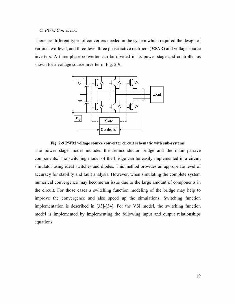
Fig. 2-9 PWM voltage source converter circuit schematic with sub-systems .................. 19
Fig. 2-10 Implementation of the switching functions ....................................................... 20
Fig. 2-11 Block diagram for vector control method used ................................................. 23
Fig. 2-12 Speed controller schematic................................................................................ 26
Fig. 2-13 Schematic for the single phase PFC average model with controllers. .............. 27
Fig. 3-1 Flowchart of the basic mapping procedure ......................................................... 37
Fig. 3-2 Power system used for stability analysis ............................................................. 39
Fig. 3-3 State transition diagram for the system ............................................................... 41
Fig. 3-4 Generator three phase output current and voltage with low and high speed
respectively ............................................................................................................... 42
Fig. 3-5 Generator three phase output current and voltage with low and high speed
respectively ............................................................................................................... 43
Fig. 3-6 MPTR dc link voltage, torque and speed for M1 and M2 connected to the MPTR
running at low (400 Hz) and high speed (800 Hz) .................................................... 44

x
Fig. 3-7 DC output voltage of the two-level three phase active rectifier and the torque and
speed waveforms of the 25 kW motor drive connected to it at low and high speed
respectively ............................................................................................................... 45
Fig. 3-8 DC output voltage of the three-level three phase active rectifier and the torque
and speed waveforms of the 25 kW motor drive connected to it at low and high
speed respectively ..................................................................................................... 46
Fig. 3-9 Three phase output voltage of the transformer and the output power and dc
voltage of one PFC at low and high speed respectively ........................................... 47
Fig. 3-10 MPTR dc output voltage when M1 and M2 speed ramp time is 45ms .............. 48
Fig. 3-11 MPTR output filter ............................................................................................ 49
Fig. 3-12 MPTR dc link voltage with C=180 μF at low line frequency (400 Hz) ............ 50
Fig. 3-13 MPTR dc link voltage with C=150 μF .............................................................. 51
Fig. 3-14 MPTR dc link voltage with different capacitance values at high speed (800 Hz)
................................................................................................................................... 52
Fig. 3-15 MPTR dc link voltage with inductance L=550 μH at low frequency (400 Hz) 52
Fig. 3-16 MPTR dc link voltage with inductance L=625 μH at low frequency (400 Hz) 53
Fig. 3-17 MPTR dc link voltage with inductance L=1250 μH at high frequency (800 Hz)
................................................................................................................................... 53
Fig. 3-18 MPTR dc link voltage with inductance L=1500 μH at high frequency (800 Hz)
................................................................................................................................... 54
Fig. 3-19 MPTR dc link voltage with C=450 μF for case 2 at low frequency (f=400 Hz)
................................................................................................................................... 55
Fig. 3-20 MPTR dc link voltage and the zooming of the oscillations with L=275 μH at
low frequency (f=400 Hz) for case 2 ........................................................................ 55
Fig. 3-21 MPTR dc link voltage with motor drive speed controller bandwidth 100 Hz .. 57
Fig. 3-22 MPTR dc link voltage with motor drive speed controller bandwidth of 10 Hz 58

xi
Fig. 3-23 MPTR dc link voltage with motor drive speed controller bandwidth 1 Hz ...... 58
Fig. 3-24 Motor drive test fed by an ideal source ............................................................. 59
Fig. 3-25 Waveforms for motor drive fed from dc source with speed controller bandwidth
of 100 Hz................................................................................................................... 60
Fig. 3-26 Waveforms for motor drive fed from dc source with speed controller bandwidth
of 125 Hz................................................................................................................... 60
Fig. 3-27 MPTR dc output voltage with feeder length 100m at high frequency (800 Hz)61
Fig. 3-28 MPTR dc output voltage with generator voltage controller loop bandwidth at
200 Hz ....................................................................................................................... 62
Fig. 3-29 MPTR dc output voltage with generator voltage controller loop bandwidth at
200 Hz ....................................................................................................................... 63
Fig. 3-30 MPTR dc output voltage with generator voltage controller loop bandwidth at
200 Hz ....................................................................................................................... 63
Fig. 3-31 MPTR filter capacitance vs inductance with MD speed controller bandwidth 10
Hz at low frequency (400 Hz) ................................................................................... 66
Fig. 3-32 MPTR filter capacitance vs filter inductance with MD speed controller
bandwidth 30 Hz at low frequency (400 Hz) ............................................................ 67
Fig. 3-33 MPTR filter capacitance vs filter inductance with MD speed controller
bandwidth 50 Hz at low frequency (400 Hz) ............................................................ 68
Fig. 3-34 MPTR filter capacitance vs MPTR filter inductance with MD speed controller
bandwidth 70 Hz at low frequency (400 Hz) ............................................................ 69
Fig. 3-35 MPTR filter capacitance vs filter inductance with MD speed controller
bandwidth 30 Hz at low frequency (400 Hz) and high frequency (800 Hz)
respectively ............................................................................................................... 70
Fig. 3-36 Feeder length versus generator voltage controller bandwidth mapping at low
frequency (400 Hz) & high frequency (800 Hz) respectively .................................. 71

xii
Fig. 3-37 Motor drives speed controller bandwidth versus the generator voltage controller
bandwidth at low frequency (400 Hz) ...................................................................... 72
Fig. 3-38 Generator excitation current limit versus the generator voltage controller
bandwidth at low frequency (400 Hz) ...................................................................... 74
Fig. 3-39 Generator excitation current limit versus the generator voltage controller
bandwidth at low frequency (400 Hz) ...................................................................... 74
Fig. 3-40 MPTR output dc link voltage with load steps applied ...................................... 76
Fig. 3-41 MPTR dc output voltage when applying a load step and system running at low
frequency ................................................................................................................... 77
Fig. 3-42 MPTR dc output voltage when applying a load step and system running at high
frequency ................................................................................................................... 77
Fig. 3-43 Speed reference step, motor drive phase current and line to line voltage
respectively ............................................................................................................... 78
Fig. 3-44 Mapping the MPTR filter capacitance and inductance using switching and
average models. ......................................................................................................... 79
Fig. 4-1 System architecture: generator feeding a two-level three phase active rectifier
and a 25kW motor drive ........................................................................................... 82
Fig. 4-2 System architecture: generator feeding a three-level three-phase active rectifier
and a 25 kW motor drive .......................................................................................... 82
Fig. 4-3 Waveforms of two-level three-phase active rectifier for a two ac phases short
circuit fault ................................................................................................................ 84
Fig. 4-4 Current spectrum for phase A current at the time the fault occurs ..................... 85
Fig. 4-5 Waveforms of the motor drive when a two ac phases short circuit fault occurs . 85
Fig. 4-6 Waveforms of the three level three phase active rectifier when a two ac phases
short circuit fault occurs ............................................................................................ 86
Fig. 4-7 Waveforms of the two level three phase active rectifier when phase A is

xiii
grounded ................................................................................................................... 87
Fig. 4-8 Waveforms of the two level three phase active rectifier when three phases are
grounded ................................................................................................................... 87
Fig. 4-9 Waveforms of two-level three-phase active rectifier when dc link is shorted .... 89
Fig. 4-10 The current spectrum of Ia ................................................................................ 89
Fig. 4-11 Waveforms of the three-level three-phase active rectifier for a dc link short
fault ........................................................................................................................... 90
Fig. 4-12 Waveforms of the two-level three-phase active rectifier for grounding of a
positive rail dc link.................................................................................................... 91
Fig. 4-13 Waveforms of the three-level three-phase active rectifier for grounding of a
positive rail dc link.................................................................................................... 91
Fig. 4-14 Waveforms of the two-level three-phase active rectifier for grounding of a
negative rail dc link ................................................................................................... 92
Fig. 4-15 Waveforms of the three-level three-phase active rectifier for grounding of a
negative rail dc link ................................................................................................... 93
Fig. 4-16 Waveforms of the two-level three-phase active rectifier for a short circuit fault
at one phase switch ................................................................................................... 93
Fig. 4-17 Waveforms of the three-level three-phase active rectifier for a short circuit fault
at one phase switch ................................................................................................... 94
Fig. 4-18 Waveforms of the two-level three-phase active rectifier for a open circuit fault
at one phase switch ................................................................................................... 95
Fig. 4-19 Waveforms of the three-level three-phase active rectifier for a open circuit fault
at one phase switch ................................................................................................... 95
Fig. 4-20 Waveforms of the two-level three-phase active rectifier for a open circuit fault
at main diode of phase A .......................................................................................... 96
Fig. 4-21 Three phase circuit breaker schematic. ............................................................ 98

xiv
Fig. 4-22 Block diagram for the system representation. .................................................. 99
Fig. 4-23 Schematic for the two-level three phase active rectifier protection. .............. 100
Fig. 4-24 Protection scheme schematic for the motor drive model. .............................. 101
Fig. 4-25 Block diagram for the three level AC fed motor drive with protection model.
................................................................................................................................. 102
Fig. 4-26 Protection scheme for the three level three phase active rectifier model. ...... 102
Fig. 4-27 System architecture: Generator feeding a two-level three-phase active rectifier
and a 25kW motor drive ......................................................................................... 104
Fig. 4-28 Waveforms analyzing the system with two ac phases shorted together ......... 105
Fig. 4-29 Waveforms for the system analyses when one ac phase is grounded ............. 106
Fig. 4-30 Waveforms for analyzing the system when the three ac phases are grounded 107
Fig. 4-31 Waveforms for short circuit fault of the dc link applied to the two-level three-
phase active rectifier ............................................................................................... 108
Fig. 4-32 Waveforms for the analyses of the system when positive rail of dc link is
grounded ................................................................................................................. 109
Fig. 4-33 Waveforms for the analyses of the system when negative rail of dc link is
grounded ................................................................................................................. 110
Fig. 4-34 Waveforms of two-level three-phase active rectifier when a short circuit fault of
the switch of phase A is applied ............................................................................. 111
Fig. 4-35 Waveforms for open circuit fault at the switch of phase A applied to the two-
level three-phase active rectifier ............................................................................. 112
Fig. 4-36 Waveforms for open circuit fault at the main bridge diode leg applied to the
two-level three-phase active rectifier ...................................................................... 113

xv
LIST OF TABLES
Table 3-1 PARAMETRIC CASE STUDIES ............................................................................... 64
Table 3-2 Parametric studies considered for case one ...................................................... 65
Table 3-3 Parametric studies considered for case four ..................................................... 73
TABLE 4-1: Protection types with defined limits ............................................................ 98

xvi
NOMENCLATURE
Symbol
id
Generator stator (armature) d-axis current (A)
iq
Generator stator (armature) q-axis current (A)
vd
Generator stator (armature) d-axis voltage (V)
vq
Generator stator (armature) q-axis voltage (V)
'kdi
Generator damper windings d-axis current (A)
'kqi Generator damper windings q-axis current (A)
'fdi Generator field winding current (A)
'fdv Generator field winding voltage (V)
ra Generator stator (armature) resistance (Ω)
Lls Generator leakage inductance (H)
Lmd Generator d-axis magnetizing inductance (H)
Lmq Generator q-axis magnetizing inductance (H)
'lkdL
Generator damper windings d-axis leakage inductances (H)
'lkqL Generator damper windings q-axis leakage inductances (H)
'kdr Generator damper windings resistance in d-axis (Ω)
'kqr Generator damper windings resistance in q-axis (Ω)
'fdr Generator field winding resistance (Ω)
'lfdL Generator field winding leakage inductance (H)

xvii
Nfd Generator stator to rotor winding referral ratio
Lfd Field inductance (H)
'qfL Equivalent inductance of the exciter field winding considering exciter load for
controller design (H)
ωr Generator electrical rotating speed (rad/s)
iex,
Exciter field current (A)
vex Exciter field voltage (V)
λd
Main magnetic flux in the d axes (W)
λq Main magnetic flux in the q axes (W)
'fdλ Excitation field magnetic flux (W)
'kdλ Magnetic flux at the damping magnetic circuits in the d axes (W)
'kqλ Magnetic flux at the damping magnetic circuits in the q axes (W)
ωb Base electrical angular velocity (rad/s)
Va,Vb, Vc
Three phase direct bridge voltages for MPTR (V)
Vap, Vbp, Vcp
Three phase forward bridge voltages for MPTR (V)
Vapp, Vbpp, Vcpp
Three phase lagging bridge voltages for MPTR (V)
van, vbn, vcn Three-phase phase to neutral voltages for voltage source inverter (VSI) (V)
vdc DC link voltage (V)
sab,sbc,sca Switching functions of the VSI
ωr Electrical angular speed of the rotor (rad/s)
rdd Converter d axes duty cycles
rqd Converter q axes duty cycles

xviii
'dsv Converter d axes output voltages (V)
'qsv Converter q axes output voltages (V)
Rs Stator resistance (Ω)
Ls Stator leakage inductance (H)
'dsi PM machine d axes line currents (A)
'qsi PM machine q axes line currents (A)
λm Permanent magnet flux (W)
Te PM machine electrical torque (N.m)
ωrm Rotor mechanical speed (rad/s)
P Number of pole pairs of the machine
TL Load torque (N.m)
Jm Machine intertia (Kg. m2)
ξ Damping coefficient
1
Chapter 1 Introduction
I. Scope of this Work
This research numerically investigates the stability and fault analysis of electric
power systems through computer modeling. Most electric power systems nowadays are
turning towards being electronic since this offers a high potential for life-cycle cost
savings, great improvement in system’s efficiency, high density, voltage regulation,
reliability, smaller size and lighter weight with continuous growth of system complexity
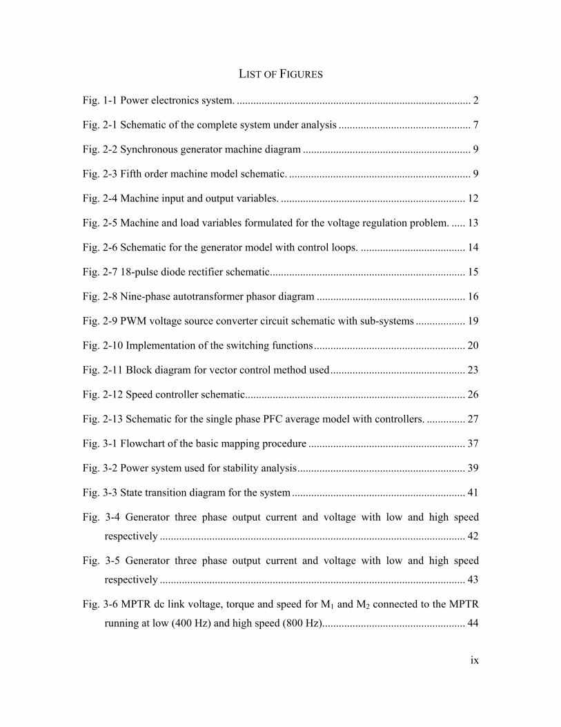
[1]- [2]. Fig. 1-1 shows the architecture of an electric power system composed of three
main stages. The first stage is an electrical power source. It can be a battery or a high
voltage storage system as in electric and hybrid-electric vehicles. It can also be a
generator as in an aircraft power system, photovoltaic arrays for space station power
system or a combination of more than one power source. The second stage is made up of
different power electronic converters in the form of ac-dc, dc-dc, dc-ac and ac-ac
converters, and transformer units. Finally, the third stage is the load. The load can be
electric motors and machines, air-conditioning systems, low power loads as power factor
correction circuits. One significant part of the system other than those three stages are the
ac connections between the main system components; and this is done through feeders.
The feeders can be modeled as lumped-parameters impedances representing the phase-
wire resistance and self-inductance.
Due to the size and complexity of most of these power systems, a good way to
analyze them is through simulation. Simulation illustrates how the system performs based
on the interaction between its different components. It also provides means for validating
and verifying the models designed [3]. In addition, simulation models minimize the cost
through avoiding repetitive hardware; minimize the concept-to-production time lag
through improving the whole system’s reliability [4]. There are several simulation
programs available nowadays, however, the selection is based on the application of the
system. Saber simulation program is used since it allows for functional modeling using
the MAST modeling language, SPICE-type model construction, combined digital and
2
analog capabilities. It is a robust simulator that allows almost any size model, and has a
large component library [3]-[8]. In addition, Saber is usually used in most multilevel
simulation because it is capable of circuit partitioning and decoupling which allows
significant speed improvement compared to modeling the whole power system as one
block. It allows the user to reduce the large system into many small sub-systems [2].
Fig. 1-1 Power electronics system.
Switching models with detailed controllers are used in this research. Switching
models are necessary when switching ripples are of interest or detailed transient
information is required [9]. They also provide accurate results but when introduced in a
large system, they can compromise the numerical convergence of the solution. The other
main drawback of using switching models is the long simulation time. Furthermore, when
the switching power system is integrated together, components dynamics and interactions
arise which can then lead to instability, or fault cases. The present work focuses on
integrating an ac-dc power electronic system and analyzing its performance using time
domain simulation. The analysis concentrates on stability, control and faults.
For fault analysis, the selection of models had to be carefully done in order to facilitate
the data manipulation and analysis of the results, in addition to optimizing the resources
[10]. Usually switching converters with protection schemes are chosen in this type of
analysis to realize the real performance of the devices. It is also usually assumed that the
fault resistance is very small, ideally zero. However, the simulation of this type of very
3
low resistance faults may complicate the simulation convergence making it more
convenient to give the fault resistance a value of several tens of mille-ohms instead.
II. Literature Review and Motivations
A. Modeling of Power Electronic Systems
The modeling of power electronic converters has generally followed two paths.
One of these paths is through modeling the individual components where the converter
model is derived from a detailed analysis of the operation that combines the component
models. A different approach that avoids this complexity focuses on the relationships
among the input/output magnitudes, producing models that are simpler, yet represent the
original system under a limited set of circumstances [11]. In this way, a wide variety of
models has been proposed, each one applicable for a particular study. Therefore, it is
useful to be familiar with models proposed in addition to the phenomena they describe
and their range of validity. Most of power electronics research is focused on analyzing
each converter individually in its stand-alone operation, and rather than the reaction of
this model in a complete system due to sophistication of most of these power systems
[12]. Some literature analyzed large dc-dc systems where multiple dc-dc converters are
used to supply needed power levels at different voltage levels as the simulation of space
station electric power system including multiple levels of switching dc-dc converters
providing different electrical loads [13]. The modeling and simulation of distributed
power system is shown in [9], and [5] illustrated the dynamic performance of a 20-kHz
spacecraft power system using computer simulation.
B. Power Electronic Systems Stability
Many efforts had been devoted in the research of power electronic system
stability. There are three types of stability analyses, steady state, small-signal and large
signal analysis [14]. Steady state analysis is the first step to approach a system stability
study that provides useful understanding of the system behavior. The next step in a
system stability study is the small-signal analysis. The small-signal analysis uses average
4
linearized models around the equilibrium point of interest. This allows using different
analytical tools that can help in the study as Bode, Nyquist and root loci plots. The small
signal stability analysis is usually done following Middlebrook’s work [15] based on the
impedance criterion, which ensures stability by preventing the loop gain Zo/Zi from
circling (-1,0) point in the s-plane. This design criterion is quite conservative as much of
the forbidden region in Nyquist plane has little influence on stability. Therefore, different
criteria were developed like the opposing component criterion and gain and phase margin
criterion (GMPM) that are considered less artificially conservative [16]-[19]. Following
that, a new stability criterion was proposed in the form of a forbidden region for the locus
of the return ratio Zsource(s) / Zload(s) on which the stability of the dc interface depended
[20]. This new criterion was extensively used in very large scale dc distributed power
systems (DPS) as for the International Space Station by redefining the forbidden region
for cascaded parallel loads [21]-[22]. In this study since switching models are used, small
signal stability is studied by running different parametric case studies. Different
parameters of the main components of the system are mapped together to predict their
influence on the system and know the limit beyond which the models become unstable.
Small-signal analysis does not always ensure stability in the large-signal sense,
therefore the stability margins based on the small signal study are often quite
conservative and the large signal stability study is necessary. The large signal stability
analysis is usually performed using computer simulations. It is examined through the
response of the system to different types of transient changes and its ability to withstand
or recover from these large perturbations [23]. These transients can be a large change in
the system parameters, which can correspond to a load step; or could be a change in the
system’s structure, as when faults appear in the system and a branch is disconnected.
There are different faults to be studied; for example, short circuit, open circuit and switch
failures. The time domain computer simulation approach is not considered an efficient
way in terms of use of the computational resources; however, it still continues to be the
most used practice, especially when detailed models are required and it can produce
accurate results based on the correctness of the models developed. Therefore, some
literature has been devoted to the modeling and implementation of stability studies in
5
computers and the use of time domain simulations as basis for the stability analysis [24]-
[26].
III. Objectives
The main objective of this research is to develop an approach for the analysis of ac/dc
hybrid power systems with large number of power converters, which can be used for a
variety of applications like automotive, ship spacecraft or aircraft. The research focused
on the computer modeling of the different parts of the system, the study of its dynamic
behavior and setting conditions for safe operation. The main challenge is to have the
system with proper switching/detailed models, sophisticated controllers and complex load
dynamics perform well without migrating close or into the unstable conditions. For this
reason the study investigated the stability behavior from the point of different critical
system parameters at different operating conditions to be able to draw some margins and
boundaries for stable and unstable operations.
IV. Thesis Outline and Summary of Contributions
Chapter 2 of the thesis discusses the modeling aspects of the major system
components. A sample system was chosen which contains components that are
representative in many ac/dc hybrid systems. These components have been developed by
others and repeated with some modifications that are related to the purpose of this study.
From these components are the three phase synchronous generator, the multi-pulse diode
rectifiers, the PWM rectifiers, the power factor correction circuits and the motor drive
loads. It concentrates on the different levels of details, accuracy and complexity of the
models.
Chapter 3 is devoted to the system stability analysis using time domain simulations. It
starts with the steady state analysis of the sample system to illustrate its performance
under normal conditions. The chapter then analyzes the small signal stability through
mapping critical parameters of the sample system. This mapping methodology allows
quantifying the impact of the system parameters on the stability of the system. Several

6
cases are analyzed allowing extracting conclusions on the stability margins and the
criticality of some parameters. Finally, the large signal stability is analyzed by means of
time domain simulations. Different types of disturbances are applied to the system to see
their impact on the system stability and define the maximum perturbations the system can
handle.
Chapter 4 examines a fault analysis for some of the critical components of the sample
system. The analysis is first done with no protection in the system to analyze the real
effect of the fault applied and study the stresses on the system components then some
basic protection schemes are added to prevent the models from breaking and the analyses
is repeated. The protections are based on monitoring the voltage or current needed using
sensors and shutting down the circuit in time of fault to avoid any losses.
Finally, chapter 5 states the main conclusions of this thesis in addition to some
proposed future work. A simulation software Saber was used to build and simulate a
sample electronic power system. This sample system was used for different stability and
fault studies like steady state, small-signal and large-signal stability analysis and time
simulations fault analysis. This work can be extended to different types of systems and
for more studies like power quality, EMI and harmonics studies.
7
Chapter 2 Power System Modeling
I. Introduction – System Description
The power system under study combines different types of components. The different
components are modeled in the stand-alone operation and then interconnected to study
the interaction of the different models together. The object of this chapter is to present the
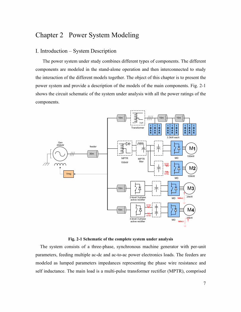
power system and provide a description of the models of the main components. Fig. 2-1
shows the circuit schematic of the system under analysis with all the power ratings of the
components.
Vreg
1ΦAR
Transformer
2-level 3-phase active rectifier
MPTR filter
M
M
MD
3-level 3-phase active rectifier
MD
MD
MD
MPTR
feeder
3-ph
10m
10m
10m
10m
30m
10m
1ΦAR
1ΦAR
1ΦAR
1ΦAR
1ΦAR
1ΦAR
1ΦAR
1ΦAR
Gen250kW
150kW
3.3kW each
25kW
25kW
100kW
100kW
0.1Ω
T
T
100kΩ
100kΩ
0.1Ω
0.1Ω
0.1Ω
M1
M2
3
4
Fig. 2-1 Schematic of the complete system under analysis
The system consists of a three-phase, synchronous machine generator with per-unit
parameters, feeding multiple ac-dc and ac-to-ac power electronics loads. The feeders are
modeled as lumped parameters impedances representing the phase wire resistance and
self inductance. The main load is a multi-pulse transformer rectifier (MPTR), comprised
8
of a transformer and directly paralleled three-phase diode bridges, and loaded with two
PWM voltage-source converter motor drives connected to a permanent magnet motor
(PMM), in parallel. The second branch consists of a two level three phase active rectifier
(3ФAR) connected to a dc-fed PWM voltage source converter motor drive connected to a
permanent magnet synchronous machine (PMSM). The third branch is a three level three
phase active rectifier followed by a motor drive model consisting of an inverter and a
permanent magnet synchronous machine (PMSM). Finally, the last branch is a
transformer model loaded with three single-phase active rectifiers (1ФAR). Each model
has different characteristics that are necessary depending on the type of analysis it will be
used for.
II. Individual Component Modeling
This section explains the modeling of the various system components. The focus is on
models appropriate for stability and fault studies. Models for stability studies required
simplified models with full controllers. The model has to account for the dynamic
behavior but still has straight forward implementation method. They have to have a high
degree of details since the analysis is based on time domain simulations. All the
following models described below have been developed before by others [27]-[38],
however, there are some modifications made based on this study.
A. Power Source Modeling
A three-phase synchronous generator with per unit parameters, variable speed and
remote regulation is modeled. It consists of a single machine that is represented in the d-
q-0 synchronous reference frame and a linear core has been assumed as shown in Fig.
2-2. The generator is mounted on the shaft of a significantly larger turbine which means
that the prime mover has a power capacity several times larger than the electric power of
the synchronous generator. Therefore, the mechanical dynamics can be neglected.
9
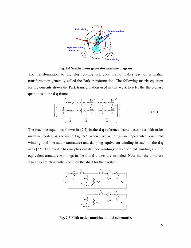
Fig. 2-2 Synchronous generator machine diagram
The transformation to the d-q rotating reference frame makes use of a matrix
transformation generally called the Park transformation. The following matrix equation
for the currents shows the Park transformation used in this work to refer the three-phase
quantities to the d-q frame:
⎥⎥⎥
⎦
⎤
⎢⎢⎢
⎣
⎡
⎥⎥⎥⎥⎥⎥⎥
⎦
⎤
⎢⎢⎢⎢⎢⎢⎢
⎣
⎡
⎟⎠⎞
⎜⎝⎛ +⎟
⎠⎞
⎜⎝⎛ −
⎟⎠⎞
⎜⎝⎛ +⎟
⎠⎞
⎜⎝⎛ −
=⎥⎥⎥
⎦
⎤
⎢⎢⎢
⎣
⎡
c
b
a
rrr
rrr
o
q
d
iii
ttt
ttt
iii
21
21
21
32cos
32coscos
32sin
32sinsin
32 πωπωω
πωπωω
(2.1)
The machine equations shown in (2.2) in the d-q reference frame describe a fifth order
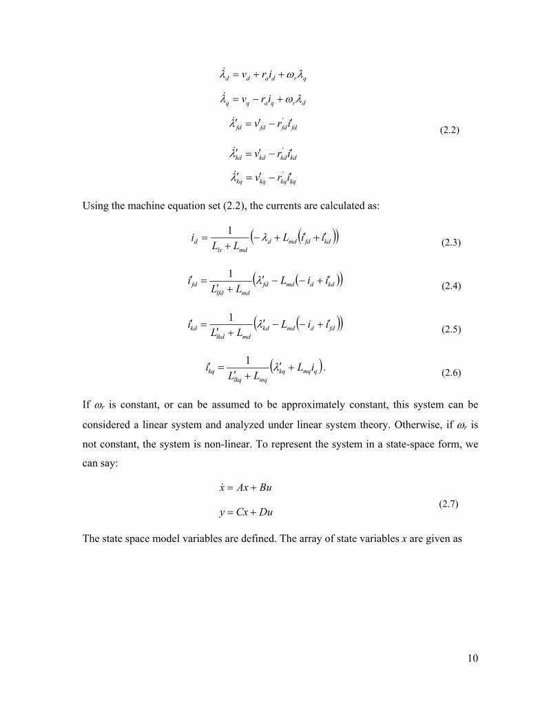
machine model, as shown in Fig. 2-3, where five windings are represented: one field
winding, and one stator (armature) and damping equivalent winding in each of the d-q
axes [27]. The exciter has no physical damper windings; only the field winding and the
equivalent armature windings in the d and q axes are modeled. Note that the armature
windings are physically placed on the shaft for the exciter.
rqωλ
d rλ ω
Fig. 2-3 Fifth order machine model schematic.
10
qrdadd irv λωλ ++=&
drqaqq irv λωλ +−=&
fdfdfdfd irv ′−′=′ 'λ&
kdkdkdkd irv ′−′=′ 'λ&
kqkqkqkq irv ′−′=′ 'λ&
(2.2)
Using the machine equation set (2.2), the currents are calculated as:
( )( )kdfdmddmdls
d iiLLL
i ′+′+−+
= λ1 (2.3)
( )( )kddmdfdmdlfd
fd iiLLL
i ′+−−′+′
=′ λ1 (2.4)
( )( )fddmdkdmdlkd
kd iiLLL
i ′+−−′+′
=′ λ1 (2.5)
( )qmqkqmqlkq
kq iLLL
i +′+′
=′ λ1 . (2.6)
If ωr is constant, or can be assumed to be approximately constant, this system can be
considered a linear system and analyzed under linear system theory. Otherwise, if ωr is
not constant, the system is non-linear. To represent the system in a state-space form, we
can say:
BuAxx +=&
DuCxy += (2.7)
The state space model variables are defined. The array of state variables x are given as

11
⎥⎥⎥⎥⎥⎥
⎦
⎤
⎢⎢⎢⎢⎢⎢
⎣
⎡
′′′=
kq
kd
fd
q
d
x
λλλλλ
, (2.8)
the input variables u,
⎥⎥⎥
⎦
⎤
⎢⎢⎢
⎣
⎡
′=
fd
q
d
vvv
u , (2.9)
and the output variables y,
⎥⎥⎥
⎦
⎤
⎢⎢⎢
⎣
⎡
′=
fd
q
d
iii
y . (2.10)
The state space representation of the generator model is given by the matrix equations
below in (2.11).
⎥⎥⎥⎥
⎦
⎤
⎢⎢⎢⎢
⎣
⎡
⎥⎥⎥⎥⎥⎥
⎦
⎤
⎢⎢⎢⎢⎢⎢
⎣
⎡
+
⎥⎥⎥⎥⎥⎥⎥
⎦
⎤
⎢⎢⎢⎢⎢⎢⎢
⎣
⎡
⎥⎥⎥⎥⎥⎥⎥⎥⎥⎥⎥⎥⎥
⎦
⎤
⎢⎢⎢⎢⎢⎢⎢⎢⎢⎢⎢⎢⎢
⎣
⎡
−
−
−
−−
−
=
⎥⎥⎥⎥⎥⎥⎥
⎦
⎤
⎢⎢⎢⎢⎢⎢⎢
⎣
⎡
'
'
'
'
'
'
'
'
''
'
'
'
'
'
''
'
'
'
''
'
'
'
'
'
'
'
'
''
'
'
'
000000100010001
000
00
00
00
0
fd
q
d
kq
kd
fd
q
d
kq
kqaq
kq
kq
ls
aq
kq
kq
kd
kdad
kd
kd
fd
ad
kd
kd
ls
ad
kd
kd
kd
ad
fd
fd
fd
fdad
fd
fd
ls
ad
fd
fd
kd
aq
ls
a
ls
lsad
ls
ar
kd
ad
ls
a
fd
ad
ls
ar
ls
lsad
ls
a
kq
kd
fd
q
d
v
vv
LLL
Lr
LL
Lr
LLL
Lr
LL
Lr
LL
Lr
LL
Lr
LLL
Lr
LL
Lr
LL
Lr
LLL
Lr
LL
Lr
LL
Lr
LLL
Lr
λ
λ
λ
λλω
ω
λ
λ
λ
λ
λ
&
&
&
&
&
(2.11)
where:
⎟⎟⎠
⎞⎜⎜⎝
⎛+
′+
′+=
mdkdfdlsad LLLL
L 1111 (2.12)
⎟⎟⎠
⎞⎜⎜⎝
⎛+
′+=
mqkqlsaq LLL
L 111 (2.13)

12
Although the measurement of the damping winding currents is not practical in the
synchronous machines, they can be included in vector y as output variables.
⎥⎥⎥⎥⎥⎥
⎦
⎤
⎢⎢⎢⎢⎢⎢
⎣
⎡
′′′=
kq
kd
fd
q
d
iiiii
y (2.14)
Therefore, the output equation is given by (2.15):
⎥⎥⎥⎥⎥⎥
⎦
⎤
⎢⎢⎢⎢⎢⎢
⎣
⎡
′′′
⎥⎥⎥⎥⎥⎥⎥⎥⎥⎥⎥⎥⎥
⎦
⎤
⎢⎢⎢⎢⎢⎢⎢⎢⎢⎢⎢⎢⎢
⎣
⎡
′
′−−
′−
′′−
−′′
−′
−
′−
′
′−−
′−
′−
′′−
=
⎥⎥⎥⎥⎥⎥
⎦
⎤
⎢⎢⎢⎢⎢⎢
⎣
⎡
′′′
kq
kd
fd
q
d
kq
kqaq
kqls
aq
kd
kdad
kdfd
ad
kdls
ad
kdls
ad
fd
fdad
lsfd
ad
kqls
aq
ls
lsaq
kdls
ad
fdls
ad
ls
lsad
kq
kd
fd
q
d
LLL
LLL
LLL
LLL
LLL
LLL
LLL
LLL
LLL
LLL
LLL
LLL
LLL
iiiii
λλλλλ
2
2
2
2
2
000
00
00
000
00
(2.15)
This state space model can be represented in a block diagram as that in Fig. 2-4.
Fig. 2-4 Machine input and output variables.
Since the interest is in having the machine voltage as the output, a system representation
closer to the formulation of the problem under study is obtained with the addition of the
load in the block diagram, as shown in Fig. 2-5.

13
G(s)vex
id
iq
iex
vd
vqLoad
Fig. 2-5 Machine and load variables formulated for the voltage regulation problem.
The controller consists of two loops as shown in Fig. 2-6. The internal feedback
loop Cex(s) controls the unidirectional exciter field current. The idea for the design of the
excitation current control loop is to have the largest possible gain and bandwidth. The
transfer function of the iex controller to estimate the loop bandwidth is given as:
1/ 1/)(
++
=pex
zexeex s
sksCωω
(2.16)
ωpex is the pole that gives the bandwidth of the loop and the dc gain of the loop. The value
of ωpex has to be chosen in order to limit the bandwidth of the excitation loop and avoid
instability. The bandwidth is practically limited by the stability requirement, with one of
the limiting factors being the delay caused by measurement time-lag due to digital
sampling. It is found that a good choice for ωpex is to make it ten times larger than the
regulator zero, provided that it is still considerably smaller than the sampling frequency.
ωzex is the zero and is calculated as,
''
'
lfdqf
fdzex LL
r+
=ω (2.17)
where 'qfL is the equivalent inductance of the exciter field winding considering exciter
load for controller design.
The exciter has to have limits in the maximum current or voltage that can be fed to the
machine field. These limits help in avoiding any huge fault current to pass during a short
circuit fault. They also require the implementation of an anti-windup scheme in the
excitation controller. Finally there is a current filter in the feedback loop, as shown in Fig.
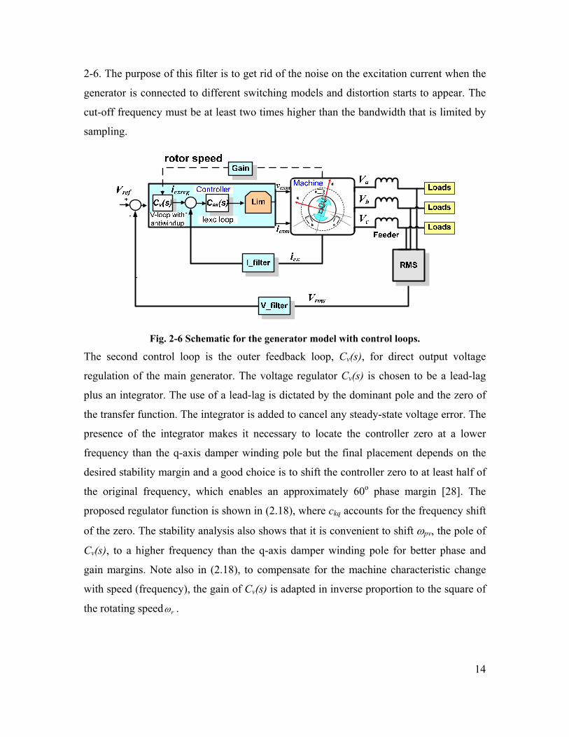
14
2-6. The purpose of this filter is to get rid of the noise on the excitation current when the
generator is connected to different switching models and distortion starts to appear. The
cut-off frequency must be at least two times higher than the bandwidth that is limited by
sampling.
q
d
b c
a
q
d
b c
a
Fig. 2-6 Schematic for the generator model with control loops.
The second control loop is the outer feedback loop, Cv(s), for direct output voltage
regulation of the main generator. The voltage regulator Cv(s) is chosen to be a lead-lag
plus an integrator. The use of a lead-lag is dictated by the dominant pole and the zero of
the transfer function. The integrator is added to cancel any steady-state voltage error. The
presence of the integrator makes it necessary to locate the controller zero at a lower
frequency than the q-axis damper winding pole but the final placement depends on the
desired stability margin and a good choice is to shift the controller zero to at least half of
the original frequency, which enables an approximately 60o phase margin [28]. The
proposed regulator function is shown in (2.18), where ckq accounts for the frequency shift
of the zero. The stability analysis also shows that it is convenient to shift ωpv, the pole of
Cv(s), to a higher frequency than the q-axis damper winding pole for better phase and
gain margins. Note also in (2.18), to compensate for the machine characteristic change
with speed (frequency), the gain of Cv(s) is adapted in inverse proportion to the square of
the rotating speed rω .

15
( )1/
1/1)(''2
max +++
⎟⎟⎠
⎞⎜⎜⎝
⎛=
pv
kqkqmqlkq
r
rvv s
crLLss
KsCωω
ω (2.18)
As in the current loop, a filter is added in the voltage feedback loop to avoid any
distortions. The voltage loop-gain bandwidth is limited by stability margins, so the filter
used would need to have a cut-off of at least five times higher than the bandwidth of the
voltage loop [9].
B. Multi-pulsed Transformer Rectifier (MPTR)
Multi-pulsed transformer rectifiers are composed of a transformer and one or more
sets of six-pulse diode bridges. The number of bridges is given by the number of phases
in the secondary side of the transformer, with a minimum of three phases corresponding
to one diode bridge. In order to reduce the output voltage ripple the number of phases in
the secondary side is increased by an appropriate interconnection of windings. Models of
this type are described in [29]-[32]. Fig. 2-7 shows the schematic of switching 18-pulse
diode rectifier as an example.
18-Pulse Autotransformer
Output DCTerminals
Diode Bridges
+vdc
[vp]abc
[vpp]abc
-vdc
P = 0.33p.u.
P = 0.33p.u.
P = 0.33p.u.
[vd]abc
vbvc
vap
va
+40º -40º
AC sourcevcpp
vcp vbpp
vbp
vapp
Fig. 2-7 18-pulse diode rectifier schematic
16
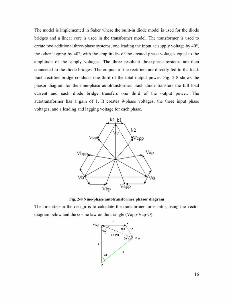
The model is implemented in Saber where the built-in diode model is used for the diode
bridges and a linear core is used in the transformer model. The transformer is used to
create two additional three-phase systems, one leading the input ac supply voltage by 40°,
the other lagging by 40°, with the amplitudes of the created phase voltages equal to the
amplitude of the supply voltages. The three resultant three-phase systems are then
connected to the diode bridges. The outputs of the rectifiers are directly fed to the load.
Each rectifier bridge conducts one third of the total output power. Fig. 2-8 shows the
phasor diagram for the nine-phase autotransformer. Each diode transfers the full load
current and each diode bridge transfers one third of the output power. The
autotransformer has a gain of 1. It creates 9-phase voltages, the three input phase
voltages, and a leading and lagging voltage for each phase.
Fig. 2-8 Nine-phase autotransformer phasor diagram
The first step in the design is to calculate the transformer turns ratio, using the vector
diagram below and the cosine law on the triangle (Vapp-Vap-O):

17
684.0)40(cos2)( 222 =°−+=− aaaVVvector appap (2.19)
Therefore,
)40(sin)_(
__sin °=
∠appap
apapp
VVvectorVVO
a ,
°=∠ 70__ apapp VVO ,
)40(sin)_(
__sin °=
∠appap
appap
VVvectorVVO
a ,
°=∠ 70__ appap VVO
(2.20)
and,
°=°−°=∠−°=∠ 207090__90__ apappappap VVOAVV . (2.21)
The cosine law is applied again to find the turns ratio gain K1 and K2,
AVV
K
appap __sin2
)120(sin684040286.0
∠=
° ,
270148.02 =K
(2.22)
Finally,
°=°−°−°=∠−°−°=∠ 4020120180__120180__ AVVAVV appapapapp . (2.23)
Therefore,
AVVK
apapp __sin1
)120(sin684040286.0
∠=
° ,
507713305.02 =K
(2.24)
With selecting the number of primary turns, Np then,

18
3
11
KNN p
k
⋅= and,
3
22
KNN p
k
⋅=
(2.25)
In addition, the output average dc voltage can be calculated as,
⎟⎠⎞
⎜⎝⎛⋅⋅
⎟⎟⎟⎟
⎠
⎞
⎜⎜⎜⎜
⎝
⎛
=
⋅⋅⎟⎟⎟⎟
⎠
⎞
⎜⎜⎜⎜
⎝
⎛
= ∫+
187cos
9
2
)sin(
9
2 9187
187
ππ
π
ππ
π
peak
peakdc
VGain
dxxVGainV
(2.26)
The second step is the design of the core used for the autotransformer by calculating the
different dimensions like the cross sectional area, the magnetic path length, the relative
permeability of the material used and the size of the wire used to handle the amount of
current needed. The cross-sectional area is related to the input voltage, primary number
of turns and the magnetic flux by the following equation,
epin ABdtdNtV ⋅⋅=⋅ )()sin(max ω ,
epinin ABNVdttV ⋅⋅==⋅∫ maxmax2
0 max1)sin(ω
ωωπ
,
π2max
max
⋅⋅⋅=
linep
ine fNB
VA or
22
maxπ
⋅⋅⋅=
linep
inrmse
fNB
VA
(2.27)
For the same model, a nonlinear core can be used when the model is used for fault
analysis. The circuit is connected to a filter at the dc side used to attenuate both common-
mode and differential-mode harmonics.
19
C. PWM Converters
There are different types of converters needed in the system which required the design of
various two-level, and three-level three phase active rectifiers (3ФAR) and voltage source
inverters. A three-phase converter can be divided in its power stage and controller as
shown for a voltage source inverter in Fig. 2-9.
Fig. 2-9 PWM voltage source converter circuit schematic with sub-systems
The power stage model includes the semiconductor bridge and the main passive
components. The switching model of the bridge can be easily implemented in a circuit
simulator using ideal switches and diodes. This method provides an appropriate level of
accuracy for stability and fault analysis. However, when simulating the complete system
numerical convergence may become an issue due to the large amount of components in
the circuit. For those cases a switching function modeling of the bridge may help to
improve the convergence and also speed up the simulations. Switching function
implementation is described in [33]-[34]. For the VSI model, the switching function
model is implemented by implementing the following input and output relationships
equations:
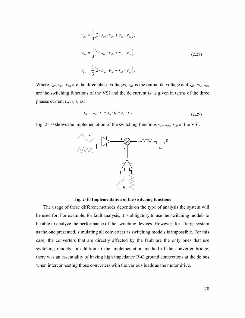
20
[ ]dcbcdcaban vsvsv ⋅+⋅⋅= 231 ,
[ ]dccadcbcbn vsvsv ⋅+⋅⋅= 231 ,
[ ]dcabdccacn vsvsv ⋅+⋅⋅= 231 ,
(2.28)
Where van, vbn, vcn are the three phase voltages, vdc is the output dc voltage and sab, sbc, sca
are the switching functions of the VSI and the dc current idc is given in terms of the three
phases current ia, ib, ic as:
ccbbaadc isisisi ⋅+⋅+⋅= . (2.29)
Fig. 2-10 shows the implementation of the switching functions sab, sbc, sca of the VSI.
+
-
a
b
sab
1
0
-1
Fig. 2-10 Implementation of the switching functions
The usage of these different methods depends on the type of analysis the system will
be used for. For example, for fault analysis, it is obligatory to use the switching models to
be able to analyze the performance of the switching devices. However, for a large system
as the one presented, simulating all converters as switching models is impossible. For this
case, the converters that are directly affected by the fault are the only ones that use
switching models. In addition to the implementation method of the converter bridge,
there was an essentiality of having high impedance R-C ground connections at the dc bus
when interconnecting those converters with the various loads as the motor drive.
21
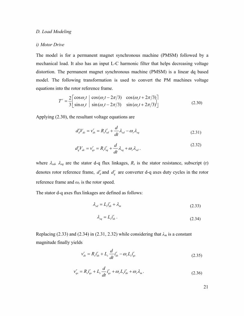
D. Load Modeling
i) Motor Drive
The model is for a permanent magnet synchronous machine (PMSM) followed by a
mechanical load. It also has an input L-C harmonic filter that helps decreasing voltage
distortion. The permanent magnet synchronous machine (PMSM) is a linear dq based
model. The following transformation is used to convert the PM machines voltage
equations into the rotor reference frame.
⎥⎦
⎤⎢⎣
⎡+−+−
=)32(sin)32(sinsin)32(cos)32(coscos
32
πωπωωπωπωω
tttttt
Trrr
rrrr (2.30)
Applying (2.30), the resultant voltage equations are
sqrsdrsds
rdsdc
rd dt
diRvVd λωλ −+== (2.31)
sdrsqrsqs
rqsdc
rq dt
diRvVd λωλ ++== . (2.32)
where λsd, λsq are the stator d-q flux linkages, Rs is the stator resistance, subscript (r)
denotes rotor reference frame, rdd and r
qd are converter d-q axes duty cycles in the rotor
reference frame and ωr is the rotor speed.
The stator d-q axes flux linkages are defined as follows:
mrdsssd iL λλ += (2.33)
rdsssq iL=λ . (2.34)
Replacing (2.33) and (2.34) in (2.31, 2.32) while considering that λm is a constant
magnitude finally yields
rqssr
rdss
rdss
rds iLi
dtdLiRv ω−+= (2.35)
mrrdssr
rqss
rqss
rqs iLi
dtdLiRv λωω +++= . (2.36)
22
Where λm is the permanent magnet flux constant, and Ls the leakage inductance.
The state space representation of the PM machine model for the real system without
including the rotor damping effects is thus given by,
⎥⎥⎥
⎦
⎤
⎢⎢⎢
⎣
⎡
⎥⎦
⎤⎢⎣
⎡−
+⎥⎥⎦
⎤
⎢⎢⎣
⎡⎥⎦
⎤⎢⎣
⎡−−
−=
⎥⎥⎦
⎤
⎢⎢⎣
⎡
PM
rqs
rds
rs
srsq
rsd
ssr
rssrsq
rsd v
v
LL
ii
LRLR
ii
λωω
ω1 0
0 01&
&. (2.37)
And the electrical torque of the PM machine is expressed as:
( )( )rqs
rdsqsds
rqsme iiLLiPT −+= λ)
2)(
23( , (2.38)
Since the stator inductance in the d-q axis are equal, qsds LL = , hence the electrical torque
reduces to,
rqsPMe iPT λ
43
= , (2.39)
where λPM is the permanent magnet flux constant, Ls the leakage inductance, the
superscript r denotes rotor reference frame, ωr is the rotor speed, P is the number of poles
of the machine and Te is the electromagnetic torque.
The mechanical load is a centrifugal load where the power is proportional to the
cube of the speed. The input signal is the PM machine electrical torque (Te), and its
output is the rotor mechanical speed (wrm). The signal flow diagram of the mechanical
load implements the load dynamics described by the following equation:
)(2 Lermrm TTPB
dtdJ −=+ ωω . (2.40)
where TL is the load torque.
The model uses vector control strategy to control the PMSM speed comprised of a
d-q axis current regulator featuring PI controllers with decoupling terms and anti-windup
loops, and an outer speed-loop PI regulator with anti-windup loop and a pre-filter
compensator for optimum transient response as shown in Fig. 2-11 [35]. This last loop
sets the reference for the q-axis control-loop that generates the torque current component
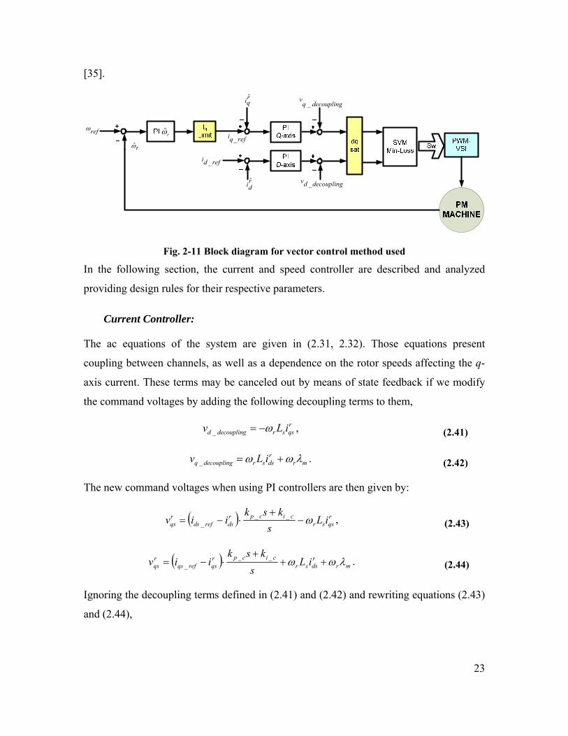
23
[35].
rdiˆ
rqiˆ
rω
refω
refdi _
decouplingqv
_
decouplingdv _
rωrefqi _
Fig. 2-11 Block diagram for vector control method used
In the following section, the current and speed controller are described and analyzed
providing design rules for their respective parameters.
Current Controller:
The ac equations of the system are given in (2.31, 2.32). Those equations present
coupling between channels, as well as a dependence on the rotor speeds affecting the q-
axis current. These terms may be canceled out by means of state feedback if we modify
the command voltages by adding the following decoupling terms to them,
rqssrdecouplingd iLv ω−=_ , (2.41)
mrrdssrdecouplingq iLv λωω +=_ . (2.42)
The new command voltages when using PI controllers are then given by:
( ) rqssr
cicprdsrefds
rqs iL
sksk
iiv ω−+
⋅−= ___ , (2.43)
( ) mrrdssr
cicprqsrefqs
rqs iL
sksk
iiv λωω +++
⋅−= ___ . (2.44)
Ignoring the decoupling terms defined in (2.41) and (2.42) and rewriting equations (2.43)
and (2.44),

24
rdss
rdss
rds i
dtdLiRv += and (2.45)
rqss
rqss
rqs i
dtdLiRv += . (2.46)
If the Laplace transform is then applied to (2.45) and (2.46), the transfer functions from
command voltages to stator currents may be obtained as follows:
( )( )
( )( ) ss
rqs
rqs
rds
rds
RsLsisv
sisv
+==
1 . (2.47)
The resultant closed-loop transfer functions for the d-q axis current loops may then be
derived as shown below.
ss
cicp
ss
cicp
refqs
rqs
refds
rds
RsLsksk
RsLsksk
sisi
sisi
++
+
++
==11
1
)()(
)()(
__
__
__
(2.48)
Clearly, the PI zero of the controller may be used to cancel out the machine dynamics if
kp_c and ki_c are chosen as Ls and Rs, but in order to tune the response of this closed loop,
kp_c and ki_c are additionally made proportional to the desired closed-loop bandwidth ωc
as follows,
cscp Lk ω=_ (2.49)
csci Rk ω=_ (2.50)
Replacing equations (2.49) and (2.50) in equation (2.48) yields the closed-loop transfer
function as:
c
c
refqs
rqs
refds
rds
ssisi
sisi
ωω+
==)(
)()(
)(
__
. (2.51)
This closed-loop transfer function shows that, in effect, the current control is only a
function of the controller bandwidth, since the machine dynamics are cancelled by the
appropriate selection of the controller parameters and the use of state feedback for
25
decoupling purposes.
There is also a d-q vector limiter to the output of both of the d-q axis current controllers,
to ensure the correct operating region. This is because duty cycles dd and dq ⎯ which are
indeed the control inputs to the converter-machine system ⎯ correspond to the actual
outputs of the d-q current loops. The intrinsic operational characteristics of the PWM-
VSI bound these control variables within the following range,
11 ≤≤− dd and
11 ≤≤− qd , (2.52)
which means,
122 ≤+ qd dd . (2.53)
However, this required implementing an anti-windup loop because there might be
winding up of the current controllers occurring when the output of the PI controller enters
the limiting region, and its integrator keeps building up without effecting any control
action. This situation leads to large current overshoot, slow settling times, and eventually
instabilities or even drives shut-downs. The wind-up is implemented as in [36], where the
difference between the limited and unbounded duty cycles is fed back through a
proportional gain (kaw_c) in order to limit the error entering the PI integrators, and thus
avoid their windup. This gain is defined as:
cp
cicaw k
kk
_
__ = (2.54)
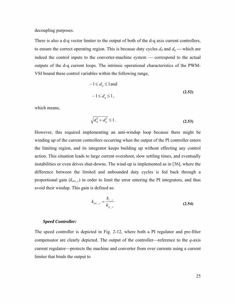
Speed Controller:
The speed controller is depicted in Fig. 2-12, where both a PI regulator and pre-filter
compensator are clearly depicted. The output of the controller⎯reference to the q-axis
current regulator⎯protects the machine and converter from over currents using a current
limiter that binds the output to
26
lim_ II refq ≤ . (2.55)
sawk _
rω
s1
spk _rω
refr _ωsisp
si
kskk
__
_
+ refqi _refqi _
sik _
rω
Fig. 2-12 Speed controller schematic.
The PI and pre-filter compensator gains are set by:
mssp Jk ζω2_ =
mssi Jk 2_ ω=
(2.56)
with Jm the machine inertia, ζ the desired damping coefficient, and ωs the desired speed-
loop bandwidth.
The anti-windup gain is simply defined by:
sp
sisaw k
kk
_
__ = . (2.57)
ii) Single-phase active rectifier (1ФAR):
The model represents low-power loads that are designed as an average model in
which the PWM-switch is replaced with controlled sources. The average model is used
here, because the switching frequency is high (100 kHz) so this is more simplified and
saves the simulation time [37].
27
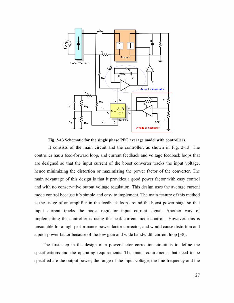
2C BAX ⋅
=
Fig. 2-13 Schematic for the single phase PFC average model with controllers.
It consists of the main circuit and the controller, as shown in Fig. 2-13. The
controller has a feed-forward loop, and current feedback and voltage feedback loops that
are designed so that the input current of the boost converter tracks the input voltage,
hence minimizing the distortion or maximizing the power factor of the converter. The
main advantage of this design is that it provides a good power factor with easy control
and with no conservative output voltage regulation. This design uses the average current
mode control because it’s simple and easy to implement. The main feature of this method
is the usage of an amplifier in the feedback loop around the boost power stage so that
input current tracks the boost regulator input current signal. Another way of
implementing the controller is using the peak-current mode control. However, this is
unsuitable for a high-performance power-factor corrector, and would cause distortion and
a poor power factor because of the low gain and wide bandwidth current loop [38].
The first step in the design of a power-factor correction circuit is to define the
specifications and the operating requirements. The main requirements that need to be
specified are the output power, the range of the input voltage, the line frequency and the

28
desired output voltage.
Input Inductor (L):
The input inductor determines the amount of high-frequency ripple current in the
input. Therefore, the maximum peak current of the sinusoidal input that occurs at the
peak of the minimum line voltage is chosen and is given by:
(min)2)(
inline V
PpkI ⋅= . (2.58)
where P is the power.
The peak-to-peak ripple current in the inductor is normally chosen to be about 20% of the
maximum peak line current. The value of the inductor is selected from the peak current at
the top of the half sine wave at low input voltage, the duty factor D at that input voltage
and the switching frequency ( sf ) where
o
ino
VVV
D−
= , (2.59)
and the inductance L is,
IfDV
Ls
in
Δ⋅⋅
= (2.60)
where IΔ is the peak-peak current ripple.
Output Capacitance (C):
The total current through the output capacitor is the root mean square (RMS) value of the
switching frequency ripple current and the second harmonic of the line current. It is
calculated using the following equation:
2(min)
2
2
inoo VV
tPC−
Δ⋅⋅= (2.61)
where P is the load power, ∆t is the hold-up time, Vo is the output voltage, and Vin(min) is

29
the minimum voltage at which the load will operate.
Current Sensor
For current sensing, a resistor current sense (Rs) configuration is used, as in Fig. 2-13, so
the inverting input to the current error amplifier is connected to ground through Rci. The
non-inverting input to the current error amplifier acts like a summing junction for the
current control loop, and adds the multiplier output current to the current from the sense
resistor (which flows through Rmo). The difference controls the boost regulator.
Multiplier Setup
The multiplier/divider is the heart of the power factor corrector. The output of the
multiplier programs the current loop to control the input current to give a high power
factor. The output of the multiplier is therefore a signal, which represents the input line
current. There are three inputs to the multiplier circuits: Iac(A), Vff (C), and Vvea (B). The
multiplier output current Imo is related to the three inputs by the following equation:
2
)1(
ff
veaacmmo V
VIKI
−⋅⋅= (2.62)
Feedforward Voltage
Vff is the input to the squaring circuit, and its range depends on the chip used. In this
design it was assumed to be 1.2V. The voltage divider for the Vff input has three resistors
(Rff1, Rff2 and Rff3) and two capacitors (Cff1 and Cff2), and thus it filters as well as provides
two outputs. The resistors and capacitors of the divider form a second-order low-pass
filter so the dc output is proportional to the average value of the input half-sine wave.
Multiplier Current
The operating current for the multiplier comes from the input voltage through RAC. The
multiplier has the best linearity at relatively high currents, but the recommended
maximum current is 0.6mA. The maximum output of the multiplier occurs at the peak of
the input sine wave at low line. The maximum output current from the multiplier can be
30
calculated from (2.62). This current, Imo, must be summed with a current proportional to
the inductor current in order to close the voltage feedback loop. Rmo, a resistor from the
output of the multiplier to the current sense resistor, performs this function and the
multiplier output pin becomes the summing junction.
Current Error Amplifier Compensation
The current loop must be compensated for stable operation. The boost converter control
to input current transfer function has a single pole response at high frequencies, which is
due to the impedance of the boost inductor and the sense resistor (Rs) forming a low-pass
filter. The equation for the control to input current transfer function is:
sLVRV
VV
s
sout
ea
rs
⋅⋅
= (2.63)
Where Vrs is the voltage across the input current sense resistor and Vea is the output of the
current error amplifier. Vout is the DC output voltage, Vs is the peak-to-peak amplitude of
the oscillator ramp, sL is the impedance of the boost inductor, and Rs is the sense resistor.
The compensation of the current error amplifier provides flat gain near the switching
frequency and uses the natural roll off the boost power stage to give the correct
compensation for the total loop. A zero at a low frequency in the amplifier response gives
the high gain, which makes average current mode control work. The gain of the error
amplifier near the switching frequency is determined by matching the down slope of the
inductor current when the switch is off with the slope of the ramp generated by the
oscillator.
The crossover frequency can be calculated as:
cis
zsoutci RLV
RRVf⋅⋅⋅⋅
=π2
(2.64)
Where fci is the current loop crossover frequency and Rcz/Rci is the gain of the current
error amplifier.
The placement of the zero in the current error amplifier response must be at or below the
crossover frequency. If it is at the crossover frequency, the phase margin will be 45°. If

31
the zero is lower in frequency, the phase margin will be greater. A 45° phase margin is
very stable, has low overshoot, and has good tolerance for component variations. The
zero must be placed at the crossover frequency so the impedance of the capacitor at that
frequency must be equal to the value of Rz.
The equation used for the calculation of the capacitance is:
zciz Rf
C⋅⋅
=π2
1 (2.65)
A pole is normally added to the current error amplifier response near the switching
frequency to reduce noise sensitivity. If the pole is above half the switching frequency,
the pole will not affect the frequency response of the control loop.
The transfer function for the current compensator is given in (2.66),
⎟⎟⎠
⎞⎜⎜⎝
⎛+
⎟⎟⎠
⎞⎜⎜⎝
⎛+
=−=
p
zici
s
s
sZZsG
ω
ωω
1
1)(
1
2 , (2.66)
where
pzz
pzz
sCsCR
sCsCR
Z11
1)1(
2
++
⋅+
= . (2.67)
From (2.64 – 2.67):
)(1(1)( 2
1
2
zpzzp
zz
cici CCsRCCs
RsCRZ
ZsG++
+−=−= . (2.68)
which means,
zzp
zpp RCC
CC +=ω (2.69)
32
zzz RC
1=ω (2.70)
cizpi RCC )(
1+
=ω . (2.71)
Voltage Error Amplifier Compensation:
The voltage control loop must be compensated for stability, but because the bandwidth of
the voltage loop is so small compared to the switching frequency, the requirements for
the voltage control loop are really driven by the need to keep the input distortion to a
minimum rather than by stability. The loop bandwidth must be low enough to attenuate
the second harmonic of the line frequency on the output capacitor to keep the modulation
of the input current small. The voltage error amplifier must also have enough phase shift
so that what modulation remains will be in phase with the input line to keep the power
factor high.
The first step in designing the voltage error amplifier compensation is to determine the
amount of ripple voltage present on the output capacitor. The peak value of the second
harmonic voltage is given by:
oor
inopk VCf
PV
⋅⋅⋅=
π2. (2.72)
Where Vopk is the peak value of the output ripple voltage (the peak to peak value will be
twice this),fr is the ripple frequency which is the second harmonic of the input line
frequency, Pin is the input power, Co is the value of the output capacitance and Vo is the
dc output voltage. Following that, the amount of distortion which the ripple contributes to
the input must be decided.
Cf, the feedback capacitor, sets the gain at the second harmonic ripple frequency, and is
chosen to give the voltage error amplifier the correct gain at the second harmonic of the
line frequency. The equation used is:
33
varf GRf
C⋅⋅⋅
=12
1π
(2.73)
where R1 can be chosen arbitrarily, but its value must be low enough that the operational
amplifier bias currents will not have a large effect on the output, and it must be high
enough so that the power dissipation is small. The gain Gva is calculated as the peak
ripple voltage allowed on the output of the voltage error amplifier divided by the peak
ripple voltage on the output capacitor.
The voltage compensator transfer function is given as
⎟⎟⎠
⎞⎜⎜⎝
⎛+
=
p
iEA
ssG
ω
ω
1)(
(2.74)
where
ffp RC
1=ω and (2.75)
1RR f
i =ω . (2.76)
Feed-forward Filter Capacitors of Voltage Divider
The percentage of second harmonic ripple voltage on the feed-forward input to the
multiplier results in the same percentage of third harmonic ripple current on the ac line.
Capacitors Cff1 and Cff2 attenuate the ripple voltage from the rectified input voltage. The
second harmonic ripple is 66.2% of the input ac line voltage. The amount of attenuation
required, or the “gain” of the filter, is simply the amount of the third harmonic distortion
allocated to this distortion source divided by 66.2%, which is the input to the divider.
The recommended divider string implements a second-order filter because this gives a
much faster response to changes in the root mean square (RMS) line voltage; typically
about six times faster. The two poles of the filter are placed at the same frequency for the
widest bandwidth. The total gain of the filter is the product of the gain of the two-filter
34
section, so the gain of each section is the square root of the total gain. The two sections of
the filter do not interact much because the impedances are different, so they can be
treated separately. The cutoff frequency is given by:
rffc fGf ⋅= (2.77)
Where Gff is the gain of the filter and fr is the ripple frequency. The cutoff frequency is
used to calculate the values for the filter capacitors, since the impedance of the capacitor
will equal the impedance of the load resistance at the cutoff frequency. The two equations
given below are used to calculate the two capacitor values:
21 2
1
ffcff Rf
C⋅⋅
=π
(2.78)
and
32 2
1
ffcff Rf
C⋅⋅
=π
. (2.79)
The circuit shown in Fig. 2-13 is implemented in Saber, and the controllers are
implemented using their derived transfer functions instead of using the operational
amplifiers [38].
III. System Implementation
The power system is simulated using Saber software. The main feature of this
system is its ability to perform parametric studies, small and large signal stability
analysis, in addition to fault analysis. It allows the simulation of realistic operating
scenarios so that an assessment of the system performance can be studied. Simulating and
understanding a large power system as the sample one proposed here is not an easy task,
and it can only be done by running different simulations with different parts of the system
and at different operating points. The system was simulated in stages. First, each model
was designed and tested for the stand-alone operation. The system was then connected
branch by branch and tested under normal operating conditions to study the steady state
stability, until finally it reached the complete system. There are several simulation

35
parameters that need to be adjusted in Saber in order to ensure a robust simulation
process, namely the time step that is chosen 100 times less than the converters switching
frequency, the number of target iterations and the truncation error which are chosen from
the algorithm selection and calibration parts respectively. The latter ones has an effect of
reduction of the time steps as its value increases [39], while the former will affect the
overall numerical convergence.
The other main issue while simulating the whole system is the essentiality of
having some high impedance R-C ground connections at the dc and neutral point model
terminals and some key power system terminals as the dc busses of the PWM converters
and at the mechanical load model as mentioned when discussing the PWM converters.
Sometimes a small resistance of 0.01 Ω is needed at the dc link busses to ensure smooth
and faster simulation. The key grounding points are shown in Fig. 2-1 in red. Finally, the
main drawback of simulating this system is the long time required for simulation, which
is to be expected as a large switching system is being simulated.
IV. Summary
This chapter described the system to be studied in this work. The different models
used in the system were illustrated; and their characteristics based on the stability and
fault analysis were also explained. Most of the models analyzed are detailed/switching
models that were easily implemented in Saber simulator which made the transient
stability analysis possible. Saber software was used to verify the models and system
operation. However, the main drawback is the long simulation time.
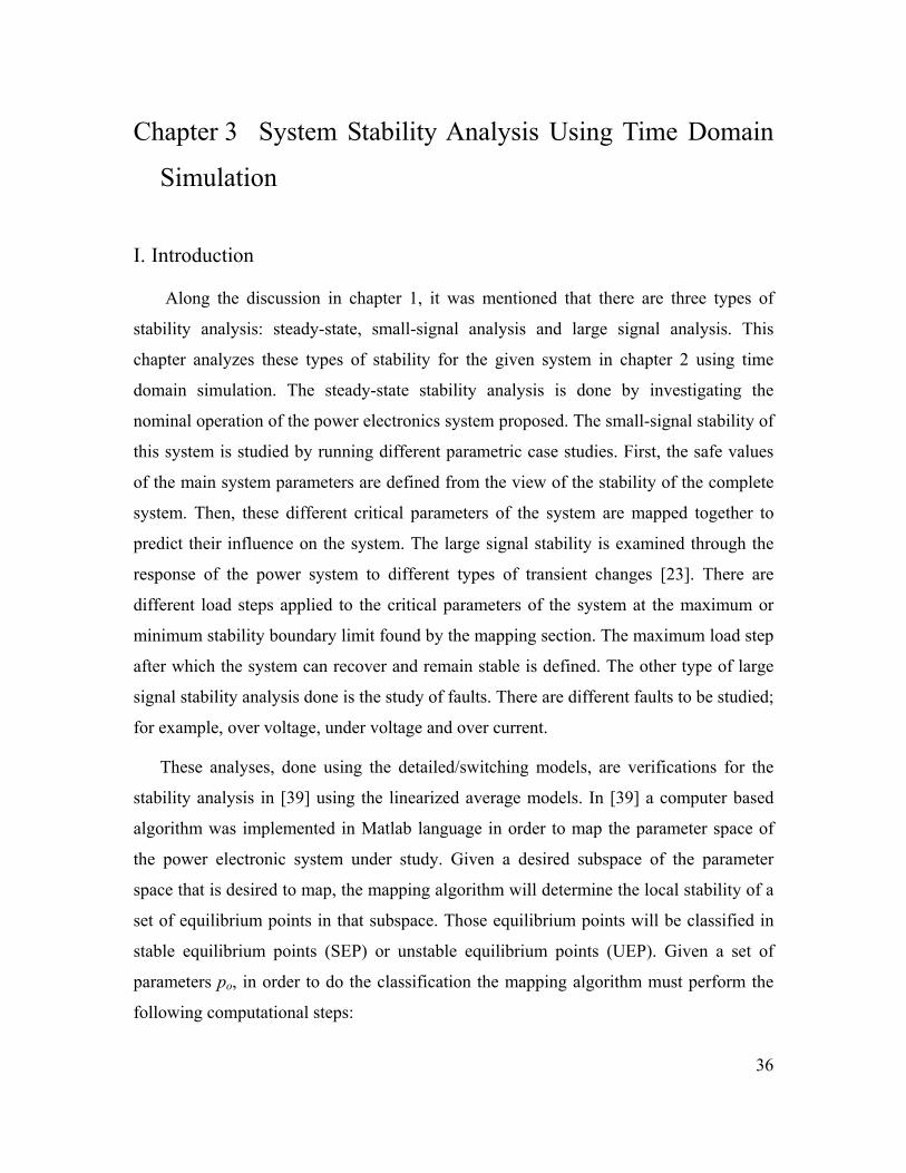
36
Chapter 3 System Stability Analysis Using Time Domain
Simulation
I. Introduction
Along the discussion in chapter 1, it was mentioned that there are three types of
stability analysis: steady-state, small-signal analysis and large signal analysis. This
chapter analyzes these types of stability for the given system in chapter 2 using time
domain simulation. The steady-state stability analysis is done by investigating the
nominal operation of the power electronics system proposed. The small-signal stability of
this system is studied by running different parametric case studies. First, the safe values
of the main system parameters are defined from the view of the stability of the complete
system. Then, these different critical parameters of the system are mapped together to
predict their influence on the system. The large signal stability is examined through the
response of the power system to different types of transient changes [23]. There are
different load steps applied to the critical parameters of the system at the maximum or
minimum stability boundary limit found by the mapping section. The maximum load step
after which the system can recover and remain stable is defined. The other type of large
signal stability analysis done is the study of faults. There are different faults to be studied;
for example, over voltage, under voltage and over current.
These analyses, done using the detailed/switching models, are verifications for the
stability analysis in [39] using the linearized average models. In [39] a computer based
algorithm was implemented in Matlab language in order to map the parameter space of
the power electronic system under study. Given a desired subspace of the parameter
space that is desired to map, the mapping algorithm will determine the local stability of a
set of equilibrium points in that subspace. Those equilibrium points will be classified in
stable equilibrium points (SEP) or unstable equilibrium points (UEP). Given a set of
parameters po, in order to do the classification the mapping algorithm must perform the
following computational steps:
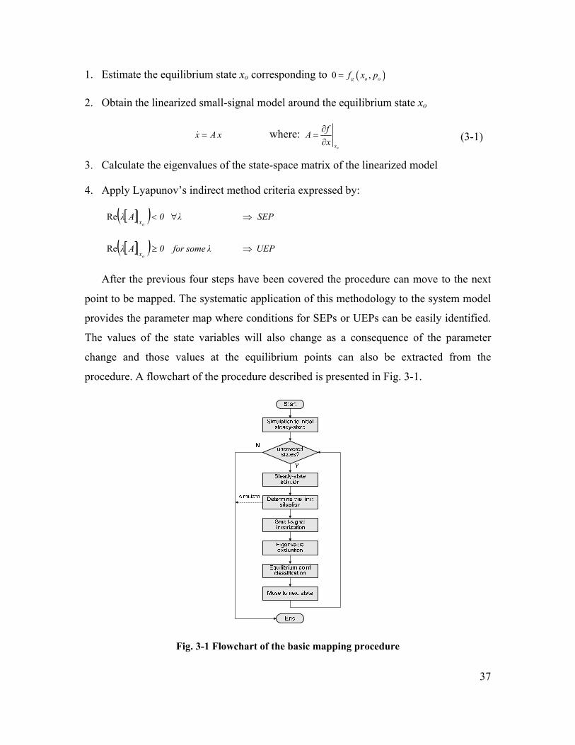
37
1. Estimate the equilibrium state xo corresponding to ( )0 ,g o of x p=
2. Obtain the linearized small-signal model around the equilibrium state xo
x A x=& where: ox
fAx∂
=∂
(3-1)
3. Calculate the eigenvalues of the state-space matrix of the linearized model
4. Apply Lyapunov’s indirect method criteria expressed by:
[ ]( ) SEPλ0Αλox
⇒∀<Re
[ ]( ) UEPλsomefor0Αλox
⇒≥Re
After the previous four steps have been covered the procedure can move to the next
point to be mapped. The systematic application of this methodology to the system model
provides the parameter map where conditions for SEPs or UEPs can be easily identified.
The values of the state variables will also change as a consequence of the parameter
change and those values at the equilibrium points can also be extracted from the
procedure. A flowchart of the procedure described is presented in Fig. 3-1.
Fig. 3-1 Flowchart of the basic mapping procedure

38
A. Definition of stability
The meaning of the stability of the system is its ability to reach and remain at the desired
equilibrium operating state. There are different definitions for stability but the one
followed in this study is the Lyapunov definition of stability, defined below.
For an autonomous nonlinear dynamical system [41] ,
))(( txfx =& , 0)0( xx = (3-2)
and assuming that the origin is an equilibrium,
1) The origin of the above system is said to be Lyapunov stable, if, for every ε >
0, there exists a δ = δ(ε) > 0 such that, if ,)0( δ<x then ,)( ε<tx for every
0≥t . This means that solutions starting "close enough" to the equilibrium
(within a distance δ from it) remain "close enough" forever (within a distance
ε from it) for any ε that one may want to choose.
2) The origin of the above system is said to be asymptotically stable if it is
Lyapunov stable and if there exists δ > 0 such that if ,)0( δ<x then
0)(lim =→∞
txt
. This means that solutions that start close enough not only remain
close enough but also eventually converge to the equilibrium.
3) The origin of the above system is said to be exponentially stable if it is
asymptotically stable and if there exist α,β,δ > 0 such that if ,)0( δ<x then
,)0()( textx βα −≤ for 0≥t . This means that solutions not only converge, but
in fact converge faster than or at least as fast as a particular known rate
.)0( tex βα −
II. System Performance Analysis
The system proposed in chapter 2 is used for the stability analysis and shown in
Fig. 3-2, together with data describing the nominal operating point.
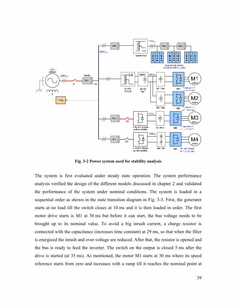
39
Fig. 3-2 Power system used for stability analysis
The system is first evaluated under steady state operation. The system performance
analysis verified the design of the different models discussed in chapter 2 and validated
the performance of the system under nominal conditions. The system is loaded in a
sequential order as shown in the state transition diagram in Fig. 3-3. First, the generator
starts at no load till the switch closes at 10 ms and it is then loaded in order. The first
motor drive starts is M1 at 30 ms but before it can start, the bus voltage needs to be
brought up to its nominal value. To avoid a big inrush current, a charge resistor is
connected with the capacitance (increases time constant) at 29 ms, so that when the filter
is energized the inrush and over-voltage are reduced. After that, the resistor is opened and
the bus is ready to feed the inverter. The switch on the output is closed 5 ms after the
drive is started (at 35 ms). As mentioned, the motor M1 starts at 30 ms where its speed
reference starts from zero and increases with a ramp till it reaches the nominal point at

40
100 ms. The second 100 kW motor drive (M2) that is running at half load, 50 kW,
follows M1 and starts 10 ms later at 40ms and reaches its full load point at 110 ms. There
is also an input filter for M2 that follows the same charging procedure as in M1 to avoid
any inrush current. The charging resistor starts at 39 ms and then the switch on the output
is closed 5 ms after the drive is started (at 45 ms) and is ready to feed the inverter. The
three-level three-phase active rectifier is connected next. It has a switch at the ac bus that
closes at 40.5 ms and connects the rectifier to the generator. The three-level three-phase
active rectifier is feeding a resistive load in the beginning till the dc bus is charged to
avoid any inrush current then a switch is opened at 55 ms and the rectifier starts feeding
the motor drive. The small 25 kW motor drive M3 connected to the three-level three-
phase active rectifier start after M2 with a 10 ms delay and 5 ms before the resistive load
is disconnected, which means it start at 50 ms and reaches steady state at 130 ms. The
motor drive M4 is fed from a two-level three-phase active rectifier that is connected to
the generator with a switch at 42.5 ms. The motor drive M4 starts with M3 at 50 ms and
reaches steady state at 130 ms. Finally, the low-power loads are connected directly as
soon as the switch closes with no delays.
41
Fig. 3-3 State transition diagram for the system
The system runs with a variable speed from 400 Hz to 800 Hz so all the performance
results were done for the maximum and minimum speed. The source is generating a three
phase sinusoidal rms output voltage of 230 V. Fig. 3-4 depicts the three phase output
current and voltage of the generator with low and high speed respectively. The distortion
that is seen on the waveforms is due to the switching of the different active rectifiers.
42
Fig. 3-4 Generator three phase output current and voltage with low and high speed
respectively
It can be seen from Fig. 3-4 that voltage is a little more distorted than the current
waveform. Usually the voltage source is relatively strong which means it has low
impedance so the voltage distortion is less than the current distortion, however, in an
autonomous system like that one studied here, it is not true anymore. Fig. 3-5 shows the
results of running the generator with a resistive load with low speed and high speed
respectively. The waveforms looks less distorted, however, as soon as the transformers
and rectifiers are connected, the system becomes more distorted.
43
Fig. 3-5 Generator three phase output current and voltage with low and high speed
respectively
The generator is connected to different loads as mentioned above. The main load is the
MPTR feeding two 100 kW motor drives, one running at full load (100 kW) and the other
at half load (50 kW). Fig. 3-6 shows the dc link voltage at the output of the MPTR (600
V) that is feeding the motor drives (M1 and M2) at both low and high speed. It also
shows the torque and speed of both machines. The waveforms follow the state transition
diagram in Fig. 3-3 where the speed reference of M1 (100 kW) starts at 30 ms and M2
(50 kW) at 40 ms and increases till the speed reaches 100%. A higher voltage is also seen
44
when the system is running at light load then starts to decrease till it reaches the nominal
operating point at full load.
Fig. 3-6 MPTR dc link voltage, torque and speed for M1 and M2 connected to the MPTR
running at low (400 Hz) and high speed (800 Hz)
The generator is also feeding a two-level three phase active rectifier that is connected to a
25 kW motor drive. Fig. 3-7 shows the waveform for the dc output voltage of the rectifier
(650 V) and the motor drive speed and torque running at both low (400 and high speed.
The 2-level three phase active rectifier is connected at 42.5 ms while the speed reference
of M3 starts increasing at 50 ms till it reaches maximum speed at 130 ms and the dc
voltage decreases when connected from light load to full load till it reaches the
equilibrium point. In addition, the generator is also supplying a three-level three phase
45
active rectifier with an output dc voltage of 700 V feeding another 25 kW motor drive.
Fig. 3-7 DC output voltage of the two-level three phase active rectifier and the torque and
speed waveforms of the 25 kW motor drive connected to it at low and high speed
respectively
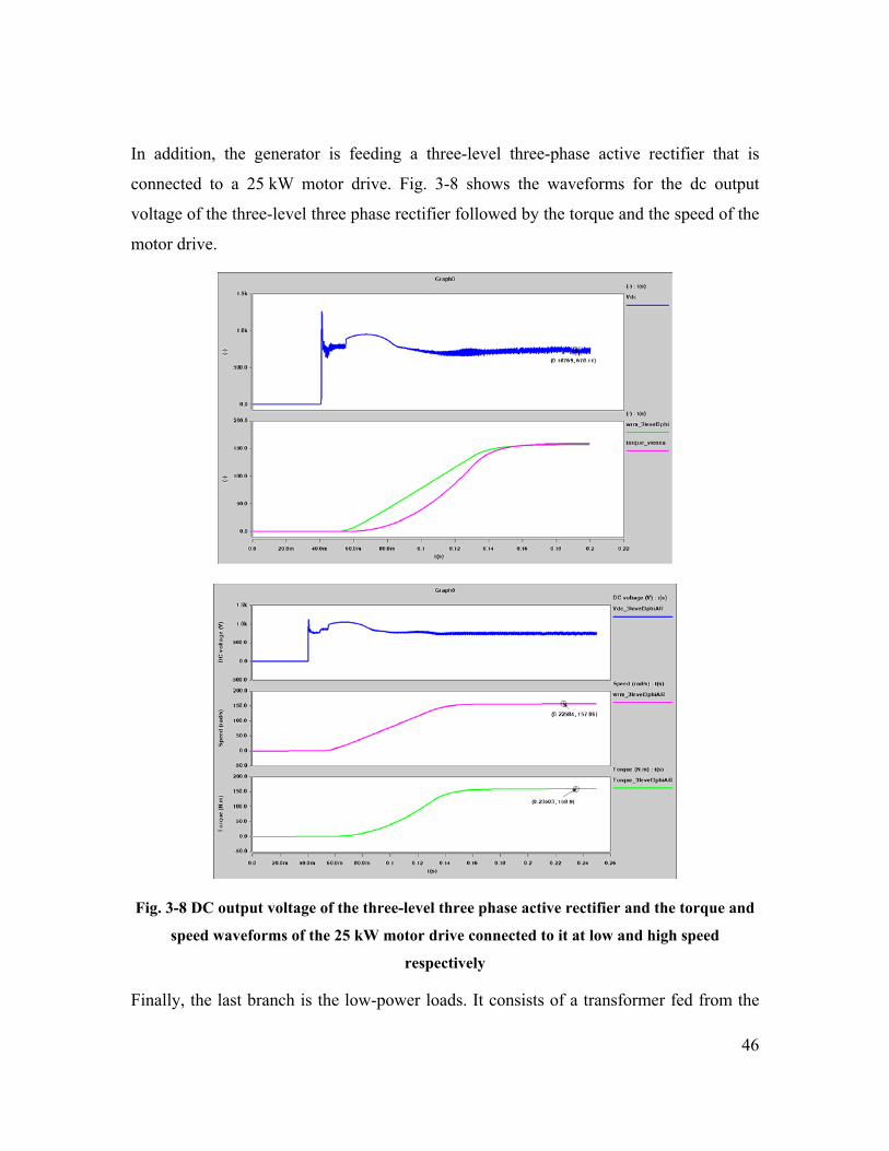
46
In addition, the generator is feeding a three-level three-phase active rectifier that is
connected to a 25 kW motor drive. Fig. 3-8 shows the waveforms for the dc output
voltage of the three-level three phase rectifier followed by the torque and the speed of the
motor drive.
Fig. 3-8 DC output voltage of the three-level three phase active rectifier and the torque and
speed waveforms of the 25 kW motor drive connected to it at low and high speed
respectively
Finally, the last branch is the low-power loads. It consists of a transformer fed from the
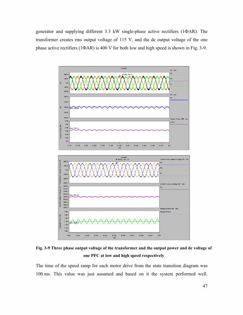
47
generator and supplying different 3.3 kW single-phase active rectifiers (1ФAR). The
transformer creates rms output voltage of 115 V, and the dc output voltage of the one
phase active rectifiers (1ФAR) is 400 V for both low and high speed is shown in Fig. 3-9.
Fig. 3-9 Three phase output voltage of the transformer and the output power and dc voltage of
one PFC at low and high speed respectively
The time of the speed ramp for each motor drive from the state transition diagram was
100 ms. This value was just assumed and based on it the system performed well.
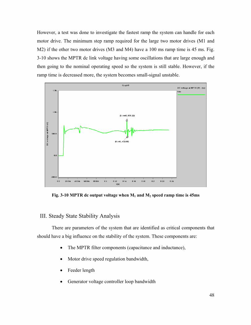
48
However, a test was done to investigate the fastest ramp the system can handle for each
motor drive. The minimum step ramp required for the large two motor drives (M1 and
M2) if the other two motor drives (M3 and M4) have a 100 ms ramp time is 45 ms. Fig.
3-10 shows the MPTR dc link voltage having some oscillations that are large enough and
then going to the nominal operating speed so the system is still stable. However, if the
ramp time is decreased more, the system becomes small-signal unstable.
Fig. 3-10 MPTR dc output voltage when M1 and M2 speed ramp time is 45ms
III. Steady State Stability Analysis
There are parameters of the system that are identified as critical components that
should have a big influence on the stability of the system. These components are:
• The MPTR filter components (capacitance and inductance),
• Motor drive speed regulation bandwidth,
• Feeder length
• Generator voltage controller loop bandwidth
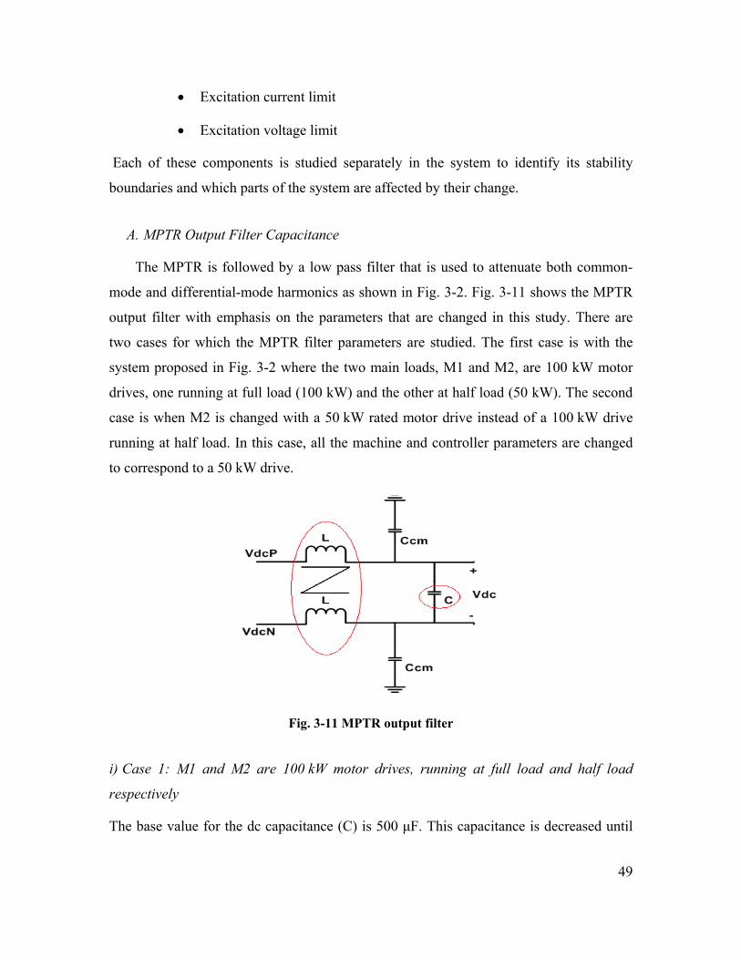
49
• Excitation current limit
• Excitation voltage limit
Each of these components is studied separately in the system to identify its stability
boundaries and which parts of the system are affected by their change.
A. MPTR Output Filter Capacitance
The MPTR is followed by a low pass filter that is used to attenuate both common-
mode and differential-mode harmonics as shown in Fig. 3-2. Fig. 3-11 shows the MPTR
output filter with emphasis on the parameters that are changed in this study. There are
two cases for which the MPTR filter parameters are studied. The first case is with the
system proposed in Fig. 3-2 where the two main loads, M1 and M2, are 100 kW motor
drives, one running at full load (100 kW) and the other at half load (50 kW). The second
case is when M2 is changed with a 50 kW rated motor drive instead of a 100 kW drive
running at half load. In this case, all the machine and controller parameters are changed
to correspond to a 50 kW drive.
Fig. 3-11 MPTR output filter
i) Case 1: M1 and M2 are 100 kW motor drives, running at full load and half load
respectively
The base value for the dc capacitance (C) is 500 μF. This capacitance is decreased until
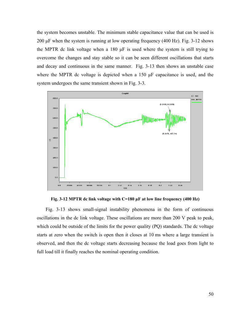
50
the system becomes unstable. The minimum stable capacitance value that can be used is
200 μF when the system is running at low operating frequency (400 Hz). Fig. 3-12 shows
the MPTR dc link voltage when a 180 μF is used where the system is still trying to
overcome the changes and stay stable so it can be seen different oscillations that starts
and decay and continuous in the same manner. Fig. 3-13 then shows an unstable case
where the MPTR dc voltage is depicted when a 150 μF capacitance is used, and the
system undergoes the same transient shown in Fig. 3-3.
Fig. 3-12 MPTR dc link voltage with C=180 μF at low line frequency (400 Hz)
Fig. 3-13 shows small-signal instability phenomena in the form of continuous
oscillations in the dc link voltage. These oscillations are more than 200 V peak to peak,
which could be outside of the limits for the power quality (PQ) standards. The dc voltage
starts at zero when the switch is open then it closes at 10 ms where a large transient is
observed, and then the dc voltage starts decreasing because the load goes from light to
full load till it finally reaches the nominal operating condition.
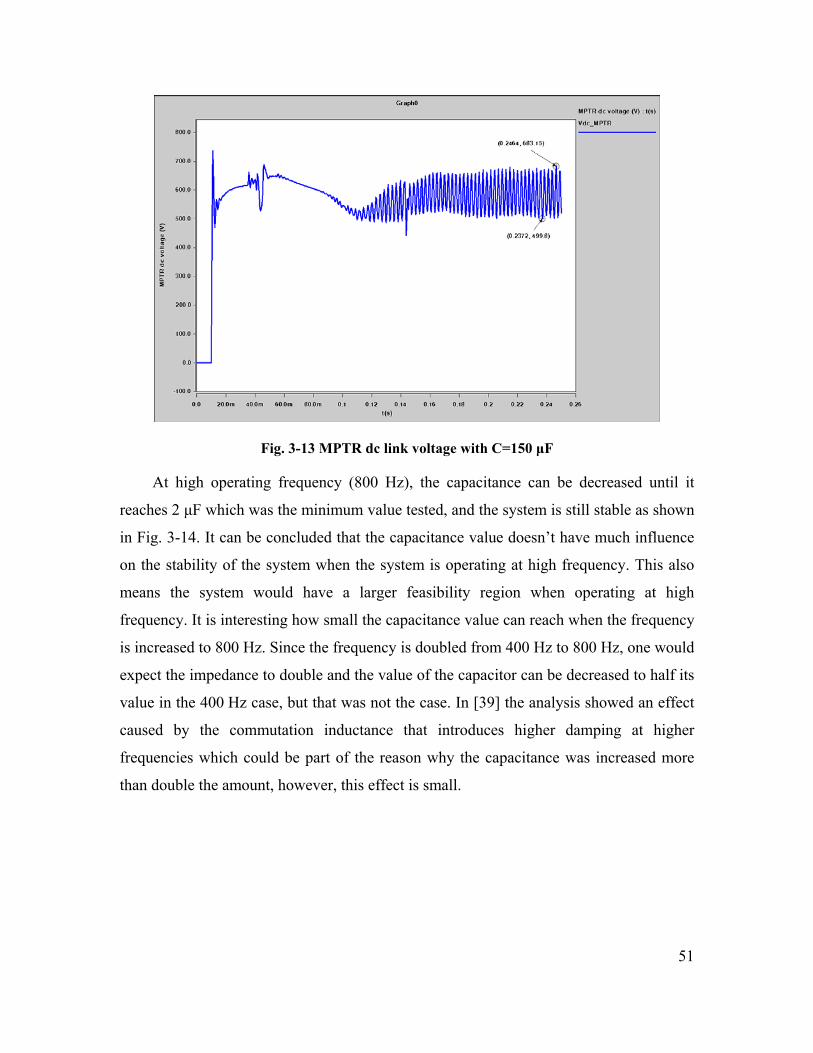
51
Fig. 3-13 MPTR dc link voltage with C=150 μF
At high operating frequency (800 Hz), the capacitance can be decreased until it
reaches 2 μF which was the minimum value tested, and the system is still stable as shown
in Fig. 3-14. It can be concluded that the capacitance value doesn’t have much influence
on the stability of the system when the system is operating at high frequency. This also
means the system would have a larger feasibility region when operating at high
frequency. It is interesting how small the capacitance value can reach when the frequency
is increased to 800 Hz. Since the frequency is doubled from 400 Hz to 800 Hz, one would
expect the impedance to double and the value of the capacitor can be decreased to half its
value in the 400 Hz case, but that was not the case. In [39] the analysis showed an effect
caused by the commutation inductance that introduces higher damping at higher
frequencies which could be part of the reason why the capacitance was increased more
than double the amount, however, this effect is small.
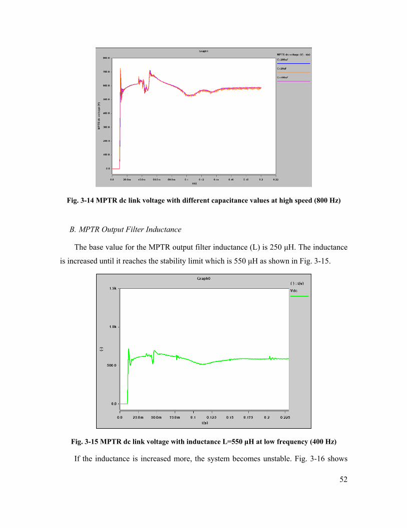
52
Fig. 3-14 MPTR dc link voltage with different capacitance values at high speed (800 Hz)
B. MPTR Output Filter Inductance
The base value for the MPTR output filter inductance (L) is 250 μH. The inductance
is increased until it reaches the stability limit which is 550 μH as shown in Fig. 3-15.
Fig. 3-15 MPTR dc link voltage with inductance L=550 μH at low frequency (400 Hz)
If the inductance is increased more, the system becomes unstable. Fig. 3-16 shows
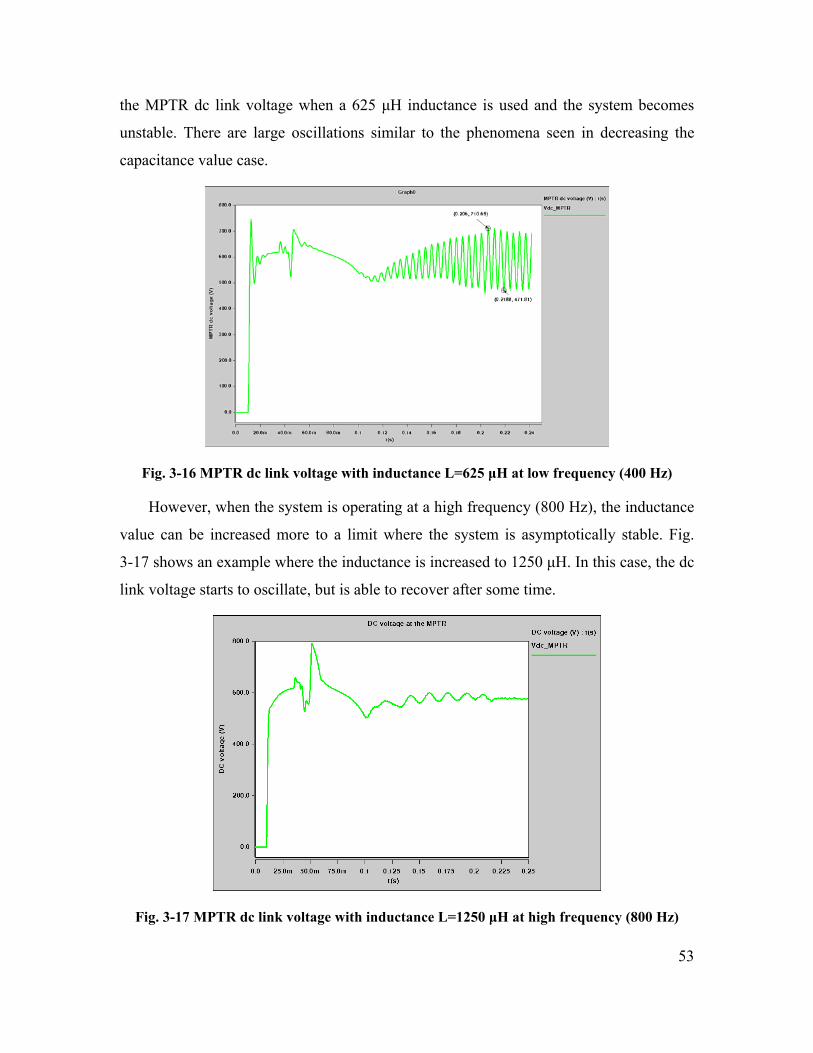
53
the MPTR dc link voltage when a 625 μH inductance is used and the system becomes
unstable. There are large oscillations similar to the phenomena seen in decreasing the
capacitance value case.
Fig. 3-16 MPTR dc link voltage with inductance L=625 μH at low frequency (400 Hz)
However, when the system is operating at a high frequency (800 Hz), the inductance
value can be increased more to a limit where the system is asymptotically stable. Fig.
3-17 shows an example where the inductance is increased to 1250 μH. In this case, the dc
link voltage starts to oscillate, but is able to recover after some time.
Fig. 3-17 MPTR dc link voltage with inductance L=1250 μH at high frequency (800 Hz)
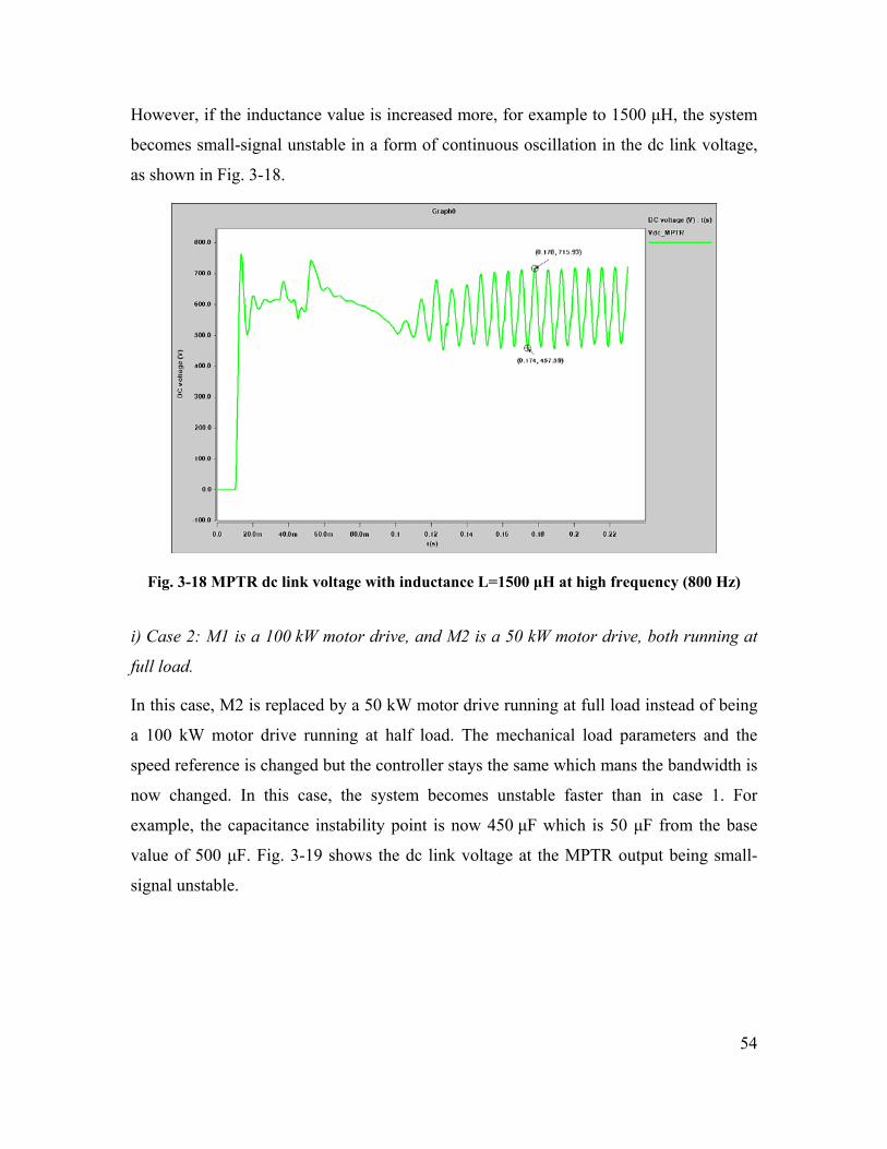
54
However, if the inductance value is increased more, for example to 1500 μH, the system
becomes small-signal unstable in a form of continuous oscillation in the dc link voltage,
as shown in Fig. 3-18.
Fig. 3-18 MPTR dc link voltage with inductance L=1500 μH at high frequency (800 Hz)
i) Case 2: M1 is a 100 kW motor drive, and M2 is a 50 kW motor drive, both running at
full load.
In this case, M2 is replaced by a 50 kW motor drive running at full load instead of being
a 100 kW motor drive running at half load. The mechanical load parameters and the
speed reference is changed but the controller stays the same which mans the bandwidth is
now changed. In this case, the system becomes unstable faster than in case 1. For
example, the capacitance instability point is now 450 μF which is 50 μF from the base
value of 500 μF. Fig. 3-19 shows the dc link voltage at the MPTR output being small-
signal unstable.
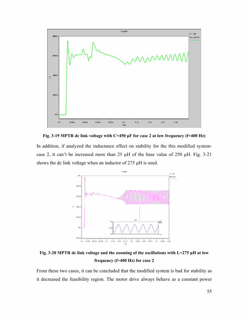
55
Fig. 3-19 MPTR dc link voltage with C=450 μF for case 2 at low frequency (f=400 Hz)
In addition, if analyzed the inductance effect on stability for the this modified system-
case 2, it can’t be increased more than 25 μH of the base value of 250 μH. Fig. 3-21
shows the dc link voltage when an inductor of 275 μH is used.
Fig. 3-20 MPTR dc link voltage and the zooming of the oscillations with L=275 μH at low
frequency (f=400 Hz) for case 2
From these two cases, it can be concluded that the modified system is bad for stability as
it decreased the feasibility region. The motor drive always behave as a constant power
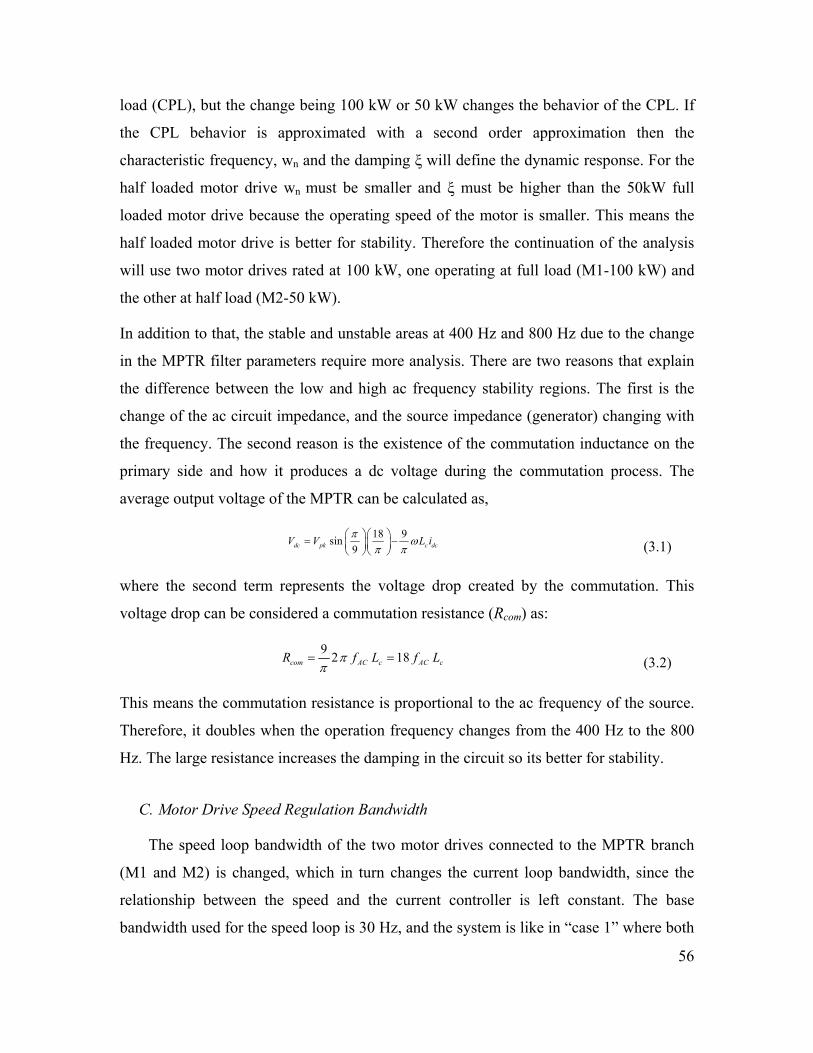
56
load (CPL), but the change being 100 kW or 50 kW changes the behavior of the CPL. If
the CPL behavior is approximated with a second order approximation then the
characteristic frequency, wn and the damping ξ will define the dynamic response. For the
half loaded motor drive wn must be smaller and ξ must be higher than the 50kW full
loaded motor drive because the operating speed of the motor is smaller. This means the
half loaded motor drive is better for stability. Therefore the continuation of the analysis
will use two motor drives rated at 100 kW, one operating at full load (M1-100 kW) and
the other at half load (M2-50 kW).
In addition to that, the stable and unstable areas at 400 Hz and 800 Hz due to the change
in the MPTR filter parameters require more analysis. There are two reasons that explain
the difference between the low and high ac frequency stability regions. The first is the
change of the ac circuit impedance, and the source impedance (generator) changing with
the frequency. The second reason is the existence of the commutation inductance on the
primary side and how it produces a dc voltage during the commutation process. The
average output voltage of the MPTR can be calculated as,
18 9sin9dc pk c dcV V L iπ ω
π π⎛ ⎞ ⎛ ⎞= −⎜ ⎟ ⎜ ⎟⎝ ⎠ ⎝ ⎠
(3.1)
where the second term represents the voltage drop created by the commutation. This
voltage drop can be considered a commutation resistance (Rcom) as:
9 2 18com AC c AC cR f L f Lππ
= = (3.2)
This means the commutation resistance is proportional to the ac frequency of the source.
Therefore, it doubles when the operation frequency changes from the 400 Hz to the 800
Hz. The large resistance increases the damping in the circuit so its better for stability.
C. Motor Drive Speed Regulation Bandwidth
The speed loop bandwidth of the two motor drives connected to the MPTR branch
(M1 and M2) is changed, which in turn changes the current loop bandwidth, since the
relationship between the speed and the current controller is left constant. The base
bandwidth used for the speed loop is 30 Hz, and the system is like in “case 1” where both
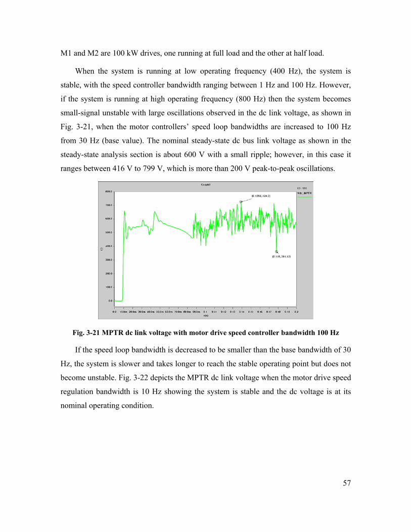
57
M1 and M2 are 100 kW drives, one running at full load and the other at half load.
When the system is running at low operating frequency (400 Hz), the system is
stable, with the speed controller bandwidth ranging between 1 Hz and 100 Hz. However,
if the system is running at high operating frequency (800 Hz) then the system becomes
small-signal unstable with large oscillations observed in the dc link voltage, as shown in
Fig. 3-21, when the motor controllers’ speed loop bandwidths are increased to 100 Hz
from 30 Hz (base value). The nominal steady-state dc bus link voltage as shown in the
steady-state analysis section is about 600 V with a small ripple; however, in this case it
ranges between 416 V to 799 V, which is more than 200 V peak-to-peak oscillations.
Fig. 3-21 MPTR dc link voltage with motor drive speed controller bandwidth 100 Hz
If the speed loop bandwidth is decreased to be smaller than the base bandwidth of 30
Hz, the system is slower and takes longer to reach the stable operating point but does not
become unstable. Fig. 3-22 depicts the MPTR dc link voltage when the motor drive speed
regulation bandwidth is 10 Hz showing the system is stable and the dc voltage is at its
nominal operating condition.
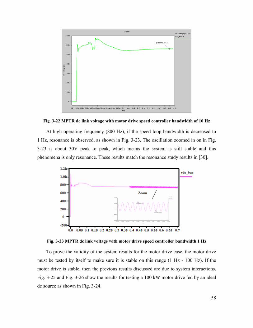
58
Fig. 3-22 MPTR dc link voltage with motor drive speed controller bandwidth of 10 Hz
At high operating frequency (800 Hz), if the speed loop bandwidth is decreased to
1 Hz, resonance is observed, as shown in Fig. 3-23. The oscillation zoomed in on in Fig.
3-23 is about 30V peak to peak, which means the system is still stable and this
phenomena is only resonance. These results match the resonance study results in [30].
Fig. 3-23 MPTR dc link voltage with motor drive speed controller bandwidth 1 Hz
To prove the validity of the system results for the motor drive case, the motor drive
must be tested by itself to make sure it is stable on this range (1 Hz - 100 Hz). If the
motor drive is stable, then the previous results discussed are due to system interactions.
Fig. 3-25 and Fig. 3-26 show the results for testing a 100 kW motor drive fed by an ideal
dc source as shown in Fig. 3-24.
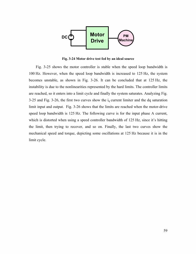
59
PMMachine
MotorDrive
DC
Fig. 3-24 Motor drive test fed by an ideal source
Fig. 3-25 shows the motor controller is stable when the speed loop bandwidth is
100 Hz. However, when the speed loop bandwidth is increased to 125 Hz, the system
becomes unstable, as shown in Fig. 3-26. It can be concluded that at 125 Hz, the
instability is due to the nonlinearities represented by the hard limits. The controller limits
are reached, so it enters into a limit cycle and finally the system saturates. Analyzing Fig.
3-25 and Fig. 3-26, the first two curves show the iq current limiter and the dq saturation
limit input and output. Fig. 3-26 shows that the limits are reached when the motor-drive
speed loop bandwidth is 125 Hz. The following curve is for the input phase A current,
which is distorted when using a speed controller bandwidth of 125 Hz, since it’s hitting
the limit, then trying to recover, and so on. Finally, the last two curves show the
mechanical speed and torque, depicting some oscillations at 125 Hz because it is in the
limit cycle.
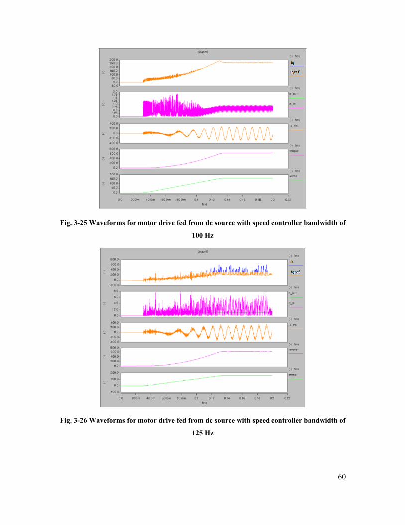
60
Fig. 3-25 Waveforms for motor drive fed from dc source with speed controller bandwidth of
100 Hz
Fig. 3-26 Waveforms for motor drive fed from dc source with speed controller bandwidth of
125 Hz
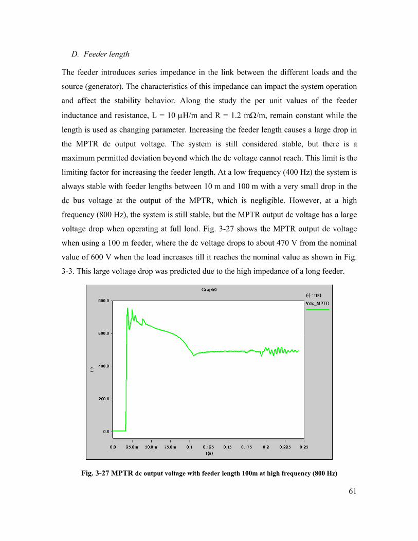
61
D. Feeder length
The feeder introduces series impedance in the link between the different loads and the
source (generator). The characteristics of this impedance can impact the system operation
and affect the stability behavior. Along the study the per unit values of the feeder
inductance and resistance, L = 10 μH/m and R = 1.2 mΩ/m, remain constant while the
length is used as changing parameter. Increasing the feeder length causes a large drop in
the MPTR dc output voltage. The system is still considered stable, but there is a
maximum permitted deviation beyond which the dc voltage cannot reach. This limit is the
limiting factor for increasing the feeder length. At a low frequency (400 Hz) the system is
always stable with feeder lengths between 10 m and 100 m with a very small drop in the
dc bus voltage at the output of the MPTR, which is negligible. However, at a high
frequency (800 Hz), the system is still stable, but the MPTR output dc voltage has a large
voltage drop when operating at full load. Fig. 3-27 shows the MPTR output dc voltage
when using a 100 m feeder, where the dc voltage drops to about 470 V from the nominal
value of 600 V when the load increases till it reaches the nominal value as shown in Fig.
3-3. This large voltage drop was predicted due to the high impedance of a long feeder.
Fig. 3-27 MPTR dc output voltage with feeder length 100m at high frequency (800 Hz)
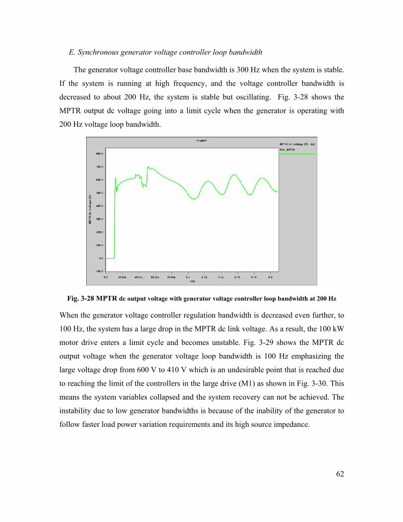
62
E. Synchronous generator voltage controller loop bandwidth
The generator voltage controller base bandwidth is 300 Hz when the system is stable.
If the system is running at high frequency, and the voltage controller bandwidth is
decreased to about 200 Hz, the system is stable but oscillating. Fig. 3-28 shows the
MPTR output dc voltage going into a limit cycle when the generator is operating with
200 Hz voltage loop bandwidth.
Fig. 3-28 MPTR dc output voltage with generator voltage controller loop bandwidth at 200 Hz
When the generator voltage controller regulation bandwidth is decreased even further, to
100 Hz, the system has a large drop in the MPTR dc link voltage. As a result, the 100 kW
motor drive enters a limit cycle and becomes unstable. Fig. 3-29 shows the MPTR dc
output voltage when the generator voltage loop bandwidth is 100 Hz emphasizing the
large voltage drop from 600 V to 410 V which is an undesirable point that is reached due
to reaching the limit of the controllers in the large drive (M1) as shown in Fig. 3-30. This
means the system variables collapsed and the system recovery can not be achieved. The
instability due to low generator bandwidths is because of the inability of the generator to
follow faster load power variation requirements and its high source impedance.
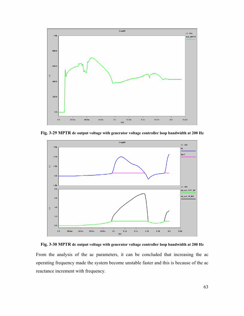
63
Fig. 3-29 MPTR dc output voltage with generator voltage controller loop bandwidth at 200 Hz
Fig. 3-30 MPTR dc output voltage with generator voltage controller loop bandwidth at 200 Hz
From the analysis of the ac parameters, it can be concluded that increasing the ac
operating frequency made the system become unstable faster and this is because of the ac
reactance increment with frequency.
64
IV. Small Signal Stability Analysis
The small signal stability is studied by mapping the critical parameters of the system in
Fig. 3-2 defined in the previous section. The impact of these system parameters is studied
with several case studies defined. Each of these case studies analyzes the impact of a
particular parameter or group of parameters in the system stability. The list of those case
studies is given in Table 3-1. The following sections analyze the impact of those
parameters in the system stable operation which means after the transients and when the
system reaches the nominal point as shown in Fig. 3-3.
A. Case definition
The cases presented in Table 3-1 represent a wide set of parameters covering the different
equipment connected in the power system of Fig. 2-1. Some of the parameters change the
system dynamic response and also the circuit stationary operation magnitudes. Example
of these types of parameters can be series ac impedance. On the contrary, other
parameters only change the dynamic behavior like the case of a controller bandwidth.
Table 3-1 PARAMETRIC CASE STUDIES
B. Multi-pulse Transformer Rectifier Filter Parameters Analysis
The purpose of case one is to study the impact of the multi-pulse transformer rectifier
filter on the system. The multi-pulse transformer rectifier capacitor and inductor impact
on the system stability behavior is studied. The dimensioning of the filter is based not
only on stability considerations but also on other requirements like the power quality in
the system. Therefore, it is important to know the range where the filter basic
Case # Case description Parameters to map
1 Multi-pulse transformer rectifier filter parameters L, C, fwMD (bw MD)
2 Source (generator) versus ac impedance (feeder) Feeder length, fwG (bw Generator)
3 Source (generator) versus load (MD) parameters fwG (bw Generator), fwMD
(bw MD)
4 Generator parameters fwG (bw Generator), Iex, Vex
65
dimensioning (L, C) does not impact on the system stability behavior. These mapping
were also done under different motor drives speed regulation bandwidths to see how the
load is related to the multi-pulse transformer rectifier in affecting the system. There are
several sub-cases for this case that are shown in Table 3-2.
Table 3-2 Parametric studies considered for case one
Case # Case description Parameters to map
1-a MPTR filter capacitance vs. inductance with
MD speed regulation bandwidth of 10 Hz and low line frequency 400Hz
C, L
1-b MPTR filter capacitance vs. inductance with
MD speed regulation bandwidth of 30 Hz and low line frequency 400Hz
C, L
1-c MPTR filter capacitance vs. inductance with
MD speed regulation bandwidth of 50 Hz and low line frequency 400Hz
C, L
1-d MPTR filter capacitance vs. inductance with
MD speed regulation bandwidth of 70 Hz and low line frequency 400Hz
C, L
1-e MPTR filter capacitance vs. inductance with
MD speed regulation bandwidth of 30 Hz and high line frequency 800Hz
C, L
The mapping corresponding to case 1-a is shown in Fig. 3-31. The filter capacitance
was mapped from an original rated value of 500 μF to 100 μF. The filter inductance was
mapped from an original rated value of 250 μH to 1000 μH. M1 and M2 in Fig. 2-1, those
connected to the MPTR branch, are the ones whose bandwidth is changed since they
consume more than half the total power of the system. The motor drives speed loop
bandwidth for this case is 10 Hz which is smaller than the base bandwidth used in the
steady state stability analysis. It can be seen from Fig. 3-31 that the region of stable
operation is small. The inductance has a bigger range of operation than the capacitance.
In addition, the capacitance value has to be large enough for the system to have stable
operation. The inductance value can’t be increased more than 750 μH and the capacitance
value can’t be decreased more than 400 μF.
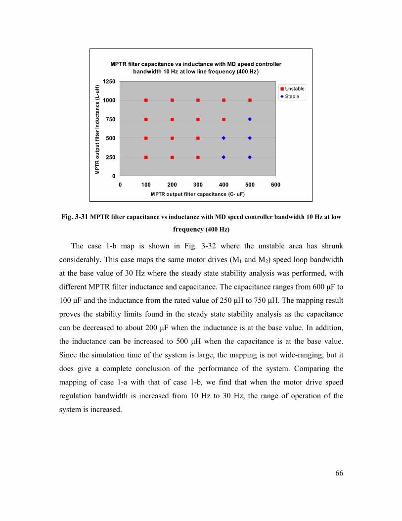
66
MPTR filter capacitance vs inductance with MD speed controller bandwidth 10 Hz at low line frequency (400 Hz)
0
250
500
750
1000
1250
0 100 200 300 400 500 600MPTR output filter capacitance (C- uF)
MPT
R o
utpu
t filt
er in
duct
ance
(L-u
H)
UnstableStable
Fig. 3-31 MPTR filter capacitance vs inductance with MD speed controller bandwidth 10 Hz at low
frequency (400 Hz)
The case 1-b map is shown in Fig. 3-32 where the unstable area has shrunk
considerably. This case maps the same motor drives (M1 and M2) speed loop bandwidth
at the base value of 30 Hz where the steady state stability analysis was performed, with
different MPTR filter inductance and capacitance. The capacitance ranges from 600 μF to
100 μF and the inductance from the rated value of 250 μH to 750 μH. The mapping result
proves the stability limits found in the steady state stability analysis as the capacitance
can be decreased to about 200 μF when the inductance is at the base value. In addition,
the inductance can be increased to 500 μH when the capacitance is at the base value.
Since the simulation time of the system is large, the mapping is not wide-ranging, but it
does give a complete conclusion of the performance of the system. Comparing the
mapping of case 1-a with that of case 1-b, we find that when the motor drive speed
regulation bandwidth is increased from 10 Hz to 30 Hz, the range of operation of the
system is increased.
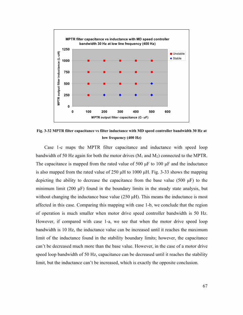
67
MPTR filter capacitance vs inductance with MD speed controller bandwidth 30 Hz at low line frequency (400 Hz)
0
250
500
750
1000
1250
0 100 200 300 400 500 600MPTR output filter capacitance (C- uF)
MPT
R o
utpu
t filt
er in
duct
ance
(L-u
H)
UnstableStable
Fig. 3-32 MPTR filter capacitance vs filter inductance with MD speed controller bandwidth 30 Hz at
low frequency (400 Hz)
Case 1-c maps the MPTR filter capacitance and inductance with speed loop
bandwidth of 50 Hz again for both the motor drives (M1 and M2) connected to the MPTR.
The capacitance is mapped from the rated value of 500 μF to 100 μF and the inductance
is also mapped from the rated value of 250 μH to 1000 μH. Fig. 3-33 shows the mapping
depicting the ability to decrease the capacitance from the base value (500 μF) to the
minimum limit (200 μF) found in the boundary limits in the steady state analysis, but
without changing the inductance base value (250 μH). This means the inductance is most
affected in this case. Comparing this mapping with case 1-b, we conclude that the region
of operation is much smaller when motor drive speed controller bandwidth is 50 Hz.
However, if compared with case 1-a, we see that when the motor drive speed loop
bandwidth is 10 Hz, the inductance value can be increased until it reaches the maximum
limit of the inductance found in the stability boundary limits; however, the capacitance
can’t be decreased much more than the base value. However, in the case of a motor drive
speed loop bandwidth of 50 Hz, capacitance can be decreased until it reaches the stability
limit, but the inductance can’t be increased, which is exactly the opposite conclusion.
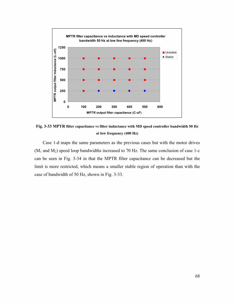
68
MPTR filter capacitance vs inductance with MD speed controller bandwidth 50 Hz at low line frequency (400 Hz)
0
250
500
750
1000
1250
0 100 200 300 400 500 600
MPTR output filter capacitance (C-uF)
MPT
R o
utpu
t filt
er in
duct
ance
(L-u
H)
UnstableStable
Fig. 3-33 MPTR filter capacitance vs filter inductance with MD speed controller bandwidth 50 Hz
at low frequency (400 Hz)
Case 1-d maps the same parameters as the previous cases but with the motor drives
(M1 and M2) speed loop bandwidths increased to 70 Hz. The same conclusion of case 1-c
can be seen in Fig. 3-34 in that the MPTR filter capacitance can be decreased but the
limit is more restricted, which means a smaller stable region of operation than with the
case of bandwidth of 50 Hz, shown in Fig. 3-33.
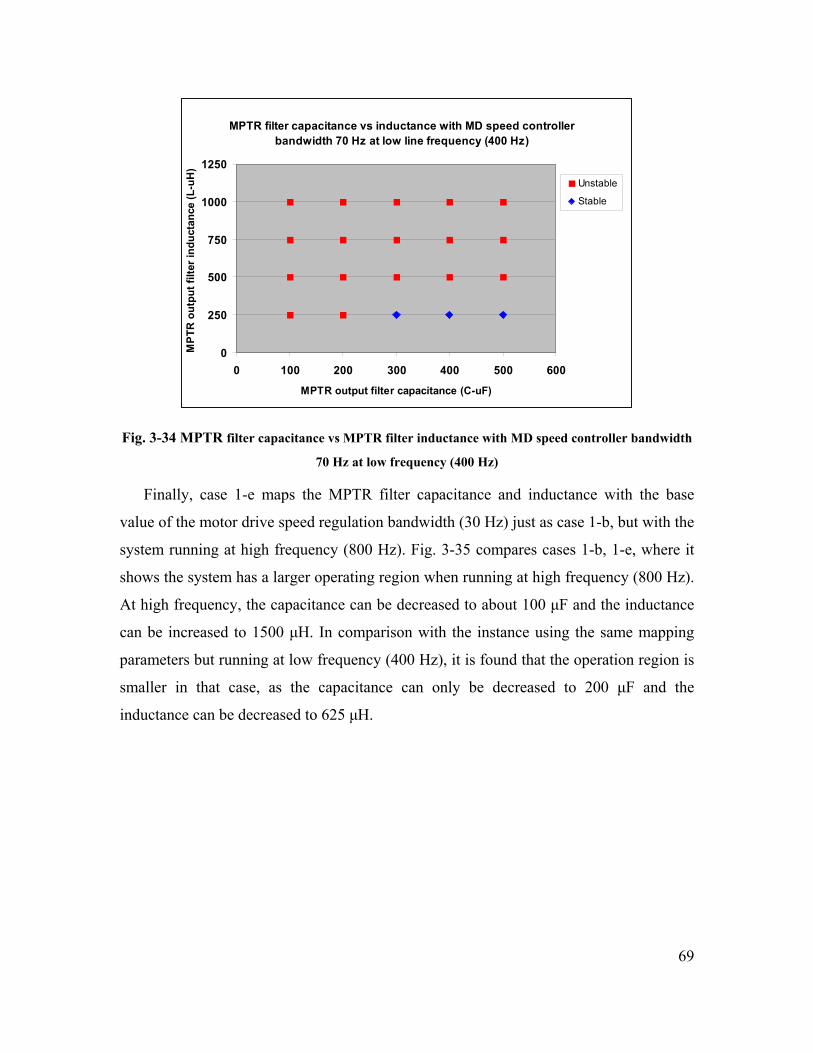
69
MPTR filter capacitance vs inductance with MD speed controller bandwidth 70 Hz at low line frequency (400 Hz)
0
250
500
750
1000
1250
0 100 200 300 400 500 600
MPTR output filter capacitance (C-uF)
MPT
R o
utpu
t filt
er in
duct
ance
(L-u
H)
Unstable
Stable
Fig. 3-34 MPTR filter capacitance vs MPTR filter inductance with MD speed controller bandwidth
70 Hz at low frequency (400 Hz)
Finally, case 1-e maps the MPTR filter capacitance and inductance with the base
value of the motor drive speed regulation bandwidth (30 Hz) just as case 1-b, but with the
system running at high frequency (800 Hz). Fig. 3-35 compares cases 1-b, 1-e, where it
shows the system has a larger operating region when running at high frequency (800 Hz).
At high frequency, the capacitance can be decreased to about 100 μF and the inductance
can be increased to 1500 μH. In comparison with the instance using the same mapping
parameters but running at low frequency (400 Hz), it is found that the operation region is
smaller in that case, as the capacitance can only be decreased to 200 μF and the
inductance can be decreased to 625 μH.
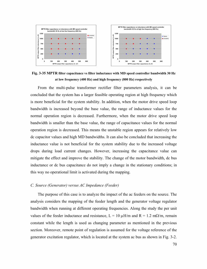
70
MPTR filter capacitance vs inductance with MD speed controller bandwidth 30 Hz at low line frequency (400 Hz)
0
250
500
750
1000
1250
0 100 200 300 400 500 600MPTR output filter capacitance (C- uF)
MPT
R o
utpu
t filt
er in
duct
ance
(L-u
H)
UnstableStable
MPTR filter capacitance vs inductance with MD speed controller bandwidth 30 Hz at high line frequency (800 Hz)
0
250
500
750
1000
1250
0 100 200 300 400 500 600MPTR output filter capactiance (C-uF)
MPT
R o
utpu
t filt
er in
duct
ance
(L-u
H)
StableUnstable
Fig. 3-35 MPTR filter capacitance vs filter inductance with MD speed controller bandwidth 30 Hz
at low frequency (400 Hz) and high frequency (800 Hz) respectively
From the multi-pulse transformer rectifier filter parameters analysis, it can be
concluded that the system has a larger feasible operating region at high frequency which
is more beneficial for the system stability. In addition, when the motor drive speed loop
bandwidth is increased beyond the base value, the range of inductance values for the
normal operation region is decreased. Furthermore, when the motor drive speed loop
bandwidth is smaller than the base value, the range of capacitance values for the normal
operation region is decreased. This means the unstable region appears for relatively low
dc capacitor values and high MD bandwidths. It can also be concluded that increasing the
inductance value is not beneficial for the system stability due to the increased voltage
drops during load current changes. However, increasing the capacitance value can
mitigate the effect and improve the stability. The change of the motor bandwidth, dc bus
inductance or dc bus capacitance do not imply a change in the stationary conditions; in
this way no operational limit is activated during the mapping.
C. Source (Generator) versus AC Impedance (Feeder)
The purpose of this case is to analyze the impact of the ac feeders on the source. The
analysis considers the mapping of the feeder length and the generator voltage regulator
bandwidth when running at different operating frequencies. Along the study the per unit
values of the feeder inductance and resistance, L = 10 μH/m and R = 1.2 mΩ/m, remain
constant while the length is used as changing parameter as mentioned in the previous
section. Moreover, remote point of regulation is assumed for the voltage reference of the
generator excitation regulator, which is located at the system ac bus as shown in Fig. 3-2.
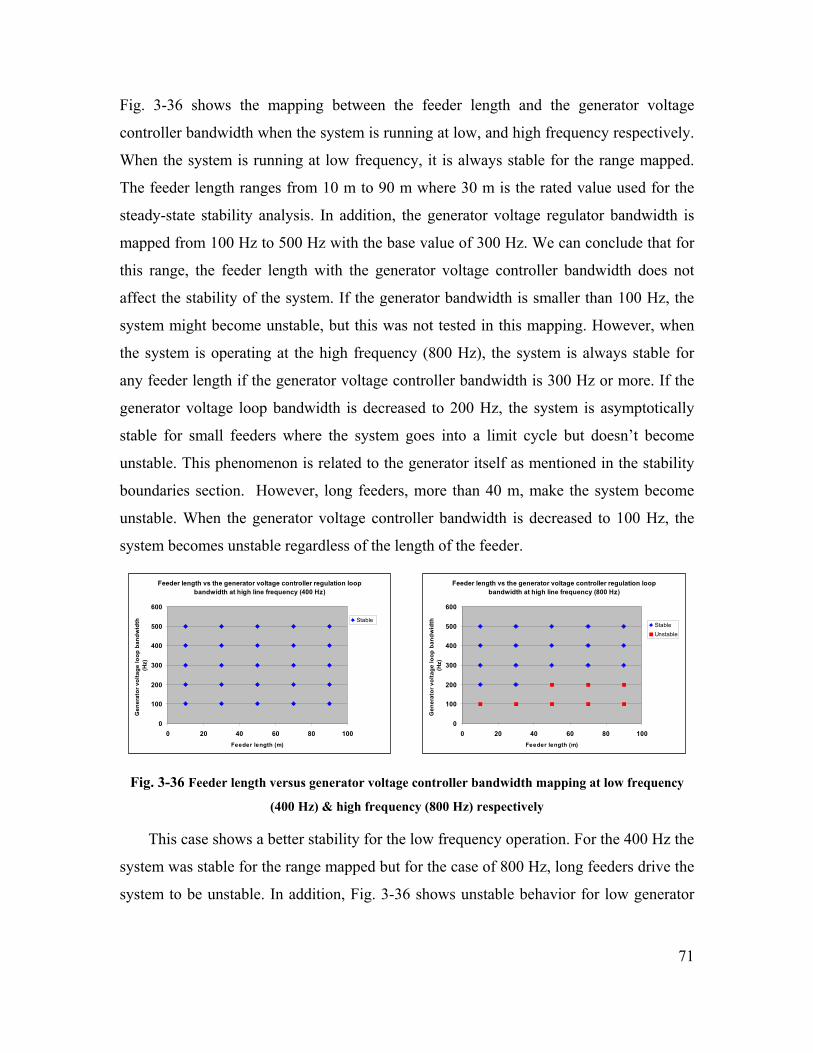
71
Fig. 3-36 shows the mapping between the feeder length and the generator voltage
controller bandwidth when the system is running at low, and high frequency respectively.
When the system is running at low frequency, it is always stable for the range mapped.
The feeder length ranges from 10 m to 90 m where 30 m is the rated value used for the
steady-state stability analysis. In addition, the generator voltage regulator bandwidth is
mapped from 100 Hz to 500 Hz with the base value of 300 Hz. We can conclude that for
this range, the feeder length with the generator voltage controller bandwidth does not
affect the stability of the system. If the generator bandwidth is smaller than 100 Hz, the
system might become unstable, but this was not tested in this mapping. However, when
the system is operating at the high frequency (800 Hz), the system is always stable for
any feeder length if the generator voltage controller bandwidth is 300 Hz or more. If the
generator voltage loop bandwidth is decreased to 200 Hz, the system is asymptotically
stable for small feeders where the system goes into a limit cycle but doesn’t become
unstable. This phenomenon is related to the generator itself as mentioned in the stability
boundaries section. However, long feeders, more than 40 m, make the system become
unstable. When the generator voltage controller bandwidth is decreased to 100 Hz, the
system becomes unstable regardless of the length of the feeder.
Feeder length vs the generator voltage controller regulation loop bandwidth at high line frequency (400 Hz)
0
100
200
300
400
500
600
0 20 40 60 80 100Feeder length (m)
Gen
erat
or v
olta
ge lo
op b
andw
idth
(H
z)
Stable
Feeder length vs the generator voltage controller regulation loop bandwidth at high line frequency (800 Hz)
0
100
200
300
400
500
600
0 20 40 60 80 100Feeder length (m)
Gen
erat
or v
olta
ge lo
op b
andw
idth
(H
z)
Stable Unstable
Fig. 3-36 Feeder length versus generator voltage controller bandwidth mapping at low frequency
(400 Hz) & high frequency (800 Hz) respectively
This case shows a better stability for the low frequency operation. For the 400 Hz the
system was stable for the range mapped but for the case of 800 Hz, long feeders drive the
system to be unstable. In addition, Fig. 3-36 shows unstable behavior for low generator
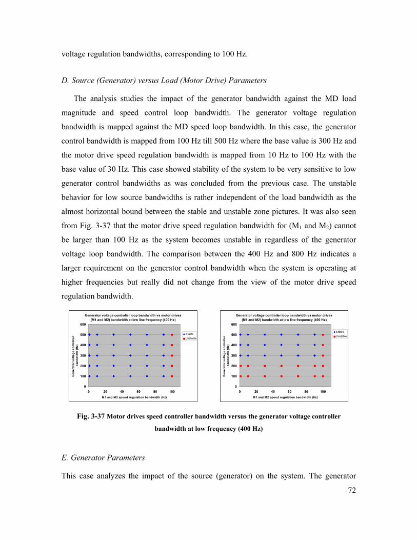
72
voltage regulation bandwidths, corresponding to 100 Hz.
D. Source (Generator) versus Load (Motor Drive) Parameters
The analysis studies the impact of the generator bandwidth against the MD load
magnitude and speed control loop bandwidth. The generator voltage regulation
bandwidth is mapped against the MD speed loop bandwidth. In this case, the generator
control bandwidth is mapped from 100 Hz till 500 Hz where the base value is 300 Hz and
the motor drive speed regulation bandwidth is mapped from 10 Hz to 100 Hz with the
base value of 30 Hz. This case showed stability of the system to be very sensitive to low
generator control bandwidths as was concluded from the previous case. The unstable
behavior for low source bandwidths is rather independent of the load bandwidth as the
almost horizontal bound between the stable and unstable zone pictures. It was also seen
from Fig. 3-37 that the motor drive speed regulation bandwidth for (M1 and M2) cannot
be larger than 100 Hz as the system becomes unstable in regardless of the generator
voltage loop bandwidth. The comparison between the 400 Hz and 800 Hz indicates a
larger requirement on the generator control bandwidth when the system is operating at
higher frequencies but really did not change from the view of the motor drive speed
regulation bandwidth.
Generator voltage controller loop bandwidth vs motor drives (M1 and M2) bandwidth at low line frequency (400 Hz)
0
100
200
300
400
500
600
0 20 40 60 80 100M1 and M2 speed regulation bandwidth (Hz)
Gen
erat
or v
olta
ge c
ontr
olle
r ba
ndw
idth
(Hz)
StableUnstable
Generator voltage controller loop bandwidth vs motor drives (M1 and M2) bandwidth at low line frequency (400 Hz)
0
100
200
300
400
500
600
0 20 40 60 80 100M1 and M2 speed regulation bandwidth (Hz)
Gen
erat
or v
olta
ge c
ontr
olle
r ba
ndw
idth
(Hz)
StableUnstable
Fig. 3-37 Motor drives speed controller bandwidth versus the generator voltage controller
bandwidth at low frequency (400 Hz)
E. Generator Parameters
This case analyzes the impact of the source (generator) on the system. The generator
73
excitation current limit provided in the excitation controller loop and the generator
excitation voltage limit provided to the system are changed with the generator voltage
loop bandwidth at different operating frequencies. The cases analyzed are shown in Table
3-3.
Table 3-3 Parametric studies considered for case four
Case # Case description Parameters to map
4-a
Generator voltage loop bandwidth vs. generator
excitation current limit at low operating frequency
(400 Hz)
fgbw, Iexlimit
4-b
Generator voltage loop bandwidth vs. generator
excitation current limit at high operating frequency
(800 Hz)
fgbw, Iexlimit
4-c
Generator voltage loop bandwidth vs. generator
excitation voltage limit at low operating frequency
(400 Hz)
fgbw, Vexlimit
4-d
Generator voltage loop bandwidth vs. generator
excitation voltage limit at high operating frequency
(800 Hz)
fgbw, Vexlimit
Cases 4-a, 4-b analyze the impact of the generator excitation current limit on the
system. The excitation current limit is changed from 40 A to 180 A with the generator
voltage loop bandwidth mapped from 100 Hz to 400 Hz with the base value of 300 Hz
and running at low and high operating frequency (400 Hz and 800 Hz respectively). It
can be concluded from Fig. 3-38 that the system is more stable when running at low
frequency, and the generator is the main influence of instability in this case so it needs to
be fast for the system to be stable. The excitation current doesn’t really affect the stability
of the system. The mapping showed the system became unstable with an excitation
current limit of 40 A and that is because it is a hard limit being 1.5 A only larger than the
rated excitation current and that caused the system to go into a limit cycle and the system
to become unstable.
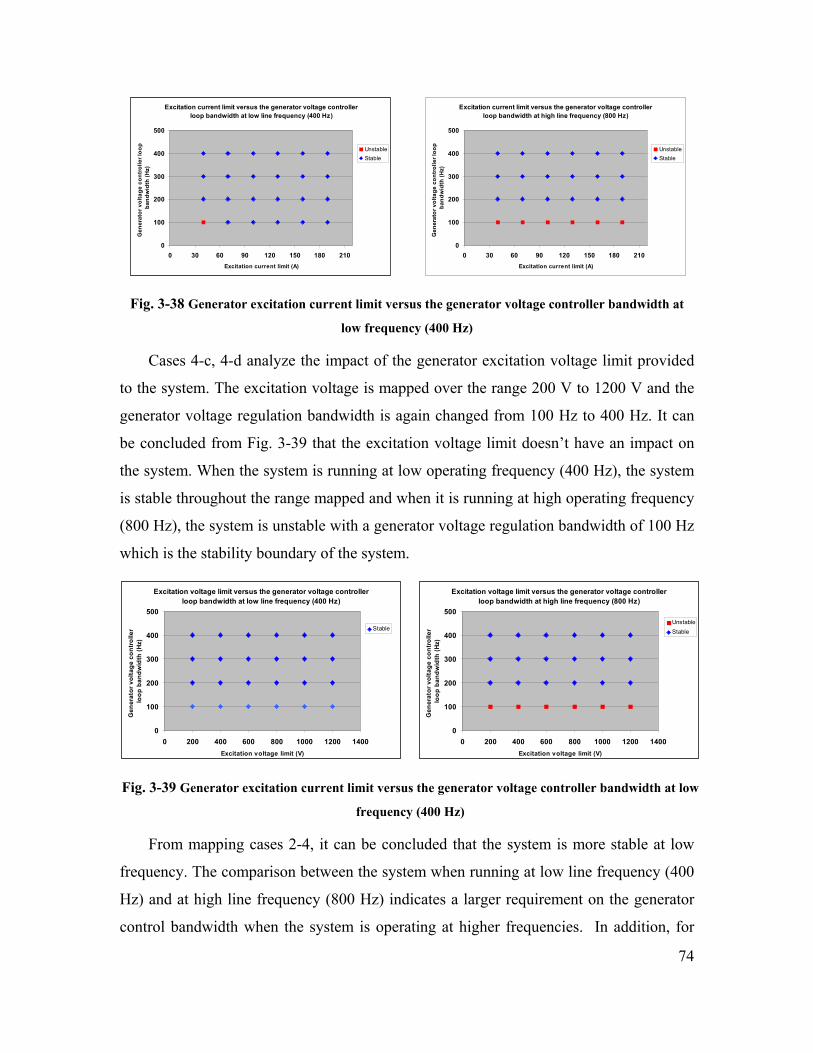
74
Excitation current limit versus the generator voltage controller loop bandwidth at low line frequency (400 Hz)
0
100
200
300
400
500
0 30 60 90 120 150 180 210Excitation current limit (A)
Gen
erat
or v
olta
ge c
ontr
olle
r loo
p ba
ndw
idth
(Hz)
UnstableStable
Excitation current limit versus the generator voltage controller loop bandwidth at high line frequency (800 Hz)
0
100
200
300
400
500
0 30 60 90 120 150 180 210Excitation current limit (A)
Gen
erat
or v
olta
ge c
ontr
olle
r loo
p ba
ndw
idth
(Hz)
UnstableStable
Fig. 3-38 Generator excitation current limit versus the generator voltage controller bandwidth at
low frequency (400 Hz)
Cases 4-c, 4-d analyze the impact of the generator excitation voltage limit provided
to the system. The excitation voltage is mapped over the range 200 V to 1200 V and the
generator voltage regulation bandwidth is again changed from 100 Hz to 400 Hz. It can
be concluded from Fig. 3-39 that the excitation voltage limit doesn’t have an impact on
the system. When the system is running at low operating frequency (400 Hz), the system
is stable throughout the range mapped and when it is running at high operating frequency
(800 Hz), the system is unstable with a generator voltage regulation bandwidth of 100 Hz
which is the stability boundary of the system.
Excitation voltage limit versus the generator voltage controller loop bandwidth at low line frequency (400 Hz)
0
100
200
300
400
500
0 200 400 600 800 1000 1200 1400Excitation voltage limit (V)
Gen
erat
or v
olta
ge c
ontr
olle
r lo
op b
andw
idth
(Hz)
Stable
Excitation voltage limit versus the generator voltage controller loop bandwidth at high line frequency (800 Hz)
0
100
200
300
400
500
0 200 400 600 800 1000 1200 1400Excitation voltage limit (V)
Gen
erat
or v
olta
ge c
ontr
olle
r lo
op b
andw
idth
(Hz)
UnstableStable
Fig. 3-39 Generator excitation current limit versus the generator voltage controller bandwidth at low
frequency (400 Hz)
From mapping cases 2-4, it can be concluded that the system is more stable at low
frequency. The comparison between the system when running at low line frequency (400
Hz) and at high line frequency (800 Hz) indicates a larger requirement on the generator
control bandwidth when the system is operating at higher frequencies. In addition, for
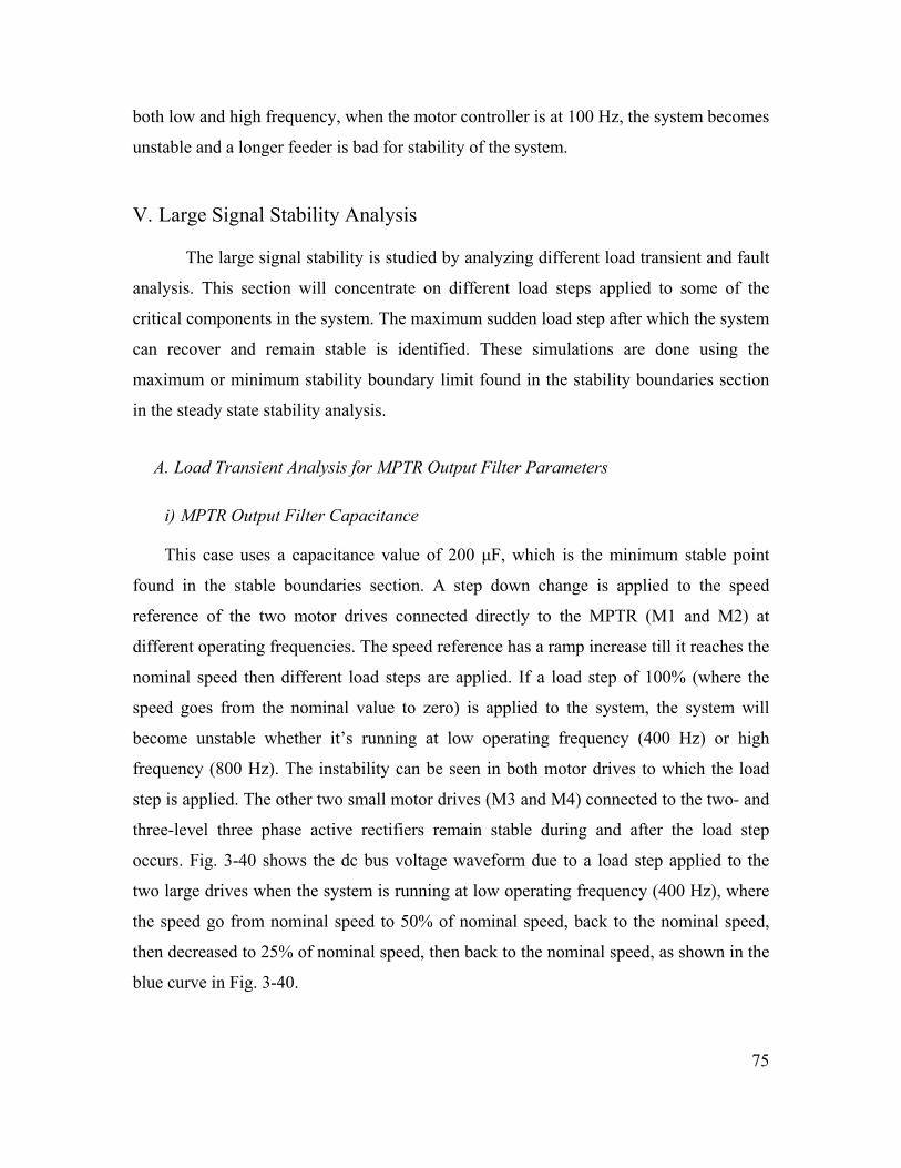
75
both low and high frequency, when the motor controller is at 100 Hz, the system becomes
unstable and a longer feeder is bad for stability of the system.
V. Large Signal Stability Analysis
The large signal stability is studied by analyzing different load transient and fault
analysis. This section will concentrate on different load steps applied to some of the
critical components in the system. The maximum sudden load step after which the system
can recover and remain stable is identified. These simulations are done using the
maximum or minimum stability boundary limit found in the stability boundaries section
in the steady state stability analysis.
A. Load Transient Analysis for MPTR Output Filter Parameters
i) MPTR Output Filter Capacitance
This case uses a capacitance value of 200 μF, which is the minimum stable point
found in the stable boundaries section. A step down change is applied to the speed
reference of the two motor drives connected directly to the MPTR (M1 and M2) at
different operating frequencies. The speed reference has a ramp increase till it reaches the
nominal speed then different load steps are applied. If a load step of 100% (where the
speed goes from the nominal value to zero) is applied to the system, the system will
become unstable whether it’s running at low operating frequency (400 Hz) or high
frequency (800 Hz). The instability can be seen in both motor drives to which the load
step is applied. The other two small motor drives (M3 and M4) connected to the two- and
three-level three phase active rectifiers remain stable during and after the load step
occurs. Fig. 3-40 shows the dc bus voltage waveform due to a load step applied to the
two large drives when the system is running at low operating frequency (400 Hz), where
the speed go from nominal speed to 50% of nominal speed, back to the nominal speed,
then decreased to 25% of nominal speed, then back to the nominal speed, as shown in the
blue curve in Fig. 3-40.
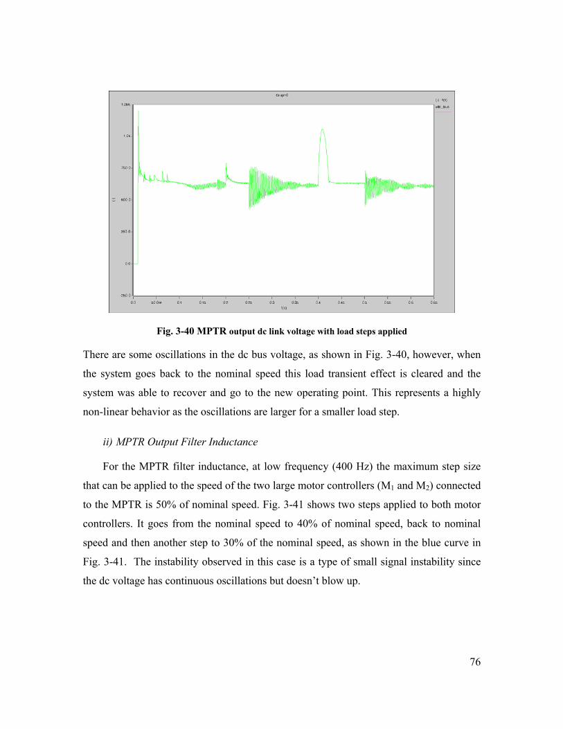
76
Fig. 3-40 MPTR output dc link voltage with load steps applied
There are some oscillations in the dc bus voltage, as shown in Fig. 3-40, however, when
the system goes back to the nominal speed this load transient effect is cleared and the
system was able to recover and go to the new operating point. This represents a highly
non-linear behavior as the oscillations are larger for a smaller load step.
ii) MPTR Output Filter Inductance
For the MPTR filter inductance, at low frequency (400 Hz) the maximum step size
that can be applied to the speed of the two large motor controllers (M1 and M2) connected
to the MPTR is 50% of nominal speed. Fig. 3-41 shows two steps applied to both motor
controllers. It goes from the nominal speed to 40% of nominal speed, back to nominal
speed and then another step to 30% of the nominal speed, as shown in the blue curve in
Fig. 3-41. The instability observed in this case is a type of small signal instability since
the dc voltage has continuous oscillations but doesn’t blow up.
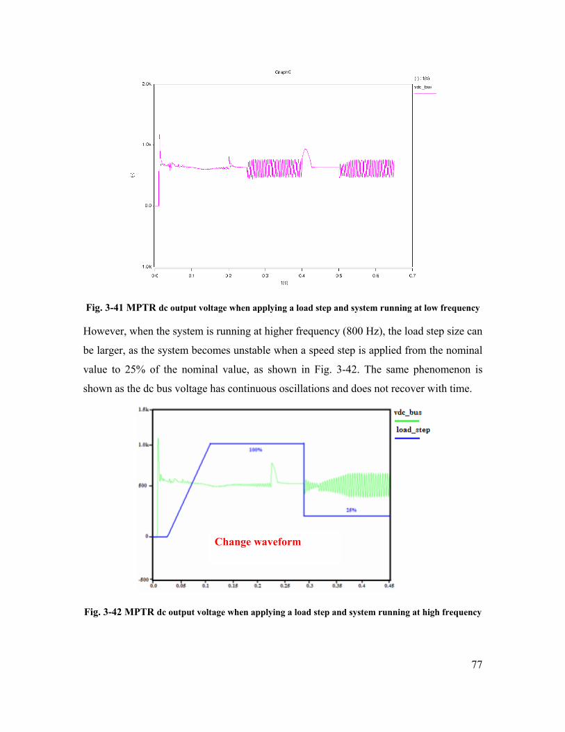
77
Fig. 3-41 MPTR dc output voltage when applying a load step and system running at low frequency
However, when the system is running at higher frequency (800 Hz), the load step size can
be larger, as the system becomes unstable when a speed step is applied from the nominal
value to 25% of the nominal value, as shown in Fig. 3-42. The same phenomenon is
shown as the dc bus voltage has continuous oscillations and does not recover with time.
Fig. 3-42 MPTR dc output voltage when applying a load step and system running at high frequency
Change waveform
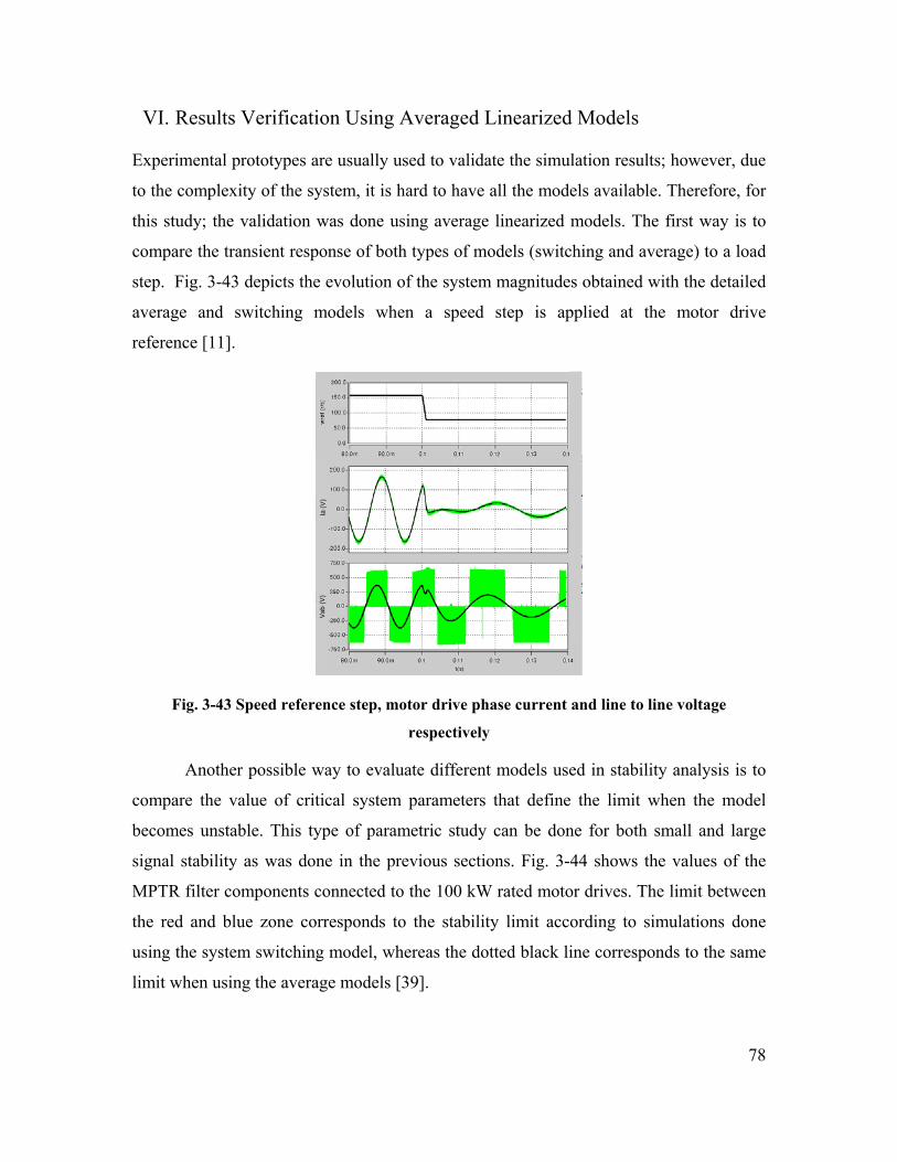
78
VI. Results Verification Using Averaged Linearized Models
Experimental prototypes are usually used to validate the simulation results; however, due
to the complexity of the system, it is hard to have all the models available. Therefore, for
this study; the validation was done using average linearized models. The first way is to
compare the transient response of both types of models (switching and average) to a load
step. Fig. 3-43 depicts the evolution of the system magnitudes obtained with the detailed
average and switching models when a speed step is applied at the motor drive
reference [11]. Ia
(V)
Vab
(V)
Fig. 3-43 Speed reference step, motor drive phase current and line to line voltage
respectively
Another possible way to evaluate different models used in stability analysis is to
compare the value of critical system parameters that define the limit when the model
becomes unstable. This type of parametric study can be done for both small and large
signal stability as was done in the previous sections. Fig. 3-44 shows the values of the
MPTR filter components connected to the 100 kW rated motor drives. The limit between
the red and blue zone corresponds to the stability limit according to simulations done
using the system switching model, whereas the dotted black line corresponds to the same
limit when using the average models [39].
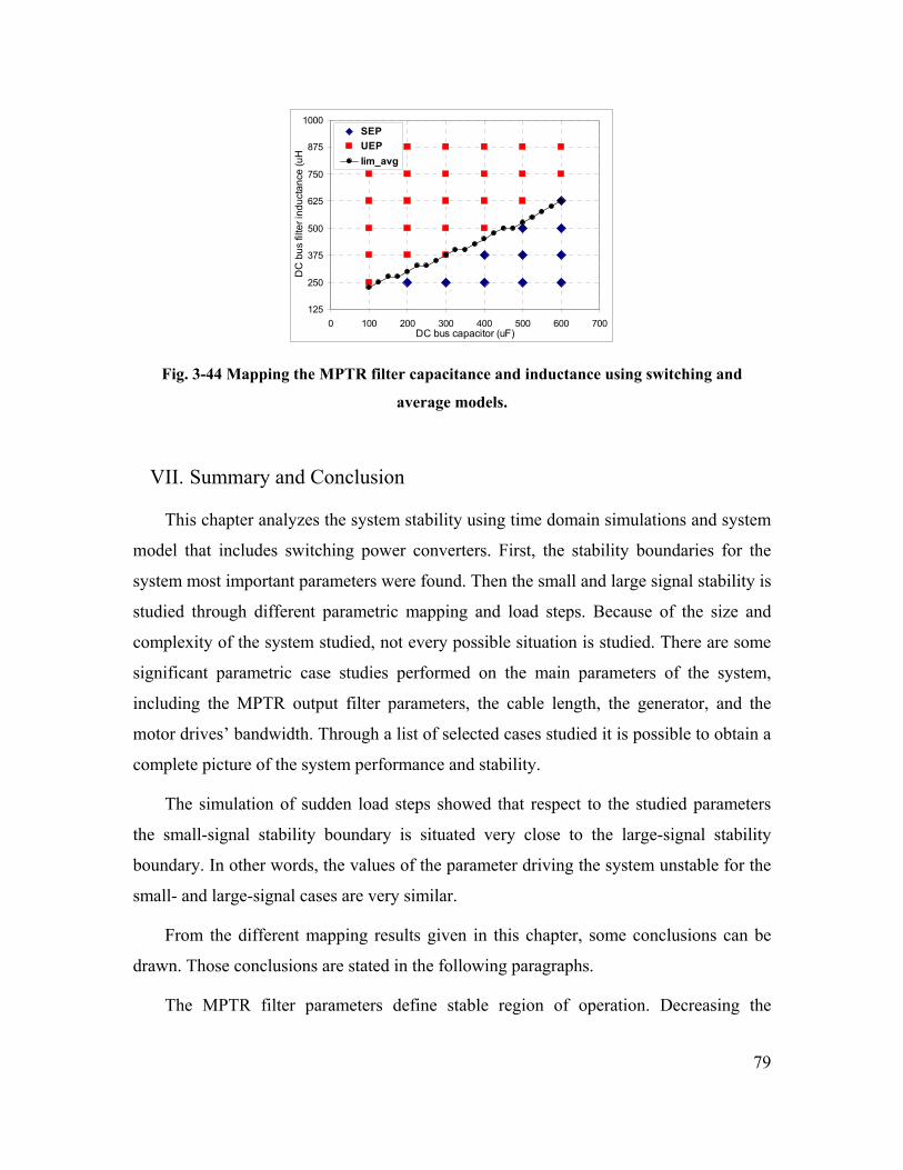
79
125
250
375
500
625
750
875
1000
0 100 200 300 400 500 600 700DC bus capacitor (uF)
DC
bus
filte
r ind
ucta
nce
(uH
)
SEPUEPlim_avg
Fig. 3-44 Mapping the MPTR filter capacitance and inductance using switching and
average models.
VII. Summary and Conclusion
This chapter analyzes the system stability using time domain simulations and system
model that includes switching power converters. First, the stability boundaries for the
system most important parameters were found. Then the small and large signal stability is
studied through different parametric mapping and load steps. Because of the size and
complexity of the system studied, not every possible situation is studied. There are some
significant parametric case studies performed on the main parameters of the system,
including the MPTR output filter parameters, the cable length, the generator, and the
motor drives’ bandwidth. Through a list of selected cases studied it is possible to obtain a
complete picture of the system performance and stability.
The simulation of sudden load steps showed that respect to the studied parameters
the small-signal stability boundary is situated very close to the large-signal stability
boundary. In other words, the values of the parameter driving the system unstable for the
small- and large-signal cases are very similar.
From the different mapping results given in this chapter, some conclusions can be
drawn. Those conclusions are stated in the following paragraphs.
The MPTR filter parameters define stable region of operation. Decreasing the

80
capacitance and increasing the inductance value can make the system less stable. The
system also has a larger operating region when running at high ac frequency (800 Hz).
From the generator point, the system is less stable when running at high ac frequency
(800 Hz). In addition, low generator voltage control bandwidths produce small-signal
instability. When in unstable operation the dc voltage starts continuous oscillations which
drive the motor drive to enter a limit cycle.
From the mapping of the motor drive speed regulation bandwidth with the generator
voltage loop bandwidth, it was observed that the system goes unstable when the motor
drive speed regulation bandwidth is 100 Hz with any generator voltage loop bandwidth.
Also when the system is running at high ac frequency (800 Hz), and the generator voltage
loop bandwidth is 100 Hz or less, the system is unstable with regardless to the motor
drive speed loop bandwidth.
The motor drive speed loop bandwidth affects the stability from the MPTR filter
parameters point of view. When the system is running at 30 Hz motor drive speed
regulation bandwidth, which is the nominal operating point the system is designed for,
the system has the largest operating region. Nevertheless, when the motor drive speed
regulation bandwidth is increased the capacitance stable region of operation is increased
and the inductance region is decreased.

81
Chapter 4 Fault Analysis of Different Components of the
System
I. Introduction
The reliability of power electronic converters became extremely important in industry
applications especially in fault situations [43]. A basic requirement for developing a
fault-tolerant scheme is a comprehensive understanding of the regular system operation
so that its behavior can be compared to that one at the onset of faults [44]-[45]. There are
different ways of detecting the fault that were proposed in different literature. The best
way of them is to monitor the output voltage and current directly [46]. The fault analysis
of two-level three phase active rectifiers is covered in a large number of references,
however, the three-level three phase active rectifier is not addressed as much. There are
different types of failures in the switching power stage of two-level three phase active
rectifier as dc link short-circuits, open circuit and short circuit damage of the switch, line
to line short-circuit and single line to ground fault at machine terminal discussed in [46].
[47] defines a generalized method for predicting the post-fault performance of IM-drives
after identifying the various faults that can occur. It studies different faults as machine
faults (open or short), inverter converter faults as phase switch open or short, multiple
phase fault or dc-link voltage drop.
This chapter analyzes the different types of faults that can occur in three phase
rectifiers and shows a comparison between the two-level and three-level three-phase
active rectifiers. The stresses over the system components are calculated and simple
protection schemes are developed. The protections are based on monitoring the voltage or
current needed using sensors and shutting down the circuit in time of fault to avoid any
losses. It also studies the large-signal stability of the system when the large-perturbation
is created by a fault.
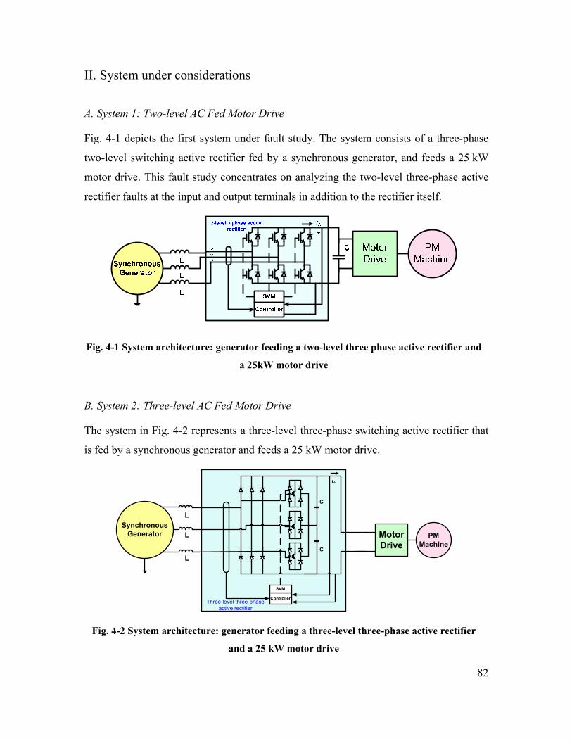
82
II. System under considerations
A. System 1: Two-level AC Fed Motor Drive
Fig. 4-1 depicts the first system under fault study. The system consists of a three-phase
two-level switching active rectifier fed by a synchronous generator, and feeds a 25 kW
motor drive. This fault study concentrates on analyzing the two-level three-phase active
rectifier faults at the input and output terminals in addition to the rectifier itself.
Fig. 4-1 System architecture: generator feeding a two-level three phase active rectifier and
a 25kW motor drive
B. System 2: Three-level AC Fed Motor Drive
The system in Fig. 4-2 represents a three-level three-phase switching active rectifier that
is fed by a synchronous generator and feeds a 25 kW motor drive.
PMMachine
MotorDrive
SynchronousGenerator L
L
L
C
Three-level three-phase active rectifier
Controller
SVM
Idc
C
C
Fig. 4-2 System architecture: generator feeding a three-level three-phase active rectifier
and a 25 kW motor drive

83
III. Fault Types For the three-phase active rectifiers shown in Fig. 4-1 and Fig. 4-2, there are various
types of faults that can be applied. These faults can be classified as:
• Faults at the input side of the rectifier such as:
1) shorting two phases of the ac link at the input of the rectifier
2) grounding one phase on the ac side at the input of the rectifier
3) grounding the three ac phases at the input of the rectifier
• Faults at the output side of the rectifier such as:
4) shorting the dc link
5) grounding the positive rail of the dc link
6) grounding the negative rail of the dc link
• Faults inside the rectifier such as:
7) one phase switch is shorted in the rectifier
8) one phase switch is opened in the two-level rectifier
9) short circuit of the rectifier main bridge diode
10) open circuit of the rectifier main bridge diode
IV. Fault Analysis with no Protection All the faults given in the fault types are analyzed and compared for both rectifiers to
study the impact over the system operation. Depending on the type of fault it is possible
that instabilities during the fault period create additional stresses and worsen the fault
effects. There are some assumptions made that might not be realistic as the inductance
does not saturate so the current stresses are not real but are based on that assumption. In
addition the fault analysis for this part was done with no protections in the system
assuming that the controllers will keep working even after the fault happens.
Case 1: Shorting two ac phases together
This case analyses the system if two phases (Phase A and B) were shorted together. A
switch is added between the two lines that is open till the system is in steady state and
then closes at 0.22s to apply the short fault. Fig. 4-3 shows the performance of the two-
level three phase active rectifier before and after the fault. The dc link voltage starts
discharging till it reaches zero but have a little spike that it caused by phase C since the
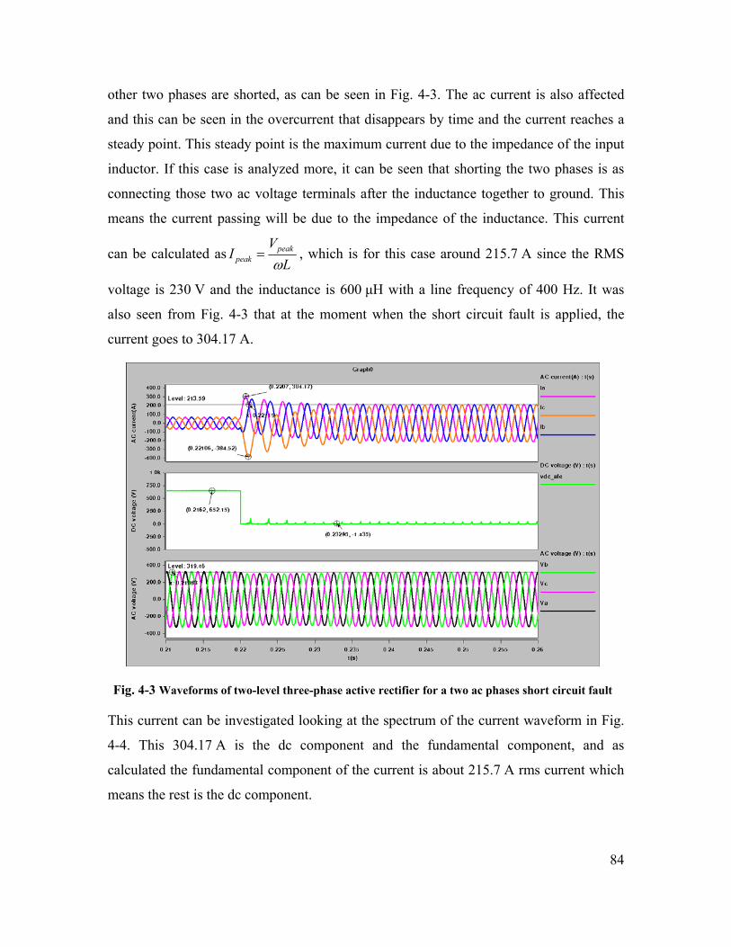
84
other two phases are shorted, as can be seen in Fig. 4-3. The ac current is also affected
and this can be seen in the overcurrent that disappears by time and the current reaches a
steady point. This steady point is the maximum current due to the impedance of the input
inductor. If this case is analyzed more, it can be seen that shorting the two phases is as
connecting those two ac voltage terminals after the inductance together to ground. This
means the current passing will be due to the impedance of the inductance. This current
can be calculated asL
VI peak
peak ω= , which is for this case around 215.7 A since the RMS
voltage is 230 V and the inductance is 600 μH with a line frequency of 400 Hz. It was
also seen from Fig. 4-3 that at the moment when the short circuit fault is applied, the
current goes to 304.17 A.
Fig. 4-3 Waveforms of two-level three-phase active rectifier for a two ac phases short circuit fault
This current can be investigated looking at the spectrum of the current waveform in Fig.
4-4. This 304.17 A is the dc component and the fundamental component, and as
calculated the fundamental component of the current is about 215.7 A rms current which
means the rest is the dc component.
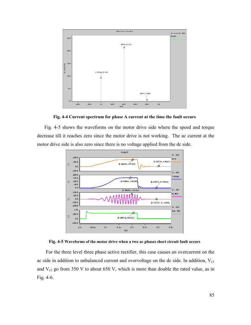
85
Fig. 4-4 Current spectrum for phase A current at the time the fault occurs
Fig. 4-5 shows the waveforms on the motor drive side where the speed and torque
decrease till it reaches zero since the motor drive is not working. The ac current at the
motor drive side is also zero since there is no voltage applied from the dc side.
Fig. 4-5 Waveforms of the motor drive when a two ac phases short circuit fault occurs
For the three level three phase active rectifier, this case causes an overcurrent on the
ac side in addition to unbalanced current and overvoltage on the dc side. In addition, Vc1
and Vc2 go from 350 V to about 650 V, which is more than double the rated value, as in
Fig. 4-6.
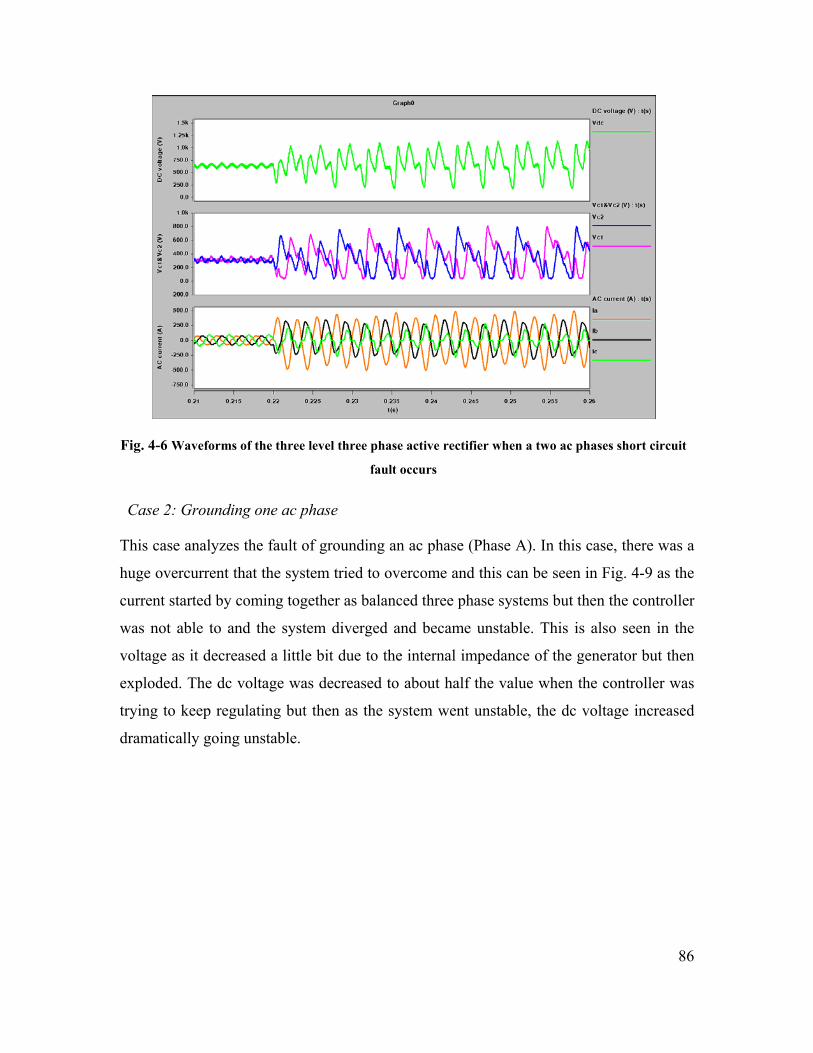
86
Fig. 4-6 Waveforms of the three level three phase active rectifier when a two ac phases short circuit
fault occurs
Case 2: Grounding one ac phase
This case analyzes the fault of grounding an ac phase (Phase A). In this case, there was a
huge overcurrent that the system tried to overcome and this can be seen in Fig. 4-9 as the
current started by coming together as balanced three phase systems but then the controller
was not able to and the system diverged and became unstable. This is also seen in the
voltage as it decreased a little bit due to the internal impedance of the generator but then
exploded. The dc voltage was decreased to about half the value when the controller was
trying to keep regulating but then as the system went unstable, the dc voltage increased
dramatically going unstable.
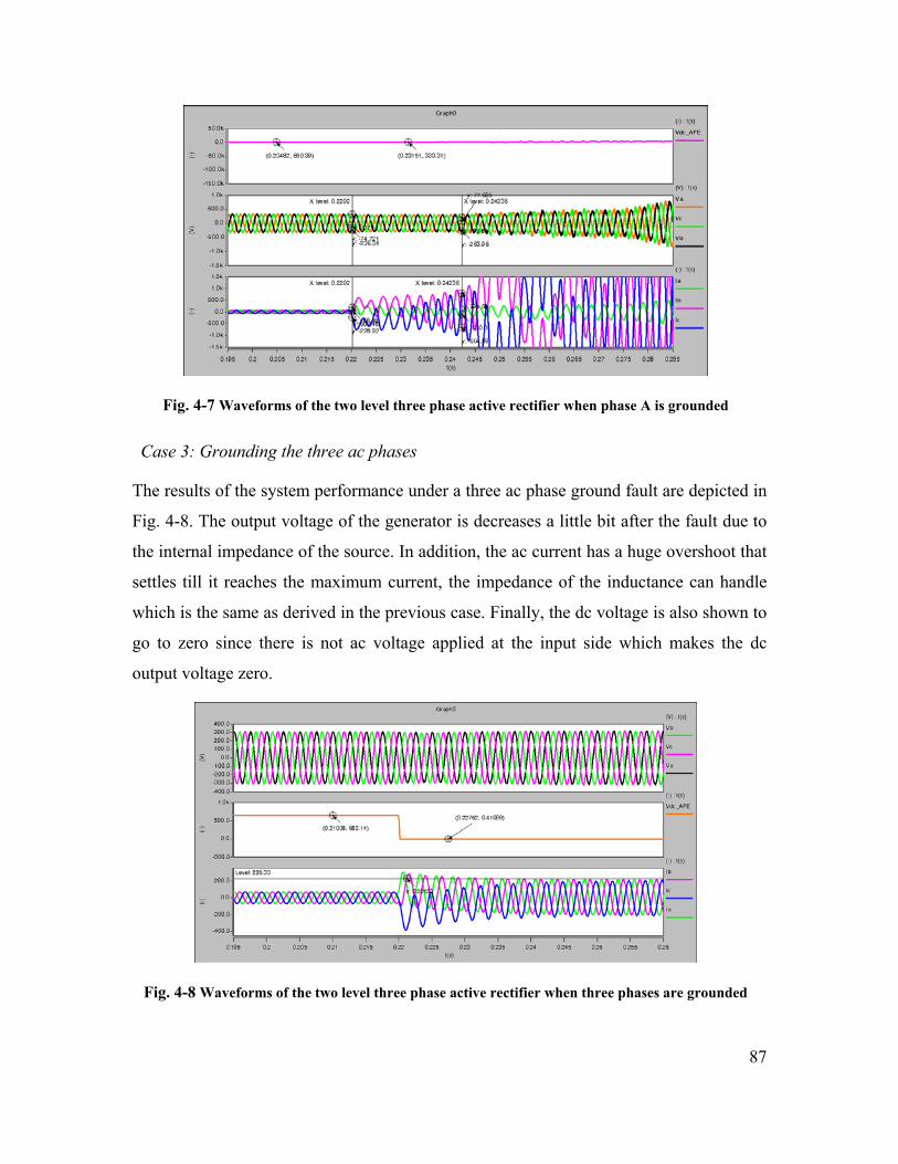
87
Fig. 4-7 Waveforms of the two level three phase active rectifier when phase A is grounded
Case 3: Grounding the three ac phases
The results of the system performance under a three ac phase ground fault are depicted in
Fig. 4-8. The output voltage of the generator is decreases a little bit after the fault due to
the internal impedance of the source. In addition, the ac current has a huge overshoot that
settles till it reaches the maximum current, the impedance of the inductance can handle
which is the same as derived in the previous case. Finally, the dc voltage is also shown to
go to zero since there is not ac voltage applied at the input side which makes the dc
output voltage zero.
Fig. 4-8 Waveforms of the two level three phase active rectifier when three phases are grounded
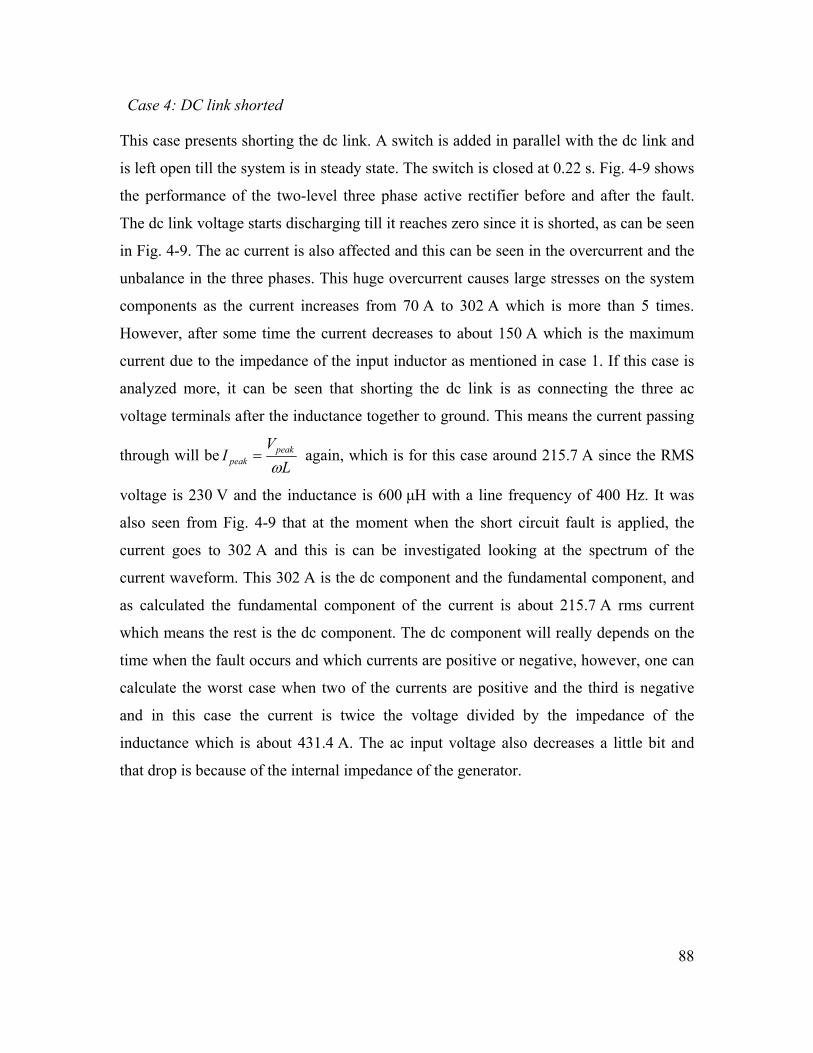
88
Case 4: DC link shorted
This case presents shorting the dc link. A switch is added in parallel with the dc link and
is left open till the system is in steady state. The switch is closed at 0.22 s. Fig. 4-9 shows
the performance of the two-level three phase active rectifier before and after the fault.
The dc link voltage starts discharging till it reaches zero since it is shorted, as can be seen
in Fig. 4-9. The ac current is also affected and this can be seen in the overcurrent and the
unbalance in the three phases. This huge overcurrent causes large stresses on the system
components as the current increases from 70 A to 302 A which is more than 5 times.
However, after some time the current decreases to about 150 A which is the maximum
current due to the impedance of the input inductor as mentioned in case 1. If this case is
analyzed more, it can be seen that shorting the dc link is as connecting the three ac
voltage terminals after the inductance together to ground. This means the current passing
through will beL
VI peak
peak ω= again, which is for this case around 215.7 A since the RMS
voltage is 230 V and the inductance is 600 μH with a line frequency of 400 Hz. It was
also seen from Fig. 4-9 that at the moment when the short circuit fault is applied, the
current goes to 302 A and this is can be investigated looking at the spectrum of the
current waveform. This 302 A is the dc component and the fundamental component, and
as calculated the fundamental component of the current is about 215.7 A rms current
which means the rest is the dc component. The dc component will really depends on the
time when the fault occurs and which currents are positive or negative, however, one can
calculate the worst case when two of the currents are positive and the third is negative
and in this case the current is twice the voltage divided by the impedance of the
inductance which is about 431.4 A. The ac input voltage also decreases a little bit and
that drop is because of the internal impedance of the generator.
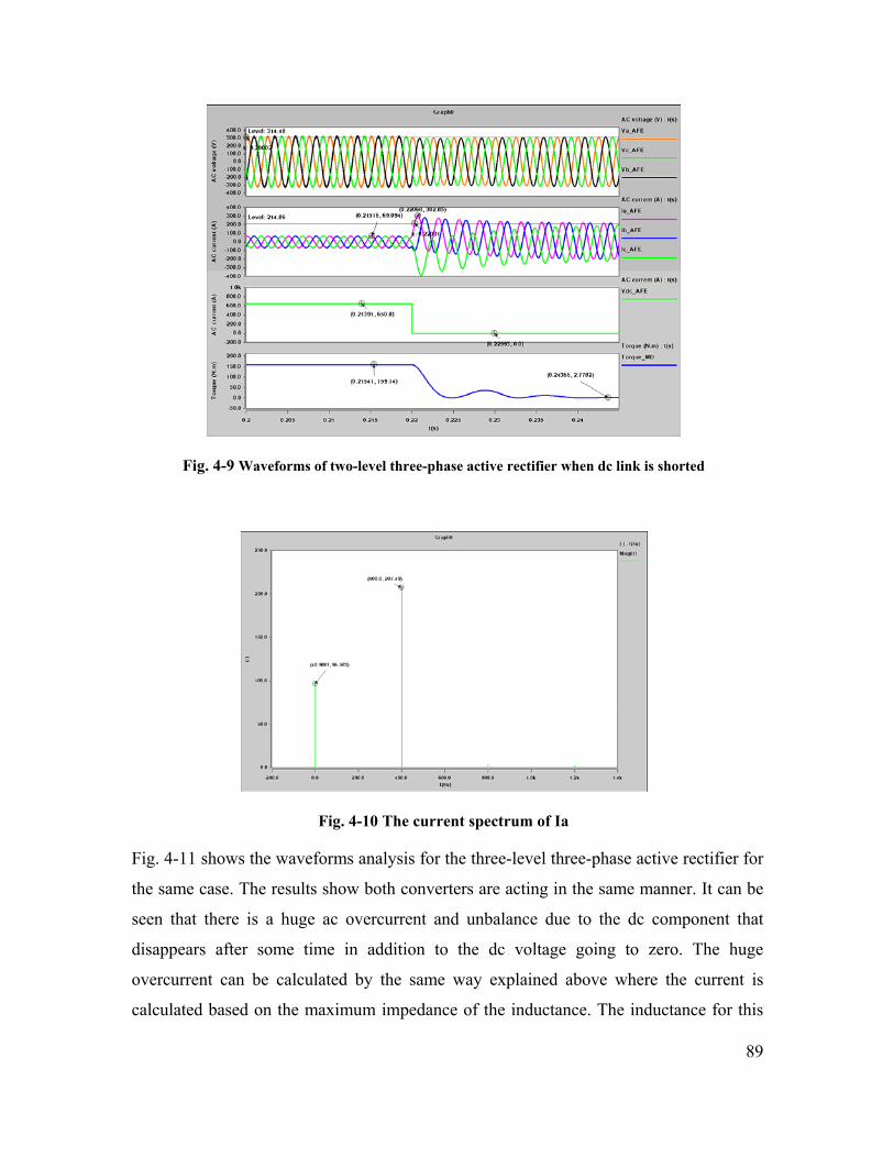
89
Fig. 4-9 Waveforms of two-level three-phase active rectifier when dc link is shorted
Fig. 4-10 The current spectrum of Ia
Fig. 4-11 shows the waveforms analysis for the three-level three-phase active rectifier for
the same case. The results show both converters are acting in the same manner. It can be
seen that there is a huge ac overcurrent and unbalance due to the dc component that
disappears after some time in addition to the dc voltage going to zero. The huge
overcurrent can be calculated by the same way explained above where the current is
calculated based on the maximum impedance of the inductance. The inductance for this
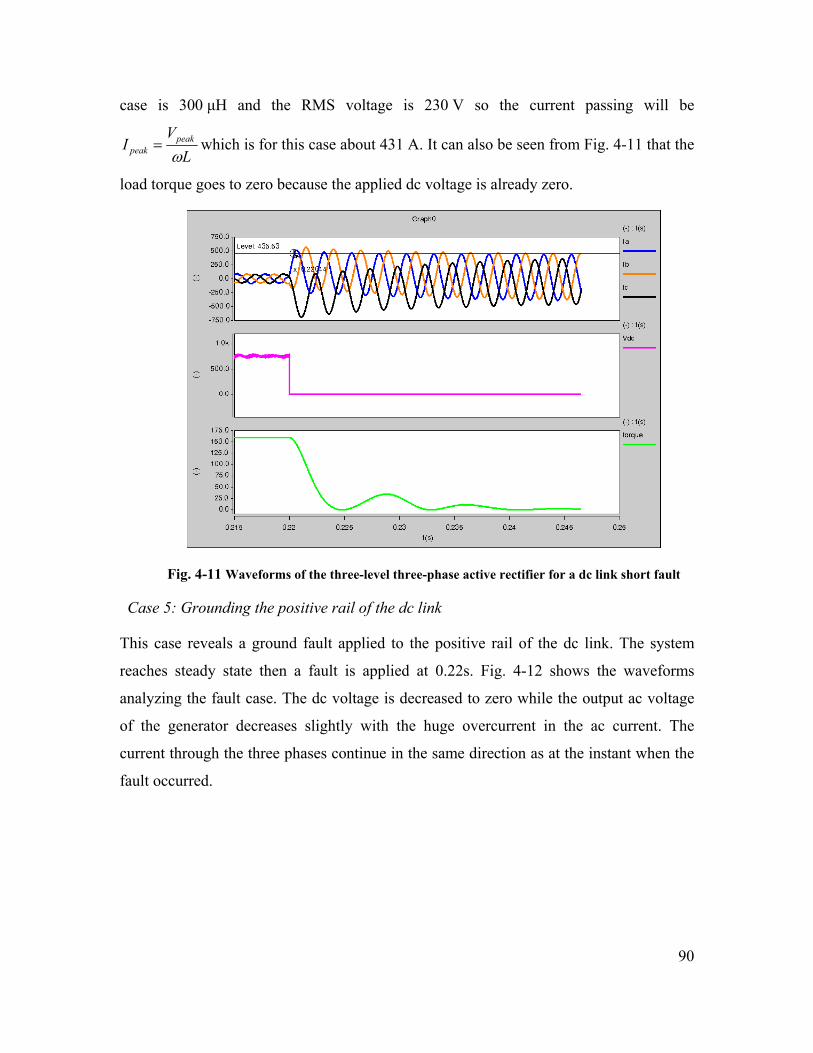
90
case is 300 μH and the RMS voltage is 230 V so the current passing will be
LV
I peakpeak ω
= which is for this case about 431 A. It can also be seen from Fig. 4-11 that the
load torque goes to zero because the applied dc voltage is already zero.
Fig. 4-11 Waveforms of the three-level three-phase active rectifier for a dc link short fault
Case 5: Grounding the positive rail of the dc link
This case reveals a ground fault applied to the positive rail of the dc link. The system
reaches steady state then a fault is applied at 0.22s. Fig. 4-12 shows the waveforms
analyzing the fault case. The dc voltage is decreased to zero while the output ac voltage
of the generator decreases slightly with the huge overcurrent in the ac current. The
current through the three phases continue in the same direction as at the instant when the
fault occurred.
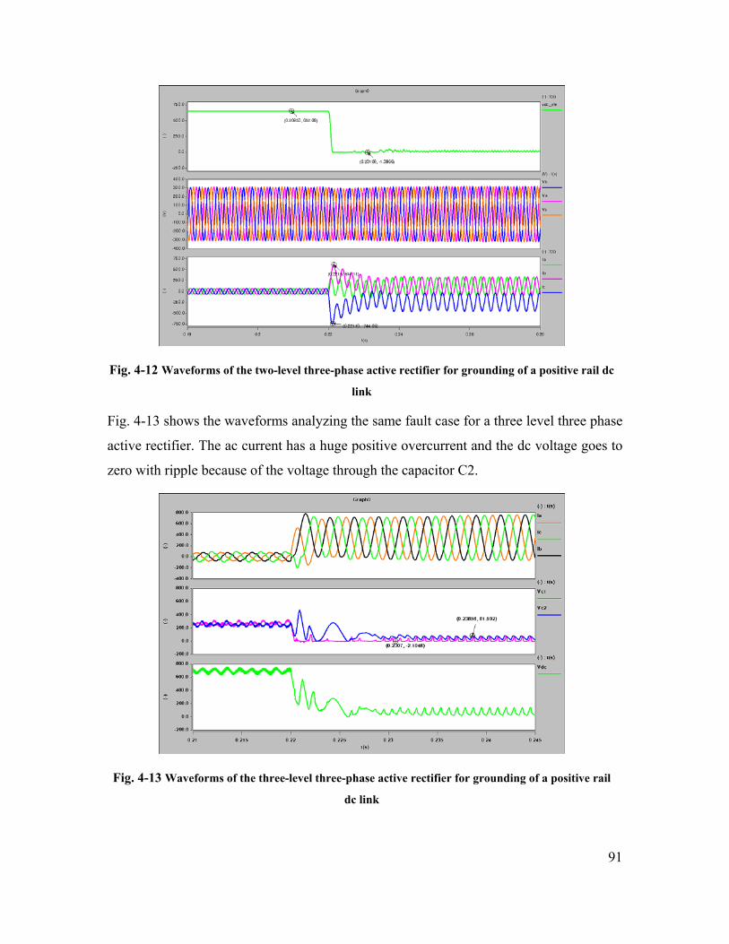
91
Fig. 4-12 Waveforms of the two-level three-phase active rectifier for grounding of a positive rail dc
link
Fig. 4-13 shows the waveforms analyzing the same fault case for a three level three phase
active rectifier. The ac current has a huge positive overcurrent and the dc voltage goes to
zero with ripple because of the voltage through the capacitor C2.
Fig. 4-13 Waveforms of the three-level three-phase active rectifier for grounding of a positive rail
dc link
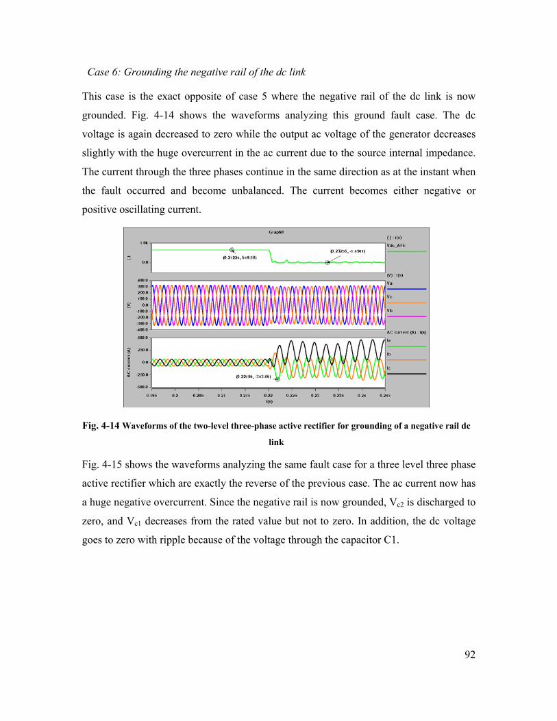
92
Case 6: Grounding the negative rail of the dc link
This case is the exact opposite of case 5 where the negative rail of the dc link is now
grounded. Fig. 4-14 shows the waveforms analyzing this ground fault case. The dc
voltage is again decreased to zero while the output ac voltage of the generator decreases
slightly with the huge overcurrent in the ac current due to the source internal impedance.
The current through the three phases continue in the same direction as at the instant when
the fault occurred and become unbalanced. The current becomes either negative or
positive oscillating current.
Fig. 4-14 Waveforms of the two-level three-phase active rectifier for grounding of a negative rail dc
link
Fig. 4-15 shows the waveforms analyzing the same fault case for a three level three phase
active rectifier which are exactly the reverse of the previous case. The ac current now has
a huge negative overcurrent. Since the negative rail is now grounded, Vc2 is discharged to
zero, and Vc1 decreases from the rated value but not to zero. In addition, the dc voltage
goes to zero with ripple because of the voltage through the capacitor C1.
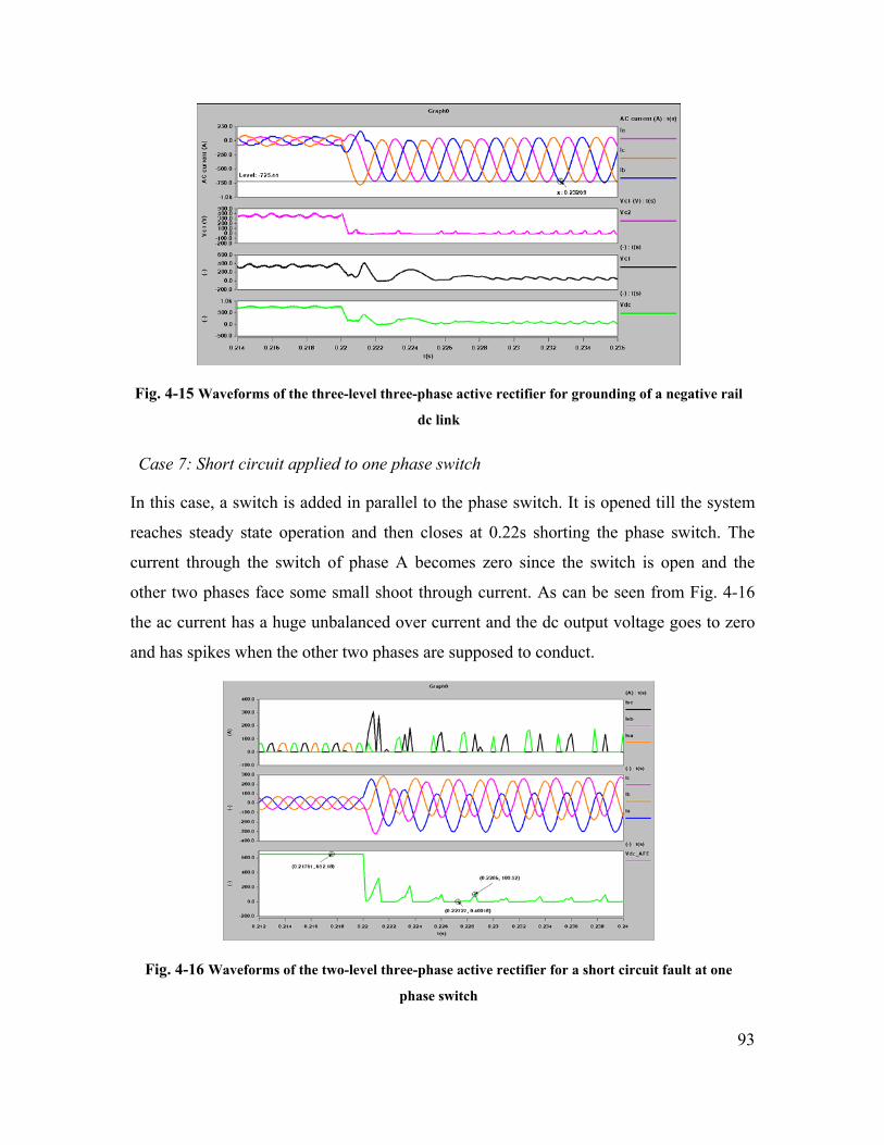
93
Fig. 4-15 Waveforms of the three-level three-phase active rectifier for grounding of a negative rail
dc link
Case 7: Short circuit applied to one phase switch
In this case, a switch is added in parallel to the phase switch. It is opened till the system
reaches steady state operation and then closes at 0.22s shorting the phase switch. The
current through the switch of phase A becomes zero since the switch is open and the
other two phases face some small shoot through current. As can be seen from Fig. 4-16
the ac current has a huge unbalanced over current and the dc output voltage goes to zero
and has spikes when the other two phases are supposed to conduct.
Fig. 4-16 Waveforms of the two-level three-phase active rectifier for a short circuit fault at one
phase switch
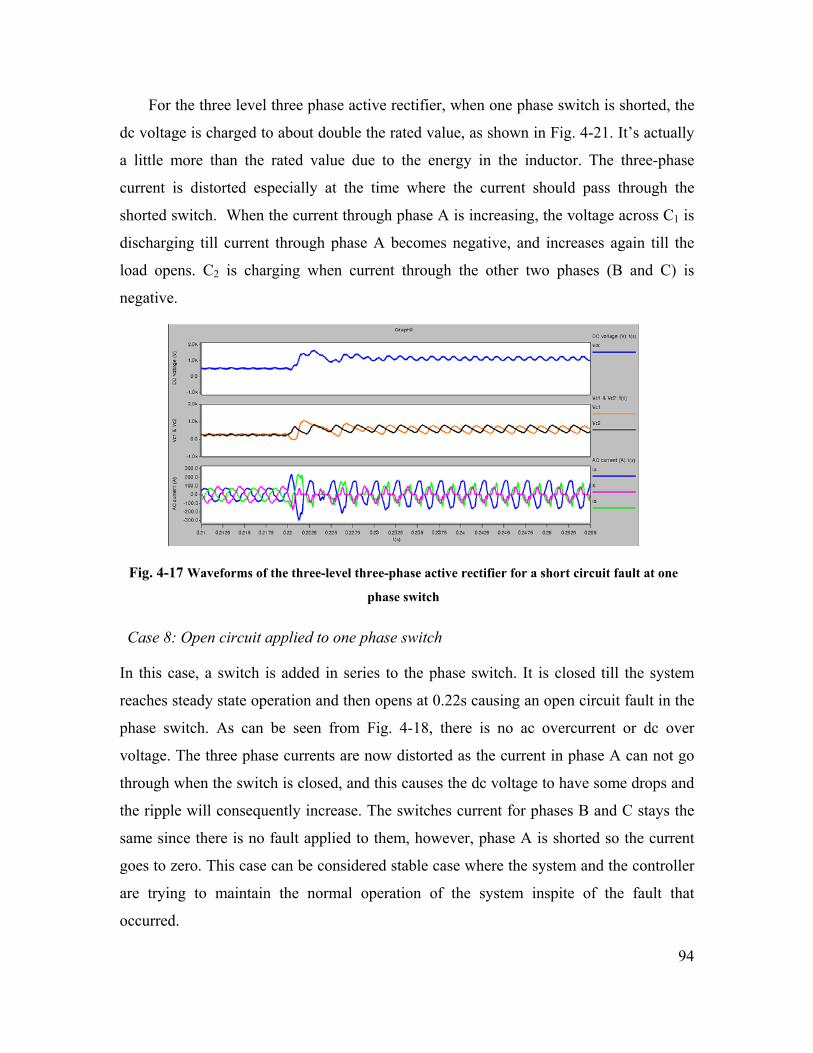
94
For the three level three phase active rectifier, when one phase switch is shorted, the
dc voltage is charged to about double the rated value, as shown in Fig. 4-21. It’s actually
a little more than the rated value due to the energy in the inductor. The three-phase
current is distorted especially at the time where the current should pass through the
shorted switch. When the current through phase A is increasing, the voltage across C1 is
discharging till current through phase A becomes negative, and increases again till the
load opens. C2 is charging when current through the other two phases (B and C) is
negative.
Fig. 4-17 Waveforms of the three-level three-phase active rectifier for a short circuit fault at one
phase switch
Case 8: Open circuit applied to one phase switch
In this case, a switch is added in series to the phase switch. It is closed till the system
reaches steady state operation and then opens at 0.22s causing an open circuit fault in the
phase switch. As can be seen from Fig. 4-18, there is no ac overcurrent or dc over
voltage. The three phase currents are now distorted as the current in phase A can not go
through when the switch is closed, and this causes the dc voltage to have some drops and
the ripple will consequently increase. The switches current for phases B and C stays the
same since there is no fault applied to them, however, phase A is shorted so the current
goes to zero. This case can be considered stable case where the system and the controller
are trying to maintain the normal operation of the system inspite of the fault that
occurred.
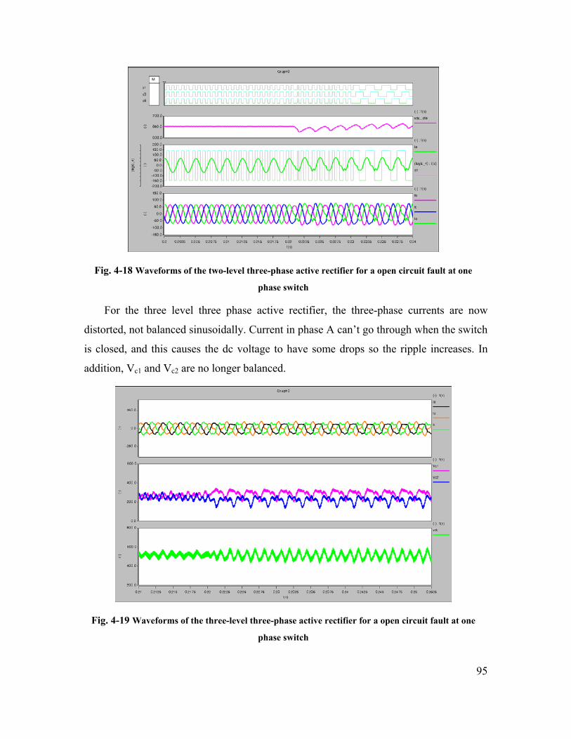
95
Fig. 4-18 Waveforms of the two-level three-phase active rectifier for a open circuit fault at one
phase switch
For the three level three phase active rectifier, the three-phase currents are now
distorted, not balanced sinusoidally. Current in phase A can’t go through when the switch
is closed, and this causes the dc voltage to have some drops so the ripple increases. In
addition, Vc1 and Vc2 are no longer balanced.
Fig. 4-19 Waveforms of the three-level three-phase active rectifier for a open circuit fault at one
phase switch
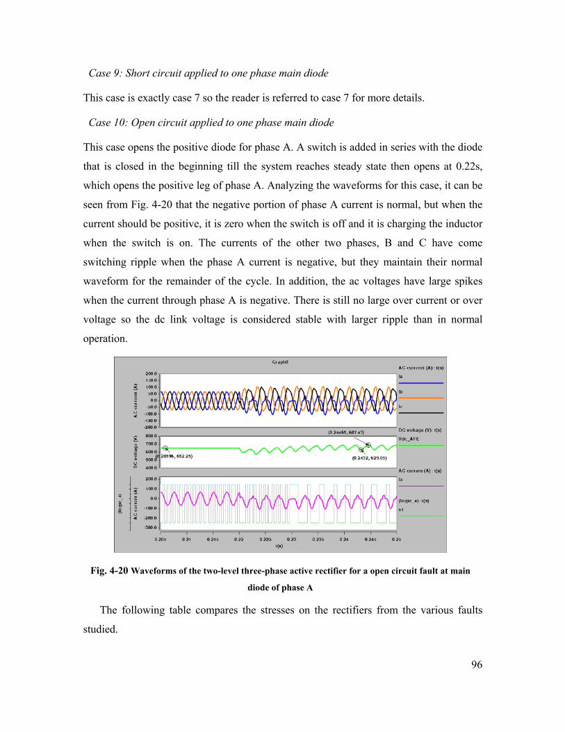
96
Case 9: Short circuit applied to one phase main diode
This case is exactly case 7 so the reader is referred to case 7 for more details.
Case 10: Open circuit applied to one phase main diode
This case opens the positive diode for phase A. A switch is added in series with the diode
that is closed in the beginning till the system reaches steady state then opens at 0.22s,
which opens the positive leg of phase A. Analyzing the waveforms for this case, it can be
seen from Fig. 4-20 that the negative portion of phase A current is normal, but when the
current should be positive, it is zero when the switch is off and it is charging the inductor
when the switch is on. The currents of the other two phases, B and C have come
switching ripple when the phase A current is negative, but they maintain their normal
waveform for the remainder of the cycle. In addition, the ac voltages have large spikes
when the current through phase A is negative. There is still no large over current or over
voltage so the dc link voltage is considered stable with larger ripple than in normal
operation.
Fig. 4-20 Waveforms of the two-level three-phase active rectifier for a open circuit fault at main
diode of phase A
The following table compares the stresses on the rectifiers from the various faults
studied.
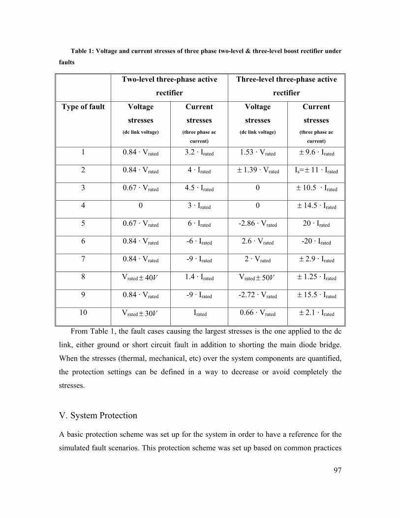
97
Table 1: Voltage and current stresses of three phase two-level & three-level boost rectifier under
faults
Two-level three-phase active
rectifier
Three-level three-phase active
rectifier
Type of fault Voltage
stresses (dc link voltage)
Current
stresses (three phase ac
current)
Voltage
stresses (dc link voltage)
Current
stresses (three phase ac
current)
1 0.84 · Vrated 3.2 · Irated 1.53 · Vrated ± 9.6 · Irated
2 0.84 · Vrated 4 · Irated ± 1.39 · Vrated Is=± 11 · Irated
3 0.67 · Vrated 4.5 · Irated 0 ± 10.5 · Irated
4 0 3 · Irated 0 ± 14.5 · Irated
5 0.67 · Vrated 6 · Irated -2.86 · Vrated 20 · Irated
6 0.84 · Vrated -6 · Irated 2.6 · Vrated -20 · Irated
7 0.84 · Vrated -9 · Irated 2 · Vrated ± 2.9 · Irated
8 Vrated V40± 1.4 · Irated Vrated V50± ± 1.25 · Irated
9 0.84 · Vrated -9 · Irated -2.72 · Vrated ± 15.5 · Irated
10 Vrated V30± Irated 0.66 · Vrated ± 2.1 · Irated
From Table 1, the fault cases causing the largest stresses is the one applied to the dc
link, either ground or short circuit fault in addition to shorting the main diode bridge.
When the stresses (thermal, mechanical, etc) over the system components are quantified,
the protection settings can be defined in a way to decrease or avoid completely the
stresses.
V. System Protection
A basic protection scheme was set up for the system in order to have a reference for the
simulated fault scenarios. This protection scheme was set up based on common practices
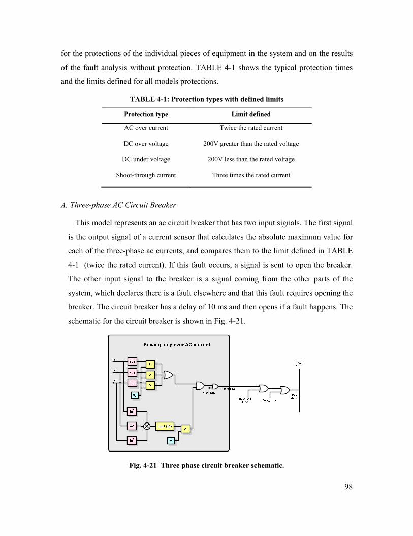
98
for the protections of the individual pieces of equipment in the system and on the results
of the fault analysis without protection. TABLE 4-1 shows the typical protection times
and the limits defined for all models protections.
TABLE 4-1: Protection types with defined limits
Protection type Limit defined
AC over current Twice the rated current
DC over voltage 200V greater than the rated voltage
DC under voltage 200V less than the rated voltage
Shoot-through current Three times the rated current
A. Three-phase AC Circuit Breaker
This model represents an ac circuit breaker that has two input signals. The first signal
is the output signal of a current sensor that calculates the absolute maximum value for
each of the three-phase ac currents, and compares them to the limit defined in TABLE
4-1 (twice the rated current). If this fault occurs, a signal is sent to open the breaker.
The other input signal to the breaker is a signal coming from the other parts of the
system, which declares there is a fault elsewhere and that this fault requires opening the
breaker. The circuit breaker has a delay of 10 ms and then opens if a fault happens. The
schematic for the circuit breaker is shown in Fig. 4-21.
Fig. 4-21 Three phase circuit breaker schematic.
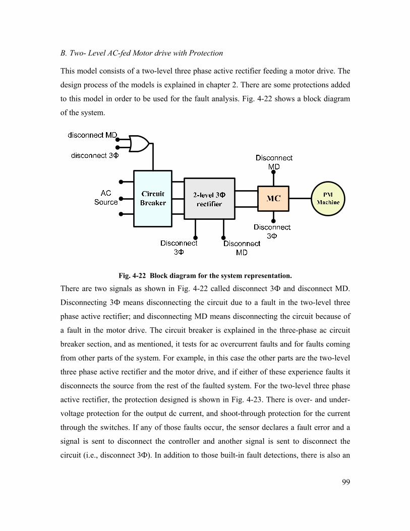
99
B. Two- Level AC-fed Motor drive with Protection
This model consists of a two-level three phase active rectifier feeding a motor drive. The
design process of the models is explained in chapter 2. There are some protections added
to this model in order to be used for the fault analysis. Fig. 4-22 shows a block diagram
of the system.
Fig. 4-22 Block diagram for the system representation.
There are two signals as shown in Fig. 4-22 called disconnect 3Ф and disconnect MD.
Disconnecting 3Ф means disconnecting the circuit due to a fault in the two-level three
phase active rectifier; and disconnecting MD means disconnecting the circuit because of
a fault in the motor drive. The circuit breaker is explained in the three-phase ac circuit
breaker section, and as mentioned, it tests for ac overcurrent faults and for faults coming
from other parts of the system. For example, in this case the other parts are the two-level
three phase active rectifier and the motor drive, and if either of these experience faults it
disconnects the source from the rest of the faulted system. For the two-level three phase
active rectifier, the protection designed is shown in Fig. 4-23. There is over- and under-
voltage protection for the output dc current, and shoot-through protection for the current
through the switches. If any of those faults occur, the sensor declares a fault error and a
signal is sent to disconnect the controller and another signal is sent to disconnect the
circuit (i.e., disconnect 3Ф). In addition to those built-in fault detections, there is also an
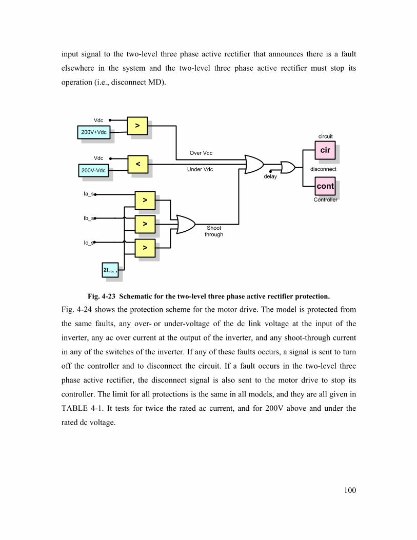
100
input signal to the two-level three phase active rectifier that announces there is a fault
elsewhere in the system and the two-level three phase active rectifier must stop its
operation (i.e., disconnect MD).
>200V+Vdc
Vdc
<200V-Vdc
Vdc
>
>
>
2Iabc_s
Ia_s
Ib_s
Ic_s
Over Vdc
Under Vdc
Shoot through
delaydisconnect
cir
cont
circuit
Controller
Fig. 4-23 Schematic for the two-level three phase active rectifier protection.
Fig. 4-24 shows the protection scheme for the motor drive. The model is protected from
the same faults, any over- or under-voltage of the dc link voltage at the input of the
inverter, any ac over current at the output of the inverter, and any shoot-through current
in any of the switches of the inverter. If any of these faults occurs, a signal is sent to turn
off the controller and to disconnect the circuit. If a fault occurs in the two-level three
phase active rectifier, the disconnect signal is also sent to the motor drive to stop its
controller. The limit for all protections is the same in all models, and they are all given in
TABLE 4-1. It tests for twice the rated ac current, and for 200V above and under the
rated dc voltage.
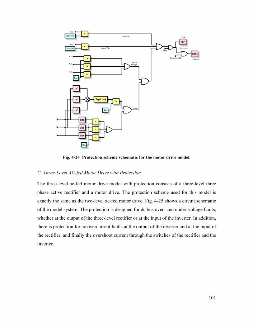
101
>200V+Vdc
Vdc
<200V-Vdc
Vdc
>
>
> 2Iabc_s
Ia_s
Ib_s
Ic_s
Over Vdc
Under Vdc
Shoot through
delaydisconnect
cir
cont
circuit
Controller
>
>
>
2Iabc
abs
abs
abs
in2
in2
in2
Sqrt (in)>
2IrImax
Ia
Ib
Ic
Disconnect 3Φ
Fig. 4-24 Protection scheme schematic for the motor drive model.
C. Three-Level AC-fed Motor Drive with Protection
The three-level ac-fed motor drive model with protection consists of a three-level three
phase active rectifier and a motor drive. The protection scheme used for this model is
exactly the same as the two-level ac-fed motor drive. Fig. 4-25 shows a circuit schematic
of the model system. The protection is designed for dc bus over- and under-voltage faults,
whether at the output of the three-level rectifier or at the input of the inverter. In addition,
there is protection for ac overcurrent faults at the output of the inverter and at the input of
the rectifier, and finally the overshoot current through the switches of the rectifier and the
inverter.
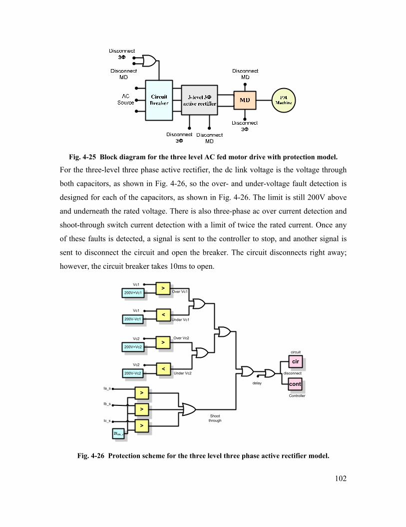
102
Fig. 4-25 Block diagram for the three level AC fed motor drive with protection model.
For the three-level three phase active rectifier, the dc link voltage is the voltage through
both capacitors, as shown in Fig. 4-26, so the over- and under-voltage fault detection is
designed for each of the capacitors, as shown in Fig. 4-26. The limit is still 200V above
and underneath the rated voltage. There is also three-phase ac over current detection and
shoot-through switch current detection with a limit of twice the rated current. Once any
of these faults is detected, a signal is sent to the controller to stop, and another signal is
sent to disconnect the circuit and open the breaker. The circuit disconnects right away;
however, the circuit breaker takes 10ms to open.
>200V+Vc1
Vc1
<200V-Vc1
Vc1
>
>
> 2Iabc_s
Ia_s
Ib_s
Ic_s
Over Vc1
Under Vc1
Shoot through
delay
disconnect
cir
cont
circuit
Controller
>200V+Vc2
Vc2
<200V-Vc2
Vc2
Over Vc2
Under Vc2
Fig. 4-26 Protection scheme for the three level three phase active rectifier model.
103
For the motor drive protection, the reader is referenced to the two level ac-fed motor
drive protection section.
VI. Fault Analysis with Protection
The systems used for the fault analysis are modified using the protection schemes defined
in the previous section. These modified systems are then used for a complete fault
analysis where the different types of faults are analyzed and the protection effect is
observed. The next sections show some examples of the different fault analysis done with
protection.
A. System 1 with Protection: Two-level AC Fed Motor Drive
i) System Architecture
The system main components didn’t change. It consists of a two-level three phase
active rectifier fed by a synchronous generator, and feeds a 25kW motor drive as shown
in Fig. 4-27. The three-phase circuit breaker is added to test for ac overcurrent faults and
for faults coming from other parts of the system (i.e., the two-level three phase active
rectifier and the motor drive (MD)). The two-level three phase active rectifier has over-
and under-voltage protection for the output dc link voltage, and shoot-through protection
for the current through the switches in the power stage as mentioned in the system
protection section. If any fault occurs, the sensor declares a fault error, a signal is sent to
disconnect the controller, and another signal is sent to disconnect the rectifier circuit (i.e.,
disconnect 3φ signal). This signal is sent to the motor drive and to the circuit breaker. In
addition to those built-in fault detections in the two-level three phase active rectifier,
there is also an input signal to the two-level three phase active rectifier that announces
there is a fault elsewhere in the system and the boost rectifier must stop its operation (i.e.,
disconnect MD signal). This fault study concentrates on analyzing the two-level three
phase active rectifier faults at the input and output terminals in addition to the rectifier
itself. The different protections are explained in detail for all parts of the system in the
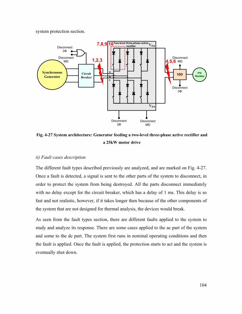
104
system protection section.
CircuitBreaker
MD
Disconnect 3Φ
PMMachine
Disconnect 3Φ
Disconnect MD
Disconnect MD
Disconnect MD
Disconnect 3Φ
Vdcn
VdcpTwo-level three-phase active
rectifier
a
bc
Synchronous Generator
1,2,3 4,5,6
7,8,9,10
Fig. 4-27 System architecture: Generator feeding a two-level three-phase active rectifier and
a 25kW motor drive
ii) Fault cases description
The different fault types described previously are analyzed, and are marked on Fig. 4-27.
Once a fault is detected, a signal is sent to the other parts of the system to disconnect, in
order to protect the system from being destroyed. All the parts disconnect immediately
with no delay except for the circuit breaker, which has a delay of 1 ms. This delay is so
fast and not realistic, however, if it takes longer then because of the other components of
the system that are not designed for thermal analysis, the devices would break.
As seen from the fault types section, there are different faults applied to the system to
study and analyze its response. There are some cases applied to the ac part of the system
and some to the dc part. The system first runs in nominal operating conditions and then
the fault is applied. Once the fault is applied, the protection starts to act and the system is
eventually shut down.
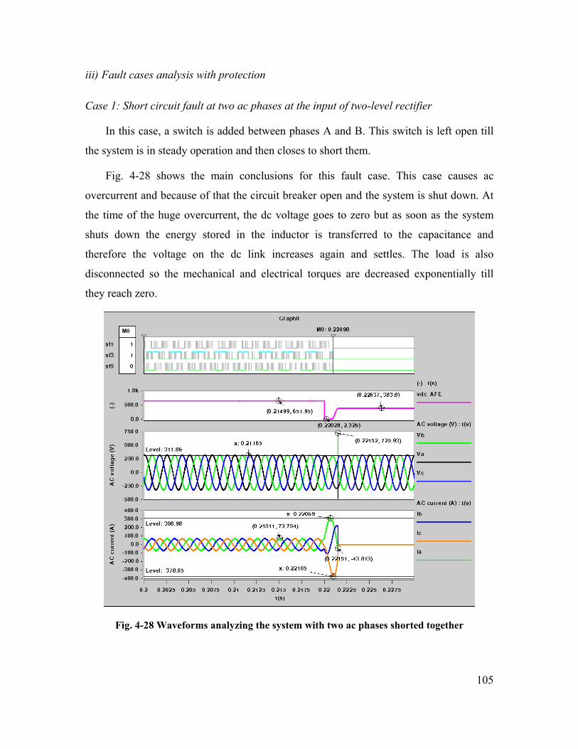
105
iii) Fault cases analysis with protection
Case 1: Short circuit fault at two ac phases at the input of two-level rectifier
In this case, a switch is added between phases A and B. This switch is left open till
the system is in steady operation and then closes to short them.
Fig. 4-28 shows the main conclusions for this fault case. This case causes ac
overcurrent and because of that the circuit breaker open and the system is shut down. At
the time of the huge overcurrent, the dc voltage goes to zero but as soon as the system
shuts down the energy stored in the inductor is transferred to the capacitance and
therefore the voltage on the dc link increases again and settles. The load is also
disconnected so the mechanical and electrical torques are decreased exponentially till
they reach zero.
Fig. 4-28 Waveforms analyzing the system with two ac phases shorted together
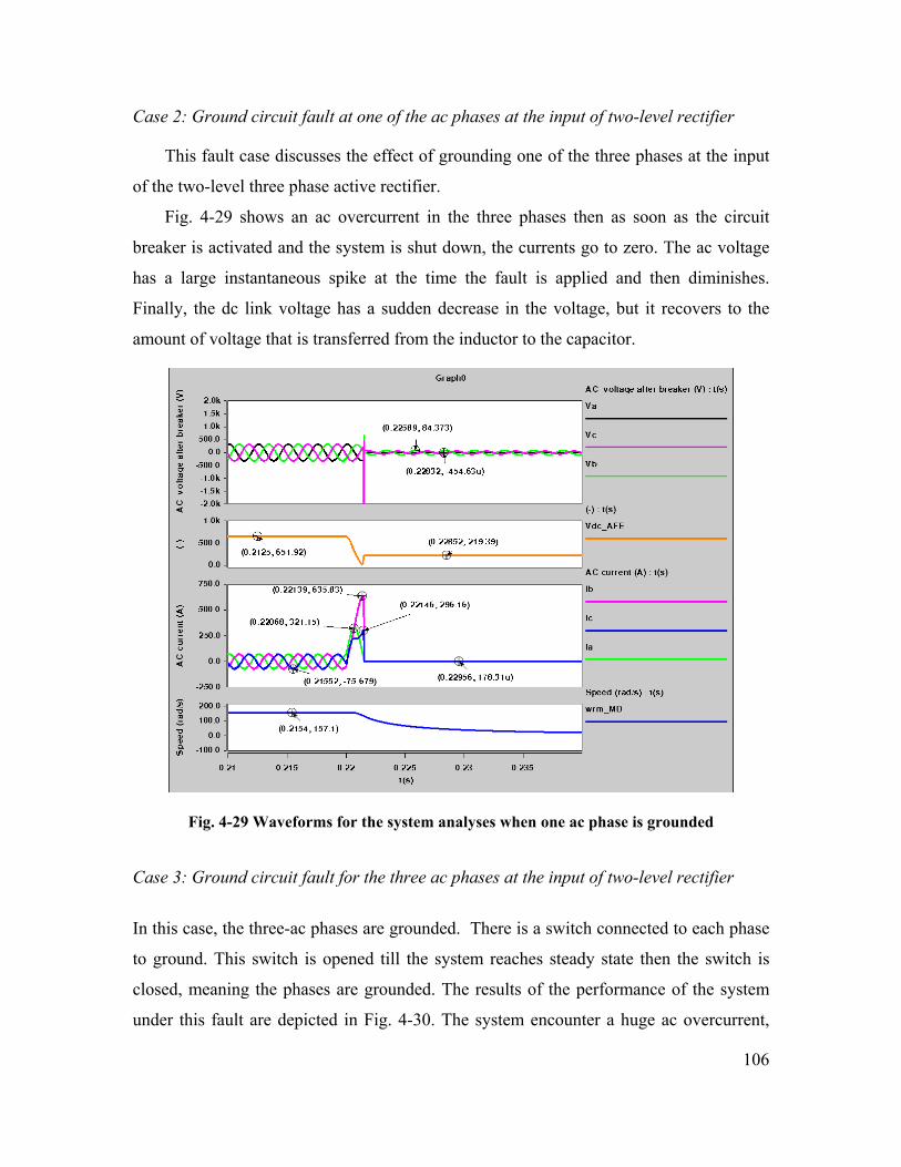
106
Case 2: Ground circuit fault at one of the ac phases at the input of two-level rectifier
This fault case discusses the effect of grounding one of the three phases at the input
of the two-level three phase active rectifier.
Fig. 4-29 shows an ac overcurrent in the three phases then as soon as the circuit
breaker is activated and the system is shut down, the currents go to zero. The ac voltage
has a large instantaneous spike at the time the fault is applied and then diminishes.
Finally, the dc link voltage has a sudden decrease in the voltage, but it recovers to the
amount of voltage that is transferred from the inductor to the capacitor.
Fig. 4-29 Waveforms for the system analyses when one ac phase is grounded
Case 3: Ground circuit fault for the three ac phases at the input of two-level rectifier
In this case, the three-ac phases are grounded. There is a switch connected to each phase
to ground. This switch is opened till the system reaches steady state then the switch is
closed, meaning the phases are grounded. The results of the performance of the system
under this fault are depicted in Fig. 4-30. The system encounter a huge ac overcurrent,
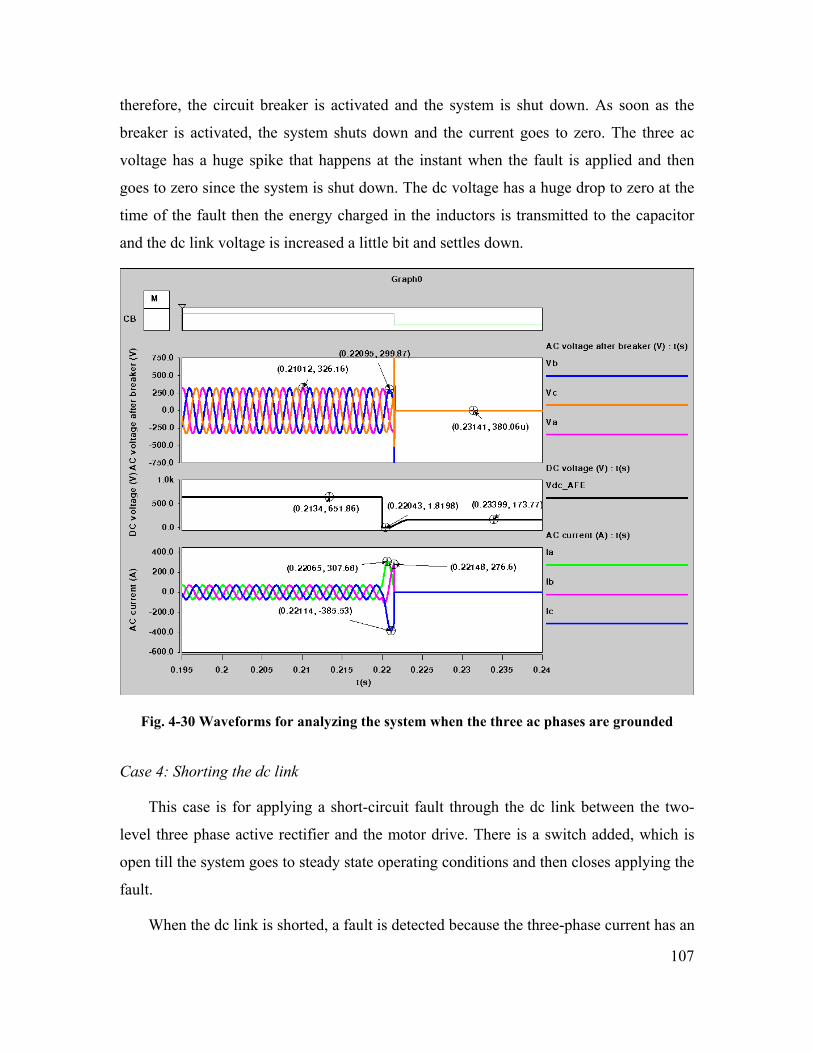
107
therefore, the circuit breaker is activated and the system is shut down. As soon as the
breaker is activated, the system shuts down and the current goes to zero. The three ac
voltage has a huge spike that happens at the instant when the fault is applied and then
goes to zero since the system is shut down. The dc voltage has a huge drop to zero at the
time of the fault then the energy charged in the inductors is transmitted to the capacitor
and the dc link voltage is increased a little bit and settles down.
Fig. 4-30 Waveforms for analyzing the system when the three ac phases are grounded
Case 4: Shorting the dc link
This case is for applying a short-circuit fault through the dc link between the two-
level three phase active rectifier and the motor drive. There is a switch added, which is
open till the system goes to steady state operating conditions and then closes applying the
fault.
When the dc link is shorted, a fault is detected because the three-phase current has an
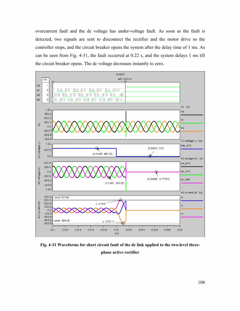
108
overcurrent fault and the dc voltage has under-voltage fault. As soon as the fault is
detected, two signals are sent to disconnect the rectifier and the motor drive so the
controller stops, and the circuit breaker opens the system after the delay time of 1 ms. As
can be seen from Fig. 4-31, the fault occurred at 0.22 s, and the system delays 1 ms till
the circuit breaker opens. The dc voltage decreases instantly to zero.
Fig. 4-31 Waveforms for short circuit fault of the dc link applied to the two-level three-
phase active rectifier
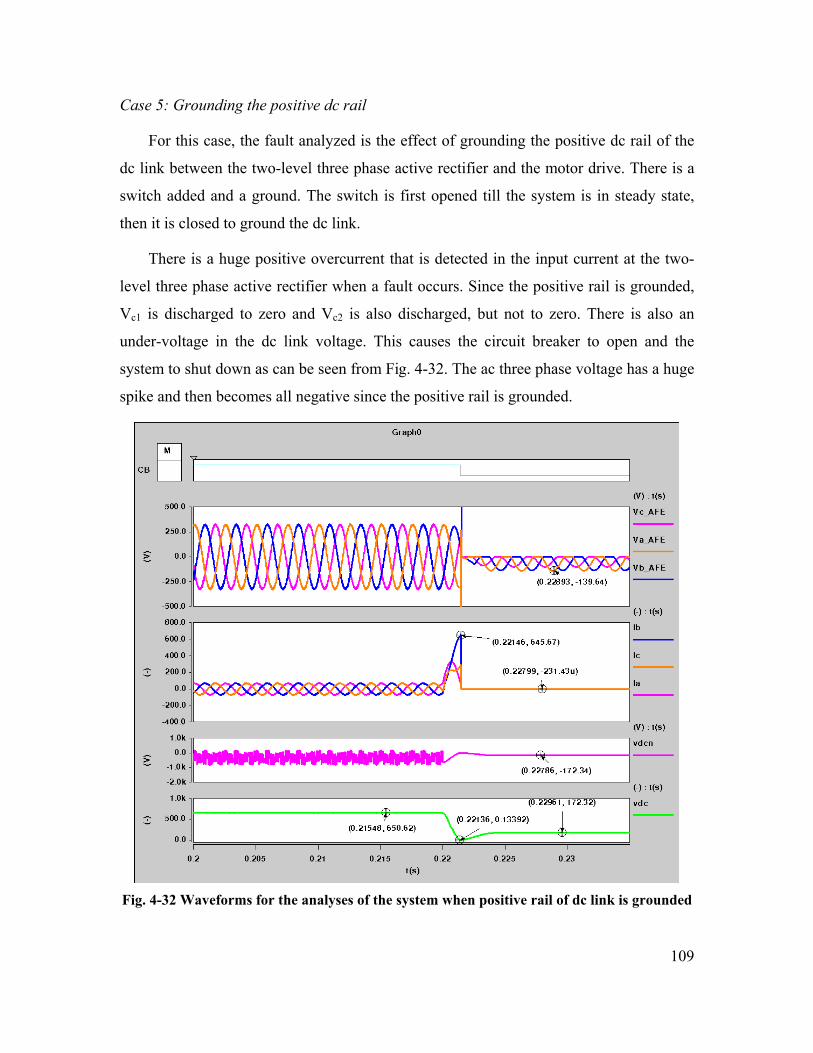
109
Case 5: Grounding the positive dc rail
For this case, the fault analyzed is the effect of grounding the positive dc rail of the
dc link between the two-level three phase active rectifier and the motor drive. There is a
switch added and a ground. The switch is first opened till the system is in steady state,
then it is closed to ground the dc link.
There is a huge positive overcurrent that is detected in the input current at the two-
level three phase active rectifier when a fault occurs. Since the positive rail is grounded,
Vc1 is discharged to zero and Vc2 is also discharged, but not to zero. There is also an
under-voltage in the dc link voltage. This causes the circuit breaker to open and the
system to shut down as can be seen from Fig. 4-32. The ac three phase voltage has a huge
spike and then becomes all negative since the positive rail is grounded.
Fig. 4-32 Waveforms for the analyses of the system when positive rail of dc link is grounded
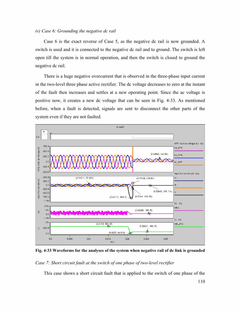
110
iv) Case 6: Grounding the negative dc rail
Case 6 is the exact reverse of Case 5, as the negative dc rail is now grounded. A
switch is used and it is connected to the negative dc rail and to ground. The switch is left
open till the system is in normal operation, and then the switch is closed to ground the
negative dc rail.
There is a huge negative overcurrent that is observed in the three-phase input current
in the two-level three phase active rectifier. The dc voltage decreases to zero at the instant
of the fault then increases and settles at a new operating point. Since the ac voltage is
positive now, it creates a new dc voltage that can be seen in Fig. 4-33. As mentioned
before, when a fault is detected, signals are sent to disconnect the other parts of the
system even if they are not faulted.
Fig. 4-33 Waveforms for the analyses of the system when negative rail of dc link is grounded
Case 7: Short circuit fault at the switch of one phase of two-level rectifier
This case shows a short circuit fault that is applied to the switch of one phase of the
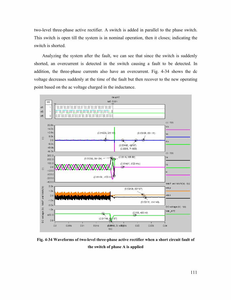
111
two-level three-phase active rectifier. A switch is added in parallel to the phase switch.
This switch is open till the system is in nominal operation, then it closes; indicating the
switch is shorted.
Analyzing the system after the fault, we can see that since the switch is suddenly
shorted, an overcurrent is detected in the switch causing a fault to be detected. In
addition, the three-phase currents also have an overcurrent. Fig. 4-34 shows the dc
voltage decreases suddenly at the time of the fault but then recover to the new operating
point based on the ac voltage charged in the inductance.
Fig. 4-34 Waveforms of two-level three-phase active rectifier when a short circuit fault of
the switch of phase A is applied
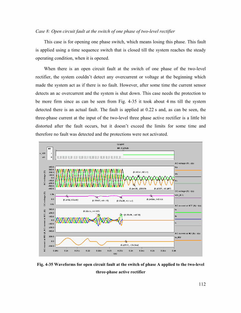
112
Case 8: Open circuit fault at the switch of one phase of two-level rectifier
This case is for opening one phase switch, which means losing this phase. This fault
is applied using a time sequence switch that is closed till the system reaches the steady
operating condition, when it is opened.
When there is an open circuit fault at the switch of one phase of the two-level
rectifier, the system couldn’t detect any overcurrent or voltage at the beginning which
made the system act as if there is no fault. However, after some time the current sensor
detects an ac overcurrent and the system is shut down. This case needs the protection to
be more firm since as can be seen from Fig. 4-35 it took about 4 ms till the system
detected there is an actual fault. The fault is applied at 0.22 s and, as can be seen, the
three-phase current at the input of the two-level three phase active rectifier is a little bit
distorted after the fault occurs, but it doesn’t exceed the limits for some time and
therefore no fault was detected and the protections were not activated.
Fig. 4-35 Waveforms for open circuit fault at the switch of phase A applied to the two-level
three-phase active rectifier
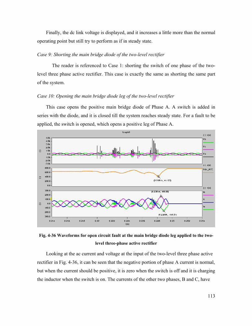
113
Finally, the dc link voltage is displayed, and it increases a little more than the normal
operating point but still try to perform as if in steady state.
Case 9: Shorting the main bridge diode of the two-level rectifier
The reader is referenced to Case 1: shorting the switch of one phase of the two-
level three phase active rectifier. This case is exactly the same as shorting the same part
of the system.
Case 10: Opening the main bridge diode leg of the two-level rectifier
This case opens the positive main bridge diode of Phase A. A switch is added in
series with the diode, and it is closed till the system reaches steady state. For a fault to be
applied, the switch is opened, which opens a positive leg of Phase A.
Fig. 4-36 Waveforms for open circuit fault at the main bridge diode leg applied to the two-
level three-phase active rectifier
Looking at the ac current and voltage at the input of the two-level three phase active
rectifier in Fig. 4-36, it can be seen that the negative portion of phase A current is normal,
but when the current should be positive, it is zero when the switch is off and it is charging
the inductor when the switch is on. The currents of the other two phases, B and C, have

114
some switching ripple when the phase A current is negative, but they have a normal sine
wave for the rest of the waveform. At the same time that the phase A current is negative,
the three phases’ voltages have large spikes.
Since there is no ac overvoltage detection, this case continues to run normally at
the beginning more than expected as if there is no fault and the protections are not
activated. The dc link voltage has ripples as long as the fault was not detected yet but as
soon as the fault is detected, the dc voltage is increased and settles at new settling point.
115
Chapter 5 Summary and Conclusions
This work used a simulation software Saber to build and simulate a sample electronic
power system. This sample system was used for different stability and fault studies like
steady state, small-signal and large-signal stability analysis and time simulations fault
analysis. This work can be extended to different types of systems and for more studies
like power quality, EMI and harmonics studies.
The different models of the system were designed for the stand alone operation then
connected together to form the system. There were different issues that face the design of
the system as when a large system is connected together, system interactions starts to
arise. The main two drawbacks of the system were the simulation time and the numerical
convergence errors due to the large amount of switching models of the system. There
were also some requirements that had to change in the software in order to get a fast and
robust system running and they are all related to the time step.
Once the system was designed, the second step was to concentrate on the stability
analysis. These analyses were done as mentioned using the detailed/switching models as
verifications for a stability analysis using linearized average models. The steady-state
stability analysis was done by investigating the nominal operation of the power
electronics system proposed. The small-signal stability of this system was studied by
running different parametric case studies. First, the safe values of the main system
parameters were defined from the view of the stability of the complete system. Then,
these different critical parameters of the system were mapped together to predict their
influence on the system and the boundaries for the safe operation. These boundaries can
be used to establish criteria for design based on physical parameters. The large signal
stability was examined through the response of the power system to different types of
transient changes. There were different load steps applied to the critical parameters of the
system at the maximum or minimum stability boundary limit found by the mapping
section. The maximum load step after which the system can recover and remain stable
was also defined. The other type of large signal stability analysis done was the study of
faults. There are different faults to be studied; for example, over voltage, under voltage

116
and over current. A fault analysis was done for different components of the system to
analyze their performance and to predict their protection requirements.
117
REFERENCES
[1] A. Emadi and M. Ehsani, “Multi-converter power electronic systems: definitions
and applications,” in Proceed. IEEE PESC ’01, vol. 2, pp. 1230−1236, June 2001.
[2] G. Franz, G. Ludwig and R. Steigerwald, “Modeling and simulation of distributed
power systems,” in Proceed. IEEE PESC ’90, pp. 606−610, June 1990.
[3] Y. Hu, J. Tatler, and Z. Chen, “Modeling and Simulation of a Power Electronic
Conversion System Using SIMULINK,” Proc. of Universities Power Engineering
Conference p. 289−293, 2004.
[4] V. Thottuvelil, and E. Lee, “On some practical aspects of power electronics
simulation,” in Proceed. IEEE Computers in Power Electronics, pp. 157−163,
Aug 1994.
[5] R. Nelms, B. Evans, and L. Grigsby, “Simulation of ac spacecraft power systems,”
IEEE Trans. on Ind. Elec., vol. 36, no. 3, pp. 398−402, Aug. 1989.
[6] A. Beuret, Fk. Bordry, and H. Seran, “Power converter simulation – power and
control domain,” in IEEE Fifth European Conf., vol. 2, pp. 77−82, Sept. 1993.
[7] B. Needham, P. Eckerling, and K. Siri, “Simulation of large distributed dc power
systems using averaged modeling techniques and the saber simulator,” in Proceed.
IEEE APEC’94, vol. 2, pp. 801−807, Orlando, FL, Feb. 1994.
[8] K. J. Karimi, S. J. Fu, “Modeling and Simulation of Space Station Laboratory
Module Electric Power System,” in Conf. AIAA’94, 1994.
[9] P. Duijsen, “Multi-level modeling and simulation of power electronics systems,”
in IEEE Trans. on Pow. Elec., vol. 4, pp. 347−352, Brighton, UK, Sept. 1993.
[10] N. Mohan, W. Robbins, T. Undeland, R. Nilssen and O. Mo, “Simulation of
power electronic and motion control systems-an overview,” Proceedings of the
IEEE, vol. 82, no 8, pp. 1287−1302, Aug. 1994.
118
[11] S. Rosado, R. Burgos, S. Ahmed, F. Wang, and D. Boroyevich, “Modeling of
power electronics for simulation-based analysis of power systems,” in Conf.
SCS SCSC 2007, San Diego, CA, July 2007.
[12] B. Cho, F. Lee, “Modeling and analysis of spacecraft power systems,” IEEE
Trans. on Pow. Elec., vol. 3, no.1, pp. 44−54, Jan. 1988.
[13] K. Karimi, A. Booker, and A. Mong, “Modeling, simulation and verification of
large dc power electronics systems,” in Proceed. IEEE PESC ’96, vol. 2, pp.
1731−1737, June 1996.
[14] S. Horowitz, A. Phadke, Power System Relaying, 2nd ed., Research Studies Press
Ltd., 1995
[15] I. Lazbin, “Analysis of the stability margins of the Space Station Freedom
electrical power system,” in Proceed. IEEE PESC’93, pp. 839−845, June 1993.
[16] R. D. Middlebrook, “Design techniques for preventing input-filter oscillations in
switched-mode regulators,” in Proceed. Powercon 5, pp. A 3.1–A 3.16, May
1978.
[17] F. Lee, Y. Yu, and J. Triner, “Modeling switching regulator power stages with and
without zero-inductor-current dwell time,” in Proceed. IEEE PESC’76, pp. 62–72,
June 1976.
[18] F. Lee, R. Iwens, Y. Yu, and J. Triner, “Generalized computer-aided discrete tome
modeling and analysis of dc-dc converters,” IEEE Trans. Indust. Elec. Contr.
Instrum., vol. 26, pp. 58–69, May 1979.
[19] B. Cho, and B. Choi, “Analysis and design of multi-stage distributed power
systems,” in Proceed. IEEE INTELEC’91, pp. 220−226, Nov. 1991.
[20] C. Wildrick, F. Lee, B. Cho, and B. Choi, “A method of defining the load
impedance specification for a stable distributed power system,” IEEE Trans. on
Pow. Elec., vol. 10, no. 3, pp. 280−285, May 1995.
[21] E. Gholdson, K. Karimi, F. Lee, J. Rajagopalan, Y. Panov, and B. Manners,
119
“Stability of large dc power systems using switching converters, with application
to the international space station,” in Proceed. Intersociety IECEC’96, vol. 1, pp.
166−171, Aug. 1996.
[22] K. Karimi, A. Booker, A. Mong, , and B. Manners, “Verification of space station
secondary power system stability using design experiment,” in Proceed.
Intersociety IECEC’97, vol. 1, pp. 526−531, July 1997.
[23] A. Emadi, and M. Ehsani, “Aircraft power systems: technology, state of the art,
and future trends,” IEEE AES Systems Mag., vol 15., no. 1, pp. 28−32., Jan. 2000.
[24] T. Esaka, Y. Kataoka, T. Ohtaka and S. Iwamoto, “Voltage Stability Preventive
Control Using a New Voltage Stability Index”, IEEE PowerCon ’04, vol. 1, pp.
344−349, Nov. 2004.
[25] M. Belkhayat, R. Cooley, A. Witulski, “Large signal stability criteria for
distributed systems with constant power loads,” n Proceed. IEEE PESC ’95, vol.
2, pp. 1333−8, June 1995.
[26] J.V. Milanovic, T.A. David, “Stability of distribution networks with embedded
generators and induction motors,” IEEE Power Engineering Society Winter
Meeting, 2002, vol. 2, pp 1023−1028, Jan. 2002
[27] S. Rosado, X. Ma, C. Han, F. Wang, and D. Boroyevich, “Model-based digital
controller for a variable frequency synchronous generator with brushless exciter,” in
Proceed. IEEE PESC ’05, pp. 90−95, June 2005.
[28] R. Burgos, S. Rosado, F. Wang, D. Boroyevich, Z. Lewis, and K. Karimi,
“Modeling considerations and stability analysis of aerospace power systems
with hybrid ac/dc distribution,” in SAE Power Systems Conf., New Orleans,
LA, Nov. 2006.
[29] A. Uan-Zo-li, R. Burgos, H. Zhu, A. Roshan, F. Lacaux, F. Wang, and D.
Boroyevich, “Analysis of new 18-pulse direct symmetric autotransformer rectifiers
with dual AC-voltage feeding capability,” in Proceed. IEEE IECON’05, pp. 531-
120
−536, Nov. 2005.
[30] H. Zhu, “New Multi-Pulse Diode Rectifier Average Models for AC and DC Power
System Studies”, PhD. Dissertation, Virginia Tech, 2006.
[31] H. Zhu, R. Burgos, F. Lacaux, A. Uan-Zo-li, F. Wang, D. Lindner and D.
Boroyevich, “Evaluation and operating region characterization of enhanced average
models for nine-phase rectifiers,” in Conf. IEEE APEC’06, pp. 1324−1330, Mar.
2006.
[32] S. Rosado, R. Burgos, F. Wang, and D. Boroyevich, “Large- and small-signal
evaluation of average models for multi-pulse diode rectifiers,” in Conf. IEEE
COMPEL’06, pp. 89−94, Troy, NY, July 2006.
[33] B. Lee, and M. Ehsani, “A simplified functional simulation model three-phase
voltage-source inverter using switching function concept,” IEEE Trans. on Ind.
Elec., vol. 48, no. 2, pp. 309−321, Apr. 2001.
[34] P. Ziogas, E. Wiechmann and V. Stefanovic “A computer aided analysis and design
approach for static voltage source inverters,” IEEE Trans. on Ind. Applicat., vol. 21,
no. 5, pp. 1234−1241, Sept. 1985.
[35] R. Burgos, P. Kshirsagar, A. Lidozzi, F. Wang, and D. Boroyevich,
“Mathematical model and control design for sensorless vector control of
permanent magnet synchronous machines,” in Conf. IEEE COMPEL’06, Troy,
NY, pp. 76−82, July 2006.
[36] R.L.A. Ribeiro, E.R.C. da Silva, C. Jacobina and A. Lima, “Fault Detection in
Voltage-Fed PWM Motor Drive Systems” in Proceed. IEEE PESC ’00, vol. 1, pp.
242−247, June 2000.
[37] B. Huang, R. Burgos, F. Wang, D. Boroyevich. “D-Q-0 Synchronous Frame
Average Model for Three-phase Arrays of Single-Phase PFC Converter Loads,” in
Conf. IEEE COMPEL ’06, Troy, NY, pp. 83−88, July 2006.
[38] P. C. Todd, “UC3854 Controlled Power Factor Correction Circuit Design,”
Application Note U-134, Texas Instruments, pp. 269−288, Available:

121
“http://www.powerdesigners.com/InfoWeb/design_center/Appnotes_Archive/u134.
pdf”.
[39] L. Goldgeisser, E. Christen, M. Vlach, and J. Langenwalter, “Open ended dynamic
ramping simulation of multi-discipline systems,” in Proceed. IEEE ISCAS’01, vol.
5, pp. 307−310, 2001.
[40] S. Rosado, “Voltage stability and control in autonomous electric power systems
with variable frequency”, PhD. Dissertation, Virginia Tech, 2007.
[41] Kundur, et al., “Definition and classification of power system stability IEEE/CIGRE
joint task force on stability terms and definitions”, IEEE Trans. Power Systems,
Vol. 19, Aug. 2004.
[42] C. Tinsley, “Modeling of multi-pulse transformer rectifier units in power
distribution systems”, PhD. Dissertation, Virginia Tech, 2003.
[43] H. ElBrouji, P. Poure and S. Saadate, “Study and Comparison of Fault Tolerant
Shunt Three-phase Active filter Topologies,” IEEE IPEMC, 2006.
[44] R. Spee and A. K. Wallace, “Remedial strategies for brushless dc drive failures,”
IEEE Trans. on Industry Applic., 26(2):259-266, March/April 1990.
[45] R.L.A. Ribeiro, E.R.C. da Silva, and etal, “Fault Detection in Voltage-Fed PWM
Motor Drive Systems” Elec. Machines and Sys. For MEA, IEE Colloquium, pp.
1/1−1/4, Nov. 1999.
[46] Hang-Seok Choi and D.Y Huh, “Protection Schemes for Various Fault Conditions
for Off-line Flyback Converters,” IEEE PESC, pp. 4355−4359, 2004.
[47] E.A. Ebrahim and N. Hammad, “Fault analysis of current-controlled PWM-inverter
fed induction-motor drives,” Proc. of the 7th International Conference on Properties
and Applications of Dielectric Materials, pp. 1065-1070, Nagoya, June 2003.