design of a linear lc digitally controlled oscillator using
TRANSCRIPT
DESIGN OF A LINEAR LC DIGITALLY
CONTROLLED OSCILLATOR USING
TOPOGRAPHICAL FIELD MAPS
by
SHAKEEB ABDULLAH
A thesis submitted to the Faculty of Graduate and PostdoctoralAffairs in partial fulfillment of the requirements
for the degree of
Master of Applied Science
in
Electrical Engineering
Ottawa-Carleton Institute for Electrical and Computer EngineeringDepartment of Electrical and Computer Engineering
Carleton UniversityOttawa, Ontario
© Copyright
Shakeeb Abdullah, 2018
Copyright© 2018. No parts of this document or the material within it may be re-produced,
transcribed, copied, reverse engineered, duplicated or be used by any means or method
without the prior permission of the author and those who holds the rights to them except
for that which has been prescribed under the clause regarding thesis reproduction embedded
inside (and that which is in conjunction with) the acts and laws of Carleton University
Institution and of Canada regarding the distribution of graduate work.
ii
ABSTRACT
The purpose of this thesis was to present a new perspective on how to design extremely
linear digitally controlled oscillators. This was achieved by introducing a new concept known
as linearity field maps. The linearity response of the measured DCO had an R2 value of
0.996; which was extremely linear. The DCO employed equal bank steps for all bank sets
to achieve this linearity. The measured frequency response of the DCO was from 6.66 GHz
to 5.45 GHz. The DCO had fine tuning steps of 20.5 kHz resolution and a tuning range
of 20%. The measured FoM was between -175 dBc/Hz and -181 dB/Hz (throughout the
entire frequency span of the DCO and for various power levels). The thesis experiment
was a success in showing how to design a linear DCO, the DCO in the thesis worked even
though the frequency was shifted from simulated results, the point of the thesis was made.
The theorem and perspective introduced in this thesis held true.
iii

EXECUTIVE SUMMARY
The reason for this report was to satisfy the requirements for MASc graduate degree at
Carleton University and the purpose of this report was to present a novel outlook on how to
design an extremely linear digitally controlled oscillator. This was achieved by introducing
a new concept known as linearity field maps. The simulated and theoretical frequency
response of the DCO was from 7.1 GHz to 5.7 GHz whereas the measured frequency response
of the DCO was from 6.6 Ghz to 5.5 GHz. This caused all the linear coefficients of the
measured DCO to be mismatched with the initial theoretical values. However when a
new theoretical DCO that ranges with the same frequency span as the measured DCO
was compared, the coefficient errors were less than 1%, proving that the design technique
presented in this thesis was valid. The R2 value of the measured DCO was 0.996 which was
extremely linear based on the requirements of the author (less than 0.5% error from perfect
linearity).
The theoretical phase noise and simulated phase noise concurred with each other
(-125 dBc/Hz at carrier frequency 6.5 GHz and 1 MHz offset) however the measured phase
noise was almost 10 dB worse. About 2-3 dB loss could have been attributed due to
poor CML performance shown through simulations. Some digital noise bleeding could have
also played a role in reducing the oscillators performance as was experimentally observed,
nevertheless FoM was still reasonable and respectable with FoM better than or equal to
-175 dBc/Hz throughout the entire span of the DCO (at it’s highest frequencies when all
banks are off and at its lowest frequency when all banks are on).
The measured Bank set 1 had a frequency step size of 66.4 MHz. The measured
Bank set 2 upper limit frequency step size was 9.91 MHz and lower limit frequency step size
was 6.20 MHz. The measured Bank set 3 had upper limit frequency step size of 2.09 MHz
and lower limit frequency step size 1.29 MHz. The measured Bank set 4 had upper limit
frequency step size of 469 kHz and lower limit frequency step size of 267 kHz. Bank set 5 to
11 did not behave as intended. Further investigation needs to be done as to why these bank
sets did not function properly; however it should be noted that the DCO was purposely
designed with successively smaller and smaller bank sets until the frequency steps would
fail - to determine the minimum practical resolution of the DCO due to technological and
parasitic limitations. The frequency settling time of the DCO also took too long; however
it is believed that it can be easily rectified by using bigger buffer drivers between the digital
control signals and the banks of the DCO. Nevertheless, the overall thesis experiment was
iv
a success in showing how to design a linear digitally controlled oscillator, the DCO in the
thesis worked even though the measured frequency was shifted, and the point of the thesis
was made.
v
ACKNOWLEDGEMENTS
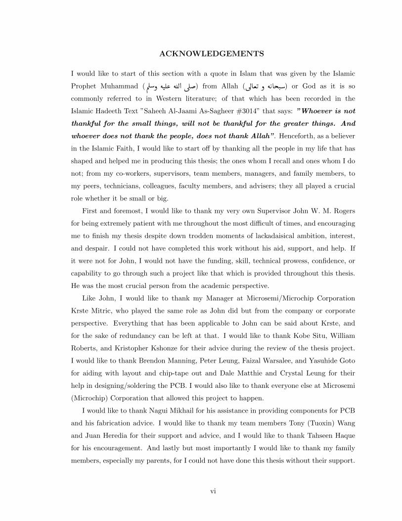
I would like to start of this section with a quote in Islam that was given by the Islamic
Prophet Muhammad (ÕÎð éJÊ« é<Ë @ úÎ) from Allah (úÍAªK ð é
KAjJ.) or God as it is so
commonly referred to in Western literature; of that which has been recorded in the
Islamic Hadeeth Text ”Saheeh Al-Jaami As-Sagheer #3014” that says: ”Whoever is not
thankful for the small things, will not be thankful for the greater things. And
whoever does not thank the people, does not thank Allah”. Henceforth, as a believer
in the Islamic Faith, I would like to start off by thanking all the people in my life that has
shaped and helped me in producing this thesis; the ones whom I recall and ones whom I do
not; from my co-workers, supervisors, team members, managers, and family members, to
my peers, technicians, colleagues, faculty members, and advisers; they all played a crucial
role whether it be small or big.
First and foremost, I would like to thank my very own Supervisor John W. M. Rogers
for being extremely patient with me throughout the most difficult of times, and encouraging
me to finish my thesis despite down trodden moments of lackadaisical ambition, interest,
and despair. I could not have completed this work without his aid, support, and help. If
it were not for John, I would not have the funding, skill, technical prowess, confidence, or
capability to go through such a project like that which is provided throughout this thesis.
He was the most crucial person from the academic perspective.
Like John, I would like to thank my Manager at Microsemi/Microchip Corporation
Krste Mitric, who played the same role as John did but from the company or corporate
perspective. Everything that has been applicable to John can be said about Krste, and
for the sake of redundancy can be left at that. I would like to thank Kobe Situ, William
Roberts, and Kristopher Kshonze for their advice during the review of the thesis project.
I would like to thank Brendon Manning, Peter Leung, Faizal Warsalee, and Yasuhide Goto
for aiding with layout and chip-tape out and Dale Matthie and Crystal Leung for their
help in designing/soldering the PCB. I would also like to thank everyone else at Microsemi
(Microchip) Corporation that allowed this project to happen.
I would like to thank Nagui Mikhail for his assistance in providing components for PCB
and his fabrication advice. I would like to thank my team members Tony (Tuoxin) Wang
and Juan Heredia for their support and advice, and I would like to thank Tahseen Haque
for his encouragement. And lastly but most importantly I would like to thank my family
members, especially my parents, for I could not have done this thesis without their support.
vi
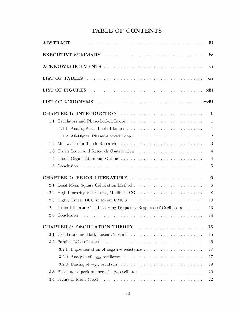
TABLE OF CONTENTS
ABSTRACT . . . . . . . . . . . . . . . . . . . . . . . . . . . . . . . . . . . . . . . iii
EXECUTIVE SUMMARY . . . . . . . . . . . . . . . . . . . . . . . . . . . . . . iv
ACKNOWLEDGEMENTS . . . . . . . . . . . . . . . . . . . . . . . . . . . . . . vi
LIST OF TABLES . . . . . . . . . . . . . . . . . . . . . . . . . . . . . . . . . . . xii
LIST OF FIGURES . . . . . . . . . . . . . . . . . . . . . . . . . . . . . . . . . . xiii
LIST OF ACRONYMS . . . . . . . . . . . . . . . . . . . . . . . . . . . . . . . . xviii
CHAPTER 1: INTRODUCTION . . . . . . . . . . . . . . . . . . . . . . . . . 1
1.1 Oscillators and Phase-Locked Loops . . . . . . . . . . . . . . . . . . . . . . . 1
1.1.1 Analog Phase-Locked Loops . . . . . . . . . . . . . . . . . . . . . . . 1
1.1.2 All-Digital Phased-Locked Loop . . . . . . . . . . . . . . . . . . . . . 2
1.2 Motivation for Thesis Research . . . . . . . . . . . . . . . . . . . . . . . . . . 3
1.3 Thesis Scope and Research Contribution . . . . . . . . . . . . . . . . . . . . 4
1.4 Thesis Organization and Outline . . . . . . . . . . . . . . . . . . . . . . . . . 4
1.5 Conclusion . . . . . . . . . . . . . . . . . . . . . . . . . . . . . . . . . . . . . 5
CHAPTER 2: PRIOR LITERATURE . . . . . . . . . . . . . . . . . . . . . . 6
2.1 Least Mean Square Calibration Method . . . . . . . . . . . . . . . . . . . . . 6
2.2 High Linearity VCO Using Modified ICO . . . . . . . . . . . . . . . . . . . . 8
2.3 Highly Linear DCO in 65-nm CMOS . . . . . . . . . . . . . . . . . . . . . . 10
2.4 Other Literature in Linearizing Frequency Response of Oscillators . . . . . . 13
2.5 Conclusion . . . . . . . . . . . . . . . . . . . . . . . . . . . . . . . . . . . . . 14
CHAPTER 3: OSCILLATION THEORY . . . . . . . . . . . . . . . . . . . . 15
3.1 Oscillators and Barkhausen Criterion . . . . . . . . . . . . . . . . . . . . . . 15
3.2 Parallel LC oscillators . . . . . . . . . . . . . . . . . . . . . . . . . . . . . . . 15
3.2.1 Implementation of negative resistance . . . . . . . . . . . . . . . . . . 17
3.2.2 Analysis of −gm oscillator . . . . . . . . . . . . . . . . . . . . . . . . 17
3.2.3 Biasing of −gm oscillator . . . . . . . . . . . . . . . . . . . . . . . . . 19
3.3 Phase noise performance of −gm oscillator . . . . . . . . . . . . . . . . . . . 20
3.4 Figure of Merit (FoM) . . . . . . . . . . . . . . . . . . . . . . . . . . . . . . 22
vii
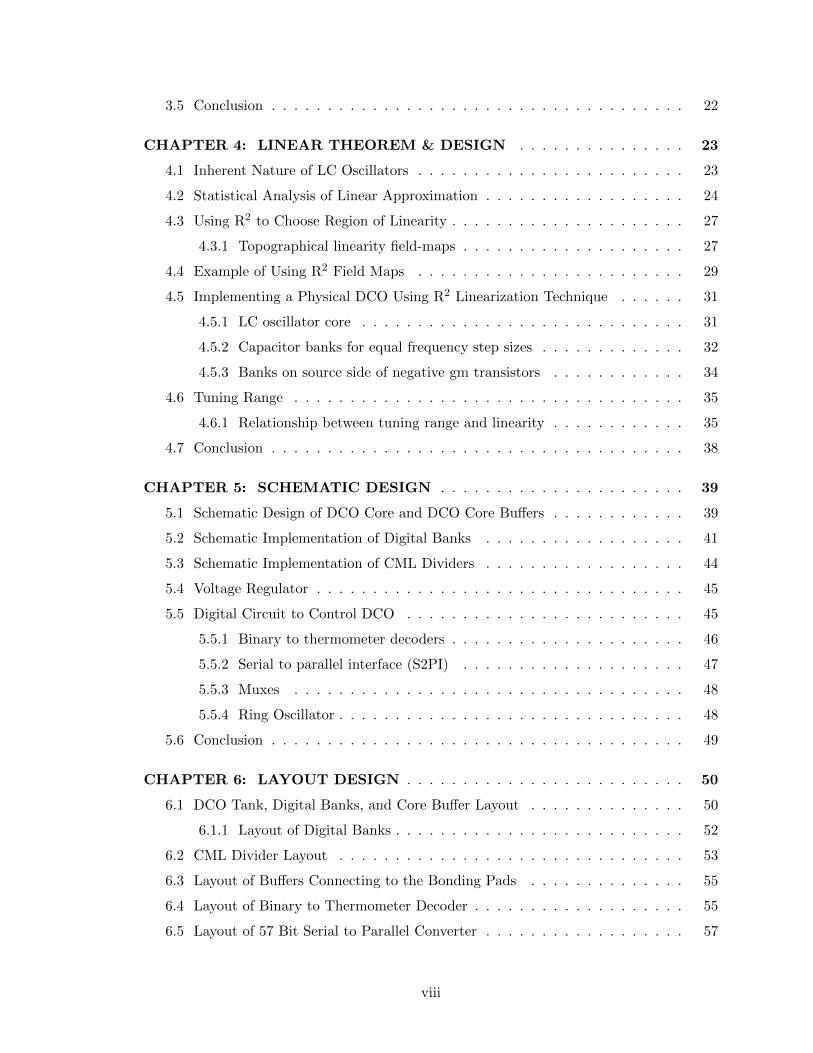
3.5 Conclusion . . . . . . . . . . . . . . . . . . . . . . . . . . . . . . . . . . . . . 22
CHAPTER 4: LINEAR THEOREM & DESIGN . . . . . . . . . . . . . . . 23
4.1 Inherent Nature of LC Oscillators . . . . . . . . . . . . . . . . . . . . . . . . 23
4.2 Statistical Analysis of Linear Approximation . . . . . . . . . . . . . . . . . . 24
4.3 Using R2 to Choose Region of Linearity . . . . . . . . . . . . . . . . . . . . . 27
4.3.1 Topographical linearity field-maps . . . . . . . . . . . . . . . . . . . . 27
4.4 Example of Using R2 Field Maps . . . . . . . . . . . . . . . . . . . . . . . . 29
4.5 Implementing a Physical DCO Using R2 Linearization Technique . . . . . . 31
4.5.1 LC oscillator core . . . . . . . . . . . . . . . . . . . . . . . . . . . . . 31
4.5.2 Capacitor banks for equal frequency step sizes . . . . . . . . . . . . . 32
4.5.3 Banks on source side of negative gm transistors . . . . . . . . . . . . 34
4.6 Tuning Range . . . . . . . . . . . . . . . . . . . . . . . . . . . . . . . . . . . 35
4.6.1 Relationship between tuning range and linearity . . . . . . . . . . . . 35
4.7 Conclusion . . . . . . . . . . . . . . . . . . . . . . . . . . . . . . . . . . . . . 38
CHAPTER 5: SCHEMATIC DESIGN . . . . . . . . . . . . . . . . . . . . . . 39
5.1 Schematic Design of DCO Core and DCO Core Buffers . . . . . . . . . . . . 39
5.2 Schematic Implementation of Digital Banks . . . . . . . . . . . . . . . . . . 41
5.3 Schematic Implementation of CML Dividers . . . . . . . . . . . . . . . . . . 44
5.4 Voltage Regulator . . . . . . . . . . . . . . . . . . . . . . . . . . . . . . . . . 45
5.5 Digital Circuit to Control DCO . . . . . . . . . . . . . . . . . . . . . . . . . 45
5.5.1 Binary to thermometer decoders . . . . . . . . . . . . . . . . . . . . . 46
5.5.2 Serial to parallel interface (S2PI) . . . . . . . . . . . . . . . . . . . . 47
5.5.3 Muxes . . . . . . . . . . . . . . . . . . . . . . . . . . . . . . . . . . . 48
5.5.4 Ring Oscillator . . . . . . . . . . . . . . . . . . . . . . . . . . . . . . . 48
5.6 Conclusion . . . . . . . . . . . . . . . . . . . . . . . . . . . . . . . . . . . . . 49
CHAPTER 6: LAYOUT DESIGN . . . . . . . . . . . . . . . . . . . . . . . . . 50
6.1 DCO Tank, Digital Banks, and Core Buffer Layout . . . . . . . . . . . . . . 50
6.1.1 Layout of Digital Banks . . . . . . . . . . . . . . . . . . . . . . . . . . 52
6.2 CML Divider Layout . . . . . . . . . . . . . . . . . . . . . . . . . . . . . . . 53
6.3 Layout of Buffers Connecting to the Bonding Pads . . . . . . . . . . . . . . 55
6.4 Layout of Binary to Thermometer Decoder . . . . . . . . . . . . . . . . . . . 55
6.5 Layout of 57 Bit Serial to Parallel Converter . . . . . . . . . . . . . . . . . . 57
viii
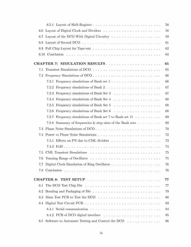
6.5.1 Layout of Shift-Register . . . . . . . . . . . . . . . . . . . . . . . . . . 58
6.6 Layout of Digital Clock and Dividers . . . . . . . . . . . . . . . . . . . . . . 58
6.7 Layout of the DCO With Digital Circuitry . . . . . . . . . . . . . . . . . . . 59
6.8 Layout of Second DCO . . . . . . . . . . . . . . . . . . . . . . . . . . . . . . 61
6.9 Full Chip Layout for Tape-out . . . . . . . . . . . . . . . . . . . . . . . . . . 62
6.10 Conclusion . . . . . . . . . . . . . . . . . . . . . . . . . . . . . . . . . . . . 64
CHAPTER 7: SIMULATION RESULTS . . . . . . . . . . . . . . . . . . . . . 65
7.1 Transient Simulations of DCO . . . . . . . . . . . . . . . . . . . . . . . . . . 65
7.2 Frequency Simulations of DCO . . . . . . . . . . . . . . . . . . . . . . . . . . 66
7.2.1 Frequency simulations of Bank set 1 . . . . . . . . . . . . . . . . . . . 66
7.2.2 Frequency simulations of Bank 2 . . . . . . . . . . . . . . . . . . . . . 67
7.2.3 Frequency simulations of Bank Set 3 . . . . . . . . . . . . . . . . . . 67
7.2.4 Frequency simulations of Bank Set 4 . . . . . . . . . . . . . . . . . . 68
7.2.5 Frequency simulations of Bank Set 5 . . . . . . . . . . . . . . . . . . 68
7.2.6 Frequency simulations of Bank Set 6 . . . . . . . . . . . . . . . . . . 68
7.2.7 Frequency simulations of Bank set 7 to Bank set 11 . . . . . . . . . . 69
7.2.8 Summary of frequencies & step sizes of the Bank sets . . . . . . . . . 69
7.3 Phase Noise Simulations of DCO . . . . . . . . . . . . . . . . . . . . . . . . . 70
7.4 Power vs Phase Noise Simulations . . . . . . . . . . . . . . . . . . . . . . . . 72
7.4.1 Effects on PN due to CML dividers . . . . . . . . . . . . . . . . . . . 73
7.4.2 FoM . . . . . . . . . . . . . . . . . . . . . . . . . . . . . . . . . . . . . 74
7.5 CML Transient Simulations . . . . . . . . . . . . . . . . . . . . . . . . . . . 75
7.6 Tunning Range of Oscillator . . . . . . . . . . . . . . . . . . . . . . . . . . . 75
7.7 Digital Clock Simulation of Ring Oscillator . . . . . . . . . . . . . . . . . . . 76
7.8 Conclusion . . . . . . . . . . . . . . . . . . . . . . . . . . . . . . . . . . . . . 76
CHAPTER 8: TEST SETUP . . . . . . . . . . . . . . . . . . . . . . . . . . . . 77
8.1 The DCO Test Chip Die . . . . . . . . . . . . . . . . . . . . . . . . . . . . . 77
8.2 Bonding and Packaging of Die . . . . . . . . . . . . . . . . . . . . . . . . . . 79
8.3 Main Test PCB to Test the DCO . . . . . . . . . . . . . . . . . . . . . . . . 80
8.4 Digital Test Circuit PCB . . . . . . . . . . . . . . . . . . . . . . . . . . . . . 83
8.4.1 Serial communication . . . . . . . . . . . . . . . . . . . . . . . . . . . 84
8.4.2 PCB of DCO digital interface . . . . . . . . . . . . . . . . . . . . . . 85
8.5 Software to Automate Testing and Control the DCO . . . . . . . . . . . . . 86
ix
8.6 Additional Test Circuit PCB . . . . . . . . . . . . . . . . . . . . . . . . . . . 87
8.7 Equipment Used to Test DCO . . . . . . . . . . . . . . . . . . . . . . . . . . 88
8.8 Conclusion . . . . . . . . . . . . . . . . . . . . . . . . . . . . . . . . . . . . . 90
CHAPTER 9: EXPERIMENTAL RESULTS . . . . . . . . . . . . . . . . . . 91
9.1 Transient Results . . . . . . . . . . . . . . . . . . . . . . . . . . . . . . . . . 91
9.1.1 Transient results of oscillator . . . . . . . . . . . . . . . . . . . . . . . 91
9.1.2 Transient results of CML divide by 2 . . . . . . . . . . . . . . . . . . 92
9.1.3 Transient simulation of internal ring oscillator (digital clock) . . . . . 92
9.2 FFT Results . . . . . . . . . . . . . . . . . . . . . . . . . . . . . . . . . . . . 93
9.3 Frequency Measurements . . . . . . . . . . . . . . . . . . . . . . . . . . . . . 96
9.3.1 Frequency measurements of Bank set 1 . . . . . . . . . . . . . . . . . 96
9.3.2 Frequency measurements of Bank set 2 . . . . . . . . . . . . . . . . . 96
9.3.3 Frequency measurements of Bank set 3 . . . . . . . . . . . . . . . . . 97
9.3.4 Frequency measurements of Bank set 4 . . . . . . . . . . . . . . . . . 98
9.3.5 Frequency measurements of Bank set 5 . . . . . . . . . . . . . . . . . 99
9.3.6 Frequency measurements of Bank set 6 to Bank set 11 . . . . . . . . 100
9.3.7 Summarized Frequency Step Measurements . . . . . . . . . . . . . . . 100
9.4 Frequency Settling Time Measurements . . . . . . . . . . . . . . . . . . . . . 100
9.4.1 Multiple bank switch - cycling between Bank 1 and Bank 2 . . . . . . 102
9.4.2 Multiple bank switch - cycling between Bank sets 1, 2, and 3 . . . . . 103
9.4.3 Multiple bank switch - cycling between Bank sets 2, 3 . . . . . . . . . 104
9.4.4 Multiple bank switch - cycling between Bank sets 2, 3, 4 . . . . . . . 105
9.5 Phase Noise Performance . . . . . . . . . . . . . . . . . . . . . . . . . . . . . 106
9.5.1 Phase Noise at upper and lower frequencies . . . . . . . . . . . . . . . 107
9.5.2 Phase noise over the frequency spectrum of oscillator . . . . . . . . . 108
9.5.3 Phase noise performance vs current consumption . . . . . . . . . . . . 109
9.6 Figure of Merit . . . . . . . . . . . . . . . . . . . . . . . . . . . . . . . . . . 110
9.7 Measured Tuning Range of Oscillator . . . . . . . . . . . . . . . . . . . . . . 110
9.8 Conclusion . . . . . . . . . . . . . . . . . . . . . . . . . . . . . . . . . . . . . 111
CHAPTER 10: ANALYSIS & DISCUSSION . . . . . . . . . . . . . . . . . . 112
10.1 Analysis of Transient Response . . . . . . . . . . . . . . . . . . . . . . . . . 112
10.2 Analysis of Frequency Response . . . . . . . . . . . . . . . . . . . . . . . . 114
10.2.1 Frequency Response of Bank 5 to Bank 11 . . . . . . . . . . . . . . . 119
x
10.3 Linearity Analysis . . . . . . . . . . . . . . . . . . . . . . . . . . . . . . . . 119
10.3.1 Linearity analysis and transformation of multiple bank sets . . . . . 120
10.4 Phase Noise Comparison . . . . . . . . . . . . . . . . . . . . . . . . . . . . 121
10.5 FoM Comparison . . . . . . . . . . . . . . . . . . . . . . . . . . . . . . . . . 123
10.6 Conclusion . . . . . . . . . . . . . . . . . . . . . . . . . . . . . . . . . . . . 123
CHAPTER 11: EXTRA WORK . . . . . . . . . . . . . . . . . . . . . . . . . . 124
11.1 Frequency Divider to Route DCO Signal to DLF . . . . . . . . . . . . . . . 124
11.2 Second Digital Controlled Oscillator to Verify Simulator Integrity . . . . . 127
11.3 DCO in 65nm Kit to Verify Theoretical Results . . . . . . . . . . . . . . . . 128
11.3.1 Tuning range of 65 nm oscillator . . . . . . . . . . . . . . . . . . . . 130
11.4 Low Frequency Oscillator to Verify Theoretical Results . . . . . . . . . . . 130
11.4.1 Tuning range of the low frequency DCO . . . . . . . . . . . . . . . . 131
11.5 Conclusion . . . . . . . . . . . . . . . . . . . . . . . . . . . . . . . . . . . . 132
CHAPTER 12: FUTURE WORK . . . . . . . . . . . . . . . . . . . . . . . . . 133
12.1 Conclusion . . . . . . . . . . . . . . . . . . . . . . . . . . . . . . . . . . . . 135
CHAPTER 13: THESIS SUMMARY . . . . . . . . . . . . . . . . . . . . . . . 136
13.1 Conclusion . . . . . . . . . . . . . . . . . . . . . . . . . . . . . . . . . . . . 137
REFERENCES . . . . . . . . . . . . . . . . . . . . . . . . . . . . . . . . . . . . . 138
APPENDIX A: SCHEMATIC DIAGRAMS . . . . . . . . . . . . . . . . . . 142
APPENDIX B: BONDING AND PACKAGING . . . . . . . . . . . . . . . 146
APPENDIX C: TEST PCBs . . . . . . . . . . . . . . . . . . . . . . . . . . . . 149
APPENDIX D: SOFTWARE TEST GUI . . . . . . . . . . . . . . . . . . . . 155
LIST OF TABLES
1 Tuning Range vs Linearity for Four Different Test Cases. . . . . . . . . . . . . 36
2 Number of Bank Sets, Banks, and Average Frequency Step Size. . . . . . . . . 43
3 Simulated Average Frequency Step Size for Each Bank Set. . . . . . . . . . . . 70
4 Measured Frequency Step Sizes for the Bank Sets of the DCO. . . . . . . . . . 100
5 Frequency Response Comparison . . . . . . . . . . . . . . . . . . . . . . . . . . 119
6 Linearity Comparison Between Theoretical, Simulated, and Measured Results. 119
7 Comparison Between New Theoretical DCO. . . . . . . . . . . . . . . . . . . . 120
8 PN Comparison. . . . . . . . . . . . . . . . . . . . . . . . . . . . . . . . . . . . 122
9 Comparison of Theoretical vs Simulated Results of 65nm Oscillator . . . . . . 129
10 Comparison of Theoretical vs Simulated Results of Low Frequency Oscillator. 131
xii
LIST OF FIGURES
1 Model of PLL . . . . . . . . . . . . . . . . . . . . . . . . . . . . . . . . . . . . 2
2 Model of ADPLL . . . . . . . . . . . . . . . . . . . . . . . . . . . . . . . . . . 3
3 A model of an 8-bit time based ADC [12]. . . . . . . . . . . . . . . . . . . . . 6
4 LMS calibration for VCO based ADC [12]. . . . . . . . . . . . . . . . . . . . . 7
5 Normalized VCO transfer curve using LMS method [12]. . . . . . . . . . . . . 8
6 VCO tuning curve using LMS method [12]. . . . . . . . . . . . . . . . . . . . . 8
7 Modified ICO. . . . . . . . . . . . . . . . . . . . . . . . . . . . . . . . . . . . . 9
8 Proposed VCO by Le et al. [14]. . . . . . . . . . . . . . . . . . . . . . . . . . . 10
9 VCO tuning curve of the VCO proposed by Le et al. [14] . . . . . . . . . . . . 10
10 Negative feedback in a) amplifier and b) VCO [5]. . . . . . . . . . . . . . . . 11
11 Feedback loop model of DCO [5]. . . . . . . . . . . . . . . . . . . . . . . . . . 11
12 Feedback linearization in closed loop [5]. . . . . . . . . . . . . . . . . . . . . . 12
13 Switch capacitor R equivalence [5]. . . . . . . . . . . . . . . . . . . . . . . . . 12
14 Results of DCO in Gorji et al. [5]. . . . . . . . . . . . . . . . . . . . . . . . . 13
15 Weighted varactors to offset effects on non-linearity [16]. . . . . . . . . . . . . 13
16 Second-order control system loop defining the function of an oscillator [35]. . 15
17 Parallel LC Resonator . . . . . . . . . . . . . . . . . . . . . . . . . . . . . . . 16
18 LC oscillator dampens and decays after an impulse signal is applied to it [35]. 16
19 Negative resistance. . . . . . . . . . . . . . . . . . . . . . . . . . . . . . . . . 17
20 Popular way of implementing negative resistance. . . . . . . . . . . . . . . . . 17
21 Implementation of negative gm oscillator using two transistors [35]. . . . . . 18
22 Small signal model of the circuit in Figure 21 [35]. . . . . . . . . . . . . . . . 18
23 Negative gm circuit. . . . . . . . . . . . . . . . . . . . . . . . . . . . . . . . . 20
24 Typical LC curve shape of L = 25 pH, 100 pH, and 400 pH. . . . . . . . . . . 24
25 R2 values. . . . . . . . . . . . . . . . . . . . . . . . . . . . . . . . . . . . . . . 28
26 Topographical map of R2. . . . . . . . . . . . . . . . . . . . . . . . . . . . . . 28
27 Linearity topographical 3D field map of frequency span of 1 GHz. . . . . . . 29
28 Field map of R2 for a frequency span of 1 GHz (L = 470 pH). . . . . . . . . 30
29 Frequency vs bits of the DCO designed from Fig. 28. . . . . . . . . . . . . . 32
30 A PMOS negative gm pair topology. . . . . . . . . . . . . . . . . . . . . . . . 32
31 Capacitance vs voltage curve of a typical varactor. . . . . . . . . . . . . . . . 33
32 All capacitors have fixed capacitance for equal frequency steps. . . . . . . . . 33
33 Relationship between linearity and tuning range. . . . . . . . . . . . . . . . . 37
xiii
34 Relationship between linearity and tuning range from 3D perspective. . . . . 37
35 Schematic implementation of the LC DCO core. . . . . . . . . . . . . . . . . 39
36 Schematic implementation of DCO core buffers. . . . . . . . . . . . . . . . . . 41
37 Example schematic of how an oscillator bank was implemented. . . . . . . . . 42
38 Alternative bank schematic. . . . . . . . . . . . . . . . . . . . . . . . . . . . . 42
39 Modelling bank capacitors and switch transistor using series RC. . . . . . . . 43
40 CML Schematic . . . . . . . . . . . . . . . . . . . . . . . . . . . . . . . . . . 45
41 Two stage method to reduce DCO digital control bits from 228 bits to 1 bit. 46
42 A 2-bit to 3 bit binary to thermometer decoder. . . . . . . . . . . . . . . . . 46
43 Schematic implementation of serial to parallel interface. . . . . . . . . . . . . 47
44 Schematic of a flip-flop used as a shift register. . . . . . . . . . . . . . . . . . 47
45 A 2 input mux using pass transistors. . . . . . . . . . . . . . . . . . . . . . . 48
46 Internal clock. . . . . . . . . . . . . . . . . . . . . . . . . . . . . . . . . . . . 49
47 DCO Core layout . . . . . . . . . . . . . . . . . . . . . . . . . . . . . . . . . . 50
48 Design of an inductor intended to be used for the DCO. . . . . . . . . . . . . 51
49 An example layout of a digital bank. . . . . . . . . . . . . . . . . . . . . . . 52
50 An example layout of a digital bank using multiple capacitors in parallel. . . 52
51 A layout of a CML used to divide the DCO frequency by half. . . . . . . . . 53
52 Layout of four CML dividers in series. . . . . . . . . . . . . . . . . . . . . . . 54
53 Layout of large common drain buffer. . . . . . . . . . . . . . . . . . . . . . . 55
54 Layout of binary to thermometer decoder. . . . . . . . . . . . . . . . . . . . . 56
55 Layout of 57 bit serial to parallel converter. . . . . . . . . . . . . . . . . . . . 57
56 Layout of a single flip flop used in the serial to parallel converter. . . . . . . . 58
57 Layout of RO. . . . . . . . . . . . . . . . . . . . . . . . . . . . . . . . . . . . 58
58 Layout of the DCO with digital compartments labelled. . . . . . . . . . . . . 59
59 High resolution layout image of the DCO in Figure 58. . . . . . . . . . . . . . 60
60 Layout of the second DCO. The size of the layout was 958 µm x 871 µm. . . 61
61 ADPLL full chip layout . . . . . . . . . . . . . . . . . . . . . . . . . . . . . . 62
62 Final layout. . . . . . . . . . . . . . . . . . . . . . . . . . . . . . . . . . . . . 63
63 Post layout transient simulations of DCO with all banks off. . . . . . . . . . 65
64 Post layout transient simulations of DCO with all banks on. . . . . . . . . . . 66
65 Frequency simulations of stepping through Bank set 1. . . . . . . . . . . . . . 66
66 Frequency simulations of stepping through Bank set 2. . . . . . . . . . . . . . 67
67 Frequency simulations of stepping through Bank set 3. . . . . . . . . . . . . . 67
xiv
68 Frequency simulations of stepping through Bank set 4. . . . . . . . . . . . . . 68
69 Frequency simulations of stepping through Bank set 5. . . . . . . . . . . . . . 68
70 Frequency simulations of stepping through Bank set 6. . . . . . . . . . . . . . 69
71 Frequency simulations of stepping through bank set 7. . . . . . . . . . . . . . 69
72 The simulated phase noise of the oscillator when all banks are turned off. . . 71
73 The simulated phase noise of the oscillator when all banks are turned on. . . 71
74 Simulated PN over frequency span of DCO. . . . . . . . . . . . . . . . . . . . 72
75 Simulated PN for various current draw. . . . . . . . . . . . . . . . . . . . . . 72
76 The phase noise performance at the output of four CML dividers in series. . 73
77 Figure of merit over DCO tuning range. . . . . . . . . . . . . . . . . . . . . . 74
78 FoM vs current. . . . . . . . . . . . . . . . . . . . . . . . . . . . . . . . . . . 74
79 Transient simulation of CML divisions. . . . . . . . . . . . . . . . . . . . . . 75
80 Transient simulation of the ring oscillator frequency divided by 50. . . . . . . 76
81 Images of the ADPLL chips containing the DCO that was fabricated. . . . . 77
82 Bottom view of die. . . . . . . . . . . . . . . . . . . . . . . . . . . . . . . . . 78
83 Top view of die. . . . . . . . . . . . . . . . . . . . . . . . . . . . . . . . . . . 78
84 Right side view of die. . . . . . . . . . . . . . . . . . . . . . . . . . . . . . . . 79
85 DCO Chip. . . . . . . . . . . . . . . . . . . . . . . . . . . . . . . . . . . . . . 79
86 Die bonding diagram. . . . . . . . . . . . . . . . . . . . . . . . . . . . . . . . 80
87 The PCB design of the main test board for the DCO. . . . . . . . . . . . . . 81
88 Main test PCB with all the components soldered on (top view). . . . . . . . 82
89 The main test PCB with all components soldered onto it (side view). . . . . 83
90 The digital testing protocol/interface of the DCO. . . . . . . . . . . . . . . . 83
91 The digital testing protocol of the DCO. . . . . . . . . . . . . . . . . . . . . . 84
92 A 4-bit DCO test PCB digital interface. . . . . . . . . . . . . . . . . . . . . . 84
93 The 3D rendering desing of the DCI PCB. . . . . . . . . . . . . . . . . . . . . 85
94 The DCI-DCO controller PCB with all components soldered. . . . . . . . . . 85
95 Slightly modified (version 2) DCI PCB with all components soldered. . . . . 86
96 Graphical User Interface (GUI) of the software created to auto test the DCO. 87
97 Test PCBs for debugging the DCO. PCBs designed by the author of this thesis. 88
98 Equipment test setup for evaluating the fabricated DCO. . . . . . . . . . . . 89
99 PCB test setup for measuring the performance of the DCO. . . . . . . . . . . 90
100 Measured transient signal of DCO when all banks off. . . . . . . . . . . . . . 91
101 Measured transient signal of DCO when all banks on. . . . . . . . . . . . . . 92
xv
102 Signals of the CML being divided by 2. . . . . . . . . . . . . . . . . . . . . . 92
103 Divided ring oscillator output at maximum frequency. . . . . . . . . . . . . 93
104 Divided ring oscillator output at minimum frequency. . . . . . . . . . . . . . 93
105 FFT signal (divide by 8) when all banks of the DCO is off. . . . . . . . . . . 94
106 FFT signal (divide by 8) when all banks of the DCO is on. . . . . . . . . . . 94
107 FFT plot of all the bank steps of Bank set 1 overlaid. . . . . . . . . . . . . . 95
108 FFT plot of all the bank steps of Bank set 2 overlaid. . . . . . . . . . . . . . 95
109 The measured frequency response of Bank 1 steps. . . . . . . . . . . . . . . 96
110 The measured frequency response of Bank set 2 at the upper frequency limit. 97
111 The measured frequency response of Bank set 2 at a lower frequency limit. . 97
112 The measured frequency response of Bank set 3 at the upper frequency limit. 97
113 The measured frequency response of Bank set 3 at a lower frequency limit. . 98
114 The measured frequency response of Bank set 4 at the upper frequency limit. 98
115 The measured frequency response of Bank set 4 at a lower frequency limit. . 99
116 The measured frequency response of Bank set 5 at the upper frequency limit. 99
117 The measured frequency response of Bank set 5 at a lower frequency limit. . 99
118 An example of frequency settling time required by banks in Bank Set 1. . . 101
119 An example of frequency settling time required by banks in Bank Set 2. . . 101
120 An example of frequency settling time required by banks in Bank Set 3. . . 102
121 An example of frequency settling time required by banks in Bank Set 4. . . 102
122 The frequency response of stepping through of Bank sets 1 and 2. . . . . . . 103
123 Banks 1 and 2 with duplicate combinations removed. . . . . . . . . . . . . . 103
124 The frequency response of stepping through Banks sets 1, 2, and 3. . . . . . 104
125 Banks 1, 2, and 3 with duplicate combinations removed. . . . . . . . . . . . 104
126 The frequency response of stepping through Bank sets 2 and 3. . . . . . . . 105
127 Banks 2 and 3 with duplicate combinations removed. . . . . . . . . . . . . . 105
128 The frequency response of stepping through Bank sets 2, 3, and 4. . . . . . 106
129 Banks 2, 3, and 4 with duplicate combinations removed. . . . . . . . . . . . 106
130 Measured PN when all banks off. . . . . . . . . . . . . . . . . . . . . . . . . 107
131 Measured PN when all banks on. . . . . . . . . . . . . . . . . . . . . . . . . 107
132 Measured PN over frequency range of DCO. . . . . . . . . . . . . . . . . . . 108
133 PN at oscillator frequency. . . . . . . . . . . . . . . . . . . . . . . . . . . . . 108
134 Measured PN vs current consumption; all banks off. . . . . . . . . . . . . . 109
135 Measured PN vs current consumption; all banks on. . . . . . . . . . . . . . 109
xvi
136 FoM of DCO vs various current consumption when all banks are off. . . . . 110
137 FoM of DCO vs various current consumption when all banks are on. . . . . 110
138 Simplified parasitic model between CML output and oscilloscope. . . . . . . 112
139 Test simulation of the parasitic model. . . . . . . . . . . . . . . . . . . . . . 113
140 Test bench for simulating the parasitic model. . . . . . . . . . . . . . . . . . 113
141 Simulation of Bank 1 with (orange) and without RC extraction (purple). . . 114
142 Metal fills around core. . . . . . . . . . . . . . . . . . . . . . . . . . . . . . . 116
143 Parasitic due to metal fill. . . . . . . . . . . . . . . . . . . . . . . . . . . . . 116
144 LC core with parasitic included. . . . . . . . . . . . . . . . . . . . . . . . . . 117
145 LC Curve showing frequency span. . . . . . . . . . . . . . . . . . . . . . . . 118
146 A theoretical DCO from 6.66 GHz to 5.59 GHz. . . . . . . . . . . . . . . . . 120
147 Simulated Q of DCO Core. . . . . . . . . . . . . . . . . . . . . . . . . . . . . 121
148 Signal propagating from CML to (÷ 2-39) dividers. . . . . . . . . . . . . . . 124
149 Layout of the divider block. . . . . . . . . . . . . . . . . . . . . . . . . . . . 125
150 Divider control signals and expected output frequencies. . . . . . . . . . . . 125
151 Division by 19. . . . . . . . . . . . . . . . . . . . . . . . . . . . . . . . . . . 126
152 Division by 18. . . . . . . . . . . . . . . . . . . . . . . . . . . . . . . . . . . 126
153 Division by 17. . . . . . . . . . . . . . . . . . . . . . . . . . . . . . . . . . . 127
154 Division by 16. . . . . . . . . . . . . . . . . . . . . . . . . . . . . . . . . . . 127
155 Frequency response of DCO 2 when all banks are off. . . . . . . . . . . . . . 128
156 Layout of DCO in 65 nm (TSMC kit). . . . . . . . . . . . . . . . . . . . . . 129
157 Frequency simulation results of 65 nm DCO. . . . . . . . . . . . . . . . . . . 129
158 Schematic design of low frequency DCO. . . . . . . . . . . . . . . . . . . . . 130
159 Frequency simulation of a low frequency oscillator. . . . . . . . . . . . . . . 131
160 Transient response of the low frequency DCO. . . . . . . . . . . . . . . . . . 131
161 Linearization calibration scheme. . . . . . . . . . . . . . . . . . . . . . . . . 134
162 Sample model of the linearization algorithm. . . . . . . . . . . . . . . . . . . 134
163 Example simulation of the linearization algorithm. . . . . . . . . . . . . . . 135
xvii
LIST OF ACRONYMS
ADC analog-to-digital converter
ADPLL all-digital phase-locked loop
BJT bipolar junction transistor
BW bandwidth
CCO current-controlled oscillator
CML current mode logic
CMOS complementary metal oxide semiconductor
DC direct current
DCI digital-controller-interface
DCO digitally controlled oscillator
DLF digital loop filter
DOE Department of Electronics
DSP digital signal processing
EMX electromagnetic simulator software
FFT fast fourier transform
FM frequency modulation
FoM figure of merit
GND ground
GUI graphical user interface
HB harmonic balance
IC integrated circuit
ICO current-controlled oscillator
LC inductor-capacitor
LMS least mean square
MASc Masters of Applied Science
MOSFET metal-oxide-semiconductor field-effect-transistor
MS Microsoft
NMOS n-type metal-oxide-semiconductor
xviii
PC personal computer
PCB printed circuit board
PMOS p-type metal-oxide-semiconductor
PN phase noise
PSS periodic steady state
QFN quad-flat no leads
QFP quad-flat package
RC resistor-capacitor
RLC resistor-inductor-capacitor
S2PI serial to parallel interface
SoC system on a chip
SPI serial to peripheral interface
SR set-reset
TDC time to digital converter
TR tunning range
TSMC Taiwan Semiconductor Manufacturing Company
TT typical-typical
VCO voltage-controlled oscillator
VDD supply voltage
xix
This page has been left blank intentionally.
xx
CHAPTER 1: INTRODUCTION
The reason for this report is to satisfy the requirements for the MASc graduate degree at
the Department of Electronics (DOE) from Carleton University, and the purpose of this
report is to methodologically observe and design an extremely linear digitally controlled
oscillator (DCO) for use in all-digital phase-locked loop (ADPLL). This report includes an
introduction that discusses the overview of this report and the motivation for the research
topic, a section on research theory and technique, a section on simulated results, a section
on the observation, findings, and results of this research, a section on the analysis of the
results, a conclusion, and references.
1.1 Oscillators and Phase-Locked Loops
An oscillator is a device, method, means, or an instigator that periodically produces
something, and sustains that periodicity over the duration of its usefulness. An electronic
oscillator is a device or circuit that generates electrical signals that are periodic such as
square waves, sine waves, saw-tooth waves, or triangle waves [1]. Electronic oscillators in
one form another are used in almost every electronic devices today, whether it be in power
sources such as buck-boost converters, personal computers (PCs), radios and consumer
goods, or whether it be used in modern day warfare equipment such as radars and sonars.
In fact modern technology, and henceforth modern civilization (due to its contemporary
social standards, affluence, and being), arguably could not exist without the electronic
oscillator. One could even argue that it is this invention “the electronic oscillator” that
gave rise to mankind’s welfare and the unprecedented global technological “marvelation”
and achievement that exists today. The backbone of all modern communications and
computational prowess is the ticking clock or synthesizer. Clocks are quite aimless to
electrical communication unless they can be synchronized for their intended purpose(s). The
clocks can be synchronized through the use of some means such as locked loops. Usually,
at the heart of these locked loops such as a phase-locked loop (PLL) is the oscillator. It is
this oscillator for use in PLL that will be discussed in the following thesis.
1.1.1 Analog Phase-Locked Loops
An example of a generic analog phase-locked loop is shown in Figure 1. The main parts of
the PLL consists of: a phase detector, a loop filter, and an oscillator. The phase detector
detects the phase difference between the reference frequency and any drift from the oscillator
1
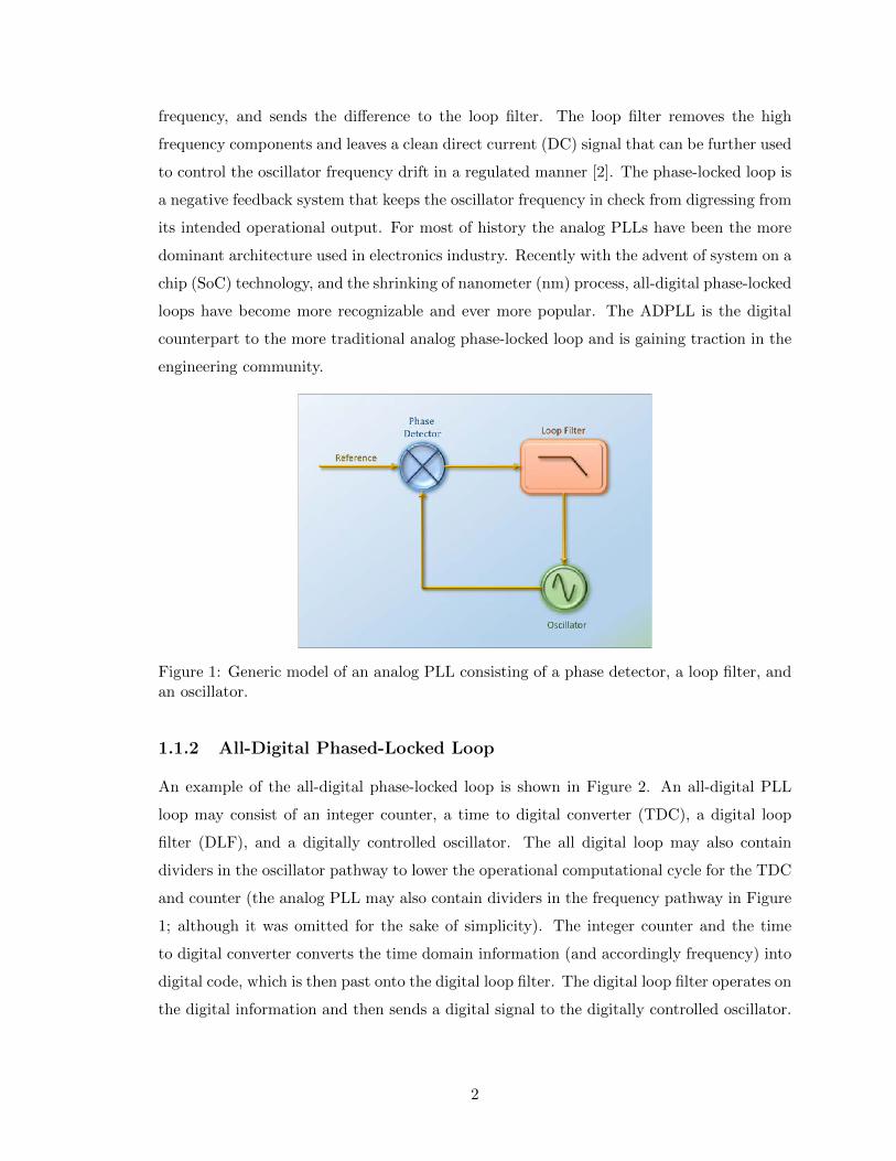
frequency, and sends the difference to the loop filter. The loop filter removes the high
frequency components and leaves a clean direct current (DC) signal that can be further used
to control the oscillator frequency drift in a regulated manner [2]. The phase-locked loop is
a negative feedback system that keeps the oscillator frequency in check from digressing from
its intended operational output. For most of history the analog PLLs have been the more
dominant architecture used in electronics industry. Recently with the advent of system on a
chip (SoC) technology, and the shrinking of nanometer (nm) process, all-digital phase-locked
loops have become more recognizable and ever more popular. The ADPLL is the digital
counterpart to the more traditional analog phase-locked loop and is gaining traction in the
engineering community.
Figure 1: Generic model of an analog PLL consisting of a phase detector, a loop filter, andan oscillator.
1.1.2 All-Digital Phased-Locked Loop
An example of the all-digital phase-locked loop is shown in Figure 2. An all-digital PLL
loop may consist of an integer counter, a time to digital converter (TDC), a digital loop
filter (DLF), and a digitally controlled oscillator. The all digital loop may also contain
dividers in the oscillator pathway to lower the operational computational cycle for the TDC
and counter (the analog PLL may also contain dividers in the frequency pathway in Figure
1; although it was omitted for the sake of simplicity). The integer counter and the time
to digital converter converts the time domain information (and accordingly frequency) into
digital code, which is then past onto the digital loop filter. The digital loop filter operates on
the digital information and then sends a digital signal to the digitally controlled oscillator.
2
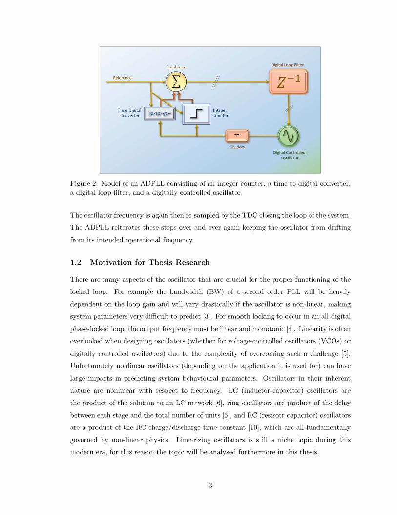
Figure 2: Model of an ADPLL consisting of an integer counter, a time to digital converter,a digital loop filter, and a digitally controlled oscillator.
The oscillator frequency is again then re-sampled by the TDC closing the loop of the system.
The ADPLL reiterates these steps over and over again keeping the oscillator from drifting
from its intended operational frequency.
1.2 Motivation for Thesis Research
There are many aspects of the oscillator that are crucial for the proper functioning of the
locked loop. For example the bandwidth (BW) of a second order PLL will be heavily
dependent on the loop gain and will vary drastically if the oscillator is non-linear, making
system parameters very difficult to predict [3]. For smooth locking to occur in an all-digital
phase-locked loop, the output frequency must be linear and monotonic [4]. Linearity is often
overlooked when designing oscillators (whether for voltage-controlled oscillators (VCOs) or
digitally controlled oscillators) due to the complexity of overcoming such a challenge [5].
Unfortunately nonlinear oscillators (depending on the application it is used for) can have
large impacts in predicting system behavioural parameters. Oscillators in their inherent
nature are nonlinear with respect to frequency. LC (inductor-capacitor) oscillators are
the product of the solution to an LC network [6], ring oscillators are product of the delay
between each stage and the total number of units [5], and RC (resisotr-capacitor) oscillators
are a product of the RC charge/discharge time constant [10], which are all fundamentally
governed by non-linear physics. Linearizing oscillators is still a niche topic during this
modern era, for this reason the topic will be analysed furthermore in this thesis.
3
1.3 Thesis Scope and Research Contribution
This thesis report focuses on designing a linearized digitally controlled oscillator (where
the output frequency is linearized with respect to the input control bits) for its use in an
all-digital phase-locked loop. More specifically, the research looks at designing LC digitally
controlled oscillators with high linearity using a different outlook and new perspective that
has not been previously explored (to best knowledge of the author). The paper analyzes LC
behaviour using statistics and a new concept known as linearity field maps. Furthermore
the technique proposed in this paper for an LC oscillator is robust and applicable for all LC
topologies, and over any technology. It can potentially be used for RC and ring oscillators
as well if the same methodology described in this paper (derived from first principles) is
used for their respective topologies. As with all architectures, there are limitations to
the technique proposed (keeping exceptional linearity over a vast and wide tuning range)
however when applicable, the method is very powerful, it is conceptually easy to understand
and implement, and produces extreme linearity. The thesis contributions are:
Introducing a new theoretical concept known as ’topographical’ linearity field maps
using regression (R2) as a tool.
Using R2 as a Figure of Merit for linearity.
Theoretical design of linear DCO using the linearity field maps.
Implementing theoretical linear DCO using a cascading pyramid scheme of equal banks
within equal banks to achieve the linearity.
1.4 Thesis Organization and Outline
The thesis includes an introduction that discusses the motivation of the thesis in Chapter
1. Chapter 2 discusses any prior literature regarding and related to the current work in
this thesis. Chapter 3 discourses on the theory of oscillation, more specifically on negative
gm oscillators. Chapter 4 introduces to the theorem used for the work of this thesis. The
theorem and its analysis is part of the contribution of this thesis. Chapter 5 deals with the
schematic design of the oscillator. Chapter 6 illustrates the drawn layouts of the oscillator
and its peripheral circuitry. Chapter 7 presents the simulated results of the oscillator.
Chapter 8 dilates on the test set-up used to assess the performance of the oscillator built
for this thesis. Chapter 9 presents the obtained measurements of the oscillator. Chapter
10 analyses and discusses the obtained results from Chapter 9. Chapter 11 talks about
4
any extra work that has been done during the course of this thesis. Chapter 12 addresses
any future work that is still left to do regarding the oscillator and topics related to it, and
Chapter 13 summarizes and concludes the thesis.
1.5 Conclusion
The introductory chapter discussed the reason and purpose of this thesis. The chapter
gave some background on oscillators and phase-locked loops, and then introduced what an
all-digital phase-locked loop was. The chapter also discussed the motivation for the thesis,
the thesis scope, research contribution, and briefly laid out the structure of the thesis.
5
CHAPTER 2: PRIOR LITERATURE
As stated previously in Chapter 1.2, linearizing oscillators, and more specifically linearizing
digitally controlled oscillators, is still a small metier in the electronics industry. It should
be noted that when talking about linearity, for a VCO it is generally referring to linearizing
the input voltage vs the output frequency of the oscillator while for a DCO it is referring to
linearizing the input digital control bits vs the output frequency. Finding recent research
on linearizing DCOs, or atleast recent publications that are accessible and undisclosed is
quite challenging; nevertheless there have been plenty of papers in the fast few decades
that have touched on the subject on how to linearize oscillators.
There have been solutions that proposed to linearize oscillators using closed loop methods
(akin to feedback loops of PLLs) [5], solutions that proposed to linearize oscillators
using open loop methods that directly interfere with and modify the core characteristic
of the oscillator [19], and solutions that use advanced digital signal processing (DSP)
and analog-to-digital converters (ADCs) to linearize the analog core characteristic of the
oscillator [11].
There have also been a few statistical approaches proposed to optimize linearity such as [7]
and [4] using least mean square (LMS) and standard deviation (σ) as the figure of merit.
The next few sections will look at a few papers on how they tried to linearize the frequency
response in an oscillator.
2.1 Least Mean Square Calibration Method
H. Venkatram et al. (2009) [12] proposes to linearize VCO non-linearity using an LMS
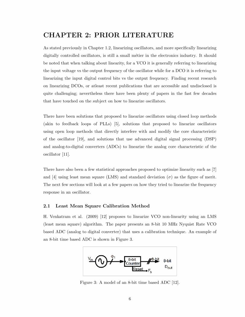
(least mean square) algorithm. The paper presents an 8-bit 10 MHz Nyquist Rate VCO
based ADC (analog to digital converter) that uses a calibration technique. An example of
an 8-bit time based ADC is shown in Figure 3.
Figure 3: A model of an 8-bit time based ADC [12].
6
The ADC uses an 8-bit coarse binary counter which is clocked by the VCO and is reset by
the sampling clock. It takes the tuning voltage to phase equation:
ΦV CO(n) = 2π
∫ (nTs+Ts)
nTs
(KV COvinsin(ωint) + fref )dt
and tries to model it by the equation:
ΦV CO(n) = αvin + βvin2 + γvin
3 + φe(n)
where α, β and γ are constraints that models the non-linearity of the VCO and φe(n) models
the quantization error from the VCO based ADC. For a given set of points (x1,y1), (x2,y2)
... (xn,yn), the best fit line using LMS can be derived from:
y1
y2
...
yn
=
x1
x2
...
xn
· [m]
where m is evaluated by:
mLMS =N∑i=i
xiyi /N∑i=1
xi2
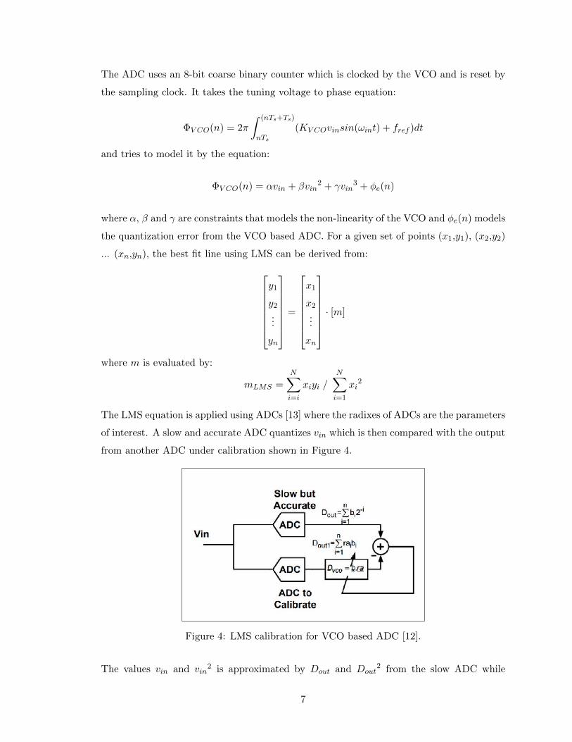
The LMS equation is applied using ADCs [13] where the radixes of ADCs are the parameters
of interest. A slow and accurate ADC quantizes vin which is then compared with the output
from another ADC under calibration shown in Figure 4.
Figure 4: LMS calibration for VCO based ADC [12].
The values vin and vin2 is approximated by Dout and Dout
2 from the slow ADC while
7
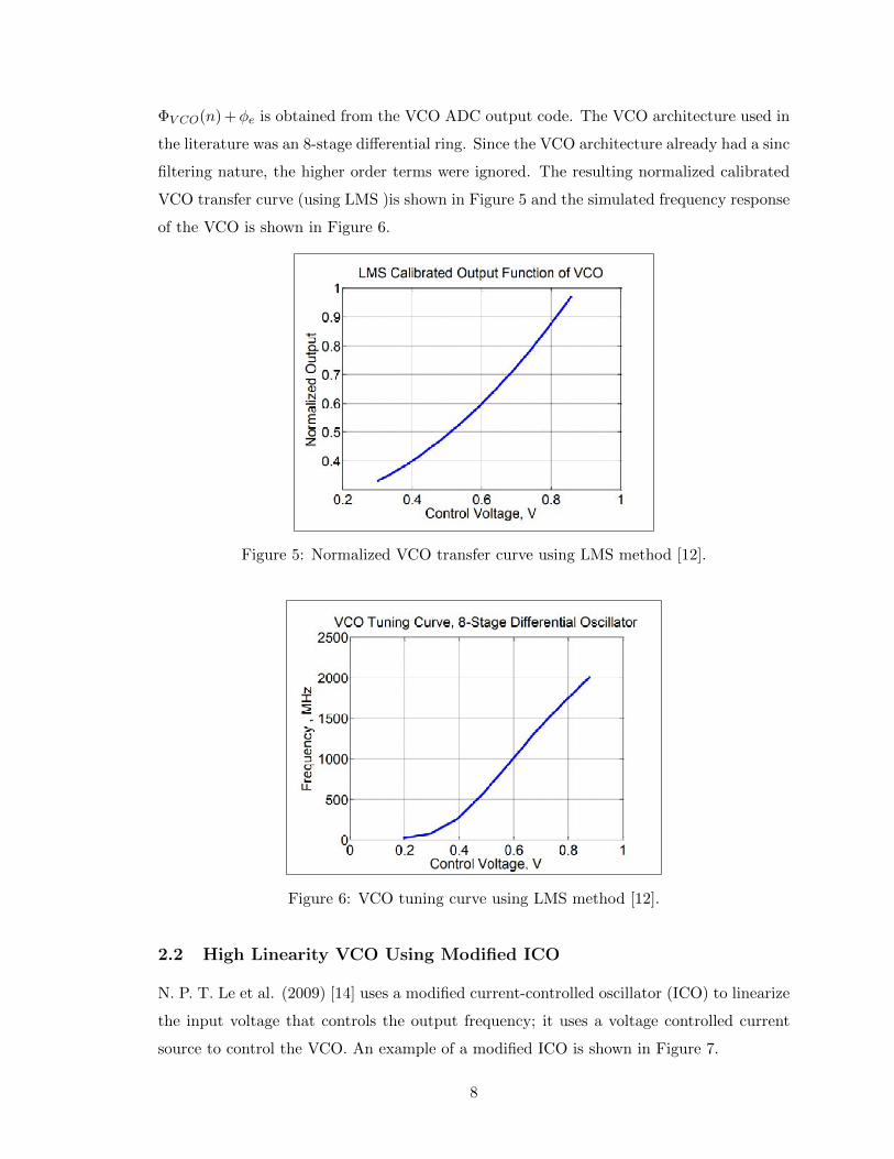
ΦV CO(n) +φe is obtained from the VCO ADC output code. The VCO architecture used in
the literature was an 8-stage differential ring. Since the VCO architecture already had a sinc
filtering nature, the higher order terms were ignored. The resulting normalized calibrated
VCO transfer curve (using LMS )is shown in Figure 5 and the simulated frequency response
of the VCO is shown in Figure 6.
Figure 5: Normalized VCO transfer curve using LMS method [12].
Figure 6: VCO tuning curve using LMS method [12].
2.2 High Linearity VCO Using Modified ICO
N. P. T. Le et al. (2009) [14] uses a modified current-controlled oscillator (ICO) to linearize
the input voltage that controls the output frequency; it uses a voltage controlled current
source to control the VCO. An example of a modified ICO is shown in Figure 7.
8
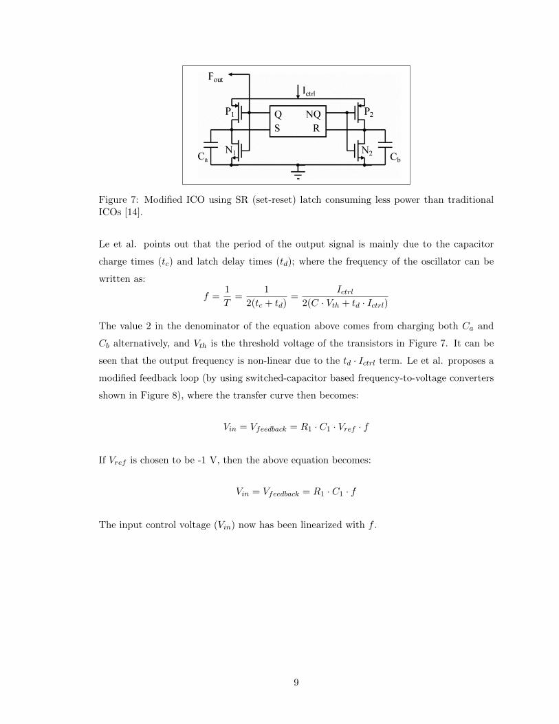
Figure 7: Modified ICO using SR (set-reset) latch consuming less power than traditionalICOs [14].
Le et al. points out that the period of the output signal is mainly due to the capacitor
charge times (tc) and latch delay times (td); where the frequency of the oscillator can be
written as:
f =1
T=
1
2(tc + td)=
Ictrl2(C · Vth + td · Ictrl)
The value 2 in the denominator of the equation above comes from charging both Ca and
Cb alternatively, and Vth is the threshold voltage of the transistors in Figure 7. It can be
seen that the output frequency is non-linear due to the td · Ictrl term. Le et al. proposes a
modified feedback loop (by using switched-capacitor based frequency-to-voltage converters
shown in Figure 8), where the transfer curve then becomes:
Vin = Vfeedback = R1 · C1 · Vref · f
If Vref is chosen to be -1 V, then the above equation becomes:
Vin = Vfeedback = R1 · C1 · f
The input control voltage (Vin) now has been linearized with f .
9
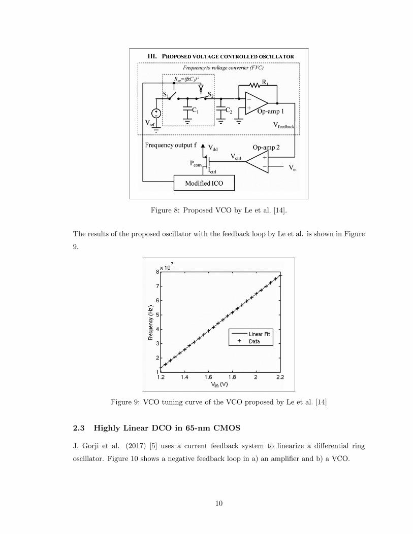
Figure 8: Proposed VCO by Le et al. [14].
The results of the proposed oscillator with the feedback loop by Le et al. is shown in Figure
9.
Figure 9: VCO tuning curve of the VCO proposed by Le et al. [14]
2.3 Highly Linear DCO in 65-nm CMOS
J. Gorji et al. (2017) [5] uses a current feedback system to linearize a differential ring
oscillator. Figure 10 shows a negative feedback loop in a) an amplifier and b) a VCO.
10
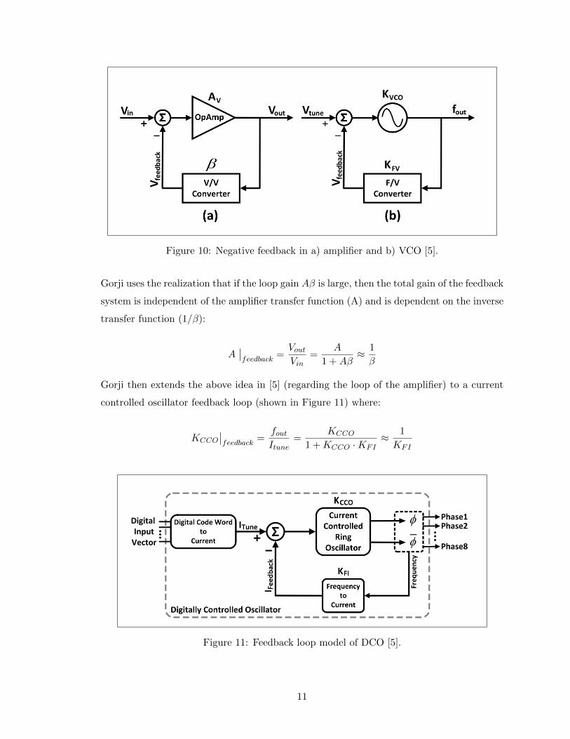
Figure 10: Negative feedback in a) amplifier and b) VCO [5].
Gorji uses the realization that if the loop gain Aβ is large, then the total gain of the feedback
system is independent of the amplifier transfer function (A) and is dependent on the inverse
transfer function (1/β):
A∣∣feedback
=VoutVin
=A
1 +Aβ≈ 1
β
Gorji then extends the above idea in [5] (regarding the loop of the amplifier) to a current
controlled oscillator feedback loop (shown in Figure 11) where:
KCCO
∣∣feedback
=foutItune
=KCCO
1 +KCCO ·KFI≈ 1
KFI
Figure 11: Feedback loop model of DCO [5].
11
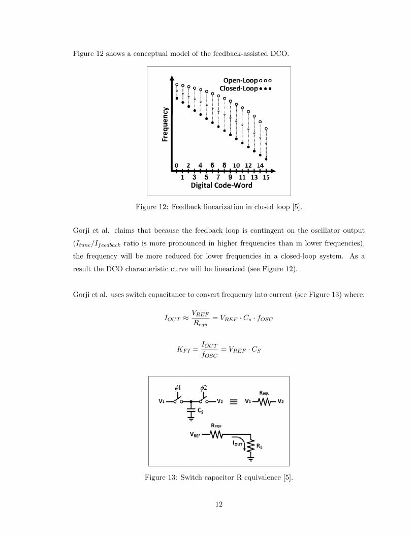
Figure 12 shows a conceptual model of the feedback-assisted DCO.
Figure 12: Feedback linearization in closed loop [5].
Gorji et al. claims that because the feedback loop is contingent on the oscillator output
(Itune/Ifeedback ratio is more pronounced in higher frequencies than in lower frequencies),
the frequency will be more reduced for lower frequencies in a closed-loop system. As a
result the DCO characteristic curve will be linearized (see Figure 12).
Gorji et al. uses switch capacitance to convert frequency into current (see Figure 13) where:
IOUT ≈VREFRequ
= VREF · Cs · fOSC
KFI =IOUTfOSC
= VREF · CS
Figure 13: Switch capacitor R equivalence [5].
12
It can be seen that substituting KFI into the feedback expression results in:
KCCO
∣∣feedback
≈ fOSCIOUT
The output frequency is now proportional to the oscillator gain. Therefore the oscillator
frequency has been linearized. The results of Gorji et al. DCO is shown in Figure 14.
Figure 14: Results of DCO in Gorji et al. [5].
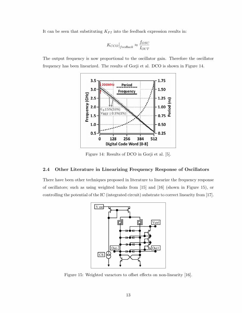
2.4 Other Literature in Linearizing Frequency Response of Oscillators
There have been other techniques proposed in literature to linearize the frequency response
of oscillators; such as using weighted banks from [15] and [16] (shown in Figure 15), or
controlling the potential of the IC (integrated circuit) substrate to correct linearity from [17].
Figure 15: Weighted varactors to offset effects on non-linearity [16].
13
Reference [7] used iterative LMS to optimize tuning bandwidth and linearity. See references
[18] - [32] for more literature on oscillator frequency linearity.
2.5 Conclusion
This chapter discussed prior literatures on how to linearize the frequency response of an
oscillator; including papers from H. Venkatram et al. which used an LMS calibration
method. N. P. T. Le et al. used a feedback loop method on a modified current-controlled
oscillator, and J. Gorji et al. used a feedback loop method on a differential ring oscillator
architecture to linearize the frequency response.
14
CHAPTER 3: OSCILLATION THEORY
This chapter will look at the theory behind the oscillation of an oscillator.
3.1 Oscillators and Barkhausen Criterion
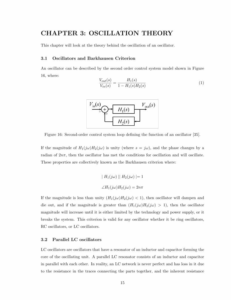
An oscillator can be described by the second order control system model shown in Figure
16, where:Vout(s)
Vin(s)=
H1(s)
1−H1(s)H2(s)(1)
Figure 16: Second-order control system loop defining the function of an oscillator [35].
If the magnitude of H1(jω)H2(jω) is unity (where s = jω), and the phase changes by a
radian of 2nπ, then the oscillator has met the conditions for oscillation and will oscillate.
These properties are collectively known as the Barkhausen criterion where:
| H1(jω) || H2(jω) |= 1
∠H1(jω)H2(jω) = 2nπ
If the magnitude is less than unity (H1(jω)H2(jω) < 1), then oscillator will dampen and
die out, and if the magnitude is greater than (H1(jω)H2(jω) > 1), then the oscillator
magnitude will increase until it is either limited by the technology and power supply, or it
breaks the system. This criterion is valid for any oscillator whether it be ring oscillators,
RC oscillators, or LC oscillators.
3.2 Parallel LC oscillators
LC oscillators are oscillators that have a resonator of an inductor and capacitor forming the
core of the oscillating unit. A parallel LC resonator consists of an inductor and capacitor
in parallel with each other. In reality, an LC network is never perfect and has loss in it due
to the resistance in the traces connecting the parts together, and the inherent resistance
15
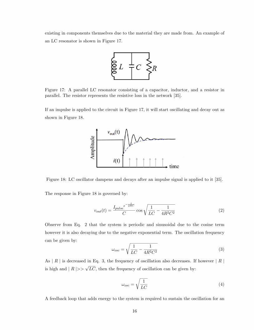
existing in components themselves due to the material they are made from. An example of
an LC resonator is shown in Figure 17.
Figure 17: A parallel LC resonator consisting of a capacitor, inductor, and a resistor inparallel. The resistor represents the resistive loss in the network [35].
If an impulse is applied to the circuit in Figure 17, it will start oscillating and decay out as
shown in Figure 18.
Figure 18: LC oscillator dampens and decays after an impulse signal is applied to it [35].
The response in Figure 18 is governed by:
vout(t) =Ipulse
e−t
2RC
Ccos
√1
LC− 1
4R2C2(2)
Observe from Eq. 2 that the system is periodic and sinusoidal due to the cosine term
however it is also decaying due to the negative exponential term. The oscillation frequency
can be given by:
ωosc =
√1
LC− 1
4R2C2(3)
As | R | is decreased in Eq. 3, the frequency of oscillation also decreases. If however | R |
is high and | R |>>√LC, then the frequency of oscillation can be given by:
ωosc =
√1
LC(4)
A feedback loop that adds energy to the system is required to sustain the oscillation for an
16
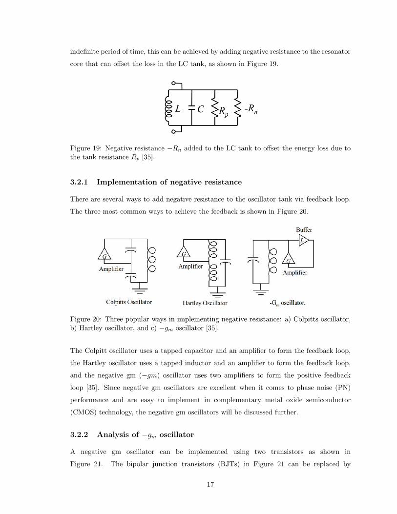
indefinite period of time, this can be achieved by adding negative resistance to the resonator
core that can offset the loss in the LC tank, as shown in Figure 19.
Figure 19: Negative resistance −Rn added to the LC tank to offset the energy loss due tothe tank resistance Rp [35].
3.2.1 Implementation of negative resistance
There are several ways to add negative resistance to the oscillator tank via feedback loop.
The three most common ways to achieve the feedback is shown in Figure 20.
Figure 20: Three popular ways in implementing negative resistance: a) Colpitts oscillator,b) Hartley oscillator, and c) −gm oscillator [35].
The Colpitt oscillator uses a tapped capacitor and an amplifier to form the feedback loop,
the Hartley oscillator uses a tapped inductor and an amplifier to form the feedback loop,
and the negative gm (−gm) oscillator uses two amplifiers to form the positive feedback
loop [35]. Since negative gm oscillators are excellent when it comes to phase noise (PN)
performance and are easy to implement in complementary metal oxide semiconductor
(CMOS) technology, the negative gm oscillators will be discussed further.
3.2.2 Analysis of −gm oscillator
A negative gm oscillator can be implemented using two transistors as shown in
Figure 21. The bipolar junction transistors (BJTs) in Figure 21 can be replaced by
17
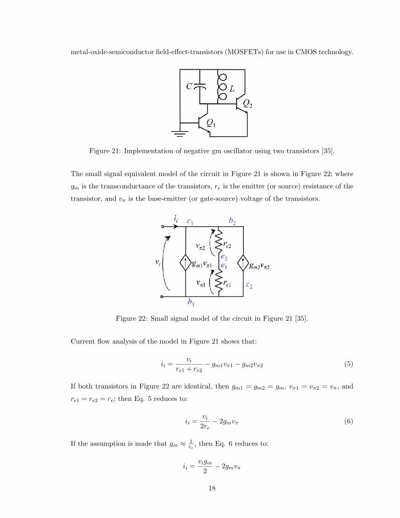
metal-oxide-semiconductor field-effect-transistors (MOSFETs) for use in CMOS technology.
Figure 21: Implementation of negative gm oscillator using two transistors [35].
The small signal equivalent model of the circuit in Figure 21 is shown in Figure 22; where
gm is the transconductance of the transistors, re is the emitter (or source) resistance of the
transistor, and vπ is the base-emitter (or gate-source) voltage of the transistors.
Figure 22: Small signal model of the circuit in Figure 21 [35].
Current flow analysis of the model in Figure 21 shows that:
ii =vi
re1 + re2− gm1vπ1 − gm2vπ2 (5)
If both transistors in Figure 22 are identical, then gm1 = gm2 = gm, vπ1 = vπ2 = vπ, and
re1 = re2 = re; then Eq. 5 reduces to:
ii =vi
2re− 2gmvπ (6)
If the assumption is made that gm ≈ 1re
, then Eq. 6 reduces to:
ii =vigm
2− 2gmvπ
18
ii =vigm
2− gmvi = vi
(gm2− gm
)= vi
(−gm
2
)(7)
Solving for the impedance (Zi) looking in where Zi = vi/ii, then:
Zi = −Rn =−2
gm(8)
For oscillation to occur, the total parallel resistance of the tank in Figure 19 must be
negative (or less than zero):
(1
Rp+
1
−Rn
)−1
=
(1
Rp+−gm
2
)−1
< 0 (9)
Then solving for gm with respect to Rp:(2− gmRp
2Rp
)−1
< 0⇒(
2− gmRp2Rp
)< 0⇒
(2
2Rp− gmRp
2Rp
)< 0
1
Rp<gm2
∴
gm >2
Rp(10)
Therefore the transconductance gm of the transistors must be greater than 2/Rp for
oscillation to occur if a negative gm configuration of the like shown in Figure 21 is used.
3.2.3 Biasing of −gm oscillator
As stated previously in Chapter 3.2.2, a negative gm oscillator can be administered using
two transistors; however for proper function to occur, the circuit requires DC biasing. A
few design examples of how the oscillator circuit can be implemented and biased is shown
in Figure 23.
19
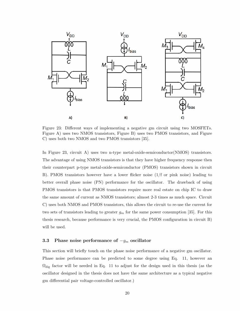
Figure 23: Different ways of implementing a negative gm circuit using two MOSFETs.Figure A) uses two NMOS transistors, Figure B) uses two PMOS transistors, and FigureC) uses both two NMOS and two PMOS transistors [35].
In Figure 23, circuit A) uses two n-type metal-oxide-semiconductor(NMOS) transistors.
The advantage of using NMOS transistors is that they have higher frequency response then
their counterpart p-type metal-oxide-semiconductor (PMOS) transistors shown in circuit
B). PMOS transistors however have a lower flicker noise (1/f or pink noise) leading to
better overall phase noise (PN) performance for the oscillator. The drawback of using
PMOS transistors is that PMOS transistors require more real estate on chip IC to draw
the same amount of current as NMOS transistors; almost 2-3 times as much space. Circuit
C) uses both NMOS and PMOS transistors, this allows the circuit to re-use the current for
two sets of transistors leading to greater gm for the same power consumption [35]. For this
thesis research, because performance is very crucial, the PMOS configuration in circuit B)
will be used.
3.3 Phase noise performance of −gm oscillator
This section will briefly touch on the phase noise performance of a negative gm oscillator.
Phase noise performance can be predicted to some degree using Eq. 11, however an
Ωdig factor will be needed in Eq. 11 to adjust for the design used in this thesis (as the
oscillator designed in the thesis does not have the same architecture as a typical negative
gm differential pair voltage-controlled oscillator.)
20
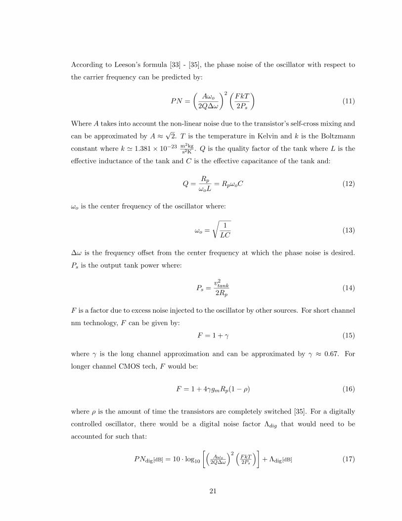
According to Leeson’s formula [33] - [35], the phase noise of the oscillator with respect to
the carrier frequency can be predicted by:
PN =
(Aωo
2Q∆ω
)2(FkT2Ps
)(11)
Where A takes into account the non-linear noise due to the transistor’s self-cross mixing and
can be approximated by A ≈√
2. T is the temperature in Kelvin and k is the Boltzmann
constant where k ' 1.381× 10⁻²³ m2kgs2K
. Q is the quality factor of the tank where L is the
effective inductance of the tank and C is the effective capacitance of the tank and:
Q =RpωoL
= RpωoC (12)
ωo is the center frequency of the oscillator where:
ωo =
√1
LC(13)
∆ω is the frequency offset from the center frequency at which the phase noise is desired.
Ps is the output tank power where:
Ps =v2tank
2Rp(14)
F is a factor due to excess noise injected to the oscillator by other sources. For short channel
nm technology, F can be given by:
F = 1 + γ (15)
where γ is the long channel approximation and can be approximated by γ ≈ 0.67. For
longer channel CMOS tech, F would be:
F = 1 + 4γgmRp(1− ρ) (16)
where ρ is the amount of time the transistors are completely switched [35]. For a digitally
controlled oscillator, there would be a digital noise factor Λdig that would need to be
accounted for such that:
PNdig[dB] = 10 · log10
[(Aωo
2Q∆ω
)2 (FkT2Ps
)]+ Λdig[dB] (17)
21
where:
Λdig[dB] =N∑i=1
Λi[dB] = Λ1[dB] + Λ2[dB] + Λ3[dB] + · · ·+ ΛN [dB] (18)
Λdig is a collective noise summation term of all ith elements. These noise elements can
arise due to factors such as the existence of digital quantization noise, noise susceptibility
of the technology, digital noise bleeding, and also because nbit switching cannot be simply
approximated using the narrow band frequency modulation (FM) assumption (rather the
signals being fed to the core are digital square waves).
3.4 Figure of Merit (FoM)
The Figure of Merit (FoM) is a metric that weighs in both the phase noise performance
of the oscillator and the power consumed by it and gives a production score based on the
formula:
FoM = PNfo − 20 · log10
(fo
foffset
)+ 10 · log10
(PDC1mW
)(19)
The above formula can be used to compare (and give insight) on the performance of the
DCO (that will be introduced later in the thesis); and see how it measures up to old
traditional VCOs.
Several offspring variations of the above formula have sprung for various architectures or
situations such as FoMT and FoML; however if caution is not taken when interpreting the
results, the FoM merit can be a deceptive caliber for performance.
Now that the theory of oscillation has been established, the next chapter will look at how
to linearize a digitally controlled oscillator using a new perspective.
3.5 Conclusion
This chapter discussed the theory of oscillators; more specifically negative gm oscillators.
It also discussed the oscillation start-up requirements, biasing of negative gm oscillators,
Leeson’s phase noise formula, and how to calculate the figure of merit for a weighted phase
noise and power performance.
22
CHAPTER 4: LINEAR THEOREM & DESIGN
This section will look at the theory on how to design a linearized digitally controlled
oscillator.
4.1 Inherent Nature of LC Oscillators
As previously stated in Chapter 3.2, the oscillation frequency of an LC oscillator can be
given by:
ωosc =
√1
LC
More specifically in the time domain, the frequency of oscillation is given by:
f =1
2π√LC
(20)
where L includes the combined total inductance (including parasitic) and C includes the
combined total capacitance of the oscillator topology. There are only two first degree
variables that can control the output frequency according to Eq. (20), namely the
inductance and the capacitance. On-chip inductors are usually difficult to implement on Si
technology. Inductors take up large amount of real estate and they are very lossy with poor
Q [40]; for these reasons on-chip inductors tend to be fixed. The more practical approach
is to make the capacitance variable for tuning the frequency. If the inductance is assumed
to be approximately the same over a certain frequency span, then Eq. (20) can be reduced
to:
f =1
2π√LC
=
(1
2π√L
)(1√C
)=
δ√C
(21)
where
δ =1
2π√L≈ constant (22)
Before touching on the fact that on chip variable capacitors are usually non-linear [16]
(whether they are varactors or CMOS based, or whether they are current controlled, voltage
controlled, or controlled by some other means), the inherent nature of the function f(C) =
δ/√C itself is non-linear to begin with. The non-linear behavior of the function δ/
√C must
be dealt with first before taking on the issue of non-linear capacitance. Some examples of
the shape of a δ/√C curve is shown in Figure 24.
23
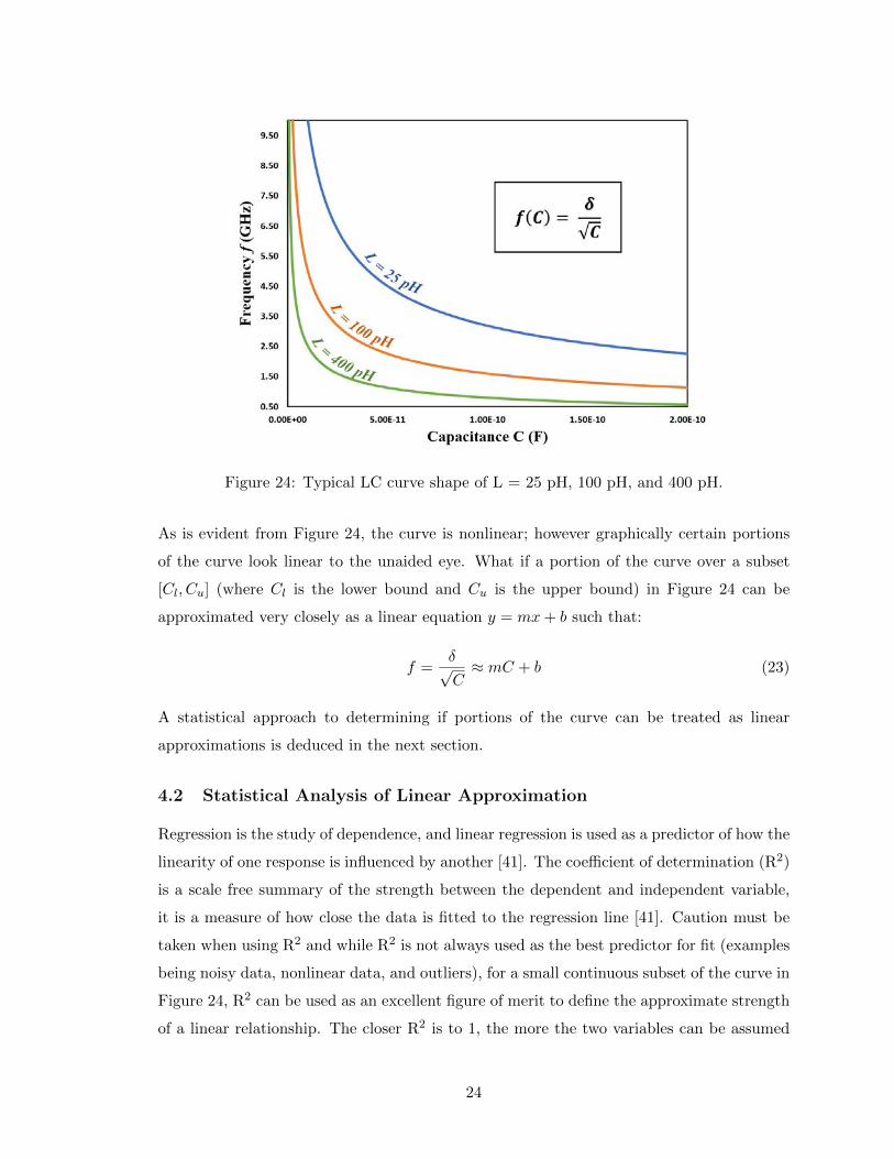
Figure 24: Typical LC curve shape of L = 25 pH, 100 pH, and 400 pH.
As is evident from Figure 24, the curve is nonlinear; however graphically certain portions
of the curve look linear to the unaided eye. What if a portion of the curve over a subset
[Cl, Cu] (where Cl is the lower bound and Cu is the upper bound) in Figure 24 can be
approximated very closely as a linear equation y = mx+ b such that:
f =δ√C≈ mC + b (23)
A statistical approach to determining if portions of the curve can be treated as linear
approximations is deduced in the next section.
4.2 Statistical Analysis of Linear Approximation
Regression is the study of dependence, and linear regression is used as a predictor of how the
linearity of one response is influenced by another [41]. The coefficient of determination (R2)
is a scale free summary of the strength between the dependent and independent variable,
it is a measure of how close the data is fitted to the regression line [41]. Caution must be
taken when using R2 and while R2 is not always used as the best predictor for fit (examples
being noisy data, nonlinear data, and outliers), for a small continuous subset of the curve in
Figure 24, R2 can be used as an excellent figure of merit to define the approximate strength
of a linear relationship. The closer R2 is to 1, the more the two variables can be assumed
24
to be linearly correlated with each other in a linear fit. Linear regression for n-points is
given by:
y = mx+ b (24)
where x is the independent variable and y is the dependent variable. The slope m and
intercept b is defined as:
m =
n
(n∑i=1
xiyi
)−(
n∑i=1
xi
)(n∑i=1
yi
)n
(n∑i=1
x2i
)−(
n∑i=1
xi
)2 (25)
b =
(n∑i=1
yi
)(n∑i=1
x2i
)−(
n∑i=1
xi
)(n∑i=1
xiyi
)n
(n∑i=1
x2i
)−(
n∑i=1
xi
)2 (26)
To fit a linear regression to a subset [Cl, Cu] of the continuous curve in Figure 24, an integral
transformation using first principles must be made to Eq. (25) and Eq. (26) such that:
m = limn→∞
n∆C
(δ
n∑i=1
√Ci∆C
)−(
n∑i=1
Ci∆C
)(δ
n∑i=1
∆C√C
)n∆C
(n∑i=1
C2i ∆C
)−(
n∑i=1
Ci∆C
)2 (27)
where:
C∆ = Cu − Cl (28)
∆C =
∣∣∣∣ C∆
n− 1
∣∣∣∣ (29)
Realizing that:
limn→∞
∣∣∣∣ C∆
n− 1
∣∣∣∣ = limn→∞
∣∣∣∣C∆
n
∣∣∣∣then lim
n→∞
n∑i=1
γi(n)∆C =
Cu∫Cl
γ(C)dC
25
Then Eq. (27) reduces to:
m =
δ(C∆
)( Cu∫Cl
√CdC
)− δ
( Cu∫Cl
CdC
)( Cu∫Cl
dC√C
)
(C∆
)( Cu∫Cl
C2dC
)−
( Cu∫Cl
CdC
)2(30)
Solving for Eq. (27) gives:
m =
13π√L
(Cu − Cl)(C3/2u − C3/2
l )− 12π√L
(C2u − C2
l )(√Cu −
√Cl)
13(Cu − Cl)(C3
u − C3l )− 1
4(C2u − C2
l )2(31)
Likewise, Eq. (26) reduces to:
b =
δ
[( Cu∫Cl
dC√C
)( Cu∫Cl
C2dC
)−
( Cu∫Cl
CdC
)( Cu∫Cl
√CdC
)]
(C∆
)( Cu∫Cl
C2dC
)−
( Cu∫Cl
CdC
)2(32)
b =
13π√L
(√Cu −
√Cl)(C
3u − C3
l )− 16π√L
(C2u − C2
l )(C3/2u − C3/2
l )
13(Cu − Cl)(C3
u − C3l )− 1
4(C2u − C2
l )2(33)
In a similar fashion to regression, the correlation coefficient value is defined by:
r =
n
(n∑i=1
xiyi
)−(
n∑i=1
xi
)(n∑i=1
yi
)√[
nn∑i=1
x2 −(
n∑i=1
x
)2][n
n∑i=1
y2 −(
n∑i=1
y
)2] (34)
26

Taking the integral transformation of r and solving for it gives:
r =
δ
( Cu∫Cl
√CdC
)δ( Cu∫Cl
CdC
)( Cu∫Cl
dC√C
)C∆√√√√√√√√√√√√
( Cu∫Cl
C2dC
)−
( Cu∫Cl
CdC
)2
C∆
δ2
( Cu∫Cl
dC
C
)−
δ2
( Cu∫Cl
1√C
)2
C∆
(35)
r =
13π√L
(√C3u −
√C3l )(Cu − Cl)− 1
2π√L
(C2u − C2
l )(√Cu −
√Cl)√
[13(C3
u − C3l )(Cu − Cl)− 1
4(C2u − C2
l )2]β(36)
where:
β =
[ ∣∣∣∣ ln(Cu)− ln(Cl)
4π2L
∣∣∣∣ (Cu − Cl)− (√Cu −
√Cl)
2
π2L
](37)
The coefficient of determination is simply then:
R2 (coefficient of determintation) = r2 (38)
4.3 Using R2 to Choose Region of Linearity
Using Eq. (36) to Eq. (38), field maps can be generated to determine regions of linearity
based on the inductance, capacitance, and frequency requirements.
4.3.1 Topographical linearity field-maps
In Eq. (20) the dependent variable is frequency. Since frequency is usually the variable
of interest, one can fix the frequency steps and then determine the required capacitance.
Then one can use Eq. (36) to Eq. (38) to plot R2 curves using numerical computational
software such as excel or MATLAB based on the required frequency span. Such
linearity field maps for different center frequencies or different values of inductance for a
frequency span of 1 GHz and 4 GHz are shown in Figure 25 to Figure 26 respectively.
A 3D rendering of the 1GHz span field map using MATLAB and excel is shown in Figure 27.
27
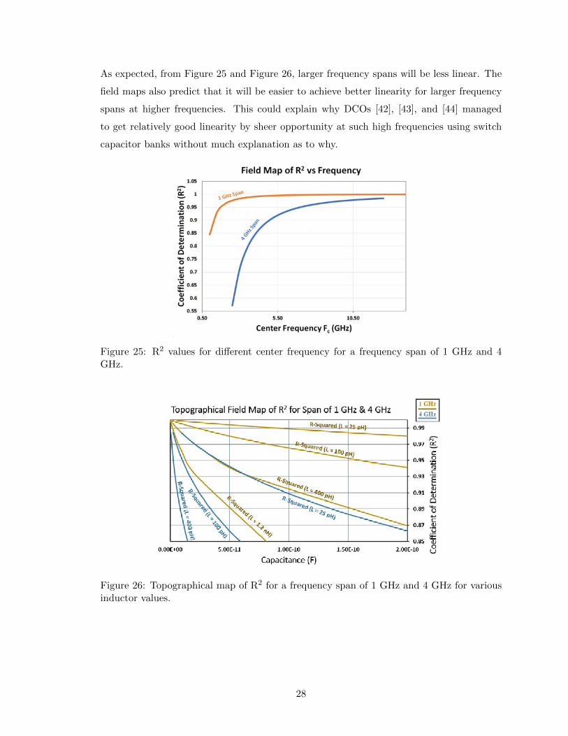
As expected, from Figure 25 and Figure 26, larger frequency spans will be less linear. The
field maps also predict that it will be easier to achieve better linearity for larger frequency
spans at higher frequencies. This could explain why DCOs [42], [43], and [44] managed
to get relatively good linearity by sheer opportunity at such high frequencies using switch
capacitor banks without much explanation as to why.
Figure 25: R2 values for different center frequency for a frequency span of 1 GHz and 4GHz.
Figure 26: Topographical map of R2 for a frequency span of 1 GHz and 4 GHz for variousinductor values.
28
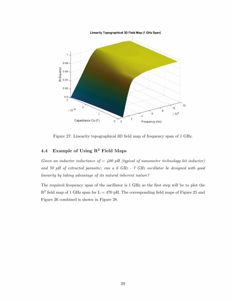
Figure 27: Linearity topographical 3D field map of frequency span of 1 GHz.
4.4 Example of Using R2 Field Maps
Given an inductor inductance of v 400 pH (typical of nanometer technology kit inductor)
and 70 pH of extracted parasitic, can a 6 GHz - 7 GHz oscillator be designed with good
linearity by taking advantage of its natural inherent nature?
The required frequency span of the oscillator is 1 GHz so the first step will be to plot the
R2 field map of 1 GHz span for L = 470 pH. The corresponding field maps of Figure 25 and
Figure 26 combined is shown in Figure 28.
29
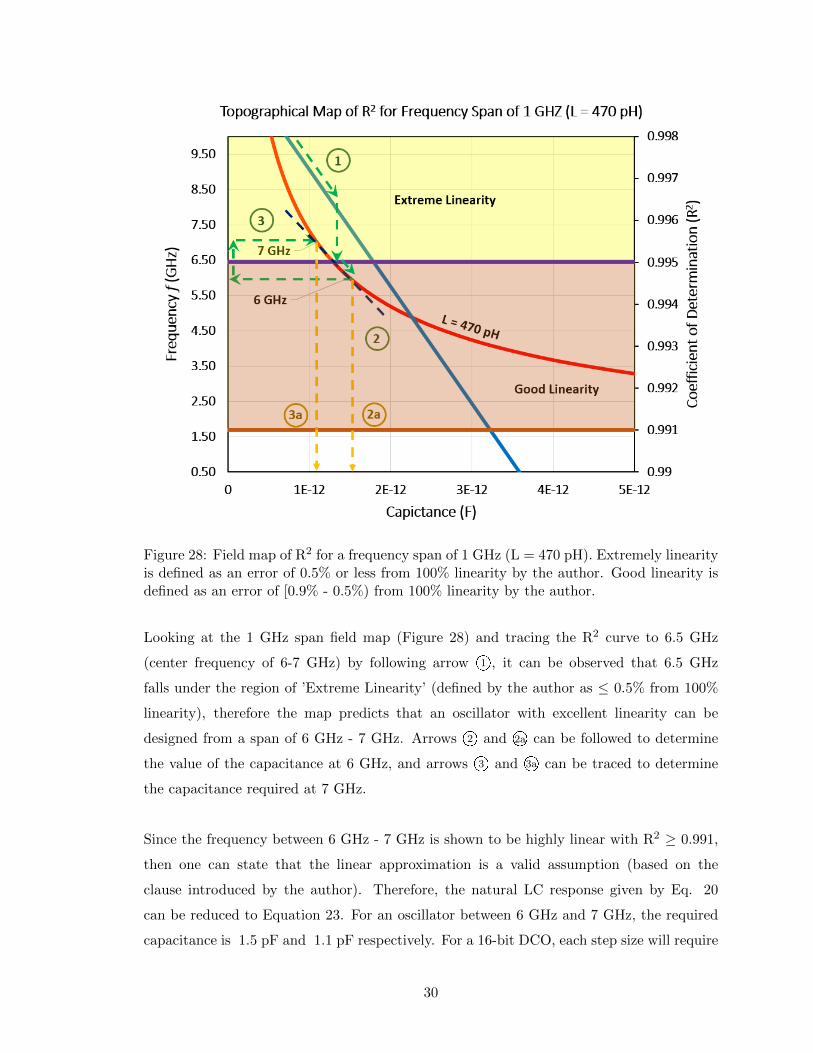
Figure 28: Field map of R2 for a frequency span of 1 GHz (L = 470 pH). Extremely linearityis defined as an error of 0.5% or less from 100% linearity by the author. Good linearity isdefined as an error of [0.9% - 0.5%) from 100% linearity by the author.
Looking at the 1 GHz span field map (Figure 28) and tracing the R2 curve to 6.5 GHz
(center frequency of 6-7 GHz) by following arrow 1O, it can be observed that 6.5 GHz
falls under the region of ’Extreme Linearity’ (defined by the author as ≤ 0.5% from 100%
linearity), therefore the map predicts that an oscillator with excellent linearity can be
designed from a span of 6 GHz - 7 GHz. Arrows 2O and 2aO can be followed to determine
the value of the capacitance at 6 GHz, and arrows 3O and 3aO can be traced to determine
the capacitance required at 7 GHz.
Since the frequency between 6 GHz - 7 GHz is shown to be highly linear with R2 ≥ 0.991,
then one can state that the linear approximation is a valid assumption (based on the
clause introduced by the author). Therefore, the natural LC response given by Eq. 20
can be reduced to Equation 23. For an oscillator between 6 GHz and 7 GHz, the required
capacitance is 1.5 pF and 1.1 pF respectively. For a 16-bit DCO, each step size will require
30
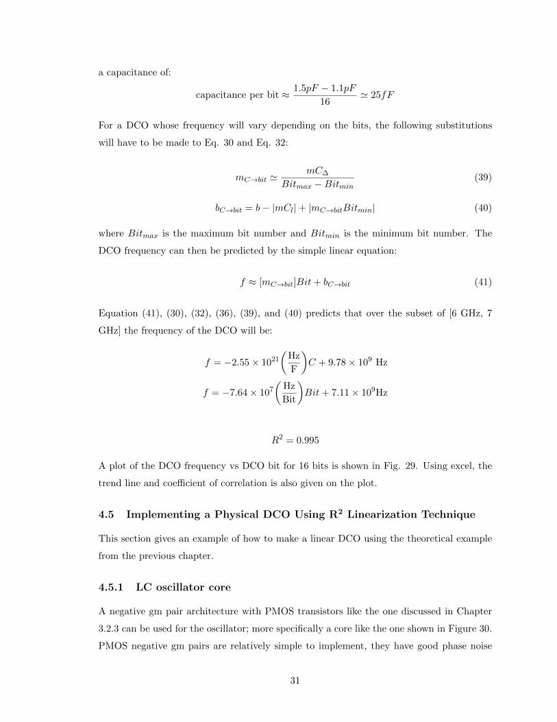
a capacitance of:
capacitance per bit ≈ 1.5pF − 1.1pF
16' 25fF
For a DCO whose frequency will vary depending on the bits, the following substitutions
will have to be made to Eq. 30 and Eq. 32:
mC→bit 'mC∆
Bitmax −Bitmin(39)
bC→bit = b− |mCl|+ |mC→bitBitmin| (40)
where Bitmax is the maximum bit number and Bitmin is the minimum bit number. The
DCO frequency can then be predicted by the simple linear equation:
f ≈ [mC→bit]Bit+ bC→bit (41)
Equation (41), (30), (32), (36), (39), and (40) predicts that over the subset of [6 GHz, 7
GHz] the frequency of the DCO will be:
f = −2.55× 10²¹
(Hz
F
)C + 9.78× 10⁹ Hz
f = −7.64× 10⁷
(Hz
Bit
)Bit+ 7.11× 10⁹Hz
R2 = 0.995
A plot of the DCO frequency vs DCO bit for 16 bits is shown in Fig. 29. Using excel, the
trend line and coefficient of correlation is also given on the plot.
4.5 Implementing a Physical DCO Using R2 Linearization Technique
This section gives an example of how to make a linear DCO using the theoretical example
from the previous chapter.
4.5.1 LC oscillator core
A negative gm pair architecture with PMOS transistors like the one discussed in Chapter
3.2.3 can be used for the oscillator; more specifically a core like the one shown in Figure 30.
PMOS negative gm pairs are relatively simple to implement, they have good phase noise
31
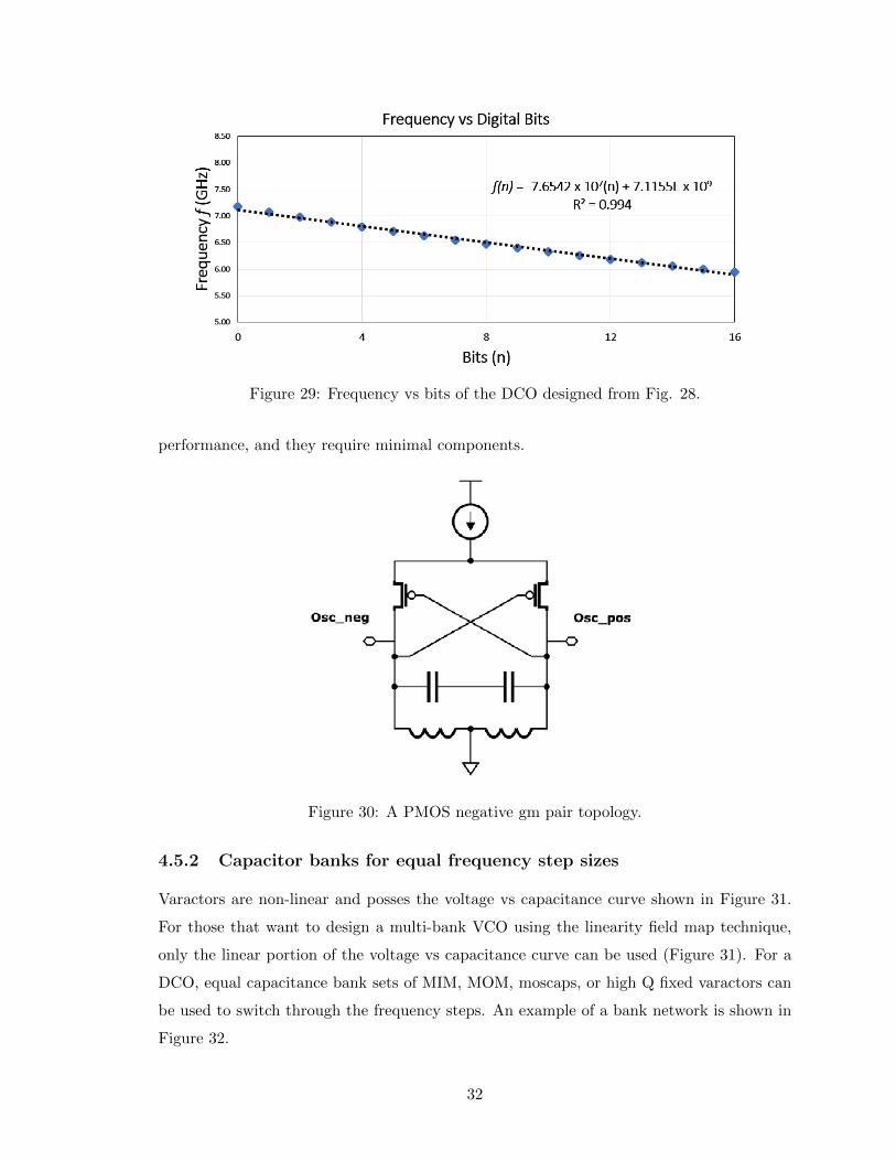
Figure 29: Frequency vs bits of the DCO designed from Fig. 28.
performance, and they require minimal components.
Figure 30: A PMOS negative gm pair topology.
4.5.2 Capacitor banks for equal frequency step sizes
Varactors are non-linear and posses the voltage vs capacitance curve shown in Figure 31.
For those that want to design a multi-bank VCO using the linearity field map technique,
only the linear portion of the voltage vs capacitance curve can be used (Figure 31). For a
DCO, equal capacitance bank sets of MIM, MOM, moscaps, or high Q fixed varactors can
be used to switch through the frequency steps. An example of a bank network is shown in
Figure 32.
32
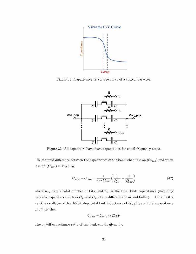
Figure 31: Capacitance vs voltage curve of a typical varactor.
Figure 32: All capacitors have fixed capacitance for equal frequency steps.
The required difference between the capacitance of the bank when it is on (Cmax) and when
it is off (Cmin) is given by:
Cmax − Cmin =1
4π2Lbtno
(1
f2min
− 1
f2max
)(42)
where btno is the total number of bits, and CT is the total tank capacitance (including
parasitic capacitance such as Cgd and Cgs of the differential pair and buffer). For a 6 GHz
- 7 GHz oscillator with a 16-bit step, total tank inductance of 470 pH, and total capacitance
of 0.7 pF then:
Cmax − Cmin ' 25fF
The on/off capacitance ratio of the bank can be given by:
33
CmaxCmin
=
(1− CT f2
min4π2L
1− CT f2max4π2L
)(f2max
f2min
)(43)
For a total tank capacitance of 0.7 pF, 470 pH inductance, and 16 bit, then the on/off
bank ratio for a 6 GHz - 7 GHz oscillator is 2. Each bit nk bit in Figure 32 is digitally
controlled by a digital circuit either pulled up to VDD high (digital bit 1) or pulled down
to ground (GND) low (digital bit 0).
The overall design of the bank (including the transistor switch) will be non-linear and the
oscillator voltage swing will be large at the two nodes of the bank, however for simplicity the
entire bank can be treated as a black box where the time average on/off total capacitance
of the bank (including parasitic from the switch transistor) is of importance for the design
of the DCO. The same non-linearity and non-linear elements will exist from bank to bank
(if the bank designs are identical) giving a linear step-through (from bank to bank switch)
of frequency.
4.5.3 Banks on source side of negative gm transistors
The smallest capacitor available (and hence the smallest capacitance available) can be
limited by the technology used to implement the oscillator. If two current mirrors are used
to sink or source the oscillator (one at each source node of each negative gm transistor),
then banks (like those in Figure 32) can also be implemented on the source side of the
negative gm transistors. The resulting effect would be that the capacitance of the banks
on the source side would translate to the drain side of the transistors (and hence adding
capacitance to the overall tank capacitance) by a factor given by [36] - [39]:
Ceq = −Cbank[
g2m
g2m + 4(C2
bankω2osc)
](44)
Looking at Eq. 44, the shrink factor is less than unity (< 1). This would allow finer
frequency tuning control of the oscillator since the capacitance on the source is effectively
shrunk when seen from the drain side.
Note that the transformation of Eq. 44 is that of a small signal transformation, and the
DCO operates in large signal, however it can still be useful for designing the DCO (as it
can be used for approximation).
34
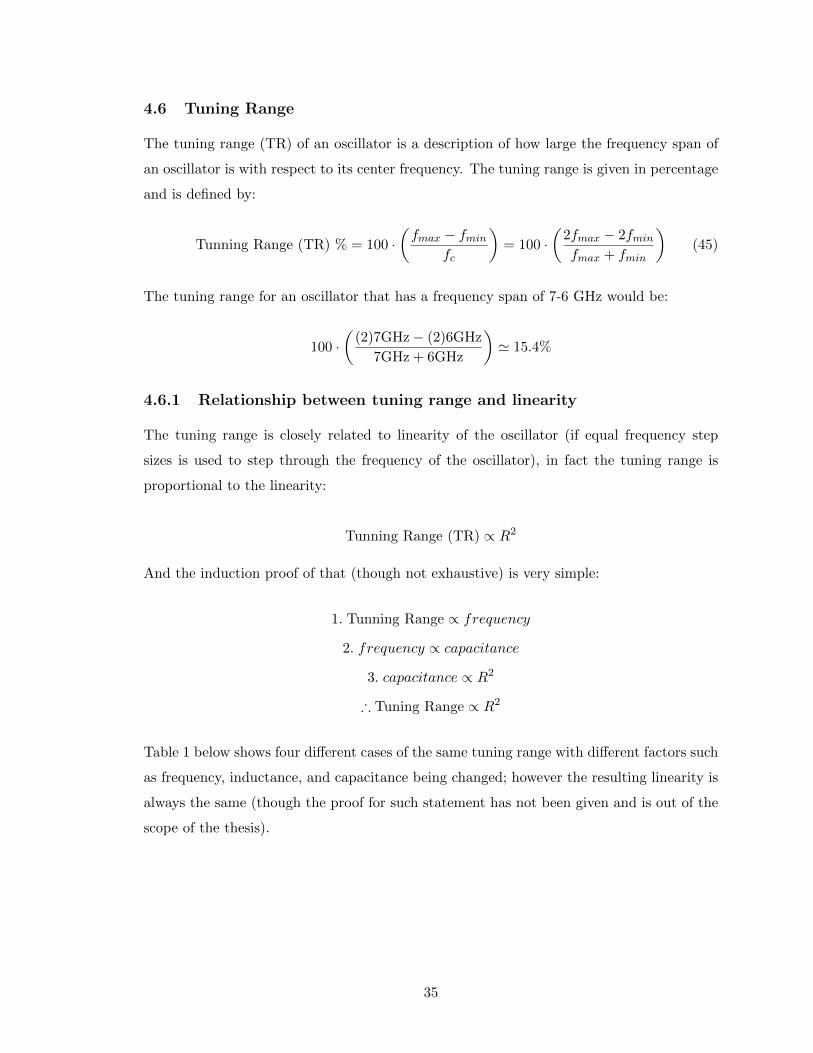
4.6 Tuning Range
The tuning range (TR) of an oscillator is a description of how large the frequency span of
an oscillator is with respect to its center frequency. The tuning range is given in percentage
and is defined by:
Tunning Range (TR) % = 100 ·(fmax − fmin
fc
)= 100 ·
(2fmax − 2fminfmax + fmin
)(45)
The tuning range for an oscillator that has a frequency span of 7-6 GHz would be:
100 ·(
(2)7GHz− (2)6GHz
7GHz + 6GHz
)' 15.4%
4.6.1 Relationship between tuning range and linearity
The tuning range is closely related to linearity of the oscillator (if equal frequency step
sizes is used to step through the frequency of the oscillator), in fact the tuning range is
proportional to the linearity:
Tunning Range (TR) ∝ R2
And the induction proof of that (though not exhaustive) is very simple:
1. Tunning Range ∝ frequency
2. frequency ∝ capacitance
3. capacitance ∝ R2
∴ Tuning Range ∝ R2
Table 1 below shows four different cases of the same tuning range with different factors such
as frequency, inductance, and capacitance being changed; however the resulting linearity is
always the same (though the proof for such statement has not been given and is out of the
scope of the thesis).
35
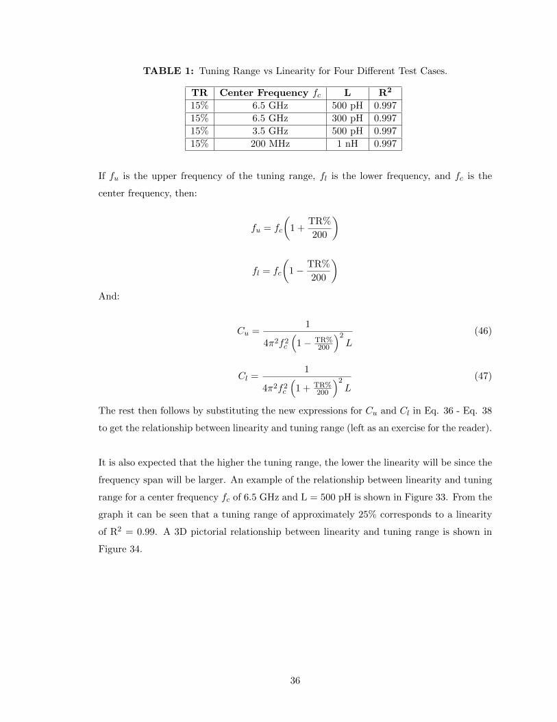
TABLE 1: Tuning Range vs Linearity for Four Different Test Cases.
TR Center Frequency fc L R2
15% 6.5 GHz 500 pH 0.997
15% 6.5 GHz 300 pH 0.997
15% 3.5 GHz 500 pH 0.997
15% 200 MHz 1 nH 0.997
If fu is the upper frequency of the tuning range, fl is the lower frequency, and fc is the
center frequency, then:
fu = fc
(1 +
TR%
200
)
fl = fc
(1− TR%
200
)And:
Cu =1
4π2f2c
(1− TR%
200
)2L
(46)
Cl =1
4π2f2c
(1 + TR%
200
)2L
(47)
The rest then follows by substituting the new expressions for Cu and Cl in Eq. 36 - Eq. 38
to get the relationship between linearity and tuning range (left as an exercise for the reader).
It is also expected that the higher the tuning range, the lower the linearity will be since the
frequency span will be larger. An example of the relationship between linearity and tuning
range for a center frequency fc of 6.5 GHz and L = 500 pH is shown in Figure 33. From the
graph it can be seen that a tuning range of approximately 25% corresponds to a linearity
of R2 = 0.99. A 3D pictorial relationship between linearity and tuning range is shown in
Figure 34.
36
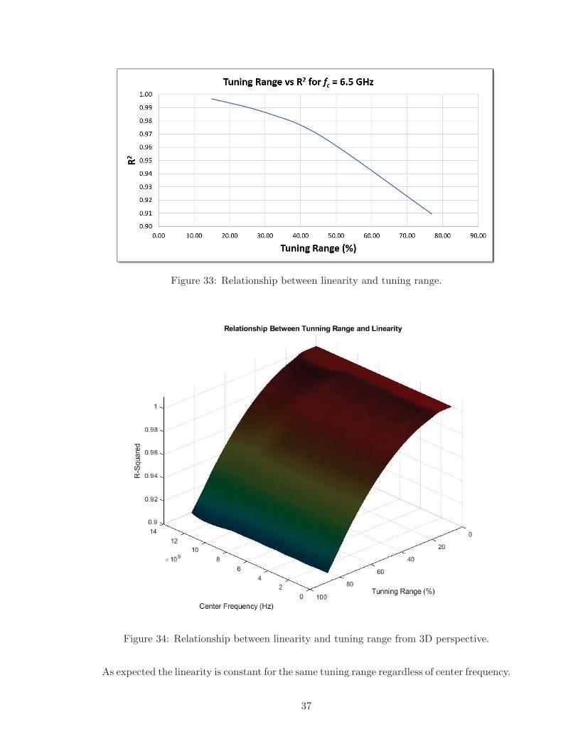
Figure 33: Relationship between linearity and tuning range.
Figure 34: Relationship between linearity and tuning range from 3D perspective.
As expected the linearity is constant for the same tuning range regardless of center frequency.
37
4.7 Conclusion
This Chapter discussed the theory behind linearizing a digitally controlled oscillator. It
discussed the inherent nature of LC oscillators, it provided a statistical method for linear
approximation, it introduced a new concept know as topographical linearity field maps, it
gave an example on how to use the linearity field maps, and then designed a theoretical
DCO using the linearity field maps. The Chapter also discussed about tuning range and
the relationship between linearity and tunning range.
38
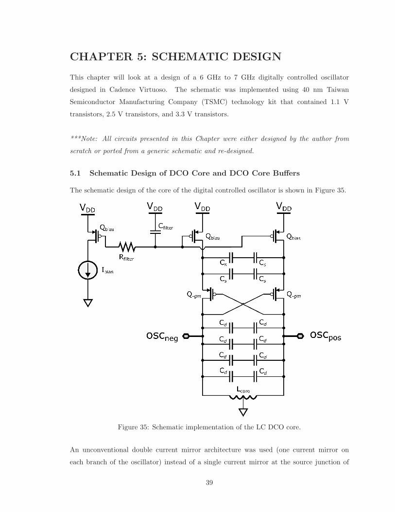
CHAPTER 5: SCHEMATIC DESIGN
This chapter will look at a design of a 6 GHz to 7 GHz digitally controlled oscillator
designed in Cadence Virtuoso. The schematic was implemented using 40 nm Taiwan
Semiconductor Manufacturing Company (TSMC) technology kit that contained 1.1 V
transistors, 2.5 V transistors, and 3.3 V transistors.
***Note: All circuits presented in this Chapter were either designed by the author from
scratch or ported from a generic schematic and re-designed.
5.1 Schematic Design of DCO Core and DCO Core Buffers
The schematic design of the core of the digital controlled oscillator is shown in Figure 35.
Figure 35: Schematic implementation of the LC DCO core.
An unconventional double current mirror architecture was used (one current mirror on
each branch of the oscillator) instead of a single current mirror at the source junction of
39
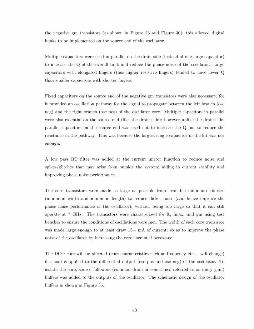
the negative gm transistors (as shown in Figure 23 and Figure 30); this allowed digital
banks to be implemented on the source end of the oscillator.
Multiple capacitors were used in parallel on the drain side (instead of one large capacitor)
to increase the Q of the overall tank and reduce the phase noise of the oscillator. Large
capacitors with elongated fingers (thus higher resistive fingers) tended to have lower Q
than smaller capacitors with shorter fingers.
Fixed capacitors on the source end of the negative gm transistors were also necessary, for
it provided an oscillation pathway for the signal to propagate between the left branch (osc
neg) and the right branch (osc pos) of the oscillator core. Multiple capacitors in parallel
were also essential on the source end (like the drain side); however unlike the drain side,
parallel capacitors on the source end was used not to increase the Q but to reduce the
reactance in the pathway. This was because the largest single capacitor in the kit was not
enough.
A low pass RC filter was added at the current mirror junction to reduce noise and
spikes/glitches that may arise from outside the system; aiding in current stability and
improving phase noise performance.
The core transistors were made as large as possible from available minimum kit size
(minimum width and minimum length) to reduce flicker noise (and hence improve the
phase noise performance of the oscillator); without being too large so that it can still
operate at 7 GHz. The transistors were characterized for ft, fmax, and gm using test
benches to ensure the conditions of oscillations were met. The width of each core transistor
was made large enough to at least draw 15+ mA of current; so as to improve the phase
noise of the oscillator by increasing the core current if necessary.
The DCO core will be affected (core characteristics such as frequency etc... will change)
if a load is applied to the differential output (osc pos and osc neg) of the oscillator. To
isolate the core, source followers (common drain or sometimes referred to as unity gain)
buffers was added to the outputs of the oscillator. The schematic design of the oscillator
buffers in shown in Figure 36.
40
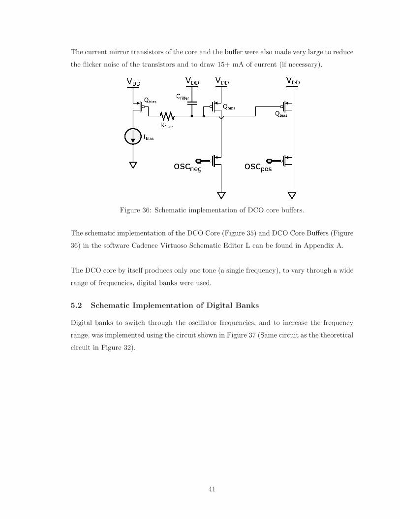
The current mirror transistors of the core and the buffer were also made very large to reduce
the flicker noise of the transistors and to draw 15+ mA of current (if necessary).
Figure 36: Schematic implementation of DCO core buffers.
The schematic implementation of the DCO Core (Figure 35) and DCO Core Buffers (Figure
36) in the software Cadence Virtuoso Schematic Editor L can be found in Appendix A.
The DCO core by itself produces only one tone (a single frequency), to vary through a wide
range of frequencies, digital banks were used.
5.2 Schematic Implementation of Digital Banks
Digital banks to switch through the oscillator frequencies, and to increase the frequency
range, was implemented using the circuit shown in Figure 37 (Same circuit as the theoretical
circuit in Figure 32).
41
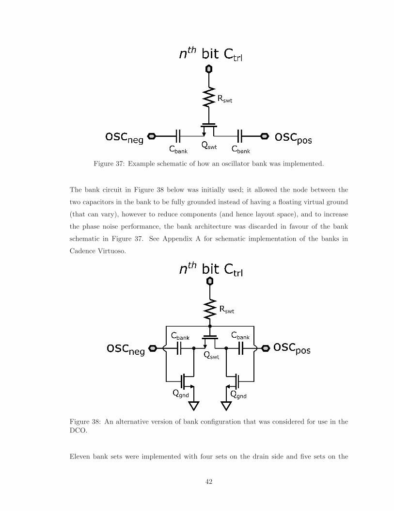
Figure 37: Example schematic of how an oscillator bank was implemented.
The bank circuit in Figure 38 below was initially used; it allowed the node between the
two capacitors in the bank to be fully grounded instead of having a floating virtual ground
(that can vary), however to reduce components (and hence layout space), and to increase
the phase noise performance, the bank architecture was discarded in favour of the bank
schematic in Figure 37. See Appendix A for schematic implementation of the banks in
Cadence Virtuoso.
Figure 38: An alternative version of bank configuration that was considered for use in theDCO.
Eleven bank sets were implemented with four sets on the drain side and five sets on the
42
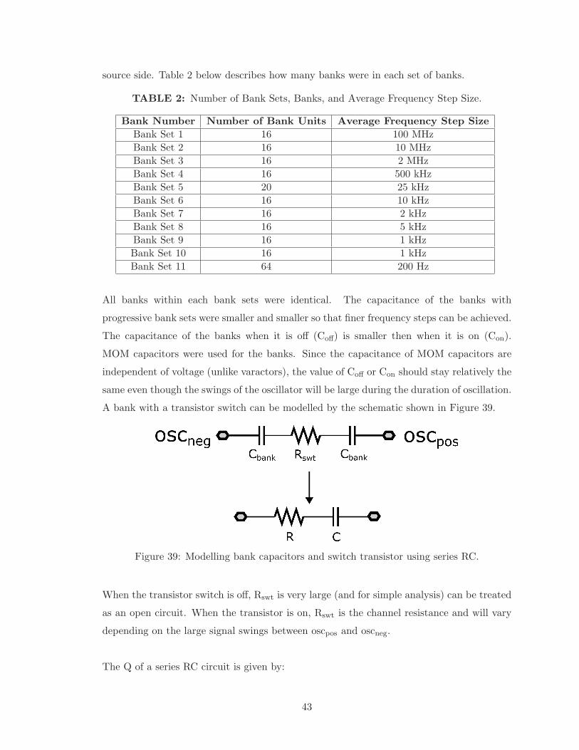
source side. Table 2 below describes how many banks were in each set of banks.
TABLE 2: Number of Bank Sets, Banks, and Average Frequency Step Size.
Bank Number Number of Bank Units Average Frequency Step Size
Bank Set 1 16 100 MHz
Bank Set 2 16 10 MHz
Bank Set 3 16 2 MHz
Bank Set 4 16 500 kHz
Bank Set 5 20 25 kHz
Bank Set 6 16 10 kHz
Bank Set 7 16 2 kHz
Bank Set 8 16 5 kHz
Bank Set 9 16 1 kHz
Bank Set 10 16 1 kHz
Bank Set 11 64 200 Hz
All banks within each bank sets were identical. The capacitance of the banks with
progressive bank sets were smaller and smaller so that finer frequency steps can be achieved.
The capacitance of the banks when it is off (Coff) is smaller then when it is on (Con).
MOM capacitors were used for the banks. Since the capacitance of MOM capacitors are
independent of voltage (unlike varactors), the value of Coff or Con should stay relatively the
same even though the swings of the oscillator will be large during the duration of oscillation.
A bank with a transistor switch can be modelled by the schematic shown in Figure 39.
Figure 39: Modelling bank capacitors and switch transistor using series RC.
When the transistor switch is off, Rswt is very large (and for simple analysis) can be treated
as an open circuit. When the transistor is on, Rswt is the channel resistance and will vary
depending on the large signal swings between oscpos and oscneg.
The Q of a series RC circuit is given by:
43
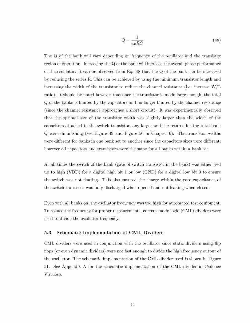
Q =1
ω0RC(48)
The Q of the bank will vary depending on frequency of the oscillator and the transistor
region of operation. Increasing the Q of the bank will increase the overall phase performance
of the oscillator. It can be observed from Eq. 48 that the Q of the bank can be increased
by reducing the series R. This can be achieved by using the minimum transistor length and
increasing the width of the transistor to reduce the channel resistance (i.e. increase W/L
ratio). It should be noted however that once the transistor is made large enough, the total
Q of the banks is limited by the capacitors and no longer limited by the channel resistance
(since the channel resistance approaches a short circuit). It was experimentally observed
that the optimal size of the transistor width was slightly larger than the width of the
capacitors attached to the switch transistor, any larger and the returns for the total bank
Q were diminishing (see Figure 49 and Figure 50 in Chapter 6). The transistor widths
were different for banks in one bank set to another since the capacitors sizes were different;
however all capacitors and transistors were the same for all banks within a bank set.
At all times the switch of the bank (gate of switch transistor in the bank) was either tied
up to high (VDD) for a digital high bit 1 or low (GND) for a digital low bit 0 to ensure
the switch was not floating. This also ensured the charge within the gate capacitance of
the switch transistor was fully discharged when opened and not leaking when closed.
Even with all banks on, the oscillator frequency was too high for automated test equipment.
To reduce the frequency for proper measurements, current mode logic (CML) dividers were
used to divide the oscillator frequency.
5.3 Schematic Implementation of CML Dividers
CML dividers were used in conjunction with the oscillator since static dividers using flip
flops (or even dynamic dividers) were not fast enough to divide the high frequency output of
the oscillator. The schematic implementation of the CML divider used is shown in Figure
51. See Appendix A for the schematic implementation of the CML divider in Cadence
Virtuoso.
44
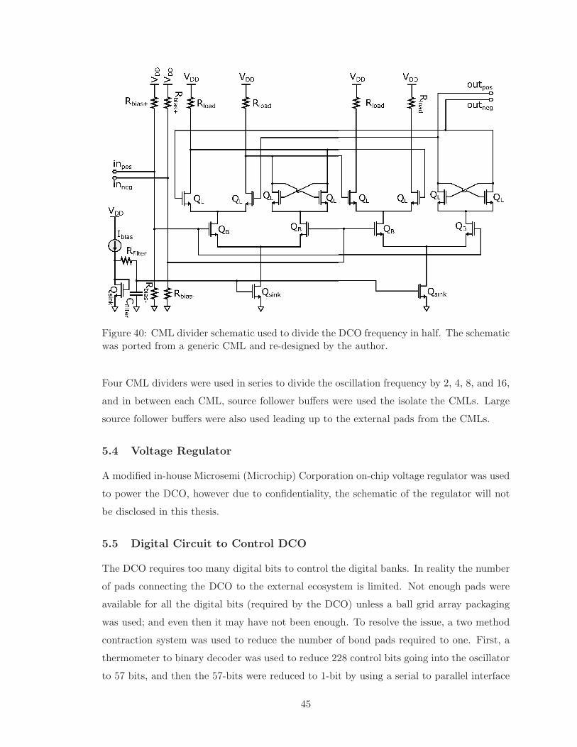
Figure 40: CML divider schematic used to divide the DCO frequency in half. The schematicwas ported from a generic CML and re-designed by the author.
Four CML dividers were used in series to divide the oscillation frequency by 2, 4, 8, and 16,
and in between each CML, source follower buffers were used the isolate the CMLs. Large
source follower buffers were also used leading up to the external pads from the CMLs.
5.4 Voltage Regulator
A modified in-house Microsemi (Microchip) Corporation on-chip voltage regulator was used
to power the DCO, however due to confidentiality, the schematic of the regulator will not
be disclosed in this thesis.
5.5 Digital Circuit to Control DCO
The DCO requires too many digital bits to control the digital banks. In reality the number
of pads connecting the DCO to the external ecosystem is limited. Not enough pads were
available for all the digital bits (required by the DCO) unless a ball grid array packaging
was used; and even then it may have not been enough. To resolve the issue, a two method
contraction system was used to reduce the number of bond pads required to one. First, a
thermometer to binary decoder was used to reduce 228 control bits going into the oscillator
to 57 bits, and then the 57-bits were reduced to 1-bit by using a serial to parallel interface
45
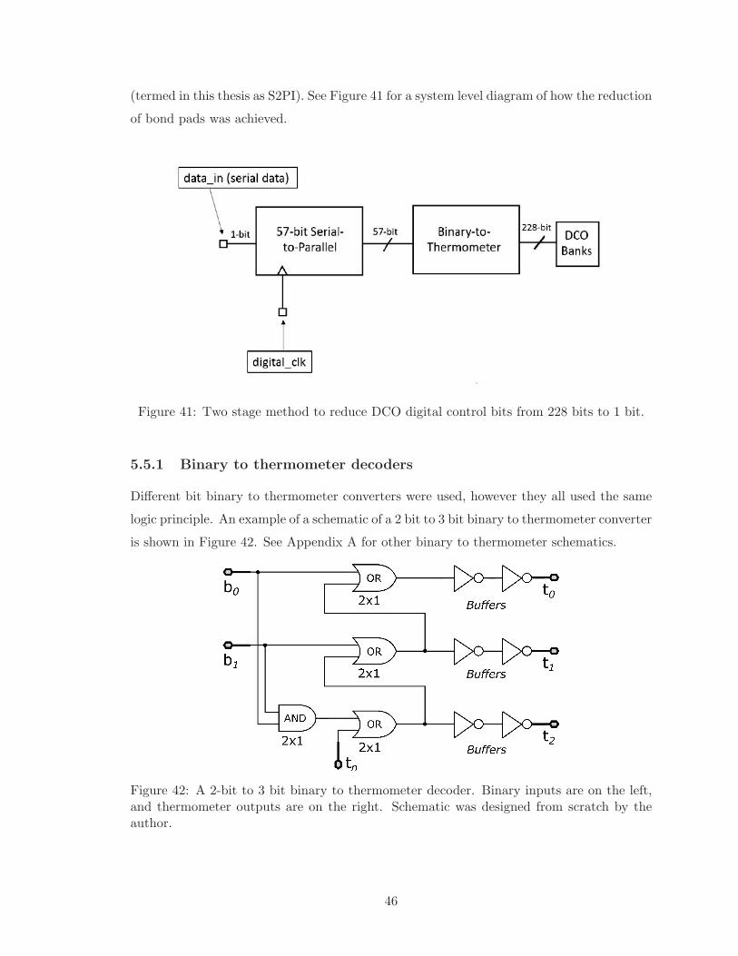
(termed in this thesis as S2PI). See Figure 41 for a system level diagram of how the reduction
of bond pads was achieved.
Figure 41: Two stage method to reduce DCO digital control bits from 228 bits to 1 bit.
5.5.1 Binary to thermometer decoders
Different bit binary to thermometer converters were used, however they all used the same
logic principle. An example of a schematic of a 2 bit to 3 bit binary to thermometer converter
is shown in Figure 42. See Appendix A for other binary to thermometer schematics.
Figure 42: A 2-bit to 3 bit binary to thermometer decoder. Binary inputs are on the left,and thermometer outputs are on the right. Schematic was designed from scratch by theauthor.
46
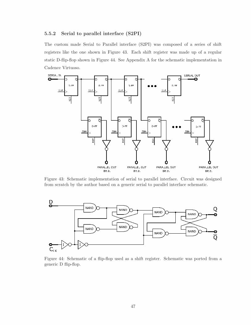
5.5.2 Serial to parallel interface (S2PI)
The custom made Serial to Parallel interface (S2PI) was composed of a series of shift
registers like the one shown in Figure 43. Each shift register was made up of a regular
static D-flip-flop shown in Figure 44. See Appendix A for the schematic implementation in
Cadence Virtuoso.
Figure 43: Schematic implementation of serial to parallel interface. Circuit was designedfrom scratch by the author based on a generic serial to parallel interface schematic.
Figure 44: Schematic of a flip-flop used as a shift register. Schematic was ported from ageneric D flip-flop.
47
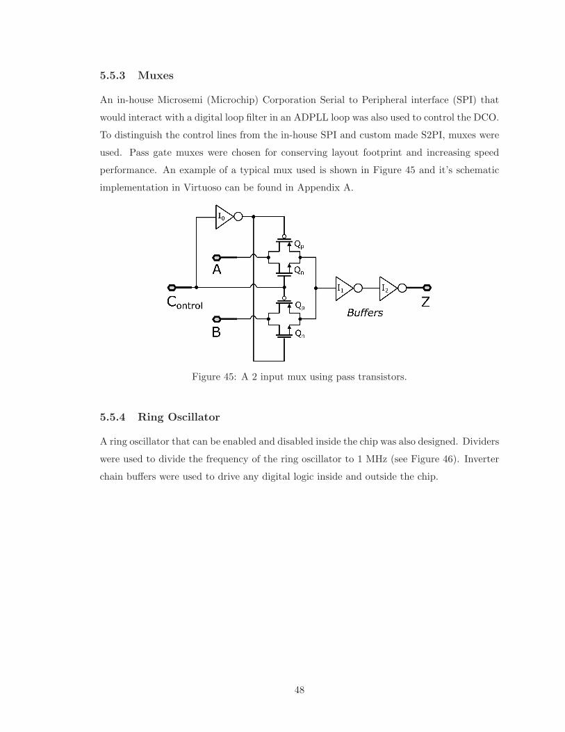
5.5.3 Muxes
An in-house Microsemi (Microchip) Corporation Serial to Peripheral interface (SPI) that
would interact with a digital loop filter in an ADPLL loop was also used to control the DCO.
To distinguish the control lines from the in-house SPI and custom made S2PI, muxes were
used. Pass gate muxes were chosen for conserving layout footprint and increasing speed
performance. An example of a typical mux used is shown in Figure 45 and it’s schematic
implementation in Virtuoso can be found in Appendix A.
Figure 45: A 2 input mux using pass transistors.
5.5.4 Ring Oscillator
A ring oscillator that can be enabled and disabled inside the chip was also designed. Dividers
were used to divide the frequency of the ring oscillator to 1 MHz (see Figure 46). Inverter
chain buffers were used to drive any digital logic inside and outside the chip.
48
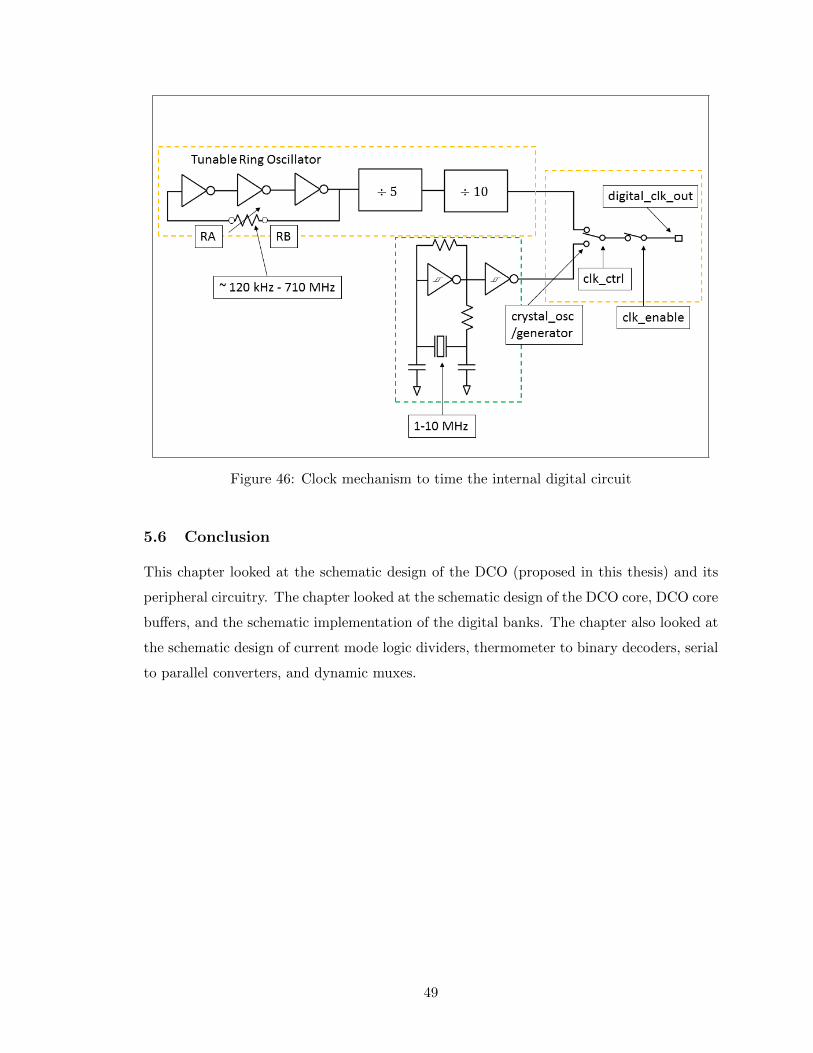
Figure 46: Clock mechanism to time the internal digital circuit
5.6 Conclusion
This chapter looked at the schematic design of the DCO (proposed in this thesis) and its
peripheral circuitry. The chapter looked at the schematic design of the DCO core, DCO core
buffers, and the schematic implementation of the digital banks. The chapter also looked at
the schematic design of current mode logic dividers, thermometer to binary decoders, serial
to parallel converters, and dynamic muxes.
49
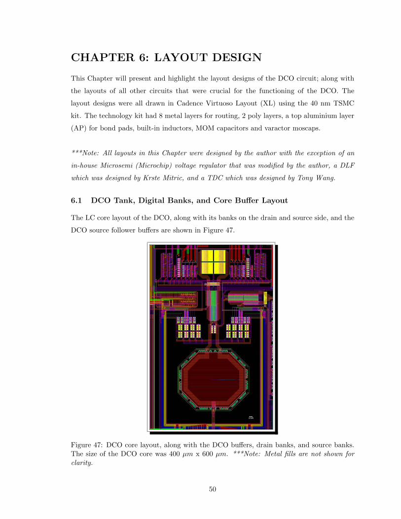
CHAPTER 6: LAYOUT DESIGN
This Chapter will present and highlight the layout designs of the DCO circuit; along with
the layouts of all other circuits that were crucial for the functioning of the DCO. The
layout designs were all drawn in Cadence Virtuoso Layout (XL) using the 40 nm TSMC
kit. The technology kit had 8 metal layers for routing, 2 poly layers, a top aluminium layer
(AP) for bond pads, built-in inductors, MOM capacitors and varactor moscaps.
***Note: All layouts in this Chapter were designed by the author with the exception of an
in-house Microsemi (Microchip) voltage regulator that was modified by the author, a DLF
which was designed by Krste Mitric, and a TDC which was designed by Tony Wang.
6.1 DCO Tank, Digital Banks, and Core Buffer Layout
The LC core layout of the DCO, along with its banks on the drain and source side, and the
DCO source follower buffers are shown in Figure 47.
Figure 47: DCO core layout, along with the DCO buffers, drain banks, and source banks.The size of the DCO core was 400 µm x 600 µm. ***Note: Metal fills are not shown forclarity.
50
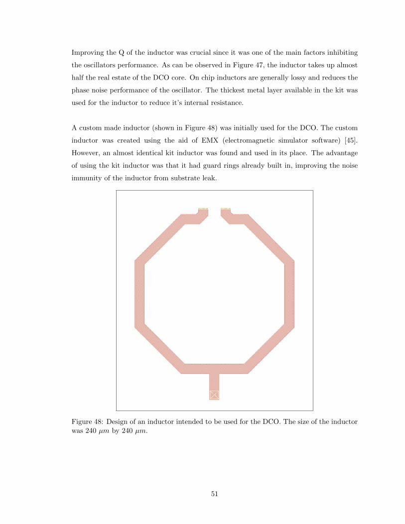
Improving the Q of the inductor was crucial since it was one of the main factors inhibiting
the oscillators performance. As can be observed in Figure 47, the inductor takes up almost
half the real estate of the DCO core. On chip inductors are generally lossy and reduces the
phase noise performance of the oscillator. The thickest metal layer available in the kit was
used for the inductor to reduce it’s internal resistance.
A custom made inductor (shown in Figure 48) was initially used for the DCO. The custom
inductor was created using the aid of EMX (electromagnetic simulator software) [45].
However, an almost identical kit inductor was found and used in its place. The advantage
of using the kit inductor was that it had guard rings already built in, improving the noise
immunity of the inductor from substrate leak.
Figure 48: Design of an inductor intended to be used for the DCO. The size of the inductorwas 240 µm by 240 µm.
51

6.1.1 Layout of Digital Banks
A couple examples of the layout design of digital banks is shown in Figure 49 and Figure
50. Figure 49 shows the layout of a bank from Bank set 3 and Figure 50 shows the layout
of a Bank set 2. The two different bank layouts from Figure 49 and Figure 50 will have
different quality factors Q depending on the capacitor values, the W/L ratio of the switch
transistor, and the RC parasitic of the metal traces connecting the components of the bank
together. Note that all the bank layouts are the same for all banks within a bank set but
the bank layouts are different from bank set to bank set.
Figure 49: An example layout of a digital bank. The size of the bank was 8.3 µm x 4.1 µm.
Figure 50: An example layout of a digital bank using multiple capacitors in parallel. Sizeof the bank was 10 µm x 11 µm.
52
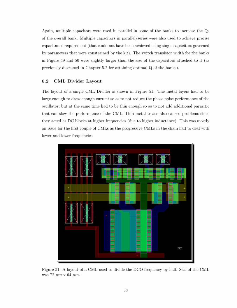
Again, multiple capacitors were used in parallel in some of the banks to increase the Qs
of the overall bank. Multiple capacitors in parallel/series were also used to achieve precise
capacitance requirement (that could not have been achieved using single capacitors governed
by parameters that were constrained by the kit). The switch transistor width for the banks
in Figure 49 and 50 were slightly larger than the size of the capacitors attached to it (as
previously discussed in Chapter 5.2 for attaining optimal Q of the banks).
6.2 CML Divider Layout
The layout of a single CML Divider is shown in Figure 51. The metal layers had to be
large enough to draw enough current so as to not reduce the phase noise performance of the
oscillator; but at the same time had to be thin enough so as to not add additional parasitic
that can slow the performance of the CML. Thin metal traces also caused problems since
they acted as DC blocks at higher frequencies (due to higher inductance). This was mostly
an issue for the first couple of CMLs as the progressive CMLs in the chain had to deal with
lower and lower frequencies.
Figure 51: A layout of a CML used to divide the DCO frequency by half. Size of the CMLwas 72 µm x 64 µm.
53
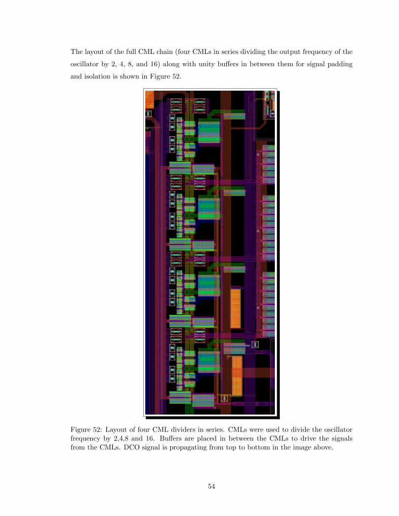
The layout of the full CML chain (four CMLs in series dividing the output frequency of the
oscillator by 2, 4, 8, and 16) along with unity buffers in between them for signal padding
and isolation is shown in Figure 52.
Figure 52: Layout of four CML dividers in series. CMLs were used to divide the oscillatorfrequency by 2,4,8 and 16. Buffers are placed in between the CMLs to drive the signalsfrom the CMLs. DCO signal is propagating from top to bottom in the image above.
54
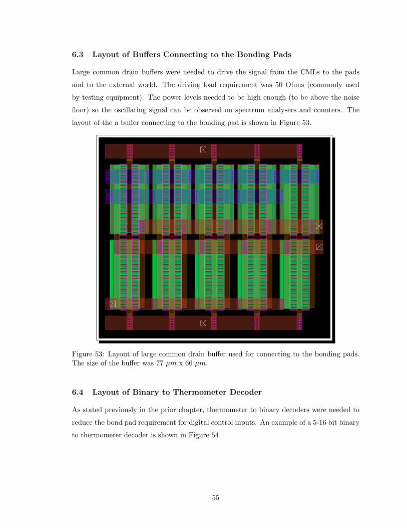
6.3 Layout of Buffers Connecting to the Bonding Pads
Large common drain buffers were needed to drive the signal from the CMLs to the pads
and to the external world. The driving load requirement was 50 Ohms (commonly used
by testing equipment). The power levels needed to be high enough (to be above the noise
floor) so the oscillating signal can be observed on spectrum analysers and counters. The
layout of the a buffer connecting to the bonding pad is shown in Figure 53.
Figure 53: Layout of large common drain buffer used for connecting to the bonding pads.The size of the buffer was 77 µm x 66 µm.
6.4 Layout of Binary to Thermometer Decoder
As stated previously in the prior chapter, thermometer to binary decoders were needed to
reduce the bond pad requirement for digital control inputs. An example of a 5-16 bit binary
to thermometer decoder is shown in Figure 54.
55
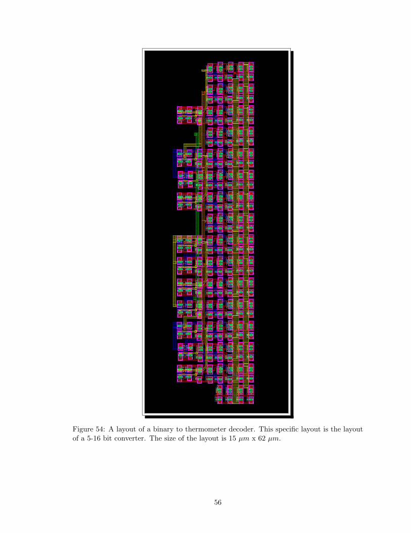
Figure 54: A layout of a binary to thermometer decoder. This specific layout is the layoutof a 5-16 bit converter. The size of the layout is 15 µm x 62 µm.
56
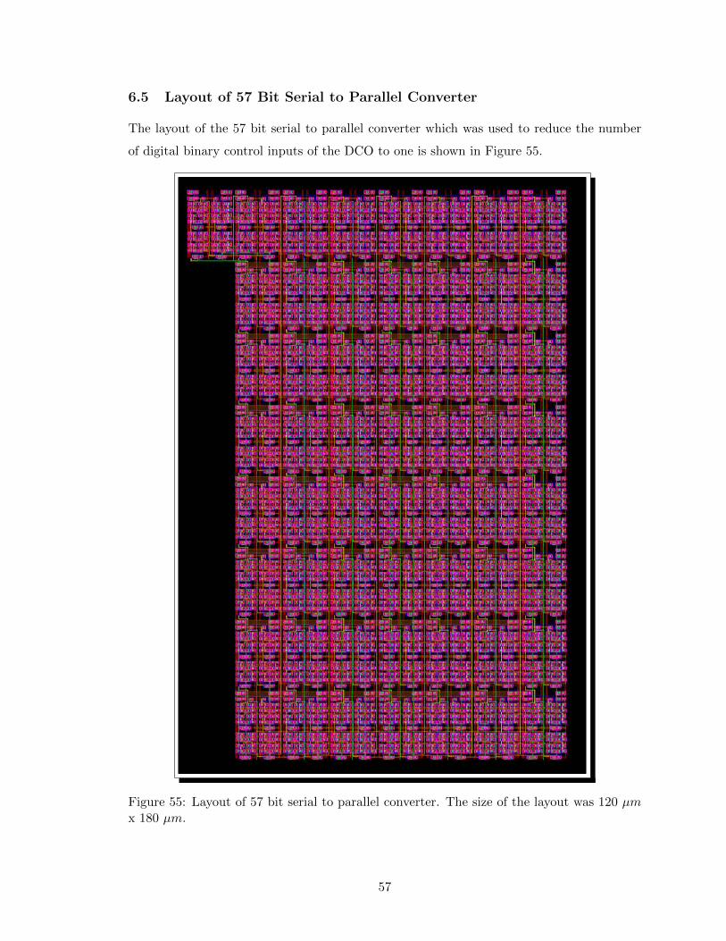
6.5 Layout of 57 Bit Serial to Parallel Converter
The layout of the 57 bit serial to parallel converter which was used to reduce the number
of digital binary control inputs of the DCO to one is shown in Figure 55.
Figure 55: Layout of 57 bit serial to parallel converter. The size of the layout was 120 µmx 180 µm.
57
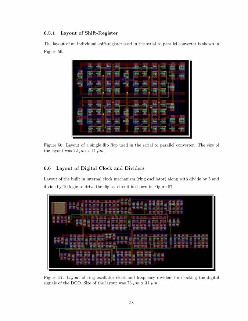
6.5.1 Layout of Shift-Register
The layout of an individual shift-register used in the serial to parallel converter is shown in
Figure 56.
Figure 56: Layout of a single flip flop used in the serial to parallel converter. The size ofthe layout was 22 µm x 14 µm.
6.6 Layout of Digital Clock and Dividers
Layout of the built in internal clock mechanism (ring oscillator) along with divide by 5 and
divide by 10 logic to drive the digital circuit is shown in Figure 57.
Figure 57: Layout of ring oscillator clock and frequency dividers for clocking the digitalsignals of the DCO. Size of the layout was 73 µm x 31 µm.
58
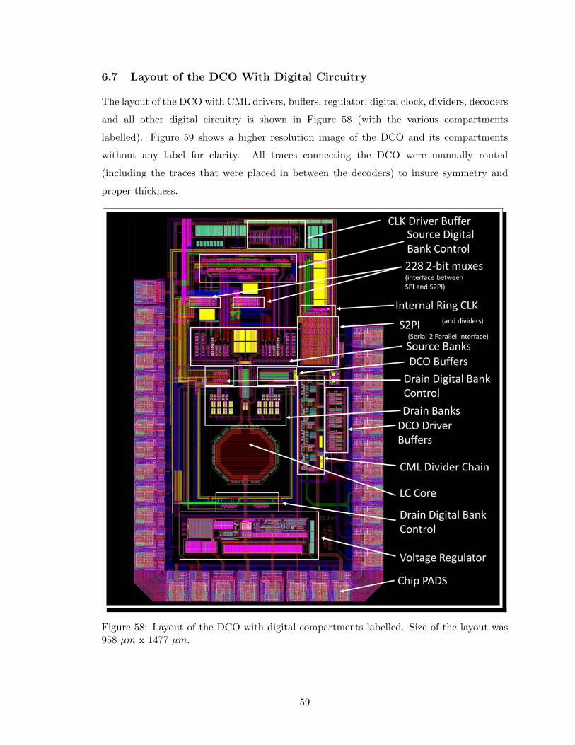
6.7 Layout of the DCO With Digital Circuitry
The layout of the DCO with CML drivers, buffers, regulator, digital clock, dividers, decoders
and all other digital circuitry is shown in Figure 58 (with the various compartments
labelled). Figure 59 shows a higher resolution image of the DCO and its compartments
without any label for clarity. All traces connecting the DCO were manually routed
(including the traces that were placed in between the decoders) to insure symmetry and
proper thickness.
Figure 58: Layout of the DCO with digital compartments labelled. Size of the layout was958 µm x 1477 µm.
59
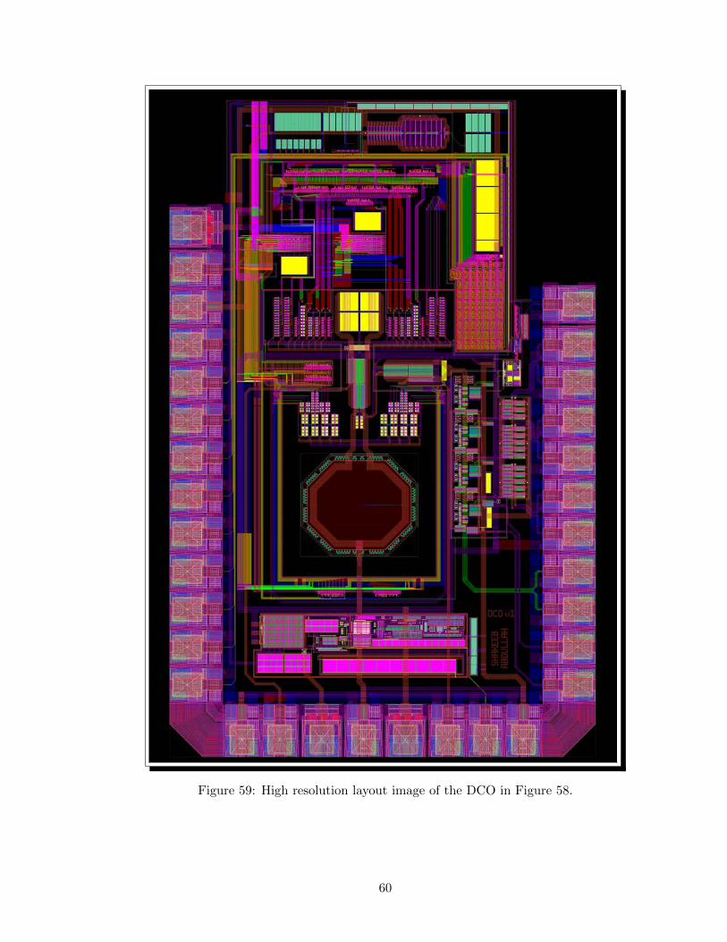
Figure 59: High resolution layout image of the DCO in Figure 58.
60
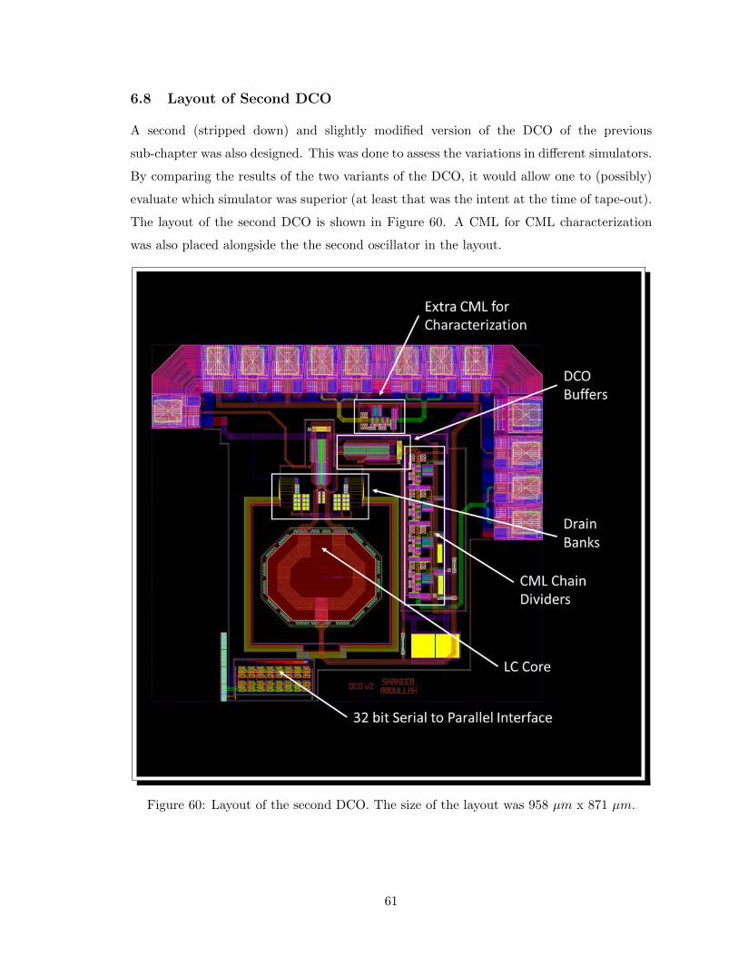
6.8 Layout of Second DCO
A second (stripped down) and slightly modified version of the DCO of the previous
sub-chapter was also designed. This was done to assess the variations in different simulators.
By comparing the results of the two variants of the DCO, it would allow one to (possibly)
evaluate which simulator was superior (at least that was the intent at the time of tape-out).
The layout of the second DCO is shown in Figure 60. A CML for CML characterization
was also placed alongside the the second oscillator in the layout.
Figure 60: Layout of the second DCO. The size of the layout was 958 µm x 871 µm.
61
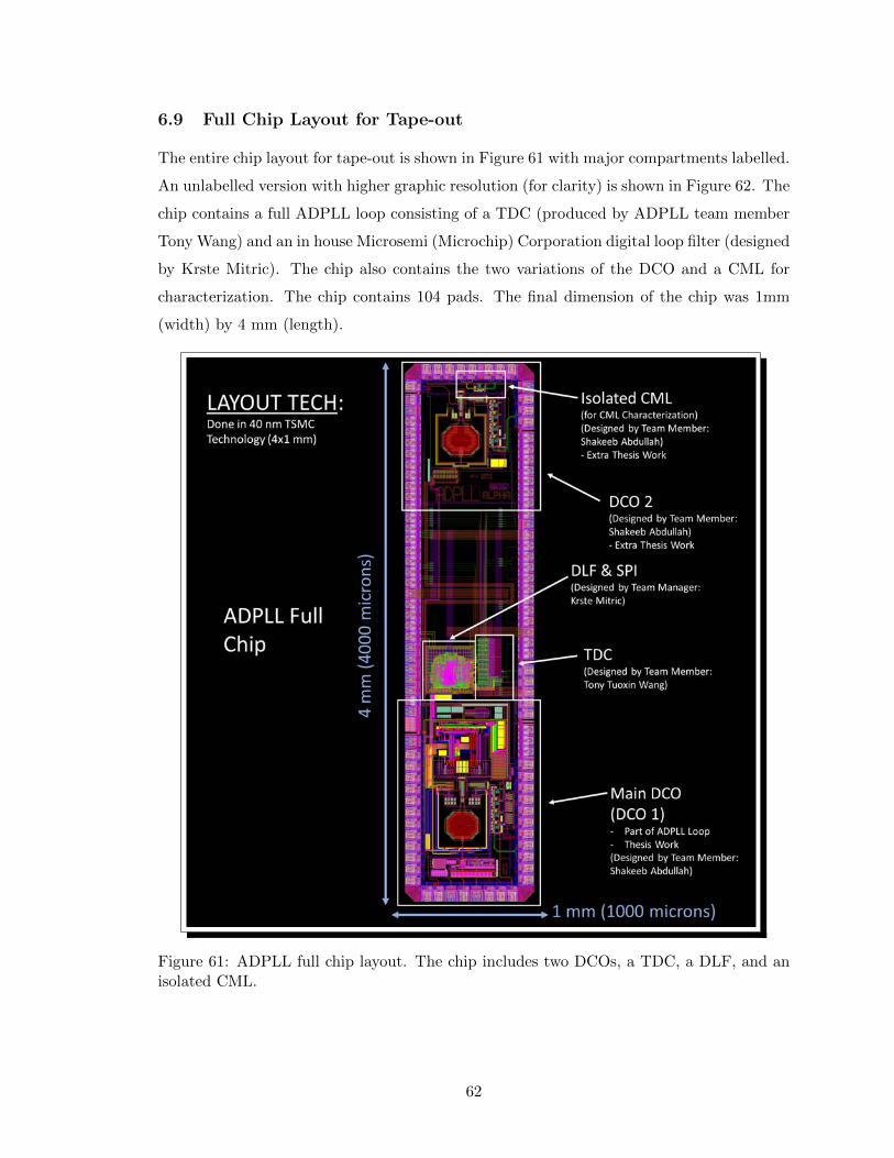
6.9 Full Chip Layout for Tape-out
The entire chip layout for tape-out is shown in Figure 61 with major compartments labelled.
An unlabelled version with higher graphic resolution (for clarity) is shown in Figure 62. The
chip contains a full ADPLL loop consisting of a TDC (produced by ADPLL team member
Tony Wang) and an in house Microsemi (Microchip) Corporation digital loop filter (designed
by Krste Mitric). The chip also contains the two variations of the DCO and a CML for
characterization. The chip contains 104 pads. The final dimension of the chip was 1mm
(width) by 4 mm (length).
Figure 61: ADPLL full chip layout. The chip includes two DCOs, a TDC, a DLF, and anisolated CML.
62
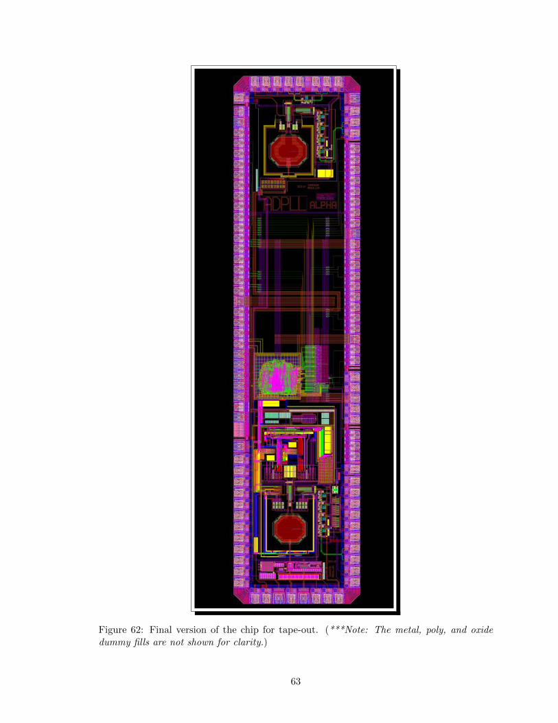
Figure 62: Final version of the chip for tape-out. (***Note: The metal, poly, and oxidedummy fills are not shown for clarity.)
63
Only one tape-out of the above layout (Figure 62) was permitted, so it was of utmost
pertinent that everything on the layout and all its post layout simulations were correct.
6.10 Conclusion
This chapter looked at the layout design of the DCO designed for this thesis. It looked at
the layout design of the DCO Core, Digital Banks, Core Buffers and CML dividers. It also
looked at the layout design of the digital circuitry, the buffers connecting to the bonding
pads, and the overall layout. Only one tape-out of the layout was permitted.
64
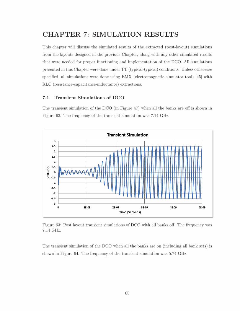
CHAPTER 7: SIMULATION RESULTS
This chapter will discuss the simulated results of the extracted (post-layout) simulations
from the layouts designed in the previous Chapter; along with any other simulated results
that were needed for proper functioning and implementation of the DCO. All simulations
presented in this Chapter were done under TT (typical-typical) conditions. Unless otherwise
specified, all simulations were done using EMX (electromagnetic simulator tool) [45] with
RLC (resistance-capacitance-inductance) extractions.
7.1 Transient Simulations of DCO
The transient simulation of the DCO (in Figure 47) when all the banks are off is shown in
Figure 63. The frequency of the transient simulation was 7.14 GHz.
Figure 63: Post layout transient simulations of DCO with all banks off. The frequency was7.14 GHz.
The transient simulation of the DCO when all the banks are on (including all bank sets) is
shown in Figure 64. The frequency of the transient simulation was 5.74 GHz.
65
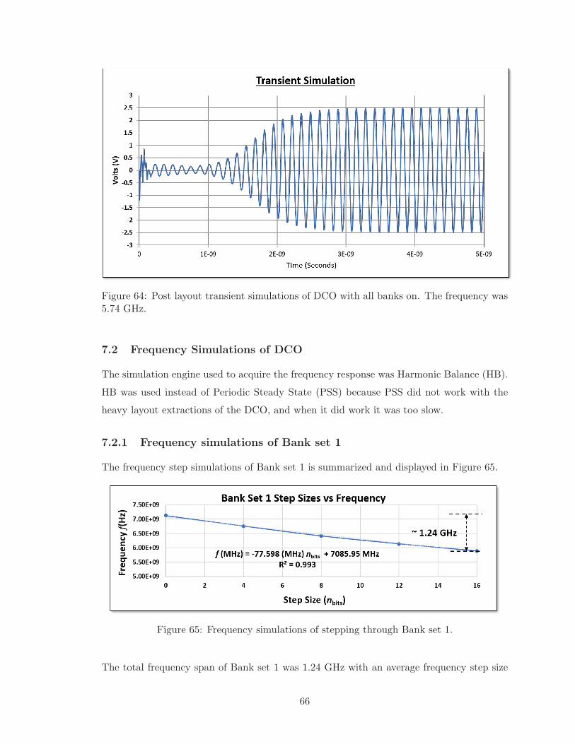
Figure 64: Post layout transient simulations of DCO with all banks on. The frequency was5.74 GHz.
7.2 Frequency Simulations of DCO
The simulation engine used to acquire the frequency response was Harmonic Balance (HB).
HB was used instead of Periodic Steady State (PSS) because PSS did not work with the
heavy layout extractions of the DCO, and when it did work it was too slow.
7.2.1 Frequency simulations of Bank set 1
The frequency step simulations of Bank set 1 is summarized and displayed in Figure 65.
Figure 65: Frequency simulations of stepping through Bank set 1.
The total frequency span of Bank set 1 was 1.24 GHz with an average frequency step size
66
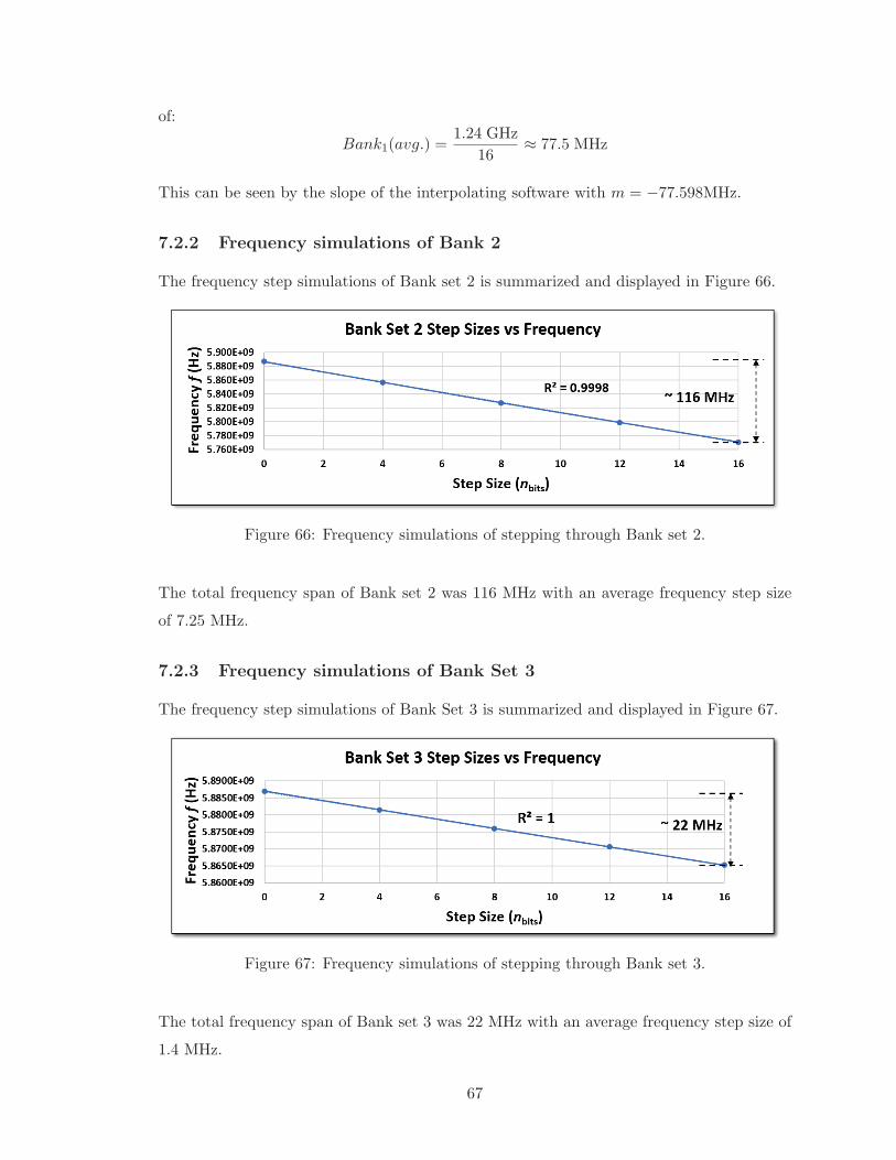
of:
Bank1(avg.) =1.24 GHz
16≈ 77.5 MHz
This can be seen by the slope of the interpolating software with m = −77.598MHz.
7.2.2 Frequency simulations of Bank 2
The frequency step simulations of Bank set 2 is summarized and displayed in Figure 66.
Figure 66: Frequency simulations of stepping through Bank set 2.
The total frequency span of Bank set 2 was 116 MHz with an average frequency step size
of 7.25 MHz.
7.2.3 Frequency simulations of Bank Set 3
The frequency step simulations of Bank Set 3 is summarized and displayed in Figure 67.
Figure 67: Frequency simulations of stepping through Bank set 3.
The total frequency span of Bank set 3 was 22 MHz with an average frequency step size of
1.4 MHz.
67
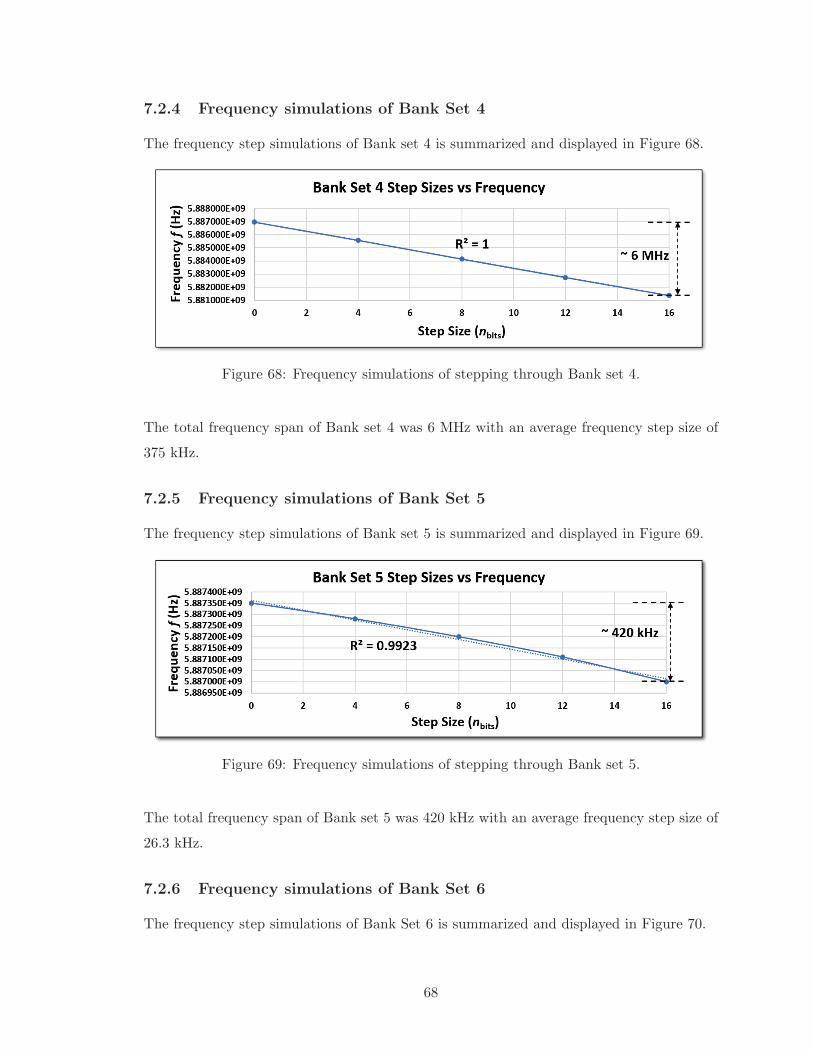
7.2.4 Frequency simulations of Bank Set 4
The frequency step simulations of Bank set 4 is summarized and displayed in Figure 68.
Figure 68: Frequency simulations of stepping through Bank set 4.
The total frequency span of Bank set 4 was 6 MHz with an average frequency step size of
375 kHz.
7.2.5 Frequency simulations of Bank Set 5
The frequency step simulations of Bank set 5 is summarized and displayed in Figure 69.
Figure 69: Frequency simulations of stepping through Bank set 5.
The total frequency span of Bank set 5 was 420 kHz with an average frequency step size of
26.3 kHz.
7.2.6 Frequency simulations of Bank Set 6
The frequency step simulations of Bank Set 6 is summarized and displayed in Figure 70.
68
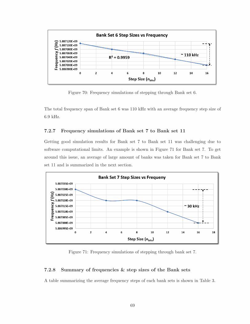
Figure 70: Frequency simulations of stepping through Bank set 6.
The total frequency span of Bank set 6 was 110 kHz with an average frequency step size of
6.9 kHz.
7.2.7 Frequency simulations of Bank set 7 to Bank set 11
Getting good simulation results for Bank set 7 to Bank set 11 was challenging due to
software computational limits. An example is shown in Figure 71 for Bank set 7. To get
around this issue, an average of large amount of banks was taken for Bank set 7 to Bank
set 11 and is summarized in the next section.
Figure 71: Frequency simulations of stepping through bank set 7.
7.2.8 Summary of frequencies & step sizes of the Bank sets
A table summarizing the average frequency steps of each bank sets is shown in Table 3.
69
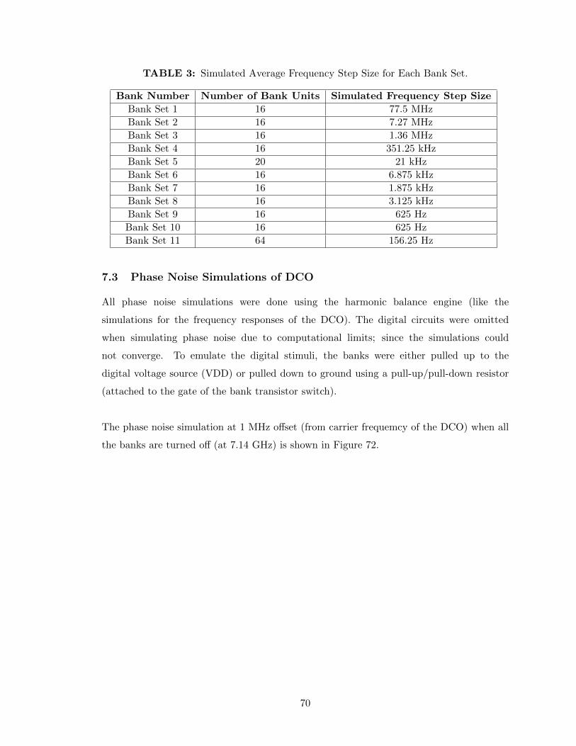
TABLE 3: Simulated Average Frequency Step Size for Each Bank Set.
Bank Number Number of Bank Units Simulated Frequency Step Size
Bank Set 1 16 77.5 MHz
Bank Set 2 16 7.27 MHz
Bank Set 3 16 1.36 MHz
Bank Set 4 16 351.25 kHz
Bank Set 5 20 21 kHz
Bank Set 6 16 6.875 kHz
Bank Set 7 16 1.875 kHz
Bank Set 8 16 3.125 kHz
Bank Set 9 16 625 Hz
Bank Set 10 16 625 Hz
Bank Set 11 64 156.25 Hz
7.3 Phase Noise Simulations of DCO
All phase noise simulations were done using the harmonic balance engine (like the
simulations for the frequency responses of the DCO). The digital circuits were omitted
when simulating phase noise due to computational limits; since the simulations could
not converge. To emulate the digital stimuli, the banks were either pulled up to the
digital voltage source (VDD) or pulled down to ground using a pull-up/pull-down resistor
(attached to the gate of the bank transistor switch).
The phase noise simulation at 1 MHz offset (from carrier frequemcy of the DCO) when all
the banks are turned off (at 7.14 GHz) is shown in Figure 72.
70
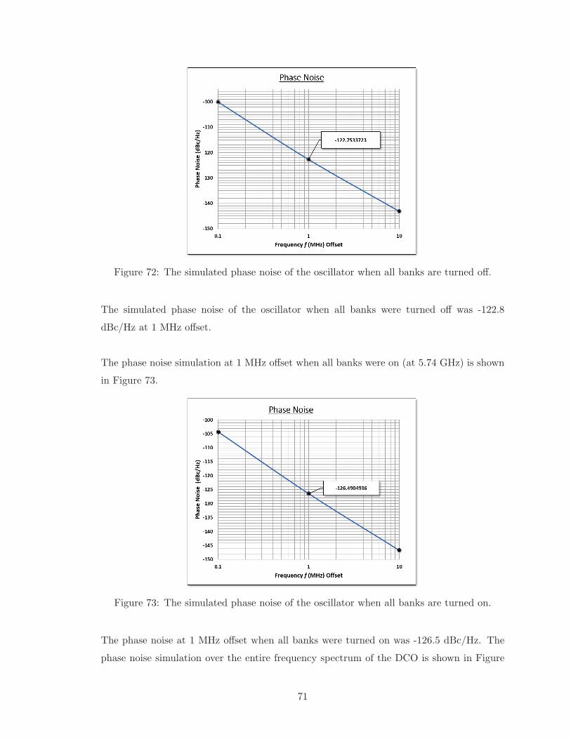
Figure 72: The simulated phase noise of the oscillator when all banks are turned off.
The simulated phase noise of the oscillator when all banks were turned off was -122.8
dBc/Hz at 1 MHz offset.
The phase noise simulation at 1 MHz offset when all banks were on (at 5.74 GHz) is shown
in Figure 73.
Figure 73: The simulated phase noise of the oscillator when all banks are turned on.
The phase noise at 1 MHz offset when all banks were turned on was -126.5 dBc/Hz. The
phase noise simulation over the entire frequency spectrum of the DCO is shown in Figure
71
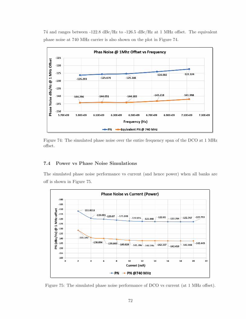
74 and ranges between -122.8 dBc/Hz to -126.5 dBc/Hz at 1 MHz offset. The equivalent
phase noise at 740 MHz carrier is also shown on the plot in Figure 74.
Figure 74: The simulated phase noise over the entire frequency span of the DCO at 1 MHzoffset.
7.4 Power vs Phase Noise Simulations
The simulated phase noise performance vs current (and hence power) when all banks are
off is shown in Figure 75.
Figure 75: The simulated phase noise performance of DCO vs current (at 1 MHz offset).
72
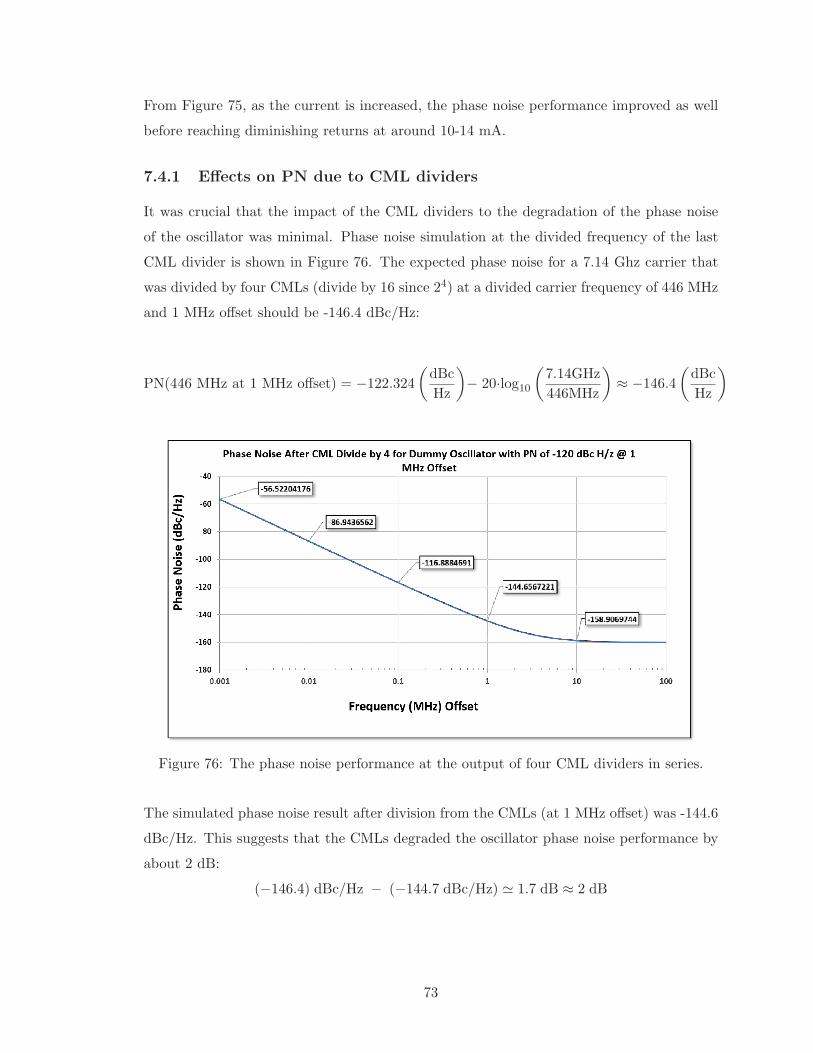
From Figure 75, as the current is increased, the phase noise performance improved as well
before reaching diminishing returns at around 10-14 mA.
7.4.1 Effects on PN due to CML dividers
It was crucial that the impact of the CML dividers to the degradation of the phase noise
of the oscillator was minimal. Phase noise simulation at the divided frequency of the last
CML divider is shown in Figure 76. The expected phase noise for a 7.14 Ghz carrier that
was divided by four CMLs (divide by 16 since 24) at a divided carrier frequency of 446 MHz
and 1 MHz offset should be -146.4 dBc/Hz:
PN(446 MHz at 1 MHz offset) = −122.324(dBc
Hz
)− 20·log10
(7.14GHz
446MHz
)≈ −146.4
(dBc
Hz
)
Figure 76: The phase noise performance at the output of four CML dividers in series.
The simulated phase noise result after division from the CMLs (at 1 MHz offset) was -144.6
dBc/Hz. This suggests that the CMLs degraded the oscillator phase noise performance by
about 2 dB:
(−146.4) dBc/Hz − (−144.7 dBc/Hz) 1.7 dB ≈ 2 dB
73
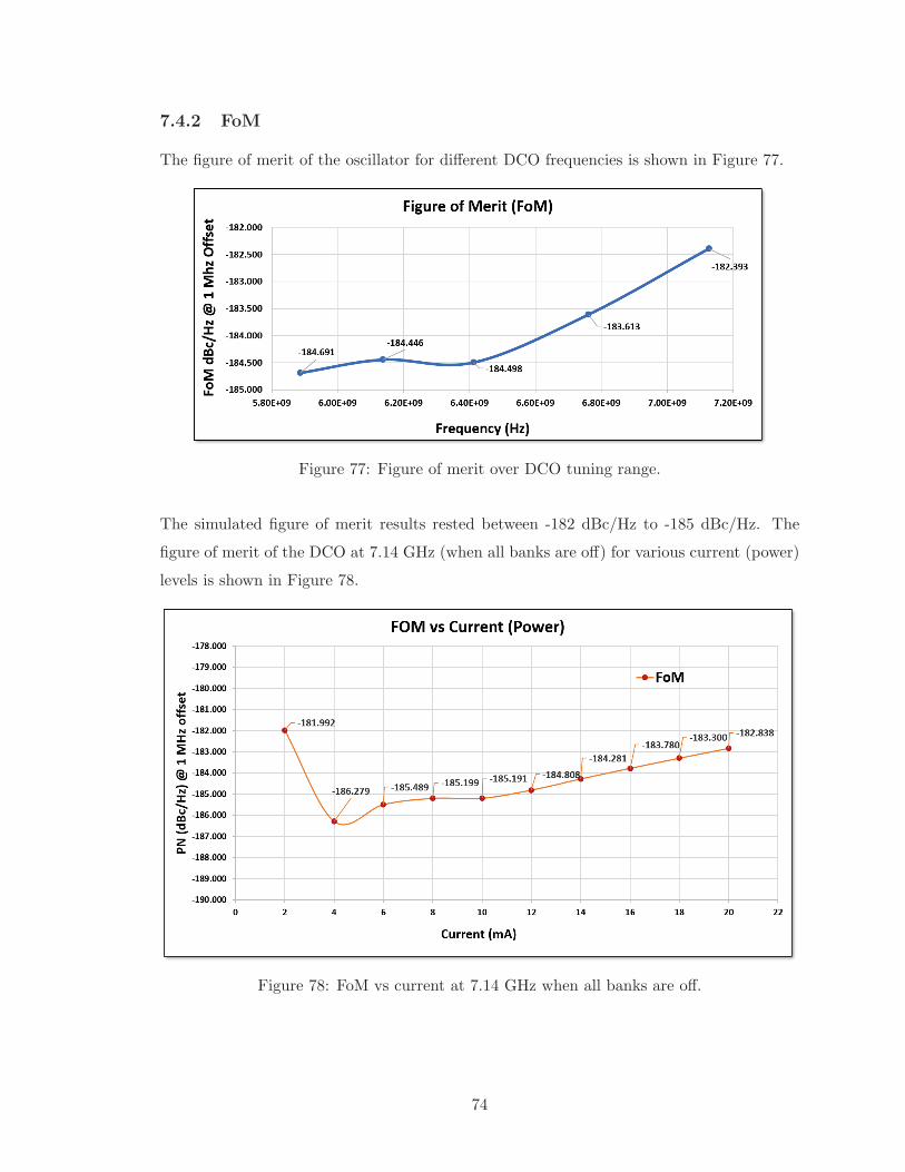
7.4.2 FoM
The figure of merit of the oscillator for different DCO frequencies is shown in Figure 77.
Figure 77: Figure of merit over DCO tuning range.
The simulated figure of merit results rested between -182 dBc/Hz to -185 dBc/Hz. The
figure of merit of the DCO at 7.14 GHz (when all banks are off) for various current (power)
levels is shown in Figure 78.
Figure 78: FoM vs current at 7.14 GHz when all banks are off.
74
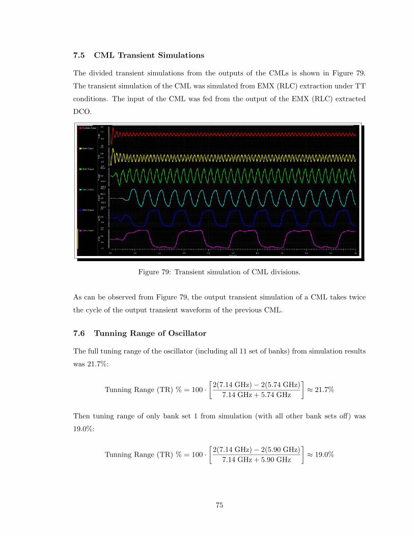
7.5 CML Transient Simulations
The divided transient simulations from the outputs of the CMLs is shown in Figure 79.
The transient simulation of the CML was simulated from EMX (RLC) extraction under TT
conditions. The input of the CML was fed from the output of the EMX (RLC) extracted
DCO.
Figure 79: Transient simulation of CML divisions.
As can be observed from Figure 79, the output transient simulation of a CML takes twice
the cycle of the output transient waveform of the previous CML.
7.6 Tunning Range of Oscillator
The full tuning range of the oscillator (including all 11 set of banks) from simulation results
was 21.7%:
Tunning Range (TR) % = 100 ·[
2(7.14 GHz)− 2(5.74 GHz)
7.14 GHz + 5.74 GHz
]≈ 21.7%
Then tuning range of only bank set 1 from simulation (with all other bank sets off) was
19.0%:
Tunning Range (TR) % = 100 ·[
2(7.14 GHz)− 2(5.90 GHz)
7.14 GHz + 5.90 GHz
]≈ 19.0%
75
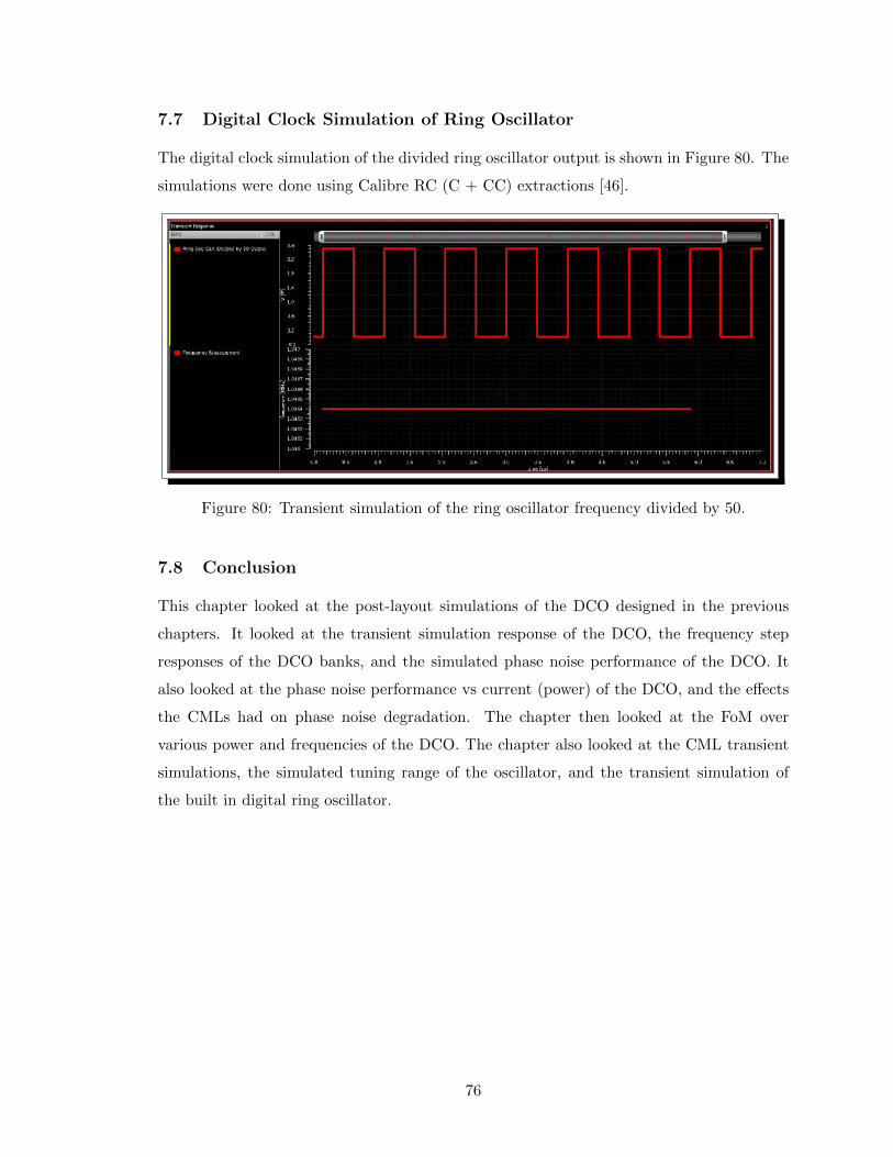
7.7 Digital Clock Simulation of Ring Oscillator
The digital clock simulation of the divided ring oscillator output is shown in Figure 80. The
simulations were done using Calibre RC (C + CC) extractions [46].
Figure 80: Transient simulation of the ring oscillator frequency divided by 50.
7.8 Conclusion
This chapter looked at the post-layout simulations of the DCO designed in the previous
chapters. It looked at the transient simulation response of the DCO, the frequency step
responses of the DCO banks, and the simulated phase noise performance of the DCO. It
also looked at the phase noise performance vs current (power) of the DCO, and the effects
the CMLs had on phase noise degradation. The chapter then looked at the FoM over
various power and frequencies of the DCO. The chapter also looked at the CML transient
simulations, the simulated tuning range of the oscillator, and the transient simulation of
the built in digital ring oscillator.
76

CHAPTER 8: TEST SETUP
This chapter will discuss the test set-up of the DCO starting from the die, bonding and
packaging, to the type of equipment that was used for measuring and verifying the DCO
performance (including the procedures and steps in between).
8.1 The DCO Test Chip Die
The fabricated dies of the DCO (part of the full ADPLL chip) is shown in Figure 81 and
a few examples of zoomed in views (underneath the microscope) is shown in Figure 82 to
Figure 84. The chips were fabricated by TSMC in China.
Figure 81: Images of the ADPLL chips containing the DCO that was fabricated.
77
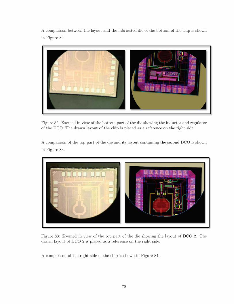
A comparison between the layout and the fabricated die of the bottom of the chip is shown
in Figure 82.
Figure 82: Zoomed in view of the bottom part of the die showing the inductor and regulatorof the DCO. The drawn layout of the chip is placed as a reference on the right side.
A comparison of the top part of the die and its layout containing the second DCO is shown
in Figure 83.
Figure 83: Zoomed in view of the top part of the die showing the layout of DCO 2. Thedrawn layout of DCO 2 is placed as a reference on the right side.
A comparison of the right side of the chip is shown in Figure 84.
78
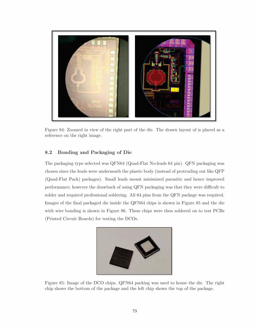
Figure 84: Zoomed in view of the right part of the die. The drawn layout of is placed as areference on the right image.
8.2 Bonding and Packaging of Die
The packaging type selected was QFN64 (Quad-Flat No-leads 64 pin). QFN packaging was
chosen since the leads were underneath the plastic body (instead of protruding out like QFP
(Quad-Flat Pack) packages). Small leads meant minimized parasitic and hence improved
performance; however the drawback of using QFN packaging was that they were difficult to
solder and required professional soldering. All 64 pins from the QFN package was required.
Images of the final packaged die inside the QFN64 chips is shown in Figure 85 and the die
with wire bonding is shown in Figure 86. These chips were then soldered on to test PCBs
(Printed Circuit Boards) for testing the DCOs.
Figure 85: Image of the DCO chips. QFN64 packing was used to house the die. The rightchip shows the bottom of the package and the left chip shows the top of the package.
79
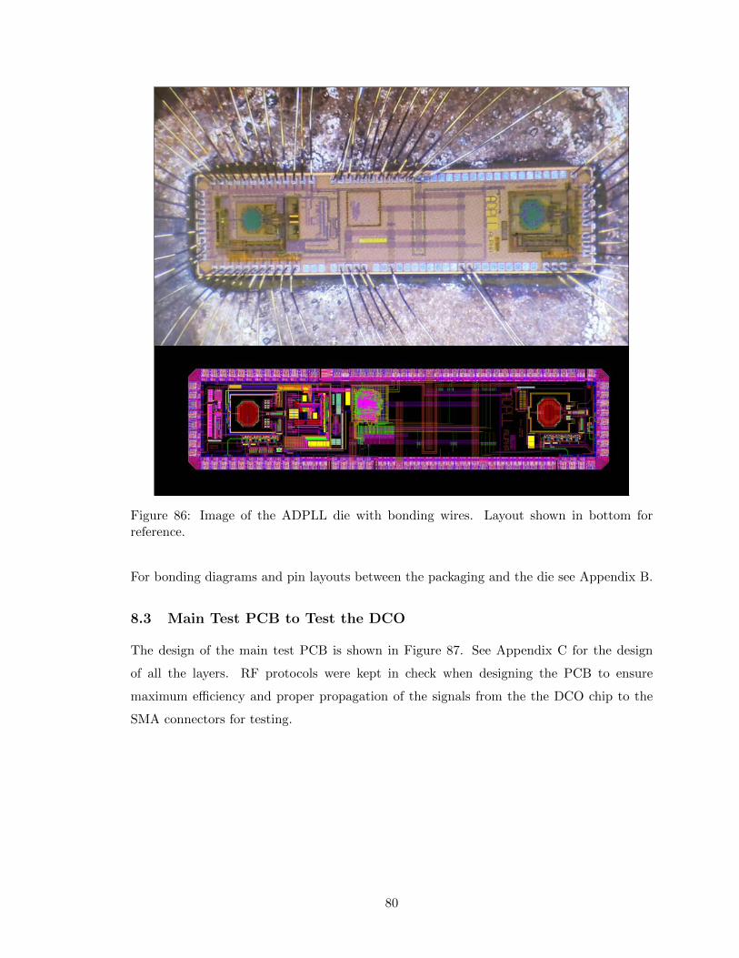
Figure 86: Image of the ADPLL die with bonding wires. Layout shown in bottom forreference.
For bonding diagrams and pin layouts between the packaging and the die see Appendix B.
8.3 Main Test PCB to Test the DCO
The design of the main test PCB is shown in Figure 87. See Appendix C for the design
of all the layers. RF protocols were kept in check when designing the PCB to ensure
maximum efficiency and proper propagation of the signals from the the DCO chip to the
SMA connectors for testing.
80
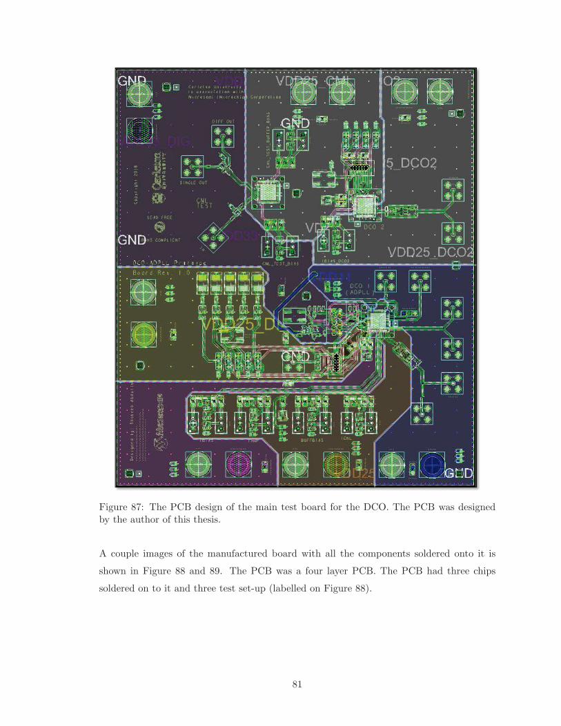
Figure 87: The PCB design of the main test board for the DCO. The PCB was designedby the author of this thesis.
A couple images of the manufactured board with all the components soldered onto it is
shown in Figure 88 and 89. The PCB was a four layer PCB. The PCB had three chips
soldered on to it and three test set-up (labelled on Figure 88).
81
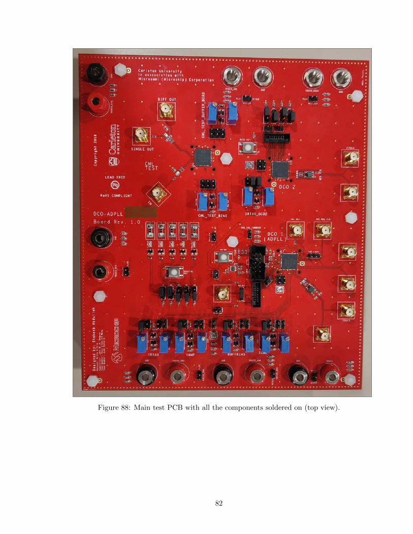
Figure 88: Main test PCB with all the components soldered on (top view).
82
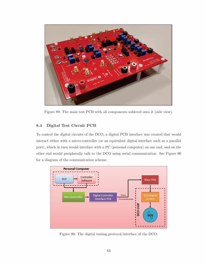
Figure 89: The main test PCB with all components soldered onto it (side view).
8.4 Digital Test Circuit PCB
To control the digital circuits of the DCO, a digital PCB interface was created that would
interact either with a micro-controller (or an equivalent digital interface such as a parallel
port), which in turn would interface with a PC (personal computer) on one end; and on the
other end would peripherally talk to the DCO using serial communication. See Figure 90
for a diagram of the communication scheme.
Figure 90: The digital testing protocol/interface of the DCO.
83
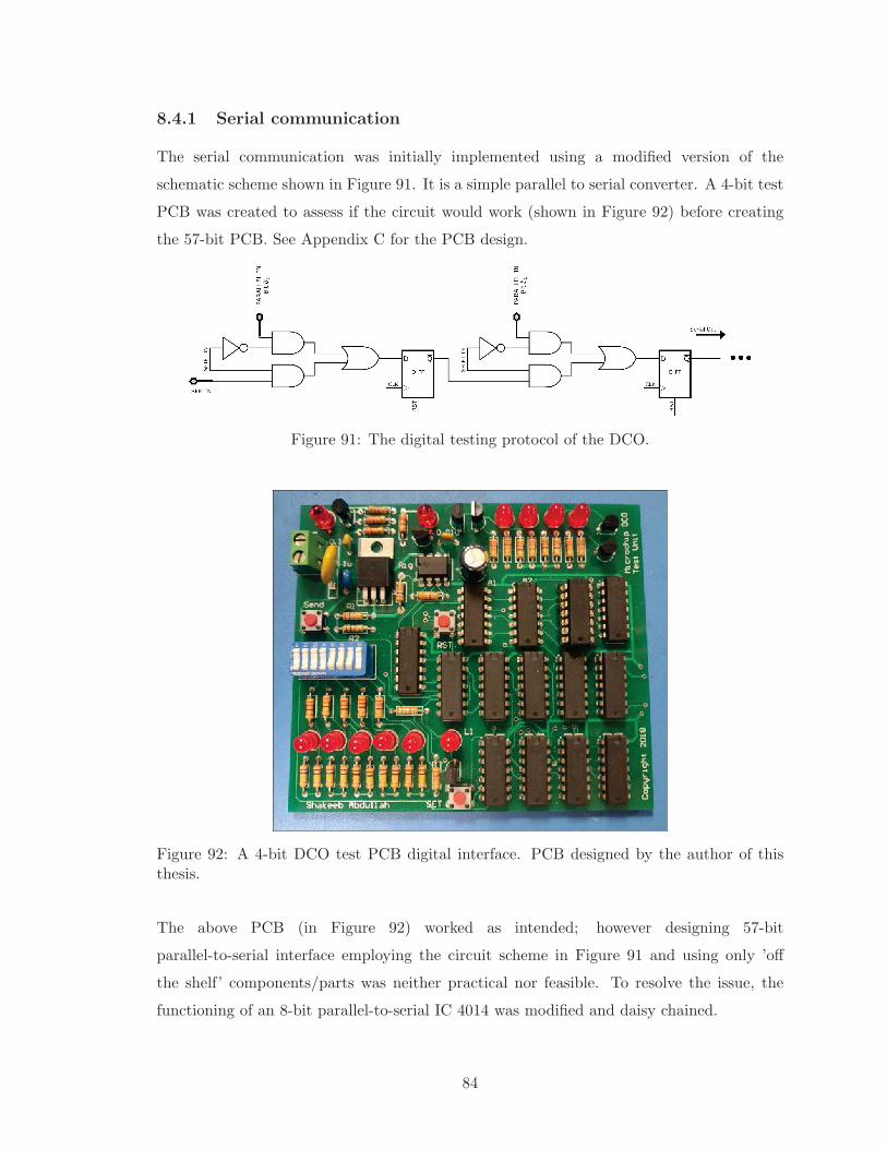
8.4.1 Serial communication
The serial communication was initially implemented using a modified version of the
schematic scheme shown in Figure 91. It is a simple parallel to serial converter. A 4-bit test
PCB was created to assess if the circuit would work (shown in Figure 92) before creating
the 57-bit PCB. See Appendix C for the PCB design.
Figure 91: The digital testing protocol of the DCO.
Figure 92: A 4-bit DCO test PCB digital interface. PCB designed by the author of thisthesis.
The above PCB (in Figure 92) worked as intended; however designing 57-bit
parallel-to-serial interface employing the circuit scheme in Figure 91 and using only ’off
the shelf’ components/parts was neither practical nor feasible. To resolve the issue, the
functioning of an 8-bit parallel-to-serial IC 4014 was modified and daisy chained.
84
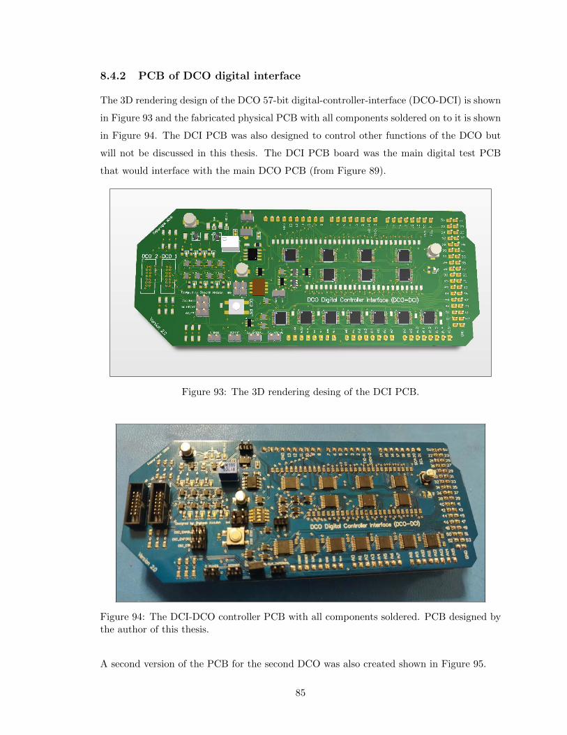
8.4.2 PCB of DCO digital interface
The 3D rendering design of the DCO 57-bit digital-controller-interface (DCO-DCI) is shown
in Figure 93 and the fabricated physical PCB with all components soldered on to it is shown
in Figure 94. The DCI PCB was also designed to control other functions of the DCO but
will not be discussed in this thesis. The DCI PCB board was the main digital test PCB
that would interface with the main DCO PCB (from Figure 89).
Figure 93: The 3D rendering desing of the DCI PCB.
Figure 94: The DCI-DCO controller PCB with all components soldered. PCB designed bythe author of this thesis.
A second version of the PCB for the second DCO was also created shown in Figure 95.
85
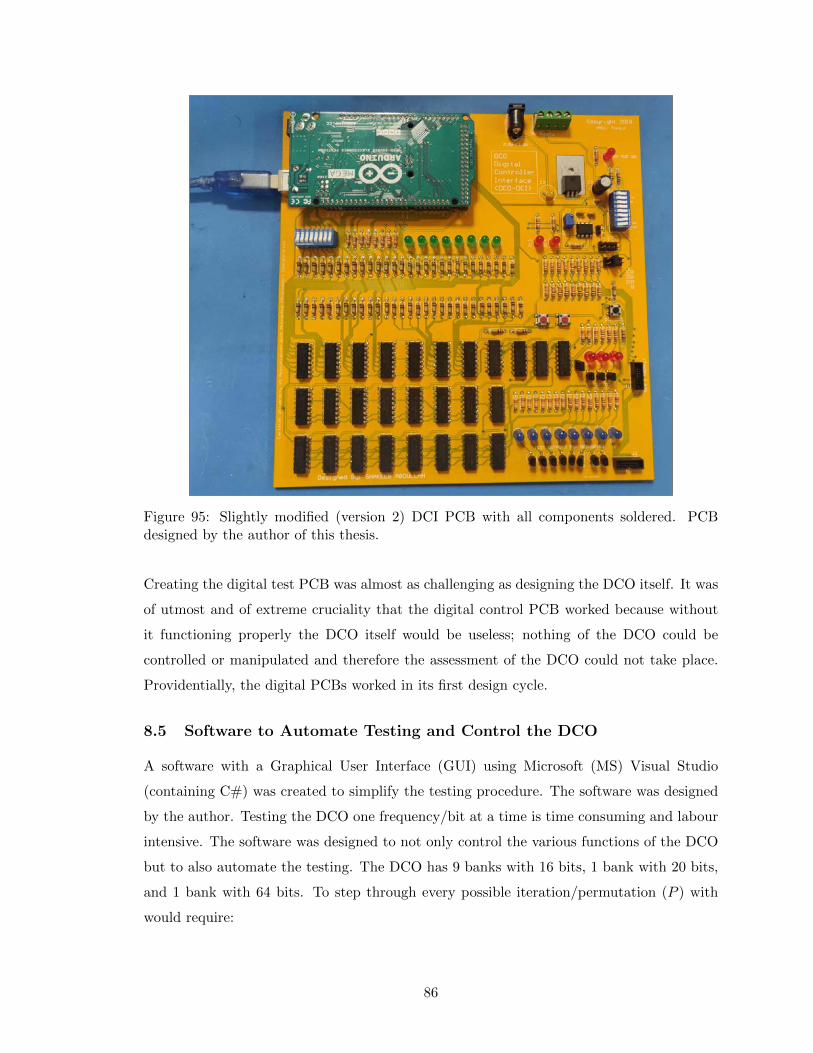
Figure 95: Slightly modified (version 2) DCI PCB with all components soldered. PCBdesigned by the author of this thesis.
Creating the digital test PCB was almost as challenging as designing the DCO itself. It was
of utmost and of extreme cruciality that the digital control PCB worked because without
it functioning properly the DCO itself would be useless; nothing of the DCO could be
controlled or manipulated and therefore the assessment of the DCO could not take place.
Providentially, the digital PCBs worked in its first design cycle.
8.5 Software to Automate Testing and Control the DCO
A software with a Graphical User Interface (GUI) using Microsoft (MS) Visual Studio
(containing C#) was created to simplify the testing procedure. The software was designed
by the author. Testing the DCO one frequency/bit at a time is time consuming and labour
intensive. The software was designed to not only control the various functions of the DCO
but to also automate the testing. The DCO has 9 banks with 16 bits, 1 bank with 20 bits,
and 1 bank with 64 bits. To step through every possible iteration/permutation (P ) with
would require:
86
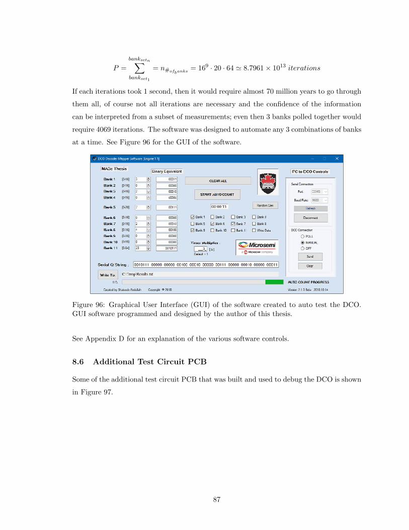
P =
banksetn∑bankset1
= n#ofbanks= 169 · 20 · 64 ' 8.7961× 10¹³ iterations
If each iterations took 1 second, then it would require almost 70 million years to go through
them all, of course not all iterations are necessary and the confidence of the information
can be interpreted from a subset of measurements; even then 3 banks polled together would
require 4069 iterations. The software was designed to automate any 3 combinations of banks
at a time. See Figure 96 for the GUI of the software.
Figure 96: Graphical User Interface (GUI) of the software created to auto test the DCO.GUI software programmed and designed by the author of this thesis.
See Appendix D for an explanation of the various software controls.
8.6 Additional Test Circuit PCB
Some of the additional test circuit PCB that was built and used to debug the DCO is shown
in Figure 97.
87
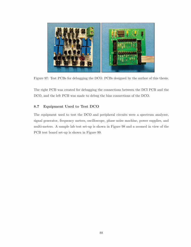
Figure 97: Test PCBs for debugging the DCO. PCBs designed by the author of this thesis.
The right PCB was created for debugging the connections between the DCI PCB and the
DCO, and the left PCB was made to debug the bias connections of the DCO.
8.7 Equipment Used to Test DCO
The equipment used to test the DCO and peripheral circuits were a spectrum analyzer,
signal generator, frequency meters, oscilloscope, phase noise machine, power supplies, and
multi-meters. A sample lab test set-up is shown in Figure 98 and a zoomed in view of the
PCB test board set-up is shown in Figure 99.
88
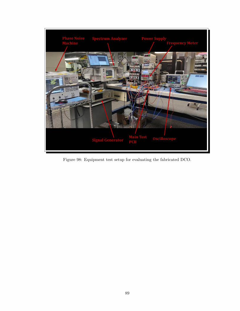
Figure 98: Equipment test setup for evaluating the fabricated DCO.
89
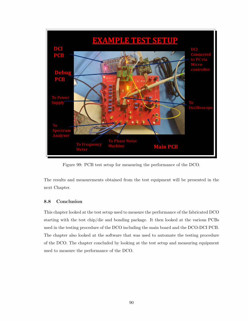
Figure 99: PCB test setup for measuring the performance of the DCO.
The results and measurements obtained from the test equipment will be presented in the
next Chapter.
8.8 Conclusion
This chapter looked at the test setup used to measure the performance of the fabricated DCO
starting with the test chip/die and bonding package. It then looked at the various PCBs
used in the testing procedure of the DCO including the main board and the DCO-DCI PCB.
The chapter also looked at the software that was used to automate the testing procedure
of the DCO. The chapter concluded by looking at the test setup and measuring equipment
used to measure the performance of the DCO.
90
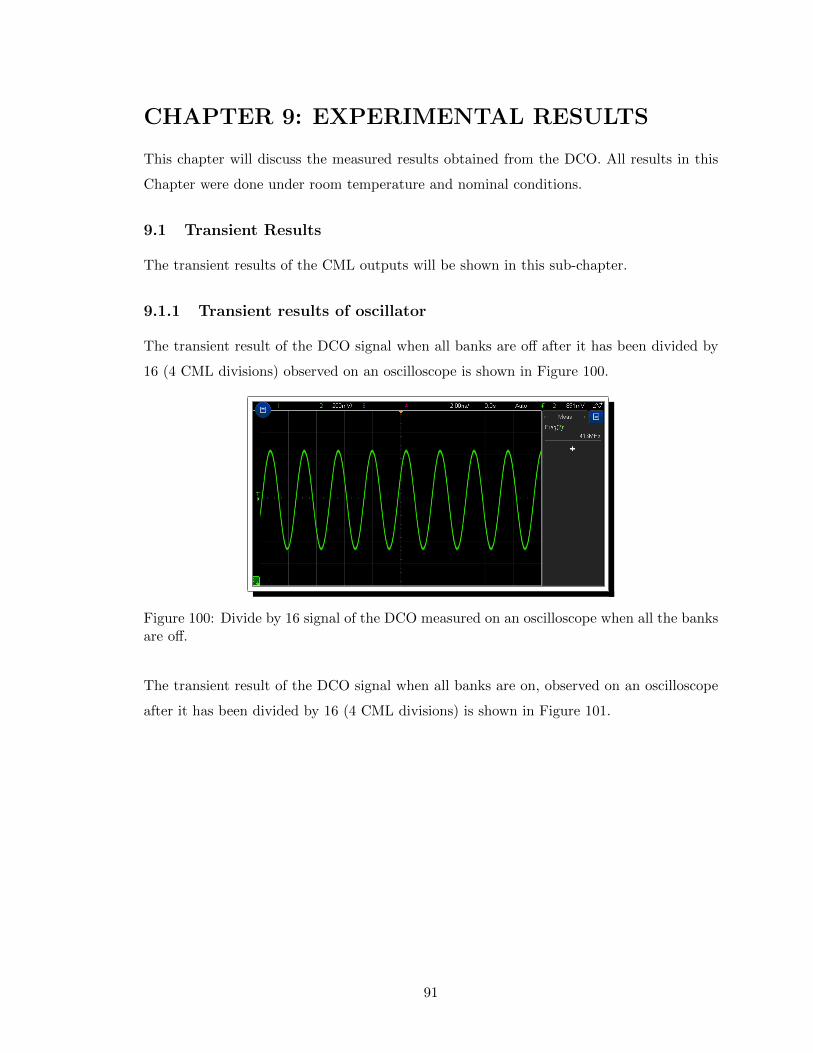
CHAPTER 9: EXPERIMENTAL RESULTS
This chapter will discuss the measured results obtained from the DCO. All results in this
Chapter were done under room temperature and nominal conditions.
9.1 Transient Results
The transient results of the CML outputs will be shown in this sub-chapter.
9.1.1 Transient results of oscillator
The transient result of the DCO signal when all banks are off after it has been divided by
16 (4 CML divisions) observed on an oscilloscope is shown in Figure 100.
Figure 100: Divide by 16 signal of the DCO measured on an oscilloscope when all the banksare off.
The transient result of the DCO signal when all banks are on, observed on an oscilloscope
after it has been divided by 16 (4 CML divisions) is shown in Figure 101.
91
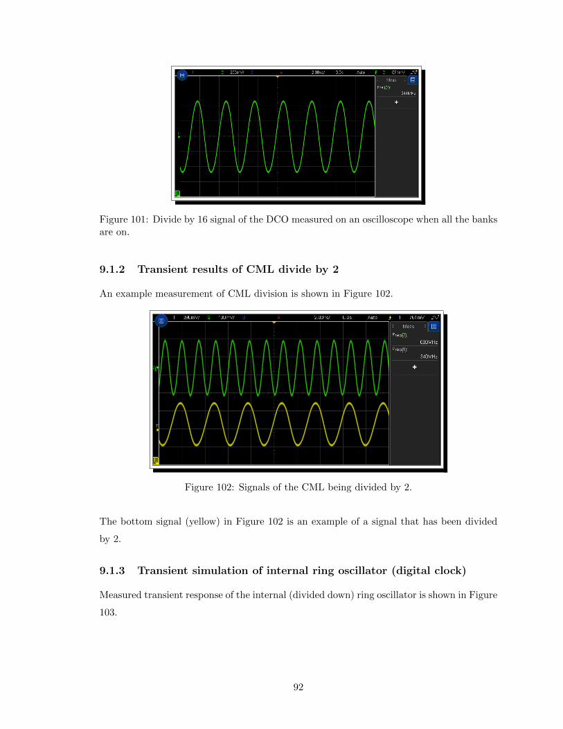
Figure 101: Divide by 16 signal of the DCO measured on an oscilloscope when all the banksare on.
9.1.2 Transient results of CML divide by 2
An example measurement of CML division is shown in Figure 102.
Figure 102: Signals of the CML being divided by 2.
The bottom signal (yellow) in Figure 102 is an example of a signal that has been divided
by 2.
9.1.3 Transient simulation of internal ring oscillator (digital clock)
Measured transient response of the internal (divided down) ring oscillator is shown in Figure
103.
92
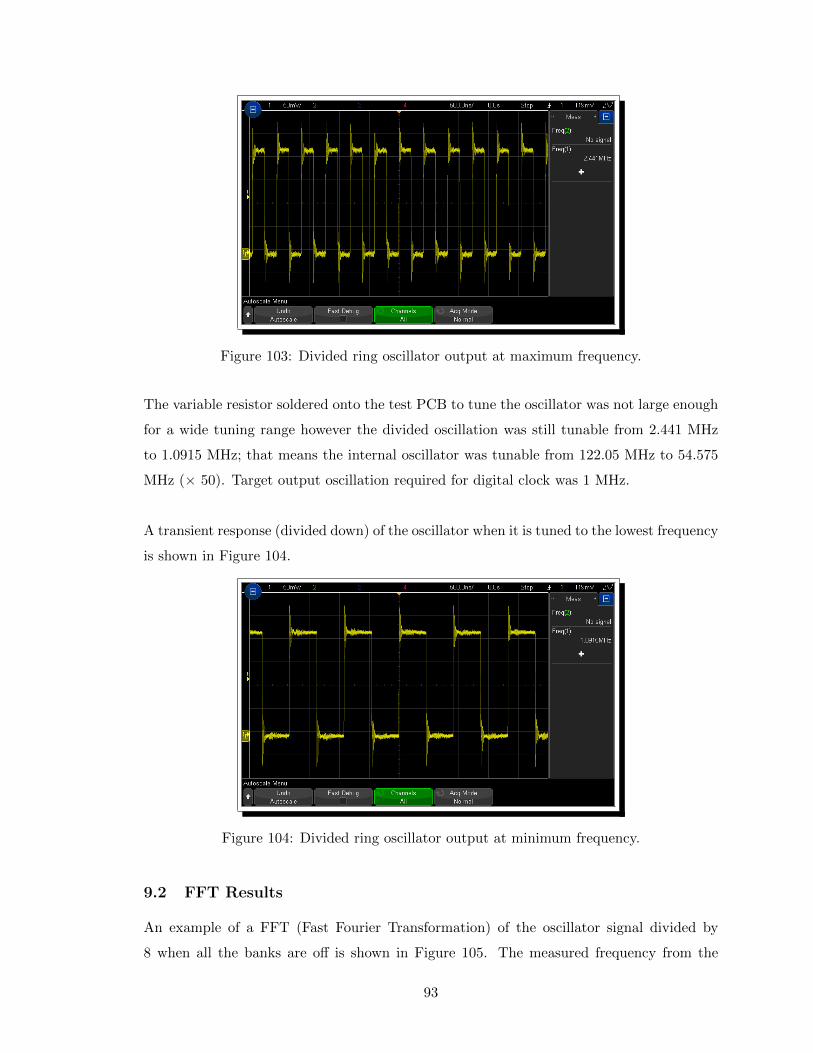
Figure 103: Divided ring oscillator output at maximum frequency.
The variable resistor soldered onto the test PCB to tune the oscillator was not large enough
for a wide tuning range however the divided oscillation was still tunable from 2.441 MHz
to 1.0915 MHz; that means the internal oscillator was tunable from 122.05 MHz to 54.575
MHz (× 50). Target output oscillation required for digital clock was 1 MHz.
A transient response (divided down) of the oscillator when it is tuned to the lowest frequency
is shown in Figure 104.
Figure 104: Divided ring oscillator output at minimum frequency.
9.2 FFT Results
An example of a FFT (Fast Fourier Transformation) of the oscillator signal divided by
8 when all the banks are off is shown in Figure 105. The measured frequency from the
93

analyzer (÷ by 8) was 827.0 MHz.
Figure 105: FFT signal (divide by 8) when all banks of the DCO is off. Sweep was 1 msand bandwidth was 1.8 MHz.
An example of a FFT of the oscillator signal divided by 8 when all banks are on is shown
in Figure 106. The measured frequency from the analyzer (÷ by 8) was 680.7 MHz.
Figure 106: FFT signal (divide by 8) when all banks of the DCO is on. Sweep was 1 msand bandwidth was 1.8 MHz.
An example of a FFT plot where all the banks of Bank 1 is stepped through and overlaid
94
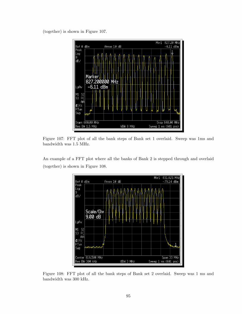
(together) is shown in Figure 107.
Figure 107: FFT plot of all the bank steps of Bank set 1 overlaid. Sweep was 1ms andbandwidth was 1.5 MHz.
An example of a FFT plot where all the banks of Bank 2 is stepped through and overlaid
(together) is shown in Figure 108.
Figure 108: FFT plot of all the bank steps of Bank set 2 overlaid. Sweep was 1 ms andbandwidth was 300 kHz.
95
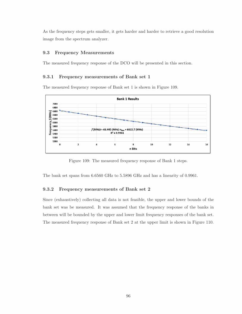
As the frequency steps gets smaller, it gets harder and harder to retrieve a good resolution
image from the spectrum analyzer.
9.3 Frequency Measurements
The measured frequency response of the DCO will be presented in this section.
9.3.1 Frequency measurements of Bank set 1
The measured frequency response of Bank set 1 is shown in Figure 109.
Figure 109: The measured frequency response of Bank 1 steps.
The bank set spans from 6.6560 GHz to 5.5896 GHz and has a linearity of 0.9961.
9.3.2 Frequency measurements of Bank set 2
Since (exhaustively) collecting all data is not feasible, the upper and lower bounds of the
bank set was be measured. It was assumed that the frequency response of the banks in
between will be bounded by the upper and lower limit frequency responses of the bank set.
The measured frequency response of Bank set 2 at the upper limit is shown in Figure 110.
96
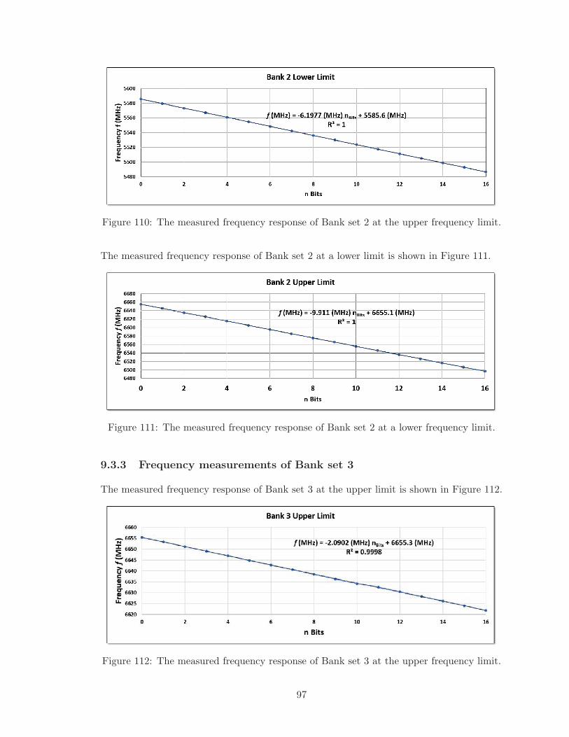
Figure 110: The measured frequency response of Bank set 2 at the upper frequency limit.
The measured frequency response of Bank set 2 at a lower limit is shown in Figure 111.
Figure 111: The measured frequency response of Bank set 2 at a lower frequency limit.
9.3.3 Frequency measurements of Bank set 3
The measured frequency response of Bank set 3 at the upper limit is shown in Figure 112.
Figure 112: The measured frequency response of Bank set 3 at the upper frequency limit.
97
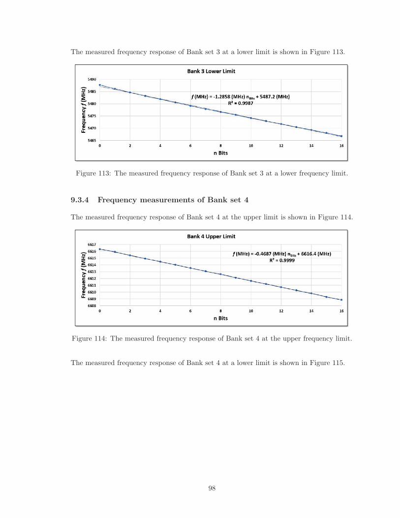
The measured frequency response of Bank set 3 at a lower limit is shown in Figure 113.
Figure 113: The measured frequency response of Bank set 3 at a lower frequency limit.
9.3.4 Frequency measurements of Bank set 4
The measured frequency response of Bank set 4 at the upper limit is shown in Figure 114.
Figure 114: The measured frequency response of Bank set 4 at the upper frequency limit.
The measured frequency response of Bank set 4 at a lower limit is shown in Figure 115.
98
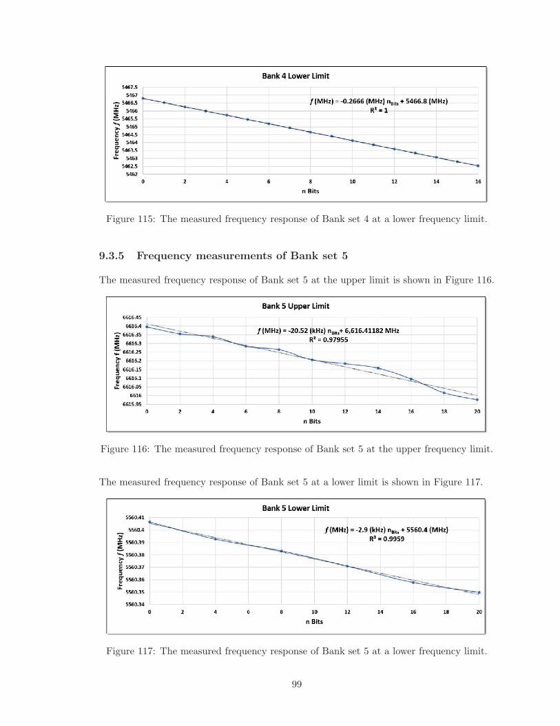
Figure 115: The measured frequency response of Bank set 4 at a lower frequency limit.
9.3.5 Frequency measurements of Bank set 5
The measured frequency response of Bank set 5 at the upper limit is shown in Figure 116.
Figure 116: The measured frequency response of Bank set 5 at the upper frequency limit.
The measured frequency response of Bank set 5 at a lower limit is shown in Figure 117.
Figure 117: The measured frequency response of Bank set 5 at a lower frequency limit.
99
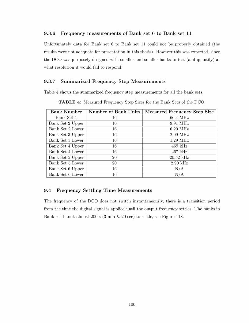
9.3.6 Frequency measurements of Bank set 6 to Bank set 11
Unfortunately data for Bank set 6 to Bank set 11 could not be properly obtained (the
results were not adequate for presentation in this thesis). However this was expected, since
the DCO was purposely designed with smaller and smaller banks to test (and quantify) at
what resolution it would fail to respond.
9.3.7 Summarized Frequency Step Measurements
Table 4 shows the summarized frequency step measurements for all the bank sets.
TABLE 4: Measured Frequency Step Sizes for the Bank Sets of the DCO.
Bank Number Number of Bank Units Measured Frequency Step Size
Bank Set 1 16 66.4 MHz
Bank Set 2 Upper 16 9.91 MHz
Bank Set 2 Lower 16 6.20 MHz
Bank Set 3 Upper 16 2.09 MHz
Bank Set 3 Lower 16 1.29 MHz
Bank Set 4 Upper 16 469 kHz
Bank Set 4 Lower 16 267 kHz
Bank Set 5 Upper 20 20.52 kHz
Bank Set 5 Lower 20 2.90 kHz
Bank Set 6 Upper 16 N/A
Bank Set 6 Lower 16 N/A
9.4 Frequency Settling Time Measurements
The frequency of the DCO does not switch instantaneously, there is a transition period
from the time the digital signal is applied until the output frequency settles. The banks in
Bank set 1 took almost 200 s (3 min & 20 sec) to settle, see Figure 118.
100
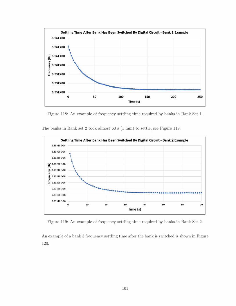
Figure 118: An example of frequency settling time required by banks in Bank Set 1.
The banks in Bank set 2 took almost 60 s (1 min) to settle, see Figure 119.
Figure 119: An example of frequency settling time required by banks in Bank Set 2.
An example of a bank 3 frequency settling time after the bank is switched is shown in Figure
120.
101
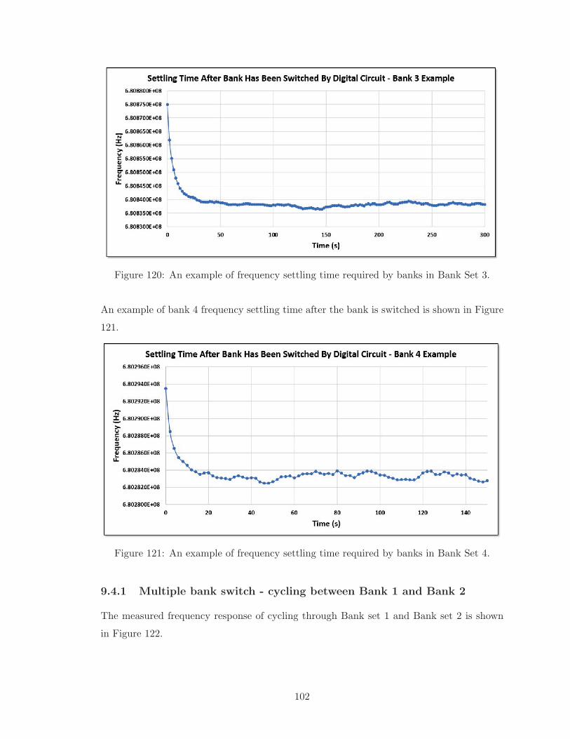
Figure 120: An example of frequency settling time required by banks in Bank Set 3.
An example of bank 4 frequency settling time after the bank is switched is shown in Figure
121.
Figure 121: An example of frequency settling time required by banks in Bank Set 4.
9.4.1 Multiple bank switch - cycling between Bank 1 and Bank 2
The measured frequency response of cycling through Bank set 1 and Bank set 2 is shown
in Figure 122.
102
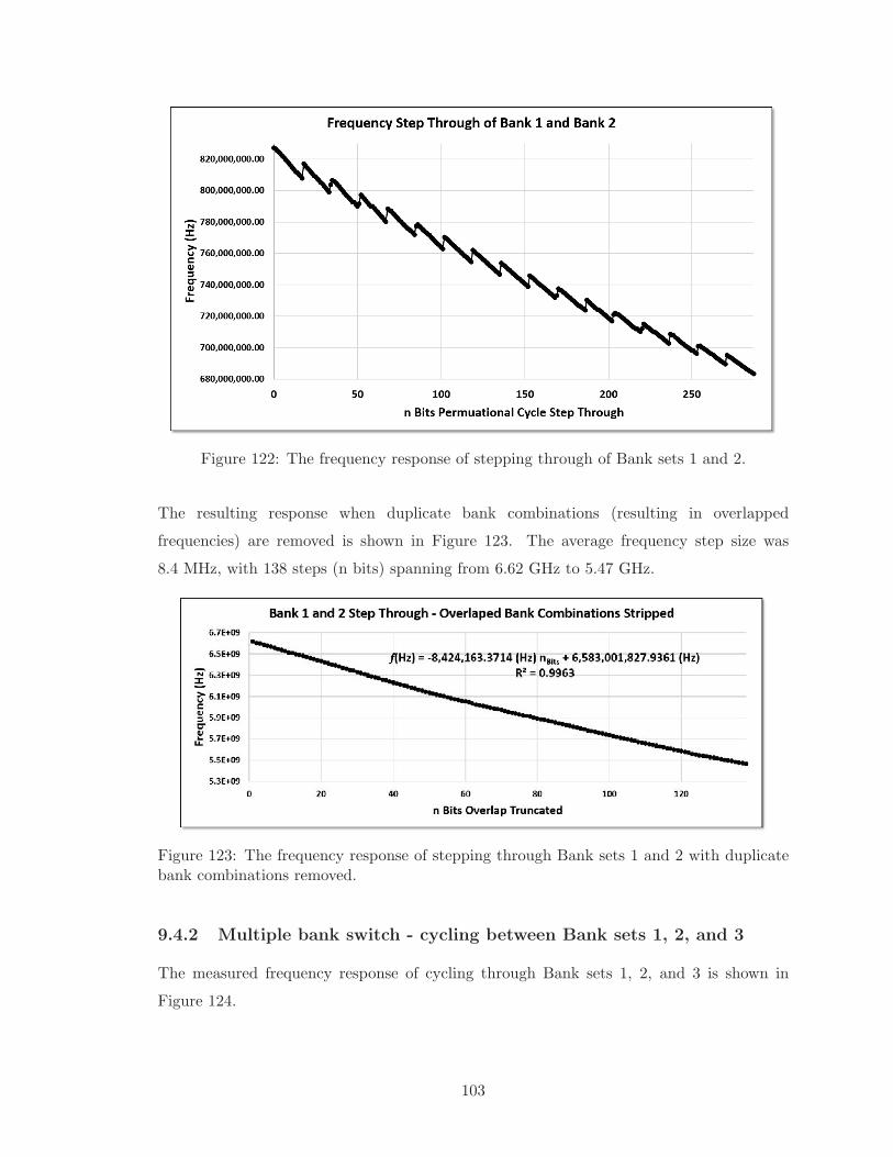
Figure 122: The frequency response of stepping through of Bank sets 1 and 2.
The resulting response when duplicate bank combinations (resulting in overlapped
frequencies) are removed is shown in Figure 123. The average frequency step size was
8.4 MHz, with 138 steps (n bits) spanning from 6.62 GHz to 5.47 GHz.
Figure 123: The frequency response of stepping through Bank sets 1 and 2 with duplicatebank combinations removed.
9.4.2 Multiple bank switch - cycling between Bank sets 1, 2, and 3
The measured frequency response of cycling through Bank sets 1, 2, and 3 is shown in
Figure 124.
103
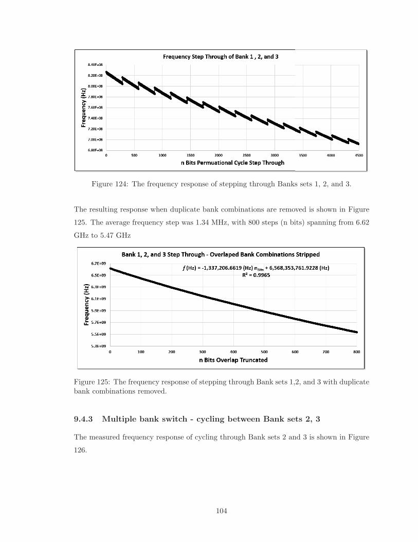
Figure 124: The frequency response of stepping through Banks sets 1, 2, and 3.
The resulting response when duplicate bank combinations are removed is shown in Figure
125. The average frequency step was 1.34 MHz, with 800 steps (n bits) spanning from 6.62
GHz to 5.47 GHz
Figure 125: The frequency response of stepping through Bank sets 1,2, and 3 with duplicatebank combinations removed.
9.4.3 Multiple bank switch - cycling between Bank sets 2, 3
The measured frequency response of cycling through Bank sets 2 and 3 is shown in Figure
126.
104
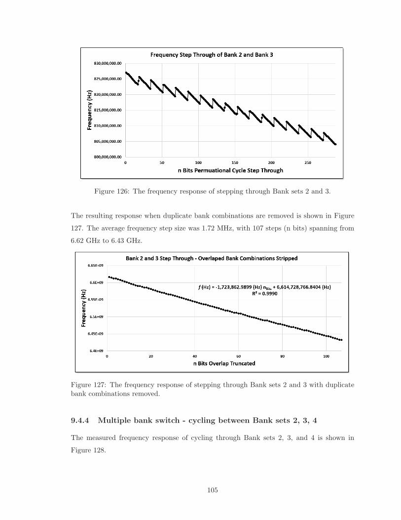
Figure 126: The frequency response of stepping through Bank sets 2 and 3.
The resulting response when duplicate bank combinations are removed is shown in Figure
127. The average frequency step size was 1.72 MHz, with 107 steps (n bits) spanning from
6.62 GHz to 6.43 GHz.
Figure 127: The frequency response of stepping through Bank sets 2 and 3 with duplicatebank combinations removed.
9.4.4 Multiple bank switch - cycling between Bank sets 2, 3, 4
The measured frequency response of cycling through Bank sets 2, 3, and 4 is shown in
Figure 128.
105
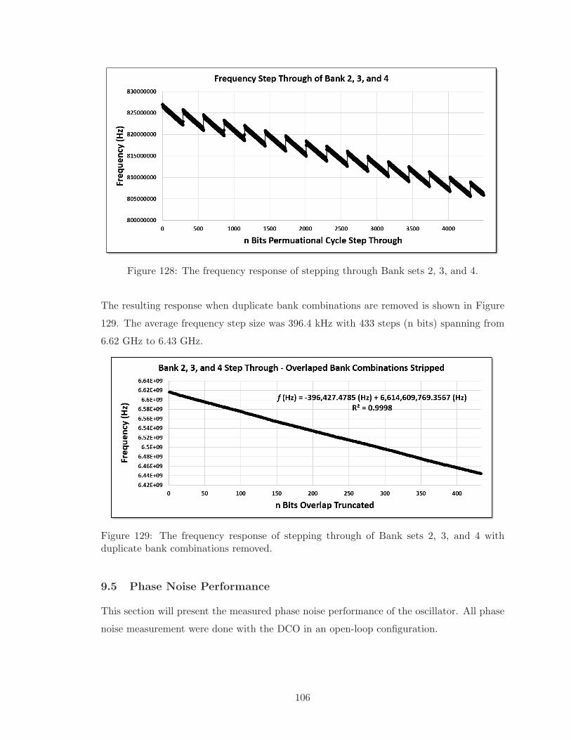
Figure 128: The frequency response of stepping through Bank sets 2, 3, and 4.
The resulting response when duplicate bank combinations are removed is shown in Figure
129. The average frequency step size was 396.4 kHz with 433 steps (n bits) spanning from
6.62 GHz to 6.43 GHz.
Figure 129: The frequency response of stepping through of Bank sets 2, 3, and 4 withduplicate bank combinations removed.
9.5 Phase Noise Performance
This section will present the measured phase noise performance of the oscillator. All phase
noise measurement were done with the DCO in an open-loop configuration.
106
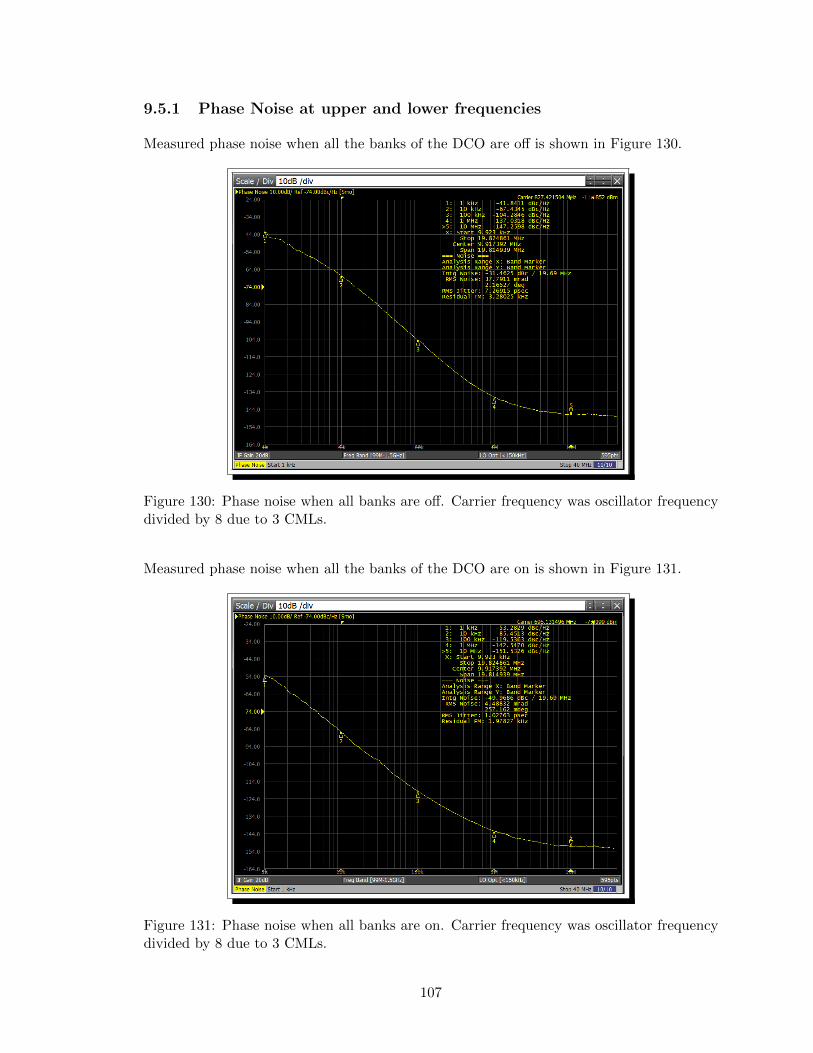
9.5.1 Phase Noise at upper and lower frequencies
Measured phase noise when all the banks of the DCO are off is shown in Figure 130.
Figure 130: Phase noise when all banks are off. Carrier frequency was oscillator frequencydivided by 8 due to 3 CMLs.
Measured phase noise when all the banks of the DCO are on is shown in Figure 131.
Figure 131: Phase noise when all banks are on. Carrier frequency was oscillator frequencydivided by 8 due to 3 CMLs.
107
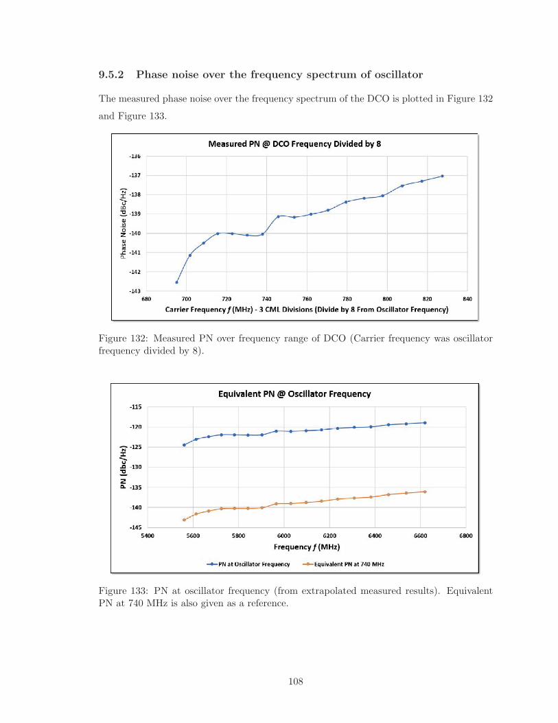
9.5.2 Phase noise over the frequency spectrum of oscillator
The measured phase noise over the frequency spectrum of the DCO is plotted in Figure 132
and Figure 133.
Figure 132: Measured PN over frequency range of DCO (Carrier frequency was oscillatorfrequency divided by 8).
Figure 133: PN at oscillator frequency (from extrapolated measured results). EquivalentPN at 740 MHz is also given as a reference.
108
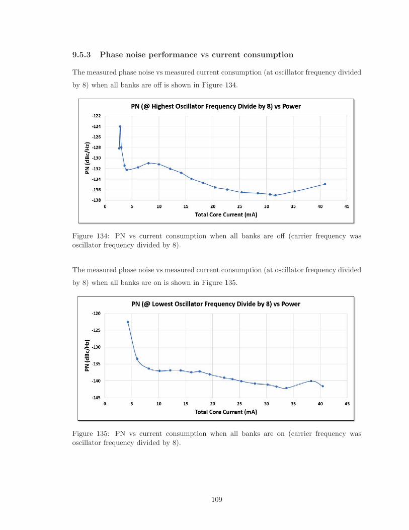
9.5.3 Phase noise performance vs current consumption
The measured phase noise vs measured current consumption (at oscillator frequency divided
by 8) when all banks are off is shown in Figure 134.
Figure 134: PN vs current consumption when all banks are off (carrier frequency wasoscillator frequency divided by 8).
The measured phase noise vs measured current consumption (at oscillator frequency divided
by 8) when all banks are on is shown in Figure 135.
Figure 135: PN vs current consumption when all banks are on (carrier frequency wasoscillator frequency divided by 8).
109

9.6 Figure of Merit
The measured FoM of the oscillator for different power levels for when the all the banks are
off and all the banks are on is shown in Figure 136 and Figure 137 respectively.
Figure 136: FoM of DCO vs various current consumption when all banks are off.
Figure 137: FoM of DCO vs various current consumption when all banks are on.
9.7 Measured Tuning Range of Oscillator
The measured tuning range of the entire oscillator frequency span (with all banks on and
off) was:
Tunning Range (TR) % = 100 ·[2(6.656 GHz)− 2(5.4456 GHz)
6.656 GHz + 5.4456 GHz
]≈ 20.00%
110
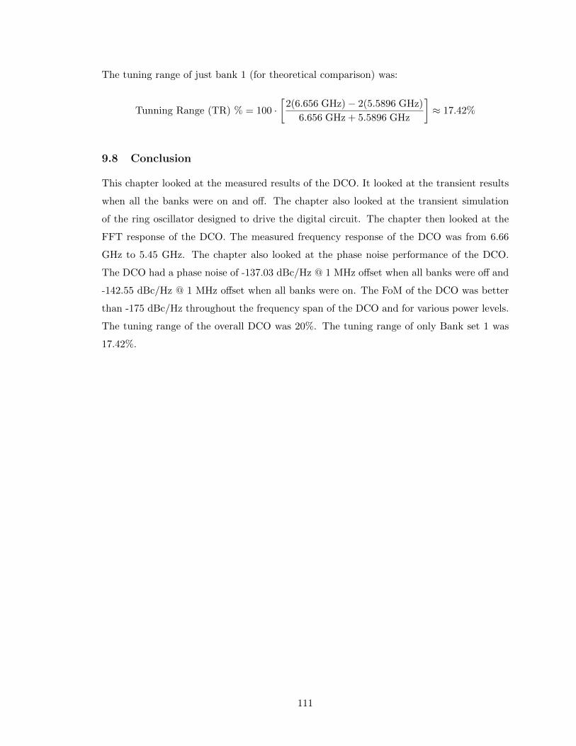
The tuning range of just bank 1 (for theoretical comparison) was:
Tunning Range (TR) % = 100 ·[
2(6.656 GHz)− 2(5.5896 GHz)
6.656 GHz + 5.5896 GHz
]≈ 17.42%
9.8 Conclusion
This chapter looked at the measured results of the DCO. It looked at the transient results
when all the banks were on and off. The chapter also looked at the transient simulation
of the ring oscillator designed to drive the digital circuit. The chapter then looked at the
FFT response of the DCO. The measured frequency response of the DCO was from 6.66
GHz to 5.45 GHz. The chapter also looked at the phase noise performance of the DCO.
The DCO had a phase noise of -137.03 dBc/Hz @ 1 MHz offset when all banks were off and
-142.55 dBc/Hz @ 1 MHz offset when all banks were on. The FoM of the DCO was better
than -175 dBc/Hz throughout the frequency span of the DCO and for various power levels.
The tuning range of the overall DCO was 20%. The tuning range of only Bank set 1 was
17.42%.
111
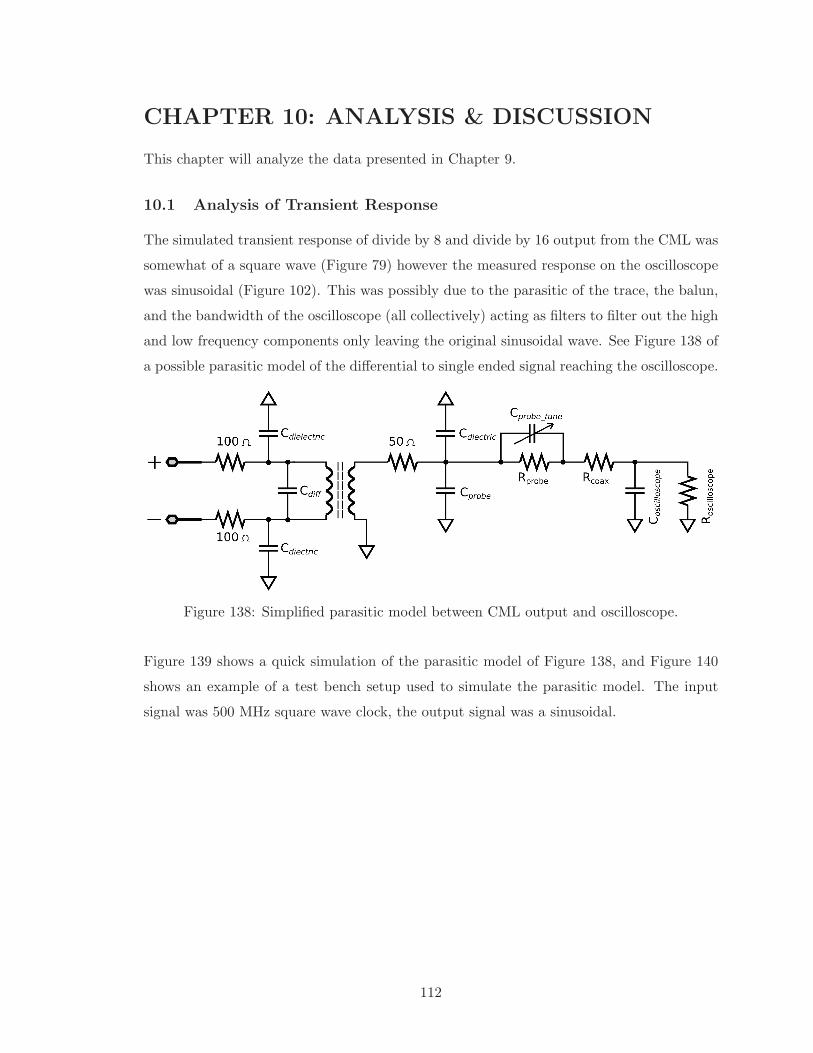
CHAPTER 10: ANALYSIS & DISCUSSION
This chapter will analyze the data presented in Chapter 9.
10.1 Analysis of Transient Response
The simulated transient response of divide by 8 and divide by 16 output from the CML was
somewhat of a square wave (Figure 79) however the measured response on the oscilloscope
was sinusoidal (Figure 102). This was possibly due to the parasitic of the trace, the balun,
and the bandwidth of the oscilloscope (all collectively) acting as filters to filter out the high
and low frequency components only leaving the original sinusoidal wave. See Figure 138 of
a possible parasitic model of the differential to single ended signal reaching the oscilloscope.
Figure 138: Simplified parasitic model between CML output and oscilloscope.
Figure 139 shows a quick simulation of the parasitic model of Figure 138, and Figure 140
shows an example of a test bench setup used to simulate the parasitic model. The input
signal was 500 MHz square wave clock, the output signal was a sinusoidal.
112
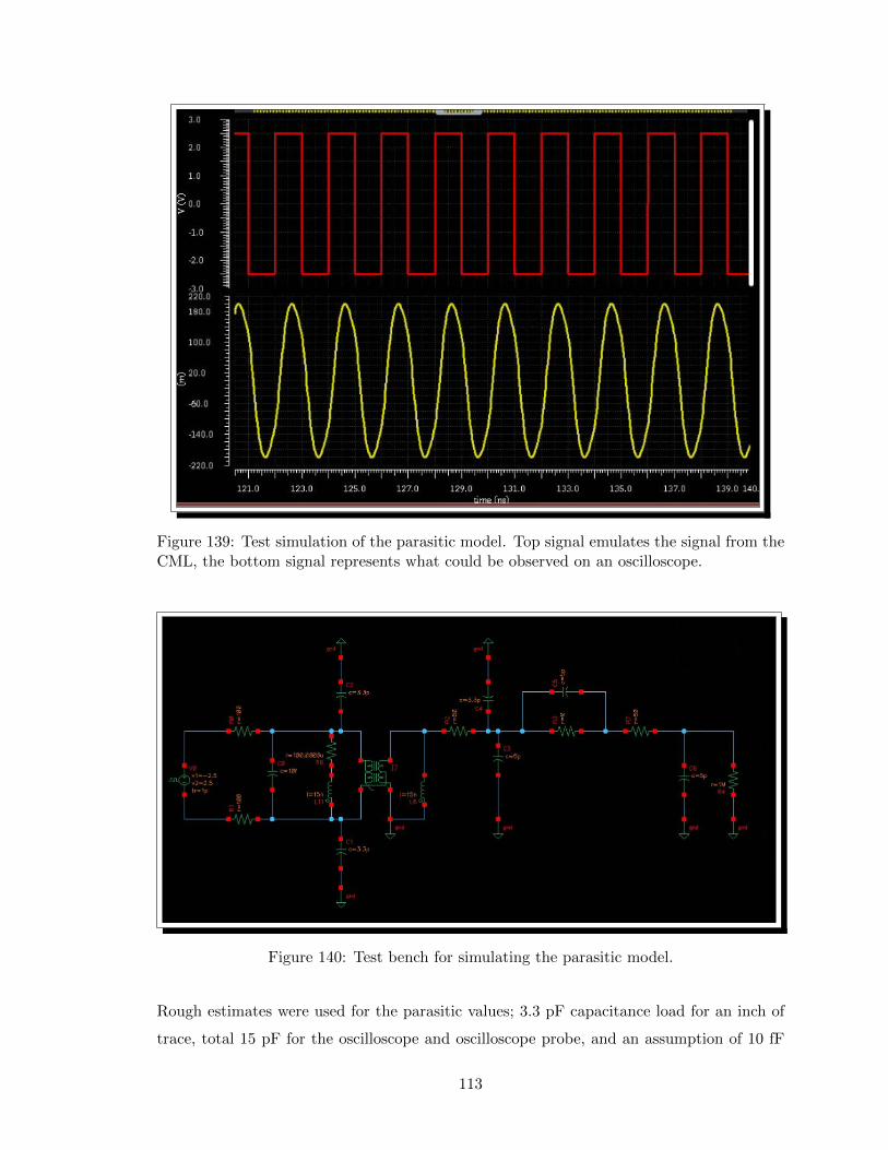
Figure 139: Test simulation of the parasitic model. Top signal emulates the signal from theCML, the bottom signal represents what could be observed on an oscilloscope.
Figure 140: Test bench for simulating the parasitic model.
Rough estimates were used for the parasitic values; 3.3 pF capacitance load for an inch of
trace, total 15 pF for the oscilloscope and oscilloscope probe, and an assumption of 10 fF
113
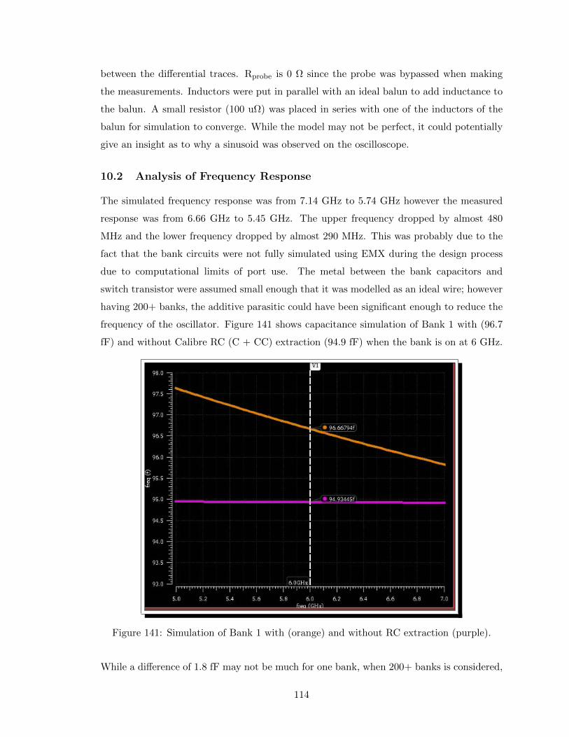
between the differential traces. Rprobe is 0 Ω since the probe was bypassed when making
the measurements. Inductors were put in parallel with an ideal balun to add inductance to
the balun. A small resistor (100 uΩ) was placed in series with one of the inductors of the
balun for simulation to converge. While the model may not be perfect, it could potentially
give an insight as to why a sinusoid was observed on the oscilloscope.
10.2 Analysis of Frequency Response
The simulated frequency response was from 7.14 GHz to 5.74 GHz however the measured
response was from 6.66 GHz to 5.45 GHz. The upper frequency dropped by almost 480
MHz and the lower frequency dropped by almost 290 MHz. This was probably due to the
fact that the bank circuits were not fully simulated using EMX during the design process
due to computational limits of port use. The metal between the bank capacitors and
switch transistor were assumed small enough that it was modelled as an ideal wire; however
having 200+ banks, the additive parasitic could have been significant enough to reduce the
frequency of the oscillator. Figure 141 shows capacitance simulation of Bank 1 with (96.7
fF) and without Calibre RC (C + CC) extraction (94.9 fF) when the bank is on at 6 GHz.
Figure 141: Simulation of Bank 1 with (orange) and without RC extraction (purple).
While a difference of 1.8 fF may not be much for one bank, when 200+ banks is considered,
114
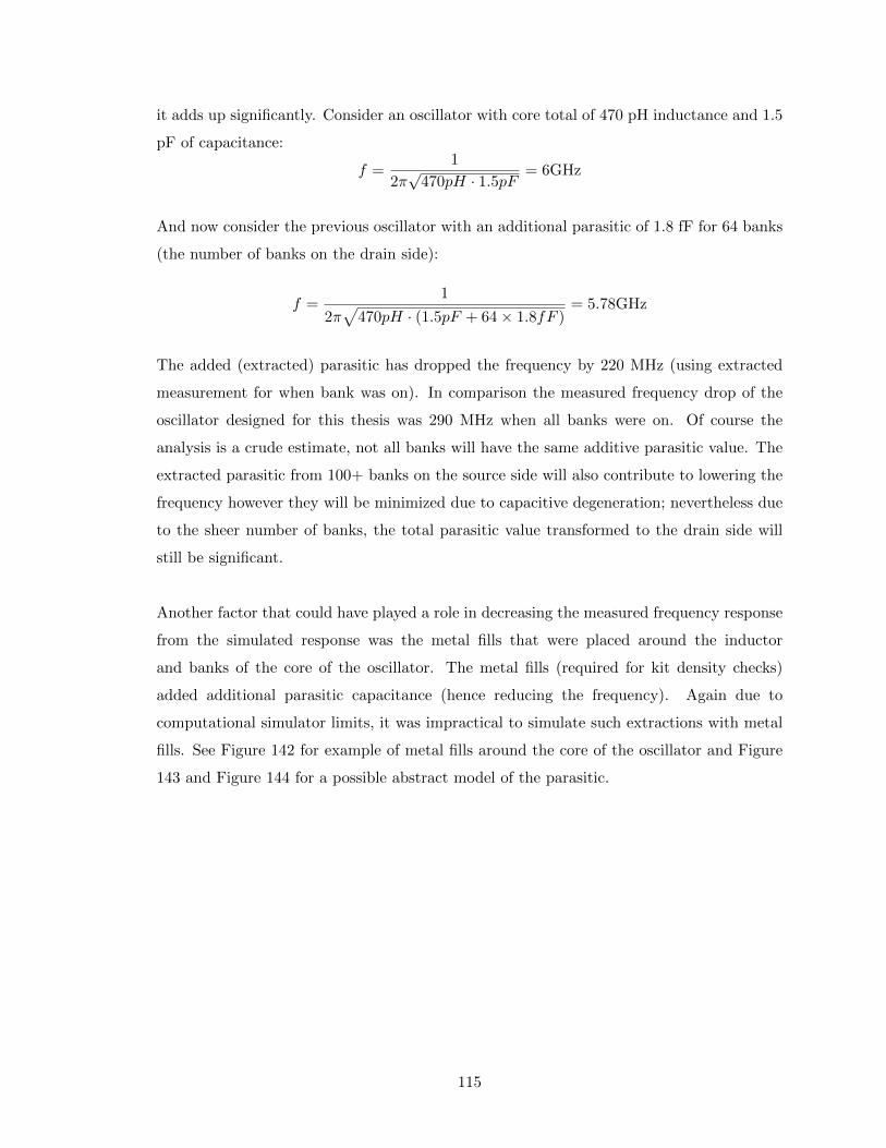
it adds up significantly. Consider an oscillator with core total of 470 pH inductance and 1.5
pF of capacitance:
f =1
2π√
470pH · 1.5pF= 6GHz
And now consider the previous oscillator with an additional parasitic of 1.8 fF for 64 banks
(the number of banks on the drain side):
f =1
2π√
470pH · (1.5pF + 64× 1.8fF )= 5.78GHz
The added (extracted) parasitic has dropped the frequency by 220 MHz (using extracted
measurement for when bank was on). In comparison the measured frequency drop of the
oscillator designed for this thesis was 290 MHz when all banks were on. Of course the
analysis is a crude estimate, not all banks will have the same additive parasitic value. The
extracted parasitic from 100+ banks on the source side will also contribute to lowering the
frequency however they will be minimized due to capacitive degeneration; nevertheless due
to the sheer number of banks, the total parasitic value transformed to the drain side will
still be significant.
Another factor that could have played a role in decreasing the measured frequency response
from the simulated response was the metal fills that were placed around the inductor
and banks of the core of the oscillator. The metal fills (required for kit density checks)
added additional parasitic capacitance (hence reducing the frequency). Again due to
computational simulator limits, it was impractical to simulate such extractions with metal
fills. See Figure 142 for example of metal fills around the core of the oscillator and Figure
143 and Figure 144 for a possible abstract model of the parasitic.
115
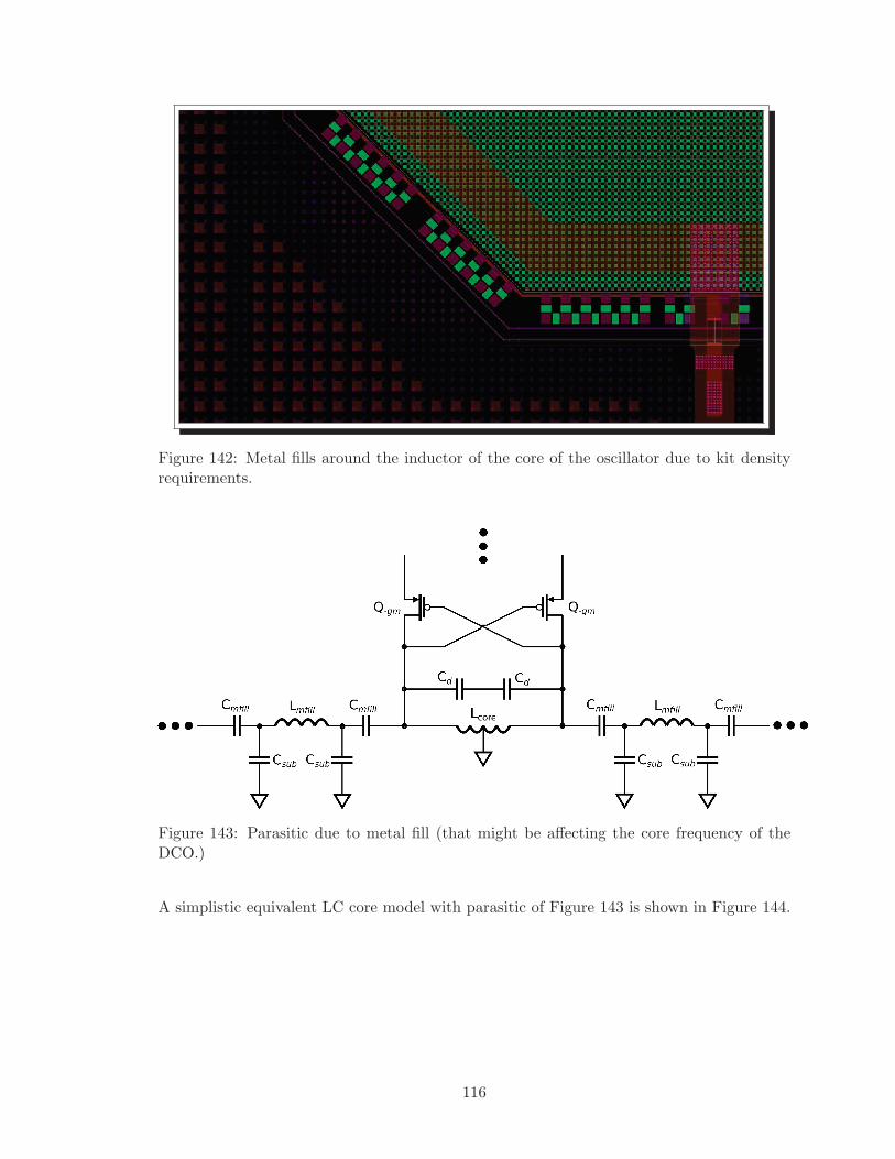
Figure 142: Metal fills around the inductor of the core of the oscillator due to kit densityrequirements.
Figure 143: Parasitic due to metal fill (that might be affecting the core frequency of theDCO.)
A simplistic equivalent LC core model with parasitic of Figure 143 is shown in Figure 144.
116
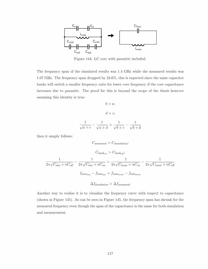
Figure 144: LC core with parasitic included.
The frequency span of the simulated results was 1.4 GHz while the measured results was
1.07 GHz. The frequency span dropped by 23.6%, this is expected since the same capacitor
banks will switch a smaller frequency ratio for lower core frequency if the core capacitance
increases due to parasitic. The proof for this is beyond the scope of the thesis however
assuming this identity is true:
b > a;
d > c;
1√a+ c
− 1√a+ d
>1√b+ c
− 1√b+ d
then it simply follows:
Cmeasured > Csimulation;
Cbankon > Cbankoff ;
1
2π√Csim + nCoff
− 1
2π√Csim + nCon
>1
2π√Cmeas + nCon
− 1
2π√Cmeas + nCoff
fmaxsim − fminsim > fmaxmeas − fminmeas
Δfsimulation > Δfmeasured
Another way to realize it is to visualize the frequency curve with respect to capacitance
(shown in Figure 145). As can be seen in Figure 145, the frequency span has shrunk for the
measured frequency even though the span of the capacitance is the same for both simulation
and measurement.
117

Figure 145: LC curve showing the frequency span between simulation and measurement.***Note: the image has been significantly pronounced and exaggerated to get the point acrossand is not to scale.
The tuning range was almost the same between simulation (21.7%) and measured results
(20.0%). This is also expected if:
Csimulation << nCbankoff
Cmeasured << nCbankoff
then:
(TR)sim =
2
(1√
L(Csim+nCoff)
)− 2
(1√
L(Csim+nCon)
)1√
L(Csim+nCoff)− 1√
L(Csim+nCon)
≈2
(1√
L(nCoff)
)− 2
(1√
L(nCon)
)1√
L(nCoff)− 1√
L(nCon)
(TR)meas =
2
(1√
L(Cmeas+nCoff)
)− 2
(1√
L(Cmeas+nCon)
)1√
L(Cmeas+nCoff)− 1√
L(Cmeas+nCon)
≈2
(1√
L(nCoff)
)− 2
(1√
L(nCon)
)1√
L(nCoff)− 1√
L(nCon)
∴ (TR)sim ≈ (TR)meas
Table 5 summarizes and compares the frequency response between the theoretical, simulated
and measured response for Bank set 1 of the DCO.
118
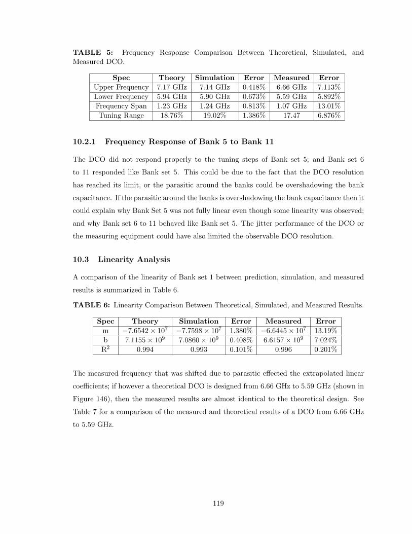
TABLE 5: Frequency Response Comparison Between Theoretical, Simulated, andMeasured DCO.
Spec Theory Simulation Error Measured Error
Upper Frequency 7.17 GHz 7.14 GHz 0.418% 6.66 GHz 7.113%
Lower Frequency 5.94 GHz 5.90 GHz 0.673% 5.59 GHz 5.892%
Frequency Span 1.23 GHz 1.24 GHz 0.813% 1.07 GHz 13.01%
Tuning Range 18.76% 19.02% 1.386% 17.47 6.876%
10.2.1 Frequency Response of Bank 5 to Bank 11
The DCO did not respond properly to the tuning steps of Bank set 5; and Bank set 6
to 11 responded like Bank set 5. This could be due to the fact that the DCO resolution
has reached its limit, or the parasitic around the banks could be overshadowing the bank
capacitance. If the parasitic around the banks is overshadowing the bank capacitance then it
could explain why Bank Set 5 was not fully linear even though some linearity was observed;
and why Bank set 6 to 11 behaved like Bank set 5. The jitter performance of the DCO or
the measuring equipment could have also limited the observable DCO resolution.
10.3 Linearity Analysis
A comparison of the linearity of Bank set 1 between prediction, simulation, and measured
results is summarized in Table 6.
TABLE 6: Linearity Comparison Between Theoretical, Simulated, and Measured Results.
Spec Theory Simulation Error Measured Error
m −7.6542× 10⁷ −7.7598× 10⁷ 1.380% −6.6445× 10⁷ 13.19%
b 7.1155× 10⁹ 7.0860× 10⁹ 0.408% 6.6157× 10⁹ 7.024%
R2 0.994 0.993 0.101% 0.996 0.201%
The measured frequency that was shifted due to parasitic effected the extrapolated linear
coefficients; if however a theoretical DCO is designed from 6.66 GHz to 5.59 GHz (shown in
Figure 146), then the measured results are almost identical to the theoretical design. See
Table 7 for a comparison of the measured and theoretical results of a DCO from 6.66 GHz
to 5.59 GHz.
119
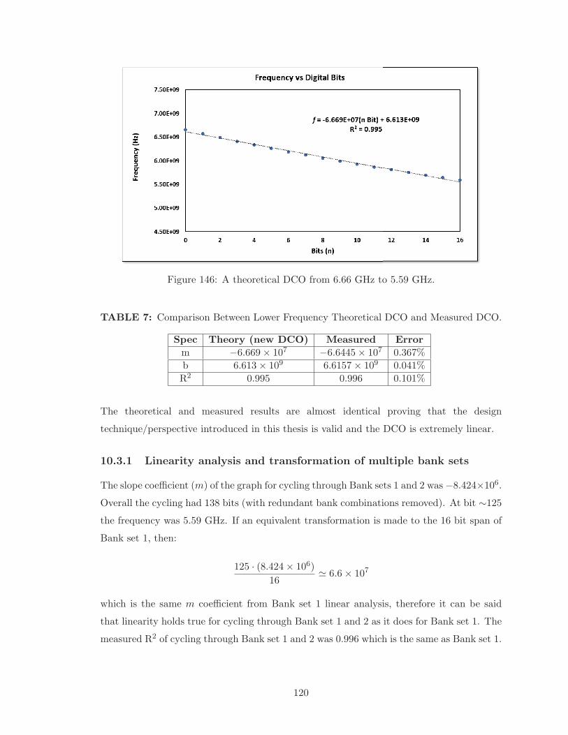
Figure 146: A theoretical DCO from 6.66 GHz to 5.59 GHz.
TABLE 7: Comparison Between Lower Frequency Theoretical DCO and Measured DCO.
Spec Theory (new DCO) Measured Error
m −6.669× 10⁷ −6.6445× 10⁷ 0.367%
b 6.613× 10⁹ 6.6157× 10⁹ 0.041%
R2 0.995 0.996 0.101%
The theoretical and measured results are almost identical proving that the design
technique/perspective introduced in this thesis is valid and the DCO is extremely linear.
10.3.1 Linearity analysis and transformation of multiple bank sets
The slope coefficient (m) of the graph for cycling through Bank sets 1 and 2 was−8.424×10⁶.Overall the cycling had 138 bits (with redundant bank combinations removed). At bit ∼125the frequency was 5.59 GHz. If an equivalent transformation is made to the 16 bit span of
Bank set 1, then:
125 · (8.424× 106)
16 6.6× 10⁷
which is the same m coefficient from Bank set 1 linear analysis, therefore it can be said
that linearity holds true for cycling through Bank set 1 and 2 as it does for Bank set 1. The
measured R2 of cycling through Bank set 1 and 2 was 0.996 which is the same as Bank set 1.
120
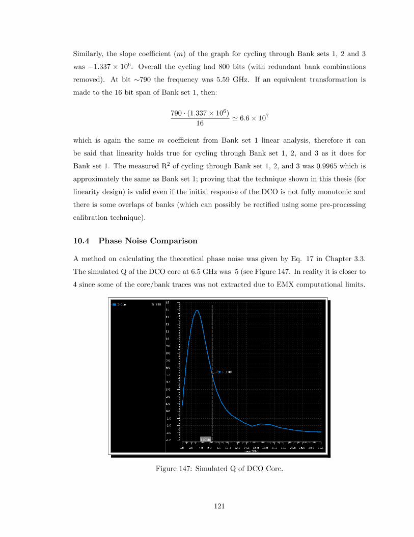
Similarly, the slope coefficient (m) of the graph for cycling through Bank sets 1, 2 and 3
was −1.337 × 10⁶. Overall the cycling had 800 bits (with redundant bank combinations
removed). At bit ∼790 the frequency was 5.59 GHz. If an equivalent transformation is
made to the 16 bit span of Bank set 1, then:
790 · (1.337× 106)
16' 6.6× 10⁷
which is again the same m coefficient from Bank set 1 linear analysis, therefore it can
be said that linearity holds true for cycling through Bank set 1, 2, and 3 as it does for
Bank set 1. The measured R2 of cycling through Bank set 1, 2, and 3 was 0.9965 which is
approximately the same as Bank set 1; proving that the technique shown in this thesis (for
linearity design) is valid even if the initial response of the DCO is not fully monotonic and
there is some overlaps of banks (which can possibly be rectified using some pre-processing
calibration technique).
10.4 Phase Noise Comparison
A method on calculating the theoretical phase noise was given by Eq. 17 in Chapter 3.3.
The simulated Q of the DCO core at 6.5 GHz was 5 (see Figure 147. In reality it is closer to
4 since some of the core/bank traces was not extracted due to EMX computational limits.
Figure 147: Simulated Q of DCO Core.
121
The tank voltage was 2.5 V (from Figure 64), then:
P =1
2VtankI = (0.5)(2.5 V)(14 mA) = 17.5 mW
PN = 10·log10
(√2(2π6.5GHz)
2(4)(2π1MHz)
)2(1.67(1.38× 10⁻²³J/K)(298K)
2(17.5mW)
) ' −125.87 dBc/Hz
The simulated phase noise at 6.5 GHz (@ 14 mA) was -125 dBc/Hz (Figure 74), and the
measured phase noise at 6.5 GHz (@ 14 mA) was -115 dBc/Hz. The phase noise comparison
is summarized in Table 8.
TABLE 8: Comparison of Theoretical, Simulated, and Measured PN Results at 6.5 GHz(I = 14 mA).
* Theoretical Simulation Measurement
PN −126 dBc/Hz −125 dBc/Hz −115 dBc/Hz
The simulated and theoretical values match closely however it is hard to pinpoint what
caused the 10 dB drop in the measured results. Approximately 2-3 dB drop can possibly
be attributed to signal degradation from the CML divisions. If the tank Q (in reality) was
actually closer to ∼1.8 due to all the metal fills and digital routing traces around the core
(not accounted during EMX simulations), then
PN = 10 · log10
( √2(2π6.5GHz)
2(1.8)(2π1MHz)
)2(1.67(1.38× 10⁻²³J/K)(298K)
2(17.5mW)
) ' −119 dBc/Hz
Then you have 2 dB of CML division performance loss and 2 dB of digital noise bleed:
PN = −119 dBc/Hz + 2 dB [CML loss] + 2 dB [noise bleed] = −115 dBc/Hz
The above statement can ‘potentially’ explain why there is noise performance loss. In fact
it has been experimentally observed that with a poor digital clock (high jitter), the PN
performance got reduced by 10 dB or more.
Another factor that could have degraded the phase noise was the fact that the short metal
traces inside the banks were simulated using ideal wires instead of being fully extracted
using EMX (due to computational limits). The parasitic that was not extracted will likely
122
decrease the Q of the bank (since both R and C will increase with extraction), and hence
degrade the overall PN of the oscillator. Nevertheless the measured FoM at 6.5 GHz (@ 14
mA) was -179 dBc/Hz. While -179 dBc/Hz FoM is not at the -183 dBc/Hz FoM mark like
typical state of the art VCOs, the DCO is still producing decent performance considering
the tank core is loaded with lots of banks.
10.5 FoM Comparison
The simulated (Figure 78) and measured (Figure 136) curves have similar topology. Of
course since the measured phase noise was worse than the simulated phase noise, it is also
expected that the measured FoM (Figure 136) would be worse than the simulated FoM
(Figure 78).
10.6 Conclusion
This chapter analyzed the theoretical, simulated, and measured results of the DCO. The
measured frequency response of the DCO dropped by 480 MHz from simulated results for
the upper frequency and 290 MHz for the lower frequency. This was probably because
of parasitic capacitance around the core of the oscillator due to kit metal fill density
requirements. The phase noise of the measured DCO was almost 10 dB lower than the
simulated and theoretical values leading to believe that the Q of the core was worse than
simulated, that there was digital bleeding and that there was quite a loss from CML
performance (2-3 dB). Nevertheless the measured FoM at 6.5 GHz (@ 14 mA) was -179
dBc/Hz which was still a decent performance.
123
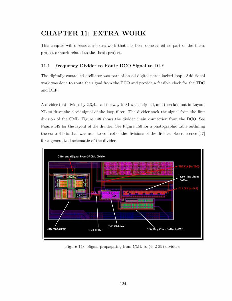
CHAPTER 11: EXTRA WORK
This chapter will discuss any extra work that has been done as either part of the thesis
project or work related to the thesis project.
11.1 Frequency Divider to Route DCO Signal to DLF
The digitally controlled oscillator was part of an all-digital phase-locked loop. Additional
work was done to route the signal from the DCO and provide a feasible clock for the TDC
and DLF.
A divider that divides by 2,3,4... all the way to 31 was designed, and then laid out in Layout
XL to drive the clock signal of the loop filter. The divider took the signal from the first
division of the CML. Figure 148 shows the divider chain connection from the DCO. See
Figure 149 for the layout of the divider. See Figure 150 for a photographic table outlining
the control bits that was used to control of the divisions of the divider. See reference [47]
for a generalized schematic of the divider.
Figure 148: Signal propagating from CML to (÷ 2-39) dividers.
124
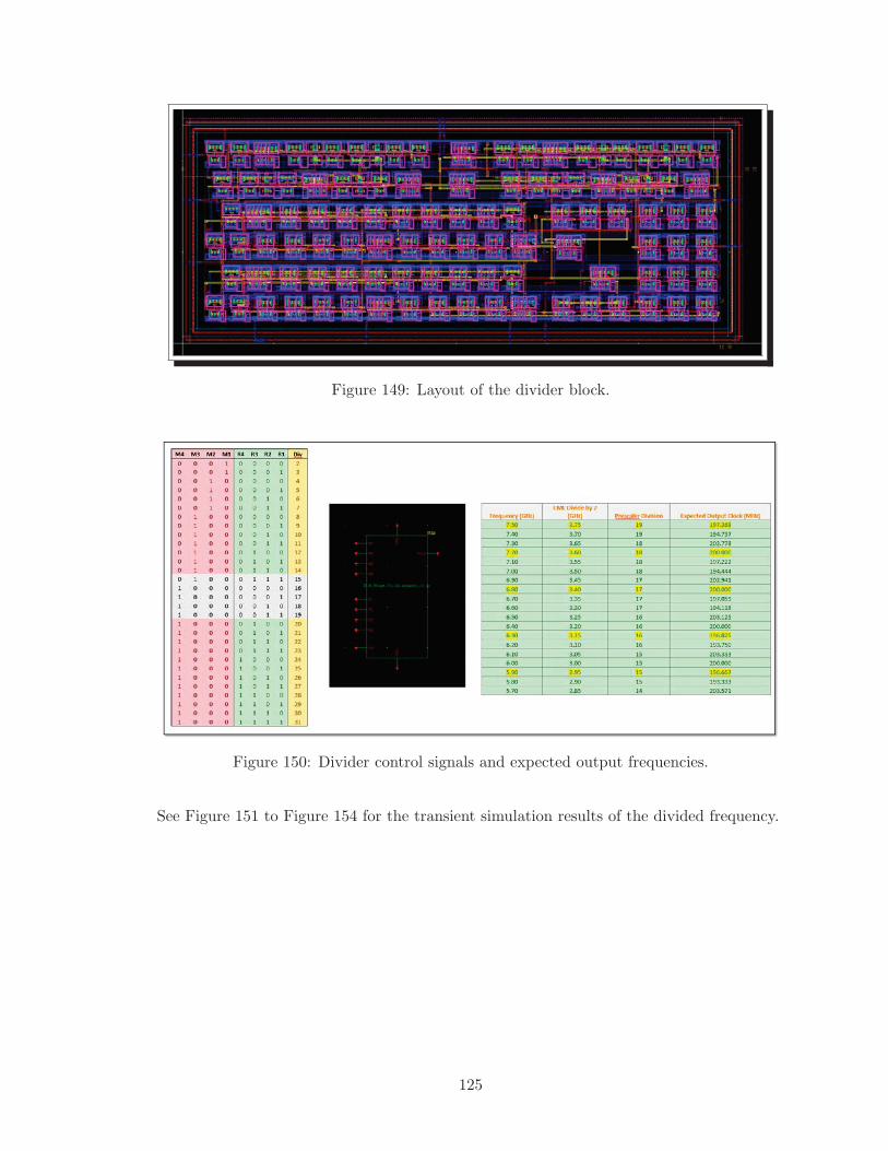
Figure 149: Layout of the divider block.
Figure 150: Divider control signals and expected output frequencies.
See Figure 151 to Figure 154 for the transient simulation results of the divided frequency.
125
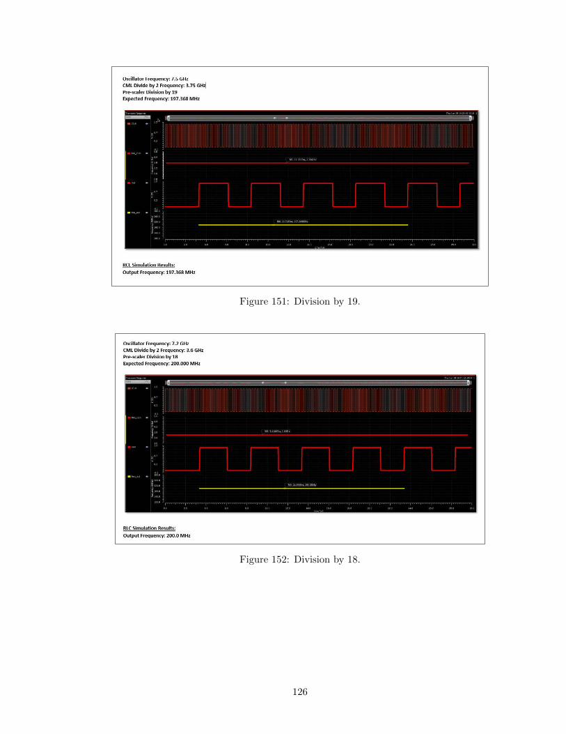
Figure 151: Division by 19.
Figure 152: Division by 18.
126
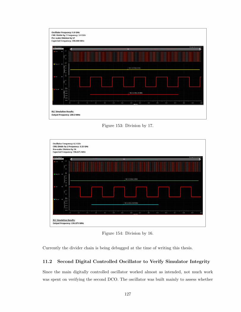
Figure 153: Division by 17.
Figure 154: Division by 16.
Currently the divider chain is being debugged at the time of writing this thesis.
11.2 Second Digital Controlled Oscillator to Verify Simulator Integrity
Since the main digitally controlled oscillator worked almost as intended, not much work
was spent on verifying the second DCO. The oscillator was built mainly to assess whether
127
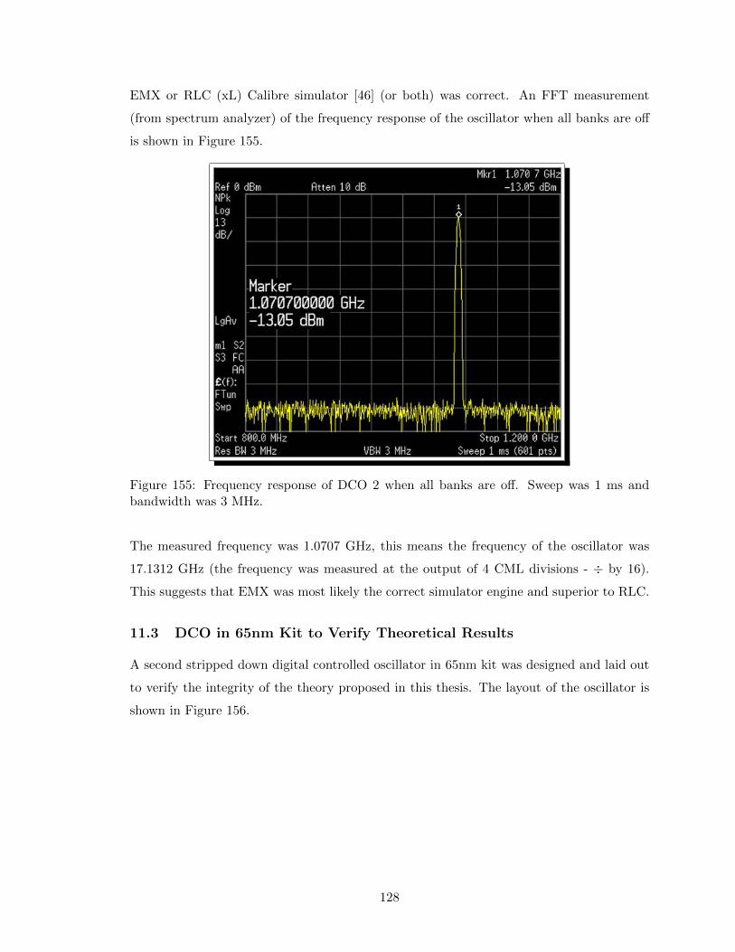
EMX or RLC (xL) Calibre simulator [46] (or both) was correct. An FFT measurement
(from spectrum analyzer) of the frequency response of the oscillator when all banks are off
is shown in Figure 155.
Figure 155: Frequency response of DCO 2 when all banks are off. Sweep was 1 ms andbandwidth was 3 MHz.
The measured frequency was 1.0707 GHz, this means the frequency of the oscillator was
17.1312 GHz (the frequency was measured at the output of 4 CML divisions - ÷ by 16).
This suggests that EMX was most likely the correct simulator engine and superior to RLC.
11.3 DCO in 65nm Kit to Verify Theoretical Results
A second stripped down digital controlled oscillator in 65nm kit was designed and laid out
to verify the integrity of the theory proposed in this thesis. The layout of the oscillator is
shown in Figure 156.
128
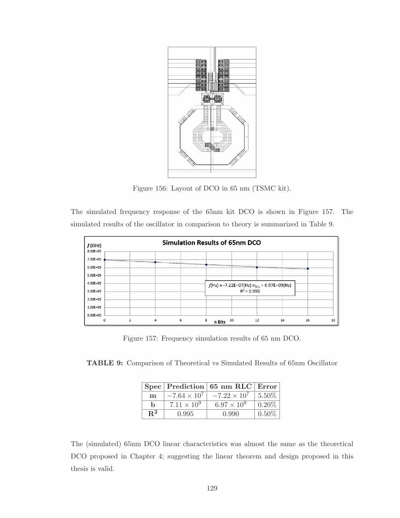
Figure 156: Layout of DCO in 65 nm (TSMC kit).
The simulated frequency response of the 65nm kit DCO is shown in Figure 157. The
simulated results of the oscillator in comparison to theory is summarized in Table 9.
Figure 157: Frequency simulation results of 65 nm DCO.
TABLE 9: Comparison of Theoretical vs Simulated Results of 65nm Oscillator
Spec Prediction 65 nm RLC Error
m −7.64× 10⁷ −7.22× 10⁷ 5.50%
b 7.11× 10⁹ 6.97× 10⁹ 0.20%
R2 0.995 0.990 0.50%
The (simulated) 65nm DCO linear characteristics was almost the same as the theoretical
DCO proposed in Chapter 4; suggesting the linear theorem and design proposed in this
thesis is valid.
129
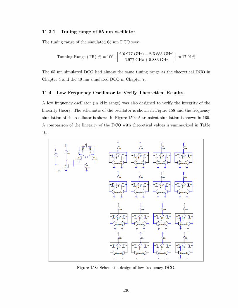
11.3.1 Tuning range of 65 nm oscillator
The tuning range of the simulated 65 nm DCO was:
Tunning Range (TR) % = 100 ·[
2(6.977 GHz)− 2(5.883 GHz)
6.977 GHz + 5.883 GHz
]≈ 17.01%
The 65 nm simulated DCO had almost the same tuning range as the theoretical DCO in
Chapter 4 and the 40 nm simulated DCO in Chapter 7.
11.4 Low Frequency Oscillator to Verify Theoretical Results
A low frequency oscillator (in kHz range) was also designed to verify the integrity of the
linearity theory. The schematic of the oscillator is shown in Figure 158 and the frequency
simulation of the oscillator is shown in Figure 159. A transient simulation is shown in 160.
A comparison of the linearity of the DCO with theoretical values is summarized in Table
10.
Figure 158: Schematic design of low frequency DCO.
130
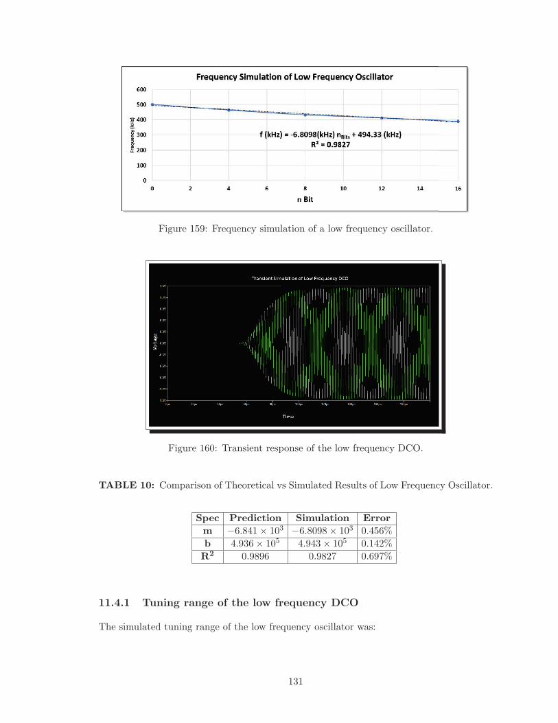
Figure 159: Frequency simulation of a low frequency oscillator.
Figure 160: Transient response of the low frequency DCO.
TABLE 10: Comparison of Theoretical vs Simulated Results of Low Frequency Oscillator.
Spec Prediction Simulation Error
m −6.841× 10³ −6.8098× 10³ 0.456%
b 4.936× 10⁵ 4.943× 10⁵ 0.142%
R2 0.9896 0.9827 0.697%
11.4.1 Tuning range of the low frequency DCO
The simulated tuning range of the low frequency oscillator was:
131
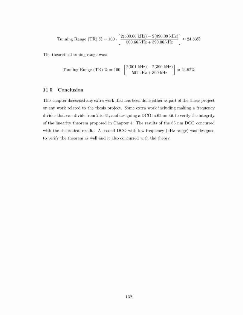
Tunning Range (TR) % = 100 ·[
2(500.66 kHz)− 2(390.09 kHz)
500.66 kHz + 390.06 kHz
]≈ 24.83%
The theoretical tuning range was:
Tunning Range (TR) % = 100 ·[
2(501 kHz)− 2(390 kHz)
501 kHz + 390 kHz
]≈ 24.92%
11.5 Conclusion
This chapter discussed any extra work that has been done either as part of the thesis project
or any work related to the thesis project. Some extra work including making a frequency
divider that can divide from 2 to 31, and designing a DCO in 65nm kit to verify the integrity
of the linearity theorem proposed in Chapter 4. The results of the 65 nm DCO concurred
with the theoretical results. A second DCO with low frequency (kHz range) was designed
to verify the theorem as well and it also concurred with the theory.
132
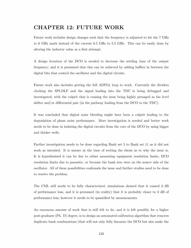
CHAPTER 12: FUTURE WORK
Future work includes design changes such that the frequency is adjusted to hit the 7 GHz
to 6 GHz mark instead of the current 6.5 GHz to 5.5 GHz. This can be easily done by
altering the inductor value as a first attempt.
A design iteration of the DCO is needed to decrease the settling time of the output
frequency; and it is presumed that this can be achieved by adding buffers in between the
digital bits that control the oscillator and the digital circuits.
Future work also includes getting the full ADPLL loop to work. Currently the dividers
clocking the SPI-DLF and the signal leading into the TDC is being debugged and
investigated; with the culprit that is causing the issue being highly presaged as the level
shifter and/or differential pair (in the pathway leading from the DCO to the TDC).
It was concluded that digital noise bleeding might have been a culprit leading to the
degradation of phase noise performance. More investigation is needed and better work
needs to be done in isolating the digital circuits from the core of the DCO by using bigger
and thicker wells.
Further investigation needs to be done regarding Bank set 5 to Bank set 11 as it did not
work as intended. It is unsure at the time of writing the thesis as to why the issue is.
It is hypothesised it can be due to either measuring equipment resolution limits, DCO
resolution limits due to parasitic, or because the bank sets were on the source side of the
oscillator. All of these possibilities confounds the issue and further studies need to be done
to resolve the problem.
The CML still needs to be fully characterized, simulations showed that it caused 2 dB
of performance loss, and it is presumed (in reality) that it is probably closer to 3 dB of
performance loss, however it needs to be quantified by measurements.
An enormous amount of work that is still left to do, and it is left possibly for a higher
post-graduate (Ph. D) degree, is to design an automated calibration algorithm that removes
duplicate bank combinations (that will not only fully linearize the DCO but also make the
133
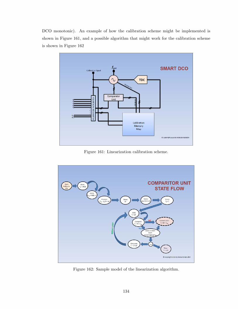
DCO monotonic). An example of how the calibration scheme might be implemented is
shown in Figure 161, and a possible algorithm that might work for the calibration scheme
is shown in Figure 162
Figure 161: Linearization calibration scheme.
Figure 162: Sample model of the linearization algorithm.
134
A sample execution of the algorithm is shown in Figure 186.
Figure 163: Example simulation of the linearization algorithm.
Overall there is still plenty of work left to do regarding the DCO before it can be used as a
daily driver for products; however as a first step the DCO experiment was a great success.
12.1 Conclusion
This chapter discussed any future work that is still left to be done regarding the DCO.
Future work includes decreasing the frequency settling time of the DCO once a bank is
switched. Other future work included characterizing the CMLs and debugging the signals
leading up to the TDC from the DCO. Future work also included getting a full ADPLL
loop to work and investigating why bank sets 5 to 11 did not work as intended.
135
CHAPTER 13: THESIS SUMMARY
This thesis presented a new outlook or perspective on how to design an extremely linear
digitally controlled oscillators using a new concept known as linearity field maps. The
thesis first analyzed the theory regarding linearity and tuning range. It then proposed a
methodological way on how to design a theoretical linear DCO. It then showed how to
implement the theoretical DCO in practice by using a cascading pyramid scheme of banks
within banks to achieve the linearity. The contributions of the thesis were:
Introducing a new concept known as linearity field maps.
Using R2 as a tool for assessing linearity.
Showing how to theoretically design a linear LC DCO using the field maps.
And then creating a physical LC DCO using a cascading pyramid scheme of equal
banks within equal banks to achieve the linearity.
The theoretical and simulated DCOs were congruent with each other, in fact the linear
coefficient errors (m, b, and R2) were less than 1%; however the measured DCO’s frequency
response was slightly lower than the simulated results. This could have been because of
additional parasitic around the DCO core due to metal fills (required for chip tape-out).
The simulated and theoretical frequency response of the DCO was from 7.1GHz - 5.7
GHz whereas the measured frequency response of the DCO was from 6.6 Ghz to 5.5 GHz.
This caused all the linear coefficients of the measured DCO to be mismatched with the
initial theoretical values. However when a new theoretical DCO that ranges with the same
frequency span as the measured DCO is compared, then the coefficient errors were less
than 1%, proving that the design technique presented in this thesis was valid. The R2
value of the measured DCO was 0.996 which was extremely linear.
The theoretical phase noise and simulated phase noise concurred with each other (-125
dBc/Hz) however the measured phase noise was almost 10 dB lower. About 2-3 dB loss
could have been attributed due to poor CML performance. Some digital noise bleeding
could have also played a role in reducing the oscillators performance, nevertheless FoM was
still reasonable and respectable with FoM better than or equal to -175 dBc/Hz throughout
the entire span of the DCO (at it’s highest frequencies when all banks are off and at its
136
lowest frequency when all banks are on).
The measured Bank set 1 had a frequency step size of 66.4 MHz. The measured Bank
set 2 upper limit frequency step size was 9.91 MHz and lower limit frequency step
size was 6.20 MHz. The measured Bank set 3 had upper limit frequency step size
of 2.09 MHz and lower limit frequency step size 1.29 MHz. The measured Bank set 4
had upper limit frequency step size of 469 kHz and lower limit frequency step size of 267 kHz.
Extra work was also done to verify the theorem proposed in this thesis. A DCO designed
in lower kHz frequency range concurred with the theory proposed in this thesis as did a
second 7-6 GHz DCO designed in 65nm kit.
There is still plenty of work left to improve the DCO. Future work includes fixing the
settling time of the DCO when a bank is switched as it currently takes too long to settle.
Further investigation needs to be done regarding Bank set 5 to Bank set 11 as to why it
did not function as intended.
Nevertheless, overall the thesis experiment was a success in showing how to design a linear
digitally controlled oscillator, the DCO in the thesis worked even though frequency was
shifted, and the point of the thesis was made with regards to linearity.
13.1 Conclusion
The reason for this report was to satisfy the requirements for MASc graduate degree at
Carleton University and the purpose of this thesis was to present a new perspective on
how to design an extremely linear digitally controlled oscillator. This was achieved by
using equal bank steps in each bank sets. The thesis first analyzed the theory regarding
linearity and then manifested it in a physical DCO. The DCO’s frequency span was shifted
from the simulated results (possibly due to parasitic arising from metal fills and not fully
extracting the banks during simulations), nevertheless the DCO had a decent FoM better
than -175 dBc/Hz through its frequency span and for different power levels. Overall the
thesis experiment was a success in implementing a linear DCO, the DCO in the thesis
worked, and the point of the thesis was made. The thesis showed how to design a linear
digitally controlled oscillator.
137
REFERENCES
[1] J. W. M. Rogers and C. Plett, Radio Frequency Integrated Circuit Design. Norwood:Artech House, 2010.
[2] J. Wight, Lecture Notes for ELEC 5606, Phase-Locked Loops and ReceiverSynchronizers. Carleton University at Ottawa, Fall semester, 2016.
[3] A. Blanchard, Phase-Locked Loops: Application to Coherent Receiver Design.. NewYork, NY, USA: Willey, 1976.
[4] A. Tomar, R. K. Pokharel, H. Kanaya and K. Yoshida, ”Design of Monotonic DigitallyControlled Oscillator (DCO) for Wide Tuning Range, KIET International Journal ofCommunications and Electronics, vol. 1, no. 3, pp. 28-33, Dec. 2013.
[5] J. Gorji and M. B. Ghaznavi-Ghoushchi, ”A Process-Independent and Highly LinearDCO for Crowded Heterogeneous IoT Devices in 65-nm CMOS,” in IEEE Transactionson Very Large Scale Integration (VLSI) Systems, vol. PP, no. 99, pp. 1-11.
[6] T. S. Rathore, ”Synthesis and classification of LC oscillators,” 2017 2nd InternationalConference on Communication Systems, Computing and IT Applications (CSCITA),Mumbai, India, 2017, pp. 28-32.
[7] Tseng-Chuan Wang, ”Design of tuning bandwidth and linearity for VCO bymathematical solution and computer method,” RAWCON 2000. 2000 IEEE Radioand Wireless Conference (Cat. No.00EX404), Denver, CO, 2000, pp. 155-158.
[8] Jing Yongqi, He Guoyu and Xu Ding, ”A new realizable technique to improve the VCOlinearity,” 6th International Symposium on Antennas, Propagation and EM Theory,2003. Proceedings. 2003, Beijing, China, 2003, pp. 396-399.
[9] S. Kurachi, T. Yoshimasu, N. Itoh and K. Yonemura, ”5-GHz Band Highly LinearVCO IC with a Novel Resonant Circuit,” 2007 Topical Meeting on Silicon MonolithicIntegrated Circuits in RF Systems, Long Beach, CA, 2007, pp. 285-288.
[10] L. Grigorescu and I. Diaconescu, ”Theoretical and experimental research on thecurrent-mode RC oscillators,” 2016 8th International Conference on Electronics,Computers and Artificial Intelligence (ECAI), Ploiesti, 2016, pp. 1-6.
[11] F. Colodro and A. Torralba, ”Linearity Enhancement of VCO-Based Quantizers forSD Modulators by Means of a Tracking Loop,” in IEEE Transactions on Circuits andSystems II: Express Briefs, vol. 61, no. 6, pp. 383-387, June 2014.
[12] H. Venkatram, R. Inti and Un-Ku Moon, ”Least Mean Square calibration method forVCO non-linearity,” 2010 International Conference on Microelectronics, Cairo, 2010,pp. 1-4.
[13] Yun Chiu, C. W. Tsang, B. Nikolic and P. R. Gray, ”Least mean square adaptive digitalbackground calibration of pipelined analog-to-digital converters,” in IEEE Transactionson Circuits and Systems I: Regular Papers, vol. 51, no. 1, pp. 38-46, Jan. 2004.
138
[14] Nguyen Phuong Thi Le, K. T. Low and Libin Yao, ”High linearity voltage-controlledoscillator,” 2009 IEEE 8th International Conference on ASIC, Changsha, Hunan, 2009,pp. 363-366.
[15] B. Hanafi and E. Hegazi, ”A Technique for Truly Linear LC VCO Tuning, a Proof ofConcept,” 2007 Internatonal Conference on Microelectronics, Cairo, 2007, pp. 93-96.
[16] S. Kurachi, T. Yoshimasu, N. Itoh and K. Yonemura, ”5-GHz Band Highly LinearVCO IC with a Novel Resonant Circuit,” 2007 Topical Meeting on Silicon MonolithicIntegrated Circuits in RF Systems, Long Beach, CA, 2007, pp. 285-288.
[17] U. Wismar, D. Wisland and P. Andreani, ”Linearity of bulk-controlled inverter ringVCO in weak and strong inversion,” 2005 NORCHIP, Oulu, Finland, 2005, pp. 145-148.
[18] J. A. McNeill, ”Interpolating ring VCO with V-to-f linearity compensation,” inElectronics Letters, vol. 30, no. 24, pp. 2003-2004, 24 Nov. 1994.
[19] Jing Yongqi, He Guoyu and Xu Ding, ”A new realizable technique to improve the VCOlinearity,” 6th International Symposium on Antennas, Propagation and EM Theory,2003. Proceedings. 2003, Beijing, China, 2003, pp. 396-399.
[20] L. Liangbing and T. Yaqing, ”A new realizable structure to improve VCO linearity,”2007 8th International Conference on Electronic Measurement and Instruments, Xi’an,2007, pp. 4-625-4-629.
[21] E. Ayranci, K. Christensen and P. Andreani, ”Enhancement of VCO Linearity andPhase Noise by Implementing Frequency Locked Loop,” EUROCON 2007 - TheInternational Conference on ”Computer as a Tool”, Warsaw, 2007, pp. 2593-2599.
[22] K. H. Koo, S. W. Yoon and C. W. Kim, ”A 34% tuning range CMOS VCO with linearfrequency tuning,” 2009 IEEE Radio and Wireless Symposium, San Diego, CA, 2009,pp. 288-291.
[23] S. Jain, F. Ellinger and N. T. Tchamov, ”Fast sampling DCO for 2.4 GHz wake-upreceiver,” in Electronics Letters, vol. 52, no. 5, pp. 374-376, 3 3 2016.
[24] M. A. T. Sanduleanu and E. Stikvoort, ”Highly linear, varactor-less, 24GHz IQoscillator,” 2005 IEEE Radio Frequency integrated Circuits (RFIC) Symposium -Digest of Papers, Long Beach, CA, USA, 2005, pp. 577-580.
[25] C. Gourdon, R. Sevin, D. Domnesque and M. Camiade, ”A High Linearity, Low PhaseNoise and High Operating Temperature Ku-band MMIC VCO-Prescaler, suitable forComplex Modulations ACC radar source,” 2006 European Microwave Conference,Manchester, 2006, pp. 91-94.
[26] E. Ayranci, K. Christensen and P. Andreani, ”Enhancement of VCO Linearity andPhase Noise by Implementing Frequency Locked Loop,” EUROCON 2007 - TheInternational Conference on ”Computer as a Tool”, Warsaw, 2007, pp. 2593-2599.
[27] W. Tan, G. Chen and H. Zhang, ”A 1-GHz LC voltage-controlled oscillator with highlinearity and wide range,” 2008 IEEE International Conference on Electron Devicesand Solid-State Circuits, Hong Kong, 2008, pp. 1-4.
139
[28] K. Miyanaga, W. Lee, A. Kato, S. Hirano and K. Ishida, ”VCO gain nonlinearitycalibration with frequency offset/drift compensation for 3G/GSM/EDGE polarmodulation transmitter,” 2011 IEEE Radio and Wireless Symposium, Phoenix, AZ,2011, pp. 231-234.
[29] B. Xi, Z. Zhanghua, S. Lihua, Z. Junhong and Y. Jie, ”A Wide Tuning Range and HighLinearity VCO Circuit Design,” 2012 International Conference on Computer Scienceand Electronics Engineering, Hangzhou, 2012, pp. 208-211.
[30] T. He, Y. Jiang, Y. Du, S. Sin, S. U and R. P. Martins, ”A 10MHz BW 78dB DR CTΣ∆ modulator with novel switched high linearity VCO-based quantizer,” 2012 IEEEInternational Symposium on Circuits and Systems, Seoul, 2012, pp. 65-68.
[31] S. K. Saha, ”Linear VCO with sine wave output,” in IEEE Transactions onInstrumentation and Measurement, vol. IM-35, no. 2, pp. 152-155, June 1986.
[32] Youming Zhang, Fengyi Huang, Xusheng Tang and Mingchi Shao, ”A broadband highlylinear 3.5-6GHz CMOS VCO for multi-standard wireless transceivers,” 2012 IEEE 14thInternational Conference on Communication Technology, Chengdu, 2012, pp. 380-384.
[33] Qiuting Huang, ”Phase noise to carrier ratio in LC oscillators,” in IEEE Transactionson Circuits and Systems I: Fundamental Theory and Applications, vol. 47, no. 7, pp.965-980, Jul 2000.
[34] D. Murphy, J. J. Rael and A. A. Abidi, ”Phase Noise in LC Oscillators: A Phasor-BasedAnalysis of a General Result and of Loaded Q,” in IEEE Transactions on Circuits andSystems I: Regular Papers, vol. 57, no. 6, pp. 1187-1203, June 2010.
[35] C. Plett, Lecture Notes for ELEC 5503, Oscillator. Carleton University at Ottawa,Winter semester, 2016.
[36] A. Hussein, S. Vasadi, M. Soliman, and J. Paramesh, A 50-to-60 GHz 65 nm CMOSAll-Digital Fractional-N PLL with 220 fs rms Jitter, University of Pennsylvania, 2017.
[37] S. Saad, M. Mhiri, A. B. Hammadi and K. Besbes, ”A fine frequency tuningfor LC-DCO using enhanced capacitive degeneration technique,” 2017 InternationalConference on Engineering & MIS (ICEMIS), Monastir, 2017, pp. 1-6.
[38] L. Fanori, A. Liscidini and R. Castello, ”3.3GHz DCO with a frequency resolution of150Hz for All-digital PLL,” 2010 IEEE International Solid-State Circuits Conference -(ISSCC), San Francisco, CA, 2010, pp. 48-49.
[39] L. Fanori, A. Liscidini and R. Castello, ”Capacitive Degeneration in LC-Tank Oscillatorfor DCO Fine-Frequency Tuning,” in IEEE Journal of Solid-State Circuits, vol. 45, no.12, pp. 2737-2745, Dec. 2010.
[40] N. Hosseini and H. Nabovati, ”New geometry for improving Q-factor of spiral integratedinductor on low cost integrated circuit process,” 2009 Canadian Conference onElectrical and Computer Engineering, St. John’s, NL, 2009, pp. 1095-1098.
[41] S. Weisberg, Applied Linear Regression. Minneapolis, MN, USA: Willey, 2014, pp. 1-36.
140
[42] A. I. Hussein, S. Saberi and J. Paramesh, ”A 10 mW 60GHz 65nm CMOS DCO with24% tuning range and 40 kHz frequency granularity,” 2015 IEEE Custom IntegratedCircuits Conference (CICC), San Jose, CA, 2015, pp. 1-4.
[43] Y. Wang, Y. Liu, A. Agrawal and A. Natarajan, ”A 74.6GHz–83.6GHz digitallycontrolled oscillator with 370kHz frequency resolution in 65nm CMOS,” 2016 IEEERadio and Wireless Symposium (RWS), Austin, TX, 2016, pp. 176-178.
[44] J. Bai, J. Lee, J. Zhang and N. Rohani, ”A 28-nm CMOS 40-GHz high-resolutiondigitally controlled oscillator for automotive radar applications,” 2017 IEEE 17thTopical Meeting on Silicon Monolithic Integrated Circuits in RF Systems (SiRF),Phoenix, AZ, 2017, pp. 91-93.
[45] EMX, 3D EM Simulator. Computer Software. Only available at Microsemi (Microchip)Corporation. Integrand Software, Inc. LINUX-PC, 2016.
[46] Calibre xL, Circuit Verification With Calibre. Computer Software. Only availableat Microsemi (Microchip) Corporation. Mentor Graphics, A Siemens Business.LINUX-PC, 2018.
[47] J. Rogers, F. Dai, and C. Plett, Integrated Circuit Design for High-Speed FrequencySynthesis. Boston: Artech House, 2006.
141
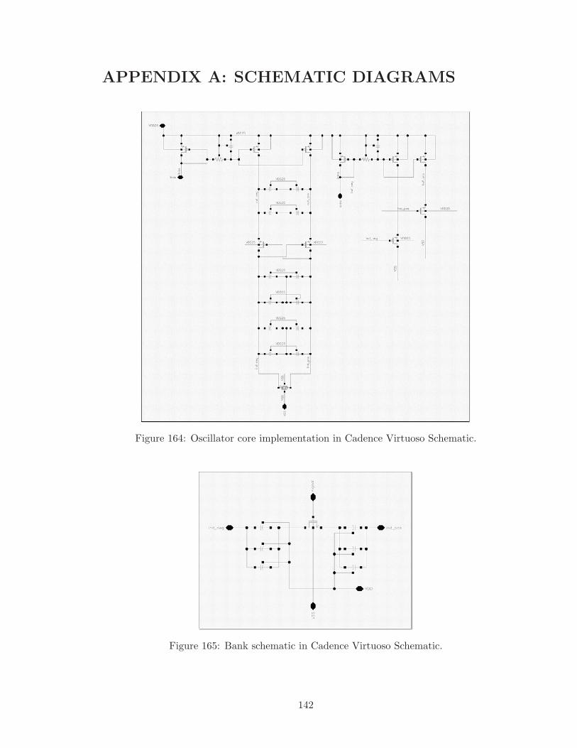
APPENDIX A: SCHEMATIC DIAGRAMS
Figure 164: Oscillator core implementation in Cadence Virtuoso Schematic.
Figure 165: Bank schematic in Cadence Virtuoso Schematic.
142
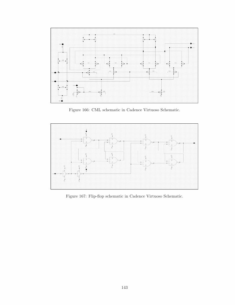
Figure 166: CML schematic in Cadence Virtuoso Schematic.
Figure 167: Flip-flop schematic in Cadence Virtuoso Schematic.
143

Figure 168: Mux schematic in Cadence Virtuoso Schematic.
Figure 169: A 4-bit Shift register schematic in Cadence Virtuoso Schematic.
144
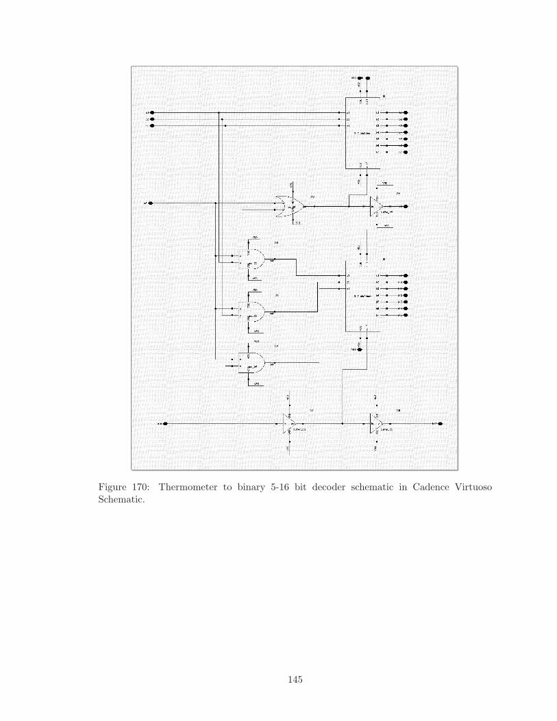
Figure 170: Thermometer to binary 5-16 bit decoder schematic in Cadence VirtuosoSchematic.
145
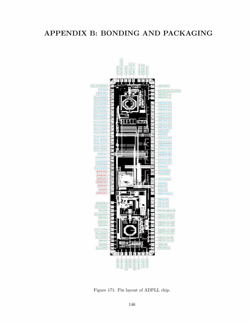
APPENDIX B: BONDING AND PACKAGING
Figure 171: Pin layout of ADPLL chip.
146
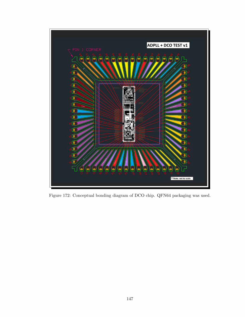
Figure 172: Conceptual bonding diagram of DCO chip. QFN64 packaging was used.
147
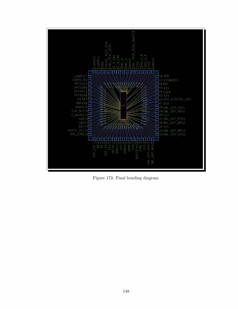
Figure 173: Final bonding diagram.
148
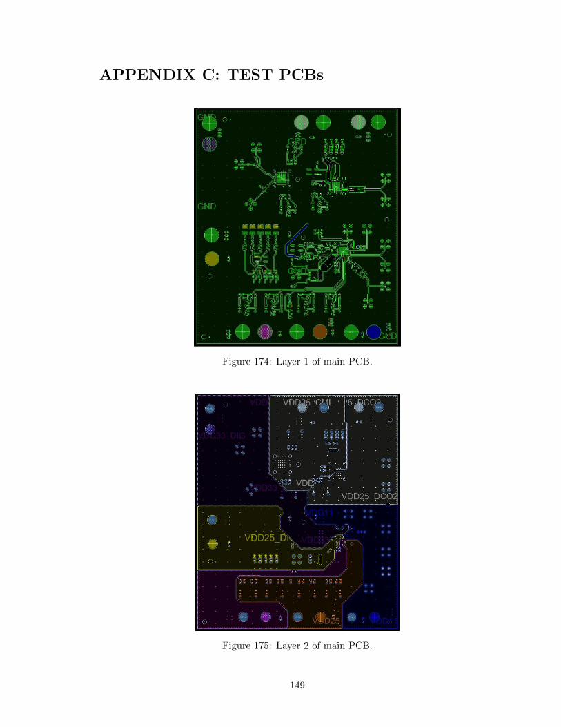
APPENDIX C: TEST PCBs
Figure 174: Layer 1 of main PCB.
Figure 175: Layer 2 of main PCB.
149
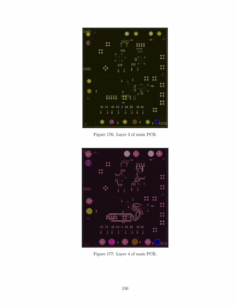
Figure 176: Layer 3 of main PCB.
Figure 177: Layer 4 of main PCB.
150
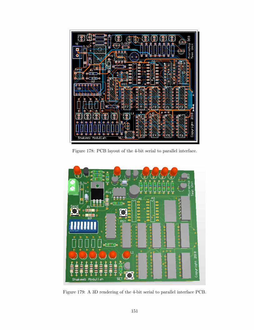
Figure 178: PCB layout of the 4-bit serial to parallel interface.
Figure 179: A 3D rendering of the 4-bit serial to parallel interface PCB.
151
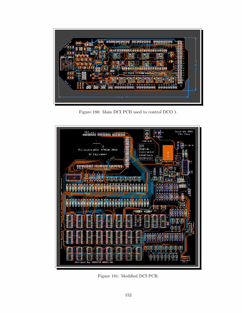
Figure 180: Main DCI PCB used to control DCO 1.
Figure 181: Modified DCI PCB.
152

Figure 182: A 3D rendering of the DCI 2 PCB.
Figure 183: Fabricated DCI 2 PCB.
153
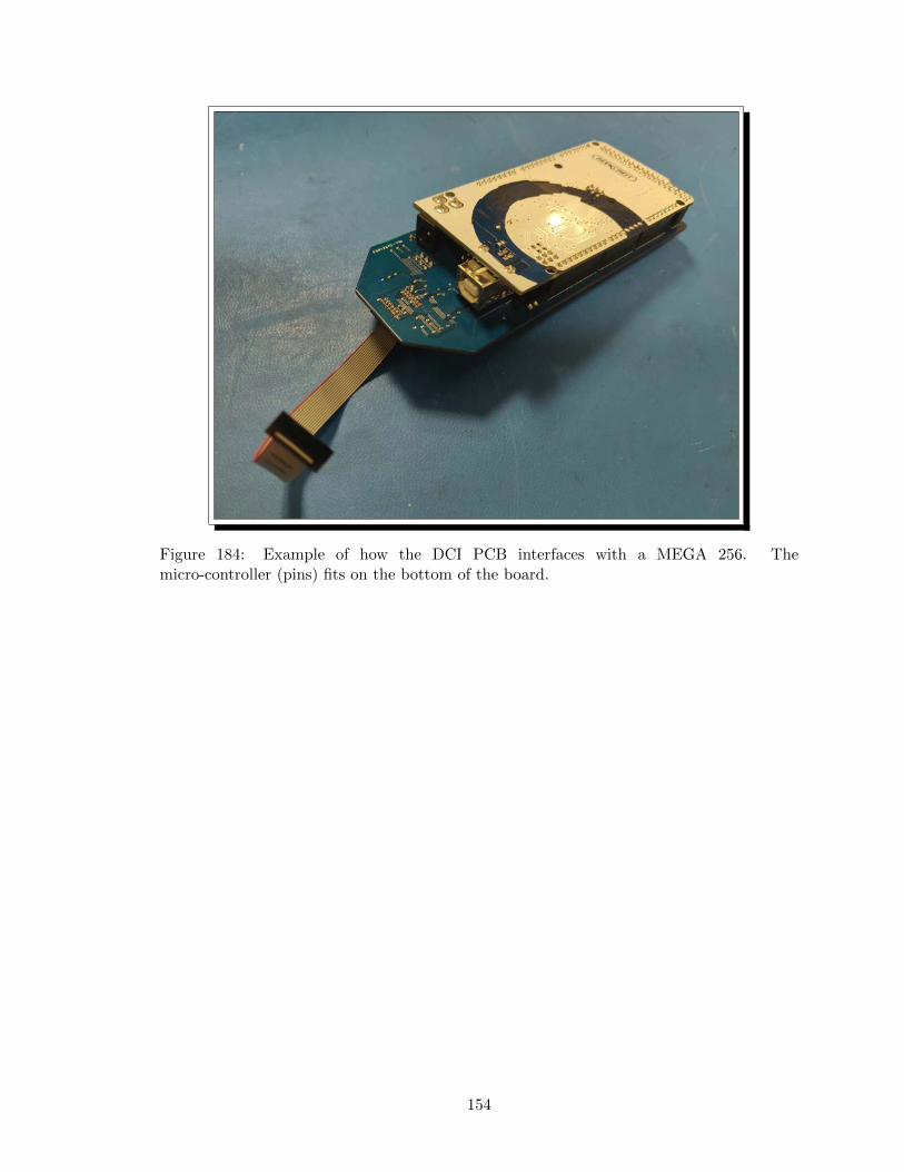
Figure 184: Example of how the DCI PCB interfaces with a MEGA 256. Themicro-controller (pins) fits on the bottom of the board.
154
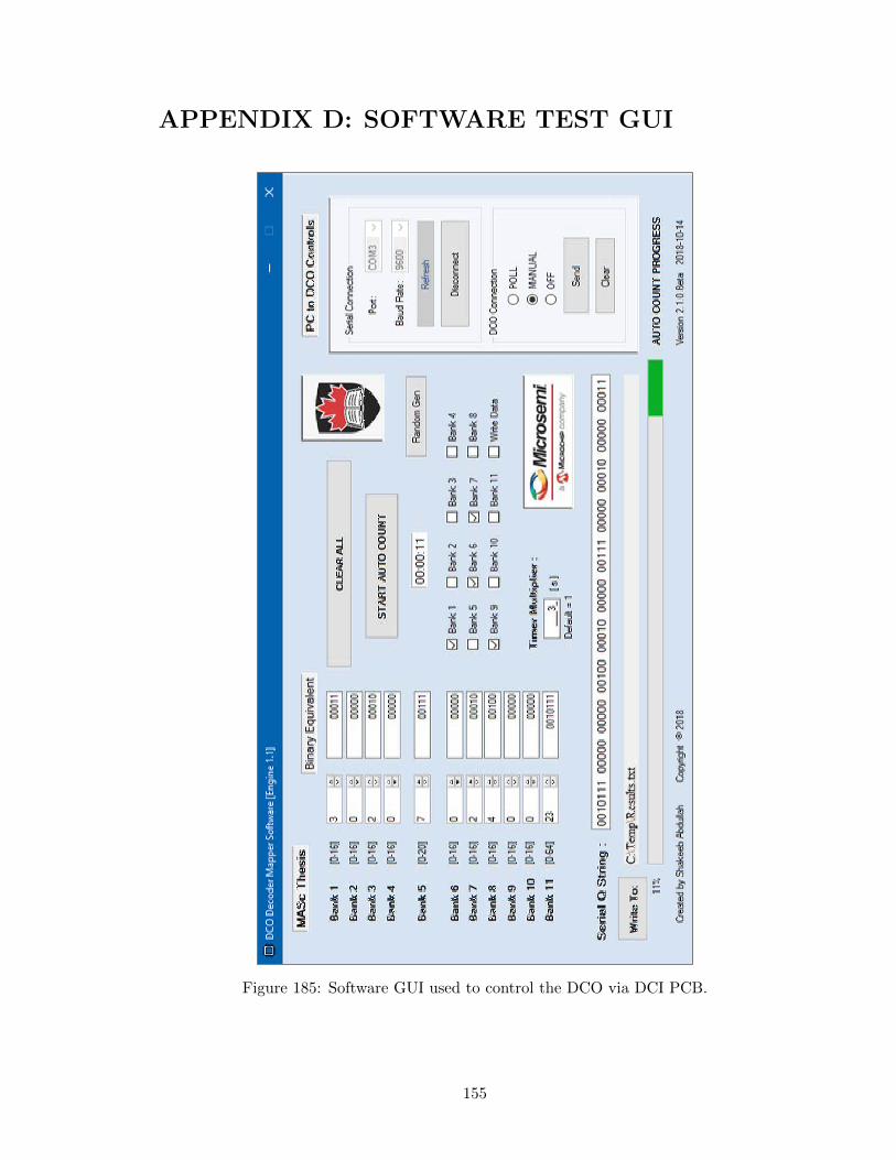
APPENDIX D: SOFTWARE TEST GUI
Figure 185: Software GUI used to control the DCO via DCI PCB.
155
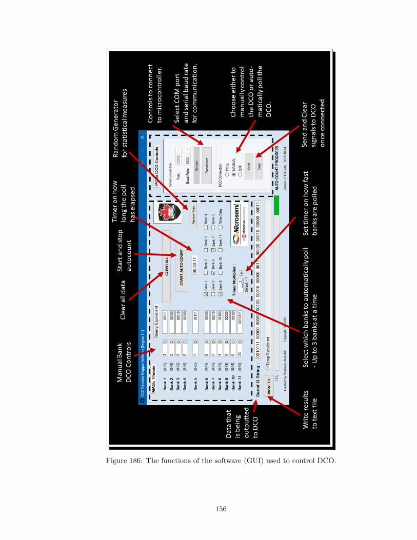
Figure 186: The functions of the software (GUI) used to control DCO.
156