design, control and analysis of a novel multilevel converter
TRANSCRIPT

Design, Control and Analysis of a NovelMultilevel Converter with a Reduced Switch Count
vorgelegt vonM. Sc.
Margarita A. Norambuena Valdiviageb. in Viña del Mar
von der Fakultät IV - Elektrotechnik und Informatikder Technischen Universität Berlin
zur Erlangung des akademischen Grades
Doktor der Ingenieurwissenschaften-Dr.-Ing-
genehmigte Dissertation
Promotionsausschuss:Vorsitzender: Prof. Dr. Marcelo Pérez (UTFSM)Gutachterin: Prof. Dr.-Ing. Sibylle Dieckerhoff (TU Berlin)Gutachter: Prof. Dr.-Ing. José Rodríguez Pérez (UNAB)
Prof. Dr.-Ing. Ralph Kennel (TU München)Dr. Samir Kouro Raener (UTFSM)
Tag der wissenschaftlichen Aussprache: 20. October 2017
Berlin, 2018.
U. Técnica Federico Santa María - Technische Universität BerlinDepartamento de Ingeniería Electrónica - Faculty IV - Elektrotechnik und Informatik
Valparaíso, Chile - Berlin, Deutschland
Design, Control and Analysis of a NovelMultilevel Converter with a Reduced Switch
Count
Margarita A. Norambuena Valdivia
2018

AcknowledgmentsThis PhD project has been done under the guidance of the Chair of Industrial Elec-
tronics of the Electronic Department at the Universidad Técnica Federico Santa María(UTFSM), Valparaíso, Chile and the Chair of the Research group of Power Electronicsat Faculty IV - Electrical Engineering and Computer Science at Technische UniversitätBerlin (TUB), Berlin, Germany. The four years I have spent on this PhD have been veryinteresting and educational. I would never have been able to finish my PhD dissertationwithout the guidance of my supervisors.
Firstly, I would like to express my deepest gratitude to my supervisor Prof. Dr.-Ing. Jo-sé Rodríguez for his constant guidance, helpful comments, advice, interest, and support.Prof. Rodríguez has always given me the confidence and security to think with freedomand to implement my new ideas. I am profoundly happy to have him as my supervisor; heis a very interesting person, he always gave me some of his time when I needed it, andwas always available to talk, not only about my PhD work, but also about new tendenciesin the world, good music and the best places to go visit.
My deepest gratitude goes also to my supervisor Prof. Dr.-Ing. Sibylle Dieckerhoff foraccepting me, for her interest, helpful comments, advice, and support. Prof. Dieckerhoffgave me the space, the opportunity and the trust to convert my ideas into reality. I cannotimagine being able to finish my PhD dissertation without her assistance and support. Sheis very meticulous, organized, clear in her goals and in the steps that must be followedand I admire her for that.
I would like to thank Prof. Dr. Samir Kouro for being the co-supervisor of my PhDdissertation from the UTFSM. His comment about a new back-to-back two-level converterwas the cornerstone that made this PhD dissertation possible.
Besides my supervisors, I would like to thank Prof. Dr.-Ing. Ralph Kennel for being thefourth examiner for this dissertation.
My sincere thanks go to my colleagues at TUB and UTFSM; I would especially like toexpress my gratitude to Tino Kahl for his help and friendship during my stay in Berlin andthereafter. Tino has a wide knowledge and experience with building PCBs, and withouthis help and comments my work would have taken more time and I would probably stillbe stuck making beginner mistakes.
I would like to thank the administrative and technical staff members from TUB whohave been kind enough to advise and help in their respective roles. I thank Mrs. GudrunPourshirazi for her help, cooperation and time.
I would like to thank my parents and siblings for supporting me spiritually as I wrotethis dissertation and throughout my life in general, even when geographical distance has

II
separated us.
I am grateful for the support of the Chilean Research Council(CONICYT) under grant“Doctorado Nacional 2014” (21140574), FONDECYT under grant 1170167 and also thesupport of German Academic Exchange Service (DAAD) under the grant “Bi-nationallySupervised Doctoral Degrees” (57129430) for funding my PhD project period.
Y por último, agradezco a la persona más trascendental de mi vida, porque sin ellajamás hubiera podido llegar hasta donde estoy, mi Padre Dios es lo más importante quepodría llegar a tener. Todo por él y nada sin él.

Table of Contents
Table of Contents I
Figures Index III
Tables Index V
Abstract 1
Resumen 2
Kurzfassung 3
1. Introduction 4
2. Multilevel Converters 72.1. Neutral Point Clamped (NPC) Converter . . . . . . . . . . . . . . . . . . . 7
2.1.1. The power circuit . . . . . . . . . . . . . . . . . . . . . . . . . . . . . 72.1.2. Vectors generated by the inverter . . . . . . . . . . . . . . . . . . . . 82.1.3. The classical modulation . . . . . . . . . . . . . . . . . . . . . . . . 112.1.4. Summary . . . . . . . . . . . . . . . . . . . . . . . . . . . . . . . . . 12
2.2. Active Neutral Point Clamped (ANPC) Converter . . . . . . . . . . . . . . 132.2.1. The power circuit . . . . . . . . . . . . . . . . . . . . . . . . . . . . . 132.2.2. Vectors generated by the inverter . . . . . . . . . . . . . . . . . . . . 142.2.3. The classical modulation . . . . . . . . . . . . . . . . . . . . . . . . 162.2.4. Summary . . . . . . . . . . . . . . . . . . . . . . . . . . . . . . . . . 17
2.3. Flying Capacitor Converter (FCC) . . . . . . . . . . . . . . . . . . . . . . 182.3.1. The power circuit . . . . . . . . . . . . . . . . . . . . . . . . . . . . . 182.3.2. Vectors generated by the inverter . . . . . . . . . . . . . . . . . . . . 182.3.3. The classical modulation . . . . . . . . . . . . . . . . . . . . . . . . 202.3.4. Summary . . . . . . . . . . . . . . . . . . . . . . . . . . . . . . . . . 21
2.4. Stacked Multicell Converter (SMC) . . . . . . . . . . . . . . . . . . . . . . 232.4.1. The power circuit . . . . . . . . . . . . . . . . . . . . . . . . . . . . . 232.4.2. Vectors generated by the inverter . . . . . . . . . . . . . . . . . . . . 232.4.3. The classical modulation . . . . . . . . . . . . . . . . . . . . . . . . 252.4.4. Summary . . . . . . . . . . . . . . . . . . . . . . . . . . . . . . . . . 26
I

Table of Contents II
3. Reduced Multilevel Converter 283.1. Basic properties . . . . . . . . . . . . . . . . . . . . . . . . . . . . . . . . 293.2. Operation principle . . . . . . . . . . . . . . . . . . . . . . . . . . . . . . . 33
3.2.1. Analysis of constraints . . . . . . . . . . . . . . . . . . . . . . . . . . 383.2.2. Implementation in Medium Voltage . . . . . . . . . . . . . . . . . . . 393.2.3. Remark about the number of output levels . . . . . . . . . . . . . . . 39
3.3. Mathematical model . . . . . . . . . . . . . . . . . . . . . . . . . . . . . . 393.4. The Classic Modulation . . . . . . . . . . . . . . . . . . . . . . . . . . . . 42
4. Control Strategy: Model Predictive Control 464.1. Classification of MPC . . . . . . . . . . . . . . . . . . . . . . . . . . . . . 46
4.1.1. Explicit Model Predictive Control (EMPC) . . . . . . . . . . . . . . . 474.1.2. Finite Control Set - Model Predictive Control (FCS-MPC) . . . . . . 48
4.2. Summary . . . . . . . . . . . . . . . . . . . . . . . . . . . . . . . . . . . . 504.3. MPC implementation strategy . . . . . . . . . . . . . . . . . . . . . . . . 514.4. FCS-MPC applied to a Reduced Multilevel Converter . . . . . . . . . . . 52
5. RMC: Analysis and Performance 555.1. System Response . . . . . . . . . . . . . . . . . . . . . . . . . . . . . . . 56
5.1.1. 3-Level Topologies . . . . . . . . . . . . . . . . . . . . . . . . . . . . 565.1.1.a. Cost Function Definition . . . . . . . . . . . . . . . . . . . . . . 565.1.1.b. Simulation Results . . . . . . . . . . . . . . . . . . . . . . . . . 57
5.1.2. 5-Level Topologies . . . . . . . . . . . . . . . . . . . . . . . . . . . . 625.1.2.a. Cost Function definition . . . . . . . . . . . . . . . . . . . . . . 625.1.2.b. Simulation Results . . . . . . . . . . . . . . . . . . . . . . . . . 63
5.2. Characteristics of the Structure . . . . . . . . . . . . . . . . . . . . . . . . 685.2.1. Blocking voltage . . . . . . . . . . . . . . . . . . . . . . . . . . . . . 685.2.2. Switching frequency . . . . . . . . . . . . . . . . . . . . . . . . . . . 695.2.3. Switching and conduction losses . . . . . . . . . . . . . . . . . . . . 715.2.4. Energy storage and size of the inner capacitors . . . . . . . . . . . . 72
5.3. Comments . . . . . . . . . . . . . . . . . . . . . . . . . . . . . . . . . . . 735.4. Back-to-Back RMC . . . . . . . . . . . . . . . . . . . . . . . . . . . . . . 76
6. Experimental Validation 826.1. Steady State Behavior . . . . . . . . . . . . . . . . . . . . . . . . . . . . . 826.2. Dynamic Response . . . . . . . . . . . . . . . . . . . . . . . . . . . . . . 88
7. Conclusions and Future Outlook 90
Appendix 92
A. Calculation of losses 92
Appendix 94
B. Test Bench 94
Bibliography 96
Figures Index
2.1. Three Phase Inverter 3-level NPC. . . . . . . . . . . . . . . . . . . . . . . 82.2. NPC inverter output . . . . . . . . . . . . . . . . . . . . . . . . . . . . . . 92.3. Space vectors of NPC. . . . . . . . . . . . . . . . . . . . . . . . . . . . . 102.4. Switching state for V0. S = +,+,+. . . . . . . . . . . . . . . . . . . . . 112.5. Switching state for V1. S = +, 0, 0. . . . . . . . . . . . . . . . . . . . . 112.6. Block diagram of Level Shifted-PWM modulation. . . . . . . . . . . . . . . 112.7. Classic Level Shifted-PWM modulation. . . . . . . . . . . . . . . . . . . . 122.8. 1-Phase 5-level ANPC Inverter. . . . . . . . . . . . . . . . . . . . . . . . . 132.9. Possible switching states of an 5L-ANPC . . . . . . . . . . . . . . . . . . 142.10. Space vectors of 5L-ANPC. . . . . . . . . . . . . . . . . . . . . . . . . . . 152.11. Block diagram of PS-PWM modulation for a 5L-ANPC. . . . . . . . . . . . 162.12. Classic PWM modulation for a 5L-ANPC. . . . . . . . . . . . . . . . . . . 172.13. 1-Phase Inverter 5-level FCC. . . . . . . . . . . . . . . . . . . . . . . . . 182.14. Space vectors of 5L-FFC. . . . . . . . . . . . . . . . . . . . . . . . . . . . 202.15. Block diagram of PS-PWM modulation for a 5-level FCC. . . . . . . . . . 212.16. Classic Phase Shifted-PWM modulation. . . . . . . . . . . . . . . . . . . 212.17. Topology of one phase of a Stacked Multicell Converter 2x2. . . . . . . . 232.18. Switching states not allowed in a SMC 2x2 . . . . . . . . . . . . . . . . . 242.19. Steps in the classical modulation of the SMC. . . . . . . . . . . . . . . . . 252.20. Block diagram of the classical modulation for an SMC 2x2. . . . . . . . . 262.21. Classical modulation of a SMC 2x2. . . . . . . . . . . . . . . . . . . . . . 27
3.1. Five Level Reduced Multilevel Converter (5L-RMC), with 3 DC-cell anda 2L-VSI output inverter. . . . . . . . . . . . . . . . . . . . . . . . . . . . 28
3.2. Generic DC-cell k of RMC. . . . . . . . . . . . . . . . . . . . . . . . . . . 293.3. Total possible output voltage vector in 5L-RMC. . . . . . . . . . . . . . . . 313.4. Output voltage space vectors generated by the RMC, including their
numbers of redundancies. . . . . . . . . . . . . . . . . . . . . . . . . . . . 343.5. Different DC-cell switching states (only non-redundant states are shown)
and their respective output potentials for a 5L-RMC. . . . . . . . . . . . . 353.6. Possible DC-DC voltage combinations in 1DC-cell RMC. . . . . . . . . . 363.7. Output voltage of the 3L-RMC for different cases . . . . . . . . . . . . . . 373.8. Block diagram of PWM modulation for a 3L-RMC. . . . . . . . . . . . . . 433.9. Carrier signals in the PWM modulation for a 3L-RMC. . . . . . . . . . . . 443.10. RMC 3-phase RMC modulation . . . . . . . . . . . . . . . . . . . . . . . 45
4.1. Structure of an explicit predictive control. . . . . . . . . . . . . . . . . . . 484.2. Structure of a direct predictive control. . . . . . . . . . . . . . . . . . . . . 494.3. Predictive Control Strategy. . . . . . . . . . . . . . . . . . . . . . . . . . . 51
III
Figures Index IV
4.4. Control scheme for FCS-MPC. . . . . . . . . . . . . . . . . . . . . . . . . 54
5.1. Output currents and output voltage 3-level 15A . . . . . . . . . . . . . . . 575.2. Output currents and output voltage 3-level 5A . . . . . . . . . . . . . . . . 585.3. Output current and output voltage spectrum 3-level 15A . . . . . . . . . . 595.4. Output current and output voltage spectrum 3-level 5A . . . . . . . . . . . 605.5. Output currents and output voltage 3-level . . . . . . . . . . . . . . . . . 615.6. Output currents and output voltage 5-level 15A . . . . . . . . . . . . . . . 635.7. Output currents and output voltage 5-level 5A . . . . . . . . . . . . . . . . 645.8. Output current and output voltage spectrum 5-level 15A . . . . . . . . . . 655.9. Output current and output voltage spectrum 5-level 5A . . . . . . . . . . . 665.10. Output currents and output voltage 5-level . . . . . . . . . . . . . . . . . 675.11. Blocking voltage in 3-level RMC . . . . . . . . . . . . . . . . . . . . . . . 695.12. Blocking voltage in 5-level RMC . . . . . . . . . . . . . . . . . . . . . . . 695.13. Switching and conduction power losses for: (a) 3-level topologies, (b)
5-level topologies. . . . . . . . . . . . . . . . . . . . . . . . . . . . . . . . 725.14. Three-level converters: (a) NPC; (b) T-type; (c) 3L-RMC. . . . . . . . . . 745.15. Five-level converters: (a) ANPC; (b) SMC; (c) 5L-RMC. . . . . . . . . . . 755.16. 3L-RMC back-to-back connection. . . . . . . . . . . . . . . . . . . . . . . 765.17. RMC back-to-back: electric variables Torque step . . . . . . . . . . . . . 785.18. RMC back-to-back: mechanic variables Torque step . . . . . . . . . . . . 795.19. RMC back-to-back: electric variables power step . . . . . . . . . . . . . . 805.20. RMC back-to-back: mechanic variables power step . . . . . . . . . . . . 81
6.1. Output current, output voltage, vAN , and capacitor voltage 6A . . . . . . . 836.2. Output current, output voltage (vAN ) and capacitor voltage 3A . . . . . . 846.3. Inner capacitor voltages for i∗ = 6sin(ωt)A. . . . . . . . . . . . . . . . . . 856.4. Inner capacitor voltages for i∗ = 3sin(ωt)A. . . . . . . . . . . . . . . . . . 856.5. Output current and output voltage, vAN , harmonic spectrum 6A . . . . . . 866.6. Output current and output voltage, vAN , harmonic spectrum 3A . . . . . . 876.7. Output current and blocking voltage in power switch SC1. . . . . . . . . . 876.8. Inner capacitor voltages. . . . . . . . . . . . . . . . . . . . . . . . . . . . 886.9. Output current, output voltage and capacitor voltage after a current step. 89
A.1. PLECSr simulation to calculate the converter’s total losses. . . . . . . . 92
B.1. RMC prototype: (1) dc-link capacitors; (2) DC-cells; (3) Variable dc-link;(4) 2L-VSI. . . . . . . . . . . . . . . . . . . . . . . . . . . . . . . . . . . . 94

Tables Index
2.1. Switching states Neutral Point Clamped . . . . . . . . . . . . . . . . . . . 82.2. Switching states Active Neutral Point Clamped . . . . . . . . . . . . . . . 152.3. Switching states Flying Capacitor Converter . . . . . . . . . . . . . . . . 192.4. Switching states Stacked Multicell Converter . . . . . . . . . . . . . . . . 25
3.1. DC-cell RMC: Possible switching states . . . . . . . . . . . . . . . . . . . 293.2. Redundant switching states for all possible output voltage levels . . . . . 313.3. Switching states Reduced Multilevel Converter . . . . . . . . . . . . . . . 323.4. Redundant Switching States for 3DC-cell RMC . . . . . . . . . . . . . . . 333.5. 1DC-cell RMC: Switching states . . . . . . . . . . . . . . . . . . . . . . . 383.6. Maximum blocking voltage in RMC . . . . . . . . . . . . . . . . . . . . . . 38
4.1. Operating characteristics of EMPC and FCS-MPC. . . . . . . . . . . . . . 50
5.1. Simulation parameters . . . . . . . . . . . . . . . . . . . . . . . . . . . . 565.2. THD for 3-level topologies . . . . . . . . . . . . . . . . . . . . . . . . . . . 595.3. THD for 5-level topologies . . . . . . . . . . . . . . . . . . . . . . . . . . . 665.4. Blocking voltage for multilevel topologies . . . . . . . . . . . . . . . . . . 685.5. Average switching frequency . . . . . . . . . . . . . . . . . . . . . . . . . 705.6. Switching frequency in 5-level RMC . . . . . . . . . . . . . . . . . . . . . 715.7. Capacitance size . . . . . . . . . . . . . . . . . . . . . . . . . . . . . . . . 735.8. Capacitance size . . . . . . . . . . . . . . . . . . . . . . . . . . . . . . . . 735.9. Simulation parameters for the back-to-back connection . . . . . . . . . . 77
6.1. Test bench parameters. . . . . . . . . . . . . . . . . . . . . . . . . . . . . 82
A.1. Devices selected . . . . . . . . . . . . . . . . . . . . . . . . . . . . . . . . 93
V

Abstract
Multilevel converters are used in a wide range of applications, such as drives, energyconversion and distributed generation. This Thesis proposes a new multilevel convertertopology that allows increasing the number of output voltage levels with a fewer requiredpower semiconductors than in standard multilevel topologies such as Active Neutral PointClamped (ANPC), Flying Capacitor Converter (FCC) and Stacked Multicell Converter(SMC).
The proposed topology consists of a cascaded connection of basic units called maincells, which are composed of three power switches, one flying capacitor and two outputswitches for each output phase.
In this Thesis, the comparisons are made between the proposed topology and con-ventional topologies such as ANPC and SMC. Points of comparison include the requirednumber of power switches, voltage stress across the switches, power distribution, capa-citors’ size and energy storage.
To verify the performance of the proposed multilevel topology, extensive simulationsand experimental studies were carried out on a 3-phase 5-level converter.
1

Resumen
Los convertidores de potencia multinivel son empleados en una amplia gama de apli-caciones, incluyendo: máquinas y accionamientos, conversión de energía y generacióndistribuida. Esta Tesis propone una nueva topología de convertidor multinivel que permiteincrementar el número de niveles de tensiones a la salida del convertidor empleando unreducido número de semiconductores de potencia en comparación con topologías multi-nivel convencionales, tales como el convertidor Active Neutral Point Clamped (ANPC), elconvertidor Flying Capacitor (FCC) y el convertidor Stacked Multicell (SMC).
Esta topología está conformada por la conexión en cascada de unidades básicasllamadas celdas principales, que se componen por un condensador flotante y tres semi-conductores de potencia, y dos semiconductores de potencia para seleccionar la salidade tensión correspondiente a cada fase del sistema.
En este trabajo se discute el número de semiconductores de potencia requeridos, elestrés de tensión a los que son sometidos, la distribución de potencia a través de ellos yla energía almacenada en los condensadores flotantes en comparación con topologíasestándares y comerciales como los son el ANPC y el SMC.
La validación de la topología multinivel propuesta es verificada a través de simulacio-nes y resultados experimentales en un prototipo trifásico de 5 niveles.
2

Kurzfassung
Mehrstufige Wechselrichter finden ein breites Anwendungsspektrum. Sie werden beis-pielsweise als Antriebsumrichter, in der Energieversorgung oder für verteilte Erzeugung-sanlagen genutzt. Verglichen mit etablierten Schaltungen wie dem Active Neutral PointClamped (ANPC) Converter, dem Flying Capacitor Converter (FCC) oder dem StackedMulticell Converter (SMC) erreicht die in dieser Arbeit vorgestellte, neuartige Umrichter-Topologie eine erhöhte Stufenzahl der Ausgangsspannung bei reduzierter Anzahl an be-nötigten Leistungsschaltern.
Die vorgeschlagene Topologie besteht aus einer kaskadierten Verbindung aus Basis-zellen, den „Main Cells“ und jeweils zwei Leistungsschaltern für jede Ausgangsphase. DieBasiszellen sind aus drei Leistungsschaltern und einem Flying Capacitor aufgebaut. Sieerzeugen eine variable Zwischenkreisspannung für die angeschlossenen Ausgangspha-sen.
In dieser Arbeit wird ein Vergleich zwischen der vorgestellten Topologie und den eta-blierten Schaltungen ANPC, FCC und SMC durchgeführt. Die Vergleichskriterien beinhal-ten die Anzahl an benötigten Leistungshalbleitern, die Sperrspannung über den einzelnenSchaltern, die Verlustleistungsverteilung sowie die in den Kondensatoren gespeicherteEnergie und deren Kapazität.
Die Verhaltensweisen der vorgeschlagenen Topologie werden in umfangreichen Si-mulationen und experimentellen Untersuchungen eines dreiphasigen 5-Level Wechsel-richters analysiert.
3

Chapter 1
Introduction
Voltage Source Converters (VSC) today have a wide variety of applications [1–3],such as:
Industry: Pumps, ventilators, conveyors, mills, etc.
Transportation: Trains, trucks, cars, airplane.
Transmission and distribution of energy: wind farms, HVDC, STATCOMs, active fil-ters, etc.
Drives: Load side and grid side converter.
VSCs can behave as a rectifier (VSR-Voltage Source Rectifier ) or as an inverter (VSI-Voltage Source Inverter ) depending on the direction of the power flow. Therefore, it is afully bidirectional structure.
Because of its simple structure and mature technology, the two-level VSC has beenthe most attractive option for industries [4]. However, the two-level VSC provides a poorvoltage quality. Large harmonic content of the output voltage of a two-level VSC hampersits application in supplying sensitive loads and also in grid-connected energy conversionsystems where strict grid codes should be followed. Adding harmonic filters to the outputof a two-level VSC to improve the power quality results in a complex, expensive and bulkysystem that is less attractive for industrial applications.
Multilevel VSCs provide several voltage steps by which a more sinusoidal voltage wa-veform can be constructed. Multilevel converters have emerged as an attractive solutionfor power electronics applications due to their numerous merits over classical two-levelconverters; these advantages include better output voltage waveform quality, lower har-monic distortion of the input and output currents, reduced filter size, lower common-modevoltages, reduced electromagnetic interference, reduced torque ripple in drive applica-tions and the feasibility of fault tolerant operation [5].
Multilevel converters consist of an array of semiconductor devices and capacitive vol-tage sources, which can generate output voltage waveforms with multiple steps by ap-propriate switching. With the increase in the number of output voltage levels or steps, thestaircase output waveform approaches a sinusoidal waveform.
4

Chapter 1. Introduction 5
The 3-level Neutral Point Clamped (NPC) converter is one of the classical multileveltopologies [6]. The NPC has become popular due to its simple structure, but it has notbeen extended to higher-level operation due to excessive losses of clamping diodes,uneven distribution of losses in inner and outer devices and the need to balance thecapacitor voltages [7].
The concept of multicell converters introduced 20 years ago, allowed an important ad-vance in the domain of medium voltage (3kV, 4.5kV, 6.6kV) and high power (several MW)applications. The development of static converters dedicated to high power applicationsis currently expanding. By using a series of connected commutation cells, the converters’input voltage can easily be increased and the waveform improved while using smallercomponents with better properties. The Flying Capacitor Converter (FCC) is an exampleof these topologies [8,9].
The Stacked Multicell Converter (SMC) is a novel multilevel converter topology in thesame line as the flying capacitor converter; it allows converters to reach output voltage,output power and performances still higher than the classical multicell FCC [10].
Like the FCC, the SMC uses flying capacitors and the voltage across these flying ca-pacitors have to be balanced to allow for a correct operation of multicell topologies. WhenPulse Width Modulation (PWM) techniques are used, it is necessary to study natural ba-lancing properties of the SMC converter, and when Model Predictive Control (MPC) isused, it is possible to control these internal voltages directly. Some external circuits (suchas the RLC filter) can be used to increase the effectiveness of the voltage balancing.
Multilevel converters are a good candidate for supplying sensitive loads and beingused in the grid-tied system, due to their good power quality, higher efficiency and su-perior electromagnetic compatibility (EMC) [11,12]. Different structures of multilevel con-verters have been reported in the literature in recent years. This thesis proposes a newmultilevel converter structure that reduces the necessary number of power switches andflying capacitors to generate the same number of output levels as in classical topologiessuch as FCC, SMC and NPC.
The new multilevel topology is called Reduced Multilevel Converter (RMC); it consistsof a cascaded connection of basic units called main cells (MC) and a 3-phase outputinverter stage. The RMC is a multilevel inverter with a single DC-bus configuration. EveryMC is formed by three power switches and one capacitor. The MCs work as a DC-DCmultilevel converter, generating a variable dc-link as their output. The output inverterstage can be any inverter with a single DC-bus configuration like the 2L-VSI, NeutralPoint Clamped (NPC), ANPC, T-type [13], FCC or Stacked Multicell Converter. However,in this work, the basic 2L-VSI is used so as to identify RMC’s real contributions.
The upcoming chapters of this dissertation are organized as follows:
Chapter 2 presents a brief description of the main multilevel converter with a singleDC-bus configuration that will be used to compare the performance of the RMC. Thesetopologies are the Neutral Point Clamped (NPC) converter, the 5-level Active Neutral PointClamped (5L-ANPC) converter, the Flying Capacitor Converter (FCC) and the StackedMulticell Converter (SMC).
Chapter 3 presents the description of the proposed topology in this dissertation, theReduced Multilevel Converter, its basic properties, operation principles and mathematical

Chapter 1. Introduction 6
model.
Chapter 4 gives a brief summary of Model Predictive Control (MPC), the control stra-tegy used to control the proposed topology. This chapter describes the principal advan-tages and disadvantages of the MPC strategy and its implementation scheme.
Chapter 5 presents a simulation analysis of the proposed topology compared with themultilevel converters described in chapter 2. The analysis is made considering the sys-tem’s response, i.e. output currents, output voltages, capacitor voltage balance, harmonicspectrum, total harmonic distortion and dynamic characteristic, and the characteristics ofthe structure, i.e. blocking voltage, switching frequency, switching and conduction losses,storage energy and size of the inner capacitors.
Chapter 6 presents an experimental validation of the designed topology using a 5L-RMC prototype.
Finally, Chapter 7 provides a brief summary of the whole dissertation and discussessome extended research ideas that can be carried out in the future.

Chapter 2
Multilevel Converters
Nowadays, multilevel inverters are a well accepted and mature technology for powerelectronic applications. In this work, the following types of multilevel inverters will be con-sidered:
Neutral Point Clamped (NPC) converter: A three-level NPC converter will be conside-red as the startup point to understand multilevel converters.
Active Neutral Point Clamped (ANPC) converter: A five-level ANPC converter will beconsidered as a comparison point for 5-level commercial topologies.
Flying Capacitor Converter (FCC): An FCC will be considered as the classical flyingcapacitor topology.
Stacked Multicell Converter (SMC): An SMC will be discussed as a flying capacitorcommercial topology.
2.1. Neutral Point Clamped (NPC) Converter
The NPC converter was introduced in the early 1980s [6]. Today, the NPC topo-logy has become very popular in industry and academic research all over the world.Some commercial examples are ACS1000 (ABB), MV Simovert (Siemens), TMdrive-70(TMEIC-GE), Silcovert-TN (Ansaldo), MV7000 (Converteam) and IngeDrive MV500 (In-geTeam). NPC inverters can be found in industry using IGCT (Integrated Gate Commu-tated Thyristor), IEGT (Injection Enhanced Gate Transistor), and medium-voltage IGBT(Insolated Gate Bipolar Transistor).
2.1.1. The power circuit
Fig 2.1 presents the power circuit of this topology. Each phase of the inverter hasfour power switches that are composed of a power transistor with an antiparallel diode.In addition, two clamping diodes (D1x, D2x, x ∈ a, b, c) are used to connect the outputterminal to the medium point (N ) of the dc-link capacitors. This configuration allows the
7

Chapter 2. Multilevel Converters 8
N
V /2DC
V /2DC
Sa1
D1a
D2a
Sa2
Sa3
Sa4
Sb1
Sb2
Sb3
Sb4
Sc1
Sc2
Sc3
Sc4
avab
vao
vaN
b
o
c
Figure 2.1. Three Phase Inverter 3-level NPC.
Table 2.1SWITCHING STATES FOR ONE PHASE OF THE NPC INVERTER
Switching State Output Voltage(Sx1, Sx2, Sx3, Sx4) vxN
(1,1,0,0) VDC/2(0,1,1,0) 0(0,0,1,1) −VDC/2
power circuit to generate three voltage levels at the output terminal of phase x with res-pect to the neutral point N , considering the switching combinations given in Table 2.1.When Sxi = 0, the power switch Sxi is OFF, and when Sxi = 1, the power switch is ON,for all i ∈ 1, 2, 3, 4.
Fig. 2.2 shows the levels of voltages generated at the NPC inverter output. The mainparameters for the simulation setup are VDC = 200V and carrier PWM period Tc = 1ms.Since NPC has three levels between the output terminal and the neutral point of theinverter (vxN ), it will have k = 2m − 1 levels in the line-to-line voltages (vab), with m thenumber of levels at the output of inverter (vxN ). Therefore, the voltage vxo will have 2k− 1levels.
2.1.2. Vectors generated by the inverter
For the three-phase inverter, 27 switching states are generated. Each switching stateis represented by three possible values denoted by +, 0 and − that represent the swit-ching combinations that generate VDC/2, 0, and −VDC/2 respectively, at the output of theinverter phase.

Chapter 2. Multilevel Converters 9
0 0.005 0.01 0.015 0.02 0.025 0.03
0 0.005 0.01 0.015 0.02 0.025 0.03
0 0.005 0.01 0.015 0.02 0.025 0.03
-200
-150
-100
-50
0
50
100
150
200
-200
-150
-100
-50
0
50
100
150
200
-200
-150
-100
-50
0
50
100
150
200
(a)
(b)
(c)
time [s]
vao
[V]
vab
[V]
vaN
[V]
Figure 2.2. NPC inverter output: (a) Voltage vaN ; (b) Voltage vab; (c) Voltage vao.
Considering that the space vector is defined for the output voltage:
vs =2
3[vaN (t) + avbN (t) + a2vcN (t)] (2.1)
a = ej2π3 = −1
2+ j
√3
2(2.2)
a2 = ej4π3 = −1
2− j√
3
2(2.3)

Chapter 2. Multilevel Converters 10
Re
Im
3V
2V
1V4V7
V
8V
9V
(0,+,0)
(- ,0,- )
(0,+,+)
(- ,0,0)
(0,0,+)
(- ,- ,0)
5V
(+,0,+)
(0,- ,0)
6V
10V
V0
(- ,+,- )
(- ,+,0)
11V
12V
(- ,+,+)
13V
(- ,0,+)
14V
(- ,- ,+)
15V
(0,- ,+)
16V
(+,- ,+)
17V
(+,- ,0)
18V
(+,- ,- )
(0,+,- )
(+,+,0)
(0,0,- )
(- ,- ,-)
(0,0,0)
(+,+,+)
(+,0,0)
(0,- ,- )
(+,0,- )
(+,+,- )
Figure 2.3. Space vectors of NPC.
and the definition of voltage states is described by:
S = (Sa, Sb, Sc) (2.4)Sa,b,c ∈ +, 0,− (2.5)
State +→ Sx1, Sx2 are onState 0→ Sx2, Sx3 are onState -→ Sx3, Sx4 are on
for x = a, b, c
The 27 switching states produce 19 different voltage vectors, as shown in Fig. 2.3.Some switching states are redundant, generating the same voltage vector. For example,vector V0 can be generated by three different switching states: (+,+,+), (0,0,0), and (-,-,-).
V0 =2
3
[VDC
2+ a
VDC
2+ a2VDC
2
](2.6)
V0 =2
3
[0 + a0 + a20
](2.7)
V0 =2
3
[−VDC
2+ a−VDC
2+ a2−VDC
2
](2.8)
Voltage vectors V1 to V6 can be generated by two different switching states, that is,they present redundant switching states.

Chapter 2. Multilevel Converters 11
N
Vdc /2
Vdc /2
o
a cb+
_
Figure 2.4. Switching state for V0. S = +,+,+.
N
Vdc /2
Vdc/2
o
a
cb
+
_
Figure 2.5. Switching state for V1. S = +, 0, 0.
Fig. 2.4 shows the configuration of the load considering a passive load (resistors) forswitching a state vector V0, with S = +,+,+, and Fig. 2.5 shows the configuration forswitching a state vector V1, with S = +, 0, 0.
2.1.3. The classical modulation
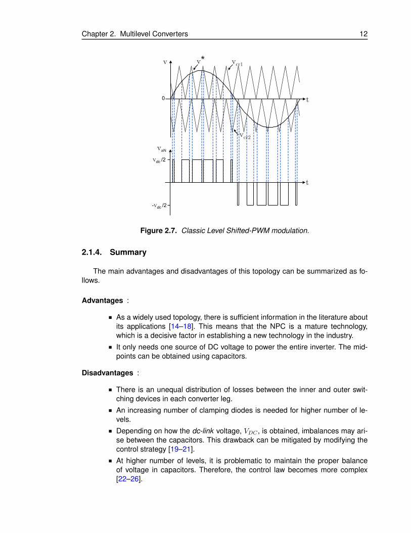
The classic PWM modulation is a special technique called: Level Shifted PWM. TheLS-PWM used in this work consists of an Alternate Opposition Disposition [14].
Fig 2.6 shows the block diagram for connecting the signals to the power switchesusing a LS-PWM modulation, while Fig. 2.7 shows the waveforms for the classic LS-PWMmodulation.
vcr1
v*+ _
1
0
1S
2
S
3S
vcr2
+ _4
S1
0
v*
vcr1
vcr2
Sx1
Sx2
Sx3
Sx4
Figure 2.6. Block diagram of Level Shifted-PWM modulation.
Chapter 2. Multilevel Converters 12
Vdc
/2
0
- /2Vdc
vaN
vcr2
vcr1
v*v
t
t
Figure 2.7. Classic Level Shifted-PWM modulation.
2.1.4. Summary
The main advantages and disadvantages of this topology can be summarized as fo-llows.
Advantages :
As a widely used topology, there is sufficient information in the literature aboutits applications [14–18]. This means that the NPC is a mature technology,which is a decisive factor in establishing a new technology in the industry.
It only needs one source of DC voltage to power the entire inverter. The mid-points can be obtained using capacitors.
Disadvantages :
There is an unequal distribution of losses between the inner and outer swit-ching devices in each converter leg.
An increasing number of clamping diodes is needed for higher number of le-vels.
Depending on how the dc-link voltage, VDC , is obtained, imbalances may ari-se between the capacitors. This drawback can be mitigated by modifying thecontrol strategy [19–21].
At higher number of levels, it is problematic to maintain the proper balanceof voltage in capacitors. Therefore, the control law becomes more complex[22–26].
Chapter 2. Multilevel Converters 13
2.2. Active Neutral Point Clamped (ANPC) Converter
The design of the multilevel converters allows for several output levels. However, suchcircuits often come at the price of far higher complexity. For example, to generate 5 outputvoltage levels in the NPC it is necessary to use additional clamping diodes, capacitorsand the corresponding control and charging circuitry, which is a complex control strategy,and even so, a more complex control might not be sufficient to operate an NPC with morethan 3 levels. An alternative approach is to connect converters in series. This again addsto the complexity of the dc-link supply circuit due to the need for galvanic separation ofthe supplies and thus costly transformers [27,28].
This issue can be solved by the 5-level ANPC that incorporates an additional capacitorper output phase. ABB commercializes the 5L-ANPC with its ACS 2000 model.
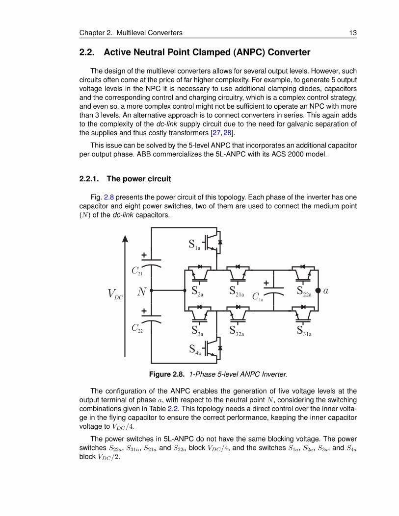
2.2.1. The power circuit
Fig. 2.8 presents the power circuit of this topology. Each phase of the inverter has onecapacitor and eight power switches, two of them are used to connect the medium point(N ) of the dc-link capacitors.
C21
C22
NVDC
a
S1a
S2a
S21a
S22a
S3a
S32a
S31a
S4a
C1a
Figure 2.8. 1-Phase 5-level ANPC Inverter.
The configuration of the ANPC enables the generation of five voltage levels at theoutput terminal of phase a, with respect to the neutral point N , considering the switchingcombinations given in Table 2.2. This topology needs a direct control over the inner volta-ge in the flying capacitor to ensure the correct performance, keeping the inner capacitorvoltage to VDC/4.
The power switches in 5L-ANPC do not have the same blocking voltage. The powerswitches S22a, S31a, S21a and S32a block VDC/4, and the switches S1a, S2a, S3a, and S4a
block VDC/2.

Chapter 2. Multilevel Converters 14
2.2.2. Vectors generated by the inverter
Fig. 2.9 shows the possible switching states for phase a of ANPC, where power swit-ches shown in grey are OFF and power switches in black are ON.
C21
C22
Na
S1a
S2a
S21a
S22a
S3a
S32a
S31a
S4a
C1a
C21
C22
Na
S1A
S2a
S21a
S22a
S3a
S32a
S31a
S4a
C1a
C21
C22
N
vaN
=0
(a)
vaN
=VDC
/4
(b)
vaN
=- /4VDC
(c)
vaN
= /2-VDC
(d)
vaN
= /2VDC
(e)
a
S1a
S2a
S21a
S22a
S3a
S32a
S31a
S4a
C1a
C21
C22
Na
S1a
S2a
S21a
S22a
S3a
S32a
S31a
S4a
C1a
C21
C22
Na
S1a
S2a
S21a
S22a
S3a
S32a
S31a
S4a
C1a
C21
C22
Na
S1a
S2a
S21a
S22a
S3a
S32a
S31a
S4a
C1a
C21
C22
Na
S1a
S2a
S21a
S22a
S3a
S32a
S31a
S4a
C1a
C21
C22
Na
S1a
S2a
S21a
S22a
S3a
S32a
S31a
S4a
C1a
Figure 2.9. Possible switching states of an 5L-ANPC: (a) Output voltage: 0; (b)Output voltage: VDC/4; (c) Output voltage: −VDC/4; (d) Output voltage: −VDC/2; (e)Output voltage: VDC/2.
Chapter 2. Multilevel Converters 15
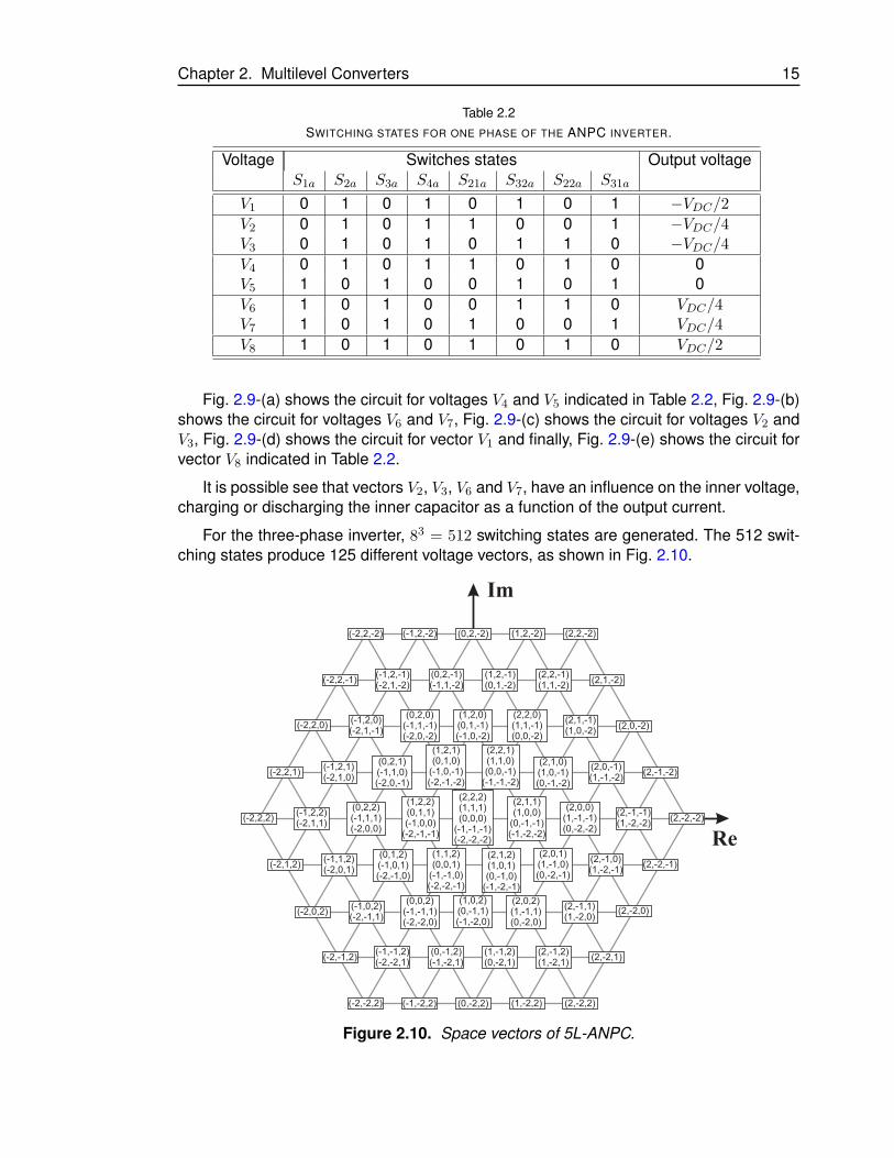
Table 2.2SWITCHING STATES FOR ONE PHASE OF THE ANPC INVERTER.
Voltage Switches states Output voltageS1a S2a S3a S4a S21a S32a S22a S31a
V1 0 1 0 1 0 1 0 1 −VDC/2
V2 0 1 0 1 1 0 0 1 −VDC/4V3 0 1 0 1 0 1 1 0 −VDC/4
V4 0 1 0 1 1 0 1 0 0V5 1 0 1 0 0 1 0 1 0V6 1 0 1 0 0 1 1 0 VDC/4V7 1 0 1 0 1 0 0 1 VDC/4
V8 1 0 1 0 1 0 1 0 VDC/2
Fig. 2.9-(a) shows the circuit for voltages V4 and V5 indicated in Table 2.2, Fig. 2.9-(b)shows the circuit for voltages V6 and V7, Fig. 2.9-(c) shows the circuit for voltages V2 andV3, Fig. 2.9-(d) shows the circuit for vector V1 and finally, Fig. 2.9-(e) shows the circuit forvector V8 indicated in Table 2.2.
It is possible see that vectors V2, V3, V6 and V7, have an influence on the inner voltage,charging or discharging the inner capacitor as a function of the output current.
For the three-phase inverter, 83 = 512 switching states are generated. The 512 swit-ching states produce 125 different voltage vectors, as shown in Fig. 2.10.
Re
Im
(2,2,2)(1,1,1)(0,0,0)
(-1,-1,-1)(-2,-2,-2)
(2,1,1)(1,0,0)
(0,-1,-1)(-1,-2,-2)
(2,1,2)(1,0,1)(0,-1,0)
(-1,-2,-1)
(1,1,2)(0,0,1)
(-1,-1,0)(-2,-2,-1)
(1,2,2)(0,1,1)(-1,0,0)
(-2,-1,-1)
(1,2,1)(0,1,0)
(-1,0,-1)(-2,-1,-2)
(2,0,0)(1,-1,-1)(0,-2,-2)
(2,-1,-1)(1,-2,-2)
(2,-1,-2)
(2,-2,-2)
(2,-2,-1)
(2,-2,0)
(2,-2,1)
(2,-2,2)(1,-2,2)(0,-2,2)(-1,-2,2)(-2,-2,2)
(-2,-1,2)
(-2,0,2)
(-2,1,2)
(-2,2,2)
(-2,2,1)
(-2,2,0)
(-2,2,-1)
(-2,2,-2) (-1,2,-2) (0,2,-2) (1,2,-2) (2,2,-2)
(2,1,-2)
(2,0,-2)
(2,0,-1)(1,-1,-2)
(2,1,-1)(1,0,-2)
(2,2,-1)(1,1,-2)
(1,2,-1)(0,1,-2)
(0,2,-1)(-1,1,-2)
(-1,2,-1)(-2,1,-2)
(-1,2,0)(-2,1,-1)
(-1,2,1)(-2,1,0)
(-1,2,2)(-2,1,1)
(-1,1,2)(-2,0,1)
(-1,0,2)(-2,-1,1)
(-1,-1,2)(-2,-2,1)
(0,-1,2)(-1,-2,1)
(1,-1,2)(0,-2,1)
(2,-1,2)(1,-2,1)
(2,-1,1)(1,-2,0)
(2,-1,0)(1,-2,-1)
(2,1,0)(1,0,-1)(0,-1,-2)
(2,2,0)(1,1,-1)(0,0,-2)
(1,2,0)(0,1,-1)(-1,0,-2)
(0,2,0)(-1,1,-1)(-2,0,-2)
(0,2,1)(-1,1,0)(-2,0,-1)
(0,2,2)(-1,1,1)(-2,0,0)
(0,1,2)(-1,0,1)(-2,-1,0)
(0,0,2)(-1,-1,1)(-2,-2,0)
(1,0,2)(0,-1,1)(-1,-2,0)
(2,0,2)(1,-1,1)(0,-2,0)
(2,0,1)(1,-1,0)(0,-2,-1)
(2,2,1)(1,1,0)(0,0,-1)
(-1,-1,-2)
Figure 2.10. Space vectors of 5L-ANPC.
Chapter 2. Multilevel Converters 16
Some voltage vectors are redundant. For example, vector V = 0 can be generated byfive different voltage states (S): (2,2,2), (1,1,1), (0,0,0), (-1,-1,-1), and (-2,-2,-2). Where:
S = (Sa, Sb, Sc) (2.9)Sa,b,c ∈ 2, 1, 0,−1,−2 (2.10)
State 2→ vaN = VDC/2
State 1→ vaN = VDC/4
State 0→ vaN = 0
State -1→ vaN = −VDC/4
State -2→ vaN = −VDC/2
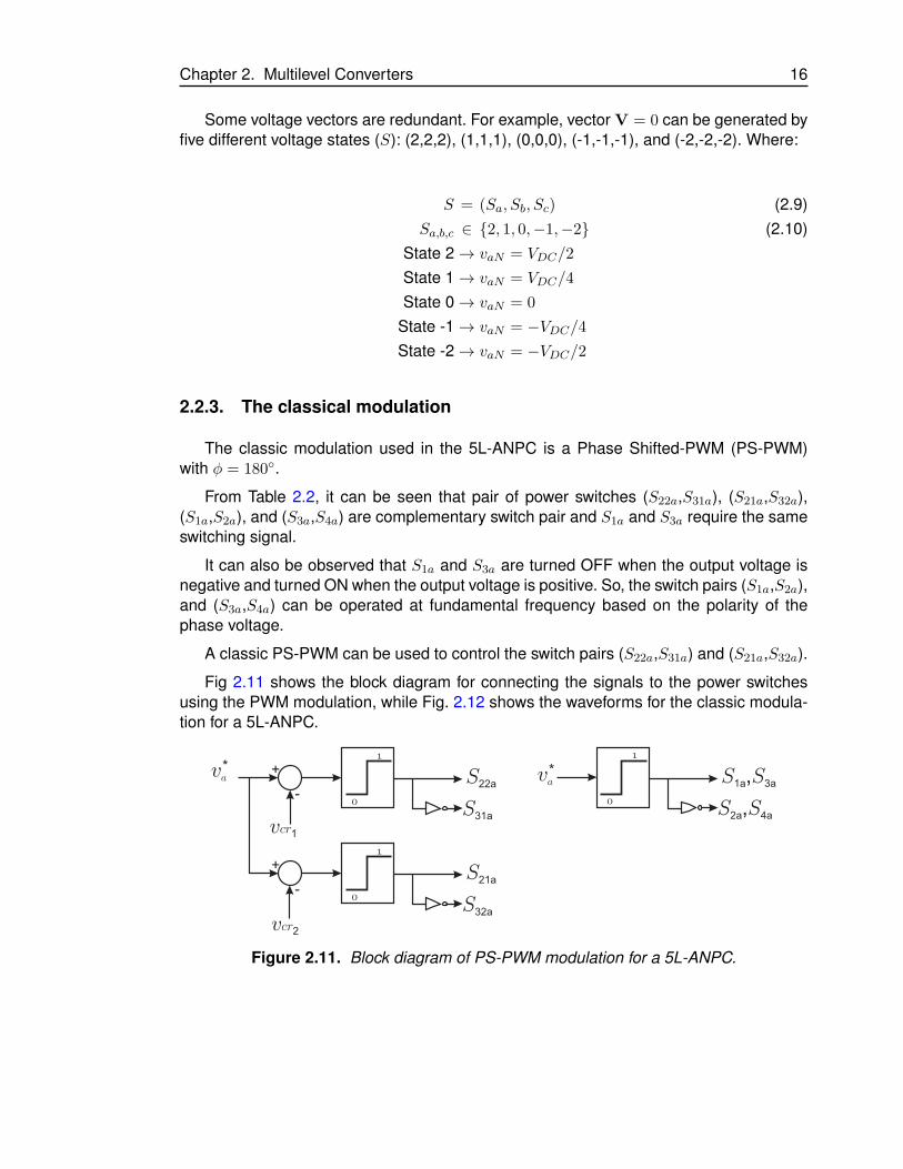
2.2.3. The classical modulation
The classic modulation used in the 5L-ANPC is a Phase Shifted-PWM (PS-PWM)with φ = 180.
From Table 2.2, it can be seen that pair of power switches (S22a,S31a), (S21a,S32a),(S1a,S2a), and (S3a,S4a) are complementary switch pair and S1a and S3a require the sameswitching signal.
It can also be observed that S1a and S3a are turned OFF when the output voltage isnegative and turned ON when the output voltage is positive. So, the switch pairs (S1a,S2a),and (S3a,S4a) can be operated at fundamental frequency based on the polarity of thephase voltage.
A classic PS-PWM can be used to control the switch pairs (S22a,S31a) and (S21a,S32a).
Fig 2.11 shows the block diagram for connecting the signals to the power switchesusing the PWM modulation, while Fig. 2.12 shows the waveforms for the classic modula-tion for a 5L-ANPC.
va
0
1
*S S1a 3a,
S S2a 4a,0
1
0
1
+va
*
-
S22a
S2 a1
S31a
S32a
+
-
vcr1
vcr2
Figure 2.11. Block diagram of PS-PWM modulation for a 5L-ANPC.

Chapter 2. Multilevel Converters 17
va
*vcr
1v
vDC
/2
vaN
-vDC
/2
vDC
/4
-vDC
/4
0
0
vcr2
t
t
Figure 2.12. Classic PWM modulation for a 5L-ANPC.
2.2.4. Summary
The main advantages and disadvantages of this topology can be summarized as fo-llows.
Advantages: It is more suitable for high-performance medium voltage motor drives[29–37].
It can overcome the limitations of the NPC inverter by reducing the total num-ber of capacitors necessary to generate five levels, which makes it easy tobalance all voltages.
It only needs one source of DC voltage to power the entire inverter. The mid-points can be obtained using capacitors.
Disadvantages: Depending on how the voltage dc-link, VDC , is obtained, imbalan-ces may arise between the capacitors. Modifying the control output switchescan mitigate this drawback.
Since it has a larger number of semiconductor devices, it has higher conduc-tion losses.
To go to medium voltage applications, it is necessary to duplicate power swit-ches S1A, S2A, S3A and S4A in all phases to get the same blocking voltage inall semiconductors.

Chapter 2. Multilevel Converters 18
2.3. Flying Capacitor Converter (FCC)
The FCC topology was developed in the 1990s [8], and it uses several floating capaci-tors instead of clamping diodes to share the voltage stress among devices and to achievedifferent voltage levels in the output.
The FCC topology can be extended, achieving more levels in the output phase by theconnection of more cells in tandem (see Fig. 2.13). Nowadays, the FCC has a reducedindustrial presence, but some commercial products can be found such as the ALSPAVDM6000 converter by Alstom [38,39].
2.3.1. The power circuit
Cell 2Cell 3Cell 4
A
N
C4dc-link
S3A
S2A
S3A
S2A
C2 C1
S1A
S1A
S4A
S4A
C3
Cell 1
Figure 2.13. 1-Phase Inverter 5-level FCC.
Fig. 2.13 shows the topology for a 5-level single-phase FCC, which is composed bythe tandem connection of four basic units called cells.
Each cell requires a capacitor and two power switches, which must be operated com-plementarily. In most works, the capacitor voltages ratio is set as vC1 : vC2 : vC3 : vC4 =1 : 2 : 3 : 4. When this condition is reached, the converter generates a 5-level voltagewaveform between the output terminal A and the inverter neutral point N . Other voltageratios have been proposed in literature [40–42]; however, the standard 1 : 2 : 3 : 4 ratiopresents the advantage of evenly spreading the voltage stress across the power switches.
Additionally, this standard ratio can be naturally achieved with a simple Phase ShiftedPulse Width Modulation (PS-PWM) strategy, i.e., in an open-loop manner [43,44].
2.3.2. Vectors generated by the inverter
Every cell of FCC can generate two possible states. In the case of a 5-level FCC withfour cells, the total possible states are: 24 = 16. Table 2.3 shows the possible states ofthe multilevel converter and the influence of the inner voltage on the output value.

Chapter 2. Multilevel Converters 19
Table 2.3SWITCHING STATES FOR ONE PHASE OF THE FCC.
Voltage Switches’ states Output voltage Output voltageS4a S3a S2a S1a [V]
V1 0 0 0 0 0 0
V2 0 0 0 1 vC1
V3 0 0 1 0 vC2 − vC1 VDC/4V4 0 1 0 0 vC3 − vC2
V5 1 0 0 0 vC4 − vC3
V6 0 0 1 1 vC2
V7 0 1 1 0 vC3 − vC1
V8 1 1 0 0 vC4 − vC2 VDC/2V9 0 1 0 1 vC3 − vC2 + vC1
V10 1 0 0 1 vC4 − vC3 + vC1
V11 1 0 1 0 vC4 − vC3 + vC2 − vC1
V12 0 1 1 1 vC3
V13 1 1 1 0 vC4 − vC1 3VDC/4V14 1 1 0 1 vC4 − vC2 + vC1
V15 1 0 1 1 vC4 − vC3 + vC2
V16 1 1 1 1 vC4 VDC
The redundancy in the voltage states V2, V3, V4 and V5 for output level VDC/4 andthe redundancy in the voltage states V6, V7, V8, V9, V10 and V11 for output level VDC/4and finally, the redundancy in the voltage states V12, V13, V14 and V15 for output level3VDC/4 achieve an appropriate combination of switching states that ensures the correctinner voltage and the desired output voltage, charging or discharging the inner capacitoras necessary.
For the 3-phase 5-level FCC there are 163 = 4096 possible switching states. Theseswitching states produce 125 different voltage vectors, as shown in Fig. 2.14.
Some voltage vectors are redundant, the vector V = 0 can be generated by fivedifferent voltage states (S): (4,4,4), (3,3,3), (2,2,2), (1,1,1), and (0,0,0). Considering:
S = (Sa, Sb, Sc) (2.11)Sa,b,c ∈ 4, 3, 2, 1, 0 (2.12)
State 4→ vaN = VDC
State 3→ vaN = 3VDC/4
State 2→ vaN = VDC/2
State 1→ vaN = VDC/4
State 0→ vaN = 0

Chapter 2. Multilevel Converters 20
Re
Im
(4,4,4)(3,3,3)(2,2,2)(1,1,1)(0,0,0)
(4,3,3)(3,2,2)(2,1,1)(1,0,0)
(4,3,4)(3,2,3)(2,1,2)(1,0,1)
(3,3,4)(2,2,3)(1,1,2)(0,0,1)
(3,4,4)(2,3,3)(1,2,2)(0,1,1)
(3,4,3)(2,3,2)(1,2,1)(0,1,0)
(4,2,2)(3,1,1)(2,0,0)
(4,1,1)(3,0,0)
(4,1,0)
(4,0,0)
(4,0,1)
(4,0,2)
(4,0,3)
(4,0,4)(3,0,4)(2,0,4)(1,0,4)(0,0,4)
(0,1,4)
(0,2,4)
(0,3,4)
(0,4,4)
(0,4,3)
(0,4,2)
(0,4,1)
(0,4,0) (1,4,0) (2,4,0) (3,4,0) (4,4,0)
(4,3,0)
(4,2,0)
(4,2,1)(3,1,0)
(4,3,1)(3,2,0)
(4,4,1)(3,3,0)
(3,4,1)(2,3,0)
(2,4,1)(1,3,0)
(1,4,1)(0,3,0)
(1,4,2)(0,3,1)
(1,4,3)(0,3,2)
(1,4,4)(0,3,3)
(1,3,4)(0,2,3)
(1,2,4)(0,1,3)
(1,1,4)(0,0,3)
(2,1,4)(1,0,3)
(3,1,4)(2,0,3)
(4,1,4)(3,0,3)
(4,1,3)(3,0,2)
(4,1,2)(3,0,1)
(4,3,2)(3,2,1)(2,1,0)
(4,4,2)(3,3,1)(2,2,0)
(3,4,2)(2,3,1)(1,2,0)
(2,4,2)(1,3,1)(0,2,0)
(2,4,3)(1,3,2)(0,2,1)
(2,4,4)(1,3,3)(0,2,2)
(2,3,4)(1,2,3)(0,1,2)
(2,2,4)(1,1,3)(0,0,2)
(3,2,4)(2,1,3)(1,0,2)
(4,2,4)(3,1,3)(2,0,2)
(4,2,3)(3,1,2)(2,0,1)
(4,4,3)(3,3,2)(2,2,1)(1,1,0)
Figure 2.14. Space vectors of 5L-FFC.
2.3.3. The classical modulation
The classic PWM modulation of the FCC that allows the inner voltage to be balancedis a special technique called: Phase Shifted PWM (PS-PWM). The phase shifted betweenthe carrier signal in an FCC is given by the expression:
φ =360
Nc(2.13)
whereNc is the number of cells in the topology. In the case of the 5-level FCC, φ = 90.
Fig 2.15 shows the block diagram that generates the signals to the power switchesemploying a PS-PWM modulation, where v∗a is the reference signal for the output phase aand vcri for all i ∈ 1, 2, 3, 4 are the carrier signals. Fig. 2.16 shows the classic PS-PWMwaveform.

Chapter 2. Multilevel Converters 21
va
0
1
0
1
+*
-
S4a
S3a
S4a
S3a
+
-
vcr4
vcr3
0
1
0
1
+va
*
-
S2a
S1a
S2a
S1a
+
-
vcr2
vcr1
Figure 2.15. Block diagram of PS-PWM modulation for a 5-level FCC.
va
*vcr
1vcr
2vcr
3 vcr4
vDC
vaN
vDC
/4
vDC
3/4
vDC
/2
0 t
Figure 2.16. Classic Phase Shifted-PWM modulation.
2.3.4. Summary
The main advantages and disadvantages of this topology can be summarized as fo-llows.
Advantages: The large number of capacitors provides a source of energy storage,which augments the system’s ability to deal with momentary loss of power fromthe grid.
In case of failure, removing cells does not decrease the maximum voltageapplied; the only consequences are the reduction of levels obtained at theoutput, the increase of blocking voltage in the semiconductors and the voltagein the capacitors.
FCC has a modular configuration, which makes it a scalable converter.
Disadvantages: The number, size and voltage rating of capacitors increases withthe number of levels; in addition to increasing the size of the inverter, these aresome of the components that make the FCC of lesser life and higher cost.
Chapter 2. Multilevel Converters 22
The main capacitor must be designed to withstand the maximum voltage. Inthe case of a very high voltage, it is necessary to resort to configurations ofthe arrangement of capacitors.
The stray inductances from large commutation loops cause high voltages overs-hoots.
Like the NPC configuration, in this inverter special considerations must be ta-ken in the implementation of the control to ensure a correct balance of thevoltages of the flying capacitors. [45,46]

Chapter 2. Multilevel Converters 23
2.4. Stacked Multicell Converter (SMC)
Today, the 3-phase 5-level SMC topology has a commercial application in mediumvoltage with the MV6 series from GE Power Conversion.
2.4.1. The power circuit
S1E1a
VDC
S1E1a
S2E2a
S2E2a
S2E1a
S2E1a
S1E2a
S1E2a
C1E2
C1E1
C2E2
C2E1
aN
Cell 2 Cell 1
Stage 2
Stage 1
Figure 2.17. Topology of one phase of a Stacked Multicell Converter 2x2.
Fig. 2.17 presents the power circuit of the 5L-SMC converter for one phase; it is basedon a hybrid association of elementary commutation cells. Each of these cells requires acapacitor and two power switches, which must be operated complementary.
Each stage (n cells stacked vertically) of the full converter can be viewed as a classicalmulticell converter (Flying Capacitor Converter) having p commutation cells in series.
Fig. 2.17 shows the particular case when p = 2 cells (horizontal) and n = 2 stages(vertical). For this converter, four flying capacitors CiEj with i ∈ 1, 2 and j ∈ 1, 2appear, where i indicates the number of the respective cell (cells put horizontally) while jindicates the number of the respective stages (cells put vertically). Each voltage acrossthese capacitors is then equal to VCiEj = i·E
n·p with E = VDC the input voltage of theconverter.
2.4.2. Vectors generated by the inverter
The SMC 2x2 shown in Fig. 2.17 has Nstates = 9 different states and Nlevels = 5different levels in the output. These 9 configurations and their respective levels consi-

Chapter 2. Multilevel Converters 24
S1E1a
VDC
S1E1a
S2E2a
S2E2a
S2E1a
S2E1a
S1E2a
S1E2a
C1E2
C1E1
C2E2
C2E1
aN
(a)
S1E1a
VDC
S1E1a
S2E2a
S2E2a
S2E1X
S2E1a
S1E2a
S1E2a
C1E2
C1E1
C2E2
C2E1
aN
(b)
S1E1a
VDC
S1E1a
S2E2a
S2E2a
S2E1a
S2E1a
S1E2a
S1E2a
C1E2
C1E1
C2E2
C2E1
aN
(c)
Figure 2.18. Switching states not allowed in a SMC 2x2: (a) Short circuit in cell1; (b) Short circuit in cell 2; (c) Short circuit in both cells.
dering the particular case of the SMC 2x2, VC2E2a= VC2E1a
; VC1E2a= VC1E1a
; E = VDC
and VDC : VC2E1a: VC1E1a
= 4 : 2 : 1, are shown in Table 2.4 where SiEja = 1 when switchSiEja is ON, and SiEja = 0 when switch SiEja is OFF.
Each power switch can take only two possible states, so, if SMC has four switches (notconsidering the complementary pair) then it will have Nstates = 42 = 16 possible states.However, this argument is invalid, because there are seven switching states that are notallowed. The state when the switch of the upper stage is ON (SjE2a = 1) and the switchof the lower stage is OFF (SjE1a = 0) (see Fig. 2.18) generates a short circuit throughboth capacitors of the stage j. Consequently, the total states for each cell of both stages(ex. cell 1 of the stage 1 and cell 1 of the stage 2) is 3 instead of Nstatescell1 = 22 = 4, sothe total number of states of an SMC 2x2 will be Nstates = 32 = 9 because it has threestates for each cells and has two cells.
Generalizing, the number of possible states of the circuit is then equal to:
Nstates = (n+ 1)p (2.14)
The number of levels in an SMC for the output voltage is equal to:

Chapter 2. Multilevel Converters 25
Table 2.4SWITCHING STATES FOR ONE PHASE OF THE STACKED MULTICELL CONVERTER 2X2
Voltage State Output Voltage Output Voltage
(S2E2a, S2E1a, S1E2a, S1E1a) vaN vaN [V]
V1 (0,0,0,0) −VC2E1a−VDC/2
V2 (0,0,0,1) VC1E1a− VC2E1a
−VDC/4
V3 (0,0,1,1) VC1E2a+ VC1E1a
− VC2E1a0
V4 (0,1,0,0) −VC1E1a−VDC/4
V5 (0,1,0,1) 0 0
V6 (0,1,1,1) VC1E2aVDC/4
V7 (1,1,0,0) VC2E2a− VC1E2a
− VC1E1a0
V8 (1,1,0,1) VC2E2a− VC1E2a
VDC/4
V9 (1,1,1,1) VC2E2aVDC/2
Nlevels = (np) + 1 (2.15)
The 3-phase 5L-FCC has 93 = 729 switching states, and these 729 switching statesproduce 125 different voltage vectors, the same as in 5L-ANPC, as shown in Fig. 2.10.
2.4.3. The classical modulation
It is necessary to define the global referential signal called vrg. This signal corres-ponds to the reference for the output voltage of the converter.
Based on this vrg signal and on the number of stages (n = 2), n signals of internalreferences (called vrEj) can be generated. These signals vrEj will be sent to each stage(n = 2) of the converter, and then each signal vrEj is modulated with the PS-PWMstrategy for each stage.
Level ShiftedPWM
Phase Shifted PWM
vrg
vrg
vrEnSpEj
vrEjSiEj
vrEj
vrE1
vrE2
vrE1
S1Ej
1
0
0.5
1
0
0.5
1
0
0.5
Figure 2.19. Steps in the classical modulation of the SMC.
Consequently, the classical modulation of the SMC requires two steps. The first step

Chapter 2. Multilevel Converters 26
modulates the vrg signal for each stage of the SMC (in vertical) to determinate the internalreference signals (called vrEj), and the second step modulates the vrEj signals for eachcell of each stages (in horizontal). The resulting modulation is a Mixed Shifted-PWM,which is composed of a Phase Shifted-PWM (PS-PWM) determined for the numbers ofcells that compose each stage (two horizontal cells in the case of the SMC 2x2), and aLevel Shifted-PWM (LP-PWM) determined by the numbers of stages that compose theconverter (two vertical stages in the case of the SMC 2x2).
vrg
vrg
vrE2
vrE1
0
1
0
1
vrE2
0
1
0
1
+
-
S2E2X
S1E2X
S2E2X
S1E2X
+
-
vcr2E2
vcr1E2
vrE1
0
1
0
1
+
-
S2E1X
S1E1X
S2E1X
S1E1X
+
-
vcr2E1
vcr1E1
Figure 2.20. Block diagram of the classical modulation for an SMC 2x2.
Fig. 2.19 shows the steps for the classical modulation of an SMC with n stages andp cells where the first step to determinate the voltage reference for each vertical stage(vrEj) is an LS-PWM.
Fig. 2.20 shows the block diagram of the classical modulation for an SMC with 2stacks and 2 cells. Fig. 2.21 shows the classical modulation in the particular case of a2x2 SMC .
2.4.4. Summary
The main advantages and disadvantages of this topology can be summarized as fo-llows.
Advantages: The capacitors are smaller than those used in FCC. In 5L-SMC, twocapacitors blocking VDC/4 and two blocking VDC/2 are necessary, and 5L-FCC requires one capacitor blocking VDC/4, one blocking VDC/2, one blocking3VDC/4 and finally one for the dc-link (VDC).

Chapter 2. Multilevel Converters 27
vcr2E2
vcr2E1
vcr1E2
vcr1E1
vrg
vDC
/2
vaN
-vDC
/2
vDC
/4
-vDC
/4
0 t
t
Figure 2.21. Classical modulation of a SMC 2x2.
It has a large number of levels to the output of converter with good current andpower dynamics.
The number of degrees of freedom increases in relation to the levels per cell.
The converter has a modular configuration feature that makes it a scalableconverter.
Disadvantages: This topology has more power semiconductors per cell than in aclassical multicell converter.
There are a lot of flying capacitors that need to be balanced.

Chapter 3
Reduced Multilevel Converter
The Reduced Multilevel Converter (RMC) [47] structure concept is composed of a va-riable dc-link converter and a 3-phase output inverter stage, like the one shown in Fig. 3.1for a 5-level configuration using a 2L-VSI. The variable dc-link structure is composed ofa cascaded connection of basic units called DC-cells which is shown in Fig. 3.2.
Every DC-cell is formed by three power switches and one capacitor; when the powerswitch in series with the capacitor (SCk) is ON, the upper and lower switches (Spk andSnk) must to work in a complementary way to avoid a short circuit.
One way to understand how this topology works is to imagine it as two parts that worktogether. The first part (the DC-cells) works as a DC-DC multilevel converter, generatinga variable dc-link between the points p and n, and the second part (output inverter) worksas a DC-AC inverter connected to a variable dc-link and can be any inverter with a singleDC-bus configuration like the 2L-VSI, NPC, 3L-ANPC, 5L-ANPC, T-type (SMC 1x2) [13],FCC, or SMC.
OutputSwitchesDC-cell 1DC-cell 2DC-cell 3
2L-VSIDC-AC Output Inverter
SA
SA
SB
SB
SC
SCSp2 Sp1
SC2 SC1
Sn2 Sn1
C2 C1 A B C
Multilevel DC-DC converter
N n
p
VDC
Sp3
SC3
Sn3
C3vVDC
variabledc-link
Figure 3.1. Five Level Reduced Multilevel Converter (5L-RMC), with 3 DC-celland a 2L-VSI output inverter.
In this work, the basic 2L-VSI is used for simplicity. The 2L-VSI is connected to the
28

Chapter 3. Reduced Multilevel Converter 29
variable dc-link and can choose the output voltage between two options: vpN or vnN asshown in Fig. 3.1.
DC-cell k
Spk
SCk
Snk
Ck
vck
vo ( + )k 1
vo ( )k
vo( + )k 1
vo ( )k
+ +
- -
Figure 3.2. Generic DC-cell k of RMC.
3.1. Basic properties
The RMC is a modular multicell structure, much like the FCC and SMC; this meansthat it is possible to increase or decrease the number of levels by connecting or discon-necting DC-cell units following the multicell arrangement.
Every main cell, see Fig. 3.2, has three possible conduction states. These are shownin Table 3.1, where Spk = 1 means that the power switch pk is ON and Spk = 0 meansthat it is OFF, for all power switches Spk, Snk and SCk.
Table 3.1DC-CELL RMC: POSSIBLE SWITCHING STATES
Switching State Output Potential
Spk Snk SCk v+o(k)
v−o(k)
1 1 0 v+o(k+1)
v−o(k+1)
0 1 1 v−o(k+1)+ vck v−o(k+1)
1 0 1 v+o(k+1)
v+o(k+1)
− vck
Hence, each additional DC-cell incorporates three possible switching states for theDC-DC multilevel part of the converter and the total possible states can be expressed asan equation in function of the number of DC-cells (NDC−cell) as follows:
NstatesDC−DC = 3NDC−cell (3.1)

Chapter 3. Reduced Multilevel Converter 30
In the case of the RMC shown in Fig. 3.1, there are 3 DC-cells, and the possibleswitching states for the DC-DC multilevel part are 33 = 27.
A 2L-VSI is used for the DC-AC inverter part, and there are two power switches foreach output phase. These two switches work in a complementary way; when Sx = 1, i.e.it is ON, the switch Sx = 0, is OFF. This is necessary, because Sx = 1 and Sx = 1 at thesame time generates a short circuit in the variable dc-link, that is, in the dc-link or in oneof the inner capacitors.
The possible switching states for each phase is 2. Therefore, the number of possiblestates in function of the number of output phases (NOP ) can be described by:
NstatesDC−AC = 2NOP (3.2)
In the case of the RMC shown in Fig. 3.1, there are 3 output phases, and the possibleswitching states for the DC-AC part is 23 = 8.
The total number of possible states of the whole converter is given by the multiplicationof the number of states in the DC-DC multilevel part and in the DC-AC part as in equation(3.3):
Nstates = NstatesDC−DC ∗NstatesDC−AC (3.3)
For the case of a 5-level, 3-phase RMC shown in Fig. 3.1, the total possible states areNstates = 27 ∗ 8 = 216.
The number of output voltages (NOV ) between the output phase (A, B or C) and theneutral point of the converter (N ) is given by:
NOV = NDC−cell + 2 (3.4)
As long as the inner voltage in the capacitors follows the relationship given by:
vCk = kVDC
NDC−cell + 1(3.5)
All possible combinations of these 216 possible switching states generate 65 outputvoltage vectors, which are shown in Fig. 3.3. The voltage vectors are described by thevariable S as follow:
S = (SA, SB, SC) (3.6)Sa,b,c ∈ 4, 3, 2, 1, 0 (3.7)
State 4→ vaN = VDC
State 3→ vaN = 3VDC/4
State 2→ vaN = VDC/2
State 1→ vaN = VDC/4
State 0→ vaN = 0
Chapter 3. Reduced Multilevel Converter 31
Re
Im
(4,4,4)(3,3,3)(2,2,2)(1,1,1)(0,0,0)
(4,3,3)(3,2,2)(2,1,1)(1,0,0)
(4,3,4)(3,2,3)(2,1,2)(1,0,1)
(3,3,4)(2,2,3)(1,1,2)(0,0,1)
(3,4,4)(2,3,3)(1,2,2)(0,1,1)
(3,4,3)(2,3,2)(1,2,1)(0,1,0)
(4,2,2)(3,1,1)(2,0,0)
(4,1,1)(3,0,0)
(4,0,0)
(4,0,4)(0,0,4)
(0,4,4)
(0,4,0) (4,4,0)
(4,4,1)(3,3,0)
(1,4,4)(0,3,3)
(1,1,4)(0,0,3)
(4,1,4)(3,0,3)
(4,4,2)(3,3,1)(2,2,0)
(2,4,2)(1,3,1)(0,2,0)
(2,4,4)(1,3,3)(0,2,2)
(2,2,4)(1,1,3)(0,0,2)
(4,2,4)(3,1,3)(2,0,2)
(4,4,3)(3,3,2)(2,2,1)(1,1,0)
(1,4,1)(0,3,0)
Figure 3.3. Total possible output voltage vector in 5L-RMC.
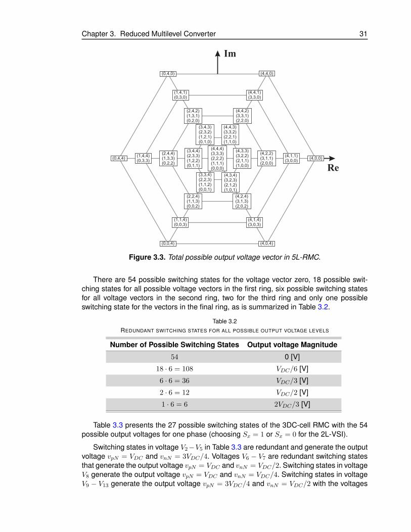
There are 54 possible switching states for the voltage vector zero, 18 possible swit-ching states for all possible voltage vectors in the first ring, six possible switching statesfor all voltage vectors in the second ring, two for the third ring and only one possibleswitching state for the vectors in the final ring, as is summarized in Table 3.2.
Table 3.2REDUNDANT SWITCHING STATES FOR ALL POSSIBLE OUTPUT VOLTAGE LEVELS
Number of Possible Switching States Output voltage Magnitude
54 0 [V]
18 · 6 = 108 VDC/6 [V]
6 · 6 = 36 VDC/3 [V]
2 · 6 = 12 VDC/2 [V]
1 · 6 = 6 2VDC/3 [V]
Table 3.3 presents the 27 possible switching states of the 3DC-cell RMC with the 54possible output voltages for one phase (choosing Sx = 1 or Sx = 0 for the 2L-VSI).
Switching states in voltage V2−V5 in Table 3.3 are redundant and generate the outputvoltage vpN = VDC and vnN = 3VDC/4. Voltages V6 − V7 are redundant switching statesthat generate the output voltage vpN = VDC and vnN = VDC/2. Switching states in voltageV8 generate the output voltage vpN = VDC and vnN = VDC/4. Switching states in voltageV9 − V13 generate the output voltage vpN = 3VDC/4 and vnN = VDC/2 with the voltages

Chapter 3. Reduced Multilevel Converter 32
Table 3.3SWITCHING STATES FOR 3-MCS 5-LEVEL REDUCED MULTILEVEL CONVERTER.
Voltage Switchings States Output VoltageSp3 SC3 Sp2 SC2 Sp1 SC1 Sx = 1 (vpN ) Sx = 0 (vnN )
V1 1 0 1 0 1 0 VDC 0
V2 1 0 1 0 1 1 VDC VDC − vC1
V3 1 0 1 1 1 1 VDC VDC − vC1
V4 1 1 1 0 1 1 VDC VDC − vC1
V5 1 1 1 1 1 1 VDC VDC − vC1
V6 1 1 1 1 1 0 VDC VDC − vC2
V7 1 0 1 1 1 0 VDC VDC − vC2
V8 1 1 1 0 1 0 VDC VDC − vC3
V9 1 0 1 1 0 1 VDC − vC2 + vC1 VDC − vC2
V10 1 1 1 1 0 1 VDC − vC2 + vC1 VDC − vC2
V11 1 1 0 1 1 1 VDC − vC3 + vC2 VDC − vC3 + vC2 − vC1
V12 0 1 1 0 1 1 vC3 vC3 − vC1
V13 0 1 1 1 1 1 vC3 vC3 − vC1
V14 1 1 0 1 1 0 VDC − vC3 + vC2 VDC − vC3
V15 0 1 1 1 1 0 vC3 vC3 − vC2
V16 0 1 1 0 1 0 vC3 0
V17 1 1 1 0 0 1 VDC − vC3 + vC1 VDC − vC3
V18 1 1 0 1 0 1 VDC − vC3 + vC1 VDC − vC3
V19 0 1 1 1 0 1 vC3 − vC2 + vC1 vC3 − vC2
V20 1 0 0 1 1 1 vC2 vC2 − vC1
V21 0 1 0 1 1 1 vC2 vC2 − vC1
V22 1 0 0 1 1 0 vC2 0V23 0 1 0 1 1 0 vC2 0
V24 1 0 1 0 0 1 vC1 0V25 1 0 0 1 0 1 vC1 0V26 0 1 1 0 0 1 vC1 0V27 0 1 0 1 0 1 vC1 0
pairs V9 − V10 and V12 − V13 each being redundant.
Switching states in voltage V14 − V15 generate the output voltages vpN = 3VDC/4 andvnN = VDC/4. Voltage V16 generates the output voltages vpN = 3VDC/4 and vnN = 0.Switching states in voltage V17 − V21 generate the output voltages vpN = VDC/2 andvnN = VDC/4 with voltages V17 − V18 and voltages V20 − V21 being redundant. Switchingstates in voltage V22 − V23 are redundant and generate the output voltages vpN = VDC/2and vnN = 0. And finally, switching states in voltage V24−V27 are redundant and generatethe output voltage vpN = VDC/4 and vnN = 0.
This redundant switching states are summarized in Table 3.4.

Chapter 3. Reduced Multilevel Converter 33
Table 3.4REDUNDANT SWITCHING STATES FOR 3DC-CELL RMC
Switching States Output Voltage
vpN vnN
V2 − V5 VDC 3VDC/4
V6 − V7 VDC VDC/2
V8 VDC VDC/4
V1 VDC 0
V9 − V13 3VDC/4 VDC/2
V14 − V15 3VDC/4 VDC/4
V16 3VDC/4 0
V17 − V21 VDC/2 VDC/4
V22 − V23 VDC/2 0
V24 − V27 VDC/4 0
3.2. Operation principle
From the 27 allowed variable dc-link switching states, only 10 generate different volta-ge potentials in the output terminals (the 17 others generate redundant levels) for a threeDC-cell RMC.
All combinations of these DC-DC multilevel voltages using a 2L-VSI in the DC-AC sta-ge give a total of 216 possible output voltage space vectors. They are shown in Fig. 3.4,which includes the number of their redundancies.
Fig. 3.5 shows a selection of the 10 different dc-link level generation possibilities.Fig. 3.5-(a) to Fig. 3.5-(d) show the possible combinations for vnN = 0 and vpN = VDC/4,vpN = VDC/2, vpN = 3VDC/4, and vpN = VDC , respectively. Fig. 3.5-(e) to Fig. 3.5-(g)show possible combinations for vpN = VDC , vnN = 3VDC/4, vnN = VDC/2, and vnN = VDC/4,respectively. Fig. 3.5-(h) and Fig. 3.5-(i) show possible combinations of vpN = 3VDC/4and: vnN = VDC/4, and vnN = VDC/2, respectively. Finally, Fig. 3.5-(j) shows the combi-nation of DC-DC voltage of vpN = VDC/2 and vnN = VDC/4.
To generate five voltage levels with the same voltage step (dv/dt), the voltages inthe inner capacitors must follow the following ratio: vC4 : vC3 : vC2 : vC1 = 4 : 3 : 2 : 1, withvC4 = VDC .
For simplicity and a better explanation, the operation principle of the 1DC-cell RMC,which is a 3-level topology, will be analyzed. The possible DC-DC voltage combinationsin a 3-level RMC is shown in Fig. 3.6. In this case, the inner voltage on capacitor C1 is setto VDC/2.
Fig. 3.6-(a) and Fig. 3.6-(b) generate the same voltage in the variable dc-link (vV DC =vC1 = VDC/2). However, the possible output voltages are different; for vpN the outputvoltage is VDC/2 or VDC , and for vnN the output voltage is 0 or VDC/2. Finally, in Fig. 3.6-(c) the switching states generate a vV DC equal to the main dc-link, i.e. vV DC = VDC , and

Chapter 3. Reduced Multilevel Converter 34
the output voltages can be vpN = VDC or vnN = 0.
Using these combinations of switching states, it is possible to have whichever of the 3possible output voltages 0, VDC/2 or VDC . This freedom allows, for example, to have twooutput phases with different modulation indices (mA and mB), phases or frequencies, asis shown in Fig. 3.7-(a), (b) and (c), respectively.
This characteristic of the operation ensures the same behavior as in standard multile-vel converters such as the FCC (see section 2.3), where one independent converter con-nected at the same dc-link is used for every phase. However, the reduction of necessarycomponents in the proposed topology has a cost. In this case, a lower number of powerswitches means fewer possible switching states and therefore, fewer possible combina-tions are able to balance the inner voltage. A consequence can be seen in Fig. 3.7, whereit is sometimes necessary to make a double step in the output voltage (from vAN = 0 tovAN = VDC) to achieve the desired inner voltage in the capacitor.
54
18
18 18
18 18
6
6
2 VDC
3 VDC
6
6 6
2
2
3
3
2
2 2
1
1 1
1 1
12618
Figure 3.4. Output voltage space vectors generated by the RMC, including theirnumbers of redundancies.

Chapter 3. Reduced Multilevel Converter 35
(a)
Sp2 Sp1
SC2 SC1
Sn2 Sn1
C2 C1
N
C4
Sp3
SC3
Sn3
C3dc-link
pv vpN C1=
vnN= 0
n
(b)
Sp2 Sp1
SC2 SC1
Sn2 Sn1
C2 C1
N
C4
Sp3
SC3
Sn3
C3dc-link
pv vpN C2=
vnN= 0
n
(c)
Sp2 Sp1
SC2 SC1
Sn2 Sn1
C2 C1
N
C4
Sp3
SC3
Sn3
C3dc-link
p
v vpN C3=
vnN= 0
n
(d)
Sp2 Sp1
SC2 SC1
Sn2 Sn1
C2 C1
N
C4
Sp3
SC3
Sn3
C3dc-link
p
v vpN C4=
vnN= 0
n
(e)
Sp2 Sp1
SC2 SC1
Sn2 Sn1
C2 C1
N
C4
Sp3
SC3
Sn3
C3dc-link
p
v vpN C4=
v v vnN C4 C1= -n
VSI
VSI VSI
VSIVSI
VSI
VSIVSI
VSI VSI
(f)
Sp2 Sp1
SC2 SC1
Sn2 Sn1
C2 C1
N
C4
Sp3
SC3
Sn3
C3dc-link
p
v vpN C4=
v v vnN C4 C2= -n
(g)
Sp2 Sp1
SC2 SC1
Sn2 Sn1
C2 C1
N
C4
Sp3
SC3
Sn3
C3dc-link
p
v vpN C4=
v v vnN C4 C3= -n
(h)
Sp2 Sp1
SC2 SC1
Sn2 Sn1
C2 C1
N
C4
Sp3
SC3
Sn3
C3dc-link
p
v vpN C3=
v v vnN C3 C2= -n
(i)
Sp2 Sp1
SC2 SC1
Sn2 Sn1
C2 C1
N
C4
Sp3
SC3
Sn3
C3dc-link
p
v vpN C3=
v v vnN C3 C1= -n
(j)
Sp2 Sp1
SC2 SC1
Sn2 Sn1
C2 C1
N
C4
Sp3
SC3
Sn3
C3dc-link
p
v vpN C2=
v v vnN C2 C1= -n
Figure 3.5. Different DC-cell switching states (only non-redundant states areshown) and their respective output potentials for a 5L-RMC.

Chapter 3. Reduced Multilevel Converter 36
Sp1
Sc1
Sn1
C1
N
C2
vnN
vpN
p
n
(a)
0
VDC /2
VDC
vpN vnN
time
Sp1
Sc1
Sn1
C1
N
C2
vnN
vpN
p
n
(c)
0
VDC /2
VDC
vpN vnN
time
(b)
0
VDC /2
VDC
vpN vnN
time
Sp1
Sc1
Sn1
C1
N
C2
vnN
v vVDC C1=
v VVDC DC=
VDC
VDC
VDC
v vVDC C1=
vpN
p
n
Figure 3.6. Possible DC-DC voltage combinations in 1DC-cell RMC.

Chapter 3. Reduced Multilevel Converter 37
Outp
ut voltagevAN
Outp
ut voltagevBN
0
VDC
/2
VDC
0 5 10 15 20 25 30 35 40time [ms]
0 5 10 15 20 25 30 35 40time [ms]
(a)
Outp
ut voltagevAN
Outp
ut voltagevBN
0
VDC
/2
VDC
0 5 10 15 20 25 30 35 40time [ms]
0 5 10 15 20 25 30 35 40time [ms]
(c)
Outp
ut voltagevAN
Outp
ut voltagevBN
0
VDC
/2
VDC
0 5 10 15 20 25 30 35 40time [ms]
0 5 10 15 20 25 30 35 40time [ms]
(b)
Figure 3.7. Output voltage of the 3L-RMC: (a) mA = 0,87, mB = 0,3; (b)mA = mB = 0,87 with φA = 0, φB = 180 and (c) mA = mB = 0,87 with fA = 50Hz,fB = 120Hz.
The 1DC-cell RMC has three power switches; all power switches can take only twopossible states ON or OFF, thus the total switching states in 1DC-cell RMC is 23 = 8 asis shown in Table 3.5.
It is possible see that states S1, S2, S3 and S4, are not recommended because theygenerate an indeterminate output voltage at one or both output points. Besides that, thestate S8 generates a short circuit through the flying capacitor and the source (C2). Con-sequently, in the 1DC-cell RMC, there are only 3 possible switching states (see Fig. 3.6).

Chapter 3. Reduced Multilevel Converter 38
Table 3.51DC-CELL RMC: SWITCHING STATES
State Switching State Output Voltage
Sp1 Sn1 SC1 vpN vnN
S1 0 0 0 indeterminate
S2 0 0 1 indeterminate
S3 0 1 0 indeterminate 0
S4 1 0 0 VDC indeterminate
S5 0 1 1 vC1 0
S6 1 0 1 VDC vC1
S7 1 1 0 VDC 0
S8 1 1 1 short circuit
From the possible switching states (S5, S6 and S7) one can see that power switchesSp1 and Sn1 work in a complementary way only when power switch SC1 is ON.
3.2.1. Analysis of constraints
An important constraint in this topology is the voltage that the power switches needto block. The blocking voltage of the transistor in a DC-cell depends on the voltagev+o(k+1)
− v−o(k+1), which can change. However, there is a maximum voltage that the tran-
sistors need to block, given by:
vblock,Sik = VDC − vCk (3.8)
where Sik is the power switch i in DC-cell k for all i ∈ p, n, C, and vCk is thevoltage of the capacitor in DC-cell k. In the case of the output switches (Sx, Sx withx ∈ A,B,C), the maximum blocking voltage is the full dc-link voltage.
The maximum blocking voltages of the transistors are summarized in Table 3.6.
Table 3.6MAXIMUM BLOCKING VOLTAGE IN RMC
vblock Power SwitchVDC
4 Sp3, Sn3, SC3
VDC2 Sp2, Sn2, SC2
3VDC4 Sp1, Sn1, SC1
VDC SA, SA, SB, SB, SC , SC

Chapter 3. Reduced Multilevel Converter 39
3.2.2. Implementation in Medium Voltage
The device blocking voltage is a disadvantage that prevents this topology from beingused in medium voltage applications. Nevertheless, multilevel converters have now beenused extensively in low voltage applications such as PV inverters, UPS systems and windpower conversion systems (all below 690 V); the most appropriate application is a subjectof further research and exploration.
However, one solution to implement this topology in medium voltage applications isto use power semiconductors with different rating voltages for cases that require a highervoltage to be blocked. Another option for blocking a higher voltage would be to connectadditional semiconductors in series.
3.2.3. Remark about the number of output levels
The number of output levels in the RMC structure depends of the number of DC-cellsand/or the number of output levels of the DC-AC output inverter stage. For example, the3DC-cell RMC shown in fig. 3.1 with a T-Type topology in the DC-AC output inverter stageresults in an RMC topology with 9 levels instead of 5 levels. Besides that, the blockingvoltage limitation will be overcome and the maximum blocking voltage will be 3VDC/4 inthe power switches in the DC-cell 1.
3.3. Mathematical model
The best way to understand the behavior of a system is the mathematical description.In the case of the RMC, the equations that describe the properties of the converter arethe output voltage and the inner capacitor voltage equations.
The output voltages, considered between the output point (A, B, or C in Fig. 3.1) andthe neutral point of the converter N , can be expressed as a function of the switchingstates and inner voltages.
There are two ways to find this expression; one is to use the circuits given in Fig. 3.5considering a 2L-VSI as a DC-AC stage and then to find an expression for each voltage.For example, the voltage in the capacitor C1 is going to appear in the output voltage vectoronly if SC1 is ON (SC1 = 1) and Sp1 6= Sx for x ∈ A,B,C, which can be written as:
vxN (vC1) = vC1SC1(Sx − Sp1) (3.9)
A similar relationship can be derived for all inner voltages. For example, the voltagein C2 is going to appear in the output voltage vector only if SC2 is ON and Sp2 6= Sx if SC1
is OFF (SC1 = 0), but if SC1 is ON the condition changes to Sp2 6= Sp1. Equation (3.10)describes the influence of vC2 in the output voltage, and Eq. (3.11) shows its reducedexpression.

Chapter 3. Reduced Multilevel Converter 40
vxN (vC2) = vC2SC2
((1− SC1)(Sx − Sp2) + SC1(Sp1 − Sp2)
)(3.10)
= vC2SC2
(SC1(Sp1 − Sp2 − Sx + Sp2) + (Sx − Sp2)
)vxN (vC2) = vC2SC2
(SC1(Sp1 − Sx) + (Sx − Sp2)
)(3.11)
A second way to find the output voltage expression is to use the possible switchingstates for the DC-cells. The 27 possible switching states for the DC-cells are given intable 3.3; there are 54 considering one phase of 2L-VSI.
To determine the expression for the output voltage, one must formulate expressionsfor all inner voltages.
For example, from Table 3.3 it is possible to see that the vectors that include vC1 in theoutput voltage are: (−)V2 − V5 (vnN ), (+)V9 − V10 (vpN ), (−)V11 − V13 (vnN ), (+)V17 − V19
(vpN ), (−)V20− V21 (vnN ), and (+)V24− V27 (vpN ). The symbol − or + represents the signof the voltage vC1 in the output voltage.
The common factor in these vectors is SC1. In all 18 possible voltages SC1 = 1.Furthermore, the other switching states that are constants in these vectors are S7 andSx.
Every time that Sp1 = 1 and Sx = 0, −vC1 appears in the output voltage, and whenSp1 = 0 and Sx = 1, +vC1 appears in the output voltage. Any other combination of theseswitches does not generate an output voltage with vC1, i.e. Sp1 = Sx.
Thus, it is possible to describe the influence of vC1 in the output voltage by:
vxN (vC1) = vC1SC1(Sx − Sp1) (3.12)
Following these steps it is possible to find analogue expressions for VDC , vC3 and vC2.
For example, for the case of VDC there two main groups of output vectors with thisvoltage: (1) when VDC is generated in vpN and vnN , which are V2−V11, V14, and V17−V18,and (2) when VDC is generated only in vpN , which is V1.
It is not easy to determine the common factor in this case, but in a first approximation,it is possible to discard the switching states which do not present VDC in the output vol-tages by multiplying Sp3SC3. This decision reduces the output voltages with presences ofVDC from V1 − V11, V14, and V17 − V18 to V1 − V3, V7, and V9.
One can see that the common factor in these 5 switching states is (1 − SC3). Thisfactor prevents the previous switching states from having an influence, but this is alsothe common factor of the undesirable switching states (output voltage without VDC). It istherefore necessary to be more precise describing this voltage.
For example, by multiplying Sp2SC2 when SC3 = 0 it is possible to discard the undesi-rable switching states. This decision reduces the output voltages with presences of VDC
from V1 − V3, V7, and V9 to V1 and V2.
One can see that the common factor in these two switching states could be (1 −SC2). This factor prevents the previous switching states from having an influence, but this

Chapter 3. Reduced Multilevel Converter 41
common factor allows the switching states V24, which is a not a desired switching state inthis case, so again, it is necessary to be more precise.
VDC is only present in V1 in vpN , so one condition could be for Sx to consider thisswitching state. This condition also considers the influence of vpN in V2 and in V24. Hence,it is now necessary to consider the influences of vnN in V2 and eliminate the influences ofvpN in V24.
The common factor of V2 and V24 could be (1 − SC1), and it is possible multiply it bythe factor (Sp1 − Sx) in order to add the influence of vnN in V2; this also eliminates theinfluence of vpN in V24 and ensures the absence of vnN in V24.
Thus, the influence of VDC in the output voltage can be written as:
vxN (VDC) = VDC
((1−SC3)
(Sp2SC2 + (1−SC2)(Sx +SC1(Sp1−Sx))
)+Sp3SC3
)(3.13)
Finally, the output voltage can be expressed by the equation (3.14).
vxN = VDC
((1− SC3)
(Sp2SC2 + (1− SC2)(Sx + SC1(Sp1 − Sx))
)+ Sp3SC3
)+ vC3SC3
((1− SC2)
(SC1(Sp1 − Sx) + (Sx − Sp3)
)+ SC2(Sp2 − Sp3)
)+ vC2SC2
(SC1(Sp1 − Sx) + (Sx − Sp2)
)+ vC1SC1(Sx − Sp1) (3.14)
Where x ∈ A,B,C, vC1, vC2 and vC3 are the inner voltages of the capacitors C1,C2 and C3, respectively.
These voltages can be expressed as shown in equations (3.15)− (3.17).
vC3 =−1
C3
∫ C∑x=A
(SC3
((1− SC2)
(SC1(Sp1 − Sx) + (Sx − Sp3)
)+ SC2(Sp2 − Sp3)
)ix
)dt
(3.15)
vC2 =−1
C2
∫ C∑x=A
(SC2
(SC1(Sp1 − Sx) + (Sx − Sp2)
)ix
)dt (3.16)
vC1 =−1
C1
∫ C∑x=A
(SC1(Sx − Sp1)ix
)dt (3.17)
While equations (3.14)−(3.17) cover the behavior of the converter, the mathematicalmodel of the whole system consists of converter and load equations. In this work, apassive load L−R is considered; it is describe by:

Chapter 3. Reduced Multilevel Converter 42
vxN =Rix + Ldixdt
+ voN (3.18)
voN =vAN + vBN + vCN
3(3.19)
x ε A,B,C (3.20)
where R and L are the load parameters and the point o is the neutral point of thethree-phase load.
3.4. The Classic Modulation
It is not easy to implement a classic modulation in RMC. Phase-Shifted PWM or Level-Shifted PWM or a combination of both modulation strategies cannot achieve a correctmodulation in all cases, even if the inner capacitor is replaced by a voltage source. Dueto the switched DC-cell capacitors, there it is not straightforward way to implement acarrier based PWM scheme.
However, it is possible to use Pulse Width Modulation in a 3-phase 3-level RMC con-sidering the following conditions:
In a 3-phase balanced system, the sum of the three output voltages is zero, andwhen one output voltage is positive the other two output voltages are negative.Likewise, when one output voltage is negative, the other two are positive.
The switching state (1,1,0) for (Sp1,Sn1,SC1) will be used when a negative outputvoltage level and a positive output voltage level are active.
The switching state (1,0,1) for (Sp1,Sn1,SC1) will be used when a positive outputvoltage level and the zero output voltage level are active.
The switching state (0,1,1) for (Sp1,Sn1,SC1) will be used when a negative outputvoltage level and the zero output voltage level are active.
Fig. 3.8 shows the block diagram for the PWM modulation implemented in a 3-phase3-level RMC. To understand the modulation scheme, it is a good idea to separate it intotwo parts, one for the multilevel DC-DC converter (DC-cell part) and another for the DC-AC output inverter (2L-VSI).
In a 3L-RMC with 1 DC-cell, the DC-cell PWM could be broken down into three steps(see Fig. 3.8). In the first step, a new variable, vref is defined, which will be modula-ted to determinate the control signal for the switch SC1. This new variable, vref , se-lects the minimum reference value between the maximum positive value and the mini-mum negative value. For example, if in the moment t = k, the references’ values are:v∗A(k) = 0,7[p.u], v∗B(k) = −0,6[p.u] and v∗C(k) = −0,1[p.u], then the value for the newvariable is vref (k) = 0,6[p.u].

Chapter 3. Reduced Multilevel Converter 43
The second step modulates the reference signal vref using the carrier signal vcr1; theoutput of this modulation is the signal SC1 and Sp1n1; this last signal is a new definedsignal to determine when both switches must be ON, Sp1 and Sn1, (1,1,0). Finally, thethird step is used to determine the control signals for Sp1 and Sn1. The first part of thisstep is used to determine which is the sign of the largest reference signal, for example,in the previous case, the sign of the largest reference signal is positive (v∗A(k) = 0,7[p.u])and the output of this modulation step must be between the positive output voltage leveland the zero output voltage level (1,0,1). Thus, the next block of the third step definesSp1 and Sn1 considering when SC1 is ON or OFF and if it is necessary to use the positiveoutput voltage level or the negative output voltage level.
max
min
min
|u|
+
vA*
*vB
*sgn( )vA
*sgn( )vB
*sgn( )vC
vref
Sc1
Sn1
Sp1
Sc1
Sp1n1
Sp1n1
vcr1
+
+
++
Step 1
Step 3
Step 2
DC-cell PWM
*vC 0
1
0
1
+
-
>0
vA*
vA2*
vA2*
| |vA*
vref
SA
SASp1n1
Sc1
vcr2
vcr3
+
+
Step 1
Step 2
0
1
0
1
+
-
+
-
+
-
2L-VSI PWMPhase A
Figure 3.8. Block diagram of PWM modulation for a 3L-RMC.
For the 2L-VSI, modulation could be separated into two steps (see Fig. 3.8). In thefirst step, a new variable, v∗x2, is defined for all x ∈ A,B,C. This new variable is zero ifthe magnitude of the reference signal is less than the variable vref defined in the DC-cellmodulation stage. For example, in the previous case, the reference value for the phase A

Chapter 3. Reduced Multilevel Converter 44
is v∗A(k) = 0,7[p.u], which is larger than vref (k) = 0,6[p.u], and consequently v∗A2(k) = 0,1.
Finally, the second step has two parts, the upper part is the normal PWM for a 2L-VSI;here, the reference signal v∗A is compared with the carrier signal vcr2. The output of thispart is selected only when Sp1n1 = 1, i.e when RMC is working as a standard 2L-VSI. Thelower part of this step is the modulation of the new reference signal v∗x2 using the carriersignal vcr3; this modulation is selected only when the active positive (or negative) outputvoltage and the zero output voltage could be selected (1,0,1) (or (0,1,1)).
vcr2
vcr3vcr1
Figure 3.9. Carrier signals in the PWM modulation for a 3L-RMC.
Fig. 3.9 shows the carrier signal for the modulation, the carrier signal used to modulatethe control signal SC1 and the carrier signal used to modulate the control signal SA andSA when SC1 = 1 are Phase-Shifted PWM with 180Â shift, see vcr1 and vcr3 in Fig. 3.9.And finally, the carrier signal used to modulate the control signal SA and SA when SC1 = 0is the typical carrier signal used to modulate a 2L-VSI (see vcr2 in Fig. 3.9).
Fig. 3.10 shows the response of an open-loop system using PWM in a 3L-RMC. Twodifferent cases are shown: in Case I instead of a flying capacitor a dc-source is used togenerate the inner voltage of the converter, and in Case II a flying capacitor is used togenerate the inner voltage of the converter.
In Case I, the modulation strategy achieves sinusoidal output currents and a 3-leveloutput voltage (vAN ). In Case II, however, the modulation strategy is not able to ensure acorrect balanced value of the inner voltage in the flying capacitor, and as a consequence,the flying capacitor is discharged and the 3L-RMC is now a 2L topology.
From these results, it is possible to conclude that with an active control over the innervoltage in the flying capacitor (vC1) it could be possible to have a modulation strategyworking properly even with a flying capacitor instead of a dc-source to generate the con-verter’s inner voltage.
This control could be made using an injection of zero-sequence in the reference sig-nals or an injection of a third harmonic. Nevertheless, in this work, an appropriate controlstrategy for the inner voltage to solve the discharged voltage problem was not found; thisis a topic for future research.

Chapter 3. Reduced Multilevel Converter 45
Ou
tpu
t cu
rre
nt
[p.u
]
1
0.5
0
-0.5
-1
1
0.5
0
-0.5
-1
Ou
tpu
t cu
rre
nt
[p.u
]
0 3 6 9 12 15 18 21 24 27 30time [ms]
0 3 6 9 12 15 18 21 24 27 30time [ms]
0 3 6 9 12 15 18 21 24 27 30time [ms]
0 3 6 9 12 15 18 21 24 27 30time [ms]
0 3 6 9 12 15 18 21 24 27 30time [ms]
0 3 6 9 12 15 18 21 24 27 30time [ms]
(a)
Case I: with dc-source Case II: with flying capacitor
Ou
tpu
t volta
ge
[V
]
Ou
tput
volta
ge
[V
]
(b)
Lo
ad
vo
lta
ge
[V
]
150
75
0
-75
-150
150
75
0
-75
-150
200
100
0
-100
-200
200
100
0
-100
-200
Lo
ad
vo
lta
ge
[V
]
(c)
iA
iA
vC1 v
C1
iB i
BiC i
C
Figure 3.10. 3-phase RMC with PWM: (a) Output current; (b) Output voltage VAN
with inner voltage vC1; (c) Load voltage VAo.

Chapter 4
Control Strategy: Model PredictiveControl
Model Predictive Control (MPC) is considered one of the most important advancedcontrol techniques in power electronics. MPC was proposed in the late 1970s and hassince developed considerably [48–51].
In general, MPC formulates a problem of linear programming or finite quadratic pro-gramming in each sampling interval. These optimization problems can become large andthe computational cost associated with solving them online can be inconvenient [52].
The term MPC does not designate a specific control strategy, but rather a wide rangeof control methods that employ an explicit use of a process model to obtain, through theminimization of the cost function, the control signal [49,50].
The ideas that all of the MPC families present, to a greater or lesser degree, arebasically:
Explicit use of a model to predict the output of the process at a future point in time(horizon or prediction window).
Calculation of the control sequence for the entire prediction horizon and minimiza-tion of a cost function.
Application of only the first control signal of the obtained sequence.
At each evaluation time, the prediction window is shifted to the future, applyingonly the first sequence control signal calculated at each stage, thus using a movinghorizon strategy.
4.1. Classification of MPC
The MPC can be classified into at least two major categories according to the natureof the system input. These categories are EMPC (Explicit Model Predictive Control) andFCS-MPC (Finite Control Set-Model Predictive Control) [53].
46

Chapter 4. Control Strategy: Model Predictive Control 47
4.1.1. Explicit Model Predictive Control (EMPC)
As previously mentioned, solving the optimal MPC problem involves a high compu-tational cost, which makes it unattractive for applications that require optimum input in afew microseconds, such as in the control of power converters.
In this context, the control technique called EMPC has arisen in order to reduce thecomputational cost, solving the optimal problem explicitly but off-line. To this end, EMPCconsiders continuous and bounded constraints of states and system inputs. Thus, it ispossible to obtain a partition of the input space in n regions. The number of regionsobtained depends on the number of states and inputs of the system, as well as on theprediction horizon. Therefore, for each partition it obtains an explicit solution (hence itsname) for the local optimal controller of the form:
κi = Fi(xk − x∗) +Gi. (4.1)
In particular, for the so-called terminal region Xf , which is the region containing thereference, the solution is given by:
κf = K(xk − x∗) + u∗, (4.2)
where K can be obtained analytically and u∗ is the steady state input required to holdx∗. Note that this expression corresponds to a linear regulator.
Consequently, each local controller can be implemented off-line in a table in the me-mory of the digital control platform. Then, in the on-line implementation, the EMPC algo-rithm only has to determine in which partition the system is located, x(k), and then applythe optimal input, κi, associated with that region.
To better illustrate how EMPC works, an example is shown in Fig. 4.1 for a two-inputsystem. In this case, six regions have been obtained, and the terminal region, Xf , whichcontains the system reference x∗[x∗1 x
∗2]T , has been highlighted in green. In addition, it
can be seen that the state is bounded, xi ∈ [0, ximax].
With regard to the use of EMPC for power converters, this control technique considersthe duty cycle (or modulation index) as input of the system. Therefore, for this type ofstrategy, the input of the system belongs to a set of bounded continuous control, forexample, di(t) ∈ [0, 1]. The cost function used considers the reference tracking error ateach sampling time. Once the minimization of this error is carried out it is necessaryto use a modulator to control the switches of the power converter in order to apply theoptimum input to the plant.
When using a PWM modulation, the typically sinusoidal actuation is compared to ahigh frequency triangular signal (carrier signal), generating a pulsed voltage waveform atthe output of the converter. The mean value of the voltage applied, within the period ofthe carrier signal corresponds to the value of the desired performance.
EMPC performs well during steady state as long as there are no modeling errors,so it can follow the reference without problems. The switching frequency in the EMPC isconstant in the electrical variables due to the use of a traditional PWM modulator.

Chapter 4. Control Strategy: Model Predictive Control 48
k4
k3
k2
x1x1MAXx1
x2
x2
x2MAX
*0
*
k1
k5
Figure 4.1. Structure of an explicit predictive control.
4.1.2. Finite Control Set - Model Predictive Control (FCS-MPC)
One of the most attractive predictive control formulations is FCS-MPC [42,51,54–58],also known as direct MPC [59]. In this case, the prediction strategy takes the states ofthe power switches directly into account as system control inputs.
Due to the fact that the power switches can only adopt two states, usually 1 or 0(ON-OFF), the input is restricted to belonging to a finite set of possible combinations,hence its name FCS-MPC (Finite Control Set-Model Predictive Control). From a certaininitial value of the system’s states, a finite number of predictions can be obtained for thedifferent electrical variables in each sampling period, which are associated with the finitenumber of combinations of the inputs. Each of these predictions is evaluated through acost function, and then the combination of switches that minimizes this function is appliedduring the following sampling period. In this way, the predictive strategy does not requirea modulation step as in the case of EMPC.
In summary, FCS-MPC is a control technique that calculates the control action bysolving an optimal control problem based on predictions of the future behavior of thesystem at each sampling instant and on a finite horizon.
Due to the FCS-MPC control strategy’s characteristics, it results in an easy-to-understandstrategy that can be implemented, in general, in a varied set of power converters andmachines, regardless of their complexity. FCS-MPC is able to incorporate complex cons-traints and nonlinearities to the predictive model. Likewise, this predictive control techni-que allows, without major difficulties and choosing a correct cost function, different mi-nimization criteria to be evaluated, and seeks the best performance that satisfies all ofthem [49,50,56,60–65].

Chapter 4. Control Strategy: Model Predictive Control 49
MotorWinding
PowerElectronics
Predictionand
alculationc
Power Electronics andMachine Model
Iner iat Posi i nt o
I w j
SwitchingState
j*
Current state
Figure 4.2. Structure of a direct predictive control.
Fig. 4.2 shows the typical structure of a predictive position control of a machine. Thedrive’s control variables, for example, machine current, velocity ω and angle ϕ, are en-tered into the model of the machine and the power electronics. The information derivedfrom this model is given to the block called “prediction and calculation”, which can beconsidered as the heart of the predictive control system. By comparing the current stateof the machine with the reference value of the position of the drive, the correct state of thepower switches that meet the optimization criterion implemented will be chosen, which,for example, can be to minimize the switching frequency, minimize current distortion orminimize ripple in the torque [66].
For each switching state, the behavior of the system can be predicted so that thebehavior of the inverter and the machine can be calculated in advance, allowing thecalculation of the prediction [67,68].
The FCS-MPC control has demonstrated its flexibility and good dynamic propertiesin power electronics, not only for controlling the waveform of the current but also in otheraspects, such as commutation losses and common mode voltage reduction [69,70].
Although the FCS-MPC strategy may present certain advantages when compared toEMPC or linear control techniques, the following practical aspects should be kept in mindat the time of implementation:
The computational effort increases as the number of switching elements (e.g. mul-tilevel converters [61,65]).
Designing the cost function, especially if it should consider more than one controlgoal, requires the use of weight factors. [50]
Variation of model parameters.
Non-zero error at steady state. [71]
High sensitivity to measurement noise.
The variable switching frequency of the different power semiconductors. [72]

Chapter 4. Control Strategy: Model Predictive Control 50
4.2. Summary
MPC presents a number of advantages over other methods and control strategies,among which the following stand out:
FCS-MPC is particularly attractive to engineers because no in-depth knowledge ofcontrol is required since the concepts involved are very intuitive.
It can be used to control a wide variety of processes, from relatively simple to com-plex ones, including systems with long delay, non-minimal or unstable phases.
Multivariate cases can be handled easily.
It allows for the compensation of dead times.
It is capable of following complex references.
It manages to compensate for the measurable disturbances by naturally incorpora-ting the feed-forward into the control.
In the case of unconstrained linear control systems, the resulting control is easy toimplement in a linear control law.
For linear systems with bounded constraints, the EMPC can be used to obtain afamily of linear controllers for different system partitions.
Its extension for the treatment of constraints is conceptually simple and can beincluded systematically during the design process.
By way of comparison, Table 4.1 summarizes the main features of both predictivecontrol strategies, FCS-MPC and EMPC.
Table 4.1OPERATING CHARACTERISTICS OF FCS-MPC (LEFT) AND EMPC (RIGHT).
FCS-MPC EMPC
Very fast response to transients.Rapid response to transients. Fasterthan the linear controller but slower
than FCS-MPC.
Variable switching frequency. Widespread and variable signals spectrum.
A fixed switching frequency can beobtained, achieving a well-defined
spectrum.Non-zero error in steady state. Good steady state performance.
It manages to face more complexobjectives of control.
It is not as flexible as the FCS-MPC.It is complicated to achieve more
than one goal in control.No modulation stage required. Modulation stage required.Requires a model to perform
prediction.Requires an invertible model.

Chapter 4. Control Strategy: Model Predictive Control 51
4.3. MPC implementation strategy
The methodology of all controls belonging to the MPC family is characterized by thestrategy represented in Fig. 4.3 and detailed in the following steps:
1. The future output for a given horizon, N , called the prediction horizon, is predictedat every instant t using the system model. These predicted outputs y(t + k, t) fork = 1...N , depend on the known values up to the instant t (previous inputs andoutputs) and the future control signal u(t + k, t) with k = 0...N − 1. These controlsignals will be calculated and sent to the system.
2. The set of future control signals, ~u = u(t, t), . . . , u(t + N − 1, t), is calculatedthrough the optimization of a certain criterion keeping the process as close as pos-sible to the reference trajectory, w(t + k), which can be the signal itself or a closeapproximation of it.These criteria generally take the form of a quadratic functionof the error between the predicted output signal and the predicted reference path,(w(t+ k)− y(t+ k, t))2, known as the cost function to be optimized (g). The controleffort, in many cases, is included in the cost function. If the optimization criterion isquadratic, the model is linear and there are no restrictions, it is possible to obtainan explicit solution, just as in a Linear Quadratic Regulator (LQR). Otherwise, aniterative optimization method should be employed or off-line solutions such as theEMPC should be used.
3. Only the first entry of the control sequence, ~u(t), this is u(t, t), is sent to the pro-cess while the remaining calculated control signals , u(t+ 1, t), . . . , u(t+N − 1, t),are discarded, because at the next sampling time y(t + 1) is again measured (orestimated). Step 1 is repeated with this new value and the entire control sequence~u(t + 1) = u(t + 1, t + 1), . . . , u(t + N, t + 1) is updated. Thus, u(t + 1, t + 1) iscalculated (its value will initially be different from the value u(t+ 1, t) due to the newinformation available) giving way to the concept of the mobile horizon.
Model
ProcessOptimiza ntio
y
y
w
t
t
t
t
t
(
(
(
)
)
)
+
+
k
k
,
u t t( ),
u t t( ), u t t( )+k,
,
CostFunction
g
Restrictions
-1
Figure 4.3. Predictive Control Strategy.

Chapter 4. Control Strategy: Model Predictive Control 52
It is possible to make a simile between the strategy of the MPC and the control stra-tegy used in driving an automobile. Assume a driver who knows perfectly the desiredreference trajectory for a finite control horizon (for example, the journey that must be ma-de daily from his house to his work), and taking into account the characteristics of thecar decides the control action. He knows, for example, that he must follow the followingsequence: first accelerate, then turn left, then brake at the junction and speed up again,finally turning right and stopping at his place of work.
However, just as in a predictive control strategy, only the first control action is takeninto account at each time of “sampling”, because as in the control strategy, the driver mayencounter new contingencies with each step he takes, despite knowing beforehand whatwould be the “ideal” path to follow.
For example, following the above-mentioned sequence, suppose that after accelera-ting for the first time, a dog crosses its path before the driver is able to turn the corner;then, the driver must choose to avoid the dog, changing the trajectory, or to brake waitingfor the road to clear. This is why the procedure is repeated again for the next control deci-sion as the horizon shifts, establishing a new sequence of actions to follow based on theevents given at each sampling time.
4.4. FCS-MPC applied to a Reduced Multilevel Converter
There is not a simple modulation scheme that can manage the inner voltages of theconverter and ensure a correct balancing of the capacitor’s voltages in an open loopcontrol strategy. For this reason, the most simple control strategy that allows multiplecontrol objectives to be handled without a modulation stage is FCS-MPC.
MPC strategies operate in discrete time with a fixed sampling frequency fs = T−1s ;
thus, it is necessary to obtain a discrete time model of the whole system, converter andload, Eq. (3.14) − (3.20). To obtain this model of the RMC converter described in Chap-ter 3, first, the three inner voltages and the output current are considered as systemstates. This is:
x(k) = [vC3(k) vC2(k) vC1(k) iA(k) iB(k) iC(k)]T (4.3)
u(k) = [S1 S2 S3 S4 S5 S6 S7 S8 S9 SA SB SC ]T (4.4)
Equation (4.3) represents the system states and equation (4.4) represents the controloutputs. Therefore, equations (3.14) − (3.20) can be discretized using the forward Eulermethod and rewritten for an FCS-MPC control strategy as follows:

Chapter 4. Control Strategy: Model Predictive Control 53
vk+1xN = VDC
((1− Sk
C3
)(SkC2S
kp2 +
(1− Sk
C2
)(SkC1
(Skp1 − Sk
x
)+ Sk
x
))+ Sk
p3SkC3
)+ vk
C3SkC3
((1− Sk
C2
)(SkC1
(Skp1 − Sk
x
)+(Skx − Sk
p3
))+ Sk
C2
(Skp2 − Sk
p3
))+ vk
C2SkC2
((Skx − Sk
p2
)+ Sk
C1
(Skp1 − Sk
x
))+ vk
C1SkC1
(Skx − Sk
p1
)(4.5)
vk+1oN =
vk+1AN + vk+1
BN + vk+1CN
3(4.6)
ik+1x = H1i
kx +H2
(vk+1xN − v
k+1oN
)(4.7)
vk+1C1 = vk
C1 −C∑
x=A
( Ts2C1
(ik+1x + ikx
)(SkC1
(Skx − Sk
p1
)))(4.8)
vk+1C2 = vk
C2 −C∑
x=A
( Ts2C2
(ik+1x + ikx
)(SkC2
((Skx − Sk
p2
)+ Sk
C1
(Skp1 − Sk
x
))))(4.9)
vk+1C3 = vk
C3 −C∑
x=A
( Ts2C3
(ik+1x + ikx
)(SkC3
((1− Sk
C2
)(SkC1
(Skp1 − Sk
x
)+(Skx − Sk
p3
))+ Sk
C2
(Skp2 − Sk
p3
))))(4.10)
x ∈ A,B,C (4.11)
where vkC3, vk
C2, vkC1 and ikx denote the measured values of the inner voltages and the
output current at the instant k, being:
H1 = e−TsRL
H2 =1
R(1−H1)
with Ts the sampling period used.
The equations (4.5), (4.10), (4.9) and (4.8) present multiplications of states by inputs,which make the whole system nonlinear.
In addition to the clear nonlinearity present, the computational cost to calculate theoutput using the FCS-MPC control strategy is quite high; in the case of 5-level 3-phaseRMC, there are 216 possible switching states which should be evaluated, see Eq. (3.3).
In the proposed topology, the control objectives are the balancing of inner capacitorvoltages and the control of the output currents. As discussed in Section 3.2 of Chapter 3in , for a 4 : 3 : 2 : 1 ratio, the reference for the internal voltages of the RMC converter are:
v∗C1 =VDC
4, v∗C2 =
VDC
2and v∗C3 = 3
VDC
4
To incorporate all control objectives, the error signal is defined as:

Chapter 4. Control Strategy: Model Predictive Control 54
e(k) ,
v∗C1(k)− vC1(k)v∗C2(k)− vC2(k)v∗C3(k)− vC3(k)i∗A(k)− iA(k)i∗B(k)− iB(k)i∗C(k)− iC(k)
(4.12)
A prediction horizon N = 1 has been established, defining the cost function as:
gk+1 =(i∗A − ik+1
A
)2+(i∗B − ik+1
B
)2+(i∗C − ik+1
C
)2
+λ1
(v∗C1 − vk+1
C1
)2+ λ2
(v∗C2 − vk+1
C2
)2+ λ3
(v∗C3 − vk+1
C3
)2(4.13)
where λ1, λ2 and λ3 are weighting factors that determine the relative importance ofthe respective errors. These weighting factors are calculated in function of the normalizedvalues of the variables.
Although the analytical solution to this problem is not trivial, an optimal system in-put can easily be obtained by evaluating all possible combinations of Si in the cost fun-ction (4.13). Finally, the combination of switches Si that minimizes (4.13) of the analyzedmodel is applied during the next sampling period.
Fig. 4.4 shows the block diagram for the FCS-MPC strategy. Here, (1) represents theblock of the estimation and prediction stages of the control strategy; (2) represents thecost function evaluation considering all 216 possible states (the equation for g is givenin Eq. (4.13)); and finally, (3) represents the power circuit with the measurements of theinner voltages in the converter and the output currents in the load.
* * *
* * *
g
Cost FunctionEvaluation
Model
Prediction
RLLoad
(1) (2) (3)
Sx
15
i i iA B C, ,v v vC1 C2 C3, ,
i i iA B C, ,v v vC1 C2 C3, ,
i i iA B C, ,
O
RMCConverter
v v vC1 C2 C3, ,
Figure 4.4. Control scheme for FCS-MPC.

Chapter 5
RMC: Analysis and Performance
To verify the proposed topology’s behavior and performance, the RMC 3-level and5-level topologies will be simulated. The simulation is carried out using the softwarePLECSr .
The simulation results will be compared with commercial topologies. For the case ofthe 3-level topology, RMC will be compared with the NPC (chapter 2, section 2.1) and the1-cell 2-stack SMC, which is known as the T-Type converter (chapter 2, section 2.4). Forthe case of 5-level topology, RMC will be compared with the ANPC (chapter 2, section 2.2)and a 2-cell 2-stack SMC.
The comparison will be done considering different aspects that could be cataloged intwo big groups: the response of the system and the characteristics of the structure.
The principal points considered in both categories are described below.
System Response:
Output currents
Output voltages (vxN )
Capacitor voltage balance
Harmonic spectrum for output voltage and output current
Total Harmonic Distortion
Dynamic characteristic
Characteristics of the structure:
Blocking voltage
Switching frequency
Switching and conduction losses
Energy storage and size of the inner capacitors
55

Chapter 5. RMC: Analysis and Performance 56
5.1. System Response
Since the proposed converter does not have a modulation stage that allows balancingthe inner voltage, the control strategy used will be FCS-MPC (chapter 4).
In order to have a fair comparison and despite the fact that all of the commercialtopologies being analyzed have a well-studied modulation stage, all topologies simulatedin this section will be controlled by FCS-MPC changing the cost function in accordancewith the specific requirements of the different topologies.
The circuit analyzed considers the converter and a passive load (RL). Since the RMChas a blocking voltage limitation (see chapter 3 subsection 3.2.1) the dc-link voltage isset to 700V. For the FCS-MPC strategy, a 10kHz sampling frequency is high enough toensure that the performance of the control strategy will be acceptable, and the differen-ces between the system responses could be attributed to the converter topology insteadof the control strategy. The most relevant parameters of the converter and control aredetailed in Table 5.1.
Table 5.1SIMULATION PARAMETERS
Parameter Value
Voltage dc-link 700 V
Load Resistance 16 Ω
Load Inductance 30 mH
Inner Capacitors 330 µF
Sampling period 100 µs
5.1.1. 3-Level Topologies
5.1.1.a. Cost Function Definition
The cost function for RMC is defined by the equation:
gk+1 =(i∗A − ik+1
A
)2+(i∗B − ik+1
B
)2+(i∗C − ik+1
C
)2+ λ
(v∗C1 − vk+1
C1
)2(5.1)
The cost function for NPC and the T-type converter are the same; they are defined byequation (5.2):
gk+1 =(i∗A − ik+1
A
)2+(i∗B − ik+1
B
)2+(i∗C − ik+1
C
)2+λ1
((v∗C − vk+1
C1
)2+(v∗C − vk+1
C2
)2)
(5.2)
where v∗C1 in equation (5.1) is the reference value for the inner voltage of the conver-ter, and the variable v∗C in equation (5.2) is the reference value for the dc-link capacitor

Chapter 5. RMC: Analysis and Performance 57
voltages. The weighting factor λ1 is calculated in function of the normalized value of thevariables.
5.1.1.b. Simulation Results
525
350
0
-175
-350
175
525
350
0
-175
-350
175
Ou
tpu
t vo
lta
ge
[V
]
15
20
10
-5
-15
-20
-10
5
0
Ou
tpu
t cu
rre
nt
[A]
0 4 8 12 16 20 24 28 32 36 40time [ms]
0 4 8 12 16 20 24 28 32 36 40time [ms]
0 4 8 12 16 20 24 28 32 36 40time [ms]
0 4 8 12 16 20 24 28 32 36 40time [ms]
0 4 8 12 16 20 24 28 32 36 40time [ms]
0 4 8 12 16 20 24 28 32 36 40time [ms](a)
Ou
tpu
t vo
lta
ge
[V
]15
20
10
-5
-15
-20
-10
5
0
Ou
tpu
t cu
rre
nt
[A]
(b)
875
700
350
175
0
525
Ou
tpu
t vo
lta
ge
[V
]
vDC
vC1
15
20
10
-5
-15
-20
-10
5
0
Ou
tpu
t cu
rre
nt
[A]
(c)
Figure 5.1. Output currents and output voltage (vAN ). Steady-state for i = 15A:(a) NPC converter; (b) T-type converter; (c) RMC converter.

Chapter 5. RMC: Analysis and Performance 58
Outp
ut voltage [V
]
7.5
5.0
-2.5
-7.5
-5.0
2.5
0
Outp
ut curr
ent [A
]
(a)
Outp
ut voltage [V
]
7.5
5.0
-2.5
-7.5
-5.0
2.5
0
Outp
ut curr
ent [A
]
(b)
875
700
350
175
0
525
Outp
ut voltage [V
]
7.5
5.0
-2.5
-7.5
-5.0
2.5
0
Outp
ut curr
ent [A
]
(c)
vDC
vC1
525
350
0
-175
-350
175
525
350
0
-175
-350
175
0 4 8 12 16 20 24 28 32 36 40time [ms]
0 4 8 12 16 20 24 28 32 36 40time [ms]
0 4 8 12 16 20 24 28 32 36 40time [ms]
0 4 8 12 16 20 24 28 32 36 40time [ms]
0 4 8 12 16 20 24 28 32 36 40time [ms]
0 4 8 12 16 20 24 28 32 36 40time [ms]
Figure 5.2. Output currents and output voltage (vAN ). Steady-state for i = 5A: (a)NPC converter; (b) T-type converter; (c) RMC converter.
Fig. 5.1 and Fig. 5.2 show the steady-state behavior of the systems with 3-level to-pologies for two different operation points. Fig. 5.1 shows the steady-state for an outputcurrent reference of 97 %Inom, and Fig. 5.2 shows the output variables for an output cu-rrent reference of 32 %Inom.
The NPC and T-type converter (Fig. 5.1-(a),(b) and Fig. 5.2-(a),(b)) achieve a sinusoi-dal waveform in the output currents with a maximum current ripple of 1.1 % of the nominalvalue.
The RMC topology (Fig. 5.1-(c)), also achieves a sinusoidal waveform in the outputcurrents, but it presents a higher ripple in the current than the NPC and T-type converters,

Chapter 5. RMC: Analysis and Performance 59
which is 1.8 % of the nominal value. This difference in the output current is a consequenceof the output voltage, which has a higher switching frequency than NPC or a T-type con-verter. The switching frequency in the output voltage is 5200Hz for RMC and 4800Hz forNPC and T-type; in all three cases, the switching frequency is calculated as the averageof the number of commutations in one period of the fundamental.
However, the three converters balance the capacitor voltages and achieve three-leveloutput voltages in both operation points. Beyond that, the Total Harmonic Distortion (THD)for the output current and output voltage is shown in Table 5.2, and it is possible to seein these results that there are no big differences between the RMC, NPC and the T-type topology. Therefore, RMC’s performance is comparable to the NPC and T-type; it isneither better nor worse, but these results show that the 3L-RMC works.
Table 5.2THD FOR 3-LEVEL TOPOLOGIES
Topology Current THD Voltage THD
15A 5A 15A 5A
NPC 1.32 % 4.03 % 48.4 % 54.3 %
T-type 1.32 % 4.02 % 48.3 % 54.8 %
RMC 1.55 % 4.31 % 48.8 % 55.2 %
Frequency [kHz]0 3 6 9 12 15 18 21 24 27 30 0 3 6 9 12 15 18 21 24 27 30
0 3 6 9 12 15 18 21 24 27 30 0 3 6 9 12 15 18 21 24 27 30
0 3 6 9 12 15 18 21 24 27 30 0 3 6 9 12 15 18 21 24 27 30
Frequency [kHz] (a)
Frequency [kHz]Frequency [kHz] (b)
Frequency [kHz]Frequency [kHz] (c)
Frequency [kHz]
0
0.03
0 1 2 4 5 63
Frequency [kHz]
0
0.03
0 1 2 4 5 63
Ou
tpu
t vo
lta
ge
[p
.u]
Ou
tpu
t vo
lta
ge
[p
.u]
Ou
tpu
t vo
lta
ge
[p
.u]
1.0
0.8
0.6
0.4
0.2
0
1.0
0.8
0.6
0.4
0.2
0
1.0
0.8
0.6
0.4
0.2
0
1.0
0.8
0.6
0.4
0.2
0
1.0
0.8
0.6
0.4
0.2
0
1.0
0.8
0.6
0.4
0.2
0
Ou
tpu
t cu
rre
nt
[p.u
]O
utp
ut
cu
rre
nt
[p.u
]O
utp
ut
cu
rre
nt
[p.u
]
Frequency [kHz]
0
0.03
0 1 2 4 5 63
Figure 5.3. Output currents and output voltage (vAN ) spectrum for i = 15A: (a)NPC converter; (b) T-type converter; (c) RMC converter.

Chapter 5. RMC: Analysis and Performance 60
Frequency [kHz]0 3 6 9 12 15 18 21 24 27 30 0 3 6 9 12 15 18 21 24 27 30
0 3 6 9 12 15 18 21 24 27 30 0 3 6 9 12 15 18 21 24 27 30
0 3 6 9 12 15 18 21 24 27 30 0 3 6 9 12 15 18 21 24 27 30
Frequency [kHz] (a)
Frequency [kHz]Frequency [kHz] (b)
Frequency [kHz]Frequency [kHz] (c)
Frequency [kHz]
0
0.03
0 1 2 4 5 63
Frequency [kHz]
0
0.03
0 1 2 4 5 63
Frequency [kHz]
0
0.03
0 1 2 4 5 63
Ou
tpu
t vo
lta
ge
[p
.u]
Ou
tpu
t vo
lta
ge
[p
.u]
Ou
tpu
t vo
lta
ge
[p
.u]
1.0
0.8
0.6
0.4
0.2
0
1.0
0.8
0.6
0.4
0.2
0
1.0
0.8
0.6
0.4
0.2
0
1.0
0.8
0.6
0.4
0.2
0
1.0
0.8
0.6
0.4
0.2
0
1.0
0.8
0.6
0.4
0.2
0
Ou
tpu
t cu
rre
nt
[p.u
]O
utp
ut
cu
rre
nt
[p.u
]O
utp
ut
cu
rre
nt
[p.u
]
Figure 5.4. Output currents and output voltage (vAN ) spectrum for i = 5A: (a)NPC converter; (b) T-type converter; (c) RMC converter.
Fig. 5.3 and Fig. 5.4 show the harmonic spectrum for the output current and out-put voltage in phase A. The current spectrums show the characteristic spectrum of aFCS-MPC controller, which has a widespread spectrum and changes significantly for thedifferent operation points. However, in the output voltage spectrum, the harmonics areconcentrated around the frequency 5kHz and its multiples; 5kHz is half of the samplingfrequency.
Finally, to verify the dynamic behavior of the system, Fig. 5.5 shows the system res-ponse after a step in the current references, from iX = 15A to iX = 5A with a phase shiftof 180. In this case, the NPC converter takes 2.18ms to achieve the new value, the T-typeconverter 2.19ms and the RMC converter 2.18ms. None of the 3L converters present abig perturbation in the output current during the transient; this is a characteristic of thedynamic response of the FCS-MPC, and the type of topology used does not have a bigimpact in this performance. In addition, in the case of RMC, the control of the inner vol-tage is fast enough to ensure no perturbation in the desired value of the flying capacitorvoltage of the converter.
A remark on these results is that the RMC topology works in both cases, steady-state and dynamic performance, and its results are quite comparable with other 3-levelinverters considering the same control strategy and load.

Chapter 5. RMC: Analysis and Performance 61
Outp
ut volta
ge [V
]
15
20
10
-5
-15
-20
-10
5
0
Outp
ut curr
ent [A
]
(a)
Outp
ut vo
ltage [V
]
15
20
10
-5
-15
-20
-10
5
0
Outp
ut curr
ent [A
]
(b)
875
700
350
175
0
525
Outp
ut volta
ge [V
]
vDC
vC1
15
20
10
-5
-15
-20
-10
5
0
Outp
ut curr
ent [A
]
(c)
525
350
0
-175
-350
175
525
350
0
-175
-350
175
0 4 8 12 16 20 24 28 32 36 40time [ms]
0 4 8 12 16 20 24 28 32 36 40time [ms]
0 4 8 12 16 20 24 28 32 36 40time [ms]
0 4 8 12 16 20 24 28 32 36 40time [ms]
0 4 8 12 16 20 24 28 32 36 40time [ms]
0 4 8 12 16 20 24 28 32 36 40time [ms]
Figure 5.5. Output currents and output voltage (vAN ). Dynamic response: (a) NPCconverter; (b) T-type converter; (c) RMC converter.

Chapter 5. RMC: Analysis and Performance 62
5.1.2. 5-Level Topologies
5.1.2.a. Cost Function definition
The cost function for RMC is defined by the equation (4.13) (Chapter 4).
In the case of ANPC, the cost function needs to add the term for the inner voltage ofC1X ; it is defined by the equation:
gk+1 =(i∗A − ik+1
A
)2+(i∗B − ik+1
B
)2+(i∗C − ik+1
C
)2
+λ1
((v∗C1 − vk+1
C1A
)2+(v∗C1 − vk+1
C1B
)2+(v∗C1 − vk+1
C1C
)2)
(5.3)
where v∗C1 is the reference value for the inner voltage of the converter and λ1 is theweighting factor and is calculated as a function of the normalized value of the variables.
For the case of SMC, the cost function needs to add the term for the inner voltage ofC1E1 and C1E2; it is defined by the equation:
gk+1 =(i∗A − ik+1
A
)2+(i∗B − ik+1
B
)2+(i∗C − ik+1
C
)2
+λ1
((v∗C11 − vk+1
C11A
)2+(v∗C11 − vk+1
C11B
)2+(v∗C11 − vk+1
C11C
)2)
+λ2
((v∗C12 − vk+1
C12A
)2+(v∗C12 − vk+1
C12B
)2+(v∗C12 − vk+1
C12C
)2)
(5.4)
where v∗C11 and v∗C12 are the reference values for the inner voltages of the converter.Furthermore, λ1 = λ2 are the weighting factors and are calculated as a function of thenormalized values, i.e λ1 = Inom/VCnom .
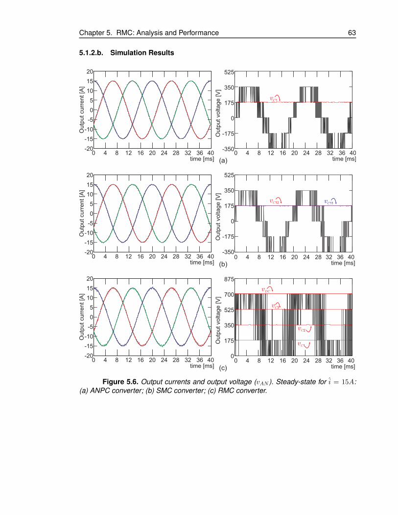
Chapter 5. RMC: Analysis and Performance 63
5.1.2.b. Simulation Results
Ou
tpu
t vo
lta
ge
[V
]
vC1
15
20
10
-5
-15
-20
-10
5
0
Ou
tpu
t cu
rre
nt
[A]
(a)
Ou
tpu
t vo
lta
ge
[V
]
15
20
10
-5
-15
-20
-10
5
0
Ou
tpu
t cu
rre
nt
[A]
(b)
875
700
350
175
0
525
Ou
tpu
t vo
lta
ge
[V
]
vDC
15
20
10
-5
-15
-20
-10
5
0
Ou
tpu
t cu
rre
nt
[A]
(c)
525
350
0
-175
-350
175
525
350
0
-175
-350
175vC12 v
C11
vC3
vC1
vC2
0 4 8 12 16 20 24 28 32 36 40time [ms]
0 4 8 12 16 20 24 28 32 36 40time [ms]
0 4 8 12 16 20 24 28 32 36 40time [ms]
0 4 8 12 16 20 24 28 32 36 40time [ms]
0 4 8 12 16 20 24 28 32 36 40time [ms]
0 4 8 12 16 20 24 28 32 36 40time [ms]
Figure 5.6. Output currents and output voltage (vAN ). Steady-state for i = 15A:(a) ANPC converter; (b) SMC converter; (c) RMC converter.

Chapter 5. RMC: Analysis and Performance 64
875
700
350
175
0
525
Ou
tpu
t vo
lta
ge
[V
]
7.5
5.0
-2.5
-7.5
-5.0
2.5
0
Ou
tpu
t cu
rre
nt
[A]
(c)
vC1
Ou
tpu
t vo
lta
ge
[V
]
7.5
5.0
-2.5
-7.5
-5.0
2.5
0
Ou
tpu
t cu
rre
nt
[A]
(a)
Ou
tpu
t vo
lta
ge
[V
]
7.5
5.0
-2.5
-7.5
-5.0
2.5
0
Ou
tpu
t cu
rre
nt
[A]
(b)
525
350
0
-175
-350
175
525
350
0
-175
-350
175vC12 v
C11
vC3
vC1
vDC
vC2
0 4 8 12 16 20 24 28 32 36 40time [ms]
0 4 8 12 16 20 24 28 32 36 40time [ms]
0 4 8 12 16 20 24 28 32 36 40time [ms]
0 4 8 12 16 20 24 28 32 36 40time [ms]
0 4 8 12 16 20 24 28 32 36 40time [ms]
0 4 8 12 16 20 24 28 32 36 40time [ms]
Figure 5.7. Output currents and output voltage (vAN ). Steady-state for i = 5A: (a)ANPC converter; (b) SMC converter; (c) RMC converter.
Fig. 5.6 and Fig. 5.7 show the steady-state behavior of the systems with 5-level to-pologies for two different operation points. Fig. 5.6 shows the steady-state for an outputcurrent reference of 97 %Inom, and Fig. 5.7 shows the output variables for an output cu-rrent reference of 32 %Inom.
The ANPC and SMC converter (Fig. 5.6-(a),(b) and Fig. 5.7-(a),(b)) achieve a sinu-soidal waveform in the output currents with a maximum current ripple of 0.8 % of thenominal value. The RMC topology (Fig. 5.6-(c)), also achieves a sinusoidal waveform inthe output currents, but the ripple in the output current is 1.1 % of the nominal value forhigh reference values and 2.05 % for low reference values. Since the 5L-RMC has fewer

Chapter 5. RMC: Analysis and Performance 65
switching states than ANPC or SMC, the FCS-MPC has fewer options to choose from,and as a consequence, RMC presents a higher ripple in the output currents.
The switching frequency in the output voltage of the ANPC and SMC converters is3900Hz, and for RMC it is 4050Hz; the switching frequency is calculated as the averageof the number of commutations in one period of the fundamental.
ANPC, SMC and RMC each present a balanced inner voltage, achieving five-leveloutput voltages. However, when the reference value is small, ANPC and SMC use onlythree levels to generate the desired output voltage (inner vectors in Fig. 2.10 in chapter2), but RMC needs to use the five levels to achieve the desired output voltage. This is dueto the number of vectors that are able to balance the inner voltages.
The Total Harmonic Distortion (THD) for the output current and output voltage isshown in Table 5.3, and it is possible to see that there are not big differences between theRMC, ANPC and the SMC topologies. As RMC uses five voltage levels in cases of lowreference currents, the THD of RMC in this case presents a lower value than the THD forANPC and SMC in the same case, but it is possible to see that this does not have a bigimpact in the THD of the current. For ANPC, the current THD is 2.36 %, and for RMC is2.37 %.
Ou
tpu
t vo
lta
ge
[p
.u]
Ou
tpu
t vo
lta
ge
[p
.u]
Ou
tpu
t vo
lta
ge
[p
.u]
Frequency [kHz]
1.0
0.8
0.6
0.4
0.2
0
1.0
0.8
0.6
0.4
0.2
0
1.0
0.8
0.6
0.4
0.2
0
1.0
0.8
0.6
0.4
0.2
0
1.0
0.8
0.6
0.4
0.2
0
1.0
0.8
0.6
0.4
0.2
0
Ou
tpu
t cu
rre
nt
[p.u
]O
utp
ut
cu
rre
nt
[p.u
]O
utp
ut
cu
rre
nt
[p.u
]
0 3 6 9 12 15 18 21 24 27 30 0 3 6 9 12 15 18 21 24 27 30
0 3 6 9 12 15 18 21 24 27 30 0 3 6 9 12 15 18 21 24 27 30
0 3 6 9 12 15 18 21 24 27 30 0 3 6 9 12 15 18 21 24 27 30
Frequency [kHz]
Frequency [kHz]
Frequency [kHz]
00
0.03
0
0.03
1 2 4 5 63
0 1 2 4 5 63
(a)
Frequency [kHz]Frequency [kHz] (b)
Frequency [kHz]Frequency [kHz] (c)
Frequency [kHz]
0
0.03
0 1 2 4 5 63
Figure 5.8. Output currents and output voltage (vAN ) spectrum, for i = 15A: (a)ANPC converter; (b) SMC converter; (c) RMC converter.

Chapter 5. RMC: Analysis and Performance 66
Table 5.3THD FOR 5-LEVEL TOPOLOGIES
Topology Current THD Voltage THD
15A 5A 15A 5A
ANPC 1.02 % 2.36 % 37.6 % 43.3 %
SMC 1.08 % 2.45 % 37.5 % 43.7 %
RMC 1.09 % 2.37 % 37.9 % 40.1 %
Frequency [kHz]0 3 6 9 12 15 18 21 24 27 30 0 3 6 9 12 15 18 21 24 27 30
0 3 6 9 12 15 18 21 24 27 30 0 3 6 9 12 15 18 21 24 27 30
0 3 6 9 12 15 18 21 24 27 30 0 3 6 9 12 15 18 21 24 27 30
Frequency [kHz] (a)
Frequency [kHz]Frequency [kHz] (b)
Frequency [kHz]Frequency [kHz] (c)
Frequency [kHz]
0
0.03
0 1 2 4 5 63
Frequency [kHz]
0
0.03
0 1 2 4 5 63
Frequency [kHz]
0
0.03
0 1 2 4 5 63
Ou
tpu
t vo
lta
ge
[p
.u]
Ou
tpu
t vo
lta
ge
[p
.u]
Ou
tpu
t vo
lta
ge
[p
.u]
1.0
0.8
0.6
0.4
0.2
0
1.0
0.8
0.6
0.4
0.2
0
1.0
0.8
0.6
0.4
0.2
0
1.0
0.8
0.6
0.4
0.2
0
1.0
0.8
0.6
0.4
0.2
0
1.0
0.8
0.6
0.4
0.2
0
Ou
tpu
t cu
rre
nt
[p.u
]O
utp
ut
cu
rre
nt
[p.u
]O
utp
ut
cu
rre
nt
[p.u
]
Figure 5.9. Output currents and output voltage (vAN ) spectrum, for i = 5A: (a)ANPC converter; (b) SMC converter; (c) RMC converter.
Fig. 5.8 and Fig. 5.9 show the harmonic spectrum for the output currents and outputvoltages in phase A. Comparable to the spectrum for the 3-level topologies, the outputcurrent spectrum is widely spread and changes significantly for the different operationpoints. In the RMC’s output current spectrum, it is possible to see that the spectrum isconcentrated around the 4kHz. In the cases of ANPC and SMC, the current spectrum hasa bigger harmonic of 350Hz.
In the output voltage spectrum, the harmonics are more concentrated around the4kHz and its multiples than in the case of 3-level topologies, a clear effect of the increaseof the number of the converter’s output voltage levels. For low reference values in theANPC topology, it is possible to see that there is a big harmonic around the switchingfrequency (4kHz).

Chapter 5. RMC: Analysis and Performance 67
Finally, to verify the dynamic behavior of the system, Fig. 5.10 shows the systemresponse after a step in the current references; it is the same step as that used in the caseof the 3-level topologies. The dynamic response in the ANPC converter takes 1.99ms toachieve the new value; SMC takes 2.01ms and the RMC converter 1.98ms. In addition,FCS-MPC achieves a balanced inner voltage even during the transient.
Consequently, RMC is scalable to a 5-level topology with a comparable performancein steady and transient states to other topologies, like ANPC and SMC.
Ou
tpu
t vo
lta
ge
[V
]
vC1
vC12 v
C11
15
20
10
-5
-15
-20
-10
5
0
Ou
tpu
t cu
rre
nt
[A]
(a)O
utp
ut
vo
lta
ge
[V
]
15
20
10
-5
-15
-20
-10
5
0
Ou
tpu
t cu
rre
nt
[A]
(b)
875
700
350
175
0
525
Ou
tpu
t vo
lta
ge
[V
]
15
20
10
-5
-15
-20
-10
5
0
Ou
tpu
t cu
rre
nt
[A]
(c)
525
350
0
-175
-350
175
525
350
0
-175
-350
175
vC3
vC1
vDC
vC2
0 4 8 12 16 20 24 28 32 36 40time [ms]
0 4 8 12 16 20 24 28 32 36 40time [ms]
0 4 8 12 16 20 24 28 32 36 40time [ms]
0 4 8 12 16 20 24 28 32 36 40time [ms]
0 4 8 12 16 20 24 28 32 36 40time [ms]
0 4 8 12 16 20 24 28 32 36 40time [ms]
Figure 5.10. Output currents and output voltage (vAN ). Dynamic response: (a)ANPC converter; (b) SMC converter; (c) RMC converter.
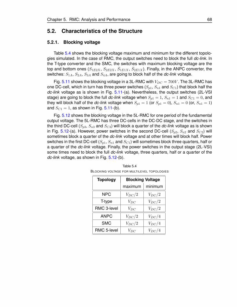
Chapter 5. RMC: Analysis and Performance 68
5.2. Characteristics of the Structure
5.2.1. Blocking voltage
Table 5.4 shows the blocking voltage maximum and minimum for the different topolo-gies simulated. In the case of RMC, the output switches need to block the full dc-link. Inthe T-type converter and the SMC, the switches with maximum blocking voltage are thetop and bottom ones (S1E2X , S2E2X , S1E1X , S2E1X ). Finally, in the ANPC converter, theswitches: S1A, S2A, S3A and S4A, are going to block half of the dc-link voltage.
Fig. 5.11 shows the blocking voltage in a 3L-RMC with VDC = 700V . The 3L-RMC hasone DC-cell, which in turn has three power switches (Sp1, Sn1 and SC1) that block half thedc-link voltage as is shown in Fig. 5.11-(a). Nevertheless, the output switches (2L-VSIstage) are going to block the full dc-link voltage when Sp1 = 1, Sn1 = 1 and SC1 = 0, andthey will block half of the dc-link voltage when Sp1 = 1 (or Sp1 = 0), Sn1 = 0 (or, Sn1 = 1)and SC1 = 1, as shown in Fig. 5.11-(b).
Fig. 5.12 shows the blocking voltage in the 5L-RMC for one period of the fundamentaloutput voltage. The 5L-RMC has three DC-cells in the DC-DC stage, and the switches inthe third DC-cell (Sp3, Sn3 and SC3) will block a quarter of the dc-link voltage as is shownin Fig. 5.12-(a). However, power switches in the second DC-cell (Sp2, Sn2 and SC2) willsometimes block a quarter of the dc-link voltage and at other times will block half. Powerswitches in the first DC-cell (Sp1, Sn1 and SC1) will sometimes block three quarters, half ora quarter of the dc-link voltage. Finally, the power switches in the output stage (2L-VSI)some times need to block the full dc-link voltage, three quarters, half or a quarter of thedc-link voltage, as shown in Fig. 5.12-(b).
Table 5.4BLOCKING VOLTAGE FOR MULTILEVEL TOPOLOGIES
Topology Blocking Voltage
maximum minimum
NPC VDC/2 VDC/2
T-type VDC VDC/2
RMC 3-level VDC VDC/2
ANPC VDC/2 VDC/4
SMC VDC/2 VDC/4
RMC 5-level VDC VDC/4

Chapter 5. RMC: Analysis and Performance 69
875
700
350
175
0
525
Blo
ckin
g v
oltage
SA
[V]
0 2 4 6 8 10 12 14 16 18 20time [ms]
875
700
350
175
0
525B
lockin
g v
oltage
SC
1 [V
]
0 2 4 6 8 10 12 14 16 18 20time [ms]
(a) (b)
Figure 5.11. Blocking voltage in 3-level RMC: (a) Switch SC1; (b) Switch SA.
875
700
350
175
0
525
Blo
ckin
g v
oltage
SA
[V]
0 2 4 6 8 10 12 14 16 18 20time [ms]
875
700
350
175
0
525
Blo
ckin
g v
oltage
SC
3 [V
]
0 2 4 6 8 10 12 14 16 18 20time [ms]
(a) (b)
Figure 5.12. Blocking voltage in 5-level RMC: (a) Switch SC3; (b) Switch SA.
5.2.2. Switching frequency
Table 5.5 shows the average switching frequency for the different topologies simula-ted. To calculate the average switching frequency, all commutations in one period of thefundamental signal are considered.
The switching frequency shown in Table 5.6 is calculated as follows:
Fsw =1
N
N∑i=1
Fsw(Si) (5.5)
where Fsw(Si) is the average switching frequency for the generic power switch Si. Forexample, in RMC there are N = 15 power switches and Si ∈ Spk, Snk, SCk, Sx, Sx fork ∈ 1, 2, 3 and k ∈ A,B,C.
In this work, FCS-MPC is used to control the system, and the cost function used isthat given in the previous section, where the output currents and the inner voltages ofthe converters are controlled. An additional term to ensure a fixed switching frequencywas not included because the focus of this study is to analyze the topologies for a similarperformance (similar system response with the same sampling frequency).
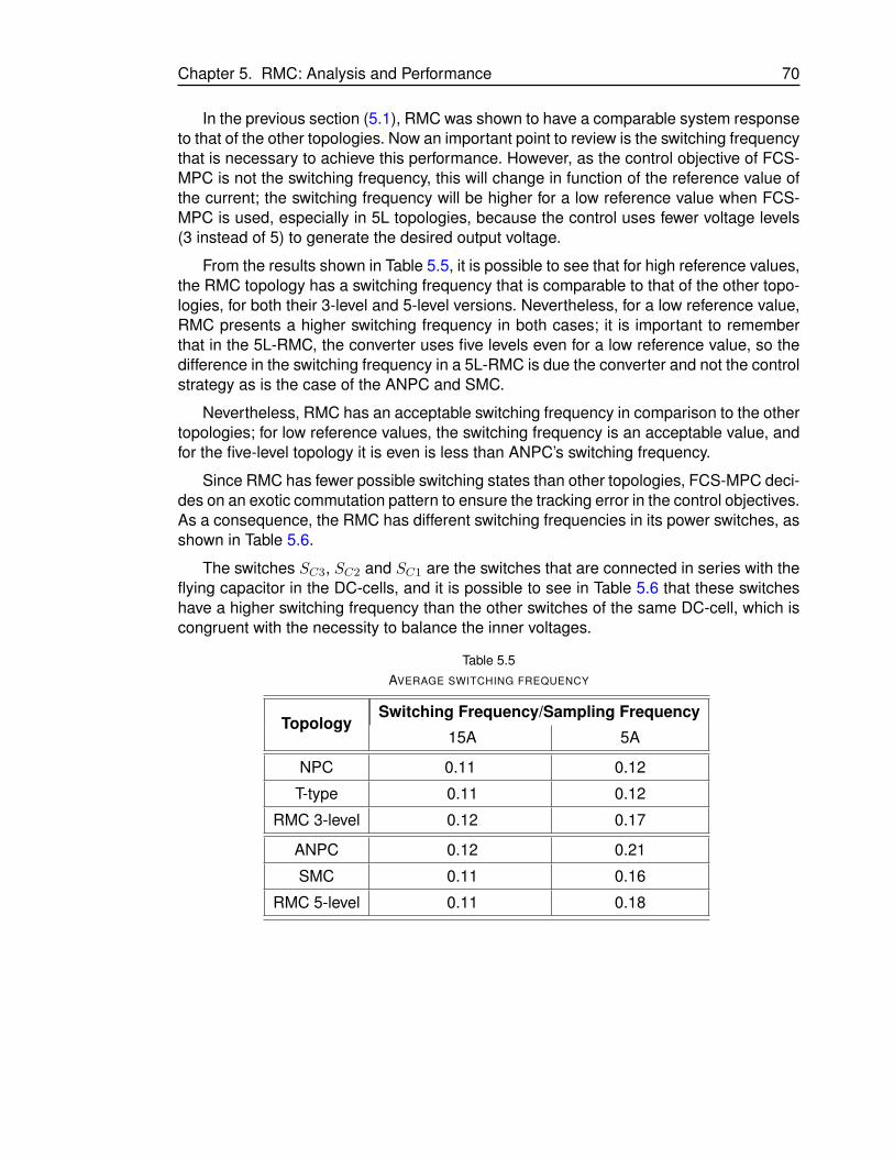
Chapter 5. RMC: Analysis and Performance 70
In the previous section (5.1), RMC was shown to have a comparable system responseto that of the other topologies. Now an important point to review is the switching frequencythat is necessary to achieve this performance. However, as the control objective of FCS-MPC is not the switching frequency, this will change in function of the reference value ofthe current; the switching frequency will be higher for a low reference value when FCS-MPC is used, especially in 5L topologies, because the control uses fewer voltage levels(3 instead of 5) to generate the desired output voltage.
From the results shown in Table 5.5, it is possible to see that for high reference values,the RMC topology has a switching frequency that is comparable to that of the other topo-logies, for both their 3-level and 5-level versions. Nevertheless, for a low reference value,RMC presents a higher switching frequency in both cases; it is important to rememberthat in the 5L-RMC, the converter uses five levels even for a low reference value, so thedifference in the switching frequency in a 5L-RMC is due the converter and not the controlstrategy as is the case of the ANPC and SMC.
Nevertheless, RMC has an acceptable switching frequency in comparison to the othertopologies; for low reference values, the switching frequency is an acceptable value, andfor the five-level topology it is even is less than ANPC’s switching frequency.
Since RMC has fewer possible switching states than other topologies, FCS-MPC deci-des on an exotic commutation pattern to ensure the tracking error in the control objectives.As a consequence, the RMC has different switching frequencies in its power switches, asshown in Table 5.6.
The switches SC3, SC2 and SC1 are the switches that are connected in series with theflying capacitor in the DC-cells, and it is possible to see in Table 5.6 that these switcheshave a higher switching frequency than the other switches of the same DC-cell, which iscongruent with the necessity to balance the inner voltages.
Table 5.5AVERAGE SWITCHING FREQUENCY
TopologySwitching Frequency/Sampling Frequency
15A 5A
NPC 0.11 0.12
T-type 0.11 0.12
RMC 3-level 0.12 0.17
ANPC 0.12 0.21
SMC 0.11 0.16
RMC 5-level 0.11 0.18

Chapter 5. RMC: Analysis and Performance 71
Table 5.6SWITCHING FREQUENCY IN 5-LEVEL RMC
Switch Switching Frequency
15A 5A
Sp3 1200Hz 1350Hz
Sn3 950Hz 1650Hz
SC3 2050Hz 2100Hz
Sp2 850Hz 1600Hz
Sn2 800Hz 1700Hz
SC2 1650Hz 1850Hz
Sp1 450Hz 1700Hz
Sn1 550Hz 1800Hz
SC1 1000Hz 1900Hz
SA 1300Hz 2000Hz
5.2.3. Switching and conduction losses
The PLECSr thermal tools are used to determine the total power losses (switchingand conduction) in the different converters.
PLECSr models thermal structures and calculates switching and conduction lossesin switches by means of lookup tables based on manufacturer information or experimentalmeasurements.
For a fair comparison, the simulation is carried out with the active devices according tothe needs in every topology (this is blocking voltage and current rating). For more detailsabout the loss calculations, please refer to Appendix A.
Fig.5.13 shows the total power losses for the different output current values. It ispossible to see that for 3-level topologies, the proposed converter has more power lossesuntil 0,55Inom output current; after this point, the proposed topology has fewer powerlosses. NPC and the T-type converter have similar power losses for low output current,and after 0,5Inom, 3L-RMC and NPC have comparable power losses.
Fig.5.13-(b) shows the total power losses for the 5-level topologies. The three topolo-gies studied have almost the same power losses until 0,7Inom. After this operation point,the 5L-RMC has fewer power losses, and SMC has 30 % more power losses than ANPCand 5L-RMC.
Thus, the proposed topology has comparable power losses and depending on theoutput current, is more efficient than other multilevel converts.

Chapter 5. RMC: Analysis and Performance 72
00
(a)
0.30.60.91.21.51.82.12.42.73.0
0.1 0.2 0.3 0.4 0.5 0.6 0.7 0.8 0.9 1.0
Output current [p.u]
Tota
l P
ow
er
Losses [%
]
NPCT-type
3L-RMC
(b)
00
0.30.60.91.21.51.82.12.42.73.0
0.1 0.2 0.3 0.4 0.5 0.6 0.7 0.8 0.9 1.0
Output current [p.u]
Tota
l P
ow
er
Losses [%
]
ANPCSMC5L-RMC
Figure 5.13. Switching and conduction power losses for: (a) 3-level topologies,(b) 5-level topologies.
5.2.4. Energy storage and size of the inner capacitors
The energy stored in the converter is given by:
∑num. of capacitor
1
2CV 2 (5.6)
with C the capacitance value and V the voltage across the capacitor.
The capacitance value is calculated to have a determinate ripple in the inner voltage.The capacitance is calculated using the equation (5.7).
C =1
∆viTs (5.7)
Here, Ts is the sampling period, i the maximum current through the capacitor and ∆v
the voltage variation in the capacitor.
Table 5.7 shows the minimum capacitance in the different topologies to accomplish amaximum ripple of 5 % (∆v) in all inner capacitors.

Chapter 5. RMC: Analysis and Performance 73
Table 5.7CAPACITANCE SIZE
Topology Capacitor Capacitance [µF] Capacitor Voltage
ANPC C1X 171.4 VDC/4
SMCC1E1 171.4 VDC/4
C1E2 171.4 VDC/4
RMCC1 171.4 VDC/4
C2 85.7 VDC/2
C3 57.1 3VDC/4
Table 5.8 shows the total energy stored in the different topologies simulated. Theenergy stored in the converter has a direct relationship with the size of the inner capaci-tors. Thus, inner capacitors in RMC are not bigger than the inner capacitors in SMC.
Table 5.8CAPACITANCE SIZE
Topology Energy Stored [kWh]
NPC 0
T-type 0
3-level RMC 2.92
ANPC 2.19
SMC 4.38
5-level RMC 4.38
5.3. Comments
The RMC topology is similar in terms of behavior and structural characteristic to thestandard and commercial topologies like NPC, ANPC and SMC.
However, RMC has fewer active components than these other topologies. Fig. 5.14shows the different three-level topologies, and Fig. 5.15 shows the different five leveltopologies.
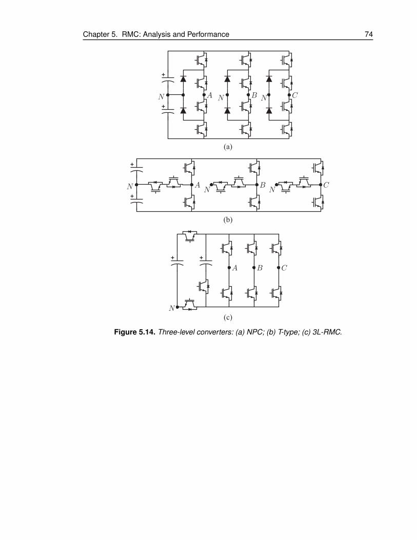
Chapter 5. RMC: Analysis and Performance 74
A B C
N
(c)
(a)
(b)
NN N
A B C
N N NA B C
Figure 5.14. Three-level converters: (a) NPC; (b) T-type; (c) 3L-RMC.
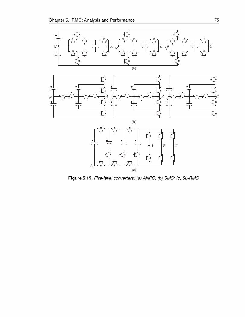
Chapter 5. RMC: Analysis and Performance 75
A B C
N
(c)
(a)
N NA B C
(b)
N
N
N NA B C
Figure 5.15. Five-level converters: (a) ANPC; (b) SMC; (c) 5L-RMC.

Chapter 5. RMC: Analysis and Performance 76
5.4. Back-to-Back RMC
An interesting configuration that RMC can easily achieve is the back-to-back, whichconsists of the connection of two converters, one as a AC-DC rectifier from the grid andthe other as a DC-AC inverter to the load, both of which use the same dc-link capacitor.
For RMC, the back-to-back connection means only six additional output switches forthe three additional output phases. To show how RMC works in this case, a back-to-backconnection is simulated between the grid and an Induction Machine (IM), as shown inFig. 5.16.
Grid IM
A WB VC U
N
Figure 5.16. 3L-RMC back-to-back connection.
The control in the machine is a Torque-Flux control without a speed loop; it has amechanical load of Tload = Tnom. The control in the grid is a power control. The costfunction for FCS-MPC is:
gk+1 =(i∗A − ik+1
A
)2+(i∗B − ik+1
B
)2+(i∗C − ik+1
C
)2+ λ1
(v∗C1 − vk+1
C1
)2
+(T ∗ − T k+1
)2+ λ2
(ψ∗ − ψk+1
)2(5.8)
where λ1 = Inom/vC1nom and λ2 = Tnom/Ψnom. The control strategy needs to evaluate192 possible switching states. A linear controller (PI) is used to control the dc-link voltage:
C = 0,3397(z − 0,93)
(z − 1)(5.9)
The most relevant parameters of the machine and control are detailed in Table 5.9.

Chapter 5. RMC: Analysis and Performance 77
Table 5.9SIMULATION PARAMETERS FOR THE BACK-TO-BACK CONNECTION
Parameter Value
Voltage dc-link 700 V
Inductance grid filter 15 mH
Inner Capacitor 300 µF
DC-link Capacitor 600 µF
Tnom 50 N
Pnom 2.5 kW
Ψnom 0.71 Wb
Lm 170 mH
Ls 175 mH
Lr 175 mH
Rs 1.2 ω
Rr 1.0 ω
J 0.062 kgm2
Sampling period 200 µs
The system’s response to a step in the Torque reference from T ∗ = Tnom to T ∗ =−Tnom is shown in Fig. 5.17 and in Fig. 5.18. In this case, a unitary power factor is seton the grid side; however, it is possible to set a different power factor. The active powerreference for the grid goes from the control over the dc-link voltage and the reactive powerreference is provided by the user.
In Fig. 5.17-(a), one can see that the control strategy achieves a sinusoidal inputcurrent with the unitary power factor (PF=1) in steady state. Additionally, the dc-link andinner capacitor voltage are controlled in the desired value with an acceptable minimumripple, Fig. 5.17-(b). The dc-link voltage presents a perturbation only when the Torquestep is made because the machine is in the regenerative zone and the dc-link controllerhas a low dynamic response. Finally, the output currents on the machine side, Fig. 5.17-(c) are sinusoidal without perturbations or low-frequency harmonics.
Fig. 5.18 shows the mechanical response of the system. It is possible to see that theFCS-MPC presents a zero-error in the torque and flux during steady state and achievesa fast response after the step in the torque reference value. The speed of the machineis not controlled, thus the results shown in Fig. 5.18-(c) are a consequence of only thetorque and flux control of the machine.

Chapter 5. RMC: Analysis and Performance 78
800
600
200
0
400
Ca
pa
cito
r vo
lta
ge
[V
]
0 20 40 60 80 100 120 220140 240160 260180 280200 300time [ms]
(b)
60
30
-30
-60
0
Ou
tpu
t cu
rre
nt
[A]
0 20 40 60 80 100 120 220140 240160 260180 280200 300time [ms]
(c)
350
175
-175
-350
0In
pu
t vo
lta
ge
[V
]
180
90
-90
-180
0
Inp
ut
Cu
rre
nt
[A]
0 20 40 60 80 100 120 220140 240160 260180 280200 300time [ms]
(a)
vC1
vDC
Figure 5.17. 3-level RMC back-to-back with a Torque step: (a) Grid side, voltageand current; (b) DC-link and inner capacitor voltages; (c) Machine output current.

Chapter 5. RMC: Analysis and Performance 79
80
40
-40
-80
0
Torq
ue
T[N
m]
0 20 40 60 80 100 120 220140 240160 260180 280200 300time [ms]
(b)
4000
2000
-2000
-4000
0
Speed
[rpm
]w
0 20 40 60 80 100 120 220140 240160 260180 280200 300time [ms]
(c)
1.2
0.9
0.3
0
0.6F
lux
[Wb]
Y
0 20 40 60 80 100 120 220140 240160 260180 280200 300time [ms]
(a)
Figure 5.18. 3-level RMC back-to-back with a Torque step: (a) Flux; (b) Torque;(c) Speed.
Fig. 5.17 and Fig. 5.18 show that the back-to-back 3L-RMC works fine when a step inthe machine side control is made. Now, the system’s response to a step in the ReactivePower reference, from Q∗ = 0 to Q∗ = −0,3Pnom, is presented.
These results are shown in Fig. 5.19 and Fig. 5.20. In this case the PF changes fromPF = 0 to PF = 0,92 capacitive.

Chapter 5. RMC: Analysis and Performance 80
800
600
200
0
400
Ca
pa
cito
r vo
lta
ge
[V
]
time [ms](b)
60
30
-30
-60
0
Ou
tpu
t cu
rre
nt
[A]
time [ms](c)
350
175
-175
-350
0In
pu
t vo
lta
ge
[V
]
180
90
-90
-180
0
Inp
ut
Cu
rre
nt
[A]
0 10 20 30 40 50 90 10060 11070 80 120
0 10 20 30 40 50 90 10060 11070 80 120
0 10 20 30 40 50 90 10060 11070 80 120
time [ms](a)
vC1
vDC
Figure 5.19. 3-level RMC back-to-back response to a Power step: (a) Grid side,voltage and current; (b) DC-link and inner capacitor voltages; (c) Machine output current.
Fig. 5.19 shows the system’s electric variable when a power step is made at 40ms. Itis possible to see that the step in the grid power does not influence the machine current(Fig. 5.19-(c)). However, after the power step, the dc-link voltage presents an oscillationof 1.4 % (Fig. 5.19-(b)). It is a small, insignificant oscillation, and it does not influencein inner voltage, where no appreciable oscillation appears. Finally, in Fig. 5.19-(a), it ispossible to see the sinusoidal output current with a different phase after the power step.

Chapter 5. RMC: Analysis and Performance 81
80
60
20
0
40
Torq
ue
T[N
m]
time [ms](b)
4000
3000
1000
0
2000
Speed
[rpm
]w
time [ms](c)
1.2
0.9
0.3
0
0.6F
lux
[Wb]
Y
time [ms](a)
0 10 20 30 40 50 90 10060 11070 80 120
0 10 20 30 40 50 90 10060 11070 80 120
0 10 20 30 40 50 90 10060 11070 80 120
Figure 5.20. 3-level RMC back-to-back with a Power step: (a) Flux; (b) Torque; (c)Speed.
Like the machine current presented in Fig. 5.19-(c), the mechanical variables shownin Fig. 5.20 have no difference in their steady-state performance after the power step onthe grid side. FCS-MPC controls the torque and flux with zero-error in steady-state andthe power step causes no appreciable disturbance.

Chapter 6
Experimental Validation
To evaluate the performance of the proposed topology, several experiments were ca-rried out in the laboratory. The proposed topology was evaluated in both dynamic andstationary state for a current reference of 50Hz. The controller was implemented on a Ds-pace MicroLabBox in which the maximum time required by the control platform to executethe control code is 56,4µs. The most relevant parameters of the test-bench and controllerare detailed in Table 6.1. For more details about the test bench, please refer to appendixB.
Table 6.1TEST BENCH PARAMETERS.
Parameter Value
Voltage dc-link 400 V
Load Resistance 16 Ω
Load Inductance 30 mH
Inner Capacitors 330 µF
Sampling period 100 µs
6.1. Steady State Behavior
The purpose of this test is to assess the performance of the system once steady statehas been reached for output current references of 75,8 %Inom and 37,9 %Inom.
The frequency spectrum of the current in phase A, the output voltage (vAN ), the totalharmonic distortion of these variables and the ripple in inner capacitor voltages shall beanalyzed.
Fig. 6.1 and Fig. 6.2 show the steady state performance of the converter with differentoutput current references. The FCS-MPC algorithm can properly perform all control tasks,achieving sinusoidal three-phase output current and ensuring balanced inner voltages.The control results in five output levels in all phases.
82

Chapter 6. Experimental Validation 83
8
6
4
2
0
-2
-4
-6
-8
500
400
300
200
100
0
Outp
ut curr
ent [A
]O
utp
ut voltage [V
]
0 10 20 30 40 50 60 70 80 90 100time [ms]
vDC
vC1
vC2
vC3
Figure 6.1. Output current, output voltage vAN and capacitor voltage withi∗ = 6sin(ωt)A.
In the experimental results shown in Fig. 6.1 and Fig. 6.2 one can see that the 5L-RMC generates an output voltage (VAN ) with five levels in both low and high referencecurrents.
For a low reference current, shown in Fig. 6.2, one observes a higher ripple in thecurrent (1,4 % of the reference current), but for a high reference current this ripple is 0,8 %of the reference current. The change in the size of the current ripple is a consequenceof the control strategy. FCS-MPC has the width of the switching signals limited to thesampling period, i.e. a finite possibility instead of a variable width as in PWM modulations,and consequently, FCS-MPC has a higher ripple for low reference values. Nevertheless,in the case of the RMC, this effect is also a consequence of the lower number of possibleswitching states in the converter because to achieve the desired inner voltage, the RMCwill commutate between higher output voltages (using all five levels).

Chapter 6. Experimental Validation 84
4
3
2
1
0
-1
-2
-3
-4
500
400
300
200
100
0
Outp
ut curr
ent [A
]O
utp
ut voltage [V
]
vDC
vC1
vC3
vC2
0 10 20 30 40 50 60 70 80 90 100time [ms]
Figure 6.2. Output current, output voltage (vAN ) and capacitor voltage withi∗ = 3sin(ωt)A.
Fig. 6.3 and Fig. 6.4 show the converter’s inner capacitor voltages. Considering thecapacitance of the flying capacitors, the maximum ripple is 2,27 % for C1, 1,14 % for C2 and0,76 % for C3 with i = 6A and 1,13 % for C1, 0,57 % for C2 and 0,38 % for C3 with i = 3A.However, by using weighting factors, the FCS-MPC strategy ensures an equal maximumvoltage ripple for the three capacitor voltages independent of the output current.
In the case of low output current shown in Fig. 6.2, FCS-MPC chooses output vectorswith a greater influence on the inner capacitors voltages, specifically in C1 and C2, be-cause it is necessary to commutate more often between 100V, 200V, and 300V to complywith the output current requirements.
The 5L-RMC produces an output voltage with 45.5 % total harmonic distortion (THD)for high reference values, whereas for low reference values this value is 50.8 %. Fig. 6.5and Fig. 6.6 show the output current iA spectrum and output voltage, VAN , spectrum forboth operation points.

Chapter 6. Experimental Validation 85
300
295
305
Inner
voltage
[V]
C3
100
95
105
Inner
voltage
[V]
C1
200
195
205
Inner
voltage
[V]
C2
0 10 20 30 40 50 60 80 9070 100time [ms]
0 10 20 30 40 50 60 80 9070 100time [ms]
400
390
410
Inner
voltage
[V]
C4
Figure 6.3. Inner capacitor voltages for i∗ = 6sin(ωt)A.
300
295
305
Inner
voltage
[V]
C3
100
95
105
Inner
voltage
[V]
C1
200
195
205
Inner
voltage
[V]
C2
0 10 20 30 40 50 60 80 9070 100time [ms]
0 10 20 30 40 50 60 80 9070 100time [ms]
400
390
410
Inner
voltage
[V]
C4
Figure 6.4. Inner capacitor voltages for i∗ = 3sin(ωt)A.
The sampling frequency of the FCS-MPC strategy is 10kHz, but the mean switchingfrequency is 5kHz. The Total Harmonic Distortion (THD) for the output current is 4,45 %for iA = 6A and 8,41 % for iA = 3A. It is possible to see that the THD increases and thespectrum changes significantly with the value of the reference.
The output current spectrum and output voltage spectrum shown in Fig. 6.5 andFig. 6.6 are widely spread. However, the output voltage spectrum has a high concen-tration around the switching frequency (5kHz), which is clearer in Fig. 6.6, where eventhe output current spectrum presents a higher concentration around the 5kHz. Howe-ver, it is possible to see that the output current spectrum presents an important numberof low-frequency harmonics with a significant value (higher than the harmonic around5kHz); these harmonics can produce resonant problems in the system and as they arewidely spread, it is not easy to filter them.
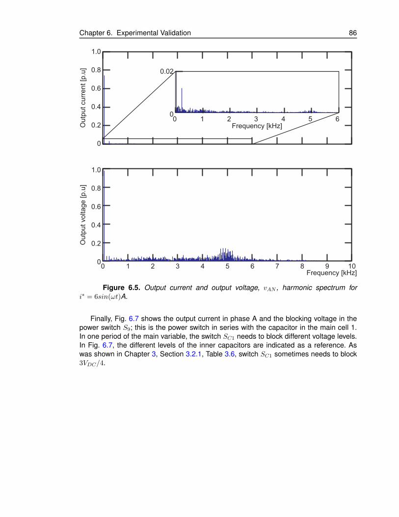
Chapter 6. Experimental Validation 86
Ou
tpu
t cu
rre
nt
[p.u
]O
utp
ut
vo
lta
ge
[p
.u]
0 1 2 3 4 5 6 7 8 9 10Frequency [kHz]
1.0
0.8
0.6
0.4
0.2
0
1.0
0.8
0.6
0.4
0.2
0
Frequency [kHz]
0
0.02
0 1 2 4 5 63
Figure 6.5. Output current and output voltage, vAN , harmonic spectrum fori∗ = 6sin(ωt)A.
Finally, Fig. 6.7 shows the output current in phase A and the blocking voltage in thepower switch S9; this is the power switch in series with the capacitor in the main cell 1.In one period of the main variable, the switch SC1 needs to block different voltage levels.In Fig. 6.7, the different levels of the inner capacitors are indicated as a reference. Aswas shown in Chapter 3, Section 3.2.1, Table 3.6, switch SC1 sometimes needs to block3VDC/4.

Chapter 6. Experimental Validation 87
0 1 2 3 4 5 6 7 8 9 10Frequency [kHz]
Frequency [kHz]
0
0.02
0 1 2 4 5 63
Ou
tpu
t cu
rre
nt
[p.u
]O
utp
ut
vo
lta
ge
[p
.u]
1.0
0.8
0.6
0.4
0.2
0
1.0
0.8
0.6
0.4
0.2
0
Figure 6.6. Output current and output voltage, vAN , harmonic spectrum fori∗ = 3sin(ωt)A.
9
6
3
0
-3
-6
-9
400
300
200
100
0
-100
Outp
ut curr
ent [A
]
Sblo
ckin
g v
oltage [V
]C
1
0 2 4 6 8 10 12 14 16 18 20time [ms]
Figure 6.7. Output current and blocking voltage in power switch SC1.

Chapter 6. Experimental Validation 88
6.2. Dynamic Response
The purpose of this test is to demonstrate the behavior of the system in the presen-ce of a variation in current reference values, bringing the system to a new steady-stateworking point.
A quite demanding step has been established for this test. This is done with the pur-pose of verifying that the implemented control is able to achieve a performance in linewith the specifications required, regardless of the disturbances to which it is exposed.Therefore, the step performed not only changes the reference signal’s magnitude, butalso causes a phase change corresponding to a displacement of 180.
Fig. 6.8 shows an enlargement of the inner capacitor voltages during the step. Inthis more detailed picture, it is possible to check the fast response of FCS-MPC and thenull disturbance in the inner capacitors’ voltages during the dynamic step. The voltage incapacitor C4 represents the voltage in the DC power supply; in this case, the extra energygenerated during the dynamic step results in a disturbance in the dc-link voltage.
Fig. 6.9 shows the converter’s performance during a dynamic step in the current refe-rence. The control strategy ensures a correctly balanced voltage in the flying capacitorsand a sinusoidal output current even during the transient time. In this case, FCS-MPC’svariables achieve a fast response, always ensuring a well balanced inner voltage. It takesonly 2.2ms (11 % of the fundamental period) to achieve the new steady-state operationpoint.
300
295
305
Inner
voltage
[V]
C3
100
95
105
Inner
voltage
[V]
C1
200
195
205
Inner
voltage
[V]
C2
0 10 20 30 40 50 60 70 80time [ms]
400
390
410
Inner
voltage
[V]
C4
0 10 20 30 40 50 60 70 80time [ms]
Figure 6.8. Inner capacitor voltages.

Chapter 6. Experimental Validation 89
8
6
4
2
0
-2
-4
-6
-8
500
400
300
200
100
0
Ou
tpu
t cu
rre
nt
[A]
Ou
tpu
t vo
lta
ge
[V
]
0 10 20 30 40 50 60 70 80time [ms]
vDC
vC1
vC3
vC2
Figure 6.9. Output current, output voltage and capacitor voltage after a current step.

Chapter 7
Conclusions and Future Outlook
This dissertation has proposed a concept for a new multilevel converter topology ba-sed on a novel switched DC-cell and variable dc-link operation. The proposed topologyis called RMC and can be split into two stages: the DC-DC multilevel converter, which isthe main contribution of the proposed topology, and the DC-AC output inverter. The RMCcan achieve the same number of output voltage levels as existing multilevel topologieswith a fraction of the active switching devices and capacitors because the variable dc-linkis shared by all of the inverter’s output phases.
In this dissertation, an RMC with a 2L-VSI in the DC-AC output inverter was analyzed.However, it is possible to choose a different DC-AC output inverter, the only condition tochange it is to use an inverter with a single DC-bus such as the NPC, ANPC, T-type, FCC,or SMC.
Using a different DC-AC output inverter, RMC will have more possible switching sta-tes, which improves the controller’s performance and could relax the constraint of theblocking voltages in the power switches.
The main control challenge of the topology is to control of the DC-cell capacitor vol-tages so as to generate the total desired number of output levels. Due to the switchedDC-cell capacitors, there it is not straightforward way to implement a carrier based PWMscheme. This is further complicated by increasing the number of output voltage levelsdue to the fact that there are not enough possible switching states and redundant sta-tes to achieve a balanced inner voltage using pulse width modulation. For this reason,FCS-MPC was used to verify the new converter’s performance.
At first glance, the maximum device blocking voltage is the main disadvantage ofthis topology. However, this is imposed by the selected inverter output stage, which inthe case analyzed in this dissertation is a 2L-VSI. This limitation prevents the use ofthis topology in medium voltage applications. Nevertheless, due to their power quality,multilevel converters have now been used extensively in low voltage applications such asPV inverters, UPS systems and wind power conversion systems (all below 690 V) makingthis topology interesting for further analysis.
In Chapter 5, an analysis of the proposed topology and a comparison with other to-pologies for 3-level and 5-level converters were presented. The results showed that theproposed topology has a comparable performance in the system variables with the ot-
90

Chapter 7. Conclusions and Future Outlook 91
her multilevel converters and achieves sinusoidal output currents, the desired number ofoutput levels in the voltage, balanced inner voltages, similar THD and spectrum.
In addition, considering the components of the topologies, it was shown in Chapter 5that the proposed topology has a switching frequency that is comparable to those of othermultilevel topologies, but it has fewer power losses. Further, it was demonstrated that thesize of its inner capacitors are comparable to those of the SMC topology. However, themain problem with the proposed topology is the blocking voltage of the output stage powerswitches, which needs to block the full dc-link.
Chapter 5 also presented a back-to-back connection of the 3L-RMC, with controls theTorque and Flux in an induction machine, the current in the grid side and the inner voltagein the converter, dc-link voltage and flying capacitor voltage. The results presented showthat the back-to-back topology works and it is possible to control the machine side andthe grid side with a unique cost function for FCS-MPC.
A laboratory prototype has been built using three shared DC-cells and a three-phase2L-VSI as the inverter output stage. Experimental results show that the DC-cell capacitorscan be balanced and controlled accurately while achieving sinusoidal output currents anda five-level output voltage waveform.
A comprehensive study to determine the most suitable applications for this topology,as well as evaluations with different output inverter stages (NPC, ANPC, etc.), which couldlead to medium voltage operation, is a matter for future research.
Other unresolved problems include the development of a carrier-based PWM or spa-ce vector modulation strategy for the converter and more sophisticated FCS-MPC tech-niques using fixed switching frequency and dv/dt reduction.

Appendix A
Calculation of losses
To determine the total power losses (switching and conduction) in the different con-verters, the thermal tools of PLECSr are used, as shown in Fig. A.1.
Figure A.1. PLECSr simulation to calculate the converter’s total losses.
For a fair comparison, the simulation is carried out with the active devices accordingto the needs in every topology (that is, blocking voltage and current rating). The list ofcommercial devices used in this simulation is shown in Table A.1.
92

Appendix A. Calculation of losses 93
Table A.1DEVICES SELECTED
Device name Cont. Current Voltage
IRGP4072DPBF 40A 300V
IRG4PC40UDPBF 40A 600V
IRG4PF50WDPBF 30A 900V
IKW40N120H3FKSA1 40A 1200V

Appendix B
Test Bench
The test bench used was built in the Chair of Power Electronics’ laboratory at Technis-che Universität Berlin. It includes the power electronic converter and the real-time controlsystem.
Three kW prototypes of the proposed multilevel topology were built. The designedconverter prototype is shown in Fig. B.1. Area (1) corresponds to the dc-link capacitors,area (2) shows the three DC-cells of the converter and area (3) shows the variable dc-link bus connection between the DC-cells and the output inverter stage. Finally, area (4)shows the 2L-VSI.
The power switches used in this prototype are Insulated Gate Bipolar Transistors(IGBTs) with a freewheeling diode from the ON Semiconductor, NGTB30N120IHSWG,with a 30A maximum collector current and a 1200V blocking voltage. The capacitance ofthe flying capacitor in all DC-cells is 330µF.
(1)
(2)(3)
(4)
Figure B.1. RMC prototype: (1) dc-link capacitors; (2) DC-cells; (3) Variable dc-link; (4) 2L-VSI.
The micro-controller platform used is the MicroLabBox from Dspace. This platform
94

Appendix B. Test Bench 95
has the following characteristics used in this dissertation: (a) Real-time 2 GHz processor;(b) Programmable FPGA; (c) Analog input 16-bit, −10..,10V ; and (d) Digital output 5V,10ns resolution.

Bibliography
[1] D. Krug, S. Bernet, and S. Dieckerhoff, “Comparison of State-of-the-art VoltageSource Converter Topologies for Medium Voltage Applications,” in Industry Applica-tions Conference, 2003. 38th IAS Annual Meeting. Conference Record of the, vol. 1,pp. 168–175, IEEE, 2003.
[2] J. R. Rodriguez, J. W. Dixon, J. R. Espinoza, J. Pontt, and P. Lezana, “PWM regene-rative rectifiers: State of the art,” IEEE Transactions on Industrial Electronics, vol. 52,no. 1, pp. 5–22, 2005.
[3] B. Wu, J. Pontt, J. Rodriguez, S. Bernet, and S. Kouro, “Current-source Converterand Cycloconverter Topologies for Industrial Medium-Voltage drives,” IEEE Transac-tions on Industrial Electronics, vol. 55, no. 7, pp. 2786–2797, 2008.
[4] M. Yazdanian and A. Mehrizi-Sani, “Internal model-based current control of the RLfilter-based voltage-sourced converter,” IEEE Transactions on Energy Conversion,vol. 29, no. 4, pp. 873–881, 2014.
[5] H. Abu-Rub, J. Holtz, J. Rodriguez, and G. Baoming, “Medium-voltage multilevelconverters: State of the art, challenges, and requirements in industrial applications,”IEEE Transactions on Industrial Electronics, vol. 57, no. 8, pp. 2581–2596, 2010.
[6] A. Nabae, I. Takahashi, and H. Akagi, “A new Neutral-Point-Clamped PWM inverter,”IEEE Transactions on industry applications, no. 5, pp. 518–523, 1981.
[7] J. Rodriguez, S. Bernet, B. Wu, J. O. Pontt, and S. Kouro, “Multilevel voltage-source-converter topologies for industrial medium-voltage drives,” IEEE Transactions on In-dustrial Electronics, vol. 54, pp. 2930–2945, Dec. 2007.
[8] T. Meynard and H. Foch, “Multi-level conversion: high voltage choppers and voltage-source inverters,” in Power Electronics Specialists Conference, 1992. PESC’92 Re-cord., 23rd Annual IEEE, pp. 397–403, IEEE, 1992.
[9] T. A. Meynard, H. Foch, P. Thomas, J. Courault, R. Jakob, and M. Nahrstaedt, “Mul-ticell Converters: basic concepts and industry applications,” IEEE Transactions onIndustrial Electronics, vol. 49, pp. 955–964, Oct. 2002.
[10] G. Gateau, T. A. Meynard, H. Foch, “Stacked multicell converter (SMC): propertiesand design.,” IEEE 32nd Annual Power Electronics Specialists Conference, PESC2001., June 17-22, Vancouver, Canada. 2001.
96

Bibliography 97
[11] E. Babaei, “A Cascade Multilevel Converter Topology with Reduced Number of Swit-ches,” IEEE Transactions on power electronics, vol. 23, no. 6, pp. 2657–2664, 2008.
[12] G. Adam, I. A. Abdelsalam, K. H. Ahmed, and B. W. Williams, “Hybrid MultilevelConverter with Cascaded H-bridge cells for HVDC applications: Operating principleand scalability,” IEEE Transactions on Power Electronics, vol. 30, no. 1, pp. 65–77,2015.
[13] M. Schweizer and J. W. Kolar, “High efficiency drive system with 3-level T-type In-verter,” in Power Electronics and Applications (EPE 2011), Proceedings of the 2011-14th European Conference on, pp. 1–10, IEEE, 2011.
[14] L. Zhe Zhang, O. C. Thomsen, and M. A. E. Andersen, “Discontinuous PWM mo-dulation strategy with circuit-level decoupling concept of three-level neutral-point-clamped (NPC) inverter,” IEEE Transactions on Industrial Electronics, vol. 60, no. 5,pp. 1897–1906, 2013.
[15] C. Osawa, Y. Matsumoto, T. Mizukami, and S. Ozaki, “A state-space modeling anda neutral point voltage control for an npc power converter,” in Power ConversionConference - Nagaoka 1997., Proceedings of the, vol. 1, pp. 225–230, 1997.
[16] Z. Xiaoming Yuan, H. Stemmler, and I. Barbi, “Evaluation of soft switching techni-ques for the neutral-point-clamped (NPC) inverter,” in Power Electronics SpecialistsConference, 1999. PESC 99. 30th Annual IEEE, vol. 2, pp. 659–664, 1999.
[17] J. D. Barros, J. F. A. Silva, and E. G. A. Jesus, “Fast-predictive optimal control of NPCmultilevel converters,” IEEE Transactions on Industrial Electronics, vol. 60, no. 2,pp. 619–627, 2013.
[18] R. Portillo, S. Vazquez, J. I. Leon, M. M. Prats, and L. G. Franquelo, “Model basedadaptive direct power control for three-level NPC converters,” IEEE Transactions onIndustrial Informatics, vol. 9, no. 2, pp. 1148–1157, 2013.
[19] R. Menzies, P. Steimer, and J. Steinke, “Five-level GTO inverters for large inductionmotor drives,” Industry Applications, IEEE Transactions on, vol. 30, no. 4, pp. 938–944, 1994.
[20] Q. Song, W. Liu, Q. Yu, X. Xie, and Z. Wang, “A neutral-point potential balancingalgorithm for three-level NPC inverters using analytically injected zero-sequencevoltage,” in Applied Power Electronics Conference and Exposition, 2003. APEC’03.Eighteenth Annual IEEE, vol. 1, pp. 228–233, IEEE, 2003.
[21] N. Celanovic and D. Boroyevich, “A comprehensive study of neutral-point voltage ba-lancing problem in three-level neutral-point-clamped voltage source PWM inverters,”Power Electronics, IEEE Transactions on, vol. 15, no. 2, pp. 242–249, 2000.
[22] Sala, R. Salehi, M. Moreno-Eguilaz, M. Salehifar, and L. Romeral, “Clamping diodecaused distortion in multilevel NPC full-bridge audio power amplifiers,” in IECON2012 - 38th Annual Conference on IEEE Industrial Electronics Society, pp. 4941–4948, 2012.

Bibliography 98
[23] P. Bartolomeüs, P. Le Moigne, and J. Mba, “Over-voltage problems of diode-clampedconverters during switchings,” in proc. of the European Power Electronics Conferen-ce (EPE’2003), 2003.
[24] G. P. Adam, S. J. Finney, A. M. Massoud, and B. W. Williams, “Capacitor balanceissues of the diode-clamped multilevel inverter operated in a quasi two-state mode,”Industrial Electronics, IEEE Transactions on, vol. 55, no. 8, pp. 3088–3099, 2008.
[25] G. P. Adam, S. J. Finney, B. W. Williams, and M. T. Mohammed, “Two-level operationof a diode-clamped multilevel inverter,” in Industrial Electronics (ISIE), 2010 IEEEInternational Symposium on, pp. 1137–1142, IEEE, 2010.
[26] C. Hochgraf, R. Lasseter, D. Divan, and T. Lipo, “Comparison of multilevel invertersfor static var compensation,” in Industry Applications Society Annual Meeting, 1994.,Conference Record of the 1994 IEEE, pp. 921–928, IEEE, 1994.
[27] T. Bruckner, S. Bernet, and H. Guldner, “The active npc converter and its loss-balancing control,” IEEE Transactions on Industrial Electronics, vol. 52, no. 3,pp. 855–868, 2005.
[28] O. Apeldoorn, B. Odegard, P. Steimer, and S. Bernet, “A 16 MVA anpc-pebb with6 kA igcts,” in Industry Applications Conference, 2005. Fourtieth IAS Annual Meeting.Conference Record of the 2005, vol. 2, pp. 818–824, 2005.
[29] P. Barbosa, P. Steimer, J. Steinke, L. Meysenc, M. Winkelnkemper, and N. Celano-vic, “Active neutral-point-clamped multilevel converters,” in Proc. IEEE 36th PowerElectronics Specialists Conf. PESC ’05, pp. 2296–2301, 2005.
[30] L. Serpa, P. Barbosa, P. Steimer, and J. Kolar, “Five-level virtual-flux Direct PowerControl for the Active Neutral-Point Clamped Multilevel Inverter,” in Power ElectronicsSpecialists Conference, 2008. PESC 2008. IEEE, pp. 1668–1674, IEEE, 2008.
[31] S. R. Pulikanti and V. G. Agelidis, “Control of neutral point and flying capacitor volta-ges in five-level SHE-PWM controlled ANPC converter,” in Industrial Electronics andApplications, 2009. ICIEA 2009. 4th IEEE Conference on, pp. 172–177, IEEE, 2009.
[32] F. Kieferndorf, M. Basler, L. Serpa, J.-H. Fabian, A. Coccia, and G. Scheuer, “A newmedium voltage drive system based on ANPC-5L technology,” in Industrial Techno-logy (ICIT), 2010 IEEE International Conference on, pp. 643–649, IEEE, 2010.
[33] S. R. Pulikanti and V. G. Agelidis, “Hybrid flying-capacitor-based active-neutral-point-clamped five-level converter operated with SHE-PWM,” IEEE Transactions on Indus-trial Electronics, vol. 58, no. 10, pp. 4643–4653, 2011.
[34] J. Li, A. Q. Huang, Z. Liang, and S. Bhattacharya, “Analysis and design of activeNPC (ANPC) inverters for fault-tolerant operation of high-power electrical drives,”IEEE Transactions on Power Electronics, vol. 27, no. 2, pp. 519–533, 2012.
[35] S. R. Pulikanti, G. Konstantinou, and V. G. Agelidis, “Generalisation of flyingcapacitor-based Active-Neutral-Point-Clamped Multilevel Converter using Voltage-Level Modulation,” IET Power Electronics, vol. 5, no. 4, pp. 456–466, 2012.

Bibliography 99
[36] K. Wang, Z. Zheng, Y. Li, K. Liu, and J. Shang, “Neutral-Point Potential Balancing ofa Five-level Active Neutral-Point-Clamped Inverter,” IEEE Transactions on IndustrialElectronics, vol. 60, no. 5, pp. 1907–1918, 2013.
[37] F. Kieferndorf, M. Basler, L. Serpa, J.-H. Fabian, A. Coccia, and G. Scheuer, “ANPC-5L technology applied to medium voltage variable speed drives applications,” inSPEEDAM 2010, pp. 1718–1725, IEEE, 2010.
[38] www.alstom.com, “Symphony drive line.,”
[39] www.alsintec.com/internacional-en.asp, “ALSTOM VDM6000. Symphony,”
[40] K. Corzine and Y. Familiant, “A new cascaded multilevel h-bridge drive,” IEEETransactions on Power Electronics, vol. 17, pp. 125–131, Jan. 2002.
[41] J. Huang and K. A. Corzine, “Extended operation of flying capacitor multilevel inver-ters,” IEEE Transactions on Power Electronics, vol. 21, pp. 140–147, Jan. 2006.
[42] P. Lezana, R. P. Aguilera, and D. E. Quevedo, “Model predictive control of anasymmetric flying capacitor converter,” IEEE Transactions on Industrial Electronics,vol. 56, pp. 1839–1846, June 2009.
[43] R. H. Wilkinson, T. H. Meynard, and H. du Toit Mouton, “Natural balance of multicellconverters: The general case,” IEEE Transactions on Power Electronics, vol. 21,pp. 1658–1666, Nov. 2006.
[44] B. Reznikov and A. Ruderman, “Five-level single-leg flying capacitor converter vol-tage balance dynamics analysis,” in Proc. 35th Annual Conference of the IEEE In-dustrial Electronics Society - IECON 2009, pp. 1–6, Portugal, Porto, 3–5 Nov. 2009.
[45] R. H. Wilkinson, T. A. Meynard, and H. du Toit Mouton, “Natural balance of multicellconverters: The general case,” IEEE Transactions on Power Electronics, vol. 21,no. 6, pp. 1658–1666, 2006.
[46] R. H. Wilkinson, T. A. Meynard, and H. du Toit Mouton, “Natural balance of multicellconverters: The two-cell case,” IEEE Transactions on Power Electronics, vol. 21,no. 6, pp. 1649–1657, 2006.
[47] M. Norambuena, J. Rodriguez, and S. Kouro, “Convertidor Multinivel para el Controly Transmisión de la Energía Eléctrica,” Sept. 2016, patent request 201602365.
[48] J. Rodríguez, M. P. Kazmierkowski, J. R. Espinoza, P. Zanchetta, H. Abu-Rub, H. A.Young, and C. A. Rojas, “State of the art of finite control set model predictive con-trol in power electronics,” IEEE Transactions on Industrial Informatics, vol. 9, no. 2,pp. 1003–1016, 2013.
[49] J. Rodríguez and P. Cortés, Predictive Control of Power Converters and ElectricalDrives. Wiley, 2012.
[50] E. F. Camacho and C. Bordons, Model Predictive Control. Springer, 1999.
[51] S. Vazquez, J. Rodriguez, M. Rivera, L. G. Franquelo, and M. Norambuena, “ModelPredictive Control for Power Converters and Drives: Advances and Trends,” IEEETransactions on Industrial Electronics, vol. 64, pp. 935–947, Feb. 2017.

Bibliography 100
[52] J. Zeng, D.-Y. Xue, and D.-C. Yuan, “A multi-model predictive control strategy ba-sed on data-centric,” in Natural Computation, 2008. ICNC ’08. Fourth InternationalConference on, vol. 4, pp. 313–316, 2008.
[53] P. Cortés, M. P. Kazmierkowski, R. M. Kennel, D. E. Quevedo, and J. Rodriguez,“Predictive control in power electronics and drives,” IEEE Transactions on IndustrialElectronics, vol. 55, no. 12, pp. 4312–4324, 2008.
[54] S. Kouro, P. Cortes, R. Vargas, U. Ammann, and J. Rodriguez, “Model predictivecontrol—a simple and powerful method to control power converters,” IEEE Transac-tions on Industrial Electronics, vol. 56, no. 6, pp. 1826–1838, 2009.
[55] J. Rodriguez, J. Pontt, C. A. Silva, P. Correa, P. Lezana, P. Cortes, and U. Ammann,“Predictive current control of a voltage source inverter,” vol. 54, pp. 495–503, Feb.2007.
[56] S. Müller, U. Ammann, and S. Rees, “New time-discrete modulation scheme for ma-trix converters,” IEEE Transactions on Industrial Electronics, vol. 52, no. 6, pp. 1607–1615, 2005.
[57] S. Kouro, P. Cortes, R. Vargas, U. Ammann, and J. Rodriguez, “Model predictive con-trol& simple and powerful method to control power converters,” IEEE Transactionson Industrial Electronics, vol. 56, pp. 1826–1838, June 2009.
[58] J. Rodriguez, M. P. Kazmierkowski, J. R. Espinoza, P. Zanchetta, H. Abu-Rub, H. A.Young, and C. A. Rojas, “State of the Art of Finite Control Set Model PredictiveControl in Power Electronics,” IEEE Transactions on Industrial Informatics, vol. 9,no. 2, pp. 1003–1016, 2013.
[59] A. Linder and R. Kennel, “Direct model predictive control - a new direct predictivecontrol strategy for electrical drives,” in Power Electronics and Applications, 2005European Conference on, 2005.
[60] N. Hoffmann, M. Andresen, F. W. Fuchs, L. Asiminoaei, and P. B. Thogersen., “Varia-ble sampling time finite control-set model predictive current control for voltage sour-ce inverters,” in Energy Conversion Congress and Exposition (ECCE), 2012 IEEE,pp. 2215–2222, 2012.
[61] P. Lezana, R. Aguilera, and D. E. Quevedo, “Model predictive control of an asymme-tric flying capacitor converter,” IEEE Transactions on Industrial Electronics, vol. 56,no. 6, pp. 1839–1846, 2009.
[62] C. Ekaputri and A. Syaichu-Rohman., “Implementation model predictive control(MPC) algorithm-3 for inverted pendulum,” in Control and System Graduate Re-search Colloquium (ICSGRC), 2012 IEEE, pp. 116–122, 2012.
[63] J. Rodriguez, J. Pontt, P. Cortes, and R. Vargas, “Predictive control of a three-phaseneutral point clamped inverter,” in Power Electronics Specialists Conference, 2005.PESC ’05. IEEE 36th, pp. 1364–1369, 2005.
[64] Y.-F. L. W. Zhang, Guang Feng and B. Wu, “A new predictive control strategy forpower factor correction,” in Applied Power Electronics Conference and Exposition,2003. APEC ’03. Eighteenth Annual IEEE, vol. 1, pp. 403–409, 2003.

Bibliography 101
[65] M. A. Perez, P. Cortes, and J. Rodriguez., “Predictive control algorithm technique formultilevel asymmetric cascaded h-bridge inverters,” IEEE Transactions on IndustrialElectronics, vol. 55, no. 12, pp. 4354–4361, 2008.
[66] R. Kennel and A. Linder, “Predictive control of inverter supplied electrical drives,” inPower Electronics Specialists Conference, 2000. PESC 00. 2000 IEEE 31st Annual,vol. 2, pp. 761–766, 2000.
[67] J. Rodríguez, J. Pontt, C. A. Silva, P. Correa, P. Lezana, P. Cortes, and U. Ammann,“Predictive current control of a voltage source inverter,” IEEE Transactions on Indus-trial Electronics, vol. 54, no. 1, pp. 495–503, 2007.
[68] R. Aguilera, P. Lezana, and D. E. Quevedo, “Finite-control-set model predictive con-trol with improved steady-state performance,” IEEE Transactions on Industrial Infor-matics, vol. 9, no. 2, pp. 658–667, 2013.
[69] P. Cortes, J. Rodriguez, D. E. Quevedo, and C. Silva, “Predictive current control stra-tegy with imposed load current spectrum,” IEEE Transactions on Power Electronics,vol. 23, no. 2, pp. 612–618, 2008.
[70] R. Vargas, P. Cortes, U. Ammann, J. Rodriguez, and J. Pontt, “Predictive control ofa three-phase neutral-point-clamped inverter,” IEEE Transactions on Industrial Elec-tronics, vol. 54, no. 5, pp. 2697–2705, 2007.
[71] P. Lezana, R. Aguilera, and D. Quevedo, “Steady-state issues with finite control setmodel predictive control,” in Industrial Electronics, 2009. IECON ’09. 35th AnnualConference of IEEE, pp. 1776–1781, 2009.
[72] R. Aguilera, P. Lezana, and D. E. Quevedo, “A switched model predictive controlformulation for flying capacitor converters,” in Power Electronics and Motion ControlConference (EPE/PEMC), 2012 15th International, 2012.