datasheet 2ed020i12-fi - infineon technologies
TRANSCRIPT
2ED020I12-FIDual IGBT Driver IC
P o w e r M a n a g m e n t & D r i v e s
Final Datasheet, September 2007
N e v e r s t o p t h i n k i n g .
Edition 2007-09-10
Published by Infineon Technologies AG, Am Campeon 1-12, D-85579 Neubiberg
© Infineon 2007. All Rights Reserved.
Attention please!
The information herein is given to describe certain components and shall not be considered as warranted char-acteristics.Terms of delivery and rights to technical change reserved.We hereby disclaim any and all warranties, including but not limited to warranties of non-infringement, regarding circuits, descriptions and charts stated herein.Infineon Technologies AG is an approved CECC manufacturer.
Information
For further information on technology, delivery terms and conditions and prices, please contact your nearest Infi-neon office in Germany or our Infineon representatives worldwide (see at http://www.infineon.com).
Warnings
Due to technical requirements components may contain dangerous substances. For information on the types in question, please contact your nearest Infineon office.Infineon components may only be used in life-support devices or systems with the express written approval of In-fineon, if a failure of such components can reasonably be expected to cause the failure of that life-support device or system, or to affect the safety or effectiveness of that device or system. Life support devices or systems are intended to be implanted in the human body, or to support and/or maintain and sustain and/or protect human life. If they fail, it is reasonable to assume that the health of the user or other persons may be endangered.
For questions on technology, delivery and prices, please contact the Infineon offices in Germany or the Infineon companies and representatives worldwide:
See our webpage at http://www.infineon.com/gatedriver
2ED020I12-FIRevision History: 2007-09-10 Final Datasheet
Previous Version: Preliminary Datasheet V3.2 2ED020I12-FI
Page Subjects (major changes since last revision)
12 Update Operating Range
21 Update Application Advices
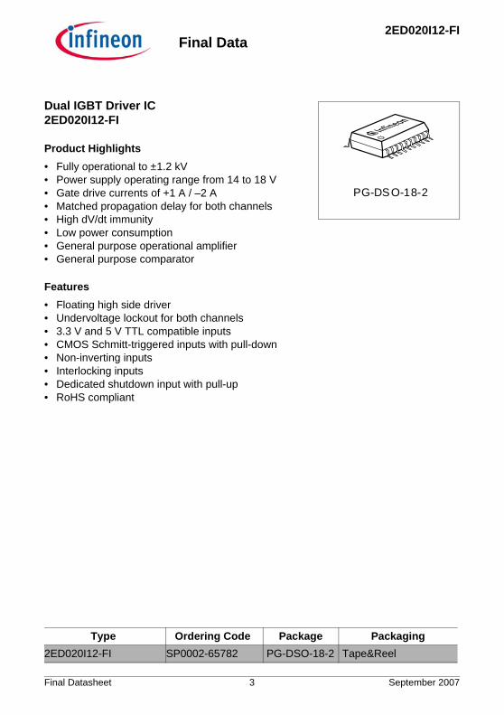
Type Ordering Code Package Packaging
2ED020I12-FI SP0002-65782 PG-DSO-18-2 Tape&Reel
2ED020I12-FIFinal Data
Final Datasheet 3 September 2007
PG-DSO-18-2
Dual IGBT Driver IC 2ED020I12-FI
Product Highlights
• Fully operational to ±1.2 kV• Power supply operating range from 14 to 18 V• Gate drive currents of +1 A / –2 A• Matched propagation delay for both channels• High dV/dt immunity• Low power consumption• General purpose operational amplifier• General purpose comparator
Features
• Floating high side driver• Undervoltage lockout for both channels• 3.3 V and 5 V TTL compatible inputs• CMOS Schmitt-triggered inputs with pull-down• Non-inverting inputs• Interlocking inputs• Dedicated shutdown input with pull-up• RoHS compliant
High and Low Side Driver2ED020I12-FI
Overview
Final Data
1 OverviewThe 2ED020I12-FI is a high voltage, high speed power MOSFET and IGBT driver with interlocking high and low side referenced outputs. The floating high side driver may be supplied directly or by means of a bootstrap diode and capacitor. In addition to the logic input of each driver the 2ED020I12-FI is equipped with a dedicated shutdown input. All logic inputs are compatible with 3.3 V and 5 V TTL. The output drivers feature a high pulse current buffer stage designed for minimum driver cross-conduction. Propagation delays are matched to simplify use in high frequency applications. Both drivers are designed to drive an N-channel power MOSFET or IGBT which operate up to 1.2 kV. In addition, a general purpose operational amplifier and a general purpose comparator are provided which may be used for instance for current measurement or overcurrent detection.
Final Datasheet 4 September 2007
High and Low Side Driver2ED020I12-FI
Pin Configuration and Functionality
Final Data
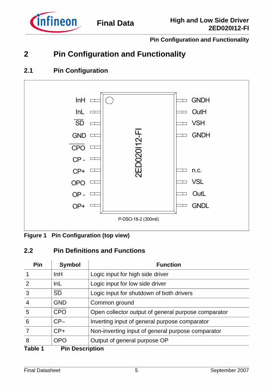
2 Pin Configuration and Functionality
2.1 Pin Configuration
VSH
GNDH
OP+
OutL
VSL
P-DSO-18-2 (300mil)
n.c.
OP -
OPO
CP+ 2ED
020I
12-F
IGND
OutHInL
CPO
InH
GNDH
CP -
SD
GNDL
Figure 1 Pin Configuration (top view)
2.2 Pin Definitions and Functions
Pin Symbol Function
1 InH Logic input for high side driver
2 InL Logic input for low side driver
3 SD Logic input for shutdown of both drivers
4 GND Common ground
5 CPO Open collector output of general purpose comparator
6 CP– Inverting input of general purpose comparator
7 CP+ Non-inverting input of general purpose comparator
8 OPO Output of general purpose OPTable 1 Pin Description
Final Datasheet 5 September 2007
High and Low Side Driver2ED020I12-FI
Pin Configuration and Functionality
Final Data
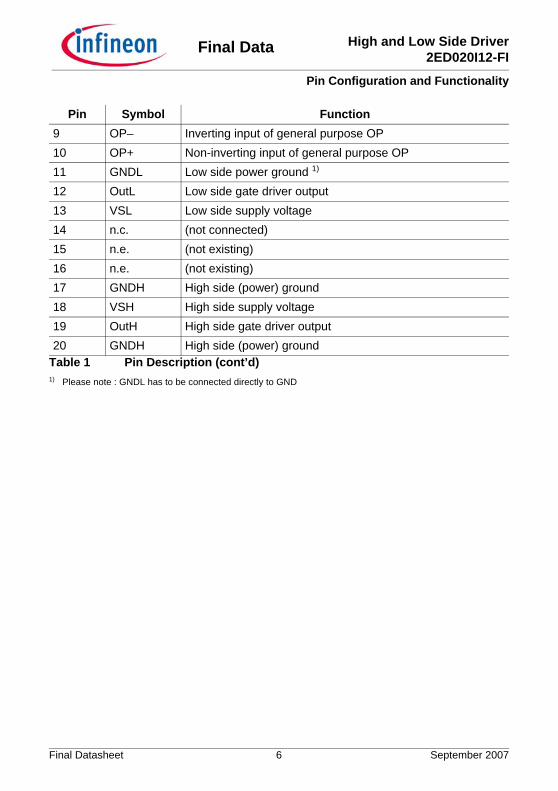
9 OP– Inverting input of general purpose OP
10 OP+ Non-inverting input of general purpose OP
11 GNDL Low side power ground 1)
12 OutL Low side gate driver output
13 VSL Low side supply voltage
14 n.c. (not connected)
15 n.e. (not existing)
16 n.e. (not existing)
17 GNDH High side (power) ground
18 VSH High side supply voltage
19 OutH High side gate driver output
20 GNDH High side (power) ground
1) Please note : GNDL has to be connected directly to GND
Pin Symbol Function
Table 1 Pin Description (cont’d)
Final Datasheet 6 September 2007
High and Low Side Driver2ED020I12-FI
Block Diagram
Final Data
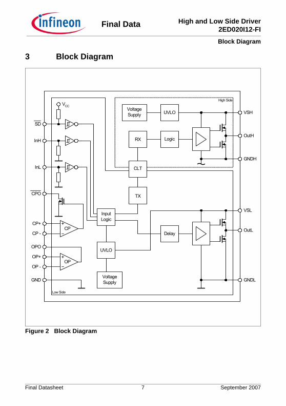
3 Block Diagram
SD
CPO
InH
InputLogic
Delay
TX
RX Logic
UVLOVoltageSupply
High Side
UVLO
VoltageSupply
OP
OPO
OP+
OP -
Low Side
CP+
CLT
CPCP -
InL
VCC
GND
VSH
OutH
GNDH
OutL
GNDL
VSL
Figure 2 Block Diagram
Final Datasheet 7 September 2007
High and Low Side Driver2ED020I12-FI
Final Data
Functional Description
4 Functional Description
4.1 Power SupplyThe power supply of both sides, “VSL” and “VSH”, is monitored by an undervoltage lockout block (UVLO) which enables operation of the corresponding side when the supply voltage reaches the “on” threshold. Afterwards the internal voltage reference and the biasing circuit are enabled. When the supply voltage (VSL, VSH) drops below the “off” threshold, the circuit is disabled.
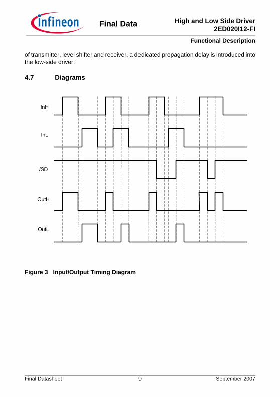
4.2 Logic InputsThe logic inputs InH, InL and SD are fed into Schmitt-Triggers with thresholds compatible to 3.3V and 5V TTL. When SD is enabled (low), InH and InL are disabled. If InH is high (while InL is low), OutH is enabled and vice versa. However, if both signals are high, they are internally disabled until one of them gets low again. This is due to the interlocking logic of the device. See Figure 3 (section 4.7).
4.3 Gate Driver2ED020I12-FI features two hard-switching gate drivers with N-channel output stages capable to source 1A and to sink 2A peak current. Both drivers are equipped with active-low-clamping capability. Furthermore, they feature a large ground bounce ruggedness in order to compensate ground bounces caused by a turn-off of the driven IGBT.
4.4 General Purpose Operational AmplifierThis general purpose operational amplifier can be applied for current measurement of the driven low-side IGBT. It is dedicated for fast operation with a gain of at least 3. The OP is equipped with a -0.1 to 2V input stage and a rail-to-rail output stage which is capable to drive ± 5mA.
4.5 General Purpose ComparatorThe general purpose comparator can be applied for overcurrent detection of the low side IGBT. A dedicated offset as well as a pull-up and pull-down resistor has been introduced to its inputs for security reasons.
4.6 Coreless Transformer (CLT)In order to enable signal transmission across the isolation barrier between low-side and high-side driver, a transformer based on CLT-Technology is employed. Signals, that are to be transmitted, are specially encoded by the transmitter and correspondingly restored by the receiver. In this way EMI due to variations of GNDH (dVGNDH/dt) or the magnetic flux density (dΗ/dt) can be suppresed.To compensate the additional propagation delay
Final Datasheet 8 September 2007
High and Low Side Driver2ED020I12-FI
Functional Description
Final Data
of transmitter, level shifter and receiver, a dedicated propagation delay is introduced into the low-side driver.
4.7 Diagrams
InH
InL
/SD
OutH
OutL
Figure 3 Input/Output Timing Diagram
Final Datasheet 9 September 2007
High and Low Side Driver2ED020I12-FI
Electrical Parameters
Final Data
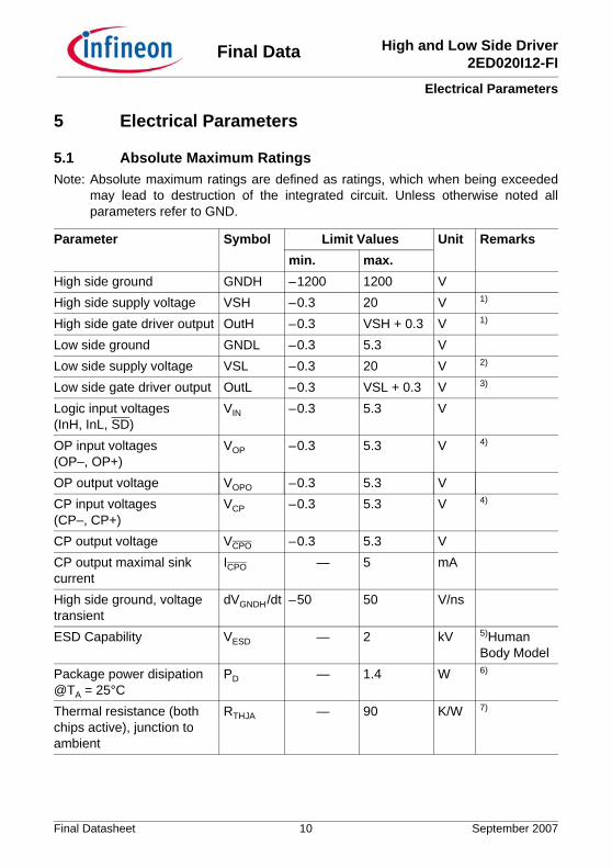
5 Electrical Parameters
5.1 Absolute Maximum RatingsNote: Absolute maximum ratings are defined as ratings, which when being exceeded
may lead to destruction of the integrated circuit. Unless otherwise noted all parameters refer to GND.
Parameter Symbol Limit Values Unit Remarks
min. max.
High side ground GNDH – 1200 1200 V
High side supply voltage VSH – 0.3 20 V 1)
High side gate driver output OutH – 0.3 VSH + 0.3 V 1)
Low side ground GNDL – 0.3 5.3 V
Low side supply voltage VSL – 0.3 20 V 2)
Low side gate driver output OutL – 0.3 VSL + 0.3 V 3)
Logic input voltages (InH, InL, SD)
VIN – 0.3 5.3 V
OP input voltages (OP–, OP+)
VOP – 0.3 5.3 V 4)
OP output voltage VOPO – 0.3 5.3 V
CP input voltages (CP–, CP+)
VCP – 0.3 5.3 V 4)
CP output voltage VCPO – 0.3 5.3 V
CP output maximal sink current
ICPO — 5 mA
High side ground, voltage transient
dVGNDH /dt – 50 50 V/ns
ESD Capability VESD — 2 kV 5)Human Body Model
Package power disipation @TA = 25°C
PD — 1.4 W 6)
Thermal resistance (both chips active), junction to ambient
RTHJA — 90 K/W 7)
Final Datasheet 10 September 2007
High and Low Side Driver2ED020I12-FI
Electrical Parameters
Final Data
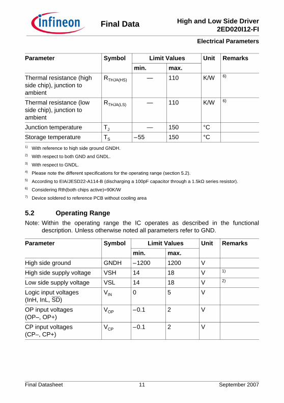
5.2 Operating RangeNote: Within the operating range the IC operates as described in the functional
description. Unless otherwise noted all parameters refer to GND.
Thermal resistance (high side chip), junction to ambient
RTHJA(HS) — 110 K/W 6)
Thermal resistance (low side chip), junction to ambient
RTHJA(LS) — 110 K/W 6)
Junction temperature TJ — 150 °C
Storage temperature TS – 55 150 °C1) With reference to high side ground GNDH.2) With respect to both GND and GNDL.3) With respect to GNDL.4) Please note the different specifications for the operating range (section 5.2).5) According to EIA/JESD22-A114-B (discharging a 100pF capacitor through a 1.5kΩ series resistor).6) Considering Rth(both chips active)=90K/W7) Device soldered to reference PCB without cooling area
Parameter Symbol Limit Values Unit Remarks
min. max.
High side ground GNDH – 1200 1200 V
High side supply voltage VSH 14 18 V 1)
Low side supply voltage VSL 14 18 V 2)
Logic input voltages (InH, InL, SD)
VIN 0 5 V
OP input voltages (OP–, OP+)
VOP – 0.1 2 V
CP input voltages (CP–, CP+)
VCP – 0.1 2 V
Parameter Symbol Limit Values Unit Remarks
min. max.
Final Datasheet 11 September 2007
High and Low Side Driver2ED020I12-FI
Electrical Parameters
Final Data
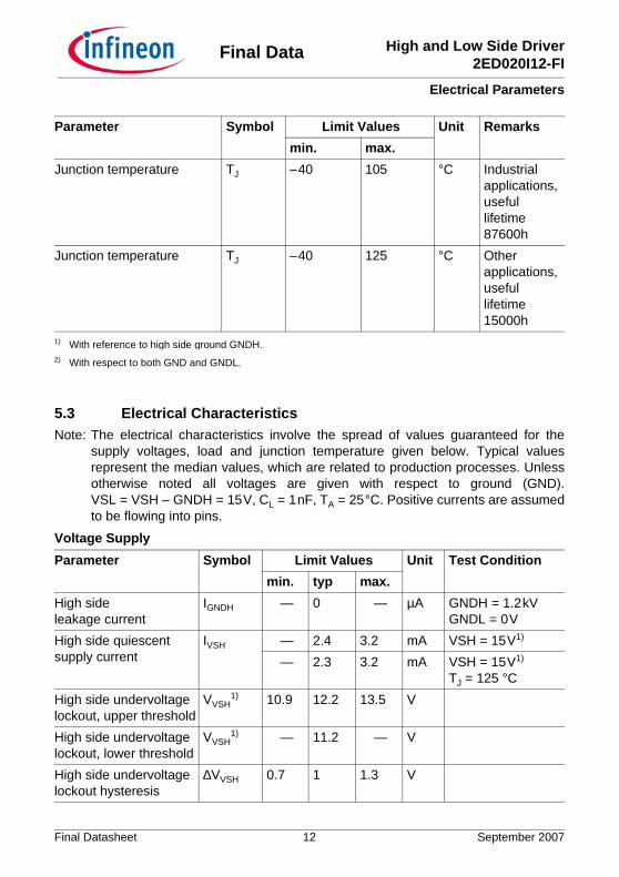
5.3 Electrical CharacteristicsNote: The electrical characteristics involve the spread of values guaranteed for the
supply voltages, load and junction temperature given below. Typical values represent the median values, which are related to production processes. Unless otherwise noted all voltages are given with respect to ground (GND). VSL = VSH – GNDH = 15 V, CL = 1 nF, TA = 25 °C. Positive currents are assumed to be flowing into pins.
Junction temperature TJ – 40 105 °C Industrial applications, useful lifetime87600h
Junction temperature TJ – 40 125 °C Other applications, useful lifetime15000h
1) With reference to high side ground GNDH.2) With respect to both GND and GNDL.
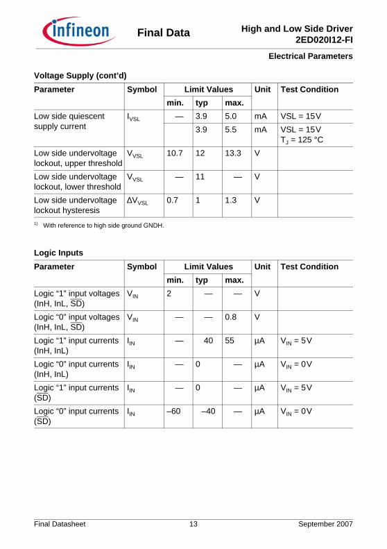
Voltage Supply
Parameter Symbol Limit Values Unit Test Condition
min. typ max.
High side leakage current
IGNDH — 0 — µA GNDH = 1.2 kVGNDL = 0 V
High side quiescent supply current
IVSH — 2.4 3.2 mA VSH = 15 V1)
— 2.3 3.2 mA VSH = 15 V1)
TJ = 125 °C
High side undervoltage lockout, upper threshold
VVSH1) 10.9 12.2 13.5 V
High side undervoltage lockout, lower threshold
VVSH1) — 11.2 — V
High side undervoltage lockout hysteresis
∆VVSH 0.7 1 1.3 V
Parameter Symbol Limit Values Unit Remarks
min. max.
Final Datasheet 12 September 2007
High and Low Side Driver2ED020I12-FI
Electrical Parameters
Final Data
Low side quiescent supply current
IVSL — 3.9 5.0 mA VSL = 15 V
3.9 5.5 mA VSL = 15 VTJ = 125 °C
Low side undervoltage lockout, upper threshold
VVSL 10.7 12 13.3 V
Low side undervoltage lockout, lower threshold
VVSL — 11 — V
Low side undervoltage lockout hysteresis
∆VVSL 0.7 1 1.3 V
Logic Inputs
Parameter Symbol Limit Values Unit Test Condition
min. typ max.
Logic “1” input voltages (InH, InL, SD)
VIN 2 — — V
Logic “0” input voltages (InH, InL, SD)
VIN — — 0.8 V
Logic “1” input currents (InH, InL)
IIN — 40 55 µA VIN = 5 V
Logic “0” input currents (InH, InL)
IIN — 0 — µA VIN = 0 V
Logic “1” input currents (SD)
IIN — 0 — µA VIN = 5 V
Logic “0” input currents (SD)
IIN –60 –40 — µA VIN = 0 V
1) With reference to high side ground GNDH.
Voltage Supply (cont’d)
Parameter Symbol Limit Values Unit Test Condition
min. typ max.
Final Datasheet 13 September 2007
High and Low Side Driver2ED020I12-FI
Electrical Parameters
Final Data
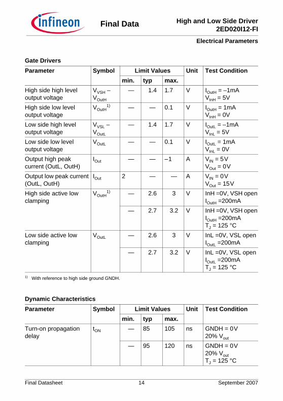
Gate Drivers
Parameter Symbol Limit Values Unit Test Condition
min. typ max.
High side high level output voltage
VVSH – VOutH
— 1.4 1.7 V IOutH = –1mAVInH = 5V
High side low level output voltage
V
1) With reference to high side ground GNDH.
OutH1) — — 0.1 V IOutH = 1mA
VInH = 0V
Low side high level output voltage
VVSL – VOutL
— 1.4 1.7 V IOutL = –1mAVInL = 5V
Low side low level output voltage
VOutL — — 0.1 V IOutL = 1mAVInL = 0V
Output high peak current (OutL, OutH)
IOut — — – 1 A VIN = 5 V VOut = 0 V
Output low peak current (OutL, OutH)
IOut 2 — — A VIN = 0 V VOut = 15 V
High side active low clamping
VOutH1) — 2.6 3 V InH =0V, VSH open
IOutH =200mA
— 2.7 3.2 V InH =0V, VSH openIOutH =200mATJ = 125 °C
Low side active low clamping
VOutL — 2.6 3 V InL =0V, VSL openIOutL =200mA
— 2.7 3.2 V InL =0V, VSL openIOutL =200mATJ = 125 °C
Dynamic Characteristics
Parameter Symbol Limit Values Unit Test Condition
min. typ max.
Turn-on propagation delay
tON — 85 105 ns GNDH = 0 V20% Vout
— 95 120 ns GNDH = 0 V20% VoutTJ = 125 °C
Final Datasheet 14 September 2007
High and Low Side Driver2ED020I12-FI
Electrical Parameters
Final Data
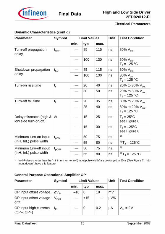
Turn-off propagation delay
tOFF — 85 115 ns 80% Vout
— 100 130 ns 80% VoutTJ = 125 °C
Shutdown propagation delay
tSD — 85 115 ns 80% Vout
— 100 130 ns 80% VoutTJ = 125 °C
Turn-on rise time tr — 20 40 ns 20% to 80% Vout
— 30 50 ns 20% to 80% VoutTJ = 125 °C
Turn-off fall time tf — 20 35 ns 80% to 20% Vout
— 25 40 ns 80% to 20% VoutTJ = 125 °C
Delay mismatch (high & low side turn-on/off)
∆t — 15 25 ns TJ = 25°C see Figure 6
— 15 30 ns TJ = 125°Csee Figure 6
Minimum turn-on input (InH, InL) pulse width
tpON — 50 75 ns 1)
— 55 80 ns 1) TJ = 125°C
Minimum turn-off input (InH, InL) pulse width
tpOFF — 50 75 ns 1)
— 55 80 ns 1) TJ = 125 °C1) InH-Pulses shorter than the “minimum turn-on(off) input pulse width” are prolonged to 50ns (See Figure 7). InL-
Input doesn´t have this feature.
General Purpose Operational Amplifier OP
Parameter Symbol Limit Values Unit Test Condition
min. typ max.
OP input offset voltage ∆VIN –10 0 10 mV
OP input offset voltage drift
VDrift — ±15 — µV/K
OP input high currents (OP–, OP+)
IIN — 0 0.2 µA VIN = 2 V
Dynamic Characteristics (cont’d)
Parameter Symbol Limit Values Unit Test Condition
min. typ max.
Final Datasheet 15 September 2007
High and Low Side Driver2ED020I12-FI
Electrical Parameters
Final Data
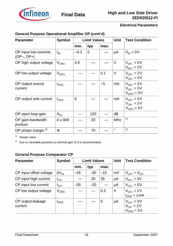
OP input low currents (OP–, OP+)
IIN – 0.2 0 — µA VIN = 0 V
OP high output voltage VOPO 4.9 — — V VOP– = 0 V VOP+ = 2 V
OP low output voltage VOPO — — 0.1 V VOP– = 2 V VOP+ = 0 V
OP output source current
IOPO — — – 5 mA VOP+ = 2 V VOP– = 0 V VOPO = 0 V
OP output sink current IOPO 5 — — mA VOP+ = 0 V VOP– = 2 V VOPO = 5 V
OP open loop gain AOL — 120 — dB
OP gain-bandwidth product
A x BW — 20 — MHz 1)
OP phase margin 2) Φ — 70 — ° 1)
1) Design value2) Due to inevitable parasitics a minimal gain of 3 is recommended
General Purpose Comparator CP
Parameter Symbol Limit Values Unit Test Condition
min. typ max.
CP input offset voltage ∆VIN –45 –30 –15 mV VCP+ = VCP-
CP input high current ICP– — 20 35 µA VCP– = 5V
CP input low current ICP+ –35 –20 — µA VCP+ = 0 V
CP low output voltage VCPO — — 0.2 V VCP+ = 2 V ICPO = 1 mA
CP output leakage current
ICPO — — 5 µA VCP+ = 0 VVCP– = 2 VVCPO = 5 V
General Purpose Operational Amplifier OP (cont’d)
Parameter Symbol Limit Values Unit Test Condition
min. typ max.
Final Datasheet 16 September 2007
High and Low Side Driver2ED020I12-FI
Electrical Parameters
Final Data
CP switch-on delay td — 100 — ns RCPO = 4.7kΩVres = 5VVCPO = 4V
CP switch-off delay td — 300 — ns RCPO = 4.7kΩVres = 5VVCPO = 1V
General Purpose Comparator CP (cont’d)
Parameter Symbol Limit Values Unit Test Condition
min. typ max.
Final Datasheet 17 September 2007
High and Low Side Driver2ED020I12-FI
Package Outline
Final Data
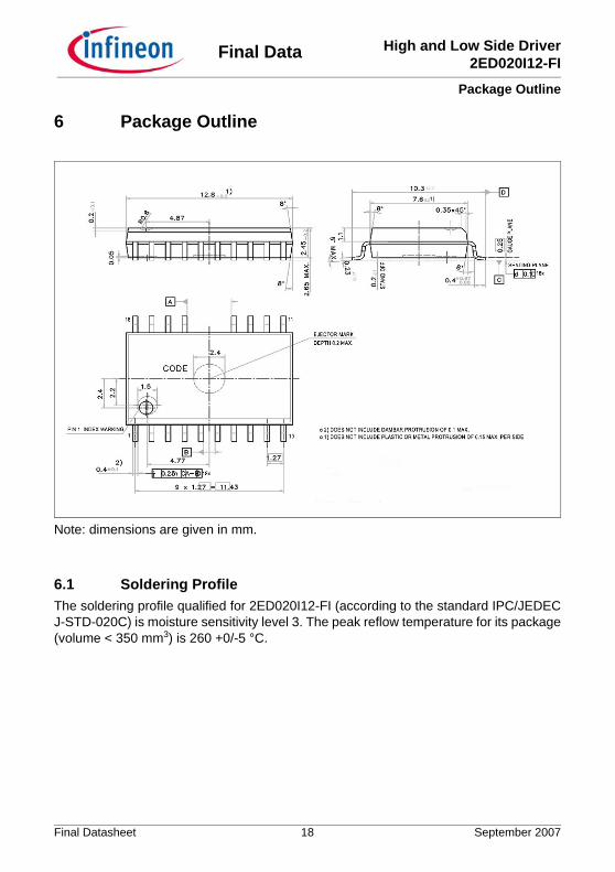
6 Package Outline
Note: dimensions are given in mm.
6.1 Soldering ProfileThe soldering profile qualified for 2ED020I12-FI (according to the standard IPC/JEDEC J-STD-020C) is moisture sensitivity level 3. The peak reflow temperature for its package (volume < 350 mm3) is 260 +0/-5 °C.
Final Datasheet 18 September 2007
High and Low Side Driver2ED020I12-FI
Diagrams
Final Data
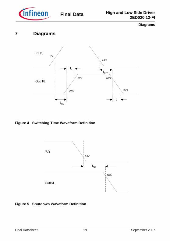
7 Diagrams
2V0.8V
80% 80%
20% 20%
InH/L
OutH/L
tr
tftON
tOFF
Figure 4 Switching Time Waveform Definition
/SD
OutH/L
tSD
0.8V
80%
Figure 5 Shutdown Waveform Definition
Final Datasheet 19 September 2007
High and Low Side Driver2ED020I12-FI
Diagrams
Final Data
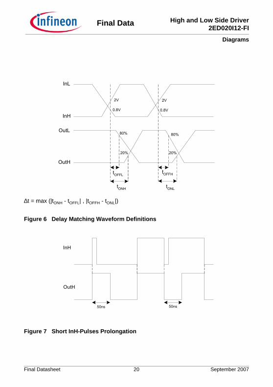
InL
InH
OutL
OutH
2V
0.8V
2V
0.8V
80% 80%
20% 20%
tOFFL
tONH
tOFFH
tONL
∆t = max (|tONH - tOFFL| , |tOFFH - tONL|)
Figure 6 Delay Matching Waveform Definitions
InH
OutH
50ns 50ns
Figure 7 Short InH-Pulses Prolongation
Final Datasheet 20 September 2007
High and Low Side Driver2ED020I12-FI
Application Advices
Final Data
8 Application Advices
8.1 Operational AmplifierTo minimize the current consumption when the operational amplifier is not used, it is necessary to connect both inputs properly, e.g connect OP+ to 5V and OP- to 0V or vice versa.
On the other hand, the operational amplifier cannot operate with a follower configuration , i.e OP- = OPO. A minimum gain of 3 has to be used so that its output OPO has a stable behaviour.
8.2 Power Supplya) The connection of a capacitor (>10nF) as close as possible to the supply pins VSH, VSL is recommended for avoiding that possible oscillations in the supply voltage can cause erroneous operation of the output driver stage. Total value of capacitance connected to the supply terminals has to be determined by taking into account gatecharge, peak current, supply voltage and kind of power supply.
b) If a bootstrap power supply for the high side driver is applied, a resistor of 10Ω minimum in series with the bootstrap diode is recommended.
Final Datasheet 21 September 2007

Qualität hat für uns eine umfassende Bedeutung. Wir wollen allen Ihren Ansprüchen in der bestmöglichen Weise gerecht werden. Es geht uns also nicht nur um die Produktqualität – unsere Anstrengungen gelten gleichermaßen der Lieferqualität und Logistik, dem Service und Support sowie allen sonstigen Beratungs- und Betreuungsleistungen.
Dazu gehört eine bestimmte Geisteshaltung unserer Mitarbeiter. Total Quality im Denken und Handeln gegenüber Kollegen, Lieferanten und Ihnen, unserem Kunden. Unsere Leitlinie ist jede Aufgabe mit „Null Fehlern“ zu lösen – in offener Sichtweise auch über den eigenen Arbeitsplatz hinaus – und uns ständig zu verbessern.
Unternehmensweit orientieren wir uns dabei auch an „top“ (Time Optimized Processes), um Ihnen durch größere Schnelligkeit den entscheidenden Wettbewerbsvorsprung zu verschaffen.
Geben Sie uns die Chance, hohe Leistung durch umfassende Qualität zu beweisen.
Wir werden Sie überzeugen.
Quality takes on an all encompassing significance at Infineon AG. For us it means living up to each and every one of your demands in the best possible way. So we are not only concerned with product quality. We direct our efforts equally at quality of supply and logistics, service and support, as well as all the other ways in which we advise and attend to you.
Part of this is the very special attitude of our staff. Total Quality in thought and deed, towards co-workers, suppliers and you, our customer. Our guideline is “do everything with zero defects”, in an open manner that is demonstrated beyond your immediate workplace, and to constantly improve.
Throughout the corporation we also think in terms of Time Optimized Processes (top), greater speed on our part to give you that decisive competitive edge.
Give us the chance to prove the best of performance through the best of quality – you will be convinced.
h t t p : / / w w w . i n f i n e o n . c o m
Total Quality Management
Published by Infineon Technologies AG