wireless components - infineon technologies
TRANSCRIPT
Wireless ComponentsASK/FSK Single Conversion Receiver
TDA7210 Version 1.0
Data Sheet December 2008
Edition December 2008Published by Infineon Technologies AG, Am Campeon 1 - 12 85579 Neubiberg, Germany© 2008 Infineon Technologies AG All Rights Reserved.
Attention please!The information herein is given to describe certain components and shall not be considered as a guarantee of characteristics.Terms of delivery and rights to technical change reserved.We hereby disclaim any and all warranties, including but not limited to warranties of non-infringement, regarding circuits, descriptions and charts stated herein.
InformationFor further information on technology, delivery terms and conditions, and prices, please contact the nearest Infineon Technologies Office in Germany or the Infineon Technologies Companies and Infineon Technologies Representatives worldwide (www.infineon.com).
WarningsDue to technical requirements, components may contain dangerous substances. For information on the types in question, please contact the nearest Infineon Technologies Office.Infineon Technologies Components may be used in life-support devices or systems only with the express written approval of Infineon Technologies, if a failure of such components can reasonably be expected to cause the failure of that life-support device or system, or to affect the safety or effectiveness of that device or system. Life support devices or systems are intended to be implanted in the human body, or to support and/or maintain and sustain and/or protect human life. If they fail, it is reasonable to assume that the health of the user or other persons may be endangered.
Revision History
Current Version: 1.0 as of 03.12.08
Previous Version: none
Page (in previous Version)
Page(s) (in current Version)
Subjects (major changes since last revision)
We Listen to Your CommentsIs there any information in this document that you feel is wrong, unclear or missing? Your feedback will help us to continuously improve the quality of this document. Please send your proposal (including a reference to this document) to:[email protected]
Product Info
Product InfoWireless Components
Data Sheet, December 2008
Package
TDA7210
Product Info
General Description The IC is a very low power consump-tion single chip FSK/ASK Superhet-erodyne Receiver (SHR) for the frequency bands 810 to 870 MHz and 400 to 440 MHz that is pin compatible with the Receiver TDA5210. The IC offers a high level of integration and needs only a few external compo-nents. The device contains a low noise amplifier (LNA), a double balanced mixer, a fully integrated VCO, a PLL synthesiser, a crystal oscillator, a lim-iter with RSSI generator, a PLL FSK demodulator, a data filter, a data com-parator (slicer) and a peak detector. Additionally there is a power down fea-ture to save battery life.
Features ■ Low supply current (typ. at 868MHz Is = 5.9mA in FSK mode, Is = 5.2mA in ASK mode)
■ Supply voltage range 5V ±10%
■ Power down mode with very low supply current (50nA typ)
■ FSK and ASK demodulation capa-bility
■ Fully integrated VCO and PLL Synthesiser
■ ASK sensitivity < –107dBm
■ Selectable frequency ranges 810-870 MHz and 400-440 MHz
■ Limiter with RSSI generation, operating at 10.7MHz
■ Selectable reference frequency
■ 2nd order low pass data filter with external capacitors
■ Data slicer with self-adjusting threshold
■ FSK sensitivity <-100dBm
Application ■ Keyless Entry Systems
■ Remote Control Systems
■ Alarm Systems
■ Low Bitrate Communication Systems
Ordering InformationType Ordering Code Package
TDA7210 SP000524274 PG-TSSOP-28
samples available on tape and reel
1 Table of Contents
1 Table of Contents . . . . . . . . . . . . . . . . . . . . . . . . . . . . . . . . . . . . . . . . . . . . . . . . . . . . . . . . . . . . i
2 Product Description . . . . . . . . . . . . . . . . . . . . . . . . . . . . . . . . . . . . . . . . . . . . . . . . . . . . . . . . . . 1
2.1 Overview. . . . . . . . . . . . . . . . . . . . . . . . . . . . . . . . . . . . . . . . . . . . . . . . . . . . . . . . . . . . . . . 2
2.2 Application . . . . . . . . . . . . . . . . . . . . . . . . . . . . . . . . . . . . . . . . . . . . . . . . . . . . . . . . . . . . . 2
2.3 Features . . . . . . . . . . . . . . . . . . . . . . . . . . . . . . . . . . . . . . . . . . . . . . . . . . . . . . . . . . . . . . . 2
2.4 Package Outlines . . . . . . . . . . . . . . . . . . . . . . . . . . . . . . . . . . . . . . . . . . . . . . . . . . . . . . . . 3
3 Functional Description . . . . . . . . . . . . . . . . . . . . . . . . . . . . . . . . . . . . . . . . . . . . . . . . . . . . . . . . 1
3.1 Pin Configuration . . . . . . . . . . . . . . . . . . . . . . . . . . . . . . . . . . . . . . . . . . . . . . . . . . . . . . . . 2
3.2 Pin Definition and Function. . . . . . . . . . . . . . . . . . . . . . . . . . . . . . . . . . . . . . . . . . . . . . . . . 3
3.3 Functional Block Diagram. . . . . . . . . . . . . . . . . . . . . . . . . . . . . . . . . . . . . . . . . . . . . . . . . . 9
3.4 Functional Blocks . . . . . . . . . . . . . . . . . . . . . . . . . . . . . . . . . . . . . . . . . . . . . . . . . . . . . . . . 10
3.4.1 Low Noise Amplifier (LNA) . . . . . . . . . . . . . . . . . . . . . . . . . . . . . . . . . . . . . . . . . . . . . . . . . 10
3.4.2 Mixer. . . . . . . . . . . . . . . . . . . . . . . . . . . . . . . . . . . . . . . . . . . . . . . . . . . . . . . . . . . . . . . . . . 10
3.4.3 PLL Synthesizer . . . . . . . . . . . . . . . . . . . . . . . . . . . . . . . . . . . . . . . . . . . . . . . . . . . . . . . . . 10
3.4.4 Crystal Oscillator . . . . . . . . . . . . . . . . . . . . . . . . . . . . . . . . . . . . . . . . . . . . . . . . . . . . . . . . 11
3.4.5 Limiter. . . . . . . . . . . . . . . . . . . . . . . . . . . . . . . . . . . . . . . . . . . . . . . . . . . . . . . . . . . . . . . . . 11
3.4.6 FSK Demodulator . . . . . . . . . . . . . . . . . . . . . . . . . . . . . . . . . . . . . . . . . . . . . . . . . . . . . . . . 12
3.4.7 Data Filter . . . . . . . . . . . . . . . . . . . . . . . . . . . . . . . . . . . . . . . . . . . . . . . . . . . . . . . . . . . . . . 12
3.4.8 Data Slicer . . . . . . . . . . . . . . . . . . . . . . . . . . . . . . . . . . . . . . . . . . . . . . . . . . . . . . . . . . . . . 12
3.4.9 Peak Detector. . . . . . . . . . . . . . . . . . . . . . . . . . . . . . . . . . . . . . . . . . . . . . . . . . . . . . . . . . . 13
3.4.10 Bandgap Reference Circuitry . . . . . . . . . . . . . . . . . . . . . . . . . . . . . . . . . . . . . . . . . . . . . . . 13
4 Applications . . . . . . . . . . . . . . . . . . . . . . . . . . . . . . . . . . . . . . . . . . . . . . . . . . . . . . . . . . . . . . . . . 1
4.1 Choice of LNA Threshold Voltage and Time Constant. . . . . . . . . . . . . . . . . . . . . . . . . . . . 2
4.2 Data Filter Design. . . . . . . . . . . . . . . . . . . . . . . . . . . . . . . . . . . . . . . . . . . . . . . . . . . . . . . . 4
4.3 Quartz Load Capacitance Calculation . . . . . . . . . . . . . . . . . . . . . . . . . . . . . . . . . . . . . . . . 5
4.4 Quartz Frequency Calculation . . . . . . . . . . . . . . . . . . . . . . . . . . . . . . . . . . . . . . . . . . . . . . 6
4.5 Data Slicer Threshold Generation . . . . . . . . . . . . . . . . . . . . . . . . . . . . . . . . . . . . . . . . . . . 7
4.6 ASK/FSK Switch Functional Description . . . . . . . . . . . . . . . . . . . . . . . . . . . . . . . . . . . . . . 8
4.6.1 FSK Mode. . . . . . . . . . . . . . . . . . . . . . . . . . . . . . . . . . . . . . . . . . . . . . . . . . . . . . . . . . . . . . 8
4.6.2 ASK Mode . . . . . . . . . . . . . . . . . . . . . . . . . . . . . . . . . . . . . . . . . . . . . . . . . . . . . . . . . . . . . 10
4.7 Principle of the Precharge Circuit . . . . . . . . . . . . . . . . . . . . . . . . . . . . . . . . . . . . . . . . . . . . 11
5 Reference . . . . . . . . . . . . . . . . . . . . . . . . . . . . . . . . . . . . . . . . . . . . . . . . . . . . . . . . . . . . . . . . . . . 1
5.1 Electrical Data . . . . . . . . . . . . . . . . . . . . . . . . . . . . . . . . . . . . . . . . . . . . . . . . . . . . . . . . . . 2
5.1.2 Operating Range . . . . . . . . . . . . . . . . . . . . . . . . . . . . . . . . . . . . . . . . . . . . . . . . . . . . . . . . 3
5.1.3 AC/DC Characteristics at TAMB = 25°C . . . . . . . . . . . . . . . . . . . . . . . . . . . . . . . . . . . . . . 4
5.1.4 AC/DC Characteristics at TAMB = -40 to 85°C . . . . . . . . . . . . . . . . . . . . . . . . . . . . . . . . . 9
5.2 Test Circuit . . . . . . . . . . . . . . . . . . . . . . . . . . . . . . . . . . . . . . . . . . . . . . . . . . . . . . . . . . . . . 12
5.3 Test Board Layouts . . . . . . . . . . . . . . . . . . . . . . . . . . . . . . . . . . . . . . . . . . . . . . . . . . . . . . 13
5.4 Bill of Materials . . . . . . . . . . . . . . . . . . . . . . . . . . . . . . . . . . . . . . . . . . . . . . . . . . . . . . . . . . 15
2 Product Description
2.1 Overview. . . . . . . . . . . . . . . . . . . . . . . . . . . . . . . . . . . . . . . . . . . . . . . 2-22.2 Application . . . . . . . . . . . . . . . . . . . . . . . . . . . . . . . . . . . . . . . . . . . . . 2-22.3 Features . . . . . . . . . . . . . . . . . . . . . . . . . . . . . . . . . . . . . . . . . . . . . . . 2-22.4 Package Outlines . . . . . . . . . . . . . . . . . . . . . . . . . . . . . . . . . . . . . . . . 2-3
Contents of this Chapter
Product Description
2 - 2
TDA7210
Wireless Components
Data Sheet, December 2008
2.1 Overview
The IC is a very low power consumption single chip FSK/ASK Superheterodyne Receiver (SHR) for the frequency bands 810 to 870 MHz and 400 to 440 MHz that is pin compatible with the Receiver TDA5210. The IC offers a high level of integration and needs only a few external components. The device contains a low noise amplifier (LNA), a double balanced mixer, a fully integrated VCO, a PLL synthesiser, a crystal oscillator, a limiter with RSSI generator, a PLL FSK demodulator, a data filter, a data comparator (slicer) and a peak detector. Addi-tionally there is a power down feature to save battery life.
2.2 Application
■ Keyless Entry Systems
■ Remote Control Systems
■ Alarm Systems
■ Low Bitrate Communication Systems
2.3 Features
■ Low supply current (at 868MHz Is = 5.9 mA typ. FSK mode, 5.2mA typ. ASK mode)
■ Supply voltage range 5V ±10%
■ Power down mode with very low supply current (50nA typ)
■ FSK and ASK demodulation capability
■ Fully integrated VCO and PLL Synthesiser
■ RF input sensitivity ASK < –107dBm
■ RF input sensitivity FSK < –100dBm
■ Selectable frequency ranges 810-870 MHz and 400-440 MHz
■ Selectable reference frequency
■ Limiter with RSSI generation, operating at 10.7MHz
■ 2nd order low pass data filter with external capacitors
■ Data slicer with self-adjusting threshold
Product Description
2 - 3
TDA7210
Wireless Components
Data Sheet, December 2008
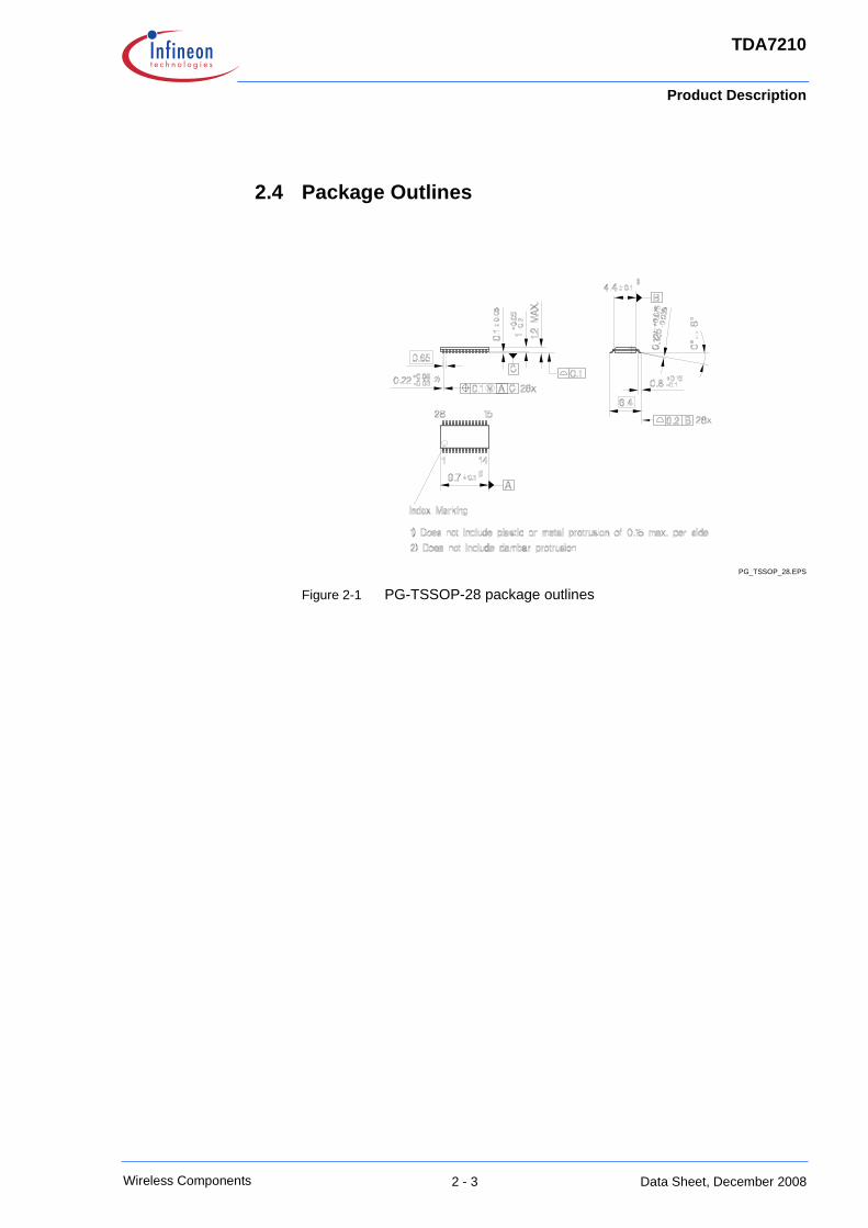
2.4 Package Outlines
PG_TSSOP_28.EPS
Figure 2-1 PG-TSSOP-28 package outlines
3 Functional Description
3.1 Pin Configuration . . . . . . . . . . . . . . . . . . . . . . . . . . . . . . . . . . . . . . . . 3-23.2 Pin Definition and Function. . . . . . . . . . . . . . . . . . . . . . . . . . . . . . . . . 3-33.3 Functional Block Diagram. . . . . . . . . . . . . . . . . . . . . . . . . . . . . . . . . . 3-93.4 Functional Blocks . . . . . . . . . . . . . . . . . . . . . . . . . . . . . . . . . . . . . . . 3-10
Contents of this Chapter
Functional Description
3 - 2
TDA7210
Wireless Components
Data Sheet, December 2008
3.1 Pin Configuration
Pin_Configuration_7210.wmf
Figure 3-1 IC Pin Configuration
CRST2
PDWN
PDO
DATA
3VOUT
THRES
FFB
OPP
SLN
SLP
LIMX
LIM
CSEL
MSEL
CRST1
VCC
LNI
TAGC
AGND
LNO
VCC
MI
MIX
AGND
FSEL
IFO
DGND
VDD
1
2
3
4
5
6
7
8
9
10
11
12
13
14
28
27
26
25
24
23
22
21
20
19
18
17
16
15
TDA 7210
Functional Description
3 - 3
TDA7210
Wireless Components
Data Sheet, December 2008
3.2 Pin Definition and Function
In the subsequent table the internal circuits connected to the pins of the device are shown. ESD-protection circuits are omitted to ease reading.
.
Table 3-1 Pin Definition and FunctionPin No. Symbol Equivalent I/O-Schematic Function
1 CRST1 External Crystal Connector 1
2 VCC 5V Supply
3 LNI LNA Input
4.15V
50uA
1
57uA
4k
1k
3
500uA
Functional Description
3 - 4
TDA7210
Wireless Components
Data Sheet, December 2008
4 TAGC AGC Time Constant Control
5 AGND Analogue Ground Return
6 LNO LNA Output
7 VCC 5V Supply
8
9
MI
MIX
Mixer Input
Complementary Mixer Input
10 AGND Analogue Ground Return
1k
4.2uA
1.5uA
1.7V
4.3V
4
6
1k
5V
8
1.7V
9
400uA
2k 2k
Functional Description
3 - 5
TDA7210
Wireless Components
Data Sheet, December 2008
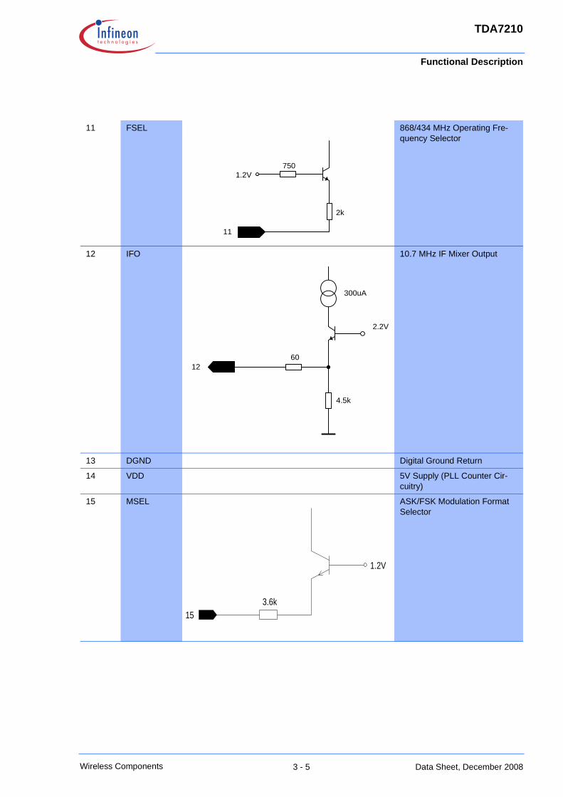
11 FSEL 868/434 MHz Operating Fre-quency Selector
12 IFO 10.7 MHz IF Mixer Output
13 DGND Digital Ground Return
14 VDD 5V Supply (PLL Counter Cir-cuitry)
15 MSEL ASK/FSK Modulation Format Selector
750
2k
11
1.2V
2.2V
4.5k
6012
300uA
15
1.2V
3.6k
Functional Description
3 - 6
TDA7210
Wireless Components
Data Sheet, December 2008
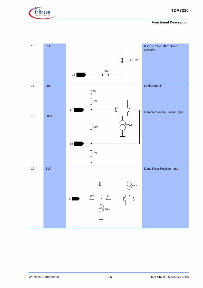
16 CSEL 6.xx or 13.xx MHz Quartz Selector
17
18
LIM
LIMX
Limiter Input
Complementary Limiter Input
19 SLP Data Slicer Positive Input
1.2V
80k16
330
15k
15k
18
17
2.4V
75uA
19
80µA
15uA
3k100
Functional Description
3 - 7
TDA7210
Wireless Components
Data Sheet, December 2008
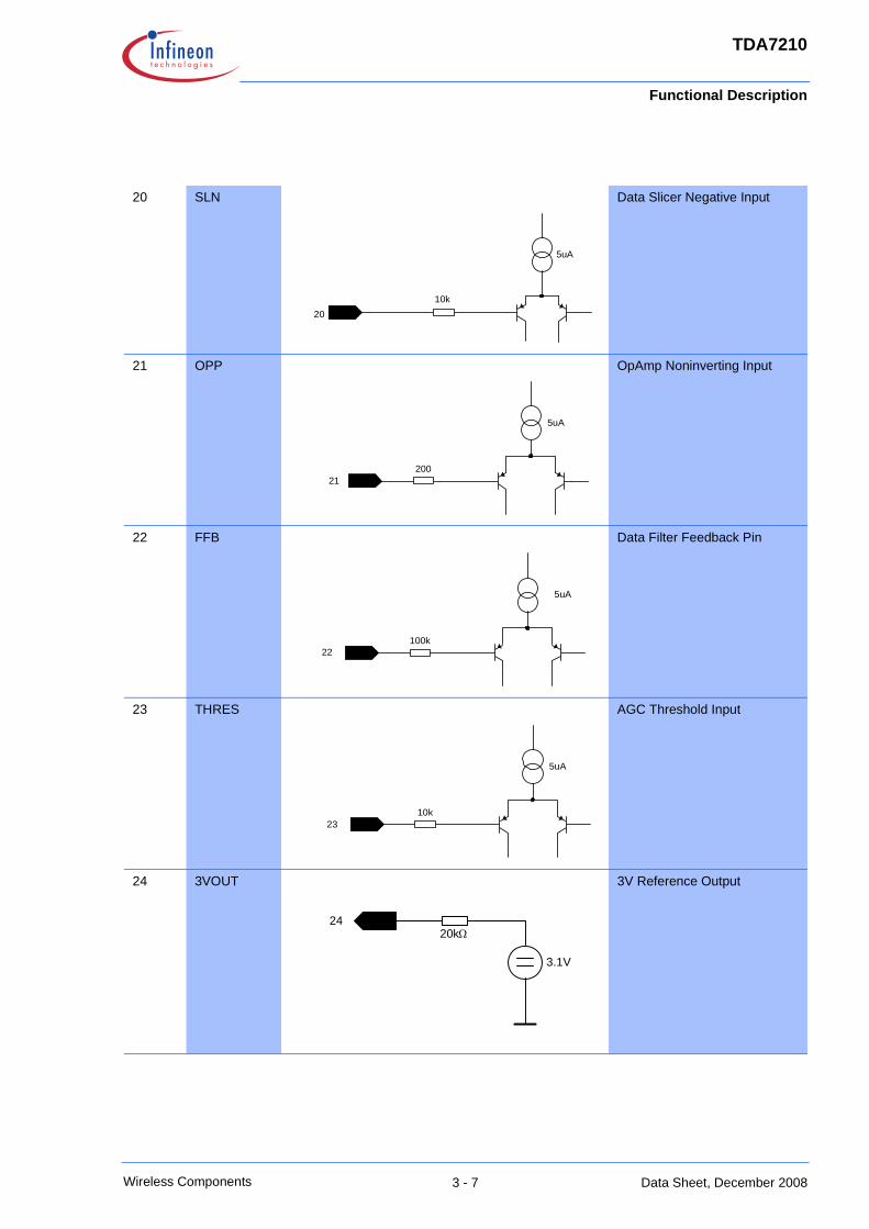
20 SLN Data Slicer Negative Input
21 OPP OpAmp Noninverting Input
22 FFB Data Filter Feedback Pin
23 THRES AGC Threshold Input
24 3VOUT 3V Reference Output
5uA
2010k
21200
5uA
100k
5uA
22
10k
5uA
23
3.1V
2420kΩ
Functional Description
3 - 8
TDA7210
Wireless Components
Data Sheet, December 2008
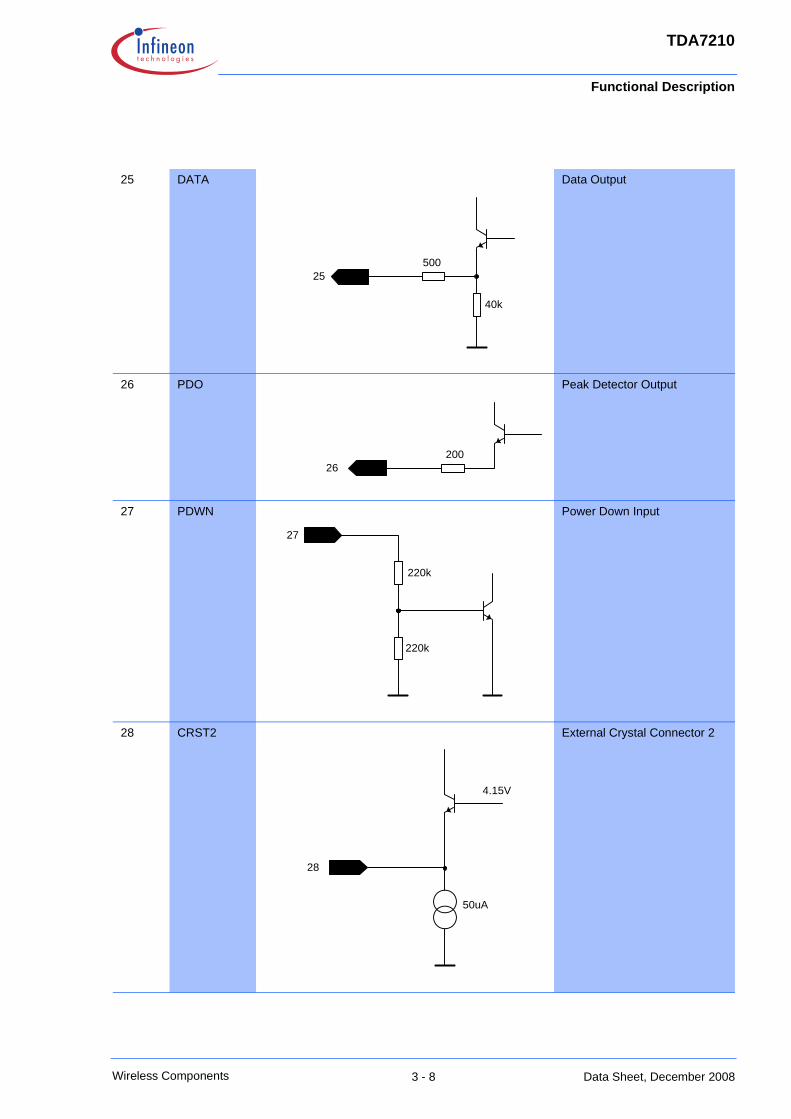
25 DATA Data Output
26 PDO Peak Detector Output
27 PDWN Power Down Input
28 CRST2 External Crystal Connector 2
25500
40k
26200
27
220k
220k
4.15V
50uA
28
Functional Description
3 - 9
TDA7210
Wireless Components
Data Sheet, December 2008
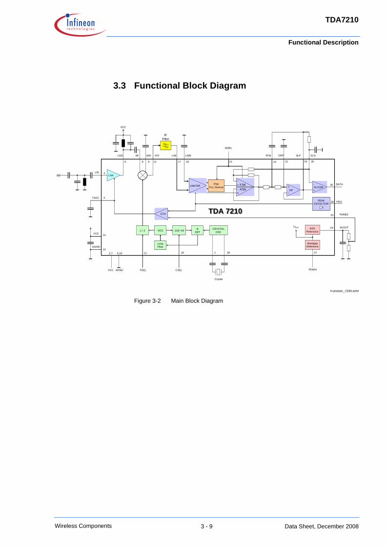
3.3 Functional Block Diagram
Function_7200.wmf
Figure 3-2 Main Block Diagram
PDO
: 1 / 2 VCO : 128 / 64 ΦDET
CRYSTALOSC
DATA
Crystal
PDWNCSELFSEL
LoopFilter
BandgapReference
UREF
LNARF
-
+SLICER
TAGC
TDA 7210TDA 7210TDA 7210
VCC
VCC AGND
AGCReference
THRES
3VOUT
FSKPLL Demod
OTA
PEAKDETECTOR
LNI
DGND
-+
MIXLNO MI OPPFFB SLP
VCC
LIM LIMX
IFFilter
IFO SLN
MSEL
LIMITER
6 8 9 12 17 18 22 21 19 20
25
26
23
24
3
4
14
132,7 5,10 11
15
16 1 28 27
-+
ASKFSK
OP
+
-
Functional Description
3 - 10
TDA7210
Wireless Components
Data Sheet, December 2008
3.4 Functional Blocks
3.4.1 Low Noise Amplifier (LNA)
The LNA is an on-chip cascode amplifier with a voltage gain of 15 to 20dB. The gain figure is determined by the external matching networks situated ahead of LNA and between the LNA output LNO (Pin 6) and the Mixer Inputs MI and MIX(Pins 8 and 9). The noise figure of the LNA is approximately 3dB, the current consumption is 500µA. The gain can be reduced by approximately 18dB. The switching point of this AGC action can be determined externally by applying a threshold voltage at the THRES pin (Pin 23). This voltage is compared internally with the received signal (RSSI) level generated by the limiter circuitry. In case that the RSSI level is higher than the threshold voltage the LNA gain is reduced and vice versa. The threshold voltage can be generated by attaching a voltage divider between the 3VOUT pin (Pin 24) which provides a temperature stable 3V output generated from the internal bandgap voltage and the THRES pin as described in Section 4.1. The time constant of the AGC action can be deter-mined by connecting a capacitor to the TAGC pin (Pin 4) and should be chosen along with the appropriate threshold voltage according to the intended operat-ing case and interference scenario to be expected during operation. The opti-mum choice of AGC time constant and the threshold voltage is described in Section 4.1.
3.4.2 Mixer
The Double Balanced Mixer downconverts the input frequency (RF) in the range of 400-440MHz/810-870MHz to the intermediate frequency (IF) at 10.7MHz with a voltage gain of approximately 21dB by utilising either high- or low-side injection of the local oscillator signal. In case the mixer is interfaced only single-ended, the unused mixer input has to be tied to ground via a capac-itor. The mixer is followed by a low pass filter with a corner frequency of 20MHz in order to suppress RF signals to appear at the IF output (IFO pin). The IF out-put is internally consisting of an emitter follower that has a source impedance of approximately 330 Ω to facilitate interfacing the pin directly to a standard 10.7MHz ceramic filter without additional matching circuitry.
3.4.3 PLL Synthesizer
The Phase Locked Loop synthesiser consists of a VCO, an asynchronous divider chain, a phase detector with charge pump and a loop filter and is fully implemented on-chip. The VCO is including on-chip spiral inductors and varac-tor diodes. It’s nominal centre frequency is 840MHz, the operating range guar-anteed over the temperature range specified is 820 to 860MHz. Depending on whether high- or low-side injection of the local oscillator is used the receive fre-quency ranges are 810 to 840 and 840 to 870MHz or 400 to 420 and 420 to 440MHz (see also Section 4.4). No additional external components are neces-
Functional Description
3 - 11
TDA7210
Wireless Components
Data Sheet, December 2008
sary. The oscillator signal is fed both to the synthesiser divider chain and to the down-converting mixer. In case of operation in the 400 to 440 MHz range, the signal is divided by two before it is fed to the mixer. This is controlled by the selection pin FSEL (Pin 11) as described in the following table. The overall division ratio of the divider chain can be selected to be either 128 or 64, depending on the frequency of the reference oscillator quartz (see below and Section 4.4). The loop filter is also realised fully on-chip.
3.4.4 Crystal Oscillator
The on-chip crystal oscillator circuitry allows for utilisation of quartzes both in the 6 and 13MHz range as the overall division ratio of the PLL can be switched between 64 and 128 via the CSEL (Pin 16) pin according to the following table.
The calculation of the value of the necessary quartz load capacitance is shown in Section 4.3, the quartz frequency calculation is explained in Section 4.4.
3.4.5 Limiter
The Limiter is an AC coupled multistage amplifier with a cumulative gain of approximately 80 dB that has a bandpass-characteristic centred around 10.7 MHz. It has a typical input impedance of 330 Ω to allow for easy interfacing to a 10.7 MHz ceramic IF filter. The limiter circuit also acts as a Receive Signal Strength Indicator (RSSI) generator which produces a DC voltage that is directly proportional to the input signal level as can be seen in Figure 4-2. This signal is used to demodulate ASK-modulated receive signals in the subsequent baseband circuitry. The RSSI output is applied to the modulation format switch, to the Peak Detector input and to the AGC circuitry.
In order to demodulate ASK signals the MSEL pin has to be left open as described in the next chapter.
Table 3-2 FSEL Pin Operating StatesFSEL RF Frequency
Open 400-440 MHz
Shorted to ground 810-870 MHz
Table 3-3 CSEL Pin Operating StatesCSEL Crystal Frequency
Open 6.xx MHz
Shorted to ground 13.xx MHz
Functional Description
3 - 12
TDA7210
Wireless Components
Data Sheet, December 2008
3.4.6 FSK Demodulator
To demodulate frequency shift keyed (FSK) signals a PLL circuit is used that is contained fully on chip. The Limiter output differential signal is fed to the linear phase detector as is the output of the 10.7 MHz center frequency VCO. The demodulator gain is typically 200µV/kHz. The passive loop filter output that is comprised fully on chip is fed to both the VCO and the modulation format switch described in more detail below. This signal is representing the demodulated sig-nal with high frequencies applied to the demodulator demodulated to logic ones and low frequencies demodulated to logic zeroes. Please note that due to this behaviour a sign inversion of the data occurs in case of high-side injection of the local oscillator at receive frequencies below 840 or 420MHz, respectively. See also .
The modulation format switch is actually a switchable amplifier with an AC gain of 11 that is controlled by the MSEL pin (Pin 15) as shown in the following table. This gain was chosen to facilitate detection in the subsequent circuits. The DC gain is 1 in order not to saturate the subsequent Data Filter wih the DC offset produced by the demodulator in case of large frequency offsets of the IF signal. The resulting frequency characteristic and details on the principle of operation of the switch are described in Section 4.6.
The demodulator circuit is switched off in case of reception of ASK signals.
3.4.7 Data Filter
The data filter comprises an OP-Amp with a bandwidth of 100kHz used as a voltage follower and two 100kΩ on-chip resistors. Along with two external capacitors a 2nd order Sallen-Key low pass filter is formed. The selection of the capacitor values is described in Section 4.2.
3.4.8 Data Slicer
The data slicer is a fast comparator with a bandwidth of 100 kHz. This allows for a maximum receive data rate of up to 100kBaud. The maximum achievable data rate also depends on the IF Filter bandwidth and the local oscillator toler-ance values. Both inputs are accessible. The output delivers a digital data sig-nal (CMOS-like levels) for sbsequent circuits. The self-adjusting threshold on pin 20 its generated by RC-term or peak detector depending on the baseband coding scheme. The data slicer threshold generation alternatives are described in more detail in Section 4.5.
Table 3-4 MSEL Pin Operating StatesMSEL Modulation Format
Open ASK
Shorted to ground FSK
Functional Description
3 - 13
TDA7210
Wireless Components
Data Sheet, December 2008
3.4.9 Peak Detector
The peak detector generates a DC voltage which is proportional to the peak value of the receive data signal. An external RC network is necessary. The input is connected to the output of the RSSI-output of the Limiter, the output is con-nected to the PDO pin (Pin 26 ). This output can be used as an indicator for the received signal strength to use in wake-up circuits and as a reference for the data slicer in ASK mode. Note that the RSSI level is also output in case of FSK mode.
3.4.10 Bandgap Reference Circuitry
A Bandgap Reference Circuit provides a temperature stable reference voltage for the device. A power down mode is available to switch off all subcircuits which is controlled by the PWDN pin (Pin 27) as shown in the following table. The sup-ply current drawn in this case is typically 50nA.
Table 3-5 PDWN Pin Operating StatesPDWN Operating State
Open or tied to ground Powerdown Mode
Tied to Vs Receiver On
4 Applications
4.1 Choice of LNA Threshold Voltage and Time Constant . . . . . . . . . . . . 4-24.2 Data Filter Design . . . . . . . . . . . . . . . . . . . . . . . . . . . . . . . . . . . . . . . . 4-44.3 Quartz Load Capacitance Calculation . . . . . . . . . . . . . . . . . . . . . . . . 4-54.4 Quartz Frequency Calculation . . . . . . . . . . . . . . . . . . . . . . . . . . . . . . 4-64.5 Data Slicer Threshold Generation . . . . . . . . . . . . . . . . . . . . . . . . . . . 4-74.6 ASK/FSK Switch Functional Description . . . . . . . . . . . . . . . . . . . . . . 4-84.7 Principle of the Precharge Circuit . . . . . . . . . . . . . . . . . . . . . . . . . . . 4-11
Contents of this Chapter
Applications
4 - 2
TDA7210
Wireless Components
Data Sheet, December 2008
4.1 Choice of LNA Threshold Voltage and Time Constant
In the following figure the internal circuitry of the LNA automatic gain control is shown.
LNA_autom.wmf
Figure 4-1 LNA Automatic Gain Control Circuitry
The LNA automatic gain control circuitry consists of an operational transimped-ance amplifier that is used to compare the received signal strength signal (RSSI) generated by the Limiter with an externally provided threshold voltage Uthres. As shown in the following figure the threshold voltage can have any value between approximately 0.8 and 2.8V to provide a switching point within the receive signal dynamic range.
This voltage Uthres is applied to the THRES pin (Pin 23) The threshold voltage can be generated by attaching a voltage divider between the 3VOUT pin (Pin 24) which provides a temperature stable 3V output generated from the internal bandgap voltage and the THRES pin. If the RSSI level generated by the Limiter is higher than Uthres, the OTA generates a positive current Iload. This yields a voltage rise on the TAGC pin (Pin 4). Otherwise, the OTA generates a negative current. These currents do not have the same values in order to achieve a fast-attack and slow-release action of the AGC and are used to charge an external capacitor which finally generates the LNA gain control volt-age.
4
LNA
RSSI (0.8 - 2.8V)
VCC
Gain controlvoltage
OTA+3.1 V
Iload
RSSI > Uthreshold: Iload=4.2µARSSI < Uthreshold: Iload= -1.5µA
UC
C
Uc:< 2.6V : Gain highUc:> 2.6V : Gain low
Ucmax= VCC - 0.7VUcmin = 1.67V
R4 R5
Pins: 24 23
Uthreshold
20kΩ
Applications
4 - 3
TDA7210
Wireless Components
Data Sheet, December 2008
RSSI-AGC.wmf
Figure 4-2 RSSI Level and Permissive AGC Threshold Levels
The switching point should be chosen according to the intended operating sce-nario. The determination of the optimum point is described in the accompanying Application Note, a threshold voltage level of 1.8V is apparently a viable choice. It should be noted that the output of the 3VOUT pin is capable of driving up to 50µA, but that the THRES pin input current is only in the region of 40nA. As the current drawn out of the 3VOUT pin is directly related to the receiver power con-sumption, the power divider resistors should have high impedance values. The sum of R1 and R2 has to be 600kΩ in order to yield 3V at the 3VOUT pin. R1 can thus be chosen as 240kΩ, R2 as 360kΩ to yield an overall 3VOUT output current of 5µA1 and a threshold voltage of 1.8V
Note: If the LNA gain shall be kept in either high or low gain mode this has to be accomplished by tying the THRES pin to a fixed voltage. In order to achieve always high gain mode operation, a voltage higher than 3.3V shall be applied to the THRES pin. A short to the 3VOLT pin will keep the LNA in high gain mode at least over a large RF-input level range. But to switch the LNA reliable into high gain mode over the whole RF-input level range, either a voltage higher than 3.3V has to be applied on pin 23 as mentioned above or, as alternative, a 330k resistor in parallel with a 47nF capacitor can be connected between pin 4 and GND. Whereas the capacitor should be placed as close as possible to pin 4. In order to achieve low gain mode operation a voltage lower than 0.7V shall be applied to the THRES, such as a short to ground.
As stated above the capacitor connected to the TAGC pin is generating the gain control voltage of the LNA due to the charging and discharging currents of the OTA and thus is also responsible for the AGC time constant. As the charging and discharging currents are not equal two different time constants will result. The time constant corresponding to the charging process of the capacitor shall be chosen according to the data rate. According to measurements performed at Infineon the capacitor value should be greater than 47nF.
1. note the 20kΩ resistor in series with the 3.1V internal voltage source
LNA alw
aysin high gain m
ode
0
0.5
1
1.5
2
2.5
3
-120 -110 -100 -90 -80 -70 -60 -50 -40 -30Input Level at LNA Input [dBm]
UTH
RES
Vol
tage
Ran
ge RSSI Level Range
LNA alw
aysin low
gain mode
RSSI Level
Applications
4 - 4
TDA7210
Wireless Components
Data Sheet, December 2008
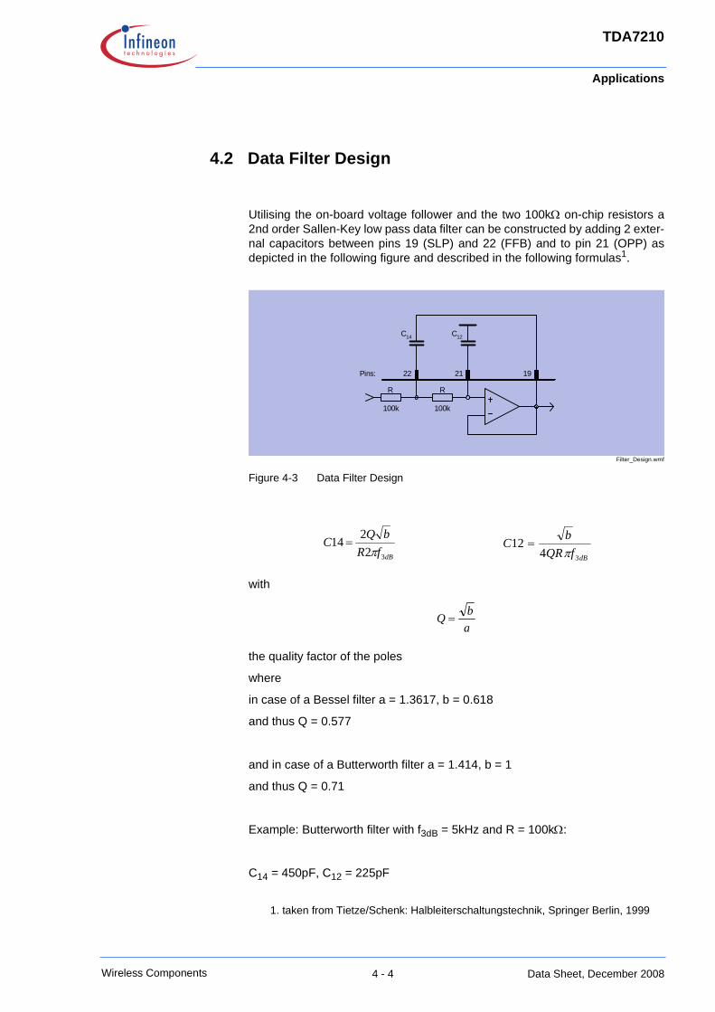
4.2 Data Filter Design
Utilising the on-board voltage follower and the two 100kΩ on-chip resistors a 2nd order Sallen-Key low pass data filter can be constructed by adding 2 exter-nal capacitors between pins 19 (SLP) and 22 (FFB) and to pin 21 (OPP) as depicted in the following figure and described in the following formulas1.
Filter_Design.wmf
Figure 4-3 Data Filter Design
with
the quality factor of the poles
where
in case of a Bessel filter a = 1.3617, b = 0.618
and thus Q = 0.577
and in case of a Butterworth filter a = 1.414, b = 1
and thus Q = 0.71
Example: Butterworth filter with f3dB = 5kHz and R = 100kΩ:
C14 = 450pF, C12 = 225pF
1. taken from Tietze/Schenk: Halbleiterschaltungstechnik, Springer Berlin, 1999
Pins: 22 21 19
R R
100k 100k
C14 C12
dBfRbQC
32214
π=
dBfQRbC
3412
π=
abQ =
Applications
4 - 5
TDA7210
Wireless Components
Data Sheet, December 2008
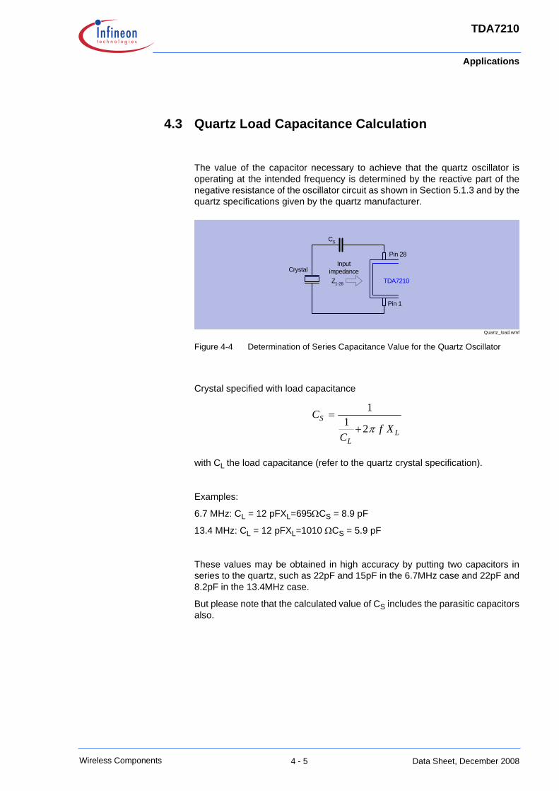
4.3 Quartz Load Capacitance Calculation
The value of the capacitor necessary to achieve that the quartz oscillator is operating at the intended frequency is determined by the reactive part of the negative resistance of the oscillator circuit as shown in Section 5.1.3 and by the quartz specifications given by the quartz manufacturer.
Quartz_load.wmf
Figure 4-4 Determination of Series Capacitance Value for the Quartz Oscillator
Crystal specified with load capacitance
with CL the load capacitance (refer to the quartz crystal specification).
Examples:
6.7 MHz: CL = 12 pFXL=695ΩCS = 8.9 pF
13.4 MHz: CL = 12 pFXL=1010 ΩCS = 5.9 pF
These values may be obtained in high accuracy by putting two capacitors in series to the quartz, such as 22pF and 15pF in the 6.7MHz case and 22pF and 8.2pF in the 13.4MHz case.
But please note that the calculated value of CS includes the parasitic capacitors also.
CS
CrystalInput
impedanceZ1-28 TDA7210
Pin 28
Pin 1
LL
SXf
C
Cπ211
+=
Applications
4 - 6
TDA7210
Wireless Components
Data Sheet, December 2008
4.4 Quartz Frequency Calculation
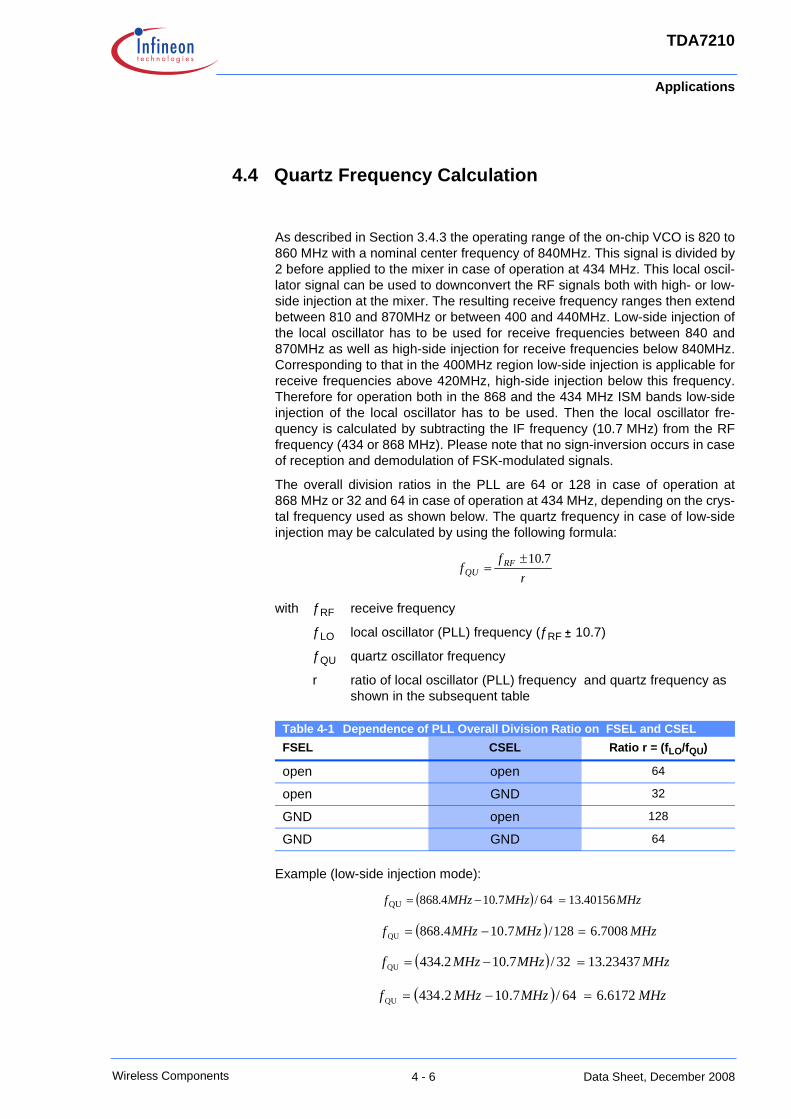
As described in Section 3.4.3 the operating range of the on-chip VCO is 820 to 860 MHz with a nominal center frequency of 840MHz. This signal is divided by 2 before applied to the mixer in case of operation at 434 MHz. This local oscil-lator signal can be used to downconvert the RF signals both with high- or low-side injection at the mixer. The resulting receive frequency ranges then extend between 810 and 870MHz or between 400 and 440MHz. Low-side injection of the local oscillator has to be used for receive frequencies between 840 and 870MHz as well as high-side injection for receive frequencies below 840MHz. Corresponding to that in the 400MHz region low-side injection is applicable for receive frequencies above 420MHz, high-side injection below this frequency. Therefore for operation both in the 868 and the 434 MHz ISM bands low-side injection of the local oscillator has to be used. Then the local oscillator fre-quency is calculated by subtracting the IF frequency (10.7 MHz) from the RF frequency (434 or 868 MHz). Please note that no sign-inversion occurs in case of reception and demodulation of FSK-modulated signals.
The overall division ratios in the PLL are 64 or 128 in case of operation at 868 MHz or 32 and 64 in case of operation at 434 MHz, depending on the crys-tal frequency used as shown below. The quartz frequency in case of low-side injection may be calculated by using the following formula:
with ƒRF receive frequency
ƒLO local oscillator (PLL) frequency (ƒRF ± 10.7)
ƒQU quartz oscillator frequency
r ratio of local oscillator (PLL) frequency and quartz frequency as shown in the subsequent table
Example (low-side injection mode):
Table 4-1 Dependence of PLL Overall Division Ratio on FSEL and CSELFSEL CSEL Ratio r = (fLO/fQU)
open open 64
open GND 32
GND open 128
GND GND 64
rf
f RFQU
7.10±=
( ) MHzMHzMHzf 40156.1364/7.104.868QU =−=
( ) MHzMHzMHzf 7008.6128/7.104.868QU =−=
( ) MHzMHzMHzf 23437.1332/7.102.434QU =−=
( ) MHzMHzMHzf 6.617264/7.102.434QU =−=
Applications
4 - 7
TDA7210
Wireless Components
Data Sheet, December 2008
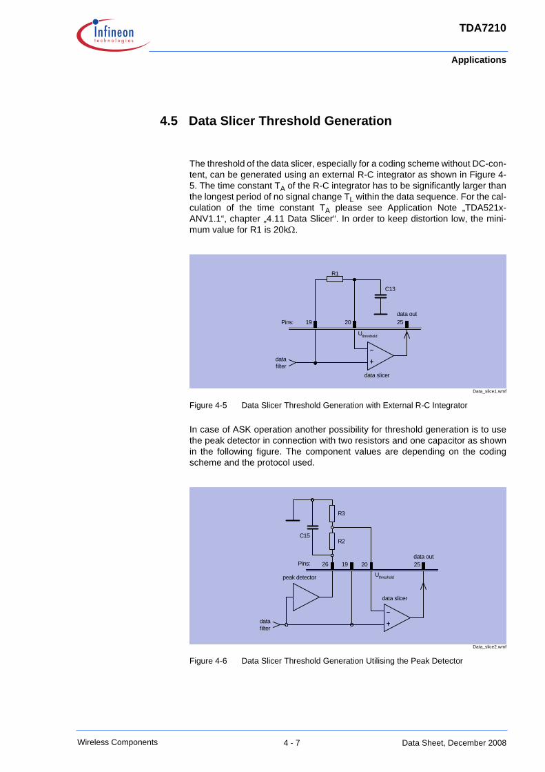
4.5 Data Slicer Threshold Generation
The threshold of the data slicer, especially for a coding scheme without DC-con-tent, can be generated using an external R-C integrator as shown in Figure 4-5. The time constant TA of the R-C integrator has to be significantly larger than the longest period of no signal change TL within the data sequence. For the cal-culation of the time constant TA please see Application Note „TDA521x-ANV1.1“, chapter „4.11 Data Slicer“. In order to keep distortion low, the mini-mum value for R1 is 20kΩ.
Data_slice1.wmf
Figure 4-5 Data Slicer Threshold Generation with External R-C Integrator
In case of ASK operation another possibility for threshold generation is to use the peak detector in connection with two resistors and one capacitor as shown in the following figure. The component values are depending on the coding scheme and the protocol used.
Data_slice2.wmf
Figure 4-6 Data Slicer Threshold Generation Utilising the Peak Detector
Pins: 2019
R1
C13
25data out
Uthreshold
data slicer
datafilter
Pins: 2019 25data out
Uthreshold
data slicer
datafilter
26
peak detector
C15
R3
R2
Applications
4 - 8
TDA7210
Wireless Components
Data Sheet, December 2008
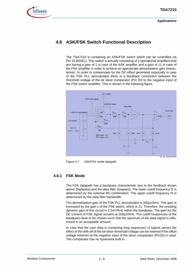
4.6 ASK/FSK Switch Functional Description
The TDA7210 is containing an ASK/FSK switch which can be controlled via Pin 15 (MSEL). This switch is actually consisting of 2 operational amplifiers that are having a gain of 1 in case of the ASK amplifier and a gain of 11 in case of the FSK amplifier in order to achieve an appropriate demodulation gain charac-teristic. In order to compensate for the DC-offset generated especially in case of the FSK PLL demodulator there is a feedback connection between the threshold voltage of the bit slicer comparator (Pin 20) to the negative input of the FSK switch amplifier. This is shown in the following figure.
ask_fsk_datapath.WMF
Figure 4-7 ASK/FSK mode datapath
4.6.1 FSK Mode
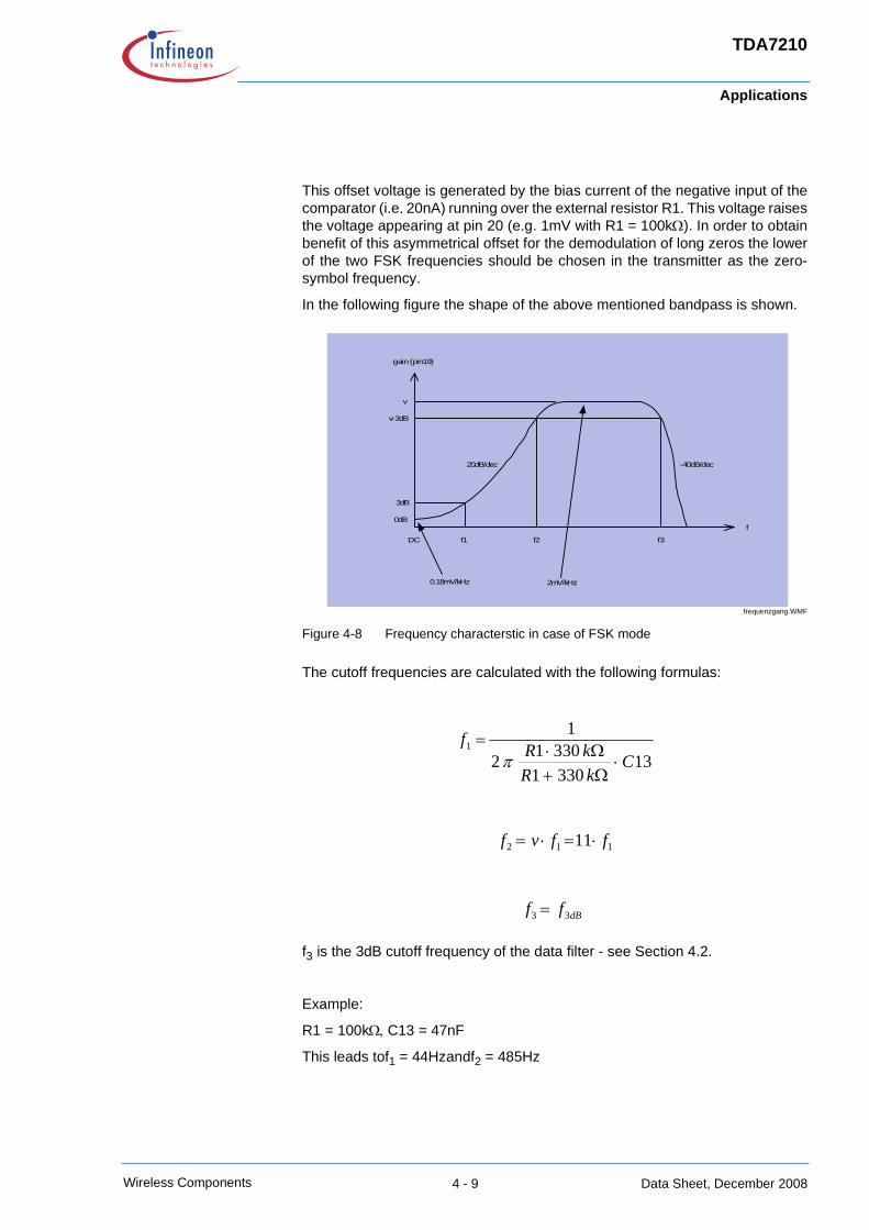
The FSK datapath has a bandpass characterisitc due to the feedback shown above (highpass) and the data filter (lowpass). The lower cutoff frequency f2 is determined by the external RC-combination. The upper cutoff frequency f3 is determined by the data filter bandwidth.
The demodulation gain of the FSK PLL demodulator is 200µV/kHz. This gain is increased by the gain v of the FSK switch, which is 11. Therefore the resulting dynamic gain of this circuit is 2.2mV/kHz within the bandpass. The gain for the DC content of FSK signal remains at 200µV/kHz. The cutoff frequencies of the bandpass have to be chosen such that the spectrum of the data signal is influ-enced in an acceptable amount.
In case that the user data is containing long sequences of logical zeroes the effect of the drift-off of the bit slicer threshold voltage can be lowered if the offset voltage inherent at the negative input of the slicer comparator (Pin20) is used. The comparator has no hysteresis built in.
RF1 int
100k
RF2 int
100kv = 1
19
30k
RF3 int
300k
DATA Out
AC
DC
typ. 2 V
1.5 V......2.5 V
0.2 mV/kHz
FSK PLL Demodulator
RSSI (ASK signal)
C14R1
ASK/FSK Switch
ASK
FSK+-
+-
22
25
C13
20ASK mode : v=1FSK mode : v=11
21
15 MSEL
FFB OPP SLP SLN
Comp-
+
Data Filter
C12
RF4 int
Applications
4 - 9
TDA7210
Wireless Components
Data Sheet, December 2008
This offset voltage is generated by the bias current of the negative input of the comparator (i.e. 20nA) running over the external resistor R1. This voltage raises the voltage appearing at pin 20 (e.g. 1mV with R1 = 100kΩ). In order to obtain benefit of this asymmetrical offset for the demodulation of long zeros the lower of the two FSK frequencies should be chosen in the transmitter as the zero-symbol frequency.
In the following figure the shape of the above mentioned bandpass is shown.
frequenzgang.WMF
Figure 4-8 Frequency characterstic in case of FSK mode
The cutoff frequencies are calculated with the following formulas:
f3 is the 3dB cutoff frequency of the data filter - see Section 4.2.
Example:
R1 = 100kΩ, C13 = 47nF
This leads tof1 = 44Hzandf2 = 485Hz
v
0dB
3dB
v-3dB
f
20dB/dec -40dB/dec
f1 f2 f3
gain (pin19)
DC
0.18mV/kHz 2mV/kHz
13330133012
11
CkRkRf
⋅Ω+Ω⋅
=π
112 11 ffvf ⋅=⋅=
dBff 33 =
Applications
4 - 10
TDA7210
Wireless Components
Data Sheet, December 2008
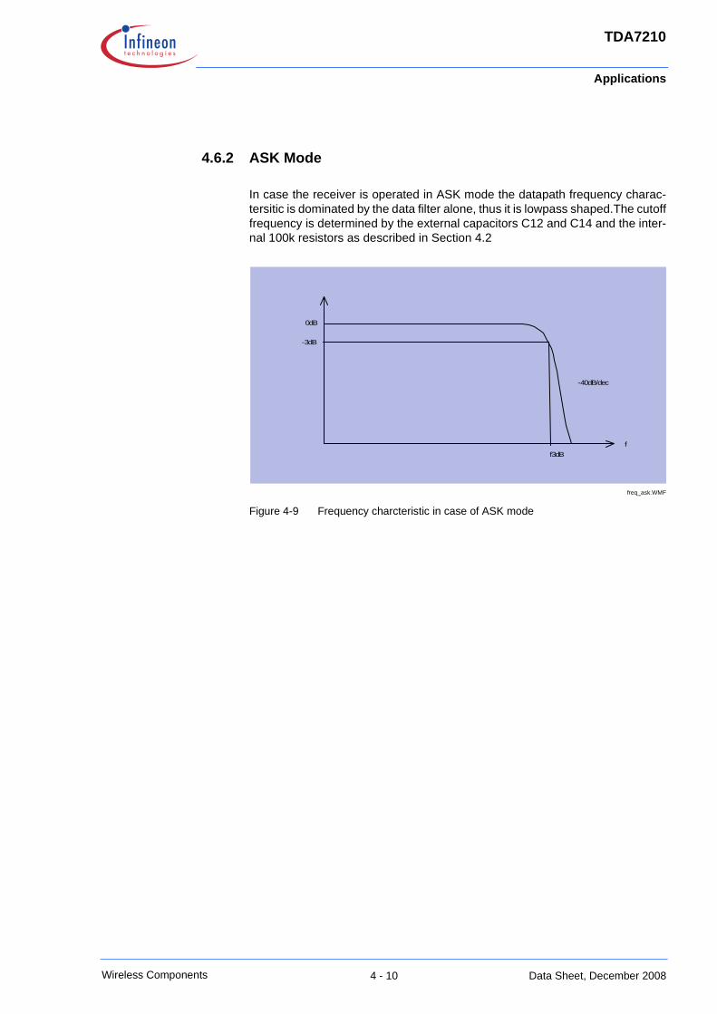
4.6.2 ASK Mode
In case the receiver is operated in ASK mode the datapath frequency charac-tersitic is dominated by the data filter alone, thus it is lowpass shaped.The cutoff frequency is determined by the external capacitors C12 and C14 and the inter-nal 100k resistors as described in Section 4.2
freq_ask.WMF
Figure 4-9 Frequency charcteristic in case of ASK mode
0dB
-3dB
f
-40dB/dec
f3dB
Applications
4 - 11
TDA7210
Wireless Components
Data Sheet, December 2008
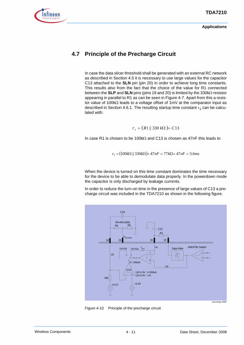
4.7 Principle of the Precharge Circuit
In case the data slicer threshold shall be generated with an external RC network as described in Section 4.5 it is necessary to use large values for the capacitor C13 attached to the SLN pin (pin 20) in order to achieve long time constants. This results also from the fact that the choice of the value for R1 connected between the SLP and SLN pins (pins 19 and 20) is limited by the 330kΩ resistor appearing in parallel to R1 as can be seen in Figure 4-7. Apart from this a resis-tor value of 100kΩ leads to a voltage offset of 1mV at the comparator input as described in Section 4.6.1. The resulting startup time constant τ1 can be calcu-lated with:
In case R1 is chosen to be 100kΩ and C13 is chosen as 47nF this leads to
When the device is turned on this time constant dominates the time necessary for the device to be able to demodulate data properly. In the powerdown mode the capacitor is only discharged by leakage currents.
In order to reduce the turn-on time in the presence of large values of C13 a pre-charge circuit was included in the TDA7210 as shown in the following figure.
precharge.WMF
Figure 4-10 Principle of the precharge circuit
( ) 13330||11 CkR ×Ω=τ
( ) msnFknFkk 6.3477747330||1001 =×Ω=×ΩΩ=τ
Iload
+3.1V
20k
+-
OTA
+2.4V
R4 R5
24 23Uthreshold
C13
0 / 240uA+
-
20 19
R1
Data Filter ASK/FSK Switch
C18
U2
Us
UcUc<UsUc>Us
U2<2.4V : I=240uAU2>2.4V : I=0
R4+R5=600k
Applications
4 - 12
TDA7210
Wireless Components
Data Sheet, December 2008
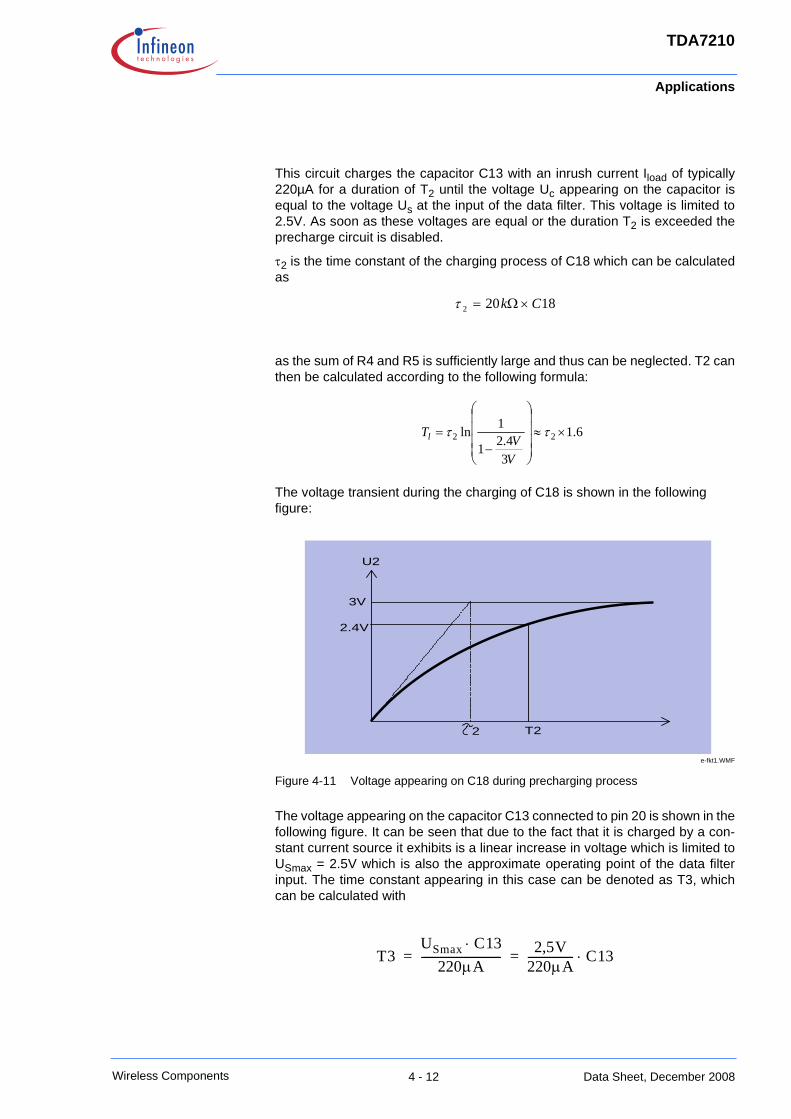
This circuit charges the capacitor C13 with an inrush current Iload of typically 220µA for a duration of T2 until the voltage Uc appearing on the capacitor is equal to the voltage Us at the input of the data filter. This voltage is limited to 2.5V. As soon as these voltages are equal or the duration T2 is exceeded the precharge circuit is disabled.
τ2 is the time constant of the charging process of C18 which can be calculated as
as the sum of R4 and R5 is sufficiently large and thus can be neglected. T2 can then be calculated according to the following formula:
The voltage transient during the charging of C18 is shown in the following figure:
e-fkt1.WMF
Figure 4-11 Voltage appearing on C18 during precharging process
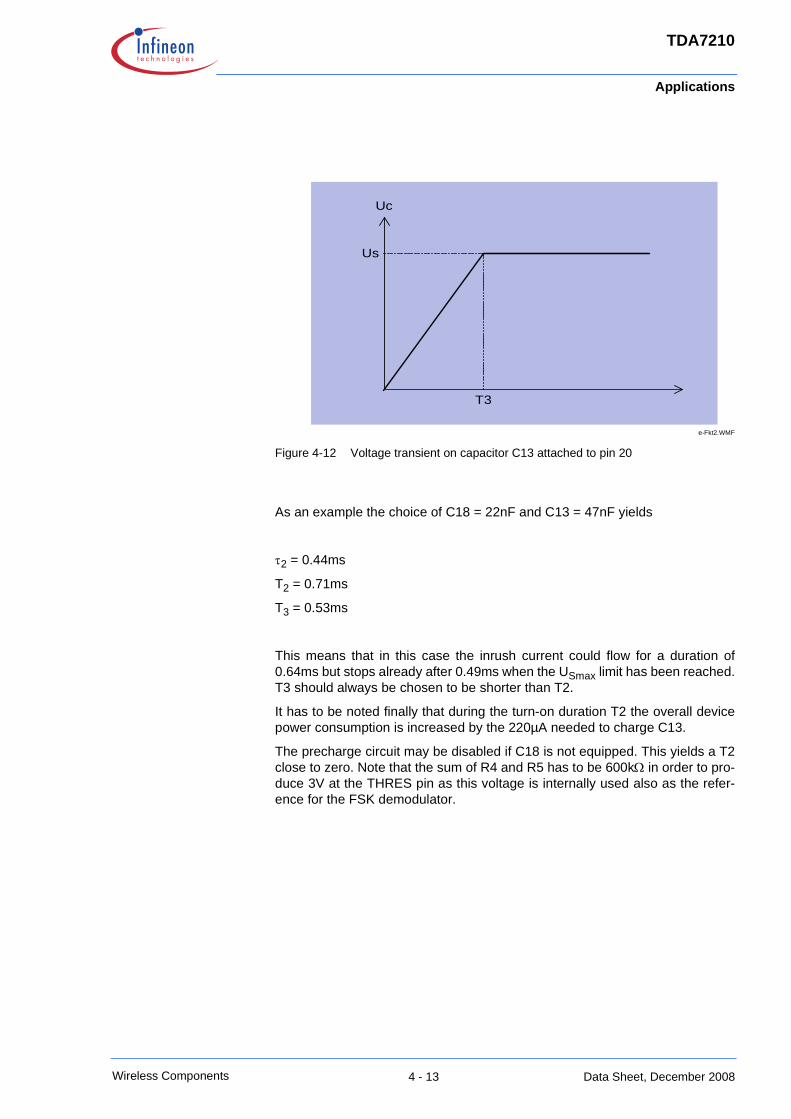
The voltage appearing on the capacitor C13 connected to pin 20 is shown in the following figure. It can be seen that due to the fact that it is charged by a con-stant current source it exhibits is a linear increase in voltage which is limited to USmax = 2.5V which is also the approximate operating point of the data filter input. The time constant appearing in this case can be denoted as T3, which can be calculated with
18202 Ck ×Ω=τ
6.1
34.21
1ln 22 ×≈⎟⎟⎟⎟
⎠
⎞
⎜⎜⎜⎜
⎝
⎛
−= ττ
VV
Tl
U2
2
3V
2.4V
T2
T3USmax C13⋅
220μA------------------------------ 2,5V220μA----------------- C13⋅= =
Applications
4 - 13
TDA7210
Wireless Components
Data Sheet, December 2008
e-Fkt2.WMF
Figure 4-12 Voltage transient on capacitor C13 attached to pin 20
As an example the choice of C18 = 22nF and C13 = 47nF yields
τ2 = 0.44ms
T2 = 0.71ms
T3 = 0.53ms
This means that in this case the inrush current could flow for a duration of 0.64ms but stops already after 0.49ms when the USmax limit has been reached. T3 should always be chosen to be shorter than T2.
It has to be noted finally that during the turn-on duration T2 the overall device power consumption is increased by the 220µA needed to charge C13.
The precharge circuit may be disabled if C18 is not equipped. This yields a T2 close to zero. Note that the sum of R4 and R5 has to be 600kΩ in order to pro-duce 3V at the THRES pin as this voltage is internally used also as the refer-ence for the FSK demodulator.
Us
T3
Uc
5 Reference
5.1 Electrical Data. . . . . . . . . . . . . . . . . . . . . . . . . . . . . . . . . . . . . . . . . . . 5-25.2 Test Circuit . . . . . . . . . . . . . . . . . . . . . . . . . . . . . . . . . . . . . . . . . . . . 5-125.3 Test Board Layouts. . . . . . . . . . . . . . . . . . . . . . . . . . . . . . . . . . . . . . 5-135.4 Bill of Materials . . . . . . . . . . . . . . . . . . . . . . . . . . . . . . . . . . . . . . . . . 5-15
Contents of this Chapter
Reference
5 - 2
TDA7210preliminary
Wireless Components
Data Sheet, December 2008
5.1 Electrical Data
5.1.1 Absolute Maximum Ratings
WARNING
The maximum ratings may not be exceeded under any circumstances, not even momentarily and individually, as permanent damage to the IC will result.
Table 5-1 Absolute Maximum Ratings, Ambient temperature TAMB=-40°C ... + 85°C
# Parameter Symbol Limit Values Unit Remarks
min max
1 Supply Voltage Vs -0.3 5.5 V
2 Junction Temperature Tj -40 +125 °C
3 Storage Temperature Ts -40 +150 °C
4 Thermal Resistance RthJA 114 K/W
5 ESD integrity, all pins excl. Pins 1,3, 6, 28ESD integrity Pins 1,3,6,28
VESD +2+1.5
kVkV
HBM according to
MIL STD 883D,
method 3015.7
Reference
5 - 3
TDA7210preliminary
Wireless Components
Data Sheet, December 2008
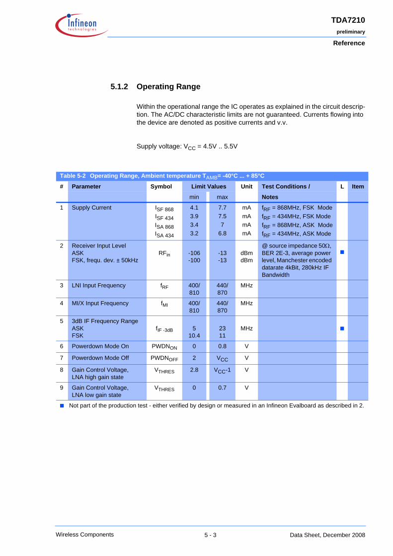
5.1.2 Operating Range
Within the operational range the IC operates as explained in the circuit descrip-tion. The AC/DC characteristic limits are not guaranteed. Currents flowing into the device are denoted as positive currents and v.v.
Supply voltage: VCC = 4.5V .. 5.5V
Table 5-2 Operating Range, Ambient temperature TAMB= -40°C ... + 85°C
# Parameter Symbol Limit Values Unit Test Conditions / L Item
min max Notes
1 Supply Current ISF 868ISF 434ISA 868ISA 434
4.13.93.43.2
7.77.57
6.8
mAmAmAmA
fRF = 868MHz, FSK ModefRF = 434MHz, FSK ModefRF = 868MHz, ASK ModefRF = 434MHz, ASK Mode
2 Receiver Input Level ASKFSK, frequ. dev. ± 50kHz
RFin -106-100
-13-13
dBmdBm
@ source impedance 50Ω, BER 2E-3, average power level, Manchester encoded datarate 4kBit, 280kHz IF Bandwidth
■
3 LNI Input Frequency fRF 400/810
440/870
MHz
4 MI/X Input Frequency fMI 400/810
440/870
MHz
5 3dB IF Frequency RangeASKFSK
fIF -3dB 510.4
2311
MHz ■
6 Powerdown Mode On PWDNON 0 0.8 V
7 Powerdown Mode Off PWDNOFF 2 VCC V
8 Gain Control Voltage, LNA high gain state
VTHRES 2.8 VCC-1 V
9 Gain Control Voltage, LNA low gain state
VTHRES 0 0.7 V
■ Not part of the production test - either verified by design or measured in an Infineon Evalboard as described in 2.
Reference
5 - 4
TDA7210preliminary
Wireless Components
Data Sheet, December 2008
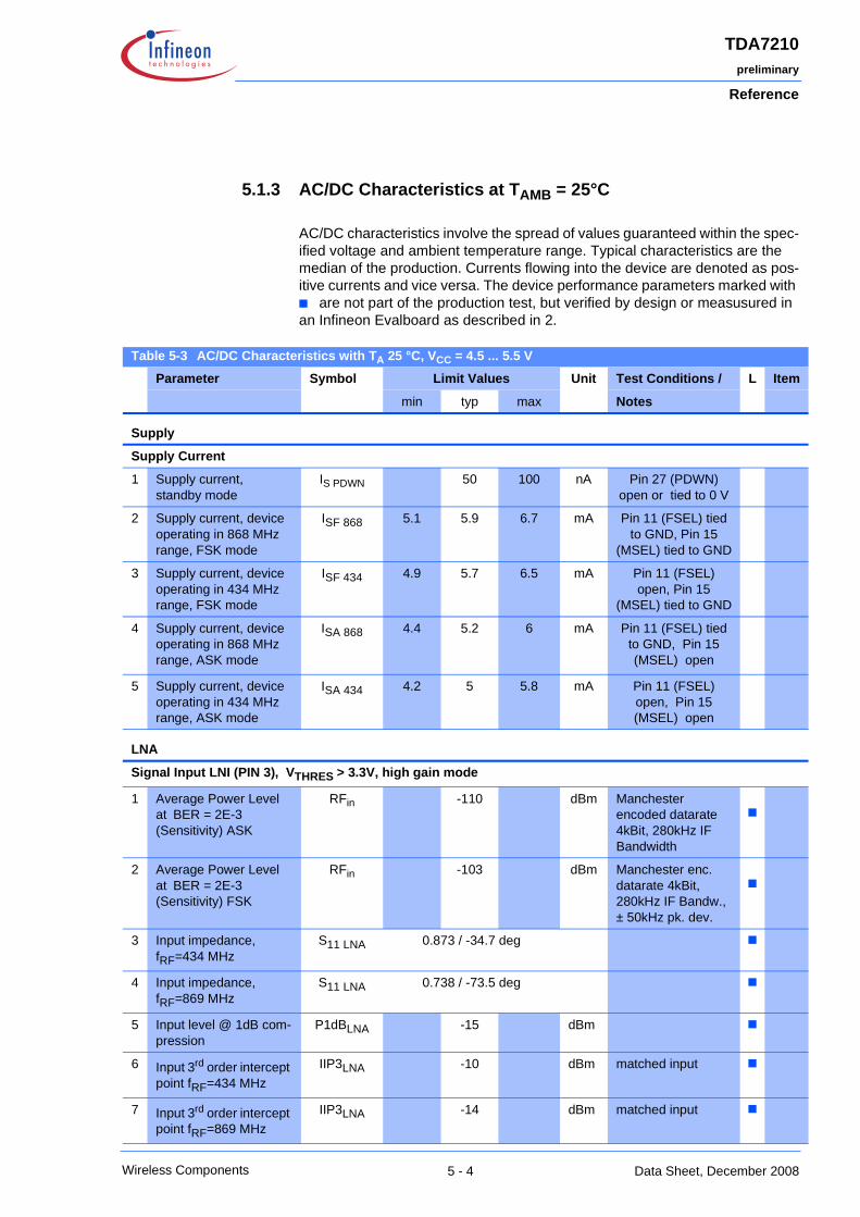
5.1.3 AC/DC Characteristics at TAMB = 25°C
AC/DC characteristics involve the spread of values guaranteed within the spec-ified voltage and ambient temperature range. Typical characteristics are the median of the production. Currents flowing into the device are denoted as pos-itive currents and vice versa. The device performance parameters marked with ■ are not part of the production test, but verified by design or measusured in an Infineon Evalboard as described in 2.
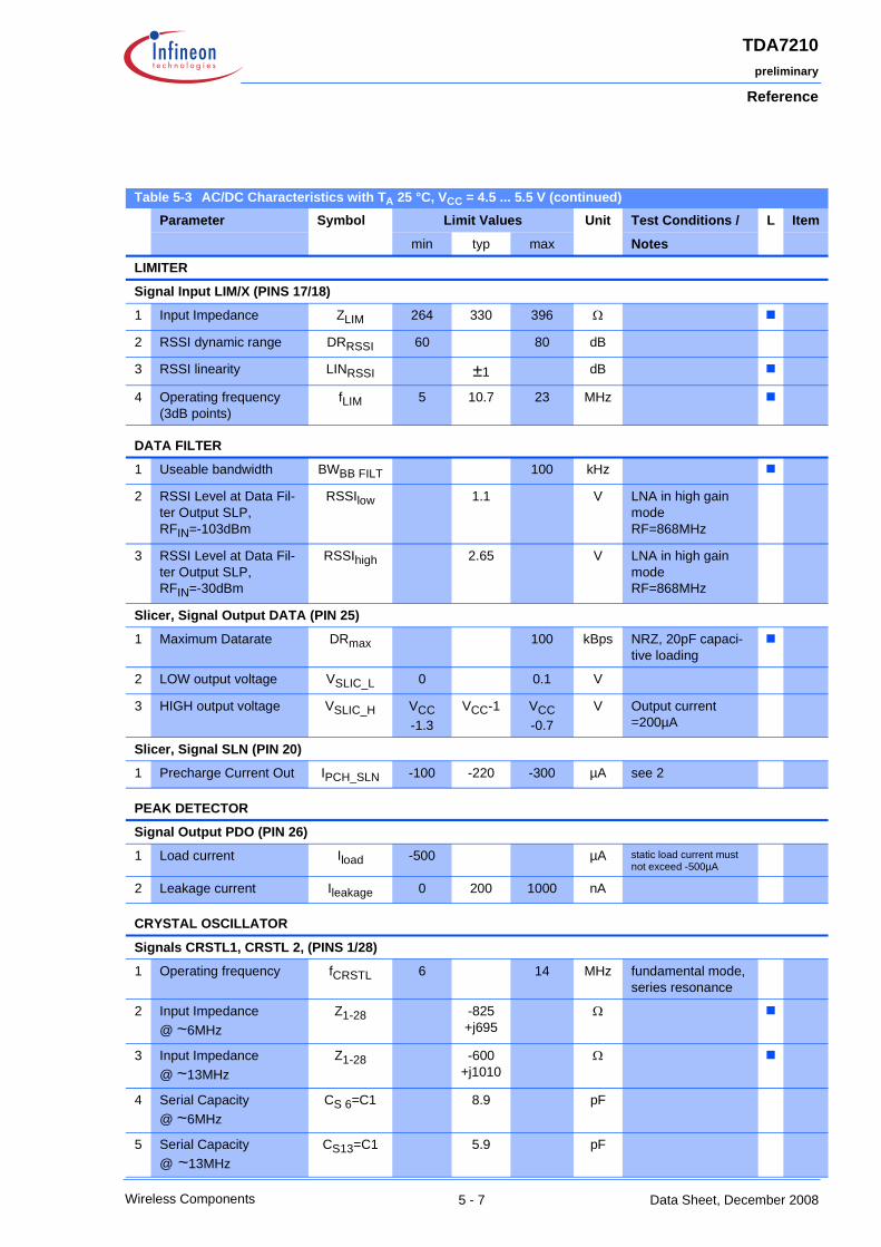
Table 5-3 AC/DC Characteristics with TA 25 °C, VCC = 4.5 ... 5.5 V
Parameter Symbol Limit Values Unit Test Conditions / L Item
min typ max Notes
Supply
Supply Current
1 Supply current,standby mode
IS PDWN 50 100 nA Pin 27 (PDWN) open or tied to 0 V
2 Supply current, device operating in 868 MHz range, FSK mode
ISF 868 5.1 5.9 6.7 mA Pin 11 (FSEL) tied to GND, Pin 15
(MSEL) tied to GND
3 Supply current, device operating in 434 MHz range, FSK mode
ISF 434 4.9 5.7 6.5 mA Pin 11 (FSEL) open, Pin 15
(MSEL) tied to GND
4 Supply current, device operating in 868 MHz range, ASK mode
ISA 868 4.4 5.2 6 mA Pin 11 (FSEL) tied to GND, Pin 15 (MSEL) open
5 Supply current, device operating in 434 MHz range, ASK mode
ISA 434 4.2 5 5.8 mA Pin 11 (FSEL) open, Pin 15 (MSEL) open
LNA
Signal Input LNI (PIN 3), VTHRES > 3.3V, high gain mode
1 Average Power Level at BER = 2E-3 (Sensitivity) ASK
RFin -110 dBm Manchester encoded datarate 4kBit, 280kHz IF Bandwidth
■
2 Average Power Level at BER = 2E-3 (Sensitivity) FSK
RFin -103 dBm Manchester enc. datarate 4kBit, 280kHz IF Bandw., ± 50kHz pk. dev.
■
3 Input impedance, fRF=434 MHz
S11 LNA 0.873 / -34.7 deg ■
4 Input impedance, fRF=869 MHz
S11 LNA 0.738 / -73.5 deg ■
5 Input level @ 1dB com-pression
P1dBLNA -15 dBm ■
6 Input 3rd order intercept point fRF=434 MHz
IIP3LNA -10 dBm matched input ■
7 Input 3rd order intercept point fRF=869 MHz
IIP3LNA -14 dBm matched input ■
Reference
5 - 5
TDA7210preliminary
Wireless Components
Data Sheet, December 2008
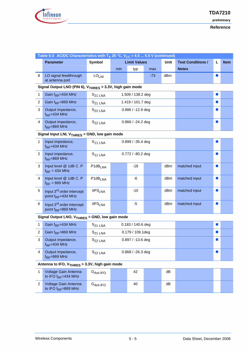
Table 5-3 AC/DC Characteristics with TA 25 °C, VCC = 4.5 ... 5.5 V (continued)
Parameter Symbol Limit Values Unit Test Conditions / L Item
min typ max Notes
8 LO signal feedthrough at antenna port
LOLNI -73 dBm ■
Signal Output LNO (PIN 6), VTHRES > 3.3V, high gain mode
1 Gain fRF=434 MHz S21 LNA 1.509 / 138.2 deg ■
2 Gain fRF=869 MHz S21 LNA 1.419 / 101.7 deg ■
3 Output impedance, fRF=434 MHz
S22 LNA 0.886 / -12.9 deg ■
4 Output impedance, fRF=869 MHz
S22 LNA 0.866 / -24.2 deg ■
Signal Input LNI, VTHRES = GND, low gain mode
1 Input impedance, fRF=434 MHz
S11 LNA 0.899 / -35.4 deg ■
2 Input impedance, fRF=869 MHz
S11 LNA 0.772 / -80.2 deg ■
3 Input level @ 1dB C. PfRF = 434 MHz
P1dBLNA -18 dBm matched input ■
4 Input level @ 1dB C. PfRF = 869 MHz
P1dBLNA -6 dBm matched input ■
5 Input 3rd order intercept point fRF=434 MHz
IIP3LNA -10 dBm matched input ■
6 Input 3rd order intercept point fRF=869 MHz
IIP3LNA -5 dBm matched input ■
Signal Output LNO, VTHRES = GND, low gain mode
1 Gain fRF=434 MHz S21 LNA 0.183 / 140.6 deg ■
2 Gain fRF=869 MHz S21 LNA 0.179 / 109.1deg ■
3 Output impedance, fRF=434 MHz
S22 LNA 0.897 / -13.6 deg ■
4 Output impedance, fRF=869 MHz
S22 LNA 0.868 / -26.3 deg ■
Antenna to IFO, VTHRES > 3.3V, high gain mode
1 Voltage Gain Antenna to IFO fRF=434 MHz
GAnt-IFO 42 dB
2 Voltage Gain Antenna to IFO fRF=869 MHz
GAnt-IFO 40 dB
Reference
5 - 6
TDA7210preliminary
Wireless Components
Data Sheet, December 2008
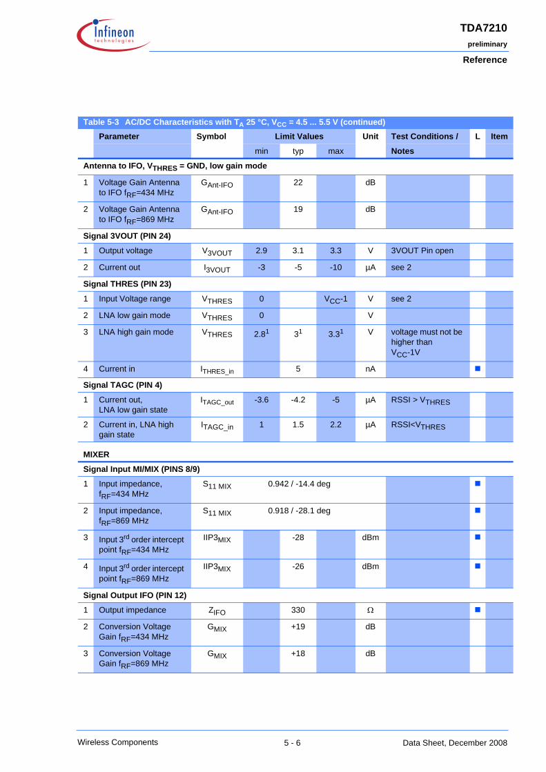
Table 5-3 AC/DC Characteristics with TA 25 °C, VCC = 4.5 ... 5.5 V (continued)
Parameter Symbol Limit Values Unit Test Conditions / L Item
min typ max Notes
Antenna to IFO, VTHRES = GND, low gain mode
1 Voltage Gain Antenna to IFO fRF=434 MHz
GAnt-IFO 22 dB
2 Voltage Gain Antenna to IFO fRF=869 MHz
GAnt-IFO 19 dB
Signal 3VOUT (PIN 24)
1 Output voltage V3VOUT 2.9 3.1 3.3 V 3VOUT Pin open
2 Current out I3VOUT -3 -5 -10 µA see 2
Signal THRES (PIN 23)
1 Input Voltage range VTHRES 0 VCC-1 V see 2
2 LNA low gain mode VTHRES 0 V
3 LNA high gain mode VTHRES 2.81 31 3.31 V voltage must not be higher than VCC-1V
4 Current in ITHRES_in 5 nA ■
Signal TAGC (PIN 4)
1 Current out,LNA low gain state
ITAGC_out -3.6 -4.2 -5 µA RSSI > VTHRES
2 Current in, LNA high gain state
ITAGC_in 1 1.5 2.2 µA RSSI<VTHRES
MIXER
Signal Input MI/MIX (PINS 8/9)
1 Input impedance, fRF=434 MHz
S11 MIX 0.942 / -14.4 deg ■
2 Input impedance, fRF=869 MHz
S11 MIX 0.918 / -28.1 deg ■
3 Input 3rd order intercept point fRF=434 MHz
IIP3MIX -28 dBm ■
4 Input 3rd order intercept point fRF=869 MHz
IIP3MIX -26 dBm ■
Signal Output IFO (PIN 12)
1 Output impedance ZIFO 330 Ω ■
2 Conversion Voltage Gain fRF=434 MHz
GMIX +19 dB
3 Conversion Voltage Gain fRF=869 MHz
GMIX +18 dB
Reference
5 - 7
TDA7210preliminary
Wireless Components
Data Sheet, December 2008
Table 5-3 AC/DC Characteristics with TA 25 °C, VCC = 4.5 ... 5.5 V (continued)
Parameter Symbol Limit Values Unit Test Conditions / L Item
min typ max Notes
LIMITER
Signal Input LIM/X (PINS 17/18)
1 Input Impedance ZLIM 264 330 396 Ω ■
2 RSSI dynamic range DRRSSI 60 80 dB
3 RSSI linearity LINRSSI ±1 dB ■
4 Operating frequency (3dB points)
fLIM 5 10.7 23 MHz ■
DATA FILTER
1 Useable bandwidth BWBB FILT 100 kHz ■
2 RSSI Level at Data Fil-ter Output SLP, RFIN=-103dBm
RSSIlow 1.1 V LNA in high gain modeRF=868MHz
3 RSSI Level at Data Fil-ter Output SLP, RFIN=-30dBm
RSSIhigh 2.65 V LNA in high gain modeRF=868MHz
Slicer, Signal Output DATA (PIN 25)
1 Maximum Datarate DRmax 100 kBps NRZ, 20pF capaci-tive loading
■
2 LOW output voltage VSLIC_L 0 0.1 V
3 HIGH output voltage VSLIC_H VCC-1.3
VCC-1 VCC-0.7
V Output current=200µA
Slicer, Signal SLN (PIN 20)
1 Precharge Current Out IPCH_SLN -100 -220 -300 µA see 2
PEAK DETECTOR
Signal Output PDO (PIN 26)
1 Load current Iload -500 µA static load current must not exceed -500µA
2 Leakage current Ileakage 0 200 1000 nA
CRYSTAL OSCILLATOR
Signals CRSTL1, CRSTL 2, (PINS 1/28)
1 Operating frequency fCRSTL 6 14 MHz fundamental mode, series resonance
2 Input Impedance @ ~6MHz
Z1-28 -825 +j695
Ω ■
3 Input Impedance @ ~13MHz
Z1-28 -600+j1010
Ω ■
4 Serial Capacity @ ~6MHz
CS 6=C1 8.9 pF
5 Serial Capacity @ ~13MHz
CS13=C1 5.9 pF
Reference
5 - 8
TDA7210preliminary
Wireless Components
Data Sheet, December 2008
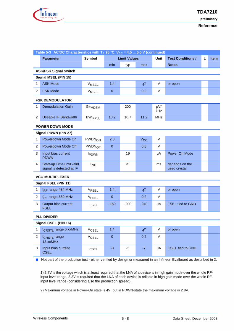
Table 5-3 AC/DC Characteristics with TA 25 °C, VCC = 4.5 ... 5.5 V (continued)
Parameter Symbol Limit Values Unit Test Conditions / L Item
min typ max Notes
ASK/FSK Signal Switch
Signal MSEL (PIN 15)
1 ASK Mode VMSEL 1.4 42 V or open
2 FSK Mode VMSEL 0 0.2 V
FSK DEMODULATOR
1 Demodulation Gain GFMDEM 200 µV/kHz
2 Useable IF Bandwidth BWIFPLL 10.2 10.7 11.2 MHz
POWER DOWN MODE
Signal PDWN (PIN 27)
1 Powerdown Mode On PWDNON 2.8 VCC V
2 Powerdown Mode Off PWDNOff 0 0.8 V
3 Input bias current PDWN
IPDWN 19 uA Power On Mode
4 Start-up Time until valid signal is detected at IF
TSU <1 ms depends on the used crystal
VCO MULTIPLEXER
Signal FSEL (PIN 11)
1 fRF range 434 MHz VFSEL 1.4 42 V or open
2 fRF range 869 MHz VFSEL 0 0.2 V
3 Output bias current FSEL
IFSEL -160 -200 -240 µA FSEL tied to GND
PLL DIVIDER
Signal CSEL (PIN 16)
1 fCRSTL range 6.xxMHz VCSEL 1.4 42 V or open
2 fCRSTL range 13.xxMHz
VCSEL 0 0.2 V
3 Input bias current CSEL
ICSEL -3 -5 -7 µA CSEL tied to GND
■ Not part of the production test - either verified by design or measured in an Infineon Evalboard as described in 2.
1) 2.8V is the voltage which is at least required that the LNA of a device is in high gain mode over the whole RF-input level range. 3.3V is required that the LNA of each device is reliable in high gain mode over the whole RF-input level range (considering also the production spread).
2) Maximum voltage in Power-On state is 4V, but in PDWN-state the maximum voltage is 2.8V.
Reference
5 - 9
TDA7210preliminary
Wireless Components
Data Sheet, December 2008
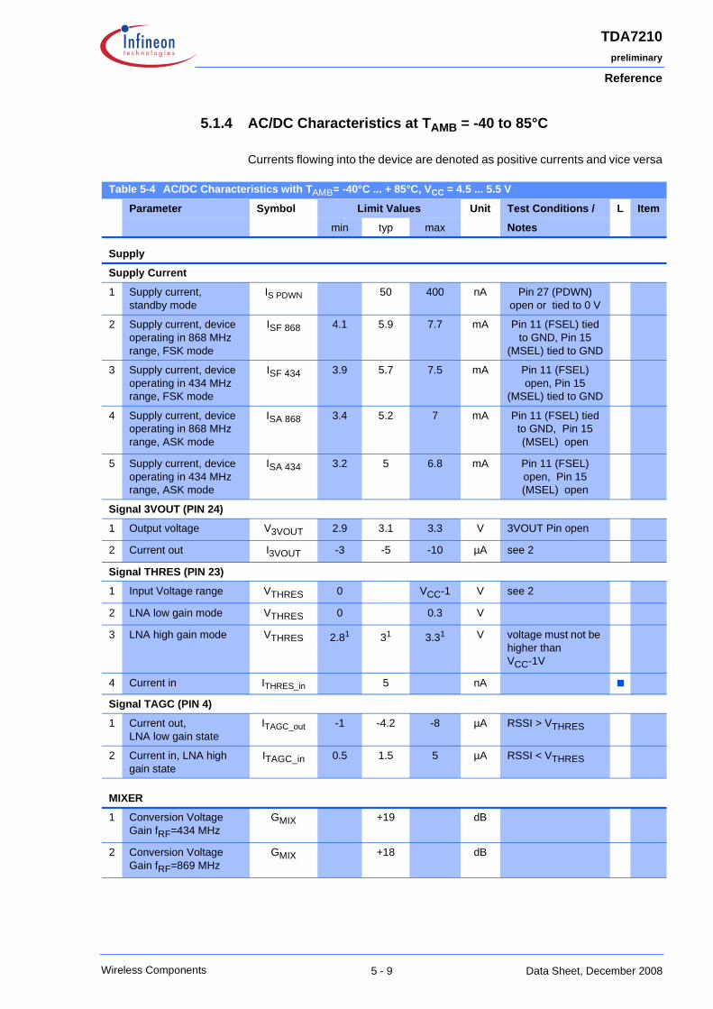
5.1.4 AC/DC Characteristics at TAMB = -40 to 85°C
Currents flowing into the device are denoted as positive currents and vice versa
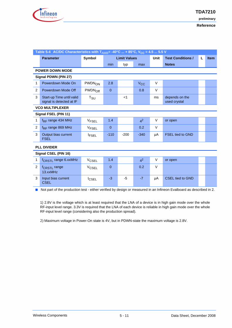
Table 5-4 AC/DC Characteristics with TAMB= -40°C ... + 85°C, VCC = 4.5 ... 5.5 V
Parameter Symbol Limit Values Unit Test Conditions / L Item
min typ max Notes
Supply
Supply Current
1 Supply current,standby mode
IS PDWN 50 400 nA Pin 27 (PDWN) open or tied to 0 V
2 Supply current, device operating in 868 MHz range, FSK mode
ISF 868 4.1 5.9 7.7 mA Pin 11 (FSEL) tied to GND, Pin 15
(MSEL) tied to GND
3 Supply current, device operating in 434 MHz range, FSK mode
ISF 434 3.9 5.7 7.5 mA Pin 11 (FSEL) open, Pin 15
(MSEL) tied to GND
4 Supply current, device operating in 868 MHz range, ASK mode
ISA 868 3.4 5.2 7 mA Pin 11 (FSEL) tied to GND, Pin 15 (MSEL) open
5 Supply current, device operating in 434 MHz range, ASK mode
ISA 434 3.2 5 6.8 mA Pin 11 (FSEL) open, Pin 15 (MSEL) open
Signal 3VOUT (PIN 24)
1 Output voltage V3VOUT 2.9 3.1 3.3 V 3VOUT Pin open
2 Current out I3VOUT -3 -5 -10 µA see 2
Signal THRES (PIN 23)
1 Input Voltage range VTHRES 0 VCC-1 V see 2
2 LNA low gain mode VTHRES 0 0.3 V
3 LNA high gain mode VTHRES 2.81 31 3.31 V voltage must not be higher than VCC-1V
4 Current in ITHRES_in 5 nA ■
Signal TAGC (PIN 4)
1 Current out,LNA low gain state
ITAGC_out -1 -4.2 -8 µA RSSI > VTHRES
2 Current in, LNA high gain state
ITAGC_in 0.5 1.5 5 µA RSSI < VTHRES
MIXER
1 Conversion Voltage Gain fRF=434 MHz
GMIX +19 dB
2 Conversion Voltage Gain fRF=869 MHz
GMIX +18 dB
Reference
5 - 10
TDA7210preliminary
Wireless Components
Data Sheet, December 2008
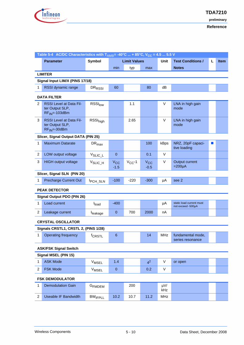
Table 5-4 AC/DC Characteristics with TAMB= -40°C ... + 85°C, VCC = 4.5 ... 5.5 V
Parameter Symbol Limit Values Unit Test Conditions / L Item
min typ max Notes
LIMITER
Signal Input LIM/X (PINS 17/18)
1 RSSI dynamic range DRRSSI 60 80 dB
DATA FILTER
2 RSSI Level at Data Fil-ter Output SLP, RFIN=-103dBm
RSSIlow 1.1 V LNA in high gain mode
3 RSSI Level at Data Fil-ter Output SLP, RFIN=-30dBm
RSSIhigh 2.65 V LNA in high gain mode
Slicer, Signal Output DATA (PIN 25)
1 Maximum Datarate DRmax 100 kBps NRZ, 20pF capaci-tive loading
■
2 LOW output voltage VSLIC_L 0 0.1 V
3 HIGH output voltage VSLIC_H VCC-1.5
VCC-1 VCC-0.5
V Output current =200µA
Slicer, Signal SLN (PIN 20)
1 Precharge Current Out IPCH_SLN -100 -220 -300 µA see 2
PEAK DETECTOR
Signal Output PDO (PIN 26)
1 Load current Iload -400 µA static load current must not exceed -500µA
2 Leakage current Ileakage 0 700 2000 nA
CRYSTAL OSCILLATOR
Signals CRSTL1, CRSTL 2, (PINS 1/28)
1 Operating frequency fCRSTL 6 14 MHz fundamental mode, series resonance
ASK/FSK Signal Switch
Signal MSEL (PIN 15)
1 ASK Mode VMSEL 1.4 42 V or open
2 FSK Mode VMSEL 0 0.2 V
FSK DEMODULATOR
1 Demodulation Gain GFMDEM 200 µV/kHz
2 Useable IF Bandwidth BWIFPLL 10.2 10.7 11.2 MHz
Reference
5 - 11
TDA7210preliminary
Wireless Components
Data Sheet, December 2008
Table 5-4 AC/DC Characteristics with TAMB= -40°C ... + 85°C, VCC = 4.5 ... 5.5 V
Parameter Symbol Limit Values Unit Test Conditions / L Item
min typ max Notes
POWER DOWN MODE
Signal PDWN (PIN 27)
1 Powerdown Mode On PWDNON 2.8 VCC V
2 Powerdown Mode Off PWDNOff 0 0.8 V
3 Start-up Time until valid signal is detected at IF
TSU <1 ms depends on the used crystal
VCO MULTIPLEXER
Signal FSEL (PIN 11)
1 fRF range 434 MHz VFSEL 1.4 42 V or open
2 fRF range 869 MHz VFSEL 0 0.2 V
3 Output bias current FSEL
IFSEL -110 -200 -340 µA FSEL tied to GND
PLL DIVIDER
Signal CSEL (PIN 16)
1 fCRSTL range 6.xxMHz VCSEL 1.4 42 V or open
2 fCRSTL range 13.xxMHz
VCSEL 0 0.2 V
3 Input bias current CSEL
ICSEL -3 -5 -7 µA CSEL tied to GND
■ Not part of the production test - either verified by design or measured in an Infineon Evalboard as described in 2.
1) 2.8V is the voltage which is at least required that the LNA of a device is in high gain mode over the whole RF-input level range. 3.3V is required that the LNA of each device is reliable in high gain mode over the whole RF-input level range (considering also the production spread).
2) Maximum voltage in Power-On state is 4V, but in PDWN-state the maximum voltage is 2.8V.
Reference
5 - 12
TDA7210preliminary
Wireless Components
Data Sheet, December 2008
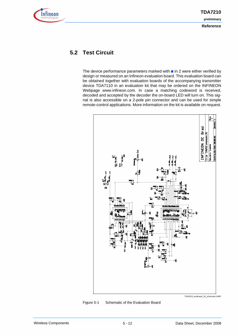
5.2 Test Circuit
The device performance parameters marked with ■ in 2 were either verified by design or measured on an Infineon evaluation board. This evaluation board can be obtained together with evaluation boards of the accompanying transmitter device TDA7110 in an evaluation kit that may be ordered on the INFINEON Webpage www.infineon.com. In case a matching codeword is received, decoded and accepted by the decoder the on-board LED will turn on. This sig-nal is also accessible on a 2-pole pin connector and can be used for simple remote-control applications. More information on the kit is available on request.
TDA5210_testboard_20_schematic.WMF
Figure 5-1 Schematic of the Evaluation Board
Reference
5 - 13
TDA7210preliminary
Wireless Components
Data Sheet, December 2008
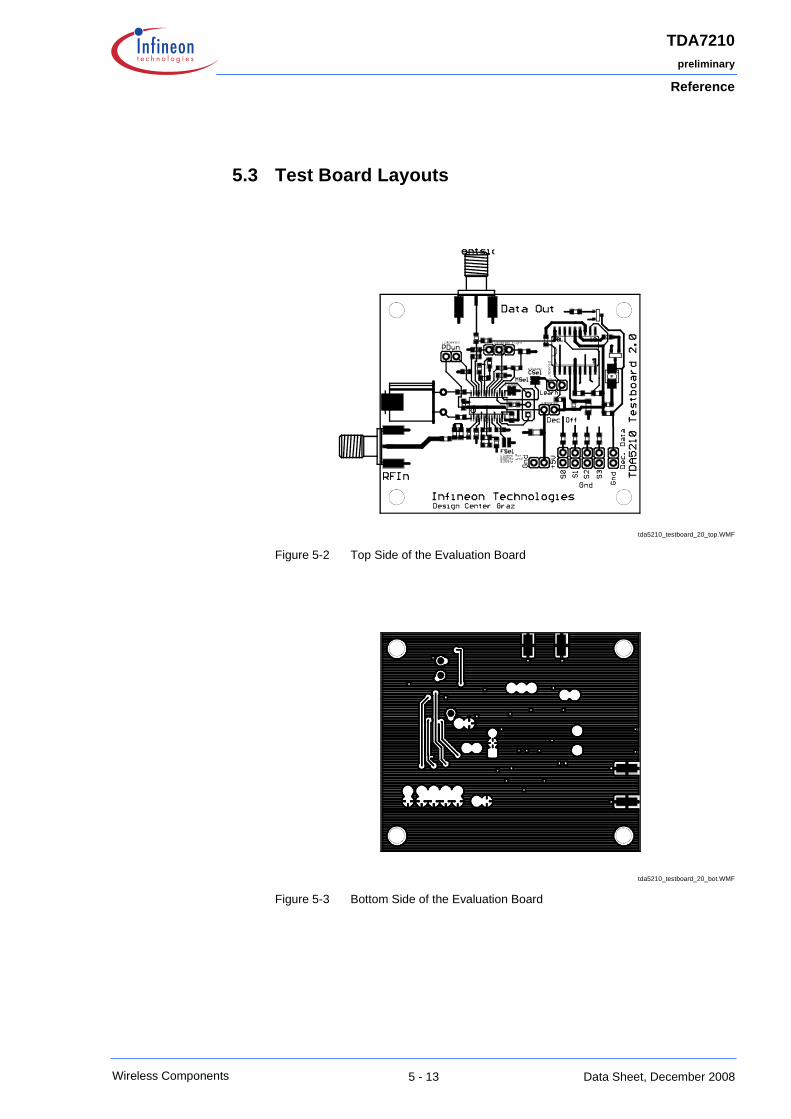
5.3 Test Board Layouts
tda5210_testboard_20_top.WMF
Figure 5-2 Top Side of the Evaluation Board
tda5210_testboard_20_bot.WMF
Figure 5-3 Bottom Side of the Evaluation Board
Reference
5 - 14
TDA7210preliminary
Wireless Components
Data Sheet, December 2008
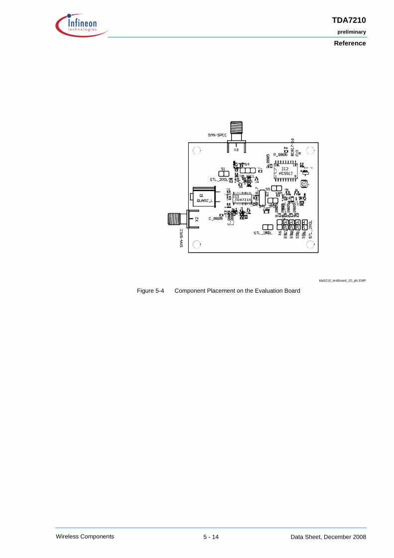
tda5210_testboard_20_plc.EMF
Figure 5-4 Component Placement on the Evaluation Board
TDA7210
Reference
5 - 15
TDA7210preliminary
Wireless Components
Data Sheet, December 2008
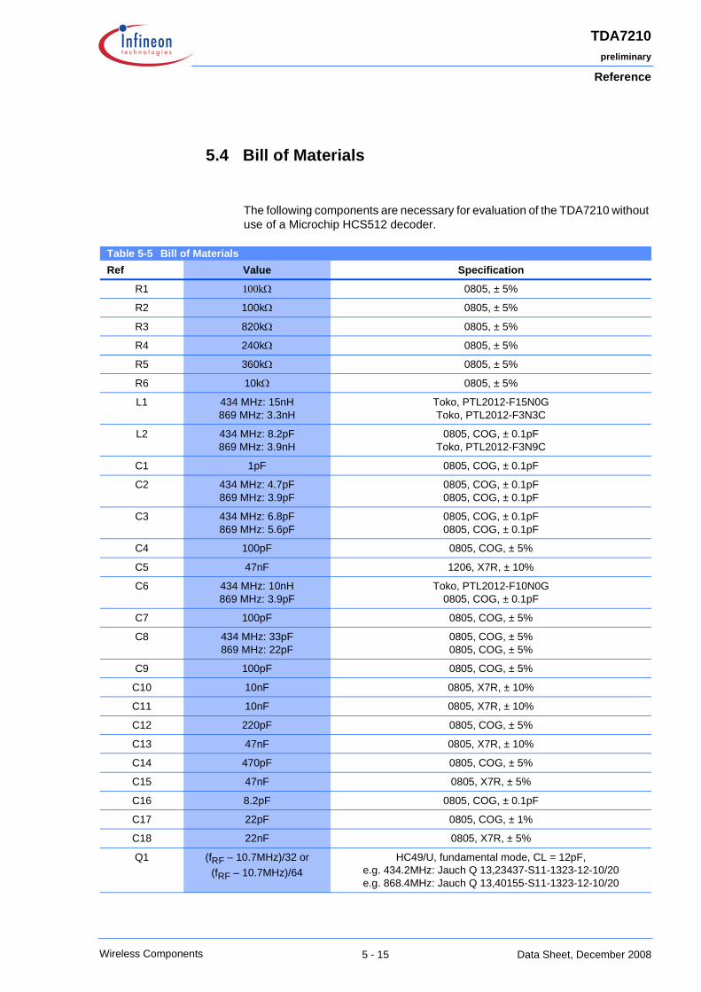
5.4 Bill of Materials
The following components are necessary for evaluation of the TDA7210 without use of a Microchip HCS512 decoder.
Table 5-5 Bill of MaterialsRef Value Specification
R1 100kΩ 0805, ± 5%
R2 100kΩ 0805, ± 5%
R3 820kΩ 0805, ± 5%
R4 240kΩ 0805, ± 5%
R5 360kΩ 0805, ± 5%
R6 10kΩ 0805, ± 5%
L1 434 MHz: 15nH869 MHz: 3.3nH
Toko, PTL2012-F15N0GToko, PTL2012-F3N3C
L2 434 MHz: 8.2pF869 MHz: 3.9nH
0805, COG, ± 0.1pFToko, PTL2012-F3N9C
C1 1pF 0805, COG, ± 0.1pF
C2 434 MHz: 4.7pF869 MHz: 3.9pF
0805, COG, ± 0.1pF0805, COG, ± 0.1pF
C3 434 MHz: 6.8pF869 MHz: 5.6pF
0805, COG, ± 0.1pF0805, COG, ± 0.1pF
C4 100pF 0805, COG, ± 5%
C5 47nF 1206, X7R, ± 10%
C6 434 MHz: 10nH869 MHz: 3.9pF
Toko, PTL2012-F10N0G0805, COG, ± 0.1pF
C7 100pF 0805, COG, ± 5%
C8 434 MHz: 33pF869 MHz: 22pF
0805, COG, ± 5%0805, COG, ± 5%
C9 100pF 0805, COG, ± 5%
C10 10nF 0805, X7R, ± 10%
C11 10nF 0805, X7R, ± 10%
C12 220pF 0805, COG, ± 5%
C13 47nF 0805, X7R, ± 10%
C14 470pF 0805, COG, ± 5%
C15 47nF 0805, X7R, ± 5%
C16 8.2pF 0805, COG, ± 0.1pF
C17 22pF 0805, COG, ± 1%
C18 22nF 0805, X7R, ± 5%
Q1 (fRF – 10.7MHz)/32 or(fRF – 10.7MHz)/64
HC49/U, fundamental mode, CL = 12pF, e.g. 434.2MHz: Jauch Q 13,23437-S11-1323-12-10/20e.g. 868.4MHz: Jauch Q 13,40155-S11-1323-12-10/20
Reference
5 - 16
TDA7210preliminary
Wireless Components
Data Sheet, December 2008
Please note that in case of operation at 434 MHz a capacitor has to be soldered in place L2 and an inductor in place C6.
The following components are necessary in addition to the above mentioned ones for evaluation of the TDA7210 in conjunction with a Microchip HCS512 decoder.
Q2 SFE10.7MA5-A orSKM107M1-A20-10
MurataToko
X2, X3 142-0701-801 Johnson
S1-S3, S6X1, X3
2-pole pin connector
S4 3-pole pin connector, or not equipped
IC1 TDA7210 Infineon
Table 5-6 Bill of Materials AddendumRef Value Specification
R7 100kΩ 0805, ± 5%
R8 10kΩ 0805, ± 5%
R9 100kΩ 0805, ± 5%
R10 22kΩ 0805, ± 5%
R11 100Ω 0805, ± 5%
R12 100Ω 0805, ± 5%
R13 100Ω 0805, ± 5%
R14 100Ω 0805, ± 5%
R21 22kΩ 0805, ± 5%
R22 10kΩ 0805, ± 5%
R23 22kΩ 0805, ± 5%
R24 820kΩ 0805, ± 5%
R25 560Ω 0805, ± 5%
C19 10pF 0805, COG, ± 5%
C21 100nF 1206, X7R, ± 10%
C22 100nF 1206, X7R, ± 10%
IC2 HCS512 Microchip
S5, X4-X9 2-pole pin connector
T1, T2 BC 847B Infineon
D1 LS T670-JL Infineon
List of Figures
List of Figures - 1
TDA7210
Wireless Components
Data Sheet, December 2008
List of Figures
Figure 2-1 PG-TSSOP-28 package outlines . . . . . . . . . . . . . . . . . . . . . . . . . . . . . . . . . . . . . . . . . . 2-3Figure 3-1 IC Pin Configuration . . . . . . . . . . . . . . . . . . . . . . . . . . . . . . . . . . . . . . . . . . . . . . . . . . . 3-2Figure 3-2 Main Block Diagram . . . . . . . . . . . . . . . . . . . . . . . . . . . . . . . . . . . . . . . . . . . . . . . . . . . 3-9Figure 4-1 LNA Automatic Gain Control Circuitry . . . . . . . . . . . . . . . . . . . . . . . . . . . . . . . . . . . . . . 4-2Figure 4-2 RSSI Level and Permissive AGC Threshold Levels . . . . . . . . . . . . . . . . . . . . . . . . . . . 4-3Figure 4-3 Data Filter Design . . . . . . . . . . . . . . . . . . . . . . . . . . . . . . . . . . . . . . . . . . . . . . . . . . . . . 4-4Figure 4-4 Determination of Series Capacitance Value for the Quartz Oscillator . . . . . . . . . . . . . . 4-5Figure 4-5 Data Slicer Threshold Generation with External R-C Integrator . . . . . . . . . . . . . . . . . . 4-7Figure 4-6 Data Slicer Threshold Generation Utilising the Peak Detector . . . . . . . . . . . . . . . . . . . 4-7Figure 4-7 ASK/FSK mode datapath . . . . . . . . . . . . . . . . . . . . . . . . . . . . . . . . . . . . . . . . . . . . . . . 4-8Figure 4-8 Frequency characterstic in case of FSK mode . . . . . . . . . . . . . . . . . . . . . . . . . . . . . . . 4-9Figure 4-9 Frequency charcteristic in case of ASK mode . . . . . . . . . . . . . . . . . . . . . . . . . . . . . . . . 4-10Figure 4-10 Principle of the precharge circuit . . . . . . . . . . . . . . . . . . . . . . . . . . . . . . . . . . . . . . . . . . 4-11Figure 4-11 Voltage appearing on C18 during precharging process . . . . . . . . . . . . . . . . . . . . . . . . 4-12Figure 4-12 Voltage transient on capacitor C13 attached to pin 20 . . . . . . . . . . . . . . . . . . . . . . . . . 4-13Figure 5-1 Schematic of the Evaluation Board . . . . . . . . . . . . . . . . . . . . . . . . . . . . . . . . . . . . . . . . 5-12Figure 5-2 Top Side of the Evaluation Board . . . . . . . . . . . . . . . . . . . . . . . . . . . . . . . . . . . . . . . . . 5-13Figure 5-3 Bottom Side of the Evaluation Board . . . . . . . . . . . . . . . . . . . . . . . . . . . . . . . . . . . . . . . 5-13Figure 5-4 Component Placement on the Evaluation Board . . . . . . . . . . . . . . . . . . . . . . . . . . . . . . 5-14
List of Tables
List of Tables - 1
TDA7210
Wireless Components
Data Sheet, December 2008
List of Tables
Table 3-1 Pin Definition and Function . . . . . . . . . . . . . . . . . . . . . . . . . . . . . . . . . . . . . . . . . . . . . . 3-3Table 3-2 FSEL Pin Operating States . . . . . . . . . . . . . . . . . . . . . . . . . . . . . . . . . . . . . . . . . . . . . . 3-11Table 3-3 CSEL Pin Operating States . . . . . . . . . . . . . . . . . . . . . . . . . . . . . . . . . . . . . . . . . . . . . . 3-11Table 3-4 MSEL Pin Operating States . . . . . . . . . . . . . . . . . . . . . . . . . . . . . . . . . . . . . . . . . . . . . . 3-12Table 3-5 PDWN Pin Operating States . . . . . . . . . . . . . . . . . . . . . . . . . . . . . . . . . . . . . . . . . . . . . 3-13Table 4-1 Dependence of PLL Overall Division Ratio on FSEL and CSEL . . . . . . . . . . . . . . . . . 4-6Table 5-1 Absolute Maximum Ratings, Ambient temperature TAMB=-40°C ... + 85°C . . . . . . . . . 5-2Table 5-2 Operating Range, Ambient temperature TAMB= -40°C ... + 85°C . . . . . . . . . . . . . . . . . 5-3Table 5-3 AC/DC Characteristics with TA 25 °C, VCC = 4.5 ... 5.5 V . . . . . . . . . . . . . . . . . . . . . . 5-4Table 5-4 AC/DC Characteristics with TAMB= -40°C ... + 85°C, VCC = 4.5 ... 5.5 V . . . . . . . . . . . 5-9Table 5-5 Bill of Materials . . . . . . . . . . . . . . . . . . . . . . . . . . . . . . . . . . . . . . . . . . . . . . . . . . . . . . . 5-15Table 5-6 Bill of Materials Addendum . . . . . . . . . . . . . . . . . . . . . . . . . . . . . . . . . . . . . . . . . . . . . . 5-16