cy3274 cypress high voltage programmable plc
TRANSCRIPT
CY3274
Cypress High VoltageProgrammable Powerline Communication
Development Kit Guide
Doc. # 001-53598 Rev. *G
Cypress Semiconductor198 Champion Court
San Jose, CA 95134-1709
Phone (USA): 800.858.1810Phone (Intnl): 408.943.2600
http://www.cypress.com

2 CY3274 Cypress High Voltage Programmable PLC Development Kit Guide, Doc. # 001-53598 Rev. *G
Copyrights
Copyrights
© Cypress Semiconductor Corporation, 2009-2014. The information contained herein is subject to change without notice.Cypress Semiconductor Corporation assumes no responsibility for the use of any circuitry other than circuitry embodied in aCypress product. Nor does it convey or imply any license under patent or other rights. Cypress products are not warrantednor intended to be used for medical, life support, life saving, critical control or safety applications, unless pursuant to anexpress written agreement with Cypress. Furthermore, Cypress does not authorize its products for use as critical componentsin life-support systems where a malfunction or failure may reasonably be expected to result in significant injury to the user.The inclusion of Cypress products in life-support systems application implies that the manufacturer assumes all risk of suchuse and in doing so indemnifies Cypress against all charges.
Any Source Code (software and/or firmware) is owned by Cypress Semiconductor Corporation (Cypress) and is protected byand subject to worldwide patent protection (United States and foreign), United States copyright laws and international treatyprovisions. Cypress hereby grants to licensee a personal, non-exclusive, non-transferable license to copy, use, modify, createderivative works of, and compile the Cypress Source Code and derivative works for the sole purpose of creating custom soft-ware and or firmware in support of licensee product to be used only in conjunction with a Cypress integrated circuit as speci-fied in the applicable agreement. Any reproduction, modification, translation, compilation, or representation of this SourceCode except as specified above is prohibited without the express written permission of Cypress.
Disclaimer: CYPRESS MAKES NO WARRANTY OF ANY KIND, EXPRESS OR IMPLIED, WITH REGARD TO THIS MATE-RIAL, INCLUDING, BUT NOT LIMITED TO, THE IMPLIED WARRANTIES OF MERCHANTABILITY AND FITNESS FOR APARTICULAR PURPOSE. Cypress reserves the right to make changes without further notice to the materials describedherein. Cypress does not assume any liability arising out of the application or use of any product or circuit described herein.Cypress does not authorize its products for use as critical components in life-support systems where a malfunction or failuremay reasonably be expected to result in significant injury to the user. The inclusion of Cypress’ product in a life-support sys-tems application implies that the manufacturer assumes all risk of such use and in doing so indemnifies Cypress against allcharges.
Use may be limited by and subject to the applicable Cypress software license agreement.
PSoC® is a registered trademark of Cypress Semiconductor Corporation. All products and company names mentioned in thisdocument may be the trademarks of their respective holders.
Purchase of I2C components from Cypress or one of its sublicensed Associated Companies conveys a license under thePhilips I2C Patent Rights to use these components in an I2C system, provided that the system conforms to the I2C StandardSpecification as defined by Philips. As from October 1st, 2006 Philips Semiconductors has a new trade name - NXP Semicon-ductors.
Flash Code Protection
Cypress products meet the specifications contained in their particular Cypress PSoC Data Sheets. Cypress believes that itsfamily of PSoC products is one of the most secure families of its kind on the market today, regardless of how they are used.There may be methods, unknown to Cypress, that can breach the code protection features. Any of these methods, to ourknowledge, would be dishonest and possibly illegal. Neither Cypress nor any other semiconductor manufacturer can guaran-tee the security of their code. Code protection does not mean that we are guaranteeing the product as "unbreakable."
Cypress is willing to work with the customer who is concerned about the integrity of their code. Code protection is constantlyevolving. We at Cypress are committed to continuously improving the code protection features of our products.
CY3274 Cypress High Voltage Programmable PLC Development Kit Guide, Doc. # 001-53598 Rev. *G 3
Contents
Safety Information 5
1. Introduction 71.1 Kit Contents .................................................................................................................71.2 Using the PLC Kit ........................................................................................................81.3 The Cypress PLC Solution ..........................................................................................81.4 Additional Learning Resources..................................................................................101.5 Acronyms...................................................................................................................111.6 Documentation Conventions......................................................................................121.7 Technical Reference..................................................................................................121.8 Technical Support ......................................................................................................12
2. Getting Started 132.1 Software Installation ..................................................................................................13
2.1.1 Before You Begin ...........................................................................................132.1.2 Prerequisites ..................................................................................................132.1.3 Installing PLC Control Panel Independently...................................................14
2.2 Kit Installation ............................................................................................................172.3 PSoC Designer ..........................................................................................................212.4 PSoC Programmer ....................................................................................................222.5 Uninstall Software......................................................................................................22
2.5.1 Uninstalling the PLC Control Panel Software.................................................22
3. Kit Operation and PLC Control Panel GUI 23
3.1 Theory of Operation...................................................................................................233.1.1 CY8CPLC20 Device Description....................................................................23
3.2 Functional Description ...............................................................................................253.2.1 Operating Conditions .....................................................................................25
3.3 PLC Control Panel GUI..............................................................................................253.3.1 Program CY3274 Boards with I2C-PLC Interface..........................................253.3.2 PLC Control Panel Quick Start.......................................................................273.3.3 PLC Control Panel Tabs.................................................................................30
4. PLC Development Board 41
4.1 Board Details .............................................................................................................414.2 CY3274 PLC Development Board Functional Overview ...........................................41
4.2.1 Operating Conditions .....................................................................................414.3 Hardware Description ................................................................................................42
4.3.1 Development ..................................................................................................434.3.2 LCD Daughter Card .......................................................................................464.3.3 RJ45 Connector for Debugging......................................................................474.3.4 RS232 COM Port ...........................................................................................47
4 CY3274 Cypress High Voltage Programmable PLC Development Kit Guide, Doc. # 001-53598 Rev. *G
Contents
4.3.5 High Voltage with Switched Mode Power Supply (SMPS).............................484.3.6 Transmit Filter, Transmit Amplifier, and Receive Filter...................................484.3.7 High Voltage Coupling Circuit ........................................................................49
5. Code Examples 51
5.1 Code Example ...........................................................................................................515.2 PLC Demo.................................................................................................................51
5.2.1 Software Requirements .................................................................................515.2.2 Using the PLT User Module in an Example Project .......................................525.2.3 Evaluating the Example Project on Hardware ...............................................595.2.4 Hardware Setup.............................................................................................62
5.3 Using CY3274 with PLC Control Panel using CY3240 I2USB Bridge.......................645.3.1 Software Requirements .................................................................................655.3.2 PLT Configuration ..........................................................................................655.3.3 I2C Interface Write Packet Structure..............................................................675.3.4 I2C Interface Read Packet Structure .............................................................675.3.5 I2C Application...............................................................................................675.3.6 I2C Host Example..........................................................................................685.3.7 Evaluating the Example Project on Hardware with PLC Control Panel GUI..68
A. Appendix 69A.1 Schematics ................................................................................................................69
A.1.1 Board Overview .............................................................................................69A.1.2 User Interface ................................................................................................70A.1.3 Transmit and Receive Filters and Coupling ...................................................71A.1.4 Power Supply.................................................................................................72
A.2 Layout........................................................................................................................73A.2.1 Top Layer.......................................................................................................73A.2.2 Ground Layer .................................................................................................74A.2.3 Power Layer...................................................................................................75A.2.4 Bottom Layer .................................................................................................76A.2.5 Top Silkscreen ...............................................................................................77A.2.6 Bottom Silkscreen..........................................................................................78
A.3 Bill of Materials ..........................................................................................................79
Revision History 85
CY3274 Cypress High Voltage Programmable PLC Development Kit Guide, Doc. # 001-53598 Rev. *G 5
Safety Information
The “High Voltage Programmable Power Line Communication Development Kit” CY3274 is intendedfor use as a development platform for hardware or software in a laboratory environment. The boardis an open system design, which does not include a shielded enclosure. Due to this reason the boardmay cause interference to other electrical or electronic devices in close proximity. In a domesticenvironment, this product may cause radio interference. In such cases, the user may be required totake adequate preventive measures. Also, this board should not be used near any medicalequipment or RF devices.
Attaching additional wiring to this product or modifying the product operation from the factory defaultmay affect its performance and cause interference with other apparatus in the immediate vicinity. Ifsuch interference is detected, suitable mitigating measures should be taken.
6 CY3274 Cypress High Voltage Programmable PLC Development Kit Guide, Doc. # 001-53598 Rev. *G
Safety Information
General Safety Instructions
ESD Protection
ESD can damage boards and associated components. Cypress recommends that the user performprocedures only at an ESD workstation. If ESD workstation is not available, use appropriate ESDprotection by wearing an antistatic wrist strap attached to the chassis ground (any unpainted metalsurface) on the board when handling parts.
Handling Boards
CY3274 boards are sensitive to ESD. Hold the board only by its edges. After removing the boardfrom its box, place it on a grounded, static free surface. Use a conductive foam pad if available. Donot slide board over any surface.
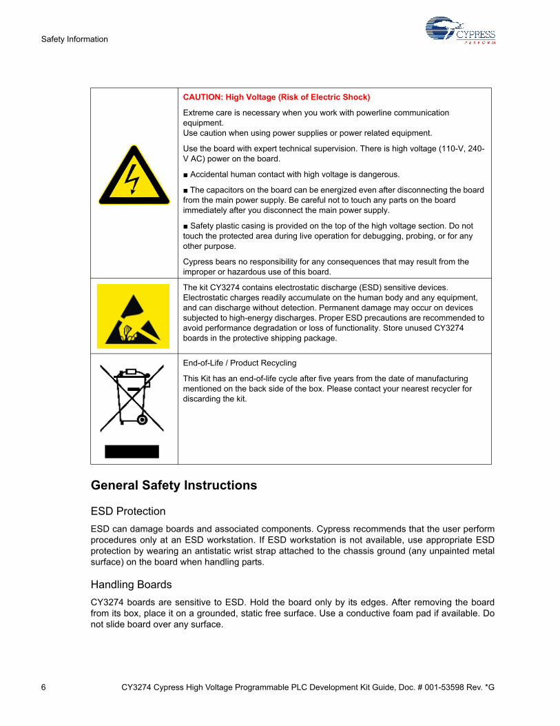
CAUTION: High Voltage (Risk of Electric Shock)
Extreme care is necessary when you work with powerline communication equipment. Use caution when using power supplies or power related equipment.
Use the board with expert technical supervision. There is high voltage (110-V, 240-V AC) power on the board.
■ Accidental human contact with high voltage is dangerous.
■ The capacitors on the board can be energized even after disconnecting the board from the main power supply. Be careful not to touch any parts on the board immediately after you disconnect the main power supply.
■ Safety plastic casing is provided on the top of the high voltage section. Do not touch the protected area during live operation for debugging, probing, or for any other purpose.
Cypress bears no responsibility for any consequences that may result from the improper or hazardous use of this board.
The kit CY3274 contains electrostatic discharge (ESD) sensitive devices. Electrostatic charges readily accumulate on the human body and any equipment, and can discharge without detection. Permanent damage may occur on devices subjected to high-energy discharges. Proper ESD precautions are recommended to avoid performance degradation or loss of functionality. Store unused CY3274 boards in the protective shipping package.
End-of-Life / Product Recycling
This Kit has an end-of-life cycle after five years from the date of manufacturing mentioned on the back side of the box. Please contact your nearest recycler for discarding the kit.
CY3274 Cypress High Voltage Programmable PLC Development Kit Guide, Doc. # 001-53598 Rev. *G 7
1. Introduction
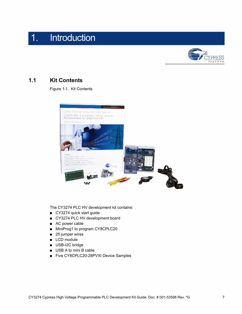
1.1 Kit Contents
Figure 1-1. Kit Contents
The CY3274 PLC HV development kit contains:■ CY3274 quick start guide■ CY3274 PLC HV development board■ AC power cable■ MiniProg1 to program CY8CPLC20■ 25 jumper wires ■ LCD module■ USB-I2C bridge■ USB A to mini B cable■ Five CY8CPLC20-28PVXI Device Samples
8 CY3274 Cypress High Voltage Programmable PLC Development Kit Guide, Doc. # 001-53598 Rev. *G
Introduction
1.2 Using the PLC Kit
Cypress’s Powerline Communication Solution (PLC) makes it possible to transmit and receive dataand control data over high voltage and low voltage powerlines. This solution is developed for lowbandwidth powerline communication.
The CY3274 PLC high voltage (HV) PLC development kit provides the capability to develop anapplication on the Cypress CY8CPLC20 device that can transmit and receive data over high voltage(110 V to 240 V AC) powerlines.
■ Introduction chapter on page 7 provides a brief overview of the Cypress PLC solution. Itdescribes the contents of the CY3274 development kits and lists special features of the kit.
■ Getting Started chapter on page 13 provides information on kit software and process for itsinstallation as well as hardware connections.
■ PLC Development Board chapter on page 41 gives the functional overview of the PLC board anddescribes the operating procedure of PLC HV board. It provides a high level hardwaredescription of the board.
■ Code Examples chapter on page 51 provides explanation on the example projects and working.
■ Appendix chapter on page 69 contains the schematics, layout, and bill of materials.
1.3 The Cypress PLC Solution
Powerlines are available everywhere in the world. This makes them one of the most widely availablecommunication media. The pervasiveness of powerlines also makes it difficult to predict theircharacteristics and noise. Because of the variability of powerline quality, implementing robustcommunication over powerline has been an engineering challenge for years. With this in mind, theCypress PLC solution is designed to enable secure, reliable, and robust communication overpowerlines.
The key features of the Cypress PLC solution are:
■ An integrated powerline PHY modem with optimized filters and amplifiers that work with rugged high and low voltage powerlines
■ Powerline optimized network protocol that supports bidirectional communication with acknowledgement based signaling and multiple retries
■ Support for 8-bit packet CRC and 4-bit header CRC for error detection and data packet retransmission
■ Carrier Sense Multiple Access (CSMA) scheme that minimizes collisions between packet transmissions on the powerline
CY3274 Cypress High Voltage Programmable PLC Development Kit Guide, Doc. # 001-53598 Rev. *G 9
Introduction
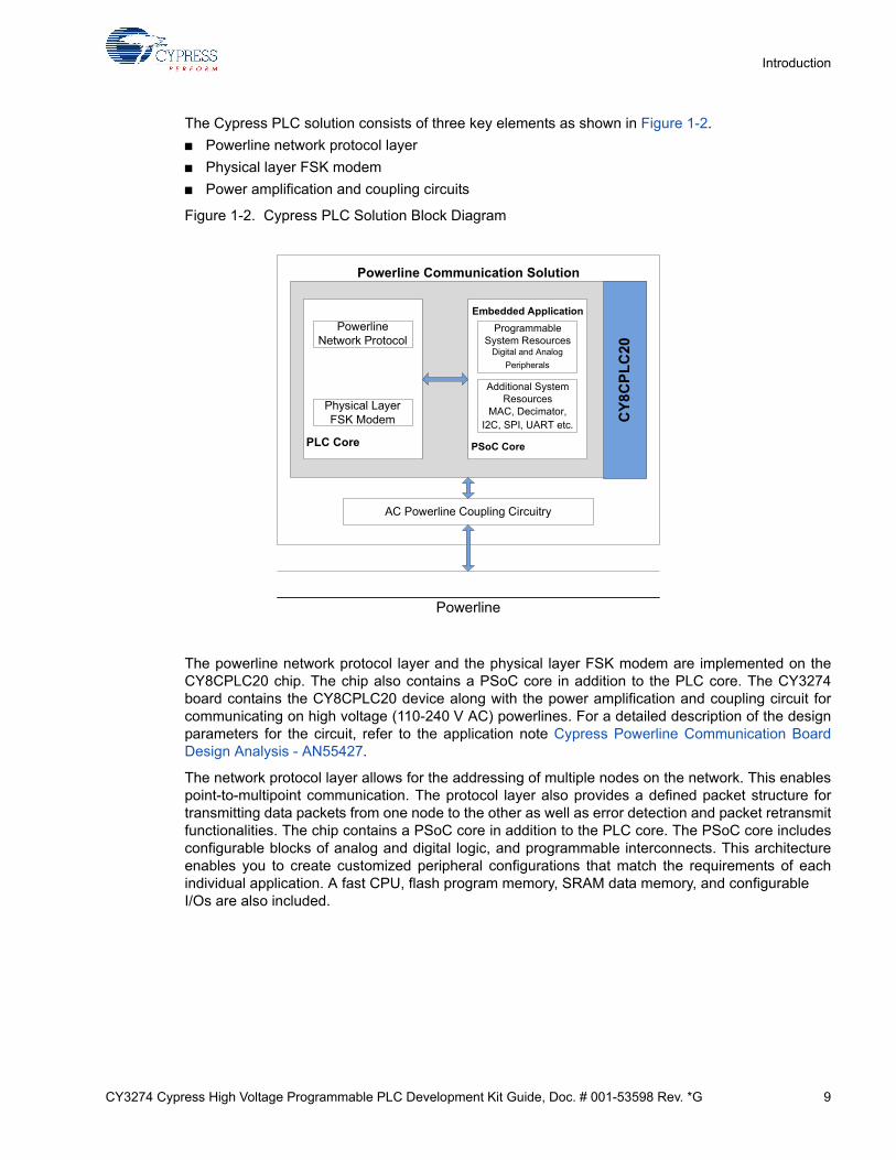
The Cypress PLC solution consists of three key elements as shown in Figure 1-2.
■ Powerline network protocol layer
■ Physical layer FSK modem
■ Power amplification and coupling circuits
Figure 1-2. Cypress PLC Solution Block Diagram
The powerline network protocol layer and the physical layer FSK modem are implemented on theCY8CPLC20 chip. The chip also contains a PSoC core in addition to the PLC core. The CY3274board contains the CY8CPLC20 device along with the power amplification and coupling circuit forcommunicating on high voltage (110-240 V AC) powerlines. For a detailed description of the designparameters for the circuit, refer to the application note Cypress Powerline Communication BoardDesign Analysis - AN55427.
The network protocol layer allows for the addressing of multiple nodes on the network. This enablespoint-to-multipoint communication. The protocol layer also provides a defined packet structure fortransmitting data packets from one node to the other as well as error detection and packet retransmitfunctionalities. The chip contains a PSoC core in addition to the PLC core. The PSoC core includesconfigurable blocks of analog and digital logic, and programmable interconnects. This architectureenables you to create customized peripheral configurations that match the requirements of eachindividual application. A fast CPU, flash program memory, SRAM data memory, and configurable I/Os are also included.
Powerline Communication Solution
CY
8C
PL
C20
PLC Core
Embedded Application
PSoC Core
Powerline Network Protocol
Physical Layer FSK Modem
Programmable System Resources
Digital and Analog
Peripherals
Additional System Resources
MAC, Decimator, I2C, SPI, UART etc.
AC Powerline Coupling Circuitry
Powerline
10 CY3274 Cypress High Voltage Programmable PLC Development Kit Guide, Doc. # 001-53598 Rev. *G
Introduction
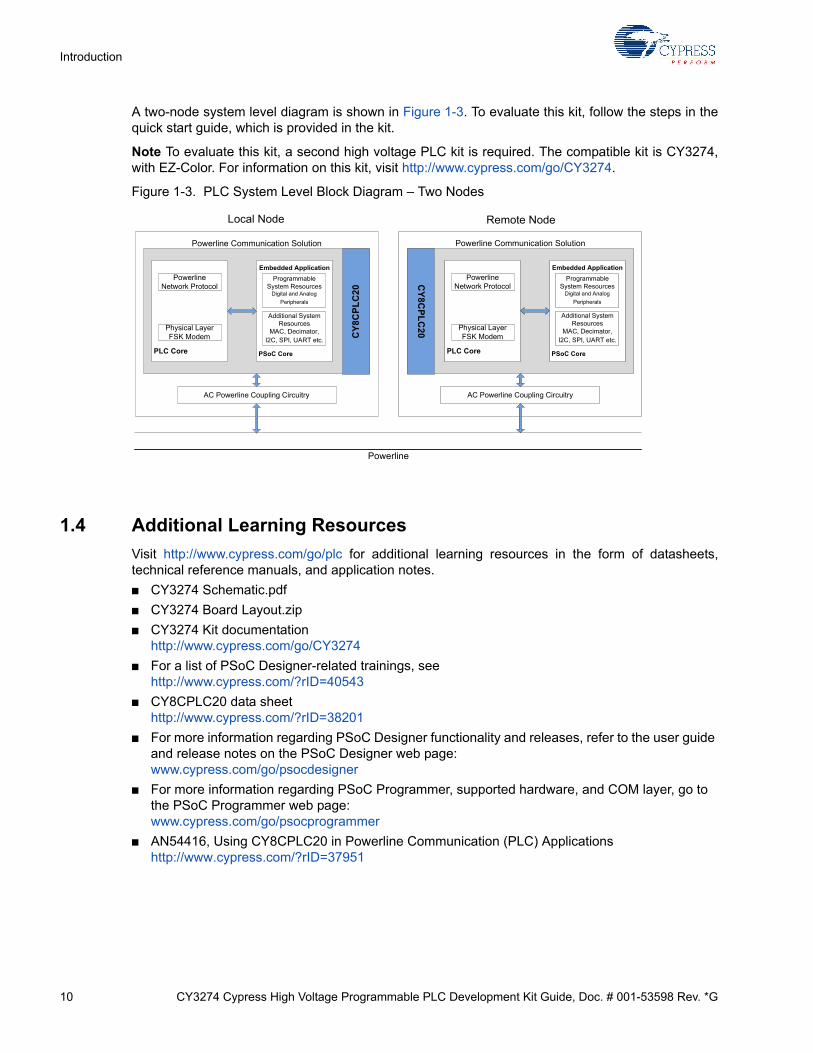
A two-node system level diagram is shown in Figure 1-3. To evaluate this kit, follow the steps in thequick start guide, which is provided in the kit.
Note To evaluate this kit, a second high voltage PLC kit is required. The compatible kit is CY3274,with EZ-Color. For information on this kit, visit http://www.cypress.com/go/CY3274.
Figure 1-3. PLC System Level Block Diagram – Two Nodes
1.4 Additional Learning Resources
Visit http://www.cypress.com/go/plc for additional learning resources in the form of datasheets,technical reference manuals, and application notes.
■ CY3274 Schematic.pdf
■ CY3274 Board Layout.zip
■ CY3274 Kit documentationhttp://www.cypress.com/go/CY3274
■ For a list of PSoC Designer-related trainings, seehttp://www.cypress.com/?rID=40543
■ CY8CPLC20 data sheethttp://www.cypress.com/?rID=38201
■ For more information regarding PSoC Designer functionality and releases, refer to the user guide and release notes on the PSoC Designer web page:www.cypress.com/go/psocdesigner
■ For more information regarding PSoC Programmer, supported hardware, and COM layer, go to the PSoC Programmer web page:www.cypress.com/go/psocprogrammer
■ AN54416, Using CY8CPLC20 in Powerline Communication (PLC) Applicationshttp://www.cypress.com/?rID=37951
Powerline Communication Solution
CY
8CP
LC
20
PLC Core
Embedded Application
PSoC Core
Powerline Network Protocol
Physical Layer FSK Modem
Programmable System Resources
Digital and Analog
Peripherals
Additional System Resources
MAC, Decimator, I2C, SPI, UART etc.
AC Powerline Coupling Circuitry
Powerline Communication Solution
CY
8CP
LC
20
PLC Core
Embedded Application
PSoC Core
Powerline Network Protocol
Physical Layer FSK Modem
Programmable System Resources
Digital and Analog
Peripherals
Additional System Resources
MAC, Decimator, I2C, SPI, UART etc.
AC Powerline Coupling Circuitry
Powerline
Local Node Remote Node
CY3274 Cypress High Voltage Programmable PLC Development Kit Guide, Doc. # 001-53598 Rev. *G 11
Introduction
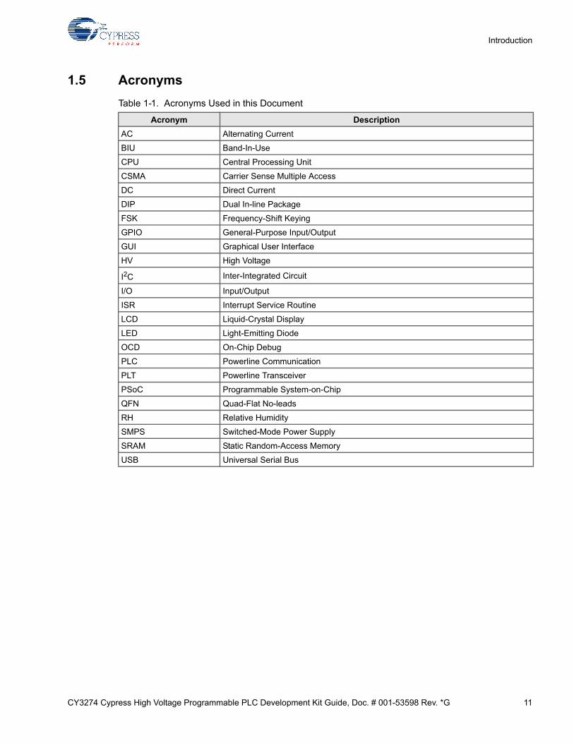
1.5 Acronyms
Table 1-1. Acronyms Used in this Document
Acronym Description
AC Alternating Current
BIU Band-In-Use
CPU Central Processing Unit
CSMA Carrier Sense Multiple Access
DC Direct Current
DIP Dual In-line Package
FSK Frequency-Shift Keying
GPIO General-Purpose Input/Output
GUI Graphical User Interface
HV High Voltage
I2C Inter-Integrated Circuit
I/O Input/Output
ISR Interrupt Service Routine
LCD Liquid-Crystal Display
LED Light-Emitting Diode
OCD On-Chip Debug
PLC Powerline Communication
PLT Powerline Transceiver
PSoC Programmable System-on-Chip
QFN Quad-Flat No-leads
RH Relative Humidity
SMPS Switched-Mode Power Supply
SRAM Static Random-Access Memory
USB Universal Serial Bus
12 CY3274 Cypress High Voltage Programmable PLC Development Kit Guide, Doc. # 001-53598 Rev. *G
Introduction
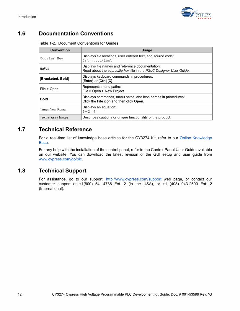
1.6 Documentation Conventions
1.7 Technical Reference
For a real-time list of knowledge base articles for the CY3274 Kit, refer to our Online KnowledgeBase.
For any help with the installation of the control panel, refer to the Control Panel User Guide availableon our website. You can download the latest revision of the GUI setup and user guide fromwww.cypress.com/go/plc.
1.8 Technical Support
For assistance, go to our support: http://www.cypress.com/support web page, or contact ourcustomer support at +1(800) 541-4736 Ext. 2 (in the USA), or +1 (408) 943-2600 Ext. 2(International).
Table 1-2. Document Conventions for Guides
Convention Usage
Courier NewDisplays file locations, user entered text, and source code:C:\ ...cd\icc\
ItalicsDisplays file names and reference documentation:Read about the sourcefile.hex file in the PSoC Designer User Guide.
[Bracketed, Bold]Displays keyboard commands in procedures:[Enter] or [Ctrl] [C]
File > OpenRepresents menu paths:File > Open > New Project
BoldDisplays commands, menu paths, and icon names in procedures:Click the File icon and then click Open.
Times New RomanDisplays an equation:2 + 2 = 4
Text in gray boxes Describes cautions or unique functionality of the product.
CY3274 Cypress High Voltage Programmable PLC Development Kit Guide, Doc. # 001-53598 Rev. *G 13
2. Getting Started
This chapter describes how to install and configure the CY3274-HV PLC Development Kit.
2.1 Software Installation
2.1.1 Before You Begin
All Cypress software installations require administrator privileges; however, this is not required to runthe installed software.
■ Shutdown any Cypress software that is currently running.
■ Disconnect any Cypress devices (USB-I2C bridge, ICE Cube, or MiniProg) from your computer.
■ If you have a previous installation of the PLC Control Panel GUI, uninstall it first. To uninstall the software, go to Start > Control Panel > Add or Remove Programs (for XP)/Programs and Features (for Win 7) and click the Remove/Uninstall button adjacent to the particular software. Follow the instructions to uninstall.
2.1.2 Prerequisites
The PLC Control Panel GUI requires the 3.5 SP1 or later version of Microsoft .NET Framework,Adobe Acrobat Reader, and a Windows Installer.
14 CY3274 Cypress High Voltage Programmable PLC Development Kit Guide, Doc. # 001-53598 Rev. *G
Getting Started
2.1.3 Installing PLC Control Panel Independently
2.1.3.1 Before You Begin
All Cypress software installations require administrator privileges; but this is not required to run theinstalled software.
■ Shut down any Cypress software that is currently running.
■ Disconnect any ICE-Cube, USB-I2C Bridge, or MiniProg devices from your computer.
■ If you have a previous installation of the PLC Control Panel GUI, uninstall it first. To uninstall the software, go to Start > Control Panel > Add or Remove Programs (for XP)/Programs and Features (for Win 7) and click the Remove/Uninstall button adjacent to the particular software. Follow the instructions to uninstall.
2.1.3.2 Prerequisites
The following software is required for the PLC Control Panel:
Microsoft .NET Framework 3.5 SP1 or later
To check if this software is installed, go to Start> Control Panel> Add/Remove Programs(for XP)/Programs and Features (for Win 7). This software can be downloaded from: http://www.microsoft.com/downloads/details.aspx?Fami-lyID=AB99342F-5D1A-413D-8319-81DA479AB0D7&displaylang=en
Windows Installer 3.1 or later
To check if this software is installed, go to Start> Control Panel> Add/Remove Programs. Thissoftware can be downloaded from: http://www.microsoft.com/downloads/details.aspx?Fami-lyID=889482FC-5F56-4A38-B838-DE776FD4138C&displaylang=en
2.1.3.3 Installing PLC Control Panel Software
When installing the PLC Control Panel, the installer checks if the prerequisites - Windows Installer,Windows.NET, and Acrobat Reader - are installed in your PC. If these applications are not installed,then the installer prompts you to install them.
1. Download the PLC Control Panel GUI.zip from http://www.cypress.com/?rID=38135 and extract it.
2. Run the setup.exe file to start the installer.
CY3274 Cypress High Voltage Programmable PLC Development Kit Guide, Doc. # 001-53598 Rev. *G 15
Getting Started
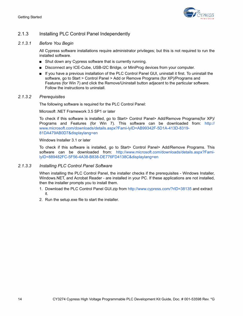
3. As specified, this installation process first determines if you have all prerequisite software. Follow the on-screen dialogs to complete all required installations.
Figure 2-1. Installation Wizard
4. Click the Next button in Figure 2-1.
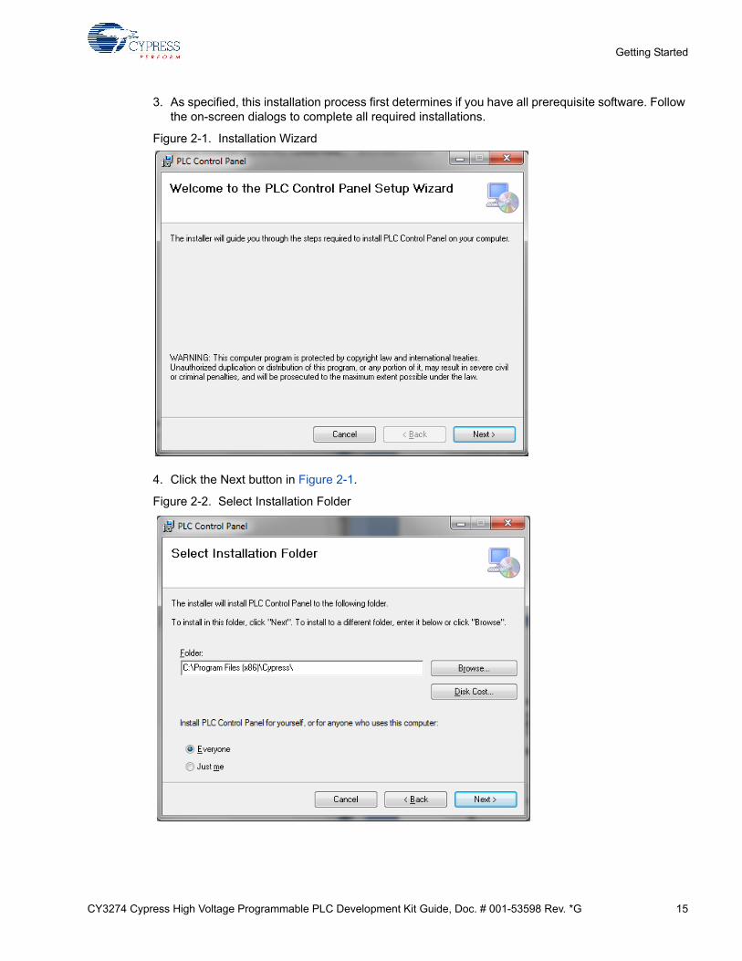
Figure 2-2. Select Installation Folder
16 CY3274 Cypress High Voltage Programmable PLC Development Kit Guide, Doc. # 001-53598 Rev. *G
Getting Started
5. Click Browse to select Installation Folder and then click the Next button in Figure 2-2.
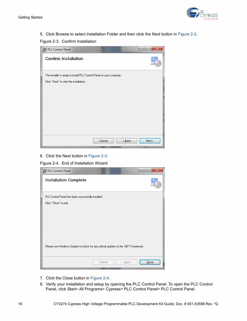
Figure 2-3. Confirm Installation
6. Click the Next button in Figure 2-3.
Figure 2-4. End of Installation Wizard
7. Click the Close button in Figure 2-4.
8. Verify your installation and setup by opening the PLC Control Panel. To open the PLC Control Panel, click Start> All Programs> Cypress> PLC Control Panel> PLC Control Panel.
CY3274 Cypress High Voltage Programmable PLC Development Kit Guide, Doc. # 001-53598 Rev. *G 17
Getting Started
9. Continue to the next section to learn how to evaluate the PLC Control Panel with two PLC evaluation or development kits.
After installing PLC Control Panel, refer to the documentation as needed:
<Install_Dir>\PLC Control Panel\PLC Control Panel Release Notes.pdf
<Install_Dir>\PLC Control Panel\User Guide for Cypress PLC Control Panel GUI.pdf
The PLC Control Panel user guide is also available in the installation directory. It contains extrainformation about installation and how to set up the kit to work with the GUI. It can also be accessedfrom the Help menu in the PLC Control Panel GUI.
2.2 Kit Installation
To install the kit software, follow these steps:
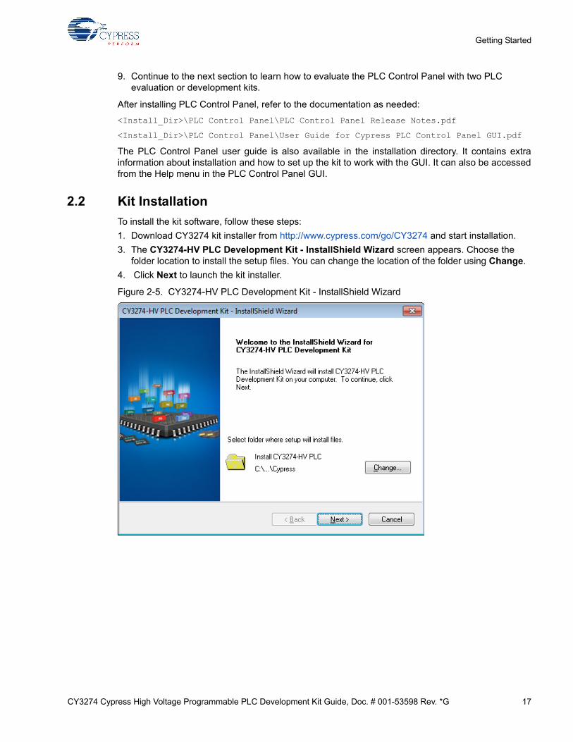
1. Download CY3274 kit installer from http://www.cypress.com/go/CY3274 and start installation.
3. The CY3274-HV PLC Development Kit - InstallShield Wizard screen appears. Choose the folder location to install the setup files. You can change the location of the folder using Change.
4. Click Next to launch the kit installer.
Figure 2-5. CY3274-HV PLC Development Kit - InstallShield Wizard
18 CY3274 Cypress High Voltage Programmable PLC Development Kit Guide, Doc. # 001-53598 Rev. *G
Getting Started
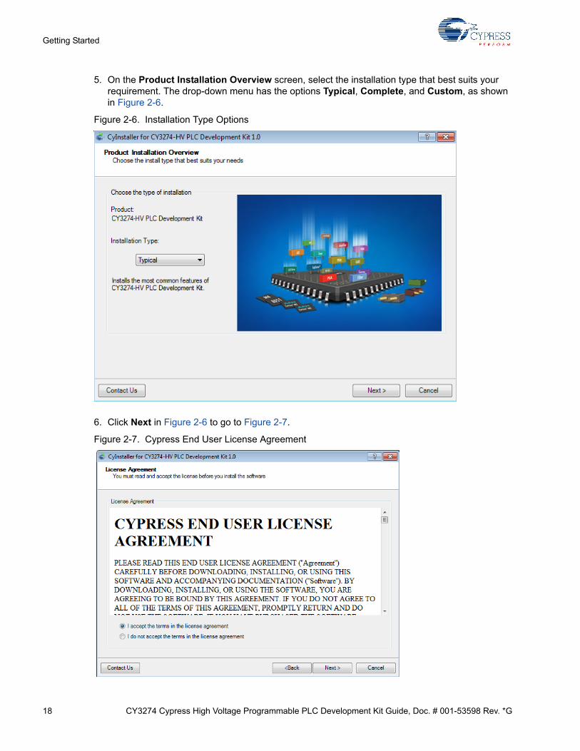
5. On the Product Installation Overview screen, select the installation type that best suits your requirement. The drop-down menu has the options Typical, Complete, and Custom, as shown in Figure 2-6.
Figure 2-6. Installation Type Options
6. Click Next in Figure 2-6 to go to Figure 2-7.
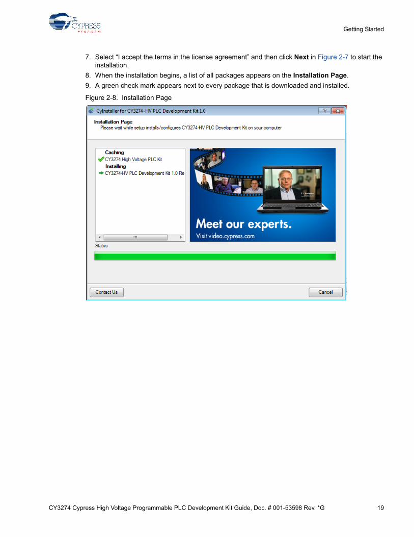
Figure 2-7. Cypress End User License Agreement
CY3274 Cypress High Voltage Programmable PLC Development Kit Guide, Doc. # 001-53598 Rev. *G 19
Getting Started
7. Select “I accept the terms in the license agreement” and then click Next in Figure 2-7 to start the installation.
8. When the installation begins, a list of all packages appears on the Installation Page.
9. A green check mark appears next to every package that is downloaded and installed.
Figure 2-8. Installation Page
20 CY3274 Cypress High Voltage Programmable PLC Development Kit Guide, Doc. # 001-53598 Rev. *G
Getting Started
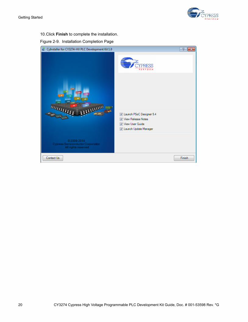
10.Click Finish to complete the installation.
Figure 2-9. Installation Completion Page
CY3274 Cypress High Voltage Programmable PLC Development Kit Guide, Doc. # 001-53598 Rev. *G 21
Getting Started
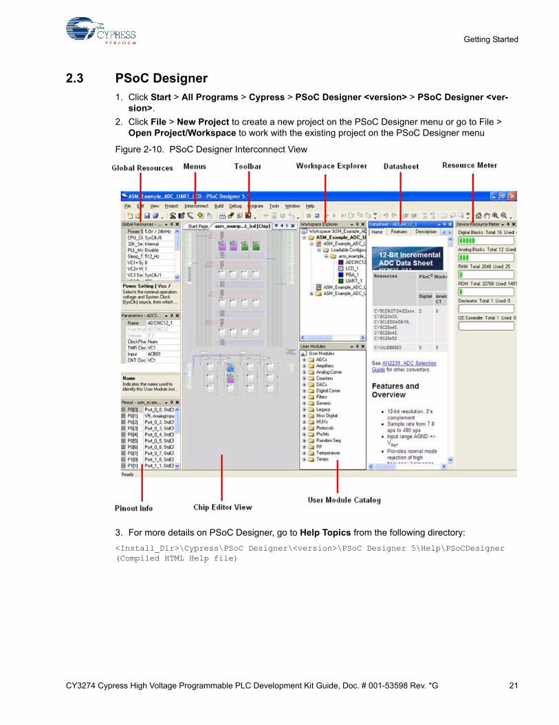
2.3 PSoC Designer1. Click Start > All Programs > Cypress > PSoC Designer <version> > PSoC Designer <ver-
sion>.
2. Click File > New Project to create a new project on the PSoC Designer menu or go to File > Open Project/Workspace to work with the existing project on the PSoC Designer menu
Figure 2-10. PSoC Designer Interconnect View
3. For more details on PSoC Designer, go to Help Topics from the following directory:
<Install_Dir>\Cypress\PSoC Designer\<version>\PSoC Designer 5\Help\PSoCDesigner(Compiled HTML Help file)
22 CY3274 Cypress High Voltage Programmable PLC Development Kit Guide, Doc. # 001-53598 Rev. *G
Getting Started
2.4 PSoC Programmer1. Click Start > All Programs > Cypress > PSoC Programmer <version> > PSoC Programmer
<version>.
2. Connect the MiniProg from Port Selection.
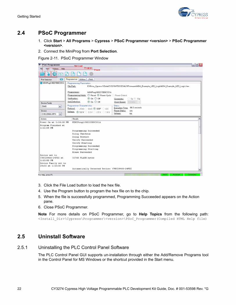
Figure 2-11. PSoC Programmer Window
3. Click the File Load button to load the hex file.
4. Use the Program button to program the hex file on to the chip.
5. When the file is successfully programmed, Programming Succeeded appears on the Action pane.
6. Close PSoC Programmer.
Note For more details on PSoC Programmer, go to Help Topics from the following path:<Install_Dir>\Cypress\Programmer\<version>\PSoC_Programmer(Compiled HTML Help file)
2.5 Uninstall Software
2.5.1 Uninstalling the PLC Control Panel Software
The PLC Control Panel GUI supports un-installation through either the Add/Remove Programs toolin the Control Panel for MS Windows or the shortcut provided in the Start menu.
CY3274 Cypress High Voltage Programmable PLC Development Kit Guide, Doc. # 001-53598 Rev. *G 23
3. Kit Operation and PLC Control Panel GUI
This chapter explains kit operation and PLC Control Panel GUI.
3.1 Theory of Operation
The Cypress PLC family is a single chip solution for powerline communication (PLC). The solutionhas a robust FSK modem with a user-friendly powerline network protocol. CY3274 has a simplepowerline coupling circuit to create a low-cost communication interface using the existing powerlines. This interface can be used for intelligent command and control systems such as:
■ Lighting control
■ Automatic meter reading
■ Home automation
Figure 3-1 shows a block diagram of the Cypress CY8CPLC20 PLC Solution. To interface theCY8CPLC20 device to the powerline, a coupling circuit is required.
Complete PLC evaluation and development kits, compliant with PLC standards in Europe and NorthAmerica, are available at www.cypress.com/go/plc.
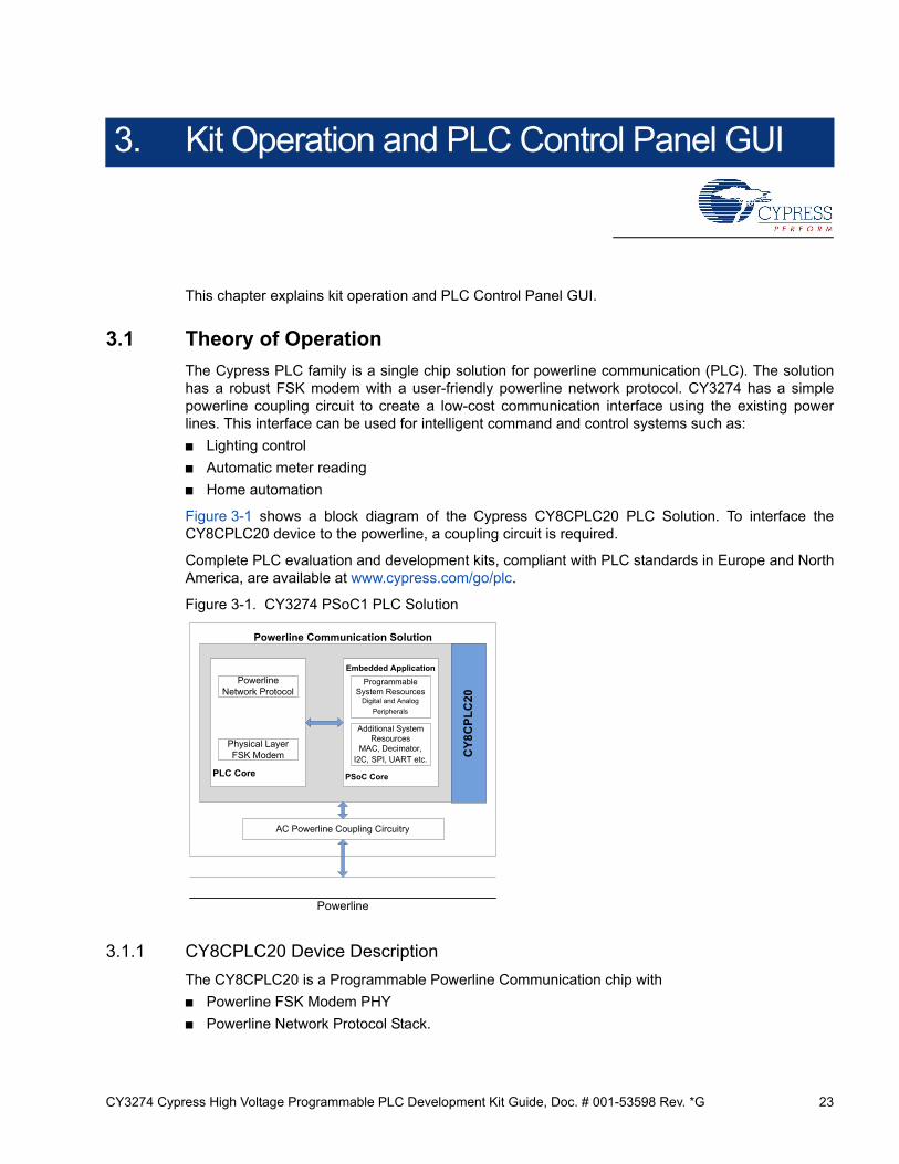
Figure 3-1. CY3274 PSoC1 PLC Solution
3.1.1 CY8CPLC20 Device Description
The CY8CPLC20 is a Programmable Powerline Communication chip with
■ Powerline FSK Modem PHY
■ Powerline Network Protocol Stack.
Powerline Communication Solution
CY
8C
PL
C20
PLC Core
Embedded Application
PSoC Core
Powerline Network Protocol
Physical Layer FSK Modem
Programmable System Resources
Digital and Analog
Peripherals
Additional System Resources
MAC, Decimator, I2C, SPI, UART etc.
AC Powerline Coupling Circuitry
Powerline
24 CY3274 Cypress High Voltage Programmable PLC Development Kit Guide, Doc. # 001-53598 Rev. *G
Kit Operation and PLC Control Panel GUI
3.1.1.1 Powerline FSK Modem PHY
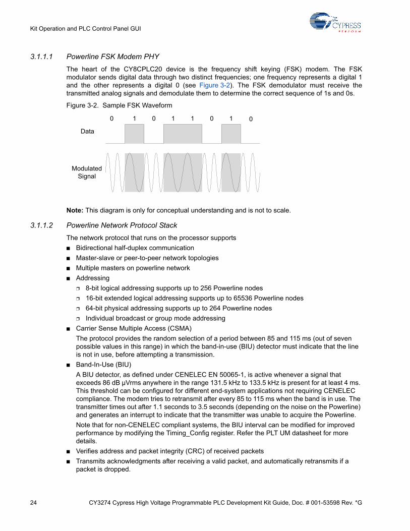
The heart of the CY8CPLC20 device is the frequency shift keying (FSK) modem. The FSKmodulator sends digital data through two distinct frequencies; one frequency represents a digital 1and the other represents a digital 0 (see Figure 3-2). The FSK demodulator must receive thetransmitted analog signals and demodulate them to determine the correct sequence of 1s and 0s.
Figure 3-2. Sample FSK Waveform
Note: This diagram is only for conceptual understanding and is not to scale.
3.1.1.2 Powerline Network Protocol Stack
The network protocol that runs on the processor supports
■ Bidirectional half-duplex communication
■ Master-slave or peer-to-peer network topologies
■ Multiple masters on powerline network
■ Addressing
❐ 8-bit logical addressing supports up to 256 Powerline nodes
❐ 16-bit extended logical addressing supports up to 65536 Powerline nodes
❐ 64-bit physical addressing supports up to 264 Powerline nodes
❐ Individual broadcast or group mode addressing
■ Carrier Sense Multiple Access (CSMA)
The protocol provides the random selection of a period between 85 and 115 ms (out of seven possible values in this range) in which the band-in-use (BIU) detector must indicate that the line is not in use, before attempting a transmission.
■ Band-In-Use (BIU)
A BIU detector, as defined under CENELEC EN 50065-1, is active whenever a signal that exceeds 86 dB µVrms anywhere in the range 131.5 kHz to 133.5 kHz is present for at least 4 ms. This threshold can be configured for different end-system applications not requiring CENELEC compliance. The modem tries to retransmit after every 85 to 115 ms when the band is in use. The transmitter times out after 1.1 seconds to 3.5 seconds (depending on the noise on the Powerline) and generates an interrupt to indicate that the transmitter was unable to acquire the Powerline.
Note that for non-CENELEC compliant systems, the BIU interval can be modified for improved performance by modifying the Timing_Config register. Refer the PLT UM datasheet for more details.
■ Verifies address and packet integrity (CRC) of received packets
■ Transmits acknowledgments after receiving a valid packet, and automatically retransmits if a packet is dropped.
0 1 0 0 01 1 1
Data
Modulated Signal
CY3274 Cypress High Voltage Programmable PLC Development Kit Guide, Doc. # 001-53598 Rev. *G 25
Kit Operation and PLC Control Panel GUI
3.2 Functional Description
The CY3274 PLC development board is designed as a product development platform for lowbandwidth (up to 2400 bps) powerline communication.
The user-written application running on the CY8CPLC20 generates the data. The PLC coreencapsulates this data into a PLC network packet. The FSK modem then modulates this packet andthe coupling circuitry incorporates the resulting sinusoidal waveform on to the existing waveform onthe high voltage bus.
3.2.1 Operating Conditions
■ Input voltage: 110 V AC/240 V AC
■ Input current: 100 mA/50 mA
■ Operating temperature: 0 °C to 40 °C
■ Operating humidity condition: 5% to 95% relative humidity (RH), non-condensing
This document provides instructions to install and uninstall Cypress’s Powerline Communication(PLC) solution. It describes how to set up the boards and includes detailed descriptions of all tabs inthe PLC Control Panel.
3.3 PLC Control Panel GUI
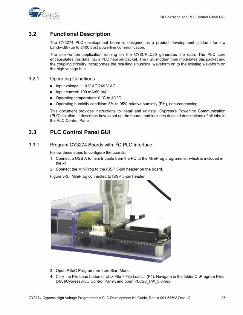
3.3.1 Program CY3274 Boards with I2C-PLC Interface
Follow these steps to configure the boards:
1. Connect a USB A to mini B cable from the PC to the MiniProg programmer, which is included in the kit.
2. Connect the MiniProg to the ISSP 5-pin header on the board.
Figure 3-3. MiniProg connected to ISSP 5-pin header
3. Open PSoC Programmer from Start Menu.
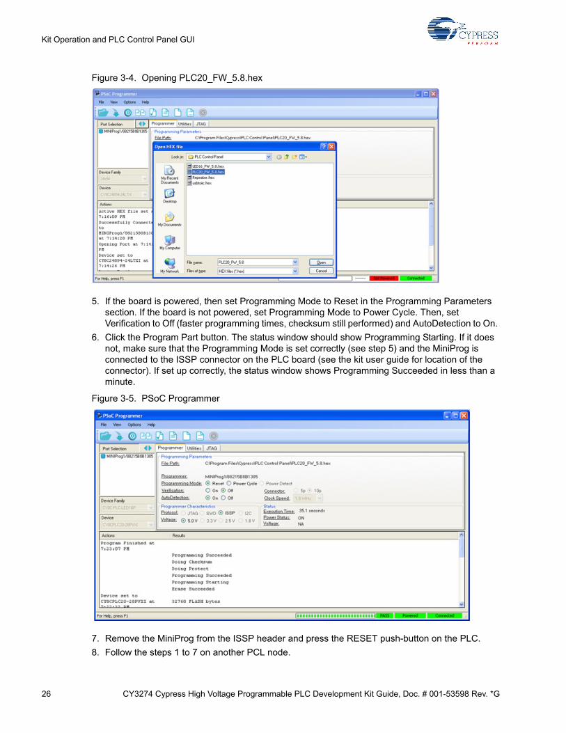
4. Click the File Load button or click File > File Load… (F4). Navigate to the folder C:\Program Files (x86)\Cypress\PLC Control Panel\ and open PLC20_FW_5.8.hex.
26 CY3274 Cypress High Voltage Programmable PLC Development Kit Guide, Doc. # 001-53598 Rev. *G
Kit Operation and PLC Control Panel GUI
Figure 3-4. Opening PLC20_FW_5.8.hex
5. If the board is powered, then set Programming Mode to Reset in the Programming Parameters section. If the board is not powered, set Programming Mode to Power Cycle. Then, set Verification to Off (faster programming times, checksum still performed) and AutoDetection to On.
6. Click the Program Part button. The status window should show Programming Starting. If it does not, make sure that the Programming Mode is set correctly (see step 5) and the MiniProg is connected to the ISSP connector on the PLC board (see the kit user guide for location of the connector). If set up correctly, the status window shows Programming Succeeded in less than a minute.
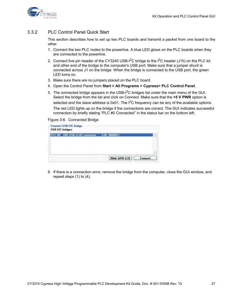
Figure 3-5. PSoC Programmer
7. Remove the MiniProg from the ISSP header and press the RESET push-button on the PLC.
8. Follow the steps 1 to 7 on another PCL node.
CY3274 Cypress High Voltage Programmable PLC Development Kit Guide, Doc. # 001-53598 Rev. *G 27
Kit Operation and PLC Control Panel GUI
3.3.2 PLC Control Panel Quick Start
This section describes how to set up two PLC boards and transmit a packet from one board to theother.
1. Connect the two PLC nodes to the powerline. A blue LED glows on the PLC boards when they are connected to the powerline.
2. Connect five pin header of the CY3240 USB-I2C bridge to the I2C header (J15) on the PLC kit and other end of the bridge to the computer's USB port. Make sure that a jumper shunt is connected across J1 on the bridge. When the bridge is connected to the USB port, the green LED turns on.
3. Make sure there are no jumpers placed on the PLC board.
4. Open the Control Panel from Start > All Programs > Cypress> PLC Control Panel.
5. The connected bridge appears in the USB-I2C bridges list under the main menu of the GUI. Select the bridge from the list and click on Connect. Make sure that the +5 V PWR option is
selected and the slave address is 0x01. The I2C frequency can be any of the available options.
The red LED lights up on the bridge if the connections are correct. The GUI indicates successful connection by briefly stating “PLC #0 Connected” in the status bar on the bottom left.
Figure 3-6. Connected Bridge
6. If there is a connection error, remove the bridge from the computer, close the GUI window, and repeat steps (1) to (4).
28 CY3274 Cypress High Voltage Programmable PLC Development Kit Guide, Doc. # 001-53598 Rev. *G
Kit Operation and PLC Control Panel GUI
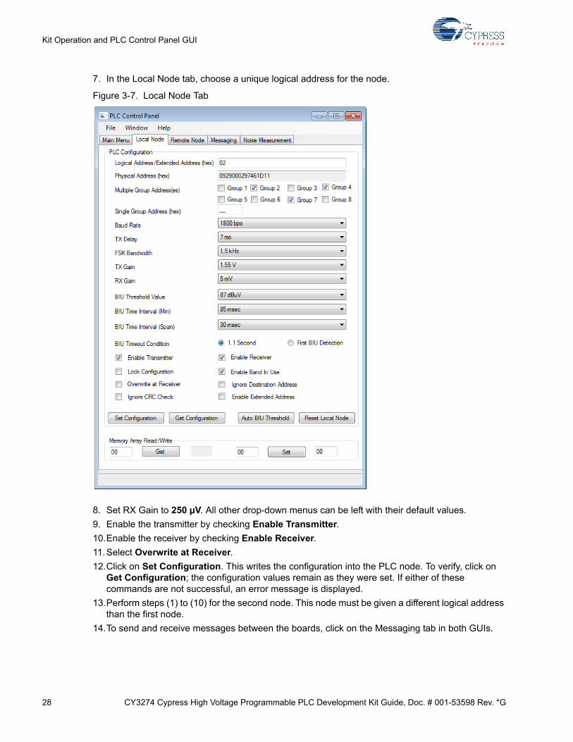
7. In the Local Node tab, choose a unique logical address for the node.
Figure 3-7. Local Node Tab
8. Set RX Gain to 250 µV. All other drop-down menus can be left with their default values.
9. Enable the transmitter by checking Enable Transmitter.
10.Enable the receiver by checking Enable Receiver.
11.Select Overwrite at Receiver.
12.Click on Set Configuration. This writes the configuration into the PLC node. To verify, click on Get Configuration; the configuration values remain as they were set. If either of these commands are not successful, an error message is displayed.
13.Perform steps (1) to (10) for the second node. This node must be given a different logical address than the first node.
14.To send and receive messages between the boards, click on the Messaging tab in both GUIs.
CY3274 Cypress High Voltage Programmable PLC Development Kit Guide, Doc. # 001-53598 Rev. *G 29
Kit Operation and PLC Control Panel GUI
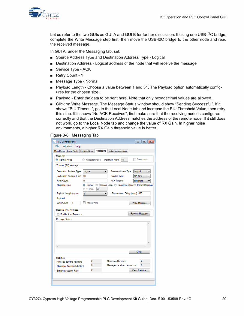
Let us refer to the two GUIs as GUI A and GUI B for further discussion. If using one USB-I2C bridge,complete the Write Message step first, then move the USB-I2C bridge to the other node and readthe received message.
In GUI A, under the Messaging tab, set:
■ Source Address Type and Destination Address Type - Logical
■ Destination Address - Logical address of the node that will receive the message
■ Service Type - ACK
■ Retry Count - 1
■ Message Type - Normal
■ Payload Length - Choose a value between 1 and 31. The Payload option automatically config-ures for the chosen size.
■ Payload - Enter the data to be sent here. Note that only hexadecimal values are allowed.
■ Click on Write Message. The Message Status window should show “Sending Successful”. If it shows “BIU Timeout”, go to the Local Node tab and increase the BIU Threshold Value, then retry this step. If it shows “No ACK Received”, first make sure that the receiving node is configured correctly and that the Destination Address matches the address of the remote node. If it still does not work, go to the Local Node tab and change the value of RX Gain. In higher noise environments, a higher RX Gain threshold value is better.
Figure 3-8. Messaging Tab
30 CY3274 Cypress High Voltage Programmable PLC Development Kit Guide, Doc. # 001-53598 Rev. *G
Kit Operation and PLC Control Panel GUI
In GUI B, under the Messaging tab, select the Enable Auto Reception. The message should appearin the Message Status window.
3.3.2.1 Additional Options
■ Check Infinite Write in A and then click Write Message. The same message is transmitted continuously until the Infinite Write is unchecked.
■ Set the Write Count to a value greater than 1. Click Write Message. This is the number of times the same message is sent by A to B.
■ Set the message type to Instant Message. The Payload field now accepts ASCII characters. Type any message in the field and click Write Message. The message appears on B as text. The setup works similar to an instant messenger.
■ To send messages in both directions, set up the parameters in B similar to the setting for A described earlier.
■ Select the Enable Auto Reception in A. Now messages may be sent bi-directionally by typing in the message in the Payload field and clicking the Write Message button.
■ The remote node configurations are retrieved and set in the Remote Node tab. To get the configurations, set the address and click Get Configuration. To change the configurations, make the changes in the corresponding fields and click Set Configuration.
3.3.3 PLC Control Panel Tabs
3.3.3.1 Main Menu Tab
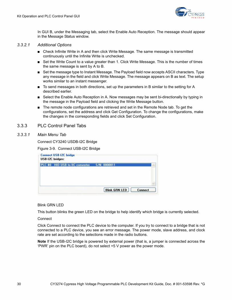
Connect CY3240 USDB-I2C Bridge
Figure 3-9. Connect USB-I2C Bridge
Blink GRN LED
This button blinks the green LED on the bridge to help identify which bridge is currently selected.
Connect
Click Connect to connect the PLC device to the computer. If you try to connect to a bridge that is notconnected to a PLC device, you see an error message. The power mode, slave address, and clockrate are set according to the selections made in the radio buttons.
Note If the USB-I2C bridge is powered by external power (that is, a jumper is connected across the‘PWR’ pin on the PLC board), do not select +5 V power as the power mode.
CY3274 Cypress High Voltage Programmable PLC Development Kit Guide, Doc. # 001-53598 Rev. *G 31
Kit Operation and PLC Control Panel GUI
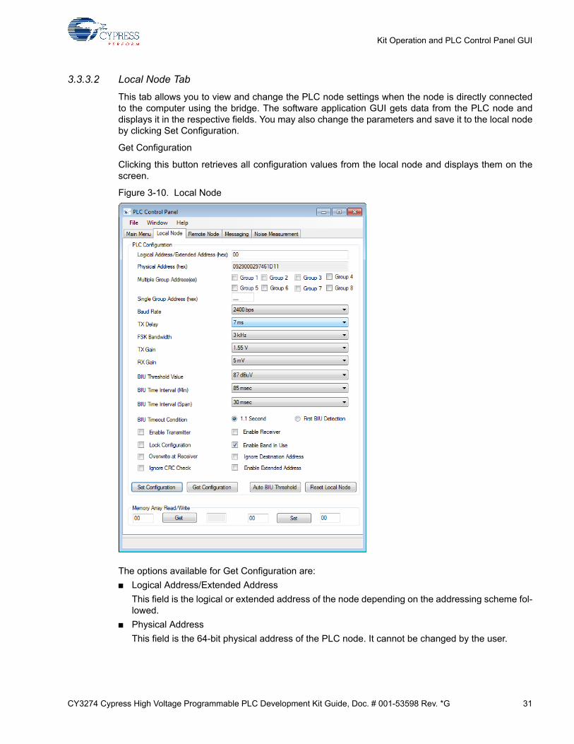
3.3.3.2 Local Node Tab
This tab allows you to view and change the PLC node settings when the node is directly connectedto the computer using the bridge. The software application GUI gets data from the PLC node anddisplays it in the respective fields. You may also change the parameters and save it to the local nodeby clicking Set Configuration.
Get Configuration
Clicking this button retrieves all configuration values from the local node and displays them on thescreen.
Figure 3-10. Local Node
The options available for Get Configuration are:
■ Logical Address/Extended Address
This field is the logical or extended address of the node depending on the addressing scheme fol-lowed.
■ Physical Address
This field is the 64-bit physical address of the PLC node. It cannot be changed by the user.

32 CY3274 Cypress High Voltage Programmable PLC Development Kit Guide, Doc. # 001-53598 Rev. *G
Kit Operation and PLC Control Panel GUI
■ Group Address(es)
This field displays the groups to which the node belongs. The local node belongs to a group if its corresponding checkbox is selected or the Group ID is mentioned in the Single Group Address field.
■ Baud Rate
This field gives the baud rate of the local node. The possible baud rates are 600, 1200, 1800, and 2400 bps.
■ TX Delay
This field sets the amount of delay from when the transmission is initiated to when the data starts being Output from the Transmit Programmable Gain Amplifier. The possible delay durations are 7, 13, 19, and 25 ms.
■ FSK Bandwidth
This parameter is used to set the separation of the FSK signals representing logic '1' and logic '0'. It can either be set to a deviation of 1.5 kHz or 3 kHz. The logic '0' frequency is always 133.3 kHz. The logic '1' frequency can be configured to either 131.8 kHz or 130.4 kHz.
■ TX Gain
This determines the gain of the transmitter's programmable gain amplifier. The possible output signal amplitude values using the Tx Gain are 55 mV, 75 mV, 100 mV, 125 mV, 180 mV, 250 mV, 360 mV, 480 mV, 660 mV, 900 mV, 1.25 V, 1.55 V, 2.25 V, 3.0 V, and 3.5 V.
■ RX Gain
This determines the minimum amplitude of the signal required to get demodulated. The different values are (in RMS) 5 mV, 2.5 mV, 1.25 mV, 600 µV, 350 µV, 250 µV, and 125 µV.
■ BIU Threshold Value
This field sets the threshold for the Band-In-Use detection circuit. This is only applicable when the Enable Band In Use checkbox is selected. The transmitter does not transmit a packet unless the level of power line signal on the powerline is less than this threshold. It should be set higher than the noise on the line, which can be determined by measuring the noise in the Noise Measurement tab of this GUI.
The possible threshold values are: 70, 75, 80, 87, 90, 93, 96, and 99 dBµV. There are six additional thresholds (103, 106, 109, 112, 115, and 118 dBµV) for the CY8CPLC20 device with PSoC Designer 5.1 or later versions.
■ BIU Time Interval (Min)
This parameter sets the minimum time interval for which the PLC node scans the powerline before transmitting a packet. The possible values are 85, 50, 20, and 10 msec. For CENELEC standard compliance, the setting should be 85 msec. This feature is only available with the CY8CPLC20 device with PSoC Designer 5.1 or later versions.
■ BIU Time Interval (Span)
This parameter sets the span from the lowest possible interval to the highest possible interval. The possible values are 30, 15, and 5 msec. For CENELEC standard compliance, the setting should be 30 msec. This feature is only available with the CY8CPLC20 device with PSoC Designer 5.4 or later versions.
■ BIU Timeout Condition
This parameter sets the BIU timeout condition to either 1.1 second or timeout on first BIU detection. When this option is set to ‘1.1 second’, if the modem detects the BIU, it still tries to acquire powerline until the powerline is free or up to a maximum of 1.1 second. If this option is set to ‘first BIU detection’, then the modem returns BIU error on first BIU detection. This feature is only available with the CY8CPLC20 device with PSoC Designer 5.1 or later versions.
CY3274 Cypress High Voltage Programmable PLC Development Kit Guide, Doc. # 001-53598 Rev. *G 33
Kit Operation and PLC Control Panel GUI
■ Enable Transmitter
This field enables the transmitter. If the transmitter on the local PLC node is disabled, the node does not transmit any data packet but continues to transmit acknowledgement packets.
■ Enable Receiver
This field enables the receiver. If the receiver on the local PLC node is disabled, the node does not receive any data packet but continues to receive acknowledgement packets.
■ Lock Configuration
This field indicates whether the local node’s configuration may be altered by another node via remote node configuration commands. If this option is selected, the remote node cannot change the configuration of the local node.
■ Enable Band In Use
This gives the “Band In Use” function to the local PLC node. When selected and a packet transmission is initiated, the PLC node first tests the line to see if it is free. The threshold to detect a band in use condition is set by the BIU Threshold Value field.
■ Overwrite at Receiver
If this option is selected, the PLC node’s RX buffer is overwritten whenever a new packet is received. If this option is not selected, the RX buffer retains the last unread packet until the host reads the message. The message is read in the Messaging tab by clicking Receive Message or Enable Auto Reception.
■ Ignore Destination Address
If this option is selected, the local node accepts all messages that are CRC verified irrespective of the destination address. Otherwise, the receiver only accepts packets addressed to it.
■ Ignore CRC Check
If this option is selected, the node ignores the CRC and accepts all received messages if the destination address matches its local address.
■ Enable Extended Addressing
If this option is selected, the local node uses the 16-bit extended logical addressing to communicate on the powerline. A node only communicates with other nodes that use the same logical addressing mode.
Set Configuration
This button saves the values in the local node fields onto the local PLC node. All fields except thephysical address field can be edited.
For the node to receive and transmit, the following changes must be made:
■ Change the logical address of the node to a value other than 00.
■ Enable the transmitter.
■ Enable the receiver.
■ Enable overwrite at receiver.
Reset Local Node
This button loads the default configuration on to the local PLC node. This preserves the logicaladdress, group address, PLC Mode, and Noise Threshold register. All the other bits are reset.
Auto BIU Threshold
This button automatically sets BIU threshold and updates the BIU threshold value in theconfiguration accordingly.
34 CY3274 Cypress High Voltage Programmable PLC Development Kit Guide, Doc. # 001-53598 Rev. *G
Kit Operation and PLC Control Panel GUI
Memory Array Read/Write
■ Get: This button reads the value from the memory array offset specified by the user (the field to the left of the Get button). The value is displayed in the field to the right of the Get button.
■ Set: This button writes the value to the memory array. The memory array offset (in the field to the left of the Set button) and value (in the field to the right of the Set button) is user specified.
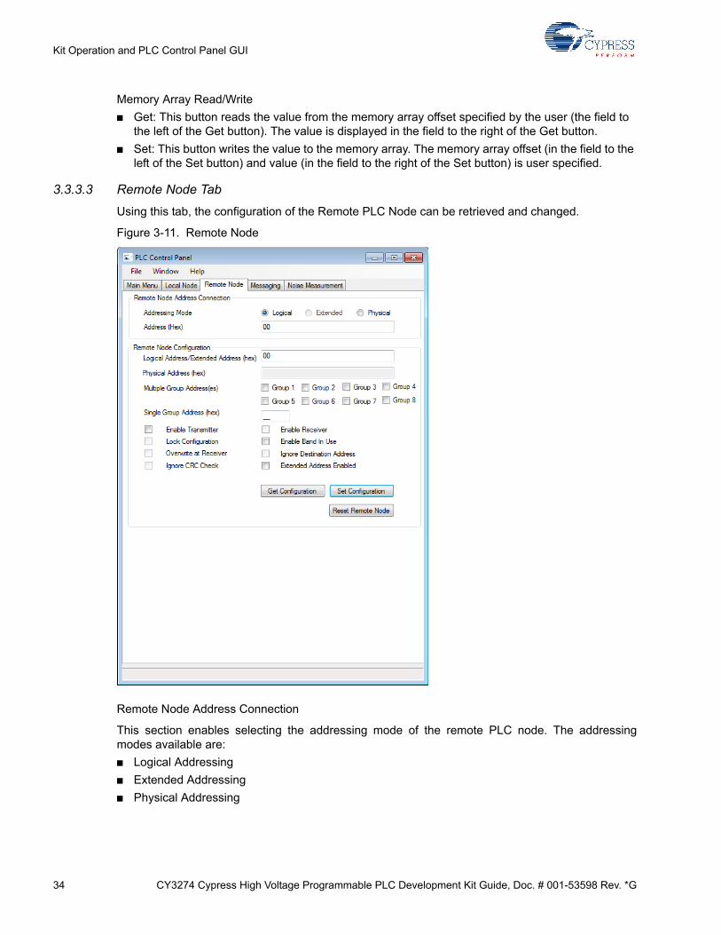
3.3.3.3 Remote Node Tab
Using this tab, the configuration of the Remote PLC Node can be retrieved and changed.
Figure 3-11. Remote Node
Remote Node Address Connection
This section enables selecting the addressing mode of the remote PLC node. The addressingmodes available are:
■ Logical Addressing
■ Extended Addressing
■ Physical Addressing
CY3274 Cypress High Voltage Programmable PLC Development Kit Guide, Doc. # 001-53598 Rev. *G 35
Kit Operation and PLC Control Panel GUI
Get Configuration
When this button is clicked, the remote node configuration is retrieved and shown in the correspond-ing fields. The correct address of the remote node must be set for successful retrieval.
The field descriptions are the same as those for the local node but apply specifically to the remotenode.
Set Configuration
This option sets the updated changes on to the remote PLC node. Only the logical address, groupaddress, transmitter state, band in use state, and the extended address state are altered by the localnode. The changes are only applied to the remote node if its Lock Configuration setting is disabled.
Reset Remote Node
Similar to the local node, this button allows the user to load the default configurations to the remotePLC node. Resetting the PLC node to default state preserves the logical address, group address,PLC Mode, and Threshold register. All other values are reset. The remote node resets only if its LockConfiguration setting is disabled.
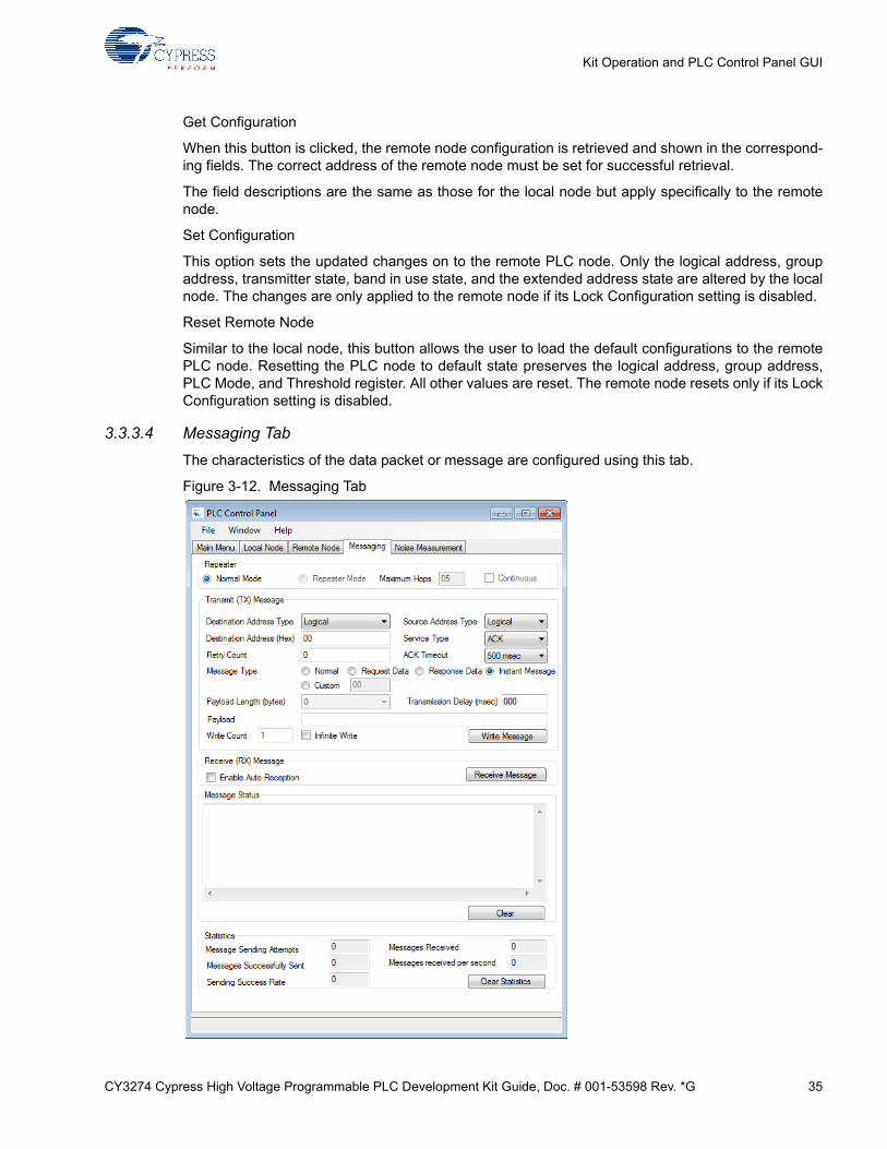
3.3.3.4 Messaging Tab
The characteristics of the data packet or message are configured using this tab.
Figure 3-12. Messaging Tab
36 CY3274 Cypress High Voltage Programmable PLC Development Kit Guide, Doc. # 001-53598 Rev. *G
Kit Operation and PLC Control Panel GUI
Write Message
When this button is pressed, a packet is sent according to the repeater mode, source address type,destination address type, destination address, service type, payload length, and payload.
■ Repeater Mode
If the repeater mode is selected, then the packet is prepared and sent according to the repeater algorithm. If the normal mode is selected, then the packet is transmitted without using repeater algorithm. Note that the repeater option is enabled only if the connected PLC node is repeater compatible. For more information on the repeater, see the application note AN62487.
■ Number of Hops
When using the repeater mode, this field sets the maximum number of hops that the packet can be repeated. If the “Continuous” option is selected, then the packet can be repeated for infinite number of hops. For more information on the repeater, see the application note Powerline Communication (PLC) Repeater Implementation.
■ Destination Address Type
The options available are logical (or extended), physical or group.
■ Source Address Type
The options available are logical (or extended) or physical.
■ Destination Address
This is the node to which the message is sent.
■ Retry Count
This is the maximum number of times a message is sent again by the transmitter if it does not get an acknowledgement for the transmitted packet.
■ ACK Timeout
This parameter sets the maximum time the node waits for the acknowledgement. The possible values are 500 msec, Auto + 100 msec, Auto + 50 msec, and Auto + 20 msec. The "Auto" value is the amount of time the acknowledgement takes if the receiver processes the packet immediately.
■ Message Types
❐ Normal: Normal messaging using only hexadecimal characters.
❐ Request Data: A hexadecimal message that expects a response from the receiver.
❐ Response Data: A hexadecimal message sent in response to a request.
❐ Instant Message: A text message (ASCII characters) to be sent.
❐ Custom - A hexadecimal message with specified custom command ID.
■ Payload
This is the actual data to be sent.
Note If using the GUI in a normal mode with a repeater enabled PLC device, the first two bits of the payload must be 00; otherwise, the PLC Control Panel GUI shows an error.
■ Payload Length
This is the length of the payload in bytes. Values can be in the range 0 to 31 in normal mode. In the repeater mode, the maximum payload length automatically varies from 13 to 27 depending on the source and destination address type.
■ Infinite Write
If this option is selected, the same message is continuously sent to the remote node until this option is cleared.
CY3274 Cypress High Voltage Programmable PLC Development Kit Guide, Doc. # 001-53598 Rev. *G 37
Kit Operation and PLC Control Panel GUI
■ Transmission Delay
The GUI inserts the specified delay (0 to 999 msec) between two consecutive successful trans-missions.
Receive Message
This button checks the receive buffer for a new message. If a message is present in the receivebuffer, it is shown in the Message Status window and the node stops receiving. If the buffer has nonew messages, the Message Status window is not updated.
Enable Auto Reception
Auto reception sets the node to the receiver mode. It displays messages in the Message Statuswindow as soon as they arrive. In this mode, packets are not dropped. The node continuously pollsfor new messages.
Clear
Clicking this button clears all status messages from the Message Status window.
Statistics
This section displays information on the packets sent over the powerline, packets sent successfully,and the success rate percentage. It also provides the number of messages received and rate ofmessage reception. To clear the statistics, click on Clear Statistics. This resets all values.
38 CY3274 Cypress High Voltage Programmable PLC Development Kit Guide, Doc. # 001-53598 Rev. *G
Kit Operation and PLC Control Panel GUI
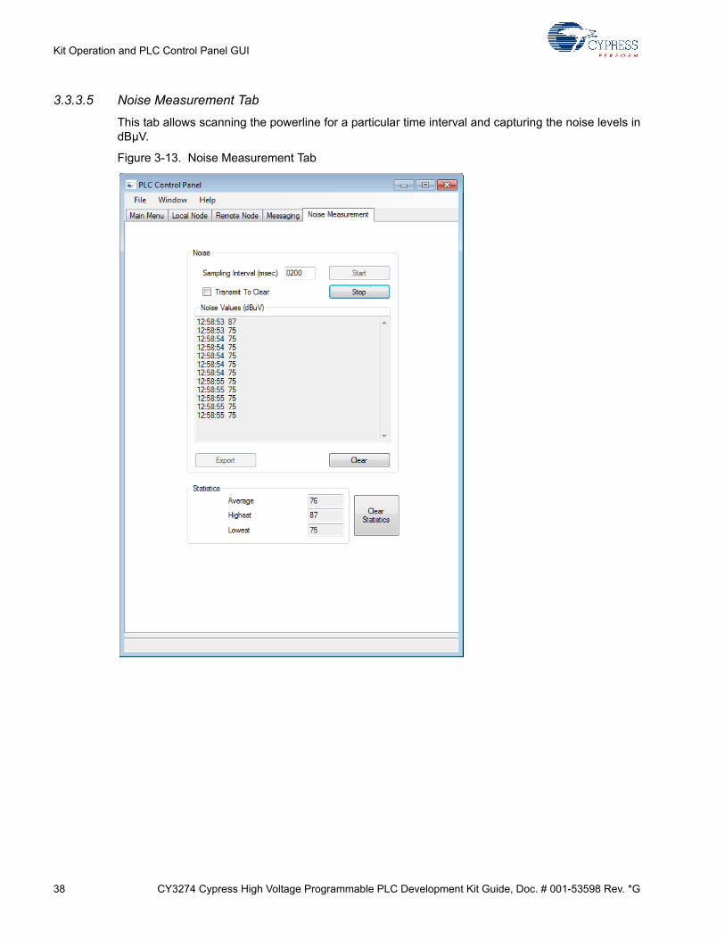
3.3.3.5 Noise Measurement Tab
This tab allows scanning the powerline for a particular time interval and capturing the noise levels indBµV.
Figure 3-13. Noise Measurement Tab
CY3274 Cypress High Voltage Programmable PLC Development Kit Guide, Doc. # 001-53598 Rev. *G 39
Kit Operation and PLC Control Panel GUI
Noise
■ Start - When this button is pressed, the PLC node starts scanning the powerline.
■ Stop - When this button is pressed, the PLC node stops scanning the powerline.
■ Sampling Interval (msec) - This field specifies the duration between two consecutive samples. The minimum value required is 200 msec and maximum is 2000 msec.
■ Transmit to Clear - When this checkbox is selected, the PLC device transmits a packet in unacknowledgement mode so that the other nodes do not transmit any packet for at least the minimum BIU interval. This is recommended for systems that may have other PLC devices transmitting while the noise is being measured. After this device transmits, the line is free while all the devices wait to acquire the line (BIU detection interval). For correct operation, the minimum BIU time interval should be atleast 50 msec.
■ Noise Values (dBµV) - This window displays the noise values sampled.
■ Export - When this button is pressed, the noise values are exported to a MS Excel spreadsheet.
■ Clear - This button clears the Noise Values window
Statistics
■ Average - This field shows the average of the noise values.
■ Highest - This field shows the highest noise value sampled.
■ Lowest - This field shows the lowest noise value sampled.
■ Clear Statistics - When this button is pressed, the statistics are reset.

40 CY3274 Cypress High Voltage Programmable PLC Development Kit Guide, Doc. # 001-53598 Rev. *G
Kit Operation and PLC Control Panel GUI
CY3274 Cypress High Voltage Programmable PLC Development Kit Guide, Doc. # 001-53598 Rev. *G 41
4. PLC Development Board
This chapter explains the key features of the CY3274 development board.
4.1 Board Details
The key features of the CY3274 development board are:
■ User friendly PLC Control Panel application
■ CY8CPLC20-OCD – 100-pin TQFP on-chip debug (OCD) device that allows quick design and debug of a PLC application.
The CY8CPLC20 100-pin TQFP is available for debug purpose only. For production quantities, CY8CPLC20 is available in 28-pin SSOP and 48-pin QFN packages.
■ Chip power supply derived from 110 V to 240 V AC
■ User configurable general purpose LEDs
■ General purpose 8-position DIP switch
■ On board surge protection and isolation circuit
■ RJ45 connector to use ICE debugger
■ RS232 COM port for communication
■ Header to attach the LCD card
■ I2C header for communicating to external device
■ ISSP header for programming the CY8CPLC20Note: For more details on ISSP, please visit http://www.cypress.com/?rID=40048.
4.2 CY3274 PLC Development Board Functional Overview
The CY3274 PLC development board is designed as a product development platform for lowbandwidth (up to 2400 bps) powerline communication.
The user-written application running on the CY8CPLC20 generates the data. The PLC coreencapsulates this data into a PLC network packet. The FSK modem then modulates this packet andthe coupling circuitry incorporates the resulting sinusoidal waveform on to the existing waveform onthe high voltage bus.
4.2.1 Operating Conditions
■ Input voltage: 110 V AC/240 V AC
■ Input current: 100 mA/50 mA
■ Operating temperature: 0 °C to 40 °C
■ Operating humidity condition: 5% to 95% relative humidity (RH), non-condensing
42 CY3274 Cypress High Voltage Programmable PLC Development Kit Guide, Doc. # 001-53598 Rev. *G
PLC Development Board
4.3 Hardware Description
The programmable high voltage PLC development board is shown in Figure 4-1. Key sections on theboard are highlighted.
Figure 4-1. Front View of Cypress Programmable PLC HV Development Board
The core of the PLC HV board is the CY8CPLC20 chip. The communication signal flows on this HVboard as follows:
Transmit: CY8CPLC20 TX pin (FSK_OUT) Transmitter Filter Circuitry Power Amplifier Cir-cuitry High Voltage Powerline Coupling Circuitry High Voltage Powerline (110 V to 240 V AC)
Receive: High Voltage Powerline (110 V to 240 V AC) High Voltage Powerline Coupling Circuitry Passive Low Pass Filtering Vdd/2 Biasing CY8CPLC20 RX pin (FSK_IN)
The CY3274 board can be divided into seven main sections:
■ Development
■ LCD daughter card
■ RJ45 connector for debugging
■ RS232 COM port
■ High voltage with SMPS (This acts as the built in Power adaptor.)
■ Transmit amplifier and filtering
■ High voltage coupling circuit
Potentiometer (R47)-> Connected to VR
High Voltage AC-DCPower Supply
High Voltage PLCCoupling Circuit
RS232 Interface
I2C Connector (J15) and Jumpers
(JP1, JP3, JP4, JP5)
LCD Connector-> Connected to Port4
Push-button (S4)-> Connected to SW
Potentiometer (R46)-> For LCD Contrast
Transmit Filter, TransmitAmplif ier, and Receive Filter
Reset Push-button (S2)
CY8CPLC20 PLC Device with On-Chip Debugger (U1)
General LEDs-> Connected to LED1-4
ISSP ProgrammingConnector (J21)
RJ45 Debugger Connector (J14)
PLC RX, TX, BIU IndicatorLEDs (DS2, DS3, DS4)
AC PowerConnector (J7)
Breadboard with surrounding GPIO headers
DIP Switch (S3)-> Connected to J12
CY3274 Cypress High Voltage Programmable PLC Development Kit Guide, Doc. # 001-53598 Rev. *G 43
PLC Development Board
4.3.1 Development
4.3.1.1 User I/Os, Bread Board and GPIO Headers
This is the area where you make custom designs. All GPIO pins excluding those required for PLCcommunication are routed to this area for ease of access. Some of the pins are shared for other pur-poses (for example, the port 4 pins P4[6:0] are also connected to the LCD connector).
Header J18 has pins that are connected to user I/Os (potentiometer, push-button, and LEDs). InFigure 4-2, these connections are represented by the green arrows. To connect one of these user I/Os to a CY8CPLC20 pin, connect a jumper wire between the respective header pins. For example,to connect the push-button S4 to pin P1[6], place a jumper wire in SW on header J18 and the otherend in P16 on header J9.
The DIP switch bank S3 is not connected directly to any of the CY8CPLC20 pins. The DIP switch isconnected to header J12, so that a jumper wire can be connected to any of the pins. The DIP switchis active LOW (connected to GND when in the ON position).
Figure 4-2. Bread Board
Potentiometer (R47)
Push- button (S4)
General LEDs
DIP Switch (S3) withHeader (J12)
Port0 Analog/Digital Port (J13)Free: P01, P02, P04, P07
Port2 Digital Port (J16)BIU LED: P21RX LED: P23TX LED: P25
Free: P26
Port4 Digital Port (J1)LCD: P40– P46
Free: P47
Port1 Digital Port (J9)I2C: P15, P17
Free: P12, P16
Port3 Digital Port (J10)Free: P30– P37
Port5 Digital PortFree: P50– P53
44 CY3274 Cypress High Voltage Programmable PLC Development Kit Guide, Doc. # 001-53598 Rev. *G
PLC Development Board
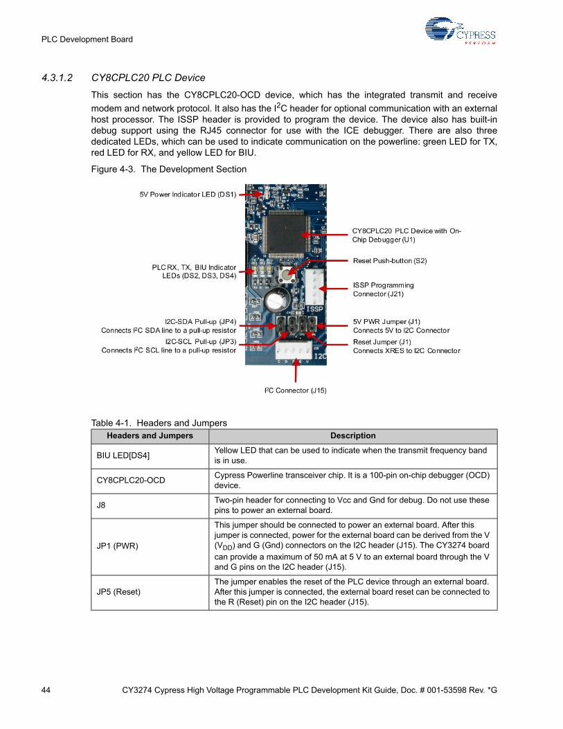
4.3.1.2 CY8CPLC20 PLC Device
This section has the CY8CPLC20-OCD device, which has the integrated transmit and receive
modem and network protocol. It also has the I2C header for optional communication with an externalhost processor. The ISSP header is provided to program the device. The device also has built-indebug support using the RJ45 connector for use with the ICE debugger. There are also threededicated LEDs, which can be used to indicate communication on the powerline: green LED for TX,red LED for RX, and yellow LED for BIU.
Figure 4-3. The Development Section
Table 4-1. Headers and JumpersHeaders and Jumpers Description
BIU LED[DS4]Yellow LED that can be used to indicate when the transmit frequency band is in use.
CY8CPLC20-OCDCypress Powerline transceiver chip. It is a 100-pin on-chip debugger (OCD) device.
J8Two-pin header for connecting to Vcc and Gnd for debug. Do not use these pins to power an external board.
JP1 (PWR)
This jumper should be connected to power an external board. After this jumper is connected, power for the external board can be derived from the V (VDD) and G (Gnd) connectors on the I2C header (J15). The CY3274 board
can provide a maximum of 50 mA at 5 V to an external board through the V and G pins on the I2C header (J15).
JP5 (Reset)The jumper enables the reset of the PLC device through an external board. After this jumper is connected, the external board reset can be connected to the R (Reset) pin on the I2C header (J15).
CY3274 Cypress High Voltage Programmable PLC Development Kit Guide, Doc. # 001-53598 Rev. *G 45
PLC Development Board
JP4 (I2C-SDA)
This is a pull-up jumper. While communicating through I2C (J15), one side has to pull up the line. When the jumper is connected, the SDA line is pulled high. This needs to be done when the user wants the I2C link to be pulled up by the CY3274 board.
This jumper does not need to be placed if the USB-I2C bridge is used for communication to the host.
JP3 (I2C-SCL)
This is a pull-up jumper. While communicating through I2C (J15), one side has to pull up the line. When the jumper is connected, the SCL line is pulled high. This needs to be done when the user wants the I2C link to be pulled up by the CY3274 board.
This jumper does not need to be placed if the USB-I2C bridge is used for communication to the host.
J15
V – VDD. This pin can provide a maximum of 50 mA at 5 V to an external
board. This pin is only to source the current. DO NOT SUPPLY POWER TO THIS PIN FOR POWERING CY8CPLC20 DEVICE. Note that the PWR jumper (JP1) needs to be connected to enable this functionality.
G – Gnd. The Gnd pin can provide the ground reference to an external board. This pin connects to the ground plane of the CY3274 board.
D – I2C data (SDA). The I2C data pin is the data line for the I2C communi-cation. This pin is directly connected to the CY8CPLC20 device. See appro-priate I2C-SDA jumper (JP4) settings before connecting I2C bus to this pin.
C – I2C clock (SCL). The I2C clock pin is the clock line for the I2C commu-nication. This pin is directly connected to the CY8CPLC20 device. See appropriate I2C-SCL jumper (JP3) settings before connecting I2C bus to this pin.
R – Reset. Connecting this pin to an external board enables the CY8CPLC20 chip to be reset by an external board. Note that the RES jumper (JP5) needs to be connected to enable this functionality.
LCD Contrast[R46] Adjusting this potentiometer adjusts the contrast on the LCD Daughter Card.
LED1-LED4 Headers connected to general purpose configurable LEDs.
PWR LED[DS1] Blue LED that glows when the board is powered on.
P01, P02, P04, P07 Free analog/digital port pins
P15 Port pin connected to SDA for I2C
P16, P12 Free port pins
P17 Port pin connected to SCL for I2C
P21 Port pin connected to yellow LED for BIU
P23 Port pin connected to red LED for RX
P25 Port pin connected to green LED for TX
P26 Free port pin
P30, P31, P32, P33, P34, P35, P36, P37
Free port pins
P40-P46 Port pins connected to LCD card
P47 Free port pin
P50, P51, P52, P53 Free port pins
Headers and Jumpers Description
46 CY3274 Cypress High Voltage Programmable PLC Development Kit Guide, Doc. # 001-53598 Rev. *G
PLC Development Board
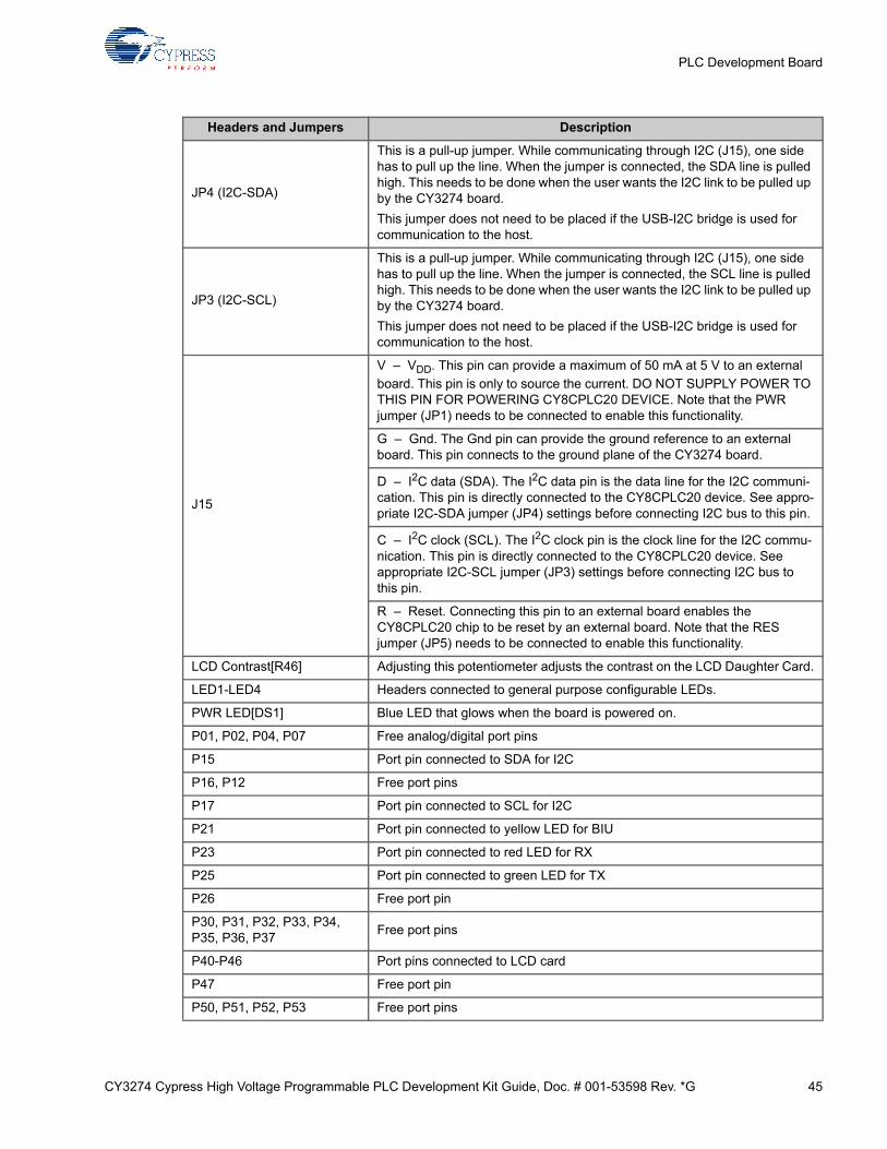
4.3.2 LCD Daughter Card
The LCD module is connected to header LCD1 and controlled with the CY8CPLC20 port 4 pinsP4[6:0].
Figure 4-4. LCD Daughter Card
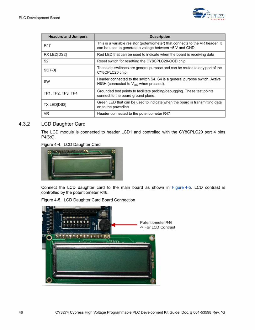
Connect the LCD daughter card to the main board as shown in Figure 4-5. LCD contrast iscontrolled by the potentiometer R46.
Figure 4-5. LCD Daughter Card Board Connection
R47This is a variable resistor (potentiometer) that connects to the VR header. It can be used to generate a voltage between +5 V and GND.
RX LED[DS2] Red LED that can be used to indicate when the board is receiving data
S2 Reset switch for resetting the CY8CPLC20-OCD chip
S3[7-0]These dip switches are general purpose and can be routed to any port of the CY8CPLC20 chip.
SWHeader connected to the switch S4. S4 is a general purpose switch. Active HIGH (connected to VDD when pressed).
TP1, TP2, TP3, TP4Grounded test points to facilitate probing/debugging. These test points connect to the board ground plane.
TX LED[DS3]Green LED that can be used to indicate when the board is transmitting data on to the powerline
VR Header connected to the potentiometer R47
Headers and Jumpers Description
Potentiometer R46-> For LCD Contrast
CY3274 Cypress High Voltage Programmable PLC Development Kit Guide, Doc. # 001-53598 Rev. *G 47
PLC Development Board
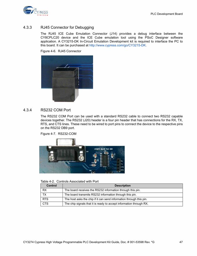
4.3.3 RJ45 Connector for Debugging
The RJ45 ICE Cube Emulation Connector (J14) provides a debug interface between theCY8CPLC20 device and the ICE Cube emulation tool using the PSoC Designer softwareapplication. A CY3215-DK In-Circuit Emulation Development kit is required to interface the PC tothis board. It can be purchased at http://www.cypress.com/go/CY3215-DK.
Figure 4-6. RJ45 Connector
4.3.4 RS232 COM Port
The RS232 COM Port can be used with a standard RS232 cable to connect two RS232 capabledevices together. The RS232 (J20) header is a four pin header that has connections for the RX, TX,RTS, and CTS lines. These need to be wired to port pins to connect the device to the respective pinson the RS232 DB9 port.
Figure 4-7. RS232-COM
Table 4-2. Controls Associated with PortControl Description
RX The board receives the RS232 information through this pin.
TX The board transmits RS232 information through this pin.
RTS The host asks the chip if it can send information through this pin.
CTS The chip signals that it is ready to accept information through RX.
48 CY3274 Cypress High Voltage Programmable PLC Development Kit Guide, Doc. # 001-53598 Rev. *G
PLC Development Board
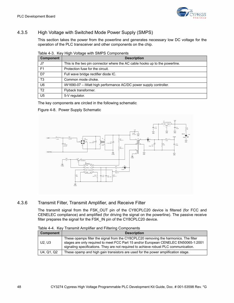
4.3.5 High Voltage with Switched Mode Power Supply (SMPS)
This section takes the power from the powerline and generates necessary low DC voltage for theoperation of the PLC transceiver and other components on the chip.
Table 4-3. Key High Voltage with SMPS Components
The key components are circled in the following schematic
Figure 4-8. Power Supply Schematic
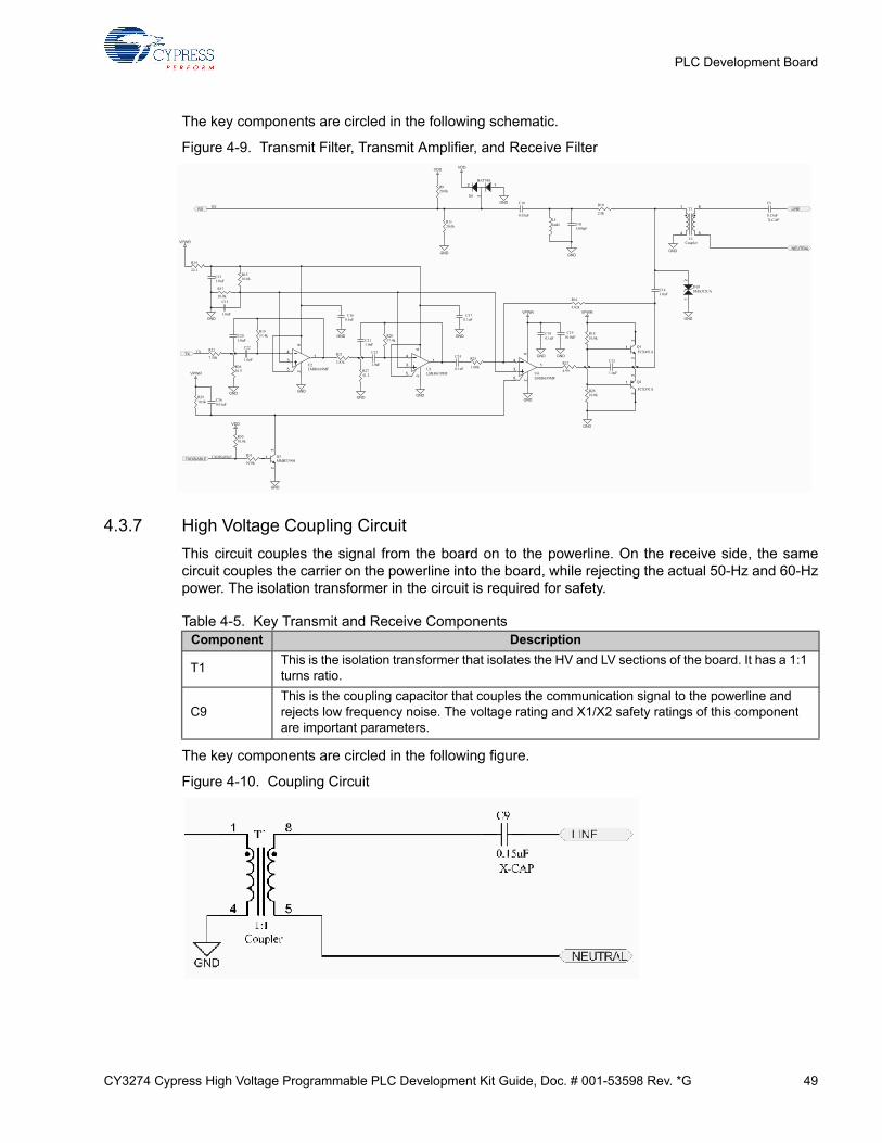
4.3.6 Transmit Filter, Transmit Amplifier, and Receive Filter
The transmit signal from the FSK_OUT pin of the CY8CPLC20 device is filtered (for FCC andCENELEC compliance) and amplified (for driving the signal on the powerline). The passive receivefilter prepares the signal for the FSK_IN pin of the CY8CPLC20 device.
Table 4-4. Key Transmit Amplifier and Filtering Components
Component Description
J7 This is the two pin connector where the AC cable hooks up to the powerline.
F1 Protection fuse for the circuit.
D7 Full wave bridge rectifier diode IC.
T3 Common mode choke.
U6 iW1690-07 – iWatt high performance AC/DC power supply controller.
T2 Flyback transformer.
U5 5-V regulator.
Component Description
U2, U3 These opamps filter the signal from the CY8CPLC20 removing the harmonics. The filter stages are only required to meet FCC Part 15 and/or European CENELEC EN50065-1:2001 signaling specifications. They are not required to achieve robust PLC communication.
U4, Q1, Q2 These opamp and high gain transistors are used for the power amplification stage.
4.7uF, 400VC31
750k, 1%R32
820k, 1%R34
PGND
PGND
470pF
C28
GND
330uF, 16VC32
GND
VPWR
Vin3
1
Vout 2
GND
U5LD1117DT50CTR
GND
VDD
GND
Vout7
Isense6
IBC4
GND5
Vin 2
Vcc 8
Vsense 1
Rin 3
U6iW1690-07
PGND
12
B1100
D9
1.0
R37
68k, 1%
R36
100kR38
2
3
1 Q4
TS13003HV3.9
R35
PGND
6.8k, 1%R40
12k, 1%R39
10uF, 50VC35
9
8
1
4
5
2
T2
1 2
3 424mH
T3
-2
~3
+1
~ 4
DF10SD7LINE
NEUTRAL
1.5mH
L3
22uH
L4
10.0uFC33
0.1uFC27
GND
10.0uFC26
10.0kR33
0.1uFC34
4.7uF, 400VC30
1 2
B1100
D8
GND
X1-CAP
Y1-CAP
0.022uFC29
10, 5W
R41
402R5
DS1
GND
BLUE
PWR
CY3274 Cypress High Voltage Programmable PLC Development Kit Guide, Doc. # 001-53598 Rev. *G 49
PLC Development Board
The key components are circled in the following schematic.
Figure 4-9. Transmit Filter, Transmit Amplifier, and Receive Filter
4.3.7 High Voltage Coupling Circuit
This circuit couples the signal from the board on to the powerline. On the receive side, the samecircuit couples the carrier on the powerline into the board, while rejecting the actual 50-Hz and 60-Hzpower. The isolation transformer in the circuit is required for safety.
Table 4-5. Key Transmit and Receive Components
The key components are circled in the following figure.
Figure 4-10. Coupling Circuit
Component Description
T1 This is the isolation transformer that isolates the HV and LV sections of the board. It has a 1:1 turns ratio.
C9 This is the coupling capacitor that couples the communication signal to the powerline and rejects low frequency noise. The voltage rating and X1/X2 safety ratings of this component are important parameters.
GND
VDD
7.50k
R22
1.00k
R25
4.99
R23
3
1
2
Q3MMBT3904
GND
VDD
2
1
3
FCX491AQ1
2
1
3
FCX591A
Q2
GND
VPWR4.02k
R16
1
3
2
D6
BAT54S
VDD
GND
4
3
2
1
6
5U2LMH6639MF
GNDGND
GND
RX
TX
TXDISABLE
4
3
2
1
6
5U3LMH6639MF
4
3
2
1
6
5U4LMH6639MF
TX
TXDISABLE
RX
10.0kR29
36.5R26
1.0nFC20
GND
1.0nF
C22
37.4kR19
3.83k
R21
41.2R27
1.0nFC21
1.0nF
C23
37.4kR20
GND
0.1uFC16
GND
0.1uFC17
GND
0.1uF
C24
0.1uFC18
GND
VPWR
10.0kR30
10.0k
R31
0.01uFC36
10.0kR18
10.0kR28
10.0uFC19
GND
12
SMAJ12CAD10
GND
22.1
R14
VPWR
10.0k
R17
1.0uFC13
1.0uF
C15
10.0kR15
GNDVPWR
2.0k
R10
0.01uF
C10
20.0kR11
20.0kR9
1500pFC41
GNDGND
1
4
8
51:1
T1
Coupler
LINE
NEUTRAL
1mHL5
1.0uFC14
X-CAP
1.0uF
C12
0.15uF
C9

50 CY3274 Cypress High Voltage Programmable PLC Development Kit Guide, Doc. # 001-53598 Rev. *G
PLC Development Board
CY3274 Cypress High Voltage Programmable PLC Development Kit Guide, Doc. # 001-53598 Rev. *G 51
5. Code Examples
5.1 Code Example
The CY3274 kit is designed for systems that require a communication interface over commercialhigh-voltage Powerlines. The CY8CPLC20 device combines the robustness and ease-of-use of thePLC solution with the configurability and flexibility of the PSoC core. The CY8CPLC20 deviceprovides the ability to run your own application. The PLT User Module manages the network protocoland the physical layer FSK modem, which transmits and receives messages over the powerline. Formore information on this user module, see AN54416, Using CY8CPLC20 in PowerlineCommunication (PLC) Applications.
5.2 PLC Demo
The PLT User Module can be implemented on the device CY8CPLC20. This section describes howto develop a PLC application to communicate between two nodes with the device CY8CPLC20.
The user is expected to know how to use PSoC Designer. To learn more about PSoC Designer, youcan see the link http://www.cypress.com/?id=1162.
5.2.1 Software Requirements
To use the PLT User Module, you must have the following software installed:
■ PSoC Designer 5.4 or higher
■ PSoC Programmer 3.20.1 or higher
Both of these software tools can be downloaded from http://www.cypress.com/psocdesigner.
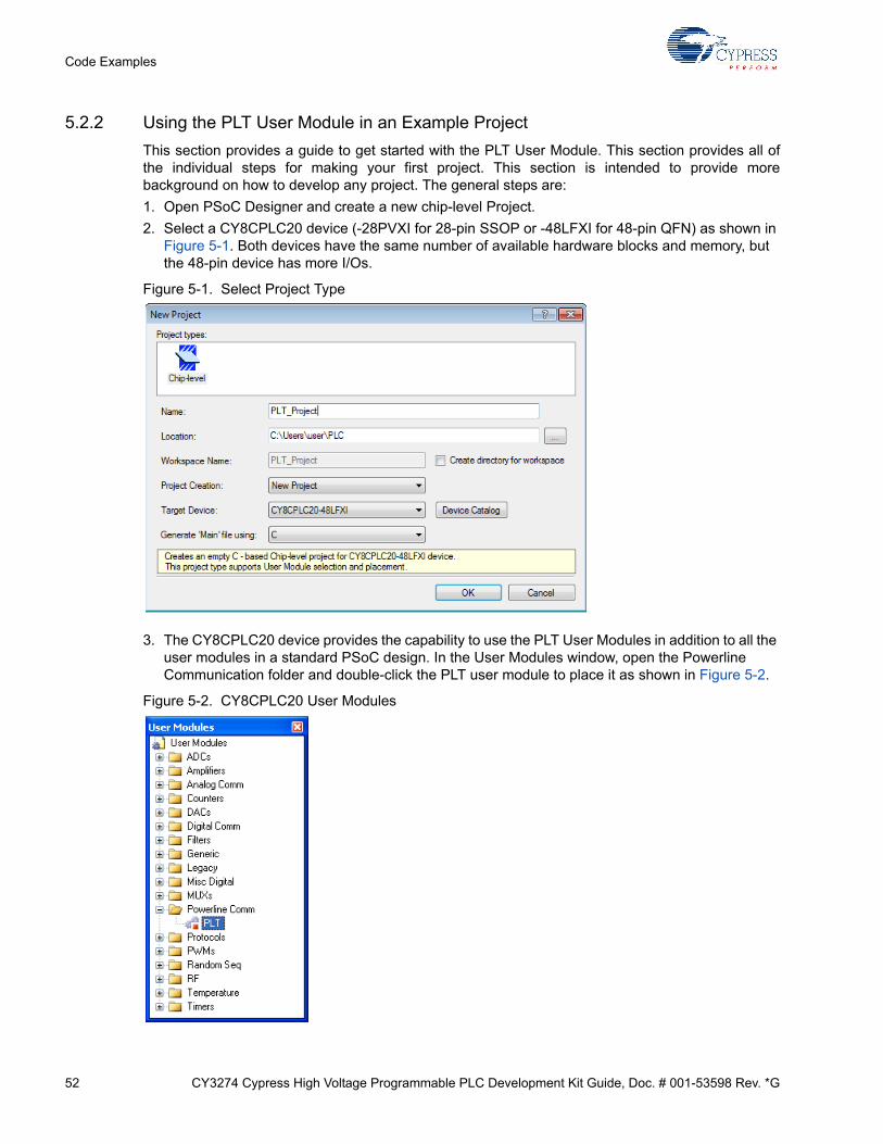
52 CY3274 Cypress High Voltage Programmable PLC Development Kit Guide, Doc. # 001-53598 Rev. *G
Code Examples
5.2.2 Using the PLT User Module in an Example Project
This section provides a guide to get started with the PLT User Module. This section provides all ofthe individual steps for making your first project. This section is intended to provide morebackground on how to develop any project. The general steps are:
1. Open PSoC Designer and create a new chip-level Project.
2. Select a CY8CPLC20 device (-28PVXI for 28-pin SSOP or -48LFXI for 48-pin QFN) as shown in Figure 5-1. Both devices have the same number of available hardware blocks and memory, but the 48-pin device has more I/Os.
Figure 5-1. Select Project Type
3. The CY8CPLC20 device provides the capability to use the PLT User Modules in addition to all the user modules in a standard PSoC design. In the User Modules window, open the Powerline Communication folder and double-click the PLT user module to place it as shown in Figure 5-2.
Figure 5-2. CY8CPLC20 User Modules
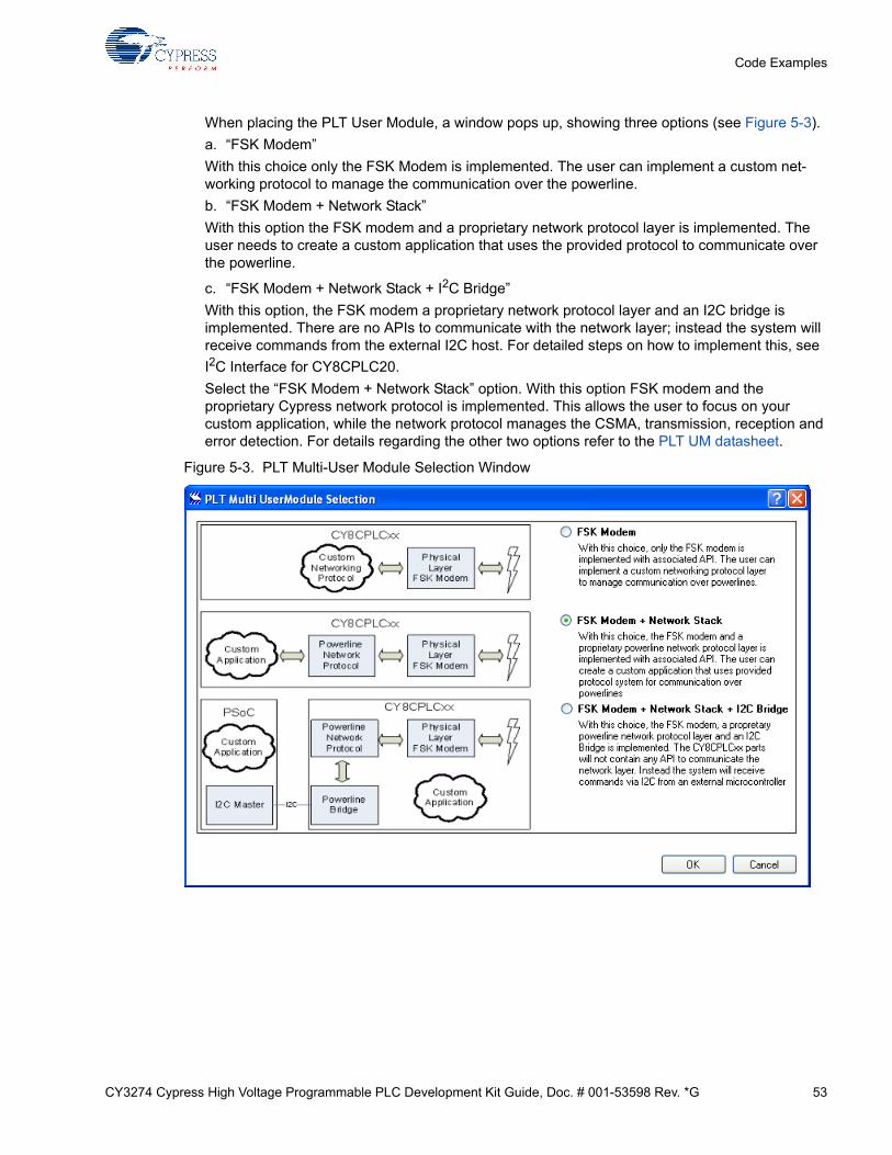
CY3274 Cypress High Voltage Programmable PLC Development Kit Guide, Doc. # 001-53598 Rev. *G 53
Code Examples
When placing the PLT User Module, a window pops up, showing three options (see Figure 5-3).
a. “FSK Modem”
With this choice only the FSK Modem is implemented. The user can implement a custom net-working protocol to manage the communication over the powerline.
b. “FSK Modem + Network Stack”
With this option the FSK modem and a proprietary network protocol layer is implemented. The user needs to create a custom application that uses the provided protocol to communicate over the powerline.
c. “FSK Modem + Network Stack + I2C Bridge”
With this option, the FSK modem a proprietary network protocol layer and an I2C bridge is implemented. There are no APIs to communicate with the network layer; instead the system will receive commands from the external I2C host. For detailed steps on how to implement this, see
I2C Interface for CY8CPLC20.
Select the “FSK Modem + Network Stack” option. With this option FSK modem and the proprietary Cypress network protocol is implemented. This allows the user to focus on your custom application, while the network protocol manages the CSMA, transmission, reception and error detection. For details regarding the other two options refer to the PLT UM datasheet.
Figure 5-3. PLT Multi-User Module Selection Window
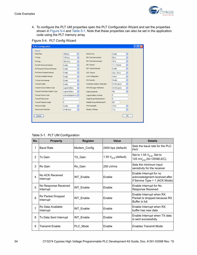
54 CY3274 Cypress High Voltage Programmable PLC Development Kit Guide, Doc. # 001-53598 Rev. *G
Code Examples
4. To configure the PLT UM properties open the PLT Configuration Wizard and set the properties shown in Figure 5-4 and Table 5-1. Note that these properties can also be set in the application code using the PLT memory array.
Figure 5-4. PLT Config Wizard
Table 5-1. PLT UM Configuration
No. Property Register Value Details
1 Baud Rate Modem_Config 2400 bps (default)Sets the baud rate for the PLC PHY
2 Tx Gain TX_Gain 1.55 Vp-p (default)Set to 1.55 Vp-p. Set to
125 mVp-p (for CENELEC).
3 Rx Gain Rx_Gain 250 uVrmsSets the minimum input sensitivity for the receiver
4No ACK Received Interrupt
INT_Enable EnableEnable Interrupt for no acknowledgment received after if Service Type = 1 (ACK Mode)
5No Response Received Interrupt
INT_Enable EnableEnable Interrupt for No Response Received
6Rx Packet Dropped Interrupt
INT_Enable EnableEnable Interrupt when RX Packet is dropped because RX Buffer is full
7Rx Data Available Interrupt
INT_Enable EnableEnable Interrupt when RX buffer has new data
8 Tx Data Sent Interrupt INT_Enable EnableEnable Interrupt when TX data is sent successfully
9 Transmit Enable PLC_Mode Enable Enables Transmit Mode
CY3274 Cypress High Voltage Programmable PLC Development Kit Guide, Doc. # 001-53598 Rev. *G 55
Code Examples
10Transmit Source Address Type
TX_ConfigLogical Address (default)
provides option to choose between logical or physical address for transmitter source
11Transmit Destination Address Type
TX_ConfigLogical Address (default)
Provides option to choose between logical or physical address as transmitter destination address type
12 Transmit Service Type TX_ConfigAcknowledgement Mode
Transmissions are acknowledged
13 Transmit Retry Count TX_Config 3Number of times a transmitter should retry before sending a new packet
14 Transmit Payload Length TX_Message_Length 0 Length of the payload
15 Receive Enable PLC_Mode Enable Enable Receiver Mode
16 Noise Threshold Value Threshold_Noise 87 dBuV (default)Threshold for BIU detection (set to 87 dBuV for CENELEC)
17 Band In Use PLC_Mode Enable (default)
Allows option to only send data when no other node is using the powerline for its communication
18 BIU Time Interval (min) Timing_Config 85 ms (default) Set BIU Time interval
19 BIU Time Interval (span) Timing_Config 30 ms (default) Set time interval span
20 BIU Timeout Timing_Config1.1 s Timeout (default)
Set BIU Timeout value
21 BIU Timeout Interrupt INT_Enable Enable (default)
Enable Interrupt for BIU Timeout and the Modem is unable to Transmit, if Disable BIU = 0
22 ACK Timeout Timing_Config Auto +20 msTime for which Transmitter waits for ACK after Auto set time.
23 Lock Configuration PLC_Mode Unlock (default)Allow device to be configured remotely
24 Rx Overwrite PLC_Mode Disable (default)If RX Buffer is full, new RX Message is dropped.
25Destination Address Verification
PLC_Mode Do not IgnoreCheck if the Destination Address is a match before processing the packet
26 CRC Address Verification PLC_Mode Do not Ignore Drop the packet if CRC fails
27 Addressing Mode PLC_Mode 8 bit Select between 8 bit and 16 bit
Table 5-1. PLT UM Configuration (continued)
No. Property Register Value Details
56 CY3274 Cypress High Voltage Programmable PLC Development Kit Guide, Doc. # 001-53598 Rev. *G
Code Examples
Note The above settings can also be done with the following application code, as shown below:
/* Set the baud rate to 2400bps with a 3kHz deviation */PLT_Memory_Array[Modem_Config] = (Modem_FSKBW_3M | Modem_BPS_2400);/* Enable the PLC Transmitter and Receiver*/PLT_Memory_Array[PLC_Mode] = (TX_Enable | RX_Enable);/* Enable Acknowledgement and 3 retries*/PLT_Memory_Array[TX_Config] = (TX_Service_Type | 0x03);/* Set the transmitter gain to 1.55Vp-p.*/PLT_Memory_Array[TX_Gain] = 0x0b;/* Set the receiver gain to 250uVrms */PLT_Memory_Array[RX_Gain] = 0x06;/* Set the length of the transmit buffer to 0x00 */PLT_Memory_Array[TX_Message_Length] = 0x00;/* Enable Interrupt reporting for all events */PLT_Memory_Array[INT_Enable] = (INT_UnableToTX | INT_TX_NO_ACK | INT_TX_NO_RESP | INT_RX_Packet_Dropped | INT_RX_Data_Available | INT_TX_Data_Sent);
5. Place a Timer8 user module with the parameters as shown below. This Timer is used to provide the timing for several operations such as switch debounce and time interval between changes in LCD display.
28 Logical Address of NodeLocal_LA_LSB
Local_LA_MSB0
In this project, Logical Address is set in the code.
29Single Group Membership ID
Local_Group 0For this example project Group Membership is not used
30Multiple Group Membership ID
Local_Group_Hot 0x0For this example project Group Membership is not used
31 FSK Bandwidth Modem_ Config 3 kHz (default)Separation of FSK signals for logic ‘1’ and ‘0’
32 Modem Tx Delay Modem_ Config 7 ms (default)This value is dependent on the BAUD rate
Table 5-2. Parameters
Name TickTimer
Clock VC3
Capture Low
TerminalCountOut None
CompareOut None
Period 192
CompareValue 100
CompareType Less Than or Equal
Table 5-1. PLT UM Configuration (continued)
No. Property Register Value Details
CY3274 Cypress High Voltage Programmable PLC Development Kit Guide, Doc. # 001-53598 Rev. *G 57
Code Examples
6. Generate the configuration by clicking on the menu Build -> Generate Configuration (Ctrl + F6). This will generate all of the user module assembly and C code needed for the application. Place an LCD UM and 3 LED UM with the following parameters:
a. LCD UM i. Name = “LCD” LCD_Port = “Port_4”. A LCD can be directly connected to the available LCD port.
b. 3 x LED UM (The corresponding LEDs are already hardwired to the respective pins on the Cypress PLC Development Kits CY3274) i. Name = “BIU_LED”, Port = “Port_2”, Pin = “Port_2_1”, Drive = “Active High”ii. Name = “RX_LED”, Port = “Port_2”, Pin = “Port_2_3”, Drive = “Active High” iii. Name = “TX_LED”, Port = “Port_2”, Pin = “Port_2_5”, Drive = “Active High”
c. Update the BIU, TX and RX ISR code snippets in PLT_1INT.asm from the PLT_1INT.asm file in the CY3274_PC_Demo example project inside <Install_Directory> -> Firmware. Each ISR enables the appropriate LED when the status is active (for example, turn on TX_LED when transmitting) or disables the appropriate LED when the status is complete.i. PLT_BIU_Active_ISR: This ISR is called when the Band In Use is activeii. PLT_BIU_Complete_ISR: This ISR is called when the Band In Use is no longer setiii. PLT_TX_Active_ISR: This ISR is called when the Transmitter is actively sending a messageiv. PLT_TX_Complete_ISR: This ISR is called when the Transmitter has completed sending the messagev. PLT_RX_Active_ISR: This ISR is called when the Receiver is in process of receiving a packetvi. PLT_RX_Complete_ISR: This ISR is called when the Receiver is no longer receiving a packet
d. Buttons i. Set P0[4] according to the settings shown below. This pin is used to select the Local Logical Address of device during the boot up of the device from reset.
ii. Set P0[7] according to the settings shown below. This pin is used to select the mode of operation (transmitter or receiver) during the boot up of the device from reset.
InterruptType Terminal Count
ClockSync Sync to SysClk
TC_PulseWidth Full Clock
InvertCapture Normal
Name ADD_Select
Port P0[4]
Port StdCPU
Drive Pull Up
Interrupt DisableInt
Initial Value 1
Table 5-2. Parameters
Name TickTimer
58 CY3274 Cypress High Voltage Programmable PLC Development Kit Guide, Doc. # 001-53598 Rev. *G
Code Examples
iii. Set P0[1] according to the settings shown below. A switch connected to this pin will be used to start, halt, resume or restart transmission if the kit is selected to be in transmitter mode (by P0[7]) or to reset the received packet count if the kit is selected to be in receiver mode.
7. Open the PSoCGPIOInt.asm file and TickTimerINT.asm file located in the Workspace explorer under the folder lib->Library Source Files. Add the instruction “ljmp _Trigger_Int” between the custom user code banners present under the label “PSoC_GPIO_ISR:” in PSoCGPIOInt.asm file. Similarly, add the instruction “ljmp _TickTimer_Int” between the custom user code banners present under the label “_TickTimer_ISR:” in TickTimerINT.asm file.
8. The main.c code from the attached code example should be copied into this project’s main.c. Also, create 2 new files “PLC_Demo.c” and “PLC_Demo.h” in the project (by clicking on menu File >> New File). The contents of the files “PLC_Demo.c” and “PLC_Demo.h” from the attached code example (CY3274_PLC_Demo) should be copied and pasted into these files. A high-level description of the code is as follows:
a. The PLT and LCD User Modules are initialized. The global interrupts are enabled. The PLT UM is configured.
b. The state of the MODE_Select Pin is checked, and based on this the mode of the device is assigned as either Transmitter or Receiver.
c. The state of the ADD_Select Pin is checked, and based on this a logical address of the node is chosen.
d. When the pin “Trigger” transitions from '1' to '0' in a kit that is in “Transmitter mode”, the Powerline Transceiver (PLT) transmits data to the other node, or halts transmission if it had previously been transmitting, or resumes transmission if it had previously been halted.
e. When the pin “Trigger” transitions from '1' to '0' in a kit that is in “Receiver mode”, the Received packet count is reset.
f. The statistics and instructions are displayed on the LCD.
Name MODE_Select
Port P0[7]
Port StdCPU
Drive Pull Up
Interrupt DisableInt
Initial Value 1
Name Trigger
Port P0[1]
Port StdCPU
Drive Pull Down
Interrupt Falling Edge
Initial Value 0

CY3274 Cypress High Voltage Programmable PLC Development Kit Guide, Doc. # 001-53598 Rev. *G 59
Code Examples
5.2.3 Evaluating the Example Project on Hardware
Once the application example projects are built, they can be evaluated in a powerline system. Thisexample is designed to run on the CY3274 high-voltage PLC DVK. The BIU, RX, and TX LEDs onthe board are hardwired to P2[1], P2[3], and P2[5], respectively.
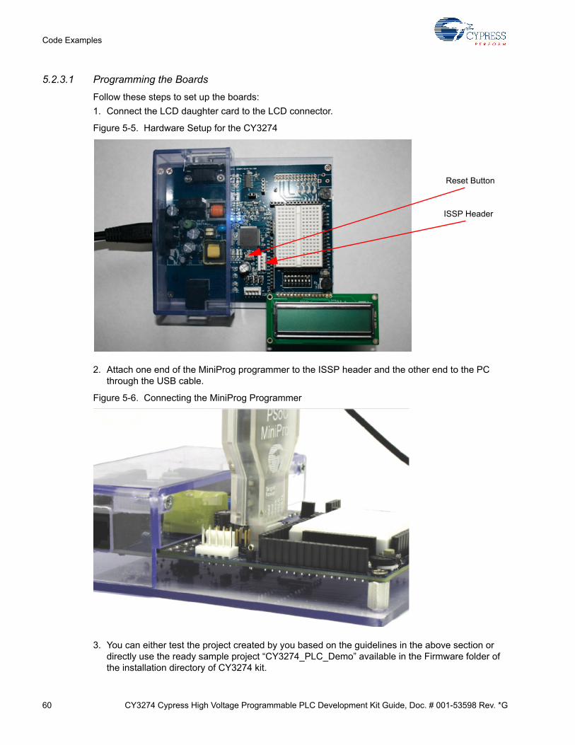
60 CY3274 Cypress High Voltage Programmable PLC Development Kit Guide, Doc. # 001-53598 Rev. *G
Code Examples
5.2.3.1 Programming the Boards
Follow these steps to set up the boards:
1. Connect the LCD daughter card to the LCD connector.
Figure 5-5. Hardware Setup for the CY3274
2. Attach one end of the MiniProg programmer to the ISSP header and the other end to the PC through the USB cable.
Figure 5-6. Connecting the MiniProg Programmer
3. You can either test the project created by you based on the guidelines in the above section or directly use the ready sample project “CY3274_PLC_Demo” available in the Firmware folder of the installation directory of CY3274 kit.
Reset Button
ISSP Header
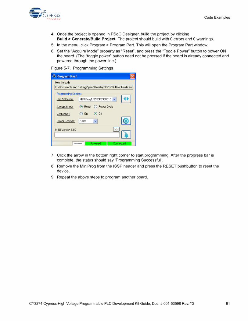
CY3274 Cypress High Voltage Programmable PLC Development Kit Guide, Doc. # 001-53598 Rev. *G 61
Code Examples
4. Once the project is opened in PSoC Designer, build the project by clicking Build > Generate/Build Project. The project should build with 0 errors and 0 warnings.
5. In the menu, click Program > Program Part. This will open the Program Part window.
6. Set the “Acquire Mode” property as “Reset”, and press the “Toggle Power” button to power ON the board. (The “toggle power” button need not be pressed if the board is already connected and powered through the power line.)
Figure 5-7. Programming Settings
7. Click the arrow in the bottom right corner to start programming. After the progress bar is complete, the status should say ‘Programming Successful’.
8. Remove the MiniProg from the ISSP header and press the RESET pushbutton to reset the device.
9. Repeat the above steps to program another board.
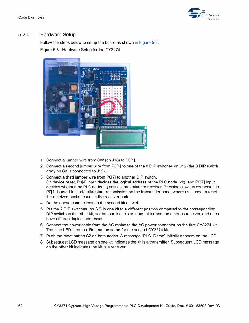
62 CY3274 Cypress High Voltage Programmable PLC Development Kit Guide, Doc. # 001-53598 Rev. *G
Code Examples
5.2.4 Hardware Setup
Follow the steps below to setup the board as shown in Figure 5-8.
Figure 5-8. Hardware Setup for the CY3274
1. Connect a jumper wire from SW (on J18) to P0[1].
2. Connect a second jumper wire from P0[4] to one of the 8 DIP switches on J12 (the 8 DIP switch array on S3 is connected to J12).
3. Connect a third jumper wire from P0[7] to another DIP switch. On device reset, P0[4] input decides the logical address of the PLC node (kit), and P0[7] input decides whether the PLC node(kit) acts as transmitter or receiver. Pressing a switch connected to P0[1] is used to start/halt/restart transmission on the transmitter node, where as it used to reset the received packet count in the receiver node.
4. Do the above connections on the second kit as well.
5. Put the 2 DIP switches (on S3) in one kit to a different position compared to the corresponding DIP switch on the other kit, so that one kit acts as transmitter and the other as receiver, and each have different logical addresses.
6. Connect the power cable from the AC mains to the AC power connector on the first CY3274 kit. The blue LED turns on. Repeat the same for the second CY3274 kit.
7. Push the reset button S2 on both nodes. A message “PLC_Demo” initially appears on the LCD.
8. Subsequest LCD message on one kit indicates the kit is a transmitter. Subsequent LCD message on the other kit indicates the kit is a receiver.
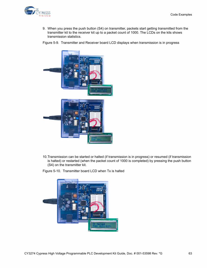
CY3274 Cypress High Voltage Programmable PLC Development Kit Guide, Doc. # 001-53598 Rev. *G 63
Code Examples
9. When you press the push button (S4) on transmitter, packets start getting transmitted from the transmitter kit to the receiver kit up to a packet count of 1000. The LCDs on the kits shows transmission statistics.
Figure 5-9. Transmitter and Receiver board LCD displays when transmission is in progress
10.Transmission can be started or halted (if transmission is in progress) or resumed (if transmission is halted) or restarted (when the packet count of 1000 is completed) by pressing the push button (S4) on the transmitter kit.
Figure 5-10. Transmitter board LCD when Tx is halted
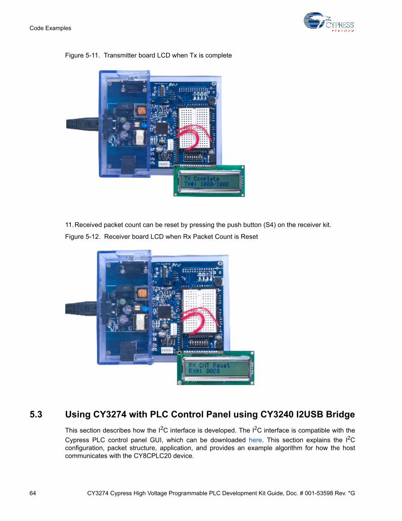
64 CY3274 Cypress High Voltage Programmable PLC Development Kit Guide, Doc. # 001-53598 Rev. *G
Code Examples
Figure 5-11. Transmitter board LCD when Tx is complete
11.Received packet count can be reset by pressing the push button (S4) on the receiver kit.
Figure 5-12. Receiver board LCD when Rx Packet Count is Reset
5.3 Using CY3274 with PLC Control Panel using CY3240 I2USB Bridge
This section describes how the I2C interface is developed. The I2C interface is compatible with the
Cypress PLC control panel GUI, which can be downloaded here. This section explains the I2Cconfiguration, packet structure, application, and provides an example algorithm for how the hostcommunicates with the CY8CPLC20 device.
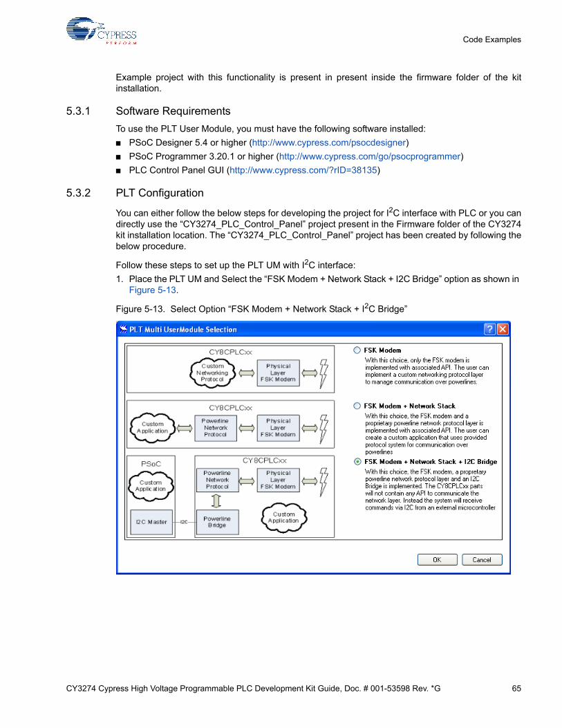
CY3274 Cypress High Voltage Programmable PLC Development Kit Guide, Doc. # 001-53598 Rev. *G 65
Code Examples
Example project with this functionality is present in present inside the firmware folder of the kitinstallation.
5.3.1 Software Requirements
To use the PLT User Module, you must have the following software installed:
■ PSoC Designer 5.4 or higher (http://www.cypress.com/psocdesigner)
■ PSoC Programmer 3.20.1 or higher (http://www.cypress.com/go/psocprogrammer)
■ PLC Control Panel GUI (http://www.cypress.com/?rID=38135)
5.3.2 PLT Configuration
You can either follow the below steps for developing the project for I2C interface with PLC or you candirectly use the “CY3274_PLC_Control_Panel” project present in the Firmware folder of the CY3274kit installation location. The “CY3274_PLC_Control_Panel” project has been created by following thebelow procedure.
Follow these steps to set up the PLT UM with I2C interface:
1. Place the PLT UM and Select the “FSK Modem + Network Stack + I2C Bridge” option as shown in Figure 5-13.
Figure 5-13. Select Option “FSK Modem + Network Stack + I2C Bridge”
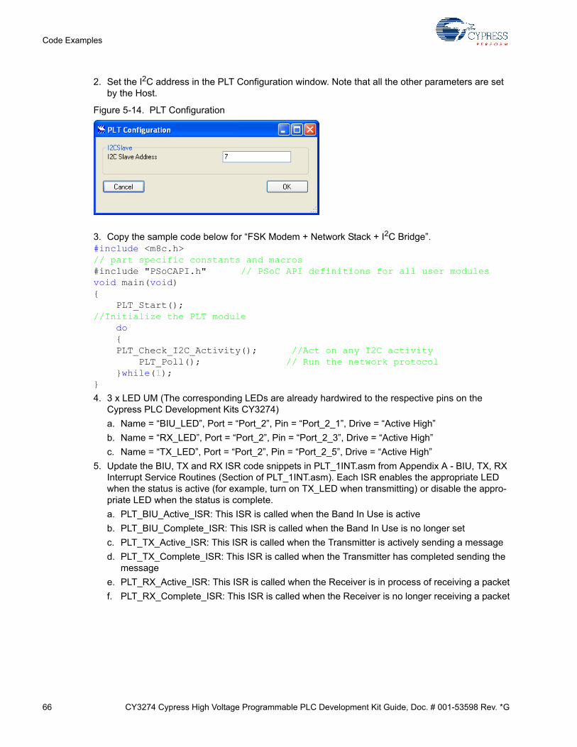
66 CY3274 Cypress High Voltage Programmable PLC Development Kit Guide, Doc. # 001-53598 Rev. *G
Code Examples
2. Set the I2C address in the PLT Configuration window. Note that all the other parameters are set by the Host.
Figure 5-14. PLT Configuration
3. Copy the sample code below for “FSK Modem + Network Stack + I2C Bridge”. #include <m8c.h> // part specific constants and macros#include "PSoCAPI.h" // PSoC API definitions for all user modulesvoid main(void){ PLT_Start();//Initialize the PLT module do { PLT_Check_I2C_Activity(); //Act on any I2C activity PLT_Poll(); // Run the network protocol }while(1);}
4. 3 x LED UM (The corresponding LEDs are already hardwired to the respective pins on the Cypress PLC Development Kits CY3274)
a. Name = “BIU_LED”, Port = “Port_2”, Pin = “Port_2_1”, Drive = “Active High”
b. Name = “RX_LED”, Port = “Port_2”, Pin = “Port_2_3”, Drive = “Active High”
c. Name = “TX_LED”, Port = “Port_2”, Pin = “Port_2_5”, Drive = “Active High”
5. Update the BIU, TX and RX ISR code snippets in PLT_1INT.asm from Appendix A - BIU, TX, RX Interrupt Service Routines (Section of PLT_1INT.asm). Each ISR enables the appropriate LED when the status is active (for example, turn on TX_LED when transmitting) or disable the appro-priate LED when the status is complete.
a. PLT_BIU_Active_ISR: This ISR is called when the Band In Use is active
b. PLT_BIU_Complete_ISR: This ISR is called when the Band In Use is no longer set
c. PLT_TX_Active_ISR: This ISR is called when the Transmitter is actively sending a message
d. PLT_TX_Complete_ISR: This ISR is called when the Transmitter has completed sending the message
e. PLT_RX_Active_ISR: This ISR is called when the Receiver is in process of receiving a packet
f. PLT_RX_Complete_ISR: This ISR is called when the Receiver is no longer receiving a packet
CY3274 Cypress High Voltage Programmable PLC Development Kit Guide, Doc. # 001-53598 Rev. *G 67
Code Examples
5.3.3 I2C Interface Write Packet Structure
The I2C interface follows the packet structure defined by the I2C specification. The write packet is asfollows. The master always sends the entire packet.
5.3.4 I2C Interface Read Packet Structure
The I2C interface follows the packet structure defined by the I2C specification. The read packet is asfollows. The master sends the first byte. The offset is set by sending a write packet for that offset(sending data is not necessary).
5.3.5 I2C Application
The I2C write and read messages are processed automatically by the EzI2Cs user module by the
ISRs associated with the user module. It is important to note that I2C interrupts are disabled by the
PLT user module when it is transmitting. During this time, if the host initiated an I2C message, theCY8CPLC20 device holds the SCL bus low until it finishes transmitting the PLC packet. It then
resumes processing the I2C message.
7 6 5 4 3 2 1 0
Byte 0 I2C Address (0b0000001) 0
Byte 1 Offset
Byte 2+ Data from host to CY8CPLC20 (Optional)
7 6 5 4 3 2 1 0
Byte 0 I2C Address (0b0000001) 1
Byte 1+ Data from CY8CPLC20 to host
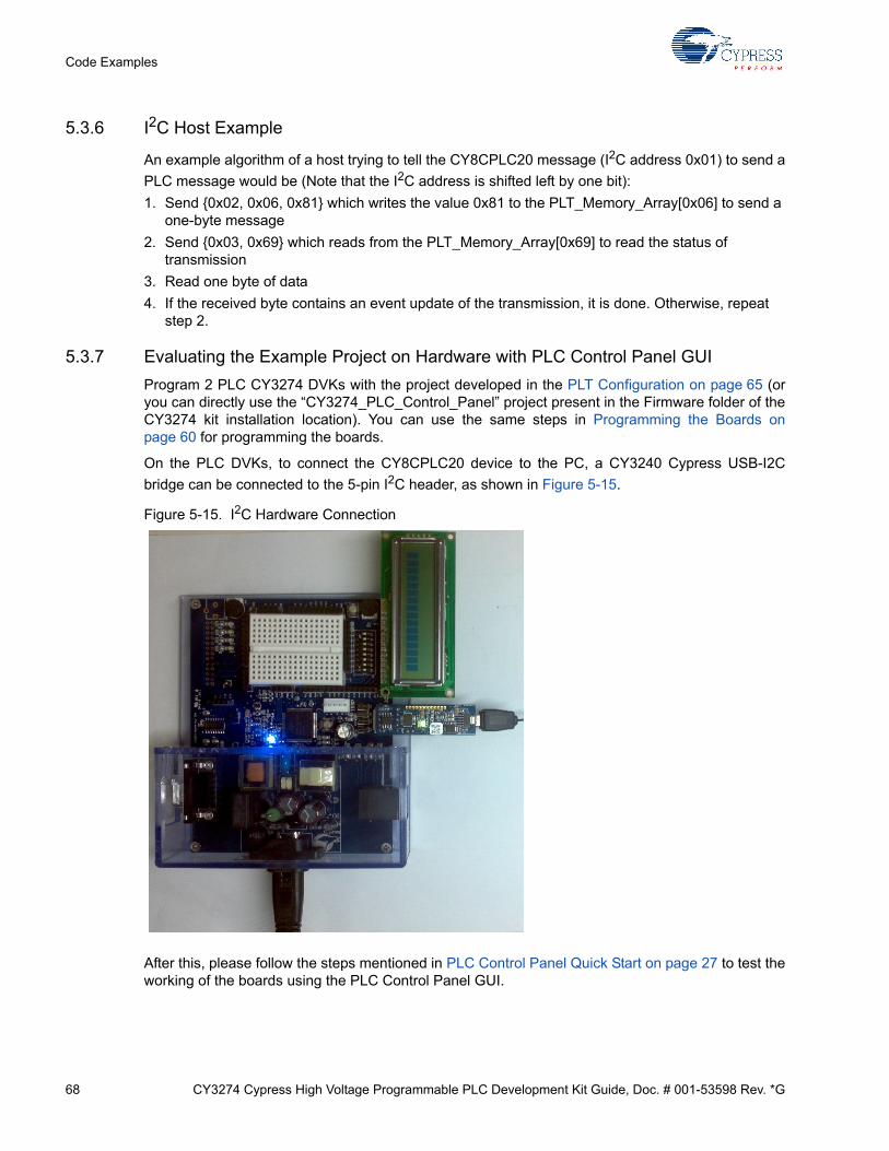
68 CY3274 Cypress High Voltage Programmable PLC Development Kit Guide, Doc. # 001-53598 Rev. *G
Code Examples
5.3.6 I2C Host Example
An example algorithm of a host trying to tell the CY8CPLC20 message (I2C address 0x01) to send a
PLC message would be (Note that the I2C address is shifted left by one bit):
1. Send {0x02, 0x06, 0x81} which writes the value 0x81 to the PLT_Memory_Array[0x06] to send a one-byte message
2. Send {0x03, 0x69} which reads from the PLT_Memory_Array[0x69] to read the status of transmission
3. Read one byte of data
4. If the received byte contains an event update of the transmission, it is done. Otherwise, repeat step 2.
5.3.7 Evaluating the Example Project on Hardware with PLC Control Panel GUI
Program 2 PLC CY3274 DVKs with the project developed in the PLT Configuration on page 65 (oryou can directly use the “CY3274_PLC_Control_Panel” project present in the Firmware folder of theCY3274 kit installation location). You can use the same steps in Programming the Boards onpage 60 for programming the boards.
On the PLC DVKs, to connect the CY8CPLC20 device to the PC, a CY3240 Cypress USB-I2C
bridge can be connected to the 5-pin I2C header, as shown in Figure 5-15.
Figure 5-15. I2C Hardware Connection
After this, please follow the steps mentioned in PLC Control Panel Quick Start on page 27 to test theworking of the boards using the PLC Control Panel GUI.
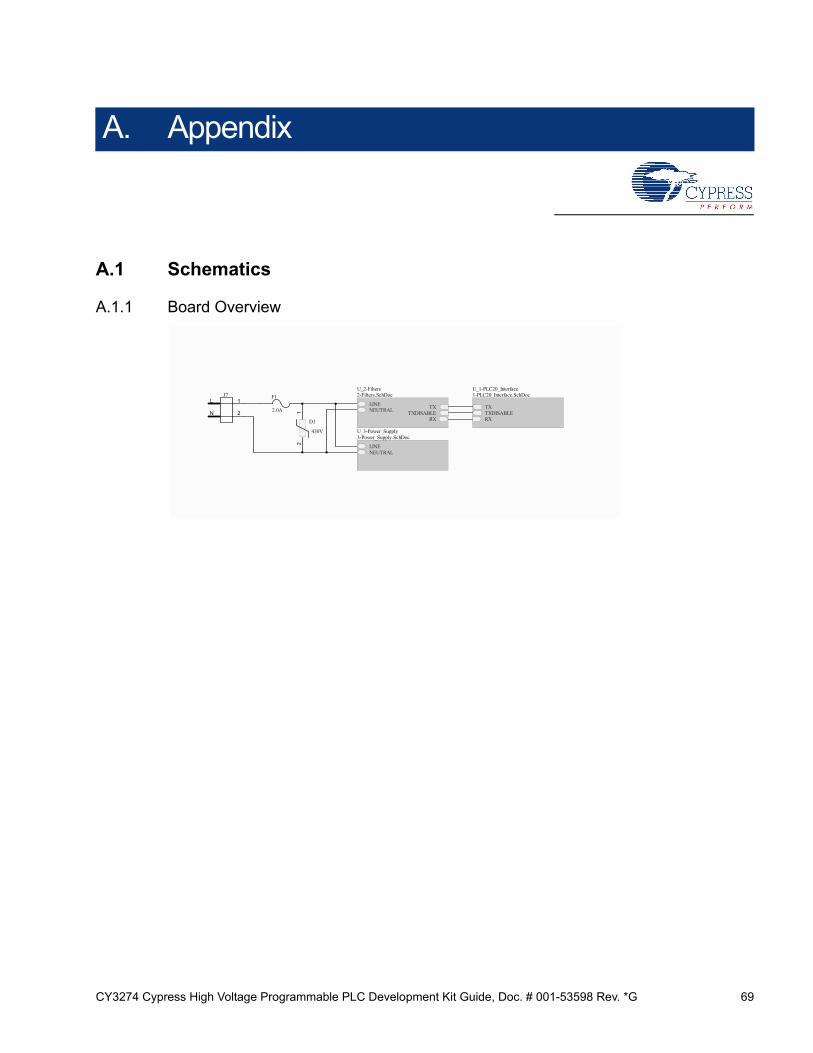
CY3274 Cypress High Voltage Programmable PLC Development Kit Guide, Doc. # 001-53598 Rev. *G 69
A. Appendix
A.1 Schematics
A.1.1 Board Overview
2
1L
N
J7
2.0A
F1
12
430V
D1
TX
RXTXDISABLE
U_1-PLC20_Interface1-PLC20_Interface.SchDoc
RX
TXTXDISABLE
LINENEUTRAL
U_2-Filters2-Filters.SchDoc
LINENEUTRAL
U_3-Power_Supply3-Power_Supply.SchDoc
70 CY3274 Cypress High Voltage Programmable PLC Development Kit Guide, Doc. # 001-53598 Rev. *G
A.1.2 User Interface
2
198 Cha
mpion
Cou
rtSa
n Jo
se, C
alifo
rnia
USA
951
34-170
94
PLC HV DVK
- Use
r Interface
CY32
74**
11/20/20
091:37
:02 PM
1-PL
C20
Interfa
ceSc
hDoc
Title
Size
:Num
ber:
Date:
File:
Rev
ision:
Shee
tof
Time:
B
*
Cyp
ress
Sem
icon
ductor
www.cyp
ress
.com
Vcc16
C1+
1
C1-
3
C2+
4
C2-
5
R1in
13
R2in
8
T1ou
t14
T2ou
t7
R1o
ut12
R2o
ut9
T1in
11
T2in
10
V+2
V-6
Gnd 15
MAX3232EC
DR
U8
1 6 2 7 3 8 4 9 5
DB9
-F
J19
VDD
VDD
0.47uF
,16V
C38
1.0uF,16V
C11
0.1uF,16V
C37
0.47uF
,16V
C25
0.47uF
,16V
C42U
ART
_RX
UART
_TX
P0[1]
3
P2[7]
4
P2[5]
5P2
[3]
6P2
[1]
7
P4[7] 8
P4[5] 9
P4[3] 10
P4[1] 11
P3[7] 16
P3[5] 17
P3[3] 18
P3[1] 19
P5[3]
22
P5[1]
23
P1[7]
24
P1[5]
28
P1[3]
29
P1[1]
30
P5[0]
52
P5[2]
53
P3[0] 56
P3[2] 57
P3[4] 58
P3[6] 59
XRES
62
P4[0] 63
P4[2] 64
P4[4] 66
P4[6] 67
P2[0]
68
P2[2]
69
P2[4]
70
P2[6]
72
P0[2]
77
P0[4]
79
P0[6]
81
P0[7]
95P0
[5]
97
P0[3]
99
P1[0]
44
P1[2]
45
P1[4]
46
P1[6]
47
P0[0]
74
P5[7]
20
P5[5]
21P5
[4]
54
P5[6]
55
P7[7]36
P7[6]37
P7[5]38
P7[4]39
P7[3]40
P7[2]41
P7[1]42
P7[0]43
P6[2]88
P6[0]86 P6[1]87
P6[3]89 P6[4]90 P6[5]91 P6[6]92 P6[7]93
U1A
CY8C
PLC20
OCD
NC
14
NC
48NC
49NC
50NC
51
NC
1
NC
2
NC
25
NC
26
NC
27
NC
31
NC
71
NC
73
NC
75
NC
76NC
78NC
80
NC
94NC
96NC
98NC
100
NC
33
NC
35
U1C C
Y8C
PLC20
OCD
Vss 1
Vdd 2
Vo 3
RS 4
R/W 5
E 6
D0 7
D1 8
D2 9
D3 10
D4 11
D5 12
D6 13
D7 14
LCD1
VDD
VDD
P17
P16
P15P1
3
P40
P37P36P35P34P33P32P31P30
P20
P22
P24
XRE
S
VDD
VDD
P15
P17
Vcc
1
GND
2
XRES
3
P1[1]
4
P1[0]
5
ISSP
_CON
J21
5-pin ISSP
Header
VDD P10
P11
XRE
S
R46
I2C Connector
I2C Pullup En
able
1 2
JP3
1 2
JP4
12345678910
J12
123456789
10
J10
P46P45
P44
P43P42P41P40
1 2 3 4
J20
Header 4
CTS
RTS
Red
LED4
1KR51
Red
LED3
1KR50
Red
LED2
1KR49
Red
LED1
VDD
1KR48
VDD
VDD
VDD 12
S4
1 2 3 4
J9
TXRX
VDD
VDD
12
Y2
32.768kH
z
22pF
C8
22pF
C7
GND
0.1uF
C5
2.10k
R2
0.01uF
C3
GND
GND
1uF
C6
TXDISAB
LE
1 2 3 4
J16
P01
P02
P04
1 2 3 4J13
1 2 3 4
J17
7.50k
R67.50k
R7
Vcc
1
GND
2
XRES
3
SClk
4
SData
5
I2C_C
ON
J15
5-pin ISSP
Header
12
JP5
RXP07
TX TXDISABL
E
P41P42P43P44P45P46P47
P10
P11
12345678
161514131211109
S3 SW-DIP8
GND
1 3 2
J22
12V LED
Supply Connector (D
NP
12V
1
LED_G
7 11
SHUTD
OWN
13
VF_S
EN1
15
VF_S
EN2
17 21
GND
3
LED_R
5
LED_B
9
VF_S
EN3
19
GND
23
12V
2512
V2620
I_SE
N3
16I_SE
N2
14I_SE
N1
1210
I2C_D
6
GND
245V
2218
I2C_C
8
GND
412
V2
J23
LED DaughterCard Co
nnector (DNP)
P21
P23
P25
P26
P50
P51
P52
P53
P12
P01
P02
P04
VDD
P30
P31
P32
P33
P34
P35
123456789
10
J1
GND
MTG
1
MTG
2
MTG
3
MTG
4
MOUNTING HOLE
S
1 2
JP1
12
S2VDD 33
0R8
VDD
Bread Bo
ard
H1 BR
EADBO
ARD
VDD
82
OCDE
12
OCDO
13
HCLK
60
CCLK
61
GND
15
VDD
32
GND
65GND
84GND
34VD
D83
GND
85
U1B
CY8C
PLC20 OCD
56R5
7
56R5
8
56R5
9
56R6
0
VDD
1KR64
1KR63
1KR62
1KR61
1KR65
VDD
100pF
C40
OCD
HC
OCDCC
OCDDO
OCDDE
XRES
TP1
Gnd
TP2
Gnd
TP3
Gnd
TP4
Gnd
1 2
J8
0.1uF
C1
DS3
GND
GND
GND
GRN
RED
YEL
DS2
DS4
Tx
Rx
BIU
1.00k
R3
1.00k
R1
1.00k
R4
24.00 MHz
EN1
GND
2
VCC
4
OUT
3
Y1
VDD
GND
0.01uFC4
1.0nF
C2
GND
1
OCDHC
2
XRES
3
OCDCC
4
GND
5
OCDDO
6
VCC
7
OCDDE
8
ICE CONN
J14
12345678910
J18
R47
CY3274 Cypress High Voltage Programmable PLC Development Kit Guide, Doc. # 001-53598 Rev. *G 71
A.1.3 Transmit and Receive Filters and Coupling
GND
VDD
7.50k
R22
1.00k
R25
4.99
R23
3
1
2
Q3
MMBT
3904
GND
VDD
2
1
3
FCX491A
Q1
2
1
3
FCX591A
Q2
GND
VPWR
4.02k
R16
1
3
2 D6
BAT5
4S
VDD
GND
4 3
2
1
6
5U2
LMH6639MF
GND
GND
GND
RX
TX TXDISAB
LE
4 3
2
1
65
U3
LMH6639MF
4 3
2
1
6
5U4
LMH6639MF
TX
TXDISABL
E
RX
10.0k
R29
36.5
R261.0nF
C20
GND
1.0nF
C22
37.4k
R19
3.83k
R21
41.2
R271.0nF
C21
1.0nF
C23
37.4k
R20
GND
0.1uF
C16
GND
0.1uF
C17
GND
0.1uF
C24
0.1uF
C18
GND
VPWR
10.0k
R30
10.0k
R31
0.01uF
C36
10.0k
R18
10.0k
R28
10.0uF
C19
GND
12
SMAJ12C
AD10
GND
22.1
R14
VPWR
10.0k
R17
1.0uF
C13
1.0uF
C15
10.0k
R15
GND
VPWR
2.0k
R10
0.01uF
C10
20.0k
R11
20.0k
R9
1500pF
C41
GND
GND
1 4
8 51:1
T1
Coupler
LINE
NEU
TRAL
1mH
L5
1.0uF
C14
X-CAP
1.0uF
C12
0.15uF
C9
72 CY3274 Cypress High Voltage Programmable PLC Development Kit Guide, Doc. # 001-53598 Rev. *G
A.1.4 Power Supply
4.7uF, 400V
C31
750k, 1%
R32
820k, 1%
R34
PGND
PGND
470pFC28
GND
330uF, 16VC32
GND
VPWR
Vin
3
1
Vou
t2
GND
U5
LD1117DT5
0CTR
GND
VDD
GND
Vou
t7
Isen
se6
IBC
4
GND
5
Vin
2
Vcc
8
Vsen
se1
Rin
3
U6
iW1690-07
PGND
12
B1100D
9
1.0
R37
68k, 1%
R36
100k
R38
2
3
1Q4
TS13003H
V3.9
R35
PGND
6.8k, 1%
R40
12k, 1%
R39
10uF
, 50V
C35
9 8
1 4 5 2
T2
1
2
3
4
24mH
T3
- 2
~3
+1
~4
DF1
0SD7
LINE
NEU
TRAL
1.5m
H
L3
22uH
L4
10.0uF
C33
0.1uF
C27
GND
10.0uF
C26
10.0k
R33
0.1uF
C34
4.7uF, 400V
C30
12
B1100
D8
GND
X1-CAP
Y1-CAP
0.022uF
C29
10, 5W
R41
402
R5
DS1
GND
BLUE
PWR
CY3274 Cypress High Voltage Programmable PLC Development Kit Guide, Doc. # 001-53598 Rev. *G 73
A.2 Layout
A.2.1 Top Layer
74 CY3274 Cypress High Voltage Programmable PLC Development Kit Guide, Doc. # 001-53598 Rev. *G
A.2.2 Ground Layer
CY3274 Cypress High Voltage Programmable PLC Development Kit Guide, Doc. # 001-53598 Rev. *G 75
A.2.3 Power Layer
76 CY3274 Cypress High Voltage Programmable PLC Development Kit Guide, Doc. # 001-53598 Rev. *G
A.2.4 Bottom Layer
CY3274 Cypress High Voltage Programmable PLC Development Kit Guide, Doc. # 001-53598 Rev. *G 77
A.2.5 Top Silkscreen
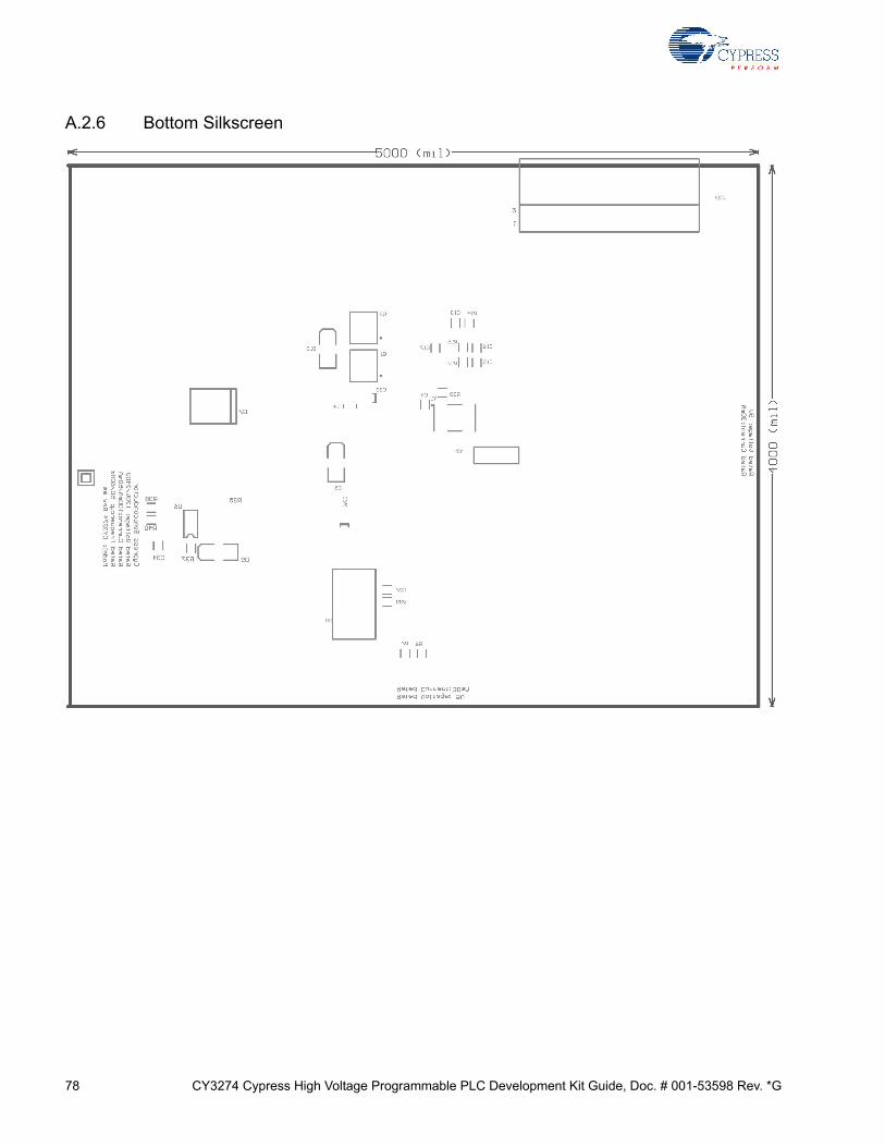
78 CY3274 Cypress High Voltage Programmable PLC Development Kit Guide, Doc. # 001-53598 Rev. *G
A.2.6 Bottom Silkscreen
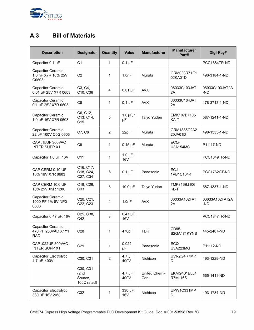
CY3274 Cypress High Voltage Programmable PLC Development Kit Guide, Doc. # 001-53598 Rev. *G 79
A.3 Bill of Materials
Description Designator Quantity Value ManufacturerManufacturer
Part#Digi-Key#
Capacitor 0.1 µF C1 1 0.1 µF PCC1864TR-ND
Capacitor Ceramic 1.0 nF X7R 10% 25V C0603
C2 1 1.0nF MurataGRM033R71E102KA01D
490-3184-1-ND
Capacitor Ceramic 0.01 µF 25V X7R 0603
C3, C4, C10, C36
4 0.01 µF AVX06033C103JAT2A
06033C103JAT2A-ND
Capacitor Ceramic 0.1 µF 25V X7R 0603
C5 1 0.1 µF AVX06033C104JAT2A
478-3713-1-ND
Capacitor Ceramic 1.0 µF 16V X7R 0603
C6, C12, C13, C14, C15
51.0 µF, 1 µF
Taiyo YudenEMK107B7105KA-T
587-1241-1-ND
Capacitor Ceramic 22 pF 100V C0G 0603
C7, C8 2 22pF MurataGRM1885C2A220JA01D
490-1335-1-ND
CAP .15UF 300VAC INTER SUPP X1
C9 1 0.15 µF MurataECQ-U3A154MG
P11117-ND
Capacitor 1.0 µF, 16V C11 11.0 µF, 16V
PCC1849TR-ND
CAP CERM 0.10 UF 10% 16V X7R 0603
C16, C17, C18, C24, C27, C34
6 0.1 µF PanasonicECJ-1VB1C104K
PCC1762CT-ND
CAP CERM 10.0 UF 10% 25V X5R 1206
C19, C26, C33
3 10.0 µF Taiyo YudenTMK316BJ106KL-T
587-1337-1-ND
Capacitor Ceramic 1000 PF 1% 5V NP0 0603
C20, C21, C22, C23
4 1.0nF AVX06033A102FAT2A
06033A102FAT2A-ND
Capacitor 0.47 µF, 16VC25, C38, C42
30.47 µF, 16V
PCC1847TR-ND
Capacitor Ceramic 470 PF 250VAC X1Y1 RAD
C28 1 470pF TDKCD95-B2GA471KYNS
445-2407-ND
CAP .022UF 300VAC INTER SUPP X1
C29 10.022 µF
PanasonicECQ-U3A223MG
P11112-ND
Capacitor Electrolytic 4.7 µF, 400V
C30, C31 24.7 µF, 400V
NichiconUVR2G4R7MPD
493-1229-ND
C30, C31 (2nd Source, 105C rated)
4.7 µF, 400V
United Chemi-Con
EKMG401ELL4R7MJ16S
565-1411-ND
Capacitor Electrolytic 330 µF 16V 20%
C32 1330 µF, 16V
NichiconUPW1C331MPD
493-1784-ND
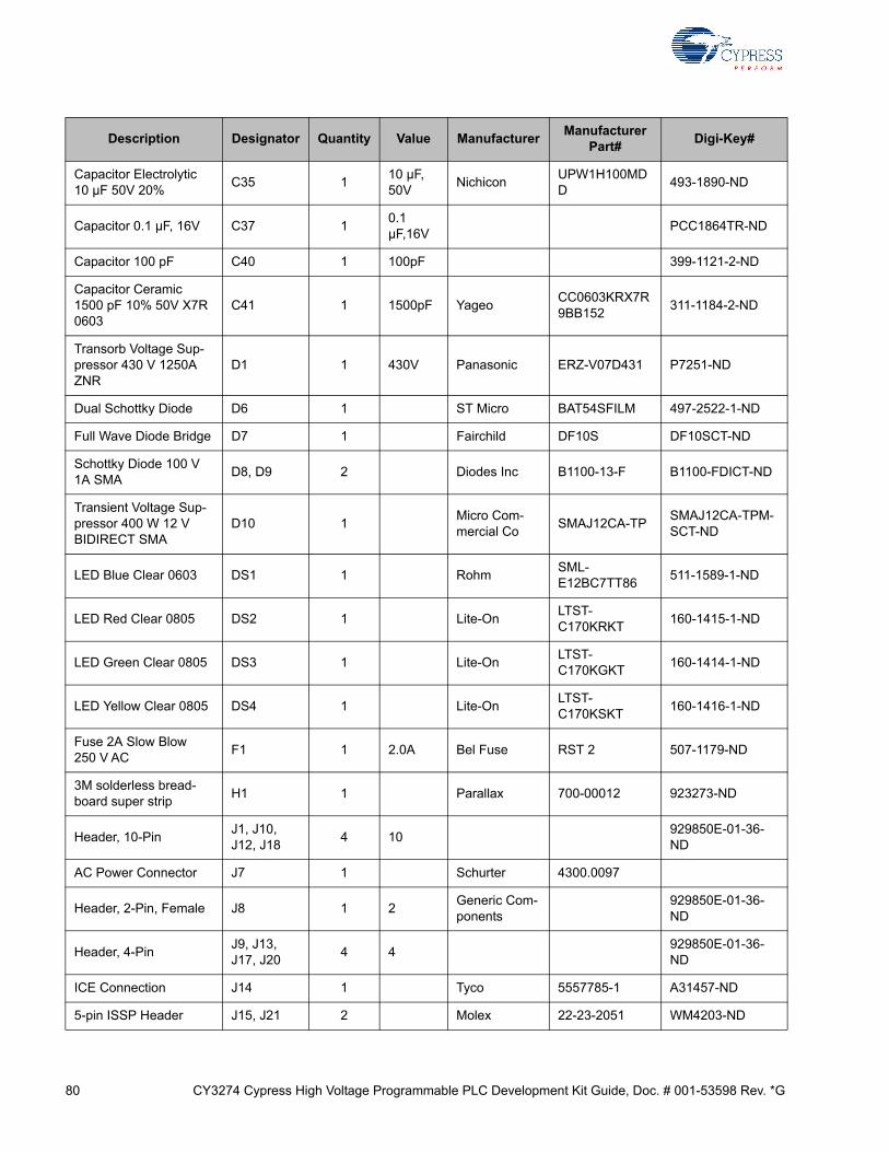
80 CY3274 Cypress High Voltage Programmable PLC Development Kit Guide, Doc. # 001-53598 Rev. *G
Capacitor Electrolytic 10 µF 50V 20%
C35 110 µF, 50V
NichiconUPW1H100MDD
493-1890-ND
Capacitor 0.1 µF, 16V C37 10.1 µF,16V
PCC1864TR-ND
Capacitor 100 pF C40 1 100pF 399-1121-2-ND
Capacitor Ceramic 1500 pF 10% 50V X7R 0603
C41 1 1500pF YageoCC0603KRX7R9BB152
311-1184-2-ND
Transorb Voltage Sup-pressor 430 V 1250A ZNR
D1 1 430V Panasonic ERZ-V07D431 P7251-ND
Dual Schottky Diode D6 1 ST Micro BAT54SFILM 497-2522-1-ND
Full Wave Diode Bridge D7 1 Fairchild DF10S DF10SCT-ND
Schottky Diode 100 V 1A SMA
D8, D9 2 Diodes Inc B1100-13-F B1100-FDICT-ND
Transient Voltage Sup-pressor 400 W 12 V BIDIRECT SMA
D10 1Micro Com-mercial Co
SMAJ12CA-TPSMAJ12CA-TPM-SCT-ND
LED Blue Clear 0603 DS1 1 RohmSML-E12BC7TT86
511-1589-1-ND
LED Red Clear 0805 DS2 1 Lite-OnLTST-C170KRKT
160-1415-1-ND
LED Green Clear 0805 DS3 1 Lite-OnLTST-C170KGKT
160-1414-1-ND
LED Yellow Clear 0805 DS4 1 Lite-OnLTST-C170KSKT
160-1416-1-ND
Fuse 2A Slow Blow 250 V AC
F1 1 2.0A Bel Fuse RST 2 507-1179-ND
3M solderless bread-board super strip
H1 1 Parallax 700-00012 923273-ND
Header, 10-PinJ1, J10, J12, J18
4 10929850E-01-36-ND
AC Power Connector J7 1 Schurter 4300.0097
Header, 2-Pin, Female J8 1 2Generic Com-ponents
929850E-01-36-ND
Header, 4-PinJ9, J13, J17, J20
4 4929850E-01-36-ND
ICE Connection J14 1 Tyco 5557785-1 A31457-ND
5-pin ISSP Header J15, J21 2 Molex 22-23-2051 WM4203-ND
Description Designator Quantity Value ManufacturerManufacturer
Part#Digi-Key#
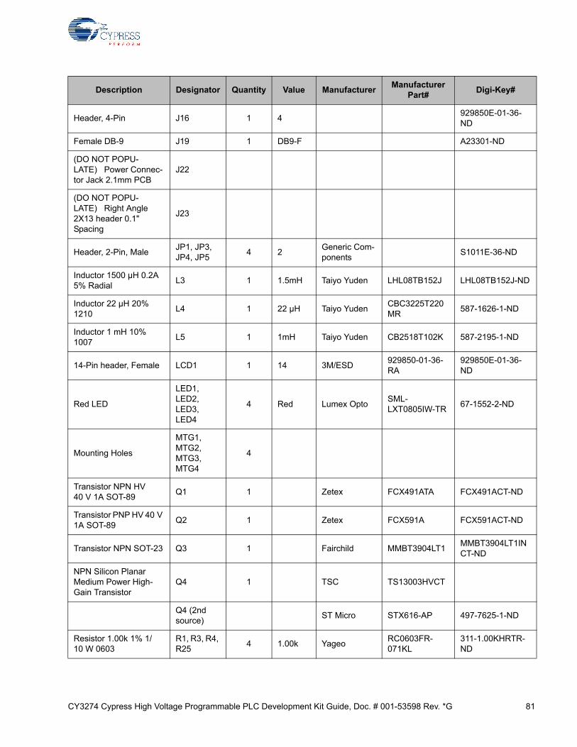
CY3274 Cypress High Voltage Programmable PLC Development Kit Guide, Doc. # 001-53598 Rev. *G 81
Header, 4-Pin J16 1 4929850E-01-36-ND
Female DB-9 J19 1 DB9-F A23301-ND
(DO NOT POPU-LATE) Power Connec-tor Jack 2.1mm PCB
J22
(DO NOT POPU-LATE) Right Angle 2X13 header 0.1" Spacing
J23
Header, 2-Pin, MaleJP1, JP3, JP4, JP5
4 2Generic Com-ponents
S1011E-36-ND
Inductor 1500 µH 0.2A 5% Radial
L3 1 1.5mH Taiyo Yuden LHL08TB152J LHL08TB152J-ND
Inductor 22 µH 20% 1210
L4 1 22 µH Taiyo YudenCBC3225T220MR
587-1626-1-ND
Inductor 1 mH 10% 1007
L5 1 1mH Taiyo Yuden CB2518T102K 587-2195-1-ND
14-Pin header, Female LCD1 1 14 3M/ESD929850-01-36-RA
929850E-01-36-ND
Red LED
LED1, LED2, LED3, LED4
4 Red Lumex OptoSML-LXT0805IW-TR
67-1552-2-ND
Mounting Holes
MTG1, MTG2, MTG3, MTG4
4
Transistor NPN HV 40 V 1A SOT-89
Q1 1 Zetex FCX491ATA FCX491ACT-ND
Transistor PNP HV 40 V 1A SOT-89
Q2 1 Zetex FCX591A FCX591ACT-ND
Transistor NPN SOT-23 Q3 1 Fairchild MMBT3904LT1MMBT3904LT1INCT-ND
NPN Silicon Planar Medium Power High-Gain Transistor
Q4 1 TSC TS13003HVCT
Q4 (2nd source)
ST Micro STX616-AP 497-7625-1-ND
Resistor 1.00k 1% 1/10 W 0603
R1, R3, R4, R25
4 1.00k YageoRC0603FR-071KL
311-1.00KHRTR-ND
Description Designator Quantity Value ManufacturerManufacturer
Part#Digi-Key#
82 CY3274 Cypress High Voltage Programmable PLC Development Kit Guide, Doc. # 001-53598 Rev. *G
Resistor 2.1k 1% 1/10 W 0603
R2 1 2.10k RohmMCR03EZPFX2101
RHM2.10KHCT-ND
Resistor 402 1% 1/10 W 0603
R5 1 402 YageoRC0603FR-07402RL
311-402HRTR-ND
Resistor 7.50k 1% 1/10 W 0603
R6, R7, R22
3 7.50k YageoRC0603FR-077K5L
311-7.50KHRTR-ND
Resistor 330 Ohm 1% 1/10 W 0603
R8 1 330 RohmMCR03EZPFX3300
RHM330HCT-ND
Resistor 20.0 k 1% 1/10 W 0603
R9, R11 2 20.0k YageoRC0603FR-0720KL
311-20.0KHRCT-ND
Resistor 2.0k 1% 1/10 W 0603
R10 1 2.0k YageoRC0603FR-072KL
311-2.00KHRCT-ND
Resistor 22.1 1% 1/10 W 0603
R14 1 22.1 YageoRC0603FR-0722R1L
311-22.1HRCT-ND
Resistor 10.0k 1% 1/10 W 0603
R15, R17, R18, R28, R29, R30, R31, R33
8 10.0k YageoRC0603FR-0710KL
311-10.0KHRTR-ND
Resistor 4.02k 1% 1/10W 0603
R16 1 4.02k YageoRC0603FR-072K02L
311-4.02KHRTR-ND
Resistor 37.4k 1% 1/10 W 0603
R19, R20 2 37.4k YageoRC0603FR-0737K4L
311-37.4KHRCT-ND
Resistor 3.83k 1% 1/10 W 0603
R21 1 3.83k YageoRC0603FR-073K83L
311-3.83KHRCT-ND
Resistor 4.99 1% 1/10 W 0603
R23 1 4.99 YageoRC0603FR-074R99L
311-4.99HRCT-ND
Resistor 36.5 1% 1/10 W 0603
R26 1 36.5 YageoRC0603FR-0736R5L
311-36.5HRCT-ND
Resistor 41.2 1% 1/10 W 0603
R27 1 41.2 YageoRC0603FR-0741R2L
311-41.2HRCT-ND
750 k 1% Resistor 1206 R32 1750k, 1%
YageoRC1206FR-07750KL
311-750KFRCT-ND
820 k 1% Resistor 1206 R34 1820k, 1%
YageoRC1206FR-07820KL
311-820KFRCT-ND
3.9 Ohm 1% Resistor 0805
R35 1 3.9 YageoRC0805FR-073R9L
311-3.90CRCT-ND
RES 68.0 K OHM 1/8W 1% 0805 SMD
R36 1 68k, 1% YageoRC0805FR-0768KL
311-68.0KCRTR-ND
RES 1.00 OHM 1/10W 1% 0603 SMD
R37 1 1.0 YageoRC0603FR-071RL
311-1.00HRCT-ND
Description Designator Quantity Value ManufacturerManufacturer
Part#Digi-Key#
CY3274 Cypress High Voltage Programmable PLC Development Kit Guide, Doc. # 001-53598 Rev. *G 83
RES 100 k OHM 1/10W 1% 0603 SMD
R38 1 100k YageoRC0603FR-07100KL
311-100KHRTR-ND
RES 12.0 K OHM 1/10W 1% 0603 SMD
R39 1 12k, 1% YageoRC0603FR-0712KL
311-12.0KHRCT-ND
6.8k, 1% Resistor 0603 R40 1 6.8k, 1% YageoRC0603FR-076K8L
311-6.80KHRTR-ND
RESISTOR 10.0 OHM 5W 5% WIREWND
R41 1 10, 5W VishayAC05000001009JAC00
PPC5W10.0CT-ND
Potentiometer R46, R47 2 Bourns Inc 3352T-1-103LF 3352T-103LF-ND
Resistor 1.0 K, SMT
R48, R49, R50, R51, R61, R62, R63, R64, R65
9 1K PanasonicERJ-6GEYJ102V
P1.0KACT-ND
Resistor 56 Ohm, SMTR57, R58, R59, R60
4 56 P56ACT-ND
Swtich, SPST S2, S4 2 Omron B3F-1022 SW403-ND
4009 Series DIP Switch, Raised actuator
S3 1 ESwitch KAJ08LAGT EG4441-ND
Isolation Transformer T1 1Precision Components
0505-0821G
Power Trasnsformer EE-16
T2 1 3.2mHShenzen Goldenway
EE-16 (5+5) (rev-A)
T2 (2nd Source)
1Renco Elec-tronics
RLCY-1014
24 mH Common Mode Choke
T3 1 24mHShenzen Goldenway
EE8.3(2+2)-hori, (rev-A)
T3 (2nd Source)
1Renco Elec-tronics
RLCY-1013
Simple Test pointTP1, TP2, TP3, TP4
4 5006K-ND
CY8CPLC20 OCD Part U1 1 CypressCY8CPLC20-OCD
Op-Amp 190 MHz U2, U3, U4 3National Semiconduc-tor
LMH6639MF/NOPB
LMH6639MFCT-ND
Voltage Regulator 5 V U5 1 ST MicroLD1117DT50CTR
497-1237-1-ND
Off-Line Switcher U6 1 iWatt iW1690-07
Description Designator Quantity Value ManufacturerManufacturer
Part#Digi-Key#
84 CY3274 Cypress High Voltage Programmable PLC Development Kit Guide, Doc. # 001-53598 Rev. *G
RS-232 tranceiver (1.0 µF Caps)
U8 1 MAX3232ECDR 296-19851-2-ND
Oscillator Y1 124.00 MHz
Crystek C3290-24.000 C3290-24.000-ND
Y1 (2nd Source)
CitizenCSX750FCC24.000M-UT
300-7214-2-ND
Crystal 32.768 kHz 12.5 pF
Y2 132.768kHz
ECS Inc. ECS-3X8X X1123-ND
LCD Module LCD1 1Cypress Semiconduc-tor
1187-00003
Description Designator Quantity Value ManufacturerManufacturer
Part#Digi-Key#
CY3274 Cypress High Voltage Programmable PLC Development Kit Guide, Doc. # 001-53598 Rev. *G 85
Revision History
Document Revision HistoryDocument Title: CY3274 Cypress High Voltage Programmable Powerline Communication Development Kit Guide
Document Number: 001-53598
Revision ECN# Issue DateOrigin of Change
Description of Change
** 2752289 8/14/09 IUS New kit guide.
*A 2759193 9/3/09 IUS Rework for external release.
*B 2825364 12/10/09 RARP Content updates.
*C 3040868 09/28/10 RKPM
Updated Introduction chapter on page 7:
Added “Technical Reference” on page 12.
Updated Getting Started chapter on page 13:
Added “Software Installation” on page 13.
Updated PLC Development Board chapter on page 41:
Updated “Hardware Description” on page 42:
Added schematic s (Figure 4-8, Figure 4-9, Figure 4-10).
Added “Code Example” on page 30.
*D 3190764 03/08/2011 FRE
Updated Introduction chapter on page 7:
Updated “The Cypress PLC Solution” on page 8:
Added references to the compatible high voltage PLC kits.
Updated PLC Development Board chapter on page 41:
Updated “Hardware Description” on page 42:
Updated “RJ45 Connector for Debugging” on page 47:
Added a reference to the quick start guide for evaluation.
Added clarifications to the text throughout.
*E 3403015 10/12/2011 ADIY
Removed references of CY3276 and CY8CLED16P01 in all instances across the document.
Updated Introduction chapter on page 7:
Updated “The Cypress PLC Solution” on page 8:
Updated Figure 1-3.
Updated hyperlinks in Note above Figure 1-3.
Added “Additional Learning Resources” on page 10
Added Getting Started chapter on page 13.
*F 4120074 09/11/2013 ADIYNo technical updates.
Completing Sunset Review.
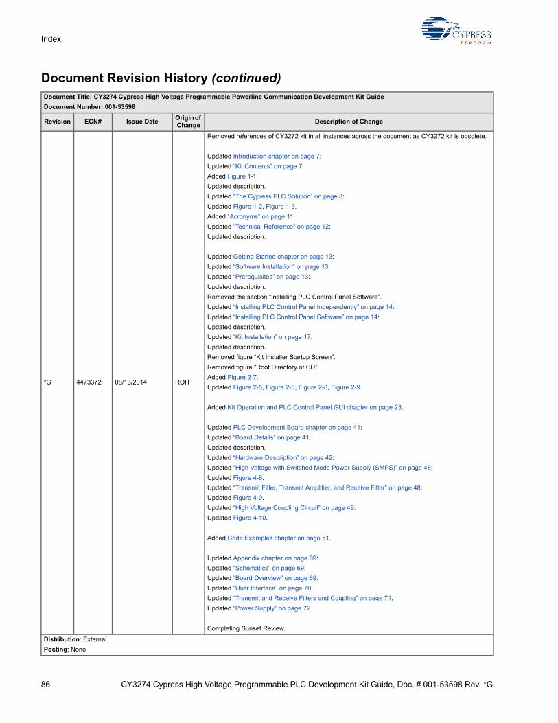
86 CY3274 Cypress High Voltage Programmable PLC Development Kit Guide, Doc. # 001-53598 Rev. *G
Index
*G 4473372 08/13/2014 ROIT
Removed references of CY3272 kit in all instances across the document as CY3272 kit is obsolete.
Updated Introduction chapter on page 7:
Updated “Kit Contents” on page 7:
Added Figure 1-1.
Updated description.
Updated “The Cypress PLC Solution” on page 8:
Updated Figure 1-2, Figure 1-3.
Added “Acronyms” on page 11.
Updated “Technical Reference” on page 12:
Updated description.
Updated Getting Started chapter on page 13:
Updated “Software Installation” on page 13:
Updated “Prerequisites” on page 13:
Updated description.
Removed the section “Installing PLC Control Panel Software”.
Updated “Installing PLC Control Panel Independently” on page 14:
Updated “Installing PLC Control Panel Software” on page 14:
Updated description.
Updated “Kit Installation” on page 17:
Updated description.
Removed figure “Kit Installer Startup Screen”.
Removed figure “Root Directory of CD”.
Added Figure 2-7.
Updated Figure 2-5, Figure 2-6, Figure 2-8, Figure 2-9.
Added Kit Operation and PLC Control Panel GUI chapter on page 23.
Updated PLC Development Board chapter on page 41:
Updated “Board Details” on page 41:
Updated description.
Updated “Hardware Description” on page 42:
Updated “High Voltage with Switched Mode Power Supply (SMPS)” on page 48:
Updated Figure 4-8.
Updated “Transmit Filter, Transmit Amplifier, and Receive Filter” on page 48:
Updated Figure 4-9.
Updated “High Voltage Coupling Circuit” on page 49:
Updated Figure 4-10.
Added Code Examples chapter on page 51.
Updated Appendix chapter on page 69:
Updated “Schematics” on page 69:
Updated “Board Overview” on page 69.
Updated “User Interface” on page 70.
Updated “Transmit and Receive Filters and Coupling” on page 71.
Updated “Power Supply” on page 72.
Completing Sunset Review.
Distribution: External
Posting: None
Document Revision History (continued)Document Title: CY3274 Cypress High Voltage Programmable Powerline Communication Development Kit Guide
Document Number: 001-53598
Revision ECN# Issue DateOrigin of Change
Description of Change