control of the light transmission through a quasiperiodic waveguide
TRANSCRIPT

Control of the light transmission througha quasiperiodic waveguide
Priya Rose T., Gianluigi Zito, Emiliano Di Gennaro,∗Giancarlo Abbate, and Antonello Andreone
CNR-SPIN and Department of Physical Sciences, Universita di Napoli “Federico II,” Naples,Italy
Abstract: We studied the waveguiding properties of a photonic quasicrys-tal based on an octagonal tiling. The structure exhibits intrinsic localisationin the band gap region, that can be exploited to manipulate the signal trans-mission through a linear defect. The electromagnetic characteristics are firstnumerically analysed using a full wave simulation and then experimentallyverified by measurements carried out in the X-band microwave region.Possible photonic applications include tunable notch filters having largeattenuation.
© 2012 Optical Society of America
OCIS codes: (050.5298) Photonic crystals; (130.5296) Photonic crystal waveguides.
References and links1. A. Della Villa, S. Enoch, G. Tayeb, V. Pierro, V. Galdi, and F. Capolino, “Localized modes in photonic quasicrys-
tals with Penrose-type lattice,” Phys. Rev. Lett. 94, 183903 (2005).2. Y. Wang, Y. Wang, S. Feng, and Z.-Y. Li, “The effect of short-range and long-range orientational orders on the
transmission properties of quasiperiodic photonic crystals,” Europhys. Lett. 74, 49–54 (2006).3. C. Jin, B. Cheng, B. Man, Z. Li, D. Zhang, S. Ban, and B. Sun, “Band gap and wave guiding effect in a quasiperi-
odic photonic crystal,” Appl. Phys. Lett. 75, 1848–1850 (1999).4. M. Zoorob, P. G. Charlton, M. D. B., J. Baumberg, and M. Netti, “Complete and absolute photonic bandgaps in
highly symmetric photonic quasicrystals embedded in low refractive index materials,” Mat. Scien. and Eng. B74, 168–174 (2000).
5. M. Florescu, S. Torquato, and P. J. Steinhardt, “Complete band gaps in two-dimensional photonic quasicrystals,”Phys. Rev. B 80, 155112 (2009).
6. T. PriyaRose, E. Di Gennaro, G. Abbate, and A. Andreone, “Isotropic properties of the photonic band gap inquasicrystals with low-index contrast,” Phys. Rev. B 84, 125111 (2011).
7. A. Della Villa, S. Enoch, G. Tayeb, V. Pierro, V. Galdi, and F. Capolino, “Localized modes in photonic quasicrys-tals with penrose-type lattice,” Opt. Express 14, 10021–10027 (2006).
8. Y. Neve-Oz, T. Pollok, S. Burger, M. Golosovsky, and D. Davidov, “Resonant transmission of electromagneticwaves through two-dimensional photonic quasicrystals,” J. Appl. Phys. 107, 063105 (2010).
9. Y. Wang, X. Hu, X. Xu, B. Cheng, and D. Zhang, “Localized modes in defect-free dodecagonal quasiperiodicphotonic crystals,” Phys. Rev. B. 68, 165106 (2003).
10. G. Zito, T. Priya Rose, E. Di Gennaro, A. Andreone, E. Santamato, and G. Abbate, “Bandgap properties oflow-index contrast aperiodically ordered photonic quasicrystals,” Microw. Opt. Technol. Lett. 51, 2732–2737(2009).
11. Simulation software package developed at MIT, (http://ab-initio.mit.edu/wiki/index.php/Meep).12. Harminv, (cfr. http://ab-initio.mit.edu/wiki/index.php/Harminv).13. See for example the 6th chapter of “Photonic Crystals: Molding the Flow of Light,” John D. Joannopoulos,
Robert D. Meade, and Joshua N. Winnfree (Princeton University Press, 2008)14. S. Savo, E. Di Gennaro, and A. Andreone, “Superlensing properties of one-dimensional dielectric photonic crys-
tals,” Opt. Express 17, 19848–19856 (2009).15. S. Fan, P. Villeneuve, J. Joannopoulos, and H. Haus, “Channel drop filters in photonic crystals,” Opt. Express 3,
4–11 (1998).
#160960 - $15.00 USD Received 4 Jan 2012; revised 28 Feb 2012; accepted 5 Mar 2012; published 2 Nov 2012(C) 2012 OSA 5 November 2012 / Vol. 20, No. 23 / OPTICS EXPRESS 26056

16. J. Romero-Vivas, D. Chigrin, A. Lavrinenko, and C. S. Torres, “Resonant add-drop filter based on a photonicquasicrystal,” Opt. Express 13, 826–835 (2005).
1. Introduction
Unlike their periodic counterparts, the electromagnetic (EM) properties of photonic quasicrys-tals (PQCs) are strongly dependent on the short-range order of the lattice [1,2]. Because of theirstructural peculiarities such as a higher order of rotational symmetries (> 6, not allowed for pe-riodic crystals) and the presence of many non-equivalent sites, PQCs can present novel andinteresting features, including highly isotropic and low index contrast band gaps [3–6] and in-trinsic localisation both in transparency [7,8] and in stop bands [5,9]. In particular, contrarily towhat happens in the periodic case, some aperiodically ordered photonic crystals show localisedmodes without intentionally created defects, affecting the EM response of devices based onthese peculiar structures. In this letter, we use a full wave analysis to study the transmissionof light in a linear waveguide based on a specific geometry with 8-fold rotational symmetryhaving intrinsic localisation in a photonic band gap (PBG) frequency region. We show that thewaveguide response can be controlled introducing an additional defect in close proximity of thelocalised mode. These peculiar characteristics are then experimentally verified performing sig-nal transmission and electric field spatial measurements in a quasicrystalline structure operatingin the X-band microwave region.
Samples and method
The 2D quasiperiodic geometry is based on the interference pattern of 8 coherent beams ac-cording to the following formula for the irradiance profile:
I(r) =8
∑l=1
8
∑m=1
AlA∗m exp[i(kl −km) · r+ i(φl −φm)] (1)
where Al , kl , and φl are the amplitudes, the wavevectors, and the initial phases of the interferingbeams, respectively. The phase of the interfering beams is periodically shifted by π
2 , such thatφ1 = φ5 = 0, φ2 = φ4 = φ6 = φ8 =
π2 , and φ3 = φ7 = π . The wave vectors kl of the beams are
equally distributed along the (x,y)-plane, whereas all the beams are linearly polarized alongthe z direction. The scatterers are represented by infinitely long dielectric rods (principal axisalong the z direction) displaced to occupy the regions where the interference pattern shows itslocal maxima. Their position is determined by choosing a threshold value for the light intensitylevel. Fixing also the rods radius, the filling factor η , defined as the ratio between the regionsshowing a high refractive index and the total area, is determined [10].
The sample under study in this work is a finite square tiling composed of 365 cylindrical rodsof alumina (dielectric constant ε = 8.6) with radius r = 0.3a, where a is a characteristic length,and filling factor η = 0.26. Crystal parameters have been optimised to ensure the formationof clear PBG regions, avoiding at the same time the overlapping of the scatterers. The rodsare placed in air according to the 8-fold symmetrical pattern described by Eq. (1), as shown inFig. 1.
To study EM propagation properties through the sample, numerical simulations are per-formed by using MEEP [11], a freeware code which uses the finite difference time domain(FDTD) method. Space discretization is set to have a grid resolution of 0.067a, which ensuresa number of pixels per wavelength in the range from 40 to 60. Perfectly matched layers, sur-rounding the whole area, are included to avoid spurious reflections from the boundaries. Atime-pulsed collimated Gaussian beam with TM polarization (electric field parallel to the rodaxis) and a waist of 10a is impinging on the sample from the left side (continuous line in Fig. 1).
#160960 - $15.00 USD Received 4 Jan 2012; revised 28 Feb 2012; accepted 5 Mar 2012; published 2 Nov 2012(C) 2012 OSA 5 November 2012 / Vol. 20, No. 23 / OPTICS EXPRESS 26057
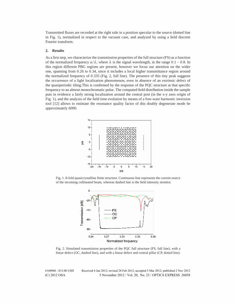
Transmitted fluxes are recorded at the right side in a position specular to the source (dotted linein Fig. 1), normalized in respect to the vacuum case, and analyzed by using a field discreteFourier transform.
2. Results
As a first step, we characterize the transmission properties of the full structure (FS) as a functionof the normalized frequency a/λ , where λ is the signal wavelength, in the range 0.1− 0.8. Inthis region different PBG regions are present, however we focus our attention on the widerone, spanning from 0.26 to 0.34, since it includes a local higher transmittance region aroundthe normalized frequency of 0.335 (Fig. 2, full line). The presence of this tiny peak suggeststhe occurrence of a light localization phenomenon, even in absence of an extrinsic defect ofthe quasiperiodic tiling.This is confirmed by the response of the PQC structure at that specificfrequency to an almost monochromatic pulse. The computed field distribution inside the sampleputs in evidence a fairly strong localization around the central post (in the x-y axes origin ofFig. 1), and the analysis of the field time evolution by means of a free-ware harmonic inversiontool [12] allows to estimate the resonance quality factor of this doubly degenerate mode beapproximately 6000.
Fig. 1. 8-fold quasicrystalline finite structure. Continuous line represents the current sourceof the incoming collimated beam, whereas dashed line is the field intensity monitor.
Fig. 2. Simulated transmission properties of the PQC full structure (FS, full line), with alinear defect (OC, dashed line), and with a linear defect and central pillar (CP, dotted line).
#160960 - $15.00 USD Received 4 Jan 2012; revised 28 Feb 2012; accepted 5 Mar 2012; published 2 Nov 2012(C) 2012 OSA 5 November 2012 / Vol. 20, No. 23 / OPTICS EXPRESS 26058

We then design a linear waveguide (OC) creating an open channel within the structure byremoving all rods in a central strip having a lateral size of 2.75a. As expected, the OC frequencyresponse shows a high transmission level in all the bandgap regions, but a marked dip in closeproximity of the localized mode, specularly to the local maximum exhibited by the full structurein the main PBG (Fig. 2, dashed line). Indeed, the presence of a linear defect passing through themiddle of the PQC sample does not produce a significant effect on the localization properties,slightly changing only the resonance frequency of the mode.
To better understand the influence of localisation in the waveguide properties, we show inFig. 3(a) the electric field map produced by a continuous wave source at the localized modefrequency. The radiation travels throughout the waveguide until it reaches the position where thecentral pillar should be, behind this point the light propagation is inhibited. The analysis of thefield map time evolution indicates the presence of standing waves inside the waveguide, whichrepresents a clear evidence that the light is reflected back in correspondence of the channelmidpoint, giving rise to the transmission dip shown in Fig. 2.
We then study the influence of a mode perturbation on the transmission properties of the PQClinear waveguide. We consider the sample with an open channel and an additional pillar placedin its center (CP) (x-y origin). As it can be seen from (Fig. 2 (dotted line), signal transmissionis fully restored at the localized mode frequency and is almost unaffected in the remainingpart of the frequency range analyzed. It is also clear from the electric field map shown inFig. 3(b) that, when the central pillar is present, reflection is strongly damped and light can passthrough the whole waveguide as it would happen in a simple periodic linear waveguide [13]. If’milder’ pertubations are considered, the localized mode can be tuned. Indeed, decreasing thedielectric constant or the radius of the pillar, a dip in the transmission characteristics appearsand becomes more and more evident, whereas the frequency gradually downshifts until theoverall e.m. response superimposes on what observed in the OC case. Similar effect can be alsoobserved by gradually misplacing the pillar from the central position.
Fig. 3. Electric field z-component spatial maps for the OC sample (a) and the CP sample(b) at the normalised frequency 0.335 where the localised mode occurs.
In order to experimentally verify these results, we designed and carried out measurements
#160960 - $15.00 USD Received 4 Jan 2012; revised 28 Feb 2012; accepted 5 Mar 2012; published 2 Nov 2012(C) 2012 OSA 5 November 2012 / Vol. 20, No. 23 / OPTICS EXPRESS 26059
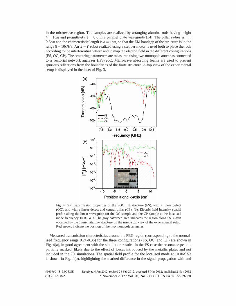
in the microwave region. The samples are realized by arranging alumina rods having heighth = 1cm and permittivity ε = 8.6 in a parallel plate waveguide [14]. The pillar radius is r =0.3cm and the characteristic length is a = 1cm, so that the EM bandgap of the structure is in therange 8−10GHz. An X −Y robot realized using a stepper motor is used both to place the rodsaccording to the interferential pattern and to map the electric field in the different configurations(FS, OC, CP). The scattering parameters are measured using two monopole antennas connectedto a vectorial network analyzer HP8720C. Microwave absorbing foams are used to preventspurious reflections from the boundaries of the finite structure. A top view of the experimentalsetup is displayed in the inset of Fig. 3.
Fig. 4. (a): Transmission properties of the PQC full structure (FS), with a linear defect(OC), and with a linear defect and central pillar (CP). (b): Electric field intensity spatialprofile along the linear waveguide for the OC sample and the CP sample at the localisedmode frequency 10.06GHz. The gray patterned area indicates the region along the x-axisoccupied by the quasicristalline structure. In the inset a top view of the experimental setup.Red arrows indicate the position of the two monopole antennas.
Measured transmission characteristics around the PBG region (corresponding to the normal-ized frequency range 0.24-0.36) for the three configurations (FS, OC, and CP) are shown inFig. 4(a), in good agreement with the simulation results. In the FS case the resonance peak ispartially masked, likely due to the effect of losses introduced by the metallic plates and notincluded in the 2D simulations. The spatial field profile for the localised mode at 10.06GHzis shown in Fig. 4(b), highlighting the marked difference in the signal propagation with and
#160960 - $15.00 USD Received 4 Jan 2012; revised 28 Feb 2012; accepted 5 Mar 2012; published 2 Nov 2012(C) 2012 OSA 5 November 2012 / Vol. 20, No. 23 / OPTICS EXPRESS 26060

without the central dielectric pillar in the waveguide. The presence of the central pillar clearlymodifies the light transmission at the frequency corresponding to the localized state. The signalis restored and travels through the linear waveguide almost unaffected.
3. Conclusion
We have numerically found and experimentally verified that the waveguiding properties of aphotonic quasicrystal structure with 8-fold rotational symmetry are affected by the presence ofdefect-free localized states within the photonic band gap.
The introduction of a perturbation (defect) in the linear channel alters the transmissionthrough the waveguide. Actually, the defect affects the degeneracy of the resonant mode in-trinsically localized in that position, allowing or preventing the signal propagation. This findingis analogous to what have been previously observed in numerical studies on add-and-drop filtersbased on both periodic [15] and quasiperiodic [16] dielectric structures. In those works two par-allel linear waveguides are coupled by means of an extrinsic defect. Here we use instead a singlewaveguide and exploit the intrinsic defect of the quasiperiodic structure. In all these cases thepresence of two degenerate modes with opposite symmetries seems to favour the propagationin the backward direction and to inhibit the propagation in the forward direction. Consequentlythe EM properties of the waveguide can be tuned changing the defect characteristics (radius,dielectric constant, position).
Obviously, since these peculiar effects are associated to the presence of a localized stated,their EM behaviour is extremely confined in terms of frequency, suggesting that 8-fold qua-sicrystalline structure can be exploited for the realisation of photonic tunable notch filters hav-ing very narrow bandwidth and a large attenuation.
#160960 - $15.00 USD Received 4 Jan 2012; revised 28 Feb 2012; accepted 5 Mar 2012; published 2 Nov 2012(C) 2012 OSA 5 November 2012 / Vol. 20, No. 23 / OPTICS EXPRESS 26061