comparative studies of undoped/al-doped/in-doped zno
TRANSCRIPT

Citation: Koralli, P.; Varol, S.F.;
Mousdis, G.; Mouzakis, D.E.;
Merdan, Z.; Kompitsas, M.
Comparative Studies of
Undoped/Al-Doped/In-Doped ZnO
Transparent Conducting Oxide Thin
Films in Optoelectronic Applications.
Chemosensors 2022, 10, 162.
https://doi.org/10.3390/
chemosensors10050162
Academic Editor: Tun Cao
Received: 23 February 2022
Accepted: 25 April 2022
Published: 28 April 2022
Publisher’s Note: MDPI stays neutral
with regard to jurisdictional claims in
published maps and institutional affil-
iations.
Copyright: © 2022 by the authors.
Licensee MDPI, Basel, Switzerland.
This article is an open access article
distributed under the terms and
conditions of the Creative Commons
Attribution (CC BY) license (https://
creativecommons.org/licenses/by/
4.0/).
chemosensors
Article
Comparative Studies of Undoped/Al-Doped/In-Doped ZnOTransparent Conducting Oxide Thin Films inOptoelectronic ApplicationsPanagiota Koralli 1,* , Songül Fiat Varol 2 , George Mousdis 1 , Dionysios E. Mouzakis 3,* , Ziya Merdan 4
and Michael Kompitsas 1
1 National Hellenic Research Foundation, 48 Vassileos Constantinou Avenue, 11635 Athens, Greece;[email protected] (G.M.); [email protected] (M.K.)
2 Electric and Energy Department, Vocational School of Technical Sciences, Manisa Celal Bayar University,45140 Manisa, Turkey; [email protected]
3 Hellenic Army Academy, Leoforos Eyelpidon (Varis-Koropiou) Avenue, Vari P.O., 16673 Attica, Greece4 Physics Department, Faculty of Arts and Sciences, Gazi University, 06500 Ankara, Turkey;
[email protected]* Correspondence: [email protected] (P.K.); [email protected] (D.E.M.)
Abstract: In this paper, undoped, Al-, and In-doped zinc oxide thin films were deposited. Film growthwas performed using the sol–gel technique. The method included (a) preparing homogeneous andstable solutions of zinc acetate 2-hydrate, (b) mixing them with aluminum nitrate and indium acetatein 2-methoxyethanol and 2-aminoethanol solutions with various concentrations, and (c) spin coatingthem onto transparent glass substrates. After thermal annealing, the films showed a high transparency(80–90%) and good stability. Using typical diagnostic tools, the structural, morphological, optical,and electrical film properties were investigated and linked to the dopant type, and concentrations inview of optoelectronics were investigated.
Keywords: ZnO; Al-doped ZnO; In-doped ZnO; nanomaterials; thin films; sol–gel spin coating;optoelectronics; physical properties; electrical properties
1. Introduction
Transparent conductive metal oxides (TCOs) are very attractive materials, both forresearch and industry. In general, they provide excellent properties, such as high opti-cal transmittance in the UV-VIS-NIR spectrum and high free-carrier density resulting ingood electrical conductivity [1]. In particular, zinc oxide (ZnO) is an n-type transparentsemiconductor with a direct wide bandgap of 3.37 eV. Furthermore, it crystallizes in thestable wurtzite structure with a lattice constant of 3.25 Å and has a large exciton bindingenergy (60 meV). It has been explored in a variety of applications, such as plasma displaypanels, surface acoustic waves, optical waveguides, flexible displays, photodetectors, andlight-emitting diodes (LEDs). To meet the requirements of high-brightness LEDs, thewide-bandgap ZnO semiconductor, with its excellent structural and physical properties, isa better candidate compared to GaN [2]. In addition, ZnO thin films have been used forthe development of transparent electrodes for solar cells [3–7], various types of sensors(chemical, bio, and gas) [8,9], thin-film transistors [10], photoconductive detectors [11], andpiezoelectric transducers [12]. Furthermore, its salient characteristics are the variety of itssynthetic methods, its non-toxicity, and its high stability. Its structure plays an essential rolein the determination of a devices’ performance (e.g., power conversion efficiency, lifetime,and stability).
ZnO thin films have been grown using various methods, such as spray pyrolysis [13],pulsed laser deposition (PLD) [14], and molecular beam epitaxy (MBE) [15]. Solution-basedmethods, such as solvothermal/hydrothermal and sol–gel processes, are more attractive
Chemosensors 2022, 10, 162. https://doi.org/10.3390/chemosensors10050162 https://www.mdpi.com/journal/chemosensors

Chemosensors 2022, 10, 162 2 of 15
because of the mild synthesis conditions used. In particular, these methods are character-ized by low-temperature processing, large substrate area film growth, easy film thicknesscontrol, increased homogeneity and purity, efficient microstructural control of metallic par-ticles, high film density and uniformity, and, most importantly, cost effectiveness [7,16,17]for industrial applications.
In fact, ZnO is defined as a savior material as a transparent electrode in OrganicLight-Emitting Diode (OLED) applications [18–20]. ZnO/GaN n-p heterojunctions arethe most preferred semiconductors for optoelectronic devices. It is well known that theprocess of producing GaN is very complex. In particular, to produce p-type GaN, dopingand activating Mg and keeping the carrier concentration at the desired level (>1019) [21]involve a laborious and costly process such as MOCVD. However, n-type ZnO can be easilyproduced with the economical sol–gel spin coating technique, which provides high control-lability and a straightforward and practical methodology. Therefore, in the production ofZnO/GaN, we can at least achieve ZnO production at a more reasonable cost, making theproduction of the whole p-n structure more attractive.
In photovoltaic devices, doped indium tin oxide (ITO) and indium zinc oxide (IZO)conductive oxides are mostly preferred due to their high transparency and good con-ductivity [22]. Sobrado et al. [23] reported the effect of microstructured IZO contacts onamorphous silicon (a-Si) thin-film solar cells. They used a new process to integrate alight-trapping (LT) structure on the front contact of the cells. An enhancement of 26.7%in the cell photocurrent was measured when using an ultra-thin (30 nm) flat IZO layerbetween the LT structures and the a-Si absorber. Moreover, IZO is used in CIGS solar cellsas an antireflector [24]. Jošt et al. [25] presented detailed guidelines on how to achieve high-efficiency tandem devices by using a light-trapping strategy. Textured light managementfoils added on top of an IZO transparent contact led to a minimization of the light reflectionin double-textured monolithic PVSK/Si tandem solar cells and increased energy yield.
The need for increased efficiency of photovoltaic modules has led to the developmentof two subsequent solar cells of different technologies (tandem structure) in recent years.Kranz et al. [26] combined a large-bandgap (~1.6 eV) perovskite solar cell placed on asmall-bandgap (~1 eV) CIGS-type solar cell in a superstrate configuration. As a result, UVand VIS solar photons were efficiently absorbed in the perovskite layer, while the NIRphotons were not. The novelty in their work was to replace the typical Au back electrodeof the upper cell with a sputtered Al-doped ZnO layer. Therefore, making use of the highAZO transparency, they obtained an NIR-transparent perovskite solar cell, with an averagetransmission of 71% for photons in the wavelength of 800–1.000 nm. These photons wereabsorbed by the lower CICS cell, giving altogether an efficiency of 19.5% of the tandemstructure, the highest achieved at that time. These results indicate that AZO performs asa better material for the back electrode as well as for the interface between the two cells.More examples from the literature show that the research on ZnO and its doped structuresis still attractive today.
In view of sensing applications, ZnO has attracted lots of attention in recent decades.It is one of the mostly used metal oxide materials for gas sensors [27,28]. Although it issensitive to a variety of volatile and noxious gases, exhibiting good stability, there arestill some crucial drawbacks that prevent its expansion in this field. These drawbacks areits high working temperature, low sensitivity, and poor selectivity [29,30]. Many studieshave reported different strategies to surmount these disadvantages [31–33]. One of themproposed controllable doping with appropriate metals (Al, In, Ga, Cu, Fe, etc.) to improveZnO sensing performance. Such dopants, depending on their intrinsic characteristics,as well as their concentration in the film, can amend the structural, morphological, andelectro-optical properties by affecting the crystal structure and the development of defects.Among the aforementioned dopants, the group III elements Al and In have been shown toplay an important role in improving the performance of ZnO-based sensors. Nimbalkaret al. showed that Al-doped ZnO thin films improved gas sensor response for the detectionof NO2 at a relatively low 200 C working temperature [28], whilst Bharath et al. presented
Chemosensors 2022, 10, 162 3 of 15
a study where In-doped ZnO thin films prepared using spray pyrolysis exhibited a goodsensitivity to volatile organic compounds, especially ethanol [34].
In the present work, undoped ZnO, In-doped ZnO (IZO), and Al-doped ZnO (AZO)were prepared on glass substrates using the sol–gel/spin coating method. This seriesof thin films allowed us to perform an extensive structure–property relationship studyby investigating the influence of the dopant type and its concentration on the structural,morphological, and electro-optical properties of the grown thin films. The obtained resultsprovide a clear understanding of how the above-mentioned parameters affected the thinfilm properties, making them suitable candidates in optoelectronic and sensing applications.
2. Materials and Methods
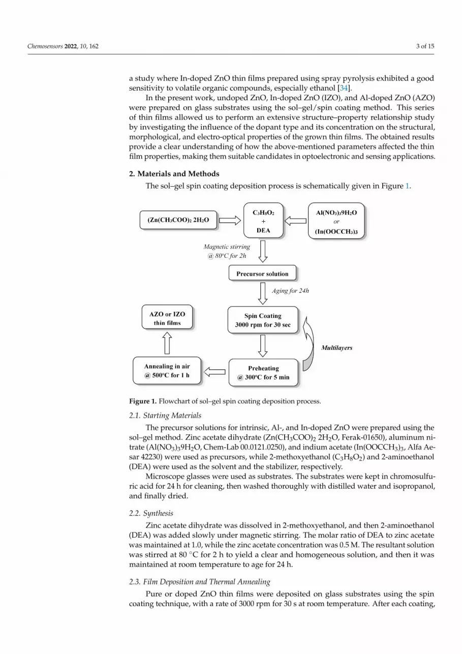
The sol–gel spin coating deposition process is schematically given in Figure 1.
Chemosensors 2022, 10, x FOR PEER REVIEW 2 of 17
ZnO thin films have been grown using various methods, such as spray pyrolysis [13], pulsed laser deposition (PLD) [14], and molecular beam epitaxy (MBE) [15]. Solution-based methods, such as solvothermal/hydrothermal and sol–gel processes, are more at-tractive because of the mild synthesis conditions used. In particular, these methods are characterized by low-temperature processing, large substrate area film growth, easy film thickness control, increased homogeneity and purity, efficient microstructural control of metallic particles, high film density and uniformity, and, most importantly, cost effective-ness [7,16,17] for industrial applications.
In fact, ZnO is defined as a savior material as a transparent electrode in Organic Light-Emitting
Diode (OLED) applications [18–20]. ZnO/GaN n-p heterojunctions are the most pre-
ferred semiconductors for optoelectronic devices. It is well known that the process of pro-ducing GaN is very complex. In particular, to produce p-type GaN, doping and activating Mg and keeping the carrier concentration at the desired level (>1019) [21] involve a labori-ous and costly process such as MOCVD. However, n-type ZnO can be easily produced with the economical sol–gel spin coating technique, which provides high controllability and a straightforward and practical methodology. Therefore, in the production of ZnO/GaN, we can at least achieve ZnO production at a more reasonable cost, making the production of the whole p-n structure more attractive.
In photovoltaic devices, doped indium tin oxide (ITO) and indium zinc oxide (IZO) conductive oxides are mostly preferred due to their high transparency and good conduc-tivity [22]. Sobrado et al. [23] reported the effect of microstructured IZO contacts on amor-phous silicon (a-Si) thin-film solar cells. They used a new process to integrate a light-trap-ping (LT) structure on the front contact of the cells. An enhancement of 26.7% in the cell photocurrent was measured when using an ultra-thin (30 nm) flat IZO layer between the LT structures and the a-Si absorber. Moreover, IZO is used in CIGS solar cells as an anti-reflector [24]. Jošt et al. [25] presented detailed guidelines on how to achieve high-effi-ciency tandem devices by using a light-trapping strategy. Textured light management foils added on top of an IZO transparent contact led to a minimization of the light reflec-tion in double-textured monolithic PVSK/Si tandem solar cells and increased energy yield.
Figure 1. Flowchart of sol–gel spin coating deposition process.
2.1. Starting Materials
The precursor solutions for intrinsic, Al-, and In-doped ZnO were prepared using thesol–gel method. Zinc acetate dihydrate (Zn(CH3COO)2 2H2O, Ferak-01650), aluminum ni-trate (Al(NO3)39H2O, Chem-Lab 00.0121.0250), and indium acetate (In(OOCCH3)3, Alfa Ae-sar 42230) were used as precursors, while 2-methoxyethanol (C3H8O2) and 2-aminoethanol(DEA) were used as the solvent and the stabilizer, respectively.
Microscope glasses were used as substrates. The substrates were kept in chromosulfu-ric acid for 24 h for cleaning, then washed thoroughly with distilled water and isopropanol,and finally dried.
2.2. Synthesis
Zinc acetate dihydrate was dissolved in 2-methoxyethanol, and then 2-aminoethanol(DEA) was added slowly under magnetic stirring. The molar ratio of DEA to zinc acetatewas maintained at 1.0, while the zinc acetate concentration was 0.5 M. The resultant solutionwas stirred at 80 C for 2 h to yield a clear and homogeneous solution, and then it wasmaintained at room temperature to age for 24 h.
2.3. Film Deposition and Thermal Annealing
Pure or doped ZnO thin films were deposited on glass substrates using the spincoating technique, with a rate of 3000 rpm for 30 s at room temperature. After each coating,
Chemosensors 2022, 10, 162 4 of 15
the films were heat-treated at 300 C for 5 min in air for the solvent and organic residuesto evaporate. This procedure was repeated for a number of times, varying from 1 to 10 inorder to obtain films with different thicknesses. Finally, these films were annealed in air at500 C for 1 h.
2.4. Characterization
X-ray diffraction (XRD) studies were performed using CuKα1,2 radiation from aD8 Advance Brucker X-ray generator, operating at 40 mA and 40 kV. Film morphologywas examined with a scanning electron microscope (JEOL 6301F microscope) and atomicforce microscopy (Dual Scope DS 95-50/200). The AFM images were acquired in contactmode. Optical transmittance spectra were recorded by using a Perkin Elmer Lambda19 spectrophotometer in the 300–1200 nm range, and the optical bandgap energy wascalculated. The resistivity of the thin films was estimated by applying the four-pointmethod, whilst film thickness measurements were performed by profilometry using aKLA-Tencor Alpha-Step IQ surface profiler.
3. Results and Discussion3.1. Microstructure Analysis
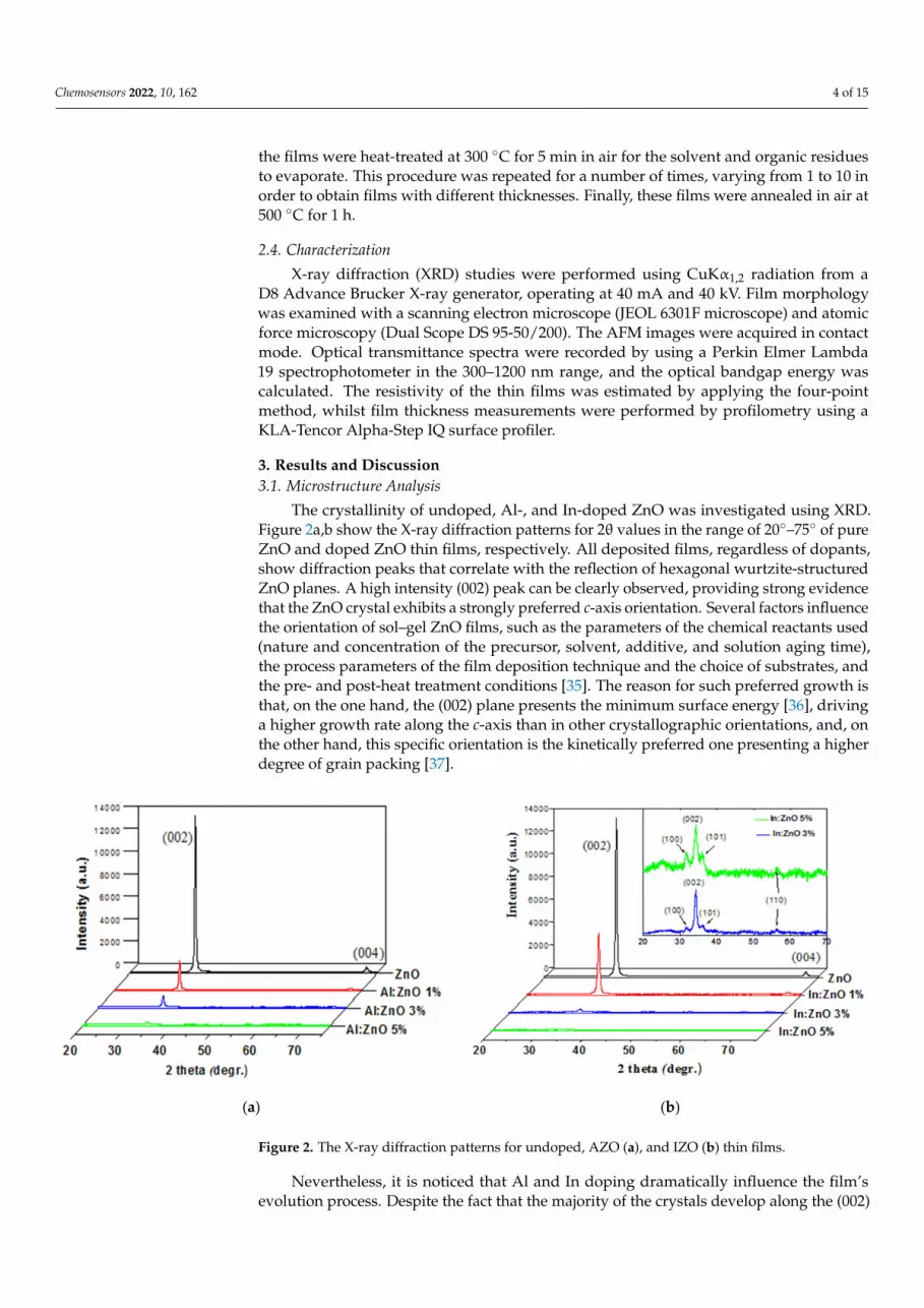
The crystallinity of undoped, Al-, and In-doped ZnO was investigated using XRD.Figure 2a,b show the X-ray diffraction patterns for 2θ values in the range of 20–75 of pureZnO and doped ZnO thin films, respectively. All deposited films, regardless of dopants,show diffraction peaks that correlate with the reflection of hexagonal wurtzite-structuredZnO planes. A high intensity (002) peak can be clearly observed, providing strong evidencethat the ZnO crystal exhibits a strongly preferred c-axis orientation. Several factors influencethe orientation of sol–gel ZnO films, such as the parameters of the chemical reactants used(nature and concentration of the precursor, solvent, additive, and solution aging time),the process parameters of the film deposition technique and the choice of substrates, andthe pre- and post-heat treatment conditions [35]. The reason for such preferred growth isthat, on the one hand, the (002) plane presents the minimum surface energy [36], drivinga higher growth rate along the c-axis than in other crystallographic orientations, and, onthe other hand, this specific orientation is the kinetically preferred one presenting a higherdegree of grain packing [37].
Chemosensors 2022, 10, x FOR PEER REVIEW 5 of 16
than that of Zn2+). Furthermore, we remark that any characteristic diffraction peaks of
Al2O3 or zinc spinel (ZnAl2O4) and In2O3 phases in the AZO and IZO thin films’ diffraction
patterns are presented, indicating that Al3+ or In3+ ions are substituted into Zn2+ ion sites.
Hence, we conclude that the presence of Al or In atoms does not change the crystal struc-
ture of ZnO film in small concentrations. Other researchers’ groups have also reported
similar observations [38–41].
(a) (b)
Figure 2. The X-ray diffraction patterns for undoped, AZO (a), and IZO (b) thin films.
The mean crystallite size can be estimated according to the Debye–Scherrer formula
below by applying the integral width β of the (002) line:
𝐷 =𝑘 × 𝜆
𝛽 × 𝑐𝑜𝑠𝜃 (1)
where D represents the mean crystallite size, k corresponds to the shape factor (0.94), λ
indicates the wavelength of the incident X-ray (1.5406Å ), β implies the full width at half
maximum (FWHM) of the (002) peak in radians, and θ is the Bragg’s angle in degrees.
The dislocation density of the films (δ) is designated by the equation 𝛿 =1
𝐷2. It is
known that grain boundaries and other dislocations decelerate the dislocation in the stage
of polycrystal materials’ deformation [7]. The dislocation density and crystallite size pos-
sess an inverse link that could be correlated to mechanical properties, supported by com-
paring the results in Table 1 of dislocation density to crystallite size. These results high-
light that a decrease in crystallite size will increase the dislocation density.
The c-axis strain (εzz) values were estimated from the observed shift in the diffraction
peak between their position in the XRD spectra via the formula 휀𝑧𝑧 =𝑐−𝑐0
𝑐0× 100% [42],
where c denotes the lattice parameter of the strained films calculated from the X-ray dif-
fraction data, whilst co is the unstrained lattice parameter of bulk ZnO (co = 5.20662Å ) [43].
The c-lattice parameter in this work was calculated according to the formula 𝑐 = 𝜆/ 𝑠𝑖𝑛 𝜃,
Bragg’s law for hexagonal crystals.
For hexagonal crystal structure, the residual stress (σ) in the plane of the film can be
calculated using the biaxial strain model in the equation below:
𝜎 =2𝑐13
2 − 𝑐33(𝑐11 + 𝑐12)
2𝑐13
× 휀𝑧𝑧 (2)
where cij represents the elastic stiffness constants (i.e., c11 = 208.8 GPa, c12 = 119.7 GPa, c13 =
104.2 GPa, and c33 = 213.8 GPa) [44]. Substituting these values in the above equation gives
𝜎 = −233 × 휀𝑧𝑧 GPa.
Figure 2. The X-ray diffraction patterns for undoped, AZO (a), and IZO (b) thin films.
Nevertheless, it is noticed that Al and In doping dramatically influence the film’sevolution process. Despite the fact that the majority of the crystals develop along the (002)

Chemosensors 2022, 10, 162 5 of 15
direction and only a few crystals grow along other directions, such as the (004) directionfor undoped and Al-doped ZnO, the In-doped thin films exhibit crystallization to theadditional orientations (101), (100), and (110) for concentrations greater than 1% (see insetin Figure 2b). It is perceived that the induction of amorphous phases is caused due to thecompetition of Zn2+ ions with Al3+ and In3+ ions in order to capture more O atoms, forminghigher Al–O/In-O bonding states. This phase raises the possibility of obstructing crystalgrowth, affecting the preferential crystalline plane orientation [35]. The absence of (002) and(102) planes may be induced by the crystalline distortions provoked by the difference in theionic radii of Al3+/In3+ compared to that of Zn2+ (the radii of Al3+/In3+ ions is smaller thanthat of Zn2+). Furthermore, we remark that any characteristic diffraction peaks of Al2O3 orzinc spinel (ZnAl2O4) and In2O3 phases in the AZO and IZO thin films’ diffraction patternsare presented, indicating that Al3+ or In3+ ions are substituted into Zn2+ ion sites. Hence,we conclude that the presence of Al or In atoms does not change the crystal structure ofZnO film in small concentrations. Other researchers’ groups have also reported similarobservations [38–41].
The mean crystallite size can be estimated according to the Debye–Scherrer formulabelow by applying the integral width β of the (002) line:
D =k × λ
β × cosθ(1)
where D represents the mean crystallite size, k corresponds to the shape factor (0.94), λindicates the wavelength of the incident X-ray (1.5406Å), β implies the full width at halfmaximum (FWHM) of the (002) peak in radians, and θ is the Bragg’s angle in degrees.
The dislocation density of the films (δ) is designated by the equation δ = 1D2 . It
is known that grain boundaries and other dislocations decelerate the dislocation in thestage of polycrystal materials’ deformation [7]. The dislocation density and crystallite sizepossess an inverse link that could be correlated to mechanical properties, supported bycomparing the results in Table 1 of dislocation density to crystallite size. These resultshighlight that a decrease in crystallite size will increase the dislocation density.
Table 1. Variation in the Bragg’s angle 2θ; the full width at half maximum; the crystallite size; latticeparameter c; main strain ε; and the stress of undoped ZnO, AZO, and IZO thin films.
Sample (002) PeakAngle (2θ)
FWHM of(002) Peak (o)
CrystalliteSize (nm)
DislocationDensity
(1014 Lines/m2)
LatticeParameter c (Å)
Strain ofc-axis (%)
Stress(GPa)
ZnO 34.392 0.317 27.35 13.37 5.210 0.07 −16.36AZO 1% 34.457 0.373 23.26 18.48 5.202 −0.1 22.58AZO 3% 34.372 0.485 17.90 31.21 5.214 0.14 −33.04AZO 5% 34.338 0.787 11.04 82.05 5.219 0.24 −55.4IZO 1% 34.406 0.420 20.67 23.41 5.209 0.05 −10.78IZO 3% 34.279 0.618 14.05 50.66 5.228 0.41 −94.62IZO 5% 34.355 1.733 5.01 39.84 5.216 0.19 −44.27
The c-axis strain (εzz) values were estimated from the observed shift in the diffractionpeak between their position in the XRD spectra via the formula εzz = c−c0
c0× 100% [42],
where c denotes the lattice parameter of the strained films calculated from the X-raydiffraction data, whilst co is the unstrained lattice parameter of bulk ZnO (co = 5.20662Å) [43].The c-lattice parameter in this work was calculated according to the formula c = λ/ sin θ,Bragg’s law for hexagonal crystals.
For hexagonal crystal structure, the residual stress (σ) in the plane of the film can becalculated using the biaxial strain model in the equation below:
σ =2c2
13 − c33(c11 + c12)
2c13× εzz (2)
Chemosensors 2022, 10, 162 6 of 15
where cij represents the elastic stiffness constants (i.e., c11 = 208.8 GPa, c12 = 119.7 GPa,c13 = 104.2 GPa, and c33 = 213.8 GPa) [44]. Substituting these values in the above equationgives σ = −233 × εzz GPa.
The Bragg’s angle (2θ); the FWHM; the average crystallite size; the lattice parameter c;the main strain ε; and the stress of undoped ZnO, AZO, and IZO thin films are presented inTable 1. It is found that, upon doping with aluminum or indium, there is a gradual decreasein crystallite size, which is more pronounced for In. There are similar results showing thatthe increase in the Al doping level up to 2% deteriorates the films’ crystallinity, primarilybecause of Al segregation at grain boundaries. Moreover, the ions of Al3+ and In3+ have alarger nuclear charge than the Zn2+ ion, capturing a greater extent of oxygen, and this maybe another parameter that affects the crystallinity [1].
In the case of ZnO doping with Al, we do not observe significant changes in the clattice parameter because the ionic radius of aluminum (0.56 Å) is smaller than that of zinc(0.74 Å). For the same reason, at low doping concentrations, the residual stress is similar tothat of pure ZnO. A slight increase in the c lattice parameter is observed for Al doping withconcentrations larger than 1%. This is because some aluminum ions may occupy interstitialpositions in the ZnO lattice [1]. In the case of In doping, the lattice constant of IZO isalso larger than that of pure ZnO films [45], because the bigger In3+ ions (radius 0.84 Å)substitute the Zn2+ ions (radius 0.74 Å) in the lattice. For this reason and for In dopinglarger than 1%, the lattice is distorted, and the residual stress is increased. The minus signindicates that the residual stress is compressive. This results in a smaller crystallite size forboth dopants.
As the FWHM values in Table 1 result from the XRD measurements in Figure 3, theyfurther support the above discussion. For all three concentration values of both dopants,the FWHM values increase monotonically with concentration; furthermore, the FWHMvalues of In are larger than those of Al. This results in a decrease in the crystalline size, inparticular, a stronger decrease for In, as clearly derived from Equation (1).
Chemosensors 2022, 10, x FOR PEER REVIEW 7 of 16
hundred nanometers are evenly distributed. In both cases, this explains the poor crystal-
linity that the XRD patterns present. For the 5% doping concentration, the surfaces of both
AZO and IZO thin films change entirely compared to the lower concentration values,
clearly showing the influence of the incorporation of dopants at high concentrations on
the morphology of the undoped ZnO films. The AZO film shows a smoother surface with
some pores of a few hundred nanometers in size. In particular, the SEM micrograph of
IZO 3% (Figure 3) comprises ‘‘rice-like’’ grains, with sizes of several tens of nanometers.
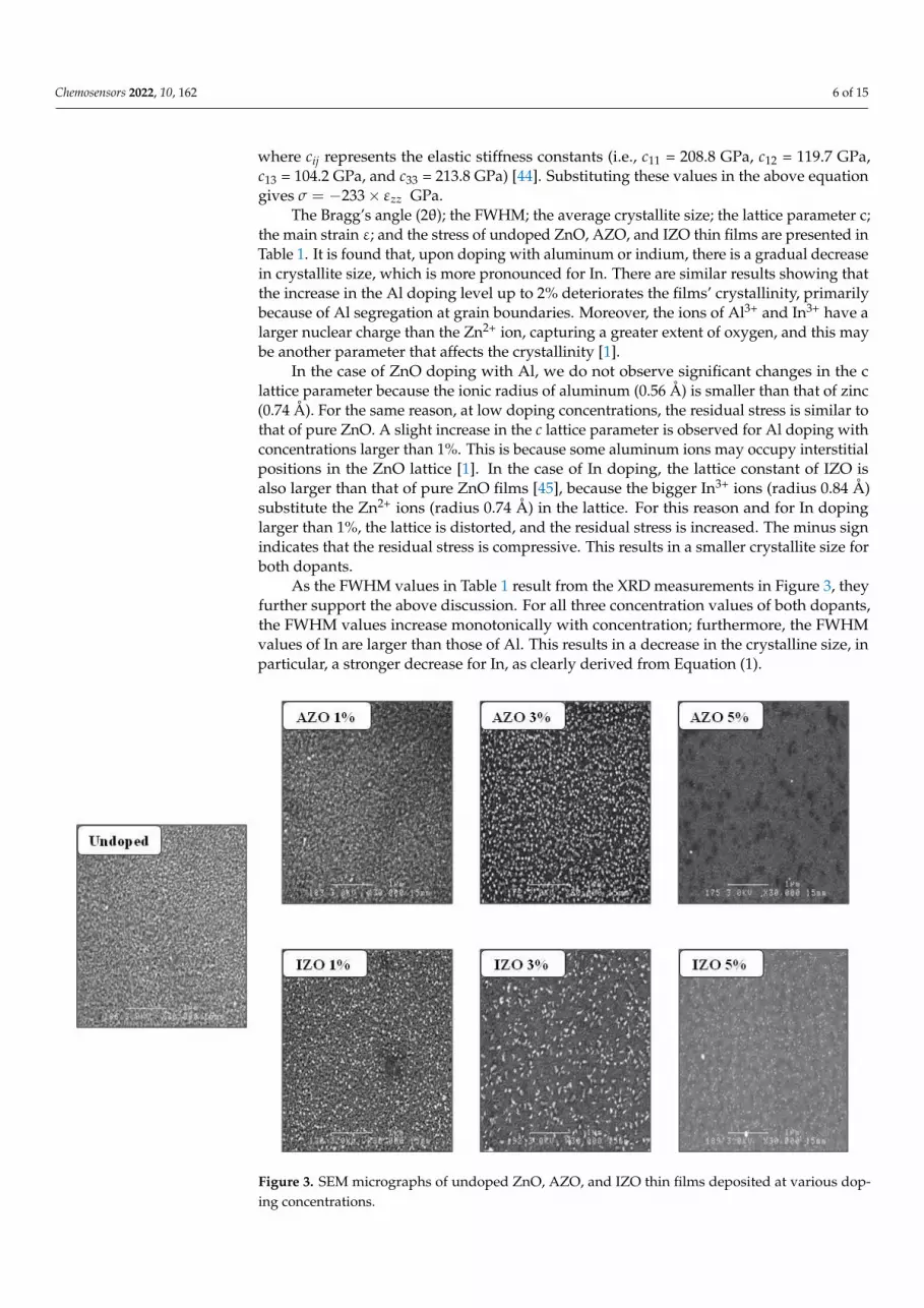
Figure 3. SEM micrographs of undoped ZnO, AZO, and IZO thin films deposited at various doping
concentrations.
Several authors have reported similar network textures of undoped [46–48] and Al-
doped [47,49] ZnO films prepared by applying the same deposition technique. In the lit-
erature, several groups argued that the growth of the film along the c-axis orientation de-
teriorates due to the formation of surface wrinkles [46], and some others have observed
that the evolution of the surface texturing is strongly affected by the heating procedure
[48]. Network thin films of Ni-doped ZnO have been grown with the same solution type
used in this work, and it was noticed that an increase in the Ni doping concentration led
to a decrease in the network density [47]. This phenomenon was also observed for thin
films prepared by applying two different compositions of AZO solutions [49]. According
to Ref. [50], “the formation of a continuous network is ascribed to the competition between sinter-
ing and crystallization, i.e., the densification of the amorphous matrix is arrested when a certain
fraction of crystallinity develops”. Based on the above discussion, we conclude that several
factors, including sol composition, doping concentration, and heat treatment, should act
in combination to guide the network texture’s self-assembly. Among them, heat treatment
is of primary importance [49].
In the three-dimensional AFM (contact mode) images (see Figure 4), we observe that
the surfaces of all films with different compositions are very smooth and exhibit hillock
morphology. Both doped and undoped thin films include columnar grains growing along
the c-axis, perpendicular to the substrate surface, which is in agreement with the XRD
Figure 3. SEM micrographs of undoped ZnO, AZO, and IZO thin films deposited at various dop-ing concentrations.

Chemosensors 2022, 10, 162 7 of 15
3.2. Surface Morphology Analysis
SEM and AFM images of the prepared ZnO, AZO, and IZO thin films are shown inFigures 3 and 4, respectively. The SEM images reveal that each film consists of a homoge-neous distribution of grains that are randomly oriented, corroborating the polycrystallinestructure confirmed by XRD analysis. However, it is evident that there is a remarkablechange in the morphology of the films, which correlates with the type of dopant anddoping concentration. No film cracking is observed. Furthermore, we notice that, at the1% doping level, the surface appears almost the same as the surface of pure ZnO, whichis granular, highly dense, and compact, though it exhibits a more porous structure. ThisZnO microstructure is coherent with a nanocrystalline structure with its distinct outlinesof grains suggested by XRD analysis. The surface of the 3% AZO thin film presents astructure with irregular and disordered grains. In contrast, the corresponding IZO filmconsists of particles forming a uniform background layer on which particles with sizes ofa few hundred nanometers are evenly distributed. In both cases, this explains the poorcrystallinity that the XRD patterns present. For the 5% doping concentration, the surfaces ofboth AZO and IZO thin films change entirely compared to the lower concentration values,clearly showing the influence of the incorporation of dopants at high concentrations onthe morphology of the undoped ZnO films. The AZO film shows a smoother surface withsome pores of a few hundred nanometers in size. In particular, the SEM micrograph of IZO3% (Figure 3) comprises “rice-like” grains, with sizes of several tens of nanometers.
Chemosensors 2022, 10, x FOR PEER REVIEW 8 of 16
results. The grain boundaries of ZnO are clear, and the grains seem to have similar dimen-
sions and a round shape in the plane. The evidence of crystallization is mainly due to the
vertical growth of the grains. The insertion of Al or In dopants affects the normal growth
of ZnO crystals, and as we can observe, it changes the surface morphology, resulting in
fewer grains with smaller sizes. These effects increase with the concentration of the do-
pants. Moreover, for both AZO and IZO and for the 3% and 5% dopant concentrations,
we observe that the grain boundaries are unclear, and the surface morphology, which
refers to the grain growth mode, changes completely. This may be an effect of increasing
the film thickness while increasing the dopant concentration. The effect of the film thick-
ness of sol–gel dip-coated ZnO [36] and PLD-grown AZO [51] on the structural properties
has shown that the grains’ growth mode turns from vertical to lateral for thicker films.
This result seems to be independent of the growth process.
Figure 4. Three-dimensional AFM images of undoped ZnO, AZO, and IZO thin films deposited at
various doping concentrations.
The degree of surface roughness was deduced from AFM studies by determining the
average and root mean square (rms) values, and the values confirm that the surfaces of all
thin films are very smooth. As denoted in Table 2, the roughness increases for the 1%
doping concentration regardless of the dopant, and it gradually reduces by increasing the
concentration of Al or In.
Table 2. Average and root mean square (rms) values of surface roughness measured using AFM.
Sample Ra (nm) Rrms (nm)
ZnO (reference) 3.38 4.23
AZO 1% 4.44 5.76
AZO 3% 3.17 4.19
AZO 5% 1.45 2.11
IZO 1% 5.08 6.56
IZO 3% 4.57 5.82
IZO 5% 2.82 3.57
Figure 4. Three-dimensional AFM images of undoped ZnO, AZO, and IZO thin films deposited atvarious doping concentrations.
Several authors have reported similar network textures of undoped [46–48] and Al-doped [47,49] ZnO films prepared by applying the same deposition technique. In theliterature, several groups argued that the growth of the film along the c-axis orientationdeteriorates due to the formation of surface wrinkles [46], and some others have observedthat the evolution of the surface texturing is strongly affected by the heating procedure [48].Network thin films of Ni-doped ZnO have been grown with the same solution type usedin this work, and it was noticed that an increase in the Ni doping concentration led to adecrease in the network density [47]. This phenomenon was also observed for thin filmsprepared by applying two different compositions of AZO solutions [49]. According toRef. [50], “the formation of a continuous network is ascribed to the competition between sintering
Chemosensors 2022, 10, 162 8 of 15
and crystallization, i.e., the densification of the amorphous matrix is arrested when a certainfraction of crystallinity develops”. Based on the above discussion, we conclude that severalfactors, including sol composition, doping concentration, and heat treatment, should act incombination to guide the network texture’s self-assembly. Among them, heat treatment isof primary importance [49].
In the three-dimensional AFM (contact mode) images (see Figure 4), we observethat the surfaces of all films with different compositions are very smooth and exhibithillock morphology. Both doped and undoped thin films include columnar grains growingalong the c-axis, perpendicular to the substrate surface, which is in agreement with theXRD results. The grain boundaries of ZnO are clear, and the grains seem to have similardimensions and a round shape in the plane. The evidence of crystallization is mainly dueto the vertical growth of the grains. The insertion of Al or In dopants affects the normalgrowth of ZnO crystals, and as we can observe, it changes the surface morphology, resultingin fewer grains with smaller sizes. These effects increase with the concentration of thedopants. Moreover, for both AZO and IZO and for the 3% and 5% dopant concentrations,we observe that the grain boundaries are unclear, and the surface morphology, which refersto the grain growth mode, changes completely. This may be an effect of increasing thefilm thickness while increasing the dopant concentration. The effect of the film thicknessof sol–gel dip-coated ZnO [36] and PLD-grown AZO [51] on the structural properties hasshown that the grains’ growth mode turns from vertical to lateral for thicker films. Thisresult seems to be independent of the growth process.
The degree of surface roughness was deduced from AFM studies by determining theaverage and root mean square (rms) values, and the values confirm that the surfaces ofall thin films are very smooth. As denoted in Table 2, the roughness increases for the 1%doping concentration regardless of the dopant, and it gradually reduces by increasing theconcentration of Al or In.
Table 2. Average and root mean square (rms) values of surface roughness measured using AFM.
Sample Ra (nm) Rrms (nm)
ZnO (reference) 3.38 4.23AZO 1% 4.44 5.76AZO 3% 3.17 4.19AZO 5% 1.45 2.11IZO 1% 5.08 6.56IZO 3% 4.57 5.82IZO 5% 2.82 3.57
3.3. Optical Properties
The effects of the dopant type and concentration on the optical transmittance and thebandgap for the sol–gel-grown ZnO, AZO, and IZO thin films after thermal annealing wereinvestigated. In Figure 5, it is evident that all thin films exhibit high transmittance in thevisible NIR region from 82% to 94%, opening up possibilities for usage in optoelectronicdevices as transparent windows. The high transmittance level is enhanced by the fact thatall thin films are oriented along the c-axis (002) plane because it avoids light scattering atthe grain boundaries.
All thin films present a sharp absorption edge near the ultraviolet region at about380 nm, which corresponds to ZnO’s optical bandgap transition. In addition, the weakmodulation in the spectra is due to interference effects between the film surface and thefilm/surface interface.

Chemosensors 2022, 10, 162 9 of 15
Chemosensors 2022, 10, x FOR PEER REVIEW 9 of 16
3.3. Optical Properties
The effects of the dopant type and concentration on the optical transmittance and the
bandgap for the sol–gel-grown ZnO, AZO, and IZO thin films after thermal annealing
were investigated. In Figure 5, it is evident that all thin films exhibit high transmittance in
the visible NIR region from 82% to 94%, opening up possibilities for usage in optoelec-
tronic devices as transparent windows. The high transmittance level is enhanced by the
fact that all thin films are oriented along the c-axis (002) plane because it avoids light scat-
tering at the grain boundaries.
All thin films present a sharp absorption edge near the ultraviolet region at about 380
nm, which corresponds to ZnO’s optical bandgap transition. In addition, the weak mod-
ulation in the spectra is due to interference effects between the film surface and the
film/surface interface.
Figure 5. Optical transmittance spectra of undoped ZnO, (a) AZO, and (b) IZO thin films.
The optical bandgap of the thin films was estimated by employing the Tauc model
[52] taking into account that ZnO is a direct transition semiconductor material following
from the international literature:
(𝑎ℎ𝑣) = 𝐴(ℎ𝑣 − 𝐸𝑔)1/2 (3)
where α indicates the absorption coefficient, hv denotes the photon energy, and A corre-
sponds to a constant that depends on the electron–hole mobility. Eg is the optical bandgap,
derived by extrapolating the linear section of the plot of (αhv)2 versus photon energy (x-
axis). The acquired Eg values of the films are presented in Table 3 and Figure 6. Although
the optical bandgap of the AZO thin films increases monotonically while increasing the
Al concentration, the bandgap of the IZO films also decreases monotonically while in-
creasing the In concentration. In a previous publication [37], we deposited ZnO, AZO, and
IZO thin films and found similar results: the bandgap of the AZO films increased with the
Al concentration, while the IZO bandgap decreased with the In concentration. Those films
were deposited using a dual-target, dual-laser PLD, and the dopant concentration was
defined by the laser fluence.
Figure 5. Optical transmittance spectra of undoped ZnO, (a) AZO, and (b) IZO thin films.
The optical bandgap of the thin films was estimated by employing the Tauc model [52]taking into account that ZnO is a direct transition semiconductor material following fromthe international literature:
(ahv) = A(hv − Eg
)1/2 (3)
where α indicates the absorption coefficient, hv denotes the photon energy, and A corre-sponds to a constant that depends on the electron–hole mobility. Eg is the optical bandgap,derived by extrapolating the linear section of the plot of (αhv)2 versus photon energy(x-axis). The acquired Eg values of the films are presented in Table 3 and Figure 6. Althoughthe optical bandgap of the AZO thin films increases monotonically while increasing the Alconcentration, the bandgap of the IZO films also decreases monotonically while increasingthe In concentration. In a previous publication [37], we deposited ZnO, AZO, and IZOthin films and found similar results: the bandgap of the AZO films increased with the Alconcentration, while the IZO bandgap decreased with the In concentration. Those filmswere deposited using a dual-target, dual-laser PLD, and the dopant concentration wasdefined by the laser fluence.
Table 3. The thickness and the calculated energy gap of undoped ZnO, AZO, and IZO thin films.
Sample Thickness (nm) Eg (eV)
ZnO (reference) 234 3.26AZO 1% 244 3.28AZO 3% 247 3.29AZO 5% 261 3.30IZO 1% 245 3.24IZO 3% 270 3.22IZO 5% 289 3.19
In the case of Al doping, the value of the bandgap energy demonstrates an increasefrom 3.26 to 3.30 eV with augmentation of the doping concentration. This increase can beelucidated by the Burstein–Moss theory: the phenomenon of the energy band widening(blue shift) arises from the shift of the Fermi plane to the conduction band of the degeneratesemiconductor [53,54].
By increasing the doping concentration, the donor electrons fill the energy states aboveand close the bottom of the semiconductor’s conduction band. Taking into account the Pauliexclusion principle, these states can be occupied by only one (donor) electron. Therefore,

Chemosensors 2022, 10, 162 10 of 15
for electrons from the valence band, the optical vertical transitions (see Equation (2)) needa photon with more energy than that for the undoped ZnO [55]. Based on all of the above,we conclude that the experimentally measured energy gap resulting from the transmittanceand reflectance spectra is greater than the “real” one specified by the semiconductor latticestructure. This phenomenon has been observed not only in the case of Al doping [56] butalso with the B and Ga doping of ZnO [55,57].
Chemosensors 2022, 10, x FOR PEER REVIEW 10 of 16
Table 3. The thickness and the calculated energy gap of undoped ZnO, AZO, and IZO thin films.
Sample Thickness (nm) Eg (eV)
ZnO (reference) 234 3.26
AZO 1% 244 3.28
AZO 3% 247 3.29
AZO 5% 261 3.30
IZO 1% 245 3.24
IZO 3% 270 3.22
IZO 5% 289 3.19
In the case of Al doping, the value of the bandgap energy demonstrates an increase
from 3.26 to 3.30 eV with augmentation of the doping concentration. This increase can be
elucidated by the Burstein–Moss theory: the phenomenon of the energy band widening
(blue shift) arises from the shift of the Fermi plane to the conduction band of the degener-
ate semiconductor [53,54].
Figure 6. The energy gap of undoped ZnO, AZO, and IZO thin films deposited at various doping
concentrations.
By increasing the doping concentration, the donor electrons fill the energy states
above and close the bottom of the semiconductor’s conduction band. Taking into account
the Pauli exclusion principle, these states can be occupied by only one (donor) electron.
Therefore, for electrons from the valence band, the optical vertical transitions (see Equa-
tion (2)) need a photon with more energy than that for the undoped ZnO [55]. Based on
all of the above, we conclude that the experimentally measured energy gap resulting from
the transmittance and reflectance spectra is greater than the “real” one specified by the
semiconductor lattice structure. This phenomenon has been observed not only in the case
of Al doping [56] but also with the B and Ga doping of ZnO [55,57].
Obviously, increasing the content of external contaminants cannot continue indefi-
nitely. Furthermore, the Burnstein–Moss effect cannot explain the decrease in Eg in the
In:ZnO films in this work. A reduction in Eg [58] on amorphous Si and Ge has previously
been observed, and it was attributed to the existence of energy states (the so-called Urbach
tails [59]) extending into the energy gap just above the valence band. Such states are due
to the deviation of amorphous Si and Ge from the periodicity of the monocrystal. As
shown in Figure 7, the energy states of the valence band extend to higher states and those
of the conduction band to lower states inside the energy gap of Ev–Ec as it is defined by a
Figure 6. The energy gap of undoped ZnO, AZO, and IZO thin films deposited at various dop-ing concentrations.
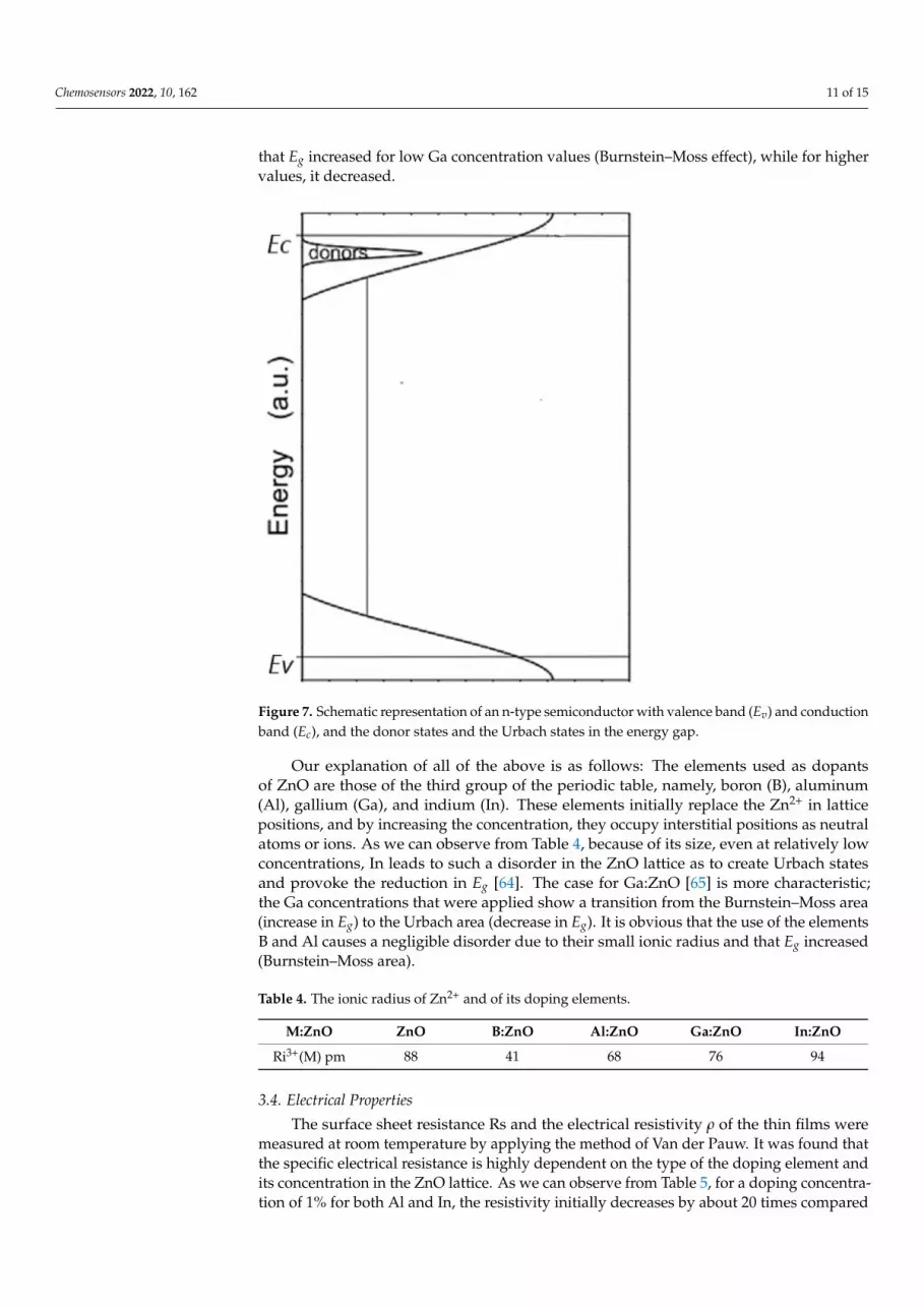
Obviously, increasing the content of external contaminants cannot continue indefinitely.Furthermore, the Burnstein–Moss effect cannot explain the decrease in Eg in the In:ZnOfilms in this work. A reduction in Eg [58] on amorphous Si and Ge has previously beenobserved, and it was attributed to the existence of energy states (the so-called Urbachtails [59]) extending into the energy gap just above the valence band. Such states are due tothe deviation of amorphous Si and Ge from the periodicity of the monocrystal. As shownin Figure 7, the energy states of the valence band extend to higher states and those of theconduction band to lower states inside the energy gap of Ev–Ec as it is defined by a singlecrystal material. This results in new electron excitations that become possible betweenthe valence band and the Urbach states, between the Urbach states and the conductionband, and also between the Urbach states themselves. The energy gap resulting from theabsorption spectra appears shrunken, and the width of the Urbach states becomes larger asthe lattice disorder increases due to various causes, including doping. In conclusion, thewidening of Eg due to the Burnstein–Moss phenomenon and the shrinkage as a result oflattice disorders act competitively, and one of the two prevail as appropriate.
In this work, the In-doped thin films exhibit different behavior, and the narrowingof the energy bandgap with the incorporation of In has been reported in many articlesin the literature [60–63]. Moreover, the results show that the behaviors of the In-dopedfilms are independent of the way in which they are developed (e.g., spin coating andthermal evaporation). A more in-depth understanding of the decrease in Eg is reportedin the works of Tang et al. [64] and Saha et al. [65]. Tang et al. deposited In:ZnO thinfilms by applying the MOCVD technique. They calculated the electron density Ne as afunction of the In concentration and showed that, for values less than 1019/cm3, Eg remainsconstant, while for values ~1020/cm3 and above, they observed a reduction in Eg (criticalconcentration by Mott). Similarly, Saha et al. developed thin films of Ga:ZnO using thesol–gel technique, and Eg was measured as a function of the Ga concentration. It was found
Chemosensors 2022, 10, 162 11 of 15
that Eg increased for low Ga concentration values (Burnstein–Moss effect), while for highervalues, it decreased.
Chemosensors 2022, 10, x FOR PEER REVIEW 11 of 16
single crystal material. This results in new electron excitations that become possible be-
tween the valence band and the Urbach states, between the Urbach states and the conduc-
tion band, and also between the Urbach states themselves. The energy gap resulting from
the absorption spectra appears shrunken, and the width of the Urbach states becomes
larger as the lattice disorder increases due to various causes, including doping. In conclu-
sion, the widening of Eg due to the Burnstein–Moss phenomenon and the shrinkage as a
result of lattice disorders act competitively, and one of the two prevail as appropriate.
Figure 7. Schematic representation of an n-type semiconductor with valence band (Ev) and conduc-
tion band (Ec), and the donor states and the Urbach states in the energy gap.
In this work, the In-doped thin films exhibit different behavior, and the narrowing of
the energy bandgap with the incorporation of In has been reported in many articles in the
literature [60–63]. Moreover, the results show that the behaviors of the In-doped films are
independent of the way in which they are developed (e.g., spin coating and thermal evap-
oration). A more in-depth understanding of the decrease in Eg is reported in the works of
Tang et al. [64] and Saha et al. [65]. Tang et al. deposited In:ZnO thin films by applying
the MOCVD technique. They calculated the electron density Ne as a function of the In
concentration and showed that, for values less than 1019/cm3, Eg remains constant, while
for values ~1020/cm3 and above, they observed a reduction in Eg (critical concentration by
Mott). Similarly, Saha et al. developed thin films of Ga:ZnO using the sol–gel technique,
and Eg was measured as a function of the Ga concentration. It was found that Eg increased
for low Ga concentration values (Burnstein–Moss effect), while for higher values, it de-
creased.
Our explanation of all of the above is as follows: The elements used as dopants of
ZnO are those of the third group of the periodic table, namely, boron (B), aluminum (Al),
gallium (Ga), and indium (In). These elements initially replace the Zn2+ in lattice positions,
and by increasing the concentration, they occupy interstitial positions as neutral atoms or
Figure 7. Schematic representation of an n-type semiconductor with valence band (Ev) and conductionband (Ec), and the donor states and the Urbach states in the energy gap.
Our explanation of all of the above is as follows: The elements used as dopantsof ZnO are those of the third group of the periodic table, namely, boron (B), aluminum(Al), gallium (Ga), and indium (In). These elements initially replace the Zn2+ in latticepositions, and by increasing the concentration, they occupy interstitial positions as neutralatoms or ions. As we can observe from Table 4, because of its size, even at relatively lowconcentrations, In leads to such a disorder in the ZnO lattice as to create Urbach statesand provoke the reduction in Eg [64]. The case for Ga:ZnO [65] is more characteristic;the Ga concentrations that were applied show a transition from the Burnstein–Moss area(increase in Eg) to the Urbach area (decrease in Eg). It is obvious that the use of the elementsB and Al causes a negligible disorder due to their small ionic radius and that Eg increased(Burnstein–Moss area).
Table 4. The ionic radius of Zn2+ and of its doping elements.
M:ZnO ZnO B:ZnO Al:ZnO Ga:ZnO In:ZnO
Ri3+(M) pm 88 41 68 76 94
3.4. Electrical Properties
The surface sheet resistance Rs and the electrical resistivity ρ of the thin films weremeasured at room temperature by applying the method of Van der Pauw. It was found thatthe specific electrical resistance is highly dependent on the type of the doping element andits concentration in the ZnO lattice. As we can observe from Table 5, for a doping concentra-tion of 1% for both Al and In, the resistivity initially decreases by about 20 times compared

Chemosensors 2022, 10, 162 12 of 15
with that of ZnO, while by further increasing the dopants, we notice a gradual increaseagain. Despite the different deposition techniques, this dependence of the resistivity on thedoping concentration has also been observed in the literature [60,66].
Table 5. The thickness and the calculated sheet resistance and electrical resistivity of undoped ZnO,AZO, and IZO thin films.
Sample Thickness(nm)
SheetResistance Rs (MΩ)
ElectricalResistivity ρ (Ωcm)
ZnO (reference) 234 69.47 1625.60AZO 1% 244 2.35 57.34AZO 3% 247 5.67 140.05AZO 5% 261 14.06 366.96IZO 1% 245 3.51 85.99IZO 3% 270 6.91 186.57IZO 5% 289 6.09 176
Electrical resistivity is closely related to the carrier density of electrons Ne andthe mobility µe by the relationship 1/ρ = e Ne µe, where e is the charge of an electron(1.60 × 10⁻¹⁹ C) [67]. The carrier density depends on the dopant concentration, while themobility is determined by the scattering of electrons, which is related to the crystal structureof the material. In the literature, Ne and µe were measured independently for IZO [64] andAZO [66] thin films, and it was found that Ne systematically increased with the increase indoping content, which is also expected in the present study.
However, the dopant concentration affects the mobility in two ways: (1) As is alsostated in Kim et al. [66], a reduction in the mobility µe occurs due to the fact that, with anincrease in dopants, Al3+ and In3+ ions substitute at Zn2+ cation sites or are incorporated ininterstitial positions that deteriorate the periodicity of the ZnO lattice and scatter the donorelectrons. In Table 1, we can observe that, for the 3% and 5% dopant concentrations, thec-axis lattice parameter is larger than that of ZnO, which is an indication of the existence ofAl3+ and In3+ ions in interstitial positions (2). In the present work, as well as in Ref [66],there is a noticeable grain size reduction when increasing the content of the dopants (seeTable 1). This entails an increased number of grain boundaries that form electron scatteringregions, which contribute to a further reduction in mobility. As the electrical resistivity isgiven by the product Ne µe, the value of ρ is defined by the interplay between the increase inNe and the decrease in µe, as well as the rate of their increase and decrease when the dopingconcentration changes. It is also well known that, the bigger the grains, the lesser the grainboundaries (see Figure 4). When the number of grain boundaries, which act as a barrier toelectron propagation, in the thin film reduce, as observed with the thin films deposited athigher temperatures (500 C annealing temperature), the resistivity lowers since it increasesthe mean free path for the electrons. This works in favor of the sensor performance.
4. Conclusions
We successfully fabricated high-quality ZnO, AZO, and IZO thin films via the sol–gelspin coating technique. This work constitutes a comprehensive analysis of ZnO structures,which may be potentially applied in optoelectronics and sensing applications. The coreof the present research was a comparison of the structural, morphological, optical, andelectrical parameters between undoped ZnO and IZO and AZO polycrystalline films inthe 234–289 nm thickness range. The increase in the dopant concentration decreased thecrystallinity of the AZO and IZO thin films. The optical transmittance spectra of the filmsshowed a high transmittance value of over 90% in the visible range, making the filmssuitable for use in optoelectronic devices. The optical bandgap energy Eg increased forAZO and decreased for IZO while increasing the dopant concentration. The electricalresistivity decreased significantly with doping, and it increased slightly with the type anddopant concentration.

Chemosensors 2022, 10, 162 13 of 15
Author Contributions: P.K.: Conceptualization, Methodology, Software, Resources, Investigation,Data Curation, Writing—Original Draft, Visualization, Formal Analysis, and Project Administration.S.F.V.: Writing—Original Draft and Writing—Review and Editing. G.M.: Supervision, Resources, andWriting—Review and Editing. D.E.M.: Resources and Writing—Review and Editing. Z.M.: Resourcesand Writing—Review and Editing. M.K.: Supervision, Resources, Writing—Review and Editing, andFunding Acquisition. All authors have read and agreed to the published version of the manuscript.
Funding: This research was supported by the Greek Secretariat for Research and Technology in theframe of the European ERA-NET-RUS “FilmSolar” Project.
Institutional Review Board Statement: Not applicable.
Informed Consent Statement: Not applicable.
Acknowledgments: The authors are grateful to Mihaela Girtan for the SEM images.
Conflicts of Interest: The authors declare that they have no known competing financial interests orpersonal relationships that could have appeared to influence the work reported in this paper.
References1. Salam, S.; Islam, M.; Akram, A. Sol-gel synthesis of intrinsic and aluminum-doped zinc oxide thin films as transparent conducting
oxides for thin film solar cells. Thin Solid Films 2013, 529, 242–247. [CrossRef]2. Choi, Y.S.; Kang, J.W.; Hwang, D.K.; Park, S.J. Recent advances in ZnO-based light-emitting diodes. IEEE Trans. Electron Devices
2010, 57, 26–41. [CrossRef]3. Sarma, B.; Barman, D.; Sarma, B.K. AZO (Al:ZnO) thin films with high figure of merit as stable indium free transparent conducting
oxide. Appl. Surf. Sci. 2019, 479, 786–795. [CrossRef]4. Rahman, F. Zinc oxide light-emitting diodes: A review. Opt. Eng. 2019, 58, 1. [CrossRef]5. Ding, M.; Guo, Z.; Zhou, L.; Fang, X.; Zhang, L.; Zeng, L.; Xie, L.; Zhao, H. One-dimensional zinc oxide nanomaterials for
application in high-performance advanced optoelectronic devices. Crystals 2018, 8, 223. [CrossRef]6. Baskoutas, S. Special issue: Zinc oxide nanostructures: Synthesis and characterization. Materials 2018, 11, 873. [CrossRef]7. Fiat Varol, S.; Babür, G.; Çankaya, G.; Kölemen, U. Synthesis of sol-gel derived nano-crystalline ZnO thin films as TCO window
layer: Effect of sol aging and boron. RSC Adv. 2014, 4, 56645–56653. [CrossRef]8. Ocola, L.E.; Wang, Y.; Divan, R.; Chen, J. Multifunctional UV and gas sensors based on vertically nanostructured zinc oxide:
Volume versus surface effect. Sensors 2019, 19, 2061. [CrossRef]9. Regmi, G.; Rohini, M.; Reyes-Figueroa, P.; Maldonado, A.; de la Luz Olvera, M.; Velumani, S. Deposition and characterization of
ultrathin intrinsic zinc oxide (i-ZnO) films by radio frequency (RF) sputtering for propane gas sensing application. J. Mater. Sci.Mater. Electron. 2018, 29, 15682–15692. [CrossRef]
10. Lee, J.; Seul, H.; Jeong, J.K. Solution-processed ternary alloy aluminum yttrium oxide dielectric for high performance indium zincoxide thin-film transistors. J. Alloys Compd. 2018, 741, 1021–1029. [CrossRef]
11. Gu, P.; Zhu, X.; Yang, D. Effect of annealing temperature on the performance of photoconductive ultraviolet detectors based onZnO thin films. Appl. Phys. A Mater. Sci. Process. 2019, 125, 50. [CrossRef]
12. Li, Y.; Feng, J.; Zhang, J.; He, B.; Wu, Y.; Zhao, Y.; Xu, C.; Wang, J. Towards high-performance linear piezoelectrics: Enhancing thepiezoelectric response of zinc oxide thin films through epitaxial growth on flexible substrates. Appl. Surf. Sci. 2021, 556, 149798.[CrossRef]
13. Laurenti, M.; Cauda, V. Porous zinc oxide thin films: Synthesis approaches and applications. Coatings 2018, 8, 67. [CrossRef]14. Tsoutsouva, M.G.; Panagopoulos, C.N.; Kompitsas, M. Laser energy density, structure and properties of pulsed-laser deposited
zinc oxide films. Appl. Surf. Sci. 2011, 257, 6314–6319. [CrossRef]15. Özgür, Ü.; Avrutin, V.; Morkoç, H. Zinc Oxide Materials and Devices Grown by Molecular Beam Epitaxy. In Molecular Beam
Epitaxy; Elsevier: Amsterdam, The Netherlands, 2018; pp. 343–375. ISBN 9780128121368.16. Yin, J.; Gao, F.; Wei, C.; Lu, Q. Water Amount Dependence on Morphologies and Properties of ZnO nanostructures in Double-
solvent System. Sci. Rep. 2014, 4, 3736. [CrossRef]17. Xu, L.; Zheng, G.; Miao, J.; Xian, F. Dependence of structural and optical properties of sol-gel derived ZnO thin films on sol
concentration. Appl. Surf. Sci. 2012, 258, 7760–7765. [CrossRef]18. Lee, C.Y.; Kuo, Y.P.; Chen, P.Y.; Lu, H.H.; Lin, M.Y. Influence of annealing temperature on weak-cavity top-emission red quantum
dot light emitting diode. Nanomaterials 2019, 9, 1639. [CrossRef]19. Yu, S.; Li, L.; Lyu, X.; Zhang, W. Preparation and investigation of nano-thick FTO/Ag/FTO multilayer transparent electrodes
with high figure of merit. Sci. Rep. 2016, 6, 20399. [CrossRef]20. Wang, W.; Peng, H.; Chen, S. Highly transparent quantum-dot light-emitting diodes with sputtered indium-tin-oxide electrodes.
J. Mater. Chem. C 2016, 4, 1838–1841. [CrossRef]

Chemosensors 2022, 10, 162 14 of 15
21. Chichibu, S.F.; Shima, K.; Kojima, K.; Takashima, S.; Edo, M.; Ueno, K.; Ishibashi, S.; Uedono, A. Large electron capture-cross-section of the major nonradiative recombination centers in Mg-doped GaN epilayers grown on a GaN substrate. Appl. Phys. Lett.2018, 112, 211901. [CrossRef]
22. Ying, Z.; Zhu, Y.; Feng, X.; Xiu, J.; Zhang, R.; Ma, X.; Deng, Y.; Pan, H.; He, Z. Sputtered Indium-Zinc Oxide for Buffer LayerFree Semitransparent Perovskite Photovoltaic Devices in Perovskite/Silicon 4T-Tandem Solar Cells. Adv. Mater. Interfaces 2021, 8,2170029. [CrossRef]
23. Sanchez-Sobrado, O.; Mendes, M.J.; Mateus, T.; Costa, J.; Nunes, D.; Aguas, H.; Fortunato, E.; Martins, R. Photonic-structuredTCO front contacts yielding optical and electrically enhanced thin-film solar cells. Sol. Energy 2020, 196, 92–98. [CrossRef]
24. Lai, F.I.; Hsieh, M.Y.; Yang, J.F.; Hsu, Y.C.; Kuo, S.Y. Antireflection layer of ZnO nanorod embedded in PDMS film for enhancingomnidirectional photovoltaic performance of CIGS photovoltaic cell. Int. J. Energy Res. 2021, 45, 1142–1149. [CrossRef]
25. Jošt, M.; Köhnen, E.; Morales-Vilches, A.B.; Lipovšek, B.; Jäger, K.; Macco, B.; Al-Ashouri, A.; Krc, J.; Korte, L.; Rech, B.; et al.Textured interfaces in monolithic perovskite/silicon tandem solar cells: Advanced light management for improved efficiency andenergy yield. Energy Environ. Sci. 2018, 11, 3511–3523. [CrossRef]
26. Kranz, L.; Abate, A.; Feurer, T.; Fu, F.; Avancini, E.; Löckinger, J.; Reinhard, P.; Zakeeruddin, S.M.; Grätzel, M.; Buecheler, S.; et al.High-efficiency polycrystalline thin film tandem solar cells. J. Phys. Chem. Lett. 2015, 6, 2676–2681. [CrossRef]
27. Hjiri, M.; Zahmouli, N.; Dhahri, R.; Leonardi, S.G.; El Mir, L.; Neri, G. Doped-ZnO nanoparticles for selective gas sensors. J. Mater.Sci. Mater. Electron. 2017, 28, 9667–9674. [CrossRef]
28. Nimbalkar, A.R.; Patil, N.B.; Ganbavle, V.V.; Mohite, S.V.; Madhale, K.V.; Patil, M.G. Sol-gel derived aluminium doped zincoxide thin films: A view of aluminium doping effect on physicochemical and NO2 sensing properties. J. Alloys Compd. 2019, 775,466–473. [CrossRef]
29. Khorramshahi, V.; Karamdel, J.; Yousefi, R. Acetic acid sensing of Mg-doped ZnO thin films fabricated by the sol–gel method. J.Mater. Sci. Mater. Electron. 2018, 29, 14679–14688. [CrossRef]
30. Hjiri, M.; Dhahri, R.; El Mir, L.; Bonavita, A.; Donato, N.; Leonardi, S.G.; Neri, G. CO sensing properties of Ga-doped ZnOprepared by sol-gel route. J. Alloys Compd. 2015, 634, 187–192. [CrossRef]
31. Navale, S.C.; Ravi, V.; Mulla, I.S.; Gosavi, S.W.; Kulkarni, S.K. Low temperature synthesis and NOx sensing properties ofnanostructured Al-doped ZnO. Sens. Actuators B Chem. 2007, 126, 382–386. [CrossRef]
32. Chaabouni, F.; Abaab, M.; Rezig, B. Metrological characteristics of ZNO oxygen sensor at room temperature. Sens. Actuators BChem. 2004, 100, 200–204. [CrossRef]
33. Koshizaki, N.; Oyama, T. Sensing characteristics of ZnO-based NOx sensor. Sens. Actuators B Chem. 2000, 66, 119–121. [CrossRef]34. Bharath, S.P.; Bangera, K.V.; Shivakumar, G.K. Enhanced gas sensing properties of indium doped ZnO thin films. Superlattices
Microstruct. 2018, 124, 72–78. [CrossRef]35. Znaidi, L. Sol-gel-deposited ZnO thin films: A review. Mater. Sci. Eng. B Solid-State Mater. Adv. Technol. 2010, 174, 18–30.
[CrossRef]36. Xu, L.; Li, X.; Chen, Y.; Xu, F. Structural and optical properties of ZnO thin films prepared by sol-gel method with different
thickness. Appl. Surf. Sci. 2011, 257, 4031–4037. [CrossRef]37. Girtan, M.; Kompitsas, M.; Mallet, R.; Fasaki, I. On physical properties of undoped and Al and In doped zinc oxide films deposited
on PET substrates by reactive pulsed laser deposition. Eur. Phys. J. Appl. Phys. 2010, 51, 33212. [CrossRef]38. Quang, L.H.; Swee Kuan, L.; Kia Liang, G.G. Structural and electrical properties of single crystal indium doped ZnO films
synthesized by low temperature solution method. J. Cryst. Growth 2010, 312, 437–442. [CrossRef]39. Ilican, S.; Caglar, Y.; Caglar, M.; Yakuphanoglu, F. Electrical conductivity, optical and structural properties of indium-doped ZnO
nanofiber thin film deposited by spray pyrolysis method. Phys. E Low-Dimens. Syst. Nanostruct. 2006, 35, 131–138. [CrossRef]40. Kumar, P.M.R.; Kartha, C.S.; Vijayakumar, K.P.; Abe, T.; Kashiwaba, Y.; Singh, F.; Avasthi, D.K. On the properties of indium doped
ZnO thin films. Semicond. Sci. Technol. 2005, 20, 120–126. [CrossRef]41. Dhamodharan, P.; Chen, J.; Manoharan, C. Fabrication of In doped ZnO thin films by spray pyrolysis as photoanode in DSSCs.
Surf. Interfaces 2021, 23, 100965. [CrossRef]42. Malek, M.F.; Mamat, M.H.; Khusaimi, Z.; Sahdan, M.Z.; Musa, M.Z.; Zainun, A.R.; Suriani, A.B.; Sin, N.D.M.; Hamid, S.B.A.;
Rusop, M. Sonicated sol-gel preparation of nanoparticulate ZnO thin films with various deposition speeds: The highly preferredc-axis (002) orientation enhances the final properties. J. Alloys Compd. 2014, 582, 12–21. [CrossRef]
43. Abrahams, S.C.; Bernstein, J.L. Remeasurement of the structure of hexagonal ZnO. Acta Crystallogr. Sect. B Struct. Crystallogr.Cryst. Chem. 1969, 25, 1233–1236. [CrossRef]
44. Wang, Y.G.; Lau, S.P.; Lee, H.W.; Yu, S.F.; Tay, B.K.; Zhang, X.H.; Tse, K.Y.; Hng, H.H. Comprehensive study of ZnO films preparedby filtered cathodic vacuum arc at room temperature. J. Appl. Phys. 2003, 94, 1597–1604. [CrossRef]
45. Chen, K.J.; Hung, F.Y.; Chang, S.J.; Hu, Z.S. Microstructures, optical and electrical properties of In-doped ZnO thin films preparedby sol-gel method. Appl. Surf. Sci. 2009, 255, 6308–6312. [CrossRef]
46. Miller, J.B.; Hsieh, H.J.; Howard, B.H.; Broitman, E. Microstructural evolution of sol-gel derived ZnO thin films. Thin Solid Films2010, 518, 6792–6798. [CrossRef]
47. Tsay, C.Y.; Fan, K.S.; Chen, S.H.; Tsai, C.H. Preparation and characterization of ZnO transparent semiconductor thin films bysol-gel method. J. Alloys Compd. 2010, 495, 126–130. [CrossRef]
Chemosensors 2022, 10, 162 15 of 15
48. Farag, A.A.M.; Cavas, M.; Yakuphanoglu, F.; Amanullah, F.M. Photoluminescence and optical properties of nanostructure Nidoped ZnO thin films prepared by sol-gel spin coating technique. J. Alloys Compd. 2011, 509, 7900–7908. [CrossRef]
49. Wang, M.; Liang, W.; Yang, Y.; Yang, J.; Cheng, X.; Hahn, S.H.; Kim, E.J. Sol-gel derived transparent conducting ZnO:Al thinfilms: Effect of crystallite orientation on conductivity and self-assembled network texture. Mater. Chem. Phys. 2012, 134, 845–850.[CrossRef]
50. Scherer, G.W. Sintering of Sol-Gel Films. J. Sol-Gel Sci. Technol. 1997, 8, 353–363. [CrossRef]51. Dong, B.Z.; Fang, G.J.; Wang, J.F.; Guan, W.J.; Zhao, X.Z. Effect of thickness on structural, electrical, and optical properties of ZnO:
Al films deposited by pulsed laser deposition. J. Appl. Phys. 2007, 101, 033713. [CrossRef]52. Tauc, J. Optical Properties of Amorphous Semiconductors; Springer: Boston, MA, USA, 1974; ISBN 9781467344791.53. Burstein, E. Anomalous optical absorption limit in InSb. Phys. Rev. 1954, 93, 632–633. [CrossRef]54. Di Trolio, A.; Bauer, E.M.; Scavia, G.; Veroli, C. Blueshift of optical band gap in c-axis oriented and conducting Al-doped ZnO thin
films. J. Appl. Phys. 2009, 105, 113109. [CrossRef]55. Kumar, V.; Singh, R.G.; Purohit, L.P.; Mehra, R.M. Structural, Transport and Optical Properties of Boron-doped Zinc Oxide
Nanocrystalline. J. Mater. Sci. Technol. 2011, 27, 481–488. [CrossRef]56. Al Farsi, B.; Souier, T.M.; Al Marzouqi, F.; Al Maashani, M.; Bououdina, M.; Widatallah, H.M.; Al Abri, M. Structural and optical
properties of visible active photocatalytic Al doped ZnO nanostructured thin films prepared by dip coating. Opt. Mater. 2021, 113,110868. [CrossRef]
57. Babar, A.R.; Deshamukh, P.R.; Deokate, R.J.; Haranath, D.; Bhosale, C.H.; Rajpure, K.Y. Gallium doping in transparent conductiveZnO thin films prepared by chemical spray pyrolysis. J. Phys. D Appl. Phys. 2008, 41, 135404. [CrossRef]
58. O’Leary, S.K.; Zukotynski, S.; Perz, J.M. Disorder and optical absorption in amorphous silicon and amorphous germanium. J.Non. Cryst. Solids 1997, 210, 249–253. [CrossRef]
59. Ayik, C.; Studenyak, I.; Kranjec, M.; Kurik, M. Urbach Rule in Solid State Physics. Int. J. Opt. Appl. 2014, 4, 76–83. [CrossRef]60. Girtan, M.; Socol, M.; Pattier, B.; Sylla, M.; Stanculescu, A. On the structural, morphological, optical and electrical properties of
sol-gel deposited ZnO:In films. Thin Solid Films 2010, 519, 573–577. [CrossRef]61. Jie, J.; Wang, G.; Han, X.; Yu, Q.; Liao, Y.; Li, G.; Hou, J.G. Indium-doped zinc oxide nanobelts. Chem. Phys. Lett. 2004, 387,
466–470. [CrossRef]62. Bae, S.Y.; Choi, H.C.; Na, C.W.; Park, J. Influence of in incorporation on the electronic structure of ZnO nanowires. Appl. Phys.
Lett. 2005, 86, 1–3. [CrossRef]63. Caglar, M.; Ilican, S.; Caglar, Y. Influence of dopant concentration on the optical properties of ZnO: In films by sol-gel method.
Thin Solid Films 2009, 517, 5023–5028. [CrossRef]64. Tang, K.; Gu, S.; Liu, J.; Ye, J.; Zhu, S.; Zheng, Y. Effects of indium doping on the crystallographic, morphological, electrical, and
optical properties of highly crystalline ZnO films. J. Alloys Compd. 2015, 653, 643–648. [CrossRef]65. Saha, M.; Ghosh, S.; Ashok, V.D.; De, S.K. Carrier concentration dependent optical and electrical properties of Ga doped ZnO
hexagonal nanocrystals. Phys. Chem. Chem. Phys. 2015, 17, 16067–16079. [CrossRef] [PubMed]66. Kim, H.; Piqué, A.; Horwitz, J.S.; Murata, H.; Kafafi, Z.H.; Gilmore, C.M.; Chrisey, D.B. Effect of aluminum doping on zinc oxide
thin films grown by pulsed laser deposition for organic light-emitting devices. Thin Solid Films 2000, 377–378, 798–802. [CrossRef]67. Schroder, D.K. Semiconductor Material and Device Characterization; John Wiley & Sons, Ltd.: New York, NY, USA, 1990.