come-csl6 - kontron
TRANSCRIPT
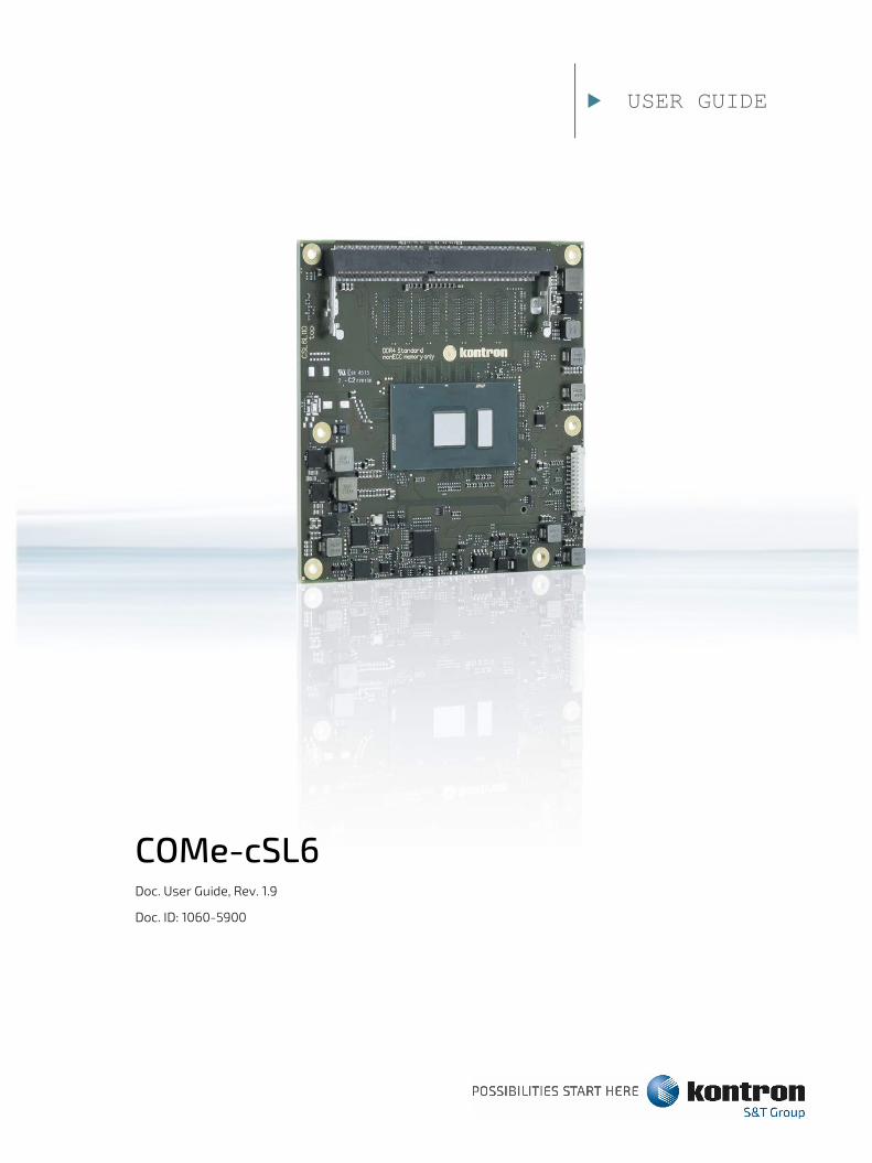
USER GUIDE
COMe-cSL6 Doc. User Guide, Rev. 1.9
Doc. ID: 1060-5900
COMe-cSL6 – User Guide, Rev. 1.9
www.kontron.com // 2
COME-CSL6 - USER GUIDE
Disclaimer
Kontron would like to point out that the information contained in this user guide may be subject to alteration, particularly as a result of the constant upgrading of Kontron products. This document does not entail any guarantee on the part of Kontron with respect to technical processes described in the user guide or any product characteristics set out in the user guide. Kontron assumes no responsibility or liability for the use of the described product(s), conveys no license or title under any patent, copyright or mask work rights to these products and makes no representations or warranties that these products are free from patent, copyright or mask work right infringement unless otherwise specified. Applications that are described in this user guide are for illustration purposes only. Kontron makes no representation or warranty that such application will be suitable for the specified use without further testing or modification. Kontron expressly informs the user that this user guide only contains a general description of processes and instructions which may not be applicable in every individual case. In cases of doubt, please contact Kontron.
This user guide is protected by copyright. All rights are reserved by Kontron. No part of this document may be reproduced, transmitted, transcribed, stored in a retrieval system, or translated into any language or computer language, in any form or by any means (electronic, mechanical, photocopying, recording, or otherwise), without the express written permission of Kontron. Kontron points out that the information contained in this user guide is constantly being updated in line with the technical alterations and improvements made by Kontron to the products and thus this user guide only reflects the technical status of the products by Kontron at the time of publishing.
Brand and product names are trademarks or registered trademarks of their respective owners.
©2018 by Kontron Europe GmbH
Kontron Europe GmbH
Gutenbergstraße 2 85737 Ismaning Germany www.kontron.com
COMe-cSL6 – User Guide, Rev. 1.9
www.kontron.com // 3
High Risk Applications Hazard Notice THIS DEVICE AND ASSOCIATED SOFTWARE ARE NOT DESIGNED, MANUFACTURED OR INTENDED FOR USE OR RESALE FOR THE OPERATION OF NUCLEAR FACILITIES, THE NAVIGATION, CONTROL OR COMMUNICATION SYSTEMS FOR AIRCRAFT OR OTHER TRANSPORTATION, AIR TRAFFIC CONTROL, LIFE SUPPORT OR LIFE SUSTAINING APPLICATIONS, WEAPONS SYSTEMS, OR ANY OTHER APPLICATION IN A HAZARDOUS ENVIRONMENT, OR REQUIRING FAIL-SAFE PERFORMANCE, OR IN WHICH THE FAILURE OF PRODUCTS COULD LEAD DIRECTLY TO DEATH, PERSONAL INJURY, OR SEVERE PHYSICAL OR ENVIRONMENTAL DAMAGE (COLLECTIVELY, "HIGH RISK APPLICATIONS").
You understand and agree that your use of Kontron devices as a component in High Risk Applications is entirely at your risk. To minimize the risks associated with your products and applications, you should provide adequate design and operating safeguards. You are solely responsible for compliance with all legal, regulatory, safety, and security related requirements concerning your products. You are responsible to ensure that your systems (and any Kontron hardware or software components incorporated in your systems) meet all applicable requirements. Unless otherwise stated in the product documentation, the Kontron device is not provided with error-tolerance capabilities and cannot therefore be deemed as being engineered, manufactured or setup to be compliant for implementation or for resale as device in High Risk Applications. All application and safety related information in this document (including application descriptions, suggested safety measures, suggested Kontron products, and other materials) is provided for reference only.
COMe-cSL6 – User Guide, Rev. 1.9
Revision History Revision Brief Description of Changes Date of Issue Author
/Editor
1.0 Initial version 2016-Jul-15 CW
1.1 Updated Standards and Certificates, and MTBF information Added specific and general product accessories
2016-Dec-22 CW
1.2 Updated memory module part numbers 2017-Jan-31 CW
1.3 Updated COMe Interface connector PU resistor information 2017-Mar-08 CW
1.4 Removed LVDS to DVI display adapters, included SATA, modified the BIOS update procedure and included audio.
2017-Aug-2 CW
1.5 Added GPIO feature information, updated commercial product names, added Kontron S&T AG, and updated BIOS set up Advanced menu and Chipset menu.
2018-Jan-23 CW
1.6 Removed BASE PCH Information (Table 10 and Figure 1) 2019-Mar-28 CW
1.7 Corrected general purpose PCIe #5 lane information 2019-Apr-25 CW
1.8 Updated Carrier Accessories 2020-Jul-23 CW
1.9 Security chip changed to option and new block diagram 2022-Feb-23 CW
Terms and Conditions Kontron warrants products in accordance with defined regional warranty periods. For more information about warranty compliance and conformity, and the warranty period in your region, visit http://www.kontron.com/terms-and-conditions.
Kontron sells products worldwide and declares regional General Terms & Conditions of Sale, and Purchase Order Terms & Conditions. Visit http://www.kontron.com/terms-and-conditions.
For contact information, refer to the corporate offices contact information on the last page of this user guide or visit our website CONTACT US.
Customer Support Find Kontron contacts by visiting: http://www.kontron.com/support.
Customer Service As a trusted technology innovator and global solutions provider, Kontron extends its embedded market strengths into a services portfolio allowing companies to break the barriers of traditional product lifecycles. Proven product expertise coupled with collaborative and highly-experienced support enables Kontron to provide exceptional peace of mind to build and maintain successful products.
For more details on Kontron’s service offerings such as: enhanced repair services, extended warranty, Kontron training academy, and more visit http://www.kontron.com/support-and-services/services.
Customer Comments If you have any difficulties using this user guide, discover an error, or just want to provide some feedback, contact Kontron Support. Detail any errors you find. We will correct the errors or problems as soon as possible and post the revised user guide on our website.
COMe-cSL6 – User Guide, Rev. 1.9
www.kontron.com // 5
Symbols The following symbols may be used in this user guide.
DANGER indicates a hazardous situation which, if not avoided,
will result in death or serious injury.
WARNING indicates a hazardous situation which, if not avoided,
could result in death or serious injury.
CAUTION indicates a hazardous situation which, if not avoided,
may result in minor or moderate injury.
NOTICE indicates a property damage message.
Electric Shock!
This symbol and title warn of hazards due to electrical shocks (> 60 V) when touching products or parts of them. Failure to observe the precautions indicated and/or prescribed by the law may endanger your life/health and/or result in damage to your material.
ESD Sensitive Device!
This symbol and title inform that the electronic boards and their components are sensitive to static electricity. Care must therefore be taken during all handling operations and inspections of this product in order to ensure product integrity at all times.
HOT Surface!
Do NOT touch! Allow to cool before servicing.
Laser!
This symbol informs of the risk of exposure to laser beam from an electric device. Eye protection per manufacturer notice shall be reviewed before servicing.
This symbol indicates general information about the product and the user guide.
This symbol also indicates detail information about the specific product configuration.
This symbol precedes helpful hints and tips for daily use.
COMe-cSL6 – User Guide, Rev. 1.9
www.kontron.com // 6
For Your Safety Your new Kontron product was developed and tested carefully to provide all features necessary to ensure its compliance with electrical safety requirements. It was also designed for a long fault-free life. However, the life expectancy of your product can be drastically reduced by improper treatment during unpacking and installation. Therefore, in the interest of your own safety and of the correct operation of your new Kontron product, you are requested to conform with the following guidelines.
High Voltage Safety Instructions
As a precaution and in case of danger, the power connector must be easily accessible. The power connector is the product’s main disconnect device.
Warning
All operations on this product must be carried out by sufficiently skilled personnel only.
Electric Shock!
Before installing a non hot-swappable Kontron product into a system always ensure that your mains power is switched off. This also applies to the installation of piggybacks. Serious electrical shock hazards can exist during all installation, repair, and maintenance operations on this product. Therefore, always unplug the power cable and any other cables which provide external voltages before performing any work on this product.
Earth ground connection to vehicle’s chassis or a central grounding point shall remain connected. The earth ground cable shall be the last cable to be disconnected or the first cable to be connected when performing installation or removal procedures on this product.
Special Handling and Unpacking Instruction
ESD Sensitive Device!
Electronic boards and their components are sensitive to static electricity. Therefore, care must be taken during all handling operations and inspections of this product, in order to ensure product integrity at all times.
Do not handle this product out of its protective enclosure while it is not used for operational purposes unless it is otherwise protected.
Whenever possible, unpack or pack this product only at EOS/ESD safe work stations. Where a safe work station is not guaranteed, it is important for the user to be electrically discharged before touching the product with his/her hands or tools. This is most easily done by touching a metal part of your system housing.
It is particularly important to observe standard anti-static precautions when changing piggybacks, ROM devices, jumper settings etc. If the product contains batteries for RTC or memory backup, ensure that the product is not placed on conductive surfaces, including anti-static plastics or sponges. They can cause short circuits and damage the batteries or conductive circuits on the product.
COMe-cSL6 – User Guide, Rev. 1.9
www.kontron.com // 7
Lithium Battery Precautions
If your product is equipped with a lithium battery, take the following precautions when replacing the battery.
Danger of explosion if the battery is replaced incorrectly.
Replace only with same or equivalent battery type recommended by the manufacturer.
Dispose of used batteries according to the manufacturer’s instructions.
General Instructions on Usage In order to maintain Kontron’s product warranty, this product must not be altered or modified in any way. Changes or modifications to the product, that are not explicitly approved by Kontron and described in this user guide or received from Kontron Support as a special handling instruction, will void your warranty. This product should only be installed in or connected to systems that fulfill all necessary technical and specific environmental requirements. This also applies to the operational temperature range of the specific board version that must not be exceeded. If batteries are present, their temperature restrictions must be taken into account. In performing all necessary installation and application operations, only follow the instructions supplied by the present user guide. Keep all the original packaging material for future storage or warranty shipments. If it is necessary to store or ship the product then re-pack it in the same manner as it was delivered. Special care is necessary when handling or unpacking the product. See Special Handling and Unpacking Instruction.
Quality and Environmental Management Kontron aims to deliver reliable high-end products designed and built for quality, and aims to complying with environmental laws, regulations, and other environmentally oriented requirements. For more information regarding Kontron’s quality and environmental responsibilities, visit http://www.kontron.com/about-kontron/corporate-responsibility/quality-management.
Disposal and Recycling
Kontron’s products are manufactured to satisfy environmental protection requirements where possible. Many of the components used are capable of being recycled. Final disposal of this product after its service life must be accomplished in accordance with applicable country, state, or local laws or regulations.
WEEE Compliance
The Waste Electrical and Electronic Equipment (WEEE) Directive aims to:
Reduce waste arising from electrical and electronic equipment (EEE)
Make producers of EEE responsible for the environmental impact of their products, especially when the product become waste
Encourage separate collection and subsequent treatment, reuse, recovery, recycling and sound environmental disposal of EEE
Improve the environmental performance of all those involved during the lifecycle of EEE
Environmental protection is a high priority with Kontron.
Kontron follows the WEEE directive
COMe-cSL6 – User Guide, Rev. 1.9
www.kontron.com // 8
Table of Contents
Symbols ................................................................................................................................................................................................................. 5 Table of Contents .............................................................................................................................................................................................. 8 List of Tables ...................................................................................................................................................................................................... 10 List of Figures ..................................................................................................................................................................................................... 11 1/ Introduction .......................................................................................................................................................................................... 12 1.1. Product Description................................................................................................................................................................................... 12 1.2. Product Naming Clarification ................................................................................................................................................................ 12 1.3. COM Express® Documentation ............................................................................................................................................................. 12 1.4. COM Express® Functionality ................................................................................................................................................................. 13 1.5. COM Express® Benefits ........................................................................................................................................................................... 13 2/ Product Specification ........................................................................................................................................................................ 14 2.1. Module Variants ........................................................................................................................................................................................ 14
Commercial Grade Modules (0°C to 60°C) ..................................................................................................................................... 14 Extended Temperature Grade Modules (E1, -25°C to 75°C) ..................................................................................................... 14 Industrial Temperature Grade Modules (E2, -40°C to 85°C) ................................................................................................... 14
2.2. Accessories ................................................................................................................................................................................................. 15 2.3. Functional Specifications ....................................................................................................................................................................... 17
Block Diagram COMe-cSL6 ................................................................................................................................................................. 17 Processor ................................................................................................................................................................................................. 18 Platform Controller Hub (PCH) ........................................................................................................................................................ 20 System Memory ................................................................................................................................................................................... 20 Graphics ................................................................................................................................................................................................... 20 LVDS........................................................................................................................................................................................................... 21 Audio .......................................................................................................................................................................................................... 21 PCI Express (PCIE) Configuration .................................................................................................................................................... 22 USB ............................................................................................................................................................................................................ 23 SATA........................................................................................................................................................................................................ 23 Ethernet .................................................................................................................................................................................................. 24 COMe High-Speed I/O Interfaces .................................................................................................................................................. 25 Storage Features ................................................................................................................................................................................ 25 BIOS/Software Features.................................................................................................................................................................. 26 COMe Features .................................................................................................................................................................................... 26 Kontron Features................................................................................................................................................................................ 26
2.4. Electrical Specification .......................................................................................................................................................................... 27 2.5. Power Supply Voltage specifications ............................................................................................................................................... 27
Power Consumption ............................................................................................................................................................................ 27 Power Management ............................................................................................................................................................................ 28 Power Supply Control Settings ....................................................................................................................................................... 28 Power Supply Modes .......................................................................................................................................................................... 29
2.6. Thermal Management ........................................................................................................................................................................... 30 Heatspreader and Cooling Solutions ............................................................................................................................................. 30 Operating with Kontron Heatspreader Plate (HSP) Assembly ............................................................................................. 30 Operating without Kontron Heatspreader Plate Assembly ................................................................................................... 30 On-board Fan Connector .................................................................................................................................................................... 31
2.7. Environmental Specification ................................................................................................................................................................. 31 Temperature ............................................................................................................................................................................................ 31
COMe-cSL6 – User Guide, Rev. 1.9
www.kontron.com // 9
Humidity ................................................................................................................................................................................................... 31 2.8. Standards and Certifications ............................................................................................................................................................... 32 2.9. MTBF ............................................................................................................................................................................................................ 33 2.10. Mechanical Specification .................................................................................................................................................................... 34
Dimensions ........................................................................................................................................................................................... 34 Height ..................................................................................................................................................................................................... 35
3/ Features and Interfaces .................................................................................................................................................................. 36 3.1. LPC ................................................................................................................................................................................................................. 36 3.2. Serial Peripheral Interface (SPI) .......................................................................................................................................................... 36
SPI boot .................................................................................................................................................................................................... 37 Using an External SPI Flash .............................................................................................................................................................. 37 External SPI flash on Modules with Intel® ME ........................................................................................................................... 38
3.3. M.A.R.S. ........................................................................................................................................................................................................ 38 3.4. Fast I2C ....................................................................................................................................................................................................... 38 3.5. UART............................................................................................................................................................................................................. 38 3.6. Triple Staged Watchdog Timer (WTD) ............................................................................................................................................. 39
Basics ........................................................................................................................................................................................................ 39 WDT Signal ............................................................................................................................................................................................. 39
3.7. GPIO .............................................................................................................................................................................................................. 40 3.8. Real Time Clock (RTC) ............................................................................................................................................................................ 40 3.9. Trusted Platform Module (TPM 2.0) ................................................................................................................................................. 40 3.10. Kontron Security Solution ................................................................................................................................................................... 40 3.11. Speedstep Technology .......................................................................................................................................................................... 41 4/ System Resources ............................................................................................................................................................................. 42 4.1. Interrupt Request (IRQ) Lines .............................................................................................................................................................. 42 4.2. Memory Area ............................................................................................................................................................................................ 42 4.3. I/O Address Map ...................................................................................................................................................................................... 43 4.4. Peripheral Component Interconnect (PCI) Devices ..................................................................................................................... 44 4.5. I2C Bus ......................................................................................................................................................................................................... 44 4.6. System Management (SM) Bus .......................................................................................................................................................... 45 5/ COMe Interface Connectors (X1A and X1B) ............................................................................................................................... 46 5.1. X1A and X1B Signals ................................................................................................................................................................................. 46 5.2. X1A and X1B Pin Assignment ................................................................................................................................................................ 47
Connector X1A Row A1-A110 .............................................................................................................................................................. 48 Connector X1A Row B1-B110 .............................................................................................................................................................. 51 Connector X1B Row C1-C110 .............................................................................................................................................................. 54 Connector X1B Row D1-D110 .............................................................................................................................................................. 57
6/ uEFI BIOS ............................................................................................................................................................................................... 60 6.1. Starting the uEFI BIOS ............................................................................................................................................................................. 60 6.2. Setup Menus .............................................................................................................................................................................................. 61
Main Setup Menu .................................................................................................................................................................................. 62 Advanced Setup Menu ........................................................................................................................................................................ 63 Chipset Setup Menu ............................................................................................................................................................................ 76 Security Setup Menu ........................................................................................................................................................................... 85 Boot Setup Menu .................................................................................................................................................................................. 86 Save and Exit Setup Menu ................................................................................................................................................................. 86
6.3. The uEFI Shell............................................................................................................................................................................................ 87 Basic Operation of the uEFI Shell .................................................................................................................................................... 87
6.4. uEFI Shell Scripting ................................................................................................................................................................................. 88
COMe-cSL6 – User Guide, Rev. 1.9
www.kontron.com // 10
Startup Scripting ................................................................................................................................................................................... 88 Create a Startup Script ....................................................................................................................................................................... 88 Examples of Startup Scripts ............................................................................................................................................................ 88
6.5. Firmware Update ..................................................................................................................................................................................... 89 Updating Procedure ............................................................................................................................................................................. 89
Appendix A: List of Acronyms ...................................................................................................................................................................... 90 About Kontron – Member of the S&T Group ........................................................................................................................................... 91
List of Tables Table 1: Pin Assignment of Type 6 and COMe-cSL6 .............................................................................................................................. 13 Table 2: Commercial Grade Modules (0°C to 60°C operating)........................................................................................................... 14 Table 3: Product Specific Accessories ....................................................................................................................................................... 15 Table 4: COMe Type 6 Specific Accessories ............................................................................................................................................. 15 Table 5: General Accessories ........................................................................................................................................................................ 15 Table 6: Memory Modules ............................................................................................................................................................................. 16 Table 7: Intel Skylake Processors Specifications ................................................................................................................................... 19 Table 8: Gen 3 PCI-Express Graphics x16 (PEG) Port ........................................................................................................................... 22 Table 9: General Purpose PCI-Express lanes ......................................................................................................................................... 22 Table 10: Premium PCH High-Speed I/O Port Interfaces .................................................................................................................... 25 Table 11: ATX Mode Settings ........................................................................................................................................................................ 29 Table 12: Single Supply Mode Settings ..................................................................................................................................................... 29 Table 13: Heatspreader Test Temperature Specifications ................................................................................................................ 30 Table 14: 3-Pin Fan Connector Pin Assignment...................................................................................................................................... 31 Table 15: Electrical Characteristics of the Fan Connector .................................................................................................................. 31 Table 16: Temperature Grade Specifications .......................................................................................................................................... 31 Table 17: Humidity Specification .................................................................................................................................................................. 31 Table 18: Standards and Certifications .................................................................................................................................................... 32 Table 19: Supported BIOS Features ........................................................................................................................................................... 36 Table 20: SPI Boot Pin Configuration ........................................................................................................................................................ 37 Table 21: Supported SPI Boot Flash Types for 8-SOIC Package ....................................................................................................... 37 Table 22: Reserved SM-Bus Addresses for Smart Battery Solutions on the Carrier ............................................................... 38 Table 23: Triple Stage Watchdog Timer- Time-out Events ............................................................................................................... 39 Table 24: List of Interrupt Requests ......................................................................................................................................................... 42 Table 25: Designated Memory Locations ................................................................................................................................................ 42 Table 26: Designated I/O Port Addresses ............................................................................................................................................... 43 Table 27: I2C Bus Port Addresses ............................................................................................................................................................... 44 Table 28: Designated I/O Port Addresses ............................................................................................................................................... 45 Table 29: General Signal Description ........................................................................................................................................................ 47 Table 30: Connector X1A Row A Pin Assignment (A1-A110) ............................................................................................................... 48 Table 31: Connector X1A Row B Pin Assignment(B1-B110) .................................................................................................................. 51 Table 32: Connector X1B Row C Pin Assignment (C1-C110)................................................................................................................ 54 Table 33: Connector X1B Row D Pin Assignment(D1-D110) ................................................................................................................ 57 Table 34: Navigation Hot Keys Available in the Legend Bar ............................................................................................................. 60 Table 35: Main Setup Menu Sub-screens and Functions ................................................................................................................... 62 Table 36: Advanced Setup menu Sub-screens and Functions ......................................................................................................... 63 Table 37: Chipset Setup Menu Sub-screens and Functions .............................................................................................................. 76 Table 38: Chipset Set > PCH-IO Configuration Sub-screens and Functions ................................................................................ 79 Table 39: Security Setup Menu Functions ............................................................................................................................................... 85 Table 40: Boot Setup Menu Functions ..................................................................................................................................................... 86 Table 41: Save and Exit Setup Menu Functions ..................................................................................................................................... 86 Table 42: List of Acronyms ........................................................................................................................................................................... 90
COMe-cSL6 – User Guide, Rev. 1.9
www.kontron.com // 11
List of Figures Figure 1: Block Diagram COMe-cSL6 .......................................................................................................................................................... 17 Figure 2: MTBF Temperature De-rating ................................................................................................................................................... 33 Figure 3: Module Dimensions ...................................................................................................................................................................... 34 Figure 4: Module Height ................................................................................................................................................................................ 35 Figure 5: X1A and X1B COMe Interface Connectors .............................................................................................................................. 46 Figure 6: Advance Setup Menu Initial Screen ......................................................................................................................................... 63 Figure 7: Chipset>System Agent Configuration Initial Screen .......................................................................................................... 76 Figure 8: PCH-IO Configuration Menu Initial Screen ............................................................................................................................ 79 Figure 9: Security Setup Menu Initial Screen .......................................................................................................................................... 85
COMe-cSL6 – User Guide, Rev. 1.9
www.kontron.com // 12
1/ Introduction
1.1. Product Description
Kontron's Computer-on-Module COMe-cSL6 is a COM Express® COMPACT TYPE 6 with the Intel® Skylake-U low power processor with support for pinout Type 6, and an additional communication interface block. The COMe-cSL6 covers the need for the latest interface technology and extended lifetime, in the embedded and IoT environment. Due to Intel’s 14nm technology, the Skylake–U offers increased efficiency and performance with TDP as low as 7.5 W, and no more than 15W. All core extensions feature Intel ® HD 520 Graphics clocked at 350 MHz, with 1000 to 1050 MHz boost, and the Celeron model features HD510 Graphics, at 30/ 900MHz.
On request, the COMe-cSL6 is available for the industrial temperature environment.
Intel® 6th Generation Core Series, Skylake-U (ULT) Processor
DDR4 memory 1866/2133, SODIMM up to 16 GB and up to 8 GB memory down
High-speed connectivity x 12 PCIe Gen 3 or PCIe Gen 2 lanes, 1 x GbE interface
1.2. Product Naming Clarification
COM Express® defines a Computer-On-Module, or COM, with all the components necessary for a bootable host computer, packaged as a super component. The product names for Kontron COM Express® Computer-on-Modules consist of:
Short form of the industry standard
COMe-
Module form factor
b=basic (125 mm x 95 mm)
c=compact (9 5mm x 95 mm)
m=mini (84 mm x 55 mm)
Intel’s processor code name
SL = Skylake
Pinout type
Type 6
Type10
Temperature variants
Commercial
Extended (E1)
Industrial (E2)
Screened industrial (E2S) and Rapid shutdown screened industrial (R E2S)
Processor Identifier
Chipset identifier (if chipset assembled)
Memory size
Memory Down + DIMM memory (#GB) / eMMC SLC memory (#S)
1.3. COM Express® Documentation
The COM Express® Specification defines the COM Express® module form factor, pinout, and signals. This document is available at the PICMG® website.
COMe-cSL6 – User Guide, Rev. 1.9
www.kontron.com // 13
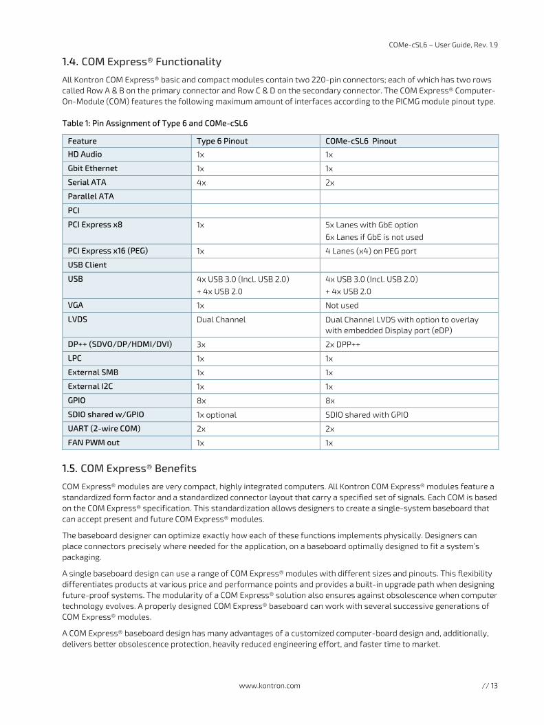
1.4. COM Express® Functionality
All Kontron COM Express® basic and compact modules contain two 220-pin connectors; each of which has two rows called Row A & B on the primary connector and Row C & D on the secondary connector. The COM Express® Computer-On-Module (COM) features the following maximum amount of interfaces according to the PICMG module pinout type.
Table 1: Pin Assignment of Type 6 and COMe-cSL6
Feature Type 6 Pinout COMe-cSL6 Pinout
HD Audio 1x 1x
Gbit Ethernet 1x 1x
Serial ATA 4x 2x
Parallel ATA
PCI
PCI Express x8 1x 5x Lanes with GbE option 6x Lanes if GbE is not used
PCI Express x16 (PEG) 1x 4 Lanes (x4) on PEG port
USB Client
USB 4x USB 3.0 (Incl. USB 2.0) + 4x USB 2.0
4x USB 3.0 (Incl. USB 2.0) + 4x USB 2.0
VGA 1x Not used
LVDS Dual Channel Dual Channel LVDS with option to overlay with embedded Display port (eDP)
DP++ (SDVO/DP/HDMI/DVI) 3x 2x DPP++
LPC 1x 1x
External SMB 1x 1x
External I2C 1x 1x
GPIO 8x 8x
SDIO shared w/GPIO 1x optional SDIO shared with GPIO
UART (2-wire COM) 2x 2x
FAN PWM out 1x 1x
1.5. COM Express® Benefits
COM Express® modules are very compact, highly integrated computers. All Kontron COM Express® modules feature a standardized form factor and a standardized connector layout that carry a specified set of signals. Each COM is based on the COM Express® specification. This standardization allows designers to create a single-system baseboard that can accept present and future COM Express® modules.
The baseboard designer can optimize exactly how each of these functions implements physically. Designers can place connectors precisely where needed for the application, on a baseboard optimally designed to fit a system’s packaging.
A single baseboard design can use a range of COM Express® modules with different sizes and pinouts. This flexibility differentiates products at various price and performance points and provides a built-in upgrade path when designing future-proof systems. The modularity of a COM Express® solution also ensures against obsolescence when computer technology evolves. A properly designed COM Express® baseboard can work with several successive generations of COM Express® modules.
A COM Express® baseboard design has many advantages of a customized computer-board design and, additionally, delivers better obsolescence protection, heavily reduced engineering effort, and faster time to market.
COMe-cSL6 – User Guide, Rev. 1.9
www.kontron.com // 14
2/ Product Specification
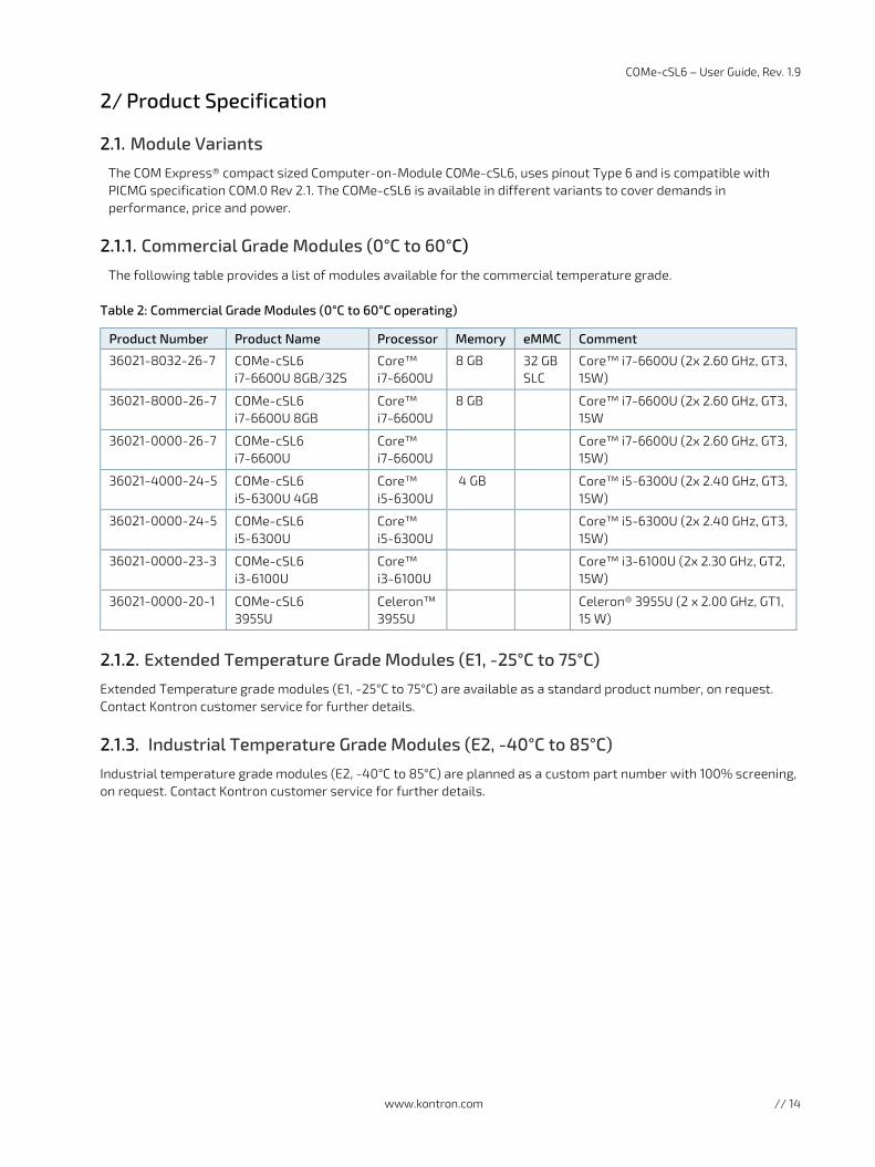
2.1. Module Variants
The COM Express® compact sized Computer-on-Module COMe-cSL6, uses pinout Type 6 and is compatible with PICMG specification COM.0 Rev 2.1. The COMe-cSL6 is available in different variants to cover demands in performance, price and power.
Commercial Grade Modules (0°C to 60°C)
The following table provides a list of modules available for the commercial temperature grade.
Table 2: Commercial Grade Modules (0°C to 60°C operating)
Product Number Product Name Processor Memory eMMC Comment
36021-8032-26-7 COMe-cSL6 i7-6600U 8GB/32S
Core™ i7-6600U
8 GB 32 GB SLC
Core™ i7-6600U (2x 2.60 GHz, GT3, 15W)
36021-8000-26-7 COMe-cSL6 i7-6600U 8GB
Core™ i7-6600U
8 GB Core™ i7-6600U (2x 2.60 GHz, GT3, 15W
36021-0000-26-7 COMe-cSL6 i7-6600U
Core™ i7-6600U
Core™ i7-6600U (2x 2.60 GHz, GT3, 15W)
36021-4000-24-5 COMe-cSL6 i5-6300U 4GB
Core™ i5-6300U
4 GB Core™ i5-6300U (2x 2.40 GHz, GT3, 15W)
36021-0000-24-5 COMe-cSL6 i5-6300U
Core™ i5-6300U
Core™ i5-6300U (2x 2.40 GHz, GT3, 15W)
36021-0000-23-3 COMe-cSL6 i3-6100U
Core™ i3-6100U
Core™ i3-6100U (2x 2.30 GHz, GT2, 15W)
36021-0000-20-1 COMe-cSL6 3955U
Celeron™ 3955U
Celeron® 3955U (2 x 2.00 GHz, GT1, 15 W)
Extended Temperature Grade Modules (E1, -25°C to 75°C)
Extended Temperature grade modules (E1, -25°C to 75°C) are available as a standard product number, on request. Contact Kontron customer service for further details.
Industrial Temperature Grade Modules (E2, -40°C to 85°C)
Industrial temperature grade modules (E2, -40°C to 85°C) are planned as a custom part number with 100% screening, on request. Contact Kontron customer service for further details.
COMe-cSL6 – User Guide, Rev. 1.9
www.kontron.com // 15
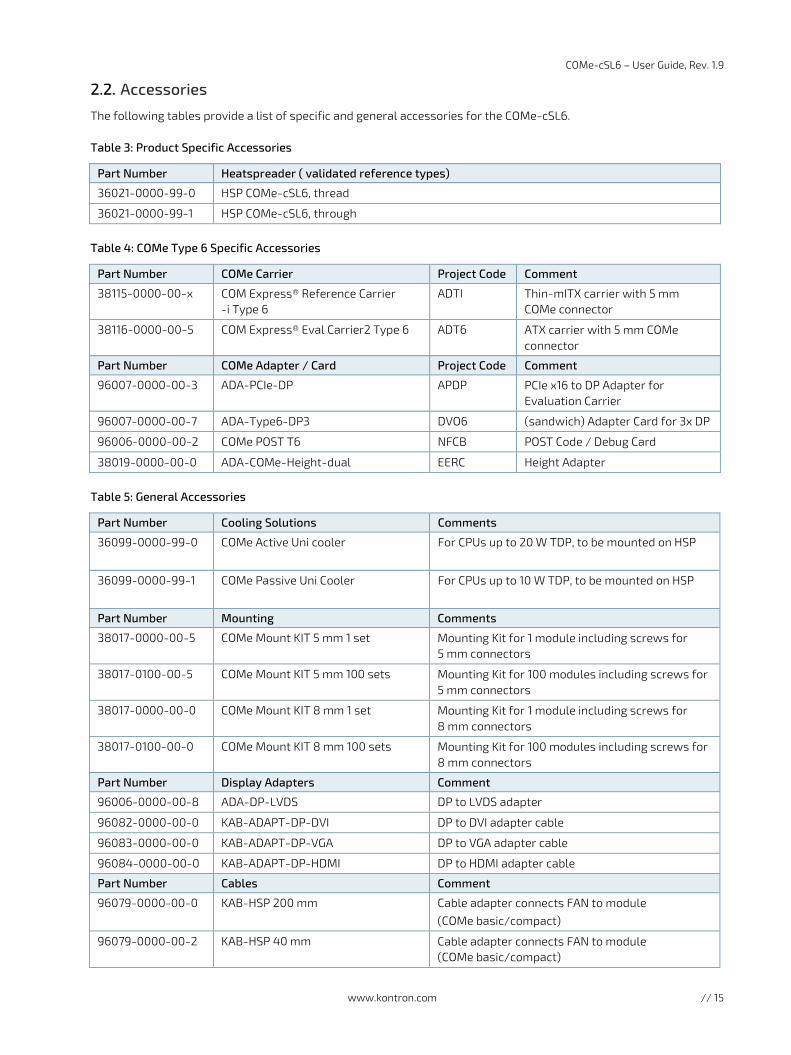
2.2. Accessories
The following tables provide a list of specific and general accessories for the COMe-cSL6.
Table 3: Product Specific Accessories
Part Number Heatspreader ( validated reference types)
36021-0000-99-0 HSP COMe-cSL6, thread
36021-0000-99-1 HSP COMe-cSL6, through
Table 4: COMe Type 6 Specific Accessories
Part Number COMe Carrier Project Code Comment
38115-0000-00-x COM Express® Reference Carrier -i Type 6
ADTI Thin-mITX carrier with 5 mm COMe connector
38116-0000-00-5 COM Express® Eval Carrier2 Type 6 ADT6 ATX carrier with 5 mm COMe connector
Part Number COMe Adapter / Card Project Code Comment
96007-0000-00-3 ADA-PCIe-DP APDP PCIe x16 to DP Adapter for Evaluation Carrier
96007-0000-00-7 ADA-Type6-DP3 DVO6 (sandwich) Adapter Card for 3x DP
96006-0000-00-2 COMe POST T6 NFCB POST Code / Debug Card
38019-0000-00-0 ADA-COMe-Height-dual EERC Height Adapter
Table 5: General Accessories
Part Number Cooling Solutions Comments
36099-0000-99-0 COMe Active Uni cooler For CPUs up to 20 W TDP, to be mounted on HSP
36099-0000-99-1 COMe Passive Uni Cooler For CPUs up to 10 W TDP, to be mounted on HSP
Part Number Mounting Comments
38017-0000-00-5 COMe Mount KIT 5 mm 1 set Mounting Kit for 1 module including screws for 5 mm connectors
38017-0100-00-5 COMe Mount KIT 5 mm 100 sets Mounting Kit for 100 modules including screws for 5 mm connectors
38017-0000-00-0 COMe Mount KIT 8 mm 1 set Mounting Kit for 1 module including screws for 8 mm connectors
38017-0100-00-0 COMe Mount KIT 8 mm 100 sets Mounting Kit for 100 modules including screws for 8 mm connectors
Part Number Display Adapters Comment
96006-0000-00-8 ADA-DP-LVDS DP to LVDS adapter
96082-0000-00-0 KAB-ADAPT-DP-DVI DP to DVI adapter cable
96083-0000-00-0 KAB-ADAPT-DP-VGA DP to VGA adapter cable
96084-0000-00-0 KAB-ADAPT-DP-HDMI DP to HDMI adapter cable
Part Number Cables Comment
96079-0000-00-0 KAB-HSP 200 mm Cable adapter connects FAN to module (COMe basic/compact)
96079-0000-00-2 KAB-HSP 40 mm Cable adapter connects FAN to module (COMe basic/compact)
COMe-cSL6 – User Guide, Rev. 1.9
www.kontron.com // 16
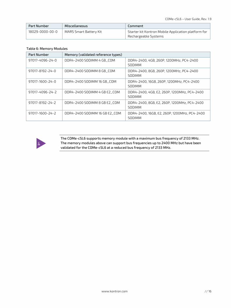
Part Number Miscellaneous Comment
18029-0000-00-0 MARS Smart Battery Kit Starter kit Kontron Mobile Application platform for Rechargeable Systems
Table 6: Memory Modules
Part Number Memory (validated reference types)
97017-4096-24-0 DDR4-2400 SODIMM 4 GB_COM DDR4-2400, 4GB, 260P, 1200MHz, PC4-2400 SODIMM
97017-8192-24-0 DDR4-2400 SODIMM 8 GB_COM DDR4-2400, 8GB, 260P, 1200MHz, PC4-2400 SODIMM
97017-1600-24-0 DDR4-2400 SODIMM 16 GB_COM DDR4-2400, 16GB, 260P, 1200MHz, PC4-2400 SODIMM
97017-4096-24-2 DDR4-2400 SODIMM 4 GB E2_COM DDR4-2400, 4GB, E2, 260P, 1200MHz, PC4-2400 SODIMM
97017-8192-24-2 DDR4-2400 SODIMM 8 GB E2_COM DDR4-2400, 8GB, E2, 260P, 1200MHz, PC4-2400 SODIMM
97017-1600-24-2 DDR4-2400 SODIMM 16 GB E2_COM DDR4-2400, 16GB, E2, 260P, 1200MHz, PC4-2400 SODIMM
The COMe-cSL6 supports memory module with a maximum bus frequency of 2133 MHz. The memory modules above can support bus frequencies up to 2400 MHz but have been validated for the COMe-cSL6 at a reduced bus frequency of 2133 MHz.
COMe-cSL6 – User Guide, Rev. 1.9
www.kontron.com // 17
2.3. Functional Specifications
Block Diagram COMe-cSL6
The following figure displays the system block diagram applicable to all COMe-cSL6 modules.
Figure 1: Block Diagram COMe-cSL6
USB #8(USB 2.0)
SDIO
GPIO
GPSPI
PEG #0-3
SMB
eSPIUARTGPIOCtrl
MgmtLPC
HDA
SATA#0-1
SPI
USB #0-3(USB3.0)
PwrCtr lSysMgmt
PCIe #5USB #0-3(USB2.0)
PWMFAN2
I2C SER0SER1
eDP x2
USB #4-7(USB 2.0)
PCIe #0-3PCIe #4
Intel® 6th Generation CoreSkylake ULT (U-Series) i7/i5/i3/Celeron
Premium PCH integrated
LIDSleep
SPI BIOS Flash
LVDS
Connector OptionStandard component
GB LANEmbedded Controller(MAX 2/5/10)
HWM NCT7802
Gen9iGFX
FAN1
xHCI
eDP2LVDSPTN3460(i)
COM Express® connector AB – Pin-out Type 6
GBLanIntel® I219LM
VCC
5VS
BVB
AT
HWM
SMB
Power sequencing
WatchdogLPC2I2C GPIO Buffer
I2C
S5eco
EEPROM
TPM
UART
COM Express® connector CD – Pin-out Type 6
DDR4 SODIMM
VCC
EHCI
2x DP++
SPD
eMMC5.0
SPD
DDR4
eMMC2-64GB
GPIOor
SDIO
GPIO/SDIO Switch
2x CSI2
Security Chip
COMe-cSL6 – User Guide, Rev. 1.9
www.kontron.com // 18
Processor
The Intel® 6th Generation Core™ series Skylake-U (ULT) product family uses the 14 nm process technology, with 42 mm x 24 mm package size and FCBGA1356.
In general, the Intel® Skylake-U series of processors supports the following technologies:
Intel® 64
Intel® Turbo Boost Technology 2.0 (i7-6600U and i5-6300U only)
Intel® Virtualization Technology (VT-x)
Intel® Virtualization Technology for Directed I/O (VT-d)
Intel® VT-x Extended Page Table (EPT)
Intel® vPro Technology (i7-6600U and i5-6300U only)
Intel® Hyper Threading Technology (i7-6600U, i5-6300U and i3-6100 only)
Intel® TSX-NI (i7-6600U and i5-6300U only)
Intel® My Wi-Fi Technology
Idle States
Enhanced Intel Speedstep® Technology
Thermal Monitoring Technologies
Intel® Flex Memory Access
Intel® Identity Protection Technology
Intel® Stable Image Platform Program (SIPP) (i7-6600U and i5-6300U only)
Intel® Smart Response Technology
Intel® Advanced Encryption Standard New Instructions (AES-NI)
Intel® Secure Key
Intel® Software Guard Extensions (Intel® SGX)
Intel® Memory Protection Extensions (Intel® MPX ) (i7-6600U, i5-6300U and i3-6100 only)
Intel® OS Guard (i7-6600U, i5-6300U and i3-6100 only)
Intel® Trusted Execution Technology (TXT) (i7-6600U and i5-6300U only)
Intel® Executive Disable Bit
COMe-cSL6 – User Guide, Rev. 1.9
www.kontron.com // 19
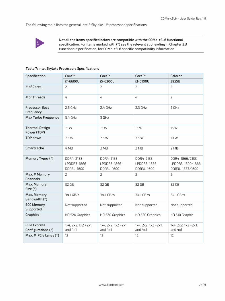
The following table lists the general Intel® Skylake-U® processor specifications.
Not all the items specified below are compatible with the COMe-cSL6 functional specification. For items marked with (*) see the relevant subheading in Chapter 2.3 Functional Specification, for COMe-cSL6 specific compatibility information.
Table 7: Intel Skylake Processors Specifications
Specification Core™ Core™ Core™ Celeron
i7-6600U i5-6300U i3-6100U 3955U
# of Cores
2 2 2 2
# of Threads
4 4 4 2
Processor Base Frequency
2.6 GHz 2.4 GHz 2.3 GHz 2 GHz
Max Turbo Frequency
3.4 GHz 3 GHz
Thermal Design Power (TDP)
15 W 15 W 15 W 15 W
TDP down
7.5 W 7.5 W 7.5 W 10 W
Smartcache
4 MB 3 MB 3 MB 2 MB
Memory Types (*) DDR4-2133 LPDDR3-1866 DDR3L-1600
DDR4-2133 LPDDR3-1866 DDR3L-1600
DDR4-2133 LPDDR3-1866 DDR3L-1600
DDR4-1866/2133 LPDDR3-1600/1866 DDR3L-1333/1600
Max. # Memory Channels
2 2 2 2
Max. Memory Size (*)
32 GB
32 GB
32 GB
32 GB
Max. Memory Bandwidth (*)
34.1 GB/s 34.1 GB/s 34.1 GB/s 34.1 GB/s
ECC Memory Supported
Not supported Not supported Not supported Not supported
Graphics
HD 520 Graphics HD 520 Graphics HD 520 Graphics HD 510 Graphic
PCIe Express Configurations (*)
1x4, 2x2, 1x2 +2x1, and 4x1
1x4, 2x2, 1x2 +2x1, and 4x1
1x4, 2x2, 1x2 +2x1, and 4x1
1x4, 2x2, 1x2 +2x1, and 4x1
Max. # PCIe Lanes (*) 12
12
12
12
COMe-cSL6 – User Guide, Rev. 1.9
www.kontron.com // 20
Platform Controller Hub (PCH)
The Intel® Skylake-U (ULT) product family includes an integrated chipset with the Intel® Platform Controller Hub.
The following table lists specific PCH features.
Rapid Storage Supported
USB 3.0 Supported
VT-d Supported
TXT Supported (Note: not supported in standard BIOS)
SATA RAID Supported
System Memory
The system memory supports two memory channels with DDR4-1866/2133 SO-DIMM sockets, for a maximum of up to 24 GByte of non ECC memory comprising of 8 Gbyte soldered down memory and up to 16 GByte DDR4 -1866/2133 non ECC memory.
The following table list specific system memory features.
Socket 1x SO-DIMM DDR4
Memory Type Channel 1: DDR4-1866/2133 SODIMM up to 16 GB non ECC Channel 2: DDR4-1866/2133 memory down up to 8 GB
Memory Module Size 4 GB, 8 GB and 16 GB
Bandwidth 34.1 Gb/s at 2133 MT/s or 29.8 GB/s at 1866 MT/s
Memory Down 1 x 8 GB (Option)
The full raw SPD (Serial Presence Detect) readout from memory channel 2 is not supported and can lead to misinterpretation by third party SPD tools. The affected entries are:
DDR4 Module Manufacturer ID CODE
DDR4 Module Manufacturer Location
DDR4 Module Manufacturer Date
DDR4 Module Serial Number
DDR4 Module Part No
DDR4 Module PCB Rev
DDR4 DRAM Manufacturer ID CODE
DDR4 DEVICE DIE REV
Graphics
2.3.5.1. Digital Display Interfaces
Up to three independent Digital Displays Interfaces (DDIs) can be used simultaneously and in combination, to implement an independent or cloned display configuration using DP 1.2 ‘Multi Media Stream Transport.
The standard DDIs are:
2x DP 1.2 (++), (CPU Port B&C on DDI1/2)
1x eDP 1.4 ( CPU Port A on DDIO used for the LVDS bridge)
HDMI 1.4 via level shifter
COMe-cSL6 – User Guide, Rev. 1.9
www.kontron.com // 21
HDMI 2.0 via LS-Pcon converter including HDCP, external hardware required
DVI-D via level shifter, external hardware required
2.3.5.2. Display Resolution
The following table lists the maximum supported display resolutions at a set frequency and bit per pixel (bpp) for the supported display interfaces.
Display Interfaces Maximum Resolution
eDP 4096 x 2304 (60 Hz, 24 bpp)
DP 4096 x 2304 (60 Hz, 24 bpp)
HDMI 1.4 ( native) 4096 x 2160 (24 Hz, 24 bpp)
HDMI 2.0 (via LS-Pcon) 4096 x 2160 (60 Hz, 24 bpp)
The maximum resolution is based on the implementation of four lanes with HBR2 link data rate and assumes maximum VCC. If more than one active display port is connected, then the processor frequency may be lower than base frequency at thermally limited scenarios.
At 4K/UHD resolution, a DisplayPort redriver on the carrier is recommended to increase the link margin.
LVDS
The embedded display port to LVDS bridge (eDP2LVDS) supports dual LVDS 18-bit or 24-bit channels. With an optional eDP instead of LVDS w/o converter chip.
The following table lists basic LVDS features.
LVD Channels 1x or 2x
LVDS Bits / Pixel 18 bit; 24 bit VESA mapping; 24 bit openLDI mapping
LVDS Maximum Resolution Up to 1920 x 1200
PWM Backlight Control Supported
Supported Panel Data JILI; EDID 1.3; EDID 1.4; DisplayID
Audio
Three independent HD Audio (HDA) streams can be supported simultaneously on HDMI/DP. The default for audio support is over the Display Port (DP), with an additional option for baseboard audio via an external HDA codec on the carrier board.
COMe-cSL6 – User Guide, Rev. 1.9
www.kontron.com // 22
PCI Express (PCIE) Configuration
The COMe-cSL6 supports 12 PCIe Gen 3 (Premium) lanes and a maximum of six devices simultaneously.
2.3.8.1. Gen 3 PCI-Express Graphics (PEG) Port
The x16 PCI Express Graphics (PEG) port is available on the COMe connector. PCIe lanes [9–12] from the Skylake PCH are connected to PEG[0-3].
Table 8: Gen 3 PCI-Express Graphics x16 (PEG) Port
COMe PEG PCH I/O Config. 0 (1 port x4) default
Other Configurations
Lane 0 PCIe #9
X4
Contact Kontron Support if you require more information. Lane 1 PCIe #10
Lane 2 PCIe #11
Lane 3 PCIe #12
Lane 4 NC
Not connected
Lane 5 NC
Lane 6 NC
Lane 7 NC
Lane 8 NC
Lane 9 NC
Lane 10 NC
Lane 11 NC
Lane 12 NC
Lane 13 NC
Lane 14 NC
Lane 15 NC
2.3.8.2. General Purpose PCI-Express Lanes
General-purpose PCI lanes are available on the COMe connector. Premium PCH is Gen 3.
Table 9: General Purpose PCI-Express lanes
COMe PCIe PCH I/O Config.0 (6 ports x1)
Config.1 (2 ports x4)
Config.2 (1 port x4 )+ (4 ports x1)
Config.3 (4 ports x1) + (1 port x4)
Config.4 (8 ports x1)
Lane 0 PCIe #1 x1
Contact Kontron Support, if you require more information.
Lane 1 PCIe #2 x1
Lane 2 PCIe #3 x1
Lane 3 PCIe #4 x1
Lane 4 PCIe #6 x1
Lane 5 PCIe #5/NC x1 PCH HSIO port without Ethernet or Not connected with Ethernet
Lane 6 NC Not connected
Lane 7 NC
COMe-cSL6 – User Guide, Rev. 1.9
www.kontron.com // 23
USB
Both USB 3.0 and USB 2.0 ports are available, where USB3.0 ports are backwards compatible with the USB 2.0 specification.
The following table lists the supported USB features.
USB Ports 4x USB 3.0 ports ( including USB 2.0) 4x USB 2.0 ports
USB Over Current Signals 4x
USB Client Port 1x (optional for all COMe-types)
The following table lists the COMe connector port and PCH port USB 3.0 and USB 2.0 port combinations.
COMe Port # USB 2.0
USB 3.0
Comments
0 USB2_1 USB3_1 USB 3/USB 2.0
1 USB2_2 USB3_2
2 USB2_3 USB3_3
3 USB2_4 USB3_4
4 USB2_5 USB 2.0
5 USB2_6
6 USB2_7
7 USB2_8
The Intel® Skylake chipset only supports up to 4 USB Hubs, due to the Skylake chipset’s internal configuration.
SATA
The SATA high-speed storage interface supports two SATA Gen3 ports with transfer rates of up to 6 Gb/s. A third SATA port can be provided on customer request. If the third SATA port is used, PEG#3 is not available
The following table lists the COMe connector port and PCH port SATA combinations.
COMe Port PCH High-speed I/O Port #
PCH I/O Function
Comments
SATA0 11 SATA #0 SATA Gen3 6Gb/s
SATA1 12 SATA #1A SATA Gen3 6Gb/s
SATA2 NC NC Optional SATA#2 on PCH port 16. If SATA#2 is implemented , PEG#3 is not available.
COMe-cSL6 – User Guide, Rev. 1.9
www.kontron.com // 24
Ethernet
The COMe-cSL6 supports Ethernet connectivity and uses the Intel® i219LM Ethernet controller.
Ethernet 10/100/1000 Mbit
Ethernet Controller Intel® I219LM
Additional features of the Intel i219LM Ethernet controller are:
10 Base-T/100 Base-TX and 1000 Base-T (IEEE 8082.3 conformity)
Auto Negotiation ( IEEE 802.3u)
Intel® vPro™ 2 Technology
Intel® Stable Image Platform Program (SIPP)
Intel Standard Manageability
Power Optimized Platform Low-power Management system
Energy Efficient Ethernet (IEEE 802.3az)
TCP/UDP checksum calculations and TCP segmentation offload (for IPv4 and IPv6)
Receive Side Scaling (RSS)
Dual Tx and Rx queues
Jumbo Frame Support for up to 9 KB
Teaming
Shared Flash with system BIOS
Server Operating System support
Network Proxy/ARP support
32 Wake Filter support
If the LAN-Cable is disconnected, the ULP (Ultra Low Power) driver featured under Windows 8.1 and Windows 10 can cause undefined LED behavior.
To disable ULP use the “Intel ULPenable-Utility 1.3”. For more information refer to EMD Customer Section or contact Kontron Support.
COMe-cSL6 – User Guide, Rev. 1.9
www.kontron.com // 25
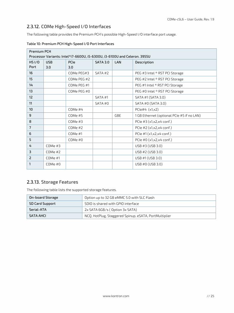
COMe High-Speed I/O Interfaces
The following table provides the Premium PCH’s possible High-Speed I/O interface port usage.
Table 10: Premium PCH High-Speed I/O Port Interfaces
Premium PCH Processor Variants: Intel®i7-6600U, i5-6300U, i3-6100U and Celeron. 3955U
HS I/O Port
USB 3.0
PCIe 3.0
SATA 3.0 LAN Description
16 COMe PEG#3 SATA #2 PEG #3 Intel ® RST PCI Storage
15 COMe PEG #2 PEG #2 Intel ® RST PCI Storage
14 COMe PEG #1 PEG #1 Intel ® RST PCI Storage
13 COMe PEG #0 PEG #0 Intel ® RST PCI Storage
12 SATA #1 SATA #1 (SATA 3.0)
11 SATA #0 SATA #0 (SATA 3.0)
10 COMe #4 PCIe#4 (x1,x2)
9 COMe #5 GBE 1 GB Ethernet (optional PCIe #5 if no LAN)
8 COMe #3 PCIe #3 (x1,x2,x4 conf.)
7 COMe #2 PCIe #2 (x1,x2,x4 conf.)
6 COMe #1 PCIe #1 (x1,x2,x4 conf.)
5 COMe #0 PCIe #0 (x1,x2,x4 conf.)
4 COMe #3 USB #3 (USB 3.0)
3 COMe #2 USB #2 (USB 3.0)
2 COMe #1 USB #1 (USB 3.0)
1 COMe #0 USB #0 (USB 3.0)
Storage Features
The following table lists the supported storage features.
On-board Storage Option up to 32 GB eMMC 5.0 with SLC Flash
SD Card Support SDIO is shared with GPIO interface
Serial-ATA 2x SATA 6GB/s ( Option 3x SATA)
SATA AHCI NCQ, HotPlug, Staggered Spinup, eSATA, PortMultiplier
COMe-cSL6 – User Guide, Rev. 1.9
www.kontron.com // 26
BIOS/Software Features
The following table lists the supported BIOS and software features.
Supported BIOS EFI AMI Aptio V UEFI
Software KEAPI 3 for all supported OS Linux PLD driver BIOS/EFI Flash utility for EFI shell, Windows 8/10, Linux BIOS/EFI Utility for customers to implement Boot Logo
OS Support Windows 10, 8.1 (64 bit) Windows 7 (32 bit & 64 bit) Windows Embedded 8 Standard (64 bit) Windows Embedded 8.1 Industry (64 bit) Windows Embedded Standard 7 (32 bit & 64 bit) Linux Yocto (64 bit) BSP + LiveCD VxWorks 7.x BSP
MS-DOS is no longer one of the official supported operating systems. Even If the system has been prepared for the usage of MS-DOS by activating CSM and Legacy Video in the setup, it may not work with all applications. If required, Kontron recommends the use of EFI shell based tools for OEM production service application.
COMe Features
The following table lists supported COMe specification features. For more information, see the COMe specification.
SPI Boot from an external SPI
LPC Supported
UART 2x UART (RX/TX)
LID Signals Supported
Sleep Signals Supported
SMBus Supported
Audio HD Audio for external HAD codecs
GPIO 8x GPIO shared with SDIO, configurable in BIOS setup options
Kontron Features
The following table lists specific Kontron features.
External I2C Bus Fast I2C, MultiMaster capable
M.A.R.S. Support Supported
Embedded API KEAPI3
Custom BIOS Settings / Flash Backup
Supported
Watchdog Support Triple Staged
COMe-cSL6 – User Guide, Rev. 1.9
www.kontron.com // 27
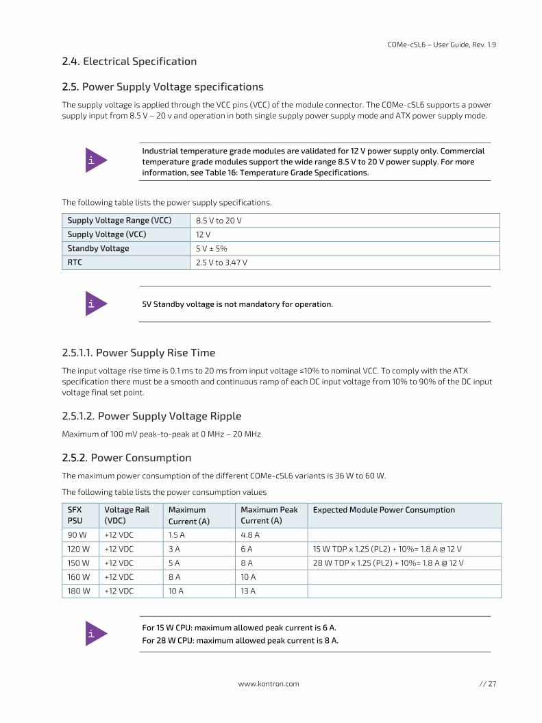
2.4. Electrical Specification
2.5. Power Supply Voltage specifications
The supply voltage is applied through the VCC pins (VCC) of the module connector. The COMe-cSL6 supports a power supply input from 8.5 V – 20 v and operation in both single supply power supply mode and ATX power supply mode.
Industrial temperature grade modules are validated for 12 V power supply only. Commercial temperature grade modules support the wide range 8.5 V to 20 V power supply. For more information, see Table 16: Temperature Grade Specifications.
The following table lists the power supply specifications.
Supply Voltage Range (VCC) 8.5 V to 20 V
Supply Voltage (VCC) 12 V
Standby Voltage 5 V ± 5%
RTC 2.5 V to 3.47 V
5V Standby voltage is not mandatory for operation.
2.5.1.1. Power Supply Rise Time
The input voltage rise time is 0.1 ms to 20 ms from input voltage ≤10% to nominal VCC. To comply with the ATX specification there must be a smooth and continuous ramp of each DC input voltage from 10% to 90% of the DC input voltage final set point.
2.5.1.2. Power Supply Voltage Ripple
Maximum of 100 mV peak-to-peak at 0 MHz – 20 MHz
Power Consumption
The maximum power consumption of the different COMe-cSL6 variants is 36 W to 60 W.
The following table lists the power consumption values
SFX PSU
Voltage Rail (VDC)
Maximum Current (A)
Maximum Peak Current (A)
Expected Module Power Consumption
90 W +12 VDC 1.5 A 4.8 A
120 W +12 VDC 3 A 6 A 15 W TDP x 1.25 (PL2) + 10%= 1.8 A @ 12 V
150 W +12 VDC 5 A 8 A 28 W TDP x 1.25 (PL2) + 10%= 1.8 A @ 12 V
160 W +12 VDC 8 A 10 A
180 W +12 VDC 10 A 13 A
For 15 W CPU: maximum allowed peak current is 6 A.
For 28 W CPU: maximum allowed peak current is 8 A.
COMe-cSL6 – User Guide, Rev. 1.9
www.kontron.com // 28
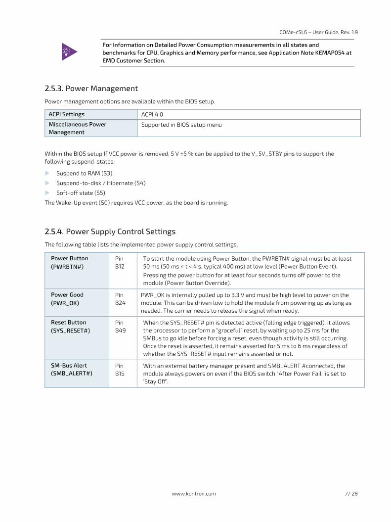
For Information on Detailed Power Consumption measurements in all states and benchmarks for CPU, Graphics and Memory performance, see Application Note KEMAP054 at EMD Customer Section.
Power Management
Power management options are available within the BIOS setup.
ACPI Settings ACPI 4.0
Miscellaneous Power Management
Supported in BIOS setup menu
Within the BIOS setup If VCC power is removed, 5 V ±5 % can be applied to the V_5V_STBY pins to support the following suspend-states:
Suspend to RAM (S3)
Suspend-to-disk / Hibernate (S4)
Soft-off state (S5)
The Wake-Up event (S0) requires VCC power, as the board is running.
Power Supply Control Settings
The following table lists the implemented power supply control settings.
Power Button (PWRBTN#)
Pin B12
To start the module using Power Button, the PWRBTN# signal must be at least 50 ms (50 ms ≤ t < 4 s, typical 400 ms) at low level (Power Button Event). Pressing the power button for at least four seconds turns off power to the module (Power Button Override).
Power Good (PWR_OK)
Pin B24
PWR_OK is internally pulled up to 3.3 V and must be high level to power on the module. This can be driven low to hold the module from powering up as long as needed. The carrier needs to release the signal when ready.
Reset Button (SYS_RESET#)
Pin B49
When the SYS_RESET# pin is detected active (falling edge triggered), it allows the processor to perform a “graceful” reset, by waiting up to 25 ms for the SMBus to go idle before forcing a reset, even though activity is still occurring. Once the reset is asserted, it remains asserted for 5 ms to 6 ms regardless of whether the SYS_RESET# input remains asserted or not.
SM-Bus Alert (SMB_ALERT#)
Pin B15
With an external battery manager present and SMB_ALERT #connected, the module always powers on even if the BIOS switch “After Power Fail” is set to ‘Stay Off’.
COMe-cSL6 – User Guide, Rev. 1.9
www.kontron.com // 29
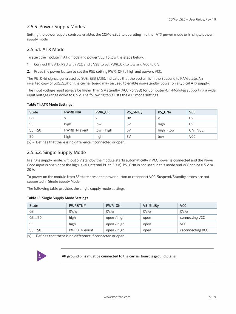
Power Supply Modes
Setting the power supply controls enables the COMe-cSL6 to operating in either ATX power mode or in single power supply mode.
2.5.5.1. ATX Mode
To start the module in ATX mode and power VCC, follow the steps below.
1. Connect the ATX PSU with VCC and 5 VSB to set PWR_OK to low and VCC to 0 V.
2. Press the power button to set the PSU setting PWR_OK to high and powers VCC.
The PS_ON# signal, generated by SUS_S3# (A15), Indicates that the system is in the Suspend to RAM state. An inverted copy of SUS_S3# on the carrier board may be used to enable non-standby power on a typical ATX supply.
The input voltage must always be higher than 5 V standby (VCC > 5 VSB) for Computer-On-Modules supporting a wide input voltage range down to 8.5 V. The following table lists the ATX mode settings.
Table 11: ATX Mode Settings
State PWRBTN# PWR_OK V5_StdBy PS_ON# VCC
G3 x x 0V x 0V
S5 high low 5V high 0V
S5 → S0 PWRBTN event low → high 5V high → low 0 V→ VCC
S0 high high 5V low VCC
(x) – Defines that there is no difference if connected or open.
2.5.5.2. Single Supply Mode
In single supply mode, without 5 V standby the module starts automatically if VCC power is connected and the Power Good input is open or at the high level (internal PU to 3.3 V). PS_ON# is not used in this mode and VCC can be 8.5 V to 20 V.
To power on the module from S5 state press the power button or reconnect VCC. Suspend/Standby states are not supported in Single Supply Mode.
The following table provides the single supply mode settings.
Table 12: Single Supply Mode Settings
State PWRBTN# PWR_OK V5_StdBy VCC
G3 0V/x 0V/x 0V/x 0V/x
G3 → S0 high open / high open connecting VCC
S5 high open / high open VCC
S5 → S0 PWRBTN event open / high open reconnecting VCC
(x) – Defines that there is no difference if connected or open.
All ground pins must be connected to the carrier board’s ground plane.
COMe-cSL6 – User Guide, Rev. 1.9
www.kontron.com // 30
2.6. Thermal Management
Heatspreader and Cooling Solutions
A heatspreader plate assembly is available from Kontron for the COMe-cSL6. The heatspreader plate on top of this assembly is NOT a heat sink. The heatspreader works as a COM Express® standard thermal interface to be use with a heat sink or external cooling devices.
External cooling must be provided to maintain the heatspreader plate at proper operating temperatures. Under worst-case conditions, the cooling mechanism must maintain an ambient air and heatspreader plate temperature on any spot of the heatspreader's surface according to the module specifications:
60°C for commercial grade modules
75°C for extended temperature grade modules (E1)
85°C for industrial temperature grade modules (E2/XT)
You can use many thermal-management solutions with the heatspreader plates, including active and passive approaches.
The optimum cooling solution varies, depending on the COM Express® application and environmental conditions. Active or passive cooling solutions provided from Kontron for the COMe-cSL6 are usually designed to cover the power and thermal dissipation for a commercial temperature range used in housing with proper airflow.
Operating with Kontron Heatspreader Plate (HSP) Assembly
The operating temperature defines two requirements:
Maximum ambient temperature with ambient being the air surrounding the module
Maximum measurable temperature on any spot on the heatspreader's surface
The heatspreader is tested for the following temperature specifications.
Table 13: Heatspreader Test Temperature Specifications
Temperature Specification Validation requirements
Commercial Grade at 60°C HSP temperature the CPU @ 100% load needs to run at nominal frequency
Extended Temperature (E1) at 75°C HSP temperature the CPU @ 75% load is allowed to start speedstepping for thermal protection
Industrial Grade by screening XT at 85°C HSP temperature the CPU @ 50% load is allowed to start throttling for thermal protection
Operating without Kontron Heatspreader Plate Assembly
The operating temperature is the maximum measurable temperature on any spot on the module's surface.
COMe-cSL6 – User Guide, Rev. 1.9
www.kontron.com // 31
On-board Fan Connector
The modules 3-pin fan connector powers, controls and monitors a fan for chassis ventilation.
Table 14: 3-Pin Fan Connector Pin Assignment
Pin Signal Description Type
1 Fan_Tach_IN# Input voltage I
2 V_FAN Limited to a max. 12 V (±10%) across the whole input range PWR
3 GND Power GND PWR
To connect a standard 3-pin connector fan to the module, use one of the following adaptor cables:
KAB-HSP 200 mm (PN 96079-0000-00-0)
KAB-HSP 40 mm (PN 96079-0000-00-2)
If the input voltage is below 13 V, the maximum supply current to the on-board fan connector is 350 mA. The maximum supply current is limited to 150 mA if the input voltage is between 13 V and 20 V.
Always check the fan specification according to the limitations of the output current.
Table 15: Electrical Characteristics of the Fan Connector
Module Input Voltage 4.75 V – 13 V Above 13 V
FAN Output Voltage 4.75 V – 13 V 13 V
Maximum FAN Output Current 350 mA 150 mA
2.7. Environmental Specification
Temperature
Kontron defines the following temperature grades for Computer-on-Modules. For more information on the available temperature grades for the COMe-cSL6, see Chapter 2.1 Module Variants.
Table 16: Temperature Grade Specifications
Temperature Grades Operating Non-operating / Storage
Validated Input Voltage
Commercial Grade 0°C to +60°C -30°C to +85°C VCC: 8.5 V – 20 V
Extended Temperature (E1) -25°C to +75°C -30°C to +85°C VCC: 12 V
Industrial Grade by Screening (XT) -40°C to +85°C (or custom)
-40°C to +85°C VCC: 12 V
Humidity
Table 17: Humidity Specification
Humidity
93% at 40°C non-condensing (according to IEC 60068-2-78)
COMe-cSL6 – User Guide, Rev. 1.9
www.kontron.com // 32
2.8. Standards and Certifications
The COMe-cSL6 complies with the following standards and certifications. For more information, contact Kontron Support.
Table 18: Standards and Certifications
Electromagnetic Compatibility Standards (EMC)
EN55022:1998 Class B
Electromagnetic compatible: Emission Standard for industrial environments
Safety IEC/EN 60950-1:2006 + A11:2009 + A1:2010 + A12:2011 + A2:2013
Information Technology Equipment Including Electrical Business Equipment
UL 60950-1 / CSA 60950-1
Information Technology Equipment Including Electrical Business Equipment NWGQ2.E304278
NWGQ8.E304278
Shock IEC/EN 60068-2-27
non-operating shock test - ( half-sinusoidal, 11 ms, 15 g)
Vibration IEC/EN 60068-2-6
non-operating vibration -(sinusoidal, 10 Hz - 4000 Hz, +/-0.15 mm, 2 g)
MTBF (Theoretical)
572225 System MTBF (hours) @ 40 °C Reliability report article number 36021-0000-26-7
For More information, see chapter 2.8 MTBF.
(RoHS II) 2011/65/EU
Compliant with the directive on the restriction of the use of certain hazardous substances in electrical and electronic equipment
COMe-cSL6 – User Guide, Rev. 1.9
www.kontron.com // 33
2.9. MTBF
The following MTBF (Mean Time Before Failure) values were calculated using a combination of manufacturer’s test data, if the data was available, and the Telcordia (Bellcore) issue 2 calculation for the remaining parts.
The Telcordia calculation used is “Method 1 Case 3” in a ground benign, controlled environment (GB,GC). This particular method takes into account varying temperature and stress data and the system is assumed to have not been burned in.
Figure 2 below shows MTBF de-rating for the E1 temperature range in an office or telecommunications environment. Other environmental stresses (such as extreme altitude, vibration, salt-water exposure) lower MTBF values.
System MTBF (hours) = 572225 @ 40°C (Reliability report article number 36021-0000-26-7)
Figure 2: MTBF Temperature De-rating
The above estimates assume no fan, but a passive heat sinking arrangement. Estimated RTC battery life (as opposed to battery failures) is not accounted for in the above figure and needs to be considered separately. Battery life depends on both temperature and operating conditions. When the Kontron unit has external power, the only battery drain is from leakage paths.
COMe-cSL6 – User Guide, Rev. 1.9
www.kontron.com // 34
2.10. Mechanical Specification
Dimensions
The module’s dimensions are:
95.0 mm x 95.0 mm (3.75 ” x 3.75 “)
Height approximately 12 mm (0.4 “)
Figure 3: Module Dimensions
COMe-cSL6 – User Guide, Rev. 1.9
www.kontron.com // 35
Height
The height of the module depends on the height of the implemented cooling solution. The height of the cooling solution is not specified in the COMe specification.
The COM Express® specification defines a module height of approximately 13 mm from module PCB bottom to heatspreader top, as shown in the figure below.
Figure 4: Module Height
Cooling solutions provided by Kontron for compact sized Computer-on-Modules are 27 mm in height from module bottom to heatsink top.
Universal Cooling solutions to be mounted on the heatspreader are 14.3 mm in height for an overall height of 27.3 mm from module bottom to heatsink top.
COMe-cSL6 – User Guide, Rev. 1.9
www.kontron.com // 36
3/ Features and Interfaces
3.1. LPC
The Low Pin Count (LPC) interface signals are connected to the LPC bus bridge located in the CPU or chipset. The LPC low speed interface can be used for peripheral circuits such as an external Super I/O controller that typically combines legacy-device support into a single IC. The implementation of this subsystem complies with the COM Express® Specification. The COM Express® Design Guide maintained by PICMG provides implementation information or refer to the official PICMG documentation for more information.
The LPC bus does not support DMA (Direct Memory Access). When more than one device is used on LPC, a zero delay clock buffer is required. This leads to limitations for ISA bus and SIO (standard I/O(s) like floppy or LPT interfaces) implementations.
All Kontron COM Express® Computer-on-Modules imply BIOS support for the following external baseboard LPC Super I/O controller features for the Winbond/Nuvoton 3.3V 83627DHG-P.
Table 19: Supported BIOS Features
3.3V 83627DHG-P AMI EFI APTIO V
PS/2 Supported
COM1/COM2 Supported
LPT Supported
HWM Not supported
Floppy Not supported
GPIO Not supported
Features marked as not supported do not exclude OS support (e.g., HWM is accessible via SMB). If any other LPC Super I/O additional BIOS implementations are necessary then contact Kontron Support.
3.2. Serial Peripheral Interface (SPI)
The Serial Peripheral Interface Bus (SPI bus) is a synchronous serial data link standard. Devices communicate in master/slave mode, where the master device initiates the data frame. Multiple slave devices are allowed with individual slave select (chip select) lines. SPI is sometimes called a four-wire serial bus, contrasting with three, two and one-wire serial buses.
The SPI interface can only be used with a SPI flash device to boot from the external BIOS on the baseboard.
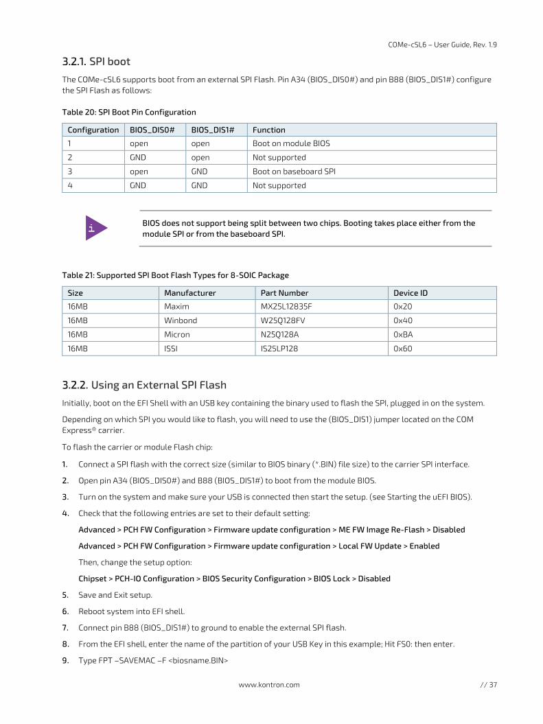
COMe-cSL6 – User Guide, Rev. 1.9
www.kontron.com // 37
SPI boot
The COMe-cSL6 supports boot from an external SPI Flash. Pin A34 (BIOS_DIS0#) and pin B88 (BIOS_DIS1#) configure the SPI Flash as follows:
Table 20: SPI Boot Pin Configuration
Configuration BIOS_DIS0# BIOS_DIS1# Function
1 open open Boot on module BIOS
2 GND open Not supported
3 open GND Boot on baseboard SPI
4 GND GND Not supported
BIOS does not support being split between two chips. Booting takes place either from the module SPI or from the baseboard SPI.
Table 21: Supported SPI Boot Flash Types for 8-SOIC Package
Size Manufacturer Part Number Device ID
16MB Maxim MX25L12835F 0x20
16MB Winbond W25Q128FV 0x40
16MB Micron N25Q128A 0xBA
16MB ISSI IS25LP128 0x60
Using an External SPI Flash
Initially, boot on the EFI Shell with an USB key containing the binary used to flash the SPI, plugged in on the system.
Depending on which SPI you would like to flash, you will need to use the (BIOS_DIS1) jumper located on the COM Express® carrier.
To flash the carrier or module Flash chip:
1. Connect a SPI flash with the correct size (similar to BIOS binary (*.BIN) file size) to the carrier SPI interface.
2. Open pin A34 (BIOS_DIS0#) and B88 (BIOS_DIS1#) to boot from the module BIOS.
3. Turn on the system and make sure your USB is connected then start the setup. (see Starting the uEFI BIOS).
4. Check that the following entries are set to their default setting:
Advanced > PCH FW Configuration > Firmware update configuration > ME FW Image Re-Flash > Disabled
Advanced > PCH FW Configuration > Firmware update configuration > Local FW Update > Enabled
Then, change the setup option:
Chipset > PCH-IO Configuration > BIOS Security Configuration > BIOS Lock > Disabled
5. Save and Exit setup.
6. Reboot system into EFI shell.
7. Connect pin B88 (BIOS_DIS1#) to ground to enable the external SPI flash.
8. From the EFI shell, enter the name of the partition of your USB Key in this example; Hit FS0: then enter.
9. Type FPT –SAVEMAC –F <biosname.BIN>
COMe-cSL6 – User Guide, Rev. 1.9
www.kontron.com // 38
10. Wait until the program ends properly and then power cycle the whole system.
The system is now updated.
Depending on the state of the external SPI flash, the program may display up to two warning messages printed in red. Do not stop the process at this point! After a few seconds of timeout, flashing proceeds.
For more information, refer to the EMD Customer Section.
External SPI flash on Modules with Intel® ME
If booting from the external (baseboard mounted) SPI flash then exchanging the COM Express® module for another module of the same type will cause the Intel® Management Engine (ME) to fail during the next start. This is due to the design of the ME that bounds itself to every module, to which it was previously flashed. In the case of an external SPI flash, this is the module present at flash time.
To avoid this issue, conduct a complete flash of the external SPI flash device after changing the COM Express® module for another module. If disconnecting and reconnecting the same module again, this step is not necessary.
3.3. M.A.R.S.
The smart battery implementation for Kontron Computer-on-Modules called Mobile Application for Rechargeable Systems (M.A.R.S.) is a BIOS extension for an external smart battery manager or charger. M.A.R.S. includes support for SMBus charger/selector (e.g. Linear Technology LTC1760 Dual Smart Battery System Manager) and provides ACPI compatibility to report battery information to the operating system.
Table 22: Reserved SM-Bus Addresses for Smart Battery Solutions on the Carrier
8-bit Address 7-bit Address Device
12h 0x09 SMART_CHARGER
14h 0x0A SMART_SELECTOR
16h 0x0B SMART_BATTERY
3.4. Fast I2C
Fast I2C supports transfer between components on the same board. The COMe-cSL6 features an onboard I2C controller connected to the LPC Bus.
The I2C controller supports:
Multimaster transfers
Clock stretching
Collision detection
Interruption on completion of an operation
3.5. UART
The UART implements an interface for serial communications and supports up to two serial RX/TX ports defined in the COM Express® specification on pins A98 (SERO_TX) /A99 (SERO_RX) for UART0 and pins A101 (SER1_TX)/A102 (SER1_RX) for UART1. The UART controller is fully 16550A compatible.
COMe-cSL6 – User Guide, Rev. 1.9
www.kontron.com // 39
Features of the UART are:
On-Chip bit rate ( baud rate) generator
No handshake lines
Interrupt function to the host
FIFO buffer for incoming and outgoing data
3.6. Triple Staged Watchdog Timer (WTD)
Basics
A watchdog timer or (computer operating properly (COP) timer) is a computer hardware or software timer. If there is a fault condition in the main program, the watchdog triggers a system reset or other corrective actions. The intention is to bring the system back from the nonresponsive state to normal operation.
Possible fault conditions are a hang, neglect to service the watchdog regularly (writing a “service pulse” to it, also referred to as “kicking the dog”, “petting the dog”, “feeding the watchdog” or “triggering the watchdog”).
The COMe-cSL6 offers a watchdog that works with three stages that can be programmed independently and used stage by stage.
Table 23: Triple Stage Watchdog Timer- Time-out Events
0000b No action The stage is off and will be skipped.
0001b Reset A reset restarts the module and starts a new POST and operating system.
0010b NMI A non-maskable interrupt (NMI) is a computer processor interrupt that cannot be ignored by standard interrupt masking techniques in the system. It is used typically to signal attention for non-recoverable hardware errors.
0011b SMI A system management interrupt (SMI) makes the processor entering the system management mode (SMM). As such, specific BIOS code handles the interrupt. The current BIOS handler for the watchdog SMI currently does nothing. For special requirements, contact Kontron Support.
0100b SCI A system control interrupt (SCI) is a OS-visible interrupt to be handled by the OS using AML code.
0101b Delay -> No action*
Might be necessary when an operating system must be started and the time for the first trigger pulse must be extended. Only available in the first stage.
1000b WDT Only This setting triggers the WDT Pin on the baseboard connector (COM Express® Pin B27) only.
1001b Reset + WDT
1010b NMI + WDT
1011b SMI + WDT
1100b SCI + WDT
1101b DELAY + WDT -> No action*
WDT Signal
Watchdog time-out event (pin B27) on COM Express® connector offers a signal that can be asserted when a watchdog timer has not been triggered with a set time. The WDT signal is configurable to any of the three stages. After reset, the signal is automatically deasserted. If deassertion is necessary during runtime, contact Kontron Support for further help.
COMe-cSL6 – User Guide, Rev. 1.9
www.kontron.com // 40
3.7. GPIO
Eight GPIO pins are available, with four pins for the in-direction (pin A54 for GPI0, pin A63 for GPI1, pin A67 for GPI2 and pin A85 for GPI3) and four pins for the out-direction (pin A93 for GPO0, pin B54 for GPO1, pin B57 for GPO2 and pin B63 for GPO3). The type of termination resistor on the module sets the direction of the GPIO where GPIs are terminated with pull-up resistors and GPOs are terminated with pull-down resistors.
Due to, the fact that both the pull-up and pull-down termination resistors are weak, it is possible to override the termination resistors using external pull-ups, pull-downs or IOs. Overriding the termination resistors means that the eight GPIO pins can be considered as bi-directional since there are no restrictions whether you use the available GPIO pins in the in-direction or out-direction.
3.8. Real Time Clock (RTC)
The RTC keeps track of the current time accurately. The RTC’s low power consumption means that it can be powered from an alternate source of power enabling the RTC to continue to keep time while the primary source of power is off or unavailable. The COMe-cSL6’s RTC battery voltage range is 2.5 V to 3.47 V.
3.9. Trusted Platform Module (TPM 2.0)
The COMe-cSL6 is compliant to TPM 2.0. A Trusted Platform Module (TPM) stores RSA encryption keys specific to the host system for hardware authentication. The term TPM refers to the set of specifications applicable to TPM chips. The LPC bus connects the TPM Chip to the CPU.
Each TPM chip contains an RSA key pair called the Endorsement Key (EK). The pair is maintained inside the chip and cannot be accessed by software. The Storage Root Key (SRK) is created when a user or administrator takes ownership of the system. This key pair is generated by the TPM based on the Endorsement Key and an owner-specified password.
A second key, called an Attestation Identity Key (AIK) protects the device against unauthorized firmware and software modification by hashing critical sections of firmware and software before they are executed. When the system attempts to connect to the network, the hashes are sent to a server that verifies that they match the expected values. If any of the hashed components have been modified since last started, the match fails, and the system cannot gain entry to the network.
3.10. Kontron Security Solution (optional)
The COMe-cSL6 is equipped with the Kontron Security Solution, providing an embedded hardware security solution that enables applications to be secured, even in unsecure environments.
The Kontron Security Solution provides features such as:
Copy protection
IP protection
License model enforcement
If required customers can customize the solution to meet specific needs. For more information, contact Kontron Support.
COMe-cSL6 – User Guide, Rev. 1.9
www.kontron.com // 41
3.11. Speedstep Technology
The COMe-cSL6 processors offer the Intel® Enhanced SpeedStep™ technology that, depending on the needs of the application, automatically switches between maximum performance mode and battery-optimized mode. Speedstep technology enables you to adapt high performance computing to your applications. When powered by a battery or running in idle mode, the processor drops to lower frequencies (by changing the CPU ratios) and voltage, thus conserving battery life while maintaining a high level of performance. The frequency is automatically set back to the high frequency, allowing you to customize performance.
In order to use the Intel® Enhanced SpeedStep™ technology the operating system must support SpeedStep™ technology.
By deactivating the SpeedStep feature in the BIOS, manual control/modification of CPU performance is possible. Setup the CPU Performance State in the BIOS Setup or use third party software to control CPU Performance States.
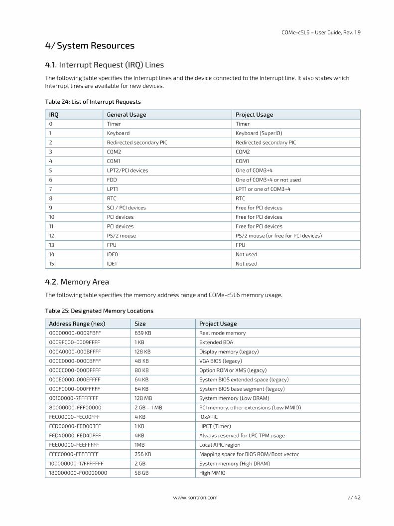
COMe-cSL6 – User Guide, Rev. 1.9
www.kontron.com // 42
4/ System Resources
4.1. Interrupt Request (IRQ) Lines
The following table specifies the Interrupt lines and the device connected to the Interrupt line. It also states which Interrupt lines are available for new devices.
Table 24: List of Interrupt Requests
IRQ General Usage Project Usage 0 Timer Timer
1 Keyboard Keyboard (SuperIO)
2 Redirected secondary PIC Redirected secondary PIC
3 COM2 COM2
4 COM1 COM1
5 LPT2/PCI devices One of COM3+4
6 FDD One of COM3+4 or not used
7 LPT1 LPT1 or one of COM3+4
8 RTC RTC
9 SCI / PCI devices Free for PCI devices
10 PCI devices Free for PCI devices
11 PCI devices Free for PCI devices
12 PS/2 mouse PS/2 mouse (or free for PCI devices)
13 FPU FPU
14 IDE0 Not used
15 IDE1 Not used
4.2. Memory Area
The following table specifies the memory address range and COMe-cSL6 memory usage.
Table 25: Designated Memory Locations
Address Range (hex) Size Project Usage 00000000-0009FBFF 639 KB Real mode memory
0009FC00-0009FFFF 1 KB Extended BDA
000A0000-000BFFFF 128 KB Display memory (legacy)
000C0000-000CBFFF 48 KB VGA BIOS (legacy)
000CC000-000DFFFF 80 KB Option ROM or XMS (legacy)
000E0000-000EFFFF 64 KB System BIOS extended space (legacy)
000F0000-000FFFFF 64 KB System BIOS base segment (legacy)
00100000-7FFFFFFF 128 MB System memory (Low DRAM)
80000000-FFF00000 2 GB – 1 MB PCI memory, other extensions (Low MMIO)
FEC00000-FEC00FFF 4 KB IOxAPIC
FED00000-FED003FF 1 KB HPET (Timer)
FED40000-FED40FFF 4KB Always reserved for LPC TPM usage
FEE00000-FEEFFFFF 1MB Local APIC region
FFFC0000-FFFFFFFF 256 KB Mapping space for BIOS ROM/Boot vector
100000000-17FFFFFFF 2 GB System memory (High DRAM)
180000000-F00000000 58 GB High MMIO
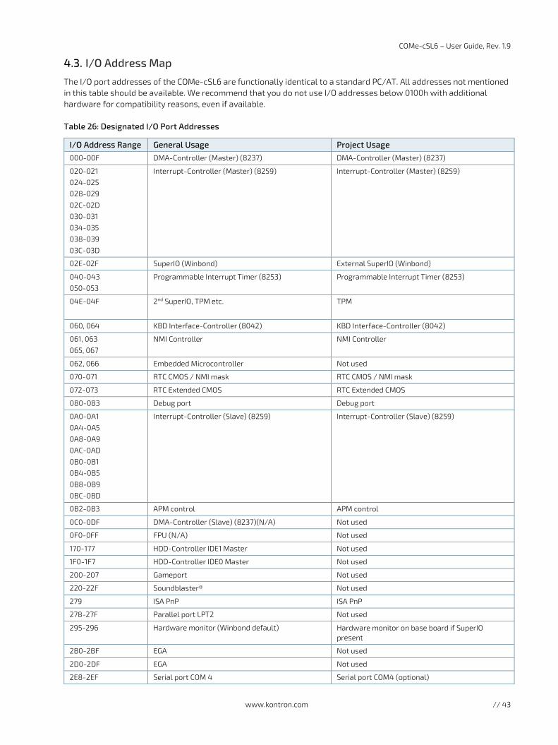
COMe-cSL6 – User Guide, Rev. 1.9
www.kontron.com // 43
4.3. I/O Address Map
The I/O port addresses of the COMe-cSL6 are functionally identical to a standard PC/AT. All addresses not mentioned in this table should be available. We recommend that you do not use I/O addresses below 0100h with additional hardware for compatibility reasons, even if available.
Table 26: Designated I/O Port Addresses
I/O Address Range General Usage Project Usage 000-00F DMA-Controller (Master) (8237) DMA-Controller (Master) (8237)
020-021
024-025 028-029
02C-02D 030-031
034-035 038-039
03C-03D
Interrupt-Controller (Master) (8259) Interrupt-Controller (Master) (8259)
02E-02F SuperIO (Winbond) External SuperIO (Winbond)
040-043
050-053
Programmable Interrupt Timer (8253) Programmable Interrupt Timer (8253)
04E-04F
2nd SuperIO, TPM etc. TPM
060, 064 KBD Interface-Controller (8042) KBD Interface-Controller (8042)
061, 063
065, 067
NMI Controller NMI Controller
062, 066 Embedded Microcontroller Not used
070-071 RTC CMOS / NMI mask RTC CMOS / NMI mask
072-073 RTC Extended CMOS RTC Extended CMOS
080-083 Debug port Debug port
0A0-0A1
0A4-0A5
0A8-0A9 0AC-0AD
0B0-0B1 0B4-0B5
0B8-0B9 0BC-0BD
Interrupt-Controller (Slave) (8259) Interrupt-Controller (Slave) (8259)
0B2-0B3 APM control APM control
0C0-0DF DMA-Controller (Slave) (8237)(N/A) Not used
0F0-0FF FPU (N/A) Not used
170-177 HDD-Controller IDE1 Master Not used
1F0-1F7 HDD-Controller IDE0 Master Not used
200-207 Gameport Not used
220-22F Soundblaster® Not used
279 ISA PnP ISA PnP
278-27F Parallel port LPT2 Not used
295-296 Hardware monitor (Winbond default) Hardware monitor on base board if SuperIO present
2B0-2BF EGA Not used
2D0-2DF EGA Not used
2E8-2EF Serial port COM 4 Serial port COM4 (optional)
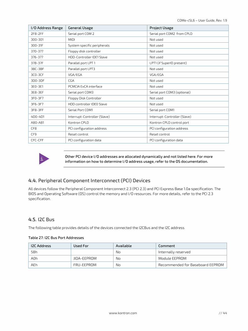
COMe-cSL6 – User Guide, Rev. 1.9
www.kontron.com // 44
I/O Address Range General Usage Project Usage 2F8-2FF Serial port COM 2 Serial port COM2 from CPLD
300-301 MIDI Not used
300-31F System specific peripherals Not used
370-377 Floppy disk controller Not used
376-377 HDD-Controller IDE1 Slave Not used
378-37F Parallel port LPT 1 LPT1 (if SuperIO present)
3BC-3BF Parallel port LPT3 Not used
3C0-3CF VGA/EGA VGA/EGA
3D0-3DF CGA Not used
3E0-3E1 PCMCIA ExCA interface Not used
3E8-3EF Serial port COM3 Serial port COM3 (optional)
3F0-3F7 Floppy Disk Controller Not used
3F6-3F7 HDD controller IDE0 Slave Not used
3F8-3FF Serial Port COM1 Serial port COM1
4D0-4D1 Interrupt-Controller (Slave) Interrupt-Controller (Slave)
A80-A81 Kontron CPLD Kontron CPLD control port
CF8 PCI configuration address PCI configuration address
CF9 Reset control Reset control
CFC-CFF PCI configuration data PCI configuration data
Other PCI device I/O addresses are allocated dynamically and not listed here. For more information on how to determine I/O address usage, refer to the OS documentation.
4.4. Peripheral Component Interconnect (PCI) Devices
All devices follow the Peripheral Component Interconnect 2.3 (PCI 2.3) and PCI Express Base 1.0a specification. The BIOS and Operating Software (OS) control the memory and I/O resources. For more details, refer to the PCI 2.3 specification.
4.5. I2C Bus
The following table provides details of the devices connected the I2CBus and the I2C address
Table 27: I2C Bus Port Addresses
I2C Address Used For Available Comment
58h No Internally reserved
A0h JIDA-EEPROM No Module EEPROM
AEh FRU-EEPROM No Recommended for Baseboard EEPROM
COMe-cSL6 – User Guide, Rev. 1.9
www.kontron.com // 45
4.6. System Management (SM) Bus
The 8-bit SMBus address uses the LSB (Bit 0) for the direction of the device.
Bit0 = 0 defines the write address
Bit0 = 1 defines the read address
The 8-bit address listed below shows the write address for all devices. The7-bit SMBus address shows the device address without bit 0.
Table 28: Designated I/O Port Addresses
8-bit Address
7-bit Address
Device Comment SMBus
5Ch 2E HWM NCT7802Y Do not use under any circumstances SMB
A0h 50h SPD DDR Channel 1 (SO-DIMM) SMB
A4h 52h SPD DDR Channel 2 (memory-down)
Raw SPD readout not fully supported, see System Memory
SMB
30h 18h SODIMM Thermal Sensor If available on used memory-module SMB
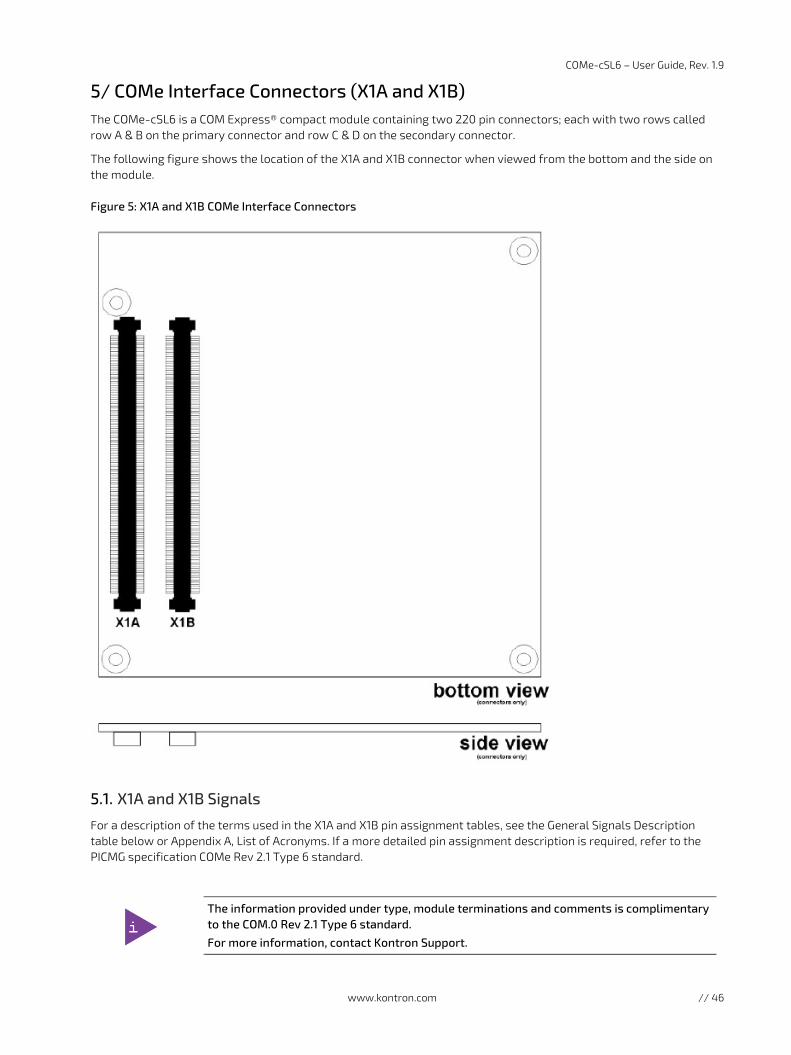
COMe-cSL6 – User Guide, Rev. 1.9
www.kontron.com // 46
5/ COMe Interface Connectors (X1A and X1B) The COMe-cSL6 is a COM Express® compact module containing two 220 pin connectors; each with two rows called row A & B on the primary connector and row C & D on the secondary connector.
The following figure shows the location of the X1A and X1B connector when viewed from the bottom and the side on the module.
Figure 5: X1A and X1B COMe Interface Connectors
5.1. X1A and X1B Signals
For a description of the terms used in the X1A and X1B pin assignment tables, see the General Signals Description table below or Appendix A, List of Acronyms. If a more detailed pin assignment description is required, refer to the PICMG specification COMe Rev 2.1 Type 6 standard.
The information provided under type, module terminations and comments is complimentary to the COM.0 Rev 2.1 Type 6 standard.
For more information, contact Kontron Support.
COMe-cSL6 – User Guide, Rev. 1.9
www.kontron.com // 47
Table 29: General Signal Description
Type Description Type Description
NC Not connected (on this product) O-1,8 1.8 V Output
I/O-3,3 Bi-directional 3.3 V I/O-Signal O-3,3 3.3 V Output
I/O-5T Bi-dir. 3.3 V I/O (5V Tolerance) O-5 5 V Output
I/O-5 Bi-directional 5V I/O-Signal DP-I/O Differential Pair Input/Output
I-3,3 3.3 V Input DP-I Differential Pair Input
I/OD Bi-directional Input/Output Open Drain
DP-O Differential Pair Output
I-5T 3.3V Input (5V Tolerance) PU Pull-Up Resistor
OA Output Analog PWR Power Connection
OD Output Open Drain
To protect external power lines of peripheral devices, make sure that: the wires have the right diameter to withstand the maximum available current.
The enclosure of the peripheral device fulfills the fire-protection requirements of IEC/EN60950.
5.2. X1A and X1B Pin Assignment
For more information regarding the pin assignment of connector X1A (Row A and Row B) and connector X1B (Row C and Row D) see the tables listed below:
Table 29: Connector X1A Row A Pin Assignment (A1-A110)
Table 30: Connector X1A Row B Pin Assignment (B1-B110)
Table 31: Connector X1B Row C Pin Assignment (C1-C110)
Table 32: Connector X1B Row D Pin Assignment (D1-D110)
COMe-cSL6 – User Guide, Rev. 1.9
www.kontron.com // 48
Connector X1A Row A1-A110
Table 30: Connector X1A Row A Pin Assignment (A1-A110)
Pin COME Signal Description Type Termination Comment A1 GND Power Ground PWR GND
A2 GBE0_MDI3- Ethernet Media Dependent Interface 3 DP-I/O
A3 GBE0_MDI3+
A4 GBE0_LINK100# Ethernet controller speed indicator OD
A5 GBE0_LINK1000# Ethernet controller speed indicator OD
A6 GBE0_MDI2- Ethernet Media Dependent Interface 2 DP-I/O
A7 GBE0_MDI2+
A8 GBE0_LINK# Ethernet Controller Link Indicator OD
A9 GBE0_MDI1- Ethernet Media Dependent Interface 1 DP-I/O
A10 GBE0_MDI1+
A11 GND Power Ground PWR GND
A12 GBE0_MDI0- Ethernet Media Dependent Interface 0 DP-I/O
A13 GBE0_MDI0+
A14 GBE0_CTREF Reference voltage for Carrier Board Ethernet magnetics center tap. The reference voltage is determined by the requirements of the Module PHY and may be as low as 0V and as high as 3.3V.
O 1 uF capacitor to GND
A15 SUS_S3# Indicates system is in Suspend to RAM state. An inverted copy of SUS_S3# on Carrier Board may be used to enable non-standby power on a typical ATX supply.
O-3.3 PD 10 kΩ
A16 SATA0_TX+ Serial ATA or SAS transmit data pair DP-O
A17 SATA0_TX-
A18 SUS_S4# Indicates system is in Suspend to Disk state. O-3.3 PD 10 kΩ
A19 SATA0_RX+ Serial ATA or SAS receive data pair DP-I
A20 SATA0_RX-
A21 GND Power Ground PWR GND
A22 SATA2_TX+ Serial ATA or SAS transmit data pair DP-O
A23 SATA2_TX-
A24 SUS_S5# Indicates system is in Soft Off state. O-3.3
A25 SATA2_RX+ Serial ATA or SAS receive data pair DP-I
A26 SATA2_RX-
A27 BATLOW# Provides a battery-low signal to the Module to indicate that external battery is low
I-3.3 PU 10 kΩ, 3.3V (S5)
Assertion prevents wake from S3-S5 state
A28 ATA_ACT# Serial ATA activity LED indicator OD-3.3 PU 10 kΩ, 3.3V (S0)
Can sink 15 mA
A29 HDA_SYNC HD Audio Sync O-3.3 PD 20 kΩ in PCH
A30 HDA_RST# HD Audio Reset O-3.3 PD 20 kΩ in PCH
A31 GND Power Ground PWR GND
A32 HDA_CLK HD Audio Bit Clock Output O-3.3 PD 20 kΩ in PCH
A33 HDA_SDOUT HD Audio Serial Data Out O-3.3 PD 20 kΩ in PCH
A34 BIOS_DIS0# BIOS Selection Straps to determine the BIOS boot device
I-3.3 PU 10 kΩ,3.3V (S5)
The Carrier should only float these or pull them low. Refer to SPI boot
A35 THRMTRIP# Thermal trip Indicates CPU has entered thermal shutdown
O-3.3 PU 10 kΩ, 3.3 V (S0)
Thermal trip event transition to S5 indicator
A36 USB6- USB 2.0 data differential pair port DP-I/O PD 14.25 kΩ to 24.8 kΩ in PCH
A37 USB6+
A38 USB_6_7_OC# USB over-current indicator port I-3.3 PU 10 kΩ, 3.3 V (S5)
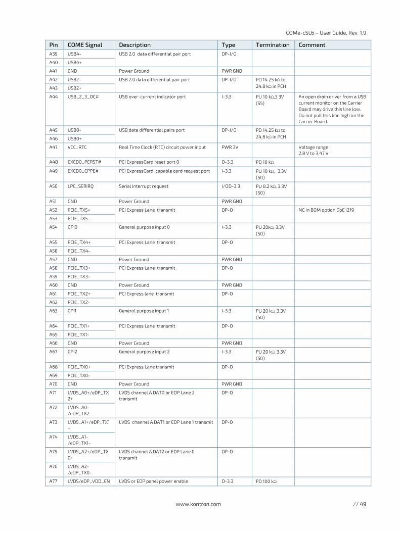
COMe-cSL6 – User Guide, Rev. 1.9
www.kontron.com // 49
Pin COME Signal Description Type Termination Comment A39 USB4- USB 2.0 data differential pair port DP-I/O
A40 USB4+
A41 GND Power Ground PWR GND
A42 USB2- USB 2.0 data differential pair port DP-I/O PD 14.25 kΩ to 24.8 kΩ in PCH
A43 USB2+
A44 USB_2_3_OC# USB over-current indicator port I-3.3 PU 10 kΩ,3.3V (S5)
An open drain driver from a USB current monitor on the Carrier Board may drive this line low. Do not pull this line high on the Carrier Board.
A45 USB0- USB data differential pairs port DP-I/O PD 14.25 kΩ to 24.8 kΩ in PCH
A46 USB0+
A47 VCC_RTC Real Time Clock (RTC) circuit power input PWR 3V Voltage range 2.8 V to 3.47 V
A48 EXCD0_PERST# PCI ExpressCard reset port 0 O-3.3 PD 10 kΩ
A49 EXCD0_CPPE# PCI ExpressCard capable card request port I-3.3 PU 10 kΩ, 3.3V (S0)
A50 LPC_SERIRQ Serial Interrupt request I/OD-3.3 PU 8.2 kΩ, 3.3V (S0)
A51 GND Power Ground PWR GND
A52 PCIE_TX5+ PCI Express Lane transmit DP-O NC in BOM option GbE i219
A53 PCIE_TX5-
A54 GPI0 General purpose input 0 I-3.3 PU 20kΩ, 3.3V (S0)
A55 PCIE_TX4+ PCI Express Lane transmit DP-O
A56 PCIE_TX4-
A57 GND Power Ground PWR GND
A58 PCIE_TX3+ PCI Express Lane transmit DP-O
A59 PCIE_TX3-
A60 GND Power Ground PWR GND
A61 PCIE_TX2+ PCI Express lane transmit DP-O
A62 PCIE_TX2-
A63 GPI1 General purpose input 1 I-3.3 PU 20 kΩ, 3.3V (S0)
A64 PCIE_TX1+ PCI Express Lane transmit DP-O
A65 PCIE_TX1-
A66 GND Power Ground PWR GND
A67 GPI2 General purpose input 2 I-3.3 PU 20 kΩ, 3.3V (S0)
A68 PCIE_TX0+ PCI Express Lane transmit DP-O
A69 PCIE_TX0-
A70 GND Power Ground PWR GND
A71 LVDS_A0+/eDP_TX2+
LVDS channel A DAT0 or EDP Lane 2 transmit
DP-O
A72 LVDS_A0-/eDP_TX2-
A73 LVDS_A1+/eDP_TX1+
LVDS channel A DAT1 or EDP Lane 1 transmit DP-O
A74 LVDS_A1-/eDP_TX1-
A75 LVDS_A2+/eDP_TX0+
LVDS channel A DAT2 or EDP Lane 0 transmit
DP-O
A76 LVDS_A2-/eDP_TX0-
A77 LVDS/eDP_VDD_EN LVDS or EDP panel power enable O-3.3 PD 100 kΩ
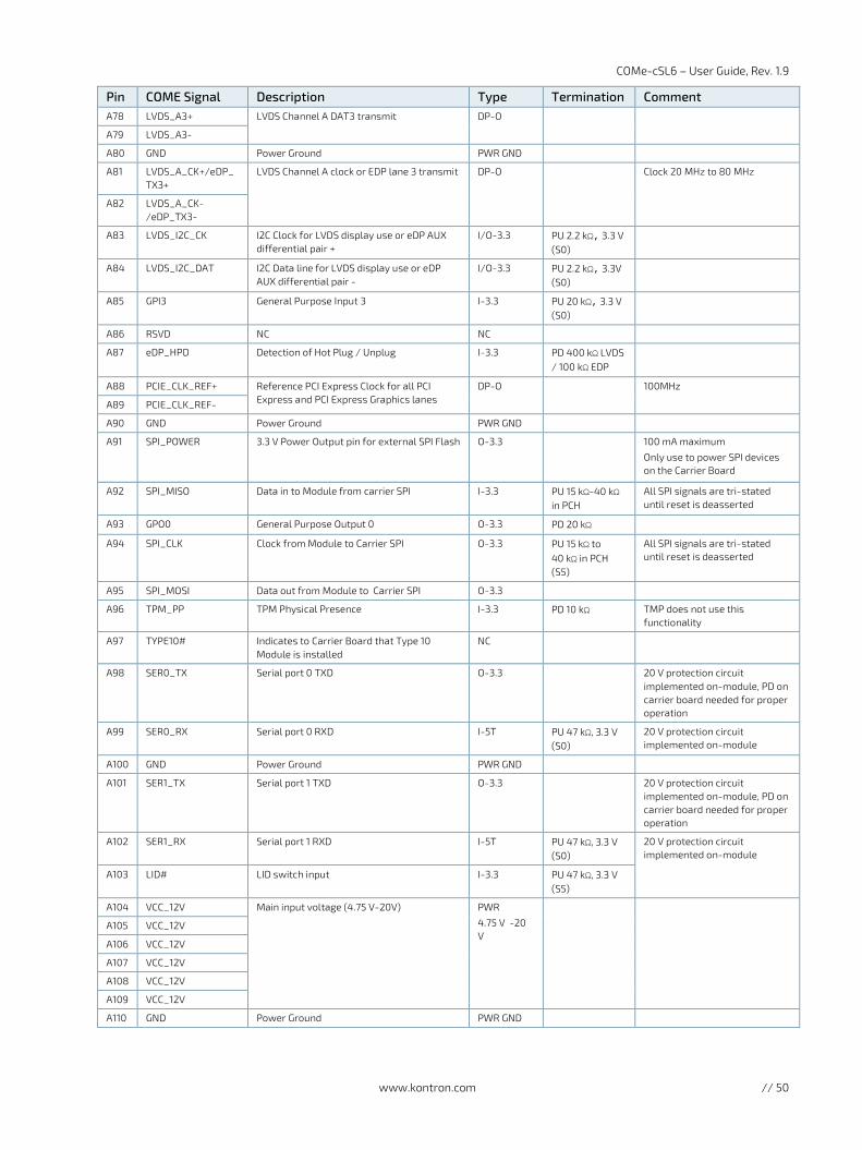
COMe-cSL6 – User Guide, Rev. 1.9
www.kontron.com // 50
Pin COME Signal Description Type Termination Comment A78 LVDS_A3+ LVDS Channel A DAT3 transmit DP-O
A79 LVDS_A3-
A80 GND Power Ground PWR GND
A81 LVDS_A_CK+/eDP_TX3+
LVDS Channel A clock or EDP lane 3 transmit DP-O Clock 20 MHz to 80 MHz
A82 LVDS_A_CK-/eDP_TX3-
A83 LVDS_I2C_CK I2C Clock for LVDS display use or eDP AUX differential pair +
I/O-3.3 PU 2.2 kΩ, 3.3 V (S0)
A84 LVDS_I2C_DAT I2C Data line for LVDS display use or eDP AUX differential pair -
I/O-3.3 PU 2.2 kΩ, 3.3V (S0)
A85 GPI3 General Purpose Input 3 I-3.3 PU 20 kΩ, 3.3 V (S0)
A86 RSVD NC NC
A87 eDP_HPD Detection of Hot Plug / Unplug I-3.3 PD 400 kΩ LVDS / 100 kΩ EDP
A88 PCIE_CLK_REF+ Reference PCI Express Clock for all PCI Express and PCI Express Graphics lanes
DP-O 100MHz
A89 PCIE_CLK_REF-
A90 GND Power Ground PWR GND
A91 SPI_POWER 3.3 V Power Output pin for external SPI Flash
O-3.3 100 mA maximum
Only use to power SPI devices on the Carrier Board
A92 SPI_MISO Data in to Module from carrier SPI I-3.3 PU 15 kΩ-40 kΩ in PCH
All SPI signals are tri-stated until reset is deasserted
A93 GPO0 General Purpose Output 0 O-3.3 PD 20 kΩ
A94 SPI_CLK Clock from Module to Carrier SPI O-3.3 PU 15 kΩ to 40 kΩ in PCH (S5)
All SPI signals are tri-stated until reset is deasserted
A95 SPI_MOSI Data out from Module to Carrier SPI O-3.3
A96 TPM_PP TPM Physical Presence I-3.3 PD 10 kΩ TMP does not use this functionality
A97 TYPE10# Indicates to Carrier Board that Type 10 Module is installed
NC
A98 SER0_TX Serial port 0 TXD O-3.3 20 V protection circuit implemented on-module, PD on carrier board needed for proper operation
A99 SER0_RX Serial port 0 RXD I-5T PU 47 kΩ, 3.3 V (S0)
20 V protection circuit implemented on-module
A100 GND Power Ground PWR GND
A101 SER1_TX Serial port 1 TXD O-3.3 20 V protection circuit implemented on-module, PD on carrier board needed for proper operation
A102 SER1_RX Serial port 1 RXD I-5T PU 47 kΩ, 3.3 V (S0)
20 V protection circuit implemented on-module
A103 LID# LID switch input I-3.3 PU 47 kΩ, 3.3 V (S5)
A104 VCC_12V Main input voltage (4.75 V-20V) PWR
4.75 V -20 V
A105 VCC_12V
A106 VCC_12V
A107 VCC_12V
A108 VCC_12V
A109 VCC_12V
A110 GND Power Ground PWR GND
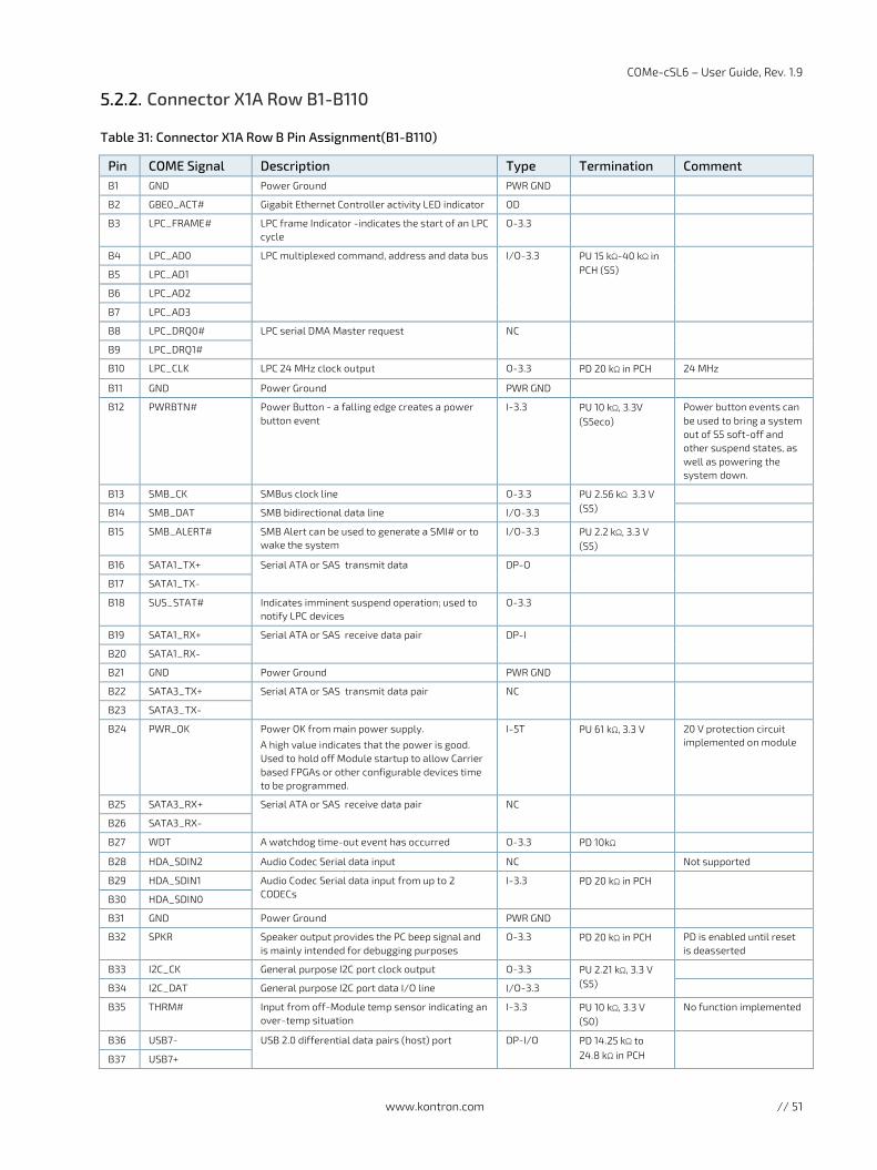
COMe-cSL6 – User Guide, Rev. 1.9
www.kontron.com // 51
Connector X1A Row B1-B110
Table 31: Connector X1A Row B Pin Assignment(B1-B110)
Pin COME Signal Description Type Termination Comment B1 GND Power Ground PWR GND
B2 GBE0_ACT# Gigabit Ethernet Controller activity LED indicator OD
B3 LPC_FRAME# LPC frame Indicator -indicates the start of an LPC cycle
O-3.3
B4 LPC_AD0 LPC multiplexed command, address and data bus I/O-3.3 PU 15 kΩ-40 kΩ in PCH (S5)
B5 LPC_AD1
B6 LPC_AD2
B7 LPC_AD3
B8 LPC_DRQ0# LPC serial DMA Master request NC
B9 LPC_DRQ1#
B10 LPC_CLK LPC 24 MHz clock output O-3.3 PD 20 kΩ in PCH 24 MHz
B11 GND Power Ground PWR GND
B12 PWRBTN# Power Button - a falling edge creates a power button event
I-3.3 PU 10 kΩ, 3.3V (S5eco)
Power button events can be used to bring a system out of S5 soft-off and other suspend states, as well as powering the system down.
B13 SMB_CK SMBus clock line O-3.3 PU 2.56 kΩ 3.3 V (S5)
B14 SMB_DAT SMB bidirectional data line I/O-3.3
B15 SMB_ALERT# SMB Alert can be used to generate a SMI# or to wake the system
I/O-3.3 PU 2.2 kΩ, 3.3 V (S5)
B16 SATA1_TX+ Serial ATA or SAS transmit data DP-O
B17 SATA1_TX-
B18 SUS_STAT# Indicates imminent suspend operation; used to notify LPC devices
O-3.3
B19 SATA1_RX+ Serial ATA or SAS receive data pair DP-I
B20 SATA1_RX-
B21 GND Power Ground PWR GND
B22 SATA3_TX+ Serial ATA or SAS transmit data pair NC
B23 SATA3_TX-
B24 PWR_OK Power OK from main power supply.
A high value indicates that the power is good. Used to hold off Module startup to allow Carrier based FPGAs or other configurable devices time to be programmed.
I-5T PU 61 kΩ, 3.3 V 20 V protection circuit implemented on module
B25 SATA3_RX+ Serial ATA or SAS receive data pair NC
B26 SATA3_RX-
B27 WDT A watchdog time-out event has occurred O-3.3 PD 10kΩ
B28 HDA_SDIN2 Audio Codec Serial data input NC Not supported
B29 HDA_SDIN1 Audio Codec Serial data input from up to 2 CODECs
I-3.3 PD 20 kΩ in PCH
B30 HDA_SDIN0
B31 GND Power Ground PWR GND
B32 SPKR Speaker output provides the PC beep signal and is mainly intended for debugging purposes
O-3.3 PD 20 kΩ in PCH PD is enabled until reset is deasserted
B33 I2C_CK General purpose I2C port clock output O-3.3 PU 2.21 kΩ, 3.3 V (S5)
B34 I2C_DAT General purpose I2C port data I/O line I/O-3.3
B35 THRM# Input from off-Module temp sensor indicating an over-temp situation
I-3.3 PU 10 kΩ, 3.3 V (S0)
No function implemented
B36 USB7- USB 2.0 differential data pairs (host) port DP-I/O PD 14.25 kΩ to 24.8 kΩ in PCH
B37 USB7+
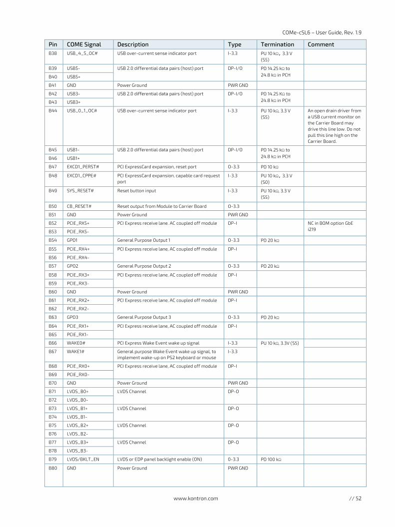
COMe-cSL6 – User Guide, Rev. 1.9
www.kontron.com // 52
Pin COME Signal Description Type Termination Comment B38 USB_4_5_OC# USB over-current sense indicator port I-3.3 PU 10 kΩ, 3.3 V
(S5)
B39 USB5- USB 2.0 differential data pairs (host) port DP-I/O PD 14.25 kΩ to 24.8 kΩ in PCH
B40 USB5+
B41 GND Power Ground PWR GND
B42 USB3- USB 2.0 differential data pairs (host) port DP-I/O PD 14.25 KΩ to 24.8 kΩ in PCH
B43 USB3+
B44 USB_0_1_OC# USB over-current sense indicator port I-3.3 PU 10 kΩ, 3.3 V (S5)
An open drain driver from a USB current monitor on the Carrier Board may drive this line low. Do not pull this line high on the Carrier Board.
B45 USB1- USB 2.0 differential data pairs (host) port DP-I/O PD 14.25 kΩ to 24.8 kΩ in PCH
B46 USB1+
B47 EXCD1_PERST# PCI ExpressCard expansion, reset port O-3.3 PD 10 kΩ
B48 EXCD1_CPPE# PCI ExpressCard expansion, capable card request port
I-3.3 PU 10 kΩ, 3.3 V (S0)
B49 SYS_RESET# Reset button input
I-3.3 PU 10 kΩ, 3.3 V (S5)
B50 CB_RESET# Reset output from Module to Carrier Board O-3.3
B51 GND Power Ground PWR GND
B52 PCIE_RX5+ PCI Express receive lane. AC coupled off module DP-I NC in BOM option GbE i219 B53 PCIE_RX5-
B54 GPO1 General Purpose Output 1 O-3.3 PD 20 kΩ
B55 PCIE_RX4+ PCI Express receive lane, AC coupled off module DP-I
B56 PCIE_RX4-
B57 GPO2 General Purpose Output 2 O-3.3 PD 20 kΩ
B58 PCIE_RX3+ PCI Express receive lane, AC coupled off module DP-I
B59 PCIE_RX3-
B60 GND Power Ground PWR GND
B61 PCIE_RX2+ PCI Express receive lane, AC coupled off module DP-I
B62 PCIE_RX2-
B63 GPO3 General Purpose Output 3 O-3.3 PD 20 kΩ
B64 PCIE_RX1+ PCI Express receive lane, AC coupled off module DP-I
B65 PCIE_RX1-
B66 WAKE0# PCI Express Wake Event wake up signal I-3.3 PU 10 kΩ, 3.3V (S5)
B67 WAKE1# General purpose Wake Event wake up signal, to implement wake-up on PS2 keyboard or mouse
I-3.3
B68 PCIE_RX0+ PCI Express receive lane, AC coupled off module DP-I
B69 PCIE_RX0-
B70 GND Power Ground PWR GND
B71 LVDS_B0+ LVDS Channel DP-O
B72 LVDS_B0-
B73 LVDS_B1+ LVDS Channel DP-O
B74 LVDS_B1-
B75 LVDS_B2+ LVDS Channel DP-O
B76 LVDS_B2-
B77 LVDS_B3+ LVDS Channel DP-O
B78 LVDS_B3-
B79 LVDS/BKLT_EN LVDS or EDP panel backlight enable (ON) 0-3.3 PD 100 kΩ
B80 GND Power Ground PWR GND
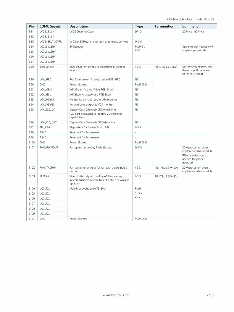
COMe-cSL6 – User Guide, Rev. 1.9
www.kontron.com // 53
Pin COME Signal Description Type Termination Comment B81 LVDS_B_CK+ LVDS Channel Clock DP-O 20 MHz - 80 MHz
B82 LVDS_B_CK-
B83 LVDS/BKLT_CTRL LVDS or EDP panel backlight brightness control O-3.3
B84 VCC_5V_SBY 5V Standby PWR 5 V (S5)
Optional, not necessary in single supply mode B85 VCC_5V_SBY
B86 VCC_5V_SBY
B87 VCC_5V_SBY
B88 BIOS_DIS1# BIOS Selection straps to determine BIOS boot device
I-3.3 PU 10 kΩ 3.3 V (S5) Carrier should only float these or pull them low. Refer to SPI boot
B89 VGA_RED Red for monitor. Analog Video RGB- RED NC
B90 GND Power Ground PWR GND
B91 VGA_GRN VGA Green. Analog Video RGB-Green NC
B92 VGA_BLU VGA Blue. Analog Video RGB-Blue NC
B93 VGA_HSYNC Horizontal sync output to VGA monitor NC
B94 VGA_VSYNC Vertical sync output to VGA monitor NC
B95 VGA_I2C_CK Display Data Channel (DDC) clock line
(I2C port dedicated to identify VGA monitor capabilities)
NC
B96 VGA_I2C_DAT Display Data Channel (DDC) data line NC
B97 SPI_CS# Chip select for Carrier Board SPI 0 3.3
B98 RSVD Reserved for future use -
B99 RSVD Reserved for future use -
B100 GND Power Ground PWR GND
B101 FAN_PWMOUT Fan speed control by PWM Output O-3.3 20 V protection circuit implemented on module,
PD on carrier board needed for proper operation
B102 FAN_TACHIN Fan tachometer input for fan with a two-pulse output
I-3.3 PU 47 kΩ 3.3 V (S0) 20 V protection circuit implemented on module
B103 SLEEP# Sleep button signal used by ACPI operating system to bring system to sleep state or wake it up again
I-3.3 PU 47 kΩ 3.3 V (S5)
B104 VCC_12V Main input voltage (4.75-20V) PWR
4.75 V-
20 V
B105 VCC_12V
B106 VCC_12V
B107 VCC_12V
B108 VCC_12V
B109 VCC_12V
B110 GND Power Ground PWR GND
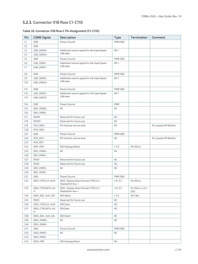
COMe-cSL6 – User Guide, Rev. 1.9
www.kontron.com // 54
Connector X1B Row C1-C110
Table 32: Connector X1B Row C Pin Assignment (C1-C110)
Pin COME Signal Description Type Termination Comment C1 GND Power Ground PWR GND
C2 GND
C3 USB_SSRX0- Additional receive signal for the SuperSpeed USB data
DP-I
C4 USB_SSRX0+
C5 GND Power Ground PWR GND
C6 USB_SSRX1- Additional receive signal for the SuperSpeed USB data
DP-I
C7 USB_SSRX1+
C8 GND Power Ground PWR GND
C9 USB_SSRX2- Additional receive signal for the SuperSpeed USB data
DP-I
C10 USB_SSRX2+
C11 GND Power Ground PWR GND
C12 USB_SSRX3- Additional receive signal for the SuperSpeed USB data
DP-I
C13 USB_SSRX3+
C14 GND Power Ground PWR
C15 DDI1_PAIR6+ NC
NC
C16 DDI1_PAIR6-
C17 RSVD1 Reserved for future use NC
C18 RSVD2 Reserved for future use NC
C19 PCIE_RX6+ PCI Express receive lane NC AC coupled off Module
C20 PCIE_RX6-
C21 GND Power Ground PWR GND
C22 PCIE_RX7+ PCI Express receive lane NC AC coupled off Module
C23 PCIE_RX7-
C24 DDI1_HPD DDI Hotplug Detect I-3.3 PD 100 kΩ
C25 DDI1_PAIR4+ NC NC
C26 DDI1_PAIR4-
C27 RSVD Reserved for future use NC
C28 RSVD Reserved for future use NC
C29 DDI1_PAIR5+ NC NC
C30 DDI1_PAIR5-
C31 GND Power Ground PWR GND
C32 DDI2_CTRLCLK_AUX+ DDI2- Display Data Channel CTRLCLK / DisplayPort Aux +
I/O-3.3 PD 100 kΩ
C33 DDI2_CTRLDATA_AUX-
DDI2- Display Data Channel CTRLCLK / DisplayPort Aux +
I/O-3.3 PU 100 kΩ, 3.3 V (S0)
C34 DDI2_DDC_AUX_SEL DDI Select I-3.3 PD 1 MΩ
C35 RSVD Reserved for future use NC
C36 DDI3_CTRLCLK_AUX+ DDI Clock NC
C37 DDI3_CTRLDATA_AUX-
DDI Date NC
C38 DDI3_DDC_AUX_SEL DDI Select NC
C39 DDI3_PAIR0+ NC NC
C40 DDI3_PAIR0-
C41 GND Power Ground PWR GND
C42 DDI3_PAIR1+ NC NC
C43 DDI3_PAIR1-
C44 DDI3_HPD DDI Hotplug Detect NC
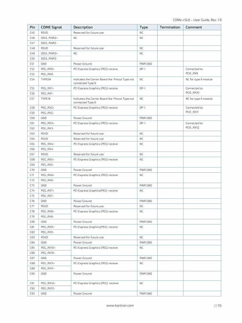
COMe-cSL6 – User Guide, Rev. 1.9
www.kontron.com // 55
Pin COME Signal Description Type Termination Comment C45 RSVD Reserved for future use NC
C46 DDI3_PAIR2+ NC
NC
C47 DDI3_PAIR2-
C48 RSVD Reserved for future use NC
C49 DDI3_PAIR3+ NC NC
C50 DDI3_PAIR3-
C51 GND Power Ground PWR GND
C52 PEG_RX0+ PCI Express Graphics (PEG) receive DP-I Connected to:
PCIE_RX9 C53 PEG_RX0-
C54 TYPE0# Indicates the Carrier Board the Pinout Type not connected Type 6
NC NC for type 6 module
C55 PEG_RX1+ PCI Express Graphics (PEG) receive DP-I Connected to:
PCIE_RX10 C56 PEG_RX1-
C57 TYPE1# Indicates the Carrier Board the Pinout Type not connected Type 6
NC NC for type 6 module
C58 PEG_RX2+ PCI Express Graphics (PEG) receive DP-I Connected to:
PCIE_RX11 C59 PEG_RX2-
C60 GND Power Ground PWR GND
C61 PEG_RX3+ PCI Express Graphics (PEG) receive DP-I Connected to:
PCIE_RX12 C62 PEG_RX3-
C63 RSVD Reserved for future use NC
C64 RSVD Reserved for future use NC
C65 PEG_RX4+ PCI Express Graphics (PEG) receive NC
C66 PEG_RX4-
C67 RSVD Reserved for future use NC
C68 PEG_RX5+ PCI Express Graphics (PEG) receive NC
C69 PEG_RX5-
C70 GND Power Ground PWR GND
C71 PEG_RX6+ PCI Express Graphics (PEG) receive NC
C72 PEG_RX6-
C73 GND Power Ground PWR GND
C74 PEG_RX7+ PCI Express Graphics(PEG) receive NC
C75 PEG_RX7-
C76 GND Power Ground PWR GND
C77 RSVD Reserved for future use NC
C78 PEG_RX8+ PCI Express Graphics (PEG) receive NC
C79 PEG_RX8-
C80 GND Power Ground PWR GND
C81 PEG_RX9+ PCI Express Graphics(PEG) receive NC
C82 PEG_RX9-
C83 RSVD Reserved for future use NC
C84 GND Power Ground PWR GND
C85 PEG_RX10+ PCI Express Graphics (PEG) receive NC
C86 PEG_RX10-
C87 GND Power Ground PWR GND
C88 PEG_RX11+ PCI Express Graphics (PEG) receive NC
C89 PEG_RX11-
C90 GND Power Ground
PWR GND
C91 PEG_RX12+ PCI Express Graphics (PEG) receive NC
C92 PEG_RX12-
C93 GND Power Ground PWR GND
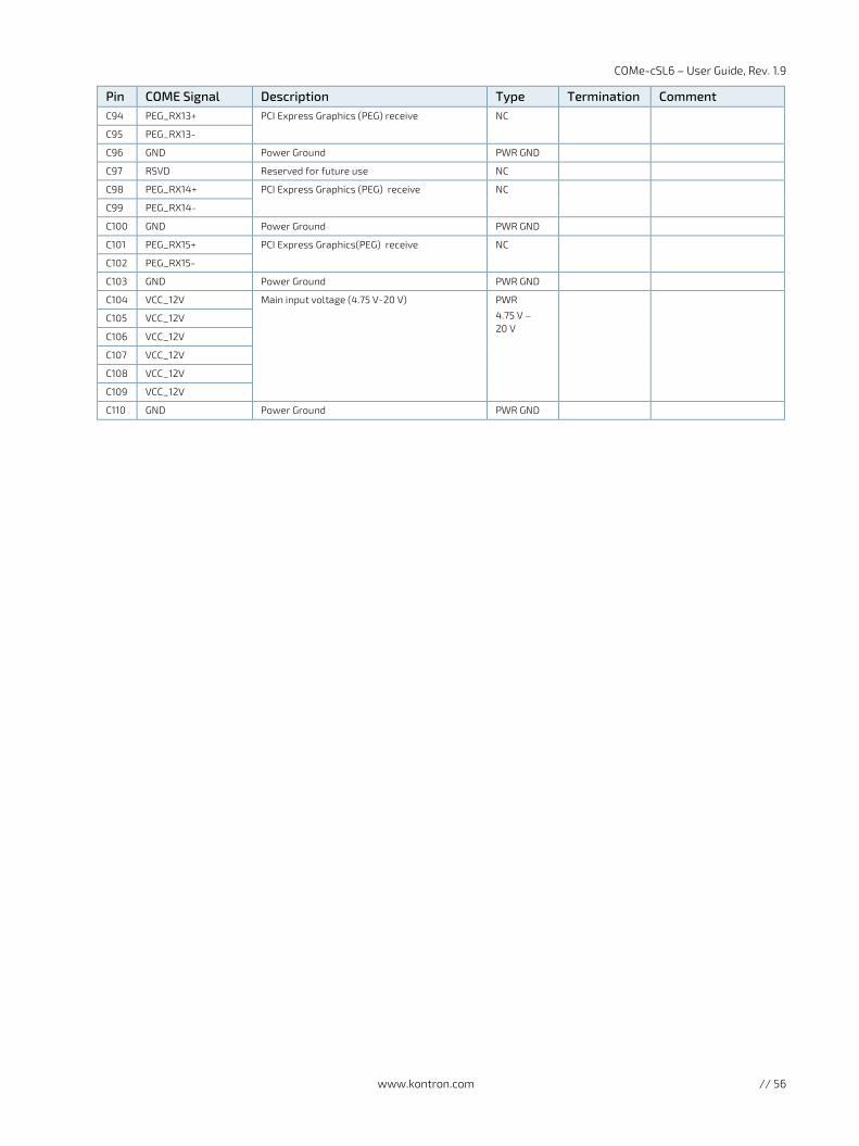
COMe-cSL6 – User Guide, Rev. 1.9
www.kontron.com // 56
Pin COME Signal Description Type Termination Comment C94 PEG_RX13+ PCI Express Graphics (PEG) receive NC
C95 PEG_RX13-
C96 GND Power Ground PWR GND
C97 RSVD Reserved for future use NC
C98 PEG_RX14+ PCI Express Graphics (PEG) receive NC
C99 PEG_RX14-
C100 GND Power Ground PWR GND
C101 PEG_RX15+ PCI Express Graphics(PEG) receive NC
C102 PEG_RX15-
C103 GND Power Ground PWR GND
C104 VCC_12V Main input voltage (4.75 V-20 V) PWR
4.75 V – 20 V
C105 VCC_12V
C106 VCC_12V
C107 VCC_12V
C108 VCC_12V
C109 VCC_12V
C110 GND Power Ground PWR GND
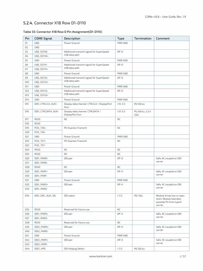
COMe-cSL6 – User Guide, Rev. 1.9
www.kontron.com // 57
Connector X1B Row D1-D110
Table 33: Connector X1B Row D Pin Assignment(D1-D110)
Pin COME Signal Description Type Termination Comment D1 GND Power Ground PWR GND
D2 GND
D3 USB_SSTX0- Additional transmit signal for SuperSpeed USB data path
DP-O
D4 USB_SSTX0+
D5 GND Power Ground PWR GND
D6 USB_SSTX1- Additional transmit signal for SuperSpeed USB data path
DP-O
D7 USB_SSTX1+
D8 GND Power Ground PWR GND
D9 USB_SSTX2- Additional transmit signal for SuperSpeed USB data path
DP-O
D10 USB_SSTX2+
D11 GND Power Ground PWR GND
D12 USB_SSTX3- Additional transmit signal for SuperSpeed USB data path
DP-O
D13 USB_SSTX3+
D14 GND Power Ground PWR GND
D15 DDI1_CTRLCLK_AUX+ Display data channel CTRLCLK / DisplayPort Aux+
I/O-3.3 PD 100 kΩ
D16 DDI1_CTRLDATA_AUX- Display data channel CTRLDATA / DisplayPort Aux-
I/O-3.3 PU 100 kΩ, 3.3 V (S0)
D17 RSVD NC
NC
D18 RSVD
D19 PCIE_TX6+ PCI Express Transmit NC
D20 PCIE_TX6-
D21 GND Power Ground PWR GND
D22 PCIE_TX7+ PCI Express Transmit NC
D23 PCIE_TX7-
D24 RSVD NC NC
D25 RSVD NC NC
D26 DDI1_PAIR0+ DDI pair DP-O Safe, AC coupled on DDI carrier D27 DDI1_PAIR0-
D28 RSVD NC NC
D29 DDI1_PAIR1+ DDI pair DP-O Safe, AC coupled on DDI carrier D30 DDI1_PAIR1-
D31 GND Power Ground PWR GND
D32 DDI1_PAIR2+ DDI pair DP-0 Safe, AC coupled on DDI carrier
D33 DDI1_PAIR2-
D34 DDI1_DDC_AUX_SEL DDI select I-3.3 PD 1 MΩ Module drives low or open drain. Module tolerates possible PU from type 6 carrier.
D35 RSVD Reserved for future use NC
D36 DDI1_PAIR3+ DDI pair DP-0 Safe, AC coupled on DDI carrier D37 DDI1_PAIR3-
D38 RSVD Reserved for future use NC
D39 DDI2_PAIR0+ DDI pair DP-O Safe, AC coupled on DDI carrier D40 DDI2_PAIR0-
D41 GND Power Ground PWR GND
D42 DDI2_PAIR1+ DDI pair DP-0 Safe, AC coupled on DDI carrier D43 DDI2_PAIR1-
D44 DDI2_HPD DDI Hotplug Detect I-3.3 PD 100 kΩ
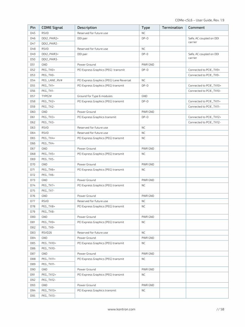
COMe-cSL6 – User Guide, Rev. 1.9
www.kontron.com // 58
Pin COME Signal Description Type Termination Comment D45 RSVD Reserved for future use NC
D46 DDI2_PAIR2+ DDI pair
DP-O Safe, AC coupled on DDI carrier D47 DDI2_PAIR2-
D48 RSVD Reserved for future use NC
D49 DDI2_PAIR3+ DDI pair
DP-0 Safe, AC coupled on DDI carrier D50 DDI2_PAIR3-
D51 GND Power Ground PWR GND
D52 PEG_TX0+ PCI Express Graphics (PEG) transmit DP-O Connected to PCIE_TX9+
D53 PEG_TX0- Connected to PCIE_TX9-
D54 PEG_LANE_RV# PCI Express Graphics (PEG) Lane Reversal NC
D55 PEG_TX1+ PCI Express Graphics (PEG) transmit DP-O Connected to PCIE_TX10+
D56 PEG_TX1- Connected to PCIE_TX10-
D57 TYPE2# Ground for Type 6 modules GND
D58 PEG_TX2+ PCI Express Graphics (PEG) transmit DP-O Connected to PCIE_TX11+
D59 PEG_TX2- Connected to PCIE_TX11-
D60 GND Power Ground PWR GND
D61 PEG_TX3+ PCI Express Graphics transmit DP-O Connected to PCIE_TX12+
D62 PEG_TX3- Connected to PCIE_TX12-
D63 RSVD Reserved for future use NC
D64 RSVD Reserved for future use NC
D65 PEG_TX4+ PCI Express Graphics (PEG) transmit NC
D66 PEG_TX4-
D67 GND Power Ground PWR GND
D68 PEG_TX5+ PCI Express Graphics (PEG) transmit NC
D69 PEG_TX5-
D70 GND Power Ground PWR GND
D71 PEG_TX6+ PCI Express Graphics (PEG) transmit NC
D72 PEG_TX6-
D73 GND Power Ground PWR GND
D74 PEG_TX7+ PCI Express Graphics (PEG) transmit NC
D75 PEG_TX7-
D76 GND Power Ground PWR GND
D77 RSVD Reserved for future use NC
D78 PEG_TX8+ PCI Express Graphics (PEG) transmit NC
D79 PEG_TX8-
D80 GND Power Ground PWR GND
D81 PEG_TX9+ PCI Express Graphics (PEG) transmit NC
D82 PEG_TX9-
D83 RSVD26 Reserved for future use NC
D84 GND Power Ground PWR GND
D85 PEG_TX10+ PCI Express Graphics (PEG) transmit NC
D86 PEG_TX10-
D87 GND Power Ground PWR GND
D88 PEG_TX11+ PCI Express Graphics (PEG) transmit NC
D89 PEG_TX11-
D90 GND Power Ground PWR GND
D91 PEG_TX12+ PCI Express Graphics (PEG) transmit NC
D92 PEG_TX12-
D93 GND Power Ground PWR GND
D94 PEG_TX13+ PCI Express Graphics transmit NC
D95 PEG_TX13-
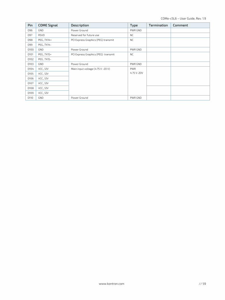
COMe-cSL6 – User Guide, Rev. 1.9
www.kontron.com // 59
Pin COME Signal Description Type Termination Comment D96 GND Power Ground PWR GND
D97 RSVD Reserved for future use NC
D98 PEG_TX14+ PCI Express Graphics (PEG) transmit NC
D99 PEG_TX14-
D100 GND Power Ground PWR GND
D101 PEG_TX15+ PCI Express Graphics (PEG) transmit NC
D102 PEG_TX15-
D103 GND Power Ground PWR GND
D104 VCC_12V Main input voltage (4.75 V -20 V)
PWR
4.75 V-20V
D105 VCC_12V
D106 VCC_12V
D107 VCC_12V
D108 VCC_12V
D109 VCC_12V
D110 GND Power Ground PWR GND
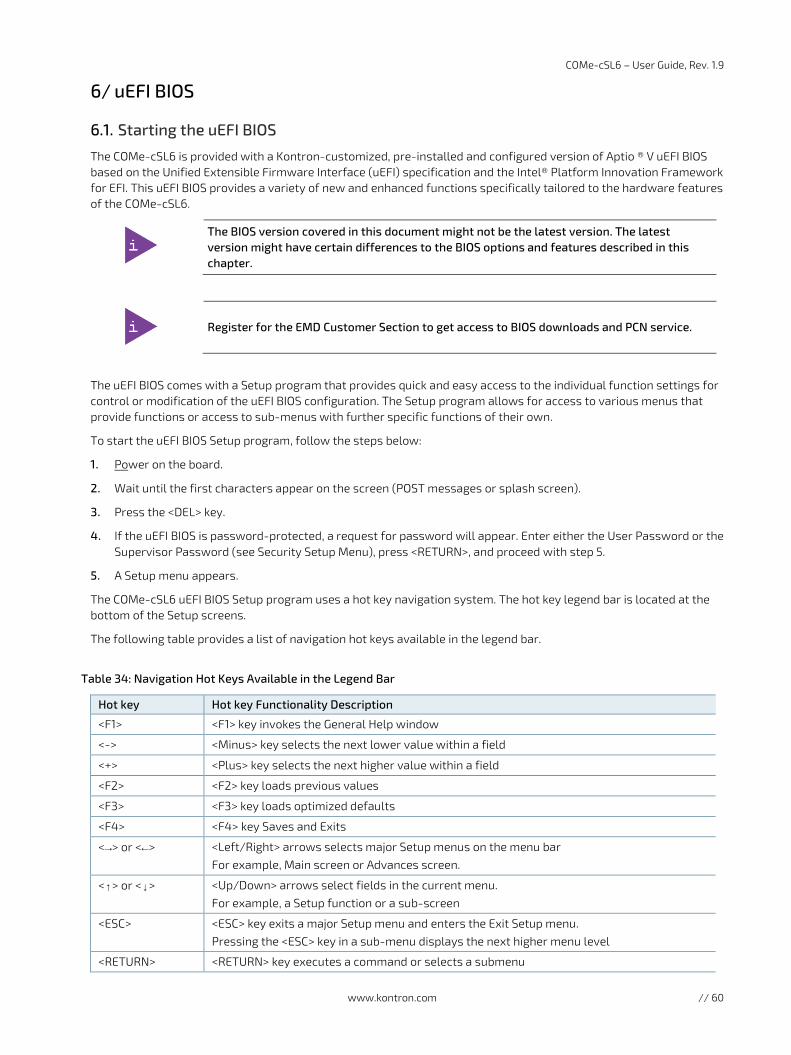
COMe-cSL6 – User Guide, Rev. 1.9
www.kontron.com // 60
6/ uEFI BIOS
6.1. Starting the uEFI BIOS
The COMe-cSL6 is provided with a Kontron-customized, pre-installed and configured version of Aptio ® V uEFI BIOS based on the Unified Extensible Firmware Interface (uEFI) specification and the Intel® Platform Innovation Framework for EFI. This uEFI BIOS provides a variety of new and enhanced functions specifically tailored to the hardware features of the COMe-cSL6.
The BIOS version covered in this document might not be the latest version. The latest version might have certain differences to the BIOS options and features described in this chapter.
Register for the EMD Customer Section to get access to BIOS downloads and PCN service.
The uEFI BIOS comes with a Setup program that provides quick and easy access to the individual function settings for control or modification of the uEFI BIOS configuration. The Setup program allows for access to various menus that provide functions or access to sub-menus with further specific functions of their own.
To start the uEFI BIOS Setup program, follow the steps below:
1. Power on the board.
2. Wait until the first characters appear on the screen (POST messages or splash screen).
3. Press the <DEL> key.
4. If the uEFI BIOS is password-protected, a request for password will appear. Enter either the User Password or the Supervisor Password (see Security Setup Menu), press <RETURN>, and proceed with step 5.
5. A Setup menu appears.
The COMe-cSL6 uEFI BIOS Setup program uses a hot key navigation system. The hot key legend bar is located at the bottom of the Setup screens.
The following table provides a list of navigation hot keys available in the legend bar.
Table 34: Navigation Hot Keys Available in the Legend Bar
Hot key Hot key Functionality Description
<F1> <F1> key invokes the General Help window
<-> <Minus> key selects the next lower value within a field
<+> <Plus> key selects the next higher value within a field
<F2> <F2> key loads previous values
<F3> <F3> key loads optimized defaults
<F4> <F4> key Saves and Exits
<→> or <←> <Left/Right> arrows selects major Setup menus on the menu bar For example, Main screen or Advances screen.
<↑> or <↓> <Up/Down> arrows select fields in the current menu. For example, a Setup function or a sub-screen
<ESC> <ESC> key exits a major Setup menu and enters the Exit Setup menu. Pressing the <ESC> key in a sub-menu displays the next higher menu level
<RETURN> <RETURN> key executes a command or selects a submenu
COMe-cSL6 – User Guide, Rev. 1.9
www.kontron.com // 61
6.2. Setup Menus
The Setup utility features menus listed in the selection bar at the top of the screen:
Main
Advanced
Chipset
Security
Boot
Save & Exit
The left and right arrow keys select the Setup menus. The currently active menu and the currently active uEFI BIOS Setup item are highlighted in white.
Each Setup menu provides two main frames. The left frame displays all available functions. Configurable functions are displayed in blue. Functions displayed in grey provide information about the status or the operational configuration. The right frame displays an Item Specific Help window providing an explanation of the respective function.
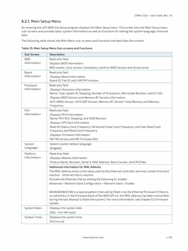
COMe-cSL6 – User Guide, Rev. 1.9
www.kontron.com // 62
Main Setup Menu
On entering the uEFI BIOS the Setup program displays the Main Setup menu. This screen lists the Main Setup menu sub-screens and provides basic system information as well as functions for setting the system language, time and date.
The following table shows the Main Menu sub-screens and functions and describes the content.
Table 35: Main Setup Menu Sub-screens and Functions
Sub-Screen Description
BIOS Information>
Read only field Displays BIOS Information: BIOS vendor, Core version, Compliancy, Kontron BIOS Version and Access level
Board Information>
Read only field Displays Board Information: Board ID, Fab ID, and LAN PHY revision
Processor Information>
Read only field Displays Processor Information: Name, Type, Speed, ID, Stepping, Number of Processors, Microcode Revision, and GT Info Displays BIOS Version and Memory RC Version Information: IGFX VBIOS Version, IGFX GOP Version, Memory RC Version Total Memory and Memory Frequency.
PCH Information>
Read only field Displays PCH Information: Name, PCH SKU, Stepping, and HSIO Revision Displays SPI Clock Information: Read ID/Status Clock Frequency, Write and Erase Clock Frequency, and Fast Read Clock Frequency and Read Clock Frequency Displays Firmware Information: ME FW Version and ME Firmware SKU
System Language>
Selects system default language [English]
Platform Information>
Read only field Displays Module Information Product Name, Revision, Serial # ‚MAC Address, Boot Counter, and CPLD Rev
Additional information for MAC Address The MAC address entry is the value used by the Ethernet controller and may contain the entry’ Inactive’ - Ethernet chip is inactive. Activate the Ethernet chip by setting the following to ‘enable’. Advanced > Network Stack Configuration > Network Stack > Enable 88:88:88:88:87:88 is a special pattern that will be filled in by the Ethernet firmware if there is no valid entry in the firmware block of the BIOS SPI (i.e. the MAC address has been overwritten during the last attempt to flash the system). For more information, see Chapter 6.5 Firmware Update.
System Date> Displays the system date [Day mm/dd/yyyy]
System Time> Displays the system time [hh:mm:ss]
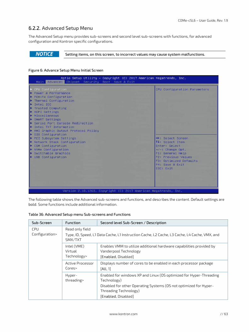
COMe-cSL6 – User Guide, Rev. 1.9
www.kontron.com // 63
Advanced Setup Menu
The Advanced Setup menu provides sub-screens and second level sub-screens with functions, for advanced configuration and Kontron specific configurations.
Setting items, on this screen, to incorrect values may cause system malfunctions.
Figure 6: Advance Setup Menu Initial Screen
The following table shows the Advanced sub-screens and functions, and describes the content. Default settings are bold. Some functions include additional information.
Table 36: Advanced Setup menu Sub-screens and Functions
Sub-Screen Function Second level Sub-Screen / Description
CPU Configuration>
Read only field Type, ID, Speed, L1 Data Cache, L1 Instruction Cache, L2 Cache, L3 Cache, L4 Cache, VMX, and SMX/TXT
Intel (VME) Virtual Technology>
Enables VMM to utilize additional hardware capabilities provided by Vanderpool Technology [Enabled, Disabled]
Active Processor Cores>
Displays number of cores to be enabled in each processor package [All, 1]
Hyper-threading>
Enabled for windows XP and Linux (OS optimized for Hyper-Threading Technology) Disabled for other Operating Systems (OS not optimized for Hyper-Threading Technology) [Enabled, Disabled]
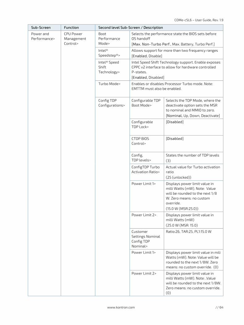
COMe-cSL6 – User Guide, Rev. 1.9
www.kontron.com // 64
Sub-Screen Function Second level Sub-Screen / Description
Power and Performance>
CPU Power Management Control>
Boot Performance Mode>
Selects the performance state the BIOS sets before OS handoff
[Max. Non-Turbo Perf., Max. Battery, Turbo Perf.]
Intel® Speedstep®>
Allows support for more than two frequency ranges [Enabled, Disable]
Intel® Speed Shift Technology>
Intel Speed Shift Technology support. Enable exposes CPPC v2 interface to allow for hardware controlled P-states. [Enabled, Disabled]
Turbo Mode> Enables or disables Processor Turbo mode. Note: EMTTM must also be enabled.
Config TDP Configurations>
Configurable TDP Boot Mode>
Selects the TDP Mode, where the deactivate option sets the MSR to nominal and MMIO to zero. [Nominal, Up, Down, Deactivate]
Configurable TDP Lock>
[Disabled]
CTDP BIOS Control>
[Disabled]
Config, TDP levels>
States the number of TDP levels (3)
ConfigTDP Turbo Activation Ratio>
Actual value for Turbo activation ratio (25 (unlocked))
Power Limit 1> Displays power limit value in milli Watts (mW). Note: Value will be rounded to the next 1/8 W. Zero means: no custom override. (15.0 W (MSR:25.0))
Power Limit 2> Displays power limit value in milli Watts (mW) (25.0 W (MSR: 15.0)
Customer Settings Nominal Config TDP Nominal>
Ratio:26, TAR:25, PL1:15.0 W
Power Limit 1> Displays power limit value in mili Watts (mW). Note: Value will be rounded to the next 1/8W. Zero means: no custom override. (0)
Power Limit 2> Displays power limit value in milli Watts (mW). Note: .Value will be rounded to the next 1/8W. Zero means: no custom override. (0)
COMe-cSL6 – User Guide, Rev. 1.9
www.kontron.com // 65
Sub-Screen Function Second level Sub-Screen / Description
Power and Performance> (continued)
CPU Power Management Control> (continued)
Config TDP Configurations> (continued)
Power Limit 1 Time Window>
Sets the time window for power limit 1 [0]
ConfigTDP Turbo Activation Ratio>
Custom value for Turbo activation ratio. This needs to be configured with valid values from LFM to Max Turbo. (0)
Customer Settings Down ConfigTDP level 1>
Ratio:8, TAR:7, PL1:7.500 W
Power Limit 1> Displays power limit value in mili Watts (mW). Note: Value will be rounded to the next 1/8 W. Zero means: no custom override” (0)
Power Limit 2> Displays power limit value in milli Watts (mW). Note: Value will be rounded to the next 1/8 W. Zero means: no custom override. (0)
Power Limit 1 Time Window>
Sets the time window for power limit 1 [0]
Customer Settings UP ConfigTDP level 2>
Ratio:27, TAR:26, PL1:25.0 W
Power Limit 1> Displays power limit value in Watts. Note: Value will be rounded to the next 1/8 W. Zero means: no custom override. (0)
Power Limit 2> Displays power limit value in Watts Note: Value will be rounded to the next 1/8 W. Zero means: no custom override. (0)
Power Limit 1 Time Window>
Sets the time window for power limit 1 [0]
ConfigTDP Turbo Activation Ratio>
Custom value for Turbo activation ratio. This needs to be configured with valid values from LFM to Max Turbo. (0)
Additional Information The system allows for cTDP (=configurable thermal design power) to be set dynamically. This option is only available for processors that really support this feature. The menu item will disappear for any other CPU. The menu screen will also be different according to the options the CPU supports.
COMe-cSL6 – User Guide, Rev. 1.9
www.kontron.com // 66
Sub-Screen Function Second level Sub-Screen / Description
Power and Performance> (continued)
CPU Power Management Control> (continued)
Usually there are three levels to support: nominal, down and up. For each level the power limits, their time window and the activation ratio may be chosen. A value of zero for the activation ratio means that this level is not being used. NOTE: Take care to create valid configurations to avoid unexpected behavior of the system.
C States> Enables or disables CPU power management to allow CPU to enter C-Sates when not 100% utilized. [Enabled, Disabled]
Enhanced C-state>
Enables or disables C1E. If enabled CPU switches to minimum speed when all cores enter C-state. [Enabled, Disabled]
Packaged C-state Limit>
Maximum Package C-State limit setting. Default: leaves the factory default value. Auto initializes to deepest available package c-state limit. [Auto, Default, C10, C9, C8, C7S, C7, C6, C3, C2, C0/C1]
Thermal Monitor>
Thermal monitor [Enabled, Disabled]
GT Power management Control>
RC6 (Render standby)>
Check to enable render standby support. [Enabled, Disabled]
Maximum GT Frequency>
Maximum GT frequency limited by user. Choose from range 300 MHz (RPN) to 1000 MHz (RPO). Out of range values are clipped to the minimum. and maximum range values above. [Default Max Frequency, 100 MHz – 1200 MHz]
PCH-FW Configuration>
Read only fields ME FW Version, ME Firmware Mode, ME Firmware SKU, ME File System Integrity Value, ME Firmware Status 1, ME Firmware Status 2 and NFC Support.
ME State> If disabled, ME enters ME temporarily disabled mode. [Enabled, Disabled]
ME Unconfig. ON RTC Clear>
If disabled, ME is not unconfigured on RTC clear.
Comms Hub Support>
Support for Comms hub [Enabled, Disabled]
JHI Support> Enables or disables Intel® DAL Host Interface Service (JHI) [Enabled, Disabled]
Core BIOS Done Message>
Enables or disables core BIOS done message sent to ME [Enabled, Disabled]
Firmware Update Configuration>
ME FW Image Re-Flash>
Enables or disables ME FW Image RE-Flash function [Enabled, Disabled]
Local FW Update>
Options for local FW update function [Enabled, Disabled]
Thermal Configuration>
CPU Thermal Configuration>
DTS SMM>
ACPI thermal management uses HWM reported values when disabled and DTS SMM mechanism to obtain CPU temperatures values when enabled.
COMe-cSL6 – User Guide, Rev. 1.9
www.kontron.com // 67
Sub-Screen Function Second level Sub-Screen / Description
Thermal Configuration> (continued)
CPU Thermal Configuration> (continued)
DTS SMM> (continued)
Note: Enabling DTS might deteriate the system’s real time behavior through handling the necessary SMMs. [Enabled, Disabled, Critical Temp Reporting]
Tcc Activation Offset>
Displays the offset from the factory TCC (Thermal Control Circuit) activation temperature. Note: This values is subtracted from the TCC threshold, i.e. ‘0’ means maximum allowed temperature.
ACPI T-States> ACPI T-States [Enabled , Disabled]
Platform Thermal Configuration>
Automatic Thermal Reporting>
Configures _CRT, _PSC and _ACO automatically based on valued recommended in BWG’S Thermal reporting Management setting. Set to disabled for manual configuration. [Enabled, Disabled]
Critical Trip Point>
Controls the temperature of the ACPI Critical Trip Point at which OS shuts off the system. The plan of record (POR) for Intel® Mobile Processors is 119°C. [127°C, 119°C (POR), 111°C, -----15°C]
Passive Trip Point>
Controls temperature of ACPI Passive Trip Point at which OS begins to throttle the processor. [119°C (POR), 111°C, 103°C, 95°C, -----15°C, Disabled]
Passive TC1 Value>
Sets TC1 /values for ACPI passive cooling formula (Range: 1-16)
Passive TC2 Value>
Sets TC2 values for ACPI passive cooling formula (Range: 1-16)
Passive TSP Value>
Sets TSP value for ACPI passive cooling formula TSP value represents how often OS reads the temperature when passive cooling is enabled, in 10ths of a second. (Range: 2-32).
Passive Trip Points>
Passive Trip Points [Enabled, Disabled]
Critical Trip Points>
Critical Trip Points [Enabled, Disabled]
Intel ICC>
ICC/OC Watchdog Timer>
Enabling Exposes the ICC/OC watchdog timer to OS as ACPI device BIOS always uses WDT HW when changing clock setting. [Enabled, Disabled]
ICC Locks After EOP>
Specifies the ICC registers to write to, after end of post. Default – Dynamic registers for runtime clock adjustments are writable. All locked - No clock register adjustment allowed after EOP. All Unlocked - All ICC registers can be written after EOP. [Default, All Locked, All Unlocked]
ICC Profile> Selects the clock profile corresponding to platform configuration. Profiles are defined by the OEM and platform capabilities. Typically , profile 0 has failsafe settings. Other profiles correspond to WiMax, 3G, or overclocking settings.
ICC PLL Shutdown>
Controls programming of ICC PLL shutdown flow. If enabled this ICC PM register is programmed on every non-SX boot. [Enabled, Disabled]
COMe-cSL6 – User Guide, Rev. 1.9
www.kontron.com // 68
Sub-Screen Function Second level Sub-Screen / Description
Intel ICC> (continued)
Additional Information two-staged watchdog DMI/BCLK/PEG/SATA/USB3/PCIe clock settings Default clock settings: 100 MHz 0.50% Downspread Frequency range limits: 99.50 MHz – 100 MHz Maximum Spread: % 0.50% Spread Mode adjustments: None Allowed
Trusted Computing>
Security Device Support>
Enables or disables BIOS support for security device. Operating system will not show security device. TCG EFI protocol and INT1A interface are not available. [Enabled, Disabled]
Active PCR Banks>
Read only field Displays active PCR Banks
Available PCR Banks>
Read only field Displays available PCR Banks
SHA-1 PCR Bank>
SHA-1 PCR Bank [Enabled, Disabled]
SHA256 PCR Bank>
SHA256 PCR Bank [Enabled, Disabled]
Pending Operation>
Schedules operation for Security Device Note: Computer reboots on restart in order to change the state of the security device. [None, TPM Clear]
Platform Hierarchy>
Platform Hierarchy [Enabled, Disabled]
Storage Hierarchy>
Storage Hierarchy [Enabled, Disabled]
Endorsement Hierarchy>
Endorsement Hierarchy [Enabled, Disabled]
TPM2.0 UEFI Spec. Version>
Selects TCG2 Spec. version. support TCG_1_2 is compatible mode for Win8/Win10 TCG_2 supports TCG2 protocol + event format Win 10 or later. [TCG_1_2, TCG_2]
Physical Presence Spec Version>
Select to tell OS to support either PPI Spec 1.2 or 1.3 Note: Some HCK test might not support 1.3. [1.2, 1.3]
TPM 20 InterfaceType>
Read only field
Device Select> BIOS support for security devices. Auto - Supports both TPM 1.2 and TPM 2.0 with TPM 2.0 as default if not
found and TMM 1.2 is enumerated.
TPM 1.2 - Restricts support to TPM 1.2
TPM 2.0 - Restricts support to TPM 2.0
[TPM 1.2, TPM 2.0, Auto]
ACPI settings>
Enable ACPI Auto Configuration>
Enables or disables BIOS ACPI auto configuration. If enabled, the system uses generic ACPI settings that may not fit the system best. [Enabled, Disabled]
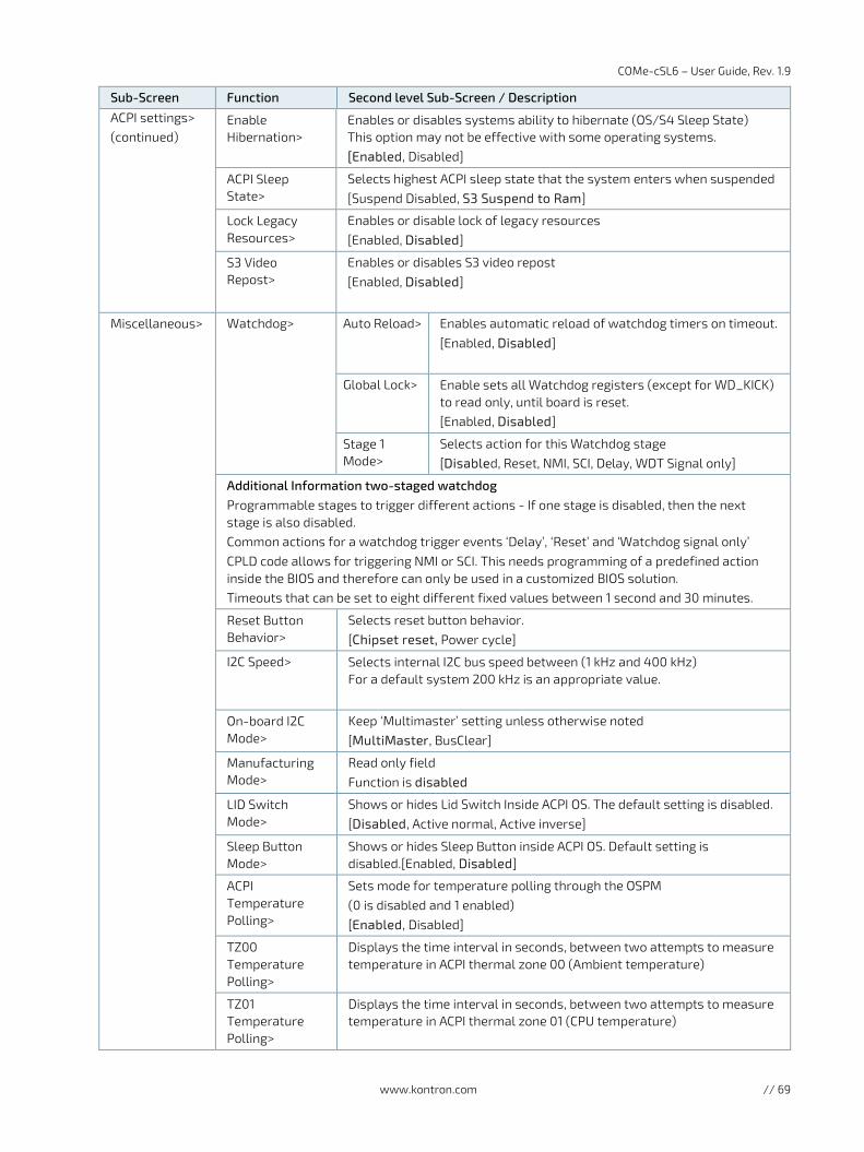
COMe-cSL6 – User Guide, Rev. 1.9
www.kontron.com // 69
Sub-Screen Function Second level Sub-Screen / Description
ACPI settings> (continued)
Enable Hibernation>
Enables or disables systems ability to hibernate (OS/S4 Sleep State) This option may not be effective with some operating systems. [Enabled, Disabled]
ACPI Sleep State>
Selects highest ACPI sleep state that the system enters when suspended [Suspend Disabled, S3 Suspend to Ram]
Lock Legacy Resources>
Enables or disable lock of legacy resources [Enabled, Disabled]
S3 Video Repost>
Enables or disables S3 video repost [Enabled, Disabled]
Miscellaneous>
Watchdog>
Auto Reload> Enables automatic reload of watchdog timers on timeout.
[Enabled, Disabled]
Global Lock> Enable sets all Watchdog registers (except for WD_KICK) to read only, until board is reset. [Enabled, Disabled]
Stage 1 Mode>
Selects action for this Watchdog stage [Disabled, Reset, NMI, SCI, Delay, WDT Signal only]
Additional Information two-staged watchdog Programmable stages to trigger different actions - If one stage is disabled, then the next stage is also disabled. Common actions for a watchdog trigger events ‘Delay’, ‘Reset’ and ‘Watchdog signal only’ CPLD code allows for triggering NMI or SCI. This needs programming of a predefined action inside the BIOS and therefore can only be used in a customized BIOS solution. Timeouts that can be set to eight different fixed values between 1 second and 30 minutes.
Reset Button Behavior>
Selects reset button behavior. [Chipset reset, Power cycle]
I2C Speed> Selects internal I2C bus speed between (1 kHz and 400 kHz) For a default system 200 kHz is an appropriate value.
On-board I2C Mode>
Keep ‘Multimaster’ setting unless otherwise noted [MultiMaster, BusClear]
Manufacturing Mode>
Read only field Function is disabled
LID Switch Mode>
Shows or hides Lid Switch Inside ACPI OS. The default setting is disabled. [Disabled, Active normal, Active inverse]
Sleep Button Mode>
Shows or hides Sleep Button inside ACPI OS. Default setting is disabled.[Enabled, Disabled]
ACPI Temperature Polling>
Sets mode for temperature polling through the OSPM (0 is disabled and 1 enabled) [Enabled, Disabled]
TZ00 Temperature Polling>
Displays the time interval in seconds, between two attempts to measure temperature in ACPI thermal zone 00 (Ambient temperature)
TZ01 Temperature Polling>
Displays the time interval in seconds, between two attempts to measure temperature in ACPI thermal zone 01 (CPU temperature)
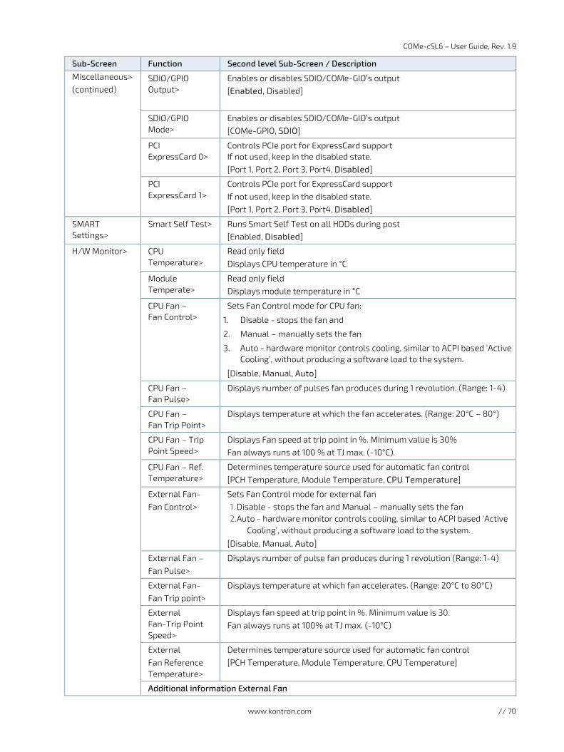
COMe-cSL6 – User Guide, Rev. 1.9
www.kontron.com // 70
Sub-Screen Function Second level Sub-Screen / Description
Miscellaneous> (continued)
SDIO/GPIO Output>
Enables or disables SDIO/COMe-GIO’s output [Enabled, Disabled]
SDIO/GPIO Mode>
Enables or disables SDIO/COMe-GIO’s output [COMe-GPIO, SDIO]
PCI ExpressCard 0>
Controls PCIe port for ExpressCard support If not used, keep in the disabled state. [Port 1, Port 2, Port 3, Port4, Disabled]
PCI ExpressCard 1>
Controls PCIe port for ExpressCard support If not used, keep in the disabled state. [Port 1, Port 2, Port 3, Port4, Disabled]
SMART Settings>
Smart Self Test> Runs Smart Self Test on all HDDs during post [Enabled, Disabled]
H/W Monitor>
CPU Temperature>
Read only field Displays CPU temperature in °C
Module Temperate>
Read only field Displays module temperature in °C
CPU Fan – Fan Control>
Sets Fan Control mode for CPU fan:
1. Disable - stops the fan and
2. Manual – manually sets the fan
3. Auto - hardware monitor controls cooling, similar to ACPI based ‘Active Cooling’, without producing a software load to the system.
[Disable, Manual, Auto]
CPU Fan – Fan Pulse>
Displays number of pulses fan produces during 1 revolution. (Range: 1-4)
CPU Fan – Fan Trip Point>
Displays temperature at which the fan accelerates. (Range: 20°C – 80°)
CPU Fan – Trip Point Speed>
Displays Fan speed at trip point in %. Minimum value is 30% Fan always runs at 100 % at TJ max. (-10°C).
CPU Fan – Ref. Temperature>
Determines temperature source used for automatic fan control [PCH Temperature, Module Temperature, CPU Temperature]
External Fan- Fan Control>
Sets Fan Control mode for external fan 1. Disable - stops the fan and Manual – manually sets the fan 2.Auto - hardware monitor controls cooling, similar to ACPI based ‘Active
Cooling’, without producing a software load to the system.
[Disable, Manual, Auto]
External Fan – Fan Pulse>
Displays number of pulse fan produces during 1 revolution (Range: 1-4)
External Fan- Fan Trip point>
Displays temperature at which fan accelerates. (Range: 20°C to 80°C)
External Fan-Trip Point Speed>
Displays fan speed at trip point in %. Minimum value is 30. Fan always runs at 100% at TJ max. (-10°C)
External Fan Reference Temperature>
Determines temperature source used for automatic fan control [PCH Temperature, Module Temperature, CPU Temperature]
Additional information External Fan
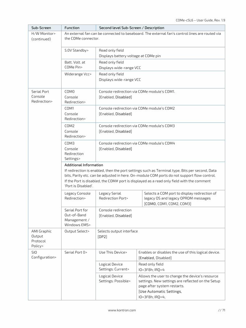
COMe-cSL6 – User Guide, Rev. 1.9
www.kontron.com // 71
Sub-Screen Function Second level Sub-Screen / Description
H/W Monitor> (continued)
An external fan can be connected to baseboard. The external fan’s control lines are routed via the COMe connector.
5.0V Standby> Read only field Displays battery voltage at COMe pin
Batt. Volt. at COMe Pin>
Read only field Displays wide-range VCC
Widerange Vcc> Read only field Displays wide-range VCC
Serial Port Console Redirection>
COM0 Console Redirection>
Console redirection via COMe module’s COM1. [Enabled, Disabled]
COM1 Console Redirection>
Console redirection via COMe module’s COM2 [Enabled, Disabled]
COM2 Console Redirection>
Console redirection via COMe module’s COM3 [Enabled, Disabled]
COM3 Console Redirection Settings>
Console redirection via COMe module’s COM4 [Enabled, Disabled]
Additional Information If redirection is enabled, then the port settings such as Terminal type, Bits per second, Data bits, Parity etc. can be adjusted in here. On-module COM ports do not support flow control. If the Port is disabled, the COM# port is displayed as a read only field with the comment ‘Port is Disabled’.
Legacy Console Redirection>
Legacy Serial Redirection Port>
Selects a COM port to display redirection of legacy OS and legacy OPROM messages [COM0, COM1, COM2, COM3]
Serial Port for Out-of-Band Management / Windows EMS>
Console redirection [Enabled, Disabled]
AMI Graphic Output Protocol Policy>
Output Select> Selects output interface [DP2]
SIO Configuration>
Serial Port 0>
Use This Device> Enables or disables the use of this logical device. [Enabled, Disabled]
Logical Device Settings: Current>
Read only field IO=3F8h; IRQ=4
Logical Device Settings: Possible>
Allows the user to change the device’s resource settings. New settings are reflected on the Setup page after system restarts. [Use Automatic Settings, IO=3F8h; IRQ=4,
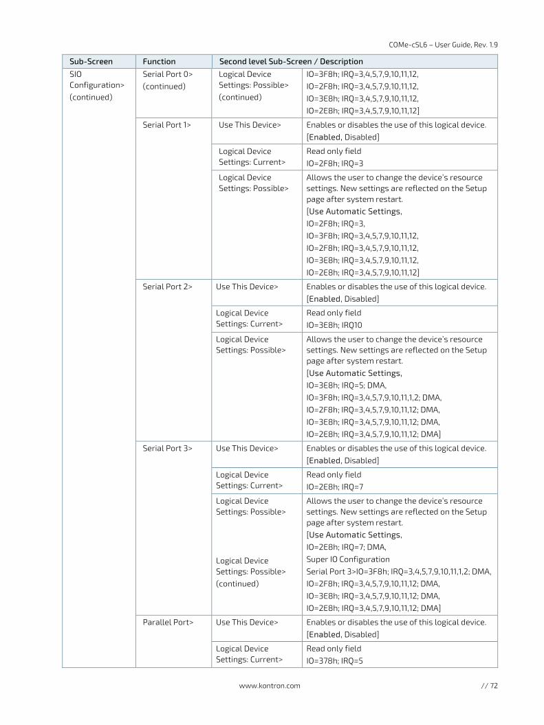
COMe-cSL6 – User Guide, Rev. 1.9
www.kontron.com // 72
Sub-Screen Function Second level Sub-Screen / Description
SIO Configuration> (continued)
Serial Port 0> (continued)
Logical Device Settings: Possible> (continued)
IO=3F8h; IRQ=3,4,5,7,9,10,11,12, IO=2F8h; IRQ=3,4,5,7,9,10,11,12, IO=3E8h; IRQ=3,4,5,7,9,10,11,12, IO=2E8h; IRQ=3,4,5,7,9,10,11,12]
Serial Port 1>
Use This Device> Enables or disables the use of this logical device. [Enabled, Disabled]
Logical Device Settings: Current>
Read only field IO=2F8h; IRQ=3
Logical Device Settings: Possible>
Allows the user to change the device’s resource settings. New settings are reflected on the Setup page after system restart. [Use Automatic Settings, IO=2F8h; IRQ=3, IO=3F8h; IRQ=3,4,5,7,9,10,11,12, IO=2F8h; IRQ=3,4,5,7,9,10,11,12, IO=3E8h; IRQ=3,4,5,7,9,10,11,12, IO=2E8h; IRQ=3,4,5,7,9,10,11,12]
Serial Port 2>
Use This Device> Enables or disables the use of this logical device. [Enabled, Disabled]
Logical Device Settings: Current>
Read only field IO=3E8h; IRQ10
Logical Device Settings: Possible>
Allows the user to change the device’s resource settings. New settings are reflected on the Setup page after system restart. [Use Automatic Settings, IO=3E8h; IRQ=5; DMA, IO=3F8h; IRQ=3,4,5,7,9,10,11,1,2; DMA, IO=2F8h; IRQ=3,4,5,7,9,10,11,12; DMA, IO=3E8h; IRQ=3,4,5,7,9,10,11,12; DMA, IO=2E8h; IRQ=3,4,5,7,9,10,11,12; DMA]
Serial Port 3>
Use This Device> Enables or disables the use of this logical device. [Enabled, Disabled]
Logical Device Settings: Current>
Read only field IO=2E8h; IRQ=7
Logical Device Settings: Possible> Logical Device Settings: Possible> (continued)
Allows the user to change the device’s resource settings. New settings are reflected on the Setup page after system restart. [Use Automatic Settings, IO=2E8h; IRQ=7; DMA, Super IO Configuration Serial Port 3>IO=3F8h; IRQ=3,4,5,7,9,10,11,1,2; DMA, IO=2F8h; IRQ=3,4,5,7,9,10,11,12; DMA, IO=3E8h; IRQ=3,4,5,7,9,10,11,12; DMA, IO=2E8h; IRQ=3,4,5,7,9,10,11,12; DMA]
Parallel Port>
Use This Device> Enables or disables the use of this logical device. [Enabled, Disabled]
Logical Device Settings: Current>
Read only field IO=378h; IRQ=5
COMe-cSL6 – User Guide, Rev. 1.9
www.kontron.com // 73
Sub-Screen Function Second level Sub-Screen / Description
SIO Configuration> (continued)
Parallel Port> (continued)
Logical Device Settings: Possible>
Allows the user to change the device’s resource settings. New settings are reflected on the Setup page after system restart. [Use Automatic Settings, IO=378h; IRQ=5, IO=378h; IRQ=5,6,7,9,10,11,12, IO=278h; IRQ=5,6,7,9,10,11,12, IO=3BCh; IRQ=5,6,7,9,10,11,12]
Additional Information SIO: Warning: Logical Devices state on the left side of the control reflects the current logical device state. Changes made during the setup session are shown after restarting the system. The SIO Configuration menu enables all available serial interfaces to be configured. The module-based serial interfaces always appear as COM1 and COM2. COM 1 and COM 2 can be treated as 16550-compatible legacy COM interfaces at the standard I/O addresses and are based in the on-module CPLD. Note: Hardware flow control is not supported. Optionally, If the baseboard contains an activated SuperIO of the type Winbond 83627, then its serial interfaces are added to the system as COM3 and COM4. COM3 and COM4 IRQ and I/O addresses are configurable in this menu, too. Although the chipset internal COMs are not supported due to technical constraints their driver must be installed. Installing the driver does not mean that these serial interfaces are useable.
PCI Subsystem Settings>
PCI Latency Timer>
Displays value to be programmed into the PCI latency timer register as PCI Bus Clocks. [32, 64, 96, 128, 160, 192, 224, 248]
PCI-X Latency Timer>
Displays value to be programmed into the PCI latency timer register as PCI Bus Clocks. [32, 64, 96, 128, 160, 192, 224, 248]
VGA Palette Snoop>
Enables or disables VGA palette register snooping [Enabled, Disabled]
PERR# Generation>
Enables or disables PCI device to generate PERR# [Enabled, Disabled]
SERR# Generation>
Enables or disables PCI device to generate SERR# [Enabled, Disabled]
Above 4G Decoding>
Enables or disables decoding in Address Space above ‘4G’ for 64 bit capable devices. Note: Only if system supports 64 bit PCI decoding. [Enabled, Disabled]
PCI Hot-Plug Settings>
BIOS Hot –Plug Support>
If enabled, BIOS builds are allowed in hot-plug support. Use this feature if OS does not support PCI express and SHPC hot-plug natively. [Enabled, Disabled]
PCI Buses Padding>
Padd PCI Buses behind the bridge for hot-plug [Disabled, 1, 2, 3, 4, 5]
I/O Resources Padding>
Padd PCI resources behind the bridge for hot-plug [Disabled, 4 k, 8 k, 16 k, 32 k]
MMIO 32 bit Resources Padding>
Padd PCI MMIO 32 bit resources behind the bridge for hot-plug. [Disabled, 1 M, 2 M, 4 M, 8 M, 16 M, 32 M, 64 M, 128 M]
COMe-cSL6 – User Guide, Rev. 1.9
www.kontron.com // 74
Sub-Screen Function Second level Sub-Screen / Description
PCI Subsystem Settings> (continued)
PCI Hot-Plug Settings> (continued)
PFMMIO 32 bit Resources Padding>
Padd PCI MMIO 32 bit pre-fetchable resources behind the bridge for hot-plug. [Disabled, 1 M, 2 M, 4 M, 8 M, 16 M, 32 M, 64 M, 128 M]
Network Stack Configuration>
Network Stack> If UEFI network stack is enabled, the Ethernet chip is active. [Enabled, Disabled]
CSM Configuration>
CSM Support>
Enables or disables CSM Support If enabled, the CSM details can be changed. Below ‘Option ROM Execution’ are ‘Network, ‘Storage’, ’Video’ and ‘Other PCI devices’. Note: ‘Network’ must be changed to’ Legacy’ for legacy boot. (Default setting is ‘Do not launch’). [Enabled, Disabled]
Additional Information CSM: Compatibility Support Module (CSM) configuration is important for legacy operating systems By default, CSM is disabled for modern OS such as Windows 8, 10 and Linux. If a legacy OS is used or a Windows or Linux system is run in legacy mode then this menu allows for detailed option settings. Note, a change in settings only come into effect after the next restart. Therefore, to be able to use the actualized settings, it is recommended to save and exit setup and re-enter. The ‘Optional ROM Execution’ settings require special care. Any OS using an INT10 based display output needs the ‘Video’ option set to ‘Legacy’, in the same way that PXE boot needs ‘Network’ ‘Optional ROM’ to be set to ‘Legacy’.
NVMe Configuration>
Read only field Acts as a message showing the connected NVMe (Non-Volatile memory PCIe) devices. [NO NVME Device Found]
Switchable Graphics>
Read only field If no switchable graphics cards are connected to the system, Set the primary display switch to SG to use switchable graphics cards. [Muxless]
USB Configuration>
Read only fields USB Configuration, UBS Module Version, USB Controllers, and USB devices
Legacy USB Support>
Enable- Supports legacy USB Auto– disables legacy support, if no USB devices are connected Disable-keeps USB devices available for EFI applications only [Enabled, Disabled, Auto]
XHCI Hand-off> XHCI ownership change claimed by XHCI driver. Note: this is a work around for OS(s) without XHCI hand-off support. [Enabled, Disabled]
USB Mass Storage Driver Support>
Enables or disables USB mass storage driver support [Enabled, Disabled]
Port 60/64 Emulation>
Enables I/O port 60h/64h emulation support Note: Enable for USB keyboard legacy support for non-USB aware OS(s). [Enabled, Disabled]
USB Transfer Time-out>
Displays timeout value for control, bulk and interrupt transfers [1 sec, 5 sec, 10 sec, 20 sec]
Device Reset Time-out>
Displays USB mass storage device start unit command time-out [10 sec, 20 sec, 30 sec, 40 sec]
COMe-cSL6 – User Guide, Rev. 1.9
www.kontron.com // 75
Sub-Screen Function Second level Sub-Screen / Description
USB Configuration> (continued)
3.
Device Power-up Delay>
Displays maximum time taken for the device to report itself to the host properly. Auto uses the default value for a root port the default is 100 ms and for a hub port the delay is taken from Hub descriptor. [Auto, Manual]
COMe-cSL6 – User Guide, Rev. 1.9
www.kontron.com // 76
Chipset Setup Menu
On entering the Chipset Setup menu, the screen lists two sub-screen options:
System Agent (previously Northbridge)
PCH-IO (previously Southbridge)
6.2.3.1. Chipset > System Agent Configuration
Figure 7: Chipset>System Agent Configuration Initial Screen
The following table shows the System Agent Configuration sub-screens and functions, and describes the content. Default settings are bold.
Table 37: Chipset Setup Menu Sub-screens and Functions
Function Second level Sub-Screen / Description
SA PCIe Code Version>
Read only field States versions of the code
VT-d > Read only field States if virtualization is supported
Graphics Configuration>
Graphics Turbo IMON Current>
Displays graphics turbo IMON supported values (14-31)
Skip Scanned for External GfX Card>
If enabled, no scan is made for external Gfx cards on PEG or PCH PCIE ports. Default setting is disabled. [Enabled, Disabled]
COMe-cSL6 – User Guide, Rev. 1.9
www.kontron.com // 77
Function Second level Sub-Screen / Description
Graphics Configuration> (continued)
Primary Display>
Selects which of IGFX / PEG /PCI graphics devices should be the primary graphics device or SG for switchable Gfx.
[Auto, IGFX, PEG, PCI, SG]
Select PCIE Card>
Selects the card used on the platform Auto: skip GPIO based power enable to dGPU Elk Creek 4: DGPU power enable = active low PEG Eval. : DGPU power enable = active high [Auto, Elk Creek 4, PEG Eval.]
Internal Graphics>
To keep IGFX enabled based on setup options [Auto, Enabled, Disabled]
GTT Size> Select GTT size [2 MB, 4 MB, 8 MB]
Aperture Size> Selects Aperture size. Note: above 4GB MMIO, BIOS assignment is automatically enabled when selecting 2048 MB aperture. Note: To use this feature disable CSM support. [128 MB, 256 MB, 512 MB, 1024 MB, 2048 MB]
DVMT Pre-Allocated>
Select DVMT 5.0 pre-allocated (fixed) graphics memory size used by internal graphics device. [0 M, 32 M……..60 M]
DVMT Total Gfx Mem>
Select DVMT 5.0 total graphics memory size used by internal graphics device [256 M, 128 M, Max.]
Gfx Low Power Mode>
Used for SFF only [Enabled, Disabled]
VDD Enable> Enables or disables VDD forcing in BIOS [Enabled, Disabled]
HDCP Support> HDCP provisioning BIOS support [Enabled, Disabled]
Algorithm> HDCP re-encryption flow [One-time, Periodic]
PM Support> Enables or disables PM support [Enabled, Disabled]
PAVP Enable> Enables or disables PAVP [Enabled, Disabled]
Cdynmax Clamping Enable>
Enables or disabled cdynmax clamping [Enabled, Disabled]
Cd Clock Frequency>
Selects highest Cd clock frequency supported by platform [337.5 MHz, 450 MHz, 540 MHz, 675 MHz]
IGD Configuration>
Read Only field LVS EEPROM data, Data format, Resolution; Color depth, and Channel count Note : Optionally visible if a LVS display is use in auto mode or if LFP has been set manually
COMe-cSL6 – User Guide, Rev. 1.9
www.kontron.com // 78
Function Second level Sub-Screen / Description
Graphics Configuration> (continued)
IGD Configuration> (continued)
IGD- Boot Type>
Selects the video device activated during post. If external graphics are present, this has no effect. [Auto, EFP, LFP, EFP2]
LFP Panel Type>
Selects panel type connected to eDP port are native eDP or LVDS via bridge device. This switch depends on the module’s hardware option. [LVDS, eDP ]
Backlight Control>
Backlight control setting [None/external, PWM, PWM Inverted, I2C]
PWM Frequency>
Sets LCD backlight PWM frequency [200 Hz, 400 Hz, 1 kHz, 2 kHz, 4 kHz, 8 kHz, 20 kHz, 40 kHz]
Backlight Value>
Sets LCD backlight brightness Range : (0-255)
LVDS Clock Center Spreading>
Selects LVDS clock frequency center spreading depth [No Spreading]
EFP1 Type> Selects the integrated HDMI/Display port configuration with external connectors. [Display Port Only, DP with HDMI/DVI, DMI/DVI]]
EFP1 LSPCON> Enables or disables HDMI2.0 feature level shifter/protocol converter. [Enabled, Disabled]
EFP2 Type> Selects the integrated HDMI/Display port configuration with external connectors. [Display Port Only, DP with HDMI/DVI, HDMI/DVI]
EFP2 LSPCON> Enables or disables HDMI2.0 feture level shifter/protocol converter. [Enabled, Disabled]
Mode Persistence>
Mode persistence [Enabled, Disabled]
Center Mode> Selects display device to be centered [Enabled, Disabled]
Memory Configuration>
Read only field Memory RC version, Memory frequency, Memory timings (tCL, tRCD, tRP, tRAS), Channel 0 slot 0, Size, Channel 0 slot 1, Channel 1 slot 0 and Channel 1, slot 1.
Max TOLUD> Sets maximum TOLUD value. Dynamic assignment adjustsTOLUD automatically, based on largest MMIO length of installed graphic controller. [Dynamic, 1 GB, 1.25 GB………3.25 GB, 3.5 GB]
VT-d> VT-d capability [Enabled, Disabled]
COMe-cSL6 – User Guide, Rev. 1.9
www.kontron.com // 79
6.2.3.2. Chipset > PCH-IO Configuration
Figure 8: PCH-IO Configuration Menu Initial Screen
The following table shows the PCH-IO sub-screens and functions, and describes the content. Default options are bold. Some functions include additional information.
Table 38: Chipset Set > PCH-IO Configuration Sub-screens and Functions
Function Second level Sub-Screen / Description
PCI Express Configuration>
PCI Express Clock Gating>
Enables or disables PCI Express clock gating for each root port [Enabled, Disabled]
Legacy IO Low Latency>
Set to enable the latency of legacy IO as some systems require lower IO latency irrespective of power. This is a tradeoff between power and IO latency. Auto is equal to POR Setting. [Enabled, Disabled]
DMI Link ASPM Control>
Enables or disables control of Active State Power Management on SA side of DMI link [Enabled, Disabled]
PCIE Port Assigned to LAN>
Read Only file This values is always 5. (5)
Port8xh Decode> Enables or disables PCI express port 8xh decode [Enabled, Disabled]
Peer Memory Write Enable>
Enables or disables peer memory write [Enabled, Disabled]
COMe-cSL6 – User Guide, Rev. 1.9
www.kontron.com // 80
Function Second level Sub-Screen / Description
PCI Express Configuration> (continued)
Compliance Test Mode>
Enable when using compliance load board
[Enabled, Disabled]
PCIe-USB Glitch W/A>
PCIe-USB Glitch work around for bad USB device(s) connected behind PCIE/PEG port [Enabled, Disabled]
PCIe Function Swap>
Disable prevents PCIO Root port function swap. If any function other than 0th is enabled, 0th becomes visible. [Enabled, Disabled]
PCI Root Port 1 (COMe PCIe#0)> or PCI Root Port 2 (COMe PCIe#1)> or PCI Root Port 3 (COMe PCIe#2)> or PCI Root Port 4 (COMe PCIe#3)> or PCI Root Port 6 (COMe PCIe#4)> or PCI Root Port 9 (COMe PEG#0)>
PCIe Root Port[#]>
Controls the PCI Express root ports [1, 2, 3, 4, 6, 9] Note: this uses the CPU enumeration
[Enabled, disabled]
Topology> Identifies the SATA Topology [Unknown, x1, x4, SATA Express, M.2.]
ASPM> Sets ASPM level: Auto is BIOS auto configuration, Force Los forces all links to Los state and Disable disables the ASPM. [Auto, LOsL1, L1, LOs, Disabled]
L1 Substates> PCI Express L1 substrates settings. [Disabled, L1.1, L1.2, L1.1 &L1.2]
Gen3 Eq Phase3 method>
PCIe Gen3 Equalization phase 3 method [Hardware, Static Coeff., Software Search]
UPTP> Upstream Port Transmitter Preset
DPTP> Downstream Port Transmitter Preset
ACS> Access Control Service Extended Capability [Enabled, Disabled]
URR> PCI Express unsupported request reporting [Enabled, Disabled]
FER> PCI Express device fatal error reporting [Enabled, Disabled]
NFER> PCI Express device non-fatal error reporting [Enabled, Disabled]
CER> PCI Express device correctable error reporting [Enabled, Disabled]
CT0> PCIe Express Completion timer (T0) [Enabled, Disabled]
SEFE> Root PCI Express System Error on Fatal Error [Enabled, Disabled]
SENFE> Root PCI Express System Error on non-Fatal Error [Enabled, Disabled]
SECE> Root PCI Express System Error on correctable error [Enabled, Disabled]
PME SCI> PCI Express PME SCI [Enabled, Disabled]
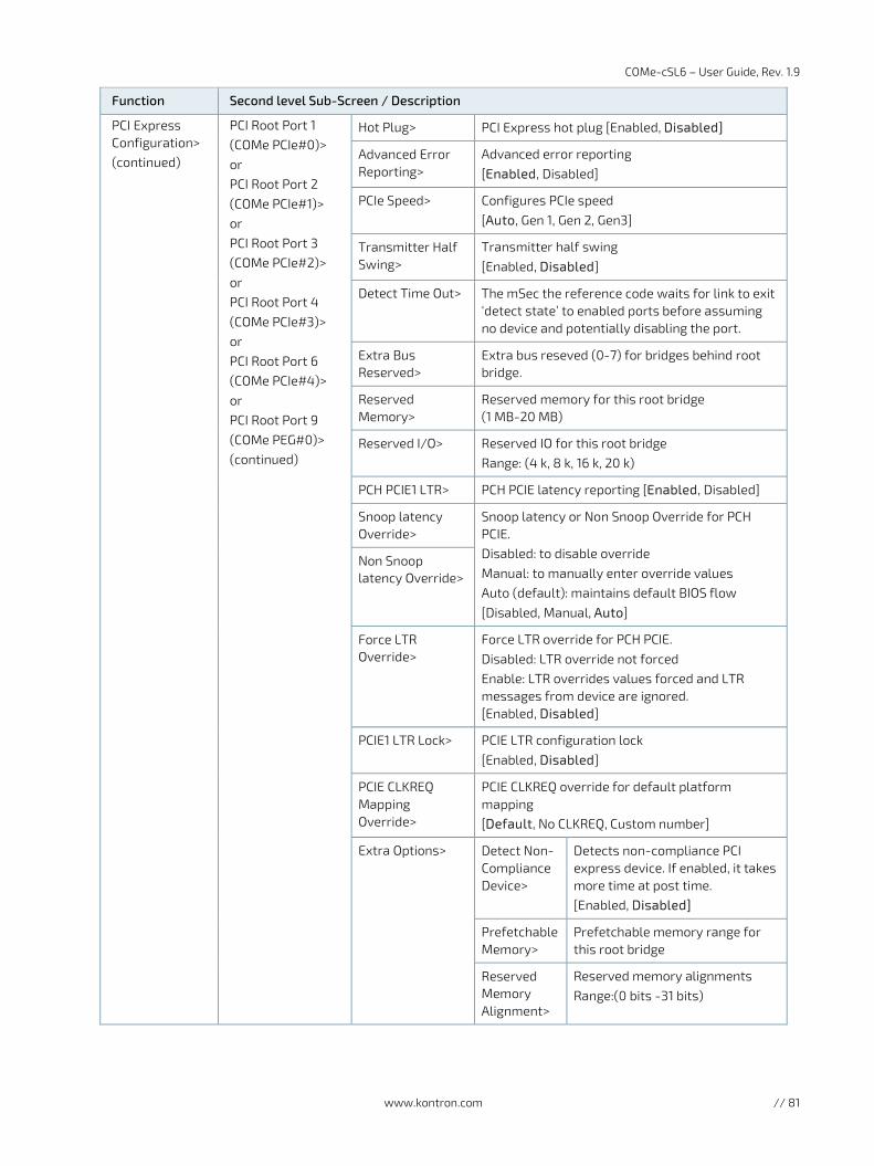
COMe-cSL6 – User Guide, Rev. 1.9
www.kontron.com // 81
Function Second level Sub-Screen / Description
PCI Express Configuration> (continued)
PCI Root Port 1 (COMe PCIe#0)> or PCI Root Port 2 (COMe PCIe#1)> or PCI Root Port 3 (COMe PCIe#2)> or PCI Root Port 4 (COMe PCIe#3)> or PCI Root Port 6 (COMe PCIe#4)> or PCI Root Port 9 (COMe PEG#0)> (continued)
Hot Plug> PCI Express hot plug [Enabled, Disabled]
Advanced Error Reporting>
Advanced error reporting [Enabled, Disabled]
PCIe Speed> Configures PCIe speed [Auto, Gen 1, Gen 2, Gen3]
Transmitter Half Swing>
Transmitter half swing [Enabled, Disabled]
Detect Time Out> The mSec the reference code waits for link to exit ‘detect state’ to enabled ports before assuming no device and potentially disabling the port.
Extra Bus Reserved>
Extra bus reseved (0-7) for bridges behind root bridge.
Reserved Memory>
Reserved memory for this root bridge (1 MB-20 MB)
Reserved I/O> Reserved IO for this root bridge Range: (4 k, 8 k, 16 k, 20 k)
PCH PCIE1 LTR> PCH PCIE latency reporting [Enabled, Disabled]
Snoop latency Override>
Snoop latency or Non Snoop Override for PCH PCIE. Disabled: to disable override Manual: to manually enter override values Auto (default): maintains default BIOS flow [Disabled, Manual, Auto]
Non Snoop latency Override>
Force LTR Override>
Force LTR override for PCH PCIE. Disabled: LTR override not forced Enable: LTR overrides values forced and LTR messages from device are ignored. [Enabled, Disabled]
PCIE1 LTR Lock> PCIE LTR configuration lock [Enabled, Disabled]
PCIE CLKREQ Mapping Override>
PCIE CLKREQ override for default platform mapping [Default, No CLKREQ, Custom number]
Extra Options>
Detect Non-Compliance Device>
Detects non-compliance PCI express device. If enabled, it takes more time at post time. [Enabled, Disabled]
Prefetchable Memory>
Prefetchable memory range for this root bridge
Reserved Memory Alignment>
Reserved memory alignments Range:(0 bits -31 bits)
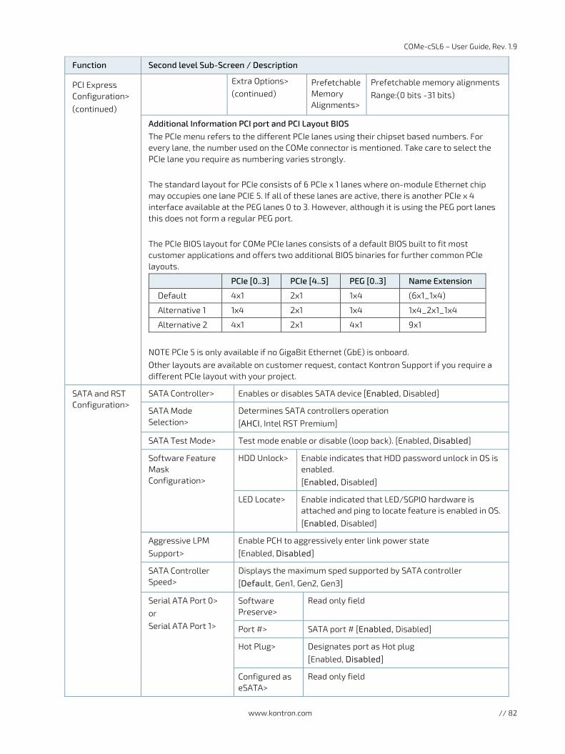
COMe-cSL6 – User Guide, Rev. 1.9
www.kontron.com // 82
Function Second level Sub-Screen / Description
PCI Express Configuration> (continued)
Extra Options> (continued)
Prefetchable Memory Alignments>
Prefetchable memory alignments Range:(0 bits -31 bits)
Additional Information PCI port and PCI Layout BIOS The PCIe menu refers to the different PCIe lanes using their chipset based numbers. For every lane, the number used on the COMe connector is mentioned. Take care to select the PCIe lane you require as numbering varies strongly. The standard layout for PCIe consists of 6 PCIe x 1 lanes where on-module Ethernet chip may occupies one lane PCIE 5. If all of these lanes are active, there is another PCIe x 4 interface available at the PEG lanes 0 to 3. However, although it is using the PEG port lanes this does not form a regular PEG port. The PCIe BIOS layout for COMe PCIe lanes consists of a default BIOS built to fit most customer applications and offers two additional BIOS binaries for further common PCIe layouts.
PCIe [0..3] PCIe [4..5] PEG [0..3] Name Extension
Default 4x1 2x1 1x4 (6x1_1x4)
Alternative 1 1x4 2x1 1x4 1x4_2x1_1x4
Alternative 2 4x1 2x1 4x1 9x1
NOTE PCIe 5 is only available if no GigaBit Ethernet (GbE) is onboard. Other layouts are available on customer request, contact Kontron Support if you require a different PCIe layout with your project.
SATA and RST Configuration>
SATA Controller> Enables or disables SATA device [Enabled, Disabled]
SATA Mode Selection>
Determines SATA controllers operation [AHCI, Intel RST Premium]
SATA Test Mode> Test mode enable or disable (loop back). [Enabled, Disabled]
Software Feature Mask Configuration>
HDD Unlock> Enable indicates that HDD password unlock in OS is enabled. [Enabled, Disabled]
LED Locate> Enable indicated that LED/SGPIO hardware is attached and ping to locate feature is enabled in OS. [Enabled, Disabled]
Aggressive LPM Support>
Enable PCH to aggressively enter link power state [Enabled, Disabled]
SATA Controller Speed>
Displays the maximum sped supported by SATA controller [Default, Gen1, Gen2, Gen3]
Serial ATA Port 0> or Serial ATA Port 1>
Software Preserve>
Read only field
Port #> SATA port # [Enabled, Disabled]
Hot Plug> Designates port as Hot plug [Enabled, Disabled]
Configured as eSATA>
Read only field
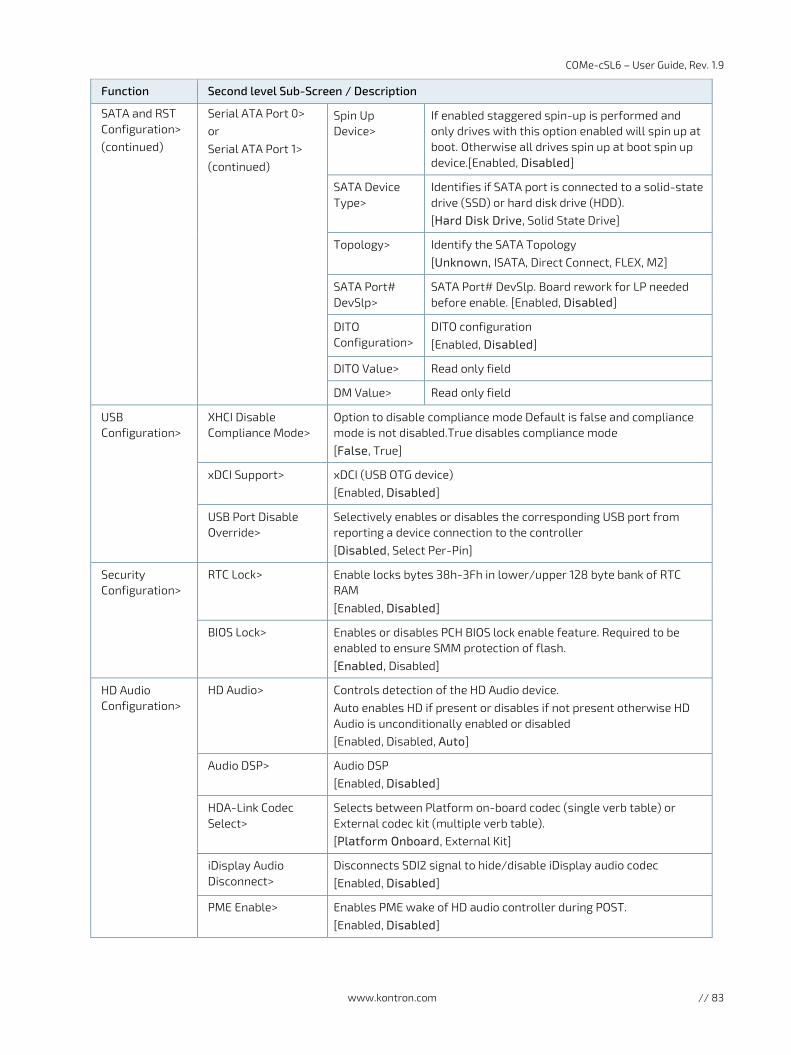
COMe-cSL6 – User Guide, Rev. 1.9
www.kontron.com // 83
Function Second level Sub-Screen / Description
SATA and RST Configuration> (continued)
Serial ATA Port 0> or Serial ATA Port 1> (continued)
Spin Up Device>
If enabled staggered spin-up is performed and only drives with this option enabled will spin up at boot. Otherwise all drives spin up at boot spin up device.[Enabled, Disabled]
SATA Device Type>
Identifies if SATA port is connected to a solid-state drive (SSD) or hard disk drive (HDD). [Hard Disk Drive, Solid State Drive]
Topology> Identify the SATA Topology [Unknown, ISATA, Direct Connect, FLEX, M2]
SATA Port# DevSlp>
SATA Port# DevSlp. Board rework for LP needed before enable. [Enabled, Disabled]
DITO Configuration>
DITO configuration [Enabled, Disabled]
DITO Value> Read only field
DM Value> Read only field
USB Configuration>
XHCI Disable Compliance Mode>
Option to disable compliance mode Default is false and compliance mode is not disabled.True disables compliance mode [False, True]
xDCI Support> xDCI (USB OTG device) [Enabled, Disabled]
USB Port Disable Override>
Selectively enables or disables the corresponding USB port from reporting a device connection to the controller [Disabled, Select Per-Pin]
Security Configuration>
RTC Lock> Enable locks bytes 38h-3Fh in lower/upper 128 byte bank of RTC RAM [Enabled, Disabled]
BIOS Lock> Enables or disables PCH BIOS lock enable feature. Required to be enabled to ensure SMM protection of flash. [Enabled, Disabled]
HD Audio Configuration>
HD Audio> Controls detection of the HD Audio device. Auto enables HD if present or disables if not present otherwise HD Audio is unconditionally enabled or disabled [Enabled, Disabled, Auto]
Audio DSP> Audio DSP [Enabled, Disabled]
HDA-Link Codec Select>
Selects between Platform on-board codec (single verb table) or External codec kit (multiple verb table). [Platform Onboard, External Kit]
iDisplay Audio Disconnect>
Disconnects SDI2 signal to hide/disable iDisplay audio codec [Enabled, Disabled]
PME Enable> Enables PME wake of HD audio controller during POST. [Enabled, Disabled]
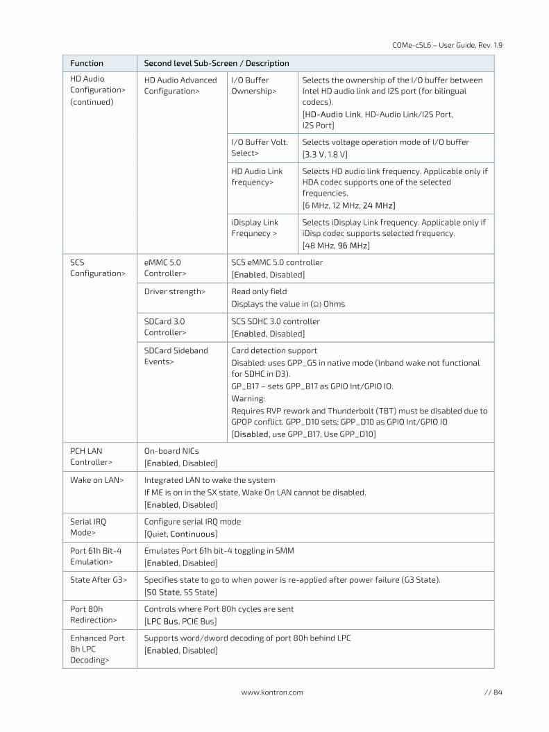
COMe-cSL6 – User Guide, Rev. 1.9
www.kontron.com // 84
Function Second level Sub-Screen / Description
HD Audio Configuration> (continued)
HD Audio Advanced Configuration>
I/O Buffer Ownership>
Selects the ownership of the I/O buffer between Intel HD audio link and I2S port (for bilingual codecs). [HD-Audio Link, HD-Audio Link/I2S Port, I2S Port]
I/O Buffer Volt. Select>
Selects voltage operation mode of I/O buffer [3.3 V, 1.8 V]
HD Audio Link frequency>
Selects HD audio link frequency. Applicable only if HDA codec supports one of the selected frequencies. [6 MHz, 12 MHz, 24 MHz]
iDisplay Link Frequnecy >
Selects iDisplay Link frequency. Applicable only if iDisp codec supports selected frequency. [48 MHz, 96 MHz]
SCS Configuration>
eMMC 5.0 Controller>
SCS eMMC 5.0 controller [Enabled, Disabled]
Driver strength> Read only field
Displays the value in (Ω)Ohms
SDCard 3.0 Controller>
SCS SDHC 3.0 controller [Enabled, Disabled]
SDCard Sideband Events>
Card detection support Disabled: uses GPP_G5 in native mode (Inband wake not functional for SDHC in D3). GP_B17 – sets GPP_B17 as GPIO Int/GPIO IO. Warning: Requires RVP rework and Thunderbolt (TBT) must be disabled due to GPOP conflict. GPP_D10 sets: GPP_D10 as GPIO Int/GPIO IO [Disabled, use GPP_B17, Use GPP_D10]
PCH LAN Controller>
On-board NICs [Enabled, Disabled]
Wake on LAN> Integrated LAN to wake the system If ME is on in the SX state, Wake On LAN cannot be disabled. [Enabled, Disabled]
Serial IRQ Mode>
Configure serial IRQ mode [Quiet, Continuous]
Port 61h Bit-4 Emulation>
Emulates Port 61h bit-4 toggling in SMM [Enabled, Disabled]
State After G3> Specifies state to go to when power is re-applied after power failure (G3 State). [S0 State, S5 State]
Port 80h Redirection>
Controls where Port 80h cycles are sent [LPC Bus, PCIE Bus]
Enhanced Port 8h LPC Decoding>
Supports word/dword decoding of port 80h behind LPC [Enabled, Disabled]
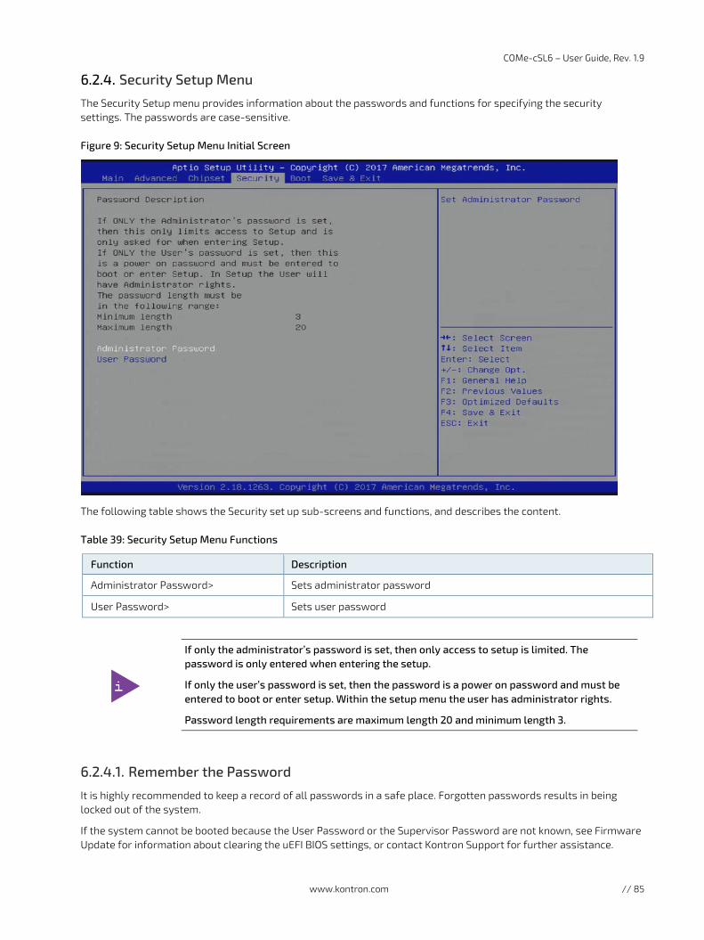
COMe-cSL6 – User Guide, Rev. 1.9
www.kontron.com // 85
Security Setup Menu
The Security Setup menu provides information about the passwords and functions for specifying the security settings. The passwords are case-sensitive.
Figure 9: Security Setup Menu Initial Screen
The following table shows the Security set up sub-screens and functions, and describes the content.
Table 39: Security Setup Menu Functions
Function Description
Administrator Password> Sets administrator password
User Password> Sets user password
If only the administrator’s password is set, then only access to setup is limited. The password is only entered when entering the setup.
If only the user’s password is set, then the password is a power on password and must be entered to boot or enter setup. Within the setup menu the user has administrator rights.
Password length requirements are maximum length 20 and minimum length 3.
6.2.4.1. Remember the Password
It is highly recommended to keep a record of all passwords in a safe place. Forgotten passwords results in being locked out of the system.
If the system cannot be booted because the User Password or the Supervisor Password are not known, see Firmware Update for information about clearing the uEFI BIOS settings, or contact Kontron Support for further assistance.
COMe-cSL6 – User Guide, Rev. 1.9
www.kontron.com // 86
Boot Setup Menu
The Boot Setup menu lists dynamically generated boot device priority order. The following table shows the Boot set up sub-screens and functions, and describes the content.
Table 40: Boot Setup Menu Functions
Function Description
Setup Prompt Timeout> Sets number of seconds that the firmware will wait before initiating the original default boot selection
Bootup NumLock State> Enables\Disables keyboard NumLock state
Quiet Boot> Enables\disables Quiet Boot
Boot Option #N> (N=1,2,3,…) Displays boot devices
Fast Boot> Enables/disables boot with initialization of a minimal set of devices required to launch active boot option
New Boot Option Policy> Controls placement of new detected UEFI boot option
Save and Exit Setup Menu
The Exit Setup menu provides functions for handling changes made to the uEFI BIOS settings and exiting of the Setup program. The following table shows the Save and Exit set up sub-screens and functions, and describes the content.
Table 41: Save and Exit Setup Menu Functions
Function Description
Save Changes and Exit > Exits system after saving changes
Discard Changes and Exit> Exits system setup without saving changes
Save Changes and Reset> Resets system after saving change
Discard Changes and Reset> Resets system setup without saving changes
Save Changes> Saves changes
Discard Changes> Discards changes
Restore Defaults> Loads standard default values
Save as User Defaults> Saves changes made so far as user defaults
Restore User Defaults> Restores user defaults to all setup options
Boot Override> Lists bootable devices
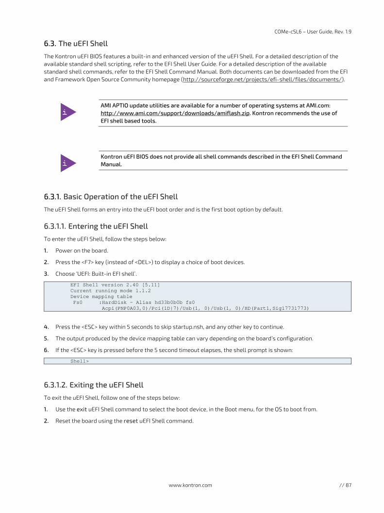
COMe-cSL6 – User Guide, Rev. 1.9
www.kontron.com // 87
6.3. The uEFI Shell
The Kontron uEFI BIOS features a built-in and enhanced version of the uEFI Shell. For a detailed description of the available standard shell scripting, refer to the EFI Shell User Guide. For a detailed description of the available standard shell commands, refer to the EFI Shell Command Manual. Both documents can be downloaded from the EFI and Framework Open Source Community homepage (http://sourceforge.net/projects/efi-shell/files/documents/).
AMI APTIO update utilities are available for a number of operating systems at AMI.com: http://www.ami.com/support/downloads/amiflash.zip. Kontron recommends the use of EFI shell based tools.
Kontron uEFI BIOS does not provide all shell commands described in the EFI Shell Command Manual.
Basic Operation of the uEFI Shell
The uEFI Shell forms an entry into the uEFI boot order and is the first boot option by default.
6.3.1.1. Entering the uEFI Shell
To enter the uEFI Shell, follow the steps below:
1. Power on the board.
2. Press the <F7> key (instead of <DEL>) to display a choice of boot devices.
3. Choose ‘UEFI: Built-in EFI shell’.
EFI Shell version 2.40 [5.11] Current running mode 1.1.2 Device mapping table Fs0 :HardDisk - Alias hd33b0b0b fs0 Acpi(PNP0A03,0)/Pci(1D|7)/Usb(1, 0)/Usb(1, 0)/HD(Part1,Sig17731773)
4. Press the <ESC> key within 5 seconds to skip startup.nsh, and any other key to continue.
5. The output produced by the device mapping table can vary depending on the board’s configuration.
6. If the <ESC> key is pressed before the 5 second timeout elapses, the shell prompt is shown:
Shell>
6.3.1.2. Exiting the uEFI Shell
To exit the uEFI Shell, follow one of the steps below:
1. Use the exit uEFI Shell command to select the boot device, in the Boot menu, for the OS to boot from.
2. Reset the board using the reset uEFI Shell command.
COMe-cSL6 – User Guide, Rev. 1.9
www.kontron.com // 88
6.4. uEFI Shell Scripting
Startup Scripting
If the <ESC> key is not pressed and the timeout has run out then the uEFI Shell tries to execute some startup scripts automatically. It searches for scripts and executes them in the following order:
1. Initially, searches for Kontron flash-stored startup script.
2. If there is no Kontron flash-stored startup script present, then the uEFI-specified startup.nsh script is used. This script must be located on the root of any of the attached FAT formatted disk drive.
3. If none of the startup scripts are present or the startup script terminates then the default boot order is continued.
Create a Startup Script
Startup scripts can be created using the uEFI Shell built-in editor edit or under any OS with a plain text editor of your choice. To create a startup shell script, simply save the script on the root of any FAT-formatted drive attached to the system. To copy the startup script to the flash, use the kBootScript uEFI Shell command.
In case there is no mass storage device attached, the startup script can be generated in a RAM disk and stored in the SPI boot flash using the kRamdisk uEFI Shell command.
Examples of Startup Scripts
6.4.3.1. Execute Shell Script on Other Harddrive
This example (startup.nsh) executes the shell script named bootme.nsh located in the root of the first detected disc drive (fs0).
fs0: bootme.nsh
COMe-cSL6 – User Guide, Rev. 1.9
www.kontron.com // 89
6.5. Firmware Update
Firmware updates are typically delivered as a ZIP archive containing only the firmware images. The content of the archive with the directory structure must be copied onto a data storage device with FAT partition.
Updating Procedure
BIOS can be updated with the Intel tool fpt.efi using the procedure below:
1. Copy these files to an USB stick.
flash.nsh (if available)
fpt.efi
fparts.txt
csl6r<xxx>.bin (where xxx stands for the version #)
2. Start the system into setup (see Starting the uEFI BIOS).
3. Check that the following entries are set to their default setting:
Advanced > PCH FW Configuration > Firmware update configuration > ME FW Image Re-Flash > Disabled
Advanced > PCH FW Configuration > Firmware update configuration > Local FW Update > Enabled
Then, change the setup option:
Chipset > PCH-IO Configuration > BIOS Security Configuration > BIOS Lock > Disabled
4. Save and exit BIOS setup.
5. On the next start, boot into shell (see Entering the uEFI Shell.)
6. Change to the drive representing the USB stick:
fsx: (x = 0,1,2,etc. represents the USB stick)
and then change to the directory where you copied the flash tool:
cd <your_directory>
7. Start flash.nsh (if available) OR enter:
fpt –SAVEMAC –F csl6r<xxx>.bin
8. Wait until flashing is successful and then power cycle the board.
Do not switch off the power during the flash process! Doing so leaves your module unrecoverable.
Changes made after step 3 above are only effective during the first boot after applying the changes. If you fail to flash during the next boot, you might have to repeat the steps under 3.
Do not forget to apply –SAVEMAC. If SAVEMAC is not applied then your system will lose its system MAC address. If the MAC address is accidentally deleted, contact Kontron Support.
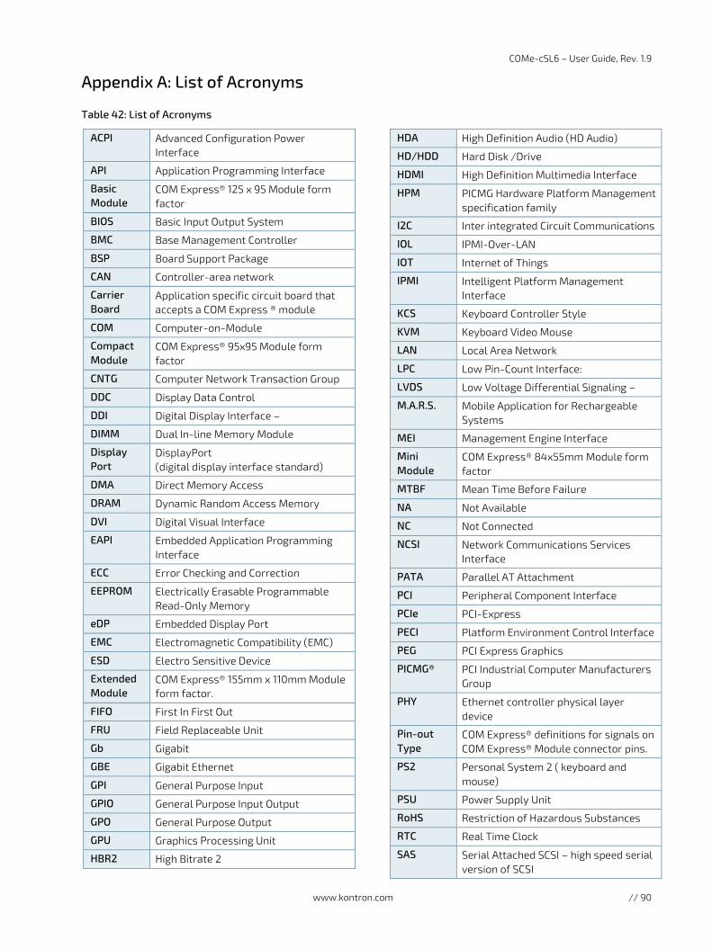
COMe-cSL6 – User Guide, Rev. 1.9
www.kontron.com // 90
Appendix A: List of Acronyms
Table 42: List of Acronyms
ACPI Advanced Configuration Power Interface
API Application Programming Interface
Basic Module
COM Express® 125 x 95 Module form factor
BIOS Basic Input Output System
BMC Base Management Controller
BSP Board Support Package
CAN Controller-area network
Carrier Board
Application specific circuit board that accepts a COM Express ® module
COM Computer-on-Module
Compact Module
COM Express® 95x95 Module form factor
CNTG Computer Network Transaction Group
DDC Display Data Control
DDI Digital Display Interface –
DIMM Dual In-line Memory Module
Display Port
DisplayPort (digital display interface standard)
DMA Direct Memory Access
DRAM Dynamic Random Access Memory
DVI Digital Visual Interface
EAPI Embedded Application Programming Interface
ECC Error Checking and Correction
EEPROM Electrically Erasable Programmable Read-Only Memory
eDP Embedded Display Port
EMC Electromagnetic Compatibility (EMC)
ESD Electro Sensitive Device
Extended Module
COM Express® 155mm x 110mm Module form factor.
FIFO First In First Out
FRU Field Replaceable Unit
Gb Gigabit
GBE Gigabit Ethernet
GPI General Purpose Input
GPIO General Purpose Input Output
GPO General Purpose Output
GPU Graphics Processing Unit
HBR2 High Bitrate 2
HDA High Definition Audio (HD Audio)
HD/HDD Hard Disk /Drive
HDMI High Definition Multimedia Interface
HPM PICMG Hardware Platform Management specification family
I2C Inter integrated Circuit Communications
IOL IPMI-Over-LAN
IOT Internet of Things
IPMI Intelligent Platform Management Interface
KCS Keyboard Controller Style
KVM Keyboard Video Mouse
LAN Local Area Network
LPC Low Pin-Count Interface:
LVDS Low Voltage Differential Signaling –
M.A.R.S. Mobile Application for Rechargeable Systems
MEI Management Engine Interface
Mini Module
COM Express® 84x55mm Module form factor
MTBF Mean Time Before Failure
NA Not Available
NC Not Connected
NCSI Network Communications Services Interface
PATA Parallel AT Attachment
PCI Peripheral Component Interface
PCIe PCI-Express
PECI Platform Environment Control Interface
PEG PCI Express Graphics
PICMG® PCI Industrial Computer Manufacturers Group
PHY Ethernet controller physical layer device
Pin-out Type
COM Express® definitions for signals on COM Express® Module connector pins.
PS2 Personal System 2 ( keyboard and mouse)
PSU Power Supply Unit
RoHS Restriction of Hazardous Substances
RTC Real Time Clock
SAS Serial Attached SCSI – high speed serial version of SCSI
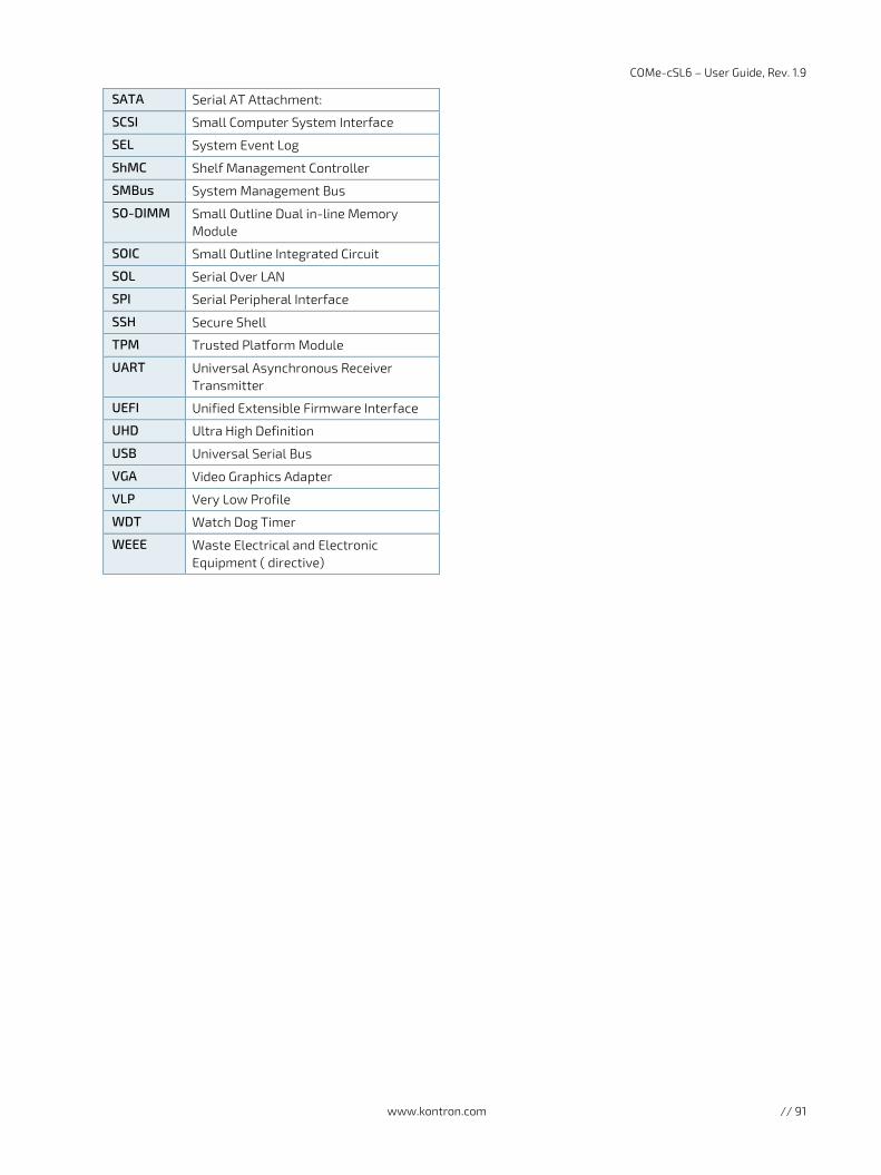
COMe-cSL6 – User Guide, Rev. 1.9
www.kontron.com // 91
SATA Serial AT Attachment:
SCSI Small Computer System Interface
SEL System Event Log
ShMC Shelf Management Controller
SMBus System Management Bus
SO-DIMM Small Outline Dual in-line Memory Module
SOIC Small Outline Integrated Circuit
SOL Serial Over LAN
SPI Serial Peripheral Interface
SSH Secure Shell
TPM Trusted Platform Module
UART Universal Asynchronous Receiver Transmitter
UEFI Unified Extensible Firmware Interface
UHD Ultra High Definition
USB Universal Serial Bus
VGA Video Graphics Adapter
VLP Very Low Profile
WDT Watch Dog Timer
WEEE Waste Electrical and Electronic Equipment ( directive)
COMe-cSL6 – User Guide, Rev. 1.9
www.kontron.com // 92
Global Headquarters
Kontron Europe GmbH
Gutenbergstraße 2 85737 Ismaning Germany Tel.: + 49 821 4086-0 Fax: + 49 821 4086-111 [email protected]
About Kontron – Member of the S&T Group Kontron is a global leader in IoT/Embedded Computing Technology (ECT). As part of the S&T technology group Kontron offers individual solutions in the areas of Internet of Things (IoT) and Industry 4.0 through a combine portfolio of hardware, software and services. With its standard and customized products based on highl reliable state-of-the-art technologies, Kontron provides secure and innovative applications for a wide variet of industries. As a result, customers benefit from accelerated time-to-market, lower total cost of ownership extended product lifecycles and the best fully integrated applications.
For more information, please visit: www.kontron.com