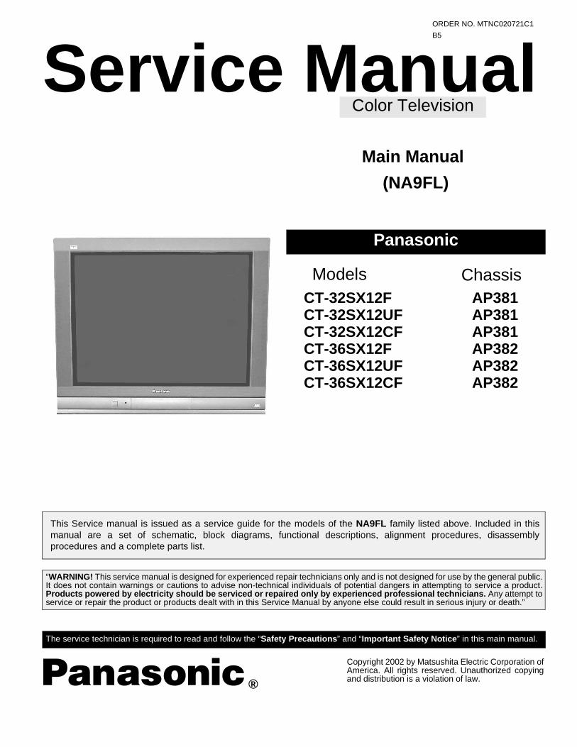
color television (na9fl) main manual
TRANSCRIPT
Panasonic
The service technician is required to read and follow the “Safety Precautions ” and “Important Safety Notice ” in this main manual.
Service ManualColor Television
(NA9FL)
Main Manual
Copyright 2002 by Matsushita Electric Corporation ofAmerica. All rights reserved. Unauthorized copyingand distribution is a violation of law.
“WARNING! This service manual is designed for experienced repair technicians only and is not designed for use by the general public.It does not contain warnings or cautions to advise non-technical individuals of potential dangers in attempting to service a product.Products powered by electricity should be serviced or repaired only by experienced professional technicians. Any attempt toservice or repair the product or products dealt with in this Service Manual by anyone else could result in serious injury or death.”
CT-32SX12F AP381CT-32SX12UF AP381CT-32SX12CF AP381CT-36SX12F AP382CT-36SX12UF AP382CT-36SX12CF AP382
ORDER NO. MTNC020721C1
B5
ChassisModels
This Service manual is issued as a service guide for the models of the NA9FL family listed above. Included in thismanual are a set of schematic, block diagrams, functional descriptions, alignment procedures, disassemblyprocedures and a complete parts list.
®
- 2 -
Important safety noticeSpecial components are used in this television set which are important for safety. These parts are identified on the
schematic diagram by the symbol and printed in BOLD TYPE on the replacement part list. It is essential thatthese critical parts are replaced with the manufacturer’s specified replacement part to prevent x-ray radiation,shock, fire or other hazards. Do not modify the original design without the manufacturer’s permission.
Safety precautionsGeneral guidelinesAn isolation transformer should always be usedduring the servicing of a receiver whose chassis is notisolated from AC power line. Use a transformer ofadequate power rating as this protects the technicianfrom accidents resulting in personal injury fromelectrical shocks. It will also protect the receiver frombeing damaged by accidental shorting that may occurduring servicing.When servicing, observe the original lead dress,especially in the high voltage circuit. Replace alldamaged parts (also parts that show signs ofoverheating.)Always replace protective devices , such asfishpaper, isolation resistors and capacitors, andshields after servicing the receiver. Use onlymanufacturer’s recommended rating for fuses, circuitsbreakers, etc.High potentials are present when this receiver isoperating. Operation of the receiver without the rearcover introduces danger for electrical shock. Servicingshould not be performed by anyone who is notthoroughly familiar with the necessary precautionswhen servicing high-voltage equipment.Extreme care should be practiced when handling thepicture tube . Rough handling may cause it to implodedue to atmospheric pressure. (14.7 lbs per sq. in.). Donot nick or scratch the glass or subject it to any unduepressure. When handling, use safety goggles andheavy gloves for protection. Discharge the picturetube by shorting the anode to chassis ground (not tothe cabinet or to other mounting hardware). Whendischarging connect cold ground (i.e. dag ground lead)to the anode with a well insulated wire or use agrounding probe.Avoid prolonged exposure at close range to unshieldedareas of the picture tube to prevent exposure to x-rayradiation.The test picture tube used for servicing the chassis atthe bench should incorporate safety glass andmagnetic shielding. The safety glass provide shieldingfor the tube viewing area against x-ray radiation as wellas implosion. The magnetic shield limits the x-rayradiation around the bell of the picture tube in additionto the restricting magnetic effects. When using apicture tube test jig for service, ensure that the jig iscapable of handling 40kV without causing x-rayradiation.Before returning a serviced receiver to the owner ,the service technician must thoroughly test the unit toensure that is completely safe to operate. Do not use aline isolation transformer when testing.Leakage current cold checkUnplug the AC cord and connect a jumper between thetwo plug prongs.Measure the resistance between the jumpered AC plugand expose metallic parts such as screwheads,antenna terminals, control shafts, etc. If the exposed
metallic part has a return path to the chassis, thereading should be between 240kΩ and 5.2MΩ. If theexposed metallic part does not have a return path tothe chassis, the reading should be infinite.Leakage current hot check (Fig. 1)
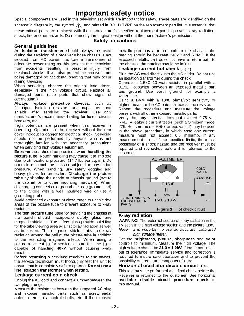
Plug the AC cord directly into the AC outlet. Do not usean isolation transformer during the check.Connect a 1.5kΩ 10 watt resistor in parallel with a0.15µF capacitor between an exposed metallic partand ground. Use earth ground, for example awater pipe.Using a DVM with a 1000 ohms/volt sensitivity orhigher, measure the AC potential across the resistor.Repeat the procedure and measure the voltagepresent with all other exposed metallic parts.Verify that any potential does not exceed 0.75 voltRMS. A leakage current tester (such a Simpson model229, Sencore model PR57 or equivalent) may be usedin the above procedure, in which case any currentmeasure must not exceed 0.5 milliamp. If anymeasurement is out of the specified limits, there is apossibility of a shock hazard and the receiver must berepaired and rechecked before it is returned to thecustomer.
X-ray radiationWARNING: The potential source of x-ray radiation in theTV set is in the high voltage section and the picture tube.Note: It is important to use an accurate, calibrated
high voltage meter.Set the brightness, picture, sharpness and colorcontrols to minimum. Measure the high voltage. Thehigh voltage should be 31.0 ± 1.0kV. If the upper limit isout of tolerance, immediate service and correction isrequired to insure safe operation and to prevent thepossibility of premature component failure.Horizontal oscillator disable circuit testThis test must be performed as a final check before theReceiver is returned to the customer. See horizontaloscillator disable circuit procedure check inthis manual.
0.15µF
COLDWATERPIPE(GROUND)
TO INSTRUMENT’SEXPOSED METALPARTS
1500Ω,10 W
AC VOLTMETER
Figure 1. Hot check circuit
- 3 -
About lead free solder (PbF)
Note: Lead is listed as (Pb) in the periodic table of elements.In the information below, Pb will refer to Lead solder, and PbF will refer to Lead Free Solder.The Lead Free Solder used in our manufacturing process and discussed below is (Sn+Ag+Cu).That is Tin (Sn), Silver (Ag) and (Cu) although other types are available.
This model uses Pb Free solder in it’s manufacture due to environmental conservation issues. Forservice and repair work, we’d suggest the use of Pb free solder as well, although Pb solder may beused.
PCBs manufactured using lead free solder will have the “PbF” or a leaf symbol stamped on theback of PCB.
Caution
• Pb free solder has a higher melting point than standard solder. Typically the meltingpoint is 50 ~ 70 °F (30 ~ 40 °C) higher. Please use a high temperature soldering ironand set it to 700 ± 20 °F (370 ± 10 °C).
• Pb free solder will tend to splash when heated too high (about 1100 °F or 600 °C).If you must use Pb solder, please completely remove all of the Pb free solder on thepins or solder area before applying Pb solder. If this is not practical, be sure to heat thePb free solder until it melts, before applying Pb solder.
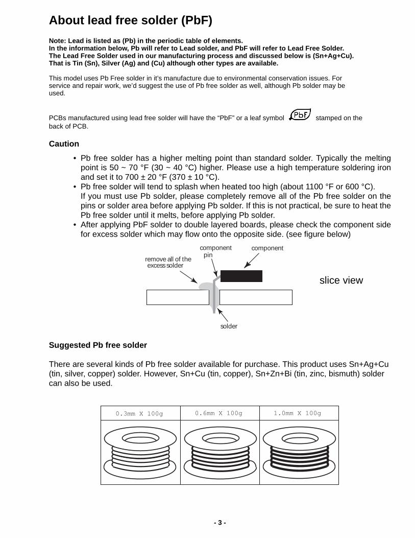
• After applying PbF solder to double layered boards, please check the component sidefor excess solder which may flow onto the opposite side. (see figure below)
Suggested Pb free solder
There are several kinds of Pb free solder available for purchase. This product uses Sn+Ag+Cu(tin, silver, copper) solder. However, Sn+Cu (tin, copper), Sn+Zn+Bi (tin, zinc, bismuth) soldercan also be used.
componentcomponentpin
solder
excess solderremove all of the
slice view
0.3mm X 100g 0.6mm X 100g 1.0mm X 100g
- 4 -
Important safety notice . . . . . . . . . . . . . . . . . . . 2
Safety precautions. . . . . . . . . . . . . . . . . . 2General guidelines. . . . . . . . . . . . . . . . . . 2Leakage current cold check. . . . . . . . . . . 2Leakage current hot check . . . . . . . . . . . 2X-ray radiation . . . . . . . . . . . . . . . . . . . . . 2Horizontal oscillator disable circuit test . . 2
Service notes . . . . . . . . . . . . . . . . . . . . . . . . . . . 5
Leadless chip component(surface mount) . . . . . . . . . . . . . . . . . 5
Component removal . . . . . . . . . . . . . . . . 5Chip component installation . . . . . . . . . . 5How to replace Flat IC . . . . . . . . . . . . . . . 5Horizontal oscillator disable circuit . . . . . 6
Receiver feature table . . . . . . . . . . . . . . . . . . . . 7
Location of controls (receiver) . . . . . . . . . . . . . 9
Quick reference control operation . . . . . . 9Location of controls (remote) . . . . . . . . . . . . . 10
Disassembly for service . . . . . . . . . . . . . . . . . 11
Back cover. . . . . . . . . . . . . . . . . . . . . . . 11A-Board . . . . . . . . . . . . . . . . . . . . . . . . . 11L-Board . . . . . . . . . . . . . . . . . . . . . . . . . 11Speakers . . . . . . . . . . . . . . . . . . . . . . . . 11Keyboard push button assembly . . . . . . 11Disassembly for CRT replacement . . . . 11CRT replacement . . . . . . . . . . . . . . . . . 11
Back cover removal . . . . . . . . . . . . . . . . . . . . . 13
Chassis service adjustment procedures . . . . 14
140.0V B+ Voltage confirmation . . . . . . 14Source voltage chart . . . . . . . . . . . . . . . 14High voltage check . . . . . . . . . . . . . . . . 14
Purity and convergence procedure . . . . . . . . 15
When the CRT or the yoke is replaced . 15Vertical raster shift adjustment . . . . . . . 15Initial center static convergence . . . . . . 16Purity adjustment. . . . . . . . . . . . . . . . . . 16Final convergence procedure . . . . . . . . 16Dynamic corvergence adjustment . . . . . 16DY(YHC, YV, XV) adjustment . . . . . . . . 16YV Adjustment (VR1 for
Horizontal dynamic convergence). . 16YH Adjustment (VR2 for
vertical dynamic convergence) . . . . 17XV Adjustment
(precise adjustment) . . . . . . . . . . . . 17Permalloy convergence corrector
strip (part No. 0FMK014ZZ) . . . . . . 17DAF adjustment. . . . . . . . . . . . . . . . . . . 17
Service mode (electronic controls). . . . . . . . . 19
Quick entry to service mode . . . . . . . . . 19To toggle between aging and
service modes . . . . . . . . . . . . . . . . . 19Exiting the service mode . . . . . . . . . . . . 19To check colors . . . . . . . . . . . . . . . . . . . 19Entering service mode
(open-back method) . . . . . . . . . . . . 19
To check purity . . . . . . . . . . . . . . . . . . . 21Instructional flow chart for service mode 22
Service adjustments (electronic controls) . . . 24
Sub-Contrast adjustment . . . . . . . . . . . . 24Sub-Brightness (BRIGH) . . . . . . . . . . . . 24Tint/Color adjustment . . . . . . . . . . . . . . 24Tint/Color adjustment
(No rainbow pattern) . . . . . . . . . . . . 25Color temperature adjustment
(B/W Tracking) . . . . . . . . . . . . . . . . 25Complete adjustment. . . . . . . . . . . . . . . 25Horizontal centering (H-POS) . . . . . . . . 26Horizontal width adjustment (H-WIDTH) 26Horizontal trapezoid
adjustment (HTRAP) . . . . . . . . . . . . 26Parallelogram adjustment (R524) . . . . . 26East west PCC balance
adjustment (SIDE). . . . . . . . . . . . . . 26Vertical linearity adjustment (V-C) . . . . . 27Vertical correction adjustment (V-S) . . . 27Vertical size and vertical position
adjustment (VEAMP & VRAS) . . . . 27PCC adjustment (PCC) . . . . . . . . . . . . . 27Corner PCC adjustment
(TOPG, TOPSL, BTMG, BTMSL) . . 27MTS circuit adjustments . . . . . . . . . . . . 28Input level adjustment (MTSIN) . . . . . . . 28Stereo separation adjustment
(SEPAL & SEPAH) . . . . . . . . . . . . . 28Clock adjustment (CLOCK) . . . . . . . . . . 28Service adjustments
(mechanical controls) . . . . . . . . . . . 28Focus (part of T551) . . . . . . . . . . . . . . . 28
Audio signal path block diagram . . . . . . . . . . 29
Video signal path block diagram . . . . . . . . . . 30
Description of connectors . . . . . . . . . . . . . . . . 31
Component identification . . . . . . . . . . . . . . . . 33
Parts list . . . . . . . . . . . . . . . . . . . . . . . . . . . . . . 36
Schematics, voltages and waveforms
A-Board schematic. . . . . . . . . . . . . . . . . . . . 50A-Board voltages . . . . . . . . . . . . . . . . . . . . . 54D-Board schematic. . . . . . . . . . . . . . . . . . . . 56D-Board voltages . . . . . . . . . . . . . . . . . . . . . 59A-Board waveforms . . . . . . . . . . . . . . . . . . . 60G-Board schematic . . . . . . . . . . . . . . . . . . . 62G-L-Board voltages . . . . . . . . . . . . . . . . . . . 65L-Board schematic . . . . . . . . . . . . . . . . . . . . 66A-Board pcb . . . . . . . . . . . . . . . . . . . . . . . . . 68D-Board pcb . . . . . . . . . . . . . . . . . . . . . . . . . 70G-Board pcb. . . . . . . . . . . . . . . . . . . . . . . . . 72L-Board pcb . . . . . . . . . . . . . . . . . . . . . . . . . 74
- 5 -
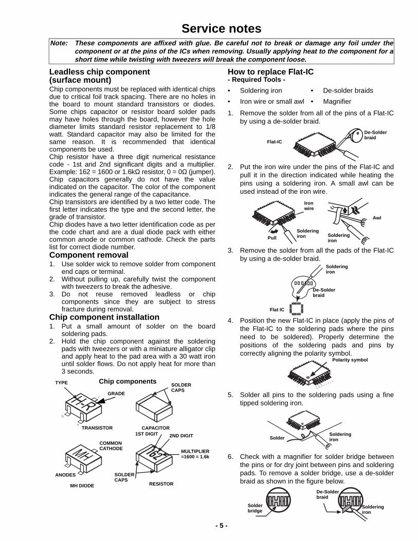
Service notes
Leadless chip component(surface mount)Chip components must be replaced with identical chipsdue to critical foil track spacing. There are no holes inthe board to mount standard transistors or diodes.Some chips capacitor or resistor board solder padsmay have holes through the board, however the holediameter limits standard resistor replacement to 1/8watt. Standard capacitor may also be limited for thesame reason. It is recommended that identicalcomponents be used.Chip resistor have a three digit numerical resistancecode - 1st and 2nd significant digits and a multiplier.Example: 162 = 1600 or 1.6kΩ resistor, 0 = 0Ω (jumper).Chip capacitors generally do not have the valueindicated on the capacitor. The color of the componentindicates the general range of the capacitance.Chip transistors are identified by a two letter code. Thefirst letter indicates the type and the second letter, thegrade of transistor.Chip diodes have a two letter identification code as perthe code chart and are a dual diode pack with eithercommon anode or common cathode. Check the partslist for correct diode number.Component removal1. Use solder wick to remove solder from component
end caps or terminal.2. Without pulling up, carefully twist the component
with tweezers to break the adhesive.3. Do not reuse removed leadless or chip
components since they are subject to stressfracture during removal.
Chip component installation1. Put a small amount of solder on the board
soldering pads.2. Hold the chip component against the soldering
pads with tweezers or with a miniature alligator clipand apply heat to the pad area with a 30 watt ironuntil solder flows. Do not apply heat for more than3 seconds.
How to replace Flat-IC- Required Tools -
1. Remove the solder from all of the pins of a Flat-ICby using a de-solder braid.
2. Put the iron wire under the pins of the Flat-IC andpull it in the direction indicated while heating thepins using a soldering iron. A small awl can beused instead of the iron wire.
3. Remove the solder from all the pads of the Flat-ICby using a de-solder braid.
4. Position the new Flat-IC in place (apply the pins ofthe Flat-IC to the soldering pads where the pinsneed to be soldered). Properly determine thepositions of the soldering pads and pins bycorrectly aligning the polarity symbol.
5. Solder all pins to the soldering pads using a finetipped soldering iron.
6. Check with a magnifier for solder bridge betweenthe pins or for dry joint between pins and solderingpads. To remove a solder bridge, use a de-solderbraid as shown in the figure below.
Note: These components are affixed with glue. Be careful not to break or damage any foil under thecomponent or at the pins of the ICs when removing. Usually applying heat to the component for ashort time while twisting with tweezers will break the component loose.
c
b
e
Chip components
TRANSISTOR CAPACITOR
RESISTORMH DIODE
SOLDERCAPS
SOLDERCAPS
1ST DIGIT 2ND DIGIT
MULTIPLIER=1600 = 1.6k
GRADE
TYPE
COMMON
ANODES
CATHODE
• Soldering iron • De-solder braids
• Iron wire or small awl • Magnifier
Flat-IC
De-Solderbraid
Pull
Ironwire
Awl
Solderingiron
Solderingiron
Solderingiron
De-Solderbraid
Flat IC
123...
..
Polarity symbol
SolderingironSolder
De-Solderbraid
Solderbridge
Solderingiron
- 6 -
Service notes (continued)IMPORTANT: To protect against possible damage tothe solid state devices due to arcing or static discharge,make certain that all ground wires are securelyconnected.
CAUTION: The power supply circuit is above earthground and the chassis cannot be polarized. Use anisolation transformer when servicing the receiver toavoid damage to the test equipment or to the chassis.Connect the test equipment to the proper ground ( ) or( ) when servicing, or incorrect voltages will bemeasured.
WARNING: This receiver has been designed to meetor exceed applicable safety and x-ray radiationprotection as specified by government agencies andindependent testing laboratories.
To maintain original product safety design standardsrelative to x-ray radiation and shock and fire hazard,
parts indicated with the symbol on the schematicmust be replaced with identical parts. Order parts fromthe manufacturer’s parts center using the partsnumbers shown in this service manual, or provide thechassis number and the part reference number.
For optimum performance and reliability, all other partsshould be replaced with components of identicalspecification.
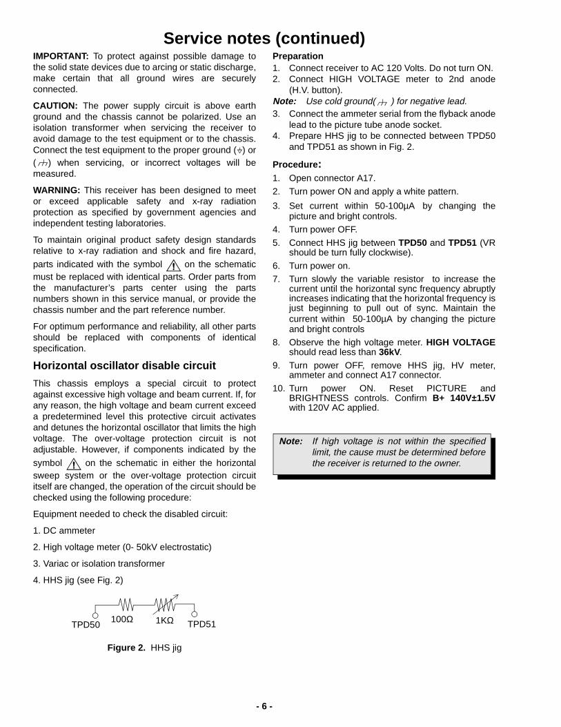
Horizontal oscillator disable circuit
This chassis employs a special circuit to protectagainst excessive high voltage and beam current. If, forany reason, the high voltage and beam current exceeda predetermined level this protective circuit activatesand detunes the horizontal oscillator that limits the highvoltage. The over-voltage protection circuit is notadjustable. However, if components indicated by the
symbol on the schematic in either the horizontalsweep system or the over-voltage protection circuititself are changed, the operation of the circuit should bechecked using the following procedure:
Equipment needed to check the disabled circuit:
1. DC ammeter
2. High voltage meter (0- 50kV electrostatic)
3. Variac or isolation transformer
4. HHS jig (see Fig. 2)
Figure 2. HHS jig
Preparation1. Connect receiver to AC 120 Volts. Do not turn ON.2. Connect HIGH VOLTAGE meter to 2nd anode
(H.V. button).Note: Use cold ground( ) for negative lead.3. Connect the ammeter serial from the flyback anode
lead to the picture tube anode socket.4. Prepare HHS jig to be connected between TPD50
and TPD51 as shown in Fig. 2.
Procedure :1. Open connector A17.
2. Turn power ON and apply a white pattern.
3. Set current within 50-100µΑ by changing thepicture and bright controls.
4. Turn power OFF.
5. Connect HHS jig between TPD50 and TPD51 (VRshould be turn fully clockwise).
6. Turn power on.
7. Turn slowly the variable resistor to increase thecurrent until the horizontal sync frequency abruptlyincreases indicating that the horizontal frequency isjust beginning to pull out of sync. Maintain thecurrent within 50-100µΑ by changing the pictureand bright controls
8. Observe the high voltage meter. HIGH VOLTAGEshould read less than 36kV.
9. Turn power OFF, remove HHS jig, HV meter,ammeter and connect A17 connector.
10. Turn power ON. Reset PICTURE andBRIGHTNESS controls. Confirm B+ 140V±1.5Vwith 120V AC applied.
TPD50 TPD51100Ω 1KΩ
Note: If high voltage is not within the specifiedlimit, the cause must be determined beforethe receiver is returned to the owner.
- 7 -
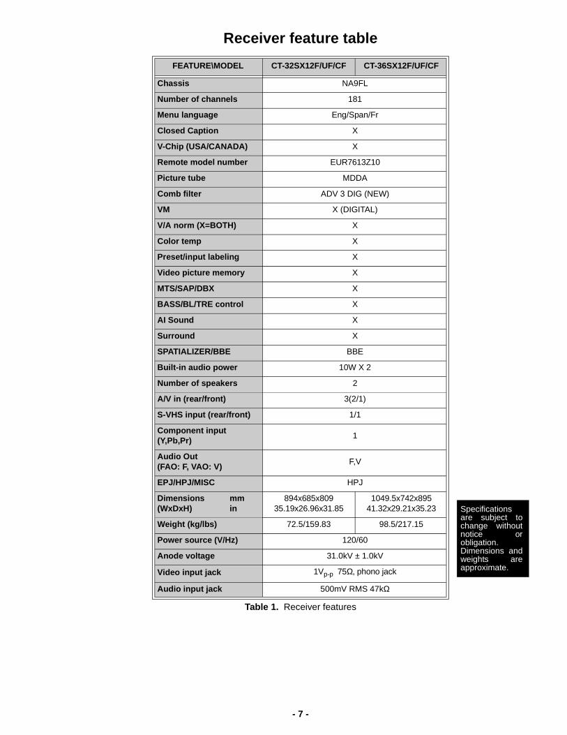
Receiver feature table
FEATURE\MODEL CT-32SX12F/UF/CF CT-36SX12F/UF/CF
Chassis NA9FL
Number of channels 181
Menu language Eng/Span/Fr
Closed Caption X
V-Chip (USA/CANADA) X
Remote model number EUR7613Z10
Picture tube MDDA
Comb filter ADV 3 DIG (NEW)
VM X (DIGITAL)
V/A norm (X=BOTH) X
Color temp X
Preset/input labeling X
Video picture memory X
MTS/SAP/DBX X
BASS/BL/TRE control X
AI Sound X
Surround X
SPATIALIZER/BBE BBE
Built-in audio power 10W X 2
Number of speakers 2
A/V in (rear/front) 3(2/1)
S-VHS input (rear/front) 1/1
Component input(Y,Pb,Pr)
1
Audio Out(FAO: F, VAO: V)
F,V
EPJ/HPJ/MISC HPJ
Dimensions mm(WxDxH) in
894x685x80935.19x26.96x31.85
1049.5x742x89541.32x29.21x35.23
Weight (kg/lbs) 72.5/159.83 98.5/217.15
Power source (V/Hz) 120/60
Anode voltage 31.0kV ± 1.0kV
Video input jack 1Vp-p 75Ω, phono jack
Audio input jack 500mV RMS 47kΩ
Table 1. Receiver features
Specificationsare subject tochange withoutnotice orobligation.Dimensions andweights areapproximate.
- 8 -
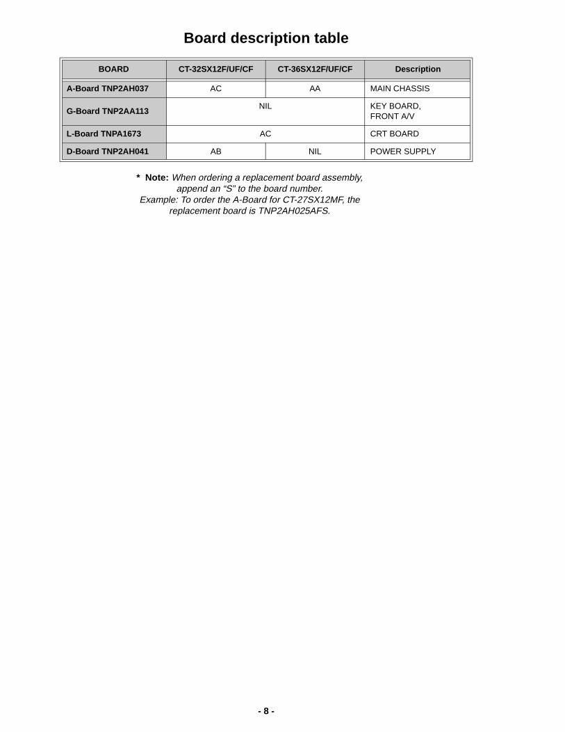
Board description table
* Note: When ordering a replacement board assembly,append an “S” to the board number.
Example: To order the A-Board for CT-27SX12MF, thereplacement board is TNP2AH025AFS.
BOARD CT-32SX12F/UF/CF CT-36SX12F/UF/CF Description
A-Board TNP2AH037 AC AA MAIN CHASSIS
G-Board TNP2AA113NIL KEY BOARD,
FRONT A/V
L-Board TNPA1673 AC CRT BOARD
D-Board TNP2AH041 AB NIL POWER SUPPLY
- 9 -
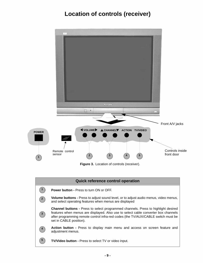
Location of controls (receiver)
Quick reference control operation
Power button - Press to turn ON or OFF.
Volume buttons - Press to adjust sound level, or to adjust audio menus, video menus,and select operating features when menus are displayed
Channel buttons - Press to select programmed channels. Press to highlight desiredfeatures when menus are displayed. Also use to select cable converter box channelsafter programming remote control infra-red codes (the TV/AUX/CABLE switch must beset in CABLE position).
Action button - Press to display main menu and access on screen feature andadjustment menus.
TV/Video button - Press to select TV or video input.
Figure 3. Location of controls (receiver).
2 4 53
Remote controlsensor
VOLUME CHANNEL ACTION TV/VIDEO
Front A/V jacks
Controls insidefront door
1
POWER
1
2
3
4
5
- 10 -
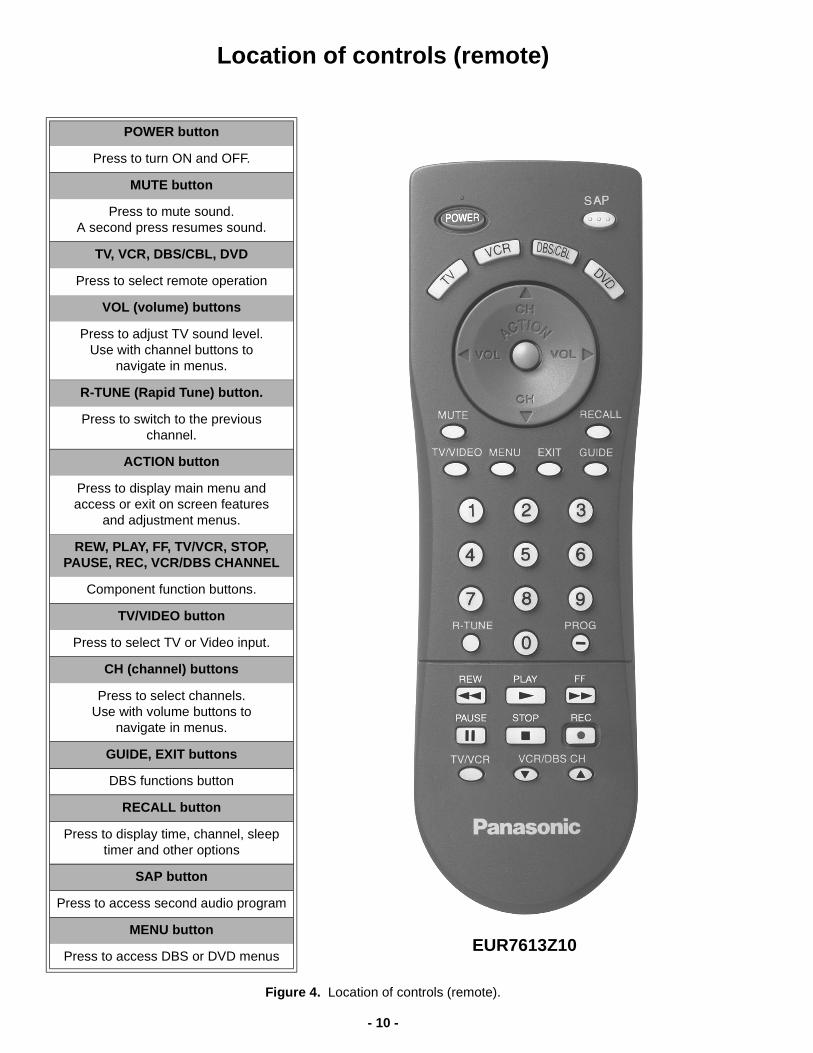
Location of controls (remote)
Figure 4. Location of controls (remote).
POWER button
Press to turn ON and OFF.
MUTE button
Press to mute sound.A second press resumes sound.
TV, VCR, DBS/CBL, DVD
Press to select remote operation
VOL (volume) buttons
Press to adjust TV sound level.Use with channel buttons to
navigate in menus.
R-TUNE (Rapid Tune) button.
Press to switch to the previouschannel.
ACTION button
Press to display main menu andaccess or exit on screen features
and adjustment menus.
REW, PLAY, FF, TV/VCR, STOP,PAUSE, REC, VCR/DBS CHANNEL
Component function buttons.
TV/VIDEO button
Press to select TV or Video input.
CH (channel) buttons
Press to select channels.Use with volume buttons to
navigate in menus.
GUIDE, EXIT buttons
DBS functions button
RECALL button
Press to display time, channel, sleeptimer and other options
SAP button
Press to access second audio program
MENU button
Press to access DBS or DVD menusEUR7613Z10
- 11 -
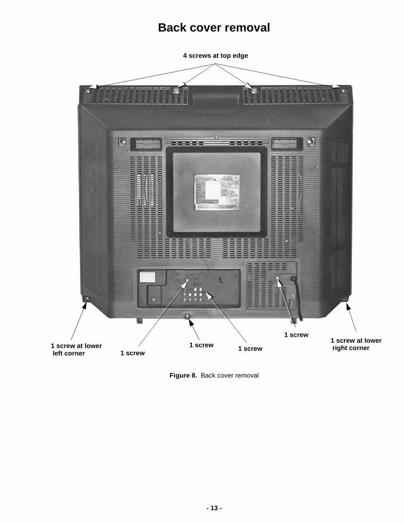
Disassembly for serviceBack coverRemove all the screws marked with an arrow( )from the back of the receiver.
Note: Screw configuration, type, and numberof screws vary depending on themodel of the receiver serviced and theapplication; various models arecovered in this manual. Use samehardware when reassembling thereceiver.
• 4 screws at the top edge of the receiver.• 3 screw by the A/V jacks.• 1 screw at each lower corner of the receiver.• 1 screw by the retainer plate of the AC power cord.
A-Board - Main chassisThe A-Board assembly rest on a chassis tray alongwith the D-Board. Slide chassis tray out. Gently lift trayand pull out. Disconnect plug connectors; release wireties and holders as required for complete chassisremoval.1. A & D-Boards are secured to the chassis tray with
screws.2. The A-Board is mated to the D-Board by three
flexible connectors: A5, A6 & A7 (D5, D6 & D7 onthe D-Board, respectively), A1, A2 & A3 (G1, G2 &G3 on the G-Board, respectively), D40 to G40. Toremove either boards, unplug the connectors onthe A-Board.
Note: Some tie-wraps that secure the wire dressingsmay need to be unfastened for chassisremoval.
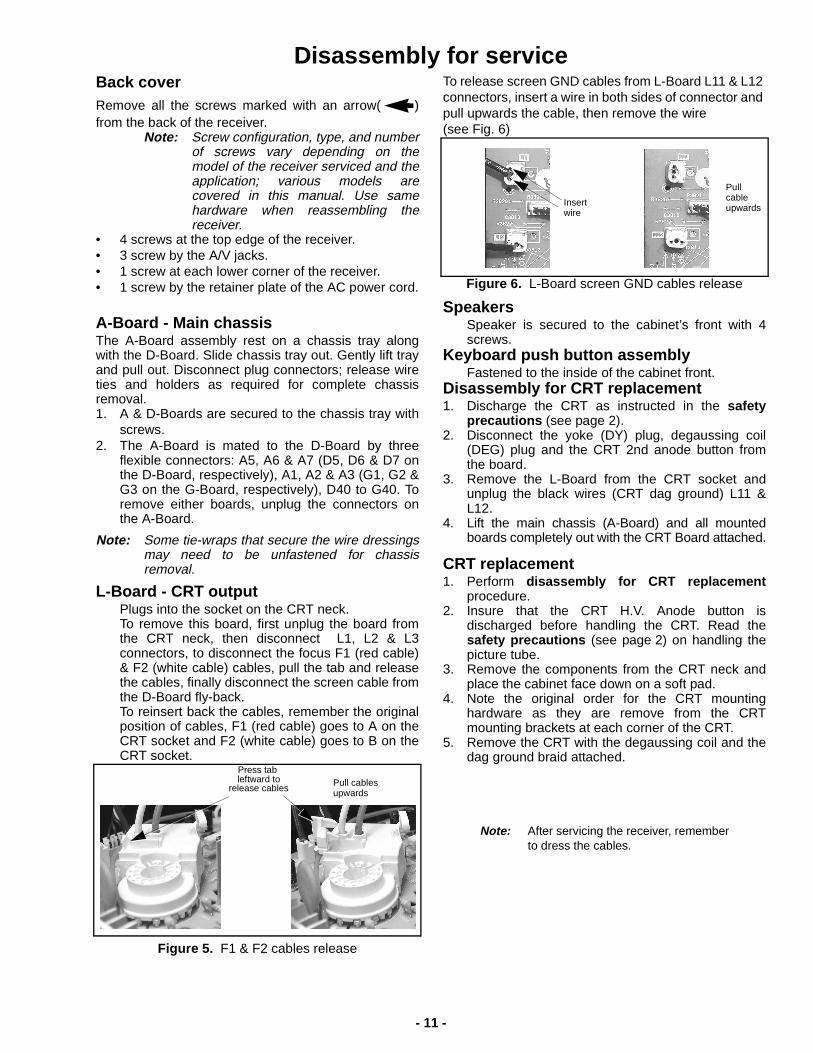
L-Board - CRT outputPlugs into the socket on the CRT neck.To remove this board, first unplug the board fromthe CRT neck, then disconnect L1, L2 & L3connectors, to disconnect the focus F1 (red cable)& F2 (white cable) cables, pull the tab and releasethe cables, finally disconnect the screen cable fromthe D-Board fly-back.To reinsert back the cables, remember the originalposition of cables, F1 (red cable) goes to A on theCRT socket and F2 (white cable) goes to B on theCRT socket.
Figure 5. F1 & F2 cables release
To release screen GND cables from L-Board L11 & L12connectors, insert a wire in both sides of connector andpull upwards the cable, then remove the wire(see Fig. 6)
Figure 6. L-Board screen GND cables release
SpeakersSpeaker is secured to the cabinet’s front with 4screws.
Keyboard push button assemblyFastened to the inside of the cabinet front.
Disassembly for CRT replacement1. Discharge the CRT as instructed in the safety
precautions (see page 2).2. Disconnect the yoke (DY) plug, degaussing coil
(DEG) plug and the CRT 2nd anode button fromthe board.
3. Remove the L-Board from the CRT socket andunplug the black wires (CRT dag ground) L11 &L12.
4. Lift the main chassis (A-Board) and all mountedboards completely out with the CRT Board attached.
CRT replacement1. Perform disassembly for CRT replacement
procedure.2. Insure that the CRT H.V. Anode button is
discharged before handling the CRT. Read thesafety precautions (see page 2) on handling thepicture tube.
3. Remove the components from the CRT neck andplace the cabinet face down on a soft pad.
4. Note the original order for the CRT mountinghardware as they are remove from the CRTmounting brackets at each corner of the CRT.
5. Remove the CRT with the degaussing coil and thedag ground braid attached.
Press tab
release cablesleftward to Pull cables
upwards
Pullcableupwards
Insertwire
Note: After servicing the receiver, rememberto dress the cables.
- 12 -
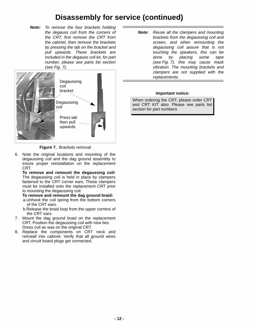
Disassembly for service (continued)Note: To remove the four brackets holding
the degauss coil from the corners ofthe CRT, first remove the CRT fromthe cabinet, then remove the bracketsby pressing the tab on the bracket andpull upwards. These brackets areincluded in the degauss coil kit, for partnumber, please see parts list section(see Fig. 7).
Figure 7. Brackets removal
6. Note the original locations and mounting of thedegaussing coil and the dag ground assembly toinsure proper reinstallation on the replacementCRT.To remove and remount the degaussing coil:The degaussing coil is held in place by clampersfastened to the CRT corner ears. These clampersmust be installed onto the replacement CRT priorto mounting the degaussing coil.To remove and remount the dag ground braid:a.Unhook the coil spring from the bottom corners
of the CRT ears.b.Release the braid loop from the upper corners of
the CRT ears.7. Mount the dag ground braid on the replacement
CRT. Position the degaussing coil with new ties.Dress coil as was on the original CRT.
8. Replace the components on CRT neck andreinstall into cabinet. Verify that all ground wiresand circuit board plugs get connected.
Note: Reuse all the clampers and mountingbrackets from the degaussing coil andscreen, and when remounting thedegaussing coil assure that is nottouching the speakers, this can bedone by placing some tape(see Fig. 7), this may cause maskvibration. The mounting brackets andclampers are not supplied with thereplacements.
Degaussingcoilbracket
Degaussingcoil
Press tabthen pullupwards
When ordering the CRT, please order CRTand CRT KIT also. Please see parts listsection for part numbers
Important notice:
- 13 -
Back cover removal
Figure 8. Back cover removal
4 screws at top edge
1 screw at lower 1 screwleft corner 1 screw
1 screw1 screw at lowerright corner1 screw
- 14 -
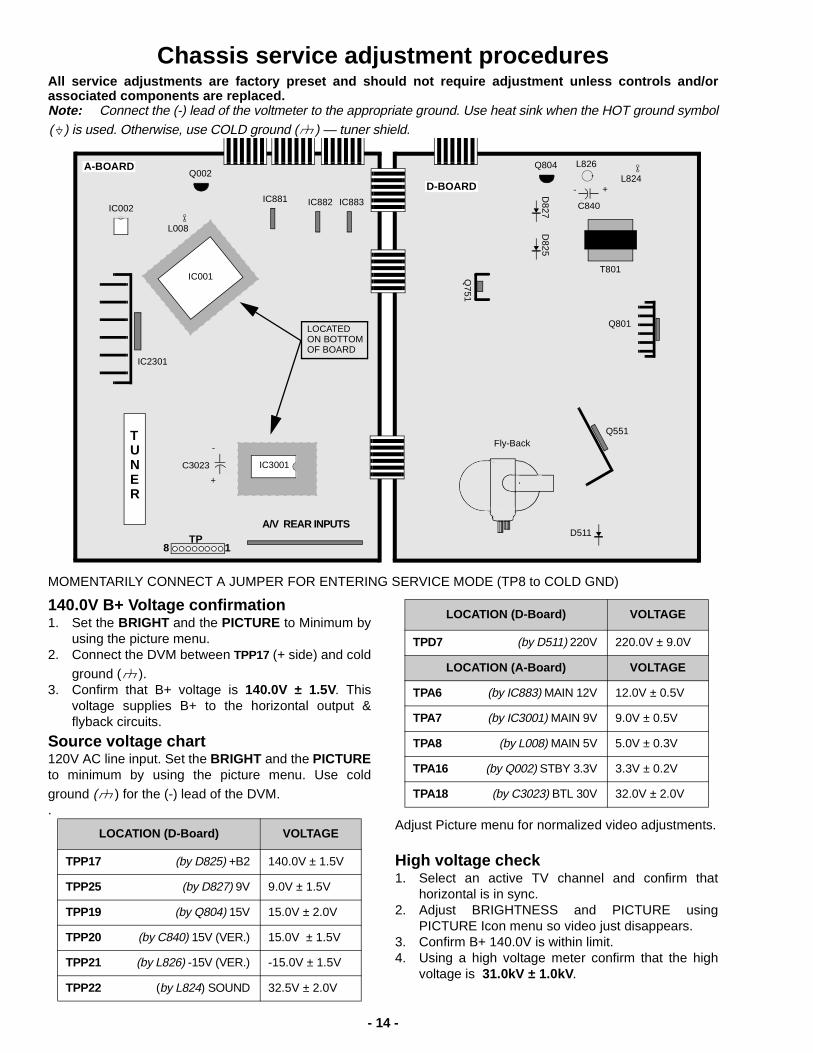
Chassis service adjustment proceduresAll service adjustments are factory preset and should not require adjustment unless controls and/orassociated components are replaced.Note: Connect the (-) lead of the voltmeter to the appropriate ground. Use heat sink when the HOT ground symbol( ) is used. Otherwise, use COLD ground ( ) — tuner shield.
MOMENTARILY CONNECT A JUMPER FOR ENTERING SERVICE MODE (TP8 to COLD GND)
140.0V B+ Voltage confirmation1. Set the BRIGHT and the PICTURE to Minimum by
using the picture menu.2. Connect the DVM between TPP17 (+ side) and cold
ground ( ).3. Confirm that B+ voltage is 140.0V ± 1.5V. This
voltage supplies B+ to the horizontal output &flyback circuits.
Source voltage chart120V AC line input. Set the BRIGHT and the PICTUREto minimum by using the picture menu. Use cold
ground ( ) for the (-) lead of the DVM..
Adjust Picture menu for normalized video adjustments.
High voltage check1. Select an active TV channel and confirm that
horizontal is in sync.2. Adjust BRIGHTNESS and PICTURE using
PICTURE Icon menu so video just disappears.3. Confirm B+ 140.0V is within limit.4. Using a high voltage meter confirm that the high
voltage is 31.0kV ± 1.0kV.
TUNER
TP18
A/V REAR INPUTS
D-BOARD
A-BOARD
IC002IC882
IC2301
D825
Q751
T801
L826
Q551
Q801
L824
D827
Q804
C840
- +IC881 IC883
L008
Q002
C3023
-
+
IC3001
IC001
LOCATEDON BOTTOMOF BOARD
D511
Fly-Back
LOCATION (D-Board) VOLTAGE
TPP17 (by D825) +B2 140.0V ± 1.5V
TPP25 (by D827) 9V 9.0V ± 1.5V
TPP19 (by Q804) 15V 15.0V ± 2.0V
TPP20 (by C840) 15V (VER.) 15.0V ± 1.5V
TPP21 (by L826) -15V (VER.) -15.0V ± 1.5V
TPP22 (by L824) SOUND 32.5V ± 2.0V
TPD7 (by D511) 220V 220.0V ± 9.0V
LOCATION (A-Board) VOLTAGE
TPA6 (by IC883) MAIN 12V 12.0V ± 0.5V
TPA7 (by IC3001) MAIN 9V 9.0V ± 0.5V
TPA8 (by L008) MAIN 5V 5.0V ± 0.3V
TPA16 (by Q002) STBY 3.3V 3.3V ± 0.2V
TPA18 (by C3023) BTL 30V 32.0V ± 2.0V
LOCATION (D-Board) VOLTAGE
- 15 -
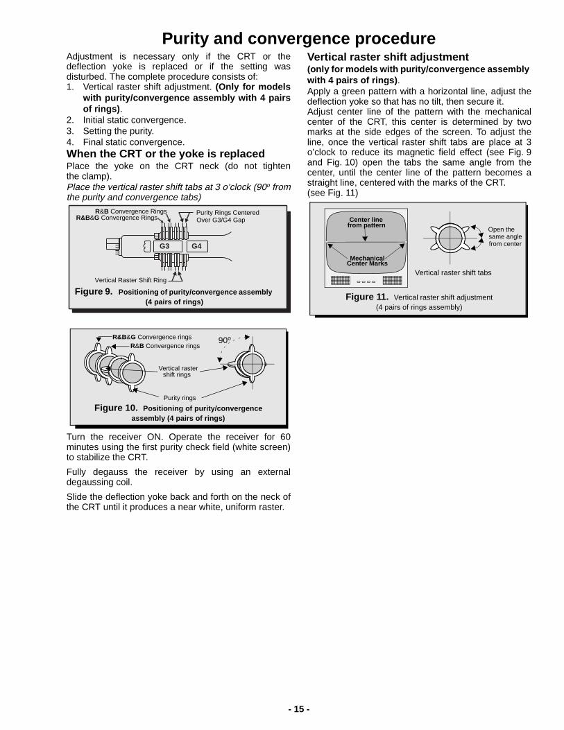
Purity and convergence procedureAdjustment is necessary only if the CRT or thedeflection yoke is replaced or if the setting wasdisturbed. The complete procedure consists of:1. Vertical raster shift adjustment. (Only for models
with purity/convergence assembly with 4 pairsof rings) .
2. Initial static convergence.3. Setting the purity.4. Final static convergence.When the CRT or the yoke is replacedPlace the yoke on the CRT neck (do not tightenthe clamp).Place the vertical raster shift tabs at 3 o’clock (90o fromthe purity and convergence tabs)
Turn the receiver ON. Operate the receiver for 60minutes using the first purity check field (white screen)to stabilize the CRT.
Fully degauss the receiver by using an externaldegaussing coil.
Slide the deflection yoke back and forth on the neck ofthe CRT until it produces a near white, uniform raster.
Vertical raster shift adjustment(only for models with purity/convergence assemblywith 4 pairs of rings) .Apply a green pattern with a horizontal line, adjust thedeflection yoke so that has no tilt, then secure it.Adjust center line of the pattern with the mechanicalcenter of the CRT, this center is determined by twomarks at the side edges of the screen. To adjust theline, once the vertical raster shift tabs are place at 3o’clock to reduce its magnetic field effect (see Fig. 9and Fig. 10) open the tabs the same angle from thecenter, until the center line of the pattern becomes astraight line, centered with the marks of the CRT.(see Fig. 11)
G3 G4
Purity Rings CenteredOver G3/G4 Gap
R&B Convergence RingsR&B&G Convergence Rings
Vertical Raster Shift Ring
Figure 9. Positioning of purity/convergence assembly(4 pairs of rings)
90o
Purity rings
Vertical raster
R&B Convergence ringsR&B&G Convergence rings
Figure 10. Positioning of purity/convergenceassembly (4 pairs of rings)
shift rings
Vertical raster shift tabs
Open thesame anglefrom center
Figure 11. Vertical raster shift adjustment(4 pairs of rings assembly)
Center Marks
from patternCenter line
Mechanical
- 16 -
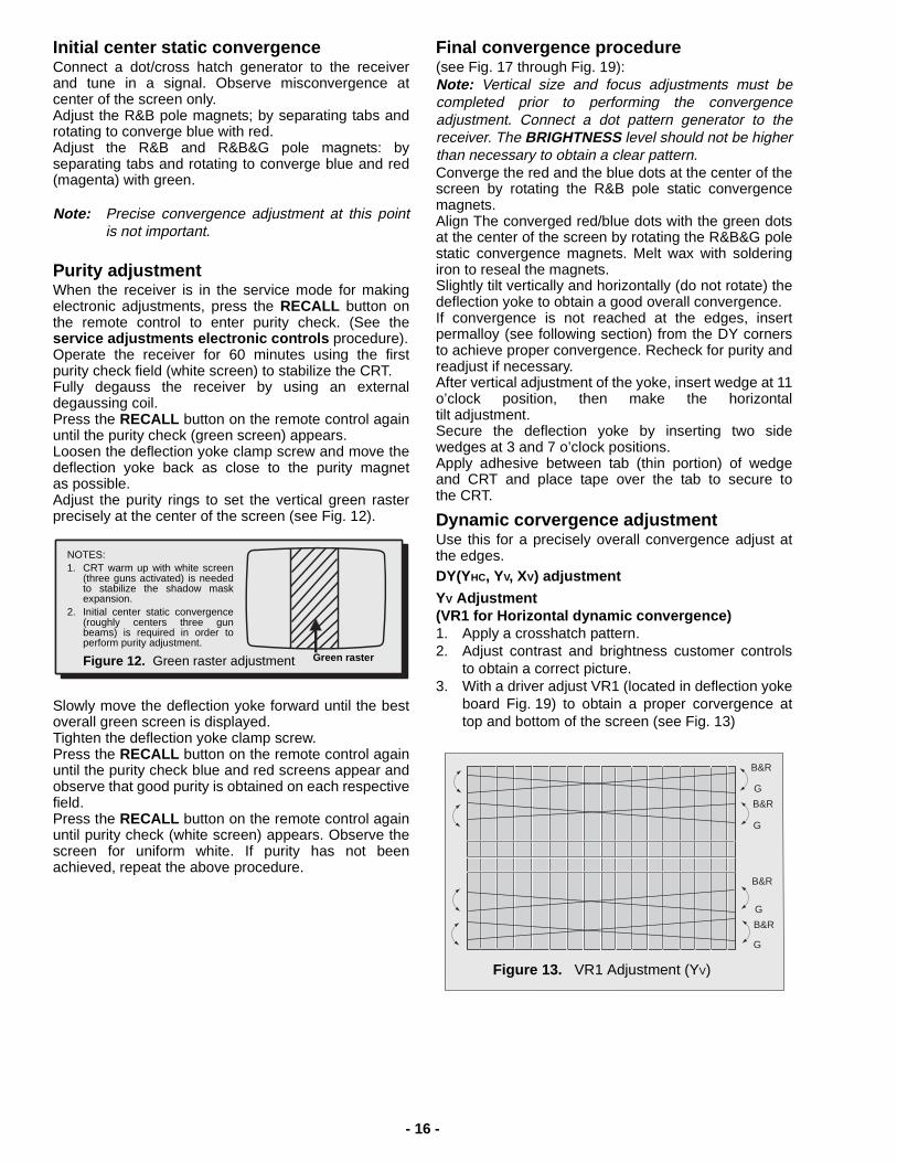
Initial center static convergenceConnect a dot/cross hatch generator to the receiverand tune in a signal. Observe misconvergence atcenter of the screen only.Adjust the R&B pole magnets; by separating tabs androtating to converge blue with red.Adjust the R&B and R&B&G pole magnets: byseparating tabs and rotating to converge blue and red(magenta) with green.
Note: Precise convergence adjustment at this pointis not important.
Purity adjustmentWhen the receiver is in the service mode for makingelectronic adjustments, press the RECALL button onthe remote control to enter purity check. (See theservice adjustments electronic controls procedure).Operate the receiver for 60 minutes using the firstpurity check field (white screen) to stabilize the CRT.Fully degauss the receiver by using an externaldegaussing coil.Press the RECALL button on the remote control againuntil the purity check (green screen) appears.Loosen the deflection yoke clamp screw and move thedeflection yoke back as close to the purity magnetas possible.Adjust the purity rings to set the vertical green rasterprecisely at the center of the screen (see Fig. 12).
Slowly move the deflection yoke forward until the bestoverall green screen is displayed.Tighten the deflection yoke clamp screw.Press the RECALL button on the remote control againuntil the purity check blue and red screens appear andobserve that good purity is obtained on each respectivefield.Press the RECALL button on the remote control againuntil purity check (white screen) appears. Observe thescreen for uniform white. If purity has not beenachieved, repeat the above procedure.
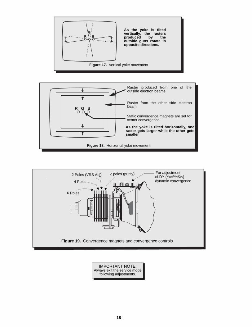
Final convergence procedure(see Fig. 17 through Fig. 19):Note: Vertical size and focus adjustments must becompleted prior to performing the convergenceadjustment. Connect a dot pattern generator to thereceiver. The BRIGHTNESS level should not be higherthan necessary to obtain a clear pattern.Converge the red and the blue dots at the center of thescreen by rotating the R&B pole static convergencemagnets.Align The converged red/blue dots with the green dotsat the center of the screen by rotating the R&B&G polestatic convergence magnets. Melt wax with solderingiron to reseal the magnets.Slightly tilt vertically and horizontally (do not rotate) thedeflection yoke to obtain a good overall convergence.If convergence is not reached at the edges, insertpermalloy (see following section) from the DY cornersto achieve proper convergence. Recheck for purity andreadjust if necessary.After vertical adjustment of the yoke, insert wedge at 11o’clock position, then make the horizontaltilt adjustment.Secure the deflection yoke by inserting two sidewedges at 3 and 7 o’clock positions.Apply adhesive between tab (thin portion) of wedgeand CRT and place tape over the tab to secure tothe CRT.
Dynamic corvergence adjustmentUse this for a precisely overall convergence adjust atthe edges.DY(YHC, YV, XV) adjustment
YV Adjustment(VR1 for Horizontal dynamic convergence)1. Apply a crosshatch pattern.2. Adjust contrast and brightness customer controls
to obtain a correct picture.3. With a driver adjust VR1 (located in deflection yoke
board Fig. 19) to obtain a proper corvergence attop and bottom of the screen (see Fig. 13)
NOTES:1. CRT warm up with white screen
(three guns activated) is neededto stabilize the shadow maskexpansion.
2. Initial center static convergence(roughly centers three gunbeams) is required in order toperform purity adjustment.
Figure 12. Green raster adjustment Green raster
G
B&R
G
B&R
G
B&R
G
B&R
Figure 13. VR1 Adjustment (YV)
- 17 -
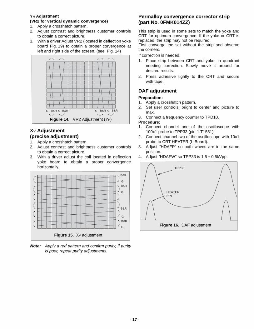
YH Adjustment(VR2 for vertical dynamic convergence)1. Apply a crosshatch pattern.2. Adjust contrast and brightness customer controls
to obtain a correct picture.3. With a driver Adjust VR2 (located in deflection yoke
board Fig. 19) to obtain a proper corvergence atleft and right side of the screen. (see Fig. 14)
XV Adjustment(precise adjustment)1. Apply a crosshatch pattern.2. Adjust contrast and brightness customer controls
to obtain a correct picture.3. With a driver adjust the coil located in deflection
yoke board to obtain a proper convergencehorizontally.
Note: Apply a red pattern and confirm purity, if purityis poor, repeat purity adjustments.
Permalloy convergence corrector strip(part No. 0FMK014ZZ)
This strip is used in some sets to match the yoke andCRT for optimum convergence. If the yoke or CRT isreplaced, the strip may not be required.First converge the set without the strip and observethe corners.If correction is needed:1. Place strip between CRT and yoke, in quadrant
needing correction. Slowly move it around fordesired results.
2. Press adhesive tightly to the CRT and securewith tape.
DAF adjustmentPreparation:1. Apply a crosshatch pattern.2. Set user controls, bright to center and picture to
max.3. Connect a frequency counter to TPD10.Procedure:1. Connect channel one of the oscilloscope with
100x1 probe to TPP33 (pin-1 T1551).2. Connect channel two of the oscilloscope with 10x1
probe to CRT HEATER (L-Board).3. Adjust “HDAFP” so both waves are in the same
position.4. Adjust “HDAFW” so TPP33 is 1.5 ± 0.5kVpp.
G B&R G B&RG B&R G B&R
Figure 14. VR2 Adjustment (YH)
G
B&R
G
B&R
G
B&R
G
B&R
Figure 15. XV adjustment
TPP33
HEATERPIN
Figure 16. DAF adjustment
- 18 -
RG
B
As the yoke is tiltedvertically, the rastersproduced by theoutside guns rotate inopposite directions.
Figure 17. Vertical yoke movement
R G B
Raster produced from one of theoutside electron beams
Raster from the other side electronbeam
Static convergence magnets are set forcenter convergence
As the yoke is tilted horizontally, oneraster gets larger while the other getssmaller
Figure 18. Horizontal yoke movement
6 Poles
4 Poles
2 poles (purity)2 Poles (VRS Adj) For adjustmentof DY (YHC/YV/XV)dynamic convergence
Figure 19. Convergence magnets and convergence controls
IMPORTANT NOTE:Always exit the service mode
following adjustments.
- 19 -
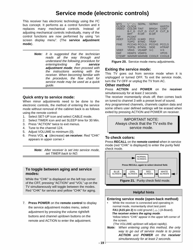
Service mode (electronic controls)This receiver has electronic technology using the I²Cbus concept. It performs as a control function and itreplaces many mechanical controls. Instead ofadjusting mechanical controls individually, many of thecontrol functions are now performed by using “onscreen display menu”. (The service adjustmentmode ).
Note: It is suggested that the technicianreads all the way through andunderstand the following procedure forentering/exiting the serviceadjustment mode ; then proceed withthe instructions working with thereceiver. When becoming familiar withthe procedure, the flow chart forservice mode may be used as a quickguide.
Quick entry to service mode:When minor adjustments need to be done to theelectronic controls, the method of entering the servicemode without removal of the cabinet back is as followsusing the remote control:1. Select SET-UP icon and select CABLE mode.2. Select TIMER icon and set SLEEP time for 30 Min.3. Press “ACTION” twice to exit menus.4. Tune to the channel 124.5. Adjust VOLUME to minimum (0).6. Press VOL (decrease) on receiver . Red “CHK”
appears in upper corner.+
Note: After receiver is set into service mode,set TIMER back to NO.
7. Press POWER on the remote control to displaythe service adjustment modes menu, selectadjustment by pressing the volume right/leftbuttons and channel up/down buttons on theremote and ACTION to enter the adjustment.
Exiting the service mode:This TV goes out from service mode when it isunplugged or turned OFF. To exit the service mode,turn the TV OFF or unplug the TV from AC.Other methodPress ACTION and POWER on the receiversimultaneously for at least 2 seconds.The receiver momentarily shuts off; then comes backon tuned to channel 3 with a preset level of sound.Any programmed channels, channels caption data andsome others user defined settings will be erased whenexited by pressing ACTION and POWER on receiver.
To check colors:Press RECALL on the remote control when in servicemode (red “CHK” is displayed) to enter the purity fieldcheck mode.
To toggle between aging and servicemodes:While the “CHK” is displayed on the left top cornerof the CRT, pressing “ACTION” and “VOL” up on theTV simultaneously will toggle between the modes.Red “CHK” for service and yellow “CHK” for aging. Helpful hints
Entering service mode (open-back method)• While the receiver is connected and operating in
normal mode, momentarily short test pointFA1 (A15 pin 2) to cold ground ( ) (A-Board).
The receiver enters the aging mode .Yellow letters “CHK” appear in the upper left corner ofthe screen.(The VOLUME up/down will adjust rapidly).
Note: When entering using this method, the onlyway to go out of service mode is to pressACTION and POWER on the receiversimultaneously for at least 2 seconds.
MTS MTSIN SEPAL SEPAHCLOCK CLOCK HHSTHVIDEO COLOR BRIGHTINT CONT
B-Y_G CUT_G CUT_R CUT_BBRT R-DR B-DR
PIP PCONTHDEF
FINE
H-POS H-WID PCC
PCCHG PCCLG PCCHS PCCLSTOPG BTMG
TOPSL BTMSL
TRAP
SIDE HTRAPVDEF VRAS VEAMP V-C
VPOSV-S
DAFCTEMP
HDAFSWARMR WARMB COOLR COOLB
VDAFG
Figure 20. Service mode menu adjustments.
IMPORTANT NOTE:Always check that the TV exits the
service mode.
Press RECALL again to select desired field.
NORMALSCREEN
WHITESCREEN
REDSCREEN
GRN.SCREEN
BLUESCREEN
Figure 21. Purity check field mode.
- 20 -
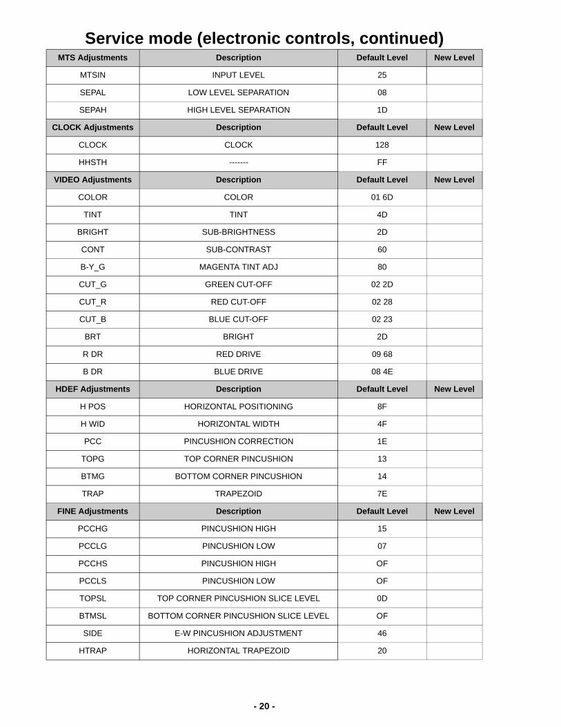
Service mode (electronic controls, continued)MTS Adjustments Description Default Level New Level
MTSIN INPUT LEVEL 25
SEPAL LOW LEVEL SEPARATION 08
SEPAH HIGH LEVEL SEPARATION 1D
CLOCK Adjustments Description Default Level New Level
CLOCK CLOCK 128
HHSTH ------- FF
VIDEO Adjustments Description Default Level New Level
COLOR COLOR 01 6D
TINT TINT 4D
BRIGHT SUB-BRIGHTNESS 2D
CONT SUB-CONTRAST 60
B-Y_G MAGENTA TINT ADJ 80
CUT_G GREEN CUT-OFF 02 2D
CUT_R RED CUT-OFF 02 28
CUT_B BLUE CUT-OFF 02 23
BRT BRIGHT 2D
R DR RED DRIVE 09 68
B DR BLUE DRIVE 08 4E
HDEF Adjustments Description Default Level New Level
H POS HORIZONTAL POSITIONING 8F
H WID HORIZONTAL WIDTH 4F
PCC PINCUSHION CORRECTION 1E
TOPG TOP CORNER PINCUSHION 13
BTMG BOTTOM CORNER PINCUSHION 14
TRAP TRAPEZOID 7E
FINE Adjustments Description Default Level New Level
PCCHG PINCUSHION HIGH 15
PCCLG PINCUSHION LOW 07
PCCHS PINCUSHION HIGH OF
PCCLS PINCUSHION LOW OF
TOPSL TOP CORNER PINCUSHION SLICE LEVEL 0D
BTMSL BOTTOM CORNER PINCUSHION SLICE LEVEL OF
SIDE E-W PINCUSHION ADJUSTMENT 46
HTRAP HORIZONTAL TRAPEZOID 20
- 21 -
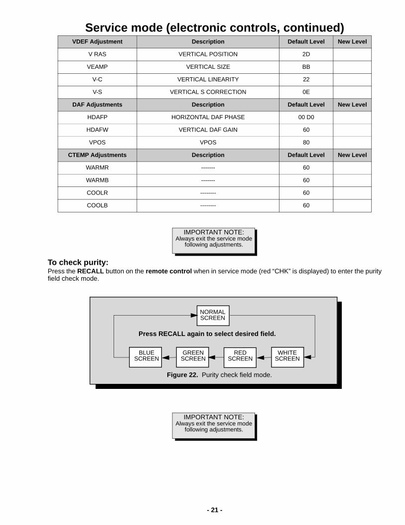
Service mode (electronic controls, continued)
To check purity:Press the RECALL button on the remote control when in service mode (red “CHK” is displayed) to enter the purityfield check mode.
VDEF Adjustment Description Default Level New Level
V RAS VERTICAL POSITION 2D
VEAMP VERTICAL SIZE BB
V-C VERTICAL LINEARITY 22
V-S VERTICAL S CORRECTION 0E
DAF Adjustments Description Default Level New Level
HDAFP HORIZONTAL DAF PHASE 00 D0
HDAFW VERTICAL DAF GAIN 60
VPOS VPOS 80
CTEMP Adjustments Description Default Level New Level
WARMR ------- 60
WARMB ------- 60
COOLR -------- 60
COOLB -------- 60
IMPORTANT NOTE:Always exit the service mode
following adjustments.
Press RECALL again to select desired field.
NORMALSCREEN
WHITESCREEN
REDSCREEN
GREENSCREEN
BLUESCREEN
Figure 22. Purity check field mode.
IMPORTANT NOTE:Always exit the service mode
following adjustments.
- 22 -
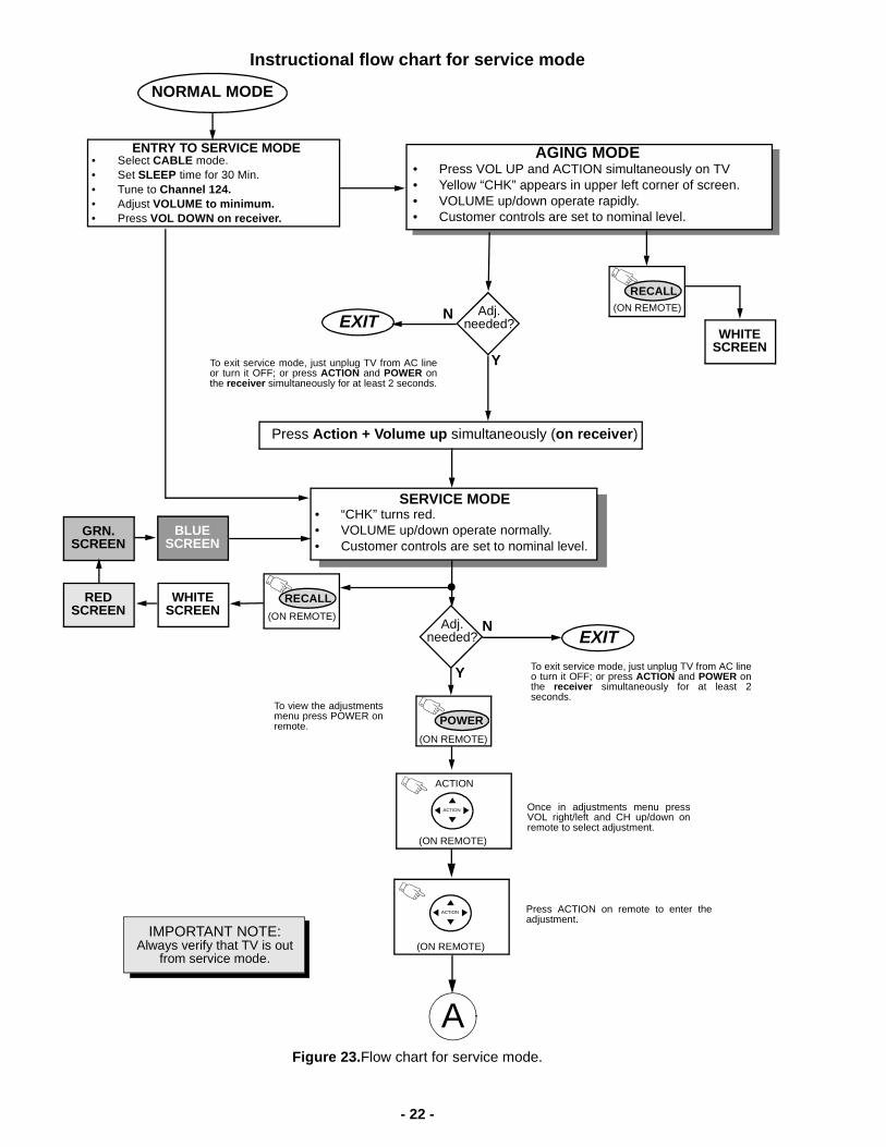
Instructional flow chart for service mode
Adj.needed?
NORMAL MODE
Press Action + Volume up simultaneously (on receiver )
Adj.needed?
WHITESCREEN
(ON REMOTE)
RECALL
WHITESCREEN
REDSCREEN
GRN.SCREEN
BLUESCREEN
POWER
(ON REMOTE)
SERVICE MODE• “CHK” turns red.• VOLUME up/down operate normally.• Customer controls are set to nominal level.
ENTRY TO SERVICE MODE• Select CABLE mode.• Set SLEEP time for 30 Min.• Tune to Channel 124.• Adjust VOLUME to minimum.• Press VOL DOWN on receiver.
EXIT
EXIT
Figure 23. Flow chart for service mode.
N
Y
N
Y
(ON REMOTE)
RECALL
(ON REMOTE)
A
(ON REMOTE)
ACTION
To view the adjustmentsmenu press POWER onremote.
Once in adjustments menu pressVOL right/left and CH up/down onremote to select adjustment.
Press ACTION on remote to enter theadjustment.
AGING MODE• Press VOL UP and ACTION simultaneously on TV• Yellow “CHK” appears in upper left corner of screen.• VOLUME up/down operate rapidly.• Customer controls are set to nominal level.
IMPORTANT NOTE:Always verify that TV is out
from service mode.
To exit service mode, just unplug TV from AC lineor turn it OFF; or press ACTION and POWER onthe receiver simultaneously for at least 2 seconds.
To exit service mode, just unplug TV from AC lineo turn it OFF; or press ACTION and POWER onthe receiver simultaneously for at least 2seconds.
ACTION
ACTION
- 23 -
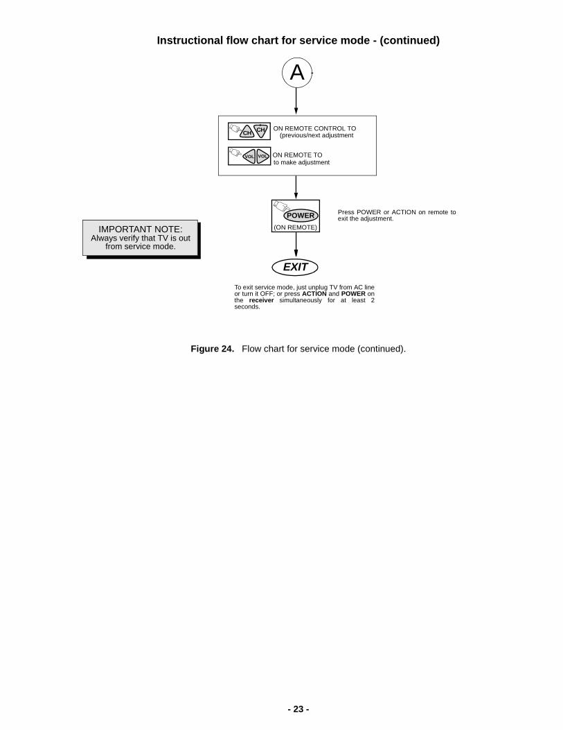
Instructional flow chart for service mode - (continued)
Figure 24. Flow chart for service mode (continued).
A
ON REMOTE CONTROL TO(previous/next adjustment
ON REMOTE TOto make adjustment
CH CH
VOL VOL
Press POWER or ACTION on remote toexit the adjustment.
EXIT
POWER
(ON REMOTE)IMPORTANT NOTE:Always verify that TV is out
from service mode.
To exit service mode, just unplug TV from AC lineor turn it OFF; or press ACTION and POWER onthe receiver simultaneously for at least 2seconds.
- 24 -
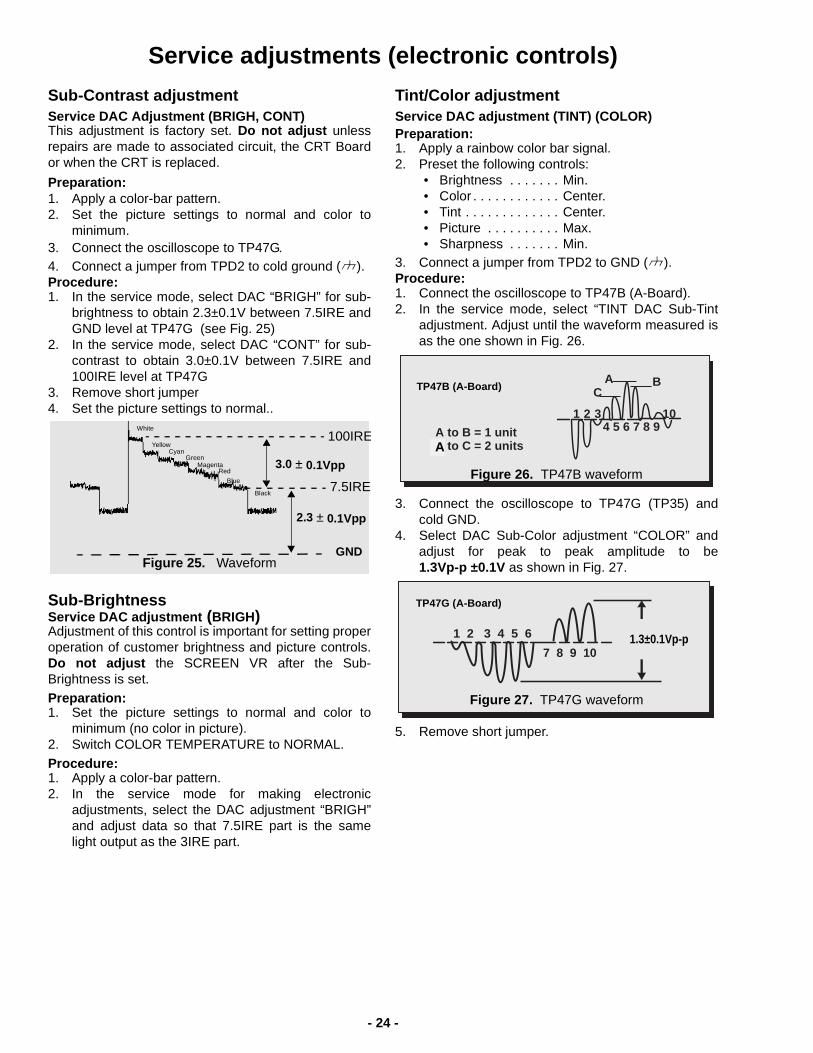
Service adjustments (electronic controls)
Sub-Contrast adjustmentService DAC Adjustment (BRIGH, CONT)This adjustment is factory set. Do not adjust unlessrepairs are made to associated circuit, the CRT Boardor when the CRT is replaced.
Preparation:1. Apply a color-bar pattern.2. Set the picture settings to normal and color to
minimum.3. Connect the oscilloscope to TP47G.4. Connect a jumper from TPD2 to cold ground ( ).Procedure:1. In the service mode, select DAC “BRIGH” for sub-
brightness to obtain 2.3±0.1V between 7.5IRE andGND level at TP47G (see Fig. 25)
2. In the service mode, select DAC “CONT” for sub-contrast to obtain 3.0±0.1V between 7.5IRE and100IRE level at TP47G
3. Remove short jumper4. Set the picture settings to normal..
Sub-BrightnessService DAC adjustment (BRIGH)Adjustment of this control is important for setting properoperation of customer brightness and picture controls.Do not adjust the SCREEN VR after the Sub-Brightness is set.Preparation:1. Set the picture settings to normal and color to
minimum (no color in picture).2. Switch COLOR TEMPERATURE to NORMAL.
Procedure:1. Apply a color-bar pattern.2. In the service mode for making electronic
adjustments, select the DAC adjustment “BRIGH”and adjust data so that 7.5IRE part is the samelight output as the 3IRE part.
Tint/Color adjustmentService DAC adjustment (TINT) (COLOR)Preparation:1. Apply a rainbow color bar signal.2. Preset the following controls:
• Brightness . . . . . . . Min.• Color . . . . . . . . . . . . Center.• Tint . . . . . . . . . . . . . Center.• Picture . . . . . . . . . . Max.• Sharpness . . . . . . . Min.
3. Connect a jumper from TPD2 to GND ( ).Procedure:1. Connect the oscilloscope to TP47B (A-Board).2. In the service mode, select “TINT DAC Sub-Tint
adjustment. Adjust until the waveform measured isas the one shown in Fig. 26.
3. Connect the oscilloscope to TP47G (TP35) andcold GND.
4. Select DAC Sub-Color adjustment “COLOR” andadjust for peak to peak amplitude to be1.3Vp-p ±0.1V as shown in Fig. 27.
5. Remove short jumper.
Figure 25. Waveform
2.3 ± 0.1Vpp
3.0 ± 0.1Vpp
GND
100IRE
7.5IRE
White
YellowCyan
GreenMagenta
Red
Blue
Black
A to B = 1 unit
A C
1 2 3 104 5 6 7 8 9
B
B to C = 2 units
Figure 26. TP47B waveform
TP47B (A-Board)
A
1 2 3 4 5 6
7 8 9 10
Figure 27. TP47G waveform
TP47G (A-Board)
1.3±0.1Vp-p
- 25 -
Tint/Color adjustmentService DAC adjustment (TINT) (COLOR)
Note: Color, tint adjustment sets thereference settings for the usercontrols; It is important to read theprocedures.
(No rainbow pattern)Make sure that sub-contrast adjustment was finishedprior to perform this adjustmentPreparation:1. Normalize the picture settings.2. Set picture mode to VIVIDProcedure:1. Apply a color bar pattern.2. In service mode adjust “TINT” sub-tint data so that
the color does not become greenish or redish.3. In service mode adjust “COLOR” sub-color data so
that the color level is not too high (saturated) or toolow (tending to black and white).
4. confirm that saturation and picture are normal(normal image).
5. If image is not satisfactory, repeat adjustment untilthe image is normal and natural.
6. The image can be compared against other set tosee the image quality.
Color temperature adjustment(B/W Tracking)Service DAC adjust(CUT_R) (CUT_G) (CUT_B) (R -DR) (B-DR)Minor touch-up methodOBSERVE low and high brightness areas of a B/Wpicture for proper tracking. Adjust only as required forgood gray scale and warm highlights”.1. LOW LIGHT areas – In service mode for making
electronic adjustments, select “CUT_R”, “CUT_G”,“CUT_B” and adjust the picture for gray.
2. HIGH LIGHT areas – In service mode for makingelectronic adjustments, select “CUT_G”, “CUT_B”and adjust the picture for warm whites.
Complete adjustment
Preparation:
1. Turn the receiver “ON” and allow 10 minutes warmup at high brightness.
2. Apply a color bar signal with color “OFF”.3. Turn the SCREEN control (part of FBT T551) fully
counterclockwise.
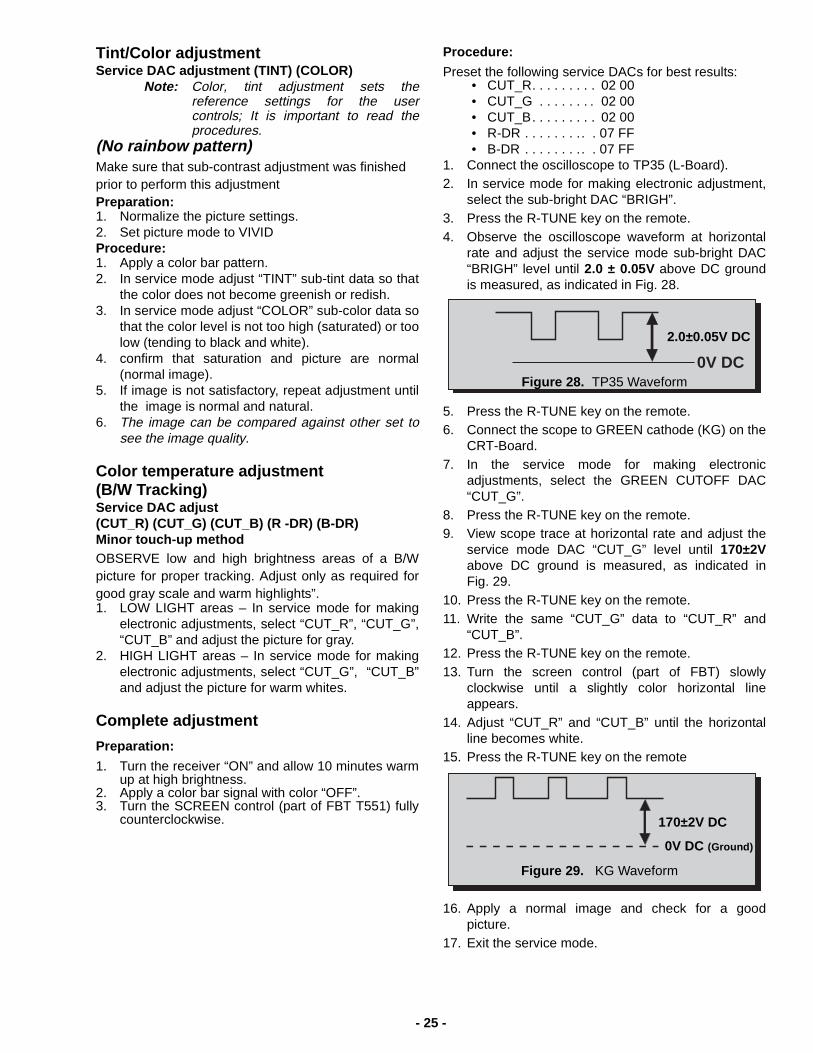
Procedure:
Preset the following service DACs for best results:• CUT_R. . . . . . . . . 02 00• CUT_G . . . . . . . . 02 00• CUT_B. . . . . . . . . 02 00• R-DR . . . . . . . .. . 07 FF• B-DR . . . . . . . .. . 07 FF
1. Connect the oscilloscope to TP35 (L-Board).2. In service mode for making electronic adjustment,
select the sub-bright DAC “BRIGH”.3. Press the R-TUNE key on the remote.4. Observe the oscilloscope waveform at horizontal
rate and adjust the service mode sub-bright DAC“BRIGH” level until 2.0 ± 0.05V above DC groundis measured, as indicated in Fig. 28.
5. Press the R-TUNE key on the remote.6. Connect the scope to GREEN cathode (KG) on the
CRT-Board.7. In the service mode for making electronic
adjustments, select the GREEN CUTOFF DAC“CUT_G”.
8. Press the R-TUNE key on the remote.9. View scope trace at horizontal rate and adjust the
service mode DAC “CUT_G” level until 170±2Vabove DC ground is measured, as indicated inFig. 29.
10. Press the R-TUNE key on the remote.11. Write the same “CUT_G” data to “CUT_R” and
“CUT_B”.12. Press the R-TUNE key on the remote.13. Turn the screen control (part of FBT) slowly
clockwise until a slightly color horizontal lineappears.
14. Adjust “CUT_R” and “CUT_B” until the horizontalline becomes white.
15. Press the R-TUNE key on the remote
16. Apply a normal image and check for a goodpicture.
17. Exit the service mode.
0V DCFigure 28. TP35 Waveform
2.0±0.05V DC
Figure 29. KG Waveform
170±2V DC
0V DC (Ground)
- 26 -
Service adjustments (electronic controls, cont.)Horizontal centering (H-POS)This adjustment helps to center the picture horizontallyPreparation:
Apply a pattern that permits the centering of theimage.
Procedure:1. In the service mode for making electronic
adjustments. Select the horizontal centeringadjustment DAC “H-POS” and adjust until thecenter of the monoscope pattern is centered onCRT.
2. Exit the service adjustment mode.Horizontal width adjustment (H-WIDTH)Preparation:
Apply a pattern that permits the centering of theimage.
Procedure:1. Adjust “VRAS” data so that the picture is in the
center and lines are straight (check mark on CRTsides).
2. Apply a crosshatch pattern.3. Adjust “PCC” data to make lines straight.4. Adjust “H-WID” data to correct the horizontal width
of the image.5. Adjust “VEAMP” data to correct vetical size of the
image.
Horizontal trapezoid adjustment (HTRAP)Preparation:1. Apply a crosshatch pattern2. Normalize the picture settings.
Procedure:1. Enter service mode, select “HTRAP” and adjust
DATA so that horizontal lines are straight(see Fig. 30)
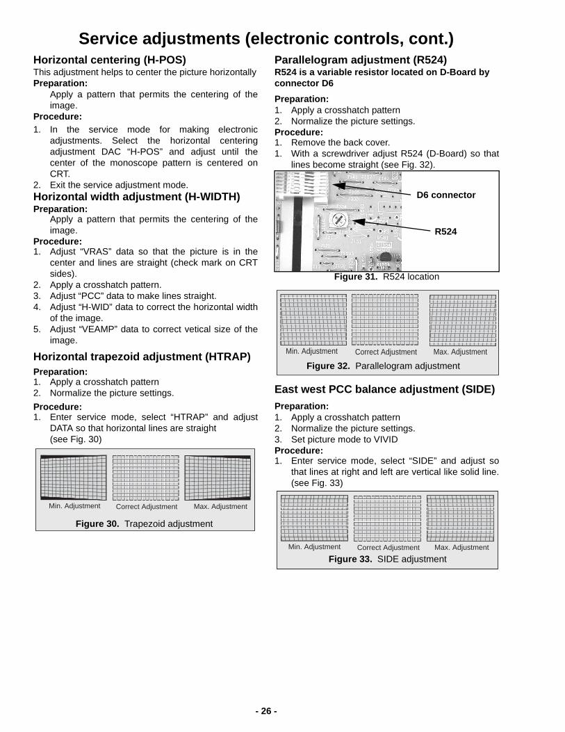
Parallelogram adjustment (R524)R524 is a variable resistor located on D-Board byconnector D6
Preparation:1. Apply a crosshatch pattern2. Normalize the picture settings.Procedure:1. Remove the back cover.1. With a screwdriver adjust R524 (D-Board) so that
lines become straight (see Fig. 32).
Figure 31. R524 location
East west PCC balance adjustment (SIDE)Preparation:1. Apply a crosshatch pattern2. Normalize the picture settings.3. Set picture mode to VIVIDProcedure:1. Enter service mode, select “SIDE” and adjust so
that lines at right and left are vertical like solid line.(see Fig. 33)
Min. Adjustment Correct Adjustment Max. Adjustment
Figure 30. Trapezoid adjustment
R524
D6 connector
Min. Adjustment Correct Adjustment Max. Adjustment
Figure 32. Parallelogram adjustment
Min. Adjustment Correct Adjustment Max. Adjustment
Figure 33. SIDE adjustment
- 27 -
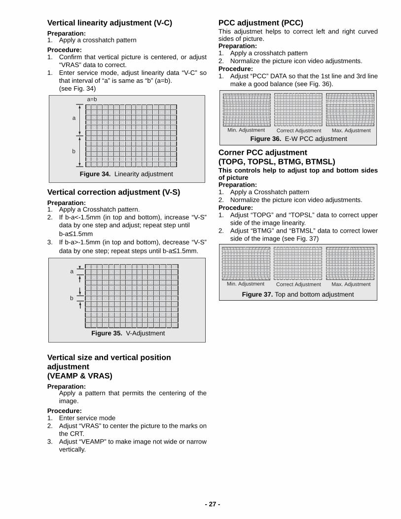
Vertical linearity adjustment (V-C)Preparation:1. Apply a crosshatch pattern
Procedure:1. Confirm that vertical picture is centered, or adjust
“VRAS” data to correct.1. Enter service mode, adjust linearity data “V-C” so
that interval of “a” is same as “b” (a=b).(see Fig. 34)
Vertical correction adjustment (V-S)Preparation:1. Apply a Crosshatch pattern.2. If b-a<-1.5mm (in top and bottom), increase “V-S”
data by one step and adjust; repeat step untilb-a≤1.5mm
3. If b-a>-1.5mm (in top and bottom), decrease “V-S”data by one step; repeat steps until b-a≤1.5mm.
Vertical size and vertical positionadjustment(VEAMP & VRAS)Preparation:
Apply a pattern that permits the centering of theimage.
Procedure:1. Enter service mode2. Adjust “VRAS” to center the picture to the marks on
the CRT.3. Adjust “VEAMP” to make image not wide or narrow
vertically.
PCC adjustment (PCC)This adjustmet helps to correct left and right curvedsides of picture.Preparation:1. Apply a crosshatch pattern2. Normalize the picture icon video adjustments.Procedure:1. Adjust “PCC” DATA so that the 1st line and 3rd line
make a good balance (see Fig. 36).
Corner PCC adjustment(TOPG, TOPSL, BTMG, BTMSL)This controls help to adjust top and bottom sidesof picturePreparation:1. Apply a Crosshatch pattern2. Normalize the picture icon video adjustments.Procedure:1. Adjust “TOPG” and “TOPSL” data to correct upper
side of the image linearity.2. Adjust “BTMG” and “BTMSL” data to correct lower
side of the image (see Fig. 37)
a
a=b
b
Figure 34. Linearity adjustment
a
b
Figure 35. V-Adjustment
Min. Adjustment Correct Adjustment Max. Adjustment
Figure 36. E-W PCC adjustment
Min. Adjustment Correct Adjustment Max. Adjustment
Figure 37. Top and bottom adjustment
- 28 -
Service adjustments (electronic controls, cont.)
MTS circuit adjustments
The MTS circuit adjustments require two steps:
1. Input level adjustment.2. Stereo separation adjustment.
Input level adjustment (MTSIN)Preparation:1. Connect an RMS meter with filter jig as shown in
Fig. 38.
2. Connect an RF signal generator to the RFantenna input.
Procedure :1. Apply the following signal from the RF signal
generator:Video: 100 IRE flat field, 30% modulation.Audio: 300Hz, 100% modulation, monaural(70 ±5dB, 75Ω OPEN, P/S 10dB).
2. Adjust the “MTSIN” input level DAC until thevoltage measured is 106 ± 6.0mV rms.
Stereo separation adjustment(SEPAL & SEPAH)Preparation:1. Connect an RF signal generator to the RF antenna
input.2. Connect oscilloscope to TPE10.
Procedure:1. Select stereo mode in audio menu2. Apply the following signal from the RF signal
generator:Video: 100 IRE flat field, 30% modulation.
Audio: 300Hz, 100% modulation, stereo (left only)(70 ±5dB, 75Ω OPEN, P/S 10dB).
3. Adjust the MTS low-level separation adjustment“SEPAL” until the amplitude displayed on thescope is minimum.
4. Apply the following signal from the RFsignal generator:
Video: 100 IRE flat field, 30% modulation.Audio: 3KHz, 100% modulation, stereo (left only)(70 ±5dB, 75Ω OPEN, P/S 10dB).
5. Adjust the MTS high-level separation adjustment“SEPAH” until the amplitude displayed on thescope is minimum.
6. Repeat above steps 2 through 5 until the amplitudeis minimum for both signals.
Clock adjustment (CLOCK)Preparation:
Connect the frequency counter to TP017 (IC001pin-79) and cold ground ( ).
Note: Frequency counter probe capacitance shouldbe 8pF or less.
Procedure:1. Measure TP017 (IC001 pin-79) for the frequency of
the waveform and record the reading.
Note: Pin 13 measurement must have at least fourdigits of resolution following the decimal point.Example: 000.0000
2. Place the receiver into service mode for makingelectronic adjustment, select the clock adjustmentDAC “CLOCK”.
3. Calculate and set “CLOCK” based on thefollowing formula:
Note: Pin 13 measurement will not changeregardless of the value stored in “CLOCK”.
Service adjustments (mechanical controls)
Focus (part of T551)This adjustment is to make the picture clearPreparation:Connect a Signal generator and select a dot pattern.
Procedure:Adjust the FOCUS controls to obtain the sharpest andclearest dot pattern.
a. Adjust VF1 to minimize width on vertical lines oncorners.
b. Adjust VF2 to minimize width on horizontal lineson corners.
10k4700p
TPE11RMSMETER
Figure 38. Filter jig
CLOCK 128 450000732.4220 pin79 Hz[ ]Ð
732.4220-------------------------------------------------------------+=
Figure 39. CLOCK adjustment
-
- 29 -
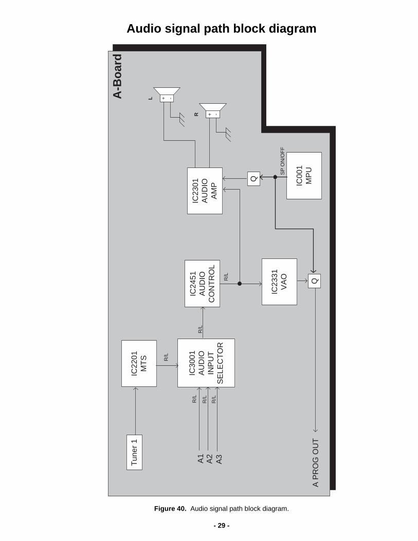
Audio signal path block diagram
Figure 40. Audio signal path block diagram.
A-B
oard
Tun
er 1
A1
A P
RO
G O
UT
IC30
01A
UD
IOIN
PU
TS
ELE
CT
OR
A2
A3
IC24
51A
UD
IOC
ON
TR
OL
IC23
01A
UD
IOA
MP
IC23
31V
AO
IC22
01M
TS
R
L + -
-+
IC00
1M
PU
Q
Q
SP
ON
/OF
F
R/L
R/L
R/L
R/L
R/L
R/L
- 30 -
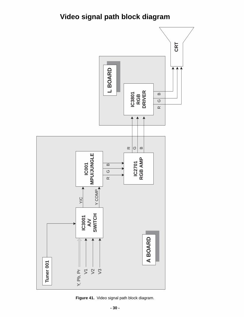
Video signal path block diagram
Figure 41. Video signal path block diagram.
Tune
r 00
1
Y, P
b, P
r
V2
V3
IC30
01A
/VS
WIT
CH
IC00
1M
PU
/JU
NG
LE
CR
T
V1
IC38
01R
GB
DR
IVE
R
Y C
OM
P
Y/C
BG
R
BGR
IC27
01R
GB
AM
P
BG
R
A B
OA
RD
L B
OA
RD
- 31 -
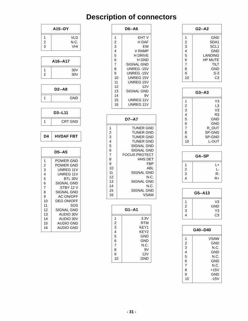
Description of connectorsA15--DY
123
VLDN.C.VHI
A16--A17
12
30V30V
D2--A8
1 GND
D3--L11
1 CRT GND
D4 HVDAF FBT
D5--A5
12345678910111213141516
POWER GNDPOWER GND
UNREG 11VUNREG 11V
BTL 30VSIGNAL GND
STBY 12 VSIGNAL GND
AC ON/OFFDEG ON/OFF
SOSSIGNAL GND
AUDIO 30VAUDIO 30V
AUDIO GNDAUDIO GND
D6--A6
12345678910111213141516
EHT VH DAF
EWV RAMPH DRIVE
H GNDSIGNAL GNDUNREG -15VUNREG -15VUNREG 15VUNREG 15V
12VSIGNAL GND
9VUNREG 11VUNREG 11V
D7--A7
12345678910111213141516
TUNER GNDTUNER GNDTUNER GNDTUNER GNDSIGNAL GNDSIGNAL GND
FOCUS PROTECTHHS DET
FBPABL
SIGNAL GNDN.C.
SIGNAL GNDN.C.
SIGNAL GNDVSAW
G1--A1
12345678910
3.3VRTM
KEY1KEY2GNDGNDN.C.
9V12V
GND
G2--A2
12345678910
GNDSDA1SCL1GND
LANDINGHP MUTE
TILTGND
S-3C3
G3--A3
12345678910
Y3L3V3R3
GNDGND
R_OUTSP-GNDSP-GND
L-OUT
G4--SP
1234
L+L-R-
R+
G5--A13
1234
V3GND
Y3C3
G40--D40
12345678910
VSAWGNDN.C.GNDN.C.GNDN.C.
+15VGND-15V
- 32 -
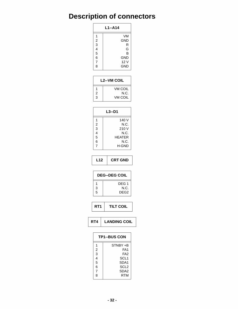
Description of connectorsL1--A14
12345678
VMGND
RGB
GND12 VGND
L2--VM COIL
123
VM COILN.C.
VM COIL
L3--D1
1234567
140 VN.C.
210 VN.C.
HEATERN.C.
H-GND
L12 CRT GND
DEG--DEG COIL
135
DEG 1N.C.
DEG2
RT1 TILT COIL
RT4 LANDING COIL
TP1--BUS CON
12345678
STNBY +BFA1FA2
SCL1SDA1SCL2SDA2RTM
- 33 -
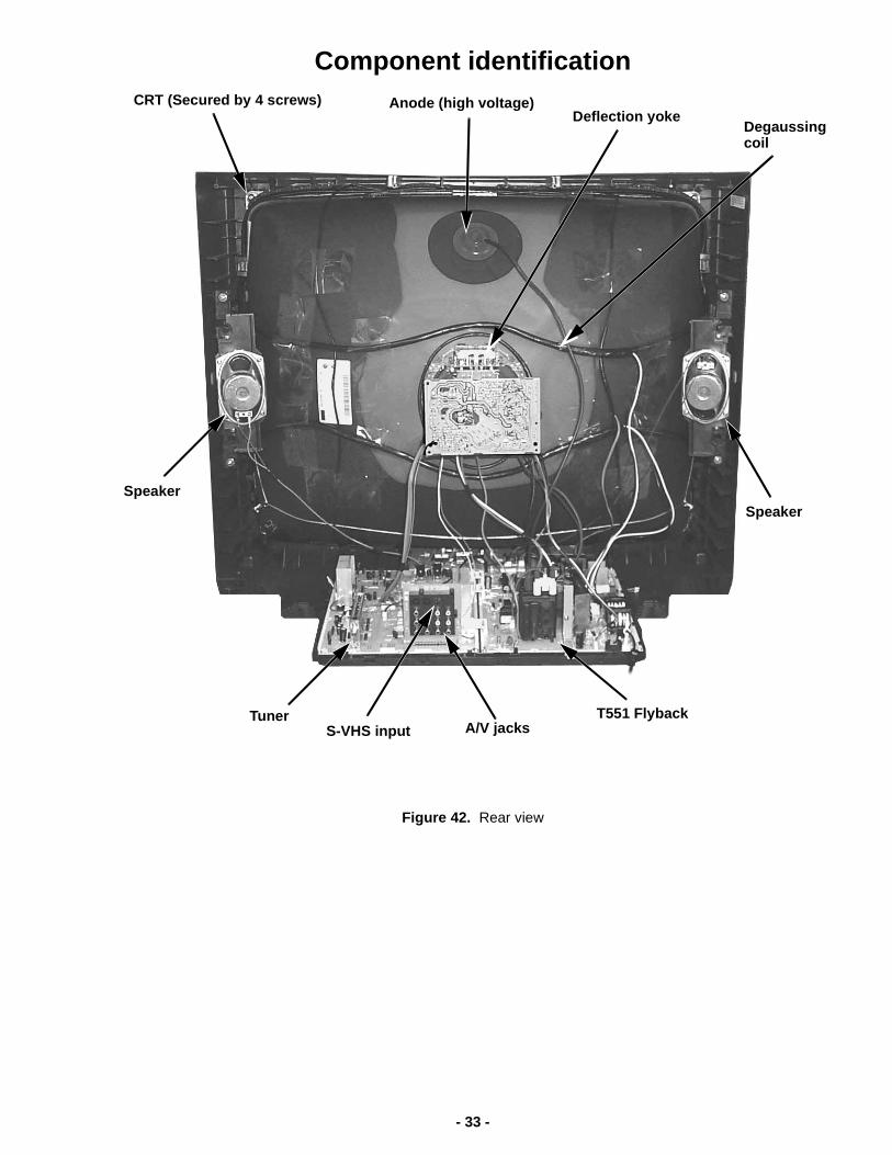
Component identification
Figure 42. Rear view
SpeakerSpeaker
TunerS-VHS input A/V jacks
T551 Flyback
Anode (high voltage)CRT (Secured by 4 screws)Deflection yoke
Degaussingcoil
- 34 -
Component identification
Figure 43. A-board
Figure 44. G-Board
IC451
A/V
TUNER
IC882
IC881
IC002
IC2301
IC4805
FRONT A/V
IC4804
IC4807
- 35 -
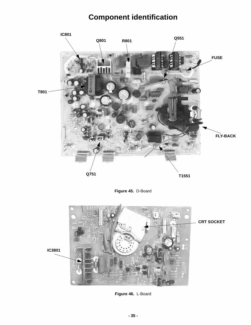
Component identification
Figure 45. D-Board
Figure 46. L-Board
IC801Q801 R801
FUSE
Q551
FLY-BACK
T1551Q751
T801
IC3801
CRT SOCKET
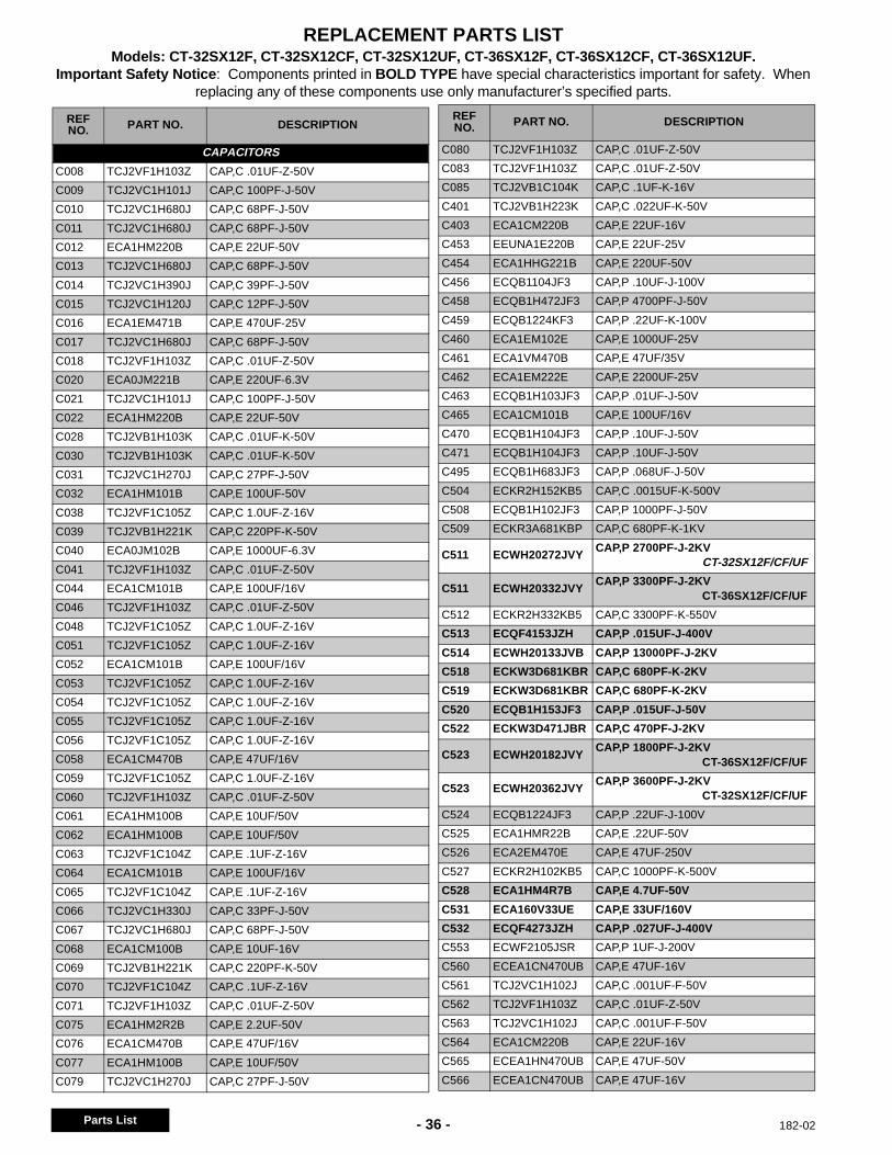
- 36 -Parts List
REPLACEMENT PARTS LISTModels: CT-32SX12F, CT-32SX12CF, CT-32SX12UF, CT-36SX12F, CT-36SX12CF, CT-36SX12UF.
Important Safety Notice : Components printed in BOLD TYPE have special characteristics important for safety. Whenreplacing any of these components use only manufacturer’s specified parts.
182-02
PA
RT
SLIS
T
REFNO. PART NO. DESCRIPTION
CAPACITORS
C008 TCJ2VF1H103Z CAP,C .01UF-Z-50V
C009 TCJ2VC1H101J CAP,C 100PF-J-50V
C010 TCJ2VC1H680J CAP,C 68PF-J-50V
C011 TCJ2VC1H680J CAP,C 68PF-J-50V
C012 ECA1HM220B CAP,E 22UF-50V
C013 TCJ2VC1H680J CAP,C 68PF-J-50V
C014 TCJ2VC1H390J CAP,C 39PF-J-50V
C015 TCJ2VC1H120J CAP,C 12PF-J-50V
C016 ECA1EM471B CAP,E 470UF-25V
C017 TCJ2VC1H680J CAP,C 68PF-J-50V
C018 TCJ2VF1H103Z CAP,C .01UF-Z-50V
C020 ECA0JM221B CAP,E 220UF-6.3V
C021 TCJ2VC1H101J CAP,C 100PF-J-50V
C022 ECA1HM220B CAP,E 22UF-50V
C028 TCJ2VB1H103K CAP,C .01UF-K-50V
C030 TCJ2VB1H103K CAP,C .01UF-K-50V
C031 TCJ2VC1H270J CAP,C 27PF-J-50V
C032 ECA1HM101B CAP,E 100UF-50V
C038 TCJ2VF1C105Z CAP,C 1.0UF-Z-16V
C039 TCJ2VB1H221K CAP,C 220PF-K-50V
C040 ECA0JM102B CAP,E 1000UF-6.3V
C041 TCJ2VF1H103Z CAP,C .01UF-Z-50V
C044 ECA1CM101B CAP,E 100UF/16V
C046 TCJ2VF1H103Z CAP,C .01UF-Z-50V
C048 TCJ2VF1C105Z CAP,C 1.0UF-Z-16V
C051 TCJ2VF1C105Z CAP,C 1.0UF-Z-16V
C052 ECA1CM101B CAP,E 100UF/16V
C053 TCJ2VF1C105Z CAP,C 1.0UF-Z-16V
C054 TCJ2VF1C105Z CAP,C 1.0UF-Z-16V
C055 TCJ2VF1C105Z CAP,C 1.0UF-Z-16V
C056 TCJ2VF1C105Z CAP,C 1.0UF-Z-16V
C058 ECA1CM470B CAP,E 47UF/16V
C059 TCJ2VF1C105Z CAP,C 1.0UF-Z-16V
C060 TCJ2VF1H103Z CAP,C .01UF-Z-50V
C061 ECA1HM100B CAP,E 10UF/50V
C062 ECA1HM100B CAP,E 10UF/50V
C063 TCJ2VF1C104Z CAP,E .1UF-Z-16V
C064 ECA1CM101B CAP,E 100UF/16V
C065 TCJ2VF1C104Z CAP,E .1UF-Z-16V
C066 TCJ2VC1H330J CAP,C 33PF-J-50V
C067 TCJ2VC1H680J CAP,C 68PF-J-50V
C068 ECA1CM100B CAP,E 10UF-16V
C069 TCJ2VB1H221K CAP,C 220PF-K-50V
C070 TCJ2VF1C104Z CAP,C .1UF-Z-16V
C071 TCJ2VF1H103Z CAP,C .01UF-Z-50V
C075 ECA1HM2R2B CAP,E 2.2UF-50V
C076 ECA1CM470B CAP,E 47UF/16V
C077 ECA1HM100B CAP,E 10UF/50V
C079 TCJ2VC1H270J CAP,C 27PF-J-50V
C080 TCJ2VF1H103Z CAP,C .01UF-Z-50V
C083 TCJ2VF1H103Z CAP,C .01UF-Z-50V
C085 TCJ2VB1C104K CAP,C .1UF-K-16V
C401 TCJ2VB1H223K CAP,C .022UF-K-50V
C403 ECA1CM220B CAP,E 22UF-16V
C453 EEUNA1E220B CAP,E 22UF-25V
C454 ECA1HHG221B CAP,E 220UF-50V
C456 ECQB1104JF3 CAP,P .10UF-J-100V
C458 ECQB1H472JF3 CAP,P 4700PF-J-50V
C459 ECQB1224KF3 CAP,P .22UF-K-100V
C460 ECA1EM102E CAP,E 1000UF-25V
C461 ECA1VM470B CAP,E 47UF/35V
C462 ECA1EM222E CAP,E 2200UF-25V
C463 ECQB1H103JF3 CAP,P .01UF-J-50V
C465 ECA1CM101B CAP,E 100UF/16V
C470 ECQB1H104JF3 CAP,P .10UF-J-50V
C471 ECQB1H104JF3 CAP,P .10UF-J-50V
C495 ECQB1H683JF3 CAP,P .068UF-J-50V
C504 ECKR2H152KB5 CAP,C .0015UF-K-500V
C508 ECQB1H102JF3 CAP,P 1000PF-J-50V
C509 ECKR3A681KBP CAP,C 680PF-K-1KV
C511 ECWH20272JVYCAP,P 2700PF-J-2KV
CT-32SX12F/CF/UF
C511 ECWH20332JVYCAP,P 3300PF-J-2KV
CT-36SX12F/CF/UF
C512 ECKR2H332KB5 CAP,C 3300PF-K-550V
C513 ECQF4153JZH CAP,P .015UF-J-400V
C514 ECWH20133JVB CAP,P 13000PF-J-2KV
C518 ECKW3D681KBR CAP,C 680PF-K-2KV
C519 ECKW3D681KBR CAP,C 680PF-K-2KV
C520 ECQB1H153JF3 CAP,P .015UF-J-50V
C522 ECKW3D471JBR CAP,C 470PF-J-2KV
C523 ECWH20182JVYCAP,P 1800PF-J-2KV
CT-36SX12F/CF/UF
C523 ECWH20362JVYCAP,P 3600PF-J-2KV
CT-32SX12F/CF/UF
C524 ECQB1224JF3 CAP,P .22UF-J-100V
C525 ECA1HMR22B CAP,E .22UF-50V
C526 ECA2EM470E CAP,E 47UF-250V
C527 ECKR2H102KB5 CAP,C 1000PF-K-500V
C528 ECA1HM4R7B CAP,E 4.7UF-50V
C531 ECA160V33UE CAP,E 33UF/160V
C532 ECQF4273JZH CAP,P .027UF-J-400V
C553 ECWF2105JSR CAP,P 1UF-J-200V
C560 ECEA1CN470UB CAP,E 47UF-16V
C561 TCJ2VC1H102J CAP,C .001UF-F-50V
C562 TCJ2VF1H103Z CAP,C .01UF-Z-50V
C563 TCJ2VC1H102J CAP,C .001UF-F-50V
C564 ECA1CM220B CAP,E 22UF-16V
C565 ECEA1HN470UB CAP,E 47UF-50V
C566 ECEA1CN470UB CAP,E 47UF-16V
REFNO. PART NO. DESCRIPTION
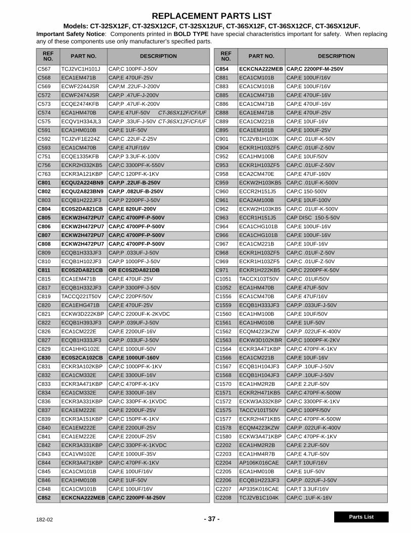
REPLACEMENT PARTS LISTModels: CT-32SX12F, CT-32SX12CF, CT-32SX12UF, CT-36SX12F, CT-36SX12CF, CT-36SX12UF.
Important Safety Notice : Components printed in BOLD TYPE have special characteristics important for safety. When replacingany of these components use only manufacturer’s specified parts.
- 37 -182-02
PA
RT
SLI
ST
Parts List
C567 TCJ2VC1H101J CAP,C 100PF-J-50V
C568 ECA1EM471B CAP,E 470UF-25V
C569 ECWF2244JSR CAP,M .22UF-J-200V
C572 ECWF2474JSR CAP,P .47UF-J-200V
C573 ECQE2474KFB CAP,P .47UF-K-200V
C574 ECA1HM470B CAP,E 47UF-50V CT-36SX12F/CF/UF
C575 ECQV1H334JL3 CAP,P .33UF-J-50V CT-36SX12F/CF/UF
C591 ECA1HM010B CAP,E 1UF-50V
C592 TCJ2VF1E224Z CAP,C .22UF-Z-25V
C593 ECA1CM470B CAP,E 47UF/16V
C751 ECQE1335KFB CAP,P 3.3UF-K-100V
C756 ECKR2H332KB5 CAP,C 3300PF-K-550V
C763 ECKR3A121KBP CAP,C 120PF-K-1KV
C801 ECQU2A224BN9 CAP,P .22UF-B-250V
C802 ECQU2A823BN9 CAP,P .082UF-B-250V
C803 ECQB1H222JF3 CAP,P 2200PF-J-50V
C804 EC0S2DA821CB CAP,E 820UF-200V
C805 ECKW2H472PU7 CAP,C 4700PF-P-500V
C806 ECKW2H472PU7 CAP,C 4700PF-P-500V
C807 ECKW2H472PU7 CAP,C 4700PF-P-500V
C808 ECKW2H472PU7 CAP,C 4700PF-P-500V
C809 ECQB1H333JF3 CAP,P .033UF-J-50V
C810 ECQB1H102JF3 CAP,P 1000PF-J-50V
C811 EC0S2DA821CB OR EC0S2DA821DB
C815 ECA1EM471B CAP,E 470UF-25V
C817 ECQB1H332JF3 CAP,P 3300PF-J-50V
C819 TACCQ221T50V CAP,C 220PF/50V
C820 ECA1EHG471B CAP,E 470UF-25V
C821 ECKW3D222KBP CAP,C 2200UF-K-2KVDC
C822 ECQB1H393JF3 CAP,P .039UF-J-50V
C826 ECA1CM222E CAP,E 2200UF-16V
C827 ECQB1H333JF3 CAP,P .033UF-J-50V
C829 ECA1HHG102E CAP,E 1000UF-50V
C830 EC0S2CA102CB CAP,E 1000UF-160V
C831 ECKR3A102KBP CAP,C 1000PF-K-1KV
C832 ECA1CM332E CAP,E 3300UF-16V
C833 ECKR3A471KBP CAP,C 470PF-K-1KV
C834 ECA1CM332E CAP,E 3300UF-16V
C836 ECKR3A331KBP CAP,C 330PF-K-1KVDC
C837 ECA1EM222E CAP,E 2200UF-25V
C839 ECKR3A151KBP CAP,C 150PF-K-1KV
C840 ECA1EM222E CAP,E 2200UF-25V
C841 ECA1EM222E CAP,E 2200UF-25V
C842 ECKR3A331KBP CAP,C 330PF-K-1KVDC
C843 ECA1VM102E CAP,E 1000UF-35V
C844 ECKR3A471KBP CAP,C 470PF-K-1KV
C845 ECA1CM101B CAP,E 100UF/16V
C846 ECA1HM010B CAP,E 1UF-50V
C848 ECA1CM101B CAP,E 100UF/16V
C852 ECKCNA222MEB CAP,C 2200PF-M-250V
REFNO. PART NO. DESCRIPTION
C854 ECKCNA222MEB CAP,C 2200PF-M-250V
C881 ECA1CM101B CAP,E 100UF/16V
C883 ECA1CM101B CAP,E 100UF/16V
C885 ECA1CM471B CAP,E 470UF-16V
C886 ECA1CM471B CAP,E 470UF-16V
C888 ECA1EM471B CAP,E 470UF-25V
C889 ECA1CM221B CAP,E 10UF-16V
C895 ECA1EM101B CAP,E 100UF-25V
C901 TCJ2VB1H103K CAP,C .01UF-K-50V
C904 ECKR1H103ZF5 CAP,C .01UF-Z-50V
C952 ECA1HM100B CAP,E 10UF/50V
C953 ECKR1H103ZF5 CAP,C .01UF-Z-50V
C958 ECA2CM470E CAP,E 47UF-160V
C959 ECKW2H103KB5 CAP,C .01UF-K-500V
C960 ECCR2H151J5 CAP,C 150-500V
C961 ECA2AM100B CAP,E 10UF-100V
C962 ECKW2H103KB5 CAP,C .01UF-K-500V
C963 ECCR1H151J5 CAP DISC 150-5-50V
C964 ECA1CHG101B CAP,E 100UF-16V
C966 ECA1CHG101B CAP,E 100UF-16V
C967 ECA1CM221B CAP,E 10UF-16V
C968 ECKR1H103ZF5 CAP,C .01UF-Z-50V
C969 ECKR1H103ZF5 CAP,C .01UF-Z-50V
C971 ECKR1H222KB5 CAP,C 2200PF-K-50V
C1051 TACCX103T50V CAP,C .01UF/50V
C1052 ECA1HM470B CAP,E 47UF-50V
C1556 ECA1CM470B CAP,E 47UF/16V
C1559 ECQB1H333JF3 CAP,P .033UF-J-50V
C1560 ECA1HM100B CAP,E 10UF/50V
C1561 ECA1HM010B CAP,E 1UF-50V
C1562 ECQM4223KZW CAP,P .022UF-K-400V
C1563 ECKW3D102KBR CAP,C 1000PF-K-2KV
C1564 ECKR3A471KBP CAP,C 470PF-K-1KV
C1566 ECA1CM221B CAP,E 10UF-16V
C1567 ECQB1H104JF3 CAP,P .10UF-J-50V
C1568 ECQB1H104JF3 CAP,P .10UF-J-50V
C1570 ECA1HM2R2B CAP,E 2.2UF-50V
C1571 ECKR2H471KB5 CAP,C 470PF-K-500W
C1572 ECKW3A332KBP CAP,C 3300PF-K-1KV
C1575 TACCV101T50V CAP,C 100PF/50V
C1577 ECKR2H471KB5 CAP,C 470PF-K-500W
C1578 ECQM4223KZW CAP,P .022UF-K-400V
C1580 ECKW3A471KBP CAP,C 470PF-K-1KV
C2202 ECA1HM2R2B CAP,E 2.2UF-50V
C2203 ECA1HM4R7B CAP,E 4.7UF-50V
C2204 AP106K016CAE CAP,T 10UF/16V
C2205 ECA1HM010B CAP,E 1UF-50V
C2206 ECQB1H223JF3 CAP,P .022UF-J-50V
C2207 AP335K016CAE CAP,T 3.3UF/16V
C2208 TCJ2VB1C104K CAP,C .1UF-K-16V
REFNO. PART NO. DESCRIPTION

- 38 -Parts List
REPLACEMENT PARTS LISTModels: CT-32SX12F, CT-32SX12CF, CT-32SX12UF, CT-36SX12F, CT-36SX12CF, CT-36SX12UF.
Important Safety Notice : Components printed in BOLD TYPE have special characteristics important for safety. Whenreplacing any of these components use only manufacturer’s specified parts.
182-02
PA
RT
SLIS
T
C2209 TCJ2VB1C104K CAP,C .1UF-K-16V
C2210 TCJ2VB1C104K CAP,C .1UF-K-16V
C2211 ECA1CM100B CAP,E 10UF-16V
C2212 ECQB1H473JF3 CAP,P .047UF-J-50V
C2215 ECA0JM101B CAP,E 100UF-6.3V
C2218 ECA1HMR47B CAP,E .47UF-50V
C2219 TCJ2VC1H100D CAP,C 10PF-J-50V
C2302 ECA1HM010B CAP,E 1UF-50V
C2303 TCJ2VB1H392K CAP,C 3900UF-K-50V
C2304 TCJ2VB1H392K CAP,C 3900UF-K-50V
C2305 ECA1HM010B CAP,E 1UF-50V
C2307 ECA1EM102E CAP,E 1000UF-25V
C2308 ECA1HM101B CAP,E 100UF-50V
C2311 ECA1HM010B CAP,E 1UF-50V
C2312 ECA1EM102E CAP,E 1000UF-25V
C2313 ECA1VM222E CAP,E 2200UF-35V
C2314 ECA1EM102E CAP,E 1000UF-25V
C2331 ECA1HM010B CAP,E 1UF-50V
C2332 ECA1HM010B CAP,E 1UF-50V
C2333 ECA1EM100B CAP,E 10UF-25V
C2334 ECA1EM100B CAP,E 10UF-25V
C2335 ECA1HM010B CAP,E 1UF-50V
C2336 ECA1HM010B CAP,E 1UF-50V
C2337 ECA1CM470B CAP,E 47UF/16V
C2350 ECA1CM101B CAP,E 100UF/16V
C2431 TCJ2VF1C105Z CAP,C 1.0UF-Z-16V
C2432 TCJ2VF1C105Z CAP,C 1.0UF-Z-16V
C2433 TCJ2VC1H222J CAP,C 2200PF-J-50V
C2437 TCJ2VB1H333K CAP,C .033UF-K-50V
C2438 TCJ2VB1H102K CAP,C 1000PF-K-50V
C2444 TCJ2VB1C104K CAP,C .1UF-K-16V
C2445 TCJ2VB1C104K CAP,C .1UF-K-16V
C2449 TCJ2VB1H333K CAP,C .033UF-K-50V
C2450 TCJ2VB1H102K CAP,C 1000PF-K-50V
C2451 ECEA1CN100UB CAP,E 10UF-16V
C2452 TCJ2VB1H103K CAP,C .01UF-K-50V
C2459 TCJ2VB1H333K CAP,C .033UF-K-50V
C2460 TCJ2VB1H333K CAP,C .033UF-K-50V
C2461 ECA1HM4R7B CAP,E 4.7UF-50V
C2462 ECA1HM4R7B CAP,E 4.7UF-50V
C2463 ECEA1CN100UB CAP,E 10UF-16V
C2464 TCJ2VB1H333K CAP,C .033UF-K-50V
C2465 TCJ2VB1H333K CAP,C .033UF-K-50V
C2468 ECA1CM101B CAP,E 100UF/16V
C2473 ECA1HM4R7B CAP,E 4.7UF-50V
C2474 ECA1CM101B CAP,E 100UF/16V
C2475 ECA1HM4R7B CAP,E 4.7UF-50V
C2501 TCJ2VC1H680J CAP,C 68PF-J-50V
C2502 TCJ2VC1H680J CAP,C 68PF-J-50V
C2503 TCJ2VC1H680J CAP,C 68PF-J-50V
REFNO. PART NO. DESCRIPTION
C2504 ECEA1CN100UB CAP,E 10UF-16V
C2505 ECEA1CN101UB CAP,E 100UF-16V
C2505 EEANA1E100B CAP,E 10UF-25V
C2506 ECEA1CN101UB CAP,E 100UF-16V
C2701 ECA1CM101B CAP,E 100UF/16V
C2702 TCJ2VF1H103Z CAP,C .01UF-Z-50V
C3001 TCJ2VF1H103Z CAP,C .01UF-Z-50V
C3002 ECA1CM101B CAP,E 100UF/16V
C3003 ECA1CM100B CAP,E 10UF-16V
C3004 ECA1CM100B CAP,E 10UF-16V
C3005 ECA1CM100B CAP,E 10UF-16V
C3006 ECA1HM010B CAP,E 1UF-50V
C3007 ECA1HM010B CAP,E 1UF-50V
C3008 ECA1CM100B CAP,E 10UF-16V
C3009 TCJ2VF1H103Z CAP,C .01UF-Z-50V
C3010 ECA1CM100B CAP,E 10UF-16V
C3011 ECA1HM010B CAP,E 1UF-50V
C3012 ECA1HM010B CAP,E 1UF-50V
C3013 ECA1CM100B CAP,E 10UF-16V
C3014 TCJ2VF1H103Z CAP,C .01UF-Z-50V
C3015 ECA1HM010B CAP,E 1UF-50V
C3016 ECA1HM010B CAP,E 1UF-50V
C3018 ECA1HM010B CAP,E 1UF-50V
C3019 TCJ2VF1H103Z CAP,C .01UF-Z-50V
C3020 ECEA1CN100UB CAP,E 10UF-16V
C3021 TCJ2VF1H103Z CAP,C .01UF-Z-50V
C3022 ECA1CM101B CAP,E 100UF/16V
C3023 ECA1HM010B CAP,E 1UF-50V
C3024 ECA1HM010B CAP,E 1UF-50V
C3025 ECA1CM100B CAP,E 10UF-16V
C3054 ECA1CM471B CAP,E 470UF-16V
C3158 ECKR1H152KB5 CAP,C 1500PF-K-50V
C3159 ECKR1H152KB5 CAP,C 1500PF-K-50V
C3807 ECA1CM221B CAP,E 10UF-16V
C3808 ECQV1H224JL3 CAP,P .22UF-J-50V
C3809 ECQM4104KZB CAP,P .10UF-K-400V
C3811 ECA2EM100B CAP,E 10UF/250V
C3812 ECEA1CN100UB CAP,E 10UF-16V
C3814 ECKC3D332KBN CAP,C 3300PF-K-2KV
C4810 ECEA1CN220UB CAP,E 22UF-16V
C4811 ECEA1HN2R2UB CAP,E 2.2UF-50V
C4812 ECA1HM0R1B CAP,E 0.1UF/50V
C4813 ECKR1H472KB5 CAP,C 4700PF-K-50V
C4814 ECA1HM4R7B CAP,E 4.7UF-50V
C4815 ECA1HM4R7B CAP,E 4.7UF-50V
C4816 ECA1HM4R7B CAP,E 4.7UF-50V
C4817 ECA1HMR47B CAP,E .47UF-50V
C4818 ECA1EM100B CAP,E 10UF-25V
C4819 ECEA1CN100UB CAP,E 10UF-16V
C4910 ECA1VM470B CAP,E 47UF/35V
REFNO. PART NO. DESCRIPTION
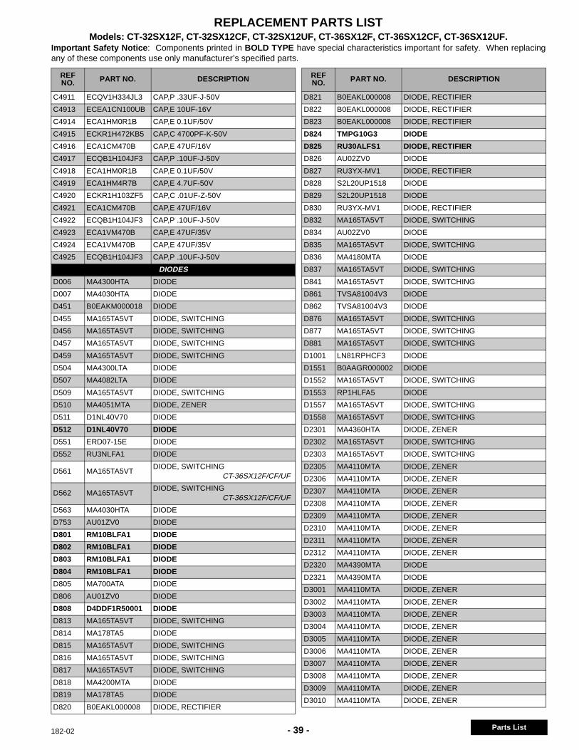
REPLACEMENT PARTS LISTModels: CT-32SX12F, CT-32SX12CF, CT-32SX12UF, CT-36SX12F, CT-36SX12CF, CT-36SX12UF.
Important Safety Notice : Components printed in BOLD TYPE have special characteristics important for safety. When replacingany of these components use only manufacturer’s specified parts.
- 39 -182-02
PA
RT
SLI
ST
Parts List
C4911 ECQV1H334JL3 CAP,P .33UF-J-50V
C4913 ECEA1CN100UB CAP,E 10UF-16V
C4914 ECA1HM0R1B CAP,E 0.1UF/50V
C4915 ECKR1H472KB5 CAP,C 4700PF-K-50V
C4916 ECA1CM470B CAP,E 47UF/16V
C4917 ECQB1H104JF3 CAP,P .10UF-J-50V
C4918 ECA1HM0R1B CAP,E 0.1UF/50V
C4919 ECA1HM4R7B CAP,E 4.7UF-50V
C4920 ECKR1H103ZF5 CAP,C .01UF-Z-50V
C4921 ECA1CM470B CAP,E 47UF/16V
C4922 ECQB1H104JF3 CAP,P .10UF-J-50V
C4923 ECA1VM470B CAP,E 47UF/35V
C4924 ECA1VM470B CAP,E 47UF/35V
C4925 ECQB1H104JF3 CAP,P .10UF-J-50V
DIODES
D006 MA4300HTA DIODE
D007 MA4030HTA DIODE
D451 B0EAKM000018 DIODE
D455 MA165TA5VT DIODE, SWITCHING
D456 MA165TA5VT DIODE, SWITCHING
D457 MA165TA5VT DIODE, SWITCHING
D459 MA165TA5VT DIODE, SWITCHING
D504 MA4300LTA DIODE
D507 MA4082LTA DIODE
D509 MA165TA5VT DIODE, SWITCHING
D510 MA4051MTA DIODE, ZENER
D511 D1NL40V70 DIODE
D512 D1NL40V70 DIODE
D551 ERD07-15E DIODE
D552 RU3NLFA1 DIODE
D561 MA165TA5VTDIODE, SWITCHING
CT-36SX12F/CF/UF
D562 MA165TA5VTDIODE, SWITCHING
CT-36SX12F/CF/UF
D563 MA4030HTA DIODE
D753 AU01ZV0 DIODE
D801 RM10BLFA1 DIODE
D802 RM10BLFA1 DIODE
D803 RM10BLFA1 DIODE
D804 RM10BLFA1 DIODE
D805 MA700ATA DIODE
D806 AU01ZV0 DIODE
D808 D4DDF1R50001 DIODE
D813 MA165TA5VT DIODE, SWITCHING
D814 MA178TA5 DIODE
D815 MA165TA5VT DIODE, SWITCHING
D816 MA165TA5VT DIODE, SWITCHING
D817 MA165TA5VT DIODE, SWITCHING
D818 MA4200MTA DIODE
D819 MA178TA5 DIODE
D820 B0EAKL000008 DIODE, RECTIFIER
REFNO. PART NO. DESCRIPTION
D821 B0EAKL000008 DIODE, RECTIFIER
D822 B0EAKL000008 DIODE, RECTIFIER
D823 B0EAKL000008 DIODE, RECTIFIER
D824 TMPG10G3 DIODE
D825 RU30ALFS1 DIODE, RECTIFIER
D826 AU02ZV0 DIODE
D827 RU3YX-MV1 DIODE, RECTIFIER
D828 S2L20UP1518 DIODE
D829 S2L20UP1518 DIODE
D830 RU3YX-MV1 DIODE, RECTIFIER
D832 MA165TA5VT DIODE, SWITCHING
D834 AU02ZV0 DIODE
D835 MA165TA5VT DIODE, SWITCHING
D836 MA4180MTA DIODE
D837 MA165TA5VT DIODE, SWITCHING
D841 MA165TA5VT DIODE, SWITCHING
D861 TVSA81004V3 DIODE
D862 TVSA81004V3 DIODE
D876 MA165TA5VT DIODE, SWITCHING
D877 MA165TA5VT DIODE, SWITCHING
D881 MA165TA5VT DIODE, SWITCHING
D1001 LN81RPHCF3 DIODE
D1551 B0AAGR000002 DIODE
D1552 MA165TA5VT DIODE, SWITCHING
D1553 RP1HLFA5 DIODE
D1557 MA165TA5VT DIODE, SWITCHING
D1558 MA165TA5VT DIODE, SWITCHING
D2301 MA4360HTA DIODE, ZENER
D2302 MA165TA5VT DIODE, SWITCHING
D2303 MA165TA5VT DIODE, SWITCHING
D2305 MA4110MTA DIODE, ZENER
D2306 MA4110MTA DIODE, ZENER
D2307 MA4110MTA DIODE, ZENER
D2308 MA4110MTA DIODE, ZENER
D2309 MA4110MTA DIODE, ZENER
D2310 MA4110MTA DIODE, ZENER
D2311 MA4110MTA DIODE, ZENER
D2312 MA4110MTA DIODE, ZENER
D2320 MA4390MTA DIODE
D2321 MA4390MTA DIODE
D3001 MA4110MTA DIODE, ZENER
D3002 MA4110MTA DIODE, ZENER
D3003 MA4110MTA DIODE, ZENER
D3004 MA4110MTA DIODE, ZENER
D3005 MA4110MTA DIODE, ZENER
D3006 MA4110MTA DIODE, ZENER
D3007 MA4110MTA DIODE, ZENER
D3008 MA4110MTA DIODE, ZENER
D3009 MA4110MTA DIODE, ZENER
D3010 MA4110MTA DIODE, ZENER
REFNO. PART NO. DESCRIPTION
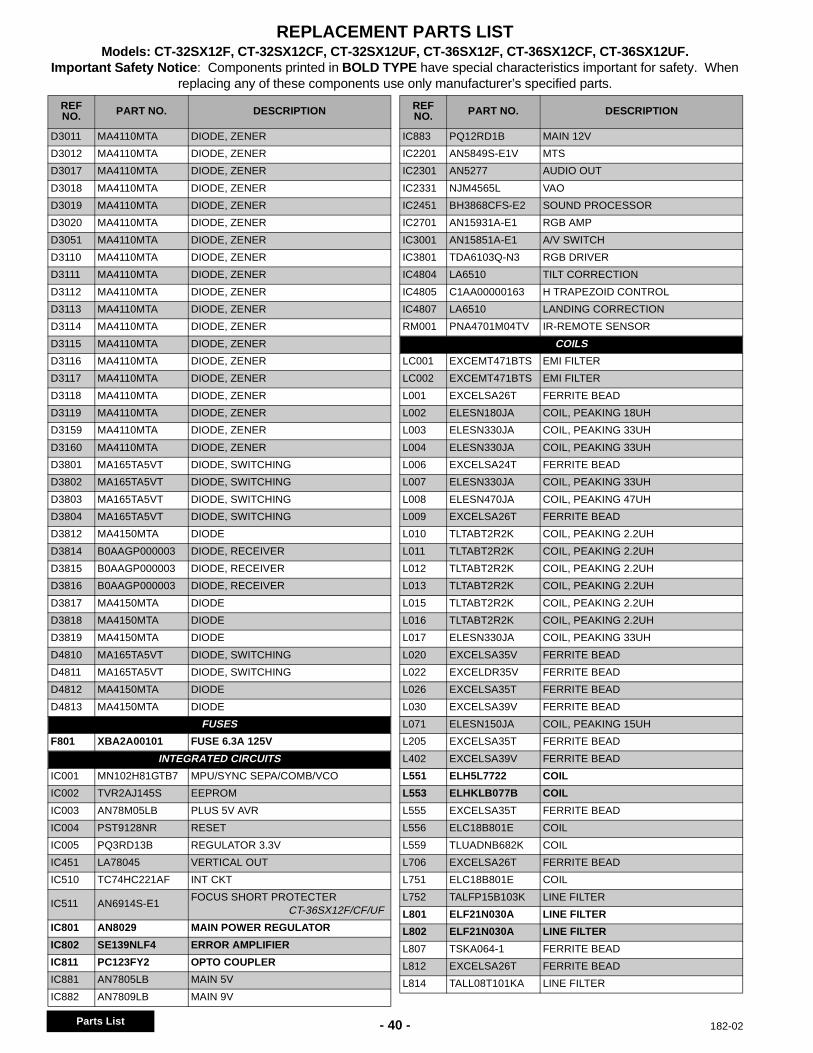
- 40 -Parts List
REPLACEMENT PARTS LISTModels: CT-32SX12F, CT-32SX12CF, CT-32SX12UF, CT-36SX12F, CT-36SX12CF, CT-36SX12UF.
Important Safety Notice : Components printed in BOLD TYPE have special characteristics important for safety. Whenreplacing any of these components use only manufacturer’s specified parts.
182-02
PA
RT
SLIS
T
D3011 MA4110MTA DIODE, ZENER
D3012 MA4110MTA DIODE, ZENER
D3017 MA4110MTA DIODE, ZENER
D3018 MA4110MTA DIODE, ZENER
D3019 MA4110MTA DIODE, ZENER
D3020 MA4110MTA DIODE, ZENER
D3051 MA4110MTA DIODE, ZENER
D3110 MA4110MTA DIODE, ZENER
D3111 MA4110MTA DIODE, ZENER
D3112 MA4110MTA DIODE, ZENER
D3113 MA4110MTA DIODE, ZENER
D3114 MA4110MTA DIODE, ZENER
D3115 MA4110MTA DIODE, ZENER
D3116 MA4110MTA DIODE, ZENER
D3117 MA4110MTA DIODE, ZENER
D3118 MA4110MTA DIODE, ZENER
D3119 MA4110MTA DIODE, ZENER
D3159 MA4110MTA DIODE, ZENER
D3160 MA4110MTA DIODE, ZENER
D3801 MA165TA5VT DIODE, SWITCHING
D3802 MA165TA5VT DIODE, SWITCHING
D3803 MA165TA5VT DIODE, SWITCHING
D3804 MA165TA5VT DIODE, SWITCHING
D3812 MA4150MTA DIODE
D3814 B0AAGP000003 DIODE, RECEIVER
D3815 B0AAGP000003 DIODE, RECEIVER
D3816 B0AAGP000003 DIODE, RECEIVER
D3817 MA4150MTA DIODE
D3818 MA4150MTA DIODE
D3819 MA4150MTA DIODE
D4810 MA165TA5VT DIODE, SWITCHING
D4811 MA165TA5VT DIODE, SWITCHING
D4812 MA4150MTA DIODE
D4813 MA4150MTA DIODE
FUSES
F801 XBA2A00101 FUSE 6.3A 125V
INTEGRATED CIRCUITS
IC001 MN102H81GTB7 MPU/SYNC SEPA/COMB/VCO
IC002 TVR2AJ145S EEPROM
IC003 AN78M05LB PLUS 5V AVR
IC004 PST9128NR RESET
IC005 PQ3RD13B REGULATOR 3.3V
IC451 LA78045 VERTICAL OUT
IC510 TC74HC221AF INT CKT
IC511 AN6914S-E1FOCUS SHORT PROTECTER
CT-36SX12F/CF/UF
IC801 AN8029 MAIN POWER REGULATOR
IC802 SE139NLF4 ERROR AMPLIFIER
IC811 PC123FY2 OPTO COUPLER
IC881 AN7805LB MAIN 5V
IC882 AN7809LB MAIN 9V
REFNO. PART NO. DESCRIPTION
IC883 PQ12RD1B MAIN 12V
IC2201 AN5849S-E1V MTS
IC2301 AN5277 AUDIO OUT
IC2331 NJM4565L VAO
IC2451 BH3868CFS-E2 SOUND PROCESSOR
IC2701 AN15931A-E1 RGB AMP
IC3001 AN15851A-E1 A/V SWITCH
IC3801 TDA6103Q-N3 RGB DRIVER
IC4804 LA6510 TILT CORRECTION
IC4805 C1AA00000163 H TRAPEZOID CONTROL
IC4807 LA6510 LANDING CORRECTION
RM001 PNA4701M04TV IR-REMOTE SENSOR
COILS
LC001 EXCEMT471BTS EMI FILTER
LC002 EXCEMT471BTS EMI FILTER
L001 EXCELSA26T FERRITE BEAD
L002 ELESN180JA COIL, PEAKING 18UH
L003 ELESN330JA COIL, PEAKING 33UH
L004 ELESN330JA COIL, PEAKING 33UH
L006 EXCELSA24T FERRITE BEAD
L007 ELESN330JA COIL, PEAKING 33UH
L008 ELESN470JA COIL, PEAKING 47UH
L009 EXCELSA26T FERRITE BEAD
L010 TLTABT2R2K COIL, PEAKING 2.2UH
L011 TLTABT2R2K COIL, PEAKING 2.2UH
L012 TLTABT2R2K COIL, PEAKING 2.2UH
L013 TLTABT2R2K COIL, PEAKING 2.2UH
L015 TLTABT2R2K COIL, PEAKING 2.2UH
L016 TLTABT2R2K COIL, PEAKING 2.2UH
L017 ELESN330JA COIL, PEAKING 33UH
L020 EXCELSA35V FERRITE BEAD
L022 EXCELDR35V FERRITE BEAD
L026 EXCELSA35T FERRITE BEAD
L030 EXCELSA39V FERRITE BEAD
L071 ELESN150JA COIL, PEAKING 15UH
L205 EXCELSA35T FERRITE BEAD
L402 EXCELSA39V FERRITE BEAD
L551 ELH5L7722 COIL
L553 ELHKLB077B COIL
L555 EXCELSA35T FERRITE BEAD
L556 ELC18B801E COIL
L559 TLUADNB682K COIL
L706 EXCELSA26T FERRITE BEAD
L751 ELC18B801E COIL
L752 TALFP15B103K LINE FILTER
L801 ELF21N030A LINE FILTER
L802 ELF21N030A LINE FILTER
L807 TSKA064-1 FERRITE BEAD
L812 EXCELSA26T FERRITE BEAD
L814 TALL08T101KA LINE FILTER
REFNO. PART NO. DESCRIPTION
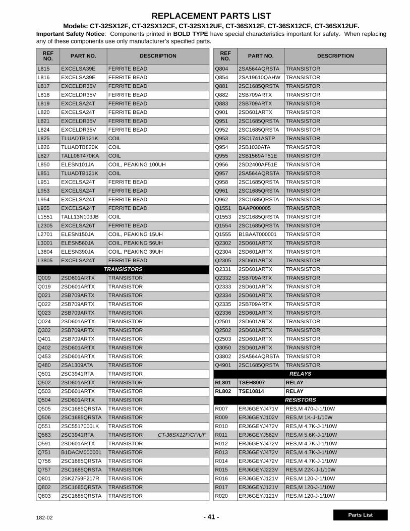
REPLACEMENT PARTS LISTModels: CT-32SX12F, CT-32SX12CF, CT-32SX12UF, CT-36SX12F, CT-36SX12CF, CT-36SX12UF.
Important Safety Notice : Components printed in BOLD TYPE have special characteristics important for safety. When replacingany of these components use only manufacturer’s specified parts.
- 41 -182-02
PA
RT
SLI
ST
Parts List
L815 EXCELSA39E FERRITE BEAD
L816 EXCELSA39E FERRITE BEAD
L817 EXCELDR35V FERRITE BEAD
L818 EXCELDR35V FERRITE BEAD
L819 EXCELSA24T FERRITE BEAD
L820 EXCELSA24T FERRITE BEAD
L821 EXCELDR35V FERRITE BEAD
L824 EXCELDR35V FERRITE BEAD
L825 TLUADTB121K COIL
L826 TLUADTB820K COIL
L827 TALL08T470KA COIL
L850 ELESN101JA COIL, PEAKING 100UH
L851 TLUADTB121K COIL
L951 EXCELSA24T FERRITE BEAD
L953 EXCELSA24T FERRITE BEAD
L954 EXCELSA24T FERRITE BEAD
L955 EXCELSA24T FERRITE BEAD
L1551 TALL13N103JB COIL
L2305 EXCELSA26T FERRITE BEAD
L2701 ELESN150JA COIL, PEAKING 15UH
L3001 ELESN560JA COIL, PEAKING 56UH
L3804 ELESN390JA COIL, PEAKING 39UH
L3805 EXCELSA24T FERRITE BEAD
TRANSISTORS
Q009 2SD601ARTX TRANSISTOR
Q019 2SD601ARTX TRANSISTOR
Q021 2SB709ARTX TRANSISTOR
Q022 2SB709ARTX TRANSISTOR
Q023 2SB709ARTX TRANSISTOR
Q024 2SD601ARTX TRANSISTOR
Q302 2SB709ARTX TRANSISTOR
Q401 2SB709ARTX TRANSISTOR
Q402 2SD601ARTX TRANSISTOR
Q453 2SD601ARTX TRANSISTOR
Q480 2SA1309ATA TRANSISTOR
Q501 2SC3941RTA TRANSISTOR
Q502 2SD601ARTX TRANSISTOR
Q503 2SD601ARTX TRANSISTOR
Q504 2SD601ARTX TRANSISTOR
Q505 2SC1685QRSTA TRANSISTOR
Q506 2SC1685QRSTA TRANSISTOR
Q551 2SC5517000LK TRANSISTOR
Q563 2SC3941RTA TRANSISTOR CT-36SX12F/CF/UF
Q591 2SD601ARTX TRANSISTOR
Q751 B1DACM000001 TRANSISTOR
Q756 2SC1685QRSTA TRANSISTOR
Q757 2SC1685QRSTA TRANSISTOR
Q801 2SK2759F217R TRANSISTOR
Q802 2SC1685QRSTA TRANSISTOR
Q803 2SC1685QRSTA TRANSISTOR
REFNO. PART NO. DESCRIPTION
Q804 2SA564AQRSTA TRANSISTOR
Q854 2SA19610QAHW TRANSISTOR
Q881 2SC1685QRSTA TRANSISTOR
Q882 2SB709ARTX TRANSISTOR
Q883 2SB709ARTX TRANSISTOR
Q901 2SD601ARTX TRANSISTOR
Q951 2SC1685QRSTA TRANSISTOR
Q952 2SC1685QRSTA TRANSISTOR
Q953 2SC1741ASTP TRANSISTOR
Q954 2SB1030ATA TRANSISTOR
Q955 2SB1569AF51E TRANSISTOR
Q956 2SD2400AF51E TRANSISTOR
Q957 2SA564AQRSTA TRANSISTOR
Q958 2SC1685QRSTA TRANSISTOR
Q961 2SC1685QRSTA TRANSISTOR
Q962 2SC1685QRSTA TRANSISTOR
Q1551 BAAP000005 TRANSISTOR
Q1553 2SC1685QRSTA TRANSISTOR
Q1554 2SC1685QRSTA TRANSISTOR
Q1555 B1BAAT000001 TRANSISTOR
Q2302 2SD601ARTX TRANSISTOR
Q2304 2SD601ARTX TRANSISTOR
Q2305 2SD601ARTX TRANSISTOR
Q2331 2SD601ARTX TRANSISTOR
Q2332 2SB709ARTX TRANSISTOR
Q2333 2SD601ARTX TRANSISTOR
Q2334 2SD601ARTX TRANSISTOR
Q2335 2SB709ARTX TRANSISTOR
Q2336 2SD601ARTX TRANSISTOR
Q2501 2SD601ARTX TRANSISTOR
Q2502 2SD601ARTX TRANSISTOR
Q2503 2SD601ARTX TRANSISTOR
Q3050 2SD601ARTX TRANSISTOR
Q3802 2SA564AQRSTA TRANSISTOR
Q4901 2SC1685QRSTA TRANSISTOR
RELAYS
RL801 TSEH8007 RELAY
RL802 TSE10814 RELAY
RESISTORS
R007 ERJ6GEYJ471V RES,M 470-J-1/10W
R009 ERJ6GEYJ102V RES,M 1K-J-1/10W
R010 ERJ6GEYJ472V RES,M 4.7K-J-1/10W
R011 ERJ6GEYJ562V RES,M 5.6K-J-1/10W
R012 ERJ6GEYJ472V RES,M 4.7K-J-1/10W
R013 ERJ6GEYJ472V RES,M 4.7K-J-1/10W
R014 ERJ6GEYJ472V RES,M 4.7K-J-1/10W
R015 ERJ6GEYJ223V RES,M 22K-J-1/10W
R016 ERJ6GEYJ121V RES,M 120-J-1/10W
R017 ERJ6GEYJ121V RES,M 120-J-1/10W
R020 ERJ6GEYJ121V RES,M 120-J-1/10W
REFNO. PART NO. DESCRIPTION
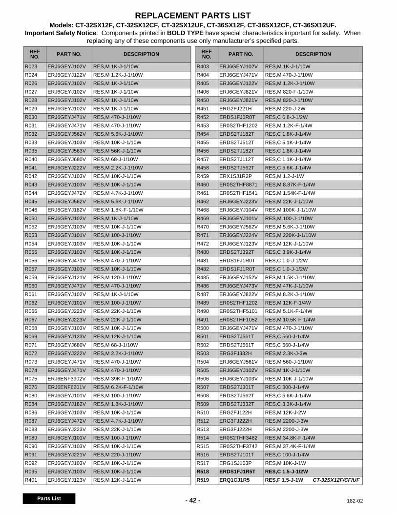
- 42 -Parts List
REPLACEMENT PARTS LISTModels: CT-32SX12F, CT-32SX12CF, CT-32SX12UF, CT-36SX12F, CT-36SX12CF, CT-36SX12UF.
Important Safety Notice : Components printed in BOLD TYPE have special characteristics important for safety. Whenreplacing any of these components use only manufacturer’s specified parts.
182-02
PA
RT
SLIS
T
R023 ERJ6GEYJ102V RES,M 1K-J-1/10W
R024 ERJ6GEYJ122V RES,M 1.2K-J-1/10W
R026 ERJ6GEYJ102V RES,M 1K-J-1/10W
R027 ERJ6GEYJ102V RES,M 1K-J-1/10W
R028 ERJ6GEYJ102V RES,M 1K-J-1/10W
R029 ERJ6GEYJ102V RES,M 1K-J-1/10W
R030 ERJ6GEYJ471V RES,M 470-J-1/10W
R031 ERJ6GEYJ471V RES,M 470-J-1/10W
R032 ERJ6GEYJ562V RES,M 5.6K-J-1/10W
R033 ERJ6GEYJ103V RES,M 10K-J-1/10W
R035 ERJ6GEYJ563V RES,M 56K-J-1/10W
R040 ERJ6GEYJ680V RES,M 68-J-1/10W
R041 ERJ6GEYJ222V RES,M 2.2K-J-1/10W
R042 ERJ6GEYJ103V RES,M 10K-J-1/10W
R043 ERJ6GEYJ103V RES,M 10K-J-1/10W
R044 ERJ6GEYJ472V RES,M 4.7K-J-1/10W
R045 ERJ6GEYJ562V RES,M 5.6K-J-1/10W
R046 ERJ6GEYJ182V RES,M 1.8K-F-1/10W
R050 ERJ6GEYJ102V RES,M 1K-J-1/10W
R052 ERJ6GEYJ103V RES,M 10K-J-1/10W
R053 ERJ6GEYJ101V RES,M 100-J-1/10W
R054 ERJ6GEYJ103V RES,M 10K-J-1/10W
R055 ERJ6GEYJ103V RES,M 10K-J-1/10W
R056 ERJ6GEYJ471V RES,M 470-J-1/10W
R057 ERJ6GEYJ103V RES,M 10K-J-1/10W
R059 ERJ6GEYJ121V RES,M 120-J-1/10W
R060 ERJ6GEYJ471V RES,M 470-J-1/10W
R061 ERJ6GEYJ102V RES,M 1K-J-1/10W
R062 ERJ6GEYJ101V RES,M 100-J-1/10W
R066 ERJ6GEYJ223V RES,M 22K-J-1/10W
R067 ERJ6GEYJ223V RES,M 22K-J-1/10W
R068 ERJ6GEYJ103V RES,M 10K-J-1/10W
R069 ERJ6GEYJ123V RES,M 12K-J-1/10W
R071 ERJ6GEYJ680V RES,M 68-J-1/10W
R072 ERJ6GEYJ222V RES,M 2.2K-J-1/10W
R073 ERJ6GEYJ471V RES,M 470-J-1/10W
R074 ERJ6GEYJ471V RES,M 470-J-1/10W
R075 ERJ6ENF3902V RES,M 39K-F-1/10W
R076 ERJ6ENF6201V RES,M 6.2K-F-1/10W
R080 ERJ6GEYJ101V RES,M 100-J-1/10W
R084 ERJ6GEYJ182V RES,M 1.8K-J-1/10W
R086 ERJ6GEYJ103V RES,M 10K-J-1/10W
R087 ERJ6GEYJ472V RES,M 4.7K-J-1/10W
R088 ERJ6GEYJ223V RES,M 22K-J-1/10W
R089 ERJ6GEYJ101V RES,M 100-J-1/10W
R090 ERJ6GEYJ103V RES,M 10K-J-1/10W
R091 ERJ6GEYJ221V RES,M 220-J-1/10W
R092 ERJ6GEYJ103V RES,M 10K-J-1/10W
R095 ERJ6GEYJ103V RES,M 10K-J-1/10W
R401 ERJ6GEYJ123V RES,M 12K-J-1/10W
REFNO. PART NO. DESCRIPTION
R403 ERJ6GEYJ102V RES,M 1K-J-1/10W
R404 ERJ6GEYJ471V RES,M 470-J-1/10W
R405 ERJ6GEYJ122V RES,M 1.2K-J-1/10W
R406 ERJ6GEYJ821V RES,M 820-F-1/10W
R450 ERJ6GEYJ821V RES,M 820-J-1/10W
R451 ERG2FJ221H RES,M 220-J-2W
R452 ERDS1FJ6R8T RES,C 6.8-J-1/2W
R453 ER0S2THF1202 RES,M 1.2K-F-1/4W
R454 ERDS2TJ182T RES,C 1.8K-J-1/4W
R455 ERDS2TJ512T RES,C 5.1K-J-1/4W
R456 ERDS2TJ182T RES,C 1.8K-J-1/4W
R457 ERDS2TJ112T RES,C 1.1K-J-1/4W
R458 ERDS2TJ562T RES,C 5.6K-J-1/4W
R459 ERX1SJ1R2P RES,M 1.2-J-1W
R460 ER0S2THF8871 RES,M 8.87K-F-1/4W
R461 ER0S2THF1541 RES,M 1.54K-F-1/4W
R462 ERJ6GEYJ223V RES,M 22K-J-1/10W
R468 ERJ6GEYJ104V RES,M 100K-J-1/10W
R469 ERJ6GEYJ101V RES,M 100-J-1/10W
R470 ERJ6GEYJ562V RES,M 5.6K-J-1/10W
R471 ERJ6GEYJ224V RES,M 220K-J-1/10W
R472 ERJ6GEYJ123V RES,M 12K-J-1/10W
R480 ERDS2TJ392T RES,C 3.9K-J-1/4W
R481 ERDS1FJ1R0T RES,C 1.0-J-1/2W
R482 ERDS1FJ1R0T RES,C 1.0-J-1/2W
R485 ERJ6GEYJ152V RES,M 1.5K-J-1/10W
R486 ERJ6GEYJ473V RES,M 47K-J-1/10W
R487 ERJ6GEYJ822V RES,M 8.2K-J-1/10W
R489 ER0S2THF1202 RES,M 12K-F-1/4W
R490 ER0S2THF5101 RES,M 5.1K-F-1/4W
R491 ER0S2THF1052 RES,M 10.5K-F-1/4W
R500 ERJ6GEYJ471V RES,M 470-J-1/10W
R501 ERDS2TJ561T RES,C 560-J-1/4W
R502 ERDS2TJ561T RES,C 560-J-1/4W
R503 ERG3FJ332H RES,M 2.3K-J-3W
R504 ERJ6GEYJ561V RES,M 560-J-1/10W
R505 ERJ6GEYJ102V RES,M 1K-J-1/10W
R506 ERJ6GEYJ103V RES,M 10K-J-1/10W
R507 ERDS2TJ301T RES,C 300-J-1/4W
R508 ERDS2TJ562T RES,C 5.6K-J-1/4W
R509 ERDS2TJ332T RES,C 3.3K-J-1/4W
R510 ERG2FJ122H RES,M 12K-J-2W
R512 ERG3FJ222H RES,M 2200-J-3W
R513 ERG3FJ222H RES,M 2200-J-3W
R514 ER0S2THF3482 RES,M 34.8K-F-1/4W
R515 ER0S2THF3742 RES,M 37.4K-F-1/4W
R516 ERDS2TJ101T RES,C 100-J-1/4W
R517 ERG1SJ103P RES,M 10K-J-1W
R518 ERDS1FJ1R5T RES,C 1.5-J-1/2W
R519 ERQ1CJ1R5 RES,F 1.5-J-1W CT-32SX12F/CF/UF
REFNO. PART NO. DESCRIPTION
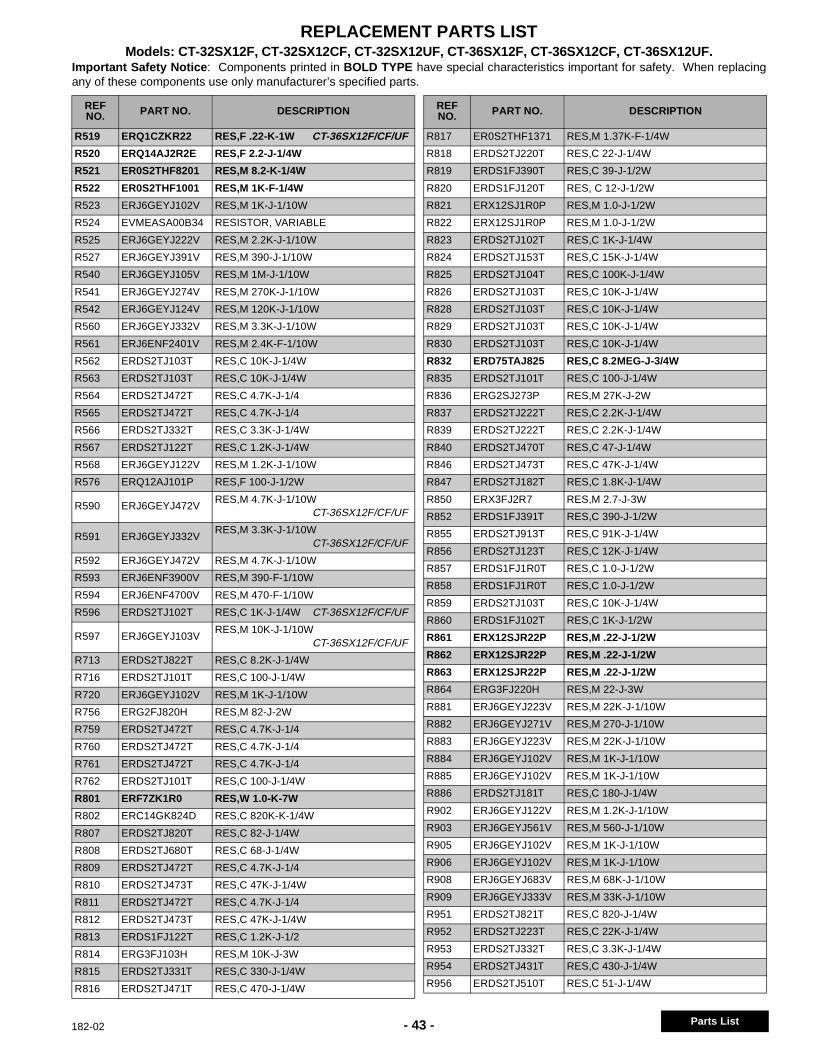
REPLACEMENT PARTS LISTModels: CT-32SX12F, CT-32SX12CF, CT-32SX12UF, CT-36SX12F, CT-36SX12CF, CT-36SX12UF.
Important Safety Notice : Components printed in BOLD TYPE have special characteristics important for safety. When replacingany of these components use only manufacturer’s specified parts.
- 43 -182-02
PA
RT
SLI
ST
Parts List
R519 ERQ1CZKR22 RES,F .22-K-1W CT-36SX12F/CF/UF
R520 ERQ14AJ2R2E RES,F 2.2-J-1/4W
R521 ER0S2THF8201 RES,M 8.2-K-1/4W
R522 ER0S2THF1001 RES,M 1K-F-1/4W
R523 ERJ6GEYJ102V RES,M 1K-J-1/10W
R524 EVMEASA00B34 RESISTOR, VARIABLE
R525 ERJ6GEYJ222V RES,M 2.2K-J-1/10W
R527 ERJ6GEYJ391V RES,M 390-J-1/10W
R540 ERJ6GEYJ105V RES,M 1M-J-1/10W
R541 ERJ6GEYJ274V RES,M 270K-J-1/10W
R542 ERJ6GEYJ124V RES,M 120K-J-1/10W
R560 ERJ6GEYJ332V RES,M 3.3K-J-1/10W
R561 ERJ6ENF2401V RES,M 2.4K-F-1/10W
R562 ERDS2TJ103T RES,C 10K-J-1/4W
R563 ERDS2TJ103T RES,C 10K-J-1/4W
R564 ERDS2TJ472T RES,C 4.7K-J-1/4
R565 ERDS2TJ472T RES,C 4.7K-J-1/4
R566 ERDS2TJ332T RES,C 3.3K-J-1/4W
R567 ERDS2TJ122T RES,C 1.2K-J-1/4W
R568 ERJ6GEYJ122V RES,M 1.2K-J-1/10W
R576 ERQ12AJ101P RES,F 100-J-1/2W
R590 ERJ6GEYJ472VRES,M 4.7K-J-1/10W
CT-36SX12F/CF/UF
R591 ERJ6GEYJ332VRES,M 3.3K-J-1/10W
CT-36SX12F/CF/UF
R592 ERJ6GEYJ472V RES,M 4.7K-J-1/10W
R593 ERJ6ENF3900V RES,M 390-F-1/10W
R594 ERJ6ENF4700V RES,M 470-F-1/10W
R596 ERDS2TJ102T RES,C 1K-J-1/4W CT-36SX12F/CF/UF
R597 ERJ6GEYJ103VRES,M 10K-J-1/10W
CT-36SX12F/CF/UF
R713 ERDS2TJ822T RES,C 8.2K-J-1/4W
R716 ERDS2TJ101T RES,C 100-J-1/4W
R720 ERJ6GEYJ102V RES,M 1K-J-1/10W
R756 ERG2FJ820H RES,M 82-J-2W
R759 ERDS2TJ472T RES,C 4.7K-J-1/4
R760 ERDS2TJ472T RES,C 4.7K-J-1/4
R761 ERDS2TJ472T RES,C 4.7K-J-1/4
R762 ERDS2TJ101T RES,C 100-J-1/4W
R801 ERF7ZK1R0 RES,W 1.0-K-7W
R802 ERC14GK824D RES,C 820K-K-1/4W
R807 ERDS2TJ820T RES,C 82-J-1/4W
R808 ERDS2TJ680T RES,C 68-J-1/4W
R809 ERDS2TJ472T RES,C 4.7K-J-1/4
R810 ERDS2TJ473T RES,C 47K-J-1/4W
R811 ERDS2TJ472T RES,C 4.7K-J-1/4
R812 ERDS2TJ473T RES,C 47K-J-1/4W
R813 ERDS1FJ122T RES,C 1.2K-J-1/2
R814 ERG3FJ103H RES,M 10K-J-3W
R815 ERDS2TJ331T RES,C 330-J-1/4W
R816 ERDS2TJ471T RES,C 470-J-1/4W
REFNO. PART NO. DESCRIPTION
R817 ER0S2THF1371 RES,M 1.37K-F-1/4W
R818 ERDS2TJ220T RES,C 22-J-1/4W
R819 ERDS1FJ390T RES,C 39-J-1/2W
R820 ERDS1FJ120T RES, C 12-J-1/2W
R821 ERX12SJ1R0P RES,M 1.0-J-1/2W
R822 ERX12SJ1R0P RES,M 1.0-J-1/2W
R823 ERDS2TJ102T RES,C 1K-J-1/4W
R824 ERDS2TJ153T RES,C 15K-J-1/4W
R825 ERDS2TJ104T RES,C 100K-J-1/4W
R826 ERDS2TJ103T RES,C 10K-J-1/4W
R828 ERDS2TJ103T RES,C 10K-J-1/4W
R829 ERDS2TJ103T RES,C 10K-J-1/4W
R830 ERDS2TJ103T RES,C 10K-J-1/4W
R832 ERD75TAJ825 RES,C 8.2MEG-J-3/4W
R835 ERDS2TJ101T RES,C 100-J-1/4W
R836 ERG2SJ273P RES,M 27K-J-2W
R837 ERDS2TJ222T RES,C 2.2K-J-1/4W
R839 ERDS2TJ222T RES,C 2.2K-J-1/4W
R840 ERDS2TJ470T RES,C 47-J-1/4W
R846 ERDS2TJ473T RES,C 47K-J-1/4W
R847 ERDS2TJ182T RES,C 1.8K-J-1/4W
R850 ERX3FJ2R7 RES,M 2.7-J-3W
R852 ERDS1FJ391T RES,C 390-J-1/2W
R855 ERDS2TJ913T RES,C 91K-J-1/4W
R856 ERDS2TJ123T RES,C 12K-J-1/4W
R857 ERDS1FJ1R0T RES,C 1.0-J-1/2W
R858 ERDS1FJ1R0T RES,C 1.0-J-1/2W
R859 ERDS2TJ103T RES,C 10K-J-1/4W
R860 ERDS1FJ102T RES,C 1K-J-1/2W
R861 ERX12SJR22P RES,M .22-J-1/2W
R862 ERX12SJR22P RES,M .22-J-1/2W
R863 ERX12SJR22P RES,M .22-J-1/2W
R864 ERG3FJ220H RES,M 22-J-3W
R881 ERJ6GEYJ223V RES,M 22K-J-1/10W
R882 ERJ6GEYJ271V RES,M 270-J-1/10W
R883 ERJ6GEYJ223V RES,M 22K-J-1/10W
R884 ERJ6GEYJ102V RES,M 1K-J-1/10W
R885 ERJ6GEYJ102V RES,M 1K-J-1/10W
R886 ERDS2TJ181T RES,C 180-J-1/4W
R902 ERJ6GEYJ122V RES,M 1.2K-J-1/10W
R903 ERJ6GEYJ561V RES,M 560-J-1/10W
R905 ERJ6GEYJ102V RES,M 1K-J-1/10W
R906 ERJ6GEYJ102V RES,M 1K-J-1/10W
R908 ERJ6GEYJ683V RES,M 68K-J-1/10W
R909 ERJ6GEYJ333V RES,M 33K-J-1/10W
R951 ERDS2TJ821T RES,C 820-J-1/4W
R952 ERDS2TJ223T RES,C 22K-J-1/4W
R953 ERDS2TJ332T RES,C 3.3K-J-1/4W
R954 ERDS2TJ431T RES,C 430-J-1/4W
R956 ERDS2TJ510T RES,C 51-J-1/4W
REFNO. PART NO. DESCRIPTION
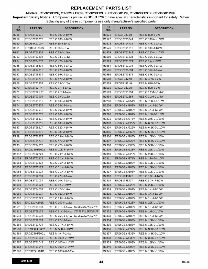
- 44 -Parts List
REPLACEMENT PARTS LISTModels: CT-32SX12F, CT-32SX12CF, CT-32SX12UF, CT-36SX12F, CT-36SX12CF, CT-36SX12UF.
Important Safety Notice : Components printed in BOLD TYPE have special characteristics important for safety. Whenreplacing any of these components use only manufacturer’s specified parts.
182-02
PA
RT
SLIS
T
R958 ERDS2TJ391T RES,C 390-J-1/4W
R959 ERDS2TJ101T RES,C 100-J-1/4W
R960 ERQ14AJ100P RES,F 10-J-1/4W
R961 ERQ1CJP331S RES,F 330-J-1W
R962 ERDS2TJ330T RES,C 33-J-1/4W
R963 ERDS2TJ330T RES,C 33-J-1/4W
R964 ERDS2TJ471T RES,C 470-J-1/4W
R965 ERDS2TJ563T RES,C 56K-J-1/4W
R966 ERDS1FJ471P RES,C 470-J-1/2W
R967 ERDS2TJ563T RES,C 56K-J-1/4W
R968 ERDS2TJ471T RES,C 470-J-1/4W
R969 ERDS2TJ390T RES,C 39-J-1/2W
R970 ERDS2TJ2R7T RES,C 2.7-J-1/4W
R971 ERDS2TJ2R7T RES,C 2.7-J-1/4W
R972 ERDS2TJ390T RES,C 39-J-1/2W
R973 ERDS2TJ101T RES,C 100-J-1/4W
R974 ERDS2TJ333T RES,C 33K-J-1/4W
R975 ERDS2TJ101T RES,C 100-J-1/4W
R976 ERDS2TJ101T RES,C 100-J-1/4W
R977 ERDS2TJ561T RES,C 560-J-1/4W
R978 ERDS2TJ101T RES,C 100-J-1/4W
R987 ERDS2TJ821T RES,C 820-J-1/4W
R988 ERDS2TJ331T RES,C 330-J-1/4W
R989 ERDS2TJ682T RES,C 6.8K-J-1/4W
R990 ERDS2TJ471T RES,C 470-J-1/4W
R993 ERDS2TJ471T RES,C 470-J-1/4W
R1051 ER0S2THF1002 RES,M 10K-F-1/4W
R1052 ERDS2TJ222T RES,C 2.2K-J-1/4W
R1053 ERDS2TJ222T RES,C 2.2K-J-1/4W
R1054 ERDS2TJ332T RES,C 3.3K-J-1/4W
R1055 ERDS2TJ512T RES,C 5.1K-J-1/4W
R1056 ERDS2TJ912T RES,C 9.1K-J-1/4W
R1057 ERDS2TJ223T RES,C 22K-J-1/4W
R1058 ERDS2TJ103T RES,C 10K-J-1/4W
R1059 ERDS2TJ102T RES,C 1K-J-1/4W
R1060 ERDS2TJ470T RES,C 47-J-1/4W
R1061 ERDS2TJ101T RES,C 100-J-1/4W
R1062 ERDS2TJ182T RES,C 1.8K-J-1/4W
R1510 ERC12GK101D RES,C 100-K-1/2W
R1511 ERDS2TJ913T RES,C 91K-J-1/4W CT-32SX12F/CF/UF
R1512 ERDS2TJ913T RES,C 91K-J-1/4W CT-32SX12F/CF/UF
R1513 ERDS2TJ753T RES,C 75K-J-1/4W CT-32SX12F/CF/UF
R1550 ERDS2TJ273T RES,C 27K-J-1/4W
R1555 ERDS2TJ272T RES,C 2.7K-J-1/4W
R1563 ER0S2THF5602 RES,M 56K-F-1/4W
R1564 ER0S2THF3001 RES,M 3K-F-1/4W
R1566 ERDS2TJ104T RES,C 100K-J-1/4W
R1567 ERDS2TJ104T RES,C 100K-J-1/4W
R1568 ERDS2TJ104T RES,C 100K-J-1/4W
R1570 ERC12GK104D RES,C 100K-K-1/2W
REFNO. PART NO. DESCRIPTION
R1571 ERG3FJ821H RES,M 820-J-3W
R1572 ERDS2TJ334T RES,C 330K-J-1/4W
R1573 ERDS2TJ473T RES,C 47K-J-1/4W
R1576 ERDS2TJ101T RES,C 100-J-1/4W
R1579 ERDS2TJ224T RES,C 220K-J-1/4W
R1580 ERDS2TJ153T RES,C 15K-J-1/4W
R1583 ERDS2TJ102T RES,C 1K-J-1/4W
R1584 ERDS2TJ103T RES,C 10K-J-1/4W
R1585 ERDS2TJ563T RES,C 56K-J-1/4W
R1586 ERDS2TJ333T RES,C 33K-J-1/4W
R1588 ERG2FJ472H RES,M 4.7K-J-2W
R1589 ERG3FJ821H RES,M 820-J-3W
R1591 ERG3FJ821H RES,M 820-J-3W
R1593 ERDS2TJ125T RES,C 1.2M-J-1/4W
R1594 ERDS2TJ125T RES,C 1.2M-J-1/4W
R2203 ERJ6GEYJ751V RES,M 750-J-1/10W
R2206 ERJ6GEYJ102V RES,M 1K-J-1/10W
R2207 ERJ6GEYJ102V RES,M 1K-J-1/10W
R2220 ERJ6GEYJ101V RES,M 100-J-1/10W
R2221 ERJ6GEYJ273V RES,M 27K-J-1/10W
R2303 ERJ6GEYJ622V RES,M 6.2K-J-1/10W
R2304 ERJ6GEYJ622V RES,M 6.2K-J-1/10W
R2305 ERJ6GEYJ562V RES,M 5.6K-J-1/10W
R2306 ERJ6GEYJ103V RES,M 10K-J-1/10W
R2307 ERJ6GEYJ822V RES,M 8.2K-J-1/10W
R2308 ERJ6GEYJ563V RES,M 56K-J-1/10W
R2309 ERJ6GEYJ223V RES,M 22K-J-1/10W
R2310 ERJ6GEYJ223V RES,M 22K-J-1/10W
R2311 ERJ6GEYJ271V RES,M 270-J-1/10W
R2312 ERJ6GEYJ103V RES,M 10K-J-1/10W
R2316 ERJ6GEYJ103V RES,M 10K-J-1/10W
R2317 ERJ6GEYJ103V RES,M 10K-J-1/10W
R2318 ERDS1TJ332T RES,C 3.3K-J-1/2W
R2319 ERDS1TJ332T RES,C 3.3K-J-1/2W
R2323 ERJ6GEYJ223V RES,M 22K-J-1/10W
R2324 ERJ6GEYJ102V RES,M 1K-J-1/10W
R2325 ERJ6GEYJ102V RES,M 1K-J-1/10W
R2326 ERJ6GEYJ102V RES,M 1K-J-1/10W
R2329 ERJ6GEYJ223V RES,M 22K-J-1/10W
R2331 ERJ6GEYJ102V RES,M 1K-J-1/10W
R2332 ERJ6GEYJ105V RES,M 1M-J-1/10W
R2333 ERJ6GEYJ102V RES,M 1K-J-1/10W
R2334 ERJ6GEYJ103V RES,M 10K-J-1/10W
R2335 ERJ6GEYJ183V RES,M 18K-J-1/10W
R2336 ERJ6GEYJ392V RES,M 3.9K-J-1/10W
R2337 ERJ6GEYJ332V RES,M 3.3K-J-1/10W
R2338 ERJ6GEYJ332V RES,M 3.3K-J-1/10W
R2339 ERJ6GEYJ183V RES,M 18K-J-1/10W
R2340 ERJ6GEYJ392V RES,M 3.9K-J-1/10W
R2345 ERJ6GEYJ103V RES,M 10K-J-1/10W
REFNO. PART NO. DESCRIPTION
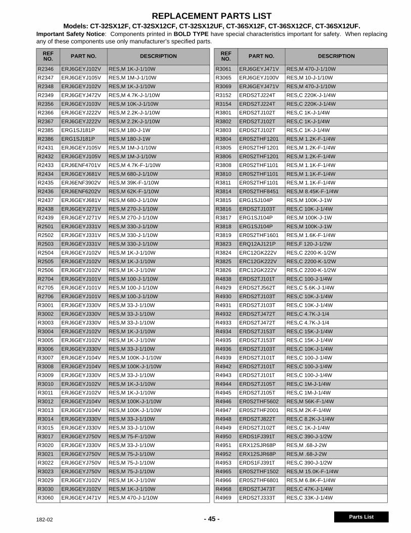
REPLACEMENT PARTS LISTModels: CT-32SX12F, CT-32SX12CF, CT-32SX12UF, CT-36SX12F, CT-36SX12CF, CT-36SX12UF.
Important Safety Notice : Components printed in BOLD TYPE have special characteristics important for safety. When replacingany of these components use only manufacturer’s specified parts.
- 45 -182-02
PA
RT
SLI
ST
Parts List
R2346 ERJ6GEYJ102V RES,M 1K-J-1/10W
R2347 ERJ6GEYJ105V RES,M 1M-J-1/10W
R2348 ERJ6GEYJ102V RES,M 1K-J-1/10W
R2349 ERJ6GEYJ472V RES,M 4.7K-J-1/10W
R2356 ERJ6GEYJ103V RES,M 10K-J-1/10W
R2366 ERJ6GEYJ222V RES,M 2.2K-J-1/10W
R2367 ERJ6GEYJ222V RES,M 2.2K-J-1/10W
R2385 ERG1SJ181P RES,M 180-J-1W
R2386 ERG1SJ181P RES,M 180-J-1W
R2431 ERJ6GEYJ105V RES,M 1M-J-1/10W
R2432 ERJ6GEYJ105V RES,M 1M-J-1/10W
R2433 ERJ6ENF4701V RES,M 4.7K-F-1/10W
R2434 ERJ6GEYJ681V RES,M 680-J-1/10W
R2435 ERJ6ENF3902V RES,M 39K-F-1/10W
R2436 ERJ6ENF6202V RES,M 62K-F-1/10W
R2437 ERJ6GEYJ681V RES,M 680-J-1/10W
R2438 ERJ6GEYJ271V RES,M 270-J-1/10W
R2439 ERJ6GEYJ271V RES,M 270-J-1/10W
R2501 ERJ6GEYJ331V RES,M 330-J-1/10W
R2502 ERJ6GEYJ331V RES,M 330-J-1/10W
R2503 ERJ6GEYJ331V RES,M 330-J-1/10W
R2504 ERJ6GEYJ102V RES,M 1K-J-1/10W
R2505 ERJ6GEYJ102V RES,M 1K-J-1/10W
R2506 ERJ6GEYJ102V RES,M 1K-J-1/10W
R2704 ERJ6GEYJ101V RES,M 100-J-1/10W
R2705 ERJ6GEYJ101V RES,M 100-J-1/10W
R2706 ERJ6GEYJ101V RES,M 100-J-1/10W
R3001 ERJ6GEYJ330V RES,M 33-J-1/10W
R3002 ERJ6GEYJ330V RES,M 33-J-1/10W
R3003 ERJ6GEYJ330V RES,M 33-J-1/10W
R3004 ERJ6GEYJ102V RES,M 1K-J-1/10W
R3005 ERJ6GEYJ102V RES,M 1K-J-1/10W
R3006 ERJ6GEYJ330V RES,M 33-J-1/10W
R3007 ERJ6GEYJ104V RES,M 100K-J-1/10W
R3008 ERJ6GEYJ104V RES,M 100K-J-1/10W
R3009 ERJ6GEYJ330V RES,M 33-J-1/10W
R3010 ERJ6GEYJ102V RES,M 1K-J-1/10W
R3011 ERJ6GEYJ102V RES,M 1K-J-1/10W
R3012 ERJ6GEYJ104V RES,M 100K-J-1/10W
R3013 ERJ6GEYJ104V RES,M 100K-J-1/10W
R3014 ERJ6GEYJ330V RES,M 33-J-1/10W
R3015 ERJ6GEYJ330V RES,M 33-J-1/10W
R3017 ERJ6GEYJ750V RES,M 75-F-1/10W
R3020 ERJ6GEYJ330V RES,M 33-J-1/10W
R3021 ERJ6GEYJ750V RES,M 75-J-1/10W
R3022 ERJ6GEYJ750V RES,M 75-J-1/10W
R3023 ERJ6GEYJ750V RES,M 75-J-1/10W
R3029 ERJ6GEYJ102V RES,M 1K-J-1/10W
R3030 ERJ6GEYJ102V RES,M 1K-J-1/10W
R3060 ERJ6GEYJ471V RES,M 470-J-1/10W
REFNO. PART NO. DESCRIPTION
R3061 ERJ6GEYJ471V RES,M 470-J-1/10W
R3065 ERJ6GEYJ100V RES,M 10-J-1/10W
R3069 ERJ6GEYJ471V RES,M 470-J-1/10W
R3152 ERDS2TJ224T RES,C 220K-J-1/4W
R3154 ERDS2TJ224T RES,C 220K-J-1/4W
R3801 ERDS2TJ102T RES,C 1K-J-1/4W
R3802 ERDS2TJ102T RES,C 1K-J-1/4W
R3803 ERDS2TJ102T RES,C 1K-J-1/4W
R3804 ER0S2THF1201 RES,M 1.2K-F-1/4W
R3805 ER0S2THF1201 RES,M 1.2K-F-1/4W
R3806 ER0S2THF1201 RES,M 1.2K-F-1/4W
R3808 ER0S2THF1101 RES,M 1.1K-F-1/4W
R3810 ER0S2THF1101 RES,M 1.1K-F-1/4W
R3811 ER0S2THF1101 RES,M 1.1K-F-1/4W
R3814 ER0S2THF8451 RES,M 8.45K-F-1/4W
R3815 ERG1SJ104P RES,M 100K-J-1W
R3816 ERDS2TJ103T RES,C 10K-J-1/4W
R3817 ERG1SJ104P RES,M 100K-J-1W
R3818 ERG1SJ104P RES,M 100K-J-1W
R3819 ER0S2THF1601 RES,M 1.6K-F-1/4W
R3823 ERQ12AJ121P RES,F 120-J-1/2W
R3824 ERC12GK222V RES,C 2200-K-1/2W
R3825 ERC12GK222V RES,C 2200-K-1/2W
R3826 ERC12GK222V RES,C 2200-K-1/2W
R4838 ERDS2TJ101T RES,C 100-J-1/4W
R4929 ERDS2TJ562T RES,C 5.6K-J-1/4W
R4930 ERDS2TJ103T RES,C 10K-J-1/4W
R4931 ERDS2TJ103T RES,C 10K-J-1/4W
R4932 ERDS2TJ472T RES,C 4.7K-J-1/4
R4933 ERDS2TJ472T RES,C 4.7K-J-1/4
R4934 ERDS2TJ153T RES,C 15K-J-1/4W
R4935 ERDS2TJ153T RES,C 15K-J-1/4W
R4936 ERDS2TJ103T RES,C 10K-J-1/4W
R4939 ERDS2TJ101T RES,C 100-J-1/4W
R4942 ERDS2TJ101T RES,C 100-J-1/4W
R4943 ERDS2TJ101T RES,C 100-J-1/4W
R4944 ERDS2TJ105T RES,C 1M-J-1/4W
R4945 ERDS2TJ105T RES,C 1M-J-1/4W
R4946 ER0S2THF5602 RES,M 56K-F-1/4W
R4947 ER0S2THF2001 RES,M 2K-F-1/4W
R4948 ERDS2TJ822T RES,C 8.2K-J-1/4W
R4949 ERDS2TJ102T RES,C 1K-J-1/4W
R4950 ERDS1FJ391T RES,C 390-J-1/2W
R4951 ERX12SJR68P RES,M .68-J-2W
R4952 ERX12SJR68P RES,M .68-J-2W
R4953 ERDS1FJ391T RES,C 390-J-1/2W
R4965 ER0S2THF1502 RES,M 15.0K-F-1/4W
R4966 ER0S2THF6801 RES,M 6.8K-F-1/4W
R4968 ERDS2TJ473T RES,C 47K-J-1/4W
R4969 ERDS2TJ333T RES,C 33K-J-1/4W
REFNO. PART NO. DESCRIPTION
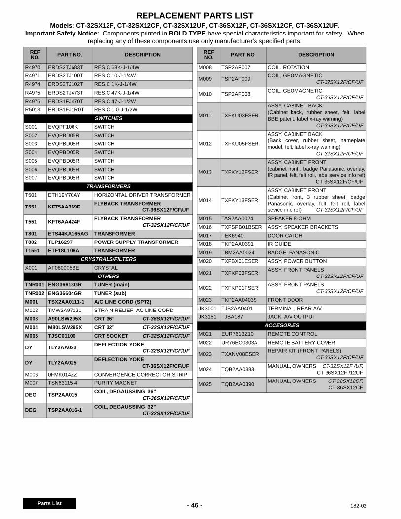
- 46 -Parts List
REPLACEMENT PARTS LISTModels: CT-32SX12F, CT-32SX12CF, CT-32SX12UF, CT-36SX12F, CT-36SX12CF, CT-36SX12UF.
Important Safety Notice : Components printed in BOLD TYPE have special characteristics important for safety. Whenreplacing any of these components use only manufacturer’s specified parts.
182-02
PA
RT
SLIS
T
R4970 ERDS2TJ683T RES,C 68K-J-1/4W
R4971 ERDS2TJ100T RES,C 10-J-1/4W
R4974 ERDS2TJ102T RES,C 1K-J-1/4W
R4975 ERDS2TJ473T RES,C 47K-J-1/4W
R4976 ERDS1FJ470T RES,C 47-J-1/2W
R5013 ERDS1FJ1R0T RES,C 1.0-J-1/2W
SWITCHES
S001 EVQPF106K SWITCH
S002 EVQPBD05R SWITCH
S003 EVQPBD05R SWITCH
S004 EVQPBD05R SWITCH
S005 EVQPBD05R SWITCH
S006 EVQPBD05R SWITCH
S007 EVQPBD05R SWITCH
TRANSFORMERS
T501 ETH19Y70AY HORIZONTAL DRIVER TRANSFORMER
T551 KFT5AA369FFLYBACK TRANSFORMER
CT-36SX12F/CF/UF
T551 KFT6AA424FFLYBACK TRANSFORMER
CT-32SX12F/CF/UF
T801 ETS44KA165AG TRANSFORMER
T802 TLP16297 POWER SUPPLY TRANSFORMER
T1551 ETF18L108A TRANSFORMER
CRYSTRALS/FILTERS
X001 AF080005BE CRYSTAL
OTHERS
TNR001 ENG36613GR TUNER (main)
TNR002 ENG36604GR TUNER (sub)
M001 TSX2AA0111-1 A/C LINE CORD (SPT2)
M002 TMW2A97121 STRAIN RELIEF: AC LINE CORD
M003 A90LSW295X CRT 36” CT-36SX12F/CF/UF
M004 M80LSW295X CRT 32” CT-32SX12F/CF/UF
M005 TJSC01100 CRT SOCKET CT-32SX12F/CF/UF
DY TLY2AA023DEFLECTION YOKE
CT-32SX12F/CF/UF
DY TLY2AA025DEFLECTION YOKE
CT-36SX12F/CF/UF
M006 0FMK014ZZ CONVERGENCE CORRECTOR STRIP
M007 TSN63115-4 PURITY MAGNET
DEG TSP2AA015COIL, DEGAUSSING 36”
CT-36SX12F/CF/UF
DEG TSP2AA016-1COIL, DEGAUSSING 32”
CT-32SX12F/CF/UF
REFNO. PART NO. DESCRIPTION
M008 TSP2AF007 COIL, ROTATION
M009 TSP2AF009COIL, GEOMAGNETIC
CT-32SX12F/CF/UF
M010 TSP2AF008COIL, GEOMAGNETIC
CT-36SX12F/CF/UF
M011 TXFKU03FSER
ASSY, CABINET BACK(Cabinet back, rubber sheet, felt, labelBBE patent, label x-ray warning)
CT-36SX12F/CF/UF
M012 TXFKU05FSER
ASSY, CABINET BACK(Back cover, rubber sheet, nameplatemodel, felt, label x-ray warning)
CT-32SX12F/CF/UF
M013 TXFKY12FSER
ASSY, CABINET FRONT(cabinet front , badge Panasonic, overlay,IR panel, felt, felt roll, label service info ref)
CT-36SX12F/CF/UF
M014 TXFKY13FSER
ASSY, CABINET FRONT(Cabinet front, 3 rubber sheet, badgePanasonic, overlay, felt, felt roll, labelsevice info ref) CT-32SX12F/CF/UF
M015 TAS2AA0024 SPEAKER 8-OHM
M016 TXFSPB01BSER ASSY, SPEAKER BRACKETS
M017 TEK6940 DOOR CATCH
M018 TKP2AA0391 IR GUIDE
M019 TBM2AA0024 BADGE, PANASONIC
M020 TXFBX01ESER ASSY, POWER BUTTON
M021 TXFKP03FSERASSY, FRONT PANELS
CT-32SX12F/CF/UF
M022 TXFKP01FSERASSY, FRONT PANELS
CT-36SX12F/CF/UF
M023 TKP2AA0403S FRONT DOOR
JK3001 TJB2AA0401 TERMINAL, REAR A/V
JK3151 TJBA187 JACK, A/V OUTPUT
ACCESORIES
M021 EUR7613Z10 REMOTE CONTROL
M022 UR76EC0303A REMOTE BATTERY COVER
M023 TXANV08ESERREPAIR KIT (FRONT PANELS)
CT-36SX12F/CF/UF
M024 TQB2AA0383MANUAL, OWNERS CT-32SX12F /UF,
CT-36SX12F /12UF
M025 TQB2AA0390MANUAL, OWNERS CT-32SX12CF,
CT-36SX12CF
REFNO. PART NO. DESCRIPTION
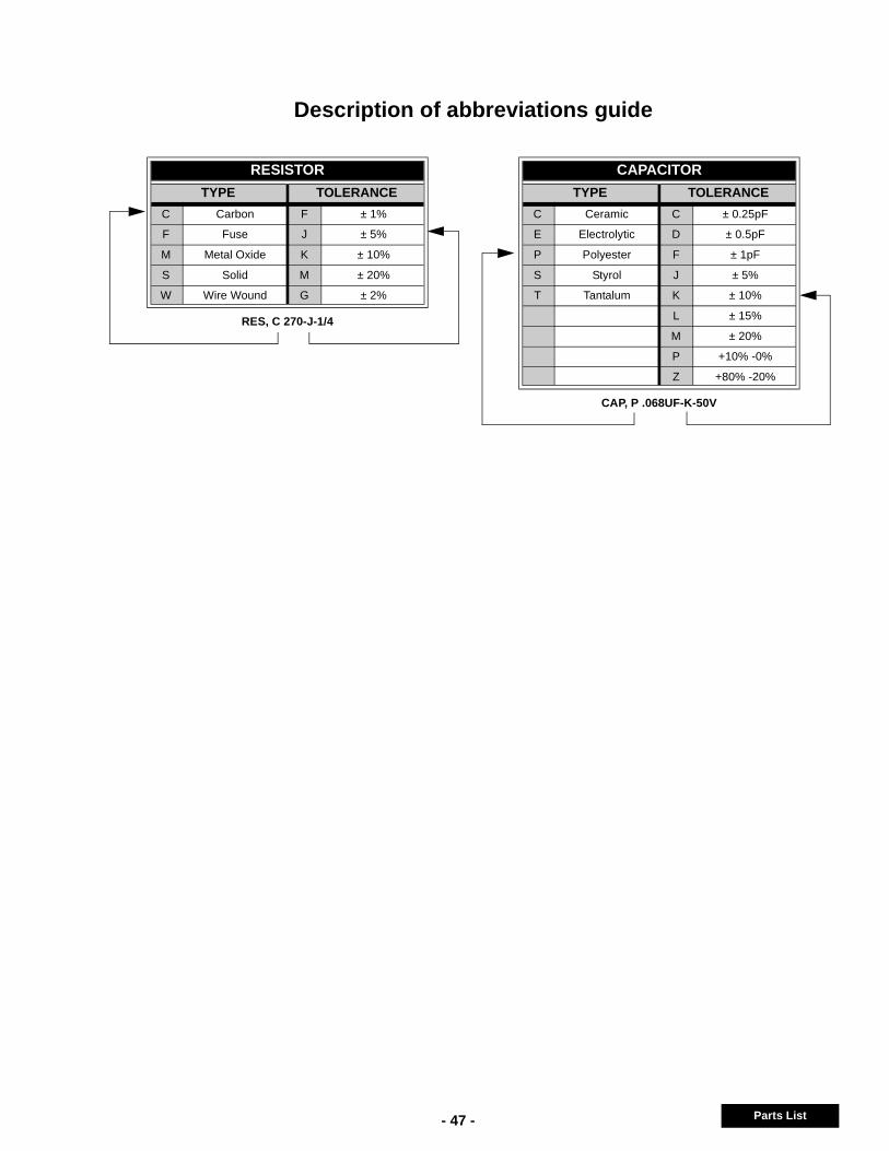
- 47 -
PA
RT
SLI
ST
Parts List
Description of abbreviations guide
RES, C 270-J-1/4
CAP, P .068UF-K-50V
RESISTOR
TYPE TOLERANCE
C Carbon F ± 1%
F Fuse J ± 5%
M Metal Oxide K ± 10%
S Solid M ± 20%
W Wire Wound G ± 2%
CAPACITOR
TYPE TOLERANCE
C Ceramic C ± 0.25pF
E Electrolytic D ± 0.5pF
P Polyester F ± 1pF
S Styrol J ± 5%
T Tantalum K ± 10%
L ± 15%
M ± 20%
P +10% -0%
Z +80% -20%
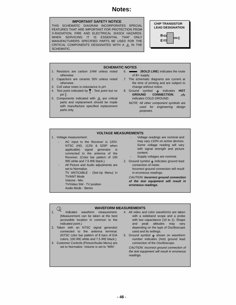
Notes:
- 48 -
PA
RT
SLI
ST
SCHEMATIC NOTES1. Resistors are carbon 1/4W unless noted
otherwise.2. Capacitors are ceramic 50V unless noted
otherwise.3. Coil value notes is inductance in µH.4. Test point indicated by ; Test point but no
pin .5. Components indicated with are critical
parts and replacement should be madewith manufacture specified replacementparts only.
6. (BOLD LINE ) indicates the routeof B+ supply.
7. The schematic diagrams are current atthe time of printing and are subject tochange without notice.
8. Ground symbol indicates HOTGROUND CONNECTION;indicates COLD GROUND.
NOTE: All other component symbols areused for engineering designpurposes.
WAVEFORM MEASUREMENTS1. indicates waveform measurement.
(Measurement can be taken at the bestaccessible location in common to theindicated point.)
2. Taken with an NTSC signal generatorconnected to the antenna terminal.(NTSC color bar pattern of 8 bars of EIAcolors, 100 IRE white and 7.5 IRE black.)
3. Customer Controls (Picture/Audio Menu) areset to Normalize. Volume is set to “MIN”.
4. All video and color waveforms are takenwith a wideband scope and a probewith low capacitance (10 to 1). Shapeand peak altitudes may varydepending on the type of Oscilloscopeused and its settings.
5. Ground symbol shown on waveformnumber indicates (Hot) ground leadconnection of the Oscilloscope.
CAUTION: Incorrect ground connection ofthe test equipment will result in erroneousreadings.
3
VOLTAGE MEASUREMENTS1. Voltage measurement:
- AC input to the Receiver is 120V.NTSC (HD, 1125i & 525P whenapplicable) signal generator isconnected to the antenna of theReceiver. (Color bar pattern of 100IRE white and 7.5 IRE black.)
- All Picture and Audio adjustments areset to Normalize.TV ANT/CABLE - (Set-Up Menu) inTV/ANT ModeVolume - Min.TV/Video SW - TV positionAudio Mode - Stereo
- Voltage readings are nominal andmay vary ±10% on active devices.Some voltage reading will varywith signal strength and picturecontent.
- Supply voltages are nominal.
2. Ground symbol indicates ground leadconnection of meter.Incorrect ground connection will resultin erroneous readings.
CAUTION: Incorrect ground connectionof the test equipment will result inerroneous readings.
IMPORTANT SAFETY NOTICETHIS SCHEMATIC DIAGRAM INCORPORATES SPECIALFEATURES THAT ARE IMPORTANT FOR PROTECTION FROMX-RADIATION, FIRE AND ELECTRICAL SHOCK HAZARDS.WHEN SERVICING IT IS ESSENTIAL THAT ONLYMANUFACTURERS SPECIFIED PARTS BE USED FOR THECRITICAL COMPONENTS DESIGNATED WITH A IN THESCHEMATIC.
BE
C
CHIP TRANSISTORLEAD DESIGNATION
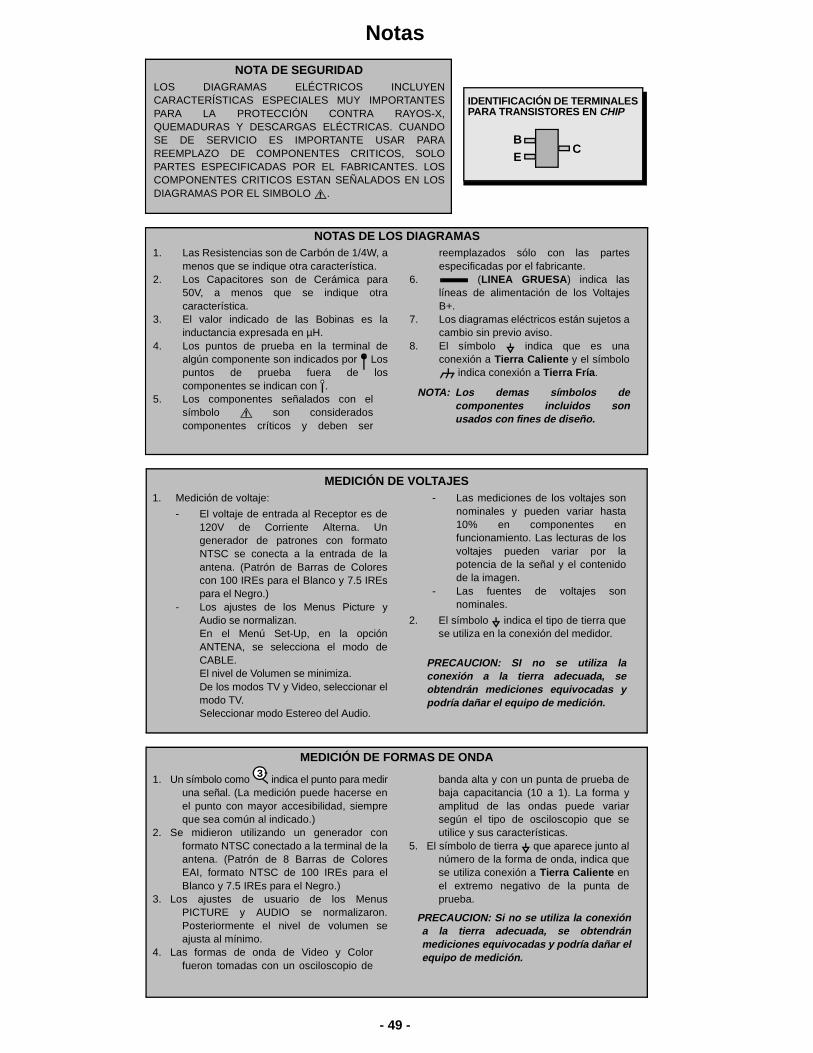
- 49 -
Notas
PA
RT
SLIS
T
NOTAS DE LOS DIAGRAMAS1. Las Resistencias son de Carbón de 1/4W, a
menos que se indique otra característica.2. Los Capacitores son de Cerámica para
50V, a menos que se indique otracaracterística.
3. El valor indicado de las Bobinas es lainductancia expresada en µH.
4. Los puntos de prueba en la terminal dealgún componente son indicados por Lospuntos de prueba fuera de loscomponentes se indican con .
5. Los componentes señalados con elsímbolo son consideradoscomponentes críticos y deben ser
reemplazados sólo con las partesespecificadas por el fabricante.
6. (LINEA GRUESA ) indica laslíneas de alimentación de los VoltajesB+.
7. Los diagramas eléctricos están sujetos acambio sin previo aviso.
8. El símbolo indica que es unaconexión a Tierra Caliente y el símbolo
indica conexión a Tierra Fría .
NOTA: Los demas símbolos decomponentes incluidos sonusados con fines de diseño.
MEDICIÓN DE VOLTAJES1. Medición de voltaje:
- El voltaje de entrada al Receptor es de120V de Corriente Alterna. Ungenerador de patrones con formatoNTSC se conecta a la entrada de laantena. (Patrón de Barras de Colorescon 100 IREs para el Blanco y 7.5 IREspara el Negro.)
- Los ajustes de los Menus Picture yAudio se normalizan.En el Menú Set-Up, en la opciónANTENA, se selecciona el modo deCABLE.El nivel de Volumen se minimiza.De los modos TV y Video, seleccionar elmodo TV.Seleccionar modo Estereo del Audio.
- Las mediciones de los voltajes sonnominales y pueden variar hasta10% en componentes enfuncionamiento. Las lecturas de losvoltajes pueden variar por lapotencia de la señal y el contenidode la imagen.
- Las fuentes de voltajes sonnominales.
2. El símbolo indica el tipo de tierra quese utiliza en la conexión del medidor.
PRECAUCION: SI no se utiliza laconexión a la tierra adecuada, seobtendrán mediciones equivocadas ypodría dañar el equipo de medición.
MEDICIÓN DE FORMAS DE ONDA
1. Un símbolo como indica el punto para mediruna señal. (La medición puede hacerse enel punto con mayor accesibilidad, siempreque sea común al indicado.)
2. Se midieron utilizando un generador conformato NTSC conectado a la terminal de laantena. (Patrón de 8 Barras de ColoresEAI, formato NTSC de 100 IREs para elBlanco y 7.5 IREs para el Negro.)
3. Los ajustes de usuario de los MenusPICTURE y AUDIO se normalizaron.Posteriormente el nivel de volumen seajusta al mínimo.
4. Las formas de onda de Video y Colorfueron tomadas con un osciloscopio de
banda alta y con un punta de prueba debaja capacitancia (10 a 1). La forma yamplitud de las ondas puede variarsegún el tipo de osciloscopio que seutilice y sus características.
5. El símbolo de tierra que aparece junto alnúmero de la forma de onda, indica quese utiliza conexión a Tierra Caliente enel extremo negativo de la punta deprueba.
PRECAUCION: Si no se utiliza la conexióna la tierra adecuada, se obtendránmediciones equivocadas y podría dañar elequipo de medición.
3
NOTA DE SEGURIDADLOS DIAGRAMAS ELÉCTRICOS INCLUYENCARACTERÍSTICAS ESPECIALES MUY IMPORTANTESPARA LA PROTECCIÓN CONTRA RAYOS-X,QUEMADURAS Y DESCARGAS ELÉCTRICAS. CUANDOSE DE SERVICIO ES IMPORTANTE USAR PARAREEMPLAZO DE COMPONENTES CRITICOS, SOLOPARTES ESPECIFICADAS POR EL FABRICANTES. LOSCOMPONENTES CRITICOS ESTAN SEÑALADOS EN LOSDIAGRAMAS POR EL SIMBOLO .
BE
C
IDENTIFICACIÓN DE TERMINALESPARA TRANSISTORES EN CHIP
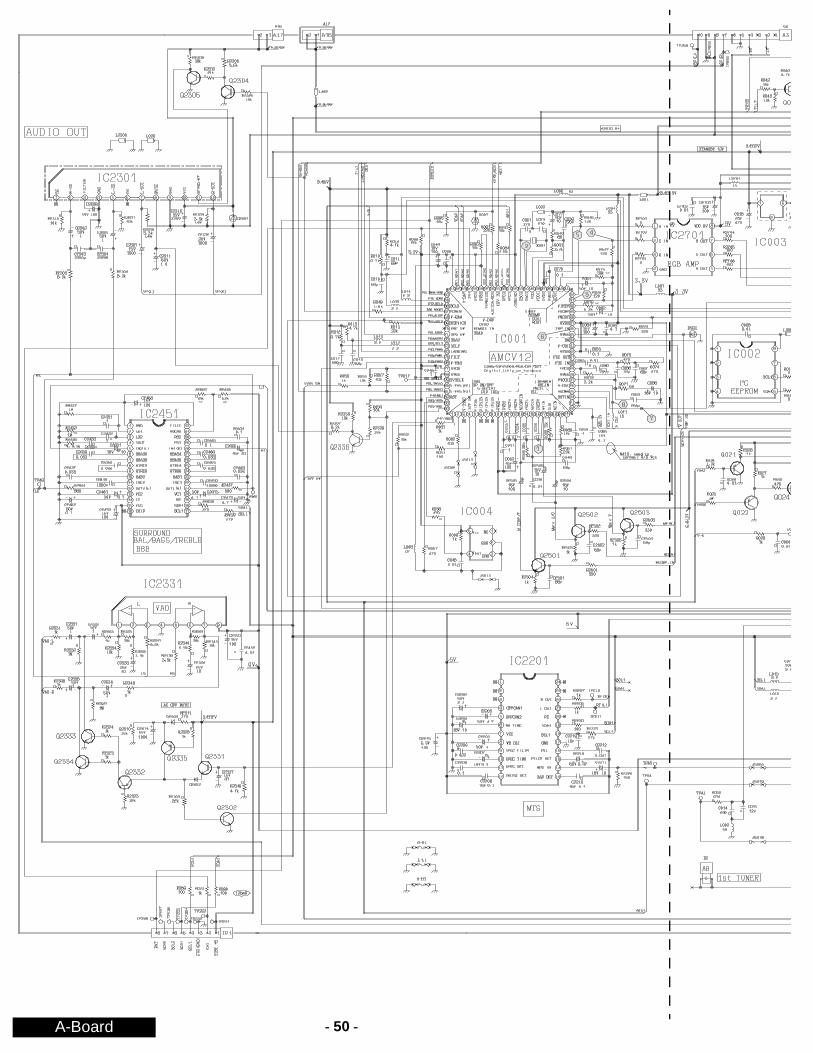
- 50 -A-Board
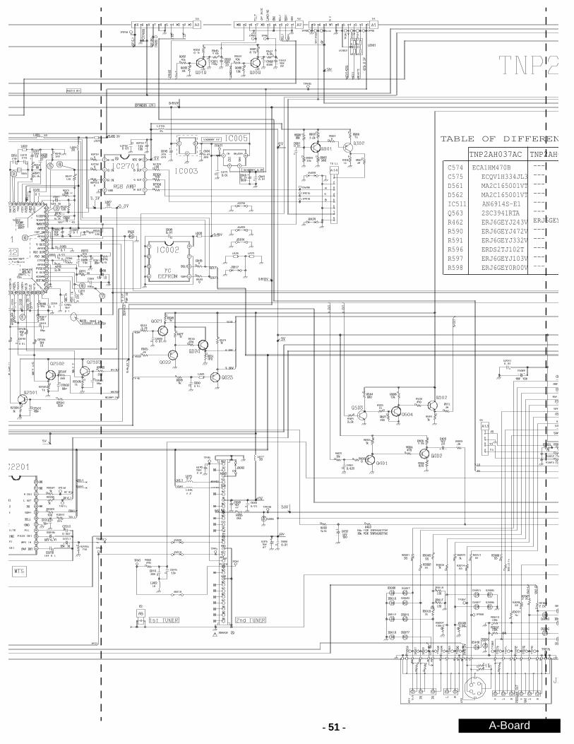
- 51 -
C574 ECA1HM470BC575 ECQV1H334JL3D561 MA2C165001VTD562 MA2C165001VTIC511 AN6914S-E1Q563 2SC3941RTAR462 ERJ6GEYJ243VR590 ERJ6GEYJ472VR591 ERJ6GEYJ332VR596 ERDS2TJ102TR597 ERJ6GEYJ103VR598 ERJ6GEY0R00V
------------------ERJ6GEY---------------
TNP2AH0TNP2AH037AC
TABLE OF DIFFEREN
A-Board
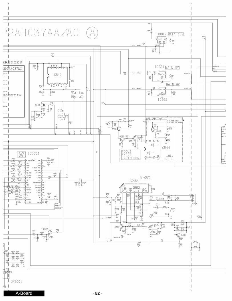
- 52 -
------------------ERJ6GEYJ183V---------------
NP2AH037AC
ERENCES
A-Board
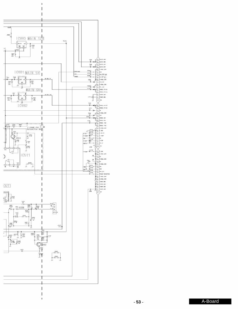
- 53 - A-Board
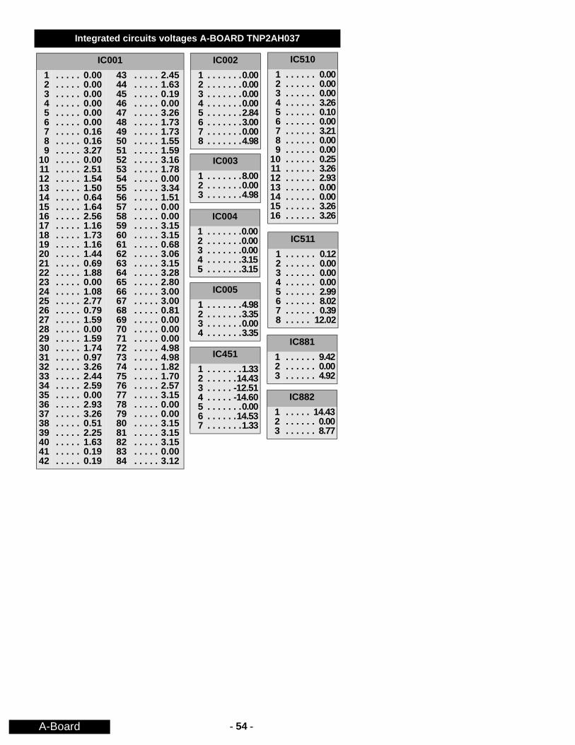
- 54 -
IC001
123456789
101112131415161718192021222324252627282930313233343536373839404142
. . . . . 0.00
. . . . . 0.00
. . . . . 0.00
. . . . . 0.00
. . . . . 0.00
. . . . . 0.00
. . . . . 0.16
. . . . . 0.16
. . . . . 3.27
. . . . . 0.00
. . . . . 2.51
. . . . . 1.54
. . . . . 1.50
. . . . . 0.64
. . . . . 1.64
. . . . . 2.56
. . . . . 1.16
. . . . . 1.73
. . . . . 1.16
. . . . . 1.44
. . . . . 0.69
. . . . . 1.88
. . . . . 0.00
. . . . . 1.08
. . . . . 2.77
. . . . . 0.79
. . . . . 1.59
. . . . . 0.00
. . . . . 1.59
. . . . . 1.74
. . . . . 0.97
. . . . . 3.26
. . . . . 2.44
. . . . . 2.59
. . . . . 0.00
. . . . . 2.93
. . . . . 3.26
. . . . . 0.51
. . . . . 2.25
. . . . . 1.63
. . . . . 0.19
. . . . . 0.19
434445464748495051525354555657585960616263646566676869707172737475767778798081828384
. . . . . 2.45
. . . . . 1.63
. . . . . 0.19
. . . . . 0.00
. . . . . 3.26
. . . . . 1.73
. . . . . 1.73
. . . . . 1.55
. . . . . 1.59
. . . . . 3.16
. . . . . 1.78
. . . . . 0.00
. . . . . 3.34
. . . . . 1.51
. . . . . 0.00
. . . . . 0.00
. . . . . 3.15
. . . . . 3.15
. . . . . 0.68
. . . . . 3.06
. . . . . 3.15
. . . . . 3.28
. . . . . 2.80
. . . . . 3.00
. . . . . 3.00
. . . . . 0.81
. . . . . 0.00
. . . . . 0.00
. . . . . 0.00
. . . . . 4.98
. . . . . 4.98
. . . . . 1.82
. . . . . 1.70
. . . . . 2.57
. . . . . 3.15
. . . . . 0.00
. . . . . 0.00
. . . . . 3.15
. . . . . 3.15
. . . . . 3.15
. . . . . 0.00
. . . . . 3.12
IC510
123456789
10111213141516
. . . . . . 0.00
. . . . . . 0.00
. . . . . . 0.00
. . . . . . 3.26
. . . . . . 0.10
. . . . . . 0.00
. . . . . . 3.21
. . . . . . 0.00
. . . . . . 0.00
. . . . . . 0.25
. . . . . . 3.26
. . . . . . 2.93
. . . . . . 0.00
. . . . . . 0.00
. . . . . . 3.26
. . . . . . 3.26
IC882
123
. . . . . 14.43
. . . . . . 0.00
. . . . . . 8.77
IC881
123
. . . . . . 9.42
. . . . . . 0.00
. . . . . . 4.92
IC451
1234567
. . . . . . .1.33
. . . . . .14.43
. . . . . -12.51
. . . . . -14.60
. . . . . . .0.00
. . . . . .14.53
. . . . . . .1.33
IC003
123
. . . . . . .8.00
. . . . . . .0.00
. . . . . . .4.98
IC511
12345678
. . . . . . 0.12
. . . . . . 0.00
. . . . . . 0.00
. . . . . . 0.00
. . . . . . 2.99
. . . . . . 8.02
. . . . . . 0.39
. . . . . 12.02
IC004
12345
. . . . . . .0.00
. . . . . . .0.00
. . . . . . .0.00
. . . . . . .3.15
. . . . . . .3.15
IC002
12345678
. . . . . . .0.00
. . . . . . .0.00
. . . . . . .0.00
. . . . . . .0.00
. . . . . . .2.84
. . . . . . .3.00
. . . . . . .0.00
. . . . . . .4.98
IC005
1234
. . . . . . .4.98
. . . . . . .3.35
. . . . . . .0.00
. . . . . . .3.35
Integrated circuits voltages A-BOARD TNP2AH037
A-Board
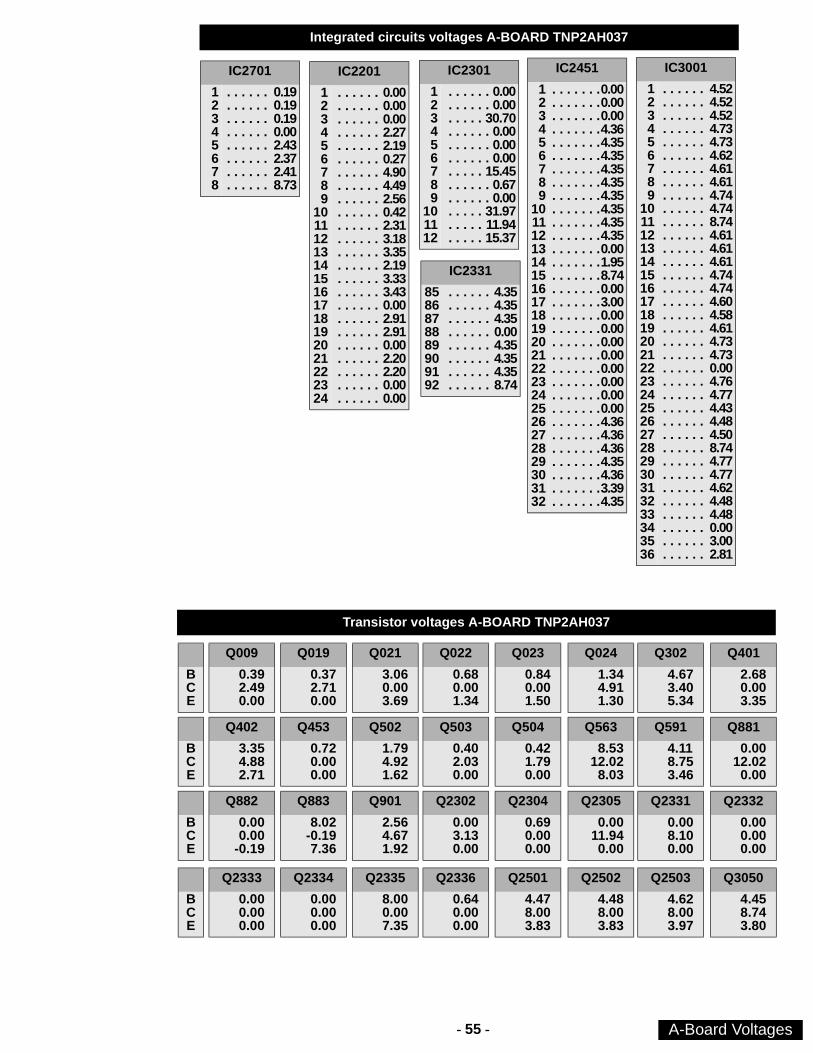
- 55 -
Integrated circuits voltages A-BOARD TNP2AH037
IC2331
8586878889909192
. . . . . . 4.35
. . . . . . 4.35
. . . . . . 4.35
. . . . . . 0.00
. . . . . . 4.35
. . . . . . 4.35
. . . . . . 4.35
. . . . . . 8.74
IC2201
123456789
101112131415161718192021222324
. . . . . . 0.00
. . . . . . 0.00
. . . . . . 0.00
. . . . . . 2.27
. . . . . . 2.19
. . . . . . 0.27
. . . . . . 4.90
. . . . . . 4.49
. . . . . . 2.56
. . . . . . 0.42
. . . . . . 2.31
. . . . . . 3.18
. . . . . . 3.35
. . . . . . 2.19
. . . . . . 3.33
. . . . . . 3.43
. . . . . . 0.00
. . . . . . 2.91
. . . . . . 2.91
. . . . . . 0.00
. . . . . . 2.20
. . . . . . 2.20
. . . . . . 0.00
. . . . . . 0.00
IC2301
123456789
101112
. . . . . . 0.00
. . . . . . 0.00
. . . . . 30.70
. . . . . . 0.00
. . . . . . 0.00
. . . . . . 0.00
. . . . . 15.45
. . . . . . 0.67
. . . . . . 0.00
. . . . . 31.97
. . . . . 11.94
. . . . . 15.37
IC3001
123456789
101112131415161718192021222324252627282930313233343536
. . . . . . 4.52
. . . . . . 4.52
. . . . . . 4.52
. . . . . . 4.73
. . . . . . 4.73
. . . . . . 4.62
. . . . . . 4.61
. . . . . . 4.61
. . . . . . 4.74
. . . . . . 4.74
. . . . . . 8.74
. . . . . . 4.61
. . . . . . 4.61
. . . . . . 4.61
. . . . . . 4.74
. . . . . . 4.74
. . . . . . 4.60
. . . . . . 4.58
. . . . . . 4.61
. . . . . . 4.73
. . . . . . 4.73
. . . . . . 0.00
. . . . . . 4.76
. . . . . . 4.77
. . . . . . 4.43
. . . . . . 4.48
. . . . . . 4.50
. . . . . . 8.74
. . . . . . 4.77
. . . . . . 4.77
. . . . . . 4.62
. . . . . . 4.48
. . . . . . 4.48
. . . . . . 0.00
. . . . . . 3.00
. . . . . . 2.81
IC2701
12345678
. . . . . . 0.19
. . . . . . 0.19
. . . . . . 0.19
. . . . . . 0.00
. . . . . . 2.43
. . . . . . 2.37
. . . . . . 2.41
. . . . . . 8.73
IC2451
123456789
1011121314151617181920212223242526272829303132
. . . . . . .0.00
. . . . . . .0.00
. . . . . . .0.00
. . . . . . .4.36
. . . . . . .4.35
. . . . . . .4.35
. . . . . . .4.35
. . . . . . .4.35
. . . . . . .4.35
. . . . . . .4.35
. . . . . . .4.35
. . . . . . .4.35
. . . . . . .0.00
. . . . . . .1.95
. . . . . . .8.74
. . . . . . .0.00
. . . . . . .3.00
. . . . . . .0.00
. . . . . . .0.00
. . . . . . .0.00
. . . . . . .0.00
. . . . . . .0.00
. . . . . . .0.00
. . . . . . .0.00
. . . . . . .0.00
. . . . . . .4.36
. . . . . . .4.36
. . . . . . .4.36
. . . . . . .4.35
. . . . . . .4.36
. . . . . . .3.39
. . . . . . .4.35
Q009
0.392.490.00
BCE
Q019
0.372.710.00
Q021
3.060.003.69
Q022
0.680.001.34
Q023
0.840.001.50
Q024
1.344.911.30
Q302
4.673.405.34
Q401
2.680.003.35
Q402
3.354.882.71
Q453
0.720.000.00
Q502
1.794.921.62
BCE
Q503
0.402.030.00
Q504
0.421.790.00
Q563
8.5312.02
8.03
Q591
4.118.753.46
Q881
0.0012.02
0.00
BCE
Q882
0.000.00
-0.19
Q883
8.02-0.197.36
Q901
2.564.671.92
Q2302
0.003.130.00
Q2304
0.690.000.00
BCE
Q2305
0.0011.94
0.00
Q2331
0.008.100.00
Q2332
0.000.000.00
Q2333
0.000.000.00
Q2334
0.000.000.00
Q2335
8.000.007.35
Q2336
0.640.000.00
Q2501
4.478.003.83
Q2502
4.488.003.83
Q2503
4.628.003.97
Q3050
4.458.743.80
Transistor voltages A-BOARD TNP2AH037
A-Board Voltages
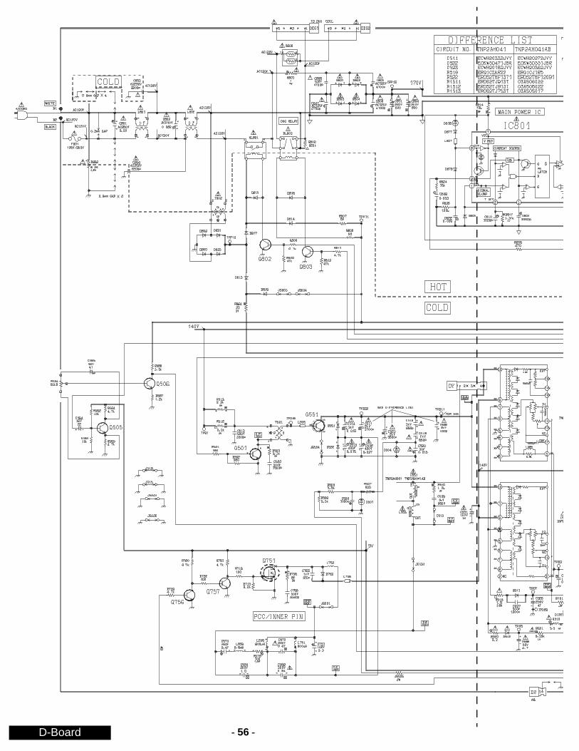
- 56 -D-Board
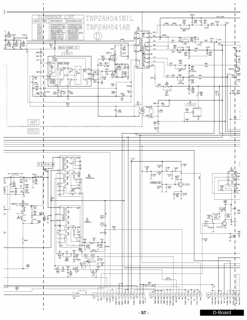
- 57 - D-Board
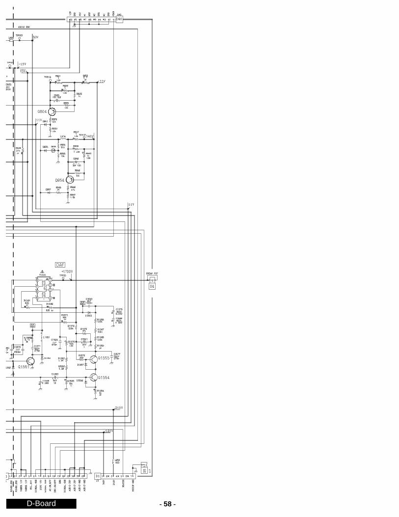
- 58 -D-Board
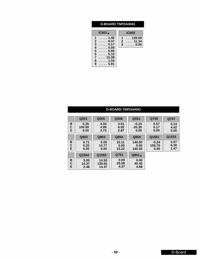
- 59 -
IC801
123456789
. . . . . 1.46
. . . . . 0.37
. . . . . 0.17
. . . . . 0.00
. . . . . 0.00
. . . . . 5.10
. . . . 15.38
. . . . . 1.04
. . . . . 5.91
IC802
123
. . . 139.00
. . . . 11.34
. . . . . 0.00
BCE
Q501
0.35100.50
0.00
Q505
4.344.993.73
Q506
3.516.922.87
Q551
-0.10-35.30
0.00
BCE
Q757
0.144.420.00
Q802
0.710.200.00
Q803
0.0014.77
0.00
Q804
15.110.00
15.22
Q854
140.000.00
140.30
BCE
Q1553
2.076.301.47
Q1554
3.0514.37
2.48
Q1555
14.93139.60
14.37
Q751
0.0025.58
4.37
Q801
0.0040.40
4.98
Q756
0.570.170.00
Q1551
-0.24105.70
0.00
D-BOARD TNP2AH041
D-BOARD TNP2AH041
D-Board
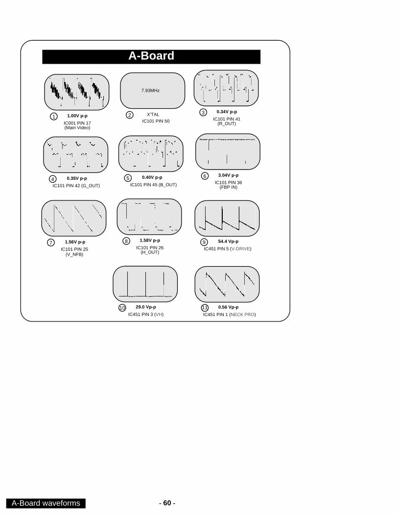
- 60 -
A-Board
1.00V p-p
IC001 PIN 17(Main Video)
1 X’TAL20.34V p-p
IC101 PIN 41(R_OUT)
3
0.35V p-p
IC101 PIN 42 (G_OUT)4 0.40V p-p
IC101 PIN 45 (B_OUT)5
3.04V p-p
IC101 PIN 36(FBP IN)
6
1.56V p-p
IC101 PIN 25(V_NFB)
7 1.58V p-p
IC101 PIN 26(H_OUT)
8
7.93MHz
IC101 PIN 50
54.4 Vp-p
IC451 PIN 5 (V-DRIVE)9
0.56 Vp-p
IC451 PIN 1 (NECK PRO)
1129.0 Vp-p
IC451 PIN 3 (VH)10
A-Board waveforms

- 61 -
notes:
NOTES
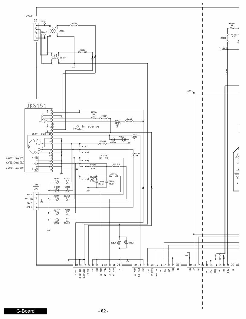
- 62 -G-Board
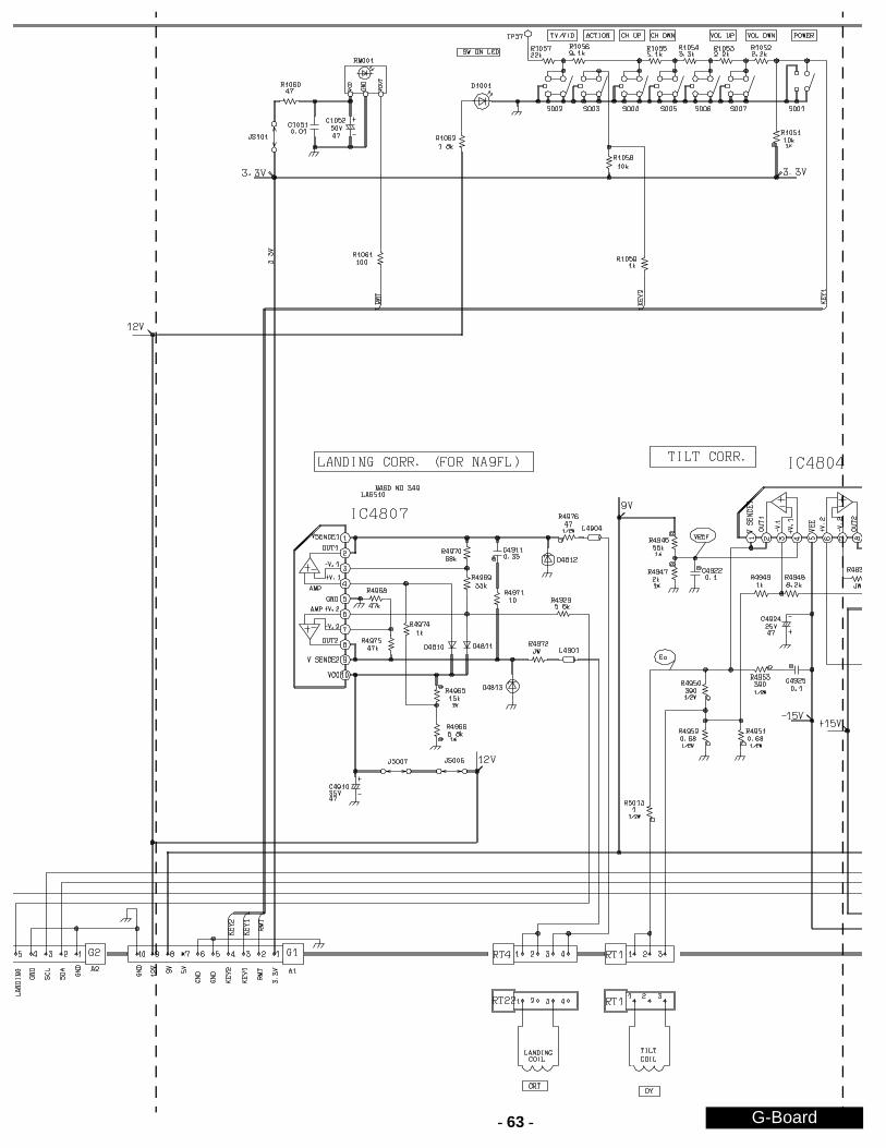
- 63 - G-Board
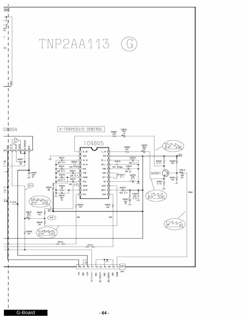
- 64 -G-Board
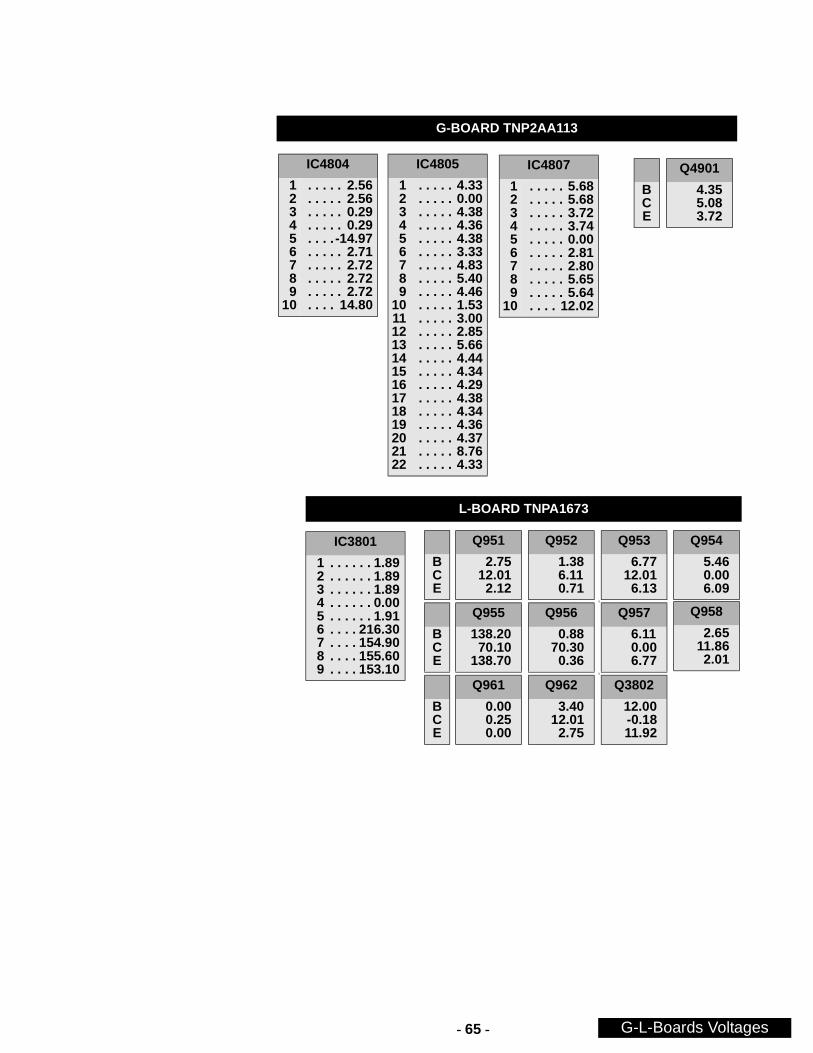
- 65 -
G-BOARD TNP2AA113
L-BOARD TNPA1673
IC4805
123456789
10111213141516171819202122
. . . . . 4.33
. . . . . 0.00
. . . . . 4.38
. . . . . 4.36
. . . . . 4.38
. . . . . 3.33
. . . . . 4.83
. . . . . 5.40
. . . . . 4.46
. . . . . 1.53
. . . . . 3.00
. . . . . 2.85
. . . . . 5.66
. . . . . 4.44
. . . . . 4.34
. . . . . 4.29
. . . . . 4.38
. . . . . 4.34
. . . . . 4.36
. . . . . 4.37
. . . . . 8.76
. . . . . 4.33
IC4804
123456789
10
. . . . . 2.56
. . . . . 2.56
. . . . . 0.29
. . . . . 0.29
. . . . -14.97
. . . . . 2.71
. . . . . 2.72
. . . . . 2.72
. . . . . 2.72
. . . . 14.80
IC4807
123456789
10
. . . . . 5.68
. . . . . 5.68
. . . . . 3.72
. . . . . 3.74
. . . . . 0.00
. . . . . 2.81
. . . . . 2.80
. . . . . 5.65
. . . . . 5.64
. . . . 12.02
BCE
Q4901
4.355.083.72
IC3801
123456789
. . . . . . 1.89
. . . . . . 1.89
. . . . . . 1.89
. . . . . . 0.00
. . . . . . 1.91
. . . . 216.30
. . . . 154.90
. . . . 155.60
. . . . 153.10
Q951
2.7512.01
2.12
BCE
Q952
1.386.110.71
Q953
6.7712.01
6.13
Q955
138.2070.10
138.70
BCE
Q956
0.8870.30
0.36
Q
Q957
6.110.006.77
Q954
5.460.006.09
Q958
2.6511.86
2.01
Q961
0.000.250.00
BCE
Q962
3.4012.01
2.75
Q
Q3802
12.00-0.1811.92
G-L-Boards Voltages
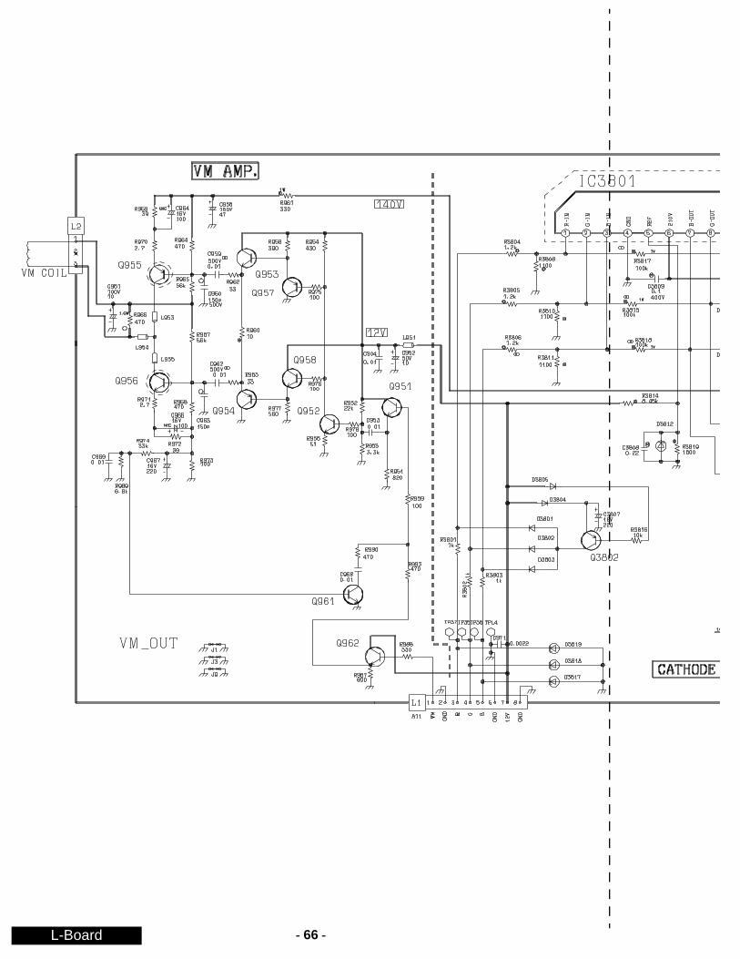
- 66 -L-Board
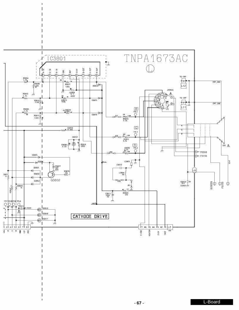
- 67 - L-Board
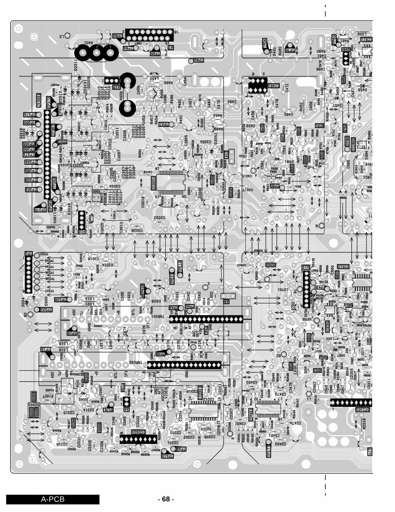
- 68 -A-PCB
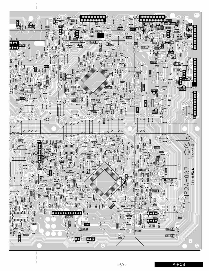
- 69 - A-PCB
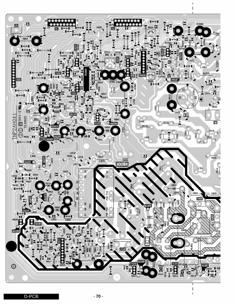
- 70 -D-PCB
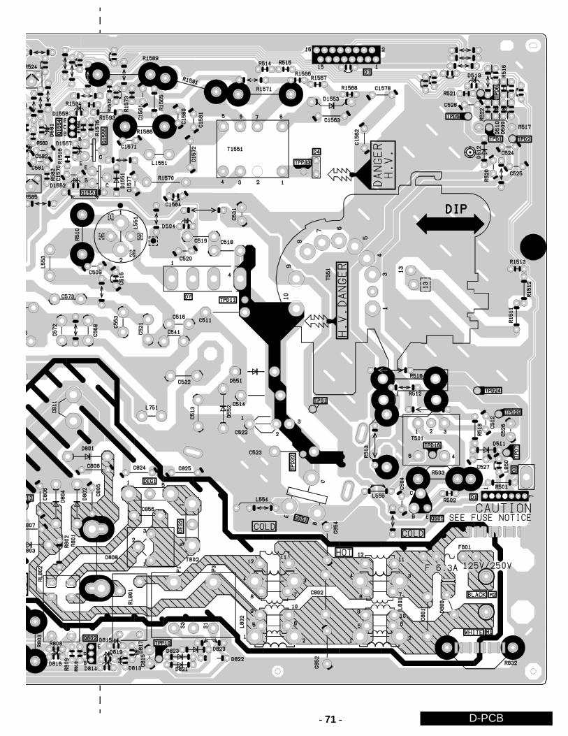
- 71 - D-PCB
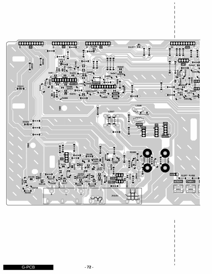
- 72 -G-PCB
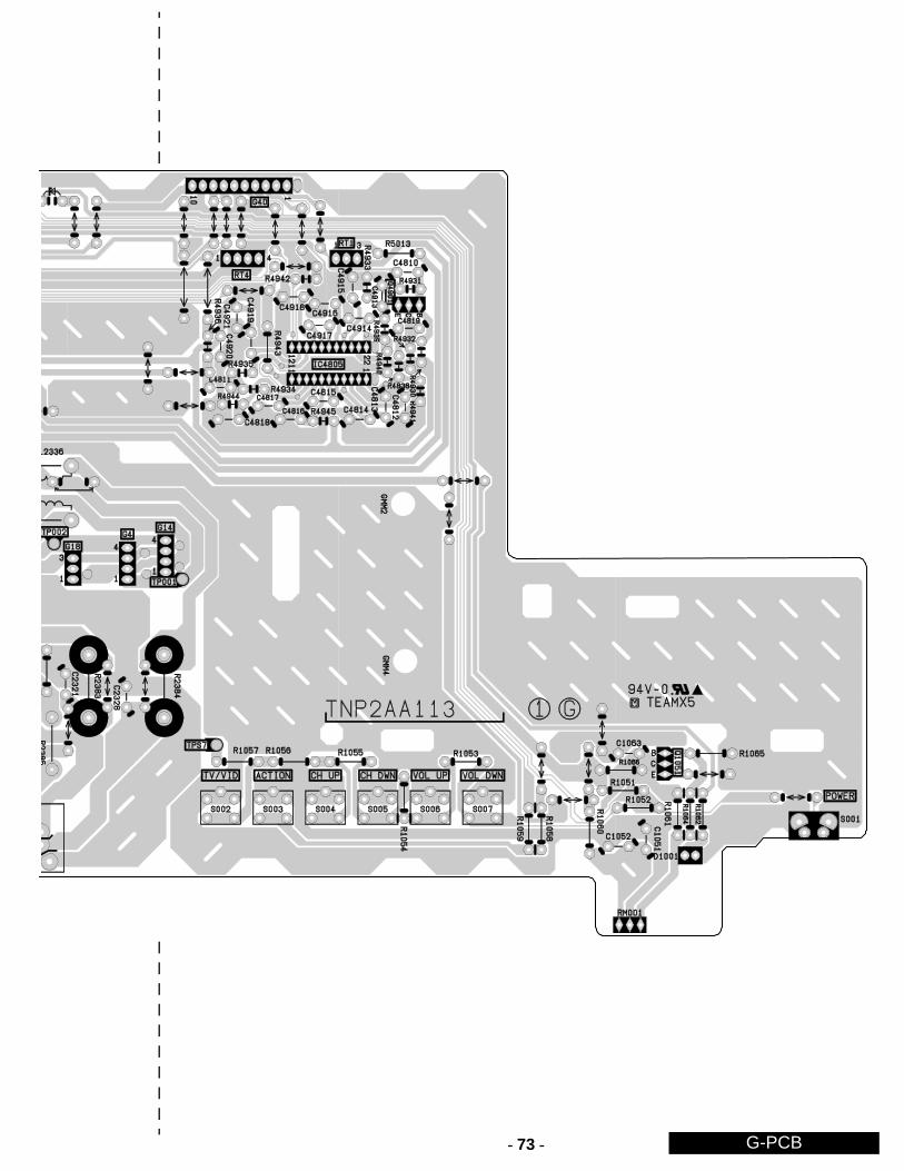
- 73 - G-PCB
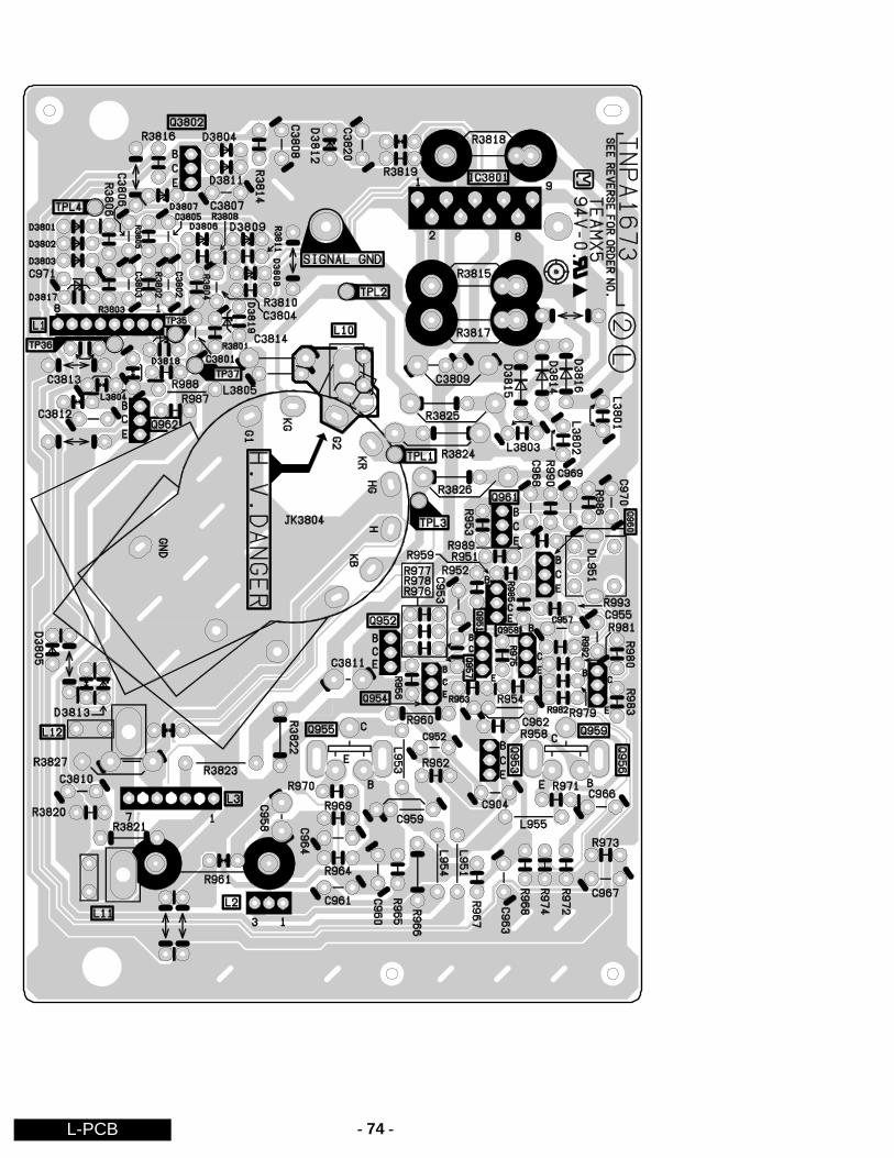
- 74 -L-PCB

- 75 -
notes:
NOTES

Printed in USAK02072127PL0717
®