characterization of poly(3-hexylthiophene
TRANSCRIPT
CHARACTERIZATION OF POLY(3-HEXYLTHIOPHENE) BASED SCHOTTKY DIODES
by
ALEXANDROS IOANNIS DIMOPOULOS
B.Eng., University of Victoria, 2005
A THESIS SUBMITTED IN PARTIAL FULFILLMENT OF THE REQUIREMENTS FOR THE DEGREE OF
MASTER OF APPLIED SCIENCE
in
THE FACULTY OF GRADUATE STUDIES
(Electrical and Computer Engineering)
THE UNIVERSITY OF BRITISH COLUMBIA
(Vancouver)
April 2012
© Alexandros Ioannis Dimopoulos, 2012

ii
Abstract This thesis describes the fabrication and electrical characterization of Schottky
diodes based on the polymer semiconductor poly(3-hexylthiophene). Printed electronics
may not be able to benefit from high vacuum processing, either for economic or
technical reasons. The aim was to observe the effects on performance when Schottky
diodes were built at atmospheric pressure. 200 nm thick films of poly(3-hexylthiophene)
were formed on glass substrates by spinning a 1 wt% polymer solution in chloroform.
Vacuum deposited aluminum and gold where used for the Schottky and ohmic contacts
respectively. Two types of diodes were manufactured. One type (Au bottom) had its
Schottky junction formed by evaporating aluminum onto the polymer under high vacuum.
The other (Al bottom) had its Schottky junction formed by depositing the polymer onto
aluminum at atmospheric pressure. The final yield of usable devices was 35% for Au
bottom and 22% for Al bottom. The hole density and bulk mobility were derived from
both DC and AC measurements. The bulk mobility was found to range from 2×
10!! cm2V-‐1s-‐1 to 6×10!! cm2V-‐1s-‐1. The hole density was determined to be between
5×10!" cm-‐3and 3×10!" cm-‐3. DC measurements showed that Au bottom devices had a
current rectification ratio of 2×10! at ±2 V, 100 times greater than Al bottom devices.
The space charge limited current (SCLC) had to be considered to successfully model
the DC behaviour. The small signal behaviour was modeled with a 2nd order
series/parallel circuit, which was determined through impedance spectroscopy. Small
signal performance of both device types was predicted to be poor. The corner
frequency was determined to be less than 100 Hz for Al bottom devices, and less than 1
kHz for Au bottom devices. Large signal frequency performance of the diodes was
tested with a half-wave peak rectifier. The maximum operating frequency was
measured to be 40 kHz for Au bottom devices and 10 kHz for Al bottom devices.

iii
Table of Contents
ABSTRACT .......................................................................................................... ii
TABLE OF CONTENTS ...................................................................................... iii
LIST OF TABLES ................................................................................................. v
LIST OF FIGURES .............................................................................................. vi
LIST OF ABBREVIATIONS ............................................................................... vii
ACKNOWLEDGEMENTS ................................................................................. viii
DEDICATION ...................................................................................................... ix
1 INTRODUCTION ............................................................................................. 1 1.1 THESIS ORGANIZATION .......................................................................................... 2 1.2 CONJUGATED POLYMERS ....................................................................................... 3 1.3 POLYTHIOPHENE .................................................................................................... 5 1.4 THE SCHOTTKY JUNCTION ..................................................................................... 7 1.5 CONCLUSIONS ....................................................................................................... 8
2 EXPERIMENTAL METHODS ....................................................................... 10 2.1 DESIGN ............................................................................................................... 10 2.2 FABRICATION ....................................................................................................... 12 2.3 MEASUREMENT .................................................................................................... 16 2.4 CONCLUSIONS ..................................................................................................... 17
3 DC MEASUREMENTS ................................................................................. 18 3.1 MEASUREMENT DESCRIPTION .............................................................................. 18 3.2 MODEL DESCRIPTION ........................................................................................... 19 3.3 MODEL FITTING ................................................................................................... 23 3.4 FIT RESULTS ....................................................................................................... 24 3.5 CONCLUSIONS ..................................................................................................... 29
4 SMALL SIGNAL AC MEASUREMENTS ..................................................... 30 4.1 DESCRIPTION OF THE C-V TECHNIQUE ................................................................. 30 4.2 GENERAL CONSIDERATIONS OF THE CV TECHNIQUE ............................................. 31 4.3 SPECIFIC CONSIDERATIONS WITH P3HT ............................................................... 32 4.4 MEASUREMENT DESCRIPTION .............................................................................. 33 4.5 DATA PREPROCESSING ........................................................................................ 33

iv
4.6 DATA PROCESSING .............................................................................................. 34 4.7 FIT RESULTS ....................................................................................................... 37 4.8 CONCLUSIONS ..................................................................................................... 41
5 PRACTICAL DIODE USES .......................................................................... 42 5.1 PEAK RECTIFIER .................................................................................................. 42 5.2 SMALL SIGNAL USE .............................................................................................. 45 5.3 CONCLUSIONS ..................................................................................................... 46
6 CONCLUSION .............................................................................................. 47 6.1 GENERAL CONCLUSIONS ...................................................................................... 47 6.2 FUTURE WORK .................................................................................................... 48
BIBLIOGRAPHY ................................................................................................ 50

v
List of Tables TABLE 3.1: CURRENT RECTIFICATION RATIO AT ±2 V. FROM DATA. ................................................. 26 TABLE 3.2: DIODE IDEALITY FACTOR (N). FROM FITS. ...................................................................... 26 TABLE 3.3: RSH (ΩCM2). FROM FITS. .............................................................................................. 27 TABLE 3.4: JS (ACM-2). FROM FITS. ................................................................................................ 27 TABLE 3.5: HOLE MOBILITY (CM2V-1S-1). FROM FITS. ....................................................................... 28 TABLE 3.6: HOLE DENSITY (CM-3). INDIRECTLY FROM FITS. ............................................................. 28 TABLE 4.1: HOLE DENSITY FROM AC MEASUREMENTS (CM-3). ........................................................ 40 TABLE 4.2: BUILT IN VOLTAGE FROM AC MEASUREMENTS (V). ....................................................... 40 TABLE 5.1: FORWARD BIAS CUTOFF FREQUENCY (HZ). ................................................................... 45

vi
List of Figures FIGURE 1.1: THE TWO EQUIVALENT FORMS OF TRANS-POLYACETYLENE. .......................................... 3 FIGURE 1.2: POLYTHIOPHENE. ........................................................................................................ 5 FIGURE 1.3: REGIOREGULAR POLY(3-HEXYLTHIOPHENE). ................................................................ 6 FIGURE 1.4: P3HT STACKING. ........................................................................................................ 6 FIGURE 1.5: THE IDEALIZED SCHOTTKY JUNCTION. .......................................................................... 7 FIGURE 2.1: SAMPLE LAYOUT. VERTICAL DIMENSIONS ARE NOT TO SCALE. ..................................... 11 FIGURE 2.2: METAL LIFT-OFF WITHOUT (LEFT) AND WITH (RIGHT) FIRST UNDERCUTTING THE
PHOTORESIST. ...................................................................................................................... 13 FIGURE 2.3:SAMPLE HOLDER USED TO MAKE ELECTRICAL MEASUREMENTS OUTSIDE OF THE
GLOVEBOX. .......................................................................................................................... 17 FIGURE 3.1: TYPICAL J-V SCANS OF EXAMINED DEVICES. ............................................................... 19 FIGURE 3.2: SCHEMATIC OF THE MODIFIED SHOCKLEY EQUATION. ................................................. 20 FIGURE 3.3: DC MODEL USED. ...................................................................................................... 21 FIGURE 3.4: LOG-LOG J-V PLOT OF AN AL-BOTTOM DIODE (DEVICE B92L1Y) SHOWING DIFFERENT
TRANSPORT REGIMES. THE CURRENT IS OHMIC AT LOW BIASES AND SPACE CHARGE LIMITED AT
HIGH BIASES. ........................................................................................................................ 22 FIGURE 3.5:REPRESENTATIVE FIT RESULTS FOR AU BOTTOM (LEFT COLUMN), AU BOTTOM (F-SERIES)
(CENTER COLUMN), AND AL BOTTOM (RIGHT COLUMN) DEVICES. FIT QUALITIES ARE BEST (TOP
ROW), MEDIAN (MIDDLE ROW), AND WORST (BOTTOM ROW). ................................................... 25 FIGURE 4.1: A SMALL SIGNAL MODEL OF AN ORGANIC SCHOTTKY DIODE. ........................................ 32 FIGURE 4.2: EXAMPLE OF AC PRE-PROCESSING. ........................................................................... 34 FIGURE 4.3: IMPEDANCE SPECTRA OF A P3HT/AL SCHOTTKY DIODE (D93R1Z) BIASED AT 0.6 V
(LEFT) AND -2 V (RIGHT). DATA PRESENTED HAS BEEN PREPROCESSED. ................................. 35 FIGURE 4.4: FIT RESULT FOR DIODE F93R2Y BIASES AT -0.8 V. TOP: OBJECTIVE FUNCTION, BOTTOM:
BODE PLOTS. ........................................................................................................................ 37 FIGURE 4.5: IMPEDANCE FIT RESULTS FOR DIODE F93R2Y. JUNCTION (�) AND BULK (+) VALUES ARE
SHOWN. ................................................................................................................................ 38 FIGURE 4.6: DEPLETION CAPACITANCE FROM THE SUSCEPTANCE FOR DIODE F92R3Y. .................. 39 FIGURE 5.1: THE HALF-WAVE PEAK RECTIFIER. .............................................................................. 42 FIGURE 5.2: FREQUENCY RESPONSE OF RECTIFIER WITH AU BOTTOM (F-SERIES) DEVICES. ............ 43 FIGURE 5.3:FREQUENCY RESPONSE OF RECTIFIER WITH AL BOTTOM DEVICES. ............................... 44

vii
List of Abbreviations AC Alternating current
DC Direct current
DI Deionized
HMDS Hexamethyldisilazane
HOMO Highest occupied molecular orbital
LUMO Lowest occupied molecular orbital
ME Mobility edge
P3HT Poly(3-hexythiophene)
PTFE polytetrafluoroethylene
RMS Root-mean-square
SCLC Space charge limited current
TFSCLC Trap free space charge limited current
TFT Thin film transistor

viii
Acknowledgements As I sail away, there are a number of people whom I would very much like to
thank for my adventure. My supervisor Dr. John Madden brought me to the strange new
shores of conducting polymers with an enthusiasm that is difficult to match. On many
occasions I felt as if I was following a path carved into an otherwise impenetrable
wilderness by Dr. Arash Takshi. My colleagues and friends in AMPEL 341 kept me
company around the campfire through many dark nights. I also happily acknowledge my
patrons, my family, who funded my expedition with a bottomless reserve of love and
patience, and even a little gold.

ix
Dedication
To adventurers everywhere
1
1 Introduction Inorganic semiconductors are a ubiquitous class of materials. Their widespread
use is primarily due to integrated circuit (IC) technology, which was first conceived in
the late 1950s when Jack Kilby demonstrated that all the elements of an oscillator
circuit could be constructed on a single silicon crystal. Robert Noyce also independently
formulated the concept [1]. Since then, ICs of every increasing complexity have become
ubiquitous. This has been due to the ability to form ever-larger perfect crystals as well
as an exponential decrease in circuit feature size. The result has been a doubling in
circuit density every 18 to 24 months in what is commonly known as Moore’s Law.
As popular as these materials have become, there are some applications for
which they are not ideally suited. High performance electronics demands that these
semiconductors be used in crystalline form. This limits their usefulness in flexible
structures. The size of the IC is also limited by the size of the crystal. In applications
where performance is less demanding, the semiconductors can be used in amorphous
or polycrystalline forms. This allows much larger circuits to be built, but the high
temperatures needed to process them still generally exclude the use of flexible
substrates. Some other drawbacks of silicon devices is that the bandgap is not
controllable, a fact which presents difficulties for sensors, light emission, and
photovoltaics. Antennas cannot be directly integrated into ICs, they must instead be
externally affixed. This represents a fixed cost in manufacturing which does not scale
with Moore’s law [2].
Various avenues are being examined to extend semiconductors past these
limitations. Some are process based, such as slicing devices from crystalline wafers
and transplanting them onto a flexible substrate [3], or finding ways to lower the
temperature needed to form poly-Si [4]. Others involve using new materials such as
graphene, engineered nanoparticles, or organic semiconductors.
Organic chemistry is a well-established discipline, which can effectively design,
synthesize, and purify new materials. This presents two interesting opportunities. First,
properties such as the bandgap can be tuned. Second, the material can be produced
inexpensively. Organic semiconductors can be divided into two groups: small molecules
2
and conjugated polymers. Many conjugated polymers have the advantage of being
soluble in liquid solvents at room temperature. Thus films of these polymers can be
formed at room temperature, which means that flexible substrates can be used.
Polymer solutions could be used as inks and integrated into industrial printing
processes, allowing arbitrarily large circuits to be produced inexpensively. Printing
would also allow direct integration with elements which cannot be built in the
semiconductor, such as antennas. For all of these interesting reasons, a conjugated
polymer was used in this work. Specifically, the well-known polymer poly(3-
hexylthiophene) was used.
The diode is a basic and versatile electronic device, with applications that include
rectification, demodulation, mixing, and filtering. The vast majority of conjugated
polymers are p-type semiconductors, which means that the Schottky diode is only diode
that can be practically built with them. Though a number of examples of P3HT based
Schottky diodes have been reported [5] [6] [7] [8] [9] [10], they are always formed under
high vacuum. This is a perfectly reasonable approach when exploring material
properties or as device demonstrations. This is however not ideal for considering
practical manufacturing issues since a high vacuum may not be economical or
compatible with processes such as roll-to-roll printing. A better analogue for a device
built using “cheap and dirty” manufacturing would be one formed at atmospheric
conditions. This thesis describes the construction and characterization of two types of
Schottky diodes. The first type had its Schottky junction formed under high vacuum, and
the second had its Schottky junction formed at atmospheric pressure.
1.1 Thesis Organization The rest of this introductory chapter presents an overview of background
information on conjugated polymers in general, poly(3-hexylthiphene) in particular, and
Schottky junction theory. The rest of this thesis is divided into four chapters. Chapter 2
covers the design and fabrication of the Schottky diodes as well as experimental
methods. Chapter 3 discusses the DC measurements, modeling, and characterization.
Chapter 4 does the same, but for small signal AC measurements. Chapter 5 briefly

3
considers the use diodes in electronic circuits. The final chapter concludes the work and
presents recommendations for future work.
1.2 Conjugated Polymers Polymers are generally thought of as being electrically insulating, and are
commonly used in this regard. For a solid to be electronically conductive, its electrons
need to be delocalized. This is not the case for many organic molecules since their
electrons are highly localized in σ orbitals [11]. A polymer that has alternating single and
double bonds along its backbone is known as a conjugated polymer. The double bonds
are due to π orbitals, which are delocalized.
Polyacetylene is a good illustrative example. It was also the first polymer to be
observed with a high conductivity, a discovery that lead to a Nobel Prize in Chemistry
[12]. The trans form of this polymer has two energetically equivalent forms, which are
shown in Figure 1.1. It is tempting to assign a resonance structure to trans-
polyacetylene and assume that conduction arises from a π orbital perfectly distributed
over the entire molecule, as in benzene. In reality, the resonance form, which would
result in metallic conduction, is unstable and polyacetylene takes a conjugated form.
The double carbon bonds are stronger than the single bonds and are thus shorter. This
causes a periodic distortion in the backbone, known as the Pieirls distortion, which
results in a splitting of the energy band. This mechanism is present in all conjugated
polymers and explains their semiconducting nature [11].
Figure 1.1: The two equivalent forms of trans-polyacetylene.
Conjugated polymers have wide bandgaps, polyacetylene for example has a
bandgap of 1.7 eV [12]. Accordingly, they have low intrinsic conductivities. Analogously
to inorganic semiconductors, they can be doped. The dopant species can either react
with the polymer in the form of a redox reaction, or affect it through electron-electron
repulsion [5]. In terms of energy structure, the result is a localized state in the bandgap.
At high enough doping levels, the bandgap can be filled and the polymer will exhibit
metallic conduction [11]. Molecular oxygen and water are known dopants for many
4
conjugated polymers [5]. This presents a problem since these polymers cannot be used
in an ambient atmosphere without introducing uncontrolled doping.
Thus far, only conduction along a single polymer chain has been considered.
This is a one-dimensional description and is inadequate for a thin film. The carrier
mobility in a thin film depends on the morphology since charges must travel between
polymer chains as well as along them. The π orbitals of adjacent polymer chains can
overlap if the chains are stacked together. This situation, known as π- π stacking,
extends charge delocalization into a second dimension. This can lead to a semi-
crystalline film composed of π- π stacked domains separated by amorphous regions.
While the mobility inside the domains may be large, the overall mobility is limited by
inter-domain transport. The degree of π- π stacking, and thus the mobility, is influenced
by the specifics of the deposition method and the surface energy of the substrate [13].
There is a low degree of π- π stacking in an amorphous film and charges must
hop between polymer chains. There is evidence of correlation between chain length and
hopping rate. A longer chain is more likely to have a region with a lowered barrier
somewhere along its length [5].
Because the charge delocalization is limited, it is not strictly correct to refer to
energy bands, as they may be very narrow or even nonexistent. Instead of a valence
and conduction band, the analogous concepts of highest occupied molecular orbital
(HOMO) and lowest unoccupied molecular orbital (LUMO) are respectively used. The
bandgap is thus the HOMO-LUMO energy difference [5].
Several mechanisms have been proposed to explain transport in conjugated
polymers. For semi-crystalline films, a mobility edge (ME) model has been proposed
and is considered promising [13] [14]. In this model, the ME is a defined energy that
separates mobile states from localized states. The mobile states are considered to form
a band and their density varies slowly at energies close to the ME. The localized states,
which are associated with grain boundaries and disordered regions, extend away from
the ME into the bandgap. Their density changes exponentially with energy [15]. The
regions of localized states are known as the band tails and their widths are a measure
of disorder in the semiconductor [14]. The model assigns a constant mobility to band
states and a mobility of zero to tail states. Transport occurs when charges are thermally
promoted from the tail to the band. Accumulating charge in the semiconductor shifts the

5
Fermi level towards the ME and increases the mobility [15]. This is done in a thin film
transistor (TFT) by charging the gate; the result is the increased field-effect mobility. It
can also be accomplished by doping the polymer [5]. Many conjugated polymers
behave as single carrier materials. This is can be explained as an asymmetry in the
band tails [5]. If for example, the tail extending from the LUMO is wider than the tail
extending from the HOMO, electrons will be more localized and thus less mobile. The
result is an intrinsically p-type material.
1.3 Polythiophene Polythiophene, shown in Figure 1.2, was first prepared in 1981 through electro-
polymerization of thiophene. Like polyacetylene, it is a planar molecule, it is a
semiconductor, and it can be doped.
Figure 1.2: Polythiophene.
Also like polyacetylene, it is unfortunately insoluble. Conjugated polymers can be
made soluble by substituting side groups longer than butyl (4 carbon atoms) [11]. A
well-known example is the polymer used in this work, poly(3-hexylthiophene) (P3HT),
shown in Figure 1.3. It is an intrinsically p-type semiconductor. Field-effect mobilities
above 0.1 cm2V-‐1s-‐1have been observed in TFTs [13], though the bulk mobility is
commonly three to five orders of magnitude smaller [7] [16] [17] [8] [9]. P3HT has a
bandgap of 1.7 eV and an electron affinity of 3.15 eV [18].

6
Figure 1.3: Regioregular poly(3-hexylthiophene).
Because the monomers are asymmetric, they can couple in several different
orientations when forming the polymer. One of the couplings is particularly undesirable
because neighbouring side chains interact with each other, causing the backbone to
twist. This disrupts the π orbital and widens the bandgap. A high degree of regular
monomer coupling, known as regioregularity, is thus desirable [11]. Solution deposited
P3HT which is highly regioregular tends to self assemble in edge-on stacks [13], as
shown in Figure 1.4. The mobility is anisotropic since the π- π stacking delocalizes
charges in planes parallel to the substrate, which are separated from each other by the
insulating hexyl groups.
Figure 1.4: P3HT stacking.

7
1.4 The Schottky Junction Depending on their relative Fermi levels, either a Schottky or ohmic junction may
form when a metal and a semiconductor are brought into intimate contact. Charges will
flow between the two until the semiconductor’s Fermi level is brought in line with the
metal’s. The system will be in thermal equilibrium at this point [19].
Figure 1.5 shows the energy diagram of a Schottky junction to an idealized
crystalline p-type semiconductor. There are no traps in the bandgap, nor are there any
interfacial states in this case. The work function of the metal is smaller so holes flow
from the semiconductor to the metal. The migration of holes out of the semiconductor
results in a zone that is depleted of mobile charge known as the depletion region. This
negative space charge causes the bands to bend down. To compensate this negative
space charge, a sheet of positive charge has built up on the metal’s surface. As can be
seen in Figure 1.5, holes passing from the metal to the semiconductor must overcome a
potential barrier:
!! = ! +!!! −Φ! (1.1)
where ! is the semiconductor’s electron affinity, !!is the semiconductor bandgap,
Φ! is the metal’s work function, and q is the electron charge.
Figure 1.5: The idealized Schottky junction.
! !
!"
!#
!$!%
!
!&
!%'(! '
! "
)*)+,-./)/)-&0
1.2(,(./

8
This barrier depends only on material properties and is not affected by an applied
bias. Holes moving in the other direction must overcome the band bending, which at
zero applied bias is characterized by the built-in voltage !!". Since applying an external
bias can both reduce and increase the band bending, the Schottky junction is rectifying
[19].
If instead, the metal’s work function is larger than the semiconductor’s, an ohmic
junction occurs. The semiconductor bands bend up and there is an accumulation of
holes at the junction. No barrier is encountered if a bias is applied so that holes flow
from the semiconductor to the metal. Unlike in the Schottky junction, current is not
impeded when a reverse bias is applied. The accumulated charge acts like an anode
and is able to provide a large number of holes. The current is thus limited by the
semiconductor bulk [20].
The idealized assumptions made when describing the Schottky junction have to
be modified when considering a conjugated polymer. Interface states will be present
unless the semiconductor surface is entirely free of oxides and defect free. These states
reduce the Schottky barrier’s size from the ideal and cause it to become bias-dependent
[20]. In the idealized case, the band edges are sharp and holes come from a shallow
acceptor level. In the polymer, the holes come from localized states in the band tail.
Numerical simulations have shown that a wider tail reduces the built-in voltage [14]. The
charge density in the depletion region is likely to be smaller than the dopant density
since many holes are trapped in the tail [14]. The idealized case assumes that the
space charge density and the dopant density are equal. The overall result is a shorter
depletion width than predicted by the idealized case [14].
1.5 Conclusions Poly(3-hexylthiophene) has a lower mobility than crystalline semiconductors, but
has the advantage of being solution processable at room temperature. It may not be
possible to construct inexpensive printed diodes in a high vacuum. It would therefore be
interesting to see how their performance is affected by building them at ambient
pressures.

9
Schottky diodes are formed by selecting metals and semiconductors with
appropriate differences in their work functions. The ideal Schottky junction theory can
be used to approximately explain the diodes built in this work. However, certain
limitations must be kept in mind. Interface states introduced into the junction by
contaminants cause the Schottky barrier to be bias-dependent. The disordered nature
of P3HT will likely cause the band bending to be overestimated.
The discussion begins with experimental methods. The design and fabrication of
the P3HT Schottky diodes is discussed, as well as measurement issues.

10
2 Experimental Methods This chapter begins by discussing the design of the Schottky diodes. Material
selection is discussed as well as justifications for physical dimensions. Next, fabrication
details are covered, including difficulties encountered. Methods to avoid unintentional
doping of the semiconductor both during manufacturing and testing are also explained.
The test fixture used in measurements is described at the end of this chapter, though
specifics of each measurement are covered in appropriate chapters later in the thesis.
2.1 Design In its most basic configuration, a Schottky diode consists of a semiconductor
sandwiched between two electrodes with differing work functions chosen to form a
Schottky contact on one side, and an Ohmic contact on the other. The semiconductor,
poly(3-hexylthiphene), is a well known soluble conjugated polymer. While the
semiconductor was a solution processed organic material, the contacts were vacuum
deposited metals.
P3HT has a band gap of 1.7 eV and an electron affinity of 3.15 eV [18]. Thus
under idealized conditions, the Schottky contact should have a work function of less
than 4.85 eV, and the Ohmic contact, a work function larger than 4.85 eV. Aluminum
(Al) and gold (Au) with work functions of 4.05 eV and 5.2 eV respectively [6], meet this
criteria. This has in fact been extensively observed [6] [5] [7] [8] [9] [10].
Other metals, such as calcium and magnesium, have smaller work functions than
aluminum. However, these materials are more reactive and hence more difficult to work
with and diffuse more rapidly into the polymer than aluminum [5].
The Schottky diodes were built in a vertical configuration by laying thin films of
the materials one on top of the other. The two types of devices were made by switching
the stack order. Au bottom devices were built in the order of Au/P3HT/Al, and Al bottom
devices in the order of Al/P3HT/Au.
The substrate needed to be smooth and rigid since the P3HT was to be spin-
coated. Si wafers with a SiO2 coating were readily available and have the required
physical properties. However, they have a parasitic capacitance large enough to
prevent proper AC measurements [5]. Glass on the other hand does not have this
problem. The devices were built on 1” square chips made by dicing large format
11
microscope slides measuring 3” by 2”. This chip size was small enough to get multiple
electrode sets from a single glass slide, and large enough to comfortably manipulate in
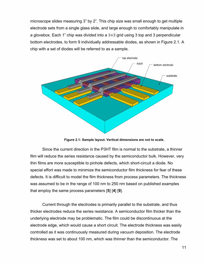
a glovebox. Each 1” chip was divided into a 3×3 grid using 3 top and 3 perpendicular
bottom electrodes, to form 9 individually addressable diodes, as shown in Figure 2.1. A
chip with a set of diodes will be referred to as a sample.
Figure 2.1: Sample layout. Vertical dimensions are not to scale.
Since the current direction in the P3HT film is normal to the substrate, a thinner
film will reduce the series resistance caused by the semiconductor bulk. However, very
thin films are more susceptible to pinhole defects, which short-circuit a diode. No
special effort was made to minimize the semiconductor film thickness for fear of these
defects. It is difficult to model the film thickness from process parameters. The thickness
was assumed to be in the range of 100 nm to 250 nm based on published examples
that employ the same process parameters [5] [4] [9].
Current through the electrodes is primarily parallel to the substrate, and thus
thicker electrodes reduce the series resistance. A semiconductor film thicker than the
underlying electrode may be problematic. The film could be discontinuous at the
electrode edge, which would cause a short circuit. The electrode thickness was easily
controlled as it was continuously measured during vacuum deposition. The electrode
thickness was set to about 100 nm, which was thinner than the semiconductor. The

12
series resistance contribution from the electrodes should be no more than a few Ohms,
and is thus negligible.
The width of the electrode lines specifies the cross sectional area of the diodes.
A large area increases the device current, making measurements easier. A smaller area
reduces the chance of encountering a pinhole in the P3HT film. Electrical
measurements of diodes of similar construction, and with a cross sectional area of
2×10!! m! have been reported [5]. This set an effective lower limit on the area of the
diodes since the same test equipment was used in this work. Such an area implies an
electrode width of about 50 µμm, half the width of a human hair. A shadow mask could
not be machined to that size in the available facilities. Features of this size would also
make alignment by eye inside the glovebox difficult. The width of both the top and
bottom electrodes was set at 1 mm.
2.2 Fabrication All bottom electrodes were patterned by photolithography instead of shadow
masking in order to save time through a higher throughput. Photolithography was
performed in the UBC nanofabrication facility which has a general cleanroom
classification of 10 000, except for the lithography room which has a classification of
1000, and this room’s wet-benches which are classified at 100 [21].
As noted above, the substrates were glass microscope slides measuring 2” by 3”
with a thickness of about 1 mm. The substrates were first cleaned in order to ensure
proper adhesion of the photoresist. The cleaning sequence was: a boiling acetone bath,
a boiling isopropyl alcohol bath, a deionized (DI) water rinse, drying with compressed
nitrogen, and a two minute dehydration bake on a hotplate. Once the substrates were
properly dried, they were primed with hexamethyldisilazane (HMDS) by spin coating in
order to improve photoresist adhesion. The positive photoresist S1813 was then applied
by spin coating at 5000 rpm for 50 s. The photomask was printed onto a Mylar sheet
using an ordinary office laser printer with a resolution of 600 dpi. Metallization was done
in a large electron beam evaporator capable of holding half a dozen substrates at a time.
The unwanted portions of the newly deposited metal films were washed away with
acetone, which dissolves the underlying photoresist. Once lift-off was complete, the
13
substrates were diced with a diamond saw and cleaned before being transferred into
the glovebox. Cleaning was done with acetone, isopropyl alcohol, DI water, and finally
an oxygen plasma treatment.
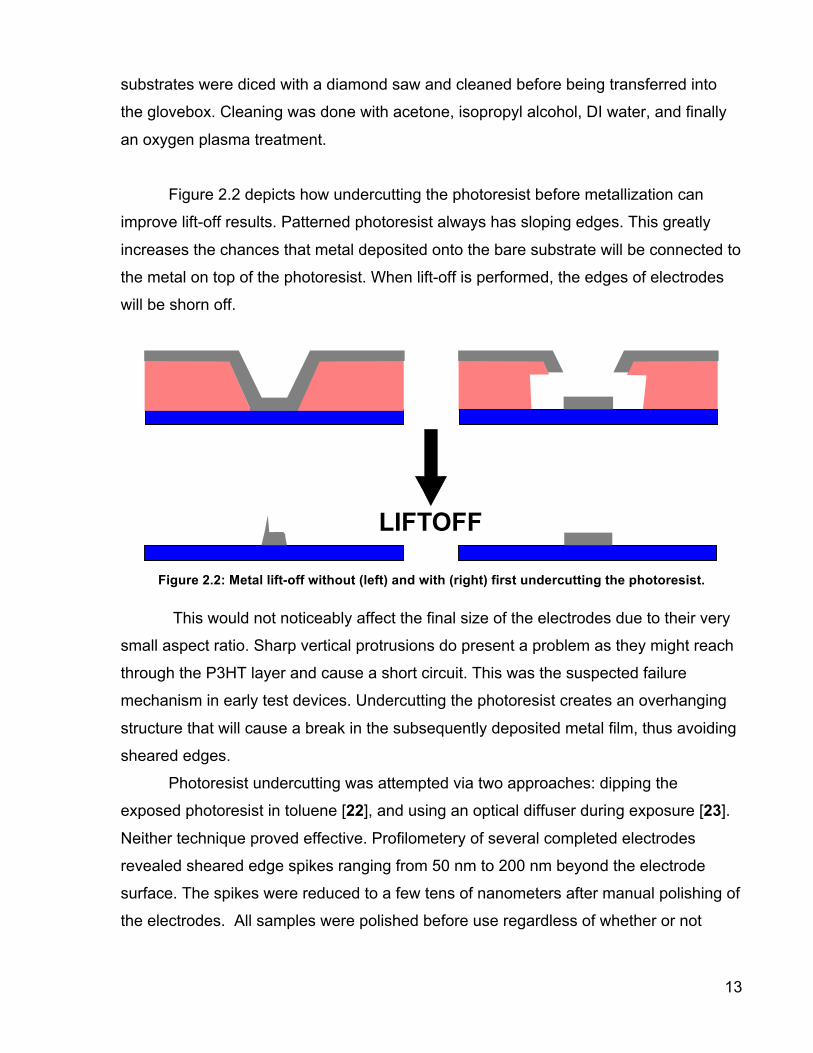
Figure 2.2 depicts how undercutting the photoresist before metallization can
improve lift-off results. Patterned photoresist always has sloping edges. This greatly
increases the chances that metal deposited onto the bare substrate will be connected to
the metal on top of the photoresist. When lift-off is performed, the edges of electrodes
will be shorn off.
Figure 2.2: Metal lift-off without (left) and with (right) first undercutting the photoresist.
This would not noticeably affect the final size of the electrodes due to their very
small aspect ratio. Sharp vertical protrusions do present a problem as they might reach
through the P3HT layer and cause a short circuit. This was the suspected failure
mechanism in early test devices. Undercutting the photoresist creates an overhanging
structure that will cause a break in the subsequently deposited metal film, thus avoiding
sheared edges.
Photoresist undercutting was attempted via two approaches: dipping the
exposed photoresist in toluene [22], and using an optical diffuser during exposure [23].
Neither technique proved effective. Profilometery of several completed electrodes
revealed sheared edge spikes ranging from 50 nm to 200 nm beyond the electrode
surface. The spikes were reduced to a few tens of nanometers after manual polishing of
the electrodes. All samples were polished before use regardless of whether or not
!"#$%##
14
undercutting was performed. Unfortunately, these complications cancelled the expected
time savings.
The resolution and contrast of the photomask were likely too low to define
adequately sharp edges. A mask produced with a better printer may have yielded better
results. There are also bilayer photoresists specifically for lift-off, but these were not
readily available.
The cleaned electrodes were immediately transferred to an argon-filled glovebox
where the remaining manufacturing took place. The glovebox was outfitted with a built
in thermal evaporator, and was also equipped with a hot plate, a spin coater, and an
analytical balance. The argon used had a purity of 99.999%. The system included a
solvent filter as well as a water and oxygen trap. However, neither oxygen nor moisture
sensors were present so some impurities may have been present.
Solution processing of conjugated polymers has long been considered the key to
developing low-cost organic electronics. High-speed printing techniques are of
particular interest, but are difficult to implement and beyond the scope of this work.
Common processing methods used in device research are dip casting and spin
coating.
Dip casting involves dipping a substrate into the polymer solution and then slowly
drawing it out. As the substrate is pulled away from the solution, the solvent on it
evaporates, and a solid film is left behind. The process is capable of forming thin, well
ordered films, but the drawing speed must be very slow. A typical drawing rate is 1
mm/min [24]. Also, enough solution must be prepared so that a sample may be totally
submerged.
In spin coating, a small volume of solution is deposited on a substrate, which is
then spun at high speed to evenly spread the solution. The solvent quickly evaporates,
leaving a solid film behind. The length of time needed depends largely on the
evaporation time of the solvent used. It is much faster than dip coating since the entire
substrate dries at once, typically less than one minute. Since the film dries more quickly
than in dip casting, the polymer chains have less time to orient themselves, resulting is
a less ordered film. This can be somewhat affected by selecting a solvent with a higher
boiling point [25].
15
The P3HT films were deposited by spin coating since a spin coater was available.
It is also a better analogue for high speed manufacturing processes due to the shorter
processing time.
P3HT was obtained from Sigma-Aldrich and used as received. The polymer was
in the form of crystalline granules; it had a number average molecular weight of 64 kDa,
and a regioregularity of over 98.5%. Chloroform was used as the solvent as it is known
to dissolve P3HT well [5] [7] [9]. Concentrations of about 1% by weight yield films of
around 120 nm in thickness [5] [9]. A concentration of 15 mg/mL was used,
corresponding to almost exactly 1% by weight. The solvent and polymer were placed in
a sealed vial and stirred for at least two hours at 40 °C. The solution was then passed
through a 0.45 μm polytetrafluoroethylene (PTFE) syringe filter into a clean receptacle
and immediately used in order to remove any remaining particles. Using a pipette, each
sample was entirely coated with the solution and then spun at 1000 rpm for 40 s. This
process was immediately repeated to form a double-layer P3HT film. Adding this
second layer reduced the number of short-circuited devices from about 50% to 30%.
This second layer likely plugged pinholes in the underlying film. The samples were then
placed on a hotplate set to 120 °C for 10 minutes to drive out any remaining solvent.
The film thickness was later determined by profilometry to be about 230 nm.
The final manufacturing step was to deposit the top electrodes. The samples
were fitted with a shadow mask and placed in the glovebox’s built-in thermal evaporator.
The deposition rate was kept to about 1 Ås-‐1. It has been suggested that a low
deposition rate may limit metal diffusion into the polymer and thus reduce the
occurrence of short circuits [5]. The electrodes were deposited to a thickness of 100
nm at a pressure of 2×10!! Torr. One set of samples (the F-series) had their top
electrodes deposited at a pressure of 1.5×10!! Torr, due to a fault in the evaporator.
The resulting devices still functioned as diodes, but their reduced performance was not
recognized until the data was analyzed.

16
A total of 11 Au bottom, and 12 Al bottom samples, each with 9 devices, were
manufactured. 30% of both Au bottom and 40% of Al bottom devices were short-
circuited. Eliminating devices which had an extremely poor DC reverse characteristic or
which short-circuited during measurement further reduced the yield. The final yield for
Au bottom devices was 35% (35 devices) and 22% (24 devices) for Al bottom devices.
2.3 Measurement Measurement leads were limited to 30 cm by performing electrical
measurements outside of the glove box. A special sample holder was prepared so that
finished samples could be taken out of the glovebox without exposure to oxygen or
water. A small polypropylene box with a gasket was fitted with wires and a set of gold
plated spring clips to hold one sample at a time. The assembly is shown in Figure 2.3.
The sample holder was placed inside of a custom-made grounded aluminum shield box
in order to reduce interference during measurements. Relevant measurement details
are covered in the next chapters. The thicknesses of the P3HT films were measured by
profilometry once electrical measurements were completed.
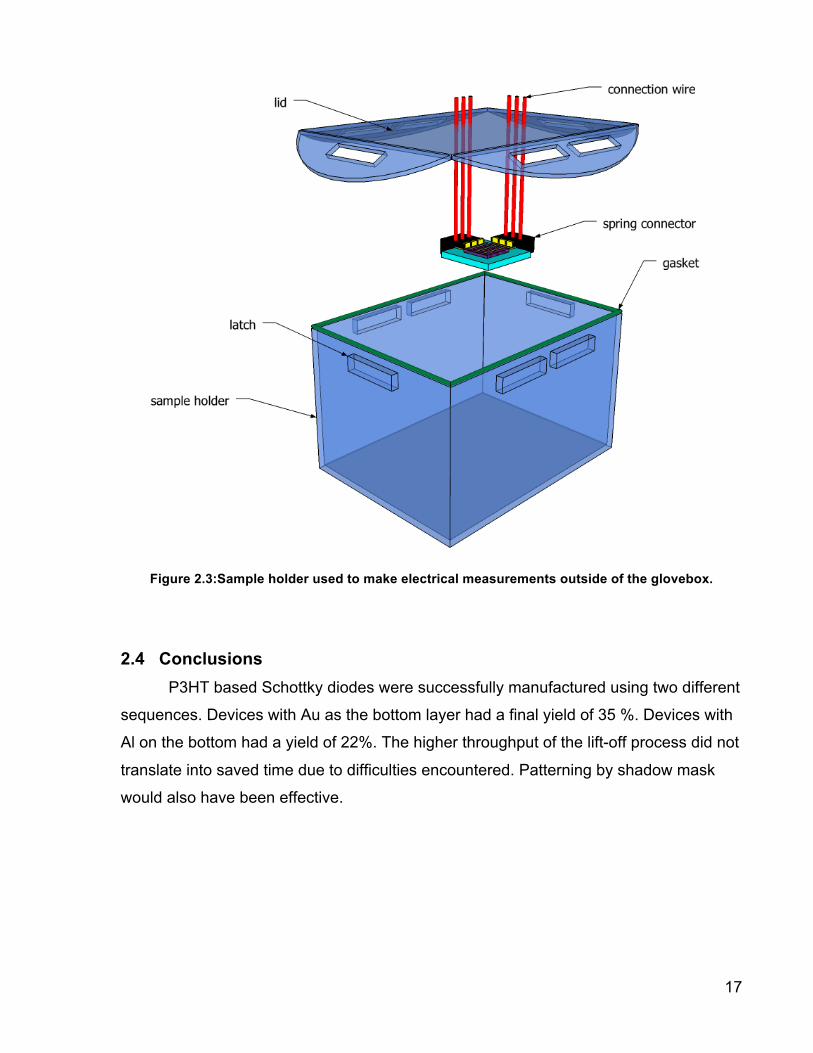
17
Figure 2.3:Sample holder used to make electrical measurements outside of the glovebox.
2.4 Conclusions P3HT based Schottky diodes were successfully manufactured using two different
sequences. Devices with Au as the bottom layer had a final yield of 35 %. Devices with
Al on the bottom had a yield of 22%. The higher throughput of the lift-off process did not
translate into saved time due to difficulties encountered. Patterning by shadow mask
would also have been effective.

18
3 DC Measurements A current density-voltage (J-V) scan is the most basic way to examine a diode. In
this chapter, a DC model of the P3HT/Al diodes is described and fitted to
measurements. The model parameters reveal information about the quality of the
diodes as well as the bulk hole mobility in the P3HT film. The hole density is also
derived.
3.1 Measurement Description Measurements were made with the Model 6430 source measurement unit (SMU)
from Keithley Instruments Inc. [26]. The I-V scans were performed outside of the
glovebox, as described in chapter 2.
The bias was applied as a linear staircase sweep with a step size of 10 mV.
There was a delay time of 100 ms between the rising edge and the start of a
measurement. Each measurement was averaged over one power line cycle, or 17 ms.
The temperature was not controlled and was assumed to be 296 K. Each device was
measured multiple times over periods of time stretching from several hours to about 10
days.
Typical results are shown in Figure 3.1. The F-series devices are clearly inferior
to the rest of the Au bottom devices. They are included as they were also used for small
signal tests presented in chapter 4.
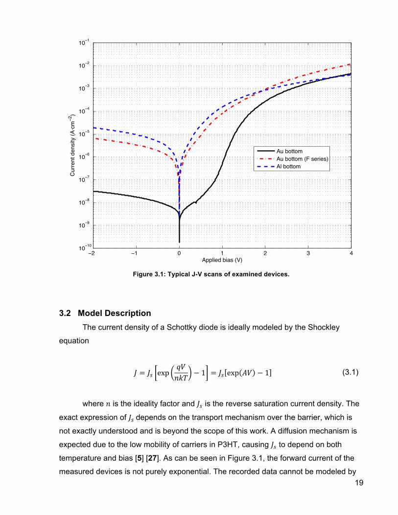
19
Figure 3.1: Typical J-V scans of examined devices.
3.2 Model Description The current density of a Schottky diode is ideally modeled by the Shockley
equation
! = !! exp!"!"# − 1 = !! exp !" − 1 (3.1)
where ! is the ideality factor and !! is the reverse saturation current density. The
exact expression of !! depends on the transport mechanism over the barrier, which is
not exactly understood and is beyond the scope of this work. A diffusion mechanism is
expected due to the low mobility of carriers in P3HT, causing !! to depend on both
temperature and bias [5] [27]. As can be seen in Figure 3.1, the forward current of the
measured devices is not purely exponential. The recorded data cannot be modeled by
2 1 0 1 2 3 410 10
10 9
10 8
10 7
10 6
10 5
10 4
10 3
10 2
10 1
Applied bias (V)
Cur
rent
den
sity
(Acm
2 )
Au bottomAu bottom (F series)Al bottom
20
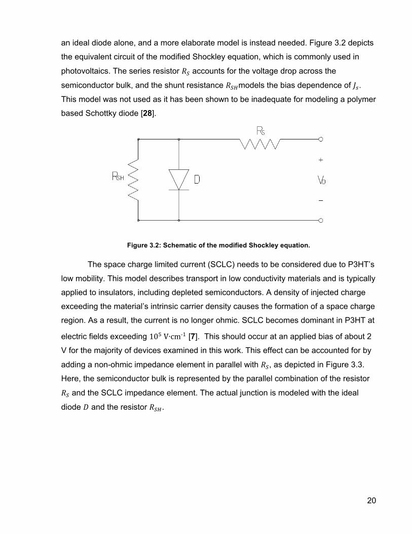
an ideal diode alone, and a more elaborate model is instead needed. Figure 3.2 depicts
the equivalent circuit of the modified Shockley equation, which is commonly used in
photovoltaics. The series resistor !! accounts for the voltage drop across the
semiconductor bulk, and the shunt resistance !!"models the bias dependence of !!.
This model was not used as it has been shown to be inadequate for modeling a polymer
based Schottky diode [28].
Figure 3.2: Schematic of the modified Shockley equation.
The space charge limited current (SCLC) needs to be considered due to P3HT’s
low mobility. This model describes transport in low conductivity materials and is typically
applied to insulators, including depleted semiconductors. A density of injected charge
exceeding the material’s intrinsic carrier density causes the formation of a space charge
region. As a result, the current is no longer ohmic. SCLC becomes dominant in P3HT at
electric fields exceeding 10! V∙cm-‐1 [7]. This should occur at an applied bias of about 2
V for the majority of devices examined in this work. This effect can be accounted for by
adding a non-ohmic impedance element in parallel with !!, as depicted in Figure 3.3.
Here, the semiconductor bulk is represented by the parallel combination of the resistor
!! and the SCLC impedance element. The actual junction is modeled with the ideal
diode ! and the resistor !!".

21
Figure 3.3: DC model used.
The applicability of this model to the current work is suggested by its successful
application in similar published work [7]. Examining the I-V data on a log-log plot, as in
Figure 3.4, lends further support. Linear regions in the plot indicate regions where the
current density is a power function of bias, with the exponent equal to the slope of the
line. The unity slope at low biases indicates ohmic conduction. The slope at high biases
is 2, which indicates a trap free space charge limited current (TFSCLC) [16]. This
means that all the traps in the bulk have been filled [16] and that the current density can
be expressed as
! =98 ∙!!!!!! !!! = !!! (3.2)
where ! is the thickness of the semiconductor film, !!!! is the permittivity of the
semiconductor, and ! is the bulk mobility [7]. Given this dependence, the bulk mobility
can be easily extracted from the J-V data, provided that data is recorded up to biases in
the SCLC regime.
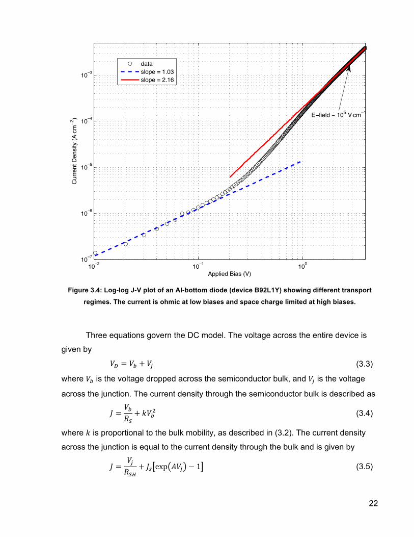
22
Figure 3.4: Log-log J-V plot of an Al-bottom diode (device B92L1Y) showing different transport
regimes. The current is ohmic at low biases and space charge limited at high biases.
Three equations govern the DC model. The voltage across the entire device is
given by
!! = !! + !! (3.3)
where !! is the voltage dropped across the semiconductor bulk, and !! is the voltage
across the junction. The current density through the semiconductor bulk is described as
! =!!!!+ !!!! (3.4)
where ! is proportional to the bulk mobility, as described in (3.2). The current density
across the junction is equal to the current density through the bulk and is given by
! =!!!!"
+ !! exp !!! − 1 (3.5)
10 2 10 1 10010 7
10 6
10 5
10 4
10 3
Applied Bias (V)
Cur
rent
Den
sity
(Acm
2 )
dataslope = 1.03slope = 2.16
E field ~ 105 V cm 1

23
where ! includes the ideality factor !, which is a measure of the quality of the rectifying
junction, as described in (3.1). A perfect junction has an ideality of 1; an increase in !
corresponds to a decrease in quality.
3.3 Model Fitting Determining the model parameters is not a straightforward process. They cannot
be directly extracted from measured data since the model depends on the hidden
variables !! and !!. The strategy employed was to iteratively solve the set of equations
(3.3)-(3.5) using the nonlinear least-squares facilities in MATLAB. The algorithm is
outlined here:
1. Solve (3.4) and (3.5) over the forward bias for the parameters. • Assume that !! and !! are correctly known. • Update the parameter values.
2. Solve the system of equations at each bias point for variables !! and !!. • Assume that the parameters are correctly known. • Update the voltage values.
3. Check the parameters for convergence. • Repeat if needed.
Convergence was defined as a relative change of less than 10!! between
iterations. The maximum number of iterations was set at 100.
There is no guarantee that the solver would converge to the desired solution, or
even to any solution, when starting from an arbitrary initial guess. It is therefore
important to start with an initial guess as close as possible to the final solution. This was
done by dividing the data into three bias ranges and assuming different model elements
dominated in each one. The resistors were assumed to dominate over reverse biases,
the SCLC element at high biases, and the diode and resistors over the intermediate
range. As discussed earlier, the bias at which the SCLC begins to dominate can be
found on a log-log plot.
The SCLC parameter, !, was estimated from a linear fit to the high bias data on
a log-log scale. For the other parameters, a first coarse estimate was refined by least
24
squares fitting. !! was coarsely estimated from the physical dimensions of the P3HT
film and an assumed resistivity of 1.47×10! Ωcm based on literature values [29].
!!"was coarsely estimated by performing a linear fit over the reverse bias range and
subtracting the coarse value of !!.The contributions of !! and !!"over the intermediate
bias region were cancelled, and then !! and ! were estimated from a linear fit in a semi-
log scale.
A least squares fit over the intermediate bias range was then performed in order
to refine the initial values of all parameters but !.
Initial estimates of the internal voltages were then found by solving (3.4) and
(3.3) for !! and !! respectively.
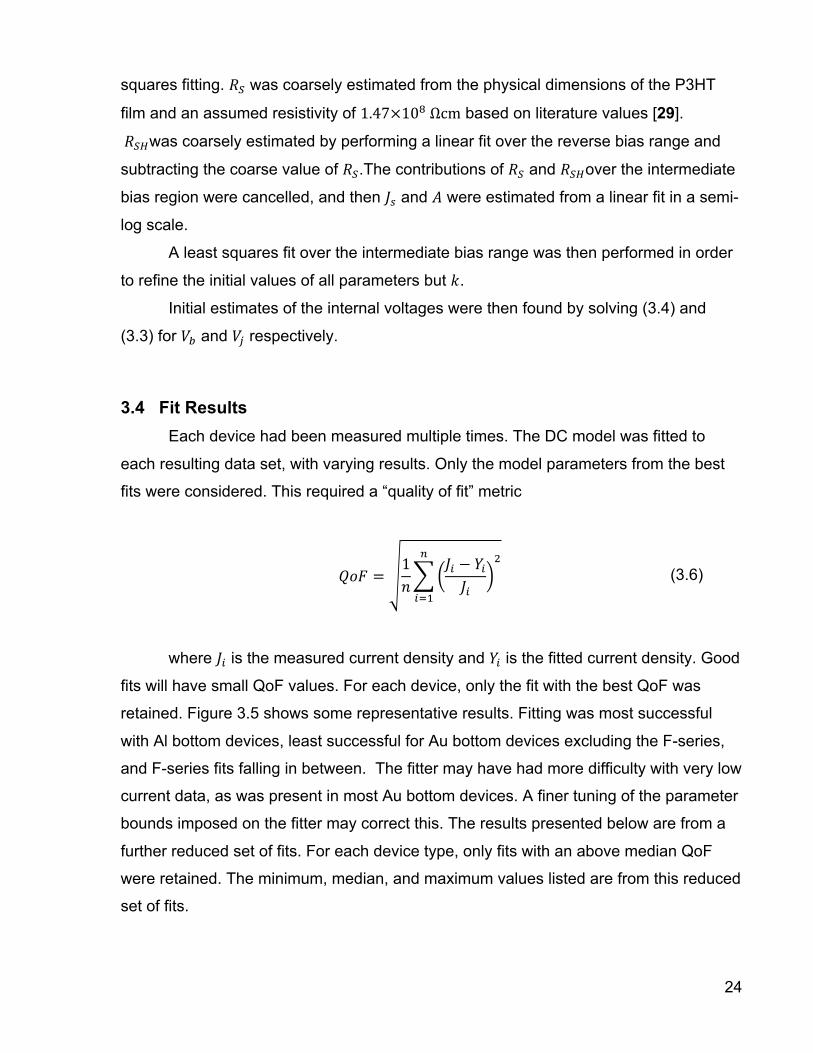
3.4 Fit Results Each device had been measured multiple times. The DC model was fitted to
each resulting data set, with varying results. Only the model parameters from the best
fits were considered. This required a “quality of fit” metric
!"# =1!
!! − !!!!
!!
!!!
(3.6)
where !! is the measured current density and !! is the fitted current density. Good
fits will have small QoF values. For each device, only the fit with the best QoF was
retained. Figure 3.5 shows some representative results. Fitting was most successful
with Al bottom devices, least successful for Au bottom devices excluding the F-series,
and F-series fits falling in between. The fitter may have had more difficulty with very low
current data, as was present in most Au bottom devices. A finer tuning of the parameter
bounds imposed on the fitter may correct this. The results presented below are from a
further reduced set of fits. For each device type, only fits with an above median QoF
were retained. The minimum, median, and maximum values listed are from this reduced
set of fits.
25
Figure 3.5:Representative fit results for Au bottom (left column), Au bottom (F-series) (center column), and Al bottom (right column)
devices. Fit qualities are best (top row), median (middle row), and worst (bottom row).
0 1 2 3 410 10
10 1
10 7
10 4
bias (V)
J (A
cm2 )
0 1 2 3 410 8
10 6
10 3
10 1
bias (V)
J (A
cm2 )
0 0.5 1 1.5 210 8
10 6
10 4
10 2
bias (V)
J (A
cm2 )
0 1 2 3 410 10
10 8
10 5
10 3
bias (V)
J (A
cm2 )
0 1 2 3 410 8
10 6
10 3
10 1
bias (V)J
(Acm
2 )0 0.5 1 1.5 2
10 8
10 6
10 4
10 2
bias (V)
J (A
cm2 )
0 1 2 3 4
10 10
10 8
10 6
10 4
bias (V)
J (A
cm2 )
0 1 2 3 410 7
10 5
10 3
10 1
bias (V)
J (A
cm2 )
0 0.5 1 1.5 210 7
10 4
10 2
bias (V)
J (A
cm2 )
QoF = 8.4E 3QoF = 3.0E 2QoF = 1.3E 1
QoF = 3.1E 1
QoF =1.7
QoF = 8.1E 2
QoF = 1.4E 1
QoF = 1.8E 2
QoF = 1.4E 1

26
The first results, presented in Table 3.1, are directly from the data instead
of the fit results. These are the current rectification ratios at ±2 V. At 2 V, the bias
is large enough for the device to be well out of the ohmic region, but the current
should not yet be dominated by the SCLC mechanism. The Au bottom devices,
excluding the F-series, demonstrated a rectification of 1.8×10!, which is in line
with reported values [16] [4]. The Au bottom devices outperformed the Al bottom
devices by two orders of magnitude. Unexpectedly, the F-series Au bottom
devices had the smallest rectification ratio of all.
Device type Min Median Max
Au bottom 3.3×10! 1.8×10! 5.6×10!
Au bottom (F-series) 1.1×10! 2.0×10! 1.8×10!
Al bottom 7.3×10! 2.2×10! 7.5×10! Table 3.1: Current rectification ratio at ±2 V. From data.
The ideality factors of the diodes were extracted from the fits by assuming
a temperature of 296 K (a thermal voltage of 26 mV) and are presented in Table
3.2. The results from the Au bottom devices are comparable to published results
[10] [28] [7] [5]. The Al bottom devices could not be compared to reported
examples since ideality factors for such a device geometry have not previously
been reported.
Device type Min Median Max
Au bottom 1.8 3.4 4.4
Au bottom (F-series) 3.5 9.9 12
Al bottom 3.1 4.4 6.5 Table 3.2: diode ideality factor (n). From fits.
!!" and !! are also directly related to the quality of the junction and are
presented in Table 3.3 and Table 3.4.
27
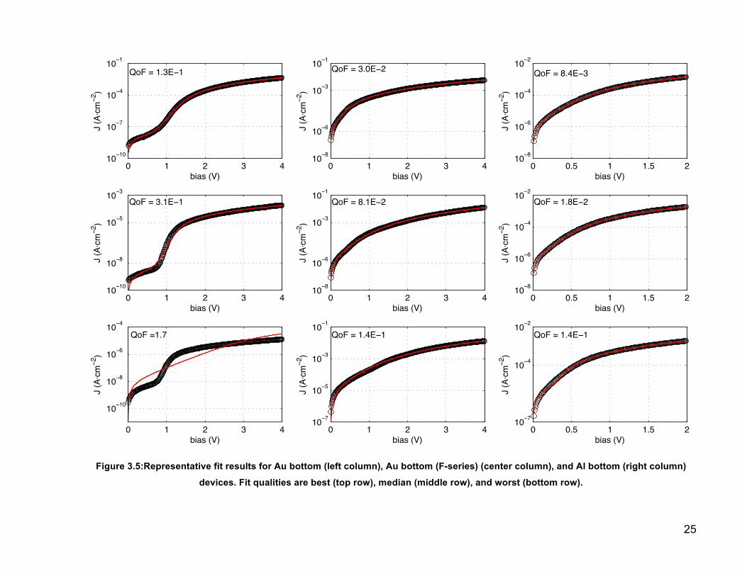
Device type Min Median Max
Au bottom 5.3×10! 3.7×10! 2.6×10!
Au bottom (F-series) 2.5×10! 3.8×10! 8.2×10!
Al bottom 7.9×10! 1.9×10! 5.5×10! Table 3.3: RSH (Ωcm2). From fits.
Device type Min Median Max
Au bottom 2.1×10!!" 7.9×10!!" 6.1×10!!!
Au bottom (F-series) 7.0×10!! 3.1×10!! 1.3×10!!
Al bottom 6.2×10!! 1.3×10!! 2.5×10!! Table 3.4: Js (Acm-2). From fits.
The model parameters which relate to the junction are generally
consistent with the observed diode rectification. That is, the Au bottom devices,
excluding the F-series, have the superior junctions, and the F-series devices
have the worst junctions. The !!" values are however inconsistent, indicating
that the Al bottom devices have the worst junctions by a factor of two.
Small signal junction resistances derived from AC measurements,
presented in chapter 4 also indicate that the F-series devices have the least ideal
junctions.
It was expected that the Al bottom devices would be the worst performing.
The Al electrodes of these devices were exposed to oxygen before deposition of
the P3HT layer, which undoubtedly led to the formation of an interfacial oxide
layer. In fact, the worst performing devices were the Au bottom F-series devices.
The Schottky junctions of these devices were formed at a higher pressure than
the rest of the Au bottom devices. A higher level of contamination could therefore
be anticipated. The fact that these devices had an even poorer performance than
the Al bottom devices suggests a large amount of contamination, possibly oil
from the molecular diffusion pump.
Results for both hole mobility and hole density fall within the range of
reported values [16] [17] [4] [7] [9]. The mobility depends only on the model

28
parameter !. The hole density cannot be determined from a single model
parameter. It can only be extracted from !! together with the mobility.
Device type Min Median Max
Au bottom 4.4×10!! 2.5×10!! 5.2×10!!
Au bottom (F-series) 1.0×10!! 2.3×10!! 1.0×10!!
Al bottom 8.0×10!! 5.8×10!! 1.2×10!! Table 3.5: Hole mobility (cm2V-1s-1). From fits.
Device type Min Median Max
Au bottom 1.6×10!" 1.3×10!" 9.7×10!"
Au bottom (F-series) 1.8×10!" 1.0×10!" 6.1×10!"
Al bottom 2.9×10!" 8.0×10!" 2.0×10!" Table 3.6: Hole density (cm-3). Indirectly from fits.
Hole mobility values extracted from AC fits in chapter 4 agree with values
presented here and can be considered correct. On the other hand, hole densities
extracted from AC measurements are an order of magnitude larger than those
derived from DC fits. The values presented here should be considered
underestimated. The hole mobility derived from AC measurements depends on
the hole density from those same measurements. If the mobility is correct, then
the hole density should also be correct. This means that the DC fits
overestimated the size of !! by an order of magnitude.

29
3.5 Conclusions J-V scans of the diodes demonstrated that the Au bottom devices outperformed
the Al bottom devices in current rectification by two orders of magnitude. The F-series
Au bottom devices had a much poorer performance than expected. This emphasized
the extreme sensitivity of the Schottky junction to contamination when being formed. A
high quality vacuum is essential for forming a high performance Schottky junction.
A proper DC model of the P3HT/Al Schottky diode must take the space charge
limited current into account. The model used adequately explained the observed
behaviour. Better fits could be achieved by applying a finer control on the algorithms
used. A more sophisticated model, that for example incorporates a field-dependent
mobility, may also yield better fits.
The bulk hole mobility in P3HT was found to be in the range of 2×10!! cm2V-‐1s-‐1
to 6×10!! cm2V-‐1s-‐1. This is in agreement with reported values as well as results from
AC measurements presented in this work.
The hole density in P3HT was found to range from 10!" cm-‐3 to 10!" cm-‐3. While
this agrees with reported values, it is likely an order of magnitude too small. This may
be due to an overestimation of the bulk resistance.
The hole density and bulk mobility values measured in this chapter were
compared to values extracted from AC measurements. These AC measurements and
results are completely independent of the DC methods described in this chapter, and
are presented next in chapter 4.
30
4 Small Signal AC Measurements In this chapter, small signal measurements are used to determine the carrier
density, and thus the trap density, in the P3HT film. The bulk mobility is also determined
from these measurements. The conventional method for determining a semiconductor’s
carrier profile is not applicable to P3HT and a modified technique is used.
4.1 Description of the C-V Technique The capacitance-voltage (C-V) technique is a well-established method of
determining the carrier profile, which has been used with Schottky diodes, as well as pn
diodes, MOS capacitors, and MOSFETs [30]. The method is based on measuring the
variation of the junction’s depletion capacitance with bias. The differential capacitance
at a given bias is measured by applying a small amplitude AC signal over a DC bias.
The C-V technique is dependent on several assumptions: that the depletion
approximation applies, that the carrier density is invariant over a short segment of the
depletion width, and that the AC signal is small enough for the differential capacitance
to be approximately linear.
As long as these assumptions hold, it has been shown that the differential
capacitance at a given bias ! can be modeled as a parallel plate capacitor
! =!!!!! (4.1)
where ! is the differential capacitance, ! is the cross-sectional area of the device,
! is the relative dielectric constant of P3HT, and ! is the width of the depletion region
when the junction is biased at ! [31]�. This allows a direct measurement of the
depletion depth since the spread of the depletion region in a Schottky junction is limited
on one side by the metal.
It has also been shown that the carrier density at a given ! can be related to the
capacitance
! ! =−2
!"!!!!!!" !
!! (4.2)

31
where ! ! is the carrier density in the semiconductor at a depth of !from the
metallurgical junction, and ! is the elementary charge [30].
In the case of a spatially uniform carrier density, a plot of !!!against ! is linear,
and the depletion width can be described as
! =2!!!!" !!" − ! −
!"! (4.3)
where !!" is the built in potential of the junction (also called the diffusion potential)
[19].
In this case, the capacitance can be related to the bias by
1!! =
2 !!" − ! −!"!
!"!!! (4.4)
[19].
4.2 General Considerations of the CV Technique The spatial resolution of the carrier density extracted by the C-V technique is
characterized by the Debye length
!! =!!!!"!!!(!)
(4.5)
. One of the simplifying assumptions made under the depletion approximation is
a sharp boundary between the depletion and bulk regions of the semiconductor. In
reality, carriers diffuse over a distance characterized by !!. This means that carrier
density variations over distances less than !! are effectively meaningless. The
depletion approximation is satisfied if the step size in a C-V scan is no less than two to
three times !! [30]. The minimum probing depth occurs at zero applied bias. The
maximum depth is limited by the semiconductor’s breakdown electric field strength [30].
The differential capacitance must behave approximately linearly if the parallel
plate capacitor model is to be valid. In order to guarantee that this is the case, the AC
amplitude must be kept small relative to the DC bias [31]. Typical values range from 10
mV to 20 mV [30].
32
4.3 Specific Considerations with P3HT The usual procedure is to apply an AC signal of constant frequency while
sweeping the applied DC bias. The measured capacitance will be almost identical to the
depletion capacitance so long as the leakage current and the series resistance are quite
small. A typical measurement frequency is 1 MHz [30]. The high mobilities in materials
such as crystalline Si and GaAs means that free carriers provided by dopant atoms will
easily respond an excitation at such a frequency.
Using a single probing frequency with the devices in this work is problematic.
Several transport mechanisms have been proposed for polymeric semiconductors [15]
[32] [16]. They have in common a dependence on trap states that have an associated
time constant, which depends on their energetic position. This would imply a frequency
dependent differential capacitance, which has in fact been observed [33] [34]. If a lump
element circuit with frequency-independent components can adequately describe the
AC behaviour, then the C-V technique can still be used to extract the carrier profile.
Such a model exists [33] [34] [35] and is depicted in Figure 4.1
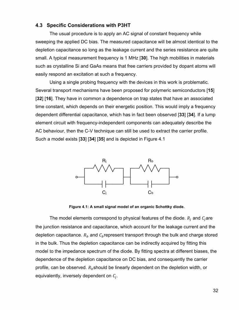
Figure 4.1: A small signal model of an organic Schottky diode.
The model elements correspond to physical features of the diode. !! and !!are
the junction resistance and capacitance, which account for the leakage current and the
depletion capacitance. !! and !!represent transport through the bulk and charge stored
in the bulk. Thus the depletion capacitance can be indirectly acquired by fitting this
model to the impedance spectrum of the diode. By fitting spectra at different biases, the
dependence of the depletion capacitance on DC bias, and consequently the carrier
profile, can be observed. !!should be linearly dependent on the depletion width, or
equivalently, inversely dependent on !!.
Rj
Cj
Rb
Cb

33
4.4 Measurement Description A Solartron 1260A impedance/gain-phase analyzer by Solartron Analytical [36]
was used to measure the impedance spectra. Measurements were carried out with a 10
mV amplitude signal. The frequency was swept from 1 Hz to 100 kHz with 50 steps per
decade. Spectra were measured at DC biases ranging from 2 V to -5 V in 200 mV
increments. Each measurement point was averaged over a period of up to 10 s before
being recorded by the impedance analyzer.
Measurements were completed outside of the glovebox, as described in chapter
2.
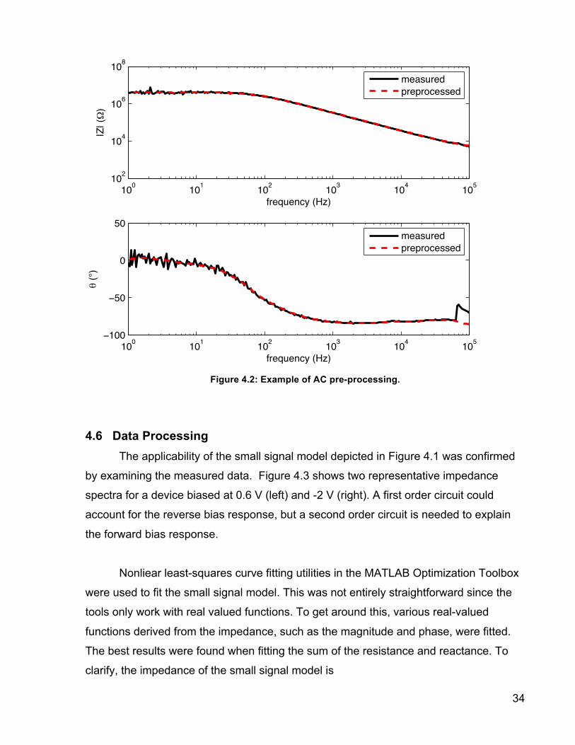
4.5 Data Preprocessing The impedance analyzer generated a separate data file for each DC bias setting.
All data pre-processing was done with MATLAB and applied independently to each
recorded spectrum. The parasitic effects of the measurement setup were measured and
subtracted from the data as a first pre-processing step. This had a minimal effect since
the parasitic elements were negligible over the frequency band of interest. Curiously, a
phase discontinuity was observed in all measurements. The discontinuity always
occurred at 66.07 kHz and ranged in size from approximately 1° to 20°, increasing as
the biased moved from away from 0 V. This was assumed to be due to an instrument
fault and was subtracted from the data. The final pre-processing step was to apply
some noise reduction filters. First, a median filter was used to eliminate outlying data
points; next a running average filter was used to smooth the noise. The real and
imaginary parts of the impedance were filtered separately.
34
Figure 4.2: Example of AC pre-processing.
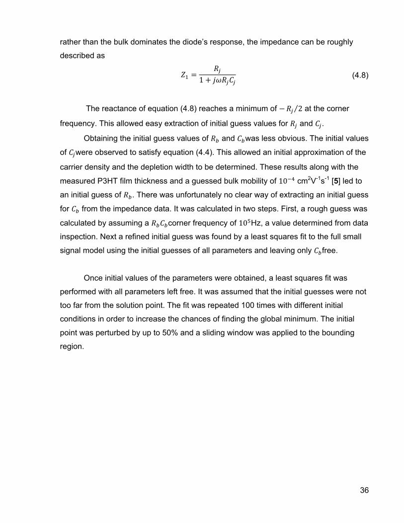
4.6 Data Processing The applicability of the small signal model depicted in Figure 4.1 was confirmed
by examining the measured data. Figure 4.3 shows two representative impedance
spectra for a device biased at 0.6 V (left) and -2 V (right). A first order circuit could
account for the reverse bias response, but a second order circuit is needed to explain
the forward bias response.
Nonliear least-squares curve fitting utilities in the MATLAB Optimization Toolbox
were used to fit the small signal model. This was not entirely straightforward since the
tools only work with real valued functions. To get around this, various real-valued
functions derived from the impedance, such as the magnitude and phase, were fitted.
The best results were found when fitting the sum of the resistance and reactance. To
clarify, the impedance of the small signal model is
100 101 102 103 104 105102
104
106
108
frequency (Hz)
|Z| (
)
100 101 102 103 104 105100
50
0
50
frequency (Hz)
(!)
measuredpreprocessed
measuredpreprocessed

35
! = ! + !" =!!
1+ !"!!!!+
!!1+ !"!!!!
(4.6)
And the chosen objective function was
! = ! + ! (4.7)
Figure 4.3: Impedance spectra of a P3HT/Al Schottky diode (D93R1Z) biased at 0.6 V (left) and -2 V
(right). Data presented has been preprocessed.
Picking a good starting point for fitting routine increases the chances of
convergence on a proper solution. With this in mind, an iterative approach was taken to
selecting the initial guess values of the parameters. The impedance spectra can be
fairly well described by a first order parallel RC circuit. By assuming that the junction
100 105103
104
105
|Z| (
)
f (Hz)100 105
102
104
106
108
f (Hz)
|Z| (
)
100 10560
40
20
0
f (Hz)
(Z) (!)
100 105100
80
60
40
20
0
f (Hz)
(Z) (!)
36
rather than the bulk dominates the diode’s response, the impedance can be roughly
described as
!! =!!
1+ !"!!!! (4.8)
The reactance of equation (4.8) reaches a minimum of −!! 2 at the corner
frequency. This allowed easy extraction of initial guess values for !! and !!.
Obtaining the initial guess values of !! and !!was less obvious. The initial values
of !!were observed to satisfy equation (4.4). This allowed an initial approximation of the
carrier density and the depletion width to be determined. These results along with the
measured P3HT film thickness and a guessed bulk mobility of 10!! cm2V-1s-1 [5] led to
an initial guess of !!. There was unfortunately no clear way of extracting an initial guess
for !! from the impedance data. It was calculated in two steps. First, a rough guess was
calculated by assuming a !!!!corner frequency of 10!Hz, a value determined from data
inspection. Next a refined initial guess was found by a least squares fit to the full small
signal model using the initial guesses of all parameters and leaving only !!free.
Once initial values of the parameters were obtained, a least squares fit was
performed with all parameters left free. It was assumed that the initial guesses were not
too far from the solution point. The fit was repeated 100 times with different initial
conditions in order to increase the chances of finding the global minimum. The initial
point was perturbed by up to 50% and a sliding window was applied to the bounding
region.
37
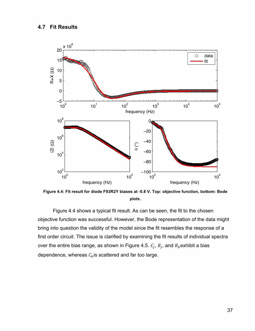
4.7 Fit Results
Figure 4.4: Fit result for diode F93R2Y biases at -0.8 V. Top: objective function, bottom: Bode
plots.
Figure 4.4 shows a typical fit result. As can be seen, the fit to the chosen
objective function was successful. However, the Bode representation of the data might
bring into question the validity of the model since the fit resembles the response of a
first order circuit. The issue is clarified by examining the fit results of individual spectra
over the entire bias range, as shown in Figure 4.5. !!, !!, and !!exhibit a bias
dependence, whereas !!is scattered and far too large.
100 105102
104
106
108
frequency (Hz)
|Z| (
)
100 105100
80
60
40
20
0
frequency (Hz)
(!)
100 101 102 103 104 1055
0
5
10
15
20x 106
R+X
()
frequency (Hz)
datafit

38
Figure 4.5: Impedance fit results for diode F93R2Y. Junction (�) and bulk (+) values are shown.
The solver failed to converge to a reasonable solution for !!in most data sets;
especially those recorded when a reverse bias was applied. The conclusion drawn is
that !! is too small to affect the impedance over the recorded frequencies. The diode
impedance would have to be measured at frequencies above 100 kHz if !! were to be
properly determined. A lack of information about !! does not affect the characterization
of the diode since !! is required for determining the carrier profile and !!for determining
the mobility.
As can be seen in Figure 4.5, !! decreases with increasing reverse bias. This is
typical of a spatially uniform carrier density, which is also localized in energy. However,
!! starts to increase at biases below -3.4 V. This behaviour was observed in all the
measured devices when bias was lowered to this region. This does not appear to be an
artefact caused by the solver. The capacitance extracted directly from the impedance
spectra by assuming a first order circuit response is a reasonable approximation of !!,
especially in reverse bias. As can be seen in Figure 4.6, the increase in capacitance at -
3.4 V is also seen directly in the data. This is not likely due to the semiconductor being
fully depleted since the capacitance should be constant for biases beyond full depletion.
5 4 3 2 1 0 1 210 11
10 10
10 9
10 8
10 7
bias (V)
Cap
acita
nce
(F)
5 4 3 2 1 0 1 2102
103
104
105
106
107
bias (V)R
esis
tanc
e (
)

39
With amorphous semiconductors, !!! is not necessarily a linear function of reverse bias.
The capacitance may also increase with reverse bias if the density of states varies
rapidly near the mobility edge [20]. It is possible that the increase in capacitance is due
to localized states at the metal interface or inside the semiconductor. These states may
be aligned with the Fermi level when the applied bias is around -3.4 V, thus accounting
for the sudden increase in capacitance. If this interpretation is correct, the capacitance
should once again decrease past a certain reverse bias and continue along the
previous trend. A number of diodes were damaged during DC measurements when
large reverse biases were applied. The reverse bias was limited to -5 V during the AC
measurements for this reason.
Figure 4.6: Depletion capacitance from the susceptance for diode F92R3Y.
Impedance spectra with variations in temperature as well as bias would be
needed to map the energetic structure of the diode [35] [20].
The results in Figure 4.5 are typical and !!!!was observed to be linear with
reverse bias between 0 V and the bias at which !! reached a minimum. Without a better
5 4.5 4 3.5 3 2.5 2 1.5 1 0.5 02
3
4
5
6
7
8x 10 10
bias (V)
B/ (F
)
10 kHz1 kHz100 Hz
40
understanding of the energetic structure, it can be assumed that most transport occurs
near the mobility edge and that the C-V technique yields a reasonable idea of the
carrier density.
Through linear regression and equation (4.4), the hole density and built in
voltage was extracted from !!. Three Al bottom devices from three different samples
were measured. Four F-series Au bottom diodes from two separate samples were also
measured. The results are summarized in Table 4.1 and Table 4.2.
Device Type Min Median Max
Au bottom (F-series) 6×10!" 3×10!" 6×10!"
Al bottom 2×10!" 5×10!" 1×10!" Table 4.1: Hole density from AC measurements (cm-3).
Device Type Min Median Max
Au bottom (F-series) 0.3 0.5 0.7
Al bottom 0.1 0.1 0.6 Table 4.2: Built in voltage from AC measurements (V).
The hole density values are within the range of reported values, though on the
high end [16] [35] [9] [17]. These values are likely overestimated since they depend on
the relative permittivity of P3HT. Many sources use a value of 3 [16] [9], which was also
adopted in this work. However, this value is derived from optical measurements [37]
and it has been shown that the relative permittivity actually increases with decreasing
frequency. The value at 100 kHz is about 4 and increases to 9 at 100 Hz [29]. The
larger hole density in the Au bottom electrode devices may be attributed to variations in
the spin coating process. These devices were all made in a single production run and
the Al bottom devices represent two production runs. The sample size was too small to
understand all variations that might result in manufacturing. A less ordered film with
more traps might lead to a larger hole density measure.
The built in voltage for the Al bottom electrode diodes was found to be smaller
than for the Au bottom electrode diodes. This may be attributed to an increased number
of interface states. For the first group of devices, the Al electrodes were exposed to air

41
before being transferred to the glovebox. For the second group, the Al electrodes were
evaporated onto the P3HT, forming a more intimate contact. The Al in the first group
may have formed a thin oxide layer while exposed to air, which resulted in an increased
number of interface states. The band bending and thus the built in voltage can be
decreased if these states have a net positive charge [20].
The bulk mobility was extracted from the fitted values of !! and the extracted
values for the hole density and built in voltage. Physically, !! is described by
!! =! −!!"#$ (4.9)
where t is the total P3HT thickness. By substituting equation (4.3), !! can be
related to the applied bias
!! =!
!"#$ −2!!!
!!!!!!!! !!" − ! (4.10)
thus making it possible to find the mobility. The extracted bulk mobility values
ranged from 4×10!! cm2V-‐1s-‐1 to 6×10!! cm2V-‐1s-‐1. There was no noticeable difference
between the two types of diodes, except for one of the samples with an Al bottom
electrode, which had a mobility five times larger. These values are within the range of
reported bulk mobility [16] [17] [4] [7].
4.8 Conclusions A small signal model of the Schottky diodes was fitted to impedance
spectroscopy data. Meaningful results for the bulk capacitance were difficult to obtain.
Extending measurements to at least 1 MHz may correct this. The hole density and
mobility in the P3HT films were extracted from the fitted model parameters. The results
agreed with reported values. The carrier profile suggests trap states are uniformly
distributed in space but not energy. Extending measurements to higher reverse biases,
as well as performing measurements at varied temperatures would clarify this.
The discussion is continued in the next chapter, where the results in Chapters 3
and 4 are used to examine the feasibility and challenges associated with practical use
of the P3HT diodes demonstrated in this work.
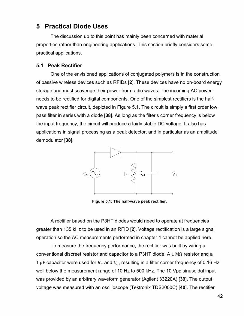
42
5 Practical Diode Uses The discussion up to this point has mainly been concerned with material
properties rather than engineering applications. This section briefly considers some
practical applications.
5.1 Peak Rectifier One of the envisioned applications of conjugated polymers is in the construction
of passive wireless devices such as RFIDs [2]. These devices have no on-board energy
storage and must scavenge their power from radio waves. The incoming AC power
needs to be rectified for digital components. One of the simplest rectifiers is the half-
wave peak rectifier circuit, depicted in Figure 5.1. The circuit is simply a first order low
pass filter in series with a diode [38]. As long as the filter’s corner frequency is below
the input frequency, the circuit will produce a fairly stable DC voltage. It also has
applications in signal processing as a peak detector, and in particular as an amplitude
demodulator [38].
Figure 5.1: The half-wave peak rectifier.
A rectifier based on the P3HT diodes would need to operate at frequencies
greater than 135 kHz to be used in an RFID [2]. Voltage rectification is a large signal
operation so the AC measurements performed in chapter 4 cannot be applied here.
To measure the frequency performance, the rectifier was built by wiring a
conventional discreet resistor and capacitor to a P3HT diode. A 1 MΩ resistor and a
1 µμF capacitor were used for !! and !!, resulting in a filter corner frequency of 0.16 Hz,
well below the measurement range of 10 Hz to 500 kHz. The 10 Vpp sinusoidal input
was provided by an arbitrary waveform generator (Agilent 33220A) [39]. The output
voltage was measured with an oscilloscope (Tektronix TDS2000C) [40]. The rectifier
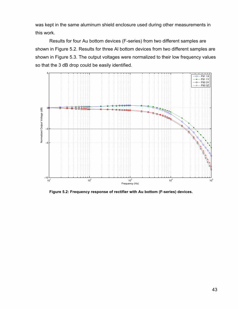
43
was kept in the same aluminum shield enclosure used during other measurements in
this work.
Results for four Au bottom devices (F-series) from two different samples are
shown in Figure 5.2. Results for three Al bottom devices from two different samples are
shown in Figure 5.3. The output voltages were normalized to their low frequency values
so that the 3 dB drop could be easily identified.
Figure 5.2: Frequency response of rectifier with Au bottom (F-series) devices.
101 102 103 104 10510
5
0
5
3
Frequency (Hz)
Nor
mal
ized
Out
put V
olta
ge (d
B)
F91 1XF91 1YF93 3YF93 3Z
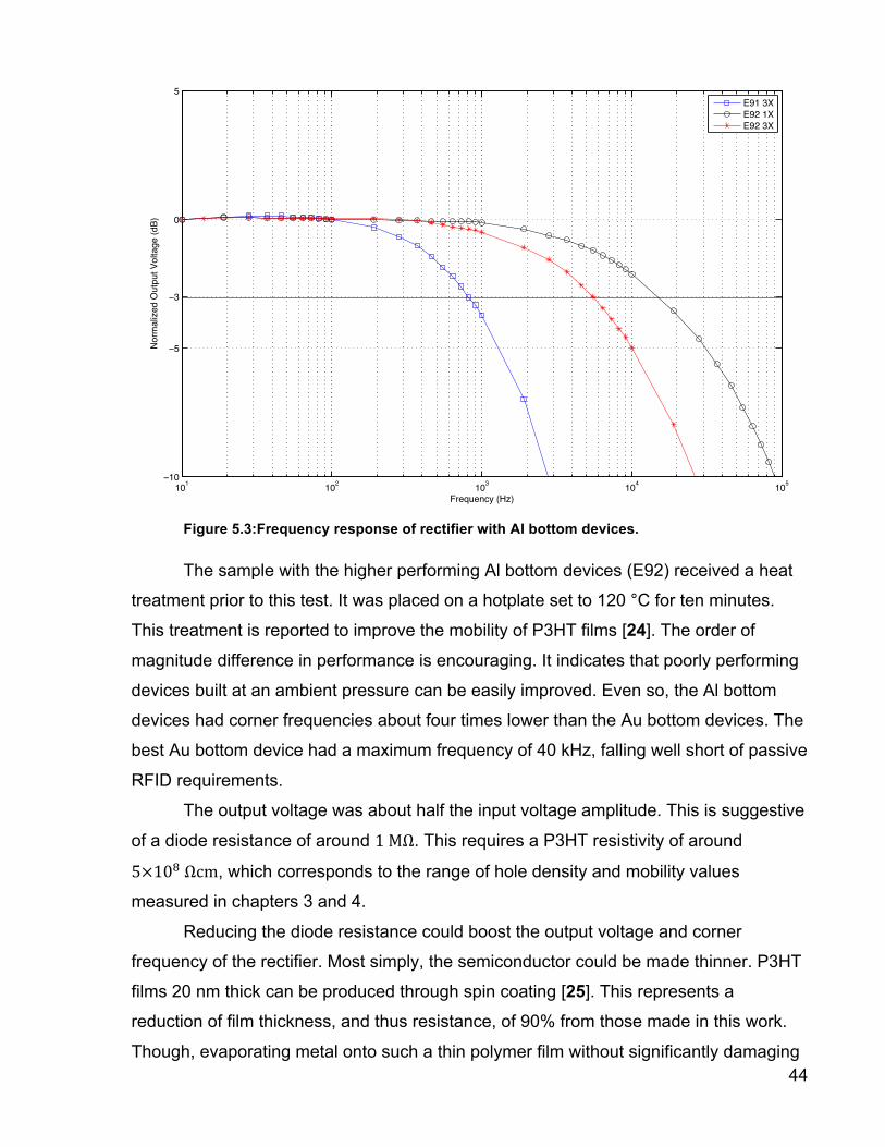
44
Figure 5.3:Frequency response of rectifier with Al bottom devices.
The sample with the higher performing Al bottom devices (E92) received a heat
treatment prior to this test. It was placed on a hotplate set to 120 °C for ten minutes.
This treatment is reported to improve the mobility of P3HT films [24]. The order of
magnitude difference in performance is encouraging. It indicates that poorly performing
devices built at an ambient pressure can be easily improved. Even so, the Al bottom
devices had corner frequencies about four times lower than the Au bottom devices. The
best Au bottom device had a maximum frequency of 40 kHz, falling well short of passive
RFID requirements.
The output voltage was about half the input voltage amplitude. This is suggestive
of a diode resistance of around 1 MΩ. This requires a P3HT resistivity of around
5×10! Ωcm, which corresponds to the range of hole density and mobility values
measured in chapters 3 and 4.
Reducing the diode resistance could boost the output voltage and corner
frequency of the rectifier. Most simply, the semiconductor could be made thinner. P3HT
films 20 nm thick can be produced through spin coating [25]. This represents a
reduction of film thickness, and thus resistance, of 90% from those made in this work.
Though, evaporating metal onto such a thin polymer film without significantly damaging
101 102 103 104 10510
5
0
5
3
Frequency (Hz)
Nor
mal
ized
Out
put V
olta
ge (d
B)
E91 3XE92 1XE92 3X

45
it may be difficult. The depletion width would also extend through the entire thickness of
such a thin film. Such a dramatic reduction in film size may not be needed. The corner
frequency of a similar rectifier has been reportedly increased by an order of magnitude
by halving the thickness of the semiconductor [8]. The semiconductor could be made
more crystalline by using a different solvent [25]. This has been reported to boost the
field effect mobility by an order of magnitude [25]. It should also have a positive effect
on the bulk mobility, but it has not been reported. The carrier density could also be
increased by controllably doping the semiconductor [41].
5.2 Small Signal Use The nonlinearity of a diode can also be exploited to build frequency multipliers.
Resistive diode multipliers use forward biased diodes as nonlinear resistors, and
reactive diode multipliers use reverse biased diodes as voltage controlled capacitors
(varactors) [42].
The small signal frequency performance of a Schottky diode can be
characterized by the forward bias cutoff frequency
!!! =1
2!!!!! (5.1)
where !! and !! are the diode’s resistance and capacitance at a bias of 0.1 V to the flat
band condition [19]. The utility of this metric lies in being able to compare devices with
different built in voltages. !!! was computed using the junction resistance and
capacitance, !! and !!, extracted from AC measurements in chapter 4. Results for Au
bottom (F-series) and Al bottom devices are listed in Table 5.1.
Bottom electrode Min Median Max
Al 28 63 120
Au (F-Series) 65 420 2800 Table 5.1: forward bias cutoff frequency (Hz).
The small signal performance of Au bottom (F-series) devices is better than that
of Al bottom devices, but still far too low for practical use. Increasing this performance is
not straight forward, especially for the Al bottom devices, since it would involve
increasing the quality of the Schottky junctions, by ensuring a clean interface.
46
5.3 Conclusions The applicability of P3HT based Schottky diodes to voltage rectification and
frequency mixing was considered in this chapter. Al bottom devices showed
consistently inferior performance. The best performing devices had poor enough
performance to make them impractical for the suggested applications. Heat treatment
appears promising for boosting performance. Better performance may also be achieved
by using thinner and better ordered P3HT layers. Improvements of almost two orders of
magnitude may be possible. A corner frequency of above 1 MHz has been reported for
a similar P3HT/Al diode based rectifier [8].

47
6 Conclusion In this thesis, two types of P3HT/Al Schottky junction diodes were fabricated,
characterized, and compared. Carrier density and mobility were derived from DC as
well as impedance measurements. Comparisons made included Schottky junction
quality, frequency performance in a rectifier, and small signal frequency performance.
6.1 General Conclusions Both varieties of diodes comprised stacks of the same materials: gold, poly(3-
hexylthiophene), and aluminum. Their difference was in the formation of the Schottky
junction. The first type, designated Au bottom, had its Schottky junction formed in a high
vacuum by evaporating aluminum onto a film of P3HT. The second type, designated Al
bottom, had its Schottky junction formed by depositing a film of P3HT onto aluminum at
a standard atmospheric pressure. Though all steps involving P3HT were carried out in
an argon-filled glovebox, the aluminum electrodes used in the Al bottom diodes had
been previously exposed to air. The final yield of usable devices was 35% for Au bottom,
and 22% for Al bottom. Due to an equipment fault, one set of Au bottom devices was
manufactured at an elevated pressure. Difficulties were also encountered during the
manufacturing of the bottom electrodes by lift-off. The cause was likely a
photolithographic mask of inadequate quality.
Current-voltage scans of the diodes showed that Au bottom devices had a
current rectification ratio of 2×10!, 100 times greater than for Al bottom devices. The
DC behaviour was properly explained by a model that took into account the space
charge limited current. Model fitting was done by least-squares and required an iterative
approach. The bulk mobility was extracted from fits and found to range from 2×
10!! cm2V-‐1s-‐1 to 6×10!! cm2V-‐1s-‐1 and is in line with reported values. The hole density
was also calculated from the fit parameters to be between from 10!" cm-‐3 and 10!" cm-‐3.
These values also agree with reported numbers.
Impedance spectroscopy was used to model the diodes’ small signal behaviour
with a 2nd order series/parallel RC circuit. The presence of a bulk capacitance could be
seen in the recorded spectra, but exact values proved difficult to determine. Fitted
values of the junction capacitance suggest a spatially uniform hole density of between
5×10!" cm-‐3and 3×10!" cm-‐3. While these values are in line with those reported in

48
literature, they are an order of magnitude larger than those derived from DC
measurements. These density values were used to extract mobility from the fitted bulk
resistance. The range of these mobilities was from 4×10!! cm2V-‐1s-‐1 to
6×10!! cm2V-‐1s-‐1. In this case the agreement between AC and DC derived mobilities
suggests that the values are correct. This implies that the AC hole densities are correct
and DC hole densities are underestimated by an order of magnitude and means that the
series resistance in the DC model was consistently overestimated. Fitted junction
capacitance and resistance values suggest poor small signal performance for both
device types. The maximum frequency is below 100 Hz for Al bottom devices, and an
order of magnitude larger for Au bottom devices.
The frequency performance of a half-wave peak rectifier built using the P3HT
diodes and conventional components was measured. The maximum operating
frequency with Au bottom diodes was 40 kHz, and 10 kHz with Al bottom diodes.
Heating the Al bottom diodes for 10 minutes at 120°C seemed to increase their
maximum frequency from 1 kHz to 10 kHz.
The Au bottom diodes consistently outperformed the Al bottom devices,
demonstrating the large sensitivity of the Schottky junction to contamination. This
suggests that practical diodes based on P3HT must be entirely manufactured in an inert
atmosphere, and that the rectifying junction may need to always be made in a high
vacuum. This is problematic if printing methods are to be employed since vacuum
deposited metals will have to be replaced with solution processable materials.
6.2 Future Work The small signal measurements should be extended in the following ways.
Measurement frequencies should be extended to at least 1 MHz to improve model
fitting. The reverse bias range should be doubled and temperature variation should be
introduced in order to probe the energetic structure of the Schottky junction.
The reverse breakdown voltage should be measured. This should be done after
all other electrical measurements are complete as it may irreversibly affect the diode.

49
Performance gains may be achieved by adjusting the fabrication. Bottom
electrodes should be entirely fabricated inside the glovebox and never exposed to air. A
solvent with a higher boiling point than chloroform should be used. Completed devices
should be heat-treated.
Major changes are needed if flexible and printable Schottky diodes are to be
explored further. First the glass substrate should be substituted with a flexible substrate.
Most significantly, the vacuum deposited metal electrodes need to be replaced with
materials which can be solution processed. Finally, devices should be entirely printed.

50
Bibliography [1] The Royal Swedish Academy of Sciences. (2012, April) The 2000 Nobel Prize in Physics
-‐ Scientific Background. [Online]. http://www.nobelprize.org/nobel_prizes/physics/laureates/2000/advanced.html
[2] V Subramanian, "Radio Frequency Identity Tags," in Organic Field Effect Transistors, Z Bao and J Locklin, Eds. Boca Raton, FL, USA: CRC Press, 2007, pp. 489-‐504.
[3] D.-‐H Kim et al., "Stretchable and Foldable Silicon Integrated Circuits," Science, vol. 320, no. 5875, pp. 507-‐511, Apr 2008.
[4] Michael G Kane et al., "100-‐MHz CMOS circuits directly fabricated on plastic using sequential laterally solidified silicon," Journal Of The Society For Information Display, vol. 15, no. 7, pp. 471-‐478, Jan 2007.
[5] A Takshi, "Organic metal-‐semiconductor field-‐effect transistor (OMESFET)," Department of Electrical and Computer Engineering, University of British Columbia, Vancouver, PhD dissertation 2007.
[6] L Burgi, TJ Richards, RH Friend, and H Sirringhaus, "Close look at charge carrier injection in polymer field-‐effect transistors," Journal of Applied Physics, vol. 94, no. 9, pp. 6129-‐6137, Jan 2003.
[7] Michele Giulianini, Eric R Waclawik, John M Bell, and Nunzio Motta, "Current-‐voltage characteristics of poly(3-‐hexylthiophene) diodes at room temperature," Applied Physics Letters, vol. 94, no. 8, p. 083302, Jan 2009.
[8] Chan-‐mo Kang, Seohee Kim, Yongtaek Hong, and Changhee Lee, "Frequency analysis on poly(3-‐hexylthiopene) rectifier using impedance spectroscopy," Thin Solid Films, vol. 518, no. 2, pp. 889-‐892, Jan 2009.
[9] VR Nikitenko, H Heil, and H von Seggern, "Space-‐charge limited current in regioregular poly-‐3-‐hexyl-‐thiophene," Journal of Applied Physics, vol. 94, no. 4, pp. 2480-‐2485, Jan 2003.
[10] HL Gomes and DM Taylor, "Schottky barrier diodes from semiconducting polymers," Iee Proceedings-‐Circuits Devices And Systems, vol. 144, no. 2, pp. 117-‐122, Jan 1997.
[11] M MacLachlan, "Course notes for Chemistry 527," Chemistry, The University of British Columbia, Vancouver, September 2006.
[12] The Royal Swedish Academy of Sciences. (2012, April) The Nobel Prize in Chemistry 2000 -‐ Scientific Background. [Online]. http://www.nobelprize.org/nobel_prizes/chemistry/laureates/2000/advanced.html
[13] A Salleo, "Charge transport in polymeric transistors," Materials Today, vol. 10, no. 3, pp. 38-‐45, Mar 2007.
[14] Arash Takshi, Milad Mohammadi, and John D Madden, "Study the effect of distribution of density of states on the depletion width of organic Schottky contacts," Solid State Electronics, vol. 52, no. 11, pp. 1717-‐1721, Nov 2008.
[15] A Salleo, T. W Chen, A. R Völkel, and R. A Street, "Intrinsic hole mobility and trapping in a regioregular poly(thiophene)," Physical Review B, vol. 70, no. 11, p. 115311, Sep 2004.
[16] Z Chiguvare and V Dyakonov, "Trap-‐limited hole mobility in semiconducting poly(3-‐hexylthiophene)," Physical Review B, vol. 70, no. 23, p. 235207, Jan 2004.

51
[17] J Li, A Nardes, Z Liang, and S Shaheen, "Simultaneous measurement of carrier density and mobility of organic semiconductors using capacitance techniques," Organic Electronics, Jan 2011.
[18] AJ Cascio et al., "Investigation of a polythiophene interface using photoemission spectroscopy in combination with electrospray thin-‐film deposition," Applied Physics Letters, vol. 88, no. 6, p. 062104, Jan 2006.
[19] S. M. Sze, Physics of Semiconductor Devices, 2nd ed. New York: John Wiley & Sons, 1981. [20] E. H. Rhoderick and R. H. Williams, Metal-‐Semiconductor Contacts, 2nd ed. New York:
Oxford University Press, 1988. [21] AMPEL Nanofabrication Facility. (2012, April) About the facility. [Online].
http://nanofab.ubc.ca/content/about-‐facility [22] The UCSB Nanofabrication Facility. (2012, April) Lithography. [Online].
http://www.nanotech.ucsb.edu/index.php?option=com_content&view=article&id=45&Itemid=27
[23] HS Lee and JB Yoon, "A simple and effective lift-‐off with positive photoresist," Journal of Micromechanics and Microengineering, vol. 15, no. 11, pp. 2136-‐2140, Jan 2005.
[24] Shinuk Cho et al., "Thermal annealing-‐induced enhancement of the field-‐effect mobility of regioregular poly(3-‐hexylthiophene) films," Journal of Applied Physics, vol. 100, no. 11, p. 114503, Jan 2006.
[25] JF Chang et al., "Enhanced mobility of poly(3-‐hexylthiophene) transistors by spin-‐coating from high-‐boiling-‐point solvents," Chemistry Of Materials, vol. 16, pp. 4772-‐4776, Jan 2004.
[26] Keithley Instruments Inc. (2012, April) 6430. [Online]. http://www.keithley.com/products/dcac/sensitive/highresistance/?mn=6430
[27] A Assadi, C Svensson, M Willander, and O Inganäs, "Properties of the planar poly (3-‐octylthiophene)/aluminum Schottky barrier diode," Journal of Applied Physics, Jan 1992.
[28] S Tagmouti et al., "Electrical characteristics of W/P3MT/Pt diodes," Thin Solid Films, vol. 379, no. 1-‐2, pp. 272-‐278, 2000.
[29] J Obrzut and K Page, "Electrical conductivity and relaxation in poly (3-‐hexylthiophene)," Physical Review B, Jan 2009.
[30] Dieter K. Schroder, Semiconductor Material and Device Characterization. New York: John Wiley & Sons, Inc., 1990.
[31] Peter Blood and John W. Orton, The electrical characterization of semiconductors: majority carriers and electron states, N. H. March, Ed. London, UK: Academic Press, 1992, vol. 14.
[32] M Vissenberg and M Matters, "Theory of the field-‐effect mobility in amorphous organic transistors," Physical Review B, vol. 57, no. 20, pp. 12964-‐12967, 1998.
[33] D. M Taylor, "Space charges and traps in polymer electronics," Ieee Transactions On Dielectrics And Electrical Insulation, vol. 13, no. 5, pp. 1063-‐1073, Jan 2006.
[34] S Karg, M Meier, and W Riess, "Light-‐emitting diodes based on poly-‐p-‐phenylene-‐vinylene.1. Charge-‐carrier injection and transport," Journal of Applied Physics, vol. 82, no. 4, pp. 1951-‐1960, Jan 1997.

52
[35] P Stallinga, HL Gomes, M Murgia, and K Müllen, "Interface state mapping in a Schottky barrier of the organic semiconductor terrylene," Organic Electronics, vol. 3, no. 1, pp. 43-‐51, 2002.
[36] Solartron Analytical. (2012, April) Model 1260A Impedance-‐Gain/Phase Analyzer. [Online]. http://www.solartronanalytical.com/Pages/1260AFRAPage.htm
[37] RHM van de Leur, B de Ruiter, and J Breen, "Dielectrical and dynamic mechanical properties of three poly (3-‐N-‐Alkaylthiophene) s," Synthetic Metals, vol. 57, no. 2-‐3, pp. 4956-‐4961, 1993.
[38] A Sedra and K C Smith, Microelectronic Circuits, 4th ed. New York, NY, USA: Oxford University Press Inc., 1998.
[39] Agilent Technologies. (2012, April) 33220A Function/Arbitrary Waveform Generator. [Online]. http://www.home.agilent.com/agilent/product.jspx?nid=-‐536902257.536883183.00&cc=CA&lc=eng
[40] Tektronix, Inc. (2012, April) TDS 2000. [Online]. http://www.tek.com/oscilloscope/tds2000
[41] Y Chen, I Shih, and S Xiao, "Effects of FeCl3 doping on polymer-‐based thin film transistors," Journal of Applied Physics, vol. 96, no. 2, pp. 454-‐458, July 2004.
[42] D. M. Pozar, Microwave Engineering, 3rd ed. Hoboken, NJ, USA: Wiley, 2005.