characterization of nickel silicides produced by millisecond anneals
TRANSCRIPT

CHARACTERIZATION OF NICKEL SILICIDES PRODUCED BY MILLISECOND ANNEALSPRODUCED BY MILLISECOND ANNEALS
Bruce Adams, Dean Jennings, Kai Ma, Abhilash Mayur, Steve Moffatt, , Stephen Nagy, Vijay Parihar
IEEE RTP 2007 Conference Catania Sicily October 4 2007Catania, Sicily October 4, 2007
FRONT END PRODUCTS GROUP

Overview
Brief Introduction to SilicidesRTP NiSi Formation ProcessRTP NiSi Formation ProcessThe Kinetic Model for NiSi TransformationThe Thermal Model for DSA– What is DSA– DSA Math Modeling
Characteristics and Morphology of DSA NiSi FilmsCharacteristics and Morphology of DSA NiSi Films– Tuning within-wafer uniformity– TEM, XDR Analysis
Predictions and ResultsSummary and Conclusions
FRONT END PRODUCTS GROUP
2
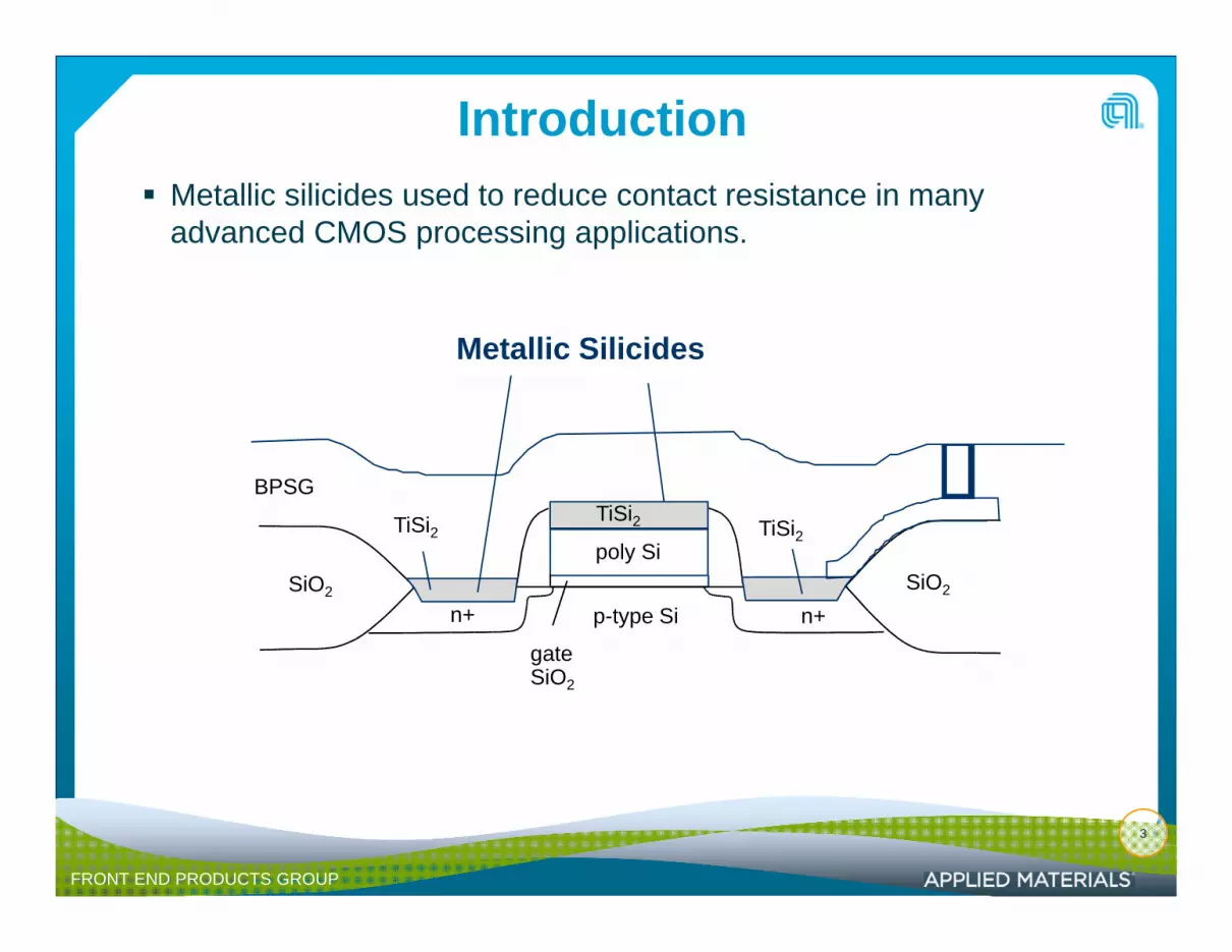
IntroductionMetallic silicides used to reduce contact resistance in many advanced CMOS processing applications.
Metallic Silicides
TiSi2TiSi2 TiSi2
BPSG
SiO2 SiO2
poly Si
n+ n+p-type Si
gate
2 S 2
gateSiO2
FRONT END PRODUCTS GROUP
3
Introduction
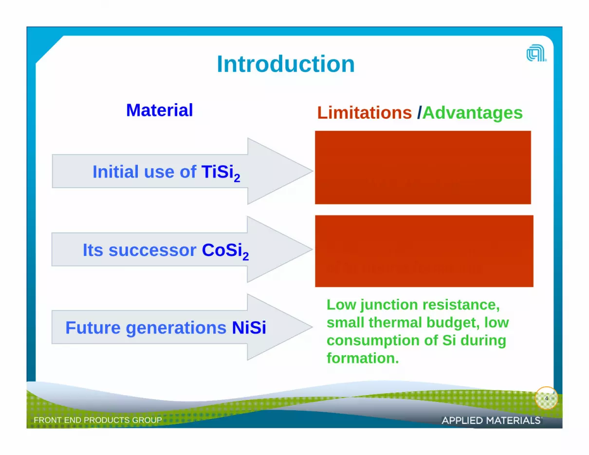
Limitations /AdvantagesMaterial
Initial use of TiSi2Inability to scaleto narrow lines
Its successor CoSi2Limited by junction leakage, high consumptionts successo CoS 2 g , g pof Si during formation
Low junction resistance, Future generations NiSi small thermal budget, low
consumption of Si duringformation.
FRONT END PRODUCTS GROUP
4

RTP NiSi Formation2 step process
RTP step 1 RTP step 2
100 Å TiN Å
(200 to 300 °C) (>300 °C)
Thermally stableh i100 Å TiN
oxygen barrier100 Å TiNoxygen barrier
100 Å Ni or Ni
Low sheet resistanceUniform film
Silicon S b t t
Silicon Silicon Silicon
Ni2Si100 Å Ni:Pt (90:10) Ni2Si NiSi
Substrate Substrate SubstrateSilicon Substrate
FRONT END PRODUCTS GROUP
5
Phase Change Transformation CurvePhase Change Transformation Curve
For a constant temperature (soak) anneal time, the sheet i t b l tt d f ti f diff t lresistance can be plotted as a function of different anneal
temperatures, and thereby quantify the phase change from Ni2Si to NiSi
FRONT END PRODUCTS GROUP
6
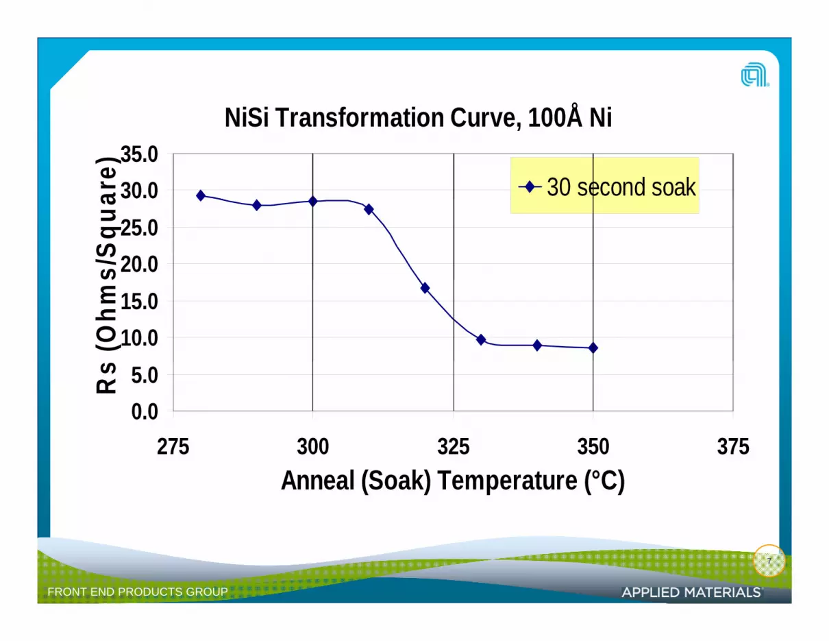
NiSi Transformation Curve 100Å NiNiSi Transformation Curve, 100Å Ni
30.035.0
are) 30 second soak
20.025.0
s/Sq
ua
10.015.0
(Ohm
s
0.05.0
275 300 325 350 375
Rs
275 300 325 350 375Anneal (Soak) Temperature (°C)
FRONT END PRODUCTS GROUP
7
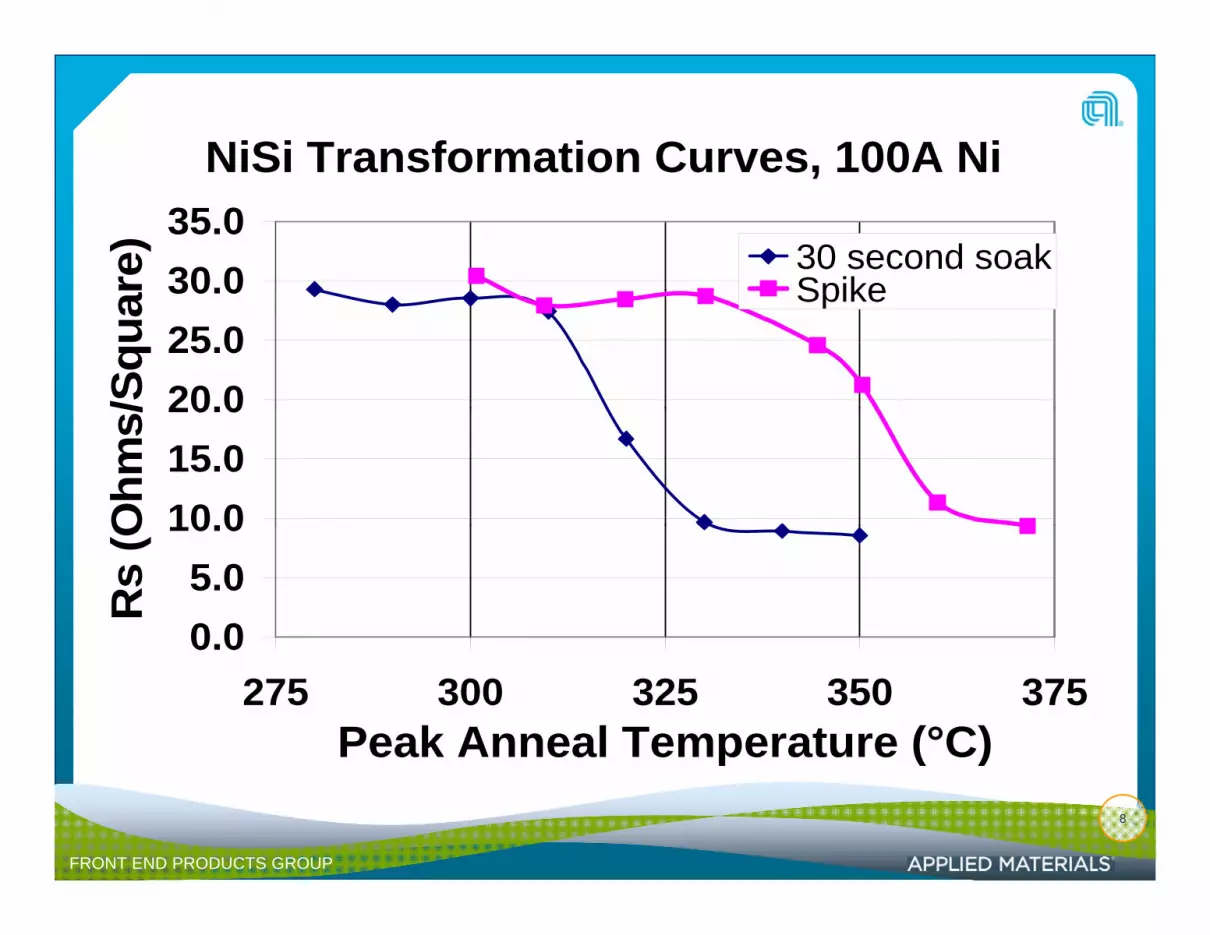
NiSi Transformation Curves, 100A Ni,
30.035.0
re) 30 second soak
Spike
20.025.030.0
/Squ
a Spike
10.015.020.0
Ohm
s/
0 05.0
10.0
Rs
(O
0.0275 300 325 350 375
Peak Anneal Temperature (°C)
FRONT END PRODUCTS GROUP
8
p ( )
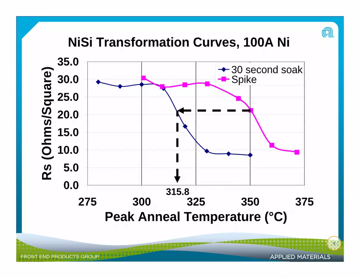
NiSi Transformation Curves, 100A Ni
30.035.0
are) 30 second soak
Spike
20.025.0
s/Sq
ua
10.015.0
(Ohm
s
0.05.0R
s (
315 8275 300 325 350 375
Peak Anneal Temperature (°C)
315.8
FRONT END PRODUCTS GROUP
9

Temperature Profiles with same Rs
340360
(°c)
280300320
atur
e
240260280
empe
ra
315 8 °C k
200220240
Te 315.8 °C soak350.0 °C spike
0 25 50 75 100 125Time (Seconds)
FRONT END PRODUCTS GROUP
10

The Kinetic Model for NiSi TransformationTransformation
FRONT END PRODUCTS GROUP
11
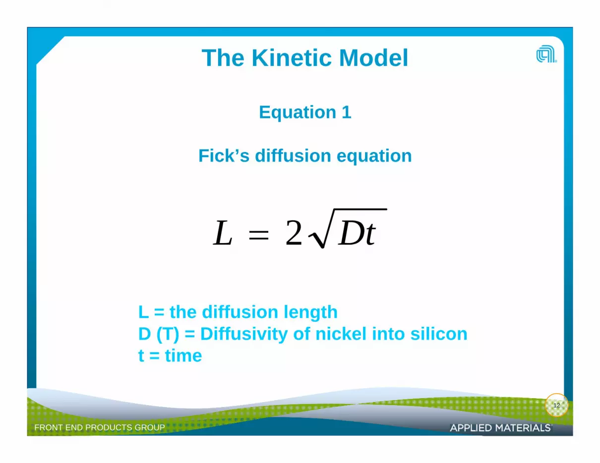
The Kinetic Model
Equation 1
Fick’s diffusion equation
DtL 2=
L = the diffusion lengthgD (T) = Diffusivity of nickel into silicont = time
FRONT END PRODUCTS GROUP
12

The Kinetic Model
Equation 2
Diffusivity has an Arrhenius relationship with temperature
aEkT−kTeDD = 0
Do = non thermal pre-exponential constantE = the activation energy barrierEa the activation energy barrierk = Boltzmann’s constantT = absolute temperature
FRONT END PRODUCTS GROUP
13

The Kinetic Model
Equation 3, Combining equations 1 and 2in integral form
Generalizes the diffusion distance for any arbitrary thermal profile
tkTEa
)(−
∫ dteDL tkT )(02 ∫∝
FRONT END PRODUCTS GROUP
14
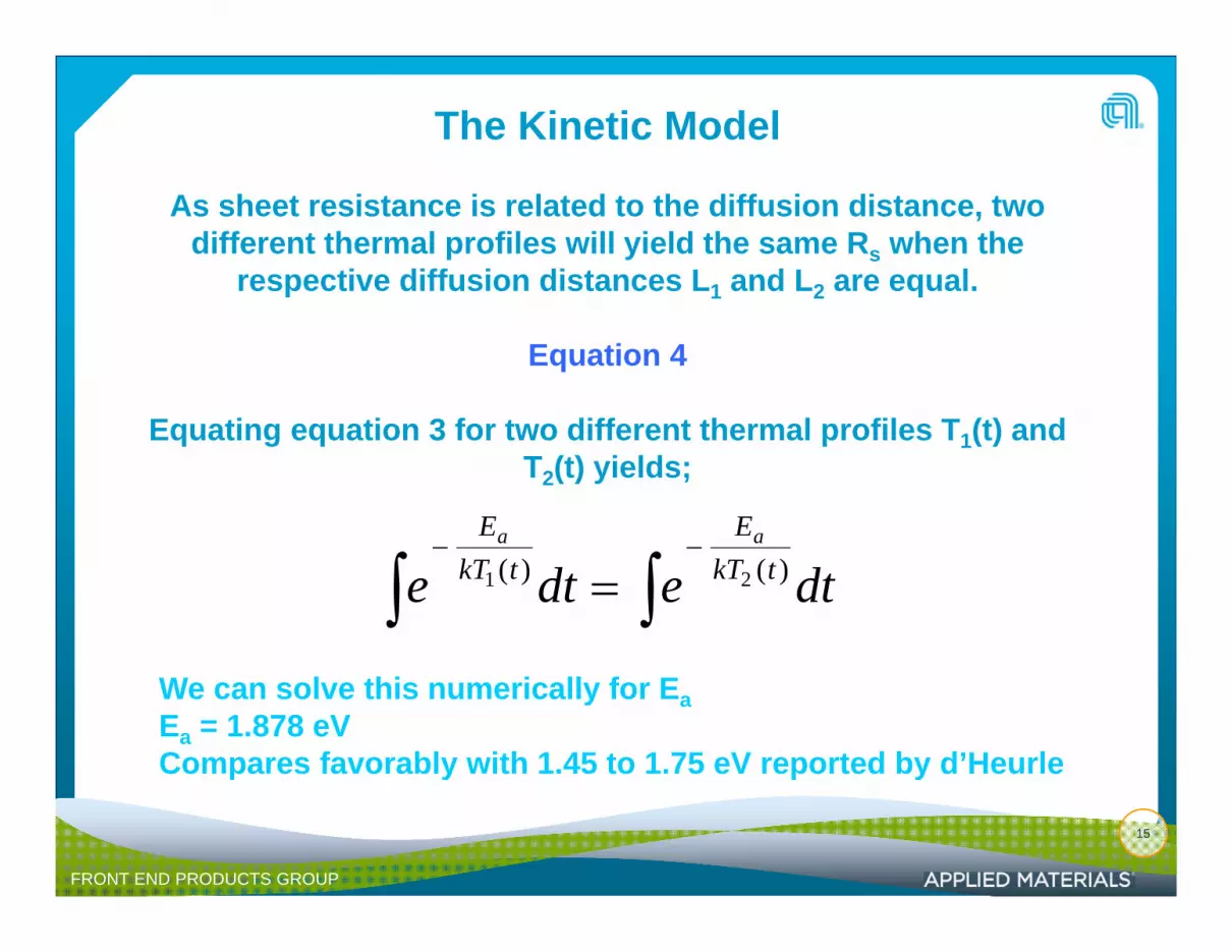
The Kinetic Model
As sheet resistance is related to the diffusion distance, two different thermal profiles will yield the same Rs when the
respective diffusion distances L1 and L2 are equal.p 1 2 q
Equation 4
EE aa
Equating equation 3 for two different thermal profiles T1(t) and T2(t) yields;
dtedte tkTtkTaa
∫∫−−
= )()( 21
We can solve this numerically for EaEa = 1.878 eVCompares favorably with 1.45 to 1.75 eV reported by d’Heurle
FRONT END PRODUCTS GROUP
15
p y p y

Thermal Model for DSA
What is Dynamic Surface Anneal (DSA)?
Thermal Modeling for DSA.
FRONT END PRODUCTS GROUP
16

Dynamic Surface AnnealyThermal Budget reduced by decreasing anneal time from ~1 sec (RTP) to ~ 1 msecOptical power densities ~100-500 kW/cm2 cause surface vs. volume heating (RTP: < 0.5 kW/cm2 ) and < 1 msec ramp up time is achieved
Optical power density achieved by focused line from continuous wave laser radiation.
Temperature distribution in wafer
kW/cm2 ) and < 1 msec ramp up time is achieved
laser radiation.Line is scanned relative to the wafer to complete the annealVolume of the wafer acts as heat sink and provides < 1 msec cool
Beam Scan Direction
Beam Scan Direction
Beam Scan Direction
sink and provides < 1 msec cool down timeLine source reduces stress, improves uniformity, and increases th h tthroughput
High Temperature Activation High Temperature Activation
FRONT END PRODUCTS GROUP
17
without Diffusionwithout Diffusion

General form of the Heat Diffusion Equation
QTkTCp =∇•∇−∂ )(ρ QTk
tCp =∇•∇−
∂)(ρ
Change in bulk heatof unit volume
Heat flux outof unit volume
Net heatof unit volume
Cp = Specific heatρ = Densityρ DensityT = Temperaturet = Timek = Boltzmann’s Constant
FRONT END PRODUCTS GROUP
18
Q = Heat
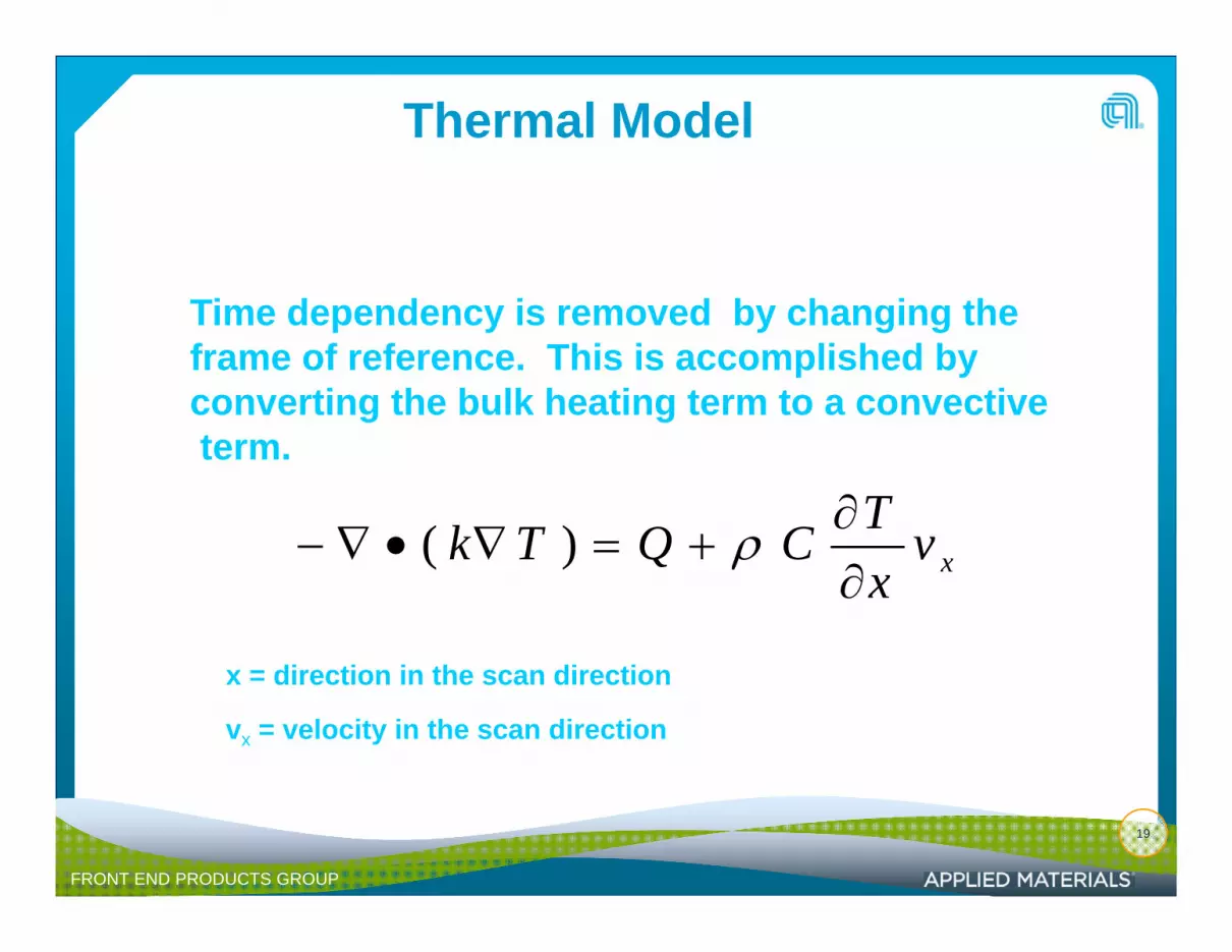
Thermal Model
Time dependency is removed by changing the frame of reference. This is accomplished by converting the bulk heating term to a convective
TCQTk ∂+∇∇ )(
g gterm.
xvx
CQTk∂
+=∇•∇− ρ)(
x = direction in the scan direction
vx = velocity in the scan direction
FRONT END PRODUCTS GROUP
19

Thermal Model
C l d bili bl l i d i l
Steady state solution allows the gridding to beOptimized for high resolution near the beam
Coupled geometry capability enables accurate solution at device scale
FRONT END PRODUCTS GROUP
20
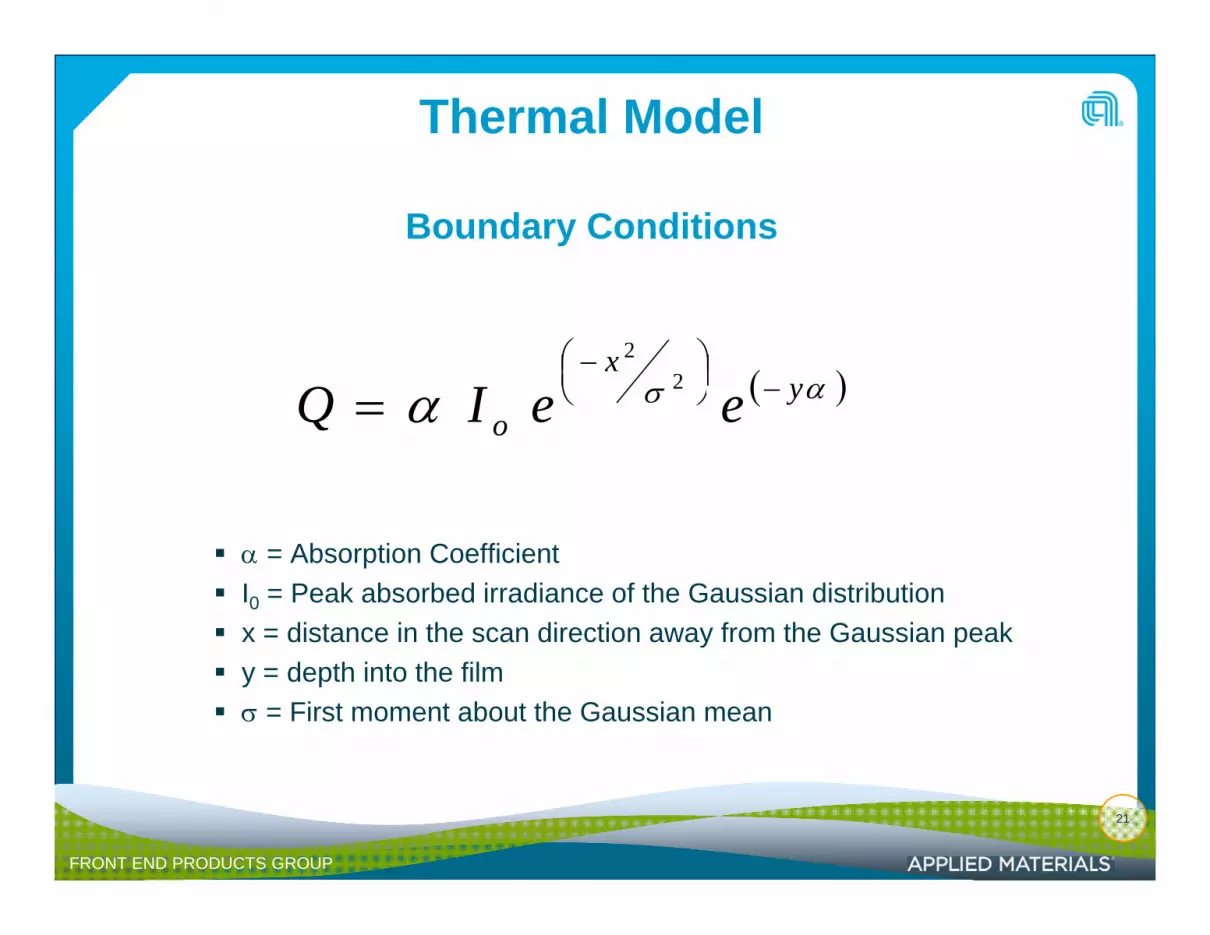
Thermal Model
Boundary Conditions
( )ασα yx
eeIQ −⎟⎠⎞⎜
⎝⎛ −
=2
2
α o eeIQ =
α = Absorption CoefficientI0 = Peak absorbed irradiance of the Gaussian distributionx = distance in the scan direction away from the Gaussian peaky py = depth into the filmσ = First moment about the Gaussian mean
FRONT END PRODUCTS GROUP
21
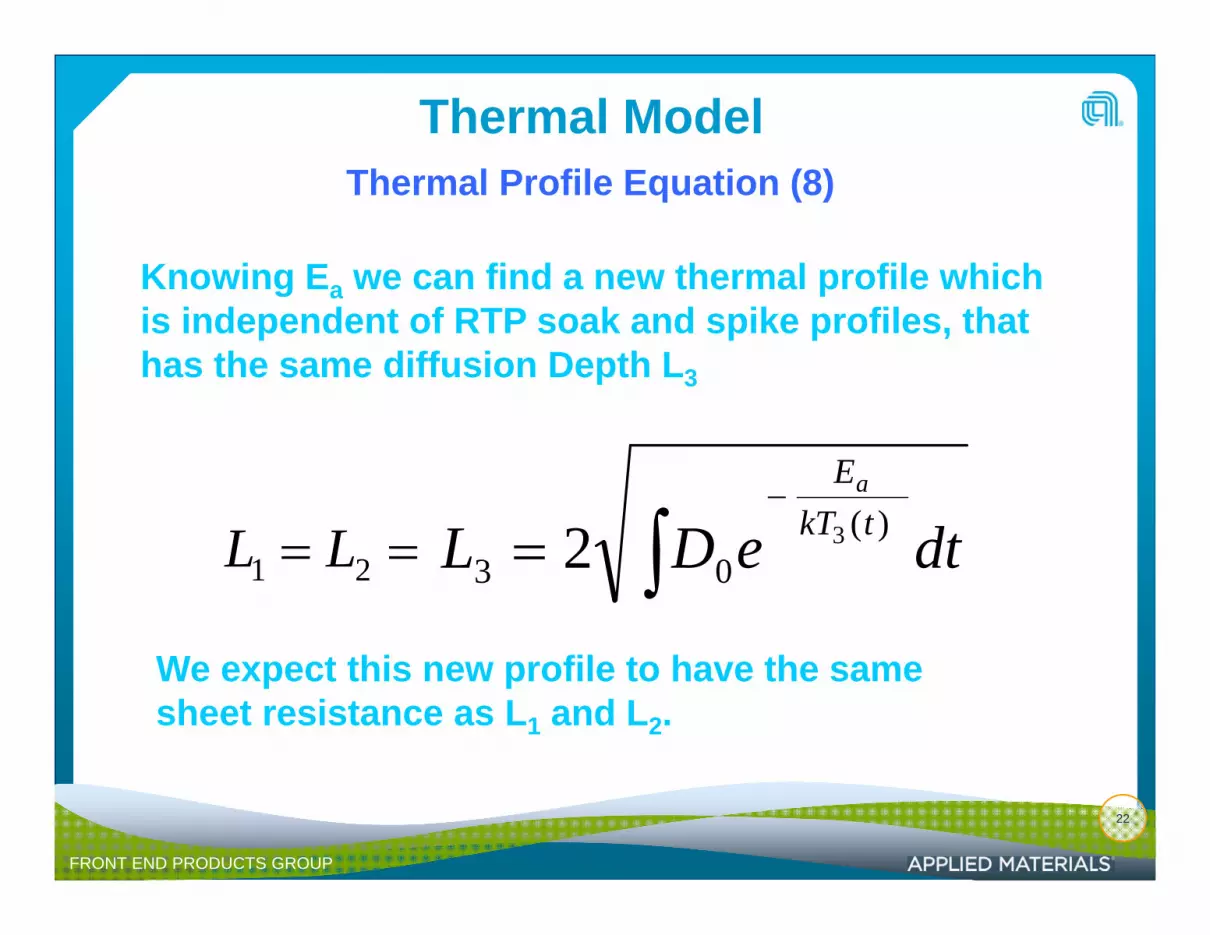
Thermal ModelTh l P fil E ti (8)Thermal Profile Equation (8)
Knowing Ea we can find a new thermal profile which g a pis independent of RTP soak and spike profiles, that has the same diffusion Depth L3
dtkTEa
)(−
∫== 21 LL dteDL tkT )(03
32 ∫=
We expect this new profile to have the samesheet resistance as L1 and L2.
FRONT END PRODUCTS GROUP
22

Results from ModelingTemperature vs Time Profiles for
Various DSA Powers1400 0
1000.0
1200.0
1400.0
ure
(°C
)
100W125W150W175W200W
600.0
800.0
mpe
ratu 200W
225W250W275W300W325W
200.0
400.0Tem 325W
350W375W400W425W
0.00.02 0.0225 0.025 0.0275 0.03 0.0325 0.035
Time (Seconds)
FRONT END PRODUCTS GROUP
23
Time (Seconds)
Results from Thermal Modeling
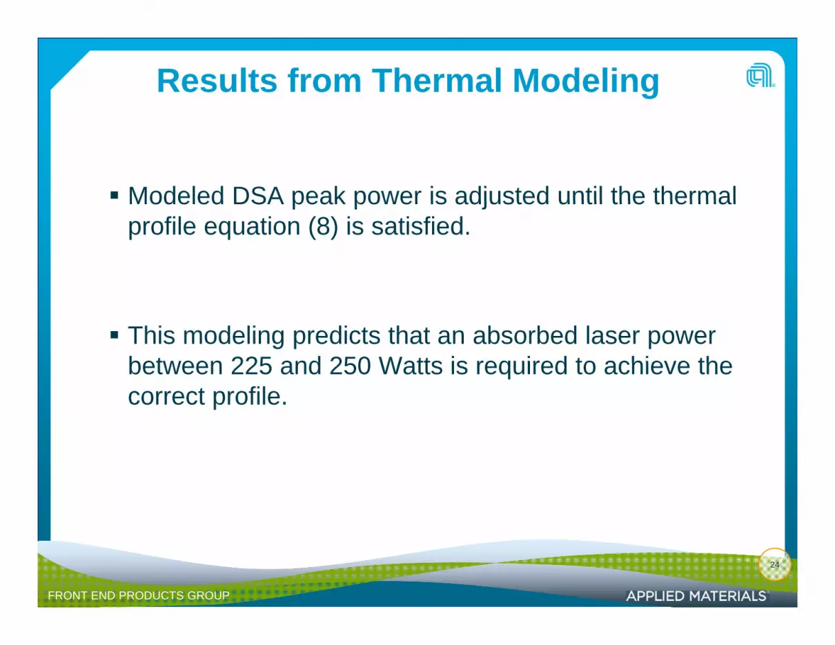
Modeled DSA peak power is adjusted until the thermalModeled DSA peak power is adjusted until the thermal profile equation (8) is satisfied.
This modeling predicts that an absorbed laser power between 225 and 250 Watts is required to achieve thebetween 225 and 250 Watts is required to achieve the correct profile.
FRONT END PRODUCTS GROUP
24

Film Characteristics and Morphology
Tuning within-wafer uniformity
STEP 1 – Anneal wafer at the steep part of the transformation curve under constant laser power.
STEP 2 – Map the sheet resistance of the wafer.STEP 2 Map the sheet resistance of the wafer.
STEP 3 – Develop a corrected laser power map using the sensitivity curveusing the sensitivity curve
FRONT END PRODUCTS GROUP
25

Millisecond Anneal Transformation curve
3 040.0
qNo Tuning
Chamber tuning for within-wafer uniformity
25.030.035.0
ohm
/sq With Tuning
1 9% 1σ
10 015.020.0
ean
Rs,
As Deposited1.9% 1σ
0.05.0
10.0
Me
Error bars represent +/- 1σ
120 140 160 180 200 220 240 260 280
Absorbed Laser Power, Watts
FRONT END PRODUCTS GROUP
26

Millisecond Anneal NiSi Transformation Curve
40.0qLocations for TEM and XRD Analysis
25 030.035.0
ohm
/sq
A
15.020.025.0
n R
s, o
As Deposited B
0.05.0
10.0
Mea A, B, C = Samples for XRD andTEM
C0 0
120 140 160 180 200 220 240 260 280
Absorbed Laser Power, Watts
FRONT END PRODUCTS GROUP
27
,
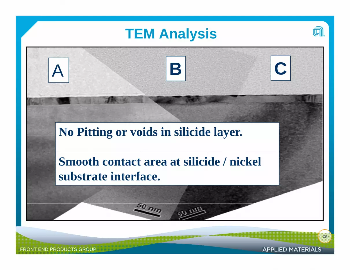
TEM Analysis
A B C
No Pitting or voids in silicide layer.
Smooth contact area at silicide / nickelsubstrate interface.
FRONT END PRODUCTS GROUP
28

TEM of poor NiSi film for comparison
During low temperature annealing epitaxial NiSi2During low temperature annealing, epitaxial NiSi2growth may occur.
FRONT END PRODUCTS GROUP
29
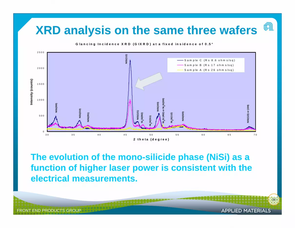
XRD analysis on the same three wafersG l a n c i n g I n c i d e n c e X R D ( G I X R D ) a t a f i x e d i n s i d e n c e o f 0 . 5 °
2 0 0 0
2 5 0 0
S a m p le C ( R s 8 . 6 o h m s / s q )
S a m p le B ( R s 1 7 o h m s / s q )
S a m p le A ( R s 2 6 o h m s / s q )
NiS
i(112
)
1 0 0 0
1 5 0 0
ensi
ty (c
ount
s)
S a m p le A ( R s 2 6 o h m s / s q )
0)
5 0 0
1 0 0 0
Inte
NiS
i(103
)
NiS
i(122
) or (
104)
NiS
i(200
)
NiS
i(210
)
NiS
i(020
)
NiS
i(201
)
Ni 2Si
(002
)
NiS
i(121
)
Ni 3Si
(402
) or N
i 3Si(2
00
Ni 2Si
(311
)
Ni 2Si
(112
)
03 0 3 5 4 0 4 5 5 0 5 5 6 0 6 5 7 0
2 t h e t a ( d e g r e e )
The evolution of the mono silicide phase (NiSi) as aThe evolution of the mono-silicide phase (NiSi) as a function of higher laser power is consistent with the electrical measurements.
FRONT END PRODUCTS GROUP
30

Comparison of Results with Predictions
1) Output power of the laser is measured directly with an in-situpower meter.
2) The absorbed power is calculated by measuring the2) The absorbed power is calculated by measuring the reflectivity of the wafer surface – for example, The reflectivity of 100Å TiN / 100Å Ni on Silicon is 59% ± 2% at the laser wavelength and angle of incidence Therefore 41% of thewavelength and angle of incidence. Therefore 41% of the laser power is absorbed into the surface.
3) The Rs at the steep portion of the RTP transformation curve 21 2 Ω/ Thi R l d t 245 W ttwas 21.2 Ω/sq. This Rs value corrorsponds to 245 Watts on
the millisecond transformatioon curve.4) Compares well with the range of 225 to 250 Watts predicted
by the model.
FRONT END PRODUCTS GROUP
31
Summary and Conclusions
We investigated the formation of NiSi in RTP and DSA from 30 second to millisecond time frame.OOur models predicted reasonably well the experimental results.Detailed numerical modeling predicts the steepest slope of the g p p pmillisecond transformation curve at 580 °C ± 10 °C. This is equivalent to 350 °C for spike, and 315 °C for a 30 second soak.Using this technique allows for tuning the laser power to optimize Rs uniformity for NiSi.We ha e demonstrated the formation of NiSi films bWe have demonstrated the formation of NiSi films by millisecond anneal with interface quality and within wafer uniformity that meet all state-of-the-art requirements.
FRONT END PRODUCTS GROUP
32

Thank You.
FRONT END PRODUCTS GROUP
33