characterization of molybdenum black coatings with reference
TRANSCRIPT
CHARACTERIZATION OF MOLYBDENUM BLACK COATINGS WITH REFERENCE TO PHOTOTHERMAL
CONVERSION OF SOLAR ENERGY
A thesis submitted for the degree of Doctor of Philosophy
by
FERDOUSE JAHAN
B. Sc. (Hons), M. Sc.
IN--cember, 1987 Department of Mechanical Engineering Brunel University Uxbridge, Middlesex, England.

PAGE
NUMBERING
AS ORIGINAL

MISSING
PAGES ARE
UNAVAILABLE
ABSTRACr
A study of thermal, structural, electrical and optical characteristics of
molybdenum black surface coatings on various substrates has been made.
The suitability of these coatings for use as selective absorbers for solar
collector applications has been assessed.
Molybdenum black (Mo black) coatings were prepared by electrodeposition
(on aluminium) and a chencial. conversion method (on zinc and electroplated
cobalt on nickel plated copper substrates). The solar absorptancer(a S)
and thermal en-Littances (e th
) of the coatings were determined frcm rocn
tenperature spectral reflectance measurements in the solar (0.3 to 2.5wn)
and infrared regims (2.5 to 50 ljzn) respectively. The effect of different
preparation parameters and substrate pretreatments on the spectral
selectivity has been investigated in order to optimize the thermal perform-
ance. The spectral selectivity is related to the Md-black coating thickness
and surface roughness together with the microstructure, of the substrate and
the intermediate layer.
Dip coatings on polished zinc have significant selectivity (a s
/C th ý 8.4
s when a=0.76). The absorptance of the dip coatings is increased to 0.87
with E-th : -- 0.13 by chemical etching of zinc prior to coating deposition.
For coatings on electroplated cobalt on nickel plated copper (cobalt (NC)
substrate), an absorptance as high as 0.94 has been obtained with an
emittance value 0.3. By using an addition agent in the plating solution
of cobalt the high emittance can be reduced to 0.1 with a. = 0.91 giving
a coating with a relatively high efficiency (82.5%) for photo-thermal
energy conversion.
i
A study of the surface composition and microstructure of the coatings has
been made using scanning and transmission electron microscopy together
with electron diffraction, X-ray diffraction and X-ray photoelectron
spectroscopy. The structural investigations indicate that Mo-black
coatings contain polycrystals of orthorhombic Mo 40 11 with a small
proportion of Ni(OH) 2* Presence of water and also Mo 40 11 in the coatings
are evident from IR spectroscopy study.
The bandgap of the coating has been determined from optical transmission
spectra (1.66 eV) and also from reflectance spectra (0.85 eV). The
discrepancy between these two values has been discussed. The refractive
indices of the coatings have also been estimated. 7he band gaps'and
refractive indices are found to be related to the spectral selectivity of
the coatings.
The durability test of the coatings shows that the coatings on etched zinc
are more resistant to heat treatment than the coatings on unetched zinc.
The coatings on cobalt (NC) substrates also show good stability for
relatively short periods at temperatures -40CPC.
A study of the electrical properties of Md-black coatings suggests that at
electrical f ield strengths (greater than 10 6 VM the dominant conduction
process is of the Poole-Frenkel type. The activation energy of the
conduction process has been estimated to be -0.56 eV at higher
temperatures. The effect of heat treatment on the electrical properties
of the coatings has been examined. The dielectric constant of Mo-black
has been estimated frcm A. C. measurements. At high frequency (20 kHz) the
value of the dielectric constant is about 4.0.
ii

To my parents my dearest husband
and our tovely dauqhter
i FARIRý
ACKNOWLEDGMENTS
I would like to express my sincere appreciation and deep gratitude to my
supervisor Dr B. E. Smith for his guidance, advice, constant encouragements
and kind help,, in many ways, throughout this study.
I wish to thank Professor A. J. Reynolds, Head of the Mechanical
Engineering Department, for his permission to use the, research facilities
within the Department.
I am especially indebted to Dr M. G. Hutchins, of the Department of Geology
and Physical Sciences at Oxford Polytechnic, for his kind permission to
use an integrating sphere spectrophotometer and for useful discussions.
I am grateful to Dr J. K. Critchley of the Chemistry Department for
providing laboratory facilities in the Chemistry Department and for
helpful advice. Thanks also to Dr J. Beynon, Physics Department, for
valuable discussions and the use of a vacuum coating unit. Thanks are due
to Dr D. N. Waters (Chemistry Department) and Dr B. R. Orton (Physics
Department) for helpful discussions in relation to IR and XPS studies.
I wish to acknowledge Dr K. A. Hodd, Department of Materials Technology and
Dr B. J. Griffiths, Department of Manufacturing and Engineering Systems,
for use of the infrared spectrophotcmeter and the Talystep equipment.
I also wish to express my sincere appreciation to Mr R. Bulpett and his
colleagues of the E. T. C. Department for the experimental assistance with
the SEM and XPS studies and to Mr. T. Purser (Physics Department) for
providing additional TEM facilities.
am obliged to the Mechanical Engineering Departments' technical staff
for their kind co-operation and assistance throughout this study.
I am indebted to the Association of Commonwealth Universities for awarding
me a Commonwealth Scholarship and to the Department of Mechanical
Engineering (Brunel University) for granting me a six months studentship.
I am most grateful to my husband, Dr. M. H. Islam, for his good
understanding, constant encouragement, helpful suggestions and
co-operation during the course of this work. I am grateful to rry parents,
brothers and sisters for their constant encouragement throughout the
long path of this study.
Finally, my thanks are due to Miss Ruth Sterland for skilfully typing this
thesis.
PACE
ACKNOWLEDGEMENTS
ABSTRACT
CHAPTER I INIBODUCTION AND THEORETICAL BACKGROUND
1.1 Introduction
1.2 Photothermal conversion of solar energy 2
1.2.1 Solar collector 2
1.2.2 Selective surfaces 5
1.2.2.1 General description 5
1.2.2.2 Physical processes leading to 6
solar selectivity
1.3 Review of molybdenum oxides 12
1.3.1 Ccmparison of structures of MoO 3 moo 2 and 12
M04911
1.3.2 Optical and electrical properties 13
1.3.3 Molybdenum oxides for use as a solar 17
selective surface
1.4 Aim of the study 20
CHAPTER II PREPARATION OF MO-BrACK COATINGS AND EXPERIMENTAL 22
TECHNIQUES
2.1 Techniques for preparation of Mo-black coatings 22
2.1.1 Electrodeposition of Mo-black coatings 22
2.1.1.1 Aluminium. substrate preparation 22
2.1.1.2 Bath composition and plating 23
conditions
2.1.2 Mo-black coatings by chemical conversion 24
2.1.2.1 Bath composition 24
2.1.2.2 Zinc substrate preparation 25
2.1.2.3 Plating conditions for zinc 25
substrates
2.1.2.4 Preparation of electroplated 26
cobalt on nickel plated copper
substrates (cobalt (NC) substrate)
2.1.2.5 Plating conditions for cobalt (NC) 28
substrates.
2.2 Measurement of thermal radiative properties 29
2.2.1 Measurement of solar absorptance (a S)
30
2.2.2 Measurement of thermal emittance (c th) 31
2.3 Structural study of Mo-black coatings 33
2.3.1 Scanning Electron Microscopy (SEM) and 34
Electron Probe Micro-Analysis (EFMA)
2.3.2 X-ray Photoelectron Spectroscopy (XPS) 35
2.3.3 X-ray diffraction 37
2.3.4 Electron diffraction 37
2.4 Study of electrical properties of Mo-black coatings 39
2.4.1 Electrical measuring systems 39
2.4.2 Electrical circuitry for DC measurements 40
2.4.3 Electrical circuitry for capacitance 40
measurements
2.5 Cptical measurements 41
CHAPTER III EXPERIMENTAL RESULTS AND INTRODUCTORY ANALYSIS 42
3.1 Spectral reflectance, solar absorptance (a ) and 42 s
thermal emittance (Eth ) of coatings and substrates
3.1.1 Mo-black dip coatings on zinc substrates 43
3.1.2 Mo-black dip coatings on cobalt (NC) 47
substrates
3.1.3 Electrodeposited Mo-black coatings on so
aluminium substrates
3.1.4 Mo-black coatings on various additional so
substrates
3.2 Scanning Electron microscopy (SEM) and Electron 52
Probe Microanalysis (EPMA)
3.2.1 Electrodeposited Mo-black coatings on 52
aluminium
3.2.2 Mo-black dip coatings on zinc 54
3.2.3 Mo-black dip coatings on cobalt (NC) 59
substrates
3.3 Electron diffraction 62
3.3.1 Reflection Electron Diffraction (RED) 62
3.3.2 Transmission Electron Diffraction (TED) 62
3.4 X-ray diffraction 64
3.5 X-ray Photoelectron Spectroscopy (XPS) 65
3.5.1 Standard materials 66
3.5.2 Electrodeposited Mo-black coatings on 68
ahminium
3.5.3 Mo-black dip coatings on zinc 70
3.5.4 Mo-black dip coatings on cobalt (NC) 74
substrates
3.6 Electrical properties of Mo-black coatings 76
3.6.1 Current-Voltage (I-V) characteristics 77
at room temperature
3.6.2 I-V characteristics at different 80
temperatures
3.6.3 A. C. measurements 81
3.7 Optical measurements 83
CHAPTER IV STABILITY OF MO-BLACK COATINGS 87
4.1 Mo-black coatings on Zinc 88
4.1.1 Spectral reflectance 88
4.1.2 Microstructure 90
4.2 Mo-black coatings on cobalt (NC) substrates 91
4.2.1 Spectral reflectance 91
4.2.2 Microstructure 92
4.3 Outdoor testing 92
4.4 Adhesion measurement 93
CHAPTER V DISCUSSION 95
5.1 Characterisation of Mo-black coatings 95
5.1.1 Electrodeposited coatings on aluminium 95
5.1.1.1 Mo-oxide present in the coatings 95
5.1.1.2 XPS study 96
5.1.2 Dip coatings on zinc 98
5.1.2.1 Structure and ccmpositional 98
analysis
5.1.2.2 Infrared spectra 101
5.1.2.3 Micrcmorphology 102
5.1.3 Mo-black dip coatings on cobalt (NC) 104
substrates
5.1.3.1 Structural and compositional 104
analysis
5.1.3.2 Micrcmorphology 106
5.2 Thermal radiative properties of Mo-black coatings 107
and their relation to other properties
5.2.1 Electrodeposited coatings on aluminium 107
5.2.2 Dip coatings on zinc substrates 113
5.2.3 Mo-black dip coatings on cobalt (NC) 119
substrates
5.3 Efficiency of Mo-black coatings when used as solar 121
selective absorbers
5.4 Stability of Mo-black coatings properties at 122
elevated temperatures
5.4.1 Coatings on zinc substrate 122
5.4.2 Mo-black coating on cobalt (NC) substrates 124
5.5 Electrical properties of Mo-black coatings 125
5.6 Presence of water in Mo-black coatings 128
5.7 Band gap and optical constant of Mo-black coatings 129
CHAPIER VI CONCLUSIONS AND SUGGESTIONS FOR FURTHER WORK 132
6.1 Conclusions 132
6.2 Suggestions for further work 137
REFERENCES
APPENDIX A RADIATION LAWS
138
AJ
APPENDIX B CALCULATIONS OF SOLAR ABSORPTANCE (a s)
THERMAL EMITIANCE A. 5
(c th ) AND RANDOM ERROR FOR THESE MEASUREMENTS
APPENDIX C CCMPARISON OF EMITTANCE MEASUREMENTS BY IR REFLECTANCE AND A. 9
CALORIMETRIC METHODS
APPENDIX D QUANTIFICATION OF XPS DATA A. 11
APPENDIX E D. C CONDUCTION MECHANISMS IN THIN INSULATING FILMS A. 12
APPENDIX F CONCEPI'S OF ENERGY BAND STRUCTURE A. 15
APPENDIX G CALCULATION OF REFLECTANCE (R A) USING THE VALUES OF OPTICAL A. 16
CONSTANTS
CHAPrER I
INTRODUMON AND THBORETICAL BACKGROUND
1.1 Introduction
Potentially useful applications of solar energy have attracted the
attention of many researchers. In recent years, direct transformation of
solar energy into electricity or heat has been successfully used in
various countries for dcmestic and industrial applications (Duf f ie and
Beckman, 1980; Dickinson and Cheremisinoff, 1980; McNelis, 1982; Sauer,
1985; Dunkui, 1986).
Solar energy is a potentially useful alternative energy source because of
its widespread availability and effectively inexhaustible supply. An
enormous amount of solar energy reaches the earth's surface (about 7X
10 17 kWh per year). Taking current annual world energy consumption at
about 7.3 X 10 13 kWh, the solar energy incidence is about 10,000 times the
current use (Tabor, 1984). However, the two greatest problems in
utilizing solar energy are (i) its low energy density and (ii) its
irregular availability due to the daily cycle as well as to seasonal and
clirntic variations. Efficient collection and conversion of solar energy
into other forms of energy is therefore needed if applications are to be
Successful. Some form of energy storage may also be needed.
Solar energy can be converted directly into thermal, chemical or
electrical energy. From the technical viewpoint, solar systems can be
divided into two broad classes as illustrated in Fig. 1-1; (i) those in
which the primary interaction is a selected quantum process and (ii) those
1
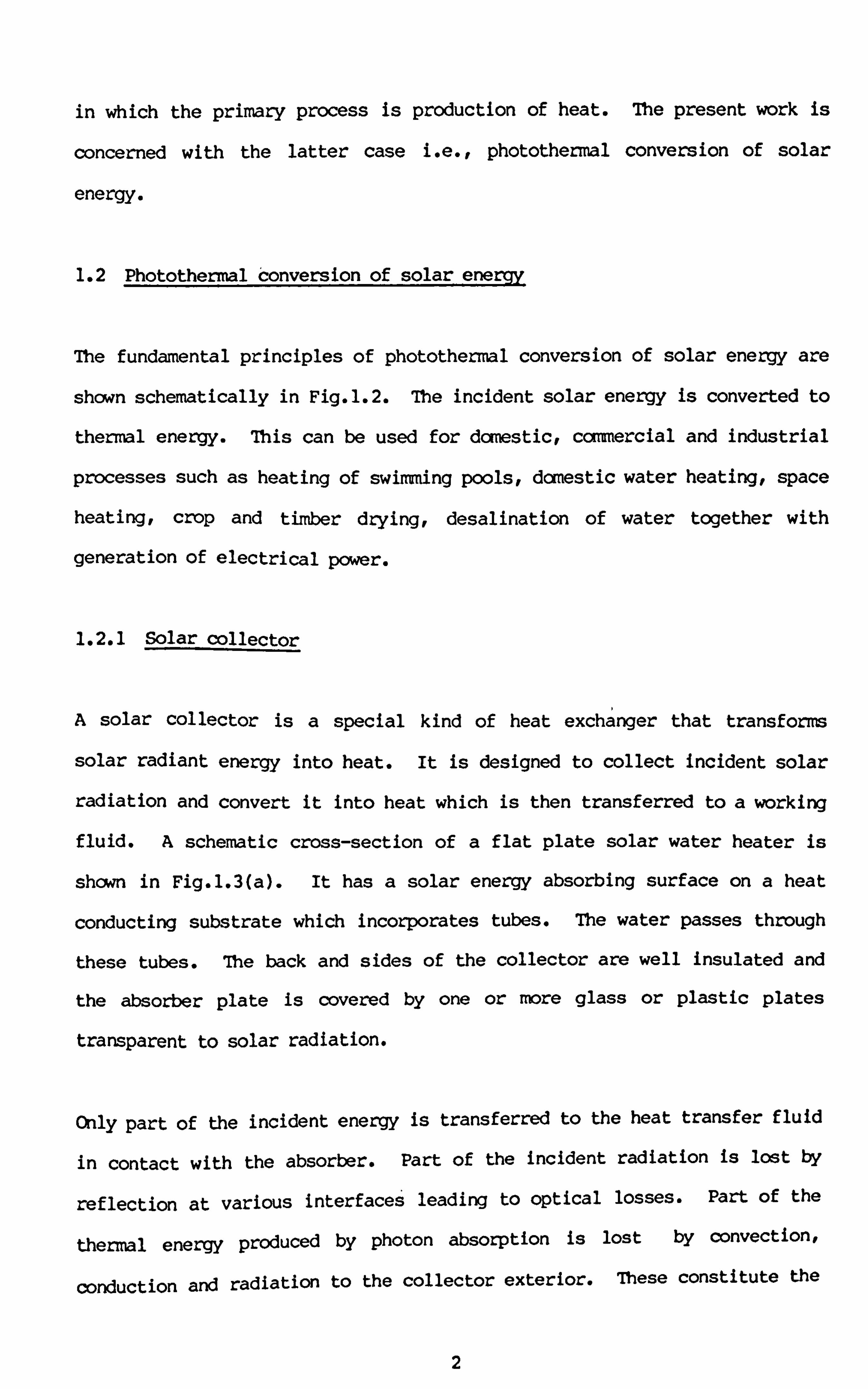
in which the primary process is production of heat. The present work is
concerned with the latter case i. e., photothermal conversion of solar
energy.
1.2 Photothermal 6onversion of solar energy
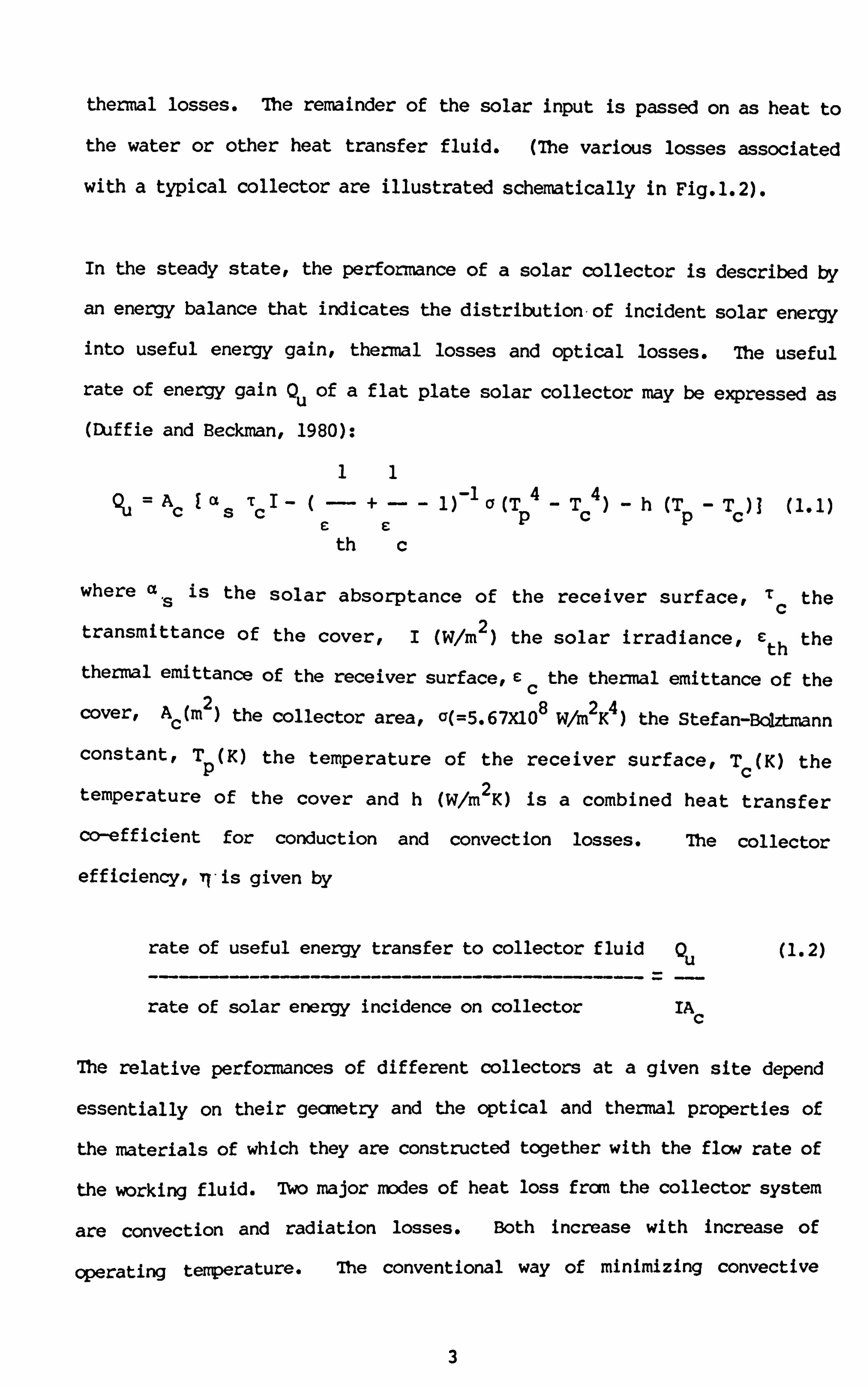
The fundamental principles of photothermal conversion of solar energy are
shown schematically in Fig. 1.2. The incident solar energy is converted to
thermal energy. 7his can be used for domestic, commercial and industrial
processes such as heating of swimming pools, danestic water heating, space
heating, crop and timber drying, desalination of water together with
generation of electrical power.
1.2.1 Solar collector
A solar collector is a special kind of heat exchýnger that transforms
solar radiant energy into heat. It is designed to collect incident solar
radiation and convert it into heat which is then transferred to a working
fluid. A schematic cross-section of a flat plate solar water heater is
shown in Fig. 1.3(a). It has a solar energy absorbing surface on a heat
conducting substrate which incorporates tubes. The water passes through
these tubes. The back and sides of the collector are well insulated and
the absorber plate is covered by one or more glass or plastic plates
transparent to solar radiation.
Only part of the incident energy is transferred to the heat transfer fluid
in contact with the absorber. Part of the incident radiation is lost by
reflection at various interfaces leading to optical losses. Part of the
thermal energy produced by photon absorption is lost by convection,
conduction and radiation to the collector exterior. 7hese constitute the
2
thermal losses. The remainder of the solar input is passed on as heat to
the water or other heat transfer fluid. (1he various losses associated
with a typical collector are illustrated schematically in Fig. 1.2).
In the steady state, the performance of a solar collector is described by
an energy balance that indicates the distribution, of incident solar energy
into useful energy gain, thermal losses and optical losses. The useful
rate of energy gain Qu of a flat plate solar collector may be expressed as (Duffie and Beckman, 1980):
11 Qu = Ac as+- -1 O(T 4_T4h (T cCCpcp
th c
where a 'S is the solar absorptance of the receiver surface, 'rc the
transmittance of the cover, I (W/M 2) the solar irradiance, E th the
thermal emittance of the receiver surface, cc the thermal emittance of the
cover, Ac (m2 ) the collector area, G(=5.67XlO 8 W/M 2K4) the Stefan-Bclztmnn
constant, Tp (K) the temperature of the receiver surface, Tc (K) the
temperature of the cover and h (W/m 2K) is a combined heat transfer
co-efficient for conduction and convection losses. The collector
efficiency, q-is given by
rate of useful energy transfer to collector fluid Qu (1.2)
rate of solar energy incidence on collector IAc
7he relative performances of different collectors at a given site depend
essentially on their geometry and the optical and thermal properties of
the materials of which they are constructed together with the flow rate of
the working fluid. Two major modes of heat loss from the collector system
are convection and radiation losses. Both increase with increase of
operating temperature. Ihe conventional way of minimizing convective
3
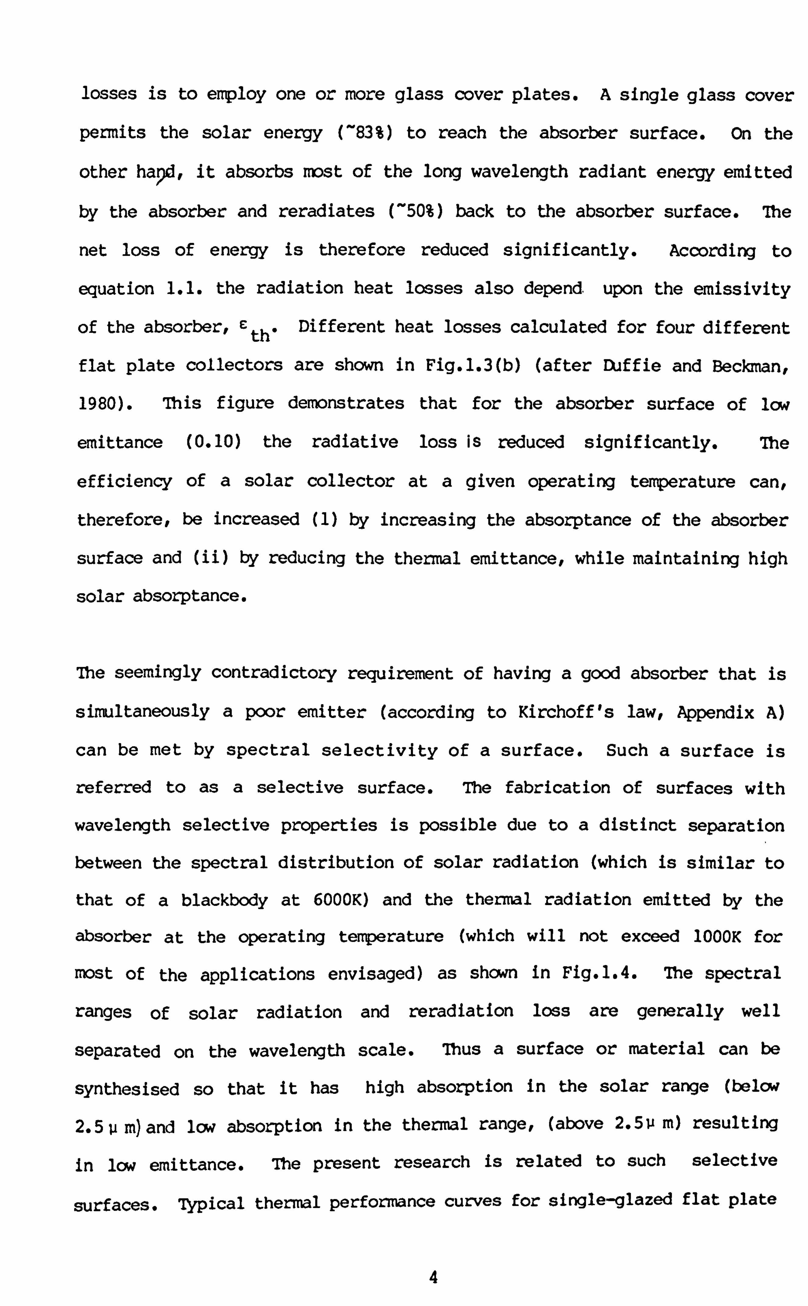
losses is to employ one or more glass cover plates. A single glass cover
pemits the solar energy (-83%) to reach the absorber surface. On the
other hapd, it absorbs most of the long wavelength radiant energy emitted
by the absorber and reradiates (-50%) back to the absorber surface. 7he
net loss of energy is therefore reduced significantly. According to
equation 1.1. the radiation heat losses also depend. upon the emissivity
of the absorber, e th' Different heat losses calculated for four different
flat plate collectors are shown in Fig. 1.3(b) (after Duffie and Beckman,
1980). This figure demonstrates that for the absorber surface of low
emittance (0.10) the radiative loss is reduced significantly. The
efficiency of a solar collector at a given operating temperature can,
therefore, be increased (1) by increasing the absorptance of the absorber
surface and (ii) by reducing the thermal emittance, while maintaining high
solar absorptance.
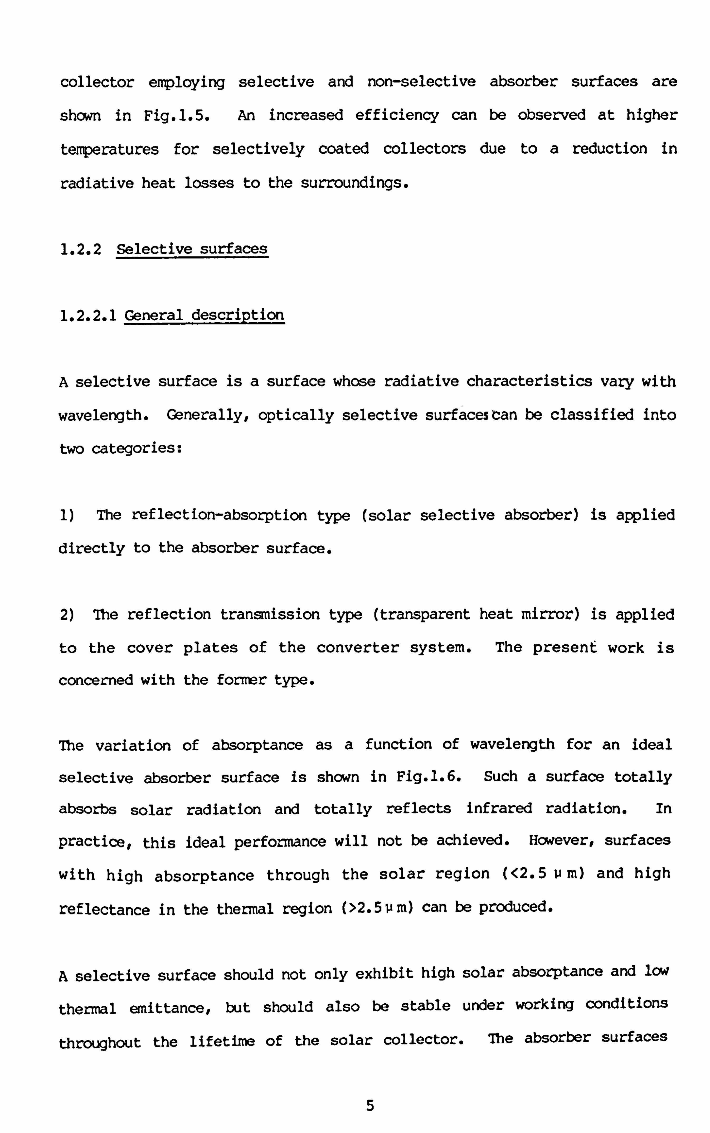
The seemingly contradictory requirement of having a good absorber that is
simultaneously a poor emitter (according to Kirchoff's law, Appendix A)
can be met by spectral selectivity of a surface. Such a surface is
referred to as a selective surface. The fabrication of surfaces with
wavelength selective properties is possible due to a distinct separation
between the spectral distribution of solar radiation (which is similar to
that of a blackbody at 6000K) and the thermal radiation emitted by the
absorber at the operating temperature (which will not exceed 1000K for
most of the applications envisaged) as shown in Fig. 1.4.7he spectral
ranges of solar radiation and reradiation loss are generally well
separated on the wavelength scale. Thus a surface or material can be
synthesised so that it has high absorption in the solar range (below
2.5 U m) and low absorption in the thermal range, (above 2.51, m) resulting
in low emittance. The present research is related to such selective
surfaces. 7ypical thermal performance curves for single-glazed flat plate
4
collector employing selective and non-selective absorber surfaces are
shown in Fig. 1.5. An increased efficiency can be observed at higher
temperatures for selectively coated collectors due to a reduction in
radiative heat losses to the surroundings.
1.2.2 Selective surfaces
1.2.2.1 General description
A selective surface is a surface whose radiative characteristics vary with
wavelength. Generally, optically selective surfacescan be classified into
two categories:
1) The reflect ion-absorpt ion type (solar selective absorber) is applied
directly to the absorber surface.
2) The reflection transmission type (transparent heat mirror) is applied
to the cover plates of the converter system. The presenE work is
concerned with the former type.
The variation of absorptance as a function of wavelength for an ideal
selective absorber surface is shown in Fig. 1.6. Such a surface totally
absorbs solar radiation and totally reflects infrared radiation. In
Practice, this ideal performance will not be achieved. However, surfaces
with high absorptance through the solar region (<2.5 11m) and high
reflectance in the thermal region (>2.5vm) can be produced.
A selective surface should not only exhibit high solar absorptance and low
thermal emittance, but should also be stable under working conditions
throughout the lifetime of the solar collector. 7he absorber surfaces
5
should satisfy the following criteria:
1) High absorptance in the solar region.
2) Low emittance in the infrared region.
3) Long term stability under operating conditions at desired
tenperatures.
4) Stability against ageing at stagnation temperature.
5) Long term compatability with substrate materials.
6) Resistance to atmospheric corrosion.
7) Good reproducibility of optical characteristics.
8) Reasonable production cost.
1.2.2.2 Physical processes leadinq to solar selectivity
The spectral selectivity of an absorber surface can be based on selections
from a range of different physical processes and types of material. These
include:
a) Intrinsic solar selective surfaces.
b) Absorbing semiconductor/reflecting metal tandems.
C) Interference stacks.
d) optical trapping by surface cavities or physical wavelength
discrimination.
e) Particulate coatings and ccrnposite films.
None of the above can individually generate a desirable spectral profile.
In practice, many selective surfaces exhibit a combination of these
properties. The selectivity of the Mo-black coatings studied in the
present investigation is also influenced by different mechanisms. 'These
are discussed below.
6
a) Intrinsic selective absorbers
Intrinsic materials are those which exhibit desired spectral selectivity
naturally, without the need for any other material to augment the
ref lectance behaviour. There is no intrinsic material in nature which
exhibits ideal solar selectivity as illustrated in Fig. 1.6. There are,
however, a very few materials which possess a pronounced degree of
intrinsic spectral selectivity, e. g., hafnium carbide (HfC) has a low
emittance in the thermal infrared (c th - 0.10) and high solar absorptance
of about 0.70 (Meinel and Meinel, 1976).
b) Semiconductor/metal tandems
Absorbing semiconductor and reflective metal tandems are one of the most
conmn types of selective absorber. 7hese tandems generally consist of a
combination of two optically active materials to provide two basic
functions of the converter, absorption and reflection. A schematic cross
section of a tandem absorber is shown in Fig. 1.7. Metals naturally
provide high infrared reflectance. Unfortunately, these are also
reflective in the solar region. If a metal is coated with a semiconductor
layer, which has high absorptance in the solar region and high
transmittance in the infrared region, then the desired spectral profile
can be obtained from the tandem. For semiconductors, solar absorptance is
a result of the absorption of photons having energies greater than the
bandgap of the semiconductor. The coating absorbs the photons which
raises the valence electrons into the conduction band. For longer
wavelength photons, whose energy is insufficient to excite the valence
electrons (i. e., less than the bandgap energy) the materials appear
transparent. This region of transparency permits the metal base to 'see
through' the absorber and suppress the emittance by its high reflectance.
7
Since most of the semiconductors have high refractive indices resulting in
large reflection losses, antiref lection coatings rrust be used or the
refractive index of the semiconductor layer should be lowered by
structural or textural effects, in order to minimize the front-surface
reflection. Therefore, if the absorber-reflector tandem is to be
effective, the absorbing semiconducting layer must have the absorption
edge in the proper spectral range (-2 ijm) and a low refractive index,
possibly a value of 2 or less (Seraphin, 1979).
The semiconductor coating may be an intrinsic element such as Si, Ge or
oxides of metals such as nickel oxide, copper oxide, chromium oxide .
There are, however, numerous successful candidates of semiconductor/ metal
tandems. Most well known examples are black nickel coatings (Ni-Zn-S
alloy) on highly reflecting metals (Tabor, 1956,1961), black chrome on
nickel plated steel or copper (Lampert, 1979, Mattox: and Sowell, 1974).
The simplest tandem stack is oxidized metal/metal ccmbination, as most of
the metal oxides are semiconducting in nature. The oxidation can be
acccrnplished by heating, dipping in baths or other methods of chemical
conversion. Mo-black coatings studied in the present work also act as
tandem absorbers.
c) Interference stacks
The interference stack consists of a combination of dielectric and metal
layers. It is also known as a multilayer thin f ilm which acts like a
selective filter for solar energy absorption by optical interference.
If a metal is covered with a thin dielectric layer, which need not have
any intrinsic absorption, then the reflectance of the metal in the solar
region can be reduced by destructive interference. The condition of zero
8
reflectance of the tandem is determined by the refractive index and
thickness of the individual layer (Park, 1963). Interference ef fects are
sometimes used in metal oxide/metal tandems to increase solar absorption,
e. g., the oxide f ilms of FeP3 and Cr 203 on stainless steel studied by
Karlsson and Ribbing (1982).
A single dielectric layer on a metal has a very narrow absorption band, as
the ref lectivity of the dielectric is weak at its air interface, and this
results in weak interference effect. In practice multilayers of alternate
dielectric and metals have been used in the interference stack to broaden
the absorption band. 7he basic concept of a four-layer interference stack
is shown in Fig. 1.8. The second reflective layer is a very thin metal
layer of thickness about 50K and is partially transparent. The absorption
in this coating is enhanced by multiple reflection between the
semitransparent, dielectric and metal alternating layers. One successful
interference stack is an Al 203 -Mo-Al 203 coating (Peterson and Ramsey,
1975). For Mo-black coatings on mechanically polished zinc, interference
effects may have some influence on the absorption process.
d) Cptical trapping and wavefront discrimination
Selectivity by wavefront discrimination is an important mechanism for the
generation of spectrally selective surfaces. 7he textural profile of a
surface can discriminate between the highly directional solar radiation
and the, hemispherical wavefront of the thermal radiation. Surface
irregularities such as grooves and pores with dimensions large compared
with the wavelengths of the incident radiation increase the solar
absorptance by multiple reflections as shown schematically in Fig. 1.9(a).
They may also increase the thermal emittance to a lesser extent, (Bogaerts
and Lampert, 1983).
9
By reducing the size of the surface roughness to the order of the cut-off
wavelength (maximum wavelength to be absorbed) the solar absorptance can
be increased without affecting thermal emittance significantly. 7he
different optical behaviour of a surface in the visible and infrared
region is explained in Fig. 1.9(b). As the visible wavelengths are similar
to the actual surface irregularities, the surface appears rough or
cavity-type to the inccming radiation and increases absorption through
multiple reflections and partial absorption in the micro-cavities. For
the thermal infrared, the wavelength is larger than the magnitude of the
surface roughness. 7he surface therefore appears smooth and mirror-like
and reflects and radiates like a flat surface.
many solar selective surfaces owe their absorptance to the topography of
the surface. Metals (which may not exhibit a high intrinsic absorption
coefficient in the visible) can also be a good absorbers if roughened by
appropriate techniques. A review of experimental methods for the
preparation of selectively absorbing textured surfaces has been published
by Pellegrini (1980). Nearly ideal textured surfaces have been produced
by chemical vapour deposition of rhenium (Seraphin, 1974) and of tungsten
(Cuomo et al, 1975).
The most successful selective absorber semi conductor/meta I tandem would
also be inferior if textural effects did not reduce the refractive index
of the semiconductor layer. An example is the PbS on aluminium
investigated by Williams et al (1963). If the PbS is applied as solid
material, the tandem should have a solar absorptance of only 0.36. When
it is deposited as a porous structure with sufficient void density, the
effective refractive index is lowered to 1.8 resulting in high absorptance
(0.90). Mere are many tandem type selective surfaces reported in the
literature where surface roughness is responsible for high absorptance,
10
such as black cobalt (Smith et al, 1980), black chrome (Lampert, 1978),
black molybdenum (Carver et al, 1982).
In the present work on Mo-black coatings, surface roughness also plays an
important role in increasing the selectivity.
e) Particulate coatings
Particulate coatings consist of dispersions of metallic or semiconductor
particles in dielectric or conductive matrices. In these coatings the
absorptance is enhanced by reflective scattering where absorption is
obtained by multiple reflections within the geometry of the surface and by
resonant scattering which is characterized by a dependence not only upon
the gecmetry but on the physical properties of the material. One good
example of a particulate coating is the well-known black chrome, in which
small particles of metallic chromium in the size range of 150A 0 are
embedded in a chromium oxide host matrix (Lampert, 1979). Other
interesting surfaces of a particulate nature are 'black molybdenum'
produced by chemical vapour deposition (Chain et al, 1981), and
semiconducting PbS imbedded in a silicon paint (Williams et al, 1963).
No attempt has been made to present a complete review on solar selective
surfaces, as a number of reviews on selective surfaces (Meinel and Meinel,
1976; Peterson and Ramsey, 1975; Lampert, 1979; Mattox and Sowell, 1980;
Koltun, 1980; Agn ihotri and Gupta, 1981) have been published. An
excellent review by Niklasson and Granqvist (1983) includes a
conprehensive list of annotated references on selective absorber surfaces
covering the period 1955 to 1981.
11
1.3 Review of molybdenum oxides
Molybdenum is a transition element (atomic number 42 and atomic weight
95.94) located in the Periodic Table in Group VI between chromium and
tungsten. It falls horizontally between niobium and technetium. The
outstanding feature of molybdenum is its extraordinary chemical
versatility. It has oxidation states from (-II) to (VI) and co-ordination
numbers from 4 to 8 (Cotton and Wilkinson, 1972).
Molybdenum forms a wide range of oxides, such as MoO 3 (Andersson and
Magneli, 1950), Mo 90 26' MOP23 (Magneli, 1948), Mo 4 01, (Magneli, 1948),
M017047 (Kihlborg, 1959) and moo 2 (Magneli, 1946, Brandt and Skapski,
1967). Among all of these oxides, moo 2 and M003 are the most well known
and researched. The intermediate oxides are formed by heating MoO3 and Mo
metal in vacuo at temperatures between 550 to 800 0C for various times
(Kihlborg, 1959). They have been characterized by means of X-ray powder
photographs and most of their structures have been determined from single
crystal X-ray data.
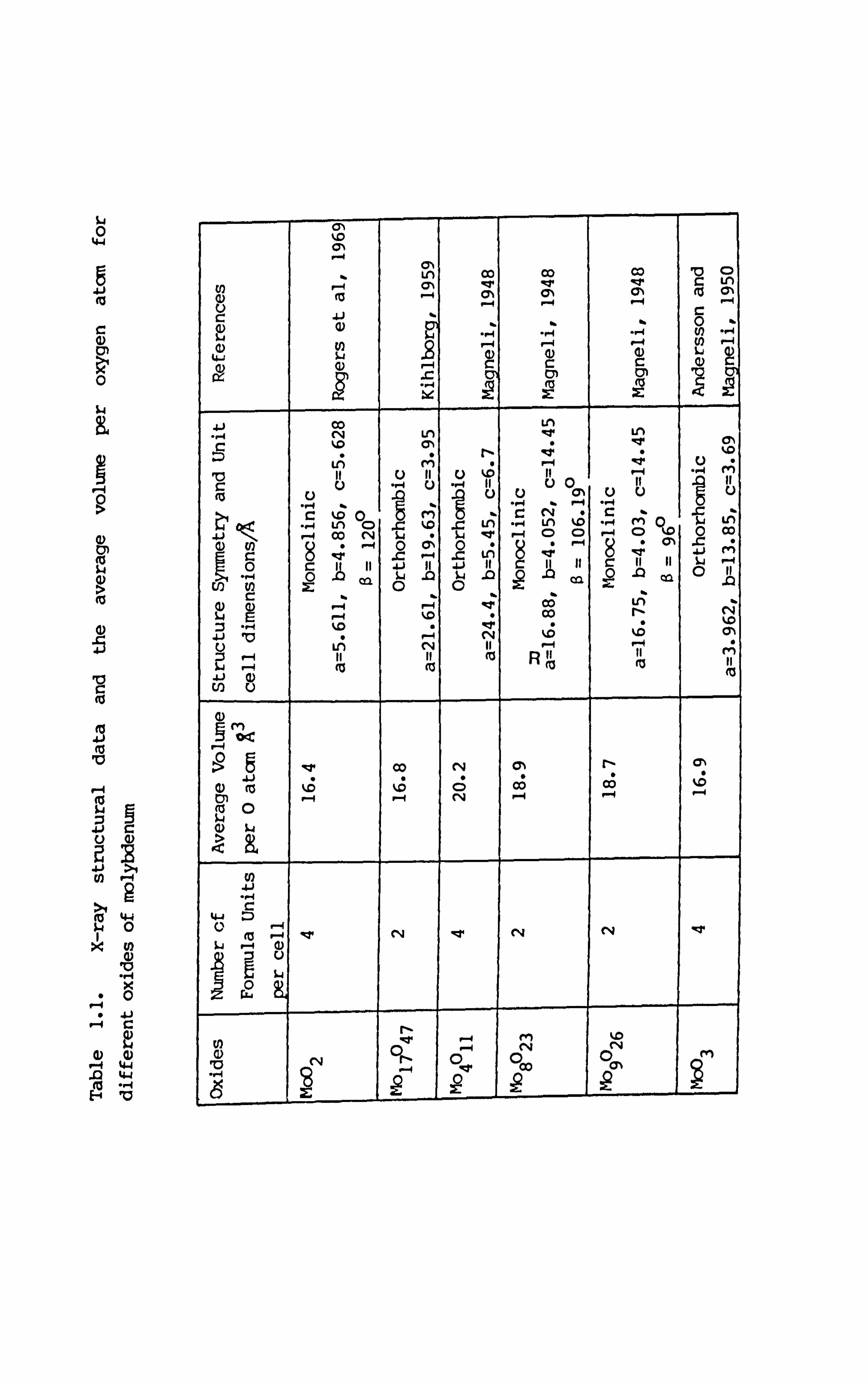
1.3.1 Ccmparison of structures of MoO.,, MaO, and Mo 0 - -=4=11
The crystal structures of different phases of molybdenum-oxygen system
(MO02' M003 and intermediate oxides between these two) have been studied
by Hagg and magneli (1944), Magneli (1948) and Kihlborg (1963). According
to them all the Mo-oxides are composed of polyhedra connected by the
sharing of comers or edges. The MoO 6 octahedron (Fig. 1.10. a) is the most
frequently occurring type of polyhedron but Moo4 tetrahedra and M007
pentagonal bipyramids (Fig. 1.10. a) are also found.
12
The structure of Mo 40 11 is rather different from those of the other
Mo-oxides. The occurrence of M004 tetrahedra in Mo4011 totally lacks
analogy with other oxides which are exclusively built-up by Moo 6
octahedra. The orthorhombic Mo 4 Oll structure projected parallel to (010)
plane is given in Fig. 1-10. b. The orthorhombic unit cell contains four
molecules of Mo4Ol,. CoTTpared to M002 and MoO3 it has large lattice
parameters (Table 1.1).
moo 2 has a distorted rutile structure (Figl. ll). It has monoclinic
synmetry. There are four molecules in a unit cell of dimensions,
5.611X; b=4.856X; c=5.628A; a= 12e
moo 3 has a unique layer structure (Fig. 1.12). In an orthorhombic unit
cell, there are four molecules of Moo 3 The unit cell dimensions are
given in Table I. I.
The structure of Mo 4 01, is a very spacious one ccmpared with those of the
other Mo-oxides. Ibis is illustrated by the quotient between the volume
of the unit cell and the number of the bulky 0 atcms per unit cell (Table
1.1). Thus Mo 40 11 has a very open oxygen packing while MoO 2 is fairly
closely packed. It was reported by Hagg and Magneli (1944) that the
stoichiometry of M04 01, may vary between MoO 2.85 to moo 2.72*
1.3.2 Optical and electrical properties
There has been considerable interest in the optical and electrical
properties of the transition metal oxides due to their wide range of
physical properties. The inconplete d-shell of the metal ion, which is
the common feature of this group is responsible for a wide range of
13
optical and other propecties. The electrical and optical properties of
moo 2 and MoO 3 both in single crystal and amorphous structures have been
studied by several investigators.
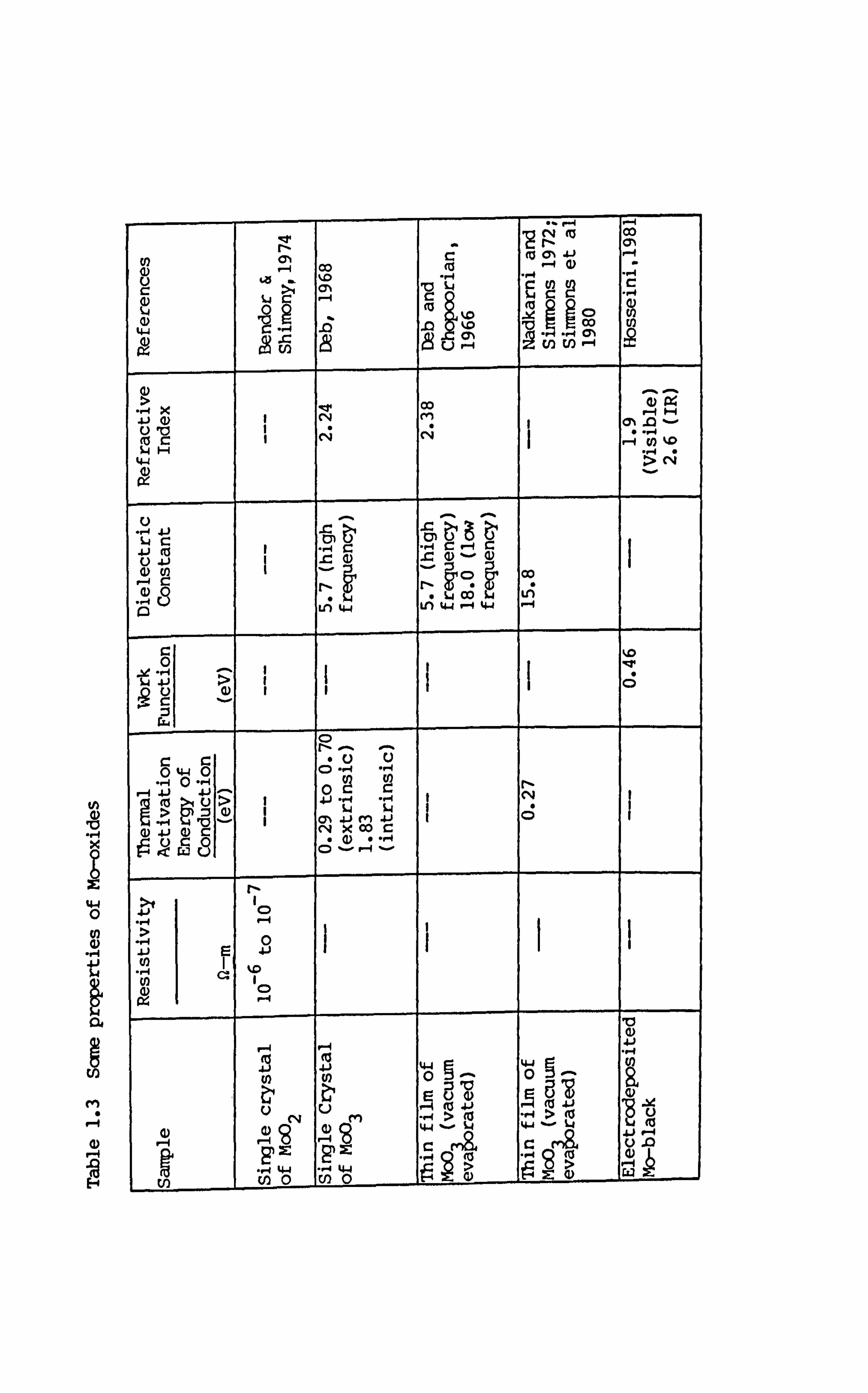
moo 2 is a dark brown solid. Its melting point is 2200K (Samsonov, 1973).
The specular reflectance of single crystal Moo 2 has been measured by Chase
(1974) in the wavelength range 0.2 to 12.011M. ACcording to his data, the
corrputed solar absorptance of crystalline Moo 2 is about 70% (Carver et al,
1982). In addition, infra red (IR) measurements in the range 2-50 um of
Moo 2 powder have shown that it has very wa. A absorption peaks in the the
region 10.2 - 11.2 ilm (Hanafi et al, 1975). We to weak absorption injIR
region it should be a poor emitter. The optical band gap of M002 is 1.72
eV (0.72 um) (Hanafi et al, 1981). This indicates the possibility of high
absorption in the visible region due to band-to-band transitions.
(However, a higher value OeV) for the bandgap of single crystal M002 has
been reported by Chase (1974)).
Electrical measurements have shown that M002 is a metallic conductor
(Ben-dor and Shimony, 1974, Roger et al, 1969). The room temperature
specific resistivity is of the order of 10-6 n-m and increases with the
increase of temperature as is expected for metals. It has been reported by
Bendor and Shimony (1974) that doping by NiO in pure MoO 2 lowers the
conductivity.
moo 3 in contrast to MoO 2 is a non-conductor. It is an almost colourless
solid with greenish tinge. Its melting point is 1068K (Samsonov, 1973).
The electrical and dielectric properties of vacuum evaporated MoO3 thin
films have been studied by Simmons and Nadkarni (1969,1970,1972),
Nadkarni and Simmons (1972), and Nadkarni et al (1982), for use as a
capacitor. According to them, evaporated f ilms of M003 contain an excess
14
of Mo-metal. These act as donor centres and control the electrical
properties of the f ilm. The donor density in MoO 3 is estimated to be
24 about 10 m. some data on electrical properties of MoO3 thin films are
given in Table 1.3.
The optical and photoelectric properties of single crystal and thin f ilm,
moo 3 have been studied by Deb (1968), Deb and Chopoorian (1966) and
Rablais et al (1974). According to them 'as deposited' thin films of M003
are transparent but they can be coloured by the application of electric
fields or by irradiating with UV light. Sufficient application of either
of these colouration techniques results in deep blue f ilms. Cptical
absorption spectra of MoO 3 thin f ilms in the visible and near infrared
region obtained by CoLton et al (1978) are shown in Fig. 1.13 before and
after colouration. It can be seen that in the blue films, the absorption
spectra have maxima near 0.6 ji m and 0.77 jim and continuous absorption
throughout the NIR region with maxima near 1.4 Vm, and 2.4 Pm. Deb and
Chopoorian (1966) reported that the same type of colour centres can also
be formed on heating the film in oxygen in inert atmosphere. According to
them the formation of colour centres in MoO 3 is closely related to the
presence of Mo +5 state and the oxygen ion vacancies in the lattice.
During the evaporation in vacuum, moo 3 undergoes scme thermal
decomposition and thereby incorporates some lower valence Mo +5 state in
the lattice which is confirmed by electron-spin-resonance (ESR)
measurements. There is considerable spread of data for the absorption
edge of MoO 3 in the literature. Hanafi et al (1981) obtained a value of
2.74 eV for the band gap of M003 from diffuse reflectance measurements. A
value of about 2.92 eV has been obtained by Comanion and Mackin (1965) on
powdered MoO 3' The absorption edge of single crystal MoO3 has been given
as 2.8 eV by Deb (1968). Considerably higher values for the band gap 3.2
eV and 3.7 eV have been obtained by Rablais et al (1974) and Deb and
is
Chopoorian (1966) respectively for vacuum evaporated MoO3 thin films.
The optical properties of M002' MoO3 and the intermediate oxides Mo, 13 0 38'
Mo, 90 26' M0023' M017047 and M0401 1 have been studied by Hanaf i et al
(1981) in the range 0.3 to 0.9 v m. The absorption spectra of all these
sanples showed strong resemblances except for Mo 40 11 and MoO 2 which were
of an entirely different character. They found that the energy gap
increased gradually from 2.74 eV for Moo 3 with increase of oxygen
deficiency to 3.1 eV for Mo 90 26 and Mo 6023 and then decreased to 1.72 eV
for MoO 2* They explained this variation of bandgap in relation to changes
in crystal structure. 7hey could not explain the great similarity in the
absorption curves and the values of bandgap between MoO 2 and Mo 4011 *
Table 1.2. shows the bandgap of the different oxides of Mo according to
the work of Hanafi et al (1981).
Hanafi et al (1975) have also measured the IR absorption spectra of all of
these oxides except mo 40 ll* They have reported that most of the
absorption bands of Moo 3 are still present in the spectra of the
non-stoichiometric oxides. This is thought to be due to the most
frequently occurring MoO 6 octahedra. The behaviour of the intermediate
oxides deviates gradually from that of MoO3 towards that of M002*
Porter et al (1972) have measured the optical absorption spectra of some
intermediate oxides of MO (M0021 M04011' M09026 ) in the visible and NIR
region. 'Ihey found that both M002 and M09026 have one main absorption
peak while the absorption peak of M04011 was split, having maxima at about
0.51,0.58 and 0.95 ijm. According to their investigation the absorption
band shif ts linearly with changing metal-oxygen ratio. The intermediate
16
oxides, Mo 40 ill Mol'P4 7' M06023' Mo 9026 are thermally unstable at higher
temperatures and decompose above 973K with formation of Moo 2 and Moo 3 (Samsonov, 1973).
1.3.3 Molvbdenum oxides for use as a solar selective surface
Molybdenum oxides for use as a solar selective surface, termed as
'Mo-black' (or 'black-Mo') has been investigated by several research
groups. Mo-black can be prepared by different methods on different
substrates.
The previous work at Brunel University (Hosseini, 1981) has shown that
Mo-black coatings for use as solar selective absorbers can be prepared by
the electrodeposition and simple chemical dip methods from an aqueous
solution, which is one of the easiest and most cost-effective methods of
producing solar selective absorbers.
Mc-black coatings known as 'Moly black' were first prepared by Hoffman and
Hull in 1939 by an electrodeposition method. They used an aqueous
solution of nickel sulphate (NiSO4) ammonium molybdate 1( NH 4)6MO7024 I and
boric acid (H 3 BO 3 ). The substrates used were aluminium, electroplated
zinc, electroplated cadmium and die-cast zinc. The purpose of their work
was to produce decorative coatings. According to their analysis, this
highly lustrous, deep black coating contains about 45% Mo, 10% Ni with the
balance chiefly oxygen. They also mentioned that very thin Mo-black
coatings can be deposited simply by immersion of zinc plated substrates in
the solution.
The electrodeposited Mo-black coating on copper substrateshas been studied
by iNcRA (1977), but the resulting coating was not satisfactory as a solar
17
selective absorber. Smith et al (1981) and Hosseini (1981) have studied
Mo-black coatings prepared by the electrodeposition method on aluminium
substrates and the chemical dip method on zinc and galvanized steel
substrates. Hosseini used an aqueous solution of ammonium molybdate and
nickel sulphate with concentration of 30 g/dm 3
and 150 g respectively.
He suggests that the electrodeposited coating is composed of M002" 2H20
together with Ni(OH)2 whereas the dip coating might be in the form of
Mo 203 oxide. According to his investigation, the electrodeposited coating
is effectively non-selective due to continuous absorption in the IR region
resulting in high emittance. 7he mechanism of the absorption in this
coating was said to be unknown. Dip coatings on zinc and galvanized steel
showed significant selectivity, e. g. j a x/ c: th = 4.3 when aV (absorptance
in the visible range) = 0.84 for a coating on zinc substrates. The
absorptance in these coatings was thought to be due to interference
effects (Hosseini et al 1983). It was concluded that the dip coating
might form a basis for selective coatings but the durability needed to be
improved. In the present research, attempts have been made to improve the
selectivity as well as durability of Mo-black coatings by changing
preparation conditions and substrate conditions.
wring the progress of the present work, sane more work has appeared in
the literature on Mo-black coatings for use as a selective solar absorber
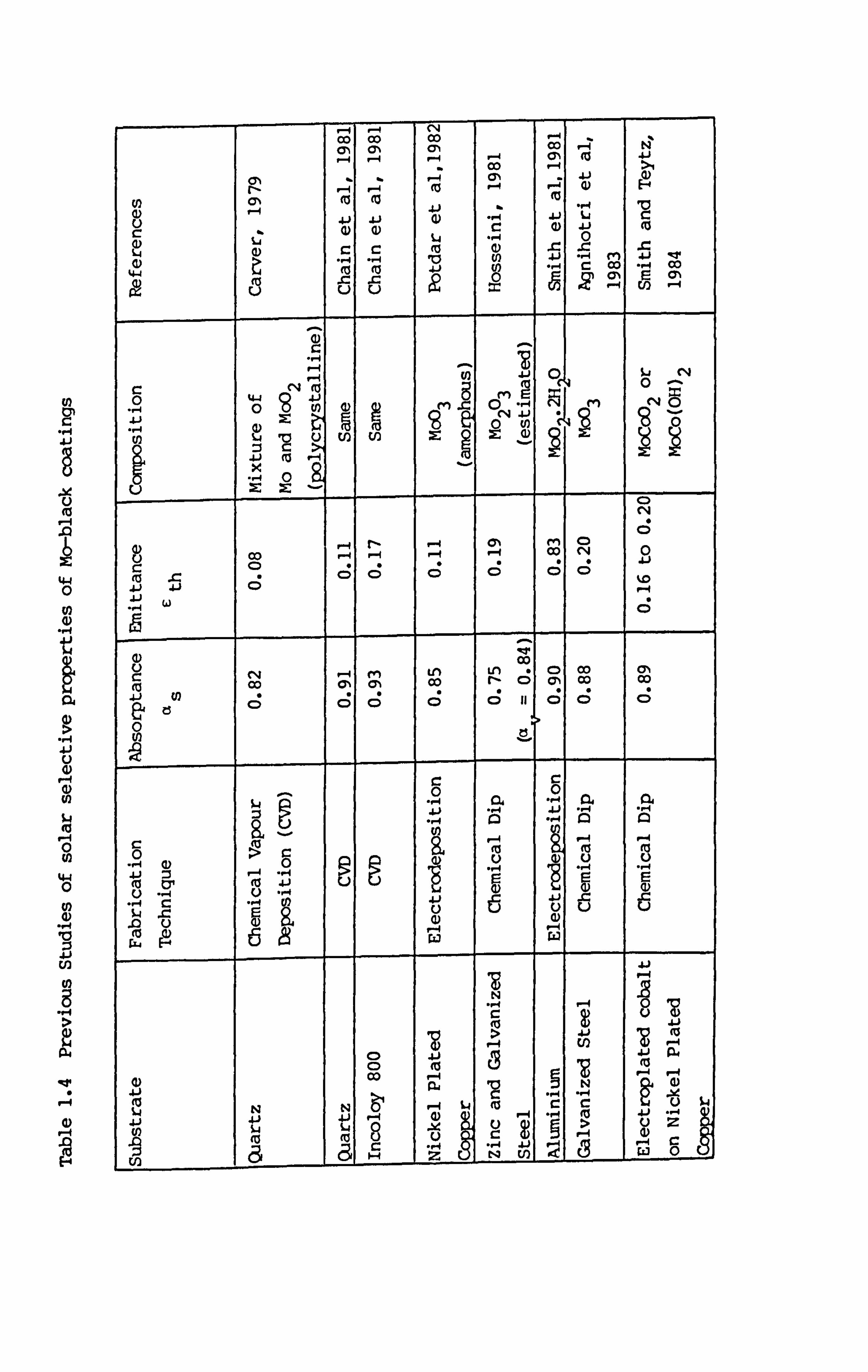
surfaces. Potdar et al (1982) have studied Mo-black coatings on nickel
plated copper substrates prepared by cathodic electrodeposition method.
These films have a solar absorptance of aS0.85 and thermal emittance of
C 0.11. It has been reported that these films are adherent and th
non-crystalline and consist of essentially M003 with some metallic nickel.
Agnihotri et al (1983) have studied black molybdenum coatings prepared by
chemical conversion method on galvanized steel and zinc plated mild steel.
The best value of solar absorptance is 0.88 with c th ý 0.20. These
18
coatings have been reported to contain MoO 3 and to be amorphous in nature.
It has been reported (Gupta et al, 1983) that Mo-black coatings on
galvanized steel do not degrade on annealing at 2500C in air up to 800
hours. 7he selective properties remain almost constant on thermal cycling
(600 times at 1500C) and 98% humidity.
Black molybdenum films prepared by chemical vapour deposition (CVD) method
frcm molybdenum carbonyl has been studied by Carver (1979) and Chain et al
(1980,1981). The CVD Mo-black exhibits a solar absorptance of as = 0.77
and a thermal emittance of c th ý 0.44. After annealing and then
overcoating these films with an antireflection layer of Si 3N 41 the
absorptance increases to 0.82 with c th = 0.08 (Carver, 1979). A higher
value of absorptance of as=0.91 with e th = 0.11 has been reported by
Chain et al (1980,1981) for CVD Mo-black. These films are stable at 50CPC
for 1000 hours in a rotary purrp vacuum. CVD Mo-black is a cermet type
absorber. It consists of moo 2 with Mo-inclusions and thus exhibits an
absorptance close to that of MoO 2 and an emittance approaching that of Mo.
Recently Smith and Teytz (1984) have prepared a Co-Mo coating by chemical
dip method from a solution of cobalt sulphate and sodium molybdate on
electroplated cobalt film on nickel plated copper. Its optimum as and e th
combination is as = 0.89 + 0.01, c th = 0.16 to 0.20.7he composition of
this coating is thought to be either MoCoO 2 or MoCo(OH) 2 or a conpound
containing Co 203 mixed with a molybdenum oxide in low valence states.
Table 1.4 summarizes the radiative properties of some coatings referred to
as Molybdenurrt--black in the literature.
19
1.4 Aim of the study
The purpose of this research is to investigate Mo-black coatings in
relation to their use as selective absorbers for photothermal conversion
of solar energy and to understand the physical processes responsible for
selective absorption in these coatings. one aim is to study the
relationship between the microstructural. and optical prcperties; under
various conditions. A previous study (Hosseini, 1981) showed that mo-black
dip coatings had some potential for use as a solar selective absorbers,
but durability needed to be improved. The aim of the present study is to
concentrate on dip coatings.
It is known that the interfacial layer or the condition of the substrate
has great influence on the radiative properties of solar selective
surfaces and also on the durability of the coatings. Therefore to improve
the selectivity and durability of Mo-black coatings different types of
substrates, such as chemically etched zinc, electroplated cobalt (plated
with and without addition agent) on nickel plated copper need to be Studied.
However, for comparison with the previous work and to see the effect of
etching of the zinc substrates on the radiative properties and
microstructures of the coatings , another aim is to study Mlo-black on unetcl. ed
zinc and aldminium substrates. To characterize these coatings,
it is intended to make detailed studies on radiative properties (cts, e th),
microstructures and caripositims of the coatings.
The radiative properties, e. g.,, solar absorptance as and thermal
emittance eth of the coatings will be determined from the
reflectance measurements in the solar (0.3 to 2.5um) and infrared
20
regions (2.5 to 50 v m).
(ii) 'Me surface moLphology of the coatings and the substrates will be
studied in the scanning electron microscope (SEM) and their
relationship to the optical properties of the coatings will be
investigated. Some optical microscopy will also be perfomed.
(iii) The effects of deposition parameters (such as, solution temperature,
deposition time) of Mo-black and suhstrate pretreatment on the
radiative properties and microstructure of the coatings will be
investigated. The effect of various deposition conditions of an
intermediate cobalt layer will also be studied. Thus the
preparation conditions for the optimum properties will be
determined.
(iv) The corrpositional analysis of the coatings will be done by using
X-ray diffraction, electron diffraction, X-ray Photoelectron
Spectroscopy (XPS), together with infrared spectroscopy.
(V) The stability of the dip coatings will be tested by short term heat
treatment at different temperatures together with atmospheric
ageing.
(vi) Transmission measurements in the UV and visible region will be
done to determine the bandgap of the coating material and its
relation to the optical properties of the coating.
(vii) Some electrical measurements (both A. C. and D. C. ) will also be
performed to yield ideas about the band structure, conduction
process and dielectric nature of the coatings.
21
W 0
4-4
0
$4
>0 Cm
M V
0)
(D 1-4 44
tw
011 u-) OD OD OD 'C) C)
CY% c Ln
CA
Ji
j ., 4 (ö 2 ,Z :2 Z :e :
Co Ln ulý
cn
9'. %0
1C3 Ln it u
ri 11 c) 0 11 P--4 . -I M
cý< 0
6 .
Ln
- f LA CD c2 --4
m0 00 0 OD
4 C 4 cý 0;
ýi o
e - ji
.. -4 w 0 M - Ji ý4
ll 0
c 11 c: 11 11 m
w 0 11
rn :2 ca (D 0 2 ca 2 m OD Co
Ln r- r4
:3 14 $ýo %ýO
u; 11
C, 4 11
(0 rö 11 4 tö cö (0
. &i Q) ul u
0 Co (14
a) tö %. 0 %Z cý 0
rn
(ö -4 " r4 -r (4 CY Wi C)
Z u 5
W
., 4 2 -4 W 000
5 9 2 2 2 , 2 -
Z
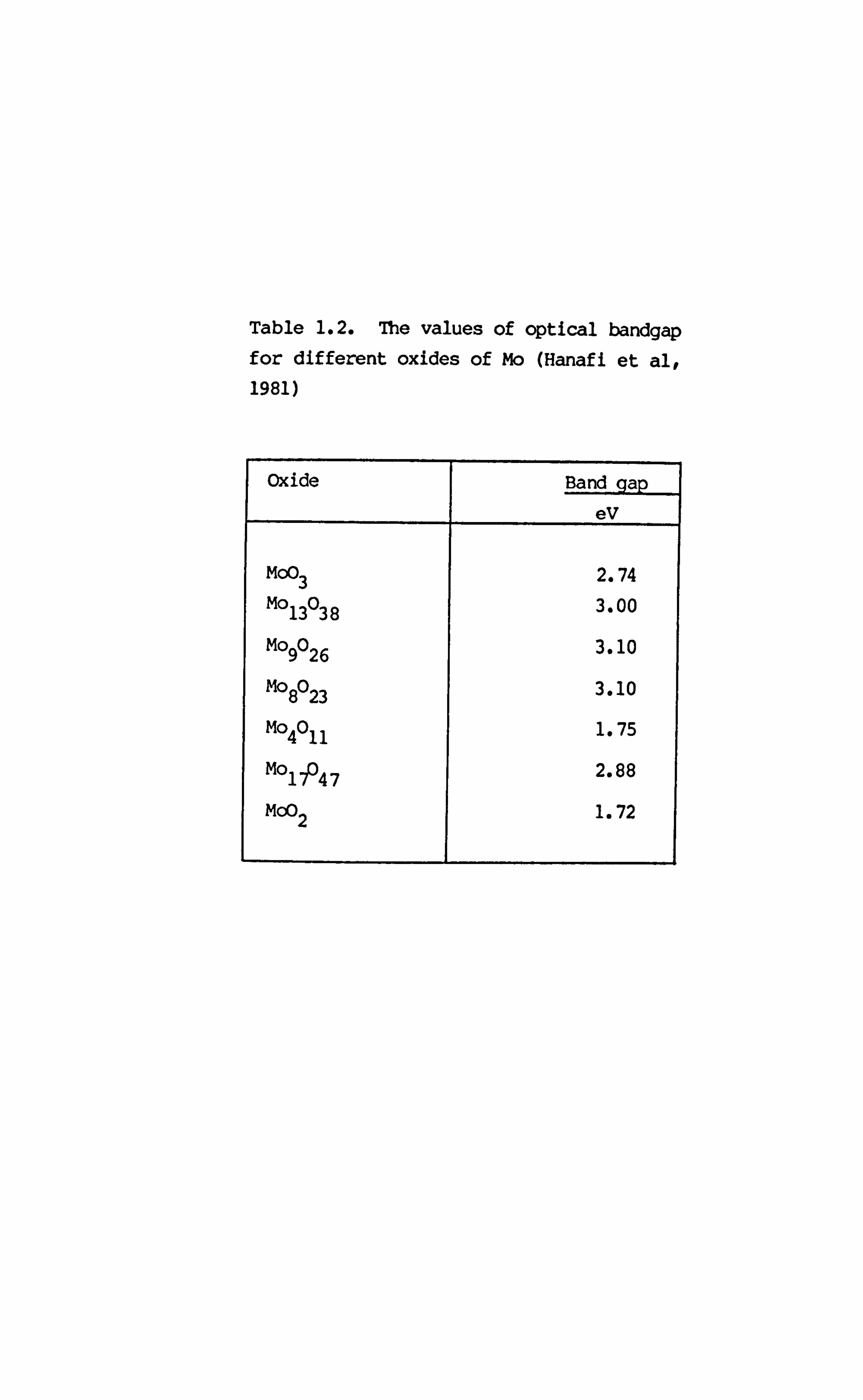
Table 1.2. The values of optical bandgap for different oxides of Mo (Hanafi et al, 1981)
Oxide Band gap
eV
Moo 3 2.74
mo 13 0 38 3.00
Mo 90 26 3.10
M08023 3.10
M04011 1.75
Mo 17047 2.88
Moo 2 1.72
th 0)
10
x
44 0
m S
a)
. -4
Cý m -4
co 00
(o aN Aj
c >4 M rs S4 c cn 14
) U
co -4 ON
U)
U
010 1 C14 C14 . -4
44 C4
4 4J C: -C ý, 6 ý, a 41 (a W
tc! Cý
LA tw -4 %w
Ln
0
C)
0 44 0 CD . -1 0. " 0
tao r- 41 -4 1 4 1 4 ;
Q) 4J (D C: , M .1 1
CQ x co r- C
. (D 0 -ý4 CD
"I >
> 1 Aj
0 41
wf
C: C:
r-4 (a 4. )
r-I (13
044 Q5 t4-j § (n R U) U)
: 310 400
cli u u
(CS (D 44 $4 4-1 41 r-4
4 44 > ý
--1 44 (n 0I
- to Q
9
(1)
., 4
OF 4. ) U 4)
ýq W
0 (a
44 0
(1)
�-I
�-4
00 (3)
00 ON
C14 OD m
1-4
--q co m (a
% N
0ý r- as
--q M
-4 (a
(o -4 _; 0)
(D c (D (L)
L4 c
-4 0) J-)
0 (a
a) L4 a)
(1) (a
c -4 tio r-
c 1-4 M
.C
(o 10 41 R
W U) (1)
J-- 4J ., 4
8 :ý
r- 00
F 01
C 'IT Aj
-. 4 CO
U) -4 r: ý ", L) U I
c 0
41
C'4 (o 4J
4J
C',
41
w C14 0
C14 0
x ., 4 o
M: X Cý
(D CC) CD ;
co ;
CN ;
0 A. )
C; C; C C C %D
-4 C;
CV CC)
rn (ý Ln CO
co Ln r r- ; c)
0) co 00
ON co J-)
e C; CD C) C; 11 C; C; 0
CA 0
., 4
t Ol r-4
I,
(o 41
0 0 EJ
1 r-4
41
15 15 6
N
8 ý9 C) CD
'9
41 (a
r4 Ef) Is
78 1-4 J-j CIO (o
4 -4 a) co r-4 Is
0
C -rq
N
C:
ý r 0)
41 ý4
m i,
m u ý
r-4 C:
o
CHAPTER II
PREPARATION OF MO-BIACK COATINGS
AND EXPERIMENTAL TIXINI=
2.1 Techniques for preparation of Mo-black coating
2.1.1 Electrodeposition of Mo-black coatinqs
Mo--black coatings were prepared by a cathodic electrodeposition method on
an aluminium substrate from an aqueous solution of ammonium paramolybdate
[(NH 4) 6Mo7C)24 AH 203, nickel sulphate [N'SO4.6H 201 and boric acid [H 3BO31 (Hof fman and Hull, 1939). A schematic diagram of the electrodeposition
equipment is shown in Fig. 2.1. The apparatus consisted of a hot water
bath with temperature control unit to provide the desired solution
temperature, a regulated power supply unit, ammeter, plating tank and
thermometer to measure the temperature of the solution. A PH meter (Data
Scientific, PTI-15) was used to measure the PH of the solution. The
density of the coatings was obtained frcm the difference of the mass of
the substrate before and after coating deposition. The coating thickness
was also measured by surface profile stylus equipment (Rank Taylor Hobson
Talystep).
2.1.1.1 Aluminium substrate preparation
Ib obtain good quality, uniform and adherent coatings, the substrate
pretreatment was extremely important. In this experiment the pretreatment
of aluminium substrates was in two stages. Firstly, the oxide layer was
22
removed by grinding with emery paper of grade 320 and 600 in one
direction. The substrates were then chemically etched with concentrated
NaOH (150 g/dm3) solution at a temperature of 25-30 0C for a few seconds
and immediately immersed in boiling distilled water for a further few
seconds with constant stirring. This was followed by washing with more
distilled water and drying with compressed air.
The use of emery paper to remove the oxide layer made the surface rougher
which gave good adhesion. However, surface roughness affected the thermal
radiative properties of the coatings. An attempt was made to avoid the
use of emery paper by dissolving the oxide layer with a chemical solution.
In this processir (Lowenheimt 1963) the aluminium substrates were first
degreased with choloroform and rinsed with alcohol. This was followed by
a mild etching with NaOH solution and washing in boiling distilled water.
These were then immersed in a zincate solution (which consisted of 200
g/dm 3
of NaOH and 80 g/dm 3
of ZnO) for a few seconds at a temperature of
259C. The oxide layer present on the surface of aluminium dissolved in
the zincate solution and a very thin layer of zinc was deposited on the
aluminium surface. The substrates were then immersed and agitated in
distilled water in two successive stages to remove all of the zincate
solution. The zinc layer formed on the aluminium was then dissolved by
dipping in a 30% (by volume) solution of HNO 3. Washing of the substrates
with distilled water was followed by their rapid transfer to the plating
bath.
2.1.1.2 Bath composition and plating conditions
In the present investigation the concentration of Mo-black electroplating
bath was
23
(NH 4)6MO 7024 AH 20 - 30 g/dm3
NiSO V 6H 20- 150 g/dm 3
H 3BO3 - 22 g/dm 3
Here boric acid was used to buffer the solution during plating. 7he
required bath terrperature was in the range of 55-70 0C and the current 2
density used from 1.5 to 3.0 mA/cm The coatings were prepared for
various lengths of time from 20 to 60 minutes on rough aluminium
substrates. on smooth aluminium substrates, the plating time varied from
5 to 20 minutes. The coating thickness expressed as the coating mass per
unit area was found to increase with plating time and current density.
Table 2.1 gives plating conditions of some coatings on aluminium
substrates.
2.1.2 Mo-black coatings by chemical conversion
Mc, -black coatings were prepared on zinc and electroplated cobalt on nickel
plated copper substrates by immersion and agitation for a few minutes in a
solution of ammonium paramolybdate and nickel sulphate. Boric acid (used
in the electroplating bath) was not required in the dipping process.
2.1.2.1 Bath ccnposition
Different concentrations of ammonium paramolybdate and nickel sulphate
(Table 2.2) were used in preparation of the Mo-black coatings by the
dipping process. Solution 1 was suggested by Agnihotri et al (1983); but
tended to be unstable at room temperature. The solution was soluble only
at a temperature above WC. Below 660C a light bluish-white precipitate
formed. However, the precipitates could be dissolved at lower
temperatures by decreasing the pH of the solution. In this case the rate
24
of deposition was very high. It was difficult to control the thickness of
the coating (which was found to be critical for optimized selectivity).
Lower concentrations of ammonium paramolybdate were, therefore, tried
(solution 2,3 and 4 in Table 2.2). These were soluble even at room
teaperature. Solution 2 (without nickel sulphate) gave no black coating
even for long times of immersion (the effect of the concentration of
nickel sulphate on the optical properties of the coatings is described in
section 3.1.1). Solution 3 gave the most reproducible results and was
used throughout this investigation.
2.1.2.2 Zinc substrate preparatio
Conmrcially available zinc sheet of thickness lmm was used in this study.
To obtain uniform and adherent coatings, the thin surface layer of oxide
was removed from the zinc substrates by using emery paper of grades 600
and 1200 under a flow of water to avoid deep scratches. 7be substrates
were then washed with distilled water, rinsed with alcohol and dried with
compressed air. 7he second step was chemical etching. Various
concentrations of HN03 were used to etch the zinc substrates ranging from
5% to 50% by volume. (The concentration of HNO 3 had some effect on the
surface topography of the coatings (Section 3.2.2)). The zinc substrates
were etched in HNO 3 at a temperature of 20 0C for a few seconds with
constant stirring, followed by washing with distilled water, rinsing with
alcohol and drying.
2.1.2.3 Plating conditions for zinc substrates
Following the pretreatment, zinc substrates were immersed in the plating
solution for various lengths of time. During the deposition processo the
solution was gently stirred in order to avoid non-uniformity and the
25
formation of air bubbles. After deposition of the coatings, they were
washed with distilled water and dried with coupressed air. The colour of
the coating depended on the time of immersion and hence on the coating
thickness. An observable colour was found just after immersion in the
solution. Up until 20 seconds the coating was very thin and non-uniform.
As the time of immersion increased, the coating became darker and more
uniform. After 60-70 seconds of immersion, no visible interference
colours were observed in the coatings on etched substrates and the colour
of the coating was dark grey. For unetched substrates, interference
colours were not observed after 3 minutes immersion. Fig. 2.2 shows the
variation of coating mass per unit area with deposition time for both
etched and unetched zinc substrates. The coating mass increased rapidly
for the first 3 minutes and then much less rapidly. The rate of
deposition was higher for etched zinc than the unetched zinc (Fig. 2.2)
indicating that the acid etched substrate was more reactive. The
difference between the measured surface area and the true surface area of
the coating on etched zinc might also account for the observed higher
deposition rate (as the etched zinc had rough topography).
7he temperature of the solution influenced the coating thickness. 7hough
the coating could be formed at rocm temperature, the rate of deposition
was low. Fig. 2.3 shows the effect of solution temperature on the coating
thickness. At high temperatures it was difficult to control the coating
thickness due to the high deposition rate and the coating adhesion was
poor. 7he best results were obtained in the temperature range 35 - 450C.
2.1.2.4 Preparation of electroplated cobalt on nickel plated copper
substrates (Cobalt (NC) substrates)
7hese substrates were prepared by electroplating a cobalt filmonbdull
26
nickel which had been plated onto copper sheet. The following procedures
were used:
a) 7he copper sheet was mechanically polished with 1200 grade of emery
paper to remove the oxide layer and washed with distilled water.
b) The copper sheet was then chemically cleaned in a solution of ammonium
persulphate (10 g/dm 3)
at a temperature of 40 - 450C for 1 minute with
constant stirring. It was then immersed in dilute H 2SO4 at room
temperature and finally washed with distilled water and alcohol and
dried.
c) Dull nickel was electroplated cntothese cleaned copper substrates from
a solution of nickel sulphate, nickel chloride and boric acid in the
respective amounts of about 200,40 and 20 g/dm 3. The operating
conditions were as follows:
Teirperature of the solution
pH of the solution
Cathode current density
Plating time
Anode used
30 - 40 0C
3.5 - 3.8
20 - 25 mA/cm 2
10 - 15 minutes
Nickel sheet
d) The final step was the electrodeposition of cobalt. The cobalt films
were prepared by the cathodic electrodeposition method on nickel
plated copper substrates. The composition of the cobalt plating bath
used in this study was as follows:
27
COS04 . 7fl2o 100 g/dm 3
H3BO3 40 g/dm3
coci 2 20 g/drrý
Plating was done under the following conditions:
Temperature of solution 45 - 600C
Cathode current density 25 - 45 mA/cm, 2
Plating time 4- 10 minutes
The major problem experienced with cobalt plating was pitting. The pits
were due to large numbers of gas bubbles [either air or hydrogen (Ollard,
1969)]. Compressed air agitation was used in an unsuccessful attempt to
prevent pitting. Finally, these pits were completely removed by using
sod ium-lauryl-sulphate (40 ) in the plating solution as an addition
agent. This reduced the surface tension at the interface between the
solution and the work and allowed small gas bubbles to detach, thus
preventing the formation of pits. In the following sections, the
electroplated cobalt on nickel-plated copper substrates will be referred
to as "cobalt (NC)" substrates.
2.1.2.5 Plating conditions for cobalt (NC) substrates
For the preparation of Mo-black dip coatings on cobalt (NC) substrates,
the nolybdate solution ccmposition was as described in section 2.1.2.1.
However, in this case the required solution temperature was in the range
60 - 860C. At lower temperatures, the chemical reaction was very slow and
the coating was non-uniform. The solution pH, to obtain an optimized
coating, was in the range 2 to 3.5. If the pH was below or above this
critical range a blue film was formed. 7b obtain uniform coatings the
28
solution was stirred continuously during deposition. After deposition,
the coatings were cleaned with distilled water and dried with compressed
air. There was a threshold time of immersion to yield an observable
conversion coating. This was of the order of 60 - 70 seconds. Partial
corrosion of the cobalt occurred during this time. It was not possible to
determine the mass per unit area or the thickness of the Mo-black coating
on cobalt (NC) substrate by weighing; as the weight of the cobalt
substrate decreased after immersion in the solution due to the initial
corrosion. The properties of the coatings were therefore compared with
reference to their immersion time in the Mo-black plating solution.
2.2 Measurement of thermal radiative properties
Two parameters of the solar selective surface which are most relevant to
the performance of the surface in solar thermal conversion are the solar
absorptance as and thermal emittance C th* Methods of measuring the
solar absorptance and thermal emittance of a surface can be classified
into two main categories (Fussell et al 1963):
a) Optical methods: in which a or e are measured by the radiation s th reflected from or emitted by the surfaces; this radiation may be
either spectrally resolved or integrated.
b) 7hermal methods: in which as or c th are measured by the tenperature or
rate of change of tenperature of the surfaces.
In the present investigation, measurement. of spectral reflectance Px was
used to determine the solar absorptance a. and thermal emittance c th of
the coatingS.
29
2.2.1 Measurement of solar absorptance(ca. )
All the specimens studied in the present work were coatings on metal
substrates and therefore, effectively opaque. The solar absorptance of
these coatings as was determined from spectral reflectance (pA)
measurements (for wavelengths throughout the solar spectrum) using an
integrating sphere reflectance spectrophotcmeter. as was then calculated
by applying Kirchoff's law for an opaque material (Appendix A) and the use
of selective ordinates for air mass 2 calculated by Wiebelt and Handerson
(1979). In the selected ordinates method, the solar spectrum is divided
into a finite number of intervals which correspond to uniform increments
of solar energy. The spectral reflectance PX of the specimen is thus
weighted equally in each such interval and no further weighting is
necessary. Table 2.3 shows the terrestrial spectrum for air mass 2
divided into twenty equal increments of energy, with a mean wavelength for
each increment that divides the increments into two equal parts (Wiebelt
and Henderson, 1979). Reflectances at these mid points X were used in
the present investigation to calculate as.
The total spectral reflectancep A of the coatings was measured by using a
Beckman 5240 integrating sphere spectrophotometer for the wavelength range
0.3 to 2.511m. The integrating sphere (Fig. 2.4(a)) was designed to
perform total or diffuse reflectance measurements with monochromatic
illumination. It consisted of a6 inch internal diameter sphere coated
inside with an excellent diffuse reflector (white barium sulphate paint).
A barium sulphate plate was used as a reference standard. Monochrcmatic
radiation was focused onto and reflected from the sample at all angles
inside the integrating sphere (the exact nature depends upon the
specularity of the sample). The scattered radiation underwent multiple
reflections from the inside surface of the sphere. It is the nature of
30
the integrating sphere to be uniformly illuminated by the reflected sample
radiation (Longhurst, 1957). The reflected energy flux reaching the
detector in the integrating sphere is therefore directly proportional to
the total reflectance of the specimen. Direct reflectionsfrom the sample
surface are prevented from reaching the detector.
An optical block diagram of the spectrophotcmeter is shown in Fig. 2.4(b).
It is a digital direct reading, ratio recording spectrophotcmeter capable
of either double or single beam operation. 7he major components of the
instrument are a power supply, single monochrcmator, UV-visible sources
(deuterium and tungsten) with automatic source changer, NIR source
(tungsten) electronics, recorder, sample carpartment, UV-visible detector
(photomultiplier) and NIR detector (PbS cell).
Before recording the spectral reflectance of a specimen, the
spectrophotometer recorder and the digital display were calibrated at 100%
ref lectance using BaSO 4 plates in both reference and test specimen
holders (through the NIR wavelength range 0.7 - 2.5 P m). Then the
specimen under investigation was placed in position and its spectral
reflectance was recorded for the same wavelength range. The
spectrophotormter recorder was again calibrated for the UV-visible region
(0.3 - 0.811 m) as above. The spectral reflectance for the same specimen
was then recorded for the UV-visible region. The reflectance data were
input to am icroconputer, and stored on a disc. The solar absorptance
as was calculated by the computer using the selected ordinate method. The
estimated random error in the measurement of as was + 0.001 (Appendix B).
2.2.2 Measurement of thermal emittance (r) -i-ttv-
In the present investigation, the thermal emittance ( eth) of the coatings
31
was determined by measuring the specular reflectance (P. ) of the surface
in the infrared region for the wavelength range from 2.5 to 50 p m. The
overall thermal emittance was calculated by applying Kirchoff Is law
(Appendix A) and weighting with the blackbody spectrum at a notional solar
collector operating temperature of 3ýOC (Duffie and Beckman, 1980).
The IR reflectance was measured by using a Perkin-Elmer (model 683) double
beam ratio recording spectrophotometer with reflectance attachment. 7he
optical diagram and a photograph of the actual specular reflectance
attachment are shown in Fig. 2.5. It consists of two front-surfaced
mirrors installed on a mounting block. The mirrors are set up in such a
way that a single reflection of the radiation from the surface of the
sample at the same angle as the angle of incidence is obtained. The area
of illumination is 1.5 X 3.5 cm 2
and the angle of incidence of the
radiation is about 26.50 from the normal. 7he reflectance of the sample
was conpared with the reflectance of a standard aluminium mirror.
Examples of the emittance and standard error calculations for this
measurement are given in Appendix B.
The thermal emittance of some specimens was measured by using a thermopile
to detect radiation emitted by the sample fixed to a vertical flat plate
heater (Walter, 1978). The heater was constructed with a resistance wire
element, which was wound on a mica sheet, sandwiched between two aluminium
sheets. The assembly was then mounted on a wooden block. The specimen
was clipped to the heater and heated to a temperature (-700C). The
surface temperature of the specimen was determined by an electronic
thermometer using a spring-loaded surface teriperature thermocouple. 7he
thermopile was located lan apart from the specimen, so that the thermopile
essentially detected only the radiation from the heated sanple. It has
been verified that the thermopile output is approximately proportional to
32
the emissive power of the sample (Walter, 1978).
To obtain the emittance of an unknown surface, the variation of the
thermopile output with the surface temperature for two standard specimens
of known emittance was obtained together with that for the unknown sample.
These two standard specimens were polished aluminium with an emittance of
0.04 and nextel black paint with emittance of 0.97. The emittance was
then calculated using the following enpirical relation:
x0 (ee0) +c 0
x
where c1 and c2 are the emittances of nextel paint and polished aluminium
respectively and x1f X0, and x are the thermopile outputs at the same
temperature for nextel, aluminium and the specimen respectively. Fig. 2.6
shows plots of thermopile output voltage as a function of surface
temperatures of the specimens, and defines the quantities x, x0 and xl.
The emittance of the standard specimens were determined by calorimetric
method using the equipment developed by Hosseini (1981) (Appendix C).
2.3 Structural study of Mo-black coatings
To explain the physical processes responsible for selective absorption of
a surface, conpositional and microstructural data are most important.
These can be obtained frcm, a range of surface analytical techniques, such
as scanning electron microscopy, X-ray microanalysis, X-ray diffraction,
electron diffraction and X-ray photoelectron spectroscopy. The various
techniques used in the present investigation are described in this
section.
33
2.3.1 Scanning Electron Microscopy (SEM) and Electron Probe
Micro-Analysis (EPMA)
Analyses of surface microstructure and conpositional variations of the
coatings were carried out using a Cambridge Stereoscan 250 MK-2 scanning
electron microscope (SEM) equipped with a solid state detector. 7he
instrument was also equipped with a link system 860, fully quantitative
energy dispersive X-ray analyser (EDX) for chemical compositional
analysis.
A schematic block diagram of the electron and X-ray optics of an SEM is
shown in Fig. 2.7. The electron optical column of the SEM focusses
electrons generated by the electron gun into a fine probe of electrons
which strikes a point on the specimen surface. The interaction between
the electrons and the specimen produces a variety of different signals:
high energy backscattered electrons, low energy secondary electrons,
absorbed electrons, X-rays and cathodo luminescent radiation (Fig. 2.8)
(Goldstein et al 1981). Each of these signals can be collected and
amplified. The resulting signal is utilized to control the brightness of
the cathode-ray-tube (CRT). To obtain signals from a particular area, the
electron beam is scanned in a TV raster fashion across the specimen
surface by two pairs of electromagnetic coils. As the CRT scan is
synchronized with the beam scan, the signals from the specimen are
transferred from point to point and a signal map of the scanned area is
displayed. In principle, all of the signals resulting from the
interaction of the electron beam with the specimen can be used to derive I
information about the topography, composition, crystal structure,
electronic structure, electrical and magnetic character of the specimen
(Goldstein et al., 1981).
34
In the scanning electron microscope (SEM), the signals of greatest
interest are those due to the secondary and backscattered electrons, since
they vary as a result of differences in surface topography as the electron
beam is swept across the specimen. In the present study, secondary
electron imaging was used to study the surface topography of the surface
coating and substrate materials. 7he secondary electron co-efficient
increases as the angle between the specimen surface and the incident beam
decreases. 7bis means that areas of the specimen with high angles of tilt
will appear bright.
In the electron probe microanalyzer (EPMA), frequently referred to as the
electron microprobe, the radiation of interest is the characteristic
X-rays which are emitted as a result of electron bombardment. The
analysis of the characteristic X-radiation can yield both qualitative and
quantitative compositional information.
Specimen preparation for SEM examination was straight forward. The
specimen was carefully cut to the required size and then firmly attached
to the mount using adhesive or double sided tape. For good electrical
contact, the specimen was earthed to the stub by using silver paint or
DAG. 7he whole specimen was coated with a thin layer of gold or carbon to
prevent charging effects. 7he same specimens were examined in the SEM
before and after heat treatment to determine the effect on the surface
topography. By using the electron probe microanalyzer, information
related to the concentration of different elements present in the coating
was obtained.
2.3.2 x-raV Photoelectron SpectrosooPY (XPS)-
X-ray photoelectmn spectroscopy (XPS) was used to analyse the elemental
35
ccmposition of the Mo-black coatings and also to determine the oxidation
state of the molybdenum in the coatings. XPS is a technique for
establishing the composition of the outer atanic layers of a surface, for
all elements (except hydrogen and helium) to a sensitivity in the range of
0.1 - 1% (Riggs and Parker, 1975, Briggs, 1977). The spectra contain
information about the chemical state of the surface atoms. In X-ray
photoelectron spectroscopy, the sample is irradiated by a monochrcmatic
beam of X-rays under high vacuum. Usually Al K, (1487.6ev) or Mg KOL(1253.6
eV) is used as the source. The X-rays of frequency v and energy, hv eject
photoelectrons directly from the core level of the atoms with a fixed
kinetic energy given by
EK ý- hv - EB - ýS (conservation law of energy) (2.2)
Here EB is the binding energy of the electmns in the material, EK is the
kinetic energy with which the electron is ejected by the incident photon
energy hv and ýs is the spectrometer work function which can be defined as
the energy required to raise an electron from Fermi level to the free
electmn state (vacuum level) outside the spectrometer. An energy level
diagram of a conducting material in electrical equilibrium with the
spectrometer is shown in Fig. 2.9. The kinetic energy of the ejected
electrons (which depends on the energy of the exciting radiation and the
energy with which the electron is bound to its nucleus) is measured in the
high resolution electron spectrometer. 7ben the binding energy can be
determined using equation (2.2), which is unique to a particular atom,
thus making identification of an element possible. Changes in the
chemical bonding around an atom in a molecule produce shifts in binding
energy which can also be measured. 7he oxidation states of the atoms can
therefore be determined from the measured binding energy shifts.
36
In the present work, the Mo-black coatings on different substrates were
investigated in a vacuum of - 1.3 X 10⁻⁵ Pa, with a spectrometer (Kratos
Analytical Instruments Ltd, Model ES300) eirploying monochromatized Al Ka
radiation. The resolution of this instrument is + 0.95 ev.
The coatings were cut to the required size and mounted on the end of the
sample probe on a removable tip using double-sided tape or special type of
metal clips. 7he sample probe also had provision for heating. 7be study
was carried out for both 'as prepared' and heat treated samples. An
attempt was also made to determine the depth profile of the coatings using
Argon ion beam etching. For comparison, standard MoO 3 and Moo 2 powder and
mo-metal foil were also studied.
2.3.3 X-ray diffraction
Attempts were made to study the structure of the coatings by using X-ray
diffraction. Several specimens were examined in the diffractometer, type
PW1050, controlled by a PW1710 diffractometer control unit. In this
investigation Co Ka radiation (X=0.179 m) (50 W, 10 rrA) was used
between Bragg angles of 40 and 500 e. 7he same specimen was studied
before and af ter heat treatment. 7he diffraction patterns for uncoated
substrates were also obtained.
2.3.4 Electron diffraction
Electron diffraction examination was performed to study the structure of
the deposited coatings on various substrates using a transmission electron
microscope (model JEM7). Both transmission and reflection electron
microscopy were used.
37
For high resolution reflection electron diffraction (RED) study, no
special technique for sample preparation was needed. The sample was cut
into the required size (1 square c: m) and directly attached on the sample
holder and investigated. Both uncoated substrates and coated area were
observed.
For transmission electron diffraction (TED) studies thin Mo-black films
were deposited by an electrodeposition method on aluminium coated glass
slides. qIie aluminium layer was etched away from the glass by using a solution
of approximately 5% Naoij. Af ter washing to remove NaOH, a drop of
water was added to the oxide film and the test film made to go into the
drop by carefully scratching from the glass using a needle. Then the drop
of water containing fragments of oxide film was collected onto a carbon
coated grid. After drying, the grid was inserted into the specimen holder
and examined in the microscope. The microscope was provided with a
heating and cooling specimen attachment capable of varying the sample
tenperature from -93 to 100CPC.
Various areas of the f ilm were viewed and representative micrographs and
diffraction patterns were taken at different fixed tezperatures. Using the
diameter D of the hkl diffraction ring the hkl interplanar spacing d could
be determined using Bragg's law. The calculations required a knowledge of
the 'electron microscope camera length L ýwhich is related to D and d by
2XL= Dd (2.3)
the wavelength of the incident electrons was 0.0042 run at 80 M Values
of 2XL the camera constant for both heating, cooling and standard stages
were calculated by using a gold film as standard; D was determined
38
experimentally and d values were obtained from the ASIM index.
2.4 Study of electrical properties of Mo-black coatings
An attempt was made to study the electrical properties of the Mo-black
coatings to get information about the conduction mechanism through the
coatings and find out the value of activation energy of the conduction
process, dielectric constant and conductivity of the coatings.
2.4.1 Electrical measuring systems
All the electrical measurements were carried out inside the water-cooled
high vacuum vapour diffusion pump (Edward model 12E7/114) at a pressure of
about 10- 3 Pa. A glass belljar 37cm high and 30 cm diameter was
positioned above a thick aluminium base plate and the topside of the
belljar was covered with a 2cm thick aluminium plate. The experimental
arrangement is shown in Fig. 2.10. The electrical measurements were taken
on a meta 1-i nsulator-metal sandwich structure. The aluminium substrate
was the bottom electrode. Spring loaded pressure contacts were obtained
from the top surface of the coating using highly polished flat metal
buttons. Aluminium, copper and brass buttons were used in the
measurements. The spring loaded metal buttons were supported on an
insulating pyrophillite rod placed at one edge of the heater assembly. A
schematic diagram of the specimen holder in the vacuum chamber is shown in
Fig. 2.11. The electrical connecting wires from the contacts, heater and
thermocouple were terminated on a lead-through which was fixed on the top
of the vacuum chamber. All connecting wires inside the vacuum chamber
were insulated by alumina beads. Outside the vacuum chamber, connections
were taken from the lead-through to the various measuring equipments.
39
The measurements were carried out in the temperature range 20 - 25CPC.
The specimen holder and its heater assembly was constructed on a single
unit as shown in Fig. 2.12. The heater was made up with nichrcme wire
wound on an insulated mica sheet, which was sandwiched between another
pair of mica sheets. TWo flat Al-sheets were then used as cover plates of
the heater. The heating power was provided by a Farnell Stabilized power
supply. The device temperature was monitored by a Comark electronic
thermometer (type 1601 Cr /Al).
2.4.2 Electrical circuitry for DC measurements
The schematic diagram of the DC circuitry for measuring the I-V
characteristics of the coatings is displayed in Fig. 2.13. A Farnell
stabilized power supply (Model-L30A) was used to pass a constant DC
current through the coatings. 7b measure the current flowing through the
coating a Hewlett-Packard DC micro-volt-amxeter (Model-425A) was used. A
digital multimeter (Farnell, Model-F0876 007) was used to measure the
potential difference across each sample.
2.4.3 Electrical circuitry for capacitance measurements
The capacitances of the coatings were measured by using a Marconi
Universal Bridge TF1313A. By using an external source and detector, the
measurements were carried out in the frequency range 50OHz to 25,000 Hz.
The measurement circuit is shown in Fig. 2.14. A low frequency oscillator
(model J2E, frequency range 15Hz - 50 kHz) was used as the source which
was connected to the bridge and the detector was a Farnell oscilloscope
(DTV 12-14).
40
2.5 optical measurements
Transmittance measurements in the UV and visible region (0.3 - 0.9 11 m)
were made on thin electrodeposited Mo-black films prepared on
semi-transparent aluminium coated glass substrate. Corning 7059 glass
slides were used as substrates for preparing the film for transmission
measurements. Before preparing the film, the glass substrates were
cleaned adequately. They were washed in water and then boiled in a 3%
solution of Decon 90 detergent in distilled water for 15 minutes. They
were then rinsed in distilled water for a further 10 minutes. Finally
they were dried by compressed air. The glass substrates were then coated
with a semi-transparent conducting aluminium layer produced by vacuum
evaporation method in a Balzers BA510 coating unit under a pressure of
about 5X 10 -4 Pa. Ihis conducting semi- transparent aluminium layer is
used to make the glass substrate the cathode for electroplating the
Mo-black film on aluminium. To prevent the oxidation of the aluminium
the Mo-black films were electrodeposited immediately after aluminium film
deposition.
Transmission measurements of the films were made using a Perkin Elmer
(model X -3) double beam spectrophotometer. To compensate for the
absorption by the aluminium film underneath the Mo-black film, a glass
substrate coated with equal thickness of aluminium, which was prepared in
the same evaporation, was used in the reference beam. The measurements
were made as a function of current density and thickness of the films.
41
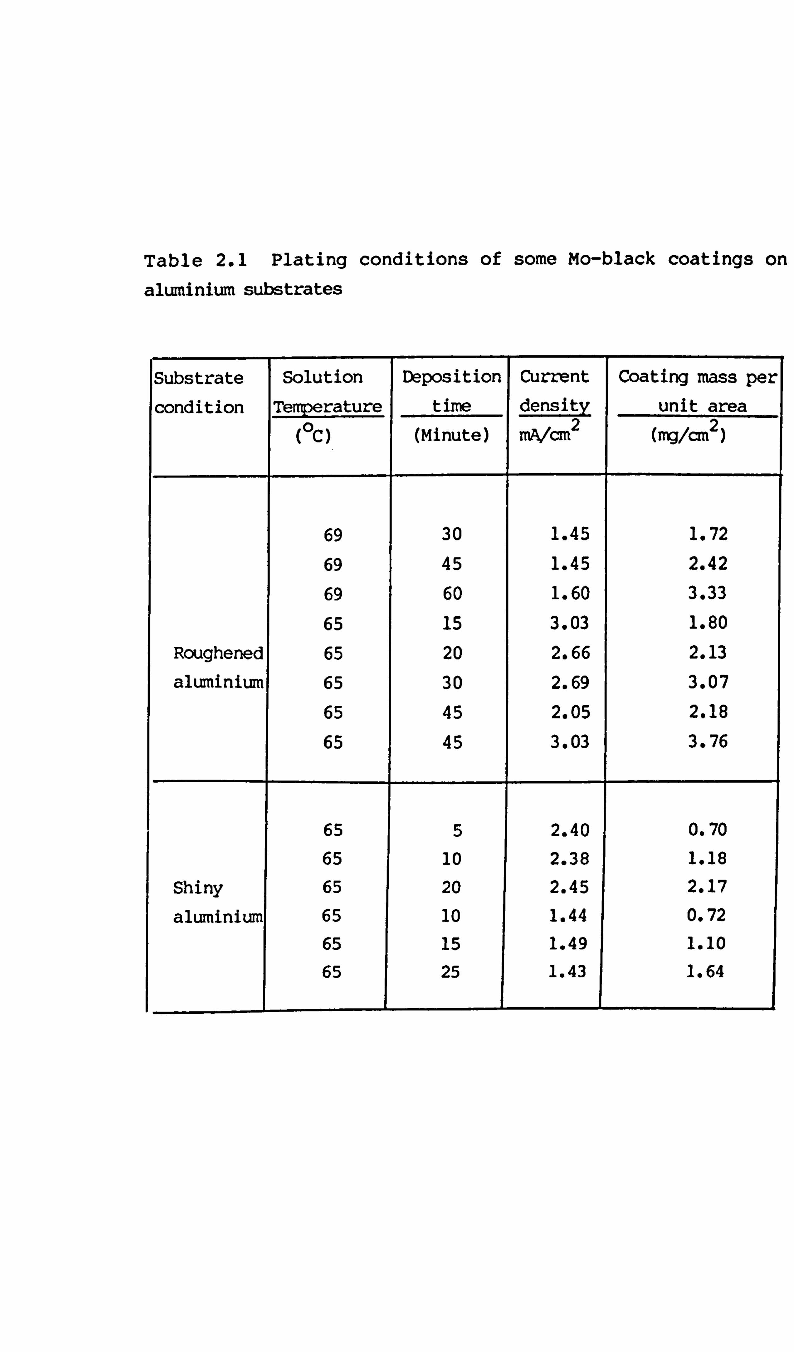
Table 2.1 Plating conditions of some Mo-black coatings on
aluminium substrates
Substrate Solution Deposition Current Coating mass per
condition Temperature time density unit area (, C)- (Minute) mA/am
2 (mg/cm 2)
69 30 1.45 1.72
69 45 1.45 2.42
69 60 1.60 3.33
65 15 3.03 1.80
Roughened 65 20 2.66 2.13
aluminium 65 30 2.69 3.07
65 45 2.05 2.18
65 45 3.03 3.76
65 5 2.40 0.70
65 10 2.38 1.18
Shiny 65 20 2.45 2.17
alurninium 65 10 1.44 0.72
65 15 1.49 1.10
65 1
25 1
1.43 1
1.64 1
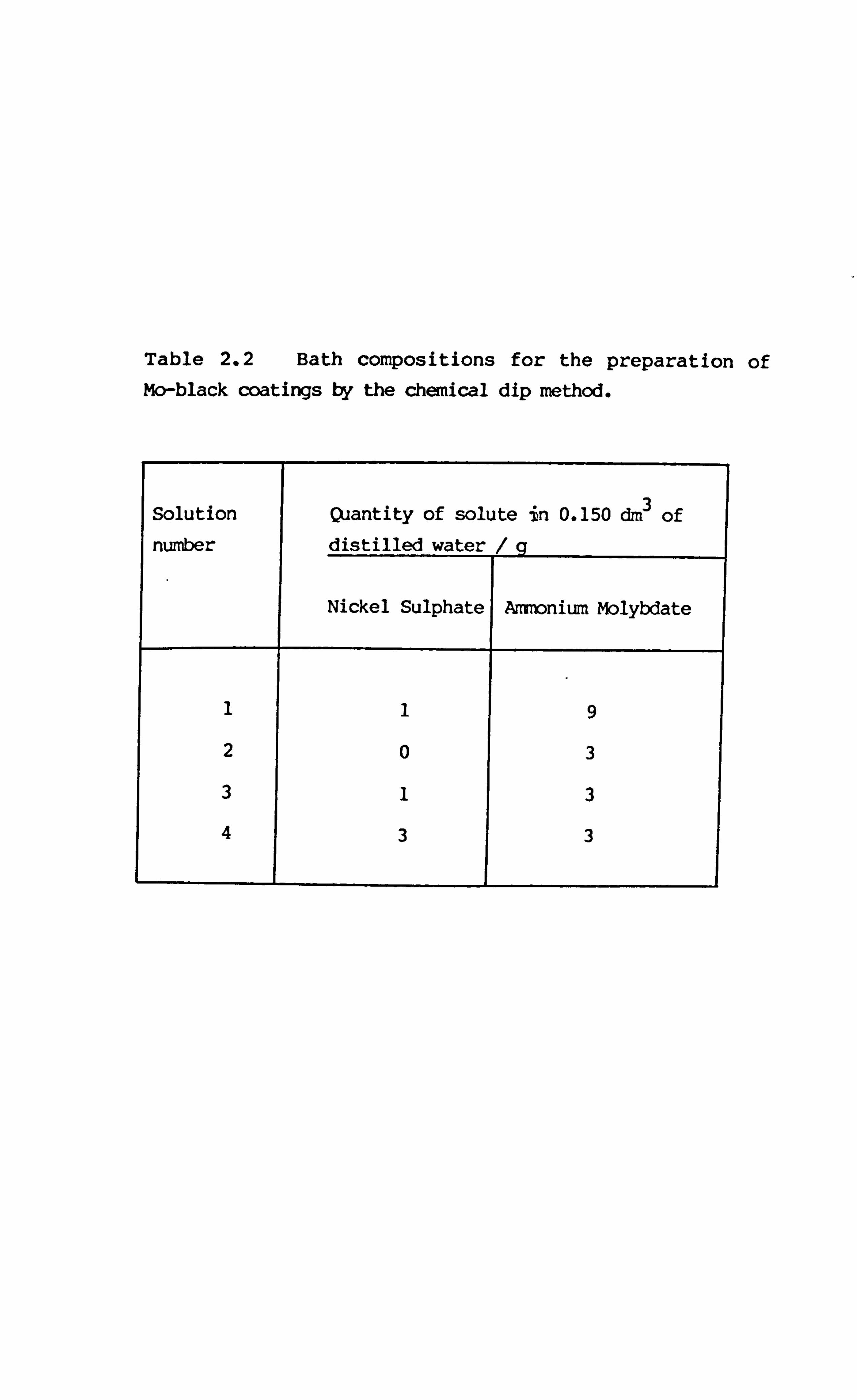
Table 2.2 Bath compositions for the preparation of Mo-black coatings by the chemical dip method.
Solution Quantity of solute in 0.150 din 3 of
number distilled water
Nickel Sulphate Ammonium Molybdate
119
203
313
433
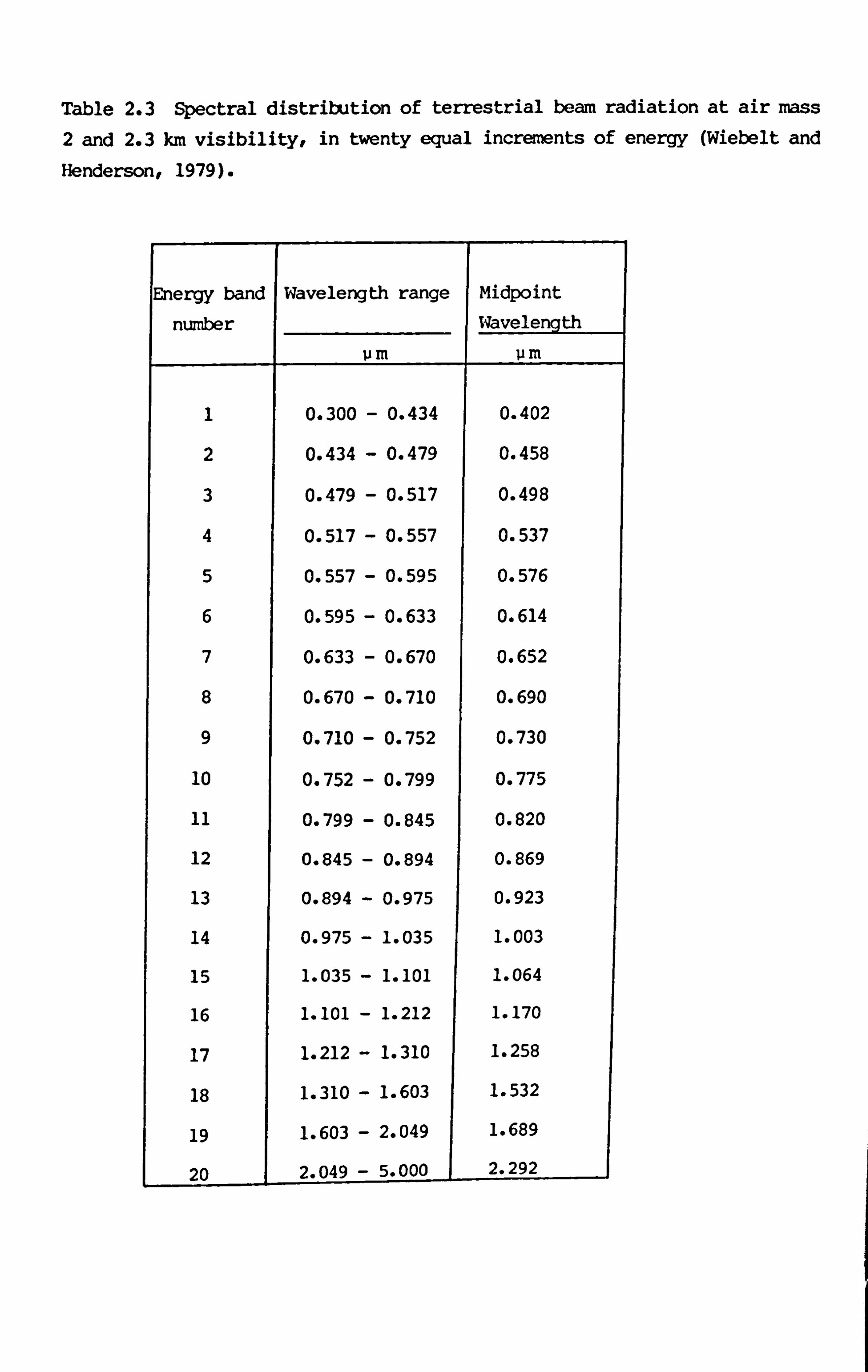
Table 2.3 Spectral distribution of terrestrial beam radiation at air mass 2 and 2.3 km visibility, in twenty equal increments of energy (Wiebelt and
Henderson, 1979).
Energy band
number
Wavelength range Midpoint
Wavelength
11 m 11 m
1 0.300 - 0.434 0.402
2 0.434 - 0.479 0.458
3 0.479 - 0.517 0.498
4 0.517 - 0.557 0.537
5 0.557 - 0.595 0.576
6 0.595 - 0.633 0.614
7 0.633 - 0.670 0.652
8 0.670 - 0.710 0.690
9 0.710 - 0.752 0.730
10 0.752 - 0.799 0.775
11 0.799 - 0.845 0.820
12 0.845 - 0.894 0.869
13 0.894 - 0.975 0.923
14 0.975 - 1.035 1.003
15 1.035 - 1.101 1.064
16 1.101 - 1.212 1.170
17 1.212 - 1.310 1.258
18 1.310 - 1.603 1.532
19 1.603 - 2.049 1.689
20 2.049 - 5.000 2.292
CHAPTER III
EXPERIKENTAL RESULTS AND
INTRODUCMRY ANALYSIS
The experimental techniques used in the present work have been described
in Chapter II. For the sake of clarity, in this chapter, the results of
these experiments are presented separately with only a brief analysis. A
complete discussion of the results will be presented in Chapter V.
3.1 Spectral reflectance, solar absorptance ( a. ) and thermal emittance
of coatinqs and substrates
Spectral reflectance rwasurements, of Mo-black coatings have been carried
out on different substrates and the effects of variables controlling the
preparation of the coatings on the absorptance, and emittance have been
examined. The coatings on zinc and cobalt substrates have been studied in
detail unlike those on alurninim which are effectively non-selective.
Solar absorptance has been determined from measurements of the total
spectral reflectance (Section 2.2.1) for the solar region 0.3 to 2.5 vm.
Generally the thermal emittance of the coating has been determined from
specular reflectance measurements (Section 2.2.2) in the range 2.5 to 50
v M. The thermal emittance of scme coatings has also been determined by
using a thermopile (Section 2.2.2).
42
3.1.1 Mo-black diD coatinas on zinc substrates
A number of factors relating to the preparation of Mo-black dip coatings
on zinc substrates have been studied with reference to their effects on
solar absorptance and thermal emittance. The factors are as follows:
solution concentration, solution temperature, substrate pretreatment and
coating mass per unit area (i. e., thickness).
Table 3.1.1 shows the effects of variation of nickel sulphate
concentration on absorptance and emittance of the coatings. All coatings
were prepared at a terrperature of 450C on mechanically polished
substrates. The addition of a small amount of nickel sulphate enhanced
the solar absorptance with only a small increase in thermal emittance.
The solution having 1g nickel sulphate (in 0.15 dm 3 of distilled water)
gives better selective properties than the other solutions i. e., led to
reasonable absorptance values with a good selectivity factor as/C th (Table 3.1.1).
The total reflectance spectra in the range 0.3 to 2.5 Um for three
Mo-black coatings (of different thicknesss) on mechanically polished zinc
are shown in Fig. 3.1.1. Interference peaks are present throughout the
solar region except in the UV region (below about 0.4 tim). The height of
the interference peaks reduces as the coating thickness increases. For
the thickest coating no peaks can be seen in the region below 0.7 Pm.
Figs. 3.1.2(a) and (b) show the spectral total reflectance spectra of
Mo-black coatings on chemically etched zinc substrates for different
thicknesses (i. e., different coating mass per unit area). No interference
peaks are present in the region below 0.7 11 m except for the thinner
coatings (-0.10 - 0.151im), where one peak can be seen having a maximum at
43
about 0.7 jim. The coatings have their lowest reflectance ordinarily in
the UV and visible region. For all coatings an interference minimum is
present in the region f ram 0.8 to 1.1 P m. This minimum does not shif t
much towards the higher wavelengths as the coating thickness increases.
After this minimum, the transition takes place between low and high
reflectance. In the near infrared, the reflectance decreases as coating
thickness increases and optical interference peaks are observed in the
reflectance spectra of thicker coatings (Fig. 3.1.2 (b)). 11he values of
ccrnputed solar absorptance as of dip coatings on both type of substrates
(etched and unetched) zinc are given in Table 3.1.2 for different coating
massper unit area.
The thermal emittances of the coatings were determined from the IR
specular reflectance in the region 2.5 - 50 vm and are given in Table
3.1.2. The IR specular reflectance spectra of the coatings on unetched
and etched zinc substrates for different coating thicknesses are shown in
Figs. 3.1-3 and 3.1.4 respectively. In both casest as the coating
thickness increases, the IR reflectance decreases i. e., the emittance
increases which is also evident from Table 3.1.2. The thinner coatings
(thickness below - 0.2 jim) appear to be transparent to the IR radiationt
i. e., thermal radiation is reflected from the substrate resulting in high
reflectance throughout the IR region. As the coating thickness increases,
the film become opaque to infrared radiation and the emittance increases.
For the thickest coating strong and broad absorption bands frci, 10.5 to
22.0 vim can be seen in Fig. 3.1.4(b). The absorption peaks at 2.9 - 3. ltjm
and at about 6.2 pm indicate the presence of water in the coatings
(Nakamoto, 1970).
Comparison between thermal emittances obtained by using thermopile
(Section 2.2.2) and from the IR specular reflectances can be seen in Table
44
3.1.3(a). The emittances determined using the thermopile are somewhat
lower than those obtained fran IR reflectance measurements. This
discrepancy may be due to the exclusion of diffuse component of the IR
reflectance as the instrument used was designed for measurement of
specular reflectance only. The emittance of some samples determined
from IR reflectance spectra is compared to that determined by a
calorimetric method (Appendix C) by Yousif (1987). The results are given
in Table 3.1.3(b) and show better agreement. However, emittances of the
coatings determined by calorimetric method are lower than those obtained
from IR reflectance.
The variations of solar absorptance and thermal emittance of the dip
coatings with coating mass per unit area are shown in Figs. 3.1.5 (a) and
(b) for etched and non-etched zinc substrates respectively. The emittance
and absorptance values are thickness dependent for coatings on both type
of substrates but the emittance is more thickness dependent than the
absorptance. On etched zinc substrates,, the absorptance first increases
frcm 0.79 to 0.87 with the increase of coating mass per unit area, while
the increase in emittance is smaller. After that the emittance increases
more rapidly with coating mass and the absorptance decreases slightly and
then goes to the maximum value. (Data for the thickest coating is not
included in Fig. 3.1-5 (a), see Table 3.1.2 (a)).
The highest selectivity factor (as/C th '2 8.78) is obtained for the
thinnest coatings on etched zinc although the absorptance for this coating
is the lowest (0.79) (Table 3.1.2(a)). On unetched substrates, the
highest value of absorptance is 0.78. The highest selectivity factor
obtained is 9.86 (Table 3.1.2 (b)) for the thinnest coating. Fig. 3.1.5(c)
shows the variation of selectivity factor as/ e th Of the coating with
45
coating mass per unit area. The values of a/C are slightly higher s th
for coatings on unetched substrates (especially at low coating mass). As
the coating mass increases, the selectivity factors approach the saine
value for both type of substrates (Fig. 3.1.5(c). In both cases the
selectivity factor decreases with the coating mass per unit area, as the
emittance gradually increases with the coating mass but the absorptance
does not change so much.
The effect of substrate pretreatment on the spectral reflectance spectra
of Mo-black dip coatings is illustrated in Fig. 3.1.6. The corresponding
values of as and 6 th are tabulated in Table 3.1.4. Chemical etching of
the zinc substrate enhances the absorptance of the coatings considerably
with only a small increase in emittance. Table 3.1.4 also shows that
etching of zinc substrates with 50% HNO 3 acid gives the highest value of
absorptance (0.89) but the emittance is also high (0.30). However, best
values of as and F- th are obtained after etching with 30% HNO 3' though
a/E has a value of 5.7 which is somewhat lower than the value (7.6) for S th
coatings on highly polished zinc (11i m finish). It is shown in section
(5.3) that the selectivity factor is not the primary factor to
characterize a selective surface (unless as >' 0.90).
The effect of solution temperature on aS and c th of the coatings was
examined and the results are shown in Table 3.1.5. The solution
temperature has no significant effect on the radiative properties of the
coating in the range 350 - &C. At 5ýOC, however, the absorptance is
lower and emittance is higher than for the coatings prepared at lower
temperature. This may be due to the change in thickness of the coatings,
as the rate of deposition increases with the solution temperature
(Fig. 2.3). As described earlier, the absorptance decreases slightly after
a certain critical thickness but the emittance increases continuously with
46
thickness.
3.1.2 Mo-black dip coatings on cobalt (NC) substrates
A range of Mo-black coatings on electroplated cobalt on nickel plated
copper substrates has been studied. Both the plating conditions of
cobalt and preparation of the Mo-black coatings influence the absorptance
and emittance of these coatings. Several parameters have been varied to
yield an absorber with the best optical properties. Table 3.1.6 shows
scme plating conditions of cobalt substrates as well as Mo-black coatings.
The values of a st
C th and as/C th are also listed in Table 3.1.6. This
shows that the highest absorptance value obtained from these coatings is
0.94 with an emittance of 0.28 - 0.33. These coatings have high
absorptance but due to the high emittances (Table 3.1.6) the selectivity
factor as/ cth is not high enough. (The highest selectivity factor
obtained is 4.1 with as=0.90). The emittance of the coatings increases
with the plating time of cobalt and also deposition time of Mo-black. Use
of an addition agent (Na-lauryl sulphate) in the plating solution of
cobalt was found to influence the values of as, and c th of the coatings
(Table 3.1.7). The eznittance values obtained with use of the addition
agent (Table 3.1.7) are significantly lower than those in Table 3.1.6,
while the absorptance drops slightly to (0.90 - 0.91). The highest
selectivity factor obtained for these coatings is 11.0 for 3 minutes
dipping time in Mo-black plating solution. The spectral reflectance
spectra in the range (0.3 - 2.5 jim) for Mo-black coatings on cobalt (NC)
substrates plated with and without addition agent are shown in Fig. 3.1.7.
Throughout the solar region, no interference peak can be seen except a low
broad hump in the 1.1. to 1.5)Am region. Fig. 3.1.7 also shows that the
coatings on cobalt (NC) without addition agent have lower reflectances
than those prepared with an addition agent. The IR specular reflectance
47
spectra in the range 2.5 - 50 = of the same two coatings are displayed in
Fig. 3.1.8.
The effect of dipping time and solution temperature on as, and c th has
been studied for Mo-black coatings on cobalt substrates plated with
addition agent (Table 3.1.8). The table shows that better values of a S,
and as/C th are obtained at a paramolybdate solution temperature of 660C,
rather than 8dOC. The absorptance and emittance of the coatings (formed
at 660C) plotted as a function of dipping time are shown in Figure 3.1.9.
The absorptance aS varies only slightly with dipping time while the
emittance varies significantly. The best values of a and E: are s th
obtained for a deposition time of 5 minutes with selectivity factor
(A /C=9.1 (Table 3.1.8). If the deposition time is below 5 minutes, s th
the coating is not sufficiently absorbing. When the deposition time is
higher than 5 minutes, the absorptance (I s decreases slightly and the
ernittance E th increases signif icantly. The rise of emittance with the
dipping time may be due to the increase of thickness.
Figs. 3.1.10(a) and N show the IR specular reflectance spectra in the
range 2.5 - 50 um for Mo-black coatings prepared at 60 0C and 800C
respectively. It can be seen from the figures that as the time of
deposition increases, the IR reflectance decreases i. e., the emittance
increases. The thickness of the coatings (which increases with the
deposition time) is affecting the transmittance in the IR region resulting
in an increase in emittance. The IR reflectance also decreases with the
rise of solution temperature for the same time of deposition (Fig. 3.1.11).
The two sets of total ref lectance spectra in the range of 0.3 - 2.5 Ij m of
Mo-black coatings on cobalt (NC) substrates prepared at 60 0C and 860C are
shown in Figs. 3.1.12 and 3.1.13 respectively. Interference peaks appear
48
in the region above 0.7, um and these are more prominent for the coatings
prepared at 800C. The number and height of the maxima tend to increase
with the increase of dipping time and temperature of the solution except
for the thinnest coating (deposition time 3 minutes) prepared at 60 0 C.
Ihis behaviour accounts for the slight decrease of solar absorptance with
the increase of dipping time above 5 minutes and also with the rise of
solution tenperature. The spectral reflectance of plated cobalt substrate
(with addition agent) on nickel plated copper has also been studied and is
given in Fig. 3.1.14. The value of solar absorptance obtained from the
cobalt substrate is 0.56.
Fig-3.1-15 shows another set of spectral reflectance spectra in the solar
region for Mo-black dip coatings on plated cobalt (NC) prepared under
different conditions. The results obtained from these coatings are
tabulated in Table 3.1.9 with their preparation conditions. The spectral
reflectance spectra show that these coatings behave as a grey surface in
the solar region, i. e., the reflectance does not change significantly
throughout the solar region and it is low resulting in high absorptance.
These coatings have high IR reflectance (Fig. 3.1.16) resulting in low
emittance. The highest selectivity factor obtained from these coatings is
10.1 with solar absorptance of 0.91 (Table 3.1.9). Long deposition time
of Mo-black does not affect the emittance of the coatings. These coatings
were prepared at a relatively high pH value (3.2), which may reduce the
deposition rate of Mo-black coatings (low deposition rate was also evident
from the conversion colour of molybdate solution during preparation).
These cobalt substrates were prepared at relatively low temperaturest with
low current density for short times (Table 3.1.9).
49
3.1.3 Electrodeposited Mo-black coatings on alLuninium substrates
The total reflectance spectra in the range 0.3 to 2.51im for four coatings
on aluminium substrates of different thicknesses are shown in Fig. 3.1.17.
As the thickness of the coatings increases, the reflectance decreases
(especially in the near infrared region) and the transition shifts towards
longer wavelengths. As a result the absorptance as increases with coating
thickness. No interference peaks have been observeL: M the reflectance
spectra of the coatings (Fig. 3.1.17). Fig. 3.1.18 shows the variation of
absorpta, -. k,. e and emittance of the coating with coating mass per unit area.
Both the absorptance and emittance of the coating increase with coating
mass but the emittance is more thickness dependent than the absorptance.
The absorptance appears to reach a limiting value in the range of 0.86 -
0.87, whereas, the emittance is still increasing with thickness but
appears to be less dependent at higher thicknesses. Fig. 3.1.19 shows
specular reflectance spectra of the coatings and the aluminium substrate
in the range 2.5 to 50 um. Though the substrate has a relatively high
reflectance, there is strong absorption in the coating material.
Absorption bands for water around 2.9 - 3.1 Pm and at about 6.2 um
(Nakamoto, 1970) are also present. The values of asIC th and aS /C th are
coating given in Table 3.1.10 with corresponding 1 masses per unit area. This table
shows that electrodeposited Mo-black coatings on aluminium substrates are
not significantly selective (a s/Eth
< 2). The observed non-selectivity
of the coatings may be due to the strong absorption in the infrared region
resulting in high emittance.
3.1.4 Mo-black coatings on various additional substrates
Mo-black coatings prepared on vacuum evaporated aluminium (on rough
glass), galvanized steel and cobalt plated aluminium have also been
50
Studied. Results obtained from these coatings are given in Table 3.1.11.
A. Aluminized glass
Mo-black coatings were prepared by the electrodeposition method on
aluminium coated glass. Before deposition of aluminium, the glass
substrates were ground with silica carbide powder (without grinding,
aluminium film diffused into the Mo-black coatings) and cleaned properly
as described in section 2.5. The ground glass substrates were then coated
with a conducting aluminium layer produced by vacuum evaporation in a
Balzers BA510 coating unit under a pressure of about 10-4 Pa using
aluminium wire on a tungsten spiral as a source. The spectral reflectance
spectra of these coatings (Fig. 3.1.20. ) are quite similar to those
obtained from coatings on aluminium sheet (Fig. 3.1.17). The highest
absorptance obtained from these coatings is 0.88 (Table 3.1.11). Due
to the roughness of the substrate and also the high thickness of the
MD-black coatings, the emittance is very high. Fig. 3.1.23 shows the
specular IR reflectance of one coating which is rather low, resulting
in high emittance. No further study, therefore has been done on these
coatings.
B. Galvanized steel
on galvanized steel substrates, Mo-black coatings were prepared by a
chemical dip method (similar to the case Of zinc substrates). The
spectral reflectance spectra of these coatings are shown in Fig. 3.1.21.
The reflectance decreases with the time of deposition giving higher
absorptance. However, these coatings also have low specular reflectance
in IR region (Fig. 3.1.23). The values of solar absorptance obtained in
these coatings are consistent with those obtained by Hosseini (1981) and
Agnihotri et al (1983).
51
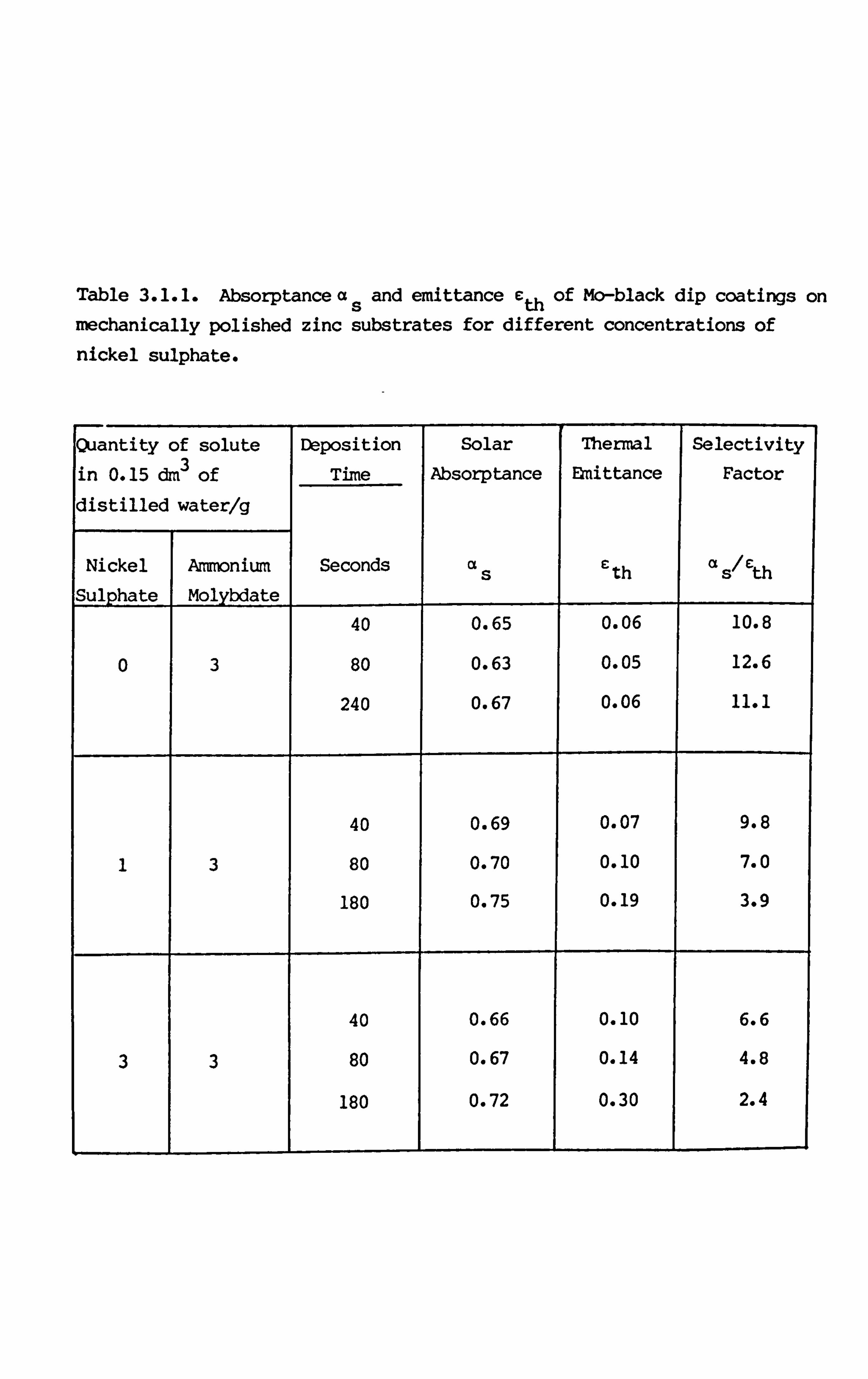
Table 3.1.1. Absorptance aS and emittance e th of Mo-black dip coatings on
mechanically polished zinc substrates for different concentrations of
nickel sulphate.
Quantity of solute Deposition Solar Thermal Selectivity
in 0.15 dm 3 of Time Absorptance Emittance Factor
distilled water/g
Nickel Ammonium Seconds as th a s/cth Sulphate Molybdate
40 0.65 0.06 10.8
0 3 80 0.63 0.05 12.6
240 0.67 0.06 11.1
40 0.69 0.07 9.8
1 3 80 0.70 0.10 7.0
180 0.75 0.19 3.9
40 0.66 0.10 6.6
3 3 80 0.67 0.14 4.8
180 0.72 0.30 2.4
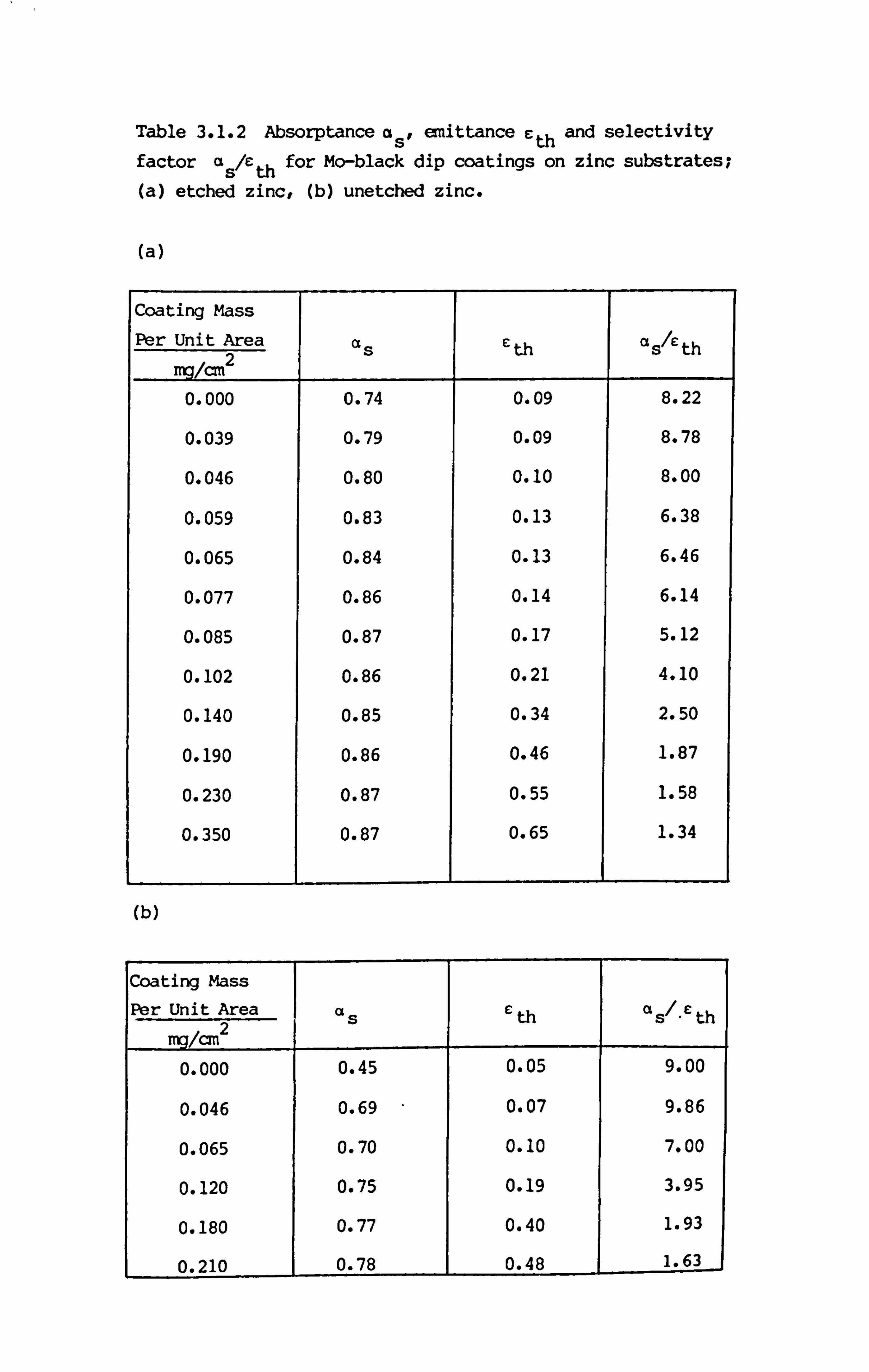
Table 3.1.2 Absorptance as, emittance e th and selectivity factor a s/eth
for Mo-black dip coatings on zinc substrates; (a) etched zinc, (b) unetched zinc.
(a)
Coating Mass
Per Unit Area
mg/cm 2
as cth as/eth
0.000 0.74 0.09 8.22
0.039 0.79 0.09 8.78
0.046 0.80 0.10 8.00
0.059 0.83 0.13 6.38
0.065 0.84 0.13 6.46
0.077 0.86 0.14 6.14
0.085 0.87 0.17 5.12
0.102 0.86 0.21 4.10
0.140 0.85 0.34 2.50
0.190 0.86 0.46 1.87
0.230 0.87 0.55 1.58
0.350 0.87 0.65 1.34
(b)
Coating Mass
Per Unit Area a c th as/. c th mg/cm
2 s
0.000 0.45 0.05 9.00
0.046 0.69 0.07 9.86
0.065 0.70 0.10 7.00
0.120 0.75 0.19 3.95
0.180 0.77 0.40 1.93
0.210 0.78 0.48 _1.63_j
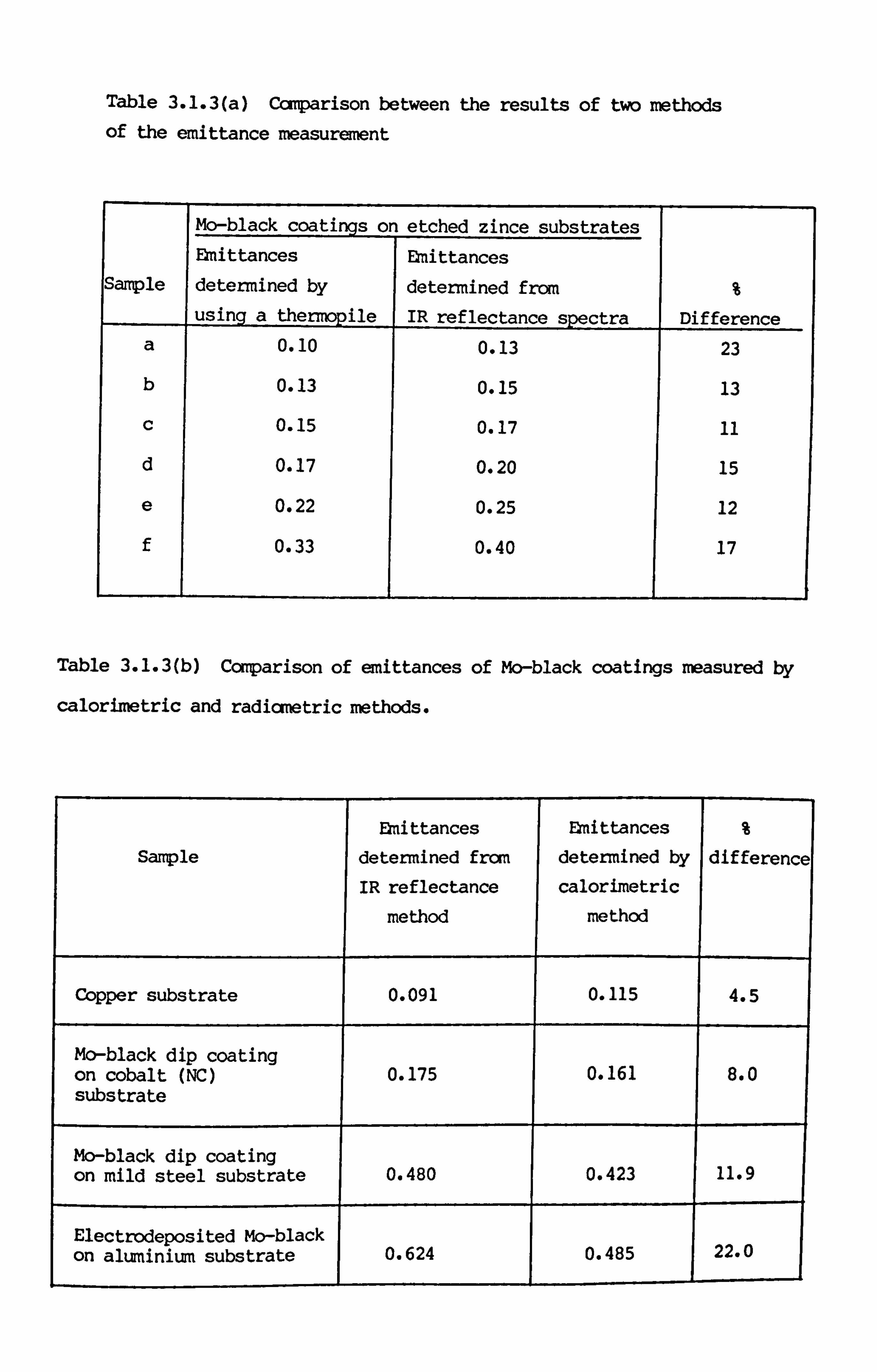
Table 3.1.3(a) CaTparison between the results of two methods of the emittance measurement
Mo-black coatings o etched zince substrates Emittances Emittances
Sarrple determined by determined from % using a thermopile IR reflectance spectra Difference
a 0.10 0.13 23
b 0.13 0.15 13
c 0.15 0.17 11
d 0.17 0.20 15
e 0.22 0.25 12
f 0.33 0.40 17
Table 3.1.3(b) Comparison of emittances of Mo-black coatings measured by
calorimetric and radicmetric methods.
Emittances Emittances %
Sample determined from determined by difference
IR reflectance calorimetric
method method
Copper substrate 0.091 0.115 4.5
Mo-black dip coating on cobalt (NC) 0.175 0.161 8.0 substrate
Mo-black dip coating on mild steel substrate 0.480 0.423 11.9
Electrodeposited Mo, -black on aluniniLm substrate 0.624 0.485 22.0
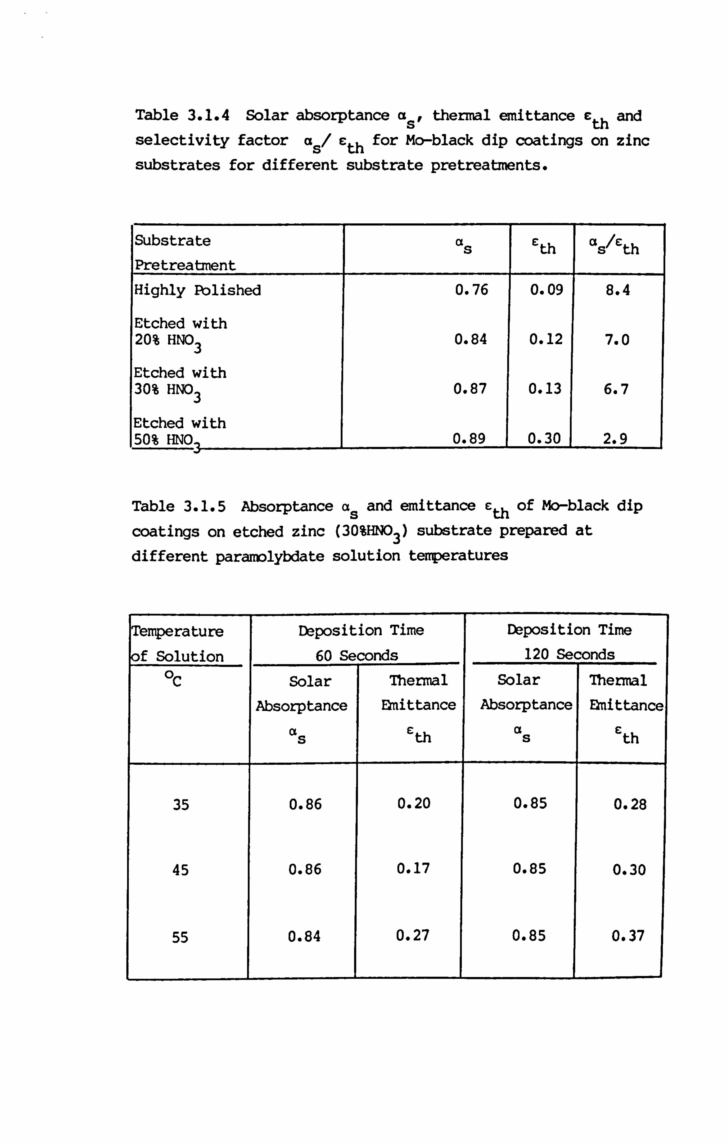
Table 3.1.4 Solar absorptance as , thennal emittance e th and selectivity factor as/C th for Mo-black dip coatings on zinc substrates for different substrate pretreatments.
Substrate Pretreatment
as C th as /C th
Highly Polished 0.76 0.09 8.4
Etched with 20% HNO 3 0.84 0.12 7.0
Etched with 30% HNO 3 0.87 0.13 6.7
Etched with 50% HNO, 0.89 0.30 2.9
Table 3.1.5 Absorptance aS and emittance c th of Mo-black dip
coatings on etched zinc (30%HNO 3) substrate prepared at
different paramolybdate solution tenperatures
Temperature
of Solution
Deposition Time
60 Seconds
Deposition Time
120 Seconds OC Solar Thermal Solar Thermal
Absorptance Ehittance Absorptance &nittance
as C th as C th
35 0.86 0.20 0.85 0.28
45 0.86 0.17 0.85 0.30
55 0.84 0.27 0.85 0.37
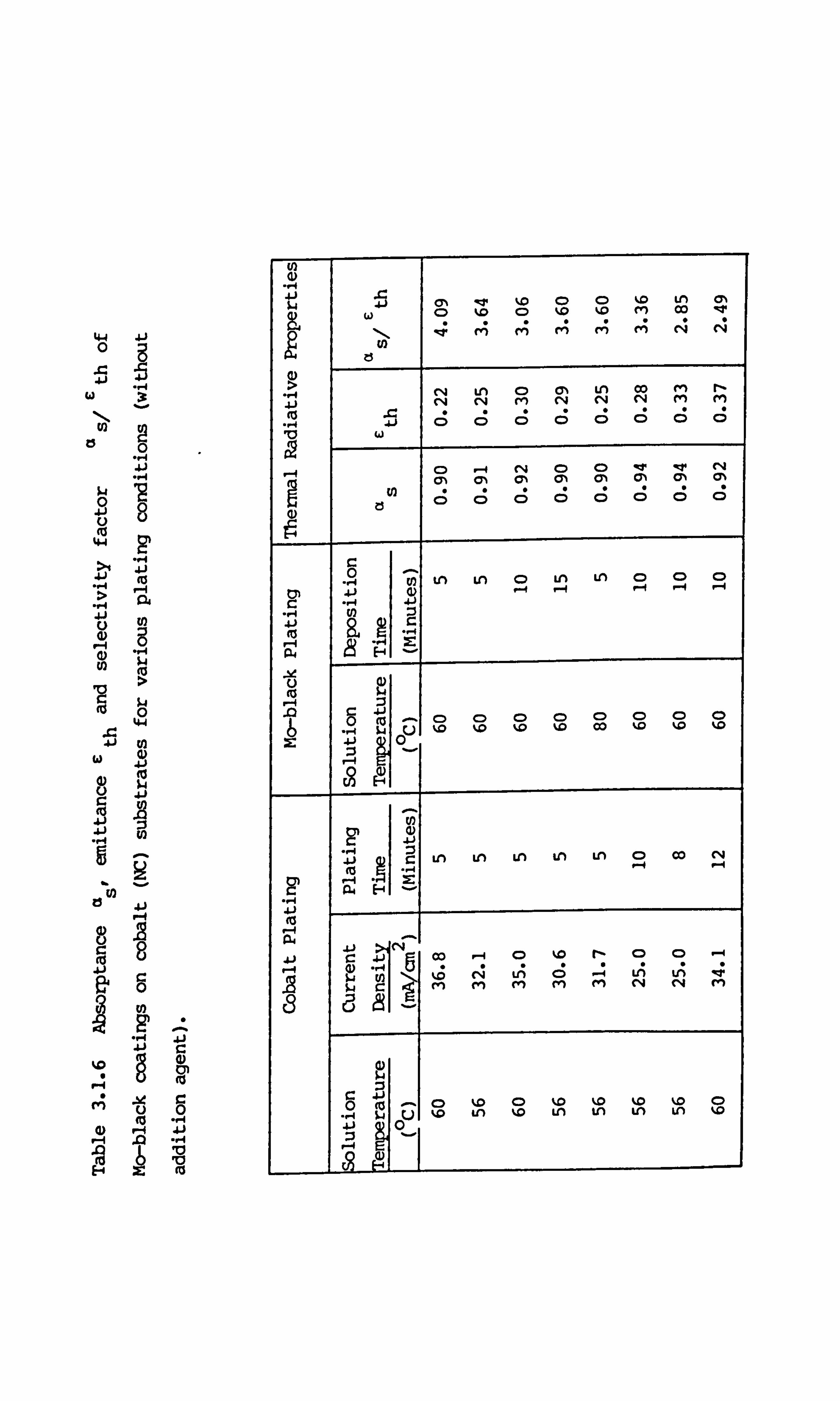
4.4 4-) 0
0
8
-4.1 tö . -1 > r--4
0 to
0
tn
1F -*
E-4 Z fö
N4 9 (i (D %0 CD %0 %0 (n OD le
lýI '; '; '; '; '; fý
? .f rq Ln (D Ln Co en r-
. 43 rq fö C
c; c; c; c; c; c5 c;
CD -4 rY (D r, 4 0) cý 0, % 0,1 011 C% (n Cl% 1
(0
c; c; c; c; :; c; c; ei 0)
0 tn Ln (D Ln Ln CD C> CD
.H to 2 4. ) fö m r-1 . Z: p4
2 to
- c2 C: ) CD CD (D (D C)
1 ou %D %0 %D Co
W -4 Z ý J,
U-) LM Ln in Ln CD Co r4 tu . ". d 1-4 -4
24
E.
(0 4
1
t24 - > r4
c2 CD ýo r- CD
.2 N, Co ý t. 0 ri
C, 4 cm LA cyl
Ch ri
-4 CM
Ln c4 u; r4 m
-4 U %0 in %D Ln in in %D Ln
0 4. D
0
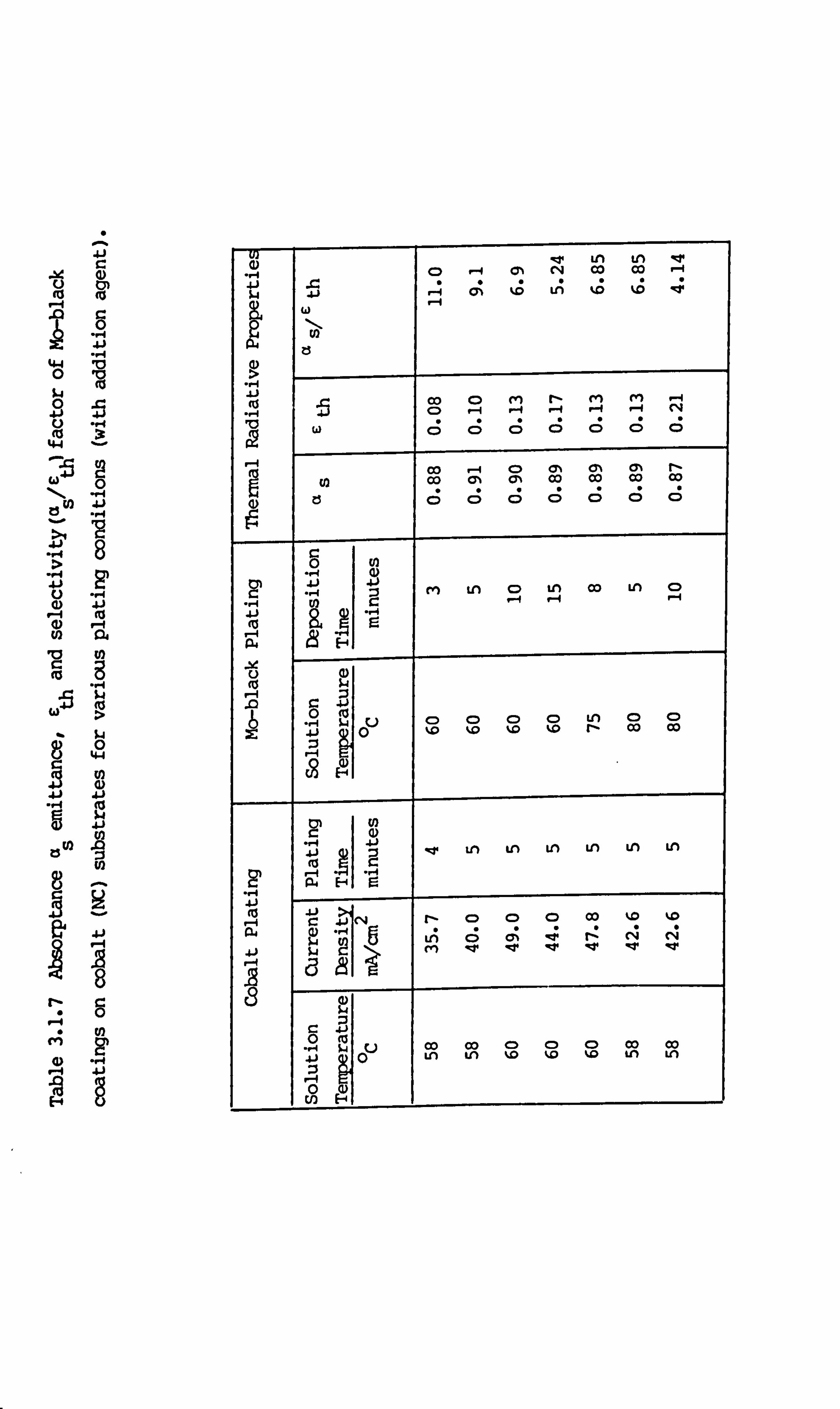
0 4.1
C) o 0)
0 10
44
-: ý, 2
P-4 tu 9) r-f to r14
12 to
to 8
0 44 9
.92
41
ts LO
to
41
M2
ER
ul a) "T Ln Lf) IV . r. 0 (D 1-4 ON cli co co r-I 4J
41 CYN %D U; -Z
(A)
ra
4J cri CC) 0 m 1ý m m 1-4
1 :5 (D P-4 . -1 -4 r-f ? -f C 4 va
12 W 6
C; C; C; c; C; 8
co -4 C) 43N (31, C31, U) Cý Cý Cý Cý Cý
C3 C) Cý C) C) C) C)
B 4J
m Ln C> Ln a) Ln (D U) 41
l 04 E
-%d 0
, CD CD CD C) Ln CD CD 41 Cý tD %0 %D %0 r- OC) co
41 -cr Ln tn tn Ln Ln Ln
'Clil F-4
r-4 "i
" r- Cý 0 "') 'o 140
LA C; Cý
IT IMT 1'ý
-41
C4
qw
C4
I-W 41
8 2 ý co 00 CD CD Cý co co
Cý in LO r 0
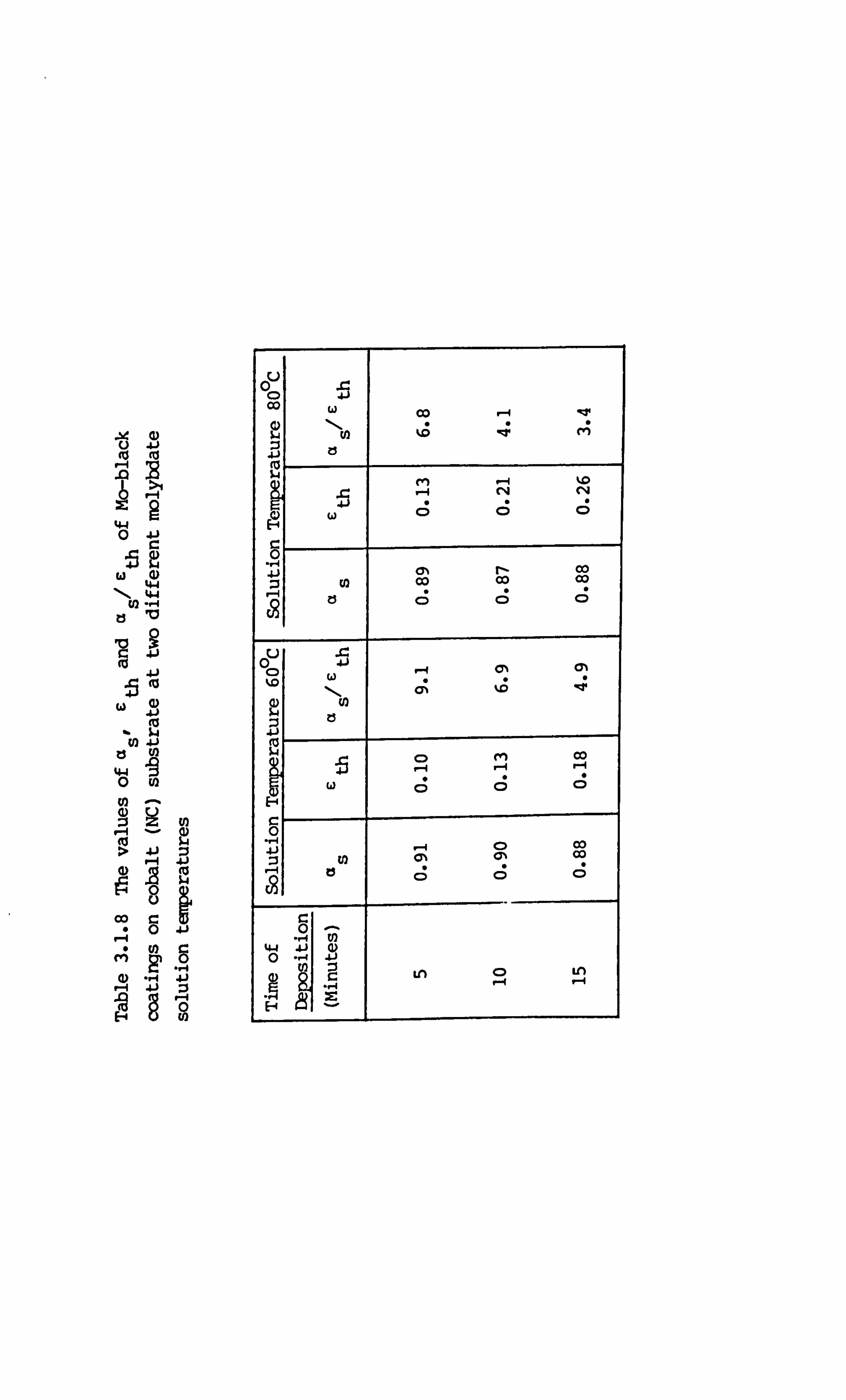
tu tu
zi 10
fi tu
Z$ to
44 -9 0
Co ce
u % 00 (X)
zi zi . c:
C) C)
c: 0
., 4 (n r- 00
Co Co CD 1. ; ?1 c
0-. ID . 41
C) Co
w 0
., 4
41 -4 C) C%
Co 00 Z] (0 C%
1-1
0
0
A
E--4 8
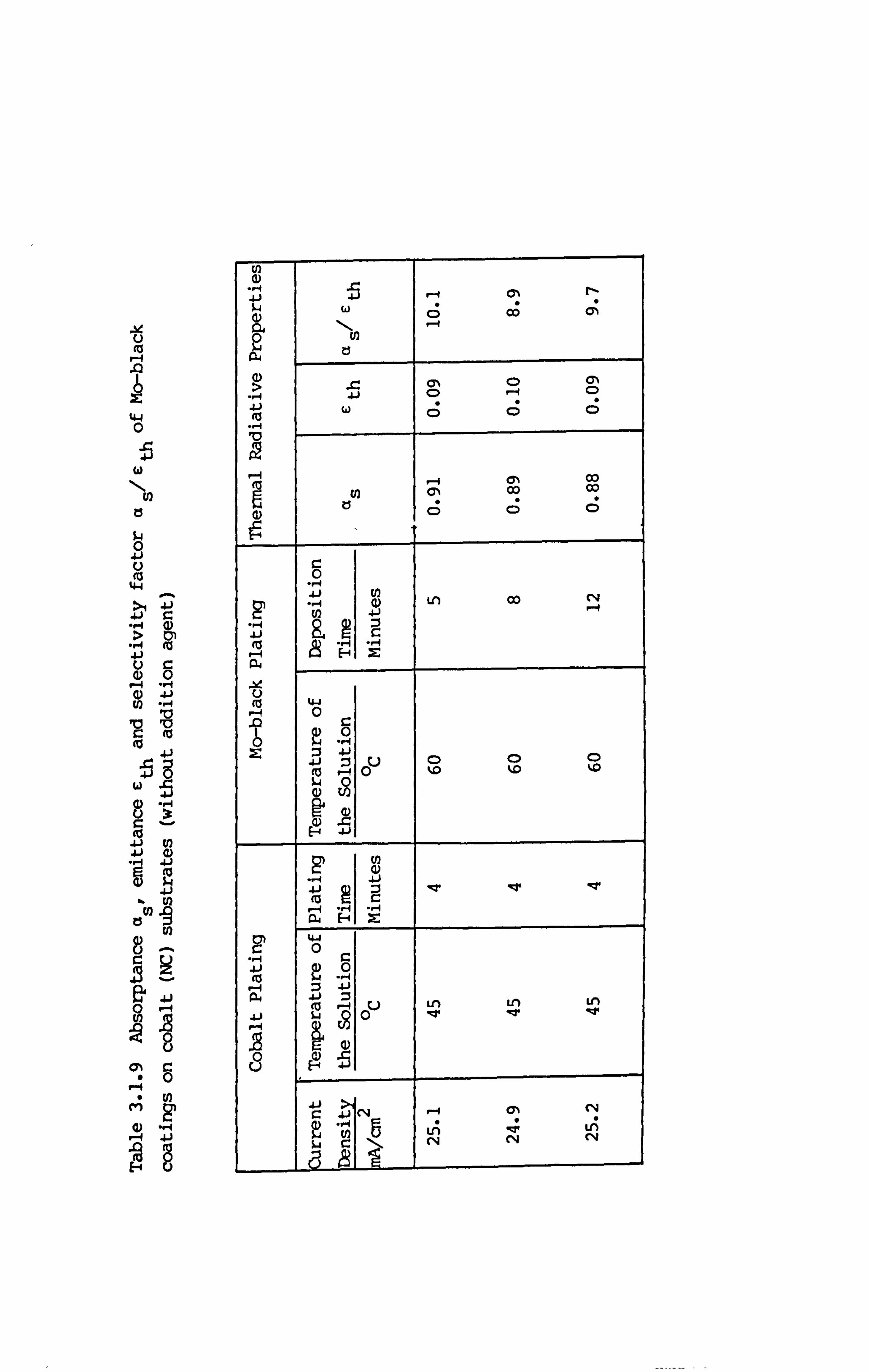
be (o
44 0
(0
'S "Cal
W ., j 4. J
ts
8 D ,i '-4
8 C.,
"0
S (I) m
4u
C;
0)
0) > X
41 ON (3)
41 10
w C) CD 0
(3) 00
00 co
C)
0 41 U) (D
J LO 00 C14
-4 4-
4J
r--l 6 H , 2: C14
(a ti-i 0
0 C) CH
(n 41
4J E (a r1 :3 41 CIO z
4 ý Ln Ln Ln 41
8
8 9
41 CN CA CN tf; CN CN
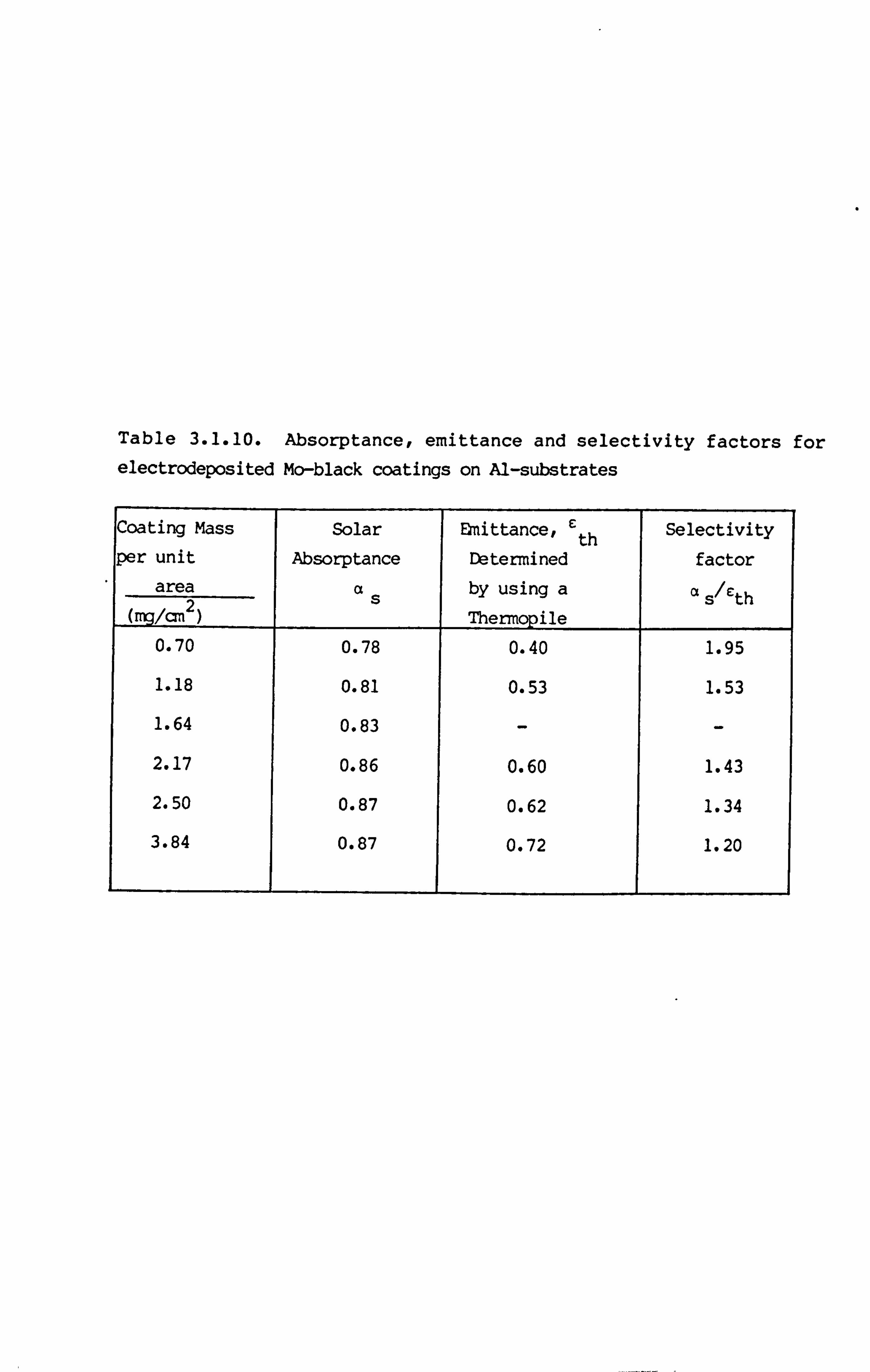
Table 3.1.10. Absorptance, emittance and selectivity factors for
electrodeposited Mo-black coatings on Al-substrates
Coating Mass
per unit
area (mg/an 2)
Solar
Absorptance
aS
Emittance, e th
Datermined
by using a Thermopile
Selectivity
factor
a s/Fth
0.70 0.78 0.40 1.95
1.18 0.81 0.53 1.53
1.64 0.83 - -
2.17 0.86 0.60 1.43
2.50 0.87 0.62 1.34
3.84 0.87 0.72 1.20
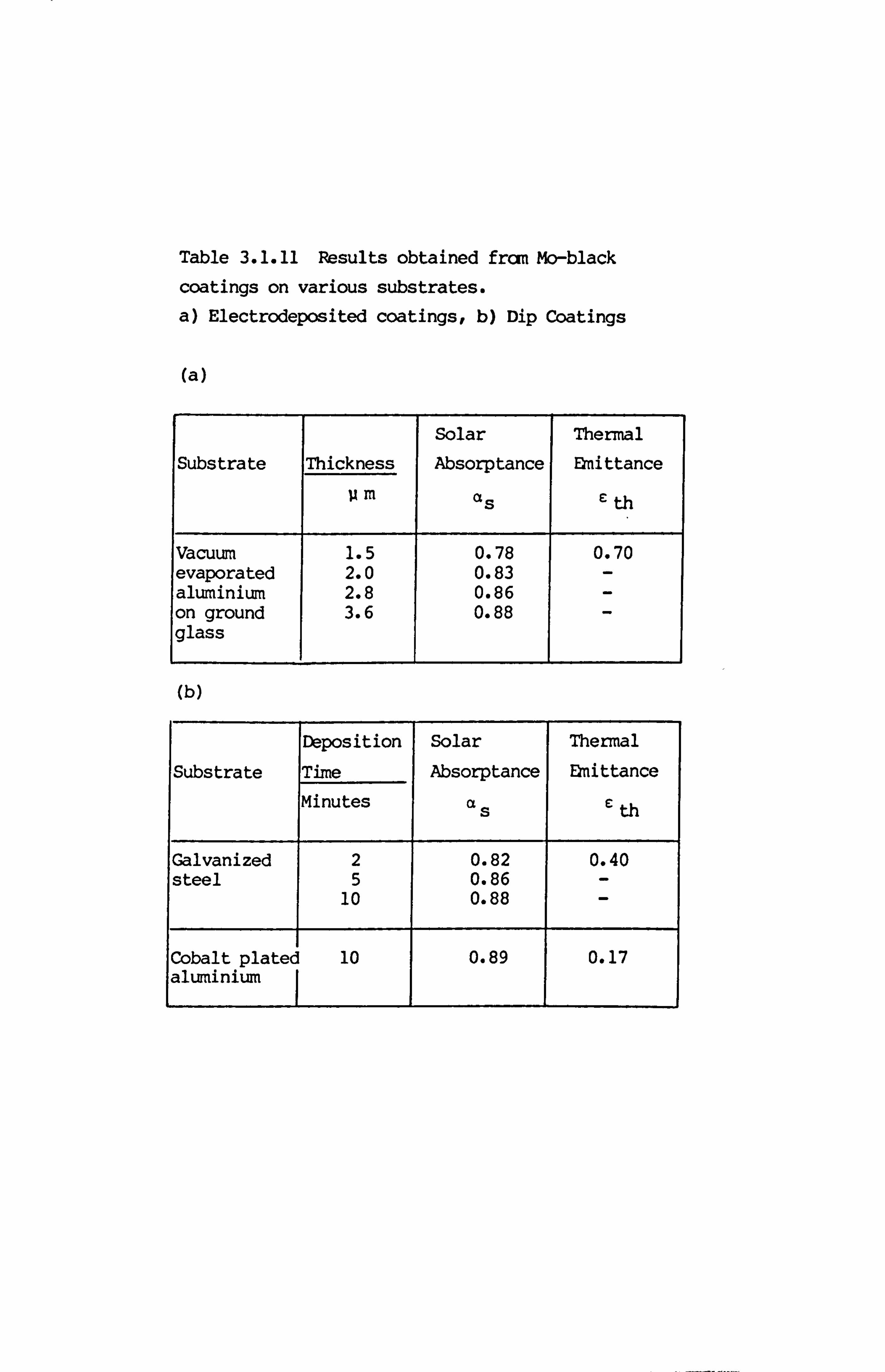
Table 3.1.11 Results obtained frcm Mo-black
coatings on various substrates.
a) Electrodeposited coatings, b) Dip Coatings
(a)
Solar Thermal Substrate Thickness Absorptance Emittance
Vm as th
Vacuum 1.5 0.78 0.70 evaporated 2.0 0.83 - aluminium 2.8 0.86 on ground 3.6 0.88 glass
(b)
Deposition Solar Thermal
Substrate Time Absorptance Emittance
Minutes as c: th
Galvanized 2 0.82 0.40 steel 5 0.86 -
10 0.88 -
Cobalt plateý 10 0.89 0.17 alurninium I
C. Cobalt r)lated aluminiun
The results obtained from Mo-black coatings on cobalt plated aluminiLan are
quite satisfactory (Table 3.1.11). A thin cobalt layer was plated on
aluminiLun sheet using the procedure of section 2.1.2.4. Mo-black coatings
was prepared by chemical dip method (section 2.1.2.5). The coating has
low reflectance in the solar region (Fig. 3.1.22) giving high absorptance
(0-89). In the IR region, the reflectance increases with wavelength
(Fig. 3.1.23) resulting in a low emittance (0.17). The selectivity factor
of this coating is 5.2.
3.2 Scanning Electron Microscopy (SEM) and Electron Probe Microanalysis
(EPMA)
Scanning electron microscopy (SEM) and electron probe microanalysis (EPMA)
techniques have been used to study the microstructure and elemental
compositions of the coatings. In SEM, the secondary electron image (SEI)
has been used for the microstructural examination, while in EM the SEI
and characteristic X-ray images have been employed for spot analysis and
X-ray line scan studies.
A metallographic technique has been employed for cross-sectional
observations using SEM. Scme optical microscopic studies of Mo-black
coatings on zinc substrate have also been performed.
3.2.1 Electrodeposited Mo-black coatings on aluminium
The electrodeposited Mo-black coatings on an aluminium substrate generally
have a microstructure of relatively flat irregular plateletst separated by
prcminent fissures. A similar surface texture has also been observed by
52
(Smith et al, 1981) and (Safi, 1985). Several coatings were observed in
the SE24. The resultant micrographs showed that there are scme differences
in the surface topography of the coatings with different thicknesses. A
typical SEM micrograph of a thick electroplated Mo-black coating (coating
mass per unit area - 3.85 mg/cm 2) is shown in Fig. 3.2.1. The surface
consists of rather smooth and flat platelets with sharp clearly defined
edges. The individual platelets are separated by wide cracks. Fig. 3.2.2
shows a secondary electron micrograph of a thin electroplated coating
(coating mass per unit area - 1.58mg/cm 2 ). It can be seen that the
surface of the coating consists of quasi-hemispheres of different sizes
with relatively narrow cracks. The width of the hemispheres varies from 3
to 20 w. Safi (1985) also reported two types of surface topography as in
Figs. 3.2.1 and 3.2.2.
These features required a more extensive study. Further work has
therefore been carried out using four different coating thicknesses and at
different current densities. The surface topography of Mo-black coatings
of four different thicknesses are shown in Figs. 3.2.3 - 3.2.6. By
comparing these figures, the following features can be observed:
As the thickness of the coating increases, the surface topography
appears more smooth and flat.
(ii) The coating becomes more uniform as the thickness increases. It can
I be observed that a few hemispheres are still present in some areas
of the coating of intemediate thickness (Fig. 3.2.4. b), which my be
due to non-uniformity of the coating thickness.
The width of the cracks, which arise. - frcm stresses in the growing
film, increases with the coating thickness.
53
(iv) As the thickness of the coating increases, the size of the fragments
increases.
No significant change in the surface topography of the coating has been
observed with the plating current density. The secondary electron image
of two coatings of almost equal thicknesses prepared with different
current densities are shown in Figs. 3.2.7 and 3.2.8. There is no
noticeable difference between these two micrographs. The elemental
analysis of the coatings has been performed by an energy dispersive X-ray
analyser (EDX). The resultant EDX patterns of these two surfaces
(Figs. 3.2.7 and 3.2-8) are shown in Figs. 3.2-9 and 3.1-10 respectively and
the corresponding compositional data in terms of mass percentage are given
in Table 3.2-1. The EDX spectrum shows that the coating consists mainly
of molybdenum and a small proportion of nickel. The percentage of nickel
decreases as the plating current density increases. Table 3.2.1 also
shows a small amount of aluminium which may come from the aluminium
substrate through the cracks.
The SEM micrograph of the underside., Mo-black coating (removed from an
aluminium substrate) is shown in Fig. 3.2.11 and the corresponding EDX
spectrum is shown in Fig. 3.2.12. The spectrum shows the presence of
molybdenum and nickel. However, a small amount of aluminium (and iron)
transferred from the substrate can also be seen in the EDX spectra.
3.2.2 Mo-black dip coatings on zinc
A typical surface microstructure of a Mo-black dip coating on mechanically
polished zinc is shown in Fig. 3.2.13. The surface consists of a large
number of smooth irregularly shaped platelets separated by prominent
fissures (i. e. j similar to the electroplated coatings on aluminium). A
54
similar surface structure was also observed by Agnihotri et al (1983) and
Hosseini (1981). Cptical microscopy was used to study cracking and growth
of Mo-black coatings on zinc substrates. Fig. 3.2.14 - 3.2.24 show the
surfaces of four Mo-black coatings of different deposition time from 6 to
60 seconds under different conditions. After deposition of Mo-black
coatings for the required time, they were washed with distilled water and
observed in the optical microscope in the wet condition. The resulting
photographs are shown in Figs. 3.2.14-17. It can be seen that the surface
of the coatings is rather smooth and continuous. There are no visible
cracks in the coating surface. Sane slightly circular and irregularly
shaped pits and voids can be seen on the surface of each coating. The
size of these pits increases with increase of deposition time. Some
polishing scratch marks can also be seen in the thinner coatings. The
coatings were left to dry naturally and dried coatings were again observed
in the microscope (Figs. 3.2.18-21). There is no significant difference
between the photographs relating to wet and dry conditions, except that
the photographs for the latter condition are sharper. The surface of the
thickest film (deposition time 60 seconds) is the roughest (Fig. 3.2.21);
but there are no cracks. However, when hot air was applied to the
coatings, (approximate temperature 55 - 760C) the surface cracked into
irregularly shaped flat platelets as shown in Figs. 3.2.22-24. No cracks
were observed in the thinnest coating (deposition time 6 seconds) after
this treatment. In the cracked coatings, it can be seen that size of the
individual fragments increases with increase of deposition time, i. e.,
with thickness. There is evidence that cracks are more likely to be
nucleated from the pits on the surface (Fig. 3.2.24). The above study
indicates that the formation of the cracks in the coating surface may be
due to the loss of some water f rom the coating or due to the thermal
expansion mismatch between the coating material and the substrate.
However, when coatings are very thin compared with the substrate, all the
55
mismatch may be taken up in the coating (Kramer, 1983).
The SEM study of Mo-black dip coatings on zinc substrate also shows that
the surface of the thinner coating is continuous, e. g., there are no
cracks in a coating of deposition time 5 seconds (Fig. 3.2.25). However,
scme voids can be seen in the surface. Fig. 3.2.26 shows the surface
topography of a coating of deposition time 8 seconds. Very few cracks can
be seen in this coating. The cracks are generally formed in rough areas
or from the voids in the surface (Fig. 3.2.26. b). Sane cracks were seen to
be formed when a particular area was focussed. This may be due to the
heating due to bombardment of the high energy electron beam.
Figs. 3.2.27-29 show the surface topography of Mo-black coatings of three
different deposition times. By comparing these figures it can be seen
that the width of the cracks and size of the fragments increases with the
increase of deposition time as observed in the optical microscopy studies.
The underneath surface of a Mo-black coating has also been studied. The
interface of the coating platelets appears as a smooth surface
(Fig. 3.2-30). Two flower-like structures can be seen in the micrograph of
the interface. Sane of these structures breakdown with the fragments.
After peeling scme fragments off the coatingr it was again observed in the
SEM. Some damaged areas can be seen in the zinc substrate (Fig. 3.2.31).
The elemental analysis of the coatings have been done by electron probe
microanalysis (EPMA). A typical EDX spectrum of a Mo-black coating on
zinc is shown in Fig. 3.2.32. The zinc signal may ccme frcm the zinc
substrate through the coatings and also through the cracks as the electron
beam in EMA can penetrate to a depth of 1 ji m (Bulpett, 1984) and the
thickness of the dip coating was below 1 11 m- Coating composition (at %)
is given in Table 3.2.2. This shows the decrease of the apparent at$ of
zinc with increase of deposition time. The EDX spectrum of the Mo-black
coating underside (Fig. 3.2.33) indicates the presence of a small amount of
56
zinc, presunably fran the zinc substrate.
The maximum value of solar absorptance as obtained from smooth flat
Mo-black dip coatings was 0.76 (Section 3.1.1). Surface pretreatment of
zinc substrates was therefore investigated as a possible means of
enhancing the solar absorptance of the coatings, i. e., use of a textured
surface. Different concentrations of HNO 3 from 5% to 50% were used to
etch the zinc substrates prior to coating deposition (Section 2.1.2.2) and
the surface of the coatings was studied in the SEM. The resultant
micrographs are shown in Figs. 3.2.34-38. All of these coatings were
prepared under the same conditions except for the surface pretreatment.
Frcm these micrographs it can be seen that the surface texture of the
coating depends on the concentration of the etchant and etching time. For
a zinc substrate etched with HNO 3 of concentration below 20%, some nodules
can be seen but they are few in number (Fig. 3-2.34) and also not spherical
and prominent (Fig-3.2.35). Etching with 20-30% HNO 3 leads to a more
uniform distribution of coatings nodules (Figs. 3.2.36-39). The number of
nodules increases with the etching time and concentration of HNO 3* More
optimal values of solar absorptance and thermal emittance are obtained
after etching the zinc substrates with 30% HN03 Pahan & Smith, 1986).
The surface of these coatings consist of a large number of rounded nodules
with typical dimensions ranging from 0.5 to 2 Um. (Fig. 3.2.39). Some
very fine cracks can also be seen in the coating surface. After etching
the zinc substrate with 50% HNO 3' the coating surface appeared to be
rougher (Fig. 3.2.40). Agglaneration of nodules or large ridges of the
coating material can be seen in a particular direction. The
microstructures of the zinc substrate after etching with HNO 3 have also
been studied (Figs. 3.2.41-42). By comparison of the topography of the
zinc substrates with those of the coating, it seems that they are related,
ioe., the coating is an outgrowth of the substrate itself. The coatings
57
may start to grow as a large number of nodular structures on the substrate
surface. As the coating thickness increases, the nodules gradually
disappear and finally flat platelets with wider cracks can be seen
(Figs. 3.2.43-44). This is probably due to the 'geanetric leveling' of the
rough topography of etched zinc (Lowenheim, 1978).
The ccmposition of the coatings on etched zinc has also been studied by
EDX technique. The EDX spectrum of three coatings of different thickness
are shown in Fig. 3.2.45-47 and the corresponding ccnpositional data are
given in Table 3.2.3. These spectra show the presence of molybdenum,
nickel and zinc in the coatings. Table 3.2.3 shows that the percentage of
zinc decreases with the coating mass per unit area which is consistent
with the zinc signal from the substrate penetrating through the coating
(as the coating thickness was below 11im). Ibis table also shows that the
percentage of nickel in the coatings increases with increase of nickel
sulphate concentration in the plating solution. Figure 3.2.45 shows the
presence of copper and titanium in the coating. These are not present in
the EDX spectrum of Mo-black coating on unetched zinc (Fig. 3.2.33).
The copper and titanium signals are probably from the etched zinc
substrate. This is shown by EPMA study of etched zinc (Fig. 3.2.48). When
the coating thickness increases, these signals disappear (Fig. 3-2-46-47).
However, the presence of these impurities (Cu, Ti) could not be detected
in the EDX spectrum of an unetched zinc substrate (Fig. 3.2.49).
The metallographic cross-section of a Mo-black dip coating on an etched
zinc substrate was prepared and studied by SEM and EPMA. The SEM
cross-sectional view (with Mo and Zn X-ray line scans of the coatings) is
shown in Fig. 3.2.50, while Fig. 3.2.51 shows the cross-section at higher
magnification. It can be seen that the zinc line starts to rise when the
Mo-black signal decreases consistent with the limited presence of zinc in
58
the coatings near its interface with the substrate. These f igures show
the rough and porous structure of the coatings which are outgrowths of the
substrate. The EDX spectrum obtained from the cross section of the
coating of Fig. 3.2.51 shows Mo and Zn signals (Fig. 3.2.52).
3.2.3 Mo-black dip coatings on cobalt (NC) substrates
SEM studies of Mo-black dip coatings on electroplated cobalt substrate
show a quite different type of surface morphology. Several coatings have
been studied in SEM. The resultant micrographs show that the surface
topography of the coatings depends upon the plating conditions of cobalt.
These are current density, temperature of solution, deposition time and
also the plating conditions of the Mo-black coatings.
The micromorphology of three different coatings is shown in
Figs. 3.2.53-55 with corresponding values of solar absorptance as and
thermal emittance c th* Widespread cracking of the Mo-black coatings is
observed in every sample. The surface of the coating of Fig. 3.2.53
consists of large numbers of limb-like protruberances with a few nodules.
They are uniformly distributed and oriented in different directions
parallel to the substrate. For this coating, cobalt was plated at a
temperature of 5dOC with 25mA/c: m 2
current density for 10 minutes. The
deposition time for Mo-black was 10 minutes. The high proportion of
surface voids and the surface roughness may be responsible for the high
solar absorptance (0.94). The surface of the coating of Fig. 3.2.54
consists of elongated oval type structures. Due to this coarse surface
texture, the emittance of the coating increases to 0.35. The absorptance
decreases to 0.92. The Mo-black was prepared under the same condition in
both samples, but in the sample of Fig. 3.2.54 cobalt was plated at a
ternperature of 600C with 34mA/cm2 current density for 12 minutes.
59
Fig. 3-2.55 shows the surface topography of another Mo-black coating. The
surface shows the same features as in Fig. 3.2.54 but they are relatively
less prominent. (This may be due to the thickness of Mo-black coating).
The Mo-black coating was prepared at 8CPC for 5 minutes. The
comparatively smooth surface gives as = o. go, when cth ý-- 0.25. Cobalt
for this coating was plated under the same condition as in Fig. 3.2.54 for
5 minutes. The surface topography of this plated cobalt is shown in
Fig. 3.2.56. By couparison the textures of the cobalt and the Mo-black
coating, it can be seen that the surface texture of Mo-black coating is
dependent on the surface texture of cobalt.
Me surface topography of the Mo-black coating changed significantly when
an addition agent (Na-lauryl sulphate) was used in the plating solution of
cobalt. A typical SEM micrograph of a Mo-black coating on electroplated
cobalt, (with addition agent) is shown in Fig. 3.2.57. It can be seen that
the coating surface is rather smooth and has large numbers of nodules of
1-2 Um in size. Cracks are also observed in the coating. The deposition
time of this Mo-black coating was 10 minutes at a temperature of 60 0 C.
The cobalt was plated at a temperature of 6CPC with 49 mA/cm 2
current
density for 5 minutes, from a solution containing addition agent. The
surface structure of the cobalt is shown in Fig. 3-2-58. The surface of
the coating beccrnes smoother as the deposition time of Mo-black coating
increases (Fig. 3.2.59). For this sample Mo-black was plated for 15
minutes. Fig. 3.2.60 shows the SEM micrograph of another coating prepared
at 860C for 10 minutes. The surface is quite smooth and flat. No surface
features were observed. 7his is probably due to the thickness of the
coating. A similar surface texture has also been observed by Smith et al
(1984) for coatings prepared at a tenperature of 800C. The values of
absorptance as and emittance c th obtained from this surface are 0.87 and
0.20 respectively.
60
Fig. 3.2.61 shows the surface morphology of a cobalt surface plated with a
low current density of about 27: mA/cm 2
at a temperature of 45 0C for 4
minutes. The surface shows large numbers of flakelike protruberences,
rather small in size. They are generally oriented with their broad face
nearly vertical. The surface texture of Mo-black coatings on this type of
cobalt surface (Fig. 3.2.61) is shown in Fig. 3.2.62. The surface consists
of submicron sized nodules. The values of solar absorptance a and the S thermal emittance E: th obtained from this coating are 0.91 and 0.09
respectively.
Energy dispersive X-ray analysis (EDX) has been carried out using the SEM
instrument for selected coatings. Figs. 3.2.63-65 show EDX spectra of scme
coatings and the corresponding compositions are given in Table 3.2.4. The
EDX spectra indicate the presence of Mo and Co in the coatings. A very
small shoulder for Ni is also observed. Table 3.2.4 shows that the
percentage of cobalt decreases with the increase of deposition time of
Mo-black coating whereas percentage of Mo increases. It may be possible
that the coating contains a significant amount of metallic cobalt or the
cobalt signal may come from the plated cobalt substrate through the
coating materials and cracks.
A metallographic cross-section of a Mo-black coating on cobalt (NC)
substrate was prepared and studied by SEM and EPMA. The SEM micrograph of
the metallographic section of the coating of Fig. 3.2.54 is shown in
Fig. 3.2.66, where the individual layersof Mo, Co, and Ni on copper
substrate can be identified. The f igure also shows the rough surface
structure of plated cobalt. Fig. 3.2.67 shows the X-ray line scans for Mot
Co and Ni superimposed on the metallographic cross-section. This f igure
clearly shows the presence of Mo at the top surface layer. The X-ray line
scan for Co rises somewhat earlier than expected, perhaps because the
61
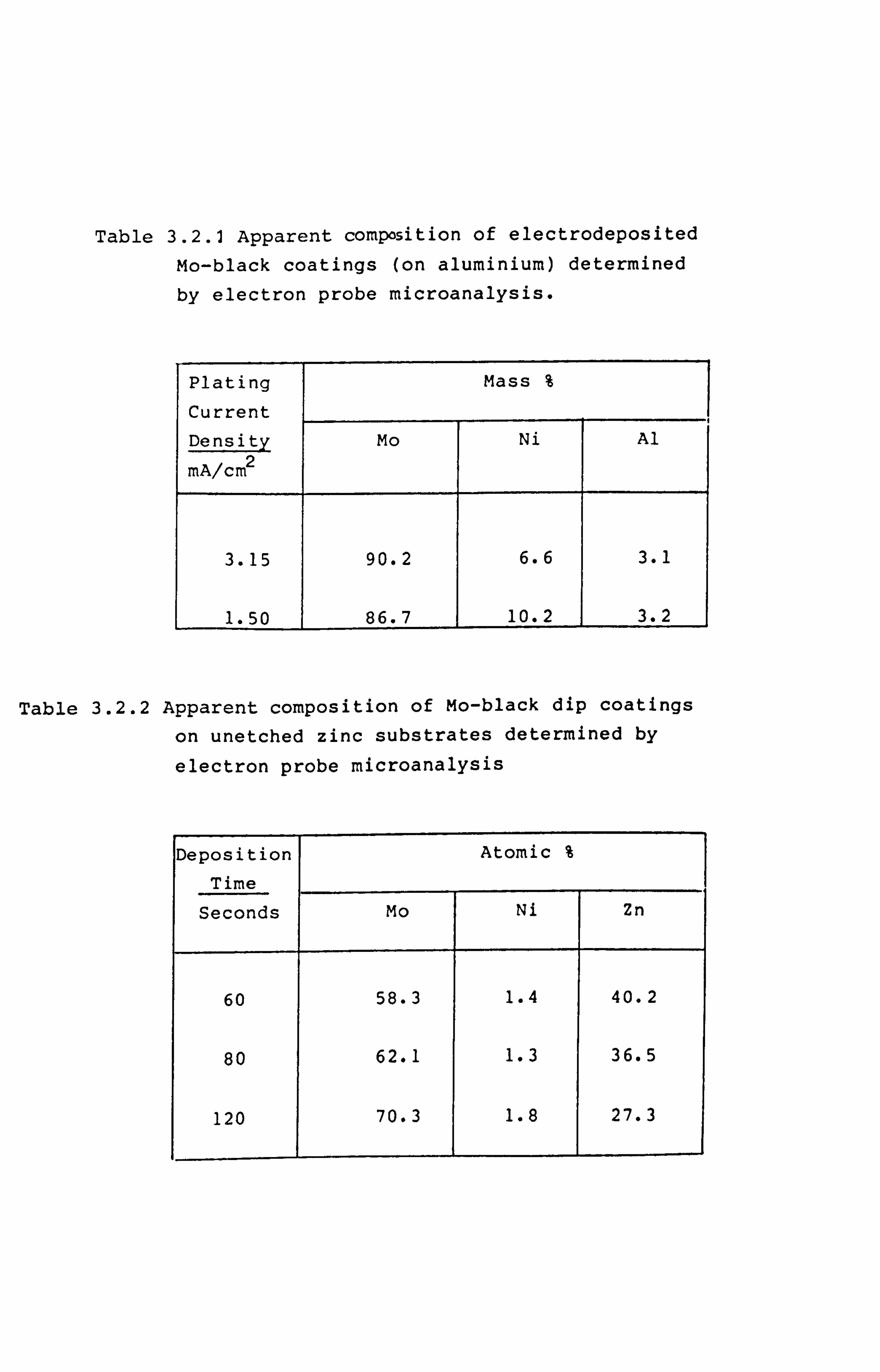
Table 3.2.1 Apparent composition of electrodeposited
Mo-black coatings (on aluminium) determined
by electron probe microanalysis.
Plating
Current
Mass %
Density Mo Ni Al
mA/crný
3.15 90.2 6.6 3.1
1.50 86.7 10.2 3.2
Table 3.2.2 Apparent composition of Mo-black dip coatings
on unetched zinc substrates determined by
electron probe microanalysis
Deposition
Time
Atomic % I
_ Seconds Mo Ni Zn
60 58.3 1.4 40.2
80 62.1 1.3 36.5
120 70.3 1.8 27.3
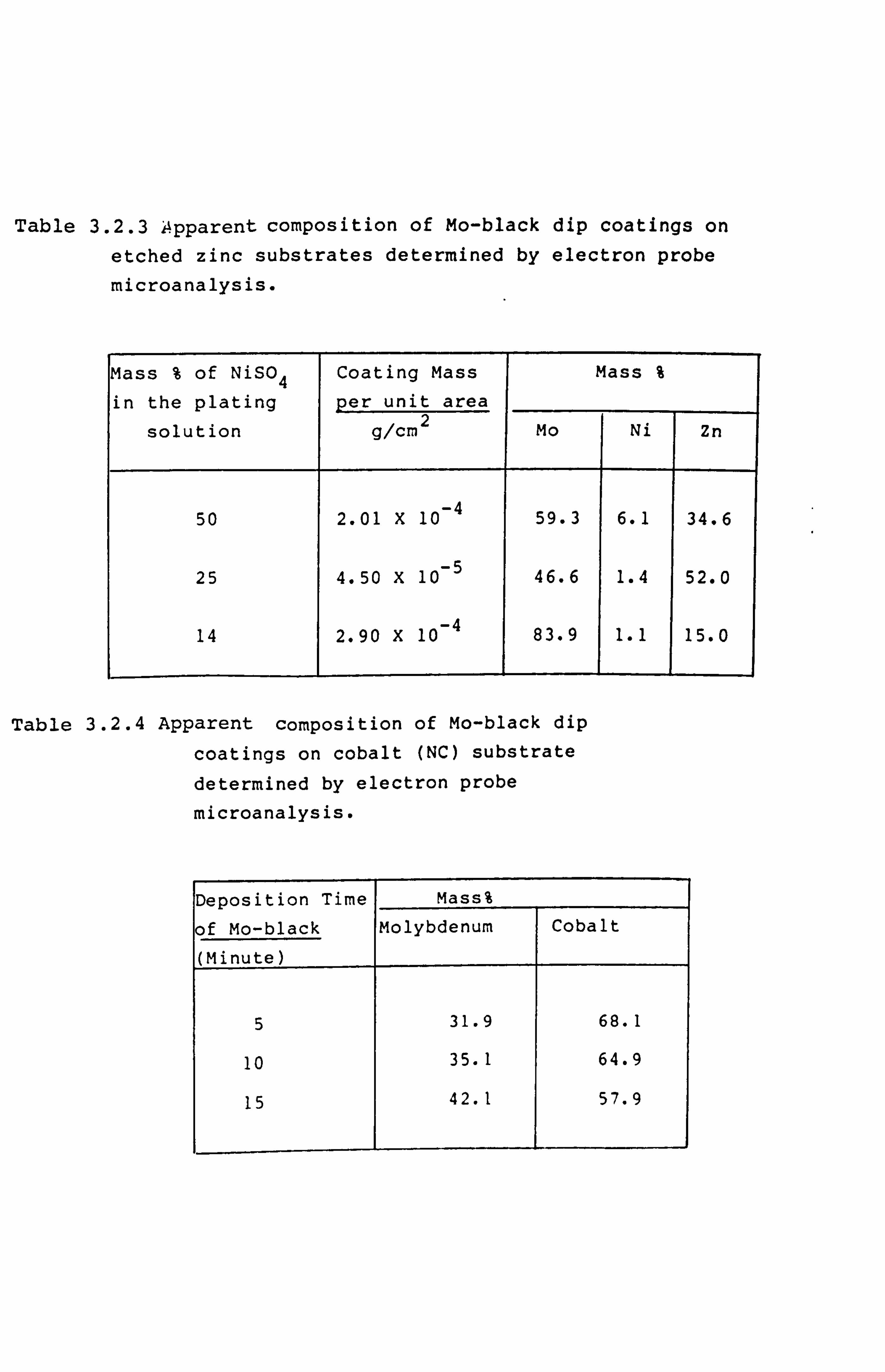
Table 3.2.3 Apparent composition of Mo-black dip coatings on etched zinc substrates determined by electron probe microanalysis.
Mass % of NiSO 4 in the plating
Coating Mass
per unit area
Mass %
solution g/cm 2 Mo Ni Zn
50 2.01 X 10- 4 59.3 6.1 34.6
25 4.50 X 10- 5 46.6 1.4 52.0
14 2.90 X 10- 4 83.9 1.1 15.0
Table 3.2.4 Apparent composition of Mo-black dip
coatings on cobalt (NC) substrate
determined by electron probe
microanalysis.
Deposition Time Mass%
of Mo-black Molybdenum Cobalt
(Minute)
5 31.9 68.1
10 35.1 64.9
15 42.1 57.9
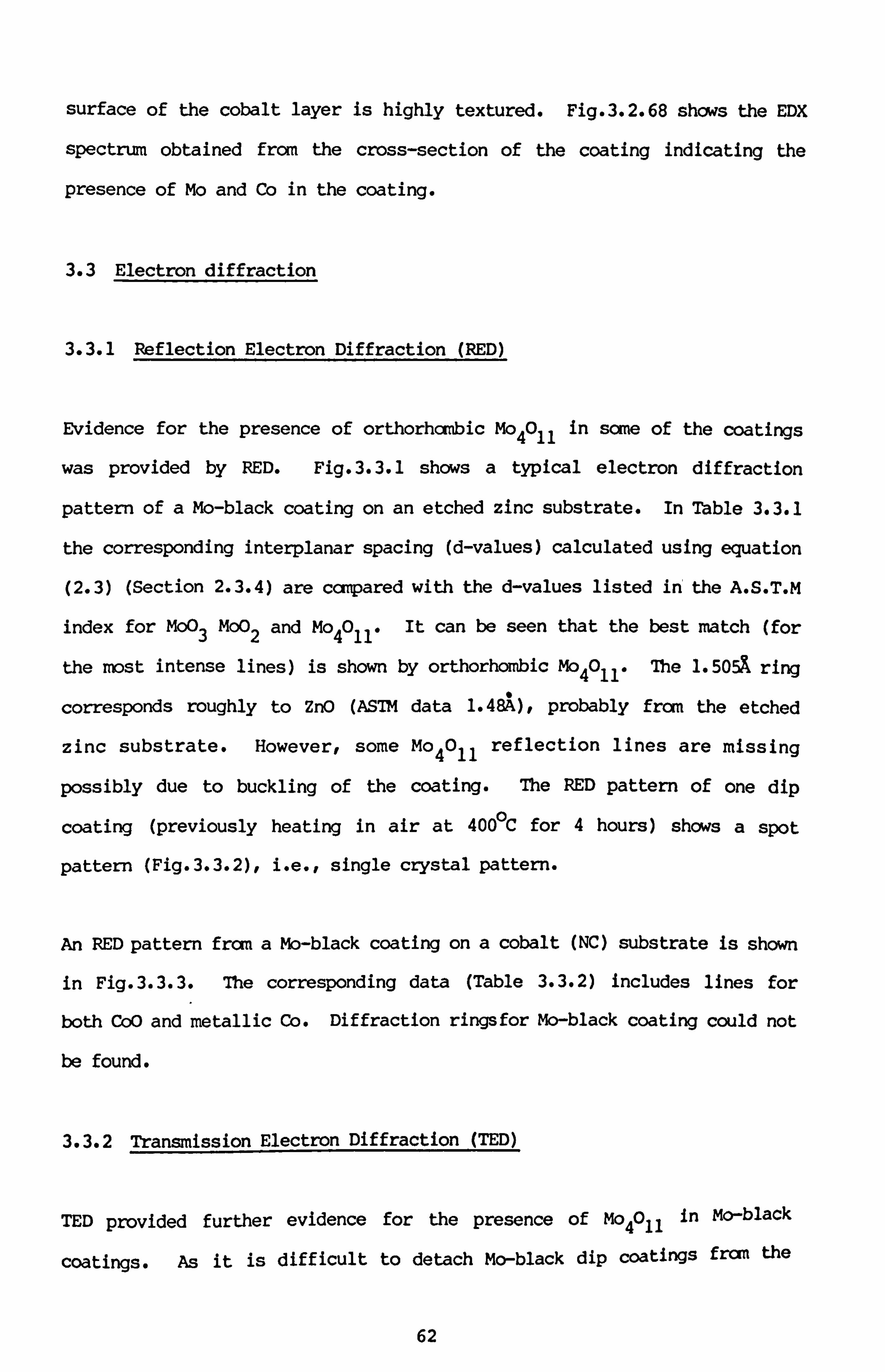
surface of the cobalt layer is highly textured. Fig-3.2.68 shows the EDX
spectrun obtained from the cross-section of the coating indicating the
presence of Mo and Co in the coating.
3.3 Electron diffraction
3.3.1 Reflection Electron Diffraction (RED)
Evidence for the presence of orthorhombic Mo 40 11 in some of the coatings
was provided by RED. Fig. 3.3.1 shows a typical electron diffraction
pattern of a Mo-black coating on an etched zinc substrate. In Table 3.3.1
the corresponding interplanar spacing (d-values) calculated using equation
(2.3) (Section 2.3.4) are ccmpared with the d-values listed in'the A. S. T. M
index for MoO 3 moo 2 and Mo 4011* It can be seen that the best match (for
the most intense lines) is shown by orthorhombic Mo 40 110 The 1.50A ring
corresponds roughly to ZnO (ASTM data 1.481), probably from the etched
zinc substrate. However, some Mo 40 11 reflection lines are missing
possibly due to buckling of the coating. The RED pattern of one dip
coating (previously heating in air at 4060C for 4 hours) shows a spot
pattern (Fig. 3.3.2), i. e., single crystal pattern.
An RED pattern frcm a Mo-black coating on a cobalt (NC) substrate is shown
in Fig. 3.3.3. The corresponding data (Table 3.3-2) includes lines for
both CoO and metallic Co. Diffraction ringsfor Mo-black coating could not
be found.
3.3.2 Transmission Electron Diffraction (TED)
TED provided further evidence for the presence of Mo 40 11 in Mo-black
coatings. As it is difficult to detach Mo-black dip coatings fran the
62
etched zinc and cobalt (NC) substrates, only the electrodeposited coating
has been studied in TED. Both electron micrographs and corresponding
diffraction patterns have been obtained at different temperatures, ranging
frcrn -160 0C to 3260C. Fig. 3.3.4 shows an electron diffraction pattern of
a Mo-black coating prepared on alaninium. The specimen was prepared by
etching away the aluminium substrate with NaOH (Section 2.3.4). The
micrograph shows block like isolated features possibly artifacts due to
etching process while the diffraction pattern is a densely populated spot
pattern. A transmission electron diffraction pattern of an
electrodeposited coating on a copper substrate shows spotty rings
(Fig. 3.3.5) (the coating is less adherent to copper so it can easily be
stripped off from the copper substrate). The calculated d-values are
given in Table 3.3.3. These correspond to orthorhombic M0401, ' The
electron micrograph of the coating (Fig. 3-3-5-a) shows rounded and sane
irregular shaped microcrystals in a net like arrangement of voids. After
holding the sample at -1660C for 2 hours, most of these crystals appeared
to be needle-like as shown in Fig. 3.3.6 with its selected area diffraction
(S. A. D. ) pattern. The calculated d-values are similar to those for Mo 40 11
(Table 3.3-3). The reason for changing the shape of the microcrystals is
not clearly understood. The effect may be due to sharper in-aging of
existing crystals at lower temperature. Needle-shaped microcrystals of
orthorhcmbic Mo4O,, were also found by Lavina et al (1980). Fig. 3.3.7
shows a rather similar room temperature image (obtained after warming the
specimen from -1600C) to that obtained before cooling (Fig-3.3.5).
Another sample stripped fran the same copper substrate was studied in a
hot stage from room temperature to 3200C. Figs. 3.3.8 - 10 show the
micrographs and corresponding S. A. D. patterns of the sample at a
temperatures of 23,200 and 320 0 C. The sample was kept at each
temperature for 65 minutes and then the micrographs were taken. The
63
. 81
10
.0
EP . _f
to
r-i .Q
r-4 A
r;
(D
E-1
P-4 -4 P-4 <D C14 rn m P-4 r-4 r-I r-4 r-4 -4 r-4 CD r-I cli CV m (D 'IV
C)
CN Ln C>
CN en co P-4 CV a% (1ý 1 i CT r-I r- in C*4
ý4 0
1 10
I 1 4
x C) C> C) CD lw t: r CD
' CD -f CD ýq C4 C*4 ce) C) s
-ýd -4 CN m m cq qlw m rý
c3 o 0 Ln o Cq co C) -W m CV r-q
I-T m Ln 0) CD ý4 C14 Ln
41
P-4 r-4 -4 C14 r-I m 1-4 P-4 cli C14
r-4 r-4 -4 C) N C) m C14 (Y) G . 1.1 C14 M IRT %D Ln I m C14 N
C) r- 4 CD
1-4 C> Ln Ln C) CD a Ln Ln 0 X C) ol co m -T qcr IRT C14 O t
: c H
C) Ln co M m 00 m 9 rý Ln N r- Ln m
m C4 C4 14 1: 14
(7% Ln co C14 co 9
Lý Cý 1ý Uý Cý CN C14
8 6 C5
1ý -tr co
9 C) Lý
C)
1ý C)
1ý () ()
c 'aý (D I 1 C) 1-4 V-4 -4 r-4 04
co u 41 i 4J
0 41 41
2 ., f
0
to 41
0
10
2 4.4 . -I 1C3
c:
R
C14
14 A
S
1)
u
C) C*4 (D m N ý4 'IT C) C) r-4 (D 0 Co r-f CD C14 CD
0 4-4 C)
CD 0 C) a x
r-I x I (N %D C) OD co OD kD (N
a) 8 e -4 ,a )-f r- I'll
%D C%j 1.4 tn Nzr %D -W r-q P-4 C) 0% C14 ýq C) CD CD
4 4 4 4 C4 C4
C) CD 1-4 -4 C> C> CN --I N m C14 CN CN m C14 M
14 4
(a C>
Ln C> CD CD Ln m C) C> LO CN I-q r-4 en
t-q
W (Y) 0 CC) N 00 %D
ll i Lý 1ý 1ý 1ý 1ý ý CN C4 CD
41 Q4 I (a CN CC) 00 co IRT
. N. 1
ýq r-q co C14 ON r- 0 0
(D 4J 2
) 41 10 S n ,4 c Lo C) C) L 1
1 9
- =; 1-4 m ON C 4 4
-ý 0 0
C4 I C4
41
(13
B k R
0 , ý-4 1-
4)
.0
114 0
.0
a) (D F-I Q-4
-2 ýý H 10
1-4 (D cli C) CN 1-4
kD (14 Ln C14
P-4
ýe M C*j ý CN CIJ MM C) 1-f 1.4 1-4 -4 C%j CN CD 0 cli -4
.4 CY) cli 4 CN C14 C 1 C ( 1 - N 4 CD CD -4 C) -4 r-q CD 1-4 CN 1.4 CD ( C - Z - N W -4 C) Dr CN :r r-4 LA M ýw -1 C'4 0 00 ko CNI q Ln
CD Ln CD Ln Ln Ln c> CD c) p CD 0a Ln a Ln cD 0 CD Ln ' 0 in co -4 Ln kD r- in -4 in -: r --v cn -, r r- in -4 . m cq C)
0 X: ý-q 4-4 g - ---
fn 0 Ln LO CO fn 0-i N kD cyý r- 00 -W co 00 N Ln 40 ( 0 4J (ý l
ý Ln 5 cr, r- -T m Fý r- Z Ln -,: r C) 0) co r- rý %0 ko ICT
; :4 ; I
10 1 _ 21 .4 .4 C4 C4 14 ý; 44 C4 C4 C4 4 14 1 I-
OCO tD r- kD C) co C> r- w
CN kD
4J 1-1 Cý I C4 C4 II14111
ko r. to co CD r- kD It: r co tD
-4 1111C; III141 C4
-6 2: 41 r. 4
Ln 0 mko m-0 C14 a Ln 25 m co in ICD ON rý ý4 (0
0 44
Ln m el C) 00 Ln 0 r- ko It: r
to m C) 0)
4J 0 a)
4.4 11 IRT II11 CN II C4 I cj II-: I ': 1 .4
, ý
(o CD 2 : ý:
1 ý:: En 1 2: 1 ý: El) 1 3: : 3: 1: U) I ý- ý1: ý:: ý:: 04 . 41 (L)
U3 -W 41
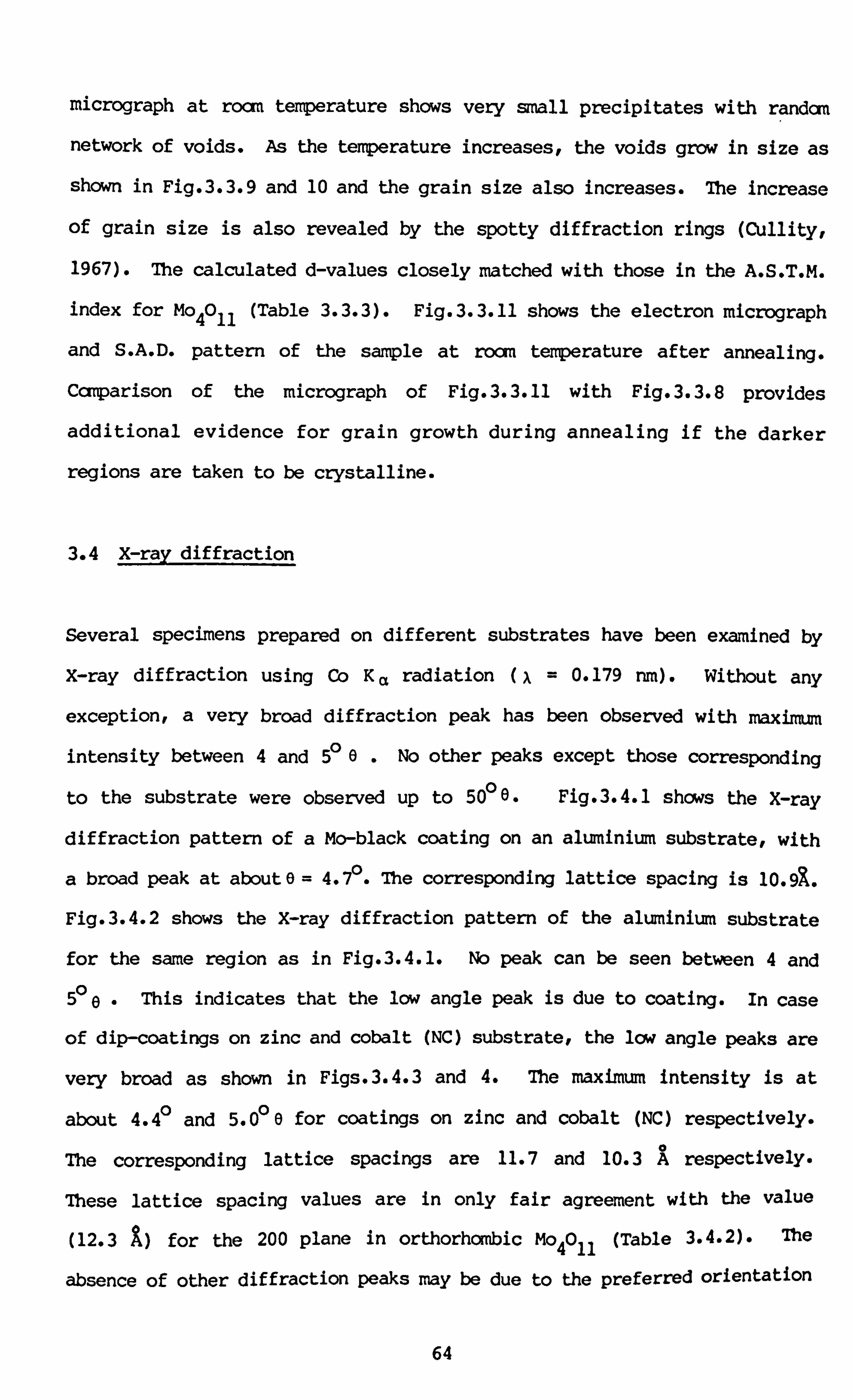
micrograph at rocrn temperature shows very small precipitates with randan
network of voids. As the temperature increases, the voids grow in size as
shown in Fig. 3.3.9 and 10 and the grain size also increases. The increase
of grain size is also revealed by the spotty diffraction rings (Cullity,
1967). The calculated d-values closely matched with those in the A. S. T. M.
index for Mo 40 11 (Table 3.3.3). Fig. 3.3.11 shows the electron micrograph
and S. A. D. pattern of the sample at roan temperature after annealing.
Ccrnparison of the micrograph of Fig. 3.3.11 with Fig. 3.3.8 provides
additional evidence for grain growth during annealing if the darker
regions are taken to be crystalline.
3.4 X-ray diffraction
several specimens prepared on different substrates have been examined by
X-ray diffraction using Co Ka radiation (x = 0.179 run). Without any
exception#, a very broad diffraction peak has been observed with maximum
intensity between 4 and 5P 6. No other peaks except those corresponding
to the substrate were observed up to 5600. Fig. 3.4.1 shows the X-ray
diffraction pattern of a Mo-black coating on an aluiiinium substrate, with
a broad peak at aboutE)= 4.70. The corresponding lattice spacing is 10.9%.
Fig. 3.4.2 shows the X-ray diffraction pattern of the aluminium substrate
for the same region as in Fig. 3.4.1. No peak can be seen between 4 and
5o 0. This indicates that the low angle peak is due to coating. In case
of dip-coatings on zinc and cobalt (NC) substrate, the low angle peaks are
very broad as shown in Figs. 3.4.3 and 4. The maximum intensity is at
about 4.4 0 and 5.000 for coatings on zinc and cobalt (NC) respectively.
The corresponding lattice spacings are 11.7 and 10.3 A respectively.
These lattice spacing values are in only fair agreement with the value
(12.3 1) for the 200 plane in orthorhombic Mo 4011 (Table 3.4.2). The
absence of other diffraction peaks may be due to the preferred orientation
64
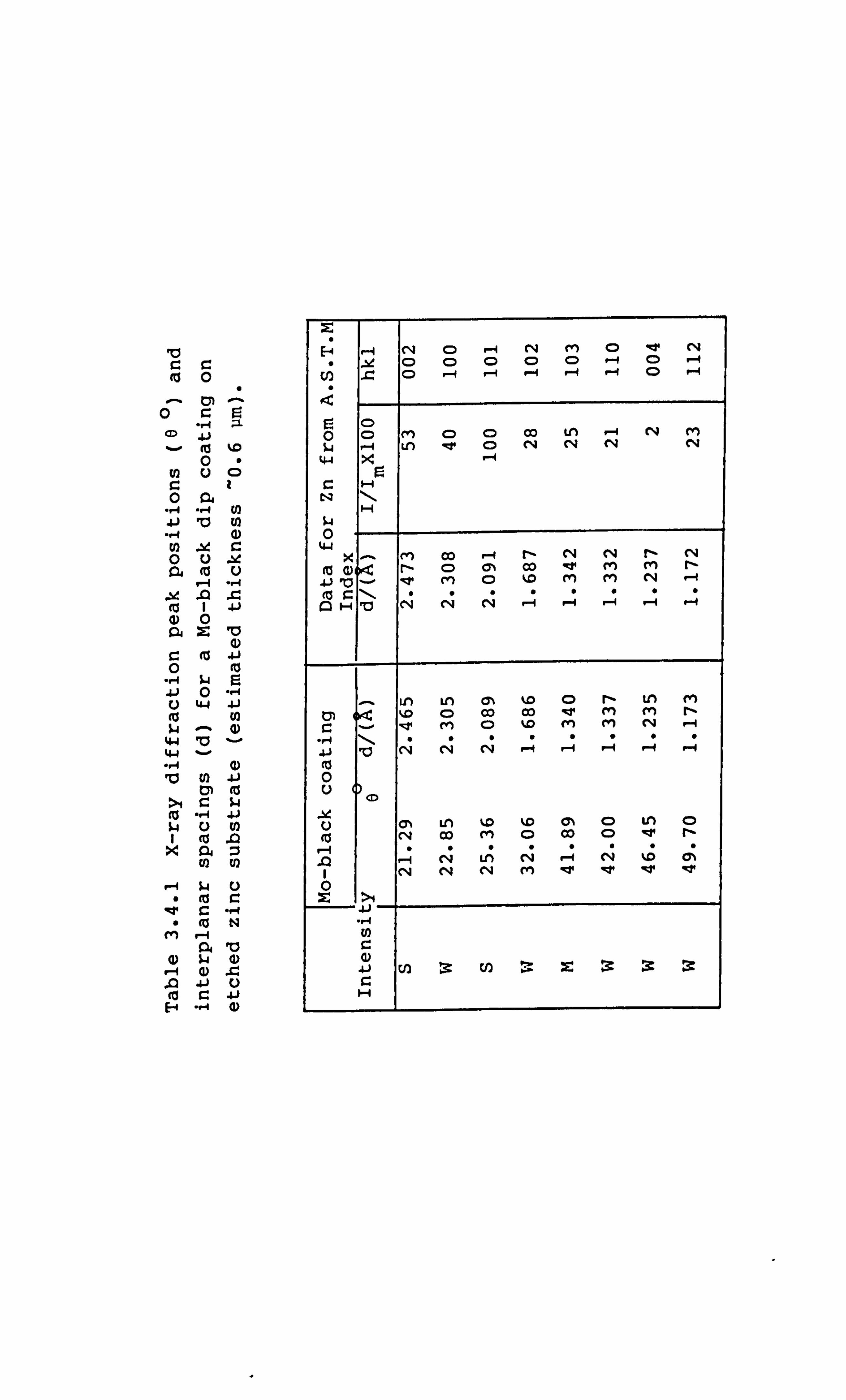
10 C r: tö 0
0
0 (0 u
0 124
Z 0u
-be n4 fö u
tö 1 11 0
0
0 C) 44 4. ) tu ý4
44 4-1 . '. i 'CJ (0 &1
cm tö >i ý4
1 cu 0 XnZ
Co m
0 tlö N M r--i
04 10
E-4
C14 CD -4 N m (D -W C*4 CD C) Q C) (D -1 C) M4 CD r-f -4 r-4 1-4 r-4 0 P. -I
0 c) m C) CD 00 Ln -4 CN en W r-4 Ln IRV CD C14 CN C4 C14
44
44 X - Cý) co r-4 r- CN N r- C14
(a a) 4 r. c) ON co -W m co r-
4j 10 - .: r cv) 0 W cn m N r-I
CN CN CN -4 -4 -4 r-4 -4
Ln Ln ON %D Ln (Y) %0 CD CO CO IW M M r-
. &j C-4 C14 CN r-4 -1 P-4 I-f P-4 (0 0
a% Ln to %D ON a Ln a
(0 CV co m 0 (X) 0 mr r-
-4 C4 U; C4 ý4 C4 Iz Cý CN eq cq m I-zr 1.4, V qcr
:c1 >4 - -
tu r_
r=
rn 10 tu r.
0 &1 0
CD tu 0 0 (D U -: r
to Zx 41 0
JO 1 000 04 x J.,
54 10 Co 0 (D (P 4. ) N4 rii . ý4 0
U) 44 c: 0 0 c14
.0 10 (0 u0 to $4 c: jý4
44 44 9)
10 a) -f 41
40 (Z (D
s4 0
44
44 c4 v tu
Mm tu
P-4 C) 12 tio tu
1-4 C) x 0 CD Ln Ln CD C) CD tn
rz -4 1-4 0) 00 CV m m m
140 V Cý 0
m Ln co ko a% (N Ln 50 - 1-4 r- 'IT cli Ln cli co 044 4 4 4 W 1; 14 r C C 44
(CS 4. ) (a s-4
CN
C) r-I 1-4 CN m CD CD r-q r-4 r-I C14 M fn -V kD kD ýq P-4
0 C) 1-4 CD X CD IT C) Ln
co m I 0 0
w :c P-4 ý4 0
Lw
4 N en Ln (Y) %D $4 X - 00
(a In
-1 00
44 N C14 0 4 CN C14 CD
CN m r-q C) r- Ln 1.4 m qzr
ON co I-*' C14 kD N 00 C) 0 0 0
M r-4 W m m m C14 (N r-4
4J (a 0
u en co Ln fn Ln Ln kD ON ON r- W C)
0 r-
0 1ý A 4 r. -1 r-( CN C14
0
41 C -4
4J 0) 4J 4. ) (0 c
of the crystalline material. For coatings on etched zinc substrate, this
low angle peak could not be identified. Fig. 3.4.5 shows the X-ray
diffraction pattern of a coating wan etched zinc substrate and the
calculated d-spacing values are tabulated in Table 3.4.1. The table shows
that the d-spacing values of the peaks in Fig. 3.4.5 closely match with
those of zinc metal listed in the A. S. T. M. index.
Fig. 3.4.6 shows the X-ray diffraction pattern obtained from a coating on
cobalt (NC) substrate. Only three peaks of Co appeared in the diffraction
pattern, possibly due to the texture of the cobalt coating. Peaks for Ni
and Cu are also present. Fig. 3.4.7 shows the X-ray diffraction pattern of
a Mo-black coating onwalLminium substrate after heat treatment at 40CPC
for 8 hours in air. The calculated d-spacing values are tabulated in
Table 3.4.2. These indicate that a mixture of M003 and Mo 40 11 is present.
No change has been observed in the diffraction pattern of the coatings on
zinc and cobalt (NC) substrates after heat treatment under the same
conditions.
3.5 X-ray Photoelectmn Spectroscopy (XPS)
XPS measurements on Mo-black coatings on different substrates have been
carried out in order to analyse the chemical elemental compositions of the
coatings and the oxidation state of molybdenum in the deposited coatings.
The XPS spectra obtained f rom the coatings have been conpared with some
standard samples i. e., molybdenum metal foil, molybdenum dioxide (MoO 2)
and molybdenum trioxide (M003 ) powders. 7he depth profile ccnposition of
the coatings has been determined by using argon ions (Ar+) bombardment and
measuring the main photoelectron peak areas of the individual constituent A
elements and then dividing by their corresponding sensitivity factors (see
Appendix D). me coatings have also been studied in xPS after various
65
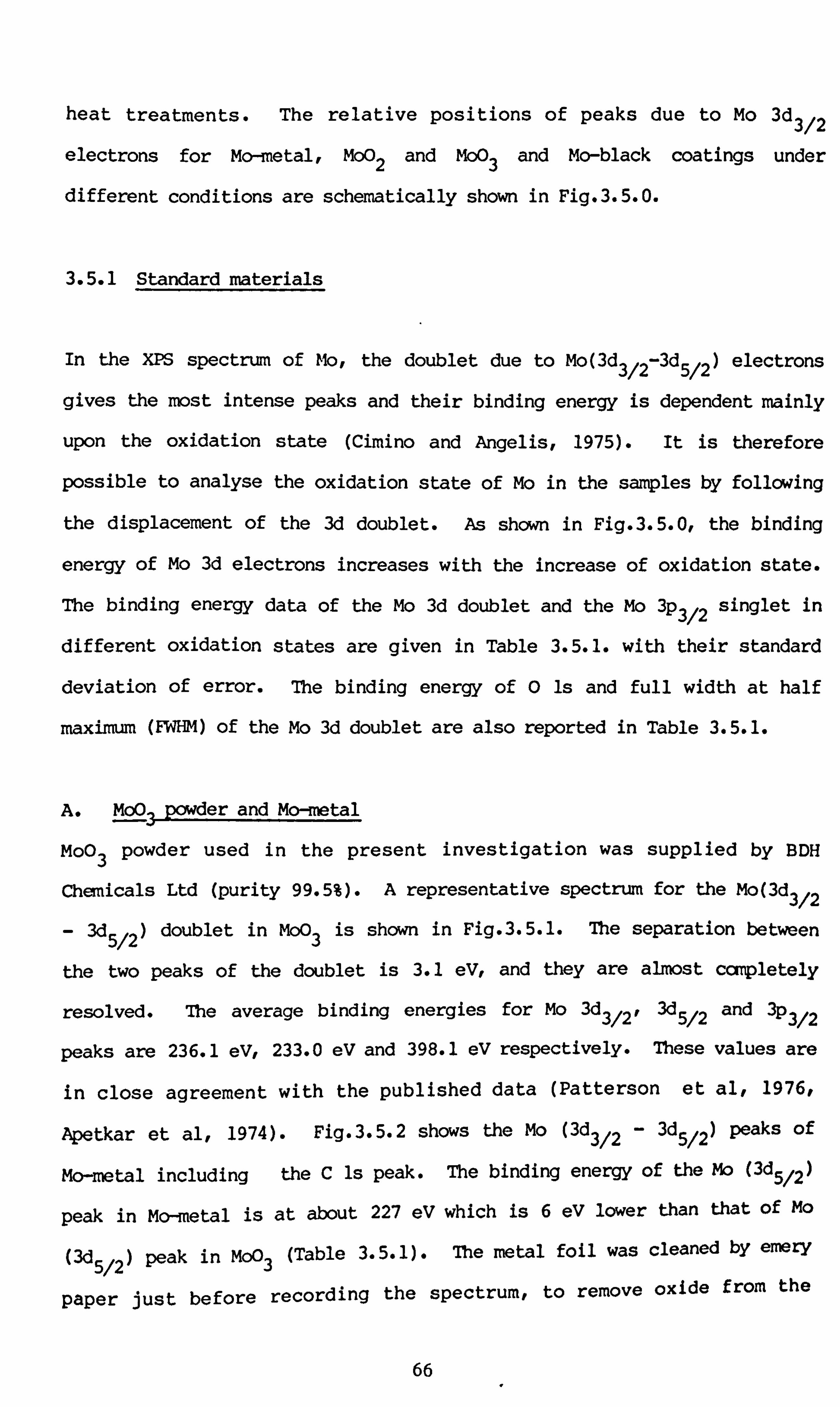
heat treatments. The relative positions of peaks due to Mo 3d 3/2
electrons for Mo-metal, MoO 2 and MoO 3 and Mo-black coatings under
different conditions are schematically shown in Fig. 3.5.0.
3.5.1 Standard materials
In the XPS spectrurn of Mo, the doublet due to Mo(3d 3/2 -3d 5/2 ) electrons
gives the most intense peaks and their binding energy is dependent mainly
upon the oxidation state (Cimino and Angelis, 1975). It is therefore
possible to analyse the oxidation state of Mo in the samples by following
the displacement of the 3d doublet. As shown in Fig. 3.5.0, the binding
energy of Mo 3d electrons increases with the increase of oxidation state.
The binding energy data of the Mo 3d doublet and the Mo 3p 3/2 singlet in
different oxidation states are given in Table 3.5.1. with their standard
deviation of error. The binding energy of 0 ls and full width at half
maximum (FWHM) of the Mo 3d doublet are also reported in Table 3.5.1.
A. Moo., powder and Mo-mtal
Moo 3 powder used in the present investigation was supplied by BDH
Chemicals Ltd (purity 99.5%). A representative spectrum for the Mo(3d 3/2
- 3d 5/2 ) doublet in MoO 3 is shown in Fig. 3.5.1. The separation between
the two peaks of the doublet is 3.1 eV, and they are almost completely
resolved. The average binding energies for Mo 3d 3/2" 3d5/2 and 3p3/2
peaks are 236.1 eVt 233.0 eV and 398.1 ev respectively. These values are
in close agreement with the published data (Patterson et al, 1976t
Apetkar et al, 1974). Fig. 3.5.2 shows the Mo Od 3/2 - 3d 5/2 ) peaks of
Mo-metal including the C ls peak. The binding energy of the Mo Od 5/2)
peak in Mo-metal is at about 227 eV which is 6 eV lower than that of Mo
Od 5/2 ) peak in MoO 3 (Table 3.5.1). The metal foil was cleaned by emery
paper just before recording the spectrum, to remove oxide from the
66
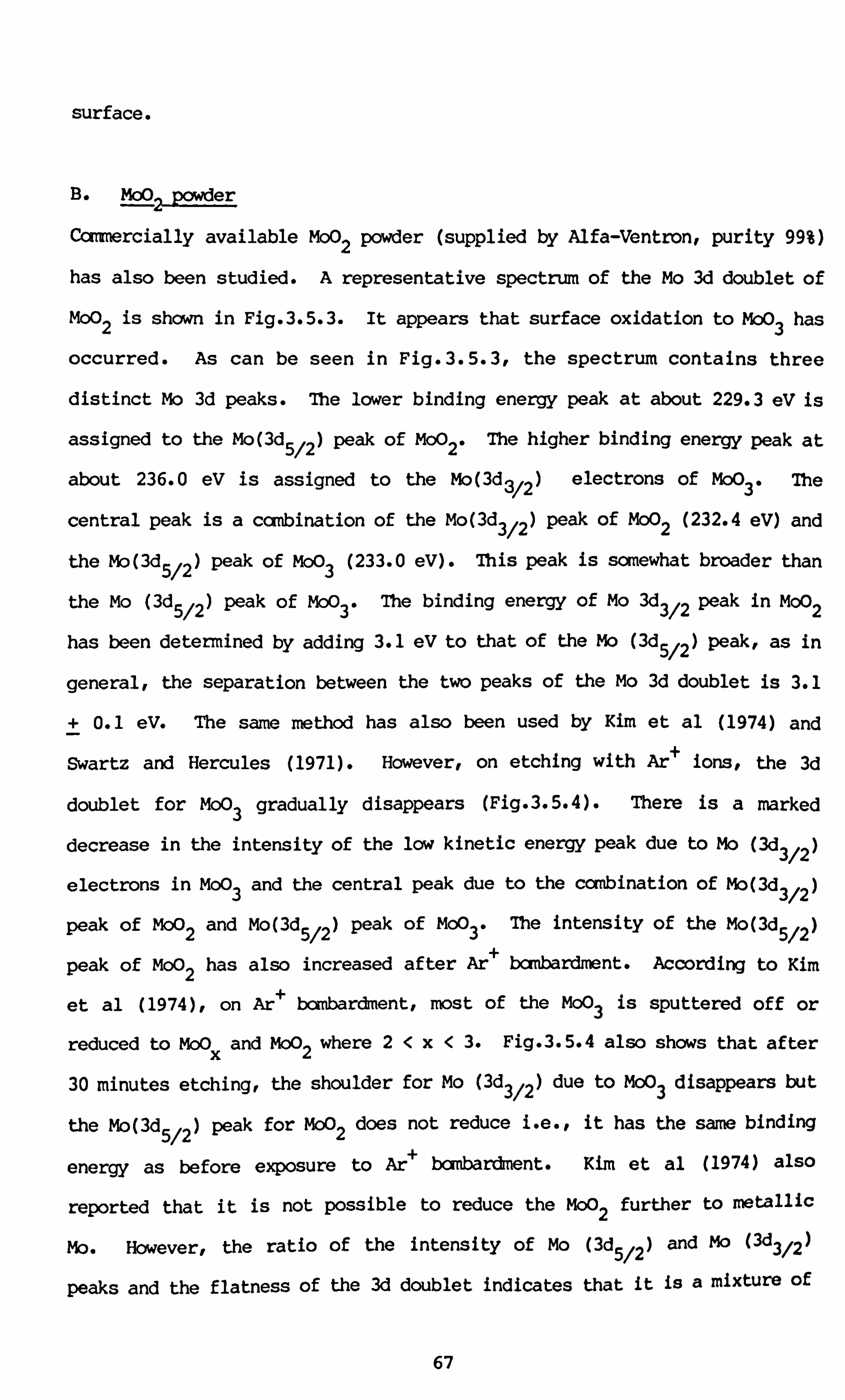
surface.
B. MoO,, powder
Camiercially available Moo 2 powder (supplied by Alfa-Ventron, purity 99%)
has also been studied. A representative spectrum of the Mo 3d doublet of
Moo 2 is shown in Fig. 3.5.3. It appears that surface oxidation to MOO 3 has
occurred. As can be seen in Fig. 3.5.3, the spectrum contains three
distinct Mo 3d peaks. The lower binding energy peak at about 229.3 eV is
assigned to the Mo(3d 5/2 ) peak of MoO 2* The higher binding energy peak at
about 236.0 eV is assigned to the Mo(3d3/2) electrons of M003 * The
central peak is a combination of the Mo(3d 3/2 ) peak of Moo 2 (232.4 eV) and
the MoOd 5/2 ) peak of Moo 3 (233.0 eV). This peak is sornewhat broader than
the Mo (3d 5/2 ) peak of Moo 3* The binding energy of Mo 3d 3/2 peak in Moo 2
has been determined by adding 3.1 eV to that of the Mo Od 5/2 ) peak, as in
general, the separation between the two peaks of the Mo 3d doublet is 3.1
+ 0.1 eV. The same method has also been used by Kim et al (1974) and
Swartz and Hercules (1971). However, on etching with Ar + ions, the 3d
doublet for MoO 3 gradually disappears (Fig. 3.5.4). There is a marked
decrease in the intensity of the low kinetic energy peak due to Mo (3d 3/2)
electrons in MoO 3 and the central peak due to the combination of MoOd 3/2)
peak of MoO 2 and MoOd 5/2 ) peak of MoO 3* The intensity of the Mo(3d 5/2)
peak of MoO 2 has also increased after Ar + bcmbardment. According to Kim
et al (1974), on Ar + bcmbardment, most of the MoO 3 is sputtered of f or
reduced to MoO x and M002 where 2<x<3. Fig. 3.5.4 also shows that after
30 minutes etching, the shoulder for Mo (3d3/2 ) due to MoO 3 disappears but
the Mo(3d 5/2 ) peak for MoO 2 does not reduce i. e., it has the same binding
energy as before exposure to Ar7ý bcmbardment. Kim et al (1974) also
reported that it is not possible to reduce the Moo 2 further to metallic
Mo. However, the ratio of the intensity of Mo (3d 5/2 ) and Mo (3d 3/2)
peaks and the flatness of the 3d doublet indicates that it is a mixture of
67
two oxides. Bombardment of MoO 3 with Ar + also produces a mixture of two
oxides: moo 2 and MoO x where 2<x<3 as shown in Fig. 3.5.5. The ef fect
of Ar + bambardment on the binding energy of Mo (3d 5/2 ) of Moo 2 and MoO 3 is
shown in Table 3.5.5.
3.5.2 Electrodeposited Mo-black coatings on aluminium
7he binding energies of Mo 3d electrons of electrodeposited Mo-black
coating are found to be higher than those for MoO 2 and lower than moo 3 (Fig. 3.5.0). The position of Mo 3d doublet shifts after various heat
treatments and Ar + ion etching.
A. As-prepared coatings
A typical survey scan XPS spectrum of a Mo-black coating on an aluminitin
substrate is given in Fig. 3.5-6. It shows that the coating consists
mainly of molybdenum oxide and a very small amount of nickel, (the nickel
peak is barely above the noise level). The appearance of the C Is peak in
the XPS spectra originates from the spectrometer rotary pump oil that
inevitably contaminates the samples at the working pressure (1.3 X 10⁻⁵
Pa). It may also ccme from mishandling of the specimen before location in
the spectrcmeter. In the present investigation the C Is peak has been
used as a reference peak for the determination of binding energies. 7he
binding energy of C Is peak was found to be 284.9 eV, by calibration of
the spectrometer according to Anthony and Seah (1984). Other values for
the C Is level have been reported in the literature (Cimino and Angelis,
1975). A different choice would change the absolute values of electrons
binding energies but not the relative values. The 0 Is peak is almost
symmetrical, as shown in Fig. 3.5.7(a), with a binding energy of about
529.9 eV. This peak, therefore, corresponds to the oxygen of a molybdenum
oxide. It is suggested by Robert et al (1972) that the 0 Is peak at about
68
530 eV is assigned to the oxide 0 2- while peaks at higher binding energies
(> 531 eV) should be assigned to surface hydroxide ions (OH-) or strongly
chemisorbed oxygen (0-). A typical narrow scan spectrLan of the Mo 3d
doublet for a Mo-black coating is shown in Fig. 3.5.7(b). The results
obtained from electrodeposited Mo-black coating on aluminium are given in
Table 3.5.2 with calculated standard deviations. The average binding
energies for the Mo 3p 3/2' 3d 3/2 and 3d5/2 peaks are 395.6 eV, 234.5 eV
and 231.3 eV respectively. The binding energies of the Mo (3d 3/2 - 3d 5/2)
peaks for the Mo-black coating are (1.6 - 1.7) eV lower than those for
moo 3 (Fig. 3.5.8) and (2.1 - 2.0) eV higher than the corresponding Moo 2
peaks. The shift in binding energy of the 3d5/2 peak from that of
Mo-metal is 4.3 eV where as for M002 and MoO 3' the shif ts in binding
energies are 2.3 eV and 6 eV respectively (Table 3.5-1). By considering
the above results it can be argued that the oxidation state of Mo in the
coating is between +4 and +6. However, Swartz and Herculus (1971)
reported that the binding energies of the Mo(3d3/2 - 3d 5/2) peaks for
oxidation state +5 are 234.5 and 231.0 eV respectively, which agree
closely with the values given above for Mo-black coatings.
B. Heat treated coatings
When the Mo-black coatings are heated in air, the 3d doublet shifts
towards the higher binding energy (Fig. 3.5.0). Fig-3-5.9 shows the shift
of the 3d doublet of Mo after heating the coating in air at a temperature
of 4000C for 2 hours. The MoOd 3/2 - 3d 5/2) peaks are well resolved like
those of Moo 3 (Fig. 3.2.5). The average binding energies of the Mo 3p 3/2'
Mo 3d 3/2 and Mo 3d 5/2 lines are shifted to 397.8 eV, 235.9 eV and 232.5 eV
respectively (Table 3.5.2). These values are very close to those for
Moo 3* There is a very small shift in binding energy (0.1 - 0.3 eV) of the
3d doublet towards the lower binding energy after heating the coating
inside the spectrometer chamber at 450oC for 2 hours. The intensity of MO
69
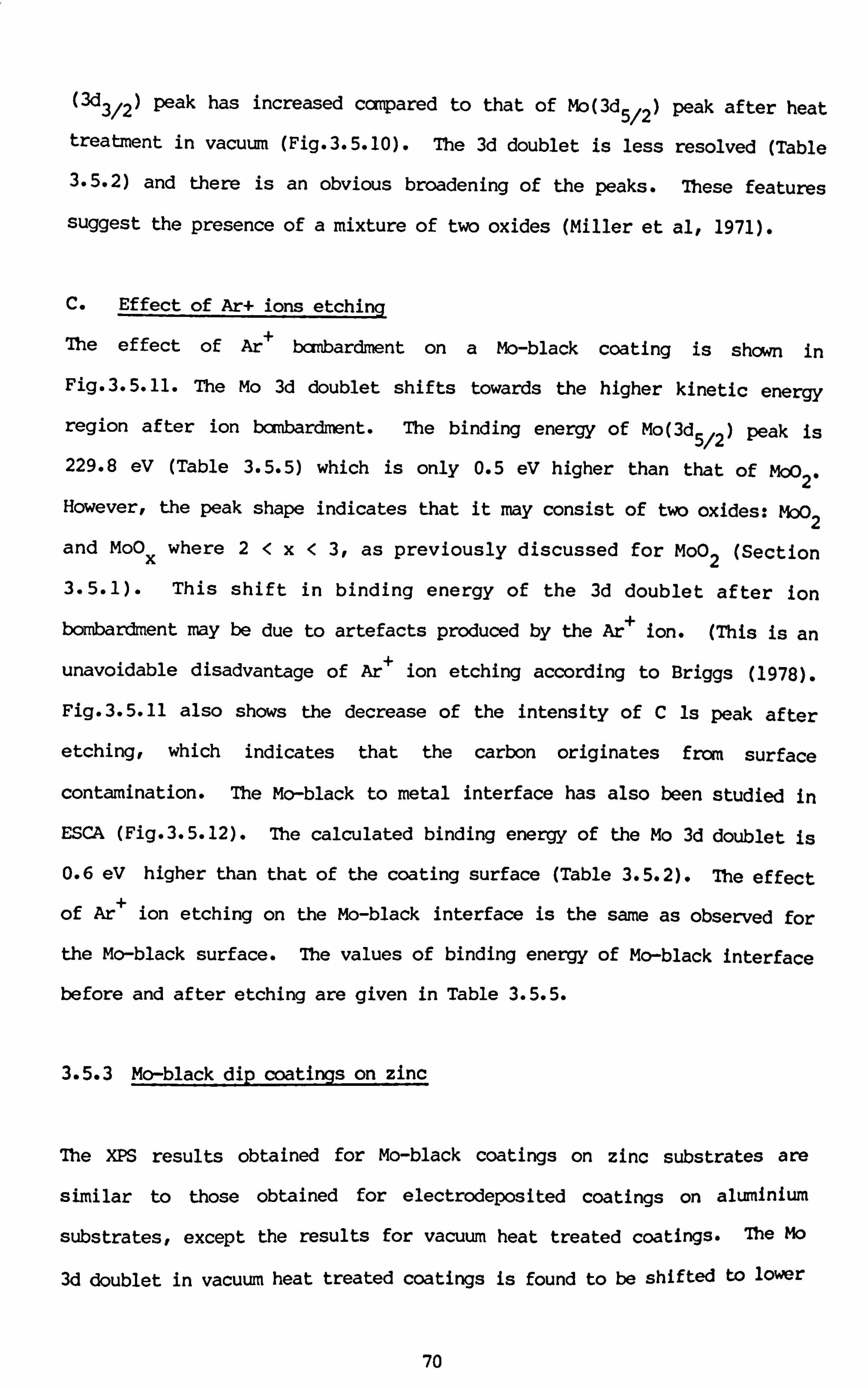
Od 3/2) peak has increased ccrrpared to that of Mo(3d5/2) peak after heat
treatment in vacuum (Fig. 3.5-10). The 3d doublet is less resolved (Table
3.5-2) and there is an obvious broadening of the peaks. Ihese features
suggest the presence of a mixture of two oxides (Miller et al, 1971).
C. Effect of Ar+ ions etching
The effect of Ar + bcmbardment on a Mo-black coating is shown in
Fig. 3.5.11. The Mo 3d doublet shifts towards the higher kinetic energy
region after ion bcmbardment. The binding energy of Mo(3d 5/2 ) peak is
229.8 eV (Table 3.5.5) which is only 0.5 eV higher than that of moo 2* However, the peak shape indicates that it may consist of two oxides: Moo 2 and MoO
x where 2<x<3, as previously discussed for MoO 2 (Section
3.5.1). This shift in binding energy of the 3d doublet after ion
bombardment way be due to artefacts produced by the Ar + ion. (This is an
unavoidable disadvantage of Ar + ion etching according to Briggs (1978).
Fig. 3.5.11 also shows the decrease of the intensity of C Is peak after
etching, which indicates that the carbon originates from surface
contamination. The Mo-black to metal interface has also been studied in
ESCA (Fig. 3.5-12). The calculated binding energy of the Mo 3d doublet is
0.6 eV higher than that of the coating surface (Table 3.5.2). The effect
of Ar + ion etching on the Mo-black interface is the same as observed for
the Mo-black surface. The values of binding energy of Mo-black interface
before and after etching are given in Table 3.5.5.
3.5.3 Mo-black dip coatings on zinc
Me XPS results obtained for Mo-black coatings on zinc substrates are
similar to those obtained for electrodeposited coatings on aluminium
substrates, except the results for vacuum heat treated coatings. The Mo
3d doublet in vacuum heat treated coatings is found to be shifted to lower
70
oxidation state (Fig. 3.5.0).
A. As-prepared coatings
A typical survey scan spectrum of a Mo-black dip coating on a zinc
substrate is shown in Fig. 3.5.13. Like electrodeposited coatings on
aluminium substrates, dip coatings also consist of oxides of molybdenum
and a small amount of nickel. Fig. 3.5.13 shows that the nickel 2p peak is
barely above the noise level. Ihe survey scan spectrum also shows an 0
ls, aC ls peak and photoelectron and Auger peaks for zinc. The survey
scan spectra obtained at two different take-off angles (70 0 and 20 0
measured relative to the surface) are shown in Figs. 3.5.13(a) and (b)
respectively. 7hese indicate that the ratio of C ls peak to Mo 3d peak
height increased (from 0.88 to 1.22) when the take off angle decreased.
This is consistent with the presence of carbon being associated with the
surface contamination of the specimen. The 0 ls peak is almost the
symmetrical (Fig. 3-5.14) indicatingi presence of one kind of oxygen
species. This peak can be assigned to oxide oxygen as the binding energy
is about 529.9 eV (Robert et al, 1972). Fig. 3.5-15 shows the narrow scan
spectrum of the Ni 2p peak. The presence of strong broad satellite bands
consistently at about 5.5 and 6.8 eV above the main peak of Ni 2p 3/2 may
indicate the presence of Ni (OH) 2 in the coatings (McIntyre and Ceok,
1975). The binding energy of Ni2p 3/2 is estimated to be 855.0 eV. After
etching with Ar + ions for 30 minutes, the satellites disappear, but the
binding energy of Ni 2p 3/2 peak does not shift significantly. This result
also suggests the presence of Ni (OH) 2 in the coatings (Kim and Winograd,
1974). Narrow scan spectra of the Mo 3d doublet of Mo-black dip coatings
on etched and unetched zinc substrates are shown in Fig. 3.5.16. lhe
calculated binding energies of Mo 3P3/2' Mo 3d 3/2 and Mo 3d5/2 electrons
are given in Table 3.5.3. The binding energy values of the Mo (3d 3/2 -
3d5/2) peaks for Mo-black dip coatings suggest that the oxidation state of
71
Mo is +5 (Swartz and Hercules 1971). A similar results were obtained for
the electrodeposited coatings (3.5.2).
B. Heat treated coatings
Mo-black dip coatings on zinc substrates have been studied in ESCA after
different heat treatments. The effectsof heat treatment on the XPS
results obtained for the Mo-black dip coatings are summarised in Table
3.5.3. No significant change in the binding energy of 0 ls has been
observed after heat treatment. There is a comparatively large shift (1.9
- 2.2 eV) in the binding energies of the Mo, Od 3/2 - 3d 5/2) peaks of the dip
coatings after heat treatment in vacuum in contrast with the results for
the electrodeposited coatings. No significant change in the binding
energy of the 3d doublet was observed after heating at 1000C (Table
3.5.3). As the temperature increases to 200 0C and 300 0 CP the Mo 3d
doublet shifts towards the higher kinetic energy region. Fig. 3.5.17 shows
the Mo 3d spectrum of a Mo-black coating on unetched zinc before and after
heating inside the spectrometer chamber at 3000C for 90 minutes. The
binding energies of Mo (3d3/2 - 3d 5/2 ) electrons are 232.2 and 229.2 eV
respectively after heat treatment (as for MoO 2 ). Fig. 3.5.17 also shows
that the intensity of the Mo (3d3/2 ) increases coniparedto Mo( 3d5/2) peak
after heat Lreatment. The shape of the Mo 3d doublet indicates that it
may consist of two oxides: M002 and Moýx where 2<x<3. The same result
was obtained after heating the Mo-black coating on etched zinc at 300 0C
for 3 hours (Fig-3.5-18). Zia- binding energyvalues ofthe 3P3/2 and 3d
doublet indicate +4 oxidation state for Mo after heat treatment in vacuum.
After the coating -vas heated in air, the binding energies of the MoOP3/2)
and 3d doublet increased (Table 3.5.3) suggesting that the coating
oxidized to a higher oxidation state. Fig. 3.5.19 shows a survey scan
spectrum of a Mo-black dip coating after heating in air at 3900C for 2
72
hours. The Mo 3d spectrum of a Mo-black coating on etched zinc, before
and after heat treatment in air at 2000C for 2 hours is shown in
Fig. 3.5.20 whereas Fig. 3.5-21 shows the results after the same treatment
for a coating on an unetched zinc substrate. Under the same heat
treatment conditions, the binding energies of the Mo ("rl-j-12- 3d 3/2 ) peaks of
coatings on unetched zinc increase more than those for coatings on etched
zinc (Table 3.5.3). This indicates that the coatings on etched zinc may
be more stable at higher temperatures than the coatings on unetched zinc.
Fig. 3.5.22 shows the Mo 3d spectrum of a coating after heating at a
temperature of 3900C for 2 hours. The figure shows a well resolved 3d
doublet similar to that of MoO 3* The calculated binding energies of Mo
Od 3/2 - 3d 5/2 ) electron are (235.6 - 232.6) eV which is only 0.4 eV lower
than that of MoO 3*
C. Depth profile of the coating usinq Ar+ ions etching
In the XPS study Ar + ions bombardment has been used in an attenpt to study
any depth variation in coating corripositions. The etching rate was roughly
IAO/minute with 5 KeV, Ar+ ion and a beam current of 5mA. Alternating
cycles of Ar + ion etching and XPS scans were used to obtain the depth
prof ile data. The atomic percentage of the chemical elements of the
coating was calculated by measuring the individual main peak areas and
dividing with their corresponding sensitivity factors (Appendix D). It
was observed that the intensity of the C Is peak decreased as the time of
etching increased. Fig. 3.5.23 shows a survey scan spectrum of Mo-black
dip coating after 200 minutes etching. It can be seen that the C Is peak
had completely disappeared, giving further confirmation that the C Is
peak originated from surface contamination. The shift in binding energies
of the M: ). 3d5/2 peak are given in Table . 3.5.5, with corresponding etching
time. rig. 3.5.24 'shows the Mo 3d spectra before etching and at twodifferent
etching times. It can be seen that after 10 minutes etching, the binding
73
energy of Mo 3d /2 Peak shifts from 231.4 to 229.9eV. The peak shape also
changed after etching. The intensity of Mo 3d 3/2 peak increased ccmpared
to that of the Mo 3d,, /2 peak and also the 3d doublet became broader. Ihis
indicates a mixture of two oxides (Fig. 3.5.24). All these above effects
may be due to the artefacts produced by Ar + ion etching (Briggs, 1978).
After 10 minutes, the shape and also the binding energy of Mo 3d doublet
did not change significantly with the increasing time of Ar + bcmbardment.
No shift in the binding energy of the Mo 3d doublet of vacuum heat treated
Mo-black dip coatings was observed after Ar + ion bcmbardment for prolonged
times (Table 3.5.5). The table also shows that in any sample, the final
product af ter prolonged bombardment is M002* The atomic percentages of
Mot Zn and 02 of a Mo-black dip coating on etched zinc at different
etching times are given in Table 3.5.6. The ratio of elements MO/Zn/0 is
1/0.44/2.56 at the surface of the coating. After 60 minutes etching the
ratio of Mo/Zn/0 becomes 1/0.23/1.33. After that the ratio of the
elements remains nearly the same (Table 3.5.6). A complete XPS depth
profile of a thin Mo-black dip coating on zinc is shown in Fig. 3.5.25.
3.5.4 Mo-black dip coatinqs on cobalt (NC) substrates
For coatings on cobalt (NC) substrates, the binding energies of Mo 3d
electrons are somewhat higher than those for coatings on Al and Zn
substrates and does not shift much after heat treatments.
A. As-prepared coating
A typical survey scan spectrum of a Mo-black dip coating on a cobalt (NC)
substrate (electroplated cobalt on nickel plated copper) is shown in
Fig. 3.5.26. The figure shows that the main element of the coating is Mo-
It also shows 0 ls, C ls peaks and very small peaks for Co 2s and . 2p. 7he
narrow scan spectra for Co 2p, 0 ls and Mo 3d are shown in Figs. 3.5.27-28.
74
Fig. 3.5.27 shows that Co 2p peaks are very broad. It is dif f icult to
measure corresponding binding energies accurately. However, the estimated
binding energy of Co (2p 3/2 ) peak is about 780.0 eV. A strong satellite
for the Co (2p 3/2 ) peak can be seen at about 6 eV higher binding energy
than the main peak. These features indicate the presence of cobalt oxide
(CoO) (McIntyre and Cook, 1975, Smith et al, 1980). Fig. 3.5.28(a) shows
the symmetric peak of 0 ls of binding energy 530.1 eV which is due to the
metal oxides (Robert et al, 1972).
The narrow scan spectrum of the Mo 3d doublet is shown in Fig-3.5.28(b).
Ccirpared to the 3d doublet for coatings on Al and Zn substrates, it is
well resolved and sharper. The average binding energies of Mo (3P3/2) , Mo
(3d 3/2 ) and Mo (3d 5/2 ) are given in Table 3.5.4. In these coatings, the
binding energy of the Mo 3d doublet is 0.5 eV higher than that for
coatings on Al and Zn. However comparing the binding energy of Mo (3d 5/2)
peak with that of the standard material, it seems that the oxidation state
of Mo in the coating is between +4 and +6.
B. Effect of heat treatment and Ar + ions etching
For coatings on cobalt substrates the shift in binding energy of the Mo
(3d 3/2 - 3d 5/2 ) peaks was only 0.3 ev after heating in air at 4009C for 2
hours (Table 3.5.4). After heat treatment the Mo 3d doublet is more
resolved and sharper (Fig. 3.5.29) and the binding energy of the Mo 3p 3/2
peak increased from 396.4 to 398.1 eV (i. e., close to the value for moo 3)'
When the coating was heated inside the spectrometer chamber at a
temperature of 30dOC for 2 hours the binding energy of the 3d doublet
decreased by 0.3 eV towards the lower oxidation state of Mo (Table 3-5.4).
Argon ion bombardment was used to profile the coatings. Fig. 3.5.30 shows
the survey scan spectrum of the coating referred to in Fig. 3.5.26 after 70
75
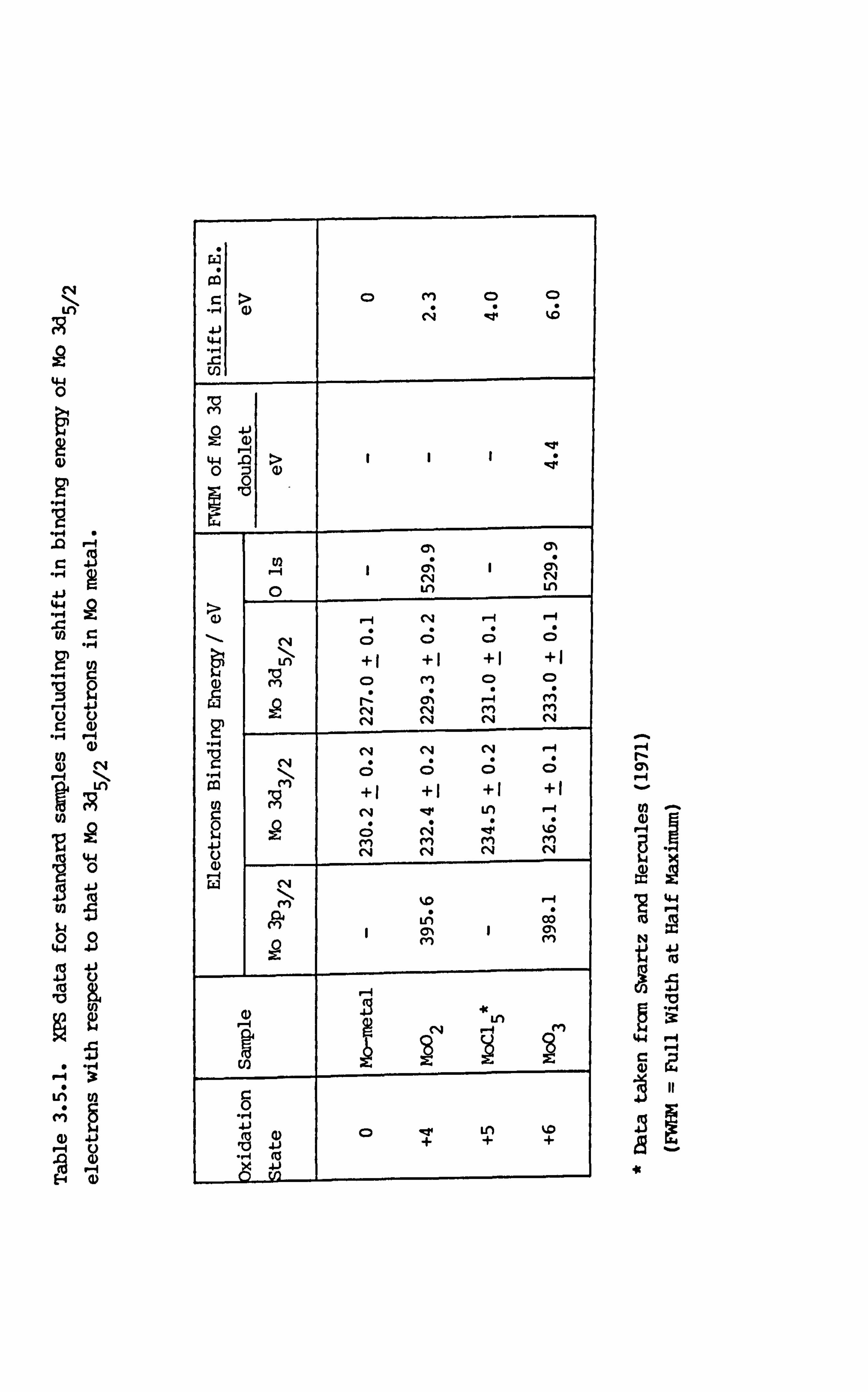
C14 I. -, Ln
ip 0
rz 4J 44
EO c
-4 Is
$04
c (D
44 0
41
$4 00
44 4j
.5 13
(a ,a&
V)
a > 0 rq 0 0 -4 (D 4 4 G 4J
,a ce)
4J
44 r .0
> I I I
1ý 1ý rn
0
(n C14 Ln
I ON CN Ln
C14 CD + +
C) + +
(1) ,a m 0 m C) C)
rz cli CN 0; cli CN C4 N
-4 C14
Cý CD 0
C14
C;
r-q C;
ca
rn C 2
+1
C14 8 m N
+1
-W C4 m N
+1
Ln rn rq
+1
m N
CN -4
k Lý C;
El)
45 Ln
8
41 (a 10 a) 4-1
0 ýr Ln w -4 (a
I)
0
44
Ai
,4 ýc
r-q r-4
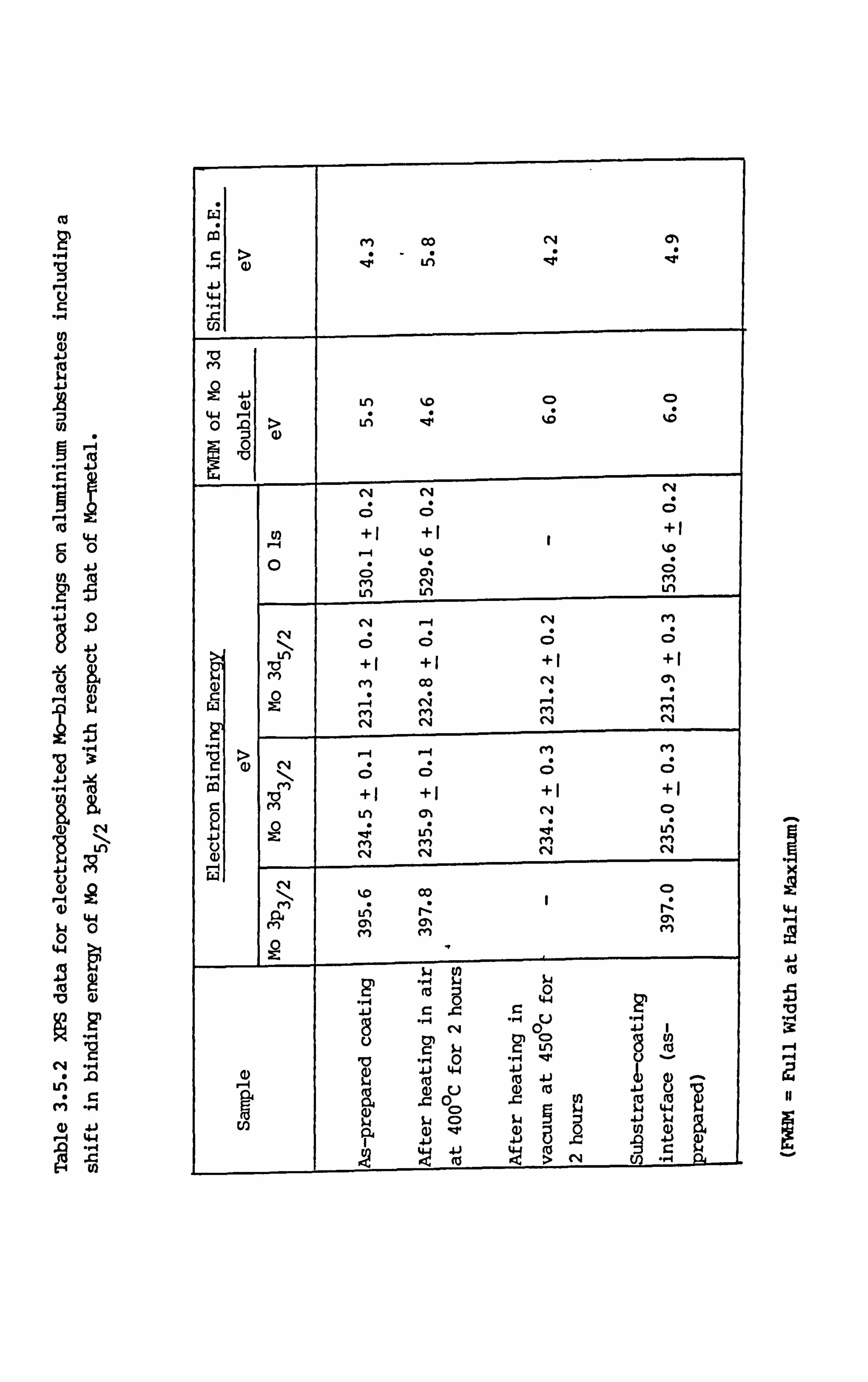
tu
m
-8
(4)
CO
tri
C4
U; C4 4)
4
0
44 0
41 44
gý cm 00 rA (n
4.4
U) .
v ei
4-1 Ln
4.4
Z$ Q 0
CD
rA +i
CD
(11 c; M Ln LA Ln
CD
+I +i +I (1)
fi m Co N oý
(n tyl m fi
r: R
er) Ln C% rli 0
ý , 41 u :e m LA m m u rm 0 c4 cm (N c4 1
-41
44
CA 0 41 1 C) F
N, 2 C: ) Ln
(0 tu
0
44 u 4
c4 N., (U
(0 (ö a) ,
ý (0 m m Cb i- 2 ($wö fö
44 CD
4 9
2
.,. 4 p4
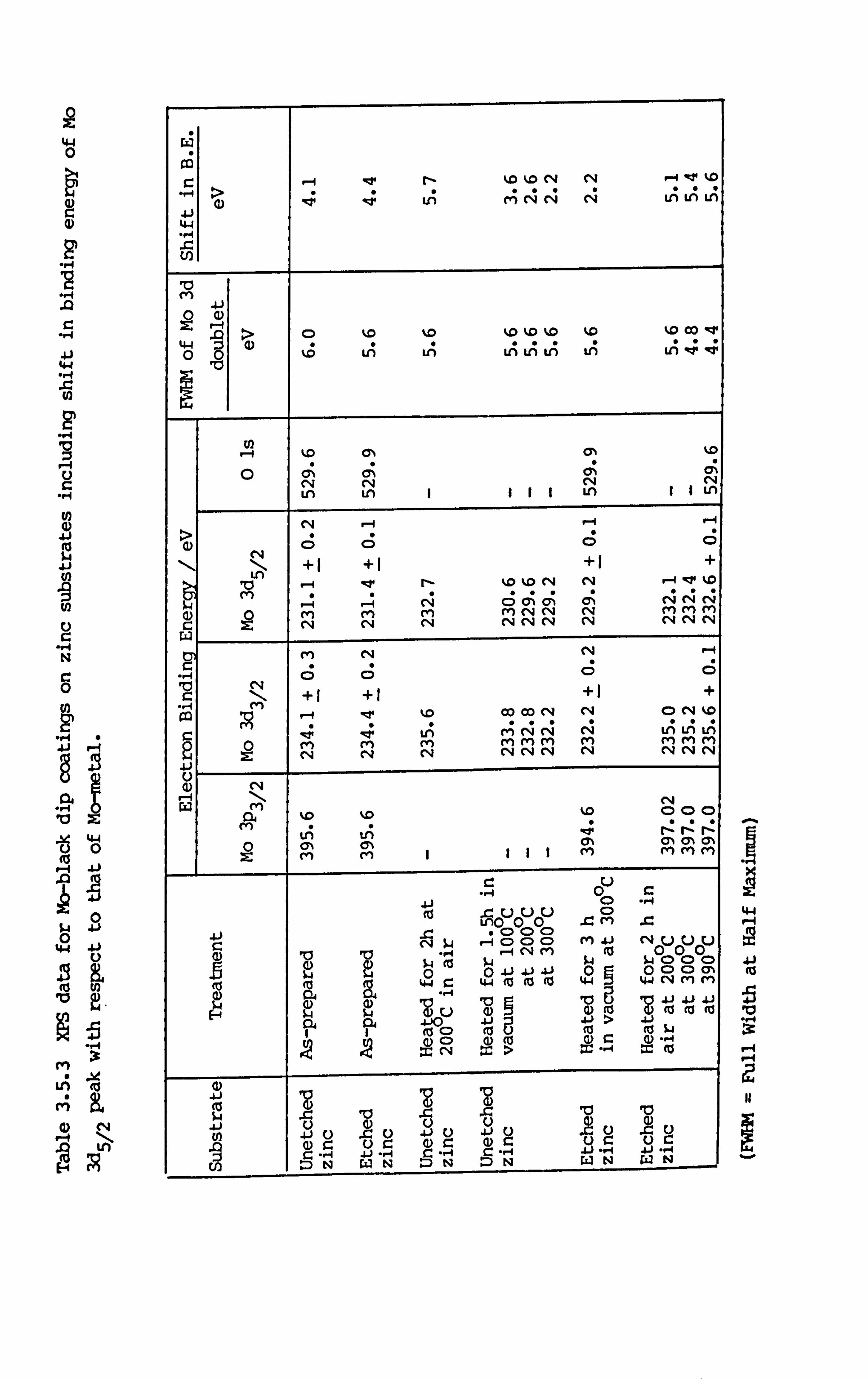
2 44 0
.0
44
w
9
-4 's
U
B
tu ý4
N
c 0
tf)
10
.0
k $4 0
.0 (a V
m
4)
lý
x: Kw 0
K
iýz
0 tn rm r*4 r*4 (%4 Ln Ln Ln
44
rn 4-)
m cý 44 0
:3 Ln Ln Ln Ln Ln LA Lin
cn tD
r4 rq 0; r4
(A t14
Lin LA Ln
+i +i +
t. 0 %ýo r4 r-4 " ýo
c; 0; 0; 444 fi (n fi ri cq N Mm (n
CD
+ to m
29 «ý lý 00 00 C*4 .0.
r4 0
(D C, 4 t. 0
le Ln m (14 r4 cli Uý LA tA en m r4
m C, 4
(VI r4
ri mM N C, 4 (4
CD 0 CD
111 ON (n
Oý Cy% cyý ri ri ri (n ri 1
to ýnc uu 920 CD
r 29 ý, ýq CD CD C> m 41 r4 _ 10 1C3 1.4 -1 (N (n (0
ý ý4%0(D% 2 2 ý4 (0 0
1.4 0 43 4. ) 4.3
(0
4 05
%W 0 CD CD m
4 1"M (n m 44 c: 14
tw (0 (ö ä - vs 9)
v a) fö
0o
4. ) 8 41 > 2
m c2 m to tö CD rq
r_
Jj 1C3 (L)
9
2 10 c: c: v v
Jj f-) ? 9 u 1
2' 0 1- JJ 0 c0 - 0 . .2
wN
44 0. -4 M
ji tu
. "4 x
r-i P-4
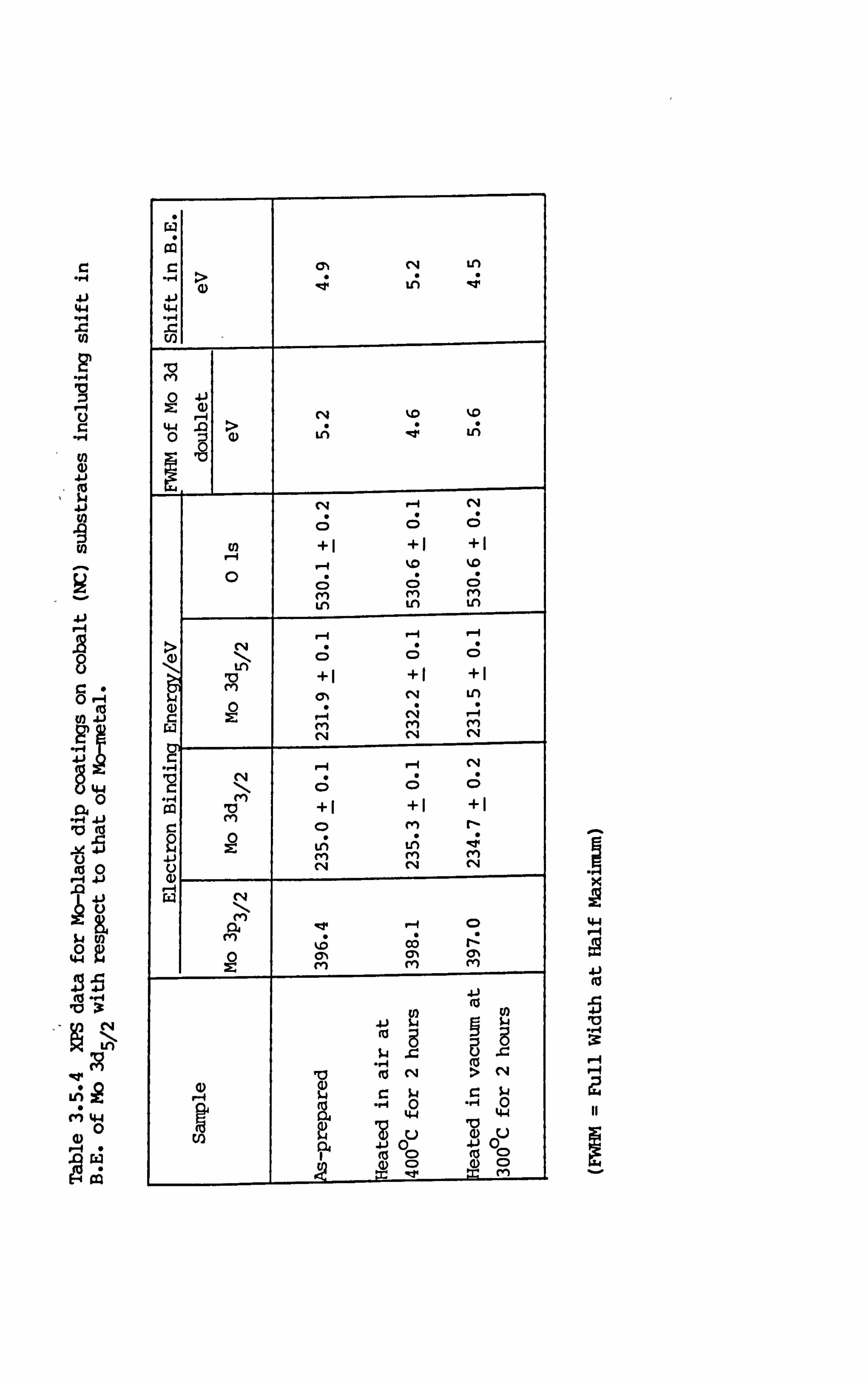
44
V)
41
8 84
co 04. )
-Fý 0
-It 41
41 U
,22 -5: 5
r; 44 0
0
W c C6 Q
Aj > Cý
Ln ItT
44
10
44 0 .0 :ý
> (, )
C14 kD tD
18
Cý CD CD
Cý CD
V) ýq 0 + 1-1
+ ko 8
+ %D ; 8
Ln in C Ln
> (D
C14 Zýn
10
i
C) +
1ý CD +
I
C) +
m cyý cn C*4
(14 C4 en C14
Ln m CN
r cn
V
C; +
Cý
0
2 ff)
:2 0
m CN
cn
m r4
r-
m C14
N
cn
ký m 0; P:
$4
,a
w
(ts C-4
C: 0
ý C14
-4 0 44
1 0
(0 0 u
%,
(0 CD
j 44
Aj
5
r-q r-4 a
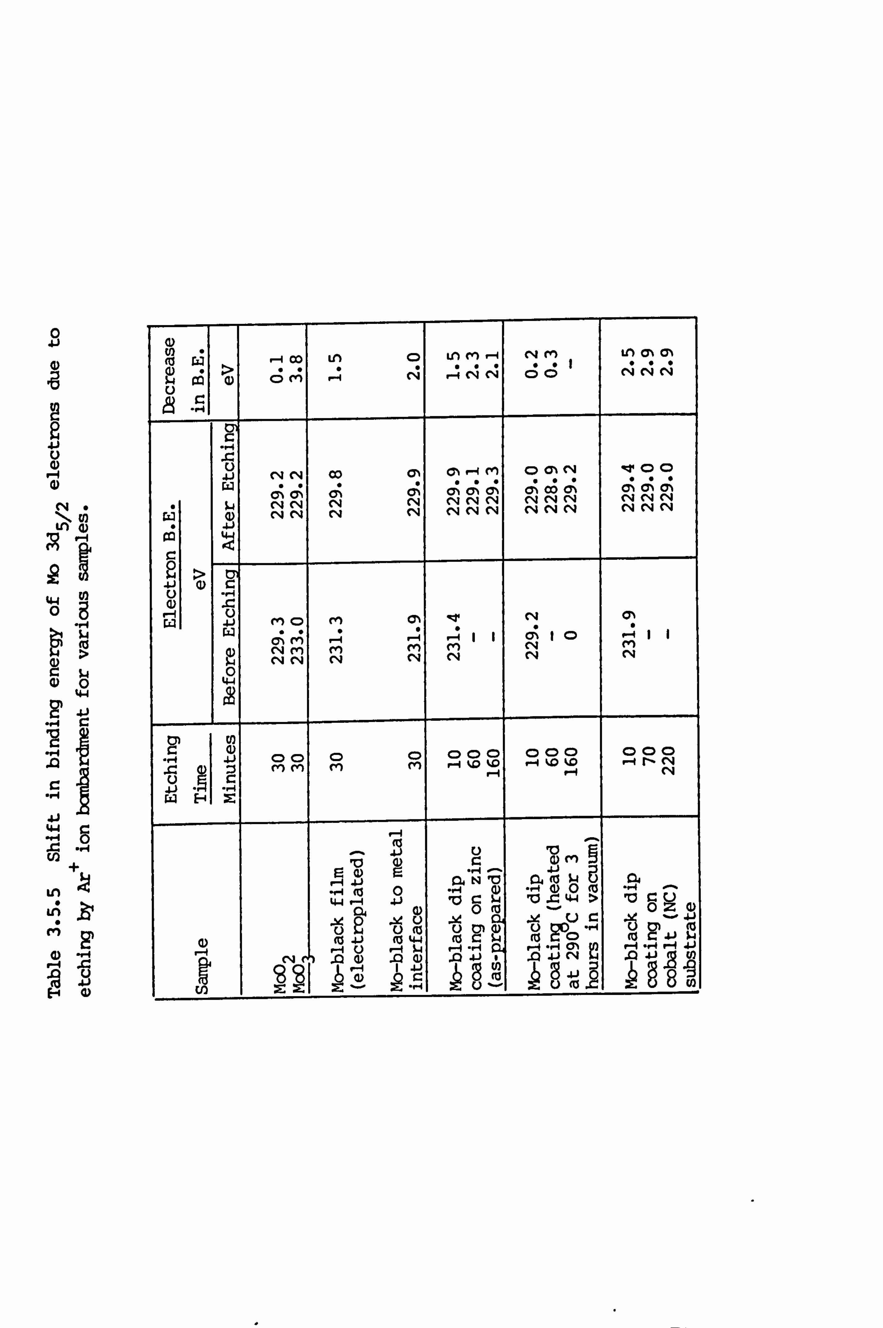
0
2 2
liý 4)
U4 0
54
ý4 Q0
44
2 4i
I I
I
., 4 V
. 1i 44
U)
Ln U; A 0
cý (N CD 0 N r4 N
rq Co ri 0 (n r4
w
0; 0; 0; 3; c9 N ;, 3; ý rq "N ;, cý ;, fli N r, 1 0; 0; 0; (14 (N c4 ý-4 c9 c9
ýý an 0
M-4 w
1 u
41 m CD 0% cm le r. 4 0, % w
(ý fý -Z -Z ii cý, 1 CD
0 44
., # U (D (D CD 0 C: ) 00
4 4. ) ýI (0 0
Nv 0 2 2'
44 r--1 0 -0 c N. 4 4 > v. -
v r. ý): 0 to
ci ö 9
Q (ö 0 (0 44 tö EP 2 (0 (0 c: 4-)
e ( r, 4j 8 D
8 i 1 2 11) C e. ý k 4 u- 1 -1 u 10 s (0 ýý1 1
:Z .., 4 : ý .
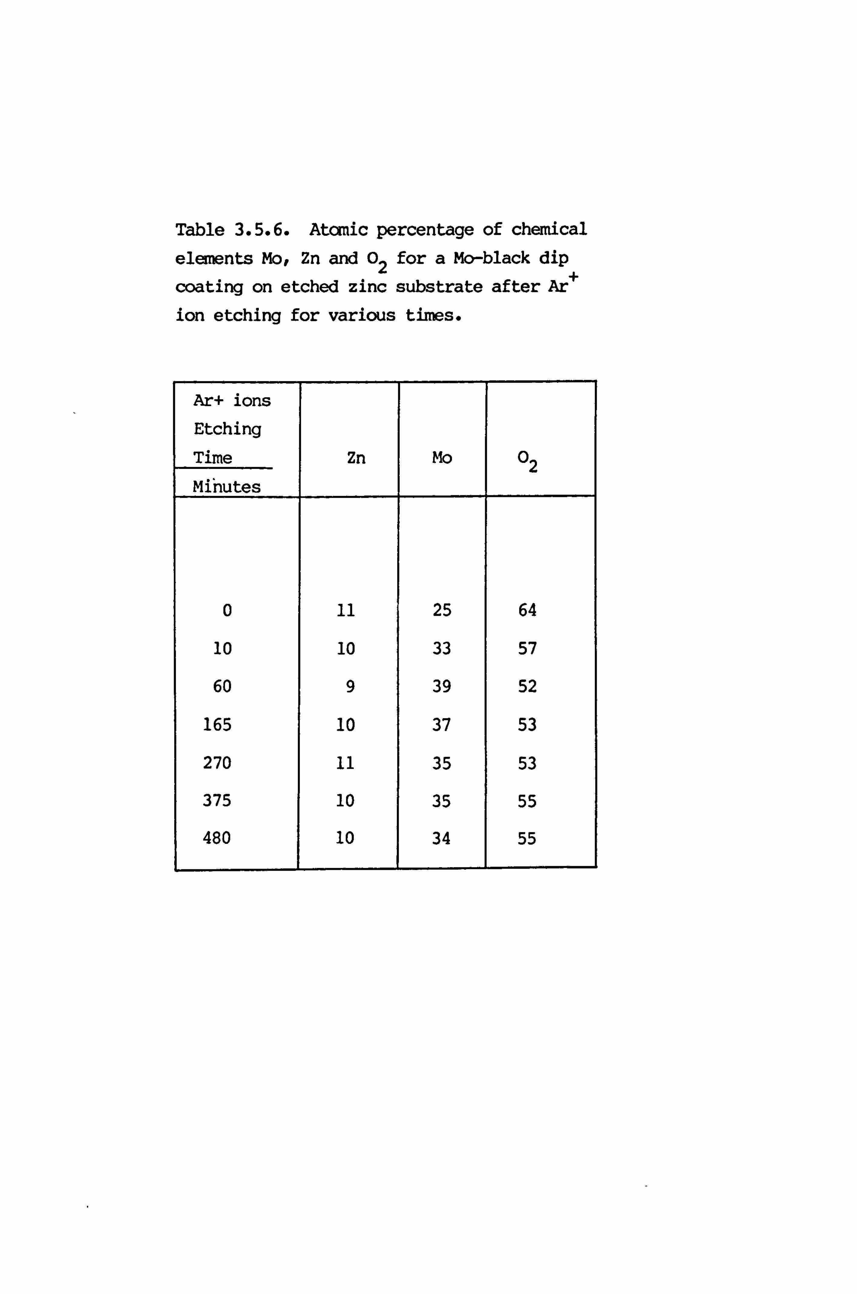
Table 3.5.6. Atomic percentage of chemical elemnts Mo, Zn and 02 for a Mo-black dip
coating on etched zinc substrate after Ar ion etching for various times.
Ar+ ions
Etching
Time
Minutes
Zn mo 02
0 11 25 64
10 10 33 57
60 9 39 52
165 10 37 53
270 11 35 53
375 10 35 55
480 10 34 55
minutes etching. The spectrum clearly shows a marked reduction of the
intensity of the C Is peak where as the intensities of Mo 3p, 3d and Co
2s, 2p have increased suggesting that carbon is the surface contamination.
The binding energy of the Mo 3d doublet shifted towards a lower oxidation
state after etching with Ar +, (Table 3.5.5). The effectsof Ar + ion the
etching onlMo 3d doublet of the coating are displayed in Fig. 3.5.31. As
the same effect has been observed in the Mo-black coatings on different
substrates (Al, Zn and Co) as well as in the standard Mo-oxide (Moo 2 and
Mc, 03) after Ar+ bombardment, it can be concluded that the observed lower
oxidation state of the Mo below the coating surface is mainly due to the
Ar + ion etching effect. Using the XPS elemental sensitivity factors
(Appendix D) the atomic ratios of Cot Mo and 0 have been calculated. At
the surface of the coating, the ratio of the elements Mo/Co/O is
1/0.22/2.31. After 10 minutes etching, the ratio becomes 1/0.21/1.84.
The reduction of 0 to Mo ratio may be due to the Ar + ion etching as it
reduces the Mo-oxide to the lower oxidation state. However, the ratio of
the elements after 10 minutes of etching remains almost constant up to 370
minutes of etching as shown in Fig. 3-5-32. In the present investigation,
the ratio of Co to Mo is somewhat less than that obtained by Smith and
Keytz (1984). They report that in an outer layer of about 80 nm thick the
ratio of Mc/Co/O is 1/0.5/1.8 and after that the ratio becomes
1/0.85/1.72.
3.6 Electrical properties of Mo-black coatings
Electrical measurements on Mo-black coating have been carried out to
determine the values of M the thermal activation energy of the
conduction process (ii) the dielectric constant (iii) and the conductivity
of the coatings. Investigation of the conduction mechanism in. the
coatings has also been an aim of this part of the work. The measurements
76
have been made on a metal-insulator-metal sandwich structure. The retal
substrate acts as the bottom electrode. A pressure contact has been made
on the top surface of the coating using highly polished flat metal
buttons. Both copper and aluminium button electrodes have been used in
the present investigation. The measurements of current-voltage (I-V)
characteristics have been carried out in the tenperature range 20 to
240 0 C. The capacitance of the coatings has been measured in the
temperature range 20 to 15CPC and over a frequency range 5X 10 2 to 2X
10 4 Hz. All the measurements have been done on electrodeposited Mo-black
coatings and in vacuum at a pressure of about 1.3 X 10⁻³ Pa.
Structural instabilities adversely affect the electrical characteristics
being examined (Chan and Loh, 1970). In order to obtain reliable and
reproducible electrical characteristics, the samples have been heat
treated to minimise the number of structural defects. The annealing
temperature (20C) and time (2 hours) was the same for all the samples.
3.6.1 Current-voltage (I-V) characteristics at room tenperature
The I-V characteristics of Mo-black coatings for four different
thicknesses are shown in Fig. 3.6.1. It can be observed that the current
decreases with increasing coating thickness. The main feature of the I-v
graphs is that they are non-linear and the slope of I-V curves is greater
than 1. Fig. 3.6.2 shows the plots of logI as a function of V112. It can
be seen that these are linear plots above an applied voltage of about 12V.
This relation is indicative of either Schottky emission (Schottky, 1914)
or Poole-Frenkel emission (Frenkel, 1938). Both phenomena are described
by
77
'E 1/2
Inc exp a
kT
where I is the current, k the Boltzmann constant,, T the absolute
temperature and E is the applied electric field (i. e., V/d). Here V is
the applied voltage and d is the sample thickness. $is the field lowering
coefficient and is given by
r e3 11/2
ireo c r]
rn (3.6.2)
where c0 is the dielectric constant of free space (8.854 X 10⁻¹² F/m) and
er is the relative dielectric constant of the dielectric while e is the
electronic charge. The difference between the Schottky and Poole-Frenkel
ef fect is expressed by n=1 for Poole-Frenkel and n=4 for Schottky
emission.
According to relation (3.6.1), the slope of the plots of logI vs Vl, " is
given by
log es=0.4348 (3.6.3)
kT d1/2 kTdl/2
The experimental values of 0 exp
havebeen calculated using equation (3.6.3)
and ccmpared with the theoretical values of as (Schottky field lowering
coefficient) and -a PF
(Poole-Frenkel field lowering coefficient).
Ibeoretical values of 5 has been calculated by using the high frequency
dielectric constant (2 X 10 4 Hz) from capacitance measurements. The
values of 0 j,
a and a for four Mo-black coatings are given in Table exp s PF
3.6-1. It can be seen from Table 3.6.1 that the experimental values of
78
Oexp agree better with the values of a PF rather than those of as. The
relative dielectric constants Cr hav e been calculated from d. c.
measurements using equation (3.6.2) for both n=4 and n=l and ccupared with
the dielectric constant calculated from a. c. measurements. The values of
E (C ) (n=4) and (e ) (n=l) are also included in Table 3.6.1. The rrsr PF
results shown in Table 3.6.1 are in favour of the Poole-Frenkel mechanism
which gives a more reliable value of dielectric constant than the
assumption of the Schottky effect and yields values of cr comparable with
those obtained from, a. c. measurements. The results therefore suggest that
the dcminant conduction mechanism in the high field region may be of the
Poole-Frenkel type.
In order to investigate the effect of electrode material on the I-V
characteristics of the coating, coatings of same thicknesses prepared
under same conditions have been studied with two different electrodes (Cu
and Al). The resultant I-V characteristics of one pair of coatings
measured at 2CPC are shown in Fig. 3-6.3. Ibis figure shows that the
electrical characteristics of the coatings with two different electrodes
are rather similar. Thus it may be stated that for the Mo-black coatings,
the conduction mechanism is independent of electrode material. However
Figs. 3.6.1 and 2 show that the conductivity of the coatings is thickness
dependent which gives further evidence for bulk limited conduction,
i. e., Poole-Frenkel type (Maissel and Glang, 1983).
In order to study the effect of annealing on the I-V characteristics of
the coating a few samples have been studied at roam temperature before and
after annealing. It has been found that the conductivity of the coating
increases more than one or-der of magnitude after annealing. A typical I-V
characteristic of a coating of thickness 3.5 Pm before and after annealing
is shown in Fig. 3.6.4.
79
3.6.2 I-V characteristics at different temperatures
The I-V characteristics of Mo-black coatings of four different thicknesses
at various temperatures are shown in Figs. 3-6-5(a-d). It is evident from
these figures that both the electric field and tezperature have a profound
influence on the magnitude of the electrical conductivity. The
temperature dependence of the current at constant bias voltages is shown
in Figs. 3.6.6(a-d) for different thicknesses. It can be observed that
these curves are nonlinear in the lower temperature region. The
nonlinearity of the curves in the lower teirperature region my be due to
the transition fran hopping conduction to free band conduction as observed
experimentally in different oxide thin films (Ramadan et al, 1984;
Al- kimail and Hogarth, 1983; Islam, 1987). It has also been reported that
the transi-. tion between these two processes was gradual.
The thermal activation energy of the conduction process has been
calculated using the following relation:
I =I 0 exp (- 4 EAT) (3.6.4)
where AE is the activation energy, k is the Botlzmann constant, T is the
absolute temperature and 10 is given by:
10= evN d (V/d)A (3.6.5)
where e is the electronic charge, V is the mobility, Nd is the trap or
impurity centre density, V is the applied voltage, d is the thickness of
the sample and A is the effective area. The calculated values of
activation energies at the higher and lower temperature regions (-23 0 C)
for different thicknesses of the coatings are given in Table 3.6.2. No
80
systematic change in the activation energy has been observed with the
thickness of the coatings or the applied voltage.
Figs. 3-6.7(a-b) show the plots of LogI versus V1112 for Mo-black coatings
of two different thicknesses at various tenperatures. These figures show
the linear dependence of I on V 1/2 at high electric fields and at
different temperatures. The values of coefficient a have been calculated
at different temperatures and are given in Table 3.6.3. This shows that
the 6 -value increases with increase of temperature. Values of the
relative dielectric constant cr of the coatings at different tenperatures
have also been determined using equation 3.6.2. and are given in Table
3.6.3.
Values of the conductivity 6 of the Mo-black coatings has been determined
at room temperature for four different thicknesses and are given in Table
3.6.1. The conductivity of the coatings increases slightly with the
increase of coating thickness as shown in Table 3.6.1. It has been
observed that the conductivity of the coating increases with the increase
of deposition rate (increase of plating current density). The variation
of conductivity with temperature for coatings prepared at two different
current densities is shown in Fig. 3-6-8- The room temperature,
conductivity of a coating increased by a factor of 2.6 when the plating 2
current density increased from 1.45 to 2.65 mA/cm
3.6.3 A. C. measurements
The aim in performing a. c. measurements on Mo-black coatings was to obtain
information about the dielectric properties. The capacitance and loss
factor have been measured simultaneously at different temperatures (20 to
1500C) over a frequency range 5X 10² to 2X 10⁴ Hz using the bridge
81
mentioned in section 2.4.3.
The variation of capacitance with frequency at room temperature for four
different thicknesses of Mo-black coatings is shown in Fig. 3.6.9. From
this figure it can be seen that at room temperature the capacitance
increases with decrease of frequency and the variation is more pronounced
at lower frequencies. Fig-3.6.9 also shows that the capacitance decreases
with increase of film thickness.
Me relative dielectric constant er of the Mo-black coatings has been
calculated at different frequencies using the relation:
coer (A/d) (3.6.6)
where co is the dielectric constant of free space, A is the effective area
and d is the coating thickness. The values of er at different frequencies
for four different coating thicknesses are given in Table 3.6.4. It can
be seen that although the capacitance decreases with the increase of
coating thickness (Fig. 3.6.9), no systematic change in the dielectric
constant has been observed with the coating thickness. The values of
dielectric constant c calculated for different coatings are in the range r
3.5 to 4.8 and decrease slightly with the increase of frequency.
The variations of capacitance with temperature at different frequencies
for two Mo-black coatings of thickness 4 and 7um. are shown in Figs. 3.6.10
(a-b). It may be seen that the capacitance of the coatings increases with
increase of temperature for all frequencies and after attaining a maximum
value at about 1060C, the capacitance decreases with further increase of
temperature. (The samples were kept at various f ixed temperatures for
about 20-30 minutes and then the measurements were taken at those
82
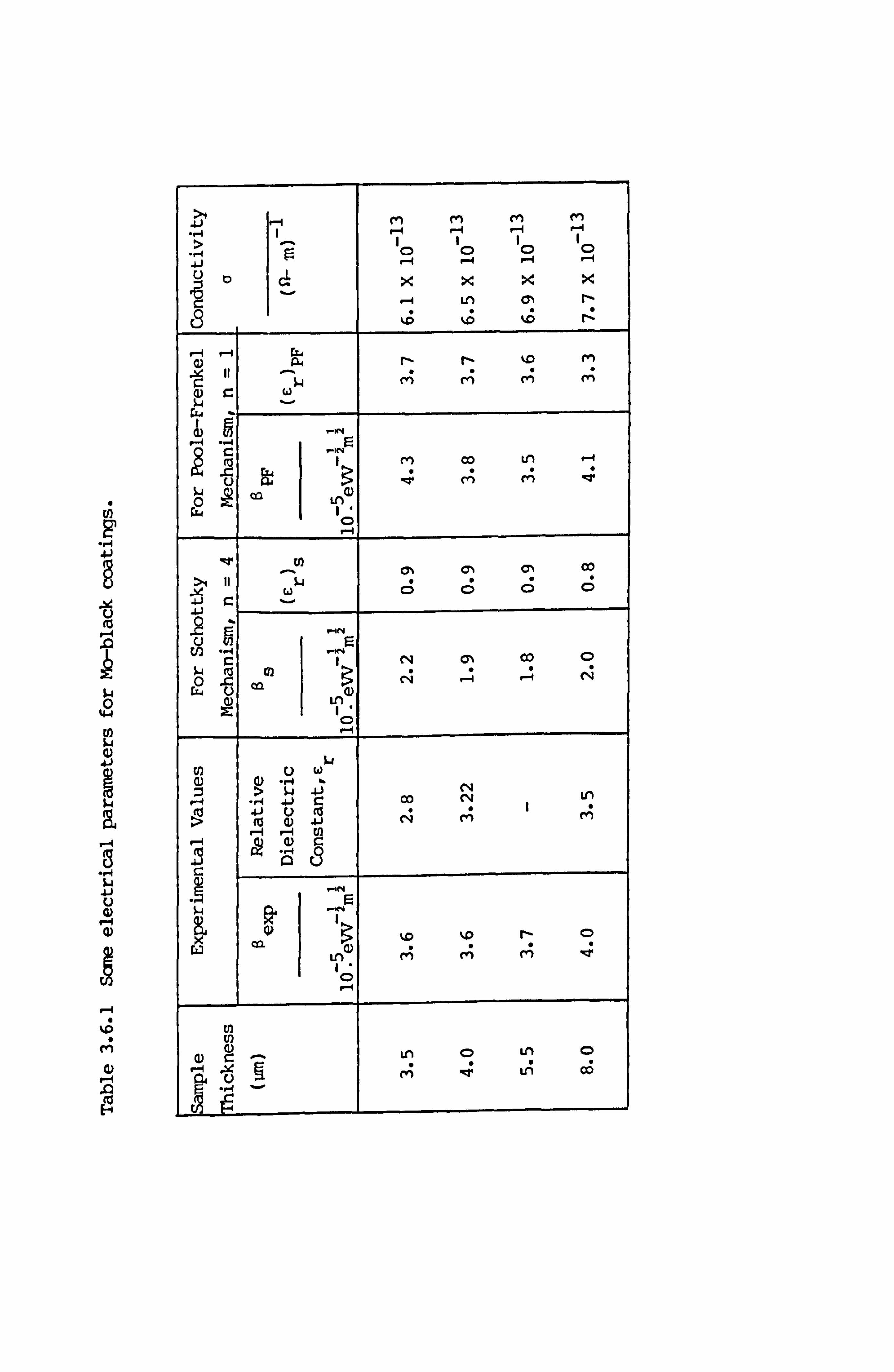
to r-4 .0
to
m
m a)
x
r -4 Ln (n r- _
%Z ýz ýz fz P4
- $4
(0 1 co Ln P-4
LnQ)
4wT El) 1ý 0% ON OD
ý4 L) CD C;
C14 OC) C>
a) Ln
CD
w
$4 41 cq 4J C: co CN LO
U)
& 4) kD kD r- CD
C, (ý 4 tn C4 1 1c;
En Ln Ln Q
LA 0;
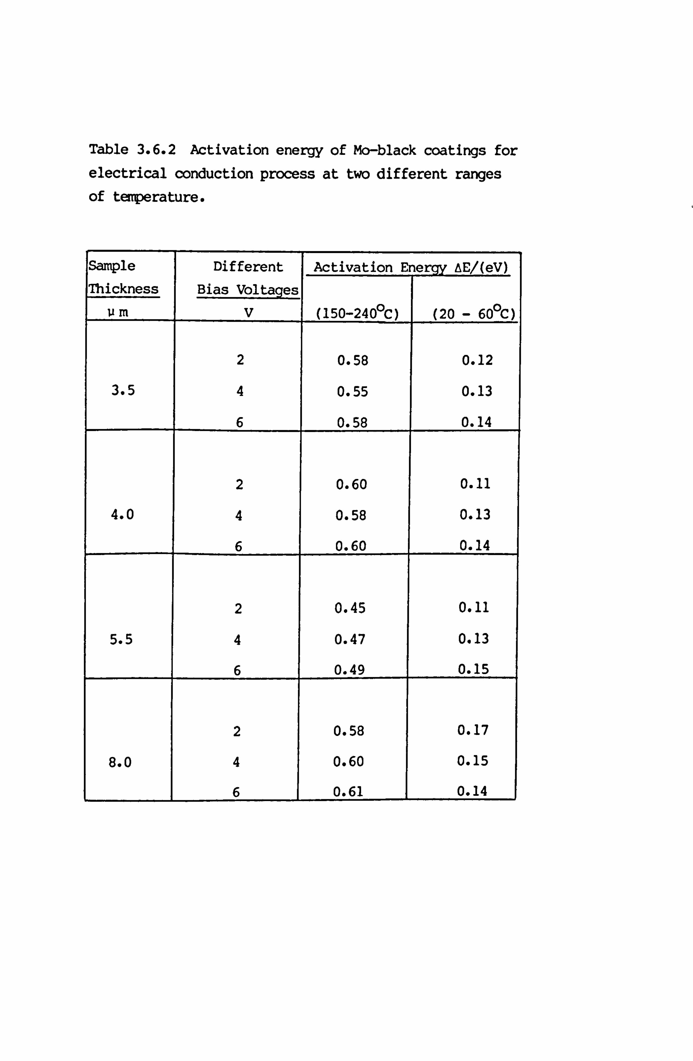
Table 3.6.2 Activation energy of Mo-black coatings for
electrical conduction process at two different ranges
of teqxrature.
Sample Different Activation ergy AE/(eV) Thickness Bias Voltages
VM V (150-24CPC) (20 - 600C)
2 0.58 0.12
3.5 4 0.55 0.13
6 0.58 0.14
2 0.60 0.11
4.0 4 0.58 0.13
6 0.60 0.14
2 0.45 0.11
5.5 4 0.47 0.13
6 0.49 0.15
2 0.58 0.17
8.0 4 0.60 0.15
6 0.61 0.14
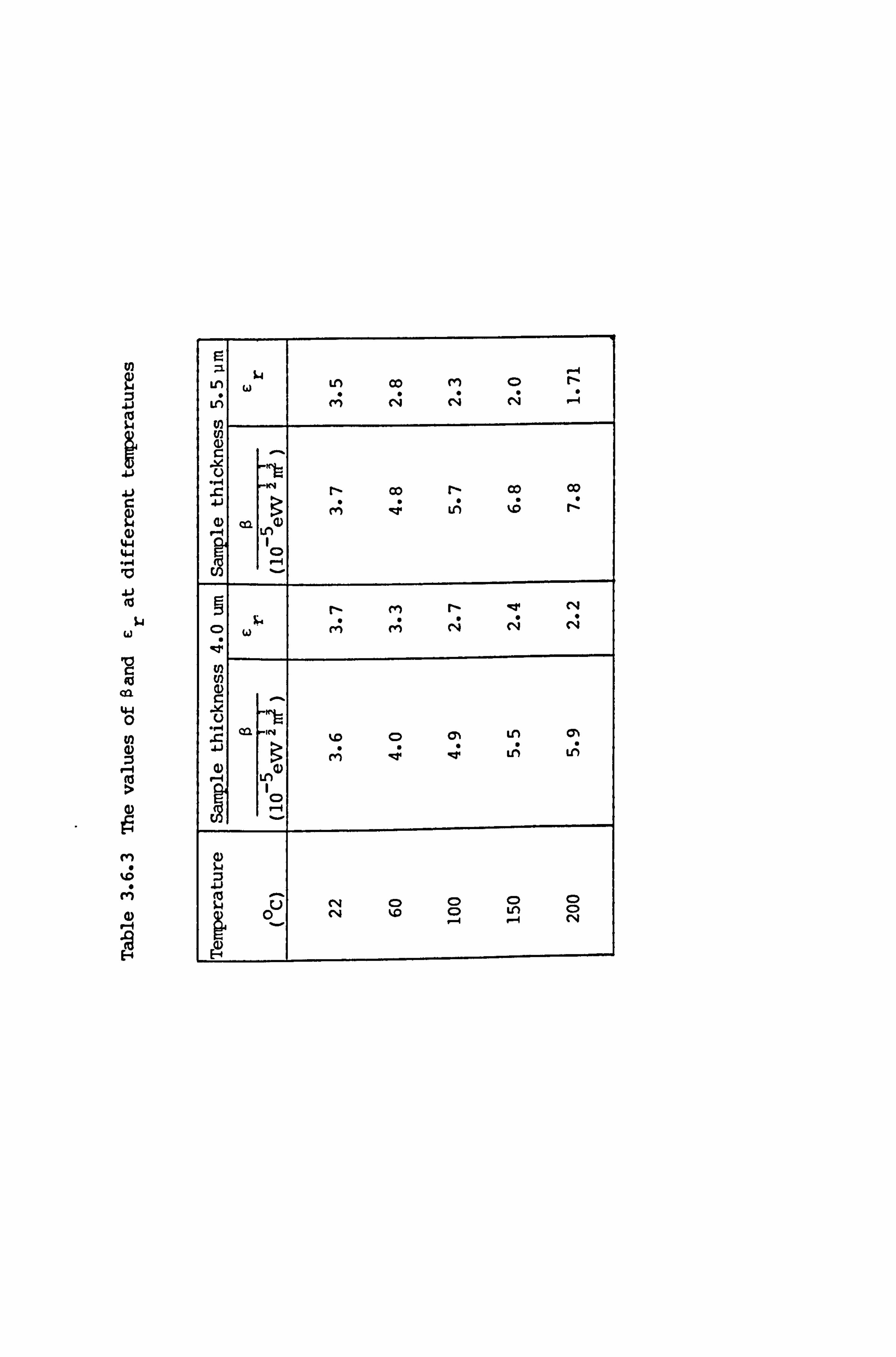
V)
to
1C3
10 c: du ca 44 0
to
0) 19
0
E-4
Ln Ln co 0 U; C4 C4 C4
U -4 X t- 00 tý co co
e) L CD
9 rý m r- -cr
4 C*4
4 (D W m m C4 C C Ef)
. 1-1 CLI Ln A
CIN ;
a) (D n .4 .4
L ti r L
CD
$04 -
Cýl CV
CNI C) ko
C) CD
4
CD C)
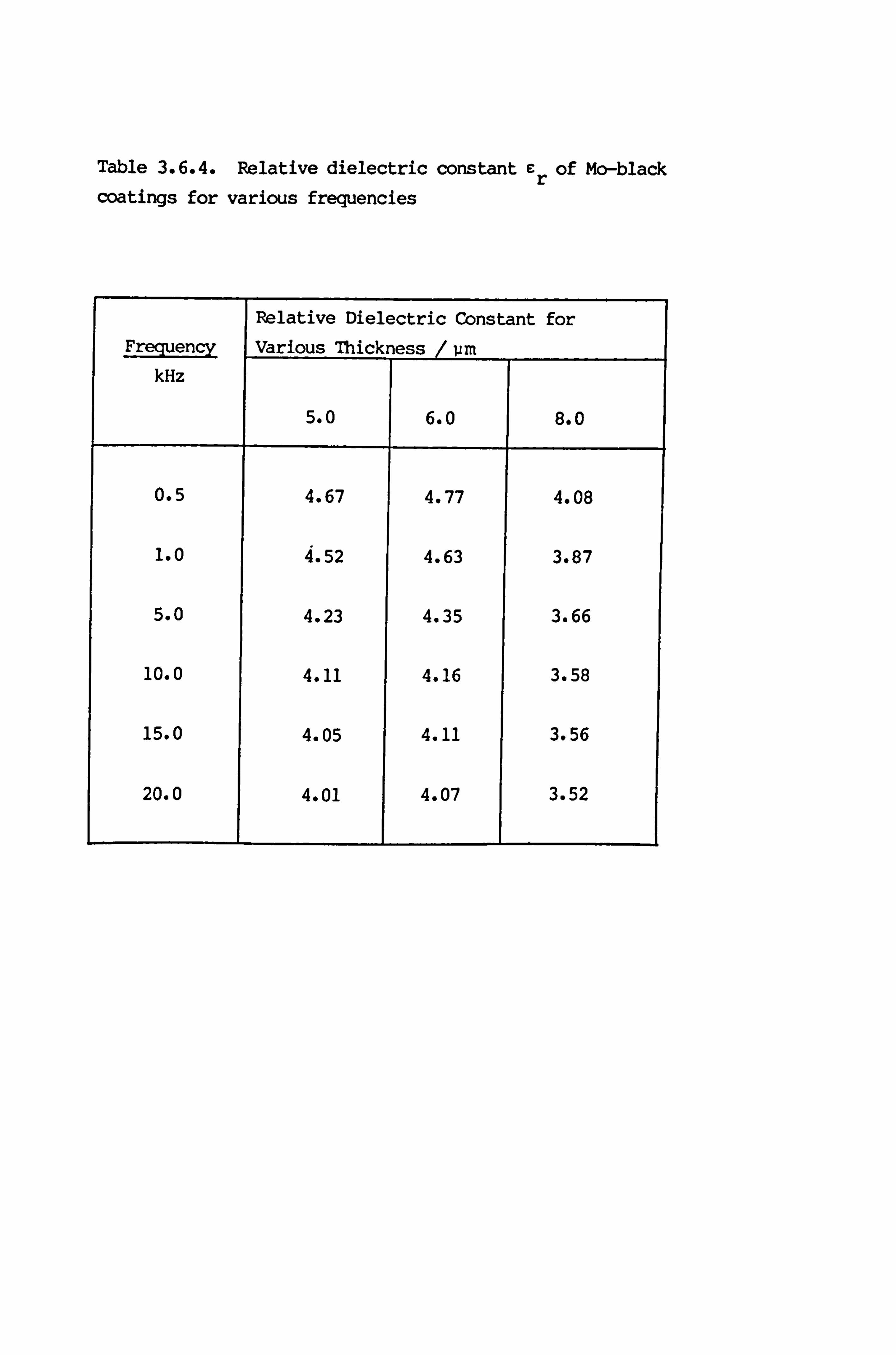
Table 3.6.4. Relative dielectric constant Er of Mo-black coatings for various frequencies
Frequency Relative Dielectric Constant for Various Thickness / Um
kHz
5.0 6.0 8.0
0.5 4.67 4.77 4.08
1.0 4.52 4.63 3.87
5.0 4.23 4.35 3.66
10.0 4.11 4.16 3.58
15.0 4.05 4.11 3.56
20.0 4.01 4.07 3.52
particular tenperatures).
The variation of dielectric constant er with temperature at various
frequencies is shown in Figs. 3.6.11(a-b). As the dielectric constant cr
is directly proportional to the capacitance for fixed coating thickness,
the variation of c with temperature and frequency is the sane as that of r
capacitance in Fig. 3.6.10. Fig. 3.6.12 shows the typical variation of
dielectric loss tan6 with frequency at different temperatures for a
coating of thickness 4 Pm. It can be seen that the dielectric loss
decreases with the increase of frequency and the variation is more
pronounced at low frequencies. Fig. 3.6.12 also shows that the dielectric
loss increases with the increase of temperature.
The capacitance measurements have also been performed before and af ter
annealing of the coatings. It has been observed that the capacitance
increases in all the samples after annealing of the coatings. Fig. 3.6.13
shows a typical variation of capacitance measured at room temperature with
frequency before and after annealing of a coating of thickness 4P m. The
dielectric constant at 20 kHz increased by 5.7% after annealing the
coating at 2400C for 2 hours.
3.7 Optical measuremnts
optical measurements in the UV and visible region have been made on thin
Mo-black coatings prepared by an electrodeposition method on
semitransparent aluminized glass substrates as described in section 2.5.
The objective of this study is to obtain an estimate of the
valence-conduction bandgap and the extent of any band tailing (Appendix
F).
83
The absorbance spectra for coatings of different thicknesses are shown in
Figs. 3.7.1 and 2 prepared at two different plating current densities. These
figures show that the fundamental absorption edge is exponential in
nature.
The absorption coefficient -a(w) has been calculated from the absorbance A
and film thickness d using the following relation (Longhurst, 1957):
a(w) = 2.303 (3.7.1)
The plots of (ahw) 1/2 as a function of tiw are shown in Figs. 3.7.3 and
4. These figures show a well defined linear region for the higher values
of absorption and thus satisfy the relation:
af1w = B(Tiw -E opt) 2 (3.7.2)
given by Tauc et al (1966) and Davis and Mott (1970). Here E opt
is the
optical energy gap and B is a constant. The values of E opt and B
estimated fran Figs. 3.7.3 and 4 are given in Table 3.7-1. The values of
optical band gap, Eopt, are obtained by extrapolating the linear region of
the curve to (a 11 w )1112 =0 and the square of the slope of these lines
give the value of the constant B.
7he values of band tails Ee are estimated frcm the Urbach (1953) relation:
a(w=a0 exp (11 w /Ee) (3.7.3)
where ao is a constant. Figs. 3.7.5 and 6 show the exponential behaviour
of the absorption edges, which are replotted from the experimental data of
84
Figs. Ii7.1 and 2 according to relation (3.7.3). The values of band tail
Ee estimated frcm, Figs. 3.7.5 and 6 are also included in Table 3.7.1.
Within this limited study, no systematic change of the optical band gap
with coating thickness has been observed. The main feature observed in
this study is the variation of E opt with the rate of deposition i. e. with
the plating current density. The mean values of E opt
for the coatings are
1.89 eV for slow deposition rate and 1.67 eV for rapid deposition rate.
The values of E opt are in fair agreement with the published value (1.75
eV) for Mo 40 11 (Hanafi et al, 1981). It is evident frcm Table 3.7.1 that
the E opt
decreases and Ee increases with the increase of rate of
deposition. This effect may be due to an increase of overall disorder
with the rapid rate of deposition. This supports the theory of Mott and
David (1971) which suggests that the extent of the localised states near
the mobility edge increases with the increase of disorder in the material.
Additionally, as the rate of deposition increases, deeper band tails of
the localised states extend to the gap and cause an increase in the value
of Ee and a decrease in the value of Eopto Similar effects have also been
observed in other oxide thin films by Shabalov and 5. eldmann (1983) and
Al-Ani et al (1984,1985). The values of the constant B from equation
(3.7.2) are of the order of 10 5 cm. -1 eV-l which is in reasonable agreement
with the theoretical value 10 5 to 10 6 cm -1 eV'-l (Mott and Davis, 1979).
The refractive index n has been estimated from the relation (Moss et al.,
1973)
12 2nd
12
(3.7.4)
85
where XI and X2 are the wavelengths of adjacent transmission maxima in
the absorbance vs wavelength curve (Figs. 3.7.1 and 2), d is the coating
thickness and n is the refractive index of the coating. The calculated
values of refractive index n for three coatings are listed in Table 3.7-1.
86
0 01
CO r-1 m
81
I .
(1)
rz Ln Ln
C) C)
41 Ju R I (a (IS
9 1ý llý cli C14
Ln m C) to Ln C4
> vlý CD
CD C> Ln
CD r- r- co
r-
8 C; 8 8
co ol
4J
0 a) I C) C) C) C14 C*4 LO
r_ (14 qw IT qw co
4 co 4
co 4
(a $4 r-I 1; 14 C C C
CHAPrER IV
STABILITY OF MO-BLACK COATINGS
Stability of selective surface propert; es is one of the most important
factors in selection of surfaces for solar thermal conversion. The
coatings for solar energy collectors must not only exhibit high solar
absorptance as and low thermal emittance E: th but should also be thermally
and mechanically stable. They should ideally retain effective as and c th
values within the operating temperature range of a solar collector
throughout its useful life time. The surface should be thermally,
chemically and mechanically stable under different environmental
conditions. It is difficult to assess actual lifetimes of the collectors.
However, the durability of the surfaces can be tested under the following
conditions: high humidity, condensation, thermal ageing at elevated
temperatures, temperature cycling, outdoor ageing, mechanical adhesion
testing.
In the present investigation, the influence of short term heat treatment
at elevated temperatures (up to 400 0 C) in both air and in vacuum on
optical properties and microstructures of Mo-black coatings has been
examined. A few coatings have also been tested after natural outdoor
ageing. As described in the previous chapter (Section 3.1.3) the
electrodeposited coatings are effectively non-selective, the stability
tests have therefore been performed on dip coatings.
Adhesion neasurements have been perfonmed on Mo-black coatings
87
electroplated on aluminiLn and attempted for dip coatings on zinc.
4.1 Mo-black coatings on zinc
4.1.1 Spectral reflectance
A number of Mo-black coatings on etched zinc substrates have been heat
treated in air at atmospheric pressure and in a vacuum of about 10-3 Pa at
tenperatures of 100,150,200 and 3000C for periods up to 4 to 24 hours.
Three to five samples have been tested at each tenperature. Generally no
significant changes in the solar absorptance 01 s and the thermal emittance
C th of the coatings have been observed in these short-term heat-treatment
tests (apart from in air at a temperature of 200 0C when the absorptance of
some coatings decreased by 2-5%). The values of as and c th for various
heat treatments in air are given in Table 4.1. Figs. 4.1(a, b) show the
spectral reflectance as a function of wavelength for two coatings after
heat treatment in air at 100 and 15CPC respectively. It can be seen that
the reflectance in the short wavelength region increases slightly after
heat treatment whereas in the NIR region it decreases. As a result the
solar absorptance a does not change significantly. On the other hand, s
coatings on unetched zinc deteriorate even after heat treatment for 8
hours at 150 0 C. Fig. 4.2 shows the effect of heat treatment on the
spectral reflectance spectra of a coating on unetched zinc. The
reflectance increases throughout the solar region resulting in a decrease
in absorptance from 0.75 to 0.70. Hosseini (1981) also reported that
these coatings degrade after heat treatment in air at 2800C for 3 hours.
Therefore, no further heat treatment at higher temperature has been done
on the coatings on unetched zinc. All the results given below are of the
coatings on etched zinc. The specular reflectance spectra in the IR
region (2.5 - 50 vm) before and after heat treatment in air at 100oC for
88
24 hours is shown in Fig. 4.3. This figure shows that the absorption band
(due to water) at 6.2 11m has almost disappeared after heat treatment and
the band at about 2.9 ýjm is drastically reduced. The slight decrease in
the emittance value after heat treatment may be due to the loss of water.
The effect of heat treatment at 20dOC in air on the spectral reflectance
of a coating is shown in Fig. 4.4. For this sample, it can be seen that
after the first 8 hours of heat treatment, the reflectance decreases in
the NIR region and increases slightly in the short wavelength region.
After 16 hours of heat treatment, the reflectance increases also in the
NIR region resulting in a slight decrease in the solar absorptance from
0.86 to 0.85. Fig. 4.5 shows the effect of heat treatment at 3060C for 4
hours on the spectral reflectance 'spectra. In the short wavelengh region
the reflectance increases considerably after heat treatment, but in the
NIR region the reflectance decreases drastically. No significant change
has therefore been observed in the values of a after heat treatment at S
30CPC. In same coatings the absorptance increases slightly. after heat
treatment, as shown in Table 4.2. Fig. 4.6 shows the reflectance spectra
of a coating after heat treatment at different temperatures and the values
of a' and Eth are tabulated in table 4.2. The corresponding specular S
reflectance spectra in the fR region is shown in Fig. 4.7. The f igure
shows that after heat treatment at 200 0C and 3000C the water peak
disappears.
The Mo-black coatings when heat treated in vacuum show no degradation at
all in this short term heat treatment test and in same cases a_ý increased
slightly and e th decreased. The effects of heat treatment in vacuum at
different teirperatures on the values of as and c th are displayed in Table
4.3. The spectral reflectance curve of the coatings after different heat
treatments are shown in Figs. 4.8-11. In most cases the reflectance
increases slightly in the short wavelength region and decreases in the NIR
89
region. The changes in the reflectance are more pronounced after heat
treatment at 3250C (Fig. 4.11). However, it has been observed that for
coatings on a zinc substrate etched with 50% HNO 3 the reflectance
increases slightly throughout the solar region. Fig. 4.9. shows the
effect of heat treatment on the spectral reflectance spectrum for one of
these coatings (corresponding to a solar absorptance as decrease fram 0.89
to 0.88). The thermal emittance c th also decreases as shown in Table 4.3.
Fig. 4.12 shows the spectral reflectance spectra of a coating after heat
treatment in vacuum at different temperatures and the values of as and
E th are given in Table 4.4. It can be seen that after these successive
heat treatments, the value of as increases by 2.3% where as c th decreases
by 5.8 %. Fig. 4.13 shows the effect of heat treatment on the IR
reflectance of the same sample. No absorption band for water can be seen
in the IR spectra after heat treatment at 30CPC.
4.1.2 Microstructure
The ef fect of heat treatment on the microstructure of the coatings has
been examined by scanning electron microscope (SEM) Figs-4.14 to 4.17
show typical surface microstructures before and after heat treatment at
dif ferent temperatures. No significant change in the surface structure
can be seen after heat treatment at 1060C for 24 hours (Fig. 4.15). By
ccnparing the as prepared structure (Fig. 4.14) with the structure after
heat treatment at 200 and 3000C (Figs-4.16-17)t it seems that heat
treatment causes a flattening of nodules i. e., they are still present, but
scme are less praninent. This may be the reason for the slight increase
in the reflectance in the short wavelength region. The fine cracks in the
as prepared coating becomes more prcminent and wider after heat treatment
at higher temperature. Some damaged areas have been observed in the
surface structure after heat treatment at higher temperatures as shown in
90
Fig. 4.18. Fig. 4.19 shows the surface structure of a coating prepared on
etched zinc with 50% HNO 3 for 8 hours. By ccrrparing the as prepared
surface with the heat treated surface, a decrease of surface roughness can
be seen after heat treatnent. This may account for a slight increase in
the reflectance (Fig. 4.9) of the coating.
4.2 Mo-black coatings on cobalt (NC) substrates
4.2.1 Spectral reflectance
Thermal stability testing of Mo-black coatings on cobalt (NC) substrates
has been performed in air at temperatures of 200,300 and 4000C for short
periods (2 -5 hours). Two samples have been tested at each temperature.
Coatings on cobalt substrates plated with and without addition agent have
been examined. The results obtained for various heat treatments are
tabulated in Table 4.5 and 4.6. The effects of heat treatment on spectral
reflectances of the coatings are shown in Figs. 4.20 - 22. It can be seen
that the reflectance of the coating generally increases slightly after
heat treatment. However, the very broad reflectance peak at about 1.1 Um
flattens somewhat. It may also be noticed that the changes in the
reflectance after heat treatment at 300 and 400 0C are less than that at
200 0 C. The solar absorptance as decreases only 0-1.1% after heat
treatment at 300 and 4000C but it decreases about 2.2% after heat
treatment at 2060C. It is evident from Table 4.5 that the emittance
decreases after all heat treatments for coatings prepared on cobalt (NC)
substrate plated without addition agent. Fig. 4.23 shows an example of an
IR reflectance increase after heat treatment. For coatings on cobalt (NC)
plated with addition agent, the emittance increases after heat treatment
(Table 4.6). Fig. 4.24 shows the IR reflectance spectra of a coating on
cobalt substrate plated with addition agent before and after heat
91
treatment in air at 3060C for 4 hours.
4.2.2 Microstructure
The surface structure of the coatings has been examined in SEM after heat
treatment. Fig. 4.25 shows a typical surface structure of a coating
prepared on cobalt plated without addition agent, before and after heat
treatment at 3000C for 5 hours. After heat treatmentr the crack width
increases and the limb-like features seem to be less conpact. Fig. 4.26
shows the microstructure of a coating prepared on cobalt substrate plated
with addition agent, before and after heat treatment at 3060C for 5 hours.
No significant changes have been observed except that the surface cracks
are scmewhat wider after heat treatment.
4.3 Outdoor testing
A few Mo-black coatings on etched zinc and cobalt (NC) substrates were
left in outside ambient air facing southward (with shelter frcm direct
rainf all --) for f ive months - Their solar absorptance and thermal
emittance have been remeasured. The values of the absorptance and
emittance of the coatings before and after outdoor testing are given in
Table 4.7. The coatings on etched zinc seem to be unchanged after outdoor
exposure. The spectral reflectance spectra in the solar region of one of
these coatings is shown in Fig. 4.27 before and after outdoor ageing. The
coatings on cobalt (NC) substratesp however, appear to be affected by the
external atmosphere. The absorptance of the coating on cobalt (NC) plated
without addition agent remains unchanged but it decreases for coatings on
cobalt plated with addition agent from 0.87 to 0.85 after outdoor ageing.
The IR reflectance of the coatings in both cases decreases giving an
increase of emittance (Table 4.7). Compared with the as prepared coating,
92
the surface appeared rougher and spotty. However, more samples should be
tested and the structural and compositional changes of the coatings (if
any) should be examined.
4.4 Adhesion measurement
It is well known that adhesion of a film to its substrate strongly depends
on the chemical nature, cleanliness and the microstructure of the
substrate (Chopra, 1969). The Mo-black coatings are quite adherent to the
substrates (aluminium, zinc and plated cobalt), when prepared under
appropriate conditions as described in section 2.1.
The adhesion of the Mo-black coatings prepared by electrodeposition on
aluminium substrate has been examined by using a Hounsfield Tenscmeter. A
schematic diagram of the testing arrangement is shown in Fig. 4.28- The
coatings have been prepared on a flanged cylinder or 'dolly' (made of
aluminium) following the same procedure as described in section 2.1.1.
They have been specially designed to fit into the adapting collets on the
Hounsfield Tensometer and also into the electrodeposition bath (Block,
1985). Ihe coated aluminium dolly was then stuck to another test dolly
using a two component adhesive (araldite) as shown in Fig. 4.28. b. The
araldite was left to cure for 24 hours under ambient conditions to reach
maximum strength. Then, using the Hounsfield Tenscmeter, the load was
applied to the adhered samples (Fig. 4.28) until the molybdenum coating
parted from the aluminium substrate. Readings have been taken
continuously during tests and recorded in the chart. The adhesion of
these coatings was in the range of 40 to 65 kg/cm 2 (depending on plating
current density). The adhesion of the coating decreased with the increase
of plating current density (Block, 1985).
93
An attempt was made to test the adhesion of Mo-black dip coatings on
etched zinc and cobalt (NC) substrates by using an Elccmeter 106 Adhesion
Tester. The photograph of this instrument is given in Fig. 4.29. The
instrument employs the pull-off method to measure the lift off force
required to pull a test dolly of a small area of coating away frcm the
substrate. The test dolly was attached to the coating using the same
method as described above (Fig. 4.28). After curing, the coating was cut
through around the base of the test dolly, the instrument claw was engaged
and then the pull-off force was applied until the dolly was removed from
the surface. The maximum pull off force achieved was recorded by
observing the position of the dragging indicator on the engraved scale.
Unfortunately, this adhesion measurement test was not satisfactory on
coatings on etched zinc or cobalt (NC) substrates. Only a very small
portion of the coatings was removed from the substrate in sane cases, and
in other cases, the failure between the adhesive and the dolly occurred in
the range 30 - 40 kg/cm 2.
Despite the microcracks in the coatings, they were mechanically stable.
The coatings did not peel or flake off even after heat treatment (apart
fran very thick coatings on highly polished zinc).
94
Table 4.1. Solar absorptance as and thermal emittance cth of Mo-black dip
coatings on etched zinc substrates after various heat treatment in air.
Temperature As prepared Period of Heat Treatment
of heat treat- 8 hours 16 hours 24 hours
ment/( 0 C) CIS c th as c th as c th as c th
100 0.87 0.14 0.87 0.14 0.87 0.15 0.86 0.13
150 0.85 0.13 0.85 0.12 0.85 0.12 0.85 0.12
200 0.86 0.17 0.86 0.15 0.85 0.14
300 0.87 0.14 0.87* 0.15*
* Heat treated for 4 hours.
Table 4.2. Solar absorptance a and thermal s
emittance c th of an air heat treated Mo-black coating
on etched zinc.
lRun no. Heat Treatment as c th
I As prepared 0.86 0.15
2 8 hours at 20CPC 0.86 0.14
3 4 hours at 3000C 0.88 0.14
Table 4.3 Solar absorptance as and thermal emittance c th of Mo-black dip coatings on etched zinc after heat treatment in vacuum.
Terrperature
lof
heat treat-
As prepared
I
__
Period of Heat Treatment
8 hours 16 hours 1 24 hours ment/( 0 C) a
s7 c th as c th I as cth as cth I
100 0.85 0.13 0.86 0.12
1
0.86 0.12 0.85 0.13 100** 0.89 0.30 0.88 0.25 0.88 0.23 0.88 0.24
200 0.86 0.14 0.86 0.14 0.86 0.13 -
325 0.87 0.14 0.87* 0.13*
Heat treated for 4 hours. ** The zinc substrate of this coating was etched with 50% HNO 3*
Table 4.4 Solar absorptance a and thermal emittance s 1h of a vacuum heat treated Mo-black dip coating on etched zinc.
Run no. Heat Treatment as c th
I As prepared 0.86 0.17
2 8 hours at 1500C 0.86 0.15
3 4 hours at 2000C 0.87 0.15
4 4 hours at 3250C 0.88 0.16
Table 4.5 Solar Absorptance a, and thermal emittance C S th of heat treated Mo-black dip coatings on cobalt (NC) substrates (without addition agent).
4eat Treatnent As Prepared After Heat
Treatnent
as c th as c th
hours at 2000C 0.91 0.25 0.89 0.25 0.92 0.30 0.90 0.28
5 hours at 3000C 0.94 0.29 0.94 0.24 0.90 0.26 0.89 0.21
2 hours at 40CPC 0.94 0.33 0.94 0.29
0.90 0.25 0.89 0.23
Table 4.6. Solar absorptance as and thermal emittance eth of heat treated Mo-black coatings on cobalt (NC) substrates (with addition agent).
Heat Treatment As Prepared After Heat
Treatment
Ols c th as c th
5 hours at 200 0C 0.88 0.19 0.86 0.21
0.89 0.13 0.88 0.17
5 hours at 300 0C 0.91 0.10 0.89 0.11
0.90 0.13 0.89 0.16
2 hours at 40CPC 0.89 0.13 0.89 0.16
0.88 0.20 0.88 0.20
Table 4.7. Effect of 5 months outdoor exposure on solar
absorptance cl s and thermal emittance E
th of Mo-black dip
coatings.
Substrate As Prepared After 5
Months
as C th as C th
Etched zinc 0.86 0.18 0.86 0.17
0.85 0.15 0.85 0.16
0.84 0.14 0.84 0.14
Cobalt (NC) plated 0.90 0.22 0.90 0.31
without addition
agent
Cobalt (NC) plated 0.87 0.13 0.85 0.16
with addition
agent
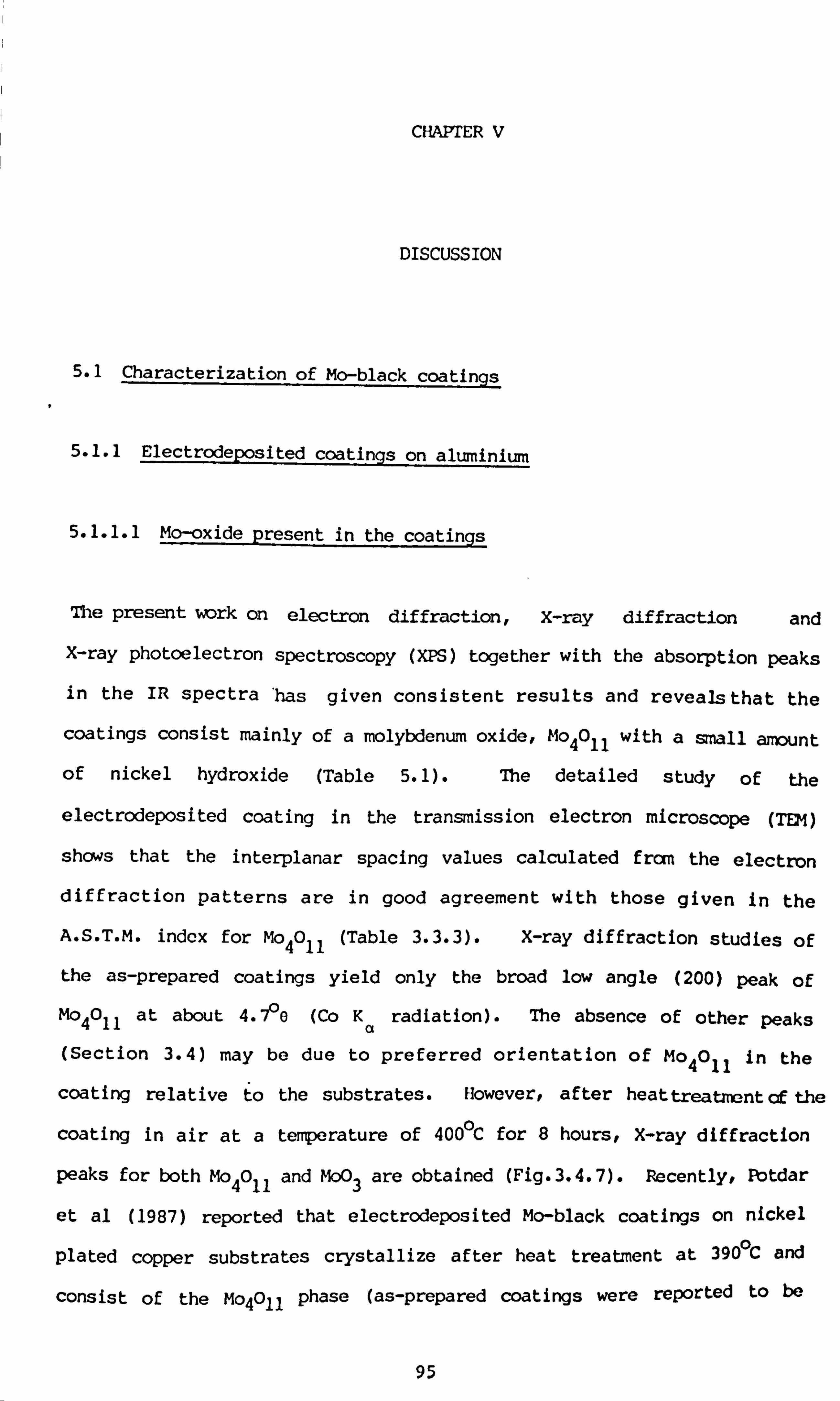
CHAPTER V
DISCUSSION
5.1 Characterization of Mo-black coatings
5.1.1 Electrodeposited coatinqs on aluminium
5.1.1.1 Mo-oxide present in the coatings
The present work on electron diffraction, x-ray diffraction and
X-ray photoelectron spectroscopy (XPS) together with the absorption peaks
in the IR spectra 'has given consistent results and revealsthat the
coatings consist mainly of a molybdenum oxide, M04 0 11 with a small amount
of nickel hydroxide (Table 5.1). The detailed study of the
electrodeposited coating in the transmission electron microscope (TEM)
shows that the interplanar spacing values calculated from the electron
diffraction patterns are in good agreement with those given in the
A. S. T. M. index for Mo 40 11 (Table 3.3.3). X-ray diffraction studies of
the as-prepared coatings yield only the broad low angle (200) peak of
MO 40 11 at about 4.70e (Co Ka radiation). The absence of other peaks
(Section 3.4) may be due to preferred orientation of Mo 40 11 in the
coating relative to the substrates. However, after heat treatment of the
coating in air at a temperature of 400 0C for 8 hours, X-ray diffraction
peaks for both Mo 40 11 and MoO 3 are obtained (Fig-3.4.7). Recently, Pbtdar
et al (1987) reported that electrodeposited Mo-black coatings on nickel
plated copper substrates crystallize after heat treatment at 3960C and
consist of the M04011 phase (as-prepared coatings were reported to be
95
amorphous). The SEM study of the electrodeposited coatings An this
work shows that they consist of rather smooth flat platelets with
widely spaced cracks.
5.1-1.2 XPS study
Evidence for the presence of Mo 40 11 in the coating is also available from
the XPS study (Section 3.5.2). This reveals that the oxidation state of
Mo in the coating is between +4 and +6. The basis of the chemical shift
of a core photoelectron peak is the change in the electrostatic potential
of the core electron when valence electron charge density is accepted or
withdrawn from the atom (Briggs and Seah, 1983). There is, therefore, a
relationship between the binding energy and the chemical state of the
element. Fig. 5.1 shows the plots of binding energy (B. E. ) for both
Mo(3d 3/2 ) and Mo (3d 5/2 ) peaks as a function of oxidation state of Mo.
This figure also includes the results obtained by Swartz and Hercules
(1971) and Cimino and Angelis (1975). In the present investigation, (in
contrast to the results of Swartz and Hercules), the variation of B. E.
with oxidation state is not linear. It is similar to that obtained by
Cimino and Angelis i. e., the binding energy values of MoO 2 are closer to
those of the metal than those of MoO 3* (However Fig. 5.1 shows that the
binding energy values obtained in the present study are different from
those obtained by Cimino and Angelis (1975). Ibis discrepancy may be due
to use of a reference value (284.9 eV) for the Cis pcak in the present
study while they used a value of 283.8 eV) Fig. 5.1 also shows that the
general trend in ý. E. as a function of oxidation state is identical for
both Mo(3d 3/2 ) and MoOd 5/2 ) levels. Using the binding energy value of
Mo(3d 5/2 ) for a Mo-black coating frcm Table 3.5.2, the estimated oxidation
state of Mo from Fig. 5.1 is +5.1. This oxidation state is fairly close to
the oxidation state of Mo 40 11 (+5.5) (Kennedy, 1972). It has been
reported by Hosseini (1981) that the oxidation state of MO in the
96
electrodeposited Mo-black coatings is +4. According to his data, the Mo
Od 3/2 ) peak of the coating has been shifted by 4.4 eV from the
corresponding peak of Mo-metal, which is close to the present data.
Comparing the B. E. of the Mo 3d doublet of standard MoO 2 (+4) and its
shift from Mo-metal (from published data and the present investigation) it
can be argued that the oxidation state of Mo in the coating is higher than
+4. Ihe presence of strong absorption bands other than those for water in
the IR region (Fig. 3.1.19) also rules out the possibility of the presence
of Moo 2 in the coatings (Section 5.1.2-2). Potdar et al (1982) reported
that the electrodeposited Mo-black coatings on nickel plated copper
substrates consist of the MoO 3 phase. This is not supported by the
present investigation. None of the X-ray diffraction, electron
diffraction or XPS results show evidence of MoO 3 in the as prepared
coatings. After heat treatnient of the coatings in air at high tenperatures
(400'C) the shift of the Mo3d5/2Peak from the corresponding peak
of Mo-metal is 5.8 eV (Section 3.5.2). The shift in B. E. and also the
shape of the Mo 3d doublet of the air heated coating (Fig. 3.5.9) is quite
similar to that of MoO 3* This indicates that after heating in air, the
surface of the coating oxidizes to M003*
Me vacuum heated coatings do not show a significant change in the B. E. of
the Mo 3d doublet, but the peak is comparatively less resolved which way
indicate the presence of more than one valency state of molybdenum. It
may be possible that after heat treatment in vacuum, some Mo (+S) in the
coating reduces to +4, via dehydroxylation (Patterson et al, 1976):
0 OH OH 0 - HP 00 0
mo + Mo mo + Mo
(V) M (VI) (IV)
The depth prof ile of the coating has been studied by, bonbarding with
Ar+ions. However, the results are not fruitful. After bombardment of
97
the coating surface, it has been observed that Mo 3d doublet shifts
towards a low binding energy, which corresponds to MoO 2 (Table 3.5.5).
Sputtering of f of water molecules by Ar + may account for this change in
B. E. However, reduction of the oxide to the lower oxidation state by Ar +
etching is very common for most of the metal oxides (Briggs, 1978). Sane
oxides even reduce to the metal (Kim and Winograd, 1974). However, it has
been reported by Kim et al (1974) that in the case of MoO 3, after
prolonged bombardment with Ar ions, the final product is MoO A similar 2*
effect has also been observed in the present investigation. It is
therefore unlikely that the observed shift in the binding energy of the Mo
3d doublet is due to an actual variation in the oxidation state of Mo with
depth in the coatings.
5.1.2 Dip coatings on zinc
5.1.2.1 Structure and ccmpositional analysis
The structure and composition of the Mo-black dip coatings on zinc
substrates have been studied by XPS, SEM, X-ray and electron diffraction.
The results of these investigations are given in Chapter In in detail.
Because of the strong adhesion of the coatings to the zinc substrates, it
is not possible to do any transmission electron microscopy. The
reflection electron diffraction (RED) study of the coatings indicates
their polycrystalline nature. However, the rings are spotty, Possibly due
to the presence of a small number of large crystallites (Cullity, 1967).
The interplanar spacing values deduced from RED give evidence for the
presence of Mo 40 11 (Table 3.3.1) in the coatings.
XPS studies of the as prepared dip coatings give results similar to those
obtained for the electrodeposited coatings, i. e., the oxidation state of
98
Mo in the coatings is between +4 and +6. There is no significant
difference between the B. E. of the Mo 3d doublet for coatings on etched
and unetched zinc. The estimated oxidation state of Mo in the coating is
about +5 frcm Fig. 5-Ij which is consistent with the presence of Mo 40 11 -
The coatings on zinc substrates are more sensitive to heat treatment in
air as well as in vacuum. The coating oxidizes to +6 oxidation state
(MOO 3) when heated in air. The shifts in B. E. of Mo 3d doublet after heat
treatment under various conditions are given in Table 3.5.3. This shows
that coatings on etched zinc substrates are more resistant to oxidation
than the coatings on unetched zinc substrates. The shift in the B. E. of
Mo 3d doublet depends upon the temperature of heat treatment. The B. E. of
Mo 3d 5/2 electrons of the coatings on etched zinc has been shifted from
231.4 eV to 235.6 eV when heated at 3900C in air for 2 hours. The same
amount of shift in the B. E. of Mo 3d 5/2 electrons has been observed for
coatings on unetched zinc substrate when heated at lower temperature
(2060C) for the same time. The dip coatings reduce readily to thelower
oxidation state (+4) when heated in vacuum,, unlike the electrodeposited
coatings. No significant change in the oxidation state of Mo has been
seen after heat treatment in vacuum at a temperature of 1000C. However
when the coating is heated above 200 0C in vacuum, the shift in B. E. of Mo
3d 5/2 peak of the coating is 2.2 eV from the corresponding peak of
Mo-metal. The same amount of shift in B. E. has been observed for M002
(Table 3.5.1) . As zinc is a low melting point metal, heating of the
coating may lead to diffusion of zinc through the coating. The coating
might then be reduced to a lower oxidation state by zinc according to the
following reaction (Verchere and Fluery, 1973):
Mo(V) oxide + Zn = Mo(IV) + ZnO
The reduction of Mo(VI) to Mo(IV) using Zn metal has also been reported by
99
Haight (1953).
Argon (Ar +) ion bombardment has been used to study the depth prof ile of
the coatings. After etching, the B. E. of the Mo 3d doublet is shifted
towards that of MoO 2 (Table 3.5.5) as in the electrodeposited coatings.
No shift in B. E. beyond MoO 2 (+4) has been observed after a prolonged time
of bombardment. It has also been observed that the B. E. of Mo 3d doublet
of a vacuum heated coating, which is already in +4 oxidation state (moo 2
phase), does not shift after Ar + bombardment. These results are in
agreement with the results reported by Kim et al (1974). According to
them, MoO 2 cannot be decomposed by Ar + bombardment. The above results
reveal that the as-prepared Mo-black coating is not in the M002 phase.
Mie elemental couposition of the mo-black dip ooatings has been detemined
from the XPS measurements. The atomic percentage of oxygen in the coating
is about 72% (Table 3.5.6). This is also consistent with the presence of
M04011 in the coatings. After etching with Ar + ions, the percentage of
oxygen reduces to 57%. The atomic percentages of Mop Zn and 02 in a thin
coating are shown in Fig. 3.5.25 as a function of etching time. The
reduction of oxygen content in the first few minutes of etching may be due
to the reduction of the coating material to the lower oxidation state by
the ion bombardment. In the present investigation, it has been observed the
that the percentage of zinc decreases slightly for I first few minutes of
etching and then remains the same until the substrate is exposed by
thinning of the coating (Fig. 3.5.25). The reason for the initial decrease
of zinc signal may be due to healing up of the cracks by Ar + bombardment.
Briggs and Seah (1983) also reported that argon ion bombardment can induce
changes in surface topography.
100
5.1.2.2 Infrared spectra
The IR spectra of a thick Mo-black dip coating on zinc shows strong
absorption bands in the region 10 to 23, Tjm (Fig. 3.1.8). These absorption
bands are also observed in the IR spectra of electrodeposited Mo-black
coatings.
To identify these absorption peaks, IR absorption spectra of standard Moo 3 and Moo 2 powder have been examined af ter ccopression into a disc formed
with a KBr binder. Fig. 5.2 compares the IR spectra of standard M003
powder with those of Mo-black coatings. The position of the absorption
peaks are tabulated in Table 5.2. Those for Moo 3 are very close to the
published data (Hanafi et al, 1975; Barraclough and Stals, 1966). No
significant absorption peaks were identified in the IR spectra of moo 2' It has been reported by Hanafi et al (1975) that Moo 2 has weak absorption
bands at 10.2,10.5 and 11.2tim only. In Mo-black coatings the absorption
bands are at about 10.5,11.7,14.5,20.3 and 21.5 um (Table 5.2). Not
all of these vibrational frequencies correspond to those of Moo 3. Unfortunately, no information is available concerning the IR absorption
spectrum of Mo 40 11 (which is thought to be present in the Mo-black
coatings). However, Hanafi et al (1975) studied the IR absorption of Moo 3
and its suboxides including Moo 2 (except Mo 4 011)- According to them most
of the bands of Moo 3 still occur in the intermediate oxides. The
behaviour of intermediate oxides changes gradually from that of M003
towards that of Moo 2* The band at 10.5 jim in the suboxides may be an
indication for the presence of an oxidation state of Mo lower than that of
moo 3* The absorption peaks at about 10.5,11.7 and 21.5 jim of Mo-black
coatings appear in the intermediate oxides between Moo 2 and M003 (Hanafi
et al, 1975). The strong absorption peak at 10.5 Um is attributed to the
M6--O stretching frequency. 7he bands at longer wavelengths are assigned
101
to stretching vibrations of Mo-O-Mo-O-Mo chains (Barraclough and Stals,
1966). The strong absorption peak at about 14.3 ým, which is not found in
the spectra of other oxides of Mo (as reported in literature), may be
related to the crystal structure of M04011 (Section 1.3.1).
5.1.2.3 Micranorphology
The surface topography of Mo-black dip coatings depends upon the
pretreatment of zinc substrate. A detailed study of the surface
microstructures of the coating in the SEM and optical microscopy reveals
the following factors:
(a) The surface topography of the dip coatings on mechanically polished
zinc substrates is quite similar to that of electrodeposited coatingsr
i. e., anooth platelet structure with widely spaced cracks (Fig. 3.2.13).
(b) The as-deposited naturally dried coating does not show any cracks in
the surface, when viewed in the optical microscope (Fig. 3.2.18-21).
Cracks develop after applying hot air on the coating surface (approximate
temperature 55-00C). It has also been observed that the cracks are more
likely to be nucleated from the surface defects such as pits (Fig. 3-2-24).
(c) Very thin coatings do not show any cracks in the surface even after
applying hot air and/or when viewed in the SEM (Fig. 3.2.25).
(d) Except for very thin coatings, all coatings show a cracked surface in
the SEM. These my be due to the heating produced by electron
bcmbardment.
Cracks in the Mo-black coatings may, therefore, be due to thermal
102
expansion mismatch between the coating and the substrate (Kramer, 1983) or
due to loss of some water fran the coatings.
(e) The surface of the coatings prepared on etched zinc substrates shows
a nodular structure (Jahan and Smith, 1986). The size and distribution of
the nodules depend upon the concentration of the etchant and etching time
and also the thickness of the Mo-black coating as described in section
3.2.2. By ccimparing the microstructure of the etched zinc substrate, it
seems that the morphology of the coatings is related to the topography of
the etched zinc susbtrates.
The carpositional analysis of the coatings by electron probe microanalysis
shows that the coating consists mainly of molybdenum with small amounts of
nickel (Table 3.2.2). However, EDX spectra also show zinc signals which
may originate from the zinc substrate through the coatings and also
through cracks. Ihe decrease of zinc signal with the increase of (coating
mass/area), i. e., thickness (Table 3.2-3) also reveals that the zinc is
caning from the substrate.
Information concerning the surface topography has been obtained using the
Talysurf surface measuring instrument which was also used to estimate the
thickness of the coatings. The surface profiles obtained across the
centres of the Mo-black dip coatings on etched and unetched zinc
substrates are shown in Fig. 5.3. Fran the Talysurf scanj, the centre line
average roughness values have obtained and are given in Table 5.3. It
should be mentioned here that the surface profiling stylus used in the
measurements had a tip of radius 2.5 um and hence only features coarser
than this would be observed. Table 5.3. shows that the roughness value is
higher for coatings prepared on etched zinc substrates.
103
5.1.3 Mo-black dip coatings on cobalt (NC) substrates
5.1.3.1 Structural and ccmpositional analysis
Due to strong adhesion of the coatings to the cobalt substrates, it was
not possible to do any transmission electron microscopy studies. The
reflection electron diffraction patterns of these coatings show rings for
the cobalt layer only. The interplanar spacing values calculated from the
ring diameter correspond to metallic cobalt and cobalt oxide (Table
3.3.2). X-ray diffraction peaks from these coatings are due to the
substrate, cobalt and nickel, i. e., both are in the metallic state. A
broad low angle peak has also been observed in the X-ray diffraction
pattern at about ýoe (with Co K radiation) (Fig. 3.4.4). a
RED patterns show the presence of cobalt oxide with metallic cobalt,
whereas, the X-ray study reveals the presence of metallic cobalt only. It
is not unusual to have scme oxide on the surface of metallic cobalt and
(in ccrnparison to X-rays) the electrons penetrate only a relatively short
distance into the material Mittel, 1968).
The results of the XPS study of the coatings on cobalt (NC) substrates
have been given in Section 3.5.4. The B. E. of Mo 3d doublet Of this
coating is 0.5 eV higher than that for coatings on aluminium and zinc.
The doublet is also sharper than for coatings on other substrates. From
Fig. 5.1, the estimated oxidation state of molybdenum is +5.4, which is
close to the oxidation state of Mo 40 11 (Kennedy, 1972). The coatings on
cobalt seem to be more resistant to heat treatment. A small increase in
B. E. (0.3 eV) of Mo 3d doublet has been observed after heat treatment in
air at 4000C for 2 hours. (The Mo 3d peaks are sharper and better
resolved (Fig. 3.5.29)). After heat treatment inside the spectrcmeter at
104
300 0C for 2 hours, the Mo 3d doublet shif ts by 0.3 eV towards the lower
oxidation state. 1he doublet is somewhat broader which may indicate that
some Mo M reduces to the lower oxidation state via dehydroxylation (as
for coatings on aluminium substrate4. Ar + bombardment has the same effect
on the B. E. of Mo 3d doublet, i. e., it shifts towards the lower binding
energy (+4 oxidation state). This is thought to be an etching effect.
The marked reduction of the intensity oftheCls level after etching
indicates that the carbon is only surface contamination (Fig. 3.5.26 and
30). The XPS study of these coatings shows the presence of a small amount
of cobalt in the coatings. However, it is not clear whether the cobalt
signal is coming from the cobalt underlayer through the cracks in the
coatings or is already present in the Mo-black coatings. The ratio of Mo
to Co in the coating was found to be 4.55. The ratio of Mo to Co in the
present coating is higher than that obtained by Smith and Teytz (1984).
They reported that in an outer layer of about 80 M, the ratio of Mo to Co
is 2.0 and af ter that it becomes 1.18. The higher percentage of Co in
their coatings may be due to use of a different plating solution for
Mo-black. Instead of nickel sulphate (used in present investigation),
they Used cobalt sulphate. So it is more likely that cobalt is deposited
with molybdenum oxide. They suggested the composition Of the coatings is
close to Morý2 or MoCo(OH2). It might also be a compound containing
COP3 mixed with a molybdenum oxide. In the present investigation the
ratio of Mo/Co/0 is found to 1/0.23/2.73 on the surface. 7he ratio of Mo
to 0 is similar to that in Mo 40 ll* After etching 10 minutes by Ar + ions
the ratio becomes 1/0.21/1.84. After that the ratio of the elements
remain approximately constant up to 370 minutes etching (thickness
37(A).
The infrared spectra of the coatings on cobalt (Fig. 3-1-10) show the main
absorption peaks more or less in the same position (10-5t 11.7 and
105
14.3 wn) as for coatings on zinc and aluminium. This may indicate that
the coatings on cobalt also contain M04 0 110
5.1-3.2 Micrcmorphology
The Mo-black dip coatings on cobalt (NC) substrates have been prepared
from the same solution of anT=ium molybdate and nickel sulphate as used the forlpreparation of coatings on zinc. However, the solution temperature is
comparatively high (60-80 0 C) as described in Section 2.1.2.5. A wide
range of surface microstructures of such coatings have been observed by
varying the preparation conditions of Mo-black as well as initial cobalt
layer (Section 3.2.3). This leads to a corresponding variation in the
thermal radiative properties of the coatings. The morphology of the
coatings seems to replicate the structure of the plated cobalt layer which
changes with the plating current density and solution temperature. In the
present investigation three different types of surface structure have been
observed:
(a) After plating at a solution temperature Of 50-600C the surface of the
cobalt layer has platelet structures of different sizes orientated in
different directions (Fig. 3.2.56) and alrx6t perpendicular to the
substrate. The Mo-black coatings on this cobalt surface consist of limb
like structures oriented randomly, forming microcavities on the surface
(Fig-3.2-53). These features become thicker when the cobalt plating
current density deposition time are increased.
(b) By using an addition agent (Na-lauryl sulphate) in the plating
solution of cobalt, the surface structure of the cobalt can be modified
into a rather smooth surface. (This has a brighter appearance). An SEM
micrograph shows that the platelets are less densely distributed and also
106
shows small flake-like protruberences (Fig. 3-2.58). Mo-black coatings On
this type of cobalt have a nodular structure (Fig. 3.2-57). Howeverr the
surface of the coating changes to a rather smooth platelet structure
(Fig. 3-2.60) when prepared at a high temperature (800C) and/or for longer
times of deposition. This smooth surface is probably due to the high
thickness of the coatings.
(c) The cobalt layer prepared at a ccnparatively low temperature (450C)
and with low current density (-25mA/an 2) consists of a large number of
small f lake like protruberences. The Mo-black coatings prepared on this
type of substrate have nodules of submicron size (Fig. 3.2.62).
The surface profiles were obtained from the Talysurf instrument for
Mo-black coatings on two types of cobalt (NC) substrate, i. e., plated with
and without addition agent. These are shown in Fig. 5.4. The CLA
roughness values of the coatings are given in Table 5.3. It can be seen
that the roughness value of the coating decreases fram 0.3 jim to 0.13 um.
after using the addition agent in the plating solution of cobalt.
5.2 lhermal radiative properties of Mo-black coatings and their relation
to other properties
5.2.1 Electrodeposited coatinqs on aluminium
The electrodeposited coatings are effectively non-selective. Although
these coatings exhibit moderate absorptance (0.86 - 0.87), the attainable
selectivity is 1.4 - 1.9 (Section 3.1.3). As the coating mass per unit
area (i. e., thickness) increases, both the solar absorptance as and
thermal emittance cth increase. The emittance is more strongly
influenced by coating thickness than is absorptance (Fig. 3.1-18).
107
Me spectral reflectance spectra (Fig. 3.1.17) show that the coating has
strong absorption (0.90 - 0.91) in the visible region and in this region
the reflectance does not change significantly with thickness or
wavelength. In the near-infrared (NIR) region the reflectance increases
with wavelength and also beccmes thickness dependent. It can be seen that
the transition between low reflectance and high reflectance takes place
around 0.9 - 1.1 U m. Ihis cut off wavelength slightly shifts towards
higher wavelengths with increase of coating thickness. According to Fosch
(1956) and Christie (1970), the onset of linear increase of the
reflectance can be taken as a measure of the forbidden energy gap E9. For
coating of the optimum properties the abrupt transition has been observed
at about 1.1 um which corresponds to an energy gap of 1.13 eV. High
absorption occurs when the incident photon energy is sufficient to excite
the valence electrons into the conduction band. Photons containing less
energy than the gap energy will not be absorbed. This accounts for the
abrupt transition in absorption in the near infrared region.
The forbidden energy gap E9 of the coating material has also been
estimated according to Kubelka-Munk (K-m) theory (1938,1948). According
to K-M theory, the total diffuse reflectance from a semi-infinite layer of
material R will be related to the ratio a/s as follows: co
Co ctls =F (R
2 R.
where a and s are the absorption and scattering coefficients respectivelY-
F(R,,, ) for any reflectance is called the Kubelka-Munk function.
K-M theory has been successfully used to estimate the absorption edge of
108
Powder and polycrystalline sanples (Nozik, 1972; Hanaf i et al, 1981;
Golestani-Fard et al, 1983). Waring and Hzu (1983) have used the diffuse
reflectance technique to study the absorption edge in pigments. A few
reports have also been found on use of diffuse reflectance of thin films
to study the absorption edge (De Chelle et al, 1984; Al-Ani, 1984; Tandon
and Gupta, 1970).
Fig. 5.5 shows plots of the K-M function F (R 40
) as a function of of a thick
Mo-black coating (-8 um) prepared on a rough aluminium substrate,
According to Tandon and Wpta (1970) the energy co-ordinate of the point
on low energy side of the curve at which the linear increase in F(R 00
)
starts is the value of the forbidden energy gap of the material. The
point at which the linear variation in F(R .)
(i. e., increase of : a) starts
gives the value of E9 (as the absorption starts when the incident photon
energy hv is sufficient to excite the valence electrons into the
conduction band i. e., E9= hv ). For mo-black coatings (Fig. 5.5), the
estimated value of E9 is about 0.85 eV. The wavelength corresponding to
this bandgap ener-gy is 1.46 um. Therefore the incident photons with
energy higher than 0.85 eV should be highly absorbed in the coatings and
the photons with energy less than 0.85 eV should not be absorbed. The
reflectance spectra of the coatings (Fig. 3.1-17) show an abrupt
transition at a lower wavelength C 1.1 Vm)- The absorptance of the
coating can be increased if by scme means, the absorption edge can be
shifted to a higher wavelength (- 2.5 lim) (Lanpert 1979).
The nonselectivity of the electrodeposited Mo-black coatings is mainly due
to their high emittance value (0.4 - 0-7)- It has been suggested by
Smith et al (1983) that to get high selectivity values, the absorbing film
thickness should not be greater than 1-2 um, unless the films are very
porous. In the present investigation, the thickness of the Mo-black
109
coatings on aluminium substrates is greater than 2 um. Due to the high
thickness, strong absorption bands in the infrared region have been
observed in the reflectance spectra of the coating (Fig. 3.1.19). The
absorption bands around 2.9 - 3.1 jim and at 6.2 Vm give evidence for the
presence of water (Nakarnoto, 1970). A very broad and strong absorption
band in the region 10.1 - 22 Um. (975-450 an-') is due to the absorption in
the coating material. (These peaks are absent in the IR spectra of thin
Mo-black coatings on zinc and cobalt substrates (Section 3.1.1 and 3.1-2).
The results obtained from electrodeposited Mo-black coatings are
consistent with the results obtained by Hosseini (1981). The Mo-black
coatings prepared on copper substrates studied by INCRA (1977) exhibited
less selectivity. Me absorptance of these coatings varied between 40 -
60% and thermal emittance in the range 30 - 70%. Potdar et al (1982)
prepared Mo-black coatings on nickel plated copper substrate by the
electrodeposition method and reported moderate absorptance (85%) and a low
thermal emittance (11%). The low emittance of this coating was said to be
due to the low thickness - O. lijm.
Me radiative properties of Mo-black film prepared by the chemical vapour
deposition (CVD) method (Carver, 1979, Chain et al, 1980,1981) are quite
different from those of the electrodeposited coatings. Me CVD Mo-black
film exhibits a solar absorptance of 0.77 and a thermal emittance of 0.44.
Post deposition annealing inareducing atnosphere and overcoating with
Si 3N4 increases the absorptance to 0.82 and also reduces the emittance to
0.08 (Carver, 1979). The abrupt changes in the thermal emittance during
annealing are explained by Carver (1979) as being due to a large increase
of electrical conductivity together with structural changes. 7he
ccmPosition of the Mo-black film prepared by the CVD method is quite
different from that prepared by electrodeposition methods. Films prepared
110
by CVD consist of an MoO 2 matrix with smaller Mo-inclusionsj, i. e., a
cermet. Coatings prepared by electrodeposition are mainly oxides of
molybdenum. According to Potdar et al (1982) Mo-black consists of MOO 3'
Smith et al (1981) suggested that the coatings consist of MOO 2* 2H20. From
the present investigation it is concluded that the coatings my contain
Mo 40 11 (Section 5.1.1) together with water. The non metallic portion of
Moo 2 in the CVD film is a conducting oxide but the Mo-oxide in the present
study is found to be a high resistance semiconductor (Section 3.6).
However, the radiative properties of the present coatings are comparable
with those of as-deposited CVD films ( 01 s/e th = 0.87/0-6 and 0.77/0.44
respectively). Wring annealing in the reducing atmosphere, the oxide
Moo 2 of CVD films partially reduces to Mo-metal which can suppress thermal
emittance drastically. In the present coatings, there is no evidence of
the presence of metallic Mo or any other metal, which could enhance the IR
reflectance. The coatings therefore exhibit a. high emittance due to high
thickness. The presence of a large amount of water, (Fig-3.1.19), is also
another reason for high emittances.
The surface topography of the electrodeposited Mo-black coatings (Section
3.2.1) corresponds to a rather smooth platelet structure. No surface
features exist on the scale of the wavelengths of interest which would
enhance absorption by multiple reflection. As these coatings are
relatively thick compared to the wavelength of solar radiation, no
interference peaks have been observed in the reflectance spectra which
could enhance the absorption. However, the wavelength dependence of the
optical constants of the coating might contribute to the wavelength
selectivity of reflectance. According to Williams et al (1963) for a
thick homogeneous coating (when the interference effect is absent), the
reflectance is given by:
III
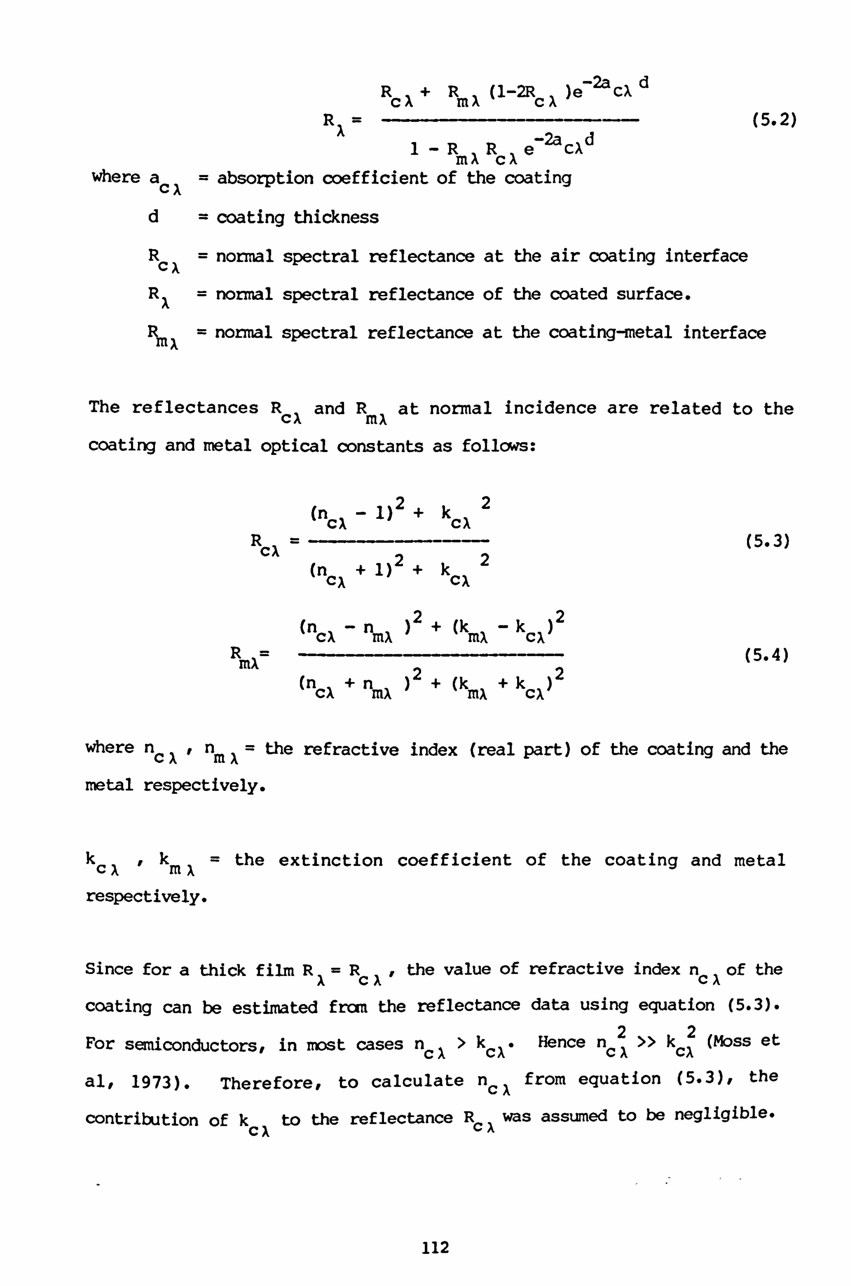
R=
R+R (1-2R )e -2acx d CX m ), cI
I-RRe -2a Cx d
mx cl where a C), = absorption coefficient of the coating
d= coating thickness
Rc normal spectral reflectance at the air coating interface
RX normal spectral reflectance of the coated surface.
(5.2)
R= normal spectral reflectance at the coating-metal interface mx
The reflectances R cl and R
mx at normal incidence are related to the
coating and metal optical constants as follows:
(n cx
1) +k CX R C, ý
(nc X+
1)2 +kcx2
(5.3)
(n cx _ %X )2 + (kmX - kc, ) 2
R=- (5.4) MÄ
(n cx +n
MÄ )2+ (k
MÄ +k CX)
2
where nc X, nm X= the refractive index (real part) of the coating and the
metal respectively.
kcX, kmX= the extinction coefficient of the coating and metal
respectively.
Since for a thick film R. =R cX , the value of refractive index ncX of the
coating can be estimated from the reflectance data using equation (5.3).
For semiconductors, in most cases n>k Hence n2 >> kc 2 (Moss et cl cx* cx x
al, 1973). Therefore, to calculate n cx from equation (5-3),, the
contribution of k to the reflectance Izcx was assumed to be negligible.
112
Fig-5.6 shows the variation of nCX with the wavelength of a Mo-black
coating of thickness of about 6 um. It may be observed that the value of
n CA is constant up to about 1= and is equal to 1.85. According to
Williams et al, (1963) one requirement for low reflectance in the solar
region is a low coating refractive index (n<2). However, for this
coatingr it can be seen that the value of ncX rises rapidly from 2.0 at
1.2 um. up to 5.88 at 2.5 un. This rapid rise of nCX in the NIR region
may be responsible for limited absorptance (0.87) of this coating. An
increase of nCX with the increase of wavelength in the solar region has
also been found by Fan (1978) in MgO-Au selective absorber.
5.2.2 Dip coatings on zinc substrates
Mo-black dip coatings on mechanically polished zinc substrates exhibit a
low thermal emittance of about 0.1. The thickness of the Mo-black dip
coatings is estimated to be in the range 0.1 to 0.6 jim. Such a thin
coating is almost transparent to longer wavelengths. The thinner
coating, therefore, may have an emittance value close to the emittance of
the Polished metal substrate. By using highly polished zinc substrates
(1 um. finish), emittances as low as 0.06 to 0.09 have been achieved
(Section 3.1-1). However, the emittance increases with increase of
coating thickness (as shown in Fig. 3.1.6(b)), due to the decrease of
transmittance in the IR region. The absorption peaks in the region 10.5
to 22 vm due to the coating material can be seen in the reflectance
spectra of a thicker coating (Fig. 3.1.4). These do not appear in the
spectra of a thin coating (Fig. 3.1.4). Such IR absorption bands together
with the absorption band due to water increase the emittance of thicker
coatings.
The results obtained from coatings on polished zinc substrates (Table
113
3.1.2. b) show that although these coatings exhibit a high selectivity
factor (in the range 7- 9) the absorptance of the coatings is
corrparatively low (0.70 - 0.78). Interference peaks can be seen in the
reflectance spectra of the coating in the solar region (Fig. 3.1.1),
especially for thinner coatings. The refractive index n has been
calculated from the interference fringes by using the formula
XX 12
2nd (5.5)
12 where d is the coating thickness and 1 and X2 are the wavelength of two
adjacent maxima (Moss et al, 1973). The values of n estimated using
equation (5-5) are tabulated in Table 5-4(a). From this table it seems
that the refractive index decreases as the coating thickness increases.
Except for the thinnest coating, the values of n are found to be 3.5 and
4.5 at wavelength - 0-95=- Such a high refractive index would cause high
reflection losses in the front surface, resulting in low absorptance.
The reflectance spectra of the dip coatings (Fig. 3.1.1)show an abrupt
transition around 0.9 - 1.1 Pm. As in the case of electrodeposited
coatings, this is possibly related to the bandgap of coating materials
(Section 5.2.1). These coatings also have high absorption (0.80 to o. 9o)
in the visible region. These results are carnparable with the results
obtained by Hosseini (1981).
For a coating of high thickness, (where no interference peaks are observed
in the short wavelength region (below 0.7 um)), the equation (5.2) has
been used to obtain a theoretically calculated value of reflectance. In
equation (5.2), R cx - the reflectance at the air-coating interface has
114
been assumed to be equal to the reflectance from a thick coating. The
value of absorption coefficient a cX has been taken from the transmission
measurements. The reflectance R mX of the metal substrate has been
calculated by using equation (5-4). (The values of the extinction
coefficient k mX and refractive index nmX of the zinc substrate were taken
frcm Gray (1972)). The experimental and predicted value of reflectances
at two different wavelengths 0.4 and 0.7 vim for two coatings are given in
Table 5.4(b). The detailed calculation is given in Appendix G. It can be
seen that the calculated values are in good agreeznent with the
experimental values. This may indicate that the influence of the
substrate on the absorptance of the coating is negligible.
Several schemes have been used to enhance the solar absorptance of
selective surfaces: (1) surface roughening (Gilbert et alp 1978); (ii)
porous surface (Williams et al, 1963); (iii) antireflection top coatings
(Seraphin, 1976); Uv) cermet type coatings (Fan, 1978) and ccmbinations
of these. In the present work an attempt has been made to reduce the
reflectance of the Mo-black dip coatings by etching the zinc substrate
prior to coating deposition. It has been observed that by using etched
zinc substrates the absorptance of the coating can be increased by 14%
without increasing the emittance significantly. The reduction of the
surface reflectance may be attributed to the surface morphology of the
coatings which develops after deposition on etched zinc substrate. The
spectral reflectance spectra of these coatings are displayed in Fig. 3.1.2.
The results are given in Table 3.1.2(a). The solar absorptance of these
coatings is 0.86 - 0.87 with a selectivity factor 6.1 to 6.7. As
described in section 3.2.2 the surface of the coatings prepared on etched
zinc substrates consists of a large number of nodules of different sizes
ranging from 0.5 to 2 pm. This surface structure may reduce the front
surface reflection and also may cause multiple reflection Of incident
115
light resulting in high absorptance in the coating. No interference peak
appears in the reflectance spectra except for the thicker coatings where
interference peaks appear in the NIR region. The absence ofan interference
peak in these coatings my be due to the surface morphology as explained
by McMahon and Jasperson (1974). They reported that due to surface
morphology, the reflection from the front surface of a PbS film does not
obey the Fresnel equation and consequently the interference is not
corrplete.
The thickness of the coating has been found to be critical to get maximum
solar absorptance. As shown in Fig. 3.1.6. (a) the absorptance first
increases sharply with coating thickness and attains a maximum value
(0.87), at this point the thickness of the coating is estimated to be in
the range 0.15 - 0.25 um. After this the absorptance decreases slightly
and then again goes back to the maximum value (0-87) and remains constant.
SIM studies reveal that as the coatings get thicker, the surface beccmes
smoother. The disappearance of the textured surface may be responsible
for the slight decrease in absorptance after a critical coating thickness
is reached - When the coating gets thicker, then the absorptance again
increases slightly due to the thickness of the coatings.
As the surface roughness of the coating is of the order of solar radiation
wavelengths, it does not affect the emittance value significantly. The
thinner coatings seem to be transparent in the IR region and as the
coating thickness increases, emittance increases due to IR absorption as
explained in previous section.
The radiative properties of the coatings on etched zinc appear to be very
sensitive to the etching conditions, e. g., time of etching, agitation,,
concentration of etchant (HN03)- Ihe effect of concentration Of HN03 on
116
the radiative properties is shown in Fig. 3.1.3. An SEM micrograph
(Fig. 3.2.41) shows that when zinc was etched with 50% HNO 3, nodules
agglcmerate to form large ridges in a definite direction, which increases
the surface roughness. The resulting coating exhibits a high absorptance
(0-89) as well as high emittance (0.3).
The use of surface roughness to provide partial solar selectivity has been
previously discussed by Tabor (1956). This technique can be used to
enhance the solar selective properties of almost any selective surface
(Petit and Sowell, 1976; Sikkens et al, 1983).
The reflectance of a surface is a sensitive function of its roughness.
The reflection of normally incident radiation from a rough surface
consists Of two Components; one is specular reflection and the other is
diffuse reflection or scattering. Thus the radiative properties of a
rough surface differ from those of a smooth surface predicted by the
electromagnetic theory. The relation between reflectance and root mean
square (rms) roughness was derived by Davies (1954) from the statistical
treatment of the reflection of electromagnetic radiation from a rough
conducting surface. According to Davies, for a perfect conductor, the
specular component of reflectance fran a rough surface reduces, for the
case of normal incidence, by a factor of exp (-4 ir a 2/ X 2). Since no
material is perfectly conductingr this is modified by Bennett and Porteu3
(1961), so that for an actual metal surface, the specular reflectance at
normal incidence is given by
%ýR0 exp (- 4 7rcr /x) (5.6)
where Rs is the specular reflectance of the rough surface, R0 that of a
Perfectly smooth surface of the same waterial, a the rMs roughness of the
117
surface and X the wavelength.
The value of Rs for a Mo-black coating (thickness - 0.2 um) on etched zinc
substrate has been calculated using the value of CLA roughness (Table 5.3)
by applying the equation (5.6). The calculated value of RS is ccmpared to
the experimental value (Table 5.4(c)). Although the Davies theory is
strictly applicable to electrical conductors, the calculated and
experimental values of Rs show fair agreement. Torrance and Sparrow
(1965) successfully applied the Davies theory to specular reflectance
of a non-conductor (polycrystalline magnesium oxide). The observed
discrepancy between the calculated and experimental values of Rs (Table
5.4(c)) could be attributed to the following reasons: (i) the surface
profiling stylus used in the measurement for roughness had a tip of radius
2.5 vm, and hence only features coarser than this would be observed. (ii)
instead of rms roughness value, CLA roughness value was used in the
present work and usually rms roughness value is higher than the CLA value
(Dagnall, 1980).
The Davies theory could not be applied to longer wavelengths due to the
presence of IR absorption bands. It is evident from equation (5.6) that
as the wavelength increases, the exponential tem increases and R, /Ro
tends to unity. This indicates that at higher wavelengths, the surface
roughness of Mo-black coating does not affect its specular reflectance and
thus the emittance of the coating does not increase significantly after
using an etched zinc substrate, which increases the absorptances.
The bandgap E9 of Mo-black dip coatings on etched zinc has been estimated the
from the reflectance data usinglKubelka-Munk (K-M) theory. Fig. 5.7 shows
Plots of K-M function F(R ..
) as .a function of wavelength for Mo-black dip
coatings on etched zinc substrates of two different thicknesses. The
118
estimated values of E9 obtained are 0.89 and 0.91 eV for coating
thicknesss 0.18 and 0.84 jim respectively. The values of E9 do not change
significantly with coating thickness and are nearly the same as for
electrodeposited Mo-black coatings.
It may be concluded therefore that the high absorption in these coatings
is due to the band gap of this semiconducting oxide coupled with surface
morphology which reduces the front surface reflections.
5.2.3 Mo-black dip coatings on cobalt (NC) substrates
Mo-black coatings on electroplated cobalt (NC) substrates have higher
selectivities than the coatings on zinc or aluminium substrate. These
coatings exhibit a high solar absorptance (0.90 - 0.94) with low thermal
emittance. Table 3.1.6 -9 show results obtained from the coatings on
cobalt substrates. The radiative properties (a sr cth) of these coatings
are sensitive to the parameters used in the initial cobalt plating and
also in the deposition of mo-black. With the variation of deposition
conditions, the surface structure of the coatings changes as described in
section 3.2-3, which in turn changes the optical response of the coatings.
The spectral reflectance spectra (Figs. 3.1.7 and 3.1.15) of the optimum
coatings show that the coatings are very good intrinsic absorbers. The
coatings exhibit low reflectance throughout the solar region. No
interference peaks involving the substrate have been observed, especially
in the visible region (Fig. 3.1.7 and Fig. 3.1.12). The high absorptance of
the coatings are mainly due to surface morphology. The presence of front
surface relief and high porosity of the coatings and underlying cobalt
layer reduces drastically the front surface reflections giving high
absorptance. Assuming that the coatings have negligible k (imaginary part
of refractive index; Moss et al, 1973) the real part of refractive index n
119
can be calculated using equation (5.3). The estimated value of n is 1.5
to 1.8. The values of n of these coatings are comparable with the values
obtained by Smith and Teytz (1984) for Mo-Co coatings. They estimated the
porosity level of the coatings to be - 30% by volume. However, in the
present study, the results (asIC th ) obtained fran the coatings prepared
at a solution tenperature of 8CPC are comparable with the results reported
by Smith and Teytz (1984). It has been observed that the coatings
prepared at a solution temperature of 600C give better selectivity (Table
3.1.8). With the increase of solution temperature, the absorptance of the
coatings decreases; this may be due to the increase of coating thickness,
which diminishes the substrate effect. The increase of thickness as well
as smoothness of the coating with the rise of solution temperature is also
revealed by SEM micrograph (Fig. 3.2.60). It is also observed that as the
coatings became smoother (owing to their comparatively high thickness),
interference peaks appear in the NIR region (Fig. 3.1.13), similar to the
spectra obtained by Smith and Teytz (1984). With the increase of
thickness the emittances of the coatings also increases (Table 3.1.8). A
similar effect is also observed with increase of deposition time at a
constant solution teirperature, which can be explained in the same manner.
With high absorptance these coatings also exhibit low thermal emittance
CO-10). The substrate metallic cobalt may lead to an increase of IR
reflectance. The actual thickness of the coating is not known. However,
the IR reflectance spectra (Fig. 3.1.10. (a)) reveals that the coatings are
thin enough to be transparent in the IR region. Thus the emittance of the
optimum coatings (0.1 - 0.13) are close to the emittance of the plated
cobalt substrate (0.09). However, for thicker coatings (prepared at
8CPC), small IR absorption peaks at about 10.5,11.6 and 14.3 Um can be
seen in the IR reflectance spectra (Fig. 3.1.13. (b)). These absorption
peaks together with the absorption peaks of water (-2.9 and 6.2 Vm) reduce
120
the IR-ref lectance of the coating. As a result emittance increases.
Similar effects were observed for coatings on zinc substrates (5.2.2).
Higher emittance values (0.22 - 0.30) have been obtained for the coatings
prepared on cobalt plated without addition agent and at a higher
temperature 56 to 600C (Table 3.1.6). These high emittance values are
mainly due to the surface microroughness (Fig. 3.2.53-54). As mentioned in
Section 5.1.3, the average roughness value for these coatings is higher
than for coatings prepared on cobalt plated with addition agent (Table
5.3). However, this microroughness enhances the solar absorptance of the
coating to 0.94, possibly due to multiple reflection.
5.3 Efficiency of Mo-black coatings when used as solar selective
absorbers
The ef f iciency n of a solar selective surface can. be def ined (Neal and
musa, 1982) as
absorbed flux - emitted flux
n= solar insolation
For a surface of absorptance as and thermal emittance c th'
the absorbed flux = aSI
and the ernitted f lux = ctif (11ý 4_Tw4
where I is the solar insolation, Ts is the surface temperature, TW is the
temperature of the enclosure wall and a is the Stephan-Bolt2nann constant.
The efficiency of Mo-black coatings on different substrates has been
calculated at a temperature of 100 0C with an insolation of 800 watt/m 2.
121
The calculated values of n are tabulated in Table 5.5. Fran this table it
can be seen that the Mo-black coating on cobalt (NC) (plated with addition
agent) has the highest efficiency (82.5%). Table 5.5 also shows that
although the selectivity factor (a s/C th ) is higher for Mo-black coatings
on highly polished zinc substrates than the coatings on an etched zinc
(30 % HNO 3) substrate, the latter hasahigher efficiency (76%) than the
former (68.2%). It indicates that the selectivity factor is not the only
primary factor to identify a good selective surface. Seraphin (1979) also
reported that under nearly all conditions, a surface with as = 0.5 and c th
= 0.05 will, in overall efficiency, be inferior to a surface with as = 1.0
and c th = 0.10, although both are characterized by the same selectivity
factor as/ Cth* Electrodeposited Mo-black coatings on aluminium
substrates have the lowest efficiency (34%). The efficiency of Mo-black
films prepared by different methods as reported in the literature has been
calculated and included in table 5.5 for comparis-on with the efficiency
of the Mo-black coatings in the present investigation. By ccmparing the
efficiency of all types of Mo-black coatings, it is observed that the
coatings on cobalt (NC) substrates in the present study have the highest
efficiencies and the efficiency of the coatings on etched zinc substrates
is also ccrnparable to that in the literature. However, it should be
mentioned that a ccmparison between the different Mo-blacks described in
the literature is difficult. The calculation method of a. and eth varies
from one author to another. This can lead to discrepancies in the values
of as and eth and as a result in the values of efficiency n.
5.4 Stability of Mo-black coating prcperties at elevated tenperatures
5.4.1 Coatings on zinc substrates
The stability of mo-black dip coatings on etched zinc substrates has been
122
examined by thermal ageing test and outdoor ageing test. Data for solar
absorptance as and thermal emittance e th of the coatings after different
heat treatment are given in Table 4.1 - 4.4. In general no significant
change in the reflectance spectra has been observed after heat treatment
at 100 and 1500C. For most coatings the absorptance decreases after heat
treatment at 2000C in air (especially for thinner coatings). There are
slight increase in reflectance in the visible region, which is
compensated by the slight decrease in reflectance in the NIR region
(Figs. 4.1 - 4.4). As a result the values of aS remain effectively
unchanged. The emittance of the coatings also remains effectively
unchanged after heat treatment and in some cases decreases. The decrease
in emittance may be due to loss of water. The water absorption peak
reduces significantly after heat treatment (Fig. 4.3). At a higher
temperature (3000C), the water absorption peak completely disappears
(Fig. 4.7). No change has been identified by visual inspection. The SEM
micrographs also show no noticeable difference after heat treatment at
100 and 20CPC except that cracks are much wider (Figs. 4.15 and 4.16).
Heat treatment at 30dOC leads to dramatic changes in the reflectance
spectra of the coatings (Figs. 4.5 and 4.6) i. e. j the reflectance increases
significantly in the UV and visible region. Reduction in the reflectance
occurs simultaneously in the NIR region, resulting in no change in the
solar absorptance. In some cases the value of as increases (Table 4.2)
and the coatings have a darker appearance. The SEM micrograph (4.17) does
not show significant difference in the surface morphology except that the
cracks become wider. It also seems that the nodules are less densely
distributed and become flattened which may explain the increase of
reflectance in the short wavelength region. The decrease of reflectance
in the NIR region is not clearly understood.
The same characteristic reflectance has been observed when coatings are
123
heat treated in vacuum. The results for the vacuum heat treated coatings
have been given in Table 4.3-4. No degradation of the radiative
properties ( clso, E th ) of the coatings has been observed apart from those
of coatings prepared on 50% HNO 3 etched zinc. For this coating, the solar
absorptance first decreases slightly and then remains constant after
further heat treatment. This is thought to be due to reduction of surface
roughness (Fig. 4.19). The emittance of the coating also decreases. In
factf the emittance of the coating decreased in all casesf for heat
treatment in vac-uum at temperatures 200 to 300 0 C. The presence of nickel
in the coating (shown by XPS and EPMA studies) could be responsible for
this reduction of emittance (Section 3.5.3 and 3.2.2). It has been
reported by Kim and Winograd (1974) that after annealing in vacuum at a
temperature of 200-3000C, Ni(OH) 2 changes to NiO via dehydration and
finally reduces to metallic Ni. This metallic nickel together with the
loss of water could enhance the IR reflectance resulting in a decrease in
emittance after annealing.
5.4.2 Mo-black coatinqs on cobalt (NC) substrates
The Mo-black coatings on cobalt (NC) substrateshave been heat treated in
air up to a temperature of 400 OC. The results are given in section 4.2.
There is very little change in the radiative properties of the coatings.
The solar absorptance decreases only 1.1% at temperatures of 300 and
400 0C respectively. At 2000C, there is a decrease of 2.2% in solar
absorptance. No change in the physical appearance has been observed. The
coatings on cobalt plated without addition agent seem to be more stable to
heat treatment. The emittance of these coatings decreases at all
temperatures. This may be due to the decrease of surface roughness as
revealed from SEM micrograph (Fig. 4.25) and also due to dehydration. The
coatings on cobalt plated with addition agent show increases in emittance
124
af ter heat treatment. No significant change in the morphology has been
observed apart f rom the cracks are somewhat wider. The IR ref lectance
spectrum (Fig. 4.24) shows that, although the reflectance increases
slightly in the short wavelength region due to loss of water, in the
longer wavelength region, the reflectance decreases, resulting in an
increase in emittance.
5.5 Electrical properties of Mo-black coatings
The current-voltage (I-V) characteristics of electrodeposited Mo-black
coatings shown in Fig. 3.6.1 reveal non-olynic behaviour in the high field
region (above 10 6 V/m). Non-ohnic behaviour in metal- insulator-meta 1
devices is usually explained by the following mechanisms: (i) Tunnelling;
(ii) Space-charge limited conduction (SCLC); (iii) Schottky emission and
(iv) Poole-Frenkel emission. The description of these mechanisms are
given briefly in Appendix E. It is possible for more than one conduction
mechanism to be operating at one particular voltage but generally one
mechanism dominates.
In the present coating, the possibility of tunnelling can be ruled out due
to the high thickness of the coatings (> 3P m). The SCLC has been
rejected as the slopes of the LogI vs logV curves (Fig-3-6.1) for all
samples are less than two. It is known that for SCLC, the current is
proportional to V2 (Simmons, 1971).
The analysis of the I-V data of the coatings as presented in section 3.6.1
closely agrees with the Poole-Frenkel conduction mechanism. The results
obtained in the present investigation are different fran the results
obtained by Hosseini (1981). He suggested that the conduction mechanism
in the electrodeposited Mo-black coatings is of Schottky emission type.
125
In the present analysis Schottky emission has been ruled out for the
following reasons: (1) For the Schottky effect the linear part of lnI vs
V1/2 plots for the same electrode material of different sample thickness
should pass through a single point but this is not found in the present
case (Fig. 3.6.2). (ii) The I-V characteristics at roan temperature using
two different types of electrode material (Al and Cu) are identical
(Fig. 3.6.3) which indicates that the conduction mechanism is independent
of electrode material. (iii) The calculated value of relative dielectric
constant with the assumption of Schottky emission is rather low and not
comparable with the vL. -ue obtained from the a. c. measurements. However,
the high frequency dielectric constant is comparable with the relative
dielectric constant calculated with the assumption of Poole-Frenkel
emission (Table 3.6.1). (iv) The experimental values of 0 exp calculated
using equation (3.6.3) agree better with the values of aPF rather than 0s
(Table 3.6.1) - Considering the above features, it seems that the
conduction mechanism of the electrodeposited Mo-black coating is dominated
by Poole-Frenkel emission. The electrical properties of vacuum deposited
moo 3 film have been studied by Nadkarni and Simmons (1972) in the
thickness range 0.22 to 1.1 jim. They reported that the conduction process
of M003 film is Schottky type below 0.6V and is bulk limited for V>0.6V.
The I-V characteristics at different temperatures (Fig. 3.6.5) show that
the conductivity of the coating increases with temperature indicating
semiconducting properties. At higher temperatures, the current is an
exponential function of temperature and the thermal activation energy
associated with this process is about 0.56 eV. In the rocm temperature
region the activation energy is found to be low (-0.13 eV). According to
the model of the density of states for disordered material (Appendix F)
hopping conduction and free band conduction occur in a disordered material
depending upon the operating temperature, (Mott and Davis# 1979). At low
126
teirperatures, there will be insufficient energy to excite electrons into
the conduction band and the dominating mechanism will be hopping of
electrons from one site to another within the localized states. As the
terperature is increased, there will be a transition from hopping to free
band conduction over some temperature range. As the band edges for
disordered materials are not sharp, this transition is gradual, which
accounts for the curvature in the logI vs; 1/1' plots (Fig. 3.6.6). If the the
measurements could be extended below, room temperature region, another
linear region in the logI vs 1/1' plots is expected which would probably be
associated with a very low activation energy indicating hopping
conduction.
The conductivity of the coating increases after annealing at high
temperatures in vacuum. It is known from XPS and EPMA studies that the
coating contains nickel hydroxide. Annealing in vacuum at high
temperature changes nickel hydroxide to nickel oxide via dehydration. It
may finally reduce to metallic nickel (Kim and Winograd, 1974). The
metallic nickel may produce excess donor centres in the matrix and
increase the carrier concentration resulting in an increase of electrical
conductivity. The removal of water molecules during heat treatment may
also account for the increase of conductivity.
The relative dielectric constant Er of the coating has been calculated
fran capacitance measurements at different tenperatures (20 to 1500C) in
the frequency range 5X10 2 to 2X10 4 Hz. The values of Er decreasesslightly
with the increase of frequency and attain a nearly constant value in the
range 3.5 to 4 at higher frequencies (Table 3.6.3). The presence of water
may influence the capacitance of the coating. It has been observed that
the capacitance increases with the rise of temperature up to 1000C and
then decreases on further increase in temperature. The decrease of
121
capacitance could be due to the removal of water molecules. Similar
results have been found by Chandrashekar and Hari Babu (1984) for a vacuum
evaporated CeO 2 film and Morley and Campbell (1968) for a silicon oxide
film. According to them, the capacitance decreases at certain temperature
because of the removal of absorbed gas molecules and defects.
5.6 Presence of water in Mo-black coatings
The IR spectra of Mo-black coatings (Figs. 3.1.3 and 3.1.4) show that the
coatings contain water. The evidence for the presence of water in the
coatings is also obtained frcm capacitance measurements at higher
temperatures (Section 5.5). The presence of H2 in the coatings was
confirmed by Butterworth Laboratories Ltd. According to their analysis?
the presence of H2 in the coatings is 2.12% (by mass) (Report 1).
Water in the coatings may be present as lattice water (physisorbed) or
co-ordinated water (chemisorbed). There is no definite border line
between the two. However, for Mo-black coatings, the shape and position
of the IR absorption bands suggests that the water contained in the
coatings is most probably lattice water. The IR spectra show strong broad
absorption bands in the 2.8 to 3.1 Pm region. These are assigned to the
OH stretching vibration of lattice water and at about 6.2 um for HOH
bending vibrations (Nakamoto, 1970). The hydroxyl ion (OH) is
characterized by a sharp band at a lower wavelength (2-7 to 2.8 um) than
the OH stretching bands of water (Nakamoto, 1970). This is not found in
the IR spectra of Mo-black coatings.
The IR spectra of the heat treated coatings also suggest that most of the
water in the coatings is physisorbed. After heat treatment of the
coatings at 100 and 2000C the absorption band at 6.2 um completelY
128
disappears and the band at 2.8 to 3.1 pm is significantly reduced
(Figs-4.3 and 4.7). Both of these absorption bands disappear after heat
treatment at 30CPC (Fig. 4.7 and 4.13). Gregg and Sing (1982) reported
that physisorbed water is removed by prolonged outgassing at a temperature
below 1060C, ligand water is progressively removed at temperatures ranging
between 100 and 3009C whilst hydroxyl groups are driven off between 300
and 50CPC. For Mo-black coatings all water absorption bands disappear
after heat treatment at 3000C and it can therefore be concluded that water
in the coatings is not chemically bonded. The presence of water in the
coatings was also reported by Hosseini (1981) on the basis of a
thermogravimetric test. Most of the weight loss of the coating was found
in the temperature below 3060C and this also suggests that the water is
physisorbed.
5.7 Band gap and optical constants of Mo-black coatings
The absorption spectra of electrodeposited Mo-black coatings of thickness
in the range 0.23 to 0.50 jim are shown in Figs. 3.7.1 and 3.7.2 in the
wavelength range 0.3 to 0.8 =- The absorption edges in these spectra are
exponential in nature indicating the presence of localized states in the
mobility gap of the coating material. Ibis could be due to the lack of
long range order or defects in the structure. The absorption cOefficienta
calculated using equation 3.7.1 is in the range 10 4 to 10 5 cm -1
0
The plots of (a ?Iw) 1/2 vs 11w (Fig. 3.7.3 and 3.7-4) show good straight
lines in the high absorption region and thus satisfy equation (3.7.2) for
indirect transitions (Mott and Davis, 1970) (Section 3.7). The values of
the optical band gap E opt
determined from the extrapolation of the linear
portions to (a rf w) 1/2
=0 are given in Table 3.7.1
129
Table 5.6 corrpares the value of band gaps of the coatings determined by
different methods. It can be seen that there is large discrepancy between
the values of band gap determined from transmission and reflectance
measurements. This discrepancy could be attributed to the different
Preparation conditions and large thickness difference. The coatings for
transmission measurements were prepared at. a comparatively low temperature
(500C) on thin semitransparent vacuum evaporated Al-film. The thickness
Of these coatings was in the range 0.23 to 0.5 jim and the colour yellow to
light green. In contrast, the coatings used in the reflectance
measurement were almost black and of high thickness (6 to 8 um). (These
coatings were prepared on rough Al-sheetat a temperature of about 650C).
The different solution temperatures could change the rate of deposition
(Hosseini, 1981), resulting in a shift in the optical band gap. It was
shown earlier (section 3.7) that the band gap decreases with the increase
of deposition rate. Very thin vacuum evaporated silicon and germanium
film_also show a shift in the absorption edges to shorter wavelength
cuTpared to that found in thick evaporated films or bulk material (Mattox
and Kcminiak, 1975). melsheimer and Ziegler (1985) also reported that the
band gap energy of tin oxide film varies between 2.25 to 4.45 eV depending
upon the preparation conditions and evaluation techniques. In Table 5.6,
the values of the band gap energy for M003' moo 2 and Mo 4 0,, obtained by
Hanafi et al, (1981) have been included. By comparison with the published
data, it may be seen that the value of Eopt obtained from transmission
measurements in this uurk agrees well with theband gapof Mo 4011. However,
the values of band gap of mo 4 Oil and M002 are quite similar (Hanafi et al,
1981), (Table 5.6).
The values of refractive index n calculated from the interference fringes
of the transmission spectra of electrodeposited Mo-black are given in
Table 3.7.1. Due to limited numbers of fringes, the wavelength dependence
130
of n could not be established. Howeverp assuming that the effect of
thickness on the value of n is negligible, it seems that n decreases with
the increase of wavelength. Deb and Chopoorian (1966) reported that the
refractive index of MoO 3 thin films decreases with increase of wavelength
and approaches a constant value of 2.38 which is close to the value
obtained in the present investigation at 0.771im, n=2.6.
The high frequency dielectric constant obtained f rcra the relation c=n2 is
about 6.7 which is in rather poor agreement with the measured dielectric
constant r, &-* 4. Table 5.7 ccnpares the value of the refractive index of
Mo-black coating obtained by different methods. The value of n varies
from 1.85 to 3.5 in the solar region. It is known that the surface
condition has a great influence on the value of refractive index. Its
value could also vary due to evaluation techniques and corresponding
errors. However, the higher value of refractive index for Mo-black dip
coatings on polished zinc indicates low absorption, which is found in the
present measurement. Electrodeposited Mo-black coatingshave comparatively
low refractive indices corresponding to high absorption, but the small
difference in the refractive indices for the solar and long wavelength
region could explain the small selectivity of this coating. For coatings
on etched zinc and cobalt (NC) substrates, the surface texture reduces the
refractive index (, < 2) and thus front surface reflection is reduced,
resulting in high absorptance. High transparency in the IR region of
these coatings is due to low thickness and leads to low emittance. Hence
these coatings are significantly selective.
131
44 41 -ý4 V
0)
x: tw 0 to
"-f in
I I
U,
0
I t o ( o
C: 0 . -1
r- -4 s Ln 4-J +
(a w 10 2 a 40-1
ý(L4)
:3 Ef) 41 a)
41 x m
U) 2
r= .
U) 44 41 0
4j ý4 Cl) ((% CD
-r4 0 to 41 4 c (L) W
C r-4
C0 (a 'o
>1 u 1-4 :ý
0 V r-4 ý
0 w
CF, :j R . 4. v 41 w-
2" v
2 U)
ý 10 44 Ix m 44 -4
m F-I w
79
0 . rq
0) 0 0
4J 24
a
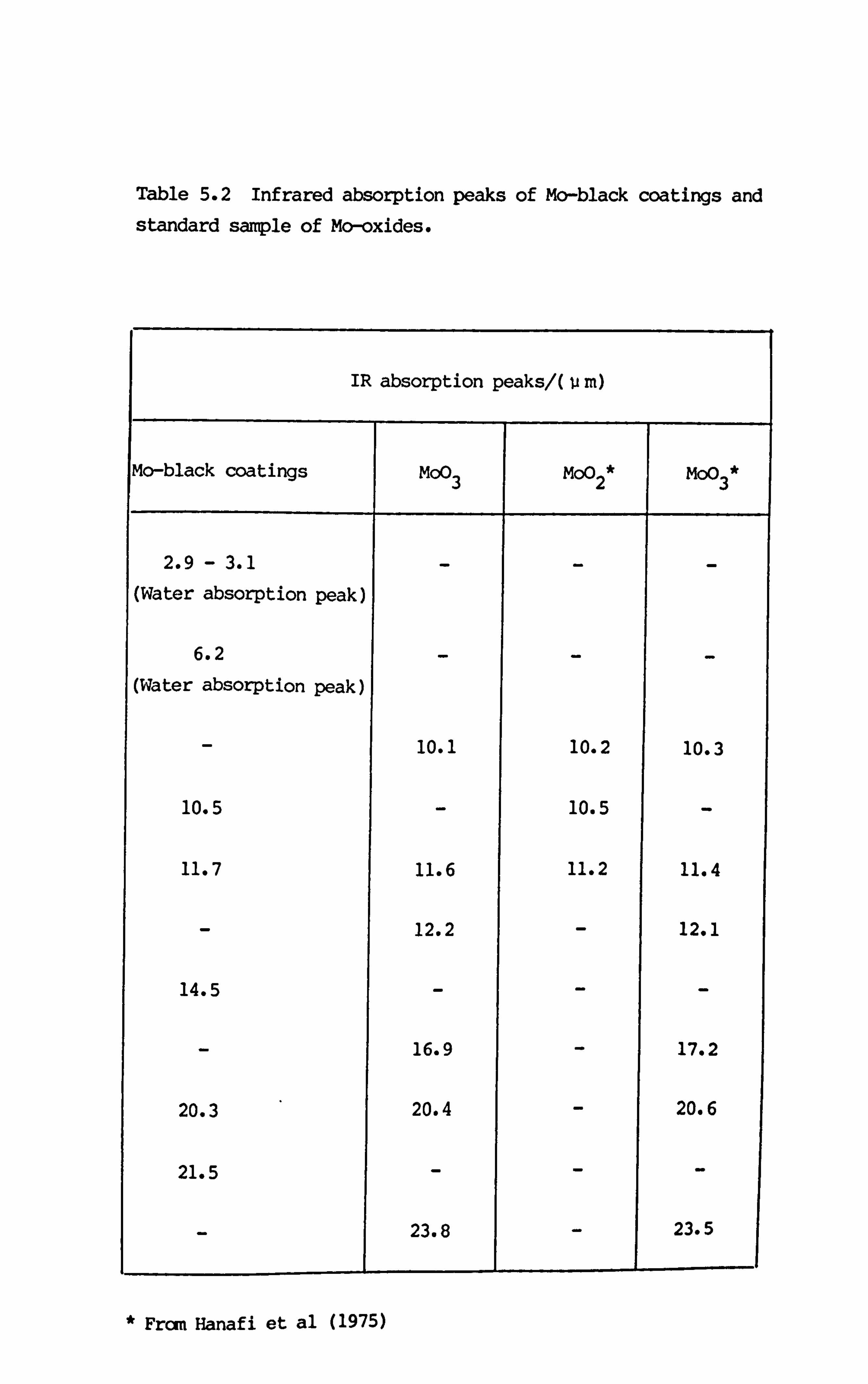
Table 5.2 Infrared absorption peaks of Mo-black coatings and standard sample of Mo-oxides.
IR absorption peaks/(u m)
Mo-black coatings moo 3 MOO 2 MOO 3
2.9 - 3.1
(Water absorption peak)
6.2 - - - (Water absorption peak)
- 10.1 10.2 10.3
10.5 - 10.5 -
11.7 11.6 11.2 11.4
- 12.2 - 12.1
14.5 - - -
- 16.9 - 17.2
20.3 20.4 - 20.6
21.5 - - -
- 23.8 - 23.5
* Frcm Hanafi et al (1975)
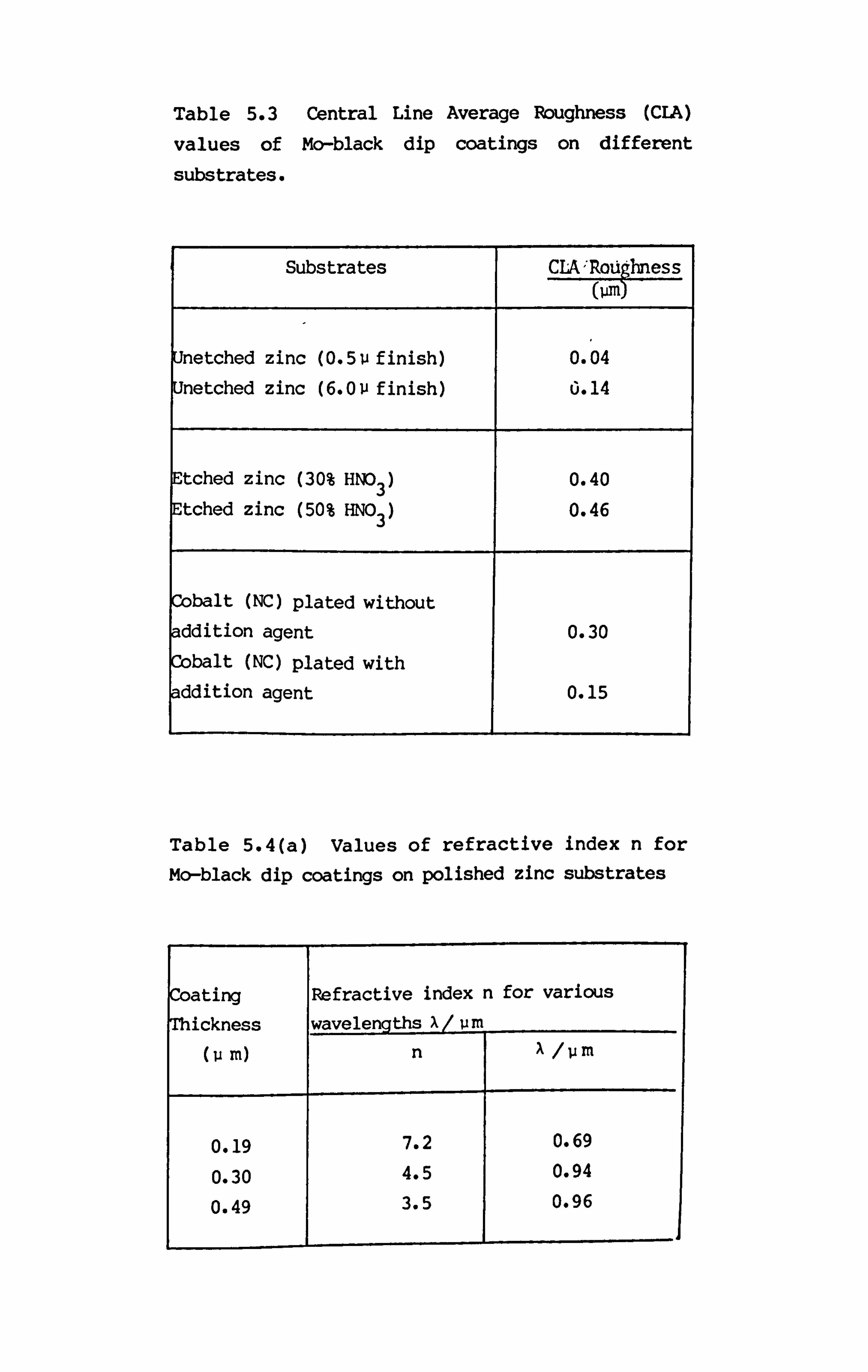
Table 5.3 Central Line Average Roughness (CLN)
values of Mo-black dip coatings on different
substrates.
Substrates CLA; Rojýýhness GO)
Unetched zinc (0.5ifinish) 0.04
Unetched zinc (6.011finish) 0.14
Etched zinc (30% HNO 3) 0.40
Etched zinc (50% HNO 3) 0.46
Cobalt (NC) plated without
addition agent 0.30
Cobalt (NC) plated with ddition agent 0.15
Table 5.4(a) Values of refractive index n for
Mo-black dip coatings on polished zinc substrates
Coating
Thickness
Refractive index n for various
wavelengths X/ pm (p M) n
0.19 7.2 0.69
0.30 4.5 0.94
0.49 3.5 0.96
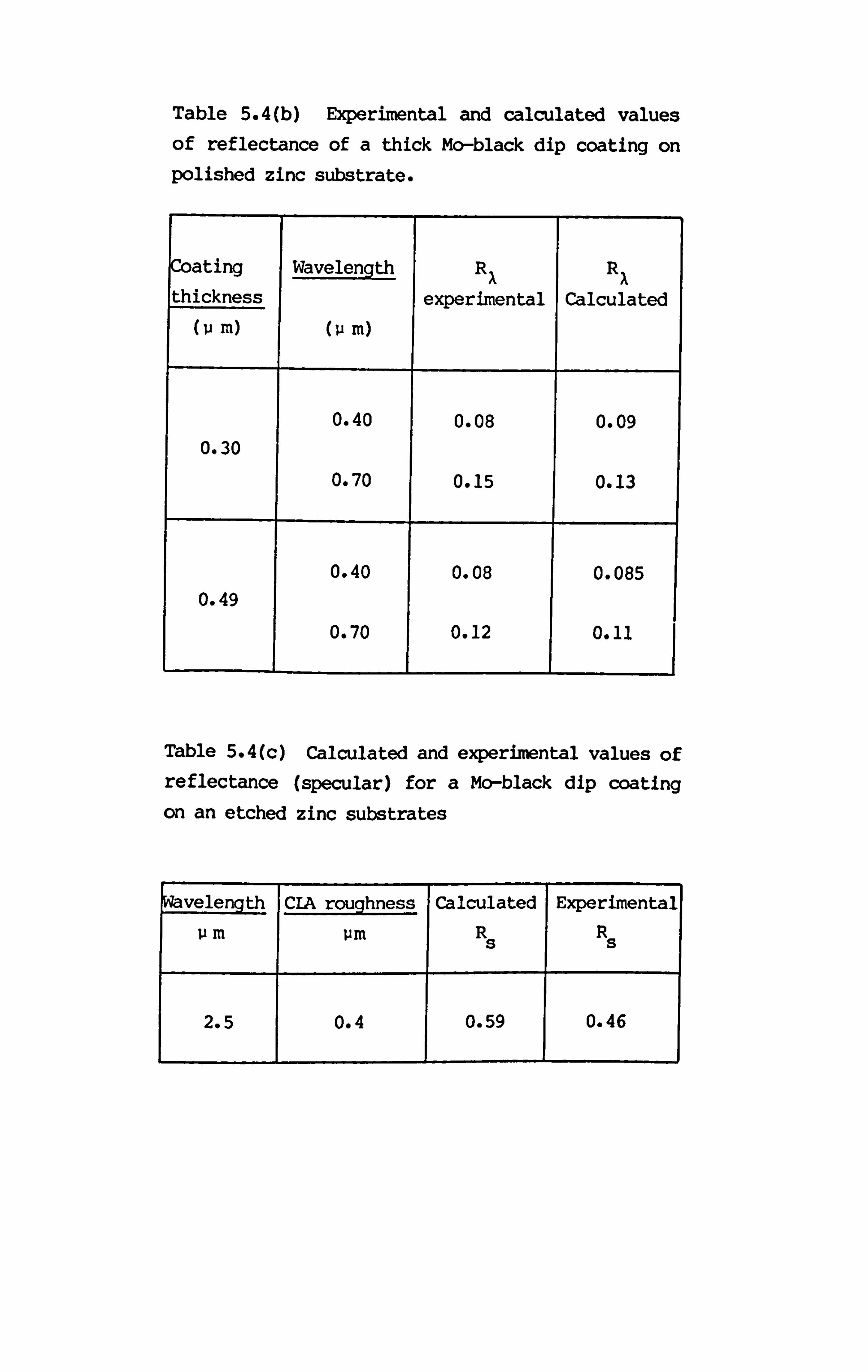
Table 5.4(b) Experimental and calculated values of reflectance of a thick Mo-black dip coating on polished zinc substrate.
I
Coating Wavelength R R
thickness experimental Calculated (P M) (P M)
0.40 0.08 0.09 0.30
0.70 0.15 0.13
0.40 0.08 0.085 0.49
0.70 0.12 0.11
Table 5.4(c) Calculated and experimental values of reflectance (specular) for a Mo-black dip coating on an etched zinc substrates
Wavelength CIA roughness Calculated Experimental
11 M 11M RS RS
2.5 0.4 0.59 0.46
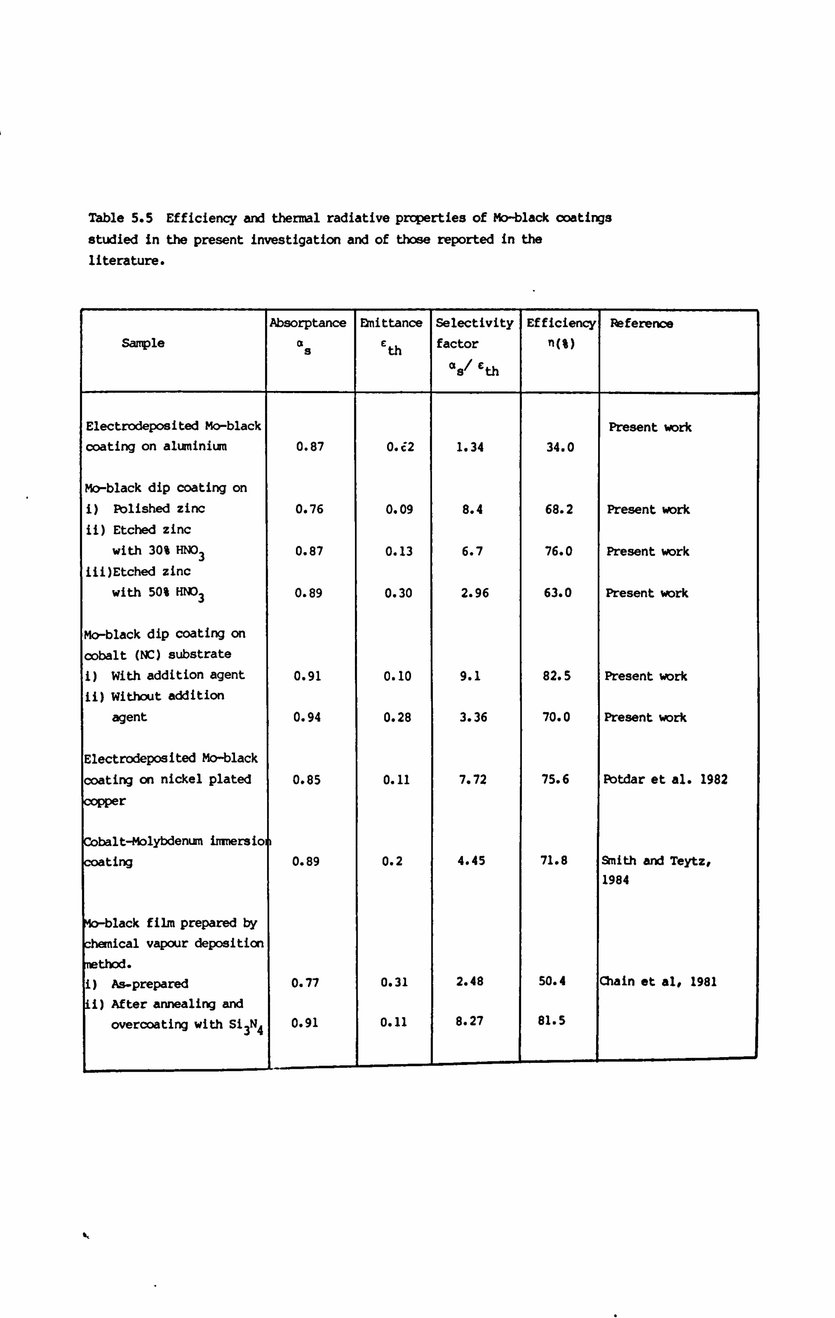
Table 5.5 Efficiency and thermal radiative properties of Mo-black coatings studied In the present investigation and of those reported in the literature.
Sample
Absorptance
at a
Emittance
C th
Selectivity
factor
at al cth
Efficiency
n(%)
Reference
Electrodeposited Mo-black Present work
coating on aluminium 0.87 M2 1.34 34.0
Mo-black dip coating on i) Polished zinc 0.76 0.09 8.4 68.2 Present work ii) Etched zinc
with 30% HNO 3 0.87 0.13 6.7 76.0 Present work iii)Etched zinc
with 50% HN03 0.89 0.30 2.96 63.0 Present work
Mo-black dip coating on
cobalt (NC) substrate J) With addition agent 0.91 0.10 9.1 82.5 Present work ii) Without addition
agent 0.94 0.28 3.36 70.0 Present work
Electrodeposited Mo-black
coating on nickel plated 0.85 0.11 7.72 75.6 Potdar at al. 1982
copper
cobalt-molybdenun immersio i
coating 0.89 0.2 4.45 71.8 Smith and Teytz, 1984
4o-black film prepared by
chemical vapour deposition
method. i) As-prepared 0.77 0.31 2.48 50.4 Chain et al, 1981
ii) After annealing and
overcoating with Si A 0,91 0.11 8.27 81.5
Table 5.6 Optical band gap of Mo-black coatings and standard samples of Mo-oxides.
Band qaV. Determination
Sarnple (eV) techniques
Thin electro- Transmission spectra deposited Mo-black 1.66 Plots of (ariw) 1/2
vs 11W
coating on vacuum (Section 3.7)
evaporated Al-film
Thick electro- Reflectance spectra deposited Mo-black 1.13 Plots of R. vs X
coating on Al-sheet 0.85 Plots of a/s vs X (Section 5.2.1)
Mo-black dip Reflectance spectra
coating on zinc 1.24 Plots of Rx vs X
0.91 Plots ofa/s vs X
(Section 5.2.2)
Powder sample of Diffuse reflectance
moo 2 1.72 spectra
Mo 4011 1.75 Plots of In a/s vs X
M003 2.74 (Hanafi et al, 1981)
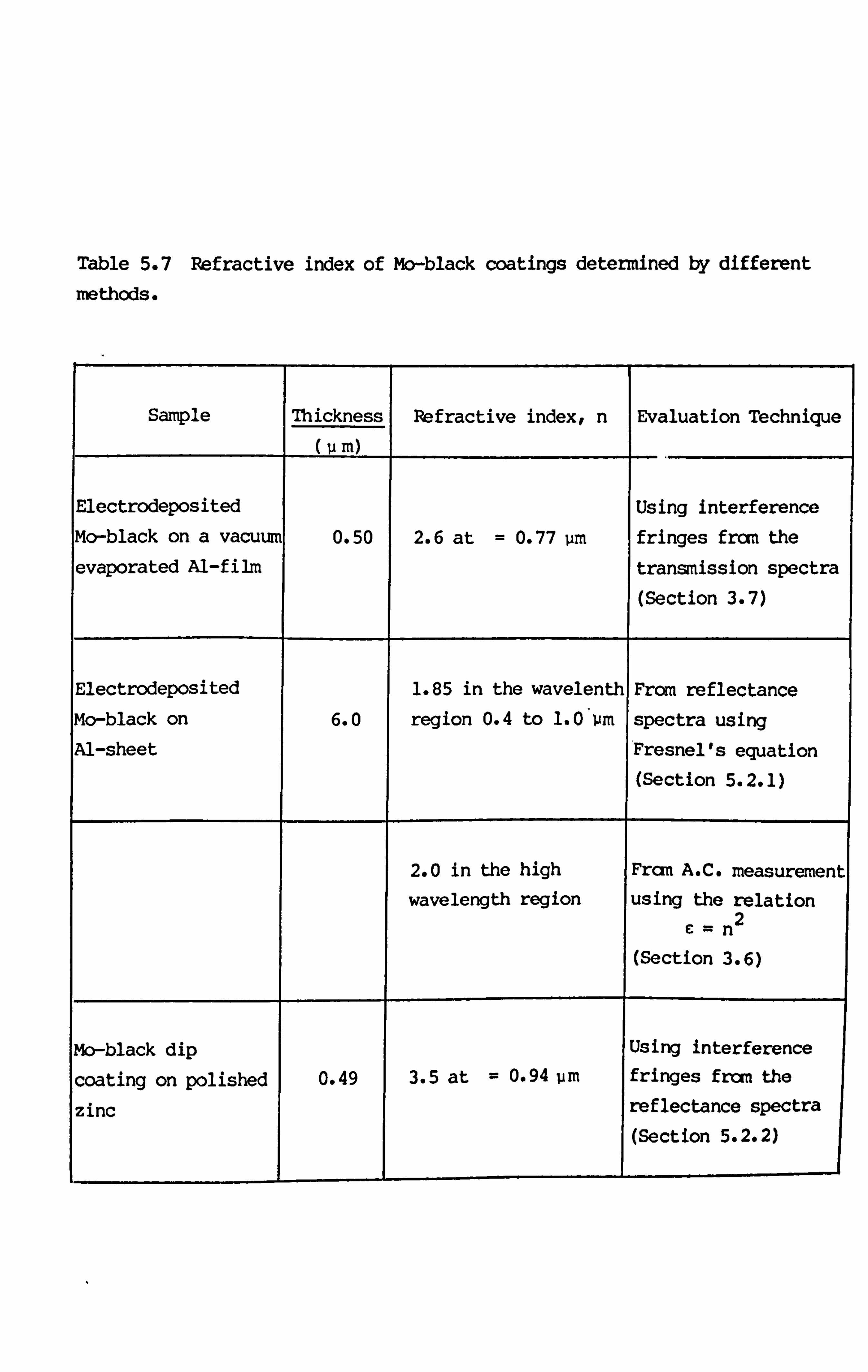
Table 5.7 Refractive index of Mo-black coatings detemined by different
methods.
Sample Thickness Refractive index, n Evaluation Technique
(P M)
Electrodeposited Using interference
Mo-black on a vacuum 0.50 2.6 at = 0.77 Pm. fringes frcm the
evaporated Al-film. transmission spectra (Section 3.7)
Electrodeposited 1.85 in the wavelenth From reflectance Mo-black on 6.0 region 0.4 to 1.0 ijm spectra using Al-sheet Fresnel's equation
(Section 5.2.1)
2.0 in the high Fram A. C. measurement
wavelength region using the relation c=n2
(Section 3.6)
Mo-black dip Using interference
coating on polished 0.49 3.5 at = 0.94 um fringes from the
zinc reflectance spectra (Section 5.2.2)
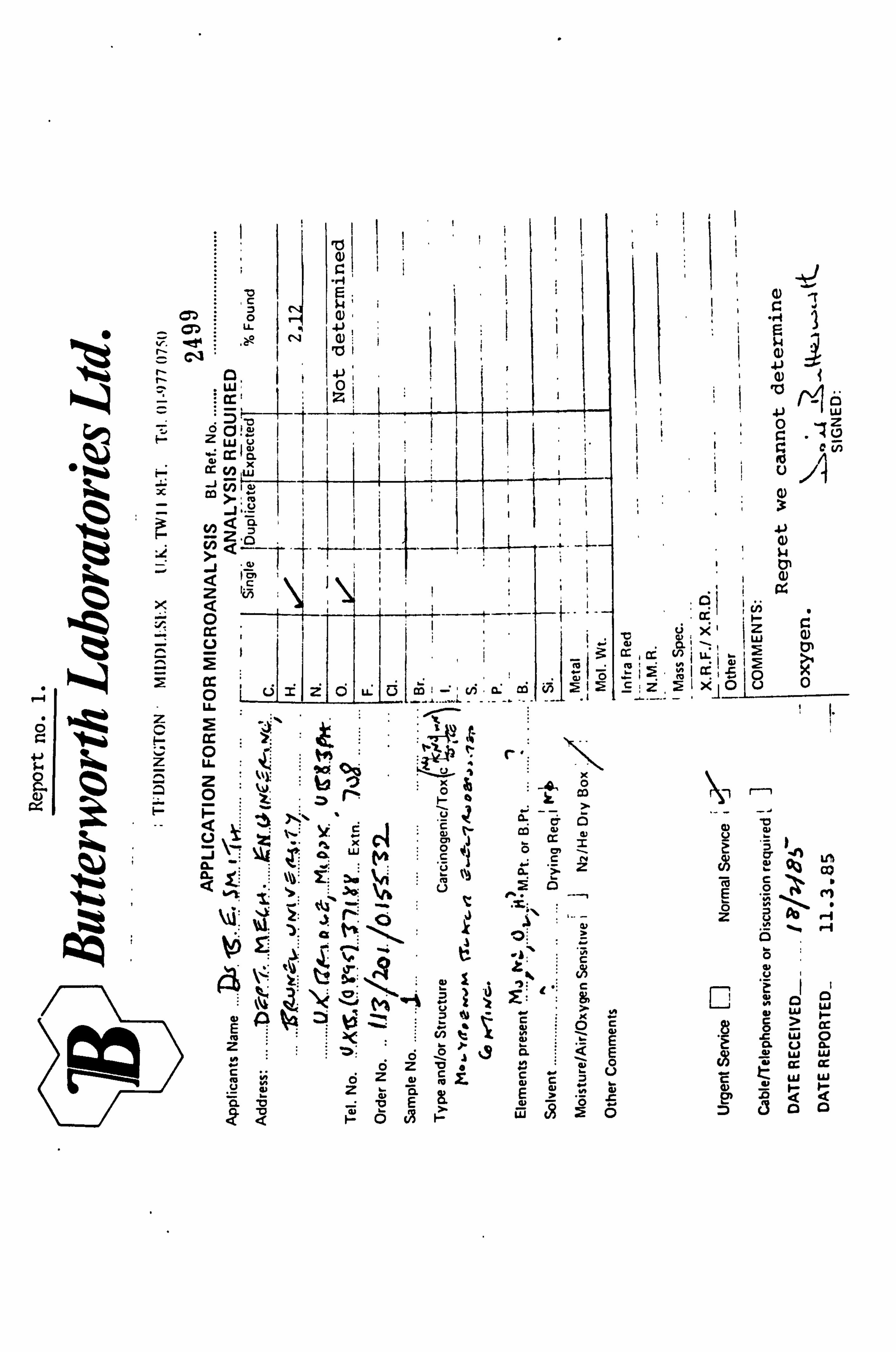
0
lij NNW4 ýOD
0 hm
4
.:
1 10 i
c2 3 (14 0 r--l
C-, ý : LL iI 4-)
4. )
cr 41 0 0
ac
x
z C
z p.,
m
. -JaK iII:. 10 V) CC CL IiI, i.
i 00 ,I, 11 iiu X, 11:
'! %- I: I w 4j
54
I lig :! iII.
IIIIP.
LU
VR cc
Li no u -1 C4 0
0L 2ý
cc j 0
.. 0% X %, I jmi. mI
Eo- QQ co CL
Vt m
. ').
a vi 1 0: t' %., f
! 4.4. v -4 tj . ';; 6
cr CL CL, z: - CL zo: a UJ 60
6Z0 6z C. Z cu CL Lm .0 CL VED Ll o
2ý co
CHAPrER VI
CONCLUSIONS AND SUGGESTIONS FOR FURTHER WORK
6.1 Conclusions
1. Mo-black coatings prepared by electrodeposition on aluminium
substrates have moderate absorptance (-0.87). Due to their high
emittances the coatings are effectively non-selective (Section 3.1.3).
The high absorptance of these coatings may be related to the bandgap of
the coating material (which is found to be about 0.85 eV using the
Kubelka-Munk theory) and the porosity of the coating (Section 5.2.1). The
high emittance of these coatings is probably due to their relatively large
thickness and presence of water in the coatings.
2. Mo-black dip coatings on polished zinc substrates have ccnparatively
low absorptance (0.70 - 0.78) with high selectivity factor P to 9.8).
The low absorptance of these coatings my be due to high reflection losses
related to a high refractive index (Section 5.2.2). 7he low emittance of
the dip coatings is due to their low thickness (below I um). 7hinner
coatings appear to be almost transparent in the IR region. Both
absorptance and emittance of these coatings increase with increase of
thickness but emittance is more thickness dependent than the absorptance
(Section 3.1.1).
3. By using chemically etched zinc substrates, the absorptance of the dip
coatings can be increased by 14% without any significant change In the
emittance (Section 3.1-1). Theenhanced, absorption is t1lought tobe dueto re-
duction, of surface reflection loss. The thickness of the coatings is found to bc
132
critical for optimun properties. Thick Mo-black coatings exhibit less
selectivity for both etched and unetched zinc substrates.
4. On electroplated cobalt (NC) (cobalt on nickel plated copper)
substrates, Mo-black dip coatings give more pramising results. These
coatings exhibit high solar absorptance (0.92 - 0.94) mainly due to the
surface morphology of the coatings together with the structure of the
plated cobalt layer. These coatings have a rather high emittance (0.25 - 0.33) probably due to surface roughness.
5. It has been observed that the properties of these coatings are
sensitive to the preparation conditions of both Mo-black and the initial
cobalt layer. By using an addition agent in the cobalt plating solution,
the emittance of the Mo-black coatings can be reduced to 0.1 to 0.13 with
a slight decrease in solar absorptance. Mo-black coatings prepared at a
solution temperature of 600C give better results than those prepared at
800C.
6. In the present investigation, maximum efficiency (82.5%) has been
obtained from the Mo-black coating on cobalt (NC) substrate plated with
addition agent (Section 5.3). The coatings on etched zinc substrates have
an efficiency of 76%. It has also been observed that although the
coatings on highly polished zinc have a higher selectivity factor than
those on etched zinc, their efficiency is lower.
7. The SEM studies have shown that both electrodeposited coatings on
aluminium and dip coatings on polished zinc consist of flat smooth$
platelets with widely spaced cracks. ibis suggests that absorptance in
these coatings is due to intrinsic absorption by the coatings and not due
to surface morphology. Mo-black coatings on chemically etched zinc
133
substrates show a nodular structure (Section 3.2.2), which may enhance the
solar absorptance without affecting the thennal emittance significantly.
8. The morphology of Mo-black coatings on cobalt (NC) substrates depends
on the preparation conditions. The coatings have a nodular structure and
ccrnparatively smooth surface when prepared on cobalt plated with addition
agent. On cobalt plated without addition agent, the surface of Mo-black
coatings consists of a large number of limb like structures with few
nodules. When cobalt is plated with a ccaparatively low current density
and at low temperature, the surface of Mo-Black coating consists of
submicron sized nodules (Section 3.2.3).
9. The electron diffraction studies of the Mo-black coatings on aluminium
and zinc substrates suggest that the coatings are polycrystalline in
nature. The interplanar spacing values indicate the presence of
orthorhombic Mo 40 11 (Section 3.3). X-ray diffraction patterns from the
coating contain only one very broad low angle (0 - 4.5) peak together with
peaks frcm the substrates. The difference in the electron and X-ray
diffraction results is probably due to the differences in atomic
scattering factors for electrons and X-rays (e. g., for lighter atcms such
as 0 2)'
10. '1he X-ray photoelectron spectroscopy study indicates that the
oxidation state of molybdenum in the Mo-black coatings is about +5, which
is close to that in Mo 40 110 The oxidation state of molybdenum
remains almst the same for coatings on different substrates (Al, Zn and
Co). It has been observed that the coatings reduce to a lower oxidation
state (+4) after bombarding with Ar + ions which is most probably the
etching effect.
134
11. The XPS study shows that the coatings mainly consist of molybdenum
with a small percentage of nickel. The EPMA also shows the same results.
However, the percentage of nickel in the coating increases with increase
of NiSO 4 concentration in the plating solution. Peaks from the substrates
(Ali, Zn, or Co) also appear in the XPS and EPMA spectra. (These possibly
due to cracks in the coatings). The atomic percentage of oxygen at the
surface of coatings is about 71%. After etching with Ar + ions it reduces
to 57 - 61%, due to the reduction of molybdenum to a lower oxidation
state.
12. XPS studies reveal that the coating oxidizes to MoO 3 (+6) after heat
treatment in air at high temperature. The coatings on cobalt seem to be
less affected by heat treatment.
Mo-black coating on zinc substrate reduce to a lower oxidation state (+4)
after heating in vacuum, (zinc probably acts as a reducing agent). No
significant shift in the binding energy of Mo 3d peaks has been observed
for coatings on aluminium and cobalt substrates after heat treatment in
vacutzn.
13. IR absorption peak positions provide further evidence that the
Mo-black coating does not consist of MoO 2 or MoO 3 (Section 5.1.2.2). But
contains an intermediate oxide, e. g., Mo 40 11 ), as suggested by the
electron diffraction study.
14. No significant changes in the reflectance spectra of Mo-black
coatings on etched zinc have been observed after heat treatment at 10Cband
20CPC for a period of 24 and 16 hours respectively. No degradation has
been observed even after heat treatment at 3000C for 4 hours. Same
characteristic reflectance has been observed whether the coatings are
135
heat treated in air or vacuum. Coatings on cobalt (NC) substrates have
been tested up to 400 0 C. The coatings on cobalt plated without addition
agent seem to be more stable than the coatings with addition agent, i. e.,
the emittance increases in the latter case whereas it decreases in the
former case. The solar absorptance remains unchanged after heat treatment
in both cases.
15. The coatings are semiconducting. Annealing at elevated tenperature
increases the electrical conductivity of the coating. The I-V
characteristics of the coating are ohmic at low applied fields but they
are non-ohmic at higher applied field. Analysis of the I-V
characteristics suggest that in the high field region the dominant
conduction mechanism is of the Poole-Frenkel emission type. It has also
been observed that the activation energy of the coating varies with
tenperature -
AC measurements show that the capacitance of the coating decreases with
the increase of frequency. The relative dielectric constant decreases
from about 4.6 to 4.0 when frequency increases from 5X 10 2 Hz to 2X 10 4
Hz. At higher frequencies it is less frequency dependent. Capacitance
measurements as a function of tenperature give evidence for the presence
of water in the coating.
16. Transmission measurements in the UV and visible region suggest that
the optical band gap E opt
decreases and the band tail increases with
increase of coating deposition rate. This may be due to an increase of
structure disorder in the system with increasing deposition rate. (71he
value of Eopt decreases from 1.89 eV to 1.66 eV with the increase Of
current density from about 1.4 mA/cm 2 to 2.8 mA/cm
2 (Section 3-7)).
136
17. It is concluded that for the production of selective surface for
a solar collector, a Mo-black coatings on electroplated cobalt on a
nickel plated copper substrate is the mst suitable of the rmterials
studied in the present work. This is reccmTended on the basis of its
performance, durability and reproducibility of optical characteristics.
136a
6.2 Sucaestions for further work
i) Longer term thermal stability testing for Mo-black coatings on etched
zinc is needed, as the short term heat treatment up to temperatures of
30dOC gives no significant degradation in the optical properties of these
coatings.
ii)A more systematic study should be done on the effect of addition agents
in the cobalt plating solution together with the effect of solution
temperature and plating conditions on the thermal radiative properties and
microstructure of the Mo-black coatings on cobalt (NC) substrates.
iii) The long term thermal stability at elevated tenperature of coatings
on cobalt (NC) substrates should be examined.
iv) The effects of humidity, ultraviolet exposure and temperature
cycling in degradation of coatings on both zinc and cobalt substrates
should be examined.
V) Further study of IR absorption spectra might provide information on
chemical bonding in the coatings.
vi) Neutron diffraction studies might be appropriate for this material
(due to the presence of lighter elements such as oxygen and hydrogen).
vii) Mo-black coatings on other substratest such as, aluninium, and mild
steel, with an intermediate cobalt layer could be studied.
viii)A flat plate solar collector could be constructed using a Mo-black
coating as a selective surface and its thermal performance under operating
conditions could be investigated.
137
REFERENCES
Agnihotry, O. P. and Gupta, B. K. (1981), "Solar Selective Surfaces", (Wiley Interscience).
Agnihotri, O. P., Gupta, B. K., Agarwal, A. K. and Bhatnagar, V. P. (1983), Thin Solid Films, 109,193.
Al-Ani, S. K. J., Arshak, K. I. and Hogarth, C. A. (1984), J. Mat. Sci., 19 1737.
Al-Ani, S. K. J., Sarkar, M. A. R., Beynon, J. and Hogarth, C. A. (1985), J. Mat. Sci., 20,1637.
Al-Ani, S. K. J., (1984) Ph. D. Ibesis, Brunel University, U. K.
Al-Ramadhan, F. A. S., Arshak, K. I. and Hogarth, C. A. (1984), J. Mat. Sci., 19,3687.
Andersson, G. and Magneli, A. (1950), Acta. Chem. Scand., 4,793.
Anthony, M. T. and Seah, M. P. (1984), Surf. Interface. Anal. 6,107.
Apetkar, E. L., Chadinov, M. G., Alkeseev, A. M. and Krylov, ON. (1974) React. Kinet-Catal-Lett. 1,493.
Barraclough, C. G. and Stals, J. (1966), Aust. J. Chem., 19,741.
Ben-dor, L. and Shimony, Y. (1974), Mat. Res. Bull. 9,837.
Bennett, H. E., and Porteus, J. O., (1961), J. Opt. Soc. Am., 51,2,123.
Block, G. R. (1985), Final Project Report, Brunel University, U. K.
Bogaerts, W. F. and Lampert, C. M. (1983). J-Mat. Sci., 18,2847.
Booth, D. C., Allred, D. D. and Seraphin, B. O. (1979). Sol. Energy Mater. 2,107.
Brandt, B. B. and Skapski, A. G. (1967) Acta Chem. Scand-, t, 21, . 661.
Briggs, D. (1978) "Handbook of X-ray and ultra-violet photoelectron spectroscopy". (Heyden: London).
Briggs, D. and Seah, M. P. (1983) "Practical surface analysis by Auger and X-ray photoelectron spectroscopy". (John-Wiley and Sons: New York).
Bulpett, R. (1984) Vacuum, 34,481.
Carver, G. E. (1979) Sol. Energy. Mater-P 1,357.
Carver, G. E. and Seraphin, B. O. (1979), App. Phys. Lett. 34,279.
Carver, G. E., Divrechy, A., Karbal, S., Robin, J. and Donnadien, A. (1982)
Thin Solid Films, 94,1269.
Chan, W. S. and Loh, C. K. (1970), Ibin Solid Films, 1,91.
Chandrashekar, M. and HariBabu, V. (1984) J. Mat. Sci-Lett-, 3,600.
138
Chain, E. E., Carver, G. E. and Seraphin, B. O. (1980), Thin solid Films, 72, 59.
Chain E. E., Seshan, K. and Seraphin, B. O. (1981) J. Appl. Phys., 52,3, 1356.
Chase, L. L. (1974) Phys. Rev. B, 10,2226.
Chopra, K. L. (1969) "Thin Film Phenomena", (Mc-Graw Hill Book Co, New York).
Christie, E. A. (1970) Intern. Solar Energy Conf., Melbourne, Australia, paper 7/81.
Cimino, A. and De Angelis, B. A. (1975) J. Catal., 22 140.
Colton, R. J., Guzman, A. M. and Rablais, J. W. (1978) J. Appl. Phys. 491 1, 409.
Ccxtpanion, A. M. and Mackin, M. (1965) J. Chem. Phys. t. 42,4219.
Cotton, F. A. and Wilkinson, G. J. (1972), "Advanced Inorganic Chemistry", 3rd Ed., Wiley, Interscience, New York, London.
Cullity, B. D. (1978) "Elements of X-ray diffraction". (Addison-hbsley publishing Co. Inc. ).
Cuomo, J. J., Ziefler, J. F. and Woodale, J. M. (1975),. App. Phys. Lett., 26,557.
Dagnall, H. (1980), "Exploring Surface Texture", Rank Taylor Hobson, Leicester, England.
Davis, H. (1954), Proc. Inst. Electr. Engn. 101,4,209.
Davis, E. A. and Mott, N. E. (1970), Phil-Mag-, 22,903.
DeChelle, F., Berger, J. M., Ance, C., Coulibaly, S. P. Ferraton, J. P., Donnadieu, A., Zellama, K., Germain, P. and Squelard, S. (1983), Thin Solid Film, 103 243.
Deb, S. K. and Chopoorian, J. A. (1966), J. App. Phys. 37,4818.
Deb, S. K. (1968), Proc. Royal Soc., A304,211.
Dickinson, W. C. and Cheremisinoff, P. N. (1980), "Solar energy technology handbook", (Part B), Marcel Dekker, Inc. Butterworths, London.
Duffie, J. A. and Beckman, W. A. (1980), "Solar Engineering of 1hermal Processes, " Wiley, New York.
Dunkui, M. (1986), Sun World, 10,2,46.
Fan, J. C. C. (1978), Thin Solid Filmst 39,87.
Fan, J. C. C. and Spura, S. A. (1977), Appl. Phys. Iztt. 30,511.
Fosch, P. D. (1956) Proc. Phys. Soc. B69,70.
Frenkel, J. (1938), Phys. Rev. 54,647.
Fussell, W. B., Triolo, J. J. and Henniger, J. H. (1963), Measurement of
139
Thermal Radiative Properties of Solid, NASA-SP31,83.
Gesheva, K. A., Chain, E. E. and Seraphin, B. O. (1980), Sol. Energy Mater., 3,415.
Gilbert, L. R., Messier, R. and Roy, R. (1978), Thin Solid Films, 54,149.
Golestani-Fard, F., Hogarth, C. A. and Waters, D. N. (1983), J. Mat-Sci. Lett. 2,505.
Goldstein, J. I., Newbury, D. E., Echlin, P. Joy, D. C., Fiori, C., Lifshin, E. (1981), "Scanning Electorn Microscopy and X-ray Microanalysis" Plenum Press, New York and London).
Gray, D. E. (1972) "American Institute of Physics Handbook", 3rd Eaition, Mc-Graw Hill Book Co*. New York.
Gregg, S. J. and Si. ig, K. S. W. (1982), "Absorption, Surface Area and Porosity", Academic Press, London.
Grim, S. O. and Matienzo, L. J. (1975), Inorg. Chem. 14,1975.
Gupta, B. K., Agarwal, A. K. and Bhatnagar, V. P. (1983), Proc. of SPIE, "Optical and Process Technology for Energy Efficiency and Solar Applications", San Diego, California, 428,182.
Hagg, G., and Magneli, A. (1944), Arkiv Kemi. Mineral. Geol. A. 19,2.
Haight, G. P., Jr. (1953), Anal. Chem. 25,4.642.
Hanafi, Z. M., Khilla, M. A. and Abu-el-Saud, A. (1975), Rev. Chim. Min. t. 12, 546.
Hanafi, Z. M., Khilla, M. A. and Abu-el-Saud, A. (1981), Rev. Chim. Min. t. 18, 133.
Hoffman, R. A. and Hull, R. O. (1939), Proc. Am. Electroplat. Soc., 45.
Hosseini, R. (1981), Ph. D Thesis, Brunel University, U. K.
Hosseini, R., Smith, B. E. and Critchley, J. K. (1983), Surface Tech. 20, 321.
International Copper Research Association (INCRA) (1977), Final Project Report No 250.
Islam, M. H. (1987), Ph. D. Thesis, Brunel University, U. K.
Jahan, F., and Smith, B. E. (1986), J. Mat. Sci-Lett. 5,905.
Karlsson, B and Ribbing, C. G. (1982), J. Appl. Phys. 53,9,6340.
Kennedy, M. J. (1972), Ph. D Thesis, Brunel University# U. K.
Kihlborg, L. (1959), Acta. Chem. Scand. t, 13,954.
Kihlborg, L. (1963), Advanc. Chem. Set, L, 39,37.
Kihlborg, L. (1963), Arkiv. Kemi. t, 21,443.
140
Kim, K. S., Baitinger, W. E., Amy, J. W. and Winograd, N. (1974), J. Electron Spectrosc. Relat. Phencm., 5,351.
Kim, K. S. and Winograd, N. (1974), Surf. Sci. 43,2,625.
Kittel, C. (1968), "Introduction to Solid State Physics, (John Wiley & Sons, Inc., New York).
Koltun, M. M. (1981), "Selective Optical Surfaces for Solar Energy Converters", Allerton Press, New York.
Kramer, B. M. (1983), Ibin Solid Film, 108,117.
KRATUS Instruction Manual for the ES300, Barton Dock Road, Urnston, Manchester
Kubelka, P. and Munk, F (1931), Z. Tech. Phys. 12,593.
Kubelka, P. (1948), J. 0pt. Am. 38,448.
Lamb, D. R. (1967), "Electrical Conduction Mechanisms in Thin Insulating Films", (Methuen Monograph, London).
Lampert, C. L. (1979), Ph. D Thesis, University of California, USA.
Lampert, C. L. (1979), Solar Energy Mater. 1,81.
Lampert, C. L. (1979), Solar Energy Mater. 1,319.
Lavina, A., Aznarez, J. A. and Ortiz, C. (1980) J. Crys. Growth, 48,100.
Longhurst, R. S. (1957), "Geometrical and Physical Optics", Longmans, Green and Co Ltd., London.
Lowenheim, F. A. (1963) "Modern Electroplating", 2nd Edition. Wiley, New York.
Lowenheim, F. A. (1978), "Electroplating", McGraw-Hill, New York.
Lubis, A., Witono and Budiono, C. (1985) Sun World, 9,2,36.
Magneli, A. (1946) Arkiv, Kem. Mineral Geol. A24,2.
Magneli, A. (1948) Acta Chem. Scand. 2,501.
Magneli, A. (1948) Acta Chem. Scand. 2,861.
Magneli, A. (1957), Acta Chem. Scand. t, ll, 1587.
Maissel, L. I. and Glang, R. (1983) nHandbook of Thin Film Technology". (McGraw-Hill Book Co., New York).
Mattox, D. M. and Kominiak, G. J. (1975) J. Vac. Sci. Tech. 12,1,182.
Mattox, D. M. and Sowell, R. R. (1980) "A Survey of Selective Solar Absorber
Surface and their limitations", US-DOE Report DE-AC04-76-DPOO789.
McMahon, T. J. and Jasperson, S. N. (1974) App-Opt. 13,12,2750.
McIntyre, N. S. and Cook, M. G. (1975) Anal. Chem. 47,2208.
141
McNelis, B. (1982) Sun at work in Britain, 15,30.
Mead, C. A. (1962), Phys. Rev. 128,2088.
Meinel, A. B. and Meinel, M. P. (1976) "Applied Solar Energy", (Addison-Wesley Publishing Co., Reading, Massachusetts).
Millard, J. P. and Streed, E. R. (1969), App. Opt. 8,7,1485.
Miller, A. W., Atkinson, W., Barber, M. and Swift, P. (1971) J. Catal. 22, 140.
Morley, A. R. and Campbell, D. S. (1968) Thin Solid Films, 2,403.
Moss, T. S., Burell, G. J. and Ellis, B. (1973), "Semiconductor Opto-Electronics", (Butterworths, London).
Mott, N. F. and Davis, E. A. (1971), "Electronic Process in Non-Crystalline Materials". Clarendon, Oxford.
Mott, N. F. (1969), Phil. Mag., 19,835.
Nadkarni, G. S. and Simmons, J. G. (1972), J. Appl. Phys. 43,3741.
Nadkarni, G. S., Shirodkar, V. S. and Simmons, J. G. (1982), Thin SOlid Films, 94,101.
Nakamoto, K. (1970), "Infrared Spectra of Inorganic and Co-ordination Carpounds".
Neal, W. E. J. and Musa, A. H. (1982), Surf. Tech. 14,345.
Niklasson, G. A. and Geranqvist, C. G. (1983) J. Mat. Sci. 18,3475.
Nozik, A. J. (1972), Phys. Rev. B6,453.
Park, C. K. (1964), App. 0pt. 3,877.
Patterson, T. A., Carver, J. C., I-eydon, D. E. and Hercules, D. M. (1976). J. Phys. Chem. 80,1700.
Pellegrini, G. (1980). Sol. Energy Mater. 3,391.
Peterson, R. E. and Ramsey, J. W. (1975) J. Vac. SCi. Technol. 12,174.
Petit, R. B. and Sowell, R. R. (1976) J. Vac-Sci. Technol. 13,2,596.
Porter, V. R., White, W. B. and Roy, R. (1972) J. Solid State Chem. 4,250.
Potdar, H. S., Hedge, R. I., Badrinarayon, S. and Pavaskar, N. (1982) Sol. Energy Mater. 6,183.
Rablais, J. W., Colton, R. J. and Guzman, A. M. (1974) Chem. Phys. lett. 29,1, 131.
Riggs, W. M. and Parker, M. J. (1975) "Methods of Surface Analysis (Ed" Czandernal, A. W. ) Elsevier, New York.
Robert, T., Bartel, M. and Offergeld, G. (1972), Surf-Sci-, 33,123.
142
Rogers, D. B., Shanon, R. D., Sleight, A. W. and Gilson, G. L. (1969), Inorg. Chem. t. 8,476.
Safi, 1. (1986), M. Pliil. Thesi4Brunel University, UK.
Sauer, H. D. (1985) Sun World, 10,2,46.
Samsonov, G. V. (1973), "The Oxide Handbook". IFI/Plenum, New York.
Schofield, J. H. (1973), Laurence Livermore Laboratory Report, CRL-51326-
Schottky, W. (1914), Physik, Z. 15,862.
Seraphin, B. O. (1974), Proc. Symp. on the Materials Science Aspects of Thin Film Systems for Solar Energy Conversion, Tucson, AS (July, 1974).
Seraphin, B. O. (1976), Thin Solid Films, 39,87.
Seraphin, B. O. (1979), "Topics in App. Phsics, " (Ed. Seraphin, B. O. ) Springer-Verlag, Berlin, Germany.
Shabalov, A. L. and Feldman, M. S. (1983) Thin Solid Films, 110,215.
Siegel, R. and Howell, J. R. (1972), "Thermal Radiation Heat Transfer", (McGraw-Hill Book Co., New York).
Sikken, M., VanHeereveld, A. A. M. T. and Vogelzang, E. (1983), Thin Solid Films, 108,229.
Simmons, J. G. and Nadkarni, G. S. (1969), J. Vac. Sci. Tech. 6,12.
Simmons, J. G. and Nadkarni, G. S. (1970), J. Appl. Phys. 41,545.
Simmons, J. G. and Nadkarni, G. S. (1972), J. Appl. Phys. 43,3650.
Simmons, J. G. (1971), 11DC Conduction in Thin Film", Mills and Boon Ltd. London.
Simmons, J. G. and Verderber, R. R. (1967), Proc. Roy. Soc-, 77, A301.
Smith, B. E., Hosseini, R., Farmakis, C. and Critchley, J. E. (1981) "Proceeding of Solar World Forum", ISES, Brighton, 11 (Pergamon, Oxfora).
Smith, G. B., Ignatiev, A. and Zajac, G. (1980), J. Appl. Phys. 51V 8,4186.
Smith, G. B. and Teytz, K. (1984), Sol. Energy Mater. 9,449.
Swartz, W. E. and Hercules, D. M. (1971), Anal. Chem. 43,1774.
Tabor, H. (1956), Bull. Res. Counc- of Israel, 5A, 119.
Tabor, H. (1977), "Application of Solar Energy for Heating and Cooling Of Buildings", ASHRAE GRP 170, Ed. Jordon, R. C. and Lin, Y. H.
Tabor, H. (1984), Sun World, 8,1,5.
Takyu, K. (1984) Sun World, 8,1,16.
Tandon, S. P. and Gupta, J-P- (1970), Phys. Stat-sol. 38,363.
143
Tauc, J., Grigorovici, R. and Vancu, A. (1966)t Phys. Stat. Solidi. 15,627.
Urbach, G. (1953), Phys. Rev. 92,1324.
Verchere, J. A. and Fleury, M. B. (1973), Proc. of the lst Intern. Conf. on the Chemistry and Uses of Molybdenum, Ed. P. C. H. Mitchel, Climax Molybdenum Co. London (1975), 59.
Walter, D. J. (1978), Final Project Report, Brunel University, U. K.
Waring, Jr. R. K. and Hzu, W. Y. (1983), J. Appl. Phys. ý4,7,4093.
Wiebelt, J. A. and Henderson, J. B. (1979), J. Heat Transfer, 101,101.
Williams, D. A., Lappin, T. A. and Duffie, J. A. (1963) Trans. A. S. M. E. J. Eng. Power, July 1983,213.
Yousif, K. M (1987), Private Communication.
144
APPENDIX A
RADIATION LAWS
7hermal radiation is electromagnetic energy that is propagated through
space at the speed of light. In the spectrum of electromagnetic
radiation, the wavelength range of thermal radiation is approximately 0.2
to 1000 = (Duffie and Beckman, 1980). It is emitted by all substances by
virtue of their temperature; the atoms molecules or electrons are raised
to excited states, return spontaneously to lower energy states, and in
doing so, emit energy in the form of electromagnetic radiation. There are
four physical laws concerned with the radiation spectra from a substance.
These are Kirchoff Is law, the Stephan-Boltzmann law, Plank's law and
Wien's law. The basic principles of selective surface are based on these
laws.
Stefan-Boltzmann law
Josef-Stefan and Ludwig Boltz: mann independently derived this law. it
states that the total rate of emission of thermal radiation frci, unit area
of a black body at absolute temperature T is given by
Eb = OT 4 (A. 1)
where a is the Stefan-Boltzmann constant and is equal to 5.6697 X 10⁻⁸
24 W/m K
No surface can emit more energy at tenperature T than this amount. Most
A. ].
surfaces radiate less as they are not perfect or ideal black bodies. (A
perfect blackbody is defined as one which absorbs all incident radiation
of all wavelength frorn all directions). Therefore, for real bodies the
equation (A. 1) can be written as
ca T4 (A. 2)
where e is the emissivity of the material and has a value less than unity.
7he value of c depends on the nature of the surface and temperature of the
surface.
A. 1.2 Kirchoff's law
Kirchoff's law is concerned with the relation between the emitting and
absorbing abilities of a material. It may be stated as follows. In
thennal equilibrium the ratio of the monochromatic emittance to
monochromatic absorptance of a body at a given wavelength must be a
constant. 1bus for a condition of thermal equilibrium
£x = (X x
where ax is the monochromatic absorptance at wavelength X and c Ix
is the
monochrcmatic emittance at the same wavelength (if the incident radiation
is independent of angle), (Siegel and flowell, 1972).
From the law of conservation of energy, for any surface, the sum of
absorptance a., transmittance T. and reflectance P, nust be unity. Ibus
for an opaque material,
+px=1( aST. = (A.
A. 2
Hence using equation (A. 3) and (A. 4)
Ex= (X x=1- px (A. 5)
Thus it is possible to determine aA or cA from the reflectance measurement
which has also been used in the present work.
A. 1.3 Planck's Law
7he Stefan-Bolt2mann equation (A. 1) represents the black body emission
over the entire wavelength range of spectrum. It does not reveal the
distribution of energy with wavelength in the spectrum. The wavelength
distribution of radiation emitted by a black body is given by Max-Planck,
which can be expressed as
E bX 'ý Cl ý-5 [exp C2/X T- 11-1 (A-6)
where E bX is the monochrcmatic emissive power at wavelength X from the
black body at a temperature T. Cl is the first radiation constant =
3.7415 10-16 W. m2. C2 is the second radiation constant = 1.43879 X 10⁻²
mK. For real bodies, the equation (A-6) beccmes
Eb A '2 cAc1x -5 [exp C2/A T- 11-1 (A. 7)
where cx is the emissivitY Of the body at temperature T. The
Stefan-Boltzmann equation (A. 1) can be obtained by integrating equation
(A-6) over all wavelength ranges. 7hat is
co EbX dl = crT
4 (A. 8)
0
A. 3
A. 1.4 Wien's Law
Wilhelm Wien detemined the wavelength at which the intensity of black
body radiation at a given temperature has its maximum value. According to
Wien's law, the wavelength corresponding to the peak intensity of the
black body radiation is inversly proportional to the temperature i. e.,
Imax = 2898/r
where X is in I'm and T is in K.
(A. 9)
About 25% of the emitted energy is at wavelengths below X max and 75%
above. Only 1% of the energy is emitted at wavelengths below 0.5 Xmax
(Tabor, 1977).
Planck's law and Wien's law are illustrated in Fig. A. 1 which shows the
spectral radiation distribution for blackbody radiation at 6000,1000 and
400K. The shape of the energy distribution curve and the displacement of
the wavelength of its maximum intensity with temperature is clearly shown
in this figure. (Wiens law is sanetimes referred to as Wien's
displacement law due to this displacement of Xmax) . The distribution of
the black body radiation at tenperature of 6000K is an approximation of
the distribution of solar radiation outside the earth's atmosphere and
thus 6000K represents an approximation of the surface temperature of the
sun. The peak intensity of solar radiation i. e.,, of black body radiation
at 6000K is at a wavelength of about 0.5 vm. At a temperature of 400K,
the peak wavelength is about 7.2pm.
A. 4
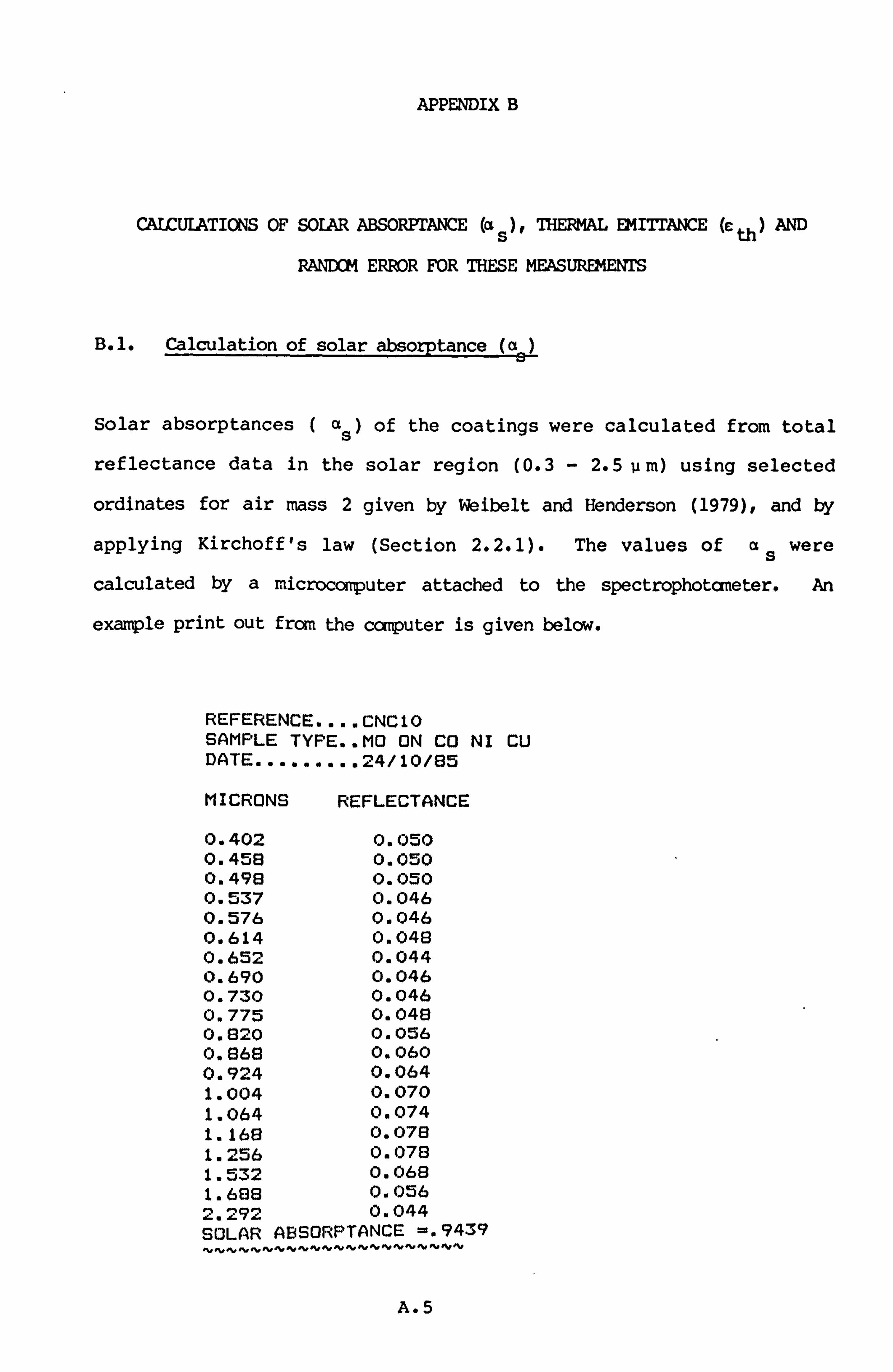
APPENDIX B
CALCULATIONS OF SOLAR ABSORPTANCE (a s
), THERKAL EMITTANCE (c th ) AND
RANDCM ERROR FOR THESE MEASUREMENTS
Calculation of solar absorptance (a )
Solar absorptances ( as) of the coatings were calculated from total
reflectance data in the solar region (0-3 - 2.5 um) using selected
ordinates for air mass 2 given by Weibelt and Henderson (1979), and by
applying Kirchoff's law (Section 2.2.1). The values of as were
calculated by a microcomputer attached to the spectrophotcrneter. An
example print out from the ccrrputer is given below.
REFERENCE.... CNC10 SAMPLE TYPE.. MO ON CO NI CU DATE ......... 24/10/85
MICRONS REFLECTANCE
0.402 0.050 0.4513 0.050 0.498 0.050 0.537 0.046 0.576 0.046 0.614 0.048 0.652 0.044 0.690 0.046 0.730 0.046 0.775 0.048 0.820 0.056 0.868 0.060 0.924 0.064 1.004 0.070 1.064 0.074 1.168 0.078 1.256 0.07B 1.532 0.068 1.688 0.056 2.292 0.044 SOLAR ABSORPTANCE -. 9439
A. 5
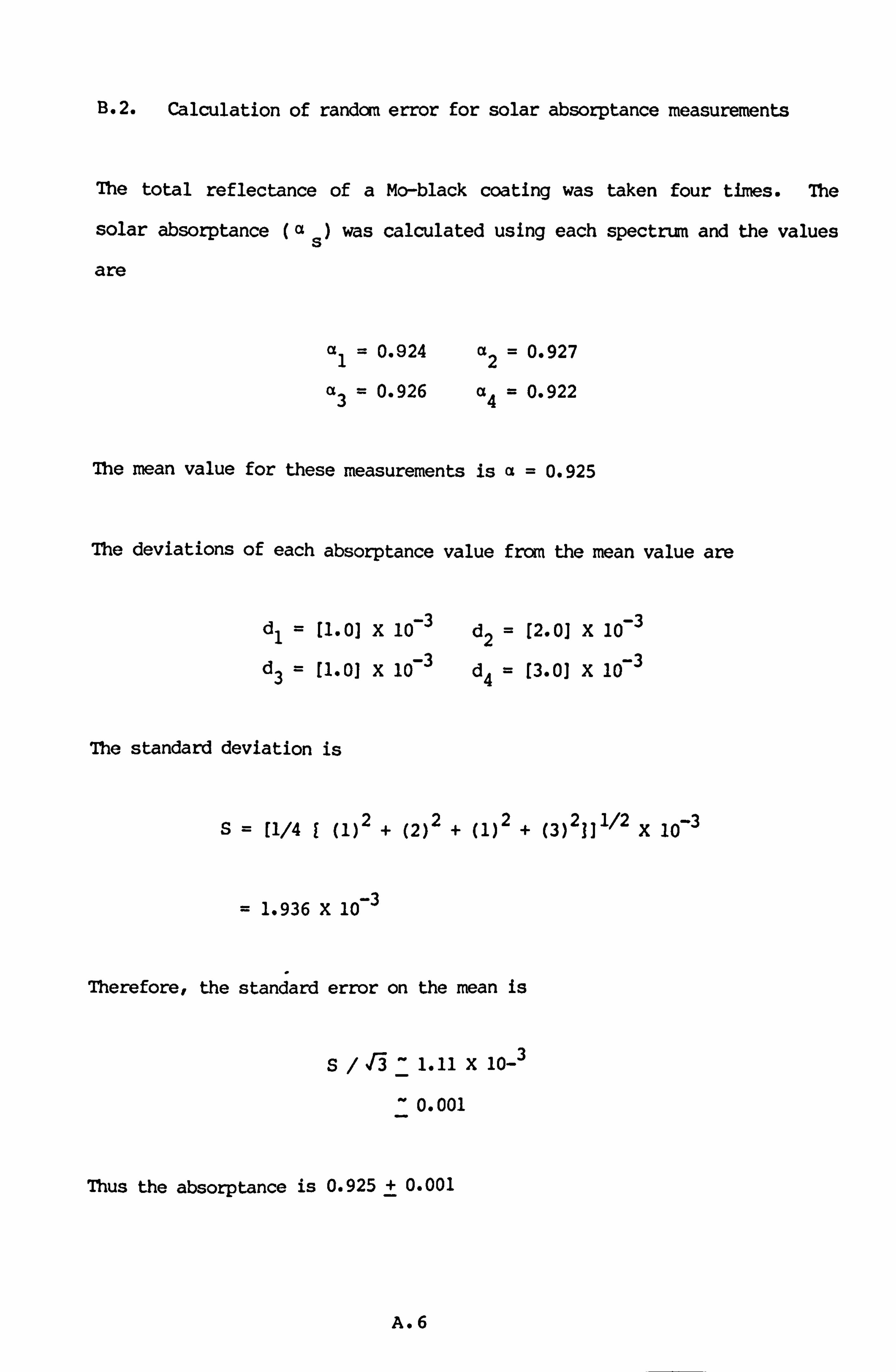
B. 2. Calculation of random error for solar absorptance measurements
The total reflectance of a Mo-black coating was taken four times. 7he
solar absorptance (a s) was calculated using each spectrun and the values
are
0.924 a2=0.927
3=0.926 a4=0.922
The mean value for these measurements is a=0.925
The deviations of each absorptance value from the mean value are
d11, - -3 , [1.0] X 10 d2 -3 [2.01 X 10
d3ý [1.0] X 10-3 d4 [3.01 X 10 -3
The standard deviation is
(1)2 + (2) 2+ (1) 2+ (3) 2 11 1/2 X 10-3
= 1.936 X 10⁻³
Therefore, the standard error on the mean is
r3 - 1.11 X 10- 3
- 0.001
Thus the absorptance is 0.925 + 0.001
A. 6
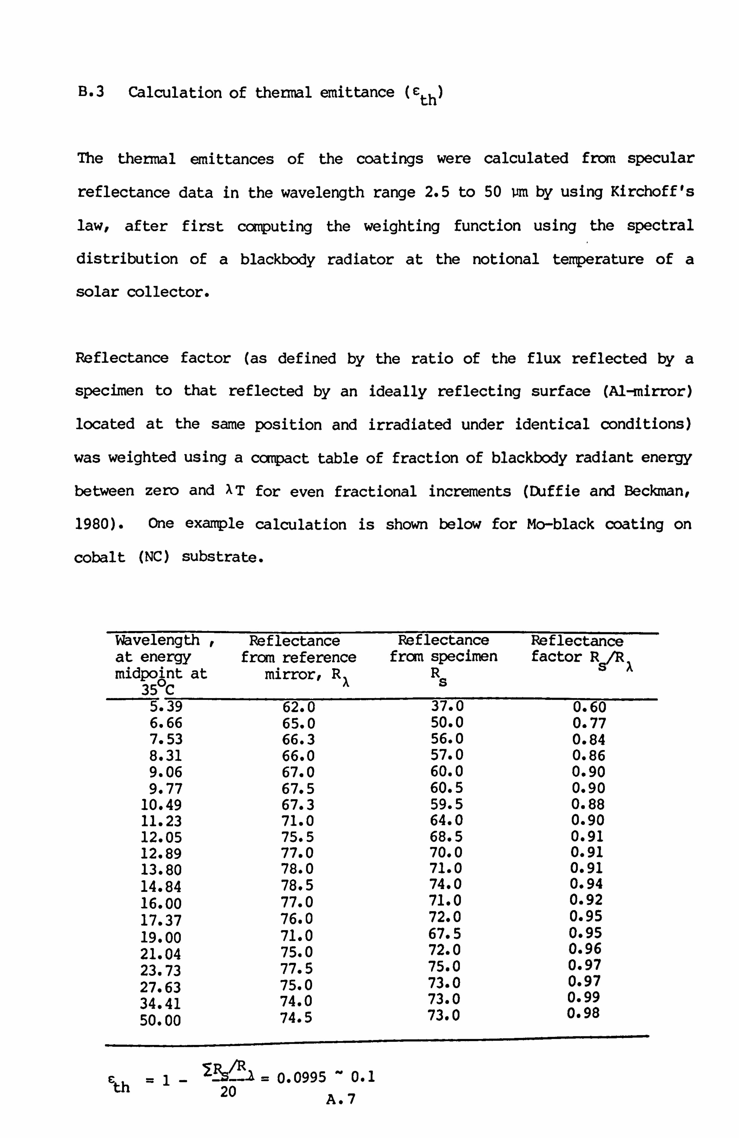
B-3 Calculation of thermal emittance (cth)
The thermal emittances of the coatings were calculated from specular
reflectance data in the wavelength range 2.5 to 50 Pm by using Kirchoff 's
law, after first conputing the weighting function using the spectral
distribution of a blackbody radiator at the notional temperature of a
solar collector.
Reflectance factor (as def ined by the ratio of the f lux ref lected by a
specimen to that reflected by an ideally reflecting surface (Al-mirror)
located at the same position and irradiated under identical conditions)
was weighted using a compact table of fraction of blackbody radiant energy
between zero and XT for even fractional increments (Duffie and Beckmant
1980). One example calculation is shown below for Mo-black coating on
cobalt (NC) substrate.
Wavelength at energy midpint at
3C
Reflectance from reference
mirror, R
Reflectance from specimen
R. S
Reflectance factor Rs/RX
5.39 62.0 37.0 0.60 6.66 65.0 50.0 0.77 7.53 66.3 56.0 0.84 8.31 66.0 57.0 0.86 9.06 67.0 60.0 0.90 9.77 67.5 60.5 0.90
10.49 67.3 59.5 0.88 11.23 71.0 64.0 0.90 12.05 75.5 68.5 0.91 12.89 77.0 70.0 0.91 13.80 78.0 71.0 0.91 14.84 78.5 74.0 0.94 16.00 77.0 71.0 0.92 17.37 76.0 72.0 0.95 19.00 71.0 67.5 0.95 21.04 75.0 72.0 0.96 23.73 77.5 75.0 0.97 27.63 75.0 73.0 0.97 34.41 74.0 73.0 0.99 50.00 74.5 73.0 0.98
jý zc, = 0.0995 - 0.1 Eth 20 - A. 7
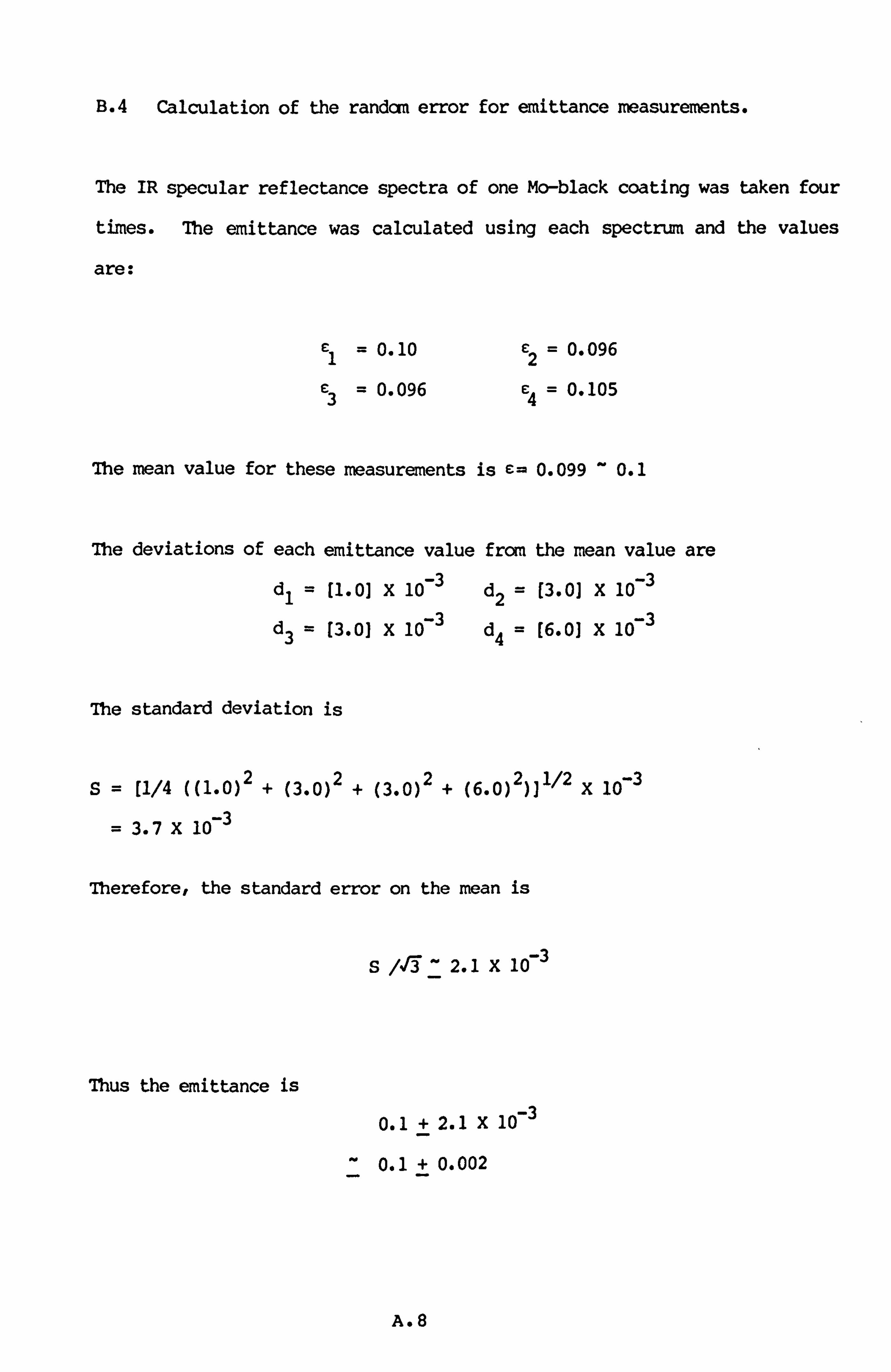
BA Calculation of the random error for emittance measurements.
The IR specular reflectance spectra of one Mo-black coating was taken four
times. The emittance was calculated using each spectrum and the values
are:
E1=0.10 £2 = 0-096
e3 = 0-096 E4 = 0* 105
7he mean value for these measurements is c= 0.099 - 0.1
The deviations of each emittance, value from the mean value are
d, [1.0] X 10-3 d2 ý (3.01 X 10⁻³
d 3 [3.01 X 10⁻³ d= [6.01 4 X 10⁻³
The standard deviation is
[1/4 M. O) 2+ (3.0) 2+ (3.0) 2+ (6.0) 2 )l 1/2 X 10-3
3.7 X 10⁻³
Therefore, the standard error on the mean is
S 1r3 - 2.1 X 10⁻³
Thus the emittance is
0.1 + 2.1 X 10⁻³
- 0.1 + 0.002
A. 8
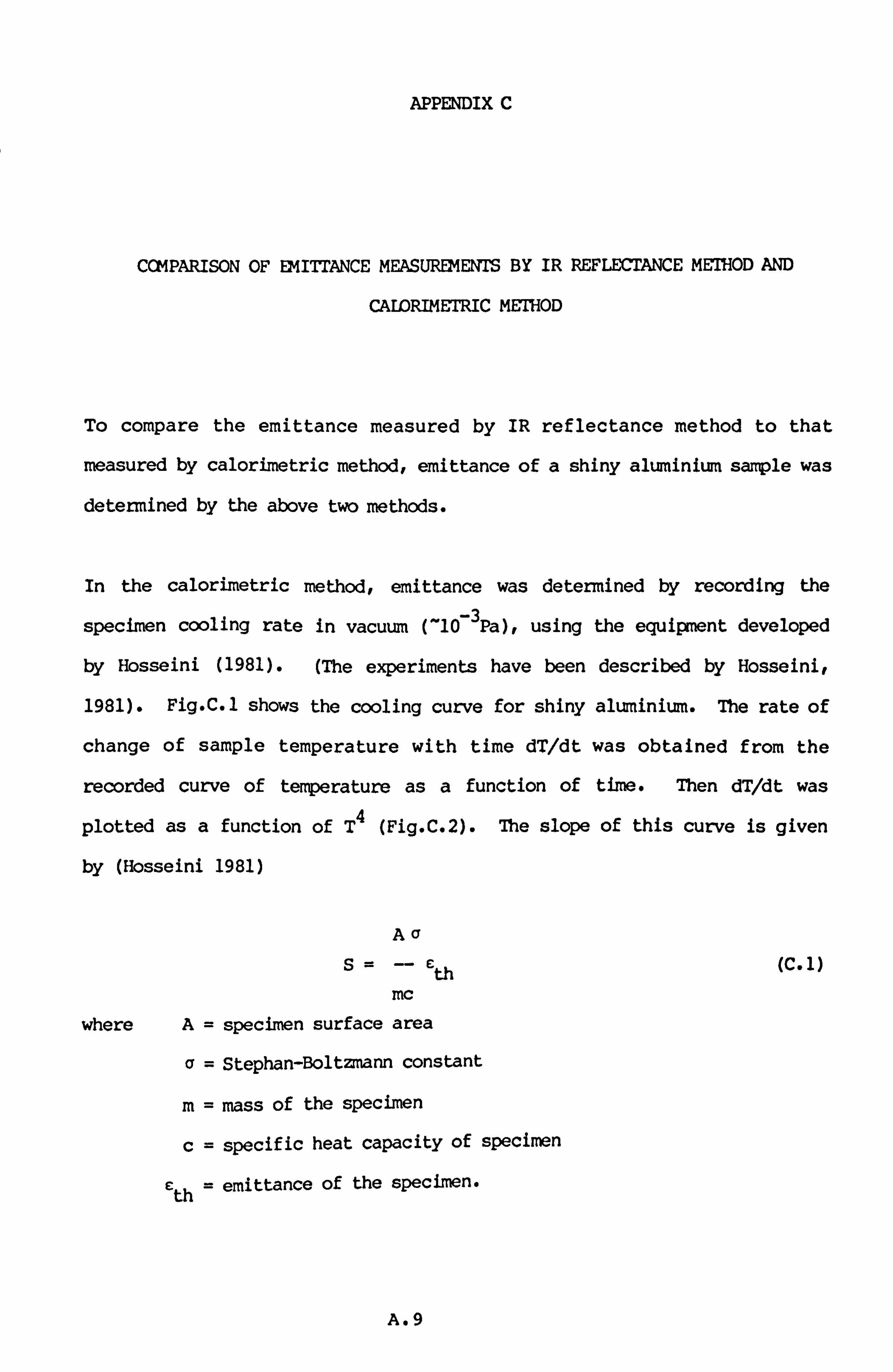
APPENDIX C
COMPARISON OF EMITTANCE MEASUREMENTS BY IR REFLECrANCE METHOD AND
CALORIM=C MMOD
To compare the emittance measured by IR reflectance method to that
measured by calorimetric method, emittance of a shiny aluminium sample was
determined by the above two methods.
In the calorimetric method, emittance was determined by recording the
specimen cooling rate in vacuum (-10-3 Pa), using the equipment developed
by Hosseini (1981). (The experiments have been described by Hosseini,
1981). Fig. C. 1 shows the cooling curve for shiny aluminium. The rate of
change of sample temperature with time dT/dt was obtained from the
recorded curve of tenperature as a function of time. Then dT/dt was
plotted as a function of T4 (Fig. C. 2). 7he slope of this curve is given
by (Hosseini 1981)
Ac' C th
mc
where A= specimen surface area
a= Stephan-Boltzmann constant
m= mass of the specimen
c= specific heat capacity of specimen
C th ý emittance of the specimen.
(C. 1)
A. 9
The slope for the shiny aluninium specimen as obtained from Fig. C. 2- was
2.5 X 10⁻¹²s-lk-3.
The emittance was calculated using equation (C. 1) and is equal to 0.036.
The emittance of the same specimen was calculated f rom the IR specular
reflectance spectrum and the value" was found to be 0.032. The percentage
discrepancy is 11%. It should be mentioned that the emittance measured in
the calorimetric method is the hemispherical value (at -100 0 C) whereas, in
IR reflectance method, the emittance is near normal and measured at roorn
temperature.
A con-parison of infrared emittance measurements and measurement techniques
has been reported by Millard and Streed (1969). The measurements were
made by two calorimetric and four reflectance techniques and with two
portable devices. According to them, for gemoetrically plane and smooth
surfaces the percent deviation of emittance value determined by specular
IR reflectance method is +(2-3)% from the steady state calorimetric value.
Large deviation (+25%) were observed for rough surface as not all the
reflected energy was collected using specular reflectance attacbment.
A. 10
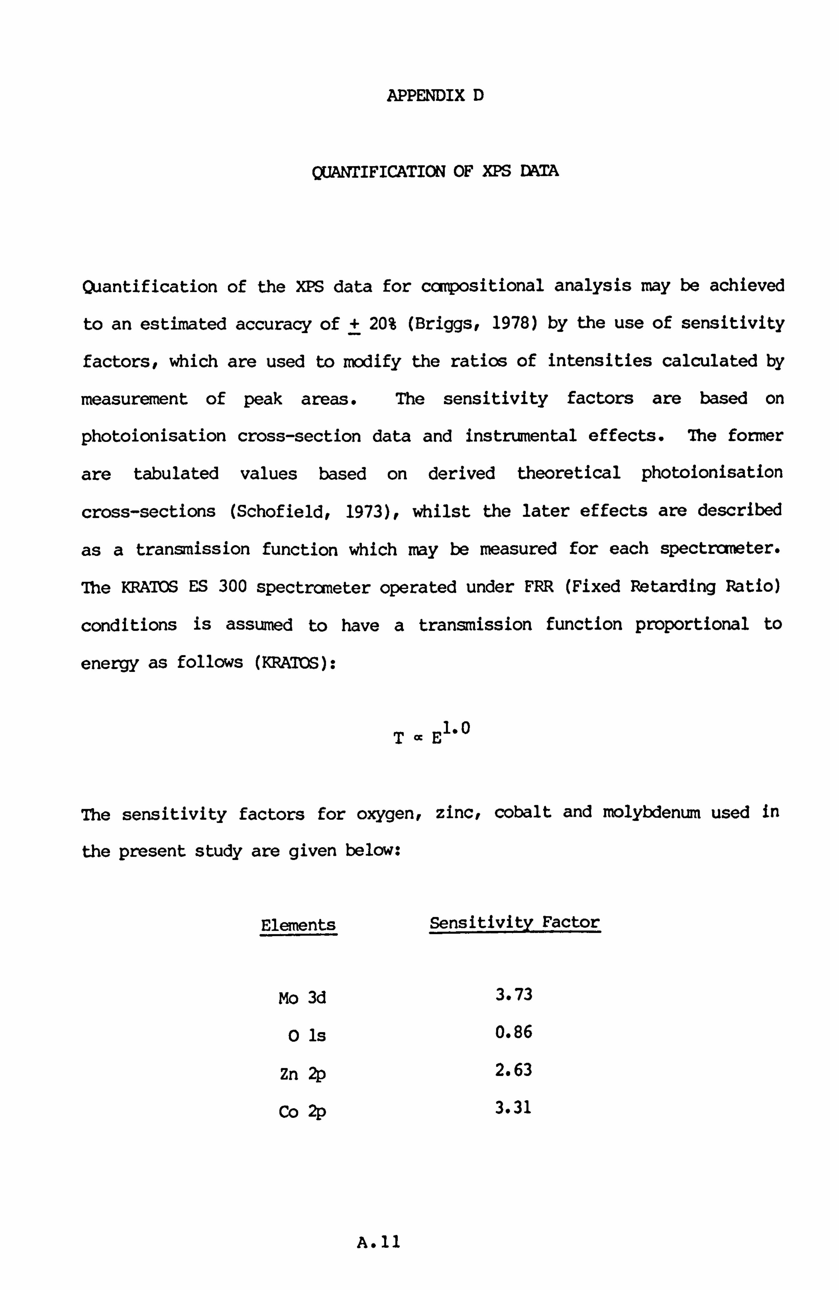
APPENDIX D
QUAMIFICATION OF XPS DATA
Quantification of the XPS data for ccnpositional analysis may be achieved
to an estimated accuracy of + 20% (Briggs, 1978) by the use of sensitivity
factors, which are used to modify the ratios of intensities calculated by
measurement of peak areas. The sensitivity factors are based on
photoionisation cross-section data and instrumental effects. 7he former
are tabulated values based on derived theoretical photoionisation
cross-sections (Schofield, 1973), whilst the later effects are described
as a transmission function which my be measured for each spectrcmeter.
The KRATOS ES 300 spectrometer operated under FRR (Fixed Retarding Ratio)
conditions is assumed to have a transmission function proportional to
energy as follows (KRAIW):
E 1.0
The sensitivity factors for oxygen, zinc, cobalt and molybdenum used in
the present study are given below:
Elements Sensitivity Factor
Mo 3d 3.73
0 ls 0.86
Zn 2p 2.63
Co 2p 3.31
A. 11
APPENDIX E
D. C. CONDUCTION MECHANISMS IN THIN INSULATING FIIMS
The various current transport mechanisms in dielectric thin f ilms have
been extensively reviewed by many authors (Lamb, 1967; Simions, 1971).
The possible mechanisms of conduction processes occurring in
metal-insulator-metal (MIM) structure are illustrated schematically in the
energy band diagram shown in Fig. E. 1 in the presence of an electric field.
The electrons can be injected f rom the metal into the conducton band of
the insulator by af ield-assisted thermal excitation over the potential
barrier at the metal insulator interface (process A). This process is
referred to as 'Schottky emission'. The electrons my also be thermally
excited into the conduction band f rom trapping levels in the forbidden
band of the insulator and this is referred to as the 'Poole-Frenkell
effect (Process B). Electrons may tunnel into the conduction band of the
insulator directly from the mtal cathode (Process C) or from the trapping
levels within the insulator (Process D). If the insulator thickness is
very thin (less than 50 X) electrons can tunnel directly between the
electrodes. Charge injection into the conduction band, tunnelling or
impurity conduction in some cases, results in a build up of space-charge
within the bulk which modulates the transfer process. The effect is
referred to as a space-charge-limited conduction.
A number of above mechanisms my operate simultaneously at one particular
applied voltage, but generally one mechanism dominates the observed
current.
12
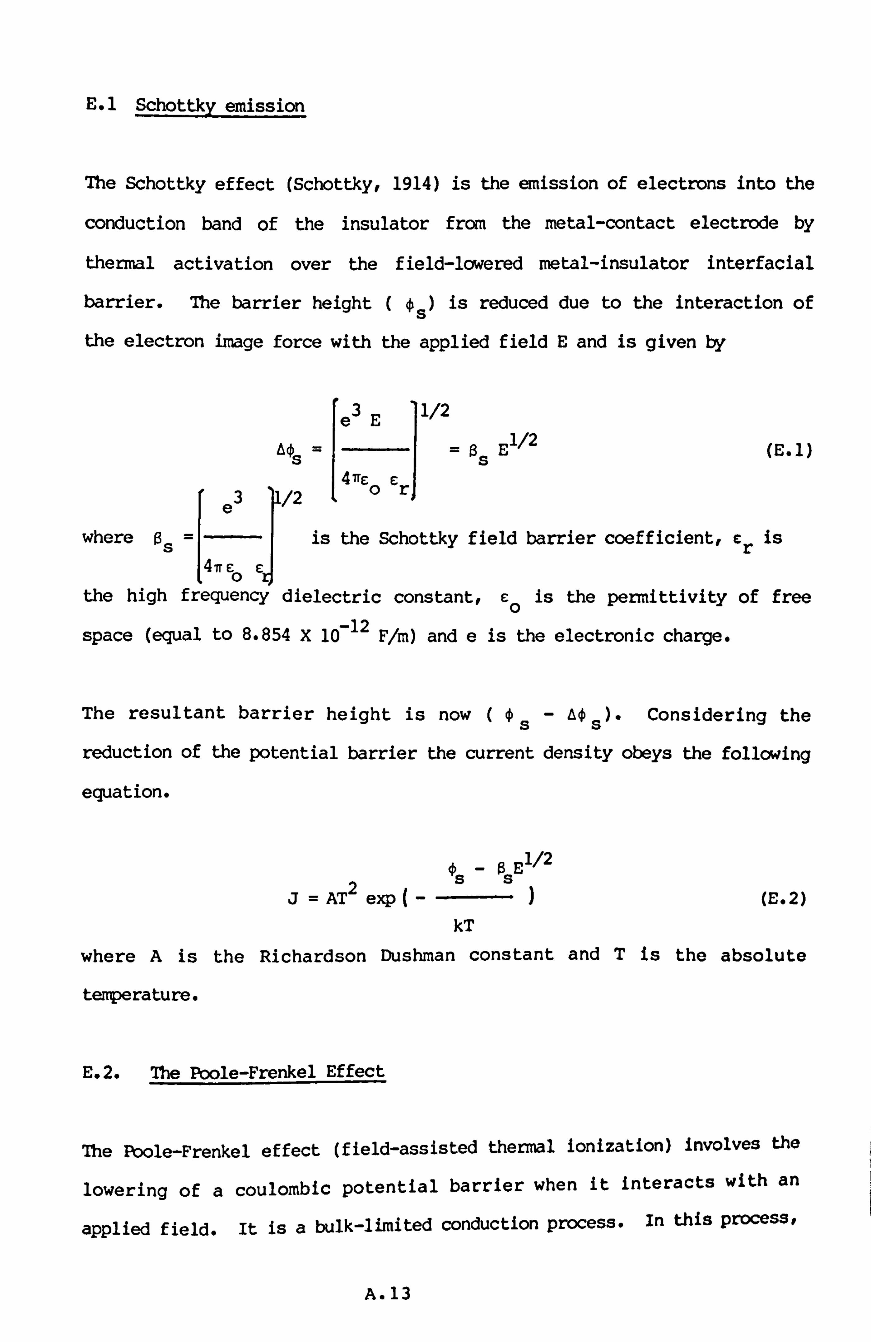
E. 1 Schottky emission
The Schottky effect (Schottky, 1914) is the emission of electrons into the
conduction band of the insulator f rom the metal-contact electrode by
thermal activation over the f ield-lawered metal-insulator interfacial
barrier. The barrier height ýs) is reduced due to the interaction of
the electron image force with the applied field E and is given by
e3E 1/2
-= as E 1/2 (E. 1) s
4 7rc C
e3 1/2
where as is the Schottky field barrier coefficient, er is
41r e 0 ed the high frequency dielectric constant, e0 is the permittivity of free
space (equal to 8.854 X 10⁻¹² F/m) and e is the electronic charge.
The resultant barrier height is now (0s- AO s)-
Considering the
reduction of the potential barrier the current density obeys the following
equation.
aE 1/2
2ss AT exp (--) (E. 2)
kT
where A is the Richardson Dushman constant and T is the absolute
teirperature.
E. 2. The Poole-Frenkel Effect
The Poole-Frenkel effect (field-assisted thermal ionization) involves the
lowering of a coulombic potential barrier when it interacts with an
applied field. It is a bulk-limited conduction process. In this process#
A. 13
the emission of electrons occurs fran trapping centres in dielectrics into
the conduction band by joint effect of tenperature and electric field. In
a uniform electric f ield the reduction of a coulcmbic barrier, Aý PF' is
given by
3E 11/2
2'- - *ý aE JL/, G (E. 3) PF PF 7r CC
e3" 1/2 0r
where $ PF - is the Poole-Frenkel coefficient which is
7r CC o r,
analytically equal to twice the value of 0s, i. e., 0 PF =2 Os*
Frenkel (1938) suggested that the ionization potential 0 PF of the atoms
in a solid is lowered by an amount AO PF as in equation (E. 3) in the
presence of a uniform electric field. The resultant barrier is now
( OPF - AOPF) *
The current density in thin f ilm insulators containing shallow traps is
given by (Mead, 1962).
aE 1/2 PF
j0 exp (-I (E. 4) kT
where J0= Nce vE exp (- ý PF / kT)
is the low field current density.
(E. 5)
In equation (E. 5) V is the mobility of the charge carriers and Nc is the
effective density of states in the conduction band of the insulator.
A. 14
APPENDIX F
CONCEPTS OF AN ENERGY BAND STRUCTURE
A crystalline material is characterized by the presence of a definite long
range order of the atomic constituents of the material. The main
characteristics of the energy distributions, of the density of states of
crystalline materials are the sharp band edges in the valence and
conduction bands. The forbidden energy gaps which separate the valence
and conduction bands are well defined as shown in Fig. F. I(a).
Non-crystalline or amorphous materials do not have a well ordered array of
atomic constituents and there is virtually no long range order in the
material (although short range order will generally be present (Mott,
1969)). It is believed that the lack of long range order in
non-crystalline materials leads to tails of states extending from the
valence and conduction bands (Fig. F. I(b)). The existence of these
localised states, termed as 'band tails', causes smearing of the valence
and conduction band edges, so that the optical energy gap is no longer
well defined (Simmons and Verderber, 1967). Furthermore, non-crystalline
materials are thought to contain inperfections, such as impurities or
dangling bonds or microvoids and these may lead to levels within the
forbidden energy gap which are called 'impurity bands' as shown in
Fig. F. l(b) (Davis and Mott, 1970). The energies Ec and Ev (Fig. F. l(b))
separate the ranges of energy where the states are localised and
nonlocalised. The energy intervals Ec-EA and EB - Ev are the width of
localised states. According to Davis and Mott (1970) the optical band
gap, E opt , is equal to EA - Ev or Ec - EB which ever is smaller.
15
APPENDIX G
CALCULATION OF REFLECLAME Rx USING THE VAUIES OF OPTICAL CONSTANIS
For a thick homogenous coating when the interference effect is absent, the
reflectance Rx is given by (Williams et al, 1963)
R+R (1-2 R,, ý e -2acXd icA. MA
RRe -2a CA d
mx CIX
The meaning of the symbols has been given in section 5.2.1. To apply this
equation to a thick Mo-black dip coating in the shortwavelength region
(below 0.7 um) where no significant" interference peak has been observed,
it was assumed that R,,, - the reflectance at the air coating interface is
equal to the reflectance from a thick coating. The values of Rx has been
calculated at two different wavelengths 0.4 um and 0.8 im.
At 0.4 jim R cx = 0.08
At 0.7 jim Rcx = 0.11
Frcm the transmission measurements
ac, x = 5.7 X 10 4 cm-1
ac Xx kcX =
4 -rr
= 0.18
(G. 2)
16
From equation (5.4)
(n cx- nmx )2+ (km X- kc X)
2
(nc ,+N)2+ (kIn kc X )2 mx
At X=0.4 pm, nm ,=0.846 km X= 2.917
The values of nmx and kmx has been taken from American Institute of
Physics Handbook (Gray, 1972). The value of n cx has been taken from the
transmission measurement (Table ý. 7.1).
ncx =4 at Az0.49 pm
Frcrn (G-3) at X=0.4 pm
(4 - 0.846 )2 + (2.917 - 0.18) 2
RX=-
(4 + 0.846) 2+ (2.917 + 0.18) 2
0.52
For a coating of thickness 0.3 m, the tem e -2a cx d-0.03.
Using the values of RX, R', and the term e -2a cx d in equation (G. 1)
mc
R. (cal) - 0.09
Similarly, using the values nmX and k mx at wavelength 0.7 Pm and also the
value of n at about 0.77 jim (as obtained from table 3.7.1), R has been cX MA
calculated and is equal to 0.33. Then the ref lectance RA at 0.7 ji m has
been calculated for the same coating and compared with the experimental
value of R. * The calculated and experimental values of RX are given in
Table 5.4(b).
17
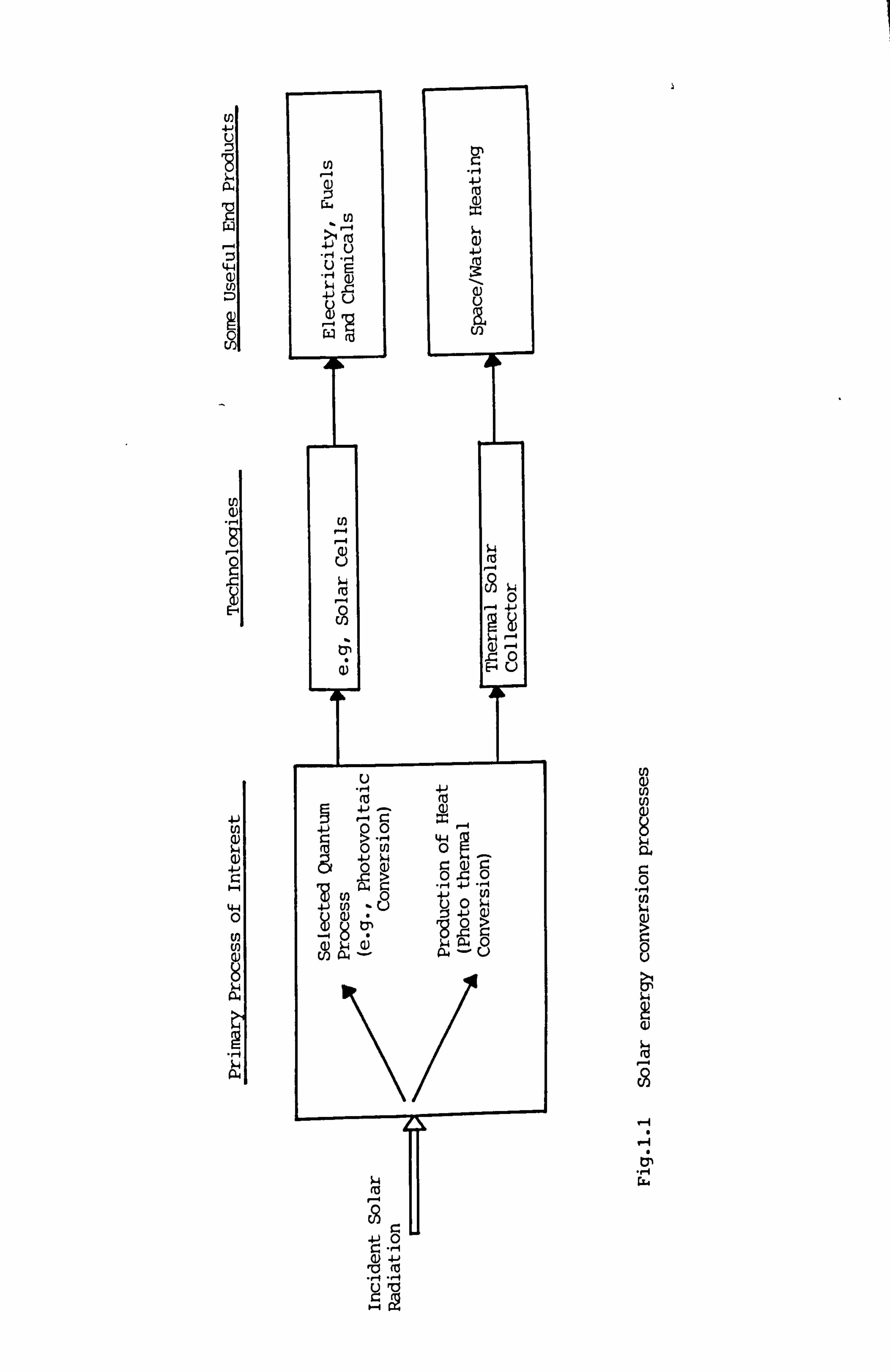
En 41 U Z t»
tn :
14-4
U) G) Z: ) 4-) L)
U)
08 rö
(ö ý
ý4 0
Q)
cö (0 4. J
5 ; t: ZM tn 4j 00 > 44
u) 0
gz C. ) -4, C . 1c4) b4 (n 4-)
4-4 -8 0 0 Icri-ý (0 ý Icri-ý
N4 (ö
.ý
v (0 . 14 -14
c: 10
a)
09
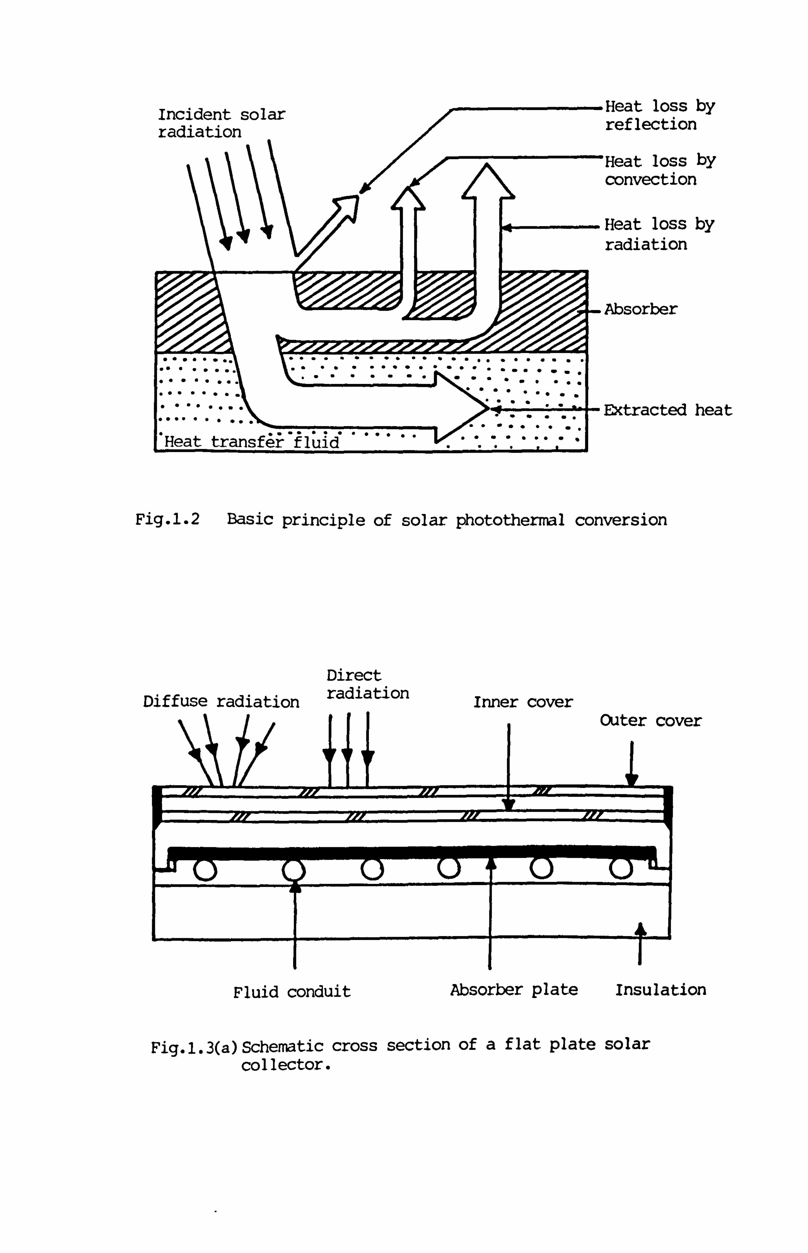
Incident solar radiation
Heat loss by reflection
Heat loss by convection
Heat loss by radiation
Absorber
Extracted heat
Fig. 1.2 Basic principle of solar photothermal conversion
ver
Fluid conduit Absorber plate Insulation
Fig. 1.3(a)Schematic cross section of a flat plate solar collector.
Direct
Diffuse radiation radiation Inner cover
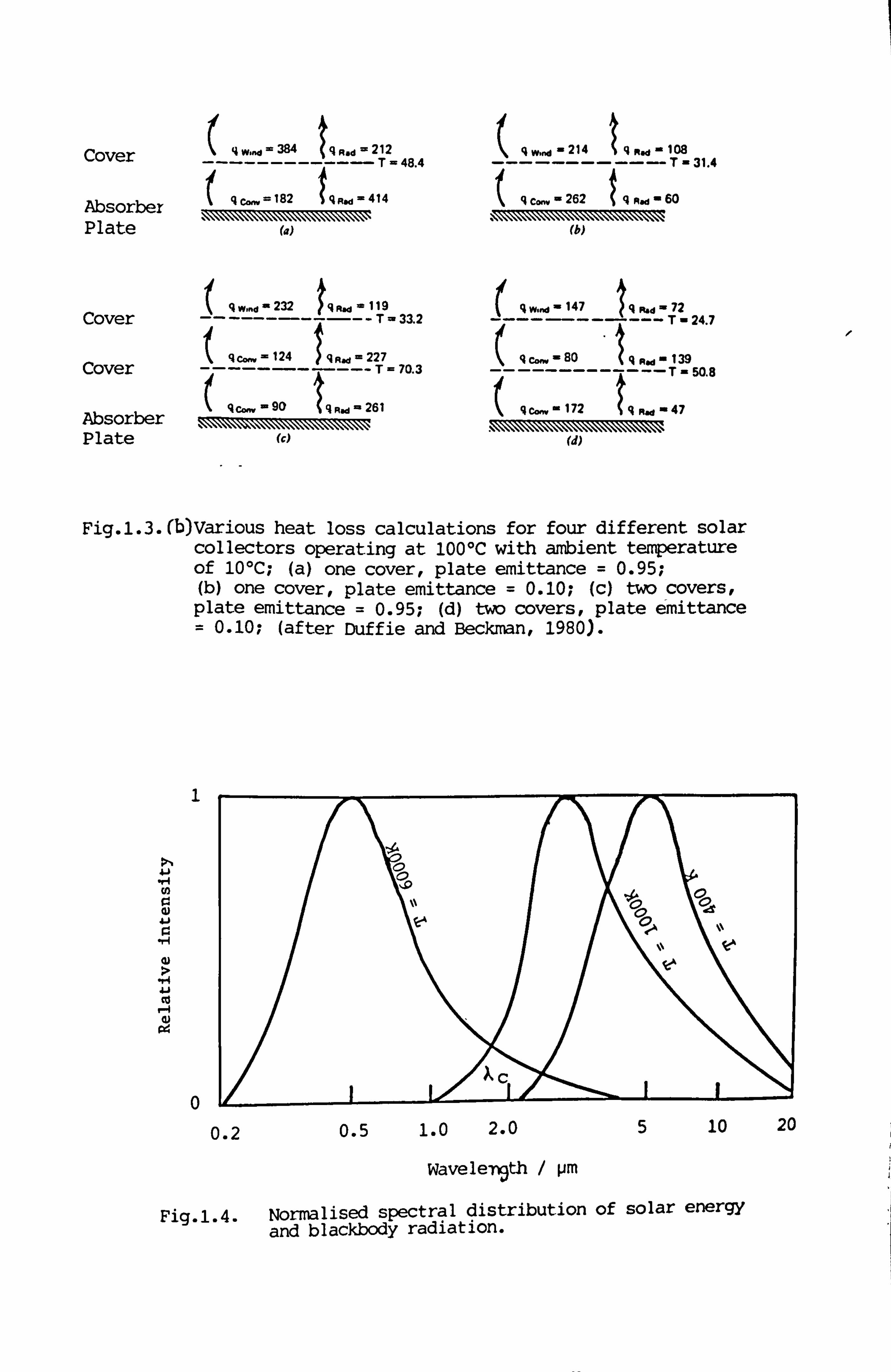
Cover q W--d = 384
tq
R. d 212 q mnd 214 q Rd 108 -- T 48.4 T- 31.4
Absorber qc-=182
fq
Rod 414 q c. 262 q FId 60
Plate (b)
q w, nd = 232
tqRd
11 9 q w, nd 147
i
7ý Cover . 24 7 T
(
qc--124
IqRd-227
qc--80
Iq
md 139 Cover ' T- 50.8
Absorber
(
qc--90
tq_Rd
- 26 1 q c- - 172
fR
Rd 47
Plate (c) (d)
Fig. 1.3. (b)Various heat loss calculations for four different solar collectors operating at 10011C with ambient temperature of 10*C; (a) one cover, plate emittance = 0.95; (b) one cover, plate emittance = 0.10; (c) two covers, plate emittance = 0.95; (d) two covers, plate emittance = 0.10; (after Duffie and Beckman, 1980).
1
P. % (0 0
13)
Co
p4
0
vk- 0 SA
xc I
0.2 0.5 1.0 2.0 5 10 20
Wavele7)gth / pm
Fig. 1.4. Normalised spectral distribution of solar energy and blackbody radiation.
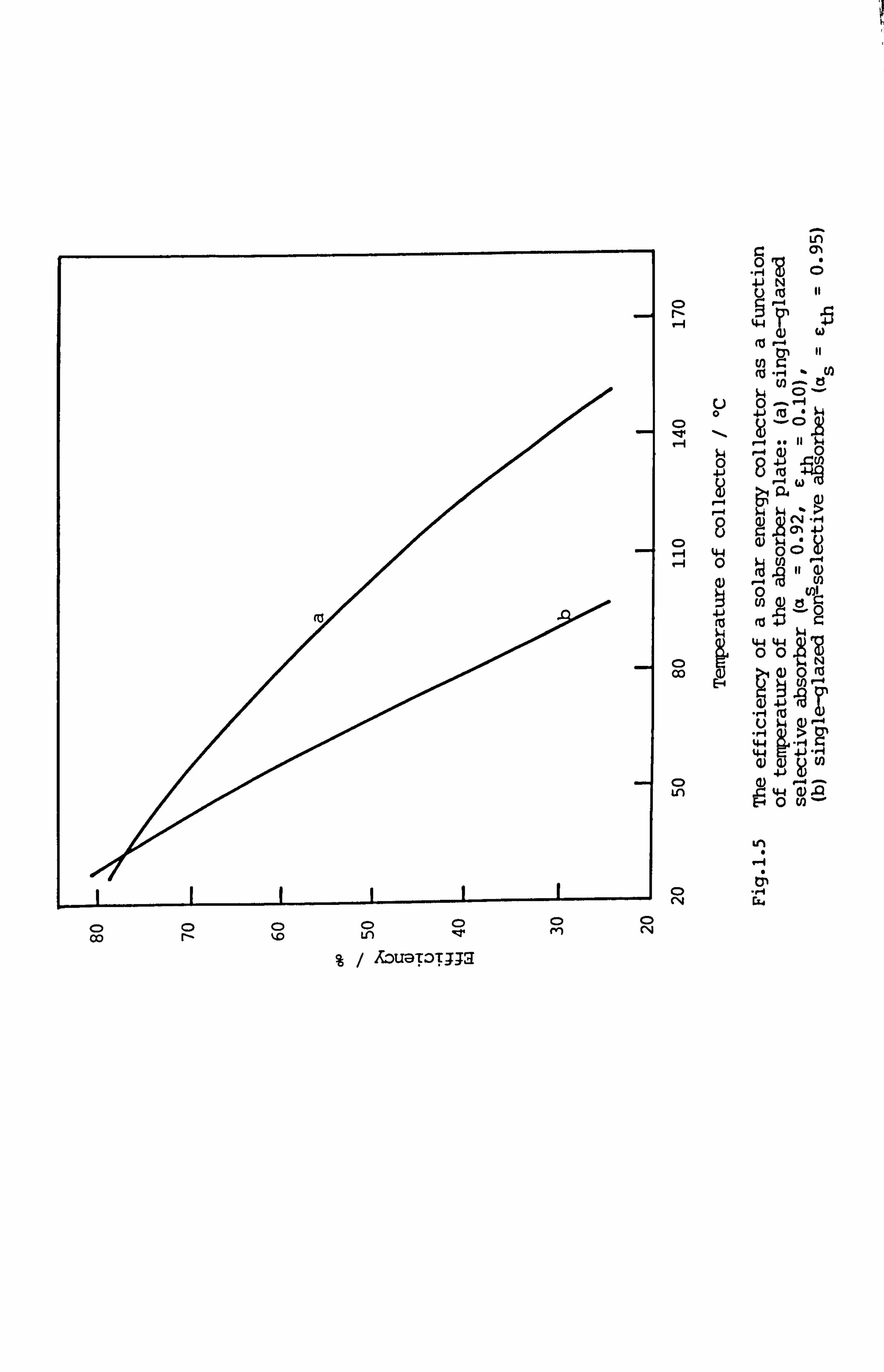
0
ý4 0 4-)
8 -4
44 0
4J
C) co
C) Ln
C) r*4
.0 rg 4J N
in
En r. ts 0- 0 --4
-CD
0
8 to
ý4 W
aN 4-) ý4
C; 0
U) 0 U)l U) ts ý::
0
44 44 00
N 0) 0 ra
U) f-4
. (a -2 K uW 44 4j .
W, 41
a) -1 - 644
0
Le)
tP
%/A. utoTJJa
C) C> C) C) C) 00 r- t. 0 Ln qzr
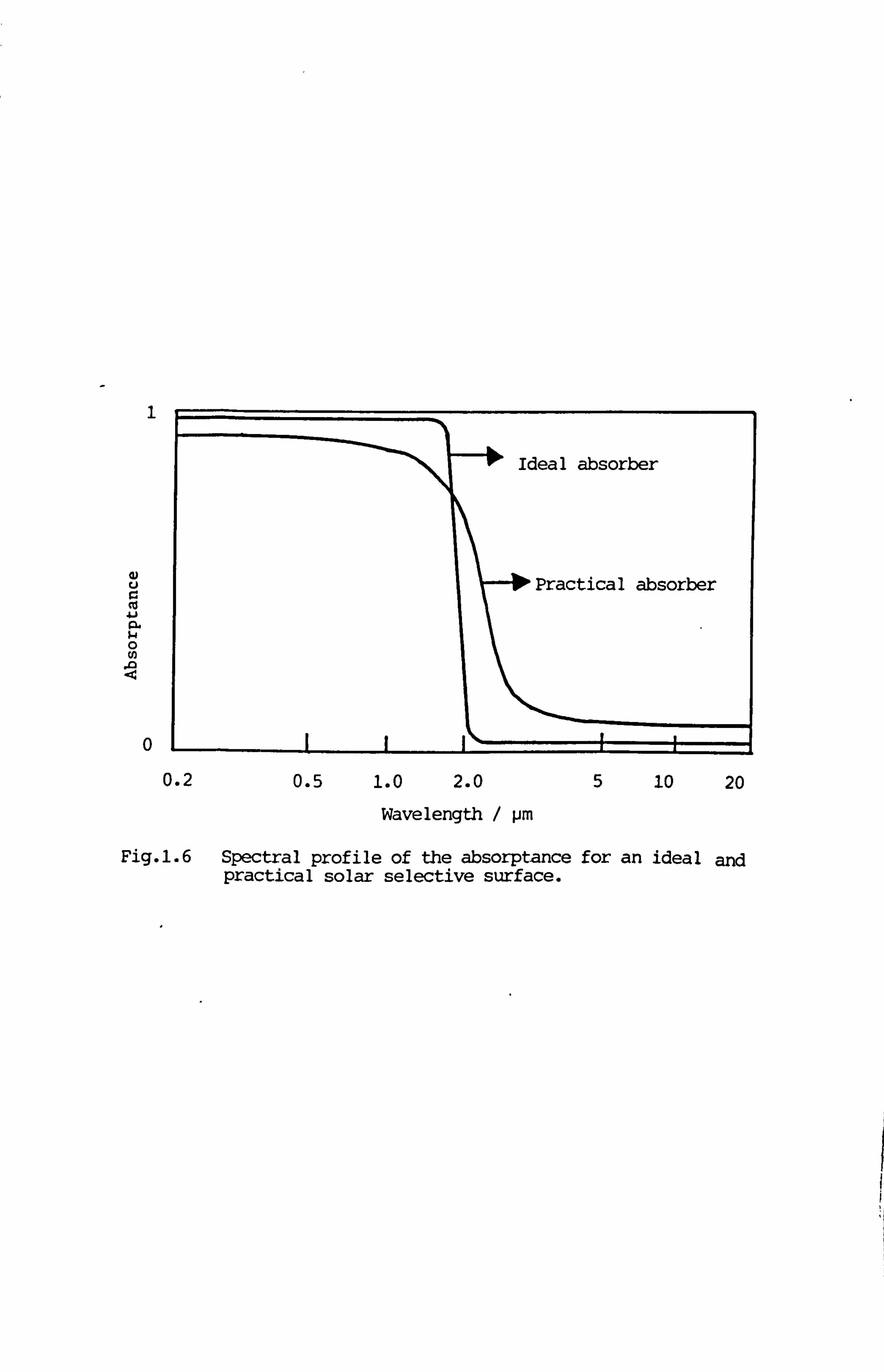
1
Ideal absorber
(L) u Z cu 41
0 (n
. 92
0
Practical absorber
0.2 0.5 1.0 2.0 5 10 20
Wavelength / pm
Fig. 1-6 Spectral profile of the absorptance for an ideal and practical solar selective surface.
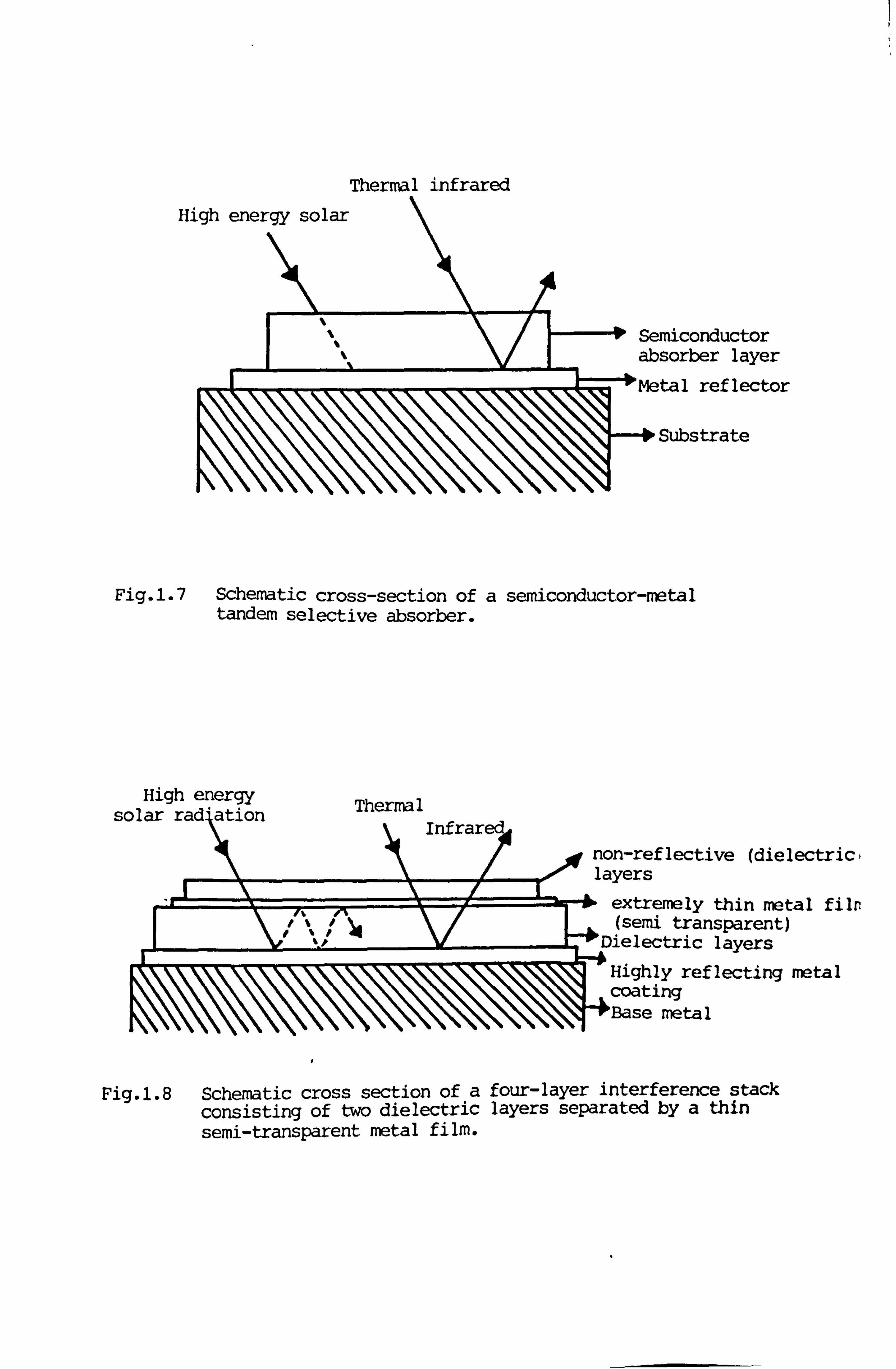
Hi
miconductor )sorber layer
ýtal reflector
Substrate
Fig. 1.7 Schematic cross-section of a semiconductor-metal tandem selective absorber.
High energy Thermal solar radiation
non-reflective (dielectric,
// --#" - layer 4
extremely thin metal filn )0 (semi transparent) v
Dielectric layers
Highly reflecting metal coating Base metal
Fig. 1.8 Schematic cross section of a four-layer interference stack consisting of two dielectric layers separated by a thin semi-transparent metal film.
Thermal infrared
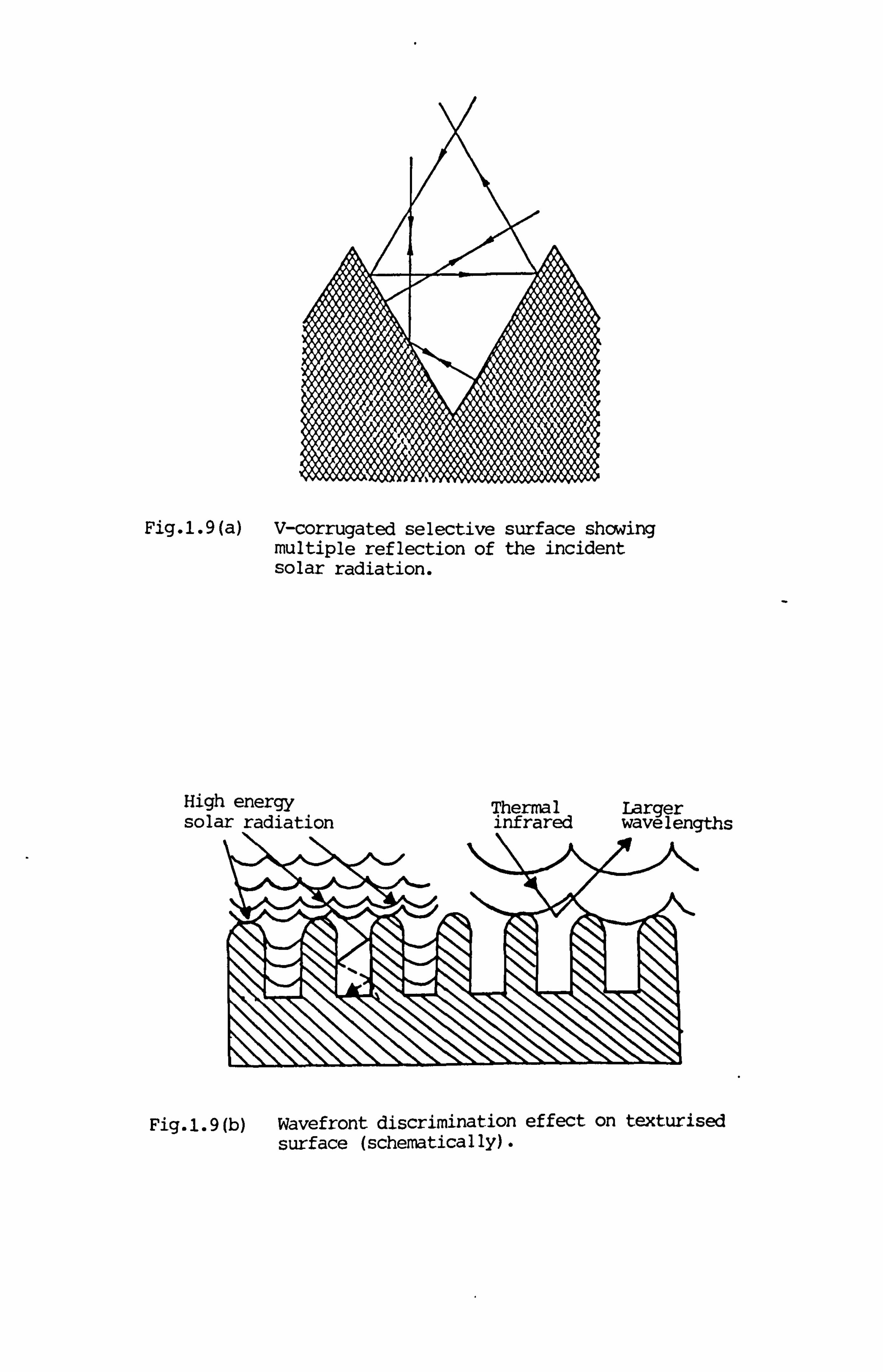
Fig-1.9(a) V-corrugated selective surface showing multiple reflection of the incident solar radiation.
High energy Thermal Larggr solar radiation infrared wavelengths
Fig. 1.9(b) Wavefront discrimination effect on texturised surface (schematically).
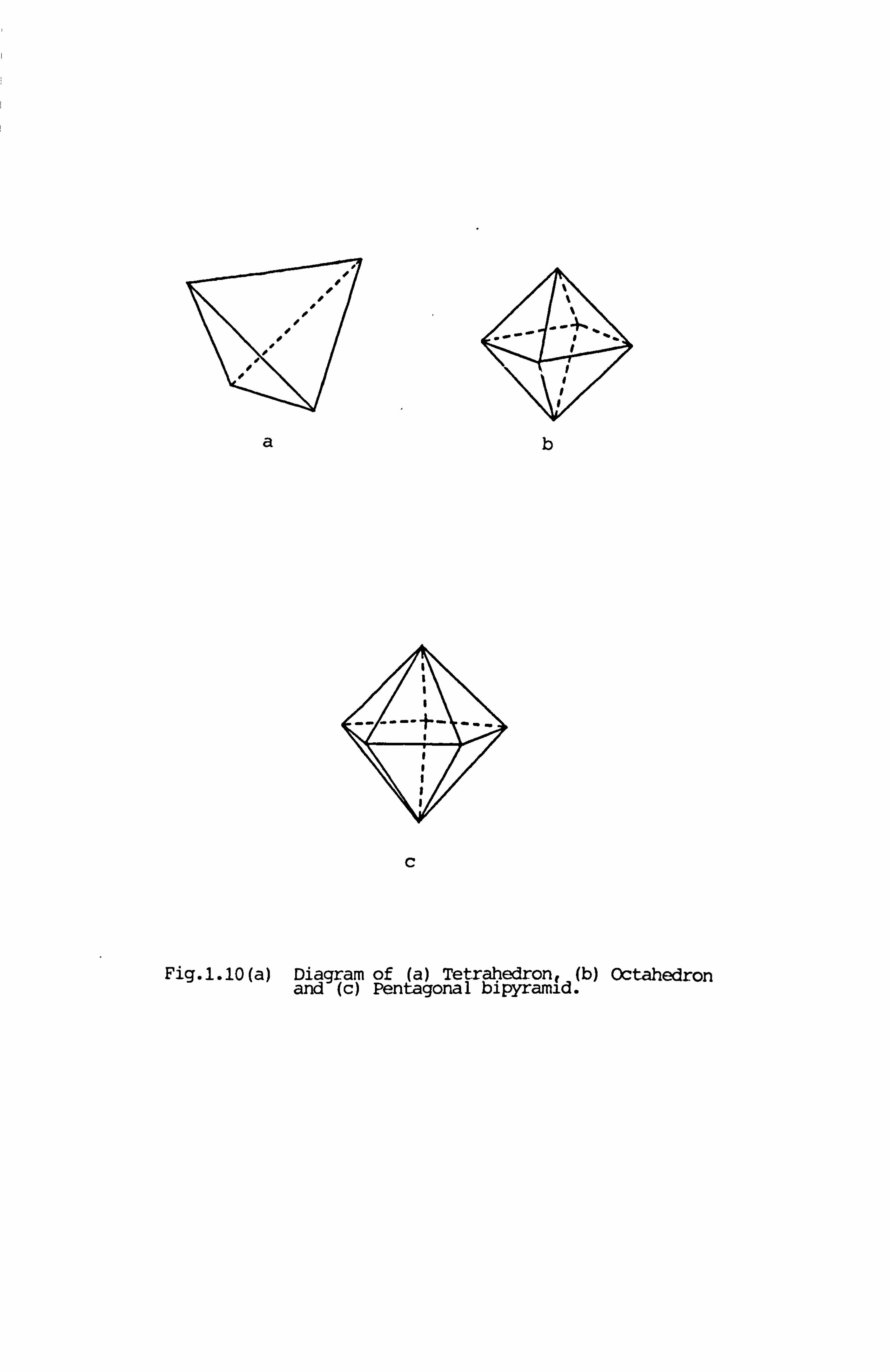
Fig. 1.10(a) Diagiýam of (a) Tetrahedron, (b) octahedron and (c) Pentagonal bipyramid.
0/1o(y-i) (D mo (y. i)
@o('-. dir) 00(, - ý, 1) @0(, -, 3) do
Fig. 1.10. (b) Projection of the unit cell of Mo 40 11 parallel to [0 1 01 (after Magneli, 1948).
(a) (b)
Fig. 1.11. (a) The rutile otructure type. Three unit cells are indicated.
(b) The MoO structure type. The black circles represeAt Mo-atoms- (after Magneli and AnJersson, 1955).
ctj, Ao
Fig. 1.12. Crystal structure of Moo viewed along (001). The extension of one uniý cell is indicated by dashed line5; (after Andersson and magneli, 1950).
> 4-) 4.7 -4
0.8
0.4-
0 LL" 300
Fig. 1.13.
:? uu f L" II VV i .ý-. -
Wavelength (nm)
optical absorption spectra of MoO3 before and after electrolytic colouration. (after Colton et. al, 1978).
2
6
il Im
1
Fig. 2.1. Schematic diagram of electrodeposition apparatus.
1. Low voltage stabilized power supply. 2. Ammeter 3. Thermometer 4. Anodes 5. Substrate 6. Specimen holder 7. Solution tank 8. Hot water bath
0
0
tn 0 Ln C) Ln 0 Ln 0
en cli C, 4 1--4 1-4
WD5 s- . OT/SSPW BUTIPOD
r-
%D
Ln
"T
M
CV
-4
0
41
10
ý4 ý2
A
8
rn 41 B
-4
0 Q) ., q Z .H En 4. )
$14 V'R
W -401
POO
4j 0. En B (o 44
0
-1 U) 4. ) (a C:
. r. 4 N
ý r- >0
15
(14
10 Ln
C)
U) E0 (a E
4-) (a
35 40 45 50 55
Temperature/ 0C
Fig. 2.3. Variation of coating mass per unit area of the plating solution for Mo-black dip etched Zn substrates at fixed deposition
60
with temperature coatings on time (60 seconds).
Aperture and Coll Mount 4
RIA RI Reference Beam F- 41 \RI
RIB
R3
Sample Beam I 132ý
S2
Is"
SPECULAR EXIT PORT
G
E
Sample Surface Reference Surface
Fig. 2.4(a) Optical diagram of an integrating sphere.
0 ul z
U3
> I 4J
t
ý4 A 144 Q)
24-) lip
ý4
4-) Z. rý 1.., -4 $4
a) z U) 0
U) 4J
> 4--) -H 4ý
10.1 4
U) a) -4 U
U)
Cl) . 1-4 >
4-)
CN -1 Ln -,
1%
44 0
IU 1-4 .1 a) 10 41
0 0
4J
CV
t; -1 Eu
ý,, ) it I, )t ( ), j I'll 'i I
Samp I (-
Fig. 2.5. Photograph and optical diaqram of specular reflectance attachment for Perkin Elmer 683 IR spectrometer
(b) Of)tjcdl dicigiim
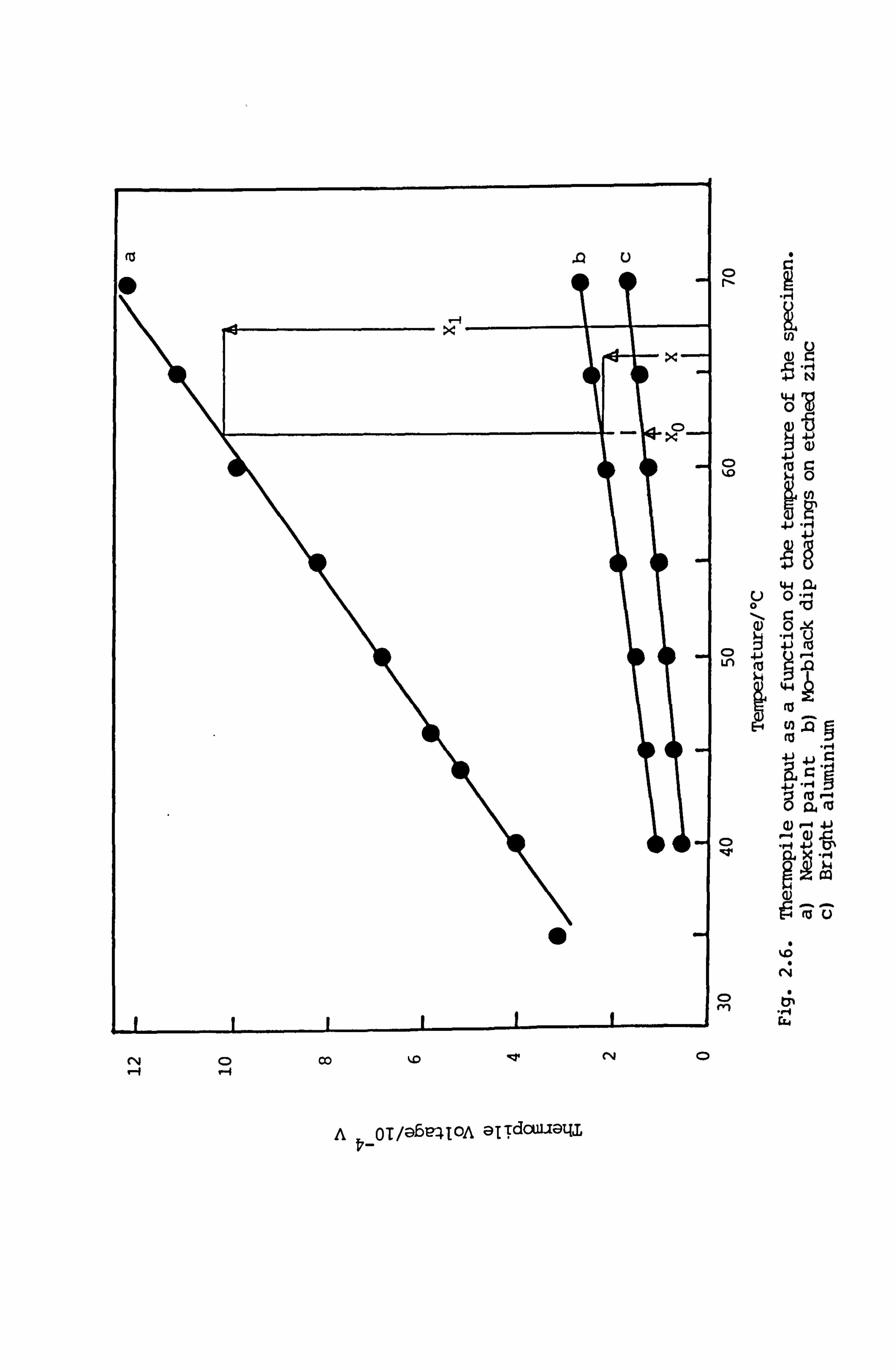
I II
.
I
(N C: ) 00 ýD ry 0 4 -4
0 N
0
u
C) Ln a
I
0
U) 0
Q) cz
4-4 0
4. )
4-1 M 0-, 4
10
.9 -ö
4-) (0 4
§0 44
tu ul
mX -m RMCIQI
a)
ý8 C4
A OT/; DfDe4lOA alTdouu; 9,4j,
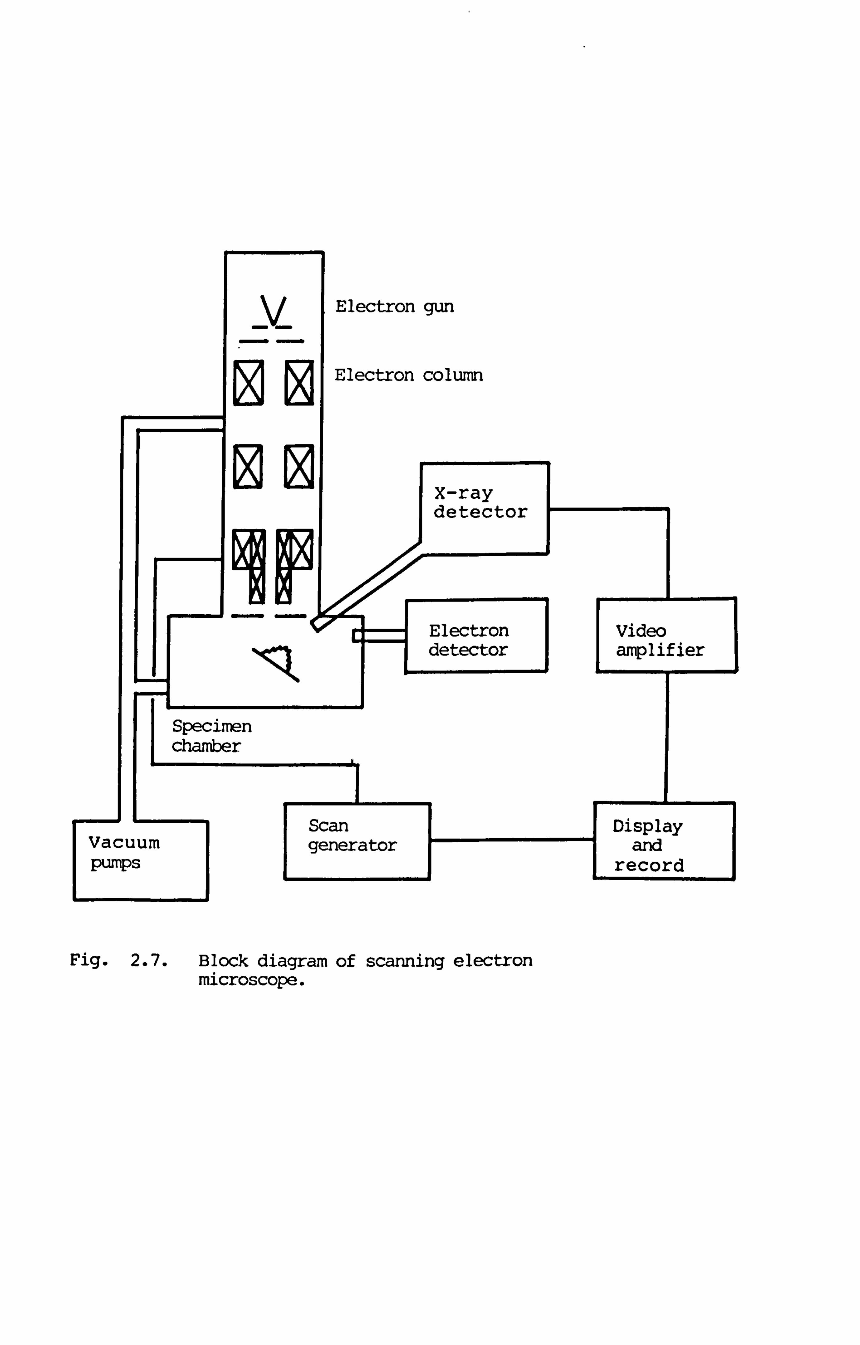
Electron gun
Electron column
X-ray detector
Electron [Video
lif _T
detec amp 1 if Lier
Specimen chamber
Scan Display Vacuum generator and
s record pumpi'71
11
Fig. 2.7. Block diagram of scanning electron microscope.
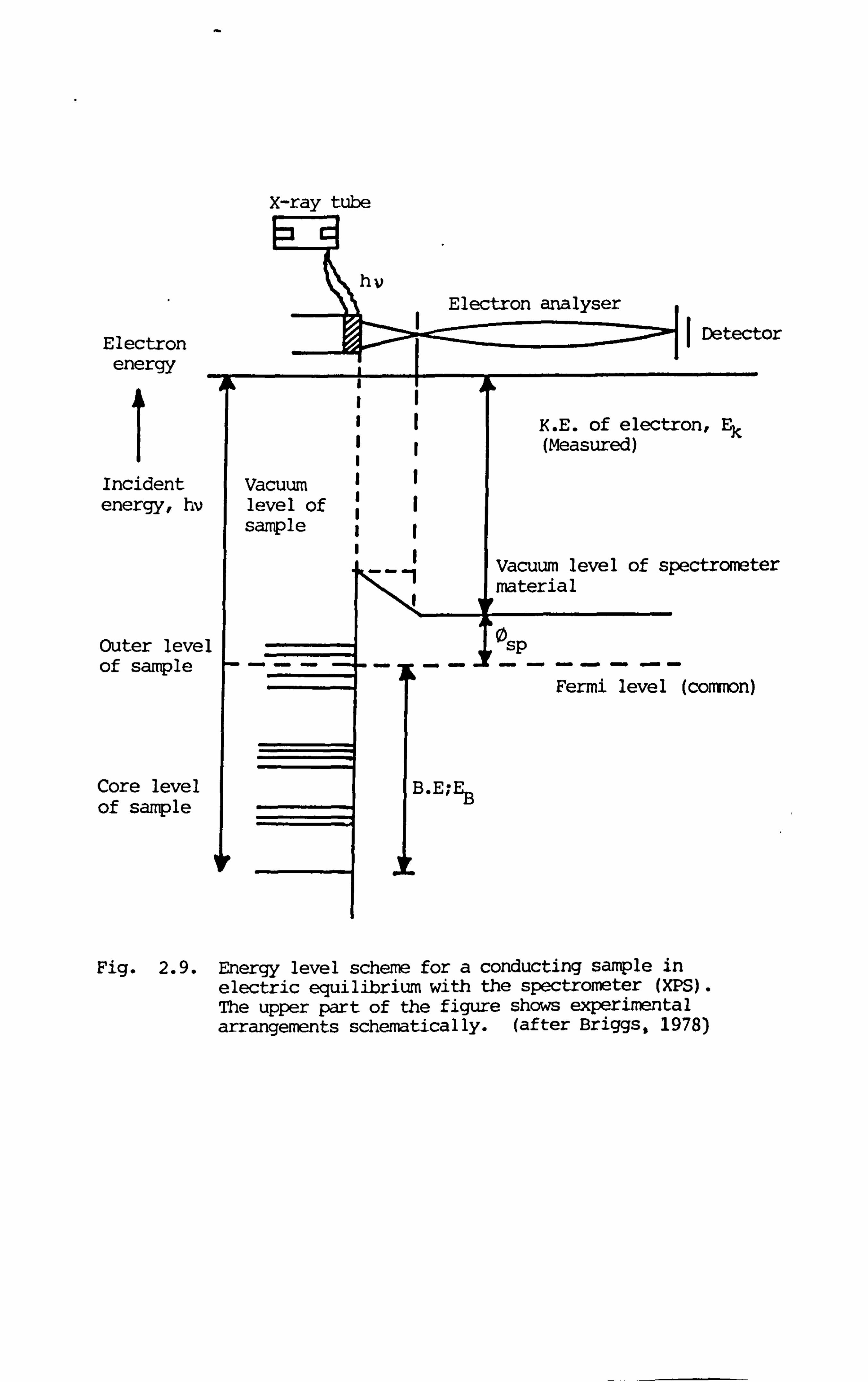
X-ray tube
hv
Electron energy
Incident Vacuum energy, hv level of
sample
Outer level of sample
Core level B. E; % of sample
Electron analyser I Detector
K. E. of electron, Ek (Measured)
Vacuum level of spectrometer material
OSP
Fermi level (common)
Fig. 2.9. Energy level scheme for a conducting sample in electric equilibrium with the spectrometer (XPS). The upper part of the figure shows experimental arrangements schematically. (after Briggs, 1978)
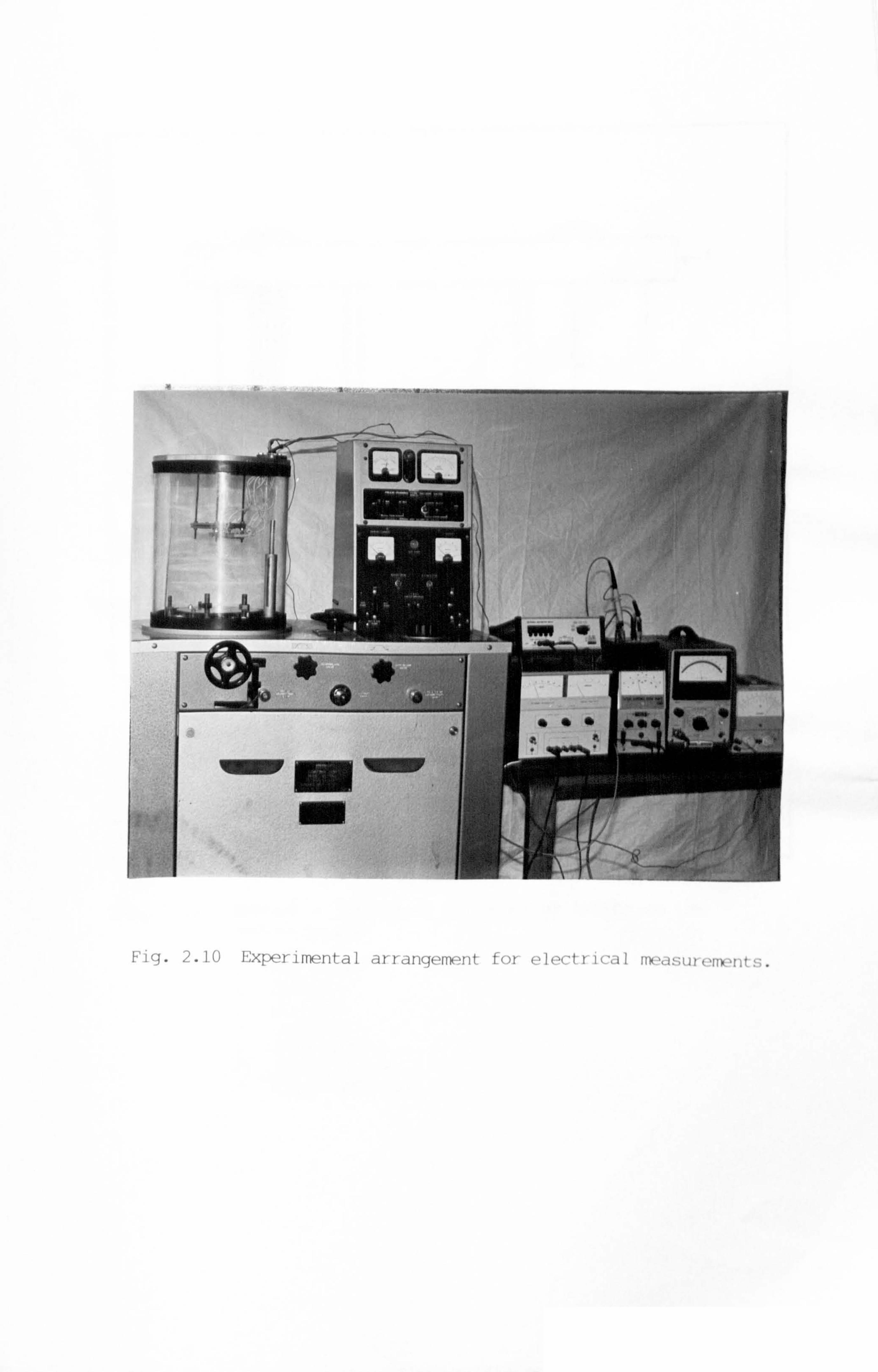
Fig. 2.10 Experimental arrangement for electrical measurements.
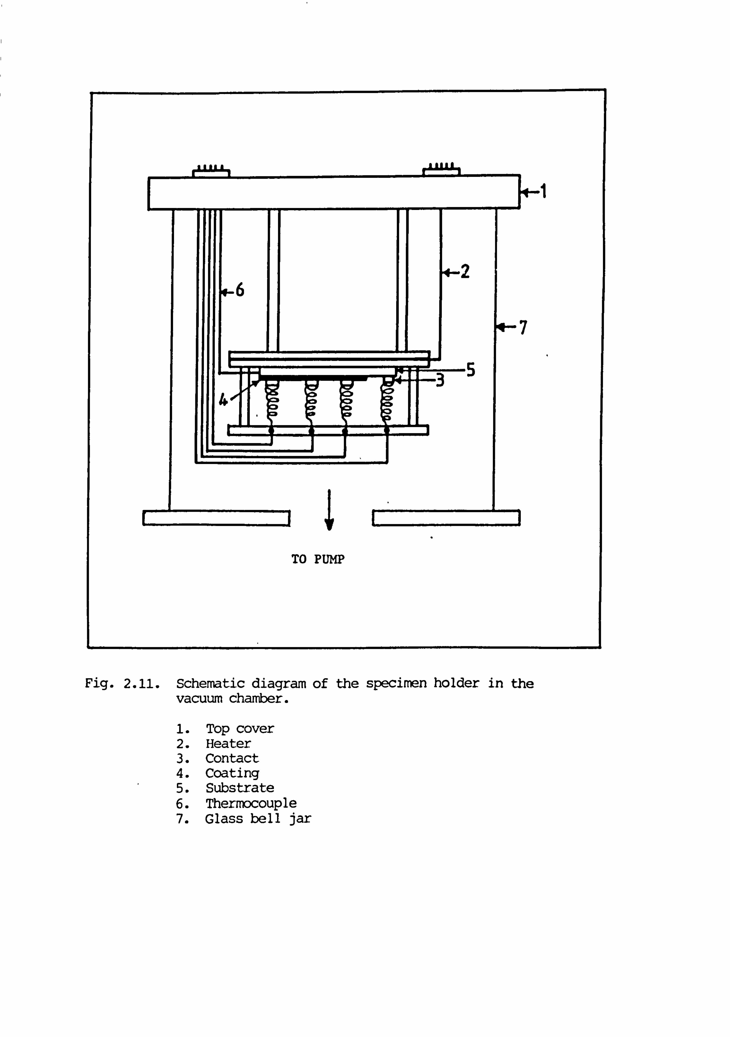
TO PUMP
Fig. 2.11. Schematic diagram of the specimen holder in the vacuum chamber.
1. Top cover 2. Heater 3. Contact 4. Coating 5. Substrate 6. Thermocouple 7. Glass bell jar
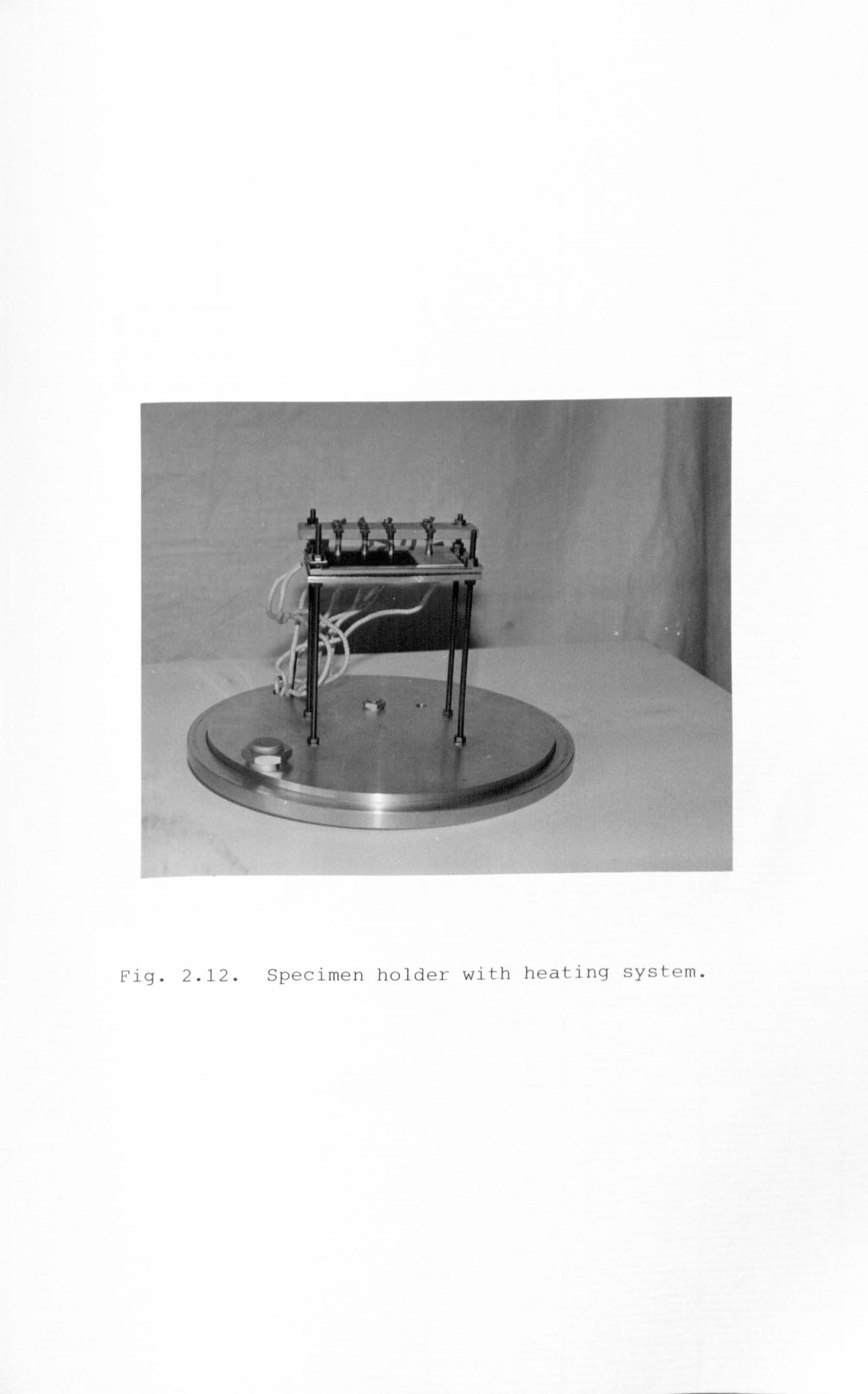
Fig. 2.12. Specimen holder with heating system.
Fig. 2.13. Schematic diagram of electrical circuitry for D. C. measurements.
Source A. F. Bridge Detector LF oscilator TF 1313A oscilloscope
Test sample
Fig. 2.14 Schematic diagram of equipments for measuring capacitance.
0.8
0.6
0.4
4J
44 (D
W4
0.2
0
... oo
0.3 0.5 0.7 1.5 2.3
Wavelength /pm
Fig. 3.1.1 Spectral total reflectance of Mo-black dip coatings on mechanically polished zinc substrates for various coating mass per unit area :( --- ) 0.065 mg/cm
0.12 mg/cm2, (-) 0.21 mg/cm'.
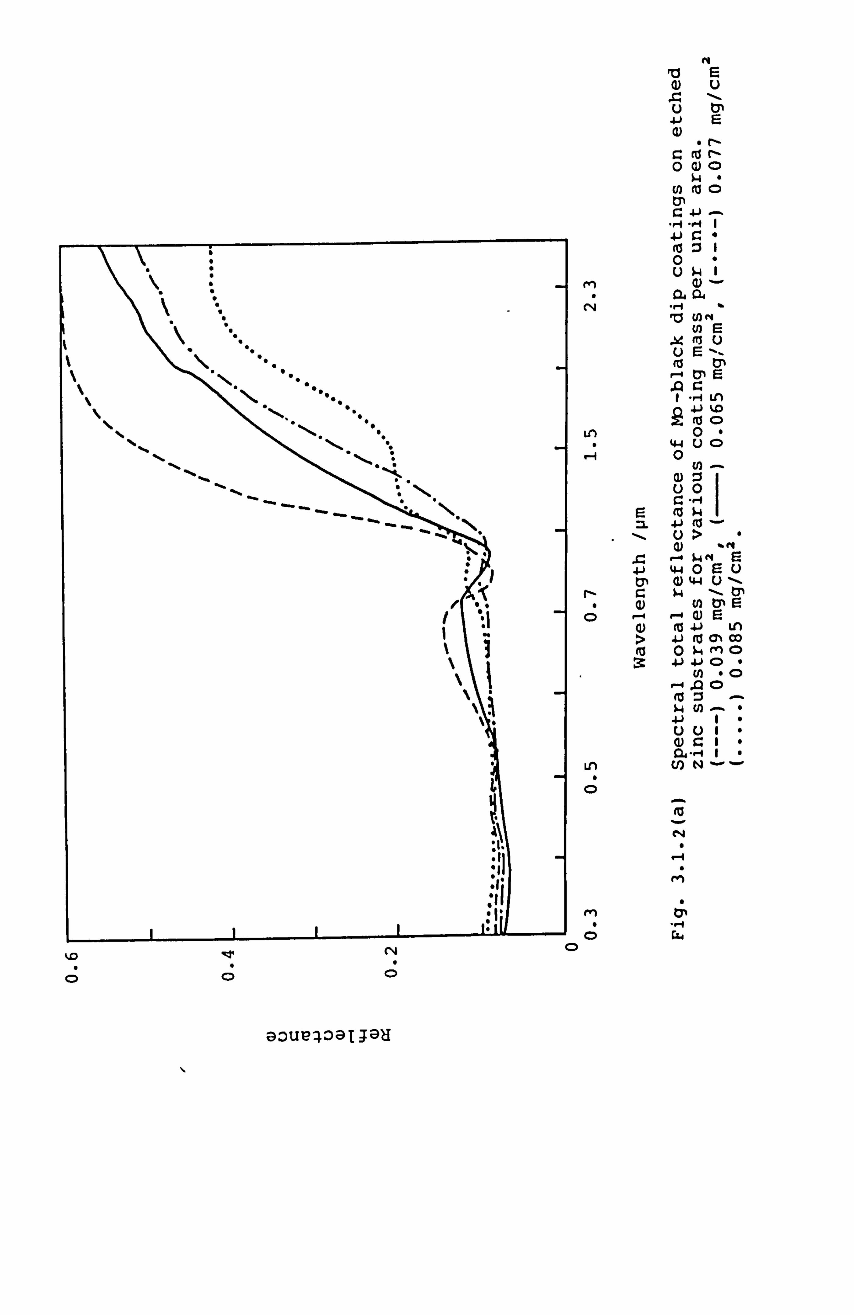
I.
\\ \\ \
\4(p "'? S%,
"t"..
"
\\ S...
.....
'\. _
"'% S..
'""%_ "% .. S.
'N .-.....
- S%"
----
-
en
-. 4
E
I i . It,
c
M Fa rz
u
u 4J
0 a)
co ro
4J
41 (13 zI 0 U ý4
ul ul
uE
AS t7% tp E
., i Ln 4-) %D
0 44 u0 0
cn - W :jI u0 C: r4 (0 ý4
ý4 44 0U
14-4 U 'ý-
U) tyl E (1) rz
tV 4J Ln 4-) (a al co 0 ý4 fn 4J 4J 0
cn 0
4J uuI a) r. I Q-4 1-
(n N--
.1 :'
. 1"
0
r4
goue-40a I Jall
0 0
r4
14 14 t; ., I PLO
1.
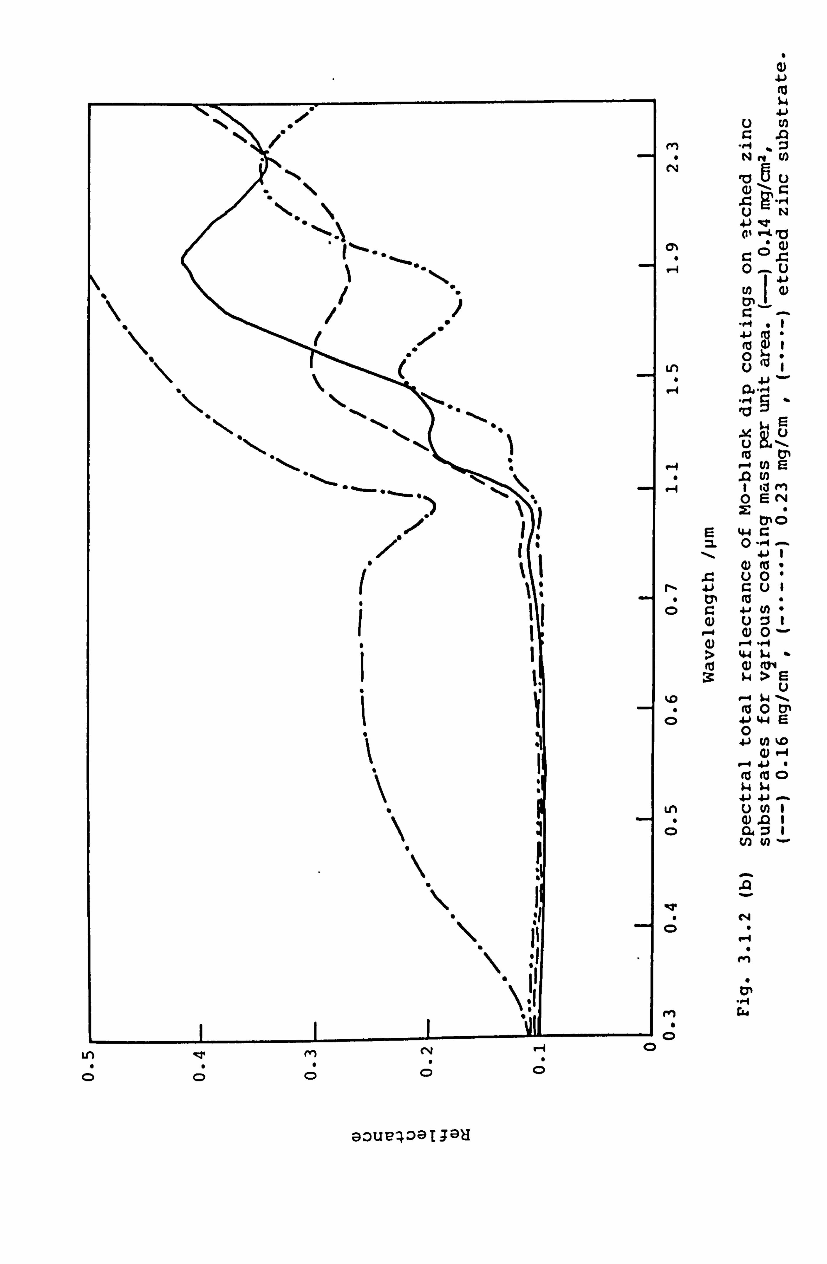
4-
to
m
ON
1ý
Ln 1ý
r-4
14
-4
(a 3:
'. D
0
tn
0
0
m
0
4. ) u U)
to 0u
u 41 qw
0u 4. )
tn 4)
0 4J
M-4 .I 'as
ý
$4 rz
u lu m
r- V) E '0 cn 1 13 M 0 EN x0 44 0
41 0) AS ww r. uI
4. J (1)
4) 0-
44 (1) ý4 >S
u
AS 0 ty% 4J 44 0 4J ti) %D
(a tio 8
W 114 4j 4. J - u U) I 4)
.01 04 :31
U) U) -
Z t14
1-4 .4 t; . 0.4 44
Ln 8
RT (n r" %. d
goue409139H
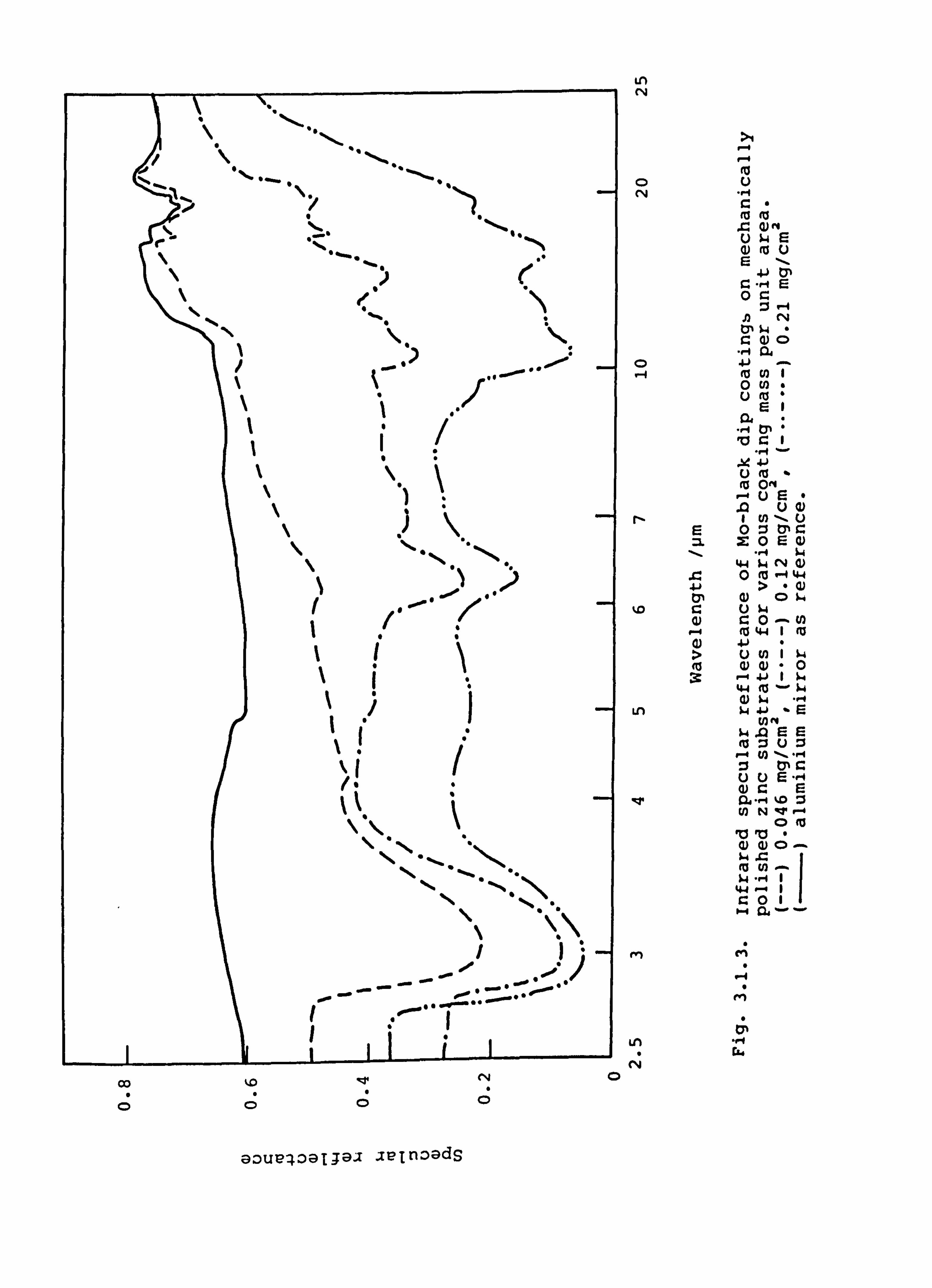
. 0.
-
1 I a
0.0ý 0
-i!
Ia
OD ýo gl, ry
Ln N
0 N
0
kD
3:
Ln
v
>4 4
r-4 (a U
-4 C: a
ri U $4 E
41 0) r. -r-4 E
0 r. :% ýq
A r-j tP ý4 - 9 a) 0
., 1 10, 4J - (a U) I 0 U) u ra
E
UM (a OM
uE I U) U 0Z tp r- 2: 0E 0)
-4 w 44 ý4 CV W 0M -4 44
>
uW r. 0 044 1M
u 0
41 $. 4 44 As
ý-4 .0EE
(U :5u0 r-4 M -ý -4 :3VIC
U L) E -4 E
U) NV 0
10 V0
44 - C0
rn
m
Lfl
0
aoue-4oalgai apinoads
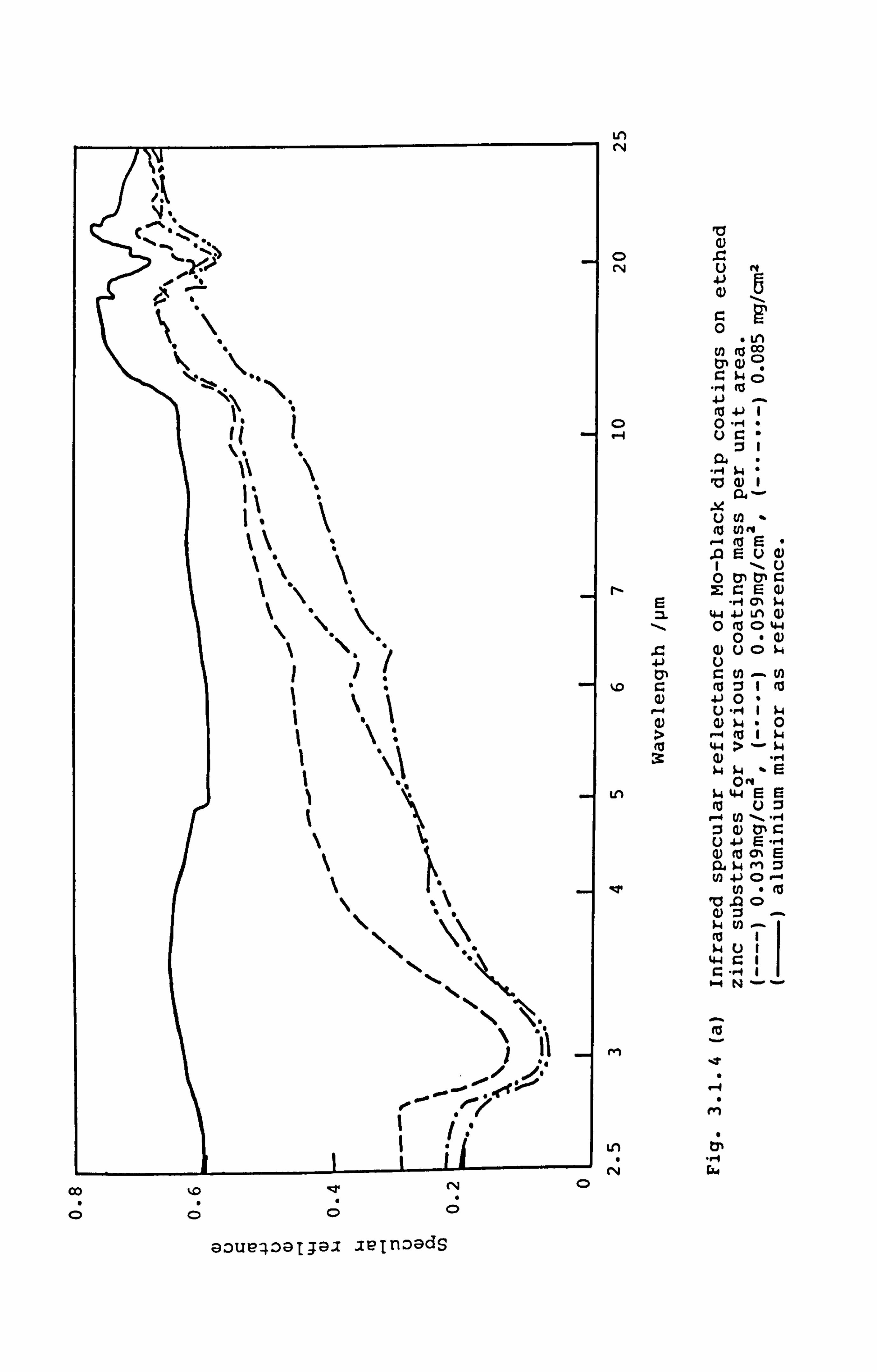
-ýZ. .0-
00 cli C)
C; C; aoueq, oalja. l jelnoads
Ln
N
0 CN
0 V-4
r- E
'0
a)
Ln
RT
rn
Ln C4
ra
4J
0 Ln
cn (1$ 00 6, a) 41
ra . 4,1 0-4 u
., q 14
04
U
(a V) rq V- (a S- .0EuW I, U 0 bli tyl r_
E 0) CN $4
44 4J Ln a) 0 (a 0
0 a) u0 u
U)
4j 0 U
0
44 > ý4
$4 E off
ý4 44 EE (U u0
U) --ý --i Q) 0"1 r. 41 E -rq
a) fu CN r= $4
10.00
ý4 44
14 t; .,. q DW
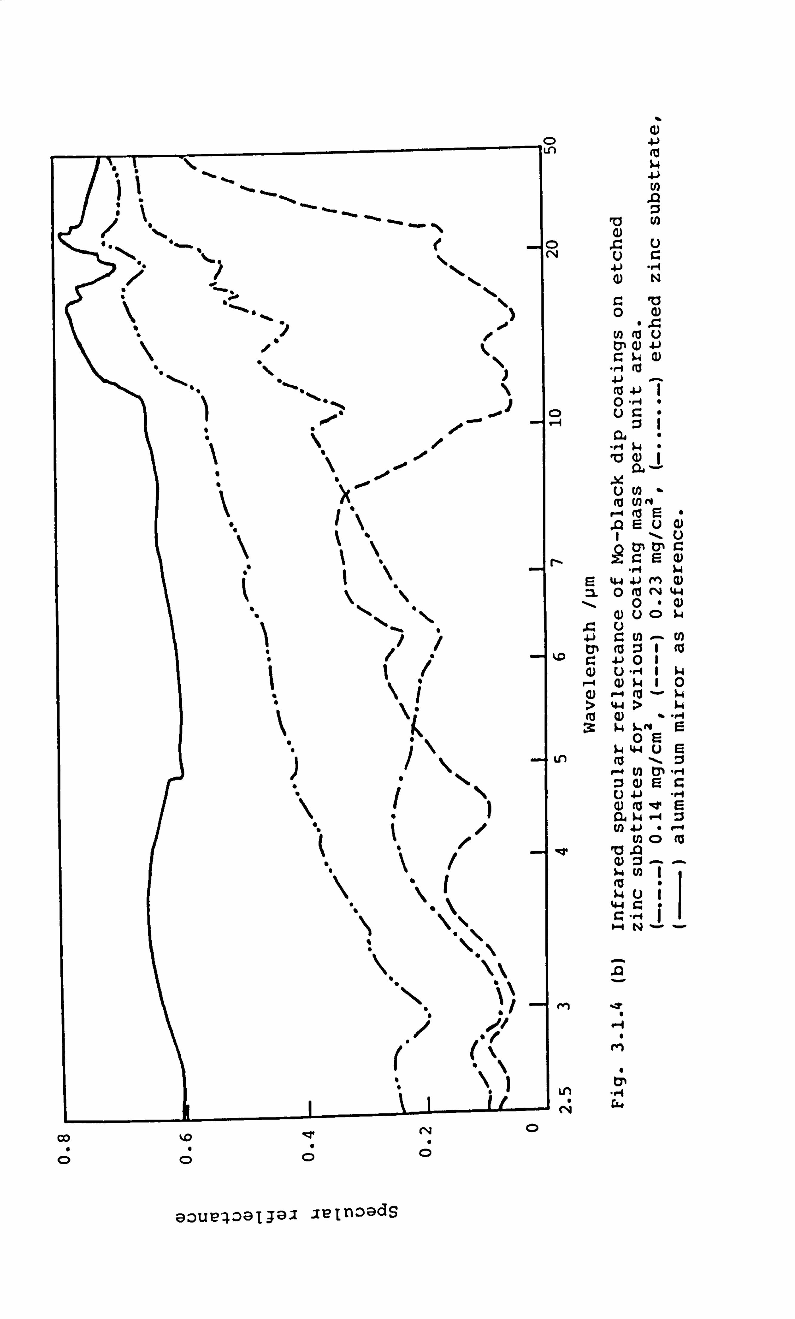
C)
D
'-I
r-
ýD
Ln
-; r
U)
ro En (U
, C: L) uc 4J -4 0) N
ca
En (13 u 0) ý4
,a 4J I 0 -1 u r-
(a Cl) C4
Eu (1)
r. E (1) -r4
E 04.4 4J rn :L0M 04 44
0- 4) a) uo w
4u 4J a E0 U) m (a :$ co
4J 01 u P. 1 1 ý4
$4 10
> 4-4 >
ý4 E 0E
ý4 44 U
U) tp ., 4 :3 (D u -W 4) (a -w E
w :3 4j r-4 cn AS
44
2
aoup-4oajj9j julnoads
rn
Lfl .4
00 %ID le C)
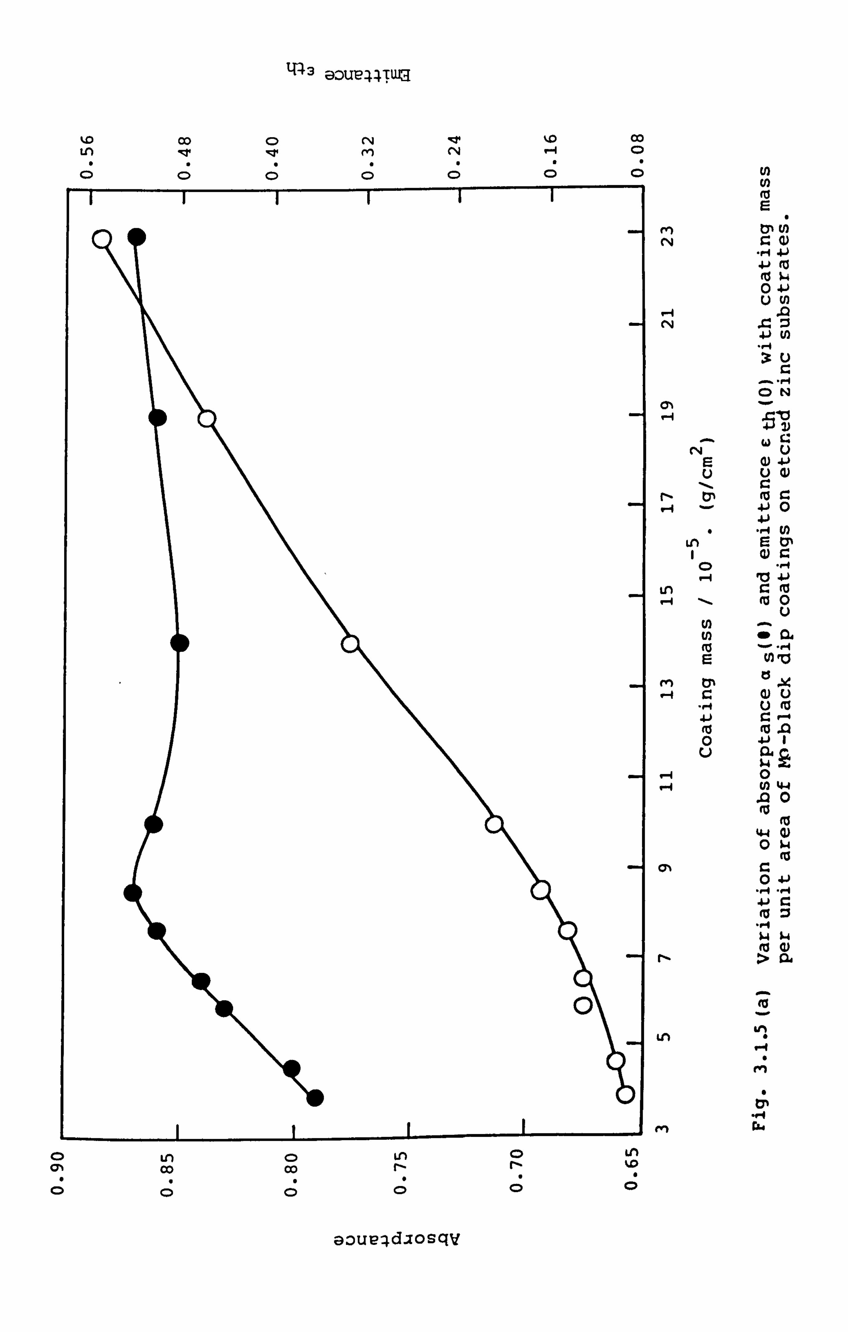
q43 @Z)U? 44TUG
kD OD 04 qzr %D 00
Ln rn CN cn
E
-rq 4j 4-)
0 4-) u
. -j
N
W u
E 4. ) uuw
11 C V) mC
4J 0 4J -, -4 ti)
Ln E ON
0 4. ) IS
.4 -- (a 0 u
(a - -4
E (va
u (a
(a (0.0 0 41 1 U
0 V) 44
.00
444 Q) 0w
0
41
(a W > Od
t;
-rq rAd
(21 00 OD f-
c;
aDueld-zosqv
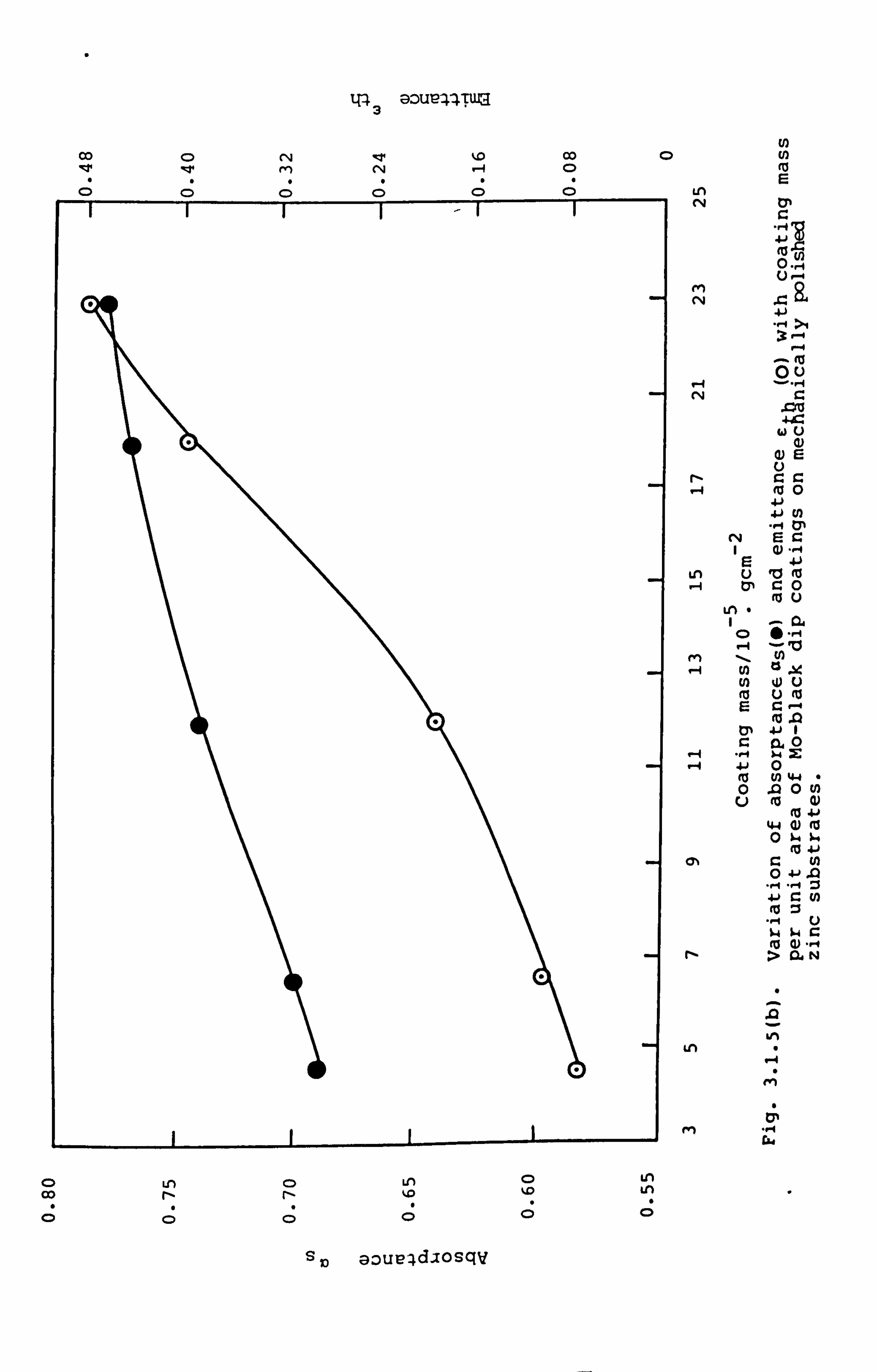
tp 3
GOUP44TUG
Co rli w 00 c «e «e
cý c;
C) Ln OD r,
C; Cý
CD Ln 0o
r- ta %D th 0000
U) U)
Ln tp
4-) la
ý
U) 0
41 ., j >4
0u
CN
U a)
0) E
1-4 (a 0 41 4J
NEC: E 41
Ln u to to 1-4 C: 0
Ln
-4 -10
fn I- in f-4 (n ts x U) u
ON 41 rk, 0
0 (0 fA 44 . 00 00
u (0 0) m 4. )
44 4) m 0 ý4 ý4
(a 41 CN a U)
0
41 r_ U) ca :3
ý4 a)
> 04 N
Ja
Ln 6?
V-4
,4 t; rn -4 Ud
s ID 9. Duv4c1. xosqV
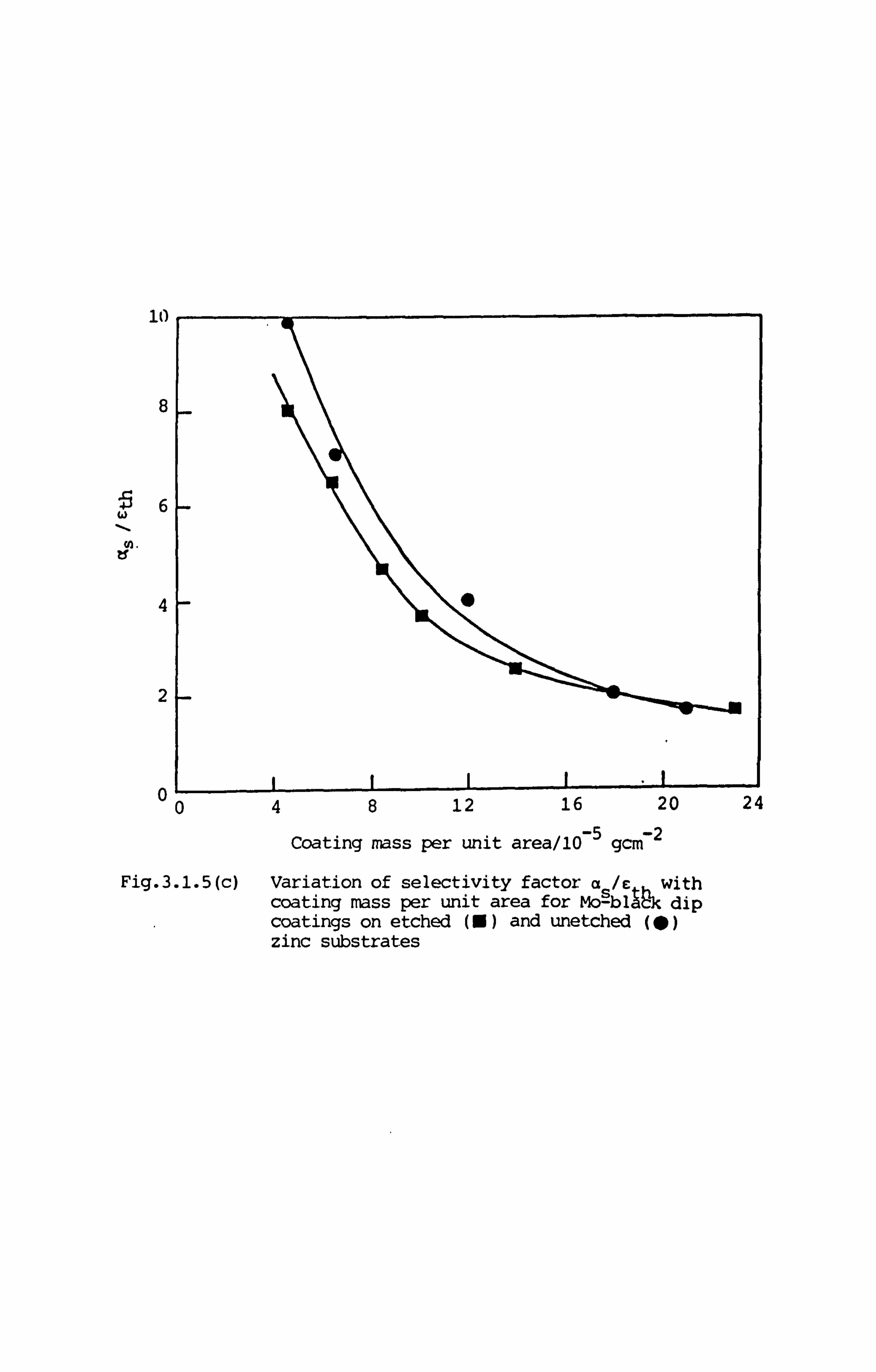
it)
0
8
49
Gn. tf
4
2
01- 0 48 12 16 20 24
Coating mass per unit area/ 10-5 gcm-2
Fig. 3.1.5(c) Variation of selectivity factor a /e with coating mass per unit area for Mo2blIPk dip coatings on etched (M ) and unetched 0) zinc substrates
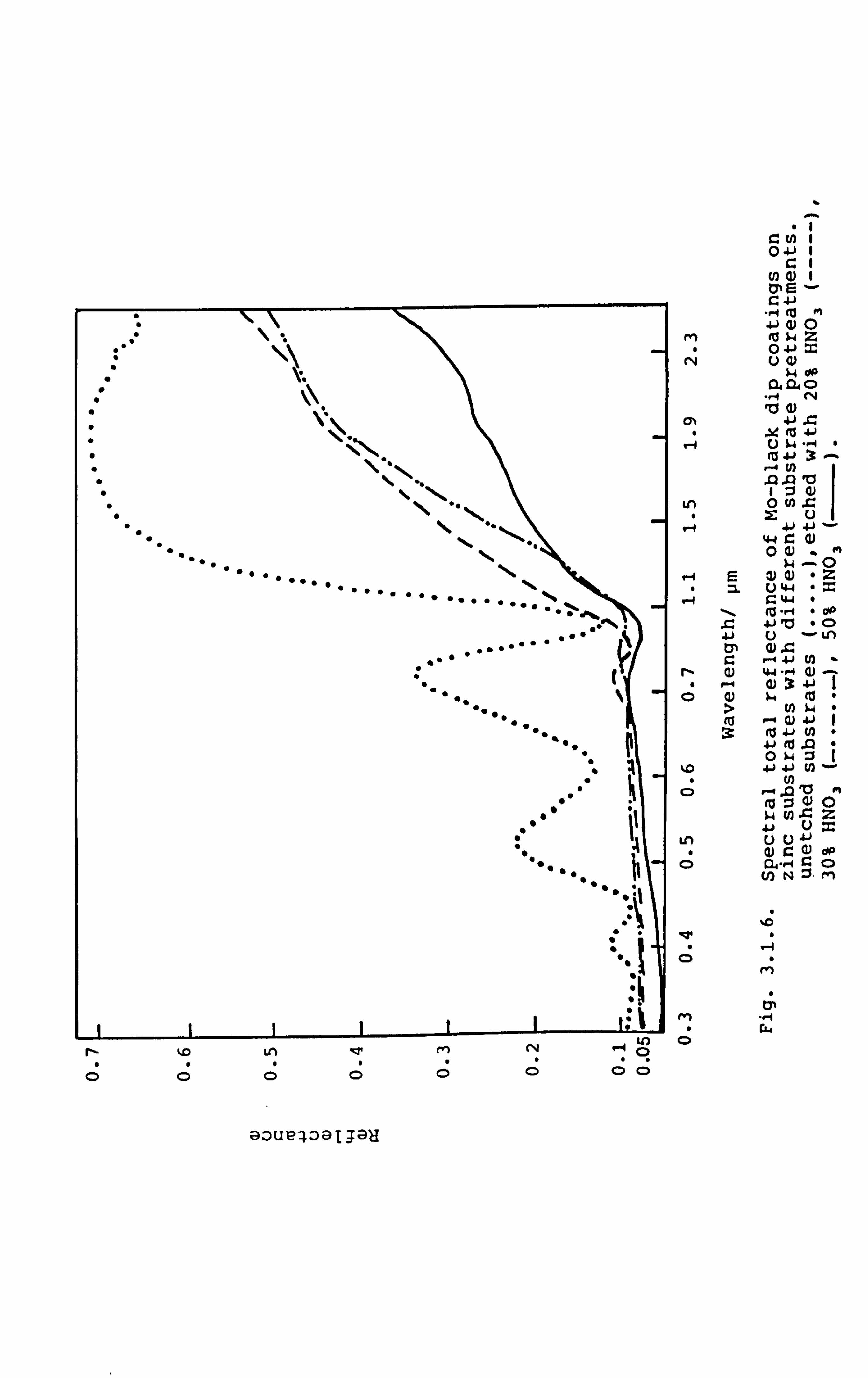
00 %4 *%
% 11-1
r- ýo le re) -4 2; c; c;
rn
VA E =L
41
kD 8
Ln
U) I 0 41
U) 0) 1 tPE r. 41
4J Q) 0 (0 ý4 Z 04-) () a)
$4 dO 04ma
-4 cli 10 (D
41 a (a ý4
U)
. 0.010 10 0) 0 U) C:
44 0 4)
Z U 44 944 (c) ., I dp 4j 00
ru - Ln r-4 41 44-4 (L)
3: 45
cl) ý-i 41
4J (13.0 0 ý4
U)
W0 z
41 U= u 4j
a) dP C0
(f) N Zý en
1ý -4
aouTe4oal jau
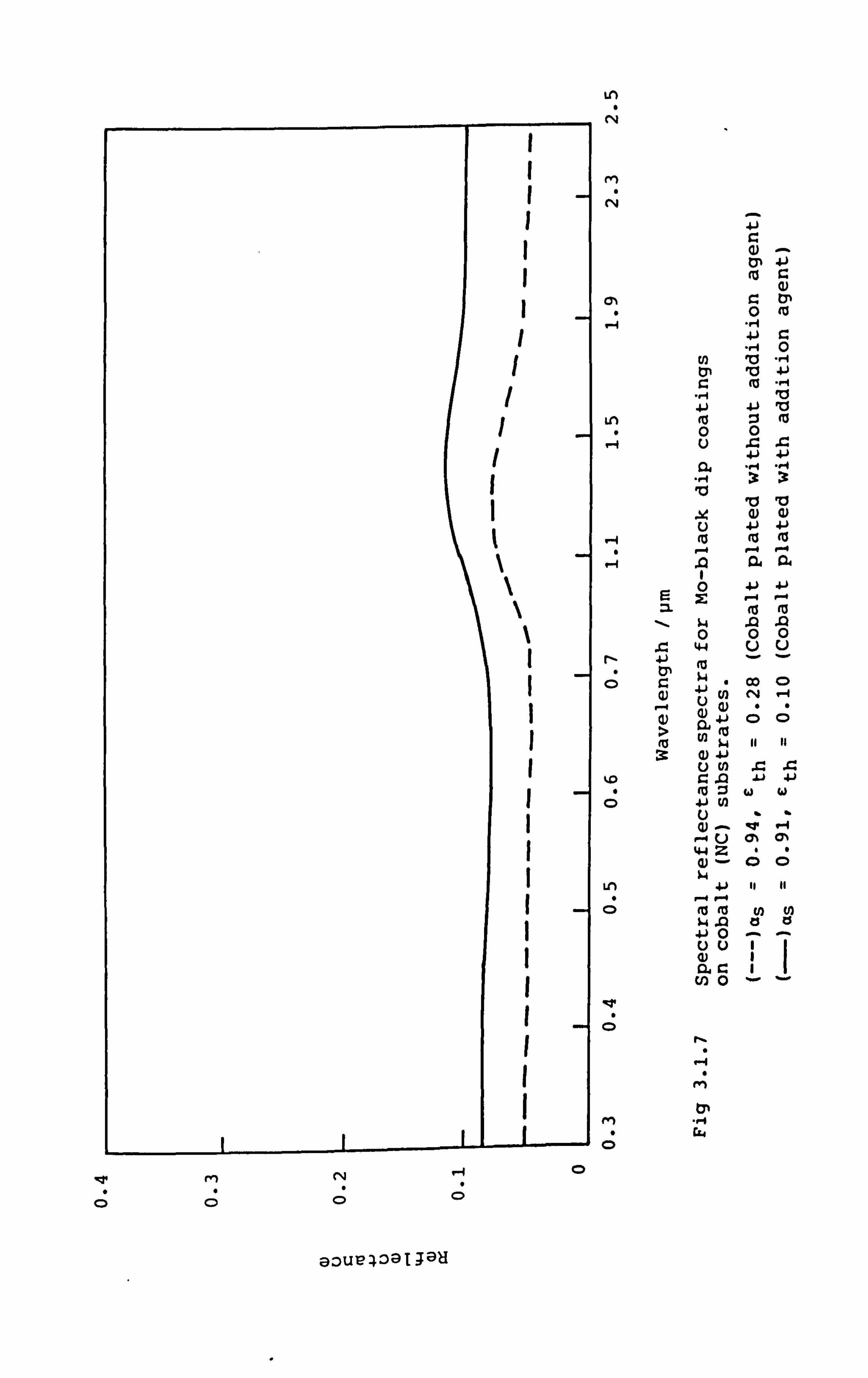
Ln CN
N
m a
0 I- : 0 (a H 4-)
0 1 01 10 4J
41 4J a
U 113 :3 (a ý 0 0 -f u 4 C: 41 41 .,.. q -4
. 14 Q) U 4J 4-) k
1-4 (a (0 (a 0-4 0.4
0 4J 41
x 1-4 P. -f
0 0 0 44 41 0) r W
. 1 CO CD
4 rj)
41 a 0 > l , (0 U) ý4 I, If
Q) 4J () U) C: C: .0 ji 4J (a 0 w w 41 U
qw a% CN
44 Z
Ln
(D to
41 0 uu I
r-
14
9: )UL, 4091 JEW
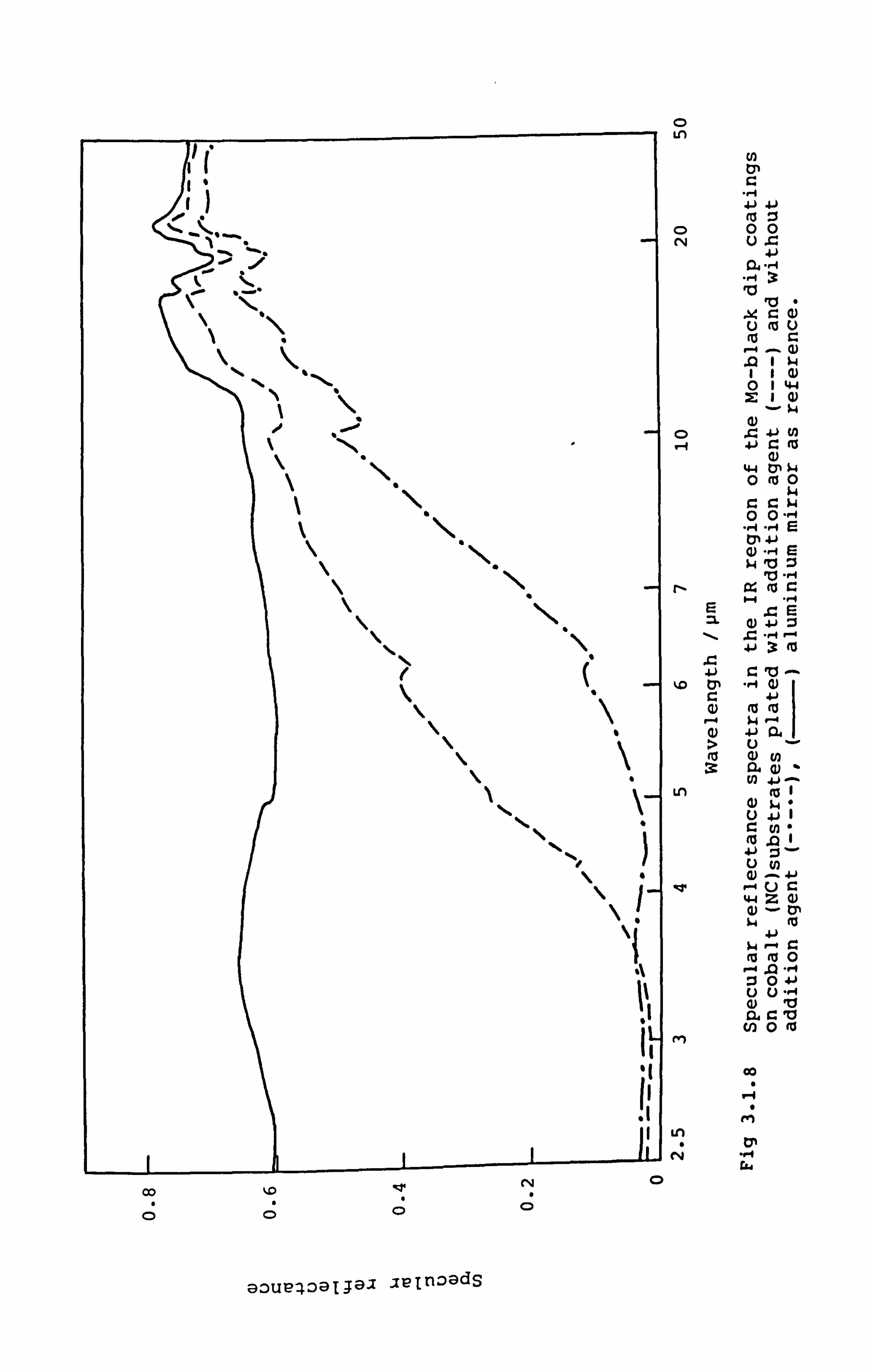
00
It I L
00 t. 0 «e N f-o
0 LO
0 CN
0
r-
E =L
kD tp
(0 3:
Ln
v
rn
(1)
(13 z 00 ua
4J
ra
() (a () fu C:
-4 - a)
.01w II a) 01 44
4J to
44 $4 0 (a 0
$4
0 0. -1 -4 HE tP 4J (L) . -I E ý4 '0 Z
0) 41 :1 X: -4 ý
to (a W r-4
4J 134
U)
En 4J
ý4 U 41
U U) 0) - 4J
r-4 r-) r- 4.4 Z (D 0) - 0) ý4
41 ý4 r- (a (a 0
ý4 Q -r4 :10 u ()
U) 0 (a
Co
ein lý c ry -f
täa
@ouL, qoqjj: aa jetnoadS
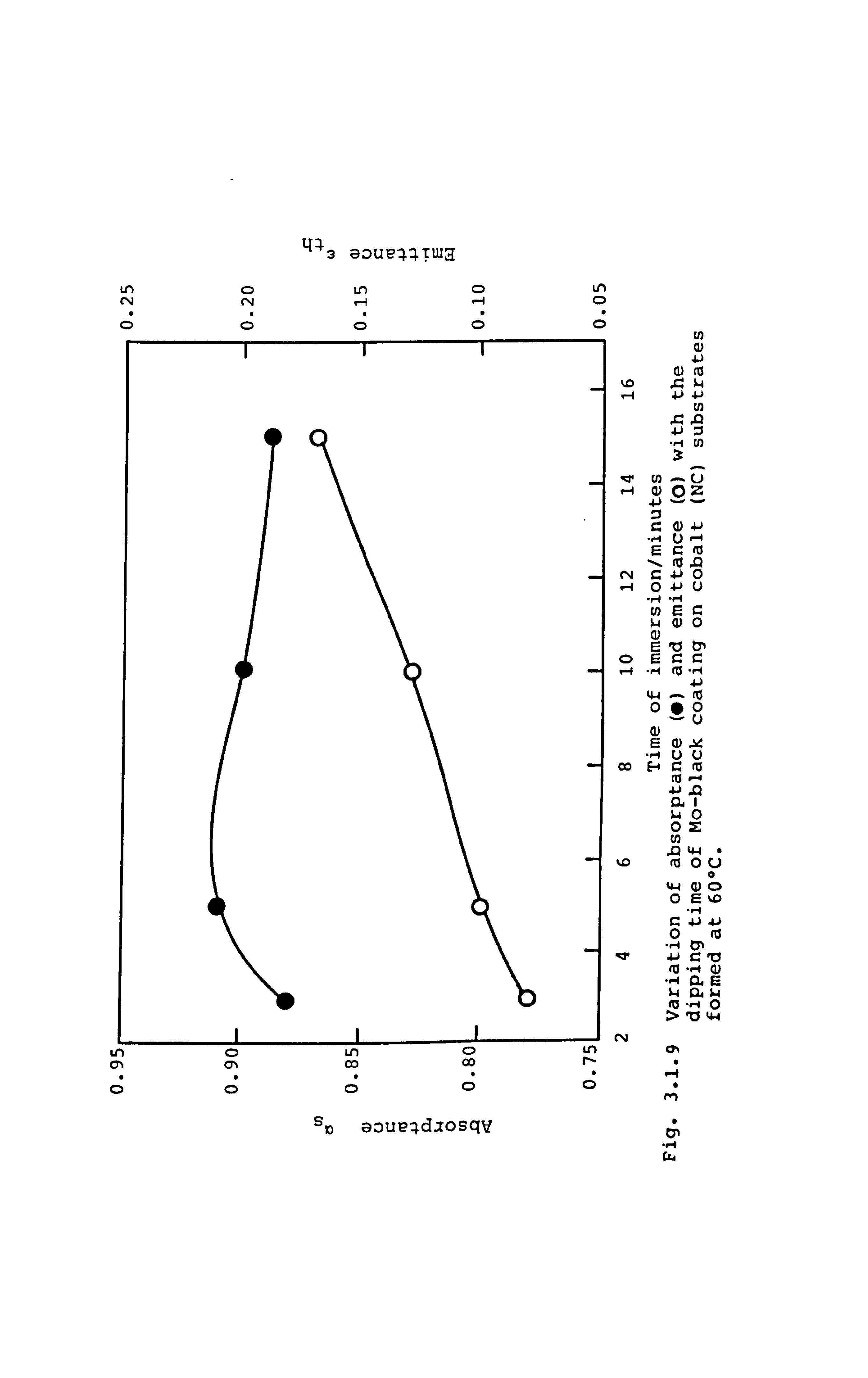
T44 3 GOUE744TWa
Ln CD C9 Ln C> Ln 0
C;
41 41 (0
34
C
E r- M
p0 0 4.1 u ., f u) C) 0
E 10 öý
44 - (0 000
0U
tu 4 .W JQ
0 0 3:
(n .Q 44 6 tu 0u
44 Q) 0E
41 0 tu
-A le 41 c: v
04
0 >V 44
(N
Ln C) Ln C) CY) ON OC) 00
Cý C;
Ln ON r,
en
SID aoue-4djosqv czd
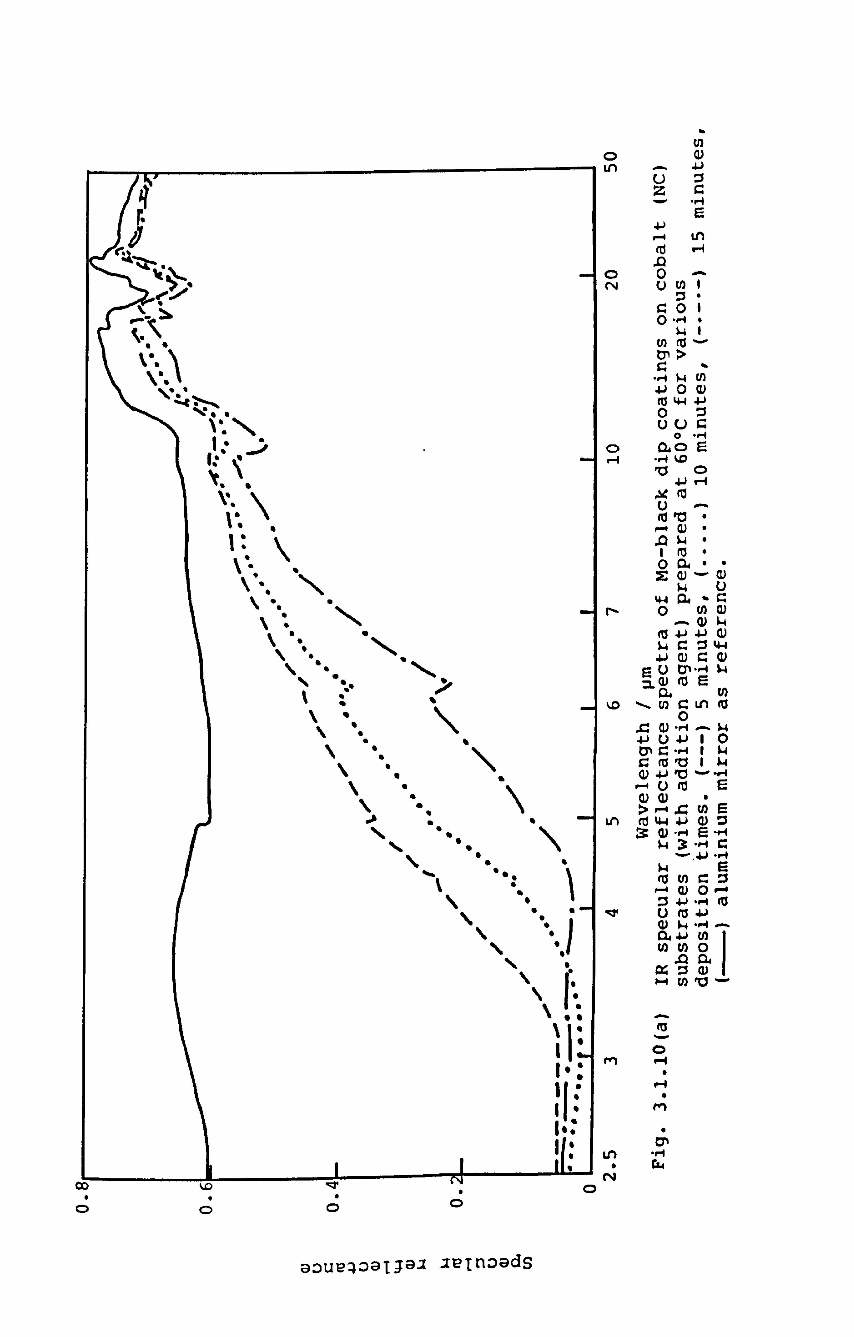
0 Ln
0 N
T. is
lb
Ss
so
00
\\00.0 0.
0 r-4
r-
ko
tn
qRr
cZ
Z; Z0 0 -H 6
N4 1 u) tu -
>
0 u) gli 44 4-) 0 uu
V0 4-) ý't
X (13
0
4-4
- Q) N4 fö 41 4. ) C) N. 4 ZZ 44 41 (0 r. iv
r= U rr -4 r=
c: Ln tu 0
10
r=
(0 tn r_ :i -4 0) C) -4 Z 41 -m tu
M
04 41 U) (0 tn 0
. 12
0
,4 t; rL,
cCC
aoue4oali9l 'eTnoods
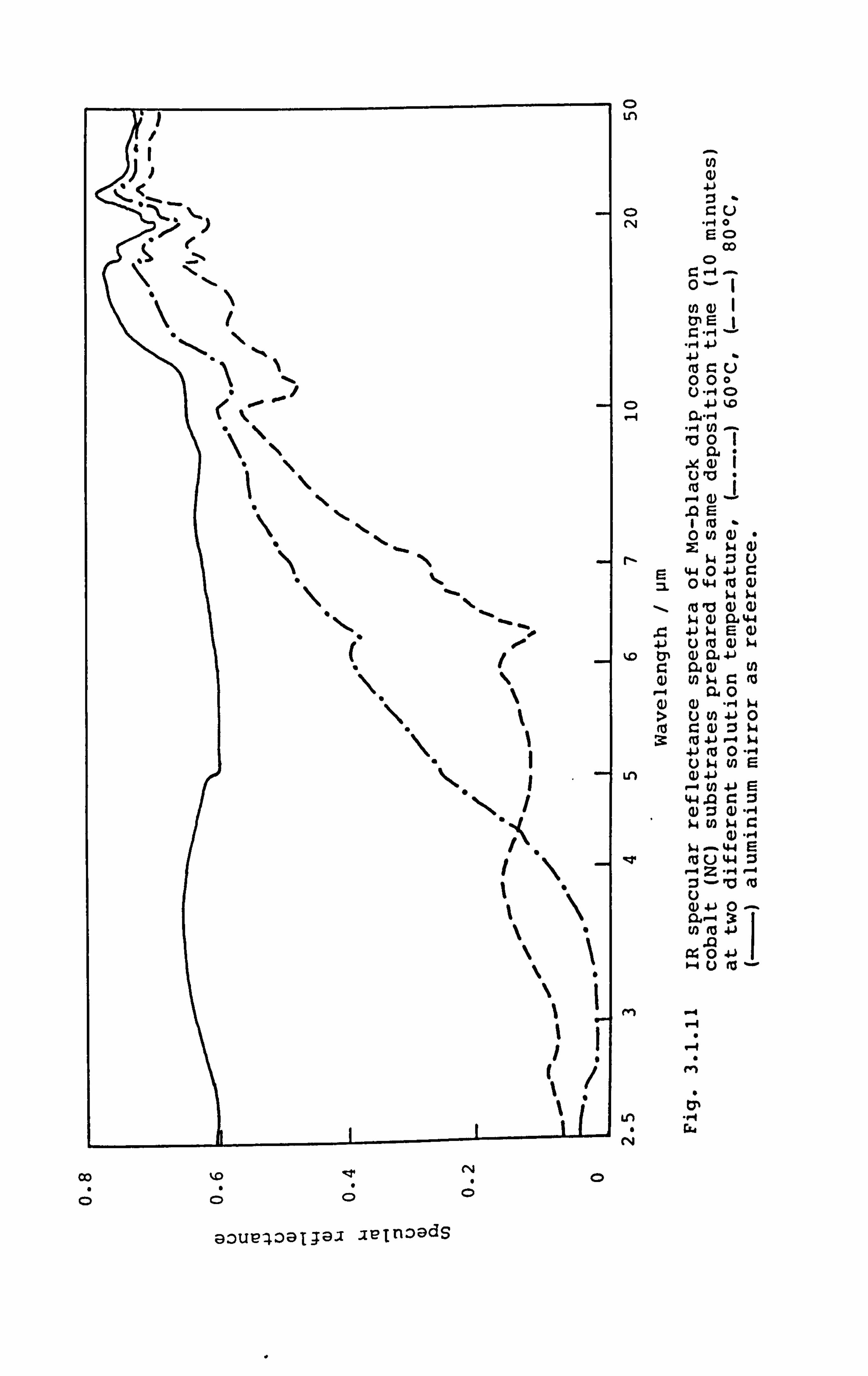
%1 . 00
1 #00
op
00
0 Ln
0 cN
0 1-4
N E
wb w a)
Ln
'IT
rn
Ln C4
4J
., j 0 E CD
00
to (v I ty, E z rl
j
. rq 4J
000 U -, q
, 00 DA
E
1 (0 - 0 to a)
u 44 0 41 r. 0 44 10 a)
ww
(a a (1) a) w a) CL I" 4J ý4 E 4) um a) w a) 41 04 U) U) $4 r. M
m0
UM4. ) 0 a) :j $4 4. ) P-4 ý4
41 (a 0 . -. 1 IL) W (1) E a) 41
-4 En 41 44.0 C: 0 (1) :3 a) . 1.4 ý4 U) W r-
0) ., q W-4.4 E (U () 44 :3
r-4 Z -r4 -4 :3- 10 (a U (L) 4J 0
.Q
,4 t; .,. 4
rid
aoup-4oalia. i jelnoadS
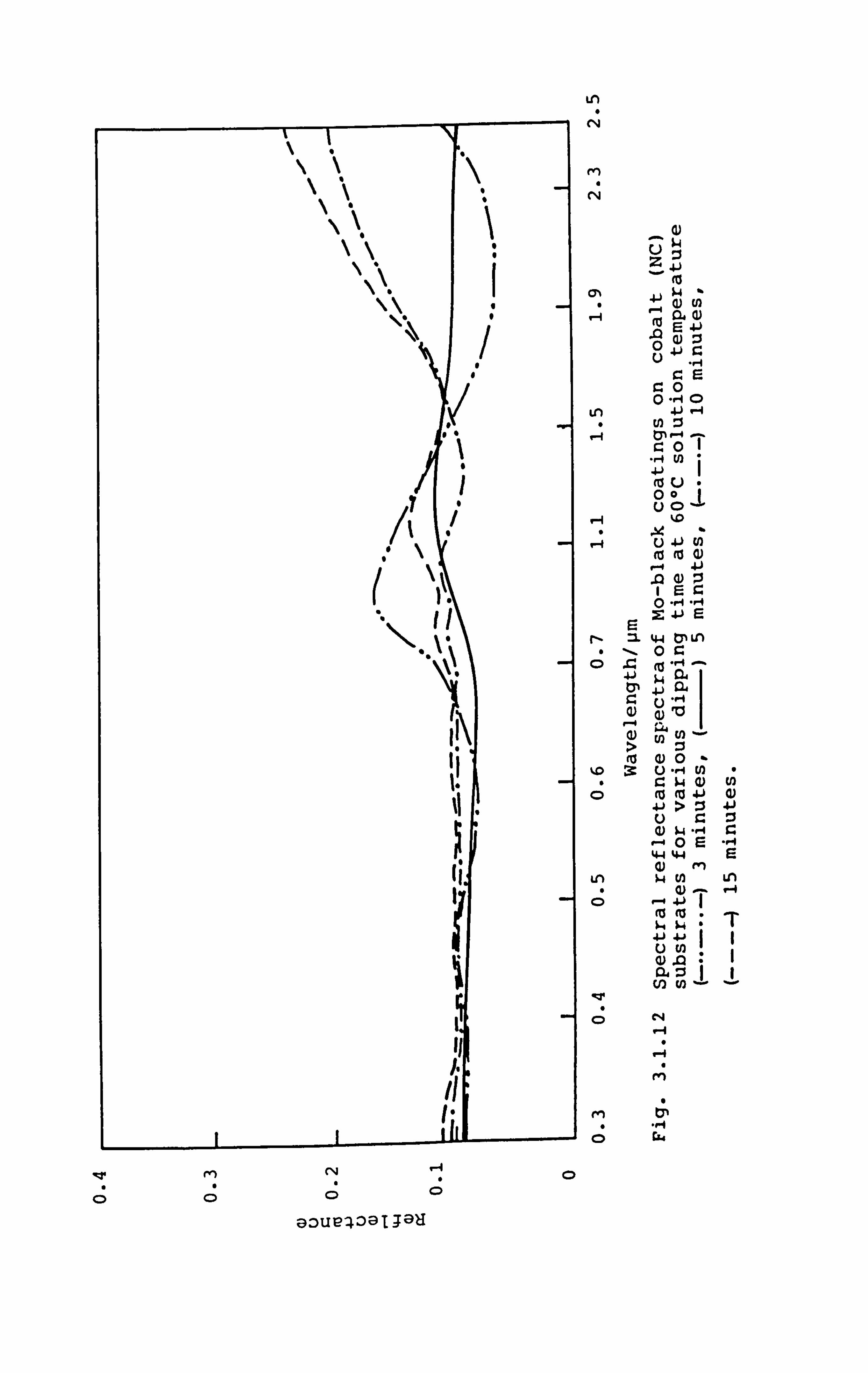
IN
CN CD
Lt
(N
m ri
CYN
1ý
Ln 1ý
-"1
�-4
N
0
%M
CD
(L)
(a 4J
E 4-) .0 a) :3 0 41 r. u
r. 0 0 -ri 4J -1 U) Z tFl r-4 - r- o
-r-4 U) 4J
00 C>
.0Wp IEr. 0 r4 -4
Ei 2:
=L 44 tP Ln 0 C: 't -4 ý4 gý'
tp 4-) 9 L) Q)
> (13 a) 0
3: L) .,. I En
$4 a) M (13 4-) Q)
41 > :3 4j
0E 4.4 44 E
Ln
4. )
-tj 41 L) U)
W. 0 :I 040
(n V)
"1-4
aoue, 40E)IJaH
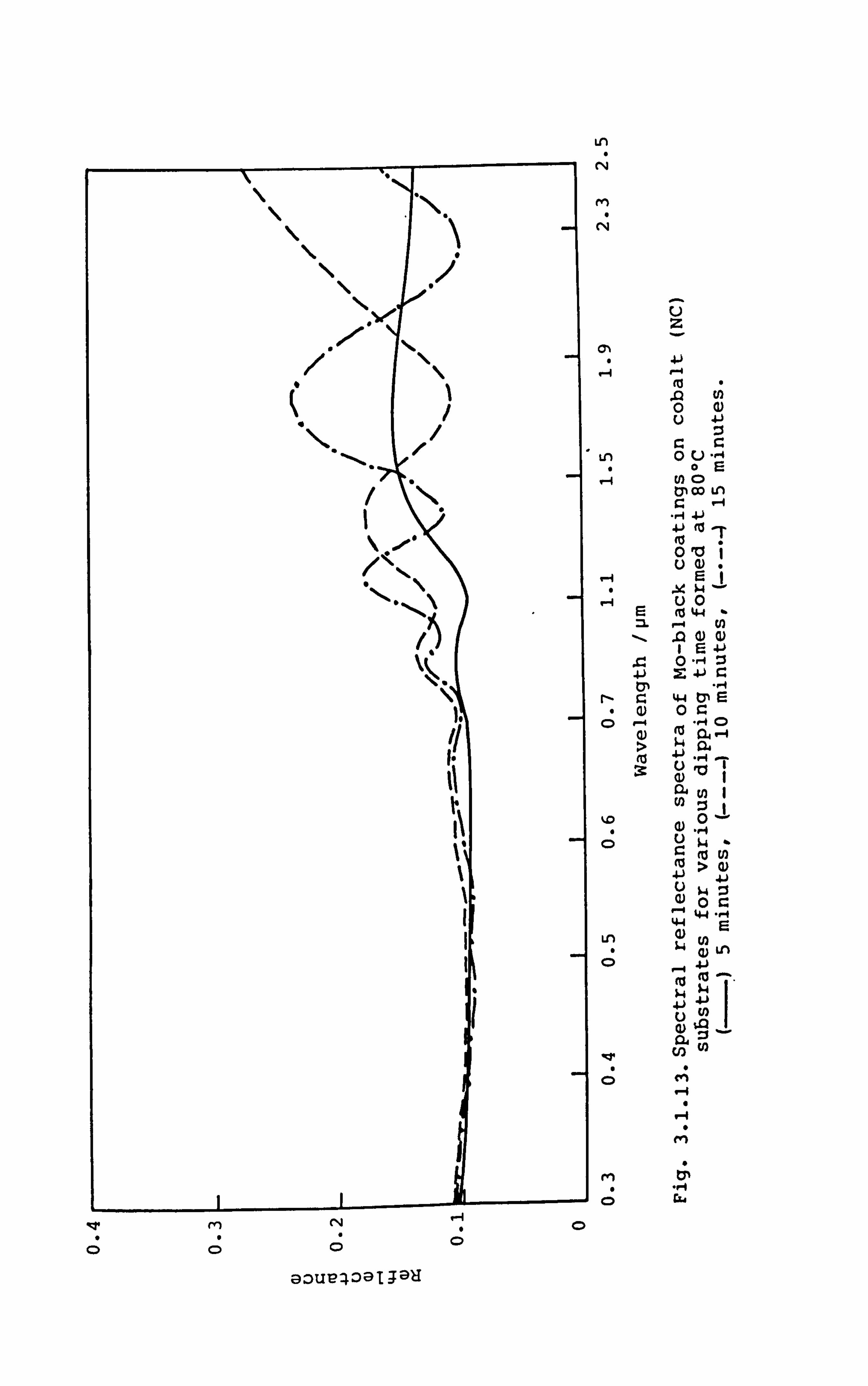
\ . -Oo
t.
fy, 0
000
331
Ln rý
N
G z
.0ý 0 0) U 41
0 r_) -4 o
-4 U) 0 tyl co Ln
4-) (0 -T 0 0'a
u a)
a -14 wj u0
E (0 44 =L
E 41 0 -4 :3 X: 41
Ol E Q) 0 r-
-4 P4 0) 041-4 >
41
Q) 04
tn 0
ý4 - (a U) >
ý4 :1 o V.
44 4 44 E
Ln 0) U) S4 a) Ln 4J
4J
US U)
C; 14
rn t; .,. I 8 rAd
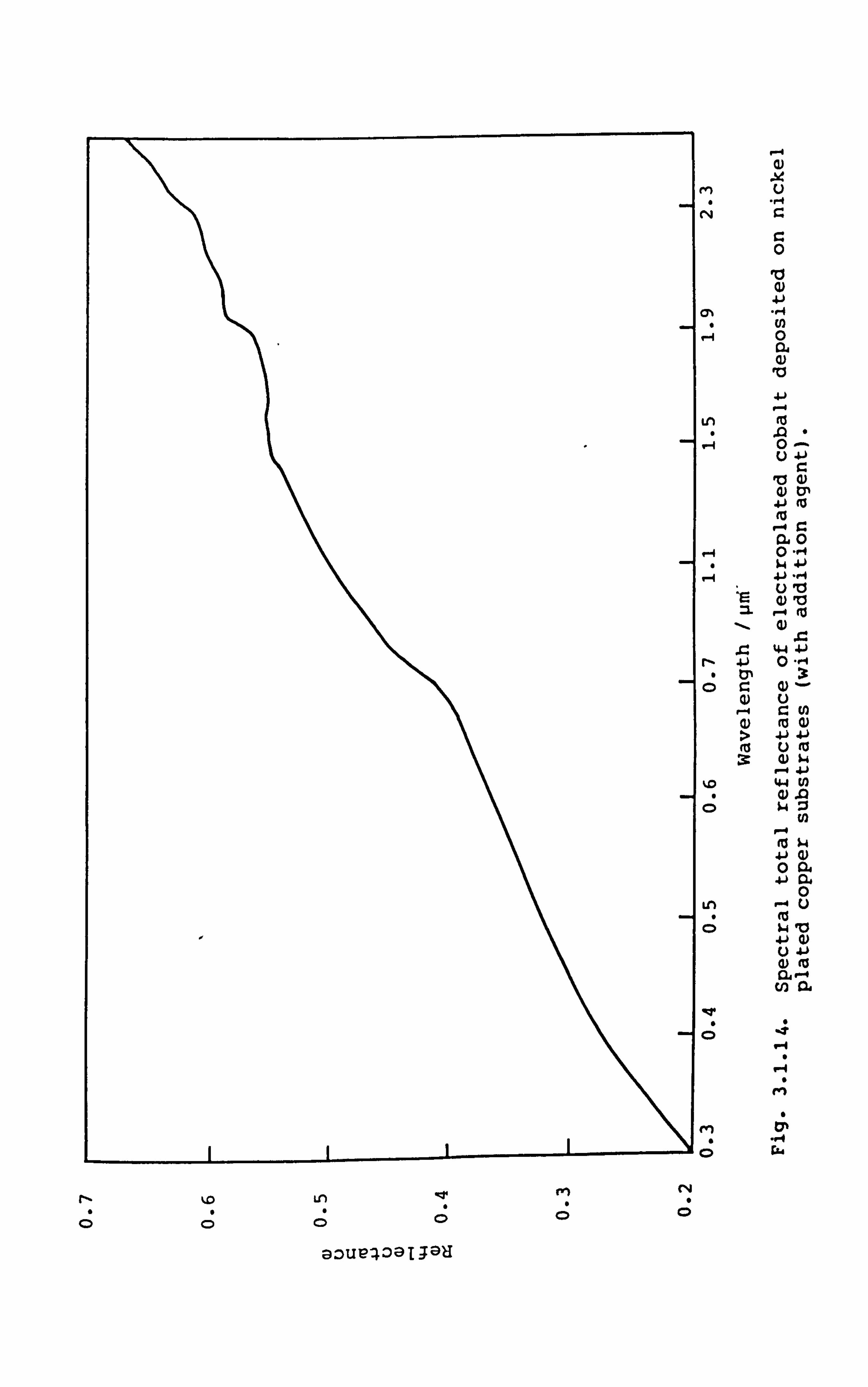
Mu
,a Q) 41
ON -4 Cl)
14 0
ro
Ln
14 0- 0) Oll
r--s r: io, 0
ý4 0., q ý4 4J 4. ) r4
ý5 U10 (D V
:L
44 4-) 41 0. '1
r- U)
> 41 41 fu
%D 44 U)
(a w 4. ) cv 0 04 41 M
0
Ln U
C; W 'a 4. ) 0) U
r-4 cn Q,
"" o
m
m "
r- "0 Ln le M
0 ru
c.. J
0
GOUP-4091jau
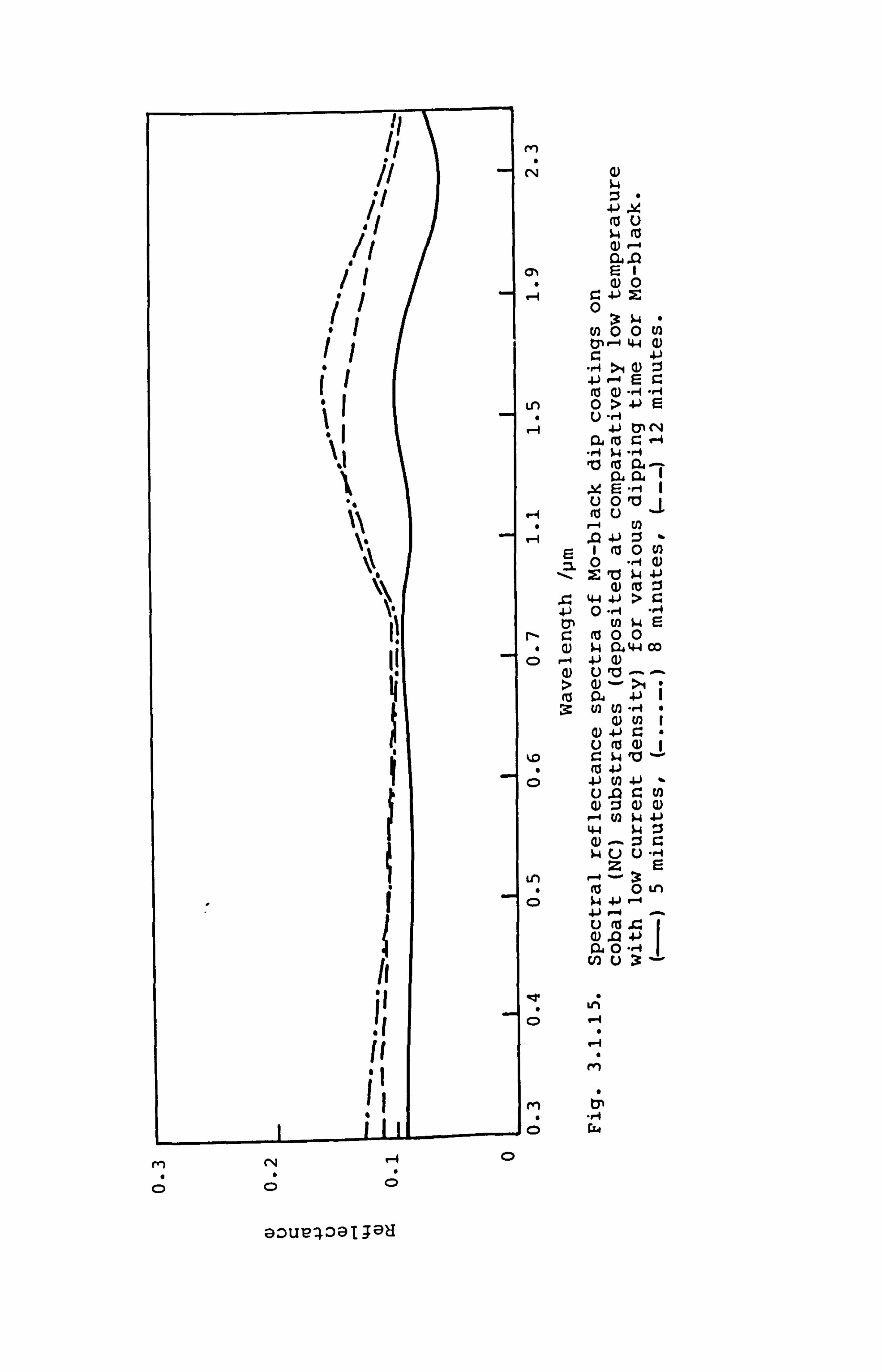
4-) ý4 fu () ý4 (13 Q) r-4 04.0
EI a) 0 4-)
0 U) 00 1,11 -, 44 a) C: 41
-r-4 >1 W0
4-) E0
Ln 0> 4-) E U -r-I
41 tp CN m ra z -4
-4 ý4 -H ýo (0 04 -1
u Oro L -4 (a u-
-4 U) 4 41 0-
E 1 (13 0M =L 0 ., f a)
W 4J
44 -Ij > 0 -4
U) wE M00 $4 04 44 00 4. ) a) L) 10
> (D - >1 as in, 41 : r. U) En -4 a) U) I
a) 4-) Z u (a (L) I
k. 0 r- w ra - (a 4j
C; 4j U) 4J - U)
4j 4-4
uu E E
Ul) 3:
tv 0 Ln ý4 4J -0 ci as .0 0) Q 4J 124 0 -rq V) u ý:
U-1
,4 t;
GOUP-409 I 99H
m CN -4
C;
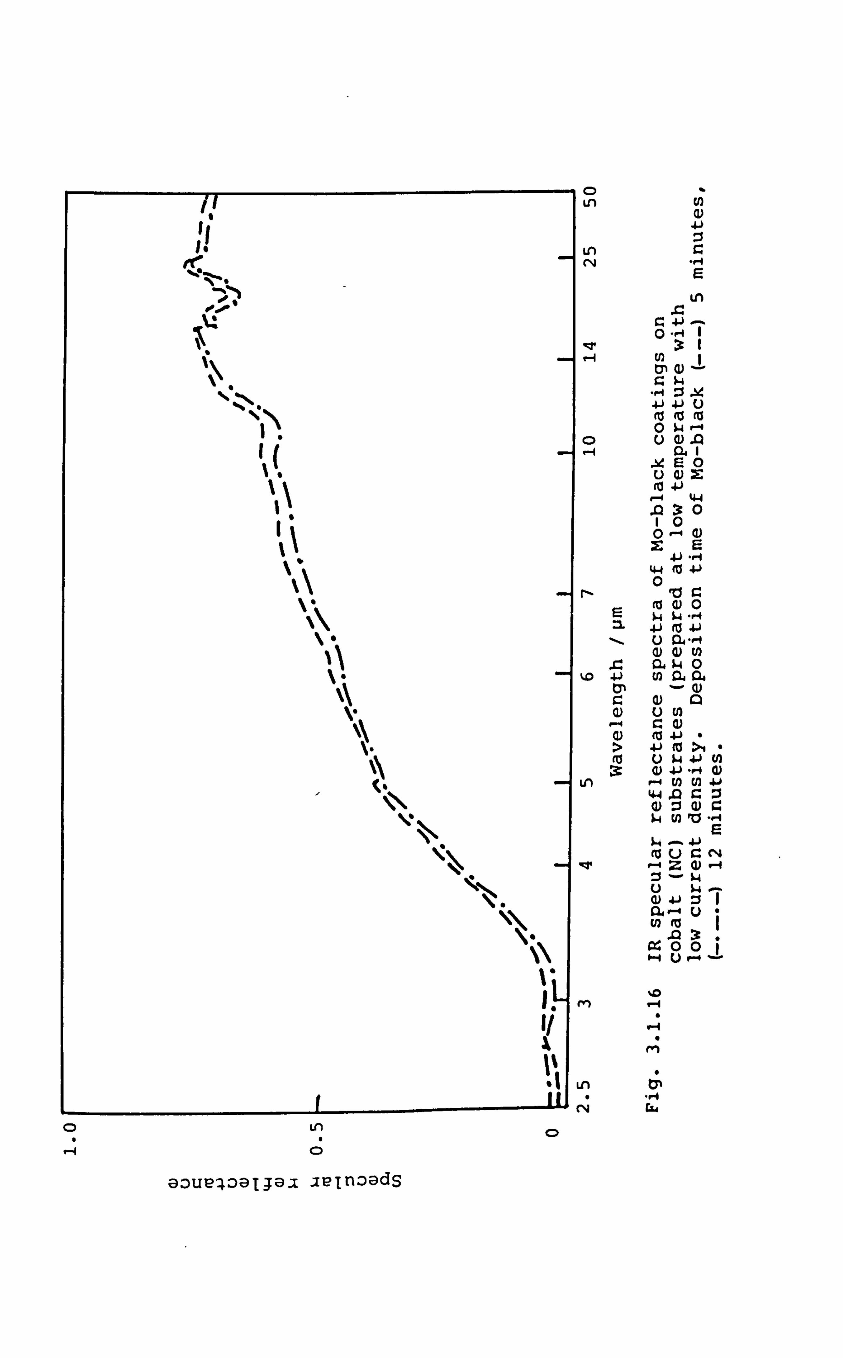
-I It to
0000 0
%. zzý*
azue:; Z)a1. Ja. 1 aeInzadS
CI Ln
Ln CN
'-4
0 1-4
r-
(a Ul
qw
rn
I. '
N
C r.
. 14 E
0H
4. ) U tu (0 tu
E0
.ný: 0 10 0 . -4 c) Z: E
4j -q 44 (Ö 4j
10 r. to a) 0 k4 ý4 H 4. ) tu 41 u n4 --4 Q) Q) U) ad ý-4 0
u U)
41 (0 >i " 41 U) 41 -Mf 0) U) (n 4j
44 r: Z
(0 u r_ (14
a) 41 :1 M- u U) fö
-I
-. 4
m
.. -$
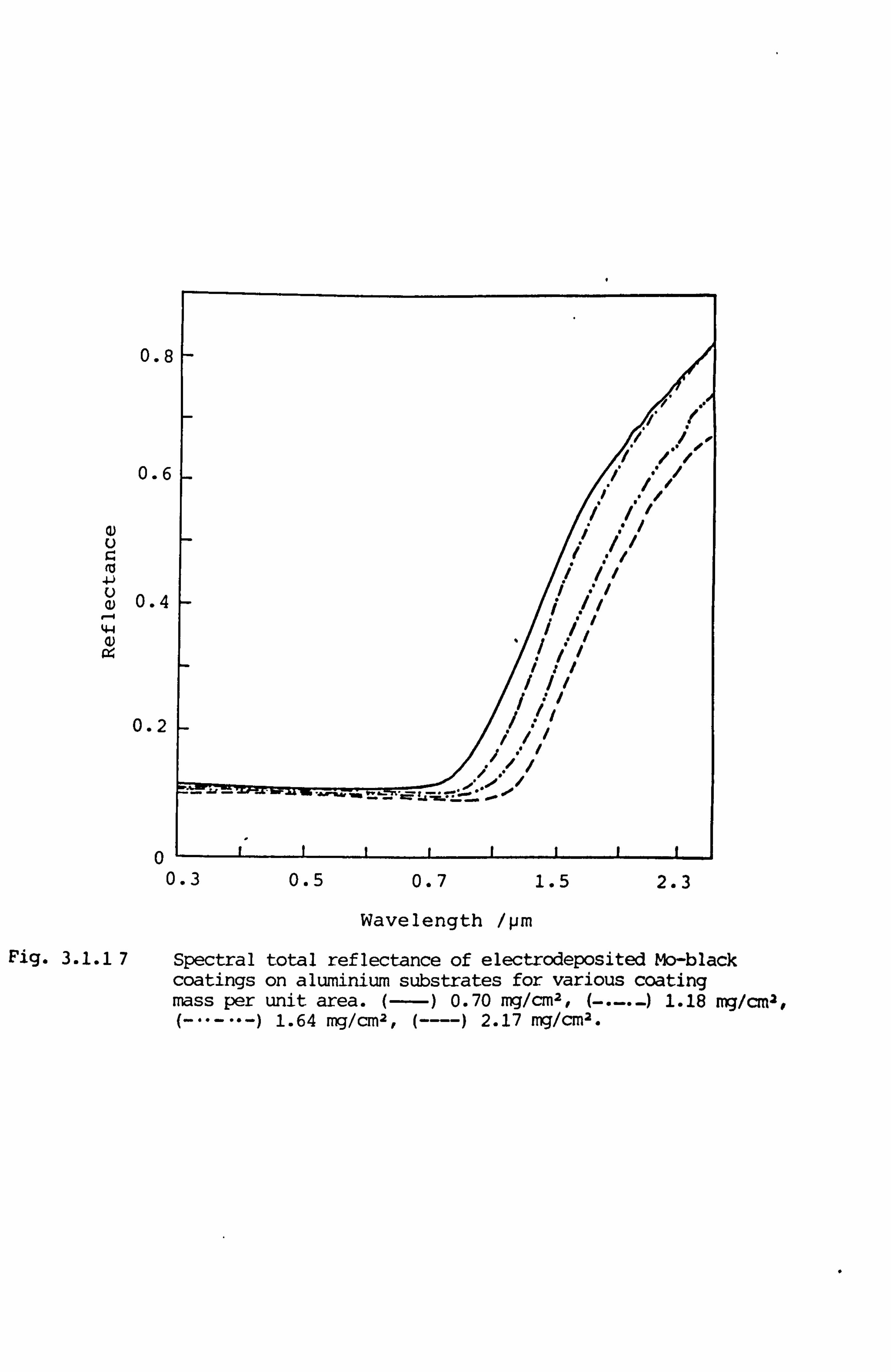
0.8
0.6
4J
0.4 44
0.2
1' /1 /"
/1 /" I, "' /! "
"/'
1/' .. /i'
// 1/ II :� If Ii /;
a" / I, 'I
I/ 1' I,:,
I//I II I' I/.. ' /
I//I I1 ."/ ('"/ /
�. � /
-. '
0.3 0.5 0.7 1.5 2.3
Wavelength /pm
Fig. 3.1.1 7 Spectral total reflectance of electrodeposited mo-black coatings on aluminium substrates for various coating mass per unit area. (-) 0.70 mg/cm2,1.18 mg/cm2,
1.64 mg/cm2, ( ---- ) 2.17 mg/cm2-
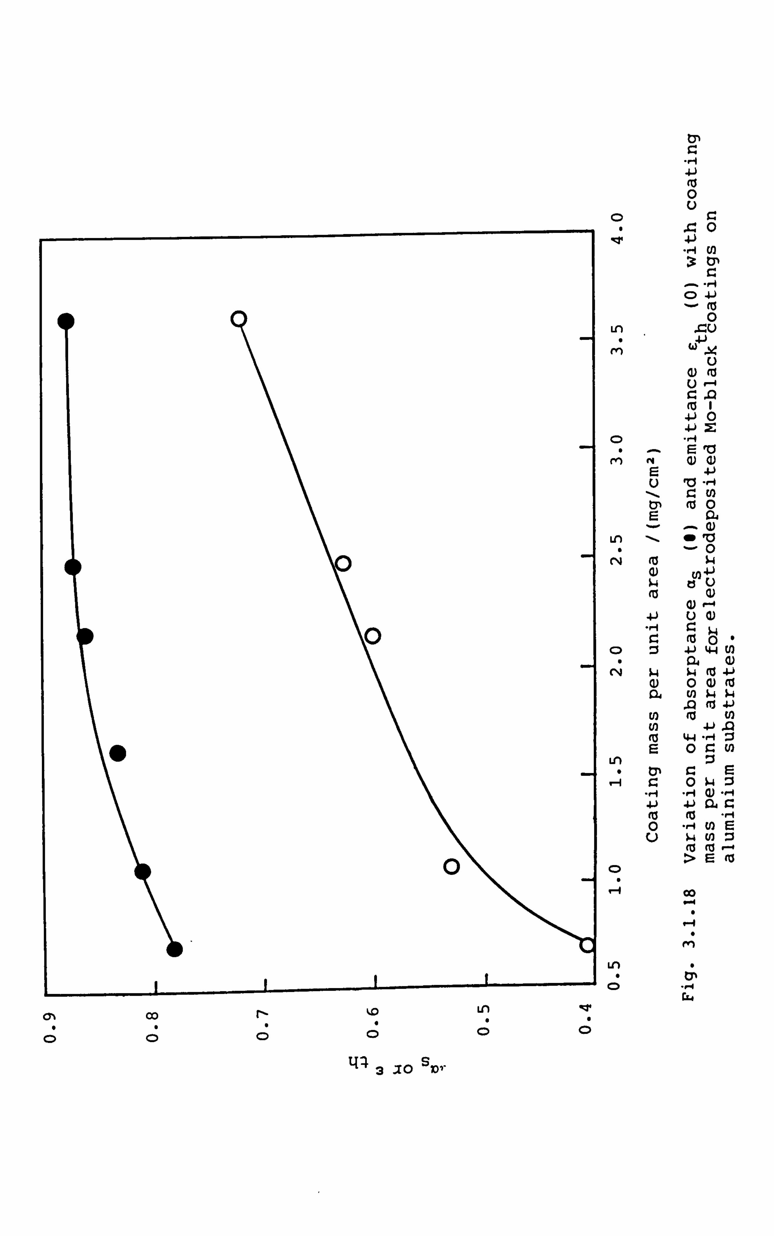
0
0
00 r, Ln -W
C; 1ý C; 144
3 . 10
slor
0
Icz 0
-rA (n tP r:
C> -41 - (ö
Ln
U
41 0 4-) 2:
E 10 ri
`, Z0 (0 0
Ln -- 40 10 0 rz (ö $4
G) N4 (ö Q)
(D :1 41 44 (n
w k4 tu 4-) Q) 0 0) (0
U) (0 U) (n 4-) Q (ö 44 -f =f r= 0 r. U)
C% Z Z%
r= r. 0 N4 :i
(0 fö ., i 0
-14 U) r= U ý4 cn :i
tu > (D
L2
CD
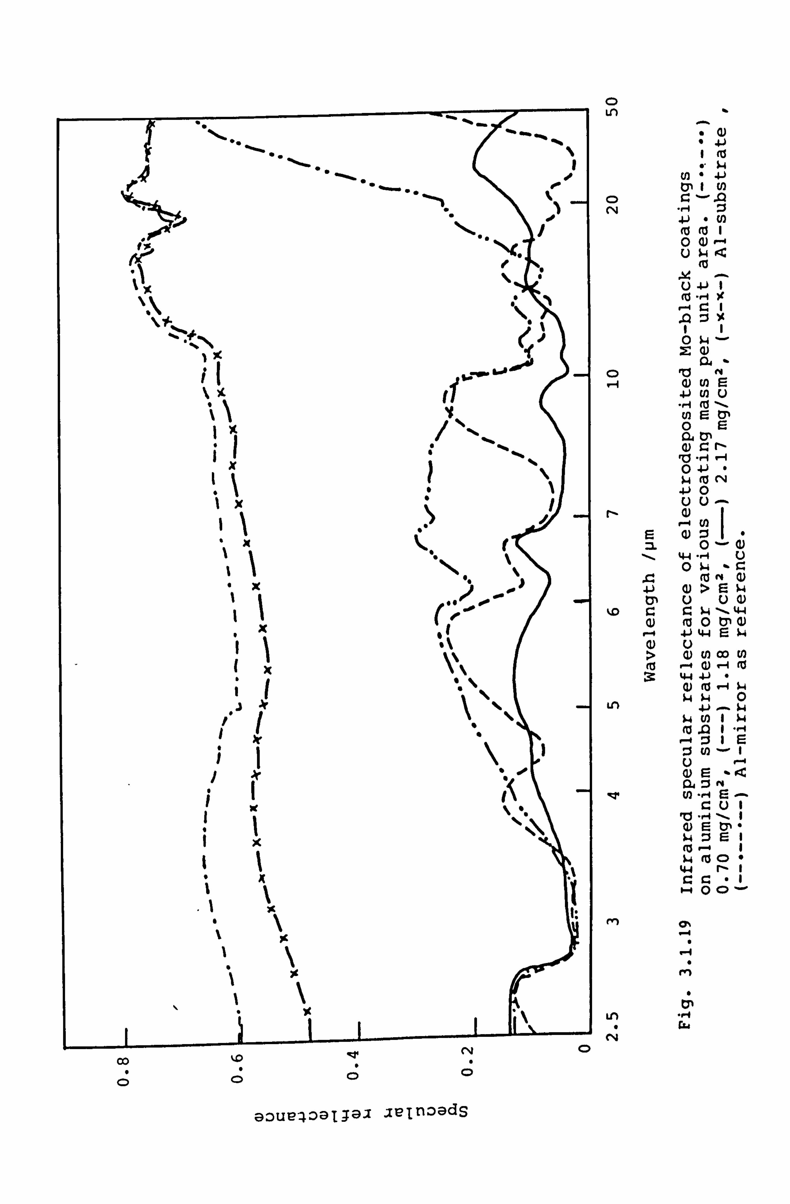
0 Ln
0. W ca 0 4-)
Cl) Co CN
4. ) U)
0 0) uw
(a k4 - U 4J
0W 2: a)
10, .
0) En S 41 U)
(n 0 rz
0 4j $4 (0 CN 4-) 0 () U- W
U)
=L 44 -4 u 0 $4
4-) >E ý4 u 0)
%D ý4 -- 44 (a 0M a)
4 4J 44 E ý4 Q) u > 4) U) OD U) (IS ý4 a) "A (cl : 3,. 44 4j -
0) (ts -I ý4 $4 ý4 0
Ln 4J - $4 $4 U) 1 $4 M
.01 . 1-4 E
u E :3m
$4 :1EI (o -4 1
ý4 (0 CD 0 44 r- I C: r- -I "0 0-
rr) CY%
uý rL4 C%i
90ue-409T. Tal aelnoads
00
cý cý
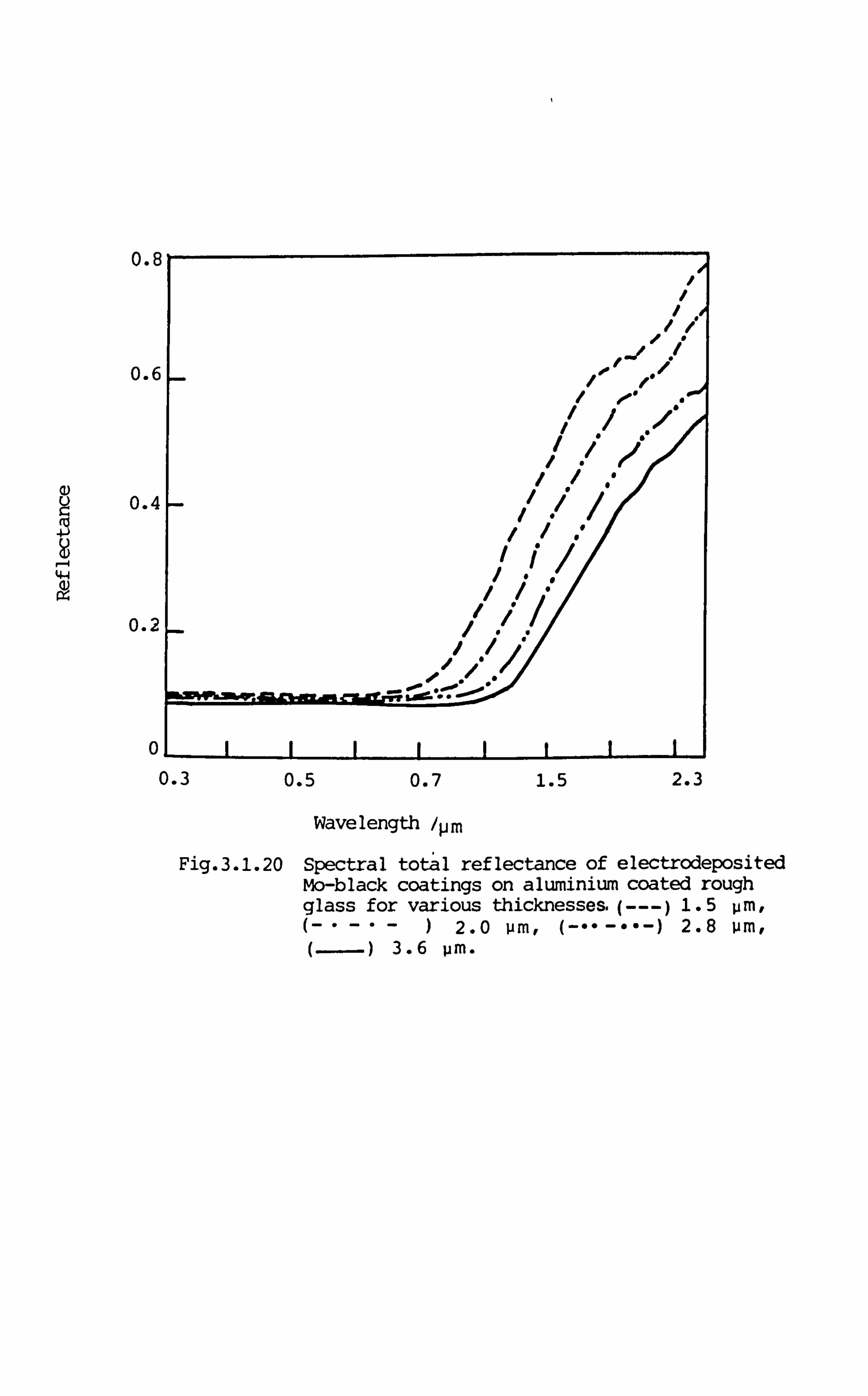
0.8
0.6
0) 0.4
0.2
0
/ /
/ 'I
-� "/ �' /
// / �"" .
// "/1 ii .
/" /�/' //". I
// /" //F
//I. /
1' . f//
// 'I �/ "1 "/� // "1
/1 I / .'"I
0.3 0.5 0.7 1.5 2.3
Wavelength /pm
Fig-3.1.20 Spectral total reflectance of electrodeposited Mo-black coatings on aluminium coated rough glass for various thicknesses, ( --- ) 1.5 pm,
-)2.0 2.8 Pm, 3.6 pm.
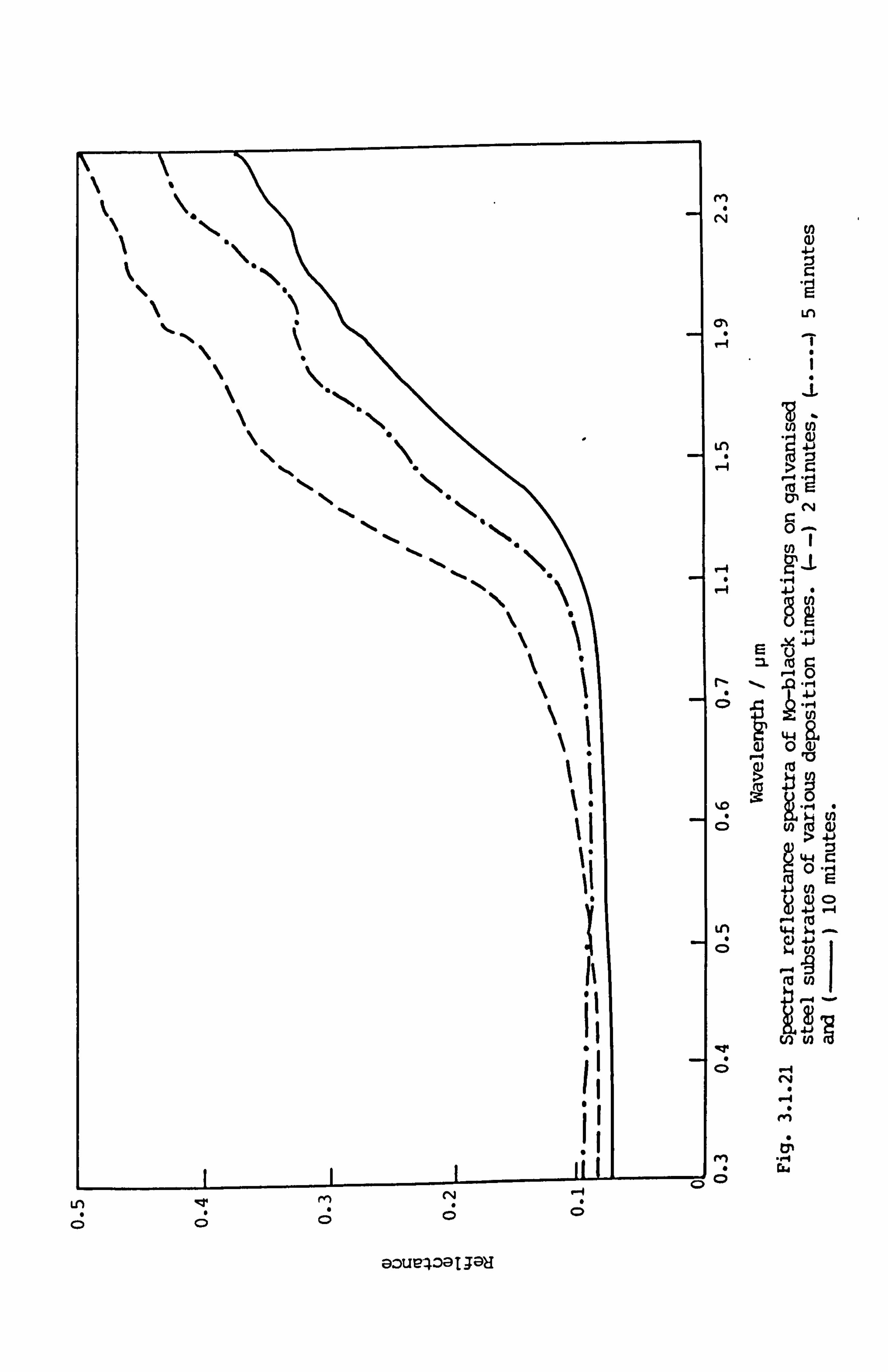
"N.
\
N
N 'S.
N �S.
N. S..
S
'\ S
�I II
�I
�'S
'I I. 1
r 1' II
1I II II SI
Ln 8
m 00
m (N
�-4
Ln 14
'-4
E
Q)
Ln C;
to
Ln
>
rY
.m
,a-, -i
44
(0 v
44
N-4 U)
ý- -8 tu U)
(n ul
-4 C4
en
t; .,.. I cu
93ue4: )@lj9H
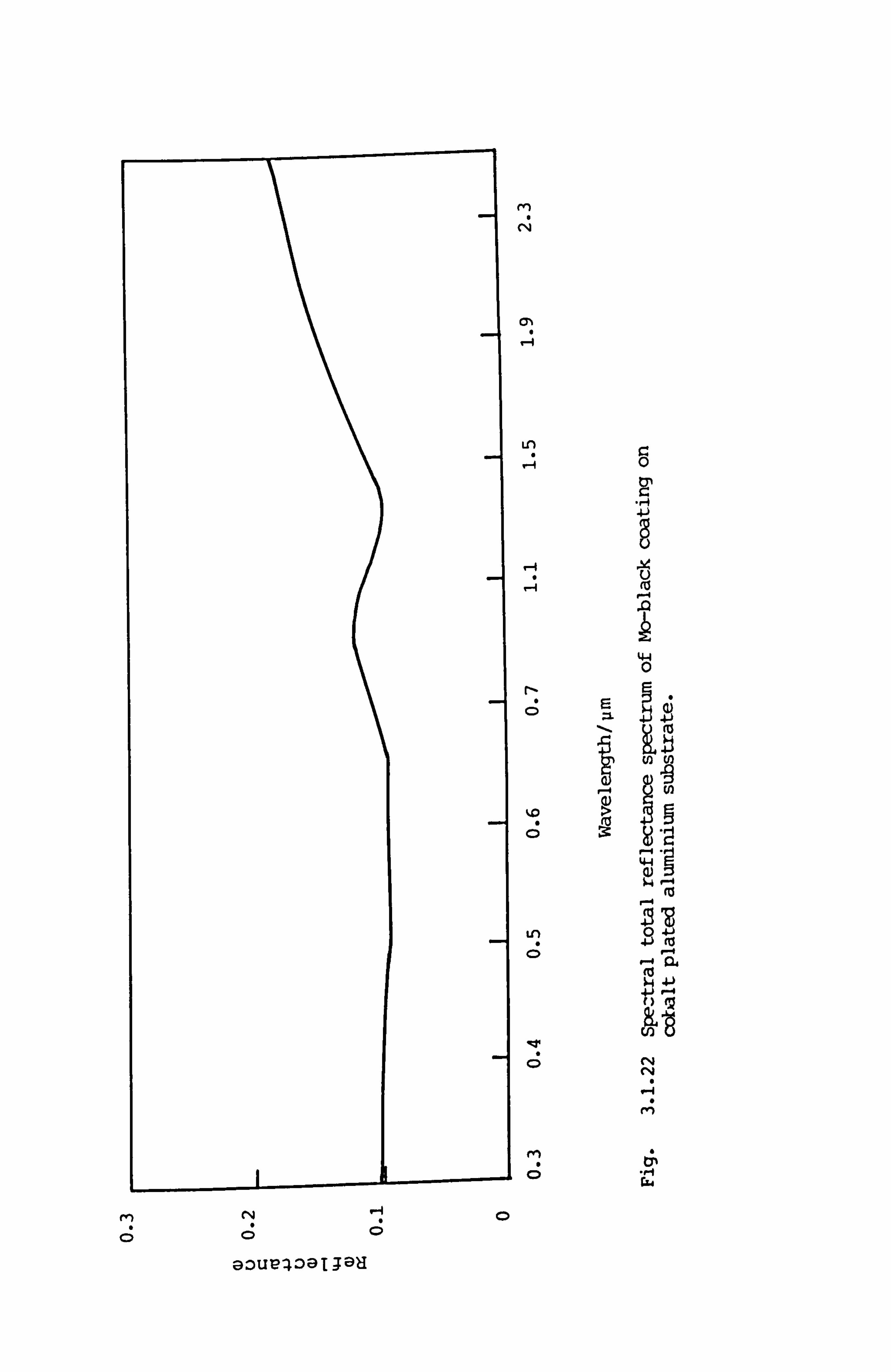
rý CN
m 14
Ln r_ 0
4 (0 1.1 10
44 0
C)
(0 r-4 219
C> JE - 'm
r 0
goue-4091jau
m-0 00
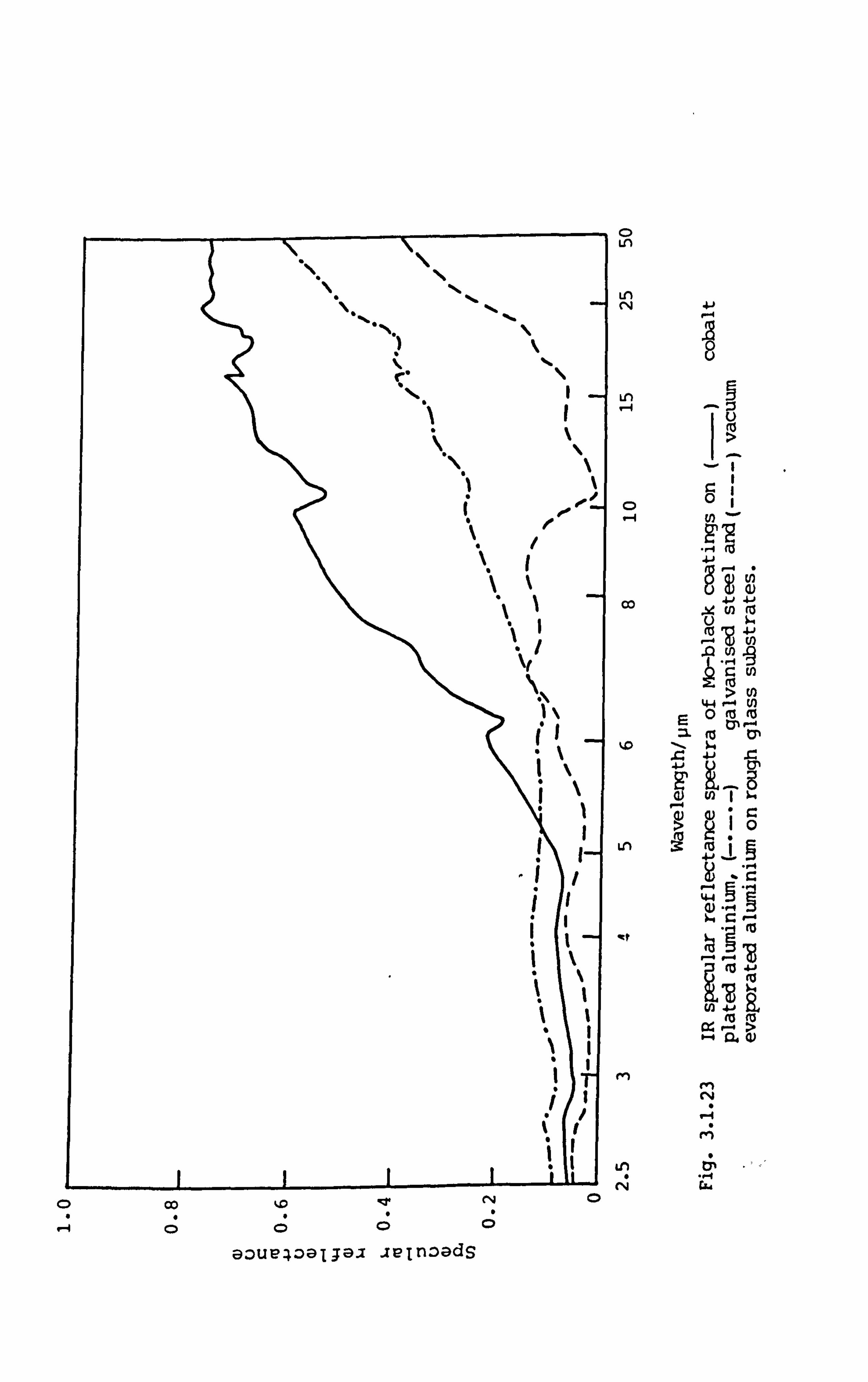
I- NI
/ I
' .�'
1 I- "� I'
! I
"1 �
i: I' "
I I
" 'I "
I) 'I
" II OD rq 0
0 Ln
Ln CN
n L
0 tn
OD 41 41
(0 4j 3 (n
E 4-4 U) 0 tö (ö
fö
Ln rö
44 - c) ., q
et
bö to
,8 ký cn ,a cý
(0 M
Ln t4
M cli
UA
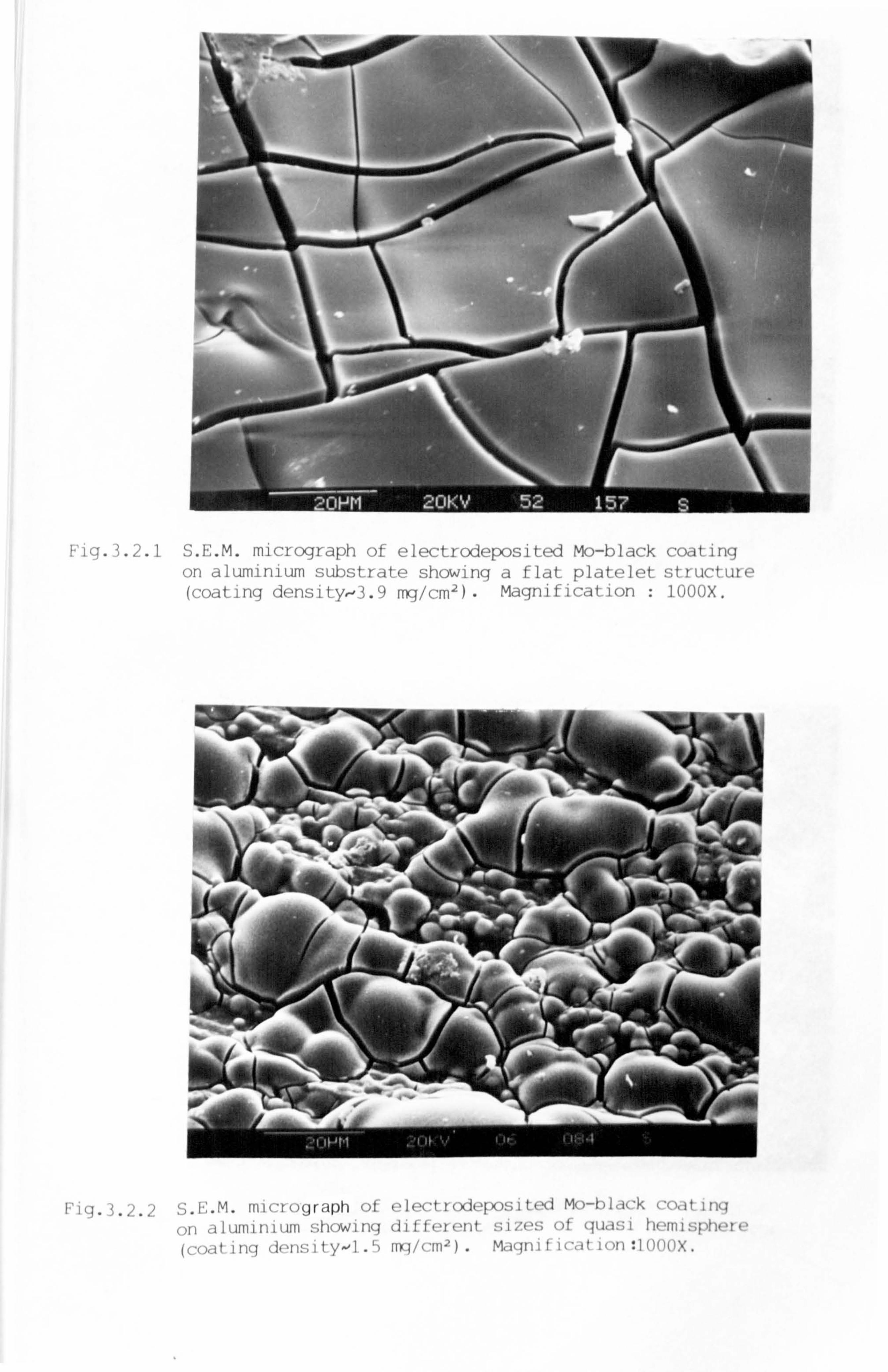
Fig. 3.2.1 S. E. M. micrograph of electrodeposited Mo-black coating on aluminium substrate showing a flat platelet structure (coating density, -3.9 Mg/CM2). Magnification : 100OX.
2, I_ M. Ili wt ()Yrapf) ý) I tý I (, k. t I It "d M'- I, I, I, K, -It .! 1'1 on aluminium showing different sizes ot quasi hemisphere
(coating density-l. ý mq/cm'). Maqnification*IOOOX.
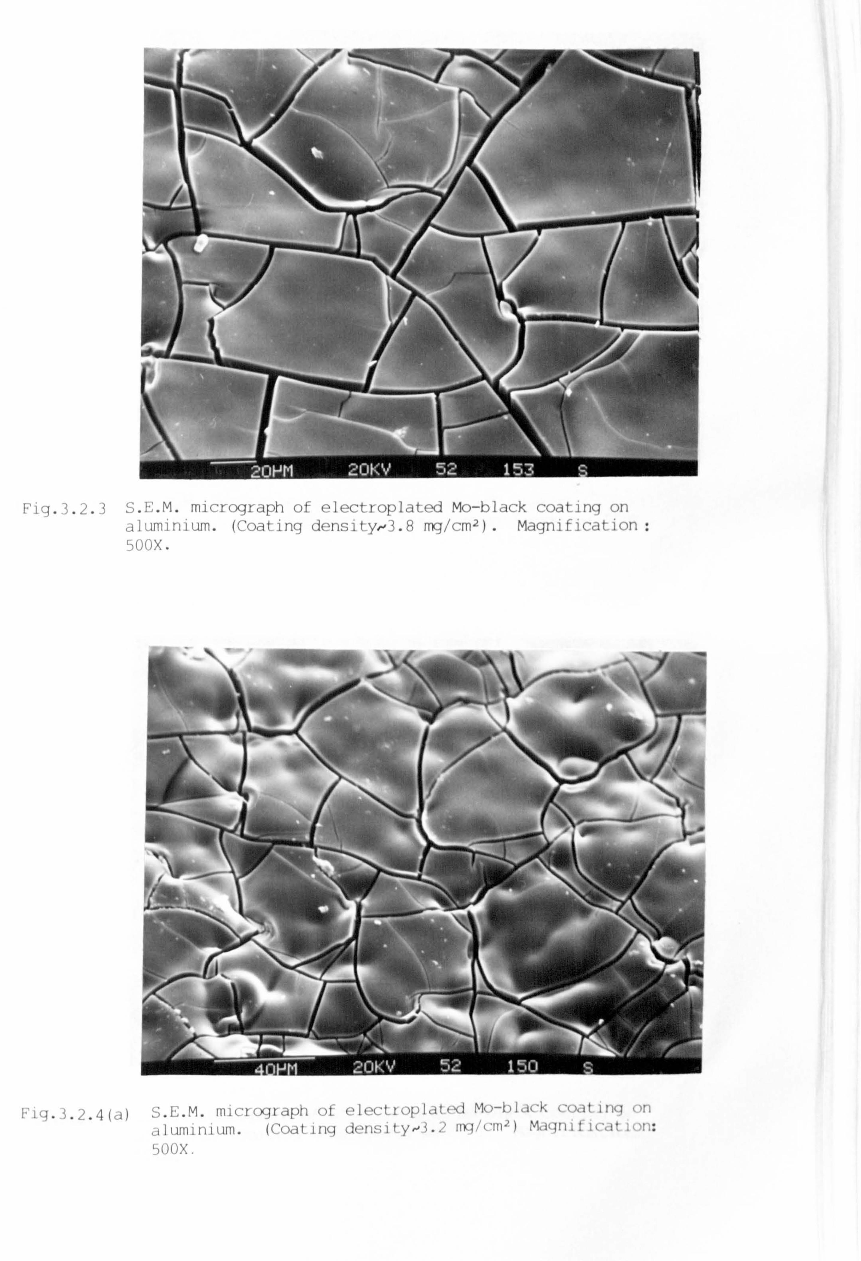
Fig. 3.2.3 S. E. M. micrograph of electroplated Mo-black coating on aluminium. (Coating density, -3.8 mglcm2). Magnification: 50OX.
ý;. 1- M. Illict (xII, II)tI,, I, II, "tI, 11 ,I,, t,, j', Iý I! 1,1, ,, ý, I,;!
I um in i um. (Coatinq density, i.., ' 50OX -
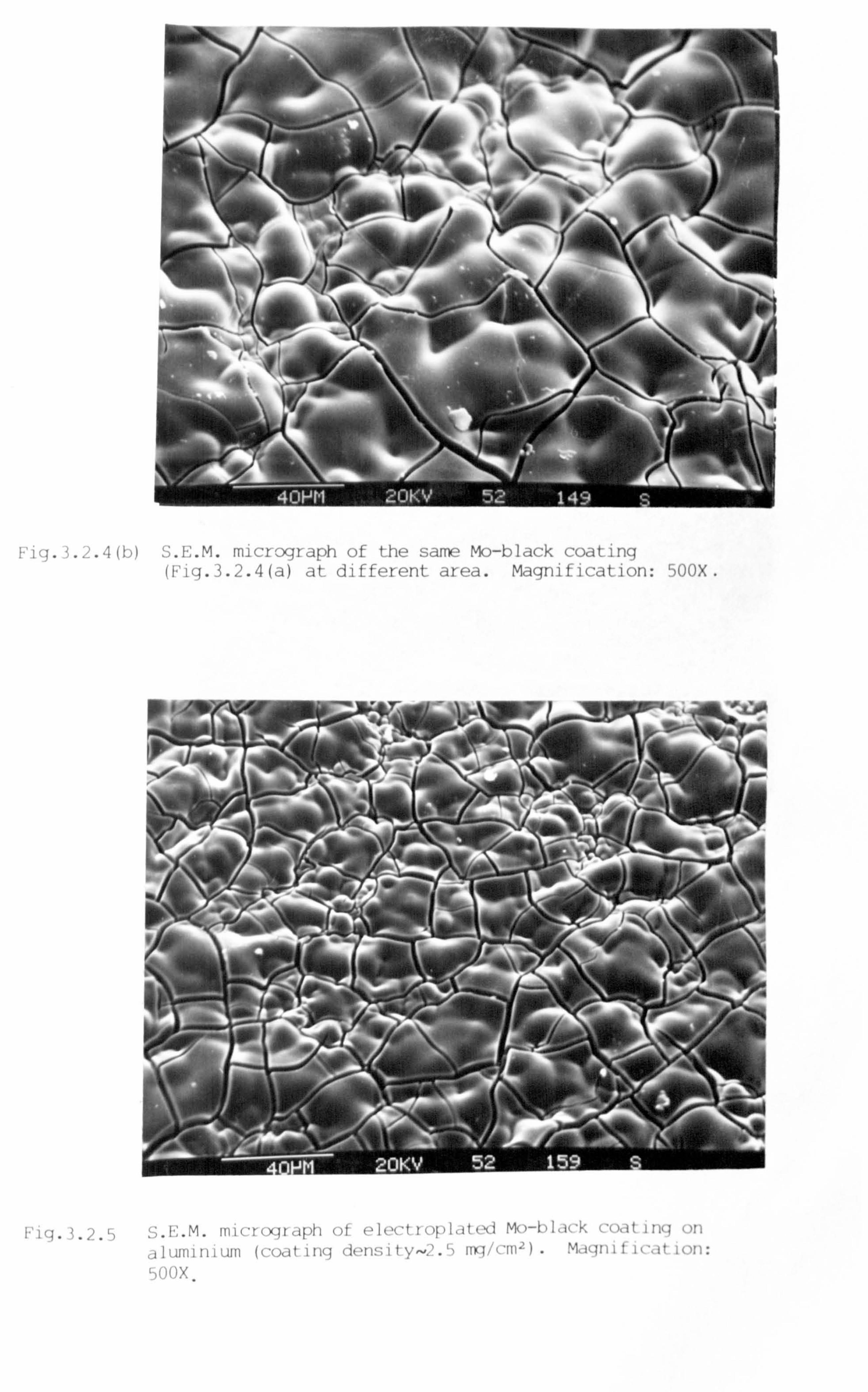
Fig. 3.2.4(b) S. E. M. micrograph of the same Mo-black coating (Fig. 3.2.4(a) at different area. Magnification: 50OX.
j
diumirlil-all (coatilly deilslty-2. ') Impoll') NI, IýJll II lcýtt loll: 50OX.
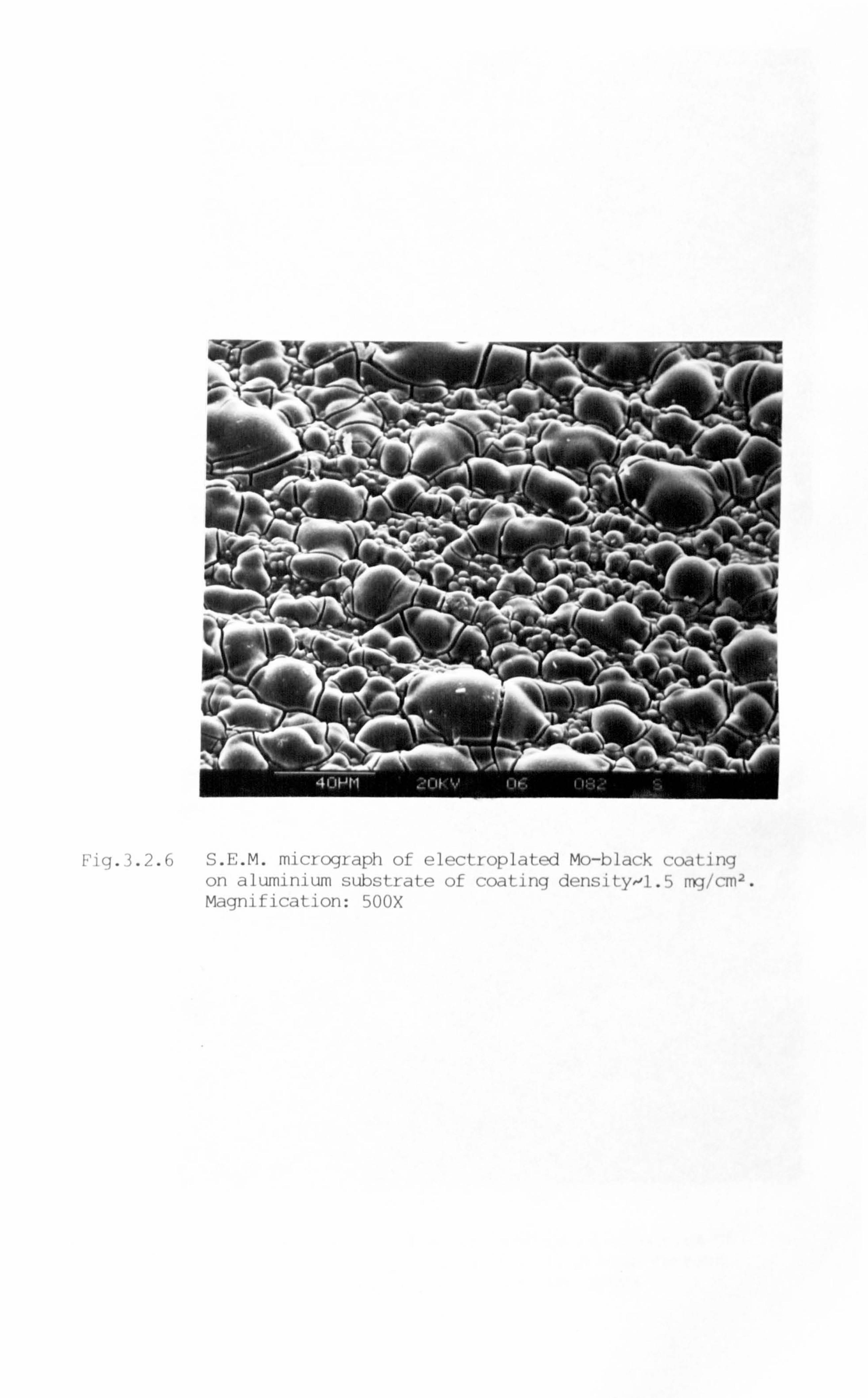
Fig. 3.2.6 S. E. M. micrograph of electroplated Mo-black coating on aluminium substrate of coating density, -1.5 Mg/CM2. Magnification: 50OX
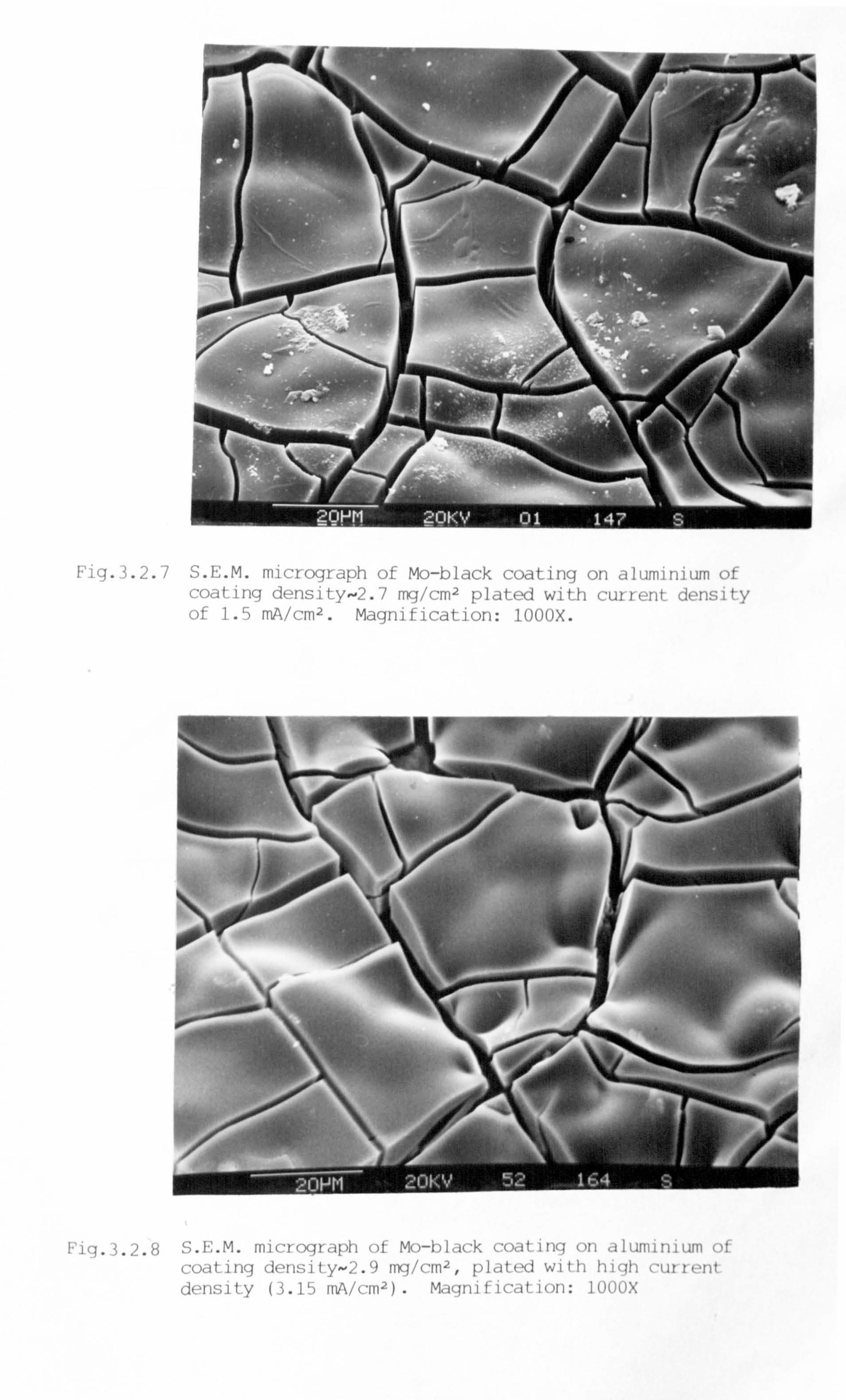
Fig. 3.2.7 S. E. M. micrograph of Mo-black coating on aluminium of coating densityý2.7 Mg/CM2 plated with current density of 1.5 mA/CM2. Magnification: 1000X.
Fig-3.2.8 S. E. M. mic. -rograph (A MO-iA, ick coating on aluminium of coating density-2.9 Mq/CM2, plated with high current density (3.15 mA/CM2). Magnification: IOOOX
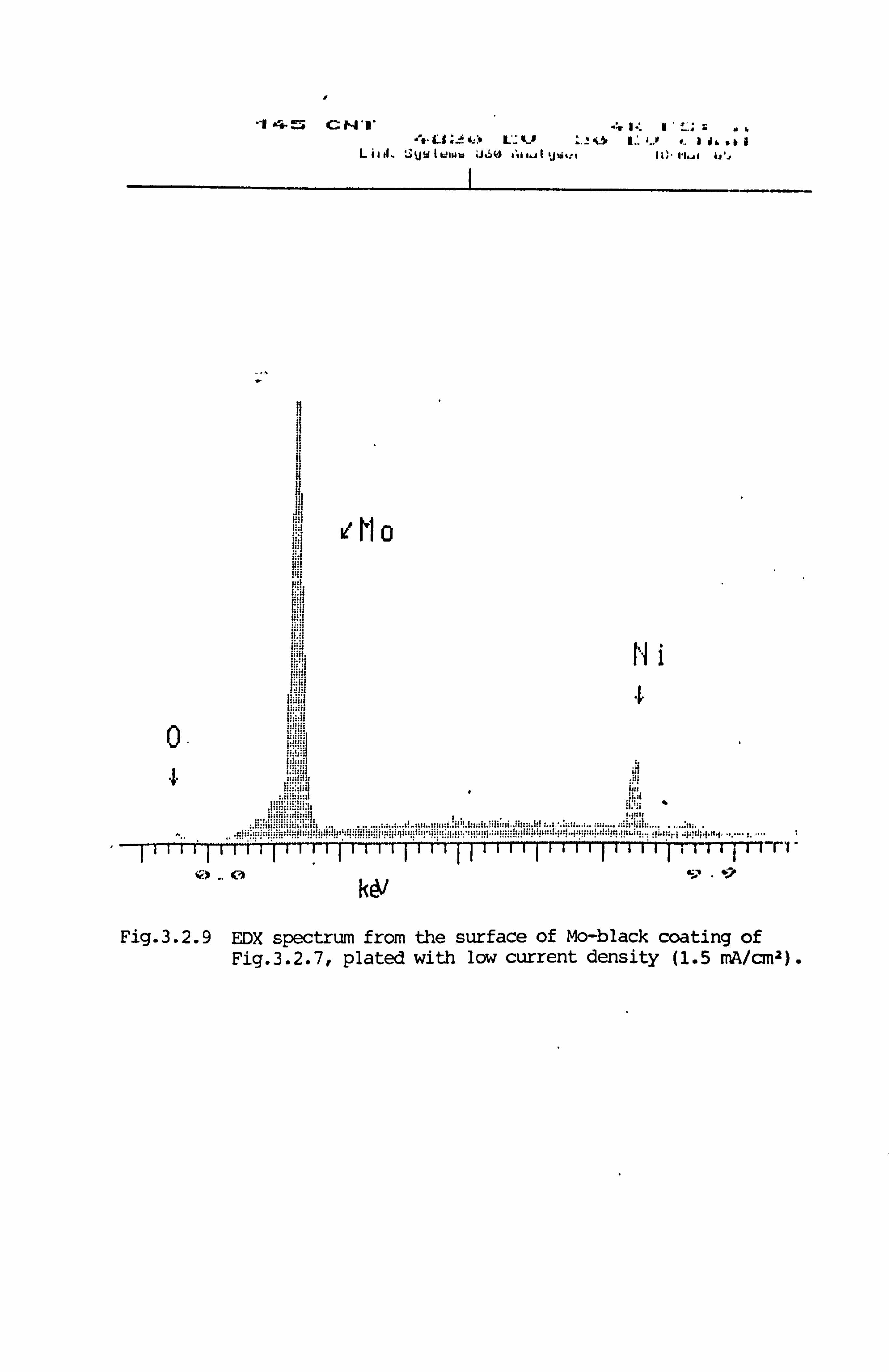
Uid, t; Vwlvmv U60 sooj('j-juo Il- I
Fig. 3.2.9 EDX spectrum from the surface of Mo-black coating of Fig. 3.2.7, plated with low current density (1.5 mA/cm2)-
0- C-') EV v
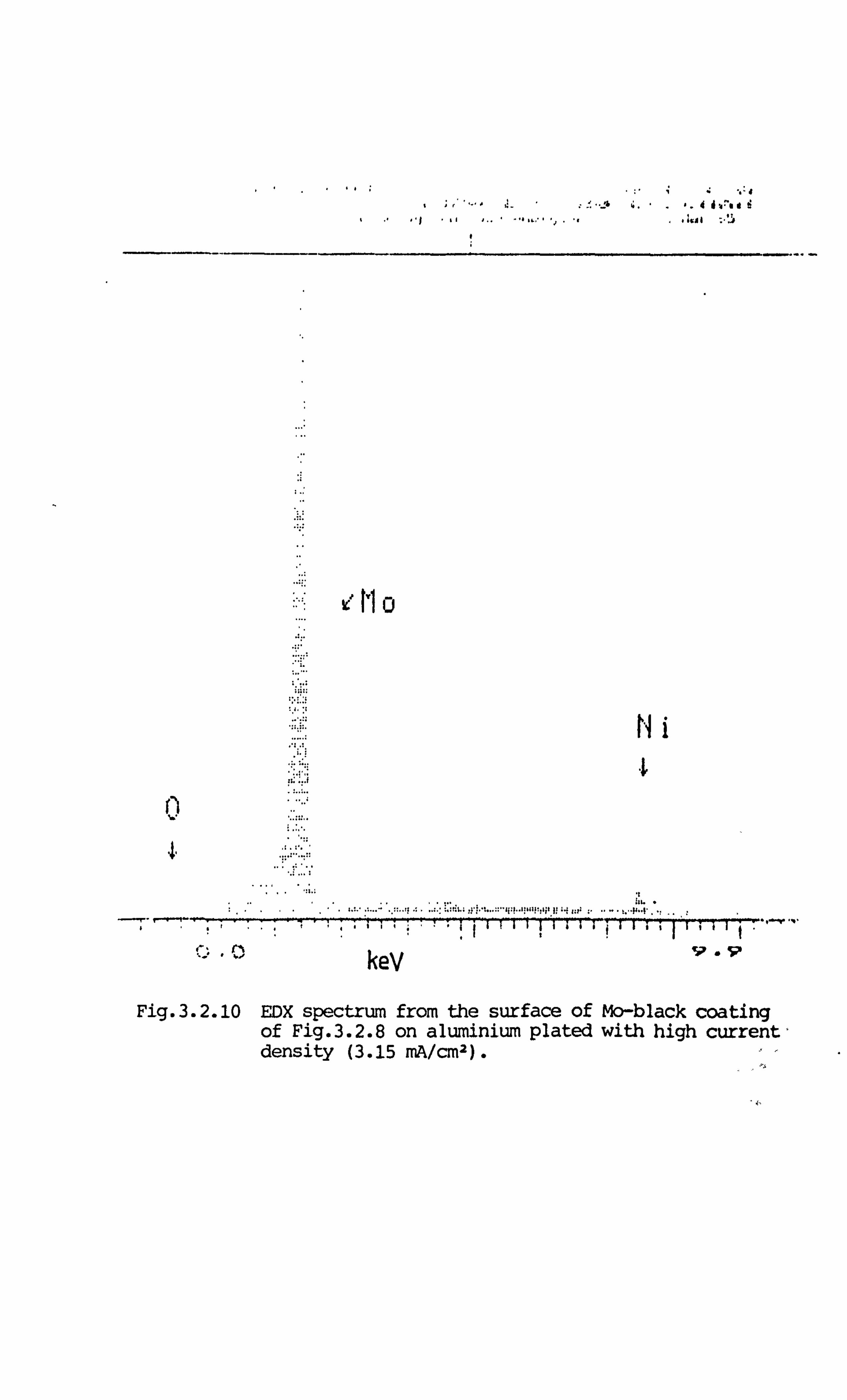
.
'l
keV
Fig. 3.2.10 EDX spectrum from the surface of Mo-black coating of Fig. 3.2.8 on aluminium plated with high current, density (3.15 mA/CM2).
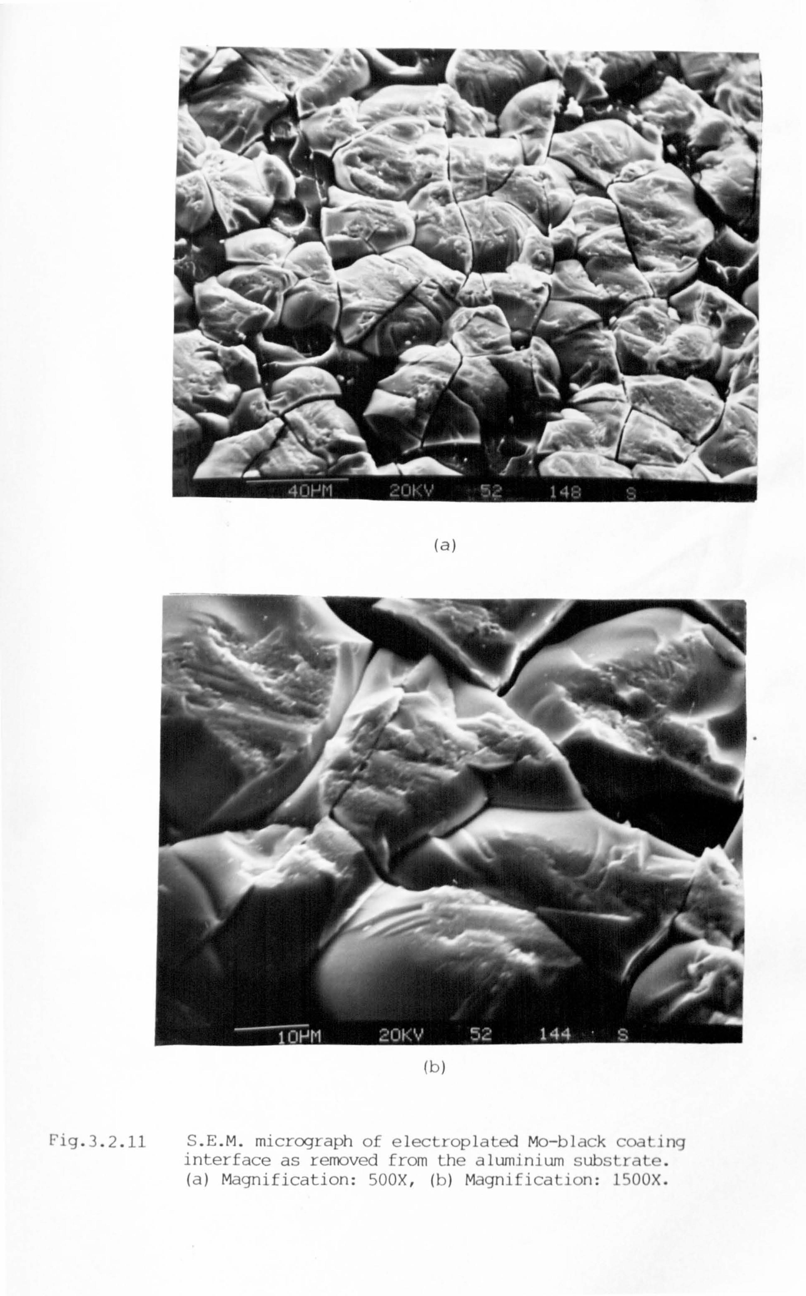
(a)
II)
Fig-3.2.11 S. E. M. micrograph of electroplated Mo-black coating interface as removed from the aluminium substrate. (a) Magnification: 50OX, (b) Magnification: 150OX.
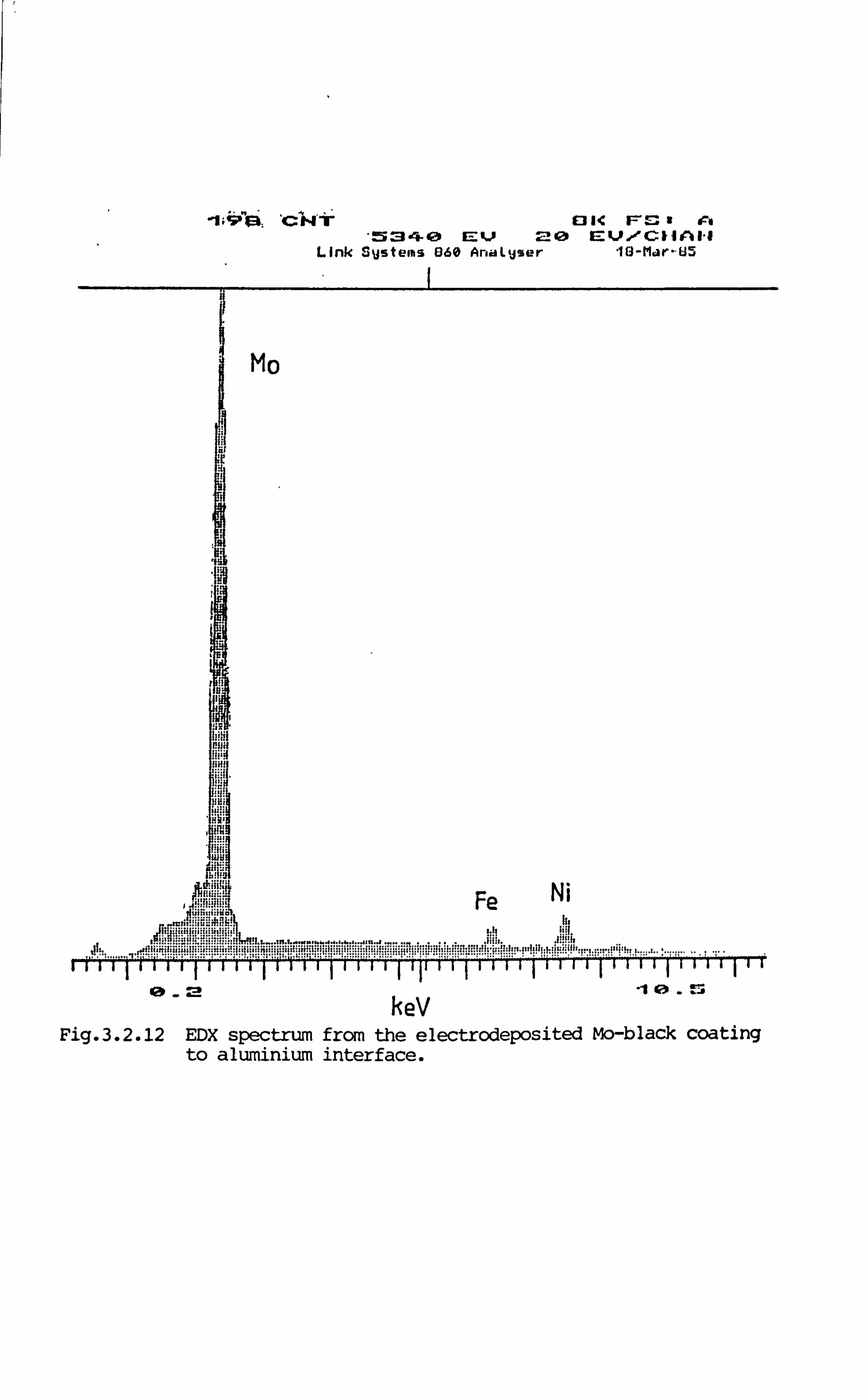
13K F==-l A 220 ev. 10CIIA14
Link Systems 060 AnaLyser 18-11jr-U5
Fig. 3.2.12 EDX spectrum from the electrodeposited Mo-black coating to aluminium interface.
la -M keV
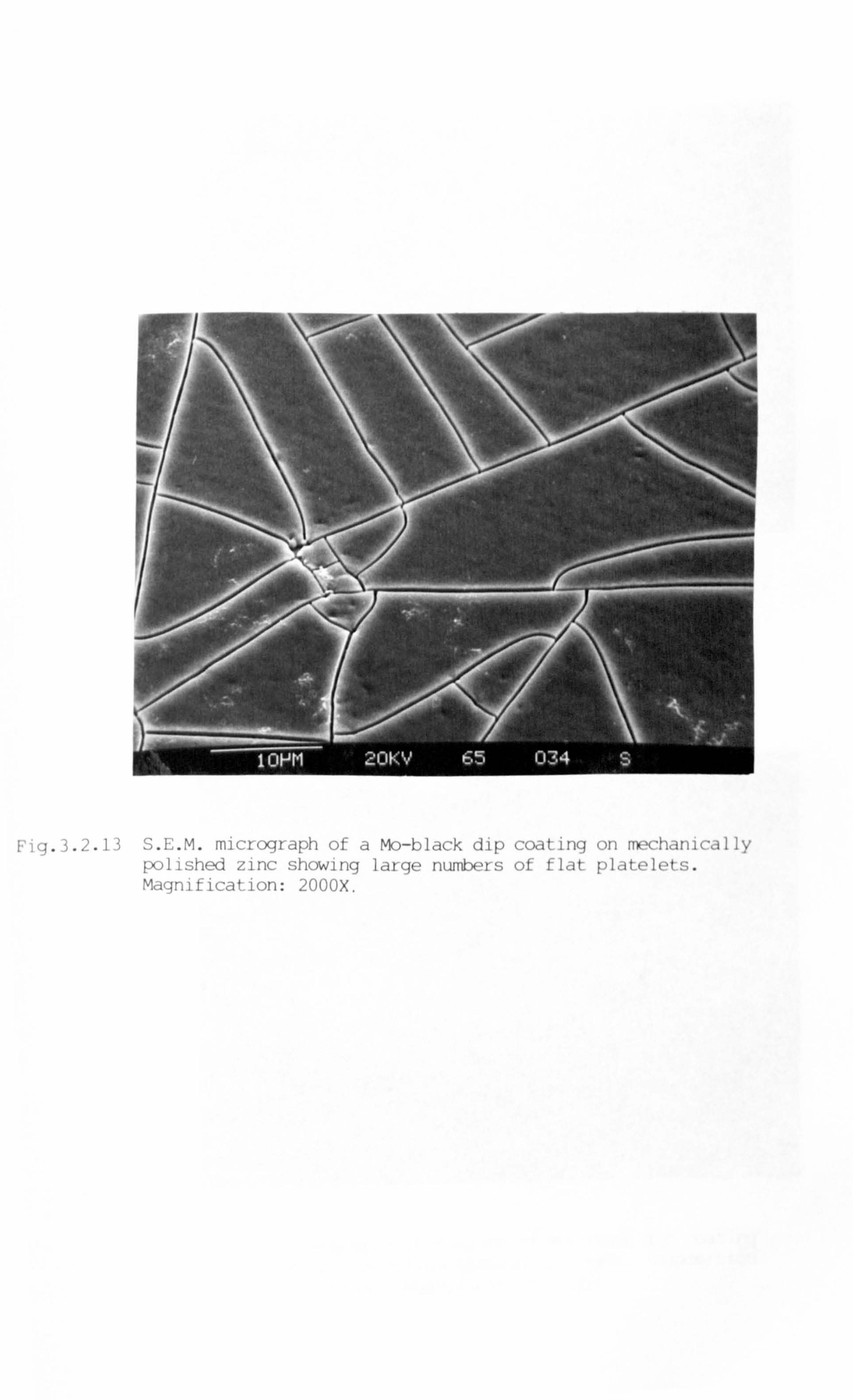
ig. 3.2-13 S. E. M. micrograph of a Mo-black dip coating on mechanically polished zinc showing large numbers of flat platelets. Magnification: 200OX.
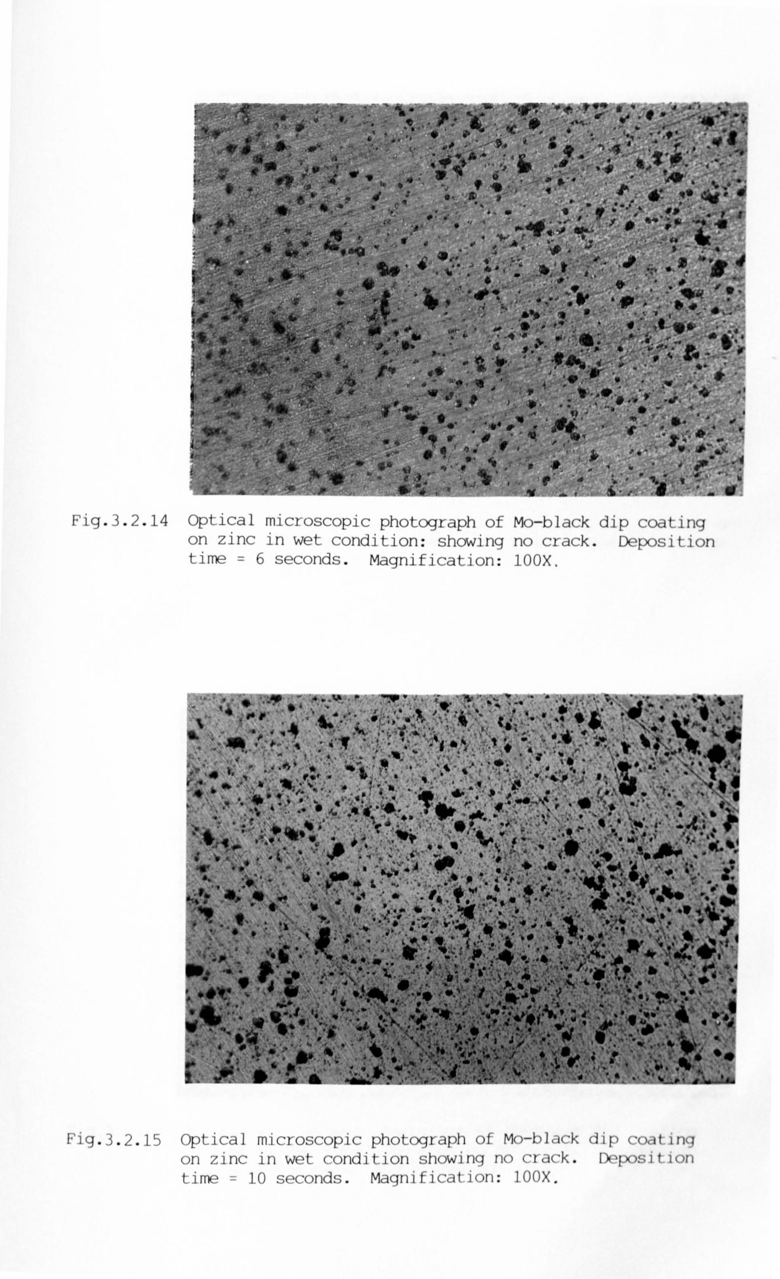
, ýi, 'Jr. "t jý "a'. 01 'r
jsý .10,., 1, ..
41; .,
A, 14 ,
ý; -
ý&
.
, 46 " OAQ a,, 0a-.
P. . 16
11" *, .,, 6, .. ý
1 46
jr
. 10,
ow
Fig. 3.2.14 optical microscopic photograph of Mo-bldck dip coating on zinc in wet condition: showing no crack. Deposition time =6 seconds. Magnification: IOOX.
---0-. ýjo 6. .--
le ,
. lý
ad» '...... .
.. 7. - C;.
. 114. IQ
!k ib
ol tII., i,
C. -. 40.
. 06
ý W, .1S, 4.0
J, *J, . ", ,,,
Pic ;w
. 41 ,- 4" '4! "ý ., . ;eD. IA Aý!
!. i ,ý, -1 "*.
.. I
Fig. 3.2.15 Optical microscopic photograph of Mo-black dip coatinq on zinc in wet condition showing no crack. Depý)sition time = 10 seconds. Magnification: 100X.
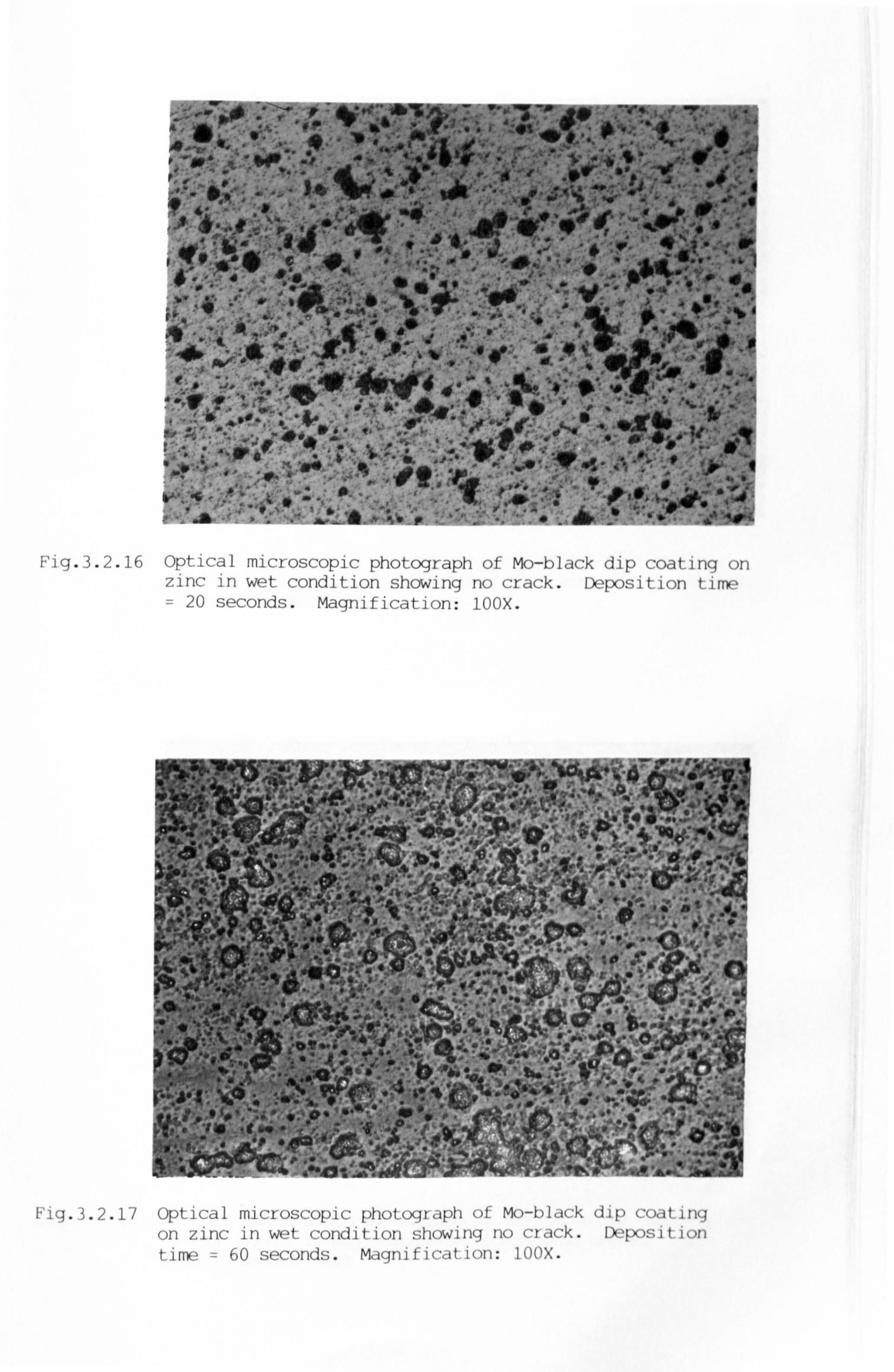
W. 1,0-'. '-; r I -i r, 04-.
. .. a .0.,.
z, 4
dr
A*. -,. 'ý p 4L " 0. '
Ws ,,
7W. ý l'-p 40
16 Ar I -, ý,. . 0.6 IL
ýI, I
,
a Ap mo
, op . iý ý
ea
jr. ..., t -0 ',
Joe
). 10 OW Ica I microscopic photograph zinc in wet condition showing = 20 seconds. Magnification:
of- Mo-f)], wk dip cwt ing ()ii no crack. Deposition time IOOX.
Fig. 3.2.17 Optical microscopic photograph of Mo-black dip coatinq on zinc in wet condition showing no cr, tck. IX, posit jon time = 60 seconds. Magnification: I00X-
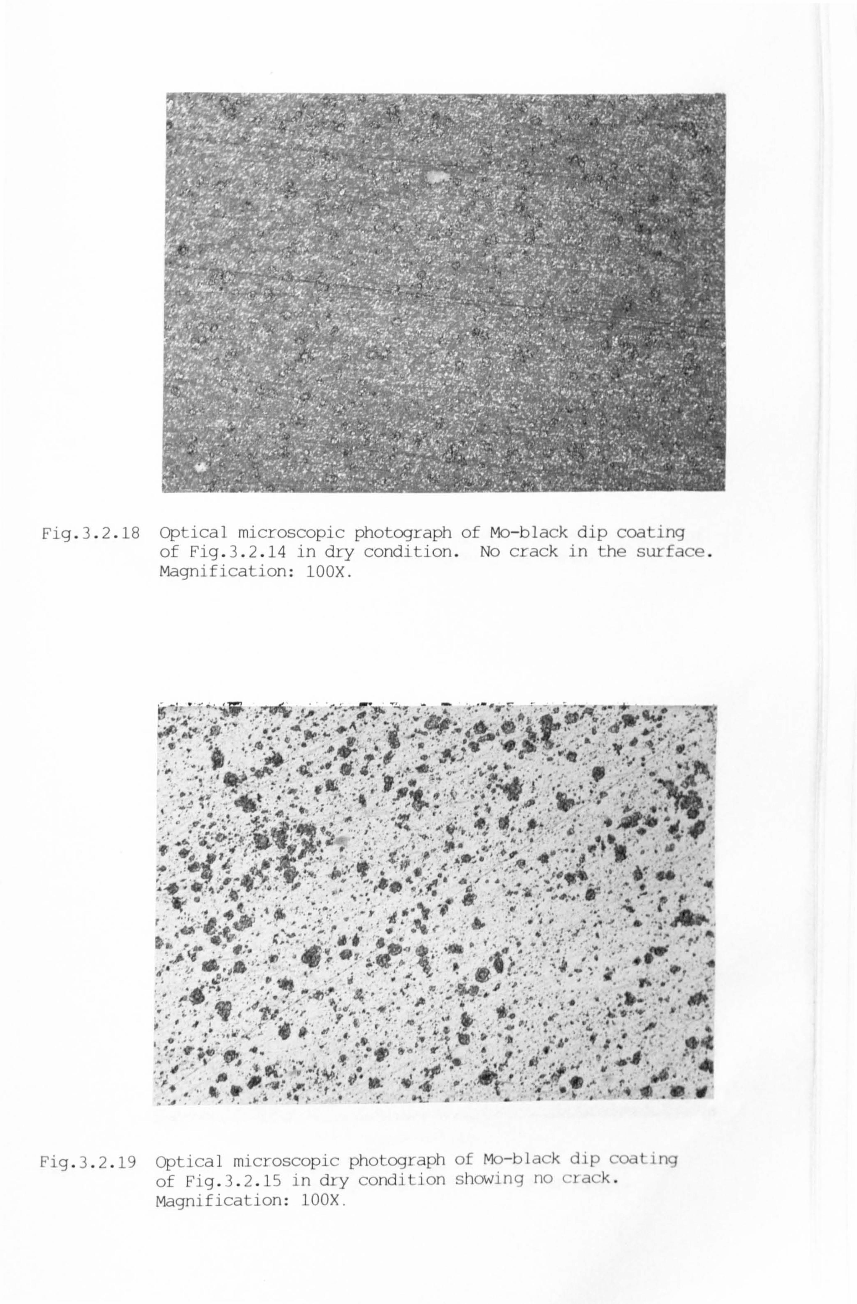
liv 41J
14 At
It
Fig. 3.2.18 optical microscopic photograph of Mo-black dip coating of Fig. 3.2.14 in dry condition. No crack in the surface. Magnification: IOOX.
. 10 A OF ilk
, v, , -f ,ýV. P. .., "' 0-11fto 1-1ý .. ý Ot .
t* ", 4ý11
Awl
df . 4: .,
ý,
.11.,
.A"o*, V-. -. -.. w '41, *1 .,
0, A, ý. r
Fig. 3.2.19 optical microscopic photograph of Mo-black dip coating of Fig. 3.2.15 in dry condition showing no crack. Magnification: IOOX.
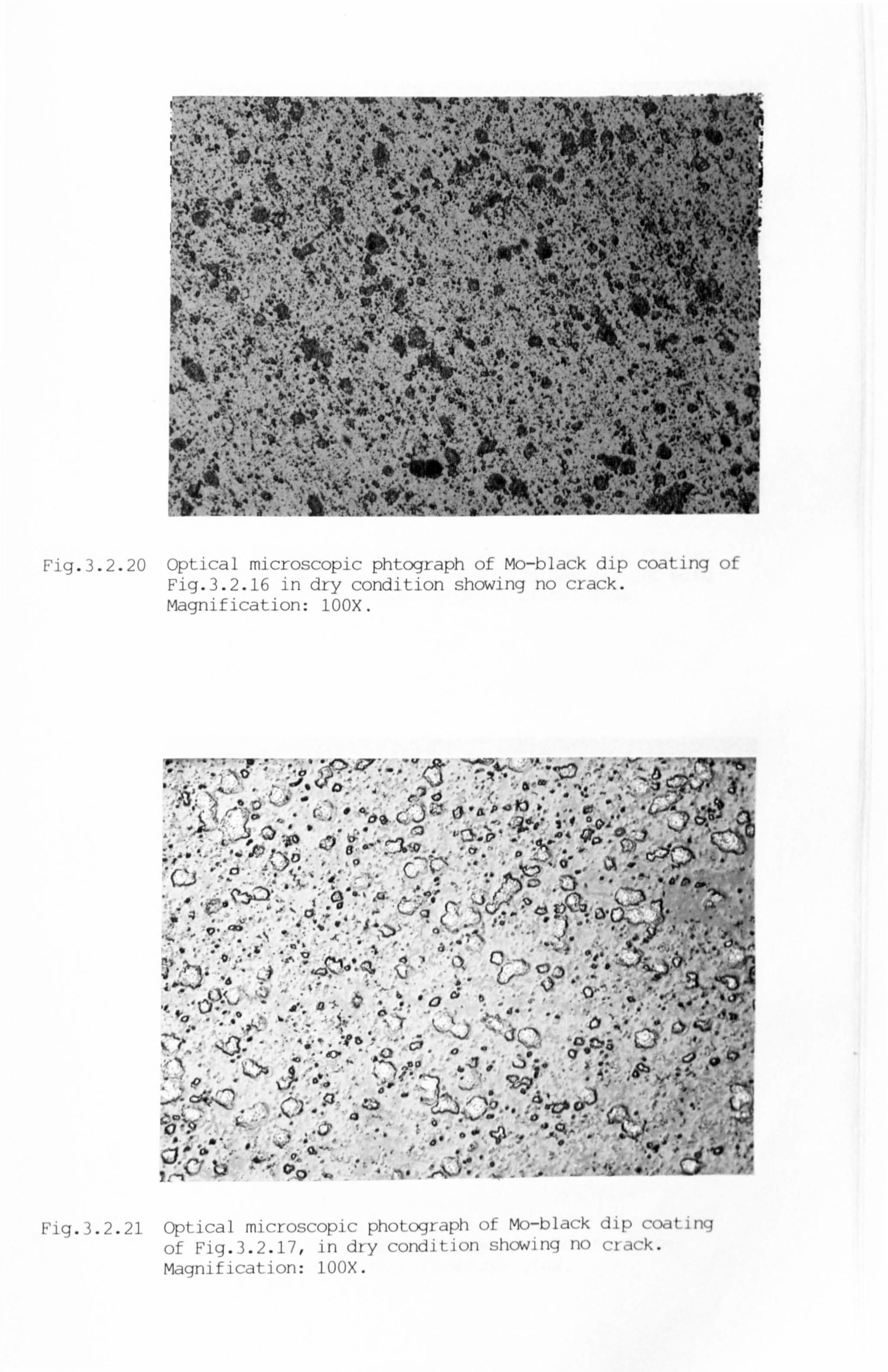
Fig. 3.2.20 optical microscopic phtograph of Mo-black dip coating of Fig. 3.2.16 in dry condition showing no crack. Magnification: 10OX.
4 ..,,. --, I. .-,. 0;
17 4p
. 4; p .... .0 40,
Fig. 3.2.21 optical microscopic photograph of Mo-black dip coating of Fig. 3.2-17, in dry condition showing no crack. Magnification: IOOX.
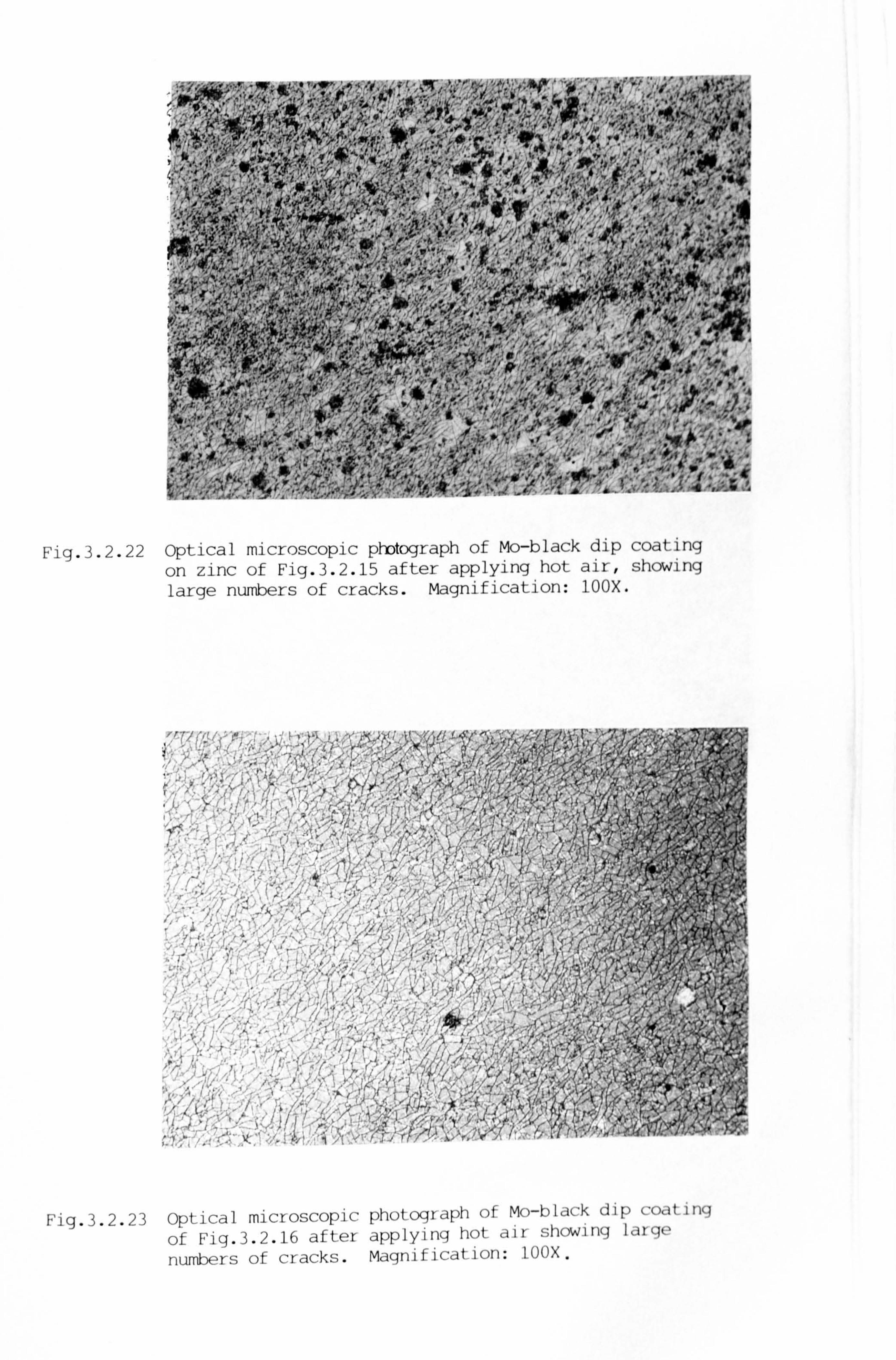
Fig. 3.2.22 optical microscopic photograph of Mo-black dip coating
on zinc of Fig-3-2-15 after applying hot air, showing large numbers of cracks. Magnification: IOOX.
Fig. 3.2.23 optical microscopic photograph of Mo-black dip coating
of Fig. 3.2.16 after applying hot air showing large
numbers of cracks. Magnification: IOOX.
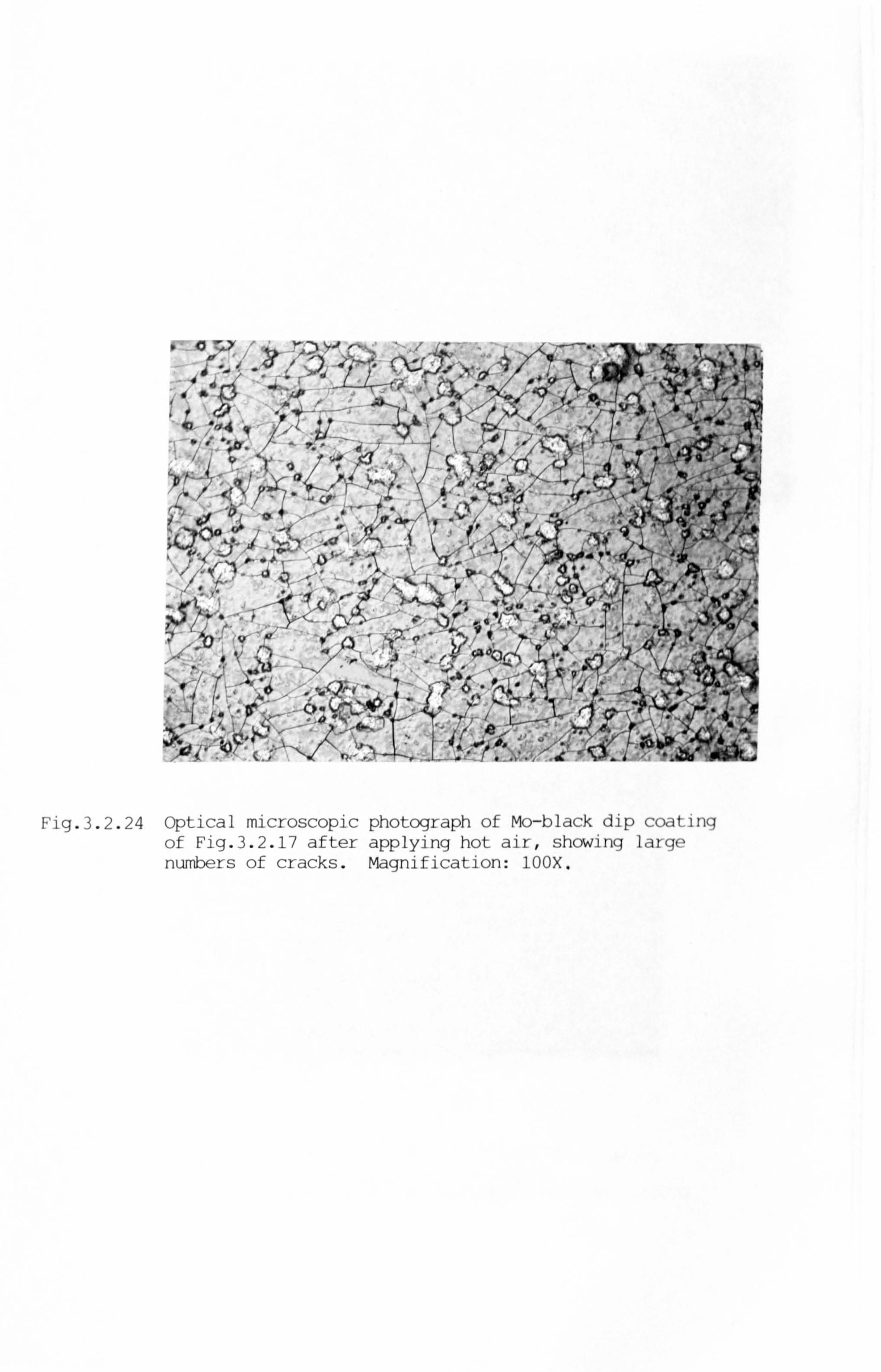
Fig. 3.2.24 Optical microscopic photograph of Mo-black dip coating of Fig. 3.2.17 after applying hot air, showing larqe numbers of cracks. Magnification: 100X.
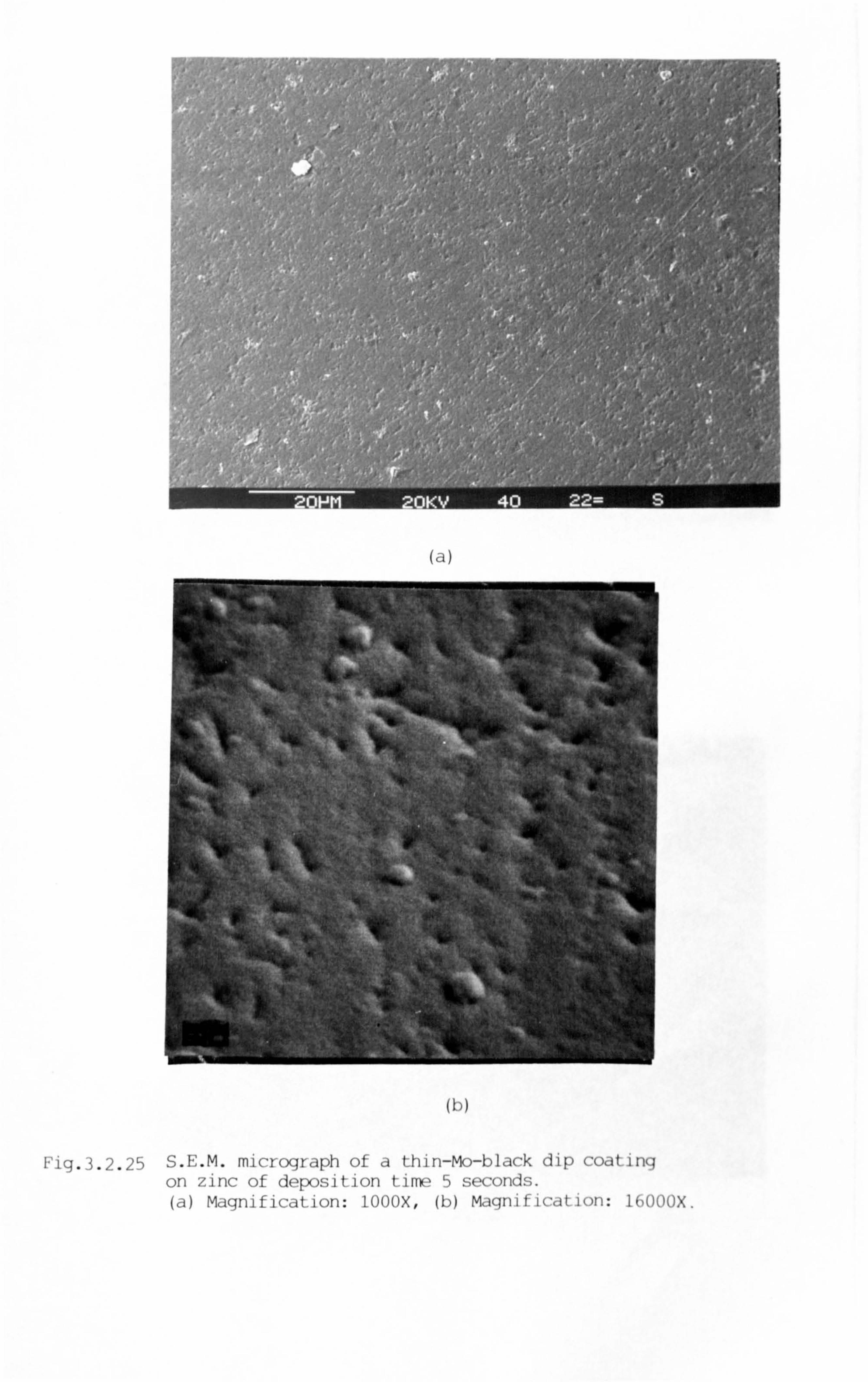
(a)
(b)
Fig. 3.2.25 S. E. M. micrograph of a thin-Mo-black dip coating on zinc of deposition time 5 seconds. (a) Magnification: 1000X, (b) Magnification: 1600OX.
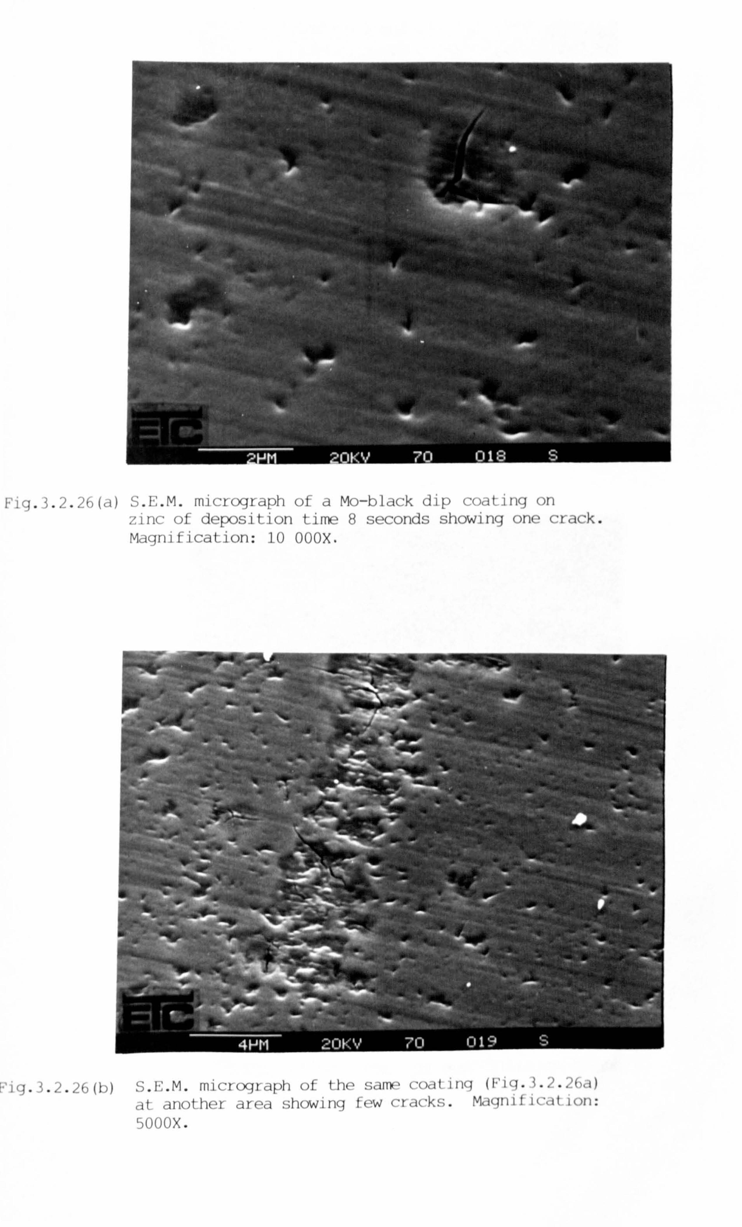
UAW,
4W
Fig. 3.2-26(a) S. E. M. inicroyraph of a Mo-black dip co(Atýng on zinc of deposition time 8 seconds showing one crack. Magnification: 10 000x.
, )'Jý. M. Illici(X31,114) ()I i I)(' c(), It III(I (1`1(j. ý-. .. 't I) at another area showing few cracks. Magnif ic, it ion: 500OX.
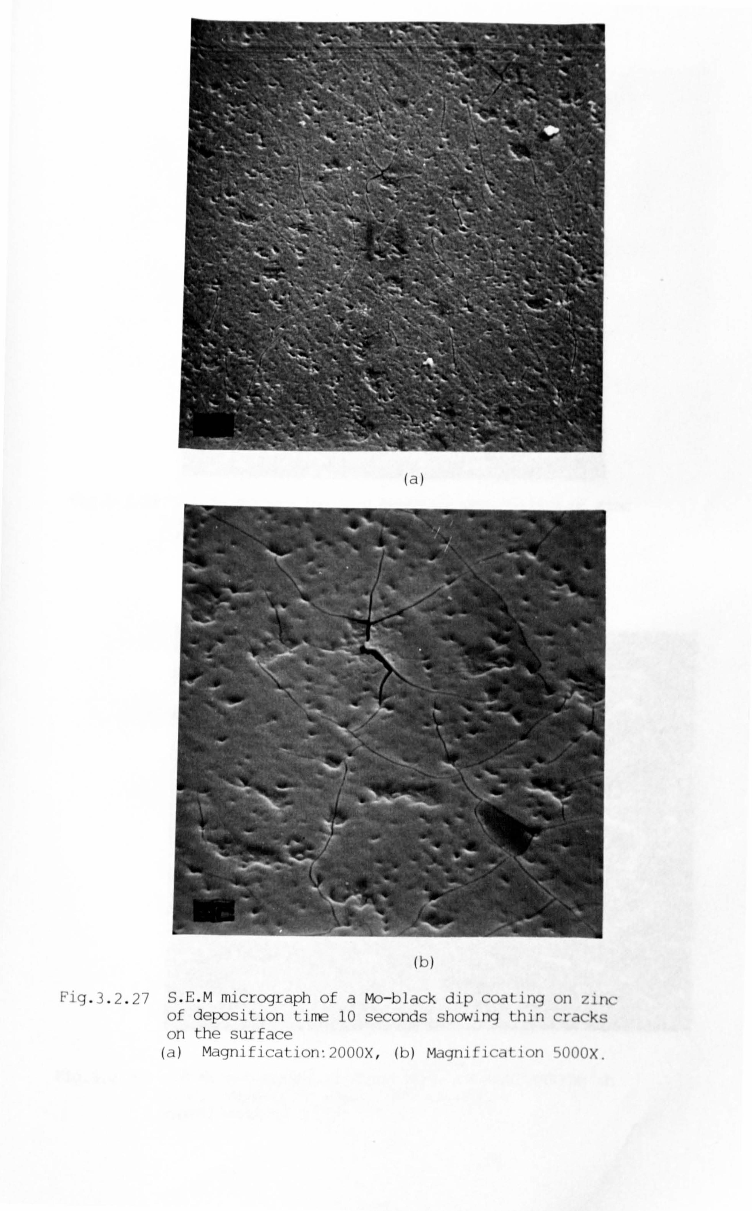
(a)
(b)
Fig-3-2.27 S. E-M micrograph of of deposition time on the surface
a Mo-black dip coating on zinc 10 seconds showing thin cracks
(a) Magnification-200OX, (b) Magnification 500OX.
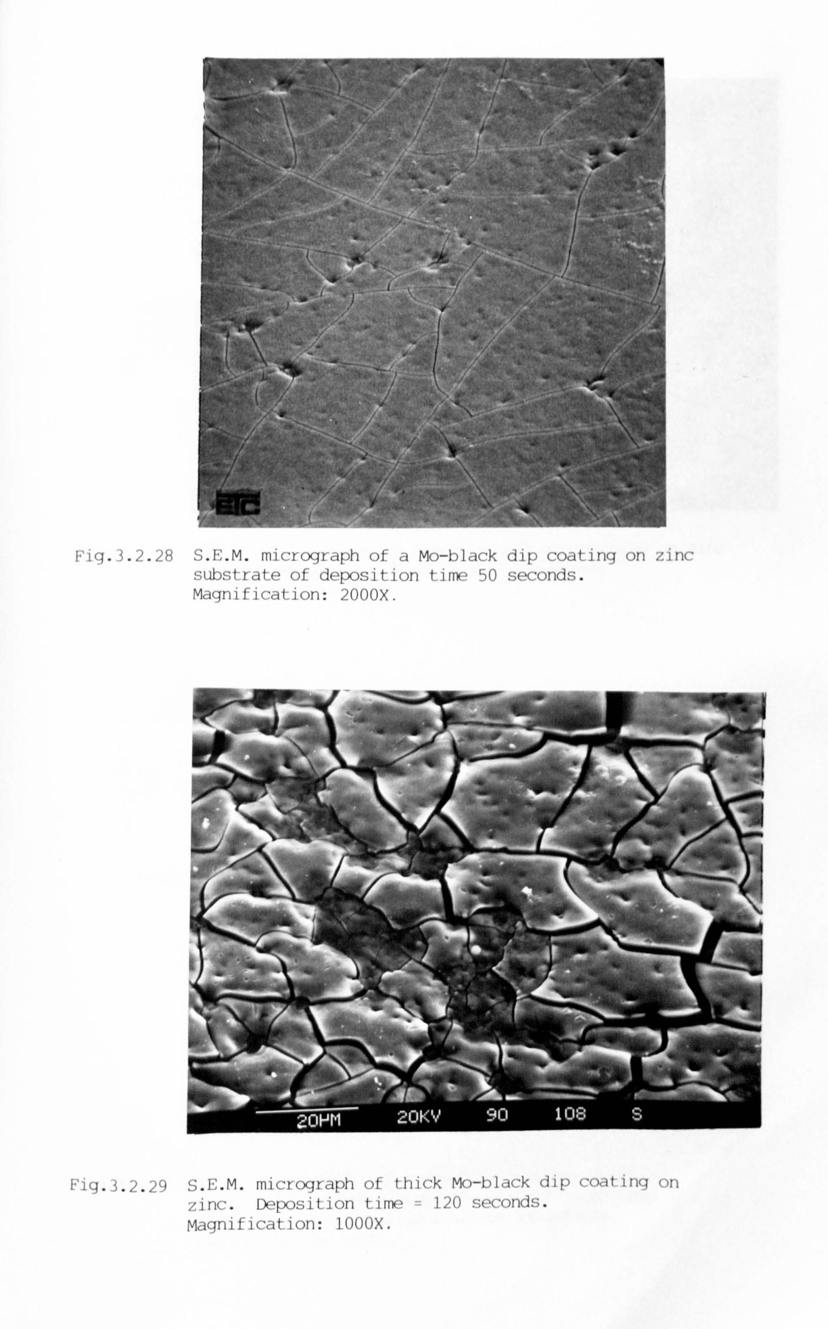
Fig. 3.2.28 S. E. M. micrograph of a Mo-black dip coating on zinc substrate of deposition time 50 seconds. Magnification: 200OX.
ý; .FM. in i ur (), -p , [, I I ()I IIii( 'k M( )-h 1,1( ýk (I i it v zi nc. Depos iti on ti me 120 seconds. Magnification: 1000X.
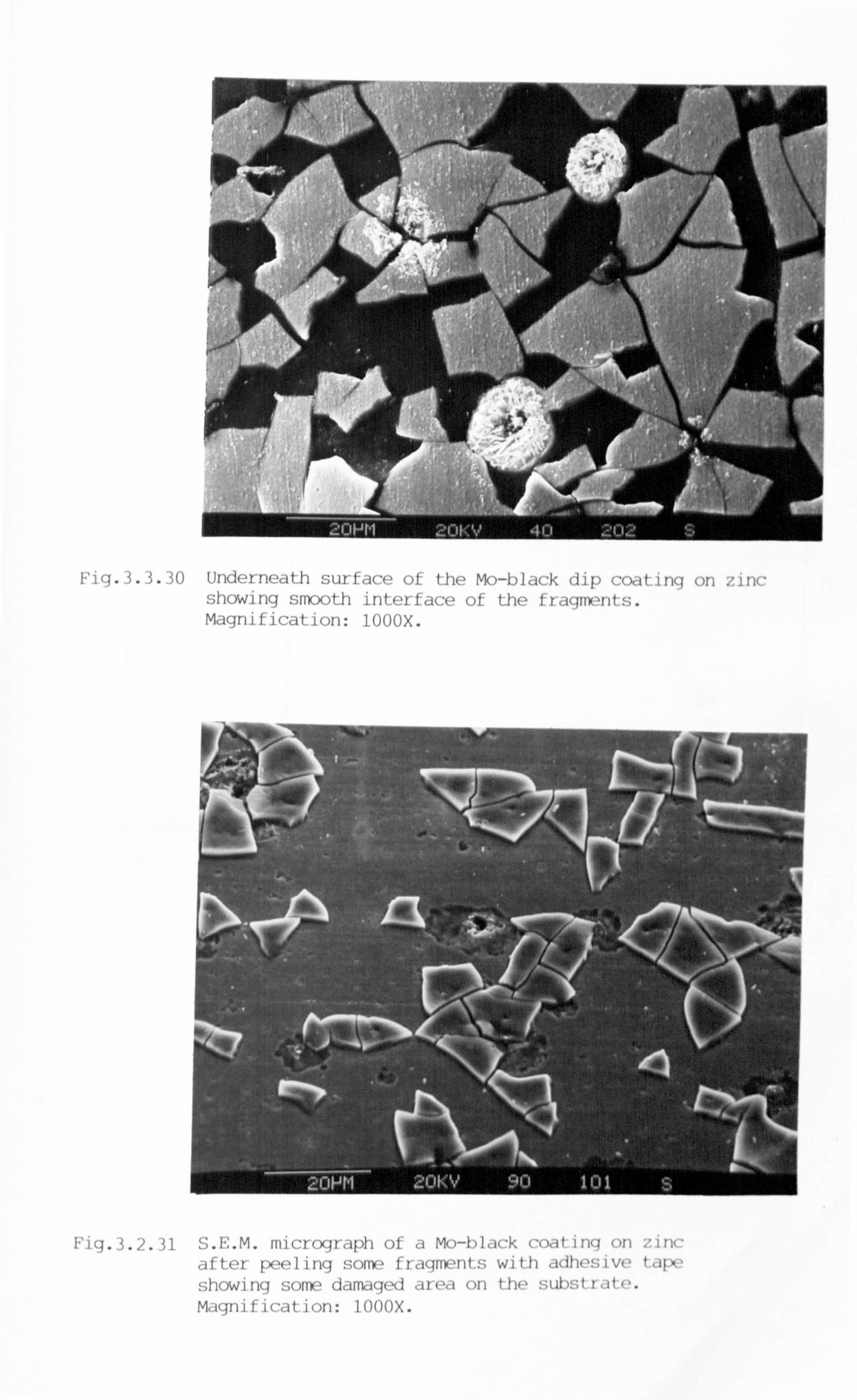
Fig. 3.3.30 Underneath surface of the Mo-black dip coating on zinc showing smooth interface of the fragments. Magnification: 1000x.
S. E. M. III. icrograph of a Mo-b1cick co, it inq ()Ii ýiiv after peeling some fraqment-s with adhesive tape showing some damaged area on the sLjl)gt rdt Magnification: 1000X.
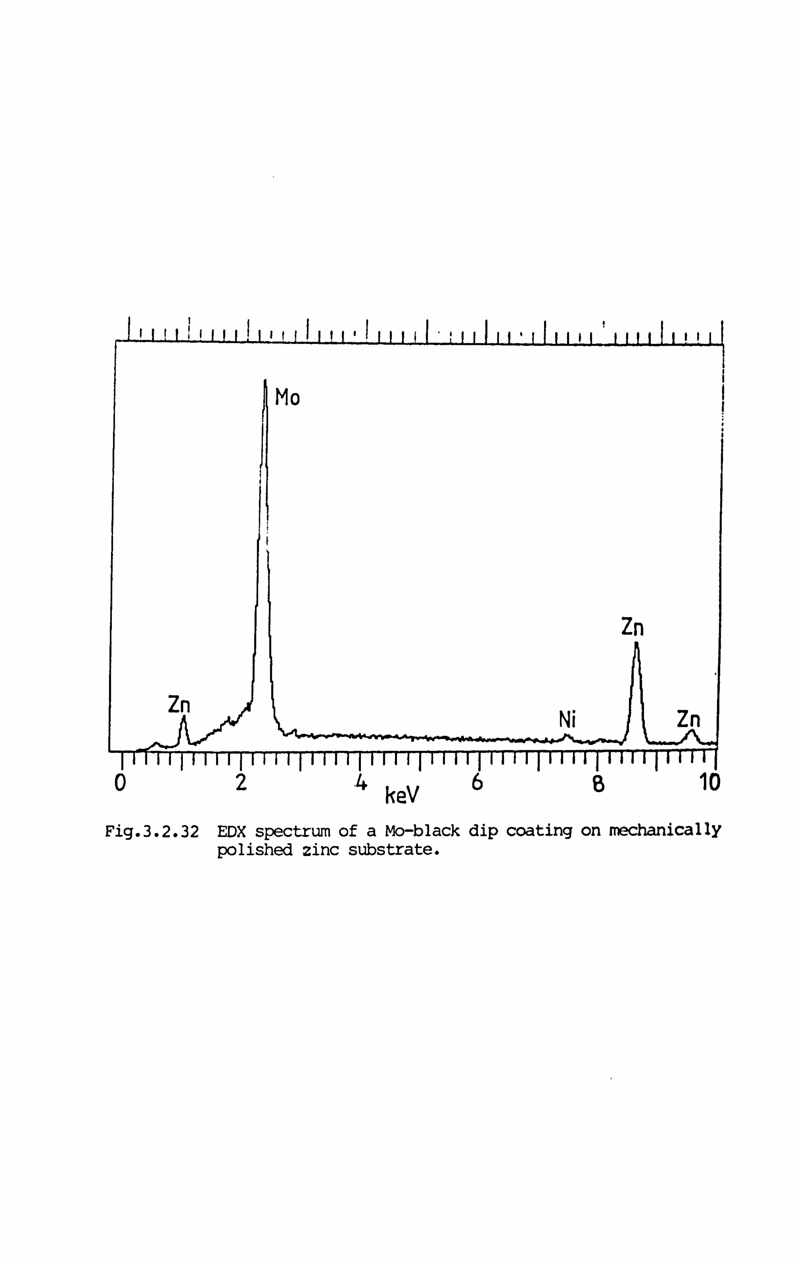
r%t: v
Fig. 3.2.32 EDX spectrum of a Mo-black dip coating on mechanically polished zinc substrate.
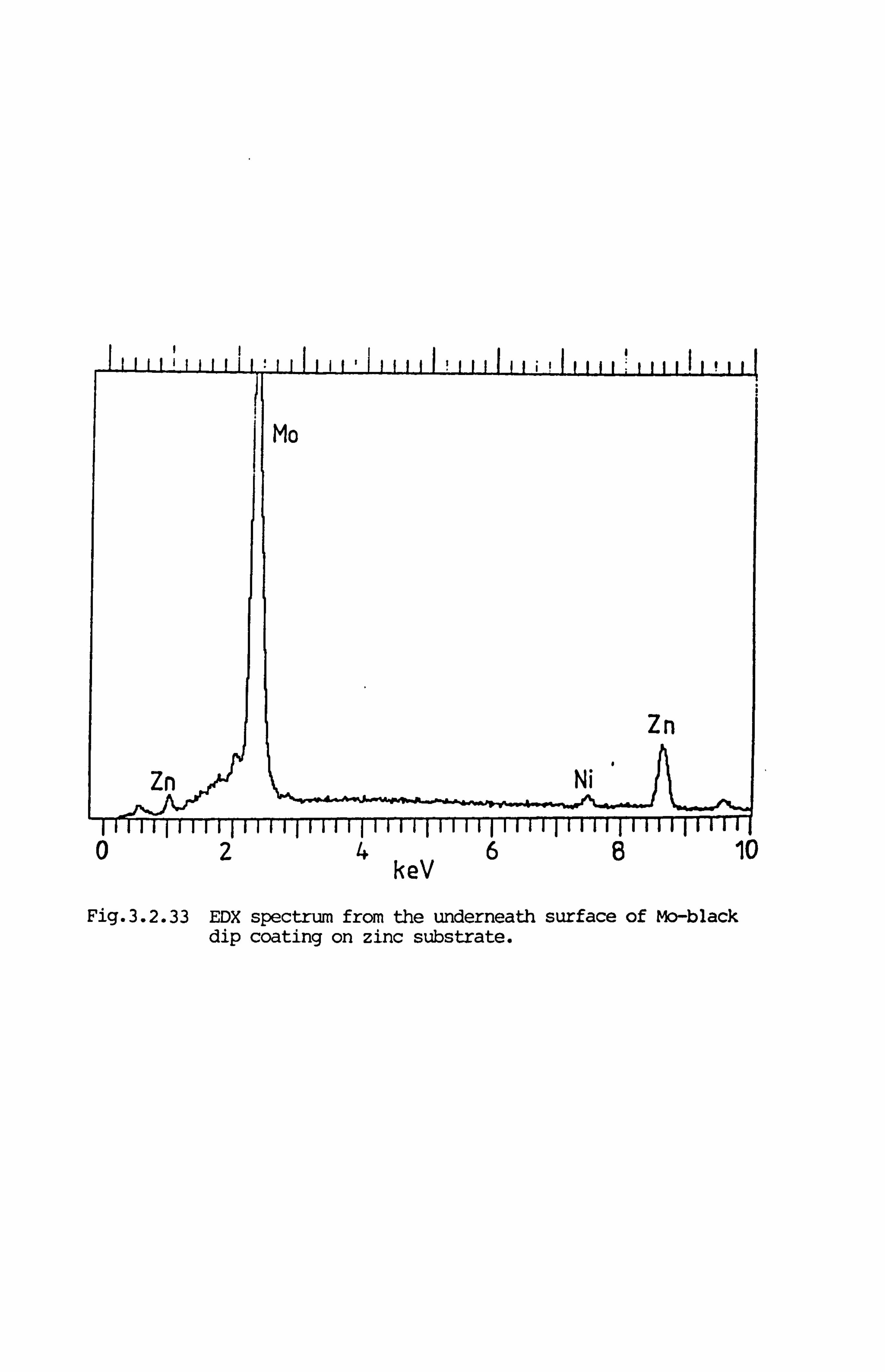
Fig. 3.2.33 EDX spectrum from the underneath surface of Mo-black dip coating on zinc substrate.
4 keV
6 10
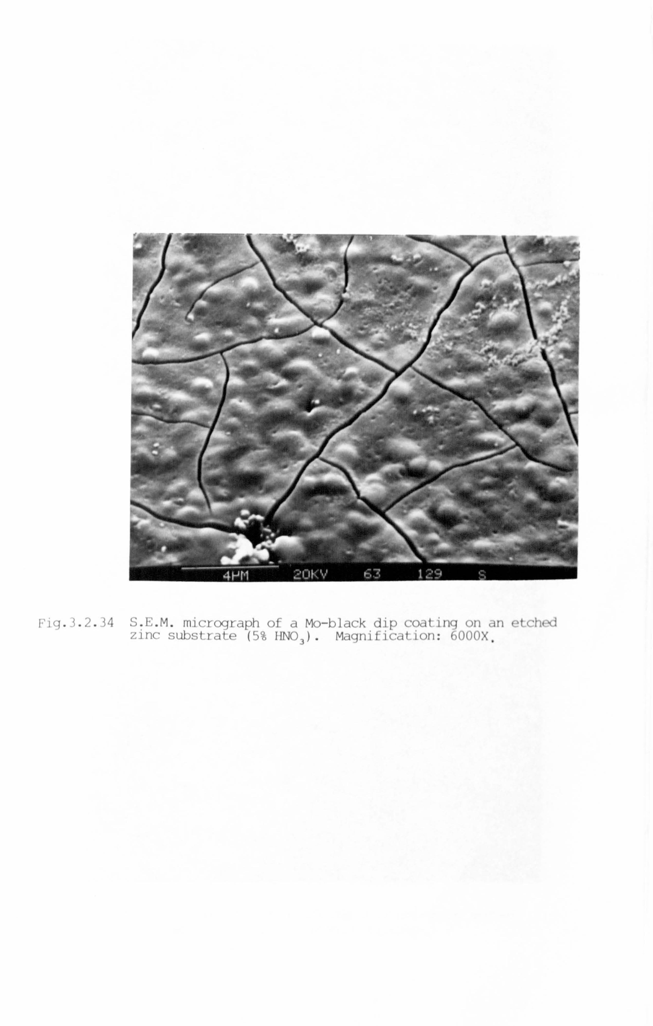
Fig. 3.2.34 S. E. M. mdcrograph of a Mo-black dip coating on an etched zinc substrate (5% IINO 3)* Magnification: 600OX.
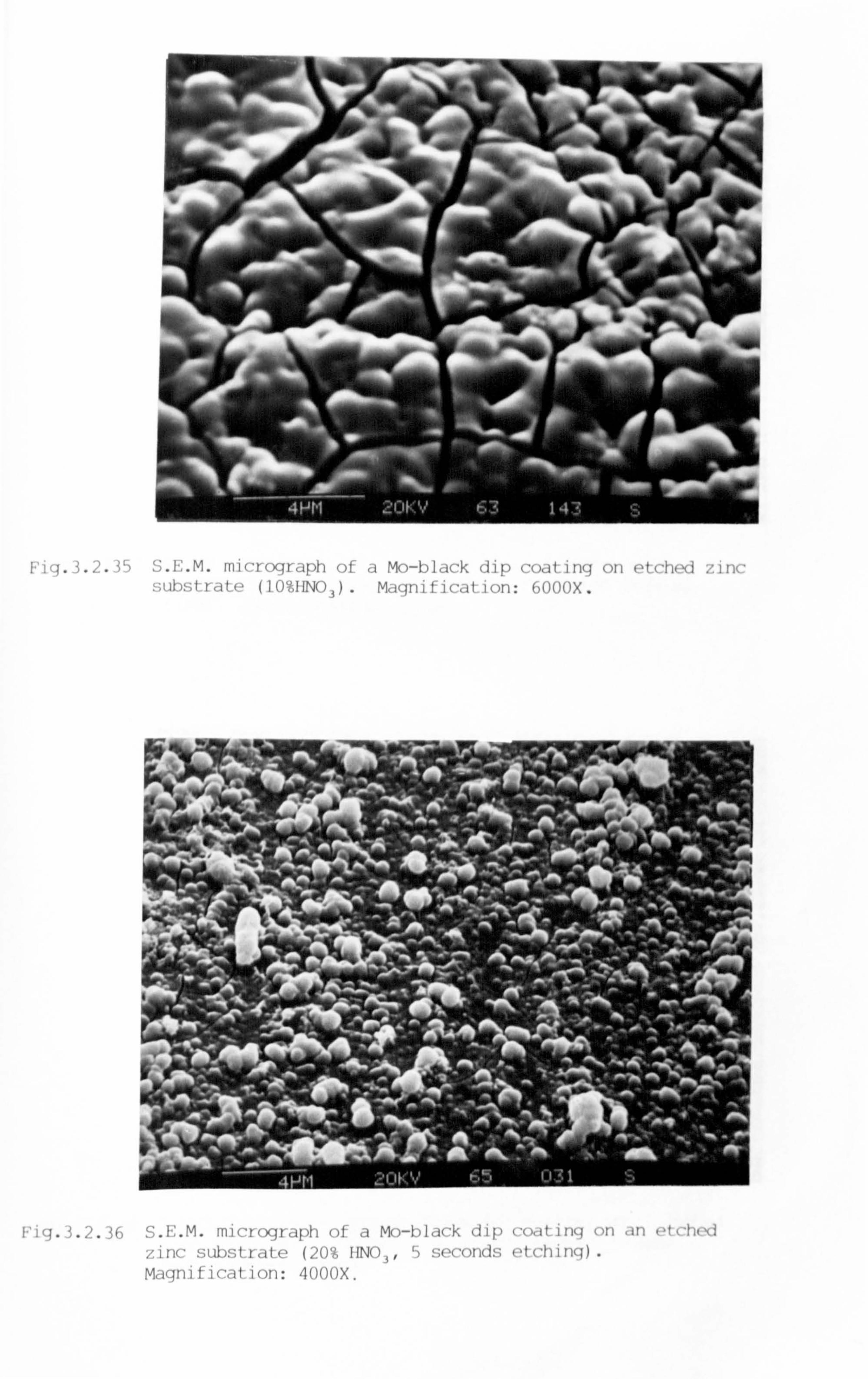
Fig. 3.2.35 S. E. M. micrograph of a Mo-black dip coating on (, t(-h(, (] ýýJjjc substrate (10%HNO, ). Magnification: 600OX.
iI ic s ui)s tIiIe OY, I INO 3' S(ICOI Kh; etdIII 1(j) Magnification: 400OX.
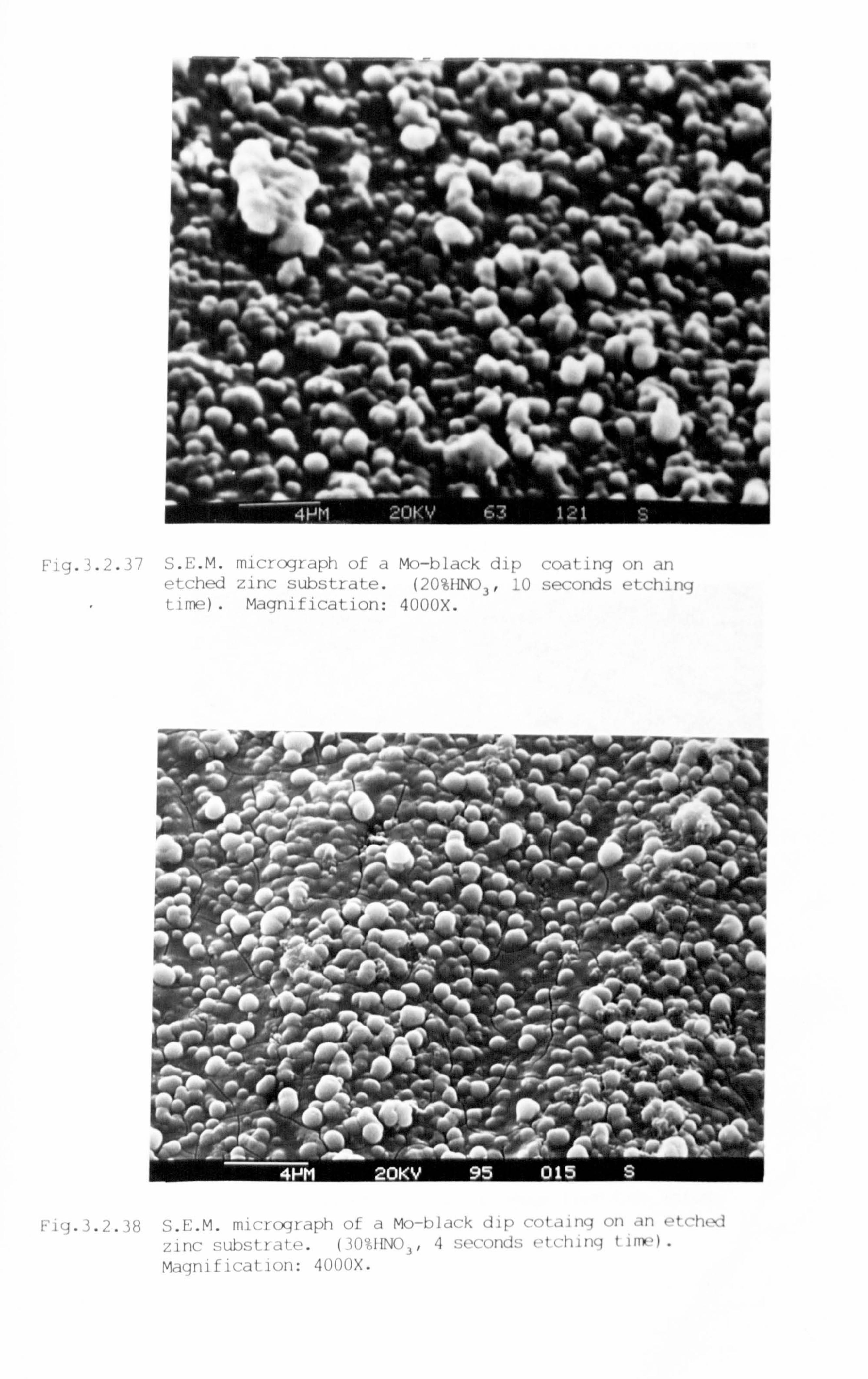
Fig. 3.2.37 S. E. M. micrograph of a Mo-black dip coating on an etched zinc substrate. (20%HNO 3F 10 seconds etching time). Magnification: 400OX.
v i, j . I' .2. WS. E. M. fill ('I ()(I I Ipl I of I M()-I) I'Ick, (IIp, '( )t ,III i(I ( )II . il ýIf,! I, Ik! zinc substrite- (3 OY, I INO
3,4 seconds et Of i rig ti me) . Magnification: 400OX.
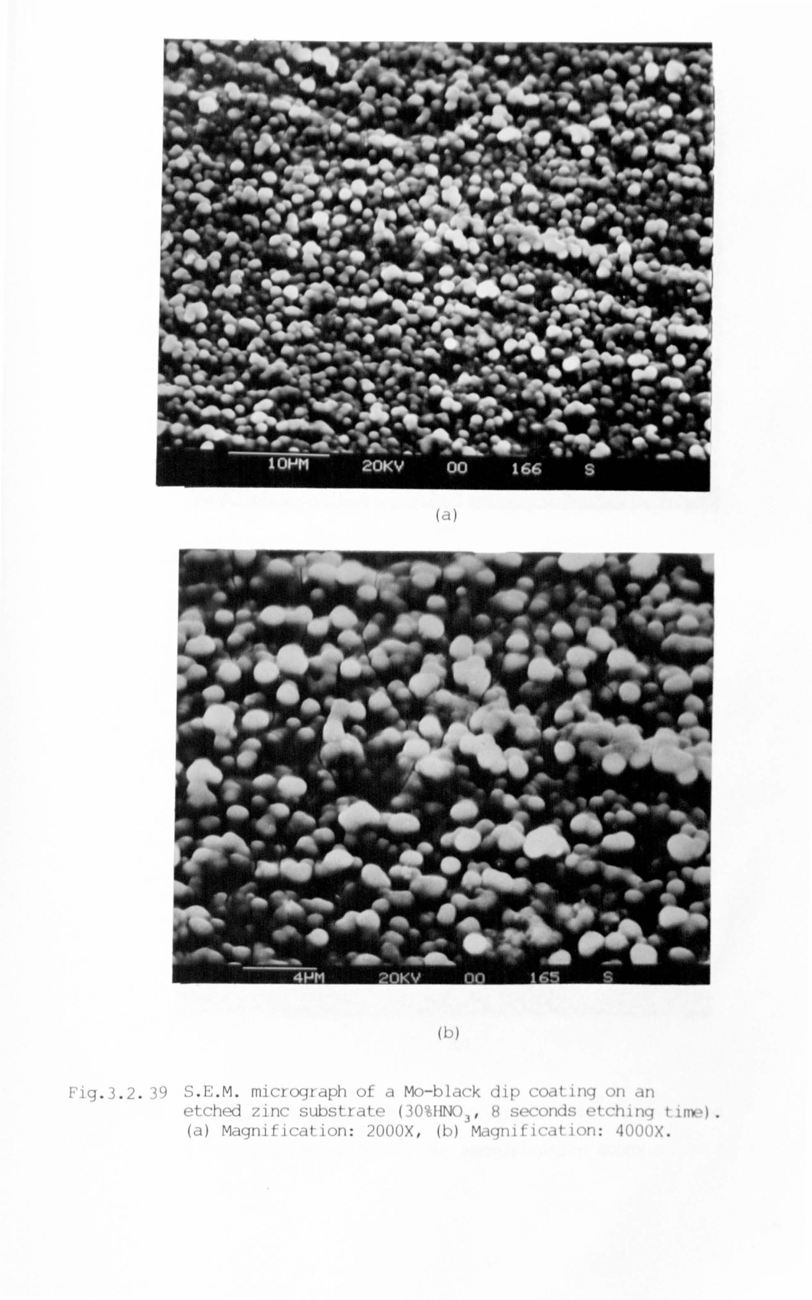
Fig. 3.2.39 S. E. M. mdcrograph of a Mo-black dip coating on an etched zinc substrate (30%IINO
3' 8 seconds etching tirrk-)
(a) Magnification: 200OX, (b) Magnification: 400OX.
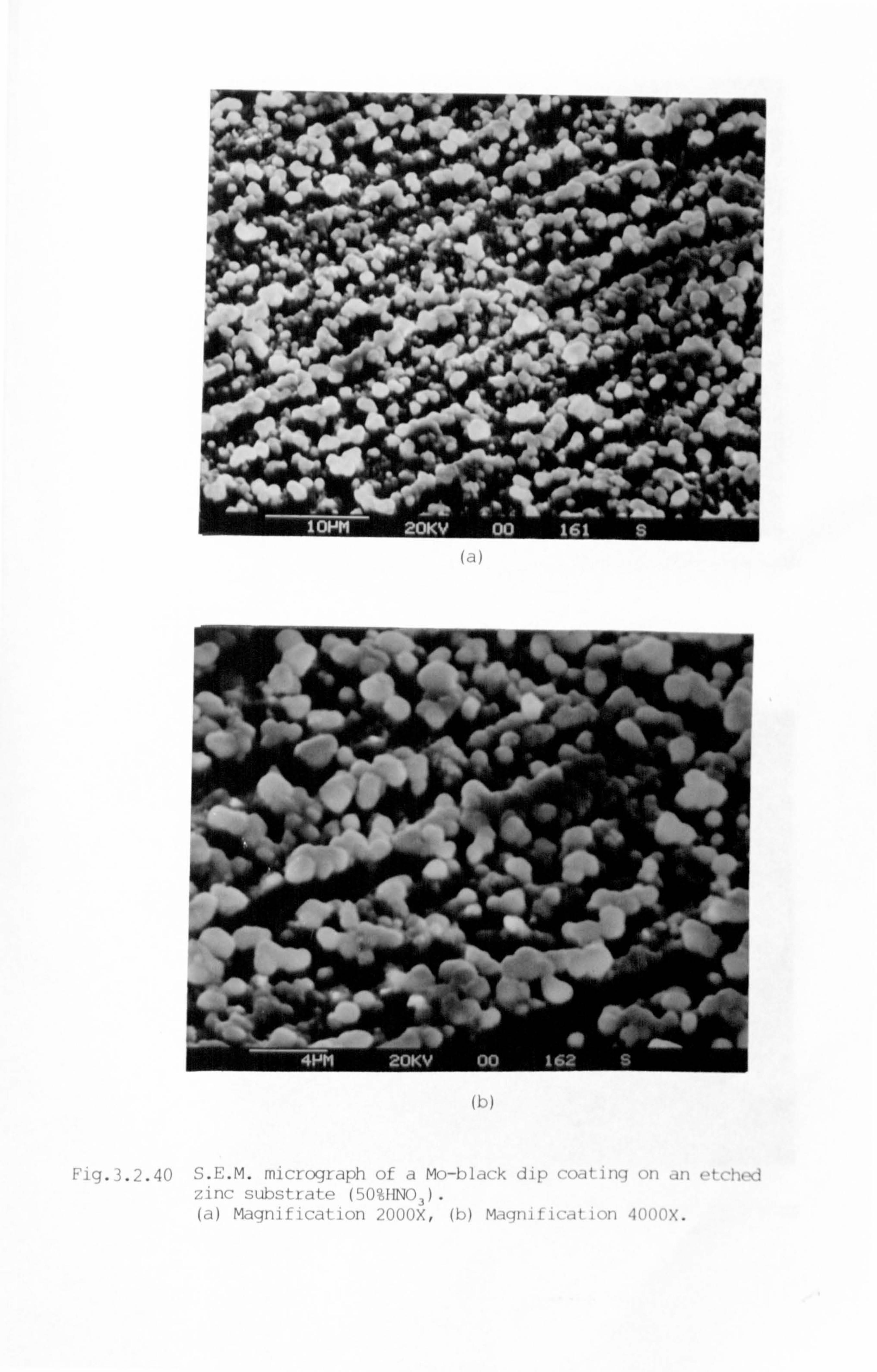
(a)
Fig-3.2.40 S. E. M. micrograph of a Mo-bl, wk dip coating on in etclied zinc substrate (50%HNO
3)' (a) Magnification 200OX, (b) Maqnification 400OX.
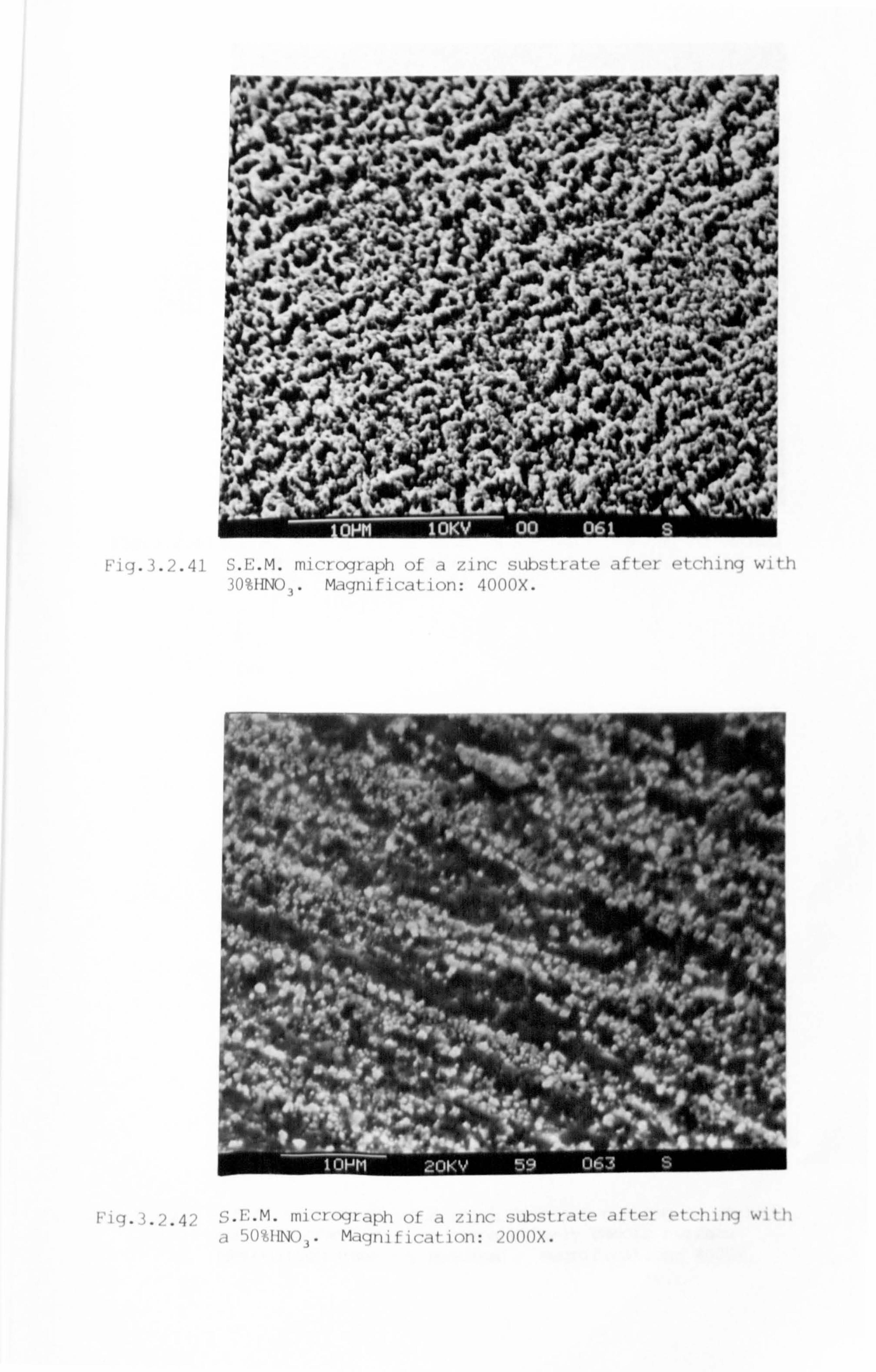
Fig. 3.2.41 S. H. M. micrograph of a zinc subst rat (, af t (, r ot ch i rici wi t 11 30%HNO 3* Magnification: 400OX.
: ;J'. illlý 1 11 11 .II, II, )I, IIIIk1ýtIi,:; tI 11 -,, 11 1, I,,.,:.:.,,,
a bOMNO.. Maqnification: 200OX.
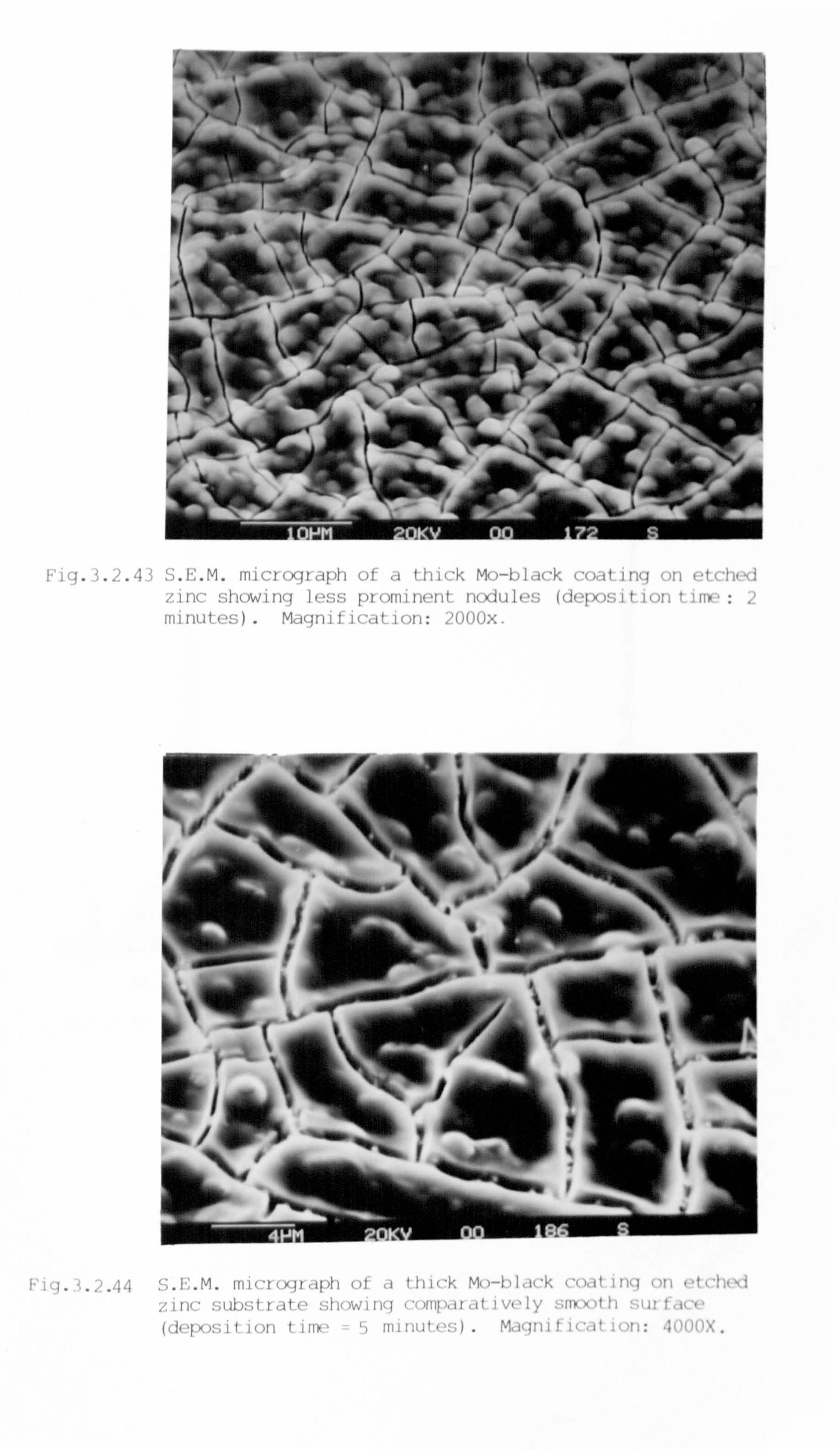
ig. 3.2.43 S. E. M. micrograph of a thick Mo-black coating on etched zinc showing less prominent nodules (deposition time: 2 minutes). Magnification: 2000x.
zinc substrate showing comp, it, it jv,, Iy smooth surface (depos it ion ti irx, ) minut(, ýi) . Maqnificatlon: 400OX.
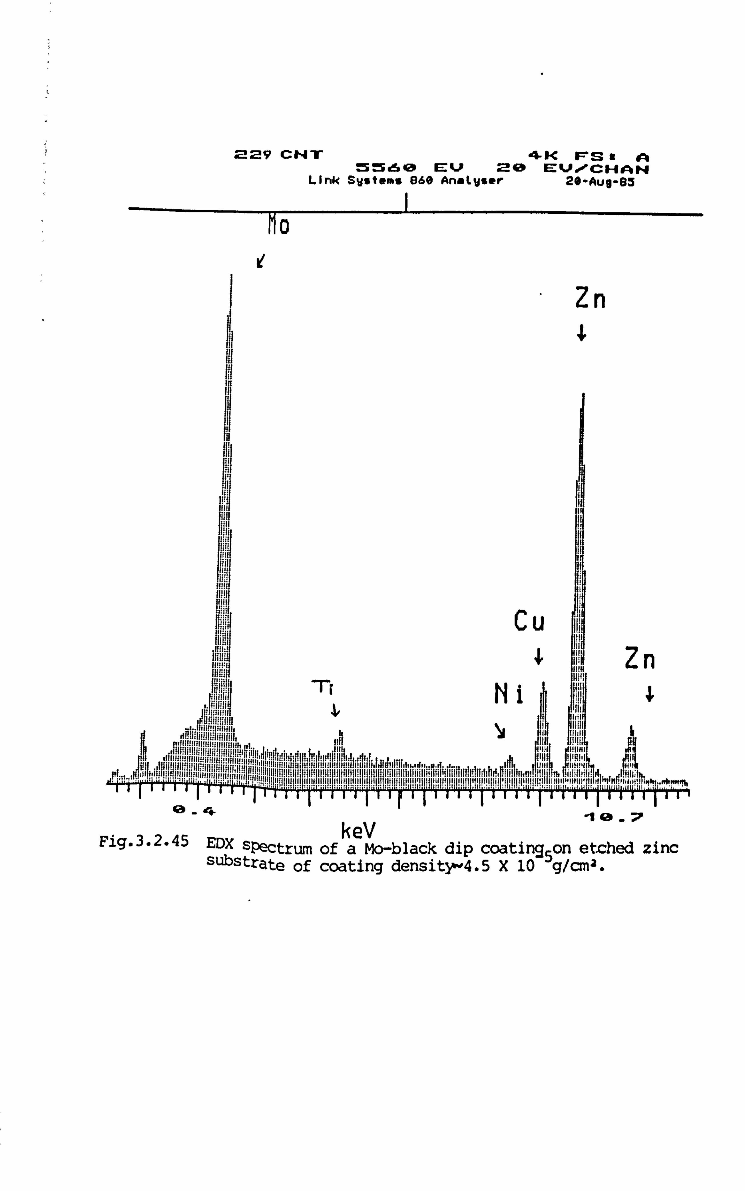
ME- 29cN «ir db- X Er, saA z25464a E: qj 2! giN Ezudopc"AN
Link Systems (360 Anntyser 20-Aug-83
0 v
keV Fig. 3.2-45 EDX sPectrum of a Mo-black dip coatin95 on etched zinc substrate of coating density-4.5 X 10 9/cma-
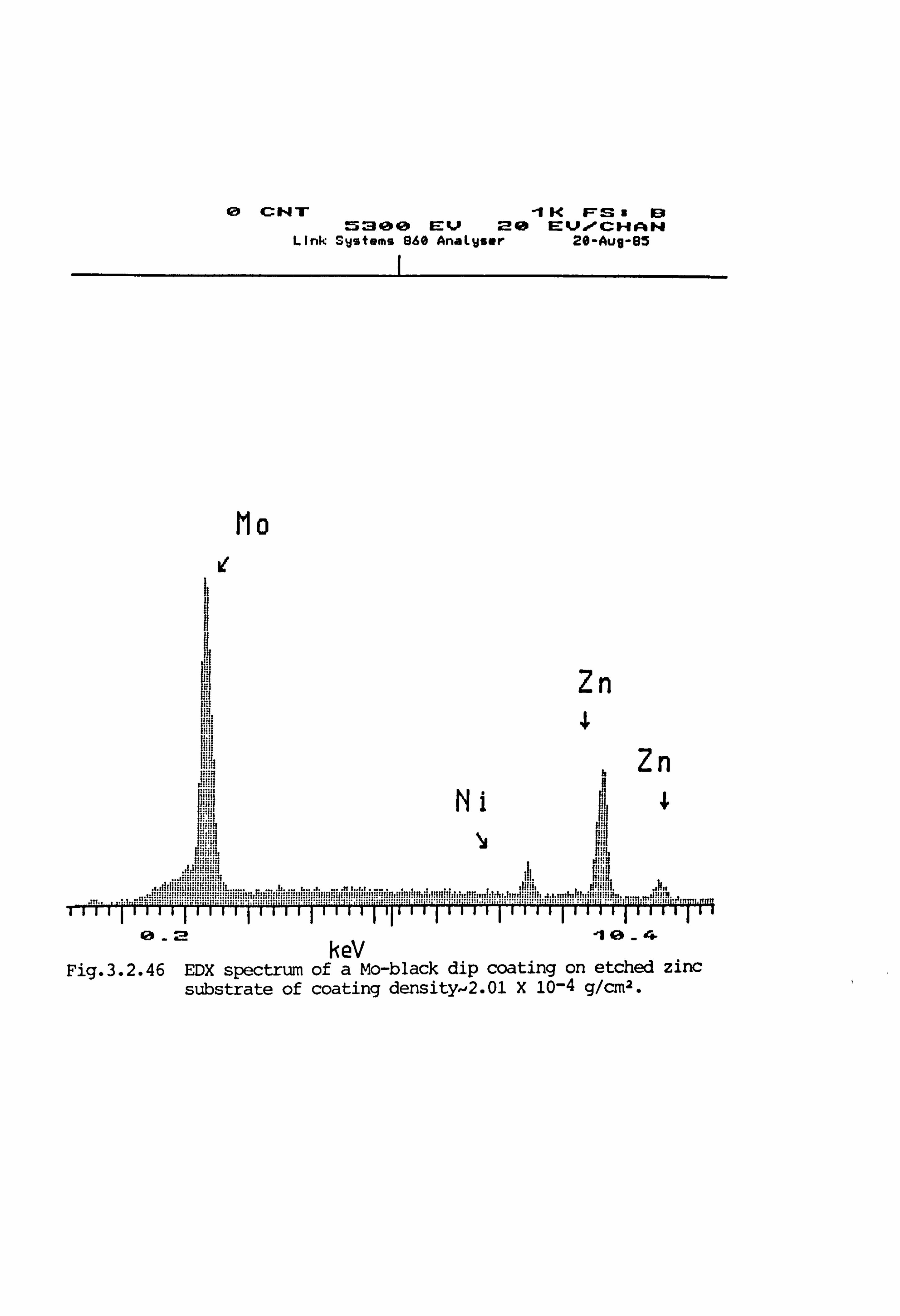
-111K 1=-1135 IE3 rs: 3 00E: v 00 E-VOOCHAN
Link S%jsfems 860 Anal. User 20-Aug-85 I
lb I'
0-M keV
Fig. 3.2.46 EDX spectrum of a Mo-black dip coating on etched zinc substrate of coating density,, 2.01 x 10⁻⁴ g/CM2.
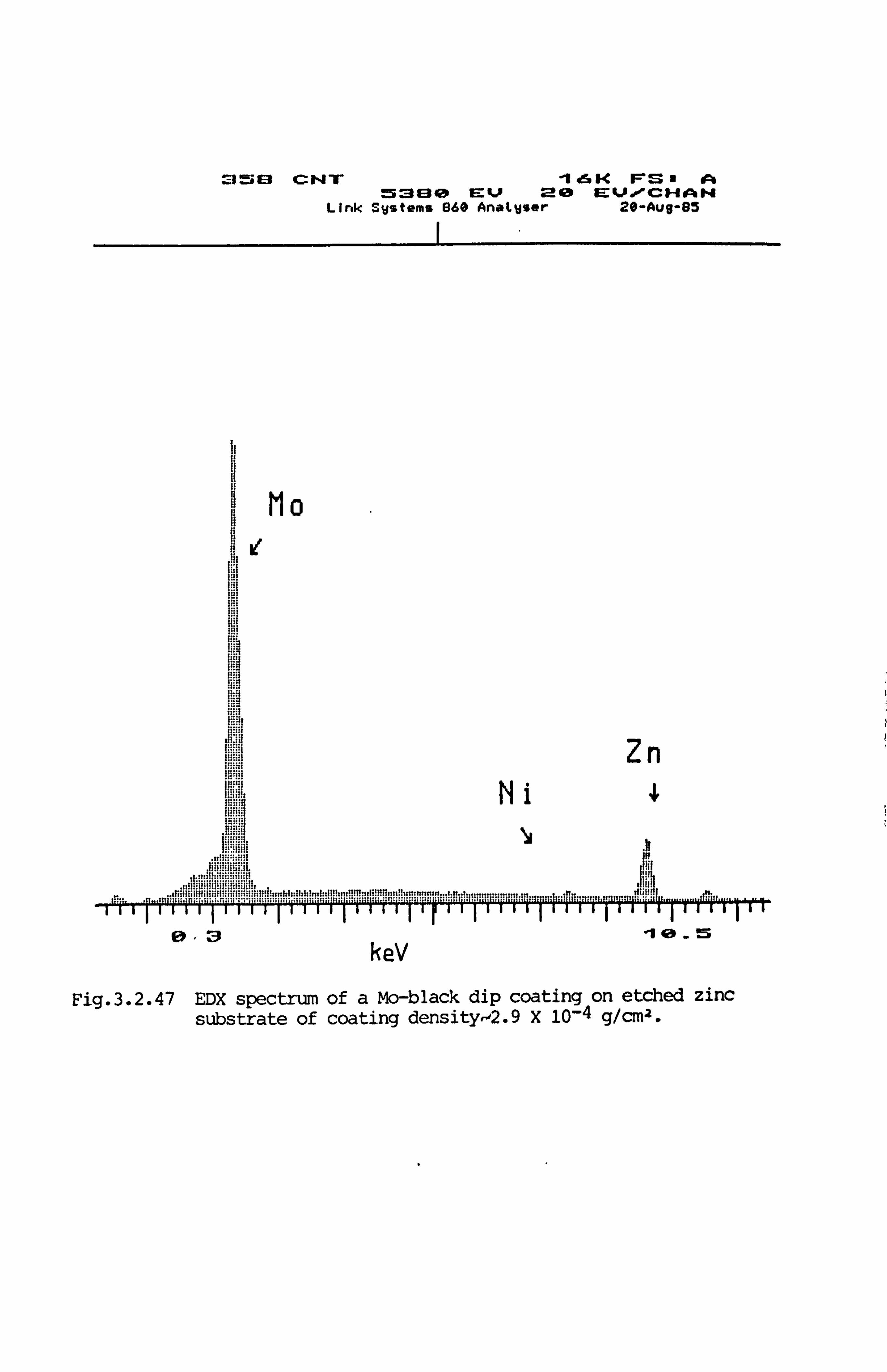
.3M la cN ir A 25: a E3 EN E: v 22! «i9 IIZ vw-e l= HA"
Link Systems 960 Anatuser 20-Aug-85
Fig. 3.2.47 EDX spectrum of a Mo-black dip coating on etched zinc substrate of coating density, -2.9 X 10⁻⁴ g/cm2.
eo El keV
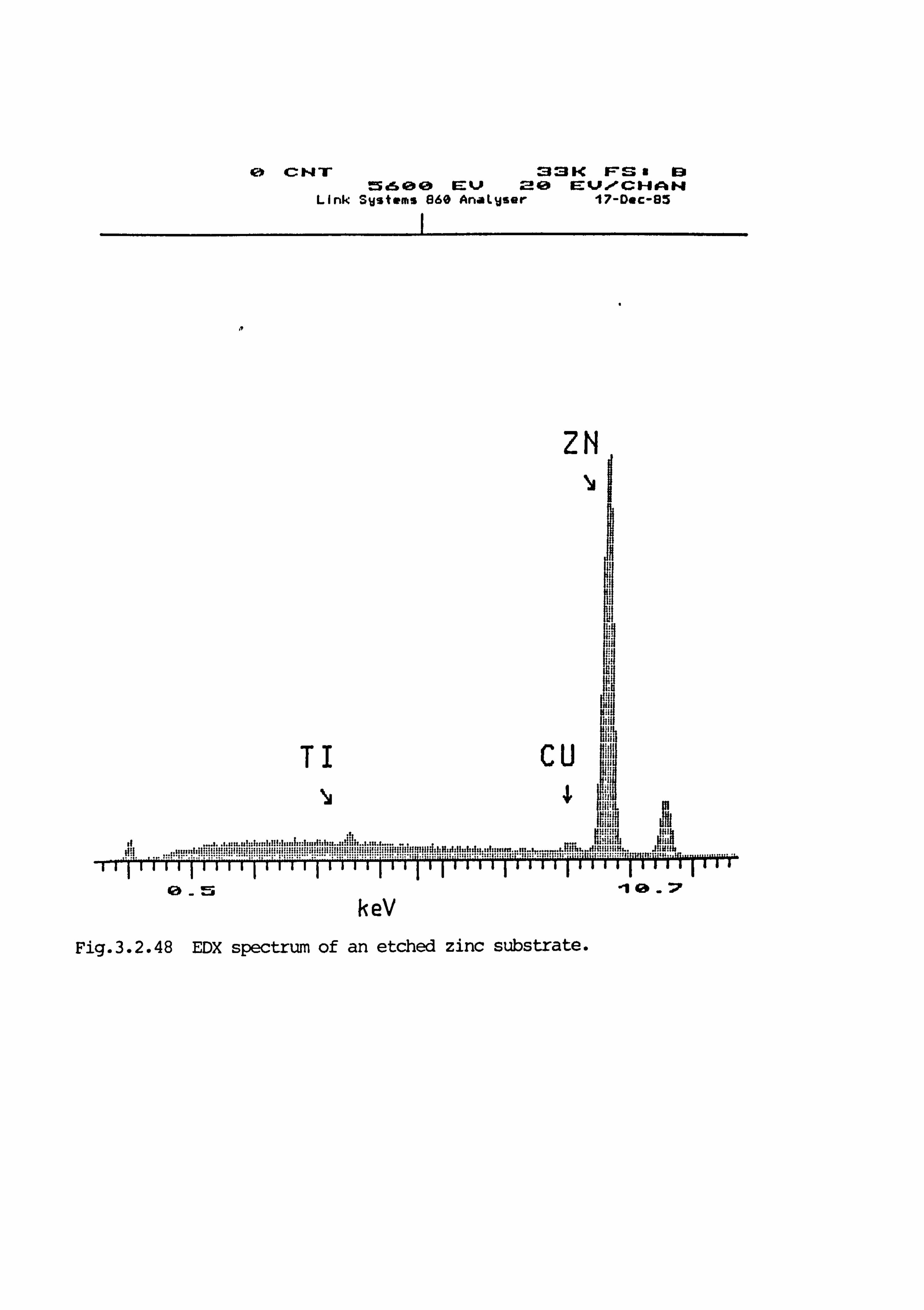
0: 3 K F'S a0 mtsee EZU 0 Ez V. -. * c"A
Link SWstems 860 AnaLyser 17-Dec-85 I
ZN
keV Fig. 3.2.48 EDX spectrum of an etched zinc substrate.
0- Es . 10-7
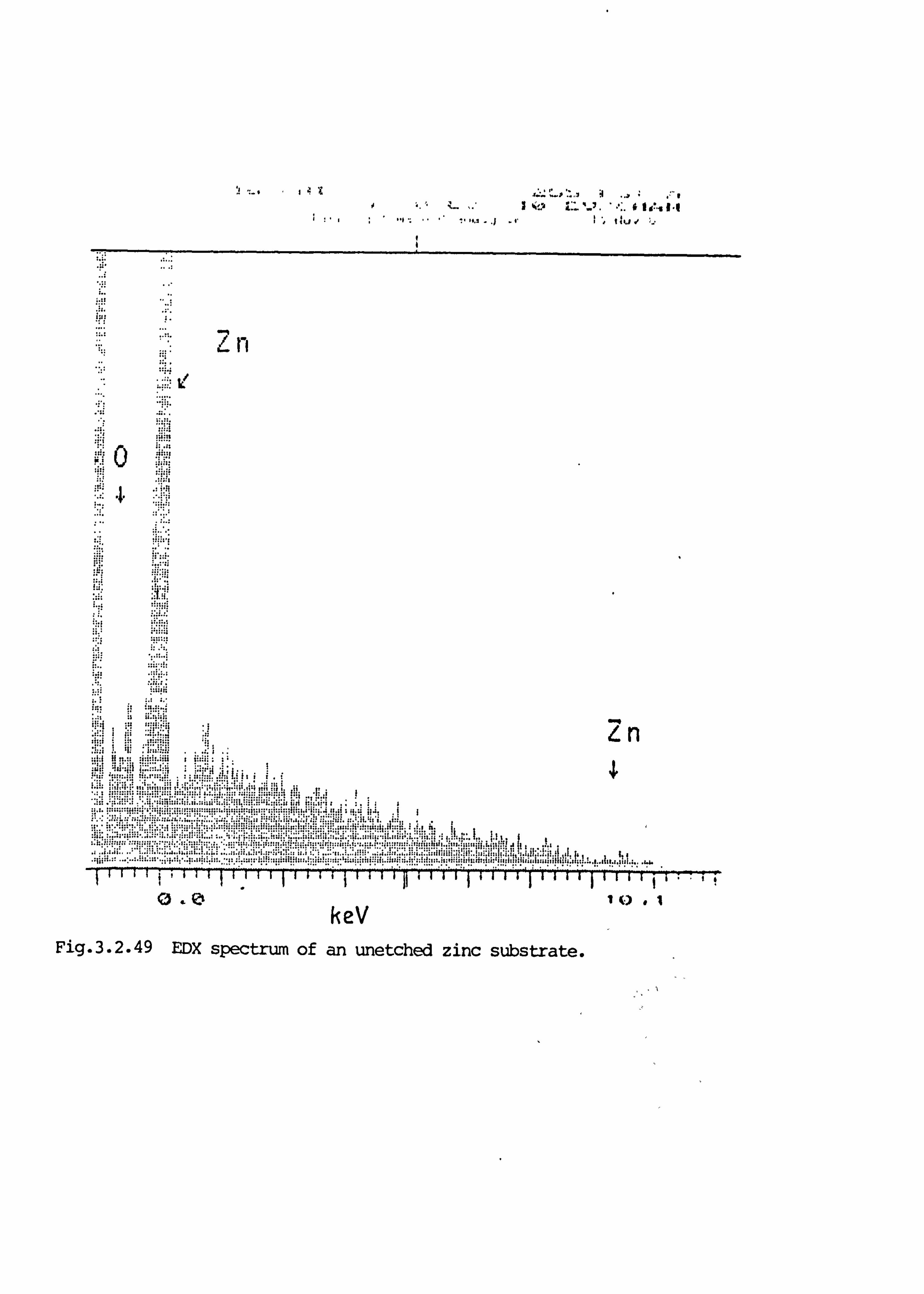
Lp . ý' I
Fig-3.2.49 EDX spectrum of an unetched zinc substrate.
0- Lh 1 (-) 01 kev
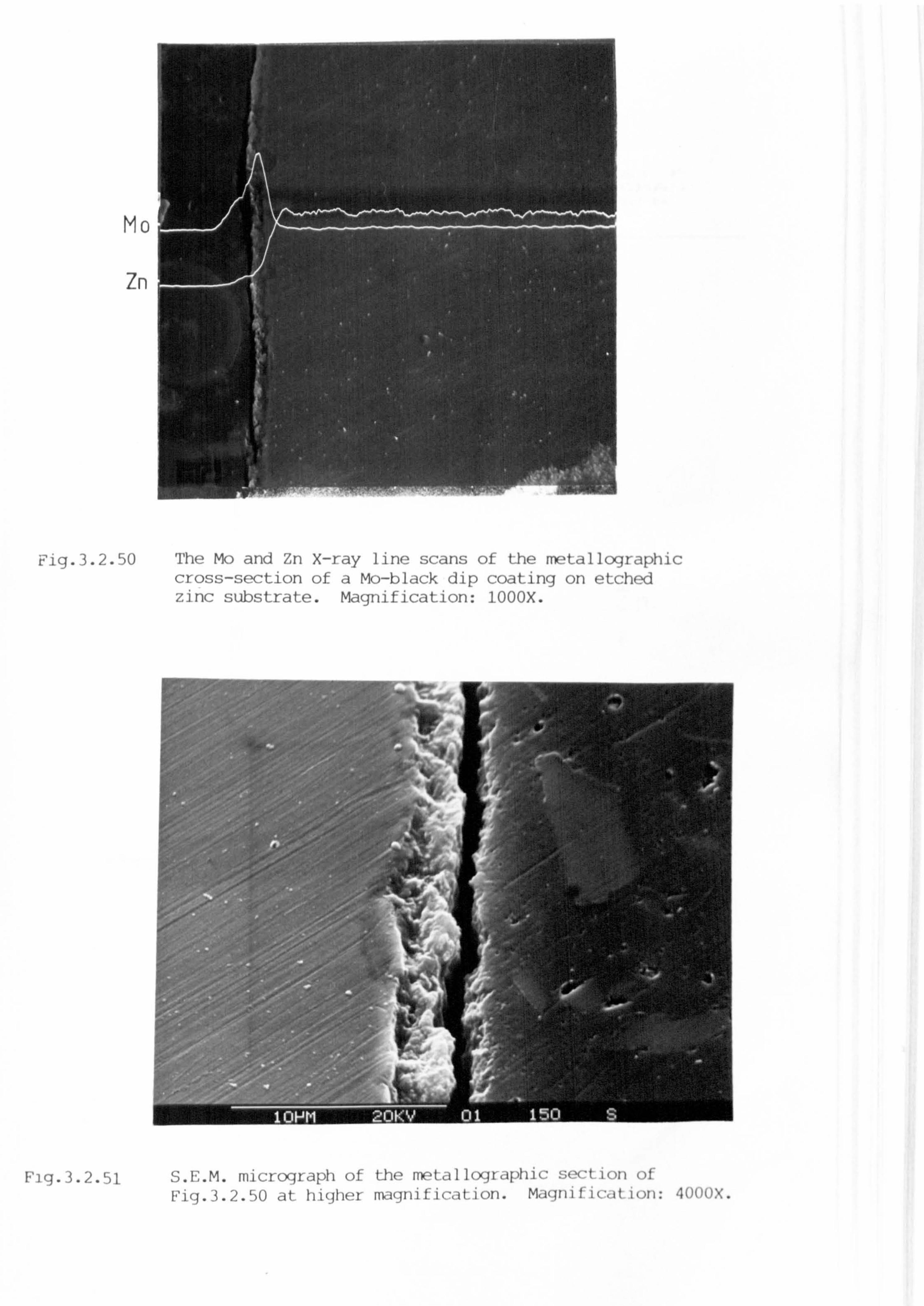
Mo
z
Fig. 3.2-50 The Mo and Zn X-ray line scans of the metallographic cross-section of a Mo-black dip coating on etched zinc substrate. Magnification: 100OX.
"; I: M III I (-: I u, j1 11 )11 ()II1 1(' fix ýt, III(), ;I, if )I IIý: ý( ýfI, 'I I, )! Fig. 3.2.50 at higher magnification. Maynilication: 400OX.
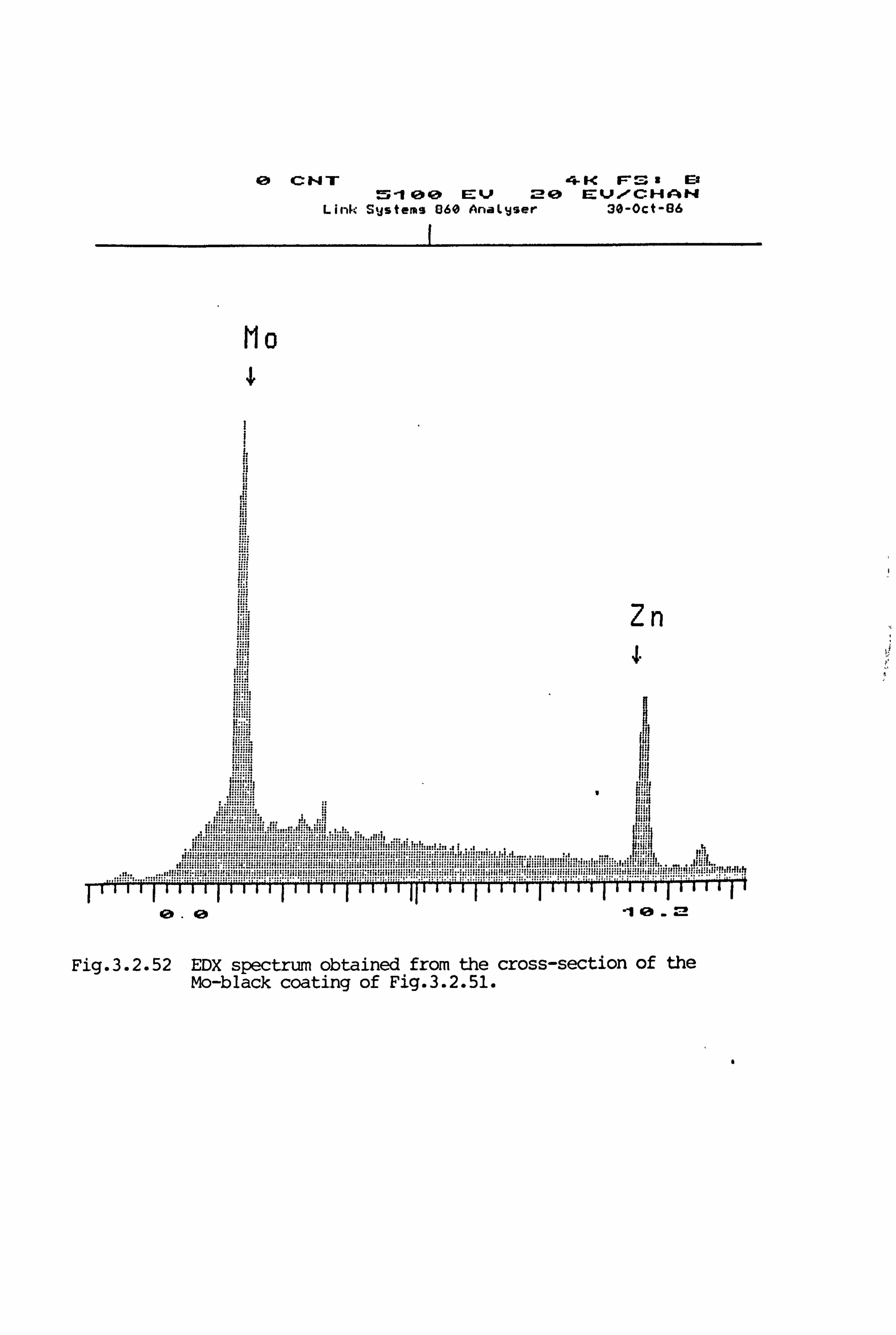
4a cNlr 4- K F, ma E# Z -1 0 ge> EZV. -*«CHAPA
Link Systems 660 Anatyser 30-Oct-86
Mo .1
Fig. 3.2.52 EDX spectrum obtained from the cross-section of the Mo-black coating of Fig. 3.2.51.
0. da
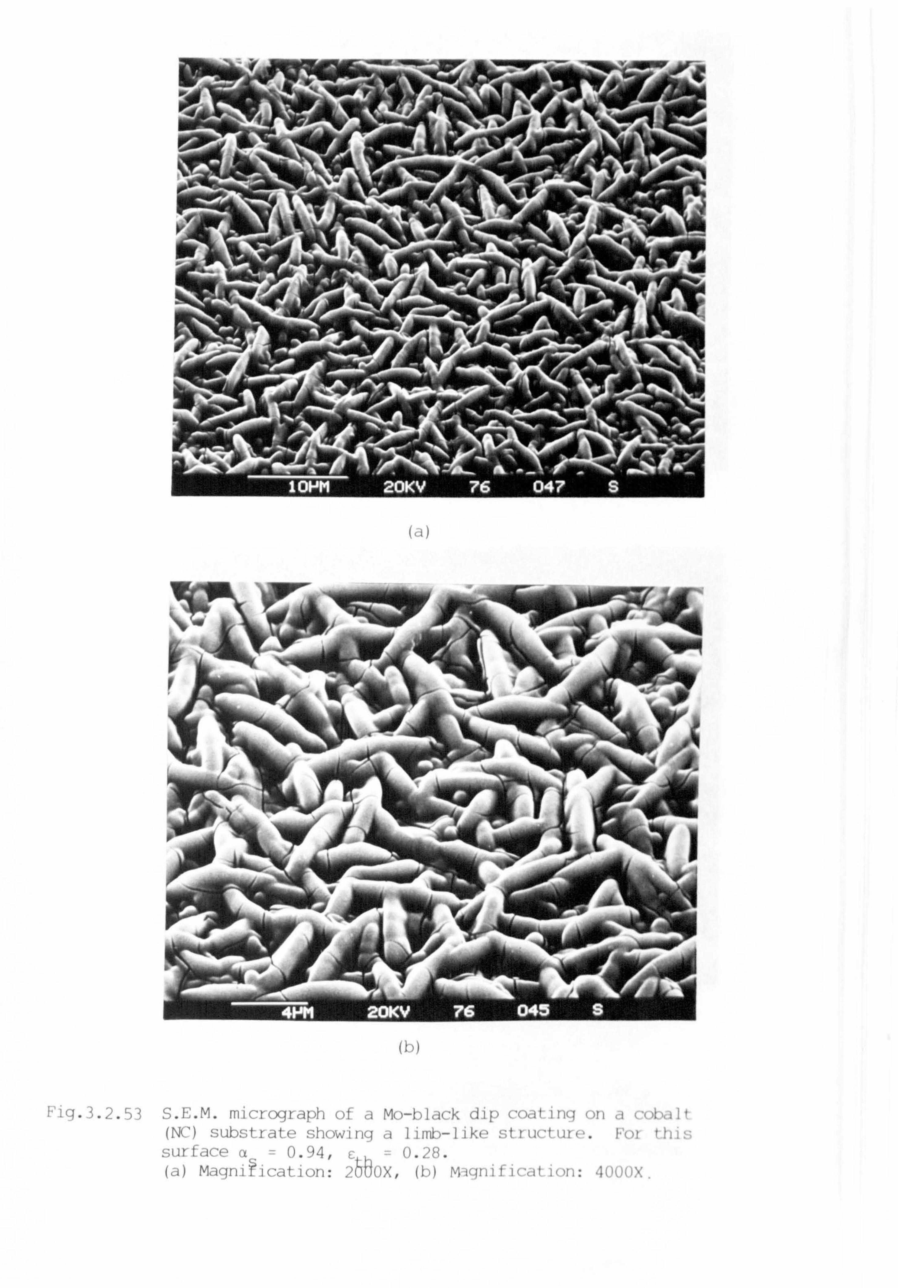
(b)
Fiq. 3.2.53 S. E. M. micrograph of a Mo-black dip coating on a cobalt (NC) substrate showing a limb-like structure. For this surface a=0.94, c=0.28. (a) Magni? ication: AM (b) M-ignification: 400OX.
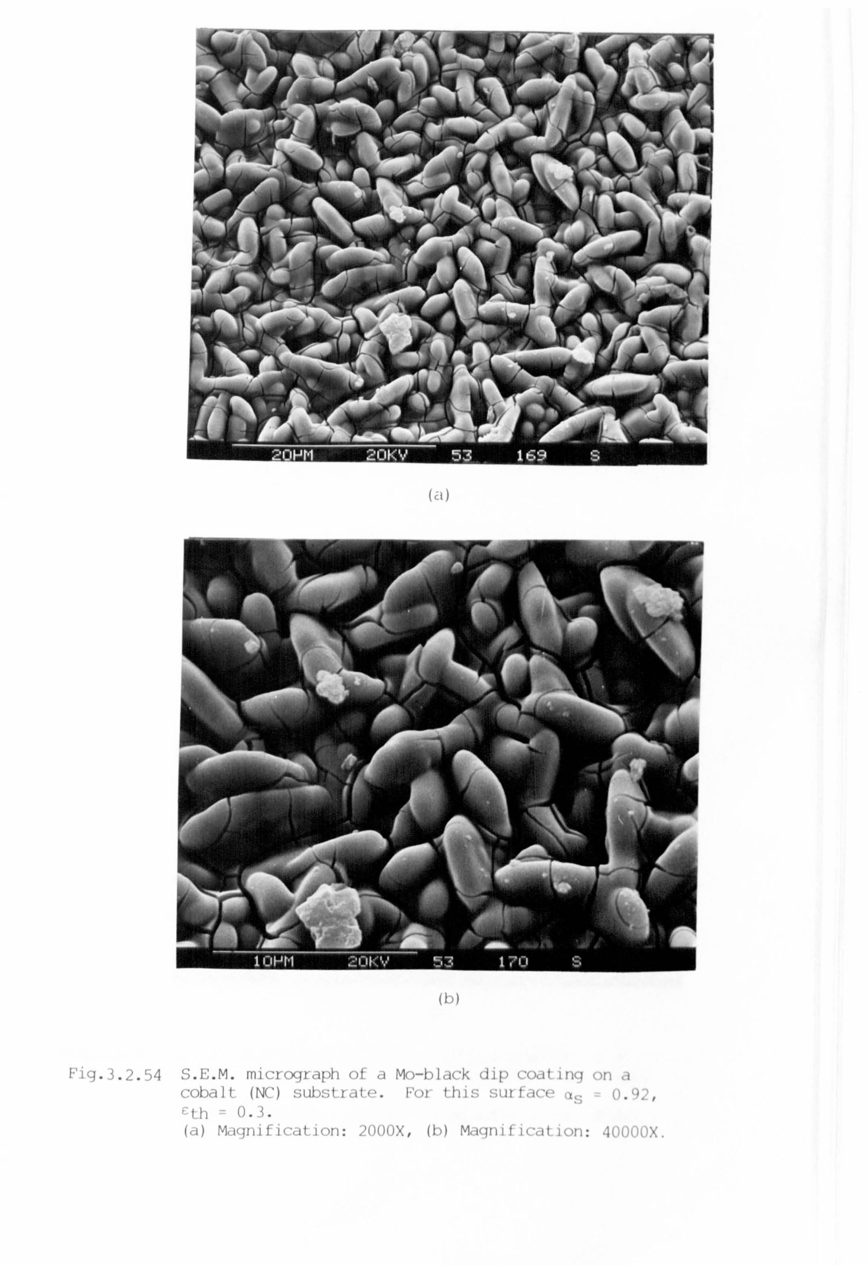
(b)
Fig-3-2.54 S. E. M. micrograph of ý-ý cobalt (NC) substrate. cth = 0.3.
Mo-black dip coating on a For this surface as = 0.92,
(a) Magnification: 200OX, (b) Magnification: 4000OX.
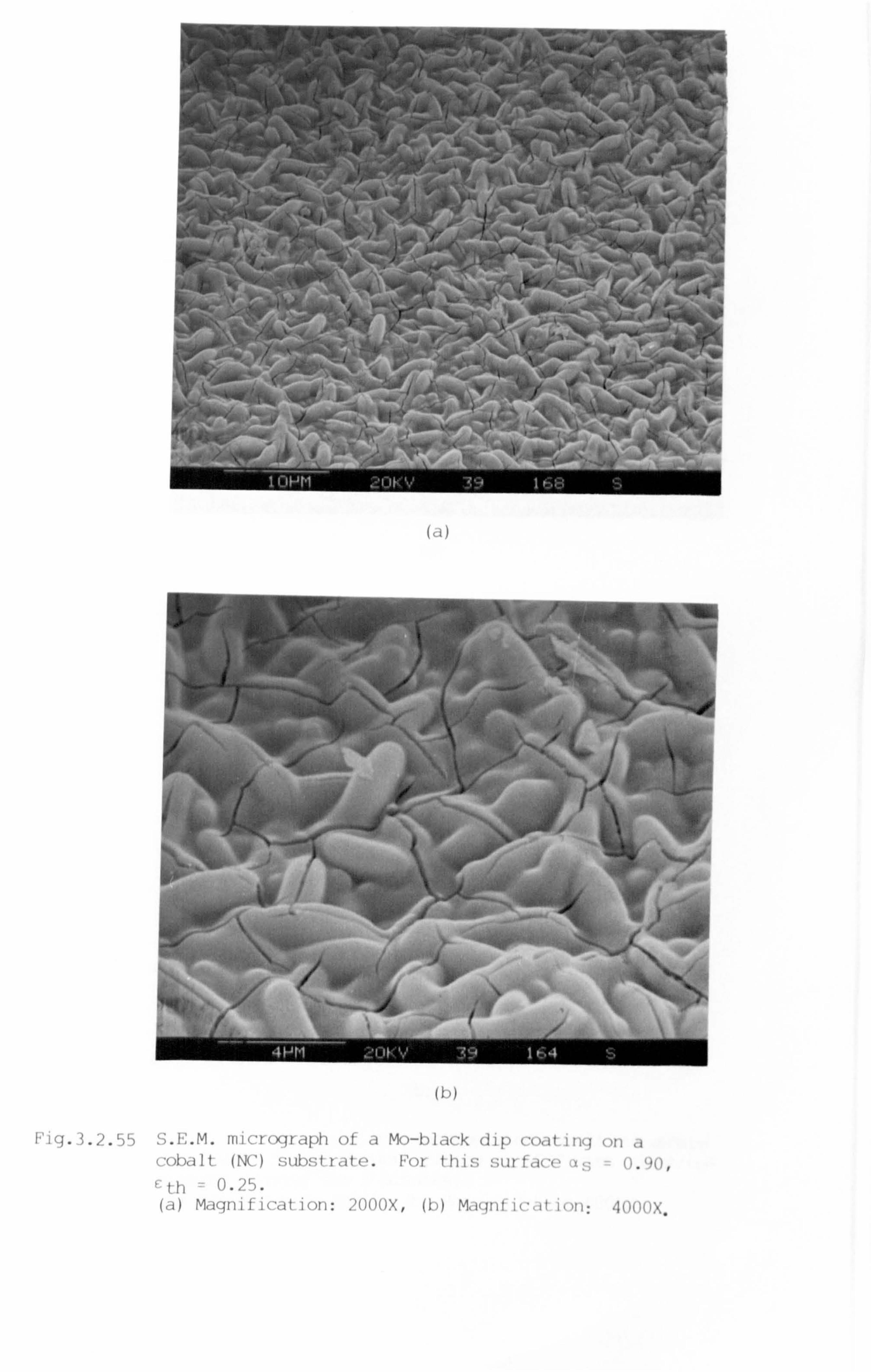
'".
-VL, ý
44e
IA
WO-
4- * L
1"19.3-2.55 S. I-,. M. micrograph of a Mo-black dip coating on a cobalt (NC) substrate. For this surface a.,; - 0., )(), rth - 0.25. (a) Magnification: 200OX, (b) 400()X.
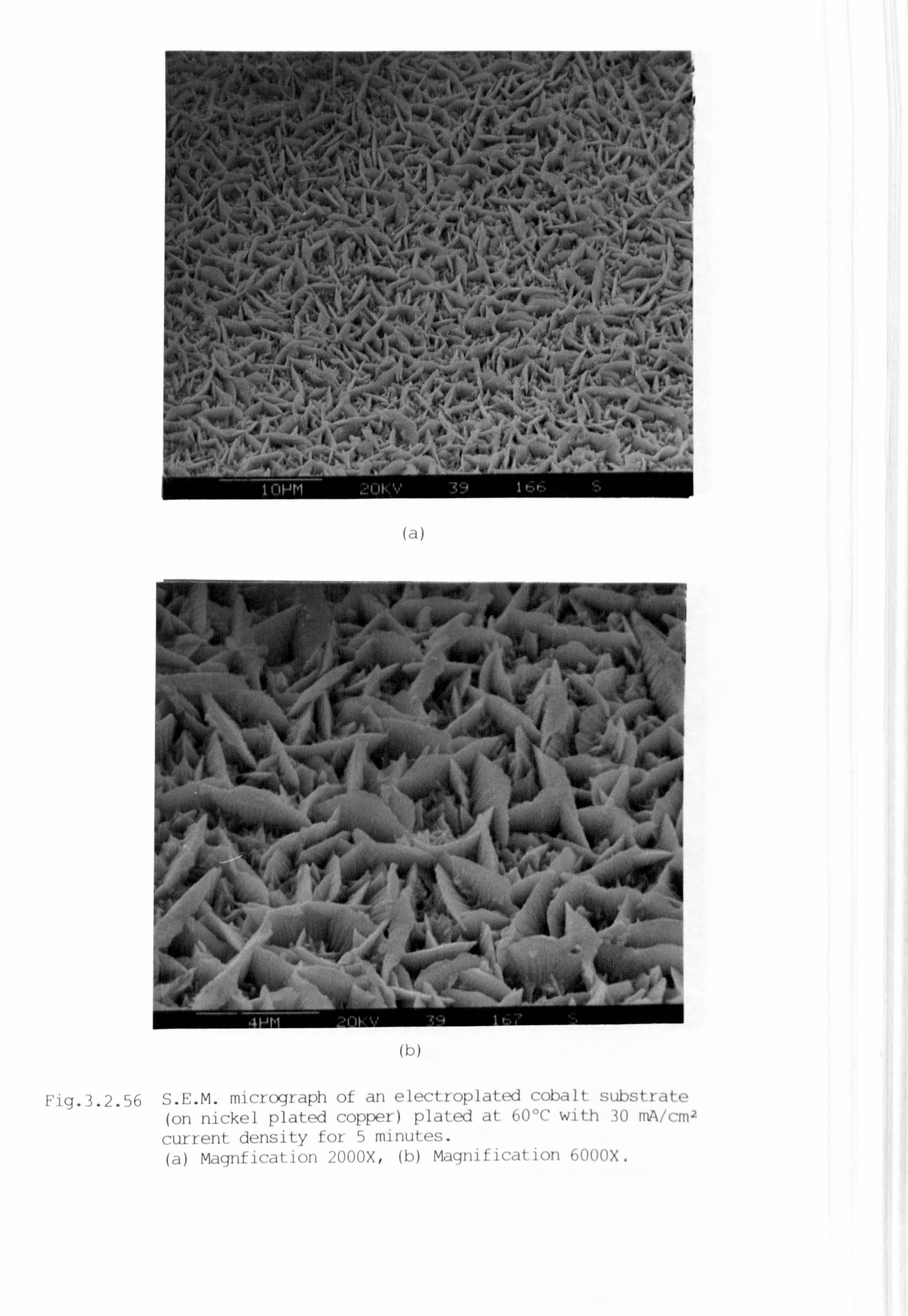
44 w
Vý ilk
>
40p,
0 1, #ýk '119 rw, *Aw ,,, 0.
,Iý jo. .. ' '.
I-. '- &V 7 Aw I, I It
'ý*; oil. qk-4ý; ' ý 4r .4 #11
'w - 4, v 'Iýk I
V, . -V4
I-I ý'. "". %- Itv. - -or -
"(ý' ., '' P'. ý wo%
.ý. I
-AAt & Im-,
()
,'i
"V .
". !
Fig. 3.2.56 S. E. M. micrograph of an electroplated cobalt substrate (on nickel plated copper) plated at 600C with 30 mA/cm2 current density for 5 minutes. (a) Magnfication 200OX, (b) Magnification 600OX.
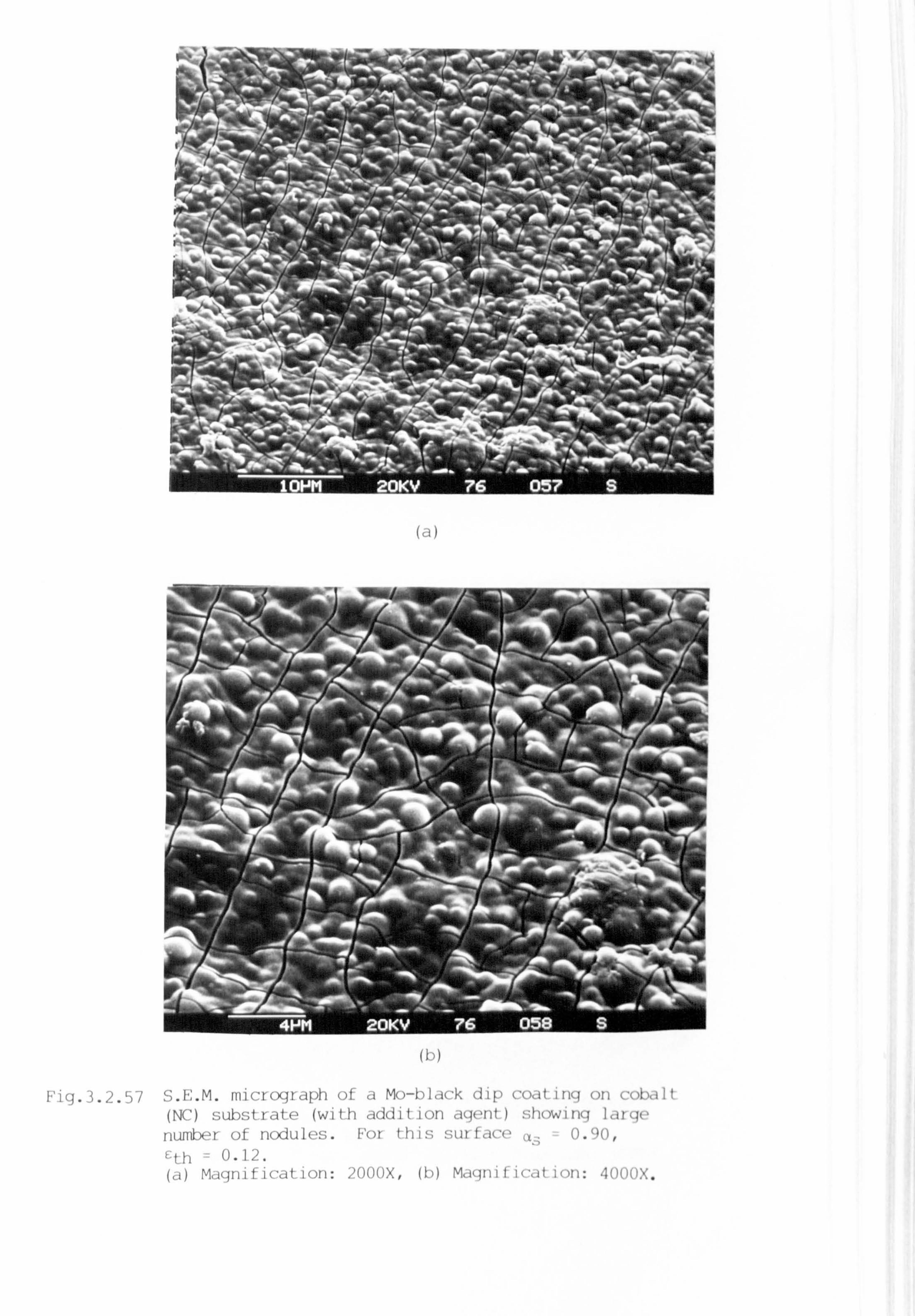
(a)
Fig. 3.2.57 S. E. M. micrograph of a Mo-black dip coatinq on cobalt (NC) substrate (with addition agent) showing large
number of nodules. For this surface 0.90, E: th - 0.12. (a) Magnification: 200OX, (b) Magnification: 400OX.
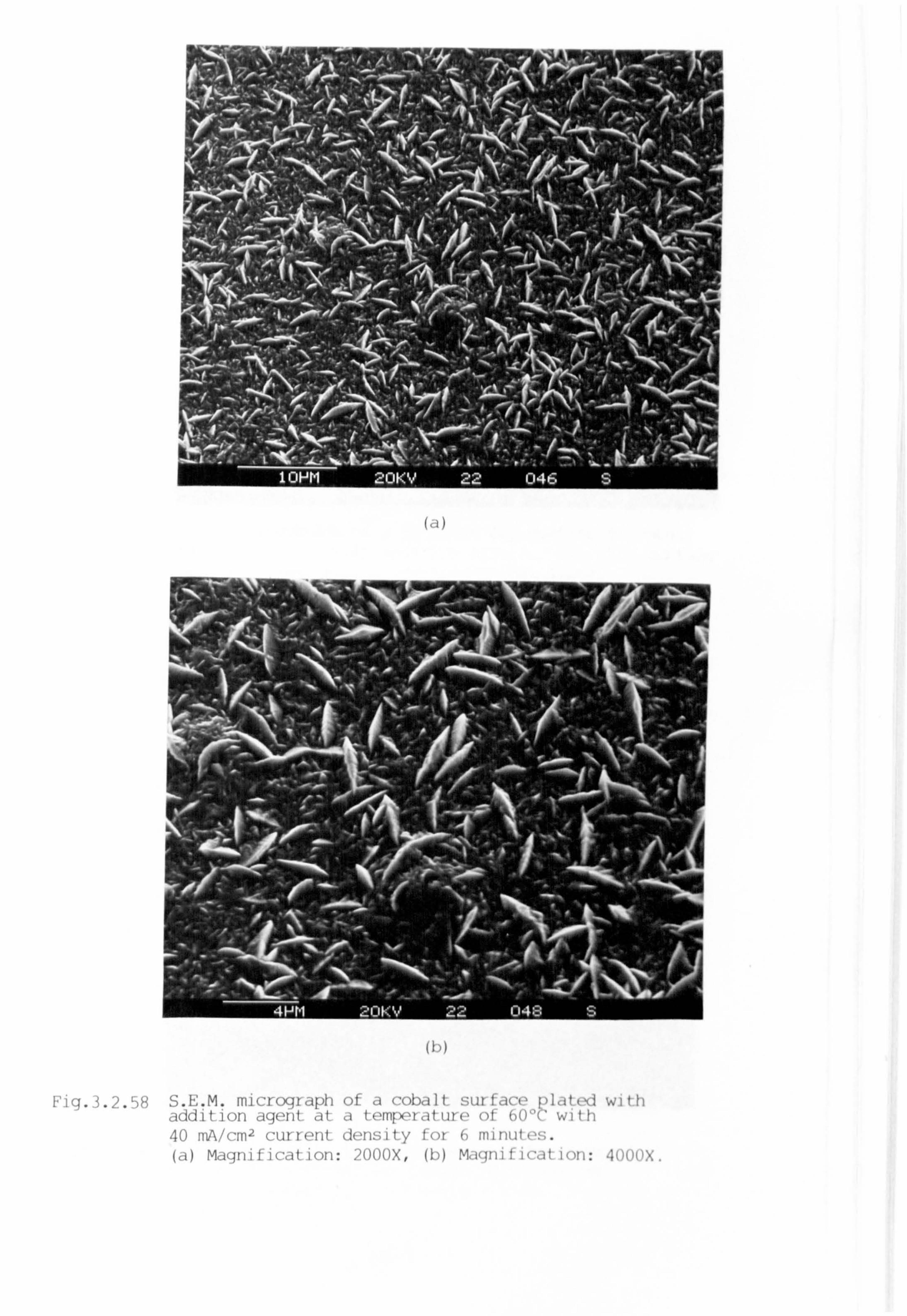
(b)
Fig. 3.2.58 S. E. M. micrograph of a cobalt surface plated with addition agent at a temperature of 60'C with 40 mA/cm2 current density for 6 minutes. (a) Magnification: 200OX, (b) Magnification: 400OX.
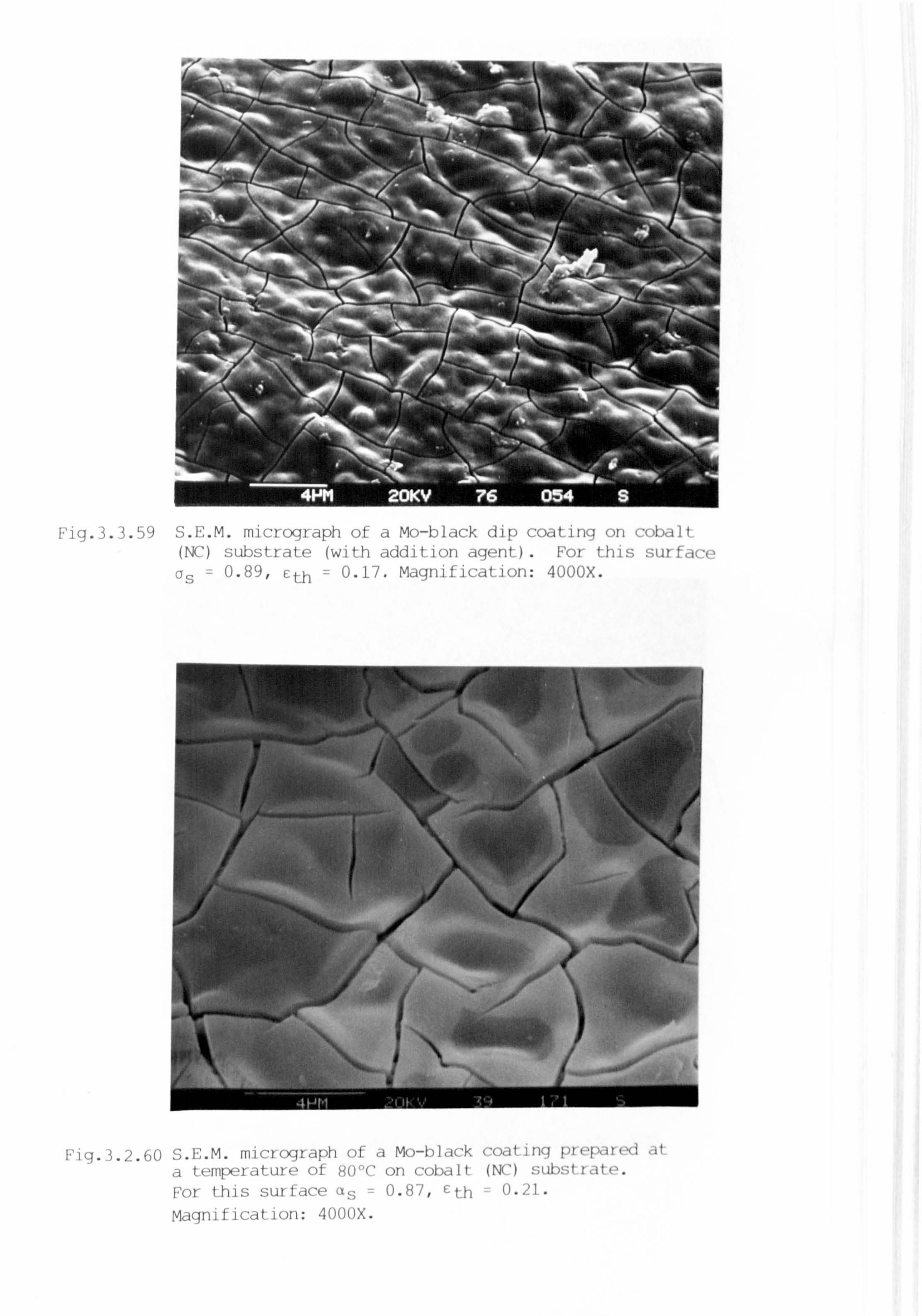
Fig. 3.3.59
:ý. Iý: .M. IIII,, I, ý 11 , It ,iI,, I, 1M, -I ý, Iý,, II: ý1,1 ,I, I,,:!, d telflpelatule Ot 80''C On coh, ilt (N(-')
For this surface ats = 0.87, cth - 0.21.
Magnification: 400OX.
S. E. M . il Iý I( -I I, q if IýIi "l, 'iil' Ili,; I (NC) substrate (wi th addi t Ion dyunt-) . FUI till!; :; Ut (A,, '('
as ý 0.89, E: th = 0.17. Magnification: 400OX.
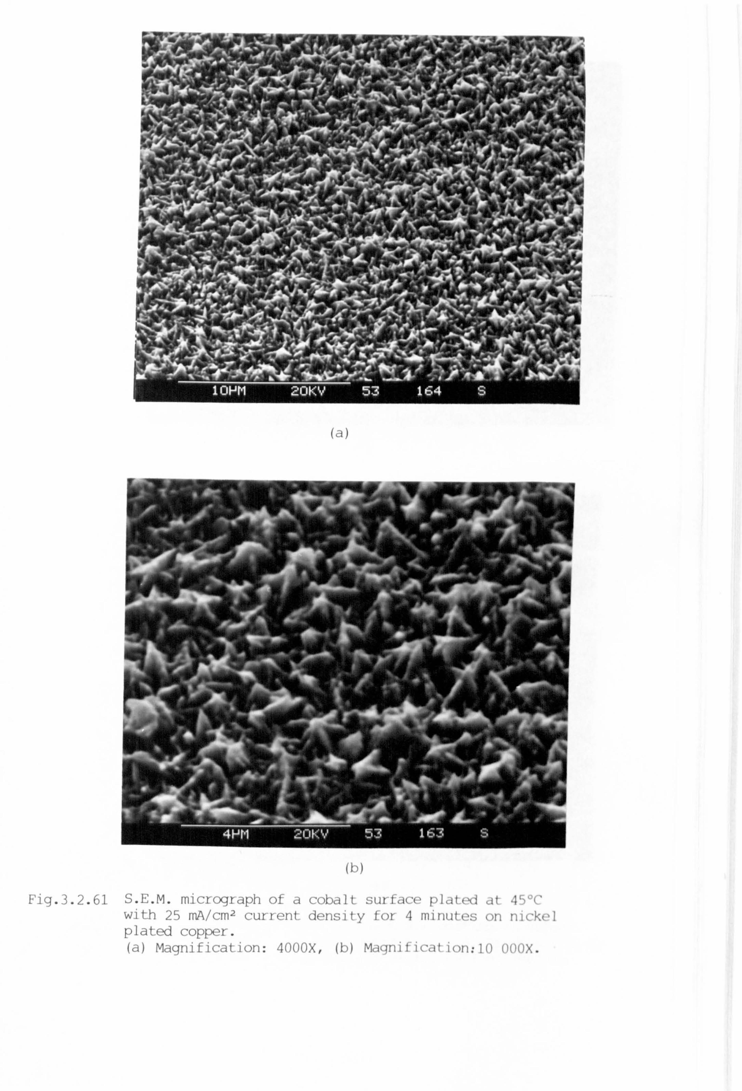
(a)
(I)
Fig. 3.2.61 S. E. M. micrograph of a with 25 mA/CM2 current plated copper.
cobalt surface plated at 450C density for 4 minutes on nickel
(a) Magnification: 400OX, (b) Magnification: 10 OOOX.
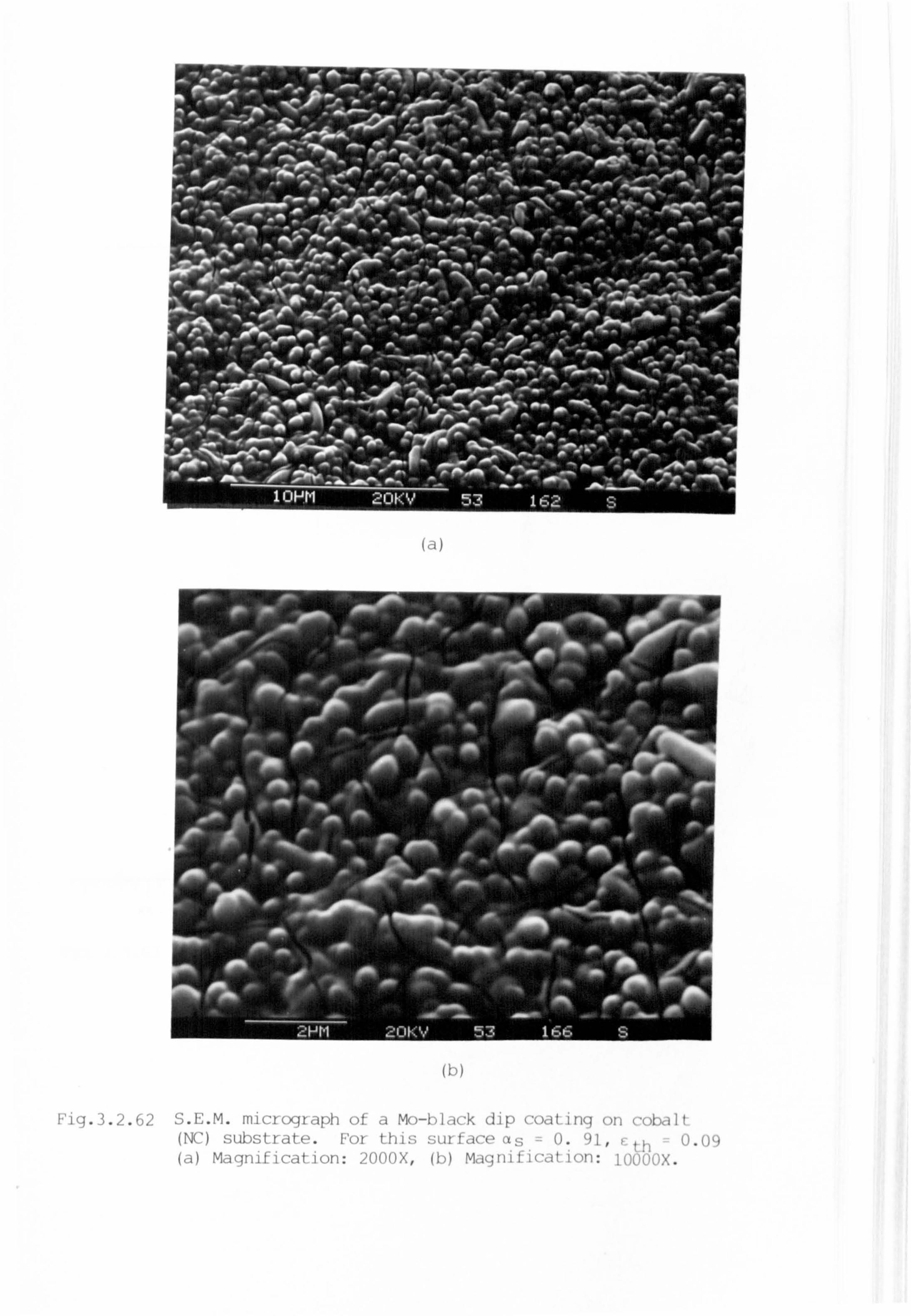
Fig. 3.2.62 S. E. M. micrograph of a Mo-black dip coating on cobalt (NC) substrate. For this surface as = 0.91, 'th = 0*09 (a) Magnification: 200OX, (b) Magnification: 1()OOOX.
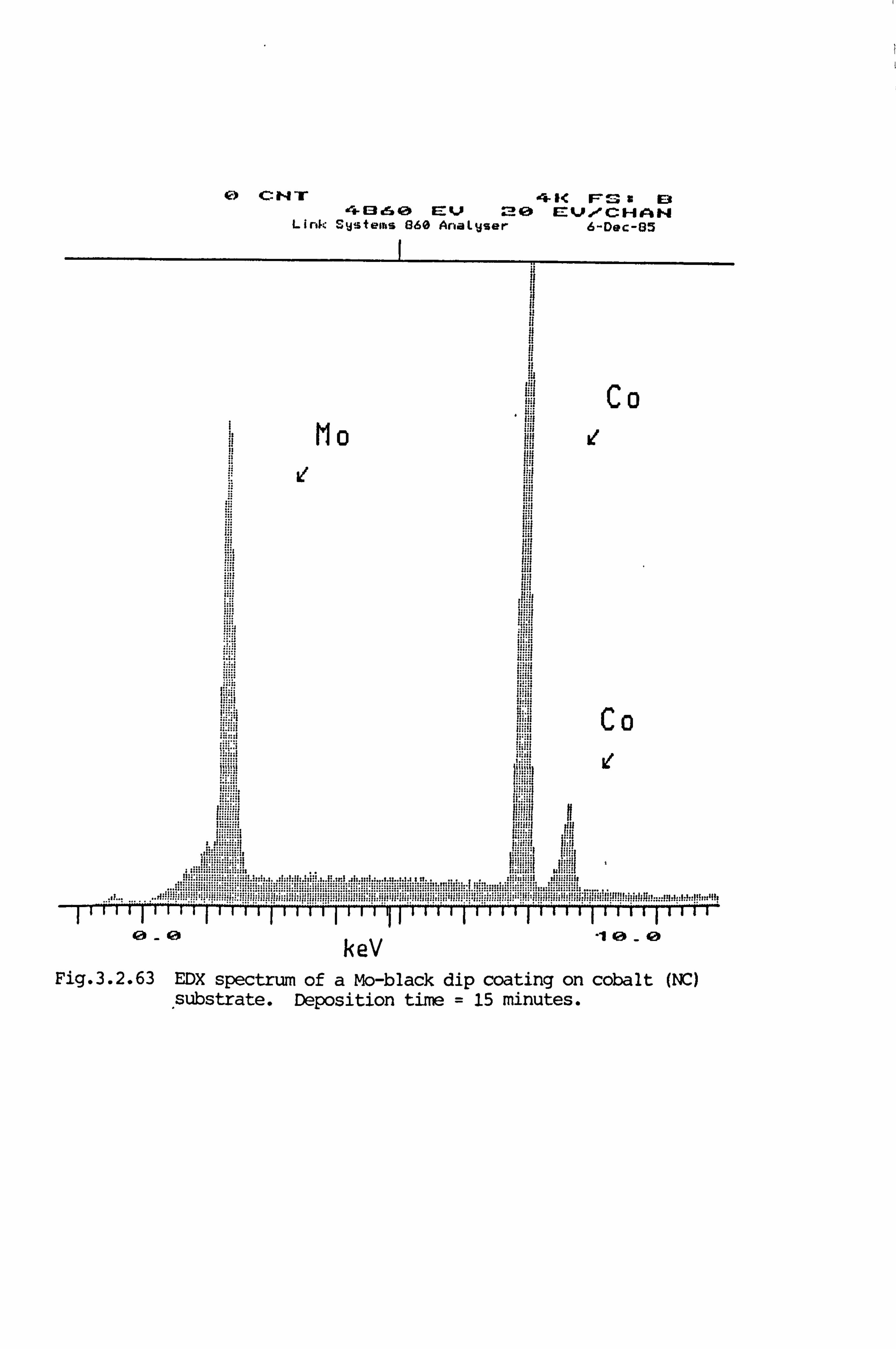
'Ir -'s 0
-VK VO an d, *- 13 em 4a EZ V E-: V. -P CHAM
Link Stjsteibs (360 Anat-jser 6-Dec-B5
Fig. 3.2.63 EDX spectrum of a Mo-black dip coating on cobalt (NC)
. substrate. Deposition time = 15 minutes.
0-0 keV -10-0
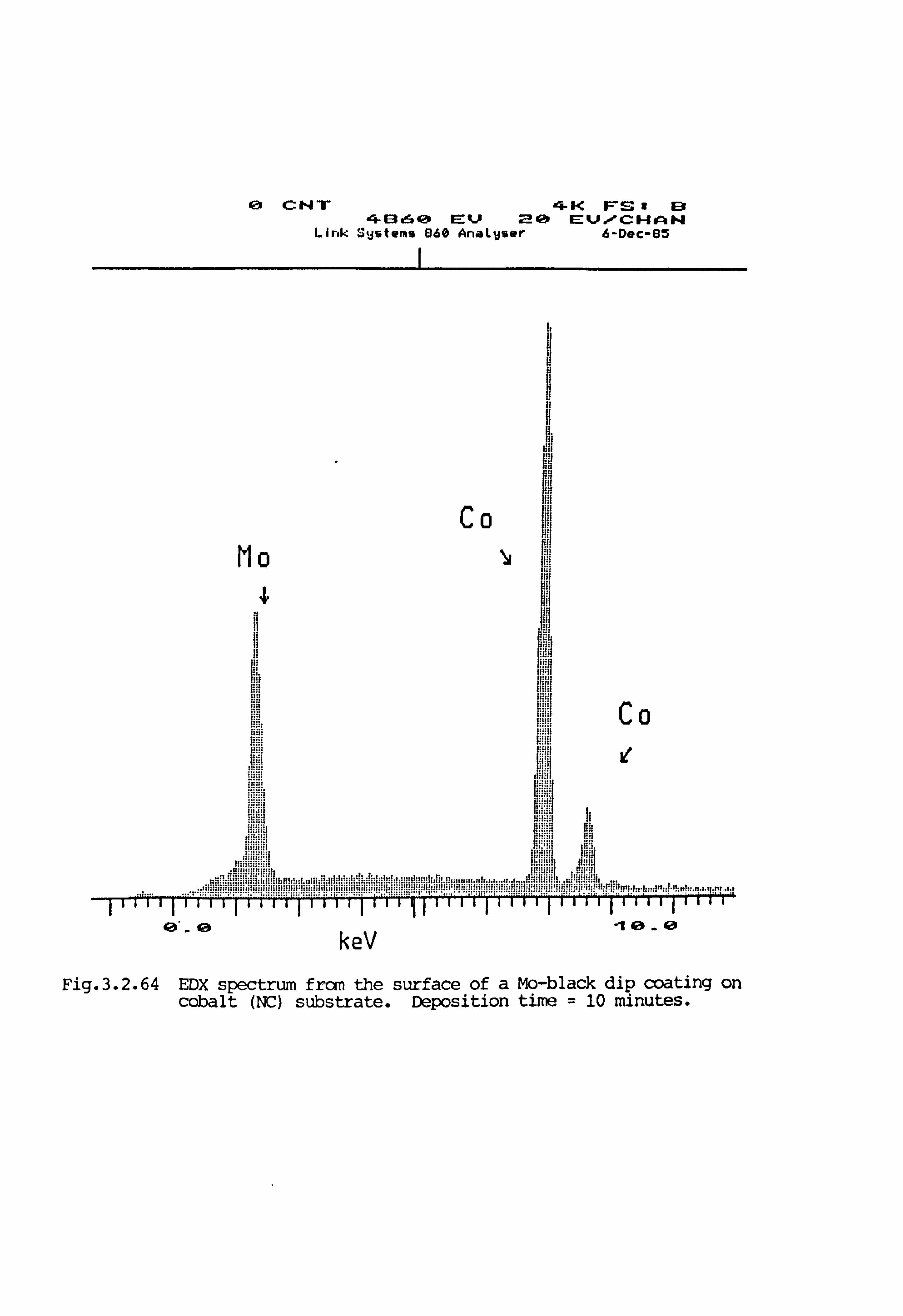
0c MY dl- K VS- I E) 4-13 e2 421 E: v 230
Link S%jstems 860 AnaLuser 6-Dec-85 I
Fig. 3.2.64 EDX spectrum from the surface of a Mo-black dip coating on cobalt (NC) substrate. Deposition time = 10 minutes.
0, - da keV
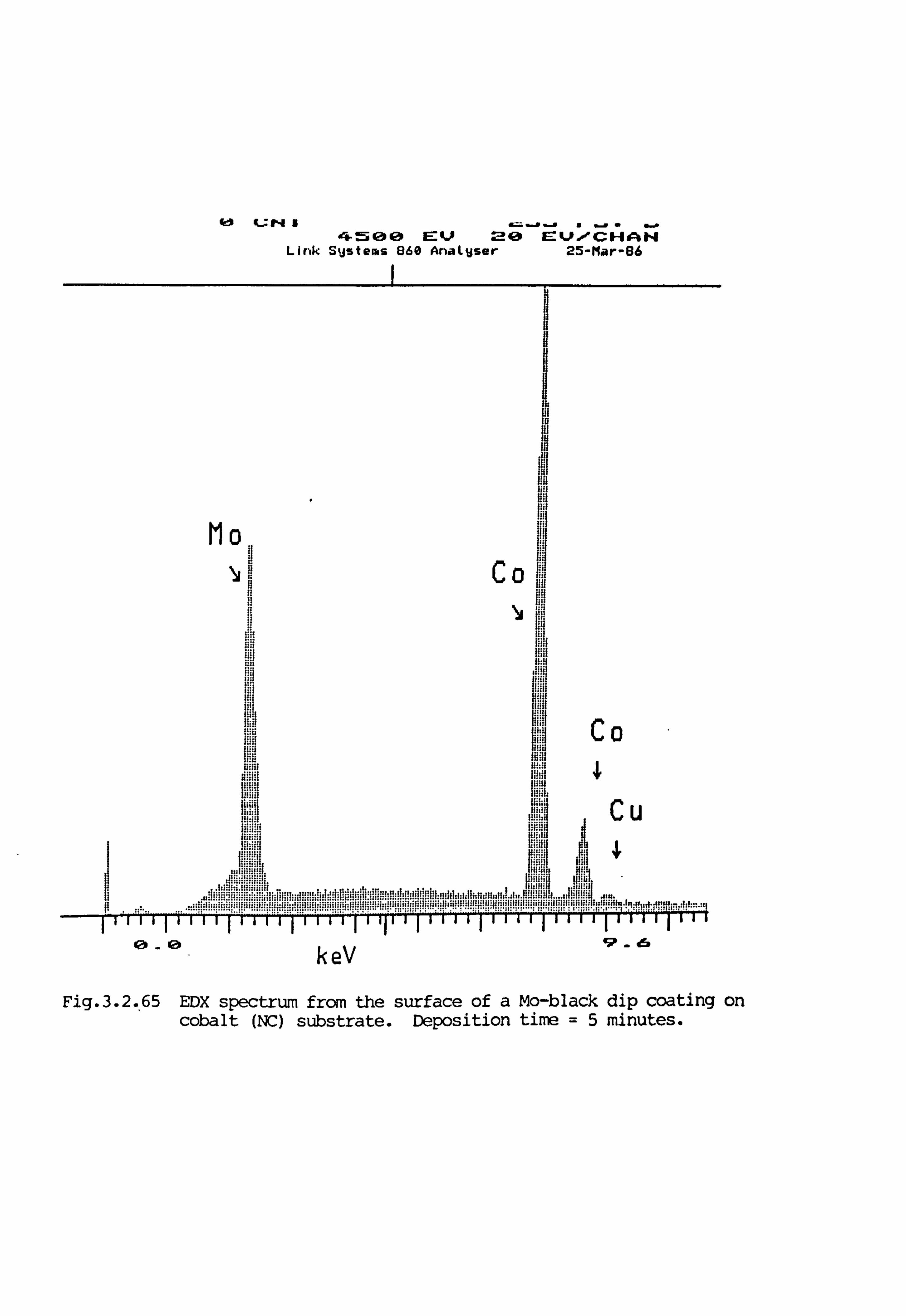
46 g.: 14 a- A+ý00 E: V 01, Q)
Link SVstems 860 AnaLilser 25-Mar-86
Fig. 3.2.. 65 EDX spectrum from the surface of a Mo-black dip coating on cobalt (NC) substrate. Deposition time =5 minutes.
0-0 v- ts keV
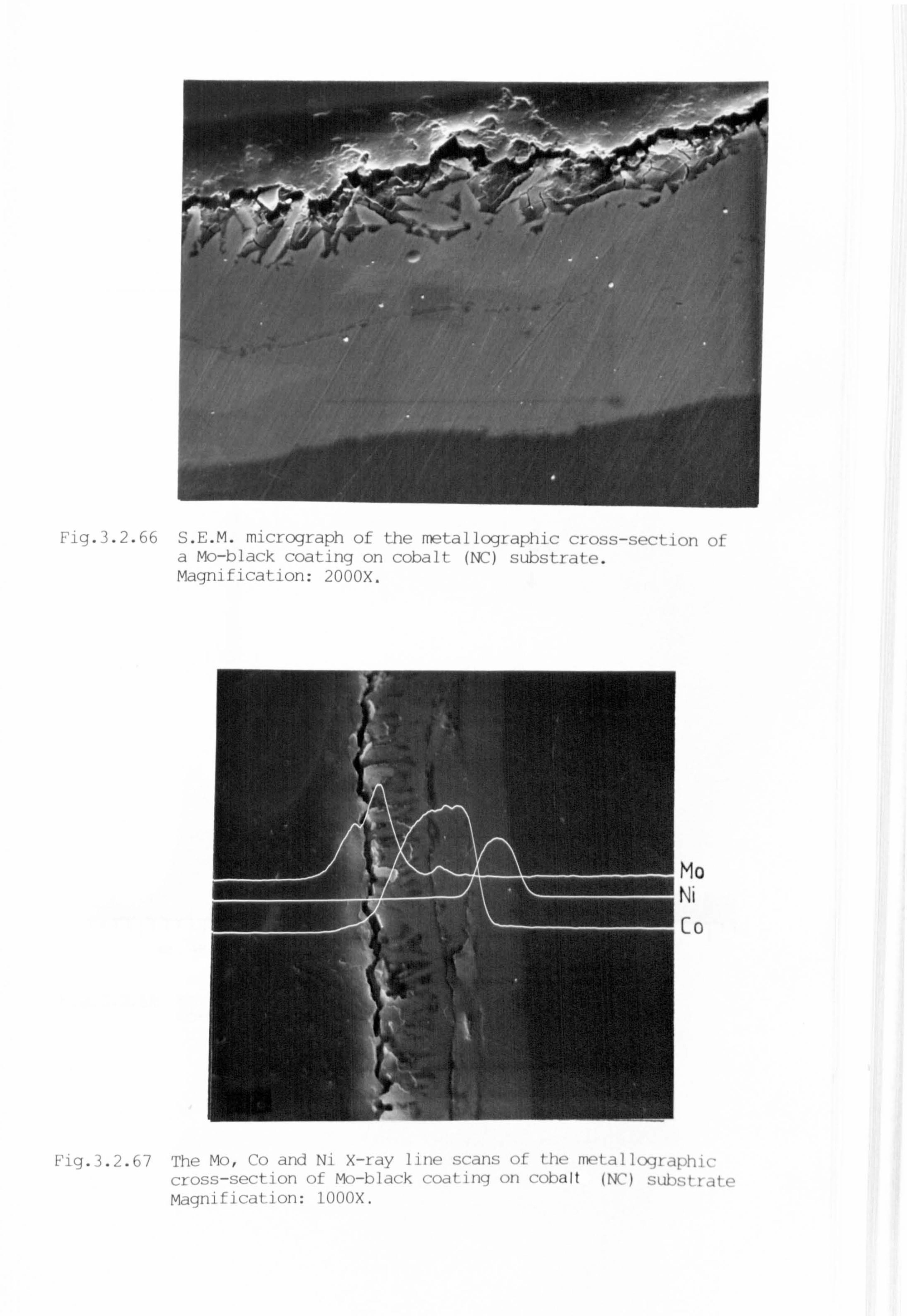
Fig. 3.2-66 S. E. M. micrograph of the metallographic cross-section ol a Mo-black coating on cobalt (NC) substrate. Magnification: 200OX.
"1 a
!
pile MO, ('() itid Ni X-Iay 11110 SUJII. 'ý ()f th('
cross-sectýon of Mo-black coating on cobalt (NC) substrjf(, Magnification: 100OX.
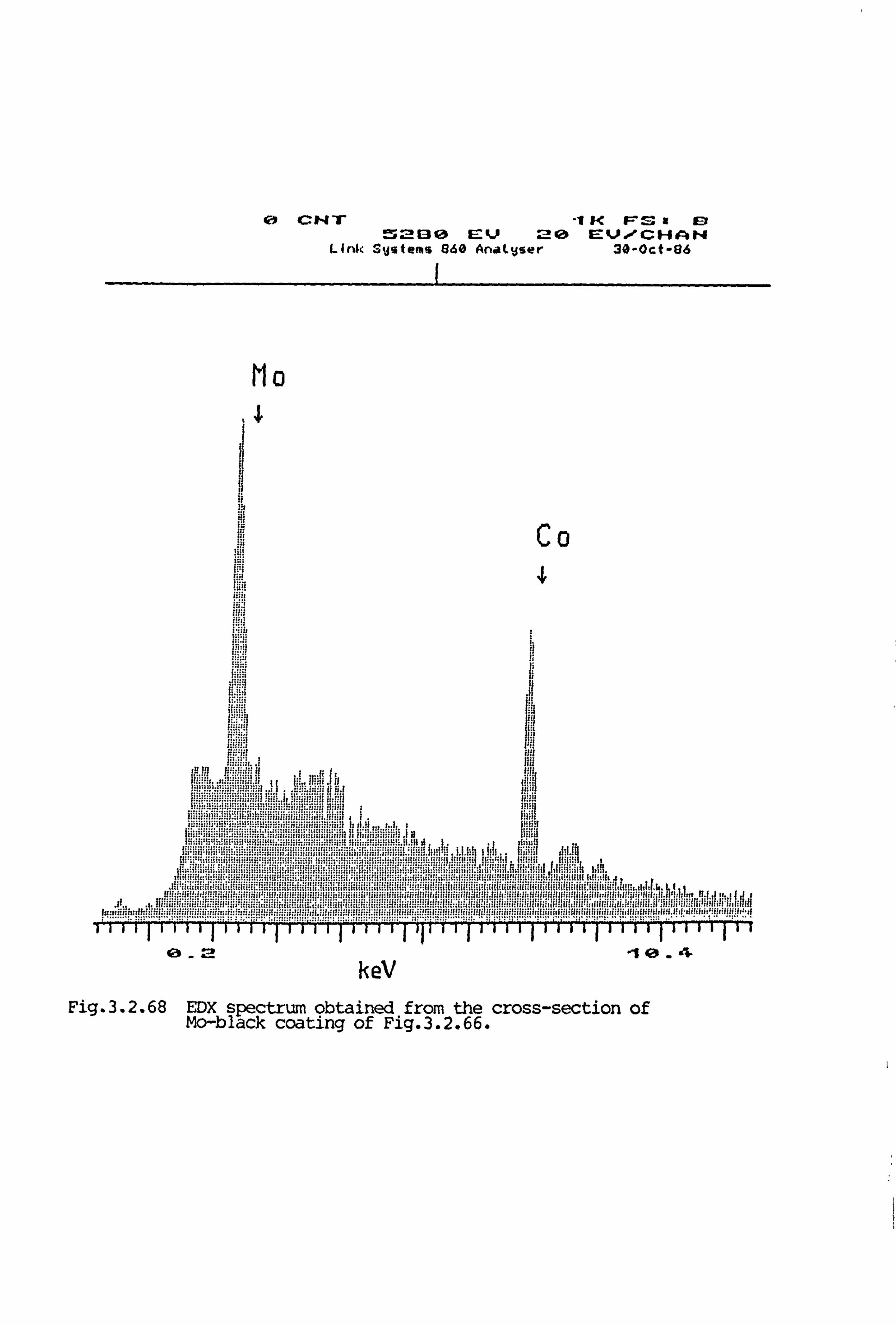
-IM FrM--a KZ V. -P cH
Link Systems 860 AnaLyser 30-Oct-96 1
lb
keV Fig. 3.2.68 EDX spectrum obtained from the cross-section of
Mo-black coating of Fig. 3.2.66.
0-Z *10.4
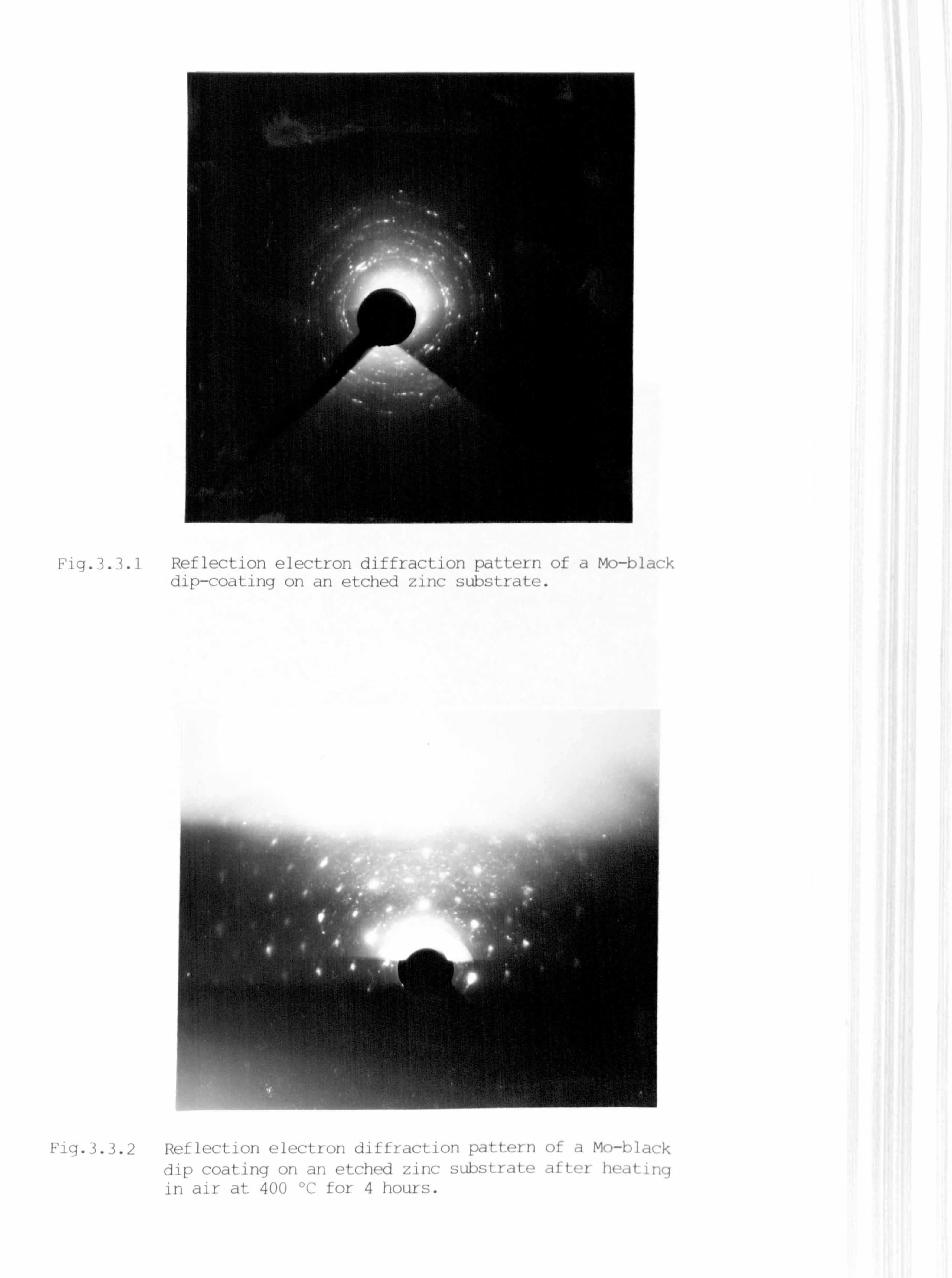
Fig. 3.3.1 Reflection electron diffraction pattern of a Mo-black dip-coating on an etched zinc substrate.
Fig. 3.3.2 Reflection electron diffracLion ()I ý, Mo-ý, I, jck, dip coating on an etched zinc substrate after heating in air at 400 'C for 4 hours.
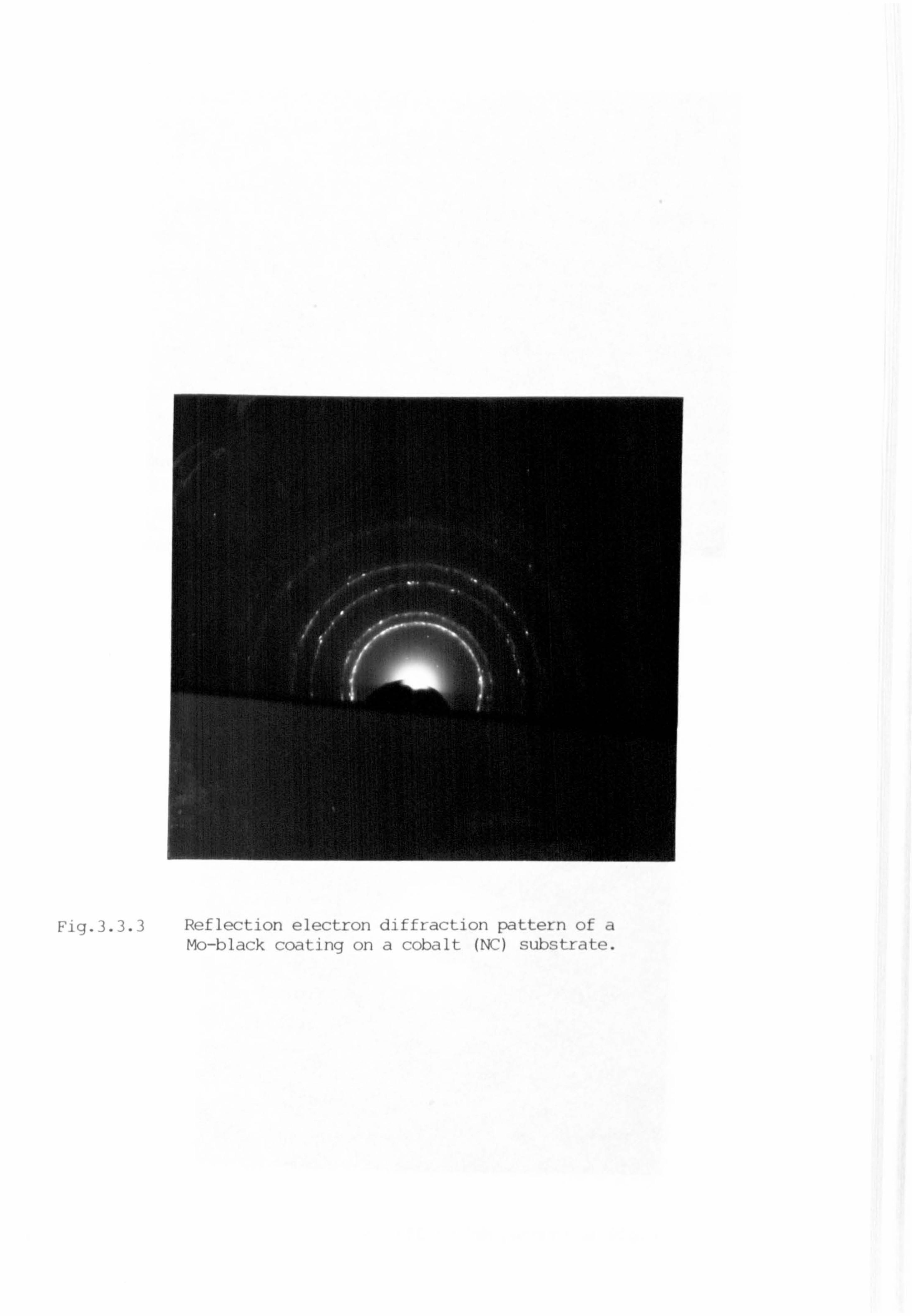
Fig. 3.3.3 Reflection electron diffraction pattern of a Mo-black coating on a cobalt (NC) substrate.
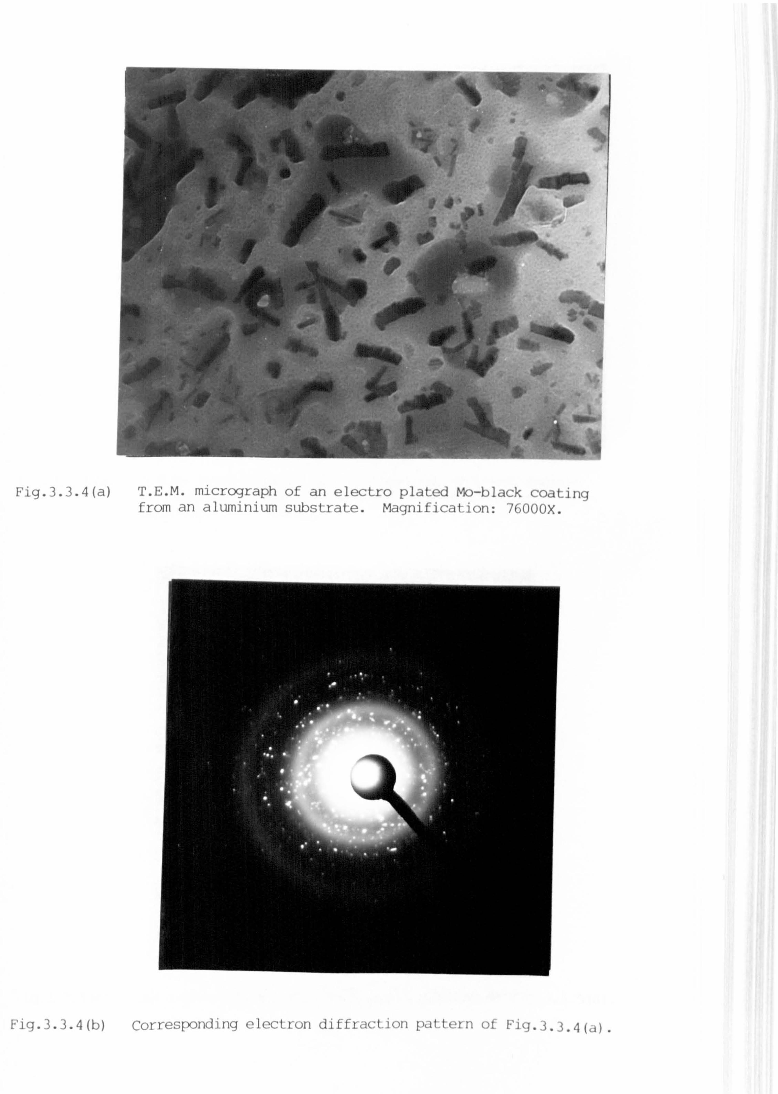
Fig. 3.3.4(a)
�4
Ap J-1 Albm- -e-,
,ý lww*
T. E. M. micrograph of an electro plated Mo-black coating from an aluminium substrate. Magnification: 7600OX.
'4 liw-
e r- jq%
Fi q-ý. ý. (b) cur ('I e(-: t I ul I ditfl, lct I ()I 1 1), It t(ý III ()I FIq. j. ý.,; (")
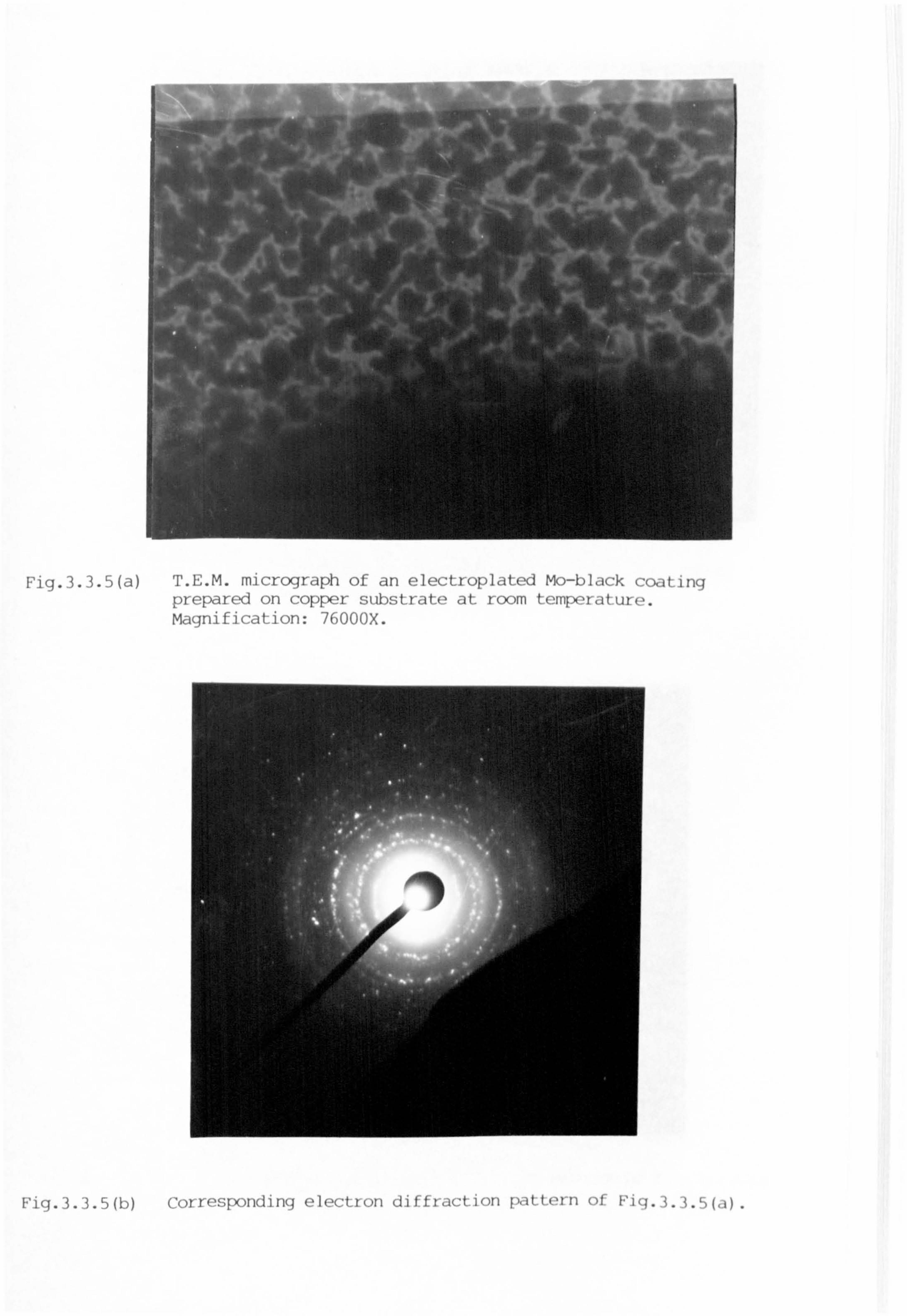
Fig. 3.3.5(a) T. E. M. micrograph of an electroplated Mo-black coating prepared on copper substrate at room temperature. Magnification: 7600OX.
IItf
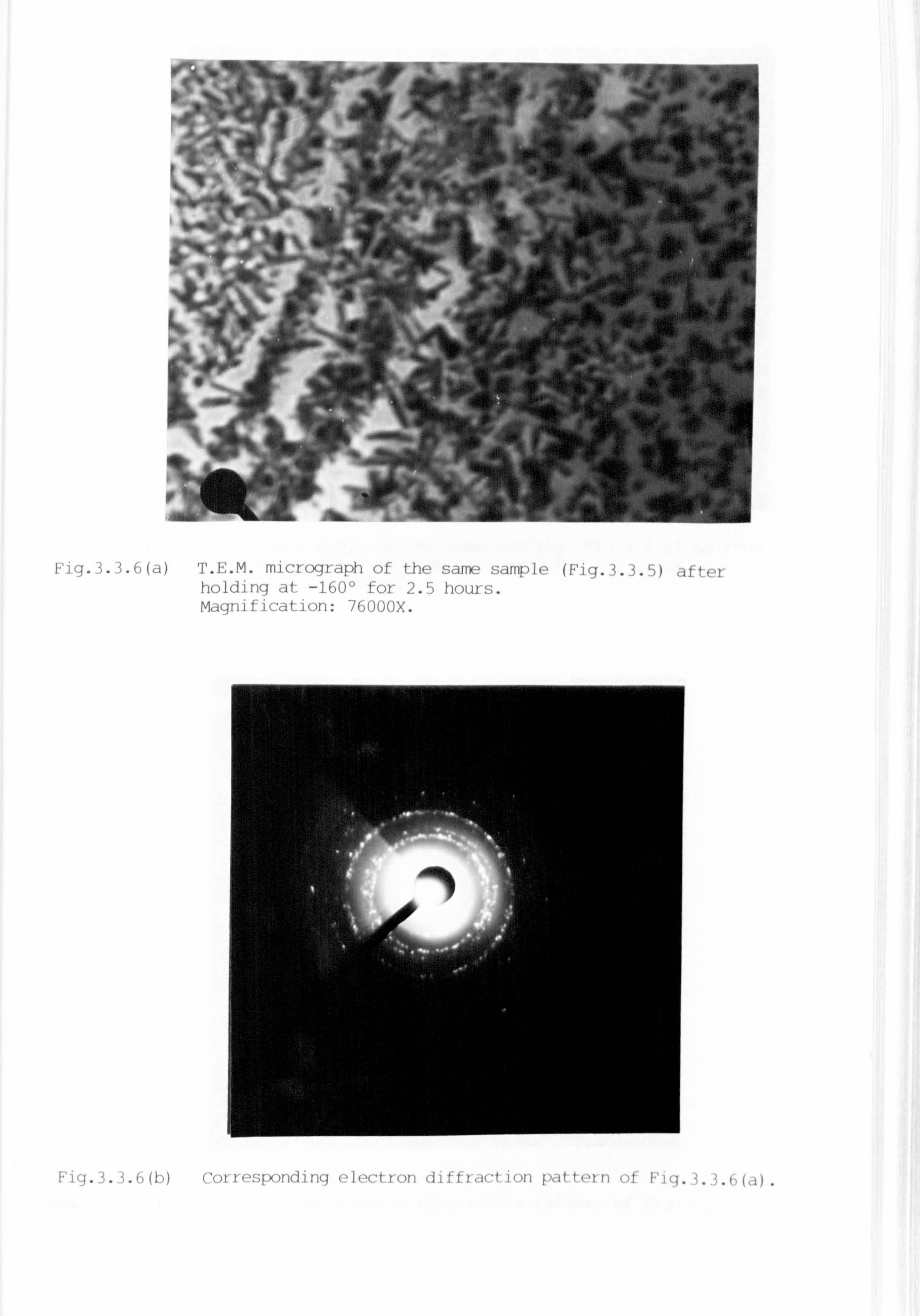
Fig. 3.3.6(a) T. E. M. micrograph of the same sample (Fig. 3.3.5) after holding at -1600 for 2.5 hours. Magnification: 7600OX.
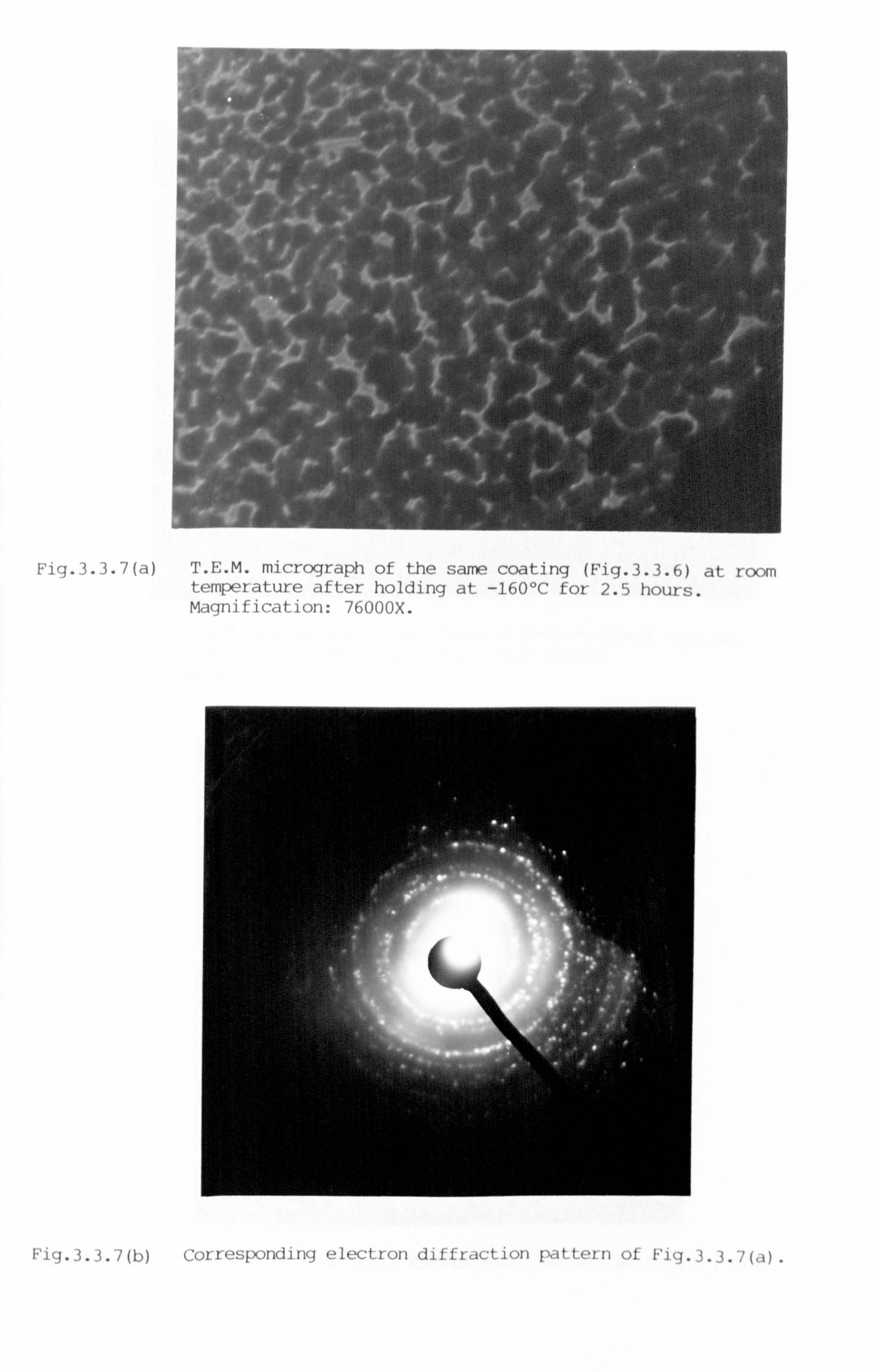
Fig. 3.3.7(a) T. E. M. micrograph of the same coating (Fig. 3-3-6) at room temperature after holding at -1600C for 2.5 hours. Magnification: 7600OX.
1(1 ;JItidt ii jttt)
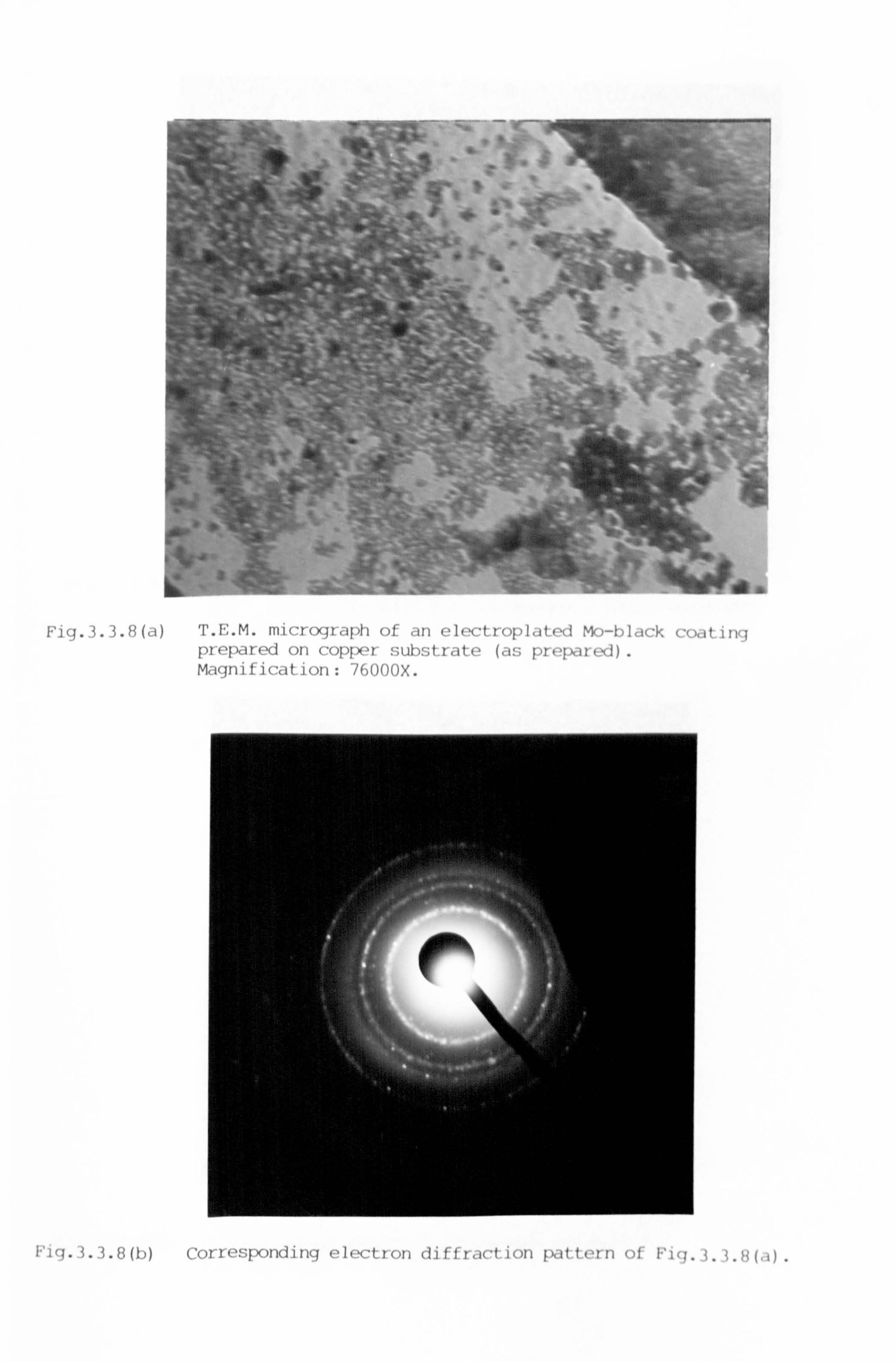
--
-log A
ký.
ýw4
W"
4 3.3.8 W) T. E. M. micrograph of an electroplated Ma-black coating
prepared on copper substrate (as prepai-ed) . Magnification: 7600OX.
(lit I I, J(. t 1ý)Il p'It t(. 111 (d 1'1ý1.
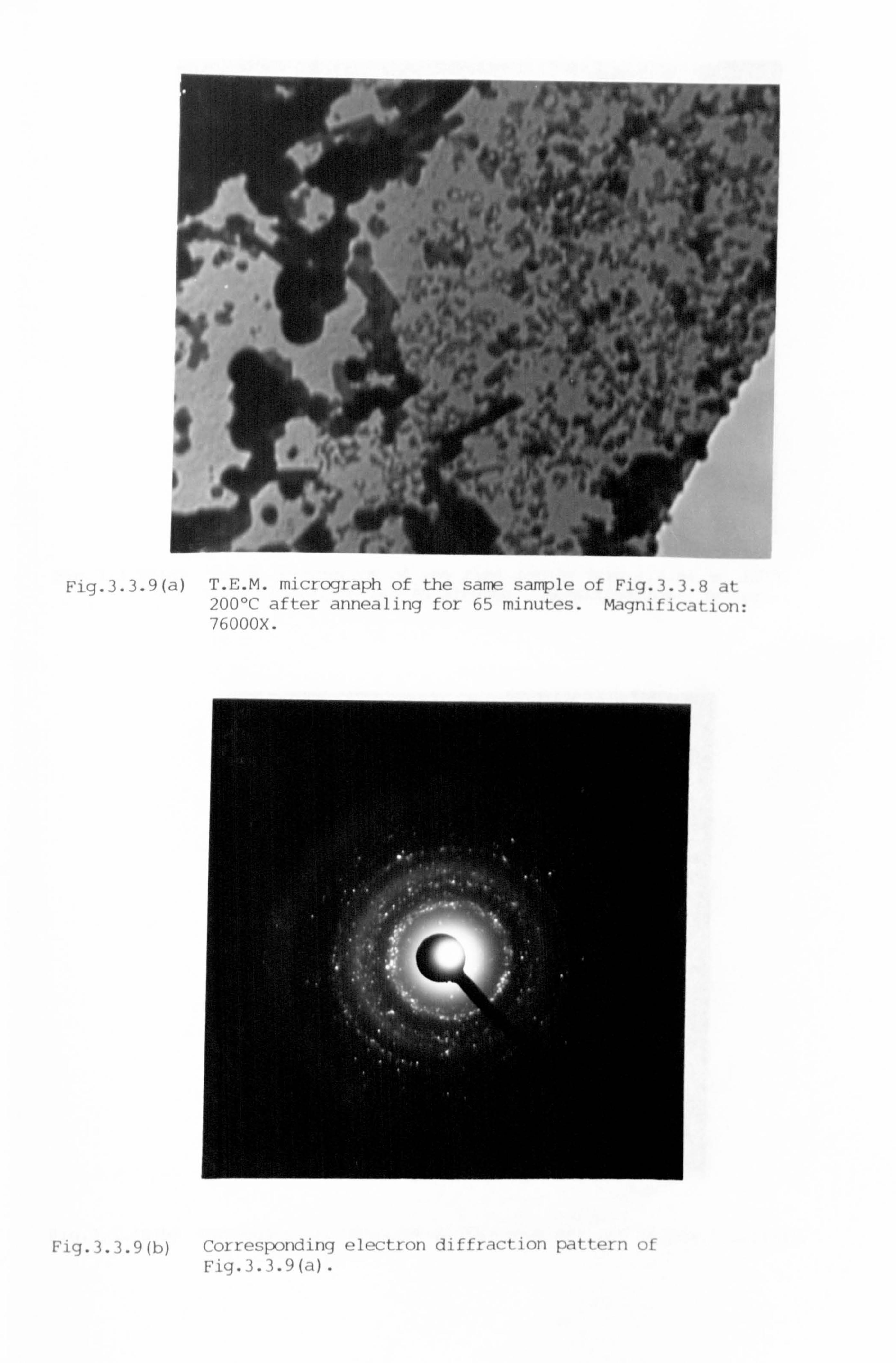
i
T. E. M. mi ci oq r aph ()I tI i(, :;, mo., samp I (ý (d F1 ýJ. i-3.8 at 2000C after annealing for 65 minutes. Magnification: 7600OX.
3 J*A Of --; 1ý IIP; 11 4". "k
A*
'ý )I I(1: ]xA Id if I(J f0 ýk iq .3. -1 .9(a).
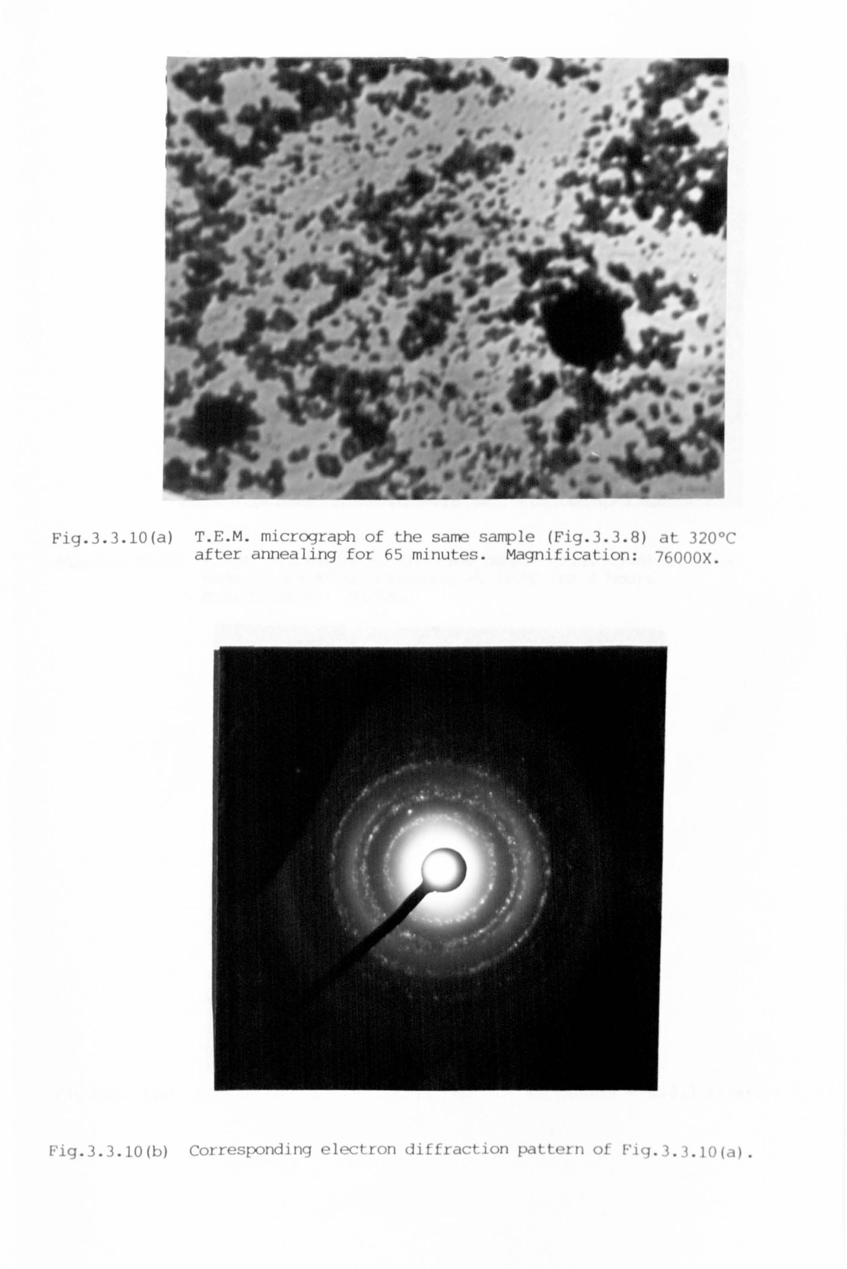
Fig. 3.3.10(a) T. E. M. micrograph of the same sample (Fig. 3.3.8) at 3201C after annealing for 65 minutes. Magnification: 7600OX.
Fly. 3.3.10 (b) Coxresix-niding electroli (JiLliaction pdttein ol Flkj-3.3.1()(d) .
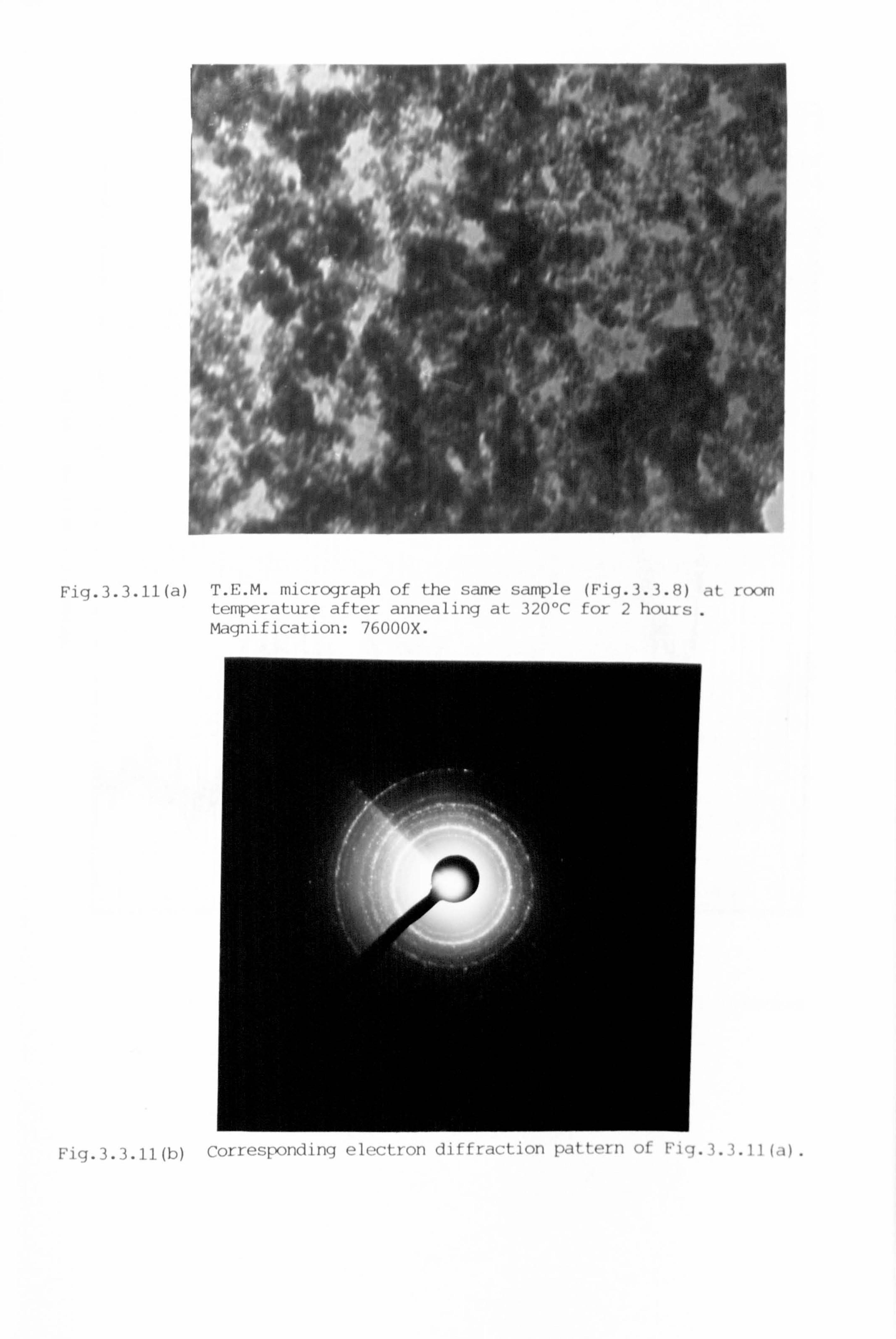
Fig. 3.3.11(a) T. E. M. micrograph of the same sample (Fig. 3.3.8) at room temperature after annealing at 3200C for 2 hours
. Magnification: 7600OX.
IýI(j. ý. ý. II (I ))(, ()I II1 ('11 ýIiII I'l, t i-11 I ý, It t ('III (d ;.:. ..:!, ).
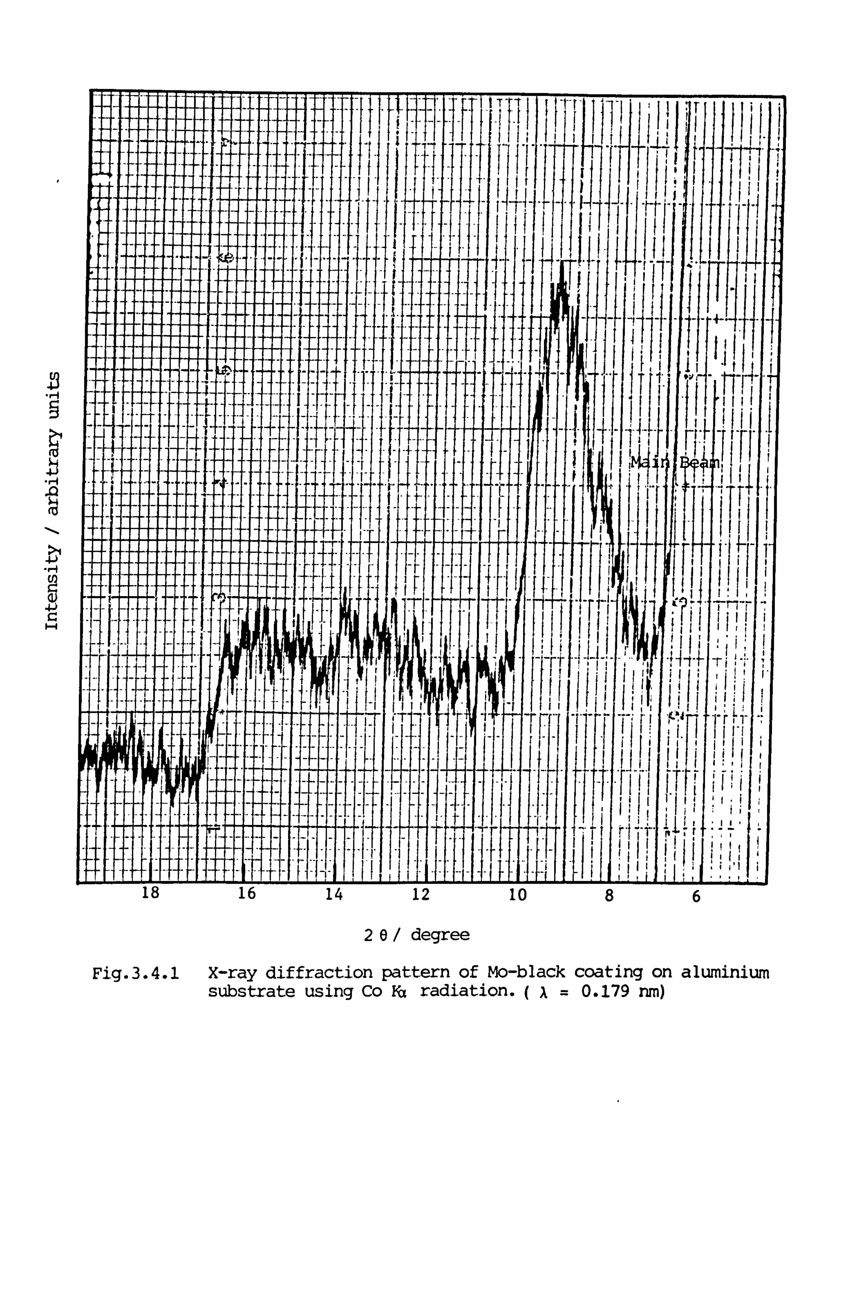
49
4JT -4 Cl) z B
T -r f t j
ýj
LP
J-t -r
-
1 t
1 I I f
I T. r-
'14
r-77
Ti - T
18 16 14 12 10 6
2e/ degree
Fig. 3.4.1 X-ray diffraction pattern of Mo-black coating on aluminium substrate using Co Fu radiation. (x=0.179 nm)
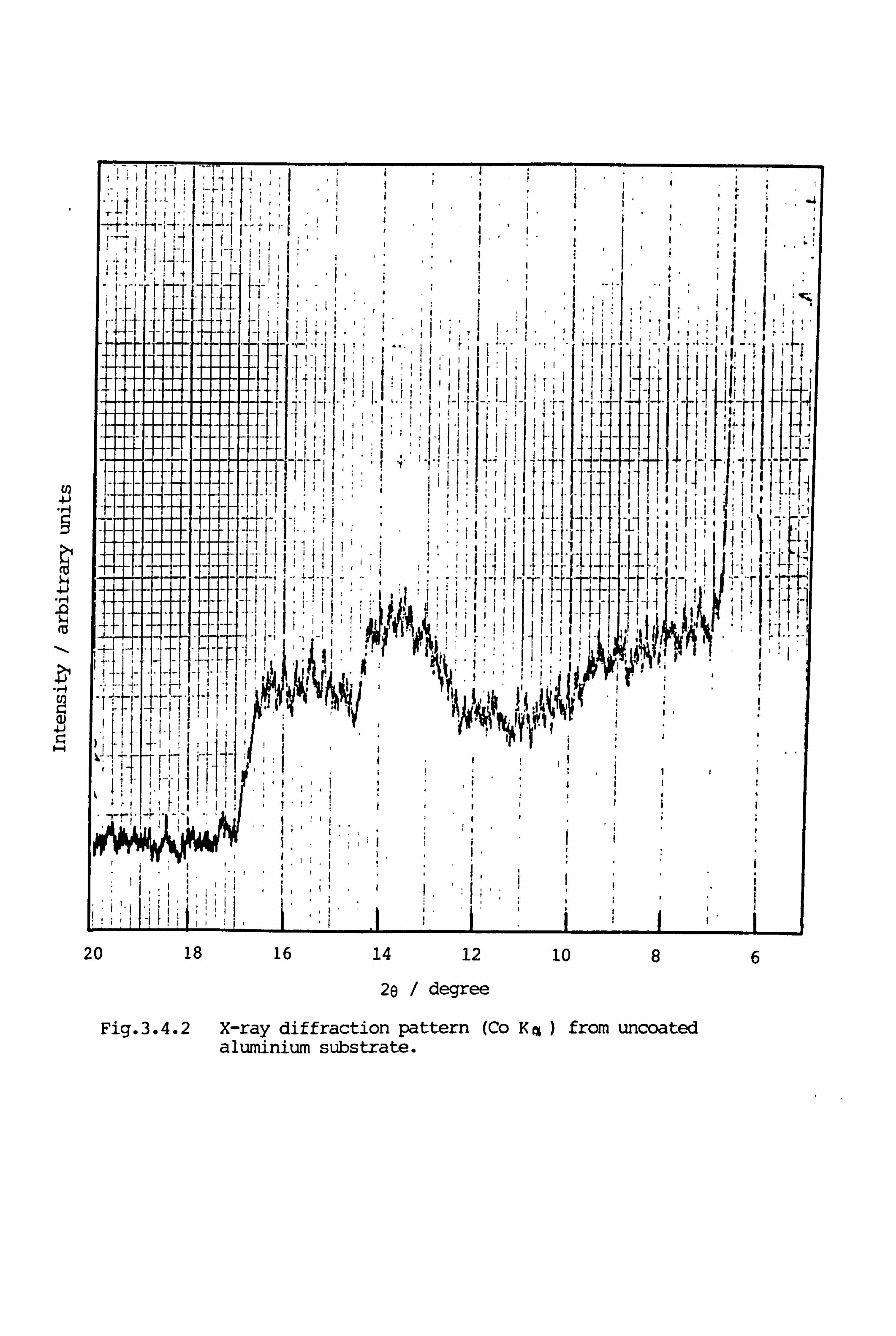
(0
(n
rq
Al
FTI
IIT Tf
I-I f
II 7
Li 20 18 86 16 14 12 10
2e / degree
Fig. 3.4.2 X-ray diffraction pattern (Co KrA ) from uncoated aluminium substrate.
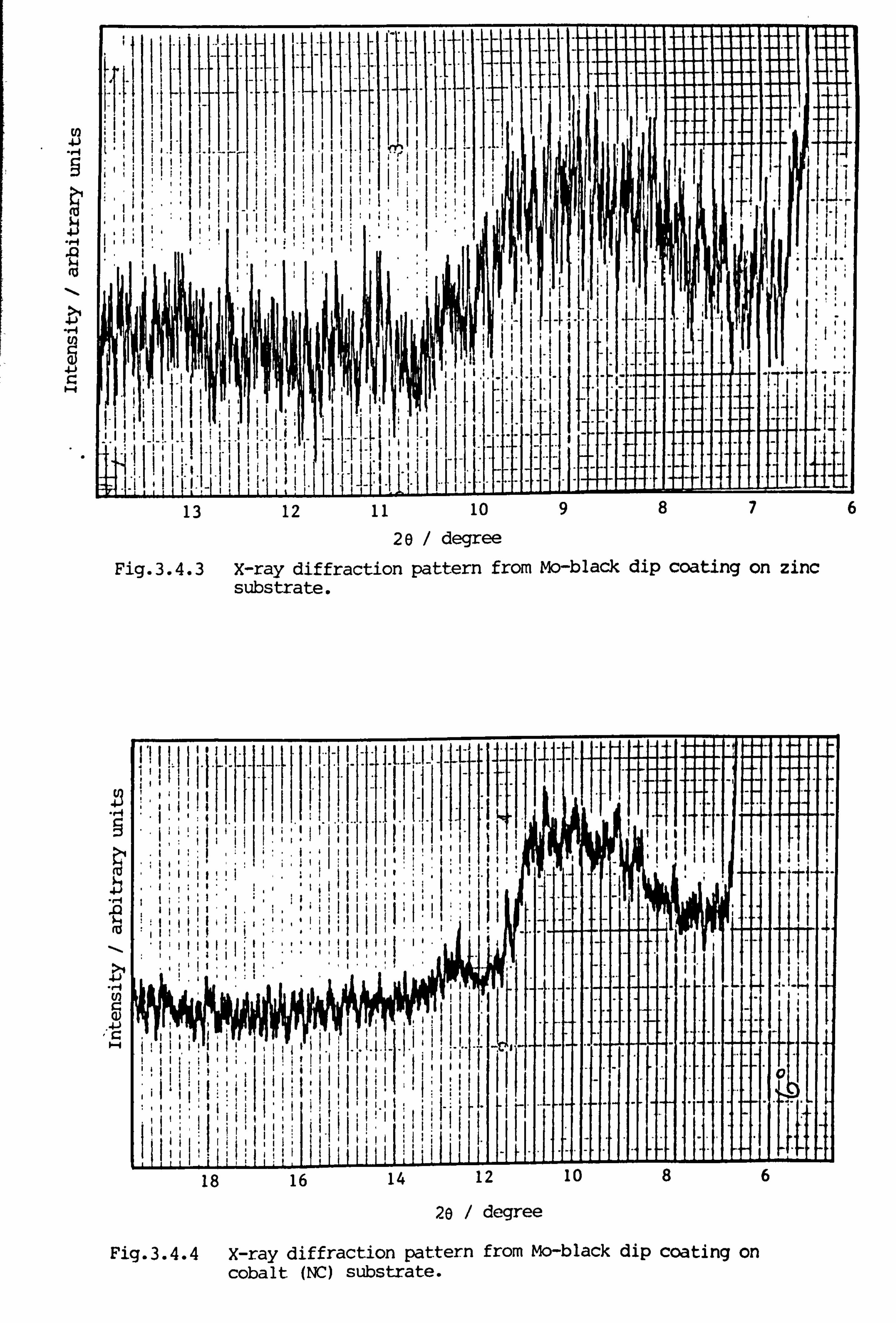
In 41
41 c 0-4
If -- --- -T ---------- T 4
-1 4
UJ P
1. I 13 12 10
20 / degree
Fig. 3.4.3 X-ray diffraction pattern from Mo-black dip coating on zinc substrate.
49
I
I l til I
IT11 4
J. L
w
18 16 14 1zLU ts 0
20 / degree
Fig. 3.4.4 X-ray diffraction pattern from Mo-black dip coating on cobalt (NC) substrate.
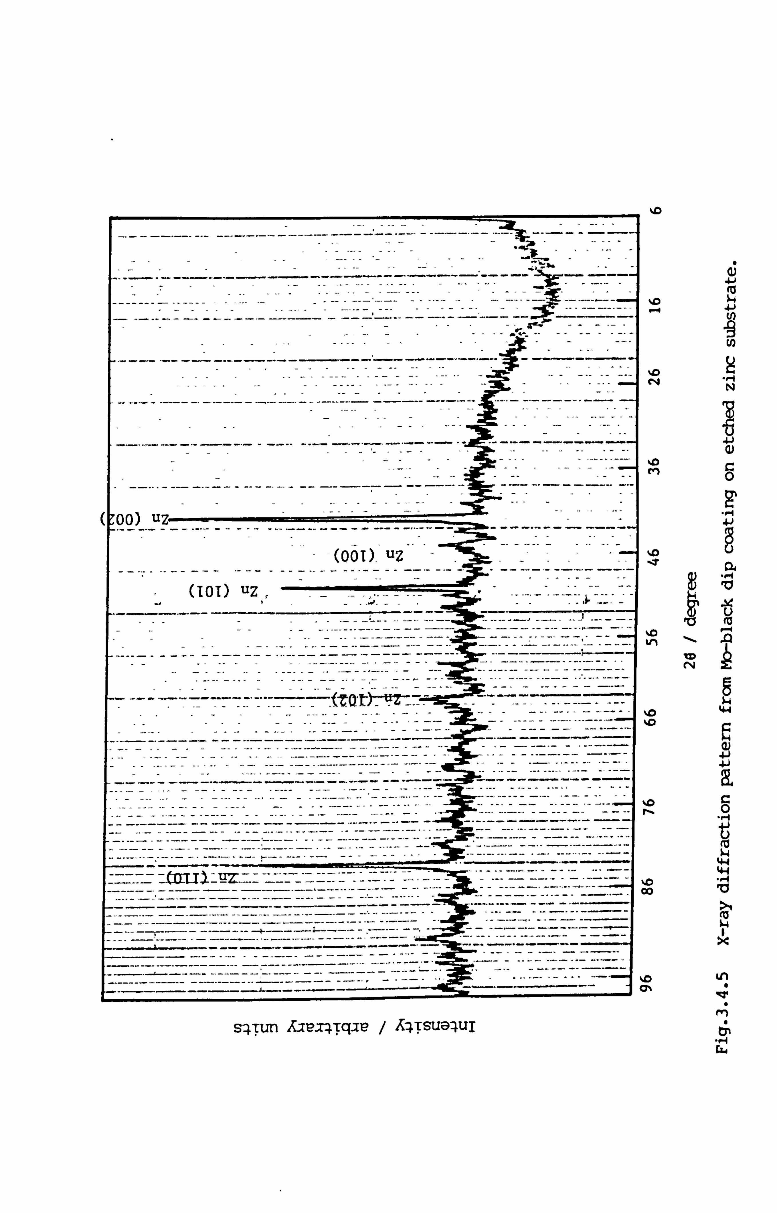
700) uz
(0 0- UZ
(101) UZ
-77--- 77--'7'-: 7-7-ftal7)7UT---
Qyul -U-T--. -
-- - -------- 7
s-4Tun lavx4Tq: 'P / AITSuDWI
%D
a)
%0 4
U) -9 U)
ýD 2
. I. i N
ri 8
(0
%0 44
%0
4-4 4
00 >l
D 3N Ln
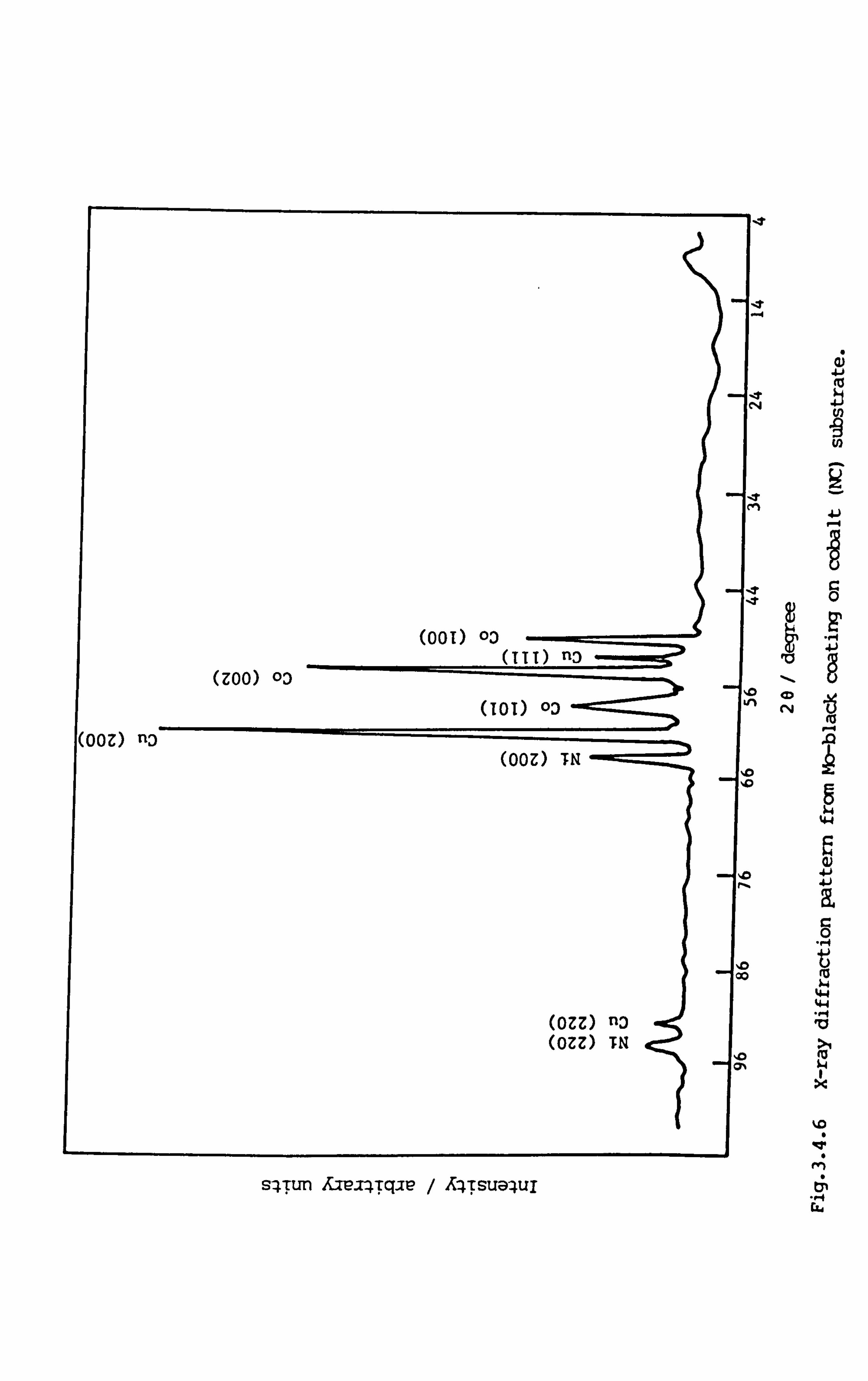
cn
(001) 00
(TIT) no (zoo) 03
(100 00 Ln
(OOZ) no (OOZ) TN
10 00
(OZZ) no (OZZ) TN
10
s4Tun fze-T4Tq-Tp / A-4Tsua-4ui
CY
a)
Cl)
Eý
41
t
44 -4 V
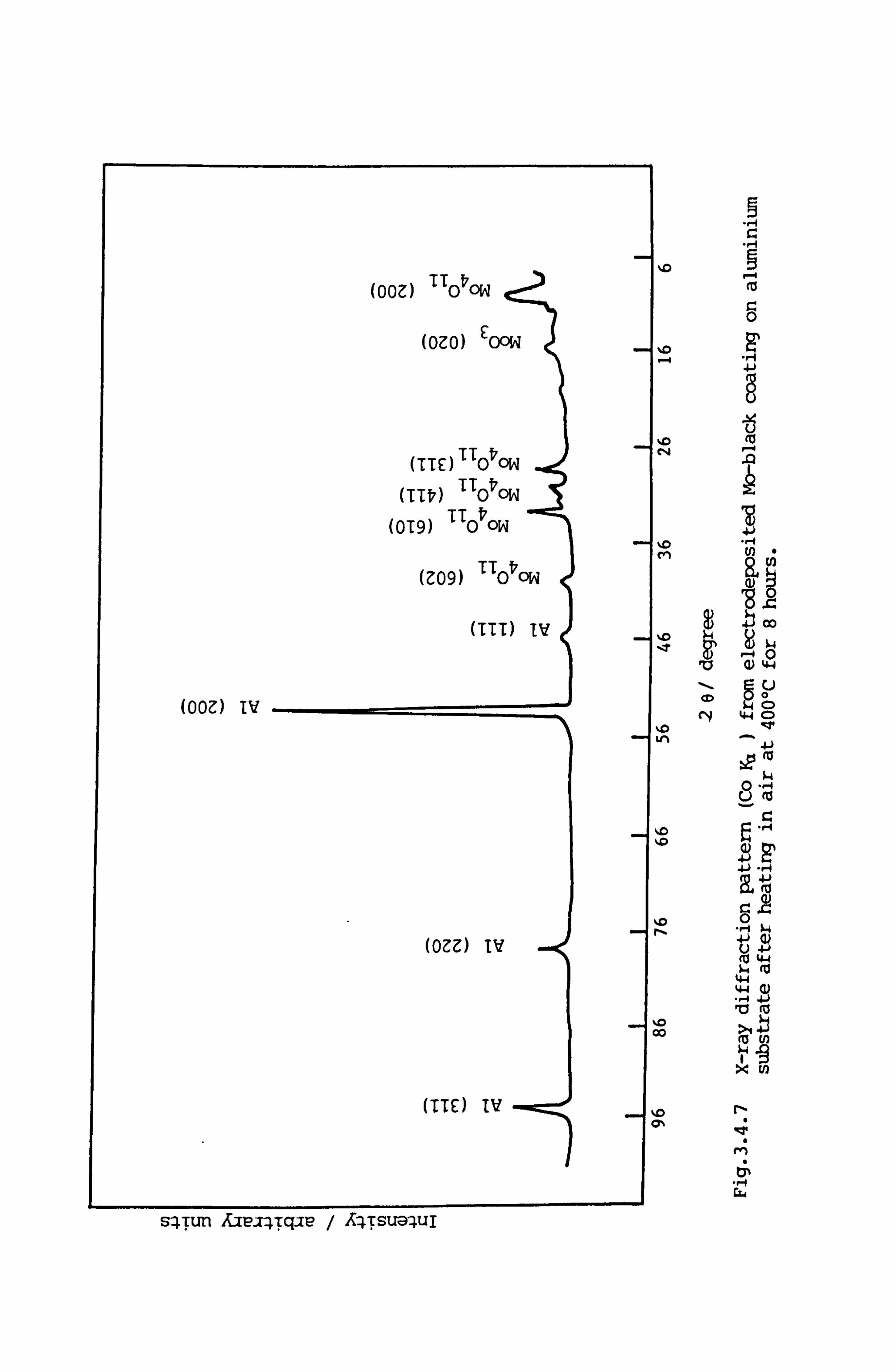
z
(OOZ) TT 0v ow <: ý
(OZO) c OOW
(TTE TT 0 f, ow
(TTV ) TTOVC)W
(OT9) TTO"OW
(Zog) T'lot, ow
(TTT) TV
(OOZ) IV
(OZZ) IV
(TTE) TV
%D
%0 24
ý. 0
en
v
1- (D r9
%D Ln
%D
20
4-1
(n 0
4ý co
0
so
ý4 CD 44 CD
4J
-4
49 4-)
t
114 2M
44 44 -1 10 (a
t 4-1
U)
N
m
s-4Tun laLzqTq-ie / A-4TsuaquI
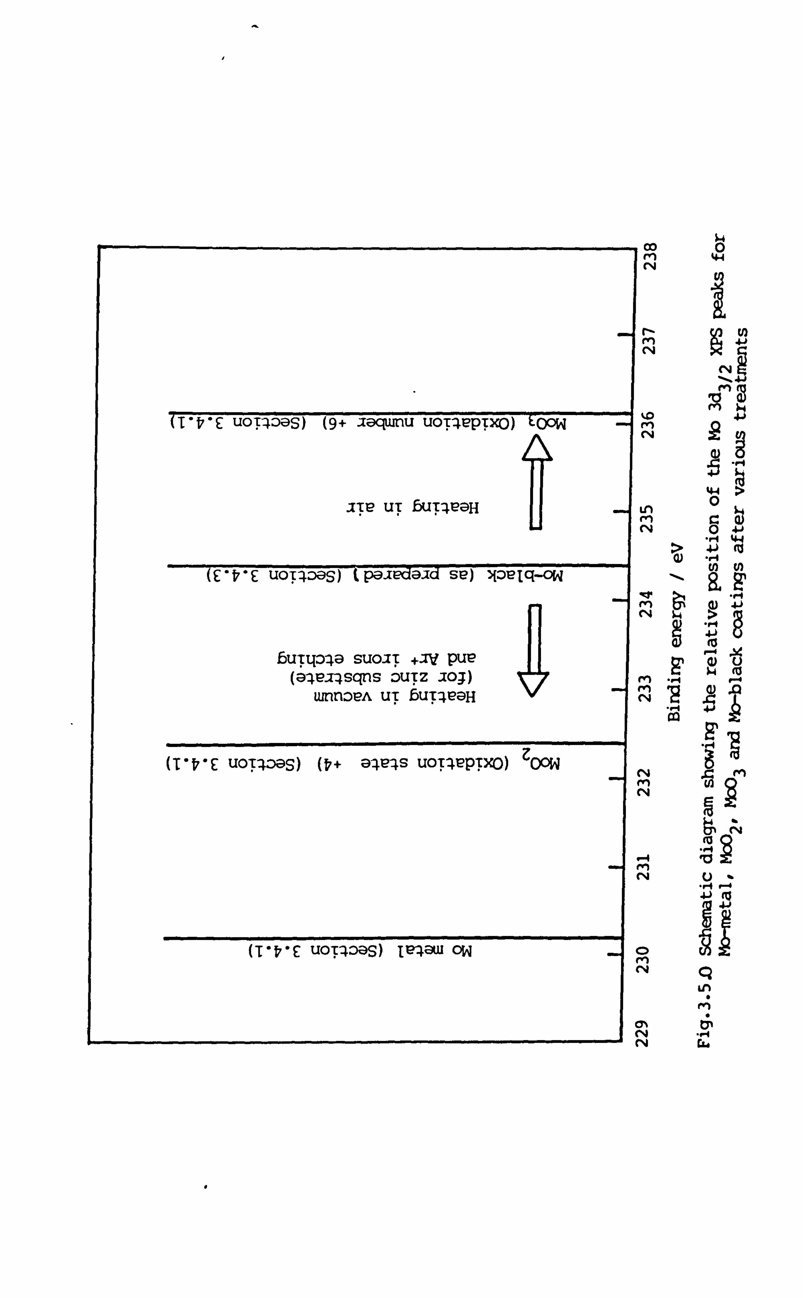
(T't, *E UOPOGS) (9+ -Iaq=U UOT4epTXD) EOOW
JTP UT WT4eaH
(E-FE UOT-405s) (pa id se) Noelq-ow
buTT40-4a SUO-IT +2v Pup
(a-4ex4sqns OUTZ JOJ) uinnoeA uT ýu'PeGH
(T*V*E UOT-4-n@S) (V+ 94eqS UOT4PpTXO) Z oow
(T'ý*E uOT'40aS) MaLu OW
00 ri r-i
r- rn rY
40 rn C14
Ln
rn C'4
N
N
-4 rn N
0 rn N
3% 14 14
ý4 0
44
2 to
C4 I.. rm @
lö
44 C)
r- b
0 . 14 4ý 4J ., 4 (n 0
fý 0) Q
eM
5ý
bl 1; ý
U- -4
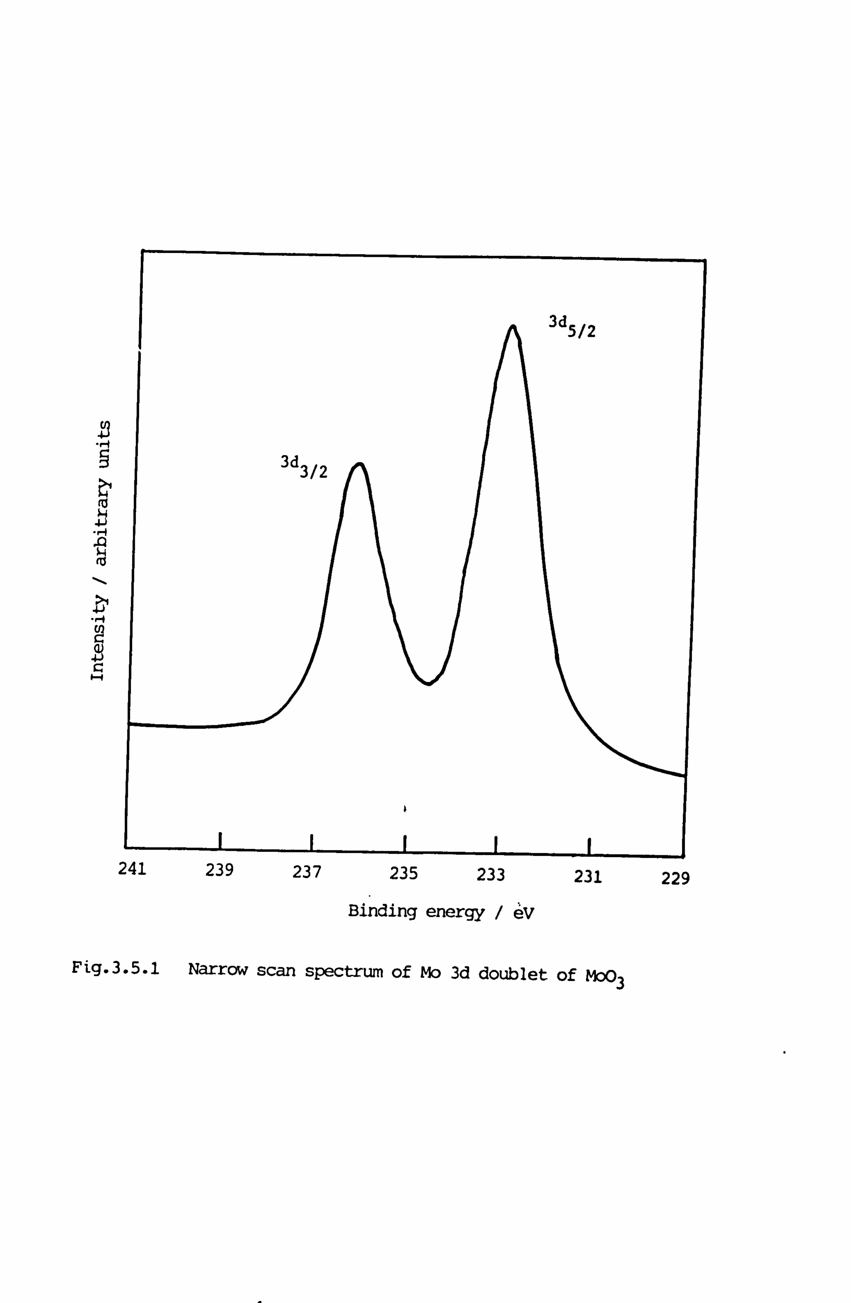
Z
fu
IT 4J 1: ý O-f
Binding energy / eV
Fig. 3.5.1 Narrow scan spectrum of Mo 3d doublet of M003
241 239 237 235 233 231 229
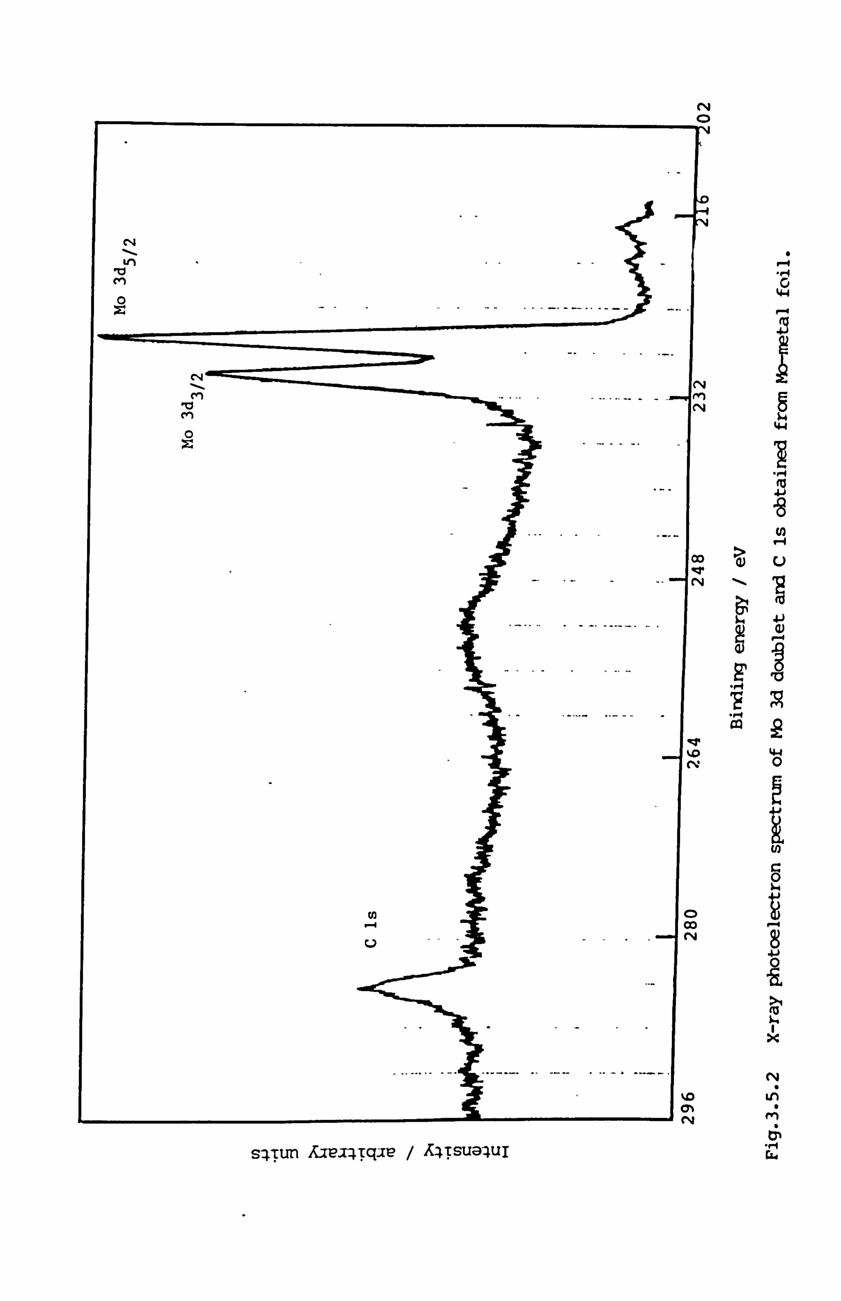
C*4 f"ll
Ln
0
C14
,a N en
00
N
-4 co
L)
cn
s4Tun Aae-TqTwe / A4Tsua-4ul
4T
L)
FV
44 0
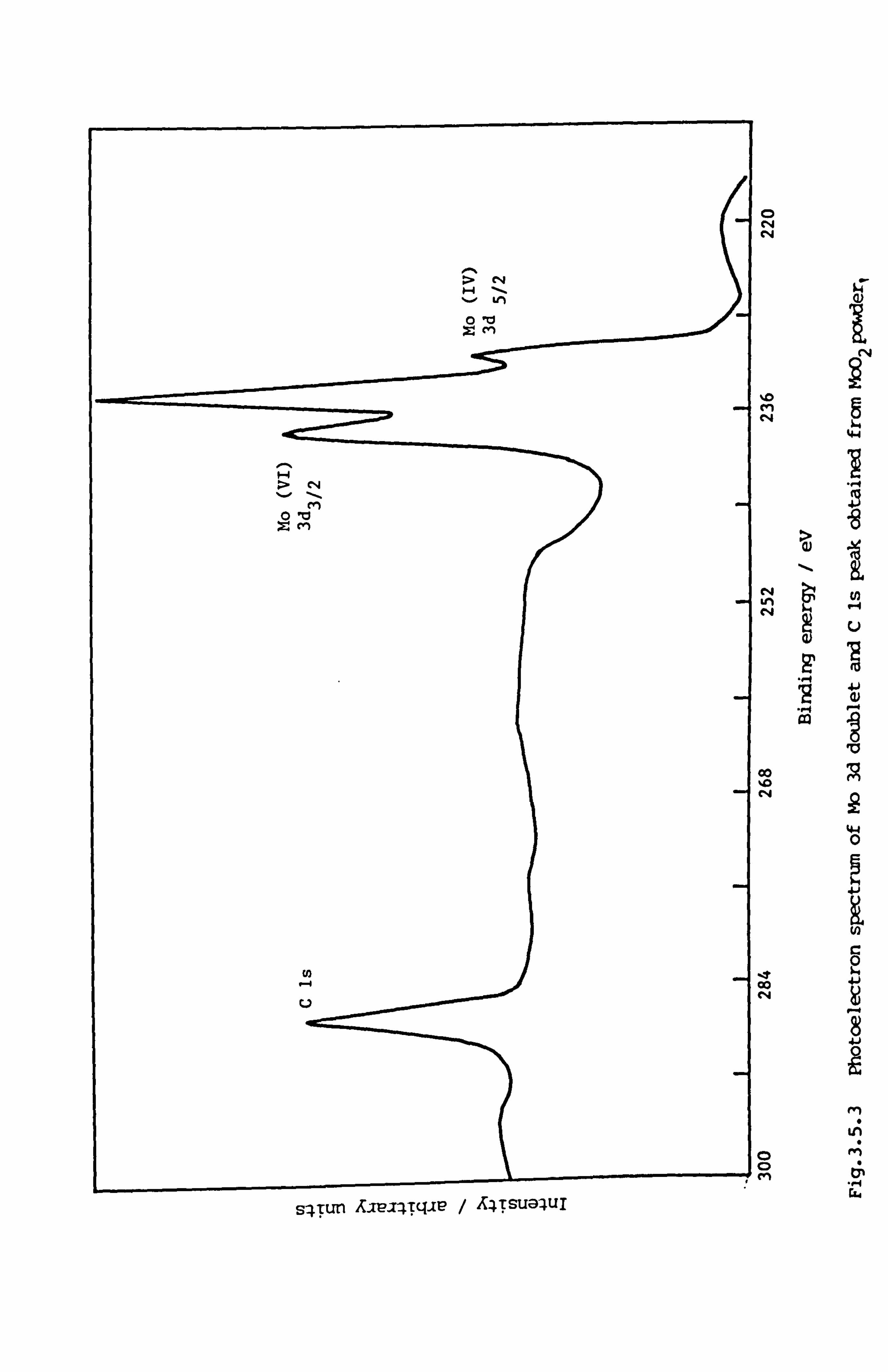
0 C14 C14
�Pl
0 10 Z cn
cm 0 Ici
Z cli
U)
U
%D ei r4
Ln C4
ca
00 %0 r4
e Co C, 4
cm
s. 4Tun Ajej4Twe / A4Tsua4uI
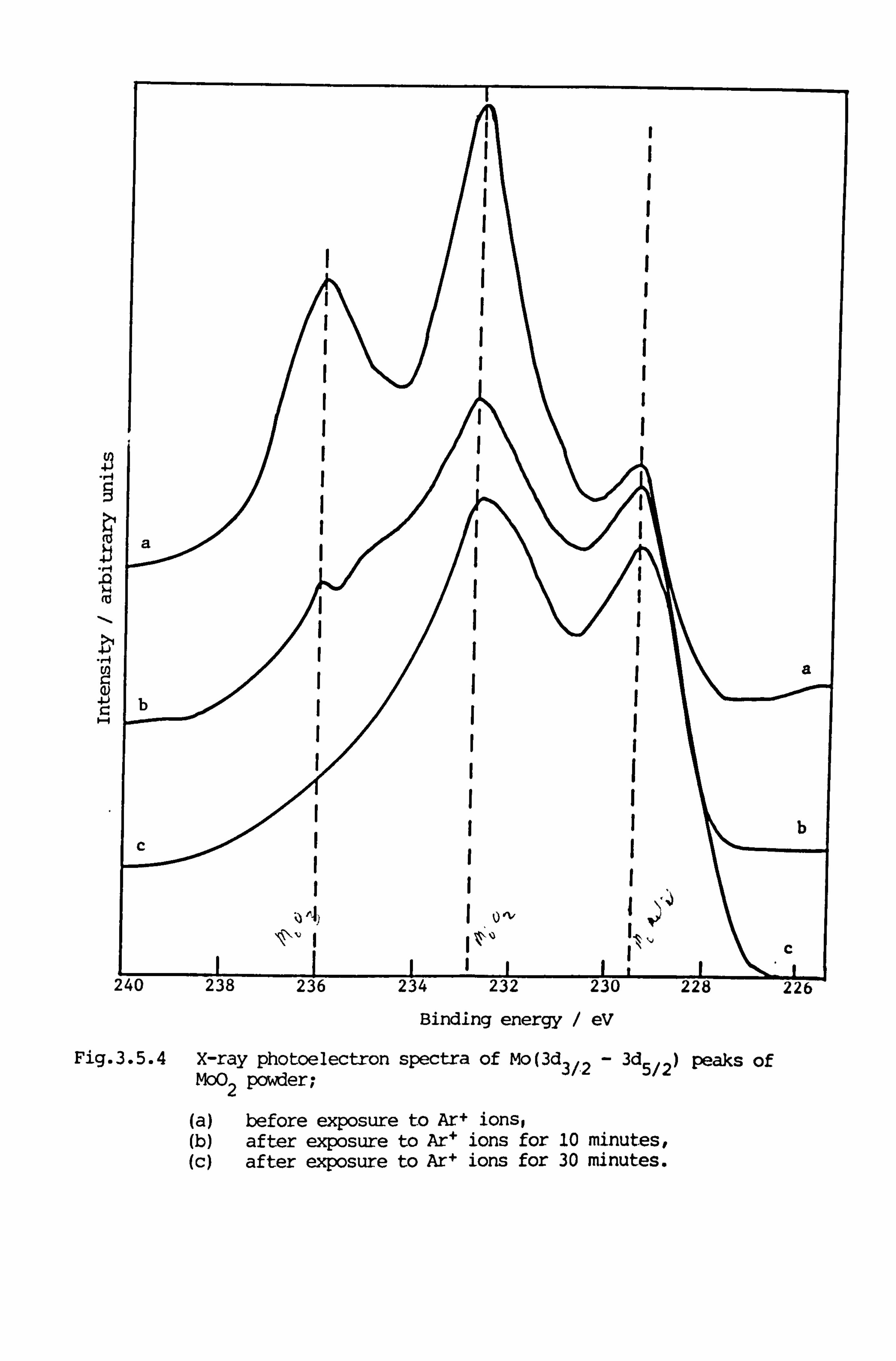
49
.0 N4 (ö
Fig. 3.5.4 X-ray photoelectron spectra of Mo(3d 3/2 - 3d 5/2 ) peaks of MoO2 powder;
(a) before exposure to Ar+ ionst (b) after exposure to Ar+ ions for 10 minutes, (C) after exposure to Ar+ ions for 30 minutes.
Binding energy / eV
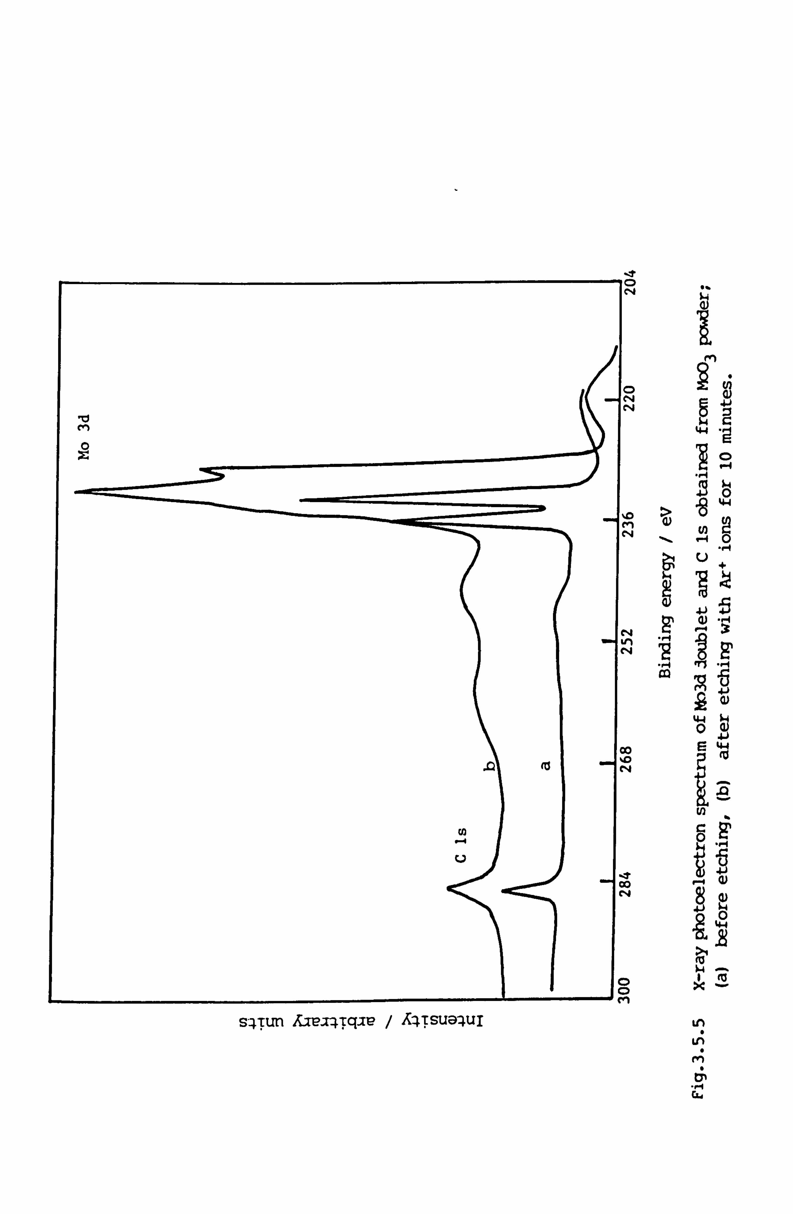
,0 en
(0
to
s-4Tun A; mjqTqxe / A4TSUD'4uI
c.. 1
0
14
44
+
41
114 0
U)
,D
44 S
In In
m
CLd
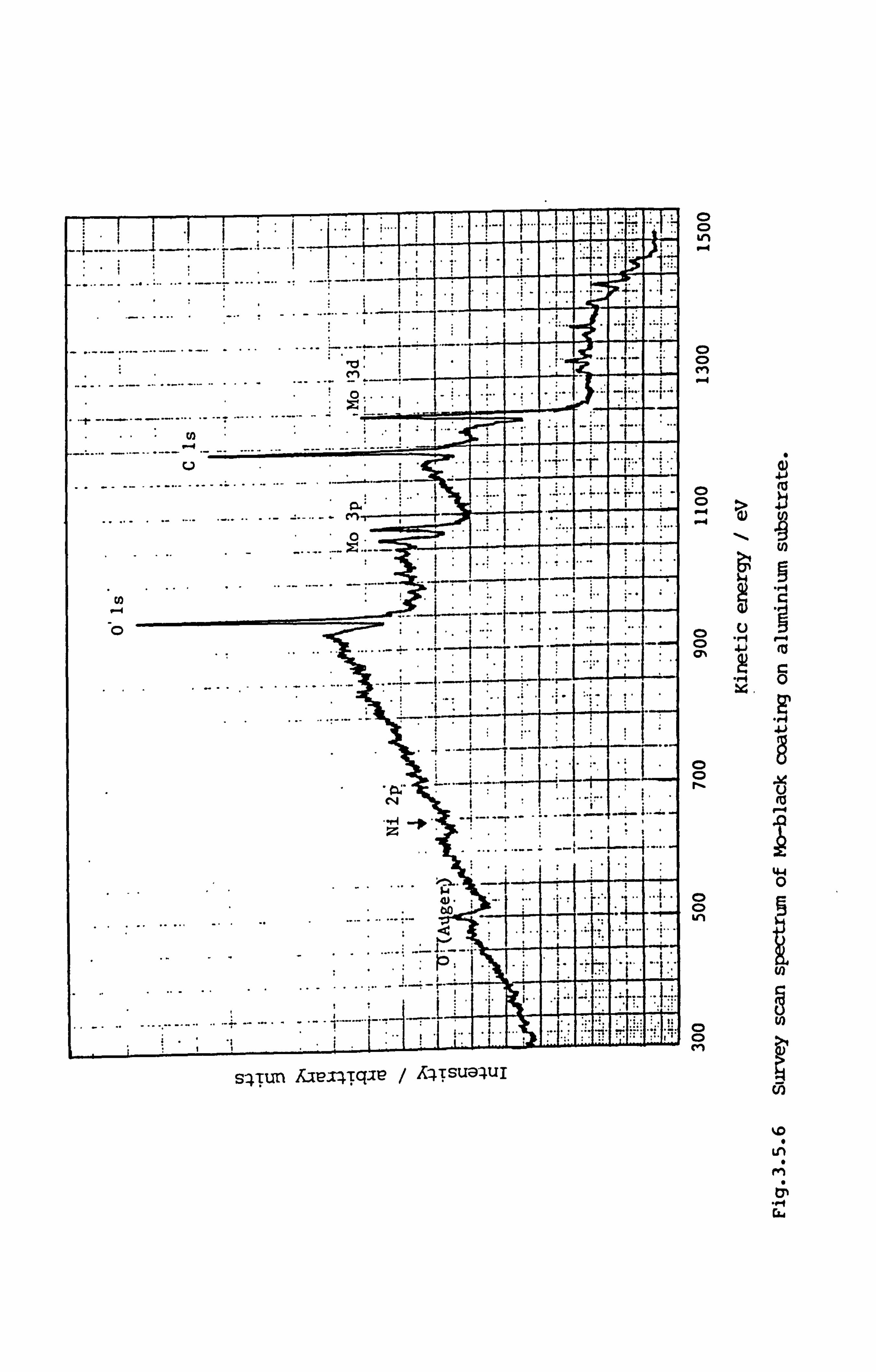
T77F.
Fq 1447
C11
W lie
74
. .....
s-4Tun AjeT4Tq. 'e / A4Tsua4uI
0 0 tn
cn -4
fi 0
(o 0>
Lo
Cý a 41 (a
Ln
cn
(7)
1ý
rAw
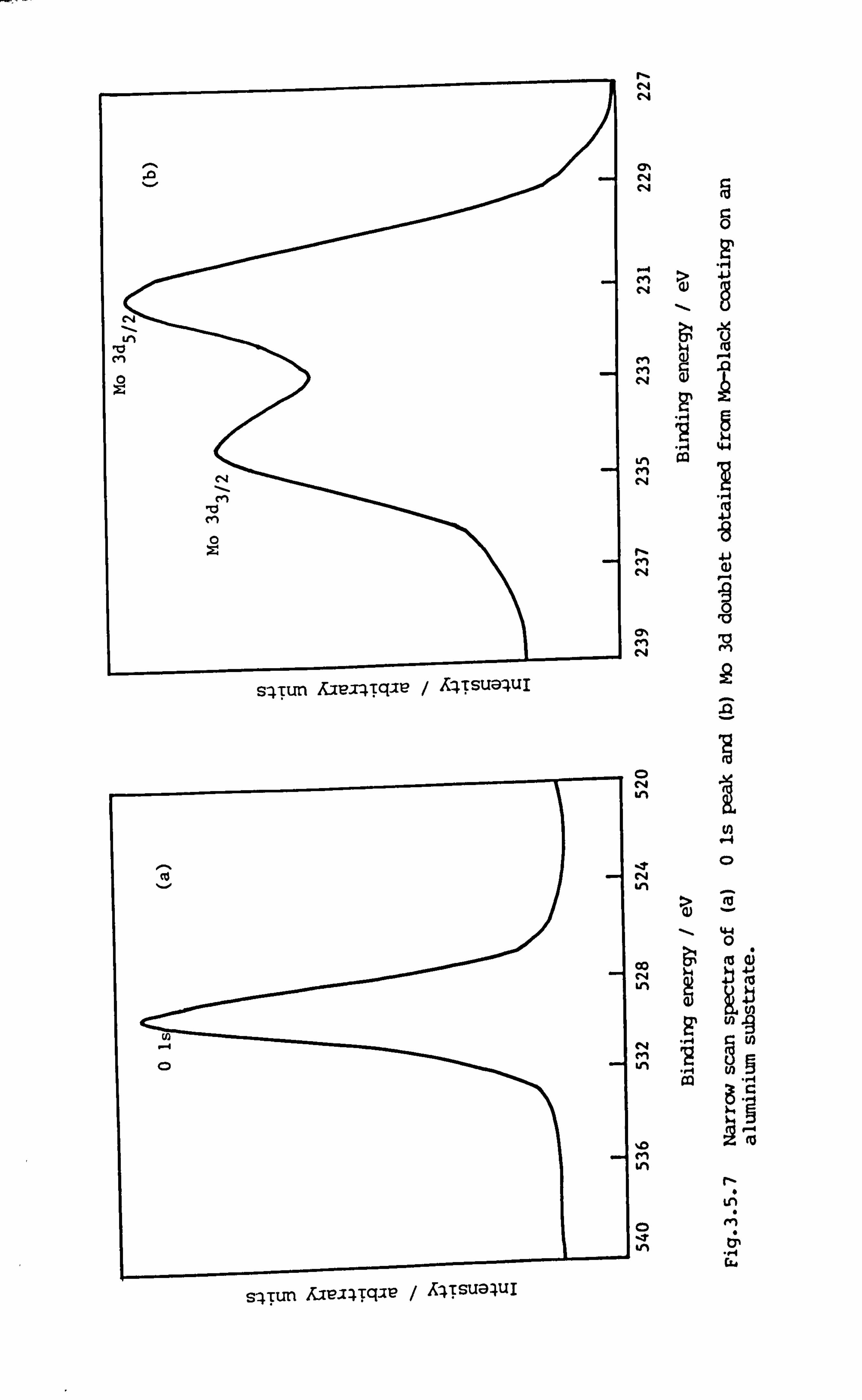
r, c4 cq
Cl% r4
CIM
M
. -f
.m LM cm
0
Co ýI, C*4
%D
ul
2 r. 0 F
rn
du 44 0
u3 .H
N
s-4Tun 7av-14Tq-1LI / A4TSU9'4uI
s'4Tun 7a-ej4TqjL, / A4TSua4uI
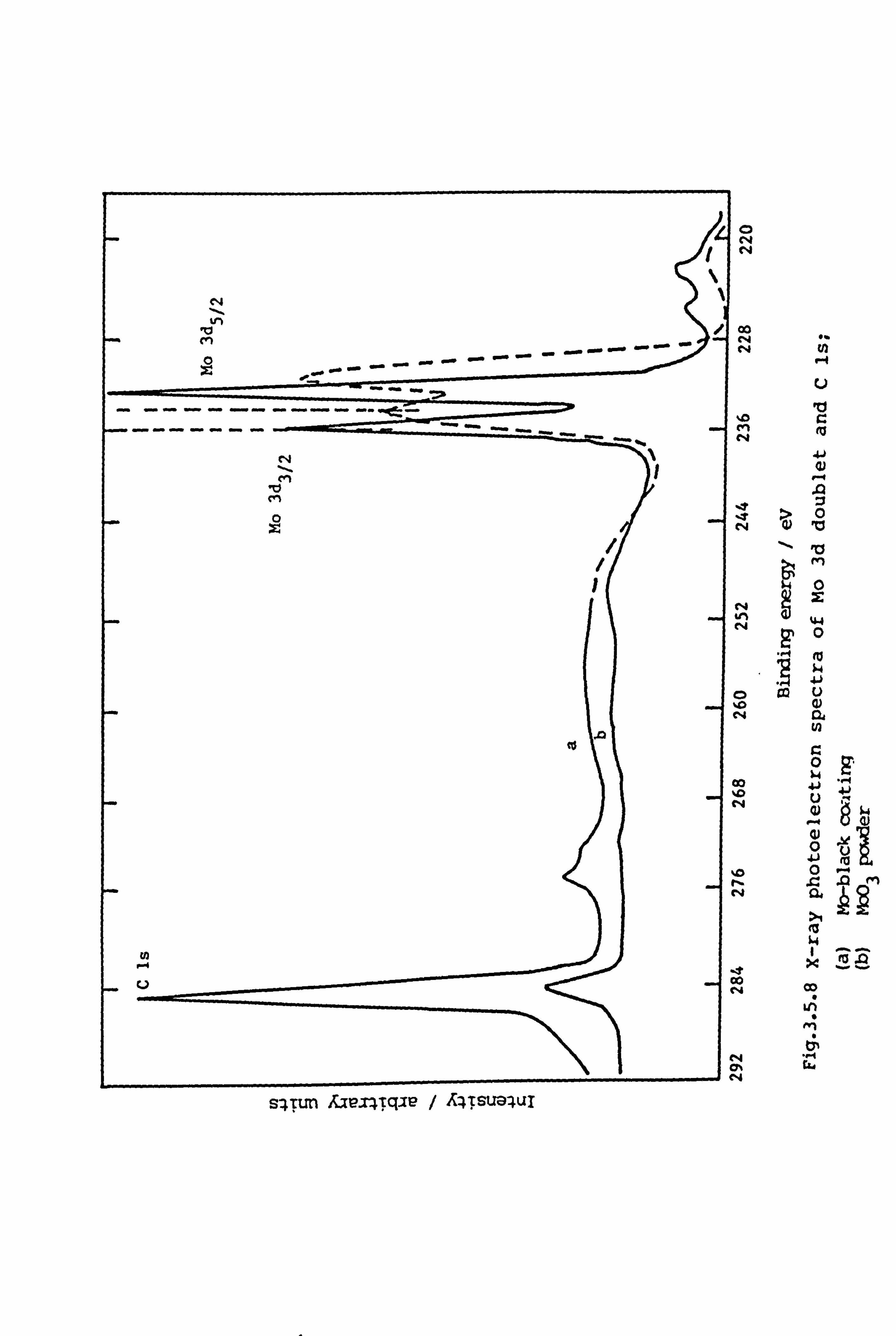
en 1
Ici cm
00
C14
C14
C4
C14
m ýo N
D
)o 14
14
s-4TLrn Ajpx4Tq-ie / A4Tsua-44
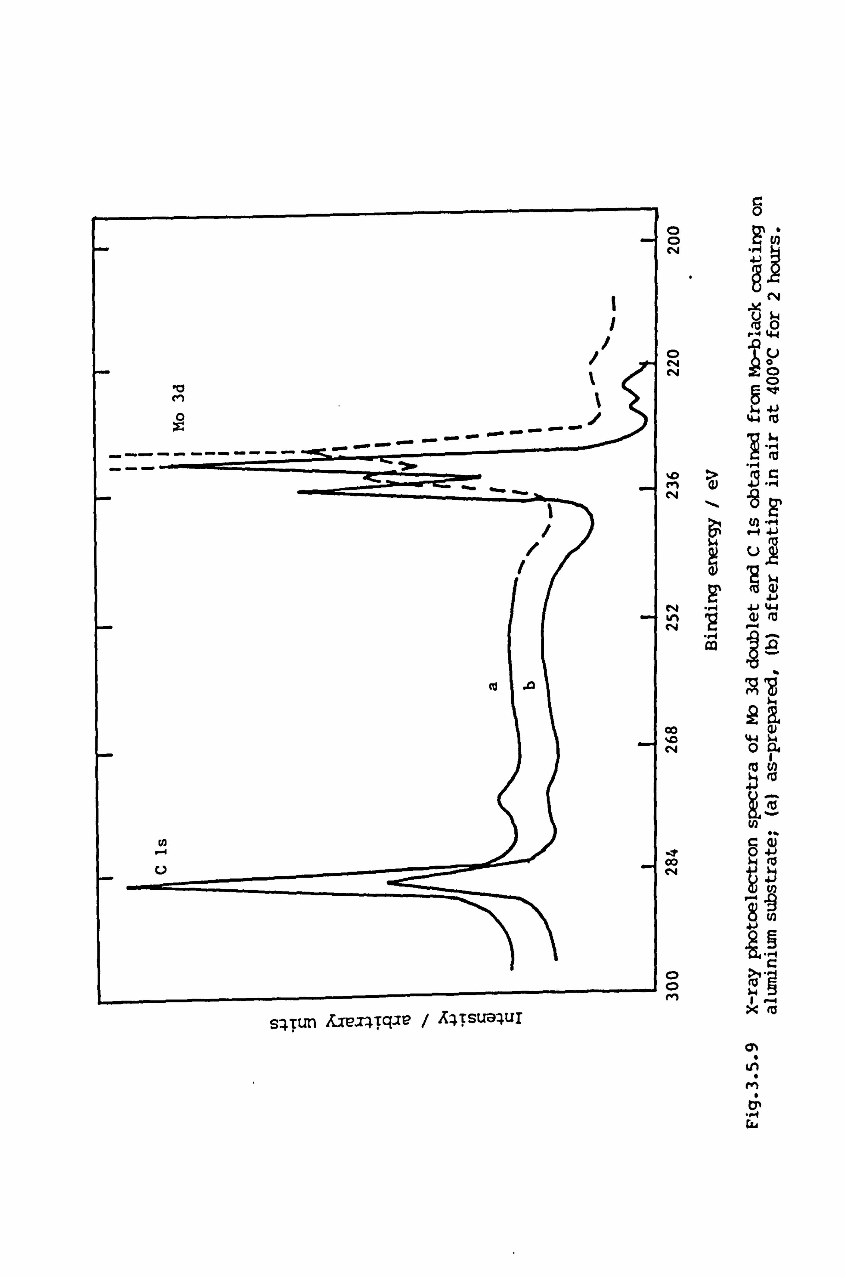
I
,0 cn
/ �
I -- ----
-----
/ /
I
co 14
rn
s-4Tun Ajej-4Tq-M / A4Tsuawr
C14
0
%0 cm r4
V4 LM 04
eld
0 0 m
I
(UO P-I t4.4
CD
4j
(0
U. 2
1P
0 lý
(0 0
g u2
c 0 41
(0
x (0
ON
U; 14
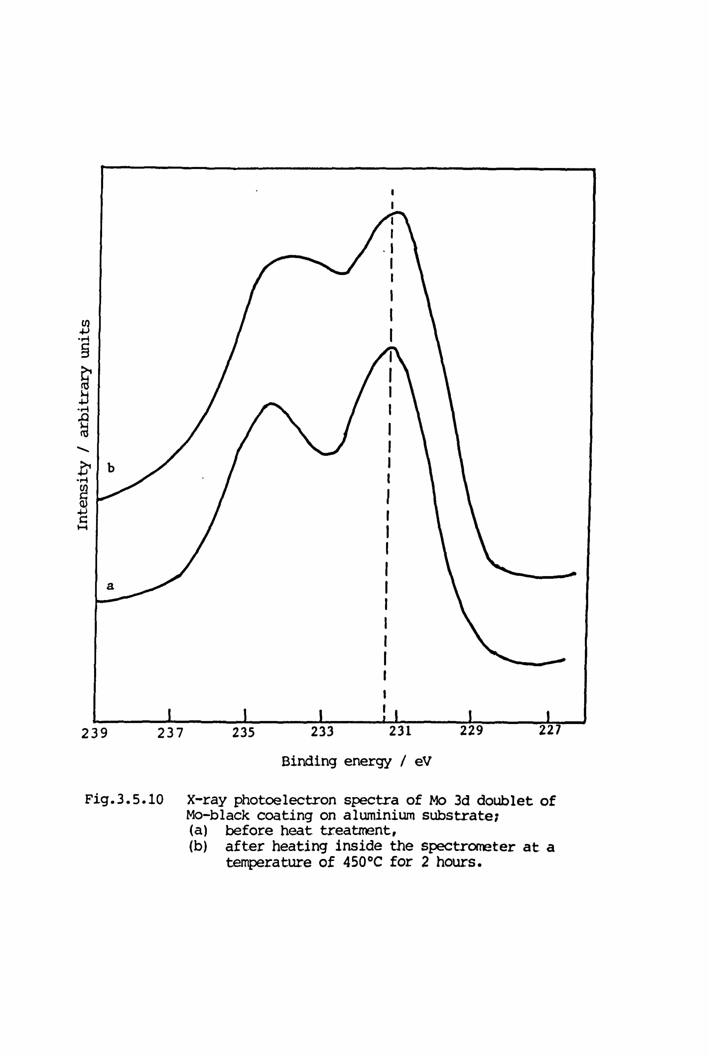
b
IQ7 'A 7 215 233 231 229 227
4ý
4ý -4
F-4
2.
Binding energy / ev
Fig. 3.5.10 X-ray photoelectron spectra of Mo 3d doublet of Mo-black coating on aluminium substrate; (a) before heat treatment, (b) after heating inside the spectrometer at a
temperature of 45011C for 2 hours.
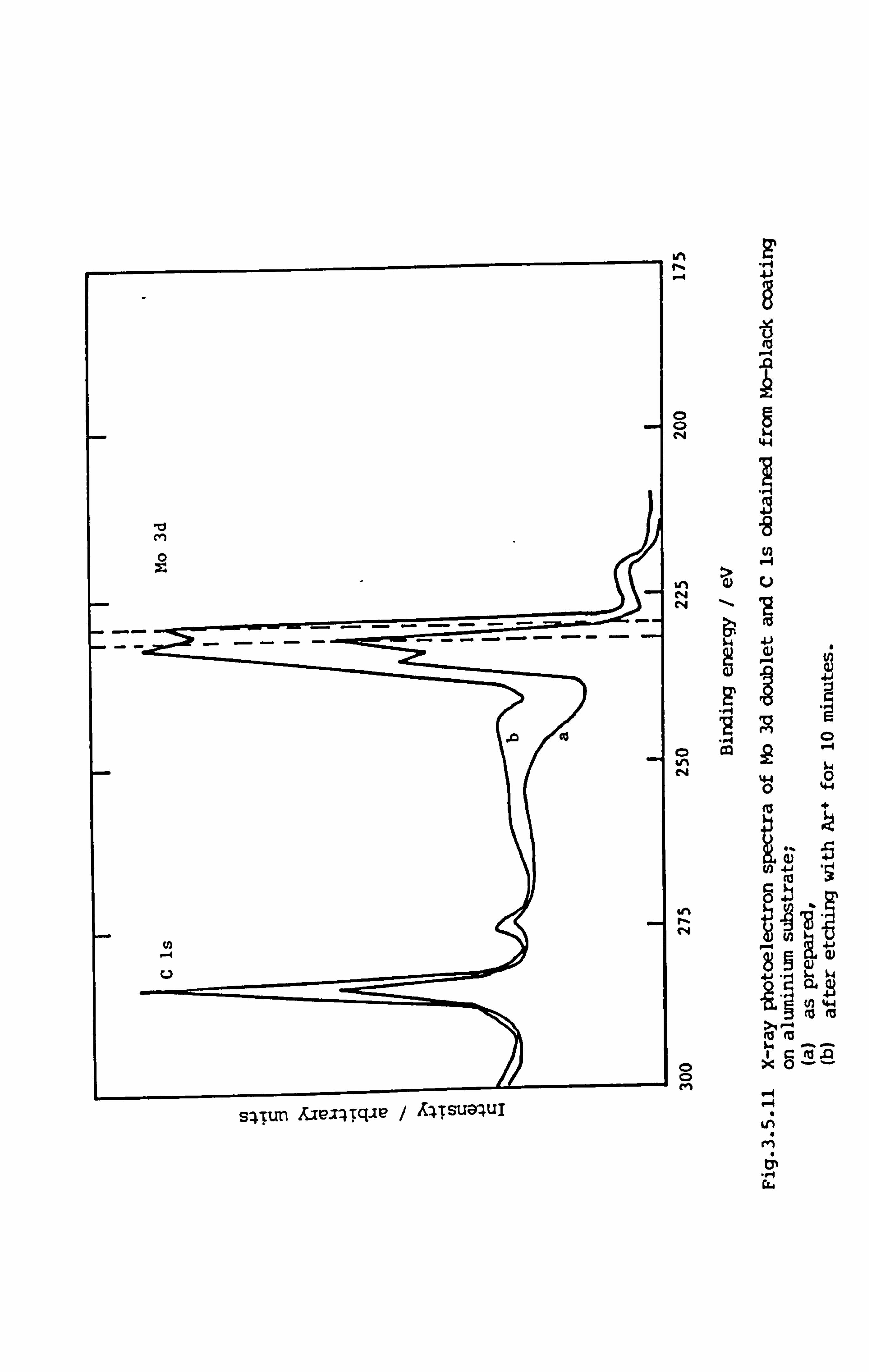
LM
.0
C4
ul L)
C-4 C*4
41
9
0
44
(a +
a 0 C14
Lit
(n 44
G
Uý
fl!
tp
. 14 rjw
s-4Tun Jap-T4Tq-ie / A4TSU9'4uI
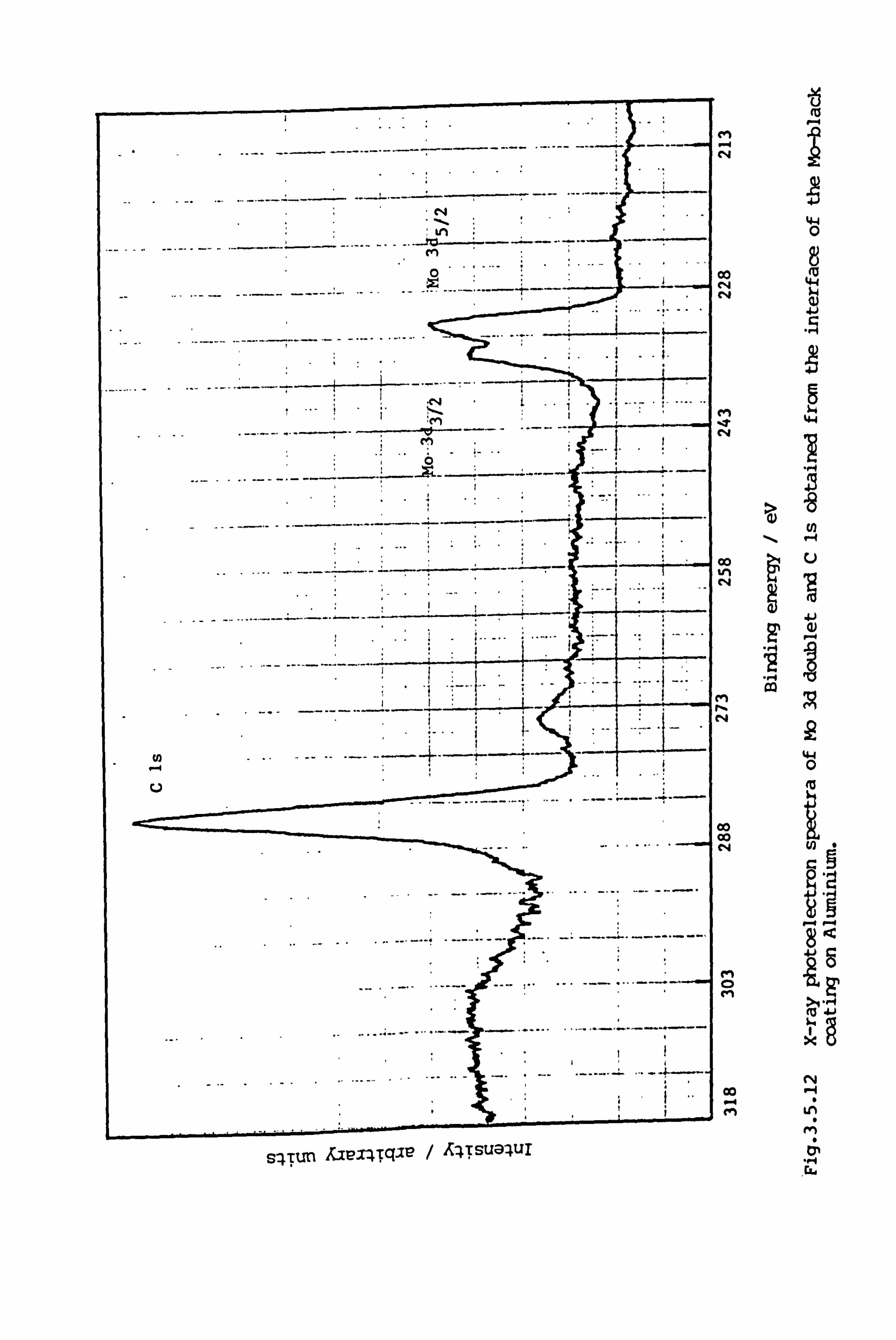
-ö tu P-4
cm .. 4 cli
44 0
8
00 rq a
> (n
00 u tn
Co 00
m 0e
N Go r-I -4 eel 'A
14 S74TUn laL"lTq"e / A4Tsua'4ul
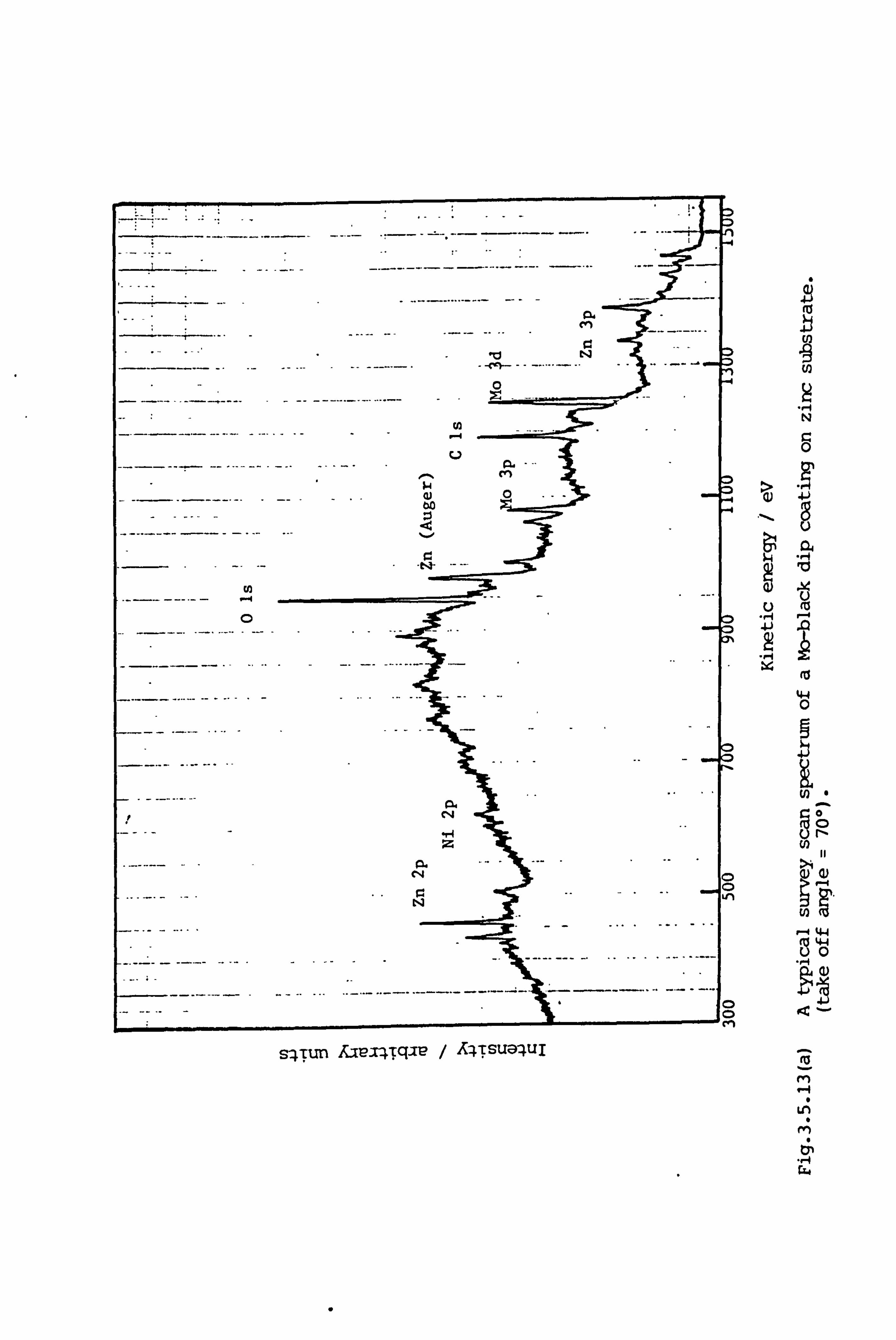
C14 -H z
Ln
sqTun Faz? x4Tq-Tu / A4TSU9'4uI
N
04 $4
4J .0 A
44 0
U)
U)
4
U3
ý,
44 'o
rn
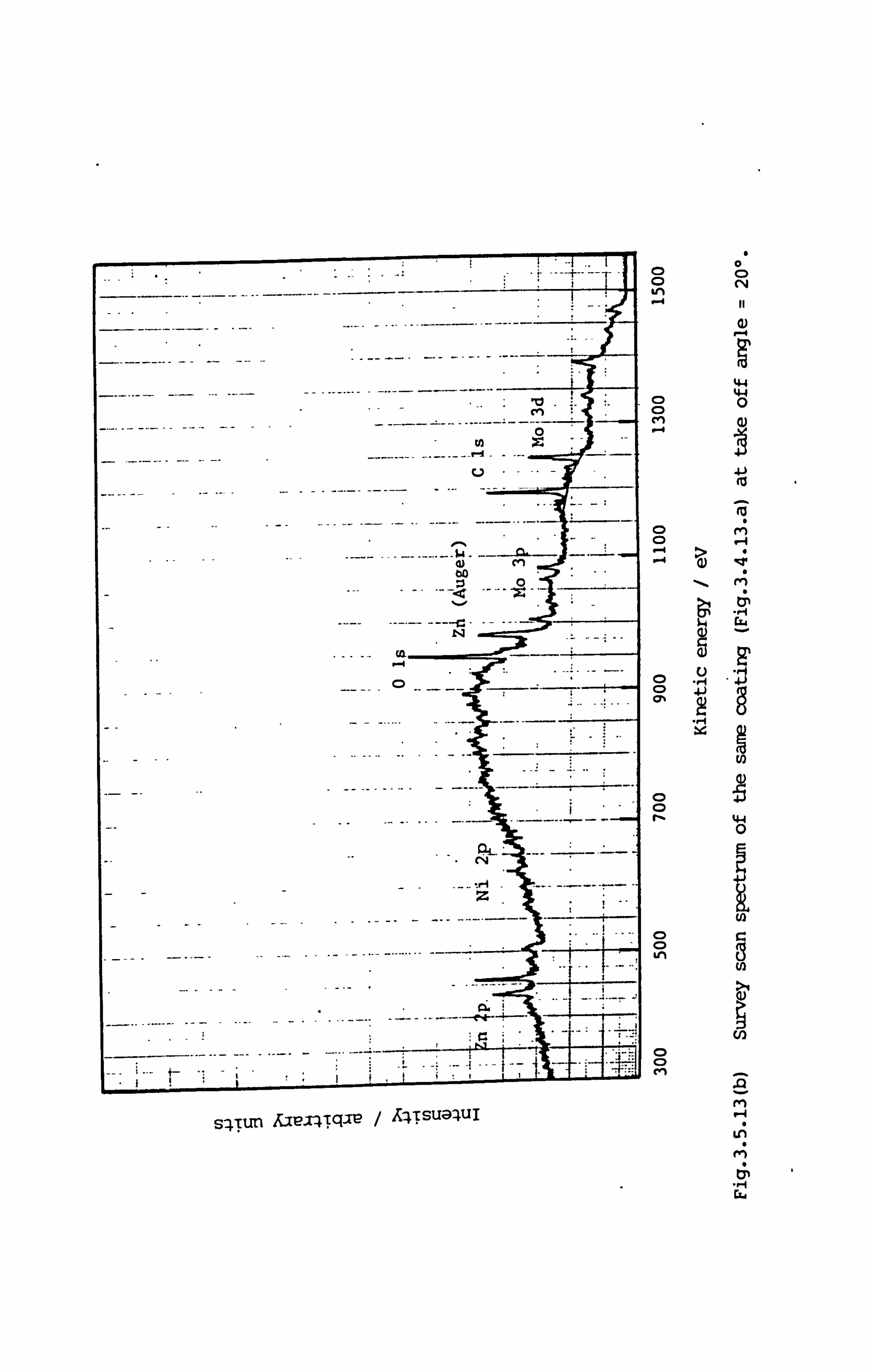
C, C%4
Ln
44 4-4
CD 0 C) en
41 (a
t4
0 0 F-
0 0 U-I
0) . 14 rT4
U)
4-4 0
C) Cý
.Q ry) r4
U;
r4
rjw
sqTun Aje-T4Tqie / 44Tsu9WI
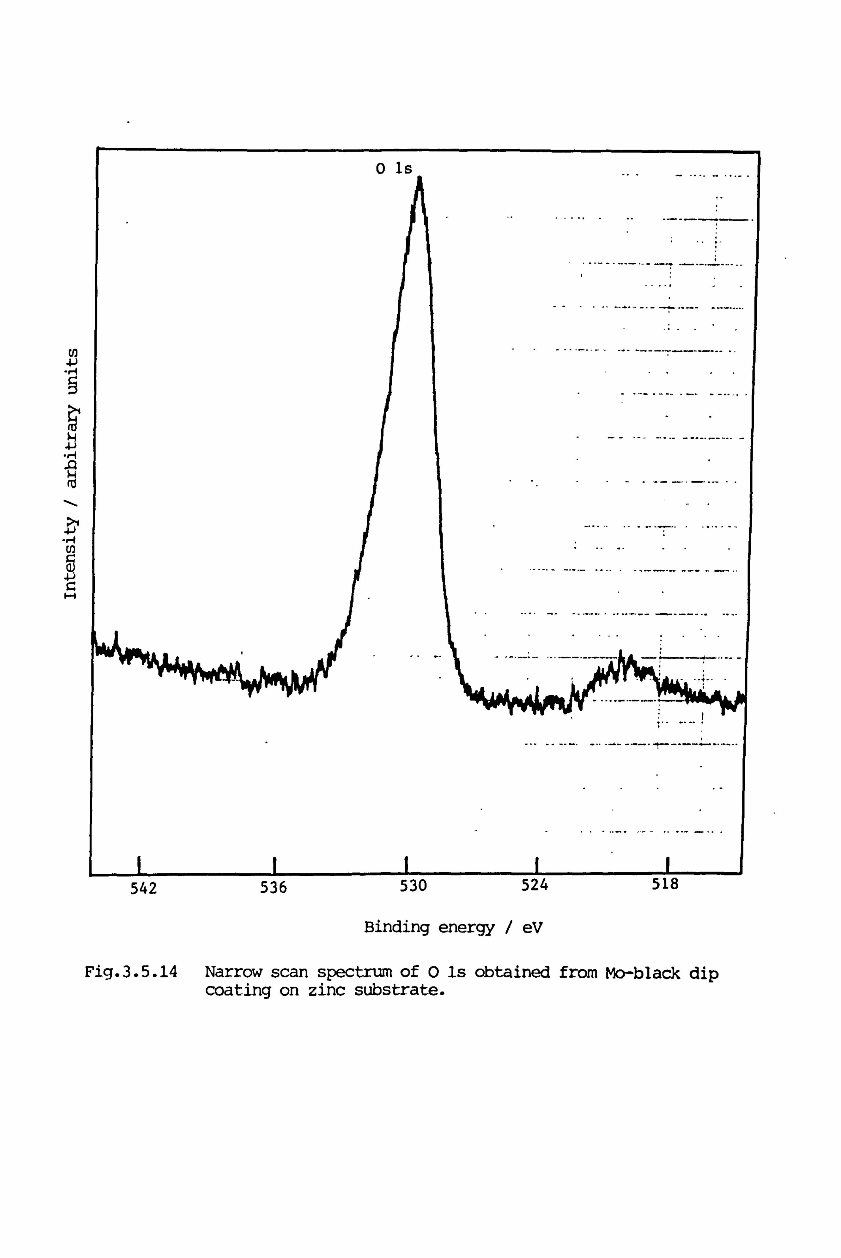
(n
(ö
(n g 4J) Z:
Binding energy / eV
Fig. 3.5.14 Narrow scan spectrum of 0 ls obtained from Mo-black dip coating on zinc substrate.
542 536 530 524 518
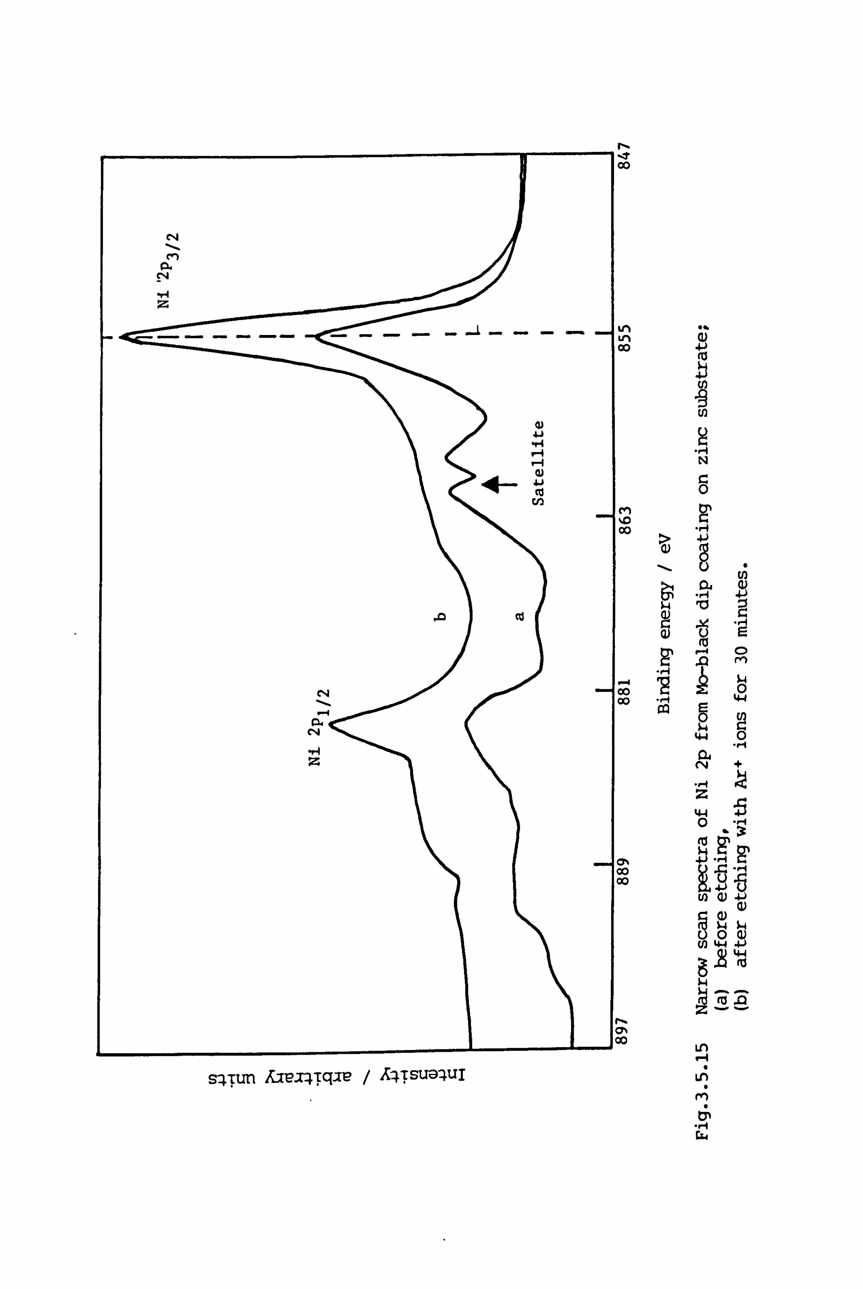
M ci
rq
4- tu
. 92 (U
sqTun U-e-qTq-ie / A-4Tsua'4uI
rý It OD
vli LM Co
m %M 00
-4 00 00
CY% 00 Co
00
w
(ö
b in -9 U) s
v2
r')
ý4 0
44
0
+
z
44 0
4ý -4
() 0 (On 41
ý. 2 to N4 MgZ
Ln
t; ., I 44
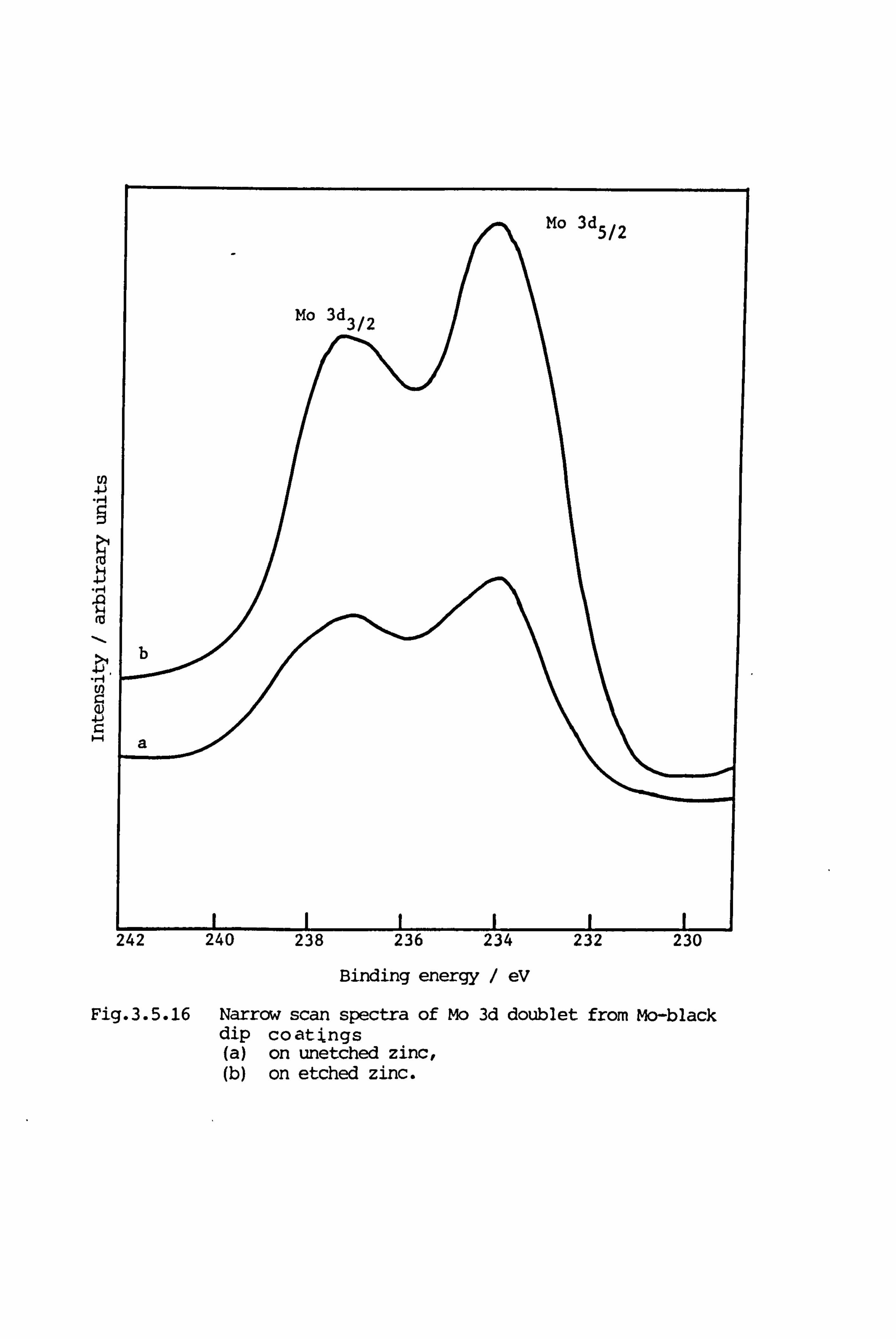
U)
(a
Fig. 3.5.16 Narrow scan spectra of Mo 3d doublet from Mo-black dip coatings (a) on unetched zinc, (b) on etched zinc.
Binding energy / eV
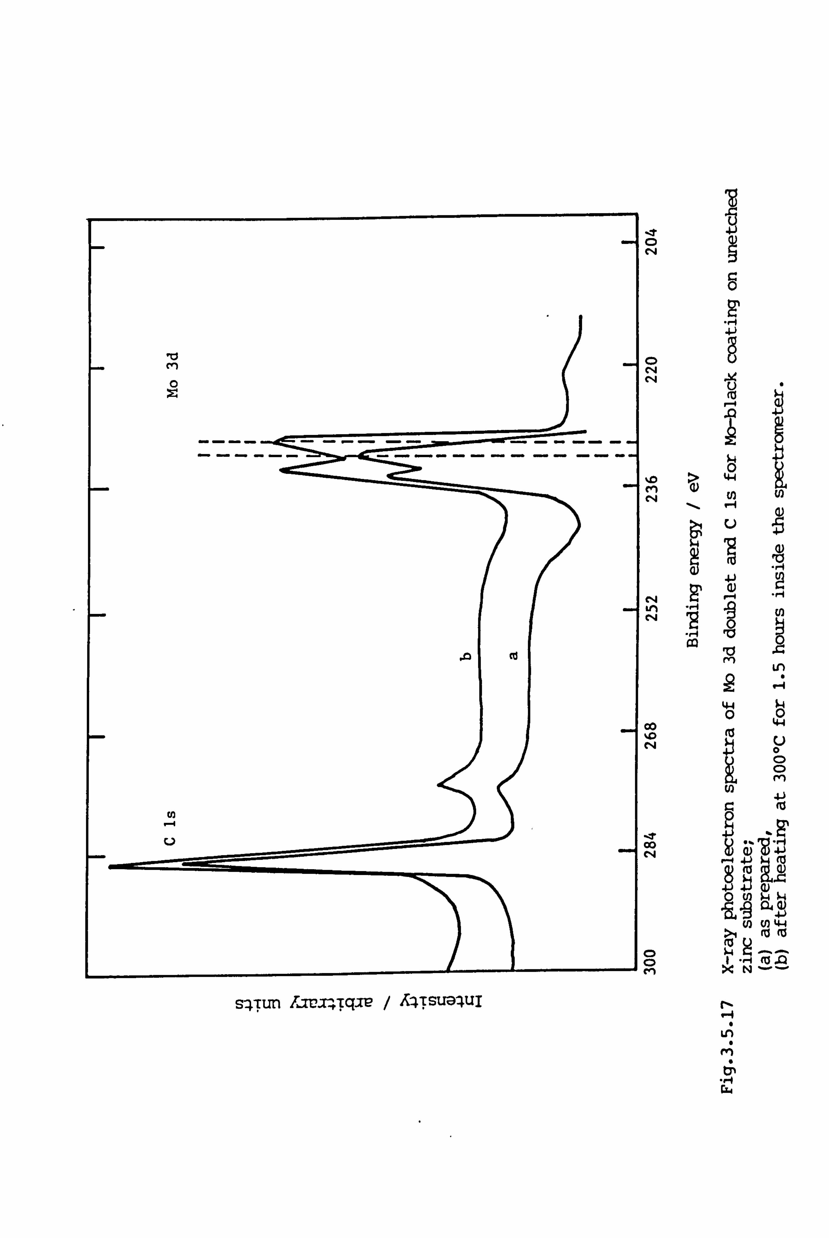
C.,
0
41 ca
cj
-I
s-4Tun Ima-, Tqae / A-4TSua'4uI
04
0 C14 C'4
%D ri C, 4
C, 4 tm r4
00 %D r4
ýT Co eN
C) C> m
I
18 16
Ici . 1. - 4-4
41
0 C) C) ri
r: (0
ý 4,0) ý ao) (n (0 4-4
g > to to
r- V-4
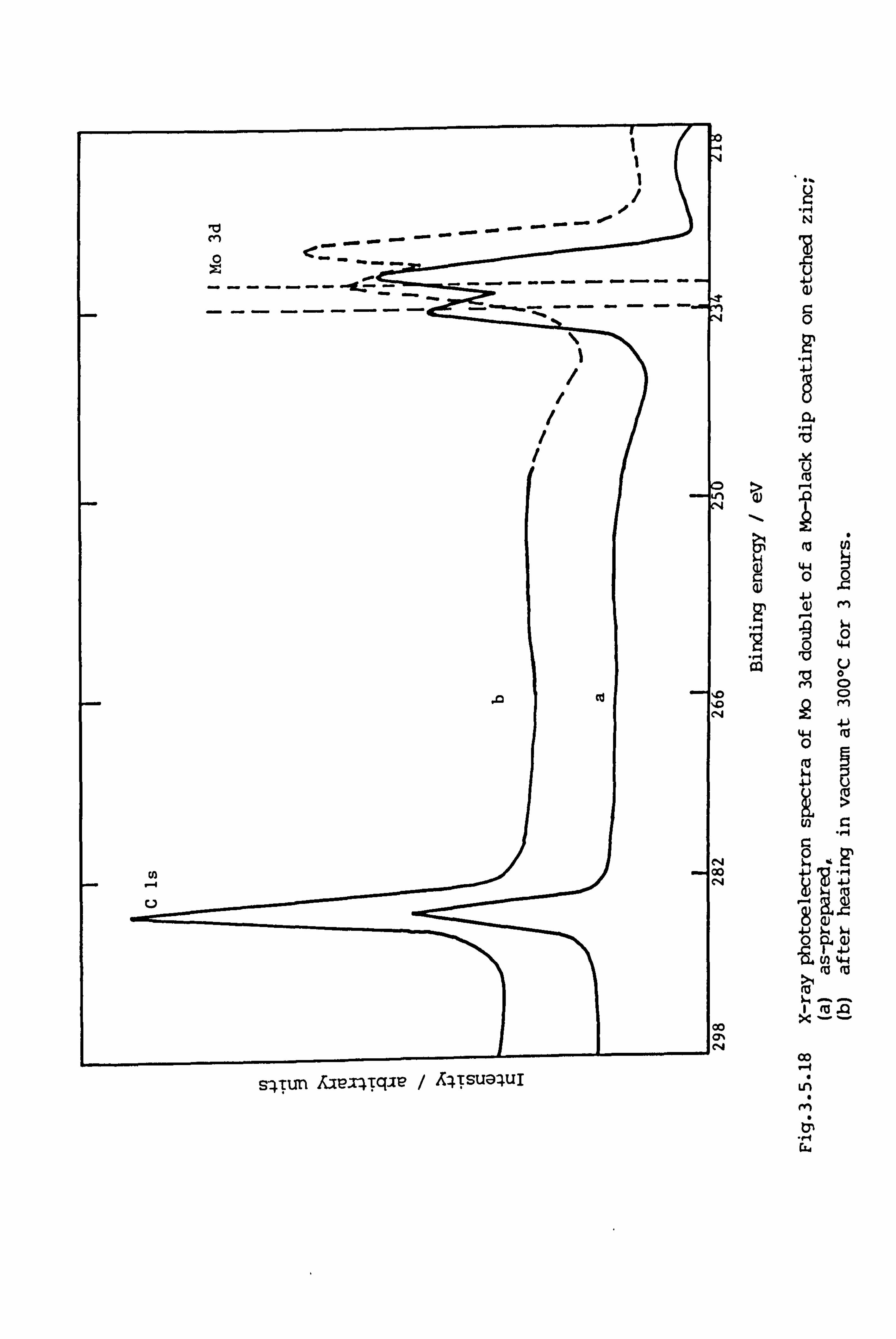
/ /
/ /
/
.010
(0
cc m C14
sqTun rae-T4Tq-ip / A4Tsu; 9'4uI
4-J
10
44 0
4J
0 0 44
'a 0 rn 0
C)
4-) 44 fu 0
(a 5
U)
0
41
4-) ý4 CIL
4-) U) '. 4
co -4
U; 14 t; . 1-4 CZ.
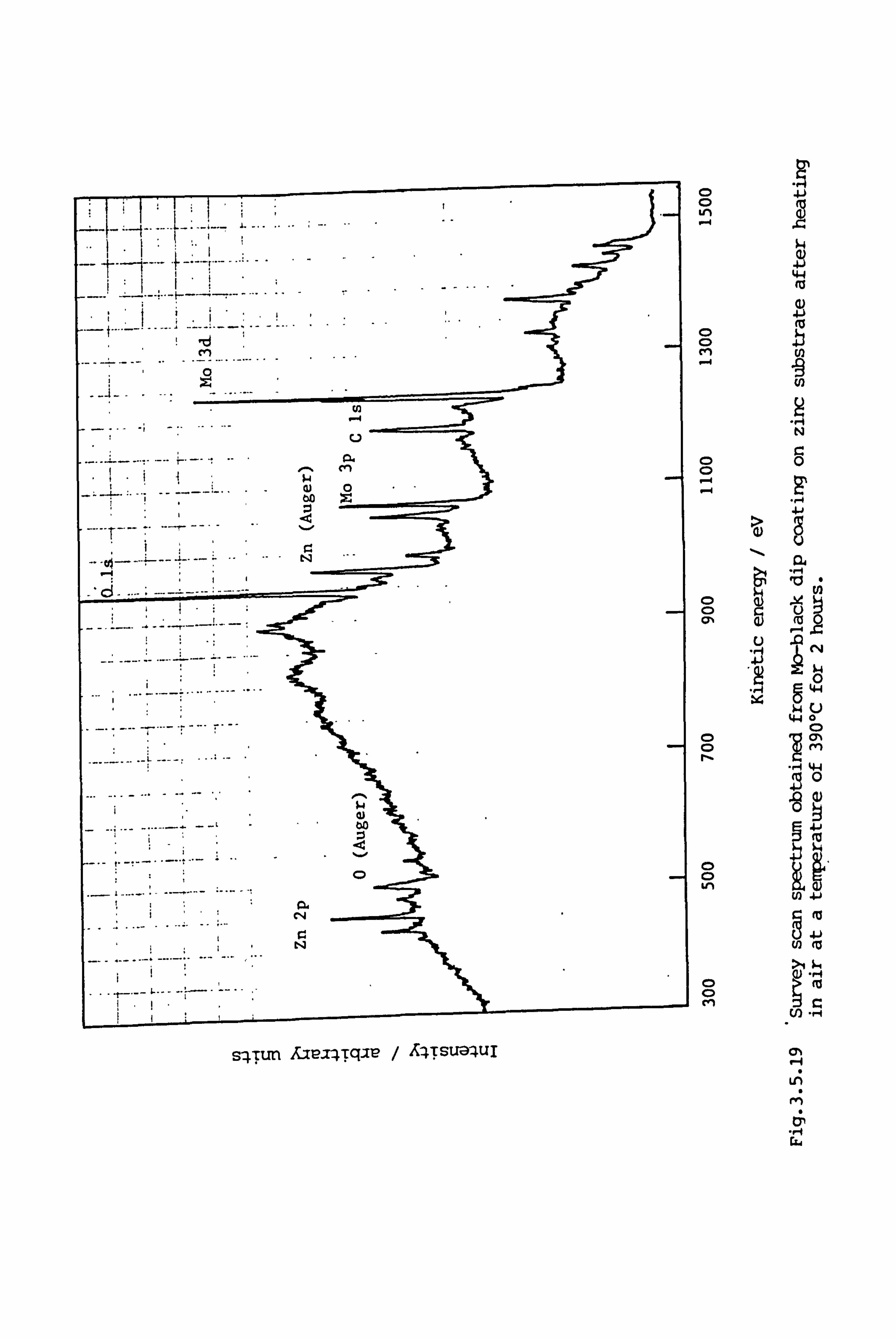
CD
(D (0
CD
N r_ 0
41
to
CYN 2
(, ö 0
44 0
cr% 0 rn
c>
.H 44 0
-0 Q)
U) -4.1
ul m
CD ri
tc:
(31, r-I
Uý
rid
sqTun Usz4Tq-'V / A4Tsu9'4uI
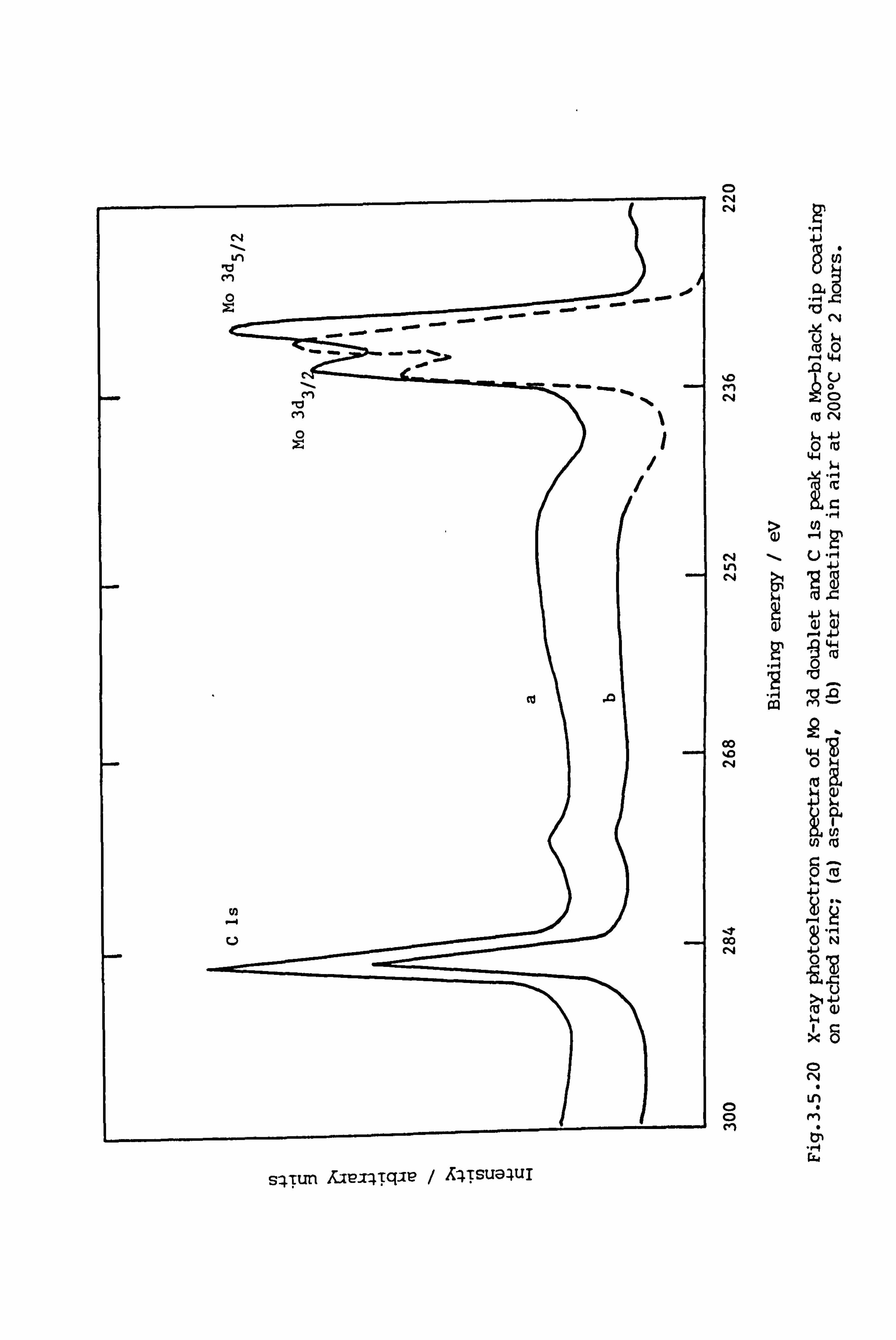
Iti Mj
01
(n %% l% , zi
rn %
(D C14
%D cm r, 1
C14 Ln C14
00 %0 r4
-t 00 C*4
0 0
10 r4
e ý4
C)
0 (ö 4-4
-4 EN 0., 4
4-4
10
g9 2 4-4 0
m ý Q)
U) (13
N
C) CV
V;
s-4Tun Axe-i-4Tqie / A4TSU@4uI
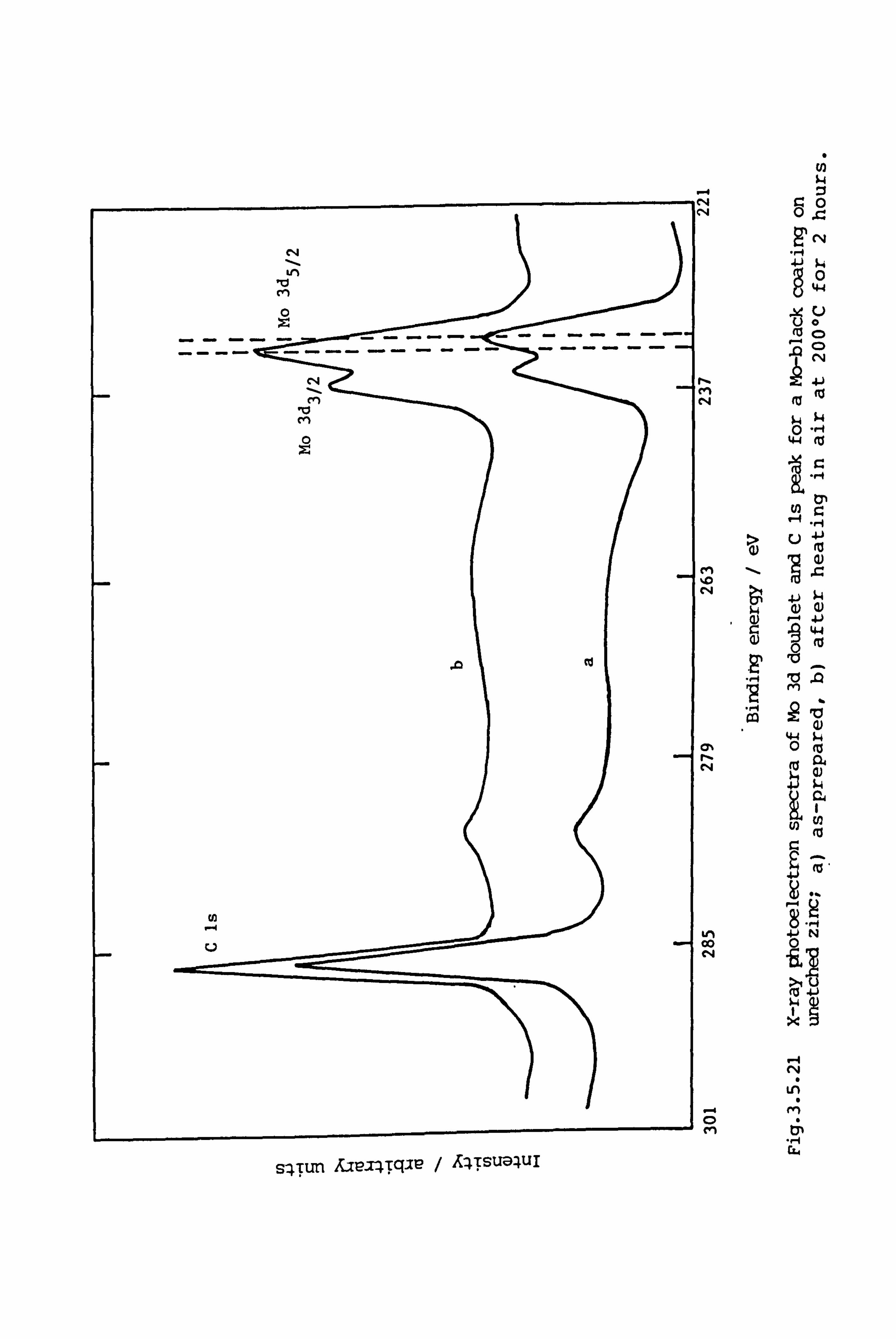
cz 0 0
'cý
0
44
ý- c> In N
rý
k
41 en (11 rq (U
ý4 0
4-1 tu
ul
>Q) (U (V
Q) 44
F0- . li
im 2v
tn
4J N Co 0
x
ý4 cli
U; t;
., j EL4
s-4Tun Ale-T4Tq-'L' / A'4Tsu'-l4uI
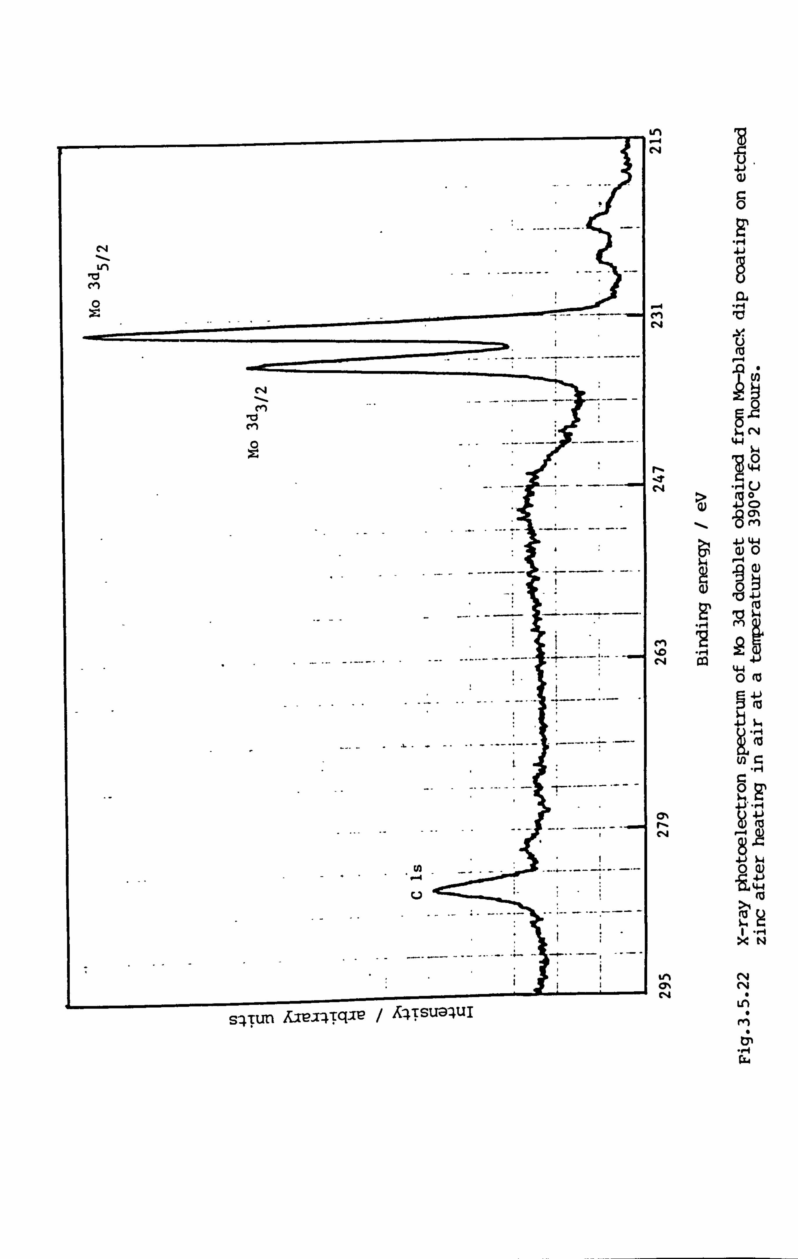
Ln 1-4 C4
Is
a) C
-4 en
cm %D C, 4
0
Lill
ON C14
0)
I
v
(0
C-) 4T
oa
(31%
-8 en 4J 44 0
00 ,8
ýý 2 if 44 0 (a
4J I
(a
C 0
4. ) ýM
N CN
U;
1;
t; -4 rL4
s-4Tun AAVI-4Tq"2 / JV4ýtiucl4ul
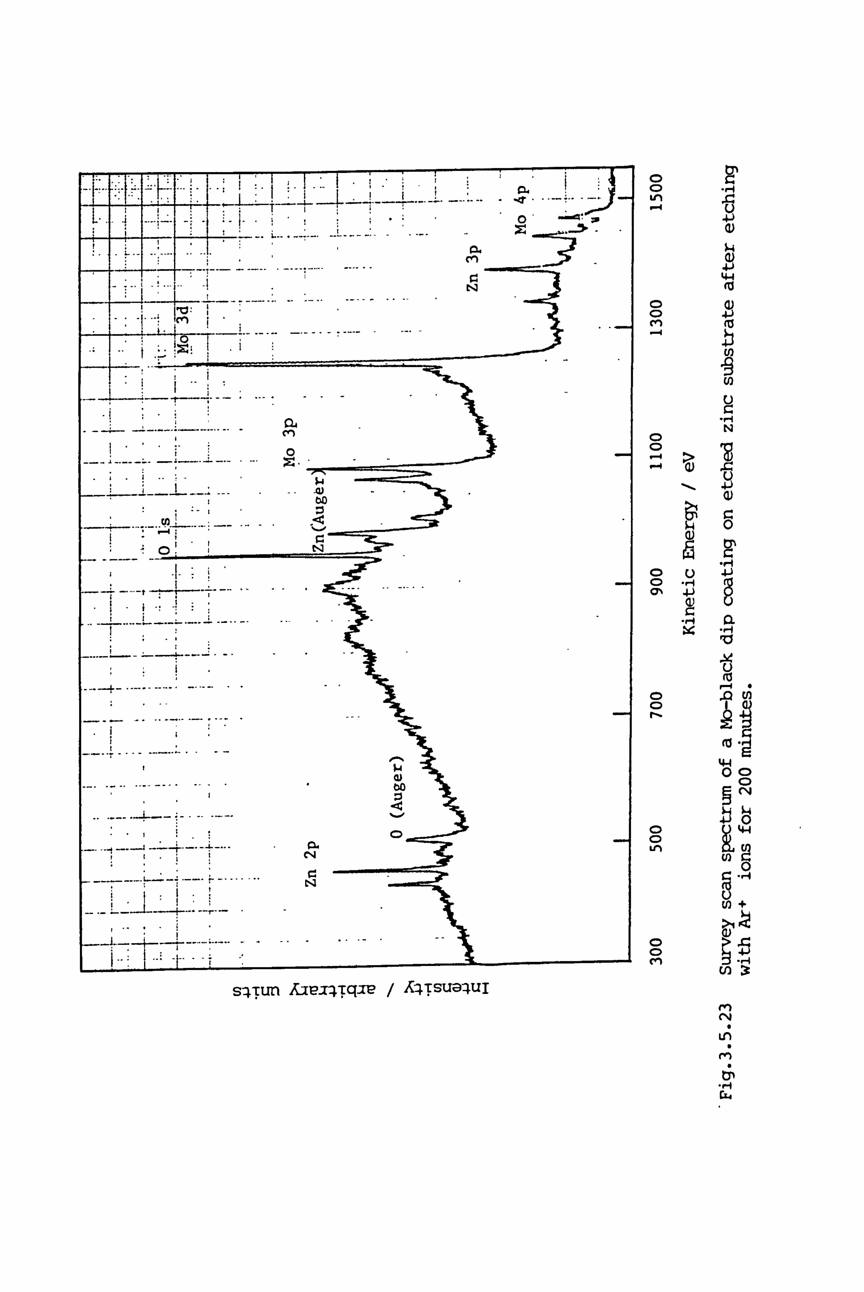
C-1
!, lo: I
04
-- -4-- cn
14
I. o! *; N
bo
C4
sqTun AipjqTqjP / A"4Tsu@4uI
tri 4
44 (a
0 a) Cl 41
El) -8 U)
N
ý4
4-) C) -4 c% 4-)
IrEl CL
(a
CD
44 0 C)
C) CN
44 CD
0
U) +
cn U) 3:
en
D.
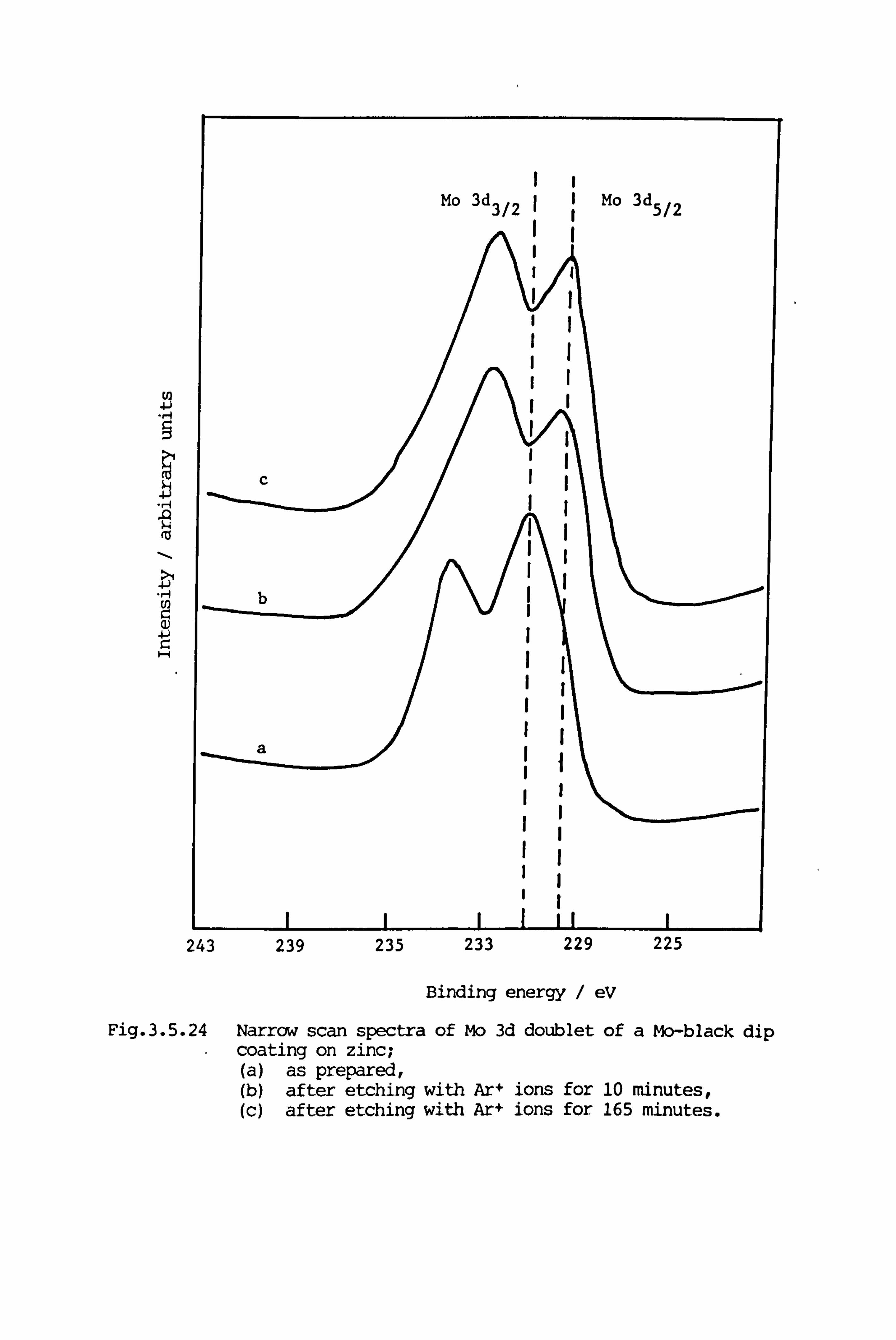
(n 41
H -2 (U
Er)
41 C:
Mo 3d 3/2 Mo 3d 5/2
c
b
a
243 239 235 233 229 225
Binding energy / eV
Fig. 3.5.24 Narrow scan spectra of Mo 3d doublet of a Mo-black dip coating on zinc; (a) as prepared, (b) after etching with Ar+ ions for 10 minutes, (c) after etching with Ar+ ions for 165 minutes.
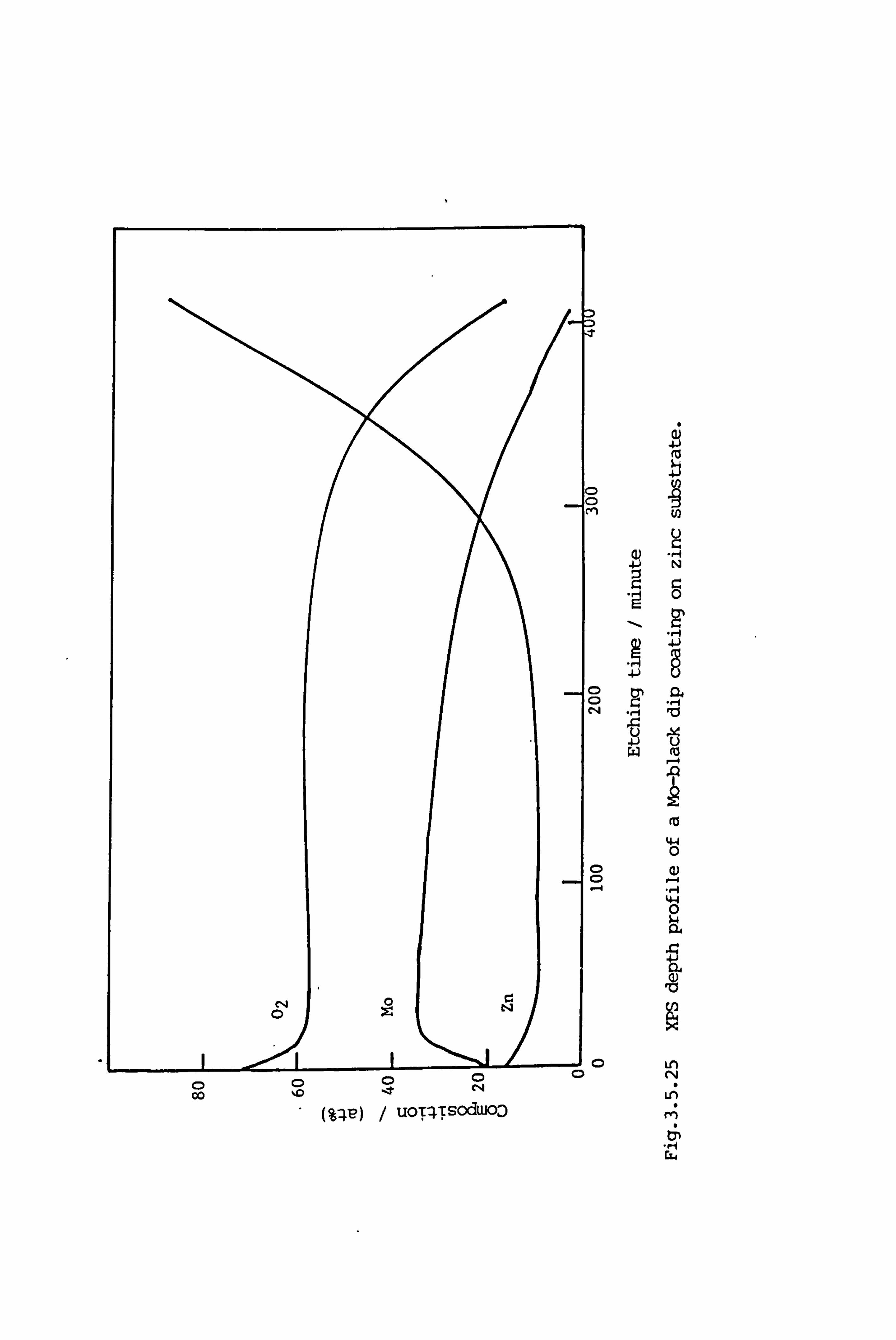
- CD M
- c c
c c
CD CD
00 %D -t CN
. (%qv) / U0T-4TsodwoD
"1I
j
fö
v lö (ö
1-4
rö 44 0
44 0
Ln N
LA
- 7 T
- 7 1
. -4----- ,- !-- --; -- ..;.. -
lad
c l o
s-4-run ýJe-T4Tqae / A, 4TSu@-4uI
Cý a
Ln -4
0 C) cn -4
0
4J
b4
0 CD r-
0 CD WN
M
124 .,.. 4 10
ko C14
Uý
rid
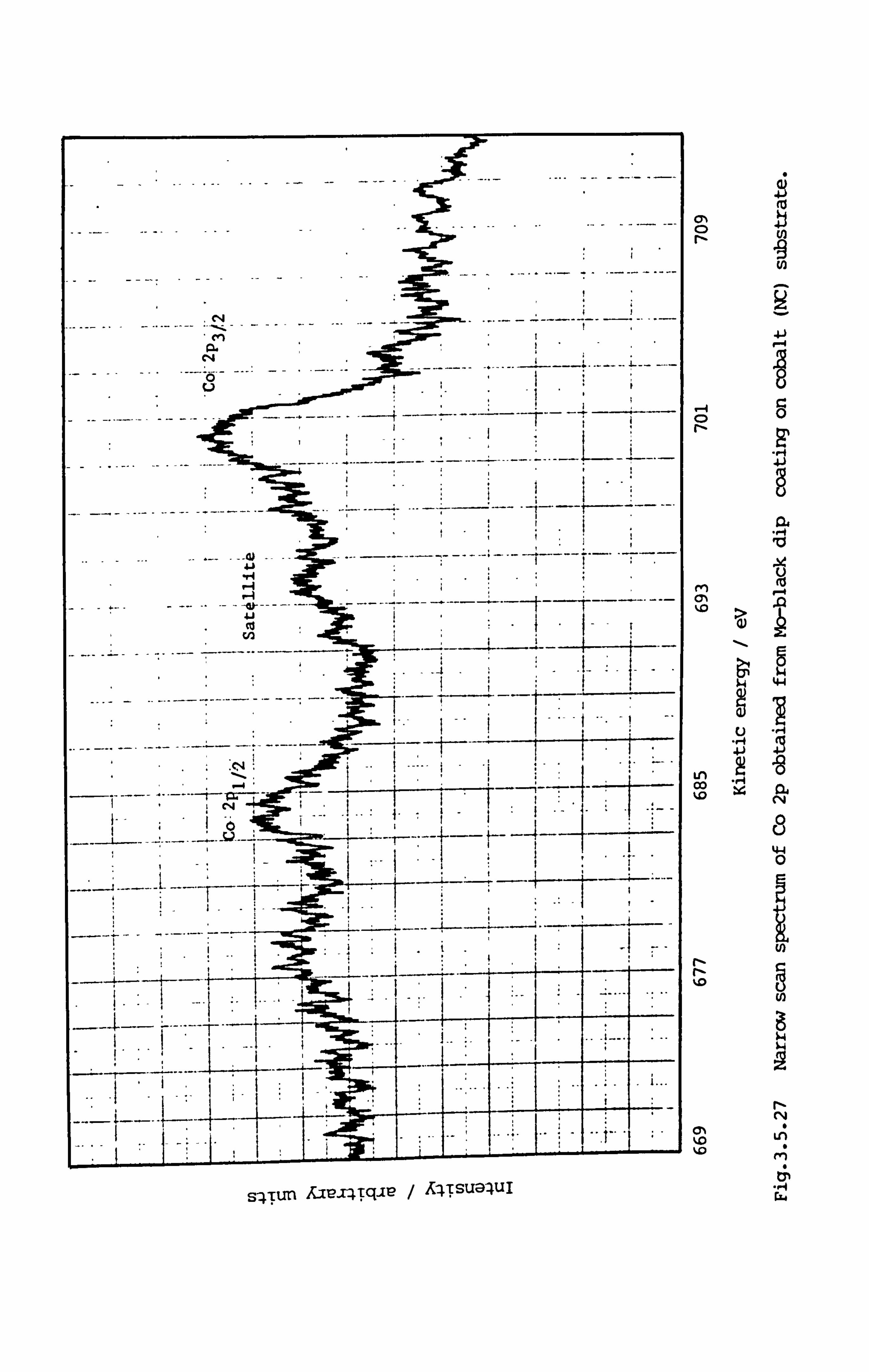
(Ti
iý 41
10
b4
r-i
9
44 0
1
U)
rl CN
II-
r
S-4TU"n A4TSUýý4UI
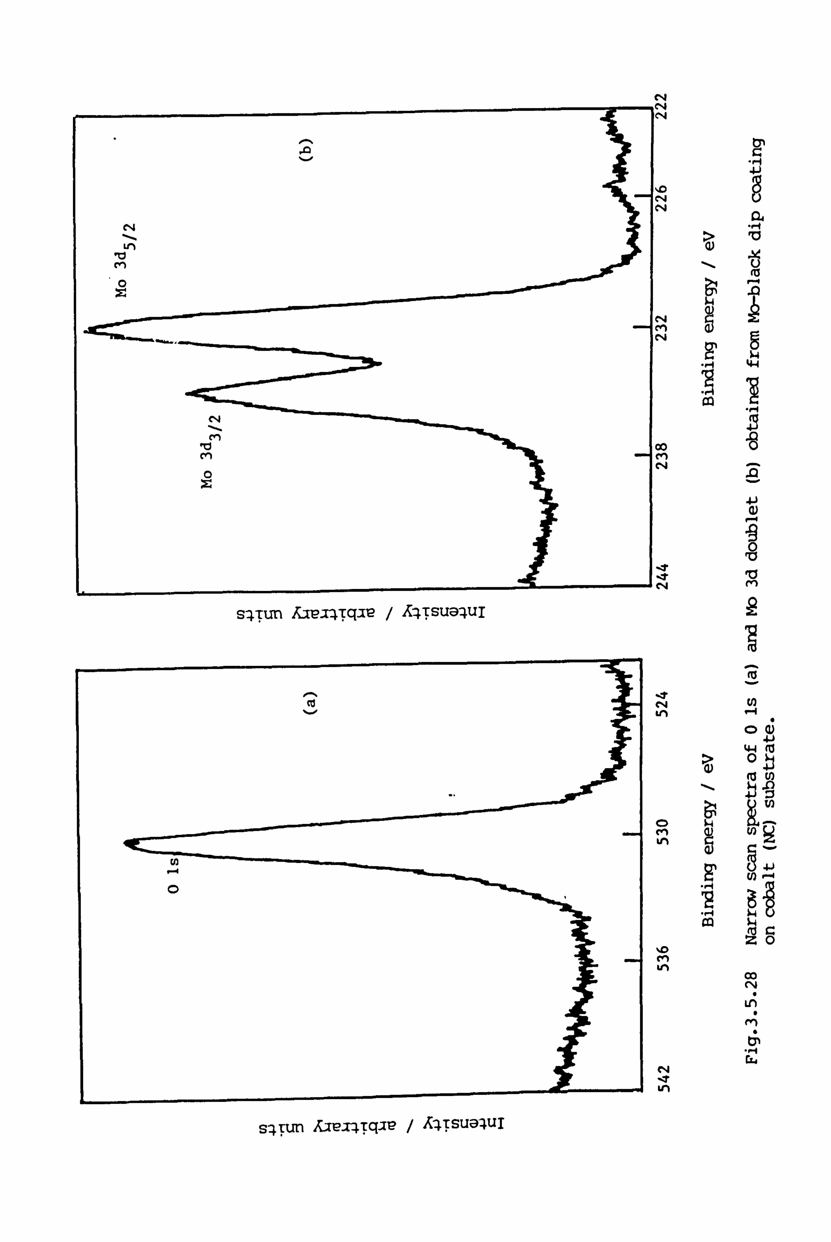
Clq
Lr) Ici cli
"0 00 cn - cm
S-4Tun A: mx4Tqae / AqTsuawI
U)
Ln
Cý en tn
- en LM
41
M
$4
4-4 N
co
41
00
0 Q) 41
4-4 fu
-11
ý4
4J r-4
Zý 0
00 (14 LA
e4 IT Ln
sqTun AIva4Tq-TP / A4TSUO'4uI
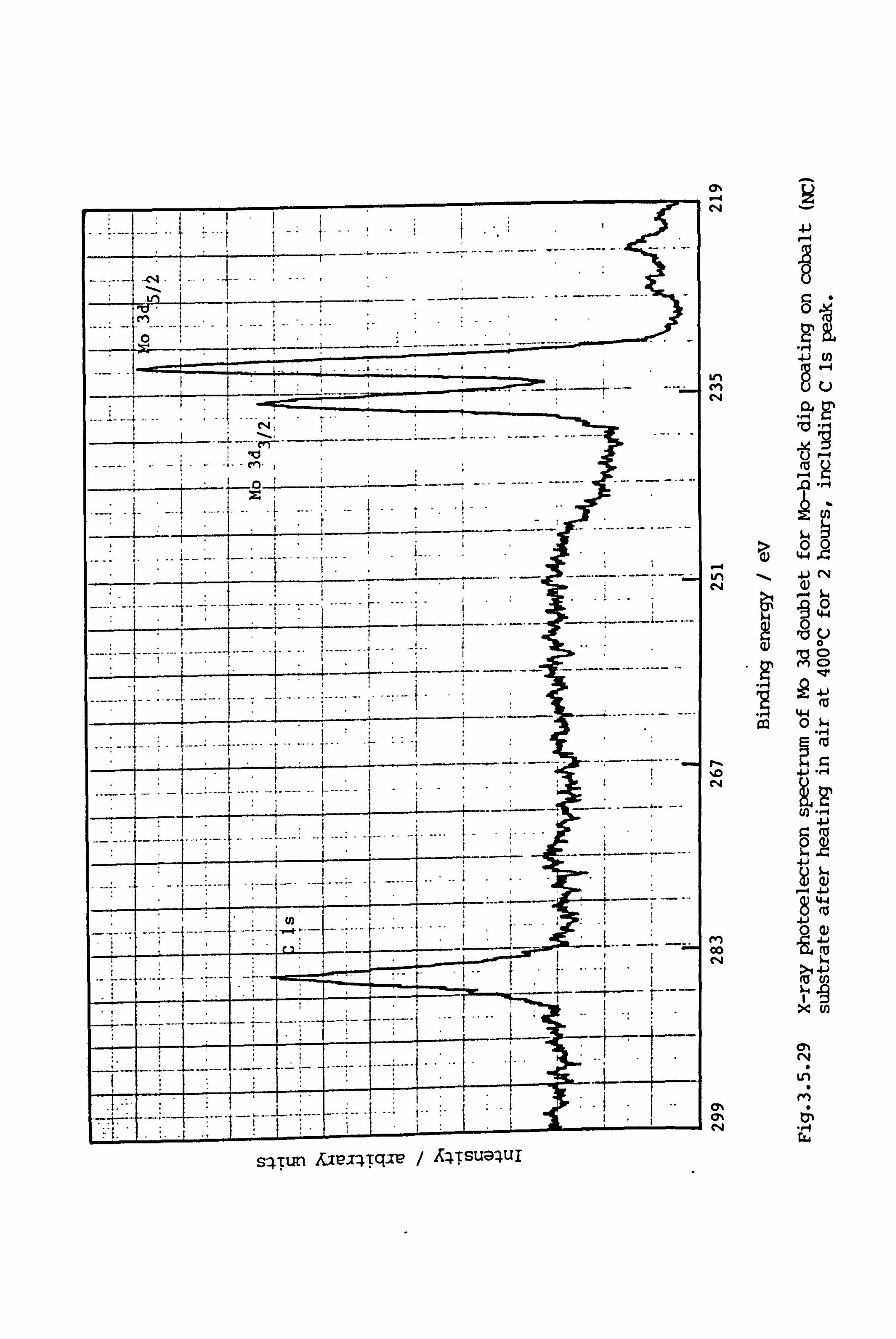
(7S -4 CA
Lri en C, 4
-4 Ln C*4
C14
rn co C14
ON 01% 04
I
4J
8
.W ul
v x
0 44 J. '
cm
'g) C: )
44 0 r= (0 ý4
Cl) 41
44
0 4) 4-)
ON N
s-4Tun AieAqTq-e / A4TSU94uI
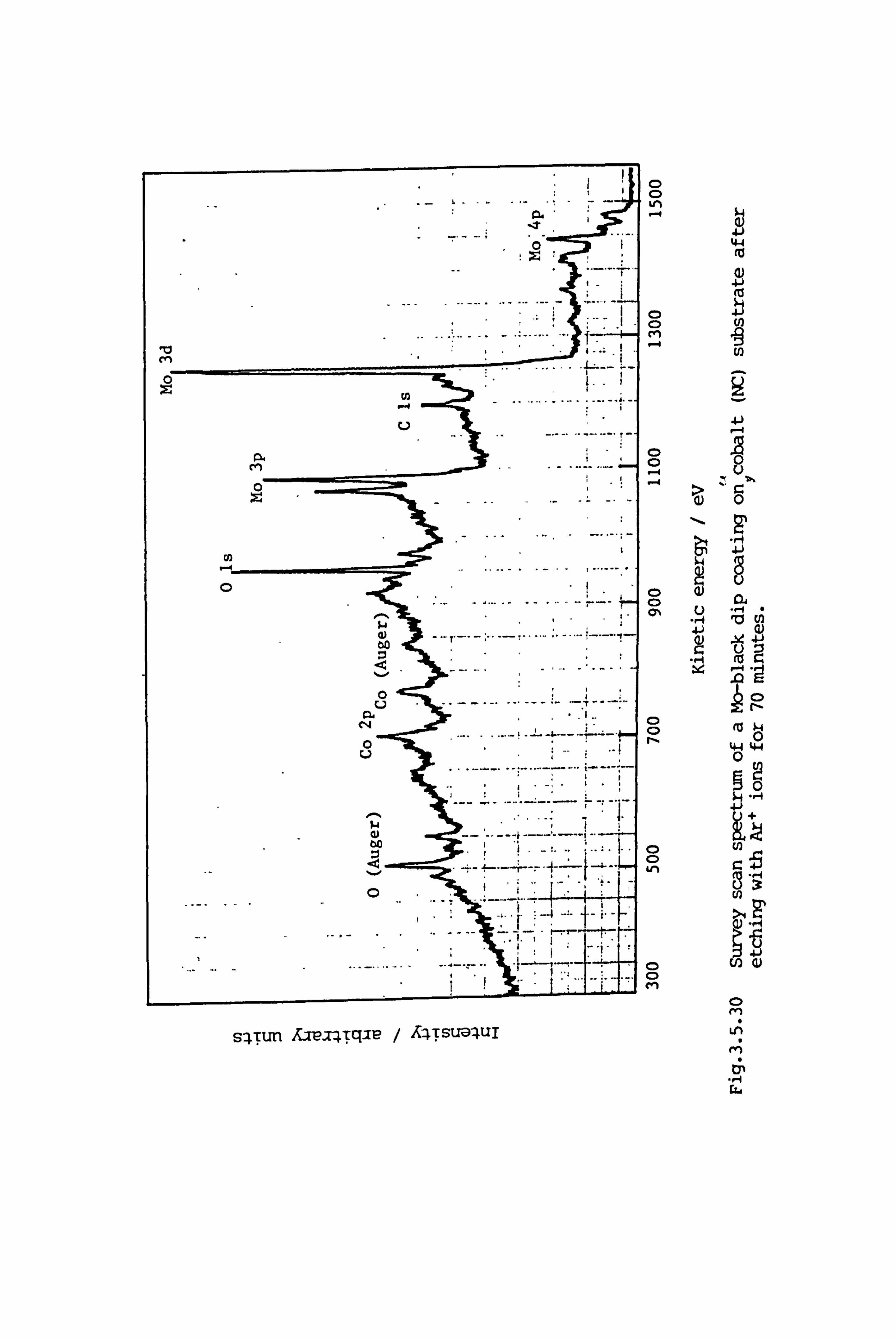
0 C)
(Z$
CD
* 41
0 0) C: ) ON
41
.0
CD (a ý
4-4 0
0
U)
Ln
U)
u
U) (L)
en
Uý rý Ul
., -I
rLd
s-4Tun rapiqTq-TE? / A-4TW94uI
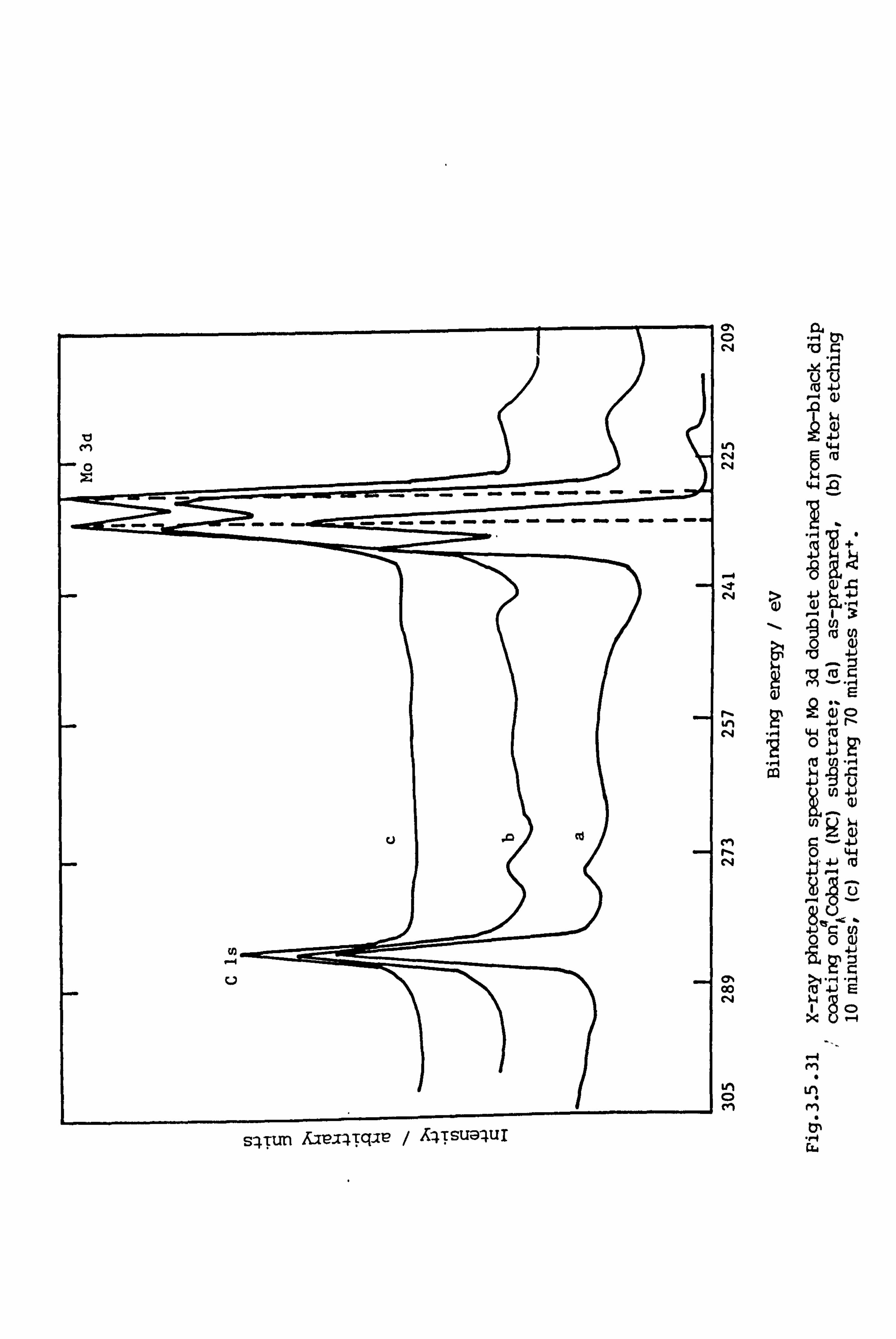
en
-0
10 Cd
S-4Tun Aav-z4Tqie / A4TSU@'4uI
(YA C) 04
In C14 C14
-4 -It C-j
r,
C-1 rý C4
C% CO r4
cn
I-
co
ý4 Q)
ý4 a) 4. )
44
41
cn to B
rv) -. ý
4.4 (a 0
(a (n 14 IJ
La
10 !ý 01) C: - 41 0 44
o 4,
> 4-) E
rn
V; r4 t; . 14 DA
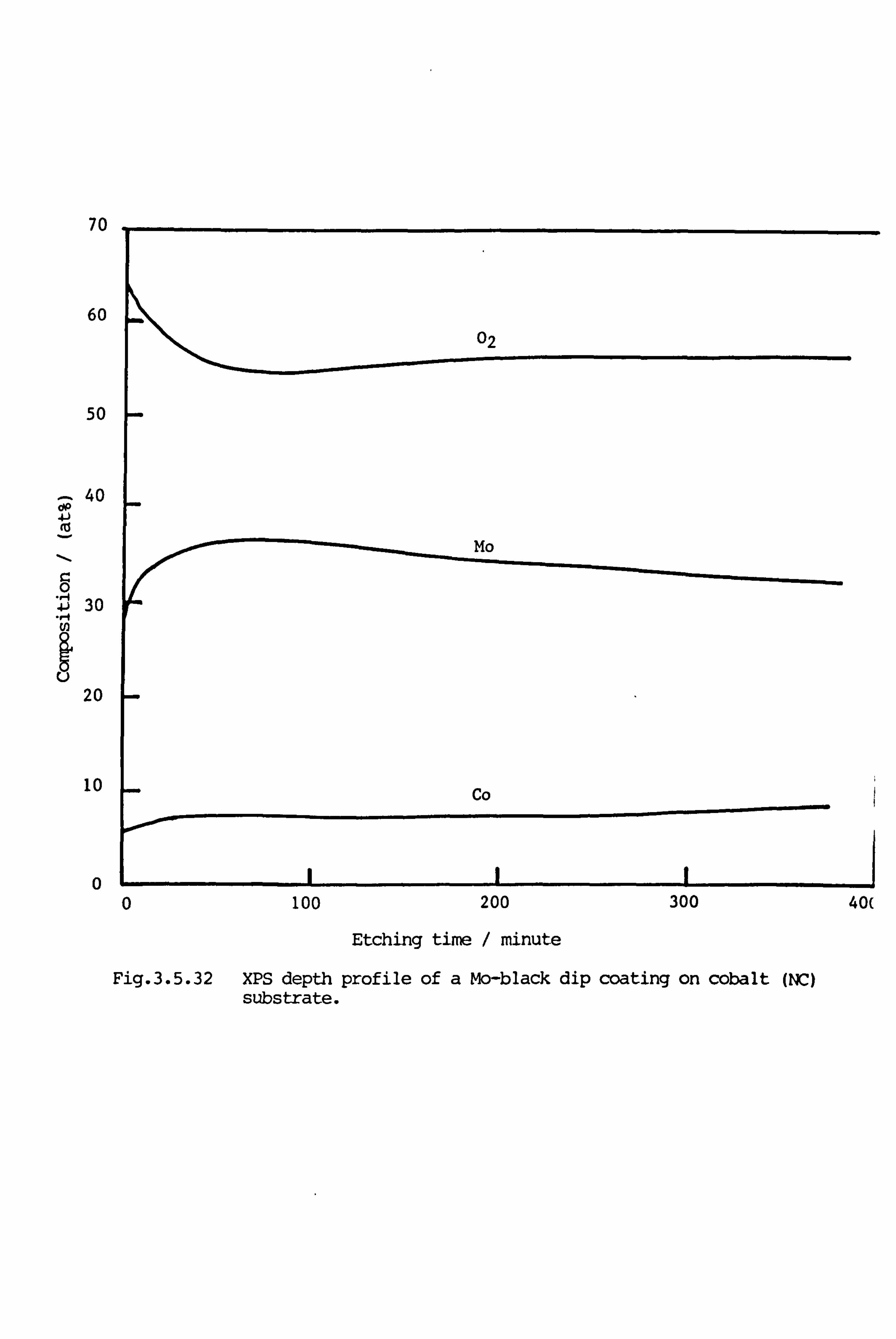
70
60
50
- 40 dP
r. 0 . -I 41 30 ., j
20
10
0
Etching time / minute
Fig. 3.5.32 XPS depth profile of a Mo-black dip coating on cobalt (NC) substrate.
0 100 200 300 40(
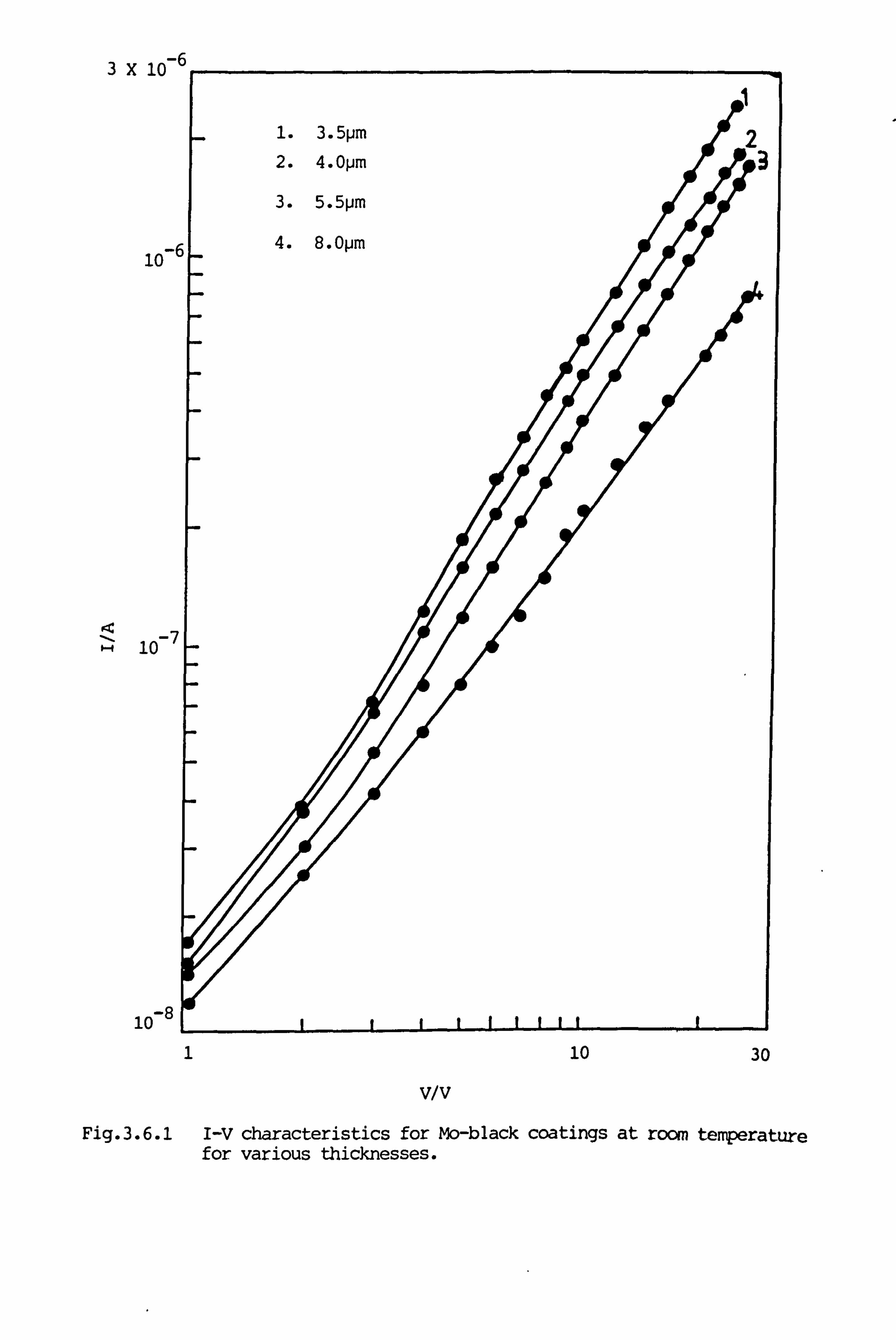
.,, , -6 -ý A LV
10-f
10
10-8
1.3.5pm
2.4. Opm
3.5.5pm
4.8. Opm
1 10 30
V/V
Fig. 3.6.1 I-V characteristics for Mo-black coatings at room temperature for various thicknesses.
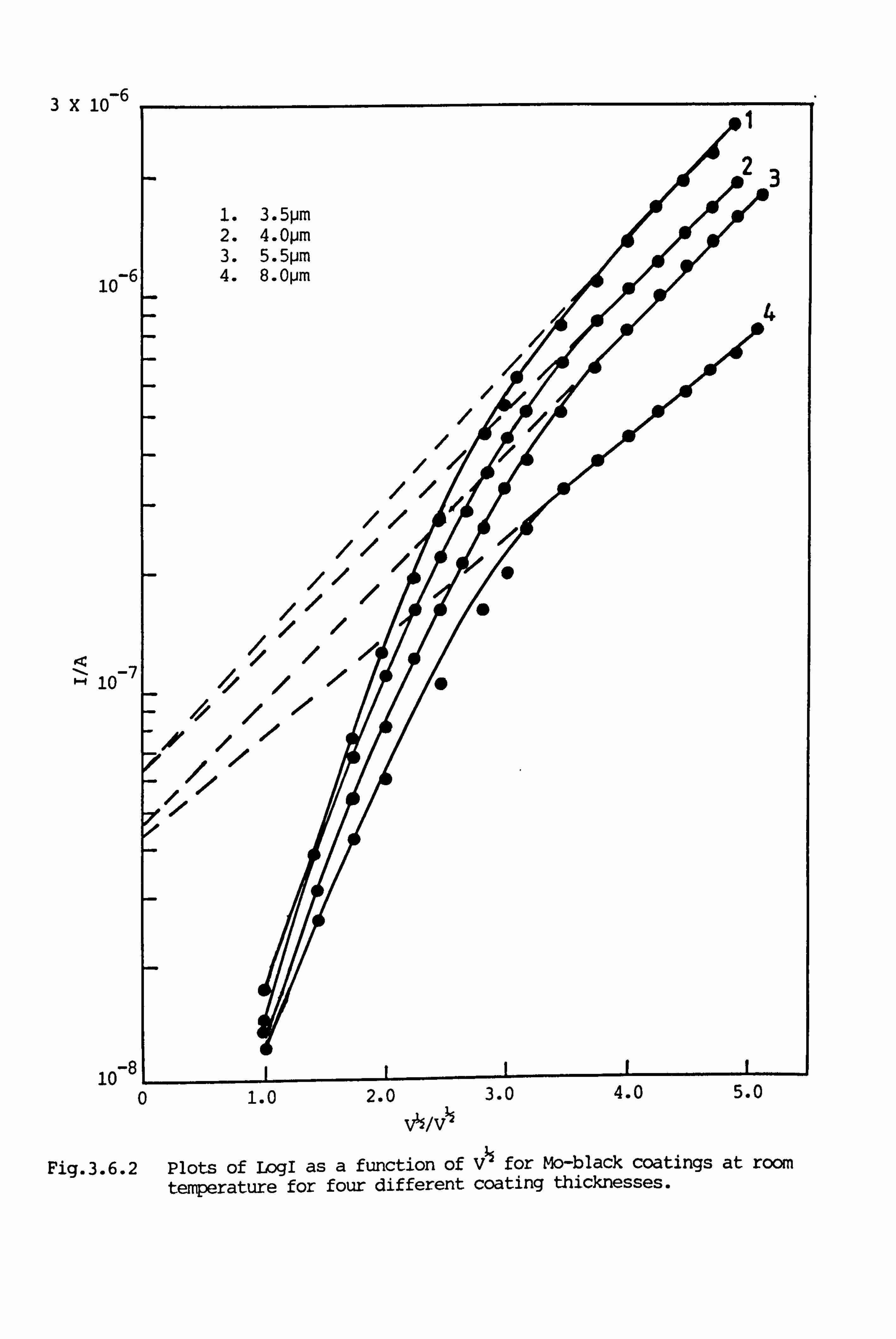
3X 10⁻⁶
10-6
10
10-8
1.3.5pm 2.4. Opm 3.5.5pm 4.8. Opm
"000,
0 1.0 2.0 3.0 4. U ! ). U
0/0 Fig. 3.6.2 Plots of LogI as a function of
0 for Mo-black coatings at room temperature for four different coating thicknesses.
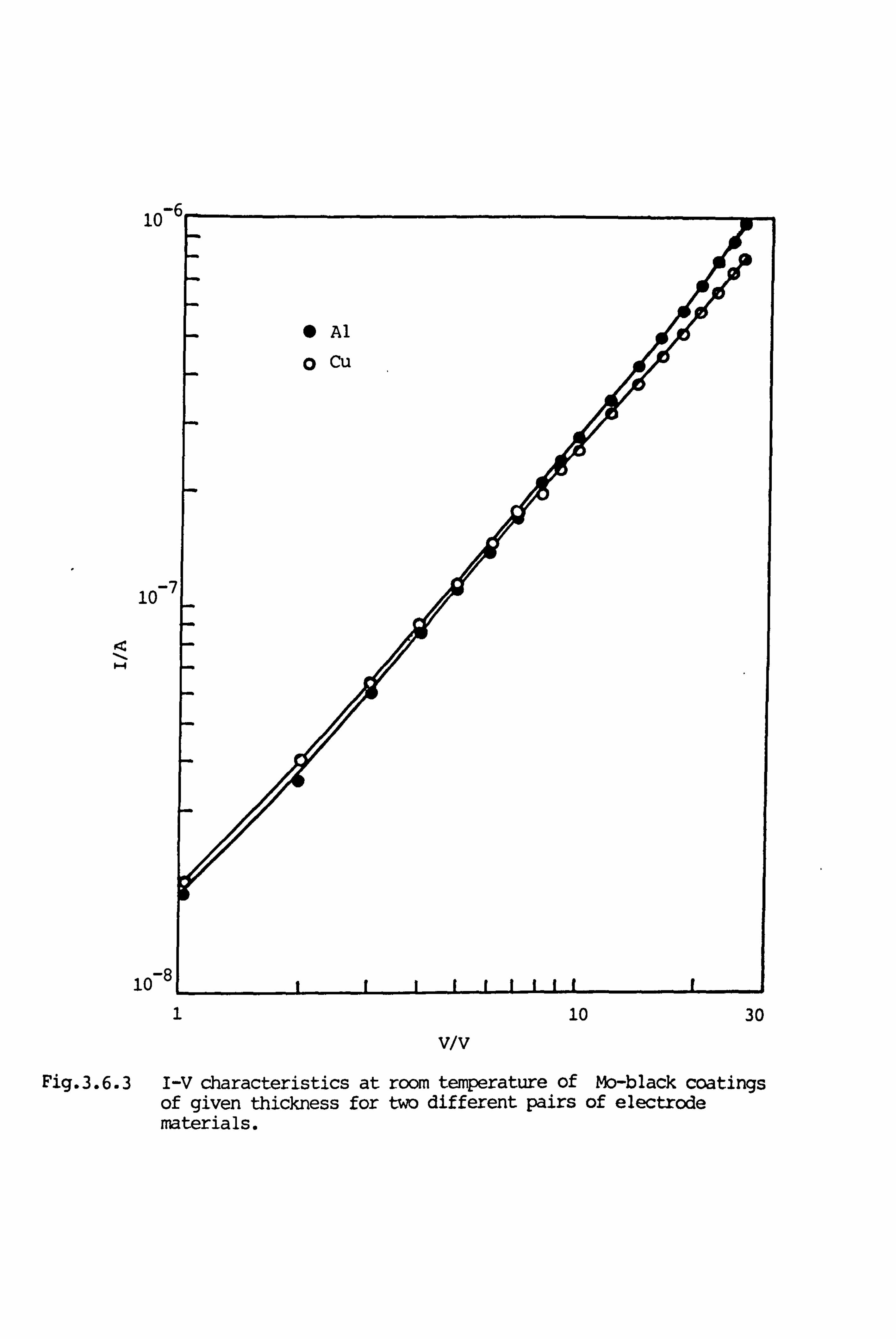
10
0 Al
0 Cu
4 1-4
10
10
10 30
V/V
Fig. 3.6.3 I-V characteristics at room temperature of Mo-black coatings of given thickness for two different pairs of electrode materials.
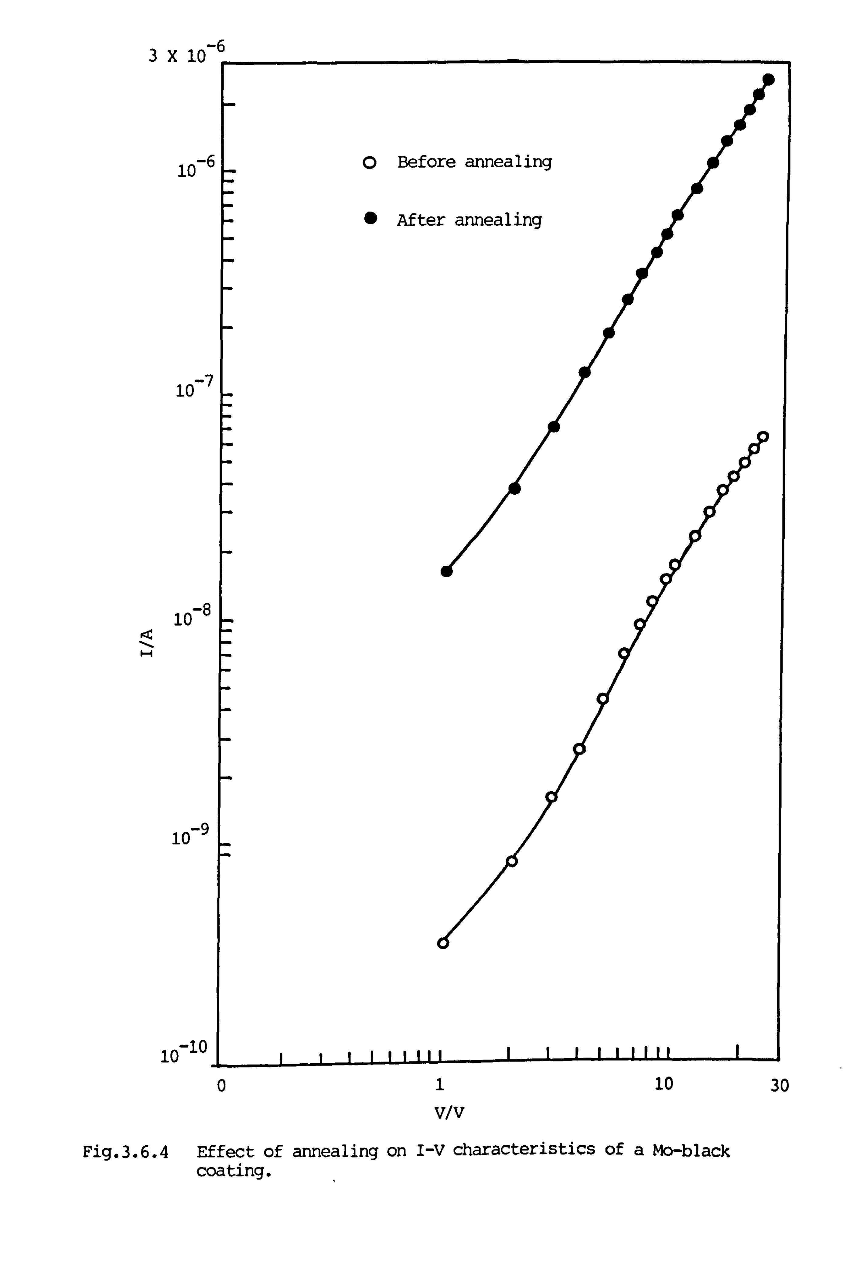
-1 v1 n-6
10 -(
10
10-8 �-I
10
10-10
0 Before annealing
0 After annealing
1 10 30
V/V
Fig. 3.6.4 Effect of annealing on I-v characteristics of a Mo-black coating.
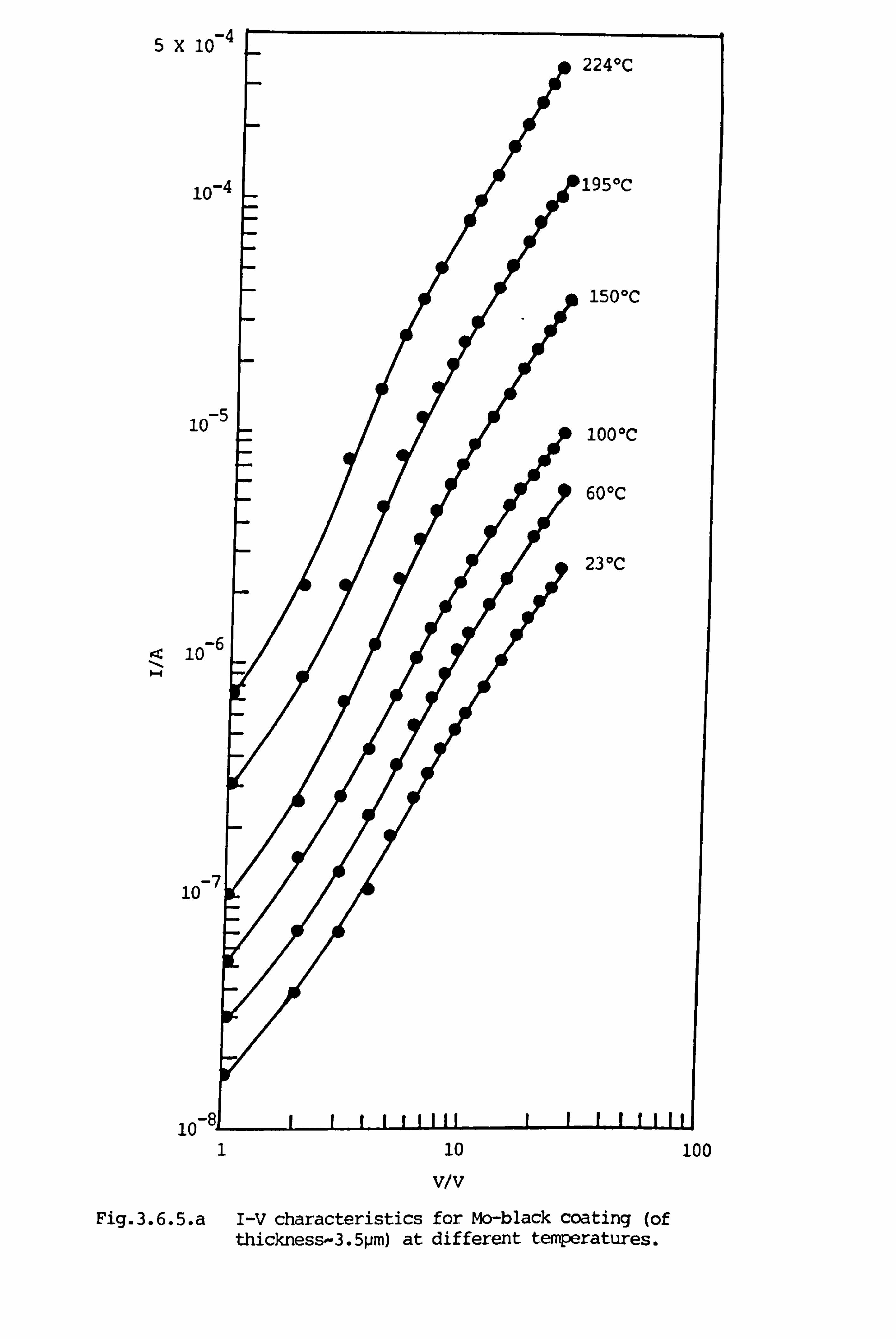
5X
1(
10
V/V
Fig. 3.6.5. a I-V characteristics for Mo-black coating (of thickness-3.5pm) at different temperatures.
1 10 100
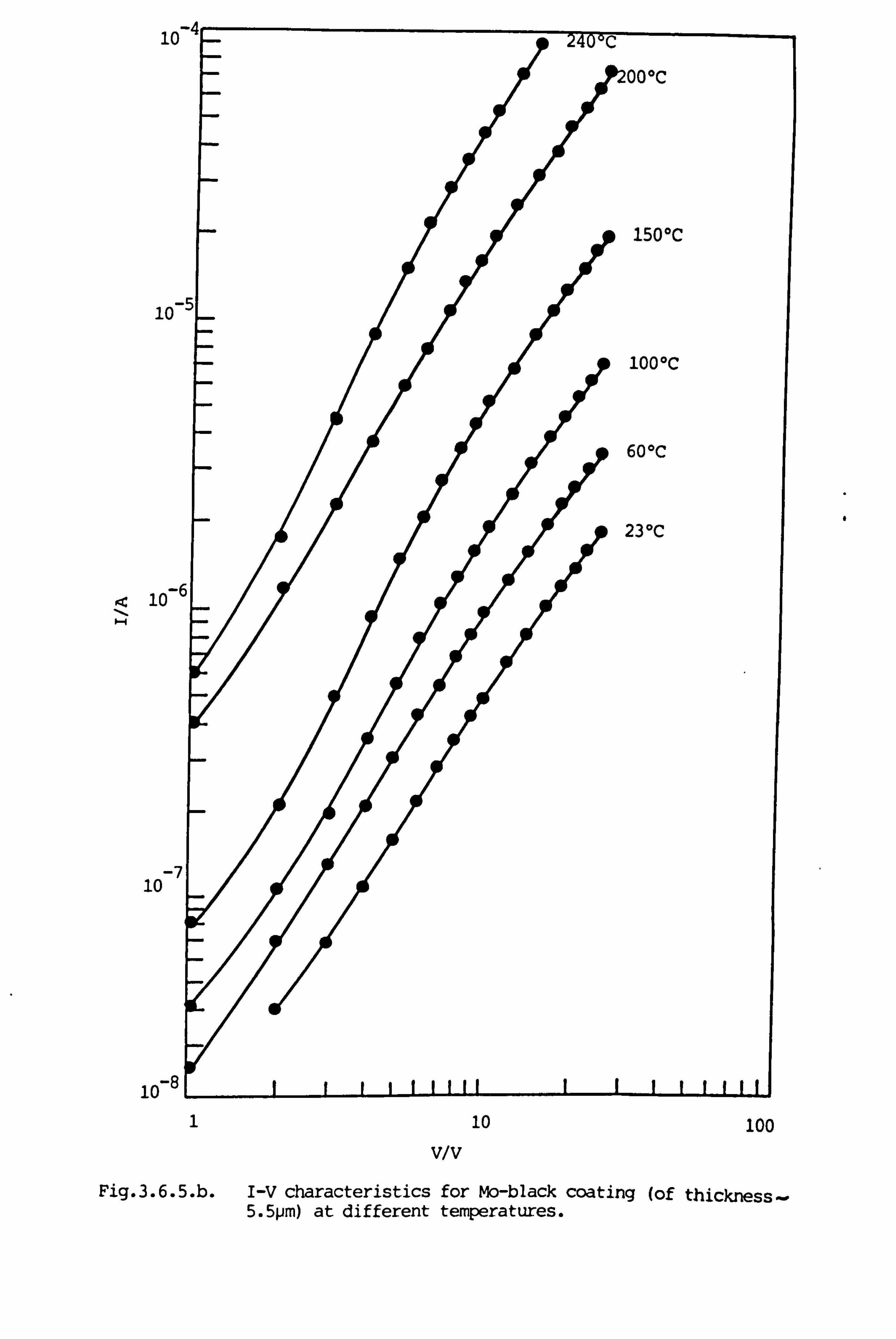
10
10
1o_
10
10-8
-4 240*C---
0011C
1500C
-5
loollc
60*C
23*C
6
10 100
V/V
Fig. 3.6.5. b. I-V characteristics for Mo-black coating (of thickness- 5.5pm) at different temperatures.
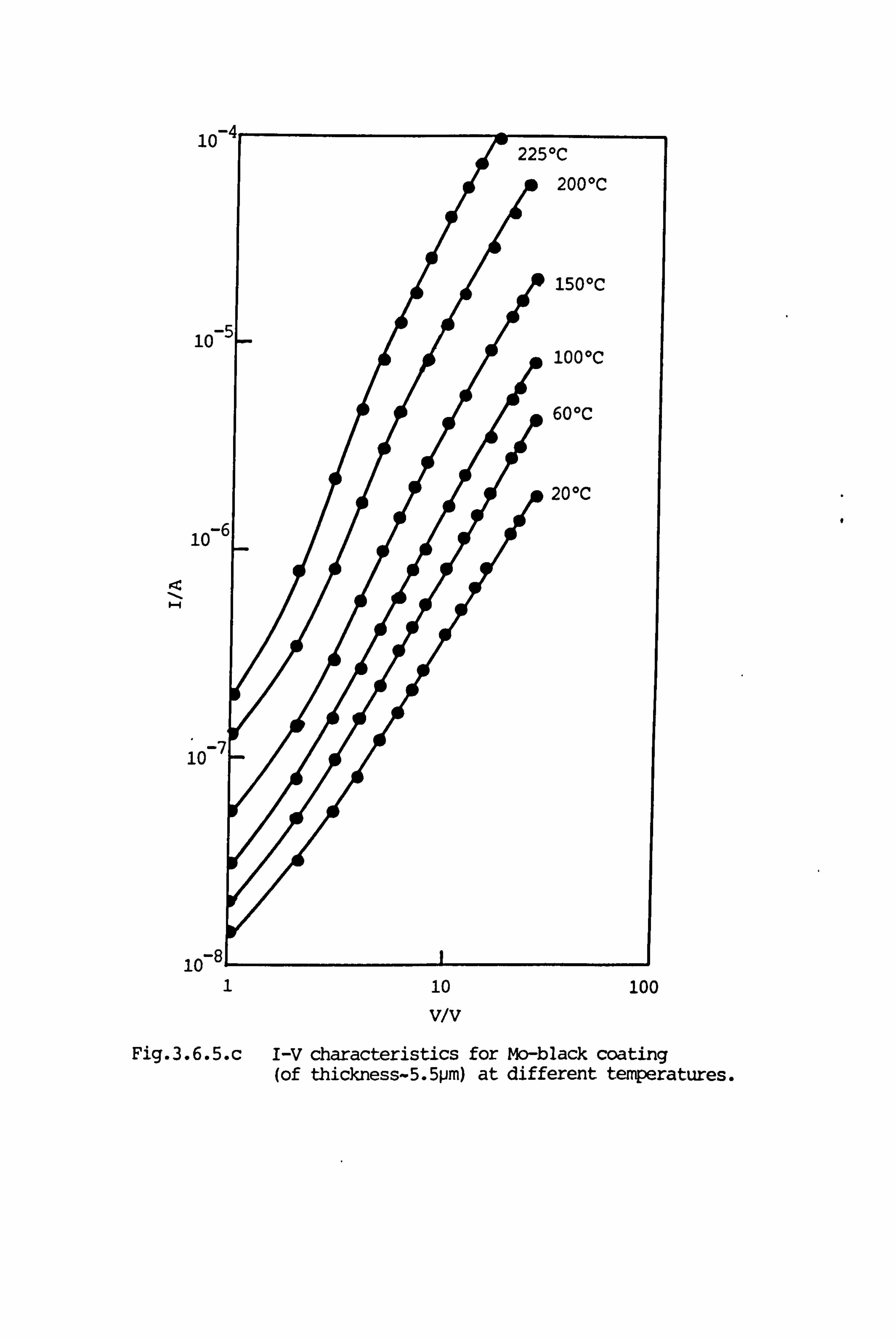
11
ic
10
10
10
V/V
Fig. 3.6.5. c I-V characteristics for Mo-black coating (of thickness-5.5pm) at different temperatures.
1 10 100
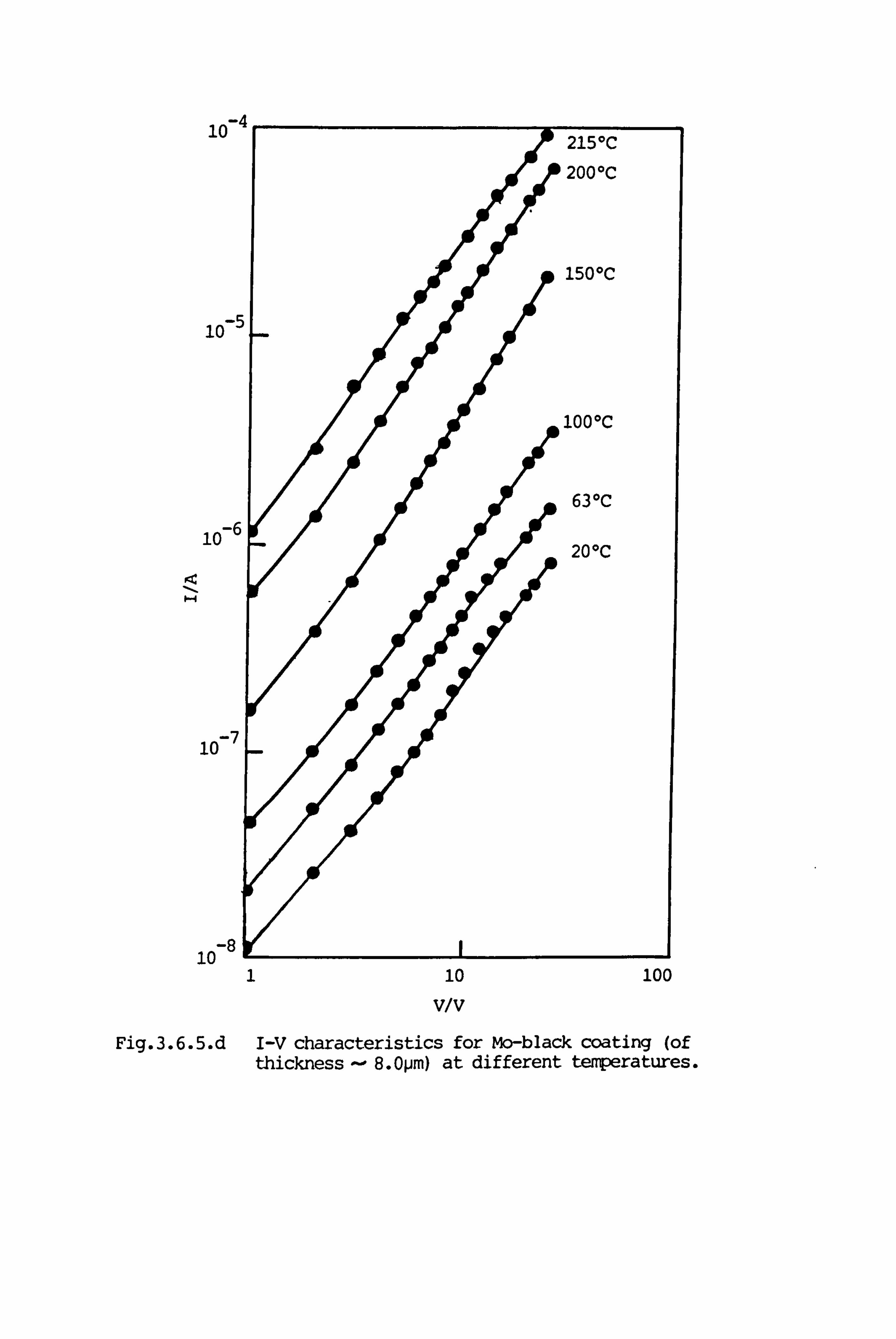
1
10
10-6
10-7
10 -8 10 100
V/V
215*C
200*C
1500C
1000C
63*C
20'C
Fig. 3.6.5. d I-V characteristics for Mo-black coating (of thickness - 8. Opm) at different temperatures.
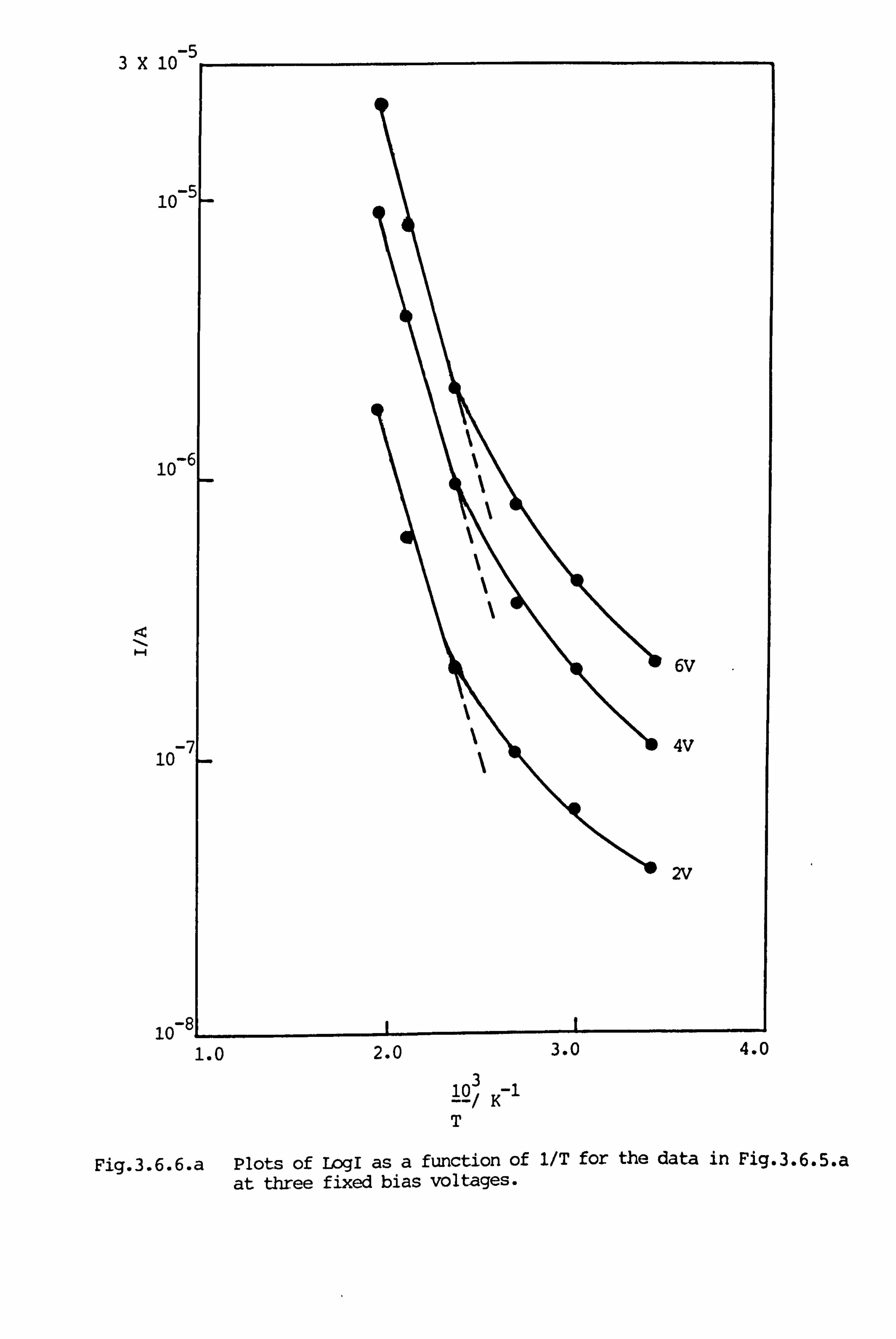
,, . --5 .3A LU
10
10
10
10
-5
-6
6v
7 V
2V
81
1.0 2.0 3.0 4.0
12 3
K-1 T
Fig. 3.6.6. a Plots of LogI as a function of l/T for the data in Fig. 3.6.5. a at three fixed bias voltages.
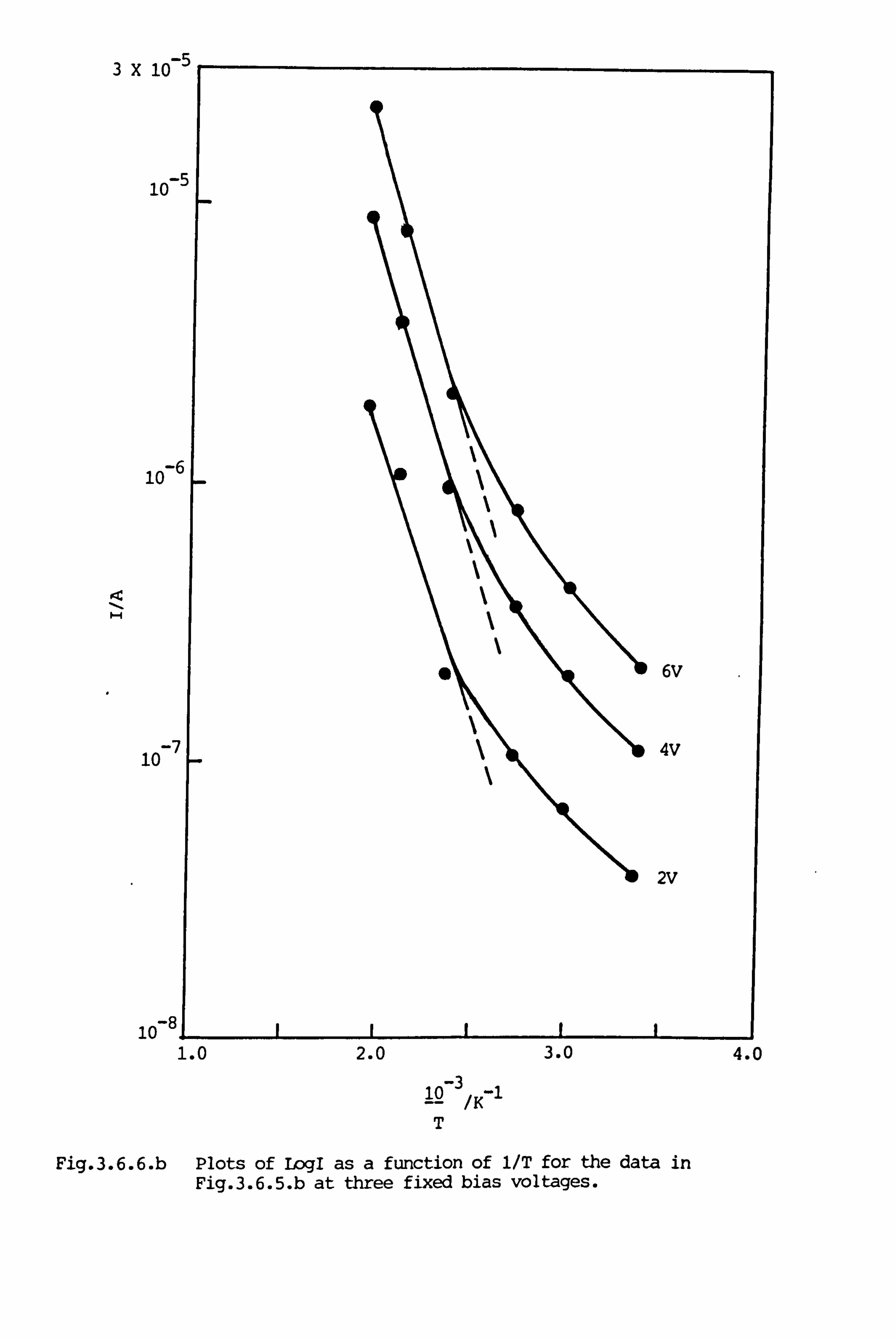
-- 3x 10
10
10-1
10-8
,5
6V
4V
2V
1.0 2.0 3.0 4.0
12-3 IK-1 T
Fig. 3.6.6. b Plots of LogI as a function of l/T for the data in Fig. 3.6.5. b at three fixed bias voltages.
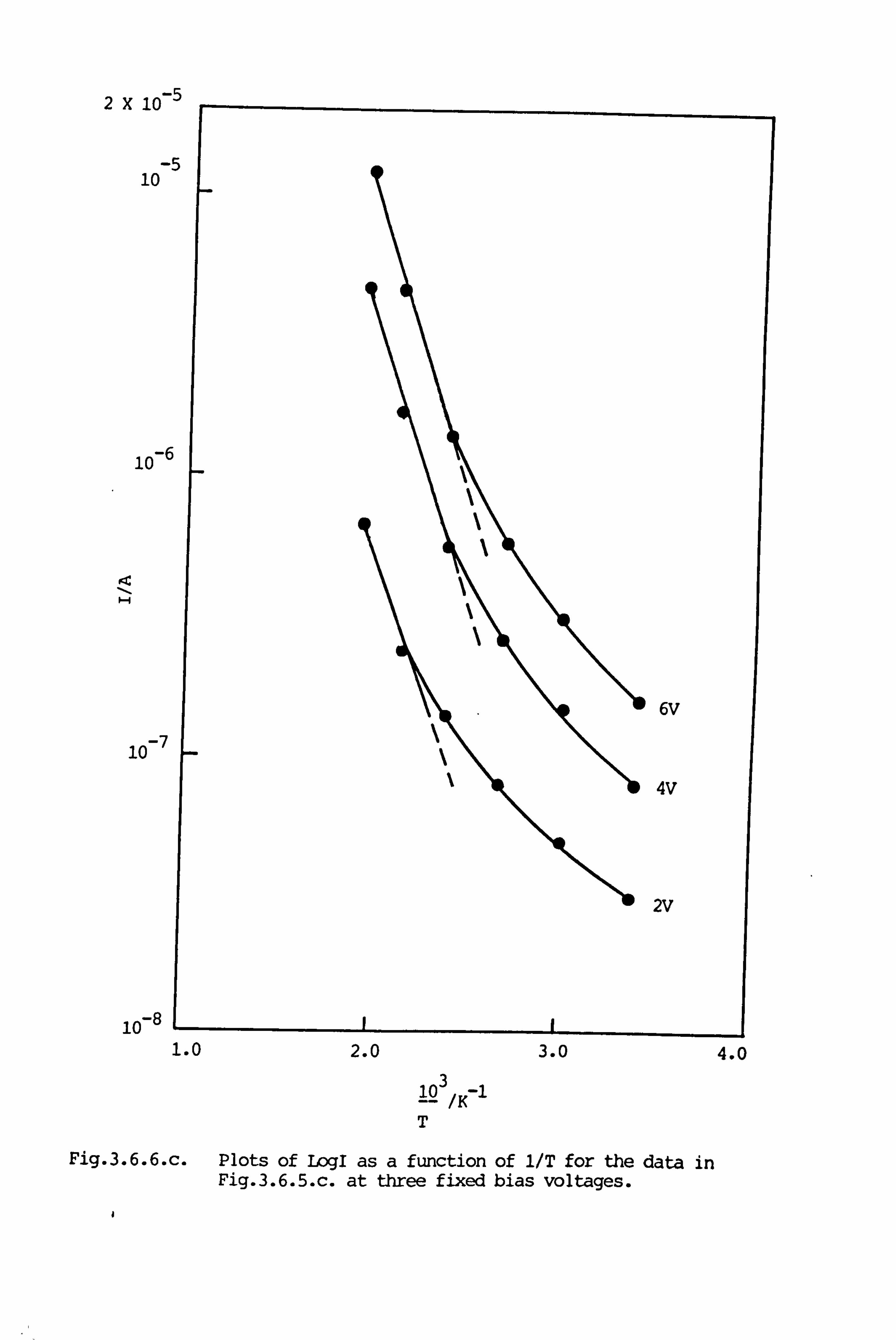
-) , , -5 & 1% LU
10
lo-E
icC
10-7
10-8
5
6V
4V
2V
1.0 2.0
10 3 IK-1
T
3.0 4.0
Fig. 3.6.6. c. Plots of LogI as a function of 1/T for the data in Fig. 3.6.5. c. at three fixed bias voltages.
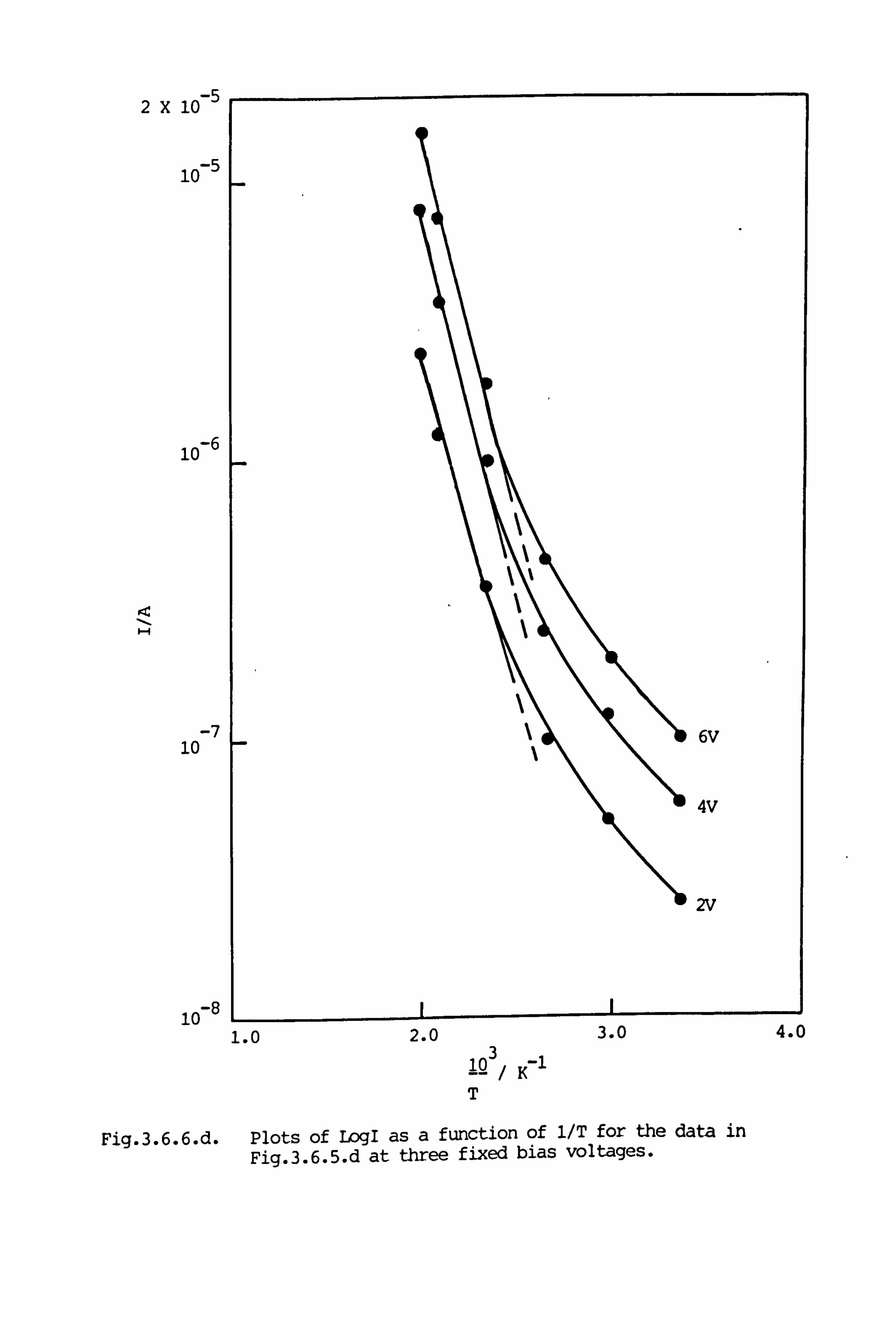
2X 10 -5
10-5
10-6
1-4
10
10-8
6V
W
2V
1.0 2.0
ig 3/
K-1 T
3.0 4.0
Fig. 3.6.6. d. plots of LogI as a function of 1/T for the data in
Fig. 3.6.5. d at three fixed bias voltages.
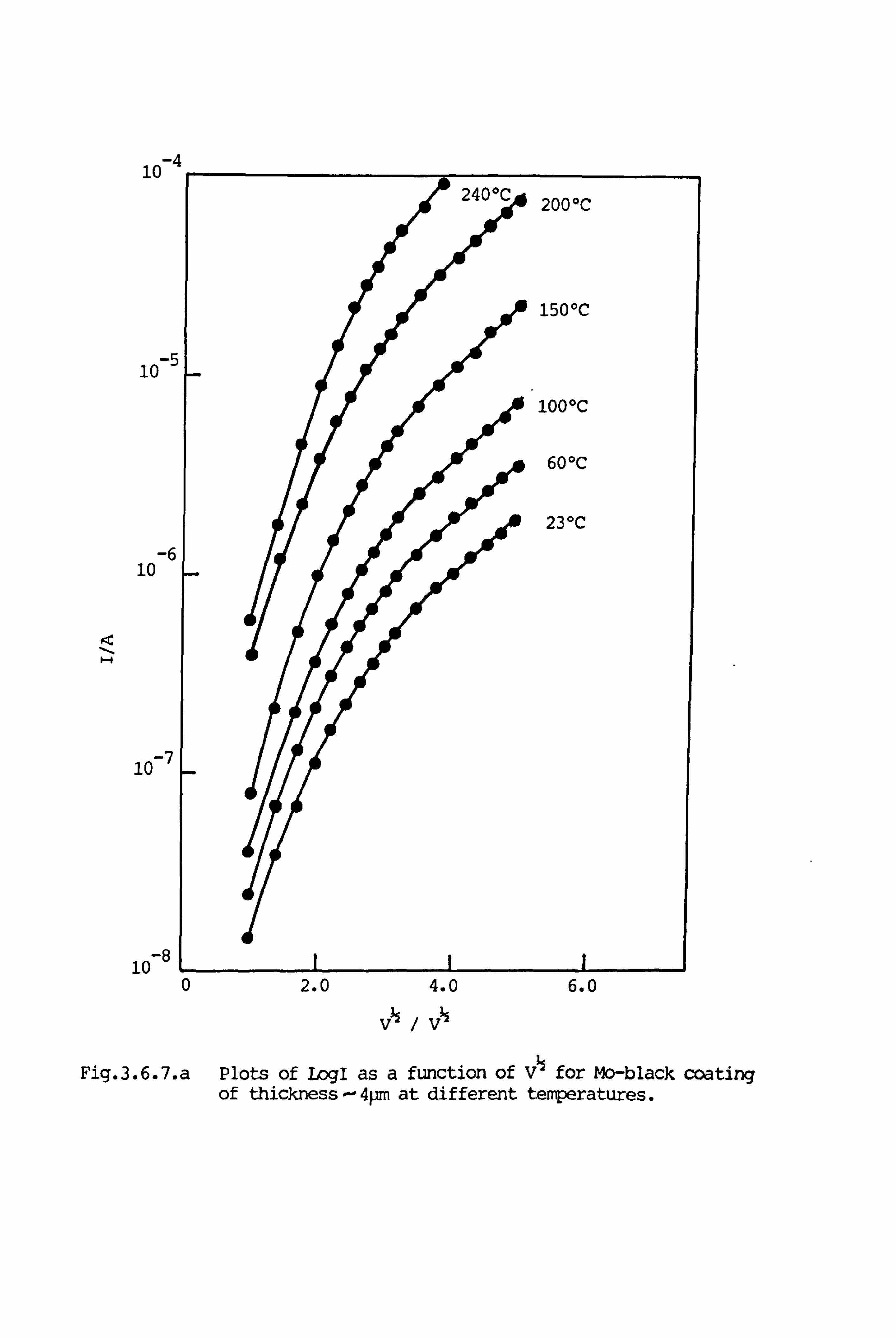
I n-4 . LV
10-5
10
10-7
10-8
240*C 200*C
150*C
1000C
600C
23"C
0 2.0 4.0 6.0
/
Fig. 3.6.7. a Plots of LogI as a function of 0 for Mo-black coating
of thickness -4pm at different temperatures.
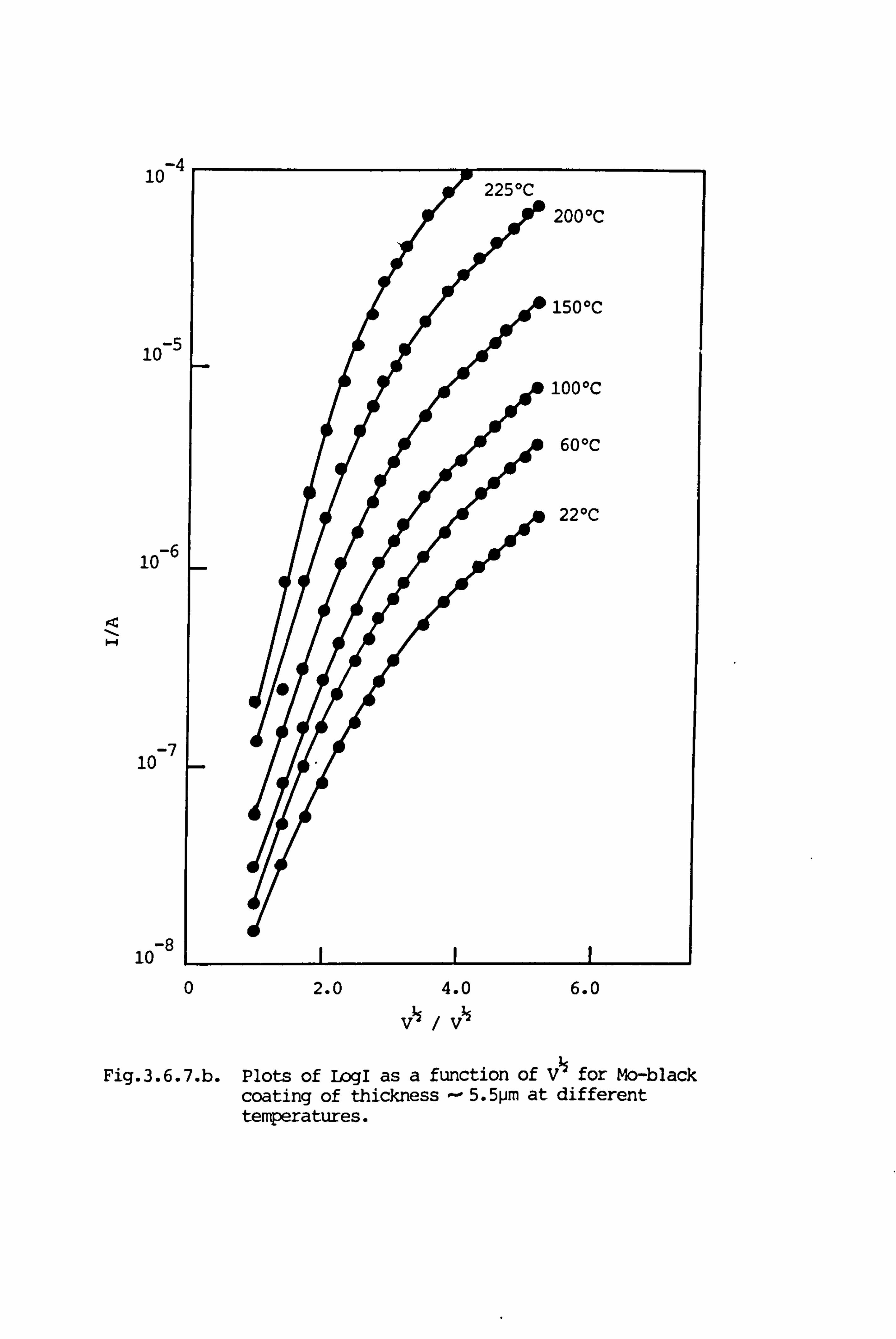
10-4
10-5
10-6
�-4
10-7
4( 10-8
225*C 2000C
150*C
1000C
ralb 60*C
A 220C
0 2.0 4.0 6.0 0/0
Fig. 3.6.7. b. Plots of LogI as a function of 0
for Mo-black coating of thickness - 5.5pm at different temperatures.
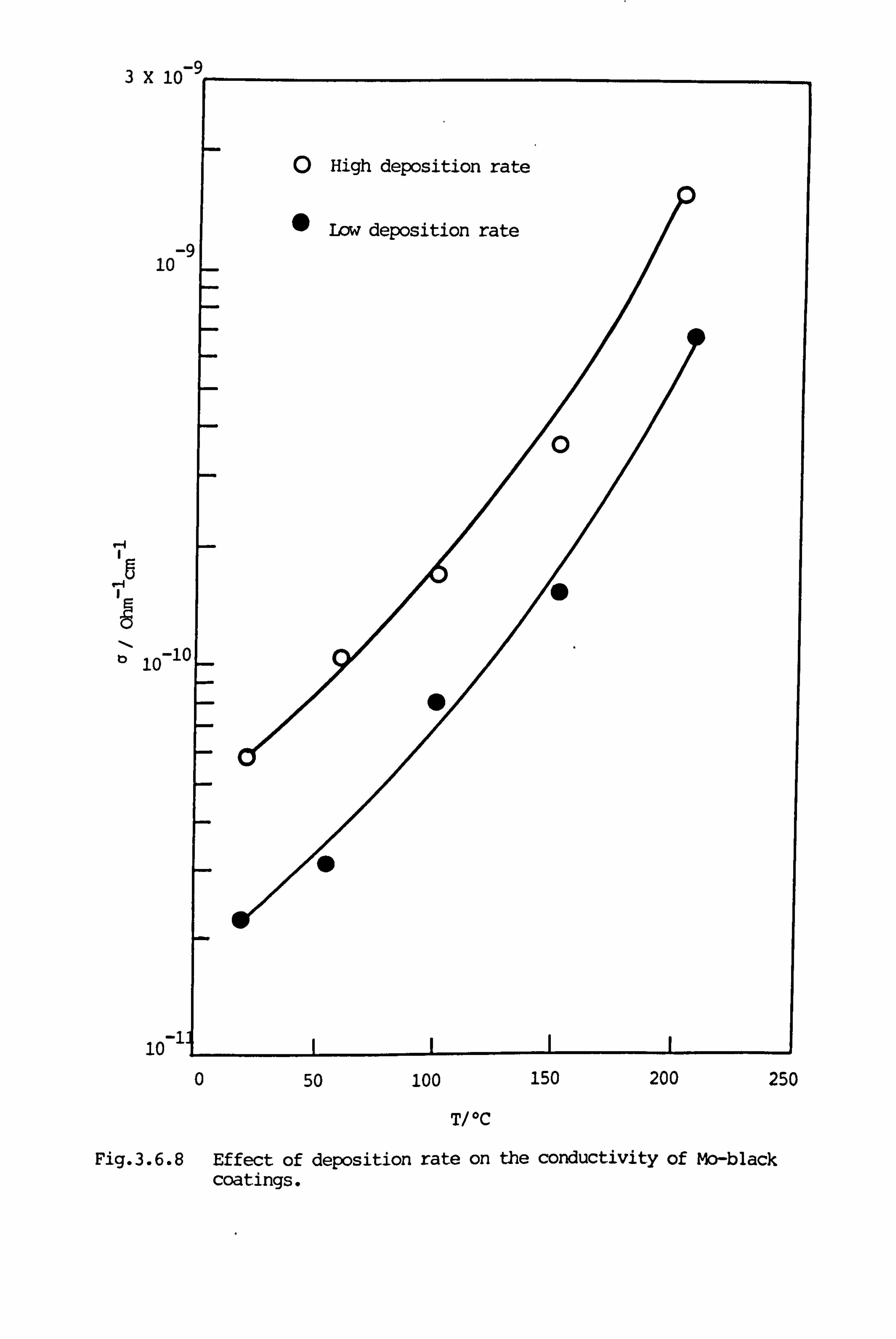
1v1 r%-9 4AV
10
-. 4
b
10
0 High deposition rate
Low deposition rate
LO
L
0 50 100 150 200 250
T/*C
Fig. 3.6.8 Effect of deposition rate on the conductivity of Mo-black coatings.
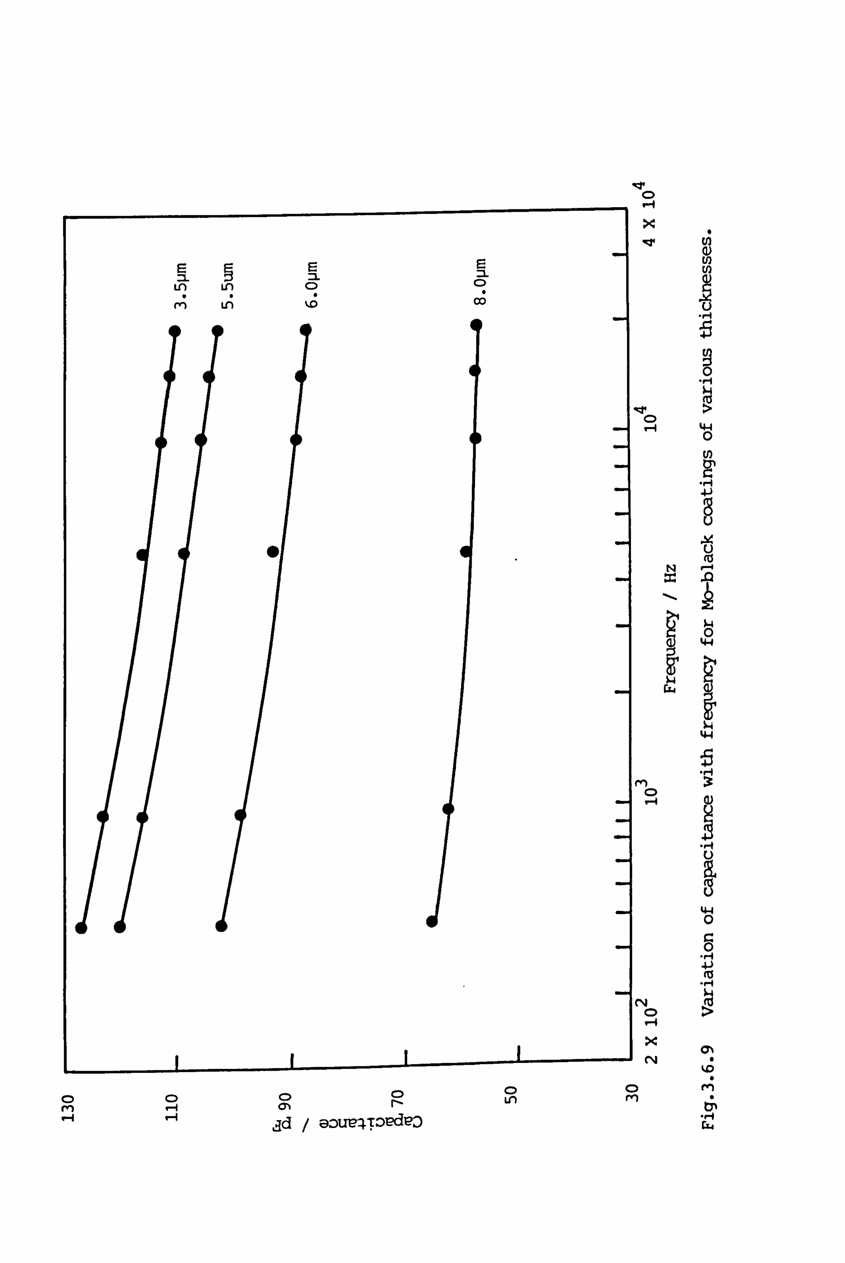
11, C) -4
rn Lt) 1.0 OD
-W
fn
(N 0 '-4 x CN
CD C) 00 ON r- Ln rn
ad aoue4Toedeo
44
U) U)
0
4-4 0
U)
41 8
u
16 (0
ý4 44
44 0
rT4
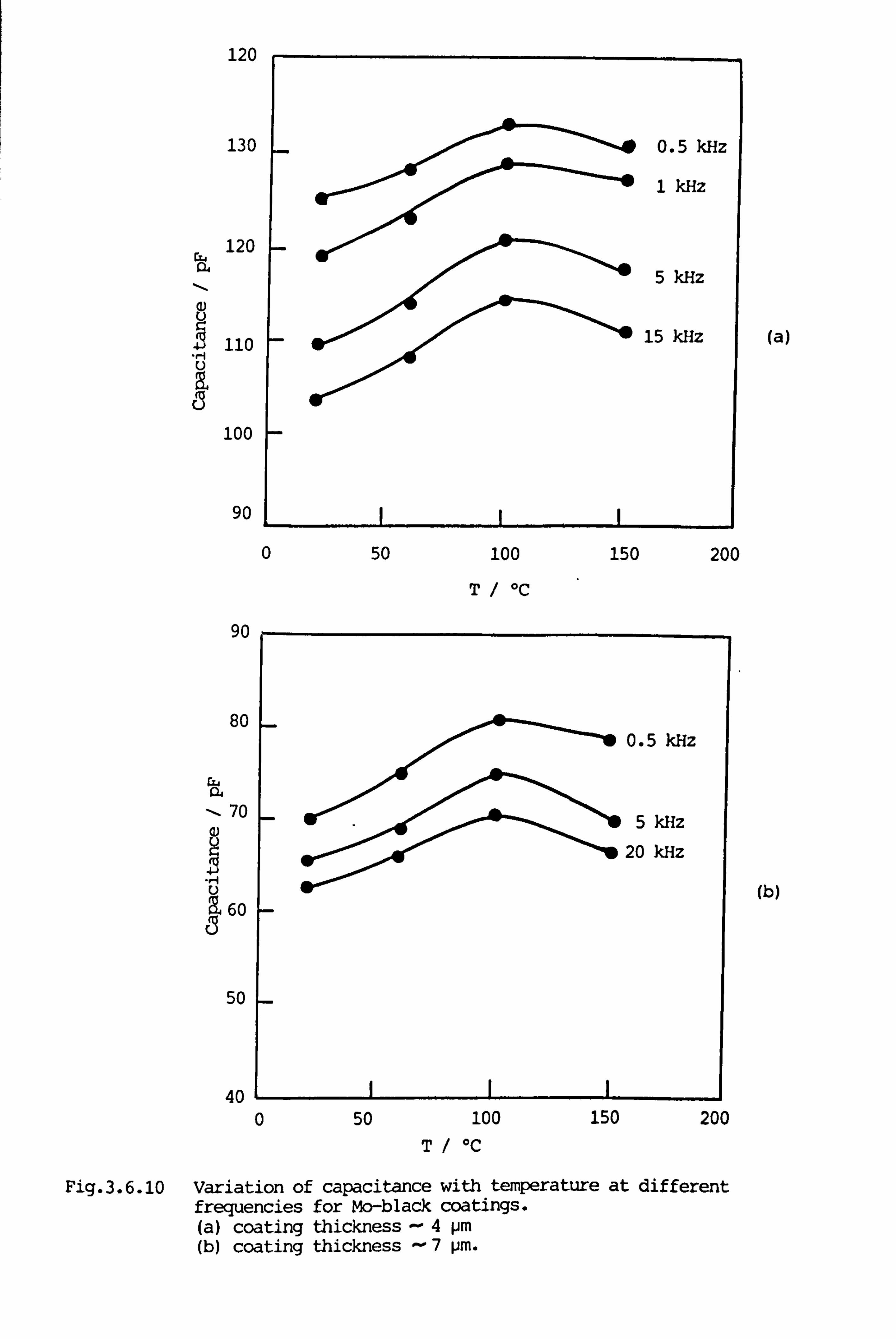
120
130
120 rX4
134
u 110
100
90
, ooo,
ý
0.5 kHz
1 kHz
5 kHz
15 kHz (a)
50 100 150 200
T/ °C
90
80
44
70
60
40
0.5 kHz
5 kHz
20 kHz
'000*,
50
50 100 150 200
T/ *C
Fig. 3.6.10 Variation of capacitance with temperature at different frequencies for Mo-black coatings. (a) coating thickness -4 pm (b) coating thickness -7 pm.
(b)
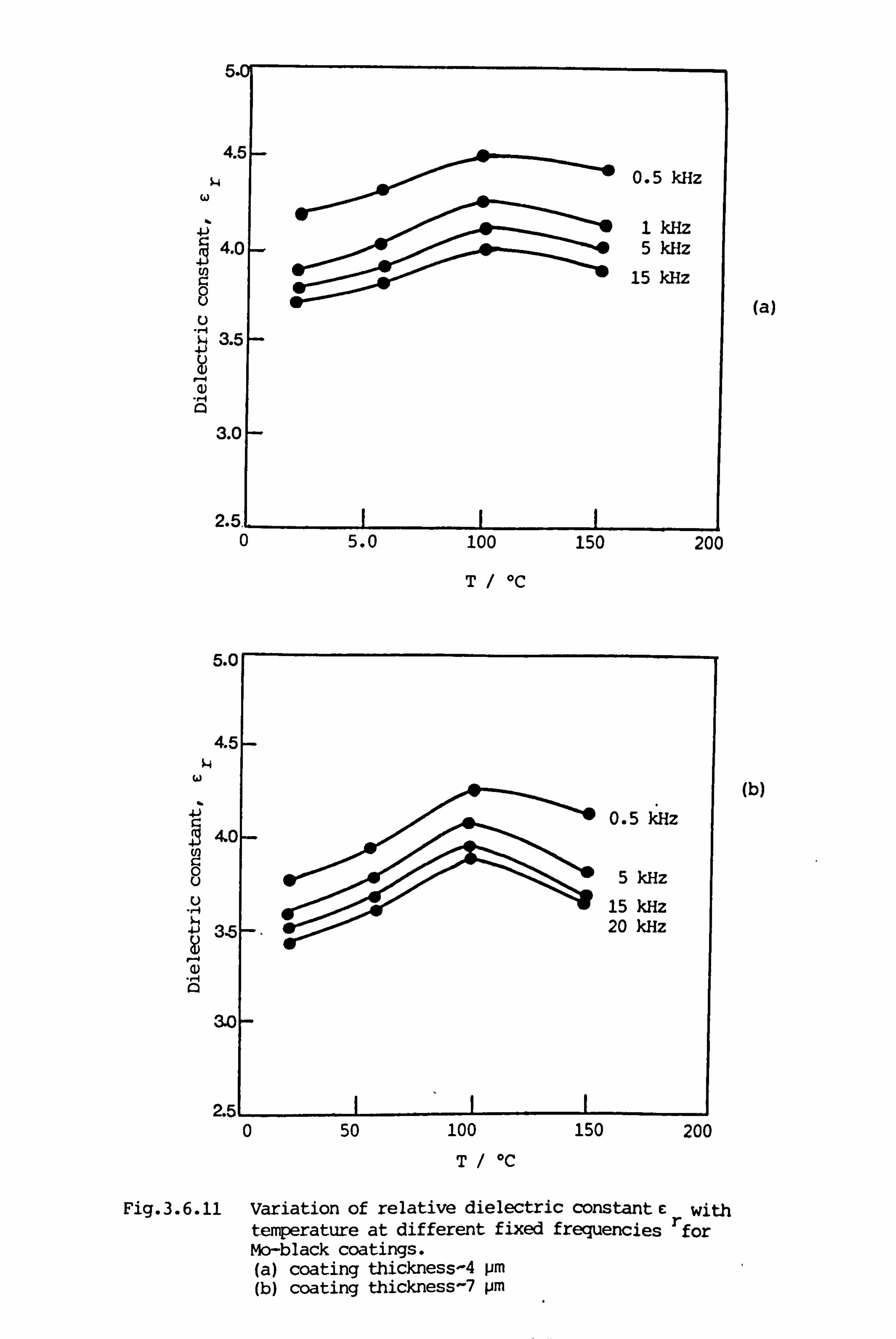
tn c:
C)
-lJ
3
0
T/ °C
I
5.0
4.5
3.5
2.5
0.5 kHz
5 kHz 15 kHz 20 kHz
0 50 100 150 200
T *C
Fig. 3.6.11 Variation of relative dielectric constant c with temperature at different fixed frequencies r for Mo-black coatings. (a) coating thickness-4 jim (b) coating thickness-7 pm
(a)
(b)
5.0 100 150 200
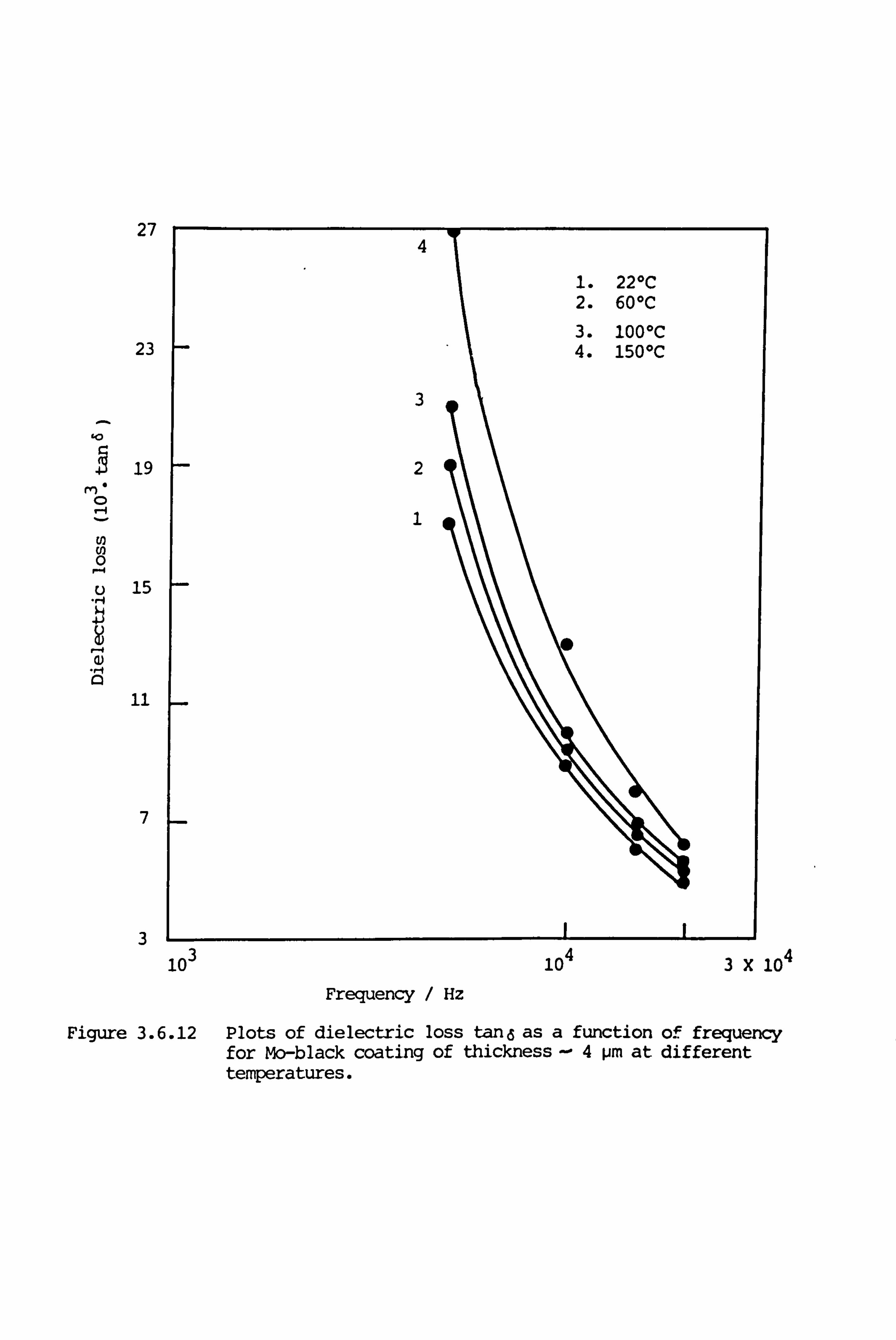
27
-0 j
0
U, (I, 0
C)
23
19
15
11
7
3
4
1. 22*C 2. 60*C 3. 100*C 4. 1500C
3
2
1
10 10 4 3X 10⁴ Frequency / Hz
Figure 3.6.12 Plots of dielectric loss tand as a function of frequency for Mo-black coating of thickness -4 pm at different temperatures.
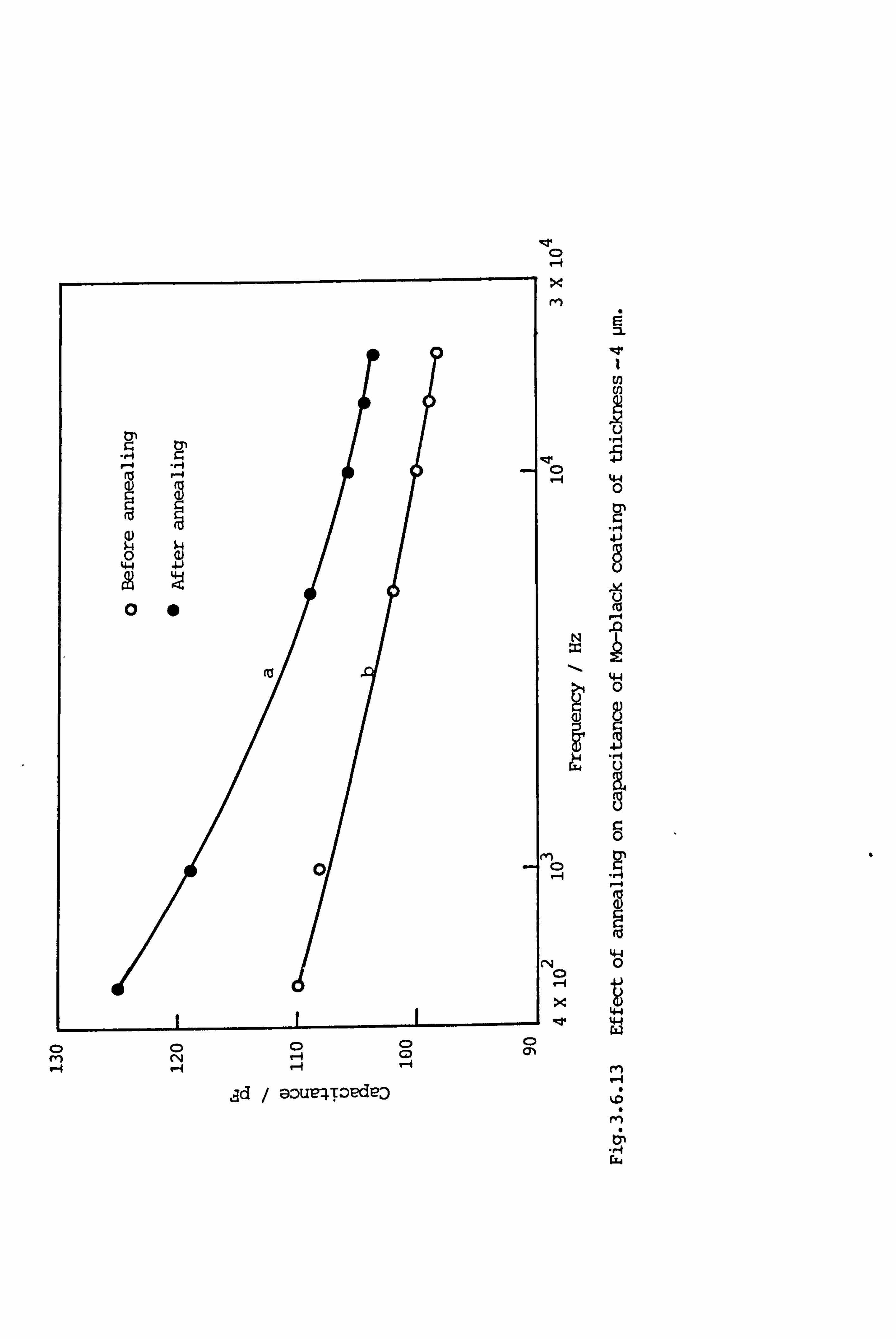
, qd / 90ue4TopdeD
1.4, C> -4
N
44 0
(Ci
N
4 0
4-4 w
M ý4 1ý
14 t;
-4 U4
000 C) C) rn ý4
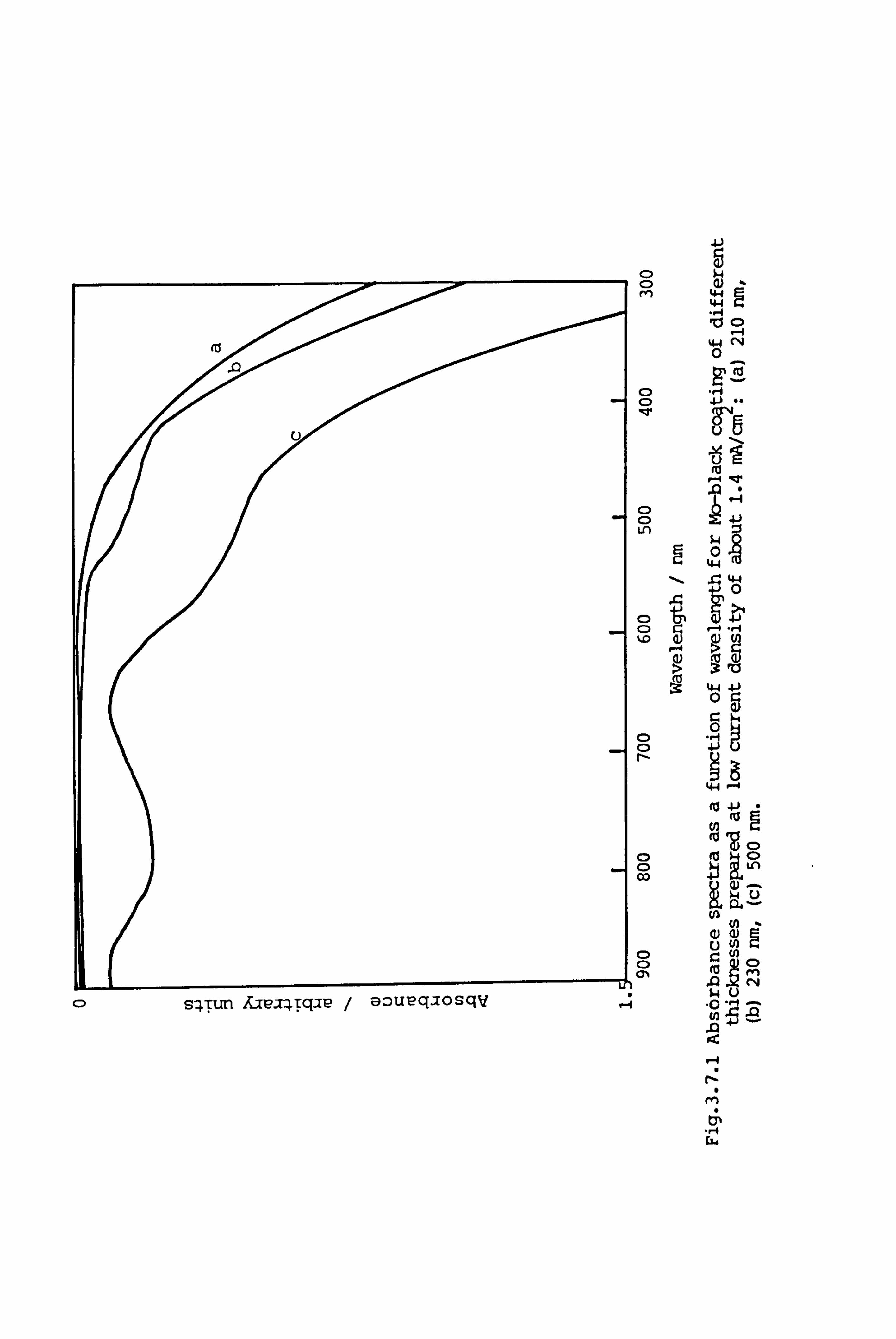
(ii
C) sqTun Aip. TqTq-TL- / aouPq-70sqv 1;
0 C) rn
C)
C) C)
C)
CD C: ) Co
ON
44 44 . 1-4
44 CN
4j nr4
86
4J
0 44
0
-ýl -4 -H
44 &J 0
41
44
fu 41
cn (a (a V
(a ý (,, 5 .0 wu .0
0) -4 cu
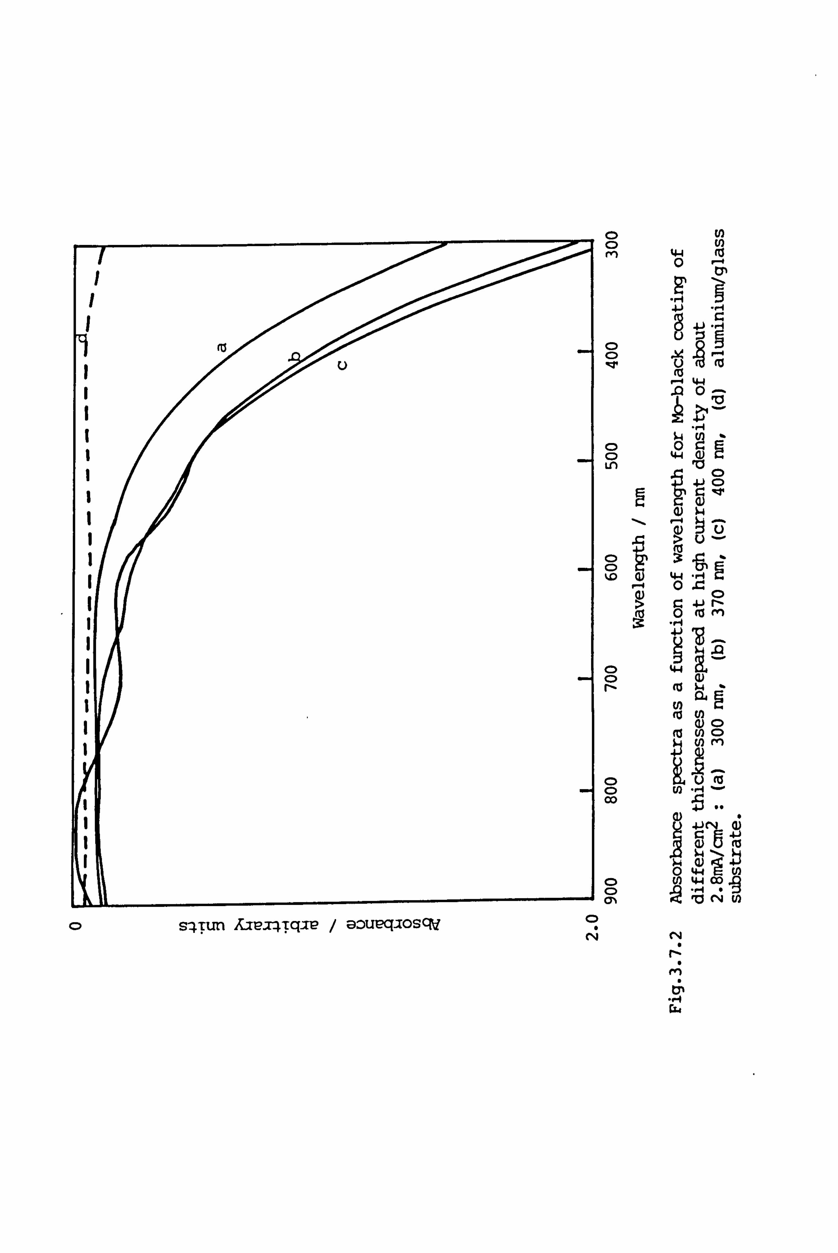
I I I
I
lt
C. )
0 0 m
C) C) 41
C) C) Ln
,01
Cý
0 C) Co
0
0 U)
eý -(ö fö
. -4 44
.Q C) -
ý -ýI 2
N4 -A 02,
44 G) E C)
Q) k4 ,5bv >
4.4 -, 4
0 9 (0 rn
.H
44
(0 U) e) 0
fo U) (D
ýu tö
96 tu
0 4.4 (n 44 OD. 9
cý u)
S'4Tun Aapx4Tq-ip / aouE? q-Toscpj 9 C4
rý 14
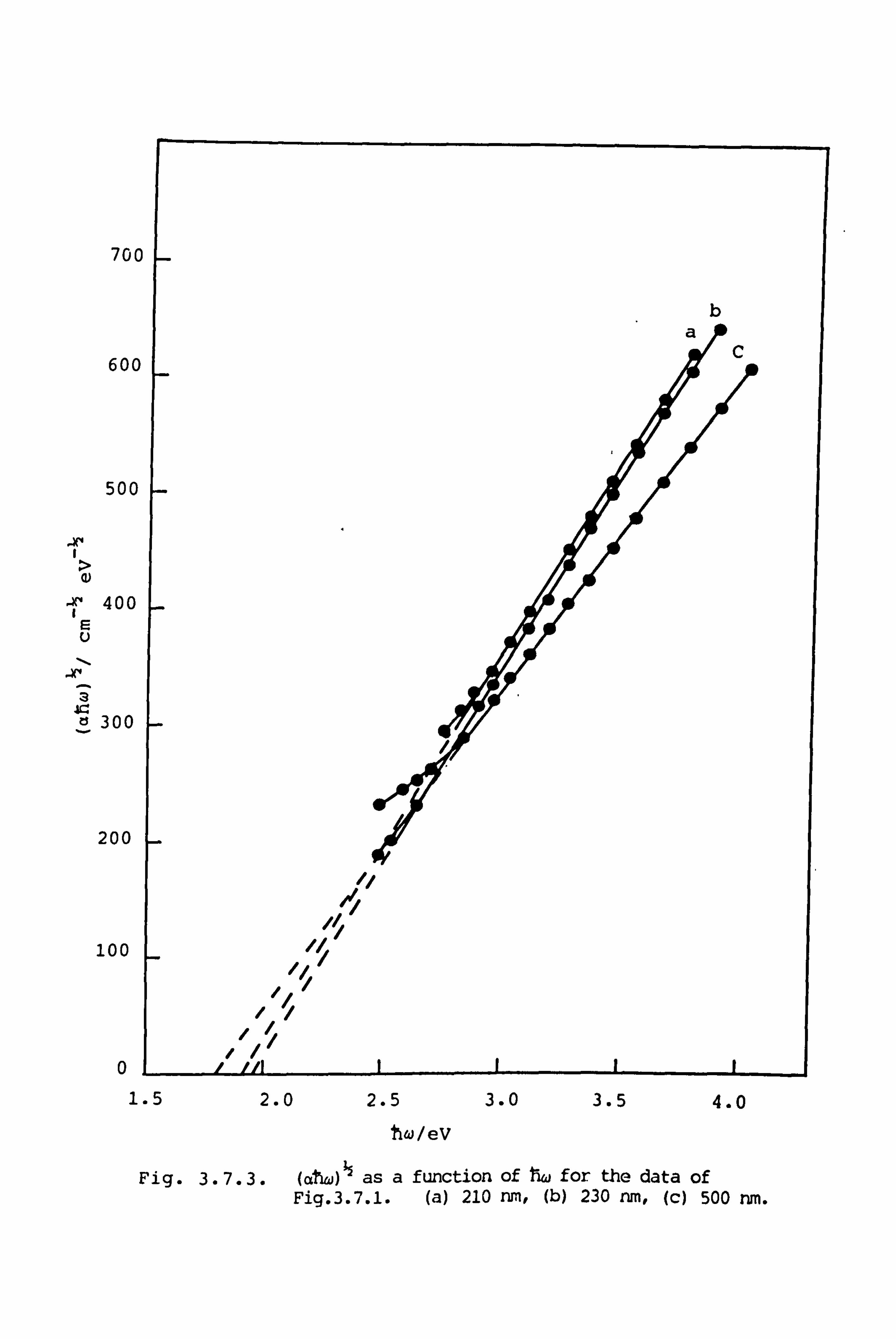
70C
600
500
400
300
200
100
0
b aft
C
/
I, //
'4
1/ ''I
/ I' I ill I
1.5 2.0 2.5 3.0 3.5 4.0
hw/ev
Fig. 3.7.3. (dtw)ý as a function of f1w for the data of Fig. 3.7.1. (a) 210runt (b) 230nm, (c) 500nm.
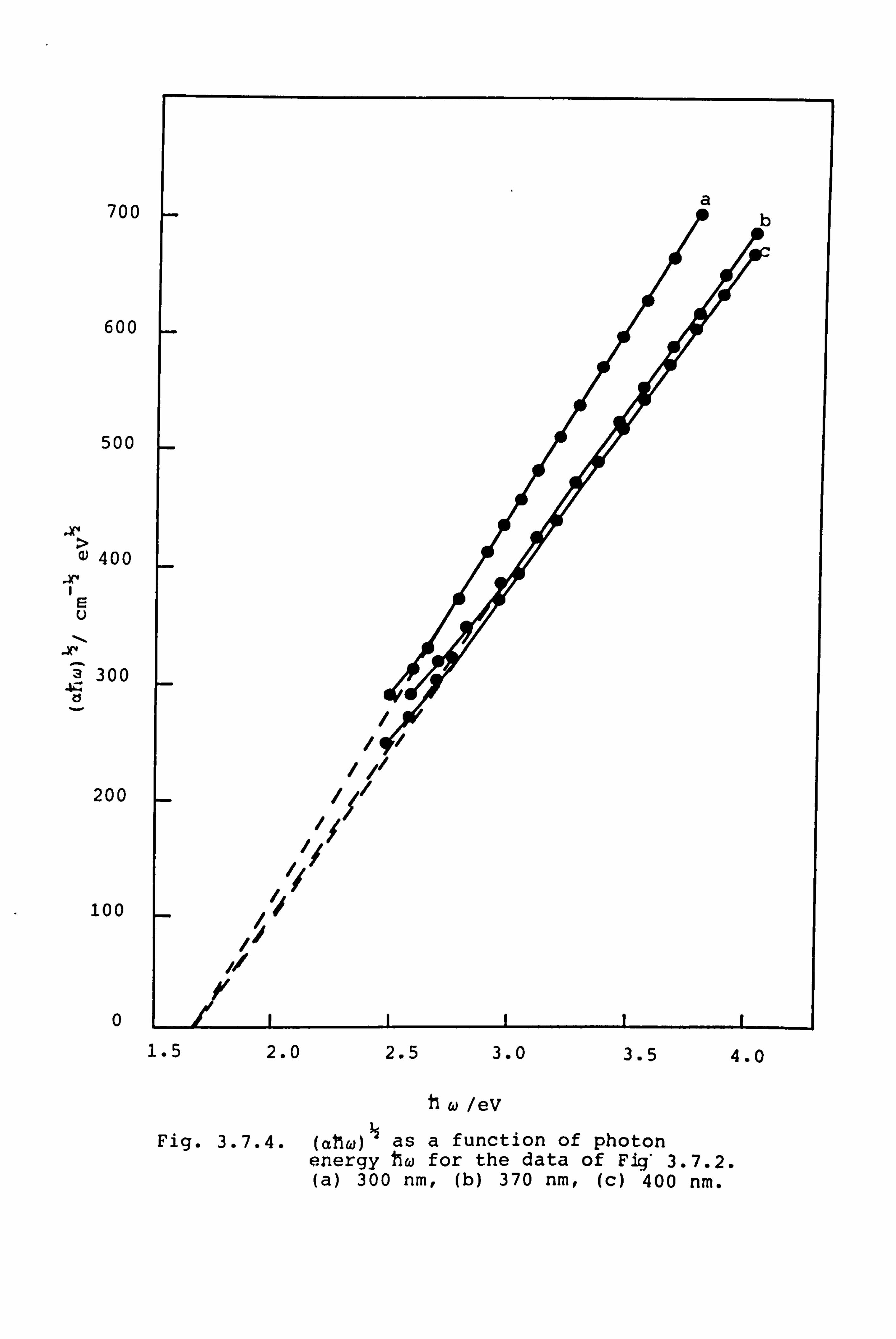
700
600
500
400
300
200
100
0
a -b
/
/ �/ /4(1
�I /
/
1 �I
4I14I4*/ i
1.5 2.0 2.5 3.0
hw /ev
Fig. 3.7-4. (allwO as a function of energy hw for the data (a) 300 nm, (b) 370 nm,
3.5 4.0
photon of Fig* 3.7.2.
(C) 400 nm.
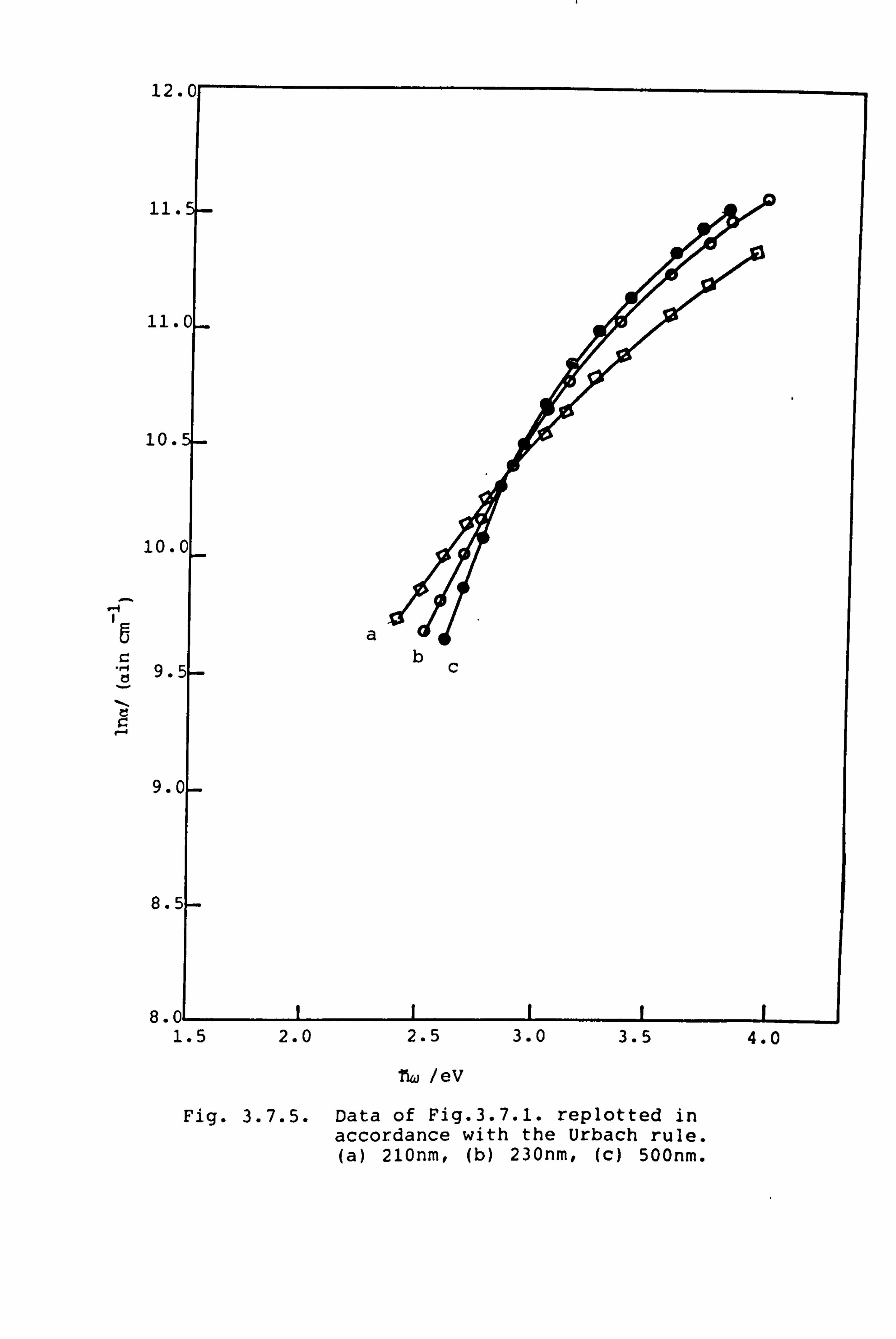
12
11
11
10.
10.
-4
.-9
9.
8.
8.
l1w / ev
Fig. 3.7.5. Data of Fig. 3.7.1. replotted in accordance with the Urbach rule. (a) 210nm, (b) 230nm, (c) 500nm.
1.5 2.0 2.5 3.0 3.5 4.0
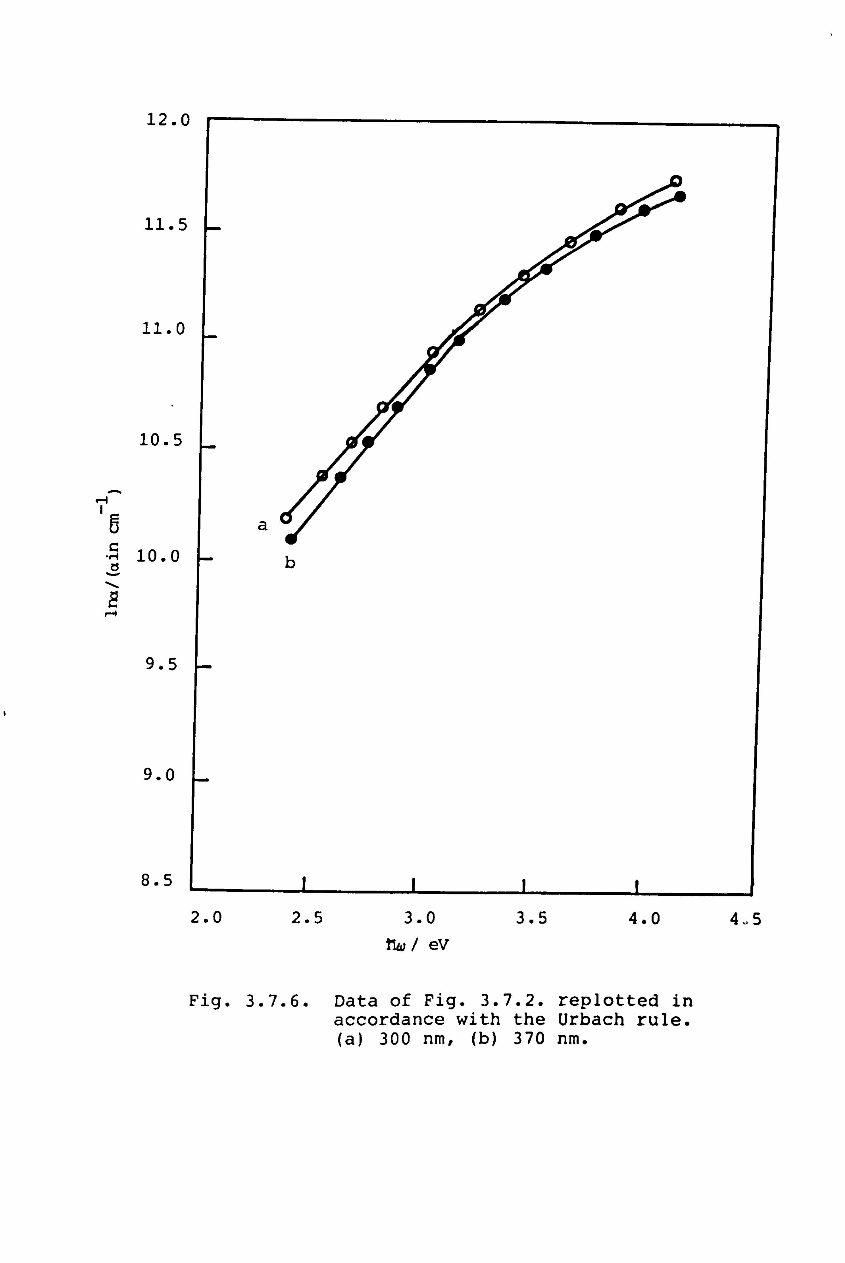
12. (
11.5
11.0
10.5
10.0
9.5
9.0
8.5
a
7
- b
III
2.0 2.5
Fig. 3.7.6.
3.0 3.5
Tlw / eV
4.0 45
Data of Fig. 3.7.2. accordance with the (a) 300 nm, (b) 370
replotted in Urbach rule. nm.
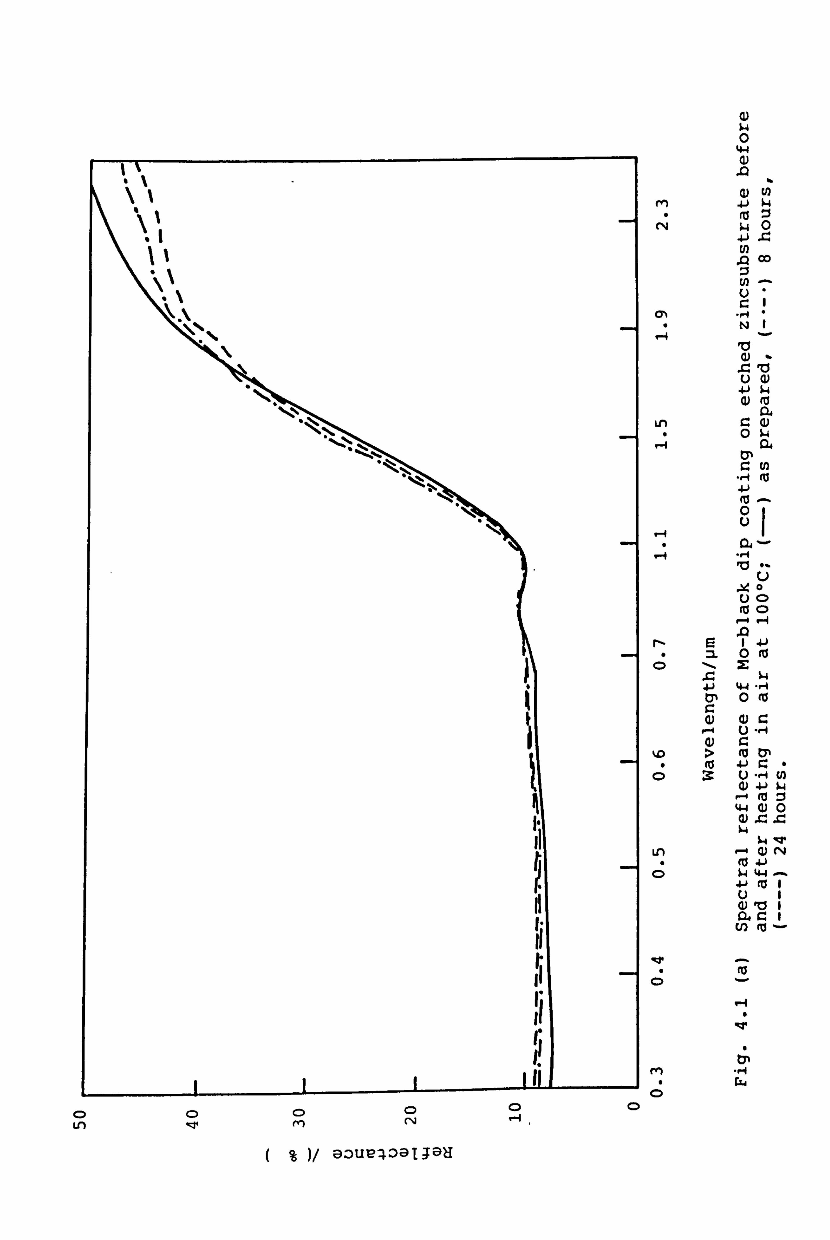
I'
I. I' I. II I. I.
I.
C) C) C) CD
Ln 4cT rn
rn
v-4
E ZL
m
0 0
0 N. 4 0
w0
. i. ) J.,
cn .Q 00
10 a) .
0 N4
01
04
r. U)
0
u
10 -
(00 -4 -ý 10 1 41 0 (0
44 H 0 (0
tu e
Q) 0
(0 4-) k4 44
(V v1
'-4
"-4 C'4
( DOUL"409IT9H
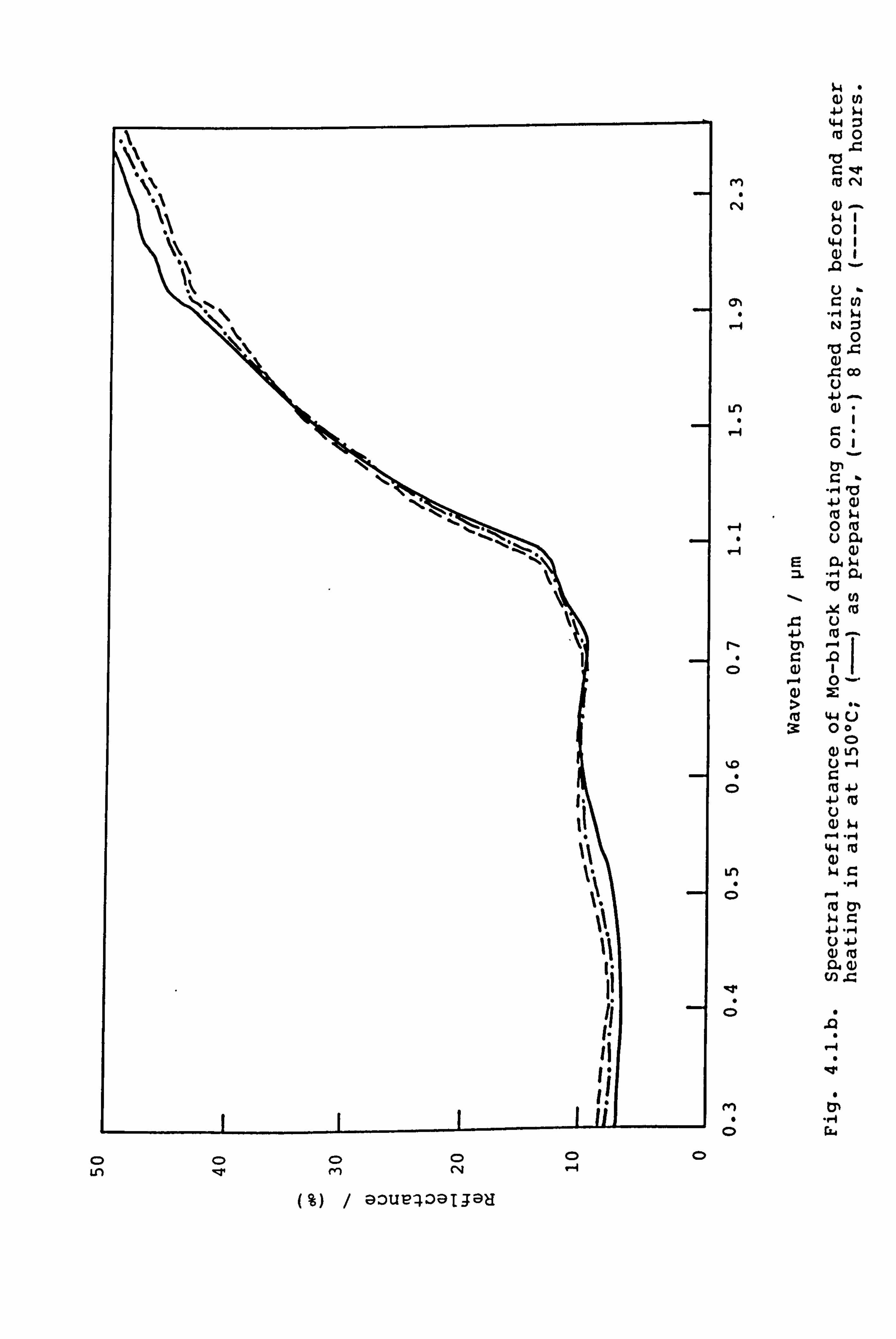
.�
\ .'
� \. \ �I'
C) C: ) CD 0
Ln 1-e rn rli 1-4
M
Ln
E =L
41
%D
Ln
fn III I
k4 . a) U) 41 k4 44 :3 (0 0
til N
01 44
U)
0
. r: 00 u 4J - w-
C: . 01
0 to
.01 0
44 00
0 0) Ln
tö 41
44 fo (1)
.6
(%) / a3ue-40qTJqH
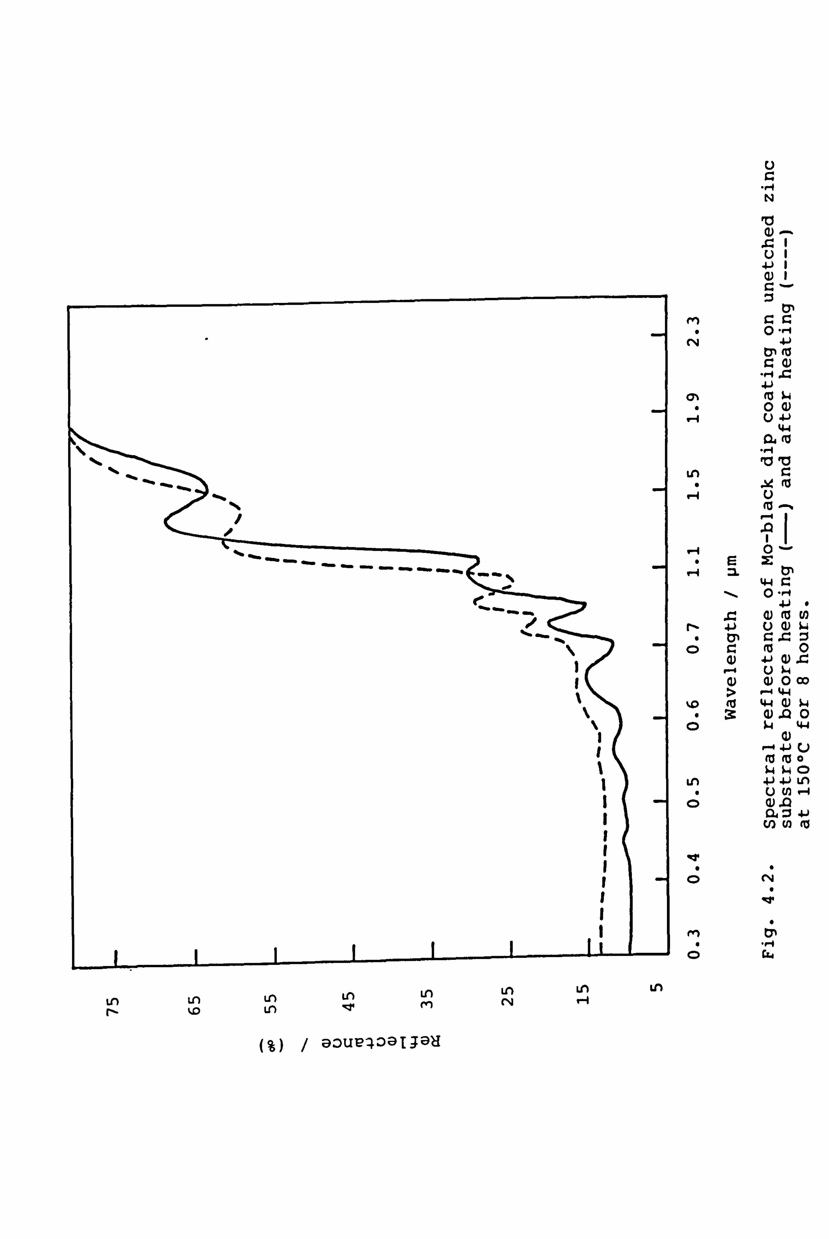
rn
C. '
-----
V S
I I
I S
-I
Ln Ln Ln Ln Ln Ln Ln Ln
r- ko Ln -: r m C14 r-4
(%) / DOUP-40alJaU
Ln
r-4
N
0
%D
Ln C;
qT
C;
0
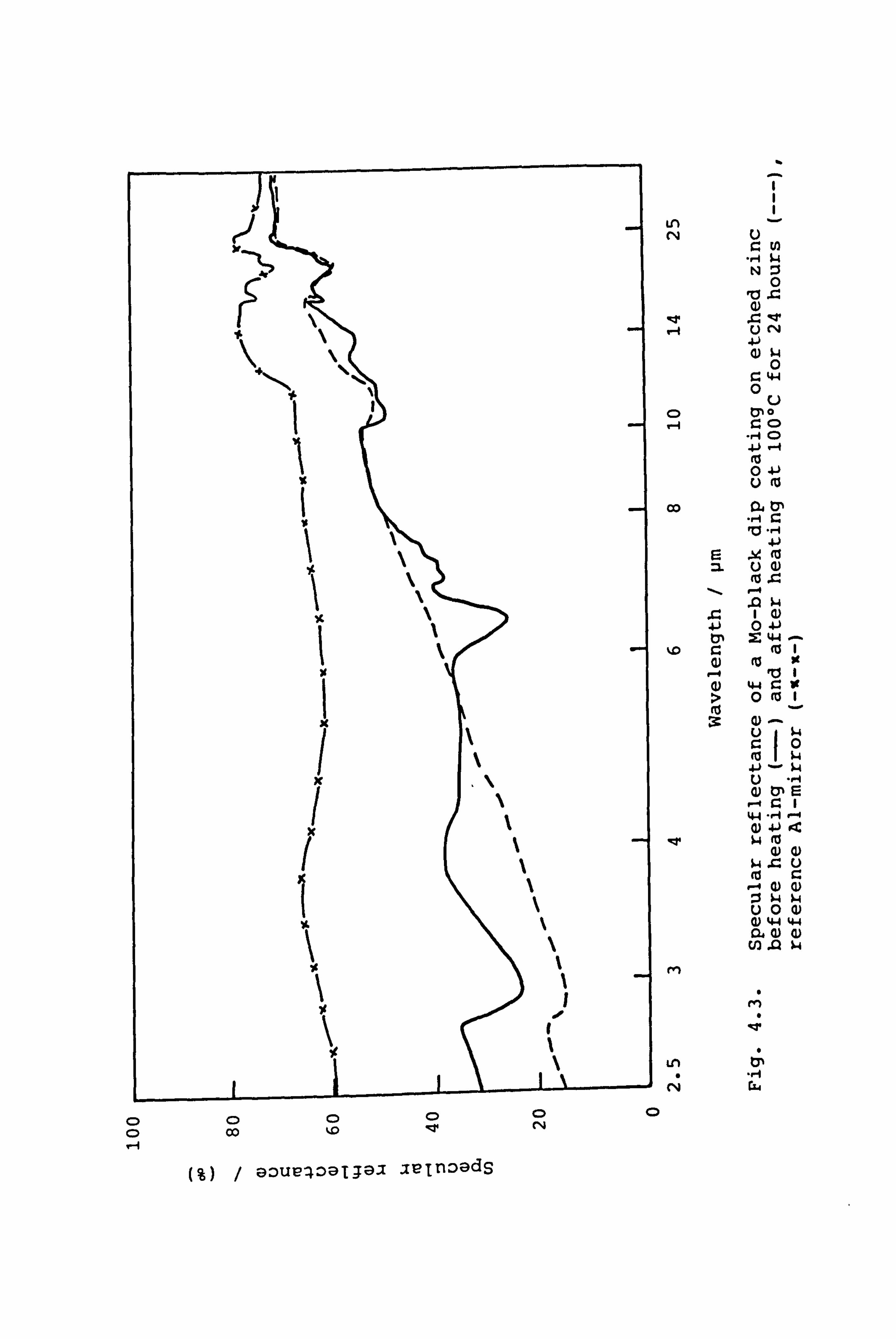
Ln N
10 A., Q)
q: r 4 ;r r-I u
. 1. ) 0) w
0 44
0 L)
CD t3) 0 V-4 C)
4J ý. 4 (a 0 41 U fu
co
41 S M (a =L () a)
.0w 4 1 a) 41 0 41
44
st
44 It > 0 fu I
0
41
4.4 a) 41
qw w (a Q) (L)
ý4 Cu (IS C
u0 0) 0) 44 44
ý4
rn
Ln C4
(%) / q: )up-40z)T_Tqi aeTnoadS
C) 0 00 I-D
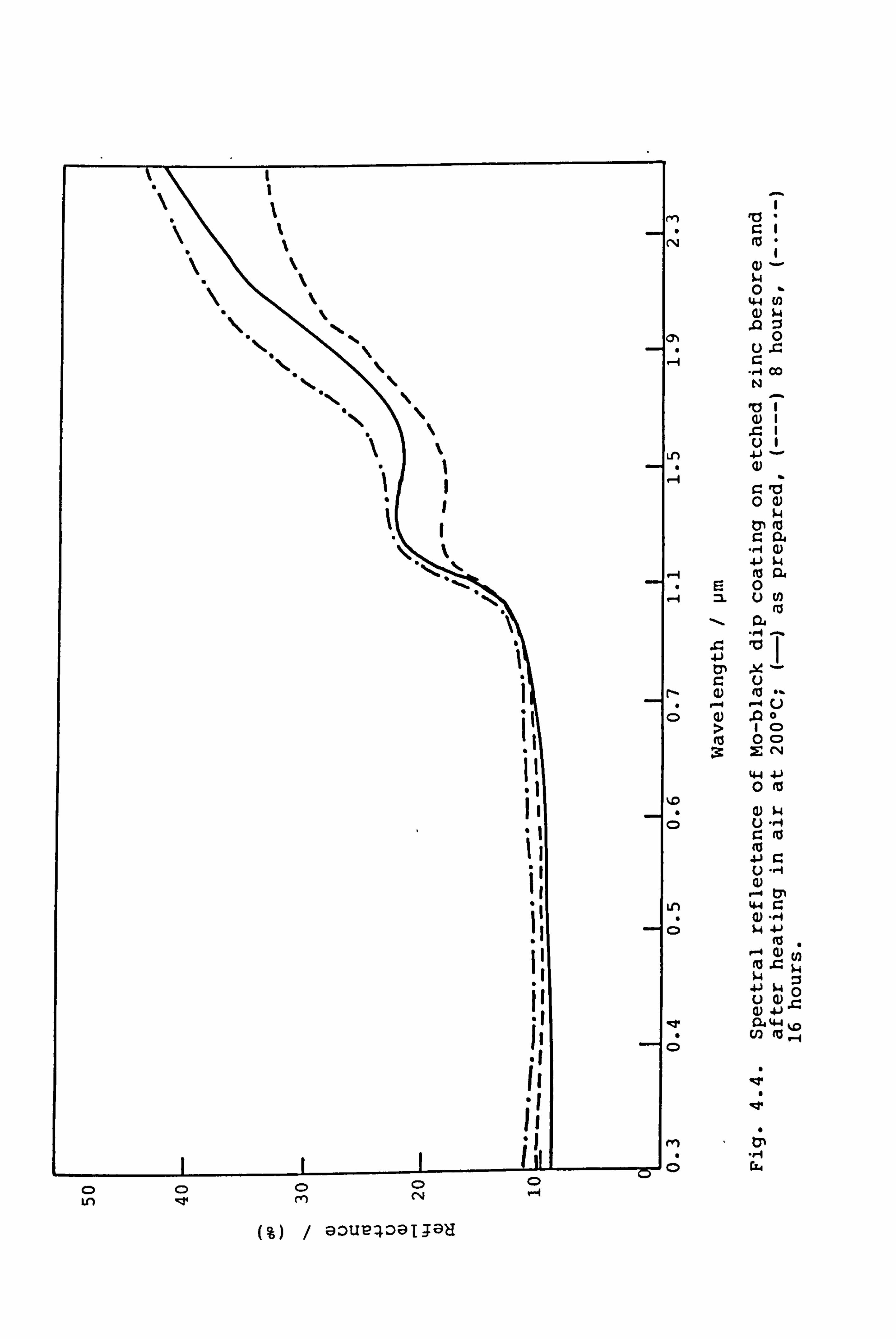
%z %.
il lt II 'I ti ii II
!i II
ii !
1.4 =L
4J 0)
C>
(a
Ln C;
C; Co CD C) C) Ln I: T m CN
rö . r_ 1 rö .
44 (D (D w
.00 0 u4 r-
-4 00 N
to I
4J a)
$Z to 0 0)
ý4 t3) (0
0 u (n
(0
, Öl
C) OCD Z (N
44 4j 0 tö
Q) W L) -H c fu (a
44
(a
to 'g" $4
0
44
t; . 14 rZ4
(%) / 83UD3UaU
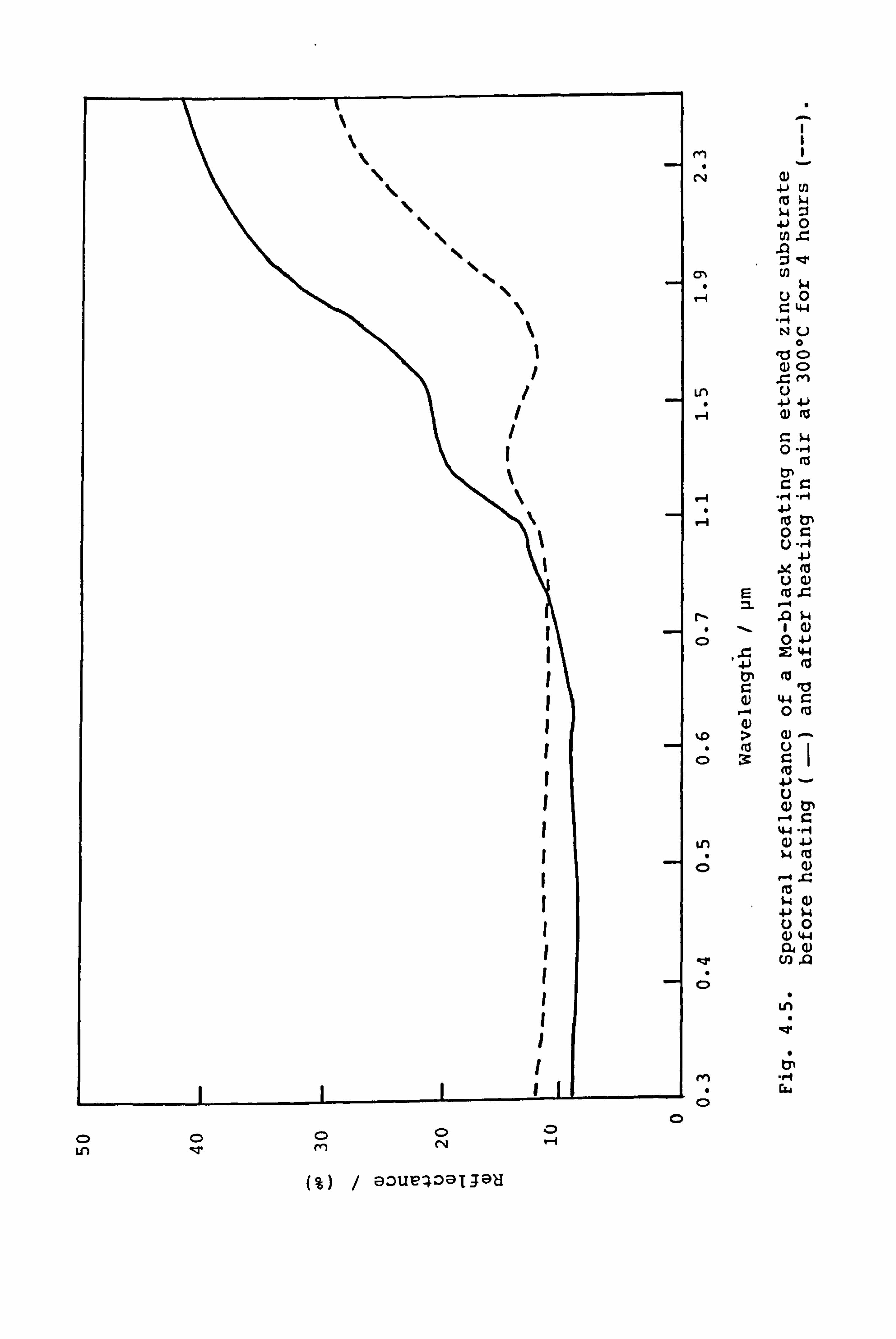
/ / I
/
I I
I I
000 C) 0 Ln "; r cn CV "A
M aoue-4091jau
rn
C4
U)
00 r- 44
Q) C) . c: rn u 4j 4. )
0-4 fö
U
tu J.,
0 3: 44
(U (0
10 44 r. 0 cu
to
a) W
4j $4 00 (1) 44
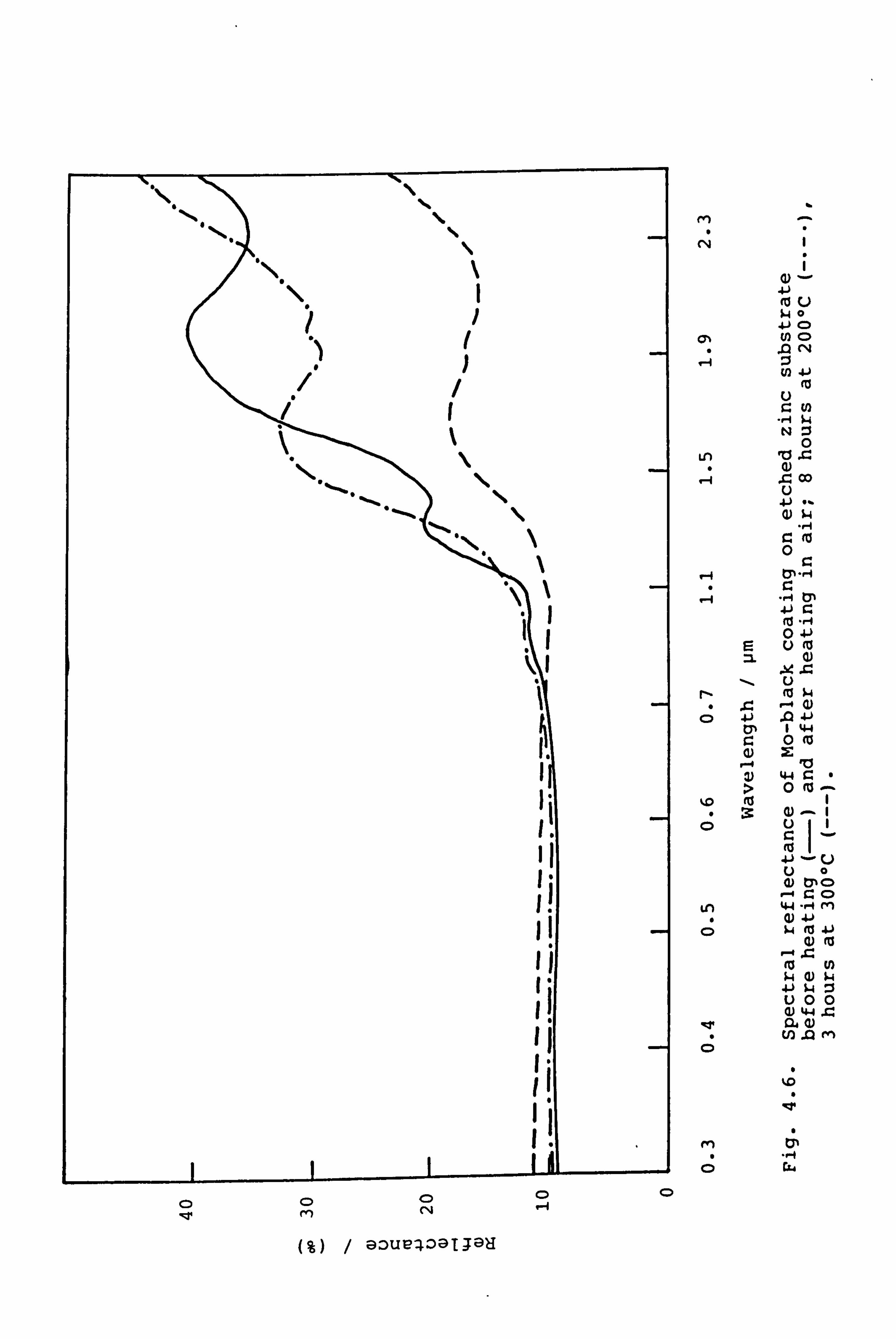
. 4'
"\ I /
(
"/ /
/I
\ . 4'
e4'% \
"I Ii 'U
1 I. ' -
I. II
ii Ii -
l"1 I;
'I -
I.
II I'.
C) C) CN ýq
rn
C4
M
(D 4J (U u w0 41 CD W C)
(a
0
OD
$4
C (a 0
41 C: (a -4 04-) u (a
(0 ý4
1 44 0 (a 2:
,a 44 r. 0 0 (0-
u
r 4) t7w C)
-4 Z C> 4.4 -r4 M
(a U) ý4 W 4-) WZ u00 Q) 44 4 04 a)
U) .0m
t; -4 CL4
(%) / 9OUL-4091jau
-
I *
x
I. '
1 I x-
I I' I'
II' '1'
I II
Ln
0
U)
0
-1
0
0 -1
C)
C;
tP r. Q)
0
0
,4
Ln C4
In fö
.. 0 u C)
CD
N 4.3
Ici tö
Q) 0
0
0 (00
P-4 C) .0" 0 X (Z
(ii In
44 00
(ö -
0 'o
01 . rl ow
CD CD 000
c> CD %I0 -e
. --1 (%) / -itinDecIs
N*, -- vs,
0
I. '
p I
I; C>
Ln -N
ON
14
Ln 14
�-4
- (D
lý CD
E
w U
0
4. ) U) (0 k4
0
ý4 0 cq
44 a) 10
, 0-
u $4 4-) zi Q) 0
r_ J.,
000
0% ý-4 Z0
-r4 44
-i-) (0 u 00 U C)
C)
0 =$
44 (Z 0>
tu 131
M-4 rö 44 0) 0m
ý4 4-4
U) tu
00
I'
\'
! 1' I' �I'
I I- I
II- 00 C> 0W ul CN -4
CN
01%
14
in 1;
to 21.
kD
1ý
Ln
8
0
M
C;
0I z. dP 0 U) Ln W
40 41 J., .H 3: 00
w 0
44
a) Cý
. C: ý4 u 4J 4J
0
9 (a _4 > 41 (13 r. 0 -r4
(a 41
0
03 4J 44
44 (a
41 u 0)
44 U) 0) 41 w ý4 (13 :3
(1) 0
ý4 4J ý4 cli u0 0)4410 04 0) r.
U) .0 (0
CL4
"
" \" \
'' I
"I
I ii I. I' I. I
ii
rn
C4
-. 4
Ln 14
-4
14 E =L
41 tp
%D
0 41 4) .0Z () $Z x. '
.H N
0
m4. )
tö =$ 0
U (13 r.
,. 4 H
.0e 0'
m .,. t
L) (U 1
44
tö tr
0 -4
a. '
Ln -4 aOUV-40alJad
VV VV
V '4%
V
N / /
\/ V/
I-
I
I- I I I 1
I11 _____
rn
C4
CY%
14
Ln
I-I
'-4
r-
C;
¼0
0
Ln 8
Irr
C;
rn
C; C) C> C>
LO qqT CN
ON
4-) M
0
.0 u
4 U) UW 41 :3 a) 0
0
0) w r. 0
*, -1 44
=L 00 U Ln
fn 41 u
(o
-4 15 a) 0 :3 >
44 0>
ON 4-) z U . 14 Q) 41
r-4 (z 44 (1) (U 4
(a 41 W 44 41 (fi u 0) a m r- rj) (a
14
t; . rj CL4
(%) / aOUP-4: ); 9lJa-d
I
'IN
14 (N mI IwI 31
3c
it
it
C) Ln
C) RT
C) cli
,a r. 0 04
U)
ý4 CN 0
4-) u (v 4) U)
ON cu E 4-) :s
14 44 r- (0
0) U> r. w
u
Ln 14 = E-4
u
0W :3
V) 4-)
4J Q) (o m 0E U Q)
4j E . 54 =L u 4J
(13 C 4)
ý4
41 0 4.4 E-4 tr 2: 44
44 -1-4 0
41 U) > tv W
its U 4) r- rz .0 M :5E
> 44 a) r. W -4 E
Ln (a -4 t7l U)
w -4 a) 41 41 J., u (a 4J (1) Q) 134 W0
U) 4J . 4. )
t; . r4
m rA4
0 0
(%) / aoue-40qTJau
-4 CN lzr
it
11
IL
ý, ,I
C) 000 OD ýo -e
C) 0 Ln r_
0 -4
Ln w IRV N
r-4 4 CD (a . 9'. E-4 41
qcr 9
$4 N a)
r
C)
-4
E
co rz =L
0 0 41
41 0)
0 %D 4J 11
U) > 44 0) (ts 0 ý4
0) 0 uu r.
u 4)
44 :1
qT (1) $4 >
:3u
in E-4
M en
ON
Ln
04
(%) / 9OULD-40gUall
Fig. 4.14 SEM micrograph of a Mo-black dip coating on etched zinc substrate Magnification : 6000 x
4 sflm mi ci oy r dph ot t fie saine coat 1 ll(-j 1-,; 1 li Fig 4.14. after heat treatment in air at 1000C for 24 hours.
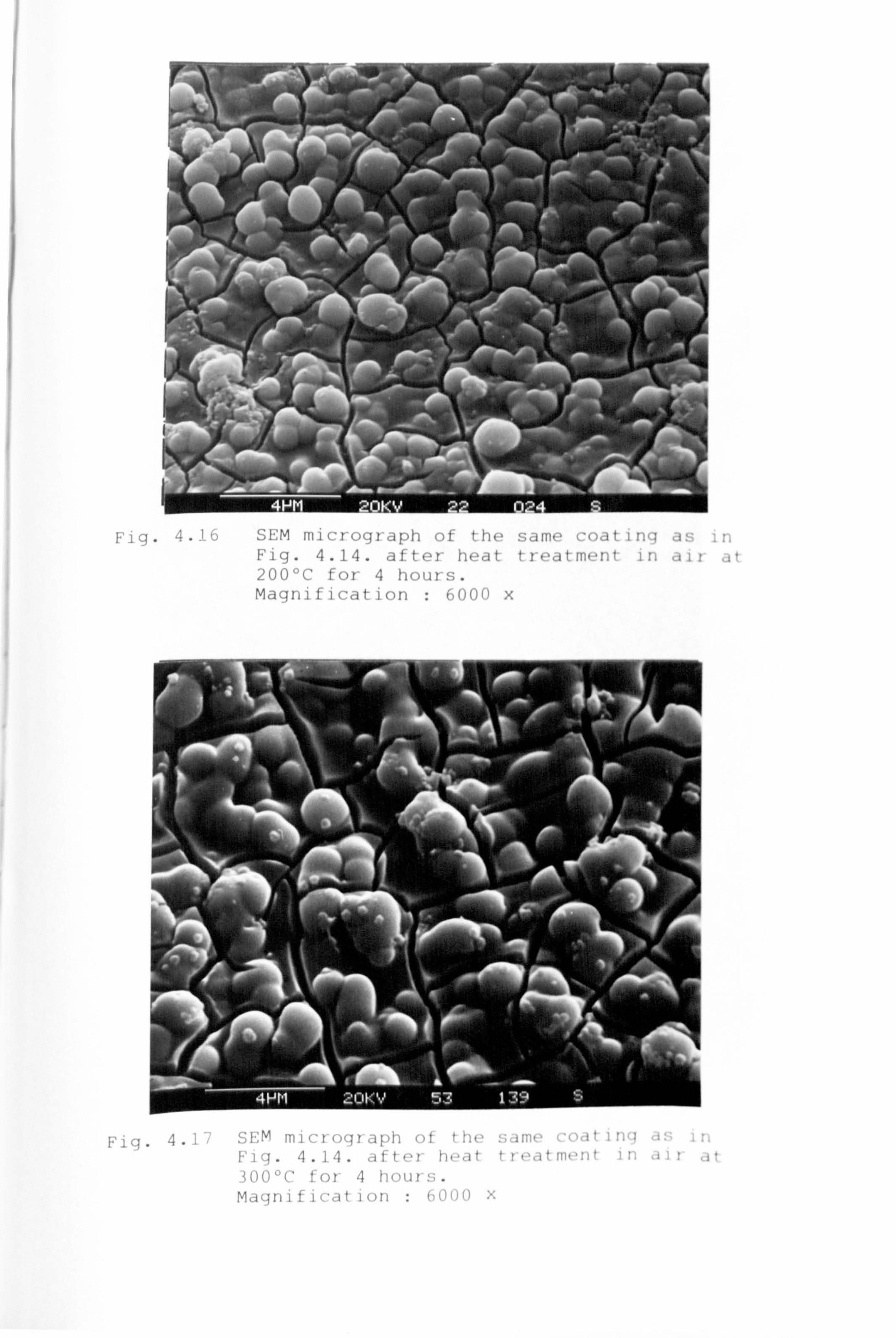
Fig. 4.16 SEM micrograph of the same coating as in Fig. 4.14. after heat treatment in air at 2000C for 4 hours. Magnification : 6000 x
i! lo -300'C for 4 hours.
Magnification : 6000 x
ýI( "i ! lo .ý,,.: I:.: I,
x
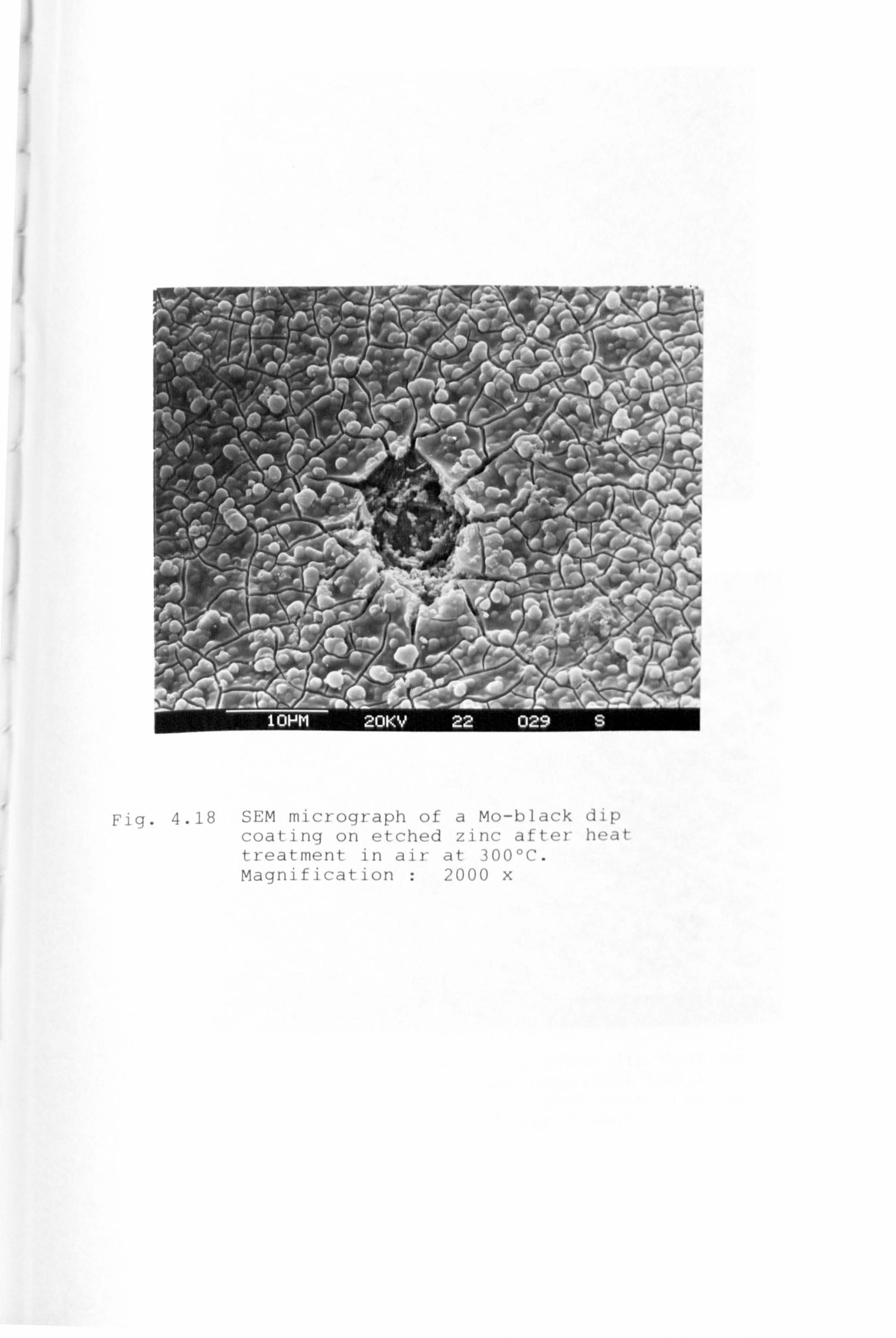
Fig. 4.18 SEM micrograph of a Mo-black dip coating on etched zinc after heat treatment in air at 3000C. magnification : 2000 x
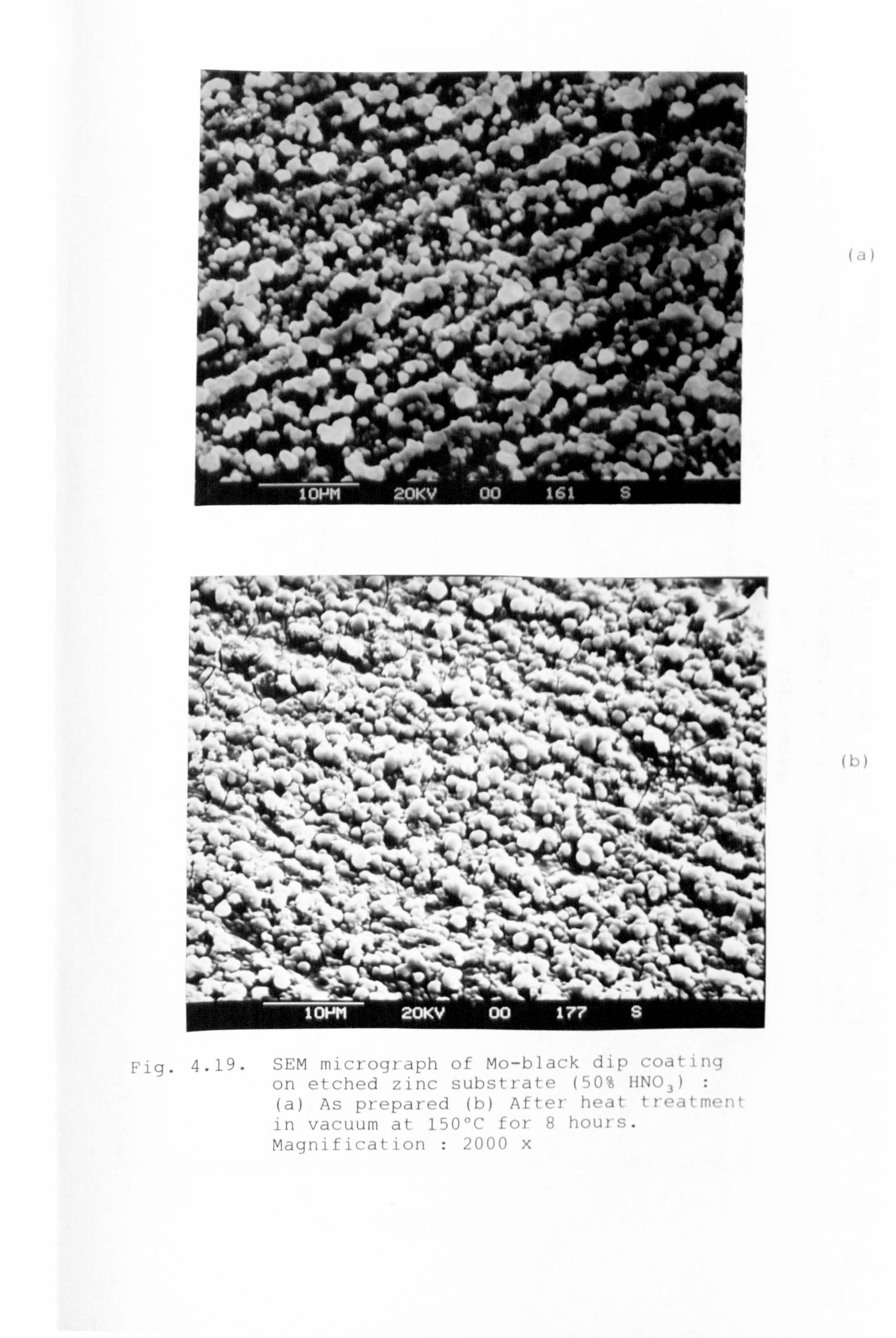
(, I)
ý ýI: M III ,ýI ()ý It 11 ýI, I:, I, ý- Iiý ýý !.!, II: on etched zinc substiate (ýO'ý HN(J3 ):
(a) As prepared (b) After heat t reatment in vacuum at 1500C for 8 hours. Magnificatiori : 2000 x
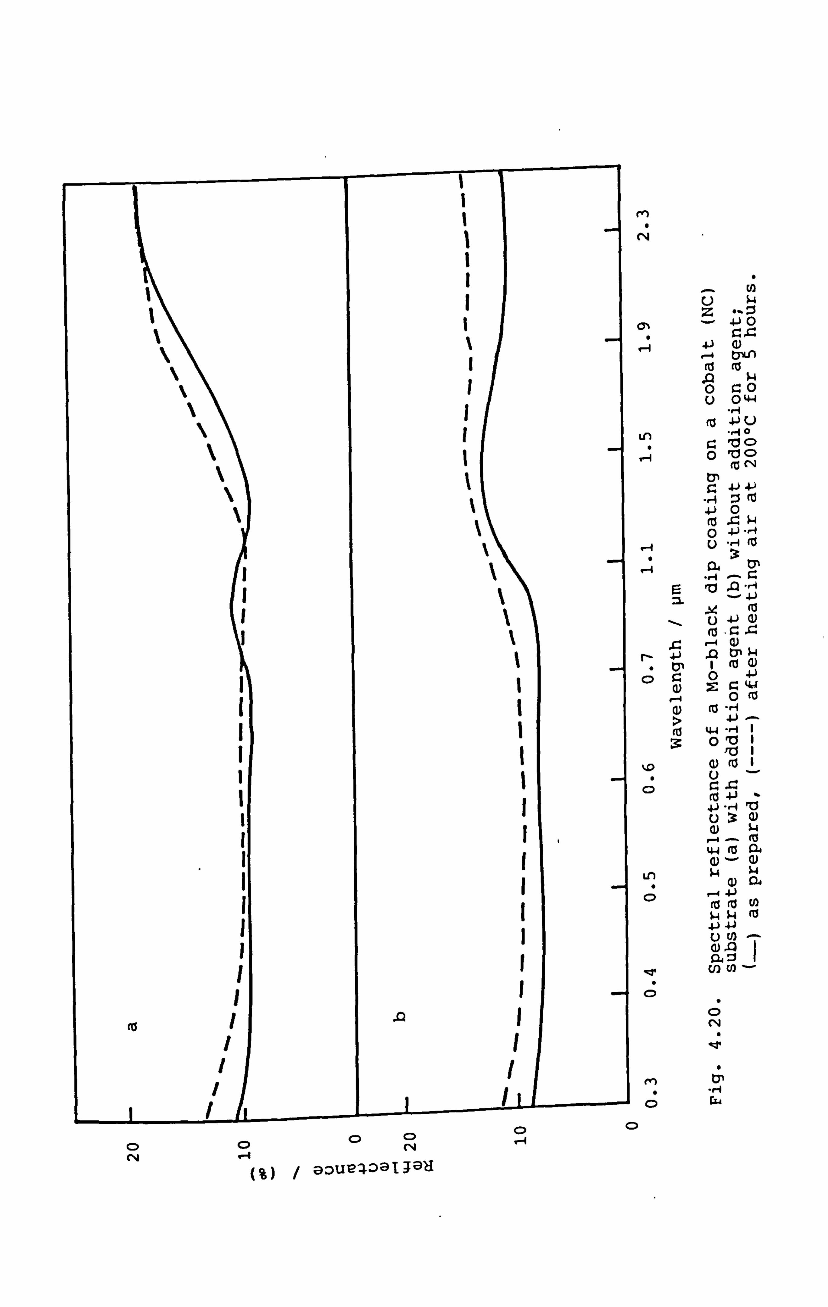
m
4-)0
4J -4 b%n
ý4 o Cý 0 U 044
4-) U , -jo
C: 'o C> 0a CD
(U C-4
4J 4-) :: s ro 0
ro Cý ý4 0 4J -14
-4 u -rA (a
r= ro in -4 =L - 4J
ý%4 (a
L) 4j
r- 4J t7l $4
0 C: 0
> 4J 44 -, 0 ra
u CD rý C
(a 4J ý
-4 al 44 fO 04
Ln 4-)
fo (t ED ý4 $4 4J 4J r) 0) -
a) ýq I ja4 :: j
U) U)
C>
CN
44
(Z) CD
r, 4 C*4
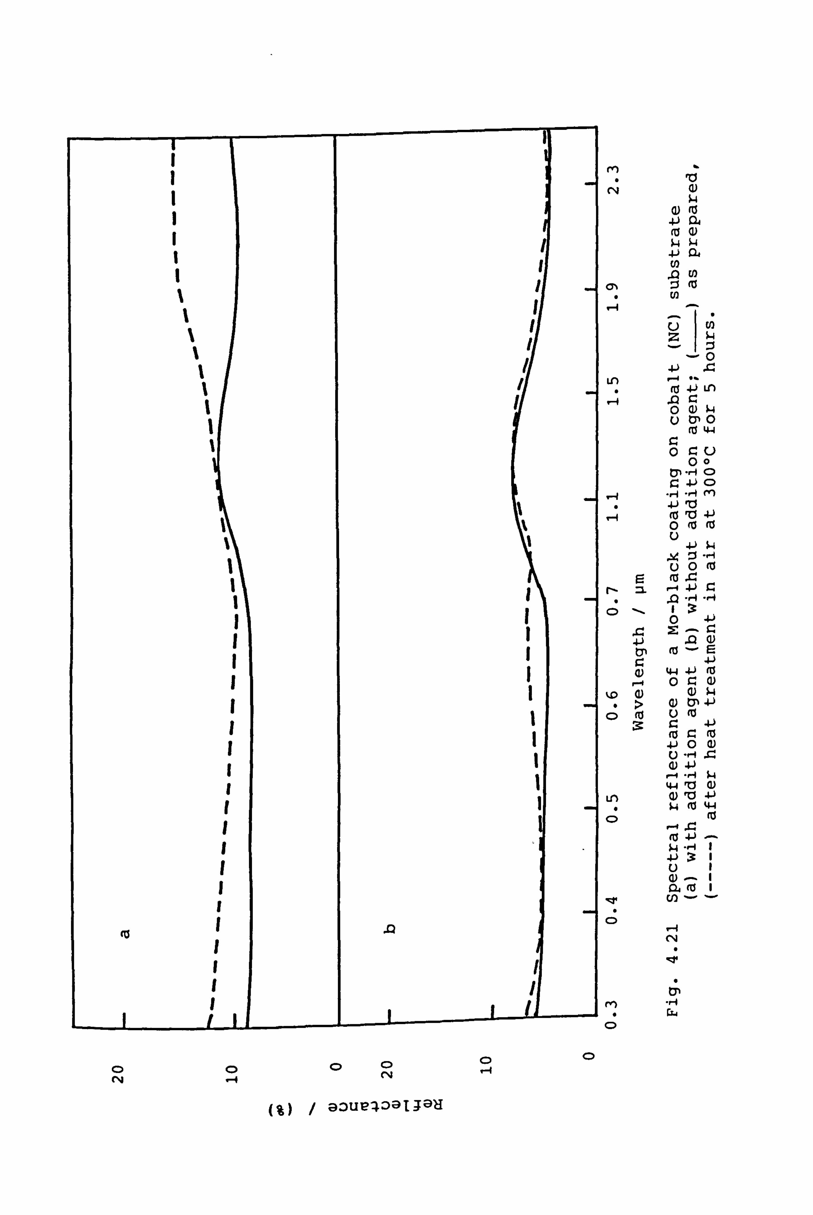
1 0 to
C) 0a CD 04 -4
CV 0 -4
rn
lý 0) rö
4. ) PA (ö (1) ý4 ý4
4. ) M to
'n rn
U)
LO -0 -
(U 4. ) Ln -4 Q Z:
0 (1) ý4 t31 0
0 00
-, -f C) CD
(0 lö 4-) 0 (0 (0 u
4-) N4 x Z$ H (-) 0 (ö
E tu J., ZL -i 4j r.
lý 0H -H
b, (ö - r=
r_ 4-) e) 4.4 4j rö
0 r: (1)
3: lz 4-) (0 Z: tö 4J 0 (1) u -f c: a) 41
,4 -H ý4 44
Ln 0) ý4 (U 44
--f CZ (0 4j
04 (ö 1 U)
t; C>
(%) / aoue-4oalieu
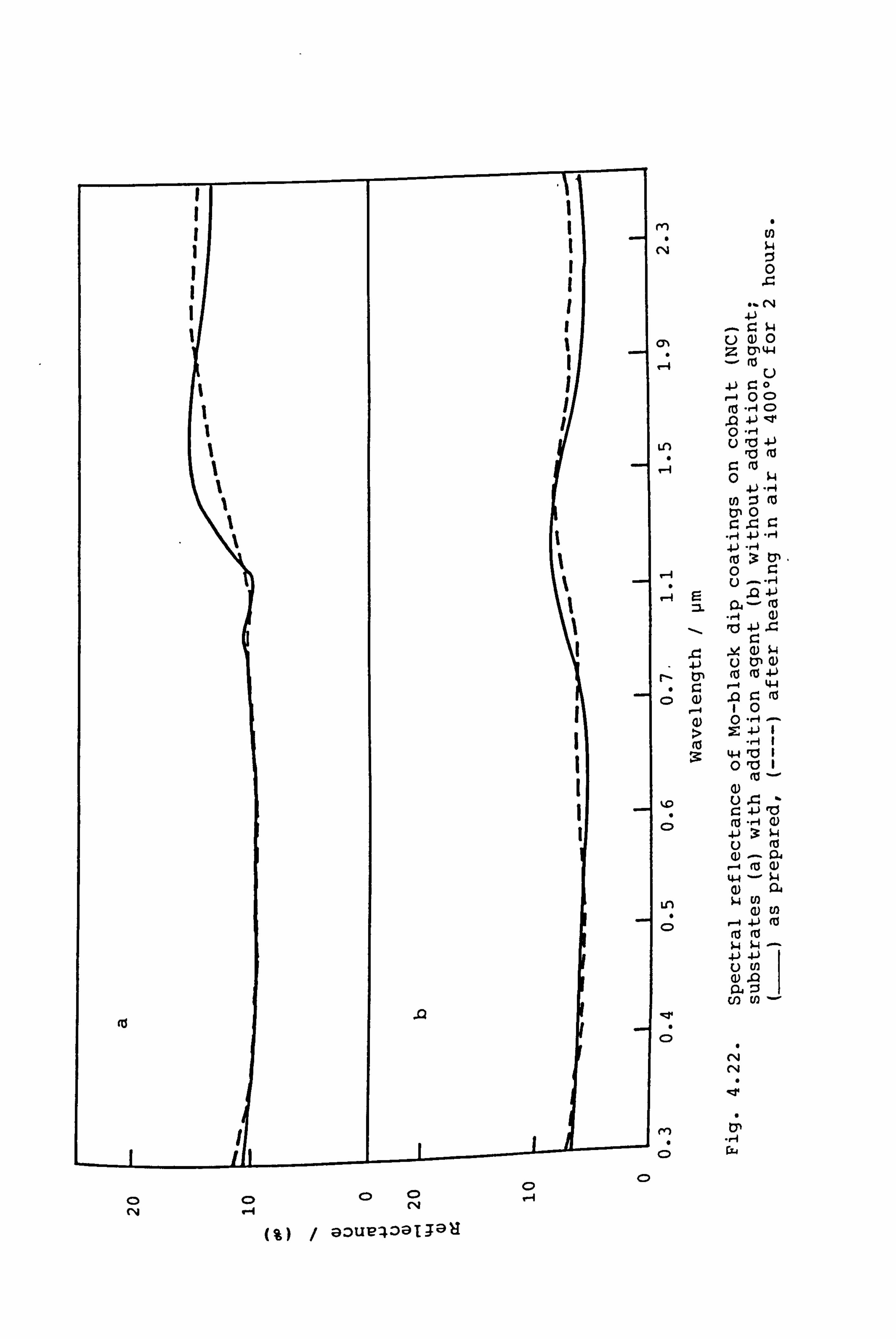
Z ra
r. N4 Q) 0
1-1 - fö u
r. 0 0 C)
-r-1 0 4-) ýzr
0 --f U rtj 4j
0
til 0
(ö ý: t3, - 0 u
ZL 12, - (0
4-) r- t7, (0 fö 4-)
(ý CZ -t 44 a) jQ
IZ (0 1 C) 0 -, 4
>
Z 44 Ici 0 rö 1
(0 - (V
C>
C) -
(0
44 N4
ul 0) to
CD -f 4.1 fö 915 N4 41
in
oý Z$ 1
CD
CD C) -4 CV
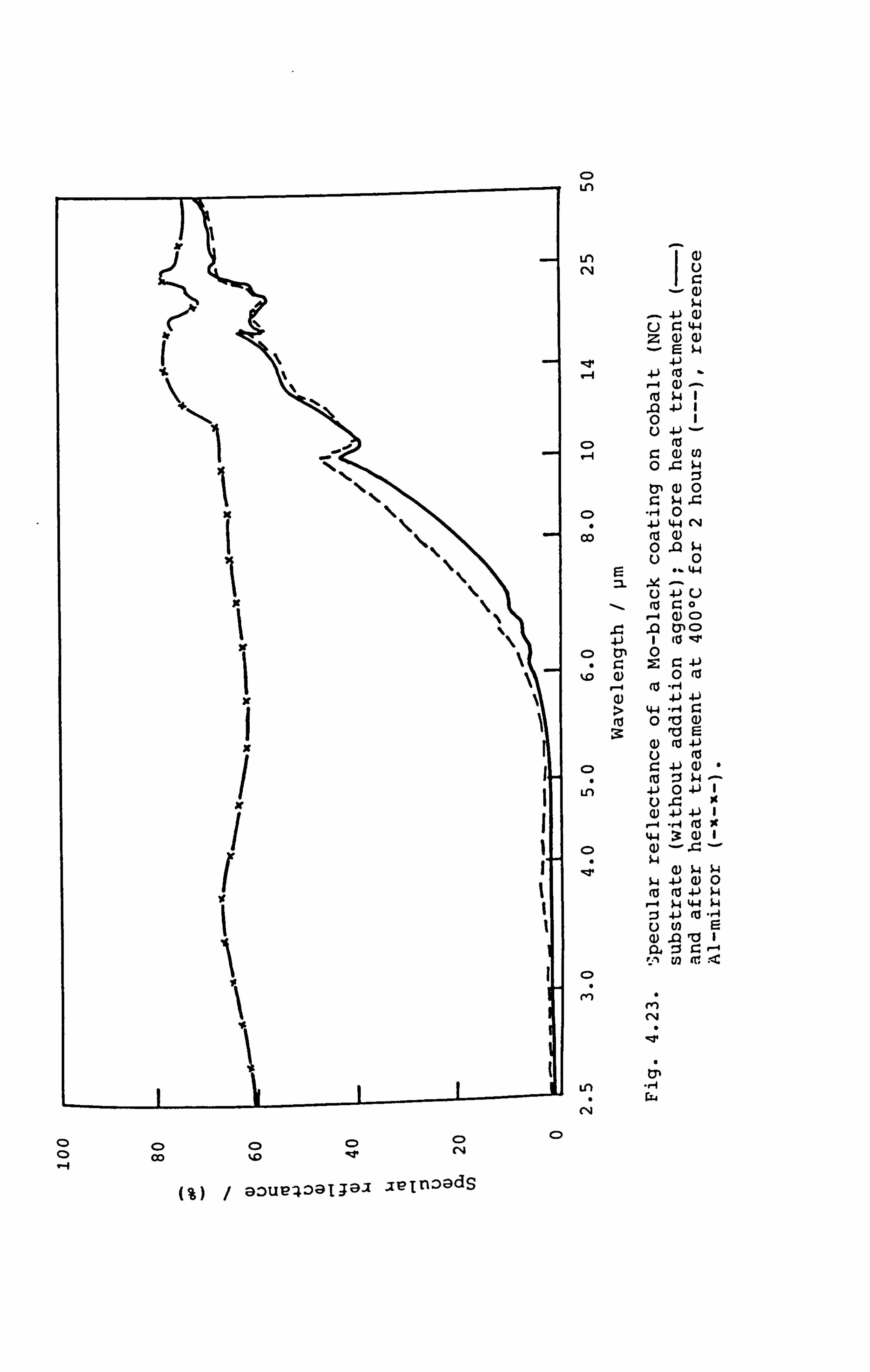
C>
Ln
CN u
4. ) 44
E $4 4-)
4J (a
4-) 0 U 4-)
Cl (a 1-4 lz
0
0 ý4
CD 0 4-) 44 04
cý (a (1) 0Q ý4 u0
E -44 =L -ý4 -
0 4-) U
C)
4J I (o -, T cp 0
2: r. 4J 0 (a
a) 41 4J > 44 -4 r.
ra 0a a) 0 4. )
C) lz 4-) a) I (a =1 ý4 - 4. ) 0 4J I
4
(is Ic 44
ý4 ý4 ý4
$4 41 a) 0 (a ra 4j ý4
ý4 44 W 4-ý
r-) En (3) QuI Q4 :I r- -. 4 t. -N U) Ir <
C)
t;
(%) / 9. oueqoajj9-i jelnoads
CD (D (D 00 --f
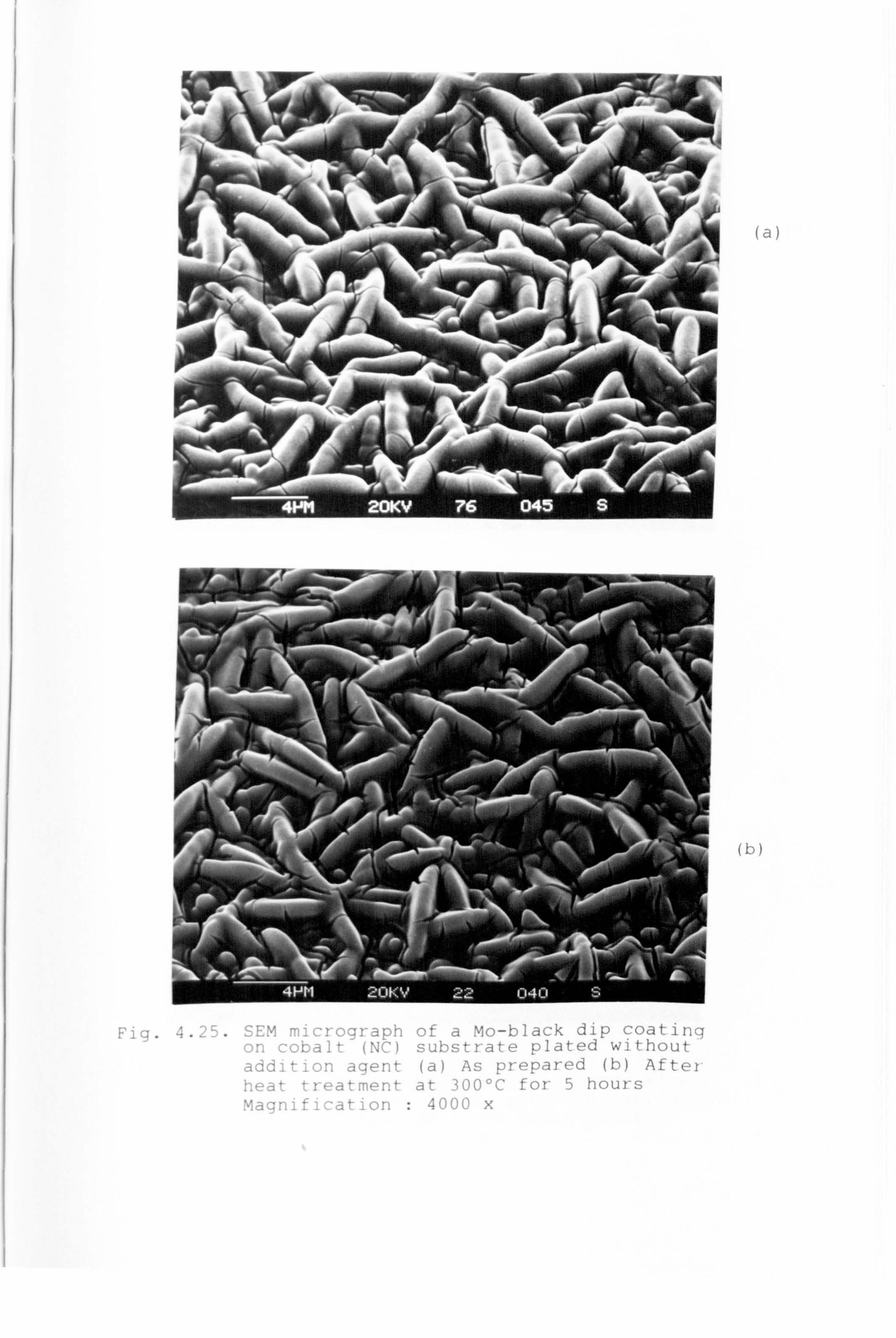
(a)
(Iý)
sui2, ýýt i ate plated without addition agent (a) As prepared (b) After heat treatment at 300'C for 5 hours Magnification : 4000 x
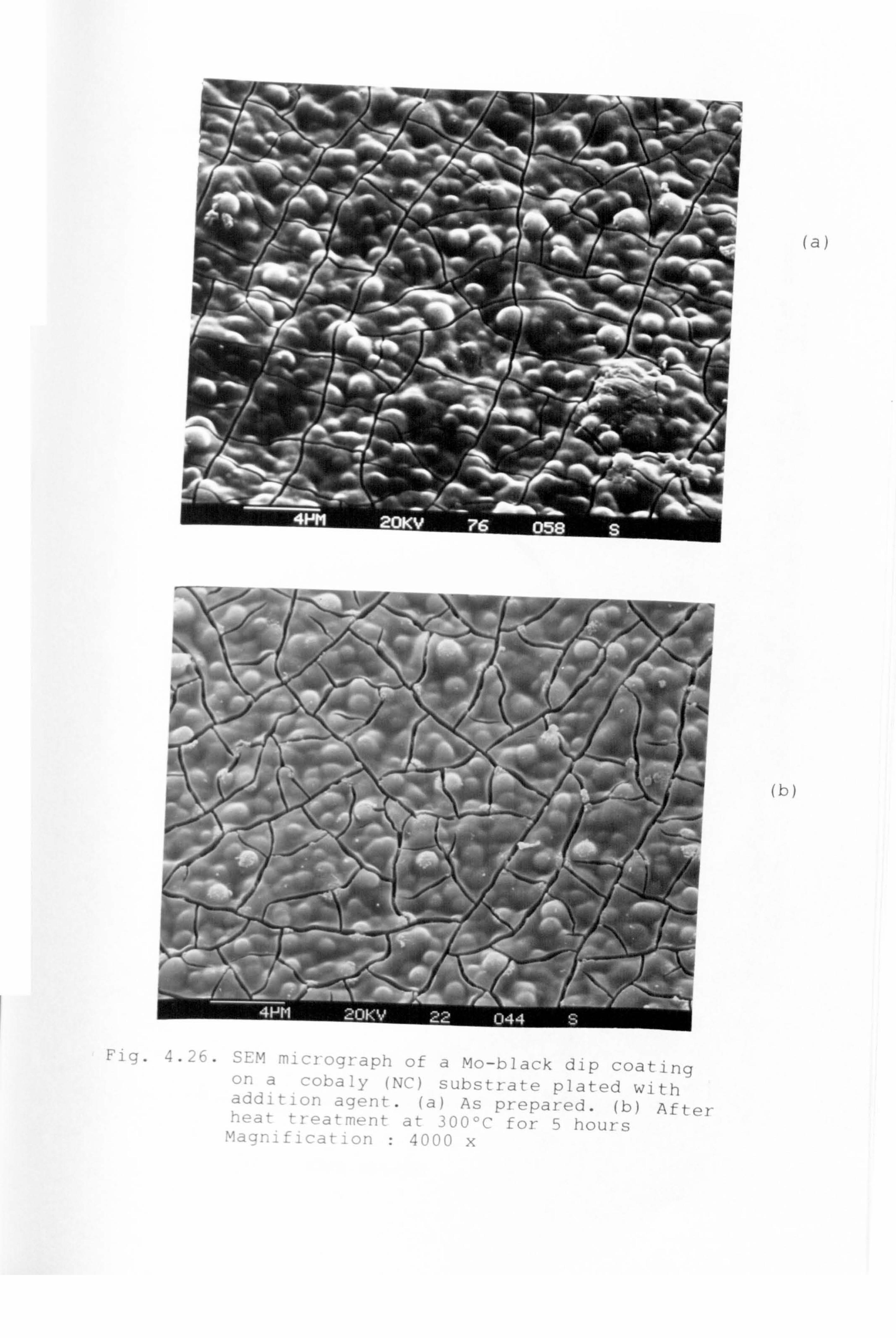
(a)
a Cobaly (NC) substrate plated with (a ddition agent. (a) As prepared. (b) After heat treatment at 3000C for 5 hours
Magnification : 4000 x
(b)
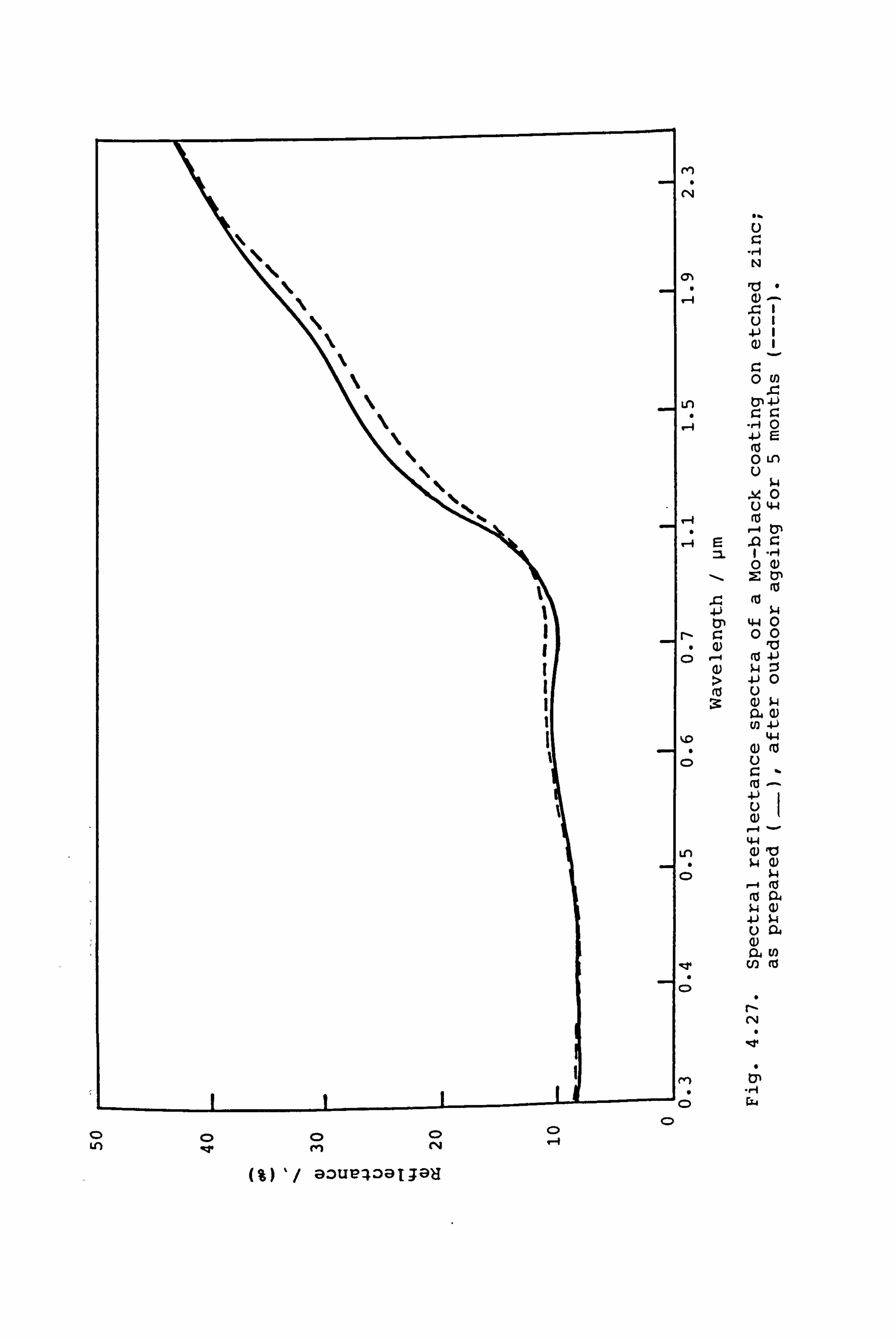
m
'4-'
\ \
'4-'
4%
a LO
t
ON
Ln
-4
N " a)
o- a)
CD
Ln
c;
1 ell
N
ro .
u 4-)
0 U)
0 4-) E (z 0 Ln U
S4 0 U 44
0 a) 2: tp
ý4 44 0 00
10 (($ 4J ý4 :: $ 4j 0 u co P 04 Q) ul 4J
44
U ra - 4-)
4.4 (1) $4
ý4
04 ý4 (1) 41 $4 r-) 04 (L) 104 U)
ri) fo
CN
44
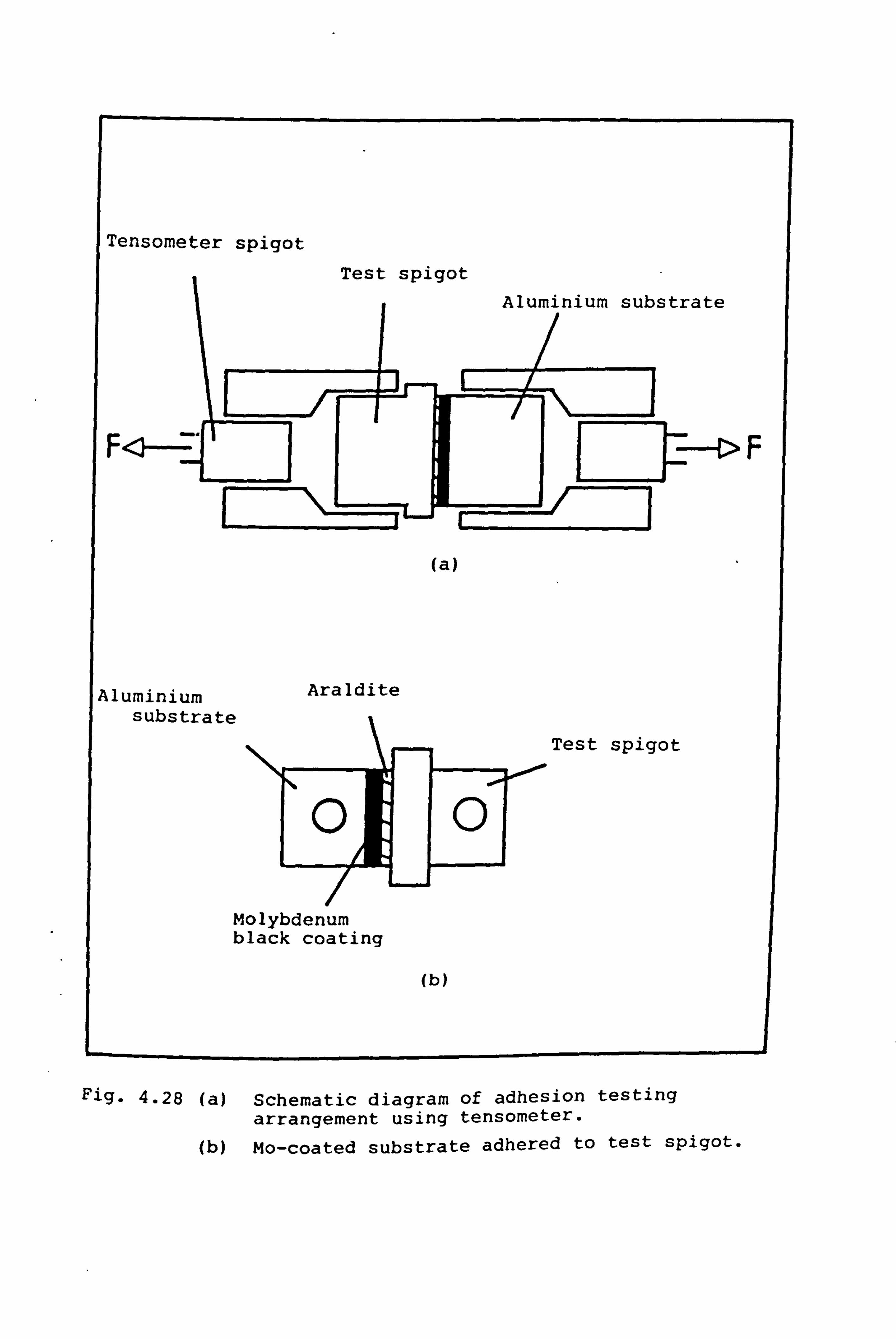
Tensometer spigot lr, o cz f- cz ni eT e-i +-
_ I'
LI
Aluminium I substrate
-
Aluminium substrate
_I1F tJ I (a)
Araldite
Test spigot
(b)
Fig. 4.28
(b)
Schematic diagram of adhesion testing arrangement using tensometer.
Mo-coated substrate adhered to test spigot.
Molybdenum black coating
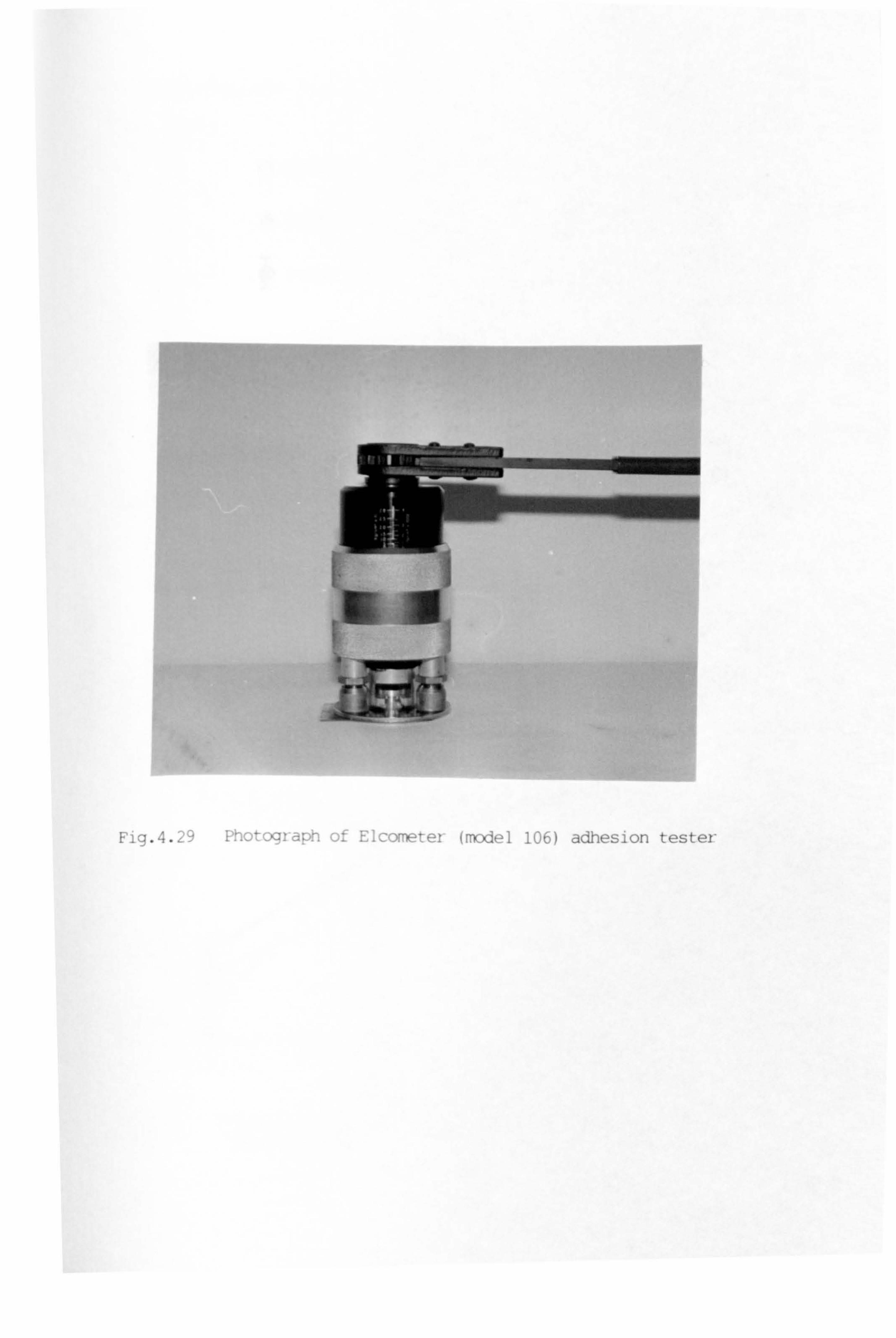
Fig. 4.29 Photograph of Elcometer (model 106) adhesion tester
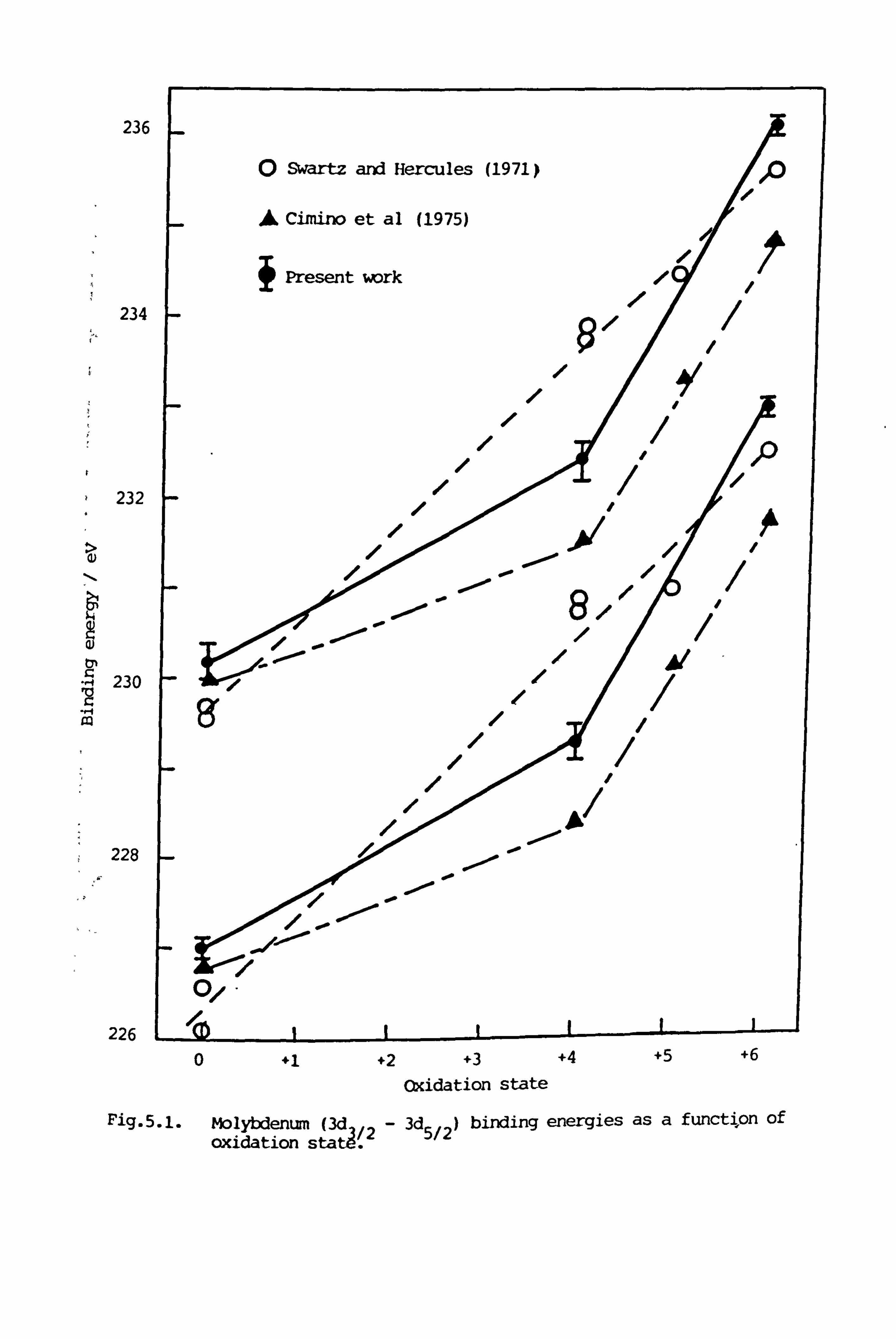
236
Swartz and Hercules (1971)
A Cimino et al (1975)
234
232
230
228
226
(�0 �
Present work
1/ / �fr � /
/ / B' '
// / //
' /
/
/
/ 0, "
0 +1 +2 +3 +4 +5 +6
Cxidation state
Fig. 5.1. Molybdenum Od - 3d ) binding energies as a function of oxidation sta
ýAý2 5/2
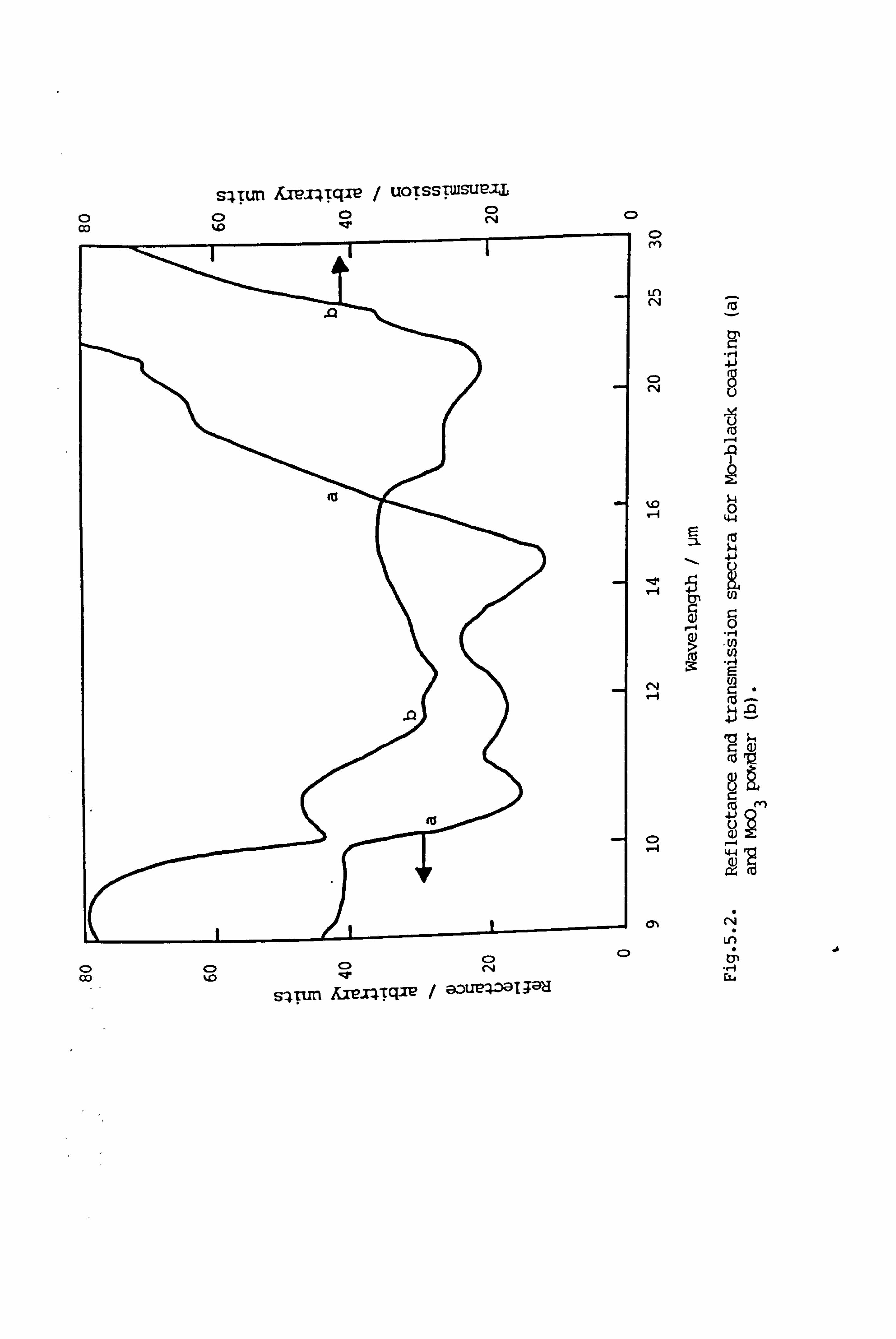
s-4Tun AzeiZTqxe / uoiss'wSUL>-zl 0 C) CD
OD %D 1-r
.0
go
.0
0
C) fl)
Ln
r4
5
(D
10 ý-, 9e
(a
0 CZ) OD -
%D -m CY
- SITIM JUVITqie / aoue4)a139U
70
(0 1-4
ý4 0
44
ra
rý 0 En U) 9 ul 2
-* 4ý 'Q
4J
4-1 M
CD
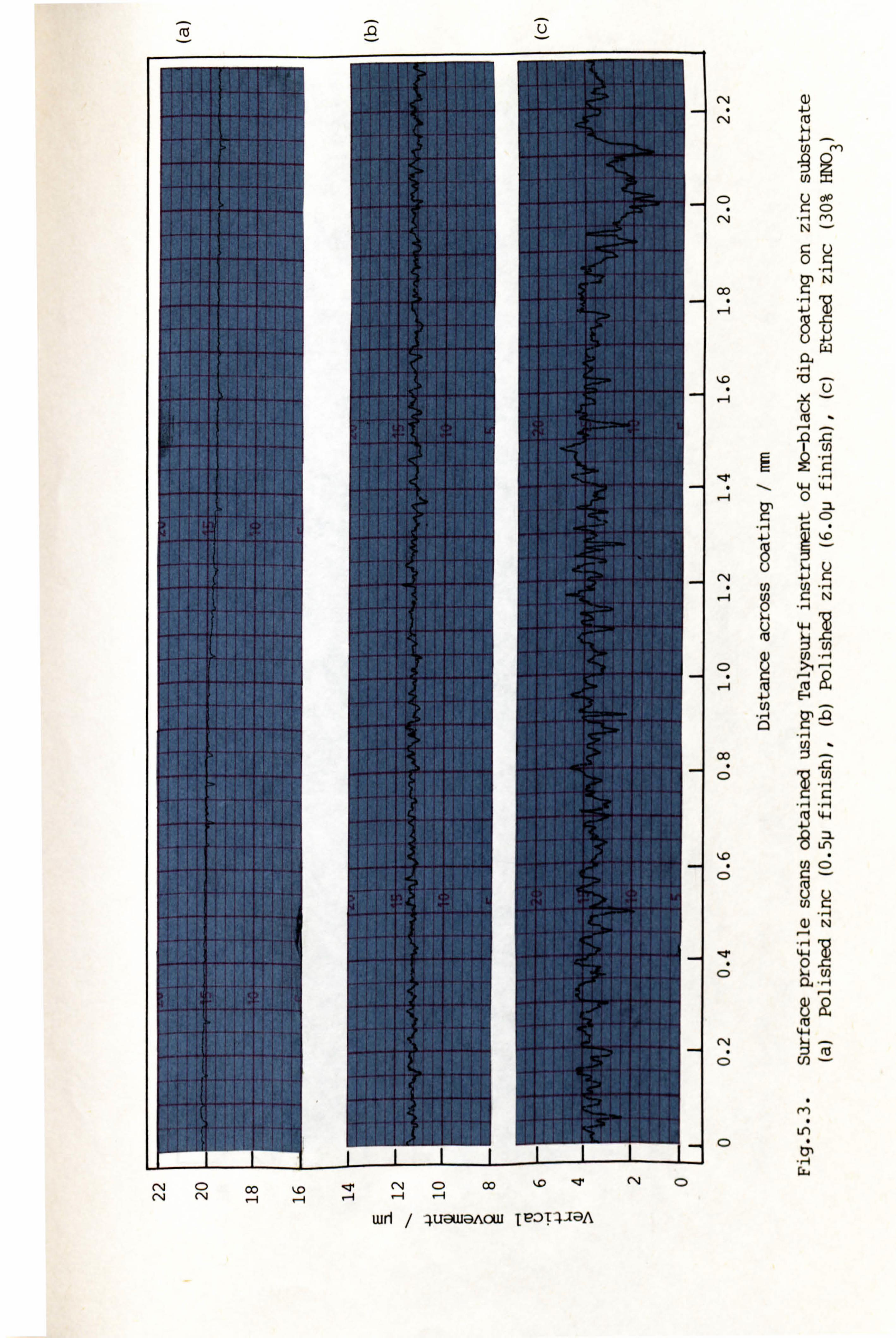
-i3 a -6
-I TI- 1 I 1 - 4-
,
1 ý 7 IT
-41 -
! I T I-F ,I -
l ., ý I I M I - i
i 4-
4 1 -4 -r r j 4 -
L
4 ý t i H
'T t
r1i CD 00 Icil (14 CD 00 kD :T r1i
r-A r-A
wrl / 4uauaAotu JE? OT4-laA
4-J
4
U)
dp C)
CN N
r- u 0C
N
ol .H
'a zý
44 u
U)
E 14-4 44 0
4-) Cý
4-)
4-) U) . 14
4 U) C: N 0
4-4
a) U) -4 9 >1
1-4 (13 4-ý E-
S
U) Cý
U)
C: C: . 1.4 -, -4
4-4
Uý U) Cý C> U3
4-4 0
C) ý4
44
U)
1ý IJ
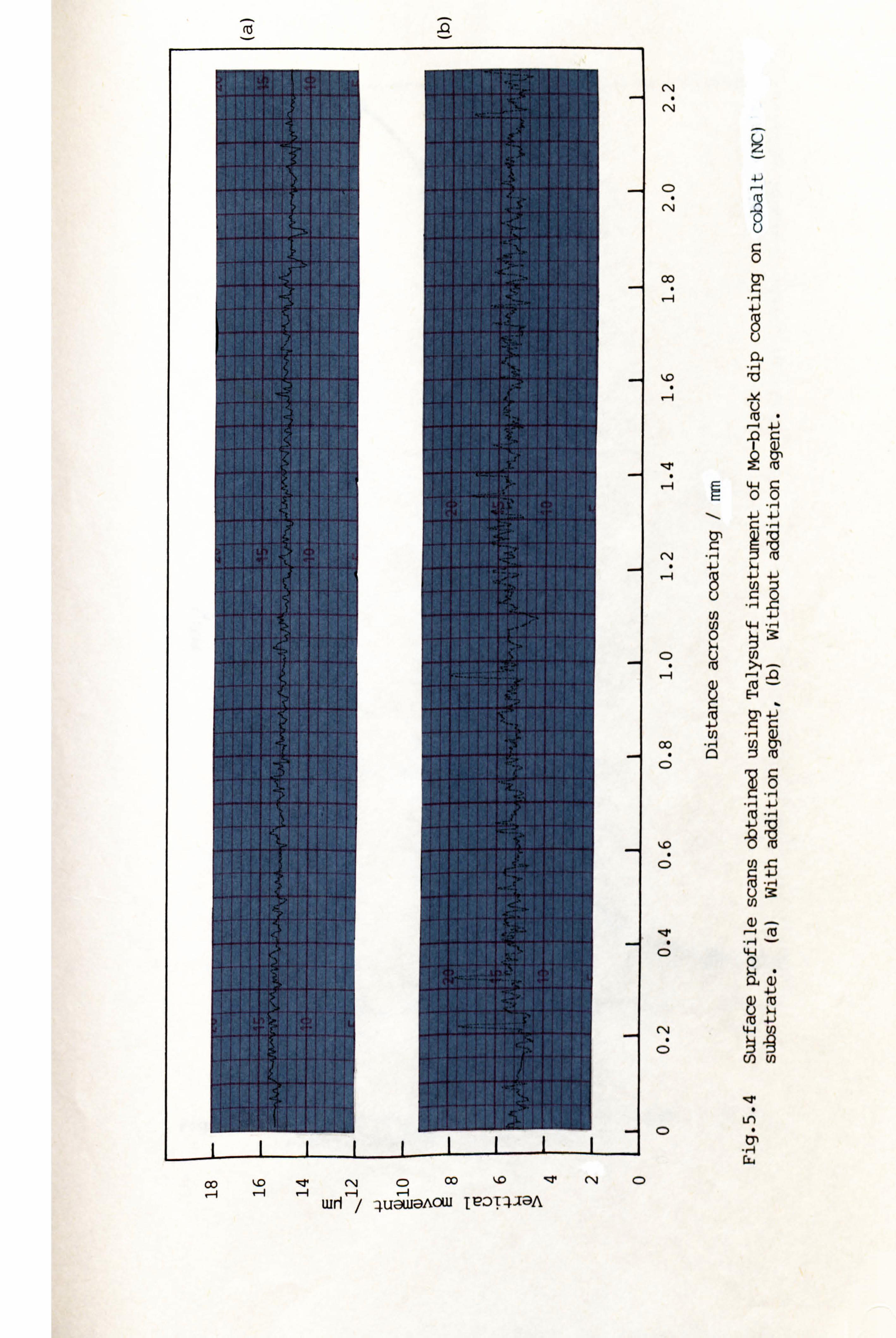
411
I , F1 7 7 1 t
t Al
- . T-- F
14.
1
4,11 7 - T -
i j
1 7 7
oid
1 4
CN
Cý
Cý CN
0
H 4-)
u
ol
. ffi -10 a
-0 C:
I Q) iM
44 r- 00
ý4 4-) 4-)
c0
U) 0 ý4 u U) M >1
4-)
- r-4 (n ýý
-, -1 4-) (10 r. 1 4-)
Cý u) u 3:
(1)
C) 4.4 0
4-J
4-J CN 44 (1)
C>
, I*
IJ" 0
CLI
OD ý. 0 (, q CD OD ýD CN CD
: 4uawaAow IPD'1: 1.1aA
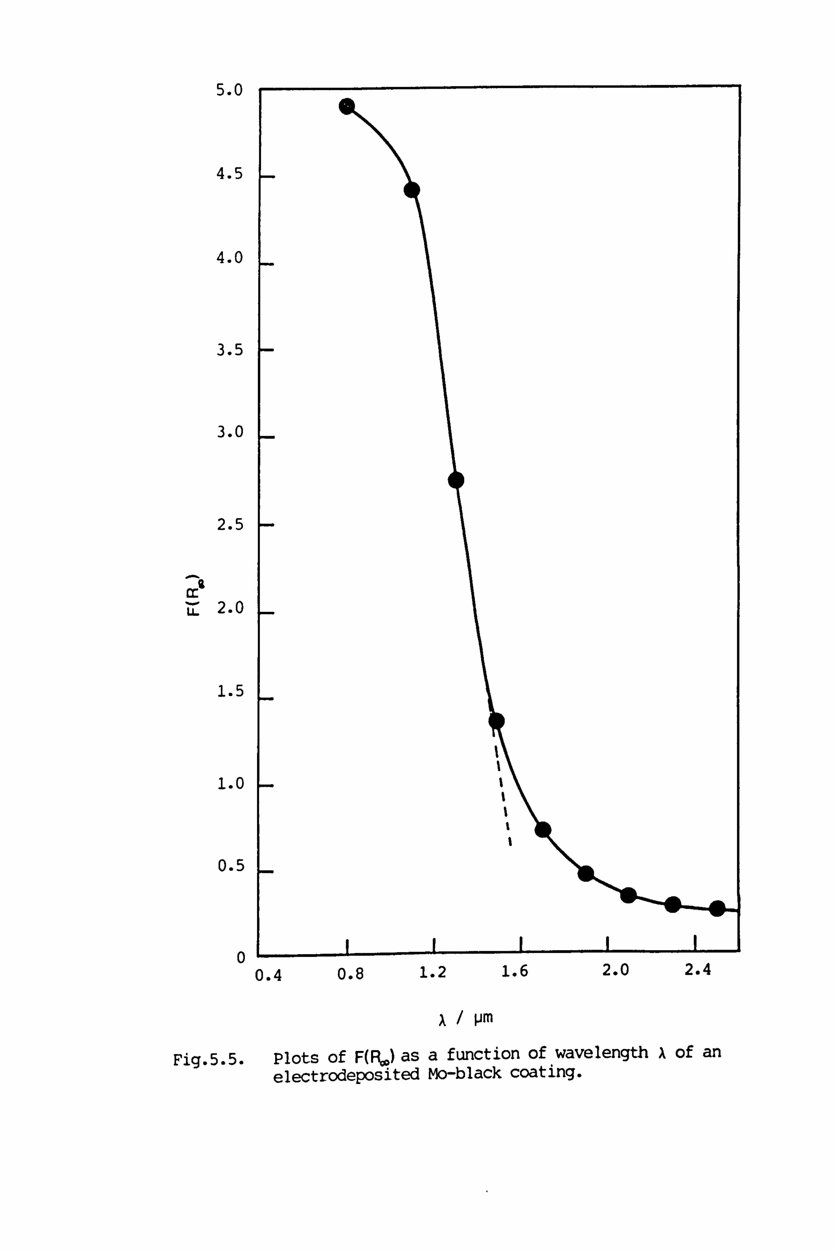
5.0
4.5
4.0
3.5
3.0
2.5
2.0
1.5
1.0
0.5
0
'I
0.4 0.8 1.2 1.6 2.0 2.4
x/ pm Fig. 5.5- Plots of F(R,, )as a function of wavelength A of an
electrodeposited Mo-black coating.
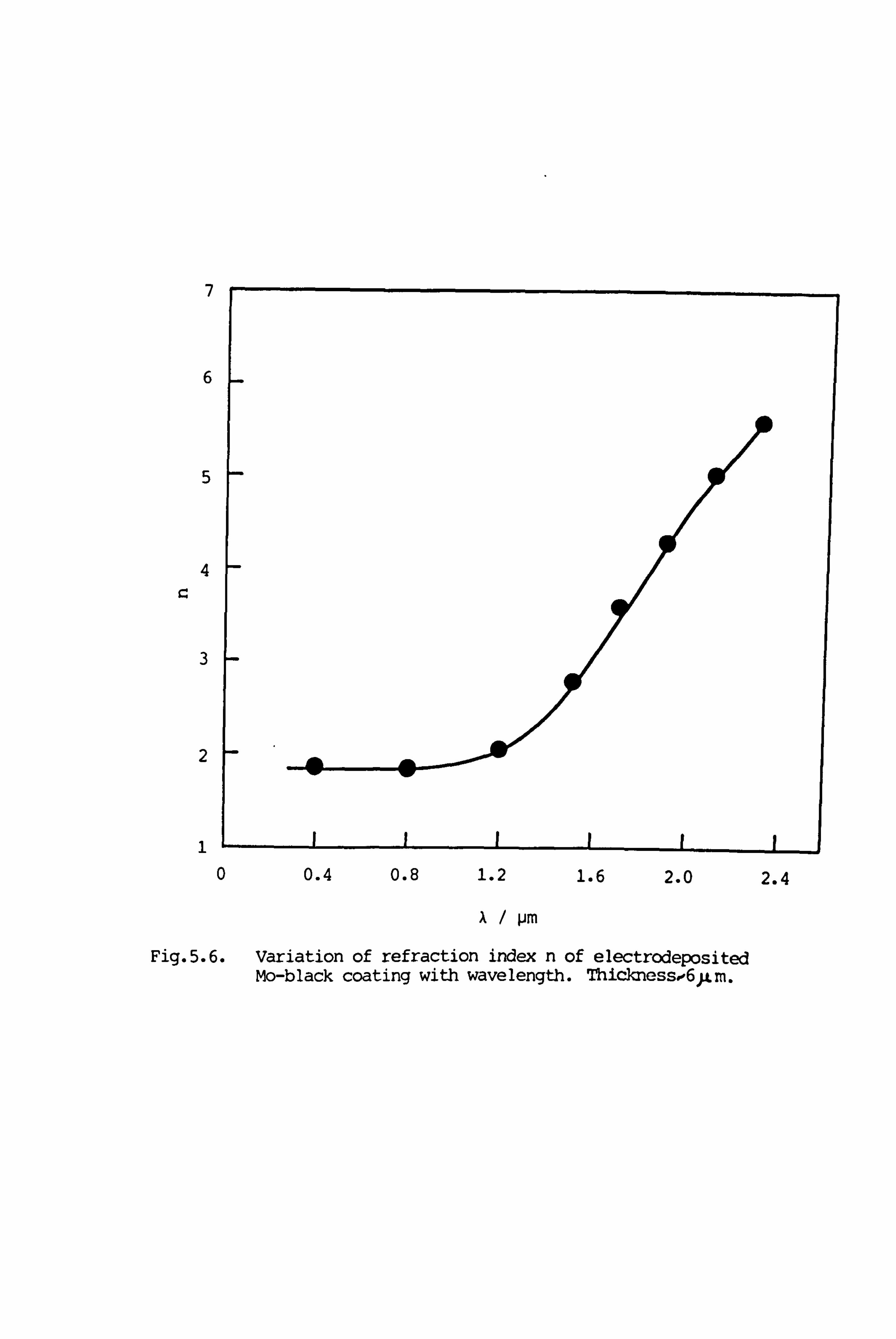
4 r.
3
0.4 0.8 1.2 1.6 2.0 2.4
A/ pm
Fig. 5.6. Variation of refraction index n of electrodeposited Mo-black coating with wavelength. Thicknesse6jum.
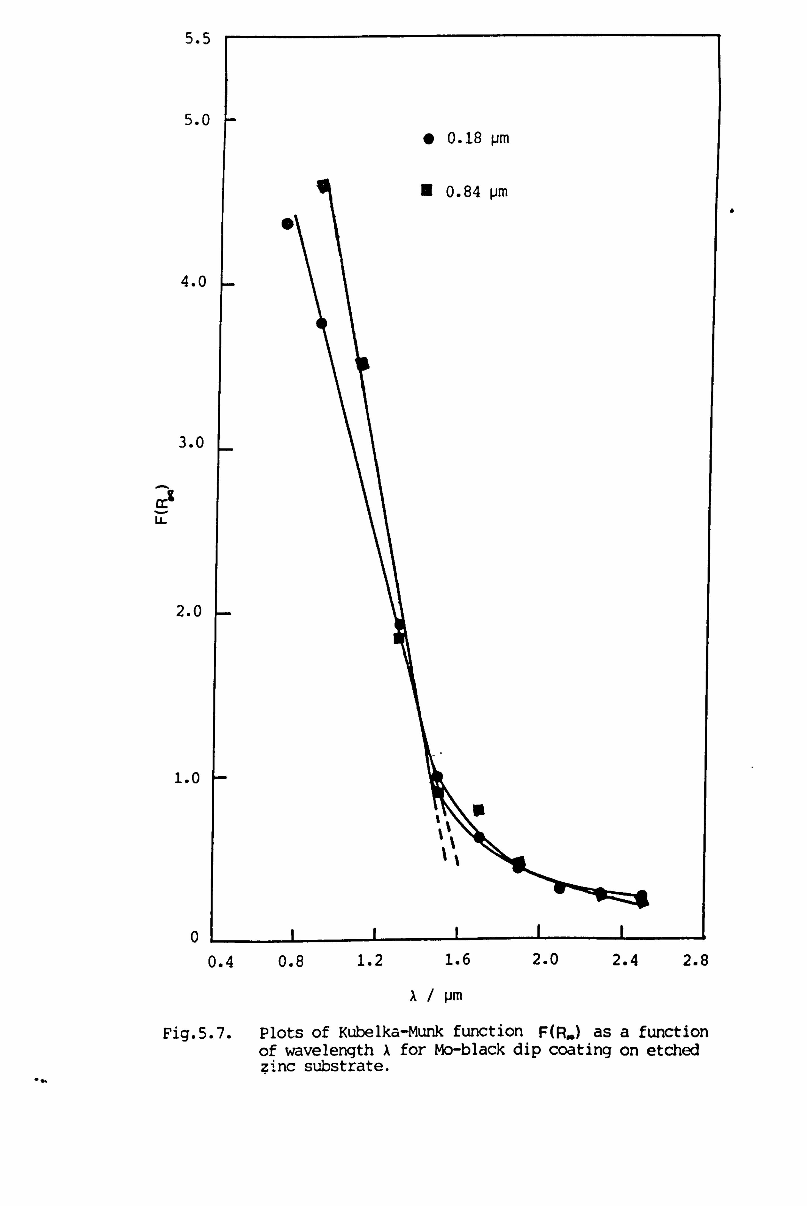
5.5
5.0
4.0
3.0
CCZ Ir
2.0
1.0
0
0 0.18 pm
0.4 0.8 1.2 1.6 2.0 2.4 2.8
A/ pm
Fig. 5.7. Plots of Kubelka-Munk function F(R. ) as a function of wavelength A for Mo-black dip coating on etched zinc substrate.
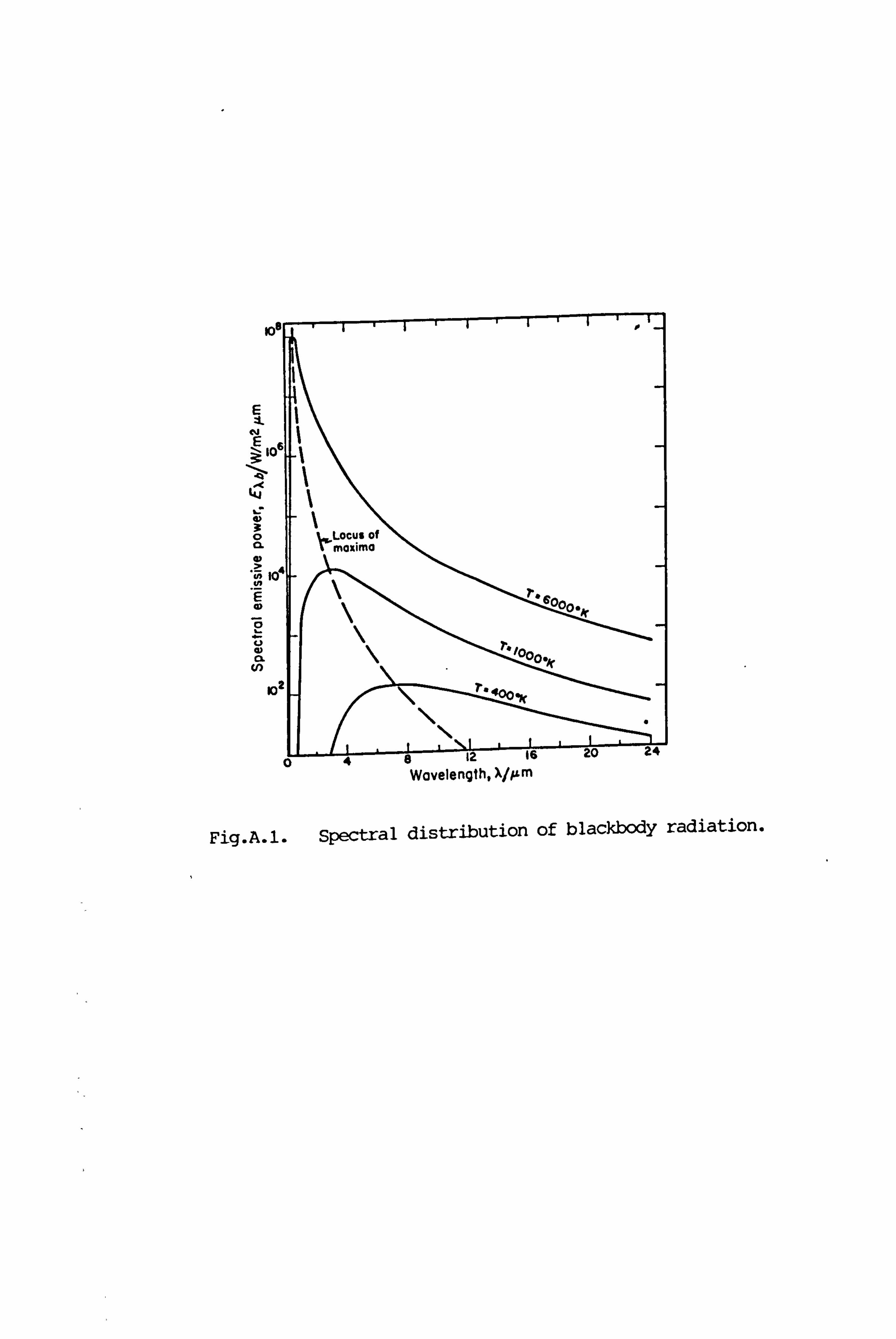
E ZL
C-i
41
cx (n
Fig. A. l. spectral distribution of blackbody radiation.
Wavelength, )/ium
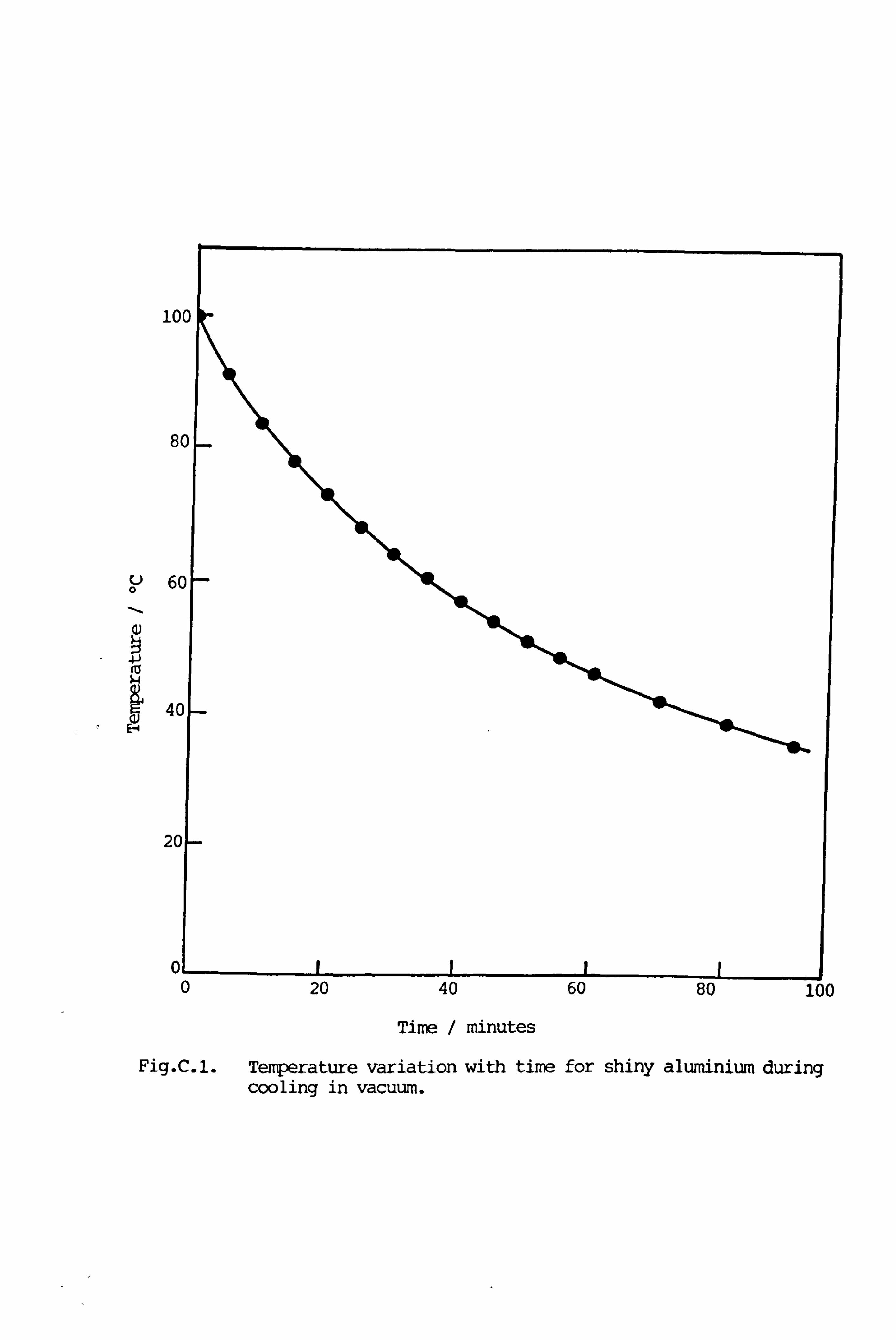
U
ý4 i
E-4
Time / minutes
Fig. C. J. Temperature variation with time for shiny aluminium during cooling in vacuum.
0 20 40 60 80 100
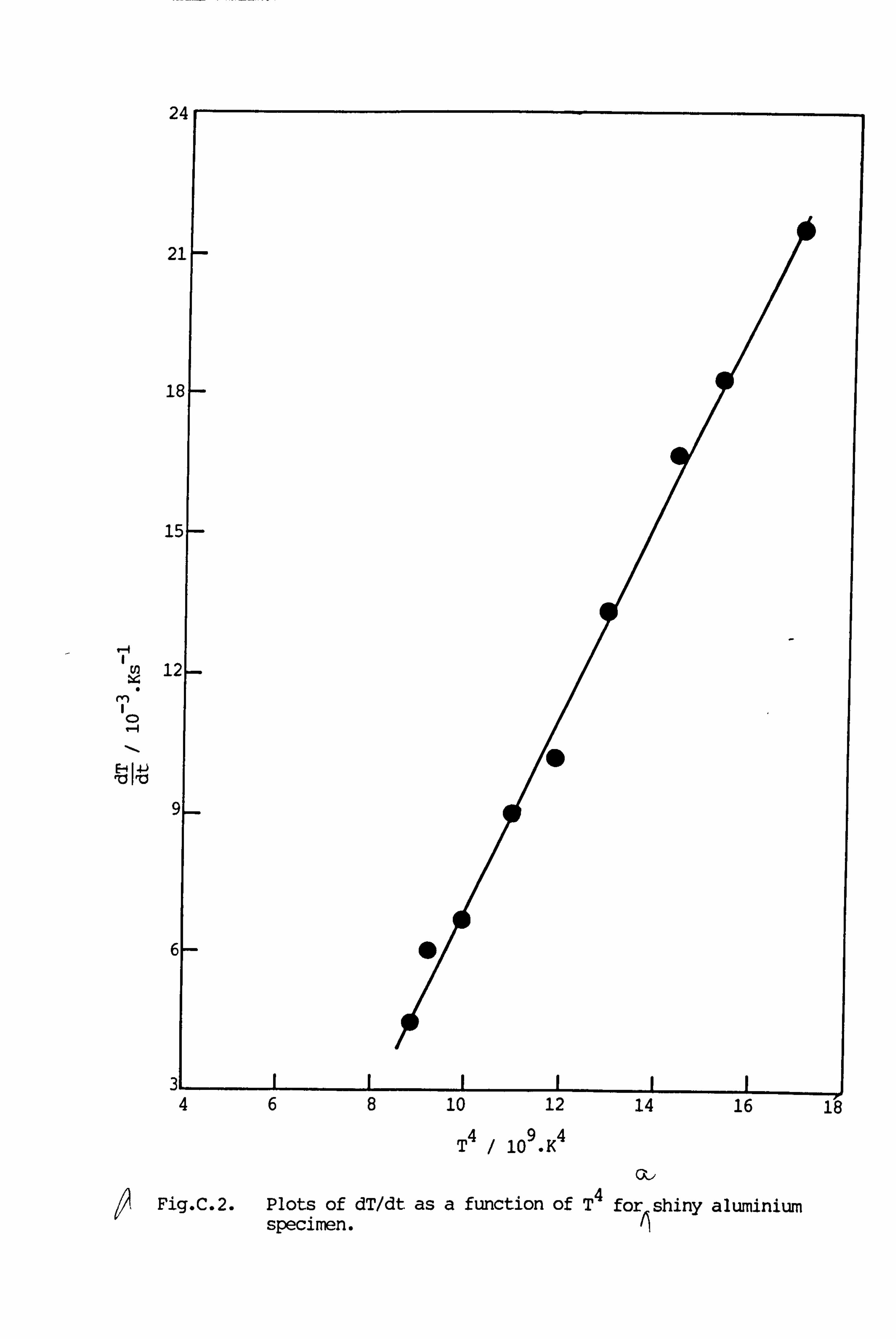
E-4 I 4J 1010
494 / 10 .K Gý/
Fig. C. 2. Plots of dT/dt as a function of T4 for shiny aluminium specimen. I
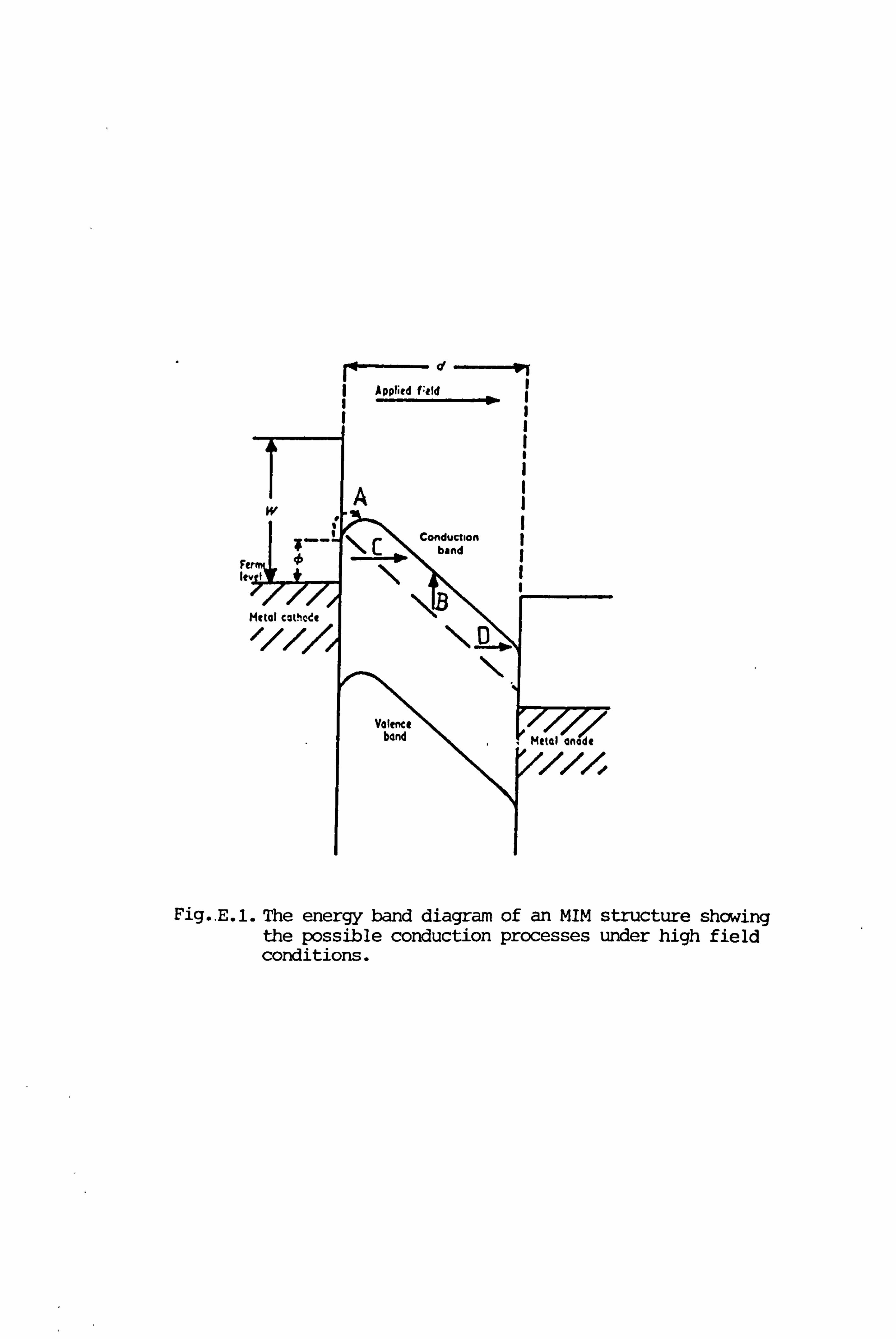
d OP , Applied Ueld
w ýonduc C Conduction
band
metal Cathode
\11 Valence
bond Metal anode
Fig.. E. 1. The energy band diagram of an MIM structure showing the possible conduction processes under high field conditions.
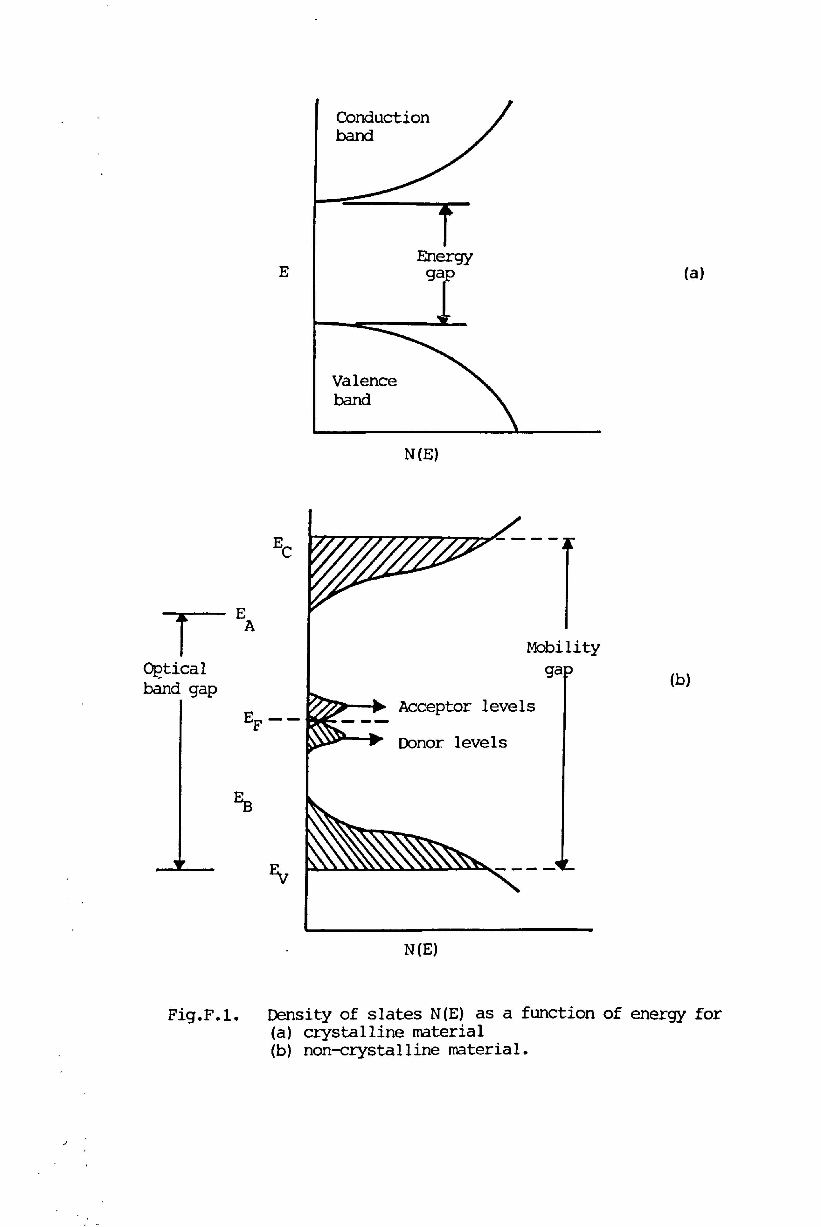
E
N(E)
Ec
E T- A
Optical band gap
E F--
EB
Ev
Mobility ga
Acceptor levels
Donor levels
N (E)
(a)
(b)
Fig. F. 1. Density of slates N(E) as a function of energy for (a) crystalline material (b) non-crystalline material.