characterization and loss analyses of passivated emitter and
TRANSCRIPT

Characterization and loss analyses ofpassivated emitter and rear cells
Von der Fakultat fur Mathematik und Physikder Gottfried Wilhelm Leibniz Universitat Hannover
zur Erlangung des akademischen GradesDoktor der Naturwissenschaften
Dr. rer. nat.
genehmigte Dissertation von
M.Sc. Christian Nikolaus Kruse
2020

Referent: Prof. Dr. Rolf BrendelKorreferenten: Prof. Dr. Rolf J. Haug
Prof. Dr. Armin G. AberleTag der Promotion: 13.07.2020

Abstract
This work presents characterization methods and simulation-based loss analyses for pas-sivated emitter and rear (PERC) solar cells. Furthermore, it discusses possible waysof introducing poly-Si on thin inter-facial oxides (POLO) junctions into industrial solarcells.
Achieving a further efficiency increase of industrial PERC cells is becoming moreand more difficult because the margin to the theoretical limit is reduced step by step.Identifying the major loss channel in terms of a potential efficiency gain, thus, playsan increasingly important role in solar cell optimization. The free energy loss analysis(FELA) [1] and the synergistic efficiency gain analysis (SEGA) [2, 3] as simulation-based loss analyses can address this task. The basis for both the FELA and the SEGAare numerical device simulations based on experimentally determined input parameters.The determination of most of these input parameters can be achieved with measurementand data analysis tools, which are commonly used in PV-research. The recombinationat local metal contacts, however, has not been studied to the same extent and standardtechniques do not apply.
In this work, we study the determination of contact recombination parameters. Wefirst analyze the required sample structures and develop an analytical model to calculatethe length scale on which regions of different charge carrier lifetimes affect each other. Wefind that a metallization pattern with three metallized and one non-metallized quartersfits our requirements best. In the analysis of suitable measurement setups we find thatphotoconductance-calibrated photoluminescence imaging is best suited because of thelow uncertainty. For the extraction of contact recombination parameters we study theanalytical model by Fischer and find an excellent agreement of better than 5% deviationwith numerical device simulations, provided the assumptions of low level injection andeither full line or periodic point contacts are fulfilled. For arbitrary contact layouts andfor the full injection dependence we introduce an approach based on numerical devicesimulations. In this context, we develop a new model for injection dependent contactrecombination currents. The model is based on the superposition of recombination atthe Si-metal interface and within the highly doped layer underneath.
We use standard measurement and evaluation techniques and determine contact re-combination parameters to perform a complete characterization of a PERC cell batch.In this characterization we determine all input parameters required for a SEGA alongwith the respective uncertainties. From the uncertainties of the input parameters wedetermine the uncertainties of the SEGA results using a Monte-Carlo simulation. Wealso analyze the differences between SEGA and FELA and introduce a graphical userinterface for automatic SEGA simulations.
Finally we discuss different cell structures for integrating POLO junctions into in-dustrial solar cells by means of SEGA simulations and hypothetical process flows. Weidentify cells featuring conventional screen-printed Al base contacts and n-type POLO(n-POLO) junctions as promising candidates for industrial integration in the near fu-

ture. A further development step are solar cells with POLO junctions for both polarities,which show an absolute efficiency benefit between 0.3% and 0.4% compared to similarcells with Al base contacts. However, further research in structuring POLO layers andscreen-printed contacting of p-type POLO (p-POLO) is required. From the SEGA sim-ulations and the hypothetical process flows a cell development roadmap was derived, inorder to focus research activities on the most promising cell concepts.Keywords: Silicon solar cells, loss analysis, device modeling

Zusammenfassung
Diese Arbeit prasentiert Charakterisierungsmethoden und SEGA Analysen (engl. syner-gistic efficiency gain analysis) fur PERC Zellen (engl. passivated emitter and rear cells).Daruber hinaus wird die Einfuhrung von POLO (engl. poly silicon on oxide) Schichtenin industrielle Solarzellen diskutiert.
Eine weitere Leistungssteigerung von industriellen PERC-Zellen wird zunehmend an-spruchsvoller, da der Abstand zum theoretischen Wirkungsgradlimit Schritt fur Schrittreduziert wird. Die Identifizierung der vielversprechendsten Zellmerkmale im Hinblickauf einen potenziellen Effizienzgewinn spielt daher eine immer wichtigere Rolle bei derSolarzellenoptimierung. Die FELA (engl. free energy loss analysis) und die SEGA alssimulationsbasierte Verlustanalysen konnen die Zellentwicklung bei dieser Aufgabe un-terstutzen. Die Grundlage fur FELA und SEGA sind numerische Halbleitersimulatio-nen, die auf experimentell bestimmten Eingangsparametern basieren. Die Bestimmungder meisten dieser Eingangsparameter kann mit etablierten Charakterisierungsmetho-den erfolgen. Fur die Rekombinationsrate an lokalen Metallkontakten gibt es jedochkein Standardverfahren.
In dieser Arbeit untersuchen wir die Bestimmung von Kontaktrekombinationspara-metern. Zuerst analysieren wir die erforderlichen Probenstrukturen und entwickeln einanalytisches Modell, um den Langenmaßstab zu berechnen, auf dem sich die Bereicheunterschiedlicher Lebensdauern gegenseitig beeinflussen. Wir stellen fest, dass ein Me-tallisierungsmuster mit 3 metallisierten und einem nicht metallisierten Viertel am bestenzu unseren Lebensdauerproben passt. Bei der Analyse geeigneter Messverfahren stellenwir fest, dass die PC-PLI (engl. photo conductance calibrated photoluminescence ima-ging) aufgrund der geringen Unsicherheit am besten geeignet ist. Fur die Extraktionvon Kontaktrekombinationsparametern untersuchen wir das analytische Modell von Fi-scher und finden eine ausgezeichnete Ubereinstimmung von unter 5% im Vergleich zunumerischen Halbleitersimulationen, vorausgesetzt, die Annahmen der Niedriginjektionund von durchgehenden Linien- oder periodischen Punkt-Kontakten sind erfullt. Furbeliebige Kontaktlayouts und zur Analyse der vollstandigen Injektionsabhangigkeit derKontaktrekombination fuhren wir eine Methode zur Bestimmung der Kontaktrekombi-nation ein, die auf Halbleitersimulationen basiert. In diesem Kontext entwickeln wir einneues Modell zur Beschreibung der injektionsabhangigen Kontaktrekombination, das aufder Uberlagerung der Rekombinationsstrome am Metall und innerhalb der hochdotiertenSchicht darunter basiert.
Wir wenden die Techniken zur Bestimmung der Kontaktrekombination zusammenmit Standardmess- und Auswertetechniken fur eine vollstandige Charakterisierung einerPERC-Zellcharge an. In dieser Charakterisierung bestimmen wir alle fur eine SEGA er-forderlichen Eingangsparameter mit den entsprechenden Unsicherheiten. Aus den Unsi-cherheiten der Eingangsparameter ermitteln wir mit Hilfe einer Monte-Carlo-Simulationdie Unsicherheiten der SEGA-Ergebnisse. Wir analysieren außerdem die Unterschiedezwischen SEGA und FELA und stellen eine grafische Benutzeroberflache fur automati-

sche SEGA-Simulationen vor.Abschließend diskutieren wir verschiedene Zellstrukturen zur Integration von PO-
LO-Schichten in industrielle Solarzellen mittels SEGA-Simulationen und hypothetischenProzessflussen. Wir identifizieren Zellen mit konventionellen, siebgedruckten Al Kontak-ten und n-Typ POLO Schichten als vielversprechende Kandidaten fur eine industrielleIntegration in naher Zukunft. Ein weiterer Entwicklungsschritt sind Solarzellen mit PO-LO-Kontakten fur beide Polaritaten, die im Vergleich zu ahnlichen Zellen mit Al Kontak-ten einen Wirkungsgradvorteil zwischen 0,3% und 0,4% aufweisen. Fur diese Konzepteist allerdings weitere Forschung zur Strukturierung von POLO-Schichten und zur sieb-gedruckten Kontaktierung von p-Typ POLO erforderlich. Aus den SEGA-Simulationenund den hypothetischen Prozessablaufen wurde eine Zellentwicklungsstrategie abgeleitet,um die Forschungsaktivitaten auf die vielversprechendsten Zellkonzepte zu fokussieren.Schlagworter: Silizium Solarzellen, Verlustanalyse, Bauteilsimulation

Contents
Acronyms ix
Symbols xi
Introduction 1
1 Theory and fundamentals 41.1 Passivated emitter and rear cells . . . . . . . . . . . . . . . . . . . . . . 41.2 Loss analysis . . . . . . . . . . . . . . . . . . . . . . . . . . . . . . . . 5
1.2.1 Power losses in solar cells . . . . . . . . . . . . . . . . . . . . . . 61.2.2 Free energy loss analysis . . . . . . . . . . . . . . . . . . . . . . 91.2.3 Synergistic efficiency gain analysis . . . . . . . . . . . . . . . . . 101.2.4 Conductive boundary model . . . . . . . . . . . . . . . . . . . . 11
1.3 Recombination and charge carrier lifetime . . . . . . . . . . . . . . . . 121.3.1 Recombination mechanisms . . . . . . . . . . . . . . . . . . . . 121.3.2 Surface recombination . . . . . . . . . . . . . . . . . . . . . . . 131.3.3 Charge carrier lifetime . . . . . . . . . . . . . . . . . . . . . . . 14
2 Measurement methods 162.1 Current-voltage characteristic . . . . . . . . . . . . . . . . . . . . . . . 162.2 Transfer length method . . . . . . . . . . . . . . . . . . . . . . . . . . . 162.3 Optical properties . . . . . . . . . . . . . . . . . . . . . . . . . . . . . . 19
2.3.1 Analytical reflectance fit . . . . . . . . . . . . . . . . . . . . . . 192.3.2 Ray tracing . . . . . . . . . . . . . . . . . . . . . . . . . . . . . 21
2.4 Recombination properties . . . . . . . . . . . . . . . . . . . . . . . . . 212.4.1 (Quasi-)steady-state photoconductance (Q)SSPC . . . . . . . . 222.4.2 Photoconductance-calibrated photoluminescence imaging . . . . 222.4.3 Infrared lifetime mapping . . . . . . . . . . . . . . . . . . . . . 242.4.4 Bulk and surface recombination . . . . . . . . . . . . . . . . . . 26
3 Recombination at metallized surfaces 283.1 Sample structures . . . . . . . . . . . . . . . . . . . . . . . . . . . . . . 28
3.1.1 Inhomogeneities . . . . . . . . . . . . . . . . . . . . . . . . . . . 293.1.2 Coupling between regions of different lifetime . . . . . . . . . . 313.1.3 Metallization patterns . . . . . . . . . . . . . . . . . . . . . . . 35

Contents viii
3.2 Measurement techniques . . . . . . . . . . . . . . . . . . . . . . . . . . 363.2.1 PC-PLI measurement . . . . . . . . . . . . . . . . . . . . . . . . 373.2.2 Difference of dynamic and static measurement . . . . . . . . . . 383.2.3 Difference of static ILM and PC-PLI . . . . . . . . . . . . . . . 39
3.3 Evaluation methods . . . . . . . . . . . . . . . . . . . . . . . . . . . . . 423.3.1 Analytical description . . . . . . . . . . . . . . . . . . . . . . . 423.3.2 Numerical evaluation of contact recombination . . . . . . . . . . 44
3.4 Summary: Determination of contact recombination parameters . . . . . 48
4 Application of loss analyses to industrial solar cells 504.1 Comparison of FELA and SEGA . . . . . . . . . . . . . . . . . . . . . 50
4.1.1 Monte-Carlo simulation for recombination channels . . . . . . . 514.1.2 Analytical description . . . . . . . . . . . . . . . . . . . . . . . 54
4.2 SEGA-GUI . . . . . . . . . . . . . . . . . . . . . . . . . . . . . . . . . 574.3 Application example: PERC+ solar cell . . . . . . . . . . . . . . . . . . 58
4.3.1 Processing cells and test structures . . . . . . . . . . . . . . . . 584.3.2 Characterization and cell geometry . . . . . . . . . . . . . . . . 604.3.3 Uncertainty analysis for the input parameters . . . . . . . . . . 654.3.4 SEGA . . . . . . . . . . . . . . . . . . . . . . . . . . . . . . . . 68
5 Integration of poly-Si junctions into industrial solar cells 725.1 Simulation parameter selection & optics . . . . . . . . . . . . . . . . . 725.2 Simulated cell structures . . . . . . . . . . . . . . . . . . . . . . . . . . 745.3 Electronic input parameters . . . . . . . . . . . . . . . . . . . . . . . . 755.4 Results and discussion . . . . . . . . . . . . . . . . . . . . . . . . . . . 785.5 Bulk lifetime variation . . . . . . . . . . . . . . . . . . . . . . . . . . . 895.6 Roadmap for further cell development . . . . . . . . . . . . . . . . . . . 895.7 Conclusion . . . . . . . . . . . . . . . . . . . . . . . . . . . . . . . . . . 90
6 Summary 93
List of publications 105
Danksagung 107

Acronyms
Al-BSF Aluminum back surface fieldAM1.5g Air mass 1.5 spectrum according to the IEEE 60904-3
standardARC Anti reflection coatingBJ Back junctionBSF Back surface fieldCCD Charge-coupled-deviceCoBo Conductive boundary modelCz Czochralski-grownEL ElectroluminescenceFCA Free carrier absorptionFELA Free energy loss analysisFJ Front junctionFRC Front and rear contacted cellFSF Front surface fieldGUI Graphical user interfaceIBC Interdigitated back contactILM Infrared lifetime mappingIR InfraredISFH Institute for solar energy research HamelinI-V Current-VoltageLCO Laser contact openingLED Light emitting diodeLIA Local impact analysisn-POLO Donator doped poly-silicon on oxidePC-PLI Photoconductance-calibrated photoluminescence
imagingPERC Passivated emitter and rear cellPERC+ Passivated emitter and rear cell with local rear side
metallizationPERT Passivated emitter and rear totally diffused cellPL PhotoluminescencePLI Photoluminescence imagingPOLO Poly-silicon on oxide

Acronyms x
p-POLO Acceptor doped poly-silicon on oxidePV PhotovoltaicsQFL Quasi-Fermi levelQSSPC Quasi-steady-state photoconductanceSEGA Synergistic efficiency gain analysisSRH Shockley-Read-HallSRV Surface recombination velocitySSPC Steady-state photoconductanceSTC Standard testing conditions according to the IEEE
60904-3 standardTLM Transfer length methodTOPCon Cell structure: ”Tunnel oxide passivated contacts”
with n-type poly-Si and a boron emitter

Symbols
α Photon absorption coefficientBrad Proportionality factor for radiative recombinationβ Inverse thermal voltageCn Proportionality factor for the Auger process involv-
ing two electronsCp Proportionality factor for the Auger process involv-
ing two holesD Diffusion constantd Contact widthdgeom Geometrical contact widthdf Front contact widthdLCO LCO dash lengthdopt Optical contact widthdr Rear contact widthdse Selective emitter width∆n Excess carrier density∆φ Quasi Fermi level splitting∆V Difference of two internal voltagesEG Band gap energyEn Equality number for the comparsion of values with
uncertaintiesε0 Vacuum permitivityεr Material permitivity
F Free energy rate
FG Rate of generated free energy
FO Rate of free energy lost due to optical effects
FR Rate of free energy lost due to recombination
FT Rate of free energy lost due to charge carrier trans-port
fmet Metalized area fractionfopt Ratio between optical and geometrical front contact
widthFF Fill factor

Symbols xii
g Generation rate of excess charge carriers due to inci-dent photons
η Energy conversion efficiencyIPL Intensity of photoluminescence emissioniVOC Implied open circuit voltageJ0 Saturation current densityJ0,Ag Saturation current density of silver contactsJ0,Al Saturation current density of aluminum contactsJ0,cont Saturation current density of metalized surfacesJ0,e Saturation current density of the emitterJ0,e,sel Saturation current density of the selective emitterJ0,eff Effective saturation current densityJ0,pas Saturation current density of passivated surfacesJGen Photo-generated current densityJrec Recombination current densityJSC Short circuit current densityje Local electron currentjh Local hole currentk Recombination asymmetry factorLD Diffusion lengthLT Transfer lengthΛb Rear side lambertian factorΛf Front side lambertian factorλ Photon wavelengthµn Electron mobilityµp Hole mobilityNA Acceptor concentrationND Donator concentrationNdop Dopant (acceptor or donator) concentrationn Electron densityni Intrinsic carrier concentrationν Real part of the refractive indexP contact pitchPf Front contact pitchPLCO LCO dash pitchPr Rear contact pitchp Hole densityφel Electrostatic potentialφn Electron quasi Fermi levelφp Hole quasi Fermi levelq Elementary chargeR Resistance

Symbols xiii
Rsheet Sheet resistanceRsheet,e Sheet resistance of an emitterRsheet,e,sel Sheet resistance of a selective emitterRseries Series resistanceRspread Spreading resistanceR ReflectanceRb Rear-side reflectanceRf Front-side reflectanceRm Reflectance at Si-metal interfacer Recombination raterAuger Recombination rate due to Auger recombinationrrad Recombination rate due to radiative recombinationrSRH Recombination rate due to Shockley-Read-Hall re-
combinationρ Resistivityρb Resistivity of the silicon bulkρc Contact resistivityρc,Ag Contact resistivity of a silver contactρc,Al Contact resistivity of an aluminum contactρl,Ag Line resistance of a silver fingerS Surface recombination velocityScont Surface recombination velocity of metallized areasSeff Effective surface recombination velocitySfront Surface recombination velocity of front surfacesSpas Surface recombination velocity of passivated surfacesSrear Surface recombination velocity of rear surfacesσL Light induced conductivityσn Electron conductivityσp Hole conductivityTf Front side transmittanceτ Carrier lifetimeτAuger Carrier lifetime due to Auger recombinationτbulk Carrier lifetime in the silicon bulkτeff Effective carrier lifetimeτn0 Minority carrier lifetime of a mid-gap Shockley-Read-
Hall defectτp0 Majority carrier lifetime of a mid-gap Shockley-Read-
Hall defectτrad Carrier lifetime due to radiative recombinationτSRH Carrier lifetime due to Shockley-Read-Hall recombi-
nationτsurface Carrier lifetime due to surface recombination

Symbols xiv
V Quasi Fermi level splitting or internal voltageVOC Open-circuit voltageVT Thermal voltageW Cell or sample thickness~x Position within the cell or samplexc Coupling length between regions of different lifetime

Introduction
In 2019 industrial p-type silicon passivated emitter and rear cells (PERC) achieved recordconversion efficiencies of over 24% [4]. The conversion efficiencies for inline productionare around 22.5% [5] in 2018 with a learning curve of about 0.5% per year over thelast few years [6]. The efficiency learning curve and reduced prices due to large-scaleproduction translate to average module prices of 0.24 $US/Wp in 2018 [5]. The highconversion efficiency in combination with low production costs due to a lean process flow[6] make the PERC concept the main technology for new production lines nowadays.PERC has reached a market share of 35% in 2018 and is expected to reach a marketshare of 50% in 2019 [5]. Continuing on the 0.5% per year efficiency-learning curve gets,however, increasingly difficult because the efficiency gap to the theoretical efficiency limitof 29.56% [7] gets smaller. Therefore, and because research capabilities are limited, it iscrucial to identify the most promising parts of the solar cell for improving the efficiency.
The ideal values for the short-circuit current density JSC, the open-circuit voltage VOC
and the fill factor FF are 43.36 mA/cm2, 763.3 mV and 89.31% for a single junctionsilicon solar cell with only intrinsic losses [7], respectively. The deviation of the mea-sured I-V parameters to these ideal values gives a first impression on whether the cellis limited by optical performance (low JSC), charge carrier recombination (low VOC) orresistive properties (low FF ). However, this approach does not reveal relative magni-tudes between the power losses. In addition, the effects on the I-V parameters are notindependent from each other. For example, a reduced charge carrier generation rate dueto optical effects leads to reduced JSC and VOC, charge carrier recombination leads toa reduction of VOC and FF and high series resistances can lead to a reduction in JSC
along with the FF reduction. Therefore, a more detailed break-down of power losses isdesirable.
The synergistic efficiency gain analysis (SEGA) and the free energy loss analysis(FELA) are both simulation-based approaches for a breakdown of power losses in solarcells, which yield results in the same unit of measure (power per area) for all present losschannels. Using device simulations for analyzing power losses has the benefit that allaspects of cell operation (eg. spatially resolved current flows and generation) are takeninto account and their respective impact on the I-V parameters can be calculated. Thesimulations are usually based on experimentally determined input parameters, whichdescribe, for example, resistances and defect recombination of excess charge carriers.The determination of most of these parameters can be achieved with techniques that arewell-established in the PV-community. For the determination of contact recombinationparameters, however, no standard approach exists.

Introduction 2
In the analysis of PERC cells often the charge carrier recombination at the contactsand diffused layers is found to be a major power loss [8]. Integrating passivating contactsusing poly-crystalline silicon on thin inter-facial oxides (POLO) is a promising approachto further reduce recombination losses and, therefore, increase the solar cell efficiency.Solar cells from market-typical p-type Si featuring POLO contacts have already achievedhigh efficiencies of 26.1% [9] on lab-scale interdigitated back contact (IBC) devices. Theintegration of POLO junctions into industrial cells faces the challenge of processingcell structures with good quality POLO junctions and their metallization with lean,industrial process flows to compete with the low-cost PERC process. In this workwe calculate the efficiency gain to be expected from specific concepts featuring POLOjunctions. This helps the industry to evaluate the economic feasibility of these concepts.
The calculation of power losses in PERC solar cells and the estimation of the efficiencybenefits when integrating POLO junctions into industrial Si solar cells is the main goalof this work. To this end, we also study the determination of contact recombinationparameters. This includes finding appropriate test samples, measurement techniquesand evaluation procedures.
Chapter 1 and 2 introduce the theoretical background for this work. In chapter 1we introduce the PERC cell concept and its various sources of power losses. We furtherintroduce the SEGA and the FELA along with the conductive boundary approach forsolving the semiconductor equations. In addition, we also introduce the basic recom-bination mechanisms and the concept of charge carrier lifetimes to lay the foundationfor lifetime and recombination measurements. In chapter 2 we introduce the I-V ,resistance, reflectance and lifetime measurement methods and the approaches for theextraction of simulation input parameters from these measurements.
In chapter 3 we analyze the determination of contact recombination parameters. Tothis end, we first discuss the requirements for the sample structures and the limitationsfor measurements setups that can be used for the measurement of these samples. We thendiscuss known analytical approaches for the extraction of recombination parameters andcompare the models to numerical device simulations. We also introduce a method solelybased on device simulations for the analysis of contact recombination. In this contextwe also introduce a new model for the injection dependency of contact recombination.
In chapter 4 we discuss the difference between the SEGA and the FELA, whichare commonly used approaches for analyzing power losses in silicon solar cells. Wefurther introduce a simulation tool (SEGA-GUI) created in the context of this workto automatically perform SEGA simulations. We then apply the measurement andevaluation techniques from chapter 2 and 3 to the complete characterization of a PERCbatch with the required reference samples. In the context of this characterization wealso discuss the uncertainties for the determination of input parameters and how thesetranslate to the uncertainties in the simulation results.
In chapter 5 we discuss optimization routes for PERC when using POLO junctions.We analyze ten cell concepts featuring POLO junctions along with a PERC and aTOPCon reference, which is a cell structure with n-type poly-Si and a boron emitter

Introduction 3
[10]. To this end, we introduce optical and electrical simulation setups based on inputparameters aimed at comparable results for all analyzed cell concepts. Finally, fromthe simulation results and the discussion of potential ways to process each structure, aroadmap for further cell development is developed.

1 Theory and fundamentals
In this chapter we describe the passivated emitter and rear cell (PERC) concept asthe current state-of-the-art industrial silicon solar cell. We then explain the power lossmechanisms present in such cells as well as the free energy loss analysis (FELA) andthe synergistic efficiency gain analysis (SEGA) as approaches for the analysis of theselosses. Because both approaches are based on device simulations, we further describethe conductive boundary (CoBo) model for solving the semiconductor equations in asolar cell. This model is based on experimentally determined input parameters. Thedetermination of most input parameters is explained in chapter 2 except for the chargecarrier recombination at the contacts. The determination of contact recombination isdiscussed in chapter 3 and, therefore, we also introduce the fundamental recombinationproperties in the silicon bulk and at the surfaces and their parameterization.
1.1 Passivated emitter and rear cells
The PERC solar cell concept [11] is shown on the left side of Fig. 1.1. The cell is basedon an acceptor-doped (p-type) crystalline Si absorber (light green). In most cases thisabsorber is a Czochralski-grown (Cz) mono-crystal doped with boron. The front sideof the cell features a highly donator-doped (n-type, usually phosphorus) layer calledemitter and shown in red. This diffusion can be varied laterally (selective emitter) tooptimize the recombination and resistive properties underneath the contacts and in theremaining area separately. The emitter is covered with silicon nitride (SiN) for surfacepassivation (see section 1.2.1) shown in blue. The SiN is simultaneously used as an anti-reflection coating (ARC) to enhance the fraction of light that enters the device. Thefront contacts are realized by screen-printing local silver contacts in a conventional H-pattern (shown in dark gray). The rear side features a stack of aluminum oxide (Al2O3)and SiN for surface passivation. This stack is opened locally using a laser. These lasercontact openings (LCO) allow the screen-printed aluminum (dark gray) to form localaluminum back surface field (Al-BSF) contacts, which are shown in dark green. Thepassivation at the rear side reduces the charge carrier recombination and allows for abetter optical performance due to the enhanced reflectivity of the Al2O3/SiN stack incomparison with conventional Al-BSF cells.
The right side of Fig. 1.1 shows a PERC+ cell [12] that differs from a PERC cell byusing rear metal fingers instead of full area metallization and an optional rear surfacetexture. This design has several advantages over the conventional PERC design [12]:

1.2 Loss analysis 5
The aluminum paste consumption is drastically reduced, the formation of the Al-BSFis improved and light incident on the rear side can be utilized. The main focus of thiswork is the analysis and simulation of PERC+ solar cells and improvements thereof.
silver gridSiN
P-emitter
Al2O3
Al-BSF
aluminum
p-type bulk
SiN
PERC PERC+
Figure 1.1: Schematic of a passivated emitter and rear cell (PERC) and a PERC+ cellwith only partial rear-side metallization and rear texture. Both cell structures fea-ture a front phosphorus doped emitter (red) with a SiN ARC and passivation (blue),a surface texture (not to scale) and silver contacts (gray). At the rear the screen-printed Al forms a local back surface field (green) while the remaining area is pas-sivated with an Al2O3/SiN stack (teal and blue).
1.2 Loss analysis
A first estimate of losses can already be obtained by analyzing the I-V characteristics (seesection 2.1 on page 16) of a solar cell. Here optical, recombination and transport lossesare quantified by reductions in the short-circuit current JSC, the open-circuit voltageVOC and the fill factor FF , respectively. However, this approach does not allow for aquantitative comparison of different loss channels due to the different units of measure.In addition, a more detailed analysis of individual losses is crucial for the optimizationprocess. Approaches that meet these requirements are often based on modeling the solarcells. Two examples are the free energy analysis (FELA) [1] and the synergistic efficiencygain analysis (SEGA) [2, 3]. Both yield results in the same unit of measure (power perarea) for all loss channels. In this section we introduce sources of power losses, FELA andSEGA as well as the numerical modeling approaches used in this work. The differencebetween FELA and SEGA as loss and gain analyses, respectively is discussed in section4.1.

1.2 Loss analysis 6
ShadingFront surface reflectance
Light trapping
Parasitic absorption
Transmission
Figure 1.2: Schematic of a solar cell with non-intrinsic optical losses. The green arrowsrepresent optical losses due to shading, an imperfect anti-reflection coating, parasiticabsorption by free charge carriers, transmission through the cell and imperfect lighttrapping.
1.2.1 Power losses in solar cells
A solar cell converts a fraction of incident light into electrical energy. This fraction,the conversion efficiency η, is always limited by intrinsic losses such as thermalization ofcharge carriers to the band edges, optical losses due to non-absorbed photons and intrin-sic recombination and transport losses. The maximum efficiency that can be achievedwith a crystalline silicon solar cell is 29.56% [7] for a cell without doping and 98.1µmthickness. In addition, a solar cell also always has non-intrinsic losses, which can, inprinciple, be avoided by optimized process characteristics. In this work we discuss char-acterization and simulation techniques with the goal to understand the origin of thedominant power losses in PERC solar cells. As we are interested in routes for furthercell optimization, we focus on the non-intrinsic losses. These losses can be categorizedinto three different groups: optical, recombination and transport losses.
Optical losses
An ideal solar cell has a perfect ARC on the front side and a perfect mirror on the rearside. In addition, incident light is completely randomized to increase the path length.This ensures Lambertian light trapping, which is a widely accepted benchmark for theideal optical performance [13].
An actual solar cell is, however, not perfect: Shading by metal contacts imposes losseson front and rear contacted (FRC) cells. This leads to the optical losses shown in Fig.1.2. It should be noted that these losses differ for bare cells and cells integrated in amodule. In this work we analyze bare cells for their losses, but this should be kept in

1.2 Loss analysis 7
mind when designing cells for module integration.In FRC cells the metal on the front side leads to a shading of the absorber, which
reduces the generated current. The relative current loss corresponds to the area fractioncovered by metal. However, the shape of the finger can allow reflected photons to hitthe cell surface and contribute to the generated current. Therefore, the optical width(or shading width) can be smaller than the geometrical finger width.
Another important loss is due to the reflectivity R at the front surface. The ARC onthe front side is a dielectric layer with a suitable refractive index to reduce reflectivity.The reflectivity of a one layer ARC can only be fully reduced to zero for one wavelengthλ as the optimal layer thickness for destructive interference is λ/(4ν) where ν is therefractive index of the ARC [14]. Most industrial solar cells feature a front surface texturewith random pyramids. Due to the pyramids, most reflected photons hit the surface asecond time thereby reducing R to R2. Further approaches to reduce reflectivity are adouble- or multi-layer ARC [15] or adapted surface topologies such as black silicon [16]or macropores [17, 18].
Light that enters the solar cell through the front surface does not necessarily create anelectron-hole pair. The photons can also be absorbed in surface layers or by free carriersin the device. This parasitic absorption cannot be utilized for generating electricalenergy.
Photons with an energy close to the band gap energy have a long absorption length dueto the low absorption probability. These photons have a chance to leave the cell throughthe rear side. These transmission losses can be avoided by increasing the reflectivityof the rear side either by a suitable dielectric layer stack or a mirror either external ordirectly applied to the dielectric stack.
The absorption probability for long-wavelength light can also be increased by suitablelight trapping schemes. Lambertian light trapping, which serves as a benchmark in thiswork, assumes complete randomization when the light enters the cell. Any remainingfraction of specular light leads to optical losses, because the mean path of the light inthe solar cell is typically shorter for specular light [13].
Recombination losses
The locations of non-intrinsic recombination are shown in Fig. 1.3. Recombinationoccurs at all surfaces and in the silicon bulk. Recombination at the surfaces can bereduced by a suitable coating, which is called passivation layer. An ideal passivationsaturates the dangling bonds from the interrupted crystal lattice (chemical passivation)and contains fixed charges inducing an electric field, which reduces the minority carrierconcentration at the surface (field effect passivation). At the metal contacts, however,the surface is not passivated leading to a large recombination current. In industrialsolar cells the metallized area is, therefore, kept to a minimum. In addition, a highlydoped area underneath the metal reduces the recombination as it reduces the minoritycarrier concentration. In chapter 5 we discuss the implementation of passivating contacts

1.2 Loss analysis 8
Surface recombinationContact recombination
Bulk recombination
Figure 1.3: Schematic of a solar cell with non-intrinsic recombination losses. The redarrows represent recombination losses at the contacts, at the diffused and un-diffusedsurfaces and in the Si bulk.
Bulk transport
Grid resistance
Contact resistance
Lateral resistance
Lateral resistance
Grid resistance
Figure 1.4: Schematic of a solar cell with non-intrinsic transport losses. The blue arrowsrepresent transport losses due to the contact and metal grid resistances, the lateralresistance (sheet resistance) between the contacts and transport losses in the Si bulk.
(i.e. contacts, which simultaneously provide surface passivation underneath the metal)into industrial production lines to reduce recombination at metal contacts. To reducerecombination in the absorber, a better Si material with reduced impurities and defectscan be used.
Transport losses
Electric currents flowing through a resistor lead to resistive heating. The power dissi-pated in the resistor is lost for delivering work in the circuit. Figure 1.4 shows the variousresistances, which exist in a solar cell. The cell metallization, especially on the front side,features thin metal fingers leading to a resistive loss due to the metallization. In addition,the contact between metal and silicon inhibits a contact resistance. The metallization

1.2 Loss analysis 9
layout has to be optimized to balance the losses due to shading and recombination withthose caused by the resistive losses at the contacts and in the metal grid. Furthermore,carrier transport in the silicon bulk also leads to power dissipation. Transport in theSi bulk can be divided into lateral and perpendicular transport. Both transport lossescan be reduced by increasing the dopant concentration in the absorber. Furthermore,highly doped layers, for example the emitter diffusion, provide an increased lateral con-ductivity for one charger carrier type. In addition, the distances between the contacts(for lateral transport losses) and device thickness (for perpendicular transport losses)can be reduced. However, all approaches lead to a trade-off between recombination andoptical losses and losses due to transport.
In the following sections we introduce approaches for analyzing all three groups ofpower losses in solar cells simultaneously.
1.2.2 Free energy loss analysis
The free energy loss analysis (FELA) [1] is a loss analysis for solar cells based on analyz-ing the free energy balance in a device. The photo-generation rate leads to a generationrate of free energy
FG = q
∫Vol.
∆φ(~x)g(~x), (1.1)
where ∆φ(~x) is the local quasi Fermi level (QFL) splitting, g(~x) is the local generationrate at position ~x and q is the elementary charge.
This free energy can, however, not be completely extracted from the solar cell todeliver work to an external circuit. The diffusion-driven and/or field-driven transportleads to an increase of entropy and, hence, to a decrease of free energy. Recombinationcurrents in a solar cell also lead to a reduction of free energy. We calculate the extractedpower in terms of free energy rates as
POUT = FG − FR − FT. (1.2)
Here FR is the rate of free energy lost by charge carrier recombination and FT is therate of free energy lost by the transport of charge carriers through the solar cell. Wecalculate the free energy loss rates with the following equations:
FR = q
∫Vol.
∆φ(~x)r(~x), (1.3)
FT =
∫Vol.
(|je|2
σn
+|jh|2
σp
), (1.4)
with local recombination rate r(~x), local electron and hole currents je and jh and electronand hole conductivities σn and σp, respectively. A detailed derivation of these equations
1.2 Loss analysis 10
Simulation:cell with all losses
Simulation:cell without loss 1
Simulation:cell without loss 2
Simulation:cell without loss 1+2
ηref
η1-ηref=G1
η2-ηref=G2
ηsyn-ηref-G1-G2=Gsyn
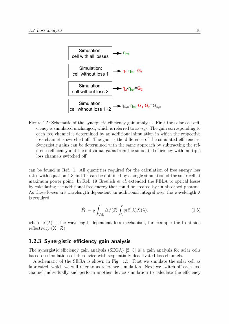
Figure 1.5: Schematic of the synergistic efficiency gain analysis. First the solar cell effi-ciency is simulated unchanged, which is referred to as ηref. The gain corresponding toeach loss channel is determined by an additional simulation in which the respectiveloss channel is switched off. The gain is the difference of the simulated efficiencies.Synergistic gains can be determined with the same approach by subtracting the ref-erence efficiency and the individual gains from the simulated efficiency with multipleloss channels switched off.
can be found in Ref. 1. All quantities required for the calculation of free energy lossrates with equation 1.3 and 1.4 can be obtained by a single simulation of the solar cell atmaximum power point. In Ref. 19 Greulich et al. extended the FELA to optical lossesby calculating the additional free energy that could be created by un-absorbed photons.As these losses are wavelength dependent an additional integral over the wavelength λis required
FO = q
∫Vol.
∆φ(~x)
∫λ
g(~x, λ)X(λ), (1.5)
where X(λ) is the wavelength dependent loss mechanism, for example the front-sidereflectivity (X=R).
1.2.3 Synergistic efficiency gain analysis
The synergistic efficiency gain analysis (SEGA) [2, 3] is a gain analysis for solar cellsbased on simulations of the device with sequentially deactivated loss channels.
A schematic of the SEGA is shown in Fig. 1.5: First we simulate the solar cell asfabricated, which we will refer to as reference simulation. Next we switch off each losschannel individually and perform another device simulation to calculate the efficiency

1.2 Loss analysis 11
gain as the difference of the two simulated conversion efficiencies (switch-off minus refer-ence). We do this for all individual loss channels in the solar cell. This means that we setthe respective parameters such that recombination currents and resistances are zero andthe optical performance is optimal as described in section 1.2.1. We then also switch offmultiple loss channels simultaneously and calculate the synergistic gain as the efficiencythat is gained in access of the sum of the individual gains. Thereby, the SEGA is ableto break down the efficiency gap between the reference efficiency and the theoreticallimit for this structure. It should be noted that this limit is not necessarily 29.56% ascalculated in [7] because the cell thickness and doping may not have the required values.
1.2.4 Conductive boundary model
Both FELA and SEGA are based on modeling the solar cell. For cell modeling we applythe conductive boundary (CoBo) model [20], because it is based on easily accessibleexperimental input parameters and leads to low simulation times.
Electrical and chemical transport are described by the quasi Fermi level (QFL), one forthe electrons and one for the holes. In addition, the Poisson equation for the electrostaticpotential applies. This leaves us with three coupled differential equations, which haveto be solved numerically using suitable boundary conditions
∇(σn∇φn) = −q(g − r), (1.6)
∇(σp∇φp) = q(g − r) (1.7)
and
∇(ε0εr∇φel) = q(ND + p−NA − n), (1.8)
where φn and φp are the QFLs for electrons and holes respectively, φel is the electro-static potential and ε0 and εr are the vacuum and material permittivity. ND and NA arethe donator and acceptor concentration, respectively and n and p are the electron andhole density, respectively. The boundary conditions are defined by the surface recom-bination. Together with the detailed doping profiles, defect densities and a generationprofile (see section 2.3 on page 19) the equations can be solved, for example by usingsoftware like COMSOL [21] or Sentaurus [22]. However, the input parameters for thesesimulations are often difficult to obtain and the simulations are time consuming due tothe steep gradients of doping profiles near the surface. An alternative approach is theconductive boundary (CoBo) model [20] in which diffused layers are treated as conduc-tive surfaces with no physical depth. These conductive boundaries are characterized bythe recombination current density and a sheet resistance. The CoBo model, thus, hastwo advantages: The input parameters are relatively easy to obtain (see chapters 2 and3) and the simulation time is drastically reduced because the steep gradients near thesurface are avoided. In addition to the CoBo model, a second simplification holds inmany cases: The Si bulk can be assumed to be quasi-neutral, i.e. there is not local netcharge [23]. This assumptions holds in cases of small electric fields. However, in cases

1.3 Recombination and charge carrier lifetime 12
of large electric fields, as for example close to short-circuit conditions, this assumptionbreaks down. If quasi-neutrality applies, equation 1.8 can be neglected and only the twoequations for the QFLs have to be solved. This further increases computational speedand numerical stability [23]. This concept is implemented in Quokka 2 [23], a freewaresimulation tool, which we use throughout this work. The input parameters that we usefor our PERC cells together with suitable methods for their determination are listed inTab. 4.4 in chapter 4.
There are two special cases of simulations that are not possible in Quokka: As de-scribed above, the assumption of quasi-neutrality breaks down when the device is op-erated close to short-circuit conditions. Consequently, the short-circuit case can not bedirectly modeled in Quokka. The short-circuit current can, however, be determined byextrapolating the current from regions where the I-V characteristic is flat but quasi-neutrality still applies. This is possible when the cell is not limited by either a largeseries or a small shunt resistance. The second case is the modeling of (lifetime) samples,which have no emitter diffusion. The solver in Quokka requires contacts of both polari-ties to be defined. A good approximation can then be achieved, according to the Quokkamanual [24], when defining the contact to cover only a few percent of the non-contactedside and, in addition, defining a high sheet resistance.
1.3 Recombination and charge carrier lifetime
Recombination effects reduce the average time between excitation and recombination ofcharge carriers, which is called effective lifetime τeff . We discuss the three fundamentalrecombination mechanisms. We further explain the parameterization of surface recom-bination and the relation between τeff and the individual recombination channels. Weconfine the scope of this section to the properties relevant for the further work. Moreelaborate information on carrier recombination and lifetime can be found, for example,in solar cell textbooks [14, 25].
1.3.1 Recombination mechanisms
Carrier recombination in semiconductors is caused by three mechanisms, namely radia-tive, Auger and Shockley-Read-Hall recombination. In the following we briefly explainthe mechanisms and give parameterizations for the recombination rates used in thiswork.
The inverse process to the absorption of photons is radiative recombination. In thisprocess an electron relaxes back to the valence band edge and emits a photon with anenergy close to the band gap energy. The rate at which the recombination process occursis proportional to the product of electron concentration n and hole concentration p. The

1.3 Recombination and charge carrier lifetime 13
recombination rate can be described by
rrad = Brad(np− ni2), (1.9)
where ni is the intrinsic carrier density and Brad the proportionality factor for radiativerecombination. In this work we use Brad = 4.82 · 10−15 cm3s−1 [26]. In indirect semi-conductors like silicon, radiative recombination only plays a minor role due to the lowprobability of this process as it requires the involvement of a phonon.
The second intrinsic recombination is the Auger recombination. This process involvesthree particles, either two electrons and one hole or one electron and two holes. In thisprocess one excited charge carrier relaxes back to the band edge by transferring energy toanother excited carrier in the same band. That charge carrier then also quickly relaxesback to the band edges by transferring energy to the crystal lattice in form of thermalenergy. The product of densities of the involved charge carriers is proportional to theprobability of the respective process. The recombination rate of an Auger process canbe described as the sum of the two processes:
rAuger = Cnn2p+ Cpnp
2, (1.10)
with proportionality factors Cn and Cp. In reality however, the description of Augerrecombination is more complex, because Coulomb enhancement of the recombinationrate has to be considered, which depends on the dopant concentration and the injectionlevel. Therefore, we employ the parameterization by Richter et al. [27] for modeling theintrinsic lifetime in this work, which is implemented in Quokka.
Shockley-Read-Hall (SRH) recombination describes recombination via trap states withinthe band gap. The SRH-recombination rate depends on the energy level of the trap-state. However, in most cases the injection dependent lifetime can be accurately modeledusing a mid-gap SRH-defect. Therefore, we use a simplified model of the general SRH-expression in this work [28]
rSRH =np− ni2
(n+ ni)τp0 + (p+ ni)τn0
, (1.11)
with hole and electron lifetime parameters τp0 and τn0, respectively.
1.3.2 Surface recombination
In addition to recombination in the silicon bulk, recombination also occurs at the sur-faces. The surface recombination current Jrec is commonly described by either a satura-tion current density J0 or a surface recombination velocity S:
Jrec = J0
(np
ni2− 1
), (1.12)
Jrec = Sq∆n, (1.13)

1.3 Recombination and charge carrier lifetime 14
Parameter ValueNdop 1016 cm−3
W 0.02 cmJ0 6 fA/cm2
τn0 3× 10⁻⁴ sτp0 3× 10⁻³ s
Table 1.1: Parameters for lifetime example in Fig. 1.6
where ∆n is the excess carrier concentration. For surface recombination ∆n is taken atthe edge of the neutral Si bulk region. When ∆n is much smaller than Ndop (low levelinjection) both models yield equal results with
S = J0Ndop
qni2, (1.14)
where Ndop is the dopant density in the bulk. If the assumption of low level injection isnot valid both descriptions show different dependencies on ∆n. For the J0-descriptionJrec is proportional to ∆n2 at high injection and for the S-description it is proportionalto ∆n.
This raises the question which model describes the physical recombination mechanismbest. This question has been discussed by McIntosh et al. in Ref. 29. He found thatthe best model depends on the surface dopant density and the surface charge. Whenmodeling PERC cells with the CoBo model we need to describe the recombination atfour different surfaces: the surfaces dielectrically passivated by an Al2O3/SiN stack, theemitter passivated with SiN and the metallized electron and hole contacts. The J0-description was originally used to describe recombination in a passivated emitter and,therefore, we employ the J0-description for emitter surfaces. McIntosh et al. found thatthe J0-description is also best suited to describe the recombination at the Al2O3/SiNstack over all relevant injection densities. Consequently, we use the J0-description forthe non-contacted surfaces, because it reproduces the injection dependency of Jrec best.Furthermore, J0-values can be stated independent of the doping concentration and in-jection level and can be determined with the Kane-Swanson method (see section 2.4.4on page 26) without knowledge of the precise bulk lifetime. The correct description ofinjection dependent contact recombination is more complicated and discussed in section3.3.2 on page 45.
1.3.3 Charge carrier lifetime
For each recombination process with a recombination rate r there is an associated life-time, which is defined as

1.3 Recombination and charge carrier lifetime 15
Effective
J0 SRH
Radiative
Auger
Life
time
τ [µs
]
10
100
1000
104
105
106
Excess carrier density Δn [1/cm-3]1013 1014 1015 1016 1017 1018
Figure 1.6: Individual lifetimes due to different recombination mechanisms and the re-sulting effective lifetime in an example device.
τ =∆n
r. (1.15)
It should be noted that surface recombination is a local process. Consequently, theimpact on τeff depends on the transport of charge carriers to the surface. In general, thiseffect is considered using device simulations. when assuming that the recombination isnot transport limited the respective lifetime is [30]
τsurface =qWni
2
2J0(Ndop + ∆n). (1.16)
The individual lifetimes for each process can be used to calculate the effective lifetimeof the device
1
τeff
=1
τrad
+1
τAuger
+1
τSRH
+1
τsurface
. (1.17)
Figure 1.6 shows the injection dependent individual lifetimes as well as the resultingeffective lifetime for an example device for which the parameters are shown in Tab. 1.1.The differences in the injection dependency of the individual lifetimes will later be usedto separate the individual effects in a measurement of the effective lifetime (section 2.4).

2 Measurement methods
Modeling solar cells requires a number of experimental input parameters, as shown inthe previous chapter. In this chapter we introduce the measurement techniques andmethods used in this work for the determination of input parameters. The analysis ofrecombination under local metal contacts is discussed in chapter 3. Furthermore, thesimulations of solar cells are often compared to measured I-V characteristics to evaluatethe quality of the simulation. Therefore, we also briefly introduce I-V measurementsand a few aspects that have to be kept in mind when using I-V measurements to verifysimulation results.
2.1 Current-voltage characteristic
In an I-V measurement a solar cell is operated at different set voltages and the outputcurrent is measured (or vice versa). The cells maximum efficiency η under standardtesting conditions (STC) according to the IEEE 60904-3 standard (illumination withAM1.5g spectrum, 100 mW/cm2 irradiation intensity and at 25C) is the most importantfigure on which all solar cells are rated [14, 25]. In addition, the open-circuit voltage VOC,the short-circuit current density JSC and the fill factor FF provide valuable informationon cell performance and limitation. Furthermore, and most important for this work, theI-V curve can be used to evaluate the quality of simulation results. Possible deviationsin JSC, VOC and FF can help identifying the origin of the deviation.
In this work we use a LOANA cell tester [31] to measure the I-V curve. The cellis illuminated with a Xenon flash approximately reproducing the AM1.5g spectrum forthe measurement of JSC. During the measurement of the I-V characteristic the cell isilluminated with an LED array where the intensity is adjusted to reproduce the measuredJSC, thereby yielding approximately the same operating conditions as under AM1.5gillumination. The cell is contacted with a four-point probe setup using contacting probesin a configuration that neglects the busbar resistance as discussed in [32]. In the contextof this work, it follows that the busbar resistance is not part of the bare cell analysisbut should be considered for module integration.
2.2 Transfer length method
The transfer length method (TLM) [33, 34] determines the contact and sheet resistancesof metal contacts on diffused semiconductors. It is based on four-point probe resistance

2.2 Transfer length method 17
P1 P2 P3
P P P PZ
Z
d
d
a)
b)
Figure 2.1: a) Conventional TLM sample with contacts of width d in different distancesP 1−P 3 to each other on a stripe with width Z. b) TLM sample as cut from a solarcell: All contacts are in the same distance P . The different measuring distancesrequired for TLM are realized by measuring between different pairs of contacts.
measurements between pairs of contacts in different distances from each other. Thecontact and sheet resistance can be determined from the measured linear dependencybetween resistance and distance. In the following we briefly introduce TLM theory anddiscuss some special cases used in this work. For the measurements in this work we usethe TLM-SCAN setup by pv-tools [35].
The resistance between two contacts on a thin diffused layer spaced by the distanceP amounts to [34]
R = 2Rc +RsheetP
Z, (2.1)
where Rc is the contact resistance and Rsheet is the sheet resistance of the thin diffusedlayer underneath the contacts. Z is the width of the sample stripe. Thin in this contextmeans that the diffused layer is much thinner than the contact width d. Measuring theresistance between the different contacts in Fig. 2.1 a) yields the resistance for differentcontact spacings. Using a linear regression both Rc and Rsheet can be determined fromequation 2.1. For the determination of the specific contact resistivity ρc from Rc, currentcrowding, i.e. locally increased current densities, has to be considered by numericallysolving [34, 36, 37]
Rc =ρc
ZLT
coth
(d
LT
), (2.2)
with the transfer length
LT =
√ρc
Rsheet
. (2.3)
For the characterization of contact resistances on solar cells it is convenient to cut TLMsamples directly from the solar cell rather than fabricating additional test structures. In

2.2 Transfer length method 18
W
a)
b) d
d
W
Figure 2.2: Cross sections of TLM samples: a) cross section of a TLM sample for contactson an emitter diffusion with intermediate contacts and b) cross section of a TLMsample for contacts to the Si base. The arrows represent the current flow in therespective sample.
this case the different contact spacings are realized by measuring between different pairsof contacts, as shown in Fig. 2.1 b). However, this means that there are intermediatecontacts between the two measuring points. These intermediate contacts reduce theresistance because part of the current flows through the metal as shown in Fig. 2.2 a).This effect can be accounted for by assigning an effective width to the contacted area,which is smaller than the width of the contact [38]
deff = 2LT tanhd
2LT
. (2.4)
Classic TLM theory only applies to metal contacts on structures where the conductivelayer thickness is small compared to the contact width. If the current spreading in thebase, which is shown in Fig. 2.2 b), is neglected when analyzing contacts to the base, thecontact resistivity is overestimated [39]. However, TLM can also be applied to contactsto the base using the empirical analytical model presented by Eidelloth and Brendel inRef. 39. For this model a geometry factor is derived from the two limiting cases of verysmall sample thickness and very low contact resistivity:
G = 1 +√
(G1D-TLM − 1)2 + (GCM − 1)2, (2.5)
2.3 Optical properties 19
with
G1D-TLM =√γ coth(
√γ),
γ =d2ρb
ρcW,
GCM = 1 + γ + γδ
π
(ln 4− ln
(eπδ − 1
)),
and
δ =W
d,
where ρb is the resistivity of the Si bulk. The contact resistivity is then determined from
G =b
m
ρbd
2ρcW, (2.6)
where m and b are the slope and intercept of the linear fit to the measured data, respec-tively. A detailed derivation and analysis of equations (2.5) and (2.6) can be found inRef. 39.
2.3 Optical properties
Modeling solar cells requires a quantification of the optical generation of electron-holepairs in the device, as described in section 1.2.4. This generation cannot be measureddirectly. Although different approaches for determining the optical generation exist, weemploy two methods in this work: An analytical model, which is fitted to a measuredreflectance spectrum and optical modeling based on ray-tracing. It should be noted thatwe confine the optical analysis to one-dimensional (average) generation profiles. This issufficient in most cases, because usually lateral optical variations are small and diffusionlengths are large.
2.3.1 Analytical reflectance fit
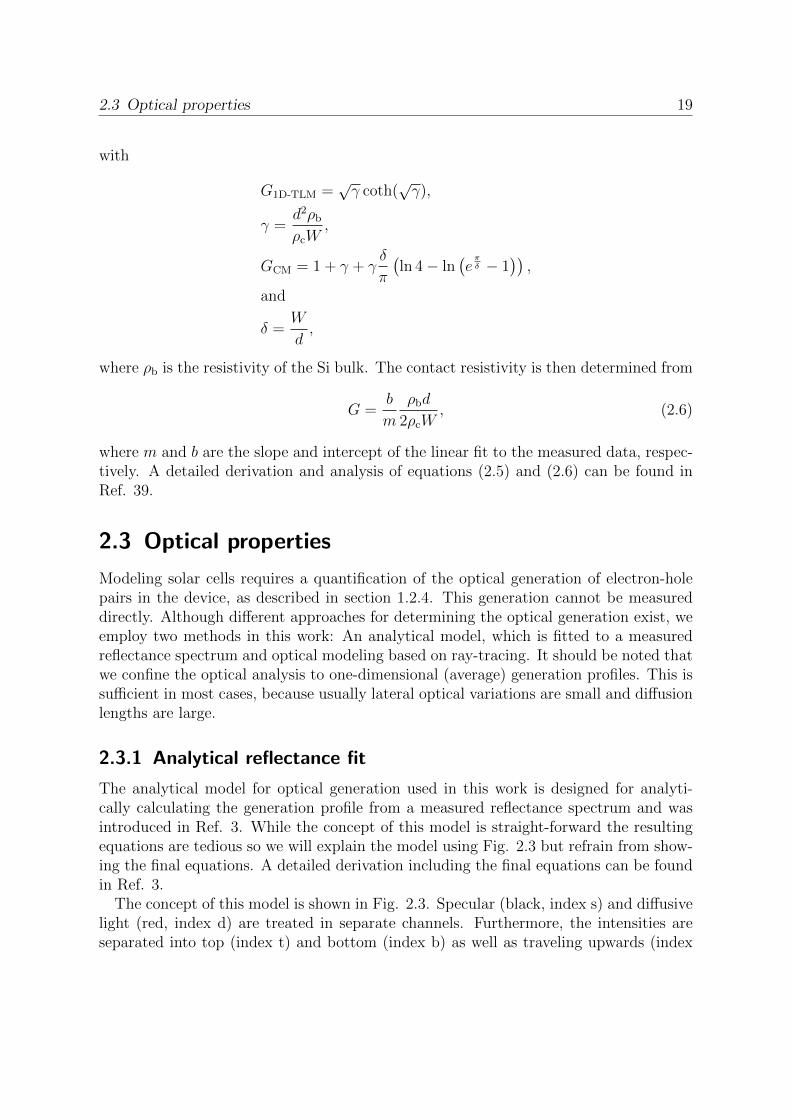
The analytical model for optical generation used in this work is designed for analyti-cally calculating the generation profile from a measured reflectance spectrum and wasintroduced in Ref. 3. While the concept of this model is straight-forward the resultingequations are tedious so we will explain the model using Fig. 2.3 but refrain from show-ing the final equations. A detailed derivation including the final equations can be foundin Ref. 3.
The concept of this model is shown in Fig. 2.3. Specular (black, index s) and diffusivelight (red, index d) are treated in separate channels. Furthermore, the intensities areseparated into top (index t) and bottom (index b) as well as traveling upwards (index

2.3 Optical properties 20
Is,t,d
Is,b,dIs,b,u
Is,t,u Id,t,u
Id,b,u
Id,t,d
Id,b,d
RdRs
Ts
(1-Tf)(1-Λf)
Rb(1-Λb)
(1-Tf)Λf
RbΛb
Tf(1-Λf) TfΛf
Td
1-Tf/n²Tf/n²
Rb
Tf(1-Λf)(1-Tf)Λf
TfΛf
Ts Td
irradiation
Figure 2.3: Schematic for the analytical optical model developed in Ref. 3. The tencircles represent the light intensity contributions analyzed in this model. The termsat the connection lines between the circles give the fraction of light that is transferredto the respective intensity. The black and red lines and circles represent specularand diffusive light, respectively. The blue dashed lines show the transition from thespecular into the diffusive channel. Figure adapted from Ref. 3.
u) or downwards (index d). The terms for the transition from one intensity contributionto another are shown in Fig. 2.3. Transmission as well as reflection at both front- andrear-side leads to a partial randomization of light due to rough surfaces. The fractionof light that is randomized with each interaction (ie. enters the diffusive channel, bluedashed lines) is described by a Lambertian factor for each side (Λf and Λb in Fig.2.3). Furthermore, the reflection probability of photons at the front and rear surface isdescribed byRf = 1−Tf andRb, respectively. Collecting all intensities and transmissionsalong the lines in Fig. 2.3 results in ten coupled linear equations for the eight intensitiesin the wafer as well as the specular and diffusive reflectance, each represented by acircle in Fig. 2.3. These equations can be solved to describe the measured reflectance,which is the sum of diffusive and specular reflectance, using Λf , Λb, Rf and Rb aswell as the refractive index of silicon and the absorption coefficients for specular anddiffusive light. The latter quantities are known from the literature. The other fourquantities can be determined by fitting the model to a measured reflectance spectrum.For short wavelengths (λ < 900 nm) the measured reflectance is equal to Rf , becauselight entering the cell is quickly absorbed. For long wavelengths Rf is extrapolated

2.4 Recombination properties 21
with a second-order polynomial fitted to the reflectance between 800 and 900 nm. Thethree remaining parameters can then be fitted to the measured reflectance using thismodel. However, both Λf and Λb have a very similar effect on the calculated reflectance.Therefore, it increases the numerical stability if one of the Lambertian factors is set to afixed value. For textured samples we use Λf = 0.335, which agrees well with the averagepath length enhancement by a pyramid texture.
The determined values for Λf , Λb, Rf and Rb can then be used for calculating thegeneration profile. The generation in an ideal solar cell can be calculated when assumingΛf = 1, Rf = 0 and Rb = 1. Note that in this case Λb is irrelevant as all light directlyenters the diffusive channel when entering the cell. It should be noted that this modelalso includes the effect of free carrier absorption (FCA) as described in Ref. 3. However,other forms of parasitic absorption, as for example in poly-Si layers, are not included inthis model.
2.3.2 Ray tracing
The analytical model described above is well suited to analyze PERC cells and similarsamples. However, the model does not include all optical aspects, which plays an impor-tant role for the analysis of poly-Si cell concepts in chapter 5. For this work the mostimportant shortcomings are parasitic absorption other than FCA and lateral variationsof optical properties. For these cases we use a ray-tracing approach for the determinationof the generation profile. In this work we employ the program SUNRAYS [40] for theray-tracing simulations. By simulating the involved unit cells and then area-averagingthe results we gain the final generation profile.
Ray tracing determines the generation profile by simulating a large number of photonsand tracing their path through the solar cell. It requires the knowledge of the geometricalproperties (layer thickness etc.) and of the (complex) refractive index of all materialspresent in the solar cell. These refractive indices are determined once and do not needto be measured on each individual cell. Like the analytical model, ray-tracing is basedon probabilities. Each photon is traced through the simulated structure and at everyinterface or pass through a layer the photon is either reflected, transmitted or absorbedbased on the probability for the respective process. By simulating a large number ofphotons, the absorption distribution yields the generation profile.
2.4 Recombination properties
In this section we describe the determination of bulk and surface recombination proper-ties. We first introduce the charge carrier lifetime measurement techniques used in thiswork, namely (quasi-)steady-state photoconductance ((Q)SSPC), photoconductance-calibrated photoluminescence imaging (PC-PLI) and infrared lifetime mapping (ILM).We then briefly introduce how to separate bulk and surface recombination from the

2.4 Recombination properties 22
measurement of the effective charge carrier lifetime τeff .
2.4.1 (Quasi-)steady-state photoconductance (Q)SSPC
(Q)SSPC [41] is a widely used technique in the PV-community as it allows for quick andprecise determination of effective lifetimes in non-metallized samples. For the (Q)SSPCmethod a sample is illuminated with steady- or quasi-steady-state illumination and theconductivity of the wafer is determined by inductive coupling of the sample to a coil. Theconductivity of a Si wafer is much lower than the conductivity of a metal layer or metalcontact-pattern. Therefore, only non-metallized samples can be analyzed with (Q)SSPC.Quasi-steady-state means that the illumination intensity changes on a timescale muchlarger than the carrier lifetime. Which light source is used depends on the measurementsetup, but does not affect the measurement theory. The quasi-steady-state illuminationhas the advantage that a wide range of injection densities can be analyzed on shorttimescales without significant sample heating. In this work we use a Sinton WCT-120lifetime tester [42] as QSSPC setup for measuring lifetime samples and a SSPC setupfor the calibration of photoluminescence images (see section 2.4.2).
A detailed derivation and description of the QSSPC measurement theory can be foundin Ref. 41. By exploiting the balance of generation and recombination in a device understeady-state conditions and the knowledge of electron and hole mobilities µn and µp insilicon the effective lifetime can be expressed as [41]
τeff =σL
JGen(µn + µp), (2.7)
where σL is the measured conductivity increase due to illumination and JGen is thegenerated photo-current. Consequently, the determination of the effective lifetime onlyrequires the knowledge of JGen, which can be determined via a reference cell and/orray-tracing. In the WCT-120 lifetime tester and the SSPC setup in the PC-PLI systema reference cell is integrated and differences of JGen of the reference cell and the sampleare considered using a suitable optical factor, which can be determined via ray-tracingor test measurements with solar cells.
2.4.2 Photoconductance-calibrated photoluminescence imaging
Photoluminescence imaging (PLI) is a widely used technique for analyzing Si lifetimesamples and solar cells. PLI allows for a spatially resolved lifetime image by detect-ing the luminescence emission of a sample using a camera, in this work a Si- charge-coupled-device (CCD) camera. Since PLI raw images only yield the amount of detectedluminescence, a calibration is required. The most practical and accurate approach is touse a SSPC setup within the PLI system to determine the lifetime under equal mea-surement conditions. This photoconductance-calibrated (PC-)PLI is described in Ref.43. PC-PLI can only be used if part of the sample is not metallized to use the SSPC

2.4 Recombination properties 23
Si-CCD
Laser @ 808 nm + Homogenisation
SSPC calibration
Sample
Long pass (LP)filterShort pass (SP)filter
Referencecell
Figure 2.4: PC-PLI measurement setup used in this work. The sample is placed on aSSPC stage. The illumination is realized by a laser with a wavelength of 808 nmwith suitable homogenisation. The luminescence emission is recorded with a Si-CCD camera. The reflected light as well as the luminescence emission reflected atthe rear side of the sample are effectively blocked using a long and a short pass filter,respectively.
method in that area or if a non-metallized sample with an identical optical behavior isavailable. We analyze the application of PC-PLI and ILM (section 2.4.3) to partiallymetallized samples in chapter 3. Therefore, we briefly review the theory of PC-PLI. Amore detailed description and derivation can be found in Ref. 43.
The luminescence emission of a lifetime sample or solar cell is proportional to theradiative recombination
IPL ∝ rrad = Bradnp ≈ Brad∆n(∆n+Ndop), (2.8)
which leaves the determination of the proportionality factor as the only step for thedetermination of the effective lifetime with equation (1.15). For each illumination in-tensity we determine ∆n using the integrated SSPC setup. We then area-average thePL intensity over the coil area and determine the coefficients a and b for the quadraticrelation between the PL intensity and ∆n
IPL = a∆n2 + b∆n. (2.9)
This calibration is valid for all samples or sample areas with the same optical behavior.If the optical generation is known, a lifetime image can be deduced from the ∆n map

2.4 Recombination properties 24
InSb camera3-5 µm
LED array @950 nm
Al mirror+ heating stage @ 70°C
Sample
Square-wave illumination
Figure 2.5: Measurement setup for ILM.The sample is placed on an Al mirror,which also heats the sample to 70 °C.It is illuminated with square-wave il-lumination at wavelength 950 nm us-ing a LED array. The IR emission isrecorded with an InSb camera sensitiveat 3-5µm wavelength.
Figure 2.6: Normalized, time dependentgeneration rate and excess carrier den-sity and image acquisition times forILM measurements. Image reprintedfrom Ref. 47.
using equation 1.15 and the equality of carrier generation and recombination understeady-state conditions.
In chapter 3 we use PC-PLI to analyze partially metallized samples. In Ref. 44 Mulleret al. showed that the metal on the rear affects the optical behavior of the sample and,therefore, makes the calibration in metallized areas invalid. However, this technique canstill be applied by integrating an additional short-pass filter in the measurement setupto avoid light reflected at the rear-side metallization to enter the camera as shown inRef. 44. The setup used in this work is described in Ref. 43 and Ref. 44 and shown inFig. 2.4.
2.4.3 Infrared lifetime mapping
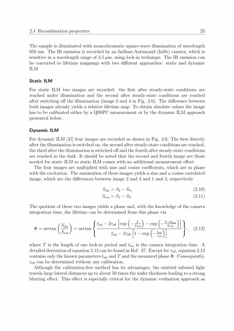
Infrared lifetime mapping (ILM) [45] utilizes the proportionality between infrared light(IR) emission and free charge carriers in a sample. We use the setup described in Ref.46, which is shown in Fig. 2.5.
The sample is placed on an aluminum mirror, which also heats the sample to 70 °C.
2.4 Recombination properties 25
The sample is illuminated with monochromatic square-wave illumination of wavelength950 nm. The IR emission is recorded by an Indium-Antimonid (InSb) camera, which issensitive in a wavelength range of 3-5µm, using lock-in technique. The IR emission canbe converted to lifetime mappings with two different approaches: static and dynamicILM
Static ILM
For static ILM two images are recorded: the first after steady-state conditions arereached under illumination and the second after steady-state conditions are reachedafter switching off the illumination (image 2 and 4 in Fig. 2.6). The difference betweenboth images already yields a relative lifetime map. To obtain absolute values the imagehas to be calibrated either by a QSSPC measurement or by the dynamic ILM approachpresented below.
Dynamic ILM
For dynamic ILM [47] four images are recorded as shown in Fig. 2.6: The first directlyafter the illumination is switched on, the second after steady-state conditions are reached,the third after the illumination is switched off and the fourth after steady-state conditionsare reached in the dark. It should be noted that the second and fourth image are thoseneeded for static ILM so static ILM comes with no additional measurement effort.
The four images are multiplied with sine and cosine coefficients, which are in phasewith the excitation. The summation of these images yields a sine and a cosine correlatedimage, which are the differences between image 2 and 4 and 1 and 3, respectively
Ssin = S2 − S4, (2.10)
Scos = S1 − S3. (2.11)
The quotient of these two images yields a phase and, with the knowledge of the cameraintegration time, the lifetime can be determined from this phase via
Φ = arctan
(Ssin
Scos
)= arctan
tint − 2τeff
[exp
(− T
4τeff
)− exp
(−T+4tint
4τeff
)]tint − 2τeff
[1− exp
(− tint
τeff
)] , (2.12)
where T is the length of one lock-in period and tint is the camera integration time. Adetailed derivation of equation 2.12 can be found in Ref. 47. Except for τeff , equation 2.12contains only the known parameters tint and T and the measured phase Φ. Consequently,τeff can be determined without any calibration.
Although the calibration-free method has its advantages, the emitted infrared lighttravels large lateral distances up to about 50 times the wafer thickness leading to a strongblurring effect. This effect is especially critical for the dynamic evaluation approach as
2.4 Recombination properties 26
the time signal from high lifetime regions dominates over the signal from adjacent lowlifetime regions as shown in Ref. 46. In addition, the analysis of lifetimes below 50 µsyields large uncertainties due to multiple effects in the setup (for a detailed discussionand analysis see Ref. 46). It is, therefore, recommended to use the dynamic ILMapproach to calibrate the static ILM image in high lifetime regions. The application ofthe ILM approach to partially metallized samples is discussed in section 3.2.
2.4.4 Bulk and surface recombination
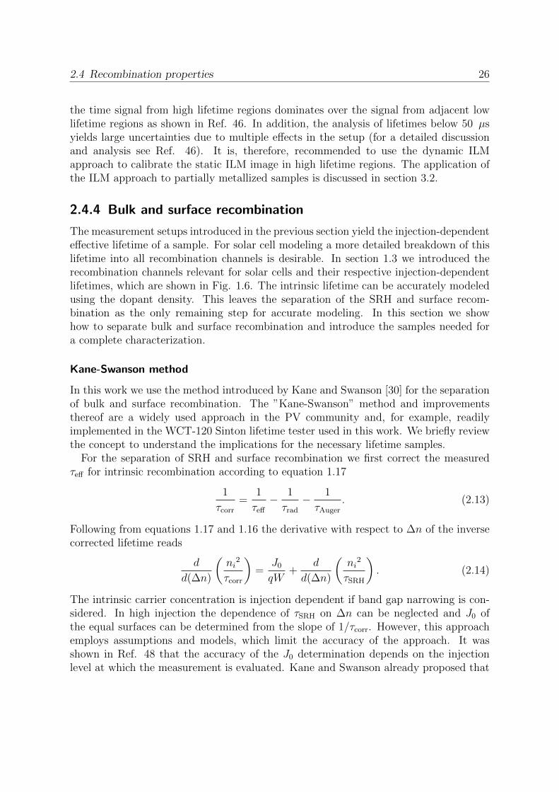
The measurement setups introduced in the previous section yield the injection-dependenteffective lifetime of a sample. For solar cell modeling a more detailed breakdown of thislifetime into all recombination channels is desirable. In section 1.3 we introduced therecombination channels relevant for solar cells and their respective injection-dependentlifetimes, which are shown in Fig. 1.6. The intrinsic lifetime can be accurately modeledusing the dopant density. This leaves the separation of the SRH and surface recom-bination as the only remaining step for accurate modeling. In this section we showhow to separate bulk and surface recombination and introduce the samples needed fora complete characterization.
Kane-Swanson method
In this work we use the method introduced by Kane and Swanson [30] for the separationof bulk and surface recombination. The ”Kane-Swanson” method and improvementsthereof are a widely used approach in the PV community and, for example, readilyimplemented in the WCT-120 Sinton lifetime tester used in this work. We briefly reviewthe concept to understand the implications for the necessary lifetime samples.
For the separation of SRH and surface recombination we first correct the measuredτeff for intrinsic recombination according to equation 1.17
1
τcorr
=1
τeff
− 1
τrad
− 1
τAuger
. (2.13)
Following from equations 1.17 and 1.16 the derivative with respect to ∆n of the inversecorrected lifetime reads
d
d(∆n)
(ni
2
τcorr
)=
J0
qW+
d
d(∆n)
(ni
2
τSRH
). (2.14)
The intrinsic carrier concentration is injection dependent if band gap narrowing is con-sidered. In high injection the dependence of τSRH on ∆n can be neglected and J0 ofthe equal surfaces can be determined from the slope of 1/τcorr. However, this approachemploys assumptions and models, which limit the accuracy of the approach. It wasshown in Ref. 48 that the accuracy of the J0 determination depends on the injectionlevel at which the measurement is evaluated. Kane and Swanson already proposed that

2.4 Recombination properties 27
n+-SiSiN
SiN
p-Si
b) surface passivation c) diffused surfaces
Al2O3
SiN
p-Si
Al2O3
SiN
n+-Si
a) bulk lifetime
5 - 20 Ωcm
Al2O3
SiN
p-Si
Al2O3
SiN
Figure 2.7: Test structures for the determination of a) the bulk lifetime, which has to beprocessed as closely to the cell process as possible and on the same wafer material, b)the recombination at the passivated surfaces processed on high resistivity Si to ensurea higher accuracy of the J0 determination and c) the diffused surfaces featuring asymmetric emitter diffusion.
the assumption of a uniform carrier density breaks down for high injections densities.However, injection densities larger than the dopant concentration are required for theseparation of SRH and surface contributions. Consequently, a sample with low dopantdensity yields a higher accuracy for the determination of J0.
Samples for the determination of charge carrier lifetimes
The recombination properties except for the contacts can be determined when using atest structure, which undergoes the entire cell process except the metallization. How-ever, the highest accuracy is achieved when using separate, symmetric reference samplesfor the bulk lifetime, the passivated and the diffused surfaces as shown in Fig. 2.7. Inaddition, the samples for the characterization of surface recombination should be pro-cessed on high resistivity (5-20 Ωcm) material to increase the accuracy of the separationof bulk and surface recombination. The accuracy is increased because high injectionconditions, where the surface is dominating, are reached at lower ∆n.
Especially boron-doped Si, which is the basis for most industrial solar cells, containsrecombination active boron-oxygen defects [49]. The recombination activity of thesedefects strongly depends on the temperature budget, hydrogen introduction and otherprocess characteristics. In addition to boron-oxygen defects, other impurities containedin the silicon can contribute to the charge-carrier recombination. Recombination defectsin silicon are still vividly discussed in solar cell research and not all defects in a solar cellare identified. For measuring bulk recombination precisely it is important to fabricatethe test structure as similar to the solar cell as possible. This includes the temperaturebudget during e.g. the diffusion and layer deposition steps.
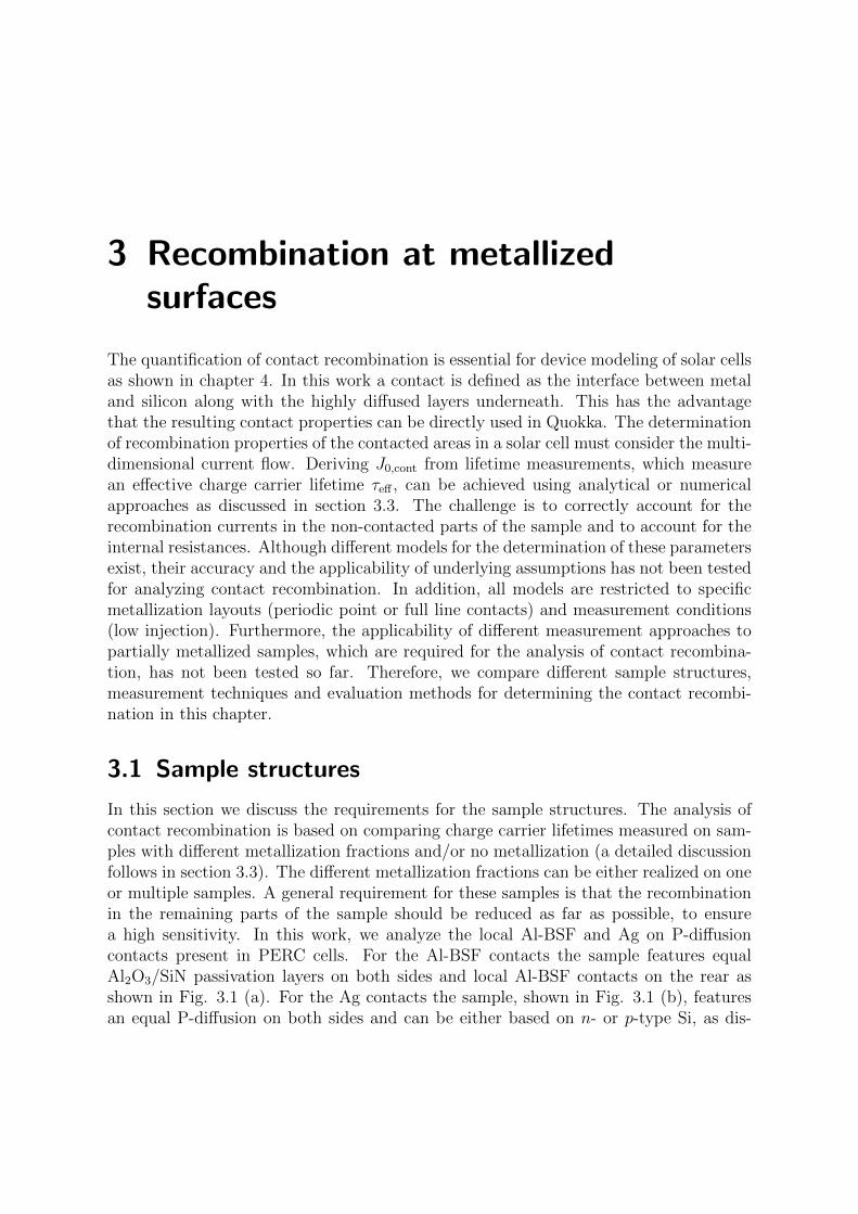
3 Recombination at metallizedsurfaces
The quantification of contact recombination is essential for device modeling of solar cellsas shown in chapter 4. In this work a contact is defined as the interface between metaland silicon along with the highly diffused layers underneath. This has the advantagethat the resulting contact properties can be directly used in Quokka. The determinationof recombination properties of the contacted areas in a solar cell must consider the multi-dimensional current flow. Deriving J0,cont from lifetime measurements, which measurean effective charge carrier lifetime τeff , can be achieved using analytical or numericalapproaches as discussed in section 3.3. The challenge is to correctly account for therecombination currents in the non-contacted parts of the sample and to account for theinternal resistances. Although different models for the determination of these parametersexist, their accuracy and the applicability of underlying assumptions has not been testedfor analyzing contact recombination. In addition, all models are restricted to specificmetallization layouts (periodic point or full line contacts) and measurement conditions(low injection). Furthermore, the applicability of different measurement approaches topartially metallized samples, which are required for the analysis of contact recombina-tion, has not been tested so far. Therefore, we compare different sample structures,measurement techniques and evaluation methods for determining the contact recombi-nation in this chapter.
3.1 Sample structures
In this section we discuss the requirements for the sample structures. The analysis ofcontact recombination is based on comparing charge carrier lifetimes measured on sam-ples with different metallization fractions and/or no metallization (a detailed discussionfollows in section 3.3). The different metallization fractions can be either realized on oneor multiple samples. A general requirement for these samples is that the recombinationin the remaining parts of the sample should be reduced as far as possible, to ensurea high sensitivity. In this work, we analyze the local Al-BSF and Ag on P-diffusioncontacts present in PERC cells. For the Al-BSF contacts the sample features equalAl2O3/SiN passivation layers on both sides and local Al-BSF contacts on the rear asshown in Fig. 3.1 (a). For the Ag contacts the sample, shown in Fig. 3.1 (b), featuresan equal P-diffusion on both sides and can be either based on n- or p-type Si, as dis-

3.1 Sample structures 29
cussed in section 3.1.2. The contacts are applied to the rear side with selective dopingunderneath if it is also used for the cells. In both cases the contact geometry is thatused in the cell except for the finger pitch that may be varied. In addition, in case ofboron-doped silicon the boron-oxygen defects should be deactivated by illuminating thesample at elevated temperatures after processing [50]. This minimizes the impact of thebulk recombination.
For the analysis of charge carrier lifetime variations due to different metallizationfractions on one wafer, the lateral inhomogeneity of the lifetime over the wafer areaand the interaction of charge carriers between regions of different lifetimes must beconsidered. Therefore, we discuss implications rising from an inhomogeneous lifetimeand coupling between different regions for partially metallized samples before we discussthe metallization patterns that can be employed for the J0,cont-analysis.
3.1.1 Inhomogeneities
A homogeneous bulk lifetime and passivation quality over the analyzed area of the sampleis essential to the determination of J0,cont values. Any inhomogeneity contributes to theuncertainty of the analysis. If the lifetime deviation due to the inhomogeneity of thebulk lifetime or the passivation quality is of the same order of magnitude as the changesdue to the metallization or even larger, the determination of meaningful J0,cont-values isnot possible. As an example, Fig. 3.2 shows a PL image of a sample with local Al-BSFcontacts with 16 differently metallized areas. The contact opening width is 64 µm forthe entire wafer and the metallization fraction is varied using different contact pitches,which are shown in the image. For this sample it is obvious that areas with identicalmetallization (eg. fields 9 and 11) yield very different lifetimes. Because changes ofthe lifetime are dominated by the inhomogeneity rather than the different metallization
Aluminium
n+-type Si
SilverSiN
SiN
n-type Si
a) b)
Al2O3
SiN
p-type Si
Al2O3SiNx
n+-type Si
Figure 3.1: Schematics for the test structures for contact recombination. a) Sample withAl2O3/SiN passivation on both sides of the p-type wafer and Al-BSF contacts onthe rear. b) Sample with n+ diffusion on both sides of the n-type wafer and Agcontacts on the rear.

3.1 Sample structures 30
Figure 3.2: PL image (not calibrated) of an inhomogeneous lifetime sample. The dif-ferent areas are metallized with Al with contact lines of 64µm width. The pitchis given in the image for each field. Here areas with equal metallization yield verydifferent lifetimes (compare e.g. field 9 and 11).
fractions, the determination of J0,cont values is not possible with this sample.Reduction of inhomogeneities in the bulk lifetime and the surface passivation must,
thus, be a primary concern when designing J0,Ag-samples. However, inhomogeneitycan not be completely avoided. In many cases the inhomogeneity shows systematicand statistic features. Examples for systematic inhomogeneity are low lifetimes at thewafer edges, rings of different lifetime due to varying defect concentrations in the bulk(Cz-rings) and side-to-side or mid-to-edge lifetime gradients due to varying passivationquality. As these effects can hardly be avoided completely, the metallization pattern (seesection 3.1.3) should be designed to reduce the systematic effect. For example, the effectof mid-to-edge gradients and/or defect rings in the bulk can be reduced by applying acentral symmetric metallization pattern. The effect of low lifetime wafer edges can bereduced by designing the metallization pattern such that the edges are not relevant forthe J0,cont analysis. Statistic variations of the lifetime should be of much shorter lengthscales than the areas of the metallization pattern and evenly distributed over the waferto ensure that these deviations are averaged out in the analysis.

3.1 Sample structures 31
3.1.2 Coupling between regions of different lifetime
Different metallization fractions on one wafer lead to regions of different lifetime, whichare not fully independent from one another. However, the analysis of these samples (seesection 3.3) is based on the assumption that these regions can be treated as independent.In this section we analyze the coupling between regions of different lifetime in order toestimate the length-scale on which the QFLs and ∆n are affected, in the following calledcoupling length xc.
We fabricate samples for which a cross section is shown in Fig. 3.3. The samplefeatures a 1.5 Ωcm, 160 µm thick p-type Si wafer with an n-type diffusion on both sideswith a sheet resistance Rsheet of 140 Ω/ passivated with SiN. The left side of the crosssection is not contacted whereas the right side features 40µm-wide Ag line contacts with0.45 mm pitch. Consequently, the left side features a higher effective lifetime and willin the following be referred to with index hl (high lifetime) whereas the right side willbe referred to with index ll (low lifetime). We measure the QFL splitting, also calledinternal voltage V , of the sample using PC-PLI. A line scan of this measurement attwo illumination intensities is shown in the bottom part of Fig. 3.3 as green and redcircles for strong and weak illumination, respectively. The photo-generation currentsare Jg,strong = 25 mA/cm2 and Jg,weak = 1.8 mA/cm2 as determined by the Quokka fitintroduced below. It is centered around the interface between both regions and extending10 mm into each region. We see that the voltage shows a continuous decrease from thehigh to the low lifetime region. Furthermore, we see that xc depends on the illuminationdensity.
We also simulate this sample using Quokka. We describe all recombination channelsin each region with a lumped J0,eff to simplify the analysis. We determine the respectiveJ0,eff-values to J0,hl = 25 fA/cm2 and J0,ll = 90 fA/cm2 by fitting the simulated lifetimeto the measurement in both regions. It should be noted that it is not possible todefine emitters at both surfaces within Quokka. To obtain the same lateral conductivityprovided by the two 140 Ω/ emitters we use one 70 Ω/ emitter in Quokka. Thesimulation results for strong and weak illumination are shown in the bottom part of Fig.3.3 as green and red line, respectively. We see that the simulation using the lumpedJ0 and Rsheet values describes the experiment well using the stated parameters. Whenplanning sample structures for J0,cont determination we could, in principle, simulate thedevice using this approach to estimate xc. However, this approach requires a goodknowledge of the sample before it is fabricated. In addition, the physical backgroundbehind the coupling and the impact of sample properties on xc remain unclear in thissimulation based approach. Therefore, we analyze the coupling analytically using alinear approximation for the voltage.
Here we analyze the coupling in the high lifetime region (between −xc and 0). How-ever, the effect is symmetric around the interface between both regions and the samearguments and equations apply for the low lifetime region. For the analysis of the cou-pling length we are interested in the distance from the interface at which the QFLs are

3.1 Sample structures 32
simulation measurement
n+-type Si
Ag contactsSiN
SiN
p-type Si
n+-type Si
contacted areanon-contacted area
I = Ic/2 I = Ic
I = Ig
I = Ir
xc
exp xc = 0.8 mm analytical xc = 1.1 mm
exp. xc = 3.2 mm analytical xc = 2.9 mm
Figure 3.3: Top: sample cross section with symmetric n+ diffusions on a p-type waferfor the analysis of coupling between regions of different lifetime. The left side isnot contacted and, therefore, has a higher lifetime, whereas the right side features40µm-wide Ag line contacts with 450 µm pitch and has a lower lifetime. Bot-tom: Measured (dotted line) and simulated (solid line) internal voltage for strong(green) and weak (red) illumination with the respective calculated and graphicallydetermined coupling lengths xc.
approximately equal to their values far away from the interface. For the definition ofthe linear voltage approximation we use two boundary conditions: The voltage at xc
from the interface equals the voltage far away from the interface (Vhl) and the voltagereduction at the interface equals half the total voltage difference (∆V ) between both

3.1 Sample structures 33
regions
V (−xc) = Vhl
V (0) = Vhl −∆V
2
⇒ V (x) = −∆V
2xc
(x+ xc) + Vhl (3.1)
To calculate xc we employ the current balance in the region between the interface and−xc. At −xc the derivatives of the QFLs are discontinuous. Therefore, we take theaverage of the derivatives left and right of −xc for the calculation of the current throughthe interface, which yields half the current through the interface at x = 0. The minorityand majority current through the interface at x = 0 are equal because there is no exter-nal electric field and no charge accumulation and hence no net current. Consequently,the coupling current density (line current density in units of A/m) through the inter-face between both regions can be calculated using the gradient of either QFL and thecorresponding conductivity:
Jc = −σnd
dxφn = σp
d
dxφp (3.2)
As we analyze the coupling using an approximation for the voltage we require an ex-pression of the current through the interface in terms of the voltage. Here we employthe equality of majority and minority current and the fact that the voltage gradient canbe calculated as the difference of the QFL gradients:
σnd
dxφn = −σp
d
dxφp
⇒ d
dxφn −
d
dxφp =
σn + σp
σp
d
dxφn
d
dxφn −
d
dxφp =
d
dxV = −∆V
2xc
⇒ Jc =∆V σnσp
2xc(σn + σp)(3.3)
During a measurement we also have generation and recombination currents in the sam-ple. In the regions far away from the interface these currents are equal because we donot extract charge carriers from the device. In the region between xc and the interfacethe generation current is balanced by recombination and the coupling current (see Fig.3.3 top):
Ig = Ir + Ic −Ic2
⇒ JGenxc =
∫ 0
−xcJrecdx+
JcW
2(3.4)

3.1 Sample structures 34
The integral over the recombination current is necessary because the recombinationcurrent depends on the voltage, which is decreasing towards the interface. Using thedescription with J0 values we can solve the integral:∫ 0
−xcJrecdx =
∫ 0
−xcJ0,hle
V (x)VT dx
= J0,hleVhlVT
∫ 0
−xce
−∆V2xcVT
(x+xc)dx
= JGen2xcVT(1− e
−∆V2VT )
∆V(3.5)
where we used the equilibrium relation Jrec = J0,hleVhl/VT = JGen far away from the inter-
face. From this equilibrium condition for both regions we further derive an expressionfor ∆V :
J0,hleVhlVT = J0,lle
VllVT
⇒ ∆V = Vhl − Vll = VT ln
(J0,ll
J0,hl
)(3.6)
Using equations (3.3) to (3.6) we can now calculate the coupling length:
→ xc =
√√√√√√√√VTσnσpW ln
(J0,ll
J0,hl
)4JGen(σn + σp)
1− 2
(1−√J0,hlJ0,ll
)ln
(J0,llJ0,hl
) (3.7)
We see that the coupling length increases with decreasing illumination intensity. Incase of low level injection, where the coupling length is largest, the conductivity of themajority carriers dominates and we have:
σp =1
ρb
(3.8)
σn =1
RsheetW(3.9)
The coupling is limited by the smaller lateral conductivity for either holes or electrons.Therefore, a sample with either only hole or only electron conducting wafer and layersshows very small coupling lengths. In case of our example we calculate xc to 1.1 mmand 3.2 mm for strong and weak illumination, respectively. These values agree wellwith the values graphically determined from the measurements of 0.8 mm and 2.9 mm,respectively as shown in Fig. 3.3. Hence, any metallization pattern for this samplemust allow a lifetime evaluation at least 3.2 mm away from every interface between

3.1 Sample structures 35
a) b) c)
Figure 3.4: Schematics for different metallization patterns for the test structures for ana-lyzing contact recombination. The black lines represent silver or aluminum contactsshown in Fig. 3.1. a) Full area cell metallization, b) Four areas with differentmetallization fractions (one without metallization) and c) 16 areas with differentmetallization fractions (two of each, two without metallization) and non-metallizededges.
metallization patterns. If the evaluation is performed at lower generation currents thanJGen = 1.8 mA/cm2 the distance to the interfaces must be increased accordingly.
To avoid coupling and the resulting implications for the samples we recommend usingn-type diffusions in n-type wafers or p-type diffusions in p-type wafers. This approachis used for the characterization in this work. However, often one type of material leadsto a much higher lifetime or reduced inhomogeneities on the sample. In this case it isoften beneficial to use the higher lifetime material and avoid the coupling by designinga metallization pattern that allows an evaluation further away from the interface thanxc.
3.1.3 Metallization patterns
There are three possibilities for the comparison of differently metallized samples: i) wecan use samples with full area metallization patterns and compare multiple sampleswith different metallization fractions, ii) we can print areas with different metallizationfractions on one wafer or iii) we can use the cell contacting geometry on one waferand etch back the metallization after the measurement and then re-passivate the wafer.However, for the latter method we cannot ensure that the etch-back and re-passivationsteps do not change recombination properties other than at the contacts. Therefore, wefocus our analysis on the first two options.
There is no general answer to what the best metallization pattern is. The best choicedepends on the lifetime of the sample and the corresponding inhomogeneities. Figure
3.2 Measurement techniques 36
3.4 shows three metallization patterns for determining the contact recombination. Usingfull area metallization as in Fig. 3.4 a) is preferable when lateral inhomogeneities of theeffective lifetime are larger than the deviations between different samples, because wecan then average over the entire wafer area. While this reduces the impact of lateralinhomogeneities it increases the uncertainty by using different samples on which theaverage lifetimes vary due to slightly different process characteristics. In addition, wehave to process multiple samples. This argument gains a large impact when a screeningof different printing properties (pastes, screens, firing temperature etc) is performed,because then a large number of samples has to be processed.
The pattern in Fig. 3.4 b) has four different areas each covering one quadrant of thewafer. This ensures that rotationally symmetric inhomogeneities (eg. Cz-rings) are av-eraged out in the analysis. Furthermore, evenly distributed, small scale inhomogeneitiesare also averaged out by the large areas of this pattern. For other systematic and sym-metric inhomogeneities the pattern should be adapted such that the inhomogeneity iscanceled out by averaging over the individual areas.
The pattern in Fig. 3.4 c) features 16 small fields with 7 different contact pitches andtwo non-metallized fields and non-metallized edges, which is similar to the pattern usedin Fig. 3.2. This pattern allows for obtaining many data points to analyze the contactrecombination and the corresponding uncertainty. The wafer edges are excluded fromthis pattern as the wafer edge often yields a low lifetime due to edge recombinationor insufficient passivation quality. This pattern can only be used if the inhomogeneityof the sample is small. Also it does not allow for the correction of any symmetricinhomogeneities.
In this work we exclusively use the metallization pattern b) with four areas eachcovering one quadrant of the sample. We have found this pattern to suit our lifetimesamples best, as our main concern are systematic rotational symmetric deviations dueto Cz-rings and mid-to-edge passivation gradients. In addition, the large areas of thepattern have the benefit that most statistical inhomogeneities average out in the analysis.
3.2 Measurement techniques
For the analysis of recombination currents we have to measure the injection-dependenteffective lifetime of partially, fully or non-metallized samples. The metallization preventsus from using QSSPC measurement for the entire analysis (see section 2.4.1 on page 22for details). In addition, measurement systems with a spatial resolution are preferred,because areas with different metallization fractions on one wafer can be analyzed with asingle measurement. Two camera-based approaches are PC-PLI (section 2.4.2 on page22) and ILM (section 2.4.3 on page 24). It should be noted that the PC-PLI setuprequires a short pass filter when measuring metallized samples (see section 2.4.2). Inthe following we compare PC-PLI, static ILM and dynamic ILM measurements for theirapplicability to partially metallized samples.

3.2 Measurement techniques 37
Figure 3.5: a) PC-PLI image, b) dynamically calibrated, static ILM image and c) dy-namic ILM image of a partially metallized reference sample (metallization patternFig. 3.4 b)) for Al-BSF contacts (cross section Fig. 3.1 a)).
As an example for the comparison of measurement systems, we use a symmetricsample with Al2O3/SiN passivation on both sides. After opening contact lines with awidth of d = 64µm, we print Al contacts in a metallization pattern shown in Fig. 3.4 b)with 4 areas, one non-metallized and the other three featuring contact pitches of 810µm,450µm and 300µm. Figure 3.5 shows the lifetime images of the sample measured with a)PC-PLI, b) dynamically calibrated, static ILM and c) dynamic ILM. The lifetime imagesshow systematic differences, which we discuss in the following sections to identify themost suitable measurement system for the analysis of partially metallized samples.
3.2.1 PC-PLI measurement
The PC-PLI technique yields lifetime images, which are calibrated using SSPC mea-surements. The SSPC calibration in the PC-PLI setup used in this work is frequentlycross-checked with a WCT-120 lifetime tester and, therefore, assumed to be correct inthe non-metallized area. For the measurement of metallized samples a short-pass filterhas to be employed (see section 2.4.2 on page 22). Consequently, the excess chargecarriers near the front surface of the samples contribute stronger to the measured sig-nal than those at the rear. In the non-metallized areas the filter has no effect on themeasured lifetime, because the SSPC calibration ∆n is uniformly distributed over thesample depth. The impact of the filter in the metallized areas has to be analyzed. Tothis end, we compare the excess carrier density at the front of the sample (measured byPC-PLI) to that averaged over the entire depth of the sample (measured by SSPC). Forthis comparison we employ a Monte-Carlo simulation with input parameters randomlychosen with uniform distribution from the respective range given in Tab. 3.1. We run1000 simulations of the excess carrier density and compare the value of ∆n directly atthe front of the sample to that averaged over the depth of the sample. The excess carrierconcentration at the front deviates by up to 8% from the concentration averaged overthe depth of the sample. For metallization fractions smaller than 50% the maximum

3.2 Measurement techniques 38
Table 3.1: Input parameters for the Monte-Carlo simulation to evaluate the applicabilityof PC-PLI measurement to partially metallized samples.
Parameter ValueW 150 to 250 µmfmet 0 to 1d 5 to 100 µmρb 1 to 20 Ωcmτbulk 50 to 500 µsJ0,pas 0 to 100 fA/cm2
J0,cont J0,pas to 1500 fA/cm2
JGen 1 to 41 mA/cm2
deviation is below 5%. In the PC-PLI measurement also light from deeper regions thandirectly at the surface contributes to the measured signal. Consequently, the ∆n mea-sured with PC-PLI lies between the value directly at the front, which we used in thesimulation, and ∆n averaged over the depth of the sample. Therefore, 5% deviation isa worst-case estimate for the uncertainty of the PC-PLI calibration in metallized areasfor metallization fractions smaller than 50%.
3.2.2 Difference of dynamic and static measurement
Both static measurements shown in Fig. 3.5 a) and b) show a very similar distributionof τeff in the passivated area in the top left corner, whereas the dynamic lifetime imageshows a deviating lifetime distribution. As discussed in Ref. 46, the dynamic approachraises certain deviations to static measurements:
1. The heat signal (i.e. the emission due to the temperature of the sample) varies dueto the time dependent generation. This effect can be corrected by measuring theheat signal separately. This effect has a significant impact on the measurement forlifetimes below 50 µs.
2. Injection dependent lifetimes affect the time dependence of the ∆n. This effectleads to an overestimation of τeff by the dynamic measurement up to 30% forτn0/τp0 5 22 with a maximum at τn0/τp0 = 15.
3. Blurring has a large impact on dynamic measurements since the signal amplitudeand hence the time dependence of high lifetime areas dominates over the smalllifetime areas. In an example in Ref. 46, two adjacent areas of the same size onewith τeff = 10µs and one with τeff = 1000µs yield a dynamic average lifetime of685 µs while static approaches yield 505 µs.
The combination of these effects allows the consistent explanation of the slightly differ-ent lifetime distribution in the dynamic measurement in Fig. 3.5 c) as compared to the

3.2 Measurement techniques 39
static measurements in a) and b). The different lifetime distribution together with thelimitations for small lifetimes, the blurred signal and the deviation for injection depen-dent lifetimes limits the use of dynamic ILM measurements for the analysis. Therefore,we recommend using a steady-state measurement approach.
3.2.3 Difference of static ILM and PC-PLI
The comparison of the static approaches PC-PLI and static ILM in Fig. 3.5 a) andb) shows that the measured lifetime decreases stronger with the metallization fractionin the static ILM measurement. Figure 3.6 shows the normalized ratio (black crosses)between the lifetimes determined by PC-PLI and static ILM for the measurement shownin Fig. 3.5. For the highest metallization fraction of 21.3% the lifetime determined bystatic ILM is about 50% lower than the lifetime determined by PC-PLI. In section 3.2.1we showed that the calibration of PLI images is correct within an uncertainty of 5%.This fails to explain the 50% difference between PC-PLI and static ILM and, therefore,we analyze the applicability of the static ILM approach to partially metallized samplesin this section.
The static ILM approach relies on the calibration of the image to obtain lifetimevalues. For this calibration to work, the emission probability for the IR light createdwithin the sample has to be the same for all sections of the sample. In the following wediscuss how the metal contacts affect the emission probability for IR from the sample.
The free carriers in the sample created by the 950 nm illumination emit IR lightin random directions. For our analysis we assume that half of the light power flux istraveling upwards (index u) and the other half traveling downwards (index d):
Iu = Id = 0.5I0 (3.10)
To estimate the change of emitted IR by the metallization we estimate the emissionprobability of an IR photon using Fig. 3.7.
At every interaction with a surface the photon is either reflected or transmitted basedon the probability for the respective process. At the front side this probability is de-scribed by the internal reflectance Rf . At the rear side, which is contacted, the reflectionprobability differs for the metallized and the non-metallized area. In the non-metallizedarea we assume perfect reflectivity due to the external Al mirror. In the metallized areatwo effects reduce the reflectivity: 1) free carrier absorption in the highly doped regionunderneath the contacts (in this case the BSF) and 2) a reduced reflectivity at the Simetal interface. Both effects yield an effective reflectivity Rm,eff of the metal contact.The reflectivity of the entire rear side Rb can thus be composed of two area-averagedcontributions
Rb = fmetRm,eff + 1− fmet, (3.11)

3.2 Measurement techniques 40
Calculated ratio with Rm,eff = 0.7
Measured lifetime ratioR
atio
of e
scap
e pr
opab
ilitie
s r
0
0,25
0,5
0,75
1
Metallization fraction f 0 0,05 0,1 0,15 0,2 0,25
Figure 3.6: Measured (black crosses) and calculated (green dashed line) ratio of the IRphoton escape probabilities for different metallization fractions compared to a non-metallized sample.
where fmet is the metallization fraction. As the IR photon energy (wavelength 3 µm to5 µm) is smaller than the Si band gap and the dopant concentration is low comparedto the highly doped regions we assume no IR absorption in the Si bulk.
We now calculate the emitted intensities due the IR light initially traveling up- anddownwards. For this we collect intensities in a geometrical series first for the photonsinitially traveling upwards as shown in Fig. 3.7:
Iem,u = Iu(1−Rf)∞∑i=0
RbiRf
i =Iu(1−Rf)
1−RbRf
(3.12)
The intensity from the light initially traveling downwards can be calculated similarly,but the first interaction is with the rear surface:
Iem,d =IdRb(1−Rf)
1−RfRb
(3.13)
The total emitted intensity is the sum of both contributions:
Iem = Iem,u + Iem,d = 0.5I0(1−Rf)1 +Rb
1−RbRf
(3.14)
Because we are interested in relative changes rather than absolute intensities we calculatethe ratio r of the emitted intensity and the intensity in a non-metallized area (Rb = 1),

3.2 Measurement techniques 41
Rb = 1
Rf
Rm
dz
IuId
Iem,d Iem,u
Representative point of emission
Figure 3.7: Schematic for the calculation of escape probabilities of IR photons in an ILMmeasurement. IR photons are emitted traveling upwards and downwards with equalintensities Iu and Id. The escape probabilities are calculated using a geometricalseries and an effective rear-side reflectivity.
where the calibration is correct:
r =Iem
Iem,f=0
= 0.5(1−Rf)1 +Rb
1−RbRf
(3.15)
For the sample analyzed in this section we determine Rf to 0.93 with a ray-tracingsimulation for diffusive light with a wavelength of 4000 nm. A fit of the calculated tothe measured ratio yields Rm,eff = 0.7 for the Al-BSF contacts on this sample, as shownin Fig. 3.6 with a green dashed line. The reduced reflectivity of the contacts can beexplained by either a reduced reflectivity at the Si metal interface Rm, by free carrierabsorption or, most likely, by a combination of both effects. In the latter case we cancalculated Rm,eff with:
Rm,eff = Rme−2αdz (3.16)
where α is the absorption coefficient due to FCA in the highly doped areas and dz isthe thickness of the highly doped area. Both FCA and a reduced Rm can lead to aRm,eff = 0.7. If no FCA is present Rm = Rm,eff = 0.7. If Rm = 1 the fit of terme−2αdz = 0.7 for FCA yields Ndop = 4.5 · 1018 cm−3, λ = 4000 nm and dz = 9µm usingthe parameterization for α at long wavelength from Schroder et al. [51]. Most likely,both effects contribute to Rm,eff with adapted parameters. The separation of the effectsis, however, not possible.
In conclusion, the calibration of the static ILM measurement in the non-metallizedareas is invalid due to the reduced effective reflectivity of the metal contacts. Thisreduced reflectivity can be explained by a combination of reduced reflectivity of themetal-Si interface and FCA in the highly doped regions underneath the contact.
3.3 Evaluation methods 42
a) b)
dP
W
dP
W
Figure 3.8: Current flow due to higher recombination at the contacts compared to thesurrounding surface passivation in rear contacted test samples without highly dif-fused layers (a) and with a diffusion layer of the same polarity as the Si bulk under-neath the contacts (b).
3.3 Evaluation methods
Extracting the contact recombination from the measured effective lifetime requires adescription of the multi-dimensional current flow, internal resistances and recombinationcurrents in other parts of the solar cell. Figure 3.8 shows a schematic for the internalcurrent flow due to higher recombination at the contacts compared to the surroundingpassivation without a diffused layer (a) and with a diffused layer underneath the contacts(b). There is no analytical solution of the semiconductor equations and, consequently,either a numerical simulation or analytical simplifications to the transport equations arerequired for extracting the contact recombination parameters.
3.3.1 Analytical description
The simplest analytical approach is to neglect all lateral inhomogeneities of ∆n and ofthe current flow. In this case the Kane-Swanson evaluation method of QSSPC mea-surements (see section 2.4.4 on page 26) can be used to determine an average surfacerecombination and the contact recombination can be determined by the area-weightedsubtraction of the surface recombination in the non-contacted areas. However, in Refs.52 and 53 Dumbrell et al. compared the slope-based methods by Blum et al. [54] andthe improvement proposed by Kimmerle et al. [55] to numerical Quokka simulations andshowed that the assumption of a homogeneous ∆n in partially metallized samples leadsto an error in the determination of J0,cont of up to a factor of 5 depending on the sampledetails. Therefore, this approach is not suited to extract J0,cont values and a more suit-able analytical description has to contain a description of the multi-dimensional currentflow.
Such an approach was originally introduced by Fischer [56]. A detailed derivation of

3.3 Evaluation methods 43
a) b)
P
P
Pd
d
Figure 3.9: Schematics for the contact geometries that can be analyzed with an analyticalapproach: a) periodic arrangement of circular contacts with a distance P to thenearest contacts and a diameter d and b) full line contacts with a spacing P and awidth d.
Fischer’s model can be be found in Ref. 56. Here we are interested in the underlyingassumptions and restrictions of the model and their consequences for determining contactrecombination parameters. We are further interested in the accuracy of the model.
The derivation of Fischer’s model can be divided into three steps: i) the simplificationof the 3-D carrier transport to a 1-D model, ii) the calculation of an effective SRV Seff,rear
required for the 1-D model and iii) the calculation of the series resistance Rseries requiredfor Seff,rear. The calculation of Seff,rear requires the calculation of the diffusion constantD, which can only be done analytically in low level injection. The calculation of Seff,rear
is further based on the assumptions that the diffusion length is much larger than the cellthickness. This requirement is usually met in today’s mono-crystalline Si. It also requiresa constant QFL splitting over the front surface. This requirement is fulfilled if we havesufficiently thick devices (over 150 µm) in combination with diffusion length much largerthan the cell thickness, as is the case for our samples. The calculation of Rseries has beendone in various studies in the literature. All models are, however, restricted to eitherfull line contacts [57, 58, 59] or a periodic arrangement of point contacts [56, 59, 60],which are shown in Fig 3.9 a) and b), respectively. The analysis of arbitrary contactgeometries is, therefore, not possible in an analytical approach. If highly conductivediffusions are present, as for example in emitter structures or passivated emitter andrear totally diffused (PERT) cells, the models for Rseries have to be adapted as shownin Ref. 61 for PERT structures with full line contacts. For contact geometries other

3.3 Evaluation methods 44
Table 3.2: Input parameters for Monte-Carlo simulation
Parameter ValueW 150 to 250 µmP 10 to 100 µmfmet 0.0001 to 0.2ρb 1 to 10 Ωcmτbulk 200 to 1200 µsScont 2 to 1000 cm/s
Spas front 2 to 100 cm/sSpas rear 2 to 100 cm/s
than lines this adaption is not as straight forward, because the similarity to TLM theorycan not be exploited. This imposes further restrictions on the structures that can beanalyzed with this approach.
We check the accuracy of Fischer’s model for analyzing contact recombination inPERC cells using a Monte-Carlo simulation with Quokka. We run 1000 simulations ofthe effective lifetime with parameters chosen randomly (with uniform distribution) fromthe ranges given in Tab. 3.2 and compare the results to Fischer’s analytical model. Theparameter ranges are chosen to represent modern PERC cells. We find an excellentagreement of Fischer’s model and the Quokka simulations with deviations below 5%.This proves the applicability of Fischer’s model for determining contact recombinationparameters in PERC cells with either full-line contacts or point contacts arranged in asquare pattern, provided low injection conditions are fulfilled.
3.3.2 Numerical evaluation of contact recombination
In this section we introduce an evaluation method solely based on Quokka. This allowsan evaluation where the requirements of full line or point contacts and/or low levelinjection for Fischer’s model are not fulfilled. This is the case for the PERC+ cellsanalyzed in section 4.3, because they feature dashed line contacts. We also want tostudy the injection dependency of contact recombination parameters for which we alsoneed the numerical evaluation method.
For numerical modeling we need to define the sample under test within Quokka.The geometrical (thickness, contact width, etc.) and resistive properties (wafer andsheet resistances) are known from the sample processing or can be measured with therespective approaches described in chapter 2. For the optical definition we use a set ofhomogeneous generation currents to compute the injection dependency of the lifetime.The respective values have to be adapted to the measurement conditions used in thelifetime measurement, but we typically use 10 to 15 values in the range of 1 mA/cm2
to 45 mA/cm2.

3.3 Evaluation methods 45
All recombination parameters, the lifetime parameters for the Si bulk, the surfacerecombination parameter for the passivated surface J0,pas and the contact recombinationparameter J0,cont, have to be determined in a fitting routine. We model the bulk lifetimeusing a mid-gap SRH defect with corresponding lifetimes τn0 and τp0 or an injectionindependent lifetime τbulk (see section 1.3 on page 12). We first fit the lifetime parametersfor the Si bulk and J0,pas in the non-metallized area. The high lifetime in this area allowsfor a high accuracy of the determined parameters and are, except for inhomogeneities,representative for the entire sample. We then fit the measured lifetime curves in themetallized areas with an individual J0,cont for each metallization fraction. We, therefore,obtain three J0,cont-values for the three metallized areas of our sample (see section 3.1.3on page 35). We also determine a J0,cont-value that yields the best fit on all three areas.The comparison of these values gives us an impression of the uncertainty with whichJ0,cont was determined. By comparing the measured and simulated lifetime curves forthe determined J0,cont we can further asses the quality of the J0,cont determination. Anapplication example of this method is given in section 4.3.
Correct description of injection dependent contact recombination
One advantage of the numerical approach described above is that the contact recom-bination can be analyzed over the entire measured injection range. Here we analyze asample, which consists of n-type Si with a symmetric n-type diffusion with Ag contactson a selective diffusion on one side. The contact lines are 40 µm wide with a pitchof 450 µm. Figure 3.10 shows a measurement of the effective lifetime (black crosses)along with simulations of the effective lifetime using the J0-model (blue line) and theS-model (green line)(see equations 1.12 and 1.13 on page 13 for details on the J0- andS-description). It is apparent that neither the J0-description nor the S-description issuited to describe the injection dependency of the contact recombination in this case. Inthe following we discuss the physical reason why neither model describes the injectiondependency correctly and propose an improved parameterization using two parameters.
As discussed in section 1.3.2 the recombination in a highly diffused layer can bedescribed using the J0-model. However, such a layer is usually passivated and, conse-quently, the recombination at the surface of the diffused layer is small when comparedto the recombination within the layer. However, when a metal is applied, the recombi-nation at the surface may contribute significantly to the total recombination. For ourmodel we assume that the recombination at the Si-metal interface can be described bythe S-model (i.e. is injection independent), because the recombination relies on theSRH-defects at the surface and is in low level injection due to the large dopant concen-tration in the diffused layer. The total recombination into the boundary is the sum ofthe recombination within the diffused layer and the recombination at the surface:
Jrec = Jrec,diff + Jrec,surf (3.17)

3.3 Evaluation methods 46
J0/k-model
J0-model
S-model
Measured lifetimeEf
fect
ive
lifet
ime
τ eff [
µs]
1000
200
500
Excess carrier density Δn [1/cm³]1015 1016
Figure 3.10: Measured (black crosses) and simulated lifetime curves of a sample con-tacted with Ag contacts. The colored lines show the simulated lifetimes for theJ0-model (blue line), the S-model (green line) and the J0/k-model (red dashed line)developed in this work for modeling contact recombination.
The recombination within the diffused layer can be described by the J0-model:
Jrec,diff = J0np
ni2= J0
∆nNdop + ∆n2
ni2(3.18)
It should be noted that the carrier and dopant densities are taken at the interface of theSi bulk and the diffused layer. The recombination at the surface is described by:
Jrec,surf = Sq∆nsurf (3.19)
here the relevant excess carrier density is that at the Si-metal interface. This ∆nsurf
depends on the recombination within the diffused layer or, more precisely, the thicknessand the diffusion length of the diffused layer. As the depth of the diffused layer isnot resolved in Quokka, we approximate this value using a linear interpolation betweenboth extreme cases of LDdiff << W diff and LDdiff >> W diff . When LDdiff << W diff
we have strong recombination within the highly diffused layer and ∆nsurf ≈ 0. WhenLDdiff >> W diff we have very little recombination and the QFLs are approximately flat,which means that the np-product is approximately constant
nsurfpsurf = np
=⇒ Nsurf∆nsurf + ∆n2surf = Ndop∆n+ ∆n2, (3.20)

3.3 Evaluation methods 47
where Ndop is the dopant concentration in the wafer and Nsurf is the dopant concentrationin the highly diffused layer. In low injection we have
∆nsurf =Ndop
Nsurf
∆n. (3.21)
For the interpolation between both extreme cases we calculate ∆nsurf as
∆nsurf = ∆nNdopLDdiff
Nsurf(LDdiff +W diff). (3.22)
Consequently, we determine the total recombination to:
Jrec = J0∆nNdop + ∆n2
ni2+ Sq∆n
NdopLDdiff
Nsurf(LDdiff +W diff)
= J0
((Sqni
2
J0
LDdiff
Nsurf(LDdiff +W diff)+ 1
)Ndop∆n
ni2+
∆n2
ni2
)= J0
(kNdop∆n+ ∆n2)
ni2. (3.23)
Here we introduce the asymmetry factor
k =Sqni
2
J0
LDdiff
Ndop(LDdiff +W diff)+ 1, (3.24)
which is a parameter describing the deviation in the injection dependency of the contactrecombination from the J0-description. It contains three relevant factors: 1.) the ratiobetween J0 and S, 2.) the dopant density in the highly doped layer and 3.) the ratiobetween diffusion length and thickness of the diffused layer. Consequently, the surfacerecombination is negligible in three cases: 1.) The recombination within the diffusedsurface is much stronger than at the surface (as is the case for e.g. a passivated surface),2.) A high dopant density in the diffused layers reduces the excess carrier density at thesurface to negligible values or 3.) The diffused layer is much thicker than the diffusionlength within the layer. In these cases k equals 1 and the total recombination into theboundary can be accurately described by the J0-model.
In our measurement evaluation we use k as a second fit parameter besides J0. Thered dashed line in Fig. 3.10 shows a fit with the J0/k-model to the measurement andwe see an excellent agreement with the measurement. We determine a value of 2.5 for kand 600 fA/cm2 for J0. To check whether this value agrees with eq. 3.24, we calculate kwith eq. 3.24 using estimated values. The dopant concentrations in the highly diffusedselective emitter underneath the metal is approximately 1020 cm−3. With an emitterthickness of less than 1 µm and a diffusion length in the emitter of 10 µm to 20 µmwe can assume LDdiff >> W diff . For J0 we take the fitted value of 600 fA/cm2 and forS at the Si-metal interface we take a value of 107 cm/s. For ni we take 9 · 109 cm−3.

3.4 Summary: Determination of contact recombination parameters 48
Inserting these values in eq. 3.24 yields k ≈ 3, which agrees reasonably well with fittedk = 2.5, given the rough estimate for the parameters. In this example, the Si-metalinterface causes additional recombination in low injection that is 1.5 times higher thanthe recombination in the highly diffused layer (60% of the total recombination). Thisvalue seems to be reasonable, because the recombination in the highly diffused layer isreduced significantly in low injection and the Si-metal interface is expected to contributea large fraction of the contact recombination.
3.4 Summary: Determination of contact recombinationparameters
The extraction of contact recombination parameters from lifetime measurements is achallenging task. In general this challenge is met by comparing the lifetimes for differentmetallization fractions. We analyzed samples structures, measurement techniques andevaluation methods for their applicability to this task. The best choice for a metallizationpattern depends on the lifetime sample used. In this work we use a pattern with fourareas, one not metallized and three with different metallization fractions. We found thispattern to be best suited for our lifetime samples, which have moderate inhomogeneities,which are, to a large fraction, rotational symmetric. If both electron and hole conductinglayers are present the coupling between regions of different lifetime must be considered.To this end, we derived an analytical formula to estimate the length scale on which thecoupling affects the respective lifetimes. In this work we use n-type diffusions in n-typewafers or p-type diffusions in p-type wafers.
For the measurement of partially metallized samples three methods were compared inthis chapter: PC-PLI, static ILM and dynamic ILM. We found PC-PLI to be best suitedfor this task because of the low uncertainty of the static measurement. The dynamicILM approach yields similar results but with higher uncertainties due to deviation ofthe dynamic approach caused by injection dependent, inhomogeneous or low lifetimes.The static ILM yields wrong results with a deviation of up to 50% due to the reducedemission of photons for higher metallization fractions. This can be explained with theenhanced IR absorption at the Si-metal interface and/or FCA in the highly doped regionsunderneath the contact.
For the extraction of recombination parameters from spatially resolved lifetime mea-surements the internal resistances of the sample must be considered. A simple areaaveraging approach yields results wrong by up to a factor of 5 [29]. We found the modelby Fischer to be accurate within 5% provided the assumptions of low level injection andlong diffusion lengths are fulfilled. Furthermore, the model is restricted to either full lineor point contacts arranged in a square pattern. Because the cells we investigate in sec-tion 4.3 have dashed line contacts, we also introduced a numerical evaluation approachbased on Quokka. The recombination properties other than those at the contacts are

3.4 Summary: Determination of contact recombination parameters 49
determined in a non-contacted field. The contact recombination parameters are thendetermined in the remaining fields by fitting the measured lifetime with individual J0,cont
for each field. This also yields an estimate for the uncertainty of the determined value.Using this method, we found that in some cases the injection dependency of the con-tact recombination can be neither described with the J0-model nor with the S-model.We identified the origin for this deviation in the combination of two recombination cur-rents: the recombination in the highly diffused layer, which follows the J0-model and therecombination at the Si-metal interface, which can be accurately described with the S-model. We derived a new parameterization, the J0/k-model, which uses two parametersto accurately describe the contact recombination.

4 Application of loss analyses toindustrial solar cells
In this chapter we show the application of modeling-based loss and gain analyses tostate-of-the-art PERC+ cells. We analyze the differences between SEGA as a gain andFELA as a loss analysis. We further present a simulation tool, which was created inthe context of this work and automatically performs SEGAs and parameter variations.We then show the complete analysis of an industrial-type PERC+ solar cell startingwith the test structures and characterization of the cell batch including an analysisof the expected uncertainties. We further show how these input parameters are usedto calculate a SEGA and how the uncertainties in the input parameters translate touncertainties in the simulation results.
4.1 Comparison of FELA and SEGA
The content presented in this section was previously published in Ref. 62.FELA and SEGA are both simulation-based analyses to identify routes for further cell
improvements and both quantify optical losses, transport losses and recombination lossesin units of power per area. However, there also is an import difference between bothapproaches. The SEGA is a gain analysis whereas the FELA is a loss analysis. A gain isdefined as the efficiency that is gained if a loss channel is deactivated. A loss, on the otherhand, is a loss of a specific quantity at the operating point of the solar cell under test.In case of the FELA this quantity is the rate of free energy. In other words, the SEGAcalculates the efficiency loss at the maximum power point relative to a cell without thatloss, whereas the FELA calculates the free energy loss rate. Both analyses are frequentlyused in solar cell optimization [63, 64, 65, 66], which raises the question of possibledifferences in the results. In solar cell optimization, researchers are always interestedin the efficiency gain that can be achieved by optimizing a specific cell property. Thisgain is determined by the SEGA. However, the FELA is considerably faster as onlyone simulation is needed for all loss channels. Here we analyze the differences of bothapproaches.
Figure 4.2 shows the results of a SEGA (a) and a FELA (b) for a 21%-efficient PERCcell shown in Fig. 4.1 both expressed in mW/cm2. The optical, recombination andresistive losses are shown with green, red and blue bars, respectively. The optical andresistive losses calculated by both approaches agree well with less than 0.02 mW/cm2

4.1 Comparison of FELA and SEGA 51
Ag
SiN
n+-emitter
Al2O3
Al-BSF
Al
p-Si
SiN
ρbulk = 2 ΩcmτSRH = 2 ms
1.2 mm
40 μm
120 μm
Rsheet,e = 100 Ω/J0,e = 150 fA/cm²
J0,pas = 20 fA/cm²
J0,cont = 1000 fA/cm²ρc = 5 mΩcm²
J0,cont = 1000 fA/cm²ρc = 5 mΩcm²
Figure 4.1: PERC schematic with input parameters for the comparison of FELA andSEGA in Fig. 4.2. Figure reprinted from Ref. 62.
difference. However, the optical losses due to rear surface reflection, lambertian lighttrapping and free carrier absorption calculated in the SEGA are not determined in theFELA, because the required wavelength dependent generation is not available in oursimulation. The recombination losses show larger deviations especially for the largestrecombination channel, which, in this case, is the emitter recombination. The loss dueto emitter recombination is 0.75 mW/cm2 as calculated with the SEGA, with the FELAthe loss results to only 0.56 mW/cm2. The sum of all recombination losses amounts to1.31 mW/cm2 in the SEGA and 1.13 mW/cm2 in the FELA. In addition, the SEGAcalculates synergistic gains, which amount to 3.21 mW/cm2 for the recombination losses.For the optical losses the synergy amounts to 0.09 mW/cm2 while for the resistive lossesthe synergy is negligible. There are also synergy effects between the three groups, whichamount to 0.56 mW/cm2 shown as a black bar. The sum of the 21% reference efficiencyand all efficiency gains yields 28.94% efficiency, which is the efficiency limit for the cellthickness of 170 µm and a base resistivity of 2 Ωcm.
4.1.1 Monte-Carlo simulation for recombination channels
From the comparison in Fig. 4.2 it is clear that the SEGA and FELA can yield dif-ferent results for the recombination channels. To better understand the magnitude andorigin of these deviations we run a Monte-Carlo simulation with random recombinationparameters with values from the ranges given in Tab. 4.1. The remaining parametersare chosen as shown in Fig. 4.1.
The results are shown in Fig. 4.3. The FELA yields smaller losses in cases of largerecombination at the front side of the cell (red data points). For recombination losschannels located at the rear side of the solar cell (green data points), the FELA yieldslarger losses for power losses up to 0.5 mW/cm2. The FELA also yields larger losses forrecombination in the absorber (blue data points).

4.1 Comparison of FELA and SEGA 52
2.07
1.31
0.69
1.13
0.69
Figure 4.2: SEGA (top) and FELA (bottom) for an example PERC test structure shownin Fig. 4.1. Optical losses are shown in green, recombination losses in red andresistive losses in blue. Figure reprinted from Ref. 62
The dashed lines in Fig. 4.3 show a 20 % deviation of the FELA loss compared tothe SEGA gain. Most data points for the power loss due to rear-side and absorberrecombination show less than 20 % deviation for power losses up to 0.8 mW/cm2 ascalculated with the FELA. For power losses at the front side the deviation between

4.1 Comparison of FELA and SEGA 53
Table 4.1: Ranges from which each recombination parameter is chosen for the compari-son of FELA and SEGA in Fig. 4.3
Recombination parameter Range
Bulk carrier lifetime 55 to 2000 µs
Emitter recombination 4 to 1000 fA/cm2
Front contact recombination 4 to 35000 fA/cm2
Rear passivation recombination 4 to 600 fA/cm2
Rear contact recombination 4 to 20000 fA/cm2
-20%
+20%
• Bulk rec.
⋆ Rear contact rec.
Rear passivation rec.
⋄ Front contact rec.
× Emitter rec.Pow
er lo
ss LFELA
[mW
/cm
²]
0
0.25
0.5
0.75
1
1.25
1.5
Power gain LSEGA [mW/cm²]0 0.25 0.5 0.75 1 1.25 1.5
Figure 4.3: Comparison of SEGA and FELA results for random recombination propertiesin a PERC solar cell structure. Front-side losses are shown in red, rear-side lossesin green and bulk losses in blue. Figure reprinted from Ref. 62.
FELA and SEGA is only within 20 % for FELA losses up to 0.4 mW/cm2. It shouldbe noted, however, that the relative deviation of FELA losses can amount up to 40 %as rear-side and bulk losses are determined larger while front-side losses are determinedsmaller. Deviations of this magnitude could possibly lead to major differences in thestrategy for further cell improvements and should, therefore, be understood.

4.1 Comparison of FELA and SEGA 54
4.1.2 Analytical description
In this section we employ the analytical description of FELA and SEGA losses to un-derstand the origin of the deviation between both approaches. The power loss per areaas calculated with the SEGA in terms of free energy follows from equation (1.2):
LSEGA = (ηnl − ηwl)PIN
= (FG,nl − FR,nl − FT,nl) (4.1)
−(FG,wl − FR,wl − FT,wl).
The indices nl and wl stand for the simulations with no loss and with loss, respectively.We simplify (4.1) by neglecting any differences in the power losses due to charge carriertransport. The differences of the generated power and the power lost due to recombina-tion sum up to the SEGA power loss
LSEGA = (FG,nl − FG,wl)− (FR,nl − FR,wl). (4.2)
We calculate all terms in (4.2) by multiplying the generation or recombination currentwith the local Fermi level splitting in the respective simulation (nl or wl). The photogen-erated current JGen is equal in both simulations. We calculate the recombination currentJrec in the i -th recombination channel using equation (1.12), which yields Jrec = J0,ie
β∆φ,where β is the inverse thermal voltage. It should be noted that the Fermi level splitting∆φ depends on the location within the cell. Consequently, the calculation of the totalrecombination current requires an integral over the volume of interest. However, to sim-plify the further calculations, we neglect the local character of the Fermi level splittingand take the average Fermi level splitting (internal voltage) V as an approximation.
Let the analyzed loss channel be channel one such that J0,i,nl = J0,i,wl = J0,i for all2 ≤ i ≤ N , where N is the total number of recombination channels. Then we can write(4.2) as
LSEGA = JGen(V nl − V wl)
−N∑i=2
J0,i(V nleβV nl − V wle
βV wl)
+ J0,1V wleβV wl . (4.3)
The last term J0,1V wleβV wl in (4.3) is the power loss LFELA as calculated by the FELA.
The deviation between the power losses calculated with both approaches is thus
LSEGA − LFELA = JGen(V nl − V wl)
−N∑i=2
J0,i(V nleβV nl − V wle
βV wl). (4.4)

4.1 Comparison of FELA and SEGA 55
Table 4.2: Recombination parameters for the PERC cell analyzed in Fig. 4.4
Recombination parameter Value
Bulk carrier lifetime 55 µs
J0 emitter recombination 1000 fA/cm2
J0 front contact recombination 35000 fA/cm2
J0 rear passivation recombination 600 fA/cm2
J0 rear contact recombination 20000 fA/cm2
V is larger for the cell with less recombination. To simplify (4.4) further, we introduce∆V = V nl − V wl. We write (4.4) as
LSEGA − LFELA = JGen∆V
−N∑i=2
J0,iV wleβV wl((1 +
∆V
V wl
)eβ∆V − 1), (4.5)
and because the difference of the internal voltages ∆V is usually small compared to Vwe can write
LSEGA − LFELA ≈ JGen∆V
−N∑i=2
LFELA,J0,i· (eβ∆V − 1), (4.6)
where we used LFELA,J0,i= J0,iV wle
βV wl . We see that the difference LSEGA − LFELA
between both analyses rises solely from an increase of the internal voltage, which doesnot show up in the FELA approach. This increase of the internal voltage leads to anincrease of generated free energy as described by the first term in (4.6). In contrast,the second term describes the increased recombination losses in other channels due tothe increased internal voltage when eliminating a specific loss. While the increase ofgenerated free energy contributes to an underestimation of the losses by the FELA withrespect to SEGA, the increased losses in other recombination channels contribute to anoverestimation. Depending on which of these terms is dominating, the FELA can eitherover- or underestimate the implied power gain.
In our derivation of equation (4.6) we approximated the Fermi level splitting ∆φ(~x)by the average Fermi level splitting V . While this approximation is useful for under-standing the origin of the under- and overestimation, it fails to explain the differencesbetween front- and rear-side losses. Figure 4.4 shows the Fermi level splitting increase∆V in the non-contacted area of an example cell simulated without emitter recombina-tion (red line) and without recombination at the rear-side passivation (green line). The

4.1 Comparison of FELA and SEGA 56
no rear pas. recombination
no emitter recombination
Fer
mi-l
evel
spl
ittin
g in
crea
se ΔV
[m
V]
0
2
4
6
8
10
Depth z [µm]0 50 100 150
Figure 4.4: The increase of the Fermi level splitting in the non-contacted area of anexample cell with strong recombination in all loss channels. The recombinationparameters of this cell can be found in Tab. in 4.2. The red line shows the Fermilevel increase when avoiding the emitter recombination. The green line shows theincrease for avoiding recombination at the rear-side passivation. The front side is atz = 0.
differences of the Fermi levels are more pronounced for larger recombination currentswithin the cell. To improve the clarity of the qualitative analysis of the Fermi levelswe use exaggerated recombination parameters, which can be found in Tab. 4.2. Allother parameters are the same as in Fig. 4.1. It should be noted that the SEGA gainsdue to recombination within the emitter and at the rear-side passivation are approxi-mately the same (0.340 mW/cm2 versus 0.334 mW/cm2, respectively) for this cell. Incomparison, the FELA losses show large differences and a different ranking of the losses(0.309 mW/cm2 versus 0.429 mW/cm2). We see that avoiding the emitter recombina-tion affects the change of the local Fermi level differently than avoiding recombination atthe rear-side passivation. Avoiding the emitter recombination leads to a strong increaseof the Fermi level splitting at the front side of the cell, which rapidly decreases withthe cell depth. This leads to a stronger increase of generated free energy compared tothe increased losses in other recombination channels (at the back) and, consequently,an underestimation of the implied gain by the FELA. For the ideal rear passivation theincrease of the Fermi level is more evenly spread over the cell depth leading to a strongerincrease of free energy losses in other recombination channels (at the front) when com-pared to the increase of generated free energy. This corresponds to an overestimation ofthe implied gain by the FELA.
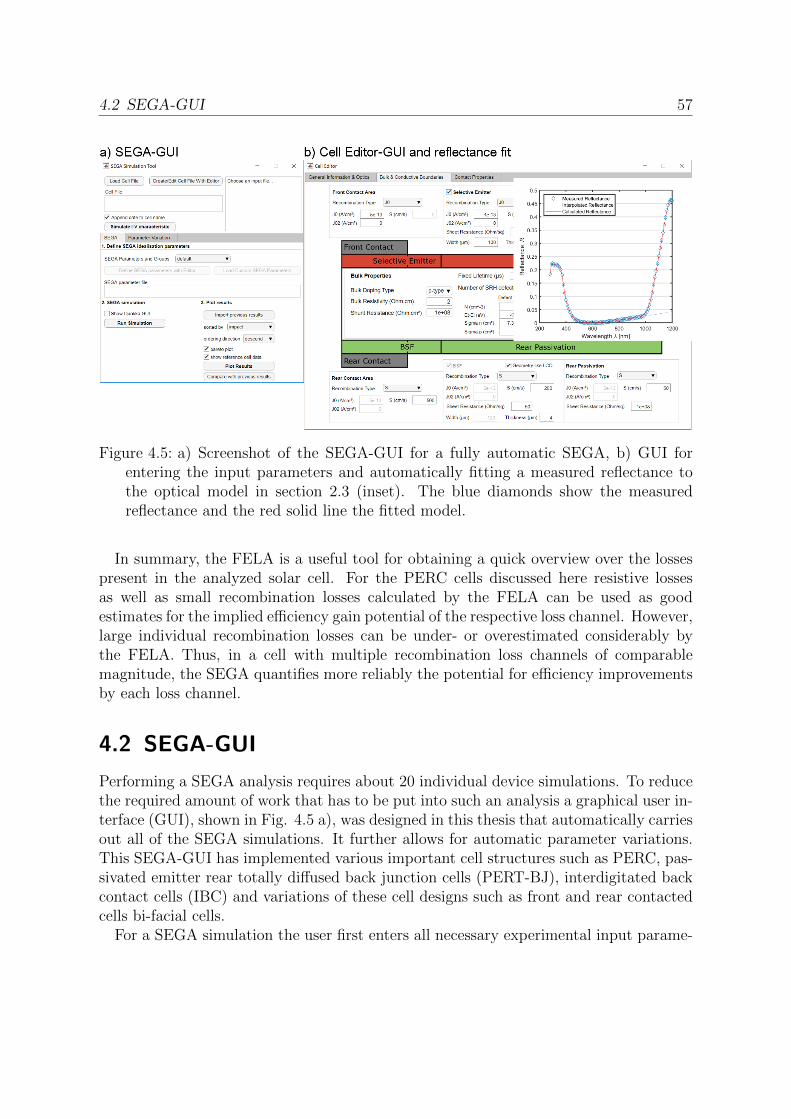
4.2 SEGA-GUI 57
Figure 4.5: a) Screenshot of the SEGA-GUI for a fully automatic SEGA, b) GUI forentering the input parameters and automatically fitting a measured reflectance tothe optical model in section 2.3 (inset). The blue diamonds show the measuredreflectance and the red solid line the fitted model.
In summary, the FELA is a useful tool for obtaining a quick overview over the lossespresent in the analyzed solar cell. For the PERC cells discussed here resistive lossesas well as small recombination losses calculated by the FELA can be used as goodestimates for the implied efficiency gain potential of the respective loss channel. However,large individual recombination losses can be under- or overestimated considerably bythe FELA. Thus, in a cell with multiple recombination loss channels of comparablemagnitude, the SEGA quantifies more reliably the potential for efficiency improvementsby each loss channel.
4.2 SEGA-GUI
Performing a SEGA analysis requires about 20 individual device simulations. To reducethe required amount of work that has to be put into such an analysis a graphical user in-terface (GUI), shown in Fig. 4.5 a), was designed in this thesis that automatically carriesout all of the SEGA simulations. It further allows for automatic parameter variations.This SEGA-GUI has implemented various important cell structures such as PERC, pas-sivated emitter rear totally diffused back junction cells (PERT-BJ), interdigitated backcontact cells (IBC) and variations of these cell designs such as front and rear contactedcells bi-facial cells.
For a SEGA simulation the user first enters all necessary experimental input parame-

4.3 Application example: PERC+ solar cell 58
ters and then the SEGA-GUI creates the required set of input files. The SEGA-GUI thenperforms the simulations by running Quokka 2 and displays the results. Programmingknowledge is not required. The SEGA-GUI was designed to help the user in findingoptions for efficiency improvements. It further features a GUI for creating the requiredinput files, which is shown in Fig. 4.5 b). This GUI allows to input values for geo-metric properties, lifetimes, including different defect and recombination models, andresistive properties. It further allows to automatically fit the optical model presentedin section 2.3 to a measured reflectance curve. An example for a reflectance fit createdby this GUI is also shown in Fig. 4.5 b). The measured reflectance spectrum is shownwith blue diamonds along with the extrapolated front surface reflectance in the nearinfrared spectral range (blue dotted line) and the fitted modeled reflectance (red line).We made the SEGA-GUI available for the scientific community [8]. The SEGA-GUI canbe downloaded for free from the ISFH website: http://www.isfh.de/tools/SEGA-GUI.
4.3 Application example: PERC+ solar cell
In this section we apply the measurement and simulation techniques introduced beforefor a complete characterization and SEGA analysis of a PERC+ cell batch.
4.3.1 Processing cells and test structures
For the characterization of the PERC+ cell batch we require six types of test structures:1) ”iVOC-samples”, which are samples that are not metallized and haves no LCOs butare otherwise identical to the cells, 2) ”J0,e-samples” for determining the emitter recom-bination, 3) ”J0,Ag-samples” for determining recombination at the front Ag-contacts, 4)”τbulk-samples” for determining the bulk lifetime, 5) ”J0,pas-samples” for determiningrecombination at the surface passivation and 6) ”J0,Al-samples” for determining recom-bination at the rear Al-contacts. The iVOC-samples contain all recombination channelsexcept for the contacts. They are not necessarily required for the characterization inthis work but serve as redundancy in case the J0,e-, τbulk- or J0,pas-samples show faults.More information on the requirements for the test structures can be found in chapters2 and 3.
Figure 4.6 shows the process sequences for the cell and all test structures. The solarcells (first column in Fig. 4.6) are processed on 0.9 Ωcm B-doped Cz-material with athickness of 161 µm. After initial cleaning a protective SiN layer is deposited as anetch barrier onto the rear side. Front-side texturing and shallow phosphorus diffusionfollow. Then the designated contact areas are laser-doped for forming the selectiveemitter. After that the protective SiN-layer is removed and a SiN-layer for anti-reflectionand passivation is applied to the front side. Next the Al2O3 and SiN for the rear-sidepassivation are applied using atomic layer deposition and plasma enhanced chemicalvapor deposition, respectively. The last step is applying the contacts by first opening

4.3 Application example: PERC+ solar cell 59
cells iVoc
wafer cleaning
protective nitride
nitride removal
Ag print
texture
laser doping
SiN ARC
LCO
Al print
emitter removal
SiN rear
Al2O3
firing
phosphorus diffusion
J0-Ag
P-dop.5 Ωcm
B-dop.0.9 Ωcm
B-dop.0.9 Ωcm
J0-Al
Ga-dop.0.8 Ωcm
J0e
B-dop0.9 Ωcm
bulklifetime
B-dop.0.9 Ωcm
surfacepas.
Ga-dop.4.5 Ωcm
Figure 4.6: Process sequences for the analyzed PERC+ cells and the required test struc-tures. From top to bottom each image represents a process step for which the labelis shown on the left. A missing image means that the process step is not requiredfor the respective sample. The columns show the sequences for the cell and thesix different types of test structures. The J0,e-samples in the third column receivelaser-doping only for two of the four quarters, which is indicated by the separationof the two sample areas.

4.3 Application example: PERC+ solar cell 60
the contact areas on the rear side using a laser (LCO) and then screen-printing an Algrid on the rear- and an Ag grid on the front side. After that the cells are treated witha short term anealing step called firing to form the contacts. The iVOC-samples (secondcolumn in Fig. 4.6) are manufactured the same as the cells except for the LCO andmetallization steps, which are omitted.
The J0,e-samples (third column in Fig. 4.6) are processed without protective SiNleading to a symmetric texture and phosphorus diffusion. The samples are divided intoquarters, two with full area laser-doping on both sides and two without laser-doping.The surfaces are passivated with SiN and then fired. The J0,Ag-samples (fourth columnin Fig. 4.6) are processed on 5 Ωcm P-doped Cz-material to avoid lateral couplingas discussed in section 3.1.2 on page 31. The samples are processed symmetrically byomitting the protective SiN, the rear passivation and the rear metallization steps. TheAg-contact pattern consists of 4 areas as shown in Fig. 3.4 b). The respective contactpitches are 450 µm, 900 µm and 1350 µm. Laser doping is only applied to the areasunderneath the contacts.
The τbulk-samples (fifth column in Fig. 4.6) and the J0,pas-samples (sixth column inFig. 4.6) are processed identically but on different bulk-materials. The τbulk-samplesare processed on the same 0.9 Ωcm boron-doped material as the cells. The material forthe J0,pas-samples is Ga-doped with 4.5 Ωcm because the higher resistivity enhances theaccuracy of the Kane-Swanson analysis as described in section 2.4.4 on page 26. Bothtypes of samples receive a phosphorus emitter diffusion, which is removed in the nextstep, in order to getter impurities from the bulk into the highly diffused layer. Afterthat an Al2O3/SiN passivation is applied to both sides of the samples, which are thenfired. The J0,Al-samples are processed identical to the τbulk-samples and J0,pas-samplesbut on 0.8 Ωcm Ga-doped material because it provides the best lifetime of our availablep-type material. After the passivation steps, LCOs and metal are applied on the rearside of the samples, which are then fired. The metallization pattern is again that shownin Fig. 3.4 b) with contact pitches of 300 µm, 450 µm and 810 µm. The LCOs are 46µm-wide dashed lines with 300 µm dash length and 900 µm dash pitch as shown in Fig.4.7.
For the estimation of process-related uncertainties in the determined values we processmultiple samples of each type: 10 solar cells, 4 iVOC-samples, 3 J0,e-samples, 4 J0,Ag-samples, τbulk-samples, 5 J0,pas-samples and 5 J0,Al-samples. It should be noted that weaimed at 10 solar cells and 5 of each test structure, but some samples did not survivethe cell process. The processing was undertaken by members of the group ”Industrialsolar cells” at ISFH and not by the author of this work.
4.3.2 Characterization and cell geometry
We list the characterization results in four groups: geometric, optical, resistance, andrecombination. For the analysis of the uncertainty of the SEGA-simulation results weare interested in the variation of the determined values. The minimum and maximum
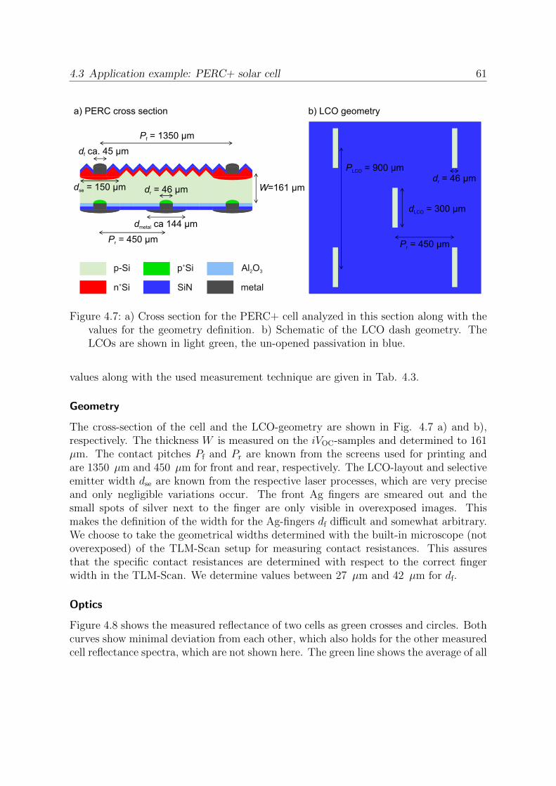
4.3 Application example: PERC+ solar cell 61
SiN
p+Si
n+Si
p-Si Al2O3
metal
W=161 µm
Pf = 1350 µm
Pr = 450 µm
dmetal ca 144 µm
dr = 46 µmdse = 150 µm
df ca. 45 µm
Pr = 450 µm
dLCO = 300 µm
PLCO = 900 µm
a) PERC cross section b) LCO geometry
dr = 46 µm
Figure 4.7: a) Cross section for the PERC+ cell analyzed in this section along with thevalues for the geometry definition. b) Schematic of the LCO dash geometry. TheLCOs are shown in light green, the un-opened passivation in blue.
values along with the used measurement technique are given in Tab. 4.3.
Geometry
The cross-section of the cell and the LCO-geometry are shown in Fig. 4.7 a) and b),respectively. The thickness W is measured on the iVOC-samples and determined to 161µm. The contact pitches Pf and Pr are known from the screens used for printing andare 1350 µm and 450 µm for front and rear, respectively. The LCO-layout and selectiveemitter width dse are known from the respective laser processes, which are very preciseand only negligible variations occur. The front Ag fingers are smeared out and thesmall spots of silver next to the finger are only visible in overexposed images. Thismakes the definition of the width for the Ag-fingers df difficult and somewhat arbitrary.We choose to take the geometrical widths determined with the built-in microscope (notoverexposed) of the TLM-Scan setup for measuring contact resistances. This assuresthat the specific contact resistances are determined with respect to the correct fingerwidth in the TLM-Scan. We determine values between 27 µm and 42 µm for df.
Optics
Figure 4.8 shows the measured reflectance of two cells as green crosses and circles. Bothcurves show minimal deviation from each other, which also holds for the other measuredcell reflectance spectra, which are not shown here. The green line shows the average of all

4.3 Application example: PERC+ solar cell 62
Extrapolated front reflectance
Modeled reflectance
Fit for fopt
Corrected reflectance
Av. measured reflectanceMeasured reflectance
Metal
Ref
lect
ance
R
0
0.25
0.5
0.75
1
Wavelegth λ [nm]1000500
Figure 4.8: Measured reflectance of two cells (green crosses and circles) and averagemeasured average reflectance (green line). The blue diamonds show the measuredreflectance corrected for the reflectance of the metal fingers. The reflectance of themetal (Ag) is shown in gray. The red line shows the fit of the optical model presentedin section 2.3. The blue dotted line shows the extrapolated front surface reflection.
measured reflectance spectra. The minimum of the measured reflectance is not zero aswould be expected for a cell with ARC. The non-zero reflectance is caused by the metalfingers, which are in the analyzed area. From the offset between the minimal reflectanceand zero and the separately measured reflectance of the metal, which is shown is gray,we determine an optical metallization fraction. This metallization fraction yields theoptical width dopt of the metal fingers, which can differ from the geometrical width df
due to either light being reflected from the finger onto the active cell area or shading bysmall spots of silver paste, which are not visible in the optical microscope. The ratio ofgeometrical and optical width is described by an optical factor fopt such that
dopt = foptdgeom. (4.7)
We determine values between 1.167 and 1.841 for fopt, which shows that a large fractionof light is reflected at small silver sports that are not visible in the microscope. Theremaining optical parameters are determined by fitting the optical model described insection 2.3 on page 19 to the corrected reflectance, which is shown as blue diamonds.The extrapolated front surface reflectanceRf is shown with a blue dotted line. The fittedmodel is shown with a red line and we see an excellent agreement between modeled andmeasured, corrected reflectance.

4.3 Application example: PERC+ solar cell 63
Resistance
The resistivity of the Si bulk ρb is determined by measuring the conductivity in the darkusing the QSSPC setup and the fact that no other conducting layers are present in ourlifetime samples. We determine values between 0.89 Ωcm and 0.96 Ωcm for ρb. Thesheet resistances Rsheet,e and Rsheet,e,sel of the shallow and selective emitter, respectively,are determined using four-point probe measurements in the respective quarters of theJ0,e-samples. In this measurement two outer probes inject a current into the sampleand the voltage drop due to the sheet resistance of the sample is measured by two innerprobes. We determine values between 70 Ω/ and 74 Ω/ for Rsheet,e and 114 Ω/ and118 Ω/ for Rsheet,e,sel. The contact resistances are determined with the TLM-approachdescribed in section 2.2 on page 16 with the fully automatic TLM-Scan setup by pv-tools. For the rear Al contacts the method by Eidelloth and Brendel [39](see section2.2) is applied. For the Al contacts we determine resistances between 1.33 mΩcm2
and 1.34 mΩcm2. For the front contacts we see a large variation in the determinedresistances, which lie between 1.9 mΩcm2 and 17.2 mΩcm2. The finger line resistanceρl,Ag is determined by measuring the resistance between two busbars, which yields theparallel resistance of all fingers between the busbars. From this we calculate averageρl,Ag values for all cells, which lie between 1.38 Ω/cm and 1.64 Ω/cm.
Recombination
For finding the J0-values of the rear-side passivation J0,pas and the bulk lifetime param-eters τn0 and τp0, we perform QSSPC measurements at five different positions on eachof the respective lifetime samples. We determine J0,pas using the Kane-Swanson analysis(section 2.4.4 on page 26) and find values between 0 fA/cm2 and 2 fA/cm2. For thebulk lifetime we correct the measured effective lifetime for the intrinsic lifetime usingthe parameterization by Richter et al. [27] and for the surface recombination using J0,pas
and equation 1.16. The resulting lifetime is that corresponding to the SRH defects inthe bulk to which we fit with a mid-gap SRH defect represented by equation 1.11. Wedetermine values between 103 µs and 253 µs for τn0 and 705 µs and 1114 µs for τp0.For the J0-values J0,e and J0,e,sel of the shallow and selective emitter, respectively, weperform one QSSPC measurement in each of the respective quarters of the J0,e-samplesand use the Kane-Swanson analysis to extract the J0-values. We find values between26 fA/cm2 and 30 fA/cm2 for J0,e and values between 119 fA/cm2 and 129 fA/cm2 forJ0,e,sel.
For the analysis of contact recombination we perform injection-dependent PC-PLImeasurements of the respective samples. Figure 4.9 shows the lifetimes in the non-metallized and the three metallized areas for two out of four J0,Ag-samples (blue and red).The measured lifetimes are shown as crosses, asterisks, circles and squares for the non-metallized area and the metallized areas with metallization fractions of 2.7%, 4% and 8%,respectively. We fit the measured lifetimes using Quokka with the procedure described

4.3 Application example: PERC+ solar cell 64
sample 2sample 1
f = 8%f = 4%
f = 2.7%f = 0
Effe
ctiv
e lif
etim
e τ e
ff [µs
] 1000
200
500
Excess carrier density Δn [1/cm³]1015 1016
Figure 4.9: Lifetime curves for two out of four J0,Ag-samples (red and blue). The mea-sured data are shown as crosses, asterisks, pluses and stars for metallization fractionsof 0%, 2.7%, 4% and 8%. The simulated lifetime curves with the best overall J0,Ag-for the respective sample are shown as solid, dash, dash-dotted and dotted lines forthe four areas of the sample.
in section 3.3.2 on page 44. For the fits we use J0/k-model introduced in section 3.3.2and find that k = 2.5 reproduces the injection dependency of the contact recombinationwell for all our J0,Ag-samples. For the first sample shown in red we find J0,Ag-values of460 fA/cm2, 440 fA/cm2and 480 fA/cm2 for the three metallized areas. The best fit forall three areas with one J0,Ag-value is achieved with 460 fA/cm2. The simulated lifetime-curves for J0,Ag = 460 fA/cm2 are shown in Fig. 4.9 as red solid, dashed, dash-dottedand dotted line for no metallization and the the three metallized areas, respectively.For this sample we see an excellent agreement of the three determined J0,Ag-valuesand consequently an excellent agreement between the measured and simulated lifetimecurves. For the second sample shown in blue we use the same procedure and determineJ0,Ag-values of 510 fA/cm2, 570 fA/cm2 and 510 fA/cm2 for the respective fields. Thebest overall J0,Ag-value is 510 fA/cm2 for which the simulated lifetimes are shown inFig. 4.9. We see a good agreement with a slightly higher deviation between simulationand measurement for this sample, which is caused by inhomogeneities on the sample.We perform the same analysis also for the two remaining samples. Overall we find J0,Ag-values between 460 fA/cm2 and 700 fA/cm2 for the four samples. We apply the sameapproach to the rear Al contacts and find a value of k = 1 and J0,Al-values between 600fA/cm2and 700 fA/cm2. It should be noted that k = 1 means that the rear Al contactsare well described with the unmodified J0-model.

4.3 Application example: PERC+ solar cell 65
Table 4.3: Parameters of the PERC+ cell batch with minimum and maximum valuesand the respective measurement technique that was used for the determination.
Parameter Minimum value Maximum value Meas. techniquedf [µm] 27 42 opt. microscopeTf See Figure 4.8 Fitted to reflectanceRb 0.924 0.927 Fitted to reflectanceΛb 0.882 0.892 Fitted to reflectancefopt 1.167 1.841 Fitted Rmin = 0ρb [ Ωcm] 0.89 0.96 QSSPCRsheet,e [ Ω/] 114 118 4-point-probeRsheet,e,sel [ Ω/] 70 74 4-point-probeρc,Al [ mΩcm2] 1.33 1.34 TLMρc,Ag [ mΩcm2] 1.9 17.2 TLMρl,Ag [ Ω/cm] 1.38 1.64 Busbar to busbarτn0 [µs] 103 253 QSSPCτp0 [µs] 705 1114 QSSPCJ0,pas [ fA/cm2] 0 2 QSSPCJ0,e [ fA/cm2] 26 30 QSSPCJ0,e,sel [ fA/cm2] 119 129 QSSPCJ0,Ag [ fA/cm2] 460 700 PC-PLIkAg 2.5 PC-PLIJ0,Al [ fA/cm2] 600 700 PC-PLIkAl 1 PC-PLI
4.3.3 Uncertainty analysis for the input parameters
The estimation of measurement uncertainties is a complex task, because all quantities,which contribute to the uncertainty have to be well-known. This includes statistical vari-ations as well as systematic effects, the precision of the involved measurement equipment,the precision of used models and correlations between measured variables. Furthermore,some of these values are not available because they cannot be measured with justifiableeffort. In addition, many of these uncertainties do not contribute significantly to the un-certainty of the final result, in this case the simulated solar cells conversion efficiency. Astandard approach in the analysis of uncertainties is to first assume worst-case scenariosfor all parameters and then analyze which of these parameters contribute significantly tothe overall uncertainty. To identify the parameters that contribute significantly to theuncertainty of the simulated conversion efficiency Usim, we perform a sensitivity analysiswith Monte-Carlo device simulations using Quokka. For this Monte-Carlo sensitivityanalysis we randomly choose the input parameters for the device simulations with auniform probability distribution between the experimentally determined minimum andmaximum values for each parameter. The values have been determined in the previous

4.3 Application example: PERC+ solar cell 66
Rel
ativ
e un
certa
inty
u
0
0.1
0.2
0.3
0.4
0.5
d f f opt
τ n0
τ p0
J 0,e
J 0,e
,sel
J 0,p
asJ 0
,Al
J 0,A
g ρ bR
S,e
RS
,e,s
elρ c
,Al
ρ c,A
g
ρ l,A
g T f Rb Λ b
Figure 4.10: Sensitivity analysis of the uncertainty of the simulated efficiency. The graybars show the relative uncertainty reduction for each parameter when the uncertaintyof the respective parameter is set to zero.
section and are shown in Tab. 4.3. For the front-side transmission we randomly chooseone of the measured transmission spectra with equal probabilities. We take the uniformdistributions between minimum and maximum value as a worst-case scenario for the pa-rameter distributions. This distribution is a worst-case assumption, because the valuesat the edges of the distribution (often outliers or extreme values) are chosen with thesame probability as the values in the middle of the distribution.
We first calculate Usim using all parameters with their respective uncertainties. Wethen calculate the relative uncertainty reduction ux when the uncertainty of parameterx (x = df , ρb, τn0, ...) is set to zero
ux =Usim − Usim(Ux = 0)
Usim
. (4.8)
We use 500 device simulations in the Monte-Carlo analysis for Usim and each ux.Figure 4.10 shows ux for each parameter in Tab. 4.3, except for the k-values, which
we did not vary. Small ux mean that the uncertainty of the respective input parameterplays no significant role for Usim of the analyzed PERC+ cell. All parameters exceptfor the front contact resistance ρc,Ag, the front finger width df and the minority carrierlifetime τn0 contribute less than 5% to the overall uncertainty (ux < 0.05). Therefore, theworst-case assumptions for the uncertainties of these parameters are sufficiently precise

4.3 Application example: PERC+ solar cell 67
b) Front finger width c) Minority carrier lifetimea) Front contact resistance
normal distribution with:µ = 8.7 mΩcm²σ = 3.4 mΩcm²
Rel
ativ
e oc
cura
nce
[arb
. uni
ts]
Front cont. res. ρc,Ag [mΩcm²]0 5 10 15
normal distribution with:µ = 36.2 µmσ = 3.2 µm
Front finger width df [µm]30 35 40
lifetime sample 2
normal distribution with:µ = 225 µsσ = 32 µs
iVoc samples
lifetime samples
Eff. min. carier lifetime τn0 [µs]100 150 200 250 300
Figure 4.11: Distribution of the measured values for a) the front contact resistance, b)the front finger width and c) the minority carrier lifetime (gray) and the respectivenormal distributions fitted to the data (red). For the measurements of the minoritycarrier lifetime the blue bars show the measurement on the iVOC-samples.
and we refrain from a further discussion of these parameters at this point.We now take a closer look at the measurements for the parameters contributing signif-
icantly to Usim. A complete uncertainty analysis for the measured parameters is beyondthe scope of this work. However, the statistical variations between different samples andmeasurements are expected to exceed uncertainties due to, for example, instrument ormodel precision by far. Therefore, we take a look at the distribution of the measuredvalues, which are shown in Fig. 4.11. For ρc,Ag (a) and df (b) we see that the mea-sured values can be accurately described with a normal distribution shown in red. Forρc,Ag this distribution has a mean value of µ = 8.7 mΩcm2 and a standard deviationof σ = 3.4 mΩcm2, which we take as the uncertainty for this parameter. Similarly, thenormal distribution for df yields µ = 36.2µm and σ = 3.2µm. For the four measuredlifetime samples (Fig. 4.11 c)) we see that three yield τn0 in the range of 200-250 µs,while one sample (”lifetime sample 2”) yields τn0 of 100-120 µs. To analyze whetherthis deviation represents the width of the distribution or lifetime sample 2 is an outlierdue to errors in processing or handling damage, we also include the iVOC-samples inthe analysis. In general the lifetime on iVOC-samples is lower because more significantrecombination channels exist, especially recombination within the P-diffusion. However,in low injection, where the τn0 is dominating, the surface recombination has a lowerimpact than in high injection. Therefore, we can use the measurements on iVOC-samplesfor the analysis of τn0, but the uncertainty of this measurement will be higher thanthe measurement on the lifetime samples. Here we see that all iVOC-samples yield life-times of 150-300 µs with a mean value of about 220 µs, proving that lifetime sample

4.3 Application example: PERC+ solar cell 68
Table 4.4: Parameters and uncertainties for the PERC+ cell batch. For a uniform dis-tribution the distribution width is the difference between max. and min. value. Fora normal distribution the distribution width is the standard deviation.
Parameter Value Distribution Distribution widthτn0 [µs] 225 normal 32τp0 [µs] 910 uniform 410J0 rear surf. [ fA/cm2] 1 uniform 2J0 shallow em. [ fA/cm2] 28 uniform 4J0 sel. em. [ fA/cm2] 124 uniform 10J0 front cont. [ fA/cm2] 655 uniform 290J0 rear cont. [ fA/cm2] 850 uniform 200ρb [ Ωcm] 0.925 uniform 0.07Rsheet shallow em. [ Ω/] 116 uniform 4Rsheet sel. em. [ Ω/] 72 uniform 4ρc,Ag [ mΩcm2] 8.7 normal 3.4ρc,Al [ mΩcm2] 1.337 uniform 0.012Av. finger res. [ Ω/cm] 1.51 uniform 0.52Rb 0.9253 uniform 0.0034Λb 0.8867 uniform 0.0096df [µm] 36.2 normal 3.2fopt 1.504 uniform 0.674
2 is indeed an outlier and will be eliminated from the further analysis. The remainingmeasurements can be accurately fitted with a normal distribution shown in red withµ = 225µs and σ = 32µs, which we take as the uncertainty for τn0.
The final uncertainties, which we will use for the calculation of the SEGA uncertainty,are shown in Tab. 4.4
4.3.4 SEGA
With the uncertainties shown in Tab. 4.4 we now run a Monte-Carlo SEGA simulationwith 160 SEGA simulations to determine the I-V parameters and potential efficiencygains with their respective uncertainties. We take the standard deviations of the simu-lated results as the uncertainty of the I-V -parameters and SEGA-gains.
The simulated I-V parameters are shown in Tab. 4.5 along with the measured I-Vparameters and their respective uncertainties. A common way of comparing two valueswith uncertainties is by using the equality En of these values [67]. En is defined by
En =xsim − xmeas√U2
sim + U2meas
, (4.9)

4.3 Application example: PERC+ solar cell 69
Table 4.5: Simulated and measured I-V parameters with their respective uncertaintiesand the En-values for the equality of the parameters.
η JSC VOC FFSimulation 21.5± 0.2% 39.8± 0.3 mA/cm2 675± 2 mV 80.1± 0.7%Measurement 20.4± 0.4% 39.7± 0.2 mA/cm2 674± 5 mV 76.2± 1.2%En value 2.5 0.28 0.28 2.8
where xsim and xmeas are the two values, in this case the simulated and measured I-Vparameter, respectively and Usim and Umeas are the respective uncertainties. Two valuesare considered equal within their uncertainties when
|En| ≤ 1. (4.10)
The En-values for the I-V parameters are also shown in Tab. 4.5. We see an excellentagreement between simulation and measurement for JSC and VOC with En-values of 0.28for both values. The FF , however, and consequently the efficiency, show En-valuesof 2.8 and 2.5, respectively, which shows the large deviations between simulation andmeasurement for these figures. In absolute terms the FF -deviation is about 4% whilethe uncertainties are only 0.7% and 1.2% for simulation and measurement, respectively.
To analyze the origin of the FF -deviation, we perform series resistance imaging ofthe cells using PL-imaging at low illumination densities at short-circuit and maximumpower point conditions and at high illumination densities at open-circuit and short-circuit conditions. From these images we calculate an image of the series resistance usingthe approach by Trupke et al. [68]. Figure 4.12 shows the resulting image of the seriesresistance. The local stripes of high series resistance are caused by finger interruptions.These regions lead to a severe FF -loss, because they contribute significantly less currentat the maximum power point of the cell. In addition, an inhomogeneous distributionof the contact resistance leads to areas with an increased series resistance, which showup in the image as lighter ”cloudy” areas. The inhomogeneity of the series resistanceis, however, not considered in the unit cell simulation that we perform. The Quokkasimulation employs average values for the contact and grid resistances. To analyzewhether this inhomogeneous series resistance explains the discrepancy between unit cellsimulation and measurement, we employ a local impact analysis (LIA) [69] in whichthe solar cell is locally described with two-diode models for each pixel. We extractall parameters required for the two-diode model from a fit to the measured I-V -curveexcept for the series resistance for which we import the spatially resolved series resistanceimage shown in Fig. 4.12. The LIA calculation yields a FF of 76.32%, which agreeswell with the measured FF of 76.67% for this cell. When we take a homogeneousseries resistance of 0.673 Ωcm2, as extracted from the Quokka simulation, we get a FFof 79.34%. Consequently, the inhomogeneous series resistance leads to a FF -loss ofapproximately 3%. Adding these 3% to the average measured FF in Tab. 4.5 yields

4.3 Application example: PERC+ solar cell 70
Figure 4.12: Series resistance image of one solar cell from the analyzed PERC+ cellbatch. Blue regions correspond to a low series resistance. The scale shows theabsolute value of the series resistance in log-scale. Marked on the scale is the seriesresistance extracted from the Quokka simulation.
79.2 ± 1.2% and the comparison to the simulated FF yields an En-value of 0.64. Thecorresponding efficiency loss is 0.7%, which yields an En-value of 0.89 for the measuredefficiency corrected for the inhomogeneous series resistance compared to the simulatedefficiency.
Consequently, the Quokka unit cell simulation is well suited to analyze the remainingefficiency gains with a SEGA. The resulting efficiency gains and their respective uncer-tainties are shown in Fig. 4.13. The largest individual losses are front finger shading(0.9%), bulk recombination (0.52%) and the front contact resistance (0.5%). In addi-tion, the synergistic effects between different recombination channels pose a large lossof 2.56%. The uncertainties in the input parameters translate to the SEGA results withan uncertainty of 0.2% for shading and the front contact resistance and 0.07% for thebulk recombination. Here we see that eliminating the outlier from the lifetime samplemeasurements reduced the uncertainty of the bulk recombination in comparison to thefinger width and the front contact resistance. The remaining losses are determined withan uncertainty of 0.05% for the synergistic effects between the recombination channelsand between the different groups, 0.04% for the 0.27% gain due to front contact recom-bination and less than 0.03% for all remaining gains. All gains combined with the 21.5%reference efficiency lead to an efficiency of 28.9%, which is the efficiency limit for 161µm thickness and a base resistivity of 0.9 Ωcm.
The logical next steps for improving the cell are to work on reliable screen printingto reduce the impact of the inhomogeneity of the series resistance, shading and contact

4.3 Application example: PERC+ solar cell 71
2.56 ± 0.05% synergy rec.0.9 ± 0.2% front finger shading
0.63 ± 0.05% synergy of groups0.52 ± 0.07% bulk rec. 0.5 ± 0.2% front contact res.
0.429 ± 0.008% front surface reflection0.331 ± 0.006% rear surface reflection0.27 ± 0.04% front contact rec.
0.24 ± 0.01% front finger res. 0.20 ± 0.02% emitter rec. 0.17 ± 0.02% rear contact rec. 0.156 ± 0.003% lambertian light trapping0.155 ± 0.008% front lateral res. 0.139 ± 0.005% rear lateral res.
0.065 ± 0.007% synergy optical0.0608 ± 0.0009% rear contact res. 0.058 ± 0.005% selective emitter rec. 0.0238 ± 0.0004% free carrier absorptionrest < 0.01%
Efficiency gain [%abs]0 1 2 3 4 5 6
Figure 4.13: SEGA for the PERC+ cell batch analyzed in this section with the uncertain-ties for each loss shown as error bars. The red bars show recombination losses, thegreen bars optical and the blue bars resistive losses. The gray bars show synergisticlosses between the different loss channels.
resistivity. These improvements promise a total efficiency gain of up to 2.1%, althoughit should be noted that, at least for contact shading, the full gain cannot be realized,because some shading is unavoidable in PERC cells. A further improvement step con-cerns the wafer material and processing. The low minority carrier lifetime, most likelycaused by contamination of the wafer, promises a gain of up to 0.52% efficiency. Thisgain can, with good quality Si and clean process steps, be almost completely avoided asB-doped Cz-Si can reach minority carrier lifetimes of about a factor of 10 higher thanmeasured in our characterization as discussed in the next chapter.
The large recombination losses due to synergistic effects between the different recom-bination channels represent another big lever in terms of higher cell efficiencies. Theoptimization of conventional contacts and diffusions is, however, limited and PERC cellefficiencies are expected to saturate at around 24% [70] with diffused contacts. There-fore, we discuss the implementation of passivating contacts into industrial solar cell inthe next chapter.

5 Integration of poly-Si junctions intoindustrial solar cells
Research [70] suggests that the maximum efficiency for PERC+ is about 24%, mainlydue the recombination at conventional diffusions and contacts. Next-generation solarcells, therefore, aim at higher efficiencies by the use of passivating contacts.
One of the approaches for passivating contacts are poly-silicon on oxide (POLO) junc-tions. Applying doped poly-crystalline silicon (poly-Si) to a crystalline silicon wafer witha thin oxide in between yields low surface recombination and, for contacted poly-Si, lowcontact resistivities. These POLO junctions are, therefore, a promising improvementover conventionally diffused junctions in terms of higher cell efficiencies. Concepts fea-turing POLO contacts or similar approaches have already achieved high efficiencies inlab-scale production [9, 71, 72] and pilot line production [73]. However, POLO contactshave not yet found their way into mass production. One of the reasons is the increasedprocess complexity for many of the cell concepts featuring POLO contacts. The otherreason may be the uncertainty in the expected cell efficiency. Therefore, we analyze dif-ferent concepts for POLO implementation into new and existing production lines in thischapter. Parts of the content in this chapter are submitted for publication [Kruse2020].
5.1 Simulation parameter selection & optics
We aim at comparing different cell structures for their potential. Two major aspects haveto be considered when evaluating new cell concepts for their potential economic benefitin large-scale production: The process complexity and the efficiency gain compared toproven concepts. To estimate the potential efficiency of each concept, we perform Quokkasimulations. We choose equal input parameters for equal or comparable properties ofthe respective structures. For example, the recombination at a 200 nm-thick n-dopedpoly-Si junction (n-POLO) is always assumed to be J0 = 3 fA/cm2 although in realitythis J0 can vary for different cell structures due to the influence of other process steps onits passivation quality. We do this to allow for a fair comparison of the various cell types.In general, we choose state-of-the-art parameters achieved in research laboratories withindustrial-type processes. We confine the analysis to screen-printed contacts.
For the optical performance of each structure we employ ray-tracing simulations usingSUNRAYS (see section 2.3.2 on page 21). We simulate all unit-cells shown in Fig. 5.1for the example of the p-Si n-POLO FJ structure introduced below. At the top the

5.1 Simulation parameter selection & optics 73
active cell area
ray-tracing unit cells
area average
U1 U2 U3 U4 U5 U6
Figure 5.1: Cell regions that are separately modeled by ray-tracing for the determinationof a generation profile. From top to bottom: Full cell structure with active cellarea marked. The six unit cells required for the optical simulation of the examplestructure. Area averaging yielding the generation profile for the complete active cellarea.
cell schematic is shown with the active cell area marked, that is the area between thecontacts. Underneath the metal we assume that there is no generation. The active cellarea is divided into separate unit cells for ray-tracing: In this example we have twodifferent front surfaces, namely a SiN ARC on P-diffused and textured Si and planarpoly-Si with SiN ARC. At the rear we have three different surfaces, namely the areascontacted with an Al-BSF and the areas with planar Al2O3/SiN passivation coveredwith metal and without metal. Two front and three rear surfaces yield the six unit cellsU1 − U6 shown in the second row of Fig. 5.1. After the ray-tracing has been completedfor all unit cells the results are averaged according to their area fractions. The resulting

5.2 Simulated cell structures 74
generation profile is, therefore:
g = ftext(fBSFg1 + fmetalg2 + fpasg3) + fPOLO(fBSFg4 + fmetalg5 + fpasg6) (5.1)
where ftext, fPOLO, fBSF, fmetal and fpas are the area fractions for the textured front sur-face, the front-side POLO, the rear contacted area, the rear passivation covered withmetal and without metal, respectively (ftext + fPOLO = 1 and fBSF + fmetal + fpas = 1).g1 through g6 are the generation profiles determined by ray-tracing for the six respectiveunit cells. It should be noted that we simulate an external mirror with unity specularreflectance on the rear side to represent a reflecting measuring chuck or a white mod-ule back-sheet. The effect of this external mirror on the simulated efficiency is similarfor all simulated structures, because all structures feature a textured front- and planarrear-side. If any structure had, for example, a textured rear side, the rear-side transmit-tance would increase and thus the impact of an external mirror would be larger for thisstructure.
5.2 Simulated cell structures
We consider ten different cell concepts featuring POLO contacts along with a PERC+and a TOPCon [10] reference cell.
The two references serve to put the absolute simulated efficiencies in this work intothe context of cell structures commonly studied by other research teams. The PERC+cell also represents state-of-the-art industrial solar cells. The ten POLO cell structuresfeature either one POLO and one conventional contact or two POLO contacts either infront junction (FJ), back junction (BJ) or interdigitated back contact (IBC) configura-tion. These cell types address the main bottlenecks of the PERC+ structure discussedin section 4.3.4 on page 68. The first part of the notation that we use for the cell typesdescribes the wafer type (n-Si or p-Si). The next part of the name describes whether oneor both polarities are contacted with POLO (POLO or POLO2). In case of the POLOconcepts a n or p describes the polarity of the POLO layer (n-POLO or p-POLO). Thelast part of the notation describes whether the concept is a FJ, BJ or IBC cell concept.
Figure 5.2 shows the ten cell structures to be analyzed: a) the reference PERC+ cell,b) the reference TOPCon cell based on n-type Si with a diffused boron emitter and a fullarea n-POLO junction on the rear, c) the p-Si p-POLO FJ concept with a PERC+ frontside and a full area p-POLO junction at the rear side, d) the p-Si n-POLO FJ structure,which is a PERC+ cell but with n-POLO under the front contacts, e) the p-Si n-POLOBJ structure, which features Al contacts on the front and a full area n-POLO on the rearside, f) the p-Si n-POLO IBC structure, which is an IBC concept featuring Al-BSF andn-POLO contacts, g) the p-Si POLO2 BJ, which features local p-POLO contacts on thefront side together with a boron-doped front surface field (FSF) and a full area n-POLOjunction on the rear, h) the same p-Si POLO2 BJ structure as in (g) but without FSF, i)p-Si POLO2 IBC, which is an IBC concept with POLO contacts for both polarities and

5.3 Electronic input parameters 75
j-l) the same structures as (g-i) but with reversed polarities, therefore based on n-typeSi.
Please note that for all cell types the structured layers underneath the contacts (se-lective emitter or POLO) are either wider than the metal contact or the metal is widerthan the LCO in case of Al contacts. This accounts for alignment tolerances of thescreen-printing metallization that we consider in our study. The Ag contacts for whichwe assume a printing width of 30 µm are printed on 75 µm-wide stripes of either POLOlayers or the selective emitter. For the Al contacts we take an LCO width of 13 µm and50 µm Al fingers. For the IBC cells we assume an emitter coverage of 80%. For all celltypes we optimize the front contact pitches individually using the parameter variationability of the SEGA-GUI (see section 4.2 on page 57). The optimized contact pitchesare given in section 5.4. For the rear side, smaller contact pitches are in most casespreferable over larger pitches due to reduced resistance contributions. We, therefore,choose a rear contact pitch of 0.5 mm for all cell types.
5.3 Electronic input parameters
We choose, if available, state-of-the-art (i.e. best-measured) parameters measured atISFH achieved with processes that can, at least in principle, be transferred to industrial-scale production, because for our in-house measurements we can evaluate whether theprocess is compatible with industrial process sequences.
For the recombination at a planar surface passivated with Al2O3/SiN and at the frontcontacts we take the values determined in section 4.3.3 with J0 = 1 fA/cm2 and J0 =660 fA/cm2 and k = 2.5, respectively, as these values represent state-of-the-art solar cellproduction. The remaining parameters were all measured at ISFH on test structuressimilar to those shown in section 4.3 and with the characterization methods presented inchapters 2 and 3. For the boron diffusions we take values from the literature (Referenceswith the respective values below).
For the B-doped Cz-Si wafer material we measure ρb = 0.9 Ωcm and mid-gap SRHlifetime parameters τn0 = 2000 µs and τp0 = 20000 µs. These values are about oneorder of magnitude higher than the values determined in section 4.3.3 due to a greatlyreduced impurity concentration. For the phosphorus-doped Cz-Si material we measurean injection independent SRH lifetime of τbulk = 22000 µs with ρb = 3 Ωcm. Thesurface passivation quality of an Al2O3/SiN stack depends on the surface topology. Forthe textured surfaces passivated with an Al2O3/SiN stack we determine a J0-value of 3fA/cm2 on p-type material. For n-type material we assume a passivation quality equalto that on p-type.
For the phosphorus-diffused surfaces we determine J0 = 22 fA/cm2 and Rsheet =133 Ω/ for the inter-finger region as published in Ref. 74. For the selective dopingunderneath the front contacts we determine J0 = 100 fA/cm2 and Rsheet = 95 Ω/.Both values represent a reduction of about 20% compared to the values determined

5.3 Electronic input parameters 76
a) PERC
f) p-Si n-POLO IBC
j) n-Si POLO² BJ with diff.
SiN
p+Si
n+Si
p-Si SiOxAl2O3 POLO (n)
POLO (p) metaln-Si
e) p-Si n-POLO BJ
h) p-Si POLO² BJ i) p-Si POLO² IBC
d) p-Si n-POLO FJ
b) TOPCon
c) p-Si p-POLO FJ
g) p-Si POLO² BJ with diff.
k) n-Si POLO² BJ l) n-Si POLO² IBC
Two polarities POLO
One polarity POLO
Reference structures
Figure 5.2: Cell structures discussed in this study. Top row: reference structures witha) the PERC+ cell and b) the TOPCon structure. 2nd row: c) concept featuringone polarity p-POLO in FJ configuration with a conventional emitter. 3rd row:concepts featuring n-POLO and conventional Al contacts in d) FJ configuration,e) BJ configuration and f) IBC configuration. 4th row: concepts featuring POLOjunctions for both polarities based on p-Si g) in BJ configuration with a conventionalB-diffusion, h) in BJ configuration without diffusion and i) in IBC configuration.5th row: concepts featuring POLO junctions for both polarities based on n-Si j)in BJ configuration with a conventional P-diffusion, k) in BJ configuration withoutdiffusion and l) in IBC configuration.

5.3 Electronic input parameters 77
Table 5.1: Electronic input parameters for the device simulations presented in this chap-ter
Parameter Recombination Resistivep-type (B) bulk τn0 = 2000 µs ρb = 0.9 Ωcm
τp0 = 20000 µsn-type (P) bulk τbulk = 22000 µs ρb = 3 ΩcmPas. on p-Si (plan.) J0 = 1 fA/cm2 n.a.Pas. on p-Si (text.) J0 = 3 fA/cm2 n.a.Pas. on n-Si J0 = 3 fA/cm2 n.a.emitter P-diff. J0 = 22 fA/cm2[74] Rsheet = 133 Ω/[74]FSF P-diff. J0 = 15 fA/cm2 Rsheet = 150 Ω/selective P-diff. J0 = 100 fA/cm2 Rsheet = 95 Ω/emitter B-diff. J0 = 14 fA/cm2 [75] Rsheet = 135 Ω/[75]FSF B-diff. J0 = 8 fA/cm2 Rsheet = 180 Ω/selective B-diff. J0 = 110 fA/cm2 [76] Rsheet = 95 Ω/[76]n-type POLO J0 = 3 fA/cm2 [77] Rsheet = 50 Ω/p-type POLO J0 = 5 fA/cm2 Rsheet = 200 Ω/Ag on P cont. J0 = 655 fA/cm2, k = 2.5 ρc = 1.5 mΩcm2
Al on Si cont. J0 = 400 fA/cm2 ρc = 1.3 mΩcm2
Ag on B cont. J0 = 740 fA/cm2 [78] ρc = 2 mΩcm2 [79]Ag on n-POLO cont. Same as n-POLO ρc = 0.9 mΩcm2
Ag on p-POLO cont. Same as p-POLO [80] ρc = 5 mΩcm2
in section 4.3.3, which shows that the emitter diffusion of the PERC+ batch analyzedin chapter 4 was reasonably good when compared to state-of-the-art parameters. Asshown in Fig. 5.2 (g) the p-Si POLO2 BJ can be processed with a FSF. Because thisFSF does not need to provide the same lateral conductivity as an emitter diffusion wetake parameters representing a weaker diffusion with J0 = 15 fA/cm2 and Rsheet =150 Ω/. For the boron emitter in the TOPCon concept we take literature values forthe shallow doped emitter [75] with J0 = 14 fA/cm2 and Rsheet = 135 Ω/ and theselective emitter [76] with with J0 = 110 fA/cm2 and Rsheet = 95 Ω/. For the boronFSF required for structure j) we again take values representing a weaker diffusion withJ0 = 8 fA/cm2 and Rsheet = 180 Ω/.
For n- and p-POLO junctions we confine the analysis to planar POLO layers andassume 200 nm thickness for the calculation of the optical performance. We assume thisthickness to be sufficient for a screen-printed POLO contact to retain its recombinationproperties. For planar n-POLO layers we measure a J0 of 3 fA/cm2 and a sheet resistanceof 50 Ω/ as published in Ref. 77. For p-POLO layers we measure a J0-value of 5fA/cm2 and a sheet resistance of 200 Ω/.
In contrast to the high contact resistivity measured in section 4.3.3, we measure low

5.4 Results and discussion 78
contact resistivity of ρc = 1.5 mΩcm2 for the state-of-the-art Ag on P contacts. Forthe Al-BSF contacts we determine J0 = 400 fA/cm2 and ρc = 1.3 mΩcm2. While therecombination at Al-BSF contacts is about 50% smaller in state-of-the-art cells comparedto the cell batch from chapter 4 the contact resistivity is approximately the same. Forthe Ag contact on B-diffusion we again refer to the literature with a J0 = 740 fA/cm2
[78] and a ρc = 2 mΩcm2 [79]. For n-POLO contacts formed with firing-through pasteswe see that the contacts do not show an increased recombination compared to the POLOlayer. These contacts were measured with a resistivity of ρc = 0.9 mΩcm2. For p-POLOthe firing-through pastes yield a high J0 of around 250 fA/cm2 as published by Macket al. [81]. However, non-firing-through pastes lead to an insignificant recombinationincrease similar to n-POLO contacts with a resistivity of ρc = 5 mΩcm2 as measured atISFH [9, 80].
5.4 Results and discussion
Table 5.2 lists the simulated parameters of the I-V -curve for each of the cell types shownin Fig. 5.2. The results show clear trends in terms of VOC and JSC: VOC increases withthe reduction of recombination losses at the conventional contacts and diffusions. Con-sequently, the POLO2 concepts show the highest VOC followed by the POLO concepts.However, POLO layers always lead to parasitic optical absorption. Therefore, conceptsfeaturing structured POLO at the front show lower JSC than those without. In addition,POLO layers on the rear also contribute to the parasitic absorption, leading to furtherJSC reduction for concepts featuring full area rear POLO.
For the discussion whether a cell concept is a promising candidate for industrial pro-duction, the process complexity has to be evaluated along with the efficiency gain overtoday’s PERC+ cells. However, here we analyze hypothetical cell structures, which havenot been fabricated yet. Therefore, we can only discuss the main steps of potential cellprocesses along with a SEGA. The processes steps that we discuss are not specific interms of deposition techniques, etching solution, protection layers and so on and are notthe only option for manufacturing the respective cells. The hypothetical cell processesonly serve to judge the process complexity qualitatively in comparison to PERC+.
The detailed results for each of the cell concepts will now be discussed: Our referencePERC+ cell shows an efficiency of 23.8% and the industrial-type production sequenceis shown on the left side of Fig. 5.3. First the wafer is prepared by cleaning and textureetching and after that both surfaces are doped with phosphorus. The front-side laser-doping for the designated contact areas is performed and in a next step the rear emitterremoved. In the next steps the SiN and Al2O3/SiN passivation for the front- and rear-side, respectively, are applied. The remaining steps serve the contacting of the solar cell:laser contact openings on the rear side, Al and Ag print for the front- and rear-side,respectively and co-firing of both contacts. The optimized front contact pitch is 1.6mm. The SEGA for the PERC+ cell is shown on the right side of Fig. 5.3. The main

5.4 Results and discussion 79
Table 5.2: Simulated I-V parameters for the cell structures shown in Fig. 5.2
Cell type η [%] JSC
[mAcm2
]VOC [mV] FF [%]
PERC+ 23.8 41.3 697 82.5TOPCon 24.4 41.2 712 83.1p-Si p-POLO FJ 23.8 41.2 700 82.5p-Si n-POLO FJ 24.1 40.9 712 82.8p-Si n-POLO BJ 24.7 40.6 736 82.7p-Si n-POLO IBC 25.5 41.7 733 83.4p-Si POLO2 BJ with diff 24.6 40.6 734 82.7p-Si POLO2 BJ 25.0 40.6 742 83.0p-Si POLO2 IBC 25.9 41.7 742 83.5n-Si POLO2 BJ with diff. 24.5 40.9 722 83.0n-Si POLO2 BJ 25.1 40.9 737 83.3n-Si POLO2 IBC 25.8 41.9 738 83.3
a) PERC
texture + cleaning
P diffusion laser dop. rear polish
rear Al2O3 +SiN
front SiN LCO Al printrear
Ag print front
co-firing
pf = 1.60 mm
Figure 5.3: Main process steps and SEGA analyses for the reference PERC+ structure.
losses are the recombination within the emitter and at the front contacts. The frontcontacts are also responsible for the shading, which cause an efficiency loss equal tothat due to emitter recombination. In addition, the PERC+ cell shows large synergisticrecombination losses of 1.8%. The SEGA shows that the front surface, especially thecontacts, poses a large potential efficiency gain when optimized. However, even thelargest individual loss is below 0.5%, which makes the economic feasibility of any conceptaddressing only one of the losses questionable.

5.4 Results and discussion 80
b) TOPCon
texture + cleaning
a-Si(n) dep.rear
rear SiN B diffusion+ POLO form.
front SiN Ag print front
co-firing
laser dop. Ag print rear
pf = 1.65 mm
Figure 5.4: Main process steps and SEGA analyses for the reference TOPCon structure.
The main process steps for the TOPCon cell along with the respective SEGA areshown in Fig. 5.4. The process requires a full area a-Si(n) deposition on the rearwith a protective SiN and a boron diffusion including laser-doping of the designatedcontact areas for the front side. The optimized front contact pitch is 1.65 mm. TheTOPCon concept yields an efficiency of 24.4% (+0.6% in comparison to PERC+) in oursimulation. The n-type material and the rear POLO junction reduce the bulk and rearcontact recombination present in the PERC+ cell. Therefore, although the boron emitterand contacts show smaller recombination than the phosphorus counterparts in PERC+,the emitter recombination loss is even larger than in PERC+ with 0.6%. However, thesynergistic recombination losses are greatly reduced by over 0.6%. Therefore, the VOC
is increased by 15 mV compared to PERC+ while the JSC is approximately the same.The FF is also higher in the TOPCon structure compared to PERC+ due to the higherlifetime and reduced resistances at the rear side (lateral and contacts).
The process steps and SEGA for the p-Si p-POLO FJ structure are shown in Fig.5.5. The process flow is similar to PERC+ except an a-Si(p) layer and SiN is depositedprior to the phosphorus diffusion. After printing Ag contacts for both front and rearthe contact firing also forms the rear POLO layer. The optimized front contact pitchis 1.65 mm. Although the complexity of this process is comparable to that of PERC+the efficiency is not higher either. The slight increase in VOC (3 mV) is compensated bythe loss in JSC (0.1 mA/cm2). The 0.2% gain simulated for avoiding the rear contactrecombination in the PERC+ cell is, therefore, entirely compensated by the slightlyincreased recombination at the p-POLO layer compared to the Al2O3 passivation and

5.4 Results and discussion 81
c) p-Si p-POLO FJ
texture + cleaning
a-Si(p) dep.rear
rear SiN P diffusion
front SiN Ag print front
co-firing + POLO form.
laser dop. Ag print rear
Pf = 1.65 mm
Figure 5.5: Main process steps and SEGA analyses for the p-Si p-POLO FJ structure.
the increased optical absorption. The p-Si p-POLO FJ concept is, therefore, not apromising option for industrial integration of POLO junctions.
In the analysis of the p-Si n-POLO FJ concept we see that replacing the selectiveemitter of the PERC+ concept with a local n-POLO layer yields an efficiency gain of0.3% by yielding a higher open-circuit voltage (+ 15 mV) and fill factor (+0.3%) dueto the reduced recombination and contact resistance thereby overcompensating the lossin the short-circuit current due to absorption and reflection at the POLO layer. Itshould be noted that the optimal front contact pitch is, with 1.3 mm, 0.3 mm smallerthan for the PERC+ cell. This smaller pitch is a result of balancing the losses due toshading with the gains due to a reduced lateral resistance and recombination when usinga smaller contact pitch. The increase in shading losses can be seen in the SEGA with0.59% compared to 0.47% in PERC+ (see Fig. 5.3). The hypothetical industrial typeproduction sequence is shown on the left in Fig. 5.6. The process is very similar to thePERC+ reference process except for the laser-doping of the selective emitter. This stepis replaced with a full area a-Si deposition, which is subsequently structured prior tothe phosphorus diffusion. While this may sound easy to implement, this structured a-Sideposition, is not a standard industrial process. It can, for example, be achieved usinglaser oxidation [82] or shadow masks [83] for a structured deposition. This challengingdeposition step may render this cell concept uneconomic given the simulated efficiencygain is only 0.3%. However, ongoing research in structured a-Si deposition may lead toindustrially feasible processes for this cell concept. We see, however, that the potentialefficiency gain due to emitter recombination is 0.8%. This poses a a big lever in terms

5.4 Results and discussion 82
d) p-Si n-POLO FJ
wafer preparation
front a-Si(i) deposition
P diffusion +POLO form.
front SiN
Al printrear
Ag print front
rear Al2O3 +SiN
front texture
LCO
co-firing
front structuring
Pf = 1.30 mm
Figure 5.6: Main process steps and SEGA analyses for the p-Si n-POLO FJ structure.
of larger cell efficiencies and brings us to the following cell concepts, the p-Si n-POLOBJ and IBC concept.
The p-Si n-POLO BJ yields an efficiency 0.9% higher than the reference PERC+process. The large shading losses of 0.71%, as show in the SEGA in Fig. 5.7, due tothe 50 µm Al fingers are overcompensated by the large gain in the open-circuit voltage(39 mV), which rises from the avoided recombination at the conventional P-diffusionand Ag on P contacts. The greatly reduced recombination shows up in the SEGA bya small synergistic recombination gain of 0.47%. The largest individual recombinationlosses are now recombination within the bulk and at the textured front surface followedby recombination at the Al contact. The fact that these gains where negligible in thePERC+ SEGA shows the strength of the SEGA, because the p-Si n-POLO BJ yieldsa much higher efficiency than PERC+ due to reduced synergistic effects between therecombination channels. The main losses for this cell are the shading by the 50 µm wideAl contacts and the front lateral resistance due to the large optimum contact pitch of 1.8mm. This cell concept can hypothetically be manufactured with a very lean process flowas shown in Fig. 5.7. After wafer preparation, which includes cleaning, texture and rear-side polishing, a full area a-Si(n) layer is deposited on the rear side. After that an Al2O3
passivation is deposited on the front side while the rear a-Si(n) layer is passivated withSiN. After that only the metallization steps remain, which include laser contact openingfor the front side, metal screen-printing of Al and Ag for front and rear, respectivelyand co-firing, which also transforms the a-Si(n) layer into a POLO junction. Therefore,the comparably high efficiency gain comes in combination with a potentially very lean

5.4 Results and discussion 83
e) p-Si n-POLO BJ
texture + cleaning
a-Si(n) dep.rear
front Al2O3 +SiN
rear SiN
LCO front Ag print rear
Al print front
co-firing + POLO form.
Pf = 1.80 mm
Figure 5.7: Main process steps and SEGA analyses for the p-Si n-POLO BJ structure.
process flow without structuring steps other than LCO and printing. However, printingnarrow Al contacts (here 50 µm width) with good electrical properties is a challengingrequirement for industrial production nowadays. Nevertheless, recent results have shownthat Al fingers down to 50 µm width are indeed possible with screen-printing [84, 85].Another critical parameter, especially for back junction concepts, is the bulk lifetime.The lifetime used in our analysis was measured on reference samples. The lifetime inthe finished cell however, can differ from that on the reference samples due to differentgettering processes within the cell process. To estimate the impact of different finallifetimes we run a variation of the bulk lifetime for all p-Si cell concepts in section 5.5.
The p-Si n-POLO IBC has the same advantages as the BJ version discussed aboveyielding a high VOC of 733 mV. This VOC is 3 mV lower than in the BJ version dueto the smaller contact pitch on the rear. The smaller contact pitch, however, yields a0.7% higher FF . In addition, this concept also avoids all shading, which is the mainloss in the BJ version. All the effects combined yield an efficiency of 25.5%, which is1.7% higher than the reference PERC+ cell and 0.8% higher than the BJ version. Theremaining losses shown in the SEGA in Fig. 5.8 are dominated by recombination at thefront surface, in the bulk and at the Al contact as well as the synergistic gains betweenthem, adding up to 1.64% total. However, the recombination at the Al contacts is theonly loss that can be addressed using POLO contacts. The other losses are caused bythe already high quality bulk material and surface passivation. A hypothetical processsequence is shown in Fig. 5.8 on the left: After wafer preparation a full area a-Si(n)layer is deposited, which then has to be structured, for example using protective layers

5.4 Results and discussion 84
f) p-Si n-POLO IBC
texture + cleaning
a-Si(n) dep.rear
co-firing + POLO form.
laser ablation+ etching
front Al2O3 +SiN
rear Al2O3 +SiN
LCO Al print Ag print
Figure 5.8: Main process steps and SEGA analyses for the p-Si n-POLO IBC structure.
and etching or laser ablation. After structuring, front and rear Al2O3/SiN passivationlayers are deposited. The remaining steps are to apply the contacts: laser opening thedesignated base contact areas, Al and Ag print for base and emitter contacts, respectivelyand co-firing, which also forms the POLO layers. Therefore, the high efficiency gain canbe achieved with a process, which may be slightly more complex than the PERC+process due to the required rear-side structuring.
With conventional Al-BSF contacts a cell structure is ultimately limited to efficienciesaround 25.5% as simulated above with the p-Si n-POLO IBC concept . The logical nextstep is to also replace the Al-BSF contacts with POLO contacts. Therefore, we introducethe p-Si POLO2 concepts in BJ configuration with and without FSF diffusion and inIBC configuration. The p-Si POLO2 BJ with diffusion concept yields an efficiencyof 24.6%, which is 0.1% lower than for the p-Si n-POLO BJ concept. The optimizedfront contact pitch is 1.5 mm. The SEGA for this concept is shown in Fig. 5.9. Themain loss is the recombination at the FSF with 0.79%, which is 0.47% higher than inthe p-Si n-POLO BJ concept. The shading, however, is reduced by 0.19% yielding thesimulated efficiency. The main steps of the potential cell process are shown on the left inFig. 5.9. It requires a double-sided a-Si(n) deposition. The front side is then structuredand textured in the regions without POLO. The FSF and the front p-POLO are thenformed in a boron diffusion step. Given the efficiency is not higher than that of the p-Sin-POLO BJ concept and the process requires complex structuring steps, this structureis not a promising candidate in terms of industrial integration of POLO junctions.
Omitting the FSF diffusion leads to the p-Si POLO2 BJ concept, which yields an

5.4 Results and discussion 85
waferpreparation
g) p-Si POLO² BJ with diffusion
a-Si(n) dep. front structuring
front texture
rear SiN Ag print front
Ag print rear
co-firing .
B - Diffusion+ POLO form.
front SiN
Pf = 1.50 mm
Figure 5.9: Main process steps and SEGA analyses for the p-Si POLO2 BJ structurewith a boron FSF.
efficiency of 25.0%, which is a gain of 1.2% in comparison to PERC+ and 0.3% incomparison with the p-Si n-POLO BJ concept. In comparison to PERC+ this efficiencygain rises mainly from the large voltage gain of 45 mV and in comparison to p-Si n-POLO BJ from the reduced shading and recombination by the Al-BSF contacts. TheSEGA for this concept is shown on the right in Fig. 5.10. The shading loss is, with0.54%, 0.17% lower than in the p-Si n-POLO BJ concept. In addition, the losses due tofront contact recombination (-0.18%) and front lateral resistance (-0.17%) are reducedby the POLO contacts and the smaller front contact pitch of 1.45 mm compared to 1.8mm for the p-Si n-POLO BJ concept. The main process steps for this cell structureare shown on the left in Fig. 5.10. It requires full area a-Si(n) and a-Si(p) depositionson the rear and front, respectively. The front side is then structured and textured, forexample using laser oxidation and subsequent texture etching [82] or directly structureddeposition using shadow masks [83]. After the structuring steps, only the passivationusing SiN and metallization steps remain. Given the high efficiency with a gain of0.3% compared to p-Si n-POLO BJ concept, this structure is a promising candidate forindustrial integration of POLO junction into industrial solar cells. However, structureddeposition or structuring after full area deposition of POLO layers is not yet a standardprocess and poses a technological challenge, which has to be overcome on industrial-scaleproduction for the economic feasibility of this concept.
The p-Si POLO2 IBC version of the POLO2 concept yields the highest efficiency inour comparison with 25.9%, which is another 0.4% higher than the p-Si n-POLO IBCconcept by avoiding the recombination at the Al-BSF contacts and 2.1% higher than

5.4 Results and discussion 86
h) p-Si POLO² BJ
waferpreparation
a-Si(n) dep.rear
a-Si(p) dep.rear
front structuring
front texture Ag print front
Ag print rear
co-firing
rear SiN front Al2O3 +SiN
Pf = 1.45 mm
Figure 5.10: Main process steps and SEGA analyses for the p-Si POLO2 BJ structurewithout FSF.
PERC+. The SEGA shown on the right side of Fig. 5.11 shows that the remaininglosses are caused by recombination at the front surface and in the Si material. Furtherimprovements can, therefore, only be achieved by improving the already very good wafermaterial and passivation quality. A hypothetical cell process for this concept is shownin Fig. 5.11: It requires structured deposition of a-Si(n) and a-Si(p) prior to Al2O3/SiNpassivation steps for front and rear respectively and the metallization steps. We includeda step for laser contact openings, because the metallization with firing-through pastes onp-POLO is not yet as good as the non firing-through pastes as discussed in section 5.3.The structured POLO layers required for the IBC concept can, for example, be achievedusing structured a-Si(n) and a-Si(p) deposition using suitable masks or by depositinga full area a-Si(i) layer and masked doping for both polarities using ion implantation.The latter technique leaves an intrinsic a-Si area between both polarities. This concepthas been realized in Ref. 66 with 26.1% efficiency. The industrial integration of thisstructure seems feasible with moderate process complexity. However, ongoing researchis required to develop process sequences for structuring POLO layers and applying goodquality screen-printed contacts to p-POLO with industrial type processes. Therefore,both the p-Si POLO2 BJ without diffusion and the IBC concept are a further step in thedevelopment and will require more time for industrial integration than the p-Si n-POLOBJ and p-Si n-POLO IBC concepts.
The concepts discussed above are all based on p-type Si, which is the basis for mostindustrial cells nowadays. However, switching to n-type material may prove beneficialin terms of overall recombination due to the higher lifetime. The SEGAs and hypothet-

5.4 Results and discussion 87
texture + cleaning
LCO Ag print
i) p-Si POLO² IBC
structured a-Si(n) dep.
structureda-Si(p) dep.
rear Al2O3 +SiN
front Al2O3 +SiN
co-firing + POLO form.
Figure 5.11: Main process steps and SEGA analyses for the p-Si POLO2 IBC structure.
j) n-Si POLO² BJ with diffusion
waferpreparation
a-Si(n) dep. front structuring
front texture
rear SiN Ag print front
Ag print rear
co-firing .
B - Diffusion+ POLO form.
front SiN
Pf = 1.65 mm
Figure 5.12: Main process steps and SEGA analyses for the n-Si POLO2 BJ structurewith a phosphorus FSF.
ical process flows for the n-Si POLO2 BJ with a FSF, the n-Si POLO2 BJ andthe n-Si POLO2 IBC concept are shown in figures 5.12, 5.13 and 5.14, respectively.The efficiencies are all within 0.1% deviation from the respective p-Si structures with

5.4 Results and discussion 88
k) n-Si POLO² BJ
waferpreparation
a-Si(n) dep.rear
a-Si(p) dep.rear
front structuring
front texture Ag print front
Ag print rear
co-firing
rear SiN front Al2O3 +SiN
Pf = 1.55 mm
Figure 5.13: Main process steps and SEGA analyses for the n-Si POLO2 BJ structurewithout FSF.
texture + cleaning
LCO Ag print
l) n-Si POLO² IBC
structured a-Si(p) dep.
structureda-Si(n) dep.
rear Al2O3 +SiN
front Al2O3 +SiN
co-firing + POLO form.
Figure 5.14: Main process steps and SEGA analyses for the n-Si POLO2 IBC structure.
reversed polarities and the potential process steps are also very similar. The gain dueto the increased n-type lifetime is compensated by the slightly higher recombination atthe p-POLO emitter. In addition, n-type Si poses additional challenges in industrial

5.5 Bulk lifetime variation 89
production, for example varying resistivity and higher costs, which makes the economicfeasibility of this concept questionable given boron-doped Cz-material is already thebases for large fractions of today’s industrial solar cell production.
5.5 Bulk lifetime variation
The bulk lifetime is a critical parameter for the evaluation of the benefit of integratingPOLO contacts into industrial production. However, the bulk lifetime, especially forB-doped material, is not independent of the cell process due to gettering effects anddefect kinetics. Therefore, the final lifetime present in a cell cannot be stated in general.We perform a parameter variation for the bulk lifetime to analyze the efficiency gain ofthe individual p-Si POLO and POLO2 concepts in comparison to PERC+ as a functionof bulk lifetime. Figure 5.15 shows the efficiency of each cell concept as a function ofa fixed, i.e. injection independent, bulk lifetime. The lifetime has only a small effecton the efficiency of both the PERC+ and the p-Si n-POLO FJ concept of less than0.5% for lifetimes between 500 µs and 10000 µs. The benefit of integrating POLOinto p-Si BJ and IBC cells however, depends strongly on the bulk lifetime. For a lowlifetime of 500 µs the efficiency gain of the n-POLO BJ and IBC concepts are only0.2% and 1.0%, respectively and for the POLO2 BJ and IBC concepts 0.5% and 1.2%,respectively in comparison to PERC+. Compared to the expected efficiency gain at τbulk
= 10000 µs, this is about 1.2% lower for the POLO concepts and 1.4% for the POLO2
concepts and does probably hardly justify the increased product complexity. Thus,the economic feasibility has to rely on good quality Si and efficient gettering withinthe process sequence. However, full area POLO layers can serve as gettering layers inhigh temperature steps [86]. This allows high lifetimes provided the initial impurityconcentration in the bulk is kept to a minimum.
5.6 Roadmap for further cell development
Figure 5.16 shows a development strategy for the integration of POLO junctions intoindustrial Si solar cells. This roadmap is the result of intense discussions on the basis ofthe simulated efficiencies and the hypothetical cell processes. The p-Si n-POLO BJ andIBC concept pose high efficiency gains of 0.9% and 1.7%, respectively, with potentiallylean process flows. In addition, the process flows re-utilize many steps from the standardPERC+ process. Therefore, starting from our PERC+ process, we currently, work on therealization of the p-Si n-POLO IBC cell for the installation of new production lines. Thehigh efficiency in combination with low process complexity makes this concept ideal forthe implementation of new production lines in the next years. We simultaneously workon the p-Si n-POLO BJ cell, thereby exploiting the large synergy in the development ofboth structures. Although the simulated efficiency for the BJ type is 0.8% lower than for

5.7 Conclusion 90
p-Si POLO2 BJ with diff.
p-Si n-POLO FJ
p-Si POLO2 IBCp-Si n-POLO IBC
p-Si n-POLO BJ
p-Si n-POLO FJ
PERC+
p-Si POLO2 BJE
ffici
ency
η [%
]
23
24
25
26
27
Fixed bulk lifetime τb [μs]1000 10000
Figure 5.15: Conversion efficiency for the p-Si concepts discussed in this work as a func-tion of an injection independent bulk lifetime.
the IBC type, the front and rear contacted BJ cell is closer to today’s industrial PERC+cells. This makes, for example, module integration of the BJ concept easier. As a nextdevelopment step we focus on the p-Si POLO2 concepts both as IBC and BJ structure,which increases the efficiency by another 0.3% to 0.4%, by avoiding the recombinationat the Al contacts. We already fabricated a p-Si POLO2 IBC cell with 26.1% efficiency[9] using lab-scale processes and evaporated contacts. We now work on the realizationof this cell concept with industrial-type process flows. The p-Si POLO2 concepts are,as shown in section 5.4, ultimately only limited by optical performance and materialquality and, of course, the intrinsic optical transmission and thermalization losses. Toaddress the intrinsic losses we focus our further research on the development of perovskitetandem cells with the Si POLO2 concepts as bottom cells for 2 and 3 terminal devices.The analysis of these tandem cells is beyond the scope of this work but we estimate anefficiency of over 33% by adding an approximate 21% efficiency for the top and half ofthe efficiency simulated here for the bottom cell. We already achieved the experimentalverification of important building blocks for the required POLO-process steps for boththe n-POLO and POLO2 concepts [82].
5.7 Conclusion
In this chapter we presented simulations to estimate the efficiency potential of ten dif-ferent cell types for the integration of POLO junctions into industrial Si cells along withPERC+ and TOPCon reference structures. The ten structures covered concepts where

5.7 Conclusion 91
PERC+ 23.8%
POLO-IBC 25.5%
POLO-BJ 24.7%
POLO²-IBC 25.9%
POLO²-BJ 25.0%
Si-Tandem >33%
Figure 5.16: Roadmap for further cell development at ISFH: Starting from our PERC+cells we focus on the p-Si POLO IBC structure for industrial Si cells in the nearfuture. We also exploit the large synergy between the p-Si POLO IBC and BJconcepts to also realize the BJ concept as it has the benefit of being compatiblewith conventional cell interconnection. As a further development step we work onthe p-Si POLO2 concepts, which require development in terms of POLO structuringand screen-printing on p-poly-Si. The development step after the POLO2 conceptsis to combine the p-Si POLO2 as bottom cells to perovskite tandem cells. Figurereprinted from [Kruse2020]
the contacts for one polarity are replaced by a POLO junction and concepts with POLOcontacts for both polarities. We found that replacing the Al contacts of the PERC+structure does not yield an efficiency gain due to the increased optical absorption. Ap-plying n-POLO under the front contact of the PERC+ structure yields an efficiencygain of 0.3%, which may not be enough to render this concept economically feasible.Replacing the entire emitter including the contacts by n-POLO in BJ configuration,however yields an efficiency gain of 0.9% compared to PERC+. In addition, this cellstructure can hypothetically be manufactured with very lean process flows, which makesthis structure a promising candidate for industrial integration of POLO contacts. Themain challenge for this concept is the screen-printing of thin Al fingers to avoid large

5.7 Conclusion 92
shading losses. The shading is also avoided in the IBC version of this cell concept, whichshows an 1.7% higher efficiency than the PERC+ cell. Replacing the Al contacts in thePOLO BJ and IBC structures yields an additional efficiency gain of 0.3% to 0.4%. How-ever, the respective structures require structuring of POLO layers and screen-printing onp-POLO layers, which requires further research for industrial implementation. Switch-ing to n-type material in the POLO2 concepts does not yield a significant efficiency gainand, therefore, does not yield any benefit for industrial POLO cells. The p-Si POLO2
IBC is ultimately only limited by wafer material quality and front surface passivation.A possible way for further improvement is the application of perovskite tandem cells toovercome the intrinsic limitation of Si cells.

6 Summary
The goal of this work was to establish a standard characterization and loss analysisroutine for PERC cells and to analyze ways of reducing the major recombination lossesin PERC cells with passivating POLO junctions.
Determination of contact recombination parameters
We studied the analysis of contact recombination currents, including the requirementsfor appropriate test structures, the correct choice of measurement techniques and theevaluation methods for extracting contact recombination parameters from those mea-surements. We further introduced a new model for correctly describing the injectiondependency of contact recombination.
The basis for determining contact recombination parameters is the comparison ofthe effective lifetime in sample areas with different metallization fractions. We foundlateral lifetime inhomogeneities due to passivation or wafer quality to be the majorsources of uncertainties. Large inhomogeneities make the determination of meaningfulrecombination parameters impossible. The reduction of such inhomogeneities is, thus, aprimary concern when designing sample structures. Regardless of which method for thedetermination of J0,cont is used, the different areas on the sample must be assumed tobe independent of each other. We, therefore, developed a new model for calculating thecoupling length xc on which the quasi Fermi levels in a sample with different metallizationfractions affect each other. xc depends on the J0-ratio between both areas as well as theillumination intensity and the lateral hole and electron conductivities. For an examplesample with n-type diffusions in a p-type wafer we found xc to be in the order of 5 mm.The metallization pattern on such samples must allow an evaluation at least 5 mm fromeach area boundary. The value of xc can be calculated with eq. 3.7 on page 34.
The measurement of the spatially resolved effective lifetime is a standard approachin PV-characterization. The application of these techniques to samples with variousmetallization fractions on one wafer, however, had not been studied before. Therefore,we compared three measurement techniques, commonly used in PV-research, namelyPC-PLI, dynamic ILM and dynamically-calibrated static ILM, for their applicability tosamples with different metallization fractions. We found the PC-PLI setup with a shortpass filter, which excludes optical effects of the rear side from the measurement, to bebest suited for this task. We determined the deviation caused by this filter in comparisonto the SSPC calibration to less than 5% for metallization fractions smaller than 50%. Thedynamic ILM approach yields similar results but with a higher uncertainty and inherent

6 Summary 94
systematic deviations for low and/or injection dependent lifetimes. The static ILM,calibrated with the dynamic measurement, shows a stronger decrease of the apparentlifetime with the metallization fraction than PC-PLI or dynamic ILM. The deviationof the lifetime measured with static ILM compared to PC-PLI was up to 50% for ametallization fraction of 21.6%. We were able to explain this systematic deviation withoptical effects on the analyzed IR light caused by the rear-side metallization. The escapeprobability for IR photons is decreased by the rear-side metallization by a combinationof FCA in the highly doped region underneath the metal and a reduced reflectivity atthe Si-metal interface.
The extraction of contact recombination parameters with analytical models is onlypossible in low injection for either full line contacts or point contacts arranged in asquare pattern. For this case we checked the applicability of Fischer’s model [87] fordetermining contact recombination parameters and found an excellent agreement towithin 5% deviation from numerical modeling. We also introduced a new numericalapproach for the analysis of arbitrary contact patterns and injection densities. We foundthat for the Ag contacts in our work the injection dependency of the measured lifetimeis not reproduced by the two commonly used models for recombination currents usingeither surface recombination velocities or saturation current densities. Therefore, wedeveloped a new model, the J0/k-model, for describing contact recombination currents,based on the superposition of recombination within the highly doped layer and therecombination at the Si-metal interface. The new model can accurately describe theinjection dependency of the recombination at the Ag contacts.
Loss analyses of PERC cells
The free energy loss analysis (FELA) and the synergistic efficiency gain analysis (SEGA)are common approaches for analyzing power losses in solar cells. We compared both ap-proaches and found important differences in the results, especially for recombinationlosses. For front-side losses the FELA underestimates the losses and the deviationexceeds 20% for large recombination losses of over 0.4 mW/cm2. For the remainingrecombination losses the FELA overestimates the losses by up to 20%. The reason forthe deviation is the voltage increase when avoiding recombination, which is not consid-ered in the FELA. The difference between the increase in generated free energy and theincrease of energy lost in other recombination channels determines whether the loss isover- or underestimated by the FELA as compared to the SEGA.
We also introduced a new simulation tool to easily perform the simulations requiredfor a SEGA using Quokka. The SEGA-GUI is designed to enable a broad spectrumof users to perform SEGA simulations as no programming is required and all inputparameters can be entered or varied using graphical user interfaces.
We have used the new findings on the determination of contact recombination to per-form a SEGA analysis of a current PERC+ cell batch. We manufactured and analyzedsolar cells and six types of test structures, including standard PV test structures and

6 Summary 95
the newly defined structures for the J0,cont-analysis. We further analyzed the statisticaluncertainty of the measured input parameters and determined the uncertainties of theSEGA results using a Monte-Carlo simulation. We found JSC and VOC to reproduce themeasured values well (En < 0.3) whereas the FF was not reproduced well (En > 2.5).We, therefore, also showed how an analysis of inhomogeneities, in this case of the seriesresistance, can be used to extend the loss analysis, which is based on a unit cell simula-tion. In our example we analyzed the finger interruptions on our cell with a local impactanalysis [69].
Integration of poly-Si junctions into industrial solar cells
The major losses in PERC solar cells are caused by recombination at the conventionaldiffusions and contacts. Therefore, we analyzed possible concepts for integrating pas-sivating POLO contacts into industrial solar cells. We based the analysis on inputparameters measured mostly at ISFH on samples representing the best lab-scale valuesavailable manufactured with industrial-type processes. For the optical properties we em-ployed a ray-tracing approach in which we also took alignment tolerances of structuredPOLO layers for front-side screen-printing into account. In addition to the expectedefficiency and the respective SEGA, we also qualitatively analyzed hypothetical processflows to estimate the process complexity required for manufacturing the respective cellstructure. We analyzed ten concepts featuring POLO concepts along with PERC andTOPCon references. Two promising concepts for industrial realization are the p-Si n-POLO BJ (back junction) and IBC (interdigitated back contact) concepts, in whichthe P-diffused emitter of PERC cells is replaced with n-POLO. The simulated efficiencygains compared to PERC are 0.9% and 1.7%, respectively. Both concepts can poten-tially be manufactured with lean process flows. The most promising concepts in whichboth polarities are replaced by POLO are the p-Si POLO2 BJ and IBC concepts with1.2% and 2.1% efficiency gain compared to PERC, respectively. Both concepts pose ahigh efficiency potential and utilize development steps from the p-Si n-POLO BJ andIBC concepts. The potential processes for these structures are also reasonably lean butrequire further research in structuring POLO layers and contacting p-POLO junctionsby screen-printing. These four concepts where combined into a two-stage (one and twopolarities POLO) development roadmap for industrial-type POLO cells. The roadmapcan be extended with tandem cells, because Si POLO cells are a good choice for a bottomcell in tandem applications.

Bibliography
[1] R. Brendel, S. Dreissigacker, N.-P. Harder, and P. P. Altermatt, “Theory of ana-lyzing free energy losses in solar cells,” Applied Physics Letters, vol. 93, no. 17, pp.3–5, 2008.
[2] J. H. Petermann, “Prozessentwicklung und Verlustanalysen fur dunne mono-kristalline Siliziumsolarzellen und deren Prozessierung auf Modullevel,” Ph.D. dis-sertation, Fakultat fur Mathematik und Physik, Leibniz University Hannover, 2014.
[3] R. Brendel, T. Dullweber, R. Peibst, C. Kranz, A. Merkle, and D. Walter,“Breakdown of the efficiency gap to 29% based on experimental input data andmodeling,” Progress in Photovoltaics: Research and Applications, vol. 24, no. 12, pp.1475–1486, dec 2016. [Online]. Available: http://doi.wiley.com/10.1002/pip.2696
[4] “LONGi Solar sets new bifacial mono-PERC solar cell world record at 24.06 percentSolar.” [Online]. Available: https://en.longi-solar.com/home/events/press detail/id/89.html
[5] “International Technology Roadmap for Photovoltaic ( ITRPV ),” 2019.
[6] T. Dullweber and J. Schmidt, “Industrial Silicon Solar Cells Applying the Passi-vated Emitter and Rear Cell ( PERC ) Concept - A Review,” IEEE Journal ofPhotovoltaics, vol. 6, no. 5, pp. 1366–1381, 2016.
[7] S. Schafer and R. Brendel, “Accurate Calculation of the Absorptance EnhancesEfficiency Limit of Crystalline Silicon Solar Cells With Lambertian LightTrapping,” IEEE Journal of Photovoltaics, vol. 8, no. 4, pp. 1156–1158, jul 2018.[Online]. Available: https://ieeexplore.ieee.org/document/8352738/
[8] C. N. Kruse, K. Bothe, B. Lim, T. Dullweber, and R. Brendel, “Synergistic Ef-ficiency Gain Analyses for the Photovoltaic Community: An Easy to Use SEGASimulation Tool for Silicon Solar Cells,” in Proceedings of the 35th European Pho-tovoltaic Solar Energy Conference and Exhibition, 2018, pp. 249–253.
[9] F. Haase, C. Hollemann, S. Schafer, A. Merkle, M. Rienacker, J. Krugener,R. Brendel, and R. Peibst, “Laser contact openings for local poly-Si-metalcontacts enabling 26.1%-efficient POLO-IBC solar cells,” Solar Energy Materialsand Solar Cells, vol. 186, pp. 184–193, nov 2018. [Online]. Available:https://linkinghub.elsevier.com/retrieve/pii/S0927024818303076

Bibliography 97
[10] F. Feldmann, M. Bivour, C. Reichel, M. Hermle, and S. W. Glunz,“Passivated rear contacts for high-efficiency n-type Si solar cells providing highinterface passivation quality and excellent transport characteristics,” Solar EnergyMaterials and Solar Cells, vol. 120, pp. 270–274, jan 2014. [Online]. Available:https://doi.org/10.1016/j.solmat.2013.09.017
[11] A. W. Blakers, A. Wang, A. M. Milne, J. Zhao, and M. A. Green, “22.8% EfficientSilicon Solar Cell,” Applied Physics Letters, vol. 55, no. 13, pp. 1363–1365, 1989.
[12] T. Dullweber, C. Kranz, R. Peibst, U. Baumann, H. Hannebauer, A. Fulle,S. Steckemetz, T. Weber, M. Kutzer, M. Muller, G. Fischer, P. Palinginis, andH. Neuhaus, “PERC+: industrial PERC solar cells with rear Al grid enablingbifaciality and reduced Al paste consumption,” Progress in Photovoltaics: Researchand Applications, vol. 24, no. 12, pp. 1487–1498, dec 2016. [Online]. Available:http://doi.wiley.com/10.1002/pip.2712
[13] A. Goetzberger, “Optical confinement in thin Si-solar cells by diffuse back reflec-tors,” in Proceedings of the 15th IEEE Photovoltaic Specialists Conference, 1981,pp. 867–870.
[14] M. A. Green, Solar cells: operating principles, technology, and system applications,1982.
[15] J. Zhao and M. A. Green, “Optimized antireflection coatings for high-efficiencysilicon solar cells,” IEEE Transactions on Electron Devices, vol. 38, no. 8, pp.1925–1934, 1991. [Online]. Available: http://ieeexplore.ieee.org/document/119035/
[16] H. Savin, P. Repo, G. Von Gastrow, P. Ortega, E. Calle, M. Garın, andR. Alcubilla, “Black silicon solar cells with interdigitated back-contacts achieve22.1% efficiency,” Nature Nanotechnology, vol. 10, no. 7, pp. 624–628, 2015.[Online]. Available: http://dx.doi.org/10.1038/nnano.2015.89
[17] K. J. Weber, A. W. Blakers, M. J. Stocks, and P. J. Verlinden, “Thin Silicon CellsUsing Novel Lase Process,” Solar Energy, pp. 2–4, 2003.
[18] R. Brendel and M. Ernst, “Macroporous Si as an absorber for thin-film solar cells,”Physica Status Solidi - Rapid Research Letters, vol. 4, no. 1-2, pp. 40–42, 2010.
[19] J. Greulich, H. Hoffler, U. Wurfel, and S. Rein, “Numerical power balance and freeenergy loss analysis for solar cells including optical, thermodynamic, and electricalaspects,” Journal of Applied Physics, vol. 114, no. 20, 2013.
[20] R. Brendel, “Modeling solar cells with the dopant-diffused layers treated asconductive boundaries,” Progress in Photovoltaics: Research and Applications,vol. 20, no. 1, pp. 31–43, jan 2012. [Online]. Available: http://doi.wiley.com/10.1002/pip.954

Bibliography 98
[21] COMSOL AB, “COMSOL Multiphysics,” Stockholm, Sweden. [Online]. Available:www.comsol.com
[22] Synopsis, “Sentaurus Device.” [Online]. Available: https://www.synopsys.com/silicon/tcad/device-simulation/sentaurus-device.html
[23] A. Fell, “A Free and Fast Three-Dimensional/Two-Dimensional Solar CellSimulator Featuring Conductive Boundary and Quasi-Neutrality Approximations,”IEEE Transactions on Electron Devices, vol. 60, no. 2, pp. 733–738, feb 2013.[Online]. Available: http://ieeexplore.ieee.org/document/6387589/
[24] ——, “Quokka manual,” 2016. [Online]. Available: https://www2.pvlighthouse.com.au/Resources/Quokka2/QM2/Quokkamanual.htm
[25] A. Goetzberger, J. Knobloch, and B. Voss, Crystalline Silicon Solar Cells.
[26] T. Trupke, M. A. Green, P. Wurfel, P. P. Altermatt, A. Wang, J. Zhao, and R. Cork-ish, “Temperature dependence of the radiative recombination coefficient of intrinsiccrystalline silicon,” Journal of Applied Physics, vol. 94, no. 8, pp. 4930–4937, 2003.
[27] A. Richter, F. Werner, A. Cuevas, J. Schmidt, and S. W. Glunz,“Improved parameterization of Auger recombination in silicon,” in EnergyProcedia, vol. 27, Leuven, Belgium, 2012, pp. 88–94. [Online]. Available:http://dx.doi.org/10.1016/j.egypro.2012.07.034
[28] W. Shockley and W. T. Read, “Statistics of the recombinations of holes and elec-trons,” Physical Review, vol. 87, no. 5, pp. 835–842, 1952.
[29] K. R. McIntosh and L. E. Black, “On effective surface recombination parameters,”Journal of Applied Physics, vol. 116, no. 1, 2014.
[30] D. E. Kane and R. M. Swanson, “Measurement of the emitter saturation current bya contactless photoconductivity decay method,” in Conference Record of the 18thIEEE Photovoltaic Specialists Conference, Las Vegas, 1985, p. 578.
[31] Pv-tools, “LOANA User manual,” 2017. [Online]. Available: http://www.pv-tools.de/products/loana-system/loana-start.html
[32] C. N. Kruse, M. Wolf, C. Schinke, D. Hinken, R. Brendel, and K. Bothe, “Impact ofContacting Geometries When Measuring Fill Factors of Solar Cell Current–VoltageCharacteristics,” IEEE Journal of Photovoltaics, vol. 7, no. 3, pp. 747–754, may2017. [Online]. Available: http://ieeexplore.ieee.org/document/7882654/
[33] H. H. Berger, “Contact resistance on diffused resistors,” in 1969 IEEE InternationalSolid-State Circuits Conference. Digest of Technical Papers, vol. XII. IEEE, 1969,pp. 160–161. [Online]. Available: http://ieeexplore.ieee.org/document/1154702/
Bibliography 99
[34] ——, “Contact Resistance and Contact Resistivity,” Journal of The ElectrochemicalSociety, vol. 119, no. 4, p. 507, 1972. [Online]. Available: http://jes.ecsdl.org/cgi/doi/10.1149/1.2404240
[35] Pv-tools, “TLM-SCAN user manual.” [Online]. Available: www.pv-tools.de
[36] H. Murrmann and D. Widmann, “Current Crowding on Metal Contacts,” IEEETrans Elec. Dev., vol. ED-16, no. 12, pp. 1022–1024, 1969.
[37] ——, “Messung des Ubergangswiderstandes zwischen Metall und Diffusionsschichtin Si-Planarelementen,” Solid State Electronics, vol. 12, no. 11, pp. 879–886, 1969.
[38] L. K. Mak, C. M. Rogers, and D. C. Northrop, “Specific contactresistance measurements on semiconductors,” Journal of Physics E: ScientificInstruments, vol. 22, no. 5, pp. 317–321, may 1989. [Online]. Available:https://iopscience.iop.org/article/10.1088/0022-3735/22/5/010
[39] S. Eidelloth and R. Brendel, “Analytical Theory for Extracting Specific ContactResistances of Thick Samples From the Transmission Line Method,” IEEEElectron Device Letters, vol. 35, no. 1, pp. 9–11, jan 2014. [Online]. Available:http://ieeexplore.ieee.org/document/6674983/
[40] R. Brendel, “Coupling of light into mechanically textured silicon solar cells: A raytracing study,” Progress in Photovoltaics: Research and Applications, vol. 3, no. 1,pp. 25–38, 1995. [Online]. Available: http://doi.wiley.com/10.1002/pip.4670030103
[41] R. A. Sinton and A. Cuevas, “Contactless determination of current-voltage char-acteristics and minority-carrier lifetimes in semiconductors from quasi-steady-statephotoconductance data,” Applied Physics Letters, vol. 69, no. 17, pp. 2510–2512,1996.
[42] Sinton-Instruments, “Sinton Instruments WCT-120 User Manual,” 2012.
[43] S. Herlufsen, J. Schmidt, D. Hinken, K. Bothe, and R. Brendel, “Photoconductance-calibrated photoluminescence lifetime imaging of crystalline silicon,” physica statussolidi (RRL) - Rapid Research Letters, vol. 2, no. 6, pp. 245–247, dec 2008.[Online]. Available: http://doi.wiley.com/10.1002/pssr.200802192
[44] J. Muller, K. Bothe, S. Herlufsen, T. Ohrdes, and R. Brendel, “ReverseSaturation Current Density Imaging of Highly Doped Regions in Silicon EmployingPhotoluminescence Measurements,” IEEE Journal of Photovoltaics, vol. 2, no. 4,pp. 473–478, oct 2012. [Online]. Available: http://ieeexplore.ieee.org/document/6226821/

Bibliography 100
[45] M. Bail, J. Kentsch, R. Brendel, and M. Schulz, “Lifetime mapping of Si wafersby an infrared camera [for solar cell production],” in Conference Record of the28th IEEE Photovoltaic Specialists Conference - 2000. IEEE, 2000, pp. 99–103.[Online]. Available: http://ieeexplore.ieee.org/document/915763/
[46] K. Ramspeck, K. Bothe, J. Schmidt, and R. Brendel, “Combined dynamic andsteady-state infrared camera based carrier lifetime imaging of silicon wafers,”Journal of Applied Physics, vol. 106, no. 11, p. 114506, dec 2009. [Online].Available: http://aip.scitation.org/doi/10.1063/1.3261733
[47] K. Ramspeck, S. Reissenweber, J. Schmidt, K. Bothe, and R. Brendel, “Dynamiccarrier lifetime imaging of silicon wafers using an infrared-camera-based approach,”Applied Physics Letters, vol. 93, no. 10, p. 102104, 2008. [Online]. Available:http://scitation.aip.org/content/aip/journal/apl/93/10/10.1063/1.2972122
[48] B. Min, A. Dastgheib-Shirazi, P. P. Altermatt, and H. Kurz, “Accurate determi-nation of the emitter saturation current density for industrial P-diffused emitters,”Proceedings of the 29th European Photovoltaic Solar Energy Conference and Exhi-bition, Amsterdam, The Netherlands, pp. 463–466.
[49] H. Fischer and W. Pschunder, “Investigation of photon and thermal induced changesin silicon solar cells,” in Proceedings ofthe 10th IEEE Photovoltaic Specialist Con-ference, New York, 1973, pp. 404–411.
[50] V. Steckenreiter, D. C. Walter, and J. Schmidt, “Two-stage permanentdeactivation of the boron-oxygen-related recombination center in crystallinesilicon,” Energy Procedia, vol. 124, pp. 799–805, 2017. [Online]. Available:https://doi.org/10.1016/j.egypro.2017.09.350
[51] D. K. Schroder, R. N. Thomas, and J. C. Swartz, “Free carrier absorption in silicon,”IEEE Transactions on Electron Devices, vol. 25, no. 2, pp. 254–261, 1978.
[52] R. Dumbrell, M. K. Juhl, T. Trupke, and Z. Hameiri, “Extracting SurfaceSaturation Current Density from Lifetime Measurements of Samples withMetallized Surfaces,” in 2018 IEEE 7th World Conference on PhotovoltaicEnergy Conversion (WCPEC) (A Joint Conference of 45th IEEE PVSC, 28thPVSEC & 34th EU PVSEC). IEEE, 2018, pp. 3243–3247. [Online]. Available:https://ieeexplore.ieee.org/document/8547720/
[53] ——, “Extracting metal contact recombination parameters from effective lifetimedata,” IEEE Journal of Photovoltaics, vol. 8, no. 6, pp. 1413–1420, 2018.
[54] A. K. A.L. Blum, J.S. Swirhun, R.A. Sinton, “An Updated Analysisto the WCT-120 QSSPC Measurement System Using Advanced DevicePhysics,” in Proceedings of the 28th European Photovoltaic Solar Energy

Bibliography 101
Conference. WIP, nov 2013, pp. 1521 – 1523. [Online]. Available: https://www.eupvsec-proceedings.com/proceedings?paper=23364
[55] A. Kimmerle, J. Greulich, and A. Wolf, “Carrier-diffusion corrected J0-analysisof charge carrier lifetime measurements for increased consistency,” Solar EnergyMaterials and Solar Cells, vol. 142, pp. 116–122, 2015. [Online]. Available:http://dx.doi.org/10.1016/j.solmat.2015.06.043
[56] B. Fischer, “Loss analysis of crystalline silicon solar cells using photoconductanceand quantum efficiency measurements,” Ph.D. dissertation, Universtat Konstanz,2003. [Online]. Available: http://en.scientificcommons.org/31058651
[57] B. Gelmont, M. Shur, and R. Mattauch, “Disk and stripe capacitances,”Solid-State Electronics, vol. 38, no. 3, pp. 731–734, mar 1995. [Online]. Available:http://linkinghub.elsevier.com/retrieve/pii/003811019400140B
[58] H. Plagwitz, “Surface passivation of crystalline silicon solar cells by amorphoussilicon films,” Ph.D. dissertation, Leibniz Universitat Hannover, 2007.
[59] S. Karmalkar, P. V. Mohan, H. P. Nair, and R. Yeluri, “Compact models of spread-ing resistances for electrical/thermal design of devices and ICs,” IEEE Transactionson Electron Devices, vol. 54, no. 7, pp. 1734–1743, 2007.
[60] R. Cox and H. Strack, “Ohmic contacts for GaAs devices,” Solid-StateElectronics, vol. 10, no. 12, pp. 1213–1218, dec 1967. [Online]. Available:https://linkinghub.elsevier.com/retrieve/pii/0038110167900639
[61] S. Meier, S. Unmußig, A. Brand, P. Saint-Cast, T. Fellmeth, A. Wolf, and S. W.Glunz, “Experimental verification of internal resistance models for PERT-typesolar cells,” Energy Procedia, vol. 124, pp. 881–890, 2017. [Online]. Available:https://doi.org/10.1016/j.egypro.2017.09.248
[62] C. N. Kruse, K. Bothe, and R. Brendel, “Comparison of Free Energy LossAnalysis and Synergistic Efficiency Gain Analysis for PERC Solar Cells,” IEEEJournal of Photovoltaics, vol. 8, no. 3, pp. 683 – 688, 2018. [Online]. Available:http://ieeexplore.ieee.org/document/8301422/
[63] B. Lim, T. Brendemuhl, T. Dullweber, and R. Brendel, “Loss analysis of n-typepassivated emitter rear totally diffused back-junction silicon solar cells withefficiencies up to 21.2%,” IEEE Journal of Photovoltaics, vol. 6, no. 2, pp. 447–453,2016. [Online]. Available: http://ieeexplore.ieee.org/lpdocs/epic03/wrapper.htm?arnumber=7400919

Bibliography 102
[64] F. Haase, F. Kiefer, S. Schafer, C. N. Kruse, J. Krugener, R. Brendel, and R. Peibst,“Interdigitated back contact solar cells with polycrystalline silicon on oxide passi-vating contacts for both polarities,” Japanese Journal of Applied Physics, vol. 56,no. 8S2, p. 08MB15, aug 2017.
[65] C. Messmer, A. Fell, F. Feldmann, N. Wohrle, J. Schon, and M. Hermle, “Efficiencyroadmap for evolutionary upgrades of perc solar cells by topcon: Impact of parasiticabsorption,” IEEE Journal of Photovoltaics, vol. 10, no. 2, pp. 335–342, 2020.
[66] C. Hollemann, F. Haase, S. Schafer, J. Krugener, R. Brendel, andR. Peibst, “26.1%-efficient POLO-IBC cells: Quantification of electricaland optical loss mechanisms,” Progress in Photovoltaics: Research andApplications, vol. 27, no. 11, pp. 950–958, nov 2019. [Online]. Available:https://onlinelibrary.wiley.com/doi/abs/10.1002/pip.3098
[67] W. Woger, “Remarks on the En-criterion used in measurement comparisons,” PTB-Mitteilungen, vol. 109, no. 1, pp. 19–27, 1999.
[68] T. Trupke, E. Pink, R. A. Bardos, and M. D. Abbott, “Spatially resolved series re-sistance of silicon solar cells obtained from luminescence imaging,” Applied PhysicsLetters, vol. 90, no. 9, pp. 1–4, 2007.
[69] D. Hinken, K. Bothe, and R. Brendel, “Impact of lateral variations on the solar cellefficiency,” in Proceedings of the 25th European Photovoltaic Solar Energy Confer-ence, no. September, 2010.
[70] B. Min, M. Muller, H. Wagner, G. Fischer, R. Brendel, P. P. Altermatt, andH. Neuhaus, “A Roadmap Toward 24% Efficient PERC Solar Cells in IndustrialMass Production,” IEEE Journal of Photovoltaics, vol. 7, no. 6, pp. 1541–1550,nov 2017. [Online]. Available: http://ieeexplore.ieee.org/document/8048349/
[71] A. Richter, J. Benick, F. Feldmann, A. Fell, M. Hermle, and S. W. Glunz, “n-TypeSi solar cells with passivating electron contact: Identifying sources for efficiencylimitations by wafer thickness and resistivity variation,” Solar Energy Materialsand Solar Cells, vol. 173, no. May, pp. 96–105, dec 2017. [Online]. Available:dx.doi.org/10.1016/j.solmat.2017.05.042
[72] K. Yoshikawa, W. Yoshida, T. Irie, H. Kawasaki, K. Konishi, H. Ishibashi,T. Asatani, D. Adachi, M. Kanematsu, H. Uzu, and K. Yamamoto,“Exceeding conversion efficiency of 26% by heterojunction interdigitated backcontact solar cell with thin film Si technology,” Solar Energy Materials andSolar Cells, vol. 173, no. June, pp. 37–42, dec 2017. [Online]. Available:http://dx.doi.org/10.1016/j.solmat.2017.06.024
Bibliography 103
[73] Y. Chen, “presented at the PV-CellTech conference,” Kuala Lumpur, Malaysia,2019.
[74] P. Jager, U. Baumann, and T. Dullweber, “Impact of the thermal budgetof the emitter formation on the pFF of PERC+ solar cells,” in AIPConference Proceedings, vol. 2147, no. 1, 2019, p. 140005. [Online]. Available:http://aip.scitation.org/doi/abs/10.1063/1.5123892
[75] V. D. Mihailetchi, H. Chu, J. Lossen, and R. Kopecek, “Surface Passivation ofBoron-Diffused Junctions by a Borosilicate Glass and in Situ Grown Silicon DioxideInterface Layer,” IEEE Journal of Photovoltaics, vol. 8, no. 2, pp. 435–440, 2018.
[76] M. Dahlinger, S. J. Eisele, P. C. Lill, J. R. Kohler, and J. H. Werner, “Fullarea laser doped boron emitter silicon solar cells,” in Conference record of the38th IEEE Photovoltaic Specialists Conference. IEEE, jun 2012, pp. 1029–1031.[Online]. Available: http://ieeexplore.ieee.org/document/6317778/
[77] F. Haase, C. Hollemann, S. Schafer, J. Krugener, R. Brendel, and R. Peibst, “Trans-ferring the record p-type Si POLO-IBC cell technology towards an industrial level,”Chicago, IL, USA, 2019.
[78] E. Lohmuller, S. Lohmuller (nee Werner), N. Wohrle, U. Belledin, and A. Wolf,“BBr3 diffusion with second deposition for laser-doped selective emitters fromborosilicate glass,” Solar Energy Materials and Solar Cells, vol. 186, pp. 291–299,nov 2018. [Online]. Available: https://doi.org/10.1016/j.solmat.2018.06.042
[79] J. Engelhardt, A. Frey, S. Fritz, G. Micard, S. Riegel, G. Hahn, and B. Ter-heiden, “Contact Formation on Boron Doped Silicon Substrates from Passivat-ing PECV-Deposited Dielectric Doping Layers with Anti-Reflective Properties byScreen-Printing Ag Pastes for High-Efficiency N-Type Silicon Solar Cells,” in Pro-ceedings of the 31st European Photovoltaic Solar Energy Conference and Exhibition,2015, pp. 351 – 354.
[80] Y. Larionova, R. Peibst, and R. Brendel, “Screen print- and PVD based metalliza-tion schemes for POLO junctions,” Konstanz, 2017.
[81] S. Mack, J. Schube, T. Fellmeth, F. Feldmann, M. Lenes, and J.-M. Luchies, “Met-allisation of Boron-Doped Polysilicon Layers by Screen Printed Silver Pastes,” phys-ica status solidi (RRL) - Rapid Research Letters, vol. 11, no. 12, p. 1700334, 2017.
[82] R. Peibst, C. Kruse, S. Schafer, V. Mertens, S. Bordihn, T. Dullweber, F. Haase,C. Hollemann, B. Lim, B. Min, R. Niepelt, H. Schulte-Huxel, and R. Brendel, “Fornone, one, or two polarities—How do POLO junctions fit best into industrial Si solarcells?” Progress in Photovoltaics: Research and Applications, p. pip.3201, nov 2019.[Online]. Available: https://onlinelibrary.wiley.com/doi/abs/10.1002/pip.3201

Bibliography 104
[83] T. Dullweber, C. Kruse, F. Haase, M. Rudolph, M. Stohr, P. Jager, R. Peibst,and R. Brendel, “PERC + POLO solar cells minimizing carrier recombination atthe Ag front contact with simulated efficiency potential up to 23 . 8 %,” in 29thInternational Photovoltaic Sience and Engineering Conference, 2019.
[84] K. Tsuji, S. Suzuki, N. Morishita, T. Kuroki, M. Nakahara, M. Dhamrin,Z.-W. Peng, T. Buck, and N. Usami, “Fine line Al printing on narrowpoint contact opening for front side metallization,” in AIP ConferenceProceedings, vol. 2147, no. August, 2019, p. 040019. [Online]. Available:http://aip.scitation.org/doi/abs/10.1063/1.5123846
[85] T. Dullweber, H. Hannebauer, B. Lim, P. Jager, M. Rudolph, H. Schulte-Huxel,F. Haase, K. Bothe, M. Kontges, S. Kajari-Schroder, R. Peibst, and R. Brendel,“Bifacial PERC+ solar cells with conversion efficiencies above 22% and high energyyield,” Shanghai, China, 2018.
[86] J. Krugener, F. Haase, M. Rienacker, R. Brendel, H. Osten, and R. Peibst,“Improvement of the SRH bulk lifetime upon formation of n-type POLOjunctions for 25% efficient Si solar cells,” Solar Energy Materials andSolar Cells, vol. 173, pp. 85–91, dec 2017. [Online]. Available: https://linkinghub.elsevier.com/retrieve/pii/S0927024817302817
[87] B. Fischer, J. Muller, and P. P. Altermatt, “A simple emitter model for quantumefficiency curves and extracting the emitter saturation current,” in 28th EuropeanPhotovoltaic Solar Energy Conference and Exhibition, 2013.

List of publications
Refereed journal papers
1. R. Peibst, C. N. Kruse, S. Schafer, V. Mertens, S. Bordihn, T. Dullweber, F. Haase,C. Hollemann, B. Lim, B. Min, R. Niepelt, H. Schulte-Huxel and R. Brendel, ”Fornone, one or two polarities – how do POLO junctions fit best into industrial Sisolar cells?”, Progress in Photovoltaics: Research and Applications, 2019
2. C. N. Kruse, K. Bothe, and R. Brendel, ”Comparison of Free Energy Loss Analysisand Synergistic Efficiency Gain Analysis for PERC Solar Cells”, IEEE Journal ofPhotovoltaics, vol. 8, no. 3, pp. 683–688, 2018.
3. F. Haase, F. Kiefer, S. Schafer, C. N. Kruse, J. Krugener, R. Brendel, and R.Peibst, ”Interdigitated back contact solar cells with polycrystalline silicon on oxidepassivating contacts for both polarities”, Japanese Journal of Applied Physics, vol.56, no. 8S2, p. 08MB15, 2017.
4. C. N. Kruse, M. Wolf, C. Schinke, D. Hinken, R. Brendel, and K. Bothe, ”Impact ofContacting Geometries When Measuring Fill Factors of Solar Cell Current-VoltageCharacteristics”, IEEE Journal of Photovoltaics, vol. 7, no. 3, pp. 747-754, 2017.
5. (not in context of dissertation:) B. Dupe, C. N. Kruse, T. Dornheim and S. Heinze,”How to reveal metastable skyrmionic spin structures by spin-polarized scanningtunneling microscopy”, New J. Phys., vol. 18, no. 5, p.055015, 2016
Papers presented at international conferences
1. T. Dullweber, C. N. Kruse, F. Haase, M. Rudolph, M. Stohr, P. Jager, R. Peibstand R. Brendel, ”PERC+ POLO solar cells minimizing carrier recombination atthe Ag front contact with simulated efficiency potential up to 23.8%,” 29th Inter-national Photovoltaic Sience and Engineering Conference, 2019.
2. M. Rudolph, C. N. Kruse, H. Wolter, B. Wolpensinger, U. Baumann, S. Braunig,M. Ripke, T. Falcon, R. Brendel and T. Dullweber, ”PERC+ solar cells withscreen-printed dashed Ag front contacts”, AIP Conference Proceedings, vol. 2147,no. 1, p.060001, 2019

List of publications 106
3. C. N. Kruse, K. Bothe, B Lim, T. Dullweber and R. Brendel, ”Synergistic efficiencygain analysis for the photovoltaic community: An easy to use SEGA simulationtool for silicon solar cells”, Proceedings of the 35th European Photovoltaic SolarEnergy Conference and Exhibition, pp. 249-253, 2018
4. R. Brendel, C. Kruse, A. Merkle, H. Schulte-Huxel, F. Haase and R. Peibst,”Screening Carrier Selective Contact Combinations for Novel Crystalline Si CellStructures”, Proceedings of the 35th European Photovoltaic Solar Energy Confer-ence and Exhibition, pp. 39-46, 2018
5. C. N. Kruse, M. Wolf, C. Schinke, D. Hinken, R. Brendel, and K. Bothe, ”Impactof contacting geometries on measured fill factors”, Energy Procedia, vol. 124, pp.84-90, 2017.
6. B. Min, C. N. Kruse, C. Schinke, M. Wolf, M. Muller, H. Strater, M. Wagner, K.Bothe, and R. Brendel, ”Identifying the location of recombination from voltage-dependent quantum efficiency measurements”, Energy Procedia, vol. 124, pp. 120-125, 2017.

Danksagung
Ich mochte mich an dieser Stelle bei allen bedanken, die zum Gelingen dieser Arbeitbeigetragen haben:
Prof. Dr. Rolf Brendel fur die Moglichkeit am ISFH zu promovieren, fur die sehrgute Betreuung und viele angeregte Diskussionen zu spannenden physikalischenProblemen.
Prof. Dr. Rolf Haug und Prof. Dr. Armin Aberle fur die Ubernahme des Kor-referats.
Prof. Dr. Olaf Lechtenfeld fur die Ubernahme des Prufungsvorsitzes.
Karsten Bothe fur die grossartige wissenschaftliche Betreuung, viele spannendeDiskussionen und eine sehr gute Arbeitsatmosphare in der Charakterisierungs-gruppe.
Carsten Schinke fur viele wissenschaftliche Diskussionen, die Unterstutzung in vie-len Bereichen der taglichen Arbeit und die sehr gute Arbeitsatmosphare in derSimulationsgruppe.
Soren Schafer fur die Durchfuhrung und viele Diskussionen zu den ray-tracingSimulationen.
Verena Mertens fur die Unterstutzung bei der Planung von Experimenten, Hilfebei Messungen und die vielen Diskussionen zur PERC Charakterisierung.
Robby Peibst fur die Anregung der Roadmap Simulationen und die vielen Diskus-sionen zu diesem Thema.
Felix Haase fur die vielen Ideen, Vorschlage und Diskussionen zu moglichen Zell-strukturen und deren Herstellung.
Byungsul Min fur viele Diskussionen und Anregungen zu verschiedensten Simula-tionen und Programmen.
Davin Hinken bei der Hilfe und Anregungen zu verschiedenen Messauswertungenund fur den Support mit SCAN.

Danksagung 108
Hannes Wagner-Mohnsen fur die gute Zusammenarbeit in GENESIS-Projekt undden vielen anderen kleineren Projekten.
Thorsten Dullweber fur die Diskussionen zur PERC Optimierung .
Der Gruppe ”Industrielle Solarzellen” fur die Zell- und Probenprozessierung .
Martin Wolf fur die Unterstutzung bei zahlreichen ”ungewohnlichen” Messvorhabenund den Support an der LOANA und der ILM.
Boris Veith-Wolf, Dennis Bredemeier und Dominic Walter fur die Diskussionen zuLebensdauern, Volumendefekten und Oberflachenpassivierung.
Bianca Lim fur viele Anregungen zur Analyse der Kontaktrekombination.
Robert Witteck, David Hinken, Carsten Schinke, Soren Schafer und Karsten Bothefur das oft kurzfristige Korrekturlesen der Arbeit.
Allen ISFH-Mitarbeitern und den ”Uni-Leuten” fur eine tolle Arbeitsatmosphare,die unkomplizierte Zusammenarbeit, die Grillabende und das ”wochentliche” Fuss-ballspielen.
Der Charakterisierungs-Gruppe und der Simulations-Gruppe fur viele gute Ideenund Anregungen zu den grosseren und kleineren Problemen, die wahrend der Ar-beit auftraten.
Bei meiner Familie fur die tolle Unterstutzung nicht nur wahrend der Doktorarbeit,sondern auch davor.
Mein besonderer Dank gilt Merle fur die super Unterstutzung und Motivation, furein offenes Ohr und die Ablenkung vom Arbeitsalltag.