chapter 24 - component data
TRANSCRIPT
Component Data 24.1
one of us has the time or space to collect all the literature available on the many differentcommercially available manufactured components. Even if we did, the task of keeping track ofnew and obsolete devices would surely be formidable. Fortunately, amateurs tend to use a
limited number of component types. This chapter, by Douglas Heacock, AA0MS, provides informationon the components most often used by the Amateur Radio experi-menter.
COMPONENT VALUES
Throughout this Handbook, composition resistors and small-value capacitors are specified in terms of a system of “preferredvalues.” This system allows manufacturers to supply these com-ponents in a standard set of values, which, when considered alongwith component tolerances, satisfy the vast majority of circuitrequirements.
The preferred values are based on a roughly logarithmic scaleof numbers between 1 and 10. One decade of these values for threecommon tolerance ratings is shown in Table 24.1.
The Table represents the two significant digits in a resistor orcapacitor value. Multiply these numbers by multiples of ten to getother standard values. For example, 22 pF, 2.2 µF, 220 µF, and2200 µF are all standard capacitance values, available in all threetolerances. Standard resistor values include 3.9 Ω, 390 Ω,39000 Ω and 3.9 MΩ in ±5% and ±10% tolerances. All standardresistance values, from less than 1 Ω to about 5 MΩ are based onthis table.
Each value is greater than the next smaller value by a multiplierfactor that depends on the tolerance. For ±5% devices, each valueis approximately 1.1 times the next lower one. For ±10% devices,the multiplier is 1.21, and for ±20% devices, the multiplier is 1.47.The resultant values are rounded to make up the series.
24Component Data
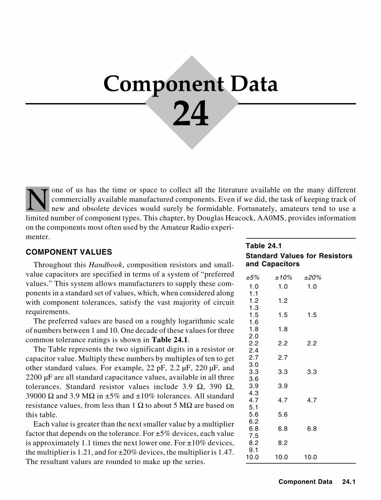
NTable 24.1Standard Values for Resistorsand Capacitors
±5% ±10% ±20%1.0 1.0 1.01.11.2 1.21.31.5 1.5 1.51.61.8 1.82.02.2 2.2 2.22.42.7 2.73.03.3 3.3 3.33.63.9 3.94.34.7 4.7 4.75.15.6 5.66.26.8 6.8 6.87.58.2 8.29.1
10.0 10.0 10.0
24.2 Chapter 24
Tolerance refers to a range of acceptable values above and below the specified component value. Forexample, a 4700-Ω resistor rated for ±20% tolerance can have an actual value anywhere between3760 Ω and 5640 Ω. You may always substitute a closer-tolerance device for one with a wider tolerance.For projects in this Handbook, assume a 10% tolerance if none is specified.
COMPONENT MARKINGS
The values, tolerances or types of most small components are typically marked with a color code oran alphanumeric code according to standards agreed upon by component manufacturers. The ElectronicIndustries Association (EIA) is a US agency that sets standards for electronic components, testingprocedures, performance and device markings. The EIA cooperates with other standards agencies suchas the International Electrotechnical Commission (IEC), a world-wide standards agency. You can oftenfind published EIA standards in the engineering library of a college or university.
The standard EIA color code is used to identify a variety of electronic components. Most resistors aremarked with color bands according to the code, shown in Table 24.2. Some types of capacitors andinductors are also marked using this color code.
Resistor Markings
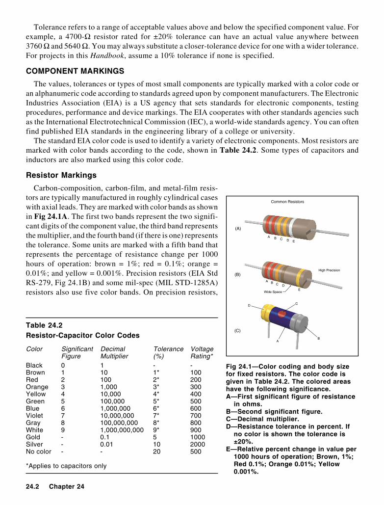
Carbon-composition, carbon-film, and metal-film resis-tors are typically manufactured in roughly cylindrical caseswith axial leads. They are marked with color bands as shownin Fig 24.1A. The first two bands represent the two signifi-cant digits of the component value, the third band representsthe multiplier, and the fourth band (if there is one) representsthe tolerance. Some units are marked with a fifth band thatrepresents the percentage of resistance change per 1000hours of operation: brown = 1%; red = 0.1%; orange =0.01%; and yellow = 0.001%. Precision resistors (EIA StdRS-279, Fig 24.1B) and some mil-spec (MIL STD-1285A)resistors also use five color bands. On precision resistors,
Table 24.2Resistor-Capacitor Color Codes
Color Significant Decimal Tolerance VoltageFigure Multiplier (%) Rating*
Black 0 1 - -Brown 1 10 1* 100Red 2 100 2* 200Orange 3 1,000 3* 300Yellow 4 10,000 4* 400Green 5 100,000 5* 500Blue 6 1,000,000 6* 600Violet 7 10,000,000 7* 700Gray 8 100,000,000 8* 800White 9 1,000,000,000 9* 900Gold - 0.1 5 1000Silver - 0.01 10 2000No color - - 20 500
*Applies to capacitors only
Fig 24.1—Color coding and body sizefor fixed resistors. The color code isgiven in Table 24.2. The colored areashave the following significance.A—First significant figure of resistance
in ohms.B—Second significant figure.C—Decimal multiplier.D—Resistance tolerance in percent. If
no color is shown the tolerance is±20%.
E—Relative percent change in value per1000 hours of operation; Brown, 1%;Red 0.1%; Orange 0.01%; Yellow0.001%.
(A)
(B)
(C)
Common Resistors
A B C D E
A
A
B
B
C
C
D
D
E
High Precision
Wide Space
Component Data 24.3
the first three bands are used for significant figures and the space between the fourth and fifth bands iswider than the others, to identify the tolerance band. On the military resistors, the fifth band indicatesreliability information such as failure rate.
For example, if a resistor of the type shown in Fig 24.1A is marked with A = red; B = red; C = orange;D = no color, the significant figures are 2 and 2, the multiplier is 1000, and the tolerance is ±20%. Thedevice is a 22,000-Ω, ±20% unit.
Some resistors are made with radial leads (Fig 24.1C) and are marked with a color code in a slightlydifferent scheme. For example, a resistor as shown in Fig 24.1C is marked as follows: A (body) = blue;B (end) = gray; C (dot) = red; D (end) = gold. The significant figures are 6 and 8, the multiplier is 100,and the tolerance is ±5%; 6800 Ω with ±5% tolerance.
Resistor Power Ratings
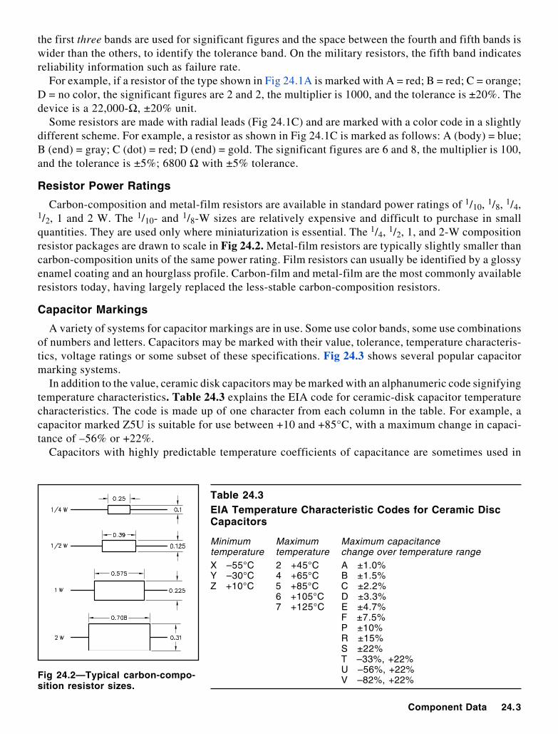
Carbon-composition and metal-film resistors are available in standard power ratings of 1/10, 1/8, 1/4,1/2, 1 and 2 W. The 1/10- and 1/8-W sizes are relatively expensive and difficult to purchase in smallquantities. They are used only where miniaturization is essential. The 1/4, 1/2, 1, and 2-W compositionresistor packages are drawn to scale in Fig 24.2. Metal-film resistors are typically slightly smaller thancarbon-composition units of the same power rating. Film resistors can usually be identified by a glossyenamel coating and an hourglass profile. Carbon-film and metal-film are the most commonly availableresistors today, having largely replaced the less-stable carbon-composition resistors.
Capacitor Markings
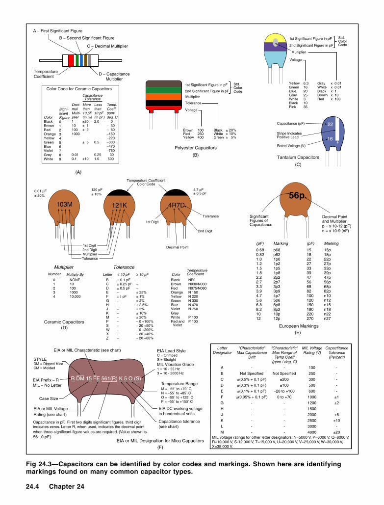
A variety of systems for capacitor markings are in use. Some use color bands, some use combinationsof numbers and letters. Capacitors may be marked with their value, tolerance, temperature characteris-tics, voltage ratings or some subset of these specifications. Fig 24.3 shows several popular capacitormarking systems.
In addition to the value, ceramic disk capacitors may be marked with an alphanumeric code signifyingtemperature characteristics. Table 24.3 explains the EIA code for ceramic-disk capacitor temperaturecharacteristics. The code is made up of one character from each column in the table. For example, acapacitor marked Z5U is suitable for use between +10 and +85°C, with a maximum change in capaci-tance of –56% or +22%.
Capacitors with highly predictable temperature coefficients of capacitance are sometimes used in
Fig 24.2—Typical carbon-compo-sition resistor sizes.
Table 24.3EIA Temperature Characteristic Codes for Ceramic DiscCapacitors
Minimum Maximum Maximum capacitancetemperature temperature change over temperature rangeX –55°C 2 +45°C A ±1.0%Y –30°C 4 +65°C B ±1.5%Z +10°C 5 +85°C C ±2.2%
6 +105°C D ±3.3%7 +125°C E ±4.7%
F ±7.5%P ±10%R ±15%S ±22%T –33%, +22%U –56%, +22%V –82%, +22%
24.4 Chapter 24
Fig 24.3—Capacitors can be identified by color codes and markings. Shown here are identifyingmarkings found on many common capacitor types.
56p
SignificantFigures ofCapacitance
Decimal Pointand Multiplierp = x 10-12 (pF)n = x 10-9 (nF)
European Markings(E)
(pF)
0.680.821.01.21.51.82.22.73.33.94.75.66.88.21012
Marking
p68p621p01p21p51p82p22p73p33p94p75p66p88p210p12p
(pF)
15182227333947566882100120150180220270
Marking
15p18p22p27p33p39p47p56p68p82pn10n12n15n18n22n27
A − First Significant Figure
B − Second Significant Figure
C − Decimal Multiplier
D − Capacitance Multiplier
TemperatureCoefficient
Ceramic Capacitors
(A)
ColorBlackBrownRedOrangeYellowGreenBlueVioletGrayWhite
0123456789
1101001000
0.010.1
±20± 1± 2
± 5
±10
2.0
0.5
0.251.0
0− 30− 80−150−220−330−470−750 30 500
CapacitanceTolerance
Color Code for Ceramic Capacitors
Temp.Coeff.ppm/deg. C
Lessthan10 pF(in pF)
Morethan10 pF(in %)
Signi-ficantFigure
Deci-malMulti-plier
1st Significant Figure in pF
2nd Significant Figure in pF
Multiplier
Tolerance
Voltage
BrownRedYellow
100250400
Std.ColorCode
BlackWhiteGreen
± 20%± 10%± 5%
Polyester Capacitors
(B)
1st Significant Figure in pF
2nd Significant Figure in pF
Multiplier
Voltage
Std.ColorCode
Tantalum Capacitors
(C)
+
22
16
Capacitance (µF)
Stripe IndicatesPositive Lead
Rated Voltage (V)
YellowGreenBlueGrayWhiteBlackPink
6.316202531035
GrayWhiteBlackBrownRed
x 0.01x 0.01x 1x 10x 100
Decimal Point
1st Digit
2nd Digit
Tolerance
121K103M 4R7D
1st Digit2nd DigitMultiplierTolerance
0.01 µF± 20%
120 pF± 10%
4.7 pF± 0.5 pF
Temperature CoefficientColor Code
MultiplierNumber Multiply By
NONE10100100010,000
01234
ToleranceLetter ≤ 10 pF ≥ 10 pF
BCDEFGHJKMPSWXZ
−−−± 25%± 1%± 2%± 2.5%± 5%± 10%± 20%− 0 +100%− 20 +50%− 0 +200%− 20 +40%− 20 +80%
± 0.1 pF± 0.25 pF± 0.5 pF−± 1 pF−−−−−−−−−−
ColorTemperatureCoefficient
BlackBrownRedOrangeYellowGreenBlueVioletGrayWhiteRed and Violet
NP0N030/N033N075/N080N 150N 220N 330N 470N 750
P 100P 100
(D)
R DM 15 FE 561(R) K 5 O (S)
CapactitanceTolerance(Percent)
-
-
-
-
-
±1
±2
-
±5
±10
-
±20
MIL VoltageRating (V)
100
250
300
500
600
1000
1200
1500
2000
2500
3000
4000
LetterDesignator
A
B
C
D
E
F
G
H
J
K
L
M
"Characteristic"Max Capacitance
Drift
-
Not Specified
±(0.5% + 0.1 pF)
±(0.3% + 0.1 pF)
±(0.1% + 0.1 pF)
±(0.05% + 0.1 pF)
-
-
-
-
-
-
"Characteristic"Max Range of
Temp Coeff(ppm / deg. C)
-
Not Specified
±200
±100
−20 to +100
0 to +70
-
-
-
-
-
-
EIA or MIL Designation for Mica Capacitors(F)
Temperature RangeM = −55˚ to +70˚ CN = −55˚ to +85˚ CO = −55˚ to +125˚ CP = −55˚ to +150˚ C
EIA Prefix − RMIL − No Letter
STYLEDM = Dipped MicaCM = Molded
Case Size
EIA or MIL Characteristic (see chart)
EIA or MIL VoltageRating (see chart)
Capacitance tolerance(see chart)
EIA DC working voltagein hundreds of volts
EIA Lead StyleC = CrimpedS = StraightMIL Vibration Grade1 = 10 - 55 Hz3 = 10 - 2000 Hz
Capacitance in pF. First two digits significant figures, third digit indicates zeros. Letter R, when used, indicates the decimal point when three-significant-figure values are required. (Value shown is 561.0 pF.) MIL voltage ratings for other letter designators: N=5000 V, P=6000 V, Q=8000 V,
R=10,000 V, S-12,000 V, T=15,000 V, U=20,000 V, V=25,000 V, W=30,000 V, X=35,000 V.
Component Data 24.5
oscillators that must be frequency stable with temperature. If anapplication called for a temperature coefficient of –750 ppm/°C(N750), a capacitor marked U2J would be suitable. The olderindustry code for these ratings is being replaced with the EIA codeshown in Table 24.4. NP0 (that is, N-P-zero) means “negative,positive, zero;” it is a characteristic often specified for RF circuitsrequiring temperature stability, such as VFOs. A capacitor of theproper value marked C0G is a suitable replacement for an NP0unit.
Some capacitors, such as dipped silver-mica units, have a letterdesignating the capacitance tolerance. These letters are decipheredin Table 24.5.
Surface-Mount Resistor and Capacitor Markings
Many different types of electronic components, both active andpassive, are now available in surface-mount packages. These arecommonly-known as chip resistors and capacitors. The very smallsize of these components leaves little space for marking withconventional codes, so brief alphanumeric codes are used to con-vey the most information in the smallest possible space.
Surface-mount resistors are typically marked with a three- orfour-digit value code and a character indicating tolerance. Thenominal resistance, expressed in ohms, is identified by three digitsfor 2% (and greater) tolerance devices. The first two digits repre-sent the significant figures; the last digit specifies the multiplieras the exponent of ten. (It may be easier to remember the multi-plier as the number of zeros you must add to the significant fig-ures.) For values less than 100 Ω, the letter R is substituted for oneof the significant digits and represents a decimal point. Here aresome examples:Resistor Code Value101 10 and 1 zero = 100 Ω224 22 and 4 zeros = 220,000 Ω1R0 1.0 and no zeros = 1 Ω22R 22.0 and no zeros = 22 ΩR10 0.1 and no zeros = 0.1 Ω
If the tolerance of the unit is narrower than ±2%, the code usedis a four-digit code where the first three digits are the significantfigures and the last is the multiplier. The letter R is used in thesame way to represent a decimal point. For example, 1001 indicates a 1000-Ω unit, and 22R0 indicatesa 22-Ω unit.
The tolerance rating for a surface-mount resistor is expressed with a single character at the end of thenumeric value code, according to Table 24.6.
Surface-mount capacitors are marked with a two-character code consisting of a letter indicating thesignificant digits (see Table 24.7) and a number indicating the multiplier (see Table 24.8). The coderepresents the capacitance in picofarads. For example, a chip capacitor marked “A4” would have acapacitance of 10,000 pF, or 0.01 µF. A unit marked “N1” would be a 33-pF capacitor. If there issufficient space on the device package, a tolerance code may be included (see Fig 24.3D for tolerance
Table 24.4EIA Capacitor Temperature-Coefficient Codes
Industry EIANP0 C0GN033 S1GN075 U1GN150 P2GN220 R2G
Industry EIAN330 S2HN470 U2JN1500 P3KN2200 R3L
Table 24.5EIA Capacitor ToleranceCodes
Code ToleranceC ±1/4 pFD ±1/2 pFF ±1 pF or ±1%G ±2 pF or ±2%J ±5%K ±10%L ±15%M ±20%N ±30%P or GMV* –0%, +100%W –20%, +40%Y –20%, +50%Z –20%, +80%
*GMV = guaranteed minimum value.
Table 24.6SMT Resistor Tolerance Codes
Letter ToleranceD ±0.5%F ±1.0%G ±2.0%J ±5.0%
24.6 Chapter 24
MIL Spec Ident(Silver)
MIL Spec Ident(Silver)
First Fig(Gray)
Second Fig(Red) Tolerance
(Silver)
Decimal(Gold)
First Fig(Orange)
Second Fig(Orange)
Tolerance(Gold)
Multiplier(Brown)Multiplier
(Brown)
8.2 µH ±10%(A)
300 µH ±5%(B)
codes). Surface-mount capacitors can be very small; you may needa magnifying glass to read the markings.
INDUCTORS AND CORE MATERIALS
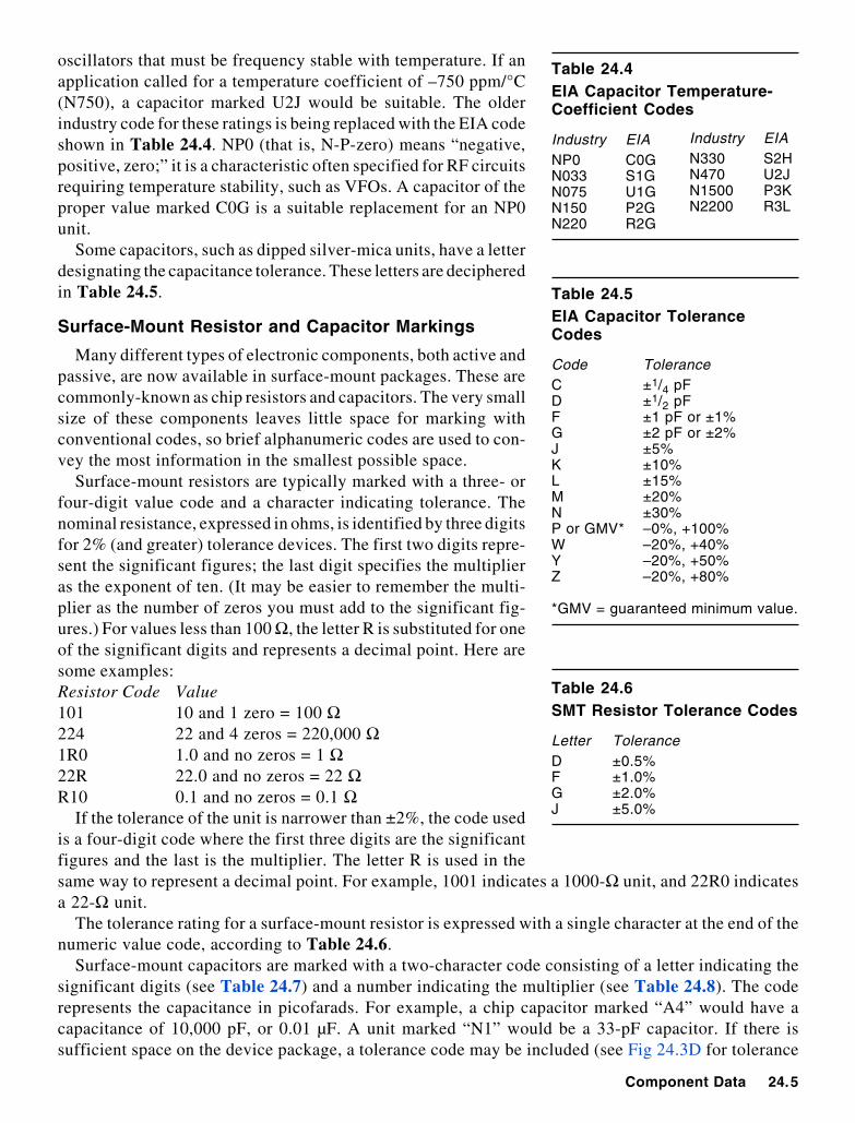
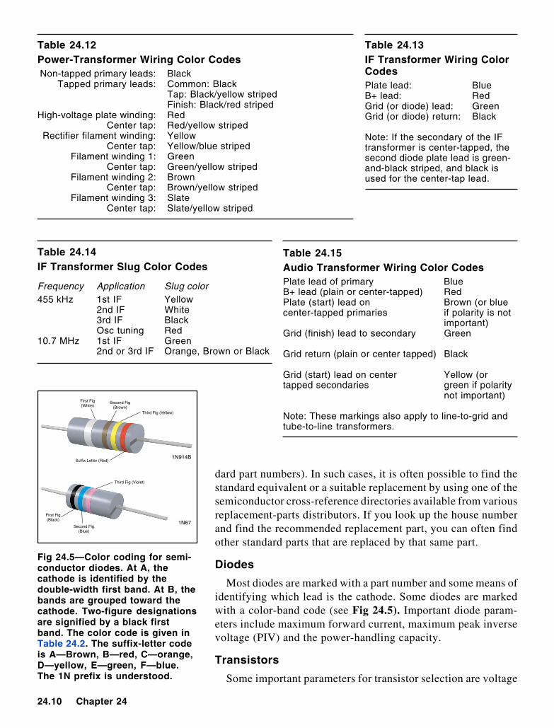
Inductors, both fixed and variable, are available in a wide varietyof types and packages, and many offer few clues as to their values.Some coils and chokes are marked with the EIA color code shown inTable 24.2. See Fig 24.4 for another marking system for tubularencapsulated RF chokes.
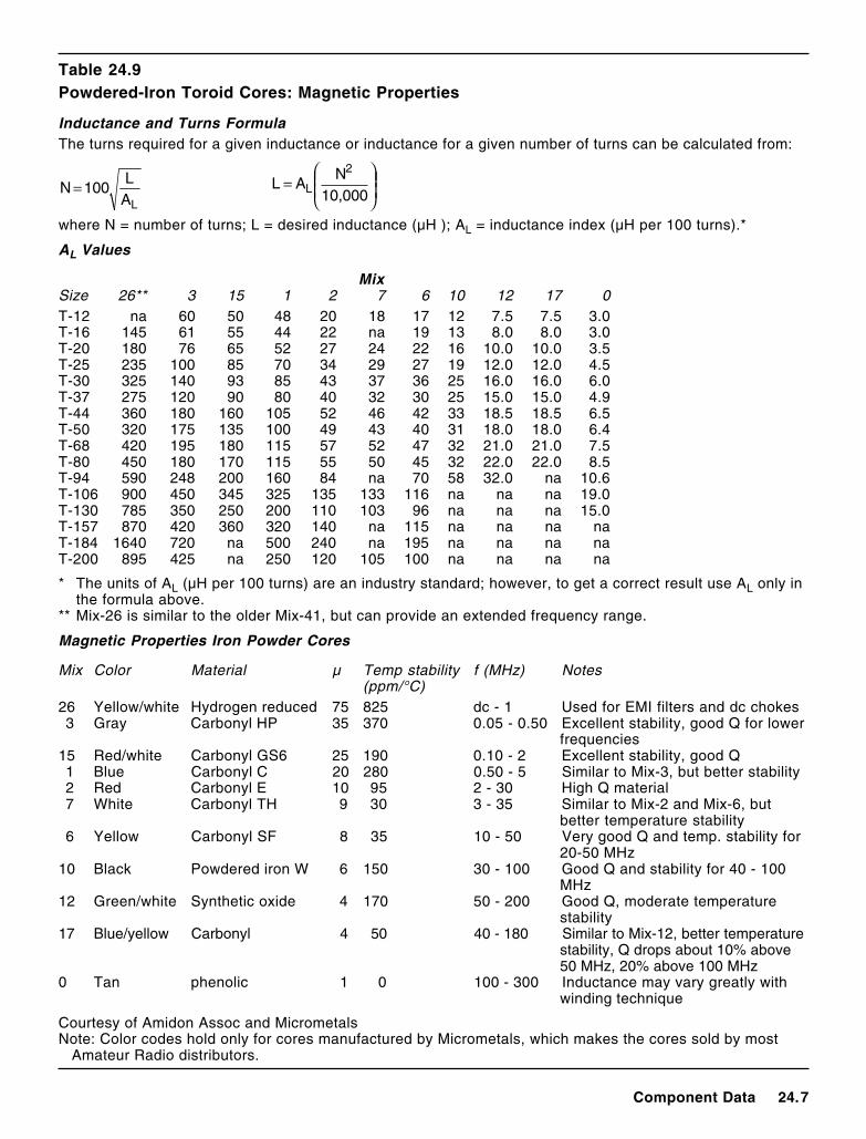
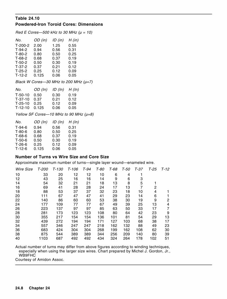
Most powdered-iron toroid cores that we amateurs use are manu-factured by Micrometals, who uses paint to identify the material usedin the core. The Micrometals color code is part of Table 24.9.Table 24.10 gives the physical characteristics of powdered-iron tor-oids. Ferrite cores are not typically painted, so identification is moredifficult. See Table 24.11 for information about ferrite cores.
TRANSFORMERS
Many transformers, including power transformers, IF transformers and audio transformers, are madeto be installed on PC boards, and have terminals designed for that purpose. Some transformers aremanufactured with wire leads that are color-coded to identify each connection. When colored wire leadsare present, the color codes in Tables 24.12, 24.13 and 24.14 usually apply.
In addition, many miniature IF transformers are tuned with slugs that are color-coded to signify theirapplication. Table 24.15 lists application vs slug color.
SEMICONDUCTORS
Most semiconductor devices are clearly marked with the part number and in some cases, amanufacturer’s date code as well. Identification of semiconductors can be difficult, however, when theparts are “house-marked” (marked with codes used by an equipment manufacturer instead of the stan-
Table 24.7SMT Capacitor Significant Figures Code
Character Significant Character SignificantFigures Figures
A 1.0 T 5.1B 1.1 U 5.6C 1.2 V 6.2D 1.3 W 6.8E 1.5 X 7.5F 1.6 Y 8.2G 1.8 Z 9.1H 2.0 a 2.5J 2.2 b 3.5K 2.4 d 4.0L 2.7 e 4.5M 3.0 f 5.0N 3.3 m 6.0P 3.6 n 7.0Q 3.9 t 8.0R 4.3 y 9.0S 4.7
Table 24.8SMT Capacitor MultiplierCodes
Numeric DecimalCharacter Multiplier0 11 102 1003 1,0004 10,0005 100,0006 1,000,0007 10,000,0008 100,000,0009 0.1
Fig 24.4—Color coding fortubular encapsulated RFchokes. At A, an example of thecoding for an 8.2-µH choke isgiven. At B, the color bands fora 330-µH inductor are illus-trated. The color code is givenin Table 24.2.
Component Data 24.7
Table 24.9Powdered-Iron Toroid Cores: Magnetic Properties
Inductance and Turns FormulaThe turns required for a given inductance or inductance for a given number of turns can be calculated from:
LAL
100N =
=
10,000N
AL2
L
where N = number of turns; L = desired inductance (µH ); AL = inductance index (µH per 100 turns).*
AL Values
MixSize 26** 3 15 1 2 7 6 10 12 17 0T-12 na 60 50 48 20 18 17 12 7.5 7.5 3.0T-16 145 61 55 44 22 na 19 13 8.0 8.0 3.0T-20 180 76 65 52 27 24 22 16 10.0 10.0 3.5T-25 235 100 85 70 34 29 27 19 12.0 12.0 4.5T-30 325 140 93 85 43 37 36 25 16.0 16.0 6.0T-37 275 120 90 80 40 32 30 25 15.0 15.0 4.9T-44 360 180 160 105 52 46 42 33 18.5 18.5 6.5T-50 320 175 135 100 49 43 40 31 18.0 18.0 6.4T-68 420 195 180 115 57 52 47 32 21.0 21.0 7.5T-80 450 180 170 115 55 50 45 32 22.0 22.0 8.5T-94 590 248 200 160 84 na 70 58 32.0 na 10.6T-106 900 450 345 325 135 133 116 na na na 19.0T-130 785 350 250 200 110 103 96 na na na 15.0T-157 870 420 360 320 140 na 115 na na na naT-184 1640 720 na 500 240 na 195 na na na naT-200 895 425 na 250 120 105 100 na na na na
* The units of AL (µH per 100 turns) are an industry standard; however, to get a correct result use AL only inthe formula above.
** Mix-26 is similar to the older Mix-41, but can provide an extended frequency range.
Magnetic Properties Iron Powder Cores
Mix Color Material µ Temp stability f (MHz) Notes(ppm/°C)
26 Yellow/white Hydrogen reduced 75 825 dc - 1 Used for EMI filters and dc chokes3 Gray Carbonyl HP 35 370 0.05 - 0.50 Excellent stability, good Q for lower
frequencies15 Red/white Carbonyl GS6 25 190 0.10 - 2 Excellent stability, good Q1 Blue Carbonyl C 20 280 0.50 - 5 Similar to Mix-3, but better stability2 Red Carbonyl E 10 95 2 - 30 High Q material7 White Carbonyl TH 9 30 3 - 35 Similar to Mix-2 and Mix-6, but
better temperature stability6 Yellow Carbonyl SF 8 35 10 - 50 Very good Q and temp. stability for
20-50 MHz10 Black Powdered iron W 6 150 30 - 100 Good Q and stability for 40 - 100
MHz12 Green/white Synthetic oxide 4 170 50 - 200 Good Q, moderate temperature
stability17 Blue/yellow Carbonyl 4 50 40 - 180 Similar to Mix-12, better temperature
stability, Q drops about 10% above50 MHz, 20% above 100 MHz
0 Tan phenolic 1 0 100 - 300 Inductance may vary greatly withwinding technique
Courtesy of Amidon Assoc and MicrometalsNote: Color codes hold only for cores manufactured by Micrometals, which makes the cores sold by most
Amateur Radio distributors.
24.8 Chapter 24
Table 24.10Powdered-Iron Toroid Cores: Dimensions
Red E Cores—500 kHz to 30 MHz (µ = 10)
No. OD (in) ID (in) H (in)T-200-2 2.00 1.25 0.55T-94-2 0.94 0.56 0.31T-80-2 0.80 0.50 0.25T-68-2 0.68 0.37 0.19T-50-2 0.50 0.30 0.19T-37-2 0.37 0.21 0.12T-25-2 0.25 0.12 0.09T-12-2 0.125 0.06 0.05
Black W Cores—30 MHz to 200 MHz (µ=7)
No. OD (In) ID (In) H (In)T-50-10 0.50 0.30 0.19T-37-10 0.37 0.21 0.12T-25-10 0.25 0.12 0.09T-12-10 0.125 0.06 0.05
Yellow SF Cores—10 MHz to 90 MHz (µ=8)
No. OD (In) ID (In) H (In)T-94-6 0.94 0.56 0.31T-80-6 0.80 0.50 0.25T-68-6 0.68 0.37 0.19T-50-6 0.50 0.30 0.19T-26-6 0.25 0.12 0.09T-12-6 0.125 0.06 0.05
Number of Turns vs Wire Size and Core SizeApproximate maximum number of turns—single layer wound—enameled wire.
Wire Size T-200 T-130 T-106 T-94 T-80 T-68 T-50 T-37 T-25 T-1210 33 20 12 12 10 6 4 112 43 25 16 16 14 9 6 314 54 32 21 21 18 13 8 5 116 69 41 28 28 24 17 13 7 218 88 53 37 37 32 23 18 10 4 120 111 67 47 47 41 29 23 14 6 122 140 86 60 60 53 38 30 19 9 224 177 109 77 77 67 49 39 25 13 426 223 137 97 97 85 63 50 33 17 728 281 173 123 123 108 80 64 42 23 930 355 217 154 154 136 101 81 54 29 1332 439 272 194 194 171 127 103 68 38 1734 557 346 247 247 218 162 132 88 49 2336 683 424 304 304 268 199 162 108 62 3038 875 544 389 389 344 256 209 140 80 3940 1103 687 492 492 434 324 264 178 102 51
Actual number of turns may differ from above figures according to winding techniques,especially when using the larger size wires. Chart prepared by Michel J. Gordon, Jr.,WB9FHC
Courtesy of Amidon Assoc.
Component Data 24.9
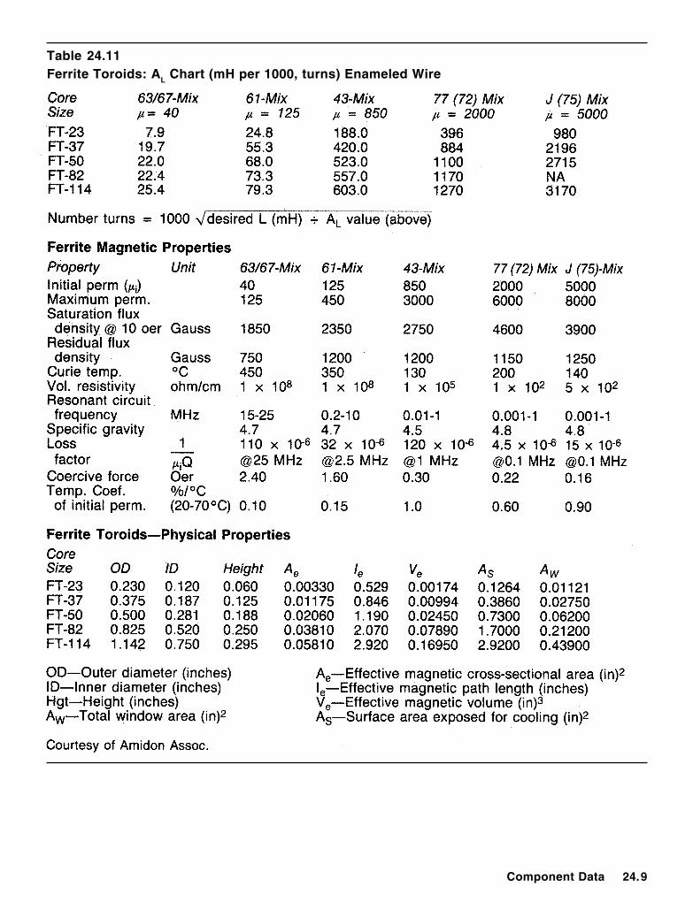
Table 24.11Ferrite Toroids: AL Chart (mH per 1000, turns) Enameled Wire
24.10 Chapter 24
1N914B
1N67
First Fig(White)
First Fig(Black)
Second Fig(Brown)
Second Fig(Blue)
Third Fig (Yellow)
Third Fig (Violet)
Suffix Letter (Red)
Table 24.12Power-Transformer Wiring Color CodesNon-tapped primary leads: Black
Tapped primary leads: Common: BlackTap: Black/yellow stripedFinish: Black/red striped
High-voltage plate winding: RedCenter tap: Red/yellow striped
Rectifier filament winding: YellowCenter tap: Yellow/blue striped
Filament winding 1: GreenCenter tap: Green/yellow striped
Filament winding 2: BrownCenter tap: Brown/yellow striped
Filament winding 3: SlateCenter tap: Slate/yellow striped
Table 24.13IF Transformer Wiring ColorCodesPlate lead: BlueB+ lead: RedGrid (or diode) lead: GreenGrid (or diode) return: Black
Note: If the secondary of the IFtransformer is center-tapped, thesecond diode plate lead is green-and-black striped, and black isused for the center-tap lead.
Table 24.14IF Transformer Slug Color Codes
Frequency Application Slug color455 kHz 1st IF Yellow
2nd IF White3rd IF BlackOsc tuning Red
10.7 MHz 1st IF Green2nd or 3rd IF Orange, Brown or Black
Table 24.15Audio Transformer Wiring Color CodesPlate lead of primary BlueB+ lead (plain or center-tapped) RedPlate (start) lead on Brown (or bluecenter-tapped primaries if polarity is not
important)Grid (finish) lead to secondary Green
Grid return (plain or center tapped) Black
Grid (start) lead on center Yellow (ortapped secondaries green if polarity
not important)
Note: These markings also apply to line-to-grid andtube-to-line transformers.
dard part numbers). In such cases, it is often possible to find thestandard equivalent or a suitable replacement by using one of thesemiconductor cross-reference directories available from variousreplacement-parts distributors. If you look up the house numberand find the recommended replacement part, you can often findother standard parts that are replaced by that same part.
Diodes
Most diodes are marked with a part number and some means ofidentifying which lead is the cathode. Some diodes are markedwith a color-band code (see Fig 24.5). Important diode param-eters include maximum forward current, maximum peak inversevoltage (PIV) and the power-handling capacity.
Transistors
Some important parameters for transistor selection are voltage
Fig 24.5—Color coding for semi-conductor diodes. At A, thecathode is identified by thedouble-width first band. At B, thebands are grouped toward thecathode. Two-figure designationsare signified by a black firstband. The color code is given inTable 24.2. The suffix-letter codeis A—Brown, B—red, C—orange,D—yellow, E—green, F—blue.The 1N prefix is understood.
Component Data 24.11
and current limits, power-handling capability, beta or gain characteristics and useful frequency range.The case style may also be an issue; some transistors are available in several different case styles.
Integrated Circuits
Integrated circuits (ICs) come in a variety of packages, including transistor-like metal cans, dual andsingle in-line packages (DIPs and SIPs), flat-packs and surface-mount packages. Most are marked witha part number and a four-digit manufacturer’s date code indicating the year (first two digits) and week(last two digits) that the component was made. ICs are frequently house-marked, and the cross-referencedirectories mentioned above can be helpful in identification and replacement.
Another very useful reference tool for working with ICs is IC Master, a master selection guide thatorganizes ICs by type, function and certain key parameters. A part number index is included, along withapplication notes and manufacturer’s information for tens of thousands of IC devices. Some of the datafrom IC Master is also available on computer disks.
IC part numbers usually contain a few digits that identify the circuit die or function and several otherletters and/or digits that identify the production process, manufacturer and package. For example, a’4066 IC contains four independent SPST switches. Harris (CD74HC4066, CD4066B and CD4066BE),National (MM74HC4066, CD4066BC and CD4066BM) and Panasonic (MN74HC4066 and MN4066B)all make similar devices (as do many other manufacturers) with slight differences. Among the numberslisted, “CD” (CMOS Digital), “MM” (MOS Monolithic), and “MN” indicate CMOS parts. “74” indicatesa commercial quality product (for applications from 0°C to 70°C), which is pin compatible with the 74/54 TTL families. “HC” means high-speed CMOS family, which is as fast as the LS TTL family. The “B”suffix, as is CD4066B, indicates a buffered output. This is only a small example of the conventions usedin IC part numbers. For more information look at data books from the various manufacturers. Basediagrams for many common ICs appear in The ARRL Electronics Data Book.
When choosing ICs that are not exact replacements, several operating needs and performance aspectsshould be considered. First, the replacement power requirements must be met: Some ICs require 5 V dc,others 12 V and some need both positive and negative supplies. Current requirements vary among thevarious IC families, so be sure that sufficient current is available from the power supply. If a replacementIC uses much more current than the device it replaces, a heat sink or blower may be needed to keep it cool.
Next consider how the replacement interacts with its neighboring components. Input capacitance and“fanout” are critical factors in digital circuits. Increased input capacitance may overload the drivingcircuits. Overload slows circuit operation, which may prevent lines from reaching the “high” condition.Fanout tells how many inputs a device can drive. The fanout of a replacement should be equal to, orgreater than, that required in the circuit. Operating speed and propagation delay are also significant.Choose a replacement IC that operates at or above the circuit clock speed. (Although increased speedcan increase EMI and cause other problems.) Some circuits may not function if the propagation delayvaries much from the specified part. Look at the Digital chapter for details of how these operatingcharacteristics relate to circuit performance.
Analog ICs have similar characteristics. Input and output capacities are often defined as how muchcurrent an analog IC can “sink” (accept at an input) or “source” (pass to a load). A replacement shouldbe able to source or sink at least as much current as the device it replaces. Analog speed is sometimeslisted as bandwidth (as in discrete-component circuits) or slew rate (common in op amps). Each of thesequantities should meet or exceed that of the replaced component.
Some ICs are available in different operating temperature ranges. Op amps, for example, are com-monly available in three standard ranges:• Commercial 0°C to 70°C• Industrial –25°C to 85°C• Military –55°C to 125°C
24.12 Chapter 24
In some cases, part numbers reflect the temperature ratings. For example, an LM301A op amp is ratedfor the commercial temperature range; an LM201A op amp for the industrial range and an LM101A forthe military range.
When necessary, you can add interface circuits or buffer amplifiers that improve the input and outputcapabilities of replacement ICs, but auxiliary circuits cannot improve basic device ratings, such as speedor bandwidth.
An excellent source of information on many common ICs is The ARRL Electronics Data Book, whichcontains detailed data for digital ICs (CMOS and TTL), op amps and other analog ICs.
OTHER SOURCES OF COMPONENT DATA
There are many sources you can consult for detailed component data. Many manufacturers publishdata books for the components they make. Many distributors will include data sheets for parts you orderif you ask for them. Parts catalogs themselves are often good sources of component data. The followinglist is representative of some of the data resources available from manufacturers and distributors.Motorola Small-Signal Transistor DataMotorola RF Device DataMotorola Linear and Interface ICsSignetics: General Purpose/Linear ICsNTE Technical Manual and Cross ReferenceTCE SK Replacement Technical Manual and Cross ReferenceNational Semiconductor:
Discrete Semiconductor Products DatabookCMOS Logic DatabookLinear Applications HandbookLinear Application-Specific ICs DatabookOperational Amplifiers Databook
Component Data 24.13
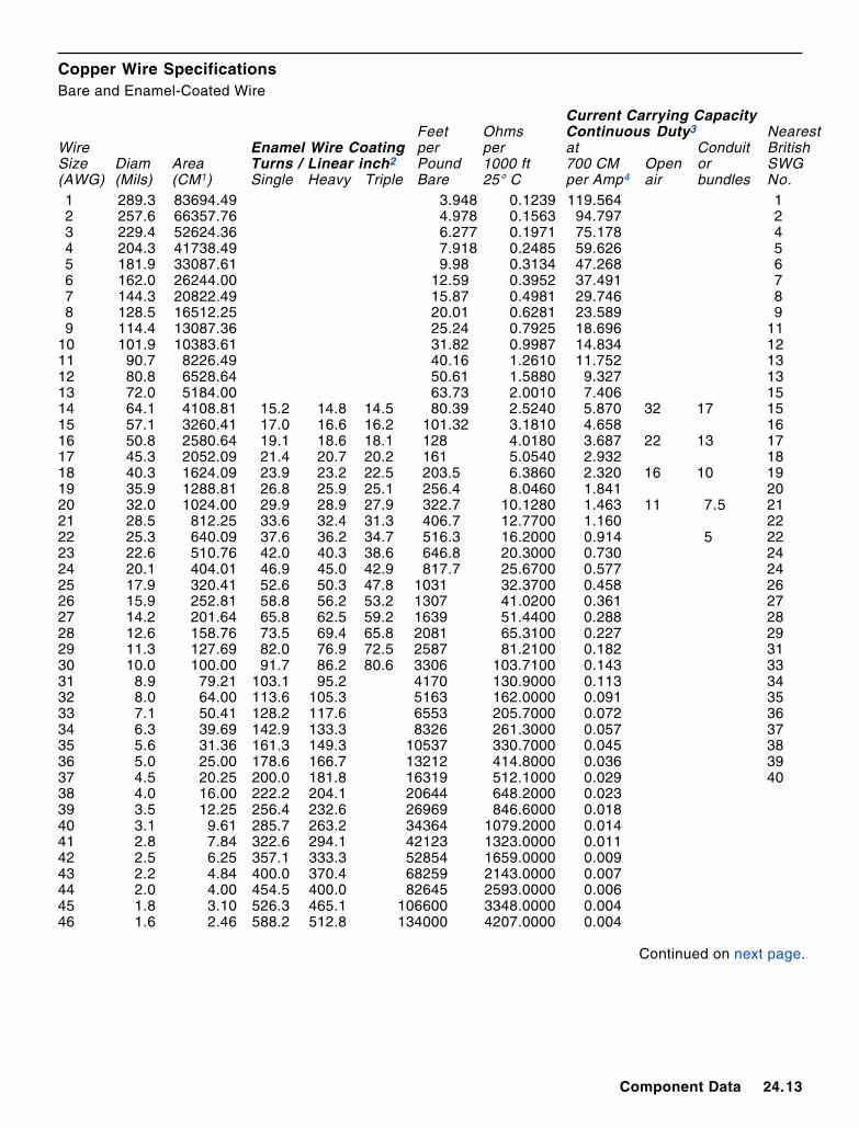
Copper Wire SpecificationsBare and Enamel-Coated Wire
Current Carrying CapacityFeet Ohms Continuous Duty3 Nearest
Wire Enamel Wire Coating per per at Conduit BritishSize Diam Area Turns / Linear inch2 Pound 1000 ft 700 CM Open or SWG(AWG) (Mils) (CM1) Single Heavy Triple Bare 25° C per Amp4 air bundles No.1 289.3 83694.49 3.948 0.1239 119.564 12 257.6 66357.76 4.978 0.1563 94.797 23 229.4 52624.36 6.277 0.1971 75.178 44 204.3 41738.49 7.918 0.2485 59.626 55 181.9 33087.61 9.98 0.3134 47.268 66 162.0 26244.00 12.59 0.3952 37.491 77 144.3 20822.49 15.87 0.4981 29.746 88 128.5 16512.25 20.01 0.6281 23.589 99 114.4 13087.36 25.24 0.7925 18.696 11
10 101.9 10383.61 31.82 0.9987 14.834 1211 90.7 8226.49 40.16 1.2610 11.752 1312 80.8 6528.64 50.61 1.5880 9.327 1313 72.0 5184.00 63.73 2.0010 7.406 1514 64.1 4108.81 15.2 14.8 14.5 80.39 2.5240 5.870 32 17 1515 57.1 3260.41 17.0 16.6 16.2 101.32 3.1810 4.658 1616 50.8 2580.64 19.1 18.6 18.1 128 4.0180 3.687 22 13 1717 45.3 2052.09 21.4 20.7 20.2 161 5.0540 2.932 1818 40.3 1624.09 23.9 23.2 22.5 203.5 6.3860 2.320 16 10 1919 35.9 1288.81 26.8 25.9 25.1 256.4 8.0460 1.841 2020 32.0 1024.00 29.9 28.9 27.9 322.7 10.1280 1.463 11 7.5 2121 28.5 812.25 33.6 32.4 31.3 406.7 12.7700 1.160 2222 25.3 640.09 37.6 36.2 34.7 516.3 16.2000 0.914 5 2223 22.6 510.76 42.0 40.3 38.6 646.8 20.3000 0.730 2424 20.1 404.01 46.9 45.0 42.9 817.7 25.6700 0.577 2425 17.9 320.41 52.6 50.3 47.8 1031 32.3700 0.458 2626 15.9 252.81 58.8 56.2 53.2 1307 41.0200 0.361 2727 14.2 201.64 65.8 62.5 59.2 1639 51.4400 0.288 2828 12.6 158.76 73.5 69.4 65.8 2081 65.3100 0.227 2929 11.3 127.69 82.0 76.9 72.5 2587 81.2100 0.182 3130 10.0 100.00 91.7 86.2 80.6 3306 103.7100 0.143 3331 8.9 79.21 103.1 95.2 4170 130.9000 0.113 3432 8.0 64.00 113.6 105.3 5163 162.0000 0.091 3533 7.1 50.41 128.2 117.6 6553 205.7000 0.072 3634 6.3 39.69 142.9 133.3 8326 261.3000 0.057 3735 5.6 31.36 161.3 149.3 10537 330.7000 0.045 3836 5.0 25.00 178.6 166.7 13212 414.8000 0.036 3937 4.5 20.25 200.0 181.8 16319 512.1000 0.029 4038 4.0 16.00 222.2 204.1 20644 648.2000 0.02339 3.5 12.25 256.4 232.6 26969 846.6000 0.01840 3.1 9.61 285.7 263.2 34364 1079.2000 0.01441 2.8 7.84 322.6 294.1 42123 1323.0000 0.01142 2.5 6.25 357.1 333.3 52854 1659.0000 0.00943 2.2 4.84 400.0 370.4 68259 2143.0000 0.00744 2.0 4.00 454.5 400.0 82645 2593.0000 0.00645 1.8 3.10 526.3 465.1 106600 3348.0000 0.00446 1.6 2.46 588.2 512.8 134000 4207.0000 0.004
Continued on next page.
24.14 Chapter 24
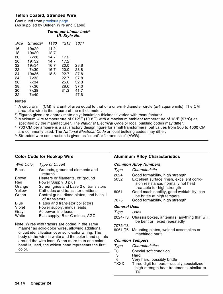
Teflon Coated, Stranded WireContinued from previous page.(As supplied by Belden Wire and Cable)
Turns per Linear inch2
UL Style No.
Size Strands5 1180 1213 137116 19×29 11.218 19×30 12.720 7×28 14.7 17.220 19×32 14.7 17.222 19×34 16.7 20.0 23.822 7×30 16.7 20.0 23.824 19×36 18.5 22.7 27.824 7×32 22.7 27.826 7×34 25.6 32.328 7×36 28.6 37.030 7×38 31.3 41.732 7×40 47.6
Notes1 A circular mil (CM) is a unit of area equal to that of a one-mil-diameter circle (π/4 square mils). The CM
area of a wire is the square of the mil diameter.2 Figures given are approximate only; insulation thickness varies with manufacturer.3 Maximum wire temperature of 212°F (100°C) with a maximum ambient temperature of 13°F (57°C) as
specified by the manufacturer. The National Electrical Code or local building codes may differ.4 700 CM per ampere is a satisfactory design figure for small transformers, but values from 500 to 1000 CM
are commonly used. The National Electrical Code or local building codes may differ.5 Stranded wire construction is given as “count” × “strand size” (AWG).
Color Code for Hookup Wire
Wire Color Type of CircuitBlack Grounds, grounded elements and
returnsBrown Heaters or filaments, off groundRed Power Supply B plusOrange Screen grids and base 2 of transistorsYellow Cathodes and transistor emittersGreen Control grids, diode plates, and base 1
of transistorsBlue Plates and transistor collectorsViolet Power supply, minus leadsGray Ac power line leadsWhite Bias supply, B or C minus, AGC
Note: Wires with tracers are coded in the samemanner as solid-color wires, allowing additionalcircuit identification over solid-color wiring. Thebody of the wire is white and the color band spiralsaround the wire lead. When more than one colorband is used, the widest band represents the firstcolor.
Aluminum Alloy Characteristics
Common Alloy NumbersType Characteristic2024 Good formability, high strength5052 Excellent surface finish, excellent corro-
sion resistance, normally not heattreatable for high strength
6061 Good machinability, good weldability, canbe brittle at high tempers
7075 Good formability, high strength
General UsesType Uses2024-T3 Chassis boxes, antennas, anything that will
be bent or flexed repeatedly7075-T36061-T6 Mounting plates, welded assemblies or
machined parts
Common TempersType CharacteristicsT0 Special soft conditionT3 HardT6 Very hard, possibly brittleTXXX Three digit tempers—usually specialized
high-strength heat treatments, similar toT6
Component Data 24.15
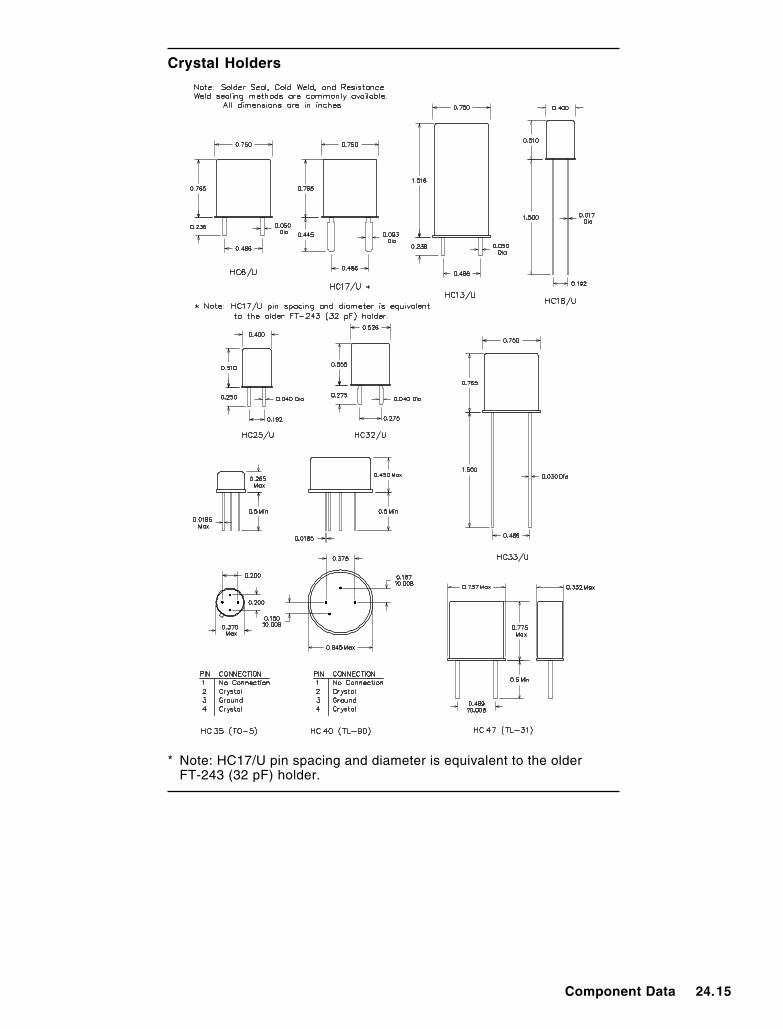
Crystal Holders
* Note: HC17/U pin spacing and diameter is equivalent to the olderFT-243 (32 pF) holder.
24.16 Chapter 24
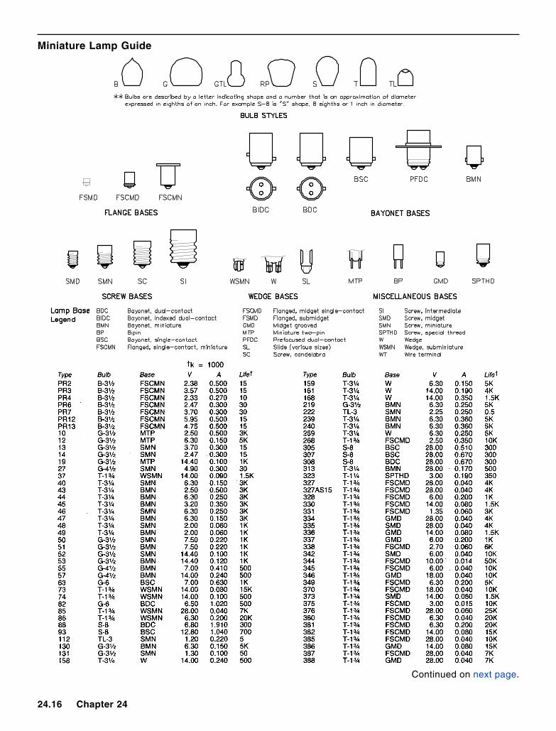
Miniature Lamp Guide
Continued on next page.
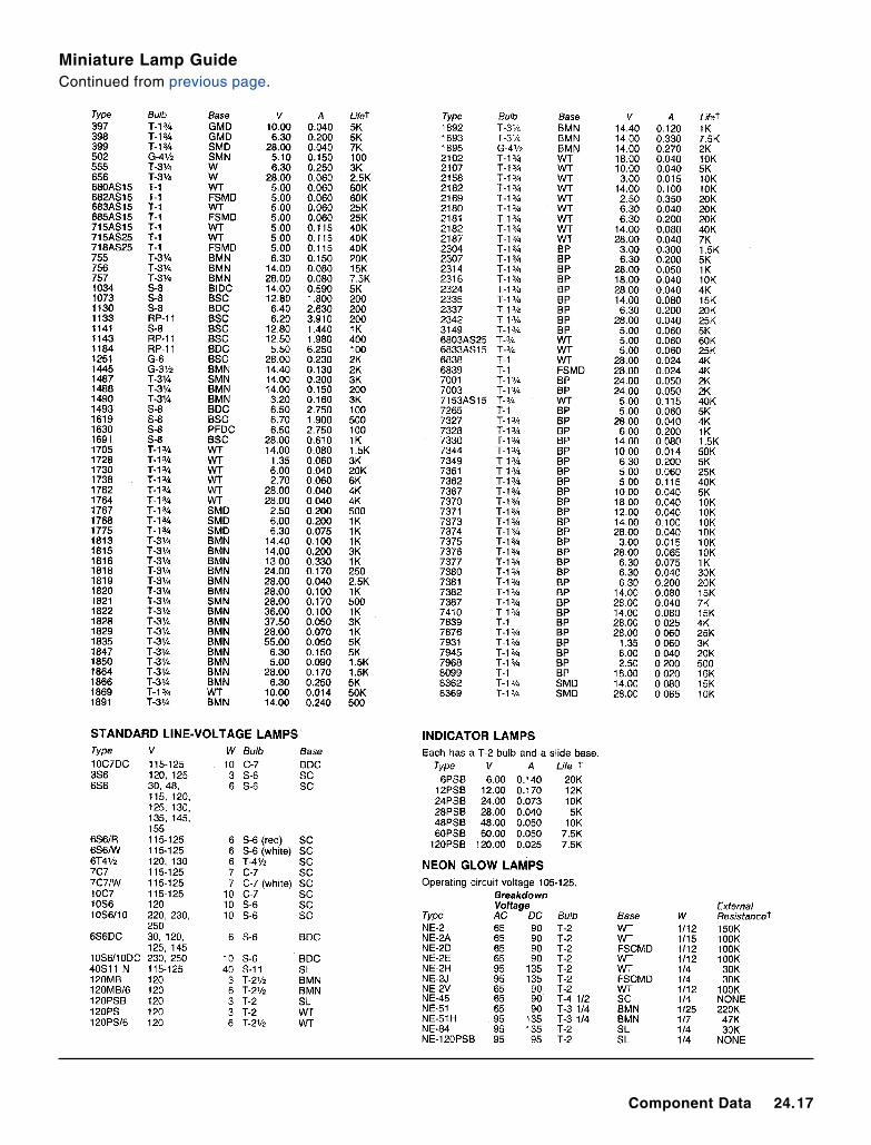
Component Data 24.17
Miniature Lamp GuideContinued from previous page.
24.18 Chapter 24
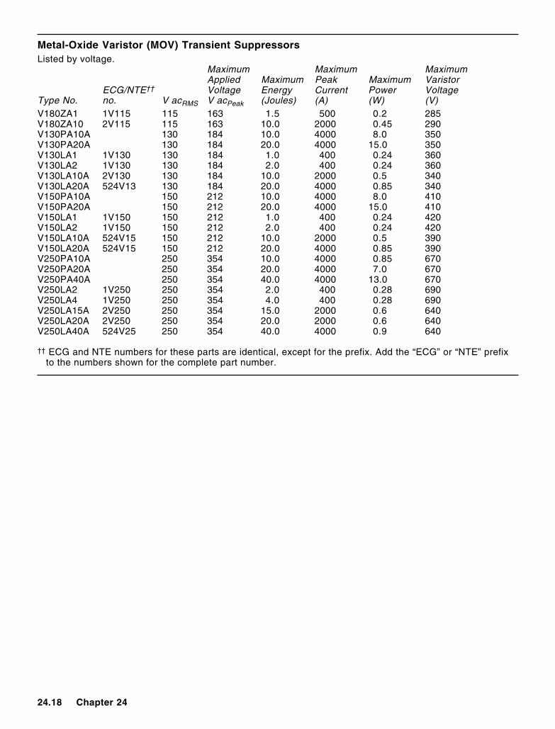
Metal-Oxide Varistor (MOV) Transient SuppressorsListed by voltage.
Maximum Maximum MaximumApplied Maximum Peak Maximum Varistor
ECG/NTE†† Voltage Energy Current Power VoltageType No. no. V acRMS V acPeak (Joules) (A) (W) (V)V180ZA1 1V115 115 163 1.5 500 0.2 285V180ZA10 2V115 115 163 10.0 2000 0.45 290V130PA10A 130 184 10.0 4000 8.0 350V130PA20A 130 184 20.0 4000 15.0 350V130LA1 1V130 130 184 1.0 400 0.24 360V130LA2 1V130 130 184 2.0 400 0.24 360V130LA10A 2V130 130 184 10.0 2000 0.5 340V130LA20A 524V13 130 184 20.0 4000 0.85 340V150PA10A 150 212 10.0 4000 8.0 410V150PA20A 150 212 20.0 4000 15.0 410V150LA1 1V150 150 212 1.0 400 0.24 420V150LA2 1V150 150 212 2.0 400 0.24 420V150LA10A 524V15 150 212 10.0 2000 0.5 390V150LA20A 524V15 150 212 20.0 4000 0.85 390V250PA10A 250 354 10.0 4000 0.85 670V250PA20A 250 354 20.0 4000 7.0 670V250PA40A 250 354 40.0 4000 13.0 670V250LA2 1V250 250 354 2.0 400 0.28 690V250LA4 1V250 250 354 4.0 400 0.28 690V250LA15A 2V250 250 354 15.0 2000 0.6 640V250LA20A 2V250 250 354 20.0 2000 0.6 640V250LA40A 524V25 250 354 40.0 4000 0.9 640
†† ECG and NTE numbers for these parts are identical, except for the prefix. Add the “ECG” or “NTE” prefixto the numbers shown for the complete part number.
Component Data 24.19
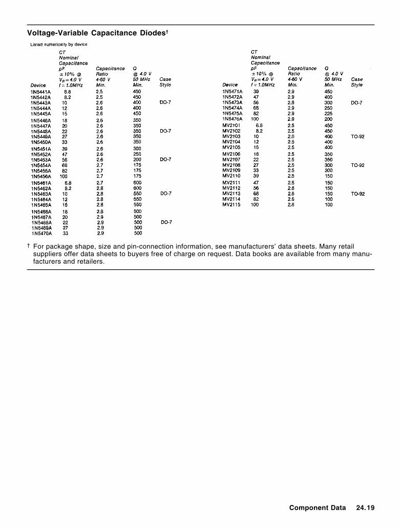
Voltage-Variable Capacitance Diodes†
† For package shape, size and pin-connection information, see manufacturers’ data sheets. Many retailsuppliers offer data sheets to buyers free of charge on request. Data books are available from many manu-facturers and retailers.
24.20 Chapter 24
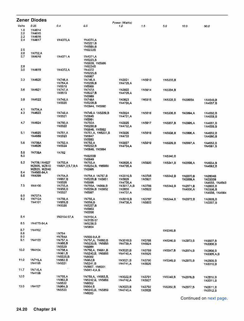
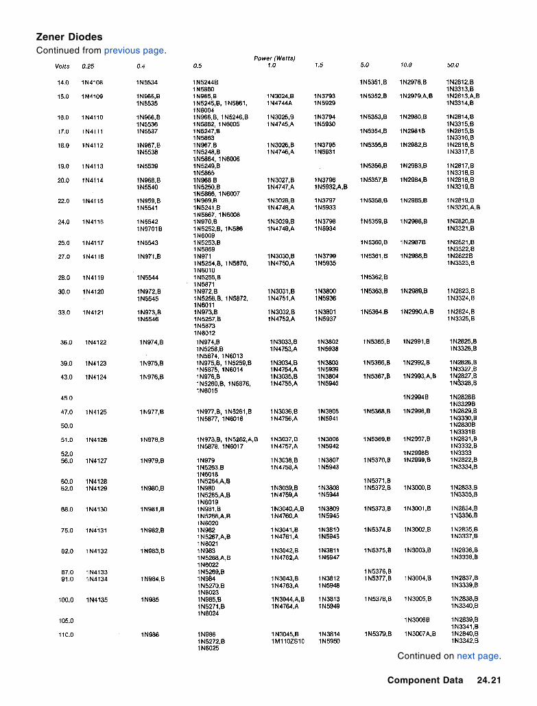
Zener Diodes
Continued on next page.
Component Data 24.21
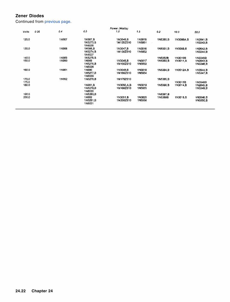
Zener DiodesContinued from previous page.
Continued on next page.
24.22 Chapter 24
Zener DiodesContinued from previous page.
Component Data 24.23
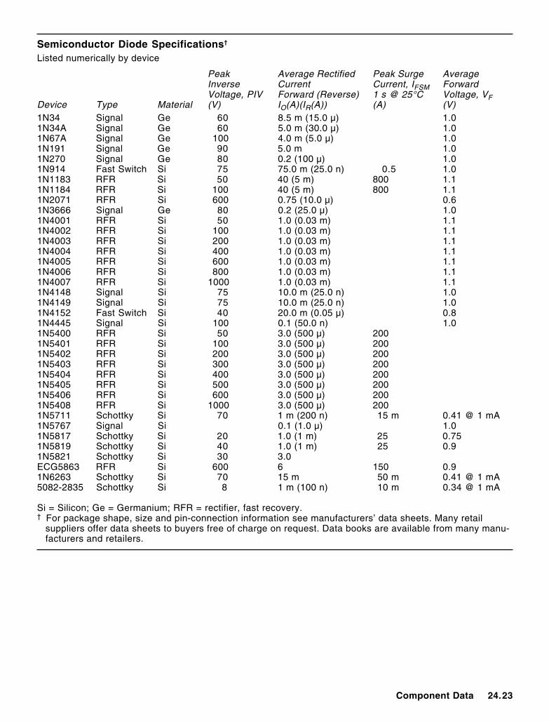
Semiconductor Diode Specifications†
Listed numerically by device
Peak Average Rectified Peak Surge AverageInverse Current Current, IFSM ForwardVoltage, PIV Forward (Reverse) 1 s @ 25°C Voltage, VF
Device Type Material (V) IO(A)(IR(A)) (A) (V)1N34 Signal Ge 60 8.5 m (15.0 µ) 1.01N34A Signal Ge 60 5.0 m (30.0 µ) 1.01N67A Signal Ge 100 4.0 m (5.0 µ) 1.01N191 Signal Ge 90 5.0 m 1.01N270 Signal Ge 80 0.2 (100 µ) 1.01N914 Fast Switch Si 75 75.0 m (25.0 n) 0.5 1.01N1183 RFR Si 50 40 (5 m) 800 1.11N1184 RFR Si 100 40 (5 m) 800 1.11N2071 RFR Si 600 0.75 (10.0 µ) 0.61N3666 Signal Ge 80 0.2 (25.0 µ) 1.01N4001 RFR Si 50 1.0 (0.03 m) 1.11N4002 RFR Si 100 1.0 (0.03 m) 1.11N4003 RFR Si 200 1.0 (0.03 m) 1.11N4004 RFR Si 400 1.0 (0.03 m) 1.11N4005 RFR Si 600 1.0 (0.03 m) 1.11N4006 RFR Si 800 1.0 (0.03 m) 1.11N4007 RFR Si 1000 1.0 (0.03 m) 1.11N4148 Signal Si 75 10.0 m (25.0 n) 1.01N4149 Signal Si 75 10.0 m (25.0 n) 1.01N4152 Fast Switch Si 40 20.0 m (0.05 µ) 0.81N4445 Signal Si 100 0.1 (50.0 n) 1.01N5400 RFR Si 50 3.0 (500 µ) 2001N5401 RFR Si 100 3.0 (500 µ) 2001N5402 RFR Si 200 3.0 (500 µ) 2001N5403 RFR Si 300 3.0 (500 µ) 2001N5404 RFR Si 400 3.0 (500 µ) 2001N5405 RFR Si 500 3.0 (500 µ) 2001N5406 RFR Si 600 3.0 (500 µ) 2001N5408 RFR Si 1000 3.0 (500 µ) 2001N5711 Schottky Si 70 1 m (200 n) 15 m 0.41 @ 1 mA1N5767 Signal Si 0.1 (1.0 µ) 1.01N5817 Schottky Si 20 1.0 (1 m) 25 0.751N5819 Schottky Si 40 1.0 (1 m) 25 0.91N5821 Schottky Si 30 3.0ECG5863 RFR Si 600 6 150 0.91N6263 Schottky Si 70 15 m 50 m 0.41 @ 1 mA5082-2835 Schottky Si 8 1 m (100 n) 10 m 0.34 @ 1 mA
Si = Silicon; Ge = Germanium; RFR = rectifier, fast recovery.† For package shape, size and pin-connection information see manufacturers’ data sheets. Many retail
suppliers offer data sheets to buyers free of charge on request. Data books are available from many manu-facturers and retailers.
24.24 Chapter 24
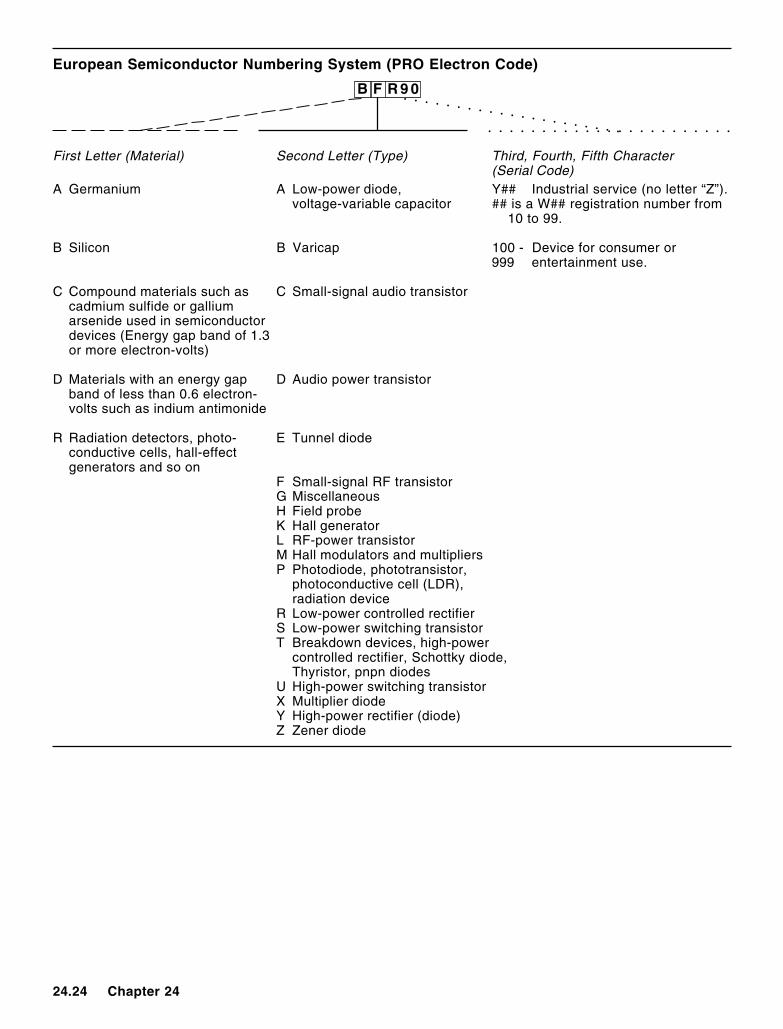
European Semiconductor Numbering System (PRO Electron Code)
B F R 9 0
First Letter (Material) Second Letter (Type) Third, Fourth, Fifth Character(Serial Code)
A Germanium A Low-power diode, Y## Industrial service (no letter “Z”).voltage-variable capacitor ## is a W## registration number from
10 to 99.
B Silicon B Varicap 100 - Device for consumer or999 entertainment use.
C Compound materials such as C Small-signal audio transistorcadmium sulfide or galliumarsenide used in semiconductordevices (Energy gap band of 1.3or more electron-volts)
D Materials with an energy gap D Audio power transistorband of less than 0.6 electron-volts such as indium antimonide
R Radiation detectors, photo- E Tunnel diodeconductive cells, hall-effectgenerators and so on
F Small-signal RF transistorG MiscellaneousH Field probeK Hall generatorL RF-power transistorM Hall modulators and multipliersP Photodiode, phototransistor,
photoconductive cell (LDR),radiation device
R Low-power controlled rectifierS Low-power switching transistorT Breakdown devices, high-power
controlled rectifier, Schottky diode,Thyristor, pnpn diodes
U High-power switching transistorX Multiplier diodeY High-power rectifier (diode)Z Zener diode
Component Data 24.25
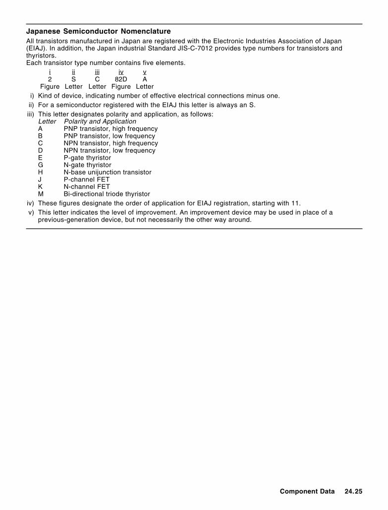
Japanese Semiconductor NomenclatureAll transistors manufactured in Japan are registered with the Electronic Industries Association of Japan(EIAJ). In addition, the Japan industrial Standard JIS-C-7012 provides type numbers for transistors andthyristors.Each transistor type number contains five elements.
i ii iii iv v2 S C 82D A
Figure Letter Letter Figure Letteri) Kind of device, indicating number of effective electrical connections minus one.ii) For a semiconductor registered with the EIAJ this letter is always an S.iii) This letter designates polarity and application, as follows:
Letter Polarity and ApplicationA PNP transistor, high frequencyB PNP transistor, low frequencyC NPN transistor, high frequencyD NPN transistor, low frequencyE P-gate thyristorG N-gate thyristorH N-base unijunction transistorJ P-channel FETK N-channel FETM Bi-directional triode thyristor
iv) These figures designate the order of application for EIAJ registration, starting with 11.v) This letter indicates the level of improvement. An improvement device may be used in place of a
previous-generation device, but not necessarily the other way around.
24.26 Chapter 24
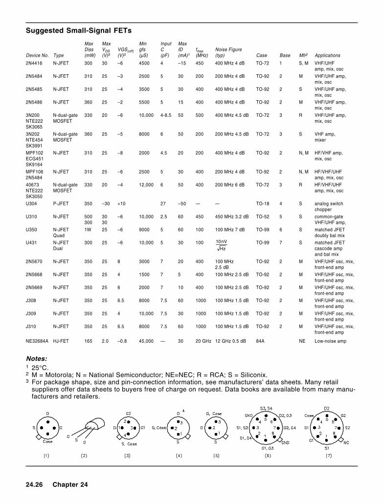
Suggested Small-Signal FETs
Max Max Min Input MaxDiss VDS VGS(off) gfs C ID fmax Noise Figure
Device No. Type (mW) (V)3 (V)3 (µS) (pF) (mA)1 (MHz) (typ) Case Base Mfr2 Applications
2N4416 N-JFET 300 30 –6 4500 4 –15 450 400 MHz 4 dB TO-72 1 S, M VHF/UHFamp, mix, osc
2N5484 N-JFET 310 25 –3 2500 5 30 200 200 MHz 4 dB TO-92 2 M VHF/UHF amp,mix, osc
2N5485 N-JFET 310 25 –4 3500 5 30 400 400 MHz 4 dB TO-92 2 S VHF/UHF amp,mix, osc
2N5486 N-JFET 360 25 –2 5500 5 15 400 400 MHz 4 dB TO-92 2 M VHF/UHF amp,mix, osc
3N200 N-dual-gate 330 20 –6 10,000 4-8.5 50 500 400 MHz 4.5 dB TO-72 3 R VHF/UHF amp,NTE222 MOSFET mix, oscSK3065
3N202 N-dual-gate 360 25 –5 8000 6 50 200 200 MHz 4.5 dB TO-72 3 S VHF amp,NTE454 MOSFET mixerSK3991
MPF102 N-JFET 310 25 –8 2000 4.5 20 200 400 MHz 4 dB TO-92 2 N, M HF/VHF amp,ECG451 mix, oscSK9164
MPF106 N-JFET 310 25 –6 2500 5 30 400 200 MHz 4 dB TO-92 2 N, M HF/VHF/UHF2N5484 amp, mix, osc
40673 N-dual-gate 330 20 –4 12,000 6 50 400 200 MHz 6 dB TO-72 3 R HF/VHF/UHFNTE222 MOSFET amp, mix, oscSK3050
U304 P-JFET 350 –30 +10 27 –50 — — TO-18 4 S analog switchchopper
U310 N-JFET 500 30 –6 10,000 2.5 60 450 450 MHz 3.2 dB TO-52 5 S common-gate300 30 VHF/UHF amp,
U350 N-JFET 1W 25 –6 9000 5 60 100 100 MHz 7 dB TO-99 6 S matched JFETQuad doubly bal mix
U431 N-JFET 300 25 –6 10,000 5 30 100 TO-99 7 S matched JFETDual cascode amp
and bal mix
2N5670 N-JFET 350 25 8 3000 7 20 400 100 MHz TO-92 2 M VHF/UHF osc, mix,2.5 dB front-end amp
2N5668 N-JFET 350 25 4 1500 7 5 400 100 MHz 2.5 dB TO-92 2 M VHF/UHF osc, mix,front-end amp
2N5669 N-JFET 350 25 6 2000 7 10 400 100 MHz 2.5 dB TO-92 2 M VHF/UHF osc, mix,front-end amp
J308 N-JFET 350 25 6.5 8000 7.5 60 1000 100 MHz 1.5 dB TO-92 2 M VHF/UHF osc, mix,front-end amp
J309 N-JFET 350 25 4 10,000 7.5 30 1000 100 MHz 1.5 dB TO-92 2 M VHF/UHF osc, mix,front-end amp
J310 N-JFET 350 25 6.5 8000 7.5 60 1000 100 MHz 1.5 dB TO-92 2 M VHF/UHF osc, mix,front-end amp
NE32684A HJ-FET 165 2.0 –0.8 45,000 — 30 20 GHz 12 GHz 0.5 dB 84A NE Low-noise amp
Notes:1 25°C.2 M = Motorola; N = National Semiconductor; NE=NEC; R = RCA; S = Siliconix.3 For package shape, size and pin-connection information, see manufacturers’ data sheets. Many retail
suppliers offer data sheets to buyers free of charge on request. Data books are available from many manu-facturers and retailers.
Hz
nV10
Component Data 24.27
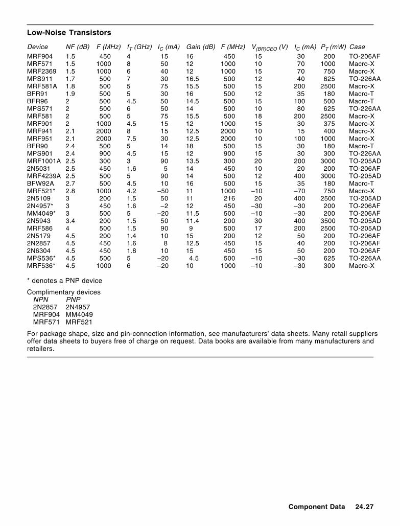
Low-Noise Transistors
Device NF (dB) F (MHz) fT (GHz) IC (mA) Gain (dB) F (MHz) V(BR)CEO (V) IC (mA) PT (mW) Case
MRF904 1.5 450 4 15 16 450 15 30 200 TO-206AFMRF571 1.5 1000 8 50 12 1000 10 70 1000 Macro-XMRF2369 1.5 1000 6 40 12 1000 15 70 750 Macro-XMPS911 1.7 500 7 30 16.5 500 12 40 625 TO-226AAMRF581A 1.8 500 5 75 15.5 500 15 200 2500 Macro-XBFR91 1.9 500 5 30 16 500 12 35 180 Macro-TBFR96 2 500 4.5 50 14.5 500 15 100 500 Macro-TMPS571 2 500 6 50 14 500 10 80 625 TO-226AAMRF581 2 500 5 75 15.5 500 18 200 2500 Macro-XMRF901 2 1000 4.5 15 12 1000 15 30 375 Macro-XMRF941 2.1 2000 8 15 12.5 2000 10 15 400 Macro-XMRF951 2.1 2000 7.5 30 12.5 2000 10 100 1000 Macro-XBFR90 2.4 500 5 14 18 500 15 30 180 Macro-TMPS901 2.4 900 4.5 15 12 900 15 30 300 TO-226AAMRF1001A 2.5 300 3 90 13.5 300 20 200 3000 TO-205AD2N5031 2.5 450 1.6 5 14 450 10 20 200 TO-206AFMRF4239A 2.5 500 5 90 14 500 12 400 3000 TO-205ADBFW92A 2.7 500 4.5 10 16 500 15 35 180 Macro-TMRF521* 2.8 1000 4.2 –50 11 1000 –10 –70 750 Macro-X2N5109 3 200 1.5 50 11 216 20 400 2500 TO-205AD2N4957* 3 450 1.6 –2 12 450 –30 –30 200 TO-206AFMM4049* 3 500 5 –20 11.5 500 –10 –30 200 TO-206AF2N5943 3.4 200 1.5 50 11.4 200 30 400 3500 TO-205ADMRF586 4 500 1.5 90 9 500 17 200 2500 TO-205AD2N5179 4.5 200 1.4 10 15 200 12 50 200 TO-206AF2N2857 4.5 450 1.6 8 12.5 450 15 40 200 TO-206AF2N6304 4.5 450 1.8 10 15 450 15 50 200 TO-206AFMPS536* 4.5 500 5 –20 4.5 500 –10 –30 625 TO-226AAMRF536* 4.5 1000 6 –20 10 1000 –10 –30 300 Macro-X
* denotes a PNP device
Complimentary devicesNPN PNP2N2857 2N4957MRF904 MM4049MRF571 MRF521
For package shape, size and pin-connection information, see manufacturers’ data sheets. Many retail suppliersoffer data sheets to buyers free of charge on request. Data books are available from many manufacturers andretailers.
24.28 Chapter 24
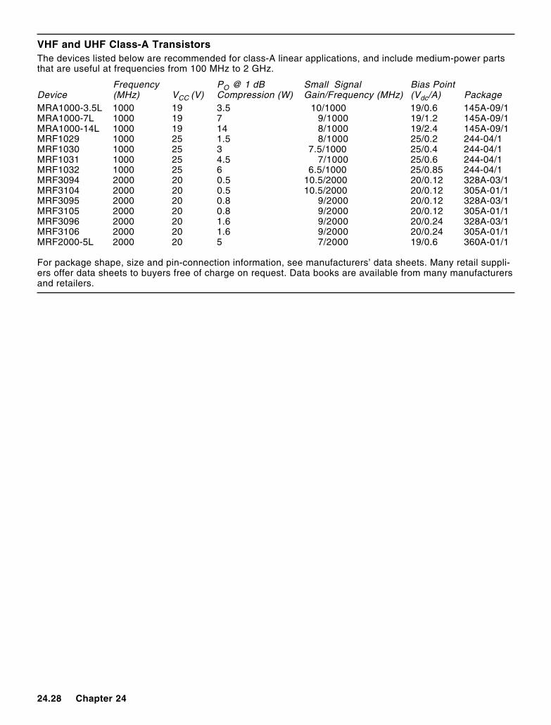
VHF and UHF Class-A TransistorsThe devices listed below are recommended for class-A linear applications, and include medium-power partsthat are useful at frequencies from 100 MHz to 2 GHz.
Frequency PO @ 1 dB Small Signal Bias PointDevice (MHz) VCC (V) Compression (W) Gain/Frequency (MHz) (Vdc/A) PackageMRA1000-3.5L 1000 19 3.5 10/1000 19/0.6 145A-09/1MRA1000-7L 1000 19 7 9/1000 19/1.2 145A-09/1MRA1000-14L 1000 19 14 8/1000 19/2.4 145A-09/1MRF1029 1000 25 1.5 8/1000 25/0.2 244-04/1MRF1030 1000 25 3 7.5/1000 25/0.4 244-04/1MRF1031 1000 25 4.5 7/1000 25/0.6 244-04/1MRF1032 1000 25 6 6.5/1000 25/0.85 244-04/1MRF3094 2000 20 0.5 10.5/2000 20/0.12 328A-03/1MRF3104 2000 20 0.5 10.5/2000 20/0.12 305A-01/1MRF3095 2000 20 0.8 9/2000 20/0.12 328A-03/1MRF3105 2000 20 0.8 9/2000 20/0.12 305A-01/1MRF3096 2000 20 1.6 9/2000 20/0.24 328A-03/1MRF3106 2000 20 1.6 9/2000 20/0.24 305A-01/1MRF2000-5L 2000 20 5 7/2000 19/0.6 360A-01/1
For package shape, size and pin-connection information, see manufacturers’ data sheets. Many retail suppli-ers offer data sheets to buyers free of charge on request. Data books are available from many manufacturersand retailers.
Component Data 24.29
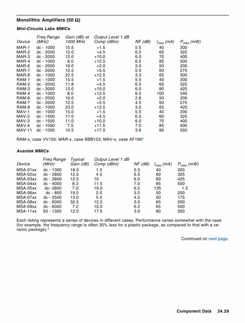
Monolithic Amplifiers (50 ΩΩΩΩΩ)
Mini-Circuits Labs MMICs
Freq Range Gain (dB) at Output Level 1 dBDevice (MHz) 1000 MHz Comp (dBm) NF (dB) Imax (mA) Pmax (mW)MAR-1 dc - 1000 15.5 +1.5 5.5 40 200MAR-2 dc - 2000 12.0 +4.5 6.5 60 325MAR-3 dc - 2000 12.0 +10.0 6.0 70 400MAR-4 dc - 1000 8.0 +12.5 6.5 85 500MAR-6 dc - 2000 16.0 +2.0 3.0 50 200MAR-7 dc - 2000 12.5 +5.5 5.0 60 275MAR-8 dc - 1000 22.5 +12.5 3.3 65 500RAM-1 dc - 1000 15.5 +1.5 5.5 40 200RAM-2 dc - 2000 11.8 +4.5 6.5 60 325RAM-3 dc - 2000 12.0 +10.0 6.0 80 425RAM-4 dc - 1000 8.0 +12.5 6.5 100 540RAM-6 dc - 2000 16.0 +2.0 2.8 50 200RAM-7 dc - 2000 12.5 +5.5 4.5 60 275RAM-8 dc - 1000 23.0 +12.5 3.0 65 420MAV-1 dc - 1000 15.0 +1.5 5.5 40 200MAV-2 dc - 1500 11.0 +4.5 6.5 60 325MAV-3 dc - 1500 11.0 +10.0 6.0 70 400MAV-4 dc - 1000 7.5 +11.5 7.0 85 500MAV-11 dc - 1000 10.5 +17.5 3.6 80 550
RAM-x, case VV105; MAR-x, case BBB123; MAV-x, case AF190†
Avantek MMICs
Freq Range Typical Output Level 1 dBDevice (MHz) Gain (dB) Comp (dBm) NF (dB) Imax (mA) Pmax (mW)MSA-01xx dc - 1300 18.5 1.5 5.5 40 200MSA-02xx dc - 2800 12.5 4.5 6.5 60 325MSA-03xx dc - 2800 12.5 10 6.0 80 425MSA-04xx dc - 4000 8.3 11.5 7.0 85 500MSA-05xx dc- 2800 7.0 19.0 6.5 135 1.5MSA-06xx dc - 800 19.5 2.0 3.0 50 200MSA-07xx dc - 2500 13.0 5.5 4.5 50 175MSA-08xx dc - 6000 32.5 12.5 3.0 65 500MSA-09xx dc - 6000 7.2 10.5 6.2 65 500MSA-11xx 50 - 1300 12.0 17.5 3.6 80 550
Each listing represents a series of devices in different cases. Performance varies somewhat with the case(for example, the frequency range is often 30% less for a plastic package, as compared to that with a ce-ramic package).†
Continued on next page.
24.30 Chapter 24
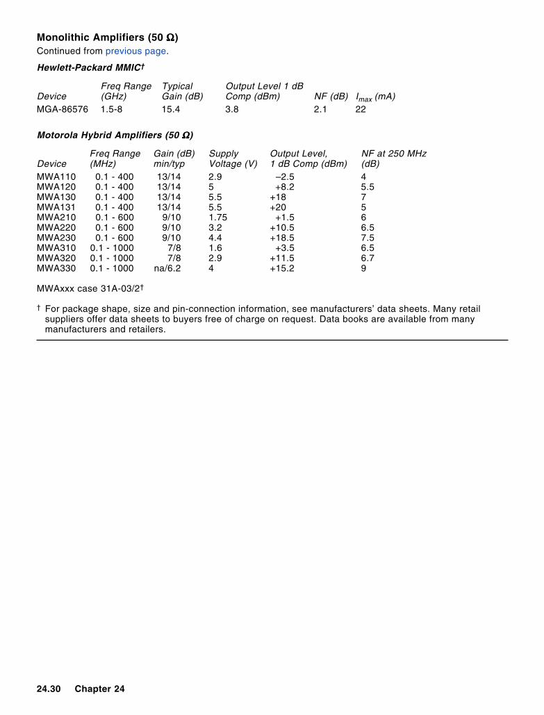
Hewlett-Packard MMIC†
Freq Range Typical Output Level 1 dBDevice (GHz) Gain (dB) Comp (dBm) NF (dB) Imax (mA)MGA-86576 1.5-8 15.4 3.8 2.1 22
Motorola Hybrid Amplifiers (50 ΩΩΩΩΩ)
Freq Range Gain (dB) Supply Output Level, NF at 250 MHzDevice (MHz) min/typ Voltage (V) 1 dB Comp (dBm) (dB)MWA110 0.1 - 400 13/14 2.9 –2.5 4MWA120 0.1 - 400 13/14 5 +8.2 5.5MWA130 0.1 - 400 13/14 5.5 +18 7MWA131 0.1 - 400 13/14 5.5 +20 5MWA210 0.1 - 600 9/10 1.75 +1.5 6MWA220 0.1 - 600 9/10 3.2 +10.5 6.5MWA230 0.1 - 600 9/10 4.4 +18.5 7.5MWA310 0.1 - 1000 7/8 1.6 +3.5 6.5MWA320 0.1 - 1000 7/8 2.9 +11.5 6.7MWA330 0.1 - 1000 na/6.2 4 +15.2 9
MWAxxx case 31A-03/2†
† For package shape, size and pin-connection information, see manufacturers’ data sheets. Many retailsuppliers offer data sheets to buyers free of charge on request. Data books are available from manymanufacturers and retailers.
Monolithic Amplifiers (50 ΩΩΩΩΩ)Continued from previous page.
Component Data 24.31
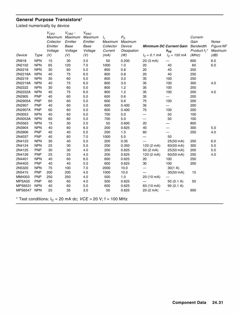
General Purpose Transistors†
Listed numerically by device
VCEO VCBO - VEBOMaximum Maximum Maximum Ic PD Current-Collector Emitter Emitter Maximum Maximum Gain NoiseEmitter Base Base Collector Device Minimum DC Current Gain Bandwidth Figure NFVoltage Voltage Voltage Current Dissipation hFE Product fT* Maximum
Device Type (V) (V) (V) (mA) (W) IC = 0.1 mA IC = 150 mA (MHz) (dB)
2N918 NPN 15 30 3.0 50 0.200 20 (3 mA) — 600 6.02N2102 NPN 65 120 7.0 1000 1.0 20 40 60 6.02N2218 NPN 30 60 5.0 800 0.8 20 40 2502N2218A NPN 40 75 6.0 800 0.8 20 40 2502N2219 NPN 30 60 5.0 800 3.0 35 100 2502N2219A NPN 40 75 6.0 800 3.0 35 100 300 4.02N2222 NPN 30 60 5.0 800 1.2 35 100 2502N2222A NPN 40 75 6.0 800 1.2 35 100 200 4.02N2905 PNP 40 60 5.0 600 0.6 35 — 2002N2905A PNP 60 60 5.0 600 0.6 75 100 2002N2907 PNP 40 60 5.0 600 0.400 35 — 2002N2907A PNP 60 60 5.0 600 0.400 75 100 2002N3053 NPN 40 60 5.0 700 5.0 — 50 1002N3053A NPN 60 80 5.0 700 5.0 — 50 1002N3563 NPN 15 30 2.0 50 0.600 20 — 8002N3904 NPN 40 60 6.0 200 0.625 40 — 300 5.02N3906 PNP 40 40 5.0 200 1.5 60 — 250 4.02N4037 PNP 40 60 7.0 1000 5.0 — 502N4123 NPN 30 40 5.0 200 0.35 — 25(50 mA) 250 6.02N4124 NPN 25 30 5.0 200 0.350 120 (2 mA) 60(50 mA) 300 5.02N4125 PNP 30 30 4.0 200 0.625 50 (2 mA) 25(50 mA) 200 5.02N4126 PNP 25 25 4.0 200 0.625 120 (2 mA) 60(50 mA) 250 4.02N4401 NPN 40 60 6.0 600 0.625 20 100 2502N4403 PNP 40 40 5.0 600 0.625 30 100 2002N5320 NPN 75 100 7.0 2000 10.0 — 30(1 A)2N5415 PNP 200 200 4.0 1000 10.0 — 30(50 mA) 15MM4003 PNP 250 250 4.0 500 1.0 20 (10 mA) —MPSA55 PNP 60 60 4.0 500 0.625 — 50 (0.1 A) 50MPS6531 NPN 40 60 5.0 600 0.625 60 (10 mA) 90 (0.1 A)MPS6547 NPN 25 35 3.0 50 0.625 20 (2 mA) — 600
* Test conditions: IC = 20 mA dc; VCE = 20 V; f = 100 MHz
24.32 Chapter 24
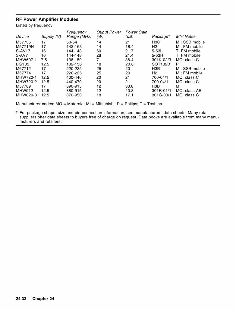
RF Power Amplifier ModulesListed by frequency
Frequency Ouput Power Power GainDevice Supply (V) Range (MHz) (W) (dB) Package† Mfr/ NotesM57735 17 50-54 14 21 H3C MI; SSB mobileM57719N 17 142-163 14 18.4 H2 MI; FM mobileS-AV17 16 144-148 60 21.7 5-53L T, FM mobileS-AV7 16 144-148 28 21.4 5-53H T, FM mobileMHW607-1 7.5 136-150 7 38.4 301K-02/3 MO; class CBGY35 12.5 132-156 18 20.8 SOT132B PM67712 17 220-225 25 20 H3B MI; SSB mobileM57774 17 220-225 25 20 H2 MI; FM mobileMHW720-1 12.5 400-440 20 21 700-04/1 MO; class CMHW720-2 12.5 440-470 20 21 700-04/1 MO; class CM57789 17 890-915 12 33.8 H3B MIMHW912 12.5 880-915 12 40.8 301R-01/1 MO; class ABMHW820-3 12.5 870-950 18 17.1 301G-03/1 MO; class C
Manufacturer codes: MO = Motorola; MI = Mitsubishi; P = Philips; T = Toshiba.
† For package shape, size and pin-connection information, see manufacturers’ data sheets. Many retailsuppliers offer data sheets to buyers free of charge on request. Data books are available from many manu-facturers and retailers.
Component Data 24.33
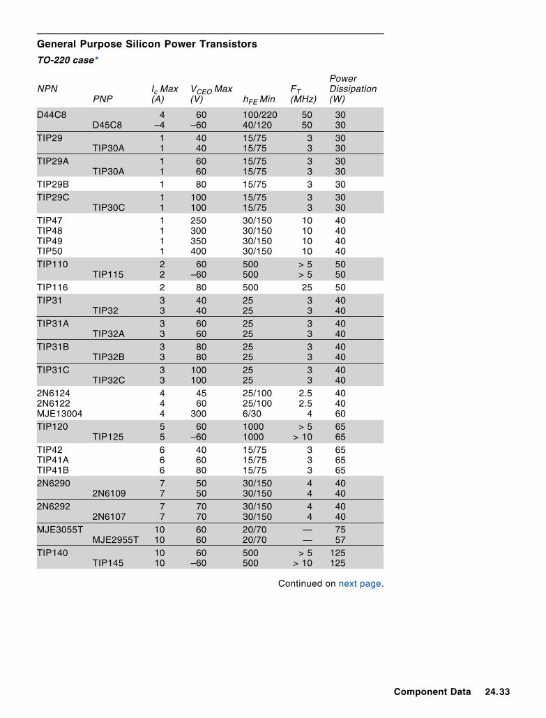
General Purpose Silicon Power Transistors
TO-220 case*
PowerNPN Ic Max VCEO Max FT Dissipation
PNP (A) (V) hFE Min (MHz) (W)
D44C8 4 60 100/220 50 30D45C8 –4 –60 40/120 50 30
TIP29 1 40 15/75 3 30TIP30A 1 40 15/75 3 30
TIP29A 1 60 15/75 3 30TIP30A 1 60 15/75 3 30
TIP29B 1 80 15/75 3 30TIP29C 1 100 15/75 3 30
TIP30C 1 100 15/75 3 30TIP47 1 250 30/150 10 40TIP48 1 300 30/150 10 40TIP49 1 350 30/150 10 40TIP50 1 400 30/150 10 40TIP110 2 60 500 > 5 50
TIP115 2 –60 500 > 5 50TIP116 2 80 500 25 50TIP31 3 40 25 3 40
TIP32 3 40 25 3 40TIP31A 3 60 25 3 40
TIP32A 3 60 25 3 40TIP31B 3 80 25 3 40
TIP32B 3 80 25 3 40TIP31C 3 100 25 3 40
TIP32C 3 100 25 3 402N6124 4 45 25/100 2.5 402N6122 4 60 25/100 2.5 40MJE13004 4 300 6/30 4 60TIP120 5 60 1000 > 5 65
TIP125 5 –60 1000 > 10 65TIP42 6 40 15/75 3 65TIP41A 6 60 15/75 3 65TIP41B 6 80 15/75 3 652N6290 7 50 30/150 4 40
2N6109 7 50 30/150 4 402N6292 7 70 30/150 4 40
2N6107 7 70 30/150 4 40MJE3055T 10 60 20/70 — 75
MJE2955T 10 60 20/70 — 57TIP140 10 60 500 > 5 125
TIP145 10 –60 500 > 10 125
Continued on next page.
24.34 Chapter 24
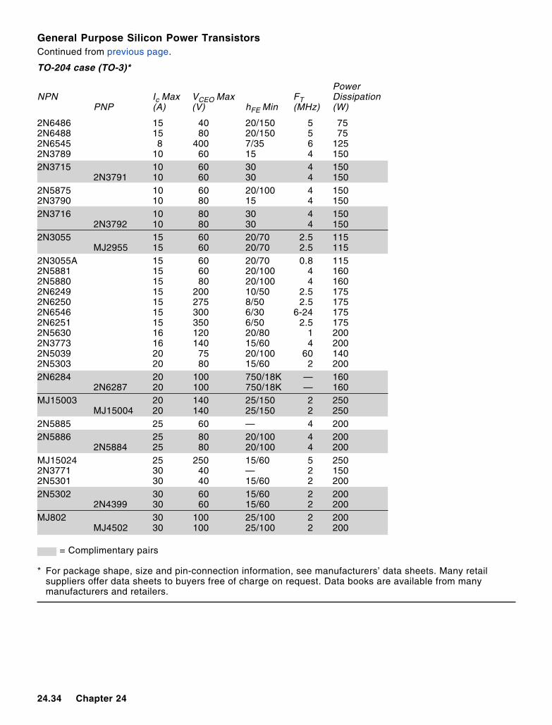
General Purpose Silicon Power TransistorsContinued from previous page.
TO-204 case (TO-3)*
PowerNPN Ic Max VCEO Max FT Dissipation
PNP (A) (V) hFE Min (MHz) (W)
2N6486 15 40 20/150 5 752N6488 15 80 20/150 5 752N6545 8 400 7/35 6 1252N3789 10 60 15 4 1502N3715 10 60 30 4 150
2N3791 10 60 30 4 1502N5875 10 60 20/100 4 1502N3790 10 80 15 4 1502N3716 10 80 30 4 150
2N3792 10 80 30 4 1502N3055 15 60 20/70 2.5 115
MJ2955 15 60 20/70 2.5 1152N3055A 15 60 20/70 0.8 1152N5881 15 60 20/100 4 1602N5880 15 80 20/100 4 1602N6249 15 200 10/50 2.5 1752N6250 15 275 8/50 2.5 1752N6546 15 300 6/30 6-24 1752N6251 15 350 6/50 2.5 1752N5630 16 120 20/80 1 2002N3773 16 140 15/60 4 2002N5039 20 75 20/100 60 1402N5303 20 80 15/60 2 2002N6284 20 100 750/18K — 160
2N6287 20 100 750/18K — 160MJ15003 20 140 25/150 2 250
MJ15004 20 140 25/150 2 2502N5885 25 60 — 4 2002N5886 25 80 20/100 4 200
2N5884 25 80 20/100 4 200MJ15024 25 250 15/60 5 2502N3771 30 40 — 2 1502N5301 30 40 15/60 2 2002N5302 30 60 15/60 2 200
2N4399 30 60 15/60 2 200MJ802 30 100 25/100 2 200
MJ4502 30 100 25/100 2 200
= Complimentary pairs
* For package shape, size and pin-connection information, see manufacturers’ data sheets. Many retailsuppliers offer data sheets to buyers free of charge on request. Data books are available from manymanufacturers and retailers.
Component Data 24.35
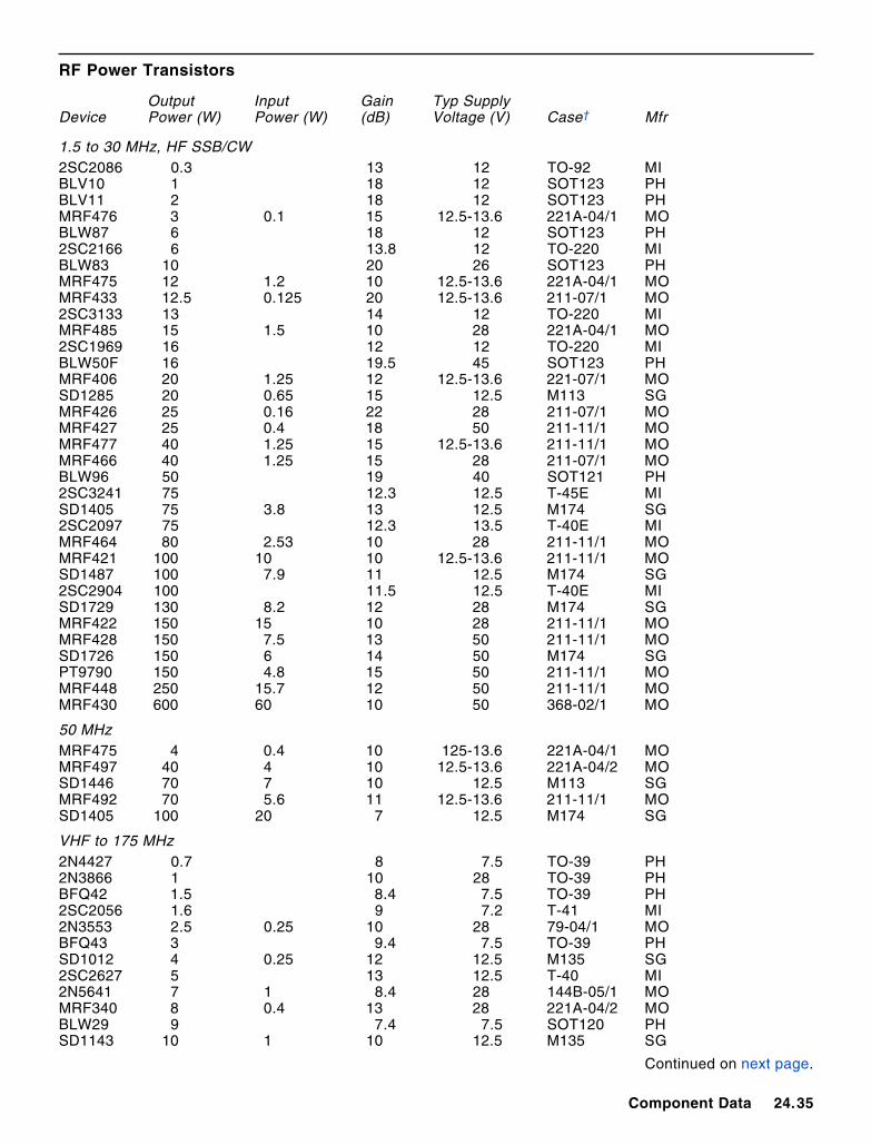
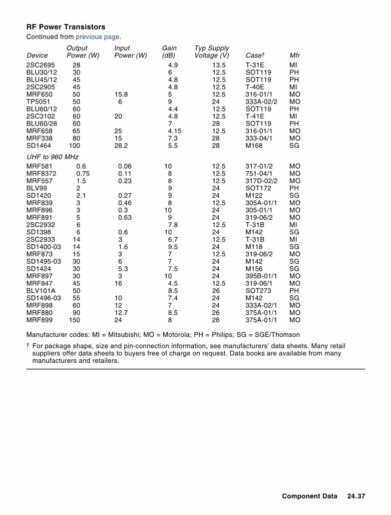
RF Power Transistors
Output Input Gain Typ SupplyDevice Power (W) Power (W) (dB) Voltage (V) Case† Mfr
1.5 to 30 MHz, HF SSB/CW2SC2086 0.3 13 12 TO-92 MIBLV10 1 18 12 SOT123 PHBLV11 2 18 12 SOT123 PHMRF476 3 0.1 15 12.5-13.6 221A-04/1 MOBLW87 6 18 12 SOT123 PH2SC2166 6 13.8 12 TO-220 MIBLW83 10 20 26 SOT123 PHMRF475 12 1.2 10 12.5-13.6 221A-04/1 MOMRF433 12.5 0.125 20 12.5-13.6 211-07/1 MO2SC3133 13 14 12 TO-220 MIMRF485 15 1.5 10 28 221A-04/1 MO2SC1969 16 12 12 TO-220 MIBLW50F 16 19.5 45 SOT123 PHMRF406 20 1.25 12 12.5-13.6 221-07/1 MOSD1285 20 0.65 15 12.5 M113 SGMRF426 25 0.16 22 28 211-07/1 MOMRF427 25 0.4 18 50 211-11/1 MOMRF477 40 1.25 15 12.5-13.6 211-11/1 MOMRF466 40 1.25 15 28 211-07/1 MOBLW96 50 19 40 SOT121 PH2SC3241 75 12.3 12.5 T-45E MISD1405 75 3.8 13 12.5 M174 SG2SC2097 75 12.3 13.5 T-40E MIMRF464 80 2.53 10 28 211-11/1 MOMRF421 100 10 10 12.5-13.6 211-11/1 MOSD1487 100 7.9 11 12.5 M174 SG2SC2904 100 11.5 12.5 T-40E MISD1729 130 8.2 12 28 M174 SGMRF422 150 15 10 28 211-11/1 MOMRF428 150 7.5 13 50 211-11/1 MOSD1726 150 6 14 50 M174 SGPT9790 150 4.8 15 50 211-11/1 MOMRF448 250 15.7 12 50 211-11/1 MOMRF430 600 60 10 50 368-02/1 MO
50 MHzMRF475 4 0.4 10 125-13.6 221A-04/1 MOMRF497 40 4 10 12.5-13.6 221A-04/2 MOSD1446 70 7 10 12.5 M113 SGMRF492 70 5.6 11 12.5-13.6 211-11/1 MOSD1405 100 20 7 12.5 M174 SG
VHF to 175 MHz2N4427 0.7 8 7.5 TO-39 PH2N3866 1 10 28 TO-39 PHBFQ42 1.5 8.4 7.5 TO-39 PH2SC2056 1.6 9 7.2 T-41 MI2N3553 2.5 0.25 10 28 79-04/1 MOBFQ43 3 9.4 7.5 TO-39 PHSD1012 4 0.25 12 12.5 M135 SG2SC2627 5 13 12.5 T-40 MI2N5641 7 1 8.4 28 144B-05/1 MOMRF340 8 0.4 13 28 221A-04/2 MOBLW29 9 7.4 7.5 SOT120 PHSD1143 10 1 10 12.5 M135 SG
Continued on next page.
24.36 Chapter 24
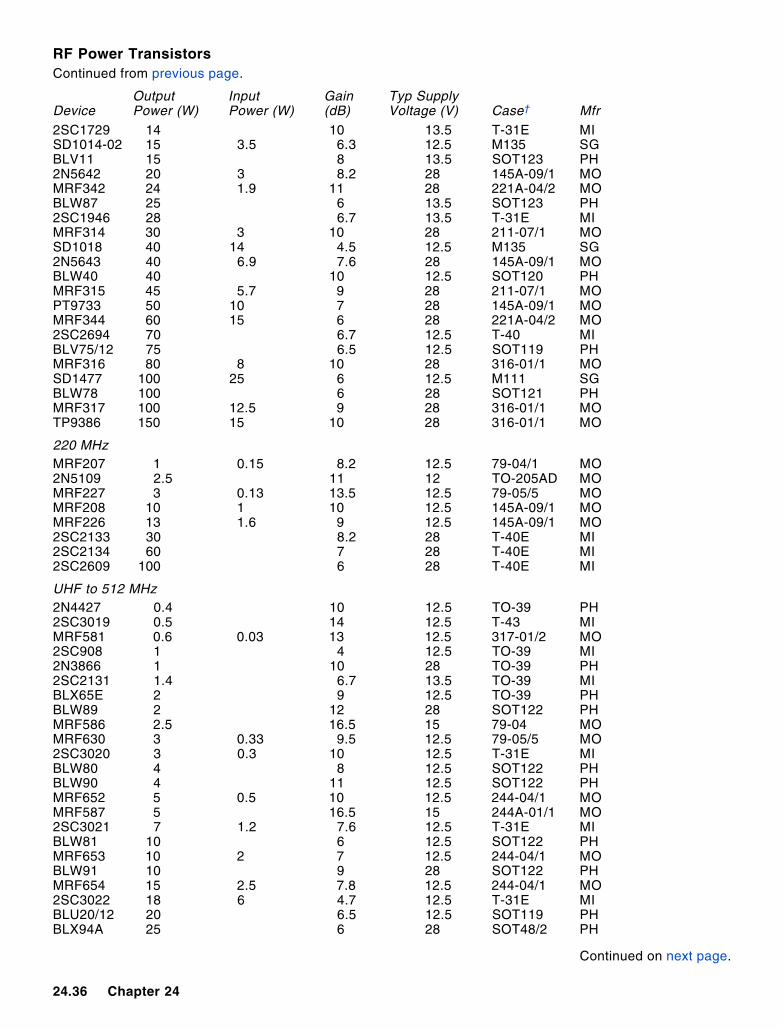
2SC1729 14 10 13.5 T-31E MISD1014-02 15 3.5 6.3 12.5 M135 SGBLV11 15 8 13.5 SOT123 PH2N5642 20 3 8.2 28 145A-09/1 MOMRF342 24 1.9 11 28 221A-04/2 MOBLW87 25 6 13.5 SOT123 PH2SC1946 28 6.7 13.5 T-31E MIMRF314 30 3 10 28 211-07/1 MOSD1018 40 14 4.5 12.5 M135 SG2N5643 40 6.9 7.6 28 145A-09/1 MOBLW40 40 10 12.5 SOT120 PHMRF315 45 5.7 9 28 211-07/1 MOPT9733 50 10 7 28 145A-09/1 MOMRF344 60 15 6 28 221A-04/2 MO2SC2694 70 6.7 12.5 T-40 MIBLV75/12 75 6.5 12.5 SOT119 PHMRF316 80 8 10 28 316-01/1 MOSD1477 100 25 6 12.5 M111 SGBLW78 100 6 28 SOT121 PHMRF317 100 12.5 9 28 316-01/1 MOTP9386 150 15 10 28 316-01/1 MO
220 MHzMRF207 1 0.15 8.2 12.5 79-04/1 MO2N5109 2.5 11 12 TO-205AD MOMRF227 3 0.13 13.5 12.5 79-05/5 MOMRF208 10 1 10 12.5 145A-09/1 MOMRF226 13 1.6 9 12.5 145A-09/1 MO2SC2133 30 8.2 28 T-40E MI2SC2134 60 7 28 T-40E MI2SC2609 100 6 28 T-40E MI
UHF to 512 MHz2N4427 0.4 10 12.5 TO-39 PH2SC3019 0.5 14 12.5 T-43 MIMRF581 0.6 0.03 13 12.5 317-01/2 MO2SC908 1 4 12.5 TO-39 MI2N3866 1 10 28 TO-39 PH2SC2131 1.4 6.7 13.5 TO-39 MIBLX65E 2 9 12.5 TO-39 PHBLW89 2 12 28 SOT122 PHMRF586 2.5 16.5 15 79-04 MOMRF630 3 0.33 9.5 12.5 79-05/5 MO2SC3020 3 0.3 10 12.5 T-31E MIBLW80 4 8 12.5 SOT122 PHBLW90 4 11 12.5 SOT122 PHMRF652 5 0.5 10 12.5 244-04/1 MOMRF587 5 16.5 15 244A-01/1 MO2SC3021 7 1.2 7.6 12.5 T-31E MIBLW81 10 6 12.5 SOT122 PHMRF653 10 2 7 12.5 244-04/1 MOBLW91 10 9 28 SOT122 PHMRF654 15 2.5 7.8 12.5 244-04/1 MO2SC3022 18 6 4.7 12.5 T-31E MIBLU20/12 20 6.5 12.5 SOT119 PHBLX94A 25 6 28 SOT48/2 PH
RF Power TransistorsContinued from previous page.
Output Input Gain Typ SupplyDevice Power (W) Power (W) (dB) Voltage (V) Case† Mfr
Continued on next page.
Component Data 24.37
2SC2695 28 4.9 13.5 T-31E MIBLU30/12 30 6 12.5 SOT119 PHBLU45/12 45 4.8 12.5 SOT119 PH2SC2905 45 4.8 12.5 T-40E MIMRF650 50 15.8 5 12.5 316-01/1 MOTP5051 50 6 9 24 333A-02/2 MOBLU60/12 60 4.4 12.5 SOT119 PH2SC3102 60 20 4.8 12.5 T-41E MIBLU60/28 60 7 28 SOT119 PHMRF658 65 25 4.15 12.5 316-01/1 MOMRF338 80 15 7.3 28 333-04/1 MOSD1464 100 28.2 5.5 28 M168 SG
UHF to 960 MHzMRF581 0.6 0.06 10 12.5 317-01/2 MOMRF8372 0.75 0.11 8 12.5 751-04/1 MOMRF557 1.5 0.23 8 12.5 317D-02/2 MOBLV99 2 9 24 SOT172 PHSD1420 2.1 0.27 9 24 M122 SGMRF839 3 0.46 8 12.5 305A-01/1 MOMRF896 3 0.3 10 24 305-01/1 MOMRF891 5 0.63 9 24 319-06/2 MO2SC2932 6 7.8 12.5 T-31B MISD1398 6 0.6 10 24 M142 SG2SC2933 14 3 6.7 12.5 T-31B MISD1400-03 14 1.6 9.5 24 M118 SGMRF873 15 3 7 12.5 319-06/2 MOSD1495-03 30 6 7 24 M142 SGSD1424 30 5.3 7.5 24 M156 SGMRF897 30 3 10 24 395B-01/1 MOMRF847 45 16 4.5 12.5 319-06/1 MOBLV101A 50 8.5 26 SOT273 PHSD1496-03 55 10 7.4 24 M142 SGMRF898 60 12 7 24 333A-02/1 MOMRF880 90 12.7 8.5 26 375A-01/1 MOMRF899 150 24 8 26 375A-01/1 MO
Manufacturer codes: MI = Mitsubishi; MO = Motorola; PH = Philips; SG = SGE/Thomson† For package shape, size and pin-connection information, see manufacturers’ data sheets. Many retail
suppliers offer data sheets to buyers free of charge on request. Data books are available from manymanufacturers and retailers.
RF Power TransistorsContinued from previous page.
Output Input Gain Typ SupplyDevice Power (W) Power (W) (dB) Voltage (V) Case† Mfr
24.38 Chapter 24
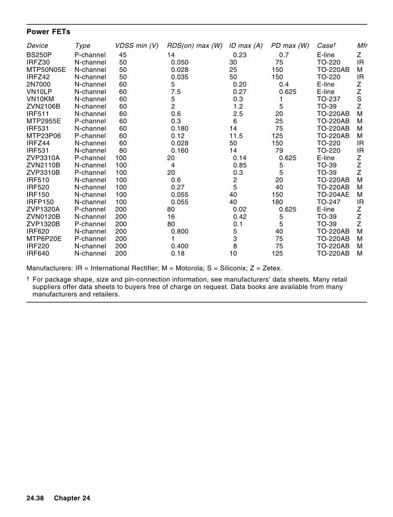
Power FETs
Device Type VDSS min (V) RDS(on) max (W) ID max (A) PD max (W) Case† MfrBS250P P-channel 45 14 0.23 0.7 E-line ZIRFZ30 N-channel 50 0.050 30 75 TO-220 IRMTP50N05E N-channel 50 0.028 25 150 TO-220AB MIRFZ42 N-channel 50 0.035 50 150 TO-220 IR2N7000 N-channel 60 5 0.20 0.4 E-line ZVN10LP N-channel 60 7.5 0.27 0.625 E-line ZVN10KM N-channel 60 5 0.3 1 TO-237 SZVN2106B N-channel 60 2 1.2 5 TO-39 ZIRF511 N-channel 60 0.6 2.5 20 TO-220AB MMTP2955E P-channel 60 0.3 6 25 TO-220AB MIRF531 N-channel 60 0.180 14 75 TO-220AB MMTP23P06 P-channel 60 0.12 11.5 125 TO-220AB MIRFZ44 N-channel 60 0.028 50 150 TO-220 IRIRF531 N-channel 80 0.160 14 79 TO-220 IRZVP3310A P-channel 100 20 0.14 0.625 E-line ZZVN2110B N-channel 100 4 0.85 5 TO-39 ZZVP3310B P-channel 100 20 0.3 5 TO-39 ZIRF510 N-channel 100 0.6 2 20 TO-220AB MIRF520 N-channel 100 0.27 5 40 TO-220AB MIRF150 N-channel 100 0.055 40 150 TO-204AE MIRFP150 N-channel 100 0.055 40 180 TO-247 IRZVP1320A P-channel 200 80 0.02 0.625 E-line ZZVN0120B N-channel 200 16 0.42 5 TO-39 ZZVP1320B P-channel 200 80 0.1 5 TO-39 ZIRF620 N-channel 200 0.800 5 40 TO-220AB MMTP6P20E P-channel 200 1 3 75 TO-220AB MIRF220 N-channel 200 0.400 8 75 TO-220AB MIRF640 N-channel 200 0.18 10 125 TO-220AB M
Manufacturers: IR = International Rectifier; M = Motorola; S = Siliconix; Z = Zetex.
† For package shape, size and pin-connection information, see manufacturers’ data sheets. Many retailsuppliers offer data sheets to buyers free of charge on request. Data books are available from manymanufacturers and retailers.
Component Data 24.39
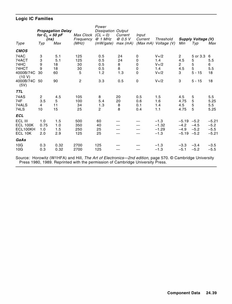
Logic IC Families
PowerPropagation Delay Dissipation Outputfor CL = 50 pF Max Clock (CL = 0) Current Input
(ns) Frequency @ 1 MHz @ 0.5 V Current Threshold Supply Voltage (V)Type Typ Max (MHz) (mW/gate) max (mA) (Max mA) Voltage (V) Min Typ Max
CMOS74AC 3 5.1 125 0.5 24 0 V+/2 2 5 or 3.3 674ACT 3 5.1 125 0.5 24 0 1.4 4.5 5 5.574HC 9 18 30 0.5 8 0 V+/2 2 5 674HCT 9 18 30 0.5 8 0 1.4 4.5 5 5.54000B/74C 30 60 5 1.2 1.3 0 V+/2 3 5 - 15 18
(10 V)4000B/74C 50 90 2 3.3 0.5 0 V+/2 3 5 - 15 18
(5V)
TTL74AS 2 4.5 105 8 20 0.5 1.5 4.5 5 5.574F 3.5 5 100 5.4 20 0.6 1.6 4.75 5 5.2574ALS 4 11 34 1.3 8 0.1 1.4 4.5 5 5.574LS 10 15 25 2 8 0.4 1.1 4.75 5 5.25
ECLECL III 1.0 1.5 500 60 — — –1.3 –5.19 –5.2 –5.21ECL 100K 0.75 1.0 350 40 — — –1.32 –4.2 –4.5 –5.2ECL100KH 1.0 1.5 250 25 — — –1.29 –4.9 –5.2 –5.5ECL 10K 2.0 2.9 125 25 — — –1.3 –5.19 –5.2 –5.21
GaAs10G 0.3 0.32 2700 125 — — –1.3 –3.3 –3.4 –3.510G 0.3 0.32 2700 125 — — –1.3 –5.1 –5.2 –5.5
Source: Horowitz (W1HFA) and Hill, The Art of Electronics—2nd edition, page 570. © Cambridge UniversityPress 1980, 1989. Reprinted with the permission of Cambridge University Press.
24.40 Chapter 24
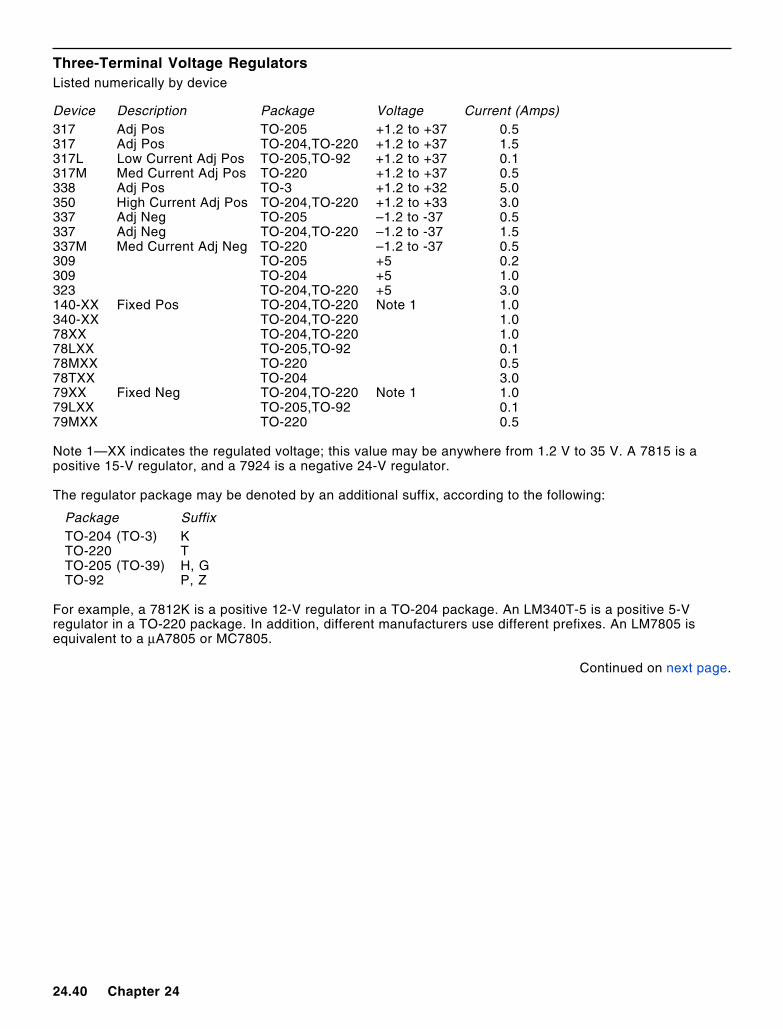
Three-Terminal Voltage RegulatorsListed numerically by device
Device Description Package Voltage Current (Amps)317 Adj Pos TO-205 +1.2 to +37 0.5317 Adj Pos TO-204,TO-220 +1.2 to +37 1.5317L Low Current Adj Pos TO-205,TO-92 +1.2 to +37 0.1317M Med Current Adj Pos TO-220 +1.2 to +37 0.5338 Adj Pos TO-3 +1.2 to +32 5.0350 High Current Adj Pos TO-204,TO-220 +1.2 to +33 3.0337 Adj Neg TO-205 –1.2 to -37 0.5337 Adj Neg TO-204,TO-220 –1.2 to -37 1.5337M Med Current Adj Neg TO-220 –1.2 to -37 0.5309 TO-205 +5 0.2309 TO-204 +5 1.0323 TO-204,TO-220 +5 3.0140-XX Fixed Pos TO-204,TO-220 Note 1 1.0340-XX TO-204,TO-220 1.078XX TO-204,TO-220 1.078LXX TO-205,TO-92 0.178MXX TO-220 0.578TXX TO-204 3.079XX Fixed Neg TO-204,TO-220 Note 1 1.079LXX TO-205,TO-92 0.179MXX TO-220 0.5
Note 1—XX indicates the regulated voltage; this value may be anywhere from 1.2 V to 35 V. A 7815 is apositive 15-V regulator, and a 7924 is a negative 24-V regulator.
The regulator package may be denoted by an additional suffix, according to the following:
Package SuffixTO-204 (TO-3) KTO-220 TTO-205 (TO-39) H, GTO-92 P, Z
For example, a 7812K is a positive 12-V regulator in a TO-204 package. An LM340T-5 is a positive 5-Vregulator in a TO-220 package. In addition, different manufacturers use different prefixes. An LM7805 isequivalent to a µA7805 or MC7805.
Continued on next page.
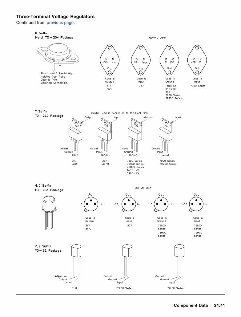
Component Data 24.41
Three-Terminal Voltage RegulatorsContinued from previous page.
24.42 Chapter 24
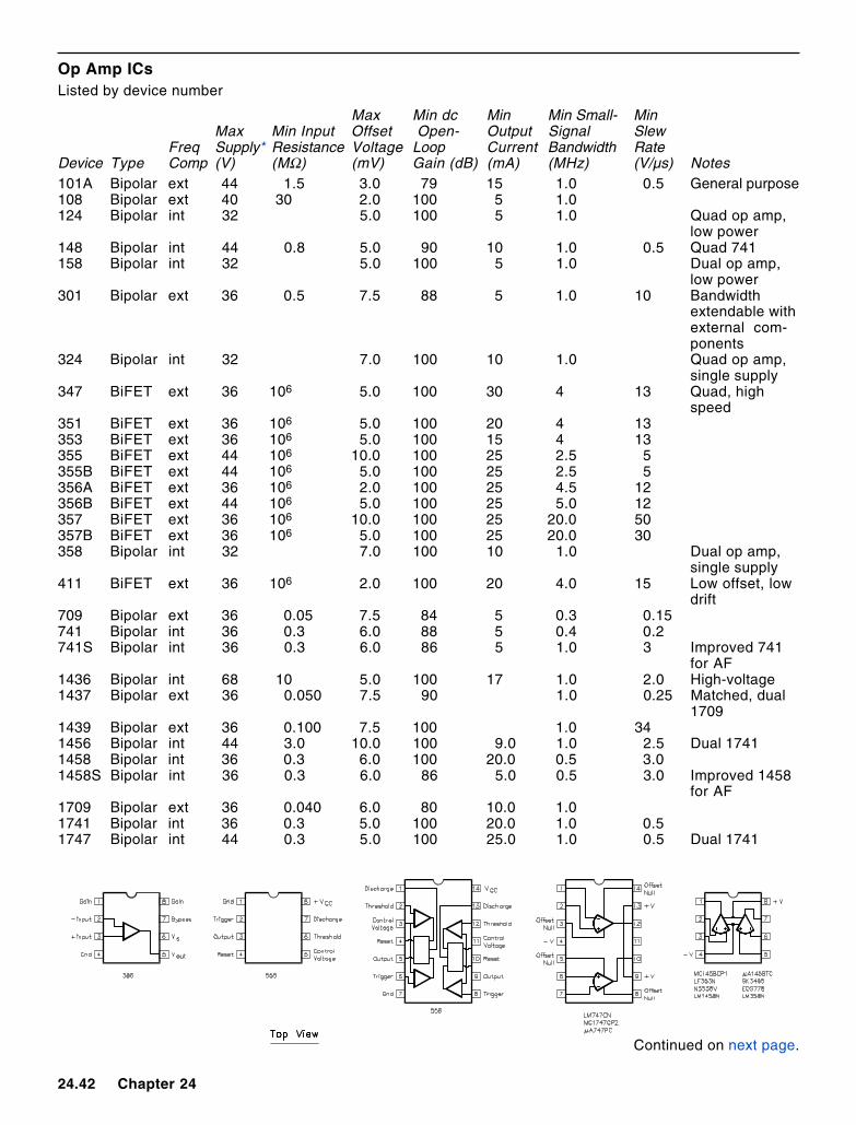
Op Amp ICsListed by device number
Max Min dc Min Min Small- MinMax Min Input Offset Open- Output Signal Slew
Freq Supply* Resistance Voltage Loop Current Bandwidth RateDevice Type Comp (V) (MΩ) (mV) Gain (dB) (mA) (MHz) (V/µs) Notes101A Bipolar ext 44 1.5 3.0 79 15 1.0 0.5 General purpose108 Bipolar ext 40 30 2.0 100 5 1.0124 Bipolar int 32 5.0 100 5 1.0 Quad op amp,
low power148 Bipolar int 44 0.8 5.0 90 10 1.0 0.5 Quad 741158 Bipolar int 32 5.0 100 5 1.0 Dual op amp,
low power301 Bipolar ext 36 0.5 7.5 88 5 1.0 10 Bandwidth
extendable withexternal com-ponents
324 Bipolar int 32 7.0 100 10 1.0 Quad op amp,single supply
347 BiFET ext 36 106 5.0 100 30 4 13 Quad, highspeed
351 BiFET ext 36 106 5.0 100 20 4 13353 BiFET ext 36 106 5.0 100 15 4 13355 BiFET ext 44 106 10.0 100 25 2.5 5355B BiFET ext 44 106 5.0 100 25 2.5 5356A BiFET ext 36 106 2.0 100 25 4.5 12356B BiFET ext 44 106 5.0 100 25 5.0 12357 BiFET ext 36 106 10.0 100 25 20.0 50357B BiFET ext 36 106 5.0 100 25 20.0 30358 Bipolar int 32 7.0 100 10 1.0 Dual op amp,
single supply411 BiFET ext 36 106 2.0 100 20 4.0 15 Low offset, low
drift709 Bipolar ext 36 0.05 7.5 84 5 0.3 0.15741 Bipolar int 36 0.3 6.0 88 5 0.4 0.2741S Bipolar int 36 0.3 6.0 86 5 1.0 3 Improved 741
for AF1436 Bipolar int 68 10 5.0 100 17 1.0 2.0 High-voltage1437 Bipolar ext 36 0.050 7.5 90 1.0 0.25 Matched, dual
17091439 Bipolar ext 36 0.100 7.5 100 1.0 341456 Bipolar int 44 3.0 10.0 100 9.0 1.0 2.5 Dual 17411458 Bipolar int 36 0.3 6.0 100 20.0 0.5 3.01458S Bipolar int 36 0.3 6.0 86 5.0 0.5 3.0 Improved 1458
for AF1709 Bipolar ext 36 0.040 6.0 80 10.0 1.01741 Bipolar int 36 0.3 5.0 100 20.0 1.0 0.51747 Bipolar int 44 0.3 5.0 100 25.0 1.0 0.5 Dual 1741
Continued on next page.
Component Data 24.43
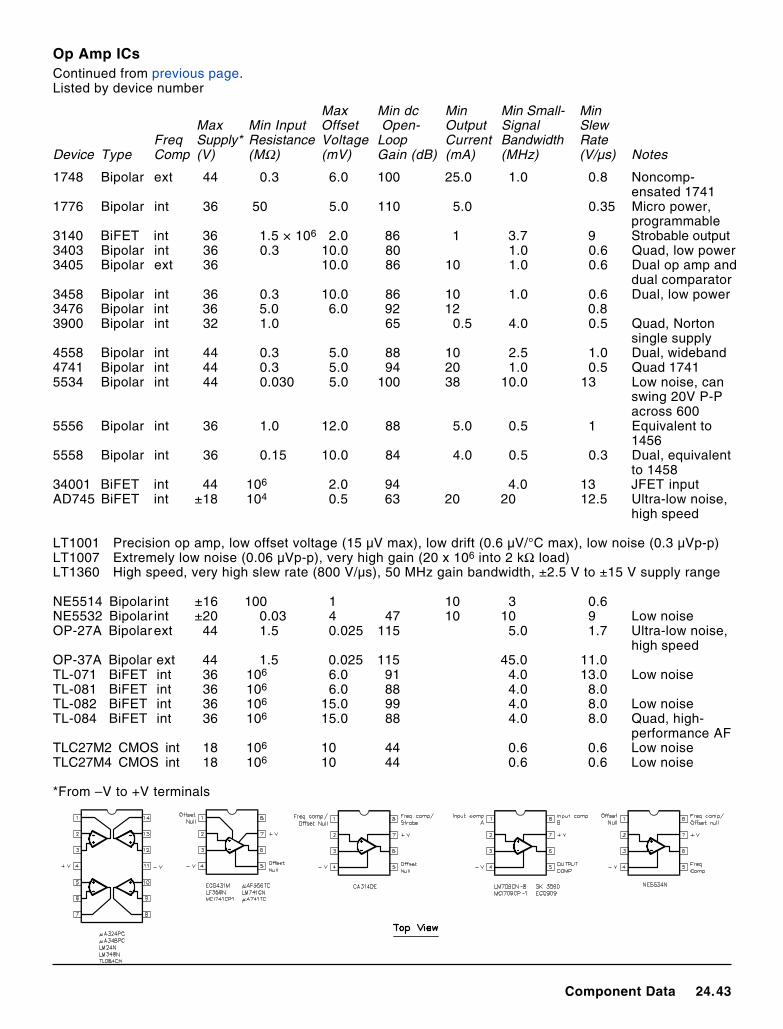
1748 Bipolar ext 44 0.3 6.0 100 25.0 1.0 0.8 Noncomp-ensated 1741
1776 Bipolar int 36 50 5.0 110 5.0 0.35 Micro power,programmable
3140 BiFET int 36 1.5 × 10⁶ 2.0 86 1 3.7 9 Strobable output3403 Bipolar int 36 0.3 10.0 80 1.0 0.6 Quad, low power3405 Bipolar ext 36 10.0 86 10 1.0 0.6 Dual op amp and
dual comparator3458 Bipolar int 36 0.3 10.0 86 10 1.0 0.6 Dual, low power3476 Bipolar int 36 5.0 6.0 92 12 0.83900 Bipolar int 32 1.0 65 0.5 4.0 0.5 Quad, Norton
single supply4558 Bipolar int 44 0.3 5.0 88 10 2.5 1.0 Dual, wideband4741 Bipolar int 44 0.3 5.0 94 20 1.0 0.5 Quad 17415534 Bipolar int 44 0.030 5.0 100 38 10.0 13 Low noise, can
swing 20V P-Pacross 600
5556 Bipolar int 36 1.0 12.0 88 5.0 0.5 1 Equivalent to1456
5558 Bipolar int 36 0.15 10.0 84 4.0 0.5 0.3 Dual, equivalentto 1458
34001 BiFET int 44 106 2.0 94 4.0 13 JFET inputAD745 BiFET int ±18 104 0.5 63 20 20 12.5 Ultra-low noise,
high speed
LT1001 Precision op amp, low offset voltage (15 µV max), low drift (0.6 µV/°C max), low noise (0.3 µVp-p)LT1007 Extremely low noise (0.06 µVp-p), very high gain (20 x 106 into 2 kΩ load)LT1360 High speed, very high slew rate (800 V/µs), 50 MHz gain bandwidth, ±2.5 V to ±15 V supply range
NE5514 Bipolar int ±16 100 1 10 3 0.6NE5532 Bipolar int ±20 0.03 4 47 10 10 9 Low noiseOP-27A Bipolar ext 44 1.5 0.025 115 5.0 1.7 Ultra-low noise,
high speedOP-37A Bipolar ext 44 1.5 0.025 115 45.0 11.0TL-071 BiFET int 36 106 6.0 91 4.0 13.0 Low noiseTL-081 BiFET int 36 106 6.0 88 4.0 8.0TL-082 BiFET int 36 106 15.0 99 4.0 8.0 Low noiseTL-084 BiFET int 36 106 15.0 88 4.0 8.0 Quad, high-
performance AFTLC27M2 CMOS int 18 106 10 44 0.6 0.6 Low noiseTLC27M4 CMOS int 18 106 10 44 0.6 0.6 Low noise
*From –V to +V terminals
Op Amp ICsContinued from previous page.Listed by device number
Max Min dc Min Min Small- MinMax Min Input Offset Open- Output Signal Slew
Freq Supply* Resistance Voltage Loop Current Bandwidth RateDevice Type Comp (V) (MΩ) (mV) Gain (dB) (mA) (MHz) (V/µs) Notes
24.44 Chapter 24
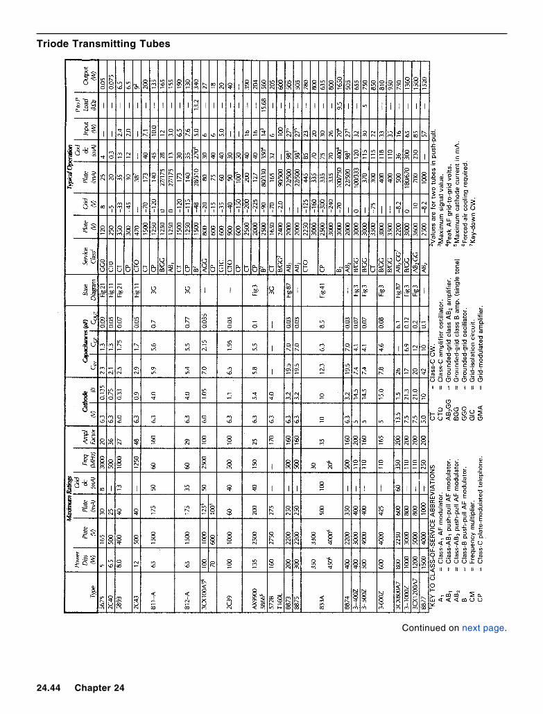
Triode Transmitting Tubes
Continued on next page.
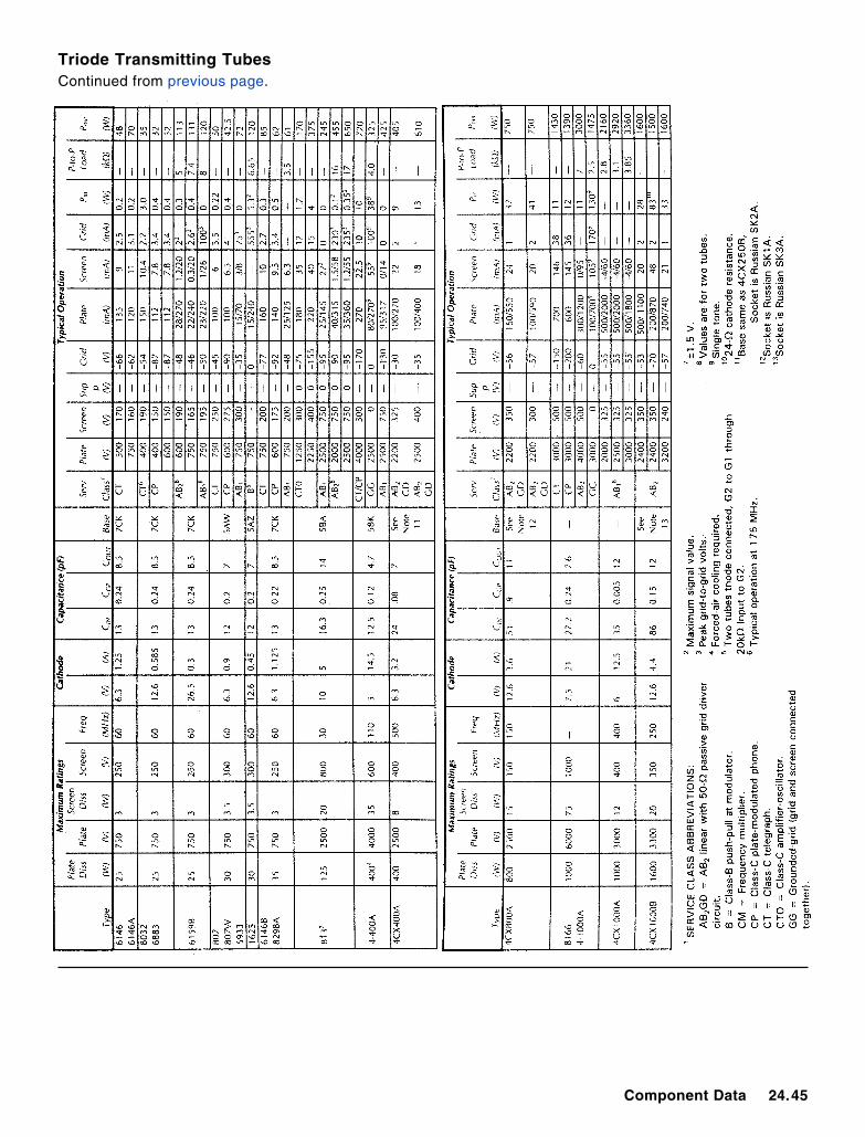
Component Data 24.45
Triode Transmitting TubesContinued from previous page.
24.46 Chapter 24
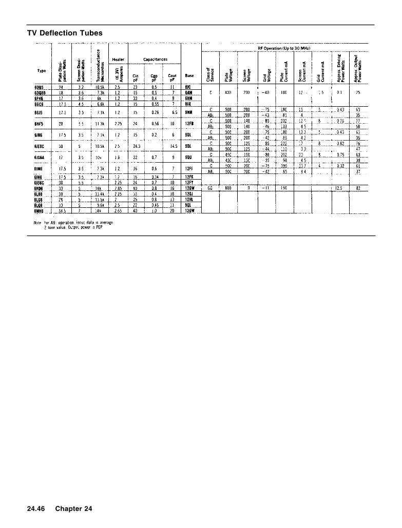
TV Deflection Tubes
Component Data 24.47
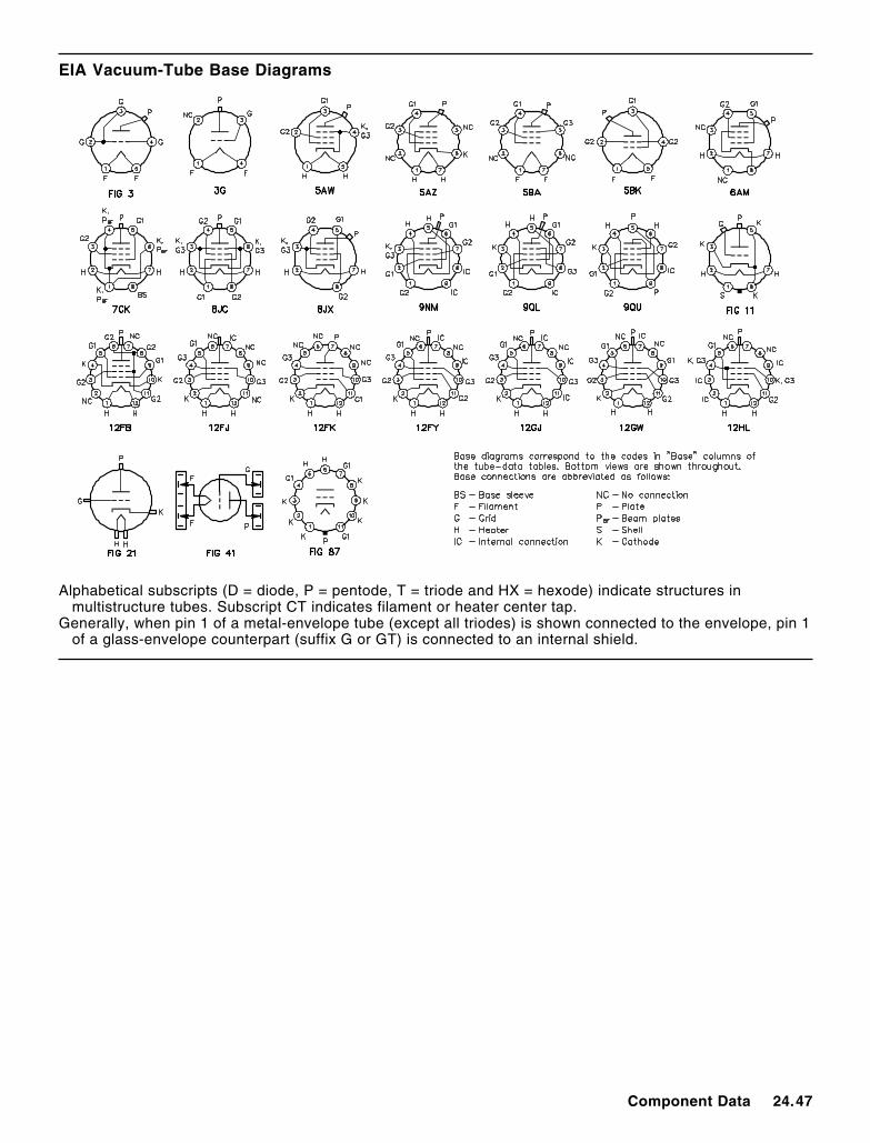
EIA Vacuum-Tube Base Diagrams
Alphabetical subscripts (D = diode, P = pentode, T = triode and HX = hexode) indicate structures inmultistructure tubes. Subscript CT indicates filament or heater center tap.
Generally, when pin 1 of a metal-envelope tube (except all triodes) is shown connected to the envelope, pin 1of a glass-envelope counterpart (suffix G or GT) is connected to an internal shield.
24.48 Chapter 24
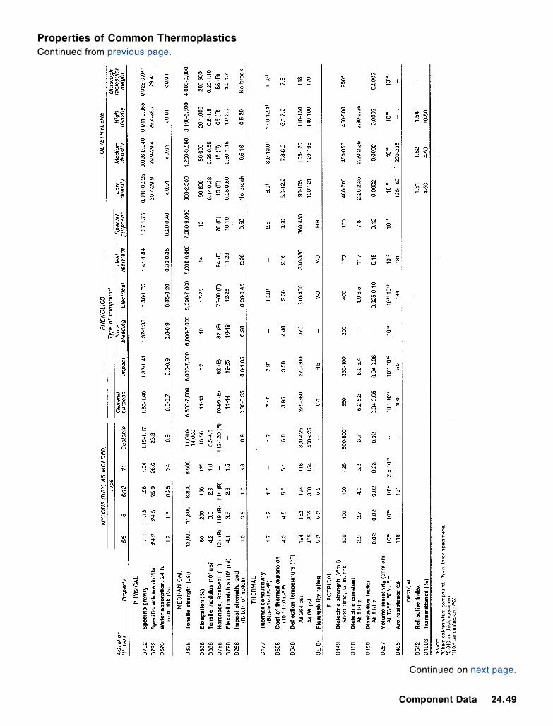
Properties of Common Thermoplastics
Continued on next page.
Component Data 24.49
Properties of Common ThermoplasticsContinued from previous page.
Continued on next page.
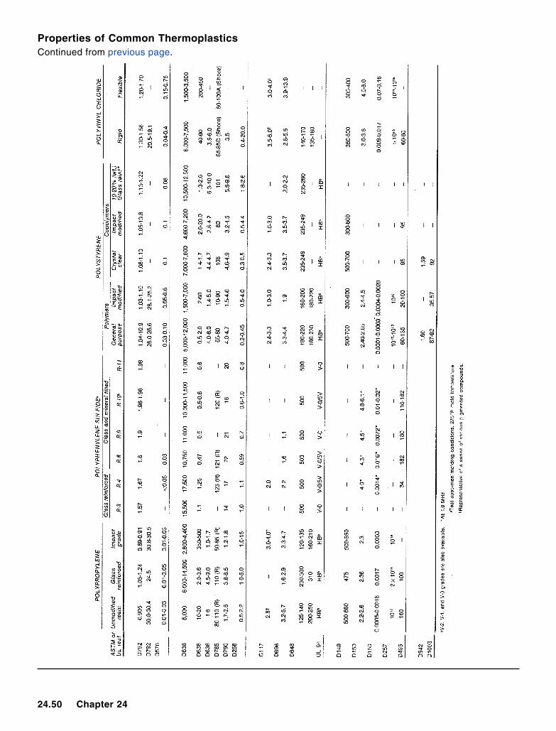
24.50 Chapter 24
Properties of Common ThermoplasticsContinued from previous page.
Component Data 24.51
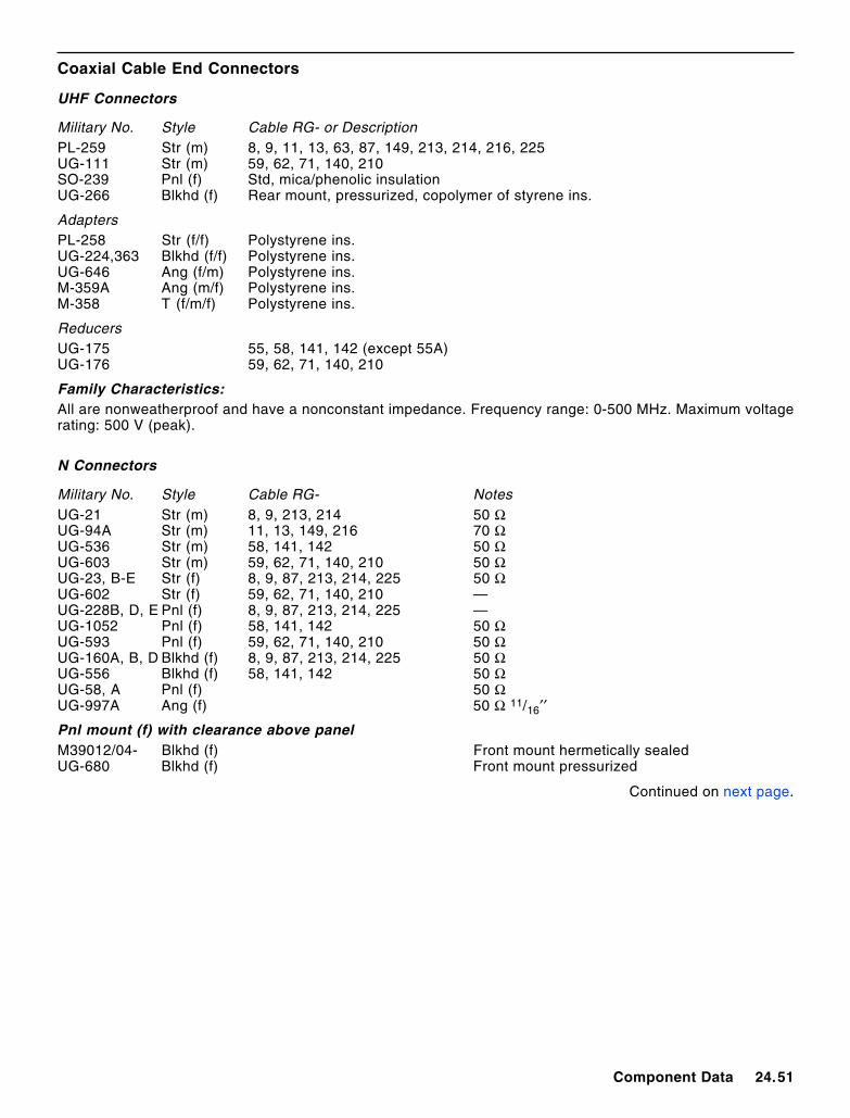
Coaxial Cable End Connectors
UHF Connectors
Military No. Style Cable RG- or DescriptionPL-259 Str (m) 8, 9, 11, 13, 63, 87, 149, 213, 214, 216, 225UG-111 Str (m) 59, 62, 71, 140, 210SO-239 Pnl (f) Std, mica/phenolic insulationUG-266 Blkhd (f) Rear mount, pressurized, copolymer of styrene ins.
AdaptersPL-258 Str (f/f) Polystyrene ins.UG-224,363 Blkhd (f/f) Polystyrene ins.UG-646 Ang (f/m) Polystyrene ins.M-359A Ang (m/f) Polystyrene ins.M-358 T (f/m/f) Polystyrene ins.
ReducersUG-175 55, 58, 141, 142 (except 55A)UG-176 59, 62, 71, 140, 210
Family Characteristics:All are nonweatherproof and have a nonconstant impedance. Frequency range: 0-500 MHz. Maximum voltagerating: 500 V (peak).
N Connectors
Military No. Style Cable RG- NotesUG-21 Str (m) 8, 9, 213, 214 50 ΩUG-94A Str (m) 11, 13, 149, 216 70 ΩUG-536 Str (m) 58, 141, 142 50 ΩUG-603 Str (m) 59, 62, 71, 140, 210 50 ΩUG-23, B-E Str (f) 8, 9, 87, 213, 214, 225 50 ΩUG-602 Str (f) 59, 62, 71, 140, 210 —UG-228B, D, E Pnl (f) 8, 9, 87, 213, 214, 225 —UG-1052 Pnl (f) 58, 141, 142 50 ΩUG-593 Pnl (f) 59, 62, 71, 140, 210 50 ΩUG-160A, B, D Blkhd (f) 8, 9, 87, 213, 214, 225 50 ΩUG-556 Blkhd (f) 58, 141, 142 50 ΩUG-58, A Pnl (f) 50 ΩUG-997A Ang (f) 50 Ω 11/16′′
Pnl mount (f) with clearance above panelM39012/04- Blkhd (f) Front mount hermetically sealedUG-680 Blkhd (f) Front mount pressurized
Continued on next page.
24.52 Chapter 24
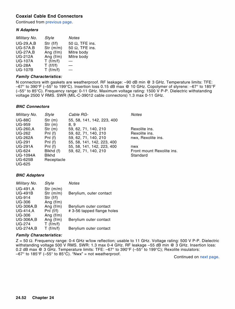
N Adapters
Military No. Style NotesUG-29,A,B Str (f/f) 50 Ω, TFE ins.UG-57A.B Str (m/m) 50 Ω, TFE ins.UG-27A,B Ang (f/m) Mitre bodyUG-212A Ang (f/m) Mitre bodyUG-107A T (f/m/f) —UG-28A T (f/f/f) —UG-107B T (f/m/f) —
Family Characteristics:N connectors with gaskets are weatherproof. RF leakage: –90 dB min @ 3 GHz. Temperature limits: TFE:–67° to 390°F (–55° to 199°C). Insertion loss 0.15 dB max @ 10 GHz. Copolymer of styrene: –67° to 185°F(–55° to 85°C). Frequency range: 0-11 GHz. Maximum voltage rating: 1500 V P-P. Dielectric withstandingvoltage 2500 V RMS. SWR (MIL-C-39012 cable connectors) 1.3 max 0-11 GHz.
BNC Connectors
Military No. Style Cable RG- NotesUG-88C Str (m) 55, 58, 141, 142, 223, 400UG-959 Str (m) 8, 9UG-260,A Str (m) 59, 62, 71, 140, 210 Rexolite ins.UG-262 Pnl (f) 59, 62, 71, 140, 210 Rexolite ins.UG-262A Pnl (f) 59, 62, 71, 140, 210 nwx, Rexolite ins.UG-291 Pnl (f) 55, 58, 141, 142, 223, 400UG-291A Pnl (f) 55, 58, 141, 142, 223, 400 nwxUG-624 Blkhd (f) 59, 62, 71, 140, 210 Front mount Rexolite ins.UG-1094A Blkhd StandardUG-625B ReceptacleUG-625
BNC Adapters
Military No. Style NotesUG-491,A Str (m/m)UG-491B Str (m/m) Berylium, outer contactUG-914 Str (f/f)UG-306 Ang (f/m)UG-306A,B Ang (f/m) Berylium outer contactUG-414,A Pnl (f/f) # 3-56 tapped flange holesUG-306 Ang (f/m)UG-306A,B Ang (f/m) Berylium outer contactUG-274 T (f/m/f)UG-274A,B T (f/m/f) Berylium outer contact
Family Characteristics:Z = 50 Ω. Frequency range: 0-4 GHz w/low reflection; usable to 11 GHz. Voltage rating: 500 V P-P. Dielectricwithstanding voltage 500 V RMS. SWR: 1.3 max 0-4 GHz. RF leakage –55 dB min @ 3 GHz. Insertion loss:0.2 dB max @ 3 GHz. Temperature limits: TFE: –67° to 390°F (–55° to 199°C); Rexolite insulators:–67° to 185°F (–55° to 85°C). “Nwx” = not weatherproof.
Coaxial Cable End ConnectorsContinued from previous page.
Continued on next page.
Component Data 24.53
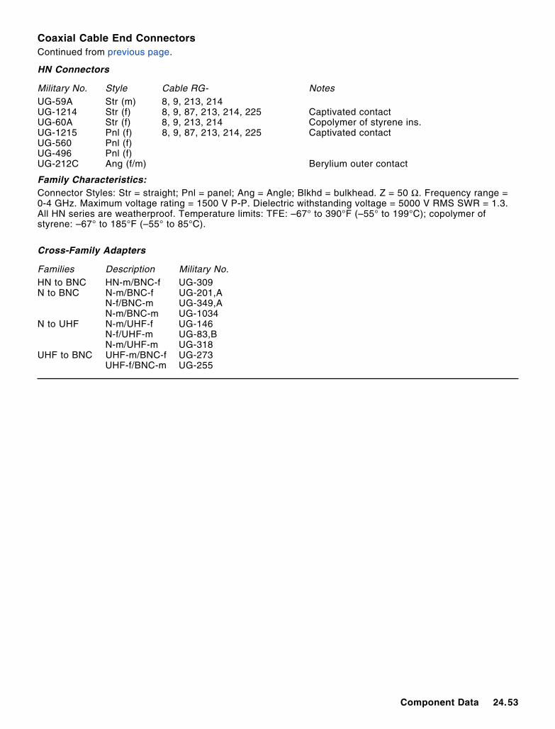
HN Connectors
Military No. Style Cable RG- NotesUG-59A Str (m) 8, 9, 213, 214UG-1214 Str (f) 8, 9, 87, 213, 214, 225 Captivated contactUG-60A Str (f) 8, 9, 213, 214 Copolymer of styrene ins.UG-1215 Pnl (f) 8, 9, 87, 213, 214, 225 Captivated contactUG-560 Pnl (f)UG-496 Pnl (f)UG-212C Ang (f/m) Berylium outer contact
Family Characteristics:Connector Styles: Str = straight; Pnl = panel; Ang = Angle; Blkhd = bulkhead. Z = 50 Ω. Frequency range =0-4 GHz. Maximum voltage rating = 1500 V P-P. Dielectric withstanding voltage = 5000 V RMS SWR = 1.3.All HN series are weatherproof. Temperature limits: TFE: –67° to 390°F (–55° to 199°C); copolymer ofstyrene: –67° to 185°F (–55° to 85°C).
Cross-Family Adapters
Families Description Military No.HN to BNC HN-m/BNC-f UG-309N to BNC N-m/BNC-f UG-201,A
N-f/BNC-m UG-349,AN-m/BNC-m UG-1034
N to UHF N-m/UHF-f UG-146N-f/UHF-m UG-83,BN-m/UHF-m UG-318
UHF to BNC UHF-m/BNC-f UG-273UHF-f/BNC-m UG-255
Coaxial Cable End ConnectorsContinued from previous page.