chapter 1.pmd - arrl
TRANSCRIPT
Getting Started 1.1
Amateur Radio is a diverse and colorfulavocation or hobby where the participantscommunicate with each other through theuse of radio signals. The communications,which can encompass and extend beyondthe planet, are often routine and predict-able, but can at times be ethereal. Theromance of communicating with the otherside of the world blends with the joy ofobserving a complicated part of nature. Forsome of us, the wonder never disappears.
Although radio can be fun, our prag-matic society demands more than excite-ment when resources are used. The virtuethat most often justifies our use of theradio spectrum is the growth of a profi-cient communications system that can becalled upon in times of emergency. Theexamples of its use are numerous.
But, “ham” radio is more than this. It isa technical avocation of diverse educa-tional potential. It has values that go wellbeyond that of a supplementary communi-cations network.
Most radio amateurs have an interest inthe technical details of the equipment theyuse. Historically, this was a requirement:The only way a radio amateur could as-semble an operating station was to person-ally build his or her gear. Commercialequipment was rare, and was often pro-hibitively expensive. But today, high qual-ity “ham” gear is readily available in mostof the world, much of it at modest prices.
Although no longer necessary, it is stillcommon for radio amateurs to build at leastsome of their own equipment. The reasonsare varied and as numerous as the partici-pants. A few purists consider building theequipment they use to be a non-optional,integral part of their hobby in the same way
1.1 EXPERIMENTING, “HOMEBREWING,” AND THE PURSUIT OF THE NEW
that a fly fishing enthusiast would neverconsider fishing with a fly that he or shehad not fabricated. The majority take anintermediate path, building parts of theirradio stations while purchasing others. Forsome, building is an exercise in craftsman-ship, an opportunity to generate equipmentwith an individual imprint and personality.
Common to all of these, amateur radiopresents an opportunity that is rare amongavocations, a chance for individual, unre-strained investigations in fundamental sci-ence and technology. This is a rarity in anage when most research and design is per-formed by teams of investigators withinlarge organizations, be they universities orthe engineering arms of corporations. There,the subjects chosen for investigation are of-ten those of corporate or national interest. Itis increasingly rare that a study is initiatedout of simple curiosity. Fortunately, we arenot so constrained within our personal in-vestigations of radio science.
Consider an example. An experimentallyinclined radio amateur envisions a newscheme for a receiver. It might be a betterfront end circuit, a new block diagram, or away to realize some receiver functions witha computer. The experimenter can analyzethe scheme, design an example, build a pro-totype, build and assemble needed testequipment, measure the receiver perfor-mance, compare it with predicted results,and use the receiver on the air. Each part ofthe investigation can interact with the oth-ers. All of the activity can be done withoutinterference from other sources. The pro-gram will never be cancelled by the chang-ing goals of an organization. Nor will it berushed by the economic pressures of a cor-porate program.
The inspiration for experiment varies. Inrare cases, the experimenter may feel thathis or her work could lead to a new twist inthe state-of-the-art, a better receiver. Butmore often it will just be a casual thoughtthat “Hey, I’ve never built one of thesebefore and I’ll learn something if I do.” Themost common is an effort spurred by a need;a ham wants a rig to take along on a hikingtrip when no such thing can be purchased.No matter what the origin, the experimentercan enjoy the knowledge that he or she islearning more about the subject and aboutthe research process.
In this book we encourage all levels ofwhat has become known as radio “home-brewing,” ranging from beginner projectsto sophisticated multi-mode creations. Wegenerally emphasize simple equipmentdescribed by primitive explanations. Byprimitive, we intend that the discussionrelate to the most fundamental and basiccircuit design concepts. The equipment andsystems presented are themselvesbasic, often without the frills, bells, andwhistles of commercial equipment. Somerefinements will be discussed, allowing theexperimenter to add those he or she needs.
This book emphasizes equipment de-sign. Our interest is in basic circuit func-tions and the underlying concepts thatallow them to be understood. This book isgenerally NOT a collection of projects forreproduction and construction. Althoughsome of the equipment may be directlyduplicated, we would prefer to have youadapt our results to fit your own needs.
This book is, in many ways, a sequel toan earlier effort, Solid State Design for theRadio Amateur.1 That 1977 book,co-authored with the late Doug DeMaw,
CHAPTER 1Getting Started
1.2 Chapter 1
W1FB, had goals similar to those outlinedabove, plus that of introducing solid-statemethods to readers with experience lim-ited to vacuum tube electronics. The laterneed has become arguable, for virtuallyall of our equipment is now based uponsolid-state technology.
All of the circuits presented in this texthave been constructed, tested, and used inpractical, on-the-air situations. If there areexceptions where the authors have not
actually built an example of what is dis-cussed, we will so state in the related text.
We emphasize the traditional commu-nications modes of CW, the original digi-tal mode, and SSB phone. Building littlerigs and radiating and receiving continu-ous waves are to a radio experimentermuch like playing scales and folk tunesare to a musician. They are the first thingswe learn, are important parts of the dailypractice routine throughout life, and we
neglect them at our peril. The little rigs,and the concepts they represent, are at thecore of wireless technology. It is notenough to play with them as a novice andthen move on to other things; they need tobe revisited over and over again at differ-ent stages of one’s vocation, each timeachieving a new level of mastery until fi-nally one is probing the deepest mysteriesof the art.
1.2 GETTING STARTED—ROUTES FOR THE BEGINNING EXPERIMENTER
What to build:A frequent question asked by the pro-
spective experimenter regards an initialproject or subject for pursuit. A commonchoice for a first project comes from adesire to extend the capabilities of an ex-isting station. The future experimenter al-ready has experience with on-the-air ac-tivity and a working station. He or she thenwants to extend that station to new bands,improved transceiver performance, or fab-ricate a rig offering portability. Whilethese goals are all worthy, they can be dif-ficult. They may be conceptually impos-sible for the beginner, and impractical forthe seasoned experimenter with other lifecommitments. A better “first” experimentmay well be something that is much sim-pler. Several simple projects are offeredlater in this chapter as suitable beginnings.
How to build it:Another getting-started question re-
gards the methods to use in building elec-tronics. There are several options, all withtheir assets and weaknesses. A few arediscussed below.
PRINTED CIRCUIT BOARDSThe primary construction scheme used
in modern electronics is the printed circuitboard (PCB). Here, pads or islands ofmetal are attached to an insulating mate-rial, usually epoxy-fiberglass. Wires onthe parts are pushed through holes in theboard and soldered to the pads, which areinterconnected by printed metal runs, thusforming the circuit.
A PCB begins as a fiberglass sheet withcopper laminated to one or both sides. Themetal surfaces are then coated with a lightsensitive “photo-resist” material. A patternfor the circuit is optically transferred to thesurface and the unexposed material iswashed away. The board is now placed in asolution that chemically etches some of the
copper away, leaving only thoseregions needed to form the desired circuit.After etching, the board is washed anddrilled. Pure copper is easily corroded, soit is common to plate boards with a tin coat-ing, forming a more stable and solderablesurface. Refined boards include copper onboth sides, and even plating on the insideof the holes. Industrial boards will oftenincorporate many layers.
Modern practice features surface mounttechnology, SMT, using small compo-nents without wire leads. The leads havebeen replaced with metalized regions onthe parts that are then soldered directly tothe board. The soldering provides physi-cal mounting as well as electrical connec-tion. The SMT boards are cheaper to buildand usually much more dense. SMT partscan be so small that they are hard to handlewithout a good microscope. SMT is aninteresting way to build if there is a needfor really small equipment. The small sizeof SMT circuits often results in improvedhigh frequency performance.
Growing SMT popularity in manufactur-ing means that surface mounted is the onlyavailable form for a component. Manyparts don’t exist in leaded forms. In somecases they can be handled by the “Surf-boards” by Capital Advanced Technolo-gies which are found in DigiKey catalogs.These are small SMT boards with an inter-face that will adapt to other board forms.
Circuit boards have been built in a homeenvironment by hams for generations. Thereader should review the subject in The ARRLHandbook to find out more about the meth-ods. A major problem with home etchedboards is the disposal of the used etchant,usually a solution of ferric chloride. Disposalpractices common in the past are now ques-tioned in this era of enlightened recycling.Although some of the projects described inthis text use etched boards, few of the boardswere etched in our home labs.
BREADBOARDED CIRCUITSBreadboard, as applied to electronics,
is a term from a time when early radioexperimenters built their equipment onslabs of wood, often procured from thekitchen. The term remains as an industry-wide description of a preliminary experi-mental circuit. There are numerousmodern methods that can be used to gener-ate a one-of-a-kind circuit.
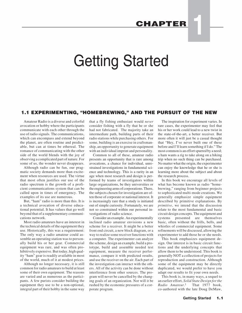
UGLY CONSTRUCTIONA particularly simple method was out-
lined in an early QST paper and is nowknow as “Ugly Construction.”2 Althoughcertainly not unique, the scheme workswell and continues as a recommendedmethod. The scheme consist of the follow-ing:
1. A ground plane is established usingan un-etched scrap of copper clad circuitboard material.
2. Following the schematic for a circuitbeing built, grounded components are sol-dered directly to the ground foil with shortleads.
3. Some non-grounded parts are sol-dered to and supported by the groundedcomponents.
4. Other non-grounded components aresupported with suitable “tie down points”consisting of high value resistors.
5. Once finished and working, the boardcan be mounted in a suitable box, hiddenfrom view if desired, where it becomes apermanent application of the idea. Uglyconstruction is illustrated in Fig 1.1.
Casual circuit analysis allows thebuilder to pick the standoff resistor values.Any “high R” value resistors can be used.Usually, 1-MΩ resistors work well any-where within RF circuits. The typical 1/4W resistor of any value has a stray lead-to-lead parallel capacitance of about 0.3 to0.4 pF, perhaps a little more with longerleads, and a series inductance of 3 to 5 nH.
Getting Started 1.3
Reactance is of little consequence for workup through 150 MHz or so. High R meansthat resistance is high with respect to thereactance of the inductance. We some-times use R values as low as 10 kΩ. It isoften surprising just how few standoff re-sistors are needed in an ugly breadboard.
The greatest virtue of the ugly method islow inductance grounding. Any construc-tion scheme that preserves this groundingintegrity will work as well. Picking amethod is a choice that the builder has, aplace where he or she can develop themethods that work best.
Integrated circuits can be placed on anugly board with leads sticking up, “deadbug” style. There is little need to glue thechips down, for components and wires willeventually hold them in place. GroundedIC leads are bent and soldered directly tothe foil.
Some builders prefer to maintain ICswith the IC label facing upward, allowinglater inspection. They then bend all leadsout in a “spread eagle” format.
We have never had a problem with uglyequipment being less than robust. Many ofour ugly rigs have been hauled through themountains of the Pacific Northwest inpacks without incident. An outstandingexample, the work of a friend, is the W7ELOptimized QRP Transceiver, a rig that hastraveled around the world in suitcases andpacks.3 Few if any standoff resistors wereused in that rig.
MANHATTAN BREADBOARDINGSeveral other construction schemes of-
fer similar grounding fidelity, includingthose where small pads of circuit boardmaterial are glued or soldered to theground foil. These pads then have compo-nents soldered to them. We have found this
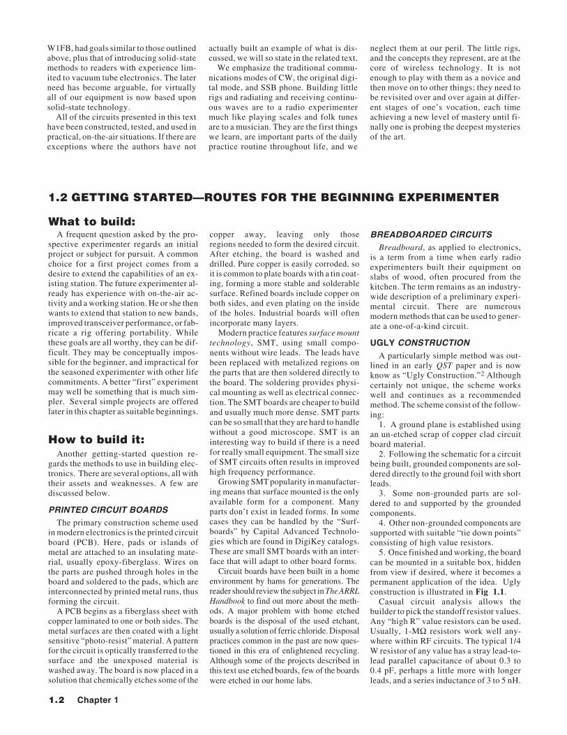
method to be especially useful for slightlymassive components such as floating, non-grounded, trimmer capacitors. The spe-cific glue type has little impact on circuitperformance. Variations of this methodhave been called “Manhattan Construc-tion,” and can be mixed with other bread-boarding schemes. The reader can findnumerous examples on the Web on sitesdealing with QRP experiments, as well asin Fig 1.2.
The proponents of Manhattan Construc-tion often use small round pads that areglued to a ground foil with epoxy or simi-lar glue. The pads are placed so that allcomponents are parallel to board edgesand close to the ground foil. This producesan attractive board resembling a commer-cial, PC board. This does not seem to com-promise performance.
With traditional ugly construction, partscan be moved about to make room for an-other stage. In the extreme, an entire cir-cuit can be lifted and moved, a stage at atime, to another board.
A primary virtue of a bread-boardingscheme is construction speed and flexibil-ity, especially important when the primarypurpose of building gear is informationabout circuit behavior.
Some folks prefer to rebuild a circuitafter a breadboarding phase, replacing anugly prototype with a more permanent,production-like version. These efforts takeadditional time and rarely produce perfor-mance superior to the original bread-boards. Even looks can be deceptive whenone hides ugly breadboards behind moreattractive front panels.
QUASI-PRINTED BOARDSSome experimenters prefer to build
equipment that looks like a PCB, even
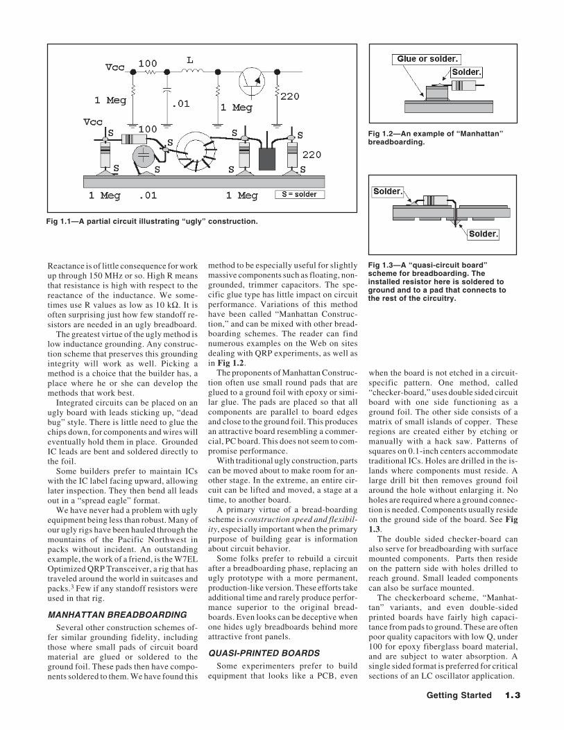
when the board is not etched in a circuit-specific pattern. One method, called“checker-board,” uses double sided circuitboard with one side functioning as aground foil. The other side consists of amatrix of small islands of copper. Theseregions are created either by etching ormanually with a hack saw. Patterns ofsquares on 0.1-inch centers accommodatetraditional ICs. Holes are drilled in the is-lands where components must reside. Alarge drill bit then removes ground foilaround the hole without enlarging it. Noholes are required where a ground connec-tion is needed. Components usually resideon the ground side of the board. See Fig1.3.
The double sided checker-board canalso serve for breadboarding with surfacemounted components. Parts then resideon the pattern side with holes drilled toreach ground. Small leaded componentscan also be surface mounted.
The checkerboard scheme, “Manhat-tan” variants, and even double-sidedprinted boards have fairly high capaci-tance from pads to ground. These are oftenpoor quality capacitors with low Q, under100 for epoxy fiberglass board material,and are subject to water absorption. Asingle sided format is preferred for criticalsections of an LC oscillator application.
Fig 1.1—A partial circuit illustrating “ugly” construction.
Fig 1.3—A “quasi-circuit board”scheme for breadboarding. Theinstalled resistor here is soldered toground and to a pad that connects tothe rest of the circuitry.
Fig 1.2—An example of “Manhattan”breadboarding.
1.4 Chapter 1
1.3 SOME GUIDELINES FOR THE EXPERIMENTER
With Solid-State Design for the RadioAmateur came considerable interactionwith the rest of the amateur radio commu-nity. A frequent question we heard was“How do I get started with experiment-ing?” Or, “I’ve read about and have evenbuilt some kits and published projects, butI want to go further. I want to do my owndesign. What is the next step?”
A set of guidelines is offered in an at-tempt to answer some of these questions.These are not firm, well established rules,but mere impressions and personal biasesthat we have generated, approaches thatwork for us. They are offered withoutguarantee.
•KISS: This British term is short for“Keep It Simple, Stupid.” We often designequipment that is more complicated thanneeded. It is well worth some extra timeduring design to evaluate every part to see ifit is really needed. The function of each partshould be understood and justified. The cir-cuit should function as intended. This doesnot imply that designs with the minimumnumber of parts are best. However, it israrely justified to overdesign by adding ex-tra components “because a problem mightoccur.” For example, designs with a profu-sion of ferrite beads and “stability enhanc-ing” resistors may be suspect.
•Avoid lore: Lore, in this case, refers to“knowledge” that is based upon experi-ences that are divorced from carefulthought. A classic example in amateur ra-dio regards the thermal stability of LCoscillators. Envision the amateur experi-menter who built an oscillator using a tor-oid. The circuit drifted when he openedthe window to the winter weather. Thenext evening he replaced the inductor withone wound on a ceramic coil form, notic-ing less drift when he opened the window.He concluded that ceramic forms are bet-ter than toroids, having never consideredthe specific coil forms that were used, theother components in the circuit, or the factthat the weather had improved. Poorlyexecuted experiments like this often gen-erate erroneous conclusions. The result-ing lore, although interesting, shouldalways be questioned. It is always betterto do meaningful measurements.
•Plan your projects with block dia-grams: Start with small diagrams whereeach block is a global element, perhapscontaining several stages. Expand these toshow greater detail. Block diagrams willbe discussed further below.
•Generate modular equipment: A highperformance receiver, for example, should
consist of several sections, each designedso that it can be built, tested, modified, andredesigned as needed, with minimalchange to the rest of the system. Even thesimplest little rig should be built a stage ata time, turned on sequentially, tested, andmodified as needed. Single board trans-ceiver designs are popular in the QRParena. But realize that the ones that workwell are probably the result of several re-builds, and even then, some don’t workvery well; others are superb.
• Avoid excessive miniaturization: Ittakes much more time to build small thingsthan those where the circuitry can expandwithout bound. Even when building smallportable QRP transceivers, it’s oftenworthwhile to establish the design with alarger breadboard.
• Base projects on your own goals: Ourcentral personal goal is learning throughexperimentation. Hence, we base projectson questions that need investigation ratherthan what we need or want for on-the-airoperation. But your goals may be differ-ent. It is worthwhile to review and definethem as a means of picking the bestprojects for you. Isolate primary goalsfrom those that are serendipity.
• Be wary of “Creeping Features.” Theterm “appliance” often describes thetransceivers that we purchase foron-the-air communications. Appliances,even ones that we build ourselves, areusually expected to have many features,but these bells and whistles can actuallyimpede experimental progress. A singleband, single mode transceiver can be asexperimentally enlightening and informa-tive as a multiple mode, general coveragetransceiver.
• Use the literature. Peruse catalogs,data manuals, web sites, and even instruc-tion manuals for circuit ideas. When a cir-cuit method is not understood, it should bestudied in texts appropriate to the technol-ogy. It is useful to build something withthe part as a way to really understand thatpart.
• While planning is necessary, don’tspend excessive time in the preliminarydesign phase of a project. Rather, outlinepreliminary ideas and goals, do initial cal-culations (on a computer only if they arereally complicated), gather parts, andbegin building. Enjoy the freedom thatallows you to change your mind in themiddle of an investigation. Refined calcu-lations can occur during and after con-struction and are not just “design phase”activities.
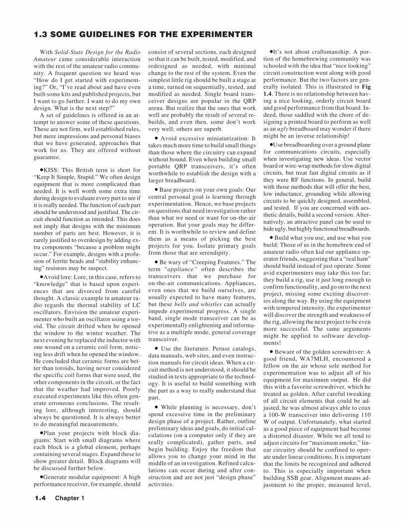
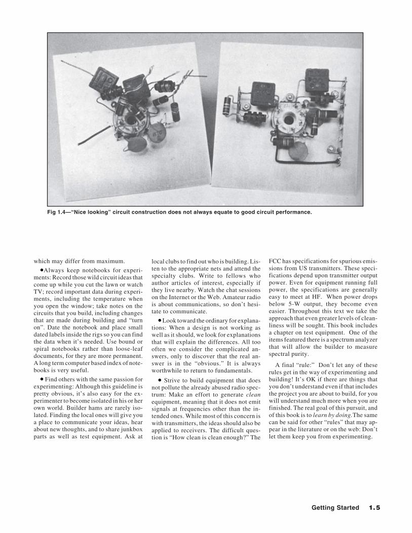
•It’s not about craftsmanship: A por-tion of the homebrewing community wasschooled with the idea that “nice looking”circuit construction went along with goodperformance. But the two factors are gen-erally isolated. This is illustrated in Fig1.4. There is no relationship between hav-ing a nice looking, orderly circuit boardand good performance from that board. In-deed, those saddled with the chore of de-signing a printed board to perform as wellas an ugly breadboard may wonder if theremight be an inverse relationship!
•Use breadboarding over a ground planefor communications circuits, especiallywhen investigating new ideas. Use vectorboard or wire-wrap methods for slow digitalcircuits, but treat fast digital circuits as ifthey were RF functions. In general, buildwith those methods that will offer the best,low inductance, grounding while allowingcircuits to be quickly designed, assembled,and tested. If you are concerned with aes-thetic details, build a second version. Alter-natively, an attractive panel can be used tohide ugly, but highly functional breadboards.
• Build what you use, and use what youbuild: Those of us in the homebrew end ofamateur radio often kid our appliance op-erator friends, suggesting that a “real ham”should build instead of just operate. Someavid experimenters may take this too far;they build a rig, use it just long enough toconfirm functionality, and go on to the nextproject, missing some exciting discover-ies along the way. By using the equipmentwith tempered intensity, the experimenterwill discover the strength and weakness ofthe rig, allowing the next project to be evenmore successful. The same argumentsmight be applied to software develop-ments!
• Beware of the golden screwdriver: Agood friend, WA7MLH, encountered afellow on the air whose sole method forexperimentation was to adjust all of hisequipment for maximum output. He didthis with a favorite screwdriver, which hetreated as golden. After careful tweakingof all circuit elements that could be ad-justed, he was almost always able to coaxa 100-W transceiver into delivering 110W of output. Unfortunately, what startedas a good piece of equipment had becomea distorted disaster. While we all tend toadjust circuits for “maximum smoke,” lin-ear circuitry should be confined to oper-ate under linear conditions. It is importantthat the limits be recognized and adheredto. This is especially important whenbuilding SSB gear. Alignment means ad-justment to the proper, measured level,
Getting Started 1.5
which may differ from maximum.
•Always keep notebooks for experi-ments: Record those wild circuit ideas thatcome up while you cut the lawn or watchTV; record important data during experi-ments, including the temperature whenyou open the window; take notes on thecircuits that you build, including changesthat are made during building and “turnon”. Date the notebook and place smalldated labels inside the rigs so you can findthe data when it’s needed. Use bound orspiral notebooks rather than loose-leafdocuments, for they are more permanent.A long term computer based index of note-books is very useful.
• Find others with the same passion forexperimenting: Although this guideline ispretty obvious, it’s also easy for the ex-perimenter to become isolated in his or herown world. Builder hams are rarely iso-lated. Finding the local ones will give youa place to communicate your ideas, hearabout new thoughts, and to share junkboxparts as well as test equipment. Ask at
Fig 1.4—“Nice looking” circuit construction does not always equate to good circuit performance.
local clubs to find out who is building. Lis-ten to the appropriate nets and attend thespecialty clubs. Write to fellows whoauthor articles of interest, especially ifthey live nearby. Watch the chat sessionson the Internet or the Web. Amateur radiois about communications, so don’t hesi-tate to communicate.
• Look toward the ordinary for explana-tions: When a design is not working aswell as it should, we look for explanationsthat will explain the differences. All toooften we consider the complicated an-swers, only to discover that the real an-swer is in the “obvious.” It is alwaysworthwhile to return to fundamentals.
• Strive to build equipment that doesnot pollute the already abused radio spec-trum: Make an effort to generate cleanequipment, meaning that it does not emitsignals at frequencies other than the in-tended ones. While most of this concern iswith transmitters, the ideas should also beapplied to receivers. The difficult ques-tion is “How clean is clean enough?” The
FCC has specifications for spurious emis-sions from US transmitters. These speci-fications depend upon transmitter outputpower. Even for equipment running fullpower, the specifications are generallyeasy to meet at HF. When power dropsbelow 5-W output, they become eveneasier. Throughout this text we take theapproach that even greater levels of clean-liness will be sought. This book includesa chapter on test equipment. One of theitems featured there is a spectrum analyzerthat will allow the builder to measurespectral purity.
A final “rule:” Don’t let any of theserules get in the way of experimenting andbuilding! It’s OK if there are things thatyou don’t understand even if that includesthe project you are about to build, for youwill understand much more when you arefinished. The real goal of this pursuit, andof this book is to learn by doing.The samecan be said for other “rules” that may ap-pear in the literature or on the web: Don’tlet them keep you from experimenting.
1.6 Chapter 1
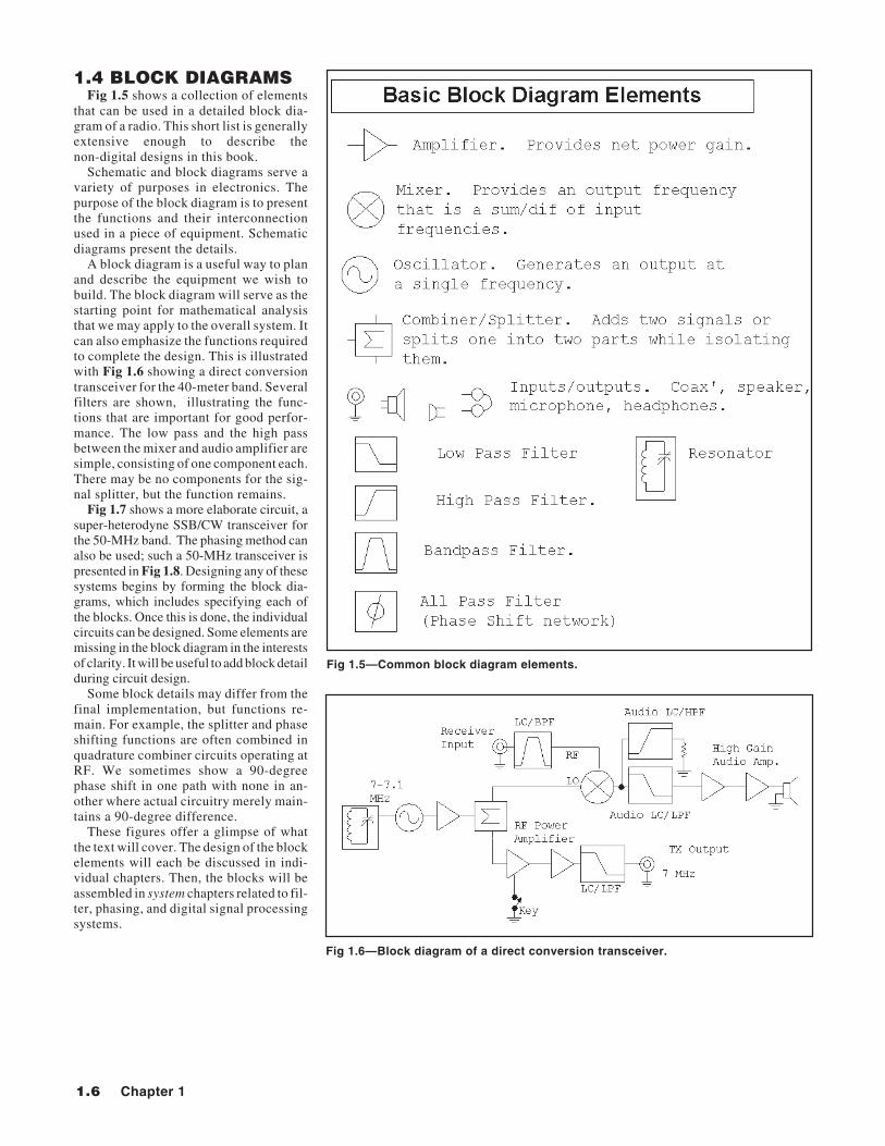
1.4 BLOCK DIAGRAMSFig 1.5 shows a collection of elements
that can be used in a detailed block dia-gram of a radio. This short list is generallyextensive enough to describe thenon-digital designs in this book.
Schematic and block diagrams serve avariety of purposes in electronics. Thepurpose of the block diagram is to presentthe functions and their interconnectionused in a piece of equipment. Schematicdiagrams present the details.
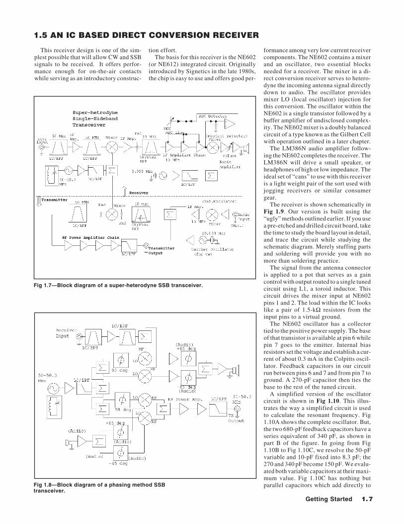
A block diagram is a useful way to planand describe the equipment we wish tobuild. The block diagram will serve as thestarting point for mathematical analysisthat we may apply to the overall system. Itcan also emphasize the functions requiredto complete the design. This is illustratedwith Fig 1.6 showing a direct conversiontransceiver for the 40-meter band. Severalfilters are shown, illustrating the func-tions that are important for good perfor-mance. The low pass and the high passbetween the mixer and audio amplifier aresimple, consisting of one component each.There may be no components for the sig-nal splitter, but the function remains.
Fig 1.7 shows a more elaborate circuit, asuper-heterodyne SSB/CW transceiver forthe 50-MHz band. The phasing method canalso be used; such a 50-MHz transceiver ispresented in Fig 1.8. Designing any of thesesystems begins by forming the block dia-grams, which includes specifying each ofthe blocks. Once this is done, the individualcircuits can be designed. Some elements aremissing in the block diagram in the interestsof clarity. It will be useful to add block detailduring circuit design.
Some block details may differ from thefinal implementation, but functions re-main. For example, the splitter and phaseshifting functions are often combined inquadrature combiner circuits operating atRF. We sometimes show a 90-degreephase shift in one path with none in an-other where actual circuitry merely main-tains a 90-degree difference.
These figures offer a glimpse of whatthe text will cover. The design of the blockelements will each be discussed in indi-vidual chapters. Then, the blocks will beassembled in system chapters related to fil-ter, phasing, and digital signal processingsystems.
Fig 1.6—Block diagram of a direct conversion transceiver.
Fig 1.5—Common block diagram elements.
Getting Started 1.7
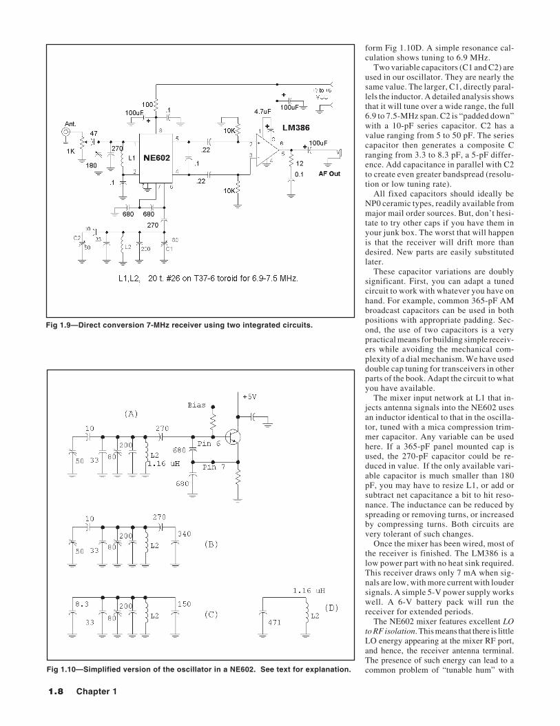
1.5 AN IC BASED DIRECT CONVERSION RECEIVER
Fig 1.8—Block diagram of a phasing method SSBtransceiver.
Fig 1.7—Block diagram of a super-heterodyne SSB transceiver.
This receiver design is one of the sim-plest possible that will allow CW and SSBsignals to be received. It offers perfor-mance enough for on-the-air contactswhile serving as an introductory construc-
tion effort.The basis for this receiver is the NE602
(or NE612) integrated circuit. Originallyintroduced by Signetics in the late 1980s,the chip is easy to use and offers good per-
formance among very low current receivercomponents. The NE602 contains a mixerand an oscillator, two essential blocksneeded for a receiver. The mixer in a di-rect conversion receiver serves to hetero-dyne the incoming antenna signal directlydown to audio. The oscillator providesmixer LO (local oscillator) injection forthis conversion. The oscillator within theNE602 is a single transistor followed by abuffer amplifier of undisclosed complex-ity. The NE602 mixer is a doubly balancedcircuit of a type known as the Gilbert Cellwith operation outlined in a later chapter.
The LM386N audio amplifier follow-ing the NE602 completes the receiver. TheLM386N will drive a small speaker, orheadphones of high or low impedance. Theideal set of “cans” to use with this receiveris a light weight pair of the sort used withjogging receivers or similar consumergear.
The receiver is shown schematically inFig 1.9. Our version is built using the“ugly” methods outlined earlier. If you usea pre-etched and drilled circuit board, takethe time to study the board layout in detail,and trace the circuit while studying theschematic diagram. Merely stuffing partsand soldering will provide you with nomore than soldering practice.
The signal from the antenna connectoris applied to a pot that serves as a gaincontrol with output routed to a single tunedcircuit using L1, a toroid inductor. Thiscircuit drives the mixer input at NE602pins 1 and 2. The load within the IC lookslike a pair of 1.5-kΩ resistors from theinput pins to a virtual ground.
The NE602 oscillator has a collectortied to the positive power supply. The baseof that transistor is available at pin 6 whilepin 7 goes to the emitter. Internal biasresistors set the voltage and establish a cur-rent of about 0.3 mA in the Colpitts oscil-lator. Feedback capacitors in our circuitrun between pins 6 and 7 and from pin 7 toground. A 270-pF capacitor then ties thebase to the rest of the tuned circuit.
A simplified version of the oscillatorcircuit is shown in Fig 1.10. This illus-trates the way a simplified circuit is usedto calculate the resonant frequency. Fig1.10A shows the complete oscillator. But,the two 680-pF feedback capacitors have aseries equivalent of 340 pF, as shown inpart B of the figure. In going from Fig1.10B to Fig 1.10C, we resolve the 50-pFvariable and 10-pF fixed into 8.3 pF; the270 and 340 pF become 150 pF. We evalu-ated both variable capacitors at their maxi-mum value. Fig 1.10C has nothing butparallel capacitors which add directly to
1.8 Chapter 1
form Fig 1.10D. A simple resonance cal-culation shows tuning to 6.9 MHz.
Two variable capacitors (C1 and C2) areused in our oscillator. They are nearly thesame value. The larger, C1, directly paral-lels the inductor. A detailed analysis showsthat it will tune over a wide range, the full6.9 to 7.5-MHz span. C2 is “padded down”with a 10-pF series capacitor. C2 has avalue ranging from 5 to 50 pF. The seriescapacitor then generates a composite Cranging from 3.3 to 8.3 pF, a 5-pF differ-ence. Add capacitance in parallel with C2to create even greater bandspread (resolu-tion or low tuning rate).
All fixed capacitors should ideally beNP0 ceramic types, readily available frommajor mail order sources. But, don’t hesi-tate to try other caps if you have them inyour junk box. The worst that will happenis that the receiver will drift more thandesired. New parts are easily substitutedlater.
These capacitor variations are doublysignificant. First, you can adapt a tunedcircuit to work with whatever you have onhand. For example, common 365-pF AMbroadcast capacitors can be used in bothpositions with appropriate padding. Sec-ond, the use of two capacitors is a verypractical means for building simple receiv-ers while avoiding the mechanical com-plexity of a dial mechanism. We have useddouble cap tuning for transceivers in otherparts of the book. Adapt the circuit to whatyou have available.
The mixer input network at L1 that in-jects antenna signals into the NE602 usesan inductor identical to that in the oscilla-tor, tuned with a mica compression trim-mer capacitor. Any variable can be usedhere. If a 365-pF panel mounted cap isused, the 270-pF capacitor could be re-duced in value. If the only available vari-able capacitor is much smaller than 180pF, you may have to resize L1, or add orsubtract net capacitance a bit to hit reso-nance. The inductance can be reduced byspreading or removing turns, or increasedby compressing turns. Both circuits arevery tolerant of such changes.
Once the mixer has been wired, most ofthe receiver is finished. The LM386 is alow power part with no heat sink required.This receiver draws only 7 mA when sig-nals are low, with more current with loudersignals. A simple 5-V power supply workswell. A 6-V battery pack will run thereceiver for extended periods.
The NE602 mixer features excellent LOto RF isolation. This means that there is littleLO energy appearing at the mixer RF port,and hence, the receiver antenna terminal.The presence of such energy can lead to acommon problem of “tunable hum” withFig 1.10—Simplified version of the oscillator in a NE602. See text for explanation.
Fig 1.9—Direct conversion 7-MHz receiver using two integrated circuits.
Getting Started 1.9
some direct conversion receivers.The receiver also has problems. Some,
the audio images, are intrinsic to all simpledirect conversion receivers. This is theprice, but also the thrill of such a design.The selectivity is lacking. This can be rem-edied with audio filters that can be placedin the receiver. Examples of audio filtersare found elsewhere in this book. Thesefilters would go between the mixer and theaudio amplifier. It is easy to add suchthings to a breadboarded receiver, butmore difficult with a printed board.
The greatest performance deficiency is
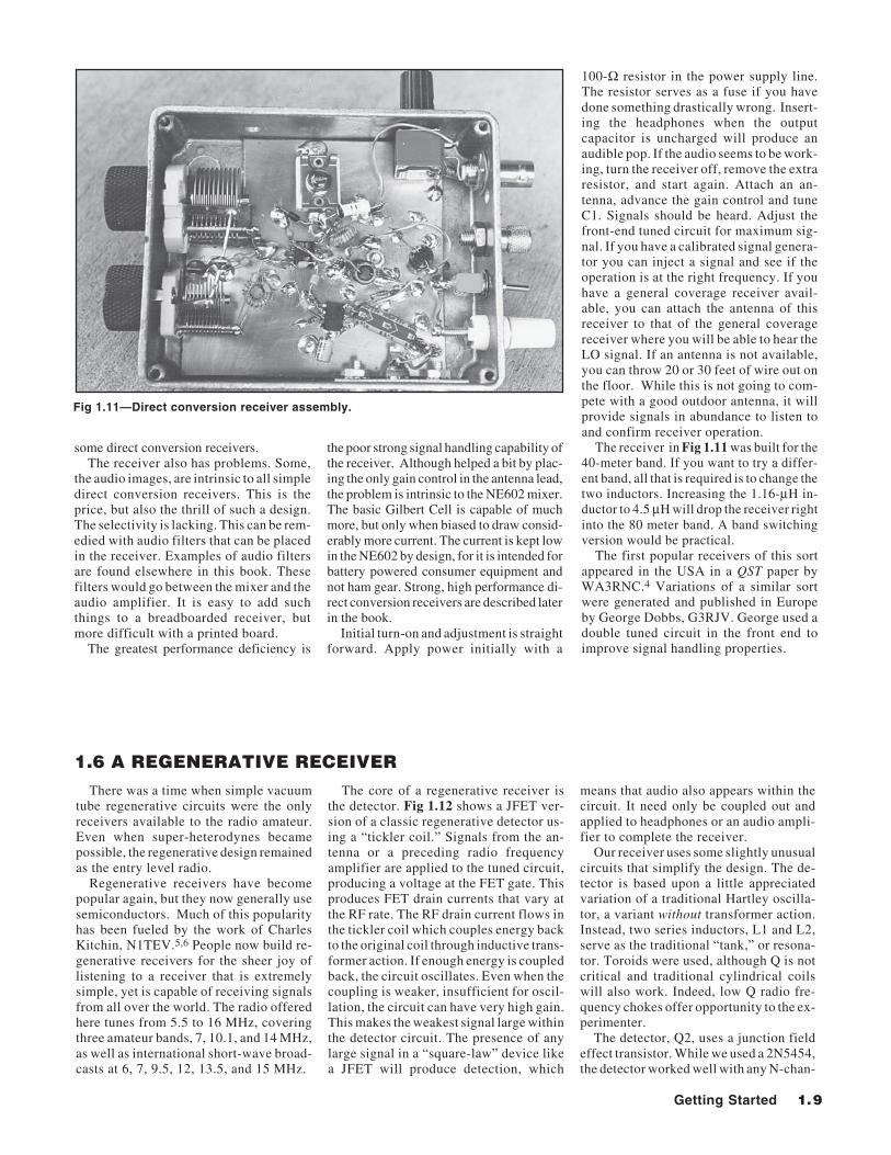
100-Ω resistor in the power supply line.The resistor serves as a fuse if you havedone something drastically wrong. Insert-ing the headphones when the outputcapacitor is uncharged will produce anaudible pop. If the audio seems to be work-ing, turn the receiver off, remove the extraresistor, and start again. Attach an an-tenna, advance the gain control and tuneC1. Signals should be heard. Adjust thefront-end tuned circuit for maximum sig-nal. If you have a calibrated signal genera-tor you can inject a signal and see if theoperation is at the right frequency. If youhave a general coverage receiver avail-able, you can attach the antenna of thisreceiver to that of the general coveragereceiver where you will be able to hear theLO signal. If an antenna is not available,you can throw 20 or 30 feet of wire out onthe floor. While this is not going to com-pete with a good outdoor antenna, it willprovide signals in abundance to listen toand confirm receiver operation.
The receiver in Fig 1.11 was built for the40-meter band. If you want to try a differ-ent band, all that is required is to change thetwo inductors. Increasing the 1.16-μH in-ductor to 4.5 μH will drop the receiver rightinto the 80 meter band. A band switchingversion would be practical.
The first popular receivers of this sortappeared in the USA in a QST paper byWA3RNC.4 Variations of a similar sortwere generated and published in Europeby George Dobbs, G3RJV. George used adouble tuned circuit in the front end toimprove signal handling properties.
Fig 1.11—Direct conversion receiver assembly.
the poor strong signal handling capability ofthe receiver. Although helped a bit by plac-ing the only gain control in the antenna lead,the problem is intrinsic to the NE602 mixer.The basic Gilbert Cell is capable of muchmore, but only when biased to draw consid-erably more current. The current is kept lowin the NE602 by design, for it is intended forbattery powered consumer equipment andnot ham gear. Strong, high performance di-rect conversion receivers are described laterin the book.
Initial turn-on and adjustment is straightforward. Apply power initially with a
1.6 A REGENERATIVE RECEIVERThere was a time when simple vacuum
tube regenerative circuits were the onlyreceivers available to the radio amateur.Even when super-heterodynes becamepossible, the regenerative design remainedas the entry level radio.
Regenerative receivers have becomepopular again, but they now generally usesemiconductors. Much of this popularityhas been fueled by the work of CharlesKitchin, N1TEV.5,6 People now build re-generative receivers for the sheer joy oflistening to a receiver that is extremelysimple, yet is capable of receiving signalsfrom all over the world. The radio offeredhere tunes from 5.5 to 16 MHz, coveringthree amateur bands, 7, 10.1, and 14 MHz,as well as international short-wave broad-casts at 6, 7, 9.5, 12, 13.5, and 15 MHz.
means that audio also appears within thecircuit. It need only be coupled out andapplied to headphones or an audio ampli-fier to complete the receiver.
Our receiver uses some slightly unusualcircuits that simplify the design. The de-tector is based upon a little appreciatedvariation of a traditional Hartley oscilla-tor, a variant without transformer action.Instead, two series inductors, L1 and L2,serve as the traditional “tank,” or resona-tor. Toroids were used, although Q is notcritical and traditional cylindrical coilswill also work. Indeed, low Q radio fre-quency chokes offer opportunity to the ex-perimenter.
The detector, Q2, uses a junction fieldeffect transistor. While we used a 2N5454,the detector worked well with any N-chan-
The core of a regenerative receiver isthe detector. Fig 1.12 shows a JFET ver-sion of a classic regenerative detector us-ing a “tickler coil.” Signals from the an-tenna or a preceding radio frequencyamplifier are applied to the tuned circuit,producing a voltage at the FET gate. Thisproduces FET drain currents that vary atthe RF rate. The RF drain current flows inthe tickler coil which couples energy backto the original coil through inductive trans-former action. If enough energy is coupledback, the circuit oscillates. Even when thecoupling is weaker, insufficient for oscil-lation, the circuit can have very high gain.This makes the weakest signal large withinthe detector circuit. The presence of anylarge signal in a “square-law” device likea JFET will produce detection, which
1.10 Chapter 1
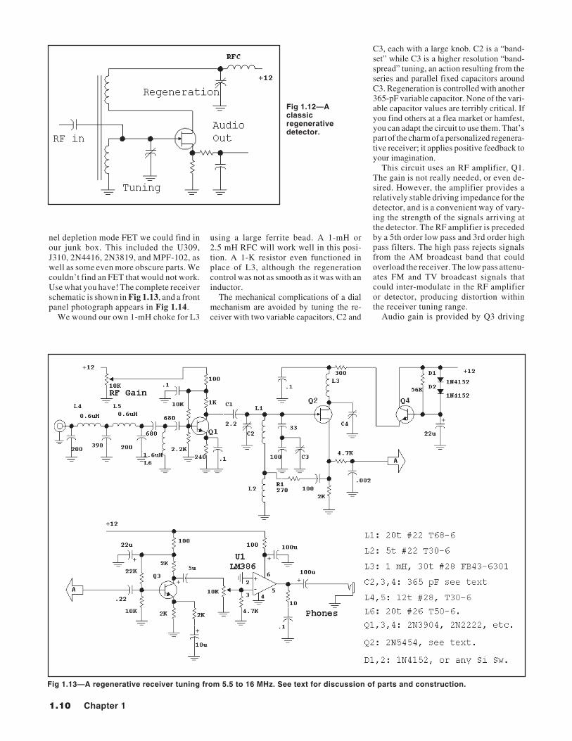
nel depletion mode FET we could find inour junk box. This included the U309,J310, 2N4416, 2N3819, and MPF-102, aswell as some even more obscure parts. Wecouldn’t find an FET that would not work.Use what you have! The complete receiverschematic is shown in Fig 1.13, and a frontpanel photograph appears in Fig 1.14.
We wound our own 1-mH choke for L3
Fig 1.13—A regenerative receiver tuning from 5.5 to 16 MHz. See text for discussion of parts and construction.
Fig 1.12—Aclassicregenerativedetector.
using a large ferrite bead. A 1-mH or2.5 mH RFC will work well in this posi-tion. A 1-K resistor even functioned inplace of L3, although the regenerationcontrol was not as smooth as it was with aninductor.
The mechanical complications of a dialmechanism are avoided by tuning the re-ceiver with two variable capacitors, C2 and
C3, each with a large knob. C2 is a “band-set” while C3 is a higher resolution “band-spread” tuning, an action resulting from theseries and parallel fixed capacitors aroundC3. Regeneration is controlled with another365-pF variable capacitor. None of the vari-able capacitor values are terribly critical. Ifyou find others at a flea market or hamfest,you can adapt the circuit to use them. That’spart of the charm of a personalized regenera-tive receiver; it applies positive feedback toyour imagination.
This circuit uses an RF amplifier, Q1.The gain is not really needed, or even de-sired. However, the amplifier provides arelatively stable driving impedance for thedetector, and is a convenient way of vary-ing the strength of the signals arriving atthe detector. The RF amplifier is precededby a 5th order low pass and 3rd order highpass filters. The high pass rejects signalsfrom the AM broadcast band that couldoverload the receiver. The low pass attenu-ates FM and TV broadcast signals thatcould inter-modulate in the RF amplifieror detector, producing distortion withinthe receiver tuning range.
Audio gain is provided by Q3 driving
Getting Started 1.11
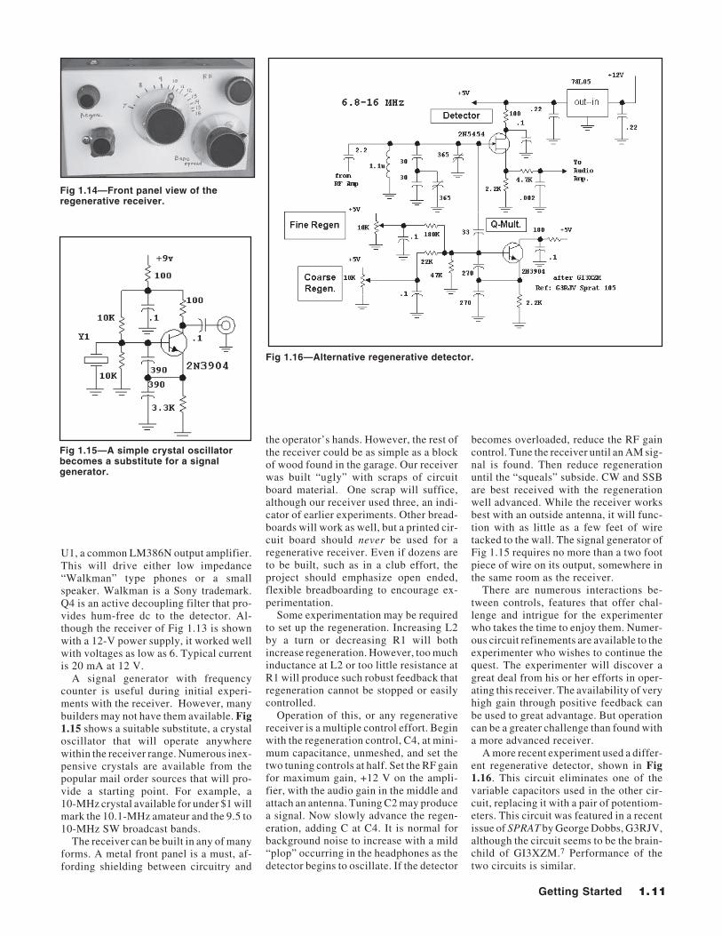
Fig 1.14—Front panel view of theregenerative receiver.
Fig 1.15—A simple crystal oscillatorbecomes a substitute for a signalgenerator.
Fig 1.16—Alternative regenerative detector.
U1, a common LM386N output amplifier.This will drive either low impedance“Walkman” type phones or a smallspeaker. Walkman is a Sony trademark.Q4 is an active decoupling filter that pro-vides hum-free dc to the detector. Al-though the receiver of Fig 1.13 is shownwith a 12-V power supply, it worked wellwith voltages as low as 6. Typical currentis 20 mA at 12 V.
A signal generator with frequencycounter is useful during initial experi-ments with the receiver. However, manybuilders may not have them available. Fig1.15 shows a suitable substitute, a crystaloscillator that will operate anywherewithin the receiver range. Numerous inex-pensive crystals are available from thepopular mail order sources that will pro-vide a starting point. For example, a10-MHz crystal available for under $1 willmark the 10.1-MHz amateur and the 9.5 to10-MHz SW broadcast bands.
The receiver can be built in any of manyforms. A metal front panel is a must, af-fording shielding between circuitry and
the operator’s hands. However, the rest ofthe receiver could be as simple as a blockof wood found in the garage. Our receiverwas built “ugly” with scraps of circuitboard material. One scrap will suffice,although our receiver used three, an indi-cator of earlier experiments. Other bread-boards will work as well, but a printed cir-cuit board should never be used for aregenerative receiver. Even if dozens areto be built, such as in a club effort, theproject should emphasize open ended,flexible breadboarding to encourage ex-perimentation.
Some experimentation may be requiredto set up the regeneration. Increasing L2by a turn or decreasing R1 will bothincrease regeneration. However, too muchinductance at L2 or too little resistance atR1 will produce such robust feedback thatregeneration cannot be stopped or easilycontrolled.
Operation of this, or any regenerativereceiver is a multiple control effort. Beginwith the regeneration control, C4, at mini-mum capacitance, unmeshed, and set thetwo tuning controls at half. Set the RF gainfor maximum gain, +12 V on the ampli-fier, with the audio gain in the middle andattach an antenna. Tuning C2 may producea signal. Now slowly advance the regen-eration, adding C at C4. It is normal forbackground noise to increase with a mild“plop” occurring in the headphones as thedetector begins to oscillate. If the detector
becomes overloaded, reduce the RF gaincontrol. Tune the receiver until an AM sig-nal is found. Then reduce regenerationuntil the “squeals” subside. CW and SSBare best received with the regenerationwell advanced. While the receiver worksbest with an outside antenna, it will func-tion with as little as a few feet of wiretacked to the wall. The signal generator ofFig 1.15 requires no more than a two footpiece of wire on its output, somewhere inthe same room as the receiver.
There are numerous interactions be-tween controls, features that offer chal-lenge and intrigue for the experimenterwho takes the time to enjoy them. Numer-ous circuit refinements are available to theexperimenter who wishes to continue thequest. The experimenter will discover agreat deal from his or her efforts in oper-ating this receiver. The availability of veryhigh gain through positive feedback canbe used to great advantage. But operationcan be a greater challenge than found witha more advanced receiver.
A more recent experiment used a differ-ent regenerative detector, shown in Fig1.16. This circuit eliminates one of thevariable capacitors used in the other cir-cuit, replacing it with a pair of potentiom-eters. This circuit was featured in a recentissue of SPRAT by George Dobbs, G3RJV,although the circuit seems to be the brain-child of GI3XZM.7 Performance of thetwo circuits is similar.
1.12 Chapter 1
Fig 1.17—Simple audio amplifier using discrete components.
1.7 AN AUDIO AMPLIFIER WITH DISCRETE TRANSISTORS
The amateur literature is rich with olderdesigns using high impedance head-phones. These designs are often very bat-tery efficient, a vital performance virtuefor portable or emergency equipment. Buthigh impedance headphones that can beused with the more efficient designs havebecome rare. The answer to this dilemmais a simple audio amplifier that will drivelow impedance headphones while main-taining reasonable efficiency.
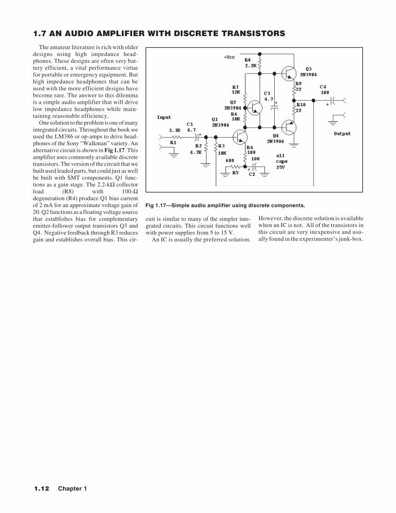
One solution to the problem is one of manyintegrated circuits. Throughout the book weused the LM386 or op-amps to drive head-phones of the Sony “Walkman” variety. Analternative circuit is shown in Fig 1.17. Thisamplifier uses commonly available discretetransistors. The version of the circuit that webuilt used leaded parts, but could just as wellbe built with SMT components. Q1 func-tions as a gain stage. The 2.2-kΩ collectorload (R8) with 100-Ωdegeneration (R4) produce Q1 bias currentof 2 mA for an approximate voltage gain of20. Q2 functions as a floating voltage sourcethat establishes bias for complementaryemitter-follower output transistors Q3 andQ4. Negative feedback through R3 reducesgain and establishes overall bias. This cir-
cuit is similar to many of the simpler inte-grated circuits. This circuit functions wellwith power supplies from 5 to 15 V.
An IC is usually the preferred solution.
However, the discrete solution is availablewhen an IC is not. All of the transistors inthis circuit are very inexpensive and usu-ally found in the experimenter’s junk-box.
Getting Started 1.13
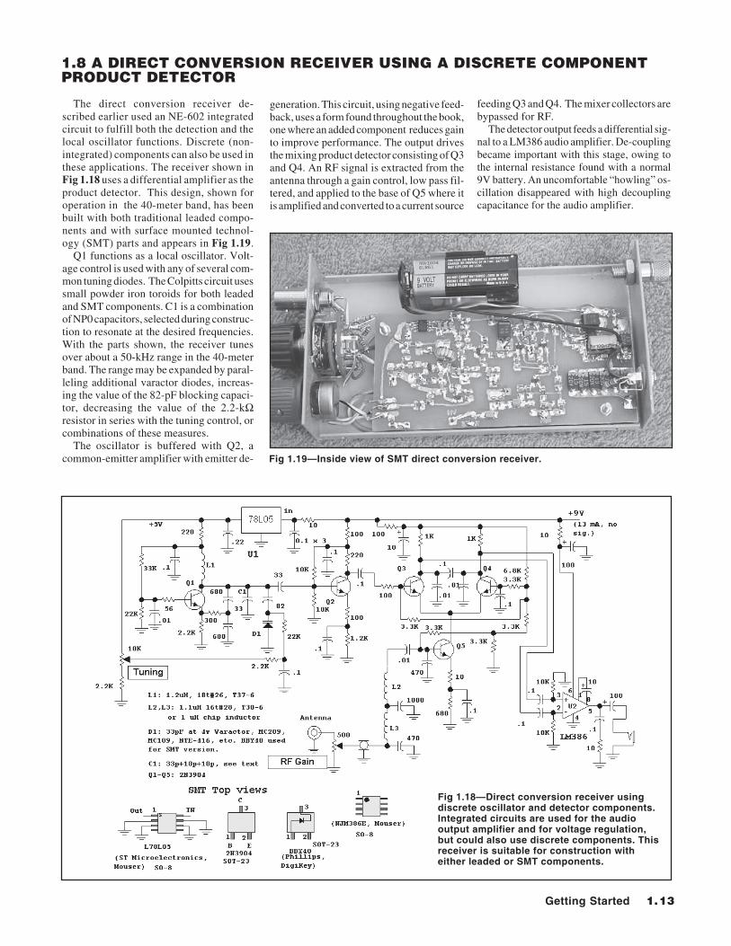
1.8 A DIRECT CONVERSION RECEIVER USING A DISCRETE COMPONENTPRODUCT DETECTOR
Fig 1.19—Inside view of SMT direct conversion receiver.
The direct conversion receiver de-scribed earlier used an NE-602 integratedcircuit to fulfill both the detection and thelocal oscillator functions. Discrete (non-integrated) components can also be used inthese applications. The receiver shown inFig 1.18 uses a differential amplifier as theproduct detector. This design, shown foroperation in the 40-meter band, has beenbuilt with both traditional leaded compo-nents and with surface mounted technol-ogy (SMT) parts and appears in Fig 1.19.
Q1 functions as a local oscillator. Volt-age control is used with any of several com-mon tuning diodes. The Colpitts circuit usessmall powder iron toroids for both leadedand SMT components. C1 is a combinationof NP0 capacitors, selected during construc-tion to resonate at the desired frequencies.With the parts shown, the receiver tunesover about a 50-kHz range in the 40-meterband. The range may be expanded by paral-leling additional varactor diodes, increas-ing the value of the 82-pF blocking capaci-tor, decreasing the value of the 2.2-kΩresistor in series with the tuning control, orcombinations of these measures.
The oscillator is buffered with Q2, acommon-emitter amplifier with emitter de-
generation. This circuit, using negative feed-back, uses a form found throughout the book,one where an added component reduces gainto improve performance. The output drivesthe mixing product detector consisting of Q3and Q4. An RF signal is extracted from theantenna through a gain control, low pass fil-tered, and applied to the base of Q5 where itis amplified and converted to a current source
Fig 1.18—Direct conversion receiver usingdiscrete oscillator and detector components.Integrated circuits are used for the audiooutput amplifier and for voltage regulation,but could also use discrete components. Thisreceiver is suitable for construction witheither leaded or SMT components.
feeding Q3 and Q4. The mixer collectors arebypassed for RF.
The detector output feeds a differential sig-nal to a LM386 audio amplifier. De-couplingbecame important with this stage, owing tothe internal resistance found with a normal9V battery. An uncomfortable “howling” os-cillation disappeared with high decouplingcapacitance for the audio amplifier.
1.14 Chapter 1
1.9 POWER SUPPLIESAmong the many tools needed by the
circuit experimenter, beginning or sea-soned, is a power supply. Indeed, severalare always useful. Batteries serve well forsimple, low current applications. How-ever, the more useful power supply ex-tracts energy from the power mains. Thatac voltage is applied to a transformer, isrectified, filtered with a large capacitor,and regulated with transistors and/or inte-grated circuits.
Two major design questions are pre-sented to the beginner: What transformershould be selected and how large shouldthe filter capacitor be? Fig 1.20 shows anexample 12-V, 0.5-A design we use toaddress these questions.
Transformers are rated for RMS outputvoltage with a load. The peak voltagewill be higher by a factor of 1.414, so a12.6-V transformer will have a peak out-put of 17.8 V. The transformer current rat-ing should equal or exceed the maximumdesired dc current, so a 0.5-A transformeris adequate for this application. This isshown in part A of Fig 1.20. A switch andprotective slow-blow fuse is added to thetransformer primary.
A bridge rectifier using four diodes isadded to the circuit to generate a dc out-put. The bridge is preferred over circuitswith just two diodes, for a center tappedtransformer is then not required. Bridgerectifier diodes should have an averagecurrent rating above the maximum powersupply current. 1-A diodes would be finefor this application.
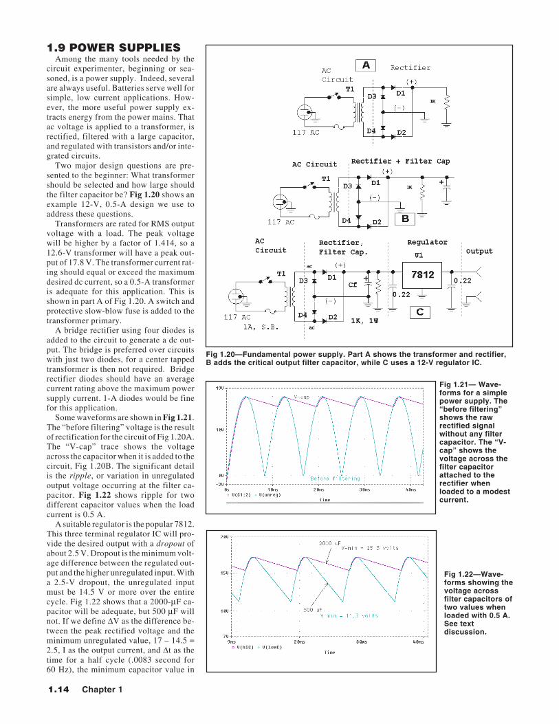
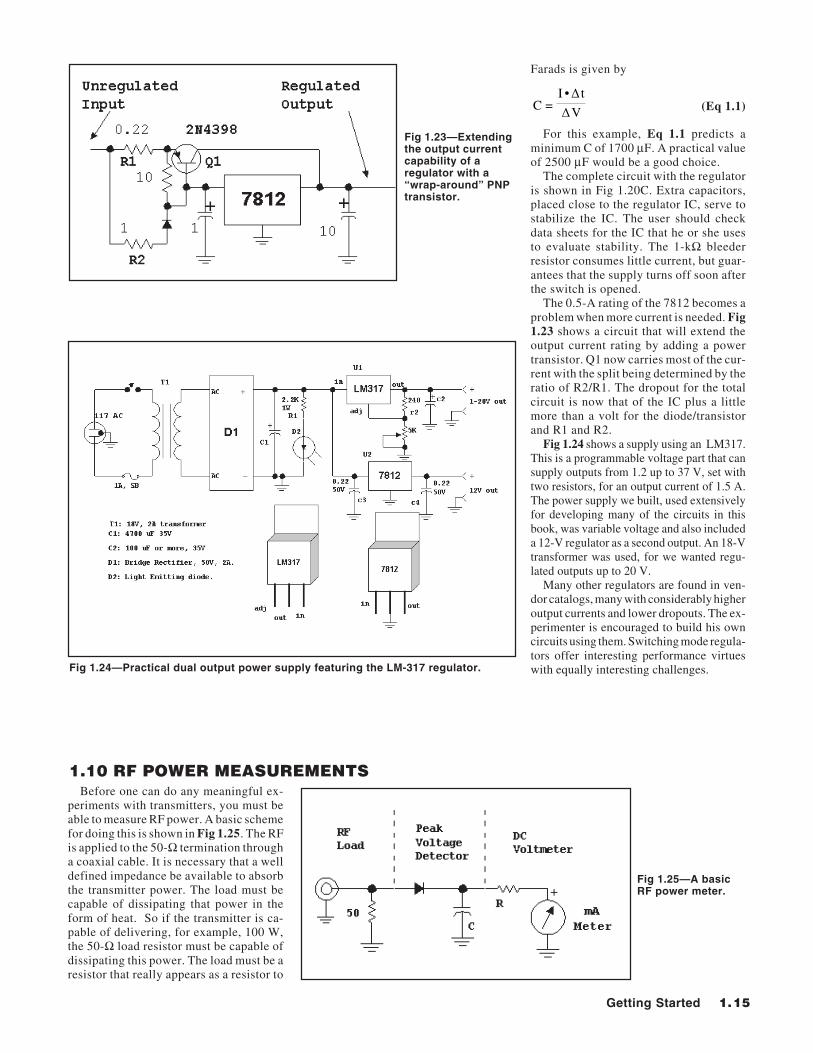
Some waveforms are shown in Fig 1.21.The “before filtering” voltage is the resultof rectification for the circuit of Fig 1.20A.The “V-cap” trace shows the voltageacross the capacitor when it is added to thecircuit, Fig 1.20B. The significant detailis the ripple, or variation in unregulatedoutput voltage occurring at the filter ca-pacitor. Fig 1.22 shows ripple for twodifferent capacitor values when the loadcurrent is 0.5 A.
A suitable regulator is the popular 7812.This three terminal regulator IC will pro-vide the desired output with a dropout ofabout 2.5 V. Dropout is the minimum volt-age difference between the regulated out-put and the higher unregulated input. Witha 2.5-V dropout, the unregulated inputmust be 14.5 V or more over the entirecycle. Fig 1.22 shows that a 2000-μF ca-pacitor will be adequate, but 500 μF willnot. If we define ΔV as the difference be-tween the peak rectified voltage and theminimum unregulated value, 17 – 14.5 =2.5, I as the output current, and Δt as thetime for a half cycle (.0083 second for60 Hz), the minimum capacitor value in
Fig 1.20—Fundamental power supply. Part A shows the transformer and rectifier,B adds the critical output filter capacitor, while C uses a 12-V regulator IC.
Fig 1.21— Wave-forms for a simplepower supply. The“before filtering”shows the rawrectified signalwithout any filtercapacitor. The “V-cap” shows thevoltage across thefilter capacitorattached to therectifier whenloaded to a modestcurrent.
Fig 1.22—Wave-forms showing thevoltage acrossfilter capacitors oftwo values whenloaded with 0.5 A.See textdiscussion.
Getting Started 1.15
Farads is given by
VΔtΔ•I
=C (Eq 1.1)
For this example, Eq 1.1 predicts aminimum C of 1700 μF. A practical valueof 2500 μF would be a good choice.
The complete circuit with the regulatoris shown in Fig 1.20C. Extra capacitors,placed close to the regulator IC, serve tostabilize the IC. The user should checkdata sheets for the IC that he or she usesto evaluate stability. The 1-kΩ bleederresistor consumes little current, but guar-antees that the supply turns off soon afterthe switch is opened.
The 0.5-A rating of the 7812 becomes aproblem when more current is needed. Fig1.23 shows a circuit that will extend theoutput current rating by adding a powertransistor. Q1 now carries most of the cur-rent with the split being determined by theratio of R2/R1. The dropout for the totalcircuit is now that of the IC plus a littlemore than a volt for the diode/transistorand R1 and R2.
Fig 1.24 shows a supply using an LM317.This is a programmable voltage part that cansupply outputs from 1.2 up to 37 V, set withtwo resistors, for an output current of 1.5 A.The power supply we built, used extensivelyfor developing many of the circuits in thisbook, was variable voltage and also includeda 12-V regulator as a second output. An 18-Vtransformer was used, for we wanted regu-lated outputs up to 20 V.
Many other regulators are found in ven-dor catalogs, many with considerably higheroutput currents and lower dropouts. The ex-perimenter is encouraged to build his owncircuits using them. Switching mode regula-tors offer interesting performance virtueswith equally interesting challenges.Fig 1.24—Practical dual output power supply featuring the LM-317 regulator.
Fig 1.23—Extendingthe output currentcapability of aregulator with a“wrap-around” PNPtransistor.
Fig 1.25—A basicRF power meter.
1.10 RF POWER MEASUREMENTSBefore one can do any meaningful ex-
periments with transmitters, you must beable to measure RF power. A basic schemefor doing this is shown in Fig 1.25. The RFis applied to the 50-Ω termination througha coaxial cable. It is necessary that a welldefined impedance be available to absorbthe transmitter power. The load must becapable of dissipating that power in theform of heat. So if the transmitter is ca-pable of delivering, for example, 100 W,the 50-Ω load resistor must be capable ofdissipating this power. The load must be aresistor that really appears as a resistor to
1.16 Chapter 1
the radio frequency applied to it. Thismeans that the usual power resistors soldby vendors, even if capable of dissipating100 W, will not be suitable. They are usu-ally built as a “wire wound” part, makingthem highly inductive for RF. It is some-times possible to tune them, an interestingavenue for the advanced experimenter.
Suitable 50-Ω terminations, or “dummyloads” can be built with parallel combina-tions of 2-W carbon resistors, or similar 2or 3-W metal oxide power resistors suchas those manufactured by Yaego or Xicon.Some of these are used in power attenua-tors described in Chapter 7.
The RF power dissipated in the resistorwill develop a corresponding RF voltage.That is rectified with a simple diode detec-tor, providing a signal across the capacitorequaling the peak RF voltage, less 0.7 Vfor the diode turn-on voltage.
The power meter is completed with a suit-able dc volt meter. It can be as simple as a0-1-mA current meter and a resistor,an FET voltmeter, or even a digital voltmeter.
Fig 1.26 shows a dual range powermeter. Essentially it is a pair of powermeters sharing a single meter movement.The higher power part of the circuit startswith a 4-W load built from two parallel100-Ω, 2-W resistors. These can be car-bon or metal film resistors. If 2-W resis-tors are not available, four parallel 200-Ω1-W parts will work as well. The resultingRF voltage is rectified with a siliconswitching diode. This should be a 100-Vpart such as the 1N4148, 1N4152, or simi-lar diode. The voltmeter part of the circuitis a 20-kΩ resistor driving a 0-1 mA meter.
Assume a transmitter is attached and keyedon to produce an indication of 0.6 mA. Thisrepresents a peak of 12 V, for the meter mul-tiplier is the 20-kΩ resistor. The resultingpower is then calculated from the formulagiven with the figure, 1613 mW, or 1.6 W.
The 50-mW input to the power meteruses a single 51-Ω, ¼-W, resistor with amore sensitive 1N34A rectifier diode. Themeter multiplier is now just 1.5 kΩ. Anapproximate calibration curve is shown inFig 1.27. The finished meter is shown inFig 1.28.
Other schemes suitable for RF powermeasurement include terminated oscillo-scopes, microwave power meters (usuallyusing calorimeter measurement methods,)spectrum analyzers, and wideband loga-rithmic integrated circuits. Some of thesewill be covered in a later chapter.
Often we wish to examine an RF voltageto see if a circuit is “alive,” and perhaps toadjust it. The classic method for doing thisused an RF probe with a high impedance,usually vacuum tube or FET voltmeter. Themethod is still very useful, especially when
Fig 1.27—Calibration curve for the 50mW range of the previous power meter.
Fig 1.28—The front panel of the dual-range QRP power meter.
Fig 1.29—RF probe suitable for use with a VTVM, FET voltmeter, or even a DVM.Resistors marked with * are standoff resistors used for probe construction andhave little impact on circuit operation.
Fig 1.26—Dualrange powermeter. The4-W input usesthe formula tocalculate powerin milliwatts. The50-mW rangeuses the curve ofFig 1.23.
instrumentation is limited. Fig 1.29 shows avery simple RF probe. The photo in Fig 1.30shows an open breadboard version; it’s thesort of circuit that one builds when a mea-surement must be done immediately. A longlasting version of the same circuit mightbetter be built inside a cylinder at the end ofthe coaxial cable.
The probe may require calibration. Thisis best done with one of the other power
meters and a small transmitter or similarRF source. The transmitter is attached tothe power meter and the output is mea-sured. The corresponding RF voltage isnoted and the RF probe is attached to thepower meter 50-Ω resistor, producing aresult that can be compared.
Fig 1.31 shows a high impedance dc volt-meter suitable for use with this probe. It isalso a good starting measurement tool for
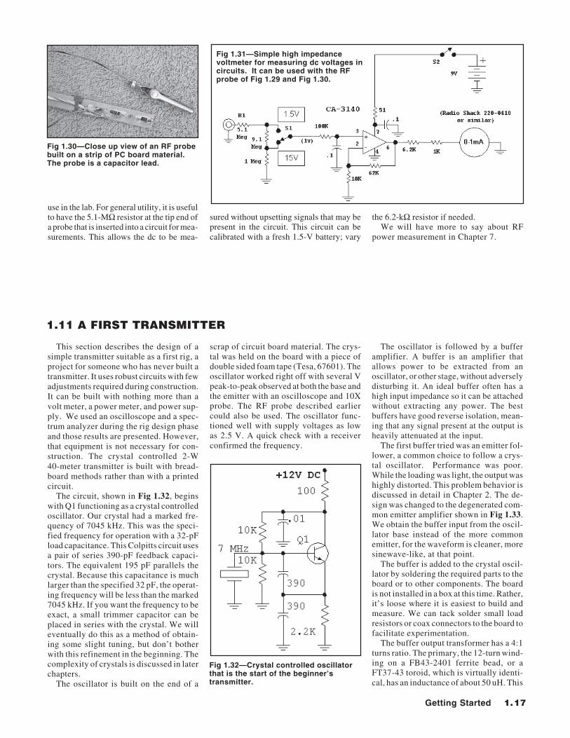
Getting Started 1.17
Fig 1.30—Close up view of an RF probebuilt on a strip of PC board material.The probe is a capacitor lead.
use in the lab. For general utility, it is usefulto have the 5.1-MΩ resistor at the tip end ofa probe that is inserted into a circuit for mea-surements. This allows the dc to be mea-
1.11 A FIRST TRANSMITTER
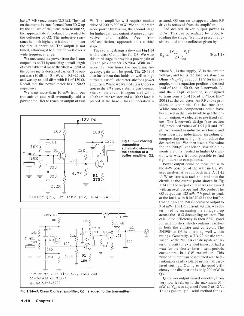
Fig 1.32—Crystal controlled oscillatorthat is the start of the beginner’stransmitter.
This section describes the design of asimple transmitter suitable as a first rig, aproject for someone who has never built atransmitter. It uses robust circuits with fewadjustments required during construction.It can be built with nothing more than avolt meter, a power meter, and power sup-ply. We used an oscilloscope and a spec-trum analyzer during the rig design phaseand those results are presented. However,that equipment is not necessary for con-struction. The crystal controlled 2-W40-meter transmitter is built with bread-board methods rather than with a printedcircuit.
The circuit, shown in Fig 1.32, beginswith Q1 functioning as a crystal controlledoscillator. Our crystal had a marked fre-quency of 7045 kHz. This was the speci-fied frequency for operation with a 32-pFload capacitance. This Colpitts circuit usesa pair of series 390-pF feedback capaci-tors. The equivalent 195 pF parallels thecrystal. Because this capacitance is muchlarger than the specified 32 pF, the operat-ing frequency will be less than the marked7045 kHz. If you want the frequency to beexact, a small trimmer capacitor can beplaced in series with the crystal. We willeventually do this as a method of obtain-ing some slight tuning, but don’t botherwith this refinement in the beginning. Thecomplexity of crystals is discussed in laterchapters.
The oscillator is built on the end of a
scrap of circuit board material. The crys-tal was held on the board with a piece ofdouble sided foam tape (Tesa, 67601). Theoscillator worked right off with several Vpeak-to-peak observed at both the base andthe emitter with an oscilloscope and 10Xprobe. The RF probe described earliercould also be used. The oscillator func-tioned well with supply voltages as lowas 2.5 V. A quick check with a receiverconfirmed the frequency.
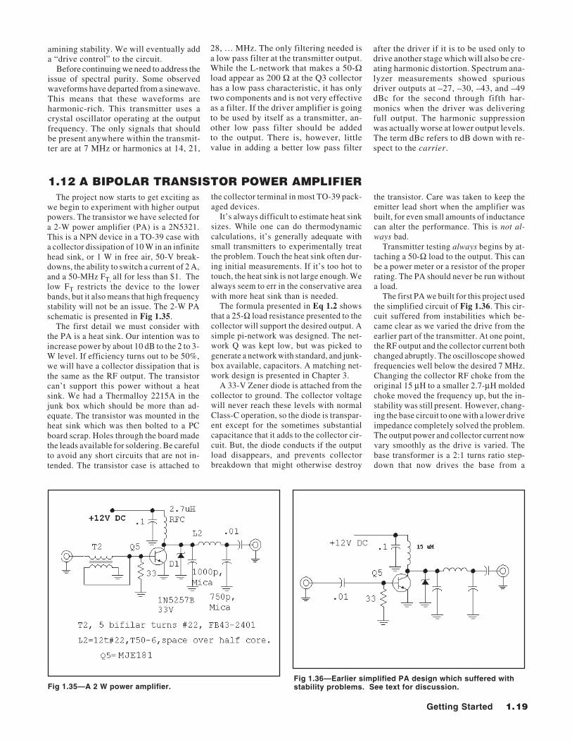
The oscillator is followed by a bufferamplifier. A buffer is an amplifier thatallows power to be extracted from anoscillator, or other stage, without adverselydisturbing it. An ideal buffer often has ahigh input impedance so it can be attachedwithout extracting any power. The bestbuffers have good reverse isolation, mean-ing that any signal present at the output isheavily attenuated at the input.
The first buffer tried was an emitter fol-lower, a common choice to follow a crys-tal oscillator. Performance was poor.While the loading was light, the output washighly distorted. This problem behavior isdiscussed in detail in Chapter 2. The de-sign was changed to the degenerated com-mon emitter amplifier shown in Fig 1.33.We obtain the buffer input from the oscil-lator base instead of the more commonemitter, for the waveform is cleaner, moresinewave-like, at that point.
The buffer is added to the crystal oscil-lator by soldering the required parts to theboard or to other components. The boardis not installed in a box at this time. Rather,it’s loose where it is easiest to build andmeasure. We can tack solder small loadresistors or coax connectors to the board tofacilitate experimentation.
The buffer output transformer has a 4:1turns ratio. The primary, the 12-turn wind-ing on a FB43-2401 ferrite bead, or aFT37-43 toroid, which is virtually identi-cal, has an inductance of about 50 uH. This
Fig 1.31—Simple high impedancevoltmeter for measuring dc voltages incircuits. It can be used with the RFprobe of Fig 1.29 and Fig 1.30.
sured without upsetting signals that may bepresent in the circuit. This circuit can becalibrated with a fresh 1.5-V battery; vary
the 6.2-kΩ resistor if needed.We will have more to say about RF
power measurement in Chapter 7.
1.18 Chapter 1
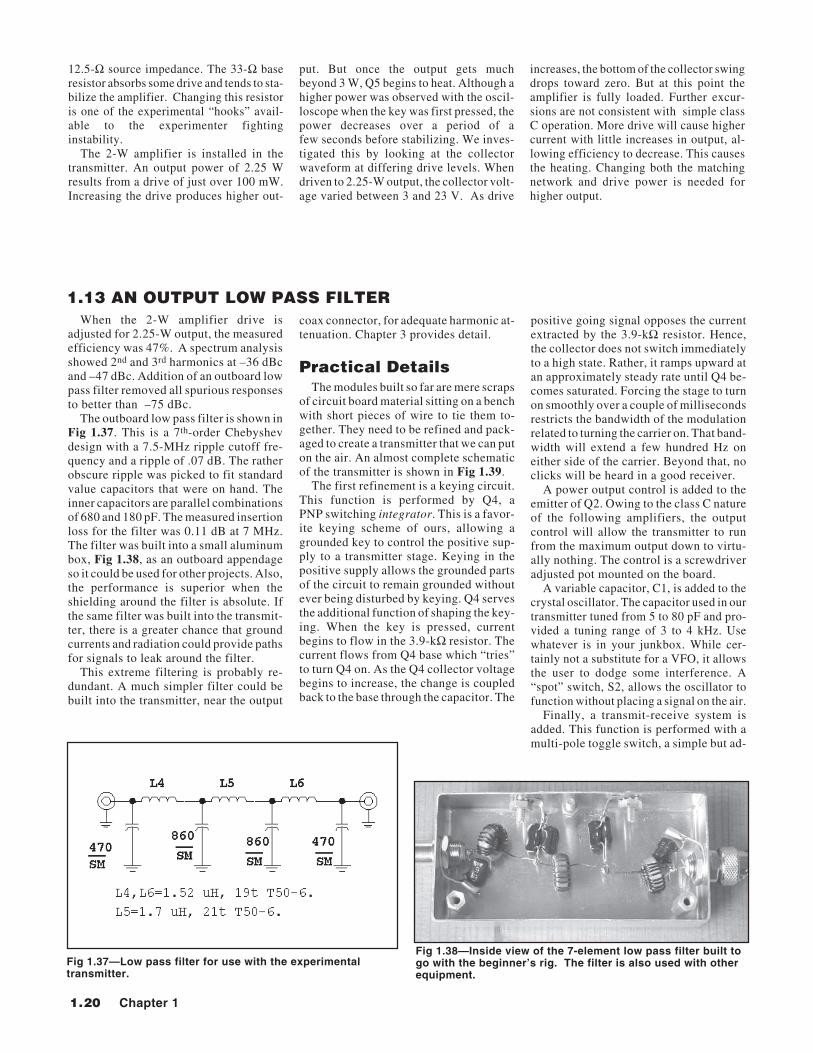
Fig 1.34—A Class C driver amplifier, Q3, is added to the transmitter.
has a 7-MHz reactance of 2.3-kΩ. The loadon the output is transformed from 50 Ω upby the square of the turns ratio to 800 Ω,the approximate impedance presented tothe collector of Q2. The inductive reac-tance is much higher, so it does not impactthe circuit operation. The output is nottuned, allowing it to function well over awide frequency range.
We measured the power from the 3-turnoutput link on T1 by attaching a small lengthof coax cable that ran to the 50-mW input ofthe power meter described earlier. The out-put was +10 dBm, 10 mW, with R1=270 Ω,and was up to +15 dBm with R1 of 150 Ω.Recall that the power meter has a 50-Ωimpedance.
We want more than 10 mW from ourtransmitter and will eventually add apower amplifier to reach an output of two
Fig 1.33—Evolvingtransmitterschematic showingthe addition of abuffer amplifier, Q2.
W. That amplifier will require modestdrive of 200 to 300 mW. We could obtainmore power by biasing the second stagefor higher gain and output. A more conser-vative and stable, free fromself-oscillation, approach adds a thirdstage.
The evolving design is shown in Fig 1.34with a class C amplifier for Q3. We wantthis third stage to provide a power gain of10 and pick another 2N3904. With an Ftmore than ten times the operating fre-quency, gain will be good. The 2N3904also has a beta that holds up well at highcurrents, a useful characteristic for a poweramplifier. While we wanted class C opera-tion in the 3rd stage, stability was deemedvital, so the circuit is degenerated with a10-Ω emitter resistor and a 100-Ω load isplaced at the base. Class C operation is
assured. Q3 current disappears when RFdrive is removed from the amplifier.
The desired driver output power is1/3 W. This can be realized by properlyloading the stage. We must present a re-sistive load to the collector given by
out
2eCC
L P•2
)V(V=R
_ (Eq. 1.2)
where Vcc is the supply, Ve is the emittervoltage, and RL is the load resistance inOhms. (Vcc–Ve) is about 11 V for this ex-ample, so the equation predicts a desiredload of about 150 Ω. An L-network, L1and the 200-pF capacitor, is designedto transform a 50-Ω load to “look like”200 Ω at the collector. An RF choke pro-vides collector bias for the transistor.While tunable components could havebeen used in the L-network to get the op-timum output, we elected to use fixed val-ues. The L-network design (see section3.6) produced values of 1.97 μH and 197pF. We wound an inductor on a toroid andthen measured inductance, spreading orcompressing turns slightly to produce thedesired value. We then used a 5% valuefor the 200-pF capacitor. Variable ele-ments are only needed in higher Q situa-tions, or where it is not possible to findtight tolerance components.
Power output could be measured withthe 4-W position of the watt meter. Weused an alternative approach here. A 51-Ω1/2-W resistor was tack soldered into thecircuit at the output point shown in Fig1.34 and the output voltage was measuredwith an oscilloscope and 10X probe. TheQ3 output was 123 mW, 7 V peak-to-peakat the load, with R1=270 Ω in the buffer.Changing R1 to 150 Ω increased output to314 mW. The DC current, 43 mA, was de-termined by measuring the voltage dropacross the 10-Ω decoupling resistor. Thecalculated efficiency is then 62%, goodfor an amplifier which contains resistorsin both the emitter and collector. The2N3904 at Q3 is operating well withinratings. Generally, a TO-92 plastic tran-sistor like the 2N3904 can dissipate a quar-ter of a watt for extended times, or half awatt for the shorter intermittent periodsencountered in a CW transmitter. This“rule of thumb” can be stretched with heat-sinking, or easily violated in thermally iso-lated settings. Owing to the good effi-ciency, the dissipation is only 200 mW inQ3.
Q3 power output varied smoothly fromvery low levels up to the maximum 314mW as Vcc was adjusted from 5 to 12 V.This is generally a useful method for ex-
Getting Started 1.19
amining stability. We will eventually adda “drive control” to the circuit.
Before continuing we need to address theissue of spectral purity. Some observedwaveforms have departed from a sinewave.This means that these waveforms areharmonic-rich. This transmitter uses acrystal oscillator operating at the outputfrequency. The only signals that shouldbe present anywhere within the transmit-ter are at 7 MHz or harmonics at 14, 21,
28, … MHz. The only filtering needed isa low pass filter at the transmitter output.While the L-network that makes a 50-Ωload appear as 200 Ω at the Q3 collectorhas a low pass characteristic, it has onlytwo components and is not very effectiveas a filter. If the driver amplifier is goingto be used by itself as a transmitter, an-other low pass filter should be addedto the output. There is, however, littlevalue in adding a better low pass filter
after the driver if it is to be used only todrive another stage which will also be cre-ating harmonic distortion. Spectrum ana-lyzer measurements showed spuriousdriver outputs at –27, –30, –43, and –49dBc for the second through fifth har-monics when the driver was deliveringfull output. The harmonic suppressionwas actually worse at lower output levels.The term dBc refers to dB down with re-spect to the carrier.
1.12 A BIPOLAR TRANSISTOR POWER AMPLIFIER
Fig 1.35—A 2 W power amplifier.Fig 1.36—Earlier simplified PA design which suffered withstability problems. See text for discussion.
The project now starts to get exciting aswe begin to experiment with higher outputpowers. The transistor we have selected fora 2-W power amplifier (PA) is a 2N5321.This is a NPN device in a TO-39 case witha collector dissipation of 10 W in an infinitehead sink, or 1 W in free air, 50-V break-downs, the ability to switch a current of 2 A,and a 50-MHz FT, all for less than $1. Thelow FT restricts the device to the lowerbands, but it also means that high frequencystability will not be an issue. The 2-W PAschematic is presented in Fig 1.35.
The first detail we must consider withthe PA is a heat sink. Our intention was toincrease power by about 10 dB to the 2 to 3-W level. If efficiency turns out to be 50%,we will have a collector dissipation that isthe same as the RF output. The transistorcan’t support this power without a heatsink. We had a Thermalloy 2215A in thejunk box which should be more than ad-equate. The transistor was mounted in theheat sink which was then bolted to a PCboard scrap. Holes through the board madethe leads available for soldering. Be carefulto avoid any short circuits that are not in-tended. The transistor case is attached to
the collector terminal in most TO-39 pack-aged devices.
It’s always difficult to estimate heat sinksizes. While one can do thermodynamiccalculations, it’s generally adequate withsmall transmitters to experimentally treatthe problem. Touch the heat sink often dur-ing initial measurements. If it’s too hot totouch, the heat sink is not large enough. Wealways seem to err in the conservative areawith more heat sink than is needed.
The formula presented in Eq 1.2 showsthat a 25-Ω load resistance presented to thecollector will support the desired output. Asimple pi-network was designed. The net-work Q was kept low, but was picked togenerate a network with standard, and junk-box available, capacitors. A matching net-work design is presented in Chapter 3.
A 33-V Zener diode is attached from thecollector to ground. The collector voltagewill never reach these levels with normalClass-C operation, so the diode is transpar-ent except for the sometimes substantialcapacitance that it adds to the collector cir-cuit. But, the diode conducts if the outputload disappears, and prevents collectorbreakdown that might otherwise destroy
the transistor. Care was taken to keep theemitter lead short when the amplifier wasbuilt, for even small amounts of inductancecan alter the performance. This is not al-ways bad.
Transmitter testing always begins by at-taching a 50-Ω load to the output. This canbe a power meter or a resistor of the properrating. The PA should never be run withouta load.
The first PA we built for this project usedthe simplified circuit of Fig 1.36. This cir-cuit suffered from instabilities which be-came clear as we varied the drive from theearlier part of the transmitter. At one point,the RF output and the collector current bothchanged abruptly. The oscilloscope showedfrequencies well below the desired 7 MHz.Changing the collector RF choke from theoriginal 15 μH to a smaller 2.7-μH moldedchoke moved the frequency up, but the in-stability was still present. However, chang-ing the base circuit to one with a lower driveimpedance completely solved the problem.The output power and collector current nowvary smoothly as the drive is varied. Thebase transformer is a 2:1 turns ratio step-down that now drives the base from a
1.20 Chapter 1
Fig 1.38—Inside view of the 7-element low pass filter built togo with the beginner’s rig. The filter is also used with otherequipment.
Fig 1.37—Low pass filter for use with the experimentaltransmitter.
12.5-Ω source impedance. The 33-Ω baseresistor absorbs some drive and tends to sta-bilize the amplifier. Changing this resistoris one of the experimental “hooks” avail-able to the experimenter fightinginstability.
The 2-W amplifier is installed in thetransmitter. An output power of 2.25 Wresults from a drive of just over 100 mW.Increasing the drive produces higher out-
put. But once the output gets muchbeyond 3 W, Q5 begins to heat. Although ahigher power was observed with the oscil-loscope when the key was first pressed, thepower decreases over a period of afew seconds before stabilizing. We inves-tigated this by looking at the collectorwaveform at differing drive levels. Whendriven to 2.25-W output, the collector volt-age varied between 3 and 23 V. As drive
increases, the bottom of the collector swingdrops toward zero. But at this point theamplifier is fully loaded. Further excur-sions are not consistent with simple classC operation. More drive will cause highercurrent with little increases in output, al-lowing efficiency to decrease. This causesthe heating. Changing both the matchingnetwork and drive power is needed forhigher output.
1.13 AN OUTPUT LOW PASS FILTERWhen the 2-W amplifier drive is
adjusted for 2.25-W output, the measuredefficiency was 47%. A spectrum analysisshowed 2nd and 3rd harmonics at –36 dBcand –47 dBc. Addition of an outboard lowpass filter removed all spurious responsesto better than –75 dBc.
The outboard low pass filter is shown inFig 1.37. This is a 7th-order Chebyshevdesign with a 7.5-MHz ripple cutoff fre-quency and a ripple of .07 dB. The ratherobscure ripple was picked to fit standardvalue capacitors that were on hand. Theinner capacitors are parallel combinationsof 680 and 180 pF. The measured insertionloss for the filter was 0.11 dB at 7 MHz.The filter was built into a small aluminumbox, Fig 1.38, as an outboard appendageso it could be used for other projects. Also,the performance is superior when theshielding around the filter is absolute. Ifthe same filter was built into the transmit-ter, there is a greater chance that groundcurrents and radiation could provide pathsfor signals to leak around the filter.
This extreme filtering is probably re-dundant. A much simpler filter could bebuilt into the transmitter, near the output
coax connector, for adequate harmonic at-tenuation. Chapter 3 provides detail.
Practical DetailsThe modules built so far are mere scraps
of circuit board material sitting on a benchwith short pieces of wire to tie them to-gether. They need to be refined and pack-aged to create a transmitter that we can puton the air. An almost complete schematicof the transmitter is shown in Fig 1.39.
The first refinement is a keying circuit.This function is performed by Q4, aPNP switching integrator. This is a favor-ite keying scheme of ours, allowing agrounded key to control the positive sup-ply to a transmitter stage. Keying in thepositive supply allows the grounded partsof the circuit to remain grounded withoutever being disturbed by keying. Q4 servesthe additional function of shaping the key-ing. When the key is pressed, currentbegins to flow in the 3.9-kΩ resistor. Thecurrent flows from Q4 base which “tries”to turn Q4 on. As the Q4 collector voltagebegins to increase, the change is coupledback to the base through the capacitor. The
positive going signal opposes the currentextracted by the 3.9-kΩ resistor. Hence,the collector does not switch immediatelyto a high state. Rather, it ramps upward atan approximately steady rate until Q4 be-comes saturated. Forcing the stage to turnon smoothly over a couple of millisecondsrestricts the bandwidth of the modulationrelated to turning the carrier on. That band-width will extend a few hundred Hz oneither side of the carrier. Beyond that, noclicks will be heard in a good receiver.
A power output control is added to theemitter of Q2. Owing to the class C natureof the following amplifiers, the outputcontrol will allow the transmitter to runfrom the maximum output down to virtu-ally nothing. The control is a screwdriveradjusted pot mounted on the board.
A variable capacitor, C1, is added to thecrystal oscillator. The capacitor used in ourtransmitter tuned from 5 to 80 pF and pro-vided a tuning range of 3 to 4 kHz. Usewhatever is in your junkbox. While cer-tainly not a substitute for a VFO, it allowsthe user to dodge some interference. A“spot” switch, S2, allows the oscillator tofunction without placing a signal on the air.
Finally, a transmit-receive system isadded. This function is performed with amulti-pole toggle switch, a simple but ad-
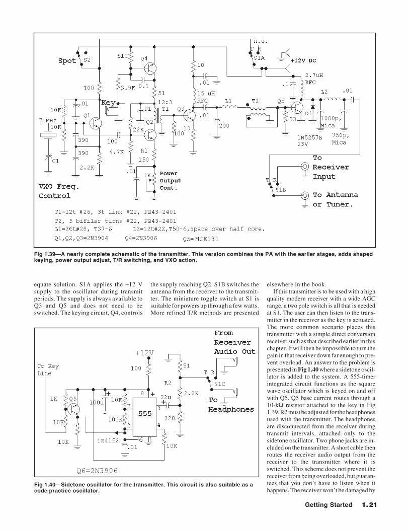
Getting Started 1.21
Fig 1.39—A nearly complete schematic of the transmitter. This version combines the PA with the earlier stages, adds shapedkeying, power output adjust, T/R switching, and VXO action.
Fig 1.40—Sidetone oscillator for the transmitter. This circuit is also suitable as acode practice oscillator.
equate solution. S1A applies the +12 Vsupply to the oscillator during transmitperiods. The supply is always available toQ3 and Q5 and does not need to beswitched. The keying circuit, Q4, controls
the supply reaching Q2. S1B switches theantenna from the receiver to the transmit-ter. The miniature toggle switch at S1 issuitable for powers up through a few watts.More refined T/R methods are presented
elsewhere in the book.If this transmitter is to be used with a high
quality modern receiver with a wide AGCrange, a two pole switch is all that is neededat S1. The user can then listen to the trans-mitter in the receiver as the key is actuated.The more common scenario places thistransmitter with a simple direct conversionreceiver such as that described earlier in thischapter. It will then be impossible to turn thegain in that receiver down far enough to pre-vent overload. An answer to the problem ispresented in Fig 1.40 where a sidetone oscil-lator is added to the system. A 555-timerintegrated circuit functions as the squarewave oscillator which is keyed on and offwith Q5. Q5 base current routes through a10-kΩ resistor attached to the key in Fig1.39. R2 must be adjusted for the headphonesused with the transmitter. The headphonesare disconnected from the receiver duringtransmit intervals, attached only to thesidetone oscillator. Two phone jacks are in-cluded on the transmitter. A short cable thenroutes the receiver audio output from thereceiver to the transmitter where it isswitched. This scheme does not prevent thereceiver from being overloaded, but guaran-tees that you don’t have to listen when ithappens. The receiver won’t be damaged by
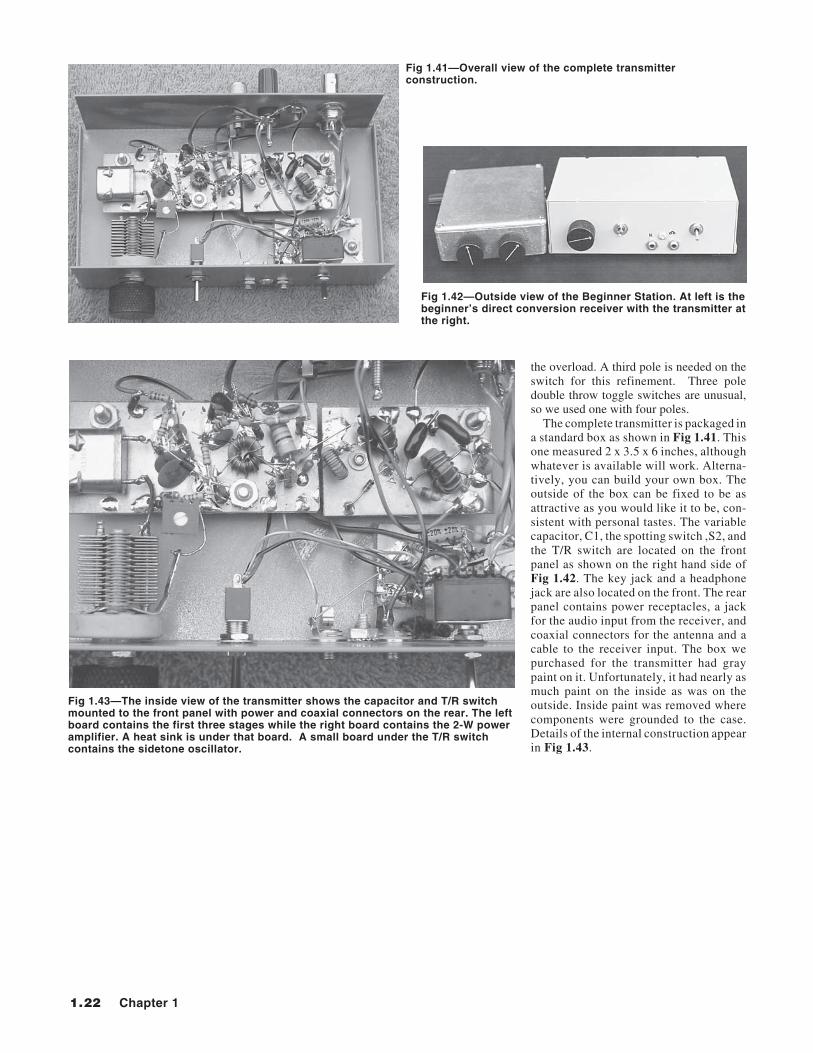
1.22 Chapter 1
Fig 1.43—The inside view of the transmitter shows the capacitor and T/R switchmounted to the front panel with power and coaxial connectors on the rear. The leftboard contains the first three stages while the right board contains the 2-W poweramplifier. A heat sink is under that board. A small board under the T/R switchcontains the sidetone oscillator.
Fig 1.42—Outside view of the Beginner Station. At left is thebeginner’s direct conversion receiver with the transmitter atthe right.
Fig 1.41—Overall view of the complete transmitterconstruction.
the overload. A third pole is needed on theswitch for this refinement. Three poledouble throw toggle switches are unusual,so we used one with four poles.
The complete transmitter is packaged ina standard box as shown in Fig 1.41. Thisone measured 2 x 3.5 x 6 inches, althoughwhatever is available will work. Alterna-tively, you can build your own box. Theoutside of the box can be fixed to be asattractive as you would like it to be, con-sistent with personal tastes. The variablecapacitor, C1, the spotting switch ,S2, andthe T/R switch are located on the frontpanel as shown on the right hand side ofFig 1.42. The key jack and a headphonejack are also located on the front. The rearpanel contains power receptacles, a jackfor the audio input from the receiver, andcoaxial connectors for the antenna and acable to the receiver input. The box wepurchased for the transmitter had graypaint on it. Unfortunately, it had nearly asmuch paint on the inside as was on theoutside. Inside paint was removed wherecomponents were grounded to the case.Details of the internal construction appearin Fig 1.43.

Getting Started 1.23
1. W. Hayward and D. DeMaw, Solid StateDesign for the Radio Amateur, ARRL,1977.2. R. Hayward and W. Hayward, “The UglyWeekender,” QST, Aug, 1981, pp 18-21. Seealso G. Grammer, Understanding Amateur
Radio, ARRL, 2nd Edition, 1976, p 144.3. R. Lewallen, “An Optimized QRPTransceiver,” QST, Aug, 1980, pp 14-19.4. J. Dillon, “The Neophyte Receiver,”QST, Feb, 1988, p 14-18.5. C. Kitchin, “A Simple Regenerative
Radio for Beginners,“ QST, Sep, 2000, p 61.6. C. Kitchin, “An Ultra-Simple VHF Re-ceiver for 6 Meters ,” QST, Dec, 1997, p 39.7. G. Dobbs, “A Stable RegenerativeReceiver,” SPRAT, Issue 105, Dec, 2000,p 21.
REFERENCES
1.14 ABOUT THE SCHEMATICS IN THIS BOOKThe schematic diagrams used in this
book differ slightly from other ARRL pub-lications in that we use slightly differentconventions. Not all details are presentedin all schematics.
Capacitors are in microfarads if electro-lytic or if they have decimal values lessthan 1. Values greater than unity are inpicofarad if they are not electrolytic. Elec-trolytic caps always have a voltage ratinggreater than the Vcc or Vdd value used
in the circuit with 25 V being typical. Insome applications we will use C values innF, which stands for nanofarad. 1000 pF =1 nF.
RF transformers are specified by turnsratio rather than impedance ratio. Oftenthis data is presented within the schematicdiagram rather than as part of a caption.The same holds for inductance values. Westrive to load the schematic with as muchinformation as possible.
We generally label schematics with theparts that we used. But that does not meanthat this is what you might want to use. Anexample is our frequent use the 1N4152silicon switching diode. In all cases, vir-tually all of these can be replaced by themore common 1N4148 or 1N914. Whenthere is a question about such details, lookthe part up and see if the parts you have onhand are similar. Then try the substitu-tion.

1.24 Chapter 1