carrier motion in as-spun and annealed p3ht:pcbm blends revealed by ultrafast optical electric field...
TRANSCRIPT

Carrier motion in as-spun and annealed P3HT:PCBM blends
revealed by ultrafast optical electric field probing and Monte Carlo simulations
Journal: Physical Chemistry Chemical Physics
Manuscript ID: CP-ART-10-2013-054605.R1
Article Type: Paper
Date Submitted by the Author: 02-Dec-2013
Complete List of Authors: Abramavicius, Vytautas; Vilnius University, Department of Theoretical Physics; Center for Physical Sciences and Technology, Amarasinghe Vithanage, Dimali; Lund University, Chemical Physics Devižis, Andrius; Center for Physical Sciences and Technology, Infahsaeng, Yingyot; Lund University, Chemical Physics Bruno, Annalisa; Imperial College London, Department of Chemistry and Centre for Plastic Electronics Foster, Samuel; Imperial College London, Department of Chemistry and Centre for Plastic Electronics Keivanidis, Panagiotis; Istituto Italiano di Tecnologia, Center for Nano Science and Technology@PoliMi Abramavicius, Darius; Vilnius university, Department of Theoretical Physics Nelson, Jenny; Imperial College London, Department of Chemistry and Centre for Plastic Electronics Yartsev, Arkady; Lund University, Chemical Physics Sundstrom, Villy; Lund University, Chemical Physics Gulbinas, Vidmantas; Center for Physical Sciences and Technology,
Physical Chemistry Chemical Physics
PCCP RSCPublishing
ARTICLE
This journal is © The Royal Society of Chemistry 2013 J. Name., 2013, 00, 1‐3 | 1
Cite this: DOI: 10.1039/x0xx00000x Received 00th January 2012, Accepted 00th January 2012 DOI: 10.1039/x0xx00000x www.rsc.org/
Carrier motion in as-spun and annealed P3HT:PCBM blends revealed by ultrafast optical electric field probing and Monte Carlo simulations Vytautas Abramavičiusa,b, Dimali Amarasinghe Vithanagec, Andrius Devižisa, Yingyot Infahsaengc, Annalisa Brunod, Samuel Fosterd, Panagiotis E.Keivanidise, Darius Abramavičiusb, Jenny Nelsond , Arkady Yartsevc, Villy Sundströmc and Vidmantas Gulbinasa
Charge transport dynamics in solar cell devices based on as-spun and annealed P3HT:PCBM films are compared using ultrafast time-resolved optical probing of electric field by means of field induced second harmonic generation. The results show that charge carriers drift about twice as far during the first 3 ns after photogeneration in a device where the active layer has been thermally annealed. The carrier dynamics were modelled using Monte-Carlo simulations and good agreement between experimental and simulated drift dynamics was obtained with identical model parameters for both cells, but with different average PCBM and polymer domain sizes. The calculations suggest that small domain sizes in as spun samples limit the carrier separation distance disabling their escape from geminate recombination.
1. Introduction Diminishing sources of fossil fuels and the need to meet rising global demands for carbon-free energy has led to renewable sources being explored as replacements. Conjugated polymers have been investigated as an alternative to solar cells based on inorganic semiconductors1 due to their light weight, flexibility, abundance in material, low material usage and manufacturing costs. The invention of the bulk heterojunction structure (BHJ) using a donor and acceptor homogeneously mixed to produce the active material2 has aided the increase in solar cell efficiency, which presently is 9.2% for the best reported cells.3 To improve device efficiency, the charge dynamics have also been investigated and three key stages in the charge separation pathway have been identified – charge generation,4 transport5 and recombination.6 Excitons are generated when light within the absorption spectrum of the material impinges on the devices. These excitons very rapidly6 separate into positive and negative charges forming Coulombically bound electron-hole pairs (or, charge transfer states (CT)). In order to separate further, the charges have to overcome the Columbic attraction and form mobile charges which can move towards the electrodes through a combination of diffusion and drift.7 The collection of the separated charges results in completion of the circuit and current produced by the solar cell. Here we study the polymer:fullerene combination poly(3-hexylthiophene) (P3HT) and [6,6]-phenyl-C61butyric acid methyl ester (PCBM). The method of processing P3HT:PCBM devices is known to impact the active layer morphology and, as a result, the efficiency of devices and has therefore been extensively studied. Several factors have been investigated with
the aim to improve device efficiency, such as effect of solvent, morphology, film thickness and processing conditions.8-17 Annealing was shown to have great impact on the conversion efficiency for P3HT:PCBM solar cells, quite different from most other polymer:fullerene blends. The carrier dynamics of annealed and as-spun P3HT:PCBM films have been studied using several techniques aiming at investigating differences in mobility,5,15 morphology,14-17 EQE14 and I-V characteristics.5 Annealing to a high temperature changes the morphology and enhances the hole mobility,5,9 resulting in it being only an order of magnitude below the electron mobility.5 A similar effect was achieved with slow solvent evaporation.18 Using microsecond time scale techniques, a large spread in mobilities and their differences in as-spun and annealed samples have been reported.5,15,19 The measurements show that the two different processing methods drastically affect the mobility and charge separation time scales. Morphological studies have shown that high temperature results in phase separation due to crystallization of the polymer5,15,16,20 and formation of large PCBM clusters.12,14-17 There is a consensus that thermal annealing results in improved device efficiency due to enhanced phase segregation, which consequently leads to increased charge separation efficiency,21,22 improved hole conductivity and formation of optimized charge transport pathways.9,15 and consequently reduced bimolecular recombination.23 The mechanism through which the thermal annealing process enables higher charge carrier mobilities is now fairly well understood. Annealing induced crystallisation of the polymer results in larger domains (thicker lamellae) of pure polymer and at the same time expels fullerene molecules out of
Page 1 of 7 Physical Chemistry Chemical Physics
ARTICLE Journal Name
2 | J. Name., 2012, 00, 1‐3 This journal is © The Royal Society of Chemistry 2012
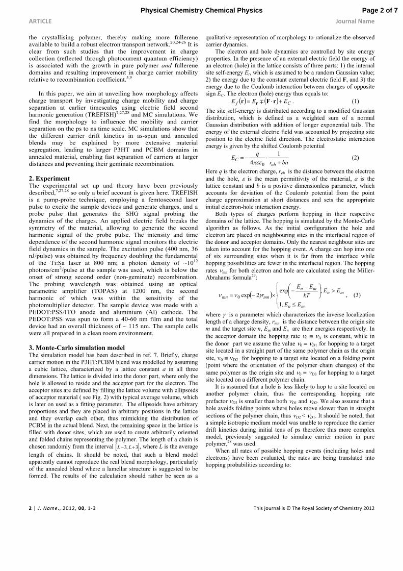
the crystallising polymer, thereby making more fullerene available to build a robust electron transport network.20,24-26 It is clear from such studies that the improvement in charge collection (reflected through photocurrent quantum efficiency) is associated with the growth in pure polymer and fullerene domains and resulting improvement in charge carrier mobility relative to recombination coefficient.5,9 In this paper, we aim at unveiling how morphology affects charge transport by investigating charge mobility and charge separation at earlier timescales using electric field second harmonic generation (TREFISH)7,27,28 and MC simulations. We find the morphology to influence the mobility and carrier separation on the ps to ns time scale. MC simulations show that the different carrier drift kinetics in as-spun and annealed blends may be explained by more extensive material segregation, leading to larger P3HT and PCBM domains in annealed material, enabling fast separation of carriers at larger distances and preventing their geminate recombination. 2. Experiment The experimental set up and theory have been previously described,7,27,28 so only a brief account is given here. TREFISH is a pump-probe technique, employing a femtosecond laser pulse to excite the sample devices and generate charges, and a probe pulse that generates the SHG signal probing the dynamics of the charges. An applied electric field breaks the symmetry of the material, allowing to generate the second harmonic signal of the probe pulse. The intensity and time dependence of the second harmonic signal monitors the electric field dynamics in the sample. The excitation pulse (400 nm, 36 nJ/pulse) was obtained by frequency doubling the fundamental of the Ti:Sa laser at 800 nm; a photon density of ~1012 photons/cm2/pulse at the sample was used, which is below the onset of strong second order (non-geminate) recombination. The probing wavelength was obtained using an optical parametric amplifier (TOPAS) at 1200 nm, the second harmonic of which was within the sensitivity of the photomultiplier detector. The sample device was made with a PEDOT:PSS/ITO anode and aluminium (Al) cathode. The PEDOT:PSS was spun to form a 40-60 nm film and the total device had an overall thickness of ~ 115 nm. The sample cells were all prepared in a clean room environment. 3. Monte-Carlo simulation model The simulation model has been described in ref. 7. Briefly, charge carrier motion in the P3HT:PCBM blend was modelled by assuming a cubic lattice, characterized by a lattice constant a in all three dimensions. The lattice is divided into the donor part, where only the hole is allowed to reside and the acceptor part for the electron. The acceptor sites are defined by filling the lattice volume with ellipsoids of acceptor material ( see Fig. 2) with typical average volume, which is later on used as a fitting parameter. The ellipsoids have arbitrary proportions and they are placed in arbitrary positions in the lattice and they overlap each other, thus mimicking the distribution of PCBM in the actual blend. Next, the remaining space in the lattice is filled with donor sites, which are used to create arbitrarily oriented and folded chains representing the polymer. The length of a chain is chosen randomly from the interval 3 ,3 LL , where L is the average length of chains. It should be noted, that such a blend model apparently cannot reproduce the real blend morphology, particularly of the annealed blend where a lamellar structure is suggested to be formed. The results of the calculation should rather be seen as a
qualitative representation of morphology to rationalize the observed carrier dynamics.
The electron and hole dynamics are controlled by site energy properties. In the presence of an external electric field the energy of an electron (hole) in the lattice consists of three parts: 1) the internal site self-energy Er, which is assumed to be a random Gaussian value; 2) the energy due to the constant external electric field F, and 3) the energy due to the Coulomb interaction between charges of opposite sign EC. The electron (hole) energy thus equals to:
Cf EEE rFr r . (1)
The site self-energy is distributed according to a modified Gaussian distribution, which is defined as a weighted sum of a normal Gaussian distribution with addition of longer exponential tails. The energy of the external electric field was accounted by projecting site position to the electric field direction. The electrostatic interaction energy is given by the shifted Coulomb potential
bar
qE
ehC
1
4 0 (2)
Here q is the electron charge, reh is the distance between the electron and the hole, is the mean permittivity of the material, a is the lattice constant and b is a positive dimensionless parameter, which accounts for deviation of the Coulomb potential from the point charge approximation at short distances and sets the appropriate initial electron-hole interaction energy.
Both types of charges perform hopping in their respective domains of the lattice. The hopping is simulated by the Monte-Carlo algorithm as follows. As the initial configuration the hole and electron are placed on neighbouring sites in the interfacial region of the donor and acceptor domains. Only the nearest neighbour sites are taken into account for the hopping event. A charge can hop into one of six surrounding sites when it is far from the interface while hopping possibilities are fewer in the interfacial region. The hopping rates mn for both electron and hole are calculated using the Miller-Abrahams formula29:
mn
mnmn
mnmn
EE
EEkT
EE
r
,1
,exp2exp0 , (3)
where is a parameter which characterizes the inverse localization length of a charge density, rmn is the distance between the origin site m and the target site n, Em and En are their energies respectively. In the acceptor domain the hopping rate 0 A is constant, while in the donor part we assume the value 0 D1 for hopping to a target site located in a straight part of the same polymer chain as the origin site, 0 D2 for hopping to a target site located on a folding point (point where the orientation of the polymer chain changes) of the same polymer as the origin site and 0 D3 for hopping to a target site located on a different polymer chain.
It is assumed that a hole is less likely to hop to a site located on another polymer chain, thus the corresponding hopping rate prefactor D3 is smaller than both D1 and D2. We also assume that a hole avoids folding points where holes move slower than in straight sections of the polymer chain, thus D2 <D1. It should be noted, that a simple isotropic medium model was unable to reproduce the carrier drift kinetics during initial tens of ps therefore this more complex model, previously suggested to simulate carrier motion in pure polymer,28 was used.
When all rates of possible hopping events (including holes and electrons) have been evaluated, the rates are being translated into hopping probabilities according to:
Page 2 of 7Physical Chemistry Chemical Physics
Journal Name ARTICLE
This journal is © The Royal Society of Chemistry 2012 J. Name., 2012, 00, 1‐3 | 3
kk
mnmnp
, (4)
where the summation is performed over all calculated rates of both the hole and the electron. These probabilities are then used to determine the destination site n for either the hole or the electron, chosen by a linearly distributed random number. The charge configuration is then switched to the one that has been determined and the rates of the next hopping events are recalculated.
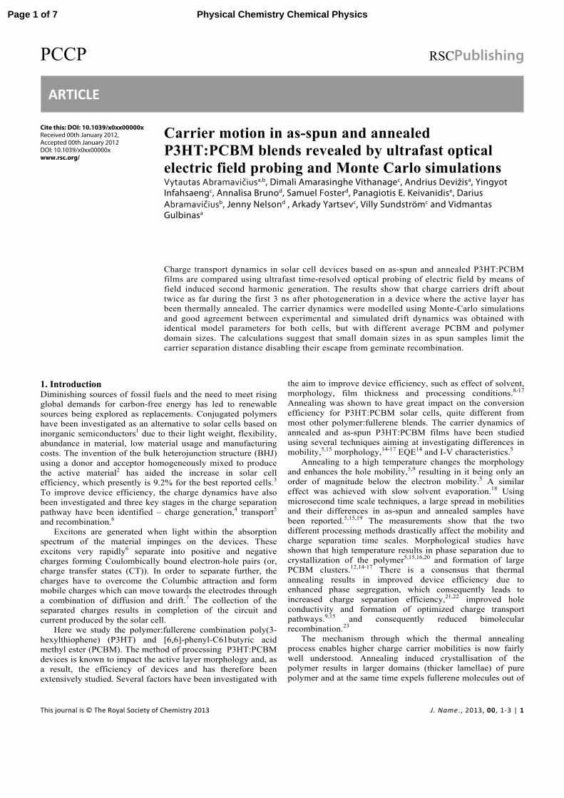
For the simulation a 100x400x400 lattice was used. This lattice simulates the actual structure of the blend, motivating that no cyclic boundary conditions are introduced. Initially, charges were created at a random location at the interface between the donor and the acceptor regions and due to the external electric field they drifted apart in opposite directions. While charges moved through the lattice, the distance between them projected in the direction of the external electric field F, dk(t) was recorded and the result was averaged over 5000 realizations. Only one electron-hole pair was present in the lattice at once, thus the model did not account for the nongeminate charge carrier recombination. The geminate recombination was also not accounted assuming it being much slower than the examined time domain. 4. Experimental results Figure 1 shows the carrier drift dynamics in as-spun and annealed samples for various applied voltages, calculated by the procedure described in ref. 19 from the experimentally measured TREFISH kinetics (not shown). Briefly, the electric field kinetics was reconstructed from the EFISH kinetics by using steady state EFISH dependence on the electric field strength. Next we assume that the electric field drop is proportional to the carrier drift distance and obtain the drift distance kinetics by normalizing the time-resolved field drop to the total field drop at long delay time when all carriers are extracted and, thus, their average drift distance equals to the half of the film thickness. The drift distances presented in Figure 1 are averaged over electrons and holes and rapidly increase on the tens of ps time scale in both samples. At long times (>200 ps) the increase rate gradually slows down to reach a separation distance of 15-30 nm (depending on film treatment) at 2.5 ns. The drift distances are approximately proportional to the internal electric field, suggesting that the initial carrier mobility is independent of the electric field strength. Qualitatively, similar drift dynamics has been observed for neat polymers28 and attributed to carrier relaxation within a distributed density of states. The drift distances in the as-spun sample are about half those in the annealed sample at the same applied voltages. Electron and hole drift in opposite directions by about 2.5 nm during the initial 10 ps at 6.7105 V/cm electric field in annealed sample. Thus, the electron-hole separation distance along the electric field is about 5 nm. This separation distance is around half as large in the as spun sample as in the annealed sample and is approximately proportional to applied field. 4. MC calculation results Monte Carlo simulations by the procedure described above have been performed to model the carrier drift dynamics and to get insight into the microscopic properties responsible for the observed differences in drift dynamics of annealed and as-spun material. The modelling of the hole motion dynamics accounts for the hole relaxation within the density of states (DOS),
different hole hopping rates within a conjugated segment (D1), between segments (D2) and between polymer chains (D3). The electron motion is simpler – the model accounts for the electron relaxation within the DOS and electron motion inside PCBM domains is characterised by a single electron hopping rate prefactor, A. Both electron and hole motions are also affected by the domain structure of the blend; reaching the domain boundaries carriers are forced to search for alternative pathways to continue their motions – this process results in a domain-size dependence of carrier mobility. The drift kinetics at different voltages were simulated with the same model parameters, only varying the internal field strength.
Figure 1: (a) Experimental (symbols) and simulated (lines) charge drift dynamics in the as-spun (top) and annealed (bottom) samples at various electric fields strengths.
Carrier drift kinetics in as-spun and annealed samples have
been modelled by using exactly the same motion parameters except for polymer and PCBM domain sizes. The best agreement was obtained with an average acceptor domain diameter of 7.5 nm for as-spun sample and 33 nm for annealed sample. As a result of fullerene aggregation the polymer domain dimensions were accordingly larger for annealed samples as well, but because of nonregular shapes their quantitative characterization, is more difficult. Figure 2 illustrates the corresponding material morphologies and Figure 1 shows the simulated carrier drift dynamics. The quite good agreement with experimental results obtained for all curves with only one free variable, the domain size, validates the
Page 3 of 7 Physical Chemistry Chemical Physics
AR
4 |
simanndomres30 recdo samlonthe
Figspuacc(P3
thenotpop
mounrdatdisundbeirateultrbesdricon
Tab
Ldi
10
Ado
6
Pa
5
C
2
RTICLE
J. Name., 2012
mulation resulnealed samplemains estimaults.30 On the
nm were combination in
not perfectly mples at high nger than 1 ns.e relatively sim
gure 2. Cross un (left) and ceptor regions 3HT). The red
We proceed t
e data for separt mobilities apulations of c
obilities descrirelaxed chargeta gives us inftances, the adisclosed, the ing a free parae on the basirafast time-resst agreement ft kinetics. nductivity, Sa
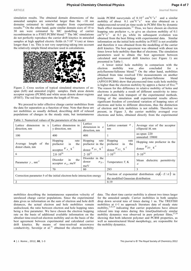
ble 1: Numeric
attice dimenirection, nm
00
Average lengtonor chain, nm
arameter , n
Correction para
2, 00, 1‐3
lts. The obtaies are somew
ated in similother hand, questimated b
n a P3HT:PCBreproduce theapplied electr This is not ve
mple blend stru
section of tyannealed (righ(PCBM) and line represent
to infer effectiration as a funs usually deficharges in the
ibing the instae carrier popu
formation on tactual electroratio betweenameter. We his of additionsolved electronbetween expeBy means
avenije et al.3
cal values of th
sion in x
th of the m
-1nm
ameter b of the
ined domain what larger lar samples uite similar do
by MC modBM blend.23 Te carrier drift kric fields (6.7ery surprising ucture used in
ypical simulateht) samples. white areas de
ts the length of
ive charge carnction of time.fined, describie steady state
antaneous sepulations. Sincthe sum of eleon and hole n electron and have chosen thnal available in mobility anderimental and
of time-res1 obtained the
he parameters
Lattice dimeny direction, nm
400
Hopping prefactor i
acceptor A ,16108.2
Disorder iacceptor A ,
70
e initial electro
dimensions othan the ~10from experim
omain sizes ofdelling of c
The MC simulkinetics in ann105 V/cm) at taking into accalculations.
ed structures oDark areas d
enote donor ref 50 nm.
rrier mobilities Note that theng drift of re, but instanta
paration velocce the experimctron and holemobilities rehole hopping
he electron hoinformation o
d on the basis d calculated csolved microe electron mo
of the model
nsion in m
Ladimdir
400
rate in the
, -1s
Hopre
don
2
in the meV
Didon
me80
on-hole interac
of the 0 nm
mental f 10 to carrier ations nealed times
ccount
of as-denote egions
s from ese are elaxed aneous
city of mental e drift emain
g rates opping on the of the
carrier owave obility
insidmobisubpiStarkhoppcm2Vobtaiinforand tdrift timesparamcalcuprese Aelectrpolyfobtaipolyf(APFis higThe relectrand Fittinsignielectrof elpreseelectr
data. for tdrop mobimobirelaxmobishowwell the m
attice mension in z rection, nm
0
opping rate efactor in the
nor 1D , -1s
1510 sorder in the nor D ,
eV
ction energy
T
e PCBM nanility of abouticosecond-sev
k effect measuing rate prefa
V-1s-1 at 0.3ined from the mation on the therefore it wakinetics. The
s lower hole mmeters used ulated and mented in Table A lower initiaron mobilifluorene/fullerined from timfluorene loFO3/PCBM) shgher than the ereason for thisrons is probabinter-chain ho
ng of the simficant freedomrons and holelectron and hoent, in Figurrons and hole
The short timhe annealed down severa
ilities at t>1ility,5,18,19 indi
xed into trap ility dynamics
wing that both as nanostruct
mobility dynam
Lattice connm
1
Hopping prefactor
donor 2D15101
Temperatur
293
Fraction of
the modifie0.19
This journal is ©
ncrystals of 8t 0.1 cm2V-1
eral ps time-screments.32 Thu
actor A to giv3 ps, while ibest fitting wiinitial hole m
as obtained frobest agreemen
mobility than thto obtain t
measured drift 1. al hole mobity was
rene blend.33 me resolved Tow-bandgap how that picoselectron mobils difference inbly a result oole transport mulation and
m of correlateds to different ole mobilities e 3, the cares, obtained d
me carrier mobsample. Carril tens of timens approach
icating that castates during s was observeinherent polyured blend m
mics.
nstant a , Ael
asan
rate in the
, -1s
H
d
5
re T, K M
3
f exponential
ed Gaussian di
The Royal Socie
10-2 cm2V-1s-
1s-1 was alscale in PCBM
hus, we have cve an electronits subsequenith experimen
mobility in P3Hom the modellnt was obtainehat of electronthe best agrt kinetics (se
ility in compalso conclOn the other
THz measurempolymer/fu
second time sclity by approx n relative mobof different se
of the experid experimentad variation ofdirections, th
s is not reliabrrier mobilitydirectly from
bility is almosier mobilities es during 1 nliterature data
arrier populatthis timeQua
ed in pure pymer and PCB
morphology, ar
Average size ollipsoid M, nm
s-spun: 220 nnealed: 1980
Hopping rate p
donor 3D , -s
14105
Mean dielectr
distribution
istribution
Journal Na
ty of Chemistry 2
-1 and a simo obtained o
M film by dynahosen an electn mobility of nt evolution tal data. Sim
HT is not availaling of the cared with about
ns. The simulareement betwe Figure 1)
parison with luded for
hand, mobiliments on anoullerene blcale hole mobia factor of fiv
bility of holes ensitivity to inimental methoal results allf hopping ratehus the distincble. Therefore y averaged othe experime
t two times larin both samp
s. The TREFIa of steady sions have almalitatively simolymer films,
BM propertiesre responsible
of the acceptm
00
prefactor in th
1
ric permittivi
/exp E
ame
2012
milar on a amic tron 0.1
was milar able rrier t ten ation ween
are
the a
ities ther lend ility ve.34 and
ntra- ods. ows s of tion we
over ental
rger ples ISH state most milar ,27,28
s, as for
tor
he
ity
in
Page 4 of 7Physical Chemistry Chemical Physics
Journal Name ARTICLE
This journal is © The Royal Society of Chemistry 2012 J. Name., 2012, 00, 1‐3 | 5
Our experimental data give information on the carrier drift distance, while the absolute carrier separation distance is determined by carrier diffusion as well as drift. . These two processes are interrelated through the Einstein relation
qTkD B / , where D is diffusion coefficient, is the carrier
mobility, kB is Boltzmann coefficient, T is temperature and q is electron charge. In our previous paper we have shown that the diffusion distance on a ps time scale significantly exceeds the drift distance at low fields and is responsible for the weakly field dependent carrier separation yield.7
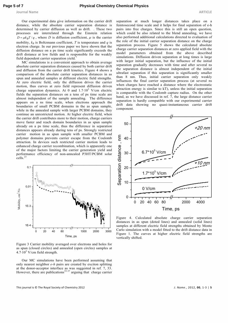
MC simulations is a convenient approach to obtain average absolute carrier separation distances caused by both carrier drift and diffusion from the carrier drift kinetics. Figure 4 shows a comparison of the absolute carrier separation distances in as spun and annealed samples at different electric field strengths. At zero electric field, only the diffusion drives the carrier motion, thus curves at zero field represent diffusion driven charge separation dynamics. At 0 and 1.7105 V/cm electric fields the separation distances on a tens of ps time scale are almost independent of the sample annealing. The difference appears on a ns time scale, when electrons approach the boundaries of small PCBM domains in the as spun sample, while in the annealed sample with larger PCBM domains, they continue an unrestricted motion. At higher electric field, when the carrier drift contributes more to their motion, charge carriers move faster and reach domain boundaries in as spun sample already on a ps time scale, thus the difference in separation distances appears already during tens of ps. Strongly restricted carrier motion in as spun sample with smaller PCBM and polymer domains prevents carrier escape from the Coulomb attraction. In devices such restricted carrier motion leads to enhanced charge carrier recombination, which is apparently one of the major factors limiting the carrier generation yield and performance efficiency of non-annealed P3HT/PCBM solar cells.23
Figure 3 Carrier mobility averaged over electrons and holes for as spun (closed circles) and annealed (open circles) samples at 4.7105 V/cm field strength.
Our MC simulations have been performed assuming that only nearest neighbor e-h pairs are created by exciton splitting at the donor-acceptor interface as was suggested in ref. 7, 33. However, there are publications35-37 arguing that charge carrier
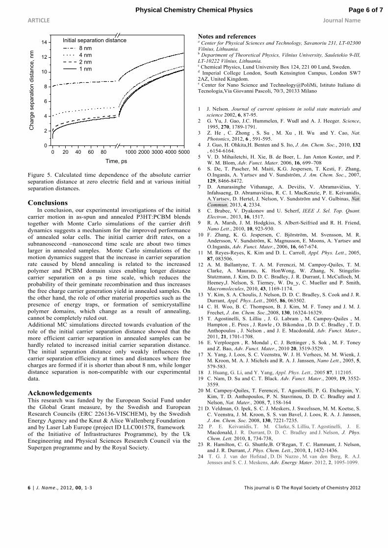
separation at much longer distances takes place on a femtosecond time scale and it helps for final separation of e-h pairs into free charges. Since this is still an open question, which could be also related to the blend annealing, we have also performed additional calculations directed to evaluation of the role of the initial carrier separation distance on the charge separation process. Figure 5 shows the calculated absolute charge carrier separation distances at zero applied field with the model parameters obtained from the above described simulations. Diffusion driven separation at long times is large with larger initial separation, but the influence of the initial separation gradually decreases with time and after several ns the separation distance is almost independent of the initial ultrafast separation if this separation is significantly smaller than 8 nm. Thus, initial carrier separation only weakly influences the final carrier separation process (at several ns when charges have reached a distance where the electrostatic attraction energy is similar to kT), unless the initial separation is comparable with the Coulomb capture radius. On the other hand, as we have discussed in ref. 7, the large distance carrier separation is hardly compatible with our experimental carrier drift data showing no quasi-instantaneous carrier drift component.
Figure 4. Calculated absolute charge carrier separation distances in as spun (doted lines) and annealed (solid lines) samples at different electric field strengths obtained by Monte Carlo simulation with a model fitted to the drift distance data in Figure 1. The curves at higher electric field strengths are vertically shifted.
Page 5 of 7 Physical Chemistry Chemical Physics
ARTICLE Journal Name
6 | J. Name., 2012, 00, 1‐3 This journal is © The Royal Society of Chemistry 2012
Figure 5. Calculated time dependence of the absolute carrier separation distance at zero electric field and at various initial separation distances. Conclusions In conclusion, our experimental investigations of the initial carrier motion in as-spun and annealed P3HT:PCBM blends together with Monte Carlo simulations of the carrier drift dynamics suggests a mechanism for the improved performance of annealed solar cells. The initial carrier drift rates, on a subnanosecond –nanosecond time scale are about two times larger in annealed samples. Monte Carlo simulations of the motion dynamics suggest that the increase in carrier separation rate caused by blend annealing is related to the increased polymer and PCBM domain sizes enabling longer distance carrier separation on a ps time scale, which reduces the probability of their geminate recombination and thus increases the free charge carrier generation yield in annealed samples. On the other hand, the role of other material properties such as the presence of energy traps, or formation of semicrystalline polymer domains, which change as a result of annealing, cannot be completely ruled out. Additional MC simulations directed towards evaluation of the role of the initial carrier separation distance showed that the more efficient carrier separation in annealed samples can be hardly related to increased initial carrier separation distance. The initial separation distance only weakly influences the carrier separation efficiency at times and distances where free charges are formed if it is shorter than about 8 nm, while longer distance separation is non-compatible with our experimental data. Acknowledgements This research was funded by the European Social Fund under the Global Grant measure, by the Swedish and European Research Councils (ERC 226136-VISCHEM), by the Swedish Energy Agency and the Knut & Alice Wallenberg Foundation and by Laser Lab Europe (project ID LLC001578, framework of the Initiative of Infrastructures Programme), by the Uk Enegineering and Physical Sciences Research Council via the Supergen programme and by the Royal Society.
Notes and references a Center for Physical Sciences and Technology, Savanoriu 231, LT-02300 Vilnius, Lithuania. b Department of Theoretical Physics, Vilnius University, Sauletekio 9-III, LT-10222 Vilnius, Lithuania. c Chemical Physics, Lund University Box 124, 221 00 Lund, Sweden. d Imperial College London, South Kensington Campus, London SW7 2AZ, United Kingdom. e Center for Nano Science and Technology@PoliMi, Istituto Italiano di Tecnologia,Via Giovanni Pascoli, 70/3, 20133 Milano 1 J. Nelson. Journal of current opinions in solid state materials and
science 2002, 6, 87-95. 2 G. Yu, J. Gao, J.C. Hummelen, F. Wudl and A. J. Heeger. Science,
1995, 270, 1789-1791. 3 Z. He , C. Zhong , S. Su , M. Xu , H. Wu and Y. Cao, Nat.
Photonics, 2012, 6 , 591-595. 4 J. Guo, H. Ohkita,H. Benten and S. Ito, J. Am. Chem. Soc., 2010, 132
, 6154-6164. 5 V. D. Mihailetchi, H. Xie, B. de Boer, L. Jan Anton Koster, and P.
W. M. Blom, Adv. Funct. Mater. 2006, 16, 699–708 6 S. De, T. Pascher, M. Maiti, K.G. Jespersen, T. Kesti, F. Zhang,
O.Inganäs, A. Yartsev and V. Sundström, J. Am. Chem. Soc., 2007, 129, 8466-8472.
7 D. Amarasinghe Vithanage, A. Devižis, V. Abramavičius, Y. Infahsaeng, D. Abramavičius, R. C. I. MacKenzie, P. E. Keivanidis, A.Yartsev, D. Hertel, J. Nelson, V. Sundström and V. Gulbinas, Nat. Commun. 2013, 4, 2334.
8 C. Brabec, V. Dyakonov and U. Scherf, IEEE J. Sel. Top. Quant. Electron., 2013, 16, 1517.
9 R. A. Marsh, J. M. Hodgkiss, S. Albert-Seifried and R. H. Friend, Nano Lett., 2010, 10, 923-930.
10 F. Zhang, K. G. Jespersen, C. Björström, M. Svensson, M. R. Andersson, V. Sundström, K. Magnusson, E. Moons, A. Yartsev and O.Inganäs, Adv. Funct. Mater., 2006, 16, 667-674.
11 M. Reyes-Reyes, K. Kim and D. L. Carroll, Appl. Phys. Lett., 2005, 87, 083506.
12 A. M. Ballantyne, T. A. M. Ferenczi, M. Campoy-Quiles, T. M. Clarke, A. Maurano, K. HonWong, W. Zhang, N. Stingelin-Stutzmann, J. Kim, D. D. C. Bradley, J. R. Durrant, I. McCulloch, M. Heeney,J. Nelson, S. Tierney, W. Du_y, C. Mueller and P. Smith, Macromolecules, 2010, 43, 1169-1174.
13 Y. Kim, S. A. Choulis, J. Nelson, D. D. C. Bradley, S. Cook and J. R. Durrant, Appl. Phys..Lett., 2005, 86, 063502.
14 C. H. Woo, B. C. Thompson, B. J. Kim, M. F. Toney and J. M. J. Frechet, J. Am. Chem. Soc.,2008, 130, 16324-16329.
15 T. Agostinelli, S. Lilliu , J. G. Labram , M. Campoy-Quiles , M. Hampton , E. Pires , J. Rawle , O. Bikondoa , D. D. C. Bradley , T. D. Anthopoulos , J. Nelson , and J. E. Macdonald, Adv. Funct. Mater., 2011, 21, 1701-1708.
16 E. Verploegen , R. Mondal , C. J. Bettinger , S. Sok , M. F. Toney and Z. Bao, Adv. Funct. Mater., 2010 20, 3519-3529.
17 X. Yang, J. Loos, S. C. Veenstra, W. J. H. Verhees, M. M. Wienk, J. M. Kroon, M. A. J. Michels and R. A. J. Janssen, Nano Lett., 2005, 5, 579-583.
18 J. Huang, G. Li, and Y. Yang, Appl. Phys. Lett., 2005 87, 112105. 19 C. Nam, D. Su and C. T. Black. Adv. Funct. Mater., 2009, 19, 3552-
3559. 20 M. Campoy-Quiles, T. Ferenczi, T. Agostinelli, P. G. Etchegoin, Y.
Kim, T. D. Anthopoulos, P. N. Stavrinou, D. D. C. Bradley and J. Nelson, Nat. Mater., 2008, 7, 158-164
21 D. Veldman, O. Ipek, S. C. J. Meskers, J. Sweelssen, M. M. Koetse, S. C. Veenstra, J. M. Kroon, S. S. van Bavel, J. Loos, R. A. J. Janssen, J. Am. Chem. Soc. 2008, 130, 7221-7235.
22 P. E. Keivanidis, T. M. Clarke, S. Lilliu, T. Agostinelli, J. E. Macdonald, J. R. Durrant, D. D. C. Bradley and J. Nelson, J. Phys. Chem. Lett. 2010, 1, 734-738,
23 R. Hamilton, C. G. Shuttle,B. O’Regan, T. C. Hammant, J. Nelson, and J. R. Durrant, J. Phys. Chem. Lett., 2010, 1, 1432-1436.
24 T. G. J. van der Hofstad , D. Di Nuzzo , M. van den Berg, R. A.J. Jensses and S. C. J. Meskens, Adv. Energy Mater. 2012, 2, 1095-1099.
Page 6 of 7Physical Chemistry Chemical Physics
Journal Name ARTICLE
This journal is © The Royal Society of Chemistry 2012 J. Name., 2012, 00, 1‐3 | 7
25 C. Müller, T. A. M. Ferenczi, M. Campoy-Quiles, J. M. Frost, D. D. C. Bradley, P. Smith, N. Stingelin-Stutzmann and J. Nelson, Adv. Mater. 2008,18, 3510-3515.
26 T.Agostinelli , S. Lilliu , J. G. Labram , M. Campoy-Quiles , M. Hampton , E. Pires , J. Rawle , O. Bikondoa , D. D. C. Bradley, T. D. Anthopoulos , J. Nelson , J. E. Macdonald, Adv. Funct. Mater. 2011, 21, 1701-1708.
27 A. Devizis, A. Serbenta, K. Meerholz, D. Hertel, and V. Gulbinas. Phys. Rev. Lett., 2009, 103, 027404.
28 A. Devizis, K. Meerholz, D. Hertel and V. Gulbinas. Chem. Phys. Lett., 2010, 498, 302-306.
29 A. Miller, and E. Abrahams, Phys. Rev.,1960, 120, 745-755. 30 W. L. Ma, C. Y. Yang, and A. J. Heeger, Adv. Mater. 2007, 19, 1387-
1390. 23 R. Hamilton, C. G. Shuttle,B. O’Regan, T. C. Hammant, J. Nelson,
and J. R. Durrant, J. Phys. Chem. Lett., 2010, 1, 1432. 31 T. J. Savenije, J. E. Kroeze, M. M. Wienk, J. M. Kroon, and J. M.
Warman,. Phys. Rev. B, 2004, 69, 155205. 32 J. Cabanillas-Gonzalez, T. Virgili, A. Gambetta, G. Lanzani, T.
Anthopoulos, and D. De Leeuw. Phys. Rev. Lett., 2006, 96, 106601. 33 D.Veldman, O. Ipek, S. C. J. Meskers, J. Sweelssen, M. M. Koetse,
S. C. van Bavel, J. Loos, and R. A. J. Janssen, J. Am. Chem. Soc.,2008, 130, 7721-7735.
34 C. S. Ponseca, H. Nemec, N. Vukmirovic, S. Fusco, E. Wang, M. R. Andersson, P. Chabera, A. Yartsev,.and V. Sundstrom J. Phys. Chem. Lett., 2012, 3, 2442-2446.
35 A. A. Bakulin, A. Rao, V. G. Pavelyev, P. H. M. van. Loosdrecht, M. S. Pshenichnikov, D. Niedzialek, J. Cornil,. D. Beljonne, and R. H. Friend. Science 2012, 335, 1340–1344.
36 I. A. Howard, R. Mauer, M. Meister and F. Laquai, J. Am. Chem. Soc., 2010, 132, 14866–14876.
37 C. Deibel, T. Storbel, and V. Dyakonov, Phys. Rev. Lett. 2009 103, 036402.
Page 7 of 7 Physical Chemistry Chemical Physics