effect of modular diffraction gratings on absorption in p3ht:pcbm layers
TRANSCRIPT
Effect of modular diffraction gratings onabsorption in P3HT:PCBM layers
Byron Cocilovo,1,* Akram Amooali,1 Alejandra Lopez-Santiago,1 Jacob Favela,2
Safatul Islam,1 Binh Duong,4 Palash Gangopadhyay,1 Mahmoud Fallahi,1
Jeanne E. Pemberton,3 Jayan Thomas,4 and Robert A. Norwood1
1College of Optical Sciences, University of Arizona, 1630 E. University Blvd., Tucson, Arizona 85721, USA2Department of Materials Science and Engineering, University of Arizona, 1235 E. James E. Rogers Way,
Tucson, Arizona 85721, USA3Department of Chemistry and Biochemistry, University of Arizona, 1306 East University Blvd.,
Tucson, Arizona 85721, USA4NanoScience Technology Center and CREOL, University of Central Florida, 12424 Research Parkway
Suite 480, Orlando, Florida 32826-3250, USA
*Corresponding author: [email protected]
Received 8 October 2012; revised 28 November 2012; accepted 5 January 2013;posted 8 January 2013 (Doc. ID 177521); published 8 February 2013
Various gratings with 700 nm feature spacings are patterned on the reverse side of organic solar cellactive layers to increase the path length and constrain light to the cell through total internal reflection.The absorption enhancement is studied for 15, 40, and 120 nm active layers.Wewere able to confine 9% ofthe incident light over the wavelength range of 400–650 nm, with thinner gratings having a greaterenhancement potential. The measurement setup utilizing an integrating sphere to fully characterizescattered or diffracted light is also fully described. © 2013 Optical Society of AmericaOCIS codes: 050.1950, 350.6050, 120.3150.
1. Introduction
Organic solar cells (OSCs), in particular, bulk hetero-junction (BHJ) OSCs, are promising photovoltaiccandidates. They are flexible, lightweight, low cost,and can be produced in large quantities using simpleprocessing techniques [1]. However, the efficiency ofOSCs needs to be enhanced for them to become acompetitive energy source for most applications[1–3]. Efficiencies between 1% and 10% have beendemonstrated for various OSC designs, but improve-ment is still needed [4–10].
Radiant energy passes through several stages in asolar cell before it is converted to electrical energy.First, a fraction of the incident light, ηA (absorption
efficiency), is absorbed in the active layer and createsexcitons. Some excitons recombine and are wasted,but a fraction, ηD (dissociation efficiency), reach amaterial boundary where they dissociate into elec-trons and holes. A fraction of the remaining electronsand holes, ηC (collection efficiency), are then collectedby the respective cathode or anode. The product ofthese efficiencies is the power conversion efficiency(PCE), which describes the fraction of radiant energythat is converted into electrical energy, as indicatedin Eq. (1):
PCE � η � ηAηDηC: (1)
The charge dissociation efficiency, ηD, is related tothe exciton diffusion length and average distance todonor–acceptor interfaces. The Frenkel excitons inOSCs have diffusion lengths of only 5–10 nm,making
1559-128X/13/051025-10$15.00/0© 2013 Optical Society of America
10 February 2013 / Vol. 52, No. 5 / APPLIED OPTICS 1025
it difficult for them to reach a boundary before recom-bination occurs [7]. This has driven makers of OSCsto use BHJs with nanoscale morphology instead ofconventional planar heterojunctions.
The absorption efficiency, ηA, and charge collectionefficiency, ηC, can be manipulated by adjusting theactive layer thickness. ηA is enhanced with thickerlayers, and ηC is enhanced with thinner layers,leading to an optimal layer thickness that producesthe greatest efficiency. This optimal thickness is be-tween 100 and 250 nm for conventional cells usingP3HT:PCBM [11].
To simultaneously increase ηA and ηC it has beenproposed to add diffraction gratings to solar cell sub-strates [12–16]. Diffraction gratings enhance thepath length of light in the cell, thereby increasingηA and the PCE. Alternatively, ηA can be maintainedand the active layer can be made thinner to increaseηC and the PCE.
Textured surfaces have been applied to siliconsolar cells to a great degree and to OSCs to a lesserdegree. The driving factor behind texturing inorganiccells is to lower the cost of the device by reducing theamount of silicon needed to absorb an equivalentamount of light as planar cells. OSCs, on the otherhand, have found minimal use for gratings becauseof their low cost and high absorptance. Over 90% ofgreen light is absorbed in 100 nm OSC active layers,compared to only 18% in crystalline silicon [17–19].The primary benefit of using diffraction gratingson OSCs comes from the increase of charge collectionefficiency achieved through reduction of the requiredactive layer thickness.
Another factor restricting the use of textured sur-faces on OSCs is their thinness. The well-known 4n2
optical enhancement limit, discussed below, assumesthe active layer is much thicker than a wavelengthso many photon modes may be confined. This holdstrue for silicon solar cells, where the wafer thick-nesses are tens to hundreds of microns thick. In con-trast, OSCs have active layer thicknesses of only 100or 200 nm—significantly less than the wavelengthsof interest. Thin layers such as these are unable toconfine light, making it difficult to approach the4n2 limit. Instead, the light must be confined in thesubstrate and absorbed only when it extends intothe active layers. An upside to the breakdown ofthe 4n2 limit when thin layers are used is that thelimit may be surpassed when gratings are used un-der the right conditions [20].
Previous studies on the effects of applying gratingsto OSCs have used textured active materials andelectrodes, making it difficult to discern what factorscontribute to changes in absorptance or PCE. The in-tended purpose of diffraction gratings is to enhancethe path length of light in the active layer, but manyother variables are also changed when active layersare patterned that may have advantageous or ad-verse effects. Charges in textured active layers havevarying distances to travel depending on their proxi-mity to a peak or trough, possibly leading to a change
in ηC. The surface area of textured electrodes is alsoincreased, causing an increase in electrode resis-tance and a reduction in the PCE. Textured electro-des and active layers can also suffer from resonanceanomalies, where light is coupled into surface plas-mons at structured dielectric-metallic interfaces [21].OSCs are a developing technology, and more re-search is needed to fully understand their operation.Patterning the OSC active layers can introduce toomany unknown effects to clearly identify their im-pacts on the absorptance and PCE.
In this work we isolate gratings from the solar cellmaterials in order to understand how the diffractiveproperties of gratings affect absorption enhancementin OSCs. The grating and OSC layers are patternedon opposite sides of the glass substrate. In this config-uration we can do a rigorous analysis of diffraction en-hancement while ignoring surface texturing effects,interfacial interactions, and resonance anomalies.
Isolation of the gratings from the active layers alsoenables them to be completely modular. The pattern-ing and analysis of the gratings are independent ofthe methods and materials used to create the solarcells. Both the physical gratings and their theoreticaldescriptions outlined here are not limited to OSCs,or even solar cells in general, but may be appliedto any device that would benefit from the use of dif-fracted light.
To observe and understand the absorption enhance-ment in OSC active layers, we prepared texturedand planar samples with various P3HT:PCBM thick-nesses; numerous gratings were also examined. Thegratings were made from polyacrylonitrile (PAN), adielectric polymer with an index of refraction similarto that of glass (n � 1.52). The index of PANwasmea-sured using an ellipsometer and is shown in Fig. 1(a).Figure 1(b) shows a diagram of the samples used. Intandem with sample fabrication, we used a combina-tion of analytical and numerical models to understandand design our samples. A setup utilizing an integrat-ing sphere capable of quantifying the absorption, re-flection, and transmission of diffracting devices wasnecessary, as standard UV–Vis spectrophotometershave limited capability for measuring diffracted andscattered light.
The concepts of diffraction and scattering permeatethis work, both in device design as well as character-ization. Before continuing with the details and resultsof our research, we present a number of the basic prin-ciples of optics tied to diffraction and measurement.The following explanations should serve as a briefsummary of diffraction and scattering theory as it re-lates to solar cell improvement and characterization.
2. Theory
A. Diffraction and Scattering
Textured surfaces and their ability to increase theoptical density in solar cells have been extensivelystudied [12–16,22]. The enhancement factor, equal tothe ratio of the optical density in a textured sample
1026 APPLIED OPTICS / Vol. 52, No. 5 / 10 February 2013

to that of a planar sample, is a standard metric forquantifying light harvesting. In 1982, Yablonovitchexplored the maximum enhancement factor fromusing textured surfaces. The aptly named Yablono-vitch limit, equal to 4n2, is the theoretical maximumenhancement factor achievable by the use of texturedsurfaces. The limit is found by calculating the num-ber of photon states in a material in thermal equili-brium and is only dependent on the refractive index,n [22]. The Yablonovitch limit assumes the activelayer is much thicker than a wavelength, and thematerial is weakly absorbing, where the averagepath length of light due to absorption is much longerthan the cell thickness. To achieve the 4n2 limit, thetextured surfaces must be Lambertian, where the in-tensity leaving the surface varies with the cosine ofthe angle from normal. All non-Lambertian surfaces,such as gratings and mirrors, have lower enhance-ment factors.
The absorption enhancement from weak absorbersis directly related to the enhancement factor. Rayspropagating in a sample at an angle θ from thenormal have larger path lengths and provide greateroptical densities than normally propagating rays. Inaddition, reflectance generally increases with largerangles, further increasing the optical density.
The percent of light absorbed in a material witha complex refractive index, N � n� ik, at a givenwavelength, λ, is related to the optical path lengthaccording to Beer’s law:
A � 1 − e−αl; (2)
whereA is the absorptance, l is the path length, and αis the absorption coefficient, which is equal to 4πκ∕λ[5]. Forweakabsorbers,Eq. (2) canbe simplifiedusingthe first two terms of a Taylor expansion, yielding
A � αl: (3)
In the weak absorber approximation, l is the aver-age path length of light over all angles and reflec-tances. We can easily see from Eqs. (2) and (3) thatincreasing either the layer thickness or the propaga-tion angles increases the amount of absorbed light.
Although Lambertian scattering surfaces providethe greatest average path length enhancement, inpractice, they are difficult to produce and are oftenapproximated using diffraction gratings or etchedpyramids [13,20].
B. Diffraction Theory
Diffraction gratings provide a precise way to manip-ulate light. The optical path difference between theperiodic peaks and valleys of gratings forces incidentlight to interfere with itself. After passing throughgratings and reaching the far field, incident planewaves evolve into multiple plane waves propagatingat fixed angles. Each propagation angle correspondsto a separate diffraction order according to
nsub sin θm � ni sin θi �mλ
p; (4)
where ni and nsub are the refractive indices of theincident and substrate material, respectively, m isthe order number, θm is the mth diffraction angle,θi is the incident angle, λ is the wavelength, and pis the period [5]. Propagation angles increase withwavelength and order number and decrease withgrating period. The percent of light diffracted intoeach order can be derived for an arbitrary gratingusing scalar diffraction analysis by propagatingthe incident light to the far field. The diffraction ef-ficiency for a plane wave incident on an arbitrarygrating is
Em;n ����� 1pxpy
FξFη
�f px;py
�x; y�⋅rect�xpx
;ypy
������2; (5)
where x and y are the spatial coordinates at the grat-ing, px and py are the respective periods, FξFηfg de-notes the Fourier transform with variables ξ � m∕pxand η � n∕py, f px;py
�� is the functional form of thegrating over one period, and rect�� is the rectanglefunction (1 for jx; yj ≤ px; py, 0 otherwise) [23]. The dif-fraction efficiency, Em;n, is only dependent on thewavelength, grating refractive index, and gratingshape. Although it is included in Eq. (4), the gratingperiod only serves to normalize the function and hasno effect on Em;n. In general the majority of incident
Fig. 1. (Color online) (a) Refractive index of PAN measured using an ellipsometer. (b) Diagram of the structure used to measure absorp-tion enhancement. The top of the glass substrate is coated with a PAN grating, and the bottom is coated with P3HT:PCBM.
10 February 2013 / Vol. 52, No. 5 / APPLIED OPTICS 1027
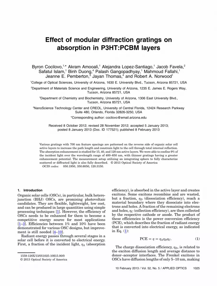
light is diffracted into the first few orders. The aboveequations predict that over 80% of the light isdistributed among the 0 and �1 orders for gratingswith 700 nm periods and 350 nm depths, as shown inFig. 2(a).
Together, the above diffraction equations enableus to predict the average path length of light inany layer: the path length of each order is found fromEq. (4) and the percent of light in each order is foundusing Eq. (5). Although Eqs. (4) and (5) predict aninfinite number of orders, only a few of them propa-gate. As the wavelength increases relative to thegrating period, so too does the propagation angle ofa given order, until it reaches 90°, at which point thelight becomes evanescent and is redistributed amongthe propagating orders [21]. The amount of light re-distributed this way is generally low for wavelengthswith the same magnitude as the grating period.Figure 2(b) shows the diffraction angles of the firstthree orders in a P3HT:PCBM layer calculated usingEq. (4). The �2 orders stop propagating at 525 nmbecause they become evanescent. Equations (4)and (5) can effectively predict the angles and distri-bution of diffracted light but do not incorporatepolarization.
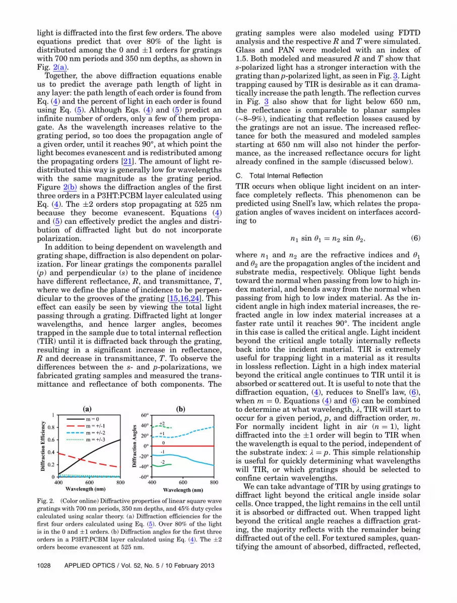
In addition to being dependent on wavelength andgrating shape, diffraction is also dependent on polar-ization. For linear gratings the components parallel(p) and perpendicular (s) to the plane of incidencehave different reflectance, R, and transmittance, T,where we define the plane of incidence to be perpen-dicular to the grooves of the grating [15,16,24]. Thiseffect can easily be seen by viewing the total lightpassing through a grating. Diffracted light at longerwavelengths, and hence larger angles, becomestrapped in the sample due to total internal reflection(TIR) until it is diffracted back through the grating,resulting in a significant increase in reflectance,R and decrease in transmittance, T. To observe thedifferences between the s- and p-polarizations, wefabricated grating samples and measured the trans-mittance and reflectance of both components. The
grating samples were also modeled using FDTDanalysis and the respective R and T were simulated.Glass and PAN were modeled with an index of1.5. Both modeled and measured R and T show thats-polarized light has a stronger interaction with thegrating than p-polarized light, as seen in Fig. 3. Lighttrapping caused by TIR is desirable as it can drama-tically increase the path length. The reflection curvesin Fig. 3 also show that for light below 650 nm,the reflectance is comparable to planar samples(∼8–9%), indicating that reflection losses caused bythe gratings are not an issue. The increased reflec-tance for both the measured and modeled samplesstarting at 650 nm will also not hinder the perfor-mance, as the increased reflectance occurs for lightalready confined in the sample (discussed below).
C. Total Internal Reflection
TIR occurs when oblique light incident on an inter-face completely reflects. This phenomenon can bepredicted using Snell’s law, which relates the propa-gation angles of waves incident on interfaces accord-ing to
n1 sin θ1 � n2 sin θ2; (6)
where n1 and n2 are the refractive indices and θ1and θ2 are the propagation angles of the incident andsubstrate media, respectively. Oblique light bendstoward the normal when passing from low to high in-dex material, and bends away from the normal whenpassing from high to low index material. As the in-cident angle in high index material increases, the re-fracted angle in low index material increases at afaster rate until it reaches 90°. The incident anglein this case is called the critical angle. Light incidentbeyond the critical angle totally internally reflectsback into the incident material. TIR is extremelyuseful for trapping light in a material as it resultsin lossless reflection. Light in a high index materialbeyond the critical angle continues to TIR until it isabsorbed or scattered out. It is useful to note that thediffraction equation, (4), reduces to Snell’s law, (6),when m � 0. Equations (4) and (6) can be combinedto determine at what wavelength, λ, TIR will start tooccur for a given period, p, and diffraction order, m.For normally incident light in air (n � 1), lightdiffracted into the �1 order will begin to TIR whenthe wavelength is equal to the period, independent ofthe substrate index: λ � p. This simple relationshipis useful for quickly determining what wavelengthswill TIR, or which gratings should be selected toconfine certain wavelengths.
We can take advantage of TIR by using gratings todiffract light beyond the critical angle inside solarcells. Once trapped, the light remains in the cell untilit is absorbed or diffracted out. When trapped lightbeyond the critical angle reaches a diffraction grat-ing, the majority reflects with the remainder beingdiffracted out of the cell. For textured samples, quan-tifying the amount of absorbed, diffracted, reflected,
Fig. 2. (Color online) Diffractive properties of linear square wavegratings with 700 nm periods, 350 nm depths, and 45% duty cyclescalculated using scalar theory. (a) Diffraction efficiencies for thefirst four orders calculated using Eq. (5). Over 80% of the lightis in the 0 and �1 orders. (b) Diffraction angles for the first threeorders in a P3HT:PCBM layer calculated using Eq. (4). The �2orders become evanescent at 525 nm.
1028 APPLIED OPTICS / Vol. 52, No. 5 / 10 February 2013

and transmitted light cannot be done using a stan-dard UV–Vis spectrophotometer, as the scatteredcomponents do not reach the detector. Instead, an in-tegrating sphere is needed to capture the diffractedand scattered light.
D. Integrating Spheres
Integrating spheres provide an effective way to mea-sure scattered light in reflection and transmissionacross a broad range of wavelengths. Their designis simple: they are hollow spheres coated with highlyreflective, diffuse, and spectrally flat material. Lightentering the sphere is uniformly reflected across theinterior, where it continues to diffuse. Because of thehighly reflective interior coating, light may reverbe-rate hundreds of times before reaching the exit portof the sphere, where it is homogenous and diffuse andcan easily be measured with a variety of detectors.
The intensity of the light at the exit port can bederived by assuming the inner surface of the sphereto be Lambertian. As mentioned above, light reflect-ing from Lambertian surfaces has an angular inten-sity profile proportional to the cosine of the anglefrom normal. A convenient consequence of this withregards to integrating spheres is that light incidentfrom any angle on the interior of the sphere is evenlydistributed across the surface of the sphere, greatlysimplifying the formula for the exit port surfaceradiance. The wavelength dependent radiance atthe exit port, after correcting for ports and nonidealsurface reflectance, is
L�λ� � Rinc�λ�⋅Φ�λ�πAsph�1 − Rsph�λ�⋅�1 − f ��
�W
m2⋅nm⋅sr
�; (7)
whereΦ�λ� is the incident power entering the sphere,Asph is the area of the sphere, Rsph�λ� is the reflec-tance of the sphere wall, f is the fraction of total portarea to sphere area, and Rinc�λ� is the initial reflec-tance of the light entering the sphere [25]. For reflec-tance measurements, Rinc�λ� is the reflectance of the
sample. In all other configurations, Rinc�λ� is equal toRsph�λ�. Rays reflect an average of 1∕f times beforeescaping through one of the ports [26]. For mostspheres the average number of reflections is between50 and 1000, but can be even higher for large sphereswith small ports. Because of the large number of re-flections, it is imperative that the reflectance be nearunity and spectrally flat, as small amounts of absorp-tion quickly compound. The sphere radius should beas large as possible relative to the ports to increasethe radiant signal and reduce the amount of straylight entering and exiting the sphere. Lastly, thecoating should be near Lambertian to ensure a uni-form distribution at the exit port, where the light canthen be measured. The total transmittance, Ttot, andreflectance, Rtot, can be rapidly measured by placingthe sample at the entrance or exit ports of the sphere,respectively, as shown in Fig. 4.
Measurements obtained using an integratingsphere can be used to find various properties of sam-ples. Light will either be specularly reflected, Rspec,diffusely reflected, Rdiff , specularly transmitted,Tspec, diffusely transmitted, Tdiff , or absorbed, A,according to
Fig. 3. (Color online) Total reflectance, R, and transmittance, T, of p- and s-polarized light for a grating on a glass substrate measuredusing an integrating sphere (a) and modeled using FDTD analysis (b). (c) Modeling approach used in the FDTD simulation. For both themodeled and measured gratings the s-polarized light has a much stronger interaction with the grating. The large feature starting at700 nm is caused by TIR: diffracted light does not transmit through the grating, and is instead reflected, resulting in increased reflectionand decreased transmission. The magnitude of the feature is reduced in the measured case compared to the modeled because of imperfec-tions in the grating, and the differences between the finite size of the measured grating and infinite size of the modeled grating.
Fig. 4. (Color online) Integrating sphere setup to measure (a) to-tal transmission and (b) total reflection of scattering or diffractingsamples. These results may be combined to determine the absorp-tance of the sample.
10 February 2013 / Vol. 52, No. 5 / APPLIED OPTICS 1029

1 � Rspec � Rdiff � Tspec � Tdiff � A: (8a)
Integrating spheres measure the total reflectance,Rtot � Rspec �Rdiff , and the total transmittance,Ttot � Tspec � Tdiff , of a sample. The absorption of thesample is easily calculated using only an integratingsphere together with Eq. (8a). UV–Vis spectrophot-ometers measure only the specular components,Rspec and Tspec, which are insufficient to determinethe absorptance of a scattering sample. However,UV–Vis measurements can be combined with inte-grating sphere measurements to isolate the scat-tered or diffracted components according to
Rdiff � Rtot − Rspec (8b)
Tdiff � Ttot − Tspec: (8c)
Integrating spheres allow for a vast variety of sam-ples to be measured. Figure 5 shows the results frommeasuring a leaf, nanoparticle composite used in all-optical magnetometers [27], and transparent honey-comb Au lattice, which all require an integratingsphere to be correctly characterized.
3. Measurement Setup
Our measurement setup consisted of an integratingsphere, source, and spectrometer. The integratingsphere was 4 inches in diameter and coated withSpectraflect, a highly reflective and spectrally flatscatteringmaterial. The entrance port, used for trans-mittance measurements, was 3 mm in diameter, andthe reflectance port was 12.6 mm in diameter. A1000 W∕m2 Oriel solar simulator with an AM 1.5filter was used for all spectral measurements. Thisensured high throughput over the spectral range ofinterest with minimal spectral mismatch [28]. Theradiance inside the sphere was measured using aportable Ocean Optics USB4000 spectrometer andthe data were recorded using SpectraSuite. The spec-ular reflectance and transmittance were measuredusing a Cary 5000 UV–Vis–NIR spectrophotometer.
4. Device Fabrication and Design
The goal of this work is to design a grating structurethat diffracts light at large angles into the photoac-tive layer of the OSC. There are many tradeoffs toconsider when designing a grating. Shorter periodsdiffract light at larger angles, but may cause all thediffraction orders to become evanescent at longer wa-velengths and have the light redistributed amonglower orders. Taller structures increase the fractionof light in the first-order but are difficult to manu-facture. Linear gratings have high diffraction effi-ciencies, but are only effective for one polarizationof light.
Considering the above factors as well as commer-cial availability, a linear square wave silicon gratingwith 700 nm period, 350 nm depth, a 55% duty cycle,and an area of 8 mm× 8.3 mm was selected for use
as a mold for forming gratings in polymers. Overthe absorption range of P3HT:PCBM (from 400 to650 nm), Eqs. (4) and (5) predict that imprinteddielectric gratings (n � 1.5) diffract 23% of theAM1.5 spectrum into the zeroth-order and 62% intothe �1 orders. The remaining 15% is in evanescentorders and distributed between the zeroth and �1orders. Two separate two-dimensional (2D) gratingswith posts on a square grid and hexagonal gridwere also used to diffract both s- and p-polarizations.The 2D silicon grating molds had posts with 350 nmdiameters, spacings of 700 nm, heights of 350 nm,and spanned 8 mm × 8.3 mm. The molds were usedto imprint PAN on glass substrates [29]. PAN wasused due to its clarity, strength, and chemical stability.Figure 6 shows images of the PAN gratings takenusing a scanning electron microscope (SEM). TheSEM images show that the silicon molds effectivelyimprint onto the PAN. To measure the absorptionenhancement for various active layer thicknesses,15, 40, and 120 nm layers of P3HT:PCBM were
Fig. 5. (Color online) Various samples demonstrating the impor-tance of using both an integrating sphere and a UV–Vis spectro-photometer to measure scattered transmittance, scatteredreflectance, and absorptance. (a) One of nature’s solar cells: a leaf.(b) TEM image of cobalt ferrite nanoparticles used in magneto-optic nanocomposite-based magnetometers (right). Plot of cobaltferrite based polymer nanocomposite film optical properties (left).(c) Transparent Au honeycomb lattice.
1030 APPLIED OPTICS / Vol. 52, No. 5 / 10 February 2013

spin-coated onto the opposite sides of the substratefrom the PAN gratings, as shown in Fig. 1(b).
As stated above, previous workers have texturedthe absorbing and reflecting layers of OSCs, andthese methods have many issues. In addition to in-troducing many unknown variables, patterning theactive layers can cause problems in fabrication andincrease production time and complexity. Texturingthe active layer restricts the aspect ratio, as tall andnarrow structures create shorts between the celllayers. In addition, textured electrodes generallyhave greater electrical resistance due to their in-creased surface area.
Applying gratings to the opposite side of the sub-strate from the organic layers avoids shorting and in-creasing the electrode resistance, and ensures a highindex contrast at the grating interface, a necessity for
high diffraction efficiency. The fabrication processis also unaffected by the addition of the gratings, asthe chemical and structural stability of PAN allowsthe gratings to be patterned months before the cellsare made. PAN gratings are also strong enough to beplaced in the vacuum seal of a spin coater withoutcompromising their integrity, enabling the oppositesurface to be coated with various materials.
5. Results and Discussion
The fraction of light diffracted from the linear, rec-tangular, and hexagonal gratings as a function ofwavelength is shown in Fig. 7(a). As predicted, thelinear gratings diffract more s-polarized light thanp-polarized light. Because of their symmetry, therectangular and hexagonal gratings diffract s andp polarizations equally. However, the total fractiondiffracted is much less for the 2D gratings than thelinear gratings. The reason for this is that the ratio ofthe area taken up by mesas and valleys in the lineargrating is roughly 1∶1, so equal amounts of light in-terfere. Rectangular and hexagonal gratings, on theother hand, have hole-to-mesa ratios of only 1∶4 and1∶3, respectively. Because of their greater diffractionefficiency, only the linear gratings were used to mea-sure the absorption enhancement of P3HT:PCBM.
The absorption of the various P3HT:PCBM layerswith and without diffraction gratings from 400 to800 nm was measured with an integrating sphere,and is shown in Fig. 7(b). The fraction of absorbedlight was calculated by taking the product of theAM 1.5 G spectrum and the absorptance and inte-grating over the absorption range of P3HT:PCBM(400–650 nm). The 120 nm samples show a reductionin absorption when the grating is added, with 51.2�1.6% of the incident light absorbed without a grating,and 46.4� 1.7% with a grating. The absorptances inthe 40 nm samples are also reduced with the additionof a grating, but the reduction is less significant andwithin the uncertainty of the measurement, with28.0� 1.4% of the light being absorbed without a
Fig. 6. (Color online) SEM images of PAN gratings with 700 nmfeature spacings and 350 nm depths: (a) linear grating, (b) rectan-gular grating, (c) hexagonal grating, and (d) PAN linear grating ona glass substrate.
Fig. 7. (Color online) (a) Fraction of diffracted light from linear, rectangular, and hexagonal gratings measured using an integratingsphere and UV–Vis spectrophotometer. (b) Absorptance of P3HT:PCBM layers of various thicknesses with and without gratings appliedto the opposite side of the substrate. Absorptance is relative to total light incident on the sample.
10 February 2013 / Vol. 52, No. 5 / APPLIED OPTICS 1031

grating, and 27.2� 2.3% with a grating. The 15 nmsamples continue the trend of reducing the differenceof the organic layer absorptance between the planarand grating samples to the extent that the respectiveabsorptances are equal. The planar samples absorb15.9� 0.1% of the light and the grating samplesabsorb 16.0� 0.8%, practically equivalent given theuncertainty in the measurement.
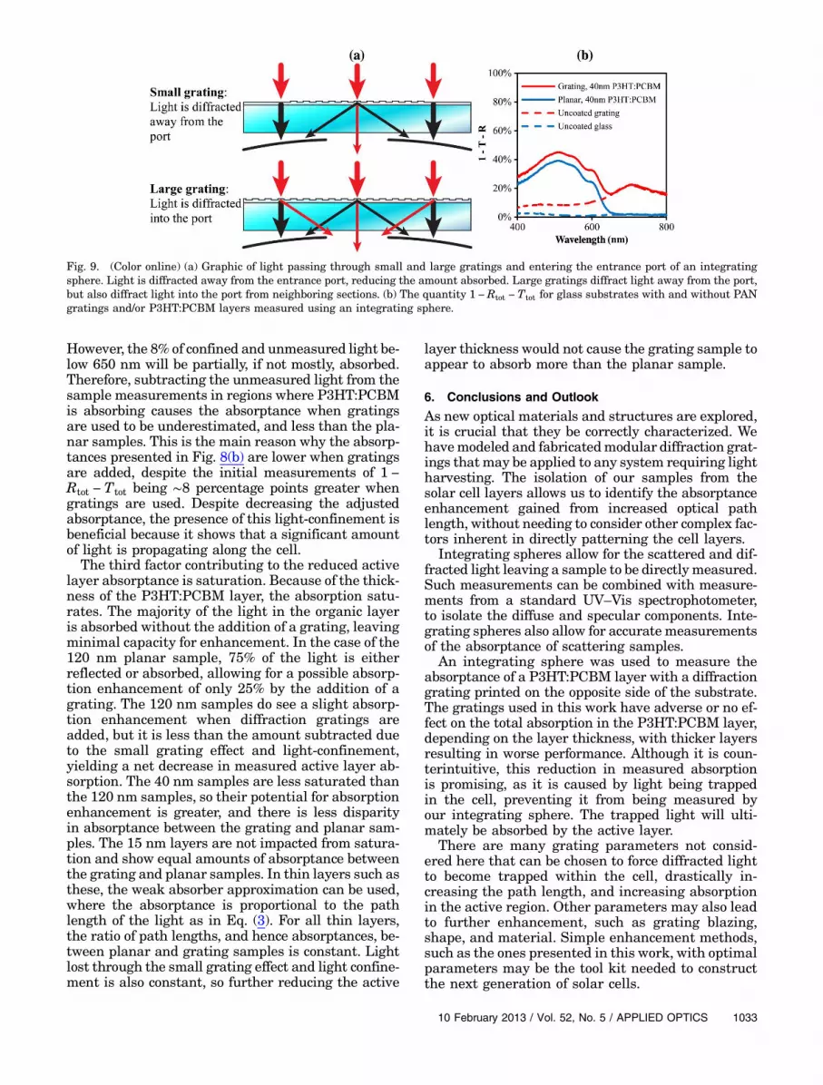
There are three reasons for the reduction inmeasured absorption when gratings were used: light-confinement, small grating size, and saturation.Light-confinement refers to rays diffracted beyondthe critical angle that propagate laterally throughthe cell and are unmeasured, as shown in Fig. 8(a).A portion of the light confined this way diffracts backout through the grating, but the majority remainstrapped in the cell until it is absorbed. Figure 8(b)shows the fraction of �1 order light that exits thesample through the grating. Wavelengths less than700 nm have high transmission through the planarand grating interfaces and are poorly confined. Con-versely, wavelengths greater than 700 nm are comple-tely reflected at the planar interface, and mostlyreflected at the grating interface, resulting in highconfinement and greatly enhanced path lengths.Light at shorter wavelengths that diffracts into higherorders (and angles) also has high confinement.
The second reason contributing to the reduction inthe measured absorptance is the small grating size.Because of the limited size of the gratings in thisstudy, only the absorption of rays diffracted at smallangles was measured. Rays diffracted at sufficientlylarge angles travel laterally as they propagatethrough the 1 mm glass substrate and overshoot themeasurement port of the integrating sphere, redu-cing the amount of measured light. Figure 9(a)illustrates this effect. This reduction is merely an ar-tifact caused by the limited size of the gratings usedin this work. If larger gratings are used, the amountof light overshooting the measurement port will
equal the amount of light entering the port fromneighboring regions, thereby negating this effectand increasing the absorptance.
The small grating effect and light-confinement caneasily be quantified by using an integrating sphere tomeasure 1 − Rtot − Ttot of a glass substrate with aPAN grating. Neither glass nor PAN is significantlyabsorbing from 400 to 800 nm, so the quantity 1 −
Ttot − Rtot should be zero regardless of whether agrating is used. However, this is not the case for tex-tured samples. Figure 9(b) shows 1 −Rtot − Ttot forplanar and grating samples with and without 40 nmP3HT:PCBM layers. As expected, all the light leav-ing the uncoated glass substrate is accounted for,yielding 1 − Rtot − Ttot � 0. Yet when a PAN gratingis added, roughly 8% of the light with wavelengthsbetween 400 and 650 nm, and as much as 20% withwavelengths beyond 650 nm, is unaccounted fordue to a combination of the small grating effect andlight-confinement. We refrain from referring to thequantity “1 − Rtot − Ttot” for the uncoated gratingas absorptance because the light is merely unac-counted for, not absorbed. This effect can also be seenwhen an absorbing layer is added to the sample.Figure 9(b) shows that the 40 nm P3HT:PCBM grat-ing sample has the exact same feature at 700 nmas the uncoated grating sample. P3HT:PCBM istransparent past 650 nm, so the unmeasured lightpast 650 nm does not increase the actual absorptanceof the sample. Although not shown, this feature wasalso present in the measurements of the 15 and120 nm P3HT:PCBM grating samples as well. Toobtain accurate absorptances of the coated gratingsamples, measurements of the uncoated gratingswere subtracted from those of the coated grating sam-ples, yielding the absorptances shown in Fig. 7(b).This modification of the measured data effectivelyeliminates the feature starting at 700 nm, whereP3HT:PCBM is transparent, and cannot receive anabsorption enhancement from the confined light.
Fig. 8. (Color online) Light confinement (a) light-confinement for the PAN gratings on glass substrates used in this study. Light at longerwavelengths TIRs and is confined in the device. A small fraction of the confined light diffracts out of the cell. (b) Fraction of light in the�1orders that exits the substrate through the grating. Wavelengths greater than 700 nm are confined in the sample, and have minimalleakage through the grating. The plot was calculated using FDTD analysis for a square wave grating with 700 nm period, 350 nm height,and index of 1.5. A separate simulation was run for each wavelength. The �1 order diffraction angle, θm, was calculated using Eq. (4). Amonochromatic plane wave source at angle θm was inserted in a glass medium with a diffraction grating at its surface. A transmissionmonitor was used to measure the light diffracted out through the grating.
1032 APPLIED OPTICS / Vol. 52, No. 5 / 10 February 2013
However, the 8% of confined and unmeasured light be-low 650 nm will be partially, if not mostly, absorbed.Therefore, subtracting the unmeasured light from thesample measurements in regions where P3HT:PCBMis absorbing causes the absorptance when gratingsare used to be underestimated, and less than the pla-nar samples. This is the main reason why the absorp-tances presented in Fig. 8(b) are lower when gratingsare added, despite the initial measurements of 1 −
Rtot − Ttot being ∼8 percentage points greater whengratings are used. Despite decreasing the adjustedabsorptance, the presence of this light-confinement isbeneficial because it shows that a significant amountof light is propagating along the cell.
The third factor contributing to the reduced activelayer absorptance is saturation. Because of the thick-ness of the P3HT:PCBM layer, the absorption satu-rates. The majority of the light in the organic layeris absorbed without the addition of a grating, leavingminimal capacity for enhancement. In the case of the120 nm planar sample, 75% of the light is eitherreflected or absorbed, allowing for a possible absorp-tion enhancement of only 25% by the addition of agrating. The 120 nm samples do see a slight absorp-tion enhancement when diffraction gratings areadded, but it is less than the amount subtracted dueto the small grating effect and light-confinement,yielding a net decrease in measured active layer ab-sorption. The 40 nm samples are less saturated thanthe 120 nm samples, so their potential for absorptionenhancement is greater, and there is less disparityin absorptance between the grating and planar sam-ples. The 15 nm layers are not impacted from satura-tion and show equal amounts of absorptance betweenthe grating and planar samples. In thin layers such asthese, the weak absorber approximation can be used,where the absorptance is proportional to the pathlength of the light as in Eq. (3). For all thin layers,the ratio of path lengths, and hence absorptances, be-tween planar and grating samples is constant. Lightlost through the small grating effect and light confine-ment is also constant, so further reducing the active
layer thickness would not cause the grating sample toappear to absorb more than the planar sample.
6. Conclusions and Outlook
As new optical materials and structures are explored,it is crucial that they be correctly characterized. Wehavemodeled and fabricatedmodular diffraction grat-ings thatmay be applied to any system requiring lightharvesting. The isolation of our samples from thesolar cell layers allows us to identify the absorptanceenhancement gained from increased optical pathlength, without needing to consider other complex fac-tors inherent in directly patterning the cell layers.
Integrating spheres allow for the scattered and dif-fracted light leaving a sample to be directly measured.Such measurements can be combined with measure-ments from a standard UV–Vis spectrophotometer,to isolate the diffuse and specular components. Inte-grating spheres also allow for accuratemeasurementsof the absorptance of scattering samples.
An integrating sphere was used to measure theabsorptance of a P3HT:PCBM layer with a diffractiongrating printed on the opposite side of the substrate.The gratings used in this work have adverse or no ef-fect on the total absorption in the P3HT:PCBM layer,depending on the layer thickness, with thicker layersresulting in worse performance. Although it is coun-terintuitive, this reduction in measured absorptionis promising, as it is caused by light being trappedin the cell, preventing it from being measured byour integrating sphere. The trapped light will ulti-mately be absorbed by the active layer.
There are many grating parameters not consid-ered here that can be chosen to force diffracted lightto become trapped within the cell, drastically in-creasing the path length, and increasing absorptionin the active region. Other parameters may also leadto further enhancement, such as grating blazing,shape, and material. Simple enhancement methods,such as the ones presented in this work, with optimalparameters may be the tool kit needed to constructthe next generation of solar cells.
Fig. 9. (Color online) (a) Graphic of light passing through small and large gratings and entering the entrance port of an integratingsphere. Light is diffracted away from the entrance port, reducing the amount absorbed. Large gratings diffract light away from the port,but also diffract light into the port from neighboring sections. (b) The quantity 1 −Rtot − Ttot for glass substrates with and without PANgratings and/or P3HT:PCBM layers measured using an integrating sphere.
10 February 2013 / Vol. 52, No. 5 / APPLIED OPTICS 1033

A. Amooali and R. A. Norwood acknowledge thesupport of the U.S. Air Force Office of SponsoredResearch under Award No. FA955010-1-0555. J.Thomas acknowledges NSF EAGER award (ECCS-1247838) for the partial fulfillment of this work.J. Favela and J. E. Pemberton acknowledge partialsupport of this work through the Center for InterfaceScience: Solar Electric Materials, an Energy FrontierResearch Center funded by the U.S. Department ofEnergy, Office of Science, Office of Basic EnergySciences, under award number DE-SC0001084. Allother authors acknowledge the support of the NSFSTC CMDITR, Grant No. 0120967.
References1. J. Kalowekamo and E. Baker, “Estimating the manufacturing
cost of purely organic solar cells,” Solar Energy 83, 1224–1231(2009).
2. A. L. Roes, E. A. Alsema, K. Blok, and M. K. Patel, “Ex-anteenvironmental and economic evaluation of polymer photovol-taics,” Prog. Photovoltaics 17, 372–393 (2009).
3. F. He and L. Yu, “How far can polymer solar cells go? In need ofa synergistic approach,” J. Phys. Chem. Lett. 2, 3102–3113(2011).
4. P. Peumans, A. Yakimov, and S. Forrest, “Small molecularweight organic thin-film photodetectors and solar cells,”J. Appl. Phys. 93, 3693–3723 (2003).
5. M. Born, E. Wolf, and A. B. Bhatia, Principles of Optics :Electromagnetic Theory of Propagation, Interference andDiffraction of Light (Cambridge University, 2005).
6. Y. Liang, Z. Xu, J. Xia, S. Tsai, Y. Wu, G. Li, C. Ray, and L. Yu,“For the bright future-bulk heterojunction polymer solar cellswith power conversion efficiency of 7.4%,” Adv. Mater. 22,E135–E138 (2010).
7. P. Kumar and S. Chand, “Recent progress and future aspectsof organic solar cells,” Prog. Photovoltaics 20, 377–415 (2012).
8. M. A. Green, K. Emery, Y. Hishikawa, W. Warta, and E. D.Dunlop, “Solar cell efficiency tables (version 39),” Prog. Photo-voltaics 20, 12–20 (2012).
9. C. J. Brabec, S. Gowrisanker, J. J. M. Halls, D. Laird, S. Jia,and S. P. Williams, “Polymer-fullerene bulk-heterojunctionsolar cells,” Adv. Mater. 22, 3839–3856 (2010).
10. S. Shahin, P. Gangopadhyay, and R. A. Norwood, “Ultrathinorganic bulk heterojunction solar cells: plasmon enhancedperformance using au nanoparticles,” Appl. Phys. Lett. 101,053109 (2012).
11. A. J. Moule, J. B. Bonekamp, and K. Meerholz, “The effect ofactive layer thickness and composition on the performance ofbulk-heterojunction solar cells,” J. Appl. Phys. 100, 094503(2006).
12. S. Na, S. Kim, S. Kwon, J. Jo, J. Kim, T. Lee, and D. Kim,“Surface relief gratings on poly (3-hexylthiophene) andfullerene blends for efficient organic solar cells,” Appl. Phys.Lett. 91, 173509 (2007).
13. P. Campbell and M. Green, “Light trapping properties of pyr-amidally textured surfaces,” J. Appl. Phys. 62, 243–249 (1987).
14. L. Roman, O. Inganas, T. Granlund, T. Nyberg, M. Svensson,M. Andersson, and J. Hummelen, “Trapping light in polymerphotodiodes with soft embossed gratings,” Adv. Mater. 12,189–195 (2000).
15. F. Llopis and I. Tobias, “The role of rear surface in thin siliconsolar cells,” Solar Energy Mater. Solar Cells 87, 481–492(2005).
16. M. Niggemann, M. Glatthaar, A. Gombert, A. Hinsch, and V.Wittwer, “Diffraction gratings and buried nano-electrodes—architectures for organic solar cells,” Thin Solid Films 451,619–623 (2004).
17. F. Monestier, J. Simon, P. Torchio, L. Escoubas, F. Florya, S.Bailly, R. de Bettignies, S. Guillerez, and C. Defranoux,“Modeling the short-circuit current density of polymer solarcells based on P3HT:PCBM blend,” Solar Energy Mater. SolarCells 91, 405–410 (2007).
18. E. D. Palik, Handbook of Optical Constants of Solids(Academic, 1985).
19. K. Rajkanan, R. Singh, and J. Shewchun, “Absorption-coefficient of silicon for solar-cell calculations,” Solid-StateElectron. 22, 793–795 (1979).
20. Z. Yu, A. Raman, and S. Fan, “Fundamental limit of nanopho-tonic light trapping in solar cells,” Proc. Natl. Acad. Sci. USA107, 17491–17496 (2010).
21. E. G. Loewen and E. Popov, Diffraction Gratings and Applica-tions (M. Dekker, 1997).
22. E. Yablonovitch, “Statistical ray optics,” J. Opt. Soc. Am. 72,899–907 (1982).
23. J. Bendickson, E. Glytsis, and T. Gaylord, “Scalar integraldiffraction methods: unification, accuracy, and comparisonwith a rigorous boundary element method with applicationto diffractive cylindrical lenses,” J. Opt. Soc. Am. A 15,1822–1837 (1998).
24. J. R. Tumbleston, D. Ko, E. T. Samulski, and R. Lopez,“Electrophotonic enhancement of bulk heterojunction organicsolar cells through photonic crystal photoactive layer,” Appl.Phys. Lett. 94, 043305 (2009).
25. J. M. Palmer and B. G. Grant, The Art of Radiometry (SPIE,2010).
26. J. Hodgkinson, D.Masiyano, and R. P. Tatam, “Using integrat-ing spheres as absorption cells: path-length distribution andapplication of Beer’s law,” Appl. Opt. 48, 5748–5758 (2009).
27. A. Lopez-Santiago, H. R. Grant, P. Gangopadhyay, R.Voorakaranam, R. A.Norwood, andN. Peyghambarian, “Cobaltferrite nanoparticles polymer composites based all-opticalmag-netometer,” Opt. Mater. Express 2, 978–986 (2012).
28. V. Shrotriya, G. Li, Y. Yao, T. Moriarty, K. Emery, and Y. Yang,“Accurate measurement and characterization of organic solarcells RID D-7774-2011 RID A-2944-2011,” Adv. Funct. Mater.16, 2016–2023 (2006).
29. J. Thomas, P. Gangopadhyay, E. Araci, R. A. Norwood, and N.Peyghambarian, “Nanoimprinting bymelt processing: an easytechnique to fabricate versatile nanostructures,” Adv. Mater23, 4782–4787 (2011).
1034 APPLIED OPTICS / Vol. 52, No. 5 / 10 February 2013