cappello_tommaso_phdthesis... - ams dottorato
TRANSCRIPT
Alma Mater Studiorum – Universita di Bologna
Scuola di Ingegneria e Architettura
Dipartimento di Ingegneria dell’Energia Elettrica e dell’Informazione
Dottorato di Ricerca in Ingegneria Elettronica,Telecomunicazioni e Tecnologie dell’Informazione Ciclo XXIX
Settore Concorsuale di Afferenza: 09/E3 Elettronica
Settore Scientifico Disciplinare: ING-INF/01 Elettronica
Design and Characterization of
Power Converters and Amplifiers
for Supply-Modulation based
Transmitter Architectures
Presentata da:Tommaso Cappello
Coordinatore Dottorato:Prof. A. Vanelli Coralli
Relatore:
Prof. A. Santarelli
Correlatore:Dr. C. Florian
Esame Finale Anno 2017


Contents
Abstract i
Acknowledgements iii
List of Figures iv
List of Tables xvii
1 Introduction 1
1.1 Efficiency Definitions . . . . . . . . . . . . . . . . . . . . . . . . . 3
1.2 Signal Property Definitions . . . . . . . . . . . . . . . . . . . . . 4
1.3 Characteristics of Modulated Signals . . . . . . . . . . . . . . . . 5
1.3.1 Telecommunication Signals . . . . . . . . . . . . . . . . . 5
1.3.2 Radar Signals . . . . . . . . . . . . . . . . . . . . . . . . . 6
1.4 Architectures for Efficiency-Enhancement . . . . . . . . . . . . . 7
1.4.1 Doherty . . . . . . . . . . . . . . . . . . . . . . . . . . . . 8
1.4.2 Outphasing . . . . . . . . . . . . . . . . . . . . . . . . . . 9
1.4.3 Envelope Elimination and Restoration . . . . . . . . . . . 10
1.4.4 Envelope Tracking . . . . . . . . . . . . . . . . . . . . . . 11
1.5 Envelope Characteristics . . . . . . . . . . . . . . . . . . . . . . . 12
1.6 Supply-Modulator Architectures . . . . . . . . . . . . . . . . . . 14
1.6.1 Linear-assisted Switching Converters . . . . . . . . . . . . 15

1.6.2 Multi-phase Switching Converters . . . . . . . . . . . . . 15
1.6.3 Multi-level Switching Converters . . . . . . . . . . . . . . 16
1.7 Organization of the Thesis . . . . . . . . . . . . . . . . . . . . . . 18
2 Power-DAC Supply Modulator 22
2.1 Ideal Digital-to-Analog Converter (DAC) . . . . . . . . . . . . . 23
2.2 Power-DAC Topology . . . . . . . . . . . . . . . . . . . . . . . . 24
2.3 Ideal Power-DAC . . . . . . . . . . . . . . . . . . . . . . . . . . . 26
2.4 Switching Behavior . . . . . . . . . . . . . . . . . . . . . . . . . . 29
2.5 Power-DAC Technology . . . . . . . . . . . . . . . . . . . . . . . 32
2.6 Experimental Prototype . . . . . . . . . . . . . . . . . . . . . . . 34
2.7 Digital Control . . . . . . . . . . . . . . . . . . . . . . . . . . . . 37
2.8 Multi-Output Supply Board . . . . . . . . . . . . . . . . . . . . . 40
2.9 Measurement Results with Resistive Load . . . . . . . . . . . . . 43
2.9.1 Sinusoidal Test . . . . . . . . . . . . . . . . . . . . . . . . 44
2.9.2 Step Response . . . . . . . . . . . . . . . . . . . . . . . . 46
2.9.3 Telecommunications Signals . . . . . . . . . . . . . . . . . 47
2.9.4 Comparison with State-of-Art . . . . . . . . . . . . . . . . 49
2.10 Conclusion . . . . . . . . . . . . . . . . . . . . . . . . . . . . . . 50
3 Supply Modulation of RF PAs for Telecommunications 53
3.1 Class-AB L-Band Power-Amplifier . . . . . . . . . . . . . . . . . 54
3.2 ET-PA Connection and Characterization Setup . . . . . . . . . . 56
3.2.1 Digital Baseband (FPGA VI) . . . . . . . . . . . . . . . . 59
3.2.2 Setup Control (Host VI) . . . . . . . . . . . . . . . . . . . 62
3.2.3 PA Drain Voltage and Current Sensing . . . . . . . . . . . 65
3.2.4 DUT Characterization . . . . . . . . . . . . . . . . . . . . 65
3.2.5 DUT Modeling and Pre-Distortion . . . . . . . . . . . . . 67
3.3 Measurement Results with Telecom Signals . . . . . . . . . . . . 69
3.3.1 LTE 1.4-MHz Bandwidth, 7.5-dB PAPR . . . . . . . . . . 69
3.3.2 LTE 10-MHz Bandwidth, 11.65-dB PAPR . . . . . . . . . 72
3.3.3 Experimental Results Discussion . . . . . . . . . . . . . . 72

3.4 Conclusion . . . . . . . . . . . . . . . . . . . . . . . . . . . . . . 74
4 Supply-Modulation of RF PAs for Radars 76
4.1 Radar Transmitter Architectures . . . . . . . . . . . . . . . . . . 79
4.2 Radar Transmitter with Supply Modulation . . . . . . . . . . . . 80
4.2.1 Digital Baseband . . . . . . . . . . . . . . . . . . . . . . . 82
4.2.2 Class-AB X-Band Power-Amplifier . . . . . . . . . . . . . 83
4.3 GaN PA Characterization, Modeling and Pre-Distortion . . . . . 85
4.3.1 PA Characterization . . . . . . . . . . . . . . . . . . . . . 86
4.3.2 PA Modeling and Pre-Distortion . . . . . . . . . . . . . . 90
4.4 Measurement Results with Arbitrary Pulse-Shaped Waveforms . 92
4.4.1 Pulse-to-Pulse Modulation . . . . . . . . . . . . . . . . . . 94
4.5 Conclusion . . . . . . . . . . . . . . . . . . . . . . . . . . . . . . 96
5 Integrated Power-DAC and PA Transmitter 98
5.1 Integrated Power-DAC Supply Modulator . . . . . . . . . . . . . 100
5.1.1 Power-DAC MMIC Design . . . . . . . . . . . . . . . . . 101
5.1.2 Power-DAC PCB Schematic and Manufacturing . . . . . 104
5.1.3 Power-DAC Multi-Output Supply Board . . . . . . . . . . 106
5.1.4 Power-DAC MMIC Functionality Tests . . . . . . . . . . 109
5.1.5 Power-DAC and Power-Amplifier Characterization . . . . 110
5.1.6 Power-Amplifier Characterization . . . . . . . . . . . . . . 112
5.1.7 Power-DAC Characterization . . . . . . . . . . . . . . . . 113
5.1.8 Baseband Digital Part and Pre-Distortion . . . . . . . . . 115
5.2 Experimental Results . . . . . . . . . . . . . . . . . . . . . . . . . 118
5.2.1 Pulsed Radars with Amplitude and Frequency Modulation 118
5.2.2 High Bandwidth, High PAPR Telecom Signal . . . . . . . 120
5.3 Conclusion . . . . . . . . . . . . . . . . . . . . . . . . . . . . . . 123
6 Supply-Modulation of an Outphasing Chireix PA 125
6.1 Outphasing Chireix X-band PA . . . . . . . . . . . . . . . . . . . 127
6.1.1 Setup for Static Characterization . . . . . . . . . . . . . . 128

6.1.2 Experimental Results . . . . . . . . . . . . . . . . . . . . 129
6.1.3 Setup for Dynamic Characterization . . . . . . . . . . . . 132
6.1.4 Experimental Results . . . . . . . . . . . . . . . . . . . . 136
6.2 Conclusion . . . . . . . . . . . . . . . . . . . . . . . . . . . . . . 137
7 Dynamic Effects of Electron Devices in SMs and PAs 138
7.1 State-of-Art and Commercial I/V Pulsers . . . . . . . . . . . . . 140
7.2 Dynamic RON in GaN Switches . . . . . . . . . . . . . . . . . . . 142
7.2.1 Measurement Setup . . . . . . . . . . . . . . . . . . . . . 143
7.2.2 Current Source . . . . . . . . . . . . . . . . . . . . . . . . 144
7.2.3 IDS and VDS Sensing and Measurement . . . . . . . . . . 146
7.2.4 TC Measurement . . . . . . . . . . . . . . . . . . . . . . . 148
7.3 Devices Under Tests (DUTs) . . . . . . . . . . . . . . . . . . . . 149
7.3.1 AlGaN/GaN on Si HEMT . . . . . . . . . . . . . . . . . . 149
7.3.2 AlGaN/GaN on SiC HEMT . . . . . . . . . . . . . . . . . 150
7.4 Experimental Results . . . . . . . . . . . . . . . . . . . . . . . . . 151
7.4.1 Dependency of the RON on TJ . . . . . . . . . . . . . . . 151
7.4.2 Dependency of the RON on TJ and on X(t) . . . . . . . . 154
7.4.3 Dependency of the RON on TJ and on VDD . . . . . . . . 156
7.5 Conclusion . . . . . . . . . . . . . . . . . . . . . . . . . . . . . . 158
7.6 Appendix: Detailed operation of the Setup . . . . . . . . . . . . 159
7.7 Dynamic Effects in LDMOS PAs . . . . . . . . . . . . . . . . . . 162
7.7.1 PA Electro-Thermal Model . . . . . . . . . . . . . . . . . 162
7.7.2 PA Model Identification . . . . . . . . . . . . . . . . . . . 163
7.7.3 Measurement Setup . . . . . . . . . . . . . . . . . . . . . 164
7.7.4 Experimental Results . . . . . . . . . . . . . . . . . . . . 166
7.8 Conclusion . . . . . . . . . . . . . . . . . . . . . . . . . . . . . . 166
8 Conclusions and Future Work 167
8.1 Main Contributions . . . . . . . . . . . . . . . . . . . . . . . . . . 167
8.2 Possible Topics for Future Work . . . . . . . . . . . . . . . . . . 170
8.3 List of Publications . . . . . . . . . . . . . . . . . . . . . . . . . . 172

8.3.1 International Journals . . . . . . . . . . . . . . . . . . . . 172
8.3.2 International Conferences . . . . . . . . . . . . . . . . . . 172
Bibliography 190

Abstract
The rapid evolution of telecommunication systems has strongly influenced our
lives, and the way we communicate and exchange information. Nevertheless,
much progress is expected to happen in the next years with the introduction
of new generations of wireless communications standards, which require signals
with large bandwidth and very high Peak-to-Average Power Ratio (PAPR) in
order to enhance the spectral efficiency and maximize the data rate. However,
such developments can only take place through the evolution of Radio-Frequency
(RF) and microwave technology which should be capable of working at higher
frequencies, higher bandwidth and with higher efficiencies than before. In order
to meet these demanding specifications, transmitter architectures have to evolve
from a single linear RF Power-Amplifier (PA) into more complex architectures.
Envelope Tracking (ET) is one of the most promising solutions for the efficiency-
enhancement of next generation transmitters. In ET, the performance and the
efficiency of the supply modulator affects directly the overall performance of the
transmitter.
The research described in this thesis aims to provide solutions to enhance
the efficiency of the RF PA by means of an ET architecture. To this purpose,
a novel discrete level supply modulator is investigated, which is based on a di-
rect digital-to-analog power conversion. This supply modulator is capable of
synthesizing eight voltage steps by means of three isolated voltage sources, thus
behaving like a Power Digital-to-Analog Converter (Power-DAC). This fine volt-
i

Abstract ii
age resolution allows for almost continuous tracking, with very small steps, of
the ideal supply voltage that maximizes the efficiency of the PA, while maintain-
ing the high efficiency typical of a switching converter. A hybrid version of the
Power-DAC exploiting very fast GaN devices is developed and tested with an
L-band PA achieving efficiency improvement up to 13% with 10 MHz of band-
width. Furthermore, a monolithic GaN version of the Power-DAC is prototyped
and tested with an X-band PA both with radar and telecommunication signals
achieving efficiency improvement up to 20% and bandwidth of 20 MHz. This
supply modulator is tested with even more non-linear PAs such as the ones used
in the outphasing architecture showing promising results with modulated signals
and efficiency improvement up to 9%. Finally, dispersive phenomena, which af-
fect PAs and switches in supply modulators, are investigated, characterized and
modeled.

Acknowledgements
Firstly, I would like to express my sincere gratitude to my advisor Prof. Alberto
Santarelli for the continuous support during my Ph.D study, for his patience,
motivation, and knowledge. I am also extremely grateful to Dr. Corrado Flo-
rian, basically my co-advisor, who taught me a lot in these years on how to
conduct research and experiments.
I want also to thank Prof. Fabio Filicori for enlightening me the first glance
of research with the idea of the the Power-DAC and on the setup for RON mea-
surement. I would like also to express my deep gratitude to all my labmates
present and past whom I owe much of my professional growth. Therefore I wish
to mention Rudi, Gian Piero, Daniel, Rafael and Pier Andrea. Thank you for
all the support, advises and stimulating discussions in these years.
Besides my labmates, I would like to thank my thesis committee: Prof. Zoya
Popovic and Prof. Dragan Maksimovic for their insightful comments and en-
couragement. In particular I want to thank Prof. Zoya Popovic to host me for
6 months in her research group at the University of Colorado at Boulder. Being
part of that group involved many opportunities and just as many difficulties.
The best aspect was obviously the chance to meet many talented people: Gre-
gor, Tibault, Scott, Parisa, Michael, Ignacio, Yuanzhe and Ali.
Last but not the least, I would like to thank my family for supporting me
throughout this study and my life in general.
iii
List of Figures
1.1 Block diagram of an ET transmitter. A supply modulator dy-
namically adjusts the VDD drain voltage of a RF PA to increase
its efficiency. The RF input power PIN and the control signal
F [PIN ] of the supply modulator are generated from the base-
band part. The RF output power POUT is downconverted and
analyzed by the baseband part. . . . . . . . . . . . . . . . . . . . 2
1.2 PAE of a class-AB PA at different VDD supply voltages super-
posed with the histogram of the PDF of a 4G OFDM signal
with 10.7-dB PAPR and 20-MHz bandwidth. The PAE could
be increased by supply modulating the RF PA and following the
trajectory (red-dashed line). . . . . . . . . . . . . . . . . . . . . . 5
1.3 Left: general block diagram for a efficiency-enhanced transmitter
employing two PAs and a combiner. Right: different implemen-
tations: Doherty, outphasing and ERR/ET [1]. . . . . . . . . . . 7
1.4 Single RF input Doherty PA: a hybrid block produces two output
which are 90 out-of-phase. After the PAs, the phase match be-
tween the two ways is restored with a quarter-wavelength impedance
inverter. . . . . . . . . . . . . . . . . . . . . . . . . . . . . . . . . 8
iv

List of Figures v
1.5 The outphasing PA: two constant envelope out-phased signals are
amplified by two symmetric PAs and a quarter-wavelength non-
isolating Chireix combiner restore the modulated envelope at the
output. . . . . . . . . . . . . . . . . . . . . . . . . . . . . . . . . 9
1.6 Envelope Elimination and Restoration and Envelope Tracking PA
block diagram. The power combining is directly performed in the
RF PA which essentially acts as a mixer. . . . . . . . . . . . . . . 11
1.7 Spectra of a baseband 10-MHz 12-dB PAPR LTE signal (blue-
square) illustrating the bandwidth expansion (red-circle) due to
the nonlinear envelope extraction. . . . . . . . . . . . . . . . . . 12
1.8 Categories of supply modulators reported in the literature: linear-
assisted switching converter, multi-level converter and multi-phase
switching converter. . . . . . . . . . . . . . . . . . . . . . . . . . 14
1.9 Continuous shaping function F (square-blue) and approximation
of the shaping table with N = 8 levels (dot-red). The shaping
function starts from a minimum voltage offset of 6 V (triangle-
black). . . . . . . . . . . . . . . . . . . . . . . . . . . . . . . . . . 17
2.1 Left: block diagram of a N-bit DAC, supplied by VREF and syn-
thesizing a VOUT signal. Right: transfer curve for an ideal 3-bit
DAC synthesizing L = 23 = 8 voltage levels. . . . . . . . . . . . . 24
2.2 N -bit Power-DAC topology. N half-bridges are stacked up and
supplied by binary-scaled isolated voltage sources and controlled
by digital signals. . . . . . . . . . . . . . . . . . . . . . . . . . . . 25
2.3 Left: simulation setup of the 3-bit Power-DAC; control part on
the top-left (green wires), power stage on the bottom-left (red
wires). . . . . . . . . . . . . . . . . . . . . . . . . . . . . . . . . . 27
2.4 Simulation of a sine input at 1 MHz. The combination of the
control bits Vb1, Vb2, and Vb3 generates a multilevel output voltage
VOUT . . . . . . . . . . . . . . . . . . . . . . . . . . . . . . . . . . 28

List of Figures vi
2.5 Simulated waveforms for the 3-bit Power-DAC. VIN : input sinu-
soidal waveforms at fIN = 1 MHz (left) and 6 MHz (right). Vbi:
i-th control bit. VOUT : staircase with 8-level output voltage. . . . 30
2.6 Simulated waveforms for the 3-bit Power-DAC. VIN : input en-
velopes of a LTE signal at fIQ = 1.4 MHz (left) and 20 MHz
(right). Vbi: i-th control bit. VOUT : staircase with 8-level output
voltage. . . . . . . . . . . . . . . . . . . . . . . . . . . . . . . . . 31
2.7 Detailed structure of the 3-bit Power-DAC: three half-bridge cells
are stacked up and supplied by isolated voltages. High-side and
low-side drivers control the power stage and digital isolators pro-
vides isolation to the control bits. . . . . . . . . . . . . . . . . . . 33
2.8 Picture of the PCB of the Power-DAC prototype (left) and detail
of the power stage (right) with physical dimension indicated. The
control bit Vbi are fed on the west side of the PCB while the
isolated power supplies VDCi are connected on the east side. The
generated output voltage VOUT is accessible on the north part of
the board. . . . . . . . . . . . . . . . . . . . . . . . . . . . . . . . 35
2.9 Top (left) and second layer (right) of the PCB layout. . . . . . . 36
2.10 Third (left) and bottom layer (right) of the PCB layout. . . . . . 36
2.11 Block diagram of the control logic of the Power-DAC imple-
mented in the FPGA. A counter selects the control bit bi stored
in a LUT, which can be configured by a .mif file. The complemen-
tary bit bi is generated by a specific logic which also introduces
the deadtime. The whole logic is clocked by a 160 MHz PLL. . . 38
2.12 Deadtime generator logic implemented in the FPGA (blue-dotted
rectangle). A safety AND gate is inserted at the output to avoid
spurious commutations due to delays in the signals propagation
inside the FPGA. A register synchronize the control bit bi and
its complementary with deadtime bi to the FPGA clock. . . . . . 39
List of Figures vii
2.13 Left: control bits for a 1 MHz sinusoid generated by the FPGA;
high-side control signal bi in blue, low-side control signal with
deadtime bi in red. Right: enlarged picture of the transition
showing the deadtime of 6.25 ns. . . . . . . . . . . . . . . . . . . 40
2.14 Schematic of a single module of the Power-DAC multi-output
supply. This module is replicated 4 times (the fan circuit only
one time). . . . . . . . . . . . . . . . . . . . . . . . . . . . . . . . 42
2.15 Left picture: two modules connected to the front panel and to the
main supply (36 V-72 V). Right: front panel of the supply box.
Four isolated ground (black plug) and three voltage outputs (red
plug). Label GND: isolated ground, 1: 2.5 V-12.6 V, 2: 11.85 V-
22 V, 3: 23.8 V-29.8 V. Enable, disable and voltage regulation of
the isolated output voltages are possible with the trimmer and
switch below the red plug. . . . . . . . . . . . . . . . . . . . . . . 43
2.16 Measured converter output to a full-scale sinusoidal set-point at
different frequencies. The waveform before (dashed red) and af-
ter the filter (continuous blue) are superimposed for comparison.
Normalized full-power bandwidth in dB of the converter (bottom
right). . . . . . . . . . . . . . . . . . . . . . . . . . . . . . . . . . 44
2.17 Measurement of the converter slew-rate with a 42 V input step:
in the enlarged plot on the right a slew rate of 4.23 kV/µs is
appreciable. . . . . . . . . . . . . . . . . . . . . . . . . . . . . . . 47
2.18 Spectra (left) and time-domain waveforms (right) of the telecom-
munication signals. Top raw: 4-MHz 3.2-dB PAPR 3GPP-WCDMA.
Central raw: 10-MHz 12-dB PAPR LTE. Bottom raw: 20-MHz
11-dB PAPR WiFi. . . . . . . . . . . . . . . . . . . . . . . . . . . 48
3.1 Left: PA mounted on an aluminum baseplate carrier and labeled
connections. Right: PA connected to a VNA for S-parameters
measurements. . . . . . . . . . . . . . . . . . . . . . . . . . . . . 55
List of Figures viii
3.2 Measured |S11| and |S21| of the PA at V 3DD = 32 V around the
designed center frequency of 1.84 GHz. . . . . . . . . . . . . . . . 56
3.3 Simulated static characterization at 1.84 GHz at 4, 8, 12, 16, 20,
24, 28, and 32 V (thick line). . . . . . . . . . . . . . . . . . . . . . 57
3.4 Measured static characterization at 1.84 GHz at 4, 8, 12, 16, 20,
24, 28, and 32 V. . . . . . . . . . . . . . . . . . . . . . . . . . . . 57
3.5 Left: Connection between the PA and the Power-DAC. Right:
NI rack (PXIe-1082) with the PC controller (PXIe-8840) and the
VST (PXIe-5644R) connected to the PA and to the Power-DAC. 58
3.6 Block diagram of the setup. In the FPGA VI it is implemented
the real-time part of the setup which includes the Power-DAC
control and the DPD. In the Host VI it is implemented the signal
analysis algorithm. The PA drain current and voltage is measured
by means of an external oscilloscope. . . . . . . . . . . . . . . . . 60
3.7 Graphical interface of the Host VI program in LabVIEW: setup
hardware parameters could be set in the top-left box. In the
bottom-left box the spectrum of the received signal is shown. In
the top-right plot, the ideal and the generated envelope by the
amplifier is shown. In the bottom-right plot, distortion charac-
teristics of the supply-modulated PA are shown. . . . . . . . . . 62
3.8 Characterization of the PA at discrete voltage levels. Left: gain
compression vs. normalized input |x(n)|. Right: Power-Added
Efficiency (PAE) vs. output power (POUT ). . . . . . . . . . . . . 66
3.9 Characterization of the PA at discrete voltage levels. Left: Am-
plitude Modulation vs. Amplitude Modulation (AM/AM). Right:
Phase Modulation vs. Amplitude Modulation (AM/PM). . . . . 68
3.10 Measured power spectra for a 1.4 MHz LTE signal. Left: output
spectra with and without DPD. Right: output spectra with fixed
bias (VDD = 32 V) and with ET+DPD regime. . . . . . . . . . . 71

List of Figures ix
3.11 Transmitted and received envelopes for a 1.4 MHz LTE signal
with the supply voltage. Left: output envelope without DPD
(ET no DPD). Right: output envelope with DPD (ET+DPD). . 71
3.12 Measured power spectra for a 10 MHz LTE signal. Left: output
spectra with and without DPD. Right: output spectra with fixed
bias (VDD = 32 V) and with ET+DPD regime. . . . . . . . . . . 74
4.1 High-level block diagram of the radar transmitter with a Power-
DAC supply modulator. The digital baseband provides the signal
that is upconverted and drives the PA as well as the control bits
for the Power-DAC. The Power-DAC is implemented with GaN-
on-Si power devices, while the PA is a GaN-on-SiC MMIC. The
digital signal processing includes predistortion. . . . . . . . . . . 78
4.2 Radar PA architectures: (a) pulse waveforms and circuit diagram
for constant supply case. (b) amplitude-modulated pulse wave-
form with discretized envelope and associated circuit architecture. 79
4.3 Block diagram of the setup for radar transmitter with pulse shap-
ing waveforms and Power-DAC supply modulator. The signal
is generated at baseband by the VST and up-converted at X-
band by an external up-conversion stage. A benchtop driver and
an attenuator set the correct power levels at the DUT reference
planes S1 and S2. The setup is calibrated to directly measure
the input/output power at the DUT reference planes while an
oscilloscope acquires the drain voltage VD(t) and current ID(t). . 81
4.4 Control logic of the Power-DAC and of the DPD implemented
in the FPGA. The envelope is extracted from the original I/Q
and used by the discretized shaping table which generates the
control bits of the Power-DAC. For each bias level, a correction
coefficient is applied to the original I/Q. . . . . . . . . . . . . . . 83

List of Figures x
4.5 Photographs of the Power-DAC board and of the MMIC PA, with
a sketch of the connections. The second-stage bypass capacitors
are removed and the PA bias pad are directly connected to the
Power-DAC output. . . . . . . . . . . . . . . . . . . . . . . . . . 84
4.6 (a): operative pulse shaping radar regime with ET. (b): charac-
terization regime without (b) and with (c) pre-pulse (PP). A PP
is employed to set the trap-state to Xmax so that the extracted
characteristics are more similar to the actual operating ones. . . 87
4.7 Output power and available gain of the PA at different VD: com-
parison between measurement with (continuous line) and without
pre-pulse (dashed line). . . . . . . . . . . . . . . . . . . . . . . . 88
4.8 Measured PAE with PP for different VD. The dashed bold lines
represent the ET trajectory followed with selected bias shaping
function. In the inset, the selected discretized bias shaping func-
tion is listed as a function of the output power. . . . . . . . . . . 89
4.9 AM/AM (left) and AM/PM (right) characteristics of the PA
(blue) and of the pre-distorter (red) at the different bias levels
which are reported in the inset. . . . . . . . . . . . . . . . . . . . 90
4.10 Left: Ideal envelope (blue dashed) and pre-distorted envelope
input signal (red continuous) for the case of pulse shaping with
Blackman window. Right: Dynamic bias voltage VD(t) (blue
square) and PA output power POUT (t) with DPD OFF (red dot)
and DPD ON (black star). . . . . . . . . . . . . . . . . . . . . . . 91
4.11 Plot comparing the Pout vs. Pavs in three cases: without DPD,
with DPD without pre-pulse, and with DPD with pre-pulse. . . . 91
4.12 Comparison between input (TX, i.e. ideal) and output spec-
tra (RX) of the PA with Triangular (left), Hanning (center) and
Blackman (right) pulse shaping in ET regime with the Power-
DAC and DPD applied. The Rectangular (RR regime) pulse
response is also shown. . . . . . . . . . . . . . . . . . . . . . . . . 93

List of Figures xi
4.13 PA measured output spectrum (RX) compared to the ideal one
(TX) in pulse shaping regimes with unmodulated rectangular bias
pulse. . . . . . . . . . . . . . . . . . . . . . . . . . . . . . . . . . 93
4.14 Left: Arbitrary pulse sequence: Triangular, Hanning, Blackman
and square pulse envelopes. The transmitted RF envelope is in-
distinguishable from the ideal one, due to the DPD correction.
Right: Instantaneous PA output power for an arbitrary rectan-
gular pulse sequence. . . . . . . . . . . . . . . . . . . . . . . . . . 95
5.1 Two-stage power amplifier (top) and multi-level supply mod-
ulator (bottom) implemented in the same GaN-on-SiC MMIC
process. Three waveforms types are demonstrated: wideband
high-PAPR telecom signals (a), radar rectangular pulses with
frequency chirp (b) and with pulse shaping (c). . . . . . . . . . . 99
5.2 Left: block diagram and electric circuit of the Power-DAC. Right:
schematic of a Power-DAC half-bridge with the integrated driver.
Bottom-right: table showing the functionality of a half-bridge
with integrated driver. . . . . . . . . . . . . . . . . . . . . . . . . 100
5.3 Left: layout in Microwave Office of the Power-DAC. Right: pho-
tograph of the fabricated MMIC and packaged in a QFN trans-
parent lid package. . . . . . . . . . . . . . . . . . . . . . . . . . . 103
5.4 Left: top layer of the PCB. Right: second layer of the PCB. . . . 104
5.5 Left: third layer of the PCB. Right: bottom layer of the PCB. . 104
5.6 Schematic of the Power-DAC board. A stack of isolators provide
the control signals to the Power-DAC chip. Bypass capacitors
are placed close to the QFN package of the Power-DAC. . . . . . 105
5.7 Schematic of the multi-output supply board (no offset voltage
supply is shown). . . . . . . . . . . . . . . . . . . . . . . . . . . . 107
List of Figures xii
5.8 Picture of the supply board. Three modules composed by DC/DC
brick converters generate the isolated supply voltages VDDi, while
a separate module generate the offset voltage VOS . These mod-
ules are fed by the main non-isolated supply VBUS . . . . . . . . . 108
5.9 Left: response of the Power-DAC to a positive and negative ramp
of 1µs sweeping all the levels upside-down. Right: step response
of the Power-DAC and simulation result. . . . . . . . . . . . . . . 109
5.10 Left: photograph of the PA MMIC. Right: Power-DAC MMIC
implemented in the same Qorvo 0.15µm process of the PA. . . . 110
5.11 Left: connection between the Power-DAC board and the PA
mounted on a test jig. Right: running setup with the control
software on the screen. . . . . . . . . . . . . . . . . . . . . . . . . 111
5.12 Pulse sequence to extract the characteristics of the PA. The pre-
pulse at the peak voltage VD7 = 20 V is used to pre-condition the
PA to a known state of trap, then a pulse VDi is performed to
extract the input-output characteristic of the PA for each voltage
level. . . . . . . . . . . . . . . . . . . . . . . . . . . . . . . . . . . 112
5.13 Left: measured PA input-output characteristic at different supply
voltages (blue solid). Right: measured PA gain at different supply
voltages (blue solid). Both: the thick traces (red solid) are the
trajectory followed by the PA while supply modulated. . . . . . . 113
5.14 Left: measured efficiency of the Power-DAC including driver
losses at different levels and output power (blue solid). Right:
PAE (blue dotted) and Composite PAE (blue solid) at different
levels. Both: the thick traces are the trajectory followed by the
DUT (red solid). . . . . . . . . . . . . . . . . . . . . . . . . . . . 114
5.15 AM/AM (left) and AM/PM (right) characteristics of the DUT.
The direct non-linear characteristics with memory at the differ-
ent supply levels are marked with symbols (blue lines). The in-
verted non-linear characteristics with memory of the DPD are
also shown (red lines). . . . . . . . . . . . . . . . . . . . . . . . . 116

List of Figures xiii
5.16 Left: block diagram of the base-band part of the transmitter.
The envelope of x(n) is extracted and quantized in 8 levels which
are associated to the PA optimal bias voltage level. For every
voltage level, a DPD LUT is selected and a correction coefficient
is applied to the original I/Q. Right: time-domain waveform of a
Blackman pulse. . . . . . . . . . . . . . . . . . . . . . . . . . . . 117
5.17 Output spectra of the PA with the DPD enabled. The three
weighting windows are compared with a rectangular chirped pulse.
Similar bandwidth (i.e. range resolution) can be obtained but
with an improved spectral purity. . . . . . . . . . . . . . . . . . . 120
5.18 Output of the matched filter in a pulse-compressed radar receiver
with linear frequency modulation. Lower temporal side-lobes are
obtained by means of amplitude weighting of the transmitted signal.120
5.19 Power spectra of the three different channel bandwidth consid-
ered: 1.4 MHz (left), 10 MHz (center), and 20 MHz (right). For
comparison, the spectrum with the DPD disabled is overlaid in
the three cases showing spectral regrowth out of band. . . . . . . 122
5.20 Output power with DPD ON (red solid), with DPD OFF (blue
dotted), and supply voltage (black solid) of the three different
channel bandwidth considered: 1.4 MHz (left), 10 MHz (center),
and 20 MHz (right). . . . . . . . . . . . . . . . . . . . . . . . . . 122
6.1 Simplified diagram of the ML-CO system. The signal component
separator controls the additional phase and discrete supply mod-
ulation.The technique uses a multi-level Power-DAC converter to
modulate a Chireix outphasing PA. . . . . . . . . . . . . . . . . . 126
6.2 Left: layout of the ML-CO PA, showing harmonic terminations
at the combiner reference plane. Right: MMIC mounted on the
CuMo carrier plate and bonded to the alumina lines and DC pads
(VG for the gates and VD for the drains). . . . . . . . . . . . . . . 128
List of Figures xiv
6.3 Outphasing PA measurement setup for static characterization.
Separate sources drive each PA branch, while a phase shifter
sweeps the differential phase. . . . . . . . . . . . . . . . . . . . . 129
6.4 Compilation of measured phase sweeps at different supply levels
without (left) and with (right) considering the Power-DAC dissi-
pation. The optimal trajectory is selected to maximize ηTOT,SY S .
In black is the PDF of a 6-dB PAPR QPSK signal used to calcu-
late average total efficiency. . . . . . . . . . . . . . . . . . . . . . 130
6.5 Left: comparison of optimal trajectories without (ηTOT ) and with
(ηTOT,SY S) the Power-DAC efficiency. Right: efficiency of the
Power-DAC, showing the operating points of the optimal trajectory.130
6.6 Comparison of the average total efficiency for a 6-dB PAPR
QPSK signal with restricted supply levels, without (ηTOT ) and
with the Power-DAC efficiency (ηTOT,SY S). . . . . . . . . . . . . 131
6.7 Block diagram of the setup: two VSTs generate two constant en-
velope out-phased signals which are upconverted to 9.7 GHz and
amplified by two drivers. These two signals (A1(t) and A2(t)) are
connected at the input of the multi-level Chireix outphasing PA.
The PA output (Sout(t)) is first attenuated and down-converted
at 3 GHz for the acquistion in one of the two VSTs. . . . . . . . 133
6.8 Picture of the setup implementing the block diagram of Fig. 6.7. 133
6.9 Left: pulsed measurements used to characterize the PA at dif-
ferent supply levels. Center: output power vs. outphasing angle
over discrete supply voltages. Right: drain efficiency vs. output
power over discrete supply voltages. . . . . . . . . . . . . . . . . 134
6.10 Normalized measured AM/AM and AM/PM characteristics of
the ML-CO PA at different drain supply levels, and DPD correc-
tion. The normalized input envelope refers to the envelope of the
original signal S(t) before decomposition into A1(t) and A2(t). . 135

List of Figures xv
6.11 Left: time-domain drain voltage, output power, and DC power
consumption waveforms. Right: ideal spectrum and output spec-
trum of multi-level supply modulated signals with and without
DPD for a 1.4-MHz LTE signal with 9.3-dB PAPR. . . . . . . . . 137
7.1 Block diagram of the presented setup for the characterization of
the dynamic RON in GaN HEMTs directly inside the final circuit
half-bridge. . . . . . . . . . . . . . . . . . . . . . . . . . . . . . . 143
7.2 Working principle of the setup: during TOFF the high-side device
applies a voltage stress to the DUT. During TON the RON of the
DUT is measured by means of a current injection on the switching
node of the half-bridge. . . . . . . . . . . . . . . . . . . . . . . . 144
7.3 Schematic of the setup for the characterization of the dynamic
RON in GaN switches. The extraction is directly performed in the
final circuit half-bridge operated with Pulse-Width Modulation
(PWM). . . . . . . . . . . . . . . . . . . . . . . . . . . . . . . . . 145
7.4 Left: I/V pulsed characteristic at 25 C of the Voltage-Controlled
Current-Source at different supply voltages. Right: normalized
small-signal gain of a 20x voltage amplifiers. Both: simulation
(dashed blue line) and measurement results (continuous red line)
are compared. . . . . . . . . . . . . . . . . . . . . . . . . . . . . . 146
7.5 Setup for the dynamic RON characterization. Left: pulsed mea-
surement on the Qorvo 0.15-µm half-bridge. Right: low-frequency
sinusoidal measurement on the EPC2014 demo board. . . . . . . 150
7.6 Left: measured RON variation due to the TJ junction tempera-
ture for the three DUTs. Right: measured RON variation due
to the TJ junction temperature for the three DUTs: RON are
normalized to the RON at 25 C. . . . . . . . . . . . . . . . . . . 152
7.7 Measured RON after different voltage stresses pulse lengths TOFF
in the EPC2014 starting from 20 ns up to 700 ns. . . . . . . . . . 155

List of Figures xvi
7.8 Left: dynamic RON vs. TON for EPC2014. Right: dynamic RON
vs. TON for Qorvo. . . . . . . . . . . . . . . . . . . . . . . . . . . 156
7.9 Measured dynamicRON vs. the drain voltage stress VDD, parametrized
at three different TJ junction temperatures (25, 80 and 150 C)
for the three DUTs (left: Qorvo 0.15µm, center: EPC2014, right:
EPC2007) at tD = 2µs. . . . . . . . . . . . . . . . . . . . . . . . 157
7.10 Predicted dynamicRON vs. the switching frequency fSW , parametrized
at some VDD voltage stresses for the three considered DUTs (left:
Qorvo 0.15µm, center: EPC2014, right: EPC2007) with the de-
vice parameters listed in Table 7.1. . . . . . . . . . . . . . . . . . 158
7.11 Left: amplifiers response acquired to a 5-µs ICS current pulse
without voltage stress (VDD = 0 V). Center: amplifiers response
to a 100 ns off-state voltage stress and to a current injection after
2µs Right: amplifiers response to a 100 ns voltage stress and to
a current injection immediately after the voltage-stress. . . . . . 160
7.12 Measurement setup used for the experiments: (a) block diagram;
(b) picture of the instrumentation; (c) zoom of the PA with the
DUT and the temperature sensing board. . . . . . . . . . . . . . 164
7.13 Measured isothermal gain curves (H function) at three equivalent
junction temperatures θ (left) and sensitivity hθ (right). . . . . . 165
7.14 Measured isothermal supply current curves (F function) at three
equivalent junction temperatures θ (left) and sensitivity fθ (right).165
7.15 Validation of the model extracted at θ∗ = 59.1 C (lines) vs. mea-
surements (crosses). Isothermal characteristics (red and blue) are
measured at the indicated equivalent junction temperatures θ;
CW characteristics (black) are obtained at a constant case tem-
perature θC = 30 C. Self-heating effects are properly predicted
by the model for both the RF output power (left) and supply
current (right). . . . . . . . . . . . . . . . . . . . . . . . . . . . . 165

List of Tables
2.1 Converter performance with full-scale sinusoidal inputs at differ-
ent frequencies. . . . . . . . . . . . . . . . . . . . . . . . . . . . . 45
2.2 Converter performance with telecommunication signals at differ-
ent bandwidths and PAPRs. . . . . . . . . . . . . . . . . . . . . . 49
2.3 Comparison with published converters for ET and EER applica-
tions. SMLA: Switched Mode Linear Assisted. SMMP: PWM
Switching Mode Multi Phase. ML: Multi Level. SMML: PWM
Switching Mode ML. . . . . . . . . . . . . . . . . . . . . . . . . . 51
3.1 Simulated nominal voltage and current biases for each stage of
the presented power amplifier. . . . . . . . . . . . . . . . . . . . . 54
3.2 Measured system performance for a LTE 1.4 MHz, PAPR of 7.5 dB.
When considering the same average output power POUT,AV G, ET
and fixed supply performances are reported for comparison in the
gray-shaded columns. . . . . . . . . . . . . . . . . . . . . . . . . . 70
3.3 Measured system performance with LTE 10 MHz, 11.65-dB PAPR.
When considering the same average output power POUT,AV G, ET
and fixed supply performances are reported for comparison in the
gray-shaded columns. . . . . . . . . . . . . . . . . . . . . . . . . . 73
xvii

List of Tables xviii
4.1 Performance with different pulse windows and bias supply mod-
ulations. . . . . . . . . . . . . . . . . . . . . . . . . . . . . . . . . 94
4.2 Performance with different rectangular pulse amplitudes. . . . . . 96
5.1 Performance with different pulse waveforms for radars. . . . . . . 119
5.2 Performance with different LTE channel bandwidths. *ACLR:
defined as the ratio of the average power in the channel bandwidth
and the average power centered in the next channel with the same
bandwidth. . . . . . . . . . . . . . . . . . . . . . . . . . . . . . . 121
6.1 Performance summary with LTE signals, with and without En-
velope Tracking. . . . . . . . . . . . . . . . . . . . . . . . . . . . 136
7.1 Measured RON,DC of the considered GaN DUTs. . . . . . . . . . 151

Chapter 1
Introduction
The research described in this thesis aims to provide solutions to improve the
efficiency of Radio Frequency (RF) Power Amplifiers (PAs) when fed with high
Peak-to-Average Power Ratio (PAPR) signals such as the ones employed in
modern communication standards. A traditional linear RF PA exhibits efficien-
cies as low as 10% to 15% with high-PAPR signals, which are typically employed
to achieve high-data throughput within limited spectrum resources [2].
A few percentage points of improvement in the RF PA efficiency can make
a substantial profit and cut the overall costs needed to operate the system.
Consequently, extensive effort is made by the wireless communication industry
and by the academia in order to improve efficiency.
For instance, in the wireless infrastructure industry, there is an increasing
demand to reduce OPerating EXpenditure (OPEX) in the 4G transmitters.
Around 10% to 30% of the OPEX is utilized on energy and the RF PA in a
base-station usually takes from 50% to 80% of the supplied energy [2]. In the
portable mobile industry, with high-PAPR signals, manufactures are concerned
by the efficiency of the RF PA since the battery life is limited.
Envelope-Tracking (ET) is one of the most promising architecture for en-
hancing the efficiency of transmitters and its simplified block diagram is shown
1

Introduction 2
RF PA
Supply Modulator
Upconverter
Downconverter
POUT
ℱ[PIN]
Digital Baseband
Signal Splitting
Shaping Table (ℱ)
DPD
Time-Alignment
PIN
PBUS
VDD(t)
IsolatorDriver
PDC
Figure 1.1: Block diagram of an ET transmitter. A supply modulator dynami-cally adjusts the VDD drain voltage of a RF PA to increase its efficiency. The RFinput power PIN and the control signal F [PIN ] of the supply modulator are gen-erated from the baseband part. The RF output power POUT is downconvertedand analyzed by the baseband part.
in Fig. 1.1. The RF PA converts DC power PDC , provided by a supply modula-
tor, to RF power POUT , by amplifying the input RF power PIN . The amplified
signal can be employed for a variety of application, such as driving an antenna
of a transmitter, either in a mobile handset or in a base station.
The supply modulator follows a control signal F [PIN ] (either digital or ana-
log), function of the input RF signal power PIN , and generates a time-varying
voltage VDD(t) at the RF PA drain. The shaping table F maps the optimal
bias point VDD that maximizes the efficiency of the RF PA for any given output
RF power POUT .
ET is typically used in conjunction with Digital Pre-Distortion (DPD) to
recover the signal linearity and the combination of ET and DPD can consid-
erably improve the RF PA efficiency while maintaining the required linearity
performance [3–7].

Introduction 3
1.1 Efficiency Definitions
With regard to the definition of efficiency of a RF PA, there are three definitions
reported in the literature: drain efficiency ηD, Power-Added Efficiency (PAE),
and total efficiency ηTOT .
Drain efficiency ηD is defined as the ratio of the output RF power POUT to
the supplied DC power PDC to the RF PA:
ηD =POUTPDC
(1.1)
The disadvantage of this metric is that it does not consider the input RF power
to the PA. In the case of a single-stage RF PA, this RF power could be sub-
stantial since the gain is low. Therefore, drain efficiency is not a comprehensive
metric for the efficiency of a RF PA.
On the other hand, PAE is preferred for a more comprehensive understand-
ing of the efficiency of a PA. This metric differs from the drain efficiency since
it takes into account also the input RF power PIN and it is defined as:
PAE =POUT − PIN
PDC(1.2)
If the efficiency of the PA power supply ηPS = PDC/PBUS is also taken into ac-
count, the PAE definition could be generalized in the Composite PAE (CPAE):
CPAE = PAE · ηPS = PAE · PDCPBUS
(1.3)
CPAE is often employed with transmitter architectures such as envelope track-
ing (see Fig. 1.1) or envelope elimination and restoration in which a dynamic
power supply is used. The objective of such architectures is to maximize the
product PAE ·ηPS in order to provide an efficiency improvement over a PA sup-
plied with a fixed voltage which has typically a very low PAE with high-PAPR
signals.

Introduction 4
Another definition often reported in literature is the total efficiency ηTOT .
This metric is defined as the ratio of the output RF power POUT to the sum of
all the entering powers in the PA, which are the input RF power PIN and the
supplied DC power PDC :
ηTOT =POUT
PDC + PIN(1.4)
This last definition in particular is the more representative of the thermal state
of the PA and it is typically employed to characterize the efficiency of an out-
phasing PA.
1.2 Signal Property Definitions
Amplitude modulated signal typically employed in modern communication stan-
dards are often characterized in the literature by means of their statistical prop-
erties, such as the crest factor, the peak-to-average-ratio and the probability
density function. This signal characteristics have a deep impact on the effi-
ciency of the RF PA.
The Crest Factor (CF) of an amplitude modulated signal is defined as the
ratio of the signal peak power PMAX and the signal average power PAVG:
CF =
√PMAX
PAVG(1.5)
Typically, for wireless communications, the Peak-to-Average Power Ratio
(PAPR) is the main indicator of the CF and it is usually expressed in logarithmic
format and defined as:
PAPR = 10 · log10 (CF 2) = 20 · log10 (CF ) (1.6)
The Probability Density Function (PDF) defines the likelihood of a certain
power level of a modulated signal through a normalized histogram, as shown
Introduction 5
ET PATrajectory
PAPR
POUT,AVG POUT,MAX
VDD
Figure 1.2: PAE of a class-AB PA at different VDD supply voltages superposedwith the histogram of the PDF of a 4G OFDM signal with 10.7-dB PAPR and20-MHz bandwidth. The PAE could be increased by supply modulating the RFPA and following the trajectory (red-dashed line).
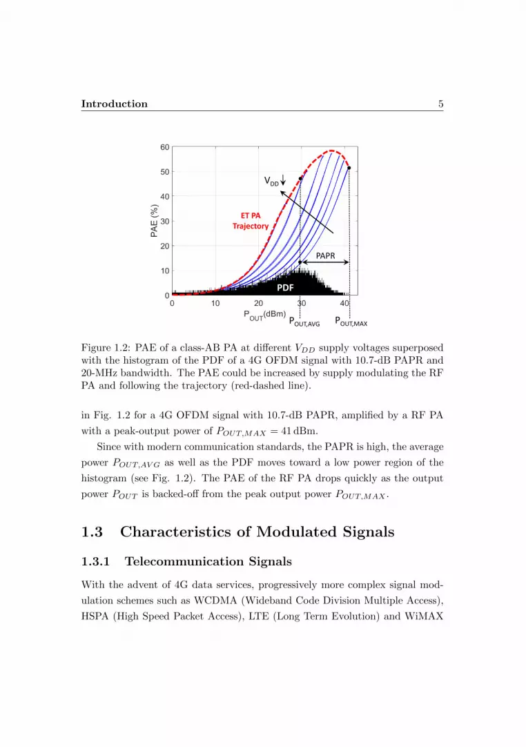
in Fig. 1.2 for a 4G OFDM signal with 10.7-dB PAPR, amplified by a RF PA
with a peak-output power of POUT,MAX = 41 dBm.
Since with modern communication standards, the PAPR is high, the average
power POUT,AV G as well as the PDF moves toward a low power region of the
histogram (see Fig. 1.2). The PAE of the RF PA drops quickly as the output
power POUT is backed-off from the peak output power POUT,MAX .
1.3 Characteristics of Modulated Signals
1.3.1 Telecommunication Signals
With the advent of 4G data services, progressively more complex signal mod-
ulation schemes such as WCDMA (Wideband Code Division Multiple Access),
HSPA (High Speed Packet Access), LTE (Long Term Evolution) and WiMAX

Introduction 6
(Worldwide Interoperability for Microwave Access) are introduced to fulfill the
need for data and video demands from the market.
These 4G data services typically employ large-bandwidth digital-modulated
signals (1-20 MHz per channel) with high-PAPR (9-11 dB) to enhance spectral
efficiency and maximize the data rate [8–15].
While high-PAPR modulations are very effective in terms of data through-
put, they are strongly detrimental for the RF PA efficiency, compared to constant-
envelope digital-modulation standards (e.g. GSMK, PSK, MSK). Indeed, due
to the high-PAPR of these modulated signals, the RF PA operates for most
of the time at low efficiency in the order of 10%-15% or less, as shown in Fig.
1.2 and in [4, 16–18]. Therefore, there is a challenging efficiency trade-off when
designing a PA between the efficiency and the linearity for such high-PAPR
signals.
1.3.2 Radar Signals
The majority of pulse radar systems operate the PA of the transmitter with
gated CW signals: the characteristics of the RF/microwave pulses in terms
of duty cycle, pulse width, repetition frequency, transmitted power and pulse
shaping directly affect radar performance [19,20]. A typical transmit module of
a solid-state radar has an efficient nonlinear deep class-AB to class-C PA that
transmits constant-envelope pulses with significant spectral content over a large
bandwidth [19,20].
However, advanced radar waveforms employ amplitude modulation to pro-
vide spectral confinement, improve range ambiguity and decrease detectability
of the radar [21–26]. For instance, in search and tracking radar, target detec-
tion and identity discrimination can be improved [27], while in weather radar
suppression of transmitted spectral sidebands enhances performance [28]. Ad-
ditionally, there is increased concern about radar spectral emissions interfering
with nearby spectrum allocations [29].
Introduction 7
The amplitude-modulated pulse can be provided at the input of the PA
while the supply voltage is kept constant over the pulse duration. Such drive-
modulated PAs operate in back-off at lower amplitudes, resulting in significant
average efficiency degradation in the PA with such radar signals.
1.4 Architectures for Efficiency-Enhancement
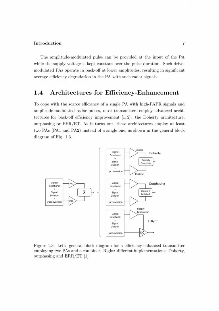
To cope with the scarce efficiency of a single PA with high-PAPR signals and
amplitude-modulated radar pulses, most transmitters employ advanced archi-
tectures for back-off efficiency improvement [1, 2]: the Doherty architecture,
outphasing or EER/ET. As it turns out, these architectures employ at least
two PAs (PA1 and PA2) instead of a single one, as shown in the general block
diagram of Fig. 1.3.
Doherty Combiner
Digital Baseband
+Signal
Division+
Upconversion
Carrier
Peaking
Chireix / Isolated
Digital Baseband
+Signal
Division+
Upconversion
Digital Baseband
+Signal
Division+
Upconversion
SupplyModulator
Σ
Digital Baseband
+Signal
Division+
Upconversion
PA1
PA2
Doherty
Outphasing
EER/ET
Figure 1.3: Left: general block diagram for a efficiency-enhanced transmitteremploying two PAs and a combiner. Right: different implementations: Doherty,outphasing and ERR/ET [1].
Introduction 8
In the Doherty and in the outphasing, the two PAs operate at RF frequency,
while in the EER/ET, only one PA works at RF and the second PA (i.e. supply
modulator or envelope modulator) typically operates at video-bandwidth. The
two PAs of the Doherty and outphasing operate on the principle of the active
load modulation [2,30]. However, in the Doherty case the two PAs are generally
different and optimized for different output power levels, while in the outphasing
the two PAs are ideally identical. The output signals of the PAs are summed
with a combiner in the Doherty and in the outphasing, while in the EER/ET
the combining of the two PAs is directly performed inside the RF PA, which
essentially acts as mixer.
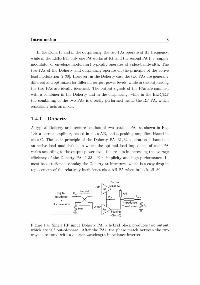
1.4.1 Doherty
A typical Doherty architecture consists of two parallel PAs as shown in Fig.
1.4: a carrier amplifier, biased in class-AB, and a peaking amplifier, biased in
class-C. The basic principle of the Doherty PA [31, 32] operation is based on
an active load modulation, in which the optimal load impedance of each PA
varies according to the output power level; this results in increasing the average
efficiency of the Doherty PA [2, 33]. For simplicity and high-performance [1],
most base-stations use today the Doherty architectures which is a easy drop-in
replacement of the relatively inefficienct class-AB PA when in back-off [30].
Digital Baseband
+ Upconversion
Carrier
Peaking(Class-C)
50 Ω
-90°
-180°
λ/4
(Class-AB)
ImpedanceTransformer
Hybrid
RL
PDC POUT
PIN
PA
PA
Figure 1.4: Single RF input Doherty PA: a hybrid block produces two outputwhich are 90 out-of-phase. After the PAs, the phase match between the twoways is restored with a quarter-wavelength impedance inverter.
Introduction 9
However, Doherty PAs present some disadvantages as the amplifiers are re-
quired to work at different carrier frequencies as it typically happens with multi-
mode and multi-bandwidth signals used in the base-stations. As shown in Fig.
1.3, the two PA outputs are connected with a Doherty combiner. In case of
a traditional, single RF input, Doherty (see Fig. 1.4), the Doherty combiner
is realized with a quarter-wavelength impedance inverter and offset lines which
introduces frequency dependences. This means that the efficiency superiority
of Doherty PAs over linear PAs (such as class-AB) decreases rapidly as the
frequency of operation deviates from the design frequency; this greatly compro-
mises the bandwidth of Doherty PAs [34].
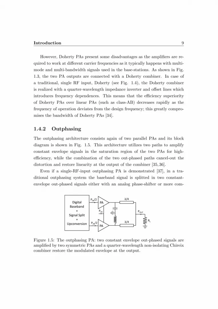
1.4.2 Outphasing
The outphasing architecture consists again of two parallel PAs and its block
diagram is shown in Fig. 1.5. This architecture utilizes two paths to amplify
constant envelope signals in the saturation region of the two PAs for high-
efficiency, while the combination of the two out-phased paths cancel-out the
distortion and restore linearity at the output of the combiner [35,36].
Even if a single-RF-input outphasing PA is demonstrated [37], in a tra-
ditional outphasing system the baseband signal is splitted in two constant-
envelope out-phased signals either with an analog phase-shifter or more com-
Digital Baseband
+Signal Split
+ Upconversion
PA
RL
PAλ/4
λ/4PIN/2
PDC POUT
PIN/2
Figure 1.5: The outphasing PA: two constant envelope out-phased signals areamplified by two symmetric PAs and a quarter-wavelength non-isolating Chireixcombiner restore the modulated envelope at the output.

Introduction 10
monly in the digital baseband by means of signal processing techniques. These
two digital signals are converted at IF by two DACs and then upconverted to
RF. Each of these two signals is fed in its nonlinear RF PA, typically biased
in class-E or F. After the PAs, the amplified signal is reconstructed, ideally
without distortion, at the output of the combiner.
Depending on the combiner type, the outphasing architecture can be re-
ferred as LINC [36] (Linear Amplification using Nonlinear Components) when
the combiner is isolating and lossy (e.g. a Wilkinson combiner), or as Chireix
outphasing [35] when a non-isolating and loss-less (e.g. Chireix combiner) is
employed [38].
The advantages of outphasing are obvious: the nonlinear regime of the RF
PAs provides high efficiency to the transmitter, however some drawbacks may
limit the architecture performance. The matching between the two signal path,
both in terms of phase and amplitude may introduce distortion while the passive
components may introduce bandwidth restrictions. Although, this architecture
provides high efficiencies with acceptable linearity [38–40], it is still challenging
to out-phase the signals to achieve wide bandwidths [2].
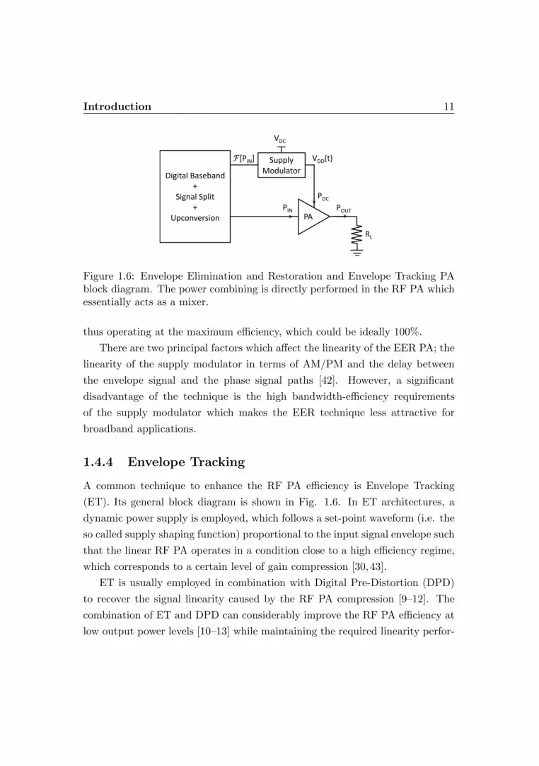
1.4.3 Envelope Elimination and Restoration
The Envelope Elimination and Restoration (EER) or Kahn technique imple-
ments a linear PA by combining a nonlinear but highly efficient RF PA and an
envelope supply modulator [41]. The block diagram of EER is the same as that
of the Envelope Tracking (ET) and it is shown in Fig. 1.6.
The baseband I/Q input signal contains both amplitude and phase informa-
tion. In EER, this signal is split in two signals; a highly efficient RF PA provides
amplification to the constant-envelope phase-modulated signal in the RF path,
while an envelope amplifier (or supply modulator) generates an output voltage
which is proportional to the input envelope signal. The resulting envelope signal
is used to modulate the RF PA and thus restoring at the output a high-power
replica of the input signal. Typically, the RF PA in EER is always saturated,
Introduction 11
RL
PA
PDC
POUTPIN
Supply Modulator
VDD(t)
Digital Baseband+
Signal Split+
Upconversion
ℱ[PIN]
VDC
Figure 1.6: Envelope Elimination and Restoration and Envelope Tracking PAblock diagram. The power combining is directly performed in the RF PA whichessentially acts as a mixer.
thus operating at the maximum efficiency, which could be ideally 100%.
There are two principal factors which affect the linearity of the EER PA; the
linearity of the supply modulator in terms of AM/PM and the delay between
the envelope signal and the phase signal paths [42]. However, a significant
disadvantage of the technique is the high bandwidth-efficiency requirements
of the supply modulator which makes the EER technique less attractive for
broadband applications.
1.4.4 Envelope Tracking
A common technique to enhance the RF PA efficiency is Envelope Tracking
(ET). Its general block diagram is shown in Fig. 1.6. In ET architectures, a
dynamic power supply is employed, which follows a set-point waveform (i.e. the
so called supply shaping function) proportional to the input signal envelope such
that the linear RF PA operates in a condition close to a high efficiency regime,
which corresponds to a certain level of gain compression [30,43].
ET is usually employed in combination with Digital Pre-Distortion (DPD)
to recover the signal linearity caused by the RF PA compression [9–12]. The
combination of ET and DPD can considerably improve the RF PA efficiency at
low output power levels [10–13] while maintaining the required linearity perfor-

Introduction 12
mance.
In this architecture, the overall efficiency of the supply-modulated PA can be
increased if the efficiency of the supply modulator is sufficiently high. However,
for high-bandwidth signals, the required slew-rate, tracking accuracy and high
efficiency become challenges for the supply modulator.
An advantage of this architecture over the outphasing and Doherty is that
the PA can be operated at different carrier frequency without changing the
matching of the RF PA, allowing the use of multi-mode and multi-band signals
with the same supply-modulated PA. Although ET architectures for handsets
are already commercial products [44], there is still research on the use of ET for
base-station transmitters [1].
1.5 Envelope Characteristics
ET technique is considered as the ideal solution for multi-mode and multi-
band PAs. Unlike in EER, the amplitude and phase signals are not completely
separated in the RF path of an ET transmitter. Therefore, ET demands a lower
supply modulator bandwidth and alleviates the timing requirements between the
supply waveform and the RF signal.
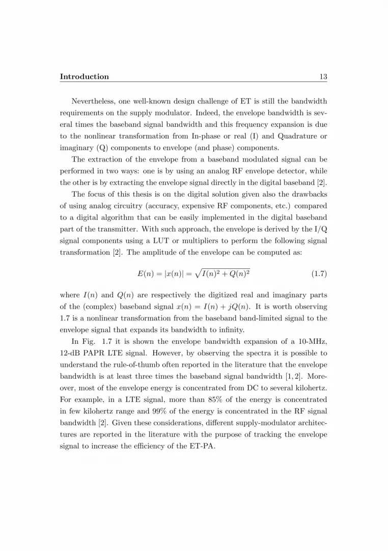
Figure 1.7: Spectra of a baseband 10-MHz 12-dB PAPR LTE signal (blue-square) illustrating the bandwidth expansion (red-circle) due to the nonlinearenvelope extraction.
Introduction 13
Nevertheless, one well-known design challenge of ET is still the bandwidth
requirements on the supply modulator. Indeed, the envelope bandwidth is sev-
eral times the baseband signal bandwidth and this frequency expansion is due
to the nonlinear transformation from In-phase or real (I) and Quadrature or
imaginary (Q) components to envelope (and phase) components.
The extraction of the envelope from a baseband modulated signal can be
performed in two ways: one is by using an analog RF envelope detector, while
the other is by extracting the envelope signal directly in the digital baseband [2].
The focus of this thesis is on the digital solution given also the drawbacks
of using analog circuitry (accuracy, expensive RF components, etc.) compared
to a digital algorithm that can be easily implemented in the digital baseband
part of the transmitter. With such approach, the envelope is derived by the I/Q
signal components using a LUT or multipliers to perform the following signal
transformation [2]. The amplitude of the envelope can be computed as:
E(n) = |x(n)| =√I(n)2 +Q(n)2 (1.7)
where I(n) and Q(n) are respectively the digitized real and imaginary parts
of the (complex) baseband signal x(n) = I(n) + jQ(n). It is worth observing
1.7 is a nonlinear transformation from the baseband band-limited signal to the
envelope signal that expands its bandwidth to infinity.
In Fig. 1.7 it is shown the envelope bandwidth expansion of a 10-MHz,
12-dB PAPR LTE signal. However, by observing the spectra it is possible to
understand the rule-of-thumb often reported in the literature that the envelope
bandwidth is at least three times the baseband signal bandwidth [1, 2]. More-
over, most of the envelope energy is concentrated from DC to several kilohertz.
For example, in a LTE signal, more than 85% of the energy is concentrated
in few kilohertz range and 99% of the energy is concentrated in the RF signal
bandwidth [2]. Given these considerations, different supply-modulator architec-
tures are reported in the literature with the purpose of tracking the envelope
signal to increase the efficiency of the ET-PA.
Introduction 14
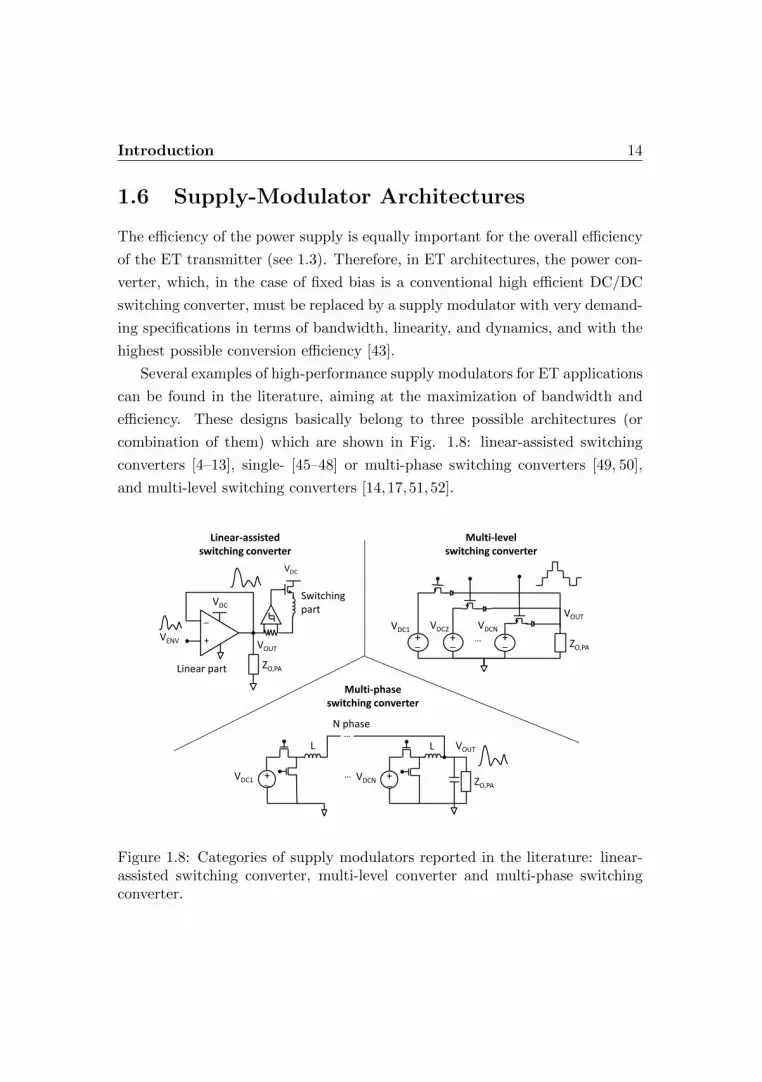
1.6 Supply-Modulator Architectures
The efficiency of the power supply is equally important for the overall efficiency
of the ET transmitter (see 1.3). Therefore, in ET architectures, the power con-
verter, which, in the case of fixed bias is a conventional high efficient DC/DC
switching converter, must be replaced by a supply modulator with very demand-
ing specifications in terms of bandwidth, linearity, and dynamics, and with the
highest possible conversion efficiency [43].
Several examples of high-performance supply modulators for ET applications
can be found in the literature, aiming at the maximization of bandwidth and
efficiency. These designs basically belong to three possible architectures (or
combination of them) which are shown in Fig. 1.8: linear-assisted switching
converters [4–13], single- [45–48] or multi-phase switching converters [49, 50],
and multi-level switching converters [14,17,51,52].
_
+
Linear part
Switchingpart
VDC
VDC
VOUT
ZO,PA
VENV
Linear-assistedswitching converter
Multi-phaseswitching converter
LL
VDCNVDC1
N phase
…
…ZO,PA
VOUT
++
ZO,PA+ + +
VDC1…
VDC2 VDCN
VOUT
Multi-levelswitching converter
Figure 1.8: Categories of supply modulators reported in the literature: linear-assisted switching converter, multi-level converter and multi-phase switchingconverter.

Introduction 15
1.6.1 Linear-assisted Switching Converters
In this category, the supply modulator is made up of as a series or parallel
combination of a switching converter and of a linear amplifier: the switching
converter provides the majority of the output power with high efficiency, while
the linear amplifier manages the rest of the power, improving linearity and
extending the overall bandwidth.
The switching circuit is typically driven by a PWM modulation or by an hys-
teretic control [53]. In any case, the switching converter bandwidth is usually
limited by the switching frequency for complex modulating signals [14, 18, 53],
(although some less demanding limits are theoretically derived for simple mod-
ulating signals [54]). Therefore, multi-MHz bandwidths cannot be achieved by
this part of the supply modulator, that typically reaches a few hundred kHz
bandwidth with high efficiency [55].
Thus, the overall efficiency of this approach highly depends on the spectral
distribution of required dynamic supply voltage, which is directly related to the
spectral characteristics of the RF signal envelope [55]: for this reason, very good
performances are achieved when only a very small fraction of the output power,
amplified by the linear part, is located beyond the bandwidth of the switching
amplifier [13, 53]. This can be verified by several modulation standards [5, 13],
but represents in any case a relevant limitation of this approach.
1.6.2 Multi-phase Switching Converters
In a single-phase switching converter (e.g. a Buck converter), a single half-bridge
is controlled by PWM modulation and a passive output LC filter reconstructs
the desired supply voltage at the load (i.e. the PA drain). However, it is shown
that the PWM switching frequency has to be at least 4− 5 times the baseband
signal bandwidth with obvious consequences on the efficiency [56].
To overcome this limitation, with the multi-phase converters several half-
bridges are adopted in parallel and controlled by phase-shifted PWM signals
to obtain a larger bandwidth (it doubles for each added phase) [49, 50]: in

Introduction 16
this case the converter can manage large amounts of power with high efficiency
within a larger bandwidth but, given the bandwidth/efficiency trade-off of the
PWM converters, a large number of circuits has to be used to obtain multi-MHz
responses; hence the circuit cost and complexity become considerable.
The main challenges in single- and multi-phase supply modulators are as-
sociated with the required design of the output filter. Indeed, the filter is not
loaded by a fixed resistor but by a PA, which presents a dynamic nonlinear
complex impedance load, as discussed in detail in [57–59].
1.6.3 Multi-level Switching Converters
This category of supply-modulators relies on the use of multilevel converters to
overcome the frequency and LC filtering limitations of PWM converters: indeed,
in multilevel architectures there is no need for PWM modulation (even though it
can also be used in some applications with low bandwidth requirements [60,61])
and so the converter bandwidth can be improved.
Various types of multilevel topologies are possible. In the field of supply
modulators, some authors have proposed commutated voltage source architec-
tures (called also multiplexed or switched voltage sources) as in Fig. 1.8 and
in [14,16,17]. With this approach, various independent voltage sources are mul-
tiplexed one at a time, depending on the power level of the signal envelope;
thus the switching frequency of the power devices in each voltage branch has an
upper limit equal to the envelope signal bandwidth (and not 4-5 times): indeed,
considering a sinusoidal envelope signal with an amplitude sweeping the entire
dynamic range of the converter (i.e. full-scale sinusoid), each power switch is
activated only once per cycle of the envelope signal [60–62].
The drawback of this approach is that the converter output signal is a step
wave with a number of levels N equal to the number of the input voltage sources
and of their associated switches as shown in Fig. 1.9; thus, due to the discretiza-
tion error, a high number of levels N need to be used to obtain a sufficient linear-
ity for the synthesized signal (even considering the use of DPD, as is explained

Introduction 17
0
5
10
15
20
25
30
35
40
45
50
0 0.2 0.4 0.6 0.8 1
PA supply shaping function
Discretized HPA supply shaping function
Fixed bias offset (VO)
Normalized Envelope
VD
D(V
)
Figure 1.9: Continuous shaping function F (square-blue) and approximation ofthe shaping table with N = 8 levels (dot-red). The shaping function starts froma minimum voltage offset of 6 V (triangle-black).
in the following).
To avoid an ineffective complexity of the circuit, the discretization of the
voltage steps needs usually to be kept quite coarse (small N, typically 3 − 4)
and a linear amplifier is used in series with the multilevel converter to recover
linearity (and also to enlarge the bandwidth if needed) [17,51]. Clearly the lower
N, the larger the voltage steps (i.e. lower voltage resolution) at the multilevel
converter output and the higher is the amount of power to be managed by the
linear amplifier, resulting in a noticeable degradation of the overall efficiency.
It is useful to point out that in an ET architecture combined with DPD,
the nonlinearity of the multilevel converter can be compensated by the pre-
distortion algorithm, and so the sole high efficiency multilevel converter can be
used without the need for a linear amplifier with better efficiency.
However, this efficiency improvement can be really effective only if a rea-
sonable fine voltage resolution is implemented with the multilevel converter. In
fact, for every power level of the RF input signal PIN , the characterization of

Introduction 18
the RF PA identifies the corresponding optimum value of the RF PA drain bias
voltage VDD that enables the RF PA operation at the best efficiency condi-
tion (i.e. gain compression) [43] made compatible, by the DPD action, with
the required linearity: the optimum trajectory (see Fig. 1.3) that relates the
bias voltage to the input (or output) signal envelope power is usually called the
supply shaping function F .
Practically, the shaping function determines the set-point signal F [PIN ] to
be followed by the supply modulator for a given modulated RF signal PIN .
If only the multilevel converter is used, its step wave response can follow the
envelope signal with a voltage error proportional to its voltage resolution: the
closer the step wave response of the multilevel converter to the ideal envelope
set-point signal, the higher the RF PA efficiency. Thus, a high number of voltage
levels at the output of the converter is highly desirable.
In this thesis, a binary-coded cascaded multilevel converter (i.e. Power-DAC)
is researched and employed as a supply-modulator of RF PAs. In addition to the
choice of the circuit architecture, high switching frequencies are also achieved by
exploiting fast GaN-based power switches. The presented converter is controlled
by digital signals coming directly from the transmitter baseband DSP/FPGA,
without the need for digital-to-analog conversion and envelope detector circuitry
and comparators adopted by analog envelope amplifiers for RF transmitters.
1.7 Organization of the Thesis
This thesis is organized as follows:
Chapter 2 presents a cascaded multilevel power converter, based on a di-
rect digital-to-analog power conversion architecture which is capable of
achieving 20-MHz full-power bandwidth at 28-W average output power
and 82.8% power efficiency; measured dynamic range is 42 V with a full-
scale slew rate of 4.2 kV/µs. The circuit is controlled directly by dig-
ital signals from a FPGA, without introducing any PWM modulation.

Introduction 19
This digital-to-analog power conversion architecture makes this circuit a
real Power-DAC, suggesting its use for many other applications. Large
bandwidth and high efficiency are achieved also by exploiting GaN-on-Si
switches, whose high switching speed and power density enable a compact
layout. Experimental data demonstrate the capability of the converter
to synthesize the supply voltage required for the envelope tracking of 4-
MHz WCDMA, 10-MHz LTE and 20-MHz WiFi communication signals
delivering an average power of about 17 W and 159 W of peak power,
with state-of-the-art efficiency performance of 91.7%, 84.5% and 78.2%,
respectively.
Chapter 3 presents an ET transmitter based on the Power-DAC supply modu-
lator introduced in chapter 2. The Power-DAC is based on a direct digital-
to-analog conversion architecture that implements the binary-coded sum
of three isolated DC voltages, allowing the synthesis of an output waveform
with eight voltage levels. With this fine voltage resolution, the residual
discretization error in the transmitter RF output signal is reduced and
can be compensated by means of DPD of the RF signal without the need
of an auxiliary linear envelope amplifier. The presented ET solution is
tested with a L-band 30-W Lateral-Diffused MOS (LDMOS) RF PA with
1.4-MHz and 10-MHz LTE signals. Under these conditions the converter
demonstrated 92% and 83% efficiency, respectively, whereas the compos-
ite efficiencies of the transmitter are 38.3% and 23.9% at 5.5 W and 1.9 W
of average RF output power, respectively. This performance corresponds
to an improvement of 17.2 and 17.9 points for the PAE of the RF PA
and to 13.4 and 13 points of improvement for the efficiency of the entire
transmitter with respect to fixed bias operation.
Chapter 4 introduces an X-band radar transmitter in which the Power-DAC
presented in chapter 2 is employed to modulate an efficient 12-W GaN
MMIC 10-GHz PA. In this approach, the digital baseband signal is gener-
ated and pre-distorted in an FPGA and upconverted to drive the PA. The
Introduction 20
PA is characterized in a controlled thermal- and trap-state allowing the
implementation an open-loop DPD. The pulse shape is fully programmable
and can provide not only amplitude modulation of each pulse, but also
pulse-to-pulse modulation, while maintaining high composite efficiency.
The switches of the Power-DAC commutate at only a few kHz, and the
nonlinearities are compensated with DPD, allowing for large efficiency
increase to over 55% at X-band.
Chapter 5 explores the use of a high-performance Qorvo 0.15µm GaN-on-SiC
HEMT process to implement an integrated multilevel converter for ET
applications. The converter is designed for the supply modulation of a X-
band, 10-W MMIC PA implemented in the same GaN technology for the
perspective development of a single chip. The integrated multilevel con-
verter performance modulating the MMIC PA are evaluated through the
implementation and test of the high-efficiency ET transmitter with DPD
described in the chapter 4. Measured results for amplitude and frequency-
modulated pulse waveforms show a composite Power-Added Efficiency
(CPAE) of 45% with a peak pulse power of 10 W at 9.57 GHz, with si-
multaneous spectral confinement and 52 dB improvement in the first time
sidelobe level. For a wideband high peak-to-average ratio LTE signal,
the CPAE increases from 11 to 32% compared to a constant drain supply
transmitter, while linearity is maintained through digital predistortion.
Chapter 6 investigates a high-efficiency transmitter based on a Multi-Level
Chireix Outphasing (ML-CO) PA modulated by the Power-DAC (see
chapter 2). This architecture is preliminarily tested by means of Continu-
ous Wave (CW) measurements and supply modulation with static biases.
A high composite efficiency of 44% with a 6-dB PAPR QPSK is reached,
thus demonstrating the feasibility of the approach. An experimental test
bench able to dynamically generate phase- and time-aligned modulated
signals for outphasing and supply modulation is developed. The DPD-
linearized ML-CO PA is demonstrated with 1.4-MHz and 10-MHz LTE
Introduction 21
signals. For both signals, the average total power consumption is reduced
by a factor of two when supply modulation is used. For the 9.3-dB PAPR,
1.4-MHz signal the PA operates with 38% average drain efficiency at 0.54-
W average output power.
Chapter 7 provides some insights about dynamic effects of electron devices
employed in supply modulators and PAs. At first, a laboratory setup
and characterization procedure for the dynamic RON of GaN HEMTs
in presence of thermal- and trapping-effects is presented. This setup is
used for the characterization of the GaN-on-SiC and GaN-on-Si HEMTs,
which are respectively employed to implement the discrete component
and the integrated version of the Power-DAC. Finally, a behavioral model
including self-heating is used to predict the static characteristics of the
LDMOS PA presented in the chapter 3.
Chapter 8 concludes the thesis and provides some possible research develop-
ments.
Chapter 2
Power-DAC
Supply Modulator
The efficiency of wireless transmitters for telecommunications can be improved
by using transmitter architectures such as Envelope Tracking (ET) that en-
hances the efficiency of the RF Power Amplifier (PA) by means of a dynamic
bias supply, modulated by the envelope of the RF transmitted signal (section
1.4.4). Overall high efficiency of the transmitter can be obtained only by ex-
ploiting a highly efficient bias supply modulator (section 1.6). Its requirements
in terms of efficiency and dynamics are very demanding, due to the large band-
widths and high peak-to-average power ratios of modern telecommunications
standards (section 1.3.1).
In this chapter a cascaded multilevel power converter, based on a direct
digital-to-analog power conversion architecture is presented, capable of achiev-
ing 20-MHz full-power bandwidth at 28-W average output power and 82.8%
power efficiency; measured dynamic range is 42 V with a full-scale slew rate of
4.2 kV/µs. The circuit is controlled directly by digital signals from a FPGA
unit, without introducing any PWM modulation. This digital-to-analog power
22

Power-DAC Supply Modulator 23
conversion architecture makes this circuit a real power-DAC, suggesting its use
for many other applications. Large bandwidth and high efficiency are achieved
also by exploiting GaN-on-Si switches, whose high switching speed and power
density enable a very compact layout.
Experimental data demonstrate the capability of the converter to synthe-
size the supply voltage required for the envelope tracking of 4-MHz WCDMA,
10-MHz LTE and 20-MHz WiFi communication signals delivering an average
power of about 17 W and 159 W of peak power, with state-of-the-art efficiency
performance of 91.7%, 84.5% and 78.2%, respectively.
2.1 Ideal Digital-to-Analog Converter (DAC)
Let us define the binary word (b1, ..., bi, ..., bN ), where the bit bi state could be
0 or 1. Let us associate to the binary word a positive number BIN such that:
BIN = b11
2+ b2
1
22+ ...+ bN
1
2N, (2.1)
where b1 is the Most Significant Bit (MSB) and bN is the Least Significant Bit
(LSB) of the binary word. From 2.1, it follows that BIN takes values between
0 and (1 − 1/2N ) and the number of different configurations is L = 2N when
using an N -bit word.
If BIN is multiplied by a fixed reference voltage VREF we get:
VOUT = VREF ·BIN2.1−−→ VOUT =
N∑i=1
biVREF
2i. (2.2)
Therefore, the output analog voltage VOUT is a scaled version of the reference
voltage VREF , controlled by BIN , or equivalently by the digital word (b1, ..., bN ).
This conversion is typically performed by a Digital-to-Analog Converter
(DAC) [63] and its block diagram is shown on left in Fig. 2.1. The voltage
range at the output of the DAC varies between 0 and VREF · (1 − 1/2N ), and
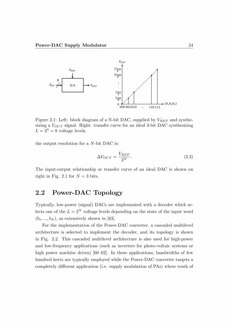
Power-DAC Supply Modulator 24
D/A
𝑉𝑅𝐸𝐹
𝑉𝑂𝑈𝑇𝐵𝐼𝑁
𝑁
000 001010 111110…0
𝑉𝑅𝐸𝐹8
𝑉𝑅𝐸𝐹4
6𝑉𝑅𝐸𝐹8
…
7𝑉𝑅𝐸𝐹8
(𝑏1𝑏2𝑏3)
𝑉𝑂𝑈𝑇
Figure 2.1: Left: block diagram of a N-bit DAC, supplied by VREF and synthe-sizing a VOUT signal. Right: transfer curve for an ideal 3-bit DAC synthesizingL = 23 = 8 voltage levels.
the output resolution for a N -bit DAC is:
∆VOUT =VREF
2N. (2.3)
The input-output relationship or transfer curve of an ideal DAC is shown on
right in Fig. 2.1 for N = 3 bits.
2.2 Power-DAC Topology
Typically, low-power (signal) DACs are implemented with a decoder which se-
lects one of the L = 2N voltage levels depending on the state of the input word
(b1, ..., bN ), as extensively shown in [63].
For the implementation of the Power-DAC converter, a cascaded multilevel
architecture is selected to implement the decoder, and its topology is shown
in Fig. 2.2. This cascaded multilevel architecture is also used for high-power
and low-frequency applications (such as inverters for photo-voltaic systems or
high power machine drives) [60–62]. In these applications, bandwidths of few
hundred hertz are typically employed while the Power-DAC converter targets a
completely different application (i.e. supply modulation of PAs) where tenth of
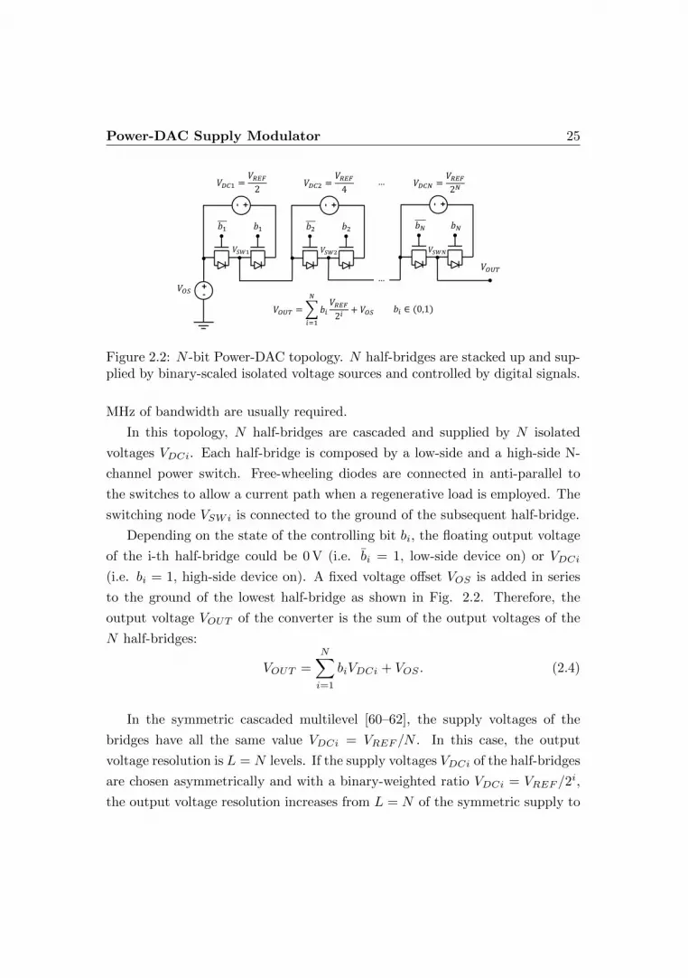
Power-DAC Supply Modulator 25
+-
𝑏1 𝑏1
+-
𝑉𝑂𝑆
𝑉𝐷𝐶1 =𝑉𝑅𝐸𝐹2
…𝑉𝑂𝑈𝑇
𝑉𝑂𝑈𝑇 =
𝑖=1
𝑁
𝑏𝑖𝑉𝑅𝐸𝐹2𝑖+ 𝑉𝑂𝑆 𝑏𝑖 ∈ (0,1)
+-
𝑏2 𝑏2
+-
𝑏𝑁 𝑏𝑁
𝑉𝐷𝐶2 =𝑉𝑅𝐸𝐹4
𝑉𝐷𝐶𝑁 =𝑉𝑅𝐸𝐹2𝑁
…
𝑉𝑆𝑊1 𝑉𝑆𝑊2 𝑉𝑆𝑊𝑁
Figure 2.2: N -bit Power-DAC topology. N half-bridges are stacked up and sup-plied by binary-scaled isolated voltage sources and controlled by digital signals.
MHz of bandwidth are usually required.
In this topology, N half-bridges are cascaded and supplied by N isolated
voltages VDCi. Each half-bridge is composed by a low-side and a high-side N-
channel power switch. Free-wheeling diodes are connected in anti-parallel to
the switches to allow a current path when a regenerative load is employed. The
switching node VSWi is connected to the ground of the subsequent half-bridge.
Depending on the state of the controlling bit bi, the floating output voltage
of the i-th half-bridge could be 0 V (i.e. bi = 1, low-side device on) or VDCi
(i.e. bi = 1, high-side device on). A fixed voltage offset VOS is added in series
to the ground of the lowest half-bridge as shown in Fig. 2.2. Therefore, the
output voltage VOUT of the converter is the sum of the output voltages of the
N half-bridges:
VOUT =
N∑i=1
biVDCi + VOS . (2.4)
In the symmetric cascaded multilevel [60–62], the supply voltages of the
bridges have all the same value VDCi = VREF /N . In this case, the output
voltage resolution is L = N levels. If the supply voltages VDCi of the half-bridges
are chosen asymmetrically and with a binary-weighted ratio VDCi = VREF /2i,
the output voltage resolution increases from L = N of the symmetric supply to

Power-DAC Supply Modulator 26
L = 2N of the binary asymmetric supply distribution.
By substituting the binary-scaled voltages in (2.4), the input-output rela-
tionship results in the same of the ideal DAC (2.2) plus an offset voltage VOS :
VOUT =N∑i=1
biVREF
2i+ VOS . (2.5)
Therefore, with such architecture it is possible to increase the resolution from
L = N of the symmetric supplies strategy to L = 2N , which allows a finer
approximation of the continuous set-point waveform. The output voltage range
is comprised between VOS and VOS+VREF (1−1/2N ) and the voltage resolution
is ∆VOUT = VREF /2N (2.3).
2.3 Ideal Power-DAC
For the design of the Power-DAC, a bit resolution of N = 3 is selected, which
leads to L = 23 = 8 voltage levels at the output of the converter. This choice
represents a good compromise between output voltage resolution and switching
losses as discussed in section 2.4.
Indeed, these two aspects are in conflict: higher the voltage resolution, more
continuous is the staircase at the output of the Power-DAC, which keeps the
PA closer to compression and increases its efficiency. However, the higher the
number of levels, the higher the commutation rate of the half-bridge with the
smallest voltage supply, which results in higher switching losses.
The 3-bit cascaded multilevel topology of the converter is shown on the left
of Fig. 2.3. Since VREF = 40 V is selected for the simulation, the bottom half-
bridge is supplied with VDC1 = 20 V, the middle half-bridge with VDC2 = 10 V
and the top half-bridge with VDC3 = 5 V. The voltage offset is set to VOS = 5 V.
Therefore, the voltage range at the output of the converter is between 5 V and
40 V.
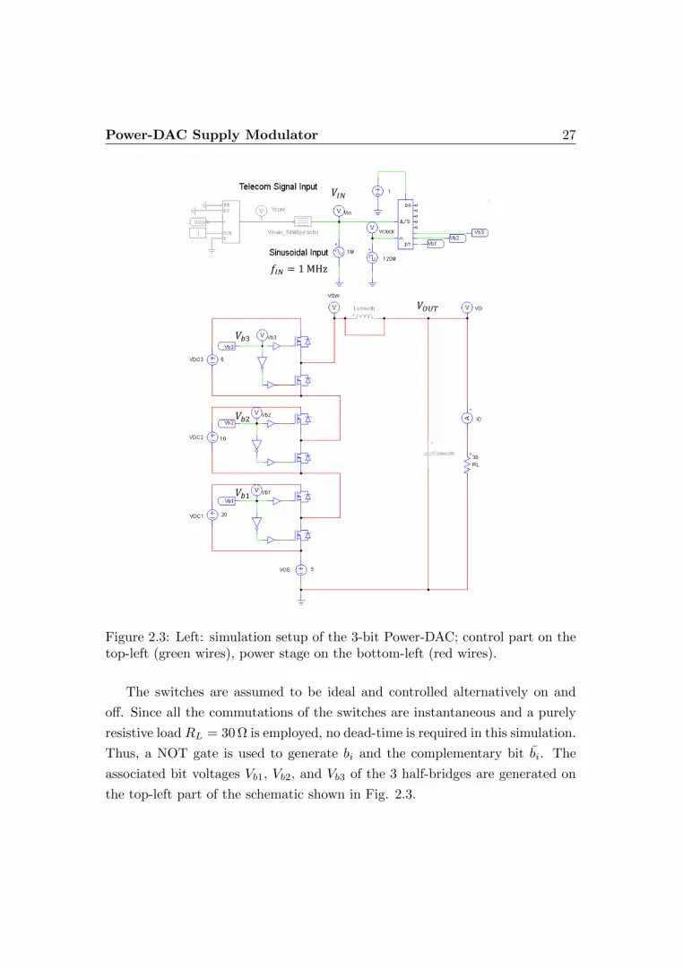
Power-DAC Supply Modulator 27
𝑉𝐼𝑁
𝑉𝑂𝑈𝑇
𝑓𝐼𝑁 = 1MHz
𝑉𝑏3
𝑉𝑏2
𝑉𝑏1
Figure 2.3: Left: simulation setup of the 3-bit Power-DAC; control part on thetop-left (green wires), power stage on the bottom-left (red wires).
The switches are assumed to be ideal and controlled alternatively on and
off. Since all the commutations of the switches are instantaneous and a purely
resistive load RL = 30 Ω is employed, no dead-time is required in this simulation.
Thus, a NOT gate is used to generate bi and the complementary bit bi. The
associated bit voltages Vb1, Vb2, and Vb3 of the 3 half-bridges are generated on
the top-left part of the schematic shown in Fig. 2.3.
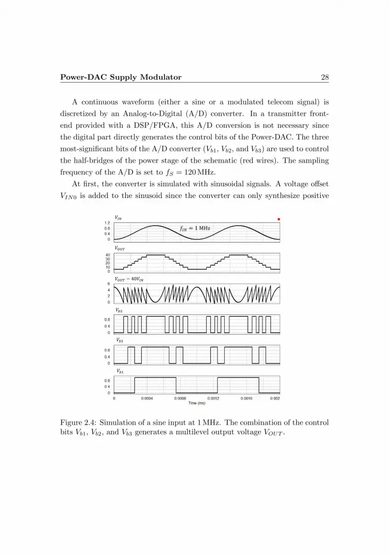
Power-DAC Supply Modulator 28
A continuous waveform (either a sine or a modulated telecom signal) is
discretized by an Analog-to-Digital (A/D) converter. In a transmitter front-
end provided with a DSP/FPGA, this A/D conversion is not necessary since
the digital part directly generates the control bits of the Power-DAC. The three
most-significant bits of the A/D converter (Vb1, Vb2, and Vb3) are used to control
the half-bridges of the power stage of the schematic (red wires). The sampling
frequency of the A/D is set to fS = 120 MHz.
At first, the converter is simulated with sinusoidal signals. A voltage offset
VIN0 is added to the sinusoid since the converter can only synthesize positive
𝑉𝑂𝑈𝑇
𝑉𝐼𝑁
𝑉𝑂𝑈𝑇 − 40𝑉𝐼𝑁
𝑓𝐼𝑁 = 1 MHz
𝑉𝑏3
𝑉𝑏2
𝑉𝑏1
Figure 2.4: Simulation of a sine input at 1 MHz. The combination of the controlbits Vb1, Vb2, and Vb3 generates a multilevel output voltage VOUT .

Power-DAC Supply Modulator 29
voltages. The input sinusoid VIN (t) can be written as:
VIN (t) = VIN0 + VA sin(2πfIN t), (2.6)
where VIN0 and VA are set to 0.5 V. The A/D reference voltage is set to 1 V.
In this way, VIN (t) sweeps the full scale of the A/D from 0 to 1 V. With such
parameters, the setup is simulated and the converter response to a continuous
sine wave at fIN = 1 MHz is shown in Fig. 2.4.
The difference between the continuous sine wave and the 8-level output stair-
case of the Power-DAC is the discretization error. As can be observed by the
plot, this discretization error is always positive and between 0 and 5 V. This
discretization error is consumed by the PA in order to produce a linear ampli-
fication by means of DPD.
It is also worth observing the variation of the switching frequency of Vb1, Vb2,
and Vb3 over the period, where the former has the faster switching frequency.
These switching frequencies have a direct impact on the switching losses of the
half-bridges.
2.4 Switching Behavior
Let us define the average switching frequency < fSWi > of the i-th bit over a
period T as:
< fSWi >=NPi2T
, (2.7)
where NPi is the number of commutation cycles of a bit from 0 to 1 back to
0. In the case of a sinusoid at fIN = 1/T = 1 MHz sampled by the A/D at
fS = 120 MHz, the number of commutation cycles are NP1 = 2, NP1 = 6
and NP1 = 14 as can be seen in Fig. 2.5. By 2.7, it follows that the average
switching frequencies of the three bits are the following:
< fSW1 >= 1 MHz, < fSW2 >= 3 MHz, < fSW3 >= 7 MHz. (2.8)

Power-DAC Supply Modulator 30
𝑓𝐼𝑁 = 1 MHz
7 MHz
3 MHz
1 MHz
Vb1
Vb2
VOUT
VIN
Vb3
𝑓𝐼𝑁 = 6 MHz
5 MHz
3 MHz
1 MHz
Vb1
Vb2
VOUT
VIN
Vb3
Figure 2.5: Simulated waveforms for the 3-bit Power-DAC. VIN : input sinu-soidal waveforms at fIN = 1 MHz (left) and 6 MHz (right). Vbi: i-th control bit.VOUT : staircase with 8-level output voltage.
It is worth to point out that, for a sine waveform of an arbitrary frequency
fIN sampled at fS , 2.7 could be generalized as:
< fSW1 >= fIN , < fSW2 >= 3 · fIN , < fSW3 >= 7 · fIN , (2.9)
only if the following condition is met [63] :
fSfIN
> 2NπN=3−−−→ fS
fIN> 8π ∼= 25.133. (2.10)
For instance, with fS = 120 MHz and N = 3, the maximum frequency of
the sinusoid in which (2.9) are still valid is fIN = 4.8 MHz. In such case, the
“fastest” bit commutates at < fSW3 >= 34 MHz. With an higher frequency
sinusoid such as fIN = 6 MHz, the least significant bit Vb3 misses some commu-
tation (NP3 = 10 instead of 14) and its average switching frequency is decreased
(5fIN instead of 7fIN ), as also shown in Fig. 2.5.

Power-DAC Supply Modulator 31
LTE 𝑓𝐼𝑄 = 1.4 MHz
941 kHz
Vb1
Vb2
VOUT
VIN
Vb3
Vb1
Vb2
VOUT
VIN
Vb3
420 kHz
185 kHz
LTE 𝑓𝐼𝑄 = 20 MHz
15.2 MHz
6.1 MHz
270 kHz
Figure 2.6: Simulated waveforms for the 3-bit Power-DAC. VIN : input envelopesof a LTE signal at fIQ = 1.4 MHz (left) and 20 MHz (right). Vbi: i-th controlbit. VOUT : staircase with 8-level output voltage.
Even if the switching frequency of b3 is decreased, this does not affect the
Power-DAC operation and its use as a supply modulator. Indeed, the generated
output waveform is always above the desired set-point waveform, allowing a
positive margin to the PA to operate linearly.
The schematic is simulated with high-PAPR telecommunications signals and
results are reported in Fig. 2.6. Two cases are considered: LTE downlink
channels at 1.4 MHz and 20 MHz [64]. The envelope of these (complex) signals
is extracted and used at the input. The extraction of the envelope from a band-
limited signal (1.4 MHz and 20 MHz) is a nonlinear transformation, which causes
a bandwidth expansion in the envelope signal (section 1.5). In the sinusoidal
case of (2.6), all the energy of the signal is concentrated at a fixed frequency
(DC and fIN ). When considering the envelope of telecommunications signals,
the spectrum presents a wide-band pattern (typically, 4 − 5 times the original
bandwidth (section 1.5).
Further investigation will be conducted to extract an analytical expression
for the average switching frequencies of the bits for complex telecommunication

Power-DAC Supply Modulator 32
signals. Simulation results showed that, for the LTE with a baseband IQ band-
width of 1.4 MHz, the average switching frequencies results in 185 kHz, 420 kHz
and 941 kHz. In the 20-MHz LTE case, these frequencies are 270 kHz, 6.1 MHz
and 15.2 MHz.
2.5 Power-DAC Technology
The 3-bit Power-DAC is designed to modulate the supply of Si LDMOS or GaN
PAs with a maximum supply voltage of 48 V. With such supply voltage, power
switches with a breakdown voltage of 40 V are selected.
The EPC2014 [65] from EPC Corporation [66] is selected as the main power
switch for the Power-DAC. This device is a GaN High Electron Mobility Tran-
sistors (HEMT) in which an AlGaN/GaN heterostructure is used to generate a
2-Dimensional Electron Gas (2-DEG) conductive channel.
These devices are grown on a Si substrate for a reduced component cost. A
p-GaN diode is placed on the gate of the device in order to shift the threshold
voltage from a negative value (GaNs are typically normally-on) to a positive
voltage (VGS,TH = 1.4 V). A body diode with a threshold voltage of VD = 1.4 V
and zero recovery-charge is embodied in the switch. Field plating is used to
reduce the RON deterioration due to trapping effects caused by drain voltage
stresses (more details in chapter 7).
The EPC2014 main characteristics include: RON = 14 mΩ, VDS,MAX =
40 V, IDS,MAX = 10 A, CISS = 300 pF, and COSS = 150 pF. The device on-
resistance RON is equal or less than the state-of-the-art of the Si power MOS-
FETs [66]. Moreover, the RON in a GaN device is less sensitive to the operating
junction temperature than in a Si device, which leads to a more stable RON and
lower conduction losses (see chapter 7). Reduced switching losses are obtained
with low input and output capacitances which are ensured by the lateral struc-
ture of the device. Also the low threshold voltage compared to an equivalent
Si MOSFET enables the device to be driven with a gate-source swing of only 5 V.

Power-DAC Supply Modulator 33
Finally, this device features very small (0.8 mm × 1.6 mm), flip-chip wafer-
level bumped-die packages. No bond-wires are used with such packaging tech-
nology, which results in a low connection resistance and inductance.
The switches are controlled by a high-side/low-side integrated BGA driver
from Texas Instruments (LM5113) [67]. A bootstrap technique is used to supply
the high-side totem-pole driver of the power switch, provided with an internal
clamp circuitry at 5.2 V for safety. This driver is specifically developed for
enhancement-mode GaN power switches from EPC since it provides very short
𝑉𝑏3
𝑉𝐷𝐶3
DriverDigital
Isolator
Linear (LDO)Regulator
5𝑉5𝑉
𝑉𝑏3
𝑉𝐿𝐷𝑂3
𝑉𝐷𝐶3
𝑏3
𝑏3
𝑉𝑏2
𝑉𝐷𝐶2
DriverDigital
Isolator
Linear (LDO)Regulator
5𝑉5𝑉
𝑉𝑏2
𝑉𝐿𝐷𝑂2
𝑉𝐷𝐶2
𝑏2
𝑏2
𝑉𝑏1
𝑉𝐷𝐶1
DriverDigital
Isolator
Linear (LDO)Regulator
5𝑉5𝑉
𝑉𝑏1
𝑉𝐿𝐷𝑂1
𝑉𝐷𝐶1
𝑏1
𝑏1
𝑉𝑂𝑈𝑇
𝑉𝑂𝑆
𝑉𝑆𝑊1
𝑉𝑆𝑊2
𝑉𝑆𝑊3
𝑉𝐺𝑁𝐷2
𝑉𝐺𝑁𝐷3
𝑉𝐺𝑁𝐷1 = 𝑉𝑂𝑆
𝑉𝐵𝑈𝑆
Mu
lti-
Ou
tpu
t Sw
itch
ing
DC
/DC
Co
nve
rter
𝑉𝑂𝑈𝑇
Figure 2.7: Detailed structure of the 3-bit Power-DAC: three half-bridge cellsare stacked up and supplied by isolated voltages. High-side and low-side driverscontrol the power stage and digital isolators provides isolation to the controlbits.
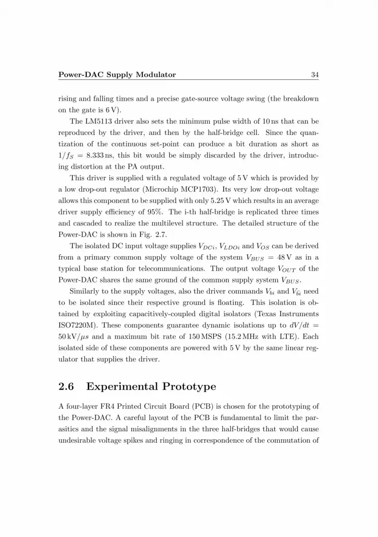
Power-DAC Supply Modulator 34
rising and falling times and a precise gate-source voltage swing (the breakdown
on the gate is 6 V).
The LM5113 driver also sets the minimum pulse width of 10 ns that can be
reproduced by the driver, and then by the half-bridge cell. Since the quan-
tization of the continuous set-point can produce a bit duration as short as
1/fS = 8.333 ns, this bit would be simply discarded by the driver, introduc-
ing distortion at the PA output.
This driver is supplied with a regulated voltage of 5 V which is provided by
a low drop-out regulator (Microchip MCP1703). Its very low drop-out voltage
allows this component to be supplied with only 5.25 V which results in an average
driver supply efficiency of 95%. The i-th half-bridge is replicated three times
and cascaded to realize the multilevel structure. The detailed structure of the
Power-DAC is shown in Fig. 2.7.
The isolated DC input voltage supplies VDCi, VLDOi and VOS can be derived
from a primary common supply voltage of the system VBUS = 48 V as in a
typical base station for telecommunications. The output voltage VOUT of the
Power-DAC shares the same ground of the common supply system VBUS .
Similarly to the supply voltages, also the driver commands Vbi and Vbi need
to be isolated since their respective ground is floating. This isolation is ob-
tained by exploiting capacitively-coupled digital isolators (Texas Instruments
ISO7220M). These components guarantee dynamic isolations up to dV/dt =
50 kV/µs and a maximum bit rate of 150 MSPS (15.2 MHz with LTE). Each
isolated side of these components are powered with 5 V by the same linear reg-
ulator that supplies the driver.
2.6 Experimental Prototype
A four-layer FR4 Printed Circuit Board (PCB) is chosen for the prototyping of
the Power-DAC. A careful layout of the PCB is fundamental to limit the par-
asitics and the signal misalignments in the three half-bridges that would cause
undesirable voltage spikes and ringing in correspondence of the commutation of
Power-DAC Supply Modulator 35
the GaN switches [68].
In Fig. 2.8 it is shown a picture of the Power-DAC prototype with indication
of the connections: the control bits Vbi are fed from the west side of the PCB.
The DC power supplies VDCi of the half-bridges are connected on the east side
and the output voltage VOUT of the converter is at the north edge of the board.
With reference to the layouts of the 4 layers shown in Figs. 5.4-5.5, the three
half-bridge cell layouts are all identical and stacked in parallel to minimize
path mismatches. The digital control cable is connected to the PCB with a
standard 2.54 mm pitch female connector. A high-speed voltage level shifter (TI
SN74AVC4T245PW) is used to convert the 3.3 V CMOS input to a 5 V supply
compatible with the isolators. The track length and impedance is carefully
evaluated to equalize the electrical length of the paths.
Three digital isolators provides isolation to the commands bi and bi. The
metal underneath the isolators is removed to reduce the coupling between the
signal side and the power side of the board. The output signal of the iso-
lators is connected to a Resistance-Capacitance-Diode (RCD) network that is
initially inserted to generate an analog dead-time in the complementary com-
Dig
ital In
put
from
FP
GA
Digital Isolators
Isola
ted
Pow
er S
upply
VOUT
VDC3VDC2VDC1VOS
b3b3b2b2b1b1
6.5 mm
28 m
m
Figure 2.8: Picture of the PCB of the Power-DAC prototype (left) and detail ofthe power stage (right) with physical dimension indicated. The control bit Vbiare fed on the west side of the PCB while the isolated power supplies VDCi areconnected on the east side. The generated output voltage VOUT is accessible onthe north part of the board.

Power-DAC Supply Modulator 36
mands. Afterwards, the dead-time is introduced digitally with the FPGA for
more flexibility. Therefore the RCD network is substituted with a short and
the output of the isolators is directly connected to the high-side and low-side
input of the drivers. An external bootstrap ceramic capacitor of 22 nF is placed
close to the driver. Its value is dimensioned considering the half-bridge commu-
tation frequency and duty cycle. For the targeted tenth of MHz of switching
frequencies, 22 nF is selected as a compromise between charging time from the
Figure 2.9: Top (left) and second layer (right) of the PCB layout.
Figure 2.10: Third (left) and bottom layer (right) of the PCB layout.

Power-DAC Supply Modulator 37
bootstrap diode and energy storage.
The power switches are connected close to the driver to minimize the in-
ductance between the GaN devices and the driver. Two 50 V ceramic bypass
capacitors of 10µF are placed on the backside of the half-bridges directly under-
neath the power-switches in order to minimize the inductance. Micro-via holes
of 150 µm diameter are used to directly connect the LGA pins of the EPC2014
to the bypass capacitors below. A total PCB thickness of 0.8 mm is also selected
to minimize vias inductance and resistance. The digital isolators, the drivers
and the GaN switches are soldered on the upper side of the PCB board while
the linear regulators are placed on the backside. Test points are distributed on
the non-isolated and in the isolated side to access the testing of the various node
of the circuit.
In Fig. 2.8 the picture of the prototype PCB is shown. The power stage of
the circuit occupies a very limited area of 6.5 mm × 28 mm, which is allowed
by the very small size of the GaN switches and the BGA driver.
2.7 Digital Control
The Power-DAC converter requires six independent commands for its control.
The three high-side bit (b3b2b1) are generated with an FPGA (Altera Cyclone
II [69]) along with the three complementary bit (b3b2b1) of the low-side switches.
Quartus II software is employed to develop the VHDL code of the FPGA logic
network, whose block diagram is shown in Fig. 2.11.
The bit sequence is generated off-line with a Matlab script (see the attached
DVD) and saved in a file (.mif). This file can be directly compiled with the
VHDL code and then stored in a Look-Up Table (LUT) of the FPGA. The size
of this LUT is 214 = 16384 memory elements, each one of 3-bit width. Since
the control sequence is sampled at fS = 160 MHz, the repetition period results
in 102.4 µs. The LUT is indexed by a 14-bit counter, which is initialized by a
Reset control signal.
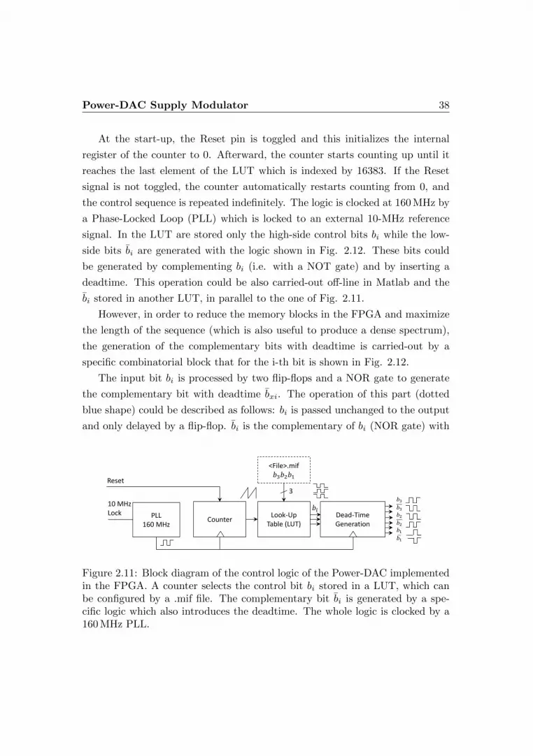
Power-DAC Supply Modulator 38
At the start-up, the Reset pin is toggled and this initializes the internal
register of the counter to 0. Afterward, the counter starts counting up until it
reaches the last element of the LUT which is indexed by 16383. If the Reset
signal is not toggled, the counter automatically restarts counting from 0, and
the control sequence is repeated indefinitely. The logic is clocked at 160 MHz by
a Phase-Locked Loop (PLL) which is locked to an external 10-MHz reference
signal. In the LUT are stored only the high-side control bits bi while the low-
side bits bi are generated with the logic shown in Fig. 2.12. These bits could
be generated by complementing bi (i.e. with a NOT gate) and by inserting a
deadtime. This operation could be also carried-out off-line in Matlab and the
bi stored in another LUT, in parallel to the one of Fig. 2.11.
However, in order to reduce the memory blocks in the FPGA and maximize
the length of the sequence (which is also useful to produce a dense spectrum),
the generation of the complementary bits with deadtime is carried-out by a
specific combinatorial block that for the i-th bit is shown in Fig. 2.12.
The input bit bi is processed by two flip-flops and a NOR gate to generate
the complementary bit with deadtime bxi. The operation of this part (dotted
blue shape) could be described as follows: bi is passed unchanged to the output
and only delayed by a flip-flop. bi is the complementary of bi (NOR gate) with
10 MHzLock
Reset
PLL160 MHz
Dead-TimeGeneration
Counter
𝑏3𝑏3𝑏2𝑏2𝑏1 𝑏1
3
Look-UpTable (LUT)
𝑏𝑖
<File>.mif𝑏3𝑏2𝑏1
Figure 2.11: Block diagram of the control logic of the Power-DAC implementedin the FPGA. A counter selects the control bit bi stored in a LUT, which canbe configured by a .mif file. The complementary bit bi is generated by a spe-cific logic which also introduces the deadtime. The whole logic is clocked by a160 MHz PLL.

Power-DAC Supply Modulator 39
Figure 2.12: Deadtime generator logic implemented in the FPGA (blue-dottedrectangle). A safety AND gate is inserted at the output to avoid spuriouscommutations due to delays in the signals propagation inside the FPGA. Aregister synchronize the control bit bi and its complementary with deadtime bito the FPGA clock.
a “chopped 1” at the commutation (0 to 1 or 1 to 0). Since the “chopped
1” duration is 1/160 MHz a time sample in which both bi and bxi are low is
inserted. During this deadtime interval, both the switches in the half-bridge are
turned-off.
However, delays due to the analog propagation of the signals in the logic
gates inside the FPGA could cause overlaps in the complementary control bits
and produce shoot-through in the corresponding half-bridge. Therefore, an
AND gate at the output stage of the network forces bi = 0 only in the case
of the spurious transition bi = bi = 1. Otherwise, the bits are propagated
unchanged. Finally, at the end of the network, two flip-flops synchronize the
outputs with the pipeline clock. Since this network could be synthesized on the
Cyclone II FPGA at a maximum clock frequency of 160 MHz, the minimum
deadtime achievable with this hardware is 6.25 ns.
The generated control signals for a 1 MHz full-scale sinusoid at the output of
the FPGA development board are shown in Fig. 2.13. In the left-hand graph the
deadtime instants (bi = bi = 0) are clearly visible, whereas in the right plot the
commutation of the signal with a measured deadtime of 6.25 ns is appreciable.
During the deadtime, the direction of the output current forces the turn-on of

Power-DAC Supply Modulator 40
Figure 2.13: Left: control bits for a 1 MHz sinusoid generated by the FPGA;high-side control signal bi in blue, low-side control signal with deadtime bi inred. Right: enlarged picture of the transition showing the deadtime of 6.25 ns.
the body diode of the low-side switch. This diode introduces a small voltage
drop (VD = 1.4 V) in the output waveform and a non-negligible dissipation that
could be minimized by reducing the deadtime duration (until possible). As soon
as the bi turns-on, the low-dissipation current path is restored by the low-side
GaN switch.
2.8 Multi-Output Supply Board
Low-power (signal) DACs typically generate the intermediate voltage levels
starting from a reference voltage VREF and by means of resistor-based net-
works, often with binary-weighted values for a reduced component count [63].
This is not obviously suitable for efficiency and the VREF /2i voltage levels are
provided separately to the Power-DAC by means of an external multi-output
switching converter.
In this section, details on the realization of a multi-output supply board for
the generation of the voltages of the Power-DAC supply modulator are pro-
vided. The 3-bit Power-DAC requires the generation of three isolated voltage
levels VDC1, VDC2, and VDC3 for the synthesis of an eight levels staircase at
the output. If the application requires a constant minimum level voltage (dif-
ferent from 0 V), a fixed voltage offset VOS could be also generated by the board.
Power-DAC Supply Modulator 41
Standard bench-top supply systems typically provides galvanic isolation be-
tween the different outputs but this isolation is typically guaranteed at DC and
not under a fast commutating regime as in the Power-DAC half-bridges. Ini-
tially, lead-acid batteries were employed for the testing of the Power-DAC with a
resistive load. However, for a precise modulation of the PA, the generated volt-
age levels have to be stable and regulated. Therefore, a custom multi-output
supply board that provides isolation under dynamic condition is designed and
built. This power supply is designed to provide flexibility of testing with dif-
ferent operating scenarios and the efficiency of this multi-output power supply
is not a primary objective of this thesis. Once the voltage levels are selected
by considering the characterization of a PA, a more efficient, yet less flexible
supply could be designed.
Four identical modules generates the isolated supply voltages for the Power-
DAC, and the schematic is shown in 2.14. The main power supply could be
chosen between 36 V to 72 V. Bypass capacitors of 1µF and 47µF are used to
minimize the impedance of the source. The galvanic isolation is provided by off-
the-shelves DC/DC brick converter (Murata PAQ-29/5-D48NB-C). This module
also provides a first step-down conversion from the main supply voltage to an
intermediate isolated voltage of 22 V to 28 V, which is also available between
the outputs of the supply. The transformer of this DC/DC converter features a
low input-output capacitance (1.5 nF) which is useful to minimize stray currents
under fast commutations of the bridges. The stray current between the primary
and the secondary of the transformer can be estimated with a differential voltage
sensing on the 1.5 nF capacitance. However, this measurement is not possible
due to the lack of a differential voltage probe. This brick converter could be
regulated with a trimmer in the front panel or disabled with a switch (see right
picture of Fig. 2.15). The output is filtered with an L-C in order to provide a
low-ripple voltage as suggested by the DC/DC converter manufacturer.
Two other non-isolated buck converters provides the remaining voltage range
(2.5 V to 22 V). The first brick converter (TI PTN78020W) covers the range

Power-DAC Supply Modulator 42
5 5
4 4
3 3
2 2
1 1
DD
CC
BB
AA
36-72V
2.5-12.6Vdc
5A max
PTN78020W
23.8-29.8V
5A Max
(attenzione alla tensione in ingresso)
11.85-22Vdc
5A max
PTN78020H
(attenzione alla tensione in ingresso)
ISOLATED POWER SUPPLY (x4)
SWITCH PANEL (PAQ)
SWITCH/TRIMMER PANEL (BUCK) (x4)
FAN
Trim
PA
Q
Sw
PA
Q1
Trim
Bu
ckW
Trim
Bu
ckH
Sw
Bu
ckW
Sw
Bu
ckH
SwPAQ1
SwPAQ2
SwPAQ3
SwPAQ4
TrimPAQ
TrimBuckW
TrimBuckH
SwBuckW
SwBuckH
0
0
0
T6
1k
C14
2.2
u
C3
1u
S2
12
12
C2
1u
C4
33
0u
J7 CO
N1
1
MM
1F
AN
1V+
2V-
C10
10u
T4
1k
U4
V7
81
2W-5
00R
1V
in+
GND2
3V
ou
t+
T1
100
k
L1
12
U2 PT
N78
02
0
GN
D1
ON
/OF
F*
3
VIN
2
GN
D7
TR
IM4
VS
EN
SE
5
VO
6T
31
00k
C5
2.2
u
J3 CO
N1
1
S3
12
J6 CO
N1
1
C7
2.2
u
C1
47
u
T5
1k
T2
10
0k
C15
33
0u
S1
12
12
J1 CO
N1
1
J5 CO
N1
1
J1 CO
N1
1
C8
33
0uC
62
.2u
U1
PA
Q-2
9/5
-D48
NB
-C
+V
in1
On
/Off*
2
GN
D (
Opt
.)3
Vin
-4
-Vo
ut5
-Se
nse
6
Trim
7
+S
en
se8
+V
ou
t9
J2 CO
N1
1
U3 PT
N78
02
0
GN
D1
ON
/OF
F*
3
VIN
2
GN
D7
TR
IM4
VS
EN
SE
5
VO
6
C11
10
u
J4 CO
N1
1
J1 CO
N1
1
C16
20u
J2 CO
N1
1
Figure 2.14: Schematic of a single module of the Power-DAC multi-output sup-ply. This module is replicated 4 times (the fan circuit only one time).

Power-DAC Supply Modulator 43
1 2 3 1 2 3
1 2 3 1 2 3
GND GND
GND GND
36-72V
FAN
PAQ
PTN-H PTN-H
PAQ
PTN-W PTN-W
Figure 2.15: Left picture: two modules connected to the front panel and to themain supply (36 V-72 V). Right: front panel of the supply box. Four isolatedground (black plug) and three voltage outputs (red plug). Label GND: isolatedground, 1: 2.5 V-12.6 V, 2: 11.85 V-22 V, 3: 23.8 V-29.8 V. Enable, disable andvoltage regulation of the isolated output voltages are possible with the trimmerand switch below the red plug.
between 2.5 V and 12.6 V while the second the range between 11.85 V to 22 V
(TI PTN78020H). Both the converters could be enabled with a switch and the
output voltage regulated with a trimmer in the front panel (see right picture of
Fig. 2.15). The four modules are distributed in a two-by-two stack and enclosed
in a plastic box. A step-down converter (CUI Inc. V7812W-500R) provides 12 V
for the cooling fan of the box. Vent holes are drilled on the side of the box.
The need for a transformer for the isolation of the half-bridge supplies should
not be considered as a disadvantage of this approach since in the power supply
system of a base station, isolated DC/DC converters from the non-isolated input
voltage (e.g. 48 V) are yet necessary even for fixed bias supplies [70].
2.9 Measurement Results with Resistive Load
The Power-DAC converter is tested with a resistive load using different input
signals such as sinusoids, voltage steps and telecommunication signals. For
these tests, the three half-bridge supplies are set to VDC3 = 6 V, VDC2 = 12 V

Power-DAC Supply Modulator 44
and VDC1 = 24 V respectively, whereas the fixed offset voltage is not applied
(VOS = 0 V). The Power-DAC control signal are synthesized by the FPGA
board, with the LUT mapped with the selected test sequence.
All the different current consumptions and voltage levels are carefully mon-
itored with a current and a voltage probe for the calculation of the converter
efficiency. The output waveforms are acquired using a 2.5 GHz bandwidth, 12-
bit oscilloscope [71] with 500-MHz bandwidth high-impedance voltage probes.
2.9.1 Sinusoidal Test
At first, the performance of the converter with sinusoidal input signals at dif-
ferent frequencies are evaluated. For such signals, the converter load is a low-
parasitics output resistance RL = 30 Ω. The converter responses to the full-scale
sinusoids are shown in Fig. 2.16.
Figure 2.16: Measured converter output to a full-scale sinusoidal set-point atdifferent frequencies. The waveform before (dashed red) and after the filter (con-tinuous blue) are superimposed for comparison. Normalized full-power band-width in dB of the converter (bottom right).

Power-DAC Supply Modulator 45
All the reported output waveforms are measured before and after the LC
low-pass output filter. The filter effectively suppresses the voltage spikes in
correspondence of the level commutations. As discussed in section 2.4, all the
8 levels are still clearly present up to a sinusoidal frequency of 2 MHz, whereas
from 4 MHz upwards some commutations are lost due to the combination of
the driver limitation (10 ns minimum pulse width) and the FPGA sampling
frequency limit (2.10).
In Fig. 2.16, the measured Spurious Free Dynamic Range (SFDR) of the
filtered waveform is also reported, which shows a noticeable deterioration at
4 MHz, when some levels begin to be lost, whereas it starts to improve at
16 MHz, where the harmonics begin to be attenuated by the output filter (ft =
40 MHz).
For the different sinusoidal frequencies, power and efficiency results are re-
ported in the following Table 2.1. The table shows the RMS power of the
output waveform (PRMS), its peak power (PPK), the RMS current (IRMS)
and the peak current (IPK), the total DC power consumption (PDC), the DC
power consumptions of the three DC links separately (PDC1, PDC2, PDC3), the
DC power consumption of the drivers (PDC,DRIV ER linear regulators included),
the efficiency of the half-bridge cells (ηHB) and of the entire converter (ηTOT ).
As far as the DC power consumption of the three input DC links and of the
drivers is concerned, also their percentage with respect to the overall power con-
𝐒𝐢𝐠𝐧𝐚𝐥𝑷𝑹𝑴𝑺
(𝐖)𝑷𝑷𝑲
(𝐖)𝑰𝑷𝑲(𝐀)
𝑰𝑹𝑴𝑺
(𝐀)𝑷𝑫𝑪𝟏
(𝐖)(%)𝑷𝑫𝑪𝟐
(𝐖)(%)𝑷𝑫𝑪𝟑
(𝐖)(%)𝑷𝑫𝑪
(𝐖)𝑷𝑫𝑪, 𝑫𝑹𝑰𝑽𝑬𝑹
(𝐖)(%)𝜼𝑯𝑩(%)
𝜼𝑻𝑶𝑻(%)
𝜼𝑯𝑩, 𝑺𝑰𝑴(%)
𝑨(𝐝𝐁)
500 kHz 24.48 62.8 1.45 0.903 15.34 / 59.8 6.83 / 26.6 3.01 / 11.7 25.63 0.45 / 1.8 97.3 95.5 96.3 0
1 MHZ 24.3 62.8 1.45 0.900 15.38 / 58.8 6.91 / 26.4 3.13 /12.0 26.14 0.71 / 2.7 95.5 92.9 94.3 0
2 MHZ 24.3 62.8 1.45 0.900 15.59 / 56.5 7.35 / 26.6 3.78 / 13.7 27.61 0.87 / 3.1 90.9 88.0 89.7 0
4 MHZ 27.26 62.8 1.45 0.953 16.28 / 53.3 9.03 / 29.5 4.70 / 15.4 30.57 0.54 / 1.8 90.8 89.2 91.2 0
8 MHZ 30.94 62.8 1.45 1.016 18.16 / 53.6 10.10 / 29.8 4.93 / 14.6 33.9 0.70 / 2.1 93.2 91.3 92.5 0.1
16 MHZ 29.78 66.2 1.48 0.996 18.67 / 53.7 10.41 / 29.9 4.89 / 14.1 38.78 0.82 / 2.4 87.7 85.6 88.5 0.7
20 MHZ 28.01 66.1 1.48 0.966 18.21 / 53.5 10.46 / 30.8 4.55 / 13.4 34.00 0.78 / 2.3 84.3 82.8 83.2 2
Table 2.1: Converter performance with full-scale sinusoidal inputs at differentfrequencies.

Power-DAC Supply Modulator 46
sumption is computed in Table 2.1. The measured efficiency of the converter
remains relatively high also at high frequencies and also very close to simulations
(ηHB,SIM ).
Considering the normalized attenuation (A) of the first harmonic of the
output waveform, the full-power bandwidth of the converter can be computed
[72]. The circuit reaches a −2 dB full-power bandwidth of 20 MHz, which is
obtained with 83% efficiency. It is very important to point-out that this is
a large-signal bandwidth, that is not met by any other solution in literature
[3, 7, 8, 12, 15], where the specified bandwidths are at small-signal (action of
linear part of the circuit) and suitable only for envelope signals with very small
power content at high frequencies.
As observed, the full-scale sinusoidal input drive described in Fig. 2.16
and Table 2.1 represents the most demanding operation of the converter in
terms of bandwidth, since the number of commutations of each power device is
maximized 2.10. Indeed, for a sinusoidal signal the entire energy of the signal is
concentrated at its frequency. This is clearly a worst case, since all the practical
signals for ET applications exhibit a distribution of the signal power along the
bandwidth that clearly decreases for increasing frequencies [5,13,53]. Thus, the
full wave sinusoidal test proposed in Fig. 2.16 is not usually considered in most
papers, since it is unnecessarily demanding for the converter and it would lead
to extremely poor results in terms of efficiency (or bandwidth) if applied to
more conventional architectures (e.g. linear assisted SMPS, multiphase PWM
SMPS).
2.9.2 Step Response
The converter is tested with a set-point control signal characterized by a rect-
angular pulse in which all the half-bridges are activated simultaneously (bi =
1, i = 1, 2, 3) during the pulse duration. In this way, it is possible to evaluate
the converter step response and its slew-rate. A 250 ns pulse is inserted in a
long period of 102.4µs in which the converter output is 0 V in order to reduce

Power-DAC Supply Modulator 47
Figure 2.17: Measurement of the converter slew-rate with a 42 V input step: inthe enlarged plot on the right a slew rate of 4.23 kV/µs is appreciable.
the dissipation on the switches and on the load.
The measured step response is shown in Fig. 2.17. On the left plot, the
waveform before (blue) and after the filter (red) is shown for comparison. It is
worth noticing that the peak voltage is increased by the parasitics of the voltage
probe and it is not representative of the actual ringing present on the output
of the converter. On the right plot, it is showed the commutation in which
it is possible to appreciate the slew-rate difference before (20 kV/µs) and after
filtering (4.23 kV/µs).
2.9.3 Telecommunications Signals
The converter is tested with three different telecommunication signals (W-
CDMA, LTE and Wi-Fi 802.11g), characterized by high PAPR (respectively
3.2 dB, 12 dB and 11 dB) and different bandwidths (respectively 4 MHz, 10 MHz
and 20 MHz). The converter control bits are generated by means of the con-
tinuous envelope of such signals, and quantized to produce an 8-level control
set-point signal. Since the load is a resistor (without any nonlinear compression
behavior), the quantization law is arbitrarily selected with evenly-spaced thresh-
olds. For these tests, the same half-bridge supplies of section 2.9 are employed
and a lower value resistor RL = 12 Ω is used to compensate for the reduced
average power (compared to sinusoids).
The spectra and the time-domain waveforms of the considered signals are

Power-DAC Supply Modulator 48
Vout (V
), P
EN
V(d
Bm
)
Time (μs)
3GPP
WCDMA
Vout (V
), P
EN
V(d
Bm
)
Time (μs)
LTE
Vout (V
), P
EN
V(d
Bm
)
Time (μs)
WiFi
Figure 2.18: Spectra (left) and time-domain waveforms (right) of the telecom-munication signals. Top raw: 4-MHz 3.2-dB PAPR 3GPP-WCDMA. Centralraw: 10-MHz 12-dB PAPR LTE. Bottom raw: 20-MHz 11-dB PAPR WiFi.
shown in Fig. 2.18. From the left plots, it is possible to notice the very broad-
band spectral re-growth in the bias signal spectrum with respect to the original
baseband signal spectrum, due to the nonlinearity of the envelope operator. In
the right-hand plots, it can be observed that the converter accurately tracks
the input set-point (NRMSE < 5%) for all the three different test signals. This
happens also when voltage profiles as sharp as 1 kV/µs are required by the
set-point signal. The only exception is visible between 0.5µs and 0.6µs for the
WiFi signal, where a very narrow (6 ns) voltage peak of the set-point signal is not
perfectly tracked by the converter, due to the minimum pulse width limitation
of the drivers previously discussed (in this particular case, VOUT is slightly in
excess with respect to the optimum set-point waveforms).
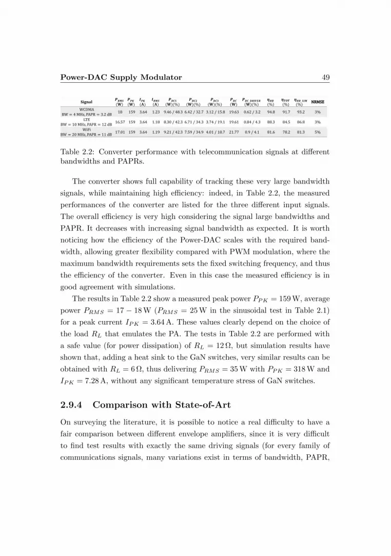
Power-DAC Supply Modulator 49
𝐒𝐢𝐠𝐧𝐚𝐥𝑷𝑹𝑴𝑺
(𝐖)𝑷𝑷𝑲
(𝐖)𝑰𝑷𝑲(𝐀)
𝑰𝑹𝑴𝑺
(𝐀)𝑷𝑫𝑪𝟏
(𝐖)(%)𝑷𝑫𝑪𝟐
(𝐖)(%)𝑷𝑫𝑪𝟑
(𝐖)(%)𝑷𝑫𝑪
(𝐖)𝑷𝑫𝑪, 𝑫𝑹𝑰𝑽𝑬𝑹
(𝐖)(%)𝜼𝑯𝑩(%)
𝜼𝑻𝑶𝑻(%)
𝜼𝑯𝑩, 𝑺𝑰𝑴(%)
NRMSE
WCDMABW = 4MHz, PAPR = 3.2 dB
18 159 3.64 1.23 9.46 / 48.3 6.42 / 32.7 3.12 / 15.8 19.63 0.62 / 3.2 94.8 91.7 93.2 3%
LTEBW = 10 MHz, PAPR = 12 dB
16.57 159 3.64 1.18 8.30 / 42.3 6.71 / 34.3 3.74 / 19.1 19.61 0.84 / 4.3 88.3 84.5 86.8 3%
WiFiBW = 20 MHz, PAPR = 11 dB
17.01 159 3.64 1.19 9.21 / 42.3 7.59 / 34.9 4.01 / 18.7 21.77 0.9 / 4.1 81.6 78.2 81.3 5%
Table 2.2: Converter performance with telecommunication signals at differentbandwidths and PAPRs.
The converter shows full capability of tracking these very large bandwidth
signals, while maintaining high efficiency: indeed, in Table 2.2, the measured
performances of the converter are listed for the three different input signals.
The overall efficiency is very high considering the signal large bandwidths and
PAPR. It decreases with increasing signal bandwidth as expected. It is worth
noticing how the efficiency of the Power-DAC scales with the required band-
width, allowing greater flexibility compared with PWM modulation, where the
maximum bandwidth requirements sets the fixed switching frequency, and thus
the efficiency of the converter. Even in this case the measured efficiency is in
good agreement with simulations.
The results in Table 2.2 show a measured peak power PPK = 159 W, average
power PRMS = 17 − 18 W (PRMS = 25 W in the sinusoidal test in Table 2.1)
for a peak current IPK = 3.64 A. These values clearly depend on the choice of
the load RL that emulates the PA. The tests in Table 2.2 are performed with
a safe value (for power dissipation) of RL = 12 Ω, but simulation results have
shown that, adding a heat sink to the GaN switches, very similar results can be
obtained with RL = 6 Ω, thus delivering PRMS = 35 W with PPK = 318 W and
IPK = 7.28 A, without any significant temperature stress of GaN switches.
2.9.4 Comparison with State-of-Art
On surveying the literature, it is possible to notice a real difficulty to have a
fair comparison between different envelope amplifiers, since it is very difficult
to find test results with exactly the same driving signals (for every family of
communications signals, many variations exist in terms of bandwidth, PAPR,

Power-DAC Supply Modulator 50
modulation format, complementary cumulative distribution function, etc...).
One parameter which is useful for a more general converter comparison is
its slew rate (combined with the maximum dynamic range). In Fig. 2.17 the
measured response of the converter to a 42 V step set-point (full dynamic range)
is shown: the output waveforms measured before and after the output filter
show that the slew rate is limited by the output low pass filter, and not by the
extremely high switching speed of the three power cells (very fast GaN devices
with optimal synchronization). The measured slew-rate of 4.23 kV/µs (at large
signal, i.e. 10% to 90% of the full dynamic range) is extremely high if compared
with many other published results as in [15, 17, 18, 49] and largely compliant
with the requirements for typical wideband communication signals [43].
Finally, even though a fair and precise comparison between different products
is practically impossible, due to the already mentioned issues with test signals
definitions and to the quite arbitrary definitions of bandwidth and dynamics
used by different authors and vendors, the performances of several published
converter circuits for ET applications are listed in Table 2.3. Given these con-
siderations, the proposed circuit can certainly be considered at the state of the
art for these applications. Moreover, the use of tiny wafer-level package GaN
devices with very high power density makes the proposed converter extremely
convenient in terms of mass and dimensions with respect to any other published
circuit.
2.10 Conclusion
A new 3-bit power converter circuit based on a direct digital-to-analog power
conversion architecture is designed and implemented exploiting very fast switch-
ing devices in a commercial GaN-on-Si technology. The circuit can be used as a
supply modulator for envelope tracking architectures in telecommunication base
station transmitters. The proposed design implements a binary-coded asym-
metric multilevel structure, which synthesizes eight output voltage levels from
three isolated input voltage supplies. The use of this structure is a novelty for

Power-DAC Supply Modulator 51
𝐑𝐞𝐟 𝐓𝐲𝐩𝐞 𝐒𝐰𝐢𝐭𝐜𝐡 𝐓𝐞𝐜𝐡𝐧𝐨𝐥𝐨𝐠𝐲 𝐓𝐞𝐬𝐭 𝐒𝐢𝐠𝐧𝐚𝐥 / 𝐁𝐚𝐧𝐝𝐰𝐢𝐝𝐭𝐡 𝑷𝑶𝑼𝑻,𝑨𝑽𝑮 / 𝑷𝑶𝑼𝑻,𝑴𝑨𝑿 𝐒𝐥𝐞𝐰 𝐑𝐚𝐭𝐞 𝜼
this work ML 40-V GaN
Full-scale 2 MHz
Full-scale 20 MHz
WCDMA / 4 MHZ
LTE / 10 MHz
WiFi /20 MHz
24.3 W / 62.8 W
28 W / 66.1 W
18 W / 159 W
16.57 W / 159 W
17.01 W / 159 W
4.23 kV/μs
88%
82.8%
91.7%
84.5%
78.2%
[12] SMLA Si FET WCDMA / 4 MHZ 34 W / n.a. n.a. 83.2%
[7] SMLA n.a WiMAX / 10 MHz n.a. / n.a n.a. n.a.
[8] SMLA n.a. WiMAX / 10 MHz 20.1 W / n.a. n.a. 69.0%
[15] SMLA 30-V Si FET WCDMA / n.a. n.a. / n.a 100 V/μs 60.0%
[9] SMLA n.a. WCDMA / 4 MHz 66 W / n.a. n.a. 64%
[10] SMLA 100-V Si FET WiMAX / 10 MHz 46 W / n.a. n.a. 70.1%
[11] SMLA n.a. LTE / 10 MHz 25 W / n.a. n.a. 76.0%
[13] SMLA 20-V Si FET LTE / 60 MHz 7 W / n.a. n.a. 72.3%
[14] ML 100-V Si FET Sine wave / 300 kHz 10 W / n.a. n.a. 88.0%
[4] SMLA Si FET WLAN / 16.25 MHz 176 mW / 1 W n.a. 55%
[16] ML Si FET Sine wave / 1 MHz 22 W / 50 W n.a. 75.5%
[17] ML Si FET Sine wave / 2 MHz 17 W / n.a. 800 V/μs 63.2%
[18] SMML 65-V Si FET Half Sine wave / 10 KHz 20 W / 51 W 6 V /μs 92%
[49] SMMP 60-V Si FET WCDMA / 4 MHz 2.7 W / 13 W 560 V/μs n.a.
Table 2.3: Comparison with published converters for ET and EER applications.SMLA: Switched Mode Linear Assisted. SMMP: PWM Switching Mode MultiPhase. ML: Multi Level. SMML: PWM Switching Mode ML.
applications requiring such high operation frequency.
The proposed converter actually realizes the function of a real power-DAC,
since it is controlled by digital signals coming directly from a DSP/FPGA unit,
without the need for digital-to-analog conversion and PWM modulation. This
circuit can be used for many other applications (possibly in conjunction with
an additional linear amplifier, for additional, less significant bits) in any field
where the efficient generation (digital synthesis) of an arbitrary power waveform
in the MHz range is needed.
The converter exhibits 42-V dynamic range with a considerable 4.23 kV/µs
slew rate. The measured full-power bandwidth at 28-W average output power
is 20 MHz obtained with 82.8% power efficiency. The circuit is tested using
input set-points suitable for the RF PA operation with three different wideband
communication signals: 4-MHz 3GPP WCDMA, 10-MHz LTE, 20-MHz WiFi.
In those conditions the circuit shows to accurately follow the input set-points,

Power-DAC Supply Modulator 52
while operating with efficiencies of 91.7%, 84.5% and 78.2% respectively and
delivering 158 W of peak power (about 17 W average output power).
Simulations have shown that at least double power levels can be delivered
by the circuit by using heatsinks on the GaN switches. Measured performances
show that the proposed converter is at the state of the art for the proposed
application, with a very relevant advantage in terms of space savings, due to
the use of wafer-level package GaN devices. Moreover, the measured 20 MHz
bandwidth at full-scale operation makes the circuit suitable for the amplification
of signals with uniform distribution of the power spectrum along the band and,
consequently more demanding in terms of dynamics and bandwidth compared
with presently used communication signals.

Chapter 3
Supply Modulation of RF
PAs for Telecommunications
In this chapter1, details on an Envelope Tracking (ET) transmitter for com-
munication signals at L-band exploiting the Power-DAC supply modulator pre-
sented in chapter 2 are provided. The Power-DAC supply modulator is based on
a direct digital-to-analog conversion architecture that implements the binary-
coded sum of N isolated DC voltages, allowing the synthesis of an output
waveform with L = 2N voltage levels, with a binary distribution in the range
∆V = VMAX − VOS (maximum voltage VMAX , offset voltage VOS). This so-
lution provides a better voltage resolution (VS = ∆V/(2N − 1)) with respect
to typical multilevel switched-sources topologies (VS = ∆V/N). The improved
voltage resolution enables the correction of the residual discretization error in
the ET transmitter by means of DPD of the RF signal, without the need of an
auxiliary linear envelope amplifier.
1C. Florian, T. Cappello, R. P. Paganelli, D. Niessen, F. Filicori, “Envelope Tracking of anRF High Power Amplifier With an 8-Level Digitally Controlled GaN-on-Si Supply Modulator,”IEEE Transaction on Microwave Theory and Techniques, vol. 63, no. 8, pp. 2589–2602, Aug.2015.
53
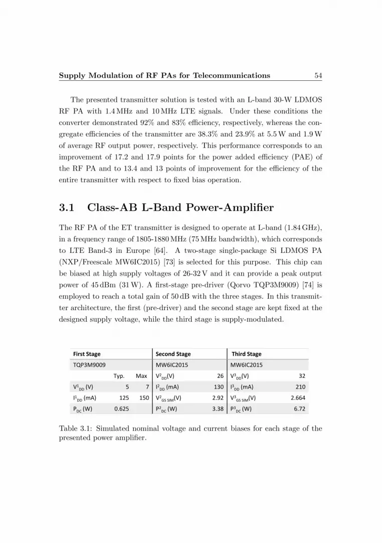
Supply Modulation of RF PAs for Telecommunications 54
The presented transmitter solution is tested with an L-band 30-W LDMOS
RF PA with 1.4 MHz and 10 MHz LTE signals. Under these conditions the
converter demonstrated 92% and 83% efficiency, respectively, whereas the con-
gregate efficiencies of the transmitter are 38.3% and 23.9% at 5.5 W and 1.9 W
of average RF output power, respectively. This performance corresponds to an
improvement of 17.2 and 17.9 points for the power added efficiency (PAE) of
the RF PA and to 13.4 and 13 points of improvement for the efficiency of the
entire transmitter with respect to fixed bias operation.
3.1 Class-AB L-Band Power-Amplifier
The RF PA of the ET transmitter is designed to operate at L-band (1.84 GHz),
in a frequency range of 1805-1880 MHz (75 MHz bandwidth), which corresponds
to LTE Band-3 in Europe [64]. A two-stage single-package Si LDMOS PA
(NXP/Freescale MW6IC2015) [73] is selected for this purpose. This chip can
be biased at high supply voltages of 26-32 V and it can provide a peak output
power of 45 dBm (31 W). A first-stage pre-driver (Qorvo TQP3M9009) [74] is
employed to reach a total gain of 50 dB with the three stages. In this transmit-
ter architecture, the first (pre-driver) and the second stage are kept fixed at the
designed supply voltage, while the third stage is supply-modulated.
First Stage Second Stage Third Stage
TQP3M9009 MW6IC2015 MW6IC2015
Typ. Max V2DD(V) 26 V3
DD(V) 32
V1DD (V) 5 7 I2
DD (mA) 130 I3DD (mA) 210
I1DD (mA) 125 150 V2
GS SIM(V) 2.92 V3GS SIM(V) 2.664
PDC (W) 0.625 P2DC (W) 3.38 P3
DC (W) 6.72
Table 3.1: Simulated nominal voltage and current biases for each stage of thepresented power amplifier.
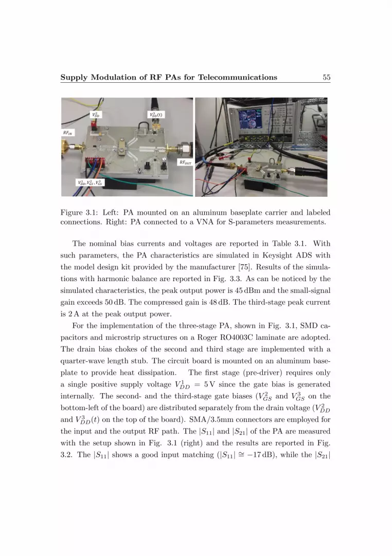
Supply Modulation of RF PAs for Telecommunications 55
𝑉𝐷𝐷3 (t)𝑉𝐷𝐷
2
𝑅𝐹𝐼𝑁
𝑅𝐹𝑂𝑈𝑇
𝑉𝐷𝐷1 , 𝑉𝐺𝑆
2 , 𝑉𝐺𝑆3
Figure 3.1: Left: PA mounted on an aluminum baseplate carrier and labeledconnections. Right: PA connected to a VNA for S-parameters measurements.
The nominal bias currents and voltages are reported in Table 3.1. With
such parameters, the PA characteristics are simulated in Keysight ADS with
the model design kit provided by the manufacturer [75]. Results of the simula-
tions with harmonic balance are reported in Fig. 3.3. As can be noticed by the
simulated characteristics, the peak output power is 45 dBm and the small-signal
gain exceeds 50 dB. The compressed gain is 48 dB. The third-stage peak current
is 2 A at the peak output power.
For the implementation of the three-stage PA, shown in Fig. 3.1, SMD ca-
pacitors and microstrip structures on a Roger RO4003C laminate are adopted.
The drain bias chokes of the second and third stage are implemented with a
quarter-wave length stub. The circuit board is mounted on an aluminum base-
plate to provide heat dissipation. The first stage (pre-driver) requires only
a single positive supply voltage V 1DD = 5 V since the gate bias is generated
internally. The second- and the third-stage gate biases (V 2GS and V 3
GS on the
bottom-left of the board) are distributed separately from the drain voltage (V 2DD
and V 3DD(t) on the top of the board). SMA/3.5mm connectors are employed for
the input and the output RF path. The |S11| and |S21| of the PA are measured
with the setup shown in Fig. 3.1 (right) and the results are reported in Fig.
3.2. The |S11| shows a good input matching (|S11| ∼= −17 dB), while the |S21|
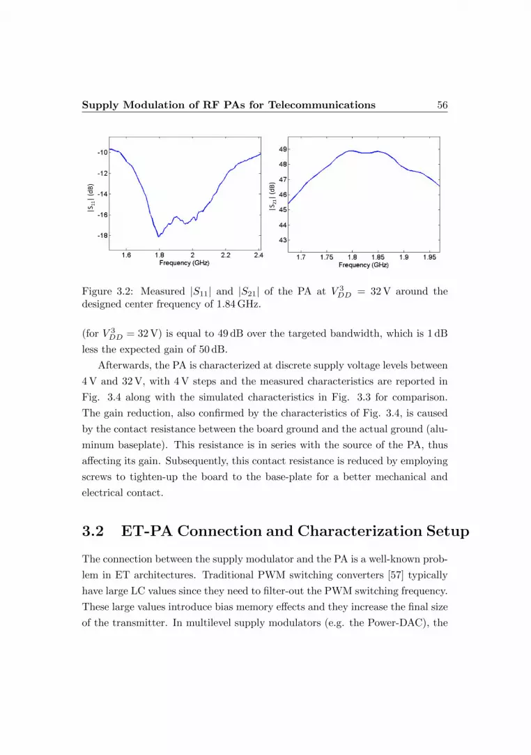
Supply Modulation of RF PAs for Telecommunications 56
|S1
1|
(dB
)
|S2
1|
(dB
)
Figure 3.2: Measured |S11| and |S21| of the PA at V 3DD = 32 V around the
designed center frequency of 1.84 GHz.
(for V 3DD = 32 V) is equal to 49 dB over the targeted bandwidth, which is 1 dB
less the expected gain of 50 dB.
Afterwards, the PA is characterized at discrete supply voltage levels between
4 V and 32 V, with 4 V steps and the measured characteristics are reported in
Fig. 3.4 along with the simulated characteristics in Fig. 3.3 for comparison.
The gain reduction, also confirmed by the characteristics of Fig. 3.4, is caused
by the contact resistance between the board ground and the actual ground (alu-
minum baseplate). This resistance is in series with the source of the PA, thus
affecting its gain. Subsequently, this contact resistance is reduced by employing
screws to tighten-up the board to the base-plate for a better mechanical and
electrical contact.
3.2 ET-PA Connection and Characterization Setup
The connection between the supply modulator and the PA is a well-known prob-
lem in ET architectures. Traditional PWM switching converters [57] typically
have large LC values since they need to filter-out the PWM switching frequency.
These large values introduce bias memory effects and they increase the final size
of the transmitter. In multilevel supply modulators (e.g. the Power-DAC), the
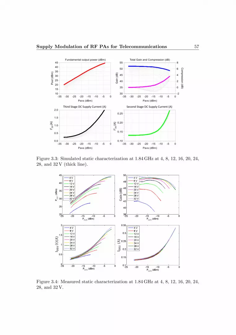
Supply Modulation of RF PAs for Telecommunications 57I3
DD
(A)
I2D
D (A
)
Third Stage DC Supply Current (A) Second Stage DC Supply Current (A)
Figure 3.3: Simulated static characterization at 1.84 GHz at 4, 8, 12, 16, 20, 24,28, and 32 V (thick line).
Gain(dB)
I DD3
t(A
)
I DD2(A
)
Figure 3.4: Measured static characterization at 1.84 GHz at 4, 8, 12, 16, 20, 24,28, and 32 V.
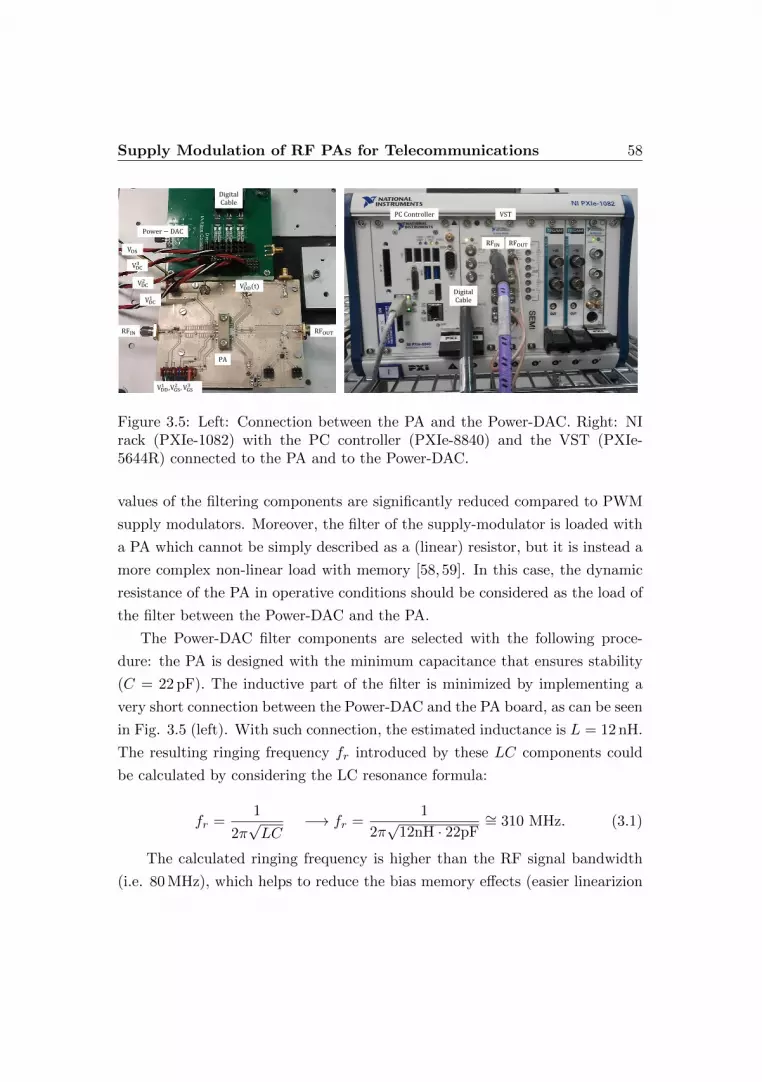
Supply Modulation of RF PAs for Telecommunications 58
RFIN RFOUT
Power − DAC
VDD3 (t)
PA
VDC1
VDC2
VDC3
VOS
VDD1 ,VGS
2 , VGS3
DigitalCable
RFIN RFOUT
DigitalCable
PC Controller VST
Figure 3.5: Left: Connection between the PA and the Power-DAC. Right: NIrack (PXIe-1082) with the PC controller (PXIe-8840) and the VST (PXIe-5644R) connected to the PA and to the Power-DAC.
values of the filtering components are significantly reduced compared to PWM
supply modulators. Moreover, the filter of the supply-modulator is loaded with
a PA which cannot be simply described as a (linear) resistor, but it is instead a
more complex non-linear load with memory [58, 59]. In this case, the dynamic
resistance of the PA in operative conditions should be considered as the load of
the filter between the Power-DAC and the PA.
The Power-DAC filter components are selected with the following proce-
dure: the PA is designed with the minimum capacitance that ensures stability
(C = 22 pF). The inductive part of the filter is minimized by implementing a
very short connection between the Power-DAC and the PA board, as can be seen
in Fig. 3.5 (left). With such connection, the estimated inductance is L = 12 nH.
The resulting ringing frequency fr introduced by these LC components could
be calculated by considering the LC resonance formula:
fr =1
2π√LC
−−→ fr =1
2π√
12nH · 22pF∼= 310 MHz. (3.1)
The calculated ringing frequency is higher than the RF signal bandwidth
(i.e. 80 MHz), which helps to reduce the bias memory effects (easier linearizion

Supply Modulation of RF PAs for Telecommunications 59
with DPD of the ET-PA). As shown in the following measurements, with this
solution the commutation glitches in the drain voltage waveform at the PA drain
port are reasonably suppressed, even though there is still space for further op-
timizations.
A setup for the characterization of the 1.84 GHz, 31 W peak-power PA,
supply-modulated by the Power-DAC, is developed. For its characterization,
a Vector Signal Transceiver (VST) by National Instruments (NI VST PXIe-
5644R) [76] is employed (Fig. 3.5). The VST comprises in a single instrument a
Vector Signal Generator (VSG) and a Vector Signal Analyzer (VSA), and it is
capable to generate and analyze 80 MHz of analog bandwidth, and up-convert
and down-convert to an RF carrier of 6 GHz. In addition, the VST features an
internal FPGA which can be programmed to process in real-time the baseband
I/Qs (e.g. apply the DPD) and to generate the command of the Power-DAC by
means of a digital I/O interface. The I/Q data are sampled in the digital do-
main at fS = 120 MHz. Two LabVIEW programs or VIs (Virtual Instruments)
are developed: the Host VI runs on a PC controller and it is used to configure
and control the setup, while the FPGA VI runs on the FPGA for real-time
processing.
3.2.1 Digital Baseband (FPGA VI)
In order to perform a measurement with the presented setup, the Host VI has
to be executed on the Controller PC. At the initialization of this VI, the FPGA
VI is downloaded and mapped on the FPGA. Afterwards, the Host VI loads a
pre-configured input I/Q sequence into a large-capacity DRAM memory inside
the VSG. This I/Q sequence is fetched by the FPGA and streamed in the pro-
cessing blocks (top part of Fig. 3.6). These I/Qs are processed by an envelope
extraction block (√I2 +Q2) which generates the continuous envelope signal,
which is represented by a normalized, high bit-width (i.e. 22-bit) signal.
Since the envelope extraction is a non-linear transformation which produces a
frequency expansion, the supply-modulator could not be able to track precisely

Supply Modulation of RF PAs for Telecommunications 60
this broad-band signal. Indeed, as discussed in section 2.9, the Power-DAC
could miss some level commutations due to the gate-driver limitation (10 ns
minimum pulsed width). To this aim, a slew-rate reduction algorithm [77] is
employed to slow-down the rate of variation of the envelope signal. By setting
the slew-rate limit parameter in the algorithm, the 3-bit quantized version of
this slow-envelope has a minimum pulse-width always greater than an arbitrary
limit. No upper limit could be set by the algorithm. By employing this algo-
rithm, the Power-DAC could synthesize the “slow” set-point without distortion.
The slow envelope is still a high bit-width signal which is discretized in three
V1…V8
Figure 3.6: Block diagram of the setup. In the FPGA VI it is implementedthe real-time part of the setup which includes the Power-DAC control and theDPD. In the Host VI it is implemented the signal analysis algorithm. The PAdrain current and voltage is measured by means of an external oscilloscope.

Supply Modulation of RF PAs for Telecommunications 61
bits by the supply shaping table or quantizer of the Power-DAC. The quantizer
transfer curve, qualitatively shown in Fig. 2.1, is defined by 7 thresholds and 8
output levels, which can be coded with 3-bits (i.e. 000...111). The thresholds,
normalized to 1, are chosen based on the characterization of the PA which is dis-
cussed in section 3.2.4. The output of the quantizer is an 8-level staircase used
to control the Power-DAC. A time-delay, implemented with a shift-register, is
employed to align the Power-DAC commands to the RF PA input signal. The
output of this shift-register is connected to a block for the Power-DAC command
generation. This block comprises the logic for the generation of the complemen-
tary commands with deadtime bi and of the direct bits bi as shown in section
2.7.
For each of the 8 voltage levels synthesized by the Power-DAC at the PA
drain, a correction LUT table, used for the compensation of the non-linear dis-
tortion of the PA, is stored into the corresponding LUT in the FPGA. The
LUT is selected by the current level synthesized by the Power-DAC. The se-
lected LUT is indexed by the continuous envelope, with full slew-rate, which is
representative of the actual envelope RF PA input power. Finally, the selected
correction complex number is applied in real-time to the original I/Qs by means
of complex multiplier. The 16-bit width pre-distorted I/Qs are then converted
by the DAC of the VSG and upconverted to 1.84 GHz by an external (analog)
I/Q modulator.
After the attenuator at the output of the PA, the RF signal is down-converted
at baseband and I/Q converted by two 16-bit ADCs in the VSA. The VSA acqui-
sition is triggered by a digital signal which is synchronous with the RF genera-
tion of the VSG. Therefore, a fixed time-delay is present between the transmitted
I/Qs and the received I/Qs which is due to the cascade of the digital-to-analog
conversion, channel filtering and up-conversion and vice-versa. This fixed time-
delay is de-embedded by the Host VI program. The received I/Qs are stored
in an external DRAM memory in the VSA, which can be accessed by the PC
Controller, running the Host VI, using the high-capacity PXI-express.

Supply Modulation of RF PAs for Telecommunications 62
3.2.2 Setup Control (Host VI)
The Host VI program which controls the setup runs on the PC controller in
the NI rack (Fig. 3.5). Its graphical interface, shown in Fig. 3.7, allows the
configuration of the hardware parameters of the setup and of the DUT, as well
as the software settings for the subsequent measurement and result analysis. In
the Hardware Setup box of Fig. 3.7, it is possible to configure the Carrier
Figure 3.7: Graphical interface of the Host VI program in LabVIEW: setuphardware parameters could be set in the top-left box. In the bottom-left boxthe spectrum of the received signal is shown. In the top-right plot, the idealand the generated envelope by the amplifier is shown. In the bottom-right plot,distortion characteristics of the supply-modulated PA are shown.
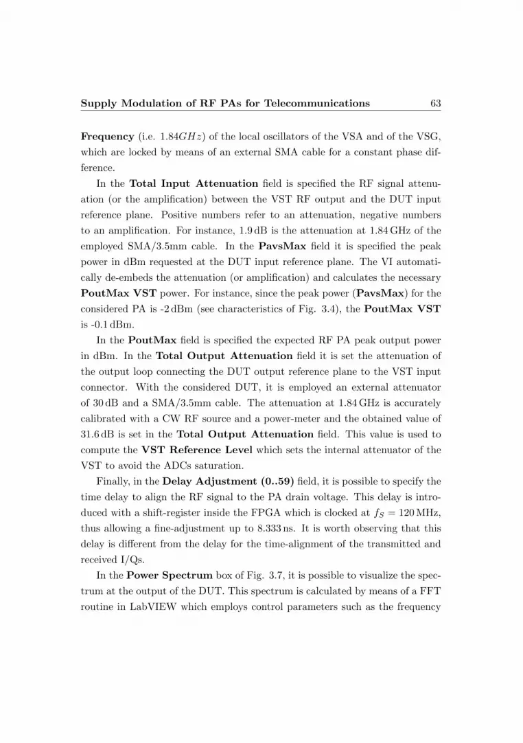
Supply Modulation of RF PAs for Telecommunications 63
Frequency (i.e. 1.84GHz) of the local oscillators of the VSA and of the VSG,
which are locked by means of an external SMA cable for a constant phase dif-
ference.
In the Total Input Attenuation field is specified the RF signal attenu-
ation (or the amplification) between the VST RF output and the DUT input
reference plane. Positive numbers refer to an attenuation, negative numbers
to an amplification. For instance, 1.9 dB is the attenuation at 1.84 GHz of the
employed SMA/3.5mm cable. In the PavsMax field it is specified the peak
power in dBm requested at the DUT input reference plane. The VI automati-
cally de-embeds the attenuation (or amplification) and calculates the necessary
PoutMax VST power. For instance, since the peak power (PavsMax) for the
considered PA is -2 dBm (see characteristics of Fig. 3.4), the PoutMax VST
is -0.1 dBm.
In the PoutMax field is specified the expected RF PA peak output power
in dBm. In the Total Output Attenuation field it is set the attenuation of
the output loop connecting the DUT output reference plane to the VST input
connector. With the considered DUT, it is employed an external attenuator
of 30 dB and a SMA/3.5mm cable. The attenuation at 1.84 GHz is accurately
calibrated with a CW RF source and a power-meter and the obtained value of
31.6 dB is set in the Total Output Attenuation field. This value is used to
compute the VST Reference Level which sets the internal attenuator of the
VST to avoid the ADCs saturation.
Finally, in the Delay Adjustment (0..59) field, it is possible to specify the
time delay to align the RF signal to the PA drain voltage. This delay is intro-
duced with a shift-register inside the FPGA which is clocked at fS = 120 MHz,
thus allowing a fine-adjustment up to 8.333 ns. It is worth observing that this
delay is different from the delay for the time-alignment of the transmitted and
received I/Qs.
In the Power Spectrum box of Fig. 3.7, it is possible to visualize the spec-
trum at the output of the DUT. This spectrum is calculated by means of a FFT
routine in LabVIEW which employs control parameters such as the frequency

Supply Modulation of RF PAs for Telecommunications 64
Span, the Resolution Bandwidth, the Weighting Window to apply to the
analyzed I/Q sequence and the Number of Averages.
On the right side of the graphical interface, in the Time-Domain Wave-
forms box, are reported the input envelope (white) and the output envelope
(red) of an high-PAPR telecommunication signal. These two envelopes are time
aligned for comparison by means of the fixed delay (its value is not visible and it
is hard-coded in LabVIEW). By comparing the two envelopes, non-linear distor-
tion at the output of the DUT is evident (no DPD is applied). This distortion
could be quantified with metrics such as the Normalized Root Mean Square
Error which is automatically calculated by the Host VI and indicated in the
NRMSE field.
In the bottom-right side of the graphical interface, in the Amplification
Characteristics box, are reported the characteristics of the DUT. In the
Power Amplifier Gain plot, the PA gain in dB vs. the PA input power
in dBm is shown. With reference to the Fig. 3.7, the gain characteristic of
the DUT presents steps and discontinuities, which are due to the continuous
adaptation of the supply voltage by the Power-DAC which is tracking the sig-
nal. The Pavs-Pout plot shows the DUT output power vs. the DUT input
power. In the remaining two plots, the AM/AM and AM/PM normalized
characteristics are also reported.
The transmitted and received I/Q data are also saved in a file (.tdms) for fur-
ther analysis outside the LabVIEW environment. The I/Q test sequence could
be generated directly with the Host VI or loaded from a file. For instance, the
Pulse tab in the graphical interface is used to generate amplitude-modulated
signal with a Gaussian-like profile and inserted in a repetition period with a
configurable duty cycle. These pulses are employed extensively in this thesis to
perform quick checks of the DUT response. Otherwise, with the Load I/Q file
tab, the I/Q sequence could be loaded with external files.
Supply Modulation of RF PAs for Telecommunications 65
3.2.3 PA Drain Voltage and Current Sensing
In the block diagram of the setup (Fig. 3.6), it is also described the PA drain
voltage and current sensing. This operation is performed by means of a 2.5 GHz
4-channel external oscilloscope [71] which can be also interfaced with the Lab-
VIEW Host VI for an automatic measurement of the input-output RF power
and also of the supplied power, necessary for the PA efficiency calculation. The
oscilloscope acquisition is triggered by a marker synchronous with the gener-
ated RF signal similarly to the triggered acquisition of the VSA. Since also the
oscilloscope is locked with the 10 MHz reference to the VST, they both share
the same time-base and the measured waveforms could be easily time-aligned.
Given the multi-MHz of bandwidth necessary to measure the output of the
Power-DAC, the voltage sensing is performed with a high-impedance, 500 MHz
bandwidth, voltage probe (Keysight 1161A) [78]. The drain current is sensed
by means of 50 MHz bandwidth current probe (Keysight 1147A) [79]. However,
this information is only exploited for the characterization of the Power-Added
Efficiency (PAE) of the PA.
3.2.4 DUT Characterization
In this paragraph, the characterization results of the supply-modulated PA are
presented. These results are employed to choose the quantizer thresholds that
optimize the PA efficiency with a given supply voltage level selection. In such
characterization, the PA is modulated by the Power-DAC between a minimum
of 8 V (i.e. voltage offset) and a maximum voltage of 32 V.
To this aim, the Power-DAC voltage sources are configured as VOS = 8 V,
V 1DC = 13.7 V, V 2
DC = 6.84 V and V 3DC = 3.43 V. In this way, the PA drain
voltage is swept by the Power-DAC between 8 V and 32 V with 3.43 V steps.
The intermediate supply voltages are VOS = 8 V, V1 = 11.43 V, V2 = 14.86 V,
V3 = 18.29 V, V4 = 21.7 V, V5 = 25.13 V, V6 = 28.56 V and V7 = 32 V (2.5).
Therefore, the DUT is characterized in terms of RF output power, gain and
PAE for each level and the results are reported in Fig. 3.8.
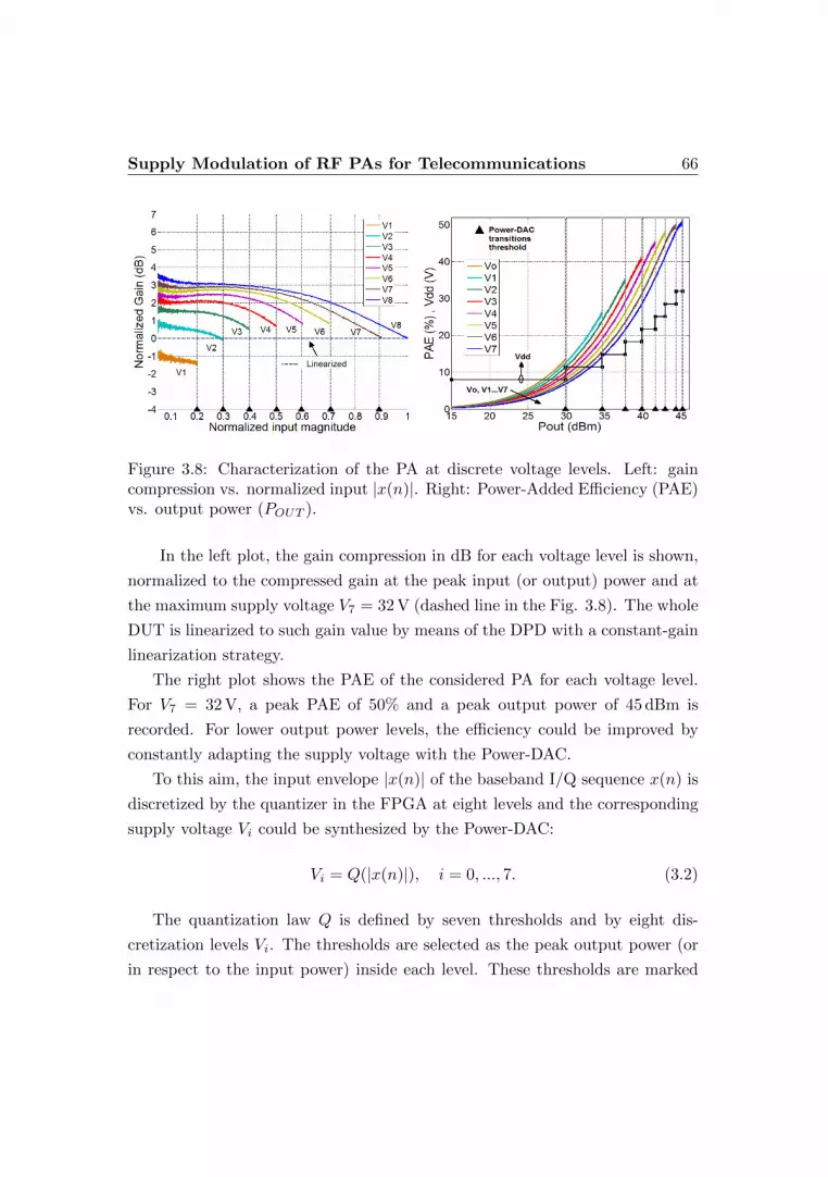
Supply Modulation of RF PAs for Telecommunications 66
Figure 3.8: Characterization of the PA at discrete voltage levels. Left: gaincompression vs. normalized input |x(n)|. Right: Power-Added Efficiency (PAE)vs. output power (POUT ).
In the left plot, the gain compression in dB for each voltage level is shown,
normalized to the compressed gain at the peak input (or output) power and at
the maximum supply voltage V7 = 32 V (dashed line in the Fig. 3.8). The whole
DUT is linearized to such gain value by means of the DPD with a constant-gain
linearization strategy.
The right plot shows the PAE of the considered PA for each voltage level.
For V7 = 32 V, a peak PAE of 50% and a peak output power of 45 dBm is
recorded. For lower output power levels, the efficiency could be improved by
constantly adapting the supply voltage with the Power-DAC.
To this aim, the input envelope |x(n)| of the baseband I/Q sequence x(n) is
discretized by the quantizer in the FPGA at eight levels and the corresponding
supply voltage Vi could be synthesized by the Power-DAC:
Vi = Q(|x(n)|), i = 0, ..., 7. (3.2)
The quantization law Q is defined by seven thresholds and by eight dis-
cretization levels Vi. The thresholds are selected as the peak output power (or
in respect to the input power) inside each level. These thresholds are marked

Supply Modulation of RF PAs for Telecommunications 67
on the plot as the vertical dashed lines. The eight output levels of the quan-
tizer, which control the supply bias voltage synthesized by the Power-DAC, are
also shown in the plot. By using these thresholds and levels in the quantizer,
the supply-modulated PA always operates with a PAE trajectory on top of the
eight PAE traces, thus maximizing the efficiency for a given selection of voltage
levels.
3.2.5 DUT Modeling and Pre-Distortion
The baseband x(n) signal before DPD is up-converted by the setup and amplified
by the DUT and the resulting output signal is acquired by the setup to produce
an y(n) sequence of I/Qs comprising the PA distortion. The x(n) and y(n)
sequences could be conveniently employed to represent the nonlinear behavior
of the DUT with AM/AM and AM/PM plots (also known as Booth plots),
which are shown in Fig. 3.9.
In the AM/AM plot, the x-axis is the time-varying input envelope |x(n)| and
the y-axis is the output envelope |y(n)|. In the AM/PM plot the y-axis is the
phase shift ∠y(n) and it is represented in degree in this plot. The PM/AM and
PM/PM are not typically relevant for the description of the non-linear behavior
of the considered PA operating in class-AB.
By swapping the input with the output, a model with the inverse non-linear
characteristic of the original DUT could be identified. In this way, the cascade
of the inverse non-linearity and of the DUT (direct) non-linearity provides a
linearized output. The inverse model can be described by means of a memoryless
polynomial model [80,81], as follows:x(n) =∑Ki
k=1 ak,iy(n)|y(n)|k−1
Vi = Q(|x(n)|) i = 0, ..., 7(3.3)
By solving the resulting least-square problem, the complex polynomial coef-
ficients ak,i could be obtained. The ak,i coefficients depend on the instantaneous
supply-voltage Vi, whereas Vi are selected by the input signal amplitude |x(n)|,
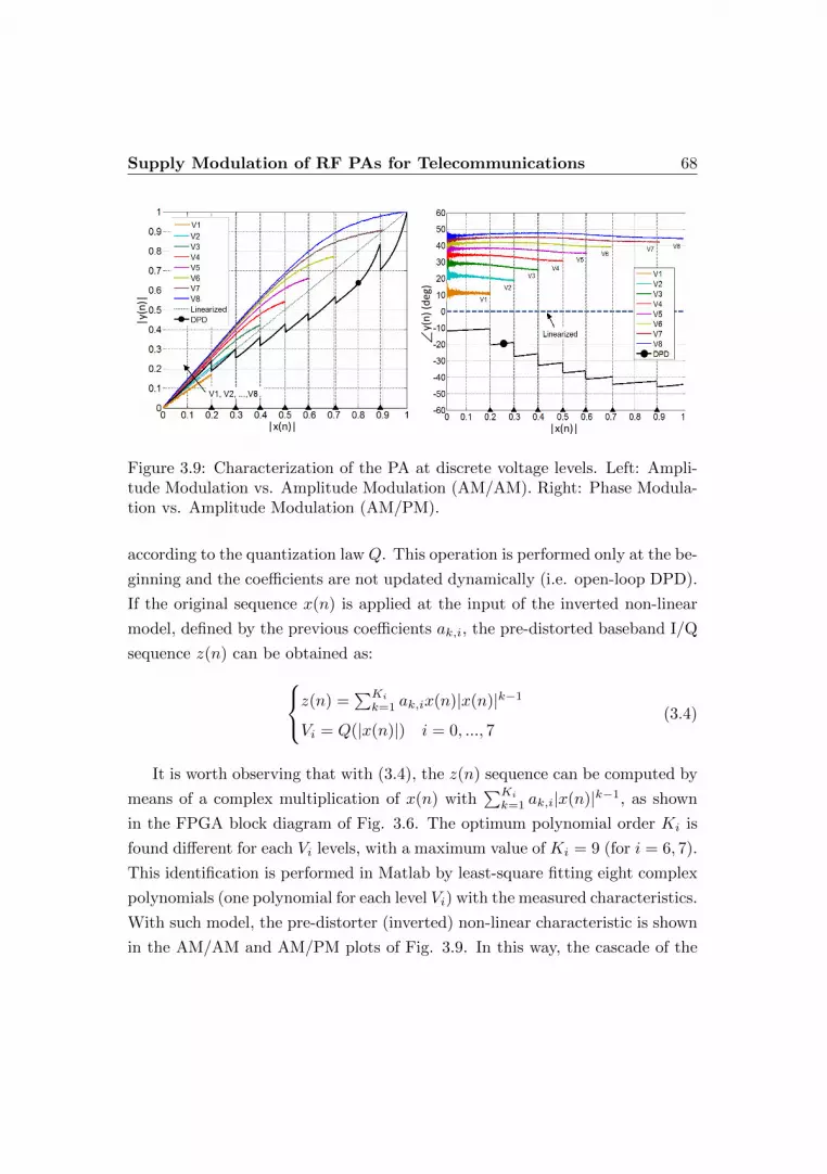
Supply Modulation of RF PAs for Telecommunications 68
|x(n)| |x(n)|
|y(n
)|
y(n
) (d
eg)
Figure 3.9: Characterization of the PA at discrete voltage levels. Left: Ampli-tude Modulation vs. Amplitude Modulation (AM/AM). Right: Phase Modula-tion vs. Amplitude Modulation (AM/PM).
according to the quantization law Q. This operation is performed only at the be-
ginning and the coefficients are not updated dynamically (i.e. open-loop DPD).
If the original sequence x(n) is applied at the input of the inverted non-linear
model, defined by the previous coefficients ak,i, the pre-distorted baseband I/Q
sequence z(n) can be obtained as:z(n) =∑Ki
k=1 ak,ix(n)|x(n)|k−1
Vi = Q(|x(n)|) i = 0, ..., 7(3.4)
It is worth observing that with (3.4), the z(n) sequence can be computed by
means of a complex multiplication of x(n) with∑Ki
k=1 ak,i|x(n)|k−1, as shown
in the FPGA block diagram of Fig. 3.6. The optimum polynomial order Ki is
found different for each Vi levels, with a maximum value of Ki = 9 (for i = 6, 7).
This identification is performed in Matlab by least-square fitting eight complex
polynomials (one polynomial for each level Vi) with the measured characteristics.
With such model, the pre-distorter (inverted) non-linear characteristic is shown
in the AM/AM and AM/PM plots of Fig. 3.9. In this way, the cascade of the

Supply Modulation of RF PAs for Telecommunications 69
inverted model (3.4) and the non-linearity of the DUT are compensated and
linearized to a constant gain [80,81].
3.3 Measurement Results with Telecom Signals
In this section, measurement results with modern telecommunication signals
are presented by considering LTE downlink signals typically employed in base-
stations [64]. These LTE signals are characterized respectively with 1.4 MHz
and 10 MHz channel bandwidths and 7.5 dB and 11.7 dB PAPRs. The PA is
characterized with four different operating regime:
• Fixed VDD with the same PIN,AV G as in the ET+DPD regime (column
V 1DDs)
• Fixed VDD with the same POUT,AV G as in the ET+DPD regime (column
V 2DD)
• ET operation without linearization (column ET)
• ET operation with Digital Pre-Distortion (column ET+DPD)
3.3.1 LTE 1.4-MHz Bandwidth, 7.5-dB PAPR
Measured data with the LTE 1.4 MHz are reported in Table 3.2 and Fig. 3.10.
The most significant comparison is the one between fixed V 2DD operation and
the ET+DPD regime with the same POUT,AV G = 5.5 W (gray shaded columns
in Table 3.2).
Since the PA gain is clearly reduced (12.6 dB vs. 15.4 dB) when operating
in ET+DPD regime, the condition of a constant POUT,AV G = 5.5 W is achieved
by decreasing the input signal average power PIN,AV G for the fixed V 2DD regime
(24.8 dB vs. 22 dB). This comparison shows an improvement of the PAE from
24.4% to 41.6%, corresponding to a DC power consumption decreasing from

Supply Modulation of RF PAs for Telecommunications 70
21.9 W to 12.48 W. In this regime the Power-DAC works with a very high ef-
ficiency of 92%, providing a still considerable composite efficiency of 38.3% to
the entire transmitter.
In Table 3.2, also the linearity performances are listed for both out-of-band
(ACLR) and in-band (NRMSE) distortions. The implemented open-loop mem-
oryless DPD is effective in compensating the additional distortion produced by
the Power-DAC nonlinearity and the ET operation: the ACLR improvement in
the closest sideband (E-UTRA) is 15 dB and the NRMSE drops from 27.8% to
4.2%. These effects of the DPD can be also appreciated in the plots of Fig. 3.10
and 3.11.
Fixed 𝑽𝑫𝑫𝟏 Fixed 𝑽𝑫𝑫
𝟐 𝐄𝐓 𝐄𝐓 + 𝐃𝐏𝐃
𝐆𝐚𝐢𝐧 15 dB 15.4 dB 13.6 dB 12.6 dB
𝐕𝐃𝐃
𝐌𝐚𝐱 32 V 32 V 32 V 32 V
𝐑𝐌𝐒 32 V 32 V 16.77 V 16.77 V
𝐌𝐢𝐧 32 V 32 V 8 V 8 V
𝐏𝐈𝐍,𝐀𝐕𝐆 24.8 dBm 22 dBm 24.8 dBm 24.8 dBm
𝐏𝐎𝐔𝐓,𝐀𝐕𝐆 39.8 dBm 37.4 dBm 38.4 dBm 37.4 dBm
𝐏𝐎𝐔𝐓,𝐀𝐕𝐆 9.5 W 5.5 W 6.92 W 5.5 W
𝐏𝐎𝐔𝐓,𝐏𝐊 44.7 dBm 43.8 dBm 44.9 dBm 45.1 dBm
𝐒𝐮𝐩𝐩𝐥𝐲 𝐏𝐨𝐰𝐞𝐫 28.5 W 21.9 W 14.46 W 12.48 W
𝐏𝐀𝐄 32.3% 24.4% 45.8% 41.6%
𝐒𝐮𝐩𝐩𝐥𝐲 𝐄𝐟𝐟𝐢𝐜𝐢𝐞𝐧𝐜𝐲 n. a. n. a. 93.5% 92%
𝐂𝐨𝐦𝐩𝐨𝐬𝐢𝐭𝐞 𝐄𝐟𝐟𝐢𝐜𝐢𝐞𝐧𝐜𝐲 (𝐂𝐏𝐀𝐄) 32.3% 24.4% 42.8% 38.3%
𝐀𝐂𝐋𝐑
𝐄 − 𝐔𝐓𝐑𝐀 −35.7 dB −42.4 dB −25.4 dB −40.4 dB
𝐔𝐓𝐑𝐀𝟏 −61.1 dB −60.7 dB −40.1 dB −49.9 dB
𝐔𝐓𝐑𝐀𝟐 −69.8 dB −70.2 dB −44.9 dB −52.3 dB
𝐍𝐑𝐌𝐒𝐄 10.74% 7.3% 27.8% 4.2%
Table 3.2: Measured system performance for a LTE 1.4 MHz, PAPR of 7.5 dB.When considering the same average output power POUT,AV G, ET and fixedsupply performances are reported for comparison in the gray-shaded columns.
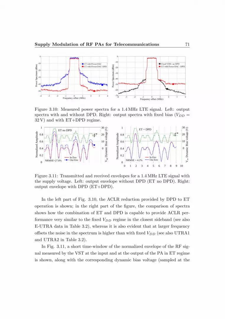
Supply Modulation of RF PAs for Telecommunications 71
Figure 3.10: Measured power spectra for a 1.4 MHz LTE signal. Left: outputspectra with and without DPD. Right: output spectra with fixed bias (VDD =32 V) and with ET+DPD regime.
Time (μs)
0 1 2 3 4 5 6 7 8 9 10
No
rmal
ized
Am
pli
tud
e
1
0.8
0.6
0.4
0.2
0
1
0.8
0.6
0.4
0.2
0
No
rmal
ized
Am
pli
tud
e
Vd
dD
yn
amic
Bia
s v
olt
age
(V)30
20
10
0
Vd
d D
yn
amic
Bia
s v
olt
age
(V)30
20
10
0
ET no DPD ET + DPD
In EnvOut Env
In EnvOut EnvNRMSE=27.8% NRMSE = 4.2%
Figure 3.11: Transmitted and received envelopes for a 1.4 MHz LTE signal withthe supply voltage. Left: output envelope without DPD (ET no DPD). Right:output envelope with DPD (ET+DPD).
In the left part of Fig. 3.10, the ACLR reduction provided by DPD to ET
operation is shown; in the right part of the figure, the comparison of spectra
shows how the combination of ET and DPD is capable to provide ACLR per-
formance very similar to the fixed VDD regime in the closest sideband (see also
E-UTRA data in Table 3.2), whereas it is also evident that at larger frequency
offsets the noise in the spectrum is higher than with fixed VDD (see also UTRA1
and UTRA2 in Table 3.2).
In Fig. 3.11, a short time-window of the normalized envelope of the RF sig-
nal measured by the VST at the input and at the output of the PA in ET regime
is shown, along with the corresponding dynamic bias voltage (sampled at the
Supply Modulation of RF PAs for Telecommunications 72
connection point between the Power-DAC and the PA with an oscilloscope).
These data are used for the calculation of the in-band distortion which is
evaluated with the NRMSE metric. The left plot puts in evidence the distortion
introduced by the ET operation; in the right graph, the linearizing effect of the
DPD can be appreciated, ensuring the drop of the NRMSE from 27.8% to 4.2%.
The dynamic bias voltage is unchanged in the two graphs, since the DPD is only
applied to the I/Qs of the RF signal, while the Power-DAC operates in the same
way in the two cases, since the supply voltage level is always switched on the
bases of the original signal envelope (see Fig. 3.6).
3.3.2 LTE 10-MHz Bandwidth, 11.65-dB PAPR
The same experiment is carried out with a 10 MHz bandwidth, 11.65 dB PAPR
LTE signal. Results are shown in Table 3.3 and Fig. 3.12. The PA PAE
improves from 10.9% to 28.8%, corresponding to a DC power consumption de-
creasing from 16.96 W to 6.28 W. With this wide-band signal the Power-DAC
works with a still high efficiency of 83%, providing 13 point of improvement
of composite efficiency for the entire transmitter. The ACLR improvement be-
tween ET and ET+DPD operations in the closest sideband (Table 3.3) is 11 dB
and the NRMSE reduces from 10.32% to 5.39%. As for the 1.4 MHz LTE signal,
at larger frequency offsets the spectrum noise is quite higher than with fixed
VDD.
3.3.3 Experimental Results Discussion
The comparisons between the PA output spectra with fixed VDD and with the
ET+DPD operation presented in the lower graphs of Fig. 3.10 and 3.12, show
that the main issue with the proposed approach is the noise performance in
the far-out-of-band spectrum. This noise is mainly due to the commutation
glitches shown in Fig. 3.11. The larger the signal bandwidth, the bigger the
effect of these glitches, since their duration becomes more significant relative to
the symbol rate. This phenomenon is the main reason for the trade-off between
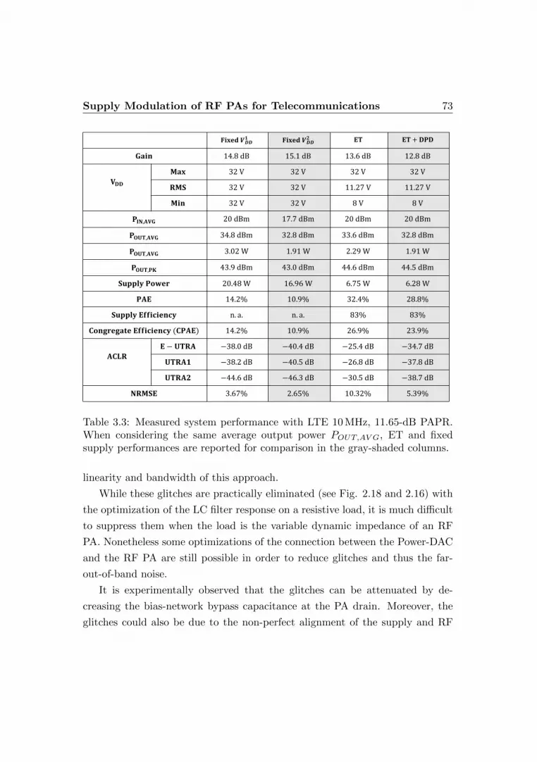
Supply Modulation of RF PAs for Telecommunications 73
𝐅𝐢𝐱𝐞𝐝 𝑽𝑫𝑫𝟏 𝐅𝐢𝐱𝐞𝐝 𝑽𝑫𝑫
𝟐 𝐄𝐓 𝐄𝐓 + 𝐃𝐏𝐃
𝐆𝐚𝐢𝐧 14.8 dB 15.1 dB 13.6 dB 12.8 dB
𝐕𝐃𝐃
𝐌𝐚𝐱 32 V 32 V 32 V 32 V
𝐑𝐌𝐒 32 V 32 V 11.27 V 11.27 V
𝐌𝐢𝐧 32 V 32 V 8 V 8 V
𝐏𝐈𝐍,𝐀𝐕𝐆 20 dBm 17.7 dBm 20 dBm 20 dBm
𝐏𝐎𝐔𝐓,𝐀𝐕𝐆 34.8 dBm 32.8 dBm 33.6 dBm 32.8 dBm
𝐏𝐎𝐔𝐓,𝐀𝐕𝐆 3.02 W 1.91 W 2.29 W 1.91 W
𝐏𝐎𝐔𝐓,𝐏𝐊 43.9 dBm 43.0 dBm 44.6 dBm 44.5 dBm
𝐒𝐮𝐩𝐩𝐥𝐲 𝐏𝐨𝐰𝐞𝐫 20.48 W 16.96 W 6.75 W 6.28 W
𝐏𝐀𝐄 14.2% 10.9% 32.4% 28.8%
𝐒𝐮𝐩𝐩𝐥𝐲 𝐄𝐟𝐟𝐢𝐜𝐢𝐞𝐧𝐜𝐲 n. a. n. a. 83% 83%
𝐂𝐨𝐧𝐠𝐫𝐞𝐠𝐚𝐭𝐞 𝐄𝐟𝐟𝐢𝐜𝐢𝐞𝐧𝐜𝐲 (𝐂𝐏𝐀𝐄) 14.2% 10.9% 26.9% 23.9%
𝐀𝐂𝐋𝐑
𝐄 − 𝐔𝐓𝐑𝐀 −38.0 dB −40.4 dB −25.4 dB −34.7 dB
𝐔𝐓𝐑𝐀𝟏 −38.2 dB −40.5 dB −26.8 dB −37.8 dB
𝐔𝐓𝐑𝐀𝟐 −44.6 dB −46.3 dB −30.5 dB −38.7 dB
𝐍𝐑𝐌𝐒𝐄 3.67% 2.65% 10.32% 5.39%
Table 3.3: Measured system performance with LTE 10 MHz, 11.65-dB PAPR.When considering the same average output power POUT,AV G, ET and fixedsupply performances are reported for comparison in the gray-shaded columns.
linearity and bandwidth of this approach.
While these glitches are practically eliminated (see Fig. 2.18 and 2.16) with
the optimization of the LC filter response on a resistive load, it is much difficult
to suppress them when the load is the variable dynamic impedance of an RF
PA. Nonetheless some optimizations of the connection between the Power-DAC
and the RF PA are still possible in order to reduce glitches and thus the far-
out-of-band noise.
It is experimentally observed that the glitches can be attenuated by de-
creasing the bias-network bypass capacitance at the PA drain. Moreover, the
glitches could also be due to the non-perfect alignment of the supply and RF
Supply Modulation of RF PAs for Telecommunications 74
Figure 3.12: Measured power spectra for a 10 MHz LTE signal. Left: outputspectra with and without DPD. Right: output spectra with fixed bias (VDD =32 V) and with ET+DPD regime.
paths, which at the moment is implemented in the FPGA with a timing reso-
lution of 8.333 ns: this is related, in the actual implementation, to the FPGA
clock of 120 MHz, but can be reduced with some modification of the logic net-
works.
Finally some further in-band and in-near-sidebands linearity improvements
can be achieved with the introduction of a DPD strategy with memory, which
can take into account the memory effects introduced by the PA within each bias
level and in the transitions between different bias levels [82, 83]. It is expected
that these optimizations and the definition of a systematic procedure to iden-
tify the optimal quantizer, based on the characteristics of the PA and of the
modulated signal (i.e. the PAPR and PDF), can bring even higher linearity and
efficiency improvement to the transmitter.
3.4 Conclusion
An Envelope-Tracking (ET) transmitter architecture based on the combination
of a digitally-controlled eight-level supply modulator presented in chapter 2 and
digital pre-distortion is presented. The complete ET architecture is tested with
an L-band LDMOS RF PA with 1.4 MHz and 10 MHz LTE signals with high
PAPR. In these conditions the converter operates at 92% and 83% efficiency

Supply Modulation of RF PAs for Telecommunications 75
respectively, whereas the composite efficiency of the transmitter are 38.3% and
23.9%. These performance correspond to an improvement of 17.2 and 17.9
points for the power added efficiency of the PA and to 13.4 and 13 points of
improvement for the efficiency of the entire transmitter.

Chapter 4
Supply-Modulation of
RF PAs for Radars
The majority of radar systems operate the Power Amplifier (PA) of the trans-
mitter in pulsed regime: the characteristics of the RF/microwave pulses in terms
of duty cycle, pulse-width, repetition frequency, transmitted power, and pulse
shaping directly affect radar performance [19,20]. Solid-state phased array radar
is enabled by a large number of transmit modules that produce very high trans-
mit powers. A typical transmit module has an efficient nonlinear deep class-AB
to class-C PA that transmits constant-envelope pulses with significant spectral
content over a large bandwidth [19,20].
Advanced radar waveforms can be used to provide spectral confinement,
improve range ambiguity, and decrease detectability for active electronically
scanned arrays [24]. In search and tracking radar, target detection and iden-
tity discrimination can be improved [27], while in weather radar suppression of
transmitted spectral sidebands enhances performance [28]. In addition, there is
increased concern about radar spectral emissions interfering with communica-
tion spectrum allocations [29].
76

Supply-Modulation of RF PAs for Radars 77
Amplitude modulation of the envelope provides spectral confinement effects
on radar system performance for different envelope shapes [19,21,22,24,27–29].
The amplitude-modulated pulse can be provided at the input of the PA while the
supply voltage is kept constant over the pulse duration. Such drive-modulated
PAs operate in back-off at lower amplitudes, resulting in significant average effi-
ciency degradation. In [21] and [22] an outphasing PA with a Gaussian envelope
shape, with up to a 3-dB Peak-to-Average Power Ratio (PAPR) waveform, is
experimentally investigated, but the average system efficiency is not reported.
More recently, Supply Modulation (SM) is introduced as a means to am-
plify amplitude-modulated pulses without sacrificing PA efficiency [5,23–26,84,
85]. Various types of SM following up on the early Envelope Elimination and
Restoration (EER) technique [41] are applied to improve efficiency of trans-
mitters for high PAPR communication signals [5, 85]. In [24], a Pulse-Width
Modulation (PWM) 100-MHz switching converter is used for linear pulse shap-
ing of an integrated S-band PA, with a total efficiency of 27%. For pulse shaping
of a hybrid S-band GaN PA in [23], a variable supply [25] is implemented as a
simple damped resonant circuit with efficiency greater than 90% at 6-W output
power and a total efficiency 50% and greater than 65% for the PAPR values of
8 and 4 dB, respectively. An average 66% total efficiency is demonstrated for
a Blackman-window pulse with a 4.1-dB PAPR and -30-dB spectral sidelobe
levels. In [25] and [26], this method is applied to X-band GaN PAs with vari-
able 7-15-µs pulsewidths and a resulting efficiency of 40%. For good sideband
suppression, simple predistortion of the PA gain and phase is required in this
approach. Although good efficiency improvement and spectral confinement are
demonstrated, the drawback of the technique is that it is limited to a single
pulse shape due to the resonant nature of the supply.

Supply-Modulation of RF PAs for Radars 78
PABaseband Signal
Generation, DPD andPower-DAC Control
Upconverter,Driver
𝑉𝐷(𝑡)
𝑍𝐿
Control Bits
Power-DACSupply Modulator 𝑅𝐹𝑂𝑈𝑇
Figure 4.1: High-level block diagram of the radar transmitter with a Power-DACsupply modulator. The digital baseband provides the signal that is upconvertedand drives the PA as well as the control bits for the Power-DAC. The Power-DACis implemented with GaN-on-Si power devices, while the PA is a GaN-on-SiCMMIC. The digital signal processing includes predistortion.
In this chapter12, we extend the supply pulse shaping technique to a fully
programmable discrete-level supply, which modulates an efficient 12-W GaN
MMIC X-band PA, as shown in Fig. 4.1. In this approach, the digital baseband
signal is generated and predistorted in an FPGA and upconverted to drive mod-
ulate the GaN-on-SiC 10-GHz MMIC PA. The FPGA also provides control bits
for a 3-bit power DAC (Power-DAC) multilevel dynamic supply, implemented
with GaN-on-Si power devices. The pulse shape is fully programmable and can
provide not only amplitude modulation of each pulse, but also pulse-to-pulse
modulation. In the work presented here, and in contrast to linear tracking,
such as described in [24], the Power-DAC discretizes the envelope in steps and
the linearity is recovered by Digital Pre-Distortion (DPD) of the RF PA. The
switches of the Power-DAC commutate at only a few kilohertz’s, and the nonlin-
1C. Florian, T. Cappello, D. Niessen, R. P. Paganelli, S. Schafer, Z. Popovic, “Efficient Pro-grammable Pulse Shaping for X-Band GaN MMIC Radar Power Amplifiers,” IEEE Microw.Theory Techn., Dec. 2016.
2A. Zai, C. Florian, T. Cappello, Z. Popovic, “Efficient power amplifiers for amplitude-tapered pulses with improved spectral confinement,” in IEEE MTT-S Int’l Microw. Symp.,San Francisco, CA, USA, May 2016.

Supply-Modulation of RF PAs for Radars 79
earities are compensated with DPD, allowing for large efficiency increase to over
55% at the X-band. The multilevel power converter (Power-DAC) used here as
the supply modulator of a radar transmitter is first introduced in chapter 2 for
the implementation of an Envelope-Tracking (ET) transmitter at L-band for
LTE communication signals with a hybrid LDMOS PA. Here, the Power-DAC
is used as a part of an X-band radar transmitter based on a GaN MMIC PA.
The exploitation of the Power-DAC for this new application enables the syn-
thesis of arbitrary, digitally programmable radar pulse envelope shaping, while
maintaining very high composite efficiency. This type of transmitter enables
other useful operating modes, such as PWM and pulse-to-pulse modulation.
4.1 Radar Transmitter Architectures
A common configuration for the power supply of a radar transmitter is illus-
trated in Fig. 4.2a. The bias voltage VD of the RF PA is provided by switching
on and off the system bus voltage supply VBUS , which is typically supplied by
a DC/DC converter. A power switch SW is connected in series between VBUS
time time time
Vd(t)
Rectangular Pulse Rectangular Envelope (RR)
RF pulse RF pulse RF pulse
Vd(t)PS
Vd(t)
CBank
ESR Id
SW Vd
VBUS
Id
VdSupply Modulator
VBUS
RF pulse input
b) Shaped supply voltage pulsea) Rectangular supply voltage pulse
RF pulse outputPA RF pulse
inputRF pulse output
PA
Pulse ShapingRectangular Envelope (PS)
Pulse ShapingEnvelope Tracking (PS+ET)
Figure 4.2: Radar PA architectures: (a) pulse waveforms and circuit diagram forconstant supply case. (b) amplitude-modulated pulse waveform with discretizedenvelope and associated circuit architecture.
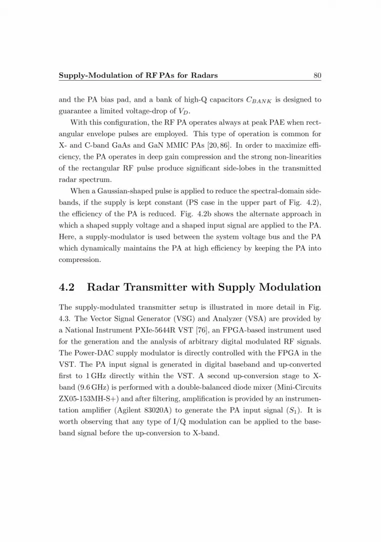
Supply-Modulation of RF PAs for Radars 80
and the PA bias pad, and a bank of high-Q capacitors CBANK is designed to
guarantee a limited voltage-drop of VD.
With this configuration, the RF PA operates always at peak PAE when rect-
angular envelope pulses are employed. This type of operation is common for
X- and C-band GaAs and GaN MMIC PAs [20, 86]. In order to maximize effi-
ciency, the PA operates in deep gain compression and the strong non-linearities
of the rectangular RF pulse produce significant side-lobes in the transmitted
radar spectrum.
When a Gaussian-shaped pulse is applied to reduce the spectral-domain side-
bands, if the supply is kept constant (PS case in the upper part of Fig. 4.2),
the efficiency of the PA is reduced. Fig. 4.2b shows the alternate approach in
which a shaped supply voltage and a shaped input signal are applied to the PA.
Here, a supply-modulator is used between the system voltage bus and the PA
which dynamically maintains the PA at high efficiency by keeping the PA into
compression.
4.2 Radar Transmitter with Supply Modulation
The supply-modulated transmitter setup is illustrated in more detail in Fig.
4.3. The Vector Signal Generator (VSG) and Analyzer (VSA) are provided by
a National Instrument PXIe-5644R VST [76], an FPGA-based instrument used
for the generation and the analysis of arbitrary digital modulated RF signals.
The Power-DAC supply modulator is directly controlled with the FPGA in the
VST. The PA input signal is generated in digital baseband and up-converted
first to 1 GHz directly within the VST. A second up-conversion stage to X-
band (9.6 GHz) is performed with a double-balanced diode mixer (Mini-Circuits
ZX05-153MH-S+) and after filtering, amplification is provided by an instrumen-
tation amplifier (Agilent 83020A) to generate the PA input signal (S1). It is
worth observing that any type of I/Q modulation can be applied to the base-
band signal before the up-conversion to X-band.

Supply-Modulation of RF PAs for Radars 81
Power-DACSupply Modulator
PA
Isolated DCVoltages
𝑉𝐷(𝑡)
+-
3-bit
S1 S2
ID(t)
VSG
VSA
FPGA
𝑉𝐵𝑈𝑆
NI VST
50dB Coaxial Attenuator
30dBDriver
IRF
IRF
Int. LO1 GHz
𝑉𝐷(𝑡)
Ext. LO(10.6 GHz)
9.6 GHz
9.6 GHz
1 GHz
1 GHz
Figure 4.3: Block diagram of the setup for radar transmitter with pulse shap-ing waveforms and Power-DAC supply modulator. The signal is generated atbaseband by the VST and up-converted at X-band by an external up-conversionstage. A benchtop driver and an attenuator set the correct power levels at theDUT reference planes S1 and S2. The setup is calibrated to directly measure theinput/output power at the DUT reference planes while an oscilloscope acquiresthe drain voltage VD(t) and current ID(t).
In the receiver section, the PA output signal (S2) is attenuated (50 dB coax-
ial attenuator), down-converted to 1 GHz by means of an external mixer (Mini-
Circuits ZX05-153MH-S+), and low-pass filtered before the VST input port. A
micro-strip IMage-Rejection (IMR) filter in the up-conversion chain and a band-
pass filter in the down-conversion chain are designed in-house. Both the VSG
and the VSA are locked with the same low-frequency reference clock (10 MHz)
as well as the internal transmitter and receiver LOs (1 GHz) are locked for phase
consistency. An external LO (Agilent 83650B), locked to the same 10 MHz ref-
erence, is used to generate a 10.6 GHz carrier frequency. The mixing product at
9.6 GHz is selected by means of the IMR filter. In the down-conversion chain,
the 1 GHz product is obtained by filtering out the other terms (at 10.6 and
20.2 GHz).
Supply-Modulation of RF PAs for Radars 82
The set-up is calibrated at the DUT input and output ports, S1 and S2,
corresponding to the Ground-Signal-Ground (GSG) probe tips connected at the
input and output port of the MMIC PA. The VST stores the I/Q data cor-
responding to the RF signal at the S1 and S2 ports, after de-embedding the
scalar values of the input gain and of the output attenuation. The modulated
supply voltage VD(t) and the current ID(t) of the PA are acquired by a digital
oscilloscope [71] equipped with wide-band voltage [78] and current sensors [79].
4.2.1 Digital Baseband
The DPD and the Power-DAC control logic is implemented in a firmware and
loaded into the FPGA in the VST. The firmware also generates the digital com-
mands for the control of the dynamic bias supply, by comparing the I/Q signal
envelope with the supply shaping-table of the PA. This supply shaping table is
obtained by means of a previous characterization of the PA at different supply
levels and it consists of the optimum bias voltage VD trajectory for PAE max-
imization [85]. The firmware also regulates time alignment between RF signal
and the supply voltage, which is fundamental for a correct ET operation.
The signal flow through the test setup can be summarized as follows, refer-
ring to Fig. 4.4:
1. The I/Q sequence x(n) of the arbitrary shaped pulsed RF waveform is
generated in the VST and their corresponding envelope |x(n)| is calculated
in the FPGA;
2. The voltage level Vi(n) that maximize the PAE for a given input envelope
|x(n)| is generated by the PA supply shaping table. The voltage level is
coded into a bit sequence bi(n) of commands for the Power-DAC control;
3. A k-tap shift-register is used to introduce a time-delay to synchronize the
RF path to the supply voltage of the PA;
4. The value of Vi(n) dictates the complex DPD coefficients ak,i to com-
pensate AM/AM and AM/PM non-linear characteristics of the PA at the

Supply-Modulation of RF PAs for Radars 83
Realak
Imagak
Baseband I/Q signal
DPD LUT
Predistorted I/Q
DiscretizedShaping
Table
k-tapDelay
Envelope Calculation
Power-DACControl
z(n)
bi bi
x n = I n + jQ(n)
ak,i = ak,i(Vi)
x(n) Vi(n) Vi(n − k)
x(n)
Vi(n)
Figure 4.4: Control logic of the Power-DAC and of the DPD implemented inthe FPGA. The envelope is extracted from the original I/Q and used by thediscretized shaping table which generates the control bits of the Power-DAC.For each bias level, a correction coefficient is applied to the original I/Q.
Vi(n) supply level;
5. The DPD coefficients are applied to the input signal x(n) to generate
the pre-distorted I/Q z(n), which is then up-converted to the PA input,
synchronously with the corresponding supply commands bi(n).
4.2.2 Class-AB X-Band Power-Amplifier
The PA is a two-stage MMIC implemented with the Qorvo 0.15-µm GaN-on-
SiC HEMT process, designed to operate at X-band with supply-modulation and
with wide-band communication signals [87]. The first stage is composed by two
8× 50µm devices, whereas four 10× 90µm devices are power-combined in the
second stage. The nominal (and maximum) drain bias voltage is VD = 20 V,
whereas the class-AB gate biases are VG1 = VG2 = −2.7 V which lead to a total
quiescent drain current ID = 325 mA (55 mA for the first stage, 270 mA for the
second stage) [86].

Supply-Modulation of RF PAs for Radars 84
As seen in Fig. 4.5, only the second stage of the PA is modulated by the
Power-DAC, while the drain voltage of the first stage is kept fixed at VD1 = 20 V.
Fig. 4.5 shows the connections between the PA and the Power-DAC, along with
the other drain and gate bias networks. While for VG1, VG2 and VD1 bias con-
nections, off-chip bypass capacitors are added to ensure PA stability, no external
capacitance is added to the second stage drain pad VD2 in order to enable fast
modulation of this supply voltage. The only bypass capacitance to this node
is provided by the on-chip integrated Metal-Insulator-Metal (MIM) capacitors,
for a total value of 30 pF.
Power-DACGND
b3,b3
b2,b2
b1,b1
1nF
10 µF100 µF
10 µF100 µF
10 uF
1
DCV
2
DCV
3
DCV
𝑉𝐷2(t)𝑉𝐺
𝑉𝐷1
1nF 1nF
Isolated DCVoltages
𝑉𝐺1 𝑉𝐺2
Figure 4.5: Photographs of the Power-DAC board and of the MMIC PA, with asketch of the connections. The second-stage bypass capacitors are removed andthe PA bias pad are directly connected to the Power-DAC output.

Supply-Modulation of RF PAs for Radars 85
The connection between the supply modulator and the PA is kept as short
as possible for a total estimated inductance of about 30 nH. The PA is attached
on a large CuMo carrier and the input/output RF pads are accessed with GSG
micro-probes through short 50-Ω micro-strip lines on alumina, wire-bonded to
the MMIC RF pads. The PA frequency sweep shows a bandwidth from 9 to
10.5 GHz, with a peak efficiency at 9.6 GHz.
4.3 GaN Power-Amplifier Characterization,
Modeling and Pre-Distortion
The electrical performance of GaN based HEMTs is affected by charge trapping
mechanisms documented in the literature [88–91], such as current collapse and
knee walkout in the device pulsed I/V characteristics. These in turn have an
impact on PA design, and are responsible for reduced output power density and
PAE at increasing drain voltages [92]. As shown in [88–91], time constants asso-
ciated with charge trapping effects in GaN FETs show an asymmetry between
charge capture (very fast, in the order of ps) and release (up to several seconds).
Moreover, it is observed that the trap state is set by the instantaneous peak val-
ues of the voltages applied to the device terminals with nonlinear dependence.
While device models specific to GaN HEMTs are proposed to describe such
behavior [88,89,93], measurements for pulsed I/V characterization also need to
be suitably modified to account for trapping mechanisms. Pulsed I/V systems
should produce conditions that maintain the device in isothermal and constant
trapped charge state. In the pulsed I/V setup described in [89], this is ac-
complished by applying a very fast pre-pulse that sets the trap state, shortly
before each point of the pulsed I/V measurement. This very fast pre-pulse
sets the trap-state corresponding to an arbitrary combination of gate and drain
voltages, typically the ones reached by the device load line when used for PA
operation.

Supply-Modulation of RF PAs for Radars 86
In this section, a similar concept is applied at the amplifier level: pre-pulsing
enables large signal characterization of a microwave PA at a controlled charge-
trapping state and thermal condition of the active devices. The setup can be
used in particular with PAs operated with dynamically-variable bias regimes
(e.g. ET), which are more affected by trapping phenomena, since the trapping
state is a nonlinear function of the instantaneous voltages applied to the active
device [88,89].
4.3.1 PA Characterization
The supply-modulated PA (DUT) introduced in section 4.2.2 is characterized
with the setup of Fig. 4.3 in order to identify the supply shaping table and the
complex polynomial for the DPD. For this characterization, the PA is operated
in pulsed mode with 50µs pulse width (PW) and 10% duty cycle (T = 500µs)
at 10 GHz. These are typical values for many types of pulse-compressed radar
transmitters (e.g. as the ones in [23–26]).
Fig. 4.6a shows a discretized multi-level approximation of a Gaussian-like
dynamically variable supply profile VD(t), synchronized with the envelope of the
RF pulse. The efficiency is enhanced by forcing the PA to operate at a certain
level of gain compression during the entire pulse, which results in nonlinearities
that need to be compensated by DPD. A preliminary AM-AM/AM-PM char-
acterization of the PA at each VD level is needed to find the DPD coefficients.
The supply modulator enables the characterization of the PA in a pulsed
regime, under thermal conditions very similar to the actual operating ones.
The AM-AM/AM-PM measurements of the PA are performed by pulsing the
supply with the same PW and duty cycle as that of the radar pulse and simul-
taneously driving the PA input with an amplitude-modulated RF pulse. This is
repeated at the different supply voltage levels Vi (see Fig. 4.6b). However, since
the period T (in the range 10µs - 1000µs, typical of pulsed radars) is shorter
than the slow trap release transient [88,89,94], the GaN PA performance during
each level of a given pulse is still affected by the large amount of charge trapping

Supply-Modulation of RF PAs for Radars 87
t
Sup
ply
pu
lse
VD
volt
age
Pre-Pulses (DC+RF)
Measurement Pulse
RF
Pou
t (W
)
RF Poutmax
TPP
≈T
Sup
ply
pu
lse
VD
volt
age
Measurement Pulse
RF
Pou
t (W
)
TM = PW
T
TM = PW
Sup
ply
pu
lse
VD
volt
age
RF
Pou
t (W
)
Radar operative regime
PW
Measurement Pulse
Characterization w/o PP
PP characterization
DC PPDC+RF
PP
Trapping state
X=Xmax
X=Xmax
VD = Vi
a)
b)
c)
VD = ViVD = Vi
VD = V7
t
t
Figure 4.6: (a): operative pulse shaping radar regime with ET. (b): characteri-zation regime without (b) and with (c) pre-pulse (PP). A PP is employed to setthe trap-state to Xmax so that the extracted characteristics are more similar tothe actual operating ones.
from the previous pulse level, where the peak level VD = V7 corresponds to the
trap state X = Xmax (Fig. 4.6).
In order to obtain a more representative characterization of the PA at the
different levels Vi under pulsed radar operation, a pre-pulse (PP), is applied to
the PA before the actual “Measurement Pulse”, as described in Fig. 4.6c. The
PP is composed of a bias pulse (DC PP) at the maximum level VD = V7 pro-
vided by the supply modulator, and an RF pulse (RF PP) synthesized by the
VST that drives the PA to operate at its peak output power. In this way, the
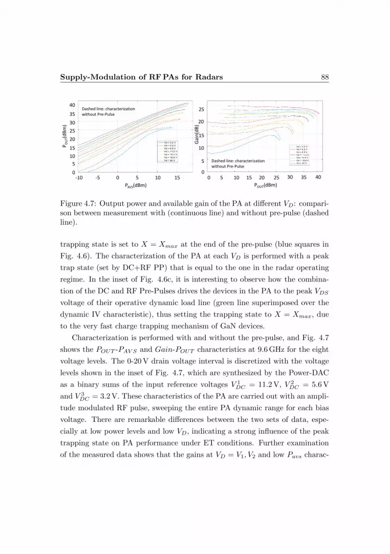
Supply-Modulation of RF PAs for Radars 88
-10 -5 0 10 155
PAVS(dBm)
0
5
10
15
20
25
30
35
40
PO
UT(
dB
m)
0 5 10 15 20 25 30 35 400
5
10
15
20
25
POUT(dBm)
Gai
n(d
B)
Dashed line: characterizationwithout Pre-Pulse
Dashed line: characterizationwithout Pre-Pulse
Figure 4.7: Output power and available gain of the PA at different VD: compari-son between measurement with (continuous line) and without pre-pulse (dashedline).
trapping state is set to X = Xmax at the end of the pre-pulse (blue squares in
Fig. 4.6). The characterization of the PA at each VD is performed with a peak
trap state (set by DC+RF PP) that is equal to the one in the radar operating
regime. In the inset of Fig. 4.6c, it is interesting to observe how the combina-
tion of the DC and RF Pre-Pulses drives the devices in the PA to the peak VDS
voltage of their operative dynamic load line (green line superimposed over the
dynamic IV characteristic), thus setting the trapping state to X = Xmax, due
to the very fast charge trapping mechanism of GaN devices.
Characterization is performed with and without the pre-pulse, and Fig. 4.7
shows the POUT -PAV S and Gain-POUT characteristics at 9.6 GHz for the eight
voltage levels. The 0-20 V drain voltage interval is discretized with the voltage
levels shown in the inset of Fig. 4.7, which are synthesized by the Power-DAC
as a binary sums of the input reference voltages V 1DC = 11.2 V, V 2
DC = 5.6 V
and V 3DC = 3.2 V. These characteristics of the PA are carried out with an ampli-
tude modulated RF pulse, sweeping the entire PA dynamic range for each bias
voltage. There are remarkable differences between the two sets of data, espe-
cially at low power levels and low VD, indicating a strong influence of the peak
trapping state on PA performance under ET conditions. Further examination
of the measured data shows that the gains at VD = V1, V2 and low Pavs charac-
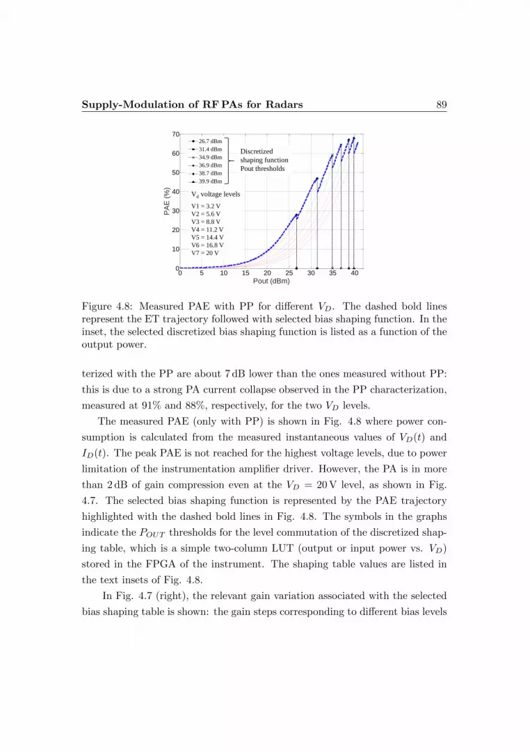
Supply-Modulation of RF PAs for Radars 89
0 5 10 15 20 25 30 35 400
10
20
30
40
50
60
70
Pout (dBm)
PA
E (
%)
PAE (%) VS Pout (dBm) VS Bias Voltage Level
0 5 10 15 20 25 30 35 400
10
20
30
40
50
60
70
Pout (dBm)
PA
E (
%)
PAE (%) VS Pout (dBm) VS Bias Voltage Level
3.2 V
5.6 V
8.8 V
11.2 V
14.4 V
16.8 V
20 V
Discretizedshaping functionthresholds
Vd voltage levels
V1 = 3.2 V
V2 = 5.6 V
V3 = 8.8 V
V4 = 11.2 V
V5 = 14.4 V
V6 = 16.8 V
V7 = 20 V
26.7 dBm
31.4 dBm
34.9 dBm
36.9 dBm
38.7 dBm
39.9 dBm
Discretized
shaping function
Pout thresholds
Figure 4.8: Measured PAE with PP for different VD. The dashed bold linesrepresent the ET trajectory followed with selected bias shaping function. In theinset, the selected discretized bias shaping function is listed as a function of theoutput power.
terized with the PP are about 7 dB lower than the ones measured without PP:
this is due to a strong PA current collapse observed in the PP characterization,
measured at 91% and 88%, respectively, for the two VD levels.
The measured PAE (only with PP) is shown in Fig. 4.8 where power con-
sumption is calculated from the measured instantaneous values of VD(t) and
ID(t). The peak PAE is not reached for the highest voltage levels, due to power
limitation of the instrumentation amplifier driver. However, the PA is in more
than 2 dB of gain compression even at the VD = 20 V level, as shown in Fig.
4.7. The selected bias shaping function is represented by the PAE trajectory
highlighted with the dashed bold lines in Fig. 4.8. The symbols in the graphs
indicate the POUT thresholds for the level commutation of the discretized shap-
ing table, which is a simple two-column LUT (output or input power vs. VD)
stored in the FPGA of the instrument. The shaping table values are listed in
the text insets of Fig. 4.8.
In Fig. 4.7 (right), the relevant gain variation associated with the selected
bias shaping table is shown: the gain steps corresponding to different bias levels

Supply-Modulation of RF PAs for Radars 90
and the gain variation within each level need to be compensated by the DPD,
which is designed to linearize the ET PA characteristic to a constant gain value
of 23 dB, which corresponds to the compressed gain at the maximum output
power (VD = 20 V and maximum input power).
4.3.2 PA Modeling and Pre-Distortion
In Fig. 6.10, the pre-distorter amplitude and phase characteristics for each
voltage level are shown (solid lines), along with the PA AM/AM and AM/PM
behavior (dashed bold lines). The DPD amplitude expansion needed for the
linearization of the PA gain compression is evident in these plots.
The same information in time domain can be seen in Fig. 4.10, where the
ideal envelope of the RF input signal (dashed bold line) for pulse shaping with
a Blackman window [95] is shown along with the actual pre-distorted envelope
for the ET PA linearization (solid thin line).
Fig. 4.11 shows clearly that the DPD identified from the data acquired
without PP fails to linearize the ET PA, especially at low Pavs and VD levels,
where the differences due to trapping effects are more prominent (see Fig. 4.7).
0 0.2 0.4 0.6 0.8 10
0.1
0.2
0.3
0.4
0.5
0.6
0.7
0.8
0.9
1
Normalized Input Envelope
No
rma
lize
d O
utp
ut E
nve
lop
e
HPA and DPD amplitude characteristics for each bias volatge level
HPA AM/AM
DPD AM/AM
V1 = 3.2 V
V2 = 5.6 V
V3 = 8.8 V
V4 = 11.2 V
V5 = 14.4 V
V6 = 16.8 V
V7 = 20 V
Vd voltage levels
0 0.2 0.4 0.6 0.8 1-60
-40
-20
0
20
40
60
Normalized Input Envelope
Pha
se S
hift (d
eg)
Vd voltage levels
HPA AM/PM
DPD AM/PM
V1 = 3.2 V
V2 = 5.6 V
V3 = 8.8 V
V4 = 11.2 V
V5 = 14.4 V
V6 = 16.8 V
V7 = 20 V
0 0.2 0.4 0.6 0.8 1-60
-40
-20
0
20
40
60
Normalized Input Envelope
Pha
se S
hift (d
eg)
0 0.2 0.4 0.6 0.8 1-60
-40
-20
0
20
40
60
Normalized Input Envelope
Pha
se S
hift (d
eg)
Figure 4.9: AM/AM (left) and AM/PM (right) characteristics of the PA (blue)and of the pre-distorter (red) at the different bias levels which are reported inthe inset.
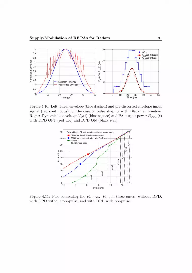
Supply-Modulation of RF PAs for Radars 91
0 10 20 30 40 500
0.1
0.2
0.3
0.4
0.5
0.6
0.7
0.8
0.9
1
Time (s)
No
rma
lize
d E
nve
lop
e
Normalized Blackman envelope and Predistorted envelope
Blackman Envelope
Predistorted Envelope
Time (µs)0 10 20 30 40 50 60
0
5
10
15
20
Vd (
t)(V
), P
ou
t(t)
(W)
Time (s)
Figure 4.10: Left: Ideal envelope (blue dashed) and pre-distorted envelope inputsignal (red continuous) for the case of pulse shaping with Blackman window.Right: Dynamic bias voltage VD(t) (blue square) and PA output power POUT (t)with DPD OFF (red dot) and DPD ON (black star).
VD=
V1 V
D=
V2
VD=
V3
VD=
V4
VD=
V5
VD=
V6
VD=
V7
Figure 4.11: Plot comparing the Pout vs. Pavs in three cases: without DPD,with DPD without pre-pulse, and with DPD with pre-pulse.
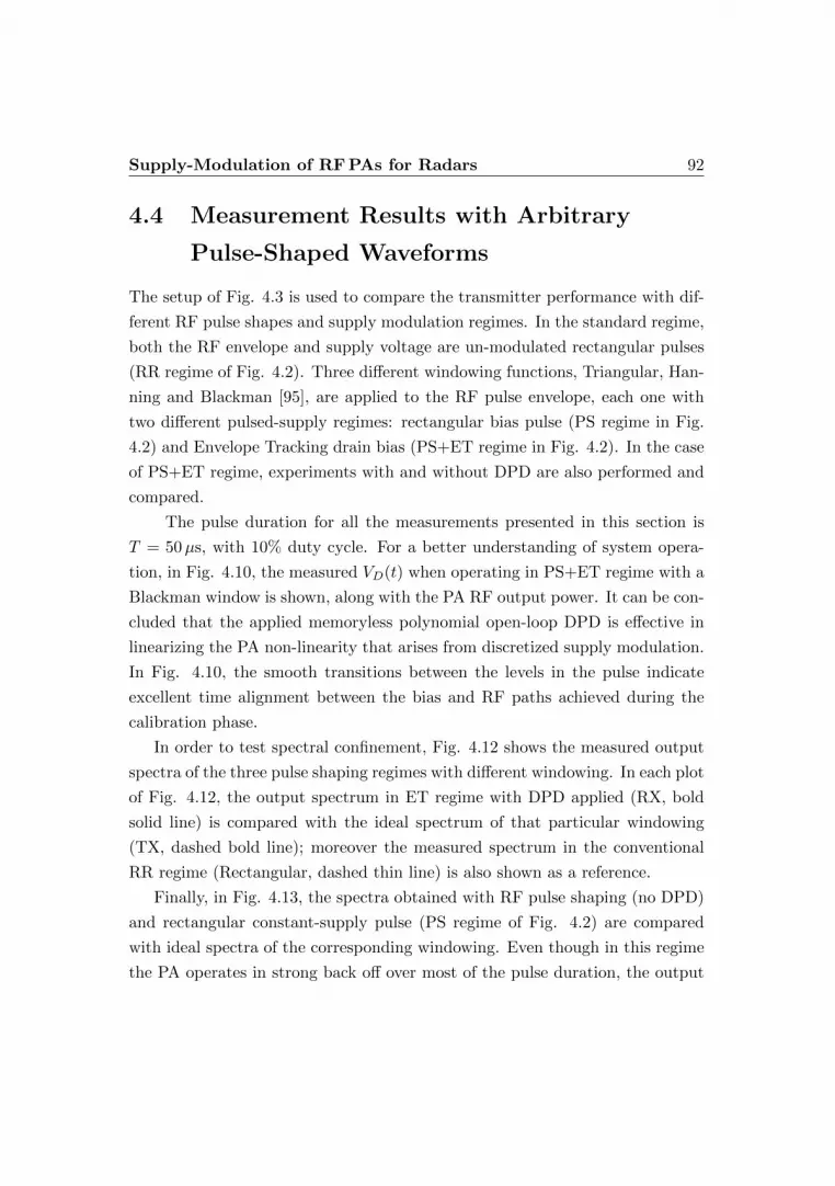
Supply-Modulation of RF PAs for Radars 92
4.4 Measurement Results with Arbitrary
Pulse-Shaped Waveforms
The setup of Fig. 4.3 is used to compare the transmitter performance with dif-
ferent RF pulse shapes and supply modulation regimes. In the standard regime,
both the RF envelope and supply voltage are un-modulated rectangular pulses
(RR regime of Fig. 4.2). Three different windowing functions, Triangular, Han-
ning and Blackman [95], are applied to the RF pulse envelope, each one with
two different pulsed-supply regimes: rectangular bias pulse (PS regime in Fig.
4.2) and Envelope Tracking drain bias (PS+ET regime in Fig. 4.2). In the case
of PS+ET regime, experiments with and without DPD are also performed and
compared.
The pulse duration for all the measurements presented in this section is
T = 50µs, with 10% duty cycle. For a better understanding of system opera-
tion, in Fig. 4.10, the measured VD(t) when operating in PS+ET regime with a
Blackman window is shown, along with the PA RF output power. It can be con-
cluded that the applied memoryless polynomial open-loop DPD is effective in
linearizing the PA non-linearity that arises from discretized supply modulation.
In Fig. 4.10, the smooth transitions between the levels in the pulse indicate
excellent time alignment between the bias and RF paths achieved during the
calibration phase.
In order to test spectral confinement, Fig. 4.12 shows the measured output
spectra of the three pulse shaping regimes with different windowing. In each plot
of Fig. 4.12, the output spectrum in ET regime with DPD applied (RX, bold
solid line) is compared with the ideal spectrum of that particular windowing
(TX, dashed bold line); moreover the measured spectrum in the conventional
RR regime (Rectangular, dashed thin line) is also shown as a reference.
Finally, in Fig. 4.13, the spectra obtained with RF pulse shaping (no DPD)
and rectangular constant-supply pulse (PS regime of Fig. 4.2) are compared
with ideal spectra of the corresponding windowing. Even though in this regime
the PA operates in strong back off over most of the pulse duration, the output
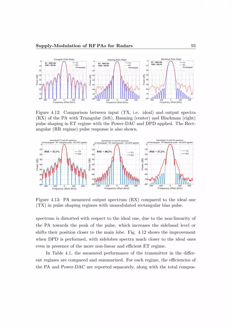
Supply-Modulation of RF PAs for Radars 93
-200 -100 0 100 200-80
-70
-60
-50
-40
-30
-20
-10
0
Frequency offset (kHz)
Pow
er
(dB
)
Normalized TX and RX spectrum: Triangular pulse - DPD ON
TX
RX
Rectangular
ET - DPD ONPAE = 58.4%
Triangular Pulse Shape
-200 -100 0 100 200-80
-70
-60
-50
-40
-30
-20
-10
0
Frequency offset (kHz)
Pow
er
(dB
)
Normalized TX and RX spectrum: Hanning pulse - DPD ON
TX
RX
Rectangular
ET - DPD ONPAE = 59.3%
Hanning Pulse Shape
-200 -100 0 100 200-80
-70
-60
-50
-40
-30
-20
-10
0
Frequency offset (kHz)
Pow
er
(dB
)
Normalized TX and RX spectrum: Blackman pulse - DPD ON
TX
RX
Rectangular
ET - DPD ONPAE = 58.1%
Blackman Pulse Shape
Figure 4.12: Comparison between input (TX, i.e. ideal) and output spectra(RX) of the PA with Triangular (left), Hanning (center) and Blackman (right)pulse shaping in ET regime with the Power-DAC and DPD applied. The Rect-angular (RR regime) pulse response is also shown.
-200 -100 0 100 200-80
-70
-60
-50
-40
-30
-20
-10
0
Frequency offset (kHz)
Pow
er
(dB
)
Normalized TX and RX spectrum: Vd Rectangular - RF Triangular pulse - NO DPD applied
TX
RX
-200 -100 0 100 200-80
-70
-60
-50
-40
-30
-20
-10
0
Frequency offset (kHz)
Pow
er
(dB
)
Normalized TX and RX spectrum: Vd Rectangular - RF Hanning pulse - NO DPD applied
TX
RX
-200 -100 0 100 200-80
-70
-60
-50
-40
-30
-20
-10
0
Frequency offset (kHz)
Pow
er
(dB
) Normalized TX and RX spectrum:
Vd Rectangular - RF Blackman pulse - NO DPD applied
TX
RXPAE = 35.1% PAE = 40.2% PAE = 37.2%
Figure 4.13: PA measured output spectrum (RX) compared to the ideal one(TX) in pulse shaping regimes with unmodulated rectangular bias pulse.
spectrum is distorted with respect to the ideal one, due to the non-linearity of
the PA towards the peak of the pulse, which increases the sideband level or
shifts their position closer to the main lobe. Fig. 4.12 shows the improvement
when DPD is performed, with sidelobes spectra much closer to the ideal ones
even in presence of the more non-linear and efficient ET regime.
In Table 4.1, the measured performance of the transmitter in the differ-
ent regimes are compared and summarized. For each regime, the efficiencies of
the PA and Power-DAC are reported separately, along with the total compos-
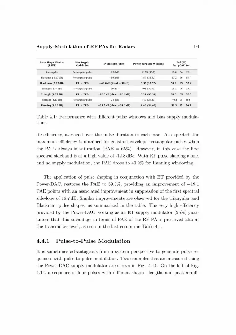
Supply-Modulation of RF PAs for Radars 94
𝐏𝐮𝐥𝐬𝐞 𝐒𝐡𝐚𝐩𝐞𝐖𝐢𝐧𝐝𝐨𝐰(𝐏𝐀𝐏𝐑)
𝐁𝐢𝐚𝐬 𝐒𝐮𝐩𝐩𝐥𝐲𝐌𝐨𝐝𝐮𝐥𝐚𝐭𝐢𝐨𝐧
𝟏𝐬𝐭 𝐬𝐢𝐝𝐞𝐥𝐨𝐛𝐞 (𝐝𝐁𝐦) 𝐏𝐨𝐰𝐞𝐫 𝐩𝐞𝐫 𝐩𝐮𝐥𝐬𝐞𝐖 (𝐝𝐁𝐦)𝐏𝐀𝐄 (%)
𝐏𝐀 𝐩𝐃𝐀𝐂 𝐭𝐨𝐭.
Rectangular Rectangular pulse −12.8 dB 11.75 (40.7) 65.0 96 62.4
Blackman ( 5.17 dB) Rectangular pulse −30.2 dB 3.57 (35.52) 37.2 96 35.7
𝐁𝐥𝐚𝐜𝐤𝐦𝐚𝐧 (𝟓. 𝟏𝟕 𝐝𝐁) 𝐄𝐓 + 𝐃𝐏𝐃 −𝟒𝟔. 𝟎 𝐝𝐁 (𝐢𝐝𝐞𝐚𝐥 − 𝟓𝟖 𝐝𝐁) 𝟑. 𝟓𝟕 (𝟑𝟓. 𝟓𝟐) 𝟓𝟖. 𝟏 𝟗𝟓 𝟓𝟓. 𝟐
Triangle (4.77 dB) Rectangular pulse −28 dB ∗ 3.91 (35.91) 35.1 96 33.4
𝐓𝐫𝐢𝐚𝐧𝐠𝐥𝐞 (𝟒. 𝟕𝟕 𝐝𝐁) 𝐄𝐓 + 𝐃𝐏𝐃 −𝟐𝟔. 𝟓 𝐝𝐁 (𝐢𝐝𝐞𝐚𝐥 − 𝟐𝟔. 𝟓 𝐝𝐁) 𝟑. 𝟗𝟏 (𝟑𝟓. 𝟗𝟏) 𝟓𝟖. 𝟗 𝟗𝟓 𝟓𝟓. 𝟗
Hanning (4.20 dB) Rectangular pulse −24.4 dB 4.40 (36.43) 40.2 96 38.6
𝐇𝐚𝐧𝐧𝐢𝐧𝐠 (𝟒. 𝟐𝟎 𝐝𝐁) 𝐄𝐓 + 𝐃𝐏𝐃 −𝟑𝟏. 𝟓 𝐝𝐁 (𝐢𝐝𝐞𝐚𝐥 − 𝟑𝟏. 𝟓 𝐝𝐁) 𝟒. 𝟒𝟎 (𝟑𝟔. 𝟒𝟑) 𝟓𝟗. 𝟑 𝟗𝟓 𝟓𝟔. 𝟑
Table 4.1: Performance with different pulse windows and bias supply modula-tions.
ite efficiency, averaged over the pulse duration in each case. As expected, the
maximum efficiency is obtained for constant-envelope rectangular pulses when
the PA is always in saturation (PAE = 65%). However, in this case the first
spectral sideband is at a high value of -12.8 dBc. With RF pulse shaping alone,
and no supply modulation, the PAE drops to 40.2% for Hanning windowing.
The application of pulse shaping in conjunction with ET provided by the
Power-DAC, restores the PAE to 59.3%, providing an improvement of +19.1
PAE points with an associated improvement in suppression of the first spectral
side-lobe of 18.7 dB. Similar improvements are observed for the triangular and
Blackman pulse shapes, as summarized in the table. The very high efficiency
provided by the Power-DAC working as an ET supply modulator (95%) guar-
antees that this advantage in terms of PAE of the RF PA is preserved also at
the transmitter level, as seen in the last column in Table 4.1.
4.4.1 Pulse-to-Pulse Modulation
It is sometimes advantageous from a system perspective to generate pulse se-
quences with pulse-to-pulse modulation. Two examples that are measured using
the Power-DAC supply modulator are shown in Fig. 4.14. On the left of Fig.
4.14, a sequence of four pulses with different shapes, lengths and peak ampli-

Supply-Modulation of RF PAs for Radars 95
0 100 200 3000
0.4
0.8
1.2
Time (s)
No
rma
lize
d E
nve
lop
e
Normalized in and out envelope and ET voltage for an arbitray pulse sequence
ET Vdd
0 1 2 3
x 10-4
0
5
10
15
20
ET
Bia
s V
olta
ge
V
d (
V)
Input Envelope
Output Envelope
Supply Voltage
ET + DPD
P1: 10 us - 28.7 dBm Triangular pulse
P2: 20 us - 34.8 dBm Hanning Pulse
P3: 50 us - 38.3 dBm Blackman Pulse
P4: 100 us - 40.7 dBm Square Pulse
100 200 300 Time (µs)
Arbitrary pulse
sequence
0 100 200 300 400 500 600 700-10
0
10
20
30
40
50
Time (s)
Po
ut
(dB
m)
Output Power - Rectangular pulses sequence
Time (µs)
Rectangular pulse sequence
P1
P2
P3P4 P5
P6P7 P8
Figure 4.14: Left: Arbitrary pulse sequence: Triangular, Hanning, Blackmanand square pulse envelopes. The transmitted RF envelope is indistinguishablefrom the ideal one, due to the DPD correction. Right: Instantaneous PA outputpower for an arbitrary rectangular pulse sequence.
tudes are shown. The normalized envelopes of the pulse sequence are shown
at the PA input and output, along with the corresponding VD(t) (supply volt-
age) synthesized by the Power-DAC. The different types of shapes and values of
length and peak power of the pulses are indicated in the inset of the figure. For
each pulse, the setup automatically selects the VD(t) trajectory that maximizes
the PAE.
On the right of Fig. 4.14, a different case of pulse-to-puse modulation is
shown in which the time-on-target and power on target can be modified on a
pulse-to-pulse basis. The Power-DAC can produce square voltage pulses with
the seven different amplitudes, since VOUT = 0 V is not used (no voltage offset).
Table 4.2 summarizes the pulse characteristics and the measured PAE and
compare them with the performance obtained with constant 0-20 V supply
pulses. The advantage in terms of PAE is substantial, since the VD(t) is prac-
tically optimized for all the different output power levels ranging from 17 to
40.5 dBm. In [23, 25, 26], a resonant pulse modulator is presented with good
efficiency. However, the pulse shape is not variable, although in [26] it is shown
that the pulse duration can be varied. In contrast, this approach is completely
flexible in terms of pulse shape and dynamic range. The VD(t) trajectory syn-
thesized by the Power-DAC automatically adapts to the RF pulse shape and
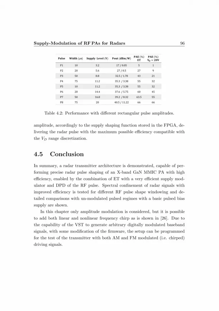
Supply-Modulation of RF PAs for Radars 96
𝐏𝐮𝐥𝐬𝐞 𝐖𝐢𝐝𝐭𝐡 (µ𝐬) 𝐒𝐮𝐩𝐩𝐥𝐲 𝐋𝐞𝐯𝐞𝐥 (𝐕) 𝐏𝐨𝐮𝐭 (𝐝𝐁𝐦/𝐖)𝐏𝐀𝐄 %
𝐄𝐓𝐏𝐀𝐄 %𝐕𝐃 = 𝟐𝟎𝐕
P1 10 3.2 17 / 0.05 5 1
P2 20 5.6 27 / 0.5 27 9
P3 50 8.8 32.5 / 1.78 43 21
P4 75 11.2 35.3 / 3.38 55 32
P5 10 11.2 35.3 / 3.38 55 32
P6 20 14.4 37.6 / 5.75 60 45
P7 50 16.8 39.2 / 8.32 63.5 55
P8 75 20 40.5 / 11.22 66 66
Table 4.2: Performance with different rectangular pulse amplitudes.
amplitude, accordingly to the supply shaping function stored in the FPGA, de-
livering the radar pulse with the maximum possible efficiency compatible with
the VD range discretization.
4.5 Conclusion
In summary, a radar transmitter architecture is demonstrated, capable of per-
forming precise radar pulse shaping of an X-band GaN MMIC PA with high
efficiency, enabled by the combination of ET with a very efficient supply mod-
ulator and DPD of the RF pulse. Spectral confinement of radar signals with
improved efficiency is tested for different RF pulse shape windowing and de-
tailed comparisons with un-modulated pulsed regimes with a basic pulsed bias
supply are shown.
In this chapter only amplitude modulation is considered, but it is possible
to add both linear and nonlinear frequency chirp as is shown in [26]. Due to
the capability of the VST to generate arbitrary digitally modulated baseband
signals, with some modification of the firmware, the setup can be programmed
for the test of the transmitter with both AM and FM modulated (i.e. chirped)
driving signals.

Supply-Modulation of RF PAs for Radars 97
The capability of the supply modulator to synthesize arbitrary supply tra-
jectories with efficiency greater than 95% and the adopted DPD strategy result
in a very high flexibility in the implementation of arbitrary pulse sequences with
variable sequence order, pulse shape, length and peak amplitude, for advanced
radar transmitters.

Chapter 5
Integrated Power-DAC and
PA Transmitter
The challenge of efficient amplification of high PAPR signals at microwave car-
rier frequencies is addressed with a number of transmitter architectures, such as
Doherty, outphasing and envelope tracking [1]. A number of authors have shown
that supply modulation can improve overall transmitter efficiency, e.g. [3–5,96].
In this approach, the average efficiency of the PA is increased by keeping the
transistor saturated through dynamic supply variation synchronized with signal
envelope variations through a trajectory, or shaping function. For high band-
width signals, the required slew rate, tracking accuracy and high efficiency be-
come challenges for the dynamic supply. Several approaches are demonstrated
for signals with 10s of MHz bandwidth: linearly assisted switchers (section
1.6.1), discrete multi-level supplies (section 1.6.3) and multi-phase switching
converters (section 1.6.2).
The high power density, high mobility, high breakdown voltage and high
temperature operation make GaN technology attractive not only for RF PAs,
but also for fast supply modulators. Single and multi-phase high-frequency
98
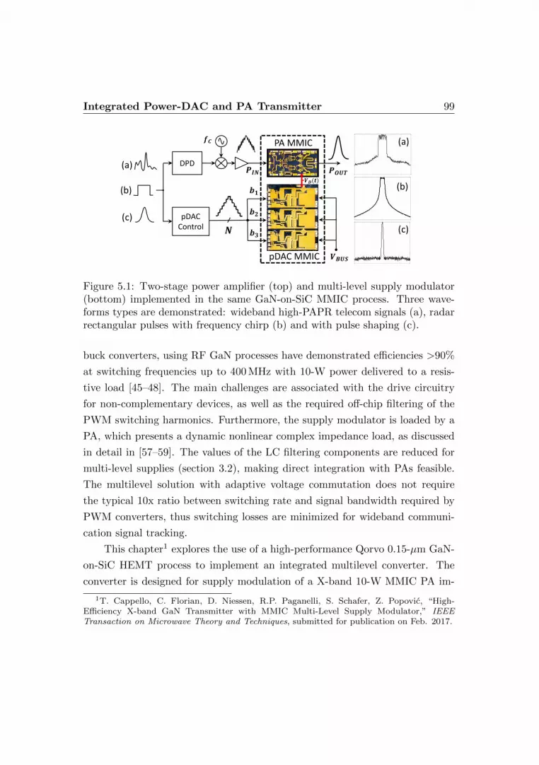
Integrated Power-DAC and PA Transmitter 99
𝑽𝑫(𝒕)
𝒃𝟏
𝑷𝑰𝑵
𝒃𝟐
𝒃𝟑
DPD
𝑵
PA MMIC
pDAC MMIC
𝒇𝑪
pDACControl
(a)
(a)
(b)
(c)
(b)
(c)
𝑽𝑩𝑼𝑺
𝑷𝑶𝑼𝑻
Figure 5.1: Two-stage power amplifier (top) and multi-level supply modulator(bottom) implemented in the same GaN-on-SiC MMIC process. Three wave-forms types are demonstrated: wideband high-PAPR telecom signals (a), radarrectangular pulses with frequency chirp (b) and with pulse shaping (c).
buck converters, using RF GaN processes have demonstrated efficiencies >90%
at switching frequencies up to 400 MHz with 10-W power delivered to a resis-
tive load [45–48]. The main challenges are associated with the drive circuitry
for non-complementary devices, as well as the required off-chip filtering of the
PWM switching harmonics. Furthermore, the supply modulator is loaded by a
PA, which presents a dynamic nonlinear complex impedance load, as discussed
in detail in [57–59]. The values of the LC filtering components are reduced for
multi-level supplies (section 3.2), making direct integration with PAs feasible.
The multilevel solution with adaptive voltage commutation does not require
the typical 10x ratio between switching rate and signal bandwidth required by
PWM converters, thus switching losses are minimized for wideband communi-
cation signal tracking.
This chapter1 explores the use of a high-performance Qorvo 0.15-µm GaN-
on-SiC HEMT process to implement an integrated multilevel converter. The
converter is designed for supply modulation of a X-band 10-W MMIC PA im-
1T. Cappello, C. Florian, D. Niessen, R.P. Paganelli, S. Schafer, Z. Popovic, “High-Efficiency X-band GaN Transmitter with MMIC Multi-Level Supply Modulator,” IEEETransaction on Microwave Theory and Techniques, submitted for publication on Feb. 2017.

Integrated Power-DAC and PA Transmitter 100
plemented in the same technology, similar to the MMIC PAs in [87, 97]. In
Fig. 5.1 the two chips and the setup block diagram are shown. This monolithic
supply modulator is an integrated version of the discrete-component multilevel
presented in chapter 2 and it allows improvements in terms of bandwidth and
system size for a further integration with the PA on a single chip.
5.1 Integrated Power-DAC Supply Modulator
The topology of the 8-level supply modulator circuit is illustrated in Fig. 5.2
on left. Three cascaded half-bridges are composed of two commutating power
switches and each half-bridge is supplied by an isolated voltage VDDi with re-
spect to the floating ground GNDi. During the commutation of the half-bridge,
a very short dead-time (both switches off) is introduced to avoid current flow
between the supply VDDi and GNDi and the associated efficiency loss. During
this dead-time, free-wheeling diodes maintain the current flow to the load. When
the high-side switch of the half-bridge is on, the supply VDDi is connected in
Isolator
DriverIsolator
Isolator
DriverIsolator
Isolator
DriverIsolator
40x125 µm
4x120 µm
650 Ω
4x60 µm
64x150 µm
64x150 µm
40x125 µm
450 Ω
4x60 µm
4x120 µm
330 pF
𝒃𝒊 𝒃𝒊 𝑽𝑺𝑾𝒊
0 1 OFF ON 0 8 mA ON OFF ~ 𝟎 𝑽
1 0 ON OFF 5 mA 0 OFF ON ~ 𝑽𝑫𝑫𝒊
Figure 5.2: Left: block diagram and electric circuit of the Power-DAC. Right:schematic of a Power-DAC half-bridge with the integrated driver. Bottom-right:table showing the functionality of a half-bridge with integrated driver.

Integrated Power-DAC and PA Transmitter 101
series with the floating ground of the subsequent cell. When the low-side switch
of the half-bridge is on, the output of the half-bridge is shorted.
If the three isolated supply voltages VDDi are chosen to be binary-scaled
(e.g. VDD
2 , VDD
4 , and VDD
8 ), it is possible to synthetize an output voltage wave-
form VOUT with eight voltage levels uniformly distributed between zero and
VOUT,MAX by using only three supplies. The circuit is controlled by 3-bit, bi,
and their complementary, bi directly generated in digital base-band. Therefore,
this circuit has the functionality of a Digital-to-Analog power converter (i.e. a
Power-DAC) and its functionality can be described with (2.4), by considering a
zero voltage offset (VOS = 0).
5.1.1 Power-DAC MMIC Design
The N-channel normally-on (D-mode) HEMT transistor in the Qorvo 0.15µm
GaN-on-SiC process has a voltage threshold of about VGS,TH = −3.5 V. The de-
vice is completely on for VGS = 0 V, and off when VGS = −5 V. The breakdown
voltage of this process exceeds 50 V, but the maximum drain supply voltage
of the PA limits the design to 20 V. The half-bridge driver is integrated in the
chip to minimize the gate loop parasitics and improve switching speed, similar
to [46, 47, 52]. Since the Qorvo 0.15µm process features only N-channel tran-
sistors, a fully-complementary efficient totem-pole driver stage is not possible,
and [47] introduced an inverting driver, referred as modified active pull-up, that
demonstrated reduced static losses compared to resistive pull-up in [45]. The
modified active pull-up driver is therefore selected for the design and is shown
in Fig. 5.2 (right).
With reference to the Fig. 5.2, the bits bi and bi are generated by an FPGA
and they control a stack of high-speed isolators (TI ISO721M), which provide
voltage level shifting to the floating ground GNDi of the half-bridges, and am-
plification to reach the necessary 0-5 V swing at the input of the integrated
driver. The non-isolated side of the ISO721M is supplied with VDIG = 3.3 V
referred to system ground (PGND), whereas the isolated side is supplied with
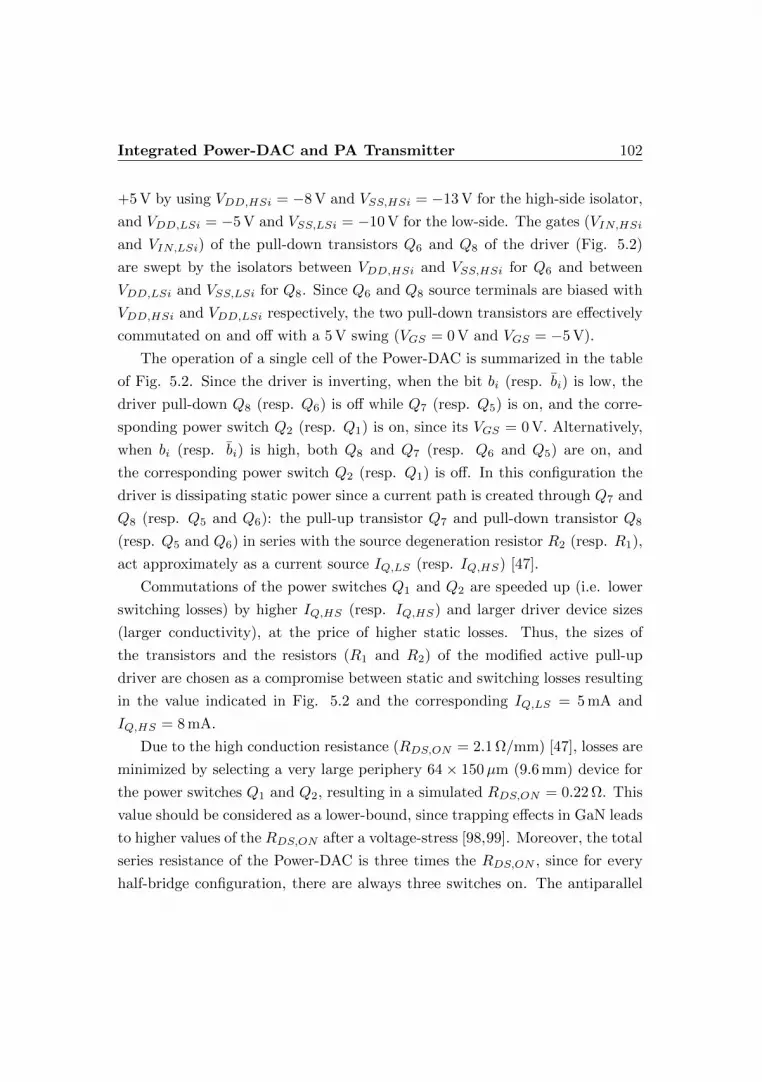
Integrated Power-DAC and PA Transmitter 102
+5 V by using VDD,HSi = −8 V and VSS,HSi = −13 V for the high-side isolator,
and VDD,LSi = −5 V and VSS,LSi = −10 V for the low-side. The gates (VIN,HSi
and VIN,LSi) of the pull-down transistors Q6 and Q8 of the driver (Fig. 5.2)
are swept by the isolators between VDD,HSi and VSS,HSi for Q6 and between
VDD,LSi and VSS,LSi for Q8. Since Q6 and Q8 source terminals are biased with
VDD,HSi and VDD,LSi respectively, the two pull-down transistors are effectively
commutated on and off with a 5 V swing (VGS = 0 V and VGS = −5 V).
The operation of a single cell of the Power-DAC is summarized in the table
of Fig. 5.2. Since the driver is inverting, when the bit bi (resp. bi) is low, the
driver pull-down Q8 (resp. Q6) is off while Q7 (resp. Q5) is on, and the corre-
sponding power switch Q2 (resp. Q1) is on, since its VGS = 0 V. Alternatively,
when bi (resp. bi) is high, both Q8 and Q7 (resp. Q6 and Q5) are on, and
the corresponding power switch Q2 (resp. Q1) is off. In this configuration the
driver is dissipating static power since a current path is created through Q7 and
Q8 (resp. Q5 and Q6): the pull-up transistor Q7 and pull-down transistor Q8
(resp. Q5 and Q6) in series with the source degeneration resistor R2 (resp. R1),
act approximately as a current source IQ,LS (resp. IQ,HS) [47].
Commutations of the power switches Q1 and Q2 are speeded up (i.e. lower
switching losses) by higher IQ,HS (resp. IQ,HS) and larger driver device sizes
(larger conductivity), at the price of higher static losses. Thus, the sizes of
the transistors and the resistors (R1 and R2) of the modified active pull-up
driver are chosen as a compromise between static and switching losses resulting
in the value indicated in Fig. 5.2 and the corresponding IQ,LS = 5 mA and
IQ,HS = 8 mA.
Due to the high conduction resistance (RDS,ON = 2.1 Ω/mm) [47], losses are
minimized by selecting a very large periphery 64× 150µm (9.6 mm) device for
the power switches Q1 and Q2, resulting in a simulated RDS,ON = 0.22 Ω. This
value should be considered as a lower-bound, since trapping effects in GaN leads
to higher values of the RDS,ON after a voltage-stress [98,99]. Moreover, the total
series resistance of the Power-DAC is three times the RDS,ON , since for every
half-bridge configuration, there are always three switches on. The antiparallel

Integrated Power-DAC and PA Transmitter 103
𝑉𝑂𝑈𝑇 𝑡
𝑉𝐷𝐷1
𝑃𝐺𝑁𝐷
𝑉𝑂𝑈𝑇 𝑡
𝑃𝐺𝑁𝐷
𝑉𝐷𝐷1
𝑉𝐷𝐷2
𝑉𝐷𝐷3
𝑉𝐷𝐷,𝐻𝑆1𝑉𝐼𝑁,𝐻𝑆1𝑉𝐼𝑁,𝐿𝑆1𝑉𝐷𝐷,𝐿𝑆1𝐺𝑁𝐷1
𝑉𝐷𝐷,𝐻𝑆2𝑉𝐼𝑁,𝐻𝑆2𝑉𝐼𝑁,𝐿𝑆2𝑉𝐷𝐷,𝐿𝑆2𝐺𝑁𝐷2
𝑉𝐷𝐷,𝐻𝑆3𝑉𝐼𝑁,𝐻𝑆3𝑉𝐼𝑁,𝐿𝑆3𝑉𝐷𝐷,𝐿𝑆3𝐺𝑁𝐷3
𝑉 𝐷𝐷,𝐻𝑆1
𝑉 𝐼𝑁,𝐻𝑆1
𝑉𝐼𝑁,𝐿𝑆1𝑉𝐷𝐷,𝐿𝑆1𝐺𝑁𝐷1
𝑉𝐷𝐷,𝐻𝑆2𝑉𝐼𝑁,𝐻𝑆2𝑉𝐼𝑁,𝐿𝑆2𝑉𝐷𝐷,𝐿𝑆2𝐺𝑁𝐷2
𝑉𝐷𝐷,𝐻𝑆3𝑉𝐼𝑁,𝐻𝑆3𝑉𝐼𝑁,𝐿𝑆3
𝑉 𝐷𝐷,𝐿𝑆3
𝐺𝑁𝐷3
𝐺𝑁𝐷1
𝑉𝐷𝐷2
𝐺𝑁𝐷2
𝑉𝐷𝐷3
𝐺𝑁𝐷3
Figure 5.3: Left: layout in Microwave Office of the Power-DAC. Right: photo-graph of the fabricated MMIC and packaged in a QFN transparent lid package.
diodes Q3 and Q4 are implemented by the two Schottky junctions at the gate-
drain and gate-source of the HEMT device. The gate of the device constitutes
the anode of the diode, the drain-source shorted together is the cathode. The
diode is dimensioned for the average current during the dead-time resulting in
a 40× 125µm periphery. Bypass capacitors are integrated in the MMIC for the
VDDi, VDD,HSi and VDD,LSi nodes with values respectively of 325 pF, 67 pF
and 70 pF. The size of the Power-DAC MMIC is 5.4 × 3.8 mm (Fig. 5.3), and
the chip is bond-wired to a 48-pin 7 × 7 mm QFN package with a transparent
lid, and with 25µm long bond wires connecting to the pads. The Power-DAC
is simulated using Keysights ADS and nonlinear models of active devices pro-
vided by Modelithics. The circuit layout is designed in National Instruments
Microwave Office.

Integrated Power-DAC and PA Transmitter 104
5.1.2 Power-DAC PCB Schematic and Manufacturing
The QFN package of the Power-DAC is mounted on a PCB board together with
the isolators (TI ISO721M) and the schematic of the board is shown in Fig. 5.6.
The digital control part of the Power-DAC is separated by means of isolators
from the power part for noise decoupling. A micro-coaxial 50 Ω cable provides
the FPGA commands to the board. Ceramic bypass capacitors of multiple val-
ues are placed close to the package to provide decoupling from the external
multi-output supply board (discussed in section 5.1.3) which is connected by
means of a flat ribbon cable to the PCB (Fig. 5.8).
Figure 5.4: Left: top layer of the PCB. Right: second layer of the PCB.
Figure 5.5: Left: third layer of the PCB. Right: bottom layer of the PCB.
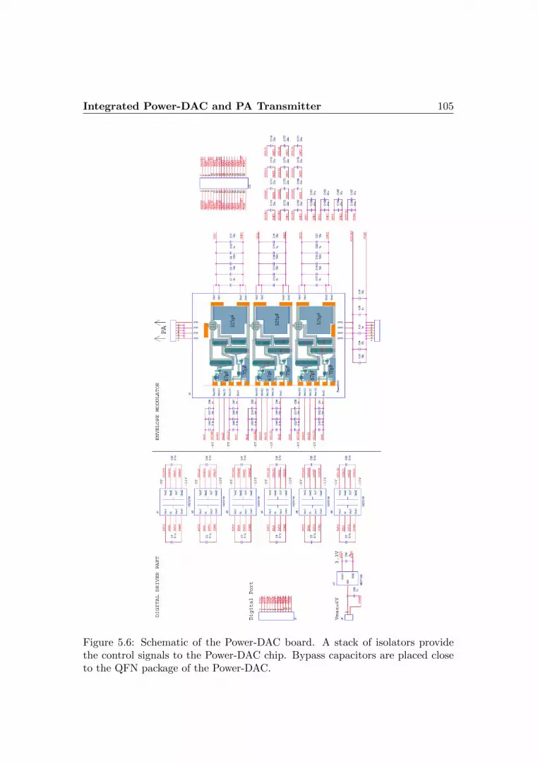
Integrated Power-DAC and PA Transmitter 105
Figure 5.6: Schematic of the Power-DAC board. A stack of isolators providethe control signals to the Power-DAC chip. Bypass capacitors are placed closeto the QFN package of the Power-DAC.
Integrated Power-DAC and PA Transmitter 106
The layout of the 4-layer board is shown in Figs. 5.4-5.5. The PGND
node and the VOUT node of the Power-DAC are placed side-by-side in order
to minimize the output loop length and parasitics. Shield planes on different
layers are used to protect the command signals of the drivers from glitches gen-
erated by the bouncing grounds of the Power-DAC. The board dimension is
66 × 42 mm. An FR4 substrate is used for the manufacturing of the board for
a total thickness of 1.58 mm. Thermal vias are placed underneath the package
pad to provide heat dissipation.
5.1.3 Power-DAC Multi-Output Supply Board
The positive supply voltages of the half-bridges (VDDi) along with the driver
supplies (VDD,HSi and VDD,LSi) are derived from a single 48 V bus supply by
means of an external multi-output supply board. This board is designed to
provide a wide configuration of supply voltages, rather than a high conversion
efficiency (although it largely employs switching converters). A more compact
design could be implemented when the VDDi voltage values are identified for a
specific PA.
The schematic of the board is shown in Fig. 5.7. Three identical circuital
configuration are paralleled and used to generate the required voltages for the
three half-bridges and drivers. The i-th half-bridge VDDi voltage is derived in
two stages from the 48 V bus supply. The first stage provides galvanic isolation
from the 48 V bus supply by means of an off-the-shelf DC/DC brick converter
(GE Critical Power SW001A2B91Z) which generates an output voltage of 12 V
with 3.5 A of maximum current. The input-output capacitance between the
non-isolated and the isolated side of the converter is 65 pF. This value has to be
minimized in order to reduce stray currents caused by the fast switching ground
of the isolated side of the converter. Connected to the 12 V, which is provided
by the first DC/DC, a non-isolated buck converter (TI PTN78000WAH) is used
to generate a tunable VDDi from 2.5 V up to almost 12 V (converter shorted)
with a maximum current of 1.5 A. A 11-turn trimmer is used to precisely regu-

Integrated Power-DAC and PA Transmitter 107
Figure 5.7: Schematic of the multi-output supply board (no offset voltage supplyis shown).
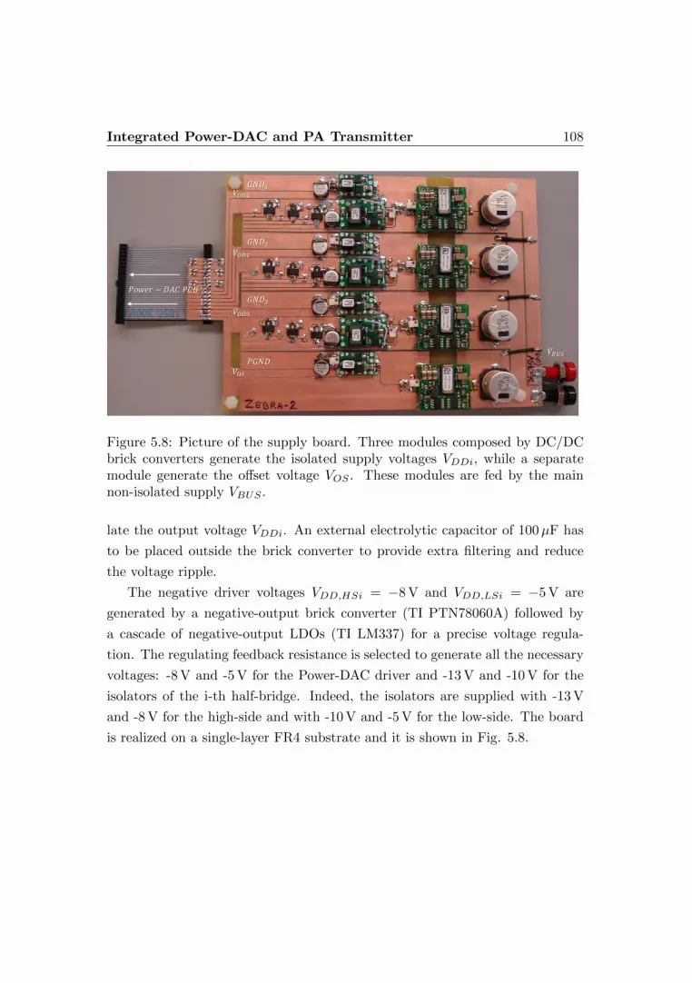
Integrated Power-DAC and PA Transmitter 108
𝑉𝐵𝑈𝑆
𝐺𝑁𝐷1
𝐺𝑁𝐷2
𝐺𝑁𝐷3
𝑃𝐺𝑁𝐷
𝑉𝐷𝐷2
𝑉𝐷𝐷1
𝑉𝐷𝐷3
𝑉𝑂𝑆
𝑃𝑜𝑤𝑒𝑟 − 𝐷𝐴𝐶 𝑃𝐶𝐵
Figure 5.8: Picture of the supply board. Three modules composed by DC/DCbrick converters generate the isolated supply voltages VDDi, while a separatemodule generate the offset voltage VOS . These modules are fed by the mainnon-isolated supply VBUS .
late the output voltage VDDi. An external electrolytic capacitor of 100µF has
to be placed outside the brick converter to provide extra filtering and reduce
the voltage ripple.
The negative driver voltages VDD,HSi = −8 V and VDD,LSi = −5 V are
generated by a negative-output brick converter (TI PTN78060A) followed by
a cascade of negative-output LDOs (TI LM337) for a precise voltage regula-
tion. The regulating feedback resistance is selected to generate all the necessary
voltages: -8 V and -5 V for the Power-DAC driver and -13 V and -10 V for the
isolators of the i-th half-bridge. Indeed, the isolators are supplied with -13 V
and -8 V for the high-side and with -10 V and -5 V for the low-side. The board
is realized on a single-layer FR4 substrate and it is shown in Fig. 5.8.

Integrated Power-DAC and PA Transmitter 109
5.1.4 Power-DAC MMIC Functionality Tests
The DC conduction resistance of the power switches are preliminarily measured
with a multimeter and it results in RDS,ON = 0.33 Ω at room temperature
(25 C), which is in agreement with the simulated value, considering also the
resistance of the 1.5 mm long bonding wires to the package pads (about 75 mΩ).
Further measurements with drain voltages commutating to 20 V showed an
increase of the resistance up to 0.43 Ω due to dynamic effects (i.e. dynamic
RDS,ON , see chapter 7), which are not described in the model. The measured
quiescent current of the driver is IQ,HS = 8 mA for the high-side active pull-
up and IQ,LS = 5 mA for the low-side, as expected from simulations. The
Power-DAC chip is initially tested in terms of functionality, switching speed
and slew-rate on a low-inductance resistive load RL = 33 Ω and the resulting
waveforms are compared with time-domain simulations. The digital commands
of the Power-DAC are generated with an FPGA, and the isolated input supply
voltages VDDi are 3.3 V, 5.8 V, and 11.4 V.
The measured and simulated converter responses to a full voltage swing of
a 500 ns ramp are reported in Fig. 5.9. The waveforms are measured with a
500 MHz passive probe (Agilent 1161A) [78] that could possibly introduce some
bandwidth limitation and additional ringing. By observing the 71.4 ns long
steps in the staircase, the longest settling time of the measured ringing is about
SimulationMeasurement
SimulationMeasurement
Time Time
Figure 5.9: Left: response of the Power-DAC to a positive and negative ramp of1µs sweeping all the levels upside-down. Right: step response of the Power-DACand simulation result.
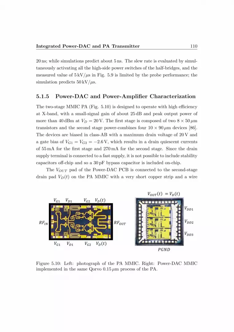
Integrated Power-DAC and PA Transmitter 110
20 ns; while simulations predict about 5 ns. The slew rate is evaluated by simul-
taneously activating all the high-side power switches of the half-bridges, and the
measured value of 5 kV/µs in Fig. 5.9 is limited by the probe performance; the
simulation predicts 50 kV/µs.
5.1.5 Power-DAC and Power-Amplifier Characterization
The two-stage MMIC PA (Fig. 5.10) is designed to operate with high efficiency
at X-band, with a small-signal gain of about 25 dB and peak output power of
more than 40 dBm at VD = 20 V. The first stage is composed of two 8× 50µm
transistors and the second stage power-combines four 10 × 90µm devices [86].
The devices are biased in class-AB with a maximum drain voltage of 20 V and
a gate bias of VG1 = VG2 = −2.6 V, which results in a drain quiescent currents
of 55 mA for the first stage and 270 mA for the second stage. Since the drain
supply terminal is connected to a fast supply, it is not possible to include stability
capacitors off-chip and so a 30 pF bypass capacitor is included on-chip.
The VOUT pad of the Power-DAC PCB is connected to the second-stage
drain pad VD(t) on the PA MMIC with a very short copper strip and a wire
𝑅𝐹𝑂𝑈𝑇𝑅𝐹𝐼𝑁
𝑉𝐷1 𝑉𝐷(𝑡)
𝑉𝐷(𝑡)𝑉𝐷1𝑉𝐺1
𝑉𝐺1 𝑉𝐺2
𝑉𝐺2
𝑉𝑂𝑈𝑇 𝑡 = 𝑉𝐷(𝑡)
𝑉𝐷𝐷1
𝑉𝐷𝐷2
𝑉𝐷𝐷3
𝑃𝐺𝑁𝐷
Figure 5.10: Left: photograph of the PA MMIC. Right: Power-DAC MMICimplemented in the same Qorvo 0.15µm process of the PA.
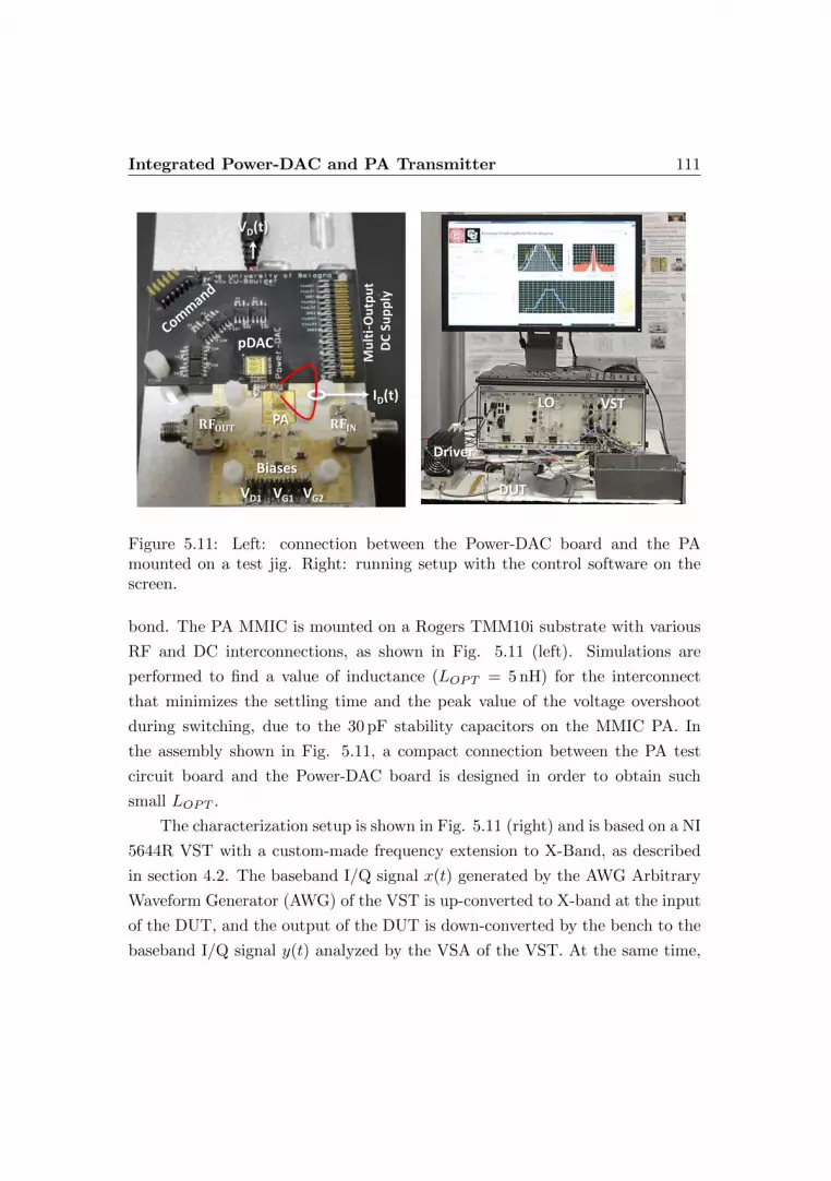
Integrated Power-DAC and PA Transmitter 111
Mu
lti-
Ou
tpu
t D
C S
up
ply
Biases
pDAC
PA
ID(t)
VD(t)
VD1 VG1 VG2
Driver
DUT
VSTLO
Figure 5.11: Left: connection between the Power-DAC board and the PAmounted on a test jig. Right: running setup with the control software on thescreen.
bond. The PA MMIC is mounted on a Rogers TMM10i substrate with various
RF and DC interconnections, as shown in Fig. 5.11 (left). Simulations are
performed to find a value of inductance (LOPT = 5 nH) for the interconnect
that minimizes the settling time and the peak value of the voltage overshoot
during switching, due to the 30 pF stability capacitors on the MMIC PA. In
the assembly shown in Fig. 5.11, a compact connection between the PA test
circuit board and the Power-DAC board is designed in order to obtain such
small LOPT .
The characterization setup is shown in Fig. 5.11 (right) and is based on a NI
5644R VST with a custom-made frequency extension to X-Band, as described
in section 4.2. The baseband I/Q signal x(t) generated by the AWG Arbitrary
Waveform Generator (AWG) of the VST is up-converted to X-band at the input
of the DUT, and the output of the DUT is down-converted by the bench to the
baseband I/Q signal y(t) analyzed by the VSA of the VST. At the same time,

Integrated Power-DAC and PA Transmitter 112
a synchronized high-speed oscilloscope measures the VD(t) and the ID(t) with
a current probe. The time alignment between these quantities is automatically
performed by a LabVIEW program controlling the bench. A setup calibration
is performed at the input-output reference plane at the MMIC PA ports.
5.1.6 Power-Amplifier Characterization
The PA and the Power-DAC MMIC are characterized at 9.57 GHz by means of
a voltage probe [78] used for the VD(t) measurement, and an additional wire
clamped to a wide-band current probe [79] for the ID(t) measurement. Af-
ter the PA characterization, the wire is removed to restore the low-impedance
connection (LOPT = 5 nH) between the PA and the supply MMIC. The PA is
characterized in pulsed mode at different drain voltage levels synthesized by the
Power-DAC and all the measurements are performed with the pulse sequence
shown in Fig. 5.12.
Figure 5.12: Pulse sequence to extract the characteristics of the PA. The pre-pulse at the peak voltage VD7 = 20 V is used to pre-condition the PA to aknown state of trap, then a pulse VDi is performed to extract the input-outputcharacteristic of the PA for each voltage level.

Integrated Power-DAC and PA Transmitter 113
×
♦
+
×
♦+
×
♦
+
×
♦+
Figure 5.13: Left: measured PA input-output characteristic at different supplyvoltages (blue solid). Right: measured PA gain at different supply voltages(blue solid). Both: the thick traces (red solid) are the trajectory followed bythe PA while supply modulated.
This characterization procedure takes into account trapping effects by a
double-pulsing technique described in section 4.3.1. A pre-pulse at the maxi-
mum voltage level pre-conditions the PA to a known trap-state, followed by a
measurement pulse at each supply voltage level, used to extract the PA behav-
ior. The drops observed in the pulse supply voltage of Fig. 5.12 are due to the
internal resistance of the Power-DAC. The PA has a peak current of 1 A and the
total conduction resistance of the Power-DAC is 1.3 Ω, leading to a maximum
voltage drop ∆VD = 1.3 V at VD = 20 V and maximum output power. Fig. 5.13
shows a peak output power of more than 40.4 dBm with an associated gain of
23 dBm at about 2 dB compression at 9.57 GHz.
5.1.7 Power-DAC Characterization
The Power-DAC efficiency is characterized with the PA acting as a variable
load, controlled by the RF input power PIN,i. This technique allows the char-
acterization of the instantaneous efficiency of the supply-modulator, since the
PSUPPLY (t) power, drawn from the load, can be continuously varied by the
input PA power. The overall efficiency ηpDAC,i of the Power-DAC supply mod-

Integrated Power-DAC and PA Transmitter 114
×
♦
+
× ♦ +
×
♦
+
×
♦+
Figure 5.14: Left: measured efficiency of the Power-DAC including driver lossesat different levels and output power (blue solid). Right: PAE (blue dotted) andComposite PAE (blue solid) at different levels. Both: the thick traces are thetrajectory followed by the DUT (red solid).
ulator at the i-th level can be defined as:
ηpDAC,i =PSUPPLY,i
PDC,i + PDRIV ER,i, (5.1)
where PSUPPLY,i is the output power of the Power-DAC, PDC,i is the total input
power provided to the three half-bridges, and PDRIV ER,i is the total dissipated
power in the drivers at the i -th level. The measured overall efficiency ηpDAC,i of
the Power-DAC, including the driving stage losses is shown on left of Fig. 5.14.
Observing the left plot of Fig. 5.14, it is interesting to notice that the
maximum efficiency of the Power-DAC is obtained for the maximum output
voltage (VD = 20 V) and moderate output current, which is in accordance with
the dominating RDS,ON losses. Indeed, when delivering 5 W at VD = 20 V
(ISUPPLY = 250 mA) the Power-DAC efficiency tops to 96.5%. The drop in
the efficiency of the Power-DAC alone at low output power levels is due to the
static driver losses, which have a fixed contribution. As the output power level
increases, the losses are mostly ascribable to the RDS,ON of the power switches,
and the driving losses are less important. At the maximum output power, the

Integrated Power-DAC and PA Transmitter 115
efficiency of the Power-DAC reaches the 91.7% and remains above the 85% for
a large range of output power.
In the right plot of Fig. 5.14, it is possible to observe that the maximum PAE
of the PA exceeds 50% for most of the levels and is reached at the maximum
output power POUT,MAX,i for each supply level. Thus, the quantized thresholds
for the supply level transitions selected to maximize the PA efficiency under
multilevel supply modulation are chosen at POUT,MAX,i, as marked on the Fig.
5.13 with the vertical dotted lines. Finally, the composite PAE (CPAE) of the
i-th level of the supply-modulated PA can be defined as:
CPAEi = PAEi · ηpDAC,i. (5.2)
The measured results of the CPAE are shown on the right of Fig. 5.14; at the
maximum output power, the CPAE reaches 50.7%.
5.1.8 Baseband Digital Part and Pre-Distortion
As described in sections 3.2 and 4.2, a linearization of the PA by means of DPD
is needed to compensate for the its nonlinear behavior (i.e. quantization error
and gain compression non-linearities) under multilevel ET regime. Given the
sharp change in the behavior of the PA, in terms of gain and output power
at different voltage levels, and considering also the high switching speed of the
supply modulator, it is not possible to fit the input-output characteristics of
the PA with a unique continuous model, since the discontinuities introduced
by the Power-DAC are too fast compared to the sampling rate of the system
(120 MHz), as can be seen in the distorted output (DPD OFF) in Fig. 5.16.
To this aim, a vector-switched architecture [82, 83] is chosen to model the
behavior of the PA, with each vector region corresponding to a selected supply
voltage level. The normalized complex values of input xi and output yi base-
band signals are collected and stored in a multidimensional array (one for each
voltage level).

Integrated Power-DAC and PA Transmitter 116
×♦+ × ♦
+
×
+
♦×♦+ × ♦
+
×
+
♦
×♦+ × ♦
+
×
+
♦
×♦+ × ♦
+
×
+
♦
Figure 5.15: AM/AM (left) and AM/PM (right) characteristics of the DUT.The direct non-linear characteristics with memory at the different supply levelsare marked with symbols (blue lines). The inverted non-linear characteristicswith memory of the DPD are also shown (red lines).
In Fig. 5.15, the AM/AM and the AM/PM characteristics at the differ-
ent supply voltage levels of the considered PA are shown. Non-linear distortion
with memory is evident from the plot, especially at high voltage levels. is evi-
dent from the plot. A memory polynomial [80, 81] is chosen to fit each region
of the Vector-Switched switched model describing the supply modulated PA for
each voltage level. The selected predistortion strategy preserves the peak output
power at an expense of a gain reduction of the linearized system. The collected
data xi(n) and yi(n) are used to model the inverted complex characteristics of
the DUT for each region as follows:
xi(n) =
Ki−1∑k=0
Qi−1∑q=0
akq,iyi(n− q)|yi(n− q)|k, (5.3)
where Ki is the order of the polynomial, and Qi are respectively the order of
the polynomial describing the non-linearity and the delay taps used to fit the
memory of the DUT at the i -th supply level. The same order Ki = 9 and
Qi = 11 are chosen for the highest supply levels (i = 5, 6, 7), while for the re-
maining levels a memoryless model is used (Qi = 0) is used for the remaining
levels. By least-square fitting the previous equations for each level, the calcu-
lated coefficients akq,i are then used to pre-distort the original signal x(n), as
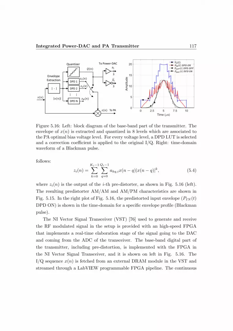
Integrated Power-DAC and PA Transmitter 117
Quantizer
3
3
To PA
To pDAC
DPD 1
DPD 2
DPD N
… …
EnvelopeExtraction
To Power-DAC
Figure 5.16: Left: block diagram of the base-band part of the transmitter. Theenvelope of x(n) is extracted and quantized in 8 levels which are associated tothe PA optimal bias voltage level. For every voltage level, a DPD LUT is selectedand a correction coefficient is applied to the original I/Q. Right: time-domainwaveform of a Blackman pulse.
follows:
zi(n) =
Ki−1∑k=0
Qi−1∑q=0
akq,ix(n− q)|x(n− q)|k, (5.4)
where zi(n) is the output of the i -th pre-distorter, as shown in Fig. 5.16 (left).
The resulting predistorter AM/AM and AM/PM characteristics are shown in
Fig. 5.15. In the right plot of Fig. 5.16, the predistorted input envelope (PIN (t)
DPD ON) is shown in the time-domain for a specific envelope profile (Blackman
pulse).
The NI Vector Signal Transceiver (VST) [76] used to generate and receive
the RF modulated signal in the setup is provided with an high-speed FPGA
that implements a real-time elaboration stage of the signal going to the DAC
and coming from the ADC of the transceiver. The base-band digital part of
the transmitter, including pre-distortion, is implemented with the FPGA in
the NI Vector Signal Transceiver, and it is shown on left in Fig. 5.16. The
I/Q sequence x(n) is fetched from an external DRAM module in the VST and
streamed through a LabVIEW programmable FPGA pipeline. The continuous

Integrated Power-DAC and PA Transmitter 118
envelope |x(n)| is extracted by means of an envelope extraction block with a
22-bit output width, then it is quantized in 8 levels and coded with 3-bits, to
generate the sequence Q(n). The i-th output zi(n) of the pre-distorter is selected
by Q(n), generated by the quantizer block which converts the high resolution
|x(n)| into a discrete 3-bit width signal that controls the Power-DAC and selects
the correct DPD. A precise time-alignment is crucial for the correct operation
of the DPD together with the supply modulator.
5.2 Experimental Results
The supply-modulated transmitter is tested with two types of signals: amplitude-
and frequency-modulated pulses that can be applied to radar for spectral con-
finement, and OFDM signals for high-capacity communications. In both cases,
a dramatic improvement in the CPAE is demonstrated while linearity is main-
tained.
5.2.1 Pulsed Radars with Amplitude and Frequency Mod-
ulation
The range resolution of a radar is proportional to the bandwidth of the trans-
mitted pulsed signal. Short pulses, however, reduce ranging capability and
pulse compression techniques overcome this trade-off by frequency (i.e. chirp-
ing) or phase modulation (e.g. BPSK, Barker codes) within a usually rectan-
gular pulses [20]. Rectangular envelope pulses results in spectral spreading due
to the fast rise- and fall-times [20,21,29]. High time side-lobes (-13.2 dB) at the
output of the matched filter in the receiver can obstruct the presence of a target
or give false target detection. Shaping the pulse envelope before transmitting
to, e.g. a Gaussian, limits the spectral spreading and gives theoretically no side-
lobes at the output of the receiver matched filter [20,21,29]. However, applying
an amplitude modulation to the RF pulse envelope increases the dissipation
in the PA, unless the PA supply voltage is modulated to track the efficiency

Integrated Power-DAC and PA Transmitter 119
𝑨𝒎𝒑𝒍𝒊𝒕𝒖𝒅𝒆𝑻𝒂𝒑𝒆𝒓 (𝑷𝑨𝑷𝑹)
𝑺𝒖𝒑𝒑𝒍𝒚 𝑴𝒐𝒅𝒖𝒍𝒂𝒕𝒊𝒐𝒏−𝟑 𝐝𝐁
𝑩𝒂𝒏𝒅𝒘𝒊𝒅𝒕𝒉𝟏𝒔𝒕 𝑻𝒊𝒎𝒆 𝑺𝒊𝒅𝒆𝒍𝒐𝒃𝒆 (𝒅𝑩𝒎)
𝑷𝒐𝒘𝒆𝒓 𝒑𝒆𝒓 𝒑𝒖𝒍𝒔𝒆𝐖 (𝐝𝐁𝐦)
𝑷𝑨𝑬 𝜼𝒑𝑫𝑨𝑪 𝑪𝑷𝑨𝑬
𝐑𝐞𝐜𝐭𝐚𝐧𝐠𝐮𝐥𝐚𝐫 (𝟎. 𝟎𝟎 𝐝𝐁) 𝐑𝐞𝐜𝐭𝐚𝐧𝐠𝐮𝐥𝐚𝐫 𝐏𝐮𝐥𝐬𝐞 𝟒. 𝟓 𝐌𝐇𝐳 −𝟏𝟑. 𝟓 𝐝𝐁 𝟏𝟎. 𝟓 (𝟒𝟎. 𝟐) 𝟓𝟒. 𝟒% 𝟗𝟑% 𝟓𝟎. 𝟔%
Triangular (3.00 dB) Rectangular Pulse + DPD 1.6 MHz −26.2 dB (ideal) 3.7 (35.7) 34.9% 90% 31.4%
𝐓𝐫𝐢𝐚𝐧𝐠𝐮𝐥𝐚𝐫 (𝟑. 𝟎𝟎 𝐝𝐁) 𝐄𝐓 + 𝐃𝐏𝐃 𝟏. 𝟔 𝐌𝐇𝐳 −𝟐𝟔. 𝟐 𝐝𝐁 (𝐢𝐝𝐞𝐚𝐥) 𝟑. 𝟕 (𝟑𝟓. 𝟕) 𝟓𝟑. 𝟑% 𝟖𝟓% 𝟒𝟓. 𝟑%
Hanning (3.01 dB) Rectangular Pulse + DPD 1.9 MHz −31.4 dB (ideal) 4.1 (36.1) 38.7% 90% 34.9%
𝐇𝐚𝐧𝐧𝐢𝐧𝐠 (𝟑. 𝟎𝟏 𝐝𝐁) 𝐄𝐓 + 𝐃𝐏𝐃 𝟏. 𝟗 𝐌𝐇𝐳 −𝟑𝟏. 𝟒 𝐝𝐁 (𝐢𝐝𝐞𝐚𝐥) 𝟒. 𝟏 (𝟑𝟔. 𝟏) 𝟓𝟐. 𝟗% 𝟖𝟕% 𝟒𝟔. 𝟎%
Blackman (3.77 dB) Rectangular Pulse + DPD 1.5 MHz −52.0 dB (ideal − 58 dB) 3.3 (35.2) 35.8% 89% 31.9%
𝐁𝐥𝐚𝐜𝐤𝐦𝐚𝐧 (𝟑. 𝟕𝟕 𝐝𝐁) 𝐄𝐓 + 𝐃𝐏𝐃 𝟏. 𝟓 𝐌𝐇𝐳 −𝟓𝟐. 𝟎 𝐝𝐁 (𝐢𝐝𝐞𝐚𝐥 − 𝟓𝟖 𝐝𝐁) 𝟑. 𝟑 (𝟑𝟓. 𝟐) 𝟓𝟐. 𝟒% 𝟖𝟒% 𝟒𝟒. 𝟎%
Table 5.1: Performance with different pulse waveforms for radars.
peak [24,26,100].
To demonstrate this concept with a MMIC PA and MMIC tracker, we con-
sider test signals with a pulse duration T = 10µs and 100µs of repetition period
(10% duty cycle). The pulse envelope is shaped with three different windowing
functions: Triangular, Hanning, and Blackman [95]. The supply-modulated PA
is then characterized with the technique presented in sections 5.1.5 and 5.1.8.
Results are compared to the standard rectangular envelope pulse. Each pulse is
also frequency modulated with a 5-MHz linear chirp to increase the bandwidth
while keeping the same pulse envelope and duration. Results of the three win-
dowing functions are summarized in Table 5.1.
The output power spectra of the three types of AM pulses are provided in
Fig. 5.17, while the output of the matched filter on the receiver is shown in
Fig. 5.18. As can be noticed from Table 5.1, the rectangular pulse reaches the
highest CPAE of 50.6% and the widest bandwidth of 4.5 MHz, but this comes
with a very high first side-lobe (-13.5 dB) at the output of the matched filter. By
tapering the pulse envelope with a Blackman weighting window, it is possible
to reduce the temporal side-lobe up to -52 dB. The efficiency improvement with
supply modulation as compared to a pulsed constant supply is between 11-14
percentage points.

Integrated Power-DAC and PA Transmitter 120
Triangular Hanning Blackman
Rect.IdealPA Out
Rect.IdealFiltered
Rect.IdealFiltered
Rect.IdealPA Out
Rect.IdealFiltered
Rect.IdealPA Out
Triangular Hanning Blackman
Figure 5.17: Output spectra of the PA with the DPD enabled. The threeweighting windows are compared with a rectangular chirped pulse. Similarbandwidth (i.e. range resolution) can be obtained but with an improved spectralpurity.
Triangular Hanning Blackman
Rect.IdealPA Out
Rect.IdealReceived
Rect.IdealReceived
Rect.IdealPA Out
Rect.IdealReceived
Rect.IdealPA Out
Triangular Hanning Blackman
Figure 5.18: Output of the matched filter in a pulse-compressed radar receiverwith linear frequency modulation. Lower temporal side-lobes are obtained bymeans of amplitude weighting of the transmitted signal.
5.2.2 High Bandwidth, High PAPR Telecom Signal
In this section we demonstrate the transmitter capability to efficiently amplify
LTE channels at 1.4, 10, and 20 MHz in Down-Link (DL) mode. For each signal,
the transmitter performance for fixed supply voltage and modulated supply is
compared, in both cases with DPD linearization. In-band metrics such as Error
Vector Magnitude (EVM), as well as out-of-band characteristics, such as the
Adjacent Channel Leakage Ratio (ACLR), are measured. For these wide-band
measurements, the short connection between the PA and the Power-DAC is re-
established, preventing measurements at the drain with the current clamp (for

Integrated Power-DAC and PA Transmitter 121
𝑳𝑻𝑬 𝑪𝒉𝒂𝒏𝒏𝒆𝒍 𝑷𝑨𝑷𝑹 (𝒅𝑩) 𝑺𝒖𝒑𝒑𝒍𝒚 𝑴𝒐𝒅𝒖𝒍𝒂𝒕𝒊𝒐𝒏 𝑬𝑽𝑴 (%) 𝑨𝑪𝑳𝑹 ∗ (𝒅𝑩) 𝑷𝒐𝒖𝒕𝑨𝒗𝒈(𝑾) 𝑷𝒊𝒏𝑨𝒗𝒈 (𝑾) 𝑷𝒔𝒖𝒑𝒑𝒍𝒚 (𝑾) 𝑪𝑷𝑨𝑬 (%)
DL 1.4 MHz 9.3 dB Fixed Supply + DPD 1.83 % 52 dB 1.38 W 19.2 mW 7.04 W 19.4 %
𝐃𝐋 𝟏. 𝟒 𝐌𝐇𝐳 𝟗. 𝟑 𝐝𝐁 𝐄𝐓 + 𝐃𝐏𝐃 𝟐. 𝟒𝟒 % 𝟒𝟔 𝐝𝐁 𝟏. 𝟒𝟏𝐖 𝟕. 𝟓 𝐦𝐖 𝟑. 𝟓𝟎𝐖 𝟒𝟎. 𝟏 %
DL 10 MHz 11.3 dB Fixed Supply + DPD 2.46 % 49 dB 0.91 W 13 mW 6.22 W 14.4 %
𝐃𝐋 𝟏𝟎𝐌𝐇𝐳 𝟏𝟏. 𝟑 𝐝𝐁 𝐄𝐓 + 𝐃𝐏𝐃 𝟑. 𝟗𝟑 % 𝟑𝟒 𝐝𝐁 𝟏. 𝟎𝟐𝐖 𝟓. 𝟏 𝐦𝐖 𝟐. 𝟗𝟒𝐖 𝟑𝟒. 𝟓 %
DL 20 MHz 11.4 dB Fixed Supply + DPD 2.90 % 47 dB 0.74 W 10.5 mW 6.56 W 11.1 %
𝐃𝐋 𝟐𝟎𝐌𝐇𝐳 𝟏𝟏. 𝟒 𝐝𝐁 𝐄𝐓 + 𝐃𝐏𝐃 𝟓. 𝟐𝟒 % 𝟑𝟑 𝐝𝐁 𝟎. 𝟖𝟓𝐖 𝟒. 𝟏 𝐦𝐖 𝟐. 𝟔𝟓𝐖 𝟑𝟐. 𝟎 %
Table 5.2: Performance with different LTE channel bandwidths. *ACLR: de-fined as the ratio of the average power in the channel bandwidth and the averagepower centered in the next channel with the same bandwidth.
the PAE), and only the CPAE is available and reported in Table 5.2.
With reference to Table 5.2, the input (PinAvg), and output average
power (PoutAvg), are measured by the VST, while the total input supply power
(Psupply) is measured with current probes at the input of each half-bridge and
of each driver of the Power-DAC. The DPD significantly reduces out-of-band
distortion, as evident in Figs. 5.19 and 5.20. For EVM calculations, the original
measured data at 120 MHz is re-sampled 10 times to get better time-alignment,
and an improved estimation of this metric. The non-perfect linearization of the
20 MHz LTE signal is most likely due to the experimental bench bandwidth
limitation constrained by the VST 5644R analog bandwidth of 80 MHz. The
non-linear expansion of the DPD would require a bandwidth of 3-5 times the
original [1], thus very close to the hardware limit of the bench.
The CPAE improves over 20 percentage points using supply-modulation as
compared to the constant supply case and the supplied DC power is reduced
by more than 50%. The corresponding linearity performance is obviously some-
what deteriorated, but still compliant with communication standards [64]. The
drop in CPAE in supply-modulated mode from 40% to 32% for signals with
1.4 MHz and 20 MHz bandwidth is due to two factors. For the 1.4 MHz signal
case, the PA delivers higher average output power (1.4 W vs. 0.85 W) and re-
quires more power from the Power-DAC (about 3 W vs. 1.8 W, estimating a
PA efficiency of around 50%). As can be observed in the characteristics of Fig.
5.14, this condition enables the Power-DAC to operate at higher efficiency, since

Integrated Power-DAC and PA Transmitter 122
DPD OFF
Downlink LTE Channel 1.4 MHz Downlink LTE Channel 10 MHz Downlink LTE Channel 20 MHz
DPD ONDPD OFFDPD ON
DPD OFFDPD ON
Pout (W) DPD OFF
Pout (W) DPD ON
Supply (V)Pout (W) DPD OFF
Pout (W) DPD ON
Supply (V)
Pout (W) DPD OFF
Pout (W) DPD ON
Supply (V)
Downlink LTE Channel 1.4 MHz Downlink LTE Channel 10 MHz Downlink LTE Channel 20 MHzFigure 5.19: Power spectra of the three different channel bandwidth consid-ered: 1.4 MHz (left), 10 MHz (center), and 20 MHz (right). For comparison, thespectrum with the DPD disabled is overlaid in the three cases showing spectralregrowth out of band.
DPD OFF
Downlink LTE Channel 1.4 MHz Downlink LTE Channel 10 MHz Downlink LTE Channel 20 MHz
DPD ONDPD OFFDPD ON
DPD OFFDPD ON
Pout (W) DPD OFFPout (W) DPD ON
Supply (V)Pout (W) DPD OFFPout (W) DPD ON
Supply (V)
Pout (W) DPD OFFPout (W) DPD ON
Supply (V)
Downlink LTE Channel 1.4 MHz Downlink LTE Channel 10 MHz Downlink LTE Channel 20 MHz
Figure 5.20: Output power with DPD ON (red solid), with DPD OFF (blue dot-ted), and supply voltage (black solid) of the three different channel bandwidthconsidered: 1.4 MHz (left), 10 MHz (center), and 20 MHz (right).
for low power levels the efficiency increases with power. For the 20 MHz signal,
the high (11.8 MHz) switching rate of the devices in the Power-DAC results in
non-negligible switching losses. The observed increased improvement obtained
with telecom signals compared to AM radar signals is due to the obvious higher
average efficiency improvement that supply modulation provides for signals with
higher PAPR.

Integrated Power-DAC and PA Transmitter 123
5.3 Conclusion
This chapter details an X-band envelope-tracking transmitter with a MMIC
GaN PA and a MMIC multi-level supply modulator. The two chips are fabri-
cated in the same 0.15µm GaN-on-SiC process. The supply modulator demon-
strates a slew rate of 5 kV/µs. The transmitter operation with DPD is demon-
strated on two signal types. An amplitude-modulated chirped pulse results in
a composite average efficiency of 45%, showing 11 to 14 percentage points im-
provement over no amplitude modulation, with a dramatic increase in linearity
evidenced by up to 52 dB attenuation of the first time sideband. Addition-
ally, 1.4 MHz, 10 MHz and 20 MHz LTE signals result in an overall efficiency
between 32-40%, corresponding to an efficiency improvement of 20 percentage
points compared to the fixed supply case, with good linearity. The performance
obtained with two separate MMICs shows the potential of a fully integrated
PA-modulator chip.
However, the 0.15µm microwave GaN process has some drawbacks for the
supply modulator integration:
1. only depletion-mode devices are available, which makes it difficult to im-
plement efficient fully-complementary drivers with zero static dissipation;
2. the normally-ON devices are not ideal for power supplies, since any failure
in the driver supply produces a destructive short circuit of the power
switches;
3. the above mentioned characteristics require additional bias voltages, with
a consequent increased complexity of the external bias board and inter-
connections to the MMIC;
4. the relatively high RDS,ON/mm of this technology and the further increase
of the dynamic RDS,ON due to trapping phenomena limits the maximum
efficiency for high supply currents and impose the use of large periphery
Integrated Power-DAC and PA Transmitter 124
power switches (i.e. large chip area, larger switching losses). Further
investigation are shown in chapter 7.
Because of these issues, the integrated Power-DAC efficiency performance
does not exceed that of hybrid implementations for communication signal (chap-
ter 2) and modulated-radar (chapter 4) and applications which use normally-on
(E-mode) GaN-on-Si power-switches with extremely low dynamic RDS,ON and
fully-complementary CMOS drivers with zero static power consumption. How-
ever, the overall size of the Power-DAC integrated version gives a higher power
density and in some cases warrants the slight reduction in efficiency. The de-
velopment of a technology with E- and D-mode devices, following recent GaAs
pHEMT industrial processes for mixed signal applications, would be ideally
suited to a fully integrated and highly efficient supply-modulated PA using the
architecture presented in this chapter.

Chapter 6
Supply-Modulation of an
Outphasing Chireix PA
Spectral mask requirements for both communication and radar systems has led
to the development of signals with high Peak-to-Average Power Ratios (PAPR).
Traditional and high efficiency Power Amplifier (PA) classes cannot operate
efficiently over a wide output power range, significantly degrading the trans-
mitter efficiency for such signals. Efficiency enhancement techniques such as
Doherty [31,32], Envelope Tracking (ET) [41,42] and outphasing [35,36] are de-
veloped to extend efficient operation into back-off. Individually, however, these
techniques may not provide sufficient back-off efficiency for communications sig-
nals [101,102]. In Chireix outphasing [35], a non-isolated combiner enables and
dictates load modulation, maintaining high efficiency operation. In LINC out-
phasing [36], an isolated combiner preserves linear amplification at the cost of
poor efficiency roll-off with output power. In this chapter, a combination of
Chireix outphasing and discrete supply modulation is employed to extend the
efficient operating range of an X-band PA.
125
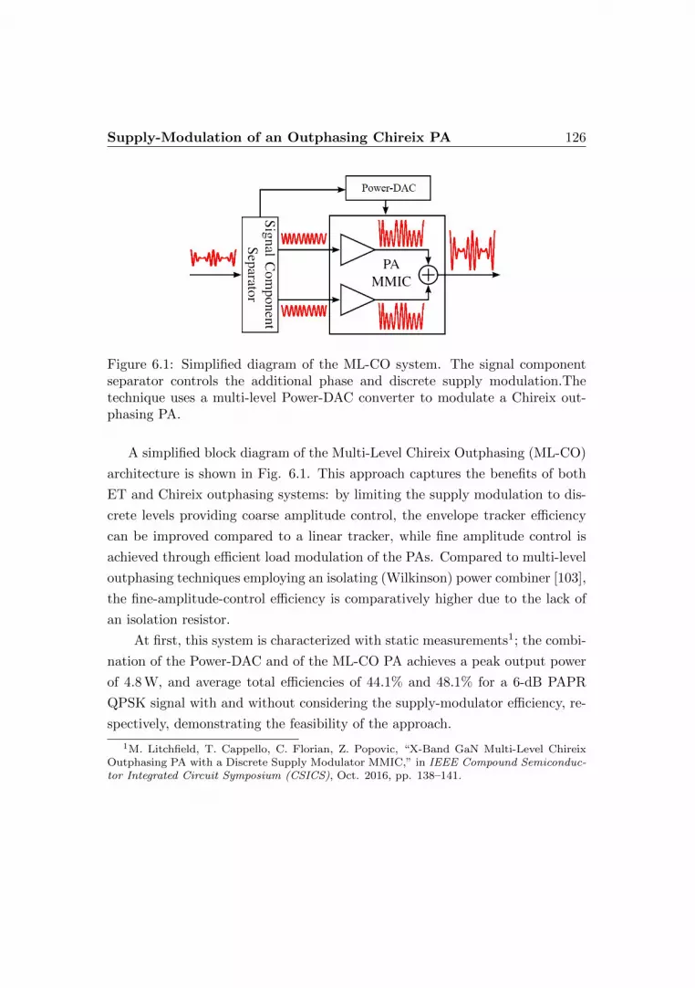
Supply-Modulation of an Outphasing Chireix PA 126
Figure 6.1: Simplified diagram of the ML-CO system. The signal componentseparator controls the additional phase and discrete supply modulation.Thetechnique uses a multi-level Power-DAC converter to modulate a Chireix out-phasing PA.
A simplified block diagram of the Multi-Level Chireix Outphasing (ML-CO)
architecture is shown in Fig. 6.1. This approach captures the benefits of both
ET and Chireix outphasing systems: by limiting the supply modulation to dis-
crete levels providing coarse amplitude control, the envelope tracker efficiency
can be improved compared to a linear tracker, while fine amplitude control is
achieved through efficient load modulation of the PAs. Compared to multi-level
outphasing techniques employing an isolating (Wilkinson) power combiner [103],
the fine-amplitude-control efficiency is comparatively higher due to the lack of
an isolation resistor.
At first, this system is characterized with static measurements1; the combi-
nation of the Power-DAC and of the ML-CO PA achieves a peak output power
of 4.8 W, and average total efficiencies of 44.1% and 48.1% for a 6-dB PAPR
QPSK signal with and without considering the supply-modulator efficiency, re-
spectively, demonstrating the feasibility of the approach.
1M. Litchfield, T. Cappello, C. Florian, Z. Popovic, “X-Band GaN Multi-Level ChireixOutphasing PA with a Discrete Supply Modulator MMIC,” in IEEE Compound Semiconduc-tor Integrated Circuit Symposium (CSICS), Oct. 2016, pp. 138–141.

Supply-Modulation of an Outphasing Chireix PA 127
An experimental test bench2 able to dynamically generate phase- and time-
aligned modulated signals for outphasing and supply modulation is developed.
The DPD-linearized ML-CO PA is demonstrated with 1.4 MHz and 10 MHz LTE
signals. For both signals, the average total power consumption is reduced by a
factor of two when supply modulation is used. For the 9.3 dB PAPR, 1.4 MHz
signal the PA operates with 38% average drain efficiency at 0.54 W average
output power.
6.1 Outphasing Chireix X-band PA
The ML-CO PA is implemented in a MMIC with a GaN-on-SiC Qorvo 0.15µm
process and it is designed to operate in class-F with second (short) and third
(open) harmonic terminations [30]. At the combiner reference plane, the internal
PAs are characterized by load-pull simulations [39, 104]. The Chireix combiner
performs all fundamental matching, and designates the desired load modulation
for outphasing operation. The overall size of the chip is 3.8 mm× 3.2 mm and
the layout is shown in Fig. 6.2.
The MMIC ML-CO PA is mounted on a 40 mil thick CuMo carrier plate
as shown in Fig. 6.2. The PA input (A1 and A2 labels) and the output RF
pad (OUT label) are bonded, with two short bond wires, to 10 mil thick alu-
mina lines, on which connectorized launchers are landed for testing. The cal-
ibration procedure de-embeds the launchers and alumina lines up to the bond
wire/alumina interface. The gate bias DC pads (VG) are connected with a
bondwire to off-chip bypass capacitors. For these static measurements, the by-
pass capacitors are kept on the drain bias pad (VD label in Fig. 6.2) which is
connected to the MMIC version of the Power-DAC (see section 5.1).
2T. Cappello, C. Florian, T. W. Barton, M. Litchfield, Z. Popovic, “Multi-Level Supply-Modulated Chireix Outphasing for LTE Signals,” IEEE MTT-S International MicrowaveSymposium (IMS), Honolulu, HI, USA, June 2017.
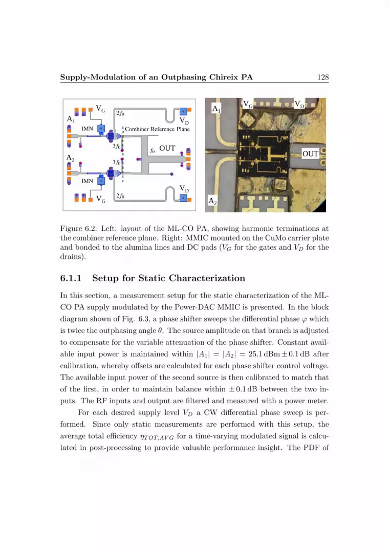
Supply-Modulation of an Outphasing Chireix PA 128
VG VDA1
A2
OUT
A1
A2
OUT
VD
VD
VG
VG
Figure 6.2: Left: layout of the ML-CO PA, showing harmonic terminations atthe combiner reference plane. Right: MMIC mounted on the CuMo carrier plateand bonded to the alumina lines and DC pads (VG for the gates and VD for thedrains).
6.1.1 Setup for Static Characterization
In this section, a measurement setup for the static characterization of the ML-
CO PA supply modulated by the Power-DAC MMIC is presented. In the block
diagram shown of Fig. 6.3, a phase shifter sweeps the differential phase ϕ which
is twice the outphasing angle θ. The source amplitude on that branch is adjusted
to compensate for the variable attenuation of the phase shifter. Constant avail-
able input power is maintained within |A1| = |A2| = 25.1 dBm± 0.1 dB after
calibration, whereby offsets are calculated for each phase shifter control voltage.
The available input power of the second source is then calibrated to match that
of the first, in order to maintain balance within ± 0.1 dB between the two in-
puts. The RF inputs and output are filtered and measured with a power meter.
For each desired supply level VD a CW differential phase sweep is per-
formed. Since only static measurements are performed with this setup, the
average total efficiency ηTOT,AV G for a time-varying modulated signal is calcu-
lated in post-processing to provide valuable performance insight. The PDF of

Supply-Modulation of an Outphasing Chireix PA 129
Figure 6.3: Outphasing PA measurement setup for static characterization. Sep-arate sources drive each PA branch, while a phase shifter sweeps the differentialphase.
a QPSK signal with a 6-dB PAPR is shown in Fig. 6.4 and used as a weighting
function to yield the average efficiency using the optimal trajectory.
The total DC input power for the Power-DAC is measured at the three
outputs of the supply board (section 5.1.3) with an oscilloscope via current
(I1, I2, I3) and voltage (V1, V2, V3) probes. The DC output power of the Power-
DAC is measured in a likewise manner along the wires interfaced to the MMIC
PA. When a measurement accounts for the Power-DAC consumption, the Power-
DAC input power is used as the DC power in the efficiency calculation, other-
wise, the Power-DAC output power is used as the DC power.
6.1.2 Experimental Results
Fig. 6.4 shows a compilation of phase sweeps for seven supply levels from the
voltage offset, 5.5 V, to 19.6 V with and without considering the Power-DAC ef-
ficiency. Due to the resistance in the Power-DAC transistors (see section 5.1.4),
the supply voltage varies during the phase sweep, since the DC current is vary-
ing. The variation ranges from 0.48 V for the 5.5 V level to 1.3 V for the 19.6 V
level, showing an increase in the voltage drop with the supplied current. The
supplies are labeled in Figs. 6.4 and 6.5 by the average voltage across the phase

Supply-Modulation of an Outphasing Chireix PA 130
Figure 6.4: Compilation of measured phase sweeps at different supply levelswithout (left) and with (right) considering the Power-DAC dissipation. Theoptimal trajectory is selected to maximize ηTOT,SY S . In black is the PDF of a6-dB PAPR QPSK signal used to calculate average total efficiency.
Figure 6.5: Left: comparison of optimal trajectories without (ηTOT ) and with(ηTOT,SY S) the Power-DAC efficiency. Right: efficiency of the Power-DAC,showing the operating points of the optimal trajectory.
sweep. At 19.6 V, a peak output power of 36.8 dBm or 4.8 W is achieved in both
cases. When taking the consumption of the Power-DAC into account, the peak
total efficiency drops from 61.3% to 57.4%, and the average total efficiency for
a 6-dB PAPR QPSK signal drops from 48.1% to 44.1%.
The decrease in efficiency is evident in the comparison by comparing the
optimal trajectory (“Opt” marker) in Fig. 6.5. The system efficiency decreases
more at higher supply voltages, because the efficiency of the Power-DAC holds
more weight at the system level, since it is supplying significantly higher cur-
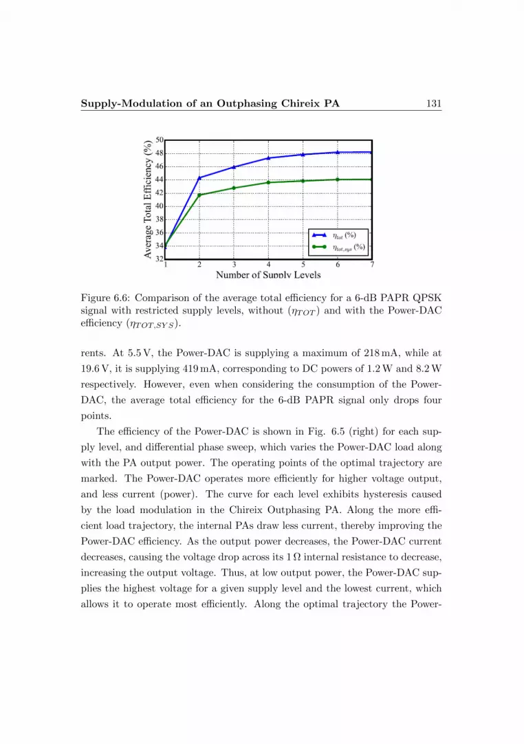
Supply-Modulation of an Outphasing Chireix PA 131
Figure 6.6: Comparison of the average total efficiency for a 6-dB PAPR QPSKsignal with restricted supply levels, without (ηTOT ) and with the Power-DACefficiency (ηTOT,SY S).
rents. At 5.5 V, the Power-DAC is supplying a maximum of 218 mA, while at
19.6 V, it is supplying 419 mA, corresponding to DC powers of 1.2 W and 8.2 W
respectively. However, even when considering the consumption of the Power-
DAC, the average total efficiency for the 6-dB PAPR signal only drops four
points.
The efficiency of the Power-DAC is shown in Fig. 6.5 (right) for each sup-
ply level, and differential phase sweep, which varies the Power-DAC load along
with the PA output power. The operating points of the optimal trajectory are
marked. The Power-DAC operates more efficiently for higher voltage output,
and less current (power). The curve for each level exhibits hysteresis caused
by the load modulation in the Chireix Outphasing PA. Along the more effi-
cient load trajectory, the internal PAs draw less current, thereby improving the
Power-DAC efficiency. As the output power decreases, the Power-DAC current
decreases, causing the voltage drop across its 1 Ω internal resistance to decrease,
increasing the output voltage. Thus, at low output power, the Power-DAC sup-
plies the highest voltage for a given supply level and the lowest current, which
allows it to operate most efficiently. Along the optimal trajectory the Power-

Supply-Modulation of an Outphasing Chireix PA 132
DAC operates between 81.5% and 91.5% efficiency.
The average total efficiency is calculated for restricted number of supply lev-
els, as shown in Fig. 6.6, with and without consideration for the Power-DAC
consumption. The 19.6 V level is included in all cases to maintain the same peak
output power. For each number of supply levels, the optimal subset of the mea-
sured supplies is found for the QPSK signal used in this work. In both cases, the
diminishing returns are clearly visible, with the system efficiency (considering
Power-DAC dissipation) approaching 44.1%, 4 points lower than the previous
measurements ignoring the efficiency of the discrete supply modulator.
Although these measurements do not prove the dynamic capabilities of am-
plifying a modulated signal with a ML-CO PA, they provide a more realistic,
static characterization of expected performance. In order to amplify with ac-
ceptable linearity, nonlinearities caused by both the ML-CO PA as well as the
discontinuities introduced by the discrete supply modulator need to be taken
into account.
6.1.3 Setup for Dynamic Characterization
The focus of this section is on the dynamic characterization and linearization
of this system. A major challenge in modulated outphasing testing is the need
to generate multiple dynamic phase- and time-aligned drive signals for the two
PAs and for the supply modulator.
The block diagram of the setup is shown in Fig. 6.7; two National Instru-
ment Vector Signal Transceivers (VSTs) [76] are employed and phased-locked
by the PXI-express bus. The 3 GHz constant-envelope, phase-modulated VSG
outputs from the VSTs are upconverted to the 9.7 GHz operating frequency of
the PAs. The external LO used for upconversion is also phase-locked to the
10 MHz reference clock of the VSTs. Simultaneously, a time-aligned digital sig-
nal generated by the integrated FPGA controls the supply modulator. One VST
is also used as an observation receiver. The picture of the experimental setup
is shown in Fig. 6.8 (bottom).
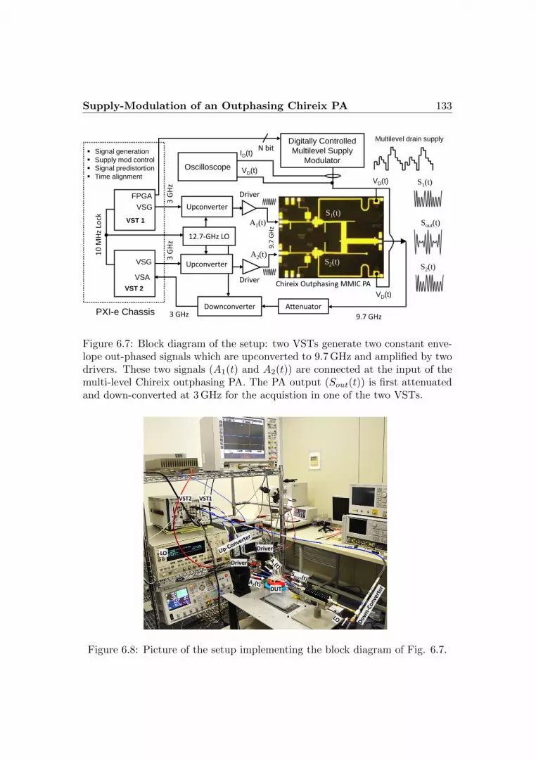
Supply-Modulation of an Outphasing Chireix PA 133
3 G
Hz
3 G
Hz
Digitally Controlled
Multilevel Supply
Modulator
10
MH
z Lo
ck
Downconverter
A1(t)
9.7 GHz
N bit
Chireix Outphasing MMIC PA
Attenuator
Oscilloscope VD(t)
ID(t)
VSG
VSA
FPGA
VSG
PXI-e Chassis
Upconverter
Upconverter
Driver
12.7-GHz LO
Driver
VST 1
VST 2
VD(t)
VD(t)
A2(t)
S1(t)
S2(t)
Sout(t)
S1(t)
S2(t)
3 GHz
9.7
GH
z
Multilevel drain supply
Signal generation
Supply mod control
Signal predistortion
Time alignment
Figure 6.7: Block diagram of the setup: two VSTs generate two constant enve-lope out-phased signals which are upconverted to 9.7 GHz and amplified by twodrivers. These two signals (A1(t) and A2(t)) are connected at the input of themulti-level Chireix outphasing PA. The PA output (Sout(t)) is first attenuatedand down-converted at 3 GHz for the acquistion in one of the two VSTs.
VST2 VST1
Driver
Driver
DUT
LO
Figure 6.8: Picture of the setup implementing the block diagram of Fig. 6.7.
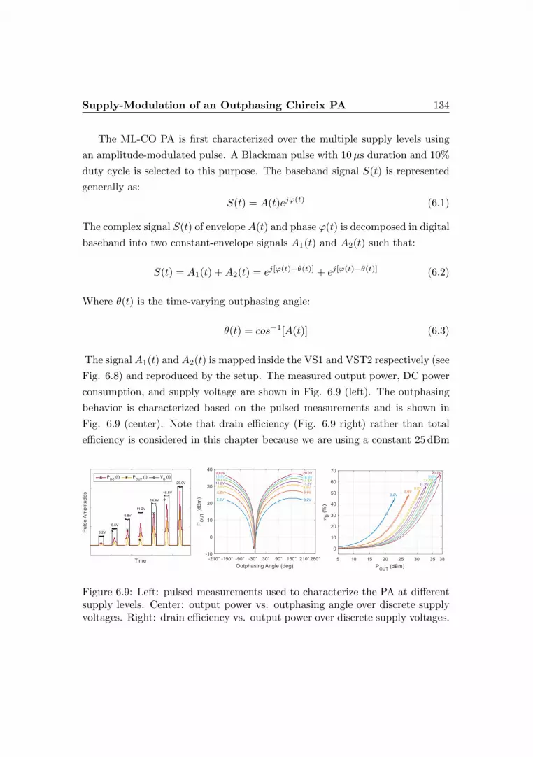
Supply-Modulation of an Outphasing Chireix PA 134
The ML-CO PA is first characterized over the multiple supply levels using
an amplitude-modulated pulse. A Blackman pulse with 10µs duration and 10%
duty cycle is selected to this purpose. The baseband signal S(t) is represented
generally as:
S(t) = A(t)ejϕ(t) (6.1)
The complex signal S(t) of envelope A(t) and phase ϕ(t) is decomposed in digital
baseband into two constant-envelope signals A1(t) and A2(t) such that:
S(t) = A1(t) +A2(t) = ej[ϕ(t)+θ(t)] + ej[ϕ(t)−θ(t)] (6.2)
Where θ(t) is the time-varying outphasing angle:
θ(t) = cos−1[A(t)] (6.3)
The signal A1(t) and A2(t) is mapped inside the VS1 and VST2 respectively (see
Fig. 6.8) and reproduced by the setup. The measured output power, DC power
consumption, and supply voltage are shown in Fig. 6.9 (left). The outphasing
behavior is characterized based on the pulsed measurements and is shown in
Fig. 6.9 (center). Note that drain efficiency (Fig. 6.9 right) rather than total
efficiency is considered in this chapter because we are using a constant 25 dBm
Figure 6.9: Left: pulsed measurements used to characterize the PA at differentsupply levels. Center: output power vs. outphasing angle over discrete supplyvoltages. Right: drain efficiency vs. output power over discrete supply voltages.
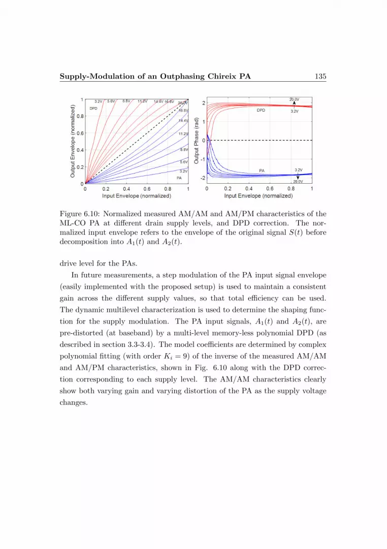
Supply-Modulation of an Outphasing Chireix PA 135
Figure 6.10: Normalized measured AM/AM and AM/PM characteristics of theML-CO PA at different drain supply levels, and DPD correction. The nor-malized input envelope refers to the envelope of the original signal S(t) beforedecomposition into A1(t) and A2(t).
drive level for the PAs.
In future measurements, a step modulation of the PA input signal envelope
(easily implemented with the proposed setup) is used to maintain a consistent
gain across the different supply values, so that total efficiency can be used.
The dynamic multilevel characterization is used to determine the shaping func-
tion for the supply modulation. The PA input signals, A1(t) and A2(t), are
pre-distorted (at baseband) by a multi-level memory-less polynomial DPD (as
described in section 3.3-3.4). The model coefficients are determined by complex
polynomial fitting (with order Ki = 9) of the inverse of the measured AM/AM
and AM/PM characteristics, shown in Fig. 6.10 along with the DPD correc-
tion corresponding to each supply level. The AM/AM characteristics clearly
show both varying gain and varying distortion of the PA as the supply voltage
changes.
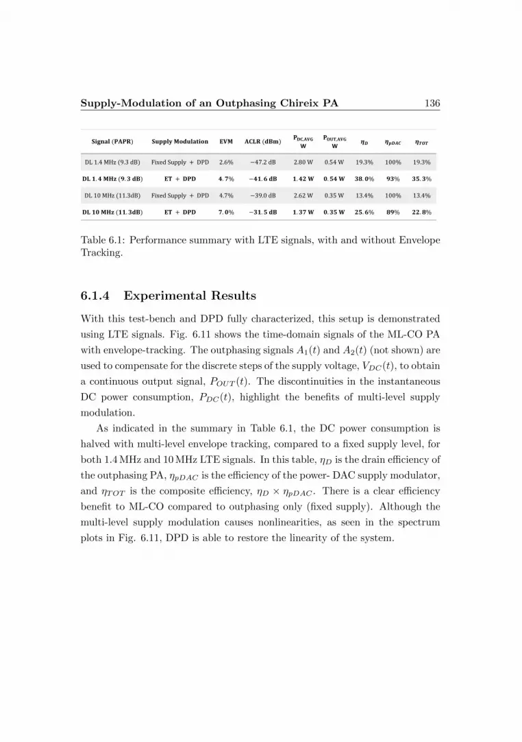
Supply-Modulation of an Outphasing Chireix PA 136
𝐒𝐢𝐠𝐧𝐚𝐥 (𝐏𝐀𝐏𝐑) 𝐒𝐮𝐩𝐩𝐥𝐲 𝐌𝐨𝐝𝐮𝐥𝐚𝐭𝐢𝐨𝐧 𝐄𝐕𝐌 𝐀𝐂𝐋𝐑 (𝐝𝐁𝐦)𝐏𝐃𝐂,𝐀𝐕𝐆
W
𝐏𝐎𝐔𝐓,𝐀𝐕𝐆W
𝜼𝑫 𝜼𝒑𝑫𝑨𝑪 𝜼𝑻𝑶𝑻
DL 1.4 MHz (9.3 dB) Fixed Supply + DPD 2.6% −47.2 dB 2.80 W 0.54 W 19.3% 100% 19.3%
𝐃𝐋 𝟏. 𝟒 𝐌𝐇𝐳 (𝟗. 𝟑 𝐝𝐁) 𝐄𝐓 + 𝐃𝐏𝐃 𝟒. 𝟕% −𝟒𝟏. 𝟔 𝐝𝐁 𝟏. 𝟒𝟐 𝐖 𝟎.𝟓𝟒 𝐖 𝟑𝟖. 𝟎% 𝟗𝟑% 𝟑𝟓. 𝟑%
DL 10 MHz (11.3dB) Fixed Supply + DPD 4.7% −39.0 dB 2.62 W 0.35 W 13.4% 100% 13.4%
𝐃𝐋 𝟏𝟎 𝐌𝐇𝐳 (𝟏𝟏. 𝟑𝐝𝐁) 𝐄𝐓 + 𝐃𝐏𝐃 𝟕. 𝟎% −𝟑𝟏. 𝟓 𝐝𝐁 𝟏. 𝟑𝟕 𝐖 𝟎.𝟑𝟓 𝐖 𝟐𝟓. 𝟔% 𝟖𝟗% 𝟐𝟐. 𝟖%
Table 6.1: Performance summary with LTE signals, with and without EnvelopeTracking.
6.1.4 Experimental Results
With this test-bench and DPD fully characterized, this setup is demonstrated
using LTE signals. Fig. 6.11 shows the time-domain signals of the ML-CO PA
with envelope-tracking. The outphasing signals A1(t) and A2(t) (not shown) are
used to compensate for the discrete steps of the supply voltage, VDC(t), to obtain
a continuous output signal, POUT (t). The discontinuities in the instantaneous
DC power consumption, PDC(t), highlight the benefits of multi-level supply
modulation.
As indicated in the summary in Table 6.1, the DC power consumption is
halved with multi-level envelope tracking, compared to a fixed supply level, for
both 1.4 MHz and 10 MHz LTE signals. In this table, ηD is the drain efficiency of
the outphasing PA, ηpDAC is the efficiency of the power- DAC supply modulator,
and ηTOT is the composite efficiency, ηD × ηpDAC . There is a clear efficiency
benefit to ML-CO compared to outphasing only (fixed supply). Although the
multi-level supply modulation causes nonlinearities, as seen in the spectrum
plots in Fig. 6.11, DPD is able to restore the linearity of the system.

Supply-Modulation of an Outphasing Chireix PA 137
Figure 6.11: Left: time-domain drain voltage, output power, and DC powerconsumption waveforms. Right: ideal spectrum and output spectrum of multi-level supply modulated signals with and without DPD for a 1.4-MHz LTE signalwith 9.3-dB PAPR.
6.2 Conclusion
In this chapter, a ML-CO PA with the Power-DAC supply modulator is pre-
sented. At first, this system is characterized with static measurements; the
combination of the Power-DAC and of the ML-CO PA achieves a peak output
power of 4.8 W, and average total efficiencies of 44.1% for a 6-dB PAPR QPSK
signal, thus demonstrating the feasibility of the approach.
The feasibility of the ML-CO PA architecture is further substantiated by
the development of a setup for the dynamic characterization of the ML-CO PA
with the Power-DAC supply-modulator. The combination of supply modulation
and outphasing halves the DC power consumption, leading to 16 percentage
points higher efficiency for a 1.4 MHz LTE signal and 9.4 percentage points for
a 10 MHz LTE signal. DPD based on a multi-level memory-less polynomial is
used to restore the linearity of the system when supply modulation is used.

Chapter 7
Dynamic Effects of Electron
Devices in Supply Modulators
and PAs
The remarkable intrinsic characteristics of gallium nitride enable the develop-
ment of GaN transistor technologies that set new targets in terms of efficiency
and power density in several power electronic applications [105–107]. The well-
known properties of wide-bandgap semiconductors and the characteristics of
HEMT devices with lateral (rather than vertical) highly-conductive channels
implemented by means of AlGaN/GaN heterostructures are exploited for the
production of compact and fast transistors with high breakdown voltage and
very low losses [105–107]. While initially developed solely for RF and microwave
applications, GaN technologies are recently proposed also for the power elec-
tronic market, with several commercial GaN switches already available [106].
These devices can be operated at higher switching speed compared to Si devices
with comparable voltage and current capabilities (Si power MOSFET), due to
lower switching and conduction losses [105–107].
138
Dynamic Effects of Electron Devices in SMs and PAs 139
Highly efficient switching-mode DC/DC converters are reported in [108–110].
The high switching frequency enables compact designs and consequent improve-
ments of the power density. Besides the increased power density, the fast switch-
ing performance of GaN have are exploited for the design of power supplies with
very fast dynamic response, to be used for example for the supply modulation
of radio frequency (RF) and microwave power amplifiers (PA) [45, 48, 52, 56].
In such applications (e.g. envelope tracking section in chapter 1), the power
supply output voltage follows the envelope of the signal (typically telecom) to
be amplified by the RF PA, thus addressing multi-MHz instantaneous band-
widths. In this context, [48] reported synchronous buck converters with 88%
total efficiency at 100 MHz switching frequency. These converters [48, 52] and
the integrated version of the Power-DAC (chapter 5) are designed with the same
0.15-µm AlGaN/GaN process of the RF PA for a perspective integration with
the power supply.
Despite offering clear advantages with respect to their silicon counterparts
for the design of highly efficient switching converters, AlGaN/GaN HEMTs suf-
fer from a degradation mechanism of the dynamic on-resistance (RON ) which
is different from Si Power MOSFETs. The application of high electric fields
to the device conductive channel created by the AlGaN/GaN heterostructure
grown over SiC or Si substrates, makes GaN HEMT prone to non-negligible
charge trapping phenomena. While in Si power MOSFET technologies trap-
ping phenomena are practically eliminated by the optimization of the passiva-
tion processes, the same cannot be done for GaN traps, since they are located
in different regions of the device, rather than in the superficial passivation inter-
faces [111,112]. The presence of traps in GaN devices is related to the intrinsic
device structure and working mechanism, and thus it cannot be completely elim-
inated, but only limited to a certain extent by means of technological solutions
as field plating [111, 112]. As a consequence, even mature, state of the art,
commercial GaN devices suffer from this phenomenon (as it is shown also in
this chapter), though with less deterioration in the dynamic performance with
respect to early research-level devices [98, 99, 111–117]. It is observed that the
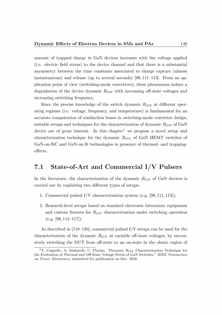
Dynamic Effects of Electron Devices in SMs and PAs 140
amount of trapped charge in GaN devices increases with the voltage applied
(i.e. electric field stress) to the device channel and that there is a substantial
asymmetry between the time constants associated to charge capture (almost
instantaneous) and release (up to several seconds) [99, 111–113]. From an ap-
plication point of view (switching-mode converters), these phenomena induce a
degradation of the device dynamic RON with increasing off-state voltages and
increasing switching frequency.
Since the precise knowledge of the switch dynamic RON at different oper-
ating regimes (i.e. voltage, frequency, and temperature) is fundamental for an
accurate computation of conduction losses in switching-mode converter design,
suitable setups and techniques for the characterization of dynamic RON of GaN
device are of great interest. In this chapter1 we propose a novel setup and
characterization technique for the dynamic RON of GaN HEMT switches of
GaN-on-SiC and GaN-on-Si technologies in presence of thermal- and trapping-
effects.
7.1 State-of-Art and Commercial I/V Pulsers
In the literature, the characterization of the dynamic RON of GaN devices is
carried out by exploiting two different types of setups:
1. Commercial pulsed I/V characterization system (e.g. [99, 111,113]);
2. Research-level setups based on standard electronic laboratory equipment
and custom fixtures for RON characterization under switching operation
(e.g. [98, 114–117]).
As described in [118–120], commercial pulsed I/V setups can be used for the
characterization of the dynamic RON at variable off-state voltages, by succes-
sively switching the DUT from off-state to an on-state in the ohmic region of
1T. Cappello, A. Santarelli, C. Florian, “Dynamic RON Characterization Technique forthe Evaluation of Thermal and Off-State Voltage Stress of GaN Switches,” IEEE Transactionon Power Electronics, submitted for publication on Dec. 2016.
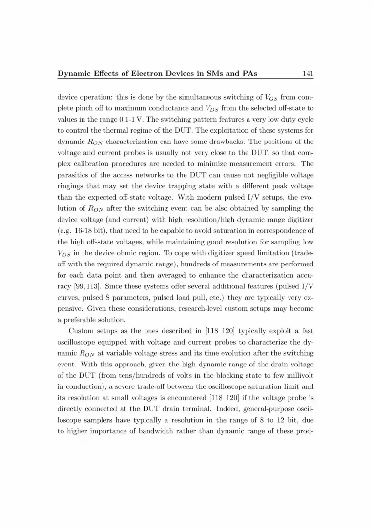
Dynamic Effects of Electron Devices in SMs and PAs 141
device operation: this is done by the simultaneous switching of VGS from com-
plete pinch off to maximum conductance and VDS from the selected off-state to
values in the range 0.1-1 V. The switching pattern features a very low duty cycle
to control the thermal regime of the DUT. The exploitation of these systems for
dynamic RON characterization can have some drawbacks. The positions of the
voltage and current probes is usually not very close to the DUT, so that com-
plex calibration procedures are needed to minimize measurement errors. The
parasitics of the access networks to the DUT can cause not negligible voltage
ringings that may set the device trapping state with a different peak voltage
than the expected off-state voltage. With modern pulsed I/V setups, the evo-
lution of RON after the switching event can be also obtained by sampling the
device voltage (and current) with high resolution/high dynamic range digitizer
(e.g. 16-18 bit), that need to be capable to avoid saturation in correspondence of
the high off-state voltages, while maintaining good resolution for sampling low
VDS in the device ohmic region. To cope with digitizer speed limitation (trade-
off with the required dynamic range), hundreds of measurements are performed
for each data point and then averaged to enhance the characterization accu-
racy [99, 113]. Since these systems offer several additional features (pulsed I/V
curves, pulsed S parameters, pulsed load pull, etc.) they are typically very ex-
pensive. Given these considerations, research-level custom setups may become
a preferable solution.
Custom setups as the ones described in [118–120] typically exploit a fast
oscilloscope equipped with voltage and current probes to characterize the dy-
namic RON at variable voltage stress and its time evolution after the switching
event. With this approach, given the high dynamic range of the drain voltage
of the DUT (from tens/hundreds of volts in the blocking state to few millivolt
in conduction), a severe trade-off between the oscilloscope saturation limit and
its resolution at small voltages is encountered [118–120] if the voltage probe is
directly connected at the DUT drain terminal. Indeed, general-purpose oscil-
loscope samplers have typically a resolution in the range of 8 to 12 bit, due
to higher importance of bandwidth rather than dynamic range of these prod-

Dynamic Effects of Electron Devices in SMs and PAs 142
ucts. In order to overcome this limitation, diode- and transistor-based clamp-
ing circuits are inserted between the oscilloscope probe and the sensed voltage
node [98, 114–117]. Optimized clamping circuits enable the characterization of
VDS (and thus RON ) starting right after the voltage stress (delay times between
hundreds of ns to few s). The drawback of these solutions is a partial loss of
accuracy, due to the need to de-embed the clamp electrical characteristic from
the measurement. Additional limitation in custom setups may arise from the
types of probes adopted for voltage and current sensing. Depending on the DUT
RON value (i.e. DUT periphery) and the amount of drain current during the
characterization, the use of passive high-impedance voltage probes may limit
the accuracy of the measurement of very low VDS , whereas the use of typical
magnetic-coupled probes may limit the accuracy in the acquisition of the cur-
rent.
Finally, one additional characteristic that is valuable for a test setup is the
possibility to characterize the RON of the DUT working in a switching condi-
tion similar to the final application. This is not always achieved by the setups
commercially available or proposed in the literature. The novel setup and char-
acterization technique presented in this chapter address the described issues.
7.2 Dynamic RON in GaN Switches
In this section, a novel laboratory setup and characterization procedure for the
dynamic RON of GaN HEMT switches in the presence of thermal- and trapping-
effects is presented. The proposed setup allows the study of RON transients after
the switching event at variable off-state voltages and temperatures. The use of
custom-designed differential amplifiers and a voltage-controlled current source
enables the accurate characterization of RON even on large periphery devices.
For both technologies dynamic RON degradations up to 75% and 20% are ob-
served for temperature and off-state voltage variations respectively. These char-
acterization data allow an accurate estimation of the conduction losses during
the design of the supply-modulator.
Dynamic Effects of Electron Devices in SMs and PAs 143
𝑇𝐶
𝑉𝐷𝐷
𝐼𝐷𝑆Driver
Half-Bridge PCB
PW
M
𝑉𝐷𝑆
𝐼𝐷𝑆
𝑇𝐶
Setup for the RON
Characterization
+
-
+
-
𝑉𝐷𝑆+
-
𝑉𝑆𝑊
Time-D
om
ain A
cqu
isition
System
Figure 7.1: Block diagram of the presented setup for the characterization of thedynamic RON in GaN HEMTs directly inside the final circuit half-bridge.
7.2.1 Measurement Setup
As described in Fig. 7.1, with the proposed technique, the DUT is tested when
operating in the final circuit synchronous half-bridge, which is representative
of a large number of switching-mode converters. This half-bridge can be either
a section of an actual converter, or a PCB board suitably developed for the
DUT RON characterization. The DUT is the low-side switch of the half-bridge,
whereas the high side transistor is used to apply the off-state voltage stress
VDD. In both cases, the operating conditions are thus very similar to the ones
in the final application in terms of thermal behavior, PCB parasitics and driving
waveforms.
With reference to Fig. 7.2, during the TOFF part of the period T , the
high-side device applies a VDD voltage to the DUT drain. As discussed in
[98,114,115,117], for GaN HEMT the level of this off-state voltage stress induces
a proportional amount of trapped charges which degrade the RON . During the
TON part of the period, the DUT is turned-on (and the high side switch is
turned-off) and a measuring current pulse ICS = IDS is injected into the DUT
by a current source. The DUT current IDS(t) and the voltage drop VDS(t)
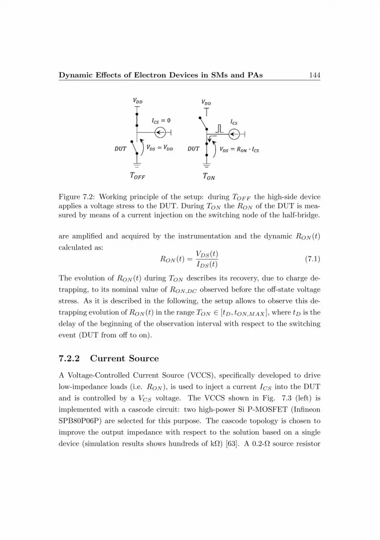
Dynamic Effects of Electron Devices in SMs and PAs 144
𝑇𝑂𝐹𝐹 𝑇𝑂𝑁
Figure 7.2: Working principle of the setup: during TOFF the high-side deviceapplies a voltage stress to the DUT. During TON the RON of the DUT is mea-sured by means of a current injection on the switching node of the half-bridge.
are amplified and acquired by the instrumentation and the dynamic RON (t)
calculated as:
RON (t) =VDS(t)
IDS(t)(7.1)
The evolution of RON (t) during TON describes its recovery, due to charge de-
trapping, to its nominal value of RON,DC observed before the off-state voltage
stress. As it is described in the following, the setup allows to observe this de-
trapping evolution of RON (t) in the range TON ∈ [tD, tON,MAX ], where tD is the
delay of the beginning of the observation interval with respect to the switching
event (DUT from off to on).
7.2.2 Current Source
A Voltage-Controlled Current Source (VCCS), specifically developed to drive
low-impedance loads (i.e. RON ), is used to inject a current ICS into the DUT
and is controlled by a VCS voltage. The VCCS shown in Fig. 7.3 (left) is
implemented with a cascode circuit: two high-power Si P-MOSFET (Infineon
SPB80P06P) are selected for this purpose. The cascode topology is chosen to
improve the output impedance with respect to the solution based on a single
device (simulation results shows hundreds of kΩ) [63]. A 0.2-Ω source resistor

Dynamic Effects of Electron Devices in SMs and PAs 145
0.2 Ω
𝑉𝐶𝐶
𝑉𝐶𝑆
𝑉𝐷𝑆
𝑉𝐷𝐷
𝑇𝐶
100x
20x
20x
Oscilloscopeor Digitizer
𝑉𝑂𝑈𝑇1(𝐼𝐶𝑆)
𝑉𝑂𝑈𝑇2(𝑉𝐷𝑆)
𝑉𝑂𝑈𝑇3(𝑇𝐶)
Thermal Chuck
Voltage-Controlled Current-Source
(VCCS)
𝑉𝐶𝑆
DUT
𝐼𝐶𝑆
𝑅𝑆
Half-BridgeDriver
12 kΩ
𝑅(𝑇𝐶)
𝑉𝑆𝑊
- +
AWG-VCCS
AWG-HB
𝐼𝐶𝑆
𝐼𝐷𝑆
𝑉𝑂𝑈𝑇2 = 20 ∙ 𝑉𝐷𝑆
10 MHz Lock
10 MHz Lock
𝑉𝑆
10 kΩ
10 𝑘Ω
1 MΩ
AD797
12 V
12 kΩ
100 Ω
1 mA 1mA18 V
𝑉𝑂𝑈𝑇3 = 0.1 ∙ 𝑅 𝑇𝐶 − 100𝑉𝐵
−18 V
Trigger
HS LS
1 kΩ
1 kΩ
20 kΩ
AD797
18V
𝑉𝑂𝑈𝑇1 = 0.4 ∙ 𝐼𝐶𝑆
−18 V
20 kΩ
1 kΩ
1 kΩ
AD797
18 V
−18 V
20 kΩ
𝐼𝐶𝑆
0.02 Ω
𝑉𝐷𝑆
1 MΩ
𝑉𝑆
Figure 7.3: Schematic of the setup for the characterization of the dynamic RONin GaN switches. The extraction is directly performed in the final circuit half-bridge operated with Pulse-Width Modulation (PWM).
improves the large-signal linearity of the VCCS by reducing its transconduc-
tance gain from 37 A/V (with RS = 0 Ω) to 3.8 A/V (with RS = 0.2 Ω) at
VCS = 3 V. A high-breakdown voltage (600 V) protection Schottky diode (Cree
C3D10060G) is also placed in series to the cascode to avoid the conduction of
the body diode of the P-MOSFETs, when the switching node VSW goes at VDD
voltage, which is typically higher than VCC .
The ICS current generated by the VCCS is measured with a high-precision
(0.1%) and high-thermal stability (15 ppm/C) current-sensing resistor, pro-
vided with 4-wire Kelvin sensing terminals (Vishay CSM3637P, 20-mΩ model).
These terminals are connected to an opamp voltage amplifier which provides the
signal to be measured to the oscilloscope/digitizer. Details on current sensing
are given in the next section.
The simulated and measured pulsed I/V characteristics at 25C of the
VCCS are shown in Fig. 7.4 (left) at different VCC supply voltages. The simu-
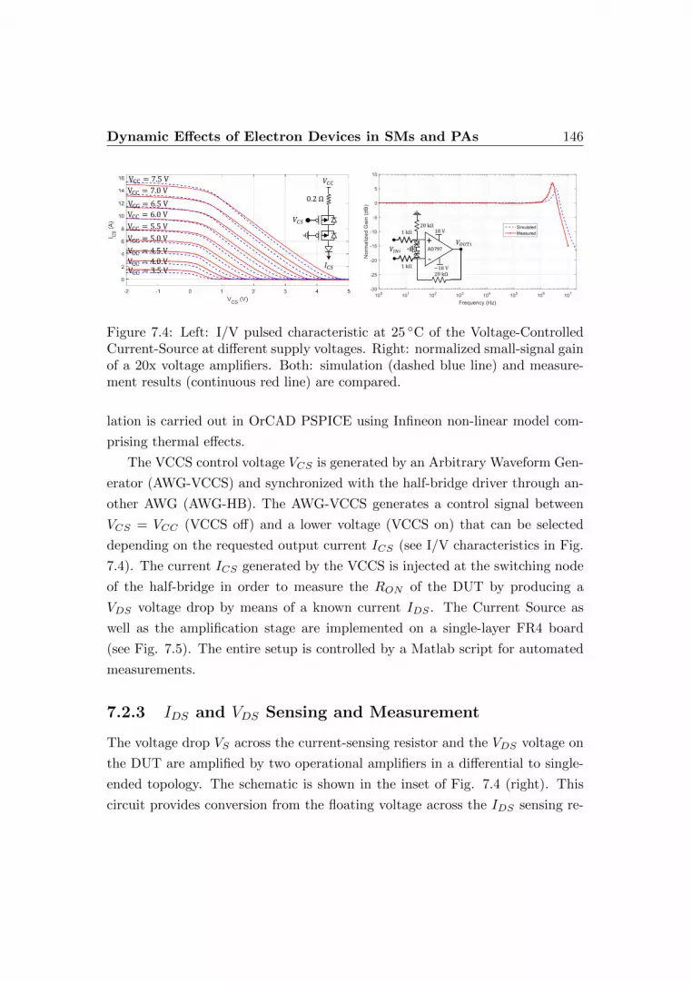
Dynamic Effects of Electron Devices in SMs and PAs 146
VCC = 3.5 VVCC = 4.0 V
VCC = 4.5 V
VCC = 5.0 V
VCC = 5.5 V
VCC = 6.0 V
VCC = 6.5 V
VCC = 7.0 V
VCC = 7.5 V
0.2 Ω
𝑉𝐶𝐶
𝑉𝐶𝑆
𝐼𝐶𝑆 1 kΩ
1 kΩ
20 kΩ
20 kΩ
AD797
18 V
𝑉𝑂𝑈𝑇𝑖𝑉𝐼𝑁𝑖
−18 V
+
-
Figure 7.4: Left: I/V pulsed characteristic at 25 C of the Voltage-ControlledCurrent-Source at different supply voltages. Right: normalized small-signal gainof a 20x voltage amplifiers. Both: simulation (dashed blue line) and measure-ment results (continuous red line) are compared.
lation is carried out in OrCAD PSPICE using Infineon non-linear model com-
prising thermal effects.
The VCCS control voltage VCS is generated by an Arbitrary Waveform Gen-
erator (AWG-VCCS) and synchronized with the half-bridge driver through an-
other AWG (AWG-HB). The AWG-VCCS generates a control signal between
VCS = VCC (VCCS off) and a lower voltage (VCCS on) that can be selected
depending on the requested output current ICS (see I/V characteristics in Fig.
7.4). The current ICS generated by the VCCS is injected at the switching node
of the half-bridge in order to measure the RON of the DUT by producing a
VDS voltage drop by means of a known current IDS . The Current Source as
well as the amplification stage are implemented on a single-layer FR4 board
(see Fig. 7.5). The entire setup is controlled by a Matlab script for automated
measurements.
7.2.3 IDS and VDS Sensing and Measurement
The voltage drop VS across the current-sensing resistor and the VDS voltage on
the DUT are amplified by two operational amplifiers in a differential to single-
ended topology. The schematic is shown in the inset of Fig. 7.4 (right). This
circuit provides conversion from the floating voltage across the IDS sensing re-

Dynamic Effects of Electron Devices in SMs and PAs 147
sistor to a single-ended signal suitable for the oscilloscope acquisition. It is also
useful to point out that this current sensing technique is not affected by common
mode measurements errors typical of high-side resistive current sensing since the
common mode voltage (VDS when the DUT is on) is typically low. The VDS
sensing of the amplifier is realized as close as possible to the switch package in
order to minimize the resistance and the parasitics of the PCB traces.
A low-offset and low-noise operational amplifier (Analog Devices AD797)
with a gain-bandwidth of 80 MHz (at 10x gain) is employed for this purpose.
The gain of the two amplifiers is set with the input (1 kΩ) and feedback re-
sistances (20 kΩ) which are selected with low tolerances (0.1%) for accuracy.
With such resistance values, the input impedance of the voltage amplifiers is
high compared to the source impedance (RS and RON are less than 1 Ω) and
a negligible current flows at the input of these circuits. With the selected volt-
age gain of 20, the measured small-signal bandwidth is 4 MHz (Fig. 7.4). The
in-band distortion of both the amplifiers is experimentally verified resulting in
a gain ripple of 0.03 dB up to 1 MHz (Fig. 7.4). The VDS voltage across the
DUT can be obtained from the output VOUT2 of the amplifier by means of:
VOUT2 =20 kΩ
1 kΩ· VDS → VDS =
VOUT2
20(7.2)
Similarly, the ICS current generated by the VCCS can be computed from the
output VOUT1 of the amplifier by considering:
VOUT1 =20 kΩ
1 kΩ· 20 mΩ · ICS → ICS =
VOUT1
0.4(7.3)
The selection of a voltage gain of 20 and a 20-mΩ current-sensing resistor sets
the maximum current measurable by the setup to approximately 40 A (pulsed).
In fact, for ICS = 40 A and by considering 7.3, the output of the amplifier results
in VOUT1 = 16 V, which is still in the linear amplification region (2 V of margin
on the supply rail of 18 V). Similarly for 7.2, the maximum VDS value linearly
amplified by the bench is 0.8 V.

Dynamic Effects of Electron Devices in SMs and PAs 148
Thus, by selecting ICS = 1 A and ICS = 40 A, two devices with very different
RON of 800 mΩ and 20 mΩ respectively, can be characterized with the same
sensing accuracy of VDS , which is for both 0.8 V at the input of the opamp
and 16 V at the oscilloscope port. Different combination of opamp resistors and
current sensing resistor could be also selected if different maximum rating of
measuring current and voltages are needed. With this technique, the setup is
capable to observe the RON evolution starting from 2µs after the switching
event and the saturation of the oscilloscope during the DUT blocking state is
avoided (more details in section 7.6).
7.2.4 TC Measurement
The case temperature TC is monitored with a PT100 temperature-sensitive re-
sistor (US-Sensor PPG101A6) with fast response (time-constant of 1.2 s in air)
and high accuracy (0.15 C). This sensor is attached to the package of the DUT.
In this way, the thermal path is minimized, providing a quick response to ther-
mal transients. As shown in Fig. 7.3 (bottom-right), the PT100 resistor is
inserted in Wheatstone bridge for a balanced reading by comparison with a
fixed 100 Ω resistor. The upper resistors (12 kΩ ± 0.1%) and the 12 V supply
voltage of the Wheatstone bridge are selected to feed a bias current of about
1 mA to the PT100, as suggested by the sensor manufacturer.
The differential voltage VB of the bridge, which is proportional to the PT100
resistance, is amplified by 100 with another AD797-based amplifier. All the gain-
setting resistances of the amplifier are chosen with low tolerances (± 0.1%). The
input resistors (10 kΩ) of the amplifier are selected to provide a high-impedance
input versus the Wheatstone bridge nodes. The feedback resistors (1 MΩ) are
chosen accordingly to obtain a gain of 100. With such gain, the bandwidth of
the amplifier in closed-loop drops to 1 MHz but it is largely enough for an accu-
rate amplification of the case temperature, which is supposed to vary in the Hz
range. The PT100 resistance R(TC) can be obtained from the output VOUT3 of

Dynamic Effects of Electron Devices in SMs and PAs 149
the amplifier by means of:
VOUT3 =1 MΩ
10 kΩ·1 mA · [R(TC)−100 Ω] → R(TC) = 100+10 ·VOUT3 (7.4)
During the characterization the DUT (the entire half bridge) is mounted over
a temperature-controlled thermal chuck. Thus the case temperature TC of the
DUT can be controlled within the large range between room temperature (25 C)
and 440 C, enabling RON characterizations at different operating temperature.
7.3 Devices Under Tests (DUTs)
Two different GaN technologies are tested with the presented setup. Both tech-
nologies are commercial product exhibiting state of the art performance in their
fields of application.
7.3.1 AlGaN/GaN on Si HEMT
This technology developed by Efficient Power Conversion [66] offers different
families of normally-off (enhancement mode) HEMT power switches grown on
silicon substrates. The different families of products have breakdown voltages
ranging from 15 V to 300 V. The devices tested with the proposed setup are:
• EPC2014: 40 V, 10 A DC current switch with a nominal maximum RON
of 16 mΩ [65]
• EPC2007: 100 V, 6 A DC current switch with a nominal maximum RON
of 30 mΩ [121]
The first DUT is tested directly within the multilevel power converter described
in section 2.1 [122], by disconnecting the load, whereas the second DUT is
measured exploiting the evaluation board provided by the vendor [123]. In both
cases the exploited DUT configuration is the same described in Fig. 7.2 and
shown in Fig. 7.5 (right).
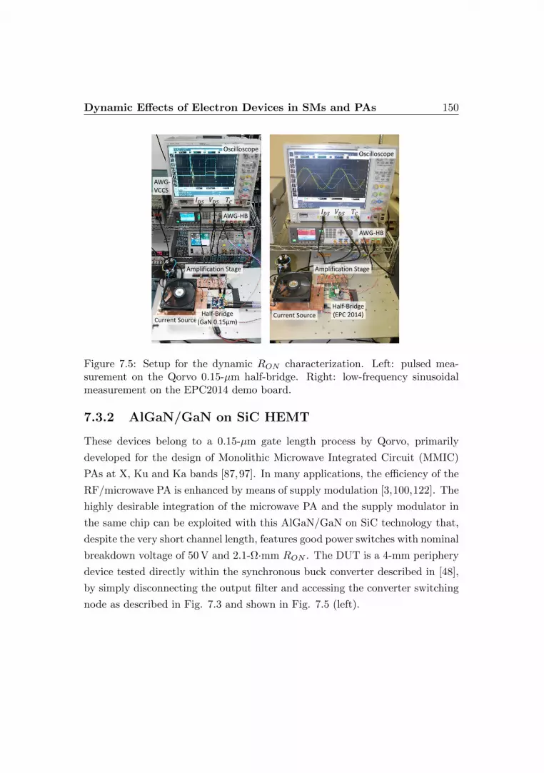
Dynamic Effects of Electron Devices in SMs and PAs 150
Oscilloscope
𝐼𝐷𝑆 𝑉𝐷𝑆 𝑇𝐶
Current Source
Amplification Stage
Half-Bridge(GaN 0.15µm)
AWG-HB
AWG-VCCS
Current Source
Half-Bridge(EPC 2014)
Amplification Stage
AWG-HB
𝐼𝐷𝑆 𝑉𝐷𝑆 𝑇𝐶
Oscilloscope
Figure 7.5: Setup for the dynamic RON characterization. Left: pulsed mea-surement on the Qorvo 0.15-µm half-bridge. Right: low-frequency sinusoidalmeasurement on the EPC2014 demo board.
7.3.2 AlGaN/GaN on SiC HEMT
These devices belong to a 0.15-µm gate length process by Qorvo, primarily
developed for the design of Monolithic Microwave Integrated Circuit (MMIC)
PAs at X, Ku and Ka bands [87,97]. In many applications, the efficiency of the
RF/microwave PA is enhanced by means of supply modulation [3,100,122]. The
highly desirable integration of the microwave PA and the supply modulator in
the same chip can be exploited with this AlGaN/GaN on SiC technology that,
despite the very short channel length, features good power switches with nominal
breakdown voltage of 50 V and 2.1-Ω·mm RON . The DUT is a 4-mm periphery
device tested directly within the synchronous buck converter described in [48],
by simply disconnecting the output filter and accessing the converter switching
node as described in Fig. 7.3 and shown in Fig. 7.5 (left).

Dynamic Effects of Electron Devices in SMs and PAs 151
7.4 Experimental Results
7.4.1 Dependency of the RON on TJ
The resistance RON of the DUT in the half-bridge is firstly measured with a
multimeter provided with a 4-wire sensing (Agilent 34401A). We define this
resistance as the DC On-Resistance RON,DC at room temperature (25C) and
any variation due to dynamic effects is referred to this value. The measured
RON,DC for the considered DUTs are reported in Table 7.1.
Let’s now consider a switch model of the DUT in which the RON is a
function of the junction temperature TJ and of the trapped charge state X(t).
The corresponding I/V model of the DUT in the ohmic region can be written
in this form:
VDS = RON [TJ , X(t)] · IDS . (7.5)
In this section, the RON variation due to the junction temperature TJ of the
power switches is investigated by means of pulsed measurements. In such mea-
surements, the high-side switch of the half-bridge is constantly turned-off and
only the low-side switch (DUT) of the half-bridge is considered (see example
waveforms of Fig. 7.11 in section 7.6).
During this measurement, the acquired drain-source voltage of the DUT
is between zero and a small voltage, the actual VDS (i.e. <0.8 V), during the
injection of the current by the VCCS. In this operating regime, no degradation
of the RON occurs due to trapping effects, since no off-state voltage stresses
are applied and the VDS in conduction is very low as observed (i.e. <0.8 V).
Device Substrate VDS,MAX RON,DC Condition
Qorvo 0.15 µm(normally-on)
SiC 50 V 525 mΩ TJ=25 °C, VGS=0 V, IDS=1.1 A
EPC2014(normally-off)
Si 40 V 14 mΩ TJ=25 °C, VGS=5 V, IDS=2.9 A
EPC2007(normally-off)
Si 100 V 20 mΩ TJ=25 °C, VGS=5 V, IDS=2.9 A
Table 7.1: Measured RON,DC of the considered GaN DUTs.
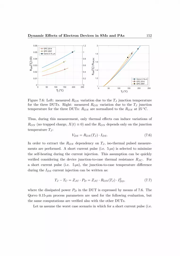
Dynamic Effects of Electron Devices in SMs and PAs 152
Δ
Δ
**
Δ
*
Δ
*
Figure 7.6: Left: measured RON variation due to the TJ junction temperaturefor the three DUTs. Right: measured RON variation due to the TJ junctiontemperature for the three DUTs: RON are normalized to the RON at 25 C.
Thus, during this measurement, only thermal effects can induce variations of
RON (no trapped charge, X(t) ≡ 0) and the RON depends only on the junction
temperature TJ :
VDS = RON (TJ) · IDS . (7.6)
In order to extract the RON dependency on TJ , iso-thermal pulsed measure-
ments are performed. A short current pulse (i.e. 5µs) is selected to minimize
the self-heating during the current injection. This assumption can be quickly
verified considering the device junction-to-case thermal resistance RJC . For
a short current pulse (i.e. 5µs), the junction-to-case temperature difference
during the IDS current injection can be written as:
TJ − TC = ZJC · PD = ZJC ·RON (TJ) · I2DS , (7.7)
where the dissipated power PD in the DUT is expressed by means of 7.6. The
Qorvo 0.15-µm process parameters are used for the following evaluation, but
the same computations are verified also with the other DUTs.
Let us assume the worst case scenario in which for a short current pulse (i.e.
Dynamic Effects of Electron Devices in SMs and PAs 153
5 µs) the thermal impedance equates the thermal resistance RJC = 1.8 C/W
and the RON does not change significantly RON ' RON,DC = 525 mΩ). Thus,
considering a measuring current IDS = 1.1 A, 7.7 provides that the temperature
rise is negligible during the current pulse (i.e. TJ − TC ≤ 1.1C). Same results
apply also to the EPC2014 and EPC2007: their worst-case temperature rise is
0.4 C and 0.6 C respectively. Thus, there is not significant self-heating during
the pulse and the TJ is iso-thermal with the case temperature TC :
TJ ' TC → RON (TJ) = RON (TC), (7.8)
Therefore it is possible to extract the RON at different TJ by characterizing the
DUT at different chuck temperature (TC). The results of this characterization
are reported in Fig. 7.6 (left).
In order to highlight the variation due to the junction temperature and to
allow a comparison between the three considered DUTs, each RON (TJ) are nor-
malized to the corresponding RON,DC (i.e. at 25 C) and the results are plotted
in Fig. 7.6 (right). The RON temperature dependency shows a weak non-
linearity over the tested temperature range in all the three considered DUTs.
The normalized increase of RON for the GaN-on-Si HEMT at 150 C are 1.75
and 1.7 times their RON,DC at 25 C.
Very similar results are provided by the vendor in the datasheets of the
EPC2014 and EPC2007 [65,121]. Very similar results are also reported in [116]
for normally-off GaN-on-Si devices in which the normalized increase of the re-
sistance at 150 C is between 1.56 and 1.73 times with respect to their RON,DC
at 25 C (= 150 mΩ and 65 mΩ respectively). It can be observed that the RON
temperature sensitivity is slightly higher in the DUTs with the Si substrate
compared to the SiC substrate. It is fair to notice that this is not in contrast
with the well-known non-linear behavior of SiC thermal resistance [124], since
the measurement in Fig. 7.6 are performed at controlled TJ with negligible
power dissipation. If the same devices are operated at fixed base plate temper-
ature with non-negligible power dissipation, the nonlinearity of the SiC thermal

Dynamic Effects of Electron Devices in SMs and PAs 154
resistance would contribute to the device channel heating and thus the RON of
GaN-on-SiC devices would have an higher degradation rate at increasing base
plate temperature.
7.4.2 Dependency of the RON on TJ and on X(t)
In this section, the RON dependency on the thermal-state TJ and on the
trapped-charge state X(t) is investigated and the complete switch model 7.5
is considered. Due to short current pulses, and low duty cycles, the DUT RON
characterization is carried out with negligible dissipated power and thus in the
same iso-thermal conditions described in section 7.4.1 that ensure TJ ' TC .
This time, the DUT RON is measured (i.e. VDS and IDS sensing) right after
its commutation from the off-state VDD (synthesized with the high-side switch
of the half-bridge) to full conduction (see example waveforms in Figs. 7.11 in
section 7.6). Due to the very fast charge capture time-constants of GaN HEMT
technology [88, 89, 125], an off-state voltage pulse duration TOFF = 100 ns can
be considered long enough to activate fast charge capture mechanisms. This
is also experimentally verified on the EPC2014 with the results shown in Fig.
7.7. In such experiment, the RON is measured immediately after (tD = 2µs) a
voltage stress of different VDD amplitudes and at different TOFF pulse lengths.
The RON shows a substantial independency from the duration of the voltage
stress between 20 ns and 700 ns. Therefore, a VDD pulse length TOFF = 100 ns
is selected for the characterization.
The iso-thermal RON at different off-state voltages VDD and TON are re-
ported in Fig. 7.11 (center and right) for two of the considered DUTs (EPC2014
and Qorvo 0.15 µm). After the DUT switching, the RON is sampled by the setup
at a variable time TON from the voltage stress, enabling the observation of the
RON [TJ , X(t)] evolution due to trap release.
The RON [TJ , XMAX ] measured after switching from an off-state voltage
VDD is higher compared to the static value RON [TJ , 0], even for off-state volt-
age as low as VDD = 5 V. From voltages higher than VDD = 10 V, RON starts
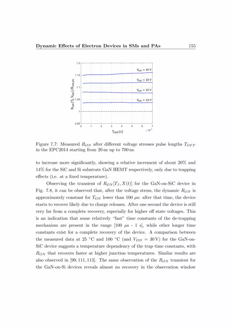
Dynamic Effects of Electron Devices in SMs and PAs 155
VDD = 40 V
VDD = 30 V
VDD = 20 V
VDD = 10 V
RON(T
J,VDD)/RON,DC
TOFF(s)
Figure 7.7: Measured RON after different voltage stresses pulse lengths TOFFin the EPC2014 starting from 20 ns up to 700 ns.
to increase more significantly, showing a relative increment of about 20% and
14% for the SiC and Si substrate GaN HEMT respectively, only due to trapping
effects (i.e. at a fixed temperature).
Observing the transient of RON [TJ , X(t)] for the GaN-on-SiC device in
Fig. 7.8, it can be observed that, after the voltage stress, the dynamic RON is
approximately constant for TON lower than 100 µs: after that time, the device
starts to recover likely due to charge releases. After one second the device is still
very far from a complete recovery, especially for higher off state voltages. This
is an indication that some relatively “fast” time constants of the de-trapping
mechanism are present in the range [100 µs - 1 s], while other longer time
constants exist for a complete recovery of the device. A comparison between
the measured data at 25 C and 100 C (and VDD = 30 V) for the GaN-on-
SiC device suggests a temperature dependency of the trap time constants, with
RON that recovers faster at higher junction temperatures. Similar results are
also observed in [99, 111, 113]. The same observation of the RON transient for
the GaN-on-Si devices reveals almost no recovery in the observation window

Dynamic Effects of Electron Devices in SMs and PAs 156
RON[100 °C, 0]
RON[25 °C, 0]
40 V25 V +
x 10 V
5 V0 V
x
+
x
+
VDD
VDD
RON[T
J,Xt]/RON,DC
TON(s)
RON[25 °C, XMAX]
RON[25 °C, 0]
RON[100 °C, XMAX]
RON[100 °C, 0]
tD
30 V25 V20 V +
*
.x 15 V
10 V5 V0 V
x
.*+
x
.*+
VDD
VDD
TON(s)
RON[T
J,Xt]/RON,DC
RON[25 °C, 0]
RON[25 °C, XMAX]
RON[25 °C, 0]
RON[100 °C, 0]RON[100 °C, 0]
RON[100 °C, XMAX]
tD
Figure 7.8: Left: dynamic RON vs. TON for EPC2014. Right: dynamic RONvs. TON for Qorvo.
of 1 s (Fig. 7.8), indicating the presence of longer time constants. We ver-
ified a complete recovery of both devices between two experiments that took
places some hours apart. Though the complete monitoring of the trap recov-
ery transient (hours) can be interesting for a deeper insight and speculation on
the trapping/de-trapping mechanism as in [99, 113], it does not have practical
interest in actual applications.
7.4.3 Dependency of the RON on TJ and on VDD
Since the PWM switching frequencies of DC/DC converters are typically in
the hundreds of kHz or low-MHz range, especially with GaN technology, the
RON of the measured devices does not have time to any degree of recovery: for
100 kHz switching frequency the period is 10µs, which is largely lower than the
observed 100µs of no-recovery. The trap-state X(t) of the GaN switch is thus
frozen to the maximum value X(t) = XMAX . This value XMAX is set by the
operating off-state voltage VDD and therefore it is possible to express the RON
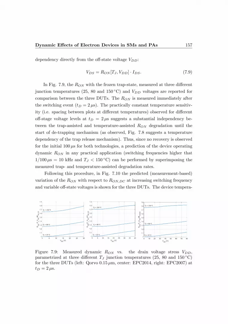
Dynamic Effects of Electron Devices in SMs and PAs 157
dependency directly from the off-state voltage VDD:
VDS = RON [TJ , VDD] · IDS . (7.9)
In Fig. 7.9, the RON with the frozen trap-state, measured at three different
junction temperatures (25, 80 and 150 C) and VDD voltages are reported for
comparison between the three DUTs. The RON is measured immediately after
the switching event (tD = 2µs). The practically constant temperature sensitiv-
ity (i.e. spacing between plots at different temperatures) observed for different
off-stage voltage levels at tD = 2µs suggests a substantial independency be-
tween the trap-assisted and temperature-assisted RON degradation until the
start of de-trapping mechanism (as observed, Fig. 7.8 suggests a temperature
dependency of the trap release mechanism). Thus, since no recovery is observed
for the initial 100µs for both technologies, a prediction of the device operating
dynamic RON in any practical application (switching frequencies higher that
1/100µs = 10 kHz and TJ < 150 C) can be performed by superimposing the
measured trap- and temperature-assisted degradation rates.
Following this procedure, in Fig. 7.10 the predicted (measurement-based)
variation of the RON with respect to RON,DC at increasing switching frequency
and variable off-state voltages is shown for the three DUTs. The device tempera-
TJ = 25 °C
TJ = 80 °C
TJ = 150 °C
Qorvo 150nm
TJ = 25 °C
TJ = 80 °C
TJ = 150 °C
EPC 2014C
TJ = 25 °C
TJ = 80 °C
TJ = 150 °C
EPC 2007C
Figure 7.9: Measured dynamic RON vs. the drain voltage stress VDD,parametrized at three different TJ junction temperatures (25, 80 and 150 C)for the three DUTs (left: Qorvo 0.15µm, center: EPC2014, right: EPC2007) attD = 2µs.

Dynamic Effects of Electron Devices in SMs and PAs 158
Figure 7.10: Predicted dynamic RON vs. the switching frequency fSW ,parametrized at some VDD voltage stresses for the three considered DUTs (left:Qorvo 0.15µm, center: EPC2014, right: EPC2007) with the device parameterslisted in Table 7.1.
ture variation due to increasing switching losses is computed using the switching
losses model proposed in [56]. It is useful to note that for a Power MOSFET
only a single curve would be needed, since there is not dependency of the dy-
namic RON on off-state voltage VDD [115]. The graphs in Fig. 7.10 clearly
show that even for well-assessed commercial GaN devices the degradation of
the dynamic RON at increasing blocking voltages and switching frequency (i.e.
increasing junction temperature) can’t be overlocked for a precise computation
of the converter conduction losses. High switching frequency converter design
would benefit from the availability of such characterization data, rather than
typical static RON values measured at 0 V off-state voltage, that can underes-
timate the conduction losses up to 100% (Fig. 7.10).
7.5 Conclusion
A novel laboratory setup along with a characterization procedure for the dy-
namic RON extraction of GaN switches in presence of thermal- and voltage-
stress is presented. The DUT is directly characterized inside the final circuit
half-bridge which comprises the final application thermal network, PCB para-
sitics and driving waveforms for an improved accuracy of the characterization.
Dynamic Effects of Electron Devices in SMs and PAs 159
The presented setup allows the study of RON transients after the switching
event at variable off-state voltages stress and operating temperature.
The setup is used for the characterization of two different switch technolo-
gies exhibiting state-of-art performance in their fields of applications. For both
technologies dynamic RON degradations up to 75% and 20% are observed for
temperature and off-state voltage variations respectively. By means of these
characterization data, it is possible to compute the dynamic RON at the oper-
ating switching frequency of the supply modulator, thus allowing an improved
estimation of the conduction losses and efficiency. With the considered DUT
GaN-on-Si and GaN-on-SiC technologies, an increase up to +100% is experimen-
tally verified when the devices is pushed to the limit of the switching frequencies
and high off-state voltage stresses.
7.6 Appendix: Detailed operation of the Setup
In this section, explanatory waveforms at the output of the amplification stage
are commented showing in detail how the RON of the DUT is measured by the
presented setup.
In the measurement waveforms shown in Fig. 7.11 (left), the high side switch
is constantly kept off, while the DUT (low side switch) is always on. No voltage
stresses are applied to the DUT. The VCCS injects a 5-µs current pulse in the
DUT and the oscilloscope/digitizer samples the waveforms VOUTi at the output
of the voltage amplifiers. Thus, the RON (TJ) is calculated by considering 7.1-
7.2-7.3-7.4 after the output VOUTi reach steady values. These waveforms are
representative of the measurements performed in section 7.4.1.
If the commutation of the high-side switch is introduced imposing the volt-
age stress VDD to the DUT, the switching node is raised to VDD and thus it is
necessary to protect the inputs of the opamps from over-voltages (VDD generally
higher than their rail voltage of VRAIL = 18 V). Transient Voltage Suppression
diodes (TVS, Littelfuse SMAJ5.0) are used to this purpose and the adopted
configuration is shown in Fig. 7.3. The TVS diodes clamp the input nodes of
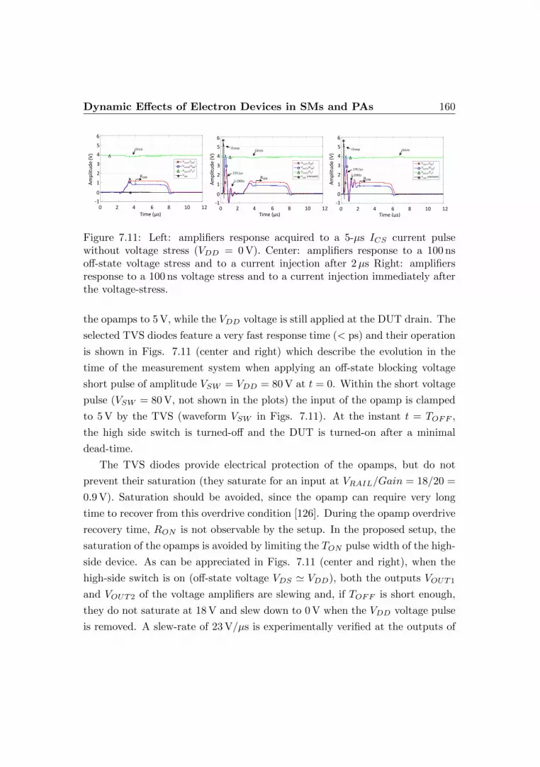
Dynamic Effects of Electron Devices in SMs and PAs 160
x
x
o
o*
*
Δ
ΔRON
Glitch
2.2MHz
x
x
oo
*
*
Δ
ΔRON
Glitch
23V/µs
Clamp
2.2MHz
x
x
oo
*
*
Δ
ΔRON
Glitch
23V/µs
Clamp
0 2 4 6 8 10 12 0 2 4 6 8 10 12 0 2 4 6 8 10 12
6
5
4
3
2
1
0
-1
6
5
4
3
2
1
0
-1
6
5
4
3
2
1
0
-1
Am
plit
ud
e(V
)
Am
plit
ud
e(V
)
Am
plit
ud
e(V
)
Time (µs) Time (µs) Time (µs)
Figure 7.11: Left: amplifiers response acquired to a 5-µs ICS current pulsewithout voltage stress (VDD = 0 V). Center: amplifiers response to a 100 nsoff-state voltage stress and to a current injection after 2µs Right: amplifiersresponse to a 100 ns voltage stress and to a current injection immediately afterthe voltage-stress.
the opamps to 5 V, while the VDD voltage is still applied at the DUT drain. The
selected TVS diodes feature a very fast response time (< ps) and their operation
is shown in Figs. 7.11 (center and right) which describe the evolution in the
time of the measurement system when applying an off-state blocking voltage
short pulse of amplitude VSW = VDD = 80 V at t = 0. Within the short voltage
pulse (VSW = 80 V, not shown in the plots) the input of the opamp is clamped
to 5 V by the TVS (waveform VSW in Figs. 7.11). At the instant t = TOFF ,
the high side switch is turned-off and the DUT is turned-on after a minimal
dead-time.
The TVS diodes provide electrical protection of the opamps, but do not
prevent their saturation (they saturate for an input at VRAIL/Gain = 18/20 =
0.9 V). Saturation should be avoided, since the opamp can require very long
time to recover from this overdrive condition [126]. During the opamp overdrive
recovery time, RON is not observable by the setup. In the proposed setup, the
saturation of the opamps is avoided by limiting the TON pulse width of the high-
side device. As can be appreciated in Figs. 7.11 (center and right), when the
high-side switch is on (off-state voltage VDS ' VDD), both the outputs VOUT1
and VOUT2 of the voltage amplifiers are slewing and, if TOFF is short enough,
they do not saturate at 18 V and slew down to 0 V when the VDD voltage pulse
is removed. A slew-rate of 23 V/µs is experimentally verified at the outputs of

Dynamic Effects of Electron Devices in SMs and PAs 161
the AD797 which sets a maximum TOFF of: 1 µs = 18 V/23 V ' 0.7 µs without
incurring in the saturation condition. It is useful to notice that a short VDD
pulse width of hundreds of ns that avoid saturation of the opamp is still suit-
able to observe the trap-assisted degradation of RON , since the trap activation
mechanism in GaN is extremely fast as it is experimentally verified in Fig. 7.7
(left) and in [88, 89, 125]. However, even without saturating, the response of
the amplifiers to a 100 ns off-state voltage pulse shows some ringing (2.2 MHz)
which requires 2µs to settle down (center Fig. 7.11). It is worth to point out,
that this settling time is independent from the amplitude of the off-state VDD
pulse, since the opamp dynamic response (ringing) always starts from the same
condition (5 V input clamping) for a TOFF = 100 ns.
In Fig. 7.11 (center), the 2µs needed for the stabilization of VOUT1 and
VOUT2 are awaited before applying the current measurement pulse: as a result,
the 2-µs duration of the current injection transient is added to the 2µs of the
post-commutation settling time and the delay time (tD) between the switching
event and the start of an accurate acquisition of waveforms (i.e. RON evolution)
is about 4µs.
Fig. 7.11 (right) shows the strategy that we adopted for a further mini-
mization of tD: the measuring current pulse command VCS is set just after the
commutation from the off-state. In this way the transients associated with the
two events (voltage and current pulse) share the same time slot and the system
is ready for a clear measure after a delay time of 2µs. This short time delay is
in line with the results obtained applying clamping circuit as in [98] and [112].
Some papers report also time delay below 1µs, but in many cases the proposed
measuring plots clearly show that the measure is still not reliable (clear ringing
behavior) in the immediate proximity of the switching event, and become totally
settled after 1µs [98, 114]. Moreover the typical long time constants associated
to trap release mechanism in GaN HEMT [112] do not probably require an
observable starting time shorter that 2µs as it is also shown in the presented
measurements.

Dynamic Effects of Electron Devices in SMs and PAs 162
7.7 Dynamic Effects in LDMOS PAs
In this section, it is reported a formulation and an experimental validation
of a behavioral electro-thermal model2 for LDMOS RF PAs [127]. Sensitivity
functions with respect to an equivalent temperature are defined for the RF input-
output and drain current characteristics, and then coupled with a quasi-static
thermal equivalent network. The model is empirically identified with pulse-
modulated RF signals and takes advantage of the possibility to impose and
sense the case temperature of the PA. The presented model accurately predicts
the influence of temperature on quasi-static and dynamic characteristics of the
LDMOS PA presented in section 3.1. Charge trapping effects are supposed to
be negligible for this technology and they are not addressed in this model.
7.7.1 PA Electro-Thermal Model
Let us consider the generic input-output relationship for a matched RF PA:
b(t) = H(|a(t)|, θ(t))a(t) (7.10)
where a(t) and b(t) are, respectively, the complex baseband equivalent input
and output power waves, θ(t) is an equivalent junction temperature and H is
a complex describing function. Assuming that the thermal impact on the PA
characteristics is small enough, it is possible to linearize H with respect to θ(t),
thus obtaining:
H(|a(t)|, θ(t)) ' H∗(|a(t)|, θ∗) + hθ(|a(t)|, θ∗)(θ(t)− θ∗) (7.11)
2G. P. Gibiino, T. Cappello, D. Niessen, D. M. M. -P. Schreurs, A. Santarelli, F. Filicori,“An empirical behavioral model for RF PAs including self-heating,” in Integrated NonlinearMicrowave and Millimetre-wave Circuits Workshop (INMMiC), Taormina, IT, Oct. 2015.

Dynamic Effects of Electron Devices in SMs and PAs 163
where hθ is a complex sensitivity function. In a similar way, considering a
generic relationship F between the supply current and the RF input a(t):
i(t) = F (|a(t)|, θ(t)) (7.12)
it is possible to apply the linearization such as in (7.11) by means of another
sensitivity function fθ such that:
F (|a(t)|, θ(t)) ' F ∗(|a(t)|, θ∗) + fθ(|a(t)|, θ∗)(θ(t)− θ∗) (7.13)
In order to extract the thermo-electrical model, (7.11) and (7.13) are coupled
with a quasi-static thermal-equivalent network equation:
θ(t) = θC(t) +Rθ[v(t)i(t) + |a(t)|2 − |b(t)|2] (7.14)
where Rθ is an equivalent thermal resistance, θC is the temperature of the case
upon which the PA is positioned, and v(t) is the supply voltage applied to the
PA, which may be considered constant v(t) = V0 to the extent of this quasi-static
model.
7.7.2 PA Model Identification
The identification procedure must provide the isothermal functions H∗ and F ∗
along with the sensitivity functions hθ and fθ, and the thermal resistance Rθ.
Isothermal functions H∗ and F ∗ must be measured at the specific temperature
θ∗ and in absence of self-heating effects. This can be obtained by imposing a
specific θC and by setting the nominal bias (V0, I0) at which the model should
be extracted. After a steady-state condition is reached, we have an equivalent
temperature θ = θC +RθV0I0. Then, a pulsed RF input with a modulation rate
shorter than the thermal constants (but slow enough to avoid fast dynamics)
is applied, and RF output envelope and current are synchronously captured.
The differentials hθ and fθ are obtained by isothermal measures at two differ-

Dynamic Effects of Electron Devices in SMs and PAs 164
ent equivalent junction temperatures θ∗ and θ∗ + ∆θ, through the following
approximation:
hθ(|a(t)|, θ∗) ' H∗(|a(t)|, θ∗ + ∆θ)−H∗(|a(t)|, θ∗)
∆θ(7.15)
fθ(|a(t)|, θ∗) ' F ∗(|a(t)|, θ∗ + ∆θ)− F ∗(|a(t)|, θ∗)
∆θ(7.16)
The equivalent thermal resistance Rθ is evaluated by adapting to power ampli-
fiers the approach used in [124] for electron devices.
7.7.3 Measurement Setup
The measurement setup used for the identification and validation of the pro-
posed model is reported in Fig. 7.12. It consists of the VST [76] which allows
generating and receiving complex modulated RF signals. The supply current is
acquired with a commercial sensor based on the combination of a wideband Hall
sensor and a transformer; both this signal and the supply voltage are monitored
with an oscilloscope. The case temperature θC is imposed by a Peltier cell po-
sitioned under the DUT and is sensed by a means of a resistive sensor (PT100),
whose signal is properly amplified and conditioned in order to be captured by
the oscilloscope. The measured PA is a three-stage RF PA operating at 1.84
GHz presented in section 3.1.
(a) (b) (c)
Figure 7.12: Measurement setup used for the experiments: (a) block diagram;(b) picture of the instrumentation; (c) zoom of the PA with the DUT and thetemperature sensing board.

Dynamic Effects of Electron Devices in SMs and PAs 165
Figure 7.13: Measured isothermal gain curves (H function) at three equivalentjunction temperatures θ (left) and sensitivity hθ (right).
Figure 7.14: Measured isothermal supply current curves (F function) at threeequivalent junction temperatures θ (left) and sensitivity fθ (right).
Figure 7.15: Validation of the model extracted at θ∗ = 59.1 C (lines) vs. mea-surements (crosses). Isothermal characteristics (red and blue) are measured atthe indicated equivalent junction temperatures θ; CW characteristics (black)are obtained at a constant case temperature θC = 30 C. Self-heating effectsare properly predicted by the model for both the RF output power (left) andsupply current (right).

Dynamic Effects of Electron Devices in SMs and PAs 166
7.7.4 Experimental Results
The behavioral model proposed is applied to the three-stage DUT; however,
drain current measurements and thermal network take into account only the
final stage, as the pre-driver and the driver mainly work linearly and minimally
contribute to overall self-heating. Isothermal PA characteristics and sensitivity
functions obtained through the methodology described in section 7.7.2 are re-
ported in Figs. 7.13 and 7.14.
The DUT shows a gain variability of about 2 dB and a drain current drop of
about 300 mA in the maximum available temperature range [θMIN = 32.5 C,
θMAX = 77.8 C] considered. The model, extracted at θ∗ = 59.1 C, suitably
predicts isothermal characteristics measured at θMIN and θMAX (Fig. 7.15).
Moreover, a CW validation is performed. Such measurements are obtained by
imposing a constant case temperature with the peltier cell (θC = 30 C) and
waiting the settling of long-term self-heating effects before the acquisition for
each input power. The model reliably reproduces both the gain and the supply
current quasi-static characteristics affected by self-heating with a relative error
< 4% (Fig. 7.15). An equivalent thermal resistance Rθ ' 1 C/W is measured
for this DUT.
7.8 Conclusion
In this section, it is reported a model and an experimental validation of a be-
havioral electro-thermal model for LDMOS RF PAs. The presented model ac-
curately predicts with a <4% relative error the influence of temperature on
quasi-static and dynamic characteristics of a LDMOS PA. Future work will
address the thermal dynamics in presence of RF modulated signals.

Chapter 8
Conclusions and Future Work
8.1 Main Contributions
The focus of this thesis is on the development of an Envelope-Tracking (ET)
architecture for the efficient amplification of high Peak-to-Average Power Ratio
(PAPR) signals, both for communication and radar applications, by means of
an innovative supply modulator (Power-DAC) and a multilevel Digital Pre-
Distortion (DPD) algorithm.
The activity of this Ph.D. is carried out at the University of Bologna where
most of this research is conducted in cooperation with the local group, except
for a six-month period the author spent as a visiting researcher at the University
of Colorado in Boulder. This activity produced the following results:
• A new 3-bit Power-DAC converter is designed and implemented exploiting
very fast switching devices in a commercial GaN-on-Si technology. The
circuit can be used as a supply modulator for ET architectures in telecom-
munication base station transmitters. This circuit can be used for many
other different applications (possibly in conjunction with an additional
linear amplifier, for additional, less significant bits) in any field where the
167
Conclusions and Future Work 168
efficient generation (digital synthesis) of an arbitrary power waveform in
the MHz range is needed. The converter exhibits 42-V dynamic range with
a considerable 4.23 kV/µs slew rate. The measured full-power bandwidth
at 28-W average output power is 20 MHz obtained with 82.8% power ef-
ficiency. The circuit is tested using control signals suitable for the RF PA
operation with three different wideband communication signals: 4-MHz
3GPP WCDMA, 10-MHz LTE, 20-MHz WiFi. In those conditions the
circuit shows to accurately follow the control waveforms, while operating
with efficiencies of 91.7%, 84.5% and 78.2% respectively and delivering
158 W of peak power (about 17 W average output power).
• An ET transmitter architecture based on the combination of the Power-
DAC supply modulator and multilevel DPD is presented. The complete
ET architecture is tested with a L-band LDMOS RF PA with 1.4 MHz and
10 MHz LTE signals with high PAPR. In these conditions the converter
operates at 92% and 83% efficiency respectively, whereas the composite
efficiency of the transmitter are 38.3% and 23.9%. These performance
correspond to an improvement of 17.2 and 17.9 points for the Power Added
Efficiency (PAE) of the PA and to 13.4 and 13 points of improvement for
the efficiency of the entire transmitter.
• The Power-DAC converter is used to modulate a X-band 12-W peak power
GaN-on-SiC Monolithic Microwave Integrated Circuit (MMIC) PA1. A
novel characterization method employing a pre-pulse is used to allow an
accurate extraction of the GaN PA characteristics for DPD correction in
presence of trapping effects. The combination of supply modulation and
DPD results in high Composite PAE (CPAE) of over 55%, with simul-
taneous high dynamic range and flexible digitally programmable pulse
shaping. Envelope shaping of a pulsed waveform results in improved spec-
tral confinement greater than 15 dB for the first sideband compared with
constant-envelope pulses, with over 20 points improvement in the compos-
1PA designed by S. R. Schafer, see more details in his Ph.D. thesis [86].

Conclusions and Future Work 169
ite efficiency.
• A high-efficiency ET transmitter employing a MMIC version of the Power-
DAC is presented2. Both the supply modulator and the X-band 10-
W peak-power MMIC PA1 are implemented with the same GaN-on-SiC
Qorvo 0.15-µm process. Measured results for amplitude- and frequency-
modulated pulse waveforms shows a CPAE of 45% with simultaneous spec-
tral confinement and 52 dB improvement in the first time side-lobe level.
For a wideband high-PAPR LTE signal, the CPAE increases from 11% to
32% compared to a constant drain supply transmitter, while linearity is
maintained through DPD.
• A Chireix Outphasing PA3 with a Multi-Level (ML-CO) supply modula-
tor is investigated. Static measurements provides a peak output power
of 4.8 W at X-band, and average total efficiencies up to 44.1% for a 6-
dB PAPR QPSK. Thus, an experimental test bench able to dynamically
generate phase- and time-aligned modulated signals is developed. The
DPD-linearized ML-CO PA is tested with 1.4-MHz and 10-MHz LTE sig-
nals. For both signals, the average total power consumption decreases by a
factor of two when supply modulation is used. For the 9.3-dB PAPR, 1.4-
MHz signal the PA operated with 38% average drain efficiency at 0.54-W
average output power.
• Dynamic effects of electron devices employed to realize supply-modulated
RF transmitters are investigated. In particular, the GaN-on-Si and the
GaN-on-SiC switches employed for the hybrid and MMIC version of the
Power-DAC are considered. GaN HEMT devices are affected by the degra-
dation of the RON at increasing off-state voltages and operative temper-
atures. A novel laboratory setup along with a characterization procedure
for the dynamic RON extraction in presence of thermal- and voltage-stress
2The MMIC Power-DAC is funded by a DARPA project at the University of Colorado atBoulder.
3PA designed by M. Litchfield, see more details in his Ph.D. thesis [104].

Conclusions and Future Work 170
is presented. For both technologies dynamic RON degradations up to 75%
and 20% are observed for temperature and off-state voltage variations, re-
spectively. By means of these characterization data, it is possible to com-
pute the dynamic RON at the operating switching frequency of the supply
modulator, thus allowing an improved estimation of the conduction losses
and efficiency.
8.2 Possible Topics for Future Work
• Despite the results obtained in this Ph.D., there is still much to investi-
gate on ET architectures especially with regard to the possibility to inte-
grate the supply modulator with the PA in a single MMIC and to further
broaden the bandwidth, increase efficiency and decrease the overall size of
the ET PA. To this aim, it should be interesting to explore different types
of supply modulator topologies, both with discrete levels and with output
filter/linear part.
• Commutations between voltage levels in discrete supply modulators (i.e.
the Power-DAC) produce voltage ringing and this ringing at the drain
of the PA is converted into distortion in the amplified RF signal. This
ringing is typically due to the parasitics in the power loop between the
supply modulator, PA and ground. A “light” LC filter can be introduced
on purpose between the supply modulator and the PA. However the design
of this filter is complicated by the connected load PA, which is not a
resistor but a nonlinear dynamic impedance. Further investigations could
be conducted on this topic.
• A digital envelope filter capable to reduce the commutation rate of the
supply modulator is employed throughout this thesis but never exploited
to its full capabilities. This component would allow to investigate the
trade-off between signal characteristics (bandwidth, PAPR, PDF, etc.)
and the ET PA linearity-efficiency trade-off and temperature distribution

Conclusions and Future Work 171
among the supply modulator and the PA. By means of this filter, it should
be possible to increase the overall performance of the ET PA by maximiz-
ing the CPAE, as the product of the PAE of the PA and the efficiency of
the supply modulator.
• A test bench for the co-design and test of the PA with a supply modula-
tor. The bench should provide enough bandwidth to test wideband (ET)
PAs. For the characterization of the PA, the bench should be able to di-
rectly measure the PDC(t) of the PA along with the RF input and output
power. The purpose of this bench should be the test with multiple kind of
waveforms for telecommunications, radars, frequency agile transmitters,
etc.
• A DPD with the dynamic update of the coefficients by means of a feedback
loop (typically available in the setups for the analysis of the PA output) to
compensate long-term effects (aging, thermal, etc.). The digital envelope
filter allows to dynamically adapt the bias supply to a given signal passing
from a more averaged tracking to a closer tracking of the ideal supply
voltage. However, the thermal state (and trap state) of a Si or GaN
PA is conditioned by the supplied waveform. DPD coefficients should be
adapted accordingly. Different types of DPDs could be tested (generalized
memory polynomial, deviation reduction Volterra series, etc.) for a more
robust description of fast memory effects in the PA, which should be taken
into account with wider bandwidths.
• Regarding the Chireix outphasing PA, a step modulation of the PA input
signal envelope could be used to maintain high efficiency when the PA
output power is low, so that total efficiency can be improved. The trade-
off between the number of supply levels and efficiency is another activity
that is currently carried out. Preliminary measurements show that further
improvements in the PA efficiency could be achieved by using a continuous
amplitude modulation at the input (instead of steps). Asymmetric multi-
level outphasing is another possible efficiency improvement that could be

Conclusions and Future Work 172
explored.
8.3 List of Publications
8.3.1 International Journals
1. T. Cappello, C. Florian, D. Niessen, Member, R.P. Paganelli, S. Schafer,and Z. Popovic, “High-Efficiency X-band GaN Transmitter with MMICMulti-Level Supply Modulator,” IEEE Transactions on Microwave Theoryand Techniques, submitted for publication on Feb. 2017.
2. T. Cappello, C. Florian, and A. Santarelli, “Dynamic RON Characteriza-tion Technique for the Evaluation of Thermal and Off-State Voltage Stressof GaN Switches,” IEEE Transactions on Power Electronics, submittedfor publication on Dec. 2016.
3. C. Florian, T. Cappello, A. Santarelli, D. Niessen, F. Filicori, and Z.Popovic, “A Pre-Pulsing Technique for the Characterization of GaN PowerAmplifiers with Dynamic Supply under Controlled Thermal and TrappingStates,” IEEE Transactions on Microwave Theory and Techniques, sub-mitted for publication on July 2016.
4. C. Florian, T. Cappello, D. Niessen, R.P. Paganelli, S. Schafer, and Z.Popovic, “Efficient Programmable Pulse Shaping for X-Band GaN MMICRadar Power Amplifiers,” IEEE Transactions on Microwave Theory andTechniques, vol. PP, no. 9, pp. 1-11, Dec. 2016.
5. C. Florian, T. Cappello, R.P. Paganelli, D. Niessen, and F. Filicori,“Envelope Tracking of an RF High Power Amplifier With an 8-Level Dig-itally Controlled GaN-on-Si Supply Modulator,” IEEE Transactions onMicrowave Theory and Techniques, vol. 63, no. 8, pp. 2589-2602, Aug.2015.
8.3.2 International Conferences
1. T. Cappello, C. Florian, T.W. Barton, M. Litchfield, and Z. Popovic,“Multi-Level Supply-Modulated Chireix Outphasing for LTE Signals,” in

Conclusions and Future Work 173
IEEE MMT-S International Microwave Symposium (IMS), Honolulu, HI,June 2017.
2. M. Litchfield, T. Cappello, C. Florian, and Z. Popovic, “X-Band GaNMulti-Level Chireix Outphasing PA with a Discrete Supply ModulatorMMIC,” in IEEE Compound Semiconductor Integrated Circuit Symposium(CSICS), Austin, TX, Oct. 2016.
3. C. Florian, D. Niessen, T. Cappello, A. Santarelli, F. Filicori, and Z.Popovic, “Pre-pulsing characterization of GaN PAs with dynamic sup-ply,” in IEEE MTT-S International Microwave Symposium (IMS), SanFrancisco, CA, May 2016.
4. A. Zai, C. Florian, T. Cappello, and Z. Popovic, “Efficient power ampli-fiers for amplitude-tapered pulses with improved spectral confinement,” inIEEE MTT-S International Microwave Symposium (IMS), San Francisco,CA, May 2016.
5. G.P. Gibiino, T. Cappello, D. Niessen, D.M.M.-P. Schreurs, A. Santarelli,and F. Filicori, “An empirical behavioral model for RF PAs including self-heating,” in Integrated Nonlinear Microwave and Millimetre-wave CircuitsWorkshop (INMMiC), Taormina, IT, Oct. 2015.

Bibliography
[1] P. Asbeck, Z. Popovic, “ET Comes of Age: Envelope Tracking for Higher-
Efficiency Power Amplifiers,” IEEE Microwave Magazine, vol. 17, no. 3,
pp. 16–25, 2016.
[2] Z. Wang, Envelope Tracking Power Amplifiers for Wireless Communica-
tions, ch. 1–2. Artech House, 2014.
[3] F.H. Raab, P. Asbeck, S. Cripps, PB. Kenington, Z.B. Popovic, N. Pothe-
cary, J.F. Sevic, N. O. Sokal, “Power amplifiers and transmitters for RF
and microwave,” IEEE Transactions on Microwave Theory and Tech-
niques, vol. 50, no. 3, pp. 814–826, 2002.
[4] F. Wang, A. Ojo, D. Kimball, P. Asbeck, L. Larson, “Envelope track-
ing power amplifier with pre-distortion linearization for WLAN 802.11g,”
IEEE MTT-S International Microwave Symposium Digest, pp. 1543–1546,
2004.
[5] D.F. Kimball, J. Jinho, C. Hsia, P. Draxler, S. Lanfranco, W. Nagy,
K. Linthicum, L.E. Larson, P.M. Asbeck, “High-Efficiency Envelope-
Tracking W-CDMA Base-Station Amplifier Using GaN HFETs,” IEEE
Transactions on Microwave Theory and Techniques, vol. 54, no. 11,
pp. 3848–3856, 2006.
174

Bibliography 175
[6] J. Jeong, D.F. Kimball, M. Kwak, P. Draxler, C. Hsia, C. Steinbeiser,
T. Landon, O. Krutko, L.E. Larson, P.M. Asbeck, “High-Efficiency
WCDMA Envelope Tracking Base-Station Amplifier Implemented With
GaAs HVHBTs,” IEEE Journal of Solid-State Circuits, vol. 44, no. 10,
pp. 2629–2639, 2009.
[7] C. Hsia, D.F. Kimball, S. Lanfranco and P.M. Asbeck, “Wideband
High Efficiency Digitally-Assisted Envelope Amplifier with Dual Switch-
ing Stages for Radio Base-Station Envelope Tracking Power Ampli-
fiers,” IEEE MTT-S International Microwave Symposium Digest (MTT),
pp. 672–675, 2010.
[8] J.H. Kim, G.D. Jo, J.H. Oh, Y.H. Kim, K.C. Lee, J.H. Jung, “3.54 GHz
10W Envelope Tracking Amplifier with 43% efficiency Utilizing the 1.5
Bit-High Efficiency Envelope Amplifier,” IEEE Topical Conference on
Power Amplifiers for Wireless and Radio Applications (PAWR), pp. 21–
24, 2011.
[9] P. Draxler, S. Lanfranco, D. Kimball, C. Hsia, J. Jeong, J. van de Sluis,
P.M. Asbeck, “High Efficiency Envelope Tracking LDMOS Power Ampli-
fier for W-CDMA,” IEEE MTT-S International Microwave Symposium
Digest, pp. 1534–1537, 2006.
[10] C. Hsia, A. Zhu , J.J. Yan, P. Draxler, D.F Kimball, S. Lanfranco, P.M.
Asbeck, “Digitally Assisted Dual-Switch High-Efficiency Envelope Ampli-
fier for Envelope-Tracking Base-Station Power Amplifiers,” IEEE Trans-
actions on Microwave Theory and Techniques, vol. 59, no. 11, pp. 2943–
2952, 2011.
[11] J.H. Kim, H.S. Son, W.Y. Kim, C.S. Park, “Envelope Amplifier with
Multiple-Linear Regulator for Envelope Tracking Power Amplifier,” IEEE
Transactions on Microwave Theory and Techniques, vol. 61, no. 11,
pp. 3951–3960, 2013.

Bibliography 176
[12] D. Kimball, J-J. Yan, P. Theilmanrr, M. Hassan, P. Asbeck, L. Larson,
“Efficient and Wideband Envelope Amplifiers for Envelope Tracking and
Polar Transmitter,” IEEE Topical Conference on Power Amplifiers for
Wireless and Radio Applications (PAWR), pp. 13–15, 2013.
[13] P.T. Theilmann, J.J. Yan, V. Cuong, J-S. Moon, H.P. Moyer, D.F. Kim-
ball, “A 60MHz Bandwidth High Efficiency X-band Envelope Track-
ing Power Amplifier,” IEEE Compound Semiconductor Integrated Circuit
Symposium (CSICS), pp. 1–4, 2013.
[14] H. Huang, J. Bao, L. Zhang, “A MASH-Controlled Multilevel Power Con-
verter for High-Efficiency RF Transmitters,” IEEE Transactions on Power
Electronics, vol. 26, no. 4, pp. 1205–1214, 2011.
[15] P.F. Miaja, M. Rodriguez, A. Rodriguez, J. Sebastian, “A Linear As-
sisted DC/DC Converter for Envelope Tracking and Envelope Elimination
and Restoration Applications,” IEEE Transactions on Power Electronics,
vol. 27, no. 7, pp. 3302–3309, 2012.
[16] M. Vasic, O. Garcia, J.A. Oliver, P. Alou, D. Diaz, J.A. Cobos, “Compar-
ison of two multilevel architectures for envelope amplifier,” IEEE Annual
Conference of Industrial Electronics (IECON), pp. 283–289, 2009.
[17] D. Diaz, M. Vasic, O. Garcia, J.A. Oliver, P. Alou, R. Prieto, J.A. Cobos,
“Three-Level Cell Topology for a Multilevel Power Supply to Achieve
High Efficiency Envelope Amplifier,” IEEE Transactions on Circuits and
Systems, vol. 59, no. 9, pp. 2147–2160, 2012.
[18] M. Rodriguez, P. Fernandez-Miaja, A. Rodriguez, J. Sebastian, “A
Multiple-Input Digitally Controlled Buck Converter for Envelope Tracking
Applications in Radiofrequency Power Amplifiers,” IEEE Transactions on
Power Electronics, vol. 25, no. 2, pp. 369–381, 2010.
[19] M.I. Skolnik, Radar Handbook, ch. 8. McGraw-Hill, 2008.
Bibliography 177
[20] N. Levanov, E. Mozeson, Radar Signals, ch. 4. Wiley, 2004.
[21] R. Chen, B. Cantrell, “Highly bandlimited radar signals,” IEEE Radar
Conference, pp. 220–226, 2002.
[22] J. de Graaf, H. Faust, J. Alatishe, S. Talapatra, “Generation of spec-
trally confined transmitted radar waveforms: Experimental results,” IEEE
Radar Conference, pp. 76–83, 2006.
[23] M. Roberg, M. Rodriguez, D. Maksimovic, Z. Popovic, “Efficient and
Linear Amplification of Spectrally Confined Pulsed AM Radar Signals,”
IEEE Microwave and Wireless Components Letters, vol. 22, no. 6, pp. 279–
281, 2012.
[24] G. Bent, P. Hek, S. Geurts, Member, A. Telli, H. Brouzes, M. Besselink,
F.E. Vliet, “A 10 Watt S-Band MMIC Power Amplifier With Integrated
100 MHz Switch-Mode Power Supply and Control Circuitry for Active
Electronically Scanned Arrays,” IEEE Journal Of Solid-State Circuits,
vol. 48, no. 10, pp. 2285–2295, 2013.
[25] M. Rodriguez, M. Roberg, A. Zai, E. Alarcon, Z. Popovic, D. Maksimovic,
“Resonant Pulse-Shaping Power Supply for Radar Transmitters,” IEEE
Microwave and Wireless Components Letters, vol. 29, no. 2, pp. 707–718,
2014.
[26] A. Zai, M. Pinto, M. Coffey, Z. Popovic, “Supply-Modulated Radar Trans-
mitters With Amplitude-Modulated Pulses,” IEEE Trans. on Microwave
Theory and Techniques, vol. 63, no. 9, pp. 2953–2964, 2015.
[27] D. A. Garren, M. K. Osborn, A. C. Odom, J. S. Goldstein, S. U. Pillai,
J. R. Guerci, “Enhanced target detection and identification via optimized
radar transmission pulse shape,” IEEE Proceedings in Radar, Sonar and
Navigation, vol. 148, no. 3, pp. 130–138, 2001.
Bibliography 178
[28] National Research Council; Division on Earth and Life Studies; Board on
Atmospheric Sciences and Climate; Committee on Weather Radar Tech-
nology Beyond NEXRAD, Weather Radar Technology Beyond NEXRAD.
National Research Council, 2002.
[29] C. Baylis, M. Fellows, L. Cohen, R. Marks, “Solving the spectrum crisis:
Intelligent, reconfigurable microwave transmitter amplifiers for cognitive
radar,” IEEE Microwave Magazine, vol. 15, no. 5, pp. 94–107, 2014.
[30] S.C. Cripps, RF Power Amplifiers for Wireless Communications. Artech
House, 1999.
[31] W.H. Doherty, “A New High Efficiency Power Amplifier for Modulated
Waves,” Proceedings of the Institute of Radio Engineers (IRE), vol. 24,
no. 9, pp. 1163–1182, 1936.
[32] W.H. Doherty, O. W. Towner, “A 50-kilowatt broadcast station utilizing
the Doherty amplifier and designed for expansion to 500 kilowatts,” Pro-
ceedings of the Institute of Radio Engineers (IRE), vol. 27, no. 9, pp. 531–
534, 1939.
[33] R. Darraji, P. Mousavi, F. M. Ghannouchi, “Doherty Goes Digital,” IEEE
Microwave Magazine, vol. 17, no. 8, pp. 41–51, 2016.
[34] D.Y.T. Wu, S. Boumaiza, “A modified Doherty configuration for broad-
band amplification using symmetrical devices,” IEEE Transactions on Mi-
crowave Theory and Techniques, vol. 60, no. 10, pp. 3201–3213, 2012.
[35] H. Chireix, “High power outphasing modulation,” Proceedings of the In-
stitute of Radio Engineers (IRE), vol. 23, no. 11, pp. 1370–1392, 1935.
[36] D. Cox, “Linear Amplification with Nonlinear Components,” IEEE Trans-
actions on Communications, vol. 22, no. 12, pp. 1942–1945, 1974.

Bibliography 179
[37] T.W. Barton, D.J. Perreault, “An RF-input outphasing power amplifier
with RF signal decomposition network,” IEEE MTT-S International Mi-
crowave Symposium, 2015.
[38] T. Barton, “Not Just a Phase: Outphasing Power Amplifiers,” IEEE Mi-
crowave Magazine, vol. 17, no. 2, pp. 18–31, 2016.
[39] M. Litchfield, Z. Popovic, “Multi-Level Chireix Outphasing GaN MMIC
PA,” IEEE Compound Semiconductor Integrated Circuit Symposium
(CSICS), 2015.
[40] M. Litchfield, T. Reveyrand, Z. Popovic, “Load Modulation Measure-
ments of X-Band Outphasing Power Amplifiers,” IEEE Transaction on
Microwave Theory and Techniques, vol. 63, no. 12, pp. 4119–4129, 2015.
[41] L.R. Kahn, “Single-Sideband Transmission by Envelope Elimination and
Restoration,” Proceedings of the Institute of Radio Engineers (IRE),
vol. 40, no. 7, pp. 803–806, 1952.
[42] F.H. Raab, “Intermodulation distortion in Kahn-technique transmitters,”
IEEE Transactions on Microwave Theory and Techniques, vol. 44, no. 12,
pp. 2273–2278, 1996.
[43] J. Hoversten, Z. Popovic, “System considerations for and linear supply
modulated RF transmitters,” IEEE Workshop on Control and Modeling
for Power Electronics (COMPEL), pp. 1–8, 2010.
[44] T. Instruments, “LM3290 - RF Power Envelope Modulator for Power Am-
plifiers.” http://www.ti.com/product/LM3290, 2016.
[45] S. Shinjo, Y.-P. Hong, H. Gheidi, D. Kimball, P. Asbeck, “High speed,
high analog bandwidth buck converter using GaN HEMTs for envelope
tracking power amplifier applications,” IEEE Wireless Sensors and Sensor
Networks (WiSNet), 2013.
Bibliography 180
[46] Y. Zhang, M. Rodriguez, D. Maksimovic, “High frequency synchronous
buck converter using GaN-on-SiC HEMTs,” IEEE Energy Conversion
Congress and Exposition Digest (ECCE), pp. 488–494., 2013.
[47] Y. Zhang, M. Rodriguez, D. Maksimovic, “High-frequency integrated gate
drivers for half-bridge GaN power stage,” IEEE Workshop Control Mod-
eling Power Electronics (COMPEL), pp. 1–9, 2014.
[48] Y. Zhang, M. Rodriguez, D. Maksimovic, “Very High Frequency PWM
Buck Converters Using Monolithic GaN Half-Bridge Power Stages With
Integrated Gate Drivers,” IEEE Transactions on Power Electronics,
vol. 31, no. 11, pp. 7926–7942, 2016.
[49] M. Norris, D. Maksimovic, “10 MHz large signal bandwidth, 95% efficient
power supply for 3G-4G cell phone base stations,” IEEE Applied Power
Electronics Conference and Exposition (APEC), pp. 7–13, 2012.
[50] Y. Zhang, M. Rodriguez, D. Maksimovic, “Output Filter Design in High-
Efficiency Wide-Bandwidth Multi-Phase Buck Envelope Amplifiers,”
IEEE Applied Power Electronics Conference and Exposition (APEC),
pp. 2026–2032, 2015.
[51] H. Xi, Q. Jin, X. Ruan, “Feed-Forward Scheme Considering Bandwidth
Limitation of Operational Amplifiers for Envelope Tracking Power Supply
Using Series-Connected Composite Configuration,” IEEE Transactions on
Industrial Electronics, vol. 60, no. 9, pp. 3915–3926, 2013.
[52] A. Sepahvand, P. M. Roodaki, Y. Zhang, Z. Popovic, D. Maksimovic,
“Monolithic multi-level GaN converter for envelope tracking in RF power
amplifiers,” IEEE Energy Conversion Congress and Exposition Digest
(ECCE), 2016.
[53] M. Kaneta, A. Kanbe, F. Yui, H. Kobayashi, H. Hirata, T. Shimura, K.
Yamagishi, “Architecture of Wideband High-Efficiency Envelope Tracking

Bibliography 181
Power Amplifier for Base Station,” Key Engineering Materials, pp. 7–13,
2011.
[54] L. Marco, A. Poveda, E. Alarcon, D. Maksimovic, “Bandwidth limits in
PWM switching amplifiers,” IEEE International Symposium on Circuits
and Systems (ISCAS), pp. 5326–5329, 2006.
[55] V. Yousefzadeh, E. Alarcon, D. Maksimovic, “Band Separation and Ef-
ficiency Optimization in Linear-Assisted Switching Power Amplifiers,”
IEEE Power Electronics Specialists Conference (PESC), pp. 1–7, 2006.
[56] M. Rodriguez, Y. Zhang, D. Maksimovic, “High-frequency PWM buck
converters using GaN-on-SiC HEMTs,” IEEE Transactions on Power
Electronics, vol. 29, no. 5, pp. 2462–2473, 2014.
[57] J. Sebastian, P. Fernandez-Miaja, A. Rodriguez, M. Rodriguez, “Anal-
ysis and design of the output filter for buck envelope amplifiers,” IEEE
Transactions on Power Electronics, vol. 29, no. 1, pp. 213–233, 2014.
[58] S. Schafer, Z. Popovic, “A Three-Port Nonlinear Dynamic Behavioral
Model for Supply-Modulated RF PAs,” IEEE Transactions on Microwave
Theory and Techniques, vol. 63, no. 9, pp. 2931–2941, 2015.
[59] G. P. Gibiino, G. Avolio, D. M. M. -P. Schreurs, A. Santarelli, F. Fil-
icori, “A Three-Port Nonlinear Dynamic Behavioral Model for Supply-
Modulated RF PAs,” IEEE Transactions on Microwave Theory and Tech-
niques, vol. 64, no. 1, pp. 133–147, 2016.
[60] M. Malinowski, K. Gopakumar, J. Rodriguez, M. A. Perez, “A Survey on
Cascaded Multilevel Inverters,” IEEE Transactions on Industrial Elec-
tronics, vol. 57, no. 8, pp. 2197–2206, 2010.
[61] J. Rodriguez, J-S. Lai, F. Z. Peng, “Multilevel inverters: a survey of
topologies, controls, and applications,” IEEE Transactions on Industrial
Electronics, vol. 49, no. 4, pp. 724–738, 2002.

Bibliography 182
[62] J. Dixon, A. A. Breton, F. E. Rios, J. Rodriguez, J. Pontt, M. A. Perez,
“High-Power Machine Drive, Using Non redundant 27-Level Inverters and
Active Front End Rectifiers,” IEEE Transactions on Power Electronics,
vol. 22, no. 6, pp. 2527–2533, 2007.
[63] D.A. Johns, K. Martin, Analog Integrated Circuit Design, ch. 11–12. Wi-
ley, 1997.
[64] Keysight, “Generating and Analyzing LTE Signals.” http://www.
keysight.com/upload/cmc_upload/All/4-B_Track_1-Paper_2.pdf.
[65] EPC, “EPC2014 Datasheet.” http://epc-co.com/epc/Portals/0/epc/
documents/datasheets/EPC2014_datasheet.pdf, 2016.
[66] EPC, “EPC Corporate Website.” http://epc-co.com/epc/, 2016.
[67] Texas Instruments, “LM5113 Datasheet.” http://www.ti.com/lit/ds/
symlink/lm5113.pdf, 2016.
[68] EPC, “Optimzing PCB layout.” http://epc-co.com/epc/Portals/
0/epc/documents/papers/Optimizing%20PCB%20Layout%20with%
20eGaN%20FETs.pdf, 2017.
[69] Terasic, “Altera DE1 FPGA Development Board.” https://www.
terasic.com.tw/cgi-bin/page/archive.pl?No=83, 2016.
[70] Keysight, “Base Station Subassemblies: Addressing DC Power
Test Challenges.” http://literature.cdn.keysight.com/litweb/pdf/
5990-5019EN.pdf, 2009.
[71] Keysight, “DSO9254A Oscilloscope: 2.5 GHz, 4 Analog Chan-
nels.” http://www.keysight.com/en/pdx-x201761-pn-DSO9254A/
oscilloscope-25-ghz-4-analog-channels?cc=US&lc=eng, 2016.
[72] Analog Devices, “Mixed Signal and DSP Design Techniques, 2012.”
http://www.analog.com/en/education/education-library/mixed_
signal_dsp_design_book.html, 2016.

Bibliography 183
[73] NXP/Freescale, “RF LDMOS Wideband Integrated Power Amplifiers
- MW6IC2015NBR1 Datasheet.” http://cache.nxp.com/files/rf_if/
doc/data_sheet/MW6IC2015N.pdf?pspll=1, 2008.
[74] Qorvo/Triquint, “High Linearity LNA Gain Block - TQP3M9009
Datasheet.” http://cache.nxp.com/files/rf_if/doc/data_sheet/
MW6IC2015N.pdf?pspll=1, 2016.
[75] NXP/Freescale, “RF High Power Product Design Kits for Agi-
lent’s Advanced Design System.” http://www.nxp.com/files-static/
abstract/ldmos_models/OVERVIEW_MDL_DESIGN_KIT.pdf, 2016.
[76] National Instruments, “NI PXIe-5644R 6GHz Vector Signal Transceiver.”
http://sine.ni.com/nips/cds/view/p/lang/it/nid/210629, 2016.
[77] G. Montoro, P. L. Gilabert, E. Bertran, J. Berenguer, “A method for
real-time generation of slew-rate limited envelopes in envelope tracking
transmitters,” IEEE International Microwave Series on RF Front-ends
for Software-Defined Cognitive Radio Solutions, vol. 64, no. 1, pp. 1–4,
2010.
[78] Keysight, “1161A Miniature Passive Probe, 10:1, 10 MOhm,
1.5 m.” http://www.keysight.com/en/pd-1000000337%3Aepsg%
3Apro-pn-1161A/miniature-passive-probe-101-10-mohm-15-m?cc=
US&lc=eng, 2016.
[79] Keysight, “1147A 50 MHz/15A AC/DC Current Probe.” http:
//www.keysight.com/en/pd-1000003577%3Aepsg%3Apro-pn-1147A/
50-mhz-15a-ac-dc-current-probe?cc=US&lc=eng, 2016.
[80] L. Ding, G. Zhou, D. Morgan, Z. Ma, S. Kenney, J. Kim, C. Giardina, “A
Robust Digital Baseband Predistorter Constructed Using Memory Polyno-
mials,” IEEE Transaction on Communication, vol. 52, no. 1, pp. 159–165,
2004.

Bibliography 184
[81] D. Morgan, Z. Ma, J. Kim, M. Zierdt, J. Pastalan, “A Generalized Mem-
ory Polynomial Model for Digital Predistortion of RF Power Amplifiers,”
IEEE Transaction on Signal Processing, vol. 54, no. 10, pp. 159–165, 2006.
[82] S. Afsardoost, T. Eriksson, C. Fager, “Digital Predistortion Using a
Vector-Switched Model,” IEEE Transactions on Microwave Theory and
Techniques, vol. 60, no. 4, pp. 1166–1174, 2012.
[83] N. Wolff, W. Heinrich, O. Bengtsson, “A Novel Model for Digital Predis-
tortion of Discrete Level Supply-Modulated RF Power Amplifiers,” IEEE
Microwave and Wireless Components Letters, vol. 26, no. 2, pp. 146–148,
2016.
[84] E. McCune, Dynamic Power Supply Transmitters, ch. 5–6. Cambridge
University, 2015.
[85] K. Bumman, M. Junghwan, K. Ildu, “Efficiently amplified,” IEEE Mi-
crowave Magazine, vol. 11, no. 5, pp. 87–100, 2010.
[86] S. R. Schafer, Carrier and Envelope Frequency Measurements for Supply-
Modulated Microwave Power Amplifiers. PhD thesis, University of Col-
orado, 2015.
[87] A. Zai, Li Dongxue, S. Schafer, Z. Popovic, “High-efficiency X-band
MMIC GaN power amplifiers with supply modulation,” IEEE MTT-S
International Microwave Symposium, pp. 1–4, 2014.
[88] O. Jardel, F. De Groote, T. Reveyrand, J.-C. Jacquet, C. Charbonni-
aud, J.-P. Teyssier, D. Floriot, R. Quere, “An electrothermal model for
AlGaN/GaN power HEMTs including trapping effects to improve large-
signal simulation results on high VSWR,” IEEE Transaction on Mi-
crowave Theory and Techniques, vol. 55, no. 12, pp. 2660–2669, 2007.
[89] A. Santarelli, R. Cignani, G. P. Gibiino, D. Niessen, P. A. Traverso, C.
Florian, D. M. M. -P. Schreurs, F. Filicori, “A double-pulse technique
Bibliography 185
for the dynamic characterization of GaN FETs,” IEEE Microwave and
Wireless Components Letters, vol. 24, no. 2, pp. 132–134, 2014.
[90] J. Jungwoo, J.A. d. Alamo, “A current-transient methodology for trap
analysis for GaN high electron mobility transistors,” IEEE Transactions
on Electron Devices, vol. 58, no. 1, pp. 132–140, 2011.
[91] A. Santarelli, R. Cignani, D. Niessen, P. A. Traverso, F. Filicori, “New
pulsed measurement setup for GaN and GaAs FETs characterization,”
Cambridge Int. Journal Microw. Wireless Tech., vol. 4, no. 3, pp. 387–
397, 2012.
[92] S. C. Binari, K. Ikossi, J. A. Roussos, W. Kruppa, D. Park, H. B. Dietrich,
D. D. Koleske, A. E. Wickenden, R. L. Henry, “Trapping effects and mi-
crowave power performance in AlGaN/GaN HEMTs,” IEEE Transactions
on Electron. Devices, vol. 48, no. 3, pp. 465–471, 2001.
[93] J. Xu, R. Jones, S. A. Harris, T. Nielsen, D. E. Root, “Dynamic FET
modelDynaFETfor GaN transistors from NVNA active source injection
measurements,” IEEE MTT-S International Microwave Symposium Di-
gest, 2014.
[94] J. Jungwoo, J. A. del Alamo, “A current-transient methodology for trap
analysis for GaN high electron mobility transistors,” IEEE Transactions
on Electron Devices, vol. 58, no. 1, pp. 132–140, 2011.
[95] Fredric J. Harris, “On the use of windows for harmonic analysis with the
discrete Fourier transform,” Proceedings of the IEEE, pp. 51–83, 1978.
[96] G. Hanington, P. Chen, P. M. Asbeck, L. E. Larson, “High-efficiency power
amplifier using dynamic power-supply voltage for CDMA applications,”
IEEE Transactions on Microwave Theory and Techniques, vol. 47, no. 8,
pp. 1471–1476, 1999.
Bibliography 186
[97] S. Schafer, M. Litchfield, A. Zai, Z. Popovic, C. Campbell, “X-band MMIC
GaN power amplifiers designed for high-efficiency supply-modulated trans-
mitters,” IEEE MTT-S International Microwave Symposium, pp. 1–3,
2013.
[98] B. Lu, T. Palacios, D. Risbud, S. Bahl, D. I. Anderson, “Extraction
of Dynamic On-Resistance in GaN Transistors: Under Soft- and Hard-
Switching Conditions,” IEEE Compound Semiconductor Integrated Cir-
cuit Symposium (CSICS), pp. 1–4, 2011.
[99] D. Jin, J. A. del Alamo, “Mechanisms responsible for dynamic ON-
resistance in GaN high-voltage HEMTs,” IEEE International Symposium
on Power Semiconductor Devices and ICs, pp. 333–336, 2012.
[100] C. Florian, T. Cappello, D. Niessen, R.P. Paganelli, S. Schafer, Z. Popovic,
“Efficient Programmable Pulse Shaping for X-band GaN MMIC Radar
Power Amplifiers,” IEEE Transaction on Microwave Theory and Tech-
niques, vol. PP, no. 99, pp. 1–11, 2016.
[101] Y.-C. Chen, K.-Y. Jheng, A.-Y. Wu, H.-W. Tsao, B. Tzeng, “Multilevel
LINC System Design for Wireless Transmitters,” International Sympo-
sium on VLSI Design, Automation and Test (VLSI-DAT), pp. 1–4, 2007.
[102] S. Chung, P. Godoy, T. Barton, E. Huang, D. Perreault, J. Daw-
son, “Asymmetric Multilevel Outphasing Architecture for Multi-standard
Transmitters,” IEEE Radio Frequency Integrated Circuits Symposium,
pp. 237–240, 2009.
[103] P. A. Godoy, S. Chung, T. W. Barton, D. J. Perreault, J. L. Dawson,
“A 2.4-GHz, 27-dBm asymmetric multilevel outphasing power amplifier
in 65-nm CMOS,” IEEE Journal of Solid-State Circuits, vol. 47, no. 10,
pp. 2372–2384, 2012.
[104] M. Litchfield, Efficiency Enhancement Techniques for the Outphasing
Power Amplifier. PhD thesis, University of Colorado, 2016.

Bibliography 187
[105] F. C. Lee, Q. Li, “High-Frequency Integrated Point-of-Load Convert-
ers: Overview,” IEEE Transaction on Power Electronics, vol. 28, no. 9,
pp. 4127–4136, 2013.
[106] J. Millan, Member, P. Godignon, X. Perpina, A. Tomas, J. Rebollo, “A
Survey of Wide Bandgap Power Semiconductor Devices,” IEEE Transac-
tion on Power Electronics, vol. 29, no. 5, pp. 2155–2163, 2014.
[107] D. Reusch, J. Strydom, “Evaluation of Gallium Nitride Transistors in
High Frequency Resonant and Soft-Switching DCDC Converters,” IEEE
Transaction on Power Electronics, vol. 30, no. 9, pp. 5151–5158, 2015.
[108] D. Costinett, H. Nguyen, R. Zane, D. Maksimovic, “GaN-FET based-
dual active bridge DC-DC converter,” IEEE Applied Power Electronics
Conference and Exposition (APEC), pp. 1425–1432, 2011.
[109] M. J. Scott, K. Zou, J. Wang, C. Chen, M. Su, L. Chen, “A Gallium Ni-
tride Switched-Capacitor Circuit Using Synchronous Rectification,” IEEE
Transaction on Industrial Electronics, vol. 49, no. 3, pp. 1383–1391, 2013.
[110] M. Chen, K. K. Afridi, S. Chakraborty, D. J. Perreault, “A High-Power-
Density Wide-Input-Voltage-Range Isolated Dc-Dc Converter having a
MultiTrack Architecture,” IEEE Energy Conversion Congress and Ex-
position (ECCE), vol. 49, no. 3, pp. 2017–2026, 2015.
[111] H. Huang, Y. C. Liang, G. S. Samudra, T-F. Chang, C-F. Huang, “Effects
of Gate Field Plates on the Surface State Related Current Collapse in
AlGaN/GaN HEMTs,” IEEE Transaction on Power Electronics, vol. 29,
no. 5, pp. 2164–2173, 2014.
[112] M. Meneghini, D. Bisi, D. Marcon, S. Stoffels, M. Hove, T-L.Wu, St.
Decoutere, G. Meneghesso, E. Zanoni, “Trapping and Reliability Assess-
ment in D-Mode GaN-Based MIS-HEMTs for Power Application,” IEEE
Transaction on Power Electronics, vol. 29, no. 5, pp. 2199–2206, 2014.

Bibliography 188
[113] D. Jin, J. A. del Alamo, “Methodology for the Study of Dynamic ON-
Resistance in High-Voltage GaN Field-Effect Transistors,” IEEE Trans-
action on Electron Devices, vol. 60, no. 10, pp. 3190–3196, 2013.
[114] N. Badawi, S. Dieckerhoff, “A new Method for Dynamic Ron Extraction
of GaN Power HEMTs,” IEEE International Exhibition and Conference
for Power Electronics, Intelligent Motion, Renewable Energy and Energy
Management (PCIM), pp. 1–6, 2015.
[115] R. Gelagaev, P. Jacqmaer, J. Driesen, “A Fast Voltage Clamp Circuit
for the Accurate Measurement of the Dynamic ON-Resistance of Power
Transistors,” IEEE Transaction on Industrial Electronics, vol. 62, no. 2,
pp. 1241–1250, 2015.
[116] N. Badawi, J. Bcker, O. Hilt, E. Bahat-Treidel, J. Wrfl, S. Dieckerhoff,
“Investigation of the Dynamic On-State Resistance of 600V Normally-off
and Normally-on GaN HEMTs,” IEEE Energy Conversion Congress and
Exposition (ECCE), pp. 913–919, 2015.
[117] H. Wang, J. Wei, R. Xie, C. Liu, G. Tang, K. J. Chen, “Maximizing
the Performance of 650-V p-GaN Gate HEMTs: Dynamic RON Degra-
dation and Circuit Design Considerations,” IEEE Transaction on Power
Electronics, vol. pp, no. 99, pp. 1–1, 2016.
[118] A. W. Keysight, “Fundamentals of Fast Pulsed IV Measurements.” http:
//www.keysight.com/upload/cmc_upload/All/9Feb14Slides.pdf,
2014.
[119] A. Microwave, “Pulsed Measurement Theory of Operation.” http://www.
keysight.com/upload/cmc_upload/All/9Feb14Slides.pdf, 2014.
[120] AMCAD, “Pulse IV System AM3200 Serie 3.” http://www.
amcad-engineering.com/assets/piv3200_brochure_rev4.pdf, 2016.
[121] EPC, “EPC2007 Datasheet.” http://epc-co.com/epc/Portals/0/epc/
documents/datasheets/EPC2007_datasheet.pdf, 2016.

Bibliography 189
[122] C. Florian, T. Cappello, R.P. Paganelli, D. Niessen, F. Filicori, “Envelope
Tracking of an RF High Power Amplifier With an 8-Level Digitally Con-
trolled GaN-on-Si Supply Modulator,” IEEE Transactions on Microwave
Theory and Techniques, vol. 63, no. 8, pp. 2589–2602, 2015.
[123] EPC, “EPC9006 Development Board Quick Start Guide.” http:
//epc-co.com/epc/Portals/0/epc/documents/guides/EPC9006_qsg.
pdf, 2016.
[124] C. Florian, A. Santarelli, R. Cignani, F. Filicori, “Characterization of the
Nonlinear Thermal Resistance and Pulsed Thermal Dynamic Behavior of
AlGaNGaN HEMTs on SiC,” IEEE Transaction on Microwave Theory
and Techniques, vol. 61, no. 5, pp. 1879–1891, 2013.
[125] C. Florian, D. Niessen, T. Cappello, A. Santarelli, F. Filicori, Z. Popovic,
“Pre-Pulsing Characterization of GaN PAs with Dynamic Supply,” IEEE
MTT-S International Microwave Symposium (IMS), pp. 1–4, 2016.
[126] Analog Devices, “Using Op Amps As Comparators.” http://www.
analog.com/media/en/training-seminars/tutorials/MT-084.pdf,
2009.
[127] G. P. Gibiino, Nonlinear Characterization and Modeling of Radio-
Frequency Devices and Power Amplifiers with Memory Effects. PhD the-
sis, University of Bologna, 2016.
[128] J. Wood, Behavioural Modeling and Linearization of RF Power Ampli-
fiers. Artech House, 2014.
[129] V. Yousefzadeh, E. Alarcon, D. Maksimovic, “Efficiency optimization in
linear-assisted switching power converters for envelope tracking in RF
power amplifiers,” IEEE International Symposium on Circuits and Sys-
tems (ISCAS), pp. 1302–1305, 2005.
Bibliography 190
[130] S.E. Saravi, A. Tahani, F. Zare, R.A. Kordkheilir, “The effect of different
winding techniques on the stray capacitances of high frequency transform-
ers used in flyback converters,” IEEE International Power and Energy
Conference (PECon), pp. 1475–1478, 2008.
[131] M. Bathily, B. Allard, F. Hasbani, V. Pinon, J. Verdier, “Design Flow for
High Switching Frequency and Large-Bandwidth Analog DC/DC Step-
Down Converters for a Polar Transmitter,” IEEE Transactions on Power
Electronics, vol. 27, no. 2, pp. 838–847, 2012.
[132] Keysight, “Pulsed IV/RF Measurements for Compact Model Extrac-
tion.” http://www.keysight.com/upload/cmc_upload/All/2_Pulsed_
IV_RF_Measurements_for_Compact_Model_Extraction.pdf, 2016.
[133] Texas Instruments, “ISO7220M/ISO7221M.” http://www.ti.com/
product/ISO7220M, 2017.
