average current mode controlled power factor correction
TRANSCRIPT
Application ReportSPRA902A–July 2005
Average Current Mode Controlled Power FactorCorrection Converter using TMS320LF2407A
Shamim Choudhury ......................................... Digital Power, C2000 DSP and System Power Management
ABSTRACT
Low cost, high performance DSP controllers with integrated peripherals such as,analog-to-digital (A/D) converters and pulse width modulator (PWM), have enabled thepower supply designers with a new tool for implementing control for their powerconversion functions. However, the power designers with mostly analog controlexperience are faced with new challenges as they start to adopt this new technologyand make transition from the existing analog space to its new digital environment.
This application report identifies some of the basic differences between the twoapproaches and shows a step-by-step implementation of a DSP controlled averagecurrent mode power factor correction (PFC) converter. Different control loop par-ameters in the analog control space are redefined prior to their digital implementation.The loop is analyzed and the required voltage and current loop compensators arederived. Finally, the discretization of these compensators and their implementation insoftware are also presented.
Contents1 Introduction .......................................................................................... 22 PFC Stage Hardware Interface to TMS320LF2407A .......................................... 33 PFC Stage Digital Controller Design ............................................................ 44 PFC Stage Digital Controller Design Example ................................................ 105 Experimental Results ............................................................................. 136 References......................................................................................... 14
List of Figures
1 TMS320LF2407A Controlled Power Factor Correction (PFC) Stage........................ 32 Control Loop Block Diagram of the DSP Controlled PFC Stage ............................. 43 Frequency and Average Component Calculation .............................................. 64 Bode Plot For Current Loop Compensation..................................................... 95 Input Current and Voltage Waveforms (224Vrms)............................................ 136 Input Current and Voltage Waveforms (100Vrms)............................................ 14
SPRA902A–July 2005 Average Current Mode Controlled Power Factor 1Correction Converter using TMS320LF2407A
www.ti.com
1 Introduction
Introduction
Digital Signal Processors (DSPs) designed for closed loop control implementations are extensively used inareas of motor control, uninterruptible power supplies (UPS), and motion control applications.
With the availability of low cost, high performance DSP controllers featuring high CPU bandwidth andintegrated power electronics peripherals such as, analog-to-digital (A/D) converters, pulse width modulator(PWM) with built-in dead-time and asynchronous power stage protection, power supply designers havestarted to consider this technology as a suitable option for their real-time power conversion and controlapplications.
Compared to traditional analog control, DSP controllers provide many distinctive advantages:
• standard control hardware design for multiple platforms• less susceptibility to aging and environmental variations• better noise immunity• ease of implementations of sophisticated control algorithms• flexible design modifications to meet a specific customer need• single chip solution for both control and communication functions
The use of DSPs in power supply applications brings new challenges to many analog designers in theireffort to change the design from the existing analog space to its new digital environment.
For a DSP controlled power supply, many pertinent factors in the design and implementation of its digitalcontrol loop need to be addressed. Redefinition of the analog control blocks and the associatedparameters in digital domain are essential for the analog designers to change the control design from theanalog hardware to its digital software counterpart. This application report discusses the differentimplementation aspects of a DSP based average current mode control of a power factor correction (PFC)stage with input voltage feed-forward. Different control loop parameters in analog domain are redefinedprior to their digital implementation. The modifications in the analog feed-forward circuits and itsimplementation in software are discussed in detail. For the 16-bit fixed-point DSP(TMS320LF2407A)based implementation, the scaling and normalization needed to implement the universal input operatingrange (85Vac-265Vac, 47Hz-63Hz) is explained. The loop is analyzed in s-domain and the requiredvoltage and current loop compensators are derived. The discretization of these compensators and theirimplementation in software are also presented.
An example design is explained to illustrate the DSP implementation of the PFC converter. Finally, testresults from a laboratory prototype are presented to validate the performance of the digital implementation.
2 Average Current Mode Controlled Power Factor SPRA902A–July 2005Correction Converter using TMS320LF2407A
www.ti.com
2 PFC Stage Hardware Interface to TMS320LF2407A
Vac
Gvea+ +
−PWM1
ADCIN1
ADCIN0−
TMS320x2407A
Vo
Verr
Iin
Gca
RL
Vo
Q
D
ADCIN2
CalcVdc
SignalConditioning
Calc1/Vdc^2
Rs
Iref
EMIFILTER
GATEDRIVE
LIinVin
B
C
A
C
VCC
Vref
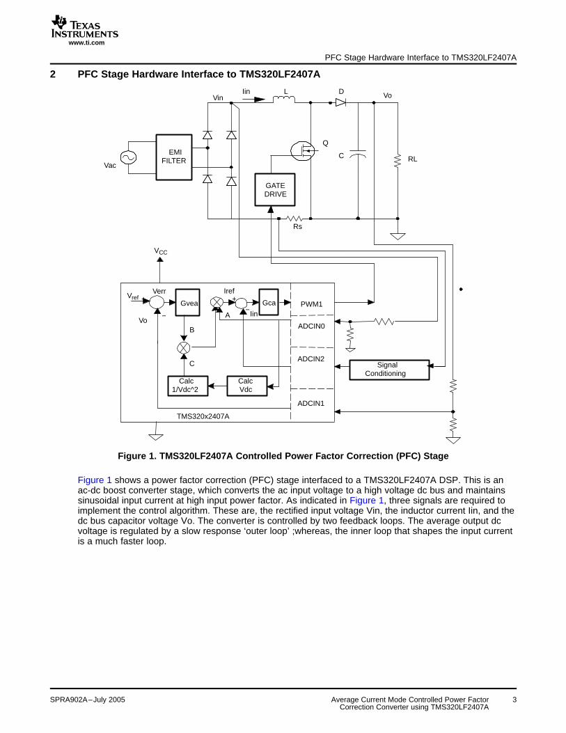
PFC Stage Hardware Interface to TMS320LF2407A
Figure 1. TMS320LF2407A Controlled Power Factor Correction (PFC) Stage
Figure 1 shows a power factor correction (PFC) stage interfaced to a TMS320LF2407A DSP. This is anac-dc boost converter stage, which converts the ac input voltage to a high voltage dc bus and maintainssinusoidal input current at high input power factor. As indicated in Figure 1, three signals are required toimplement the control algorithm. These are, the rectified input voltage Vin, the inductor current Iin, and thedc bus capacitor voltage Vo. The converter is controlled by two feedback loops. The average output dcvoltage is regulated by a slow response ‘outer loop’ ;whereas, the inner loop that shapes the input currentis a much faster loop.
SPRA902A–July 2005 Average Current Mode Controlled Power Factor 3Correction Converter using TMS320LF2407A
www.ti.com
�����
���� �
��
3 PFC Stage Digital Controller Design
d
Unv
+
Ks.Iin
Kf
Kavg
Ks
Iin
VinC
RL−
Vo
Kd
L
−
IrefA
KmABC
B
PWM MOD
UcaGca
Gvea
VrefCTMS320LF2407A
PFC Stage Digital Controller Design
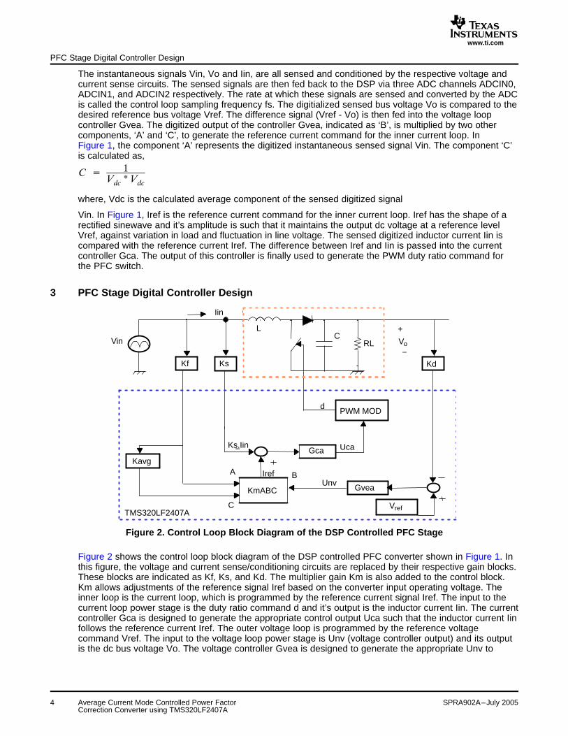
The instantaneous signals Vin, Vo and Iin, are all sensed and conditioned by the respective voltage andcurrent sense circuits. The sensed signals are then fed back to the DSP via three ADC channels ADCIN0,ADCIN1, and ADCIN2 respectively. The rate at which these signals are sensed and converted by the ADCis called the control loop sampling frequency fs. The digitialized sensed bus voltage Vo is compared to thedesired reference bus voltage Vref. The difference signal (Vref - Vo) is then fed into the voltage loopcontroller Gvea. The digitized output of the controller Gvea, indicated as ‘B’, is multiplied by two othercomponents, ‘A’ and ‘C’, to generate the reference current command for the inner current loop. InFigure 1, the component ‘A’ represents the digitized instantaneous sensed signal Vin. The component ‘C’is calculated as,
where, Vdc is the calculated average component of the sensed digitized signal
Vin. In Figure 1, Iref is the reference current command for the inner current loop. Iref has the shape of arectified sinewave and it’s amplitude is such that it maintains the output dc voltage at a reference levelVref, against variation in load and fluctuation in line voltage. The sensed digitized inductor current Iin iscompared with the reference current Iref. The difference between Iref and Iin is passed into the currentcontroller Gca. The output of this controller is finally used to generate the PWM duty ratio command forthe PFC switch.
Figure 2. Control Loop Block Diagram of the DSP Controlled PFC Stage
Figure 2 shows the control loop block diagram of the DSP controlled PFC converter shown in Figure 1. Inthis figure, the voltage and current sense/conditioning circuits are replaced by their respective gain blocks.These blocks are indicated as Kf, Ks, and Kd. The multiplier gain Km is also added to the control block.Km allows adjustments of the reference signal Iref based on the converter input operating voltage. Theinner loop is the current loop, which is programmed by the reference current signal Iref. The input to thecurrent loop power stage is the duty ratio command d and it’s output is the inductor current Iin. The currentcontroller Gca is designed to generate the appropriate control output Uca such that the inductor current Iinfollows the reference current Iref. The outer voltage loop is programmed by the reference voltagecommand Vref. The input to the voltage loop power stage is Unv (voltage controller output) and its outputis the dc bus voltage Vo. The voltage controller Gvea is designed to generate the appropriate Unv to
4 Average Current Mode Controlled Power Factor SPRA902A–July 2005Correction Converter using TMS320LF2407A
www.ti.com
3.1 Voltage and Current Sensing Gain
Vin � Vm sin 2�t, 0 � Vm � Vmax, and, Iin � Im sin 2�t, 0 � Im � Imax
A � VinKf � A|max � Vmax Kf � 1 � Vmax Kf
Kf � 1�Vmax
KS � 1�Imax
Kd � 1�Vomax
PFC Stage Digital Controller Design
control the amplitude of the reference current Iref such that for the applied load current and line voltage,the bus voltage Vo is maintained at the reference level. For this control implementation it is necessary tocalculate these voltage and current controllers. This in turn requires the identification of some of the blocksin Figure 1, especially, when this control is implemented in software using a fixed point DSP controllersuch as TMS32LF2407A.
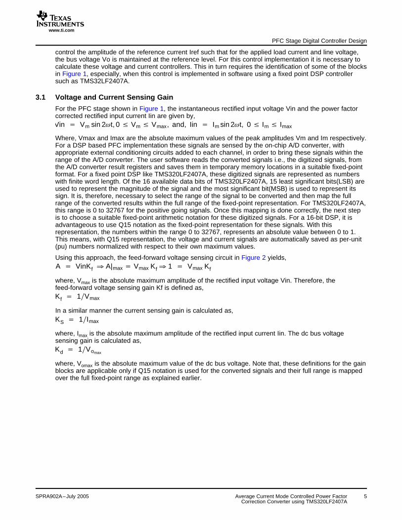
For the PFC stage shown in Figure 1, the instantaneous rectified input voltage Vin and the power factorcorrected rectified input current Iin are given by,
Where, Vmax and Imax are the absolute maximum values of the peak amplitudes Vm and Im respectively.For a DSP based PFC implementation these signals are sensed by the on-chip A/D converter, withappropriate external conditioning circuits added to each channel, in order to bring these signals within therange of the A/D converter. The user software reads the converted signals i.e., the digitized signals, fromthe A/D converter result registers and saves them in temporary memory locations in a suitable fixed-pointformat. For a fixed point DSP like TMS320LF2407A, these digitized signals are represented as numberswith finite word length. Of the 16 available data bits of TMS320LF2407A, 15 least significant bits(LSB) areused to represent the magnitude of the signal and the most significant bit(MSB) is used to represent itssign. It is, therefore, necessary to select the range of the signal to be converted and then map the fullrange of the converted results within the full range of the fixed-point representation. For TMS320LF2407A,this range is 0 to 32767 for the positive going signals. Once this mapping is done correctly, the next stepis to choose a suitable fixed-point arithmetic notation for these digitized signals. For a 16-bit DSP, it isadvantageous to use Q15 notation as the fixed-point representation for these signals. With thisrepresentation, the numbers within the range 0 to 32767, represents an absolute value between 0 to 1.This means, with Q15 representation, the voltage and current signals are automatically saved as per-unit(pu) numbers normalized with respect to their own maximum values.
Using this approach, the feed-forward voltage sensing circuit in Figure 2 yields,
where, Vmax is the absolute maximum amplitude of the rectified input voltage Vin. Therefore, thefeed-forward voltage sensing gain Kf is defined as,
In a similar manner the current sensing gain is calculated as,
where, Imax is the absolute maximum amplitude of the rectified input current Iin. The dc bus voltagesensing gain is calculated as,
where, Vomax is the absolute maximum value of the dc bus voltage. Note that, these definitions for the gainblocks are applicable only if Q15 notation is used for the converted signals and their full range is mappedover the full fixed-point range as explained earlier.
SPRA902A–July 2005 Average Current Mode Controlled Power Factor 5Correction Converter using TMS320LF2407A
www.ti.com
3.2 Software Implementation of Input Voltage Feed-forward
C �1
Vdc * Vdc
Vac
Vin
t,(nth sample)
t+T,(n+T/Ts) th sample
Vthreshld_hi
Vthreshld_lo
fPU �f
fmax�
1T1
TMIN
�
1NTS
1NMINTS
�
NMIN
N
PFC Stage Digital Controller Design
Input voltage feed-forward causes power input to remain constant at a specified level (determined by theload) regardless of line voltage changes. To implement this, a voltage Vdc proportional to rms inputvoltage is squared and divided into the control level. So we define the signal needed for feed-forwardimplementation as,
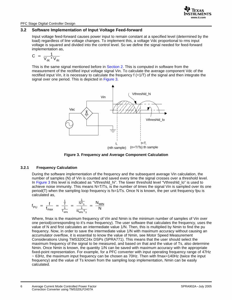
This is the same signal mentioned before in Section 2. This is computed in software from themeasurement of the rectified input voltage signal Vin. To calculate the average component Vdc of therectified input Vin, it is necessary to calculate the frequency f (=1/T) of the signal and then integrate thesignal over one period. This is depicted in Figure 3.
Figure 3. Frequency and Average Component Calculation
3.2.1 Frequency Calculation
During the software implementation of the frequency and the subsequent average Vin calculation, thenumber of samples (N) of Vin is counted and saved every time the signal crosses over a threshold level.In Figure 3 this level is indicated as “Vthreshld_hi”. The lower threshold level “Vthreshld_lo” is used toachieve noise immunity. This means N=T/Ts, is the number of times the signal Vin is sampled over its oneperiod(T) when the sampling loop frequency is fs=1/Ts. Once N is known, the per unit frequency fpu iscalculated as,
Where, fmax is the maximum frequency of Vin and Nmin is the minimum number of samples of Vin overone period(corresponding to it’s max frequency). The user software that calculates the frequency, uses thevalue of N and first calculates an intermediate value 1/N. Then, this is multiplied by Nmin to find the pufrequency. Now, in order to save the intermediate value 1/N with maximum accuracy without causing anaccumulator overflow, it is essential to know the value of Nmin, see Motor Speed MeasurementConsiderations Using TMS320C24x DSPs (SPRA771). This means that the user should select themaximum frequency of the signal to be measured, and based on that and the value of Ts, also determineNmin. Once Nmin is known, the quantity 1/N can be saved with maximum accuracy with the appropriatefixed-point representation. For example, for a PFC converter with input operating frequency range of 47Hz~ 63Hz, the maximum input frequency can be chosen as 70Hz. Then with fmax=140Hz (twice the inputfrequency) and the value of Ts known from the sampling loop implementation, Nmin can be easilycalculated.
6 Average Current Mode Controlled Power Factor SPRA902A–July 2005Correction Converter using TMS320LF2407A
www.ti.com
Vdc � 1T�t�T
t
Vin � dt
Vdc � 1T
�i�n�T�Ts
i�n
Vin(i) � Ts � �i�n�T�Ts
i�n
Vin(i) � 1T�TS
� �Vin(i) � 1N
�������� ��
Vdc1 � �Vin(1) � 1N�
Vmax�2Vmax���
, � Vdc � �
2
Vinv �1
Vdc1 � Vdc_MAX�
1Vinv_MAX
�1
Vdc1�
Vdc_MIN
Vdc_MAX�
1Vdc1
�
Vmin
Vmax
C � V 2inv
3.3 The Multiplier Gain Km
Iref � KmABC � Km�VinKf�(Unv)V 2
inv
Iref � IinKS � Iref MAX � IMAX KS � 1
PFC Stage Digital Controller Design
3.2.2 Feed-forward Component Calculation
Once the frequency of the signal Vin is known, its average component is calculated using,
where, T is the time period corresponding to the frequency f of the rectified input voltage Vin. In discreteform the average component is expressed as,
where, Vin(i) represents the digitized i-th sample of Vin.
Again when N is known, the integral under the Vin curve is computed by calculating the sum of theproducts
over one period. This gives the average component Vdc of the input rectified voltage Vin. Since Vin ismeasured as a per unit value normalized with respect to its maximum value Vmax, this calculated value ofVdc is also a pu quantity with a base value of normalization of Vmax. However, for a sine-wave inputvoltage the maximum value of the average component Vdc is only 2Vmax/π. Therefore, to achieve betteraccuracy in the fixed-point representation of Vdc, the previously calculated value is converted to a puquantity normalized with respect to its own maximum value. This value is given by:
Now, in calculating the inverse, Vinv, of Vdc1, i.e., Vinv=1/Vdc1, it is clear that Vinv is maximum whenVdc1 is minimum and vice versa. Therefore, to achieve better accuracy in the fixed-point representation ofVinv, it is necessary to represent this with a pu value normalized with respect to its own maximum value.For a sine-wave input voltage, the minimum value of Vdc is 2Vmin/π, where, the minimum amplitude,Vmin, of the rectified input voltage is selected based on the input operating voltage range of the PFCconverter. For example, to operate the PFC converter with a low line voltage of 90Vrms, the chosen valueof Vmin should be less than or equal to 127V. With the selected value of Vmin, the maximum value ofVinv is (π/2Vmin) and the corresponding pu value of Vinv with respect to its own maximum value is:
Once Vinv is calculated with the maximum accuracy, the feed-forward component C can be calculatedwith the same accuracy as,
The multiplier gain Km is adjusted such that at the minimum input voltage, the reference current Iref is atits maximum when the PFC converter delivers the maximum load. From the block diagram in Figure 2,
With the current loop closed,
SPRA902A–July 2005 Average Current Mode Controlled Power Factor 7Correction Converter using TMS320LF2407A
www.ti.com
Km � Iref MAX��
�1
VminKfUnvV 2inv��
��
Vmax
Vmin
3.4 Voltage and Current Loop Compensators
G id �
I�
in
d�
�
VO
sL
Ti � G idKSGCAFm
Fm �d�
U�
CA
GCA �
2�fci LKSVO
GVC � V�
O�U�
nv � Km2KfKS
�Vmin
Vmax�2
Zf
VO
Zf �1
1ro
�1ZL
� sC
ZL �
� VO2
PO� � ro
ZL � RL �
VO
IO� ro
PFC Stage Digital Controller Design
As explained in Section 3.2.2, at the minimum operating voltage Vinv =1. Again, for full load power thevoltage controller output will be at its maximum, i.e., Unv =1. Therefore, at minimum operating voltage, togenerate maximum reference current the required value of Km is,
High frequency approximation of the current loop power stage(1/sC = 0) is,
From the PFC control block diagram in Figure 2, the loop gain equation for the current loop is,
Where the modulator gain is,
This modulator is implemented partly in software and partly using the DSP PWM hardware. The softwareuses the modulator input, i.e., the current controller output Uca, and calculates a duty ratio value for thePWM hardware module in TMS320LF2407A. The PWM hardware uses the duty ratio value and generatesthe appropriate PWM signal for the PFC switch. The software is implemented such that, when themodulator input, Uca, is 1, the modulator output, i.e., the PWM duty ratio d, is 100%. This means, themodulator gain in this case is Fm = 1. Therefore, for a current loop crossover frequency of fci, the requiredcurrent error amplifier compensator is,
Once the current loop is closed, the voltage loop power stage transfer function can be calculated as,
where, Zf represents the equivalent impedance of the parallel branch consisting of the bus capacitor C,the PFC stage output impedance rO and the load impedance ZL, and is given by,
For a constant power load Po, the load impedance ZL and the output impedance rO are related by,
For resistive load RL, the load impedance ZL and the output impedance rO are related by,
8 Average Current Mode Controlled Power Factor SPRA902A–July 2005Correction Converter using TMS320LF2407A
www.ti.com
TV � Kd GVEAGVC
GVEA �2Kf KS
Kd Km�Vmax
Vmin�
2VO
Zf | f � fcv
3.5 Software Implementation of the Voltage and Current Loop Compensators
���
���� �� ���
�� ���
���
� �� ���
��
� ��
��
��
���
−1
−2
−1
| Gca |
| Gid.Fm.Ks |
fo fcif
Kp f
f
fci
fz
−1
| Ti |
0
0
0
UCA(n) � KP E(n) � KITS �n
j�O
E(j)
PFC Stage Digital Controller Design
From the block diagram in Figure 2, the loop gain equation for the voltage loop is,
Using this loop gain equation, for a voltage loop crossover frequency of fcv, the required voltage erroramplifier compensator is,
The voltage and current loop controllers, given in previous section, are transformed to an equivalent digitalform as explained below, before they are implemented in software using TMS320LF2407A. For example,the current controller can be written as,
Where, Kp is the magnitude of the current compensator calculated in Section 3.4 and E is the currenterror signal.
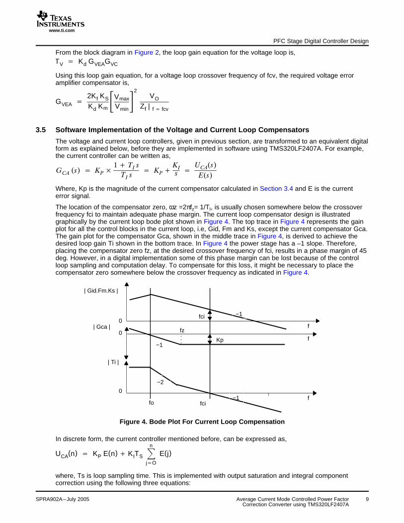
The location of the compensator zero, ωz =2πfz= 1/TI, is usually chosen somewhere below the crossoverfrequency fci to maintain adequate phase margin. The current loop compensator design is illustratedgraphically by the current loop bode plot shown in Figure 4. The top trace in Figure 4 represents the gainplot for all the control blocks in the current loop, i.e, Gid, Fm and Ks, except the current compensator Gca.The gain plot for the compensator Gca, shown in the middle trace in Figure 4, is derived to achieve thedesired loop gain Ti shown in the bottom trace. In Figure 4 the power stage has a –1 slope. Therefore,placing the compensator zero fz, at the desired crossover frequency of fci, results in a phase margin of 45deg. However, in a digital implementation some of this phase margin can be lost because of the controlloop sampling and computation delay. To compensate for this loss, it might be necessary to place thecompensator zero somewhere below the crossover frequency as indicated in Figure 4.
Figure 4. Bode Plot For Current Loop Compensation
In discrete form, the current controller mentioned before, can be expressed as,
where, Ts is loop sampling time. This is implemented with output saturation and integral componentcorrection using the following three equations:
SPRA902A–July 2005 Average Current Mode Controlled Power Factor 9Correction Converter using TMS320LF2407A
www.ti.com
UCA(n)
I(n)Epi
�
�
�
K0 * E(n)� I(n� 1),
I(n� 1)� K1 * E(n)� Kcorr * EpiUs� UCA(n)
Us � UCAmax when UCA(n)� UCAmax
Us � UCAmin when UCA(n)� UCAmin
Us � UCA(n)
K0 � KP, K1 � KITS, KCORR � K1�K0
4 PFC Stage Digital Controller Design Example
4.1 Current Controller Implementation Example
GCA(s) � 0.1985 �1 � 198.94 � 10�6s
198.94 � 10�6s
� GCA(s) � KPi �KIis �
Ui (s)
Ei (s)
Ui(n) � K0i * Ei(n)� Ii(n� 1),
Ii(n) � Ii(n� 1)� K1i * Ei(n)� Kcorri * Epii
Epii � Usi� Ui(n)
PFC Stage Digital Controller Design Example
where,
otherwise,
Here, Us represents the final output of the current controller with saturation and integral componentcorrection. The coefficients in the last three equations, representing the discrete form of the analog currentcompensator, are defined as,
These equations can be easily implemented in software using TMS320LF2407A.
The system parameters used in this design are:
Output power Po=825 W,DC bus voltage Vo =380V,Switching frequency fsw=120kHz;Digital loop sampling frequency fs = 60kHzL=100uH, C=390uF,Volt loop bandwidth fcv=10Hz, Current loop bandwidth fci=8kHz,Maximum frequency of rectified input voltage fmax=200HzVmax=410V, Vmin=109.95V, Vomax=410V
To deliver the maximum output power at the minimum input voltage, the maximum value of the inputcurrent (neglecting the losses in the PFC converter) is, Imax=2Po/Vmin = 15A Different gain parametersare calculated as,Kf = 1/410, Kd = 1/410, Ks = 1/15, Km = 410/109.95 = 3.7286
For fci = 8kHz, the magnitude of the current controller is, GCA = 0.1985 Set current loop PI compensatorzero at 800Hz. So, the integral time constant for the current compensator is, TIC = 1/(2π.800) =198.94x10⁻⁶ Therefore, the complete current loop controller is,
where, KPi = 0.1985 and KIi = 997.77
The discrete controller is implemented using the following equations,
where,
10 Average Current Mode Controlled Power Factor SPRA902A–July 2005Correction Converter using TMS320LF2407A
www.ti.com
Usi � Uimax when Ui(n)� Uimax
Usi � Uimin when Ui(n)� Uimin
Usi � Ui(n)
K0i � KPi � 0.1985 � 6504(Q15)
K1i � KIi TS � 0.016629 � 545(Q15)
Kcorri �K1iK0i
� 0.08376 � 2745(Q15)
PFC Stage Digital Controller Design Example
otherwise,
The coefficients for the discrete current controller are,
where, TS = 16.667x 10⁻⁶ sec.
The code segment that implements the above controller is given below:
PFC_I_CONTROL_INIT:;PFC current control loop initialization
LDP # K0iSPLK #6504,K0i ;Q15SPLK #545,K1i ;Q15SPLK #2745,Kcorri ;Q15RET
PFC_I_CONTROL:;PFC current control loop using feed-forward technique
SETC SXMSETC OVMspm #0LDP #Iref
LACC Iref ;Q15SUB Ipfc ;Q15SACL En0i ;Q15LACC Uni,15 ;Q30,32-bitLT En0i ;Q15MPY K0i ;Q15*Q15APAC ;Q30SACH GPR0_pfcADDH GPR0_pfc ;Q31SACH Upii ;Q15SACH Usi ;Q15UiMAX .set 7ffehUiMIN .set 0
LACC UpiiBCND SAT_UiMIN, LT ;LACC UpiiSUB #UiMAXBCND SAT_UiMAX, GEQ ;B FWD_i
SAT_UiMIN SPLK #UiMIN,UsiB FWD_iSAT_UiMAX SPLK #UiMAX,UsiFWD_i: LACC Usi ;Q15SUB Upii ;Q15SACL Epii ;Q15LT Epii ;Q15MPY Kcorri ;Q15LTP En0i ;Q15MPY K1i ;Q15APAC ;Q30ADD Uni,15SACH GPR0_pfcADDH GPR0_pfc ; Q31
SPRA902A–July 2005 Average Current Mode Controlled Power Factor 11Correction Converter using TMS320LF2407A
www.ti.com
4.2 Voltage Controller Implementation Example
Gvea(s) � 4.7517 �1 � 15.9155 � 10�3s
15.9155 � 10�3s
� Gvea(s) � KPv �KIvs �
Uv(s)Ev(s)
Uv(n) � K0v * Ev(n)� Iv(n� 1),
Ivi(n) � Iv(n� 1)� K1v * Ev(n)� Kcorrv * Epiv
Epiv � Usv� Uv(n)
Usv � Uvmax when Uv(n)� Uvmax
Usv � Uvmin when Uv(n)� Uvmin
Usv � Uv(n)
K0v � KPv � 4.7517 � 19463(Q12)
K1v � KIv TS � 0.004976 � 163(Q15)
Kcorrv �K1vK0v
� 0.001047 � 34(Q15)
PFC Stage Digital Controller Design Example
SACH Uni ;Q15, Controller final outputRET
For constant power load, ZL = -175.03. For fcv = 10Hz, the magnitude of the voltage controller is, GVEA =4.63. Set the volt loop PI compensator zero at 10Hz. Then the integral time constant is, TIV = 1/(2π.10) =15.9155x10⁻³. Therefore, the complete voltage loop controller is,
where, KPV = 4.63 and KIV = 290.91
The discrete controller is implemented using the following equations,
where,
otherwise,
The coefficients for the discrete voltage controller are,
where, TS = 16.667x 10⁻⁶ sec.
The code segment that implements the above controller can be written in the same way as shown inSection 4.1.
12 Average Current Mode Controlled Power Factor SPRA902A–July 2005Correction Converter using TMS320LF2407A
www.ti.com
5 Experimental Results
Experimental Results
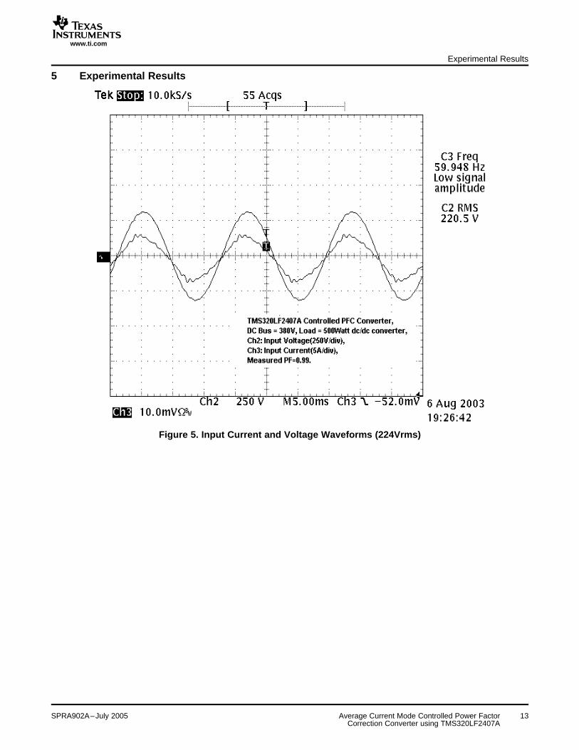
Figure 5. Input Current and Voltage Waveforms (224Vrms)
SPRA902A–July 2005 Average Current Mode Controlled Power Factor 13Correction Converter using TMS320LF2407A
www.ti.com
6 References
References
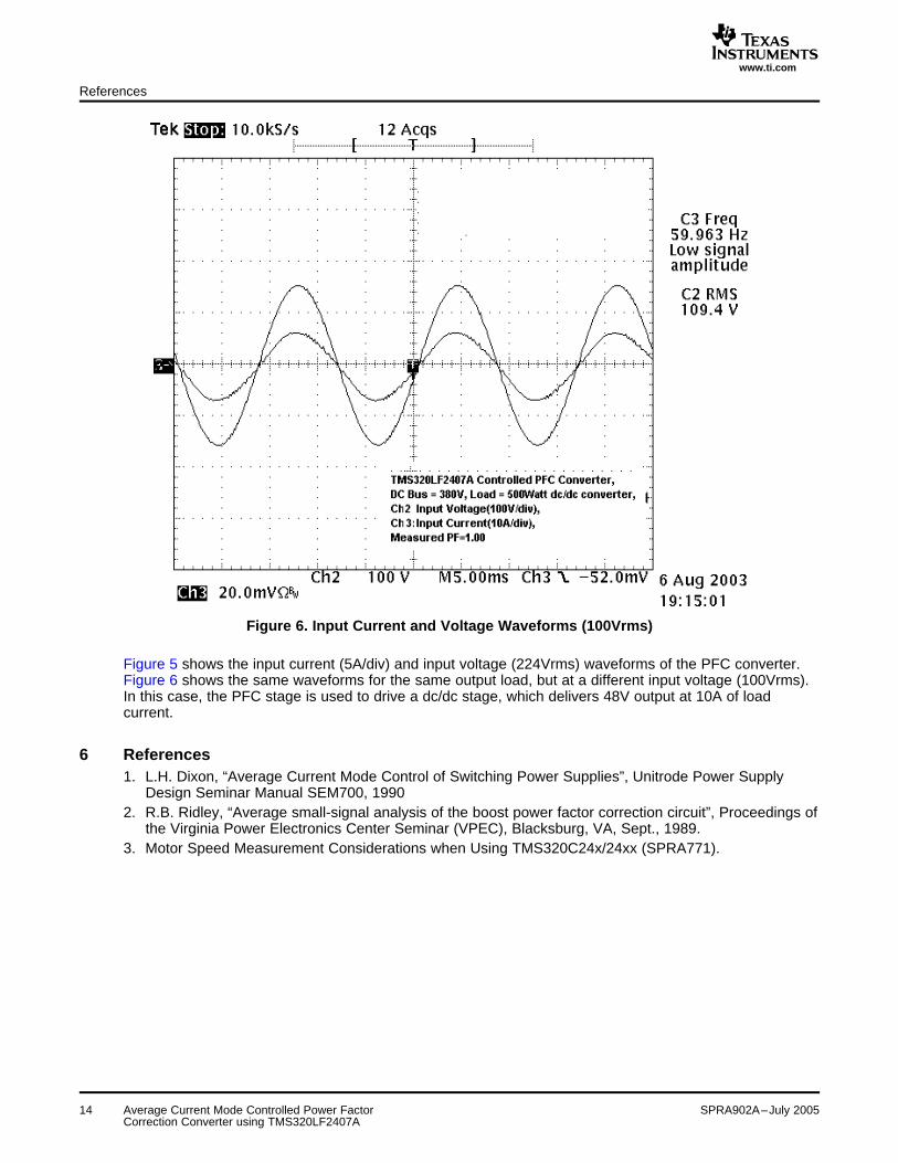
Figure 6. Input Current and Voltage Waveforms (100Vrms)
Figure 5 shows the input current (5A/div) and input voltage (224Vrms) waveforms of the PFC converter.Figure 6 shows the same waveforms for the same output load, but at a different input voltage (100Vrms).In this case, the PFC stage is used to drive a dc/dc stage, which delivers 48V output at 10A of loadcurrent.
1. L.H. Dixon, “Average Current Mode Control of Switching Power Supplies”, Unitrode Power SupplyDesign Seminar Manual SEM700, 1990
2. R.B. Ridley, “Average small-signal analysis of the boost power factor correction circuit”, Proceedings ofthe Virginia Power Electronics Center Seminar (VPEC), Blacksburg, VA, Sept., 1989.
3. Motor Speed Measurement Considerations when Using TMS320C24x/24xx (SPRA771).
14 Average Current Mode Controlled Power Factor SPRA902A–July 2005Correction Converter using TMS320LF2407A
IMPORTANT NOTICE
Texas Instruments Incorporated and its subsidiaries (TI) reserve the right to make corrections, modifications,enhancements, improvements, and other changes to its products and services at any time and to discontinueany product or service without notice. Customers should obtain the latest relevant information before placingorders and should verify that such information is current and complete. All products are sold subject to TI’s termsand conditions of sale supplied at the time of order acknowledgment.
TI warrants performance of its hardware products to the specifications applicable at the time of sale inaccordance with TI’s standard warranty. Testing and other quality control techniques are used to the extent TIdeems necessary to support this warranty. Except where mandated by government requirements, testing of allparameters of each product is not necessarily performed.
TI assumes no liability for applications assistance or customer product design. Customers are responsible fortheir products and applications using TI components. To minimize the risks associated with customer productsand applications, customers should provide adequate design and operating safeguards.
TI does not warrant or represent that any license, either express or implied, is granted under any TI patent right,copyright, mask work right, or other TI intellectual property right relating to any combination, machine, or processin which TI products or services are used. Information published by TI regarding third-party products or servicesdoes not constitute a license from TI to use such products or services or a warranty or endorsement thereof.Use of such information may require a license from a third party under the patents or other intellectual propertyof the third party, or a license from TI under the patents or other intellectual property of TI.
Reproduction of information in TI data books or data sheets is permissible only if reproduction is withoutalteration and is accompanied by all associated warranties, conditions, limitations, and notices. Reproductionof this information with alteration is an unfair and deceptive business practice. TI is not responsible or liable forsuch altered documentation.
Resale of TI products or services with statements different from or beyond the parameters stated by TI for thatproduct or service voids all express and any implied warranties for the associated TI product or service andis an unfair and deceptive business practice. TI is not responsible or liable for any such statements.
Following are URLs where you can obtain information on other Texas Instruments products and applicationsolutions:
Products Applications
Amplifiers amplifier.ti.com Audio www.ti.com/audio
Data Converters dataconverter.ti.com Automotive www.ti.com/automotive
DSP dsp.ti.com Broadband www.ti.com/broadband
Interface interface.ti.com Digital Control www.ti.com/digitalcontrol
Logic logic.ti.com Military www.ti.com/military
Power Mgmt power.ti.com Optical Networking www.ti.com/opticalnetwork
Microcontrollers microcontroller.ti.com Security www.ti.com/security
Telephony www.ti.com/telephony
Video & Imaging www.ti.com/video
Wireless www.ti.com/wireless
Mailing Address: Texas Instruments
Post Office Box 655303 Dallas, Texas 75265
Copyright 2005, Texas Instruments Incorporated