analog electronics 3331102 manual2
TRANSCRIPT
FREQ. RESPONSE OF NEG. FEEDBACK AMPLIFIER
EXPERIMENT NO. 1

SCHEMATIC DIAGRAM
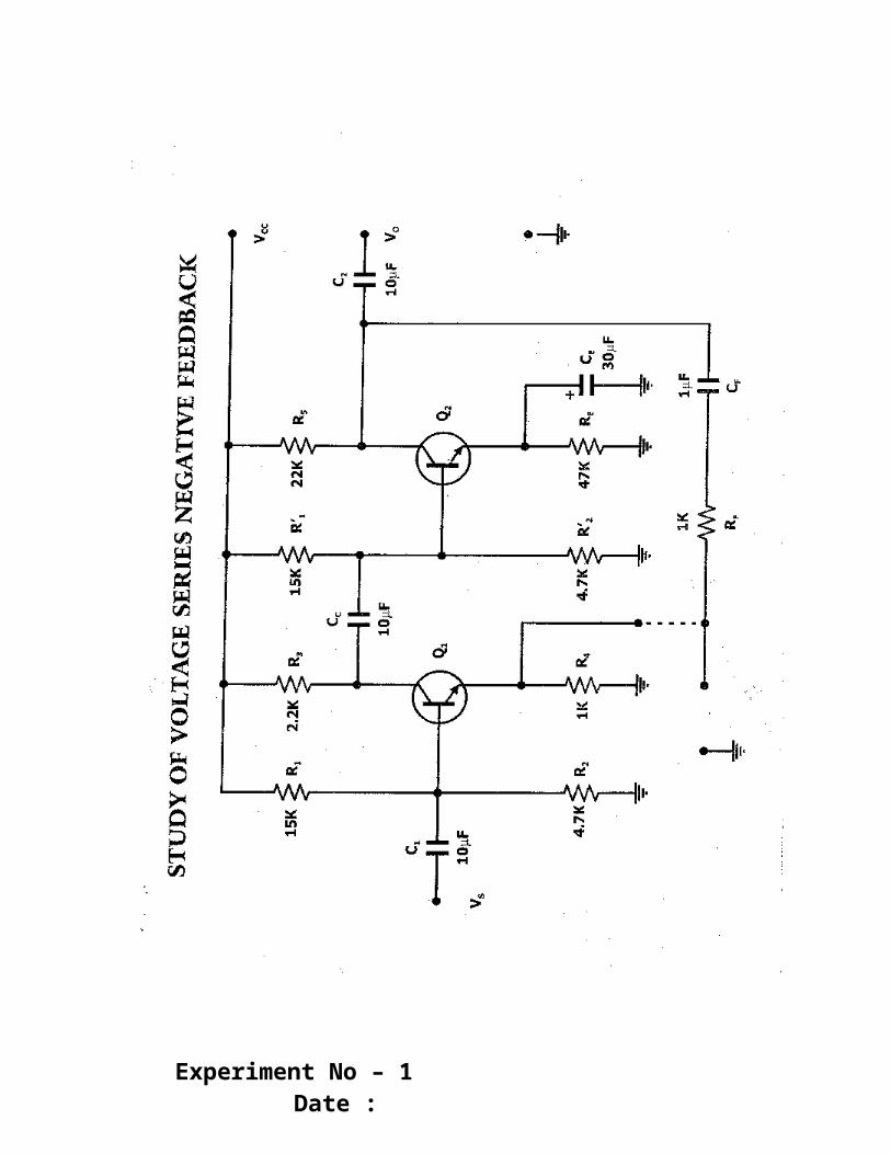
Experiment No – 1 Date :
SERIES NEGATIV
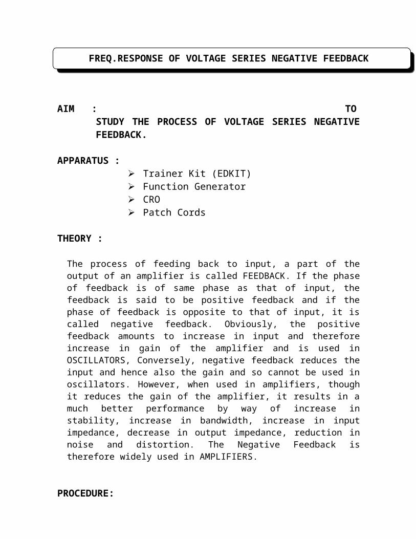
AIM : TOSTUDY THE PROCESS OF VOLTAGE SERIES NEGATIVEFEEDBACK.
APPARATUS : Trainer Kit (EDKIT) Function Generator CRO Patch Cords
THEORY :
The process of feeding back to input, a part of theoutput of an amplifier is called FEEDBACK. If the phaseof feedback is of same phase as that of input, thefeedback is said to be positive feedback and if thephase of feedback is opposite to that of input, it iscalled negative feedback. Obviously, the positivefeedback amounts to increase in input and thereforeincrease in gain of the amplifier and is used inOSCILLATORS, Conversely, negative feedback reduces theinput and hence also the gain and so cannot be used inoscillators. However, when used in amplifiers, thoughit reduces the gain of the amplifier, it results in amuch better performance by way of increase instability, increase in bandwidth, increase in inputimpedance, decrease in output impedance, reduction innoise and distortion. The Negative Feedback istherefore widely used in AMPLIFIERS.
PROCEDURE:
FREQ.RESPONSE OF VOLTAGE SERIES NEGATIVE FEEDBACK
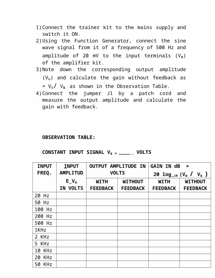
1)Connect the trainer kit to the mains supply andswitch it ON.
2)Using the Function Generator, connect the sinewave signal from it of a frequency of 500 Hz andamplitude of 20 mV to the input terminals (Vs)of the amplifier kit.
3)Note down the corresponding output amplitude(Vo) and calculate the gain without feedback as= Vo/ Vs as shown in the Observation Table.
4)Connect the jumper J1 by a patch cord andmeasure the output amplitude and calculate thegain with feedback.
OBSERVATION TABLE:
CONSTANT INPUT SIGNAL Vs = …………….. VOLTS
INPUTFREQ.
INPUTAMPLITUD
E VoIN VOLTS
OUTPUT AMPLITUDE INVOLTS
GAIN IN dB = 20 log 10 (Vo / Vs )
WITHFEEDBACK
WITHOUTFEEDBACK
WITHFEEDBACK
WITHOUTFEEDBACK
20 Hz50 Hz100 Hz200 Hz500 Hz1KHz2 KHz5 KHz10 KHz20 KHz50 KHz

100 KHz200 KHz500 KHz
5)For both conditions, vary the frequency of theinput signal from the function generator andnote down the readings of corresponding outputvoltage amplitudes and calculate the gains asbefore.
6)Plot the graphs of freq. Vs. gain on a semilogpaper for both with & w/o feedback.
CONCLUSION:
_________________________________________________
_________________________________________________
_________________________________________________
_________________________________________________
_________________________________________________
___________________________
ASSESMENT SCHEME:
No. Criteria %Weightag
e Marks
1 Proper Connection 30
2Proper handling of
equipment20
3 Proper Observation 204 Submission in time 30

________________________
SIGN OF FACULTY

EXPERIMENT NO. 2
COLPITTS OSCILLATOR
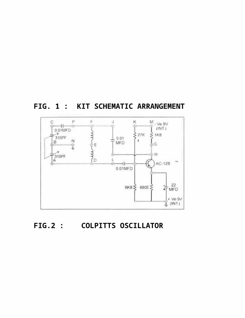
FIG. 1 : KIT SCHEMATIC ARRANGEMENT
FIG.2 : COLPITTS OSCILLATOR
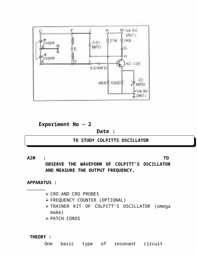
Experiment No – 2 Date :
AIM : TOOBSERVE THE WAVEFORM OF COLPITT’S OSCILLATORAND MEASURE THE OUTPUT FREQUENCY.
APPARATUS :
CRO AND CRO PROBES FREQUENCY COUNTER (OPTIONAL) TRAINER KIT OF COLPITT’S OSCILLATOR (omegamake)
PATCH CORDS
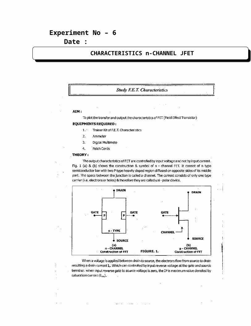
THEORY : One basic type of resonant circuit
TO STUDY COLPITTS OSCILLATOR
oscillator is the Colpitts, named afterit’s inventor. As shown in the figure, thistype of oscillator uses an LC circuit inthe feedback type loop to provide thenecessary phase shift and to act as aresonant filter that passes only thedesired frequency of oscillation.The approximate frequency is the resonantfrequency of the LC circuit is establishedby the values of C1,C2 and L, according tothe familiar formula, which also applies tothe Clapp and Hartley oscillators i.e.
fr= 1 / 2 π root LCTBecause the capacitors effectively appear inseries around the tank circuit, the totalcapacitance CT = C1C2/C1+C2
CONDITIONS FOR OSCILLATION AND STARTUP:1. Active device: Valve, Transistoror FET which works as an amplifier.
2. Power Supply: For biasing of amplifier and to overcome losses.
3. Frequency determining network: In Colpitts Oscillator, the LC tunednetwork (also called Tank Circuit) consisting of one coil L and two capacitors C1 and C2 forms the frequency
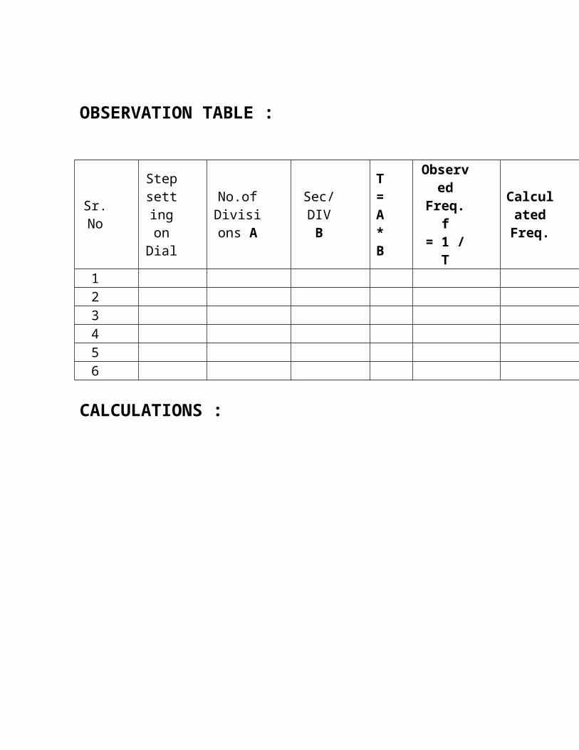
OBSERVATION TABLE :
Sr.No
StepsettingonDial
No.ofDivisions A
Sec/DIVB
T=A*B
Observed
Freq.f
= 1 /T
CalculatedFreq.
123456
CALCULATIONS :
determining network.4. Positive feedback : Positive feedback from output to input is essential for oscillations to take place. In Colpitts oscillator, it isprovided via the tuned LC network.
5. Value of Aβ : Value of Aβ should be more than 1 in the beginning and should become 1 once the oscillations have started. This is achieved by adjusting the gain ofthe amplifier with the help of positive feedback.
PROCEDURE: 1)In the provided trainer kit of RF (L-C)
OSCILLATORS (OMEGA TYPE ETB-25) , connect A to D, D to L, N to B, C to F, F to J andG to H. Now, the circuit is same as shown in FIG.1
2)Switch ON the supply provided at the left hand corner on the panel.
3)Connect CRO at the output on collector of the transistor at point G which is same aspoint H and observe the waveform of Colpitt’s oscillator. It should be a pure SINE wave.
4)Calculate the frequency by the formula fr= 1 / 2 π root LCT
5)Compare the calculated value with the observed frequency.
6)Change the value of the ganged capacitorsby rotating the knob on the semi-circulardial and observe the output and repeat steps 4 and 5 above.
CONCLUSION:
_________________________________________________
_________________________________________________
_________________________________________________
_________________________________________________
_________________________________________________
___________________________
___________________
SIGN OFFACULTY
CALCULATIONS :

EXPERIMENT NO. 3
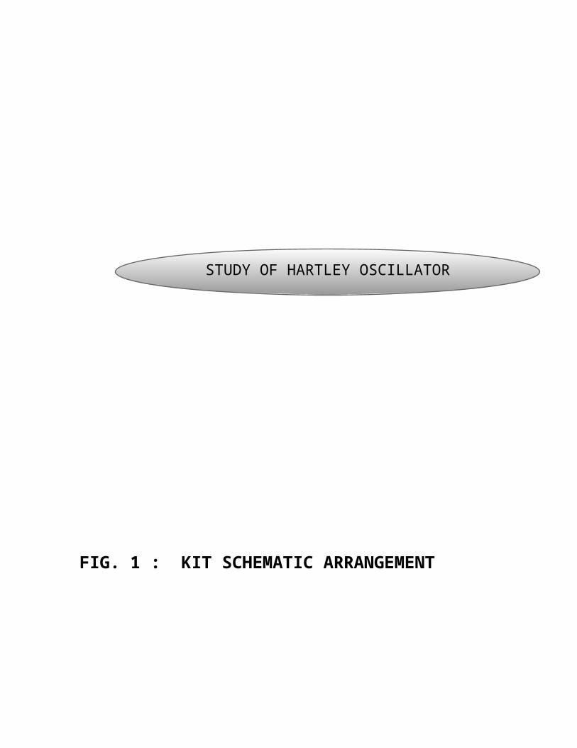
FIG. 1 : KIT SCHEMATIC ARRANGEMENT
STUDY OF HARTLEY OSCILLATOR
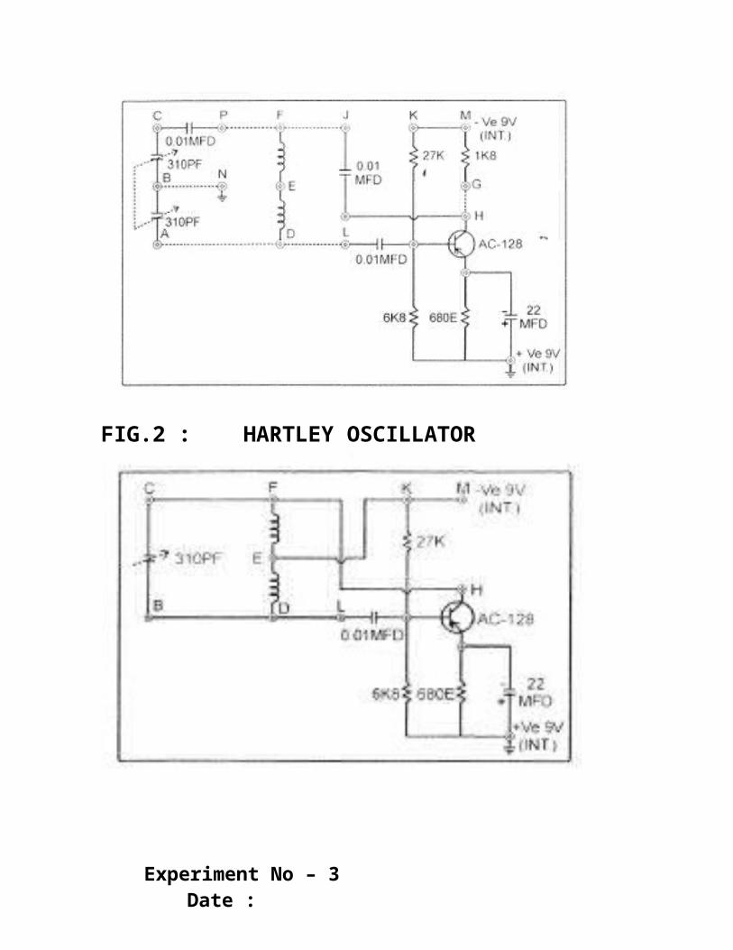
FIG.2 : HARTLEY OSCILLATOR
Experiment No – 3 Date :
AIM: TO OBSERVE THE WAVEFORM OF HARTLEY OSCILLATOR AND MEASURE THE OUTPUT FREQUENCY.
APPARATUS :
CRO AND CRO PROBES FREQUENCY COUNTER (OPTIONAL) TRAINER KIT OF COLPITT’S OSCILLATOR PATCH CORDS
THEORY : Hartley Oscillator is used for the generation of
high frequencies (Radio frequencies). A splitinductor tuned or tank circuit is used in thisoscillator, which provides the positive feedback.The frequency of oscillation depends upon the valuesof this tuned circuit viz.L1,L2 and C.
The approximate frequency is the resonantfrequency of the LC circuit is established by thevalues of L1,L2 and C, according to the familiarformula, which also applies to the Clapp andColpitts oscillators i.e.
fr =1 / 2 π root LC
Because the inductors L1 & L2 effectively appearin series around the tank circuit, the totalinductance L = L1+ L2
PROCEDURE: 1)In the provided trainer kit of RF (L-C)
OSCILLATORS (OMEGA TYPE ETB-25) , connect B to D, D to L, C to F, F to H and E to K.Now, the circuit is same as shown in FIG.1
HARTLEY OSCILLATOR
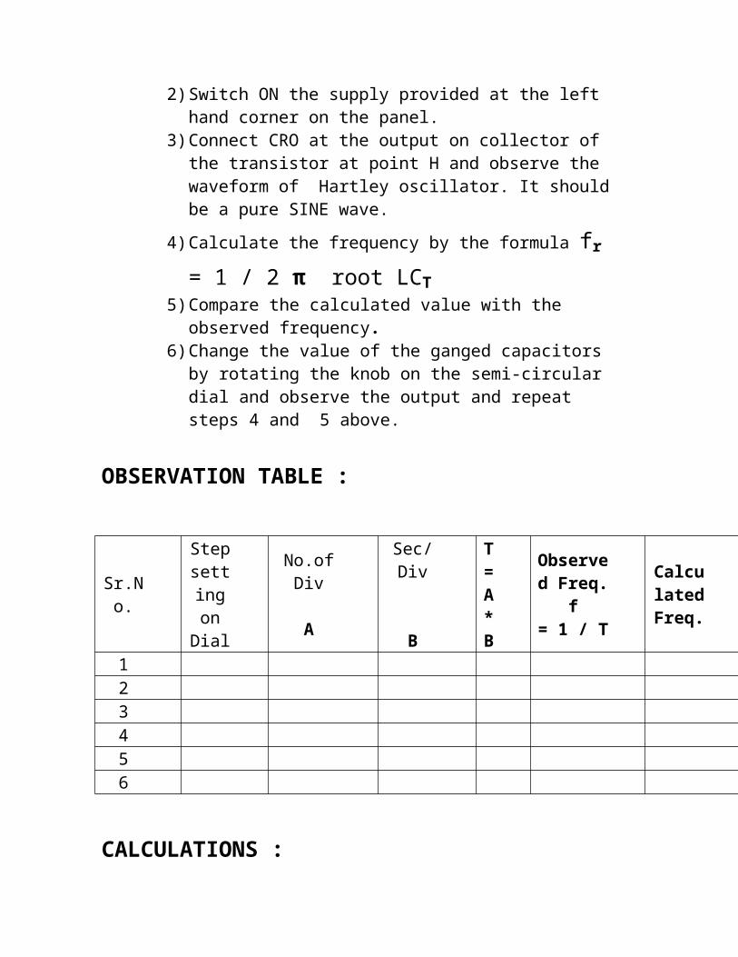
2)Switch ON the supply provided at the left hand corner on the panel.
3)Connect CRO at the output on collector of the transistor at point H and observe the waveform of Hartley oscillator. It shouldbe a pure SINE wave.
4)Calculate the frequency by the formula fr= 1 / 2 π root LCT
5)Compare the calculated value with the observed frequency.
6)Change the value of the ganged capacitorsby rotating the knob on the semi-circulardial and observe the output and repeat steps 4 and 5 above.
OBSERVATION TABLE :
Sr.No.
StepsettingonDial
No.ofDiv
A
Sec/Div
B
T=A*B
Observed Freq.
f= 1 / T
CalculatedFreq.
123456
CALCULATIONS :


CONCLUSION:_________________________________________________
_________________________________________________
_________________________________________________
_________________________________________________
_________________________________________________
___________________________
ASSESMENT SCHEME:
No. Criteria %Weightag
e Marks
1 Proper Connection 30
2Proper handling of
equipment20
3 Proper Observation 204 Submission in time 30
______________
_____
SIGN OF FACULTY

CALCULATIONS :

EXPERIMENT NO. 4
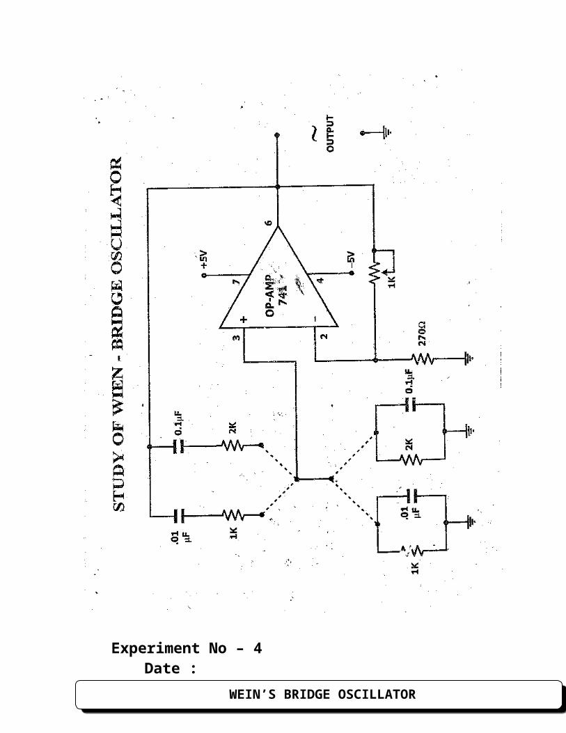
WEIN’S BRIDGE OSCILLATOR

SCHEMATIC DIAGRAM:
Experiment No – 4 Date :
WEIN’S BRIDGE OSCILLATOR
AIM : TOOBSERVE THE SINE WAVE OUTPUT OF THE GIVEN WEINBRIDGE OSCILLATOR AND COMPARE THE OBSERVEDFREQUENCY WITH THE THEORATICALLY CALCULATEDFREQUENCY.
APPARATUS :
EDKIT Trainer Kit. Oscilloscope (CRO). Patch Cords.
PROCEDURE :
Connect the trainer kit of Wein BridgeOscillator to mains supply and switch it ON.
Select R1C1 and RA1CA1 in the circuit withthe help of patch cords.
Connect C.R.O. at the output of Wein BridgeOscillator.
Adjust the Gain Potentiometer to get a properSine wave output on C.R.O.
Note the peak to peak amplitude of the outputand it should be near to 12 volts.
Observe and record the frequency of theoscillator on C.R.O. by measuring the timeperiod of 1 cycle.
Verify the observed frequency with the calculatedfrequency by the formula

f = 1 / 2 π RC
Repeat the experiment with R2C2 AND RA2C2.
OBSERVATIONS / CALCULATIONS :
CONCLUSION:
_________________________________________________________
_________________________________________________________
_________________________________________________________
_________________________________________________________
_________________________________________________________
___________________________________
ASSESMENT SCHEME:
No. Criteria %Weightage Marks
1 Proper Connection 30
2Proper handling of
equipment20
3 Proper Observation 204 Submission in time 30
______________
_____
SIGN OF FACULTY

EXPERIMENT NO. 5
UJT AS A RELAXATION OSCILLATOR
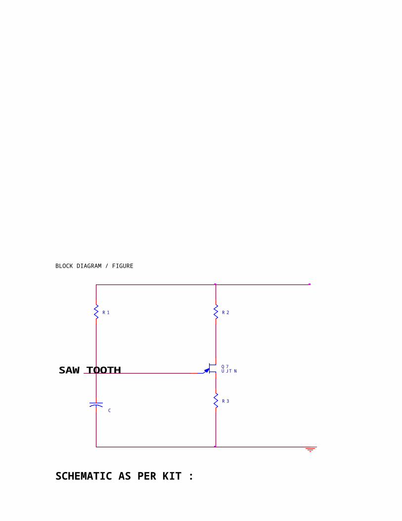
BLOCK DIAGRAM / FIGURE
R 1
SAW TOOTH
R 3
C
Q 7U JT N
R 2
SCHEMATIC AS PER KIT :
Experiment No – 5 Date :
AIM : TOSTUDY AND PERFORM THE UJT AS RELAXATIONOSCILLATOR.
APPARATUS : (AS PARTS OF SIGMA TRAINER KIT AND OTHERS)
UJT (2N2446) Resistors Capacitor CRO DC power supply
THEORY :
UJT is the Uni Junction Transistor. It is athree terminal device. They are: a) emitter b)base1 c) base2. The equivalent circuit isshown with the circuit diagram. So there aretwo resistors. One is a variable resistor andother is a fixed resistor.
The ratio of internal resistances is referredas intrinsic standoff ratio (η).It is definedas the ratio of the variable resistance to thetotal resistance. Due to the existing pnjunction, there will be a voltage drop. If weapply a voltage to the emitter, the devicewill not turn on until the input voltage isless than the drop across the diode plus thedrop at the variable resistance R1.
UJT AS RELAXATION OSCILLATOR
When the device is turned on holes moves fromemitter to base resulting in a current flow.Due to this sudden increase in chargeconcentration in base1 region conductivityincreases. This causes a drop at base1.Thisregion in the graph is known as negativeresistance region. If we further increase theemitter voltage the device undergoessaturation. So a UJT has 3 operating regions:
1. Cut off region2. Negative resistance region3. Saturation region
In a relaxation circuit there is an RC timingcircuit. When the supply is turned on, thecapacitor starts charging. When the voltageacross the capacitor reaches
OBSERVED WAVEFORMS :
the pinch off voltage, the UJT turns on. Afterdischarging of capacitor again it startscharging, and this process continues tillpower supply is turned off.
PROCEDURE :
1.Make the circuit as shown in figure. 2.Rotate potentiometer P1 fully in clockwise
direction.
3.Switch on the power supply.
4.Connect the oscillator CH1 between OP-1 groundand CH2 between OP-2 and ground and observethe waveform of pulse output.
5. Now Connect CH2 between OP-3 and ground and observethe waveform of pulse output.
6.Vary the potentiometer P1 in clockwisedirection so as to increase the frequency ofthe output.
CONCLUSION:
_________________________________________________________
_________________________________________________________
______________________________________________
ASSESMENT SCHEME:
No. Criteria %Weightage Marks
1 Proper Connection 30
2Proper handling of
equipment20
3 Proper Observation 204 Submission in time 30
______________
_____
SIGN OF FACULTY

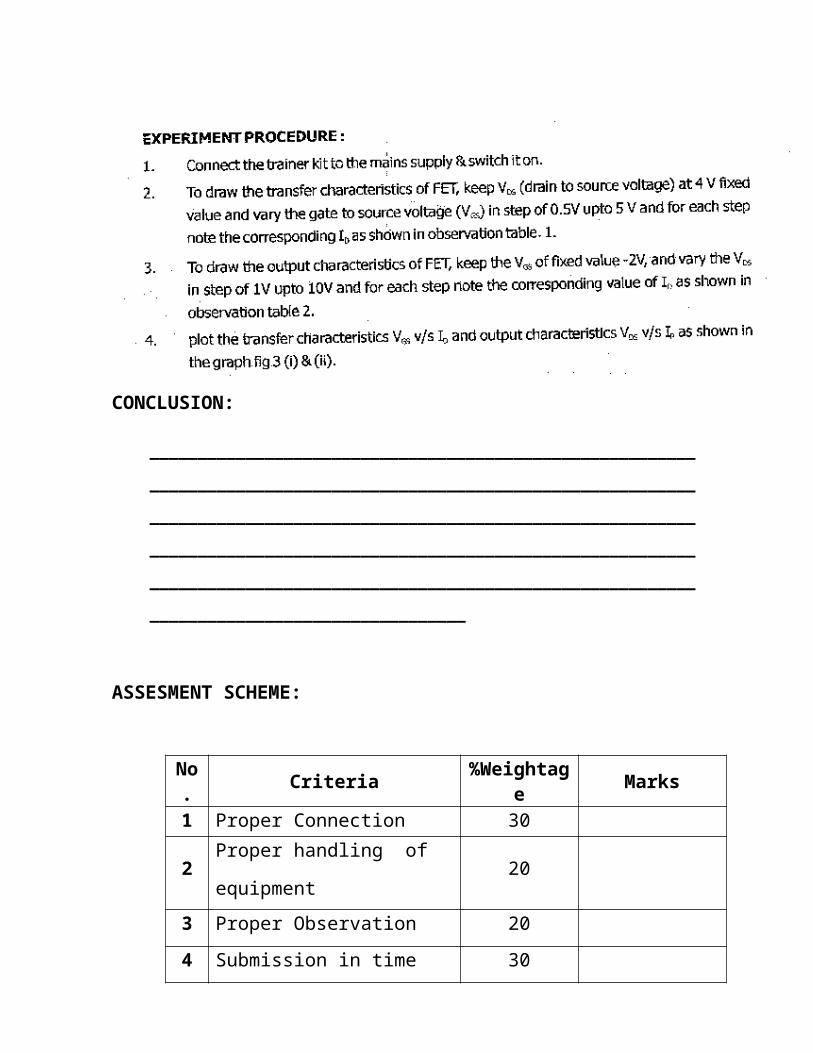
EXPERIMENT NO. 6
CHARACTERISTICS OF n-CHANNEL JFET
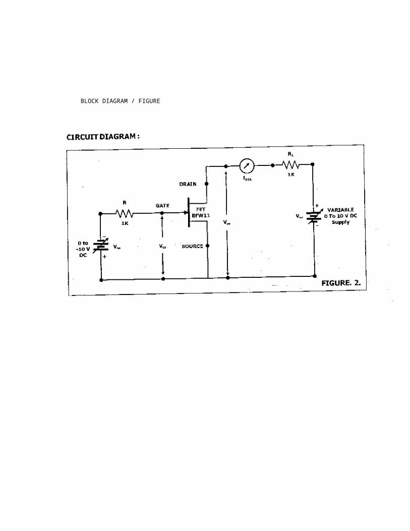
BLOCK DIAGRAM / FIGURE
Experiment No – 6 Date :
CHARACTERISTICS n-CHANNEL JFET
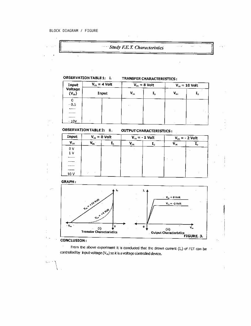
BLOCK DIAGRAM / FIGURE
CONCLUSION:
_________________________________________________________
_________________________________________________________
_________________________________________________________
_________________________________________________________
_________________________________________________________
_________________________________
ASSESMENT SCHEME:
No. Criteria %Weightag
e Marks
1 Proper Connection 30
2Proper handling of
equipment20
3 Proper Observation 204 Submission in time 30

__________________ SIGNOF FACULTY

GRAPHS :
EXPERIMENT NO. 7
CALCULATE rd, gm & μ FOR JFET AMPLIFIER
BLOCK DIAGRAM / FIGURE
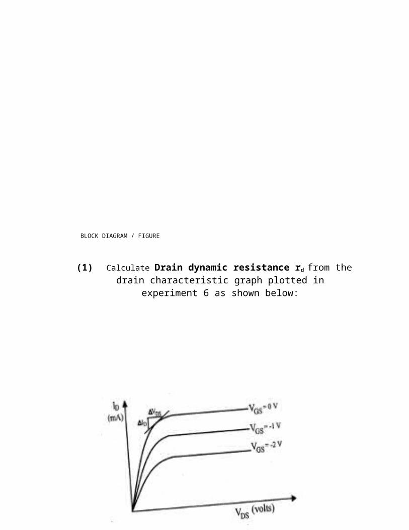
(1) Calculate Drain dynamic resistance rd from thedrain characteristic graph plotted in
experiment 6 as shown below:
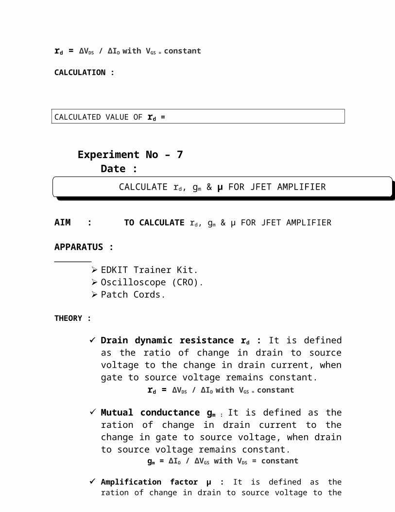
rd = ΔVDS / ΔID with VGS = constant
CALCULATION :
CALCULATED VALUE OF rd =
Experiment No – 7 Date :
AIM : TO CALCULATE rd, gm & μ FOR JFET AMPLIFIER
APPARATUS :
EDKIT Trainer Kit. Oscilloscope (CRO). Patch Cords.
THEORY :
Drain dynamic resistance rd : It is definedas the ratio of change in drain to sourcevoltage to the change in drain current, whengate to source voltage remains constant.
rd = ΔVDS / ΔID with VGS = constant
Mutual conductance gm : It is defined as theration of change in drain current to thechange in gate to source voltage, when drainto source voltage remains constant.
gm = ΔID / ΔVGS with VDS = constant
Amplification factor μ : It is defined as theration of change in drain to source voltage to the
CALCULATE rd, gm & μ FOR JFET AMPLIFIER
change in gate to source voltage, when draincurrent remains constant.
μ = ΔVDS / ΔVGS with ID = constant
μ , gm and rd are related with each other by theexpression μ = gm x rd
PROCEDURE :
1. Identify the terminals of FET, wire up the circuitand check the connections.
2. Switch on VGS and VDD supplies keeping voltagesadjusted into minimum positions. Fix VGS at 0 V.Increase VDS in steps and note down the drain currentID for each value of VDS. Repeat it for differentvalues of VGS, say 1 v and 2 V.
3. Plot drain characteristics with ID along y-axis andVDS along x-axis.
4. Keep VDS = 10 V. Vary VGS and note down the values ofID for different values of VGS. Plot the mutualcharacteristics (also called transfer ortransconductance characteristics) in the secondquadrant of a graph sheet with VGS along x-axis andID along y-axis. Repeat this step for VDS = 20 V.
5. Calculate FET parameters using their respectiveformulas.
CALCULATIONS OF JFET PARAMETERS Drain dynamicresistance rd, Mutual conductance gm andAmplification factor μ USING GRAPHS :
(2) Calculate Mutual conductance gm from the draincharacteristic graph plotted in experiment 6 asshown below:
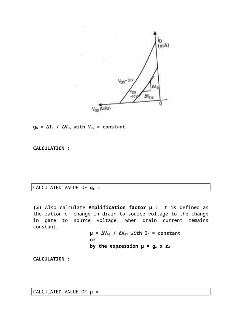
gm = ΔID / ΔVGS with VDS = constant
CALCULATION :
CALCULATED VALUE OF gm =
(3) Also calculate Amplification factor μ : It is defined asthe ration of change in drain to source voltage to the changein gate to source voltage, when drain current remainsconstant.
μ = ΔVDS / ΔVGS with ID = constant orby the expression μ = gm x rd
CALCULATION :
CALCULATED VALUE OF μ =
EXPERIMENT NO. 8
MEASURE OPAMP (IC 741) PARAMETERS
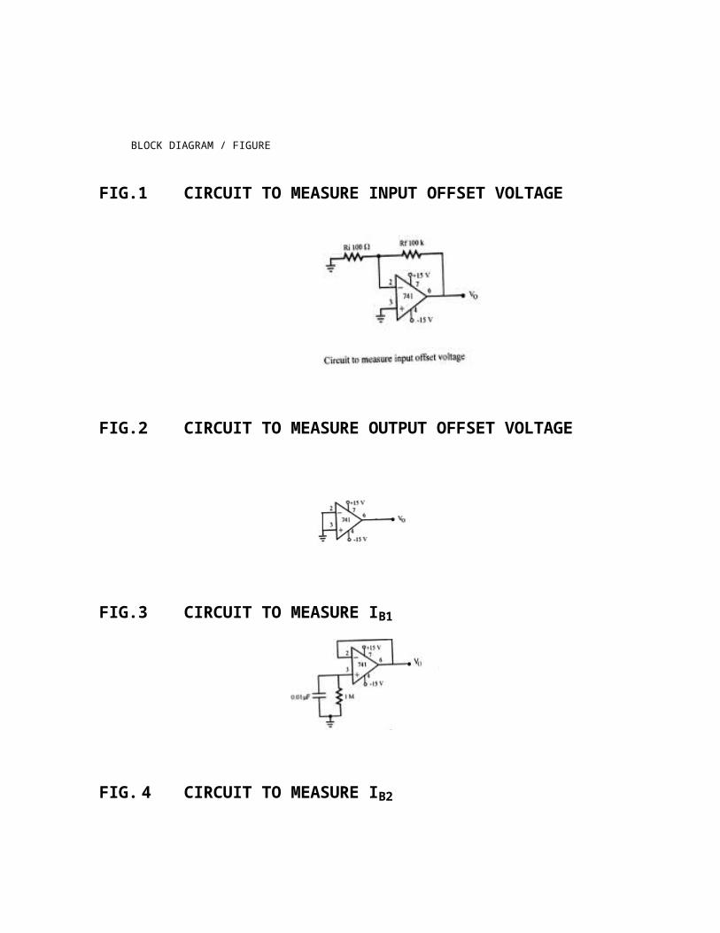
BLOCK DIAGRAM / FIGURE
FIG.1 CIRCUIT TO MEASURE INPUT OFFSET VOLTAGE
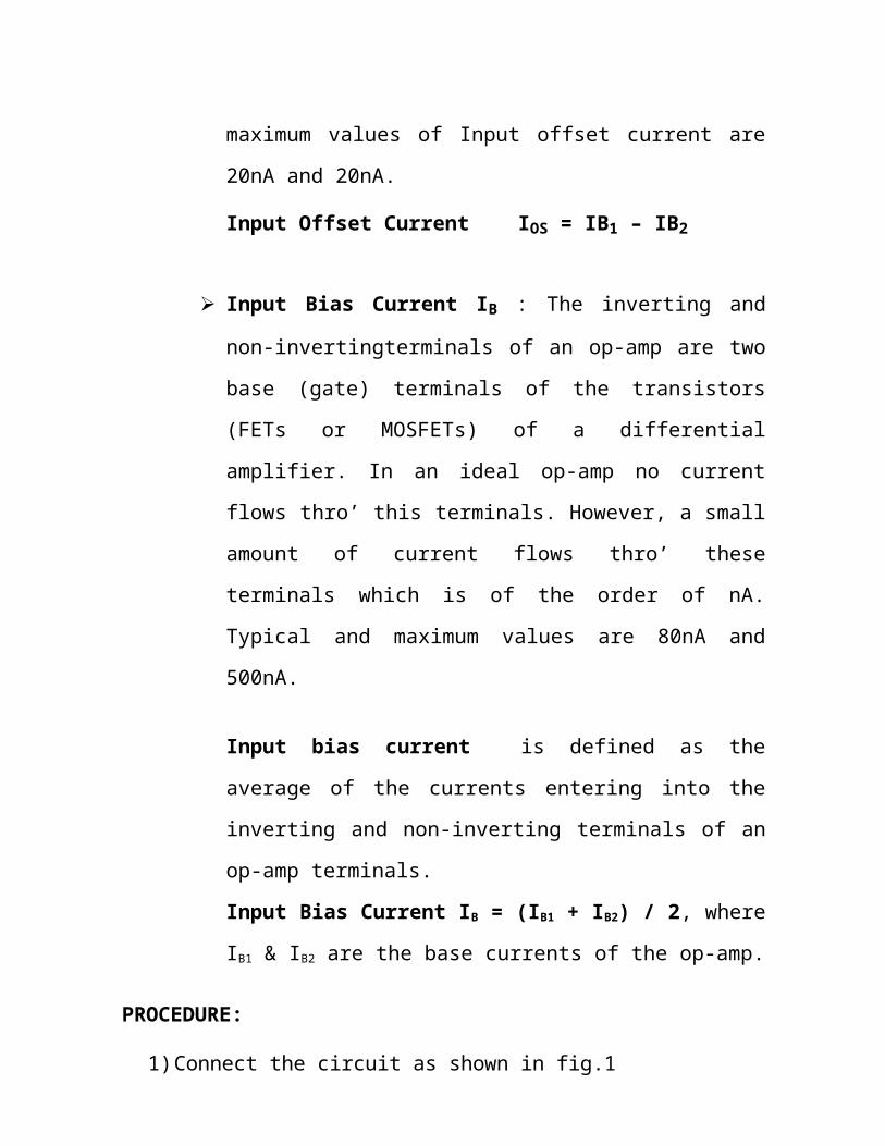
FIG.2 CIRCUIT TO MEASURE OUTPUT OFFSET VOLTAGE
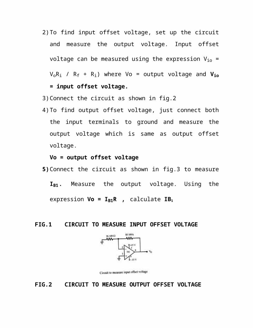
FIG.3 CIRCUIT TO MEASURE IB1
FIG. 4 CIRCUIT TO MEASURE IB2
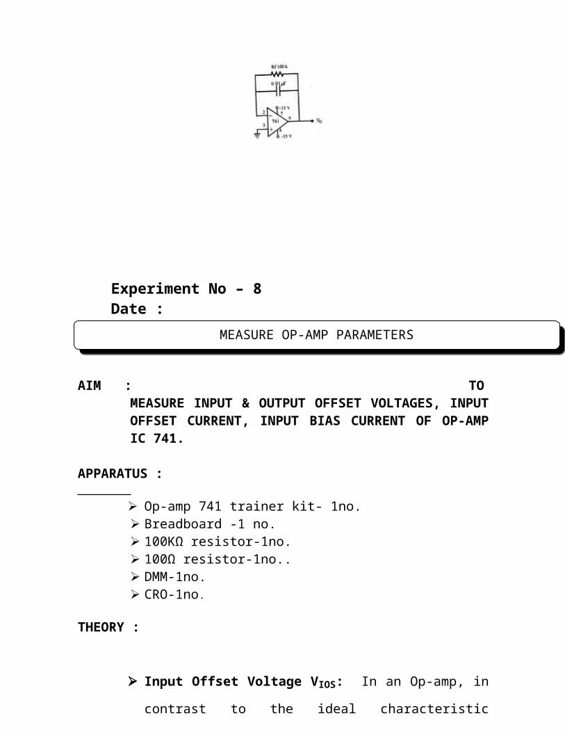
Experiment No – 8 Date :
AIM : TOMEASURE INPUT & OUTPUT OFFSET VOLTAGES, INPUTOFFSET CURRENT, INPUT BIAS CURRENT OF OP-AMPIC 741.
APPARATUS :
Op-amp 741 trainer kit- 1no. Breadboard -1 no. 100KΩ resistor-1no. 100Ω resistor-1no.. DMM-1no. CRO-1no.
THEORY :
Input Offset Voltage VIOS: In an Op-amp, in
contrast to the ideal characteristic
MEASURE OP-AMP PARAMETERS
requirement, even if the input voltages to
op-amp terminals are zero, output voltage is
generally not zero. This is because of the
circuit imbalances inside the op-amp. In
order to compensate this, a small voltage
should be applied across the two input
terminals. Input offset voltage is defined
as the voltage that must be applied between
the input terminals of the op-amp to nullify
the output voltage. Typical and maximum
values of input offset voltage are 2mV and
6mV.
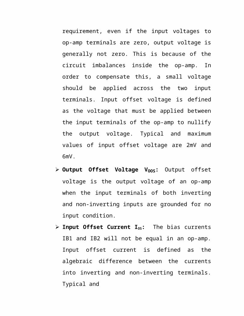
Output Offset Voltage VOOS: Output offset
voltage is the output voltage of an op-amp
when the input terminals of both inverting
and non-inverting inputs are grounded for no
input condition.
Input Offset Current IOS: The bias currents
IB1 and IB2 will not be equal in an op-amp.
Input offset current is defined as the
algebraic difference between the currents
into inverting and non-inverting terminals.
Typical and
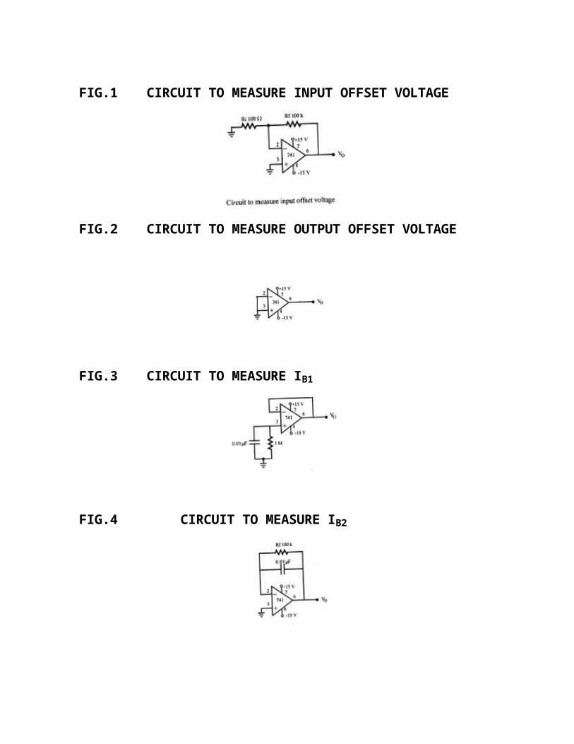
FIG.1 CIRCUIT TO MEASURE INPUT OFFSET VOLTAGE
FIG.2 CIRCUIT TO MEASURE OUTPUT OFFSET VOLTAGE
FIG.3 CIRCUIT TO MEASURE IB1
FIG.4 CIRCUIT TO MEASURE IB2
maximum values of Input offset current are
20nA and 20nA.
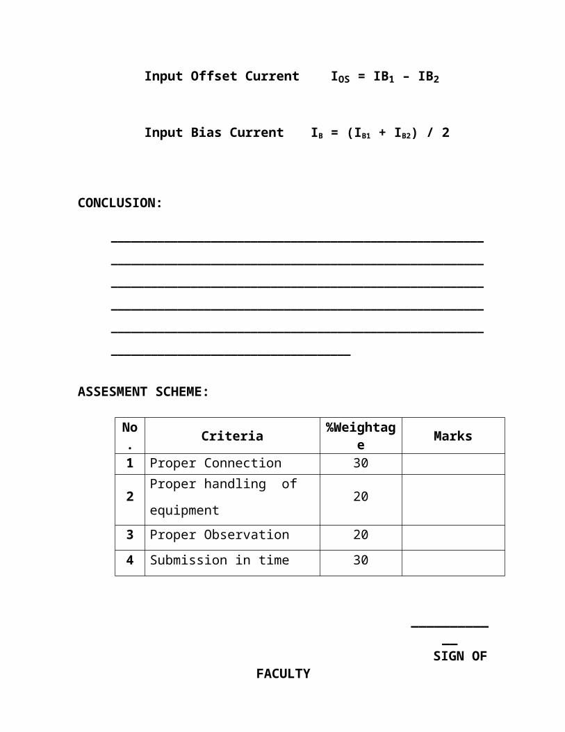
Input Offset Current IOS = IB1 – IB2
Input Bias Current IB : The inverting and
non-invertingterminals of an op-amp are two
base (gate) terminals of the transistors
(FETs or MOSFETs) of a differential
amplifier. In an ideal op-amp no current
flows thro’ this terminals. However, a small
amount of current flows thro’ these
terminals which is of the order of nA.
Typical and maximum values are 80nA and
500nA.
Input bias current is defined as the
average of the currents entering into the
inverting and non-inverting terminals of an
op-amp terminals.
Input Bias Current IB = (IB1 + IB2) / 2, where
IB1 & IB2 are the base currents of the op-amp.
PROCEDURE:
1)Connect the circuit as shown in fig.1
2)To find input offset voltage, set up the circuit
and measure the output voltage. Input offset
voltage can be measured using the expression Vio =
VoRi / Rf + Ri) where Vo = output voltage and Vio= input offset voltage.
3)Connect the circuit as shown in fig.2
4)To find output offset voltage, just connect both
the input terminals to ground and measure the
output voltage which is same as output offset
voltage.
Vo = output offset voltage
5)Connect the circuit as shown in fig.3 to measure
IB1. Measure the output voltage. Using the
expression Vo = IB1R , calculate IB1
FIG.1 CIRCUIT TO MEASURE INPUT OFFSET VOLTAGE
FIG.2 CIRCUIT TO MEASURE OUTPUT OFFSET VOLTAGE
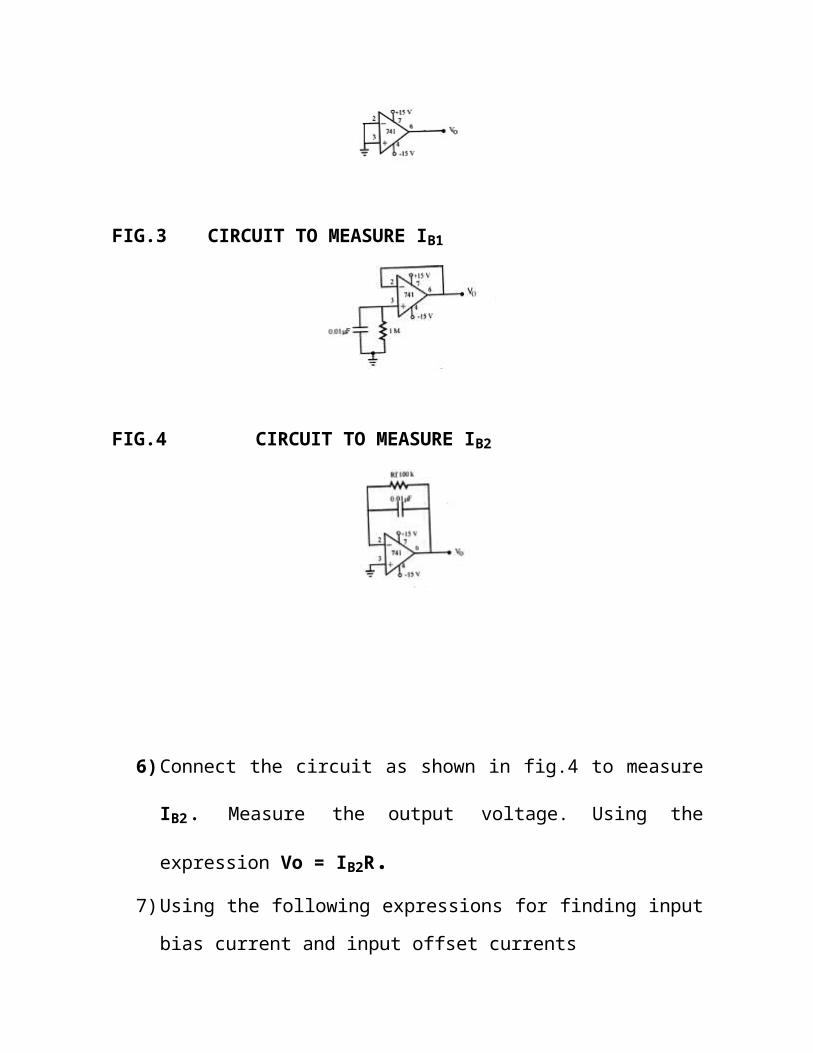
FIG.3 CIRCUIT TO MEASURE IB1
FIG.4 CIRCUIT TO MEASURE IB2
6)Connect the circuit as shown in fig.4 to measure
IB2. Measure the output voltage. Using the
expression Vo = IB2R. 7)Using the following expressions for finding input
bias current and input offset currents
Input Offset Current IOS = IB1 – IB2
Input Bias Current IB = (IB1 + IB2) / 2
CONCLUSION:
________________________________________________________
________________________________________________________
________________________________________________________
________________________________________________________
________________________________________________________
____________________________________
ASSESMENT SCHEME:
No. Criteria %Weightag
e Marks
1 Proper Connection 30
2Proper handling of
equipment20
3 Proper Observation 204 Submission in time 30
__________
__ SIGN OF
FACULTY

EXPERIMENT NO. 9
OPAMP INVERTING AMPLIFIER
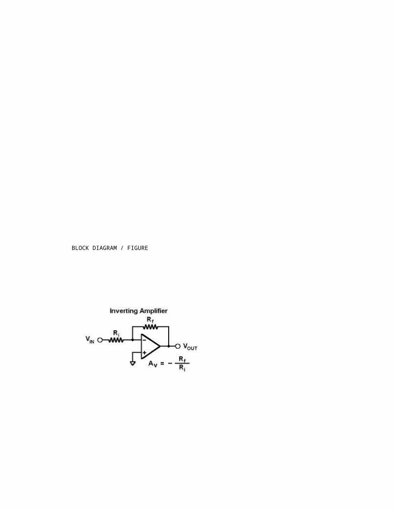
BLOCK DIAGRAM / FIGURE
Experiment No – 9 Date :
AIM : TOSTUDY INVERTING OPAMP USING IC741.
APPARATUS :
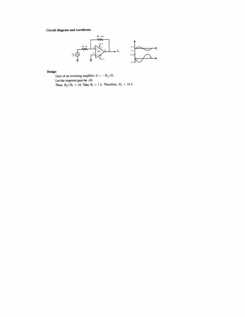
Op-amp 741 trainer kit- 1no. Breadboard -1 no. 10KΩ resistor-1no. 1KΩ resistor-1no.. DMM-1no. CRO-1no.
THEORY :
This is one of the most popular op-amp
circuits. The polarity of the input voltage gets
inverted at the output. If a Sine wave is fed to
the input of this amplifier, the output will be
an amplified sine wave with 1800 phase shift.
The gain of the amplifier is given by the
expression A = -Rf / Ri where Rf is the feedback
resistance and Ri is the input resistance.
Inverting amplifier can be used as a scalar
because the amplitude of the output can be varied
by varying either of the resistors Rf or Ri.
STUDY OF INVERTING OPAMP
PROCEDURE:
1)Set up the inverting amplifier on the bread
board or the trainer kit.
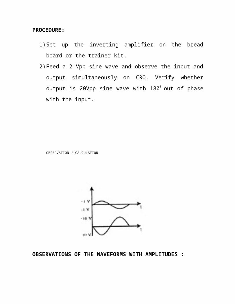
2)Feed a 2 Vpp sine wave and observe the input and
output simultaneously on CRO. Verify whether
output is 20Vpp sine wave with 1800 out of phase
with the input.
OBSERVATION / CALCULATION
OBSERVATIONS OF THE WAVEFORMS WITH AMPLITUDES :

CONCLUSION:
________________________________________________________
________________________________________________________
________________________________________________________
________________________________________________________
________________________________________________________
____________________________________
ASSESMENT SCHEME:
No. Criteria %Weightag
e Marks
1 Proper Connection 30
2Proper handling of
equipment20
3 Proper Observation 204 Submission in time 30
__________________
_ SIGN OF
FACULTY

EXPERIMENT NO. 10
NON-INVERTING OPAMP AMPLIFIER
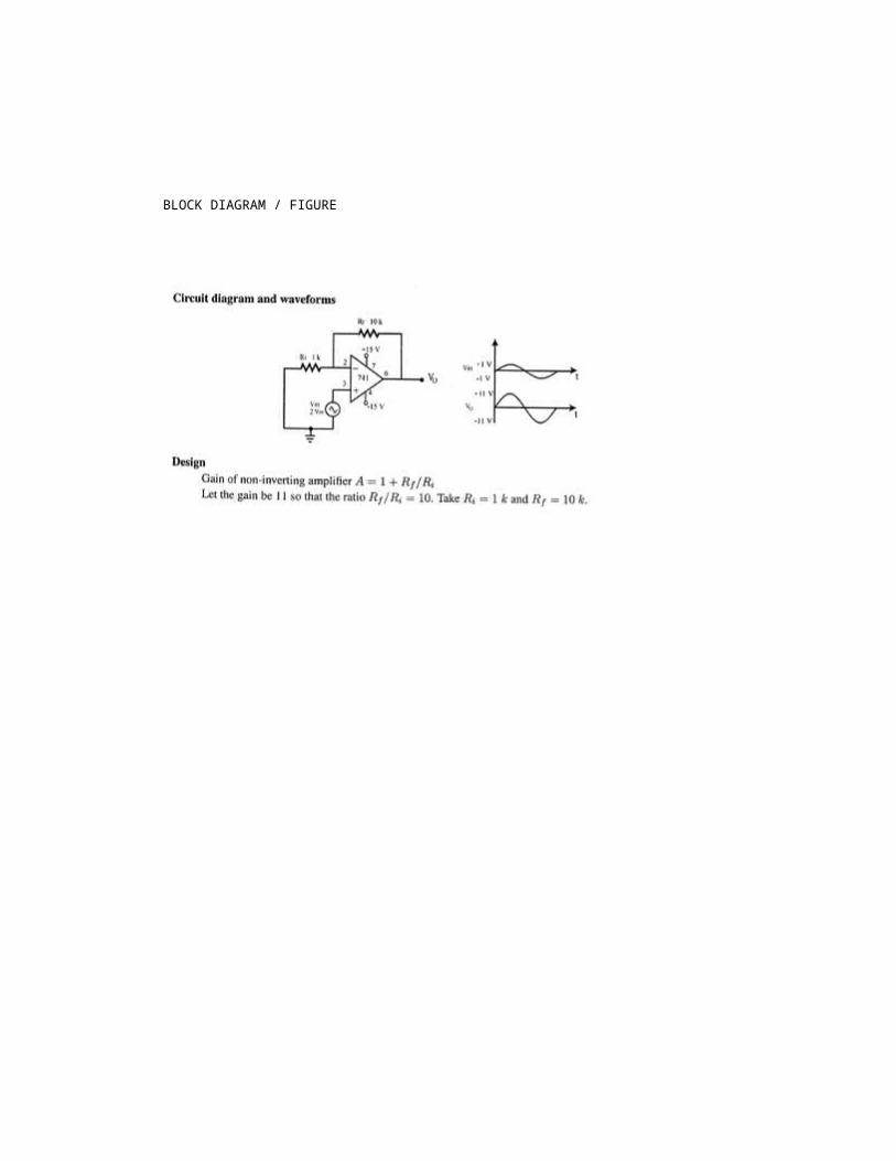
BLOCK DIAGRAM / FIGURE
Experiment No – 10 Date :
AIM : TOCONSTRUCT AND STUDY THE NON-INVERTING OP-AMPAMPLIFIER CIRCUIT.
APPARATUS : Op-amp 741 trainer kit- 1no. Breadboard -1 no. 10KΩ resistor-1no. 1KΩ resistor-1no.. DMM-1no. CRO-1no.
THEORY :
The non-inverting op-amp amplifier circuit
provides a gain to the input signal without
any change in polarity or phase of the
signal (waveform). The gain of the non-
inverting amplifier is given by the
expression
A = 1 + Rf / Ri
where Rf is the feedback resistance and Riis the input resistance.
The input impedance of the non-inverting op-
amp amplifier is extremely large, typically
STUDY OF NON INVERTING OPAMP AMPLIFIER CIRCUIT
100MΩ.
Also since 2 diodes come in circuit at a
time for the whole of one half cycle, the
PIV ratings required for each diodes is also
much less.
Design: As the gain of the non-inverting amplifier
is given by the expression
A = 1 + Rf / Ri , for the gain to be nearly
10 or say 11,
Ratio of Rf / Ri =10, when Rf = 10K and Ri =
1K, gain A = 11.
OBSERVATIONS OF THE WAVEFORMS WITH AMPLITUDES :
PROCEDURE:
1)Set up the non-inverting amplifier on thetrainer kit or on the bread board as shown inthe circuit diagram.
2)Feed a 2 Vpp sine wave and observe the inputand output waveforms on the CROsimultaneously. Verify whether the output is22 Vpp sine wave and exactly the same phaseas the input.
CONCLUSION:
________________________________________________________
________________________________________________________
________________________________________________________
________________________________________________________
________________________________________________________
____________________________________
ASSESMENT SCHEME:
No. Criteria %Weightag
e Marks
1 Proper Connection 30
2Proper handling of
equipment20
3 Proper Observation 204 Submission in time 30
___________________
SIGN OFFACULTY

EXPERIMENT NO. 11
BLOCKDIAGRAM/FIGURE
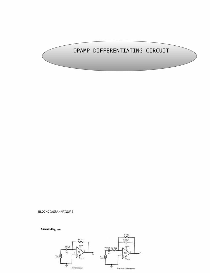
OPAMP DIFFERENTIATING CIRCUIT
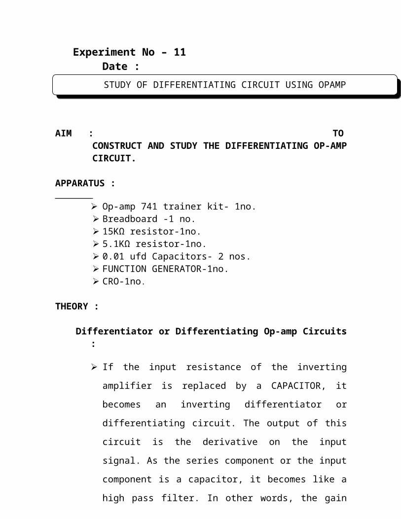
Experiment No – 11 Date :
AIM : TOCONSTRUCT AND STUDY THE DIFFERENTIATING OP-AMPCIRCUIT.
APPARATUS :
Op-amp 741 trainer kit- 1no. Breadboard -1 no. 15KΩ resistor-1no. 5.1KΩ resistor-1no. 0.01 ufd Capacitors- 2 nos. FUNCTION GENERATOR-1no. CRO-1no.
THEORY :
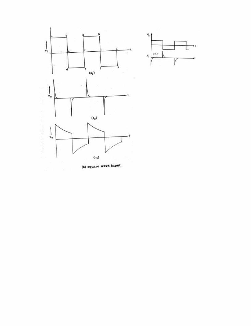
Differentiator or Differentiating Op-amp Circuits:
If the input resistance of the inverting
amplifier is replaced by a CAPACITOR, it
becomes an inverting differentiator or
differentiating circuit. The output of this
circuit is the derivative on the input
signal. As the series component or the input
component is a capacitor, it becomes like a
high pass filter. In other words, the gain
STUDY OF DIFFERENTIATING CIRCUIT USING OPAMP
of the amplifier increases with increase in
the input signal frequency. However too much
gain can also make the circuit unstable and
turn it into an oscillator. This problem is
solved by inserting a resistance Ri in the
input circuit.
The output voltage Vo can be expressed as
Vo = -RfCi (dVi/dt)
FIGURE
In this circuit, the input impedance
decreases with increase in input signal
frequency, due to which high frequency noise
appears in the output. However, a negative
feedback for such noise by way of capacitor
Ci between input and output takes care of
this problem.
PROCEDURE:
1) Connections are made as shown in fig.
2) Feed 2Vpp 1ms (1KHz) square wave at the input
and observe the output and input
simultaneously on the CRO and make a note of
it.
3) Repeat the experiment by feeding the
triangular wave and sine wave and observe the
output and input simultaneously on the CRO
and make a note of it.
CONCLUSION:
________________________________________________________
________________________________________________________
______________________________________________
ASSESMENT SCHEME:
No. Criteria %Weightag
e Marks
1 Proper Connection 30
2Proper handling of
equipment20
3 Proper Observation 204 Submission in time 30
___________________
SIGN OF FACULTY

OBSERVATIONS
EXPERIMENT NO. 12
STUDY OF INTEGRATING OP-AMP CIRCUIT
Experiment No – 12 Date :
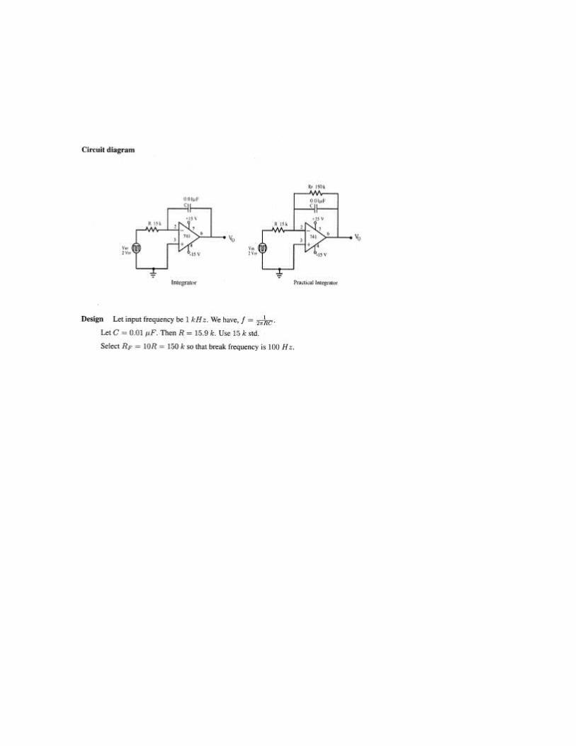
AIM : TOCONSTRUCT AND STUDY THE INTEGRATING OP-AMPCIRCUIT.
APPARATUS :
Op-amp 741 trainer kit- 1no. Breadboard -1 no. 150KΩ resistor-1no. 15KΩ resistor-1no. 0.01 ufd Capacitors- 1 nos. FUNCTION GENERATOR CRO-1no.
THEORY :
The integrating circuit performs theintegration of the input waveform. The outputvoltage Vo can be expressed as V0 = -1/RC∫Vidt +k where k is the constant ofintegration which depends upon the value ofVo at t = 0. Also this circuit can perform asa low pass filter. gain and linearity of theoutput waveform are the two importantadvantages of OP-AMP integrators as comparedto normal RC integrators.
PROCEDURE:
STUDY OF INTEGRATING CIRCUIT USING OPAMP
1)Connections are made as shown in fig.
2) Feed 2Vpp 1ms (1KHz) square wave at the input
and observe the output and input
simultaneously on the CRO and make a note of
it.
3) Vary the DC offset of the square wave and
observe the change in the output waveform.
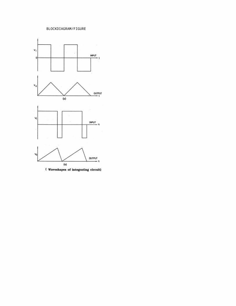
BLOCKDIAGRAM/FIGURE
4)Repeat the experiment by feeding the triangular
wave and observe the output and input
simultaneously on the CRO and make a note of it.
5)Repeat the experiment by feeding the sine wave
and observe the output and input simultaneously
on the CRO by varying the frequency of the input
signal and make a note of it.
CONCLUSION:
________________________________________________________
________________________________________________________
________________________________________________________
________________________________________________________
________________________________________________________
____________________________________
ASSESMENT SCHEME:
No. Criteria %Weightag
e Marks
1 Proper Connection 30
2Proper handling of
equipment20
3 Proper Observation 204 Submission in time 30

___________________ SIGN OF
FACULTY

EXPERIMENT NO. 13
STUDY OF SUMMING OP-AMP AMPLIFIER CIRCUIT
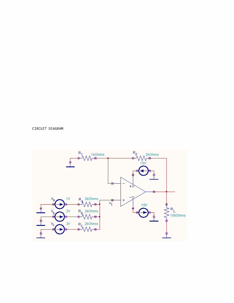
CIRCUIT DIAGRAM
Experiment No – 13 Date :
AIM : TOCONSTRUCT AND STUDY THE SUMMING AMPLIFIER OP-AMP CIRCUIT.
APPARATUS :
Op-amp 741 trainer kit- 1no. Breadboard -1 no. 10KΩ resistor-1no. 1KΩ resistor-1no. 2KΩ resistor-3no. DC SUPPLY VOLTAGE SOURCES -3 nos. CRO-1no. Digital Multimeter- 1 no.
THEORY :
An operational amplifier is a direct coupled highgain amplifier consisting of one or moredifferential amplifiers.
An operational amplifier can be used to amplify acas well as dc input signals and was originally designed for computing such mathematicalfunctions as addition, subtraction, multiplicationand integration.
An opamp can be configured in either the invertingor in the non-inverting mode. The circuit shown below is called a non-inverting amplifier since the input voltage sources and resistors are
STUDY OF SUMMING AMPLIFIER CIRCUIT USING OPAMP
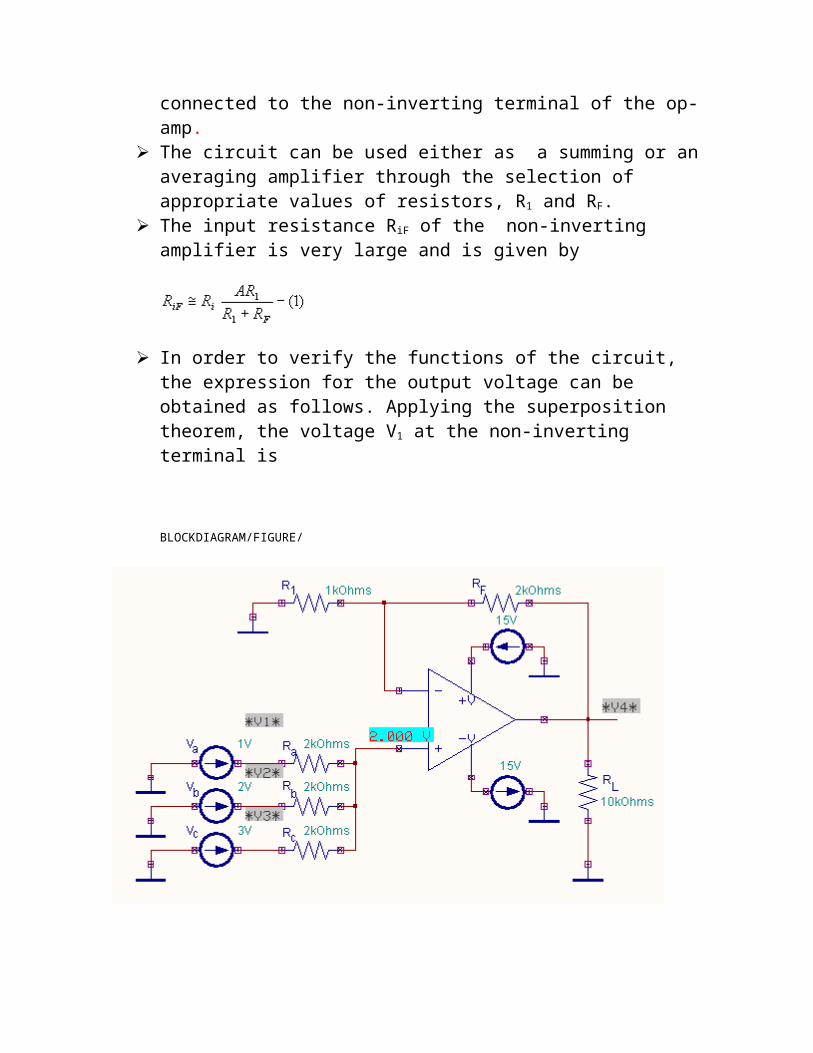
connected to the non-inverting terminal of the op-amp.
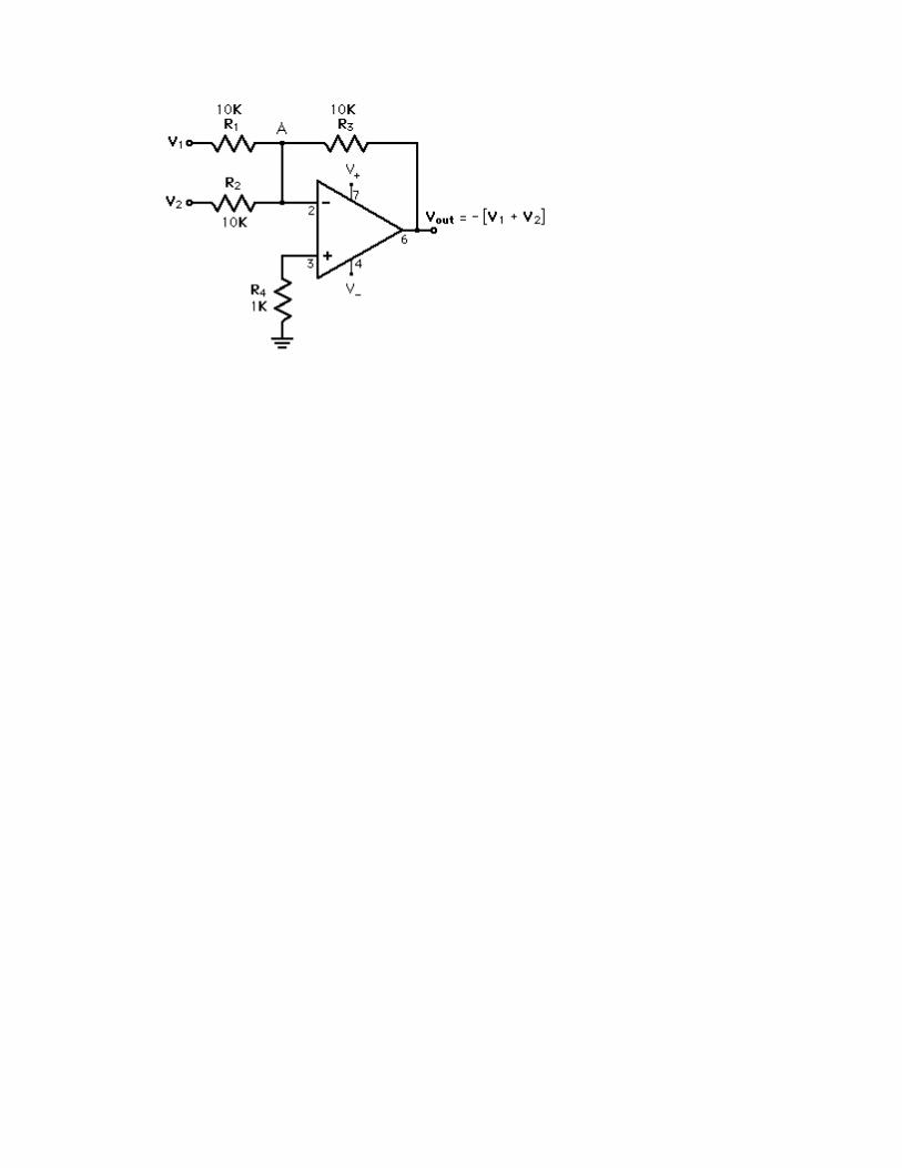
The circuit can be used either as a summing or anaveraging amplifier through the selection of appropriate values of resistors, R1 and RF.
The input resistance RiF of the non-inverting amplifier is very large and is given by
In order to verify the functions of the circuit, the expression for the output voltage can be obtained as follows. Applying the superposition theorem, the voltage V1 at the non-inverting terminal is
BLOCKDIAGRAM/FIGURE/
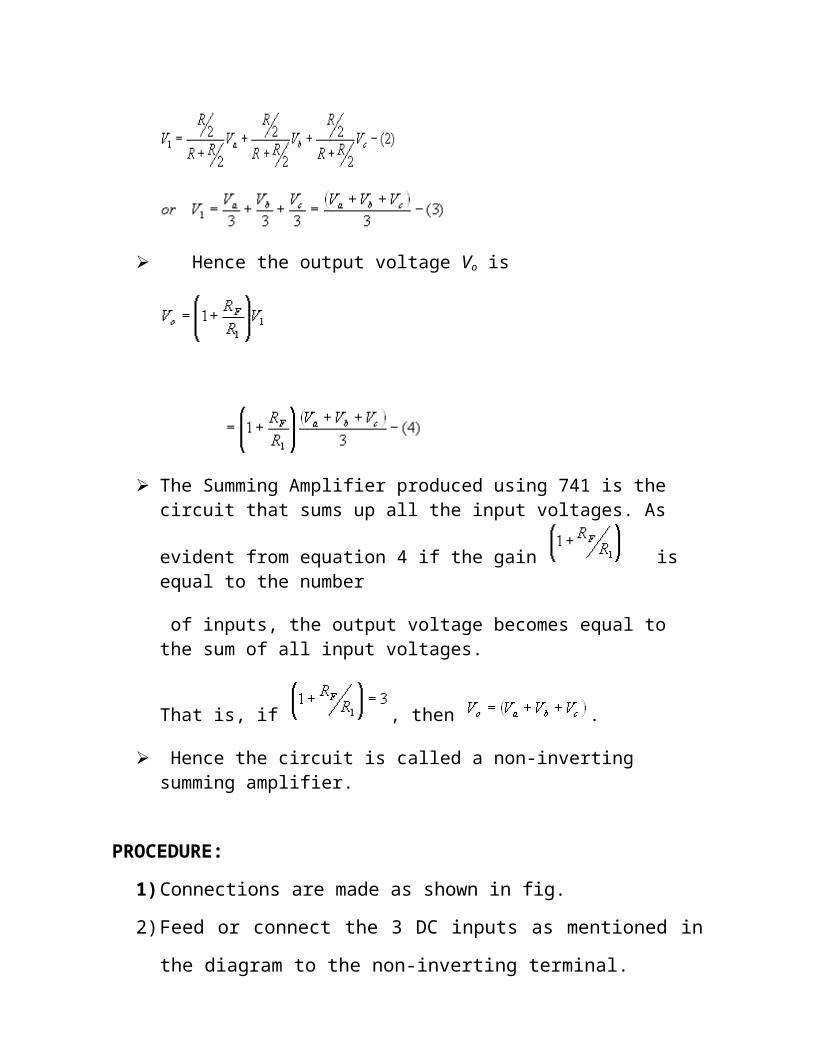
Hence the output voltage Vo is
The Summing Amplifier produced using 741 is the circuit that sums up all the input voltages. As
evident from equation 4 if the gain is equal to the number
of inputs, the output voltage becomes equal to the sum of all input voltages.
That is, if , then .
Hence the circuit is called a non-inverting summing amplifier.
PROCEDURE:
1)Connections are made as shown in fig.
2)Feed or connect the 3 DC inputs as mentioned in
the diagram to the non-inverting terminal.
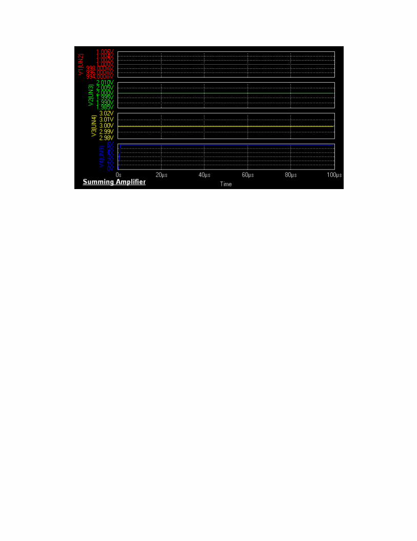
3)Measure the output DC voltage on the output pin
of the op-amp and verify that the output is the
sum total of all the input voltages applied at
the non-inverting input terminal of the op-amp.
4)
BLOCKDIAGRAM/FIGURE/
CONCLUSION:
________________________________________________________
________________________________________________________
________________________________________________________
________________________________________________________
________________________________________________________
____________________________________
ASSESMENT SCHEME:
No. Criteria %Weightag
e Marks
1 Proper Connection 30
2Proper handling of
equipment20
3 Proper Observation 204 Submission in time 30
___________________
SIGN OFFACULTY

EXPERIMENT NO. 14
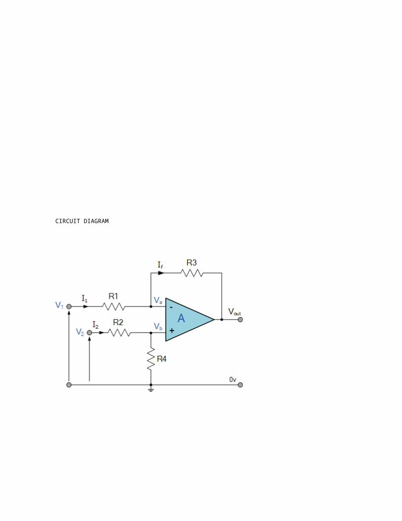
STUDY OF DIFFERENTIAL OP-AMP AMPLIFIER CIRCUIT
CIRCUIT DIAGRAM
Experiment No – 14 Date :
AIM : TOCONSTRUCT AND STUDY THE SUMMING AMPLIFIER OP-AMP CIRCUIT.
APPARATUS :
Op-amp 741 trainer kit- 1no. Breadboard -1 no. 10KΩ resistor-4nos. DC SUPPLY VOLTAGE SOURCES -2 nos. CRO-1no. Digital Multimeter- 1 no.
THEORY :
An operational amplifier is a direct coupled highgain amplifier consisting of one or moredifferential amplifiers.
An operational amplifier can be used to amplify acas well as dc input signals and was originally designed for computing such mathematicalfunctions as addition, subtraction, multiplicationand integration.
An opamp can be configured in either the invertingor in the non-inverting mode. However, we can alsotwo different inputs to the two input terminals ofthe op-amp to make another common type of op-amp amplifier circuit called the differential amplifier because the output that we will be
STUDY OF SUMMING AMPLIFIER CIRCUIT USING OPAMP
getting will be the algebraic difference of the two input signals as explained below.
The circuit can be used either as a subtractor ora difference amplifier through the selection of appropriate values of resistors, R1 and RF.
Basically, as we saw in the first tutorial about operational amplifiers, all op-amps are "Differential Amplifiers" due to their input configuration. But by connecting one voltage signal onto one input terminal and another voltagesignal onto the other input terminal the resultantoutput voltage will be proportional to the "Difference" between the two input voltage signalsof V1 and V2.
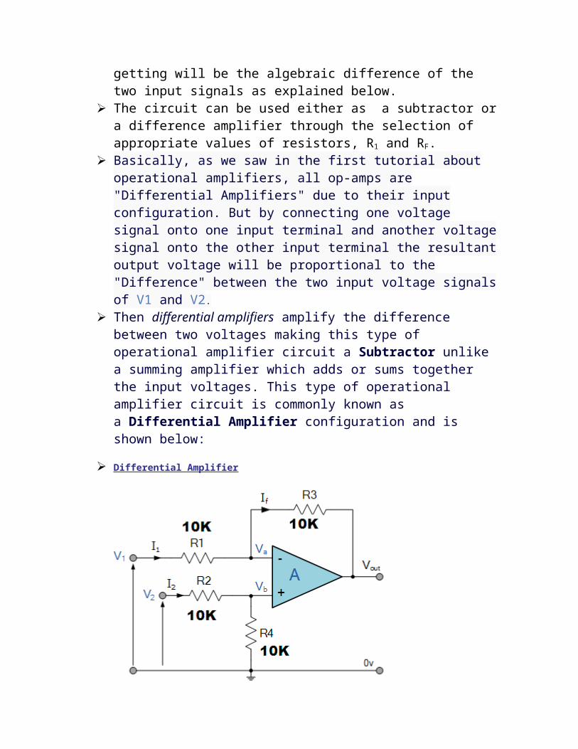
Then differential amplifiers amplify the difference between two voltages making this type of operational amplifier circuit a Subtractor unlike a summing amplifier which adds or sums together the input voltages. This type of operational amplifier circuit is commonly known as a Differential Amplifier configuration and is shown below:
Differential Amplifier
In order to verify the functions of the circuit, the expression for the output voltage can be obtained as follows. By connecting each input in turn to 0v ground we can use superposition to solve for the output voltage Vout. Then the transfer function for a Differential Amplifier circuit is given as:
When resistors, R1 = R2 and R3 = R4 the above transfer function for the differential amplifier can be simplified to the following expression:
Differential Amplifier Equation
If all the resistors are all of the same ohmic value, that is: R1 = R2 = R3 = R4 then the circuitwill become aUnity Gain Differential Amplifier andthe voltage gain of the amplifier will be exactly
one or unity. Then the output expression would simply be Vout = V2 - V1. Also note that if input V1 is higher than input V2 the ouput voltagesum will be negative, and if V2 is higher than V1,the output voltage sum will be positive.
The Differential Amplifier circuit is a very useful op-amp circuit and by adding more resistors in parallel with the input resistors R1 and R3, the resultant circuit can be made to either "Add" or "Subtract" the voltages applied to their respective inputs. One of the most common ways of doing this is to connect a "Resistive Bridge" commonly called a Wheatstone Bridge to the input of the amplifier as shown below.
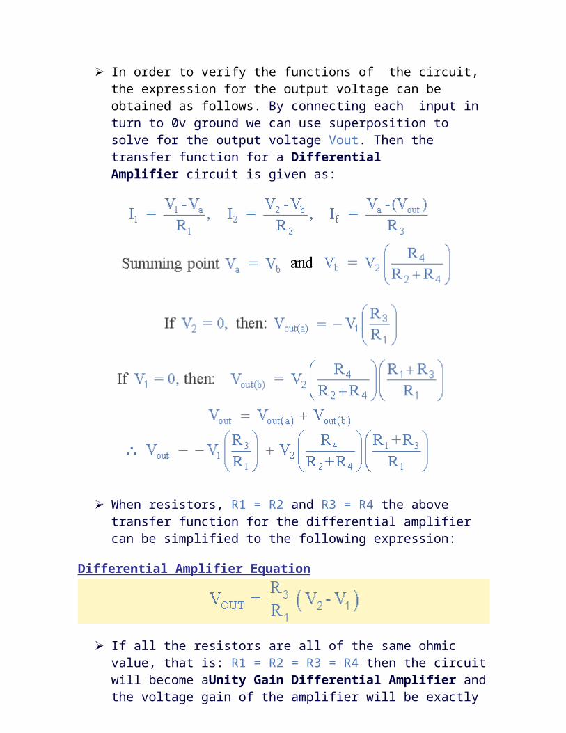
Bridge Amplifier
The standard Differential Amplifier circuit now becomes adifferential voltage comparator by "Comparing" one input voltage to the other. For example, by connecting one input to a fixed voltage reference set up on one leg of the resistive bridge network and the other to either a "Thermistor" or a "Light Dependant Resistor" the amplifier circuit can be used to detect either low or high levels of temperature or light as the output voltagebecomes a linear function of the changes in the active leg of the resistive bridge and this is demonstrated below.
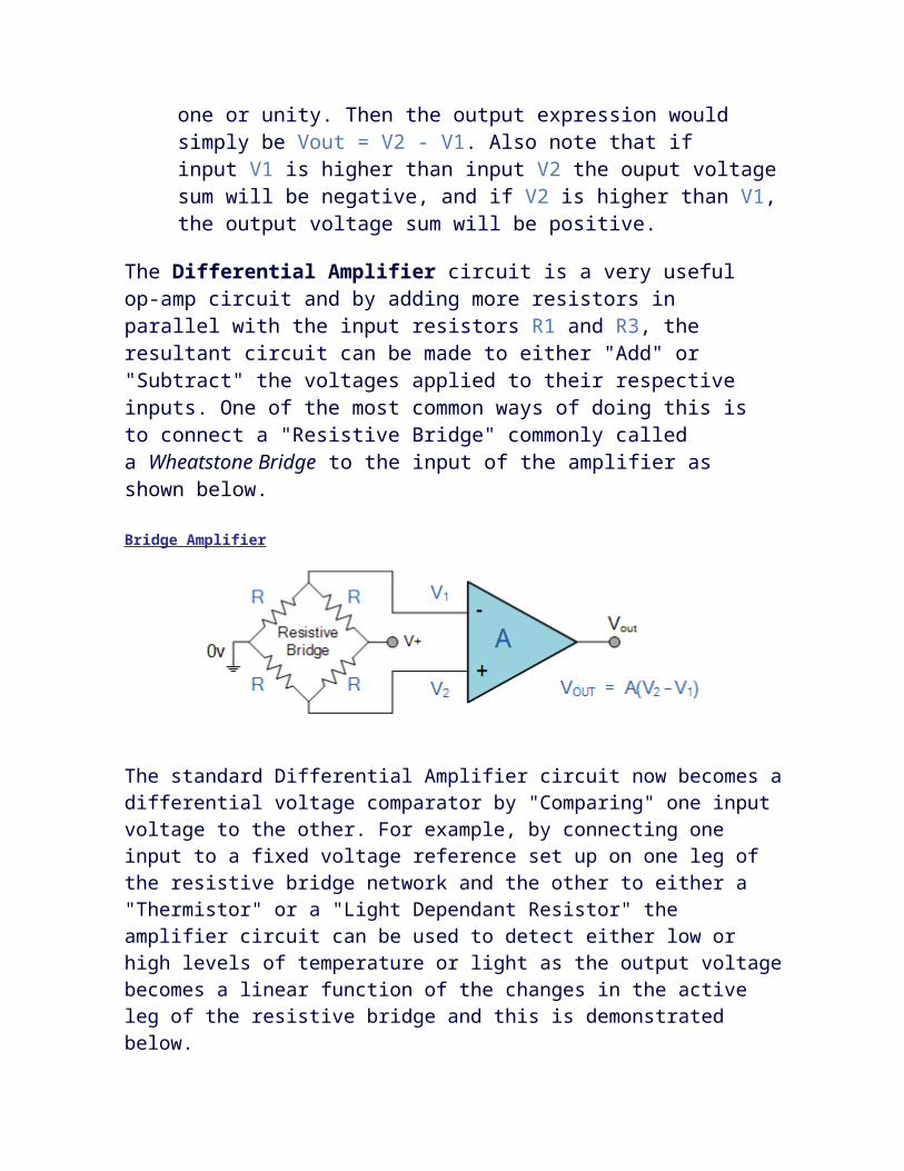
Light Activated Switch
Here the circuit above acts as a light-activated switch which turns the output relay either "ON" or "OFF" as the light level detected by the LDR resistor exceeds or fallsbelow a pre-set value at V2 determined by the position of VR1. A fixed voltage reference is applied to the inverting input terminal V1 via the R1 - R2 voltage dividernetwork and the variable voltage (proportional to the light level) applied to the non-inverting input terminal V2. It is also possible to detect temperature using this type of circuit by simply replacing the Light Dependant Resistor (LDR) with a thermistor. By interchanging the positions of VR1 and the LDR, the circuit can be used to detect either light or dark, or heat or cold using a thermistor.
One major limitation of this type of amplifier design is that its input impedances are lower compared to that of other operational amplifier configurations, for example, a non-inverting (single-ended input) amplifier. Each input voltage source has to drive current through an input resistance, which has less overall impedance than that of the op-amps input alone. This may be good for a low impedance source such as the bridge circuit above, but not so good for a high impedance source.
One way to overcome this problem is to add a Unity Gain Buffer Amplifier such as the voltage follower seen in the previous tutorial to each input resistor. This then givesus a differential amplifier circuit with very high input impedance and low output impedance as it consists of two non-inverting buffers and one differential amplifier.
PROCEDURE:
1)Connections are made as shown in fig.
2)Feed or connect the 2 DC inputs as mentioned in
the diagram to the non-inverting terminal.
3)Measure the output DC voltage on the output pin
of the op-amp and verify that the output is the
difference of the two input voltages applied at
the input terminals of the op-amp.
CONCLUSION:________________________________________________________
________________________________________________________
______________________________________________
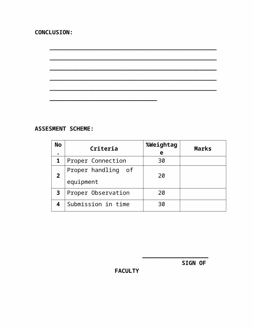
ASSESMENT SCHEME:
No. Criteria %Weightag
e Marks
1 Proper Connection 30
2Proper handling of
equipment20
3 Proper Observation 204 Submission in time 30

___________________ SIGN OF
FACULTY
BLOCKDIAGRAM/FIGURE/

STUDY OF ASTABLE MULTIVIBRATOR
EXPERIMENT NO. 16
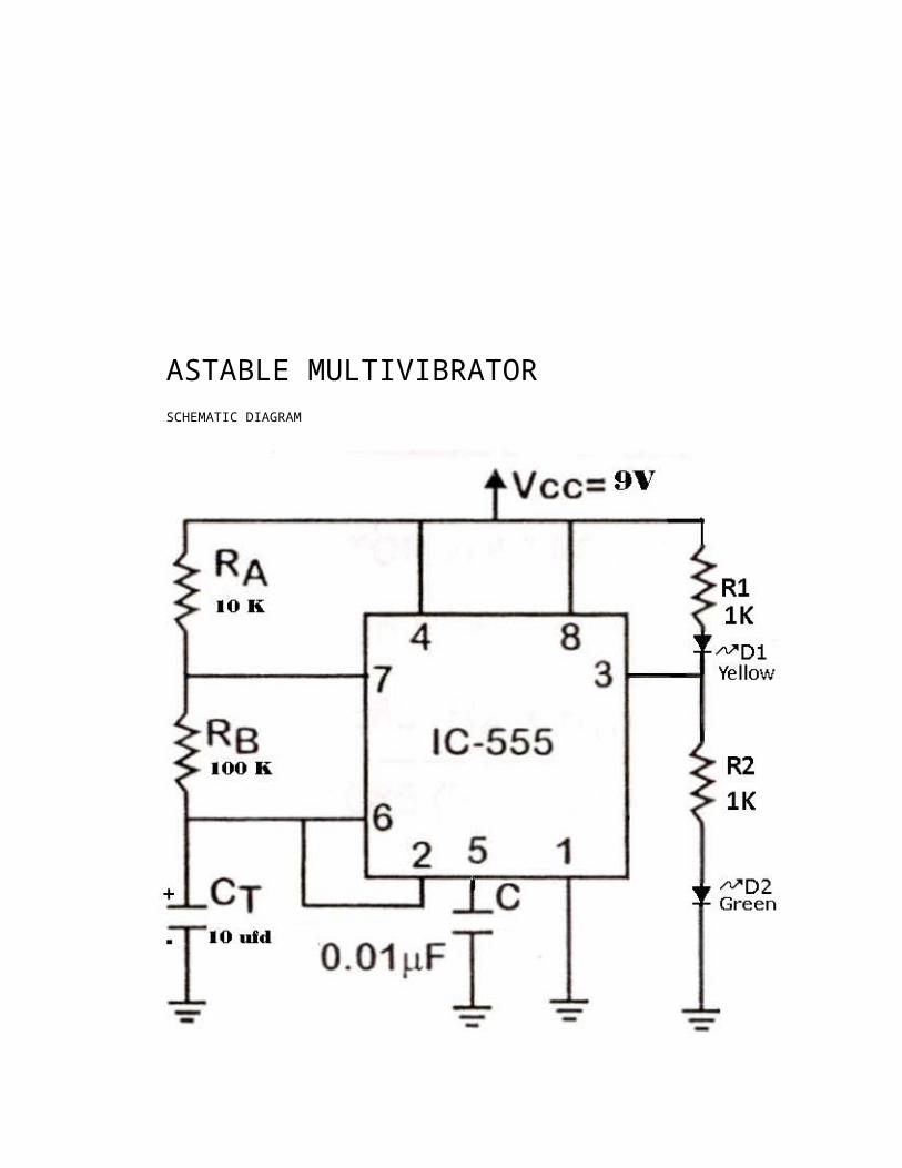
ASTABLE MULTIVIBRATORSCHEMATIC DIAGRAM
Experiment No – 16 Date :
SERIES NEGATIV
AIM : TOSTUDY THE WORKING OF ASTABLE MULTIVIBRATORUSING IC 555.
APPARATUS : Trainer Kit CRO Patch Cords
THEORY :
These circuits are not stable in any state and switchoutputs after predetermined time periods. The result of thisis that the output is a continuous square/rectangular wavewith the properties depending on values of externalresistors and capacitors. Thus, while designing thesecircuits following parameters need to be determined:
1. Frequency (or the time period) of the wave.2. The duty cycle of the wave.
ASTABLE MULTIVIBRATOR USING IC 555
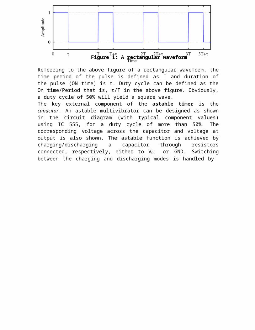
Figure 1: A rectangular waveform
Referring to the above figure of a rectangular waveform, thetime period of the pulse is defined as T and duration ofthe pulse (ON time) is τ. Duty cycle can be defined as theOn time/Period that is, τ/T in the above figure. Obviously,a duty cycle of 50% will yield a square wave.The key external component of the astable timer is thecapacitor. An astable multivibrator can be designed as shownin the circuit diagram (with typical component values)using IC 555, for a duty cycle of more than 50%. Thecorresponding voltage across the capacitor and voltage atoutput is also shown. The astable function is achieved bycharging/discharging a capacitor through resistorsconnected, respectively, either to VCC or GND. Switchingbetween the charging and discharging modes is handled by
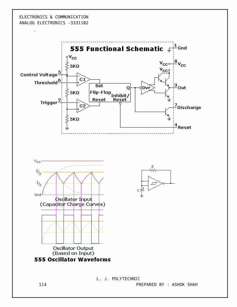
ELECTRONICS & COMMUNICATION ANALOG ELECTRONICS -3331102
.
L. J. POLYTECHNIC114 PREPARED BY : ASHOK SHAH
ELECTRONICS & COMMUNICATION ANALOG ELECTRONICS -3331102
resistor divider R1-R3, two Comparators, and an RS Flip-Flop in IC 555. The upper or lower comparator simply generates a positive pulseif VC goes above 2/3 VCC or below1/3 VCC. And these positive pulses either SET or RESET the Q output.
The time for charging C from 1/3 to 2/3 Vcc, i.e, ON Time = 0.693 (RA + RB). CThe time for discharging C from 2/3 to 1/3 Vcc, i.e. OFF Time = 0.693 RB. CTo get the total oscillation period, just add the two:
Thus,Tosc = 0.693·(RA+RB)·C + 0.693·(RB)·C = 0.693 · (RA + 2·RB) · C
fosc = 1/ Tosc = 1.44/( RA + 2·RB).C
Duty cycle = RA+RB/ RA + 2·RB
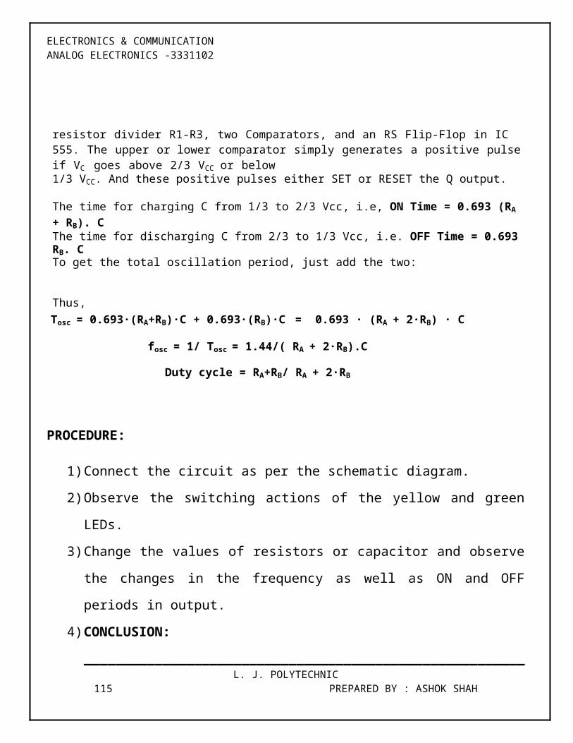
PROCEDURE:
1)Connect the circuit as per the schematic diagram.
2)Observe the switching actions of the yellow and green
LEDs.
3)Change the values of resistors or capacitor and observe
the changes in the frequency as well as ON and OFF
periods in output.
4)CONCLUSION:
________________________________________________________L. J. POLYTECHNIC
115 PREPARED BY : ASHOK SHAH

ELECTRONICS & COMMUNICATION ANALOG ELECTRONICS -3331102
________________________________________________________
________________________________________________________
_________________________________
________________________ SIGN OF FACULTY
L. J. POLYTECHNIC116 PREPARED BY : ASHOK SHAH

ELECTRONICS & COMMUNICATION ANALOG ELECTRONICS -3331102
L. J. POLYTECHNIC117 PREPARED BY : ASHOK SHAH
STUDY OF MONOSTABLE MULTIVIBRATOR
EXPERIMENT NO. 17
ELECTRONICS & COMMUNICATION ANALOG ELECTRONICS -3331102
SCHEMATIC DIAGRAM
L. J. POLYTECHNIC118 PREPARED BY : ASHOK SHAH
ELECTRONICS & COMMUNICATION ANALOG ELECTRONICS -3331102
Experiment No – 17 Date :
SERIES NEGATIV
AIM : TO STUDYTHE WORKING OF MONOSTABLE MULTIVIBRATOR USING IC 555.
APPARATUS : Trainer Kit CRO Function Generator Patch Cords
THEORY :
L. J. POLYTECHNIC119 PREPARED BY : ASHOK SHAH
MONOSTABLE MULTIVIBRATOR USING IC 555
ELECTRONICS & COMMUNICATION ANALOG ELECTRONICS -3331102
Looking at the functional schematic shown
(Figure below), you can see that pin 7 is a transistor
going to ground
This transistor is simply a switch that normally
conducts until pin 2 (which is connected through the
comparator C1, which feeds the internal flip flop) is
brought low, allowing the capacitor Ct to start
charging. Pin 7 stays off until the voltage on Ct
charges to 2/3 of the power supply voltage, where the
timer times out and pin 7 transistor turns on again, its
normal state in this circuit.
When a negative going trigger pulse is applied on Pin 2,
the transistor on pin 7 becomes off and Pin 7 is no more
connected to ground, so Ct starts charging and output on
Pin 3 also goes high, switching the YELLOW LED OFF and
the GREEN LED ON. This condition remains only till the
charge on Ct reaches 2/3 of Vcc, at
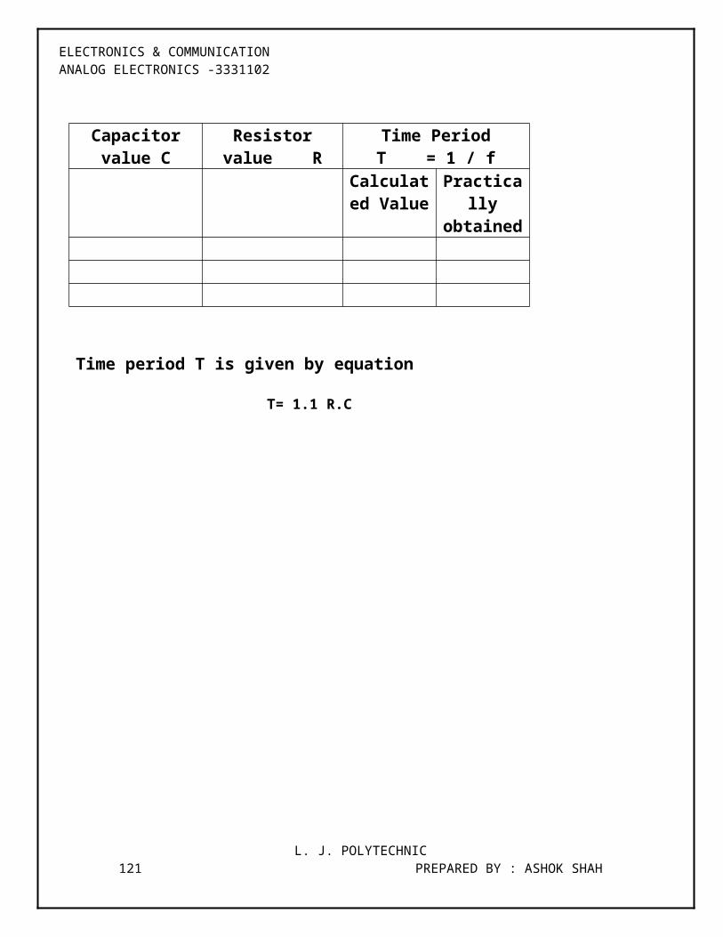
OBSERVATION TABLE:L. J. POLYTECHNIC
120 PREPARED BY : ASHOK SHAH
ELECTRONICS & COMMUNICATION ANALOG ELECTRONICS -3331102
Capacitorvalue C
Resistorvalue R
Time PeriodT = 1 / f
Calculated Value
Practically
obtained
Time period T is given by equation
T= 1.1 R.C
L. J. POLYTECHNIC121 PREPARED BY : ASHOK SHAH
ELECTRONICS & COMMUNICATION ANALOG ELECTRONICS -3331102
which point, voltages on pins 3 and 7 simultaneously go
low and the Yellow LED comes ON again as in the
beginning and the GREEN LED becomes OFF. The pulse width can be calculated as T= 1.1 R.C.
PROCEDURE:
1) Connect the circuit as per the schematic diagram.
2) Push the push-to ON switch and observe the time period after
which the circuit returns to its original state.
3) Repeat the above steps for different values of R and C and
observe the changes in the time period.
CONCLUSION:
_________________________________________________________
_________________________________________________________
_________________________________________________________
_________________________________________________________
____________________________________________
ASSESMENT SCHEME:
No. Criteria %Weightag
e Marks
1 Proper Connection 30
L. J. POLYTECHNIC122 PREPARED BY : ASHOK SHAH
ELECTRONICS & COMMUNICATION ANALOG ELECTRONICS -3331102
2Proper handling of
equipment20
3 Proper Observation 204 Submission in time 30
________________________ SIGN OF FACULTY
L. J. POLYTECHNIC123 PREPARED BY : ASHOK SHAH
ELECTRONICS & COMMUNICATION ANALOG ELECTRONICS -3331102
L. J. POLYTECHNIC124 PREPARED BY : ASHOK SHAH
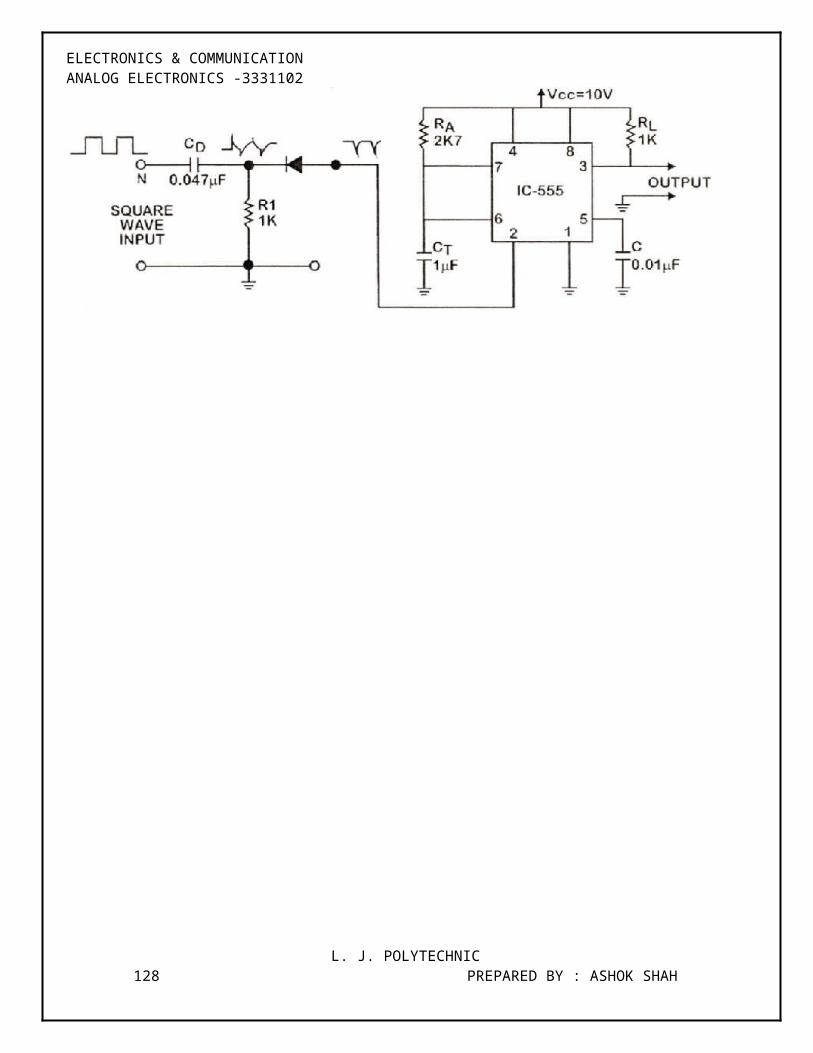
STUDY OF BISTABLE MULTIVIBRATOR
EXPERIMENT NO. 18
ELECTRONICS & COMMUNICATION ANALOG ELECTRONICS -3331102
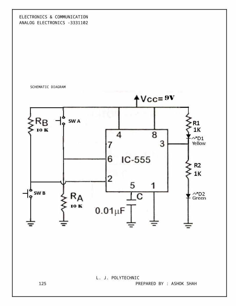
SCHEMATIC DIAGRAM
L. J. POLYTECHNIC125 PREPARED BY : ASHOK SHAH
ELECTRONICS & COMMUNICATION ANALOG ELECTRONICS -3331102
Experiment No – 18 Date :
SERIES NEGATIV
AIM : TO STUDYTHE WORKING OF BISTABLE MULTIVIBRATOR USING IC 555.
APPARATUS : Trainer Kit CRO Function Generator Patch Cords
THEORY :
In these circuits, the output is stable in both the states.
The states are switched using an external trigger but
unlike the monostable multivibrator, it does not return
back to its original state. Another trigger is needed for
L. J. POLYTECHNIC126 PREPARED BY : ASHOK SHAH
BISTABLE MULTIVIBRATOR USING IC 555
ELECTRONICS & COMMUNICATION ANALOG ELECTRONICS -3331102this to happen. This operation is similar to a flip-flop.
There are no RC timing network and hence no design
parameters. The following circuit can be used to design a
bistable multivibrator. The trigger and reset inputs (pins
2 and 4 respectively on a 555) are held high via pull-up
resistors while the threshold input (pin 6) is simply
grounded. Thus configured, pulling the trigger momentarily
to ground acts as a 'set' and transitions the output pin
(pin 3) to Vcc (high state). Pulling the threshold input to
supply acts as a 'reset' and transitions the output pin to
ground (low state). No capacitors are required in a
bistable configuration.
PRACTICAL BISTABLE MULTIVIBRATOR CIRCUIT
L. J. POLYTECHNIC127 PREPARED BY : ASHOK SHAH
ELECTRONICS & COMMUNICATION ANALOG ELECTRONICS -3331102
L. J. POLYTECHNIC128 PREPARED BY : ASHOK SHAH
ELECTRONICS & COMMUNICATION ANALOG ELECTRONICS -3331102
PROCEDURE:
1) Connect the circuit as per the schematic diagram.
2) Push the push-to ON switches alternately and observe the
output change its states in accordance with the switching as
shown by the yello and green LEDs coming On and OFF.
3) Observe that to change the state of output, the same switch
cannot be pressed in succession. In other words, one switch
acts as SET switch and the other switch acts as RESET switch.
CONCLUSION:
_________________________________________________________
_________________________________________________________
_________________________________________________________
_________________________________________________________
____________________________________________
ASSESMENT SCHEME:
No. Criteria %Weightag
e Marks
1 Proper Connection 30
2Proper handling of
equipment20
3 Proper Observation 20
L. J. POLYTECHNIC129 PREPARED BY : ASHOK SHAH
ELECTRONICS & COMMUNICATION ANALOG ELECTRONICS -3331102
4 Submission in time 30
________________________ SIGN OF FACULTY
L. J. POLYTECHNIC130 PREPARED BY : ASHOK SHAH

ELECTRONICS & COMMUNICATION ANALOG ELECTRONICS -3331102
L. J. POLYTECHNIC131 PREPARED BY : ASHOK SHAH

ELECTRONICS & COMMUNICATION ANALOG ELECTRONICS -3331102
L. J. POLYTECHNIC132 PREPARED BY : ASHOK SHAH