analog commuication lab laboratory manual department of electronics and communications engg malla...
TRANSCRIPT

ANALOG COMMUICATION
LAB
LABORATORY MANUAL
DEPARTMENT OF ELECTRONICS AND COMMUNICATIONS ENGG
MALLA REDDY COLLEGE OF ENGINEERING AND TECHNOLOGY (Sponsored by CMR Educational Society)
(Affiliated to JNTU, Hyderabad)
Secunderabad-14.
AC Lab Manual ECE, MRCET
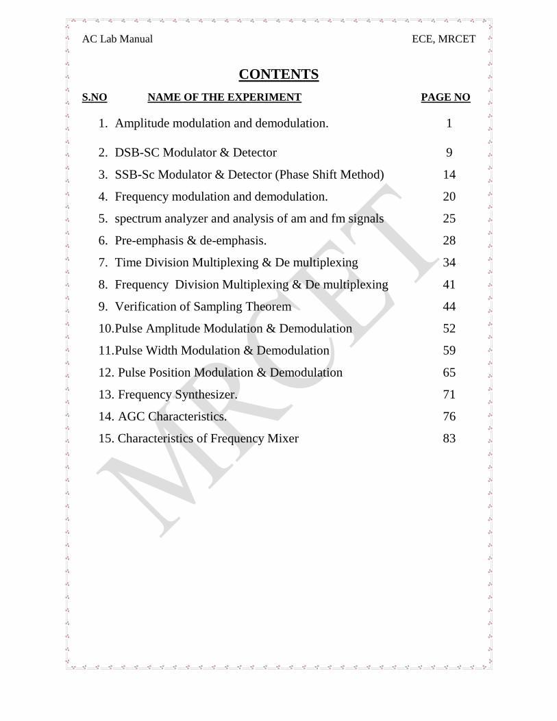
CONTENTS
S.NO NAME OF THE EXPERIMENT PAGE NO
1. Amplitude modulation and demodulation. 1
2. DSB-SC Modulator & Detector 9
3. SSB-Sc Modulator & Detector (Phase Shift Method) 14
4. Frequency modulation and demodulation. 20
5. spectrum analyzer and analysis of am and fm signals 25
6. Pre-emphasis & de-emphasis. 28
7. Time Division Multiplexing & De multiplexing 34
8. Frequency Division Multiplexing & De multiplexing 41
9. Verification of Sampling Theorem 44
10. Pulse Amplitude Modulation & Demodulation 52
11. Pulse Width Modulation & Demodulation 59
12. Pulse Position Modulation & Demodulation 65
13. Frequency Synthesizer. 71
14. AGC Characteristics. 76
15. Characteristics of Frequency Mixer 83
AC Lab Manual MRCET
1
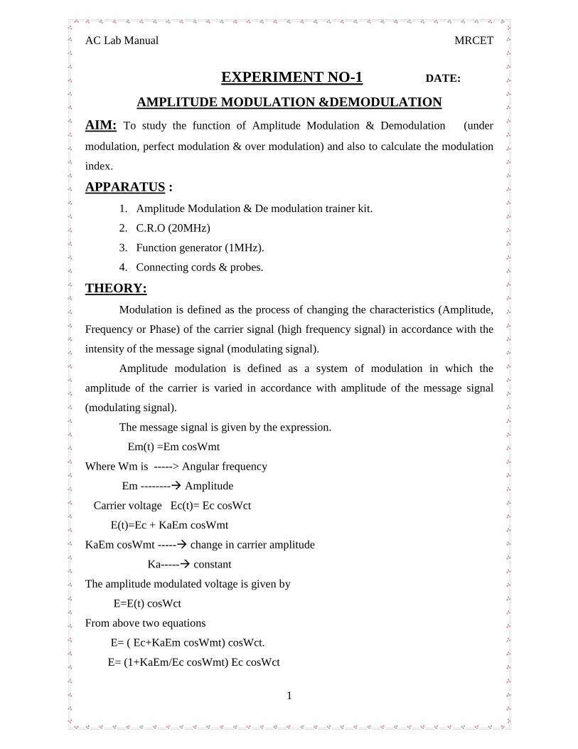
EXPERIMENT NO-1 DATE:
AMPLITUDE MODULATION &DEMODULATION
AIM: To study the function of Amplitude Modulation & Demodulation (under
modulation, perfect modulation & over modulation) and also to calculate the modulation
index.
APPARATUS :
1. Amplitude Modulation & De modulation trainer kit.
2. C.R.O (20MHz)
3. Function generator (1MHz).
4. Connecting cords & probes.
THEORY:
Modulation is defined as the process of changing the characteristics (Amplitude,
Frequency or Phase) of the carrier signal (high frequency signal) in accordance with the
intensity of the message signal (modulating signal).
Amplitude modulation is defined as a system of modulation in which the
amplitude of the carrier is varied in accordance with amplitude of the message signal
(modulating signal).
The message signal is given by the expression.
Em(t) =Em cosWmt
Where Wm is -----> Angular frequency
Em -------- Amplitude
Carrier voltage Ec(t)= Ec cosWct
E(t)=Ec + KaEm cosWmt
KaEm cosWmt ----- change in carrier amplitude
Ka----- constant
The amplitude modulated voltage is given by
E=E(t) cosWct
From above two equations
E= ( Ec+KaEm cosWmt) cosWct.
E= (1+KaEm/Ec cosWmt) Ec cosWct
AC Lab Manual MRCET
2
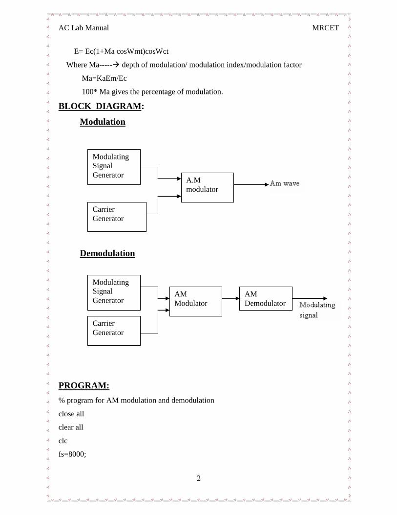
E= Ec(1+Ma cosWmt)cosWct
Where Ma----- depth of modulation/ modulation index/modulation factor
Ma=KaEm/Ec
100* Ma gives the percentage of modulation.
BLOCK DIAGRAM:
Modulation
Demodulation
PROGRAM:
% program for AM modulation and demodulation
close all
clear all
clc
fs=8000;
Modulating
Signal
Generator
Carrier
Generator
A.M
modulator
Modulating
Signal
Generator
Carrier
Generator
AM
Modulator
AM
Demodulator
AC Lab Manual MRCET
3
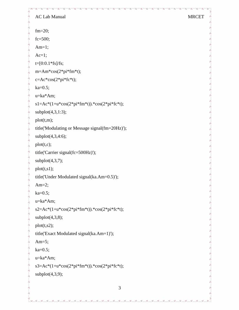
fm=20;
fc=500;
Am=1;
Ac=1;
t=[0:0.1*fs]/fs;
m=Am*cos(2*pi*fm*t);
c=Ac*cos(2*pi*fc*t);
ka=0.5;
u=ka*Am;
s1=Ac*(1+u*cos(2*pi*fm*t)).*cos(2*pi*fc*t);
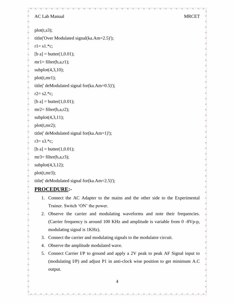
subplot(4,3,1:3);
plot(t,m);
title('Modulating or Message signal(fm=20Hz)');
subplot(4,3,4:6);
plot(t,c);
title('Carrier signal(fc=500Hz)');
subplot(4,3,7);
plot(t,s1);
title('Under Modulated signal(ka.Am=0.5)');
Am=2;
ka=0.5;
u=ka*Am;
s2=Ac*(1+u*cos(2*pi*fm*t)).*cos(2*pi*fc*t);
subplot(4,3,8);
plot(t,s2);
title('Exact Modulated signal(ka.Am=1)');
Am=5;
ka=0.5;
u=ka*Am;
s3=Ac*(1+u*cos(2*pi*fm*t)).*cos(2*pi*fc*t);
subplot(4,3,9);
AC Lab Manual MRCET
4
plot(t,s3);
title('Over Modulated signal(ka.Am=2.5)');
r1= s1.*c;
[b a] = butter(1,0.01);
mr1= filter(b,a,r1);
subplot(4,3,10);
plot(t,mr1);
title(' deModulated signal for(ka.Am=0.5)');
r2= s2.*c;
[b a] = butter(1,0.01);
mr2= filter(b,a,r2);
subplot(4,3,11);
plot(t,mr2);
title(' deModulated signal for(ka.Am=1)');
r3= s3.*c;
[b a] = butter(1,0.01);
mr3= filter(b,a,r3);
subplot(4,3,12);
plot(t,mr3);
title(' deModulated signal for(ka.Am=2.5)');
PROCEDURE:-
1. Connect the AC Adapter to the mains and the other side to the Experimental
Trainer. Switch „ON‟ the power.
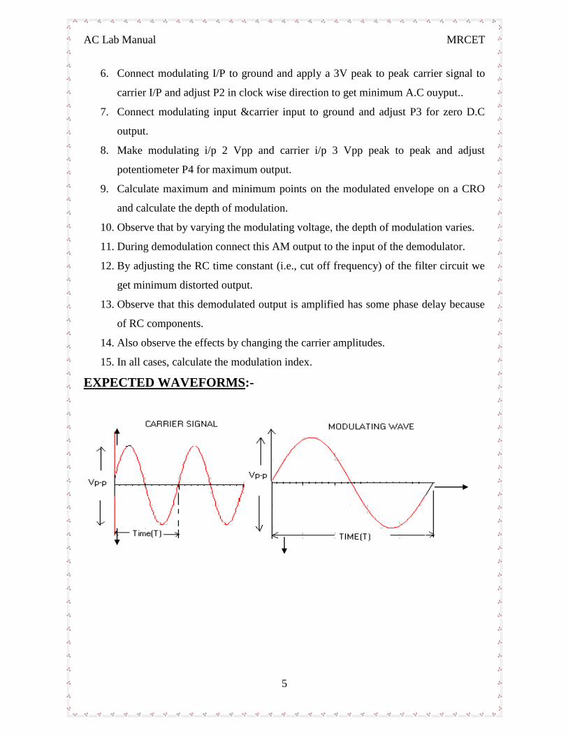
2. Observe the carrier and modulating waveforms and note their frequencies.
(Carrier frequency is around 100 KHz and amplitude is variable from 0 -8Vp-p,
modulating signal is 1KHz).
3. Connect the carrier and modulating signals to the modulator circuit.
4. Observe the amplitude modulated wave.
5. Connect Carrier I/P to ground and apply a 2V peak to peak AF Signal input to
(modulating I/P) and adjust P1 in anti-clock wise position to get minimum A.C
output.
AC Lab Manual MRCET
5
6. Connect modulating I/P to ground and apply a 3V peak to peak carrier signal to
carrier I/P and adjust P2 in clock wise direction to get minimum A.C ouyput..
7. Connect modulating input &carrier input to ground and adjust P3 for zero D.C
output.
8. Make modulating i/p 2 Vpp and carrier i/p 3 Vpp peak to peak and adjust
potentiometer P4 for maximum output.
9. Calculate maximum and minimum points on the modulated envelope on a CRO
and calculate the depth of modulation.
10. Observe that by varying the modulating voltage, the depth of modulation varies.
11. During demodulation connect this AM output to the input of the demodulator.
12. By adjusting the RC time constant (i.e., cut off frequency) of the filter circuit we
get minimum distorted output.
13. Observe that this demodulated output is amplified has some phase delay because
of RC components.
14. Also observe the effects by changing the carrier amplitudes.
15. In all cases, calculate the modulation index.
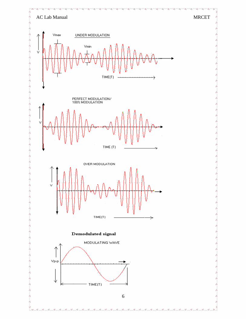
EXPECTED WAVEFORMS:-
AC Lab Manual MRCET
6
AC Lab Manual MRCET
7
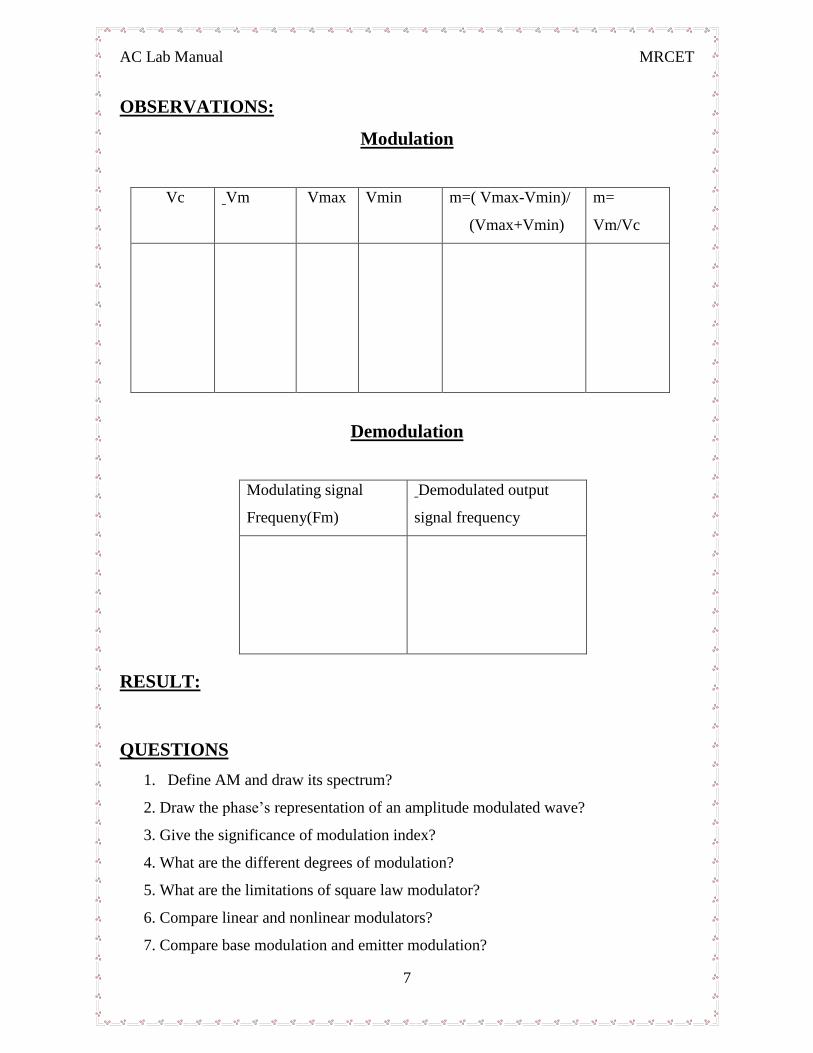
OBSERVATIONS:
Modulation
Vc Vm Vmax Vmin m=( Vmax-Vmin)/
(Vmax+Vmin)
m=
Vm/Vc
Demodulation
Modulating signal
Frequeny(Fm)
Demodulated output
signal frequency
RESULT:
QUESTIONS
1. Define AM and draw its spectrum?
2. Draw the phase‟s representation of an amplitude modulated wave?
3. Give the significance of modulation index?
4. What are the different degrees of modulation?
5. What are the limitations of square law modulator?
6. Compare linear and nonlinear modulators?
7. Compare base modulation and emitter modulation?
Tm
AC Lab Manual MRCET
8
8. Explain how AM wave is detected?
9. Define detection process?
10. What are the different types of distortions that occur in an envelop detector? How
can they be eliminated?
11. What is the condition of for over modulation?
12. Define modulation & demodulation?
13. What are the different types of linear modulation techniques?
14. Explain the working of carrier wave generator.
15. Explain the working of modulator circuit.
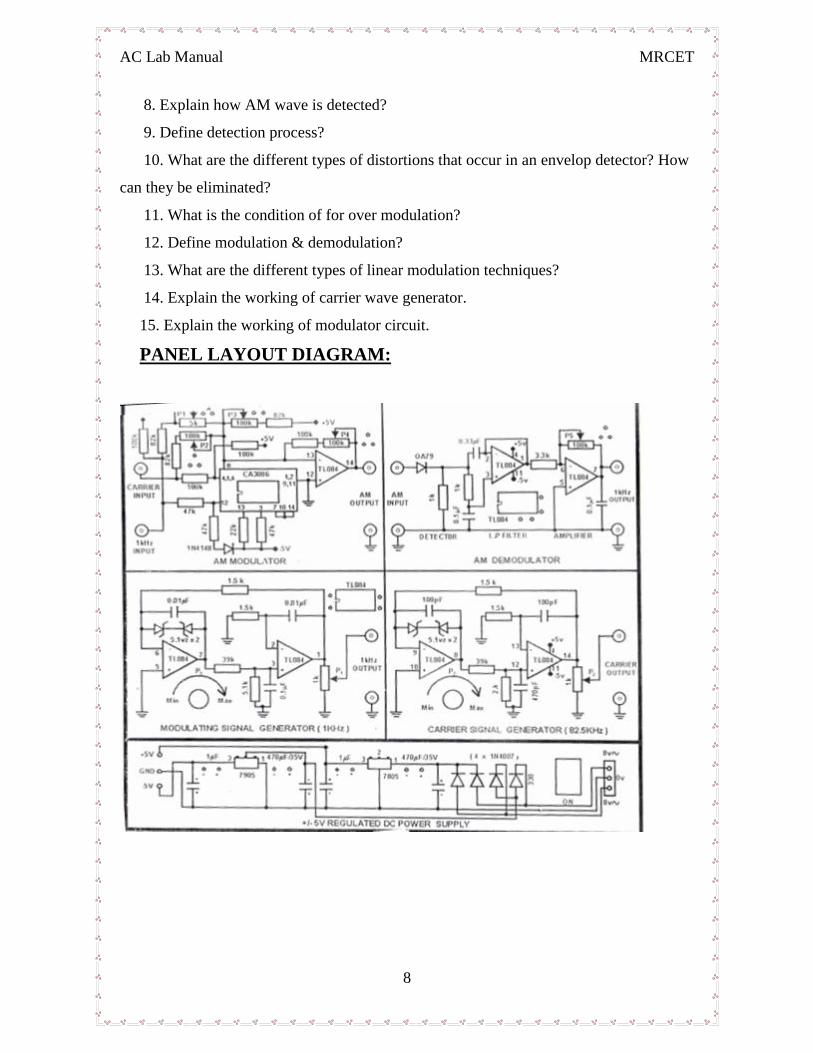
PANEL LAYOUT DIAGRAM:
AC Lab Manual MRCET
9
EXPERIMENT NO-2 DATE:
DSB-SC MODULATOR & DETECTOR
AIM: To study the working of the Balanced Modulator and demodulator.
APPARATUS:
1. Balanced modulator trainer kit
2. C.R.O (20MHz)
3. Connecting cords and probes
4. Function generator (1MHz)
THEORY:
Balanced modulator circuit is used to generate only the two side bands DSB-SC.
The balanced modulation system is a system is a system of adding message to carrier
wave frequency there by only the side bands are produced. It consists of two AM
modulators arranged in a balanced configuration. The AM modulator is assumed to be
identical. The carrier input to the two modulators is same.
If we eliminate or suppress the carrier then the system becomes suppressed carrier
DSB-SC. In this we need reinsert the carrier is complicated and costly. Hence the
suppressed carrier DSB system may be used in point to point communication system.
Generation of suppressed carrier amplitude modulated volt balanced modulator may
be of the following types.
1. Using transistors or FET.
2. Using Diodes
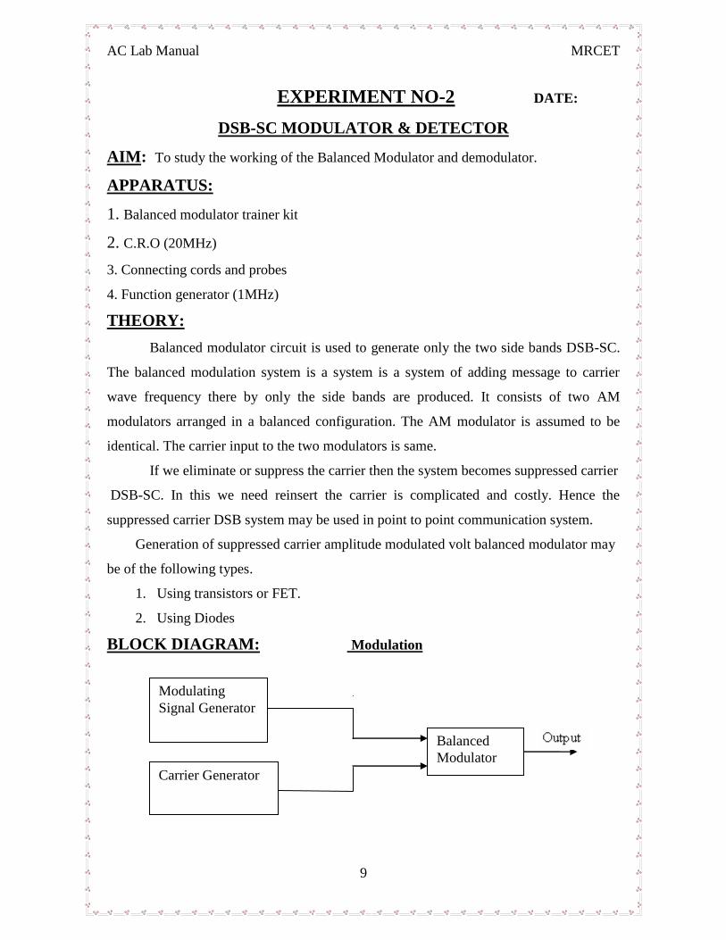
BLOCK DIAGRAM: Modulation
Modulating
Signal Generator
Carrier Generator
Balanced
Modulator
AC Lab Manual MRCET
10
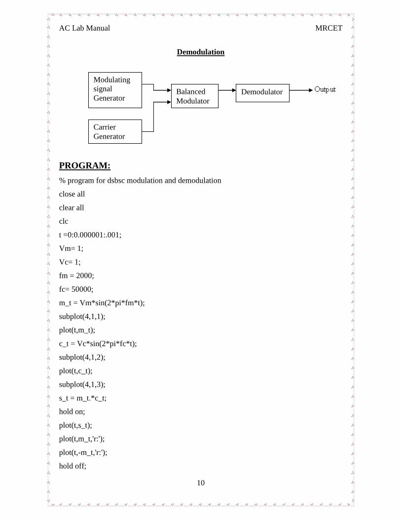
Demodulation
PROGRAM:
% program for dsbsc modulation and demodulation
close all
clear all
clc
t =0:0.000001:.001;
Vm= 1;
Vc= 1;
fm = 2000;
fc= 50000;
m_t = Vm*sin(2*pi*fm*t);
subplot(4,1,1);
plot(t,m_t);
c_t = Vc*sin(2*pi*fc*t);
subplot(4,1,2);
plot(t,c_t);
subplot(4,1,3);
s_t = m_t.*c_t;
hold on;
plot(t,s_t);
plot(t,m_t,'r:');
plot(t,-m_t,'r:');
hold off;
Modulating
signal
Generator
Carrier
Generator
Balanced
Modulator
Demodulator
AC Lab Manual MRCET
11
r = s_t.*c_t;
[b a] = butter(1,0.01);
mr= filter(b,a,r);
subplot(4,1,4);
plot(t,mr);
PROCEDURE:-
1. Connect the circuit as per the given circuit diagram.
2. Switch on the power to the trainer kit.
3. Apply a 100KHz, 0.1 peak sinusoidal to the carrier input and a 5KHz, 0.1 peak
sinusoidal to the modulation input.
4. Measure the output signal frequency and amplitude by connecting the output to
CRO.
5. And note down the output signals.
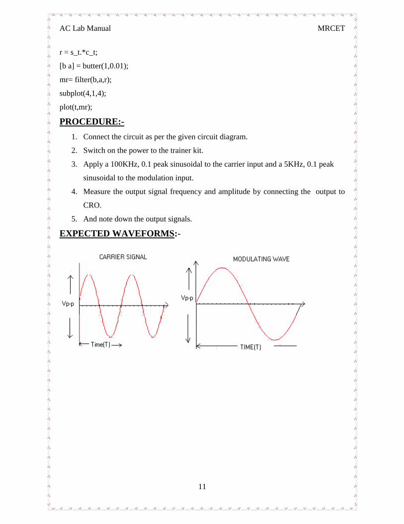
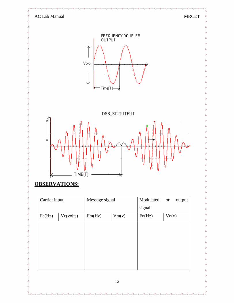
EXPECTED WAVEFORMS:-
AC Lab Manual MRCET
12
OBSERVATIONS:
Carrier input Message signal Modulated or output
signal
Fc(Hz) Vc(volts) Fm(Hz) Vm(v) Fo(Hz) Vo(v)
AC Lab Manual MRCET
13
RESULT:
QUESTIONS
1. What are the two ways of generating DSB_SC?
2. What are the applications of balanced modulator?
3. What are the advantages of suppressing the carrier?
4. What are the advantages of balanced modulator?
5. What are the advantages of Ring modulator?
6. Write the expression for the output voltage of a balanced modulator?
7. Explain the working of balanced modulator and Ring Modulator using diodes.
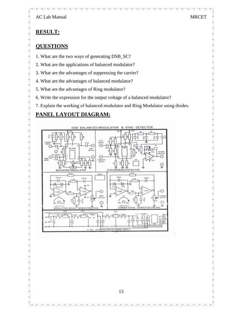
PANEL LAYOUT DIAGRAM:
AC Lab Manual MRCET
14
EXPERIMENT.NO-3 DATE:
SSB-SC MODULATOR & DETECTOR
(PHASE SHIFT METHOD)
AIM:- To generate SSB using phase method and detection of SSB signal using
Synchronous detector.
APPARATUS:-
1. SSB trainer kit
2. C.R.O (20MHz)
3. Patch cards
4. CRO probes
THEORY:
AM and DSBSC modulation are wasteful of band width because they both require
a transmission bandwidth which is equal to twice the message bandwidth In SSB only
one side band and the carrier is used. The other side band is suppressed at the transmitter,
but no information is lost. Thus the communication channel needs to provide the same
band width, when only one side band is transmitted. So the modulation system is referred
to as SSB system.
The base band signal may not be recovered from a SSB signal by the Use of a
diode modulator. The bae band signal can be recovered if the spectral component of the
output i.e either the LSB or USB is multiplied by the carrier signal.
Consider the modulating signal
M(t)=Am cos Wmt
C(t)=Ac cosWct
M(t)c(t)= AcAm cosWmt cosWct
The above signal when passed through a filter, only one of the above component is
obtained which lays the SSB signal.
AC Lab Manual MRCET
15
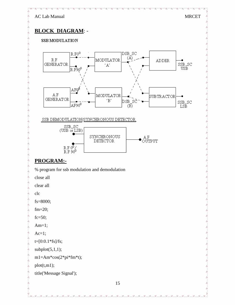
BLOCK DIAGRAM: -
PROGRAM:-
% program for ssb modulation and demodulation
close all
clear all
clc
fs=8000;
fm=20;
fc=50;
Am=1;
Ac=1;
t=[0:0.1*fs]/fs;
subplot(5,1,1);
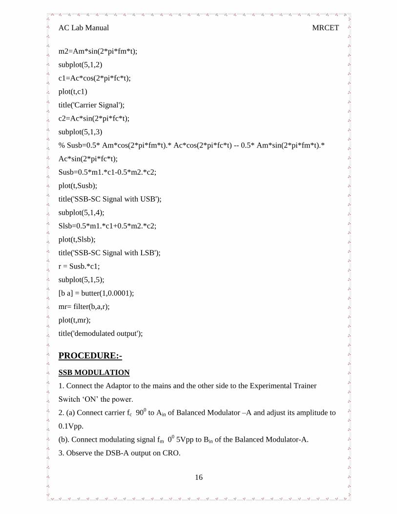
m1=Am*cos(2*pi*fm*t);
plot(t,m1);
title('Message Signal');
AC Lab Manual MRCET
16
m2=Am*sin(2*pi*fm*t);
subplot(5,1,2)
c1=Ac*cos(2*pi*fc*t);
plot(t,c1)
title('Carrier Signal');
c2=Ac*sin(2*pi*fc*t);
subplot(5,1,3)
% Susb=0.5* Am*cos(2*pi*fm*t).* Ac*cos(2*pi*fc*t) -- 0.5* Am*sin(2*pi*fm*t).*
Ac*sin(2*pi*fc*t);
Susb=0.5*m1.*c1-0.5*m2.*c2;
plot(t,Susb);
title('SSB-SC Signal with USB');
subplot(5,1,4);
Slsb=0.5*m1.*c1+0.5*m2.*c2;
plot(t,Slsb);
title('SSB-SC Signal with LSB');
r = Susb.*c1;
subplot(5,1,5);
[b a] = butter(1,0.0001);
mr= filter(b,a,r);
plot(t,mr);
title('demodulated output');
PROCEDURE:-
SSB MODULATION
1. Connect the Adaptor to the mains and the other side to the Experimental Trainer
Switch „ON‟ the power.
2. (a) Connect carrier fc 900 to Ain of Balanced Modulator –A and adjust its amplitude to
0.1Vpp.
(b). Connect modulating signal fm 00 5Vpp to Bin of the Balanced Modulator-A.
3. Observe the DSB-A output on CRO.
AC Lab Manual MRCET
17
4. Connect fc 00 at 0.1 Vpp at Cin of Balanced Modulator B. Connect fm 90
0 at 5 Vpp at
Din of Balanced Modulator B.
5. Connect the DSB-A output and DSB-B output to the summing amplifier. Observe the
output (SSB output) on the spectrum analyzer. This gives single side band (upper) only
while the lower side band is cancelled in the summing Amplifier.
SSB DEMODULATION
1. Connect the carrier fc 00 and SSB output to the synchronous detector.
2. Connect the demodulator output on the oscilloscope which is the recovered
modulating signal.
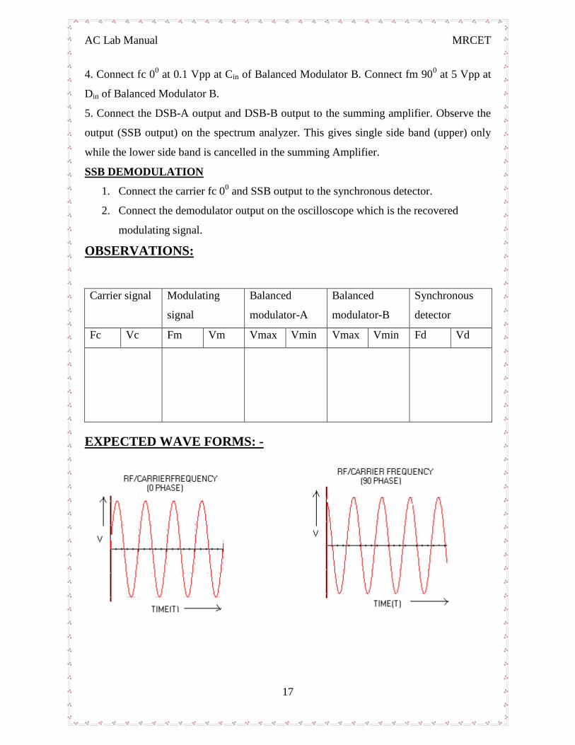
OBSERVATIONS:
Carrier signal Modulating
signal
Balanced
modulator-A
Balanced
modulator-B
Synchronous
detector
Fc Vc Fm Vm Vmax Vmin Vmax Vmin Fd Vd
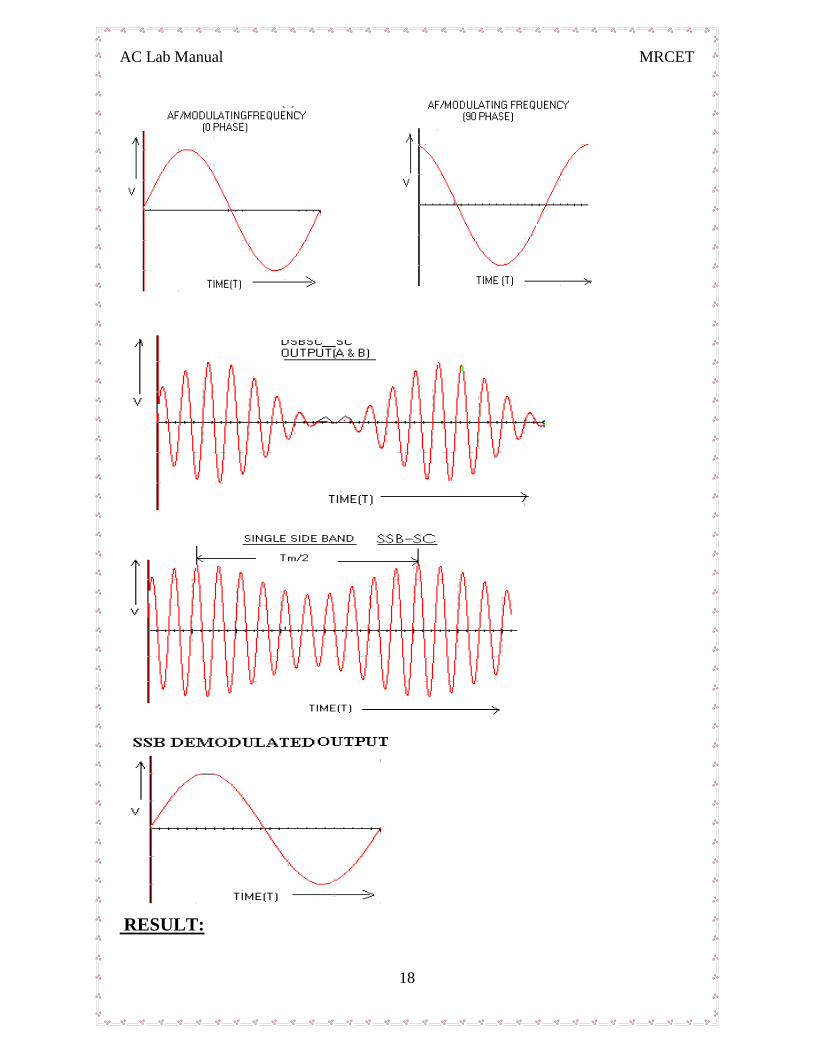
EXPECTED WAVE FORMS: -
AC Lab Manual MRCET
18
RESULT:
AC Lab Manual MRCET
19
QUESTIONS
1. What are the different methods to generate SSB-SC signal?
2. What is the advantage of SSB-SC over DSB-SC?
3. Explain Phase Shift method for SSB generation.
4. Why SSB is not used for broadcasting?
SSB DETECTION
5. Give the circuit for synchronous detector?
6. What are the uses of synchronous or coherent detector?
7. Give the block diagram of synchronous detector?
8. Why the name synchronous detector?
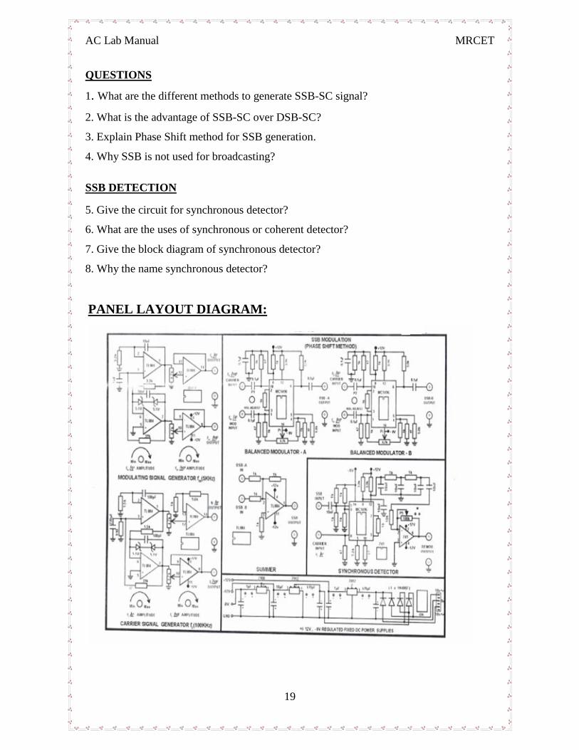
PANEL LAYOUT DIAGRAM:
AC Lab Manual MRCET
20
EXPERMENT NO-4 DATE:
FREQUENCY MODULATION AND DEMODULATION
AIM: To study the process of frequency modulation and demodulation and calculate the
depth of modulation by varying the modulating voltage.
APPARATUS :
1. FM modulation and demodulation kit
2. Dual trace CRO.
3. CRO probes
4. Patch cards.
THEORY:
The modulation system in which the modulator output is of constant amplitude, in
which the signal information is super imposed on the carrier through variations of the
carrier frequency.
The frequency modulation is a non-linear modulation process. Each spectral
component of the base band signal gives rise to one or two spectral components in the
modulated signal. These components are separated from the carrier by a frequency
difference equal to the frequency of base band component. Most importantly the nature
of the modulators is such that the spectral components which produce decently on the
carrier frquency and the base band frequencies.The spetral components in the modulated
wave form depend on the amplitude.
The modulation index for FM is defined as
Mf= max frequency deviation/ modulating frequency.
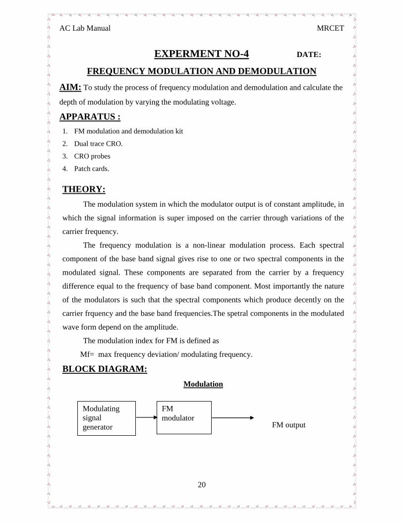
BLOCK DIAGRAM:
Modulation
FM output
Modulating
signal
generator
FM
modulator
AC Lab Manual MRCET
21
Demodulation
PROGRAM:-
% program for fm modulation and demodulation
close all
clear all
clc
%fm=35HZ,fc=500HZ,Am=1V,Ac=1V,B=10
fs=10000;
Ac=1;
Am=1;
fm=35;
fc=500;
B=10;
t=(0:.1*fs)/fs;
wc=2*pi*fc;
wm=2*pi*fm;
m_t=Am*cos(wm*t);
subplot(5,1,1);
plot(t,m_t);
title('Modulating or Message signal(fm=35Hz)');
c_t=Ac*cos(wc*t);
subplot(5,1,2);
plot(t,c_t);
title('Carrier signal(fm=500Hz)');
s_t=Ac*cos((wc*t)+B*sin(wm*t));
subplot(5,1,3);
Modulating
signal
generator
FM
modulator
FM
demodulator
Modulating
signal
AC Lab Manual MRCET
22
plot(t,s_t);
title('Modulated signal');
d=demod(s_t,fc,fs,'fm');
subplot(5,1,4);
plot(t,d);
title('demodulated signal');
PROCEDURE:
1. Switch on the experimental board.
2. Observe the FM modulator output without any modulator input which is the carrier signal
and note down its frequency and amplitude.
3. Connect modulating signal to FM modulator input and observe modulating signal and FM
output on two channels of the CRO simultaneously.
4. Adjust the amplitude of the modulating signal until we get less distorted FM output.
5. Apply the FM output to FM demodulator and adjust the potentiometer in demodulation until
we get demodulated output.
OBSERVATIONS:
Modulation
Vm F1 F2 Frequency
deviation Fd
(f1-f2)
Modulating
index
(f1-f2)/Fm
Band width=
2(Fd+Fm)
Demodulation
Modulating signal
frequency
Demodulating signal
frequency
AC Lab Manual MRCET
23
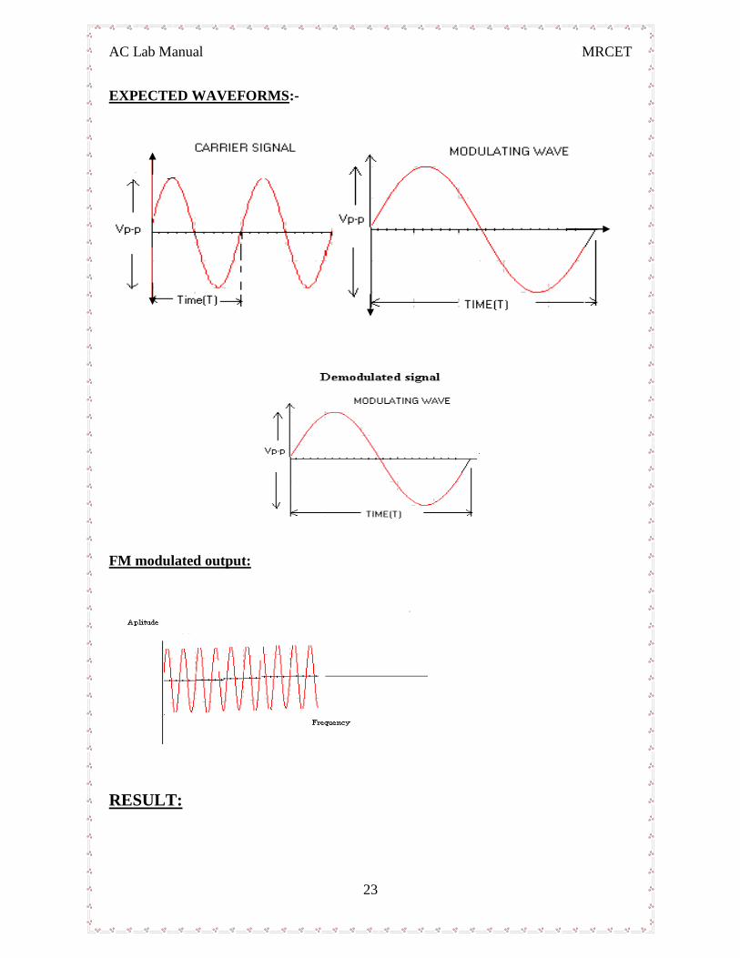
EXPECTED WAVEFORMS:-
FM modulated output:
RESULT:
AC Lab Manual MRCET
24
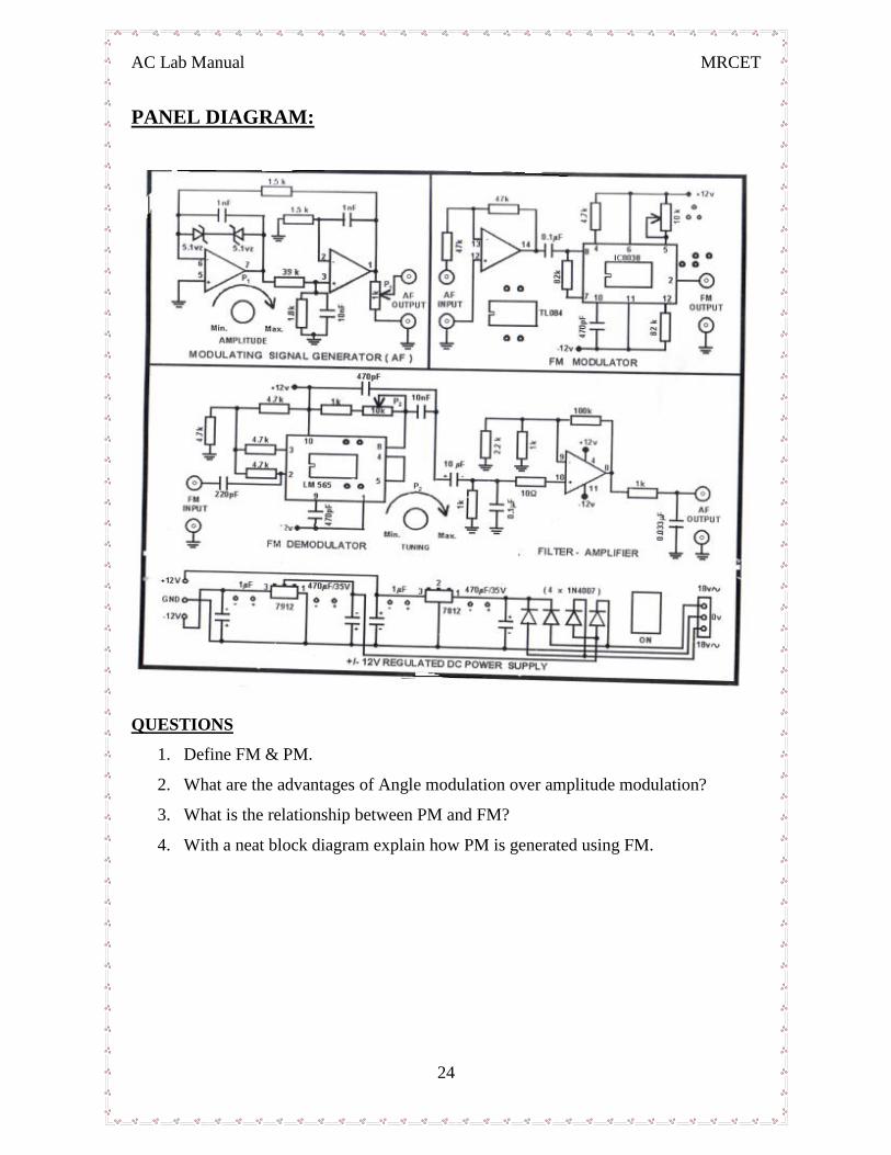
PANEL DIAGRAM:
QUESTIONS
1. Define FM & PM.
2. What are the advantages of Angle modulation over amplitude modulation?
3. What is the relationship between PM and FM?
4. With a neat block diagram explain how PM is generated using FM.
AC Lab Manual MRCET
25
EXPERIMENT NO-5 DATE:
STUDY OF SPECTRUM ANALYZER AND ANALYSIS OF AM
AND FM SIGNALS
AIM: To verify the spectrum of AM and FM signals using spectrum analyzer.
APPARATUS / SOFTWARE REQUIRED:
1. Pc with windows(95/98/XP/NT/2000)
2. Matlab Software with communication toolbox
PROGRAM:
%program of spectrum analyzer and analysis of am and fm signals
close all
clear all
clc
Fs = 100; %sampling frq
t = [0:2*Fs+1]'/Fs;
Fc = 10; % Carrier frequency
x = sin(2*pi*2*t); % message signal
Ac=1;
% compute spectra of am
xam=ammod(x,Fc,Fs,0,Ac);
zam = fft(xam);
zam = abs(zam(1:length(zam)/2+1));
frqam = [0:length(zam)-1]*Fs/length(zam)/2;
% compute spectra of dsbsc
ydouble = ammod(x,Fc,Fs, 3.14,0);
zdouble = fft(ydouble);
zdouble = abs(zdouble(1:length(zdouble)/2+1));
frqdouble = [0:length(zdouble)-1]*Fs/length(zdouble)/2;
% compute spectra of ssb
ysingle = ssbmod(x,Fc,Fs,0,'upper');
zsingle = fft(ysingle);
AC Lab Manual MRCET
26
zsingle = abs(zsingle(1:length(zsingle)/2+1));
frqsingle = [0:length(zsingle)-1]*Fs/length(zsingle)/2;
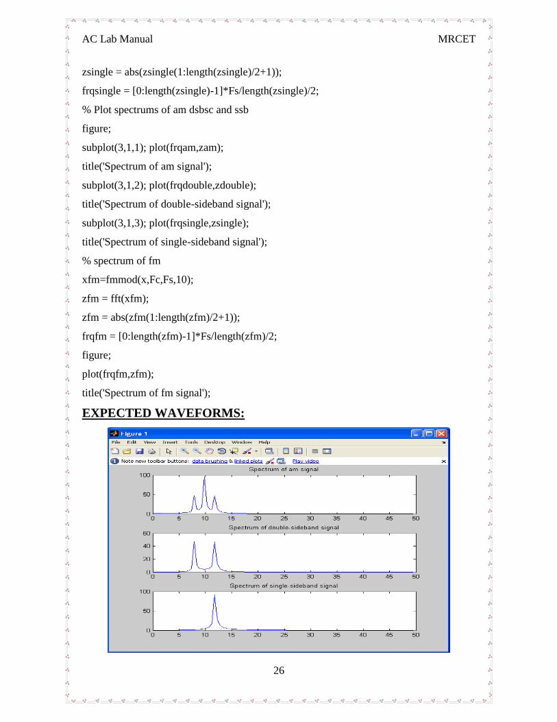
% Plot spectrums of am dsbsc and ssb
figure;
subplot(3,1,1); plot(frqam,zam);
title('Spectrum of am signal');
subplot(3,1,2); plot(frqdouble,zdouble);
title('Spectrum of double-sideband signal');
subplot(3,1,3); plot(frqsingle,zsingle);
title('Spectrum of single-sideband signal');
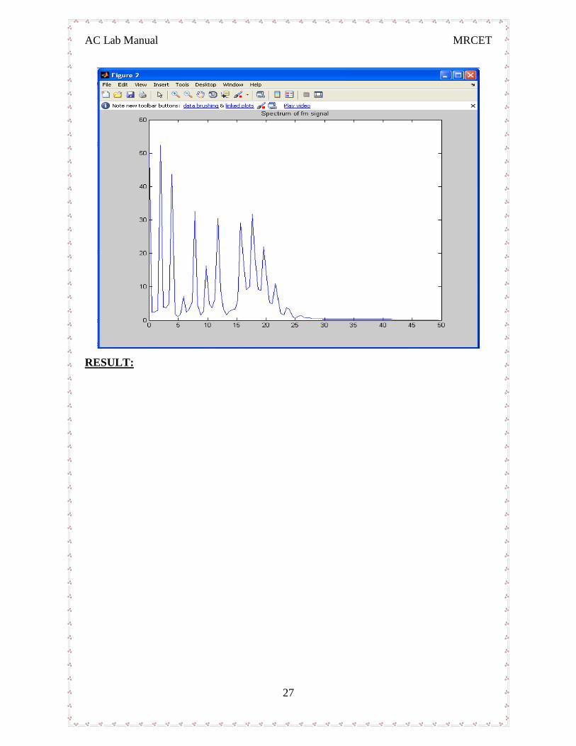
% spectrum of fm
xfm=fmmod(x,Fc,Fs,10);
zfm = fft(xfm);
zfm = abs(zfm(1:length(zfm)/2+1));
frqfm = [0:length(zfm)-1]*Fs/length(zfm)/2;
figure;
plot(frqfm,zfm);
title('Spectrum of fm signal');
EXPECTED WAVEFORMS:
AC Lab Manual MRCET
27
RESULT:
AC Lab Manual MRCET
28
EXPERIMENT.NO-6 DATE:
PRE-EMPHASIS & DE-EMPHASIS
AIM: To study the frequency response of Pre-Emphasis and De-Emphasis circuits.
APPARATUS:
1. Pre-emphasis & De-emphasis trainer kits.
2. C.R.O (20 MHz )
3. Function generator (1MHz).
4. Patch chords and Probes.
THEORY:
Frequency modulation is much immune to noise than amplitude modulation and
significantly more immune than phase modulation. A single noise frequency will affect
the output of the receiver only if it falls with in its pass band.
The noise has a greater effect on the higher modulating frequencies than on lower
ones. Thus, if the higher frequencies were artificially boosted at the transmitter and
correspondingly cut at the receiver, improvement in noise immunity could be expected.
This booting of the higher frequencies, in accordance with a pre-arranged curve, is
termed pre-emphasis, and the compensation at the receiver is called de-emphasis.
If the two modulating signals have the same initial amplitude, and one of them is
pre-emphasized to (say) twice this amplitude, whereas the other is unaffected (being at a
much lower frequency) then the receiver will naturally have to de-emphasize the first
signal by a factor of 2, to ensure that both signals have the same amplitude in the output
of the receiver. Before demodulation, I.e. while susceptible to noise interference the
emphasized signal had twice the deviation it would have had without pre-emphasis, and
was thus more immune to noise. Alternatively, it is seen that when this signal is de-
emphasized any noise sideband voltages are de-emphasized with it, and therefore have a
correspondingly lower amplitude than they would have had without emphasis again their
effect on the output is reduced.
AC Lab Manual MRCET
29
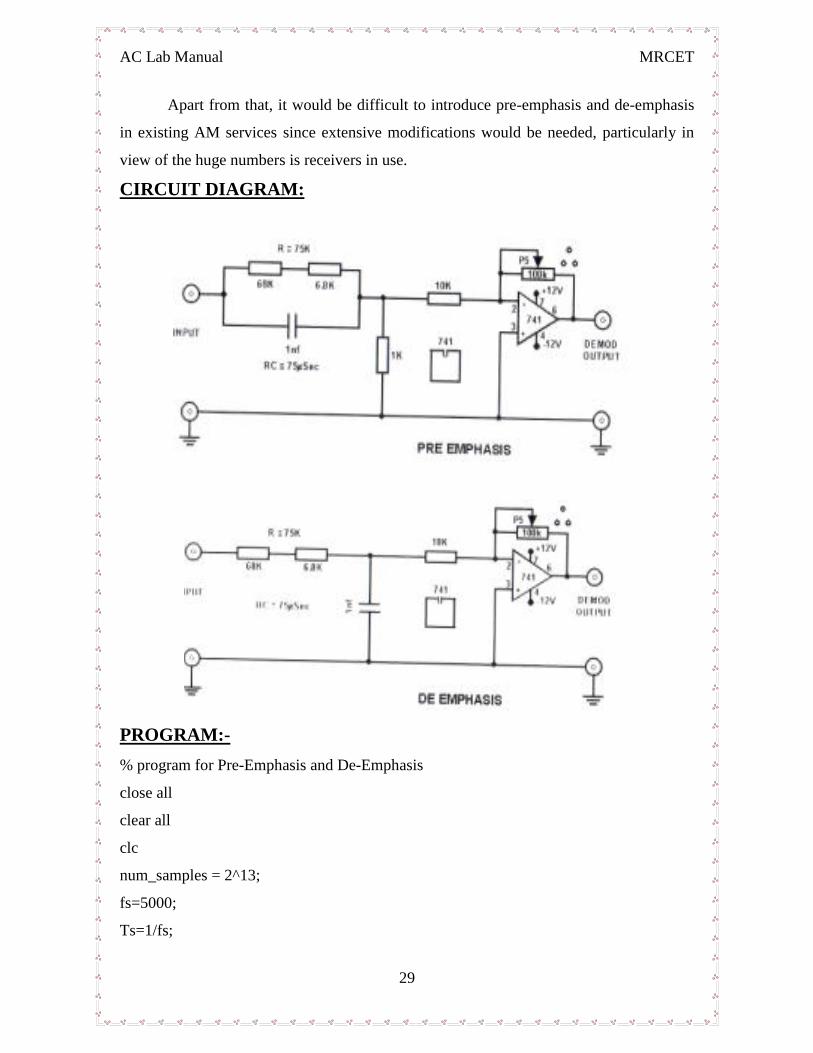
Apart from that, it would be difficult to introduce pre-emphasis and de-emphasis
in existing AM services since extensive modifications would be needed, particularly in
view of the huge numbers is receivers in use.
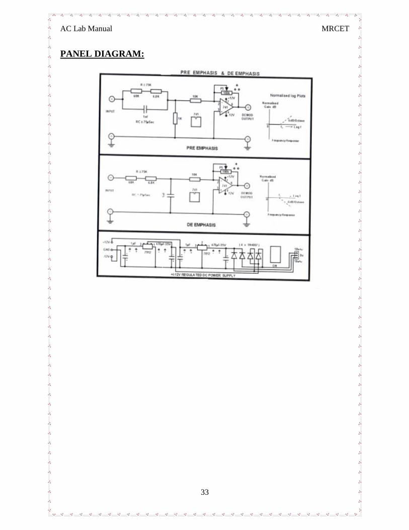
CIRCUIT DIAGRAM:
PROGRAM:-
% program for Pre-Emphasis and De-Emphasis
close all
clear all
clc
num_samples = 2^13;
fs=5000;
Ts=1/fs;
AC Lab Manual MRCET
30
fm1=20;
fm2=30;
fc=200;
t=(0:num_samples-1)*Ts;
f=(-num_samples/2:num_samples/2-1)*fs/num_samples;
mt=sin(2*pi*fm1*t);
Mf=fftshift(abs(fft(mt)));
f_cutoff_pe=15;
Wn_pe=f_cutoff_pe/(fs/2);
[b_pe,a_pe]=butter(1,Wn_pe);
[H_pe,W]=freqz(a_pe,b_pe);
a_de=b_pe;
b_de=a_pe;
[H_de,W]=freqz(a_de,b_de);
mt_pe=filter(a_pe,b_pe,mt);
Mf_pe=fftshift(abs(fft(mt_pe)));
figure(1)
subplot(211);plot(t,mt)
axis([0 .6 min(mt)-1 max(mt)+1])
grid on;title('Modulating Signal (Time Domain)')
subplot(212);plot(f,Mf)
grid on;axis([-50 50 0 max(Mf)+100])
title('Modulating Signal (Frequency Domain)')
figure(2)
subplot(211)
semilogx(W*pi*(fs/2),abs(H_pe),'m','linewidth',2)
axis([0 fs/2 0 50])
grid on;title('Pre-emphasis Filter Magnitude Response')
subplot(212)
semilogx(W*pi*(fs/2),abs(H_de),'m','linewidth',2)
axis([0 fs/2 0 1])
AC Lab Manual MRCET
31
grid on;title('De-emphasis Filter Magnitude Response')
PROCEDURE:
I-PRE-EMPHASIS
1. Connect the circuit as per the circuit diagram
2. Apply a sine wave to the input terminals of 2 VP-P (Vi)
3. By varying the input frequency with fixed amplitude, note down the output
amplitude (Vo) with respect to the input frequency.
4. Calculate the gain using the formula
Gain = 20 log (VO/ VI) db
Where VO = output voltage in volts.
VI = Input voltage in volts.
And plot the frequency response.
II-DE-EMPHASIS
1. Connect the circuit as per circuit diagram.
2. Repeat steps 2,3 & 4 of Pre-Emphasis to de-emphasis also.
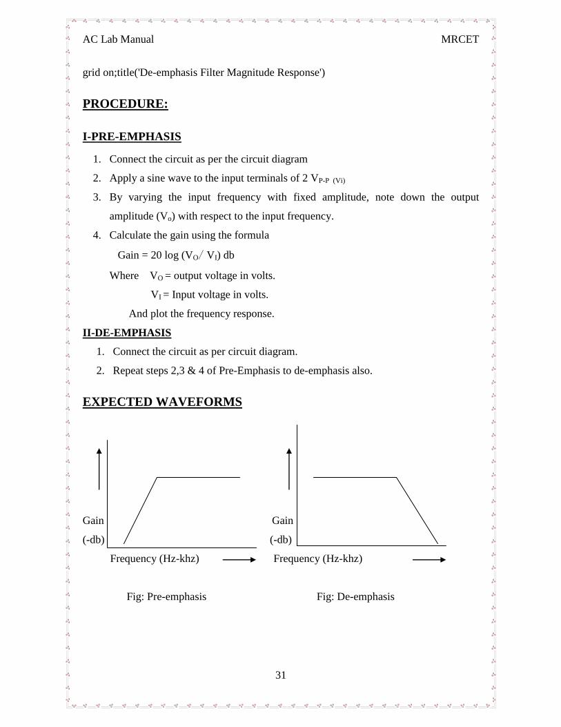
EXPECTED WAVEFORMS
Gain Gain
(-db) (-db)
Frequency (Hz-khz) Frequency (Hz-khz)
Fig: Pre-emphasis Fig: De-emphasis
AC Lab Manual MRCET
32
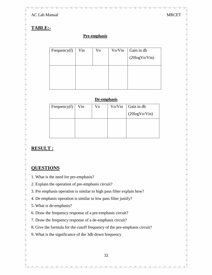
TABLE:-
Pre-emphasis
Frequency(f) Vin Vo Vo/Vin Gain in db
(20logVo/Vin)
De-emphasis
Frequency(f) Vin Vo Vo/Vin Gain in db
(20logVo/Vin)
RESULT :
QUESTIONS
1. What is the need for pre-emphasis?
2. Explain the operation of pre-emphasis circuit?
3. Pre emphasis operation is similar to high pass filter explain how?
4. De emphasis operation is similar to low pass filter justify?
5. What is de-emphasis?
6. Draw the frequency response of a pre-emphasis circuit?
7. Draw the frequency response of a de-emphasis circuit?
8. Give the formula for the cutoff frequency of the pre-emphasis circuit?
9. What is the significance of the 3db down frequency
AC Lab Manual MRCET
33
PANEL DIAGRAM:
AC Lab Manual MRCET
34
EXPERIMENT NO-7 DATE:
TIME DIVISION MULTIPLEXING & DEMULTIPLEXING
AIM:
1. Study of 4 Channel Analog Multiplexing and De multiplexing Techniques.
2. Study of the effect of sampling frequency variation on the output.
3. Study of input signal amplitude on the output.
APPARATUS:
1. TIME DIVISION MULTIPLEXING & DEMULTIPLEXING Trainer.
2. C.R.O (30 MHz)
3. Patch chords.
THEORY:-
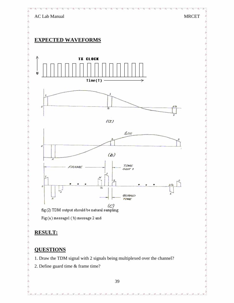
The TDM is used for transmitting several analog message signals over a
communication channel by dividing the time frame into slots, one slot for each message
signal. The four input signals, all band limited by the input filters are sequentially
sampled, the output of which is a PAM waveform containing samples of the input signals
periodically interlaced in time. The samples from adjacent input message channels are
separated by Ts/M, where M is the number of input channels. A set of M pulses
consisting of one sample from each of the input M-input channels is called a frame.
At the receiver the samples from individual channels are separated by carefully
synchronizing and are critical part TDM. The samples from each channel are filtered to
reproduce the original message signal. There are two levels of synchronization. Frame
synchronization is necessary to establish when each group of samples begin and word
synchronization is necessary to properly separate the samples within each frame.
Besides the space diversity & frequency diversity there is a method of sending
multiple analog signals on a channel using “TIME DIVISION MULTIPLEXING &
DEMULTIPLEXING” Technique.
CIRCUIT DESCRIPTION:-
Function Generator Circuit:-
A 4.096 MHz clock is used to derive the modulating signal, which is generated
by an oscillator circuit comprising a 4.096MHz crystal and three 74HC04(U2) inverter
AC Lab Manual MRCET
35
gates. this 4.096 MHz clock is then divided down in frequency by a factor of 4096, by
binary counter 74HC4040(U3), to produce 50% duty cycle, 64 KHz square wave on pin
no.1 of U4, and 32KHz square wave on pin no.4. 32 KHz square wave is given to pin
no.2 of IC NE555(U7) which act as a monostable multivibrator. Potentiometer P5 is used
to adjust the pulse width. 64KHz square wave is fed to the four bit binary counter on pin
no.1 to produce 4KHz square wave at pin no.6. this goes to pin no.13. this signal clocks
to the second half of the counter to produce square wave at following frequencies.
Counter output Frequency
2QD 250Hz
2QC 500Hz
2QB 1 KHz
2QA 2 KHz
Each of these square wave outputs is then fed to its own low pass filter circuits
TL072 (U8, U9). Which generates corresponding sine wave outputs? The amplitude of
this sine wave can be varied by potentiometers P1, P2, P3, P4 respectively. These sine
wave outputs are available at TP1, TP2, TP3, and TP4 respectively and have amplitudes
up to 10V max.
Transmitter Block:-
Each modulating signal is applied to IC TLO74(U6)(pin nos. 3,5,10,12
respectively). This IC buffers the applied signal and is fed to pin nos.3,14,11,6
respectively of IC DG211(U5). The pulse input(32KHz(clock)) is applied to pin nos.
1,16,9,8 of U5. Corresponding PAM outputs are available at test points Tp5,Tp6,Tp7,Tp8
respectively. These each PAM outputs are applied to IC 4052(U1). Which will act as
multiplexer.
4 Channel Demultiplexer:-
The multiplexed PAM signal is given to the 4 channel Demultiplexer input at pin
3(TP12). The A& B timing wave forms selects the channel and accordingly connects the
same to the output. This at the PAM signal of each channel are separated these separated
demultiplexed outputs are monitored at test points 13,14,15,16 respectively.
AC Lab Manual MRCET
36
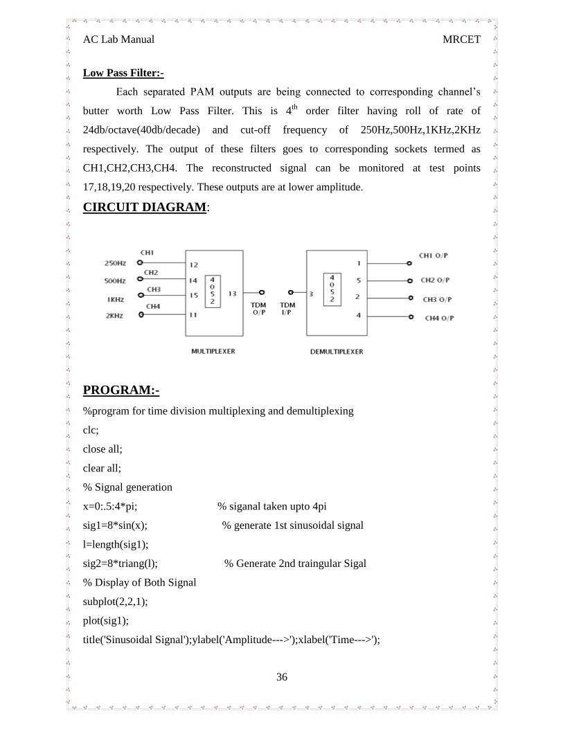
Low Pass Filter:-
Each separated PAM outputs are being connected to corresponding channel‟s
butter worth Low Pass Filter. This is 4th
order filter having roll of rate of
24db/octave(40db/decade) and cut-off frequency of 250Hz,500Hz,1KHz,2KHz
respectively. The output of these filters goes to corresponding sockets termed as
CH1,CH2,CH3,CH4. The reconstructed signal can be monitored at test points
17,18,19,20 respectively. These outputs are at lower amplitude.
CIRCUIT DIAGRAM:
PROGRAM:-
%program for time division multiplexing and demultiplexing
clc;
close all;
clear all;
% Signal generation
x=0:.5:4*pi; % siganal taken upto 4pi
sig1=8*sin(x); % generate 1st sinusoidal signal
l=length(sig1);
sig2=8*triang(l); % Generate 2nd traingular Sigal
% Display of Both Signal
subplot(2,2,1);
plot(sig1);
title('Sinusoidal Signal');ylabel('Amplitude--->');xlabel('Time--->');
AC Lab Manual MRCET
37
subplot(2,2,2);
plot(sig2);
title('Triangular Signal');ylabel('Amplitude--->');xlabel('Time--->');
% Display of Both Sampled Signal
subplot(2,2,3);
stem(sig1);
title('Sampled Sinusoidal Signal');
ylabel('Amplitude--->');xlabel('Time--->');
subplot(2,2,4);
stem(sig2);
title('Sampled Triangular Signal');
ylabel('Amplitude--->');xlabel('Time--->');
l1=length(sig1);
l2=length(sig2);
for i=1:l1
sig(1,i)=sig1(i); % Making Both row vector to a matrix
sig(2,i)=sig2(i);
end
% TDM of both quantize signal
tdmsig=reshape(sig,1,2*l1);
% Display of TDM Signal
figure
stem(tdmsig);
title('TDM Signal');ylabel('Amplitude--->');xlabel('Time--->');
% Demultiplexing of TDM Signal
demux=reshape(tdmsig,2,l1);
for i=1:l1
sig3(i)=demux(1,i); % Converting The matrix into row vectors
sig4(i)=demux(2,i);
end
% display of demultiplexed signal
AC Lab Manual MRCET
38
figure
subplot(2,1,1)
plot(sig3);
title('Recovered Sinusoidal Signal'); ylabel('Amplitude--->');
xlabel('Time--->');
subplot(2,1,2)
plot(sig4);
title('Recovered Triangular Signal'); ylabel('Amplitude--->');
xlabel('Time--->');
PROCEDURE:-
Multiplexing:-
1. Connect the circuit as shown in diagram 1..
2. Switch ON the power supply.
3. Set the amplitude of each modulating signal as 5v peak-peak.
4. Monitor the outputs at test points 5,6,7,8. these are natural sampling PAM
outputs.
5. Observe the outputs varying the duty cycle pot(P5). The PAM outputs will
varying with 10% to 50% duty cycle.
6. Try varying the amplitude of modulating signal corresponding each channel
by using amplitude pots P1,P2,P3,P4. Observe the effect on all outputs.
7. Observe the TDM output at pin no.13 (at TP9) OF 4052. all the multiplexer
channel are observed during the full period of the clock(1/32 KHz).
Demultiplexing & Low Pass Filter:-
1. Connect the circuit as shown in diagram 2.
2. Observe the demultiplexed outputs at test points 13,14,15,16 respectively.
3. Observe by varying the duty cycle pot P5 and see the effect on the outputs.
4. Observe the low pass filter outputs for each channel at test points 17,18,19,20
and at sockets channels CH1,CH2,CH3,CH4. These signals are true replica of
the inputs. These signals have lower amplitude.
AC Lab Manual MRCET
39
EXPECTED WAVEFORMS
RESULT:
QUESTIONS
1. Draw the TDM signal with 2 signals being multiplexed over the channel?
2. Define guard time & frame time?
AC Lab Manual MRCET
40
3. Explain block schematic of TDM?
4. How TDM differ from FDM?
5. What type of filter is used at receiver end in TDM system?
6. What are the applications of TDM?
7. If 2 signal band limited to 3 kHz, 5 KHz & are to be time division multiplexed. What is
the maximum permissible interval between 2 successive samples.?
8. Is the bandwidth requirement for TDM & FDM will be same?
9. Is TDM system is relatively immune to interference with in channels (inter channel
cross talk) as compared to FDM?
10. Is the FDM susceptible to harmonic distortion compared to TDM?
11. In what aspects, TDM is superior to FDM?
AC Lab Manual MRCET
41
EXPERIMENT NO-8 DATE:
FREQUENCY DIVISION MULTIPLEXING
& DE MULTIPLEXING
AIM: To study the frequency division Multiplexing and De multiplexing Techniques.
APPARATUS/SOFTWARE REQUIRED:
1. Pc with windows(95/98/XP/NT/2000)
2. Matlab Software
PROGRAM:
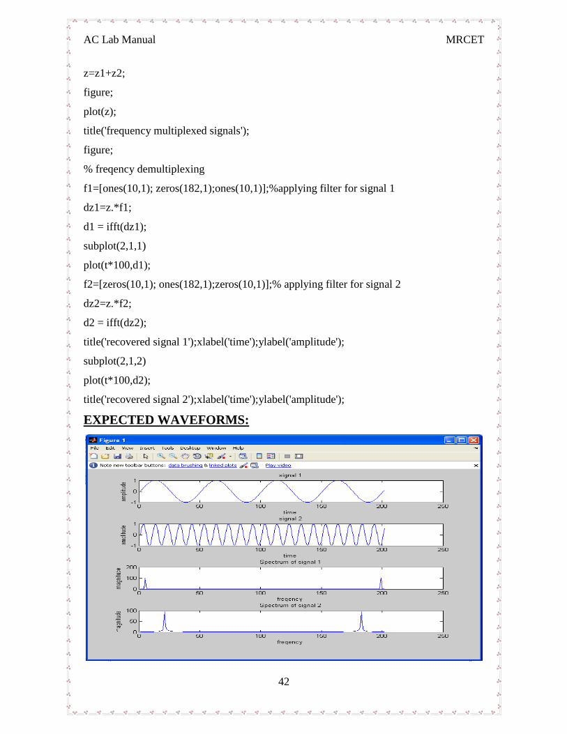
%program for frequency division multiplexing and demultiplexing
close all
clear all
clc
Fs = 100; % sampling freq
t = [0:2*Fs+1]'/Fs;
x1 = sin(2*pi*2*t); % signal 1 signal
z1 = fft(x1);
z1=abs(z1);
x2 = sin(2*pi*10*t); % signal 2 signal
z2 = fft(x2);
z2=abs(z2);
figure;
subplot(4,1,1); plot(x1);
title('signal 1');xlabel('time');ylabel('amplitude');
subplot(4,1,2); plot(x2);
title('signal 2');xlabel('time');ylabel('amplitude');
subplot(4,1,3); plot(z1);
title('Spectrum of signal 1');xlabel('freqency');ylabel('magnitude');
subplot(4,1,4); plot(z2);
title('Spectrum of signal 2');xlabel('freqency');ylabel('magnitude');
% freqency multiplexing
AC Lab Manual MRCET
42
z=z1+z2;
figure;
plot(z);
title('frequency multiplexed signals');
figure;
% freqency demultiplexing
f1=[ones(10,1); zeros(182,1);ones(10,1)];%applying filter for signal 1
dz1=z.*f1;
d1 = ifft(dz1);
subplot(2,1,1)
plot(t*100,d1);
f2=[zeros(10,1); ones(182,1);zeros(10,1)];% applying filter for signal 2
dz2=z.*f2;
d2 = ifft(dz2);
title('recovered signal 1');xlabel('time');ylabel('amplitude');
subplot(2,1,2)
plot(t*100,d2);
title('recovered signal 2');xlabel('time');ylabel('amplitude');
EXPECTED WAVEFORMS:
AC Lab Manual MRCET
43
RESULT:
AC Lab Manual MRCET
44
EXPERIMENT NO-9 DATE:
VERIFICATION OF SAMPLING THEOREM
AIM:
1. To study the sampling theorem and its reconstruction.
2. To study the effect of amplitude and frequency variation of modulating signal on the
output.
3. To study the effect of variation of sampling frequency on the demodulated output.
APPARATUS:
1. Sampling and reconstruction Trainer.
2. C.R.O(30Mhz)
3. Patch cords.
THEORY:
Pulse Modulation is used to transmit analog information. In this system
continuous wave forms are sampled at regular intervals. Information regarding the signal
is transmitted only at the sampling times together with synchronizing signals.
At the receiving end, the original waveforms may be reconstituted from the
information regarding the samples.
Sampling Theorem Statement:
A band limited signal of finite energy which has no frequency components higher
than fm Hz, is completely described by specifying the values of the signal at instants of
time separated by ½ fm seconds.
The sampling theorem states that, if the sampling rate in any pulse modulation
system exceeds twice the maximum signal frequency, the original signal can be
reconstructed in the receiver with minimum distortion.
Fs > 2fm is called Nyquist rate.
Where fs – sampling frequency
Fm – Modulation signal frequency.
If we reduce the sampling frequency fs less than fm, the side bands and the
information signal will overlap and we cannot recover the information signal simply by
AC Lab Manual MRCET
45
low pass filter. This phenomenon is called fold over distortion or aliasing.There are two
methods of sampling. (1) Natural sampling (2) Flat top sampling.
Sample & Hold circuit holds the sample value until the next sample is taken.
Sample & Hold technique is used to maintain reasonable pulse energy.The duty cycle of
a signal is defined as the ratio of Pulse duration to the Pulse repetition period. The duty
cycle of 50% is desirous taking the efficiency into account.
Circuit Description:-
Pulse and Modulating Signal Generator:-
A 4.096 MHz clock is used to derive the modulating signal, which is generated by
an oscillator circuit comprising a 4.096MHz crystal and three 74HC04(U9) inverter
gates. This 4.096MHz clock is then divided down in frequency by a factor of 4096, by
binary counter 74HC4040(U10), to produce 50% duty cycle, 1KHz square wave on pin
no.1 of U10, and 2KHz square wave on pin no.15. the frequency is selectable by means
of SW1. this input of fourth order low pass filter U11(TL072) is used to produce sine
wave from the square wave. The amplitude of this sine wave can be varied.
The square wave which is generated by the oscillator is buffered by inverter
74HC04(U9), to produce 32KHz square wave at pin no. 4 of the 74HC4040. This pulse is
given to the monostable multi(U4) to obtain the 16KHz and 32KHz square wave at the
output which are selected by the frequency pot.
Sampling Circuit:-
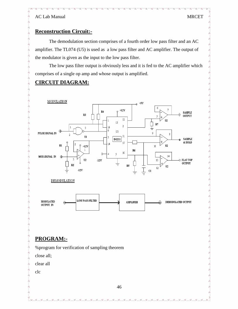
The IC DG211(U3) is used as analog switch which is used in pulse amplitude
modulation in this circuit. The modulation signal & pulse signal are given as the input to
TL074(U2), 7400(U1) IC‟s respectively. These IC output are fed to the inputs of the
DG211.
The sampled output is available at the pin no.2 of DG211 and it is buffered by
using TL074(U2) and then output is available at TP5.
Similarly the sample & hold output and the flat top output are available at pin
no15 & 10 of DG211 respectively. These are buffered by TL074(U2) and then output is
available at TP6 & TP7 respectively.
AC Lab Manual MRCET
46
Reconstruction Circuit:-
The demodulation section comprises of a fourth order low pass filter and an AC
amplifier. The TL074 (U5) is used as a low pass filter and AC amplifier. The output of
the modulator is given as the input to the low pass filter.
The low pass filter output is obviously less and it is fed to the AC amplifier which
comprises of a single op amp and whose output is amplified.
CIRCUIT DIAGRAM:
PROGRAM:-
%program for verification of sampling theorem
close all;
clear all
clc
AC Lab Manual MRCET
47
t=-10:.01:10;
T=4;
fm=1/T;
x=cos(2*pi*fm*t); % input signal
subplot(2,2,1);
plot(t,x);
xlabel('time');ylabel('x(t)');title('continous time signal');
grid;
n1=-4:1:4;
fs1=1.6*fm;
fs2=2*fm;
fs3=8*fm;
%discrete time signal with fs<2fm
x1=cos(2*pi*fm/fs1*n1);
subplot(2,2,2);
stem(n1,x1);
xlabel('time');ylabel('x(n)');
title('discrete time signal with fs<2fm');
hold on
subplot(2,2,2);
plot(n1,x1)
grid;
%discrete time signal with fs=2fm
n2=-5:1:5;
x2=cos(2*pi*fm/fs2*n2);
subplot(2,2,3);
stem(n2,x2);
xlabel('time');ylabel('x(n)');
title('discrete time signal with fs=2fm');
hold on
subplot(2,2,3);
AC Lab Manual MRCET
48
plot(n2,x2)
%discrete time signal with fs>2fm
grid;
n3=-20:1:20;
x3=cos(2*pi*fm/fs3*n3);
subplot(2,2,4);
stem(n3,x3);
xlabel('time');ylabel('x(n)');
title('discrete time signal with fs>2fm');
hold on
subplot(2,2,4);
plot(n3,x3)
grid;
PROCEDURE:
Sampling:-
1. Connect the circuit as shown in diagram 1 .
a. The output of the modulating signal generator TP1 is connected to modulating
signal input TP4 of the sampling circuit keeping the frequency switch in 1KHz position,
and amplitude knob to max position.
b. The output of pulse generator TP2 is connected to sampling pulse input TP3 of
the sampling circuit keeping the frequency switch in 16KHz position.(Adjust the duty
cycle pot to mid position i.e.50%).
2. Switch ON the power supply.
3. Observe the outputs of sampling, sampling and hold, flat top output at TP7, TP8
and TP9 respectively. By varying the amplitude pot also observe the effect on
outputs.
4. By varying Duty cycle pot observe the effect on sampling outputs (Duty cycle is
varying from 10-15%).
AC Lab Manual MRCET
49
5. Vary the switch position in the pulse generator circuit to 32 KHz and now observe
the outputs at TP7, TP8 and TP9.By varying the amplitude pot also observe the
effect on outputs.
6. Now, vary the switch position in modulating signal generator to 2 KHz and repeat
all the above steps 3&4.
7. Switch OFF the power supply.
Reconstruction:-
1. Connect the circuit as shown in diagram 2.
a. . The output of the modulating signal generator TP1 is connected to
modulating signal input TP4 of the sampling circuit keeping the frequency
switch in 1KHz position, and amplitude knob to max position.
b. The output of pulse generator TP2 is connected to sampling pulse input
TP3 of the sampling circuit keeping the frequency switch in 16KHz
position.(Adjust the duty cycle pot to mid position i.e.50%).
c. Connect the sample output from TP7 to the input of low pass filter TP10.
d. Output of low pass filter from TP11 to input of AC amplifier TP12, keep
the gain pot in AC amplifier to max position.
2. Switch ON the power supply.
3. Observe the output of AC amplifier at TP13. The output will be the replica of the
input. By varying the gain pot observe the demodulating signal amplification.
4. Similarly connect the sample and hold output and flat top output to TP10 and
observe reconstructed the signal.
5. Vary the switch position in the sampling frequency circuit to 32KHz and now
repeat the steps 3&4.
6. Vary the switch position in the modulating signal generator to 2KHz and repeat all
the above steps 3 to 5.
7. Switch OFF the power supply.
AC Lab Manual MRCET
50
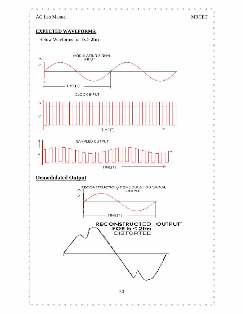
EXPECTED WAVEFORMS:
Below Wavforms for fs > 2fm
Demodulated Output
AC Lab Manual MRCET
51
RESULT:
QUESTIONS
1. What are the types of sampling?
2. State sampling theorem?
3. What happens when fs < 2 fm?
4. How will be the reconstructed signal when fs >= 2fm?
5. Explain the operation of sampling circuit?
6. Explain the operation of re-construction circuit?
7. Who formalized the sampling theorem?
8. What are the applications of the above theorem?
9. Is the sampling theorem basis for the modern digital communications?
10. Is the voice signal sampling of 8000 Hz, follows sampling theorem in Land line
Telephone Exchange.
AC Lab Manual MRCET
52
EXPERIMENT NO-10 DATE:
PULSE AMPLITUDE MODULATION
AIM:- 1.To study the Pulse amplitude modulation & demodulation Techniques.
2. To study the effect of amplitude and frequency variation of modulating signal
on the output.
APPARATUS:-
1. Pulse amplitude modulation & demodulation Trainer.
2. Dual trace CRO.
3. Patch chords.
THEORY:-
Pulse modulation is used to transmit analog information. In this system
continuous wave forms are sampled at regular intervals. Information regarding the signal
is transmitted only at the sampling times together with syncing signals.
At the receiving end, the original waveforms may be reconstituted from the
information regarding the samples.
The pulse amplitude modulation is the simplest form of the pulse modulation.
PAM is a pulse modulation system is which the signal is sampled at regular intervals, and
each sample is made proportional to the amplitude of the signal at the instant of sampling.
The pulses are then sent by either wire or cables are used to modulated carrier.
The two types of PAM are i) Double polarity PAM, and ii) the single polarity
PAM, in which a fixed dc level is added to the signal to ensure that the pulses are always
positive. Instantaneous PAM sampling occurs if the pulses used in the modulator are
infinitely short.
Natural PAM sampling occurs when finite-width pulses are used in the modulator,
but the tops of the pulses are forced to follow the modulating waveform.
Flat-topped sampling is a system quite often used because of the ease of
generating the modulated wave.
PAM signals are very rarely used for transmission purposes directly. The reason
for this lies in the fact that the modulating information is contained in the amplitude
AC Lab Manual MRCET
53
factor of the pulses, which can be easily distorted during transmission by noise, crosstalk,
other forms of distortion. They are used frequently as an intermediate step in other pulse-
modulating methods, especially where time-division multiplexing is used.
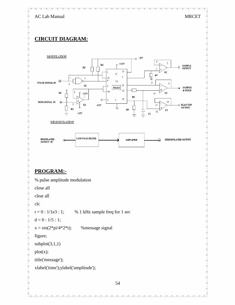
Circuit description:-
Pulse and Modulation Signal Generator:-
A 4.096 MHz clock is used to derive the modulating signal, which is generated by
an oscillator circuit comprising a 4.096MHz crystal and three 74HC04(U9) inverter
gates. This 4.096MHz clock is then divided down in frequency by a factor of 4096, by
binary counter 74HC4040(U10), to produce 50% duty cycle, 1 KHz square wave on pin
no.1 of U10, and 2KHz square wave on pin no.15. the frequency is selectable by means
of SW1. this goes to input of fourth order low pass filter U11(TL072) is used to produce
sine wave from the square wave. The amplitude of this sine wave can be varied.
The square wave which is generated by the oscillator is buffered by inverter
74HC04(U9), to produce 32KHz square wave at pin no.4 of the 74HC4040(U10). This
pulse is given to the monostable multi to obtain the 16 KHz and 32 KHz square wave at
the output which are selected by the frequency pot.
Modulation:-
The ICDG211 (U3) is used as a pulse amplitude modulation in this circuit. The
modulation signal & pulse signals are given to TL074 (U2) & 7400(U1) IC‟s
respectively. These outputs are fed to the inputs the D4211 (U3).
The sampled output is available at the pin no 2 of DG211 and it is buffered by
using TL074 (U2) and then output is available at TP5.
Similarly the sample & hold output and the flat top output are available at pin
no.15 &10 of DG211 respectively. These are buffered by TL074 (U2) and then output is
available at TP6&TP7 respectively.
Demodulation:-
The demodulation section comprises of fourth order low pass filter and an AC
amplifier. The TL074(U5) is used as a low pass filter and AC amplifier. The output of the
modulator is given as the input to the low pass filter.
The low pass filter output is obviously less and it is fed to the AC amplifier which
comprises of a single op amp and whose output is amplified.
AC Lab Manual MRCET
54
CIRCUIT DIAGRAM:
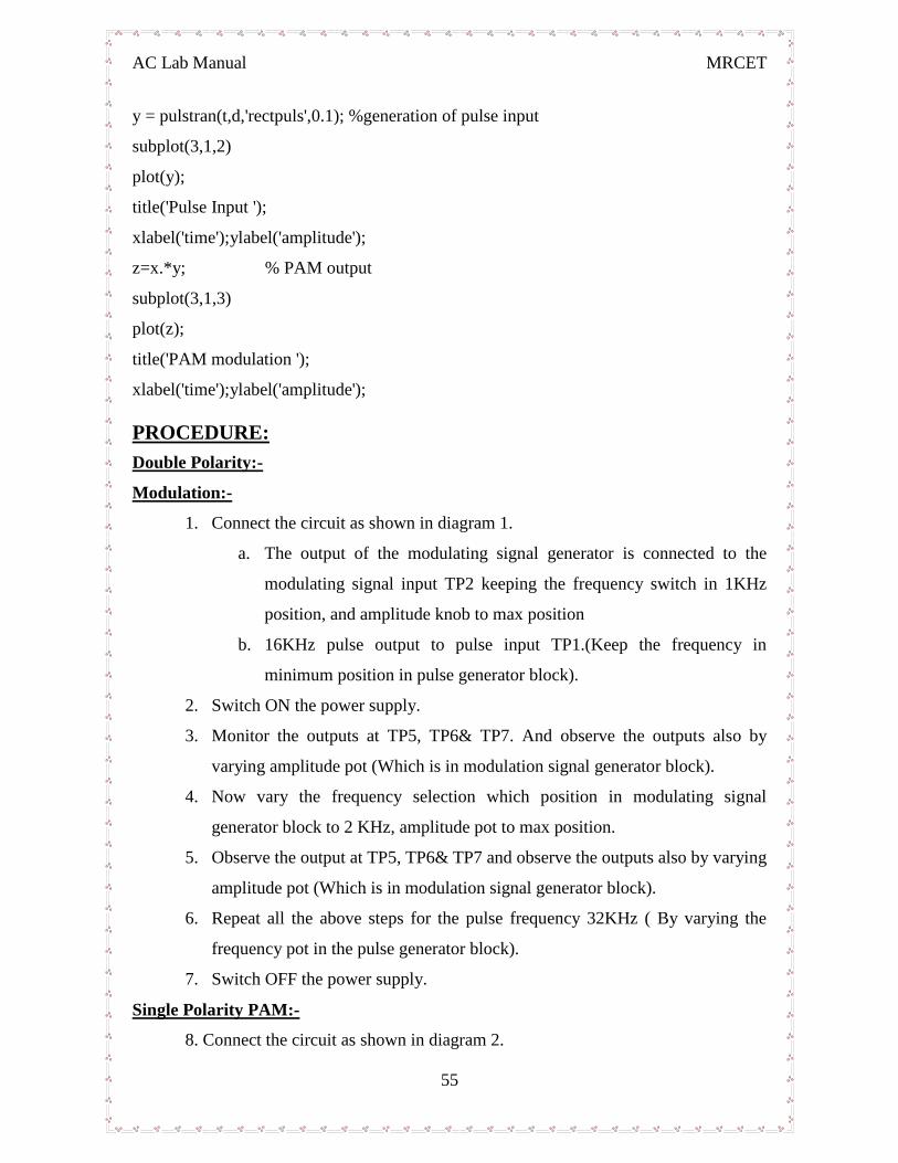
PROGRAM:-
% pulse amplitude modulation
close all
clear all
clc
t = 0 : 1/1e3 : 1; % 1 kHz sample freq for 1 sec
d = 0 : 1/5 : 1;
x = sin(2*pi/4*2*t); %message signal
figure;
subplot(3,1,1)
plot(x);
title('message');
xlabel('time');ylabel('amplitude');
AC Lab Manual MRCET
55
y = pulstran(t,d,'rectpuls',0.1); %generation of pulse input
subplot(3,1,2)
plot(y);
title('Pulse Input ');
xlabel('time');ylabel('amplitude');
z=x.*y; % PAM output
subplot(3,1,3)
plot(z);
title('PAM modulation ');
xlabel('time');ylabel('amplitude');
PROCEDURE:
Double Polarity:-
Modulation:-
1. Connect the circuit as shown in diagram 1.
a. The output of the modulating signal generator is connected to the
modulating signal input TP2 keeping the frequency switch in 1KHz
position, and amplitude knob to max position
b. 16KHz pulse output to pulse input TP1.(Keep the frequency in
minimum position in pulse generator block).
2. Switch ON the power supply.
3. Monitor the outputs at TP5, TP6& TP7. And observe the outputs also by
varying amplitude pot (Which is in modulation signal generator block).
4. Now vary the frequency selection which position in modulating signal
generator block to 2 KHz, amplitude pot to max position.
5. Observe the output at TP5, TP6& TP7 and observe the outputs also by varying
amplitude pot (Which is in modulation signal generator block).
6. Repeat all the above steps for the pulse frequency 32KHz ( By varying the
frequency pot in the pulse generator block).
7. Switch OFF the power supply.
Single Polarity PAM:-
8. Connect the circuit as shown in diagram 2.
AC Lab Manual MRCET
56
a. The output of the modulating signal generator is connected to the
modulating signal input TP2 keeping the frequency switch in 1KHz
position, and amplitude knob to max position
b. 16KHz pulse output to pulse input TP1 .
9. Switch ON the power supply.
10. Repeat above step 3 to 6 and observe the outputs.
11. Vary DC output pot until you get single polarity PAM at TP5,TP6,TP7.
12. Switch OFF the power supply.
Demodulation:-
1. Connect the circuit as shown in diagram 3.
a. The output of the modulating signal generator is connected to the
modulating signal input TP2 keeping the frequency switch in 1KHz
position, and amplitude knob to max position
b. 16KHz pulse output to pulse input TP1.
c. Sample output, sample and hold output and flat top outputs
Respectively to the input of low pass filter(TP9) and LPF
output (TP10) to AC amplifier input(TP11).
2. Observe the output of LPF and AC amplifier at TP10,TP12 respectively,
corresponding to inputs from TP5,TP6 &TP7. The outputs will be the true replica
of the input.
3. Now, set the switch position in modulating signal generator to 2KHz and
observe the outputs at TP10&TP12 respectively, corresponding to inputs from
TP5,TP6& TP7.
4. Vary the frequency of pulse to 32KHz (By varying the frequency pot(Put in
max position) in pulse generator block) and repeat the above steps 2&3.
5. Switch OFF the power supply.
AC Lab Manual MRCET
57
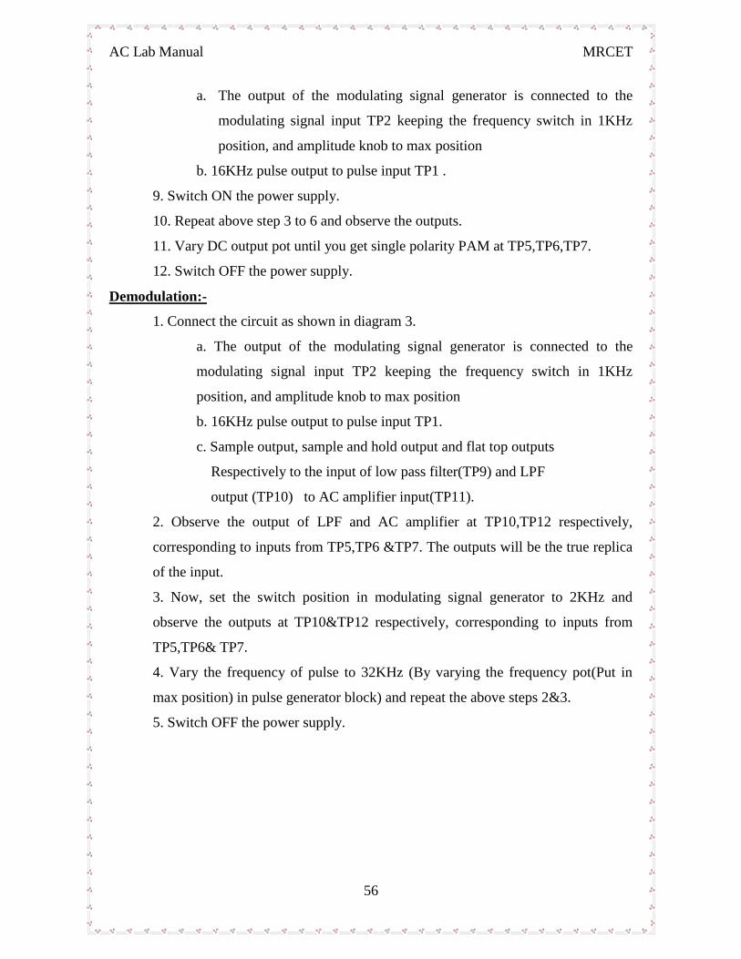
EXPECTED WAVEFORMS
RESULT:
QUESTIONS
1. TDM is possible for sampled signals. What kind of multiplexing can be used in
continuous modulation systems?
2. What is the minimum rate at which a speech signal can be sampled for the purpose of
PAM?
3. What is cross talk in the context of time division multiplexing?
4. Which is better, natural sampling or flat topped sampling and why?
5. Why a dc offset has been added to the modulating signal in this board? Was it essential
for the working of the modulator? Explain?
6. If the emitter follower in the modulator section saturates for some level of input signal,
then what effect it will have on the output?
7. Derive the mathematical expression for frequency spectrum of PAM signal.
AC Lab Manual MRCET
58
8. Explain the modulation circuit operation?
9. Explain the demodulation circuit operation?
10. Is PAM & Demodulation is sensitive to Noise?
AC Lab Manual MRCET
59
EXPERIMENT NO-11 DATE:
PULSE WIDTH MODULATION & DEMODULATION
AIM:
1. To study the Pulse Width Modulation (PWM) and Demodulation
Techniques.
2. To study the effect of Amplitude and Frequency of Modulating Signal on
PWM output.
APPARATUS:
1. PWM trainer kit
2. C.R.O(30MHz)
3. Patch Chords.
THEORY:-
Pulse modulation is used to transmit analog information. In this system
continuous wave forms are sampled at regular intervals. Information regarding the signal
is transmitted only at the sampling times together with synchronizing signals.
At the receiving end, the original waveforms may be reconstituted from the
information regarding the samples.
The pulse Width Modulation of the PTM is also called as the Pulse Duration
Modulation (PDM) & less often Pulse length Modulation (PLM).
In pulse Width Modulation method, we have fixed and starting time of each pulse,
but the width of each pulse is made proportional to the amplitude of the signal at that
instant.
This method converts amplitude varying message signal into a square wave with
constant amplitude and frequency, but which changes duty cycle to correspond to the
strength of the message signal.
Pulse-Width modulation has the disadvantage, that its pulses are of varying width
and therefore of varying power content. This means that the transmitter must be powerful
enough to handle the maximum-width pulses. But PWM still works if synchronization
between transmitter and receiver fails, whereas pulse-position modulation does not.
AC Lab Manual MRCET
60
Pulse-Width modulation may be generated by applying trigger pulses to control
the starting time of pulses from a mono stable multivibrator, and feeding in the signal to
be sampled to control the duration of these pulses.
When the PWM signals arrive at its destination, the recovery circuit used to
decode the original signal is a sample integrator (LPF).
CIRCUIT DESCRIPTION:-
Pulse & Modulating Signal Generator:-
A 4.096MHz clock is used to derive the modulating signal, which is generated by
an oscillator circuit comprising a 4.096MHz crystal and three 74HC04(U9) inverter
gates. This 4.096MHz clock is then divided down in frequency by a factor of 4096, by
binary counter 74HC4040(U2), to produce 50% duty cycle, 1KHz square wave on pin
no.1 of U4, and 2KHz square wave on pin no.15. the frequency is selectable by means of
SW1. This goes to input of fourth order low pass filter U3 is used to produce sine wave
from the square wave. The amplitude of this sine wave can be varied.
The square wave which is generated by the oscillator is buffered by inverter
74HC04, to produce 32KHz square wave at pin no.4 of the 74HC4040(U2). This pulse is
given to the monostable multi to obtain the 16KHz and 32KHz square wave at the output
which are selected by the frequency pot.
Modulation:-
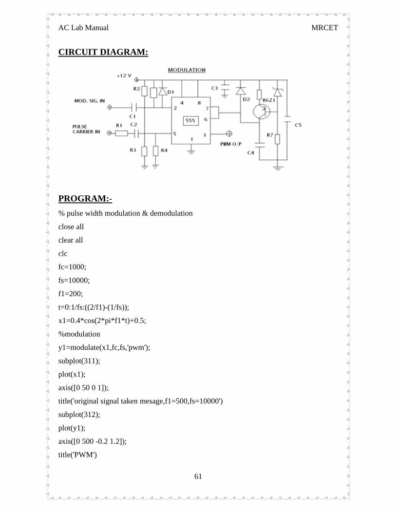
The PWM circuit uses the 555 IC(U1) in monostable mode. The Modulating
signal input is applied to pin no.5 of 555IC, and there Pulse input is applied to pin no.2.
The output of PWM is taken at the pin no.3 of 555IC i.e., TP3.
Demodulation:-
The demodulation section comprises of a fourth order low pass filter and an AC
amplifier. The TL074(U5) is used as a low pass filter and an AC amplifier. The output of
the modulator is given as the input to the low pass filter.
The low pass filter output is obviously less and it is feed to the AC amplifier
which comprises of a single op amp and whose output is amplified.
AC Lab Manual MRCET
61
CIRCUIT DIAGRAM:
PROGRAM:-
% pulse width modulation & demodulation
close all
clear all
clc
fc=1000;
fs=10000;
f1=200;
t=0:1/fs:((2/f1)-(1/fs));
x1=0.4*cos(2*pi*f1*t)+0.5;
%modulation
y1=modulate(x1,fc,fs,'pwm');
subplot(311);
plot(x1);
axis([0 50 0 1]);
title('original signal taken mesage,f1=500,fs=10000')
subplot(312);
plot(y1);
axis([0 500 -0.2 1.2]);
title('PWM')
AC Lab Manual MRCET
62
%demodulation
x1_recov=demod(y1,fc,fs,'pwm');
subplot(313);
plot(x1_recov);
title('time domain recovered, single tone,f1=200')
axis([0 50 0 1]);
PROCEDURE:
Modulation:-
1. Connect the circuit as shown in the diagram 1.
a. The output of the modulating signal generator is connected to the
modulating signal input TP2 keeping the frequency switch in 1KHz
position, and amplitude knob to max position
b. 16KHz pulse output (by varying the frequency pot (put it min position) in
pulse generator block) from pulse generator to pulse input(TP1).
2. Switch ON the power supply.
3. Observe the output of pulse width modulation block at TP3.(By varying the
amplitude pot).
4. Vary the modulating signal generator frequency by switching the frequency
selector switch to 2 KHz.
5. Now, again observe the PWM output at TP3.(By varying the amplitude pot).
6. Repeat the above steps (3 to 5) for the pulse frequency of 32KHz(by varying the
frequency pot(put it in max position) in pulse generator block).
7. Switch OFF the power supply.
Demodulation:-
8. Connect the circuit as shown in diagram 2.
a. The output of the modulating signal generator is connected to the modulating
signal input TP2 keeping the frequency switch in 1KHz position, and amplitude knob
to max position.
b. 16KHz pulse output (put frequency pot minimum) from pulse generator block
to pulse input TP1.
c. PWM output to LPF input.
AC Lab Manual MRCET
63
d. LPF output to AC amplifier input.
9. Switch ON the power supply.
10. Observe the output of low pass filter and AC amplifier respectively at TP6 &
TP8. The output will be the true replica of the input.
11. Now vary the position of the switch in modulating signal generator to 2 KHz and
observe the outputs at TP6 & TP8.
12. Repeat the steps 10& 11 for pulse frequency 32 KHz (By varying the frequency
pot (put in max). in pulse generator block). Observe the output waveforms.
13. Switch OFF the power supply.
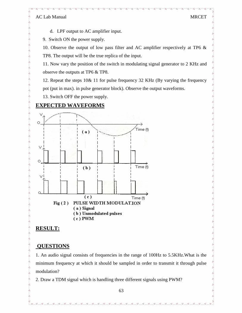
EXPECTED WAVEFORMS
RESULT:
QUESTIONS
1. An audio signal consists of frequencies in the range of 100Hz to 5.5KHz.What is the
minimum frequency at which it should be sampled in order to transmit it through pulse
modulation?
2. Draw a TDM signal which is handling three different signals using PWM?
AC Lab Manual MRCET
64
3. What do you infer from the frequency spectrum of a PWM signal?
4. Clock frequency in a PWM system is 2.5 kHz and modulating signal frequency is
500Hzhowmany pulses per cycle of signal occur in PWM output? Draw the PWM
signal?
5. Why should the curve for pulse width Vs modulating voltage be linear?
6. What is the other name for PWM?
7. What is the disadvantage of PWM?
8. Will PWM work if the synchronization between Tx and Rx fails?
9. Why integrator is required in demodulation of PWM?
10. What kind of conversion is done in PWM generation?
AC Lab Manual MRCET
65
EXPERIMENT NO-12 DATE:
PULSE POSITION MODULATION AND DEMODULATION
AIM:
1. To study the generation Pulse Position Modulation (PPM) and Demodulation.
2. To study the effect of Amplitude and the frequency of modulating signal on its
output and observe the wave forms.
APPARATUS:
1. Pulse Position Modulation (PPM) and demodulation Trainer.
2. C.R.O(30MHz)
3. Patch chords.
THEORY:-
Pulse Modulation is used to transmit analog information in this system continuous
wave forms are sampled at regular intervals. Information regarding the signal is
transmitted only at the sampling times together with synchronizing signals.
At the receiving end, the original waveforms may be reconstituted from the
information regarding the samples. Pulse modulation may be subdivided in to two types
analog and digital. In analog the indication of sample amplitude is the nearest variable. In
digital the information is a code.
The pulse position modulation is one of the methods of the pulse time
modulation.PPM is generated by changing the position of a fixed time slot.
The amplitude& width of the pulses is kept constant, while the position of each
pulse, in relation to the position of the recurrent reference pulse is valid by each instances
sampled value of the modulating wave. Pulse position modulation into the category of
analog communication. Pulse-Position modulation has the advantage of requiring
constant transmitter power output, but the disadvantage of depending on transmitter
receiver synchronization.
Pulse-position modulation may be obtained very simply from PWM. However, in
PWM the locations of the leading edges are fixed, whereas those of the trailing edges are
not. Their position depends on pulse width, which is determined by the signal amplitude
at that instant. Thus, it may be said that the trailing edges of PWM pulses are, in fact,
AC Lab Manual MRCET
66
position-modulated. This has positive-going narrow pulses corresponding to leading
edges and negative-going pulses corresponding to trailing edges. If the position
corresponding to the trailing edge of an un modulated pulse is counted as zero
displacement, then the other trailing edges will arrive earlier or later. They will therefore
have a time displacement other than zero; this time displacement is proportional to the
instantaneous value of the signal voltage. The differentiated pulses corresponding to the
leading edges are removed with a diode clipper or rectifier, and the remaining pulses, is
position-modulated.
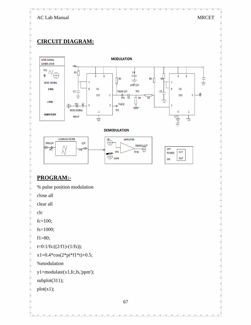
Circuit Description:-
Modulating Signal Generator:-
A 4.096 MHz clock is used to derive the modulating signal, which is generated by
an oscillator circuit comparing a 4.096MHz crystal and three 74HC04(U9) inverter gates.
This 4.096 MHz clock is then divided down in frequency by a factor of 4096, by binary
counter 74HC4040(U4), to produce 50% duty cycle, 1 KHz square wave on pin no.1 of
U4, and 2 KHz square wave on pin no.15. The frequency is selectable by means of SW1.
This goes to input of fourth order low pass filter U3 (TL072) is used to produce sine
wave from the square wave. The amplitude of this sine wave can be varied.
Modulation:-
The circuit uses the IC 555(U1) a Mono stable Multivibrator to perform the pulse
position Modulation action.
The Modulating signal is given to Pin No. 5 at Pin No.2 the pulse is 32 KHz
which is connected internally.
The PWM is available at TP2; this PWM output is differentiated by using
differentiated circuit. This differentiated output is available at TP8. This differentiated
output is fed to the 555 IC (U2) (Mono stable Mode) Pin No.2. The PPM output is
available at TP3.
AC Lab Manual MRCET
67
CIRCUIT DIAGRAM:
PROGRAM:-
% pulse position modulation
close all
clear all
clc
fc=100;
fs=1000;
f1=80;
t=0:1/fs:((2/f1)-(1/fs));
x1=0.4*cos(2*pi*f1*t)+0.5;
%modulation
y1=modulate(x1,fc,fs,'ppm');
subplot(311);
plot(x1);
AC Lab Manual MRCET
68
axis([0 15 0 1]);
title('original signal taken mesage,f1=80,fs=1000')
subplot(312);
plot(y1);
axis([0 250 -0.2 1.2]);
title('PPM')
%demodulation
x1_recov=demod(y1,fc,fs,'ppm');
subplot(313);
plot(x1_recov);
title('time domain recovered, single tone,f1=80')
axis([0 15 0 1]);
PROCEDURE:
Modulation:
1. Connect the circuit as shown in diagram 1.
a. Connect the modulating signal generator output to modulating signal input
(TP1) in PPM block.
b. Keep the switch in 1 KHz position and amplitude pot in max position.
2. Switch ON the power supply
3. Observe the PWM output at TP2, and the differentiated output signal at TP8.
4. Now, monitor the PPM output at TP3.
5. Try varying the amplitude and frequency of sine wave by varying amplitude pot.
6. Repeat Step 5 for frequency of 2 KHz and observe the PPM output.
7. Switch OFF the power supply.
Demodulation:-
8. Connect the circuit as shown in diagram2.
a. Connect the modulating signal generator output to modulating signal input
(TP1) in PPM block.
b. Keep the switch in 1 KHz position and amplitude pot in max position.
c. Connect the PPM output (TP3) to input of LPF(TP4).
9. Switch ON the power supply
AC Lab Manual MRCET
69
10. Observe the demodulated signal at the output of LPF at TP5.
11. Thus the recovered signal is true replica of the input signal
12. a. As the output of LPF has less amplitude, connect the output of LPF to the input
of an AC amplifier (TP5 to TP6).
b. Observe the demodulated out put on the oscilloscope at TP7 and also
observe the amplitude of demodulated signal by varying gain pot. This is amplitude
demodulated output.
13. Repeat the steps (7 to 9) for the modulating signal for frequency 2 KHz.
14. Switch OFF the power supply.
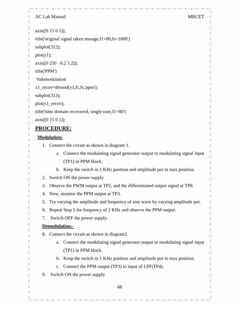
EXPECTED WAVEFORMS:
RESULT:
QUESTIONS:
1. What is the advantage of PPM over PWM?
2. Is the synchronization is must between Tx and Rx
AC Lab Manual MRCET
70
3. Shift in the position of each pulse of PPM depends on what?
4. Can we generate PWM from PPM?
5. Why do we need 555 timers?
6. Does PPM contain derivative of modulating signal compared to PWM?
7. For above scheme, do we have to use LPF and integrator in that order?
8. If we convert PPM to PWM & then detect the message signal, will the o/p has less
distortion?
9. Is synchronization critical in PPM?
10. How robust is the PPM to noise?
AC Lab Manual MRCET
71
EXPERIMENT.NO-13 DATE:
FREQUENCY SYNTHESIZER
AIM: To study the operation of frequency synthesizer using PLL
APPARATUS :
1. Frequency synthesizer trainer
2. Dual trace C.R.O (20 MHZ)
3. Digital frequency counter or multimeter
4. Patch chords
THEORY:
PLL stands for „Phase locked loop‟ and it is basically a closed loop frequency
control system, whose functioning is based on phase sensitive detection of phase
difference between the input and output signals of controller oscillator.
Before the input is applied the PLL is in free running state. Once the input
frequency is applied the VCO frequency starts change and phase locked loop is said to be
in captured mode. The VCO frequency continues to change until it equals the input
frequency and PLL is then in the phase locked state. When phase locked the loop tracks
any change in the input frequency through its repetitive action.
Frequency Synthesizer:
The frequency divider is inserted between the VCO and the phase comparator.
Since the output of the divider is locked to the input frequency fin, VCO is running at
multiple of the input frequency. The desired amount of multiplication can be obtained by
selecting a proper divide by N network. Where N is an integer. For example fout = 5 fin a
divide by N=10, 2 network is needed as shown in block diagram. This function
performed by a 4 bit binary counter 7490 configured as a divide by 10, 2 circuit. In this
circuit transistor Q1 used as a driver stage to increase the driving capacity of LM565 as
shown in fig.b.
To verify the operation of the circuit, we must determine the input frequency
range and then adjust the free running frequency Fout of VCO by means of R1 (between
10th
and 8th
pin) and CI (9th
pin), so that the output frequency of the 7490 driver is
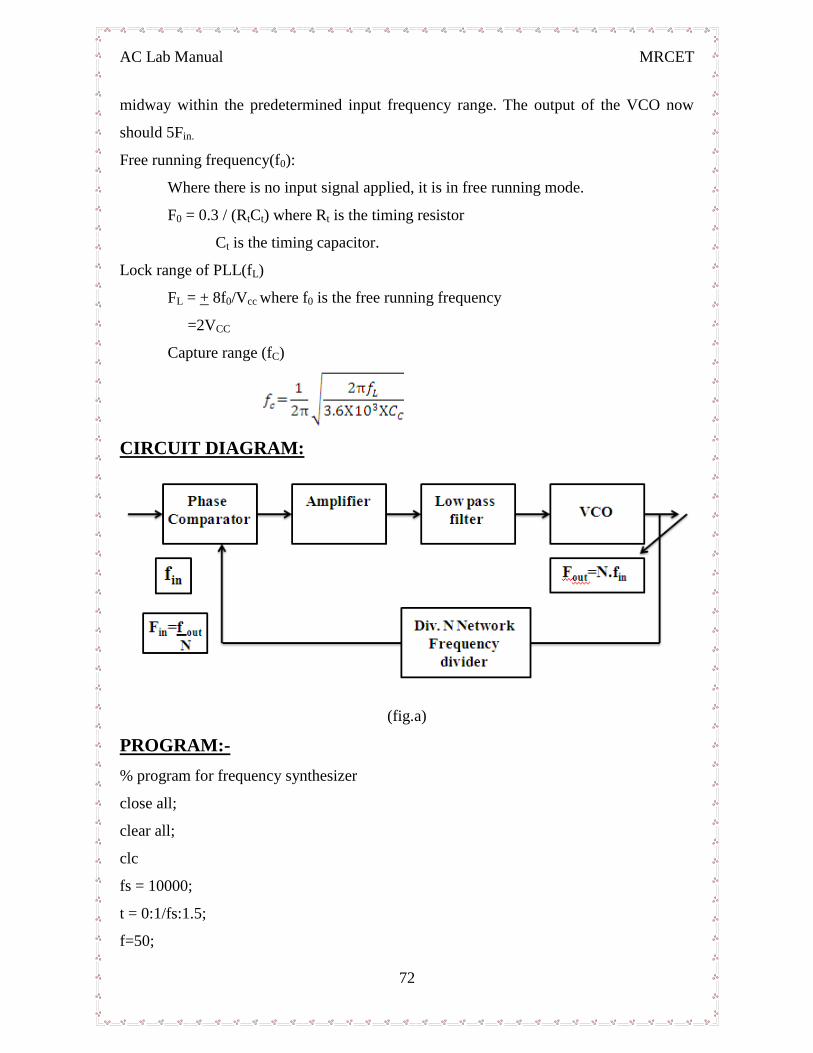
AC Lab Manual MRCET
72
midway within the predetermined input frequency range. The output of the VCO now
should 5Fin.
Free running frequency(f0):
Where there is no input signal applied, it is in free running mode.
F0 = 0.3 / (RtCt) where Rt is the timing resistor
Ct is the timing capacitor.
Lock range of PLL(fL)
FL = + 8f0/Vcc where f0 is the free running frequency
=2VCC
Capture range (fC)
CIRCUIT DIAGRAM:
(fig.a)
PROGRAM:-
% program for frequency synthesizer
close all;
clear all;
clc
fs = 10000;
t = 0:1/fs:1.5;
f=50;
AC Lab Manual MRCET
73
x1 = square(2*pi*f*t);
subplot(3,1,1)
plot(t,x1); axis([0 0.2 -1.2 1.2])
xlabel('Time (sec)');ylabel('Amplitude');
title('Square wave input with freq=50HZ');
t = 0:1/fs:1.5;
x2 = square(2*pi*2*f*t);
subplot(3,1,2)
plot(t,x2); axis([0 0.2 -1.2 1.2])
xlabel('Time (sec)');ylabel('Amplitude');
title('frequency multiplication by a factor of 2');
x3 = square(2*pi*f/2*t);
subplot(3,1,3)
plot(t,x3); axis([0 0.2 -1.2 1.2])
xlabel('Time (sec)');ylabel('Amplitude');
title('frequency division by a factor of 2');
PROCEDURE:
1. Switch on the trainer and verify the output of the regulated power supply i.e. +
5V. These supplies are internally connected to the circuit so no extra connections
are required.
2. Observe output of the square wave generator using oscilloscope and measure the
range with the help of frequency counter, frequency range should be around 1
KHz to 10 KHz.
3. Calculate the free running frequency range of the circuit (VCO output between 4th
pin and ground). For different values of timing resistor R1 (to measure Rt switch
off the trainer and measure Rt value using digital multimeter between given test
points) . and record the frequency values in tabular 1. Fout = 0.3 /(RtCt) where Rt is
the timing resistor and Ct is the timing capacitor =0.01 µf.
4. Connect 4th
pin of LM 565 (Fout) to the driver stage and 5th
pin (Phase
comparator) connected to 11th
pin of 7490. Output can be taken at the 11th
pin of
the 7490. It should be divided by the 10, 2 times of the fout.
AC Lab Manual MRCET
74
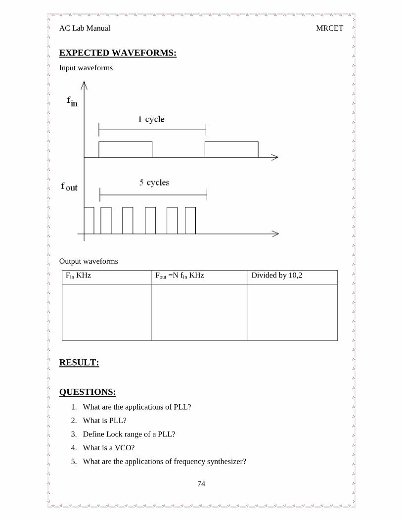
EXPECTED WAVEFORMS:
Input waveforms
Output waveforms
Fin KHz Fout =N fin KHz Divided by 10,2
RESULT:
QUESTIONS:
1. What are the applications of PLL?
2. What is PLL?
3. Define Lock range of a PLL?
4. What is a VCO?
5. What are the applications of frequency synthesizer?
AC Lab Manual MRCET
75
6. What is meant by the free running frequency of PLL?
7. What is the operation of a frequency synthesizer?
8. Which block is mainly used in frequency synthesizer?
AC Lab Manual MRCET
76
EXPERIMENT NO-14 DATE:
AGC CHARADTERISTICS
AIM: To study the operation of AGC in communication system.
APPARATUS:
1. Trainer Kit
2. Dual trace oscilloscope
3. Digital multi meter.
THEORY:
A Simple AGC is a system by means of which the overall gain of a radio
receiver is varied automatically with the changing strength of the received signal, to
keep the output substantially constant. A dc bias voltage, derived from the detector. The
devices used in those stages are ones who‟s trans-conductance and hence gain depends
on the applied bias voltage or current. It may be noted in passing that, for correct AGC
operation, this relationship between applied bias and trans-conductance need not to be
strictly linear, as long as trans-conductance drops significantly with increased bias. All
modern receivers are furnished with AGC, which enables tuning to stations of varying
signal strengths without appreciable change in the size of the output signal thus AGC
“irons out” input signal amplitude variations, and the gain control dose not have to be
re adjusted every time the receiver is tuned from one station to another, except when
the change in signal strengths is enormous. In addition, AGC helps to smooth out the
rapid fading which may occur with long-distance short-wave reception and prevents the
overloading of last IF amplifier which might otherwise have occurred.
CIRCUIT DESCRIPTION:
RF Generator:
Colpitts oscillator using FET is used here to generate RF signal of 455 KHz
frequency to use as carrier signal in this experiment. Adjustments for amplitude and
frequency are provided on panel for easy operation
AF generator:
Low frequency signal of approximately 1 KHz is generated using op-amp based
wine bridge oscillator; required application and adjustable attenuation are provided
AC Lab Manual MRCET
77
Regulated power supply:
This consist of bridge rectifiers, capacitor filters and thee terminal regulators to
provide required dc voltages in the circuit i.e. +12v, -12v, +6v @150mA each
AM MODULATOR:
Modulator section illustrates the circuit of modulating amplifier employing
transistor (BC 107) as an active device in common emitter amplifier mode. R1 and R2
establish quiescent forward bias for the transistor. The modulating signal is fed at the
emitter section causes the bias to increase or decrease in accordance with the modulating
signal. R4 is emitter resistance and C3 is by pass capacitor for carrier. Thus the carrier
signal applied at the base gets amplified more when the amplitude of the modulating
signal is at its maximum and less when the signal by the modulating signal output is
amplitude- modulated signal. C2 couples the modulated signal to output of the modulator.
Detector and AGC Stage:
This circuit incorporates two-stage amplifier, diode detector and AGC circuit.
1st IF amplifier
Q2 (BF 495c) acts as 1st if amplifier. The base of Q2 is connected through R5
(68k0 to the detector output .R6 (100E) and C4 (47n) is decoupling filter for +B line. The
base potential depends on R4 (220k) base biasing resistor and detector current supplied
by R5. The detector current is proportional to the signal strength received. This is called
A.G.C C6 (4.7/16) is used as base bias and AGC decoupling capacitor C18 (2n7). This is
given to the base of Q3 (BF 495D).
2nd
IF AMPLIFIER
Q3 (BF 195C) acts as 2nd
IF amplifier. The base bias for Q3 is provided by R7
(180k), C7 (47) is used to keep the end 4of L8 (IFT2) at ground potential for if signal.
The collector of Q3 is connected to the L9 (IFT3). L9 contains 200pf capacitor inside
across the primary. The output of Q3 is available across the secondary of L9, the primary
of which tuned by the internal 200pf capacitor. R8 (220e), C8 (47n) consists the
decoupling circuit for the collector supply of Q3. The output of Q3 is coupled to detector
diode D1 (OA 79).
AC Lab Manual MRCET
78
Detector
Modulated IF signal from the secondary of L9 (IFT3) is fed to the detector diode
D1D1 rectifies the modulated if signal &if component of modulated signal is filtered by
c8 (22n),r9(680e0&c14(22n).r9 is the detector load resistor. The detected signal (AF
signal) is given to the volume control P2 (10k Log) tough maximum audio output-
limiting resister r21 (10k). It is also given to AGC circuit made of R5 (68k) and C6
(a.7/16).
AGC:
The Sound received from the LS will depend on the strength of the signals
received at the antenna. The strength of the received signals can vary widely due to
fading. This will cause variations in sound which can be annoying. Moreover, the
Strength of signals can also be too large in close vicinity of MW transmitters causing
overloading of 2nd
IF amplifier.
Automatic gain control (AGC) is used to minimize the variations in sound with
changes in Signals strength & to prevent overloading. The operation of AGC depends
on the fact that The gain obtained from any transistor depends on its collector current &
becomes less When the collector current is reduced to cut off (or increased to saturation
For AGC, DC voltage obtained from the detection of IF signals is applied to the 1st
amplifier transistor base in such a way that an increase in this voltages reduces the gain
of the transistor. The result is that when the strength of the incoming signal increases,
the DC voltage also increases and this tends to reduce the gain of the amplifier thus not
permitting the output to change much. Here R5 (68k) C6 (4.7/16) performs this
function. C6 (4.7/16) is the AGC decoupling capacitor to by pass any AF signals and
keep the bias steady.
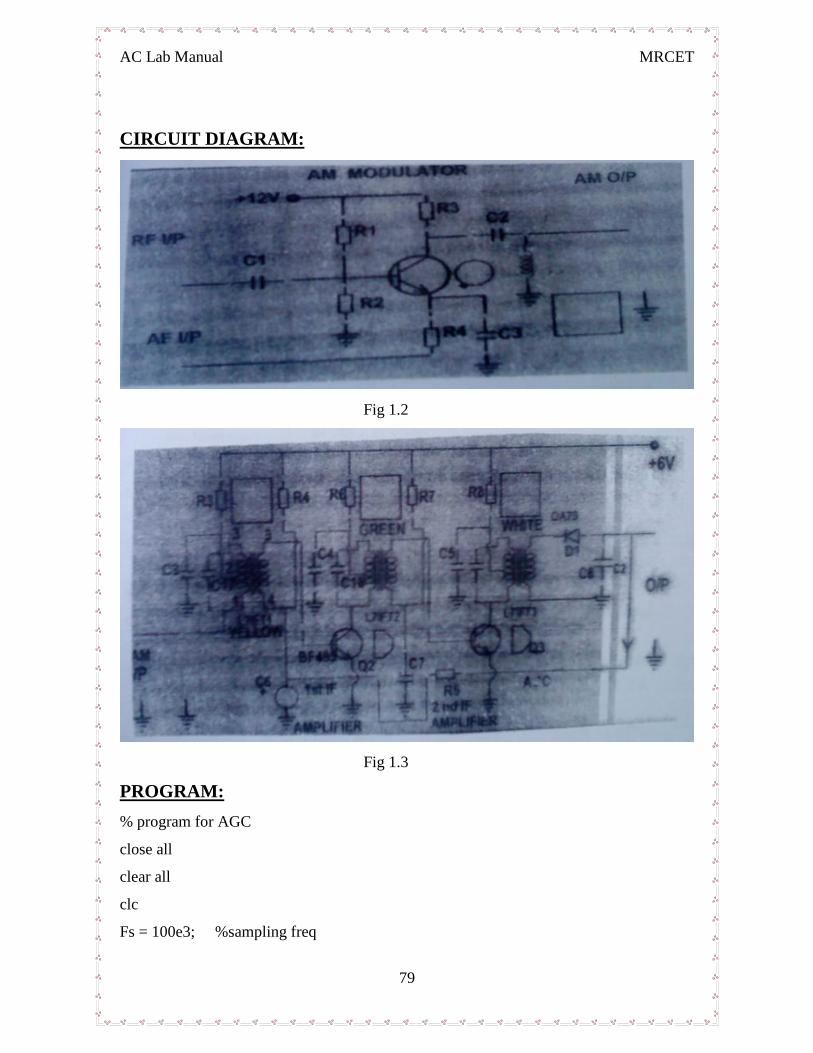
AC Lab Manual MRCET
79
CIRCUIT DIAGRAM:
Fig 1.2
Fig 1.3
PROGRAM:
% program for AGC
close all
clear all
clc
Fs = 100e3; %sampling freq
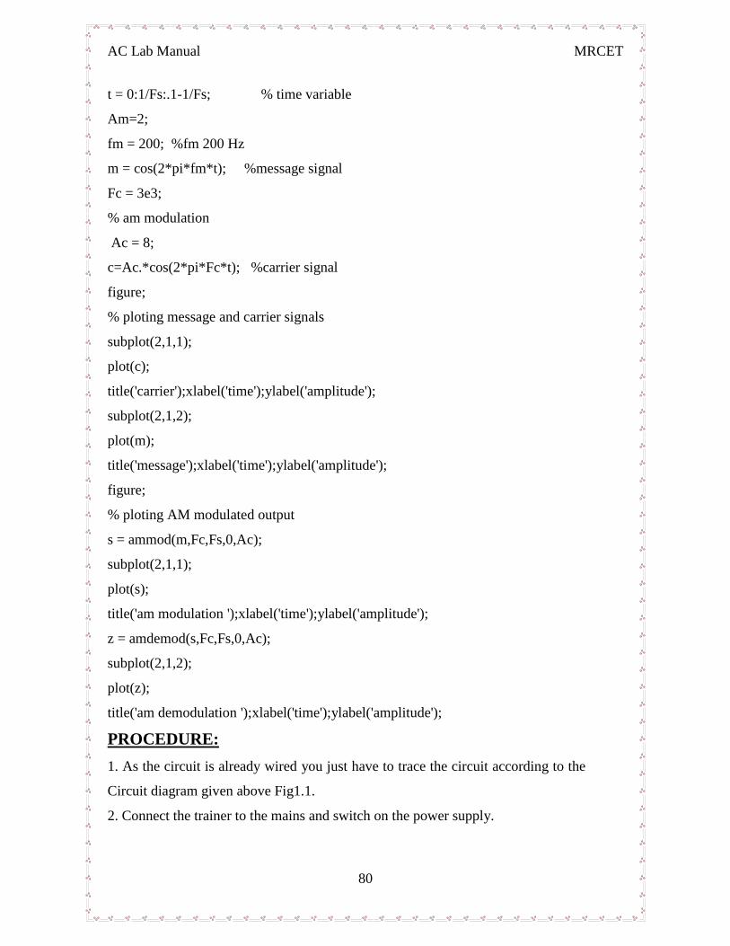
AC Lab Manual MRCET
80
t = 0:1/Fs:.1-1/Fs; % time variable
Am=2;
fm = 200; %fm 200 Hz
m = cos(2*pi*fm*t); %message signal
Fc = 3e3;
% am modulation
Ac = 8;
c=Ac.*cos(2*pi*Fc*t); %carrier signal
figure;
% ploting message and carrier signals
subplot(2,1,1);
plot(c);
title('carrier');xlabel('time');ylabel('amplitude');
subplot(2,1,2);
plot(m);
title('message');xlabel('time');ylabel('amplitude');
figure;
% ploting AM modulated output
s = ammod(m,Fc,Fs,0,Ac);
subplot(2,1,1);
plot(s);
title('am modulation ');xlabel('time');ylabel('amplitude');
z = amdemod(s,Fc,Fs,0,Ac);
subplot(2,1,2);
plot(z);
title('am demodulation ');xlabel('time');ylabel('amplitude');
PROCEDURE:
1. As the circuit is already wired you just have to trace the circuit according to the
Circuit diagram given above Fig1.1.
2. Connect the trainer to the mains and switch on the power supply.
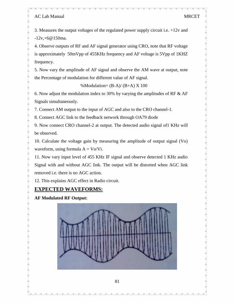
AC Lab Manual MRCET
81
3. Measures the output voltages of the regulated power supply circuit i.e. +12v and
-12v,+6@150ma.
4. Observe outputs of RF and AF signal generator using CRO, note that RF voltage
is approximately 50mVpp of 455KHz frequency and AF voltage is 5Vpp of 1KHZ
frequency.
5. Now vary the amplitude of AF signal and observe the AM wave at output, note
the Percentage of modulation for different value of AF signal.
%Modulation= (B-A)/ (B+A) X 100
6. Now adjust the modulation index to 30% by varying the amplitudes of RF & AF
Signals simultaneously.
7. Connect AM output to the input of AGC and also to the CRO channel-1.
8. Connect AGC link to the feedback network through OA79 diode
9. Now connect CRO channel-2 at output. The detected audio signal of1 KHz will
be observed.
10. Calculate the voltage gain by measuring the amplitude of output signal (Vo)
waveform, using formula A = Vo/Vi.
11. Now vary input level of 455 KHz IF signal and observe detected 1 KHz audio
Signal with and without AGC link. The output will be distorted when AGC link
removed i.e. there is no AGC action.
12. This explains AGC effect in Radio circuit.
EXPECTED WAVEFORMS:
AF Modulated RF Output:
AC Lab Manual MRCET
82
Detected output with AGC:
RESULT:
AC Lab Manual MRCET
83
EXPERIMENT.NO-15 DATE:
CHARACTERISTICS OF FREQUENCY MIXER
AIM: To study the functioning and characteristics of mixer and filter.
APPARATUS:
1. Frequency mixer trainer kit.
2. C.R.O (20MHz)
3. Connecting cords and probes.
4. Function generator (1MHz).
THEORY:
To construct frequency mixer. Connect two different inputs signal at Base (IF
frequency) and emitter (Local Oscillator) and the collector output is given to low pass
filter to get the beat frequency and observe the wave forms.
A frequency mixer is used in very radio and television receiver; it is also used in
many other electronic systems. When a sine wave drives a nonlinear circuit, we get
harmonics of each sine wave plus new frequencies called the sum and difference
frequencies.
USUAL SIZE OF INPUT SIGNALS
In most applications, one of the input signals to the mixer will be large. This is
necessary to ensure nonlinear operation, unless one of the signals is large, we cannot get
inter-modulation components. This large input signal is often supplied by an oscillator or
signal generator. The other input signal is usually small. By itself, this signal produces
only small-signal operation of the mixer. Often one of the reasons this signal is small is
because it is a weak signal coming from an antenna.
The normal inputs to a mixer, therefore, are:
1. A large signal adequate to produce medium – or large-signal operation of the
mixer.
2. A small signal that by itself can produce only small-signal operation.
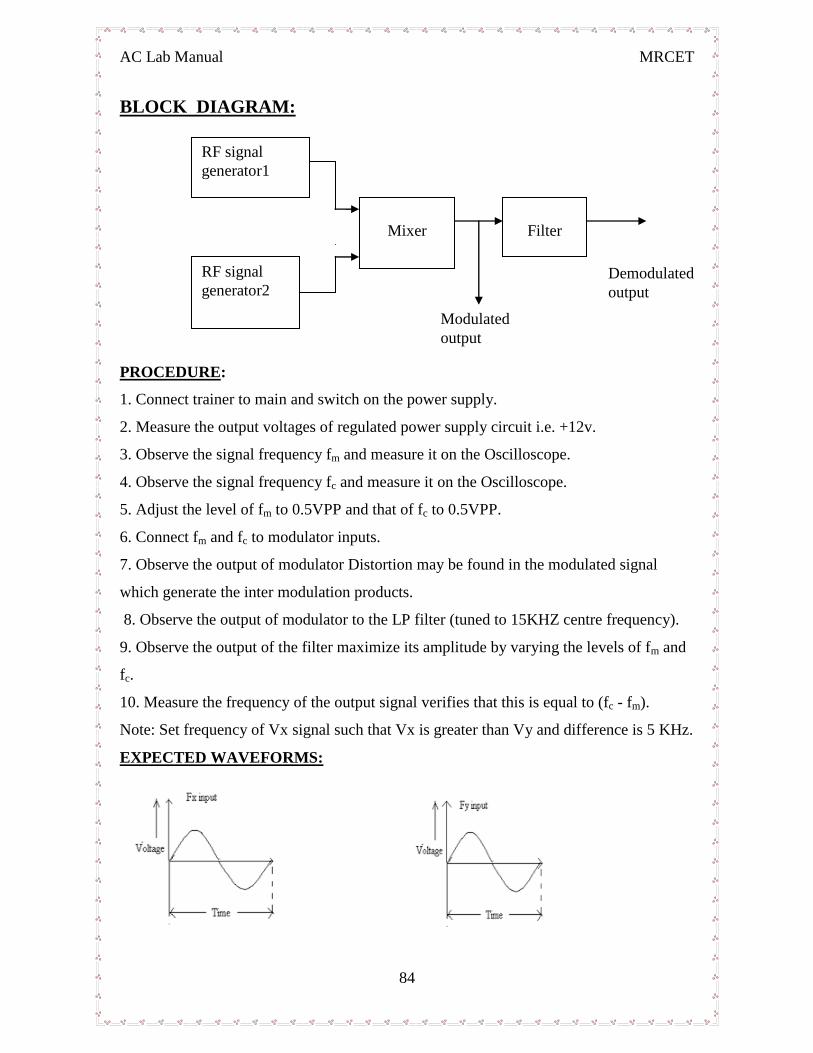
AC Lab Manual MRCET
84
BLOCK DIAGRAM:
PROCEDURE:
1. Connect trainer to main and switch on the power supply.
2. Measure the output voltages of regulated power supply circuit i.e. +12v.
3. Observe the signal frequency fm and measure it on the Oscilloscope.
4. Observe the signal frequency fc and measure it on the Oscilloscope.
5. Adjust the level of fm to 0.5VPP and that of fc to 0.5VPP.
6. Connect fm and fc to modulator inputs.
7. Observe the output of modulator Distortion may be found in the modulated signal
which generate the inter modulation products.
8. Observe the output of modulator to the LP filter (tuned to 15KHZ centre frequency).
9. Observe the output of the filter maximize its amplitude by varying the levels of fm and
fc.
10. Measure the frequency of the output signal verifies that this is equal to (fc - fm).
Note: Set frequency of Vx signal such that Vx is greater than Vy and difference is 5 KHz.
EXPECTED WAVEFORMS:
RF signal
generator2
Mixer
Filter
RF signal
generator1
Modulated
output
Demodulated
output
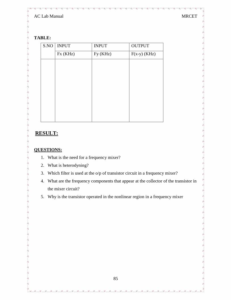
AC Lab Manual MRCET
85
TABLE:
S.NO INPUT INPUT OUTPUT
Fx (KHz) Fy (KHz) F(x-y) (KHz)
RESULT:
QUESTIONS:
1. What is the need for a frequency mixer?
2. What is heterodyning?
3. Which filter is used at the o/p of transistor circuit in a frequency mixer?
4. What are the frequency components that appear at the collector of the transistor in
the mixer circuit?
5. Why is the transistor operated in the nonlinear region in a frequency mixer
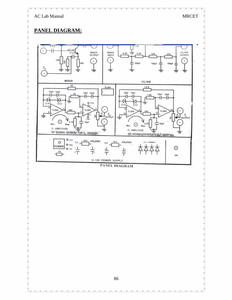
AC Lab Manual MRCET
86
PANEL DIAGRAM: