active plasmonics in wdm traffic switching applications
TRANSCRIPT

Active plasmonics in WDM trafficswitching applicationsSotirios Papaioannou1,2, Dimitrios Kalavrouziotis3, Konstantinos Vyrsokinos2, Jean-Claude Weeber4,Karim Hassan4, Laurent Markey4, Alain Dereux4, Ashwani Kumar5, Sergey I. Bozhevolnyi5, Matthias Baus6,Tolga Tekin7, Dimitrios Apostolopoulos3, Hercules Avramopoulos3 & Nikos Pleros1,2
1Department of Informatics, Aristotle University of Thessaloniki, 54124 Thessaloniki, Greece, 2Informatics and Telematics Institute,Center for Research and Technology Hellas, 57001 Thessaloniki, Greece, 3School of Electrical and Computer Engineering,National Technical University of Athens, 15780 Zografou, Athens, Greece, 4Institut Carnot de Bourgogne, University of Burgundy, F-21078 Dijon Cedex, France, 5Faculty of Engineering, Institute of Technology and Innovation, University of Southern Denmark, DK-5230 Odense M, Denmark, 6AMO GmbH, 52074 Aachen, Germany, 7Fraunhofer IZM, D-13355 Berlin, Germany.
With metal stripes being intrinsic components of plasmonic waveguides, plasmonics provides a ‘‘naturally’’energy-efficient platform for merging broadband optical links with intelligent electronic processing,instigating a great promise for low-power and small-footprint active functional circuitry. The first activeDielectric-Loaded Surface Plasmon Polariton (DLSPP) thermo-optic (TO) switches with successfulperformance in single-channel 10 Gb/s data traffic environments have led the inroad towards bringinglow-power active plasmonics in practical traffic applications. In this article, we introduce active plasmonicsinto Wavelength Division Multiplexed (WDM) switching applications, using the smallest TO DLSPP-basedMach-Zehnder interferometric switch reported so far and showing its successful performance in 4310 Gb/slow-power and fast switching operation. The demonstration of the WDM-enabling characteristics of activeplasmonic circuits with an ultra-low power 3 response time product represents a crucial milestone in thedevelopment of active plasmonics towards real telecom and datacom applications, where low-energy andfast TO operation with small-size circuitry is targeted.
The need for higher throughput connectivity with minimal power consumption and size requirements innext-generation High Performance Computing Systems and Data Centers has brought integrated photonicsinto the spot-light, targeting their penetration into board-level and chip-scale interconnects1. In this
development, the emerging discipline of plasmonics2,3 has started to gain ground as the ‘‘beyond photonics’’chip-scale platform that can enter the interconnect area4–6. Plasmonics relies on the propagation of SurfacePlasmon Polariton (SPP) modes along metallic stripes yielding in this way strong mode confinements even atsub-wavelength scale7, while the underlying metallic circuitry offers a seamless energy-efficient approach tointeroperability between light beams and electrical control signals.
The low-energy functional perspective of plasmonics is especially highlighted in the case of Dielectric-LoadedSPP (DLSPP) waveguides that employ a dielectric (e.g. polymer) ridge on top of a metallic stripe. This offers anadditional factor for actively controlling electromagnetic wave propagation through the TO5,8–13 or electro-opticcharacteristics14,15 of the dielectric loading. Since the DLSPP mode field reaches its maximum at the metal-dielectric interface, the metallic layer not only supports the plasmonic mode but simultaneously can serve asan energy-efficient heating electrode when electric current is applied to it, exploiting the TO effect. At the sametime, fast TO responses are feasible due to the direct contact of the polymer with the underlying metallic film thatleads to significantly decreased heat capacity between the waveguide and the electrode, yielding immediatechange of the effective index of the propagating SPP mode when the TO effect occurs. DLSPP waveguides are,to the best of our knowledge, the only plasmonic waveguides that have been already employed for activemanipulation of SPP signals in a number of functional circuitry implementations like TO modulation10,11, On/Off gating9, switching12,13 and power monitoring16, greatly benefiting also from their recent successful interfacingwith the low-loss silicon photonic waveguide transmission platform5,8,17,18. The progress made so far on activeDLSPP-based circuits suggests the TO effect as the most mature mechanism that can be exploited currentlytowards bringing low-energy active plasmonics in true data traffic environments: TO tuning of Polymethyl-methacrylate (PMMA)-loaded SPP -based racetrack resonators has been recently demonstrated by the authorsrequiring only 3.3 mW of power8, providing the first solid proof of the low power characteristics of the DLSPP
SUBJECT AREAS:NANOPHOTONICS
FIBRE OPTICS AND OPTICALCOMMUNICATIONS
OPTICAL MATERIALS ANDSTRUCTURES
ULTRAFAST PHOTONICS
Received14 March 2012
Accepted28 August 2012
Published12 September 2012
Correspondence andrequests for materials
should be addressed toS.P. ([email protected].
gr)
SCIENTIFIC REPORTS | 2 : 652 | DOI: 10.1038/srep00652 1

platform. In addition, we have recently presented an active PMMA-loaded SPP-based TO switch with 90 mm plasmonic phase armsoperating with single-channel 10 Gb/s optical data traffic9, success-fully evaluating for the first time the performance of active DLSPPs intrue data traffic environments.
However, the transition to practical active plasmonic circuits canonly be completed by proving their credentials in true WDM appli-cations in order to support the complete broadband portfolio ofoptics. The dimension of WDM appears currently as the mainstreamapproach in photonic Network-on-Chip (NoC) implementationstowards increasing the aggregate on-chip throughput; Silicon-on-Insulator (SOI)-based TO switching elements employed so far inNoC deployments19,20 have adapted their design to the WDM-enab-ling framework, aiming to deliver both low-power and fast reconfi-gurable dynamic link characteristics21. In addition, the case for usingTO plasmonics instead of the low-loss and more mature siliconphotonics platform is still lacking a solid evidence, since TO SOI-based photonic switch circuitry can offer power and switching timevalues that go down to mW and ms scales, respectively22–26. In thepresent communication, we report on the smallest TO PMMA-basedDLSPP switch relying on an Asymmetric Mach-Zehnder interfero-metric (A-MZI) configuration with only 60mm long active phasebranches and performing error-free with 4 data carrying channelsin dynamic conditions, with each channel being modulated with10 Gb/s data. The maximum power penalty was measured to be3.6 dB for a Bit Error Rate (BER) of 1029, with the power consump-tion being only 13.1 mW and the response time found to be 3.8 ms.The obtained power consumption and response time values renderthe DLSPP technology as a powerful TO switch platform in applica-tions where fast, low energy and low footprint TO switching circuitryis needed. They lead to a power 3 response time product that is lowercompared to undoped TO SOI-based22–26 or polymer-based27,28
switches reported so far, providing the first tangible advantage ofactive TO plasmonics over the well-established silicon nanophotonicwaveguide platform in WDM data traffic environments.
ResultsA-MZI layout and principle of operation. The DLSPP waveguideoperation relies on the SPP field confinement by a dielectric ridgeplaced on top of a metal stripe supporting the SPP propagation. TheDLSPP waveguide characteristics, i.e., the mode field confinement,effective index and propagation length, are thereby stronglyinfluenced by the width and height of the employed dielectricridge29. Considering PMMA ridges placed on gold stripes to beoperated at telecom wavelengths (,1.55 mm), the optimum ridgedimensions, ensuring tight mode confinement (,1 mm) and rela-tively long propagation (,50 mm) of DLSPP modes, were found tobe about 500 nm and 600 nm for the ridge width and height,respectively29. In this configuration, the DLSPP mode fills practi-cally the whole PMMA ridge, so that its heating by an underlyinggold stripe (via transmitting through it signal currents) modifiesvery efficiently the DLSPP mode effective index via changing the
PMMA refractive index10–12,30. In fact, theoretical estimations10 andcalculations30 have shown that these ridge dimensions promise TOmodulation and switching with record-low driving powers(,1 mW) and response times (,1 ms). Moreover, a temperatureincrease by ,61 K in PMMA requires an interaction length of,120 mm for p phase shift at telecom wavelengths that wouldinduce excessive propagation losses10. These losses can be greatlyreduced by considering only 60 mm interaction length, equivalentto typical propagation length of radiation in DLSPP waveguides,achieving in this way a phase shift of p/2. The remaining neededp/2 phase shift can be completed by making use of an A-MZIconfiguration, in which this phase shift is permanently introducedin one of the MZI arms by slightly widening the PMMA ridge over ashort distance. The width dispersion curves for the DLSPP modeeffective index29,30 indicate that an increase of the 600-nm-highPMMA ridge width from 500nm to 700 nm would result in anincrease of the DLSPP mode effective index by ,0.06, implyingthat the length of 6 mm of a widened ridge section should besufficient to introduce a p/2 phase shift.
Fig. 1(a) illustrates the employed A-MZI, comprising two DLSPPwaveguides as its active, electrically controlled branches that areincorporated between two silicon coupler stages. The upper plasmo-nic arm of the A-MZI has a length of L1560 mm and a PMMA ridgecross-section with W15500 nm width and 600 nm height. Thesedimensions ensure the existence of a single TM mode inside thepolymer at telecom wavelengths, as depicted in Fig. 1(b). The lowerplasmonic arm has again a total length of 60 mm and identicalPMMA ridge dimensions, employing however a L256 mm longDLSPP waveguide section that is widened from W1 to W25700nm. This widened DLSPP waveguide section introduces a defaultphase asymmetry of p/2 between the two MZI arms, taking advant-age of the higher effective refractive index value experienced by theDLSPP waveguide mode in the PMMA ridge. This larger width hasbeen carefully chosen in order to keep the lower branch mono-modeand avoid any interference between fundamental and higher ordermodes. The field map of this mode in the widened waveguide isshown in Fig. 1(c).
The switching operation in all-plasmonic MZIs has already beendescribed30–32 and relies on inducing a total phase shift of p betweentheir two arms. However, in our A-MZI, only a p/2 phase shift isrequired for switching operation due to the default asymmetry. Here,the phase shift is obtained by changing the temperature locally in oneor two MZI arms as a result of the injected electric current. ThisTO effect has already been predicted30 and observed10,12 on similardevices, and is now well understood. The effective index of the modethat propagates on one arm is modified by the heat compared to thesecond arm, inducing a phase difference at the output that ideally isp. By electrically controlling the upper A-MZI arm, a negative phaseshift is experienced by the propagating DLSPP waveguide mode as aresult of the negative thermo-optic coefficient (TOC) of the PMMAthat equals 21.0531024 K21. When the induced phase shift equalsp/2, the phase difference between the modes travelling through the
Figure 1 | Asymmetric Mach-Zehnder interferometer. (a) Schematic layout. The lower plasmonic branch is widened in order to introduce a default
asymmetry, (b) fundamental quasi-TM mode of the 5003600 nm2 PMMA-loaded SPP waveguide, (c) fundamental quasi-TM mode of the
7003600 nm2 PMMA-loaded SPP waveguide.
www.nature.com/scientificreports
SCIENTIFIC REPORTS | 2 : 652 | DOI: 10.1038/srep00652 2
two MZI branches equals p and therefore the whole mode power isexported to the BAR output of the device. On the contrary, when thesame current level applies only to the lower MZI plasmonic branch,the default MZI phase asymmetry is cancelled out due to the –p/2thermo-optically induced phase shift and, thus, the whole modepower emerges at the CROSS port of the MZI.
As such, complete On/Off switching operation can be obtained byelectrically driving only the upper plasmonic arm of the switch whenOn operation is targeted, while the electric current has to flow onlythrough the lower plasmonic arm during Off operation. However, itshould be noted that high-quality switching can be obtained even ifonly one of the two plasmonic MZI branches is thermo-opticallyaddressed. The initial p/2 phase asymmetry results in biasing ofthe MZI at its quadrature point shifting its operational state to thelinear regime of its output power transfer function when no electricaldriving signal is present. This asymmetry provides thereby the pos-sibility for high performance switching that requires only a (thermo-optically induced) p/2 instead of p phase shift, offering in this way asimple and passive mechanism for reducing the required energy leveland the active plasmonic arm length for a given maximum servicetemperature. The reduction in the PMMA-loaded plasmonic armlength is highly beneficial towards bringing down the device losses,since the limited maximum service temperature of the PMMA neces-sitates a DLSPP waveguide length of over 100 mm10 in case a full p-phase shift has to be thermo-optically induced, leading to total plas-monic branch propagation losses of close to 10 dB. In the case of the60 mm-long DLSPP-based A-MZI that we present, the total propaga-tion losses of the plasmonic part are reduced down to 6 dB, yielding atotal loss value including the Si-to-DLSPP and DLSPP-to-Si junc-tions of close to ,11 dB.
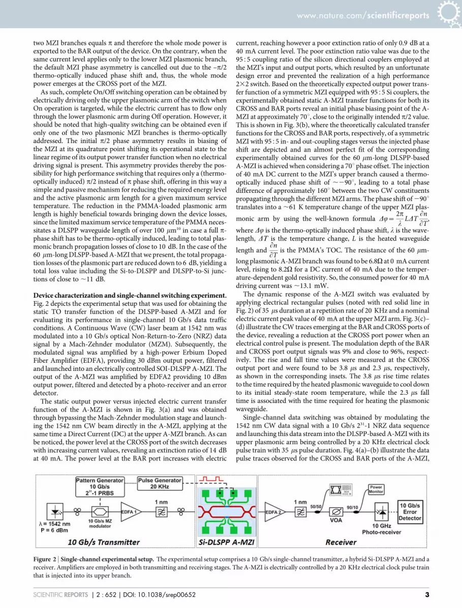
Device characterization and single-channel switching experiment.Fig. 2 depicts the experimental setup that was used for obtaining thestatic TO transfer function of the DLSPP-based A-MZI and forevaluating its performance in single-channel 10 Gb/s data trafficconditions. A Continuous Wave (CW) laser beam at 1542 nm wasmodulated into a 10 Gb/s optical Non-Return-to-Zero (NRZ) datasignal by a Mach-Zehnder modulator (MZM). Subsequently, themodulated signal was amplified by a high-power Erbium DopedFiber Amplifier (EDFA), providing 30 dBm output power, filteredand launched into an electrically controlled SOI-DLSPP A-MZI. Theoutput of the A-MZI was amplified by EDFA2 providing 10 dBmoutput power, filtered and detected by a photo-receiver and an errordetector.
The static output power versus injected electric current transferfunction of the A-MZI is shown in Fig. 3(a) and was obtainedthrough bypassing the Mach-Zehnder modulation stage and launch-ing the 1542 nm CW beam directly in the A-MZI, applying at thesame time a Direct Current (DC) at the upper A-MZI branch. As canbe noticed, the power level at the CROSS port of the switch decreaseswith increasing current values, revealing an extinction ratio of 14 dBat 40 mA. The power level at the BAR port increases with electric
current, reaching however a poor extinction ratio of only 0.9 dB at a40 mA current level. The poor extinction ratio value was due to the9555 coupling ratio of the silicon directional couplers employed atthe MZI’s input and output ports, which resulted by an unfortunatedesign error and prevented the realization of a high performance232 switch. Based on the theoretically expected output power trans-fer function of a symmetric MZI equipped with 9555 Si couplers, theexperimentally obtained static A-MZI transfer functions for both itsCROSS and BAR ports reveal an initial phase biasing point of the A-MZI at approximately 70u, close to the originally intended p/2 value.This is shown in Fig. 3(b), where the theoretically calculated transferfunctions for the CROSS and BAR ports, respectively, of a symmetricMZI with 9555 in- and out-coupling stages versus the injected phaseshift are depicted and an almost perfect fit of the correspondingexperimentally obtained curves for the 60 mm-long DLSPP-basedA-MZI is achieved when considering a 70u phase offset. The injectionof 40 mA DC current to the MZI’s upper branch caused a thermo-optically induced phase shift of ,290u, leading to a total phasedifference of approximately 160u between the two CW constituentspropagating through the different MZI arms. The phase shift of 290utranslates into a ,61 K temperature change of the upper MZI plas-
monic arm by using the well-known formula DQ~2pl
LDTLnLT
,
where DQ is the thermo-optically induced phase shift, l is the wave-length, DT is the temperature change, L is the heated waveguide
length andLnLT
is the PMMA’s TOC. The resistance of the 60 mm-
long plasmonic A-MZI branch was found to be 6.8V at 0 mA currentlevel, rising to 8.2V for a DC current of 40 mA due to the temper-ature-dependent gold resistivity. So, the consumed power for 40 mAdriving current was ,13.1 mW.
The dynamic response of the A-MZI switch was evaluated byapplying electrical rectangular pulses (noted with red solid line inFig. 2) of 35 ms duration at a repetition rate of 20 KHz and a nominalelectric current peak value of 40 mA at the upper MZI arm. Fig. 3(c)–(d) illustrate the CW traces emerging at the BAR and CROSS ports ofthe device, revealing a reduction at the CROSS port power when anelectrical control pulse is present. The modulation depth of the BARand CROSS port output signals was 9% and close to 96%, respect-ively. The rise and fall time values were measured at the CROSSoutput port and were found to be 3.8 ms and 2.3 ms, respectively,as shown in the corresponding insets. The 3.8 ms rise time relatesto the time required by the heated plasmonic waveguide to cool downto its initial steady-state room temperature, while the 2.3 ms falltime is associated with the time required for heating the plasmonicwaveguide.
Single-channel data switching was obtained by modulating the1542 nm CW data signal with a 10 Gb/s 231-1 NRZ data sequenceand launching this data stream into the DLSPP-based A-MZI with itsupper plasmonic arm being controlled by a 20 KHz electrical clockpulse train with 35 ms pulse duration. Fig. 4(a)–(b) illustrate the datapulse traces observed for the CROSS and BAR ports of the A-MZI,
Figure 2 | Single-channel experimental setup. The experimental setup comprises a 10 Gb/s single-channel transmitter, a hybrid Si-DLSPP A-MZI and a
receiver. Amplifiers are employed in both transmitting and receiving stages. The A-MZI is electrically controlled by a 20 KHz electrical clock pulse train
that is injected into its upper branch.
www.nature.com/scientificreports
SCIENTIFIC REPORTS | 2 : 652 | DOI: 10.1038/srep00652 3

respectively, with the red dashed line showing the correspondingelectrical control driving signal. The corresponding eye diagramsare depicted in Fig. 4(c)–(d) for the CROSS and BAR output signals,respectively. As can be noticed, inverted mode operation is obtainedat the CROSS port with an extinction ratio of close to 14 dB. TheBAR port exiting signal follows the electrical control pattern show-ing, however, a poor extinction ratio of only 0.9 dB. The noise level ofthe optical data pulses emerging at the CROSS port resulted to anamplitude modulation of close to 3 dB and was due to the EDFA2
output noise, since the optical power exiting the A-MZI at its CROSSport and entering the EDFA2 was below the amplifier’s input powerrequirements. Fig. 4(e) illustrates the BER measurement curvesobtained for the Back-to-Back (B2B) as well as for the ON andOFF states of the switch. The OFF state was determined by thecomplete absence of any electrical control signal, so that the datasignal emerges at the CROSS port, which was also used for monitor-ing the BER performance. During ON state, the A-MZI was driven bya constant DC current level of 40 mA, enforcing the optical data to
Figure 3 | CW injection. (a) Static TO transfer functions for the CROSS and BAR output ports of the A-MZI, (b) theoretically calculated transfer
function for the CROSS and BAR output ports of a symmetric MZI showing the region confirmed by the experimentally obtained transfer function of the
A-MZI, (c) BAR output TO modulation, (d) CROSS output TO modulation and rise/fall times (insets). Dashed red lines in (c) and (d) show the
corresponding electrical control signal.
Figure 4 | Data injection. Modulation with 35 ms electrical rectangular pulses at 20 KHz repetition rate for 10 Gb/s (a) data trace at the CROSS port,
(b) data trace at the BAR port, (c) eye diagram at the CROSS port, (d) eye diagram at the BAR port. (e) (231-1) BER curves for a single channel at B2B, ON
and OFF states.
www.nature.com/scientificreports
SCIENTIFIC REPORTS | 2 : 652 | DOI: 10.1038/srep00652 4

emerge at the BAR port, which was used in this case for BER mea-surement purposes. Error-free performance was obtained in bothcases, with the ON state BER curve revealing an almost 0 dB powerpenalty while a negligible and close to the statistical error powerpenalty of 0.15 dB was obtained during the OFF state operation withrespect to the B2B curve. The corresponding eye diagrams for B2Band for ON and OFF operational states are included as insets in thesame figure.
It should be mentioned that our A-MZI device did not allow forthe wire-bonding of both MZI arms, so that its performance couldnot be evaluated by applying electrical current to both MZI branchesalternatively. However, its operation with two complementary elec-trical control signals applied at the two MZI branches would notaffect its peak power requirements, since the maximum phase shiftneeded also in that case will be again p/2. The use of two controlsignals would only improve the extinction ratio performance, sincethis would allow for complete p-phase difference between the CWconstituents, without increasing the necessary amount of power.
WDM switching experiment. The experimental setup used for theWDM switching application is shown in Fig. 5(a). Four CW lasersources emitting light at 1545.1 nm, 1546.7 nm, 1547.7 nm and1549.1 nm were multiplexed in pairs and each channel pair wasmodulated to a 10 Gb/s 231-1 NRZ data signal by a correspondingTi:LiNbO3 MZM. The four data streams were multiplexed into a4310 Gb/s WDM signal that was then amplified by a high-powerEDFA providing 31 dBm power at the input of the electricallycontrolled DLSPP-based A-MZI. After exiting the A-MZI, theWDM data signal was amplified in a two stage EDFA with a 5 nmoptical bandpass filter (OBPF) residing between the two stages forout-of-band Amplified Spontaneous Emission (ASE) noise rejection.Individual channel isolation was performed after EDFA3 in a 0.8 nmOBPF and the signal quality was evaluated by means of a samplingoscilloscope and a photo-receiver followed by an error-detector.
Fig. 5(b) illustrates the 4-channel spectrum after being amplifiedby EDFA1 and prior entering the A-MZI. The unequal power profileof the WDM signal owes mainly to the respective non-flattened gainprofile of the high-power EDFA1 as well as to the energy transfer tothe four-wave mixing (FWM) terms that originate as a result of thehigh-power signal propagating in the fiber link between EDFA1 andthe A-MZI. The FWM components within the 1545–1549 nm wave-length window are, however, out-of-band with respect to the datachannels so that they can be easily isolated by subsequent filteringstages. Fig. 5(c) shows the corresponding 4-channel spectrumdirectly at the output of the A-MZI, revealing that their spectralpower profile has been altered compared to the corresponding A-MZI input profile and follows the power distribution dictated by theA-MZI’s spectral response including the TM grating couplers, alsodepicted in this figure by the dashed line. As can be noticed, thespectral response of the chip over the wavelength window of inter-est has a clear wavelength-dependent behavior with the transmissionlosses increasing by 3 dB when moving from 1545 nm to 1550 nm,originating from the spectral response of the TM grating couplerstages that had a resonance dip around 1560 nm. The multi-wave-length signal after exiting the receiver’s pre-amplification stage(EDFA2) is depicted in Fig. 5(d). The wavelength-dependent gainprofile of EDFA2 promoted the amplification of shorter wavelengthsbeing closer to the peak spectral gain of the amplifier, leading in thisway to different power levels and also different optical signal-to-noise ratios (OSNR) between the four received channels.
Fig. 6 illustrates representative data traces and eye diagrams forchannel 1 (l1) and channel 2 (l2) signals recorded at the A-MZICROSS and BAR output ports. The electrical control signal shownwith the dashed curves had a repetition rate of 20 KHz, with rect-angular pulses of 15 ms duration and an electric current peak value of40 mA. Successful operation of the device was obtained revealingagain inverted mode operation at the CROSS port with an ERvalue close to 14 dB. The BAR output port had again a poor ER
Figure 5 | WDM switching experiment. (a) Experimental setup and the 4-channel spectrum at (b) MZI input, (c) directly at the MZI output before
entering EDFA2, (d) after the receiver’s pre-amplification stage. The spectral response of the chip including the A-MZI and the TM grating couplers is
shown with the red dashed line in (c).
www.nature.com/scientificreports
SCIENTIFIC REPORTS | 2 : 652 | DOI: 10.1038/srep00652 5

performance, not exceeding 0.9 dB, due to the 9555 coupler splittingratio. The non-perfectly rectangular shape of the CROSS-port outputdata packets that yields an amplitude modulation of close to 1 dBoriginates from the noise accumulated when being amplified in thereceiver’s stage amplifier units (EDFA2 and EDFA3), since the signalpower emerging at the CROSS port was again below the input powerrange requirements of the EDFA2 pre-amplifier. Similar results forboth CROSS and BAR output ports were also obtained for datachannels 3 and 4 at l3 and l4 wavelengths, respectively (seeSupplementary Fig. S1).
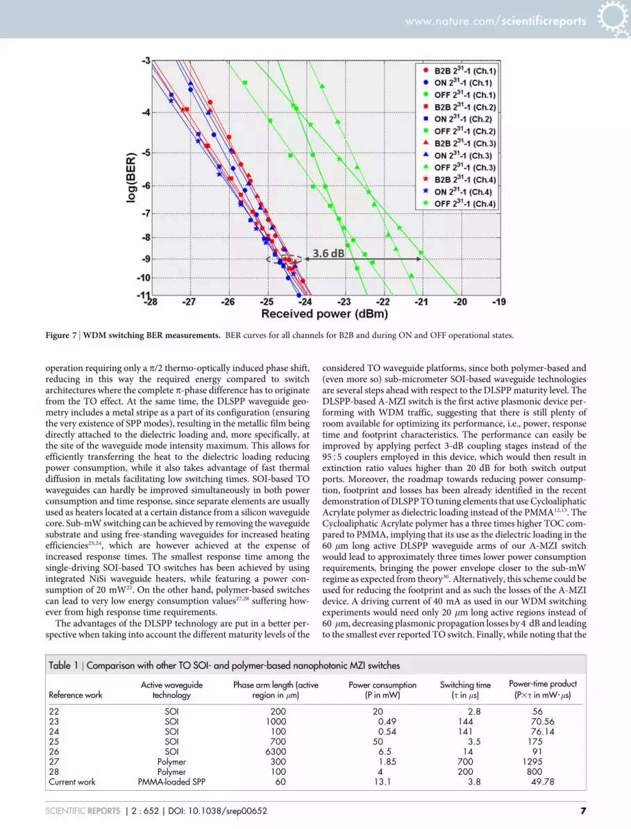
Fig. 7 presents the BER curves obtained for the four channels forthe B2B case and when the A-MZI operates in both ON and OFFoperational states. Since the intention has been to monitor the signaldegradation of the A-MZI device and not of the complete chipincluding its lossy in- and output grating coupler stages, a straightsilicon waveguide employed on the chip has been used for the B2Bcase. During ON operation, the BER curve was recorded at the BARoutput port controlling the A-MZI with a DC electric current value of40 mA. When operating in OFF state, the BER curve was obtainedfor the CROSS output port. In both ON and OFF operational stateserror-free performance was monitored. The ON state shows a nega-tive power penalty close to the statistical error of 0.2 dB for all fourchannels compared to the B2B curve. When operating at OFF state,the power penalties were ranging between 1.7 dB and 3.6 dB mea-sured at a BER value of 1029 for the four channels. The enhancedpower penalty values compared to the corresponding ON state per-formance owes mainly to the 8 dB lower power level received atMZI’s CROSS output (226 dBm) against its BAR port during ONstate (218 dBm). The 226 dBm of power entering EDFA2 werebelow the required input power of the amplifier yielding in thisway excess noise levels that affected the BER performance at thereceiver. Moreover, the power penalty increases with the channelwavelength, being the result of the wavelength-dependent gain andOSNR profile experienced by the four channels during amplificationin EDFA2. Finally, the different slopes observed between the BERgraphs of channels 1, 3 and the BER curves of channels 2 and 4 owe tothe use of a separate data modulation stage per channel pair at the4310 Gb/s transmitter end.
DiscussionThe successful demonstration of WDM switching using a DLSPP-based A-MZI device constitutes a major step towards bringing ac-tive plasmonics into the realm of true datacom and telecom trafficapplications, since the progress made so far in the area of activeplasmonics is mainly limited to proof-of-principle experimentaldemonstrations8,10–13,15,33–35 that cannot certainly be considered as
being close to real datacom testing procedures. Even in the area ofpurely passive plasmonic waveguides, their WDM signal integrityand data carrying credentials were only recently addressed36. Thisstep is, however, crucial in order to allow their performance evalu-ation in real network conditions and address their advantages anddrawbacks when it comes to practical application-driven technologydevelopments. All the work carried out so far on active plasmonicshas indicated a remarkable potential for low-footprint, low-energyand eventually ultra-fast circuitry, but the transition from a highlypromising to a tangible and practical technology has inevitably toproceed along their employment in practical WDM-enabling func-tional elements.
The WDM DLSPP-based A-MZI switch presented in this workreveals also a clear advantage compared to the Silicon-on-Insulatorand the polymer-based TO waveguide technology platforms, as itprovides the lowest, to the best of our knowledge, power consump-tion 3 response time product over every type of undoped thermo-optically addressed nanophotonic MZI switch. This product, whichactually provides also the approximate amount of energy that isdissipated when changing the switching state, has been commonlyused for comparing TO switching elements in terms of their utiliza-tion in applications where both low energy and fast operation arerequired27.
Table 1 provides an overview of the respective performance met-rics reported for different TO MZI switch implementations relyingon SOI-based and polymer-based nanophotonic waveguides, whichexhibit either the smallest power-time product or the lowest energyconsumption or the lowest response time among all TO MZIswitches demonstrated so far. TO switches exploiting doped siliconnanophotonic waveguides for using the waveguide core itself as theresistive heater37 have been excluded from this comparison, since theaim has been to compare the TO efficiency properties of waveguidetechnology platforms without assuming any modifications in theirintrinsic waveguide characteristics in favor of improving theirthermo-optical addressing properties. In addition, only single-con-trol driving schemes have been considered in order to evaluate theresponse times of the waveguide material platform without takinginto account any architectural intervention in the form of differentialdriving techniques37, which are well-known for their switching timereduction advantages. This Table shows that the DLSPP-loaded A-MZI TO switch offers the lowest power-time product using also theshortest active region length, rendering it suitable for TO switchingapplications where both low energy and low response times arerequired. The low power operation comes both from its asymmetricarrangement as well as from the inherent DLSPP waveguide char-acteristics: the asymmetric arrangement allows complete switching
Figure 6 | Data injection. Modulation with 15ms electrical rectangular pulses at 20 KHz repetition rate for 10 Gb/s (a) data trace at the CROSS port
(channel 1), (b) data trace at the BAR port (channel 1), (c) eye diagram at the CROSS port (channel 1), (d) eye diagram at the BAR port (channel 1),
(e) data trace at the CROSS port (channel 2), (f) data trace at the BAR port (channel 2), (g) eye diagram at the CROSS port (channel 2), (h) eye diagram at
the BAR port (channel 2).
www.nature.com/scientificreports
SCIENTIFIC REPORTS | 2 : 652 | DOI: 10.1038/srep00652 6
operation requiring only a p/2 thermo-optically induced phase shift,reducing in this way the required energy compared to switcharchitectures where the complete p-phase difference has to originatefrom the TO effect. At the same time, the DLSPP waveguide geo-metry includes a metal stripe as a part of its configuration (ensuringthe very existence of SPP modes), resulting in the metallic film beingdirectly attached to the dielectric loading and, more specifically, atthe site of the waveguide mode intensity maximum. This allows forefficiently transferring the heat to the dielectric loading reducingpower consumption, while it also takes advantage of fast thermaldiffusion in metals facilitating low switching times. SOI-based TOwaveguides can hardly be improved simultaneously in both powerconsumption and time response, since separate elements are usuallyused as heaters located at a certain distance from a silicon waveguidecore. Sub-mW switching can be achieved by removing the waveguidesubstrate and using free-standing waveguides for increased heatingefficiencies23,24, which are however achieved at the expense ofincreased response times. The smallest response time among thesingle-driving SOI-based TO switches has been achieved by usingintegrated NiSi waveguide heaters, while featuring a power con-sumption of 20 mW22. On the other hand, polymer-based switchescan lead to very low energy consumption values27,28 suffering how-ever from high response time requirements.
The advantages of the DLSPP technology are put in a better per-spective when taking into account the different maturity levels of the
considered TO waveguide platforms, since both polymer-based and(even more so) sub-micrometer SOI-based waveguide technologiesare several steps ahead with respect to the DLSPP maturity level. TheDLSPP-based A-MZI switch is the first active plasmonic device per-forming with WDM traffic, suggesting that there is still plenty ofroom available for optimizing its performance, i.e., power, responsetime and footprint characteristics. The performance can easily beimproved by applying perfect 3-dB coupling stages instead of the9555 couplers employed in this device, which would then result inextinction ratio values higher than 20 dB for both switch outputports. Moreover, the roadmap towards reducing power consump-tion, footprint and losses has been already identified in the recentdemonstration of DLSPP TO tuning elements that use CycloaliphaticAcrylate polymer as dielectric loading instead of the PMMA12,13. TheCycloaliphatic Acrylate polymer has a three times higher TOC com-pared to PMMA, implying that its use as the dielectric loading in the60 mm long active DLSPP waveguide arms of our A-MZI switchwould lead to approximately three times lower power consumptionrequirements, bringing the power envelope closer to the sub-mWregime as expected from theory30. Alternatively, this scheme could beused for reducing the footprint and as such the losses of the A-MZIdevice. A driving current of 40 mA as used in our WDM switchingexperiments would need only 20 mm long active regions instead of60 mm, decreasing plasmonic propagation losses by 4 dB and leadingto the smallest ever reported TO switch. Finally, while noting that the
Figure 7 | WDM switching BER measurements. BER curves for all channels for B2B and during ON and OFF operational states.
Table 1 | Comparison with other TO SOI- and polymer-based nanophotonic MZI switches
Reference workActive waveguide
technologyPhase arm length (active
region in mm)Power consumption
(P in mW)Switching time
(t in ms)Power-time product
(P3t in mW?ms)
22 SOI 200 20 2.8 5623 SOI 1000 0.49 144 70.5624 SOI 100 0.54 141 76.1425 SOI 700 50 3.5 17526 SOI 6300 6.5 14 9127 Polymer 300 1.85 700 129528 Polymer 100 4 200 800Current work PMMA-loaded SPP 60 13.1 3.8 49.78
www.nature.com/scientificreports
SCIENTIFIC REPORTS | 2 : 652 | DOI: 10.1038/srep00652 7

thermal management in DLSPP waveguide components has yet to beoptimized, one should also bear in mind that, at any rate, responsetime reduction could be realized by applying well-known differentialdriving schemes37.
In conclusion, we have demonstrated the first active plasmonicdevice operating with true WDM traffic. An A-MZI switching struc-ture employing silicon-based coupler stages and TO PMMA-basedDLSPP waveguides as its active arms has been shown to provideerror-free switching functionality with 4310 Gb/s incoming datatraffic, requiring only 13.1 mW of power and having on/off responsetimes of 3.8 ms and 2.3 ms, respectively. These results verify thepotential of plasmonics in developing fast and low-power TOswitches with small footprints, providing the smallest power-timeproduct among all undoped SOI- and polymer-based nanophotonicTO switching structures. This clear advantage of the DLSPP TOswitch technology platform over respective SOI- and polymer-baseddevices can pave the way towards a whole new class of ultra-small,energy efficient and fast TO routing fabrics relying on hybrid silicon-plasmonic waveguide platforms, where low-loss silicon is used forthe passive functions and DLSPP waveguide components areexploited for the active circuit parts5.
MethodsSOI-DLSPP A-MZI and waveguide platform fabrication. The SOI motherboardrelied on a 4003340 nm2 silicon rib waveguide platform with a 50-nm-thickremaining slab to support TM light propagation and was equipped with TM gratingcouplers as input/output interfaces. Silicon coupler stages were employed for the A-MZI input/output ports. The plasmonic (DLSPP) parts of the A-MZI were hetero-integrated on the SOI rib waveguide platform. The hosting area of the DLSPPWs onthe SOI motherboard was etched forming a 200-nm-deep recess in the buried oxide(BOX) of the SOI substrate. The DLSPPWs inside the recess consisted of5003600 nm2 PMMA-made strips placed on top of 3- mm-wide and 65-nm-thickgold films. The interface between the silicon and plasmonic parts of the hybrid A-MZIwas attained through a butt-coupling approach following the same designspecifications described in8. The length of the A-MZI active plasmonic arms was60 mm and its asymmetric biasing was obtained by using a 700-nm-wide and 6- mm-long DLSPPW section at its lower branch. The total fiber-to-fiber losses of the A-MZIwere 40 dB while the insertion losses of only the A-MZI were 11 dB. The high fiber-to-fiber loss value includes 26 dB of losses that were introduced by the two TMgrating coupler stages (each grating coupler had an insertion loss of 13 dB) and 3 dBlosses owing to propagation in the silicon parts between the TM grating coupler stagesand the A-MZI input/output ports. The 11 dB A-MZI device losses are analyzed in5 dB coming from the Si-to-DLSPP coupling interfaces (2.5 dB per couplinginterface) and 6 dB that were the plasmonic propagation losses in the 60 mm longplasmonic sections.
Single-channel experimental setup. A CW signal at 1542 nm was fed into aTi:LiNbO3 MZM driven by a 10 Gb/s MP1763C Anritsu pattern generator and wasconsequently modulated to a 10 Gb/s 231-1 NRZ data sequence. Subsequently, a high-power EDFA (EDFA1) was utilized to attain adequate output power of 30 dBm forthe modulated signal before entering the A-MZI. Electrical rectangular pulses at20 KHz repetition frequency were provided by a SRS DG535 digital delay/pulsegenerator to the metal pads of the DLSPPW in order to control the A-MZI in adynamic way. The corresponding static TO transfer function measurements wereobtained by using a DC current instead of the electrical pulses. After propagationthrough the A-MZI, the output signal was amplified by an EDFA with 10 dBm outputpower for an input power of 215 dBm (EDFA2) and was filtered in a narrow OBPFwith 1 nm 3-dB bandwidth. The data signal was then split and simultaneouslydetected by a 30 GHz bandwidth HP 83480 A sampling oscilloscope and a 10 GHz 3-dB bandwidth DSC-R402PIN photo-receiver followed by a 10 Gb/s MP1764CAnritsu error detector for BER measurements. A 20 GHz MG3692B Anritsu signalgenerator was employed so as to generate the 10 GHz reference signal for thetransmitter and the receiver.
Multi-channel (WDM) experimental setup. Four distributed feedback (DFB) lasersemitting CW light at 1545.1 nm, 1546.7 nm, 1547.7 nm and 1549.1 nm, respectively,were used as the four transmitter channels in the WDM switching experimentalsetup. The four CW signals were initially multiplexed using fiber 3-dB couplers andmodulated in pairs (channels 1 and 3 together and channels 2 and 4 forming anotherpair) by two Ti:LiNbO3 MZMs driven by 10 Gb/s data and data bar outputs of theMP1763C Anritsu pattern generator. In this way, four 10 Gb/s 231-1 NRZ datasequences were generated with channels 1–3 and channels 2–4 carrying decorrelatedsignals. All four channels were subsequently combined into the same optical link via afiber 3-dB coupler. The multi-wavelength data signal was then amplified by a high-power EDFA (EDFA1) providing 31 dBm output power before being fed into theSOI-DLSPP A-MZI. A polarizer in conjunction with mechanical polarization
controllers were used for ensuring TM polarized light at the input of the SOI-DLSPPchip. A SRS DG535 digital delay/pulse generator operating at 20 KHz controlleddynamically the switching state of the MZI based on the TO effect. For the BERmeasurement performance, the electrical pulsed control signal was replaced by a DCcurrent. The multi-channel signal that was received at the MZI’s output was amplifiedby a two stage EDFA (EDFA2 with –15 dBm output power for an input power of222 dBm and EDFA3) that included a 5 nm OBPF between the two stages for noiserejection. The WDM signal was demultiplexed into its constituent wavelengthsthrough a narrow OBPF (0.8 nm). Each data channel was then split and launchedconcurrently into a 30 GHz HP 83480 A sampling oscilloscope and a 10 GHz 3-dBbandwidth DSC-R402PIN photo-receiver attached to a 10 Gb/s MP1764C Anritsuerror detector. The 10 GHz reference signal for the transmitter and the receiver wasprovided by a 20 GHz MG3692B Anritsu signal generator.
BER measurements. The BER curves were obtained by measuring the BER values forincreasing mean optical signal power levels launched at the photo-receiver andapplying a fitting curve to the measured points, following the method described in38.The B2B measurements were performed by replacing the A-MZI with a straight3 mm long silicon waveguide section that had 27.3 dB total fiber-to-fiber lossesoriginating from 26 dB losses due to the two TM grating couplers and 4.4 dB/cmsilicon propagation losses.
1. Taubenblatt, M. A., Kash, J. A. & Taira, Y. Optical interconnects for highperformance computing. Proc. OFC/NFOEC Conf., paper OThH3, LA, CA, USA(2011).
2. Atwater, H. A. The promise of plasmonics. Sci. Am. Mag. 296, 38–45 (2007).3. Brongersma, M. L. & Shalaev, V. M. The case for plasmonics. Science 328, 440–441
(2010).4. Zia, R., Schuller, J. A., Chandran, A. & Brongersma, M. L. Plasmonics: the next
chip-scale technology. Mater. Today 9, 20–27 (2006).5. Papaioannou, S. et al. A 320 Gb/s-throughput capable 232 silicon-plasmonic
router architecture for optical interconnects. J. Lightw. Technol. 29, 3185–3195(2011).
6. Kim, J. T. et al. Chip-to-chip optical interconnect using gold long-range surfaceplasmon polariton waveguides. Opt. Express 16, 13133–13138 (2008).
7. Gramotnev, D. K. & Bozhevolnyi, S. I. Plasmonics beyond the diffraction limit.Nat. Phot. 4, 83–91 (2010).
8. Giannoulis, G. et al. Data transmission and thermo-optic tuning performance ofdielectric-loaded plasmonic structures hetero-integrated on a silicon chip. IEEEPhoton. Technol. Lett. 24, 374–376 (2012).
9. Kalavrouziotis, D. et al. First demonstration of active plasmonic device in true datatraffic conditions: ON/OFF thermo-optic modulation using a hybrid silicon-plasmonic asymmetric MZI. Proc. OFC/NFOEC Conf., OW3E.3, LA, CA, USA(2012).
10. Gosciniak, J. et al. Thermo-optic control of dielectric-loaded plasmonicwaveguide components. Opt. Express 18, 1207–1216 (2010).
11. Hassan, K. et al. Thermo-optical control of dielectric loaded plasmonic racetrackresonators. J. Appl. Phys. 110, 023106 (2011).
12. Hassan, K. et al. Thermo-optic plasmo-photonic mode interference switchesbased on dielectric loaded waveguides. Appl. Phys. Lett. 99, 241110 (2011).
13. Hassan, K. et al. Characterization of thermo-optical 232 switch configurationsmade of dielectric loaded surface plasmon polariton waveguides for telecomrouting architecture. Proc. OFC/NFOEC Conf., OW3E.5, LA, CA, USA (2012).
14. Krasavin, A. V. & Zayats, A. V. Electro-optic switching element for dielectric-loaded surface Plasmon polariton waveguides. Appl. Phys. Lett. 97, 041107 (2010).
15. Randhawa, S. et al. Performance of electro-optical plasmonic ring resonators attelecom wavelengths. Opt. Express 20, 2354–2362 (2012).
16. Kumar, A. et al. Power monitoring in dielectric-loaded surface plasmon-polaritonwaveguides. Opt. Express 19, 2972–2978 (2011).
17. Briggs, R. M., Grandidier, J., Burgos, S. P., Feigenbaum, E. & Atwater, H. A.Efficient coupling between dielectric loaded plasmonic and silicon photonicwaveguides. Nano Lett. 10, 4851–4857 (2010).
18. Tsilipakos, O. et al. Interfacing Dielectric-Loaded Plasmonic and Silicon PhotonicWaveguides: Theoretical Analysis and Experimental Demonstration. IEEE J.Quantum Electron. 48, 678–687 (2012).
19. Lee, B. G., Biberman, A., Chan, J. & Bergman, K. High-performance modulatorsand switches for silicon photonic networks-on-chip. IEEE J. Sel. Top. Quant.Electron. 16, 6–22 (2010).
20. Sherwood-Droz, N. et al. Optical 434 hitless silicon router for optical networks-on-chip (NoC). Opt. Express 16, 15915–15922 (2008).
21. Shacham, A., Bergman, K. & Carloni, L. P. Photonic networks-on-chip for futuregenerations of chip multiprocessors. IEEE Trans. on Comp. 57, 1246–1260 (2008).
22. Van Campenhout, J., Green, W. M., Assefa, S. & Vlasov, Y. A. Integrated NiSiwaveguide heaters for CMOS-compatible silicon thermo-optic devices. Opt. Lett.35, 1013–1015 (2010).
23. Fang, Q. et al. Ultralow power silicon photonics thermo-optic switch withsuspended phase arms. IEEE Photon. Technol. Lett. 23, 525–527 (2011).
24. Sun, P. & Reano, R. M. Submilliwatt thermo-optic switches using free-standingsilicon-on-insulator strip waveguides. Opt. Express 18, 8406–8411 (2010).
www.nature.com/scientificreports
SCIENTIFIC REPORTS | 2 : 652 | DOI: 10.1038/srep00652 8

25. Espinola, R. L., Tsai, M.-C., Yardley, J. T. & Osgood, R. M. Fast and low-powerthermooptic switch on thin silicon-on-insulator. IEEE Photon. Technol. Lett. 15,1366–1368 (2003).
26. Densmore, A. et al. Compact and low power thermo-optic switch using foldedsilicon waveguides. Opt. Express 17, 10457–10465 (2009).
27. Al-Hetar, A. M, Mohammad, A. B., Supa’at, A. S. M. & Shamsan, Z. A. MMI-MZIpolymer thermo-optic switch with a high refractive index contrast. J. Lightw.Technol. 29, 171–178 (2011).
28. Xie, N., Hashimoto, T. & Utaka, K. Very low-power, polarization-independent,and high-speed polymer thermooptic switch. IEEE Photon. Technol. Lett. 21,1861–1863 (2009).
29. Holmgaard, H. & Bozhevolnyi, S. I. Theoretical analysis of dielectric-loadedsurface plasmon-polariton waveguides. Phys. Rev. B 75, 245405 (2007).
30. Pitilakis, A. & Kriezis, E. E. Longitudinal 232 switching configurations based onthermo-optically addressed dielectric-loaded plasmonic waveguides. J. Lightw.Technol. 29, 2636–2646 (2011).
31. Krasavin, A. V. & Zayats, A. V. Three-dimensional numerical modeling ofphotonic integration with dielectric-loaded SPP waveguides. Phys. Rev. B 78,045425 (2008).
32. Tsilipakos, O., Pitilakis, A., Tasolamprou, A. C., Yioultsis, T. V. & Kriezis, E. E.Computational techniques for the analysis and design of dielectric-loadedplasmonic circuitry. Opt. Quant. Electron. 42, 541–555 (2011).
33. Krasavin, A. V., Vo, T. P., Dickson, W., Bolger, P. M. & Zayats, A. V.All-plasmonic modulation via stimulated emission of co-propagating surfaceplasmon polaritons on a substrate with gain. Nano Lett. 11, 2231–2235 (2011).
34. MacDonald, K. F., Samson, Z. L., Stockman, M. I. & Zheludev, N. I. Ultra-fastactive plasmonics. Nat. Phot. 3, 55–58 (2009).
35. Melikyan, A. et al. Surface plasmon polariton absorption modulator. Opt. Express19, 8855–8869 (2011).
36. Kalavrouziotis, D. et al. 0.48 Tb/s (12340 Gb/s) WDM transmission and high-quality thermo-optic switching in dielectric loaded plasmonics. Opt. Express 20,7655–7662 (2012).
37. Geis, M. W., Spector, S. J., Williamson, R. C. & Lyszczarz, T. M. Submicrosecondsubmilliwatt silicon-on-insulator thermooptic switch. IEEE Photon. Technol. Lett.16, 2514–2516 (2004).
38. Marcuse, D. Calculation of bit-error probability for a lightwave system withoptical amplifiers and post-detection Gaussian noise. J. Lightw. Technol. 9, 505–513 (1991).
AcknowledgmentsThis work was partially supported by the European FP7 ICT-PLATON (ICT- STREP no.249135) project.
Author contributionsS.P., D.K., K.V., D.A., H.A. and N.P. devised the experimental setup and carried out theexperimental testing procedure and measurements. J.-C.W., K.H., L.M. and A.D. designedthe widened plasmonic MZI arm for providing the phase offset and fabricated theplasmonic parts of the A-MZI structure. M.B. fabricated the SOI motherboard. T.T.designed the silicon parts and prepared the mask layout. A.K. and S.B. characterized thesample and performed the wire-bonding. S.P., D.K., K.V. and N.P. analyzed the results andprepared the figures. All authors co-wrote the paper.
Additional informationSupplementary information accompanies this paper at http://www.nature.com/scientificreports
Competing financial interests: The authors declare no competing financial interests.
License: This work is licensed under a Creative Commons Attribution 3.0 UnportedLicense. To view a copy of this license, visit http://creativecommons.org/licenses/by/3.0/
How to cite this article: Papaioannou, S. et al. Active plasmonics in WDM traffic switchingapplications. Sci. Rep. 2, 652; DOI:10.1038/srep00652 (2012).
www.nature.com/scientificreports
SCIENTIFIC REPORTS | 2 : 652 | DOI: 10.1038/srep00652 9