a new generation of scanners for dna chips
TRANSCRIPT

A new generation of scanners for DNA chips
Francois Perraut a,*, Alexandre Lagrange c, Patrick Pouteau a, O. Peyssonneaux c,Pierre Puget a, G. McGall d, Lionel Menou b, Richard Gonzalez b, Pierre Labeye c,
Frederic Ginot a
a Equipe bioMerieux-LETI, CEA/LETI/DSYS, 17, rue des Martyrs, 38054 Grenoble Cedex, Franceb bioMerieux, Parc Club du Moulin a Vent, 33 av. Docteur Levy, 69693 Venissieux Cedex, France
c CEA/LETI/DSYS, 17, rue des Martyrs, 38054 Grenoble Cedex, Franced Affymetrix, 3380 Central Expressway, Santa Clara, CA 95051, USA
Received 17 May 2001; received in revised form 7 March 2002; accepted 15 May 2002
Abstract
Today, most of the DNA chips are used with fluorescent markers. Associated with fluorescence confocal scanners, this technology
achieves remarkable performances in terms of sensitivity and accuracy. The main technical issues related to these scanners have
already been reviewed. However, these scanners are costly, especially when high density chips are used. In this case, a mechanical
precision of 1 mm or less is required to achieve the measurement precision required. This cost level prevents the spread of this
technology in the diagnostic market. We will present a new concept for scanners with equivalent or superior performances, with a
cost cut of 5�/10. This concept is inspired from the field of optical disk and reader. Basically, an optical format is added to the chip,
before DNA deposition. This format contains tracks which are superimposed to the DNA features. These tracks define the path that
an optical head of a CD player must follow in order to scan the surface of the DNA chip. Such a head is a very cheap component,
and has a precision of less than 100 nm thanks to real-time focus and tracking. These functions are fulfilled by electromagnetic
actuators mounted on the support of the frontal lens. We show here that it is possible to use such a head to build a fluorescence
confocal scanner with equivalent or even better performances than conventional scanners. # 2002 Elsevier Science B.V. All rights
reserved.
Keywords: Confocal scanner; Biochip format; Microarrays
1. Introduction
DNA chip technology is an enabling technology
which is now used in various fields of research in
biology. Indeed, this is a powerful analytical tool of
genetic material. Associated with fluorescence confocal
scanners, this technology achieves remarkable perfor-
mances in terms of sensitivity and accuracy (Ramsay,
1998; Basarsky et al., 2000). However, these scanners are
costly, specially when high density chips are used, like
those manufactured by Affymetrix, a Californian com-
pany who are a leader in this field.
The cost of the existing scanners is affordable for
some markets, like that of the research in the pharma-
ceutical industry. However, in the routine diagnostic
market, in which molecular diagnostic is still in its
infancy, it represents an extra cost without replacing the
conventional tests; this cost level is not acceptable, and
prevents the spread of the DNA chip technology.
We have addressed the cost issue of the current
scanners for high density chips. To reach the required
performances, the sampling of fluorescence acquisition
must be sufficient to get robust data: numerous readings
per feature, hence high quality mechanics and electro-
nics, and use of a small excitation spot. Also, confocal
reading is usually used to increase the sensitivity by
rejecting the light coming from other plans than that of
the biological signals. The more confocal the system, the
better is the signal to noise ratio but the higher is the
need for accuracy for the focus and tilt adjustments of
* Corresponding author. Tel.: �/�/33-4-3878-5544; fax: �/33-4-
3878-5787
E-mail address: [email protected] (F. Perraut).
Biosensors and Bioelectronics 17 (2002) 803�/813
www.elsevier.com/locate/bios
0956-5663/02/$ - see front matter # 2002 Elsevier Science B.V. All rights reserved.
PII: S 0 9 5 6 - 5 6 6 3 ( 0 2 ) 0 0 0 7 3 - 8
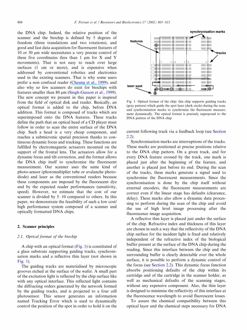
the DNA chip. Indeed, the relative position of the
scanner and the biochip is defined by 5 degrees of
freedom (three translations and two rotations), and
good and fast data acquisition for fluorescent features of10 or 30 mm wide necessitates a very precise control of
these five coordinates (less than 1 mm for X and Y
movements). That is not easy to reach over large
surfaces (1 cm or more), and is expensive when
addressed by conventional robotics and electronics
used in the existing scanners. That is why some users
prefer a non confocal reader (Cheung et al., 1999), and
also why so few scanners do exist for biochips withfeatures smaller than 80 mm (Singh-Gasson et al., 1999).
The new concept we present in this paper is inspired
from the field of optical disk and reader. Basically, an
optical format is added to the chip, before DNA
addition. This format is composed of tracks which are
superimposed onto the DNA features. These tracks
define the path that an optical head of a CD player must
follow in order to scan the entire surface of the DNAchip. Such a head is a very cheap component, and
reaches a submicronic spatial precision thanks to con-
tinuous dynamic focus and tracking. These functions are
fulfilled by electromagnetic actuators mounted on the
support of the frontal lens. The actuators allow for a
dynamic focus and tilt correction, and the format allows
the DNA chip itself to synchronise the fluorescent
measurement. Our scanner uses the same kind ofphoto-sensor (photomultiplier tube or avalanche photo-
diode) and laser as the conventional readers because
these components are imposed by the fluorescent dye
and by the expected reader performances (sensitivity,
speed). However, we estimate that the cost of our
scanner is divided by 5�/10 compared to others. In this
paper, we demonstrate the feasibility of such a low cost/
high performance system composed of a scanner andoptically formatted DNA chips.
2. Scanner principles
2.1. Optical format of the biochip
A chip with an optical format (Fig. 1) is constituted of
a glass substrate supporting guiding tracks, synchroni-sation marks and a reflective thin layer (not shown in
Fig. 1).
The guiding tracks are materialised by microscopic
grooves etched at the surface of the wafer. A small part
of the excitation light is reflected by the chip surface like
with any optical interface. This reflected light contains
the diffracting orders generated by the network formed
by the guiding tracks, and is projected to a four cellphotosensor. This sensor generates an information
named Tracking Error which is used to dynamically
control the position of the spot in order to hold it on the
current following track via a feedback loop (see Section
2.2).
Synchronisation marks are interruptions of the tracks.
These marks are positioned at precise positions relative
to the DNA chip pattern. On a given track, and for
every DNA feature crossed by the track, one mark is
placed just after the beginning of the feature, and
another is placed just before its end. During the scan
of the tracks, these marks generate a signal used to
synchronise the fluorescent measurements. Since the
synchronisation is done by the chip itself without
external encoders, the fluorescent measurements are
correct even if the linear stage has defaults (clearance,
delay). These marks also allow a dynamic data proces-
sing to perform during the scan of the chip and avoid
the use of high level image processing after the
fluorescence image acquisition.
A reflective thin layer is placed just under the surface
of the chip. Refractive index and thickness of this layer
are chosen in such a way that the reflectivity of the DNA
chip surface for the incident light is fixed and relatively
independent of the refractive index of the biological
buffer present at the surface of the DNA chip during the
reading. Since this interface between the chip and the
surrounding buffer is clearly detectable over the whole
surface, it is possible to perform a dynamic control of
the focus (see Section 2.2). This dynamic focus function
absorbs positioning defaults of the chip within its
cartridge and of the cartridge in the scanner holder, as
well as mechanical defaults of the scanning stages,
without any expensive component. Also, the thin layer
is designed to minimise the reflectivity of this interface at
the fluorescence wavelength to avoid fluorescent losses.To assure the chemical compatibility between this
optical layer and the chemical steps necessary for DNA
Fig. 1. Optical format of the chip: this chip supports guiding tracks
(gray pattern) which guide the spot laser (dark circle) during the scan,
and synchronisation marks to synchronise the fluorescent measure-
ment dynamically. The optical format is precisely superposed to the
DNA pattern of the DNA chip.
F. Perraut et al. / Biosensors and Bioelectronics 17 (2002) 803�/813804
loading of the chips, a silica layer is added on the top of
the index matching layer.
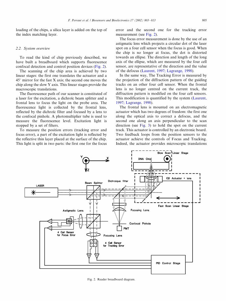
2.2. System overview
To read the kind of chip previously described, we
have built a breadboard which supports fluorescence
confocal detection and control position devices (Fig. 2).
The scanning of the chip area is achieved by twolinear stages: the first one translates the actuator and a
458 mirror for the fast X axis; the second one moves the
chip along the slow Y axis. This linear stages provide the
macroscopic translations.
The fluorescence path of our scanner is constituted of
a laser for the excitation, a dichroıc beam splitter and a
frontal lens to focus the light on the probe area. The
fluorescence light is collected by the frontal lens,reflected by the dichroıc filter and focused by a lens to
the confocal pinhole. A photomultiplier tube is used to
measure the fluorescence level. Excitation light is
stopped by a set of filters.
To measure the position errors (tracking error and
focus error), a part of the excitation light is reflected by
the reflective thin layer placed at the surface of the chip.
This light is split in two parts: the first one for the focus
error and the second one for the tracking error
measurement (see Fig. 2).
The focus error measurement is done by the use of an
astigmatic lens which projects a circular dot of the laser
spot on a four cell sensor when the focus is good. When
the chip is no longer at focus, the dot is distorted
towards an ellipse. The direction and length of the long
axis of the ellipse, which are measured by the four cell
sensor, are representative of the direction and the value
of the defocus (Laurent, 1997; Lagrange, 1998).
In the same way, The Tracking Error is measured by
the projection of the diffraction pattern of the guiding
tracks on an other four cell sensor. When the frontal
lens is no longer centred on the current track, the
diffraction pattern is modified on the four cell sensors.
This modification is quantified by the system (Laurent,
1997; Lagrange, 1998).
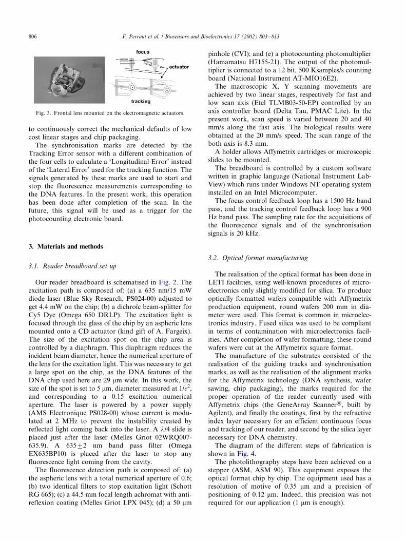
The frontal lens is mounted on an electromagnetic
actuator which has two degrees of freedom: the first one
along the optical axis to correct a defocus, and the
second one along an axis perpendicular to the scan
direction (see Fig. 3) to hold the spot on the current
track. This actuator is controlled by an electronic board.
Two feedback loops from the position sensors to the
actuator achieve the controls of Focus and Tracking.
Indeed, the actuator provides microscopic translations
Fig. 2. Reader breadboard diagram.
F. Perraut et al. / Biosensors and Bioelectronics 17 (2002) 803�/813 805
to continuously correct the mechanical defaults of low
cost linear stages and chip packaging.
The synchronisation marks are detected by the
Tracking Error sensor with a different combination of
the four cells to calculate a ‘Longitudinal Error’ instead
of the ‘Lateral Error’ used for the tracking function. The
signals generated by these marks are used to start andstop the fluorescence measurements corresponding to
the DNA features. In the present work, this operation
has been done after completion of the scan. In the
future, this signal will be used as a trigger for the
photocounting electronic board.
3. Materials and methods
3.1. Reader breadboard set up
Our reader breadboard is schematised in Fig. 2. Theexcitation path is composed of: (a) a 635 nm/15 mW
diode laser (Blue Sky Research, PS024-00) adjusted to
get 4.4 mW on the chip; (b) a dichroıc beam-splitter for
Cy5 Dye (Omega 650 DRLP). The excitation light is
focused through the glass of the chip by an aspheric lens
mounted onto a CD actuator (kind gift of A. Fargeix).
The size of the excitation spot on the chip area is
controlled by a diaphragm. This diaphragm reduces theincident beam diameter, hence the numerical aperture of
the lens for the excitation light. This was necessary to get
a large spot on the chip, as the DNA features of the
DNA chip used here are 29 mm wide. In this work, the
size of the spot is set to 5 mm, diameter measured at 1/e2,
and corresponding to a 0.15 excitation numerical
aperture. The laser is powered by a power supply
(AMS Electronique PS028-00) whose current is modu-lated at 2 MHz to prevent the instability created by
reflected light coming back into the laser. A l /4 slide is
placed just after the laser (Melles Griot 02WRQ007-
635.9). A 6359/2 nm band pass filter (Omega
EX635BP10) is placed after the laser to stop any
fluorescence light coming from the cavity.
The fluorescence detection path is composed of: (a)
the aspheric lens with a total numerical aperture of 0.6;(b) two identical filters to stop excitation light (Schott
RG 665); (c) a 44.5 mm focal length achromat with anti-
reflexion coating (Melles Griot LPX 045); (d) a 50 mm
pinhole (CVI); and (e) a photocounting photomultiplier
(Hamamatsu H7155-21). The output of the photomul-
tiplier is connected to a 12 bit, 500 Ksamples/s counting
board (National Instrument AT-MIO16E2).The macroscopic X, Y scanning movements are
achieved by two linear stages, respectively for fast and
low scan axis (Etel TLMB03-50-EP) controlled by an
axis controller board (Delta Tau, PMAC Lite). In the
present work, scan speed is varied between 20 and 40
mm/s along the fast axis. The biological results were
obtained at the 20 mm/s speed. The scan range of the
both axis is 8.3 mm.A holder allows Affymetrix cartridges or microscopic
slides to be mounted.
The breadboard is controlled by a custom software
written in graphic language (National Instrument Lab-
View) which runs under Windows NT operating system
installed on an Intel Microcomputer.
The focus control feedback loop has a 1500 Hz band
pass, and the tracking control feedback loop has a 900Hz band pass. The sampling rate for the acquisitions of
the fluorescence signals and of the synchronisation
signals is 20 kHz.
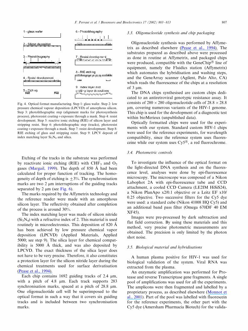
3.2. Optical format manufacturing
The realisation of the optical format has been done in
LETI facilities, using well-known procedures of micro-electronics only slightly modified for silica. To produce
optically formatted wafers compatible with Affymetrix
production equipment, round wafers 200 mm in dia-
meter were used. This format is common in microelec-
tronics industry. Fused silica was used to be compliant
in terms of contamination with microelectronics facil-
ities. After completion of wafer formatting, these round
wafers were cut at the Affymetrix square format.The manufacture of the substrates consisted of the
realisation of the guiding tracks and synchronisation
marks, as well as the realisation of the alignment marks
for the Affymetrix technology (DNA synthesis, wafer
sawing, chip packaging), the marks required for the
proper operation of the reader currently used with
Affymetrix chips (the GeneArray Scanner†, built by
Agilent), and finally the coatings, first by the refractiveindex layer necessary for an efficient continuous focus
and tracking of our reader, and second by the silica layer
necessary for DNA chemistry.
The diagram of the different steps of fabrication is
shown in Fig. 4.
The photolithography steps have been achieved on a
stepper (ASM, ASM 90). This equipment exposes the
optical format chip by chip. The equipment used has aresolution of motive of 0.35 mm and a precision of
positioning of 0.12 mm. Indeed, this precision was not
required for our application (1 mm is enough).
Fig. 3. Frontal lens mounted on the electromagnetic actuators.
F. Perraut et al. / Biosensors and Bioelectronics 17 (2002) 803�/813806
Etching of the tracks in the substrate was performed
by reactivate ionic etching (RIE) with CHF3 and O2
gases (Margail, 1999). The depth of 850 A had been
calculated for proper function of tracking. The homo-
geneity of depth of etching is 9/3%. The synchronisation
marks are two 2 mm interruptions of the guiding tracks
separated by 2 mm (see Fig. 6).
The marks required by the Affymetrix technology and
the reference reader were made with an amorphous
silicon layer. The reflectivity obtained after completion
of the process is around 30%.
The index matching layer was made of silicon nitride
(Si3N4) with a refractive index of 2. This material is used
routinely in microelectronics. This deposition of 820 A
has been achieved by low pressure chemical vapor
deposition (LPCVD) (Applied Materials, Applied
5000; see step 9). The silica layer for chemical compat-
ibility is 5000 A thick, and was also deposited by
LPCVD. The exact thickness of the silica layer does
not have to be very precise. Therefore, it also constitutes
a protection layer for the silicon nitride layer during the
chemical treatments used for surface derivatisation
(Pease et al., 1994).
Each chip contains 1692 guiding tracks of 2.4 mm,
with a pitch of 4.8 mm. Each track supports 283
synchronisation marks, spaced at a pitch of 28.8 mm.
One oligonucleotide cell will be superimposed to the
optical format in such a way that it covers six guiding
tracks and is included between two synchronisation
marks.
3.3. Oligonucleotide synthesis and chip packaging
Oligonucleotide synthesis was performed by Affyme-
trix as described elsewhere (Pease et al., 1994). Thesubstrates prepared as described above were processed
as done in routine at Affymetrix, and packaged chips
were produced, compatible with the GeneChip† line of
equipment, namely the Fluidics station (Affymetrix)
which automates the hybridisation and washing steps,
and the GeneArray scanner (Agilent, Palo Alto, CA)
which reads the fluorescence of the chips at a resolution
of 3 mm.The DNA chips synthesised are custom chips dedi-
cated to an antiretroviral genotypic resistance assay. It
consists of 280�/280 oligonucleotide cells of 28.8�/28.8
mm, covering numerous variants of the HIV-1 genome.
This chip is used for the development of a diagnostic test
within bioMerieux (unpublished data).
Optically formatted chips were used for the experi-
ments with our system. Standard custom HIV-1 chipswere used for the reference experiments, for wavelength
compatibility, since the reference system uses fluores-
ceine while our system uses Cy5†, a red fluorochrome.
3.4. Photometric controls
To investigate the influence of the optical format on
the light-directed DNA synthesis and on the fluores-
cence level, analyses were done by epi-fluorescencemicroscopy. The microscope was composed of a Nikon
Labophot 2A with epi-fluorescence tube and CCD
attachment, a cooled CCD Camera (LE2IM HiSiS24),
a Nikon PlanApo x2/0.1 objective or a Leitz EF x10/
0.25 objective. Two successive filters for the Cy5 dye
were used: a standard cube (Nikon 41008 HQ Cy5) and
an additional band pass filter (Omega 670DF 40 EM
XF45).Images were pre-processed by dark subtraction and
flat field correction. By using these materials and this
method, very precise photometric measurements are
obtained. The precision is only limited by the photon
shot noise.
3.5. Biological material and hybridisations
A human plasma positive for HIV-1 was used for
biological validation of the system. Viral RNA was
extracted from the plasma.
An enzymatic amplification was performed for Pro-
tease and reverse Transcriptase gene fragments. A single
pool of amplifications was used for all the experiments.
The amplicons were then fragmented and labelled by a
proprietary process, as described elsewhere (Monnot etal., 2001). Part of the pool was labelled with fluorescein
for the reference experiments, the other part with the
Cy5 dye (Amersham Pharmacia Biotech) for the valida-
Fig. 4. Optical format manufacturing. Step 1: glass wafer. Step 2: low
pressure chemical vapour deposition (LPCVD) of amorphous silicon.
Step 3: photolithographic step (alignment marks for photosynthesis
process), photoresist coating�/exposure through a mask. Step 4: resist
development. Step 5: reactive ionic etching (RIE) of silicon layer and
stripping resist. Step 6: photolithographic step (tracks), photoresist
coating�/exposure through a mask. Step 7: resist development. Step 8:
RIE etching of glass and stripping resist. Step 9: LPCV deposit of
index matching layer Si3N4 and silica.
F. Perraut et al. / Biosensors and Bioelectronics 17 (2002) 803�/813 807
tion of our system. Labelled amplicons were purified
and hybridised to the DNA array.
Oligonucleotides respectively labelled with fluorescein
and Cy5 were added to the hybridisation mix, to light upcontrol checkerboards located at the corners of the
chips.
Hybridisation and washing were performed using a
protocol derived from the one described else-
where (Troesch et al., 1999), using the Affymetrix
GeneChip† Fluidics Station 400.
3.6. Biological data analysis
Reference experiments were imaged by the Affymetrix
GeneArrayTM scanner, and analysed by the GeneChip†
software, followed by Excel† Macros for amino acid
calls.
Today, the data produced by our system contains two
sets of data, one containing the fluorescence signals, the
other containing the synchronisation signals. Fluores-cence images were reconstituted using these two sets of
data, simply by using the synchronisation marks to
realign the successive lines of the fluorescence image.
The resulting fluorescence images were then formatted
to become compatible with the Genechip† software.
Analysis was then done as above. No normalisation of
the fluorescence signals based on the time elapsed
between two synchronisation marks was done at thisstage of the work.
4. Technical results
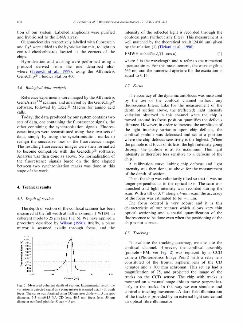
4.1. Depth of section
The depth of section of the confocal scanner has been
measured at the full width at half maximum (FWHM) in
coherent mode to 25 mm (see Fig. 5). We have applied a
procedure described by Wilson (1990). Briefly, a plane
mirror is scanned axially through focus, and the
intensity of the reflected light is recorded through the
confocal path (without any filter). This measurement is
well matched by the theoretical result (24.86 mm) given
by the relation (1) (Tiziani et al., 1996):
FMWH�0:443�l=(1�cos u) (1)
where l is the wavelength and u refer to the numerical
aperture sin u . For this measurement, the wavelength is
635 nm and the numerical aperture for the excitation is
equal to 0.15.
4.2. Focus
The accuracy of the dynamic autofocus was measured
by the use of the confocal channel without any
fluorescence filters. Like for the measurement of thedepth of section above, the (reflected) light intensity
variation observed in this channel when the chip is
moved around its focus position quantifies the defocus
distance. However, in order to increase the amplitude of
the light intensity variation upon chip defocus, the
confocal pinhole was defocused and set at a position
where the chip defocus sensitivity is the highest. (When
the pinhole is at focus of its lens, the light intensity goingthrough the pinhole is at its maximum. This light
intensity is therefore less sensitive to a defocus of the
chip.)
A calibration curve linking chip defocus and light
intensity was then done, as above for the measurement
of the depth of section.
Then, the chip was voluntarily tilted so that it was no
longer perpendicular to the optical axis. The scan waslaunched and light intensity was recorded during the
scan. With a tilt of 3.78 along a 4-mm scan, the accuracy
of the focus was estimated to be 9/1 mm.
The focus control is very robust and it is this
characteristic of our scanner which allows very thin
optical sectioning and a spatial quantification of the
fluorescence to be done even when the positioning of the
chip is not correct.
4.3. Tracking
To evaluate the tracking accuracy, we also use the
confocal channel. However, the confocal assembly(pinhole�/PM, see Fig. 2) was replaced by a CCD
camera (Photometrics Image Point) with a relay lens
constituted of the frontal aspheric lens of the CD
actuator and a 300 mm achromat. This set up had a
magnification of 75, and projected the image of the
tracks on the CCD sensor. The chip with tracks is
mounted on a manual stage able to move perpendicu-
larly to the tracks. In this way we can simulate andcontrol a tracking movement. A dark field illumination
of the tracks is provided by an external light source and
an optical fibre illuminator.
Fig. 5. Measured coherent depth of section: Experimental result: the
variation in detected signal as a plane mirror is scanned axially through
focus. The curve was obtained using 635 nm laser diode with 5 mm spot
diameter, 3.5 mm/0.15 NA CD lens, 40.5 mm focus lens, 50 mm
diameter confocal pinhole. Z step�/5 mm.
F. Perraut et al. / Biosensors and Bioelectronics 17 (2002) 803�/813808
In open loop mode, that is without tracking control, a
translation of the chip along the Y axis (perpendicular
to the tracks) induces a proportional translation of its
image formed on the CCD. On the contrary, when the
tracking control is at work, the image is locked and does
not moved perceptively, because the CD actuator holds
the spot on the current track. In practice, however, there
is a slight remaining error that can be estimated by
subtracting two images obtained for displacement of �/
100 mm and �/100 mm, a range corresponding to the
correction range of the tracking. We measure 0.66 mm
between these images.
The performances of the tracking control are thus
excellent and permit an accuracy of 9/0.33 mm for total
correction range of 9/100 mm. This range allows to scan
a 5 mm width biochip with a tilt of 28 relative to the fast
axis direction (X axis in Fig. 2) with a positionning
accuracy of 9/0.33 mm.
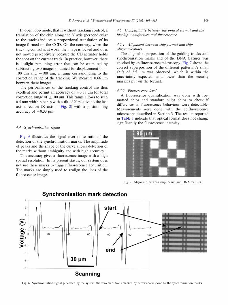
4.4. Synchronisation signal
Fig. 6 illustrates the signal over noise ratio of the
detection of the synchronisation marks. The amplitude
of peaks and the shape of the curve allows detection of
the marks without ambiguity and with high accuracy.
This accuracy gives a fluorescence image with a high
spatial resolution. In its present status, our system does
not use these marks to trigger fluorescence acquisition.
The marks are simply used to realign the lines of the
fluorescence image.
4.5. Compatibility between the optical format and the
biochip manufacture and fluorescence
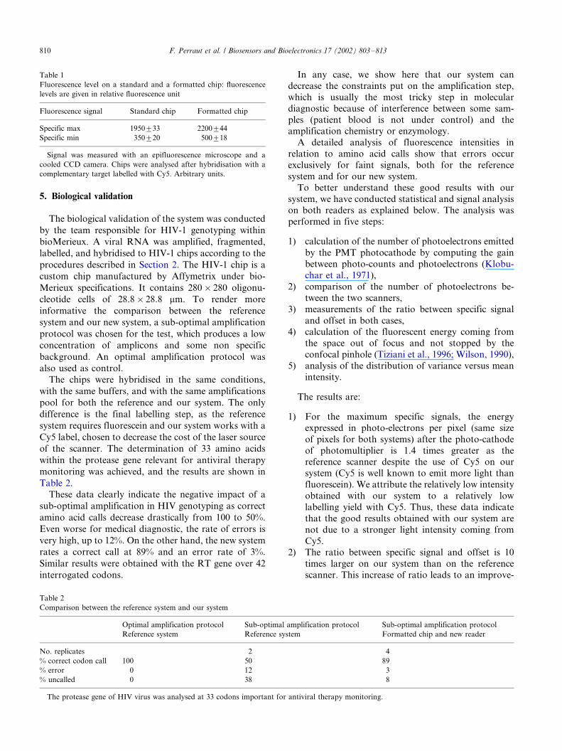
4.5.1. Alignment between chip format and chip
oligonucleotides
The aligned superposition of the guiding tracks and
synchronisation marks and of the DNA features was
checked by epifluorescence microscopy. Fig. 7 shows thecorrect superposition of the different pattern. A small
shift of 2.5 mm was observed, which is within the
uncertainty expected, and lower than the security
margins put on the format.
4.5.2. Fluorescence level
A fluorescence quantification was done with for-
matted chips and standard silica chips to check if
differences in fluorescence behaviour were detectable.
Measurements were done with the epifluorescence
microscope described in Section 3. The results reportedin Table 1 indicate that optical format does not change
significantly the fluorescence intensity.
Fig. 6. Synchronisation signal generated by the system: the zero transitions marked by arrows correspond to the synchronisation marks.
Fig. 7. Alignment between chip format and DNA features.
F. Perraut et al. / Biosensors and Bioelectronics 17 (2002) 803�/813 809
5. Biological validation
The biological validation of the system was conducted
by the team responsible for HIV-1 genotyping within
bioMerieux. A viral RNA was amplified, fragmented,
labelled, and hybridised to HIV-1 chips according to the
procedures described in Section 2. The HIV-1 chip is a
custom chip manufactured by Affymetrix under bio-
Merieux specifications. It contains 280�/280 oligonu-
cleotide cells of 28.8�/28.8 mm. To render more
informative the comparison between the reference
system and our new system, a sub-optimal amplification
protocol was chosen for the test, which produces a low
concentration of amplicons and some non specific
background. An optimal amplification protocol was
also used as control.
The chips were hybridised in the same conditions,
with the same buffers, and with the same amplifications
pool for both the reference and our system. The only
difference is the final labelling step, as the reference
system requires fluorescein and our system works with a
Cy5 label, chosen to decrease the cost of the laser source
of the scanner. The determination of 33 amino acids
within the protease gene relevant for antiviral therapy
monitoring was achieved, and the results are shown in
Table 2.
These data clearly indicate the negative impact of a
sub-optimal amplification in HIV genotyping as correct
amino acid calls decrease drastically from 100 to 50%.
Even worse for medical diagnostic, the rate of errors is
very high, up to 12%. On the other hand, the new system
rates a correct call at 89% and an error rate of 3%.
Similar results were obtained with the RT gene over 42
interrogated codons.
In any case, we show here that our system can
decrease the constraints put on the amplification step,
which is usually the most tricky step in molecular
diagnostic because of interference between some sam-ples (patient blood is not under control) and the
amplification chemistry or enzymology.
A detailed analysis of fluorescence intensities in
relation to amino acid calls show that errors occur
exclusively for faint signals, both for the reference
system and for our new system.
To better understand these good results with our
system, we have conducted statistical and signal analysison both readers as explained below. The analysis was
performed in five steps:
1) calculation of the number of photoelectrons emitted
by the PMT photocathode by computing the gain
between photo-counts and photoelectrons (Klobu-
char et al., 1971),
2) comparison of the number of photoelectrons be-
tween the two scanners,
3) measurements of the ratio between specific signal
and offset in both cases,4) calculation of the fluorescent energy coming from
the space out of focus and not stopped by the
confocal pinhole (Tiziani et al., 1996; Wilson, 1990),
5) analysis of the distribution of variance versus mean
intensity.
The results are:
1) For the maximum specific signals, the energy
expressed in photo-electrons per pixel (same size
of pixels for both systems) after the photo-cathode
of photomultiplier is 1.4 times greater as thereference scanner despite the use of Cy5 on our
system (Cy5 is well known to emit more light than
fluorescein). We attribute the relatively low intensity
obtained with our system to a relatively low
labelling yield with Cy5. Thus, these data indicate
that the good results obtained with our system are
not due to a stronger light intensity coming from
Cy5.2) The ratio between specific signal and offset is 10
times larger on our system than on the reference
scanner. This increase of ratio leads to an improve-
Table 1
Fluorescence level on a standard and a formatted chip: fluorescence
levels are given in relative fluorescence unit
Fluorescence signal Standard chip Formatted chip
Specific max 1950933 2200944
Specific min 350920 500918
Signal was measured with an epifluorescence microscope and a
cooled CCD camera. Chips were analysed after hybridisation with a
complementary target labelled with Cy5. Arbitrary units.
Table 2
Comparison between the reference system and our system
Optimal amplification protocol Sub-optimal amplification protocol Sub-optimal amplification protocol
Reference system Reference system Formatted chip and new reader
No. replicates 2 4
% correct codon call 100 50 89
% error 0 12 3
% uncalled 0 38 8
The protease gene of HIV virus was analysed at 33 codons important for antiviral therapy monitoring.
F. Perraut et al. / Biosensors and Bioelectronics 17 (2002) 803�/813810
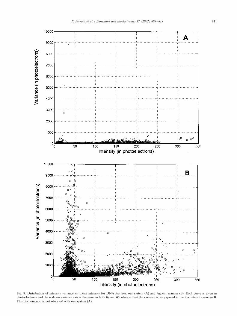
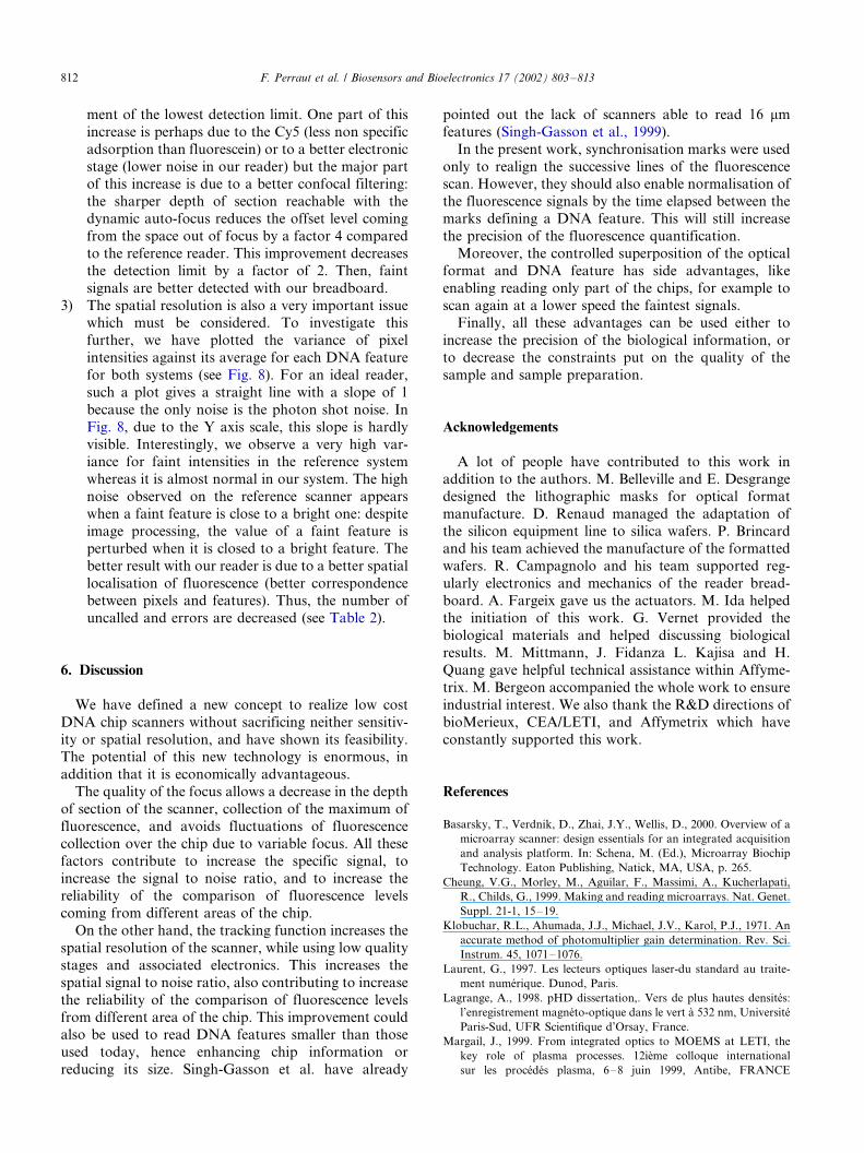
Fig. 8. Distribution of intensity variance vs. mean intensity for DNA features: our system (A) and Agilent scanner (B). Each curve is given in
photoelectrons and the scale on variance axis is the same in both figure. We observe that the variance is very spread in the low intensity zone in B.
This phenomenon is not observed with our system (A).
F. Perraut et al. / Biosensors and Bioelectronics 17 (2002) 803�/813 811
ment of the lowest detection limit. One part of this
increase is perhaps due to the Cy5 (less non specific
adsorption than fluorescein) or to a better electronic
stage (lower noise in our reader) but the major partof this increase is due to a better confocal filtering:
the sharper depth of section reachable with the
dynamic auto-focus reduces the offset level coming
from the space out of focus by a factor 4 compared
to the reference reader. This improvement decreases
the detection limit by a factor of 2. Then, faint
signals are better detected with our breadboard.
3) The spatial resolution is also a very important issuewhich must be considered. To investigate this
further, we have plotted the variance of pixel
intensities against its average for each DNA feature
for both systems (see Fig. 8). For an ideal reader,
such a plot gives a straight line with a slope of 1
because the only noise is the photon shot noise. In
Fig. 8, due to the Y axis scale, this slope is hardly
visible. Interestingly, we observe a very high var-iance for faint intensities in the reference system
whereas it is almost normal in our system. The high
noise observed on the reference scanner appears
when a faint feature is close to a bright one: despite
image processing, the value of a faint feature is
perturbed when it is closed to a bright feature. The
better result with our reader is due to a better spatial
localisation of fluorescence (better correspondencebetween pixels and features). Thus, the number of
uncalled and errors are decreased (see Table 2).
6. Discussion
We have defined a new concept to realize low cost
DNA chip scanners without sacrificing neither sensitiv-
ity or spatial resolution, and have shown its feasibility.The potential of this new technology is enormous, in
addition that it is economically advantageous.
The quality of the focus allows a decrease in the depth
of section of the scanner, collection of the maximum of
fluorescence, and avoids fluctuations of fluorescence
collection over the chip due to variable focus. All these
factors contribute to increase the specific signal, to
increase the signal to noise ratio, and to increase thereliability of the comparison of fluorescence levels
coming from different areas of the chip.
On the other hand, the tracking function increases the
spatial resolution of the scanner, while using low quality
stages and associated electronics. This increases the
spatial signal to noise ratio, also contributing to increase
the reliability of the comparison of fluorescence levels
from different area of the chip. This improvement couldalso be used to read DNA features smaller than those
used today, hence enhancing chip information or
reducing its size. Singh-Gasson et al. have already
pointed out the lack of scanners able to read 16 mm
features (Singh-Gasson et al., 1999).
In the present work, synchronisation marks were used
only to realign the successive lines of the fluorescencescan. However, they should also enable normalisation of
the fluorescence signals by the time elapsed between the
marks defining a DNA feature. This will still increase
the precision of the fluorescence quantification.
Moreover, the controlled superposition of the optical
format and DNA feature has side advantages, like
enabling reading only part of the chips, for example to
scan again at a lower speed the faintest signals.Finally, all these advantages can be used either to
increase the precision of the biological information, or
to decrease the constraints put on the quality of the
sample and sample preparation.
Acknowledgements
A lot of people have contributed to this work inaddition to the authors. M. Belleville and E. Desgrange
designed the lithographic masks for optical format
manufacture. D. Renaud managed the adaptation of
the silicon equipment line to silica wafers. P. Brincard
and his team achieved the manufacture of the formatted
wafers. R. Campagnolo and his team supported reg-
ularly electronics and mechanics of the reader bread-
board. A. Fargeix gave us the actuators. M. Ida helpedthe initiation of this work. G. Vernet provided the
biological materials and helped discussing biological
results. M. Mittmann, J. Fidanza L. Kajisa and H.
Quang gave helpful technical assistance within Affyme-
trix. M. Bergeon accompanied the whole work to ensure
industrial interest. We also thank the R&D directions of
bioMerieux, CEA/LETI, and Affymetrix which have
constantly supported this work.
References
Basarsky, T., Verdnik, D., Zhai, J.Y., Wellis, D., 2000. Overview of a
microarray scanner: design essentials for an integrated acquisition
and analysis platform. In: Schena, M. (Ed.), Microarray Biochip
Technology. Eaton Publishing, Natick, MA, USA, p. 265.
Cheung, V.G., Morley, M., Aguilar, F., Massimi, A., Kucherlapati,
R., Childs, G., 1999. Making and reading microarrays. Nat. Genet.
Suppl. 21-1, 15�/19.
Klobuchar, R.L., Ahumada, J.J., Michael, J.V., Karol, P.J., 1971. An
accurate method of photomultiplier gain determination. Rev. Sci.
Instrum. 45, 1071�/1076.
Laurent, G., 1997. Les lecteurs optiques laser-du standard au traite-
ment numerique. Dunod, Paris.
Lagrange, A., 1998. pHD dissertation,. Vers de plus hautes densites:
l’enregistrement magneto-optique dans le vert a 532 nm, Universite
Paris-Sud, UFR Scientifique d’Orsay, France.
Margail, J., 1999. From integrated optics to MOEMS at LETI, the
key role of plasma processes. 12ieme colloque international
sur les procedes plasma, 6�/8 juin 1999, Antibe, FRANCE
F. Perraut et al. / Biosensors and Bioelectronics 17 (2002) 803�/813812

(CIP99). Proceedings edited by Societe Francaise du Vide, Paris,
France.
Monnot, V., Tora, C., Lopez, S., Menou, L., Laayoun, A., 2001.
Labeling during cleavage (LDC), a new labeling approach for
RNA. Nucleos. Nucleot. Nucleic Acids 20 (4-7), 1177�/1179.
Pease, A.C., Solas, D., Sullivan, E.J., Cronin, M.T., Holmes, C.P.,
Fodor, S.P., 1994. Light-generated oligonucleotide arrays for rapid
DNA sequence analysis. Proc. Natl. Acad. Sci. USA 91, 5022�/
5026.
Ramsay, G., 1998. DNA chips: state-of-the-art. Nat. Biotechnol. 16
(1), 40�/44.
Singh-Gasson, S., Green, R.D., Yue, Y., Nelson, C., Blattner, F.,
Sussman, M.R., Cerrina, F., 1999. Maskless fabrication of light-
directed oligonucleotide microarrays using a digital micromirror
array. Nat. Biotechnol. 17 (10), 974�/978.
Tiziani, H.J., Achi, R., Kramer, R.N., Wiegers, L., 1996. Theoretical
analysis of confocal microscopy with microlenses. Appl. Optics 35
(1), 120�/125.
Troesch, A., Nguyen, H., Miyada, C.G., Desvarenne, S., Gingeras,
T.R., Kaplan, P.M., Cros, P., Mabilat, C., 1999. Mycobacterium
species identification and rifampin resistance testing with high-
density DNA probe array. J. Clin. Microbiol. 37 (1), 49�/55.
Wilson, T., 1990. Confocal Microscopy. Academic Press, New York.
F. Perraut et al. / Biosensors and Bioelectronics 17 (2002) 803�/813 813