a multichannel integrated circuit for electrical recording of neural activity, with independent...
TRANSCRIPT

IEEE TRANSACTIONS ON BIOMEDICAL CIRCUITS AND SYSTEMS, VOL. 6, NO. 2, APRIL 2012 101
A Multichannel Integrated Circuit for ElectricalRecording of Neural Activity, With Independent
Channel ProgrammabilityCarolina Mora Lopez, Student Member, IEEE, Dimiter Prodanov, Dries Braeken, Ivan Gligorijevic,
Wolfgang Eberle, Senior Member, IEEE, Carmen Bartic, Robert Puers, Fellow, IEEE, andGeorges Gielen, Fellow, IEEE
Abstract—Since a few decades, micro-fabricated neural probesare being used, together with microelectronic interfaces, to getmore insight in the activity of neuronal networks. The need forhigher temporal and spatial recording resolutions imposes newchallenges on the design of integrated neural interfaces withrespect to power consumption, data handling and versatility. Inthis paper, we present an integrated acquisition system for in vitroand in vivo recording of neural activity. The ASIC consists of16 low-noise, fully-differential input channels with independentprogrammability of its amplification (from 100 to 6000 V/V) andfiltering (1–6000 Hz range) capabilities. Each channel is AC-cou-pled and implements a fourth-order band-pass filter in order tosteeply attenuate out-of-band noise and DC input offsets. Thesystem achieves an input-referred noise density of 37 �� ��, aNEF of 5.1, a ���� � �, a �� �� and a samplingrate of 30 kS/s per channel, while consuming a maximum of 70� per channel from a single 3.3 V. The ASIC was implemented
in a 0.35 � CMOS technology and has a total area of 5.6 4.5���. The recording system was successfully validated in in vitroand in vivo experiments, achieving simultaneous multichannelrecordings of cell activity with satisfactory signal-to-noise ratios.
Index Terms—CMOS interface, in vitro recording, in vivorecording, low-noise neural recording, multichannel integratedcircuit, programmable biosensor interface.
I. INTRODUCTION
T HE investigation of neural networks is not only of greatimportance to understand the basic function of the brain,
but moreover it can lead to a better comprehension of severebrain disorders such as Alzheimer’s and Parkinson’s diseases,epilepsy, autism and psychiatric disorders [1], [2]. Novel ad-vances in computational capabilities, design tools and micro-electrode fabrication techniques allow for the development ofneural prostheses capable of interfacing with single neuronsand neuronal networks. To obtain this resolution of interfacing,
Manuscript received July 29, 2011; revised October 18, 2011; accepted De-cember 10, 2011. Date of publication February 13, 2012; date of current versionApril 19, 2012. This work was supported in part by the Flemish Government(IWT SBO Grant BrainStar). This paper was recommended by Associate Ed-itor M. Stanacevic.
C. Mora Lopez, D. Prodanov, D. Braeken, and W. Eberle are with Imec,B-3001 Leuven, Belgium (e-mail: [email protected]).
I. Gligorijevic, R. Puers, and G. Gielen are with the Electrical EngineeringDepartment-ESAT, Katholieke Universiteit Leuven, B-3001 Leuven, Belgium.
C. Bartic is with the Department of Physics and Astronomy, Katholieke Uni-versiteit Leuven, B-3001 Leuven, Belgium.
Digital Object Identifier 10.1109/TBCAS.2011.2181842
neural probes and the electrodes fabricated on these devicesneed to be customized to the anatomy and morphology of therecording site [3]. Besides this, multi-site recording function-ality that allows for simultaneous recording of neural activity indifferent brain areas is a requisite for neural interface devices.
Currently, multi-electrode arrays are being combined withCMOS electronics in an effort to convert classical passive neuralprobes into more sophisticated active neural probes. This mi-gration, mainly motivated by the need of proximity betweenelectrodes and circuitry, and the increasing density in multi-electrode arrays are generating important circuit design chal-lenges with regard to miniaturization, noise and power dissipa-tion reduction, programmability and handling of large quantityof output data.
Neural signals, usually measured with extracellular micro-electrodes, consist of action potentials (APs) or spikes super-imposed on low-frequency local field potentials (LFPs). BothAPs and LFPs are important to answer neuroscientific ques-tions and they can be, to some extent, studied distinctly usingband-separation techniques. APs are estimated by examiningthe power variation of the signals in the high-frequency range(typically 300–6000 Hz), whereas the LFPs are assessed by thepower variation in the low-frequency range (i.e., 1–200 Hz) [4].In addition, the spikes of a small group of neurons near theelectrode can be detected and classified, providing informationon single-unit activity. LFPs are usually divided into bands inorder to study activity patterns of a larger population of neu-rons, giving information about the state of the neural networkwhich is difficult to capture using spiking activity from only afew neurons [5]. Recently, it has been shown that when spikesand LFPs are measured simultaneously, substantially more in-formation about an external stimulus can be extracted when an-alyzing firing and phase information together [6], [7]. Thus,simultaneous examination of both spiking activity and LFPscan provide a better understanding of the organization of thesynaptic inputs (e.g., LFPs) to neurons and of the relationshipbetween spikes and LFPs [8]. One of the major challenges forthe recording of neural signals is therefore the successful andsimultaneous conditioning of both AP and LFP signals with op-timized parameters according to their nature. As these two kindsof signals have different amplitude ranges (30–1000 for APsand 1–10 mV for LFPs) and bandwidths, they also require dif-ferent gains, filters and even electrode sizes in order to be opti-mally measured.
1932-4545/$31.00 © 2012 IEEE
102 IEEE TRANSACTIONS ON BIOMEDICAL CIRCUITS AND SYSTEMS, VOL. 6, NO. 2, APRIL 2012
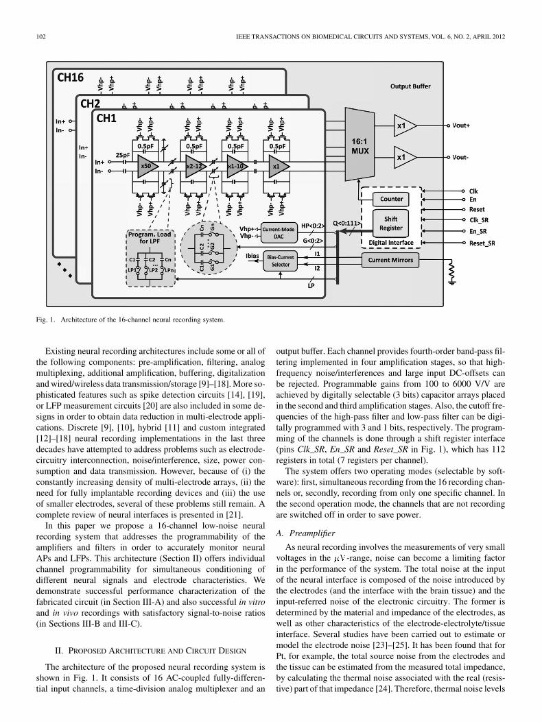
Fig. 1. Architecture of the 16-channel neural recording system.
Existing neural recording architectures include some or all ofthe following components: pre-amplification, filtering, analogmultiplexing, additional amplification, buffering, digitalizationand wired/wireless data transmission/storage [9]–[18]. More so-phisticated features such as spike detection circuits [14], [19],or LFP measurement circuits [20] are also included in some de-signs in order to obtain data reduction in multi-electrode appli-cations. Discrete [9], [10], hybrid [11] and custom integrated[12]–[18] neural recording implementations in the last threedecades have attempted to address problems such as electrode-circuitry interconnection, noise/interference, size, power con-sumption and data transmission. However, because of (i) theconstantly increasing density of multi-electrode arrays, (ii) theneed for fully implantable recording devices and (iii) the useof smaller electrodes, several of these problems still remain. Acomplete review of neural interfaces is presented in [21].
In this paper we propose a 16-channel low-noise neuralrecording system that addresses the programmability of theamplifiers and filters in order to accurately monitor neuralAPs and LFPs. This architecture (Section II) offers individualchannel programmability for simultaneous conditioning ofdifferent neural signals and electrode characteristics. Wedemonstrate successful performance characterization of thefabricated circuit (in Section III-A) and also successful in vitroand in vivo recordings with satisfactory signal-to-noise ratios(in Sections III-B and III-C).
II. PROPOSED ARCHITECTURE AND CIRCUIT DESIGN
The architecture of the proposed neural recording system isshown in Fig. 1. It consists of 16 AC-coupled fully-differen-tial input channels, a time-division analog multiplexer and an
output buffer. Each channel provides fourth-order band-pass fil-tering implemented in four amplification stages, so that high-frequency noise/interferences and large input DC-offsets canbe rejected. Programmable gains from 100 to 6000 V/V areachieved by digitally selectable (3 bits) capacitor arrays placedin the second and third amplification stages. Also, the cutoff fre-quencies of the high-pass filter and low-pass filter can be digi-tally programmed with 3 and 1 bits, respectively. The program-ming of the channels is done through a shift register interface(pins Clk_SR, En_SR and Reset_SR in Fig. 1), which has 112registers in total (7 registers per channel).
The system offers two operating modes (selectable by soft-ware): first, simultaneous recording from the 16 recording chan-nels or, secondly, recording from only one specific channel. Inthe second operation mode, the channels that are not recordingare switched off in order to save power.
A. Preamplifier
As neural recording involves the measurements of very smallvoltages in the -range, noise can become a limiting factorin the performance of the system. The total noise at the inputof the neural interface is composed of the noise introduced bythe electrodes (and the interface with the brain tissue) and theinput-referred noise of the electronic circuitry. The former isdetermined by the material and impedance of the electrodes, aswell as other characteristics of the electrode-electrolyte/tissueinterface. Several studies have been carried out to estimate ormodel the electrode noise [23]–[25]. It has been found that forPt, for example, the total source noise from the electrodes andthe tissue can be estimated from the measured total impedance,by calculating the thermal noise associated with the real (resis-tive) part of that impedance [24]. Therefore, thermal noise levels

MORA LOPEZ et al.: MULTICHANNEL INTEGRATED CIRCUIT FOR ELECTRICAL RECORDING 103
are highly dependent on the impedance of the electrode-tissueinterface for each individual recording site (due to the foreignbody reaction) and the selected recording bandwidth [25]. Theinput-referred noise of the electronic circuitry mainly includesthermal and flicker noise of the circuit input stage, which mustbe kept lower than the electrode noise so that it has a minorcontribution to the overall noise. Therefore, the design of thepreamplifier involves numerous trade-offs with other importantspecifications such as power consumption and area. If the inputstage is an operational transconductance amplifier (OTA), theideal input-referred noise, assuming differential-pair transistorsin the sub-threshold region and a first-order frequency response,can be expressed as [26]
(1)
where is Boltzmann’s constant, is the absolute temperature,is the thermal voltage, is the sub-threshold gate coupling
coefficient, is the nominal current in each input transistor andis the bandwidth of the amplifier. As can be seen,
for a given bandwidth the noise is inversely proportional to thesquare root of the supply current, that is, there exists a trade-offbetween noise and power consumption.
An important figure of merit in the design of biopotential am-plifiers is the noise-efficiency factor (NEF) [27], which scalesthe noise, power and bandwidth of a design against a referenceBJT amplifier. The NEF is calculated as
(2)
where is the total supply current of the amplifier.In this design, the preamplifier [Fig. 2(a)] is a fully-differen-
tial folded-cascode OTA with a closed-loop gain of 50, set bya feedback capacitor ratio of 25 pF/0.5 pF. The input differen-tial pair is formed by two PMOS transistors operating in thesub-threshold (weak inversion) region, which maximizes theirtransconductance-over-drain-current ratio and, therefore, min-imizes their thermal noise contribution [28]. Also, transistorsM4-M5 and M10-M11 are operated in the strong inversion re-gion to minimize their noise contribution, resulting in a trade-offwith the output signal swing. All transistors are made as largeas possible to minimize the flicker noise. Table I shows the di-mensions and the operating conditions (drain currents and theinversion coefficients) of each transistor in the OTA. Simula-tion results show that the OTA has an open-loop gain of 105 dB,a phase margin of 84 , a unit gain bandwidth of 760 kHz andan input-referred noise of 1.9 , while consuming a totalcurrent of 20 . The inputs are capacitively coupled in orderto eliminate DC offsets coming from the electrode-electrolyte/tissue interface. A continuos-time common-mode feedback cir-cuit [Fig. 2(b) [22]] has been used to control the common-modevoltage at the output nodes. Additional programmable gainsof maximum 12 and 10 V/V are added in the subsequent twostages, respectively.
B. Filters
The high-pass filtering characteristic in each channel isachieved by the parallel combination of the feedback capacitors
Fig. 2. Schematic of the preamplifier. (a) Fully-differential folded-cascodeinput amplifier. (b) Continuos-time CMFB circuit [22].
TABLE ISIZES AND OPERATING POINTS FOR TRANSISTORS IN THE PREAMPLIFIER
and the feedback PMOS-NMOS pseudo-resistor elements,which are biased in the deep-subthreshold region. Thesevoltage-controlled pseudo-resistors [28] can achieve very highresistance values in the order of , providing an area-ef-ficient way to implement very low frequency filters. The cutofffrequency can be tuned via a current-mode digital-to-analogconverter (Fig. 3) that changes the gate voltages of the tran-sistors (i.e., the resistance), in order to accept or reject theLFP signal frequencies. This circuit consists of a wide-swingcascode current mirror that copies the selected current to thediode-connected transistors Mn and Mp, which are sized withlarge ratios. A similar method was previously describedby Yin et al. [30]. The appropriate biasing of the gate of thePMOS and NMOS transistors enables the linearization of the

104 IEEE TRANSACTIONS ON BIOMEDICAL CIRCUITS AND SYSTEMS, VOL. 6, NO. 2, APRIL 2012
Fig. 3. Current-mode digital-to-analog converter to control the PMOS-NMOSpseudo-resistors.
Fig. 4. Rail-to-rail output buffer to drive an external load (ADC). It uses therecycling folded-cascode architecture described in [29].
resistance, as well as the programming of process-independentcutoff frequency values. A total of 6 predefined cutoff frequen-cies can be digitally selected with 3 control bits.
The fourth-order low-pass filter characteristic is implementedby the cascade of four first-order voltage integrators, consistingof an OTA and a load capacitor. The load capacitors are imple-mented as programmable capacitor arrays that allow the selec-tion (1 bit) of two different frequency ranges: one for the LFPsignals and another for the AP signals. Also, when the low-fre-quency LFP-recording mode is selected, the supply current ofthe amplifiers is lowered in order to save power ( ). Intotal, 7 bits are used to program independently the gain and theband-pass filter of each channel.
C. Output Stage
The output stage consists of an analog time-division mul-tiplexer and an output buffer. For the implementation of thetime-division analog multiplexer, an array of standard trans-mission gates is used to achieve rail-to-rail voltage operation.The multiplexer is controlled by a digital counter in order tosample each channel with a minimum rate of 12.5 kS/s. Twosingle-ended output buffers are placed at the output of the mul-tiplexer to drive an external load (an ADC or other instrument)of maximum 70 pF. The design of this buffer is also critical as ithas to be able to handle a large input voltage swing and a min-imum sampling rate of 200 kS/s.
The schematic of the output buffer is shown in Fig. 4. It is arail-to-rail amplifier, designed to have a(i.e., for a maximum sampling rate of 60 kS/s per channel)
Fig. 5. Die photo of the 16-channel neural recording system. The total area is5.6� 4.5�� and the core area is 4.1� 3.8 �� .
with a current consumption of 360 . The architecture of thisamplifier is based on the recycling folded-cascode architec-ture described by Assaad et al. [29], which achieves enhancedtransconductance, gain and slew rate while consuming the samepower budget as a conventional folded-cascode amplifier. Inour design, we have included double PMOS/NMOS differentialpairs in order to achieve rail-to-rail input operation. The shownamplifier makes part of a two-stage Miller CMOS OTA, wherethe second stage is just one single transistor with active load. Inthis way we can also achieve rail-to-rail output operation.
III. EXPERIMENTAL RESULTS
The 16-channel neural recording system in Fig. 1 has beenimplemented and fabricated in a 0.35 AMIS CMOStechnology. The capacitors are implemented as metal-insu-lator-metal capacitors and the resistors as polysilicon resistors.The die (Fig. 5) occupies a core area of 4.1 3.8 anda total area of 5.6 4.5 . The area of one channel is0.76 .
A. Performance Measurement
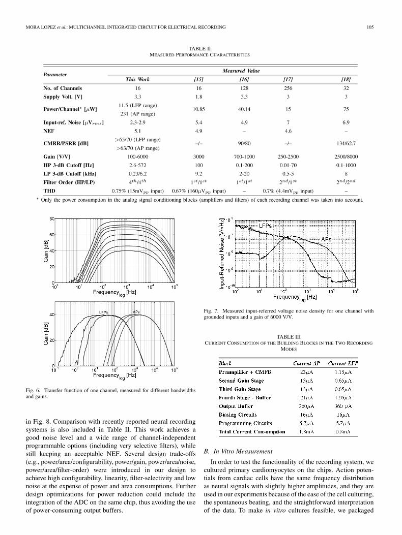
Table II summarizes the measured characteristics of theneural recording system and Table III gives an overview of thepower consumption distribution in the different building blocksof the circuit. The chip consumes 1.8 mA from a 3.3 V supply(i.e., 5.9 mW) when the chip is configured to record AP signals(200–6000 Hz bandwidth) and 0.8 mA (i.e., 2.6 mW) when itrecords LFP signals (1–200 Hz bandwidth). One channel con-sumes 70 and 17 in the two configurations, respectively.Fig. 6 shows the frequency response of one channel measuredwith a spectrum analyzer. Gains of approximately 100, 200,500, 1000, 2000, 3000, 4000 and 6000 V/V can be digitallyprogrammed for all the frequency ranges. The measuredprogrammable cutoff frequencies of the high-pass filter are 2.6,5.6, 13.4, 213, 323 and 572 Hz, and the programmable cutofffrequencies of the low-pass filter are 230 Hz and 6.2 kHz.The input-referred noise (Fig. 7) was also measured for thedifferent programmable modes and it was calculated to bebetween 2.3 and 2.9 (integrated from 1 Hz to 6 kHz).The CMRR, also measured with a spectrum analyzer, is shown
MORA LOPEZ et al.: MULTICHANNEL INTEGRATED CIRCUIT FOR ELECTRICAL RECORDING 105
TABLE IIMEASURED PERFORMANCE CHARACTERISTICS
Fig. 6. Transfer function of one channel, measured for different bandwidthsand gains.
in Fig. 8. Comparison with recently reported neural recordingsystems is also included in Table II. This work achieves agood noise level and a wide range of channel-independentprogrammable options (including very selective filters), whilestill keeping an acceptable NEF. Several design trade-offs(e.g., power/area/configurability, power/gain, power/area/noise,power/area/filter-order) were introduced in our design toachieve high configurability, linearity, filter-selectivity and lownoise at the expense of power and area consumptions. Furtherdesign optimizations for power reduction could include theintegration of the ADC on the same chip, thus avoiding the useof power-consuming output buffers.
Fig. 7. Measured input-referred voltage noise density for one channel withgrounded inputs and a gain of 6000 V/V.
TABLE IIICURRENT CONSUMPTION OF THE BUILDING BLOCKS IN THE TWO RECORDING
MODES
B. In Vitro Measurement
In order to test the functionality of the recording system, wecultured primary cardiomyocytes on the chips. Action poten-tials from cardiac cells have the same frequency distributionas neural signals with slightly higher amplitudes, and they areused in our experiments because of the ease of the cell culturing,the spontaneous beating, and the straightforward interpretationof the data. To make in vitro cultures feasible, we packaged

106 IEEE TRANSACTIONS ON BIOMEDICAL CIRCUITS AND SYSTEMS, VOL. 6, NO. 2, APRIL 2012
Fig. 8. Measured CMRR for one channel with shorted inputs and a gain of6000 V/V.
Fig. 9. Pictures of the setups used for neural recording. (a) In vitro setup con-sisting of a packaged multi-electrode (probe) test chip (left), a mechanical struc-ture to contact the probe test chip and the PCB (10� 9 �� ) with the recordingchip (right). (b) In vivo setup consisting of a 1-cm-long neural probe with 13electrodes [31], the PCB (9� 9 �� ) with the recording chip (left) and a stereo-tactic frame connected to a micro-drive (right).
multi-electrode test chips on a custom PCB. A glass ring wasglued on top of the PCB to contain the cells and the cell medium.Cardiac cells were extracted from hearts of rat embryos andgrown for 4 days in vitro on top of the packaged micro-fabri-cated probes with 50 titanium-nitride electrodes [31]. Theexperimental setup [see Fig. 9(a)] consisted of a mechanical de-vice to hold and allow electrical contact to the multi-electrodetest chip, a PCB containing the recording chip and an externalADC with 12-bit resolution (Analog Devices AD7450A), andthe interface with the computer (through a National Instruments
Fig. 10. Pseudo-fluorescence images of Fluo-4 loaded cardiac cells in overlaywith neural probe images (left). Relative intracellular �� change (���� )in the cell during spontaneous activity in the regions of interest Ch1, Ch2, Ch3and Ch4 (top right). Recording of electrical action potentials (bottom right).
USB-6259 data acquisition card). The computer has custom-de-veloped acquisition software (in Matlab), which allows the pro-gramming of the chip as well as the real-time transmission, dis-play and storing of the recorded data. Signals with amplitudesas small as 40 were detected due to the low input noiselevels (around 10–30 , coming mainly from the elec-trodes).
In order to validate the spikes that were recorded with ourchips and to make sure they originate from cells on top of theelectrodes, we performed Fluo4-AM calcium imaging exper-iments on the cardiac cells while recording electrical signalswith the chip. This technique, based on the optical detection ofchanges in the intracellular calcium concentration ( ), al-lows to identify the origin of the electrical activity of the beatingcells. Hence, large calcium transients in these embryonic cellsare coinciding with action potentials, and thus the presence ofa change in the on top of an electrode is representedby an action potential. This technique also allows us to mea-sure the spatiotemporal distribution of the electrical signal ontop of multiple electrodes. Fig. 10 represents the relative fluo-rescence intensity ( ) at four different electrodes (areas ofinterest are marked with circles Ch1, Ch2, Ch3 and Ch4 ), cap-tured by a CCD camera coupled to a fluorescence microscope.In this graph, we also show the electrical signals measured fromfour electrodes underneath the marked circles, which were mea-sured with four adjacent channels in our recording system. Itis clear that the measured APs coincide with large tran-sients, although the latter last longer in comparison to the AP.The slow calcium transient is due to influx of inside thecell through opening of voltage-gated channels, and itsrelative slow clearance out of the cell by calcium transporters[32]. This experiment demonstrates that the signals recorded bythe presented recording system and micro-fabricated chip cor-respond to actual cardiac action potentials.
C. In Vivo Measurement
We have also validated our integrated recording system inin vivo experiments. For that, we have used an implantablemicro-machined 1-cm-long neural probe [31], containing13 Pt electrodes (one large triangular electrode with an areaof 0.007 , one large rectangular electrode with an areaof 0.022 and 11 small circular electrodes with 10, 25 or
MORA LOPEZ et al.: MULTICHANNEL INTEGRATED CIRCUIT FOR ELECTRICAL RECORDING 107
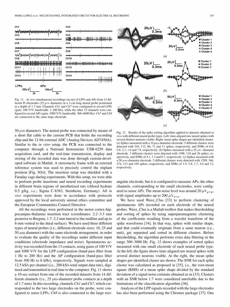
Fig. 11. In vivo simultaneous recordings (in rat) of LFPs and APs from 13 dif-ferent Pt electrodes (25 �� diameter) in a 1-cm-long neural probe positionedat a depth of 1.7 mm. Channels Ch1 and Ch7 were configured to record LFPs(gain: 100 V/V, bandwidth: 1–200 Hz), while the other 12 channels were con-figured to record APs (gain: 1000 V/V, bandwidth: 300–6000 Hz). Ch7 and Ch8are connected to the same large electrode.
50 diameter). The neural probe was connected by means ofa short flat cable to the custom PCB that holds the recordingchip and the 12-bit external ADC (Analog Devices AD7450A).Similar to the in vitro setup, the PCB was connected to thecomputer through a National Instruments USB-6259 dataacquisition card, and the real-time transmission, display andstoring of the recorded data was done through custom-devel-oped software in Matlab. A stereotactic frame with an externalreference system was used to precisely control the implantposition [Fig. 9(b)]. The insertion setup was shielded with aFaraday cage during experiments. With this setup, we were ableto perform probe insertions and neural recording experimentsin different brain regions of anesthetized rats (chloral hydrate0.5 g/kg, s.c.; Sigma C-8383, Steinheim, Germany). All invivo experiments were done in accordance with protocolsapproved by the local university animal ethics committee andthe European Communities Council Directive.
All the recordings were performed in the motor cortex-hip-pocampus-thalamus insertion tract (coordinates: 2.2–3.3 mmposterior to Bregma, 1.7–2.2 mm lateral to the midline and up to6 mm ventral to the dural surface). We have used three differenttypes of neural probes (i.e., different electrode sizes: 10, 25 and50 diameter) with the same electrode arrangement, in orderto evaluate the quality of the recordings under different inputconditions (electrode impedance and noise). Spontaneous ac-tivity was recorded from the 13 contacts, using gains of 100 V/Vand 1000 V/V for the LFP configuration (band-pass filter from1 Hz to 200 Hz) and the AP configuration (band-pass filterfrom 300 Hz to 6 kHz), respectively. Signals were sampled at12.5 kS/s per channel (i.e., 200 kS/s total output data rate), digi-tized and transmitted in real time to the computer. Fig. 11 showsa 10-sec extract from one of the recorded datasets from 14 dif-ferent channels (i.e., 25 -diameter probe contacts at a depthof 1.7 mm). In this recording, channels Ch1 and Ch7, which cor-responded to the two large electrodes on the probe, were con-figured to sense LFPs; Ch8 is also connected to the large rect-
Fig. 12. Results of the spike sorting algorithm applied to datasets obtained invivo with different neural probe types. Left: time-aligned raw neural spikes withseveral distinct neurons visible. Right: mean spike shapes per identified cluster.(a) Spikes measured with a 10 ��-diameter electrode. 5 different clusters weredetected with 344, 112, 86, 71 and 11 spikes, respectively, and SNRs of 6.8,5.8, 2.1, 1.6 and 7.8, respectively. (b) Spikes measured with a 25 ��-diameterelectrode. 3 different clusters were detected with 1498, 118 and 26 spikes, re-spectively, and SNRs of 4.1, 1.3 and 0.7, respectively. (c) Spikes measured witha 50 ��-diameter electrode. 5 different clusters were detected with 1299, 366,274, 113 and 169 spikes, respectively, and SNRs of 1.9, 5.8, 1.7, 4.6 and 12,respectively.
angular electrode, but it is configured to measure APs; the otherchannels, corresponding to the small electrodes, were config-ured to sense APs. The mean noise level was around 20 ,with signal amplitudes up to 200 .
We have used Wave_Clus [33] to perform clustering ofspontaneous APs recorded on each electrode of the neuralprobes. Wave_Clus is a Matlab toolbox that makes thresholdingand sorting of spikes by using superparamagnetic clusteringof the coefficients resulting from a wavelet transform of thespike waveforms [34]. In that way, spikes with similar shape,and that could eventually originate from a same neuron (i.e.,unit), get separated and sorted in different clusters. Beforethresholding, the algorithm performs extra data filtering in therange 300–3000 Hz. Fig. 12 shows examples of sorted spikesmeasured with one small electrode of each neural probe type.At the left, the figure shows time-aligned raw neural spikes withseveral distinct neurons visible. At the right, the mean spikeshapes per identified cluster are shown. The SNR for each spikecluster was calculated as proposed in [35], i.e., the root-meansquare (RMS) of a mean spike shape divided by the standarddeviation of a signal noise estimate obtained as in [33]. Clusterswith an SNR below 1.7 were considered unreliable due to thelimitations of the classification algorithm [36].
Analysis of the LFP signals recorded with the large electrodeshas also been performed using the Chronux package [37]. One
108 IEEE TRANSACTIONS ON BIOMEDICAL CIRCUITS AND SYSTEMS, VOL. 6, NO. 2, APRIL 2012
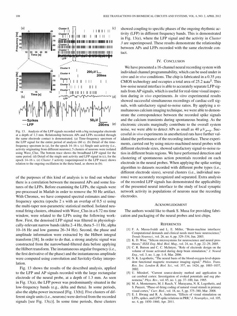
Fig. 13. Analysis of the LFP signals recorded with a big rectangular electrodeat a depth of 1.3 mm. Relationship between APs and LFPs recorded throughthe same electrode contact is demonstrated. (a) Time-frequency spectrum ofthe LFP signal for the entire period of analysis (60 s). (b) Detail of the time-frequency spectrum in (a), for the epoch 14–16 s. (c) Single unit activity (i.e.,activity originating from different neurons); 5 clusters of neurons were isolatedusing Wave_Clus. The bottom trace shows the broadband LFP signal for thesame period. (d) Detail of the single unit activity and LFP signal in (c), for theepoch 14–16 s. (e) Cluster 3 activity (superimposed to the LFP trace) showsrelation to the ongoing oscillation in the theta band, as shown in (b).
of the purposes of this kind of analysis is to find out whetherthere is a correlation between the measured APs and some fea-tures of the LFPs. Before examining the LFPs, the signals werepre-processed in Matlab in order to remove the 50 Hz artifact.With Chronux, we have computed spectral estimates and time-frequency spectra (epochs 2 s with an overlap of 0.5 s) usingthe multi-taper non-parametric statistical method. Isolated neu-ronal firing clusters, obtained with Wave_Clus in a 6.72 ms timewindow, were related to the LFPs using the following work-flow. First, the denoised LFP signal was filtered in physiologi-cally-relevant narrow bands (delta 2–4 Hz, theta 5–11 Hz, alpha10–16 Hz and low gamma 26–34 Hz). Second, the phase andamplitude information were extracted by the Hilbert integraltransform [38]. In order to do that, a strong analytic signal wasconstructed from the narrowband-filtered data before applyingthe Hilbert transform. The instantaneous angular frequency (i.e.,the first derivative of the phase) and the instantaneous amplitudewere computed using convolution and Savitzky-Golay interpo-lation.
Fig. 13 shows the results of the described analysis, appliedto the LFP and AP signals recorded with the large rectangularelectrode of the neural probe, at a depth of 1.3 mm. As seenin Fig. 13(a), the LFP power was predominantly situated in thelow-frequency bands (e.g., delta and theta). In some periods,also the alpha power increased [Fig. 13(b)]. Five clusters of dif-ferent single units (i.e., neurons) were derived from the recordedsignals [see Fig. 13(c)]. In some time periods, these clusters
showed coupling to specific phases of the ongoing rhythmic ac-tivity (LFP) in different frequency bands. This is demonstratedin Fig. 13(e), where the LFP signal and the activity in Cluster3 are superimposed. These results demonstrate the relationshipbetween APs and LFPs recorded with the same electrode con-tact.
IV. CONCLUSION
We have presented a 16-channel neural recording system withindividual channel programmability, which can be used under invitro and in vivo conditions. The chip is fabricated in a 0.35CMOS technology and occupies a total area of 25.2 . Thislow-noise neural interface is able to accurately separate LFP sig-nals from AP signals, which is useful for real-time visual inspec-tion during in vivo experiments. In vitro experimental resultsshowed successful simultaneous recordings of cardiac-cell sig-nals, with satisfactory signal-to-noise ratios. By applying a si-multaneous calcium imaging technique, we were able to demon-strate the correspondence between the recorded spike signalsand the calcium transients during spontaneous beating. As theelectronic circuits marginally contribute to the overall systemnoise, we were able to detect APs as small as 40 . Suc-cessful in vivo experiments in anesthetized rats have further val-idated the performance of the recording interface. These experi-ments, carried out by using micro-machined neural probes withdifferent electrode sizes, showed satisfactory signal-to-noise ra-tios in different brain regions. We have performed detection andclustering of spontaneous action potentials recorded on eachelectrode in the neural probes. When applying the spike sortingalgorithm to datasets recorded with different probe types (i.e.,different electrode sizes), several clusters (i.e., individual neu-rons) were accurately recognized and separated. Extra analysisof the recorded LFP signals has demonstrated the applicabilityof the presented neural interface to the study of local synapticnetwork activity in populations of neurons near the recordingelectrodes.
ACKNOWLEDGMENT
The authors would like to thank S. Musa for providing fabri-cation and packaging of the neural probes and test chips.
REFERENCES
[1] F. A. Mussa-Ivaldi and L. E. Miller, “Brain-machine interfaces:Computational demands and clinical needs meet basic neuroscience,”Trends Neurosci., vol. 26, no. 6, pp. 329–334, Jun. 2003.
[2] K. D. Wise, “Silicon microsystems for neuroscience and neural pros-theses,” IEEE Eng. Med. Biol. Mag., vol. 24, no. 5, pp. 22–29, 2005.
[3] C. R. Butson and C. C. McIntyre, “Role of electrode design on thevolume of tissue activated during deep brain stimulation,” J. NeuralEng., vol. 3, no. 1, pp. 1–8, Mar. 2006.
[4] N. K. Logothetis, “The neural basis of the blood-oxygen-level-depen-dent functional magnetic resonance imaging signal,” Philos. Trans.Roy. Soc. London B, Biol. Sci., vol. 357, no. 1424, pp. 1003–1037,2002.
[5] U. Mitzdorf, “Current source-density method and application incat cerebral cortex: Investigation of evoked potentials and eeg phe-nomena,” Phys. Rev., vol. 65, no. 1, pp. 37–100, Jan. 1985.
[6] M. A. Montemurro, M. J. Rasch, Y. Murayama, N. K. Logothetis, andS. Panzeri, “Phase-of-firing coding of natural visual stimuli in primaryvisual cortex,” Curr. Biol., vol. 18, no. 5, pp. 375–380, Mar. 2008.
[7] E. J. Hwang and R. A. Andersen, “Effects of visual stimulation onLFPs, spikes, and LFP-spike relations in PRR,” J. Neurophys., vol. 105,no. 4, pp. 1850–1860, Apr. 2011.
MORA LOPEZ et al.: MULTICHANNEL INTEGRATED CIRCUIT FOR ELECTRICAL RECORDING 109
[8] G. Kreiman, C. P. Hung, A. Kraskov, R. Q. Quiroga, T. Poggio, and J.J. DiCarlo, “Object selectivity of local field potentials and spikes in themacaque inferior temporal cortex,” Neuron, vol. 49, no. 3, pp. 433–445,Feb. 2006.
[9] G. Santhanam, M. D. Linderman, V. Gilja, A. Afshar, S. I. Ryu, T.Meng, and K. Shenoy, “HermesB: A continuous neural recordingsystem for freely behaving primates,” IEEE Trans. Biomed. Eng., vol.54, no. 11, pp. 2037–2050, 2007.
[10] X. Ye, P. Wang, J. Liu, S. Zhang, J. Jiang, Q. Wang, W. Chen, andX. Zheng, “A portable telemetry system for brain stimulation and neu-ronal activity recording in freely behaving small animals,” J. Neurosci.Methods, vol. 174, no. 2, pp. 186–193, Sep. 2008.
[11] M. Chae, K. Chen, W. Liu, J. Kim, and M. Sivaprakasam, “A 4-channelwearable wireless neural recording system,” in Proc. IEEE Int. Symp.Circuits and Systems, 2008, pp. 1760–1763.
[12] K. Najafi and K. D. Wise, “An implantable multielectrode array withon-chip signal processing,” IEEE J. Solid-State Circuits, vol. 21, no. 6,pp. 1035–1044, 1986.
[13] E. Peeters, B. Puers, W. Sansen, J. Gybels, and P. d. Sutter, “A two-wire, digital output multichannel microprobe for recording single-unitneural activity,” Sens. Actuators B, Chem., vol. 4, no. 1-2, pp. 217–223,1991.
[14] R. R. Harrison, P. T. Watkins, R. J. Kier, R. O. Lovejoy, D. J. Black,B. Greger, and F. Solzbacher, “A low-power integrated circuit for awireless 100-electrode neural recording system,” IEEE J. Solid-StateCircuits, vol. 42, no. 1, pp. 123–133, 2007.
[15] B. Gosselin, A. E. Ayoub, J.-F. Roy, M. Sawan, F. Lepore, A. Chaud-huri, and D. Guitton, “A mixed-signal multichip neural recording in-terface with bandwidth reduction,” IEEE Trans. Biomed. Circuits Syst.,vol. 3, no. 3, pp. 129–141, 2009.
[16] M. S. Chae, Z. Yang, M. R. Yuce, L. Hoang, and W. Liu, “A 128-channel 6 mw wireless neural recording IC with spike feature extrac-tion and UWB transmitter,” IEEE Trans. Neural Syst. Rehabil. Eng.,vol. 17, no. 4, pp. 312–321, 2009.
[17] J. N. Y. Aziz, K. Abdelhalim, R. Shulyzki, R. Genov, B. L. Bardakjian,M. Derchansky, D. Serletis, and P. L. Carlen, “256-channel neuralrecording and delta compression microsystem with 3D electrodes,”IEEE J. Solid-State Circuits, vol. 44, no. 3, pp. 995–1005, 2009.
[18] S. B. Lee, H.-M. Lee, M. Kiani, U.-M. Jow, and M. Ghovanloo, “Aninductively powered scalable 32-channel wireless neural recordingsystem-on-a-chip for neuroscience applications,” IEEE Trans. Biomed.Circuits Syst., vol. 4, no. 6, pp. 360–371, 2010.
[19] A. C. Hoogerwerf and K. D. Wise, “A three-dimensional microelec-trode array for chronic neural recording,” IEEE Trans. Biomed. Eng.,vol. 41, no. 12, pp. 1136–1146, 1994.
[20] R. R. Harrison, G. Santhanam, and K. V. Shenoy, “Local field potentialmeasurement with low-power analog integrated circuit,” in Proc. 26thAnnu. Int. Conf. IEEE Engineering in Medicine and Biology Society,2004, vol. 2, pp. 4067–4070.
[21] B. Gosselin, “Recent advances in neural recording microsystems,” Sen-sors, vol. 11, no. 5, pp. 4572–4597, 2011.
[22] D. Hernandez-Garduno and J. Silva-Martinez, “Continuous-timecommon-mode feedback for high-speed switched-capacitor net-works,” IEEE J. Solid-State Circuits, vol. 40, no. 8, pp. 1610–1617,2005.
[23] Z. Yang, Q. Zhao, E. Keefer, and W. Liu, Y. Bengio, D. Schuurmans,J. Lafferty, C. K. I. Williams, and A. Culotta, Eds., “Noise charac-terization, modeling, and reduction for in vivo neural recording,” inProc. Advances in Neural Information Processing Systems 22, 2009,pp. 2160–2168.
[24] X. Liu, A. Demosthenous, and N. Donaldson, “Platinum electrodenoise in the ENG spectrum,” Med. Biol. Eng. Comput., vol. 46, no. 10,pp. 997–1003, Oct. 2008.
[25] S. F. Lempka, “The Electrode-Tissue Interface During Recording andStimulation in the Central Nervous System,” Ph.D. dissertation, CaseWestern Reserve Univ., Cleveland, OH, 2010.
[26] W. Wattanapanitch, M. Fee, and R. Sarpeshkar, “An energy-efficientmicropower neural recording amplifier,” IEEE Trans. Biomed. CircuitsSyst., vol. 1, no. 2, pp. 136–147, 2007.
[27] M. S. J. Steyaert and W. M. C. Sansen, “A micropower low-noisemonolithic instrumentation amplifier for medical purposes,” IEEE J.Solid-State Circuits, vol. 22, no. 6, pp. 1163–1168, 1987.
[28] R. R. Harrison and C. Charles, “A low-power low-noise CMOS am-plifier for neural recording applications,” IEEE J. Solid-State Circuits,vol. 38, no. 6, pp. 958–965, 2003.
[29] R. S. Assaad and J. Silva-Martinez, “The recycling folded cascode: Ageneral enhancement of the folded cascode amplifier,” IEEE J. Solid-State Circuits, vol. 44, no. 9, pp. 2535–2542, Sep. 2009.
[30] M. Yin and M. Ghovanloo, “A low-noise preamplifier with adjustablegain and bandwidth for biopotential recording applications,” in Proc.IEEE Int. Symp. Circuits and Systems, 2007, pp. 321–324.
[31] S. Musa, M. Welkenhuysen, R. Huys, W. Eberle, K. Kuyck, C. Bartic,B. Nuttin, and G. Borghs, “Planar 2D-array neural probe for deep brainstimulation and recording (DBSR),” in Proc. 4th Eur. Conf. Int. Feder-ation for Medical and Biological Engineering, Berlin, Germany, 2009,vol. 22, pp. 2421–2425.
[32] C. H. Luo and Y. Rudy, “A dynamic model of the cardiac ventric-ular action potential. I. Simulations of ionic currents and concentrationchanges,” Circ. Res., vol. 74, no. 6, pp. 1071–1096, Jun. 1994.
[33] R. Q. Quiroga, Z. Nadasdy, and Y. Ben-Shaul, “Unsupervised spikedetection and sorting with wavelets and superparamagnetic clustering,”Neural Comput., vol. 16, no. 8, pp. 1661–1687, 2004.
[34] M. Blatt, S. Wiseman, and E. Domany, “Superparamagnetic clusteringof data,” Phys. Rev. Lett., vol. 76, no. 18, pp. 3251–3254, Apr. 1996.
[35] U. Rutishauser, E. M. Schuman, and A. N. Mamelak, “Online detec-tion and sorting of extracellularly recorded action potentials in humanmedial temporal lobe recordings, in vivo,” J. Neurosci. Methods, vol.154, no. 1-2, pp. 204–224, Jun. 2006.
[36] I. Gligorijevic, M. Welkenhuysen, D. Prodanov, W. Eberle, B. Nuttin,C. Bartic, and S. V. Huffel, “Statistical analysis of neural spike trainsfor evaluation of functional differences in brain activity,” in Proc.Biosignal Conf., 2010.
[37] P. Mitra and H. Bokil, Observed Brain Dynamics Oxford Univ. Press,New York, 2007 [Online]. Available: http://chronux.org
[38] C. K. Young and J. J. Eggermont, “Coupling of mesoscopic brain os-cillations: Recent advances in analytical and theoretical perspectives,”Prog. Neurobiol., vol. 89, no. 1, pp. 61–78, Sep. 2009.
Carolina Mora Lopez (S’10) received the B.S.degree in electrical engineering from Universidadde Antioquia, Medellin, Colombia, in 2004, andthe M.S. degree in electrical engineering from thePolytechnic University of Catalonia, Barcelona,Spain, in 2007.
Currently, she is working toward the Ph.D. degreein microelectronic interfaces for biomedical appli-cations at Imec, Leuven, Belgium, and KatholiekeUniversiteit Leuven, Belgium. Her research interestsinclude analog and mixed-signal circuit design for
sensor and bioelectronic interfaces.
Dimiter Prodanov was born in Sofia, Bulgaria, onMarch 16, 1975. He graduated the National HighSchool of Mathematics and Sciences, Sofia, Bul-garia, in 1993 with a degree summa cum laude, andreceived the MD degree from the Medical UniversitySofia, Bulgaria, in 1999, and the Ph.D. degree inneuroscience from Twente University, Enschede,The Netherlands, in 2006.
He was awarded a John G. Nicholls Fellowshipfrom the International Brain Research Organization(IBRO) in 2006 to continue research in neuroscience
at the Catholic University of Louvain, Belgium. In 2008, he completed postdoc-toral training at the University of Liege, Belgium. Since 2008, he has been a Se-nior Biomedical Scientist at the Nanoelectronics Research Center Imec, Leuven,Belgium, and Associate to the Laboratory for Experimental Functional Neuro-surgery, Catholic University of Leuven, Belgium. His research interests includeselective electrical stimulation and recording of the brain activity, developmentof brain-computer interfaces, digital microscopy and biomedical imaging, neu-rophysiological signal processing and image analysis.
Dr. Prodanov is a member of IBRO, the Belgian Neurological Society, theBelgian Society for Neuroscience, editorial board member of Head and FaceMedicine, and the scientific advisory board to the ImageJ User and DeveloperConference.
110 IEEE TRANSACTIONS ON BIOMEDICAL CIRCUITS AND SYSTEMS, VOL. 6, NO. 2, APRIL 2012
Dries Braeken received the M.Sc. degree in biomed-ical sciences from Katholieke Universiteit Leuven,Belgium, in 2003, and the Ph.D. degree in medicalsciences from the Katholieke Universiteit Leuven (incollaboration with Imec, Leuven, Belgium) in 2009.
Since 2009, he has been a Senior Researcher in theBiolectronic Systems group at Imec in the field of invitro biomedical research. He is member of the So-ciety for Neuroscience (SfN) and the Engineering inMedicine and Biology Society (EMBS). He is (co)-author of more than 30 internationally peer-reviewed
publications. His research interests are in the development and validation of ad-vanced electrophysiological tools for cardio- and neurophysiological research.
Ivan Gligorijevic received the degree of electricalengineering in the Faculty of Electrical Engineering,University of Belgrade, Serbia, in 2008 aftercompleting a master’s thesis in optical sensors atKatholieke Universiteit Leuven, Belgium.
In 2009, he became a Ph.D. candidate in theBiomed group, Department of Electrical En-gineering (ESAT-SCD/SISTA), K.U. Leuven,Belgium, under supervision of Prof. Sabine VanHuffel. The primary research area is connected todeveloping signal processing solutions for closing
the loop between deep brain stimulation (DBS) and recording for microarrayprobes in cooperation with Imec, Leuven, Belgium.
Wolfgang Eberle (M’00–SM’07) received theM.Sc. degree in electrical engineering from SaarlandUniversity, Saarbrucken, Germany, in 1996, withthesis projects on transceiver design for wirelessbody area networks and transcutaneous energy anddata transmission. In 2006, he received the Ph.D.degree in electrical engineering from KatholiekeUniversiteit Leuven, Belgium, with a dissertationon mixed analog/digital exploration and design forwireless broadband transceivers.
He joined Imec in 1997 as a Wireless Systems En-gineer. He consecutively had functions as a Wireless VLSI Engineer, SeniorWireless Engineer, Team Leader Mixed-Signal CAD, and Activity Leader Wire-less Multimedia Systems. In 2006, he joined Imec’s biomedical research depar-ment as a Project Manager/Senior Scientist. Since 2009, he has been an R&DManager of the Bioelectronic Systems Group and Program Manager Cell in-terfacing technology. He was a Consultant to startups Cardiomed GmbH in1993 and Resonext Communications Inc. in 2002. He is (co-)inventor of eightpatents and (co-)author of more than 70 scientific publications including onebook edited by Springer.
Dr. Eberle is the Conferences and Events Officer of the IEEE Engineeringin Medicine and Biology Society Benelux Chapter. He has been a regular com-mittee member and topic chair for Design, Automation and Test in Europe and aregular reviewer for biomedical, electronics, and wireless conferences and jour-nals.
Carmen Bartic received the Ph.D. degree in physicsfrom the Katholieke Universiteit Leuven, Belgium, in2002 with a thesis on organic-based field-effect trans-ducers for bioanalytical applications (the first pH andglucose OFET sensors).
Since 2002, she has been with Imec, Leuven,Belgium, in different positions, including SeniorScientist, Group Leader, and Program Manager.During the period 2003–2009, she coordinated theresearch activities of the Bioelectronic Systemsgroup of Imec, working on neuro-electronic inter-
facing technologies. She has been one of the initiators of the NeuroelectronicsResearch Center of Flanders (NERF), a multidisciplinary collaborative institutecreated by K.U. Leuven, Flemish Institute for Biotechnologies (VIB) and Imec.In October 2009, she joined the Department of Physics and Astronomy of theK.U. Leuven as Associate Professor on Nanobiophysics. Her research focuseson functional interactions between nano and microfabricated systems andcells (e.g., nanosensors, techniques to probe cellular functions at nanoscale).She has extensive expertise in neuro-electronic hybrid systems, biosensordesign and fabrication technologies, and technologies for on chip cellularmicroenvironments.
Robert Puers (M’86–SM’95–F’11) received thePh.D. degree from Katholieke Universiteit Leuven(K.U. Leuven), Leuven, Belgium, in 1986.
At K.U Leuven, he became Director of the CleanRoom Facilities for Silicon and Hybrid CircuitTechnology at the ESAT-MICAS laboratories.He was a European pioneer in the research onmicromachining, MEMS and packaging techniques,mainly for biomedical implantable systems. To thispurpose, he assembled the requested infrastructure,and installed a clean room in 1984, that now runs
for more than 25 years under his guidance. Recently, microfluidic and opticalMEMS based on polymers are forming the backbone of his sensor researchBeside MEMS, his work focuses also on low power systems, smart interfaces,inductive power and wireless communication. He published design guidelinesto improve the efficiency of power induction in two books. He took majorefforts to increase the impact of MEMS and microsystems in both the inter-national research community as well as in industry. He helped to launch twospin-off companies.
Georges Gielen (S’87–M’92–SM’99–F’02) re-ceived the M.S. and Ph.D. degrees in electricalengineering from Katholieke Universiteit Leuven,Leuven, Belgium, in 1986 and 1990, respectively.
In 1990, he was a Post-Doctoral Research As-sistant and Visiting Lecturer with the Departmentof Electrical Engineering and Computer Science,University of California, Berkeley. From 1991 to1993, he was a Post-Doctoral Research Assistantwith the Belgian National Fund of Scientific Re-search, ESAT Laboratory, Katholieke Universiteit
Leuven. In 1993, he was an Assistant Professor with Katholieke UniversiteitLeuven, where he was promoted to Full Professor in 2000. He has authored orco-authored two books and more than 300 papers in edited books, internationaljournals, and conference proceedings. His current research interests include thedesign of analog and mixed-signal integrated circuits, and especially analog andmixed-signal computer-aided design tools and design automation (modeling,simulation and symbolic analysis, analog synthesis, analog layout generation,analog, and mixed-signal testing). He is a coordinator or a partner of several(industrial) research projects in this area.
Dr. Gielen is regularly a member of the program committees of internationalconferences (DAC, ICCAD, ISCAS, DATE, CICC, and so on), and served as theGeneral Chair of the DATE Conference in 2006 and of the ICCAD Conferencein 2007. He serves regularly as a member of editorial boards of internationaljournals (IEEE TRANSACTIONS ON CIRCUITS AND SYSTEMS, Springer Interna-tional Journal on Analog Integrated Circuits and Signal Processing, ElsevierIntegration). He received the 1995 Best Paper Award in the John Wiley Interna-tional Journal on Circuit Theory and Applications, and was the 1997 Laureateof the Belgian Royal Academy on Sciences, Literature and Arts in the Disciplineof Engineering. He received the 2000 Alcatel Award from the Belgian NationalFund of Scientific Research for his innovative research in telecommunications,and won the DATE 2004 Best Paper Award. He served as an elected member ofthe Board of Governors of the IEEE Circuits and Systems (CAS) Society andas the Chairman of the IEEE Benelux CAS Chapter. He served as the Presidentof the CAS Society in 2005.