a band-pass instrumentation amplifier based on a differential
TRANSCRIPT
Citation: Karami Horestani, F.;
Karami Horastani, Z.; Björsell, N. A
Band-Pass Instrumentation Amplifier
Based on a Differential Voltage
Current Conveyor for Biomedical
Signal Recording Applications.
Electronics 2022, 11, 1087. https://
doi.org/10.3390/electronics11071087
Academic Editors: Shiwei Wang and
Shuang Song
Received: 20 February 2022
Accepted: 24 March 2022
Published: 30 March 2022
Publisher’s Note: MDPI stays neutral
with regard to jurisdictional claims in
published maps and institutional affil-
iations.
Copyright: © 2022 by the authors.
Licensee MDPI, Basel, Switzerland.
This article is an open access article
distributed under the terms and
conditions of the Creative Commons
Attribution (CC BY) license (https://
creativecommons.org/licenses/by/
4.0/).
electronics
Article
A Band-Pass Instrumentation Amplifier Based on aDifferential Voltage Current Conveyor for BiomedicalSignal Recording ApplicationsFatemeh Karami Horestani 1,* , Zahra Karami Horastani 2 and Niclas Björsell 1
1 Department of Electrical Engineering, Mathematics and Science, University of Gävle, 801 76 Gävle, Sweden;[email protected]
2 Department of Electrical Engineering, Shiraz Branch, Islamic Azad University, Shiraz 74731-71987, Iran;[email protected]
* Correspondence: [email protected]
Abstract: Recently, due to their abundant benefits, current-mode instrumentation amplifiers havereceived considerable attention in medical instrumentation and read-out circuit for biosensors. Thispaper is focused on the design of current-mode instrumentation amplifiers for portable, implantable,and wearable electrocardiography and electroencephalography applications. To this end, a CMOSdifferential voltage second-generation current conveyor (DVCCII) based on a linear transconductoris presented. A new band-pass instrumentation amplifier, based on the designed DVCCII, is alsoimplemented in this paper. The concept of the proposed differential voltage current conveyor andinstrumentation amplifier is validated numerically and their predicted performance is presented.The simulation results of the presented circuits were tested for 0.18 µm TSMC CMOS technologyin a post layout simulation level using the Cadence Virtuoso tool with a ±0.9 V power supply, anddemonstrated that the designed DVCCII has a wide dynamic range of ±400 mV and ±0.85 mA and apower consumption of 148 µW. The layout of the DVCCII circuit occupies a total area of 0.378 µm2.It is shown that the designed DVCCII benefits from good linearity over a wide range of inputsignals and provides a low input impedance at terminal X. Two versions of the proposed band-passinstrumentation amplifier using pseudo resistances were designed with different specifications fortwo different applications, namely for EEG and ECG signals. Numerical analyses of both designs showproper outputs and frequency responses by eliminating the undesired artifact and DC component ofthe EEG and ECG input signals.
Keywords: bio-potential signals; band-pass instrumentation amplifier; differential voltage currentconveyor; ECG; EEG
1. Introduction
Cardiovascular diseases and strokes remain the two biggest causes of death world-wide [1,2]. Thus, monitoring and recording electrocardiogram (ECG) and electroencephalo-gram (EEG), bio-potential signals from the heart and brain of patients, are essential in theanalysis of various physiological parameters and diagnosis [3,4]. An effective method formonitoring these signals while patients are moving around to do their daily activities is toutilize non-invasive, wearable, and implantable systems [1,3–8].
Among various types of medical instrumentation and read-out circuits for biosignals,current-mode integrated circuits have recently gained considerable attention due to theirnumerous benefits, such as large bandwidth, wide dynamic range, high linearity, lowpower consumption, and simple circuitry. Therefore, various types of current conveyors arethe most widely used current-mode active building blocks [9–14]. The second-generationcurrent conveyor (CCII), one of the most versatile current mode building blocks, was intro-duced by Sedra and Smith in 1970 [15]. The CCII has proved to be an efficient building block
Electronics 2022, 11, 1087. https://doi.org/10.3390/electronics11071087 https://www.mdpi.com/journal/electronics

Electronics 2022, 11, 1087 2 of 12
for application in numerous high frequency analog circuits, such as filters [6,15–20] andcurrent-mode oscillators [21,22]. Recently, it has also been used in biomedical applications,such as instrumentation amplifiers [11,23–25]. One limitation of CCII is that the circuithas only one high-impedance terminal, which is not suitable for applications, such as theimpedance converter or differential current-mode amplifiers where two high-impedanceterminals are required. In order to address this limitation, the concept of a differentialvoltage current conveyor (DVCC) is proposed in [26,27]. As shown in Figure 1, a DVCCdevice is a four-terminal circuit, which has one low impedance input terminal X, twohigh-impedance input terminals Y1 and Y2, and one high-impedance output node Z.
Electronics 2022, 11, x FOR PEER REVIEW 2 of 12
blocks, was introduced by Sedra and Smith in 1970 [15]. The CCII has proved to be an efficient building block for application in numerous high frequency analog circuits, such as filters [6,15–20] and current-mode oscillators [21,22]. Recently, it has also been used in biomedical applications, such as instrumentation amplifiers [11,23–25]. One limitation of CCII is that the circuit has only one high-impedance terminal, which is not suitable for applications, such as the impedance converter or differential current-mode amplifiers where two high-impedance terminals are required. In order to address this limitation, the concept of a differential voltage current conveyor (DVCC) is proposed in [26,27]. As shown in Figure 1, a DVCC device is a four-terminal circuit, which has one low impedance input terminal X, two high-impedance input terminals Y1 and Y2, and one high-impedance output node Z.
Figure 1. Differential voltage CCII block diagram.
The relation between the voltages and currents of the terminals is given by the fol-lowing matrix: IIVI = 0 0 0 00 0 0 0 1 0 10 01 00
VVIV
where,
VX = VY1 − VY2, IZ = IX
The differential voltage between two input terminals, Y1 and Y2, appears at the ter-minal X, and the current injected into terminal X is being replicated to the output terminal Z. Thus, in an ideal DVCC the input resistance at terminal X is zero, and the resistance at terminal Z and both Y terminals is infinity. Therefore, a current flowing through Y1 and Y2 terminals is ideally zero. In practice, however, the input resistances and currents in DVCCs are different from the ideal case. Another desirable characteristic is the linearity of the device.
To address these issues, in this paper, a new design of a DVCCII with good linearity and low input and output impedance is presented. In addition, in the following, an in-strumentation amplifier based on the designed DVCCII is presented. Instrumentation am-plifiers (IAs) have found many applications in medical instrumentation: the read-out cir-cuit of biosensors, electrocardiography, data acquisition, etc. [8,28–33]. To extract the low-value differential signals in the presence of large-value unwanted common-mode signals and noise, IAs with a high common-mode rejection ratio (CMRR) are required. For many years, voltage-mode instrumentation amplifiers (VMIAs) with three operational amplifi-ers (op-amps) and seven resistors were used for this purpose [8,34]. These circuits suffer from high power consumption due to the use of three op-amps and resistors, relatively complicated circuits, and limited bandwidth (BW). In addition, they require precise resis-tor matching to achieve high CMRR. After the introduction of the current-mode design to solve major problems associated with conventional VM, CM instrumentation amplifiers received considerable attention [11,32]. Instead of VM op-amps, CM building blocks, such as second-generation current conveyors (CCIIs), operational floating current conveyors
Figure 1. Differential voltage CCII block diagram.
The relation between the voltages and currents of the terminals is given by the follow-ing matrix:
IY1IY2VXIZ
=
0 0 0 00 0 0 0
10
−10
01
00
VY1VY2IXVZ
where,
VX = VY1 − VY2, IZ = IX
The differential voltage between two input terminals, Y1 and Y2, appears at theterminal X, and the current injected into terminal X is being replicated to the outputterminal Z. Thus, in an ideal DVCC the input resistance at terminal X is zero, and theresistance at terminal Z and both Y terminals is infinity. Therefore, a current flowingthrough Y1 and Y2 terminals is ideally zero. In practice, however, the input resistances andcurrents in DVCCs are different from the ideal case. Another desirable characteristic is thelinearity of the device.
To address these issues, in this paper, a new design of a DVCCII with good linearityand low input and output impedance is presented. In addition, in the following, aninstrumentation amplifier based on the designed DVCCII is presented. Instrumentationamplifiers (IAs) have found many applications in medical instrumentation: the read-outcircuit of biosensors, electrocardiography, data acquisition, etc. [8,28–33]. To extract the low-value differential signals in the presence of large-value unwanted common-mode signalsand noise, IAs with a high common-mode rejection ratio (CMRR) are required. For manyyears, voltage-mode instrumentation amplifiers (VMIAs) with three operational amplifiers(op-amps) and seven resistors were used for this purpose [8,34]. These circuits sufferfrom high power consumption due to the use of three op-amps and resistors, relativelycomplicated circuits, and limited bandwidth (BW). In addition, they require precise resistormatching to achieve high CMRR. After the introduction of the current-mode design tosolve major problems associated with conventional VM, CM instrumentation amplifiersreceived considerable attention [11,32]. Instead of VM op-amps, CM building blocks, suchas second-generation current conveyors (CCIIs), operational floating current conveyors(OFCC), differential voltage current conveyors (DVCCs), etc., are employed to design anew class of instrumentation amplifiers [11]. Compared with conventional VMIAs, CMIAs

Electronics 2022, 11, 1087 3 of 12
do not require matched resistors to provide a high CMRR. They also offer the extendeddifferential mode gain independent of bandwidth [11,25,32].
Moreso, note that in the context of EEG and ECG signals, wideband performance is notrequired. Therefore, this study has been focused on the application of CMIAs to benefit fromother advantages of current-mode amplifiers, such as a simpler circuitry, smaller on-chiparea, low power consumption, and higher linearity. These are important features, especiallyin portable devices such as implantable and wearable biomedical microsystems, where thesize and avoiding passive off-chip elements, weight, and power consumption—due to thelimitation of battery usage—are critical issues. This study was not aimed at achieving awide bandwidth, however, this feature has been achieved as a byproduct.
The structure of the paper is as follows. The proposed DVCC circuit is presented anddiscussed in the next section. In order to validate the DVCC design, simulation resultsusing CAD tools in a post layout level and the realization of a DVCC-based instrumentationamplifier are also provided in the methods section. The applications of the proposed instru-mentation amplifier for ECG and EEG signal filtering and amplification are presented inthe results section. Finally, the achievements of the study are highlighted in the conclusion.
2. Methods2.1. DVCCII Circuit
The schematic of the designed DVCCII, which is based on two wide linear rangetransconductor stages, is depicted in Figure 2. The pair of transconductors are formed bytransistors M1 to M10. These two stages should have equal output currents. The voltagefollower stage is connected to the outputs of these two identical transconductors, such thatthe I3 and I4 currents are equal in magnitude. Thus:
I1 = I2, therefore : I3 + I4 = 0
Using this configuration, since the transconductor stages are identical (with the sametransistor sizing) and one of the inputs of the second transconductor (gate of M3) isgrounded, the voltage at terminal X follows the voltage difference of the terminals Y1and Y2. Note that this is valid, as long as both output currents are linear and M1–M4 arein saturation.
Electronics 2022, 11, x FOR PEER REVIEW 4 of 12
Figure 2. CMOS realization of the designed DVCC. The differential voltage between two input ter-minals, Y1 and Y2, appears at the X terminal and the current injected at X terminal is being replicated to the output.
Table 1. Transistor sizing of the designed DVCC.
Transistors W (µm) L (µm) M1–M4 1.8 3 M5–M8 0.9 0.8
M9–M10 9.5 1.4 M11–M12 0.5 0.3 M13–M16 5 0.2
2.2. Post Layout Simulation Results In order to validate the proposed DVCC, it was simulated using Cadence. TSMC 0.18
μm standard CMOS technology was used for the simulation. Transistor sizes that were used in the simulation correspond to those listed in Table 1. The utilized power supply was ±0.9 V.
Since the ports X and Z have unity current gains, in order to calculate the currents Ix and Iz to depict the curve, both ports are terminated with 5 KΩ resistances. Moreso, note that port X is an output voltage port that has a small output resistance. Therefore, it should be loaded with a relatively large resistor. A 5 KΩ resistor seems to be large enough for this purpose.
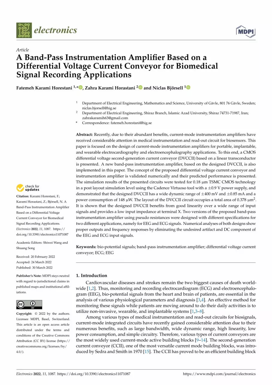
In order to investigate the linearity of the proposed circuit, the variations of the out-put voltage at terminal X versus variations in Vid = VY1−VY2 are depicted in Figure 3a. The figure shows good linearity for differential input voltages between ±0.4 V. The offset volt-age is also measured 2.24 mV and it is small enough. The offset voltage is the voltage of terminal X when Vid is equal to zero or is grounded.
Figure 3b shows the voltage frequency response of the DVCC. It shows a flat response with a unity voltage gain (Vx/Vid) of 80 MHz and a 3 dB bandwidth of 450 MHz.
Figure 2. CMOS realization of the designed DVCC. The differential voltage between two inputterminals, Y1 and Y2, appears at the X terminal and the current injected at X terminal is beingreplicated to the output.
The output stage is formed by a Class-AB CMOS push–pull network that guaranteeshigh current driving capability and low standby current. The current at terminal X istransferred to terminal Z through transistors M15 and M16. Thus, for achieving unit current
Electronics 2022, 11, 1087 4 of 12
gain, M15 and M16 must be matched with M13 and M14, respectively. All transistors aresized to operate in the saturation region. The size of the transistors is listed in Table 1.
Table 1. Transistor sizing of the designed DVCC.
Transistors W (µm) L (µm)
M1–M4 1.8 3
M5–M8 0.9 0.8
M9–M10 9.5 1.4
M11–M12 0.5 0.3
M13–M16 5 0.2
2.2. Post Layout Simulation Results
In order to validate the proposed DVCC, it was simulated using Cadence. TSMC0.18 µm standard CMOS technology was used for the simulation. Transistor sizes that wereused in the simulation correspond to those listed in Table 1. The utilized power supply was±0.9 V.
Since the ports X and Z have unity current gains, in order to calculate the currentsIx and Iz to depict the Iz
Ixcurve, both ports are terminated with 5 KΩ resistances. Moreso,
note that port X is an output voltage port that has a small output resistance. Therefore, itshould be loaded with a relatively large resistor. A 5 KΩ resistor seems to be large enoughfor this purpose.
In order to investigate the linearity of the proposed circuit, the variations of the outputvoltage at terminal X versus variations in Vid = VY1 − VY2 are depicted in Figure 3a. Thefigure shows good linearity for differential input voltages between ±0.4 V. The offsetvoltage is also measured 2.24 mV and it is small enough. The offset voltage is the voltageof terminal X when Vid is equal to zero or is grounded.
Figure 3b shows the voltage frequency response of the DVCC. It shows a flat responsewith a unity voltage gain (Vx/Vid) of 80 MHz and a 3 dB bandwidth of 450 MHz.
Electronics 2022, 11, x FOR PEER REVIEW 5 of 12
(a) (b)
Figure 3. (a) The X terminal output voltage versus changes of Vid. (b) Frequency response of the DVCC.
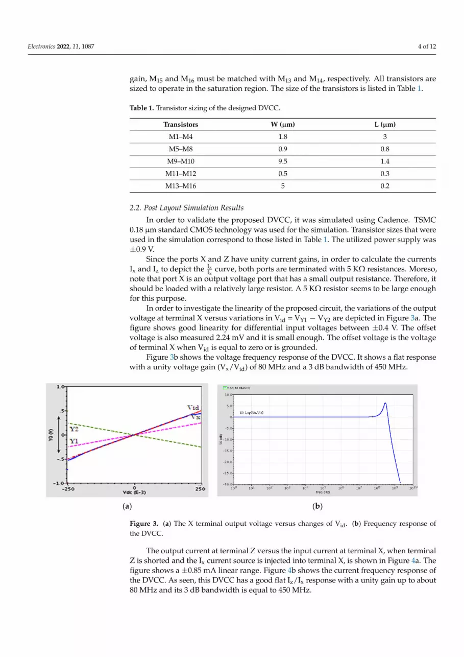
The output current at terminal Z versus the input current at terminal X, when termi-nal Z is shorted and the Ix current source is injected into terminal X, is shown in Figure 4a. The figure shows a ±0.85 mA linear range. Figure 4b shows the current frequency response of the DVCC. As seen, this DVCC has a good flat Iz/Ix response with a unity gain up to about 80 MHz and its 3 dB bandwidth is equal to 450 MHz.
(a) (b)
Figure 4. (a) Output current of terminal Z versus terminal X input current, when terminal Z is shorted. (b) Current frequency response (Iz/Ix) of the DVCC.
The simulated input impedance of terminal X, i.e., RX, is smaller than 20 Ohm at DC and low frequencies. Variations of Rx versus frequency is depicted in Figure 5. The value of Rx is also lower than 1 KΩ up to 3 dB frequency, demonstrating that port X can operate as a low impedance output port.
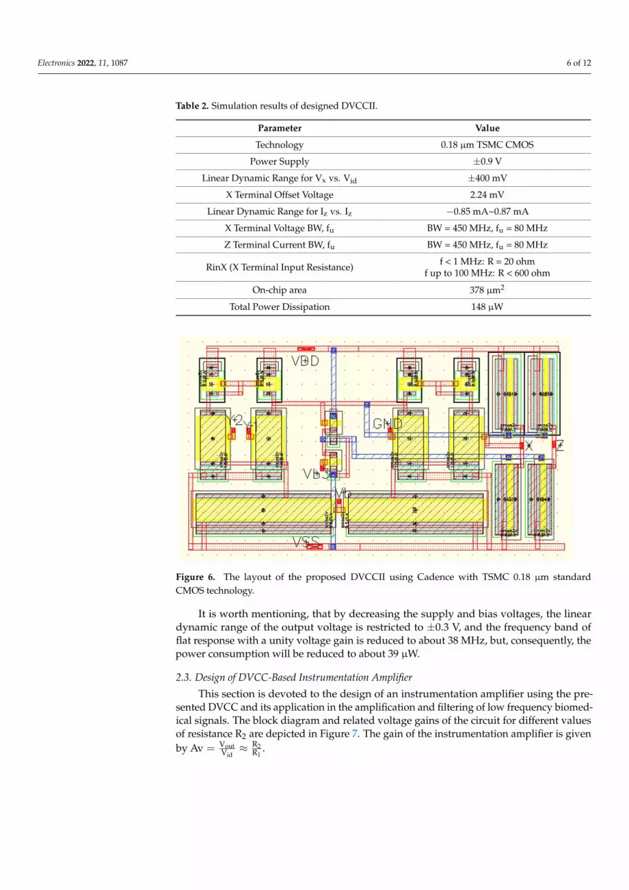
All results are summarized in Table 2. The table shows this design has proper char-acteristics for a DVCC.
The layout of the proposed DVCCII using the Cadence tool with TSMC 0.18 μm standard CMOS technology is depicted in Figure 6. The on-chip area with this layout is estimated to be equal to 378 μm2.
Figure 3. (a) The X terminal output voltage versus changes of Vid. (b) Frequency response ofthe DVCC.
The output current at terminal Z versus the input current at terminal X, when terminalZ is shorted and the Ix current source is injected into terminal X, is shown in Figure 4a. Thefigure shows a ±0.85 mA linear range. Figure 4b shows the current frequency response ofthe DVCC. As seen, this DVCC has a good flat Iz/Ix response with a unity gain up to about80 MHz and its 3 dB bandwidth is equal to 450 MHz.

Electronics 2022, 11, 1087 5 of 12
Electronics 2022, 11, x FOR PEER REVIEW 5 of 12
(a) (b)
Figure 3. (a) The X terminal output voltage versus changes of Vid. (b) Frequency response of the DVCC.
The output current at terminal Z versus the input current at terminal X, when termi-nal Z is shorted and the Ix current source is injected into terminal X, is shown in Figure 4a. The figure shows a ±0.85 mA linear range. Figure 4b shows the current frequency response of the DVCC. As seen, this DVCC has a good flat Iz/Ix response with a unity gain up to about 80 MHz and its 3 dB bandwidth is equal to 450 MHz.
(a) (b)
Figure 4. (a) Output current of terminal Z versus terminal X input current, when terminal Z is shorted. (b) Current frequency response (Iz/Ix) of the DVCC.
The simulated input impedance of terminal X, i.e., RX, is smaller than 20 Ohm at DC and low frequencies. Variations of Rx versus frequency is depicted in Figure 5. The value of Rx is also lower than 1 KΩ up to 3 dB frequency, demonstrating that port X can operate as a low impedance output port.
All results are summarized in Table 2. The table shows this design has proper char-acteristics for a DVCC.
The layout of the proposed DVCCII using the Cadence tool with TSMC 0.18 μm standard CMOS technology is depicted in Figure 6. The on-chip area with this layout is estimated to be equal to 378 μm2.
Figure 4. (a) Output current of terminal Z versus terminal X input current, when terminal Z is shorted.(b) Current frequency response (Iz/Ix) of the DVCC.
The simulated input impedance of terminal X, i.e., RX, is smaller than 20 ohm at DCand low frequencies. Variations of Rx versus frequency is depicted in Figure 5. The valueof Rx is also lower than 1 KΩ up to 3 dB frequency, demonstrating that port X can operateas a low impedance output port.
All results are summarized in Table 2. The table shows this design has proper charac-teristics for a DVCC.
The layout of the proposed DVCCII using the Cadence tool with TSMC 0.18 µmstandard CMOS technology is depicted in Figure 6. The on-chip area with this layout isestimated to be equal to 378 µm2.
Electronics 2022, 11, x FOR PEER REVIEW 6 of 12
Figure 5. The X terminal input resistance RX versus frequency changes. It is measured less than 20 ohm in low frequency and DC operation regions.
Table 2. Simulation results of designed DVCCII.
Parameter Value Technology 0.18 μm TSMC CMOS
Power Supply ±0.9 V
Linear Dynamic Range for Vx vs. Vid ±400 mV
X Terminal Offset Voltage 2.24 mV
Linear Dynamic Range for Iz vs. Iz −0.85 mA~0.87 mA
X Terminal Voltage BW, fu BW = 450 MHz, fu = 80 MHz
Z Terminal Current BW, fu BW = 450 MHz, fu = 80 MHz
RinX (X Terminal Input Resistance) f < 1 MHz: R = 20 ohm
f up to 100 MHz: R < 600 ohm On-chip area 378 μm2
Total Power Dissipation 148 μW
Figure 6. The layout of the proposed DVCCII using Cadence with TSMC 0.18 μm standard CMOS technology.
It is worth mentioning, that by decreasing the supply and bias voltages, the linear dynamic range of the output voltage is restricted to ±0.3 V, and the frequency band of flat
Figure 5. The X terminal input resistance RX versus frequency changes. It is measured less than20 ohm in low frequency and DC operation regions.
Electronics 2022, 11, 1087 6 of 12
Table 2. Simulation results of designed DVCCII.
Parameter Value
Technology 0.18 µm TSMC CMOS
Power Supply ±0.9 V
Linear Dynamic Range for Vx vs. Vid ±400 mV
X Terminal Offset Voltage 2.24 mV
Linear Dynamic Range for Iz vs. Iz −0.85 mA~0.87 mA
X Terminal Voltage BW, fu BW = 450 MHz, fu = 80 MHz
Z Terminal Current BW, fu BW = 450 MHz, fu = 80 MHz
RinX (X Terminal Input Resistance) f < 1 MHz: R = 20 ohmf up to 100 MHz: R < 600 ohm
On-chip area 378 µm2
Total Power Dissipation 148 µW
Electronics 2022, 11, x FOR PEER REVIEW 6 of 12
Figure 5. The X terminal input resistance RX versus frequency changes. It is measured less than 20 ohm in low frequency and DC operation regions.
Table 2. Simulation results of designed DVCCII.
Parameter Value Technology 0.18 μm TSMC CMOS
Power Supply ±0.9 V
Linear Dynamic Range for Vx vs. Vid ±400 mV
X Terminal Offset Voltage 2.24 mV
Linear Dynamic Range for Iz vs. Iz −0.85 mA~0.87 mA
X Terminal Voltage BW, fu BW = 450 MHz, fu = 80 MHz
Z Terminal Current BW, fu BW = 450 MHz, fu = 80 MHz
RinX (X Terminal Input Resistance) f < 1 MHz: R = 20 ohm
f up to 100 MHz: R < 600 ohm On-chip area 378 μm2
Total Power Dissipation 148 μW
Figure 6. The layout of the proposed DVCCII using Cadence with TSMC 0.18 μm standard CMOS technology.
It is worth mentioning, that by decreasing the supply and bias voltages, the linear dynamic range of the output voltage is restricted to ±0.3 V, and the frequency band of flat
Figure 6. The layout of the proposed DVCCII using Cadence with TSMC 0.18 µm standardCMOS technology.
It is worth mentioning, that by decreasing the supply and bias voltages, the lineardynamic range of the output voltage is restricted to ±0.3 V, and the frequency band offlat response with a unity voltage gain is reduced to about 38 MHz, but, consequently, thepower consumption will be reduced to about 39 µW.
2.3. Design of DVCC-Based Instrumentation Amplifier
This section is devoted to the design of an instrumentation amplifier using the pre-sented DVCC and its application in the amplification and filtering of low frequency biomed-ical signals. The block diagram and related voltage gains of the circuit for different valuesof resistance R2 are depicted in Figure 7. The gain of the instrumentation amplifier is givenby Av = Vout
Vid≈ R2
R1.

Electronics 2022, 11, 1087 7 of 12
Electronics 2022, 11, x FOR PEER REVIEW 7 of 12
response with a unity voltage gain is reduced to about 38 MHz, but, consequently, the power consumption will be reduced to about 39 μW.
2.3. Design of DVCC-Based Instrumentation Amplifier This section is devoted to the design of an instrumentation amplifier using the pre-
sented DVCC and its application in the amplification and filtering of low frequency bio-medical signals. The block diagram and related voltage gains of the circuit for different values of resistance R2 are depicted in Figure 7. The gain of the instrumentation amplifier is given by Av = ≈ .
(a) (b)
Figure 7. (a) The block diagram of the instrumentation amplifier implemented using the presented DVCC, (b) Voltage gains for different resistances at the output of this instrumentation amplifier.
Features of the designed CMIA are presented in Table 3. The table also highlights the advantages of the proposed amplifier in terms of power consumption, on-chip area, band-width, etc., compared to other studies.
Moreso, note that the designed CMIA also benefits from a large BW as a byproduct. To limit the bandwidth to the required frequency band, we then used a filter. The pro-posed configuration for filtering specified frequency bands, which leads to forming a band-pass instrumentation amplifier, is shown in Figure 8. However, note that in addition to the application in EEG/ECG recordings, the designed DVCC and CMIA are general designs that can be used for many applications with a wide BW up to 450 MHz.
Figure 8. The schematic of the proposed configuration for separating the required frequency bands for various biomedical signals through the IA.
Furthermore, note that typically biomedical signals have very small amplitude and are at relatively low frequencies. For instance, the amplitude of an EEG signal is normally below 100 μV when measured on the scalp, and about 1–2 mV when measured on the surface of the brain. The frequency band of these signals is from under 1 Hz to about 50 Hz, as demonstrated in Figure 9. Similarly, the spectrum of an ECG signal is mostly dis-tributed between 0.1 Hz to 160 Hz and its amplitude is typically below 5 mV. Thus, filter-ing of these signals requires filters with very small low cut-off frequency. As a result, the
Figure 7. (a) The block diagram of the instrumentation amplifier implemented using the presentedDVCC, (b) Voltage gains for different resistances at the output of this instrumentation amplifier.
Features of the designed CMIA are presented in Table 3. The table also highlightsthe advantages of the proposed amplifier in terms of power consumption, on-chip area,bandwidth, etc., compared to other studies.
Moreso, note that the designed CMIA also benefits from a large BW as a byproduct.To limit the bandwidth to the required frequency band, we then used a filter. The proposedconfiguration for filtering specified frequency bands, which leads to forming a band-passinstrumentation amplifier, is shown in Figure 8. However, note that in addition to theapplication in EEG/ECG recordings, the designed DVCC and CMIA are general designsthat can be used for many applications with a wide BW up to 450 MHz.
Electronics 2022, 11, x FOR PEER REVIEW 7 of 12
response with a unity voltage gain is reduced to about 38 MHz, but, consequently, the power consumption will be reduced to about 39 μW.
2.3. Design of DVCC-Based Instrumentation Amplifier This section is devoted to the design of an instrumentation amplifier using the pre-
sented DVCC and its application in the amplification and filtering of low frequency bio-medical signals. The block diagram and related voltage gains of the circuit for different values of resistance R2 are depicted in Figure 7. The gain of the instrumentation amplifier is given by Av = ≈ .
(a) (b)
Figure 7. (a) The block diagram of the instrumentation amplifier implemented using the presented DVCC, (b) Voltage gains for different resistances at the output of this instrumentation amplifier.
Features of the designed CMIA are presented in Table 3. The table also highlights the advantages of the proposed amplifier in terms of power consumption, on-chip area, band-width, etc., compared to other studies.
Moreso, note that the designed CMIA also benefits from a large BW as a byproduct. To limit the bandwidth to the required frequency band, we then used a filter. The pro-posed configuration for filtering specified frequency bands, which leads to forming a band-pass instrumentation amplifier, is shown in Figure 8. However, note that in addition to the application in EEG/ECG recordings, the designed DVCC and CMIA are general designs that can be used for many applications with a wide BW up to 450 MHz.
Figure 8. The schematic of the proposed configuration for separating the required frequency bands for various biomedical signals through the IA.
Furthermore, note that typically biomedical signals have very small amplitude and are at relatively low frequencies. For instance, the amplitude of an EEG signal is normally below 100 μV when measured on the scalp, and about 1–2 mV when measured on the surface of the brain. The frequency band of these signals is from under 1 Hz to about 50 Hz, as demonstrated in Figure 9. Similarly, the spectrum of an ECG signal is mostly dis-tributed between 0.1 Hz to 160 Hz and its amplitude is typically below 5 mV. Thus, filter-ing of these signals requires filters with very small low cut-off frequency. As a result, the
Figure 8. The schematic of the proposed configuration for separating the required frequency bandsfor various biomedical signals through the IA.
Furthermore, note that typically biomedical signals have very small amplitude andare at relatively low frequencies. For instance, the amplitude of an EEG signal is normallybelow 100 µV when measured on the scalp, and about 1–2 mV when measured on thesurface of the brain. The frequency band of these signals is from under 1 Hz to about 50 Hz,as demonstrated in Figure 9. Similarly, the spectrum of an ECG signal is mostly distributedbetween 0.1 Hz to 160 Hz and its amplitude is typically below 5 mV. Thus, filtering of thesesignals requires filters with very small low cut-off frequency. As a result, the filter requiresa very large capacitor or resistor which is hard to achieve on a limited on-chip area. Toaddress this issue, MOS pseudo resistance with a resistance in the order of tera-ohms isused in the proposed circuit [5,29,35]. Using this technique, drastically reduces the requiredon-chip area to realize the capacitors and resistors of the filter.

Electronics 2022, 11, 1087 8 of 12
Table 3. Features of the designed CMIA compared to other works.
Parameter Technology PowerSupply Gain BW (−3 dB) On-Chip Area Power
Dissipation
[11] 0.18 µm CMOS ±0.9 V 25–27.6 dB 100 MHz NA 1.15 mW
[25] 0.18 µm CMOS ±1.2 V 19 dB for RL = 8 KΩ 18.1 MHz NA 383.4 µW
[33] 0.5 µm CMOS ±1.5 V 9–23 dB 20 MHzNA,
Large size, due to use7 off-chip resistors
3.99 mW
[36] 0.18 µm CMOS 1.8 V Maximum of 40 dB 2 KHz 0.087 mm2 39.6 µW
This work 0.18 µm CMOS ±0.9 V 10 dB for RL = 20 KΩ 450 MHz 460 µm2 148 µW *
* The power consumption is reduced to about 39 µW by decreasing the supply and bias voltages. In this case, thelinear dynamic range of the output voltage is restricted to ±0.3 V, and the frequency band of the flat responsewith a unity voltage gain is reduced to about 38 MHz.
Electronics 2022, 11, x FOR PEER REVIEW 8 of 12
filter requires a very large capacitor or resistor which is hard to achieve on a limited on-chip area. To address this issue, MOS pseudo resistance with a resistance in the order of tera-ohms is used in the proposed circuit [5,29,35]. Using this technique, drastically re-duces the required on-chip area to realize the capacitors and resistors of the filter.
Table 3. Features of the designed CMIA compared to other works.
Parameter Technology Power Supply Gain BW (−3 dB) On-Chip Area Power Dissipation [11] 0.18 μm CMOS ±0.9 V 25–27.6 dB 100 MHz NA 1.15 mW [25] 0.18 μm CMOS ±1.2 V 19 dB for RL = 8 KΩ 18.1 MHz NA 383.4 μW
[33] 0.5 μm CMOS ±1.5 V 9–23 dB 20 MHz NA,
Large size, due to use 7 off-chip resistors
3.99 mW
[36] 0.18 μm CMOS 1.8 V Maximum of 40 dB 2 KHz 0.087 mm2 39.6 μW This work 0.18 μm CMOS ±0.9 V 10 dB for RL = 20 KΩ 450 MHz 460 μm2 148 μW *
* The power consumption is reduced to about 39 μW by decreasing the supply and bias voltages. In this case, the linear dynamic range of the output voltage is restricted to ±0.3 V, and the frequency band of the flat response with a unity voltage gain is reduced to about 38 MHz.
Figure 9. The frequency spectrum of normal EEG.
Equations (1) and (2) are used to estimate the cut-off frequencies, 𝑓 and 𝑓 of the circuit. The resistance Rinc produced by the MOS-pseudo resistors (Ma, Mb, and MRL) is about tera-ohm. Thus, very small C1 and CZ are required to achieve the small cut-off fre-quencies f and f , respectively. ω = 2πf = 1R , . C (1)
ω = 2πf = 1R . C (2)
3. Results In order to validate the proposed filtering instrumental amplifier, two versions of the
proposed circuit, one for filtering EEG signals and one for filtering ECG signals, are de-signed. Considering the typical frequency band of EEG signals (shown in Figure 9), the first circuit was designed to pass the frequency band of 0.2–30 Hz with a voltage gain of about 24.3 dB. To achieve this frequency band, the values of capacitors C1 and Cz are set to 1 pF and 1.5 pF, respectively, and W/L sizing of the MOS pseudo resistors Ma, Mb, and MRL are set to . µ µ and µ. µ , respectively. The frequency response of the designed band-pass IA is shown in Figure 10A. An input EEG test signal, which was recorded at the Neuro-Technology Lab in the Biomedical Engineering Department, the University of
Figure 9. The frequency spectrum of normal EEG.
Equations (1) and (2) are used to estimate the cut-off frequencies, fL and fH of thecircuit. The resistance Rinc produced by the MOS-pseudo resistors (Ma, Mb, and MRL)is about tera-ohm. Thus, very small C1 and CZ are required to achieve the small cut-offfrequencies fL and fH, respectively.
ωL = 2πfL =1
Rinc−a,b.C1(1)
ωH = 2πfH =1
Rinc−RL.CZ(2)
3. Results
In order to validate the proposed filtering instrumental amplifier, two versions ofthe proposed circuit, one for filtering EEG signals and one for filtering ECG signals, aredesigned. Considering the typical frequency band of EEG signals (shown in Figure 9),the first circuit was designed to pass the frequency band of 0.2–30 Hz with a voltage gainof about 24.3 dB. To achieve this frequency band, the values of capacitors C1 and Cz areset to 1 pF and 1.5 pF, respectively, and W/L sizing of the MOS pseudo resistors Ma, Mb,
and MRL are set to 0.5 µm5 µm and 15 µm
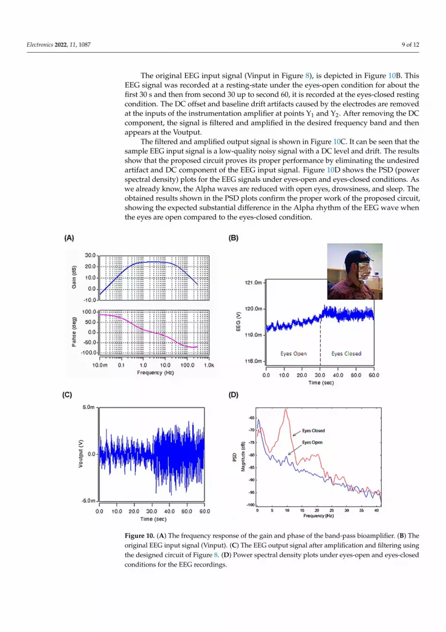
0.5 µm , respectively. The frequency response of the designedband-pass IA is shown in Figure 10A. An input EEG test signal, which was recorded atthe Neuro-Technology Lab in the Biomedical Engineering Department, the University ofIsfahan, during the eyes-closed condition, followed by the eyes-open resting condition, wasused to validate the designed circuit.
Electronics 2022, 11, 1087 9 of 12
The original EEG input signal (Vinput in Figure 8), is depicted in Figure 10B. ThisEEG signal was recorded at a resting-state under the eyes-open condition for about thefirst 30 s and then from second 30 up to second 60, it is recorded at the eyes-closed restingcondition. The DC offset and baseline drift artifacts caused by the electrodes are removedat the inputs of the instrumentation amplifier at points Y1 and Y2. After removing the DCcomponent, the signal is filtered and amplified in the desired frequency band and thenappears at the Voutput.
The filtered and amplified output signal is shown in Figure 10C. It can be seen that thesample EEG input signal is a low-quality noisy signal with a DC level and drift. The resultsshow that the proposed circuit proves its proper performance by eliminating the undesiredartifact and DC component of the EEG input signal. Figure 10D shows the PSD (powerspectral density) plots for the EEG signals under eyes-open and eyes-closed conditions. Aswe already know, the Alpha waves are reduced with open eyes, drowsiness, and sleep. Theobtained results shown in the PSD plots confirm the proper work of the proposed circuit,showing the expected substantial difference in the Alpha rhythm of the EEG wave whenthe eyes are open compared to the eyes-closed condition.
Electronics 2022, 11, x FOR PEER REVIEW 9 of 12
Isfahan, during the eyes-closed condition, followed by the eyes-open resting condition, was used to validate the designed circuit.
The original EEG input signal (Vinput in Figure 8), is depicted in Figure 10B. This EEG signal was recorded at a resting-state under the eyes-open condition for about the first 30 s and then from second 30 up to second 60, it is recorded at the eyes-closed resting condition. The DC offset and baseline drift artifacts caused by the electrodes are removed at the inputs of the instrumentation amplifier at points Y1 and Y2. After removing the DC component, the signal is filtered and amplified in the desired frequency band and then appears at the Voutput.
The filtered and amplified output signal is shown in Figure 10C. It can be seen that the sample EEG input signal is a low-quality noisy signal with a DC level and drift. The results show that the proposed circuit proves its proper performance by eliminating the undesired artifact and DC component of the EEG input signal. Figure 10D shows the PSD (power spectral density) plots for the EEG signals under eyes-open and eyes-closed con-ditions. As we already know, the Alpha waves are reduced with open eyes, drowsiness, and sleep. The obtained results shown in the PSD plots confirm the proper work of the proposed circuit, showing the expected substantial difference in the Alpha rhythm of the EEG wave when the eyes are open compared to the eyes-closed condition.
Figure 10. (A) The frequency response of the gain and phase of the band-pass bioamplifier. (B) The original EEG input signal (Vinput) (C) The EEG output signal after amplification and filtering using the designed circuit of Figure 8. (D) Power spectral density plots under eyes-open and eyes-closed conditions for the EEG recordings.
Figure 10. (A) The frequency response of the gain and phase of the band-pass bioamplifier. (B) Theoriginal EEG input signal (Vinput). (C) The EEG output signal after amplification and filtering usingthe designed circuit of Figure 8. (D) Power spectral density plots under eyes-open and eyes-closedconditions for the EEG recordings.
Electronics 2022, 11, 1087 10 of 12
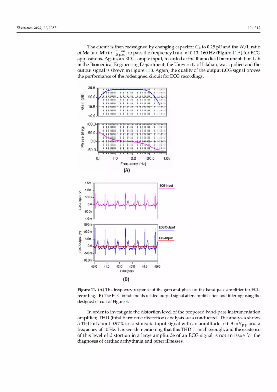
The circuit is then redesigned by changing capacitor Cz to 0.25 pF and the W/L ratioof Ma and Mb to 0.5 µm
10 µm , to pass the frequency band of 0.13–160 Hz (Figure 11A) for ECGapplications. Again, an ECG sample input, recorded at the Biomedical Instrumentation Labin the Biomedical Engineering Department, the University of Isfahan, was applied and theoutput signal is shown in Figure 11B. Again, the quality of the output ECG signal provesthe performance of the redesigned circuit for ECG recordings.
Electronics 2022, 11, x FOR PEER REVIEW 10 of 12
The circuit is then redesigned by changing capacitor Cz to 0.25 pF and the W/L ratio of Ma and Mb to . µ µ , to pass the frequency band of 0.13–160 Hz (Figure 11A) for ECG applications. Again, an ECG sample input, recorded at the Biomedical Instrumentation Lab in the Biomedical Engineering Department, the University of Isfahan, was applied and the output signal is shown in Figure 11B. Again, the quality of the output ECG signal proves the performance of the redesigned circuit for ECG recordings.
Figure 11. (A) The frequency response of the gain and phase of the band-pass amplifier for ECG recording. (B) The ECG input and its related output signal after amplification and filtering using the designed circuit of Figure 8.
In order to investigate the distortion level of the proposed band-pass instrumentation amplifier, THD (total harmonic distortion) analysis was conducted. The analysis shows a THD of about 0.97% for a sinusoid input signal with an amplitude of 0.8 mVp-p and a fre-quency of 10 Hz. It is worth mentioning that this THD is small enough, and the existence of this level of distortion in a large amplitude of an ECG signal is not an issue for the diagnoses of cardiac arrhythmia and other illnesses.
4. Conclusions
Figure 11. (A) The frequency response of the gain and phase of the band-pass amplifier for ECGrecording. (B) The ECG input and its related output signal after amplification and filtering using thedesigned circuit of Figure 8.
In order to investigate the distortion level of the proposed band-pass instrumentationamplifier, THD (total harmonic distortion) analysis was conducted. The analysis showsa THD of about 0.97% for a sinusoid input signal with an amplitude of 0.8 mVp-p and afrequency of 10 Hz. It is worth mentioning that this THD is small enough, and the existenceof this level of distortion in a large amplitude of an ECG signal is not an issue for thediagnoses of cardiac arrhythmia and other illnesses.
Electronics 2022, 11, 1087 11 of 12
4. Conclusions
In this paper, a wide range CMOS DVCC based on a wide linear range transconductorhas been presented. The proposed DVCC has a wide dynamic range of ±400 mV and±0.85 mA. Its voltage frequency response has a flat unity voltage gain (Vx/Vid) of 80 MHz.The power consumption of 148 µW was measured by a post layout simulation. The layoutof the DVCC circuit occupies a total area of 0.378 µm2. In the following, using the presentedDVCC, an instrumentation amplifier has been implemented and a new configurationhas been presented to realize a band-pass amplifier using IA. In order to validate theproposed band-pass amplifier, two versions of the circuit with different specificationshave been designed and recorded EEG and ECG signals have been successfully amplifiedand filtered. The proposed current-mode band-pass instrumentation amplifiers haveapplications in improving the quality of various biomedical signals for clinical diagnosis,including electrocardiography and electroencephalography.
Author Contributions: Conceptualization, F.K.H.; methodology, F.K.H.; software, F.K.H.; validation,F.K.H., Z.K.H. and N.B.; formal analysis, F.K.H.; investigation, Z.K.H. and N.B.; writing—originaldraft preparation, F.K.H.; writing—review and editing, Z.K.H. and N.B. All authors have read andagreed to the published version of the manuscript.
Funding: This research received no external funding.
Acknowledgments: The authors would like to thank Ali Karami and Mahmoud Norouzi for theirprecious help. The authors also thank Mohammadreza Behboodi for providing EEG and ECG samplesfor this research.
Conflicts of Interest: The authors declare no conflict of interest.
References1. Prats-Boluda, G.; Ye-Lin, Y.; Barrachina, J.B.; Senent, E.; de Sanabria, R.R.; Garcia-Casado, J. Development of a portable wireless
system for bipolar concentric ECG recording. Meas. Sci. Technol. 2015, 26, 075102. [CrossRef]2. Ettinger, S.; Stanak, M.; Szymanski, P.; Wild, C.; Hacek, R.T.; Ercevic, D.; Grenkovic, R.; Huic, M. Wearable cardioverter
defibrillators for the prevention of sudden cardiac arrest: A health technology assessment and patient focus group study. Med.Devices (Auckl. NZ) 2017, 10, 257. [CrossRef] [PubMed]
3. Niederhauser, T.; Haeberlin, A.; Marisa, T.; Mattle, D.; Abächerli, R.; Goette, J.; Jacomet, M.; Vogel, R. An optimized lead systemfor long-term esophageal electrocardiography. Physiol. Meas. 2014, 35, 517. [CrossRef]
4. Kalra, A.; Lowe, A.; Al-Jumaily, A. Critical review of electrocardiography measurement systems and technology. Meas. Sci.Technol. 2018, 30, 012001. [CrossRef]
5. Karami Horestani, F.; Eshghi, M.; Yazdchi, M. An ultra low power amplifier for wearable and implantable electronic devices.Microelectron. Eng. 2019, 216, 111054. [CrossRef]
6. Prats-Boluda, G.; Ye-Lin, Y.; Garcia-Breijo, E.; Ibanez, J.; Garcia-Casado, J. Active flexible concentric ring electrode for non-invasivesurface bioelectrical recordings. Meas. Sci. Technol. 2012, 23, 125703. [CrossRef]
7. Gargiulo, G.; Bifulco, P.; Cesarelli, M.; Ruffo, M.; Romano, M.; Calvo, R.A.; Jin, C.; van Schaik, A. An ultra-high input impedanceECG amplifier for long-term monitoring of athletes. Med. Devices (Auckl. NZ) 2010, 3, 1. [CrossRef]
8. Bifulco, P.; Gargiulo, G.D.; Romano, M.; Cesarelli, M. A simple, wide bandwidth, biopotential amplifier to record pacemakerpulse waveform. Med. Devices (Auckl. NZ) 2016, 9, 325.
9. Rao, A.; Murphy, E.; Shahghasemi, M.; Odame, K. Current-conveyor-based wide-band current driver for electrical impedancetomography. Physiol. Meas. 2019, 40, 034005. [CrossRef]
10. Mahmoud, S.A. Fully differential CMOS CCII based on differential difference transconductor. Analog Integr. Circuits Signal Process.2007, 50, 195–203. [CrossRef]
11. Chaturvedi, B.; Kumar, A. Electronically tunable current-mode instrumentation amplifier with high CMRR and wide bandwidth.AEU-Int. J. Electron. Commun. 2018, 92, 116–123. [CrossRef]
12. Arora, T.S.; Gupta, S. A new voltage mode quadrature oscillator using grounded capacitors: An application of CDBA. Eng. Sci.Technol. Int. J. 2018, 21, 43–49. [CrossRef]
13. Carrasco-Aguilar, M.; Sánchez-López, C.; Carbajal-Gómez, V. Pinched hysteresis behavior in a PID-controlled resistor. Eng. Sci.Technol. Int. J. 2018, 21, 297–301. [CrossRef]
14. Abuelma’atti, M.T. Recent Developments in Current-Mode Sinusoidal Oscillators: Circuits and Active Elements. Arab. J. Sci. Eng.2017, 42, 2583–2614. [CrossRef]
15. Sedra, A.; Smith, K. A second-generation current conveyor and its applications. IEEE Trans. Circuit Theory 1970, 17, 132–134.[CrossRef]

Electronics 2022, 11, 1087 12 of 12
16. Soliman, A. New fully-differential CMOS second-generation current conveyer. Etri J. 2006, 28, 495–501.17. Madian, A.H.; Mahmoud, S.A.; Soliman, A.M. New 1.5-V CMOS second generation current conveyor based on wide range
transconductor. Analog Integr. Circuits Signal Process. 2006, 49, 267–279. [CrossRef]18. Abrishamifar, A.; Karimi, Y.; Navidi, M.M. Current controlled current differential current conveyor: A novel building block for
analog signal processing. IEICE Electron. Express 2012, 9, 104–110. [CrossRef]19. Kunto, T.; Prommee, P.; Abuelma, A.; Taher, M. Electronically Tunable Current-mode High-order Ladder Low-pass Filters Based
on CMOS Technology. Radioengineering 2015, 24, 974–987. [CrossRef]20. Abuelma’atti, M.T.; Bentrcia, A.; Al-Shahrani, S.A.M. A novel mixed-mode current-conveyor-based filter. Int. J. Electron. 2004, 91,
191–197. [CrossRef]21. Soliman, A.M. Current feedback operational amplifier based oscillators. Analog Integr. Circuits Signal Process. 2000, 23, 45–55.
[CrossRef]22. Abuelmaatti, M.T.; Al-Qahtani, M.A. A new current-controlled multiphase sinusoidal oscillator using translinear current
conveyors. IEEE Trans. Circuits Syst. II Analog Digit. Signal Process. 1998, 45, 881–885. [CrossRef]23. Safari, L.; Azhari, S. A high performance fully differential pure current mode operational amplifier and its applications. J. Eng.
Sci. Technol. 2012, 7, 471–486.24. Eldeeb, M.A.; Ghallab, Y.H.; Ismail, Y.; Elghitani, H. Low-voltage subthreshold CMOS current mode circuits: Design and
applications. AEU-Int. J. Electron. Commun. 2017, 82, 251–264. [CrossRef]25. Ahmadi, S.; Azhari, S.J. A novel fully differential second generation current conveyor and its application as a very high CMRR
instrumentation amplifier. Emerg. Sci. J. 2018, 2, 85–92. [CrossRef]26. Elwan, H.; Soliman, A. Novel CMOS differential voltage current conveyor and its applications. IEE Proc.-Circuits Devices Syst.
1997, 144, 195–200. [CrossRef]27. Naik, A.; Devashrayee, N. Characterization of a CMOS differential current conveyor using 0.25 micron technology. Int. J. Adv.
Eng. Appl. 2010, 177–182.28. Wilson, B. Universal conveyor instrumentation amplifier. Electron. Lett. 1989, 25, 470–471. [CrossRef]29. Kumar, S.; Kim, B.-S.; Song, H. An integrated approach of CNT front-end amplifier towards spikes monitoring for Neuro-
prosthetic Diagnosis. BioChip J. 2018, 12, 332–339. [CrossRef]30. Hassan, T.M.; Mahmoud, S.A. New CMOS DVCC realization and applications to instrumentation amplifier and active-RC filters.
AEU-Int. J. Electron. Commun. 2010, 64, 47–55. [CrossRef]31. Cini, U.; Arslan, E. A high gain and low-offset current-mode instrumentation amplifier using differential difference current
conveyors. In Proceedings of the IEEE International Conference on Electronics, Circuits, and Systems (ICECS), Cairo, Egypt,6–9 December 2015.
32. Safari, L.; Yuce, E.; Minaei, S. A new transresistance-mode instrumentation amplifier with low number of MOS transistors andelectronic tuning opportunity. J. Circuits Syst. Comput. 2016, 25, 1650022. [CrossRef]
33. Pandey, N.; Nand, D.; Pandey, R. Generalized operational floating current conveyor based instrumentation amplifier. IET CircuitsDevices Syst. 2016, 10, 209–219. [CrossRef]
34. Smither, M.; Pugh, D.; Woolard, L. CMRR analysis of the 3-op-amp instrumentation amplifier. Electron. Lett. 1977, 13, 594.[CrossRef]
35. Harrison, R.R.; Charles, C. A low-power low-noise CMOS amplifier for neural recording applications. IEEE J. Solid-State Circuits2003, 38, 958–965. [CrossRef]
36. Ong, G.T.; Chan, P.K. A power-aware chopper-stabilized instrumentationamplifier for resistive wheatstone bridge sensors. IEEETrans. Instrum. Meas. 2014, 63, 2253–2263. [CrossRef]