a 30 mk, 13.5 t scanning tunneling microscope with two independent tips
TRANSCRIPT

A 30 mK, 13.5 T scanning tunneling microscope with two independent tipsAnita Roychowdhury, M. A. Gubrud, R. Dana, J. R. Anderson, C. J. Lobb, F. C. Wellstood, and M. Dreyer
Citation: Review of Scientific Instruments 85, 043706 (2014); doi: 10.1063/1.4871056 View online: http://dx.doi.org/10.1063/1.4871056 View Table of Contents: http://scitation.aip.org/content/aip/journal/rsi/85/4?ver=pdfcov Published by the AIP Publishing Articles you may be interested in Atomic resolution scanning tunneling microscopy in a cryogen free dilution refrigerator at 15 mK Rev. Sci. Instrum. 85, 035112 (2014); 10.1063/1.4868684 A 350 mK, 9 T scanning tunneling microscope for the study of superconducting thin films on insulating substratesand single crystals Rev. Sci. Instrum. 84, 123905 (2013); 10.1063/1.4849616 A compact sub-Kelvin ultrahigh vacuum scanning tunneling microscope with high energy resolution and highstability Rev. Sci. Instrum. 82, 103702 (2011); 10.1063/1.3646468 Scanning tunneling microscope with two-dimensional translator Rev. Sci. Instrum. 82, 013706 (2011); 10.1063/1.3548832 Two-photon fluorescence imaging and spectroscopy of nanostructured organic materials using a photonscanning tunneling microscope Appl. Phys. Lett. 76, 1 (2000); 10.1063/1.125637
This article is copyrighted as indicated in the article. Reuse of AIP content is subject to the terms at: http://scitationnew.aip.org/termsconditions. Downloaded to IP:
129.2.108.212 On: Thu, 07 Aug 2014 21:50:20
REVIEW OF SCIENTIFIC INSTRUMENTS 85, 043706 (2014)
A 30 mK, 13.5 T scanning tunneling microscope with two independent tipsAnita Roychowdhury,1,2 M. A. Gubrud,1 R. Dana,1 J. R. Anderson,2 C. J. Lobb,2
F. C. Wellstood,2 and M. Dreyer1
1Laboratory for Physical Sciences, College Park, Maryland 20742, USA2Center for Nanophysics and Advanced Materials, Department of Physics, University of Maryland,College Park, Maryland 20740, USA
(Received 7 November 2013; accepted 31 March 2014; published online 23 April 2014)
We describe the design, construction, and performance of an ultra-low temperature, high-field scan-ning tunneling microscope (STM) with two independent tips. The STM is mounted on a dilutionrefrigerator and operates at a base temperature of 30 mK with magnetic fields of up to 13.5 T. Wefocus on the design of the two-tip STM head, as well as the sample transfer mechanism, which allowsin situ transfer from an ultra high vacuum preparation chamber while the STM is at 1.5 K. Otherdesign details such as the vibration isolation and rf-filtered wiring are also described. Their effective-ness is demonstrated via spectral current noise characteristics and the root mean square roughnessof atomic resolution images. The high-field capability is shown by the magnetic field dependenceof the superconducting gap of CuxBi2Se3. Finally, we present images and spectroscopy taken withsuperconducting Nb tips with the refrigerator at 35 mK that indicate that the effective temperature ofour tips/sample is approximately 184 mK, corresponding to an energy resolution of 16 μeV. © 2014AIP Publishing LLC. [http://dx.doi.org/10.1063/1.4871056]
I. INTRODUCTION
Since the invention of the scanning tunneling microscope(STM),1 numerous systems have been built that operate atcryogenic temperatures.2–9 Cryogenic temperatures not onlyprovide the potential for achieving finer energy resolution, butalso open up the possibility of exploring otherwise inaccessi-ble phenomena such as superconductivity and a wide rangeof solid state quantum effects. In the 1990s a variety of 4 KSTMs5, 10–13 were developed and used to perform pioneeringstudies at the atomic scale. Since then, several groups havesuccessfully implemented STM’s on 3He refrigerators6, 7, 14–17
and dilution refrigerators.7–9, 18–22 A few groups have alsobuilt and tested dual-probe STMs, one of which operates at4.2 K.23–25 Multi-probe STMs that operate in ultra high vac-uum (UHV) conditions, with cryogenic capabilities in the4–10 K range, are also commercially available.26–29 Despitethese advances, there are still relatively few instruments thatoperate reliably at sub-Kelvin temperatures. This is due to theinherent difficulties in constructing a system that operates atultra-low temperatures, in ultra-high vacuum, with the me-chanical stability necessary for STM measurements.
In this article, we describe the design, construction, andoperation of a millikelvin STM system with a magnetic fieldand UHV sample preparation capabilities. Our microscopepossesses two scanning systems that allow us to indepen-dently acquire topographic images of a sample at mK temper-atures. In the absence of a tip-exchange mechanism, a STMwith two independent scanning systems provides a relativelysimple way to study different regions of the same samplesimultaneously or in quick succession. The instrument wasalso designed to ultimately allow two superconducting tips tobe connected via a flexible superconducting wire forming aSQUID loop with a superconducting sample. In such a modi-fied instrument, one STM tip could provide a reference point
against which the gauge invariant phase difference could bemapped out on the sample surface.30
II. SYSTEM DESIGN
Designing a STM that can operate at millikelvin tem-peratures involves satisfying several stringent requirements.First, the STM tip and sample need to be cooled to mK tem-peratures. Second, the sample must be kept in vacuum at apressure of 10−11 Torr or better to prevent contamination ofthe surface. Third, the system must be kept as vibrationallyisolated as possible—ideally with the tip-to-sample distancestable to better than 5 pm in order to resolve atomic scale fea-tures in topographic images and fine scale structure in spec-troscopy. For the same reason, we require voltage resolutionof 10 μV or better, and current resolution as fine as 1 pA. Inaddition to the above requirements, there are other featuresthat are desirable, such as the ability to prepare and transfersamples in UHV.
Figure 1 shows an overview of our system. An UHV sam-ple preparation and transfer system sits on an optical table di-rectly above a 3He-4He dilution refrigerator that has the STMassembly mounted to the mixing chamber. A vertical sam-ple transfer rod runs along the central axis of the refrigeratorto enable top loading of samples from the UHV system intothe microscope. The dilution refrigerator is an Oxford Instru-ments Kelvinox with a cooling power of 400 μW at 100 mKand a no-load base temperature of 6–7 mK. The operatingbase temperature for our STM however is 30–35 mK due to athermal heat-leak of about 30 μW from the system wiring.Radiation shields clamped to the mixing chamber and thestill (0.7 K) prevent black-body radiation from higher stagesfrom reaching the STM and a custom made super-insulatedliquid-helium cryostat31 provides a 4 K bath. This dewar is
0034-6748/2014/85(4)/043706/9/$30.00 © 2014 AIP Publishing LLC85, 043706-1
This article is copyrighted as indicated in the article. Reuse of AIP content is subject to the terms at: http://scitationnew.aip.org/termsconditions. Downloaded to IP:
129.2.108.212 On: Thu, 07 Aug 2014 21:50:20

043706-2 Roychowdhury et al. Rev. Sci. Instrum. 85, 043706 (2014)
FIG. 1. Overview of dual tip mK STM system. The dewar and radiationshields that surround the dilution refrigerator are not shown.
interchangeable with a custom made 13.5 T superconductingmagnet dewar with a LHe capacity of 140 l.32 The magnet is ahigh field (vertical bore) solenoid system, with a rated field of13.8 kG, and a rated current of 99.8 A. The entire setup sitsinside a copper and steel walled rf shielded room with a nom-inal rf attenuation of 100 dB or greater from 1 kHz to 10 GHz.
A. The UHV sample preparation chamber
The UHV subsystem consists of a preparation chamberand a transfer chamber that are separated by a gate valve (seeFig. 1). Each chamber has its own ion getter,33 titanium subli-mation pumps,34 and ion gauge.35 The system is roughed outusing a detachable turbo pump36 backed by an oil-free scrollpump37 and can be baked to 150 ◦C using heater tape. A loadlock allows the introduction of samples into the preparationchamber. Samples are mounted on sample studs that fit intothe STM and can be moved throughout the UHV system on atransfer plate using a magnetic transfer rod.
The sample preparation chamber has a residual gasanalyzer,38 two electron beam evaporators,39 and an argon ionsputter gun.40 The sample stage in this chamber is attached toan XYZ manipulator.41 Samples may be heated up to 600 ◦Cby a resistive heater or by a direct current heater.42 The prepa-ration chamber also has a room temperature Pan-style STMthat operates in UHV. This enables us to examine samplesduring or after preparation and before we transfer them intothe mK STM.
B. Sample transfer
As we noted above, a very desirable feature in a low-temperature STM is the ability to exchange samples withouthaving to warm the system to room temperature. Our designallows for top loading of samples via a 3 cm diameter accessshaft in the dilution refrigerator. This top-loading system usesa collapsible rod that fits inside a 4 ft long magnetic transfer
1
2
3 3
4
5
6
7
8
7
8
9
9
10
10
11
11
(a)
(b)
(c) 10 6
6
FIG. 2. (a) Overview of collapsible transfer rod. (b) and (c) Locking mech-anism in the (b) open and (c) closed position. (1) Shell of magnetic transferrod, (2) coupler, (3) upper lock, (4) outer rod, (5) clamp with lower lock in-side, (6) inner rod, (7) guide piece, (8) sample grabber, (9) lock, (10) outershaft, and (11) slot in outer shaft showing brass pin mounted on inner rod.
rod [Fig. 2(a)]. The collapsible rod has an outer tube madefrom a 0.5 in. diameter thick-walled aluminum tube with aslot cut along almost the entire length. Inside the slot thereis a brass pin that is attached to a thin-walled stainless steeltube. The lower end of the inner tube is fitted with a sam-ple exchange fork42 for engaging the sample stud and a guidepiece. The brass pin can be locked in place at either end ofthe outer tube. The locks have an L-shaped cut [Figs. 2(b) and2(c)] and are operated by a short wobble stick while the pin isheld in place by a clamping mechanism. Figure 3 shows thetwo spring-loaded clamp arms. The springs force the clamp-ing arms open while a pulley system is used to close them.The clamps are operated by a push/pull feedthrough hookedinto a steel rope loop running around the pulleys. Each arm
1 2 1 2 3 3 4 4 4
5 5 5
6 6
1 2 23 31
(a) (b)
FIG. 3. Transfer rod clamping mechanism in the (a) closed and (b) openposition. (1) Lock, (2) outer shaft, (3) brass pin mounted on inner rod, (4)clamp arm, (5) spike, and (6) pulley system.
This article is copyrighted as indicated in the article. Reuse of AIP content is subject to the terms at: http://scitationnew.aip.org/termsconditions. Downloaded to IP:
129.2.108.212 On: Thu, 07 Aug 2014 21:50:20

043706-3 Roychowdhury et al. Rev. Sci. Instrum. 85, 043706 (2014)
TABLE I. Wiring for dual-tip mK-STM.
Temperature Wire type Dimensions Resistance Capacitance 10 GHz attenuationrange and length (m) O.D. (mm) (�/m) (pF/m) (dB/m) Number
300–10 K, 10 K–MXC CuNi coaxa ∼2 m CuNi 0.08, PTFE0.26, CuNi 0.40
Wire 75,shield 5.2
96.2 61 12
300–10 K, 10–1.4 K Constantan loomb
(twisted pairs) ∼3.5 mConstantan 0.10,
polyester 0.1266 ∼50 ∼100 48
1.4 K–MXC CuNi-clad, NbTiloomb (twisted pairs)
∼1 m
NbTi 0.05, CuNi 0.08,polyester 0.10
52 ∼50 ∼100 48
MXC-STM Cu coaxc ∼0.7 m Cu 0.29, PTFE 0.94,Cu 1.19
Wire 0.26 96.1 3.7 48
aSC-040/50-CN-CN Coax Co., Lt., Kanagawa, Japan.bBrittania House, Cambridge, UK.cMicrostock Inc., Westpoint, PA, USA.
has a short spike. The spikes fit into counter bores on thebrass pins in the inner stainless steel tube. This arrangementallows the inner rod to be held in place while the outer rodis moved between the upper and lower latching positions, al-lowing transfer of the sample from the transfer chamber to themixing chamber.
C. Wiring and filtering
The two main kinds of wires in our system are (1) signalwires for the two STM tips, sample, and capacitive sensors,and (2) wires for the piezo drives and thermometry.43
To achieve good energy resolution, the signal wires mustbe shielded and filtered to prevent heating and smearing ofnonlinear electrical characteristics by broad-band noise. Thelength of each wire (see Table I) was chosen to reduce heatleaks between stages. Since the body of our STM is madefrom Macor, which is thermally quite insulating, the wiresfrom the STM are used to carry away heat generated dur-ing coarse approach and tunneling measurements. The wireinsulation must work with tunneling resistances that rangeup to 100 G�, and must be able to withstand several hun-dreds of volts applied during field emission in order to cleanthe tip.
One potential source of noise in our system is micro-phonic pickup on the signal wires for the tips. To reduce thispickup we used semi-rigid coax for all signal wires inside thevacuum space of the cryostat. This also provides good shield-ing against rf pickup and allows us to use rf-tight connec-tors. To minimize thermal load, we used CuNi microcoax (seeTable I). The coax is clamped to 3.35 cm long Cu posts atthe 600 mK still stage, and 7.5 cm long posts at the 100 mKstage. At the mixing chamber, these lines are connected tobronze powder filters43 by sub sub-miniature type C (SSMC)connectors. From the mixing chamber filters to the STM, thelines are semi-rigid coax with Cu shielding, and an Ag platedCu inner conductor to allow heat to be conducted away fromthe STM tip, sample, and piezos.
Four woven wiring looms,44 each with 12 twisted pairs of≈100 μm diameter wire were used for the thermometry andpiezo wiring. From 300 K to 1.4 K, two constantan wiringlooms were used as they provided a low heat load and resis-
tances that varied only slightly with temperature. From 1.4 Kto the mixing chamber, we used two CuNi-clad NbTi loomsthat were superconducting below 9 K. These lines were con-nected to the STM via semi-rigid coax as was done for thesignal wires. The looms are wrapped around copper heat sinksat each stage on the refrigerator. To ensure adequate thermalanchoring, 40 mm tall heat-sink posts were used at the 4 K,1.4 K, and 0.7 K stages, and 75 mm tall posts were used at the100 mK shield stage and mixing chamber.
To prevent external rf interference from reaching theSTM, the signal wires are filtered with low pass π -filters onentry into the shielded room and at the cryostat. The CuNimicrocoax used for the signal wires also provides some filter-ing. The cable length of 1 m from room temperature to 4 K,and 1 m from 4 K to the mixing chamber, provides a totalattenuation of about 39 dB at 1 GHz and 120 dB at 10 GHz.45
The bronze powder filters used on the signal lines weremade from 5.0 m of 50 μm Cu-clad NbTi wire, wound infour sections around rods made from Stycast 2850 FT, withalternating chirality to minimize magnetic coupling betweenthe filters. These were embedded in a bronze powder/epoxycomposite for increased thermal conductivity.46 The filterswere tested to about 500 V and the attenuation scales approx-imately as
√f with about 35 dB attenuation at 100 MHz.43
D. Vibration isolation
Vibration isolation is critical to the operation of a STMbecause the tunnel current I depends exponentially on thetip-sample spacing z, i.e., I = I0e
−z/z0 . Typically the cur-rent changes by an order of magnitude when the spacing ischanged by 0.1 nm which gives z0 = 0.23 nm. A small changeδz in z leads to a change in current δI = (I/zo)δz. Hence to sta-bilize a 1 nA current to 10 pA requires δz ≤ 2.3 pm. Thisillustrates the extreme stability required for the tip/samplespacing.
We chose a Pan-style design6 for the STM head becauseit is resistant to vibrational noise. Vibration isolation of theentire system is achieved by mounting the refrigerator onan optical table with a pneumatically damped air suspensionsystem.47 The nominal isolation efficiency is 97% at 5 Hz and99% at 10 Hz, with a resonance frequency of 0.8–1.7 Hz for
This article is copyrighted as indicated in the article. Reuse of AIP content is subject to the terms at: http://scitationnew.aip.org/termsconditions. Downloaded to IP:
129.2.108.212 On: Thu, 07 Aug 2014 21:50:20
043706-4 Roychowdhury et al. Rev. Sci. Instrum. 85, 043706 (2014)
the vertical mode. The horizontal mode has an isolation effi-ciency of up to 90% at 5 Hz and 95% at 10 Hz with a reso-nance frequency of 1–2 Hz.48 Another potential source of vi-brations is whistling in the 1 K pot, as liquid 4He is drawnin through the siphon. To eliminate whistling, the pot wascustom-made to a larger size, allowing data to be taken for1.5 days between fillings.
To reduce vibrations from the rotary circulation pumps,we place them on large rubber pads in an adjacent room. Thepipes from these pumps go through a sand box and verticaland horizontal aluminum bellows for additional vibration iso-lation. Pumping line connections to the top of the optical tablepresents a critical vibration isolation problem. We use bel-lows in a “sideways T design”43 to minimize the transfer ofpressure variation from the pumping lines to the table. The T-bellows box rests on a rubber pad and has 113 kg of Pb addedto it.
E. The dual-tip STM
The Macor STM body is bolted rigidly to the mixingchamber plate of the dilution refrigerator via a Cu flange andthree L-shaped Cu bars. The lowest internal vibrational modesof the mixing chamber plate are stiffened with the help of ad-ditional braces.43 The STM body is enclosed in a Au-platedCu can for electrical and heat shielding. This electrical shieldis surrounded by a 100 mK heat shield, which is in turn en-closed by the inner vacuum can (IVC) and the LHe dewar.
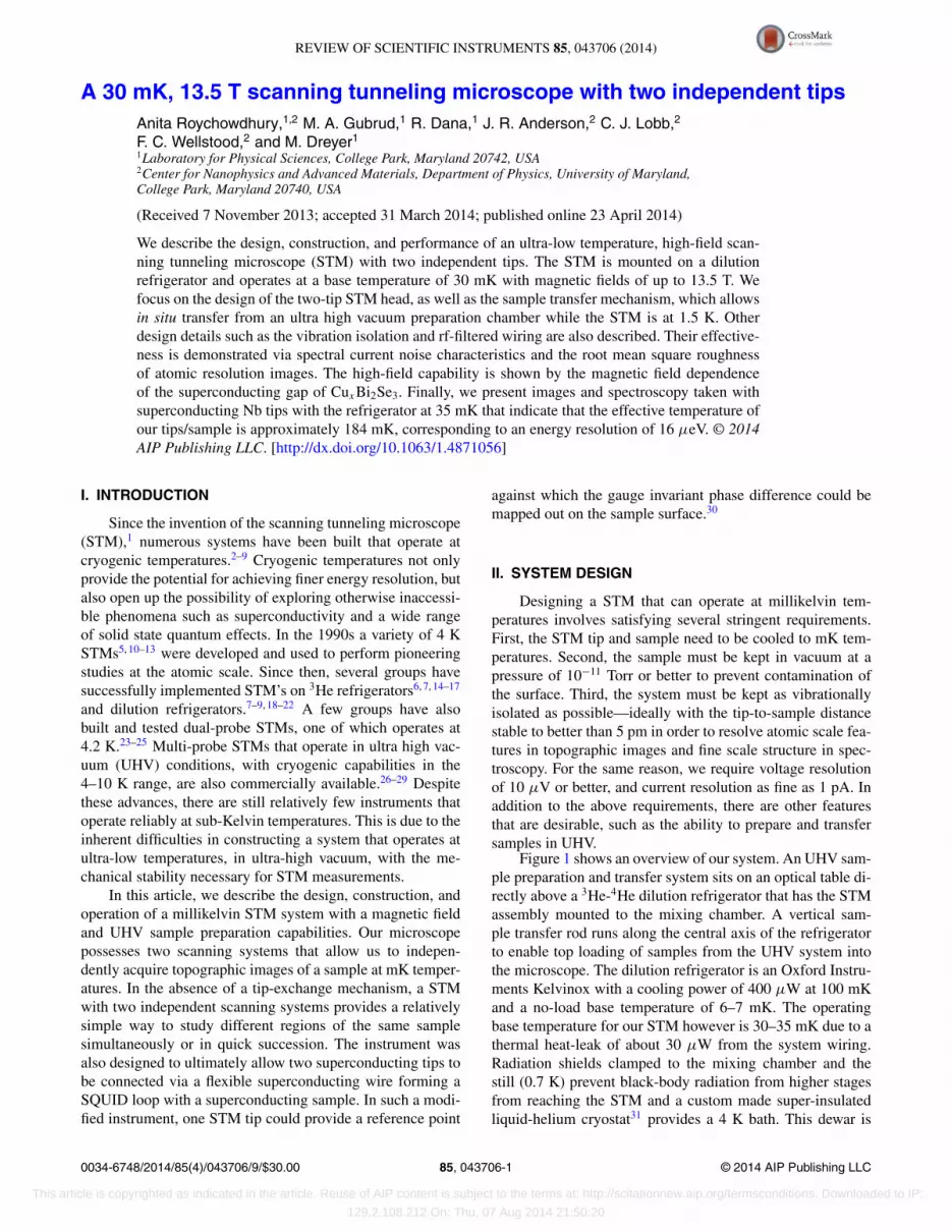
Our dual-tip STM (see Fig. 4) is a modified version of aSTM design by Pan et al.6 The main difference is that we havedoubled the number of parts in order to allow the independentoperation of two STM tips. Key aspects of Pan’s design are itsemphasis on mechanical rigidity and the use of materials thatare matched as closely as possible to minimize stress fromthermal expansion. In our case, this was achieved by making
the main STM body from a single 94 mm long Macor cylinderwith an outer diameter of 50.8 mm and an inner diameter of35.6 mm.
Figures 4(b) and 4(c) show details of our STM design.The sample stud (11) is loaded from the top, and the two tipsapproach the sample from below. The “inner” tip (1) is at-tached to the center or “inner” piezo tube (4), and the “outer”(off-center) tip (2) to the “outer” piezo tube (3). The tips areside-by-side, about 1 mm apart while the piezo tubes are con-centric and share a common axis (see Fig. 4(b)). Each piezotube is epoxied onto a Macor scanner holder. The large outerscanner (3) operates in a hole in a large sapphire prism (6).The small scanner tube (4) is located above the correspondingsmall sapphire prism (7) rather than within it.
The coarse approach mechanism is driven by six shearpiezo stacks for each tip (see Fig. 4(b)). Four large stacks (5)are epoxied to the inside of the outer Macor STM body (10)and two to a Macor piece (14) held in place by a copper springplate (13). Likewise, four small stacks (8) are epoxied ontothe smaller inner Macor body, and two to a small Macor piece(15) held in place by a small Cu-Be spring plate (16). Withthis arrangement, the outer walker carries the weight of theinner walker. For first approach, the tips are positioned withthe inner tip just behind the outer tip (out of tunneling range),and we drive just the large piezo motor so that the outer tipmakes contact with the sample first. We then retract the outertip, and approach with the small piezo motor until we detecttunneling with the inner tip.
We found that the standard design of four piezos perstack6 was not strong enough to reliably approach the sampleat mK temperatures. Accordingly we use six piezos per stack.Testing of the six-piezo stacks at various voltages throughtheir whole range of motion revealed that they walked abouttwice as fast as our four-piezo setup. The small walker forthe inner tip carries less weight and four piezos per stack
FIG. 4. (a) Close-up photograph of STM tips, (b) inner and outer tip assemblies, (c) cross section view, and (d) photograph of the STM. The sample stud (11) isinserted from the top, and the tips approach it from below. The inner tip assembly consists of the inner tip (1), attached to the small piezo scanner (4). The outertip (2) is likewise attached to the large piezo scanner (3). The coarse approach mechanism for the outer tip is formed by a sapphire prism (6) that is driven by sixlarge piezo stacks (5) and (14), four of which are epoxied to the outer MACOR body (10). The coarse approach mechanism for the inner tip (9) rides on the outercoarse approach assembly and has a small sapphire prism (7) that is driven by six small piezo stacks (8) and (15). To set the frictional force between the prismsand the piezo stacks, two piezo stacks for each stages are held against the sapphire prisms by adjustable copper spring plates (13) and (16). The capacitanceplates (12) keep track of the relative position of each tip assembly.
This article is copyrighted as indicated in the article. Reuse of AIP content is subject to the terms at: http://scitationnew.aip.org/termsconditions. Downloaded to IP:
129.2.108.212 On: Thu, 07 Aug 2014 21:50:20
043706-5 Roychowdhury et al. Rev. Sci. Instrum. 85, 043706 (2014)
are sufficient. We note that the tight space makes wiring thesmall stacks problematic, and the prototype developed shortsafter a couple of years of use. Hence, our current designfor the small walker has replaceable piezo stacks epoxiedonto copper plates that are screwed onto the small Macorbody.
III. OPERATION
Samples are mounted on copper, stainless steel, ormolybdenum sample studs that can be changed in situ. A sam-ple is either attached to the holder with silver epoxy or held inplace by an L-shaped clamping arm. We use etched W and Nbwires as STM tips.49 The tips cannot be changed in situ—themicroscope has to be warmed to room temperature and thevacuum can vented in order to replace a tip.
After STM tips are installed, the vacuum can is evacu-ated to ∼10−7 Torr. We then fill the dewar with liquid N2
and bleed 3He exchange gas into the inner vacuum can (IVC).Overnight cooling brings the STM to 77 K. The nitrogen isthen siphoned out and slowly replaced with liquid helium. Af-ter cooling to 4.2 K in about a day, the exchange gas is thenpumped out, the 1 K pot filled, and standard operation of thedilution refrigerator begins. After reaching a base temperatureof 30–35 mK, we insert a sample of single crystal Au(111) orAu(100), and clean each tip using high voltage field emis-sion. After cleaning, the I-V curve for each tip is examinedto ensure we have a stable, sharp, and metallic tip. The goldsample is then exchanged via the sample transfer system forother samples of interest. Sample exchange takes 12–15 h, in-cluding about 3 h spent pre-cooling the rod at the top plateand about 3 h pre-cooling at the 1 K stage.
One of the tip-scanner-walker subsystems of the micro-scope is controlled by an RHK Technology SPM 1000 Scan-ning Probe Microscope Control System. It has a maximumpiezo voltage of 220 V and runs in analog feedback. Thissubsystem uses an IVP-300 RHK trans-impedance amplifierwith a conversion factor of 1 nA/V to maintain the tunnel cur-rent. The other tip-scanner-walker subsystem is controlled bya Thermomicroscopes SPM control system (now obsolete),with a digital feedback electronic control unit, and a maxi-mum piezo voltage of 220 V. A variable gain DL InstrumentModel 1211 current trans-impedance amplifier monitors thetunnel current.
IV. PERFORMANCE
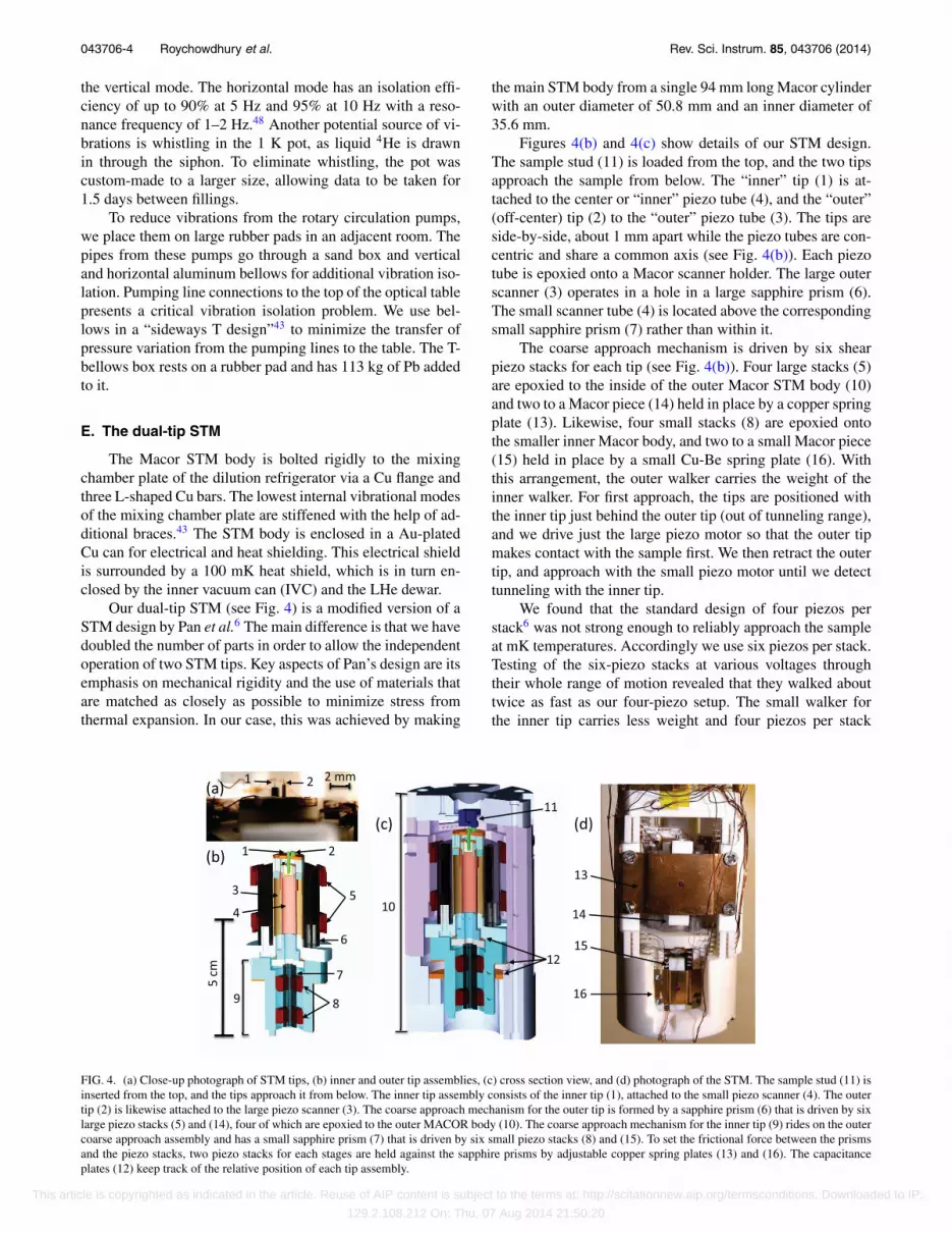
Figure 5 shows unfiltered atomic resolution images takenwith the inner and outer tips on a Bi2Se3 sample. The peakto valley atomic corrugations over the line sections shown ofthe outer and inner tips are ∼18 pm and ∼8 pm, respectively.To characterize the noise, we Fourier transformed these im-ages, filtered out the atomic lattice, and then analyzed the in-verse Fourier transform. The rms roughnesses of the resultingbackground noise for the outer and inner tip images were 3.55± 0.03 pm and 1.75 ± 0.01 pm, respectively. The noise levelfor each tip is thus well below the signal for atomic scale fea-tures. We note that these measurements were taken with the 1K pot running. We calibrated the scanners in the x, y, and z di-
FIG. 5. Unfiltered atomic resolution images of Bi2Se3 taken using Nb tips at35 mK with (a) outer tip and (b) inner tip. Top: Topographic images. Bottom:Graphs of tip height z vs. distance scanned d, showing atomic corrugationwith peak to valley heights of ∼18 pm for the outer tip (a) and ∼8 pm for theinner tip (b).
rections from these images and images of mono-atomic stepson Au(100).
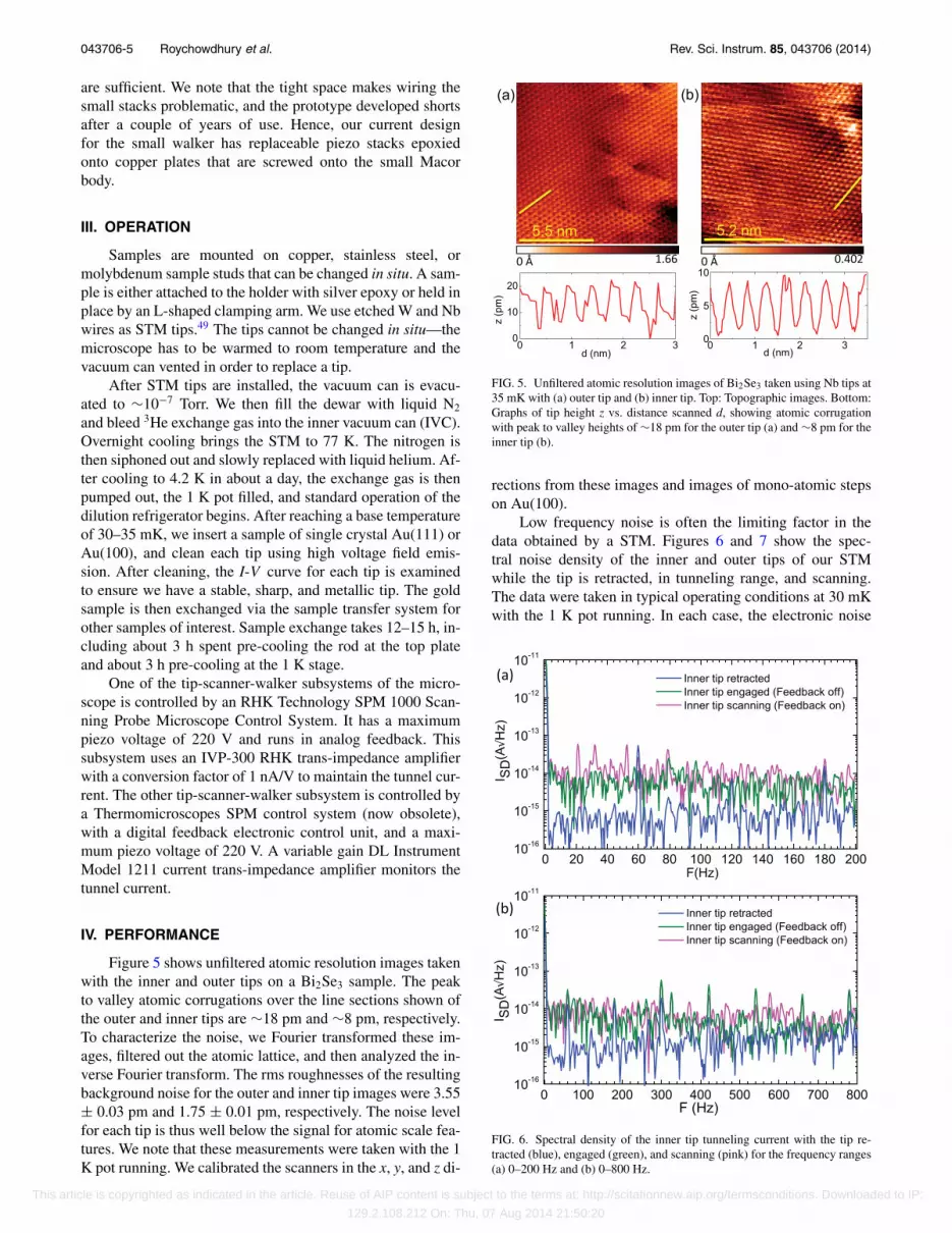
Low frequency noise is often the limiting factor in thedata obtained by a STM. Figures 6 and 7 show the spec-tral noise density of the inner and outer tips of our STMwhile the tip is retracted, in tunneling range, and scanning.The data were taken in typical operating conditions at 30 mKwith the 1 K pot running. In each case, the electronic noise
FIG. 6. Spectral density of the inner tip tunneling current with the tip re-tracted (blue), engaged (green), and scanning (pink) for the frequency ranges(a) 0–200 Hz and (b) 0–800 Hz.
This article is copyrighted as indicated in the article. Reuse of AIP content is subject to the terms at: http://scitationnew.aip.org/termsconditions. Downloaded to IP:
129.2.108.212 On: Thu, 07 Aug 2014 21:50:20

043706-6 Roychowdhury et al. Rev. Sci. Instrum. 85, 043706 (2014)
FIG. 7. Spectral density of the outer tip tunneling current with the tip re-tracted (blue), engaged (green), and scanning (pink) for the frequency ranges(a) 0–200 Hz and (b) 0–800 Hz.
floor—measured with the tip retracted—is between 10−16 and10−15 A/
√Hz. When the tip is engaged, the mechanical noise
results in the background level being raised to between 10−14
and 10−13 A/√
Hz at low frequencies. Although 60 Hz peaksand higher harmonics are noticeable with both tips, we notethat worst the peak signal is ≈1 pA for the inner tip, and ≈100pA for the outer tip. The low current noise characteristics in-dicate that the instrument will yield a good signal to noiseratio for both topographic and spectroscopic data.
The magnet dewar was tested on the system, using astandard single tip Pan-style STM, a Tungsten tip, and aCuxBi2Se3 superconducting sample. Fig. 8 demonstrates theperformance of the magnet via a series of spectroscopy curvesmeasured at different field strengths. The superconductinggap and coherence peaks were predictably diminished withincreasing magnetic field.
To obtain the effective temperature and energy resolu-tion of our instrument, conductance (dI/dV ) measurementswere performed between a superconducting tip and a normalsample. The effective temperature can be extracted by fit-ting the data to a theory that describes quasiparticle tunnelingin a superconductor-insulator-normal (SIN) tunnel junction.50
Figure 9 shows dI/dV measurements using a Nb inner tipand a Bi2Se3 sample at 35 mK. The measurements were takenby modulating the junction voltage with a small sinusoidal acvoltage and detecting the corresponding response signal witha lock-in technique. Examining the plot, we see that the gapis � ≈ 0.7 meV, which is about half that of bulk niobium dueto finite-size effects.
-1.0 -0.5 0.0 0.5 1.00.0
0.2
0.4
0.6
0.8
1.0
1.2
1.4
1.6
G/G
N
V(mV)
0 T0.25 T0.5 T0.75 T1 T1.25 T1.4 T1.5 T1.6 T1.7 T1.8 T
FIG. 8. Plot of normalized conductance G/Gn versus tip-to-sample voltage V
for a tungsten tip and copper-intercalated Bi2Se3 sample at Tmix = 35 mK.The superconducting gap is noticeably reduced as the magnetic field is in-creased to 1.8 T.
Figure 10(a) shows similar dI/dV curves measured asa function of temperature from 35 mK to 500 mK, andFig. 10(b) shows a closeup of the right conduction peak. Wenote that although the difference between the 35 mK curveand the 50 mK curve is negligible, there is a noticeable differ-ence between the 50 mK curve and the 100 mK curve, as wellas between subsequent curves. This suggests that our samplewas able to cool to temperatures on the order of 100 mK.
In order to obtain an estimate for the effective tempera-ture of our instrument, we fit each curve in Fig. 10 to
dI
dV= Gn
∫ ∞
−∞g(E + eV )Ns,tip(E)dE, (1)
where Gn is the normal conductance, g(E + eV ) = −∂f (E+ eV )/∂E, f(E) is the Fermi function at energy E, andNs,tip(E) is the normalized local density of states of the tip.For a superconducting tip with a BCS density of states and a
-2 -1 0 1 20.0
0.5
1.0
1.5
2.0
2.5
3.0
3.5
G/G
n
V (mV)
FIG. 9. Plot of normalized conductance G/Gn versus tip-to-sample voltage V
for a Nb tip and Au sample at Tmix = 35 mK. Blue points are measured dataand red curve is fit to Eq. (1) with energy gap � = 0.54 meV, temperatureTeff = 184 mK, and � ≈ 10−5 meV.
This article is copyrighted as indicated in the article. Reuse of AIP content is subject to the terms at: http://scitationnew.aip.org/termsconditions. Downloaded to IP:
129.2.108.212 On: Thu, 07 Aug 2014 21:50:20

043706-7 Roychowdhury et al. Rev. Sci. Instrum. 85, 043706 (2014)
-2 -1 0 1 20.0
0.5
1.0
1.5
2.0
2.5
3.0
3.5
G/G
n
V (mV)
35 mK50 mK100 mK200 mK300 mK400 mK500 mK
(a)
(b)
0.50 0.55 0.60 0.65 0.70
2.0
2.5
3.0
G/G
n
V (mV)
35 mK50 mK100 mK200 mK300 mK400 mK500 mK
FIG. 10. (a) Normalized conductance G/Gn versus tip voltage V measuredfrom 35 mK to 500 mK for Nb tip and Bi2Se3 sample. (b) Detailed view ofright conductance peaks near 0.6 mV reveals significant temperature depen-dence to the peak curves.
finite quasiparticle relaxation time �,51 we have
Ns,tip(E) = Re
[|E − i�|√
(E − i�)2 − �2
]. (2)
Fitting our data using a weighted least-squares minimizationvia the Levenberg-Marquardt52, 53 algorithm, we extract �, �,and the effective temperature Teff, which enters through theFermi function.
Figure 11 shows a plot of the effective temperature Teff
versus the temperature Tmix of the mixing chamber. The solidcurve in Fig. 11 shows that our data are well explained by asimple model of voltage noise54
Teff =√
T 2mix + T 2
0 , (3)
where the fitting parameter T0 =√
3e2V 2n /k2
Bπ2 is the min-imum effective sample temperature due to rms voltage noiseVn (see the Appendix). From the fit, we find T0 = 184 ± 6 mK.This is equivalent to an energy resolution of ≈16 μeV. Thegood agreement between our data and Eqs. (1) and (3) sug-gests that we are limited by voltage noise and that additionalcryogenic filtering on the scanner and walker wires would re-duce the effective temperature.
0 100 200 300 400 5000
100
200
300
400
500
Tef
f(m
K)
T (mK)
FIG. 11. Plot of effective temperature Teff vs. temperature T of the mix-ing chamber. Blue points were extracted from fitting BCS theory to the datashown in Fig. 9. The red curve is Eq. (3) with Tmix = T and T0 = 184 mK.The straight line shows Teff = T .
V. CONCLUSION
We have presented the design and performance of a STMwith two independent tips that can operate at millikelvin tem-peratures and in high magnetic fields. A connected UHV sam-ple preparation chamber and transfer chamber enable in situsample preparation and transfer to the dilution refrigerator.We have analyzed system performance by characterizing ournoise levels and z-stability of both STM tips in atomic reso-lution images. At a mixing chamber temperature of 35 mK,we estimate the effective temperature of our instrument to be≈184 mK, corresponding to an energy resolution of ≈16 μeV,indicating that phenomena corresponding to extremely lowenergy scales may be probed using this instrument.
ACKNOWLEDGMENTS
The authors thank I. Miotkowski and Y. P. Chen forthe Bi2Se3 sample and acknowledge many useful discussionswith D. Sullivan and B. Barker. Portions of this work werefunded by the NSF under DMR-0605763.
APPENDIX: EFFECTIVE TEMPERATURECALCULATION AND VOLTAGE NOISE MODEL
1. Spectroscopy with a superconducting tip
The quasiparticle tunnel current between a STM tip andsample50 is given by
I (V ) = 4πe|M|2¯
∫ ∞
−∞[ftip(E) − fsample(E + eV )]
×ρtip(E)ρsample(E + eV )dE, (A1)
where |M| is the average value of the tunneling matrix ele-ment assumed to be independent of energy, ftip and fsample
are the electron energy distribution functions in the electrodeswhich reduce to the Fermi distribution in thermal equilibrium,and ρtip and ρsample are the local electronic density of states(LDOS) of the tip and sample at the point of contact.
This article is copyrighted as indicated in the article. Reuse of AIP content is subject to the terms at: http://scitationnew.aip.org/termsconditions. Downloaded to IP:
129.2.108.212 On: Thu, 07 Aug 2014 21:50:20

043706-8 Roychowdhury et al. Rev. Sci. Instrum. 85, 043706 (2014)
For a normal metal sample, we assume that the density ofstates of the sample is constant, and can write
I = Gn
eρtip,n(0)
∫ ∞
−∞[f (E) − f (E + eV )]ρtip(E)dE, (A2)
where ρtip,n(0) is the density of states of the tip at theFermi energy when the tip is in the normal state, and Gn
= 4πe2|M|2ρsample(0)ρtip,n(0)/¯ is the tunnel conductance inthe normal state. Taking a derivative with respect to V , weobtain
dI
dV= −Gn
e
∫ ∞
−∞
∂
∂Vf (E + eV )
ρtip(E)
ρtip,n(0)dE. (A3)
It is convenient to write g(E) = −f′(E), in which case g willbe positive everywhere and may be considered a probabilitydistribution. For a superconducting tip this yields
dI
dV= Gn
∫ ∞
−∞g(E′ + eV )Ns(E)dE, (A4)
where the normalized density of states of the tip Ns(E)= ρtip(E)/ρtip,n(0) is given by55
Ns(E) = Re
[ |E|√E2 − �2
]. (A5)
Dynes incorporated finite quasiparticle lifetime effectsinto the density of states by including broadening of the sin-gularity at the gap edge.51 Adding an imaginary term i� to theenergy, Eq. (A5) becomes
Ns(E) = Re
[|E − i�|√
(E − i�)2 − �2
]. (A6)
The recombination rate �/¯ is the rate at which a quasiparticlenear the energy gap edge scatters inelastically or recombinesinto the superfluid condensate.
2. Voltage noise and effective temperature
Voltage noise fluctuations can be characterized by a prob-ability distribution function P (V ) that we assume to be aGaussian with zero mean and standard deviation Vn. The ex-perimentally observed conductance may then be written as⟨
dI
dV(V )
⟩=
∫P (V ′)
dI
dV(V + V ′)dV ′
= Gn
∫Ns(E)
∫P (V ′)g(E + e(V + V ′))dV ′dE
= Gn
∫Ns(E)(P g)(E + eV )dE, (A7)
where we have used Eq. (A4) and used to represent the con-volution of P and g. Setting F = P g, we have⟨
dI
dV
⟩∝
∫Ns,tip(E)F (E)dE. (A8)
We note that F(E) is sharply peaked with standard deviationσ F and determines the sharpness of features such as the in-crease in conductance at the gap.
Because F is a convolution of P and g, which may bothbe considered probability distributions with mean zero, their
variances add and we can write
σ 2F = e2σ 2
P + σ 2g , (A9)
where the factor of e comes from the convolution inEq. (A7). For a Fermi distribution it can be shown that σ 2
g
= ∫ ∞−∞ E2g(E)dE = k2
BT 2π2/3. Since Ns is also a sharplypeaked function, the total width of the measured coherencepeak, |σdI/dV |, should scale as
σdI/dV ∝ σ 2g + e2σ 2
P + σ 2Ns
, (A10)
where the standard deviation of the voltage noise is given byσP = Vn and σNs = � is a measure of the width of ρ. Thisyields
σdI/dV ∝(
k2BT 2π2
3+ e2V 2
n + �2
)1/2
. (A11)
From Eq. (A11), we see that the effect of voltage noise isindistinguishable from that of excess temperature when itcomes to the broadening of I-V characteristics. Assuming�2 e2V 2
n , and setting k2BT 2
effπ2/3 = k2
BT 2π2/3 + e2V 2n , we
can define the effective temperature of the instrument as54
Teff =√
T 2 + 3e2V 2n
k2Bπ2
. (A12)
1G. Binnig, H. Rohrer, C. Gerber, and E. Weibel, Phys. Rev. Lett. 49, 57(1982).
2S. A. Elrod, A. L. de Lozanne, and C. F. Quate, Appl. Phys. Lett. 45, 1240(1984).
3O. Marti, G. Binnig, H. Rohrer, and H. Salemink, Surf. Sci. 181, 230(1987).
4A. P. Fein, J. R. Kirtley, and R. M. Feenstra, Rev. Sci. Instrum. 58, 1806(1987).
5S. H. Tessmer, D. J. V. Harlingen, and J. W. Lyding, Rev. Sci. Instrum. 65,2855 (1994).
6S. H. Pan, E. W. Hudson, and J. C. Davis, Rev. Sci. Instrum. 70, 1459(1999).
7H. Suderow, M. Crespo, P. Martinez-Samper, J. Rodrigo, G. Rubio-Bollinger, S. Vieira, N. Luchier, J. Brison, and P. Canfield, Phys. C: Su-percond. 369, 106 (2002).
8Y. J. Song, A. F. Otte, V. Shvarts, Z. Zhao, Y. Kuk, S. R. Blankenship, A.Band, F. M. Hess, and J. A. Stroscio, Rev. Sci. Instrum. 81, 121101 (2010).
9M. Assig, M. Etzkorn, A. Enders, W. Stiepany, C. R. Ast, and K. Kern,Rev. Sci. Instrum. 84, 033903 (2013).
10J. W. G. Wilder, A. J. A. van Roy, H. van Kempen, and C. J. P. M. Harmans,Rev. Sci. Instrum. 65, 2849 (1994).
11G. Meyer, Rev. Sci. Instrum. 67, 2960 (1996).12C. Wittneven, R. Dombrowski, S. H. Pan, and R. Wiesendanger, Rev. Sci.
Instrum. 68, 3806 (1997).13J. H. Ferris, J. G. Kushmerick, J. A. Johnson, M. G. Yoshikawa Youngquist,
R. B. Kessinger, H. F. Kingsbury, and P. S. Weiss, Rev. Sci. Instrum. 69,2691 (1998).
14M. Kugler, C. Renner, Fischer, V. Mikheev, and G. Batey, Rev. Sci. In-strum. 71, 1475 (2000).
15A. J. Heinrich, C. P. Lutz, J. A. Gupta, and D. M. Eigler, Science 298, 1381(2002).
16J. Wiebe, A. Wachowiak, F. Meier, D. Haude, T. Foster, M. Morgenstern,and R. Wiesendanger, Rev. Sci. Instrum. 75, 4871 (2004).
17A. Kamlapure, G. Saraswat, S. C. Ganguli, V. Bagwe, P. Raychaudhuri, andS. P. Pai, Rev. Sci. Instrum. 84, 123905 (2013).
18P. Davidsson, H. Olin, M. Persson, and S. Pehrson, Ultramicroscopy 42–44(Pt 2), 1470 (1992).
19N. Moussy, H. Courtois, and B. Pannetier, Rev. Sci. Instrum. 72, 128(2001).
20M. D. Upward, J. W. Janssen, L. Gurevich, A. F. Morpurgo, and L. P.Kouwenhoven, Appl. Phys. A 72, S253 (2001).
This article is copyrighted as indicated in the article. Reuse of AIP content is subject to the terms at: http://scitationnew.aip.org/termsconditions. Downloaded to IP:
129.2.108.212 On: Thu, 07 Aug 2014 21:50:20

043706-9 Roychowdhury et al. Rev. Sci. Instrum. 85, 043706 (2014)
21H. Kambara, T. Matsui, Y. Niimi, and H. Fukuyama, Rev. Sci. Instrum. 78,073703 (2007).
22S. Misra, B. B. Zhou, I. K. Drozdov, J. Seo, L. Urban, A. Gyenis, S. C. J.Kingsley, H. Jones, and A. Yazdani, Rev. Sci. Instrum. 84, 103903 (2013).
23H. Grube, B. C. Harrison, J. Jia, and J. J. Boland, Rev. Sci. Instrum. 72,4388 (2001).
24H. Okamoto and D. Chen, Rev. Sci. Instrum. 72, 4398 (2001).25W. Wu, A. Guha, S. Kim, and A. De Lozanne, IEEE Trans. 5, 77 (2006).26Multiprobe MXPS, Oxford Instruments, UK.27attoSTM I, attocube, München, Germany.28Quadraprobe, RHK Technology, Troy, MI.29Koala TetraProbe, mProbes, Jülich, Germany.30D. Sullivan, S. Dutta, M. Dreyer, M. Gubrud, A. Roychowdhury, J. Ander-
son, C. Lobb, and F. Wellstood, J. Appl. Phys. 113, 183905 (2013).31Kadel Engineering, Danville, IN.32American Magnetics, Inc.33Varian Model Starcell 75 and 300, respectively.34Vacuum Generators Model ST2 and Varian Model 929-022.35VG Scienta Model VIG18/Arun Microelectronics Ltd. PGC1.36Varian TModel V551 Navigator/VT 1000HT.37Varian Model TriScroll600.38Extorr Model XT200.
39Omicron Model EFM3/EVC 100.40Specs Model IQE 10.41VG Scienta Model HPT.42M. Dreyer, J. Lee, H. Wang, and B. Barker, Rev. Sci. Instrum. 81, 053703
(2010).43M. A. Gubrud, Ph.D. dissertation, University of Maryland 2010.44Brittania House, Cambridge, UK.45Rami Ceramic Industries, Nazareth, Palestine.46F. P. Milliken, J. R. Rozen, G. A. Keefe, and R. H. Koch, Rev. Sci. Instrum.
78, 024701 (2007).47Technical Manufacturing Corporation, TMC Model 71-473-spl.48TMC Model 71-473-SPL, Technical Manufacturing Corporation, Peabody,
MA.49A. Roychowdhury et al., “Plasma etching of superconducting niobium
tips,” (unpublished).50J. Bardeen, Phys. Rev. Lett. 6, 57 (1961).51R. C. Dynes, V. Narayanamurti, and J. P. Garno, Phys. Rev. Lett. 41, 1509
(1978).52K. Levenberg, Quart. Appl. Math. 2, 164–168 (1944).53D. W. Marquardt, J. Soc. Ind. Appl. Math. 11, 431–441 (1963).54H. le Sueur and P. Joyez, Rev. Sci. Instrum. 77, 123701 (2006).55J. Bardeen, L. N. Cooper, and J. R. Schrieffer, Phys. Rev. 108, 1175 (1957).
This article is copyrighted as indicated in the article. Reuse of AIP content is subject to the terms at: http://scitationnew.aip.org/termsconditions. Downloaded to IP:
129.2.108.212 On: Thu, 07 Aug 2014 21:50:20