512channel vertical-cavity surface-emitting laser based free-space optical link
TRANSCRIPT
512-channel vertical-cavity surface-emitting laserbased free-space optical link
Marc Chateauneuf, Andrew G. Kirk, David V. Plant, Tsuyoshi Yamamoto, andJohn D. Ahearn
A vertical-cavity surface-emitting laser based bidirectional free-space optical interconnect has beenimplemented to interconnect two printed circuit boards. A total of 512 clustered channels with a densityof 2844 channels�cm2 are transmitted over a distance of 83 mm. The optical interconnect is a combi-nation of refractive microlenses and diffractive minilens relays. © 2002 Optical Society of America
OCIS codes: 200.2610, 200.4650, 220.4830, 200.4880, 250.7260, 350.3950.
1. Introduction
Parallel optical interconnects have great potential foruse as high bandwidth interconnects over short dis-tances, such as at the board-to-board and shelf-to-shelf levels.1 Parallel optical interconnects offercompact, high capacity interconnections with lowpower requirements. Recent developments in theintegration of large vertical cavity surface emittinglaser �VCSEL� arrays on complementary metal-oxidesemicondutor�s� CMOS�s� increase the potential ofparallel optical interconnects.2–5
A variety of approaches have been taken to imple-ment such optical interconnects. Unidimensionalparallel optical data links, linear VCSEL arrays, andfiber ribbons have demonstrated high performancesin recent years.6–10 More recently, fiber imageguides showed the possibility of propagating two-dimensional �2D� channel arrays.11–13 These guidedmediums offer flexible connections that have the ad-vantage of requiring alignment only at the ends of thelink. Free-space optical interconnects �FSOIs� havegreater alignment challenges, but they are poten-tially more suitable for short distance optical connec-tions on the order of centimeters. Over such shortdistances, FSOIs can image very large 2D channel
M. Chateauneuf, A. G. Kirk, and D. V. Plant are with the De-partment of Electrical and Computer Engineering, McGill Univer-sity, Montreal, Quebec, Canada, H3A 2A7. T. Yamamoto is nowwith NTT Optical Network System Laboratory, Kanagawa, Japan.John D. Ahearn is with BAE Systems, Nashua, New Hampshire.
Received 25 February 2002; revised manuscript received 3 June2002.
0003-6935�02�265552-10$15.00�0© 2002 Optical Society of America
5552 APPLIED OPTICS � Vol. 41, No. 26 � 10 September 2002
arrays through a small optical window resulting in alarger channel density. In addition, microoptic ele-ments used in free-space systems can be made ofplastic14–17 and be mass produced by injection mold-ing or embossing techniques. This can considerablyreduce the cost of the links.
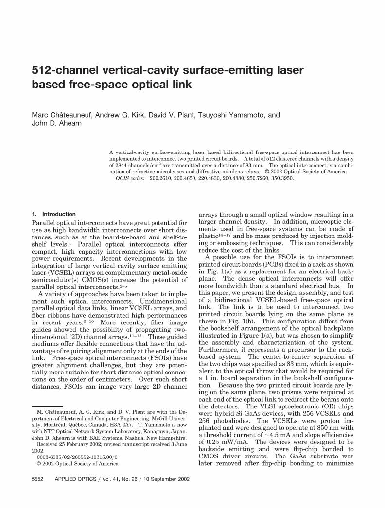
A possible use for the FSOIs is to interconnectprinted circuit boards �PCBs� fixed in a rack as shownin Fig. 1�a� as a replacement for an electrical back-plane. The dense optical interconnects will offermore bandwidth than a standard electrical bus. Inthis paper, we present the design, assembly, and testof a bidirectional VCSEL-based free-space opticallink. The link is to be used to interconnect twoprinted circuit boards lying on the same plane asshown in Fig. 1�b�. This configuration differs fromthe bookshelf arrangement of the optical backplaneillustrated in Figure 1�a�, but was chosen to simplifythe assembly and characterization of the system.Furthermore, it represents a precursor to the rack-based system. The center-to-center separation ofthe two chips was specified as 83 mm, which is equiv-alent to the optical throw that would be required fora 1 in. board separation in the bookshelf configura-tion. Because the two printed circuit boards are ly-ing on the same plane, two prisms were required ateach end of the optical link to redirect the beams ontothe detectors. The VLSI optoelectronic �OE� chipswere hybrid Si-GaAs devices, with 256 VCSELs and256 photodiodes. The VCSELs were proton im-planted and were designed to operate at 850 nm witha threshold current of �4.5 mA and slope efficienciesof 0.25 mW�mA. The devices were designed to bebackside emitting and were flip-chip bonded toCMOS driver circuits. The GaAs substrate waslater removed after flip-chip bonding to minimize
light absorption. The photodiodes were p-i-n struc-tures designed to operate with a responsivity of 0.5A�W.4 An optical interconnection between thesetwo chips had already been demonstrated with a ma-crolens system.2 However, this optical system wasbulky and did not represent a practical implementa-tion.
Throughout this paper, the term optical channelrefers to the route that propagates a single VCSELonto its corresponding detector. A total of 512 opti-cal channels were therefore required to bidirection-ally interconnect the two chips. The optical linkconsists of both collimating�focusing optics and relayoptics.
The format of this paper is as follows: Section 2describes the optical design of the different modulesthat compose the parallel free-space interconnect andthe results of a misalignment analysis. In Section 3,the assembly procedure, the alignment techniquesused as well as a description of the opto-mechanicalcomponents are discussed. Section 4 presents thecharacterization results of the assembled optical link.In Section 5, the functionality and the bidirectional-ity of the system is demonstrated by transferringdigital data through the link. Finally, Section 6 con-cludes the paper with a discussion of possible im-provements to the link.
2. Optical Design
There are three relay configurations that are com-monly used in FSOIs.1,18 The simplest of these is
the macrolens configuration in which a pair of tele-centric lenses images the entire device array. Al-though a long optical throw can be achieved with thisconfiguration, it requires fast lenses with large fieldsof vision and very low aberrations. Even if collimat-ing the VCSELs by use of microlenses would enablethe employment of slower lenses,17,19 this design doesnot scale well with the field of view. At the otherextreme, a microchannel arrangement would includepairs of microlenses for each individual channel.14,20
This configuration scales well as the device arrayincreases in size but the throw distance is limited dueto diffraction.1 Multiple relay stages would there-fore be required, which would complicate the assem-bly. A clustered or minichannel system isintermediate between these two extremes and hasalready been implemented in some systems.21,22 Inthis approach the object and image planes are dividedinto clusters of elements and telecentric pairs ofminilens arrays are used to image between them.
A clustered minichannel configuration was chosenfor the interconnection. A microlens array was usedto collimate the fast beams emitted from the VCSELsto obtain high f�number beams in the telecentric link.Slow beams enabled a larger throw distance of thetelecentric relays and provided a better balance be-tween lateral and tilt misalignment tolerances.23
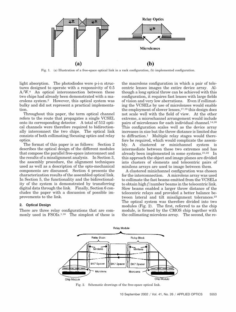
The optical system was therefore divided into twomodules �Fig. 2�. The first, referred to as the chipmodule, is formed by the CMOS chip together withthe collimating microlens array. The second, the re-
Fig. 1. �a� Illustration of a free-space optical link in a rack configuration, �b� implemented configuration.
Fig. 2. Schematic drawings of the free-space optical link.
10 September 2002 � Vol. 41, No. 26 � APPLIED OPTICS 5553
lay module, was composed of the telecentric minilenspairs. Both modules can be designed and assembledseparately. This enabled each block to be individu-ally characterized and results in better misalignmenttolerances of the components.21,24
The design of the optical link was guided by thefollowing requirements. First, the pitch betweenthe active elements on the VLSI-OE chips was fixedto 125 �m. The number of VCSELs and detectorswas specified to be 512 devices and the center-to-center separation of the chips was 83 mm. The onlyflexibility in the layout was to group the active de-vices within clusters by discarding one or more rowsand columns on the required 125-�m grid. It followsthat clustering the VCSELs�detectors increased thechip size, creating two conflicting requirements.25
The separation of the clusters should be minimized tomaximize the fraction of the GaAs die used. How-ever, to avoid beam clipping in the relays, the size ofthe active device array in the center of each clustershould be small compared to the diameter of the im-aging minilenses. Finally, the bidirectional natureof the system requires a symmetric optical link.
Within these requirements, the design parameterswere optimized through an evaluation of the maxi-mum throughput as well as a misalignment analysis.A ray-tracing algorithm was used for these simula-tions. Although as has been shown26 that this leadsto inaccuracies in the estimation of misalignment tol-erance when compared to a wave-propagation model,the additional computation time did not justify theimproved accuracy in this case.
A Monte Carlo-radiometric analysis was used to es-timate the throughout of the system for different pa-rameters and misalignments. Rays were launchedat random with a spatial probability density functiondefined by the mode field diameter of the VCSELsand with an angular probability density-function de-fined by their divergence angle. The multimode VC-SELs used in the system had a mode field diameter of6 �m and a full divergence angle of 20°. A total of5000 rays were propagated through the system foreach simulation. At the other end, the detector wasrepresented by a 50 �m � 50 �m surface, which wasequivalent to the detector size on the real CMOS chip.The throughput was calculated as the fraction of all
rays incident on the 50-�m detector aperture. In allthe simulations, the VCSEL located in a corner of acluster was modeled. This beam was the closest tothe edges of the minilenses and therefore suffered themost from clipping and misalignment of componentsin the system.
The diameter and focal length of the collimatingmicrolenses were determined by the VCSEL pitch�125 �m� and the beam divergence angle �20°�. Toavoid clipping the beams, the focal length was set to250 �m. The resulting refractive f�2 microlenseswere circular with a pitch of 125 �m. Plano-convexfast lenses, such as these microlenses are more sub-ject to aberrations. Simulations showed that if theconvex side of the collimating lenses was facing theVCSELs, the spherical aberrations introduced by thelenses could limit the maximum throughput of theoptical link to 85%. This value of throughput wasunacceptable given that the lost power would alsocontribute to crosstalk. For that reason, the beamsemitted from the VCSEL needed to be first refractedby the planar surface of the microlens array sub-strate. A 300-�m thick fused-silica substrate wastherefore selected to be able to position the chip at thefocal plane of the microlens array. This left a dis-tance of 44 �m between the VCSELs and the sub-strate. The use of a thin substrate introducedcomplex fabrication and packaging problems. Themanipulation of such substrates during the fabrica-tion process as well as the precise alignment requiredat a distance of 44 �m from the VCSELs�detectorswere delicate tasks. However, being so close to thechips, the thin substrate could also be used to seal theOE package if a hermetic seal was required.
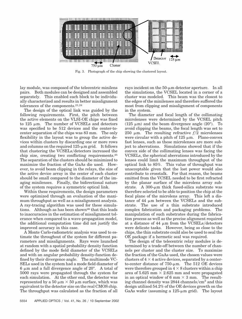
The design of the telecentric relay modules is de-termined by a trade-off between the number of chan-nels per cluster and the cluster size. To maximizethe fraction of the GaAs used, the chosen values wereclusters of 4 � 4 active devices, separated by a center-to-center distance of 750-�m. The 512 OE deviceswere therefore grouped in 4 � 8 clusters within a chiparea of 5.625 mm � 2.625 mm and were propagatedin an optical window of 6 mm � 3 mm. The result-ing channel density was 2844 channels�cm2 and thisdesign utilized 54.2% of the OE devices growth on theGaAs wafer �assuming a 125-�m grid�. The layout
Fig. 3. Photograph of the chip showing the clustered layout.
5554 APPLIED OPTICS � Vol. 41, No. 26 � 10 September 2002
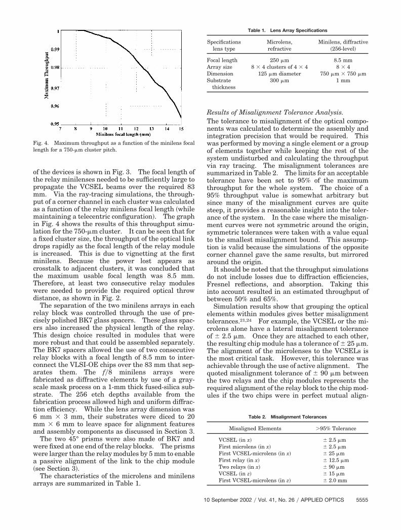
of the devices is shown in Fig. 3. The focal length ofthe relay minilenses needed to be sufficiently large topropagate the VCSEL beams over the required 83mm. Via the ray-tracing simulations, the through-put of a corner channel in each cluster was calculatedas a function of the relay minilens focal length �whilemaintaining a telecentric configuration�. The graphin Fig. 4 shows the results of this throughput simu-lation for the 750-�m cluster. It can be seen that fora fixed cluster size, the throughput of the optical linkdrops rapidly as the focal length of the relay moduleis increased. This is due to vignetting at the firstminilens. Because the power lost appears ascrosstalk to adjacent clusters, it was concluded thatthe maximum usable focal length was 8.5 mm.Therefore, at least two consecutive relay moduleswere needed to provide the required optical throwdistance, as shown in Fig. 2.
The separation of the two minilens arrays in eachrelay block was controlled through the use of pre-cisely polished BK7 glass spacers. These glass spac-ers also increased the physical length of the relay.This design choice resulted in modules that weremore robust and that could be assembled separately.The BK7 spacers allowed the use of two consecutiverelay blocks with a focal length of 8.5 mm to inter-connect the VLSI-OE chips over the 83 mm that sep-arates them. The f�8 minilens arrays werefabricated as diffractive elements by use of a gray-scale mask process on a 1-mm thick fused-silica sub-strate. The 256 etch depths available from thefabrication process allowed high and uniform diffrac-tion efficiency. While the lens array dimension was6 mm � 3 mm, their substrates were diced to 20mm � 6 mm to leave space for alignment featuresand assembly components as discussed in Section 3.
The two 45° prisms were also made of BK7 andwere fixed at one end of the relay blocks. The prismswere larger than the relay modules by 5 mm to enablea passive alignment of the link to the chip module�see Section 3�.
The characteristics of the microlens and minilensarrays are summarized in Table 1.
Results of Misalignment Tolerance Analysis.The tolerance to misalignment of the optical compo-nents was calculated to determine the assembly andintegration precision that would be required. Thiswas performed by moving a single element or a groupof elements together while keeping the rest of thesystem undisturbed and calculating the throughputvia ray tracing. The misalignment tolerances aresummarized in Table 2. The limits for an acceptabletolerance have been set to 95% of the maximumthroughput for the whole system. The choice of a95% throughput value is somewhat arbitrary butsince many of the misalignment curves are quitesteep, it provides a reasonable insight into the toler-ance of the system. In the case where the misalign-ment curves were not symmetric around the origin,symmetric tolerances were taken with a value equalto the smallest misalignment bound. This assump-tion is valid because the simulations of the oppositecorner channel gave the same results, but mirroredaround the origin.
It should be noted that the throughput simulationsdo not include losses due to diffraction efficiencies,Fresnel reflections, and absorption. Taking thisinto account resulted in an estimated throughput ofbetween 50% and 65%.
Simulation results show that grouping the opticalelements within modules gives better misalignmenttolerances.21,24 For example, the VCSEL or the mi-crolens alone have a lateral misalignment toleranceof � 2.5 �m. Once they are attached to each other,the resulting chip module has a tolerance of � 25 �m.The alignment of the microlenses to the VCSELs isthe most critical task. However, this tolerance wasachievable through the use of active alignment. Thequoted misalignment tolerance of � 90 �m betweenthe two relays and the chip modules represents therequired alignment of the relay block to the chip mod-ules if the two chips were in perfect mutual align-
Table 1. Lens Array Specifications
Specificationslens type
Microlens,refractive
Minilens, diffractive�256-level�
Focal length 250 �m 8.5 mmArray size 8 � 4 clusters of 4 � 4 8 � 4Dimension 125 �m diameter 750 �m � 750 �mSubstrate
thickness300 �m 1 mm
Table 2. Misalignment Tolerances
Misaligned Elements �95% Tolerance
VCSEL �in x� � 2.5 �mFirst microlens �in x� � 2.5 �mFirst VCSEL-microlens �in x� � 25 �mFirst relay �in x� � 12.5 �mTwo relays �in x� � 90 �mVCSEL �in z� � 15 �mFirst VCSEL-microlens �in z� � 2.0 mm
Fig. 4. Maximum throughput as a function of the minilens focallength for a 750-�m cluster pitch.
10 September 2002 � Vol. 41, No. 26 � APPLIED OPTICS 5555
ment with each other. In practice, this is unlikely tooccur and so the real tolerance is � 25 �m. Theminilens arrays were aligned together by use of aninterferometric technique.27 In this case, the tech-nique enabled an alignment better than 9 �m, whichis within the required tolerances. The two relayswere assembled together by using the same align-ment method. The block formed by the two relaymodules has a larger misalignment tolerance and canbe passively aligned to the chip module. Because arotational misalignment translates into a displace-ment in x and y, its tolerance was therefore treated inthe lateral alignment study. The tilts ��x, �y� mis-alignment tolerances were assumed to be of the sameorder as a similar FSOI21 which had a worst-casetolerance of � 0.05°. This precision can be achievedby using the retroreflected beam method.28
3. System assembly
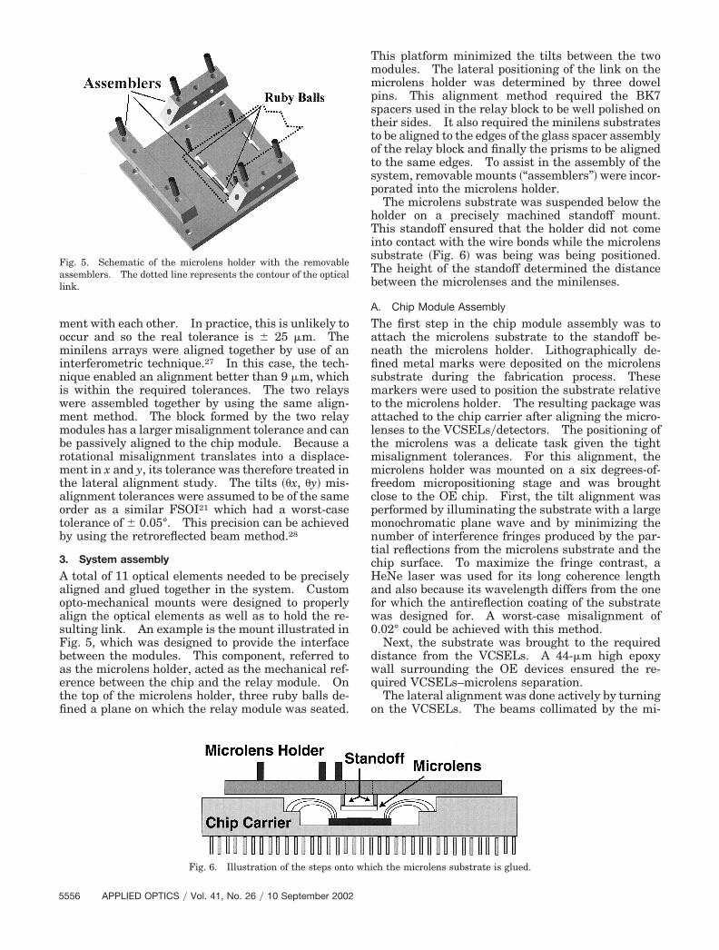
A total of 11 optical elements needed to be preciselyaligned and glued together in the system. Customopto-mechanical mounts were designed to properlyalign the optical elements as well as to hold the re-sulting link. An example is the mount illustrated inFig. 5, which was designed to provide the interfacebetween the modules. This component, referred toas the microlens holder, acted as the mechanical ref-erence between the chip and the relay module. Onthe top of the microlens holder, three ruby balls de-fined a plane on which the relay module was seated.
This platform minimized the tilts between the twomodules. The lateral positioning of the link on themicrolens holder was determined by three dowelpins. This alignment method required the BK7spacers used in the relay block to be well polished ontheir sides. It also required the minilens substratesto be aligned to the edges of the glass spacer assemblyof the relay block and finally the prisms to be alignedto the same edges. To assist in the assembly of thesystem, removable mounts �“assemblers”� were incor-porated into the microlens holder.
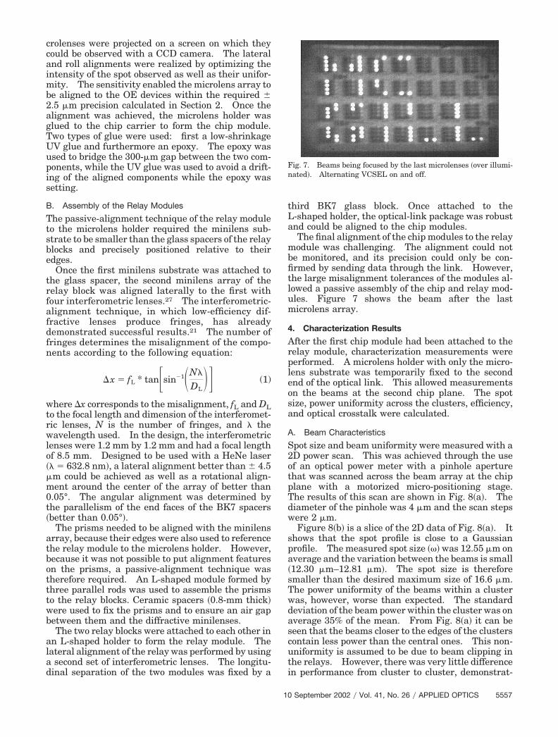
The microlens substrate was suspended below theholder on a precisely machined standoff mount.This standoff ensured that the holder did not comeinto contact with the wire bonds while the microlenssubstrate �Fig. 6� was being was being positioned.The height of the standoff determined the distancebetween the microlenses and the minilenses.
A. Chip Module Assembly
The first step in the chip module assembly was toattach the microlens substrate to the standoff be-neath the microlens holder. Lithographically de-fined metal marks were deposited on the microlenssubstrate during the fabrication process. Thesemarkers were used to position the substrate relativeto the microlens holder. The resulting package wasattached to the chip carrier after aligning the micro-lenses to the VCSELs�detectors. The positioning ofthe microlens was a delicate task given the tightmisalignment tolerances. For this alignment, themicrolens holder was mounted on a six degrees-of-freedom micropositioning stage and was broughtclose to the OE chip. First, the tilt alignment wasperformed by illuminating the substrate with a largemonochromatic plane wave and by minimizing thenumber of interference fringes produced by the par-tial reflections from the microlens substrate and thechip surface. To maximize the fringe contrast, aHeNe laser was used for its long coherence lengthand also because its wavelength differs from the onefor which the antireflection coating of the substratewas designed for. A worst-case misalignment of0.02° could be achieved with this method.
Next, the substrate was brought to the requireddistance from the VCSELs. A 44-�m high epoxywall surrounding the OE devices ensured the re-quired VCSELs–microlens separation.
The lateral alignment was done actively by turningon the VCSELs. The beams collimated by the mi-
Fig. 5. Schematic of the microlens holder with the removableassemblers. The dotted line represents the contour of the opticallink.
Fig. 6. Illustration of the steps onto which the microlens substrate is glued.
5556 APPLIED OPTICS � Vol. 41, No. 26 � 10 September 2002
crolenses were projected on a screen on which theycould be observed with a CCD camera. The lateraland roll alignments were realized by optimizing theintensity of the spot observed as well as their unifor-mity. The sensitivity enabled the microlens array tobe aligned to the OE devices within the required �2.5 �m precision calculated in Section 2. Once thealignment was achieved, the microlens holder wasglued to the chip carrier to form the chip module.Two types of glue were used: first a low-shrinkageUV glue and furthermore an epoxy. The epoxy wasused to bridge the 300-�m gap between the two com-ponents, while the UV glue was used to avoid a drift-ing of the aligned components while the epoxy wassetting.
B. Assembly of the Relay Modules
The passive-alignment technique of the relay moduleto the microlens holder required the minilens sub-strate to be smaller than the glass spacers of the relayblocks and precisely positioned relative to theiredges.
Once the first minilens substrate was attached tothe glass spacer, the second minilens array of therelay block was aligned laterally to the first withfour interferometric lenses.27 The interferometric-alignment technique, in which low-efficiency dif-fractive lenses produce fringes, has alreadydemonstrated successful results.21 The number offringes determines the misalignment of the compo-nents according to the following equation:
x � fL * tan�sin1�N�
DL�� (1)
where x corresponds to the misalignment, fL and DLto the focal length and dimension of the interferomet-ric lenses, N is the number of fringes, and � thewavelength used. In the design, the interferometriclenses were 1.2 mm by 1.2 mm and had a focal lengthof 8.5 mm. Designed to be used with a HeNe laser�� � 632.8 nm�, a lateral alignment better than � 4.5�m could be achieved as well as a rotational align-ment around the center of the array of better than0.05°. The angular alignment was determined bythe parallelism of the end faces of the BK7 spacers�better than 0.05°�.
The prisms needed to be aligned with the minilensarray, because their edges were also used to referencethe relay module to the microlens holder. However,because it was not possible to put alignment featureson the prisms, a passive-alignment technique wastherefore required. An L-shaped module formed bythree parallel rods was used to assemble the prismsto the relay blocks. Ceramic spacers �0.8-mm thick�were used to fix the prisms and to ensure an air gapbetween them and the diffractive minilenses.
The two relay blocks were attached to each other inan L-shaped holder to form the relay module. Thelateral alignment of the relay was performed by usinga second set of interferometric lenses. The longitu-dinal separation of the two modules was fixed by a
third BK7 glass block. Once attached to theL-shaped holder, the optical-link package was robustand could be aligned to the chip modules.
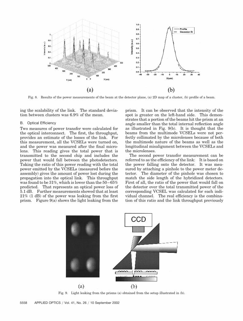
The final alignment of the chip modules to the relaymodule was challenging. The alignment could notbe monitored, and its precision could only be con-firmed by sending data through the link. However,the large misalignment tolerances of the modules al-lowed a passive assembly of the chip and relay mod-ules. Figure 7 shows the beam after the lastmicrolens array.
4. Characterization Results
After the first chip module had been attached to therelay module, characterization measurements wereperformed. A microlens holder with only the micro-lens substrate was temporarily fixed to the secondend of the optical link. This allowed measurementson the beams at the second chip plane. The spotsize, power uniformity across the clusters, efficiency,and optical crosstalk were calculated.
A. Beam Characteristics
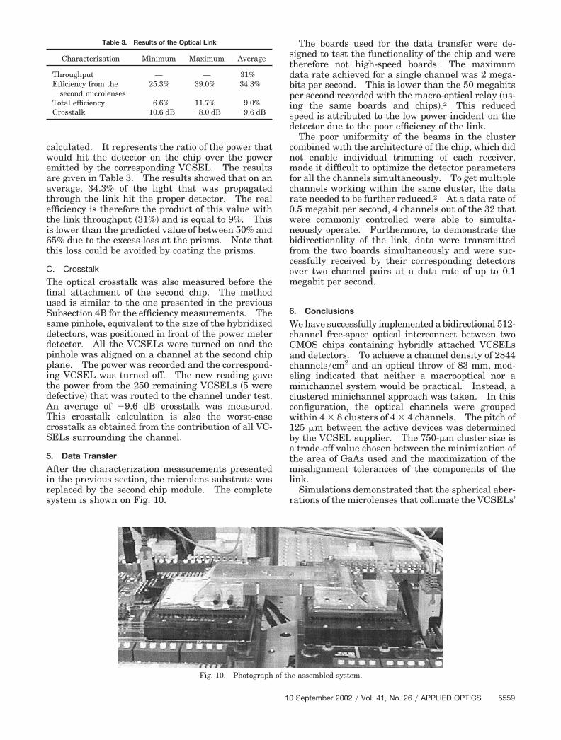
Spot size and beam uniformity were measured with a2D power scan. This was achieved through the useof an optical power meter with a pinhole aperturethat was scanned across the beam array at the chipplane with a motorized micro-positioning stage.The results of this scan are shown in Fig. 8�a�. Thediameter of the pinhole was 4 �m and the scan stepswere 2 �m.
Figure 8�b� is a slice of the 2D data of Fig. 8�a�. Itshows that the spot profile is close to a Gaussianprofile. The measured spot size � � was 12.55 �m onaverage and the variation between the beams is small�12.30 �m–12.81 �m�. The spot size is thereforesmaller than the desired maximum size of 16.6 �m.The power uniformity of the beams within a clusterwas, however, worse than expected. The standarddeviation of the beam power within the cluster was onaverage 35% of the mean. From Fig. 8�a� it can beseen that the beams closer to the edges of the clusterscontain less power than the central ones. This non-uniformity is assumed to be due to beam clipping inthe relays. However, there was very little differencein performance from cluster to cluster, demonstrat-
Fig. 7. Beams being focused by the last microlenses �over illumi-nated�. Alternating VCSEL on and off.
10 September 2002 � Vol. 41, No. 26 � APPLIED OPTICS 5557
ing the scalability of the link. The standard devia-tion between clusters was 6.9% of the mean.
B. Optical Efficiency
Two measures of power transfer were calculated forthe optical interconnect. The first, the throughput,provides an estimate of the losses of the link. Forthis measurement, all the VCSELs were turned on,and the power was measured after the final micro-lens. This reading gives the total power that istransmitted to the second chip and includes thepower that would fall between the photodetectors.Taking the ratio of this power reading with the totalpower emitted by the VCSELs �measured before theassembly� gives the amount of power lost during thepropagation into the optical link. This throughputwas found to be 31%, which is lower than the 50–65%predicted. That represents an optical power loss of5.1 dB. Further measurements showed that at least21% �1 dB� of the power was leaking from the firstprism. Figure 9�a� shows the light leaking from the
prism. It can be observed that the intensity of thespot is greater on the left-hand side. This demon-strates that a portion of the beams hit the prism at anangle smaller than the total internal reflection angleas illustrated in Fig. 9�b�. It is thought that thebeams from the multimode VCSELs were not per-fectly collimated by the microlenses because of boththe multimode nature of the beams as well as thelongitudinal misalignment between the VCSELs andthe microlenses.
The second power transfer measurement can bereferred to as the efficiency of the link: It is based onthe power falling onto the detector. It was mea-sured by attaching a pinhole to the power meter de-tector. The diameter of the pinhole was chosen tomatch the side length of the hybridized detectors.First of all, the ratio of the power that would fall onthe detector over the total transmitted power of thecorresponding VCSEL was calculated for each indi-vidual channel. The real efficiency is the combina-tion of this ratio and the link throughput previously
Fig. 8. Results of the power measurements of the beam at the detector plane, �a� 2D map of a cluster, �b� profile of a beam.
Fig. 9. Light leaking from the prisms �a� obtained from the setup illustrated in �b�.
5558 APPLIED OPTICS � Vol. 41, No. 26 � 10 September 2002
calculated. It represents the ratio of the power thatwould hit the detector on the chip over the poweremitted by the corresponding VCSEL. The resultsare given in Table 3. The results showed that on anaverage, 34.3% of the light that was propagatedthrough the link hit the proper detector. The realefficiency is therefore the product of this value withthe link throughput �31%� and is equal to 9%. Thisis lower than the predicted value of between 50% and65% due to the excess loss at the prisms. Note thatthis loss could be avoided by coating the prisms.
C. Crosstalk
The optical crosstalk was also measured before thefinal attachment of the second chip. The methodused is similar to the one presented in the previousSubsection 4B for the efficiency measurements. Thesame pinhole, equivalent to the size of the hybridizeddetectors, was positioned in front of the power meterdetector. All the VCSELs were turned on and thepinhole was aligned on a channel at the second chipplane. The power was recorded and the correspond-ing VCSEL was turned off. The new reading gavethe power from the 250 remaining VCSELs �5 weredefective� that was routed to the channel under test.An average of 9.6 dB crosstalk was measured.This crosstalk calculation is also the worst-casecrosstalk as obtained from the contribution of all VC-SELs surrounding the channel.
5. Data Transfer
After the characterization measurements presentedin the previous section, the microlens substrate wasreplaced by the second chip module. The completesystem is shown on Fig. 10.
The boards used for the data transfer were de-signed to test the functionality of the chip and weretherefore not high-speed boards. The maximumdata rate achieved for a single channel was 2 mega-bits per second. This is lower than the 50 megabitsper second recorded with the macro-optical relay �us-ing the same boards and chips�.2 This reducedspeed is attributed to the low power incident on thedetector due to the poor efficiency of the link.
The poor uniformity of the beams in the clustercombined with the architecture of the chip, which didnot enable individual trimming of each receiver,made it difficult to optimize the detector parametersfor all the channels simultaneously. To get multiplechannels working within the same cluster, the datarate needed to be further reduced.2 At a data rate of0.5 megabit per second, 4 channels out of the 32 thatwere commonly controlled were able to simulta-neously operate. Furthermore, to demonstrate thebidirectionality of the link, data were transmittedfrom the two boards simultaneously and were suc-cessfully received by their corresponding detectorsover two channel pairs at a data rate of up to 0.1megabit per second.
6. Conclusions
We have successfully implemented a bidirectional 512-channel free-space optical interconnect between twoCMOS chips containing hybridly attached VCSELsand detectors. To achieve a channel density of 2844channels�cm2 and an optical throw of 83 mm, mod-eling indicated that neither a macrooptical nor aminichannel system would be practical. Instead, aclustered minichannel approach was taken. In thisconfiguration, the optical channels were groupedwithin 4 � 8 clusters of 4 � 4 channels. The pitch of125 �m between the active devices was determinedby the VCSEL supplier. The 750-�m cluster size isa trade-off value chosen between the minimization ofthe area of GaAs used and the maximization of themisalignment tolerances of the components of thelink.
Simulations demonstrated that the spherical aber-rations of the microlenses that collimate the VCSELs’
Table 3. Results of the Optical Link
Characterization Minimum Maximum Average
Throughput — — 31%Efficiency from the
second microlenses25.3% 39.0% 34.3%
Total efficiency 6.6% 11.7% 9.0%Crosstalk 10.6 dB 8.0 dB 9.6 dB
Fig. 10. Photograph of the assembled system.
10 September 2002 � Vol. 41, No. 26 � APPLIED OPTICS 5559

beams limited the performance of the system andneeded to be minimized by having the flat surface ofthe microlens substrate facing the VCSELs. Thisconstraint added complexity to the link assembly be-cause the microlenses were fabricated on a thin sub-strate that needed to be aligned at 44 �m from theVCSELs. The simulation also showed that groupingthe optical elements into modules results in a bettermisalignment tolerance. The chip and relay mod-ules were assembled and characterized individually.
Results showed an optical efficiency of 9% and anoptical crosstalk of 9.6 dB. One of the main con-tributions to excess loss was found to be leakage fromthe prisms �approximately 1 dB each� as well as thebeam clipping within the relays. This can be attrib-uted to a poor collimation of the VCSELs beams dueto their multimode nature and possibly a longitudinalmisalignment of the microlenses in the chip module.These losses could be reduced by coating the reflec-tive surface of the prisms and by better modeling ofthe multimode nature of the VCSELs. In spite ofthe poor efficiency and crosstalk, we demonstratedunidirectional and bidirectional communication be-tween boards.
The authors gratefully acknowledge the contribu-tion of Michael Venditti, Emmanuelle Laprise, JulienFaucher, and Frederic Thomas-Dupuis. This re-search was supported by a contract from the BAESystems via the DARPA VLSI-Photonics program,DAAL01-98-C-0074, and by the Canadian Institutefor Telecommunications Research under the NCEprogram of Canada. In addition, NSERC and FCARpost-graduate fellowships are acknowledged.
References1. F. A. P. Tooley, “Challenges in optically interconnecting elec-
tronics,” IEEE J. Sel. Top. Quantum Electron. 2, 3–13 �1996�.2. D. V. Plant, M. B. Venditti, E. Laprise, J. Faucher, K. Razavi,
M. Chateauneuf, and A. G. Kirk, “A 256 channel bi-directionaloptical interconnect using VCSELs and photodiodes onCMOS,” J. Lightwave Technol., 19, 1093–1103 �2001�.
3. A. V. Krishnamoorthy, K. W. Goossen, L. M. F. Chirovsky,R. G. Rozier, P. Chandramani, W. S. Hobson, S. P. Hui, J.Lopata, J. A. Walker, and L. S. D’Asaro, “16 � 16 VCSEL arrayflip-chip bonded to CMOS VLSI circuit,” IEEE Photon. Tech-nol. Lett. 12, 1073–1075 �2000�.
4. D. V. Plant, J. A. Trezza, M. Venditti, E. Laprise, J. Faucher,K. Razavi, M. Chateauneuf, T. Maj, A. Ghanem, F. Thomas-Dupuis, P. Seghal, A. G. Kirk, and W. Luo, “A 256 Channelbidirectional optical interconnect using VCSELs and Photo-diode on CMOS,” in Optics in Computing 2000, R. A Lessardand T. V. Galsrian, eds., Proc. SPIE 4089, 1046–1054 �2000�.
5. M. Datta and M. Dagenais, “Electroless remetallization of alu-minum bond pads on CMOS driver chip for flip-chip attach-ment to vertical cavity surface emitting lasers �VCSEL’s�,”IEEE Transaction on Components Packag. Technol. Part A 22,299–306 �1999�.
6. Y.-M. Wong, D. J. Muehlner, C. C. Faudskar, D. B. Buchholz,M. Fishteyn, J. L. Brandner, W. J. Parzygnat, R. A. Morgan, T.Mullally, R. E. Leibenguth, G. D. Guth, M. W. Focht, K. G.Glogovski, J. L. Zilko, J. V. Gates, P. J. Anthony, B. H. Tyrone,Jr., T. J. Ireland, D. H. Lewis, Jr., D. F. Smith, S. F. Nati, D. K.
Lewis, D. L. Rogers, H. A. Aispain, S. M. Gowda, S. G. Walker,Y. H. Kwark, R. J. S. Bates, D. M. Kuchta, and J. D. Crow,“Technology development of a high-density 32–channel 16-Gb�s optical data link for optical interconnection applicationfor the Optoelectronis Technology Consortium,” J. LightwaveTechnol. 13, 995–1016 �1995�.
7. D. B. Schwartz, C. K. Y. Chun, B. M. Foley, D. H. Hartman, M.Lebby, H. C. Lee, C. L. Shieh, S. M. Kuo, S. G. Shook, and B.Webb, “A low-cost high-performance optical interconnect,”IEEE Trans. Components, Packag. Manuf. Technol. Part B 19,532–538 �1996�.
8. G. J. Grimes, J. P. C. Markush, Y. M. Wong, P. J. Anthony, B.Holland, E. G. Priest, C. J. Sherman, S. R. Peck, D. J. Muehl-ner, C. C. Faudskar, J. S. Nyquist, J. S. Helton, C. A Lepthian,G. L. Sonnier, J. V. Gates, W. K. Honea, and J. R. Bortolini,“Photonic packaging using laser�receiver arrays and flexibleoptical circuits,” IEEE Trans. Components Packag. Manuf.Technol. Part B, 20, 409–415 �1997�.
9. R. Nagarajan, W. Sha, B. Li, and R. Craig, “Gigabyte�s parallelfiber-optic links based on edge emitting laser diode arrays,” J.Lightwave Technol. 16, 778–787 �1998�.
10. B. Bostica, M. Burzio, F. Delpiano, P. Pellegrino, and L. Pe-sando, “Ten-channel optical transmitter module for sub-system interconnection operating at � � 1.3 �m up to 12.5Gbit�s,” IEEE Trans. Advanced Packag. 22, 442–450 �1999�.
11. H. Kosaka, M. Kajita, Y. Li, and Y. Sugimoto, “A two-dimensional optical parallel transmission using a vertical-cavity surface-emitting laser array module and an imagefiber,” IEEE Photon. Technol. Lett. 9, 253–255 �1997�.
12. T. Maj, A. G. Kirk, D. V. Plant, J. F. Ahadian, C. G. Fonstad,K. L. Lear, K. Tatah, M. S. Robinson, and J. A. Trezza, “In-terconnection of a two-dimensional array of vertical-cavitysurface-emitting lasers to a receiver array by means of a fiberimage guide,” Appl. Opt. 39, 683–689 �2000�.
13. D. M. Chiarulli, S. P. Levitan, P. Derr, R. Hofmann, B. Greiner,and M. Robinson, “Demonstration of a multichannel opticalinterconnection by use of imaging fiber bundles butt coupled tooptoelectronic circuits,” Appl. Opt. 39, 698–703 �2000�.
14. H. Thienpont, V. Baukens, H. Ottevaere, P. Vynck, P. Tute-leers, G. Verschaffelt, B. Volckaerts, A. Hermanne, and M.Hanney, “Plastic microoptical interconnect modules for paral-lel free-space inter- and intra-MCM data communication,”Proc. IEEE 88, 769–779 �2000�.
15. D. T. Neilson and E. Schenfeld, “Plastic modules for free-spaceoptical interconnects,” Appl. Opt. 37, 2944–2952 �1998�.
16. D. T. Neilson and E. Schenfeld, “Free-space optical relay forthe interconnection of multimode fibers,” Appl. Opt. 38, 2291–2296 �1999�.
17. C. Berger, J. Ekman, X. Wang, P. Marchand, H. Spaanenburg,F. Kiamilev, S. Esener, “Parallel distributed free-space opto-electronic compute engine using flat “plug-on-top”, optics pack-age,” in Optics in Computing 2000, R.A. Lessard and T. V.Galsrian, eds., Proc. SPIE 4089, 1037–1045 �2000�.
18. A. W. Lohmann, “Image formation of dilute arrays for opticalinformation processing,” Opt. Communi. 86, 365–370 �1991�.
19. M. W. Haney, M. P. Christianson, F. Milojkovic, G. J. Fokken,M. Vickberg, B. K. Gilbert, J. Rieve, J. Erkman, P. Chandra-mani, F. Kiamilev, “Description and evaluation of the fast-netsmart pixel-based optical interconnection prototype,” Proc.IEEE 88, 819–828 �2000�.
20. V. Baukens, “Scalable micro-optical modules for short-distancephotonic-VLSI interconnections; Ph.D. dissertation �Vrije Uni-versiteit Brussel, Brussels, Belgium, 2001�.
21. F. Lacroix, B. Robertson, M. H. Ayliffe, E. Bernier, F. A. P.Tooley, M. Chateauneuf, D. V. Plant, and A. G. Kirk, “Designand implementation of a four-stage clustered free-space optical
5560 APPLIED OPTICS � Vol. 41, No. 26 � 10 September 2002
interconnect,” in Optics in Computing 1998, R. H. Chavel, D. A.Miller, and H. Thienpont, eds., Proc. SPIE 3490, 107–110�1998�.
22. B. Robertson, “Design of an optical interconnect for photonicbackplane applications,” Appl. Opt. 37, 2974–2984 �1998�.
23. D. T. Neilson, “Tolerance of optical interconnections to mis-alignment,” Appl. Opt. 38, 2282–2290 �1999�.
24. M. H. Ayliffe, D. Kabal, F. Lacroix, E. Bernier, P. Khurana,A. G. Kirk, F. A. P. Tooley, and D. V. Plant, “Electrical, ther-mal, and optomechanical packaging of large 2D optoelectronicdevice arrays for free-space optical interconnects,” J. Opt. Soc.A: Pure Appl. Opt. 1, 267–271 �1999�.
25. D. R. Rolston, B. Robertson, H. S. Hinton, and D. V. Plant,
“Analysis of a microchannel interconnect based on the cluster-ing of smart-pixel-device windows,” Appl. Opt. 35, 1220–1233�1996�.
26. F. Lacroix, M. Chateauneuf, X. Xue, and A. G. Kirk, “Experi-mental and numerical analyses of misalignment tolerances infree-space interconnects,” Appl. Opt. 39, 704–713 �2000�.
27. wB. Robertson, Y. Liu, G. C. Boisset, M. R. Tagizadeh, andD. V. Plant, “In situ interferometric alignment systems for theassembly of microchannel relay systems,” Appl. Opt. 36, 9253–9260 �1997�.
28. J. Jahns and W. Daschner, “Precise alignment through thickwafer using an optical copying technique,” Opt. Lett. 17, 390–392 �1992�.
10 September 2002 � Vol. 41, No. 26 � APPLIED OPTICS 5561