\u003ctitle\u003einverted topside-emitting organic light-emitting diodes\u003c/title\u003e
TRANSCRIPT
Inverted topside-emitting organic light-emitting diodes
T. Dobbertin, D. Schneider, A. Kammoun, J. Meyer, O. Werner, M. Kroger, T. Riedl,E. Becker, Ch. Schildknecht, H.-H. Johannes, and W. Kowalsky
Institut fur Hochfrequenztechnik, Technische Universitat Braunschweig, Schleinitzstr. 22,D-38106 Braunschweig, Germany
ABSTRACT
Top-emitting organic light-emitting diodes (OLEDS) for next-generation active-matrix OLED-displays (AM-OLEDs) are discussed. The emission of light via the conductive transparent top-contact is considered necessaryin terms of integrating OLED-technology to standard Si-based driver circuitry. The inverted OLED configuration(IOLED) in particular allows for the incorporation of more powerful n-channel field-effect transistors preferen-tially used for driver backplanes in AM-OLED displays. To obtain low series resistance the overlying transparentelectrode was realized employing low-power radio-frequency magnetron sputter-deposition of indium-tin-oxide(ITO). The devices introduce a two-step sputtering sequence to reduce damage incurred by the sputtering processpaired with the buffer and hole transporting material pentacene. Systematic optimization of the organic growthsequence focused on device performance characterized by current and luminous efficiencies is conducted. Apartfrom entirely small-molecule-based IOLED that yield 9.0 cd/A and 1.6 lm/W at 1.000 cd/m2 a new approachinvolving highly conductive polyethylene dioxythiophene-polystyrene sulfonate (PEDOT:PSS) as anode buffersis presented. Such hybrid IOLEDs show luminance of 1.000 cd/m2 around 10 V at efficiencies of 1.4 lm/W and4.4 cd/A.
Keywords: organic light-emitting diode (OLED), inverted OLEDs, active-matrix displays, rf-magnetron sput-tering, photoelectric measurements
1. INTRODUCTION
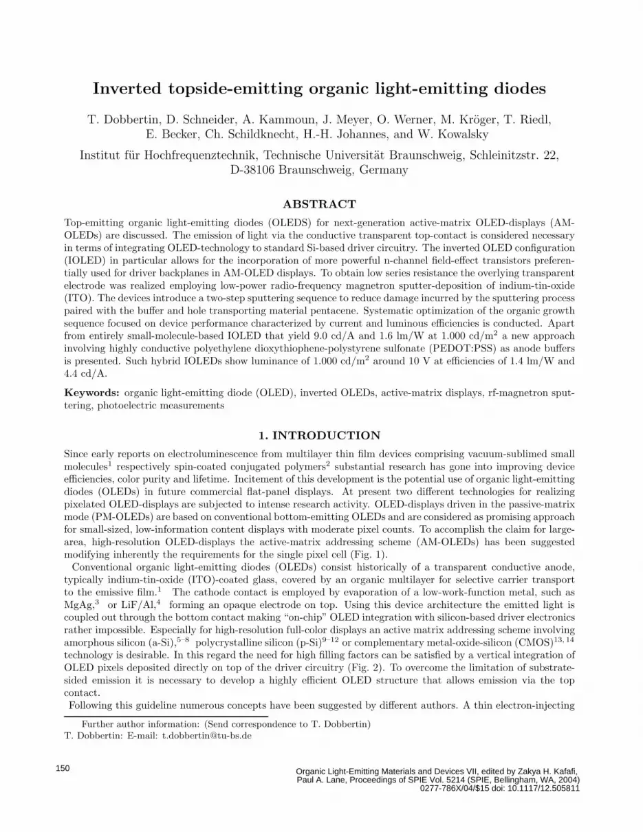
Since early reports on electroluminescence from multilayer thin film devices comprising vacuum-sublimed smallmolecules1 respectively spin-coated conjugated polymers2 substantial research has gone into improving deviceefficiencies, color purity and lifetime. Incitement of this development is the potential use of organic light-emittingdiodes (OLEDs) in future commercial flat-panel displays. At present two different technologies for realizingpixelated OLED-displays are subjected to intense research activity. OLED-displays driven in the passive-matrixmode (PM-OLEDs) are based on conventional bottom-emitting OLEDs and are considered as promising approachfor small-sized, low-information content displays with moderate pixel counts. To accomplish the claim for large-area, high-resolution OLED-displays the active-matrix addressing scheme (AM-OLEDs) has been suggestedmodifying inherently the requirements for the single pixel cell (Fig. 1).
Conventional organic light-emitting diodes (OLEDs) consist historically of a transparent conductive anode,typically indium-tin-oxide (ITO)-coated glass, covered by an organic multilayer for selective carrier transportto the emissive film.1 The cathode contact is employed by evaporation of a low-work-function metal, such asMgAg,3 or LiF/Al,4 forming an opaque electrode on top. Using this device architecture the emitted light iscoupled out through the bottom contact making “on-chip” OLED integration with silicon-based driver electronicsrather impossible. Especially for high-resolution full-color displays an active matrix addressing scheme involvingamorphous silicon (a-Si),5–8 polycrystalline silicon (p-Si)9–12 or complementary metal-oxide-silicon (CMOS)13, 14
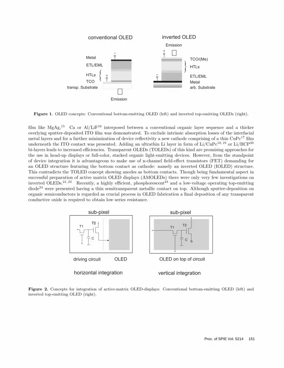
technology is desirable. In this regard the need for high filling factors can be satisfied by a vertical integration ofOLED pixels deposited directly on top of the driver circuitry (Fig. 2). To overcome the limitation of substrate-sided emission it is necessary to develop a highly efficient OLED structure that allows emission via the topcontact.Following this guideline numerous concepts have been suggested by different authors. A thin electron-injecting
Further author information: (Send correspondence to T. Dobbertin)T. Dobbertin: E-mail: [email protected]
Organic Light-Emitting Materials and Devices VII, edited by Zakya H. Kafafi, Paul A. Lane, Proceedings of SPIE Vol. 5214 (SPIE, Bellingham, WA, 2004)
0277-786X/04/$15 doi: 10.1117/12.505811
150
HTLs
TCO/(Me)
Metal
ETL/EML
transp. Substrate
conventional OLED inverted OLED
arb. Substrate
Metal
HTLs
ETL/EML
TCO
Emission
Emission
Figure 1. OLED concepts: Conventional bottom-emitting OLED (left) and inverted top-emitting OLEDs (right).
film like MgAg,15 Ca or Al/LiF16 interposed between a conventional organic layer sequence and a thickeroverlying sputter-deposited ITO film was demonstrated. To exclude intrinsic absorption losses of the interfacialmetal layers and for a further minimization of device reflectivity a new cathode comprising of a thin CuPc17 filmunderneath the ITO contact was presented. Adding an ultrathin Li layer in form of Li/CuPc18, 19 or Li/BCP20
bi-layers leads to increased efficiencies. Transparent OLEDs (TOLEDs) of this kind are promising approaches forthe use in head-up displays or full-color, stacked organic light-emitting devices. However, from the standpointof device integration it is advantageous to make use of n-channel field-effect transistors (FET) demanding foran OLED structure featuring the bottom contact as cathode: namely an inverted OLED (IOLED) structure.This contradicts the TOLED concept showing anodes as bottom contacts. Though being fundamental aspect insuccessful preparation of active matrix OLED displays (AMOLEDs) there were only very few investigations oninverted OLEDs.21, 22 Recently, a highly efficient, phosphorescent23 and a low-voltage operating top-emittingdiode24 were presented having a thin semitransparent metallic contact on top. Although sputter-deposition onorganic semiconductors is regarded as crucial process in OLED fabrication a final deposition of any transparentconductive oxide is required to obtain low series resistance.
sub-pixel
driving circuit OLED OLED on top of circuit
sub-pixel
T1T2
C
T2T2
T1
C
horizontal integration vertical integration
T2T1
C
Figure 2. Concepts for integration of active-matrix OLED-displays: Conventional bottom-emitting OLED (left) andinverted top-emitting OLED (right).
Proc. of SPIE Vol. 5214 151
transfersystem
OMBD1
Metalization 1
OMBD2
glove box
load lock
load lock
LF-TestChamber
transfe rrods
OMBD3Metalization 2
Sa
mp
leP
rep
ara
tio
nu
nd
er
N2
Figure 3. OMBD cluster tool.
2. TECHNOLOGY AND EXPERIMENTAL
2.1. Organic Molecular Beam Deposition
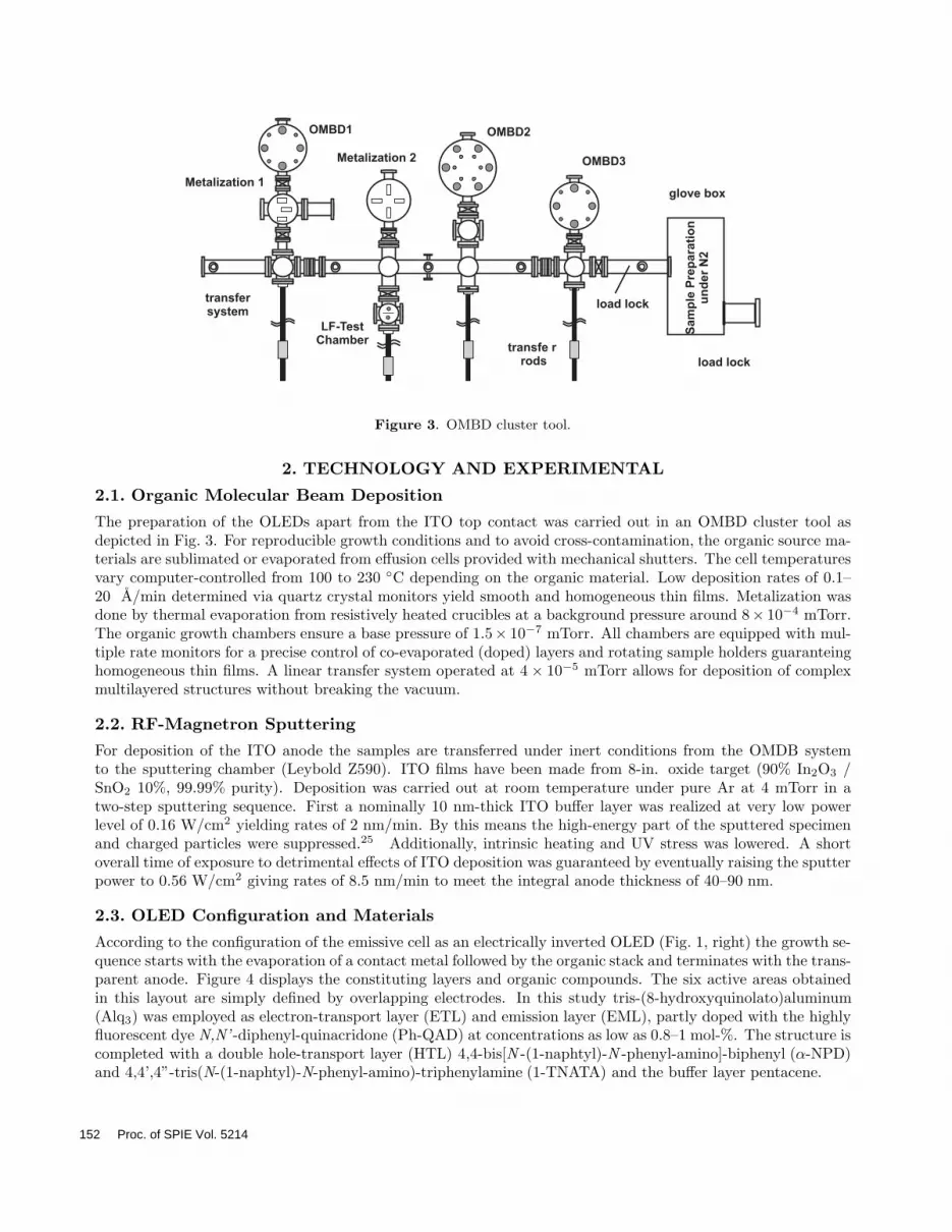
The preparation of the OLEDs apart from the ITO top contact was carried out in an OMBD cluster tool asdepicted in Fig. 3. For reproducible growth conditions and to avoid cross-contamination, the organic source ma-terials are sublimated or evaporated from effusion cells provided with mechanical shutters. The cell temperaturesvary computer-controlled from 100 to 230 C depending on the organic material. Low deposition rates of 0.1–20 A/min determined via quartz crystal monitors yield smooth and homogeneous thin films. Metalization wasdone by thermal evaporation from resistively heated crucibles at a background pressure around 8× 10⁻⁴ mTorr.The organic growth chambers ensure a base pressure of 1.5× 10⁻⁷ mTorr. All chambers are equipped with mul-tiple rate monitors for a precise control of co-evaporated (doped) layers and rotating sample holders guaranteinghomogeneous thin films. A linear transfer system operated at 4 × 10⁻⁵ mTorr allows for deposition of complexmultilayered structures without breaking the vacuum.
2.2. RF-Magnetron Sputtering
For deposition of the ITO anode the samples are transferred under inert conditions from the OMDB systemto the sputtering chamber (Leybold Z590). ITO films have been made from 8-in. oxide target (90% In2O3 /SnO2 10%, 99.99% purity). Deposition was carried out at room temperature under pure Ar at 4 mTorr in atwo-step sputtering sequence. First a nominally 10 nm-thick ITO buffer layer was realized at very low powerlevel of 0.16 W/cm2 yielding rates of 2 nm/min. By this means the high-energy part of the sputtered specimenand charged particles were suppressed.25 Additionally, intrinsic heating and UV stress was lowered. A shortoverall time of exposure to detrimental effects of ITO deposition was guaranteed by eventually raising the sputterpower to 0.56 W/cm2 giving rates of 8.5 nm/min to meet the integral anode thickness of 40–90 nm.
2.3. OLED Configuration and Materials
According to the configuration of the emissive cell as an electrically inverted OLED (Fig. 1, right) the growth se-quence starts with the evaporation of a contact metal followed by the organic stack and terminates with the trans-parent anode. Figure 4 displays the constituting layers and organic compounds. The six active areas obtainedin this layout are simply defined by overlapping electrodes. In this study tris-(8-hydroxyquinolato)aluminum(Alq3) was employed as electron-transport layer (ETL) and emission layer (EML), partly doped with the highlyfluorescent dye N,N’ -diphenyl-quinacridone (Ph-QAD) at concentrations as low as 0.8–1 mol-%. The structure iscompleted with a double hole-transport layer (HTL) 4,4-bis[N -(1-naphtyl)-N -phenyl-amino]-biphenyl (α-NPD)and 4,4’,4”-tris(N-(1-naphtyl)-N-phenyl-amino)-triphenylamine (1-TNATA) and the buffer layer pentacene.
152 Proc. of SPIE Vol. 5214
EL
N
N
NO
O
O
Al
N
N
O
O
NN
N
N
N
N
Pentacene
1-TNATA
-NPD
Ph-QAD
Alq3
V
V
Figure 4. Structural layout of individual IOLED cells including constituting organic materials and alignment on17×17 mm2 substrates.
Electro-optical characteristics were recorded under ambient conditions using source measure unit (Keithley236) and calibrated Si photodiode (Advantest TQ 8210). Conversion to photometric quantities was done bycareful calibration with a luminance meter (Minolta LS-110). Device efficiencies were calculated assuming anLambertian emission pattern.26
3. OPTIMIZATION OF SMALL-MOLECULE INVERTED OLEDS
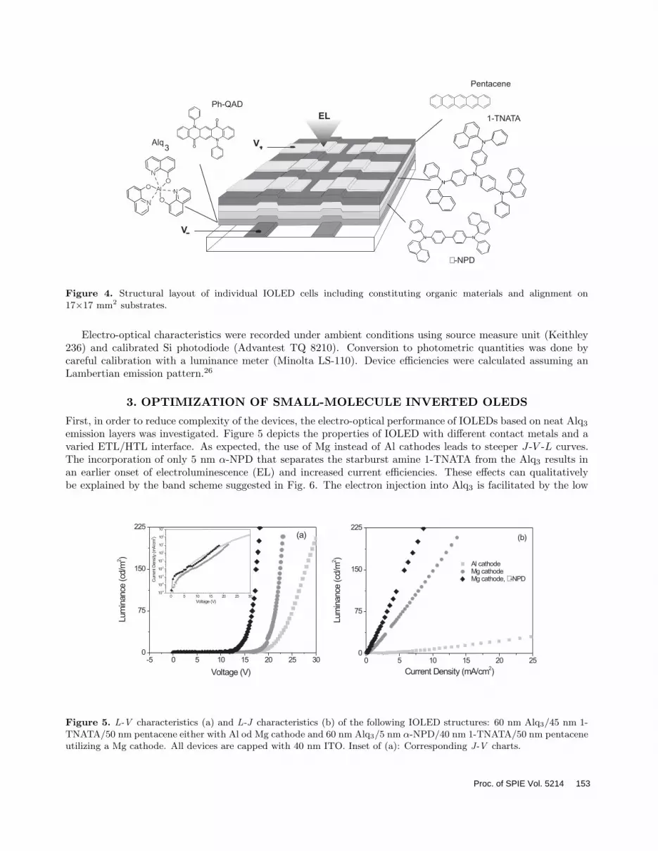
First, in order to reduce complexity of the devices, the electro-optical performance of IOLEDs based on neat Alq3
emission layers was investigated. Figure 5 depicts the properties of IOLED with different contact metals and avaried ETL/HTL interface. As expected, the use of Mg instead of Al cathodes leads to steeper J-V -L curves.The incorporation of only 5 nm α-NPD that separates the starburst amine 1-TNATA from the Alq3 results inan earlier onset of electroluminescence (EL) and increased current efficiencies. These effects can qualitativelybe explained by the band scheme suggested in Fig. 6. The electron injection into Alq3 is facilitated by the low
0 5 10 15 20 250
75
150
225
(b)
Al cathodeMg cathodeMg cathode, -NPD
Lum
inance
(cd/m
2)
Current Density (mA/cm2)
-5 0 5 10 15 20 25 300
75
150
225(a)
Lum
inance
(cd/m
2)
Voltage (V)
0 5 10 15 20 25 3010
-5
10-4
10-3
10-2
10-1
100
101
102
103
Curr
entD
ensi
ty(m
A/c
m2)
Voltage (V)
Figure 5. L-V characteristics (a) and L-J characteristics (b) of the following IOLED structures: 60 nm Alq3/45 nm 1-TNATA/50 nm pentacene either with Al od Mg cathode and 60 nm Alq3/5 nm α-NPD/40 nm 1-TNATA/50 nm pentaceneutilizing a Mg cathode. All devices are capped with 40 nm ITO. Inset of (a): Corresponding J-V charts.
Proc. of SPIE Vol. 5214 153

pentacene1-TNATA
-N
PD
5.1
5.5
5.0
5.8
3.1
1.9
ITO
2.82.3
Al
Mg
Alq3
3.6
4.0
Figure 6. Simplified sketch of the band structure of an efficient invereted OLED visualizing possible energetic barriers atmetall/organic interfaces and interorganic junctions. Grey parts denote structural change according to the series presentedin Fig. 5.
work-function metal Mg providing more electrons in the recombination zone. Thus, the current efficiency isincreased indicated by faster growing L-J plot as displayed in Fig. 5 (b). The insertion of α-NPD establishes astaircase-like evolution of the hole transport states in the diode such that hole emission into the luminescent layercan occur at lower electric fields resp. reduced operation voltage. These observations agree very well to previousstudies on the energetics of a similar interface, formed by the low-ionization-potential (IP) starburst derivativem-MTDATA (IP=5.1 eV) and Alq3.27–29 Here, it is argued that an interface exciplex between the excited stateof Alq3 and the ground state of the HTL is constituted, which, in turn, can alter emission color and lowersdevice efficiency. Adding a thin HTL with higher IPs such as TPD (IP=5.5 eV) or α-NPD positively affects thedevice efficiencies.27, 29 The IOLEDs employed 1-TNATA thin-films due to the superior morphological stabilityindicated by a high glass-transition temperature of 113 C.30
Former research in the field of top-emitting OLEDs15–22 emphasized the incorporation of additional protectivebuffer layers to prevent the OLEDs from damage inflicted by the sputtering process. Recently, we reported onthe use of pentacene as novel buffer and hole injecting/transport layer.31 Pentacene was chosen due to itssuperior hole conducting properties32 and its chemical stability towards exposure to intense UV light, elevatedtemperatures33 and water vapor.34
In order to find an optimum value for the thickness of the buffer layer, pentacene was increased from 15 nmvia 31 nm to 50 nm. 1-TNATA was chosen to 38 nm. Figure 7 shows luminous and current efficiencies obtained
ITO
Mg/AuGlas
-NPD
Emission
Alq3
1-TNATAPentacene
0.2
0.4
0.6
0.8
1.0
10 15 20 25 30 35 40 45 50 551.0
1.5
2.0
2.5
3.0
Lum
inous
effic
iency
(lm
/W)
Curr
enteffic
iency
(cd/A
)
Thickness Pentacene Layer (nm)
Figure 7. Current and luminous efficiency obtainedfor growing thickness of pentacene on top of 38 nm1-TNATA/5 nm α-NPD/60 nm Alq3 at 150 cd/m2.Inset: Schematic of layer sequence.
30 40 50 60 70 80 900.0
0.5
1.0
1.5
2.0
2.5
3.0
3.518 -2828384858
Thickness 1-TNATA (nm)
Curr
enteffic
iency
(cd/A
)
Thickness Pentacene (nm)
0.0
0.2
0.4
0.6
0.8
1.0
Lum
inous
effic
iency
(lm
/W)
Figure 8. Current and luminous efficiency obtainedat 150 cd/m2 for varying composition of 1-TNATAand pentacene being 88 nm in sum deposited on topof 5 nm α-NPD/60 nm Alq3 (solid lines are intendedas guide to the eye).
154 Proc. of SPIE Vol. 5214

0
1000
2000
3000
4000
0 20 40 60 80 1000
7
14
21
Lum
inance
(cd/m
2)
Volta
ge
(V)
Current Density (mA/cm2)
0 500 1000 1500 2000 2500 3000 35000.1
1
10
Curr
enteffic
iency
(cd/A
)
Luminance (cd/m2)
0.1
1
10
Lum
inous
effic
iency
(lm
/W)
(a) (b)
Figure 9. U-J-L characteristics (a) and device efficiencies vs. luminance (b) of an optimized IOLED utilizing a 60 nmAlq3/5 nm α-NPD/45 nm 1-TNATA/43 nm pentacene organic stack deposited without breaking the vacuum.
by typical luminance for display applications of 150 cd/m2. Evidently, the device performance is strongly coupledto the thickness of pentacene yielding efficiencies of 2.7 cd/A and 0.5 lm/W at 50 nm. As a result of the goodhole-transport abilities of pentacene the J-V curves of the samples (not presented) are almost identical. Takingthe overall thickness of the thickest device the composition of 1-TNATA and pentacene was varied systematicallyin a second series. It has to be emphasized that a vacuum-break is common to all devices in both series. In Fig. 8the evolution of device efficiencies at 150 cd/m2 is depicted in the following manner. The pentacene thicknesswas increased from 33 nm to 88 nm at the expense of the 1-TNATA film maintaining an overall thickness of153 nm. A broad maximum is clearly visible at the composition around 40 nm pentacene and 48 nm 1-TNATAgiving typical values of 3 cd/A and 0.5 lm/W for device efficiencies. The initial rise towards thicker pentacenelayers can be attributed to the growing impact of the protective buffer layer as seen in the first series whilethe flattening is presumably caused by the optical losses in pentacene. In contrast to 1-TNATA that is nearlytransparent over the entire visible range pentacene exhibits distinct absorption bands in the emissive region ofAlq3. Spectroscopic ellipsometry on a 100 nm-thick reference sample grown on Si was performed to clarify this
0
250
500
750
1000
1250
1500
0 4 8 12 160
5
10
15
20
Lum
inance
(cd/m
2)
Volta
ge
(V)
Current Density (mA/cm2)
250 500 750 1000 1250 15000.1
1
10Lum
inous
effic
iency
(lm
/W)
Curr
enteffic
iency
(cd/A
)
Luminance (cd/m2)
1
10
(a) (b)
Figure 10. U-J-L characteristics (a) and device efficiencies vs. luminance (b) of an optimized IOLED utilizing a 60 nmAlq3/5 nm α-NPD/45 nm 1-TNATA/43 nm pentacene organic stack deposited without breaking the vacuum.
Proc. of SPIE Vol. 5214 155
-10 -5 0 5 10 15-300
-200
-100
0
100
200
300
PEDOTPentacene
substrateelectrode
topelectrode
Curr
entD
ensi
yt(m
A/c
m2)
Voltage (V)
substrate electrode
top electrode
organicsemiconductor
U(a) (b)
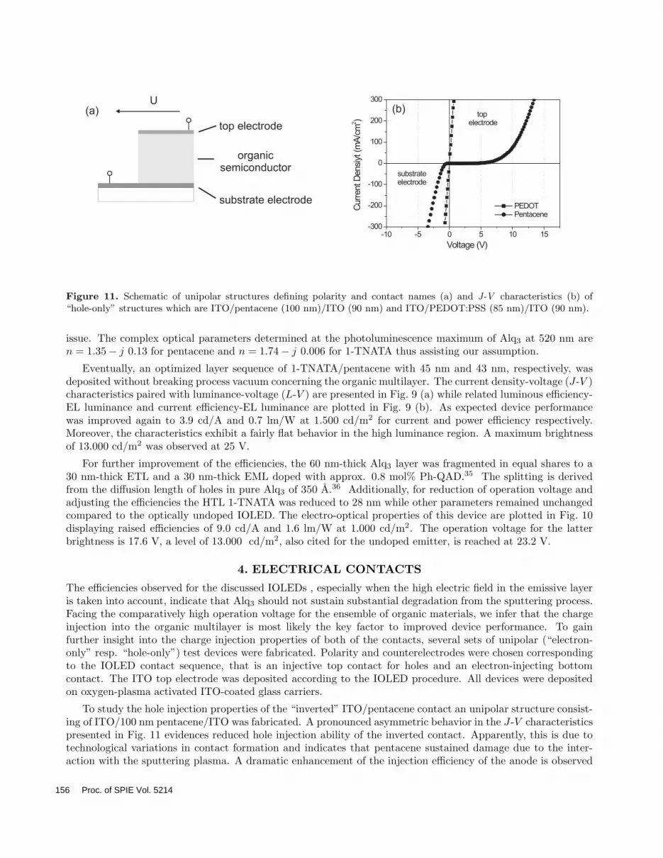
Figure 11. Schematic of unipolar structures defining polarity and contact names (a) and J-V characteristics (b) of“hole-only” structures which are ITO/pentacene (100 nm)/ITO (90 nm) and ITO/PEDOT:PSS (85 nm)/ITO (90 nm).
issue. The complex optical parameters determined at the photoluminescence maximum of Alq3 at 520 nm aren = 1.35 − j 0.13 for pentacene and n = 1.74 − j 0.006 for 1-TNATA thus assisting our assumption.
Eventually, an optimized layer sequence of 1-TNATA/pentacene with 45 nm and 43 nm, respectively, wasdeposited without breaking process vacuum concerning the organic multilayer. The current density-voltage (J-V )characteristics paired with luminance-voltage (L-V ) are presented in Fig. 9 (a) while related luminous efficiency-EL luminance and current efficiency-EL luminance are plotted in Fig. 9 (b). As expected device performancewas improved again to 3.9 cd/A and 0.7 lm/W at 1.500 cd/m2 for current and power efficiency respectively.Moreover, the characteristics exhibit a fairly flat behavior in the high luminance region. A maximum brightnessof 13.000 cd/m2 was observed at 25 V.
For further improvement of the efficiencies, the 60 nm-thick Alq3 layer was fragmented in equal shares to a30 nm-thick ETL and a 30 nm-thick EML doped with approx. 0.8 mol% Ph-QAD.35 The splitting is derivedfrom the diffusion length of holes in pure Alq3 of 350 A.36 Additionally, for reduction of operation voltage andadjusting the efficiencies the HTL 1-TNATA was reduced to 28 nm while other parameters remained unchangedcompared to the optically undoped IOLED. The electro-optical properties of this device are plotted in Fig. 10displaying raised efficiencies of 9.0 cd/A and 1.6 lm/W at 1.000 cd/m2. The operation voltage for the latterbrightness is 17.6 V, a level of 13.000 cd/m2, also cited for the undoped emitter, is reached at 23.2 V.
4. ELECTRICAL CONTACTS
The efficiencies observed for the discussed IOLEDs , especially when the high electric field in the emissive layeris taken into account, indicate that Alq3 should not sustain substantial degradation from the sputtering process.Facing the comparatively high operation voltage for the ensemble of organic materials, we infer that the chargeinjection into the organic multilayer is most likely the key factor to improved device performance. To gainfurther insight into the charge injection properties of both of the contacts, several sets of unipolar (“electron-only” resp. “hole-only”) test devices were fabricated. Polarity and counterelectrodes were chosen correspondingto the IOLED contact sequence, that is an injective top contact for holes and an electron-injecting bottomcontact. The ITO top electrode was deposited according to the IOLED procedure. All devices were depositedon oxygen-plasma activated ITO-coated glass carriers.
To study the hole injection properties of the “inverted” ITO/pentacene contact an unipolar structure consist-ing of ITO/100 nm pentacene/ITO was fabricated. A pronounced asymmetric behavior in the J-V characteristicspresented in Fig. 11 evidences reduced hole injection ability of the inverted contact. Apparently, this is due totechnological variations in contact formation and indicates that pentacene sustained damage due to the inter-action with the sputtering plasma. A dramatic enhancement of the injection efficiency of the anode is observed
156 Proc. of SPIE Vol. 5214
B
B
1
2
eUB
-
+
U
Al Me
Figure 12. Internal field as as result ofbuilt-in potential difference and externalvoltage for U = 0 (- -) and U > 0 (—).
-1.0 -0.5 0.0 0.5 1.0
1E-5
1E-4
1E-3
MgBa
Yb
Al
SmCa
Photo
curr
ent(a
.u.)
Voltage (V)
Figure 13. Magnitude of photocurrent for a 10 nmmetal/100 nm Alq/150 nm Al structure.
by replacing pentacene with the highly conductive polymer polyethylene dioxythiophene-polystyrene sulfonate(PEDOT:PSS). An ideal ohmic J-V plot independent of polarity is obtained.
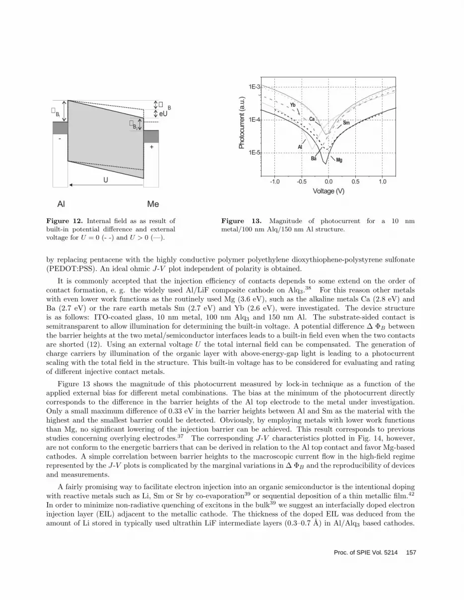
It is commonly accepted that the injection efficiency of contacts depends to some extend on the order ofcontact formation, e. g. the widely used Al/LiF composite cathode on Alq3.38 For this reason other metalswith even lower work functions as the routinely used Mg (3.6 eV), such as the alkaline metals Ca (2.8 eV) andBa (2.7 eV) or the rare earth metals Sm (2.7 eV) and Yb (2.6 eV), were investigated. The device structureis as follows: ITO-coated glass, 10 nm metal, 100 nm Alq3 and 150 nm Al. The substrate-sided contact issemitransparent to allow illumination for determining the built-in voltage. A potential difference ∆ ΦB betweenthe barrier heights at the two metal/semiconductor interfaces leads to a built-in field even when the two contactsare shorted (12). Using an external voltage U the total internal field can be compensated. The generation ofcharge carriers by illumination of the organic layer with above-energy-gap light is leading to a photocurrentscaling with the total field in the structure. This built-in voltage has to be considered for evaluating and ratingof different injective contact metals.
Figure 13 shows the magnitude of this photocurrent measured by lock-in technique as a function of theapplied external bias for different metal combinations. The bias at the minimum of the photocurrent directlycorresponds to the difference in the barrier heights of the Al top electrode to the metal under investigation.Only a small maximum difference of 0.33 eV in the barrier heights between Al and Sm as the material with thehighest and the smallest barrier could be detected. Obviously, by employing metals with lower work functionsthan Mg, no significant lowering of the injection barrier can be achieved. This result corresponds to previousstudies concerning overlying electrodes.37 The corresponding J-V characteristics plotted in Fig. 14, however,are not conform to the energetic barriers that can be derived in relation to the Al top contact and favor Mg-basedcathodes. A simple correlation between barrier heights to the macroscopic current flow in the high-field regimerepresented by the J-V plots is complicated by the marginal variations in ∆ ΦB and the reproducibility of devicesand measurements.
A fairly promising way to facilitate electron injection into an organic semiconductor is the intentional dopingwith reactive metals such as Li, Sm or Sr by co-evaporation39 or sequential deposition of a thin metallic film.42
In order to minimize non-radiative quenching of excitons in the bulk39 we suggest an interfacially doped electroninjection layer (EIL) adjacent to the metallic cathode. The thickness of the doped EIL was deduced from theamount of Li stored in typically used ultrathin LiF intermediate layers (0.3–0.7 A) in Al/Alq3 based cathodes.
Proc. of SPIE Vol. 5214 157
-25 -20 -15 -10 -5 0 5 10 15 20 25-300
-200
-100
0
100
200
300
substrateelectrode
topelectrode
Curr
entD
ensi
ty(m
A/c
m2)
Voltage (V)
MagnesiumAluminiumYtterbiumSamariumCalciumBariumITO
Figure 14. J-V characteristics of “electron-only”structures as defined in Fig.13. An ITO as cathodewas included to prove closed metallic coverage of theITO substrates.
-25 -20 -15 -10 -5 0 5 10 15 20-300
-200
-100
0
100
200
300
substrateelectrode
topelectrode
Bphen/Li (1:1)Bphen/Li (3:1)Bphen/Li (5:1)Mg
Curr
entD
ensi
ty(m
A/c
m²)
Voltage (V)
Figure 15. J-V characteristics of “electron-only”structures having an interfacially doped EIL. Thestructure data are: 5 nm Li-doped Bphen layers withvarying molecule to atom ratios (1:1, 3:1, 5:1), 5 nmintrinsic Bphen and 90 nm Alq3. Symmetric Al-electrodes were applied. A 100 nm thick Alq3 filmsandwiched between an Al substrate and a Mg topelectrode serves as reference.
Here the improvement of electron injection is ascribed to unintentional doping of Alq3 with liberated Li.40, 41
Our estimations are based on the assumption of an optimum molecule to atom ratio of unity.39
Figure 15 assembles the J-V curves for varying doping levels of Li in 5 nm-thick 4,7-diphenyl-1,10’-phenanthro-line (Bphen) films realized by co-evaporation from separate sources. Additionally, a Mg-based cathode on anintrinsic organic semiconductor is provided as reference. The doped EIL is followed by a nominally undoped5 nm-thick Bphen layer that is supposed to work as hole-blocking layer (HBL) in a complete IOLED structure.Clearly, the approach of interfacial doping results in significantly diminished voltages at comparable currentdensity. For instance, with reference to the Mg-cathode a current density of 100 mA/cm2 is obtained 5.2 Vearlier in case of the highest doped EIL. In addition to that, the injection properties of the overlying Al contactare successively improved as the doping level is raised. This phenomena can be attributed to Li diffusion throughthe adjacent layers, thereby reducing the effective length of the intrinsic organic semiconductor.38, 42
5. INVERTED OLEDS WITH DOPED CHARGE-INJECTION LAYERS
In order to assure enhanced current flow as well as balanced carrier statistics in the recombination zone it isdesirable to introduce PEDOT:PSS as anode buffer paired with an interfacially doped EIL.Moreover, the benefits of incorporating highly conductive polymers, such as PEDOT:PSS or polyaniline, ashole-injection and hole-transport layer in entirely polymer-based OLEDs44–46 and small-molecule based OLEDs(SM-OLED)49, 51 have already been presented. Similarly, both device-architectures are reported to exhibit areduced operational voltage, higher luminance levels, improved or comparable efficiencies and a better long-term stability. These observations are, among others,45, 46, 52 predominantly attributed to the following, brieflyoutlined, mechanisms. First, the good film-forming property of the intermediate polymeric layer provides repro-ducibly smooth and “spike-free” anodes resulting in a laterally homogenized current flow49 thus inhibiting theinfluence of local shorts.46, 53 In addition, the hole injection into the emissive region is enhanced due to ohmiccontacts49 and, possibly, a better matching of the electronic transport states. Similar effects can be anticipatedby proper incorporating PEDOT:PSS to an top-emitting IOLED, referred to as hy-IOLED hereafter.As stated above, thin films of pentacene are able to withstand water treatment as the latter as a result of itshydrophobic nature. This property makes it a good candidate to work as an in-situ deposited organic thin-filmsealing for the underlying organic multilayer. In previous studies we could already demonstrate the feasibility of
158 Proc. of SPIE Vol. 5214

0 100 200 300 400 500 6000
4
8
12
16
Lum
inance
(cd/m
2)
Volta
ge
(V)
Current Density (mA/cm2)
0
4000
8000
12000
16000
20000
(a) (b)
0 1 2 3 4 5 60
2
4
6
Lum
inance
(cd/m
2)
Voltage (V)
0 5000 10000 15000 200000
2
4
6
Lum
inous
effic
iency
(lm
/W)
Curr
enteffic
iency
(cd/A
)
Luminance (cd/m2)
0
1
2
3
Figure 16. J-V-L characteristics (a) and device efficiencies vs. luminance (b) of a hybrid IOLED consisting of Alcathodes with 5 nm Bphen:Li (2:1), 25 nm Bphen, 30 nm Alq:Ph-QAD (1.1 mol%), 5 nm α-NPD, 10 nm 1-TNATA,20 nm pentacene, PEDOT:PSS and 90 nm ITO. Inset of (a): Onset of EL.
this approach.54 Consequently, thin films of PEDOT:PSS (Baytron AI 4083) were deposited on an IOLED byspin-coating from filtered (0.45 µm) aqueous dispersion at 4000 rpm under ambient conditions. The process wasrepeated 3–5 times until a visibly clear and homogenous film has been constituted. By this means, employinga non-optimized coating technique a fabricational yield of ∼ 70 % was achieved. Prior to the radio-frequencymagnetron deposition of ITO the samples were stored overnight in the sputter chamber for vacuum-assisteddesorption of residual water.
Figure 16 assembles the electro-optical characteristics of a hy-IOLED. The J-V characteristics documenttypical space-charge limited current flow without any superimposed artefact that might have found its origin inlocal sorts due to the spin-coating process. Luminance values of 100 cd/m2 and 1.000 cd/m2 are reached at 7.6 Vresp. 9.9 V, the EL onset is oberserved at 3.5 V. The power efficiency peaks at 1.4 lm/W around 1.000 cd/m2
yielding a current efficiency of 4.4 cd/A. A maximum luminance of over 17.000 cd/m2 is evidence of a goodstability.
To estimate the effects of potentially varying thicknesses of PEDOT:PSS a set of hole-only devices with62, 85 and 110 nm thick polymeric layers was made. From the linear J-V curves a resistivity of only 51–56 Ω was extracted. The transmissivity was determined to 92–96 % (PEDOT:PSS only) at the maximum ofelectroluminescence so that the implication on the device performance should be negligible.
ACKNOWLEDGMENTS
The authors thank the Bundesministerium fur Bildung und Forschung (BMBF, 01 BK 918) for their generousfinancial support.
REFERENCES
1. C. W. Tang and S. A. VanSlyke, Appl. Phys. Lett. 51, 913 (1987).2. J. H. Borroughes, D. D. C. Bradley, A. R. Brown, R. N. Marks, K. MacKay, R. H. Friend, P. L. Burn, and
A. B. Holmes, Nature 347, 799 (1990).3. C. W. Tang and S. A. VanSlyke, J. Appl. Phys, 65, 3610 (1989).4. L. S. Hung, C. W. Tang, and M. G. Mason, Appl. Phys. Lett. 70, 152 (1997).5. P. Servati, S. Prakash, A. Nathan, and C. Py, J. Vac. Sci. Technol. A, 20, 1374 (2002).6. Y. He, R Hattori, and J. Kanicki, IEEE Trans. Electron Devices, 48, 1322 (2001).
Proc. of SPIE Vol. 5214 159

7. C. C. Wu, S. D. Theiss, G. Gu, M. H. Lu, J. C. Sturm, S. Wagner, and S. R. Forrest, IEEE Trans. ElectronDevices, 18, 609 (1997).
8. Y. He, R Hattori, and J. Kanicki, Jpn. J. Appl. Phys., 40, 1199 (2001).9. M. Stewart, R. S. Howell, L. Pires, and M. K. Hatalis, IEEE Trans. Electron Devices, 48, 845 (2001).
10. M. K. Hatalis, M.Stewart, C. Tang, and J. Burtis, SPIE Vol. 3057, 2767 (1997).11. Z. Meng, H. Chen, C. Qiu, L. Wang, H. S. Kwok, and M. Wong, IEDM Tech. Dig, 611 (2000).12. M. Stewart, R. S. Howell, L. Pires, M. K. Hatalis, W. Howard, and O. Prache, IEDM Tech. Dig, 871 (1998).13. D. L. Mathine, H. S. Woo, W. He, T. W. Kim, B. Kippelen, and N. Peyghambarian, Appl. Phys. Lett., 76,
3849 (2000).14. L. M. H. Heinrich, J. Muller, U. Hilleringmann, K. F. Goser, A. Holmes, D. H. Hwang, and R. Stern, IEEE
Trans. Electron Devices, 44, 1249 (2001).15. G. Gu, V. Bulovic, P. E. Burrows, S. R. Forrest, and M. E. Thompson, Appl. Phys. Lett., 68, 2606 (1996).16. P. E. Burrows, G. Gu, S. R. Forrest, E. P. Vicenzi, and T. X. Zhou, J. Appl. Phys., 87, 3080 (2000).17. G. Parthasarathy, P. E. Burrows, V. Khalfin, V. G. Kozlov, and S. R. Forrest , Appl. Phys. Lett., 72, 2138
(1998).18. L. S. Hung and C. W. Tang, Appl. Phys. Lett., 74, 3209 (1999).19. L. S. Hung, L. S. Liao, C. S. Lee, and S. T. Lee, J. Appl. Phys., 86, 4607 (1999).20. G. Parthasarathy, C. Adachi, P. E. Burrows, and S. R. Forrest, Appl. Phys. Lett., 76, 2128 (2000).21. V. Bulovic, P. Tian, P. E. Burrows, M.R. Gokhale, and S. R. Forrest, Appl. Phys. Lett. 70, 2954 (1997).22. D. R. Baigent, R. N. Marks, N. C. Greenham, and R. H. Friend, Appl. Phys. Lett. 65, 2636 (1994).23. H. Riel, S. Karg, T. Beierlein, B. Ruhstaller, W. Riess, Appl. Phys. Lett. 82, 466 (2003).24. X. Zhou, M. Pfeiffer, J. S. Huang, J. Blochwitz-Nimoth, D. S. Qin, A. Werner, J. Drechsel, B. Maenning,
and K. Leo, Appl. Phys. Lett. 81, 922 (2002).25. R. V. Stuart, V acuum Technology, Thin Films and Sputtering (Acad. Press, New York 1983).26. N. C. Greenham, R. H. Friend, and D. C. C. Bradley, Adv. Mat. 6, 491 (1994).27. Y. Shirota, Y. Kuwabara, H. Inada, T. Wakimoto, H. Nakada, Y. Yonemoto, S. Kawami, and K. Imai, Appl.
Phys. Lett. 65, 807 (1994).28. K. Itano, H. Ogawa, and Y. Shirota, Appl. Phys. Lett. 72, 636 (1998).29. C. Giebeler, H. Antoniadis, D. D. C. Bradley, and Y. Shirota, J. Appl. Phys. 85, 608 (1999).30. H. Murata, C. D. Meritt, H. Inada, Y. Shirota, and Z. H.Kafafi, Appl. Phys. Lett. 75, 3252 (1999).31. T. Dobbertin, M. Kroger, D. Heithecker, D. Schneider, D. Metzdorf, H. Neuner, E. Becker, H.-H. Johannes,
and W. Kowalsky, Appl. Phys. Lett. 82, 284 (2003).32. C. D. Dimitrakopoulos, and P. R. L. Malenfant, Adv. Mater., 14, 99 (2002).33. A. J. Salih, S. P. Lau, J. M. Marshall, J. M. Maud, W. R. Bowen, N. Hilal, R. W. Lovitt, and P. M.
Williams, Appl. Phys. Lett. 69, 2231 (1996).34. M. Halik, H. Klauk, U. Zschieschang, T. Kriem, G. Schmid, W. Radlik, and K. Wussow, Appl. Phys. Lett.
81, 289 (2002).35. H. Mattoussi, H. Murata, C. D. Merrit, Y. Iizumi, J. Kido, and Z. H. Kafafi, J. Appl. Phys. 86, 2542 (1999).36. P. E. Burrows, Z. Shen, V. Bulovic, D. M. McCarthy, and S. R. Forrest, J. Appl. Phys. 79, 7991 (1996).37. I. H. Campbell, and D. L. Smith, Appl. Phys. Lett. 74, 561 (1999).38. H. Heil, J. Steiger, S. Karg, M. Gastei, H. Ortner, and H. von Seggern, J. Appl. Phys. 89, 420 (2001).39. J. Kido, and T. Matsumoto, Appl. Phys. Lett. 73, 2866 (1998).40. Q. T. Le, L. Yan, Y. Gao, M. G. Mason, D. J. Giesen, and C. W. Tang, J. Appl. Phys. 87, 375 (2000).41. L. S. Hung, C. W. Tang, M. G. Mason, P. Raychaudhuri, and J. Madathil, Appl. Phys. Lett. 78, 544 (2001).42. G. Parthasarthy, C. Shen, A. Kahn, and S. R. Forrest, J. Appl. Phys. 89, 4986 (2001).43. D. Pribat, F. Plais, Thin Solid Films 383, 25 (2001).44. Y. Yang, and A. J. Heeger, Appl. Phys. Lett. 64, 1245 (1994).45. S. Karg, J. C. Scott, J. R. Salem, and M. Angelopoulos, Synth. Met. 80, 111 (1996).46. J. C. Scott, S. A. Carter, S. Karg, and M. Angelopoulos, Synth. Met. 85, 1197 (1997).
160 Proc. of SPIE Vol. 5214
47. Y.Cao , G. Yu, C. Zhand, R. Menon, and A. J. Heeger, Synth. Met. 87, 171 (1997).48. J. Chung, B. Choi, and H. H. Lee, Appl. Phys. Lett. 74, 3645 (1999).49. A. Elschner, F. Bruder, H.-W. Heuer, F. Jonas, A. Karbach, S. Kirchmeyer, S. Thurm, R. Wehrmann,
Synth. Met. 111-112, 139 (2000).50. D. Troadec, G. Veriot, R. Antony, and A. Moliton, Synth. Met. 124, 49 (2001).51. D. Heithecker, A. Kammoun, T. Dobbertin, T. Riedl, E. Becker, D. Metzdorf, D. Schneider, H.-H. Johannes,
and W. Kowalsky, Appl. Phys. Lett. 82, 4178 (2003).52. J. C. Scott, J. H. Kaufman, P. J. Brock, R. DiPietro, J. Salem, and J. A. Goitia, Appl. Phys. Lett. 79, 2745
(1996).53. S. A. Carter, M. Angelopoulos, S. Karg, P. J.Brock, and J. C. Scott, Appl. Phys. Lett. 70, 2067 (1997).54. T. Dobbertin, O. Werner, J. Meyer, A. Kammoun, D. Schneider, T. Riedl, E. Becker, H.-H. Johannes, and
W. Kowalsky, submitted to Appl. Phys. Lett.
Proc. of SPIE Vol. 5214 161